HD3SS215 6.0 Gbps HDMI DisplayPort 2:1/1:2 Differential ...
36
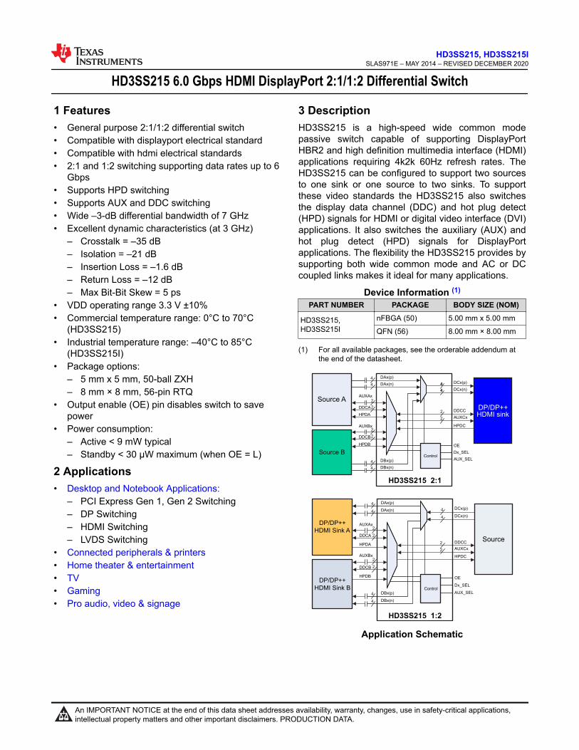
HD3SS215 6.0 Gbps HDMI DisplayPort 2:1/1:2 Differential Switch 1 Features • General purpose 2:1/1:2 differential switch • Compatible with displayport electrical standard • Compatible with hdmi electrical standards • 2:1 and 1:2 switching supporting data rates up to 6 Gbps • Supports HPD switching • Supports AUX and DDC switching • Wide –3-dB differential bandwidth of 7 GHz • Excellent dynamic characteristics (at 3 GHz) – Crosstalk = –35 dB – Isolation = –21 dB – Insertion Loss = –1.6 dB – Return Loss = –12 dB – Max Bit-Bit Skew = 5 ps • VDD operating range 3.3 V ±10% • Commercial temperature range: 0°C to 70°C (HD3SS215) • Industrial temperature range: –40°C to 85°C (HD3SS215I) • Package options: – 5 mm x 5 mm, 50-ball ZXH – 8 mm × 8 mm, 56-pin RTQ • Output enable (OE) pin disables switch to save power • Power consumption: – Active < 9 mW typical – Standby < 30 µW maximum (when OE = L) 2 Applications • Desktop and Notebook Applications: – PCI Express Gen 1, Gen 2 Switching – DP Switching – HDMI Switching – LVDS Switching • Connected peripherals & printers • Home theater & entertainment • TV • Gaming • Pro audio, video & signage 3 Description HD3SS215 is a high-speed wide common mode passive switch capable of supporting DisplayPort HBR2 and high definition multimedia interface (HDMI) applications requiring 4k2k 60Hz refresh rates. The HD3SS215 can be configured to support two sources to one sink or one source to two sinks. To support these video standards the HD3SS215 also switches the display data channel (DDC) and hot plug detect (HPD) signals for HDMI or digital video interface (DVI) applications. It also switches the auxiliary (AUX) and hot plug detect (HPD) signals for DisplayPort applications. The flexibility the HD3SS215 provides by supporting both wide common mode and AC or DC coupled links makes it ideal for many applications. Device Information (1) PART NUMBER PACKAGE BODY SIZE (NOM) HD3SS215, HD3SS215I nFBGA (50) 5.00 mm x 5.00 mm QFN (56) 8.00 mm × 8.00 mm (1) For all available packages, see the orderable addendum at the end of the datasheet. Source A Source B HPDB DAx(p) HPDA DAx(n) HPDC AUXAx DDCA DDCB AUXCx AUXBx DCx(p) DCx(n) DBx(p) DBx(n) Control AUX_SEL Dx_SEL DDCC OE DP/DP++ HDMI Sink A DP/DP++ HDMI Sink B HPDB DAx(p) HPDA DAx(n) HPDC AUXAx DDCA DDCB AUXCx AUXBx DCx(p) DCx(n) Source DBx(p) DBx(n) Control AUX_SEL Dx_SEL DDCC OE HD3SS215 2:1 HD3SS215 1:2 4 4 4 4 4 4 2 2 2 2 2 2 4 4 4 4 4 4 4 4 2 2 2 2 2 2 DP/DP++ HDMI sink Application Schematic www.ti.com HD3SS215, HD3SS215I SLAS971E – MAY 2014 – REVISED DECEMBER 2020 Copyright © 2020 Texas Instruments Incorporated Submit Document Feedback 1 Product Folder Links: HD3SS215 HD3SS215I HD3SS215, HD3SS215I SLAS971E – MAY 2014 – REVISED DECEMBER 2020 An IMPORTANT NOTICE at the end of this data sheet addresses availability, warranty, changes, use in safety-critical applications, intellectual property matters and other important disclaimers. PRODUCTION DATA.
-
Upload
khangminh22 -
Category
Documents
-
view
2 -
download
0
Transcript of HD3SS215 6.0 Gbps HDMI DisplayPort 2:1/1:2 Differential ...
HD3SS215 6.0 Gbps HDMI DisplayPort 2:1/1:2 Differential Switch
1 Features• General purpose 2:1/1:2 differential switch• Compatible with displayport electrical standard• Compatible with hdmi electrical standards• 2:1 and 1:2 switching supporting data rates up to 6
Gbps• Supports HPD switching• Supports AUX and DDC switching• Wide –3-dB differential bandwidth of 7 GHz• Excellent dynamic characteristics (at 3 GHz)
– Crosstalk = –35 dB– Isolation = –21 dB– Insertion Loss = –1.6 dB– Return Loss = –12 dB– Max Bit-Bit Skew = 5 ps
• VDD operating range 3.3 V ±10%• Commercial temperature range: 0°C to 70°C
(HD3SS215)• Industrial temperature range: –40°C to 85°C
(HD3SS215I)• Package options:
– 5 mm x 5 mm, 50-ball ZXH– 8 mm × 8 mm, 56-pin RTQ
• Output enable (OE) pin disables switch to savepower
• Power consumption:– Active < 9 mW typical– Standby < 30 µW maximum (when OE = L)
2 Applications• Desktop and Notebook Applications:
– PCI Express Gen 1, Gen 2 Switching– DP Switching– HDMI Switching– LVDS Switching
• Connected peripherals & printers• Home theater & entertainment• TV• Gaming• Pro audio, video & signage
3 DescriptionHD3SS215 is a high-speed wide common modepassive switch capable of supporting DisplayPortHBR2 and high definition multimedia interface (HDMI)applications requiring 4k2k 60Hz refresh rates. TheHD3SS215 can be configured to support two sourcesto one sink or one source to two sinks. To supportthese video standards the HD3SS215 also switchesthe display data channel (DDC) and hot plug detect(HPD) signals for HDMI or digital video interface (DVI)applications. It also switches the auxiliary (AUX) andhot plug detect (HPD) signals for DisplayPortapplications. The flexibility the HD3SS215 provides bysupporting both wide common mode and AC or DCcoupled links makes it ideal for many applications.
Device Information (1)
PART NUMBER PACKAGE BODY SIZE (NOM)
HD3SS215,HD3SS215I
nFBGA (50) 5.00 mm x 5.00 mm
QFN (56) 8.00 mm × 8.00 mm
(1) For all available packages, see the orderable addendum atthe end of the datasheet.
Source A
Source B
HPDB
DAx(p)
HPDA
DAx(n)
HPDC
AUXAx
DDCA
DDCB
AUXCx
AUXBx
DCx(p)
DCx(n)
DBx(p)
DBx(n)
ControlAUX_SEL
Dx_SEL
DDCC
OE
DP/DP++
HDMI Sink A
DP/DP++
HDMI Sink B
HPDB
DAx(p)
HPDA
DAx(n)
HPDC
AUXAx
DDCA
DDCB
AUXCx
AUXBx
DCx(p)
DCx(n)
Source
DBx(p)
DBx(n)
ControlAUX_SEL
Dx_SEL
DDCC
OE
HD3SS215 2:1
HD3SS215 1:2
4
4
4
4
4
4
2
2
2
2
2
2
4
4
4
4 4
4
4
4
2
2
2
2
2
2
DP/DP++HDMI sink
Application Schematic
www.ti.comHD3SS215, HD3SS215I
SLAS971E – MAY 2014 – REVISED DECEMBER 2020
Copyright © 2020 Texas Instruments Incorporated Submit Document Feedback 1
Product Folder Links: HD3SS215 HD3SS215I
HD3SS215, HD3SS215ISLAS971E – MAY 2014 – REVISED DECEMBER 2020
An IMPORTANT NOTICE at the end of this data sheet addresses availability, warranty, changes, use in safety-critical applications,intellectual property matters and other important disclaimers. PRODUCTION DATA.
Table of Contents1 Features............................................................................12 Applications..................................................................... 13 Description.......................................................................14 Revision History.............................................................. 25 Description (continued).................................................. 46 Pin Configuration and Functions...................................47 Specifications.................................................................. 9
7.1 Absolute Maximum Ratings (1) (2) ...............................97.2 ESD Ratings............................................................... 97.3 Recommended Operating Conditions.........................97.4 Thermal Information....................................................97.5 Electrical Characteristics...........................................107.6 Electrical Characteristics, Device Parameters (1) ..... 117.7 Switching Characteristics.......................................... 117.8 Timing Diagrams....................................................... 11
8 Detailed Description......................................................13
8.1 Overview................................................................... 138.2 Functional Block Diagram......................................... 148.3 Feature Description...................................................158.4 Device Functional Modes..........................................15
9 Applications and Implementation................................ 169.1 Application Information............................................. 169.2 Typical Applications.................................................. 16
10 Layout...........................................................................2110.1 Layout Guidelines................................................... 2110.2 Layout Example...................................................... 22
11 Device and Documentation Support..........................2411.1 Community Resources............................................2411.2 Trademarks............................................................. 24
12 Mechanical, Packaging, and OrderableInformation.................................................................... 24
4 Revision HistoryNOTE: Page numbers for previous revisions may differ from page numbers in the current version.
Changes from Revision D (September 2015) to Revision E (December 2020) Page• NOTE: The device in the MicroStar Jr. BGA packaging were redesigned using a laminate nFBGA package.
This nFBGA package offers datasheet-equivalent electrical performance. It is also footprint equivalent to theMicroStar Jr. BGA. The new package designator in place of the discontinued package designator will beupdated throughout the datasheet......................................................................................................................1
• Changed u*jr ZQE to nFBGA ZXH..................................................................................................................... 1• Changed u*jr ZQE to nFBGA ZXH..................................................................................................................... 4• Changed u*jr ZQE to nFBGA ZXH..................................................................................................................... 4• Changed u*jr ZQE to nFBGA ZXH..................................................................................................................... 4• Changed u*jr ZQE to nFBGA ZXH..................................................................................................................... 7• Changed u*jr ZQE to nFBGA ZXH. Updated thermal data.................................................................................9• Changed u*jr ZQE to nFBGA ZXH....................................................................................................................11• Changed u*jr ZQE to nFBGA ZXH................................................................................................................... 16
Changes from Revision C (August 2015) to Revision D (September 2015) Page• Changed Section 3 text string from "....DisplayPort 1.2a..." to "...DisplayPort HBR2..." and from "..HDMI2.0.."
to "...HDMI..." ..................................................................................................................................................... 1• Deleted RθJC(bot) spec from Thermal Information table as N/A...........................................................................9• Deleted "Operating free air temperature" spec from Electrical Characteristics table....................................... 10• Changed Figure 9-5 .........................................................................................................................................20• Changed Section Power Supply Recommendations text string from "Decoupling capacitors may be used to
reduce noise and improve power supply integrity" to "Decoupling capacitors must be used to reduce powersupply noise"...................................................................................................................................................0
Changes from Revision B (July 2015) to Revision C (July 2015) Page• Added ton(OE_L-H), toff(OE_H-L), and tSWITCH_OVER to the Section 7.7 ..................................................................11
Changes from Revision A (May 2014) to Revision B (July 2015) Page• Changed the title From: "2.0/DisplayPort 1.2A" To: "DisplayPort"...................................................................... 1
HD3SS215, HD3SS215ISLAS971E – MAY 2014 – REVISED DECEMBER 2020 www.ti.com
2 Submit Document Feedback Copyright © 2020 Texas Instruments Incorporated
Product Folder Links: HD3SS215 HD3SS215I
• Changed Section 1 list item From: Compatible With DisplayPort 1.2a Electrical Standard To: Compatible WithDisplayPort Electrical Standard.......................................................................................................................... 1
• Changed Section 1 list item From: Compatible With HDMI 1.4b and HDMI 2.0 Electrical Standards To:Compatible With HDMI Electrical Standards...................................................................................................... 1
• Added Section 1 item: Commercial Temperature Range: –40°C to 70°C (HD3SS215)..................................... 1• Added Section 1 item: Inductrial Temperature Range: –40°C to 85°C (HD3SS215I).........................................1• Added Section 1, Package Options: 8 mm × 8 mm, 56-Pin RTQ....................................................................... 1• Changed the Section 2 list item From: TV and Monitors To: UHDTV, HDTV and Monitors................................1• Added Section 5 paragraph. .............................................................................................................................. 4• Added the 56-Pin QFN image.............................................................................................................................4• Added RTQ column to the Pin Functions table ..................................................................................................4• Added RTQ column to the Pin Functions table ..................................................................................................7• Moved Tstg From: Section 7.2 To: Section 7.1 ................................................................................................... 9• Changed the Handling Ratings table to Section 7.2 table ................................................................................. 9• Added HD3SS2151I, Operating free-air temperature Section 7.3 .....................................................................9• Added RTQ 56 PIN values to the Section 7.4 ....................................................................................................9• Added table Note " This pin can be driven.." to the Section 7.5 table.............................................................. 10• Changed the Section 7.6 table to include ZQE and RTQ package values....................................................... 11• Added the Section 7.7 table .............................................................................................................................11• Added section: Section 9.2.4 ........................................................................................................................... 20• Added Figure 10-3 ........................................................................................................................................... 22
Changes from Revision * (May 2014) to Revision A (May 2014) Page• Changed Section 3 section ................................................................................................................................1• Changed Figure 9-1 .........................................................................................................................................16
www.ti.comHD3SS215, HD3SS215I
SLAS971E – MAY 2014 – REVISED DECEMBER 2020
Copyright © 2020 Texas Instruments Incorporated Submit Document Feedback 3
Product Folder Links: HD3SS215 HD3SS215I

5 Description (continued)One typical application would be a mother board that includes two GPUs that need to drive one DisplayPort sink.The GPU is selected by the Dx_SEL pin. Another application is when one source needs to switch between oneof two sinks, such as a side connector an a docking station connector. The switching is controlled using theDx_SEL and AUX_SEL pins. The HD3SS215I operates from a single supply voltage of 3.3 V, over full industrialtemperature range –40°C to 85°C, in the ZXH package and 56 pin RTQ package.
6 Pin Configuration and Functions1 2 3 4 5 6 7 8 9
A Dx_SEL VDD DA0(n) DA1(n) DA2(n) DA3(p) DA3(n)
B DC0(n) DC0(p) GND DA0(p) DA1(p) DA2(p) OE DB0(p) DB0(n)
C AUX_SEL GND
D DC1(n) DC1(p) DB1(p) DB1(n)
E DC2(n) DC2(p) DB2(p) DB2(n)
F DC3(n) DC3(p) DB3(p) DB3(n)
G GND GND
H AUXC(n) AUXC(p) HPDB GND DDCCLK_B AUXB(p) GND DDCCLK_A AUXA(p)
J HPDC HPDA DDCCLK_C VDD DDCDAT_B AUXB(n) DDCDAT_C DDCDAT_A AUXA(n)
Figure 6-1. 50-Pin µBGA ZXH Package (Top View)
HD3SS215, HD3SS215ISLAS971E – MAY 2014 – REVISED DECEMBER 2020 www.ti.com
4 Submit Document Feedback Copyright © 2020 Texas Instruments Incorporated
Product Folder Links: HD3SS215 HD3SS215I
HD3SS215 RTQ
GND
1
2
3
4
5
6
7
8
9
10
11
12
13
14
56
55
54
53
52
51
50
49
48
47
46
45
44
43
42
41
40
39
38
37
36
35
34
33
32
31
30
29
15
16
17
18
19
20
21
22
23
24
25
26
27
28
AUX_SEL
DC0(P)
DC0(N)
GND
DC1(P)
DC1(N)
GND
DC2(P)
DC2(N)
GND
DC3(P)
DC3(N)
AUXC(P)
AUXC(N)
NC
DB0(P)
DB0(N)
GND
DB1(P)
DB1(N)
GND
DB2(P)
DB2(N)
GND
DB3(P)
DB3(N)
AUXA(P)
AUXA(N)
HP
DC
HP
DA
HP
DB
DD
CC
LK
_C
VD
D
NC
NC
DD
CC
LK
_B
DD
CD
AT
_B
AU
XB
(P)
AU
XB
(N)
DD
CD
AT
_C
DD
CC
LK
_A
DD
CD
AT
_A
DX
_S
EL
VD
D
DA
0(P
)
DA
0(N
)
GN
D
DA
1(P
)
DA
1(N
)
GN
D
DA
2(P
)
DA
2(N
)
GN
D
DA
3(P
)
DA
3(N
)
OE
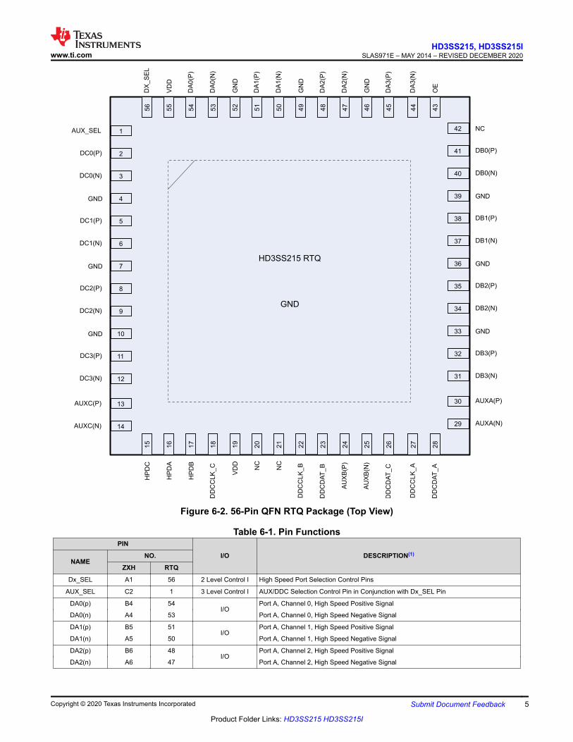
Figure 6-2. 56-Pin QFN RTQ Package (Top View)
Table 6-1. Pin FunctionsPIN
I/O DESCRIPTION(1)NAME
NO.
ZXH RTQ
Dx_SEL A1 56 2 Level Control I High Speed Port Selection Control Pins
AUX_SEL C2 1 3 Level Control I AUX/DDC Selection Control Pin in Conjunction with Dx_SEL Pin
DA0(p) B4 54I/O
Port A, Channel 0, High Speed Positive Signal
DA0(n) A4 53 Port A, Channel 0, High Speed Negative Signal
DA1(p) B5 51I/O
Port A, Channel 1, High Speed Positive Signal
DA1(n) A5 50 Port A, Channel 1, High Speed Negative Signal
DA2(p) B6 48I/O
Port A, Channel 2, High Speed Positive Signal
DA2(n) A6 47 Port A, Channel 2, High Speed Negative Signal
www.ti.comHD3SS215, HD3SS215I
SLAS971E – MAY 2014 – REVISED DECEMBER 2020
Copyright © 2020 Texas Instruments Incorporated Submit Document Feedback 5
Product Folder Links: HD3SS215 HD3SS215I
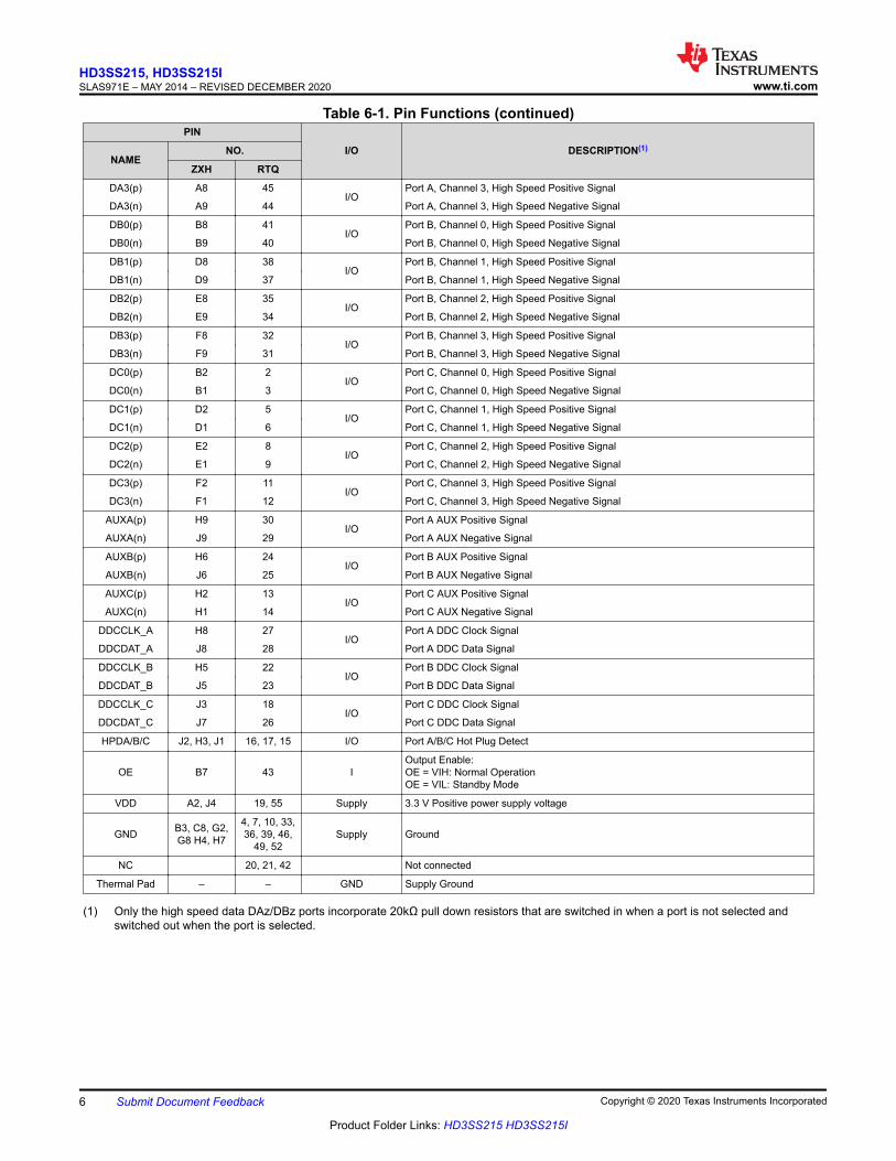
Table 6-1. Pin Functions (continued)PIN
I/O DESCRIPTION(1)NAME
NO.
ZXH RTQ
DA3(p) A8 45I/O
Port A, Channel 3, High Speed Positive Signal
DA3(n) A9 44 Port A, Channel 3, High Speed Negative Signal
DB0(p) B8 41I/O
Port B, Channel 0, High Speed Positive Signal
DB0(n) B9 40 Port B, Channel 0, High Speed Negative Signal
DB1(p) D8 38I/O
Port B, Channel 1, High Speed Positive Signal
DB1(n) D9 37 Port B, Channel 1, High Speed Negative Signal
DB2(p) E8 35I/O
Port B, Channel 2, High Speed Positive Signal
DB2(n) E9 34 Port B, Channel 2, High Speed Negative Signal
DB3(p) F8 32I/O
Port B, Channel 3, High Speed Positive Signal
DB3(n) F9 31 Port B, Channel 3, High Speed Negative Signal
DC0(p) B2 2I/O
Port C, Channel 0, High Speed Positive Signal
DC0(n) B1 3 Port C, Channel 0, High Speed Negative Signal
DC1(p) D2 5I/O
Port C, Channel 1, High Speed Positive Signal
DC1(n) D1 6 Port C, Channel 1, High Speed Negative Signal
DC2(p) E2 8I/O
Port C, Channel 2, High Speed Positive Signal
DC2(n) E1 9 Port C, Channel 2, High Speed Negative Signal
DC3(p) F2 11I/O
Port C, Channel 3, High Speed Positive Signal
DC3(n) F1 12 Port C, Channel 3, High Speed Negative Signal
AUXA(p) H9 30I/O
Port A AUX Positive Signal
AUXA(n) J9 29 Port A AUX Negative Signal
AUXB(p) H6 24I/O
Port B AUX Positive Signal
AUXB(n) J6 25 Port B AUX Negative Signal
AUXC(p) H2 13I/O
Port C AUX Positive Signal
AUXC(n) H1 14 Port C AUX Negative Signal
DDCCLK_A H8 27I/O
Port A DDC Clock Signal
DDCDAT_A J8 28 Port A DDC Data Signal
DDCCLK_B H5 22I/O
Port B DDC Clock Signal
DDCDAT_B J5 23 Port B DDC Data Signal
DDCCLK_C J3 18I/O
Port C DDC Clock Signal
DDCDAT_C J7 26 Port C DDC Data Signal
HPDA/B/C J2, H3, J1 16, 17, 15 I/O Port A/B/C Hot Plug Detect
OE B7 43 IOutput Enable:OE = VIH: Normal OperationOE = VIL: Standby Mode
VDD A2, J4 19, 55 Supply 3.3 V Positive power supply voltage
GND B3, C8, G2,G8 H4, H7
4, 7, 10, 33,36, 39, 46,
49, 52Supply Ground
NC 20, 21, 42 Not connected
Thermal Pad – – GND Supply Ground
(1) Only the high speed data DAz/DBz ports incorporate 20kΩ pull down resistors that are switched in when a port is not selected andswitched out when the port is selected.
HD3SS215, HD3SS215ISLAS971E – MAY 2014 – REVISED DECEMBER 2020 www.ti.com
6 Submit Document Feedback Copyright © 2020 Texas Instruments Incorporated
Product Folder Links: HD3SS215 HD3SS215I
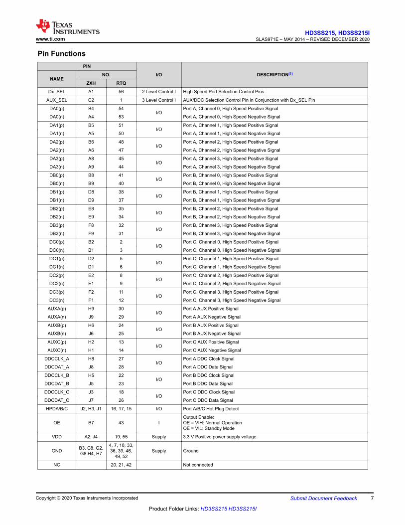
Pin FunctionsPIN
I/O DESCRIPTION(1)NAME
NO.
ZXH RTQ
Dx_SEL A1 56 2 Level Control I High Speed Port Selection Control Pins
AUX_SEL C2 1 3 Level Control I AUX/DDC Selection Control Pin in Conjunction with Dx_SEL Pin
DA0(p) B4 54I/O
Port A, Channel 0, High Speed Positive Signal
DA0(n) A4 53 Port A, Channel 0, High Speed Negative Signal
DA1(p) B5 51I/O
Port A, Channel 1, High Speed Positive Signal
DA1(n) A5 50 Port A, Channel 1, High Speed Negative Signal
DA2(p) B6 48I/O
Port A, Channel 2, High Speed Positive Signal
DA2(n) A6 47 Port A, Channel 2, High Speed Negative Signal
DA3(p) A8 45I/O
Port A, Channel 3, High Speed Positive Signal
DA3(n) A9 44 Port A, Channel 3, High Speed Negative Signal
DB0(p) B8 41I/O
Port B, Channel 0, High Speed Positive Signal
DB0(n) B9 40 Port B, Channel 0, High Speed Negative Signal
DB1(p) D8 38I/O
Port B, Channel 1, High Speed Positive Signal
DB1(n) D9 37 Port B, Channel 1, High Speed Negative Signal
DB2(p) E8 35I/O
Port B, Channel 2, High Speed Positive Signal
DB2(n) E9 34 Port B, Channel 2, High Speed Negative Signal
DB3(p) F8 32I/O
Port B, Channel 3, High Speed Positive Signal
DB3(n) F9 31 Port B, Channel 3, High Speed Negative Signal
DC0(p) B2 2I/O
Port C, Channel 0, High Speed Positive Signal
DC0(n) B1 3 Port C, Channel 0, High Speed Negative Signal
DC1(p) D2 5I/O
Port C, Channel 1, High Speed Positive Signal
DC1(n) D1 6 Port C, Channel 1, High Speed Negative Signal
DC2(p) E2 8I/O
Port C, Channel 2, High Speed Positive Signal
DC2(n) E1 9 Port C, Channel 2, High Speed Negative Signal
DC3(p) F2 11I/O
Port C, Channel 3, High Speed Positive Signal
DC3(n) F1 12 Port C, Channel 3, High Speed Negative Signal
AUXA(p) H9 30I/O
Port A AUX Positive Signal
AUXA(n) J9 29 Port A AUX Negative Signal
AUXB(p) H6 24I/O
Port B AUX Positive Signal
AUXB(n) J6 25 Port B AUX Negative Signal
AUXC(p) H2 13I/O
Port C AUX Positive Signal
AUXC(n) H1 14 Port C AUX Negative Signal
DDCCLK_A H8 27I/O
Port A DDC Clock Signal
DDCDAT_A J8 28 Port A DDC Data Signal
DDCCLK_B H5 22I/O
Port B DDC Clock Signal
DDCDAT_B J5 23 Port B DDC Data Signal
DDCCLK_C J3 18I/O
Port C DDC Clock Signal
DDCDAT_C J7 26 Port C DDC Data Signal
HPDA/B/C J2, H3, J1 16, 17, 15 I/O Port A/B/C Hot Plug Detect
OE B7 43 IOutput Enable:OE = VIH: Normal OperationOE = VIL: Standby Mode
VDD A2, J4 19, 55 Supply 3.3 V Positive power supply voltage
GND B3, C8, G2,G8 H4, H7
4, 7, 10, 33,36, 39, 46,
49, 52Supply Ground
NC 20, 21, 42 Not connected
www.ti.comHD3SS215, HD3SS215I
SLAS971E – MAY 2014 – REVISED DECEMBER 2020
Copyright © 2020 Texas Instruments Incorporated Submit Document Feedback 7
Product Folder Links: HD3SS215 HD3SS215I
PIN
I/O DESCRIPTION(1)NAME
NO.
ZXH RTQ
Thermal Pad – – GND Supply Ground
(1) Only the high speed data DAz/DBz ports incorporate 20kΩ pull down resistors that are switched in when a port is not selected andswitched out when the port is selected.
HD3SS215, HD3SS215ISLAS971E – MAY 2014 – REVISED DECEMBER 2020 www.ti.com
8 Submit Document Feedback Copyright © 2020 Texas Instruments Incorporated
Product Folder Links: HD3SS215 HD3SS215I
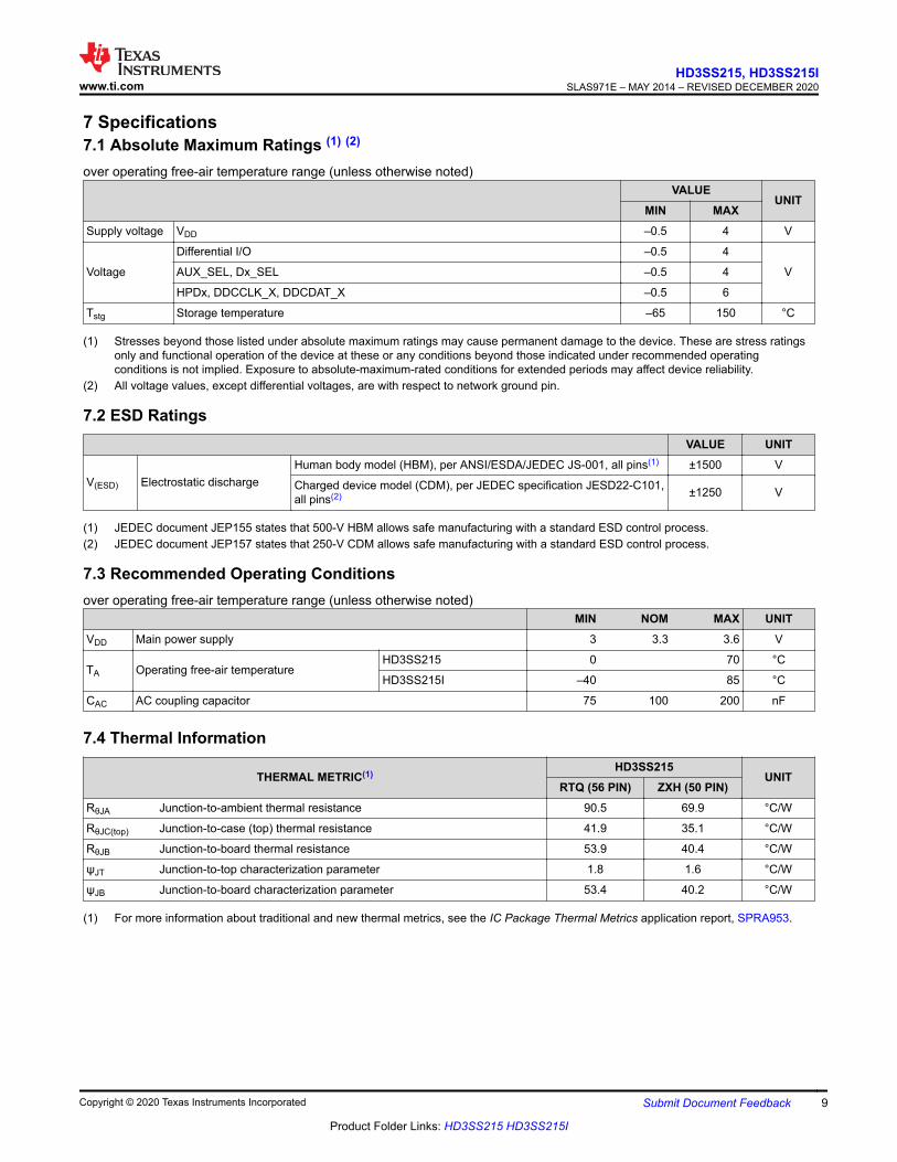
7 Specifications7.1 Absolute Maximum Ratings (1) (2)
over operating free-air temperature range (unless otherwise noted)VALUE
UNITMIN MAX
Supply voltage VDD –0.5 4 V
Voltage
Differential I/O –0.5 4
VAUX_SEL, Dx_SEL –0.5 4
HPDx, DDCCLK_X, DDCDAT_X –0.5 6
Tstg Storage temperature –65 150 °C
(1) Stresses beyond those listed under absolute maximum ratings may cause permanent damage to the device. These are stress ratingsonly and functional operation of the device at these or any conditions beyond those indicated under recommended operatingconditions is not implied. Exposure to absolute-maximum-rated conditions for extended periods may affect device reliability.
(2) All voltage values, except differential voltages, are with respect to network ground pin.
7.2 ESD RatingsVALUE UNIT
V(ESD) Electrostatic dischargeHuman body model (HBM), per ANSI/ESDA/JEDEC JS-001, all pins(1) ±1500 V
Charged device model (CDM), per JEDEC specification JESD22-C101,all pins(2) ±1250 V
(1) JEDEC document JEP155 states that 500-V HBM allows safe manufacturing with a standard ESD control process.(2) JEDEC document JEP157 states that 250-V CDM allows safe manufacturing with a standard ESD control process.
7.3 Recommended Operating Conditionsover operating free-air temperature range (unless otherwise noted)
MIN NOM MAX UNITVDD Main power supply 3 3.3 3.6 V
TA Operating free-air temperatureHD3SS215 0 70 °C
HD3SS215I –40 85 °C
CAC AC coupling capacitor 75 100 200 nF
7.4 Thermal Information
THERMAL METRIC(1)HD3SS215
UNITRTQ (56 PIN) ZXH (50 PIN)
RθJA Junction-to-ambient thermal resistance 90.5 69.9 °C/W
RθJC(top) Junction-to-case (top) thermal resistance 41.9 35.1 °C/W
RθJB Junction-to-board thermal resistance 53.9 40.4 °C/W
ψJT Junction-to-top characterization parameter 1.8 1.6 °C/W
ψJB Junction-to-board characterization parameter 53.4 40.2 °C/W
(1) For more information about traditional and new thermal metrics, see the IC Package Thermal Metrics application report, SPRA953.
www.ti.comHD3SS215, HD3SS215I
SLAS971E – MAY 2014 – REVISED DECEMBER 2020
Copyright © 2020 Texas Instruments Incorporated Submit Document Feedback 9
Product Folder Links: HD3SS215 HD3SS215I
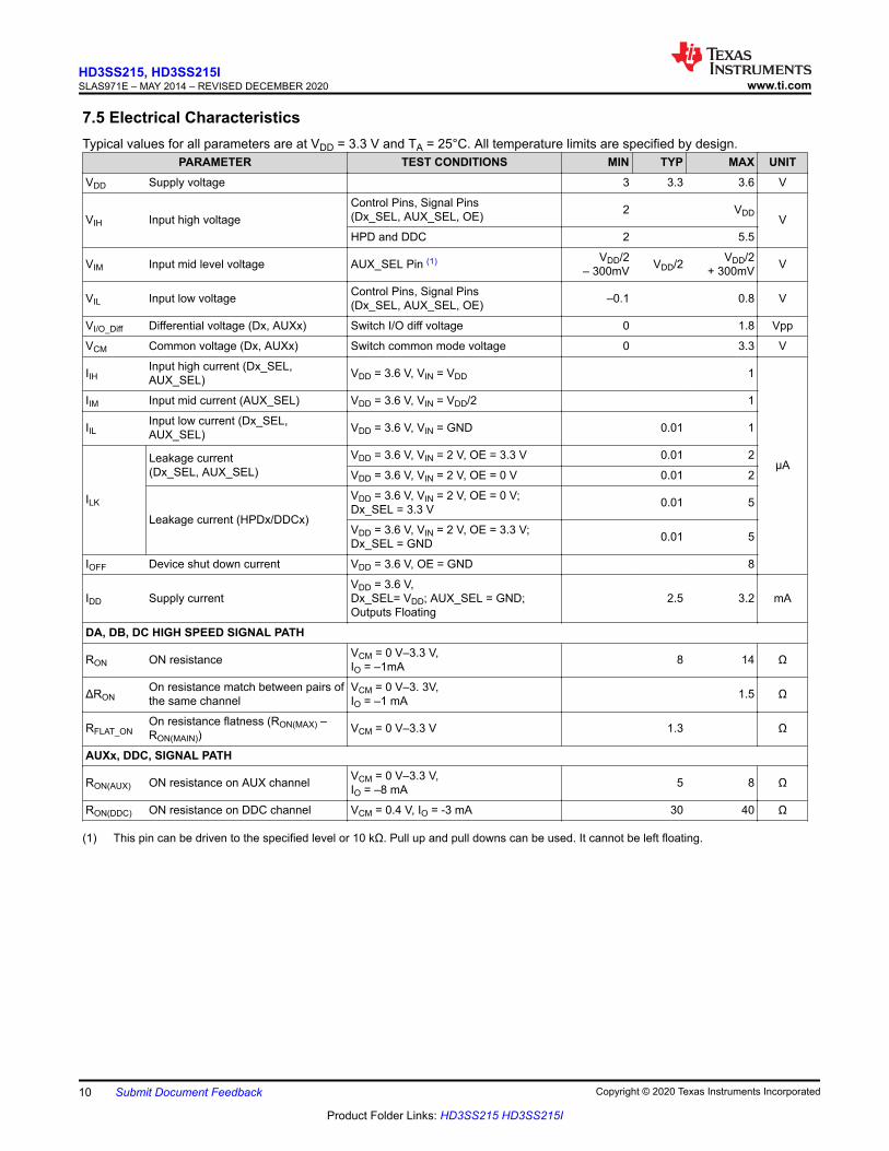
7.5 Electrical CharacteristicsTypical values for all parameters are at VDD = 3.3 V and TA = 25°C. All temperature limits are specified by design.
PARAMETER TEST CONDITIONS MIN TYP MAX UNITVDD Supply voltage 3 3.3 3.6 V
VIH Input high voltageControl Pins, Signal Pins(Dx_SEL, AUX_SEL, OE) 2 VDD VHPD and DDC 2 5.5
VIM Input mid level voltage AUX_SEL Pin (1) VDD/2– 300mV VDD/2 VDD/2
+ 300mV V
VIL Input low voltage Control Pins, Signal Pins(Dx_SEL, AUX_SEL, OE) –0.1 0.8 V
VI/O_Diff Differential voltage (Dx, AUXx) Switch I/O diff voltage 0 1.8 Vpp
VCM Common voltage (Dx, AUXx) Switch common mode voltage 0 3.3 V
IIHInput high current (Dx_SEL,AUX_SEL) VDD = 3.6 V, VIN = VDD 1
µA
IIM Input mid current (AUX_SEL) VDD = 3.6 V, VIN = VDD/2 1
IILInput low current (Dx_SEL,AUX_SEL) VDD = 3.6 V, VIN = GND 0.01 1
ILK
Leakage current(Dx_SEL, AUX_SEL)
VDD = 3.6 V, VIN = 2 V, OE = 3.3 V 0.01 2
VDD = 3.6 V, VIN = 2 V, OE = 0 V 0.01 2
Leakage current (HPDx/DDCx)
VDD = 3.6 V, VIN = 2 V, OE = 0 V;Dx_SEL = 3.3 V 0.01 5
VDD = 3.6 V, VIN = 2 V, OE = 3.3 V;Dx_SEL = GND 0.01 5
IOFF Device shut down current VDD = 3.6 V, OE = GND 8
IDD Supply currentVDD = 3.6 V,Dx_SEL= VDD; AUX_SEL = GND;Outputs Floating
2.5 3.2 mA
DA, DB, DC HIGH SPEED SIGNAL PATH
RON ON resistance VCM = 0 V–3.3 V,IO = –1mA 8 14 Ω
ΔRONOn resistance match between pairs ofthe same channel
VCM = 0 V–3. 3V,IO = –1 mA 1.5 Ω
RFLAT_ONOn resistance flatness (RON(MAX) –RON(MAIN))
VCM = 0 V–3.3 V 1.3 Ω
AUXx, DDC, SIGNAL PATH
RON(AUX) ON resistance on AUX channel VCM = 0 V–3.3 V,IO = –8 mA 5 8 Ω
RON(DDC) ON resistance on DDC channel VCM = 0.4 V, IO = -3 mA 30 40 Ω
(1) This pin can be driven to the specified level or 10 kΩ. Pull up and pull downs can be used. It cannot be left floating.
HD3SS215, HD3SS215ISLAS971E – MAY 2014 – REVISED DECEMBER 2020 www.ti.com
10 Submit Document Feedback Copyright © 2020 Texas Instruments Incorporated
Product Folder Links: HD3SS215 HD3SS215I
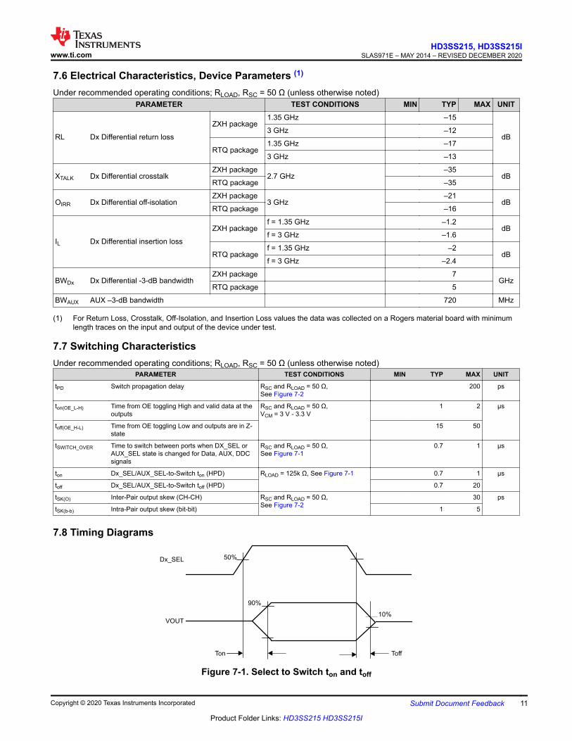
7.6 Electrical Characteristics, Device Parameters (1)
Under recommended operating conditions; RLOAD, RSC = 50 Ω (unless otherwise noted)PARAMETER TEST CONDITIONS MIN TYP MAX UNIT
RL Dx Differential return loss
ZXH package1.35 GHz –15
dB3 GHz –12
RTQ package1.35 GHz –17
3 GHz –13
XTALK Dx Differential crosstalkZXH package
2.7 GHz–35
dBRTQ package –35
OIRR Dx Differential off-isolationZXH package
3 GHz–21
dBRTQ package –16
IL Dx Differential insertion loss
ZXH packagef = 1.35 GHz –1.2
dBf = 3 GHz –1.6
RTQ packagef = 1.35 GHz –2
dBf = 3 GHz –2.4
BWDx Dx Differential -3-dB bandwidthZXH package 7
GHzRTQ package 5
BWAUX AUX –3-dB bandwidth 720 MHz
(1) For Return Loss, Crosstalk, Off-Isolation, and Insertion Loss values the data was collected on a Rogers material board with minimumlength traces on the input and output of the device under test.
7.7 Switching CharacteristicsUnder recommended operating conditions; RLOAD, RSC = 50 Ω (unless otherwise noted)
PARAMETER TEST CONDITIONS MIN TYP MAX UNIT
tPD Switch propagation delay RSC and RLOAD = 50 Ω,See Figure 7-2
200 ps
ton(OE_L-H) Time from OE toggling High and valid data at theoutputs
RSC and RLOAD = 50 Ω,VCM = 3 V - 3.3 V
1 2 µs
toff(OE_H-L) Time from OE toggling Low and outputs are in Z-state
15 50
tSWITCH_OVER Time to switch between ports when DX_SEL orAUX_SEL state is changed for Data, AUX, DDCsignals
RSC and RLOAD = 50 Ω,See Figure 7-1
0.7 1 µs
ton Dx_SEL/AUX_SEL-to-Switch ton (HPD) RLOAD = 125k Ω, See Figure 7-1 0.7 1 µs
toff Dx_SEL/AUX_SEL-to-Switch toff (HPD) 0.7 20
tSK(O) Inter-Pair output skew (CH-CH) RSC and RLOAD = 50 Ω,See Figure 7-2
30 ps
tSK(b-b) Intra-Pair output skew (bit-bit) 1 5
7.8 Timing Diagrams
Dx_SEL
VOUT
90%
10%
50%
Ton Toff
Figure 7-1. Select to Switch ton and toff
www.ti.comHD3SS215, HD3SS215I
SLAS971E – MAY 2014 – REVISED DECEMBER 2020
Copyright © 2020 Texas Instruments Incorporated Submit Document Feedback 11
Product Folder Links: HD3SS215 HD3SS215I
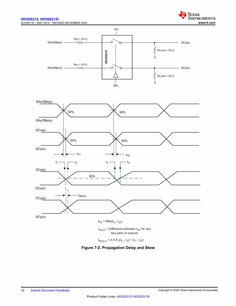
50% 50%
50% 50%
tP1 tP2
DCx(p)DAx/DBx(p)
DCx(n)DAx/DBx(n)
SEL
HD
3S
S2
15
Vcc
DAx/DBx(p)
DAx/DBx(n)
DCx(p)
DCx(n)
50%
tSK(O)DCy(p)
DCy(n)
DCx(p)
DCx(n)
t3 t4t1 t2
RLoad = 50 Ω
RLoad = 50 Ω
Rsc = 50 Ω
Rsc = 50 Ω
t = Max(t , t )
t = Difference between t for any
two pairs of outputs
t = 0.5 X (t t ) + (t t )
PD p1 p2
SK(O) PD
SK(b-b) 4 3 1 2| – – |
Figure 7-2. Propagation Delay and Skew
HD3SS215, HD3SS215ISLAS971E – MAY 2014 – REVISED DECEMBER 2020 www.ti.com
12 Submit Document Feedback Copyright © 2020 Texas Instruments Incorporated
Product Folder Links: HD3SS215 HD3SS215I
8 Detailed Description8.1 OverviewThe HD3SS215 is a generic analog, differential passive switch that can work for any high speed interfaceapplications, as long as it is biased at a common mode voltage range of 0 V to 3.3 V and has differentialsignaling with differential amplitude up to 1800 mVpp. It employs adaptive tracking that maintains the high speedchannel impedance over the entire common mode voltage range. In high-speed applications and data paths,signal integrity is an important concern. The switch offers excellent dynamic performance such as high isolation,crosstalk immunity, and minimal bit-bit skew. These characteristics allow the device to function seamlessly in thesystem without compromising signal integrity. The 2:1/1:2, mux/de-mux device operates with ports A or Bswitched to port C, or port C switched to either port A or B. This flexibility allows an application to select betweenone of two Sources on ports A and B and send the output to the sink on port C. Similarly, a Source on port C canselect between one of two Sink devices on ports A and B to send the data. To comply with DisplayPort, DP++and HDMI applications, the HD3SS215 also switches AUX, HPD, and DDC along with the high-speed differentialsignals. The HPD and data signals are both switched through the Dx_SEL pin. AUX and DDC are controlled withAUX_SEL and Dx_SEL. The Functional Modes section contains information on how to set the control pins.
With an OE control pin, the HD3SS215 is operational, with low active current, when this pin is high. When OE ispulled lowed, the device goes into standby mode and draws very little current in order to save powerconsumption in the application.
www.ti.comHD3SS215, HD3SS215I
SLAS971E – MAY 2014 – REVISED DECEMBER 2020
Copyright © 2020 Texas Instruments Incorporated Submit Document Feedback 13
Product Folder Links: HD3SS215 HD3SS215I
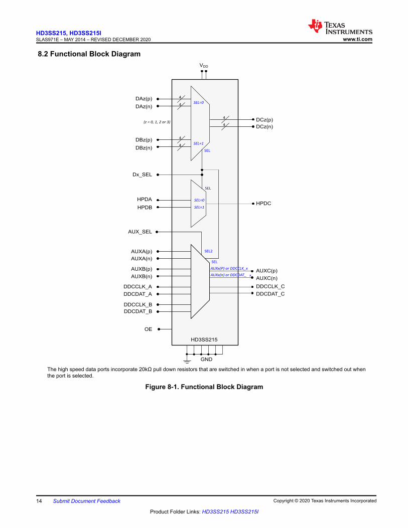
8.2 Functional Block Diagram
HPDC
DCz(p)
DCz(n)
AUXC(p)
AUXC(n)
Dx_SEL
HPDA
HPDB
AUX_SEL
VDD
OE
GND
AUXA(p)
AUXA(n)
AUXB(p)
AUXB(n)
DDCCLK_A
DDCDAT_A
DDCCLK_B
DDCDAT_B
DAz(p)
DAz(n)
DBz(p)
DBz(n)SEL
SEL
SEL
SEL2
HD3SS215
SEL=0
SEL=1
SEL=0
SEL=1
4
4
4
4
4
4(z = 0, 1, 2 or 3)
AUXx(P) or DDCCLK_x
AUXx(n) or DDCDAT_ x
DDCCLK_C
DDCDAT_C
The high speed data ports incorporate 20kΩ pull down resistors that are switched in when a port is not selected and switched out whenthe port is selected.
Figure 8-1. Functional Block Diagram
HD3SS215, HD3SS215ISLAS971E – MAY 2014 – REVISED DECEMBER 2020 www.ti.com
14 Submit Document Feedback Copyright © 2020 Texas Instruments Incorporated
Product Folder Links: HD3SS215 HD3SS215I
8.3 Feature Description8.3.1 High Speed Switching
The HD3SS215 supports switching of 6 Gbps data rates. The wide common mode of the device enables it tosupport TMDS signal levels and DisplayPort signals. The high speed muxing is designed with a wide –3dBdifferential bandwidth of 7 GHz and industry leading dynamic characteristics. All of these attributes help maintainsignal integrity in the application. Each high speed port incorporates 20kΩ pull down resistors that are switchedin when the port is not selected and switched out when the port is selected.
8.3.2 HPD, AUX, and DDC Switching
HPD, AUX and DDC switching is supported through the HD3SS215. This enables the device to work in multipleapplication scenarios within multiple electrical standards. The AUXA/B and DDCA/B lines can both be switchedto the AUXC port. This feature supports DP++ or AUX only adapters. For HDMI applications, the DDC channelsare switched to the DDC_C port only and the AUX channel can remain active or the end user can make it float.
8.3.3 Output Enable and Power Savings
The HD3SS215 has two power modes, active/normal operating mode, and standby mode. During standby mode,the device consumes very little current to save the maximum power. To enter standby mode, the OE control pinis pulled low and must remain low. For active/normal operation, the OE control pin should be pulled high to VDDthrough a resistor.
8.4 Device Functional Modes8.4.1 Switch Control Modes
Refer to the Section 8.2.
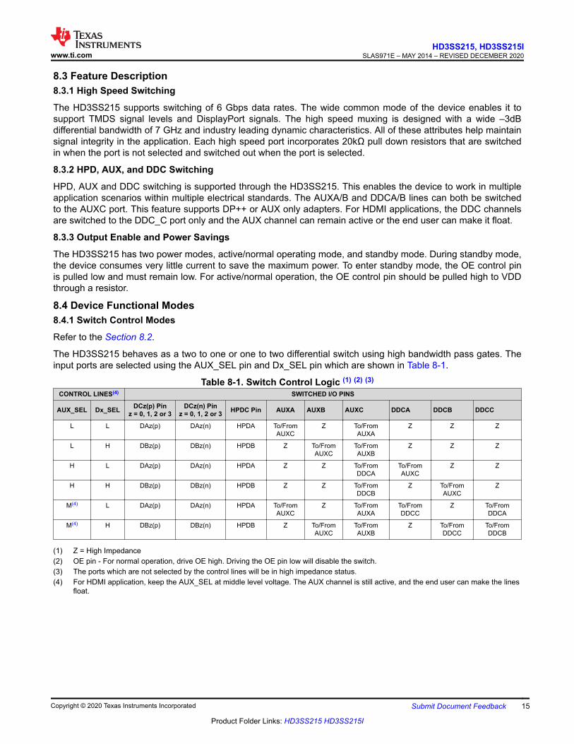
The HD3SS215 behaves as a two to one or one to two differential switch using high bandwidth pass gates. Theinput ports are selected using the AUX_SEL pin and Dx_SEL pin which are shown in Table 8-1.
Table 8-1. Switch Control Logic (1) (2) (3)
CONTROL LINES(4) SWITCHED I/O PINS
AUX_SEL Dx_SEL DCz(p) Pinz = 0, 1, 2 or 3
DCz(n) Pinz = 0, 1, 2 or 3 HPDC Pin AUXA AUXB AUXC DDCA DDCB DDCC
L L DAz(p) DAz(n) HPDA To/FromAUXC
Z To/FromAUXA
Z Z Z
L H DBz(p) DBz(n) HPDB Z To/FromAUXC
To/FromAUXB
Z Z Z
H L DAz(p) DAz(n) HPDA Z Z To/FromDDCA
To/FromAUXC
Z Z
H H DBz(p) DBz(n) HPDB Z Z To/FromDDCB
Z To/FromAUXC
Z
M(4) L DAz(p) DAz(n) HPDA To/FromAUXC
Z To/FromAUXA
To/FromDDCC
Z To/FromDDCA
M(4) H DBz(p) DBz(n) HPDB Z To/FromAUXC
To/FromAUXB
Z To/FromDDCC
To/FromDDCB
(1) Z = High Impedance(2) OE pin - For normal operation, drive OE high. Driving the OE pin low will disable the switch.(3) The ports which are not selected by the control lines will be in high impedance status.(4) For HDMI application, keep the AUX_SEL at middle level voltage. The AUX channel is still active, and the end user can make the lines
float.
www.ti.comHD3SS215, HD3SS215I
SLAS971E – MAY 2014 – REVISED DECEMBER 2020
Copyright © 2020 Texas Instruments Incorporated Submit Document Feedback 15
Product Folder Links: HD3SS215 HD3SS215I
9 Applications and ImplementationNote
Information in the following applications sections is not part of the TI component specification, and TIdoes not warrant its accuracy or completeness. TI’s customers are responsible for determiningsuitability of components for their purposes. Customers should validate and test their designimplementation to confirm system functionality.
9.1 Application InformationThe HD3SS215 can be used in a variety of applications. This section shows the typical applications forDisplayPort , DP++, and HDMI. The example diagrams illustrate using the HD3SS215 in a two source to onesink application and a one source to two sinks application. All schematics are using the ZXH pin-out.
9.2 Typical Applications9.2.1 DisplayPort and Dual Mode Adapter with Two Sources
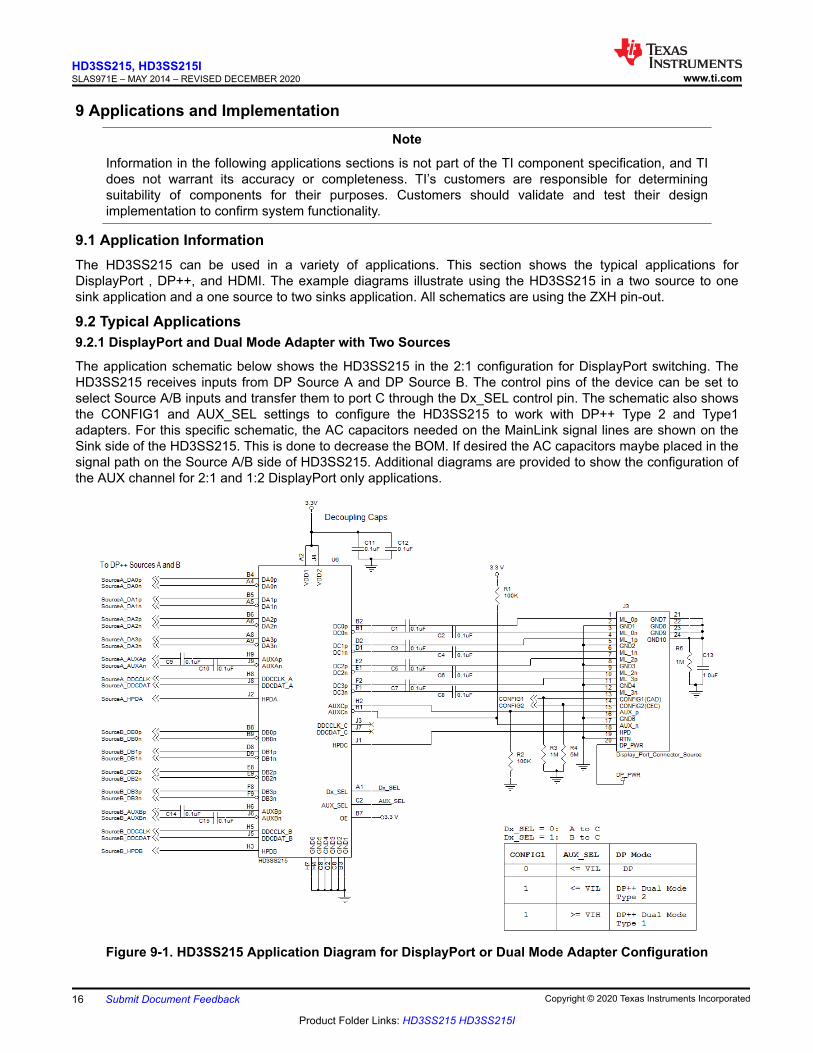
The application schematic below shows the HD3SS215 in the 2:1 configuration for DisplayPort switching. TheHD3SS215 receives inputs from DP Source A and DP Source B. The control pins of the device can be set toselect Source A/B inputs and transfer them to port C through the Dx_SEL control pin. The schematic also showsthe CONFIG1 and AUX_SEL settings to configure the HD3SS215 to work with DP++ Type 2 and Type1adapters. For this specific schematic, the AC capacitors needed on the MainLink signal lines are shown on theSink side of the HD3SS215. This is done to decrease the BOM. If desired the AC capacitors maybe placed in thesignal path on the Source A/B side of HD3SS215. Additional diagrams are provided to show the configuration ofthe AUX channel for 2:1 and 1:2 DisplayPort only applications.
Figure 9-1. HD3SS215 Application Diagram for DisplayPort or Dual Mode Adapter Configuration
HD3SS215, HD3SS215ISLAS971E – MAY 2014 – REVISED DECEMBER 2020 www.ti.com
16 Submit Document Feedback Copyright © 2020 Texas Instruments Incorporated
Product Folder Links: HD3SS215 HD3SS215I
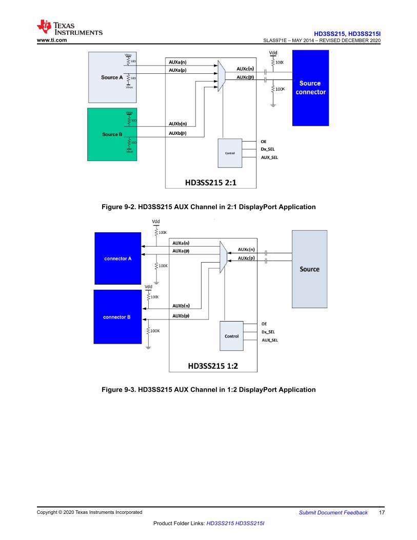
Figure 9-2. HD3SS215 AUX Channel in 2:1 DisplayPort Application
Figure 9-3. HD3SS215 AUX Channel in 1:2 DisplayPort Application
www.ti.comHD3SS215, HD3SS215I
SLAS971E – MAY 2014 – REVISED DECEMBER 2020
Copyright © 2020 Texas Instruments Incorporated Submit Document Feedback 17
Product Folder Links: HD3SS215 HD3SS215I
9.2.1.1 Design Requirements
Table 9-1. Design ParametersDESIGN PARAMETER EXAMPLE VALUE
VDD 3.3 V
Decoupling Capacitors 0.1 µF
AC Capacitors 75 nF to 200 nF (100 nF shown)
AUX Pull-Up/Pull-Down Resistors 10 kΩ to105 kΩ (100 kΩ shown)
Pull-Up/Pull-Down Resistors for Control Pins 10 kΩ
CONFIG1/CONFIG2 Pull-Down Resistors 1 MΩ and 5 MΩ
9.2.1.2 Detailed Design Procedure
The HD3SS215 is designed to operate with a 3.3 V power supply. Levels above those listed in the AbsoluteRatings table should not be used. If using a higher voltage system power supply, a voltage regulator can be usedto step down to 3.3 V. Decoupling capacitors may be used to reduce noise and improve power supply integrity.AC capacitors must be placed on the MainLink lines. Additionally, AC capacitors are placed on the AUXC lines.After the blocking capacitors, the AUXCp line must be pulled down weakly through a resistor to ground, and theAUXCn line must be pulled up weakly through a resistor to VDD. The voltage level of the control pins, AUX_SELand Dx_SEL should be set according to the application and muxing desired. For a DisplayPort connector, theCONFIG1 and CONFIG2 pins should be pulled to ground through resistors. For Dual Mode adapterimplementation, the CONFIG1 line may be used to perform cable adapter detection. The CONFIG2 line can beconfigured for an HDMI adaptor or left as a no connect for a DVI adapter. The CONFIG2 pin on the connectorshould be pulled up or left floating accordingly for Dual Mode adapter configuration.
HD3SS215, HD3SS215ISLAS971E – MAY 2014 – REVISED DECEMBER 2020 www.ti.com
18 Submit Document Feedback Copyright © 2020 Texas Instruments Incorporated
Product Folder Links: HD3SS215 HD3SS215I
9.2.2 HDMI Application with Two Sinks
The HD3SS215 can be placed in applications needing to switch between two sinks. In this example, the HDMIsource selects between Sink A or Sink B in the 1:2 configuration.
Figure 9-4. Application Diagram for a 1:2 Configuration with HDMI Source and Connectors
9.2.2.1 Design Requirements
Table 9-2. Design ParametersDESIGN PARAMETER EXAMPLE VALUE
VDD 3.3 V
Decoupling Capacitors 0.1 µF
DDC Pull-Up Resistors 1.5 kΩ to 2 kΩ to 5 V (2 kΩ shown)
Pull-Up/Pull-Down Resistors for Control Pins 10 kΩ
HPD Pull-Down Resistor 100 kΩ
9.2.2.2 Detailed Design Procedure
The HD3SS215 is designed to operate with a 3.3 V power supply. Levels above those listed in the AbsoluteRatings table should not be used. If using a higher voltage system power supply, a voltage regulator can be usedto step down to 3.3 V. Decoupling capacitors may be used to reduce noise and improve power supply integrity.Pull-up resistors to 5 V must be placed on the source side DDC clock and data lines according to the HDMI2.0Standard. A weak pull down resistor should be placed on the source side HPD line. This is to ensure the source
www.ti.comHD3SS215, HD3SS215I
SLAS971E – MAY 2014 – REVISED DECEMBER 2020
Copyright © 2020 Texas Instruments Incorporated Submit Document Feedback 19
Product Folder Links: HD3SS215 HD3SS215I
can differentiate between when HPD is disconnected or at a high voltage level. The AUX_SEL and Dx_SELcontrol pins should be set according to the application and desired muxing.
9.2.3
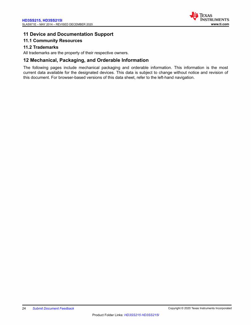
9.2.4 HDMI 2:1 Sink Application Using the RTQ Package
The HD3SS215 can be placed in applications needing to switch between two HDMI connectors and one GenericHDMI sink.
D0pD0n
D1pD1n
D2pD2n
DDC_SCLDDC_SDA
D3pD3n
HPD
GND1
GND2
GND3
GND4
Utility
DDC_GND
Source A
Source B
HDMI Connector
D0pD0n
D1pD1n
D2pD2n
DDC_SCLDDC_SDA
D3pD3n
HPD
GND1
GND2
GND3
GND4
Utility
DDC_GND
DA0pDA0n
DA1pDA1n
DA2pDA2n
AUXApAUXAn
DA3pDA3n
DDCCLK_ADDCDAT_A
HPDA
DB0pDB0n
DB1pDB1n
DB2pDB2n
AUXBpAUXBn
DB3pDB3n
DDCCLK_BDDCDAT_B
HPDB
DC0pDC0n
DC1pDC1n
DC2pDC2n
AUXCpAUXCn
DC3pDC3n
DDCCLK_CDDCDAT_C
HPDC
OE
AUX_SEL
Dx_SEL
VD
D1
VD
D2
HDMI Connector
GN
D1
GN
D2
GN
D3
GN
D4
GN
D5
GN
D6
GN
D7
GN
D8
GN
D9
D0pD0n
D1pD1n
D2pD2n
DDC_SCLDDC_SDA
D3pD3n
HPD
GND1
GND2
GND3
GND4
Utility
DDC_GND
Sink
HDMI SINK Device
5V
3.3V
0.1uF 0.1uF
47kΩ 47kΩ
100kΩ
100kΩ
5V
5V
5V 3.3V
10kΩ
10kΩ
10kΩ
HD3SS215
AUX_SEL and Dx_SEL configured for A to C
Figure 9-5. HDMI 2:1 Sink Application Using the RTQ Package
Note
According to the HDMI specification the DDC 2-kΩ pullup resistors can be replaced by47-kΩ pullups. Figure 9-5 schematic and Figure 10-3 PCB layout example shows 47-kΩ pullupresistors.
Power Supply RecommendationsThe HD3SS215 is designed to operate with a 3.3-V power supply. Levels above those listed in the AbsoluteRatings table should not be used. If using a higher voltage system power supply, a voltage regulator can be usedto step down to 3.3 V. Decoupling capacitors must be used to reduce power supply noise.
HD3SS215, HD3SS215ISLAS971E – MAY 2014 – REVISED DECEMBER 2020 www.ti.com
20 Submit Document Feedback Copyright © 2020 Texas Instruments Incorporated
Product Folder Links: HD3SS215 HD3SS215I
10 Layout10.1 Layout Guidelines• The ESD and EMI protection devices (if used) should be placed as close as possible to the connector.• Place voltage regulators as far away as possible from the high-speed differential pairs.• It is recommended that small decoupling capacitors for the HD3SS215 power rail be placed close to the
device.• The high-speed differential signal traces should be routed on the top layer to avoid the use of vias and allow
clean interconnects to the mux.• The high speed differential signal traces should be routed parallel to each other as much as possible. It is
recommended the traces be symmetrical.• In order to control impedance for transmission lines, a solid ground plane should be placed next to the high-
speed signal layer. This also provides an excellent low-inductance path for the return current flow.• The power plane should be placed next to the ground plane to create additional high-frequency bypass
capacitance.• Adding test points will cause impedance discontinuity and will therefore negatively impact signal
performance. If test points are used, they should be placed in series and symmetrically. They must not beplaced in a manner that causes stubs on the differential pair.
• Avoid 90 degree turns in traces. The use of bends in differential traces should be kept to a minimum. Whenbends are used, the number of left and right bends should be as equal as possible and the angle of the bendshould be ≥135 degrees. This will minimize any length mismatch caused by the bends and thereforeminimize the impact bends have on EMI.
www.ti.comHD3SS215, HD3SS215I
SLAS971E – MAY 2014 – REVISED DECEMBER 2020
Copyright © 2020 Texas Instruments Incorporated Submit Document Feedback 21
Product Folder Links: HD3SS215 HD3SS215I
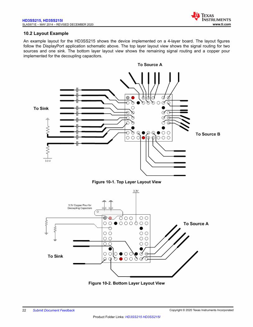
10.2 Layout ExampleAn example layout for the HD3SS215 shows the device implemented on a 4-layer board. The layout figuresfollow the DisplayPort application schematic above. The top layer layout view shows the signal routing for twosources and one sink. The bottom layer layout view shows the remaining signal routing and a copper pourimplemented for the decoupling capacitors.
Figure 10-1. Top Layer Layout View
Figure 10-2. Bottom Layer Layout View
HD3SS215, HD3SS215ISLAS971E – MAY 2014 – REVISED DECEMBER 2020 www.ti.com
22 Submit Document Feedback Copyright © 2020 Texas Instruments Incorporated
Product Folder Links: HD3SS215 HD3SS215I
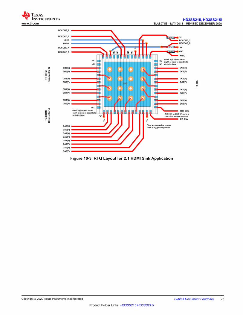
Figure 10-3. RTQ Layout for 2:1 HDMI Sink Application
www.ti.comHD3SS215, HD3SS215I
SLAS971E – MAY 2014 – REVISED DECEMBER 2020
Copyright © 2020 Texas Instruments Incorporated Submit Document Feedback 23
Product Folder Links: HD3SS215 HD3SS215I
11 Device and Documentation Support11.1 Community Resources11.2 TrademarksAll trademarks are the property of their respective owners.
12 Mechanical, Packaging, and Orderable InformationThe following pages include mechanical packaging and orderable information. This information is the mostcurrent data available for the designated devices. This data is subject to change without notice and revision ofthis document. For browser-based versions of this data sheet, refer to the left-hand navigation.
HD3SS215, HD3SS215ISLAS971E – MAY 2014 – REVISED DECEMBER 2020 www.ti.com
24 Submit Document Feedback Copyright © 2020 Texas Instruments Incorporated
Product Folder Links: HD3SS215 HD3SS215I

PACKAGE OPTION ADDENDUM
www.ti.com 30-Oct-2021
Addendum-Page 1
PACKAGING INFORMATION
Orderable Device Status(1)
Package Type PackageDrawing
Pins PackageQty
Eco Plan(2)
Lead finish/Ball material
(6)
MSL Peak Temp(3)
Op Temp (°C) Device Marking(4/5)
Samples
HD3SS215IRTQR ACTIVE QFN RTQ 56 2000 RoHS & Green Call TI | NIPDAU Level-3-260C-168 HR -40 to 85 HD3SS215I
HD3SS215IRTQT ACTIVE QFN RTQ 56 250 RoHS & Green NIPDAU Level-3-260C-168 HR -40 to 85 HD3SS215I
HD3SS215IZXHR ACTIVE NFBGA ZXH 50 2500 RoHS & Green SNAGCU Level-3-260C-168 HR -40 to 85 HD3SS215I
HD3SS215IZXHT ACTIVE NFBGA ZXH 50 250 RoHS & Green SNAGCU Level-3-260C-168 HR -40 to 85 HD3SS215I
HD3SS215RTQR ACTIVE QFN RTQ 56 2000 RoHS & Green NIPDAU Level-3-260C-168 HR 0 to 70 HD3SS215
HD3SS215RTQT ACTIVE QFN RTQ 56 250 RoHS & Green NIPDAU Level-3-260C-168 HR 0 to 70 HD3SS215
HD3SS215ZXHR ACTIVE NFBGA ZXH 50 2500 RoHS & Green SNAGCU Level-3-260C-168 HR 0 to 70 HD3SS215
(1) The marketing status values are defined as follows:ACTIVE: Product device recommended for new designs.LIFEBUY: TI has announced that the device will be discontinued, and a lifetime-buy period is in effect.NRND: Not recommended for new designs. Device is in production to support existing customers, but TI does not recommend using this part in a new design.PREVIEW: Device has been announced but is not in production. Samples may or may not be available.OBSOLETE: TI has discontinued the production of the device.
(2) RoHS: TI defines "RoHS" to mean semiconductor products that are compliant with the current EU RoHS requirements for all 10 RoHS substances, including the requirement that RoHS substancedo not exceed 0.1% by weight in homogeneous materials. Where designed to be soldered at high temperatures, "RoHS" products are suitable for use in specified lead-free processes. TI mayreference these types of products as "Pb-Free".RoHS Exempt: TI defines "RoHS Exempt" to mean products that contain lead but are compliant with EU RoHS pursuant to a specific EU RoHS exemption.Green: TI defines "Green" to mean the content of Chlorine (Cl) and Bromine (Br) based flame retardants meet JS709B low halogen requirements of <=1000ppm threshold. Antimony trioxide basedflame retardants must also meet the <=1000ppm threshold requirement.
(3) MSL, Peak Temp. - The Moisture Sensitivity Level rating according to the JEDEC industry standard classifications, and peak solder temperature.
(4) There may be additional marking, which relates to the logo, the lot trace code information, or the environmental category on the device.
(5) Multiple Device Markings will be inside parentheses. Only one Device Marking contained in parentheses and separated by a "~" will appear on a device. If a line is indented then it is a continuationof the previous line and the two combined represent the entire Device Marking for that device.
PACKAGE OPTION ADDENDUM
www.ti.com 30-Oct-2021
Addendum-Page 2
(6) Lead finish/Ball material - Orderable Devices may have multiple material finish options. Finish options are separated by a vertical ruled line. Lead finish/Ball material values may wrap to twolines if the finish value exceeds the maximum column width.
Important Information and Disclaimer:The information provided on this page represents TI's knowledge and belief as of the date that it is provided. TI bases its knowledge and belief on informationprovided by third parties, and makes no representation or warranty as to the accuracy of such information. Efforts are underway to better integrate information from third parties. TI has taken andcontinues to take reasonable steps to provide representative and accurate information but may not have conducted destructive testing or chemical analysis on incoming materials and chemicals.TI and TI suppliers consider certain information to be proprietary, and thus CAS numbers and other limited information may not be available for release.
In no event shall TI's liability arising out of such information exceed the total purchase price of the TI part(s) at issue in this document sold by TI to Customer on an annual basis.
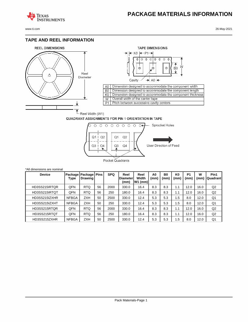
TAPE AND REEL INFORMATION
*All dimensions are nominal
Device PackageType
PackageDrawing
Pins SPQ ReelDiameter
(mm)
ReelWidth
W1 (mm)
A0(mm)
B0(mm)
K0(mm)
P1(mm)
W(mm)
Pin1Quadrant
HD3SS215IRTQR QFN RTQ 56 2000 330.0 16.4 8.3 8.3 1.1 12.0 16.0 Q2
HD3SS215IRTQT QFN RTQ 56 250 180.0 16.4 8.3 8.3 1.1 12.0 16.0 Q2
HD3SS215IZXHR NFBGA ZXH 50 2500 330.0 12.4 5.3 5.3 1.5 8.0 12.0 Q1
HD3SS215IZXHT NFBGA ZXH 50 250 330.0 12.4 5.3 5.3 1.5 8.0 12.0 Q1
HD3SS215RTQR QFN RTQ 56 2000 330.0 16.4 8.3 8.3 1.1 12.0 16.0 Q2
HD3SS215RTQT QFN RTQ 56 250 180.0 16.4 8.3 8.3 1.1 12.0 16.0 Q2
HD3SS215ZXHR NFBGA ZXH 50 2500 330.0 12.4 5.3 5.3 1.5 8.0 12.0 Q1
PACKAGE MATERIALS INFORMATION
www.ti.com 26-May-2021
Pack Materials-Page 1
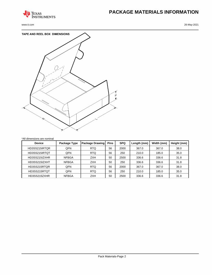
*All dimensions are nominal
Device Package Type Package Drawing Pins SPQ Length (mm) Width (mm) Height (mm)
HD3SS215IRTQR QFN RTQ 56 2000 367.0 367.0 38.0
HD3SS215IRTQT QFN RTQ 56 250 210.0 185.0 35.0
HD3SS215IZXHR NFBGA ZXH 50 2500 336.6 336.6 31.8
HD3SS215IZXHT NFBGA ZXH 50 250 336.6 336.6 31.8
HD3SS215RTQR QFN RTQ 56 2000 367.0 367.0 38.0
HD3SS215RTQT QFN RTQ 56 250 210.0 185.0 35.0
HD3SS215ZXHR NFBGA ZXH 50 2500 336.6 336.6 31.8
PACKAGE MATERIALS INFORMATION
www.ti.com 26-May-2021
Pack Materials-Page 2
NOTES:
1. All linear dimensions are in millimeters. Any dimensions in parenthesis are for reference only. Dimensioning and tolerancingper ASME Y14.5M.
2. This drawing is subject to change without notice.
NanoFree is a trademark of Texas Instruments.
PACKAGE OUTLINE
4225134/A 08/2019
www.ti.com
NFBGA - 1 mm max height
PLASTIC BALL GRID ARRAY
ZXH0050A
A
0.08 C
0.15 C A B0.05 C
B
SYMM
BALL A1 CORNER
BALL TYP
SYMM1
SEATING PLANE
C
5.14.9
5.14.9
1 MAX
0.250.15
4 TYP
4TYP
(0.5) TYP
(0.5) TYP
0.5 TYP
0.5 TYP2 3 4 5 6 7 8 9
A
B
C
D
E
F
G
H
J
50X Ø 0.350.25
NOTES: (continued)
3. Final dimensions may vary due to manufacturing tolerance considerations and also routing constraints. Refer to Texas InstrumentsLiterature number SNVA009 (www.ti.com/lit/snva009).
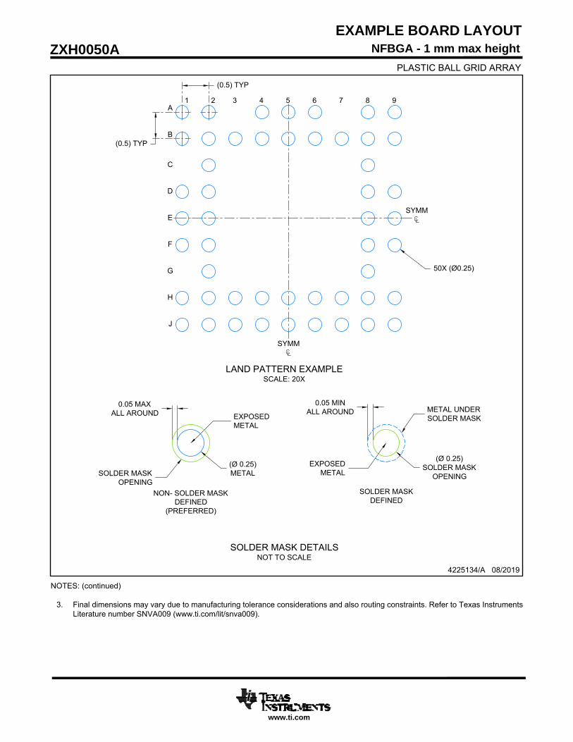
EXAMPLE BOARD LAYOUT
4225134/A 08/2019
www.ti.com
NFBGA - 1 mm max height
ZXH0050A
PLASTIC BALL GRID ARRAY
SYMM
SYMM
SOLDER MASK DETAILSNOT TO SCALE
0.05 MAXALL AROUND
0.05 MINALL AROUNDEXPOSED
METAL
SOLDER MASKOPENING
NON- SOLDER MASKDEFINED
(PREFERRED)
SOLDER MASKDEFINED
(Ø 0.25)METAL
EXPOSEDMETAL
METAL UNDERSOLDER MASK
(Ø 0.25)SOLDER MASK
OPENING
(0.5) TYP
(0.5) TYP
A
B
C
D
E
F
1 2 3 4 5 6
LAND PATTERN EXAMPLESCALE: 20X
7 8 9
G
H
J
50X (Ø0.25)
NOTES: (continued)
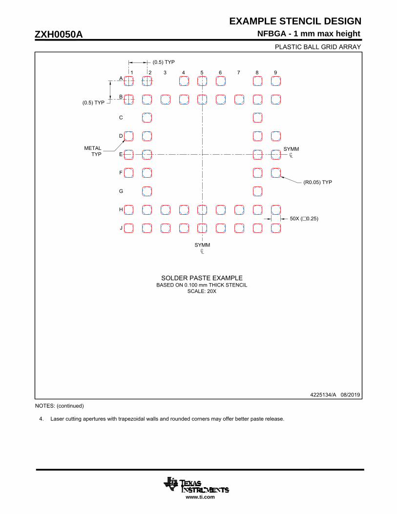
4. Laser cutting apertures with trapezoidal walls and rounded corners may offer better paste release.
EXAMPLE STENCIL DESIGN
4225134/A 08/2019
www.ti.com
NFBGA - 1 mm max height
ZXH0050A
PLASTIC BALL GRID ARRAY
SYMM
SYMM
(0.5) TYP
(0.5) TYP
A
B
C
D
E
F
1 2 3 4 5 6
50X ( 0.25)
SOLDER PASTE EXAMPLEBASED ON 0.100 mm THICK STENCIL
SCALE: 20X
(R0.05) TYP
G
H
J
METALTYP
7 8 9
www.ti.com
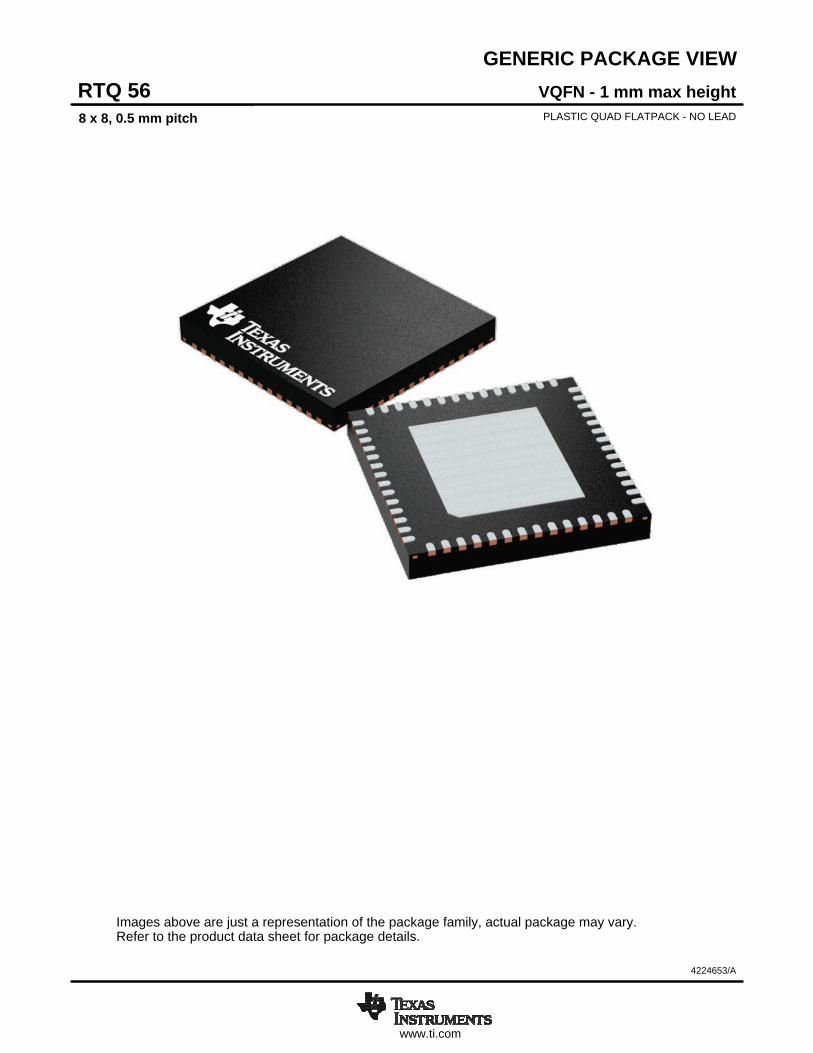
GENERIC PACKAGE VIEW
Images above are just a representation of the package family, actual package may vary.Refer to the product data sheet for package details.
VQFN - 1 mm max heightRTQ 56PLASTIC QUAD FLATPACK - NO LEAD8 x 8, 0.5 mm pitch
4224653/A
www.ti.com
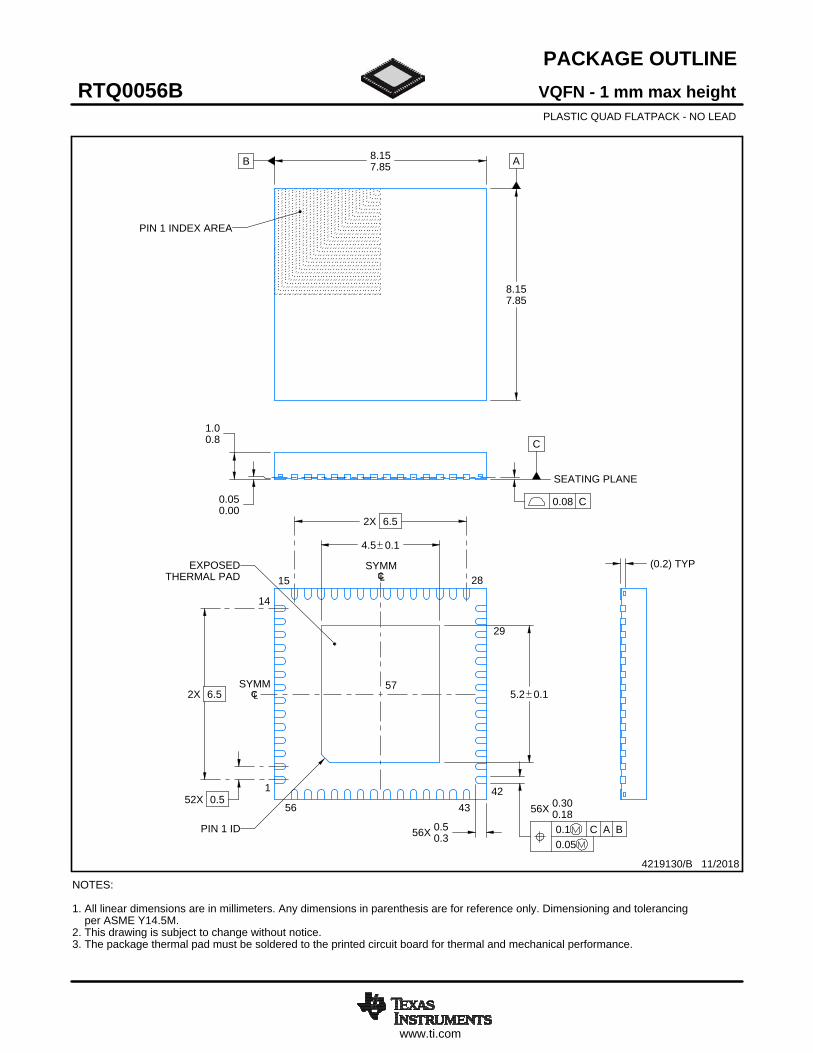
PACKAGE OUTLINE
C
8.157.85
8.157.85
1.00.8
0.050.00
2X 6.5
52X 0.5
2X 6.5
56X 0.50.3
56X 0.300.18
5.2 0.1
4.5 0.1
(0.2) TYP
VQFN - 1 mm max heightRTQ0056BPLASTIC QUAD FLATPACK - NO LEAD
4219130/B 11/2018
0.08 C
0.1 C A B0.05
NOTES: 1. All linear dimensions are in millimeters. Any dimensions in parenthesis are for reference only. Dimensioning and tolerancing per ASME Y14.5M. 2. This drawing is subject to change without notice. 3. The package thermal pad must be soldered to the printed circuit board for thermal and mechanical performance.
PIN 1 INDEX AREA
SEATING PLANE
PIN 1 ID
SYMMEXPOSEDTHERMAL PAD
SYMM
1
14
15 28
29
424356
57
SCALE 1.500
AB
www.ti.com
EXAMPLE BOARD LAYOUT
52X (0.5)
( 0.2) TYPVIA
(R0.05) TYP
0.07 MAXALL AROUND
0.07 MINALL AROUND
(1.27) TYP
(1.08) TYP
(0.73) TYP (1.27) TYP56X (0.6)
56X (0.24)
(7.8)
(7.8)
(5.2)
(4.5)
VQFN - 1 mm max heightRTQ0056BPLASTIC QUAD FLATPACK - NO LEAD
4219130/B 11/2018
NOTES: (continued) 4. This package is designed to be soldered to a thermal pad on the board. For more information, see Texas Instruments literature number SLUA271 (www.ti.com/lit/slua271).5. Vias are optional depending on application, refer to device data sheet. If any vias are implemented, refer to their locations shown on this view. It is recommended that vias under paste be filled, plugged or tented.
SYMM
SYMM
LAND PATTERN EXAMPLEEXPOSED METAL SHOWN
SCALE: 10X
SEE SOLDER MASKDETAIL
1
14
15 28
29
42
4356
57
METAL EDGE
SOLDER MASKOPENING
EXPOSED METAL
METAL UNDERSOLDER MASK
SOLDER MASKOPENING
EXPOSEDMETAL
NON SOLDER MASKDEFINED
(PREFERRED)SOLDER MASK DEFINED
SOLDER MASK DETAILS
www.ti.com
EXAMPLE STENCIL DESIGN
(0.635) TYP
(1.27) TYP
(1.46) TYP
56X (0.6)
56X (0.24)
52X (0.5)
(7.8)
(7.8)
(R0.05) TYP
12X (1.26)
12X (1.07)
VQFN - 1 mm max heightRTQ0056BPLASTIC QUAD FLATPACK - NO LEAD
4219130/B 11/2018
NOTES: (continued) 6. Laser cutting apertures with trapezoidal walls and rounded corners may offer better paste release. IPC-7525 may have alternate design recommendations.
SOLDER PASTE EXAMPLEBASED ON 0.125 MM THICK STENCIL
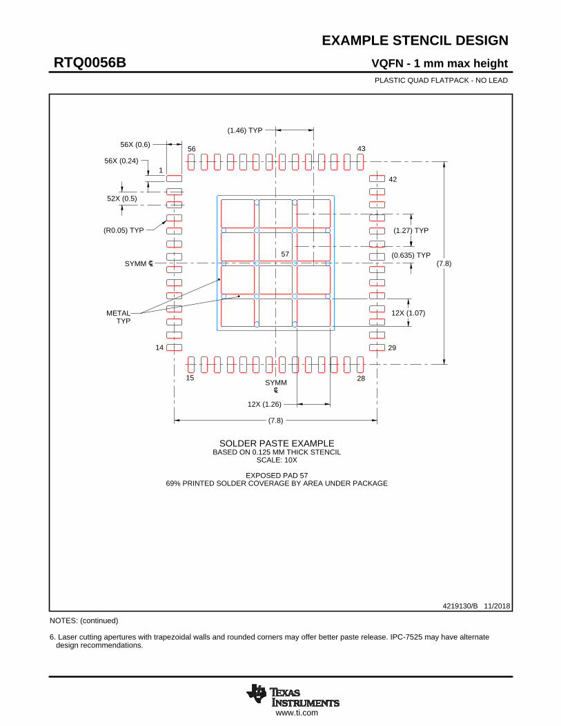
SCALE: 10X
EXPOSED PAD 5769% PRINTED SOLDER COVERAGE BY AREA UNDER PACKAGE
SYMM
SYMM
1
14
15 28
29
42
4356
57
METALTYP

IMPORTANT NOTICE AND DISCLAIMERTI PROVIDES TECHNICAL AND RELIABILITY DATA (INCLUDING DATA SHEETS), DESIGN RESOURCES (INCLUDING REFERENCE DESIGNS), APPLICATION OR OTHER DESIGN ADVICE, WEB TOOLS, SAFETY INFORMATION, AND OTHER RESOURCES “AS IS” AND WITH ALL FAULTS, AND DISCLAIMS ALL WARRANTIES, EXPRESS AND IMPLIED, INCLUDING WITHOUT LIMITATION ANY IMPLIED WARRANTIES OF MERCHANTABILITY, FITNESS FOR A PARTICULAR PURPOSE OR NON-INFRINGEMENT OF THIRD PARTY INTELLECTUAL PROPERTY RIGHTS.These resources are intended for skilled developers designing with TI products. You are solely responsible for (1) selecting the appropriate TI products for your application, (2) designing, validating and testing your application, and (3) ensuring your application meets applicable standards, and any other safety, security, regulatory or other requirements.These resources are subject to change without notice. TI grants you permission to use these resources only for development of an application that uses the TI products described in the resource. Other reproduction and display of these resources is prohibited. No license is granted to any other TI intellectual property right or to any third party intellectual property right. TI disclaims responsibility for, and you will fully indemnify TI and its representatives against, any claims, damages, costs, losses, and liabilities arising out of your use of these resources.TI’s products are provided subject to TI’s Terms of Sale or other applicable terms available either on ti.com or provided in conjunction with such TI products. TI’s provision of these resources does not expand or otherwise alter TI’s applicable warranties or warranty disclaimers for TI products.TI objects to and rejects any additional or different terms you may have proposed. IMPORTANT NOTICE
Mailing Address: Texas Instruments, Post Office Box 655303, Dallas, Texas 75265Copyright © 2021, Texas Instruments Incorporated