20 Gbps - 40GHz OFDM Ro-FSO transmission with mode division multiplexing.
842 IEEE TRANSACTIONS ON CIRCUITS AND SYSTEMS—I: REGULAR PAPERS, VOL. 53, NO. 4, APRIL 2006
A 200-Mbps 2-Gbps Continuous-RateClock-and-Data-Recovery Circuit
Rong-Jyi Yang, Student Member, IEEE, Kuan-Hua Chao, and Shen-Iuan Liu, Senior Member, IEEE
Abstract—A 200-Mbps 2-Gbps continuous-rate clock-and-data-recovery (CDR) circuit using half-rate clocking is pre-sented. To detect the data with wide-range bit rates, a frequencytracing circuit (FTC) is used to aid the frequency acquisition. Awide-range and low gain voltage-controlled oscillator (VCO) isalso presented by using analog and digital controlled mechanisms.A two-level bang-bang phase detector is utilized to improve thejitter performance and speed up the locking process. This CDRcircuit has been realized in a 2P4M 0.35- m CMOS process.The experimental results show that this CDR circuit with theproposed FTC can receive 2
311 pseudorandom bit stream
when the bit rate ranges from 200 Mbps to 2 Gbps without theharmonic-locking issue. All measured bit error rates are below10
12. The measured root-mean-square and peak-to-peak jittersare 5.86 ps and 41.8 ps, respectively, at 2 Gbps.
Index Terms—Clock-and-data-recovery (CDR), continuous rate,frequency detector, voltage-controlled oscillator (VCO).
I. INTRODUCTION
WITH the aid of wave-length division multiplexing tech-nique, several optical communication systems, such as
SDH/SONET and 10 GBased Ethernet, allow the informationto be exchanged with different bit rates at the same time inthe optical domain. The retiming circuits have to detect the bitrate from the incoming data and the harmonic locking mustbe prevented. To receive the data with different bit rates overa wide range without the harmonic-locking issue, two kindsof clock-and-data-recovery (CDR) circuits existed in literature[1]–[5]. One is the multirate CDR circuit [1], [2] and the otheris the continuous-rate CDR circuit [3]–[5]. For the multirateCDR circuits, the frequency detection mechanism for multiplebit rates is based on either multiple reference clocks [1] or singlereference clock with a programmable divider [2]. Comparedwith multirate CDR circuits, the continuous-rate CDR circuitscan detect various bit rates over a wide range. However, a com-plex frequency detection circuit would be required, such as afrequency synthesizer [4] or a time-to-digital converter [5].
To realize either continuous-rate CDR circuits or multirateones, two important issues must be considered: one is to havea harmonic-free frequency detector and the other is to have awide-range voltage-controlled oscillator (VCO) with a low con-version gain. A VCO with a high conversion gain will degrade
Manuscript received March 24, 2005; revised July 18, 2005. This paper wasrecommended by Associate Editor J. Silva-Martinez.
The authors are with Graduate Institute of Electronics Engineering & De-partment of Electrical Engineering, National Taiwan University, Taipei, Taiwan10617, R.O.C. (e-mail: [email protected]).
Digital Object Identifier 10.1109/TCSI.2005.862071
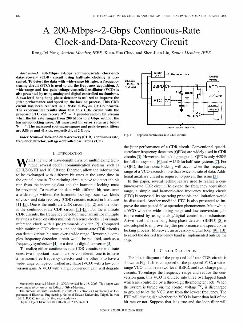
Fig. 1. Proposed continuous-rate CDR circuit.
the jitter performance of a CDR circuit. Conventional quadri-correlator frequency detectors (QFDs) are widely used in CDRcircuits [3]. However, the locking range of a QFD is only 20%for full-rate systems [6] and 15% for half-rate systems [7]. Fora QFD, the harmonic locking will occur when the frequencyrange of a VCO exceeds more than twice bit rate of data. Addi-tional auxiliary circuit is required to prevent this issue [3].
In this paper, several techniques are used to realize a con-tinuous-rate CDR circuit. To extend the frequency acquisitionrange, a simple and harmonic-free frequency tracing circuit(FTC) is proposed. Its operating principle and limitation wouldbe discussed. Another modified FTC is also presented to im-prove the unexpected false operation phenomenon. Meanwhile,a VCO with the wide tuning range and low conversion gainis presented by using analog/digital controlled mechanisms.A two-level half-rate bang-bang phase detector (BBPD) [8] isalso adopted to improve the jitter performance and speed up thelocking process. Moreover, an accessory digital loop [9], [10]to select the desired frequency band is implemented outside thechip.
II. CIRCUIT DESCRIPTION
The block diagram of the proposed half-rate CDR circuit isshown in Fig. 1. It is composed of the proposed FTC, a wide-range VCO, a half-rate two-level BBPD, and two charge pumpcircuits. To enlarge the frequency range and reduce the con-version gain, this VCO is divided into three overlapped bandswhich are controlled by a three-digit thermometer code. Whenthe system is turned on, the control voltage is dischargedto ground to let the VCO start from the lowest frequency. TheFTC will distinguish whether the VCO is lower than half of thebit rate or not. Suppose that it is true and the loop filter will
1057-7122/$20.00 © 2006 IEEE

YANG et al.: 200-Mbps 2-Gbps CONTINUOUS-RATE CDR CIRCUIT 843
Fig. 2. Timing diagrams of (a) f = 1=2 bit rate (b) f < 1=2 bit rate.
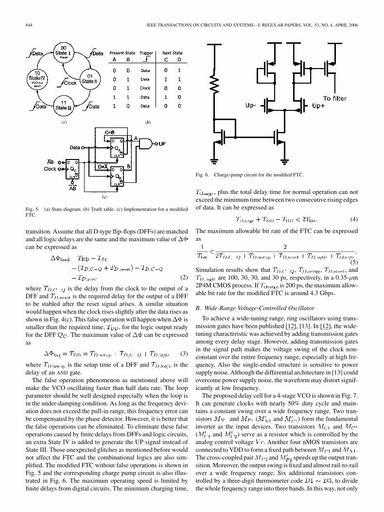
Fig. 3. (a) State diagram. (b) Truth table. (c) Implementation for simple FTC.
be charged. Once is larger than the preset reference voltageV , the off-chip digital controlled circuit will select the
higher frequency band of the VCO and discharge the loop filterto ground. The process will be repeated until the VCOs fre-quency is correct. After the frequency acquisition process wasdone, the two-level half-rate BBPD will adjust Vc according tothe phase error between the incoming data and the VCO. Finally,this CDR circuit will lock to generate the retimed data and therecovered clock. The details would be explained as follows:
A. Frequency Tracing Circuit
Assume that the CDR circuit is locked correctly with the in-coming data as shown in Fig. 2(a). Both rising and falling edgesof the clock should align with the middles of data, and at leastone rising edge of the clock will appear between two consec-utive rising edges of data [11]. When the clock is slower thanthe half bit rate, the timing relation is shown in Fig. 2(b). Notethat there is no rising edge of the clock between two consecutiverising edges of data. Based on this principle, a simple FTC canbe realized via the state diagram shown in Fig. 3(a). The truthtable and corresponding implementation for this simple FTC areshown in Fig. 3(b) and (c), respectively. Assume that the VCO
Fig. 4. Timing diagrams of FTC for (a) proper operation, (b) slightly lagoperation, (c) slightly lead operation, respectively, for the rising edges of thedata-to-clock signals.
start from the lowest frequency. Initially, the FTC stays in StateI. Assume the phase difference between the data and clock islarge enough. When the data rises to high, it will move to StateII. In State II, two possible operations can occur. Once the clockrises first, the FTC will go back to State I. Once the data risesfirst, the FTC will move to State III and outputs a signal “UP”to speed up the VCO. A typical timing diagram is illustratedin Fig. 4(a). As long as the control voltage of the VCO is dis-charged to ground first, the FTC will adjust the VCO from theslowest frequency to the right one.
Although this simple FTC will stop once the clock is equalto or higher than half bit rate, some unallowable false opera-tions still may take place. Assume that the VCO’s frequencyis equal to half the bit rate and their phase difference, , issmall. When a clock rises and the FTC initially stays in State II,the FTC must move to State I. If the clock rises slightly beforethe data, the FTC may go to State III first and then go back toState I as shown in Fig. 4(b). This false operation for the FTCwill happen when the phase difference is
(1)
where is the required delay time to reset the FSM afterthe clock arises and is the required delay time for state
844 IEEE TRANSACTIONS ON CIRCUITS AND SYSTEMS—I: REGULAR PAPERS, VOL. 53, NO. 4, APRIL 2006
Fig. 5. (a) State diagram. (b) Truth table. (c) Implementation for a modifiedFTC.
transition. Assume that all D-type flip-flops (DFFs) are matchedand all logic delays are the same and the maximum value ofcan be expressed as
(2)
where is the delay from the clock to the output of aDFF and is the required delay for the output of a DFFto be stabled after the reset signal arises. A similar situationwould happen when the clock rises slightly after the data rises asshown in Fig. 4(c). This false operation will happen when issmaller than the required time, , for the logic output readyfor the DFF . The maximum value of can be expressedas
(3)
where is the setup time of a DFF and is thedelay of an AND gate.
The false operation phenomenon as mentioned above willmake the VCO oscillating faster than half data rate. The loopparameter should be well designed especially when the loop isin the under-damping condition. As long as the frequency devi-ation does not exceed the pull-in range, this frequency error canbe compensated by the phase detector. However, it is better thatthe false operations can be eliminated. To eliminate these falseoperations caused by finite delays from DFFs and logic circuits,an extra State IV is added to generate the UP signal instead ofState III. Those unexpected glitches as mentioned before wouldnot affect the FTC and the combinational logics are also sim-plified. The modified FTC without false operations is shown inFig. 5 and the corresponding charge pump circuit is also illus-trated in Fig. 6. The maximum operating speed is limited byfinite delays from digital circuits. The minimum charging time,
Fig. 6. Charge-pump circuit for the modified FTC.
, plus the total delay time for normal operation can notexceed the minimum time between two consecutive rising edgesof data. It can be expressed as
(4)
The maximum allowable bit rate of the FTC can be expressedas
(5)Simulation results show that , , , and
are 100, 30, 30, and 30 ps, respectively, in a 0.35- m2P4M CMOS process. If is 200 ps, the maximum allow-able bit rate for the modified FTC is around 4.3 Gbps.
B. Wide-Range Voltage-Controlled Oscillator
To achieve a wide-tuning range, ring oscillators using trans-mission gates have been published [12], [13]. In [12], the wide-tuning characteristic was achieved by adding transmission gatesamong every delay stage. However, adding transmission gatesin the signal path makes the voltage swing of the clock non-constant over the entire frequency range, especially at high fre-quency. Also the single-ended structure is sensitive to powersupply noise. Although the differential architecture in [13] couldovercome power supply noise, the waveform may distort signif-icantly at low frequency.
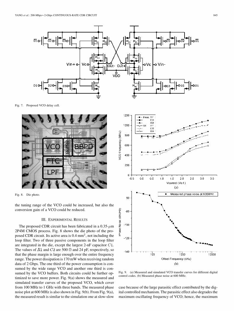
The proposed delay cell for a 4-stage VCO is shown in Fig. 7.It can generate clocks with nearly 50% duty cycle and main-tains a constant swing over a wide frequency range. Two tran-sistors and ( and ) form the fundamentalinverter as the input devices. Two transistors and( and ) serve as a resistor which is controlled by theanalog control voltage . Another four nMOS transistors areconnected to VDD to form a fixed path between and .The cross-coupled pair and speeds up the output tran-sition. Moreover, the output swing is fixed and almost rail-to-railover a wide frequency range. Six additional transistors con-trolled by a three-digit thermometer code , to dividethe whole frequency range into three bands. In this way, not only
YANG et al.: 200-Mbps 2-Gbps CONTINUOUS-RATE CDR CIRCUIT 845
Fig. 7. Proposed VCO delay cell.
Fig. 8. Die photo.
the tuning range of the VCO could be increased, but also theconversion gain of a VCO could be reduced.
III. EXPERIMENTAL RESULTS
The proposed CDR circuit has been fabricated in a 0.35- m2P4M CMOS process. Fig. 8 shows the die photo of the pro-posed CDR circuit. Its active area is 0.4 mm , not including theloop filter. Two of three passive components in the loop filterare integrated in the die, except the largest 2-nF capacitor .The values of and are 500 and 24 pF, respectively, sothat the phase margin is large enough over the entire frequencyrange. The power dissipation is 170 mW when receiving randomdata of 2 Gbps. The one third of the power consumption is con-sumed by the wide range VCO and another one third is con-sumed by the VCO buffers. Both circuits could be further op-timized to save more power. Fig. 9(a) shows the measured andsimulated transfer curves of the proposed VCO, which coverfrom 100 MHz to 1 GHz with three bands. The measured phasenoise plot at 600 MHz is also shown in Fig. 9(b). From Fig. 9(a),the measured result is similar to the simulation one at slow-slow
Fig. 9. (a) Measured and simulated VCO transfer curves for different digitalcontrol codes. (b) Measured phase noise at 600 MHz.
case because of the large parasitic effect contributed by the dig-ital controlled mechanism. The parasitic effect also degrades themaximum oscillating frequency of VCO; hence, the maximum

846 IEEE TRANSACTIONS ON CIRCUITS AND SYSTEMS—I: REGULAR PAPERS, VOL. 53, NO. 4, APRIL 2006
Fig. 10. Frequency acquisition process for different data patterns. A, B, and Crepresent the NRZ data with PRBS of 2 �1, 2 �1 and 2 �1, respectively.
Fig. 11. (a) Eye diagram and (b) clock jitter histogram @ 2 � 1 PRBS of 2Gbps.
bit rate can not achieve the theoretical value of 4.3 Gbps. Themeasured tuning range is slightly larger than simulations be-cause the parasitic effect was over estimated. Fig. 10 shows thefrequency tracing process. The VCO is initialized at 782 MHzwhile the incoming data rate is 2 Gbps. The measurement re-sult shows that the VCO can lock data at the right frequency of1 GHz without the QFD. The curves A, B, and C represent thefrequency acquisition processes when receiving nonreturn-to-zero (NRZ) data with pseudorandom bit stream (PRBS) of
, and , respectively.
Fig. 12. Measured eye diagrams for 2 � 1 PRBS of (a) 622.08 Mbps and(b) 200 Mbps.
TABLE IPERFORMANCE SUMMARY
The measured eye diagram and the jitter histogram of the re-timed clock are shown in Fig. 11(a) and (b), respectively, wheninput data rate is a PRBS of 2 Gbps. The measuredroot-mean-square and peak-to-peak jitters are 5.9 ps and 41.8ps, respectively. Fig. 12(a) and (b) shows the measured eye di-agrams for the PRBS of 622.08 and 200 Mbps, respec-tively. The measured bit error rates from 200 Mbps to 2 Gbps
YANG et al.: 200-Mbps 2-Gbps CONTINUOUS-RATE CDR CIRCUIT 847
are all below . The performance summary of this work islisted in Table I.
IV. CONCLUSION
The continuous-rate CDR circuit with the proposed FTC isrealized in a 0.35- m 2P4M CMOS process. The proposed FTCcan aid the frequency acquisition for the data over a wide bit-rate range without harmonic-locking issue as long as the initialfrequency of the clock is lower than half data rate. Accompaniedwith the proposed wide-range VCO with reasonable conversiongain, the CDR circuit can receive NRZ data of PRBSfrom 200 Mbps to 2 Gbps.
ACKNOWLEDGMENT
The authors would like to thank National Chip Implementa-tion Center, Taiwan, for fabricating this chip.
REFERENCES
[1] J. Scheytt, G. Hanke, and U. Langmann, “A 0.155, 0.622 and 2.488Gb/s automatic bit-rate selecting clock-and-data-recovery IC for bit-ratetransparent SDH systems,” IEEE J. Solid-State Circuits, vol. 34, no. 12,pp. 1935–1943, Dec. 1999.
[2] D. Belot, L. Dugoujon, and S. Dedieu, “A 3.3 V power adaptive1244/622/155 Mbit/s transceiver for ATM, SONET/SDH,” IEEE J.Solid-State Circuits, vol. 33, no. 7, pp. 1047–1058, Jul. 1998.
[3] D. Postson and A. Buchholz, “A 143–360 Mb/s auto-rate selecting data-retimer chip for serial-digital video signals,” in Dig. Tech. Papers IEEEInt. Solid-State Circuit Conf., Feb. 1996, pp. 196–197.
[4] J. Frambach, R. Heijna, and R. Krosschell, “Single reference continuousrate clock-and-data-recovery from 30 MBit/s to 3.2 GBit/s,” in Proc.IEEE Custom Integ. Circuits Conf., May 2002, pp. 375–378.
[5] J. Park and W. Kim, “An auto-ranging 50–210 Mb/s clock recovery cir-cuit with a time-to-digital converter,” in Dig. Tech. Papers IEEE Int.Solid-State Circuit Conf., Feb. 1999, pp. 350–351.
[6] B. Stilling, “Bit rate and protocol independent clock-and-data-recovery,”Electron. Lett., vol. 36, pp. 824–825, Apr. 2000.
[7] R.-J. Yang, S.-P. Chen, and S.-I. Liu, “A 3.125 Gbps clock-and-data-re-covery circuit for 10-Gbase-LX4 Ethernet,” IEEE J. Solid-State Circuits,vol. 39, no. 8, pp. 1356–1360, Aug. 2004.
[8] M. Ramezani and C. Salama, “A 10 Gb/s CDR with a half-rate bang-bang phase detector,” in Proc. IEEE Int. Sym. Circuits and Systems, vol.II, May 2003, pp. 181–184.
[9] W. B. Wilson et al., “A CMOS self-calibrating frequency synthesizer,”IEEE J. Solid-State Circuits, vol. 35, no. 10, pp. 1437–1444, Oct. 2000.
[10] T.-H. Lin et al., “A 900-MHz 2.5-mA CMOS frequency synthesizer withan automatic SC tuning loop,” IEEE J. Solid-State Circuits, vol. 36, no.3, pp. 424–431, Mar. 2001.
[11] T. H. Toifl and P. Moreira, “Simple frequency detector circuit for biphaseand NRZ clock recovery,” Electron. Lett., vol. 34, pp. 1922–1923, Oct.1998.
[12] N. Retdian, S. Takagi, and N. Fujii, “Voltage controlled ring oscillatorwith wide tuning range and fast voltage swing,” in Proc. IEEE Asia-Pacific Conf. Advanced Syst. Integr. Circuits, Aug. 2002, pp. 201–204.
[13] I.-C. Hwang and S.-M. Kang, “A self-regulating VCO with supply sen-sitivity of <0.15%-delay/1%-supply,” in Dig. Tech. Papers IEEE Int.Solid-State Circuit Conf., Feb. 2002, pp. 140–141.
Rong-Jyi Yang (S’03) was born in Taipei, Taiwan,R.O.C., in 1973. He received the B.S. degree in elec-trical engineering from National Central University,Jhongli, Taiwan, R.O.C., in 1998. He is currentlyworking toward the Ph.D. degree in electronicsengineering, National Taiwan University, Taipei,Taiwan, R.O.C.
His research interests include both analog and dig-ital approaches of phase-locked loops, delay-lockedloops, and high-speed CMOS data-communicationcircuits for multiple gigabit applications.
Kuan-Hua Chao was born in Taipei, Taiwan,R.O.C., on February 26, 1980. He received the B.S.degree in electronics engineering from the NationalChiao Tung University, Hsin Chu, Taiwan, R.O.C.,and the M.S. degree in electronics engineering fromthe National Taiwan University, Taipei, Taiwan,R.O.C., in 2002 and 2004, respectively.
His research interests include phase-locked loops,delay-locked loops (DLLs) and high-speed seriallinks. He is currently working at MediaTek Inc.,Hsin Chu, Taiwan, R.O.C., where he focuses on
analog and mix-mode circuit design.
Shen-Iuan Liu (S’88-M’93-SM’03) was born inKeelung, Taiwan, R.O.C., in 1965. He received boththe B.S. and Ph.D. degrees in electrical engineeringfrom National Taiwan University (NTU), Taipei,Taiwan, R.O.C., in 1987 and 1991, respectively.
During 1991–1993 he served as a Second Lieu-tenant in the Chinese Air Force. During 1991–1994,he was an Associate Professor in the Department ofElectronic Engineering, National Taiwan Institute ofTechnology, Taiwan, R.O.C. He joined in the Depart-ment of Electrical Engineering, NTU in 1994 and he
has been a Professor since 1998. His research interests are in analog and digitalintegrated circuits and systems.
Dr. Liu has served as a Chair on IEEE SSCS Taipei Chapter from 2004. He hasserved as a General Chair on the 15th VLSI Design/CAD Symposium, Taiwan,2004 and as a Program Co-chair on the Fourth IEEE Asia-Pacific Conference onAdvanced System Integrated Circuits, Japan, in 2004. He was the recipient of theEngineering Paper Award from the Chinese Institute of Engineers, in 2003, theYoung Professor Teaching Award from MXIC Inc., the Research AchievementAward from NTU, and the Outstanding Research Award from National ScienceCouncil, in 2004. He served as a Technical Program Committee member forA-SSCC and ISSCC, in 2005. He currently serves as an Associate Editor ofIEEE TRANSACTIONS ON CIRCUITS AND SYSTEMS—II: EXPRESS BRIEFS. He isa Member of IEICE.
Copyright © 2022 FDOKUMEN