![Inclusion of methano[60]fullerene derivatives in cavitand-based coordination cages](https://static.fdokumen.com/doc/165x107/631ed46f4c5c8fb3a00e625a/inclusion-of-methano60fullerene-derivatives-in-cavitand-based-coordination-cages.jpg)
Inclusion of methano[60]fullerene derivatives in cavitand-based coordination cages

Chapter contribution for “Trends in Fullerene Research” To be published by Nova Science Publishers, Inc. (2007)
Gago et al. Page 1 of 46
Growth mechanisms and structure of fullerene-like carbon-based thin films: superelastic materials for tribological applications R. Gago,1 G. Abrasonis,2 I. Jiménez,3 and W. Möller2 1 Centro de Micro-Análisis de Materiales, Universidad Autónoma de Madrid, E-28049 Madrid, Spain. 2 Institute of Ion Beam Physics and Materials Research, Forschungszentrum Dresden-Rossendorf,
PF510119, D-01314 Dresden, Germany. 3 Instituto de Ciencia de Materiales de Madrid, Consejo Superior de Investigaciones Científicas, E-28049
Madrid, Spain.
Abstract:
In this chapter we review our findings on the bonding structure and growth mechanisms
of carbon-based thin solid films with fullerene-like (FL) microstructure. The so-called
FL arrangements arise from the curvature and cross-linking of basal planes in graphitic-
like structures, partially resembling that of molecular fullerenes. This three-dimensional
superstructure takes advantage of the strength of planar π bonds in sp2 hybrids and
confers the material interesting mechanical properties, such as high hardness, high
elastic recovery, low-friction and wear-resistance. These properties can be tailored by
controlling the curvature, size and connectivity of the FL arrangements, making these
materials promising coatings for tribological applications. We have focused our interest
mostly on carbon nitride (CNx) since nitrogen promotes the formation of FL
arrangements at low substrate temperatures and they are emerging over pure carbon
coatings in tribological applications such as protective overcoats in magnetic hard disks.
We address structural issues such as origin of plane curvature, nature of the cross-
linking sites and sp2 clustering, together with growth mechanisms based on the role of
film-forming precursors, chemical re-sputtering or concurrent ion assistance during
growth.
Chapter contribution for “Trends in Fullerene Research” To be published by Nova Science Publishers, Inc. (2007)
Gago et al. Page 2 of 46
1. INTRODUCTION
During the last years there has been a growing interest on carbon-based nanostructures
like fullerenes, nanotubes and nano-onions due to their remarkable and tunable
mechanical, electronic and electrochemical properties [1]. The common characteristic of
these nanostructures is the presence of graphitic atomic arrangements with in-plane
curvature, giving rise to 3-dimensional (3D) structure of sp2-coordinated atoms. These
3D units constitute closed cages in the case of spherical (hetero-)fullerene molecules
and onion-like carbon.
All-sp2 3D curved structures have been also reported in graphitic carbon-based thin
solid films of pure carbon (C) [2], carbon nitride (CNx) [3] and hexagonal boron carbon
nitride (BCN) [4]. These compounds have been named as fullerene-like (FL) materials
due to the presence of curved and cross-linked basal planes, resembling the structure of
fullerene molecules. The presence of FL arrangements within the solid is normally
assessed by high resolution transmission electron microscopy (HRTEM). The typical
micrograph representing such structure in CNx grown is depicted in Figure 1. As
observed, the degree of in-plane curvature can be considerable inducing even the
formation of onion-like shells, which are cross-linked to yield a solid-phase [5].
Figure 1. HRTEM plan-view (a) and cross-sectional (b) image of FL arrangements in a CNx thin film grown by DC-MS. The interconnectivity of the onion-like shells yields the formation of a solid phase (taken from Refs. 5 and 6 with permission of Zsolt Czigány, Jörg Neidhardt, and Lars Hultman).
The main interest on FL arrangements is triggered by the extraordinary mechanical
properties that they confer to the material. The 3D FL structure takes advantage of the
strong bond between sp2 hybridized atoms. Note that the in-plane bond in graphite is
actually stronger than in the corresponding sp3 allotrope (diamond), whereas the overall
Chapter contribution for “Trends in Fullerene Research” To be published by Nova Science Publishers, Inc. (2007)
Gago et al. Page 3 of 46
strength of graphite is limited by the anisotropic character imposed with its laminar
structure. The presence of curvature introduces a high elastic recovery (>80%) under
mechanical deformation with the peculiarity that it is attained simultaneously with
moderate hardness (15-20 GPa). The hardening mechanism is induced by the
interconnectivity or cross-linking between the curved planes. Therefore, FL
nanostructured coatings are compliant and tough, making them ideal candidates as
materials for tribological applications [6]. Moreover, these mechanical properties are
tunable since they can be tailored by the orientation, corrugation, folding, and cross-
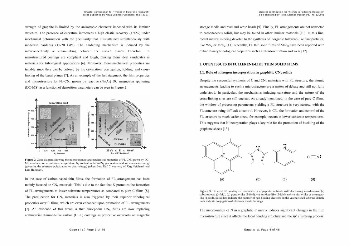
linking of the basal planes [7]. As an example of the last statement, the film properties
and microstructure for FL-CNx grown by reactive (N2/Ar) DC magnetron sputtering
(DC-MS) as a function of deposition parameters can be seen in Figure 2.
Figure 2. Zone diagram showing the microstructure and mechanical properties of FL-CNx grown by DC-MS as a function of substrate temperature, N2 content in the Ar/N2 gas mixture and ion assistance energy (given by the substrate polarization or bias voltage) (taken from Ref. 7, courtesy of Jörg Neidhardt and Lars Hultman).
In the case of carbon-based thin films, the formation of FL arrangement has been
mainly focused on CNx materials. This is due to the fact that N promotes the formation
of FL arrangements at lower substrate temperatures as compared to pure C films [8].
The predilection for CNx materials is also triggered by their superior tribological
properties over C films, which are even enhanced upon promotion of FL arrangements
[7]. An evidence of this trend is that amorphous CNx films are now replacing
commercial diamond-like carbon (DLC) coatings as protective overcoats on magnetic
Chapter contribution for “Trends in Fullerene Research” To be published by Nova Science Publishers, Inc. (2007)
Gago et al. Page 4 of 46
storage media and read and write heads [9]. Finally, FL arrangements are not restricted
to carbonaceous solids, but may be found in other laminar materials [10]. In this line,
recent interest is being devoted to the synthesis of inorganic fullerene-like nanoparticles,
like WS2 or MoS2 [11]. Recently, FL thin solid films of MoS2 have been reported with
extraordinary tribological properties such as ultra-low friction and wear [12].
2. OPEN ISSUES IN FULLERENE-LIKE THIN SOLID FILMS
2.1. Role of nitrogen incorporation in graphitic CNx solids
Despite the successful synthesis of C and CNx materials with FL structure, the atomic
arrangements leading to such a microstructure are a matter of debate and still not fully
understood. In particular, the mechanisms inducing curvature and the nature of the
cross-linking sites are still unclear. As already mentioned, in the case of pure C films,
the window of processing parameters yielding a FL structure is very narrow, with the
FL structure being difficult to control. However, in CNx the formation and control of the
FL structure is much easier since, for example, occurs at lower substrate temperatures.
This suggests that N incorporation plays a key role for the promotion of buckling of the
graphene sheets [13].
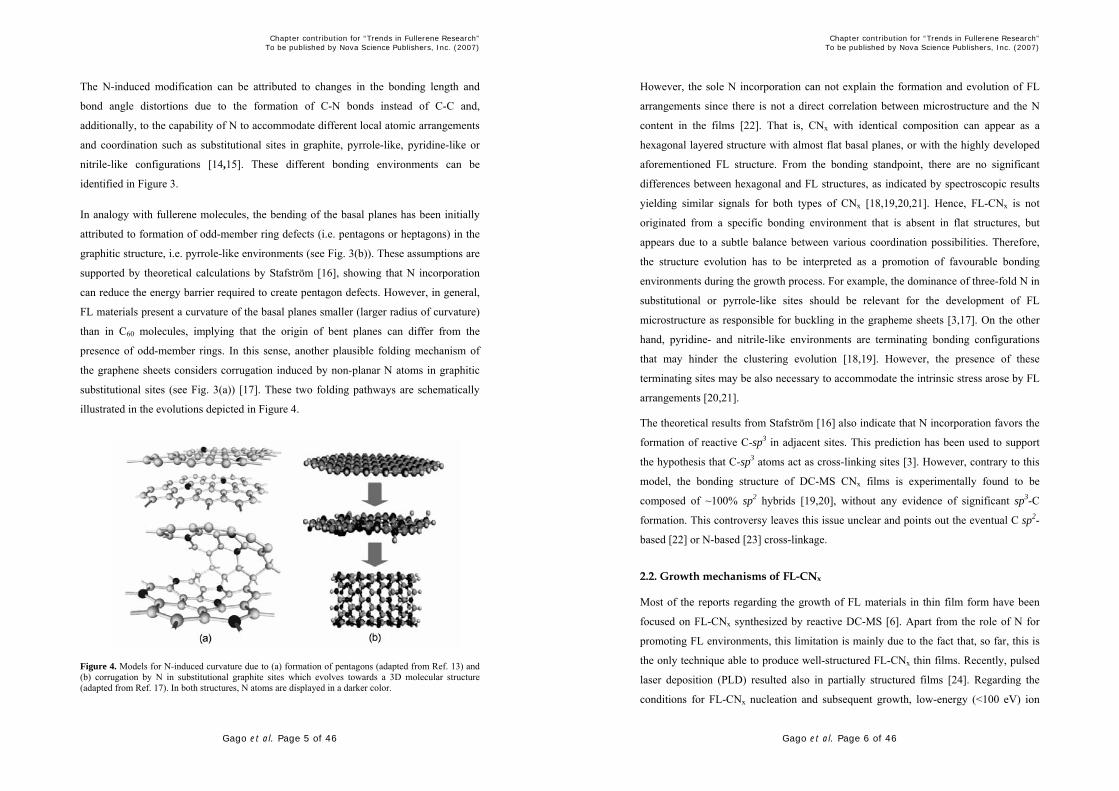
Figure 3. Different N bonding environments in a graphitic network with decreasing coordination: (a) substitutional (3-fold), (b) pyrrole-like (3-fold), (c) pyridine-like (2-fold) and (c) nitrile-like or cyanogen-like (1-fold). Solid dots indicate the number of non-binding electrons in the valence shell whereas double lines indicate conjugation of electrons inside the rings.
The incorporation of N in a graphitic C matrix induces significant changes in the film
microstructure since it affects the local bonding structure and the sp2 clustering process.
N
(a) (b) (c) (d)
N
N
N C
Chapter contribution for “Trends in Fullerene Research” To be published by Nova Science Publishers, Inc. (2007)
Gago et al. Page 5 of 46
The N-induced modification can be attributed to changes in the bonding length and
bond angle distortions due to the formation of C-N bonds instead of C-C and,
additionally, to the capability of N to accommodate different local atomic arrangements
and coordination such as substitutional sites in graphite, pyrrole-like, pyridine-like or
nitrile-like configurations [14,15]. These different bonding environments can be
identified in Figure 3.
In analogy with fullerene molecules, the bending of the basal planes has been initially
attributed to formation of odd-member ring defects (i.e. pentagons or heptagons) in the
graphitic structure, i.e. pyrrole-like environments (see Fig. 3(b)). These assumptions are
supported by theoretical calculations by Stafström [16], showing that N incorporation
can reduce the energy barrier required to create pentagon defects. However, in general,
FL materials present a curvature of the basal planes smaller (larger radius of curvature)
than in C60 molecules, implying that the origin of bent planes can differ from the
presence of odd-member rings. In this sense, another plausible folding mechanism of
the graphene sheets considers corrugation induced by non-planar N atoms in graphitic
substitutional sites (see Fig. 3(a)) [17]. These two folding pathways are schematically
illustrated in the evolutions depicted in Figure 4.
Figure 4. Models for N-induced curvature due to (a) formation of pentagons (adapted from Ref. 13) and (b) corrugation by N in substitutional graphite sites which evolves towards a 3D molecular structure (adapted from Ref. 17). In both structures, N atoms are displayed in a darker color.
Chapter contribution for “Trends in Fullerene Research” To be published by Nova Science Publishers, Inc. (2007)
Gago et al. Page 6 of 46
However, the sole N incorporation can not explain the formation and evolution of FL
arrangements since there is not a direct correlation between microstructure and the N
content in the films [22]. That is, CNx with identical composition can appear as a
hexagonal layered structure with almost flat basal planes, or with the highly developed
aforementioned FL structure. From the bonding standpoint, there are no significant
differences between hexagonal and FL structures, as indicated by spectroscopic results
yielding similar signals for both types of CNx [18,19,20,21]. Hence, FL-CNx is not
originated from a specific bonding environment that is absent in flat structures, but
appears due to a subtle balance between various coordination possibilities. Therefore,
the structure evolution has to be interpreted as a promotion of favourable bonding
environments during the growth process. For example, the dominance of three-fold N in
substitutional or pyrrole-like sites should be relevant for the development of FL
microstructure as responsible for buckling in the grapheme sheets [3,17]. On the other
hand, pyridine- and nitrile-like environments are terminating bonding configurations
that may hinder the clustering evolution [18,19]. However, the presence of these
terminating sites may be also necessary to accommodate the intrinsic stress arose by FL
arrangements [20,21].
The theoretical results from Stafström [16] also indicate that N incorporation favors the
formation of reactive C-sp3 in adjacent sites. This prediction has been used to support
the hypothesis that C-sp3 atoms act as cross-linking sites [3]. However, contrary to this
model, the bonding structure of DC-MS CNx films is experimentally found to be
composed of ~100% sp2 hybrids [19,20], without any evidence of significant sp3-C
formation. This controversy leaves this issue unclear and points out the eventual C sp2-
based [22] or N-based [23] cross-linkage.
2.2. Growth mechanisms of FL-CNx
Most of the reports regarding the growth of FL materials in thin film form have been
focused on FL-CNx synthesized by reactive DC-MS [6]. Apart from the role of N for
promoting FL environments, this limitation is mainly due to the fact that, so far, this is
the only technique able to produce well-structured FL-CNx thin films. Recently, pulsed
laser deposition (PLD) resulted also in partially structured films [24]. Regarding the
conditions for FL-CNx nucleation and subsequent growth, low-energy (<100 eV) ion
Chapter contribution for “Trends in Fullerene Research” To be published by Nova Science Publishers, Inc. (2007)
Gago et al. Page 7 of 46
bombardment and moderate substrate temperatures (400-800 K) have been shown to be
essential requisites [13,25]. These growth conditions may be necessary to increase the
surface mobility and reactivity but also to enable selective etching of less-favorable
bonding environments without detrimental ion-induced damage (amorphization) for the
evolution of the microstructure.
In the growth of CNx films (not limited to the case of FL-CNx), a relevant factor is the
presence of “chemical sputtering” [26,27,28]. This process implies the formation of
volatile species at the substrate surface that results in a lower effective growth rate than
the corresponding to the flux of incoming precursor species. This process is thermally
activated and, therefore, it is promoted at high growth temperature [29]. Under such
circumstance, no effective growth rate may be even attained. As a general trend, in the
growth of CNx materials under energetic deposition techniques, the formation of CN
volatile species at the substrate is related to the limitation in the N content, which rarely
exceeds ~30 at. %. This chemical sputtering has also implications in the microstructure
evolution of CNx solids [30].
The limited number of thin film growth techniques capable of FL-CNx synthesis
suggests the there are special requirements related to the incorporation of C and N
precursors. The analysis of the emitted species from the sputtering target during the
growth of CNx films by MS indicates that, as occurs in the substrate surface, there is a
non-negligible formation of CxNy precursors due to the nitridation and chemical
sputtering of the target [31]. This finding has been used to launch the hypothesis that
pre-formed CxNy moieties from the sputtering target may have eventual relevance as
film-forming species. In this way, these precursors may imprint their structure on the
evolving microstructure. First-principle calculations have shown that the incorporation
of CN dimers and cyanogen molecules promote an initial stabilization of pentagon
defects needed to induce FL arrangements [32].
In conclusion, the growth of FL-CNx has to be understood as an interplay between
incoming hyperthermal atomic and polyatomic species, low-energy ion bombardment
and desorption of volatile species due to the chemical sputtering. Here, physical
sputtering does not to play a significant role due to the low energies (<100eV) required
to preclude amorphization. The relative relevance of the mechanisms involved and their
Chapter contribution for “Trends in Fullerene Research” To be published by Nova Science Publishers, Inc. (2007)
Gago et al. Page 8 of 46
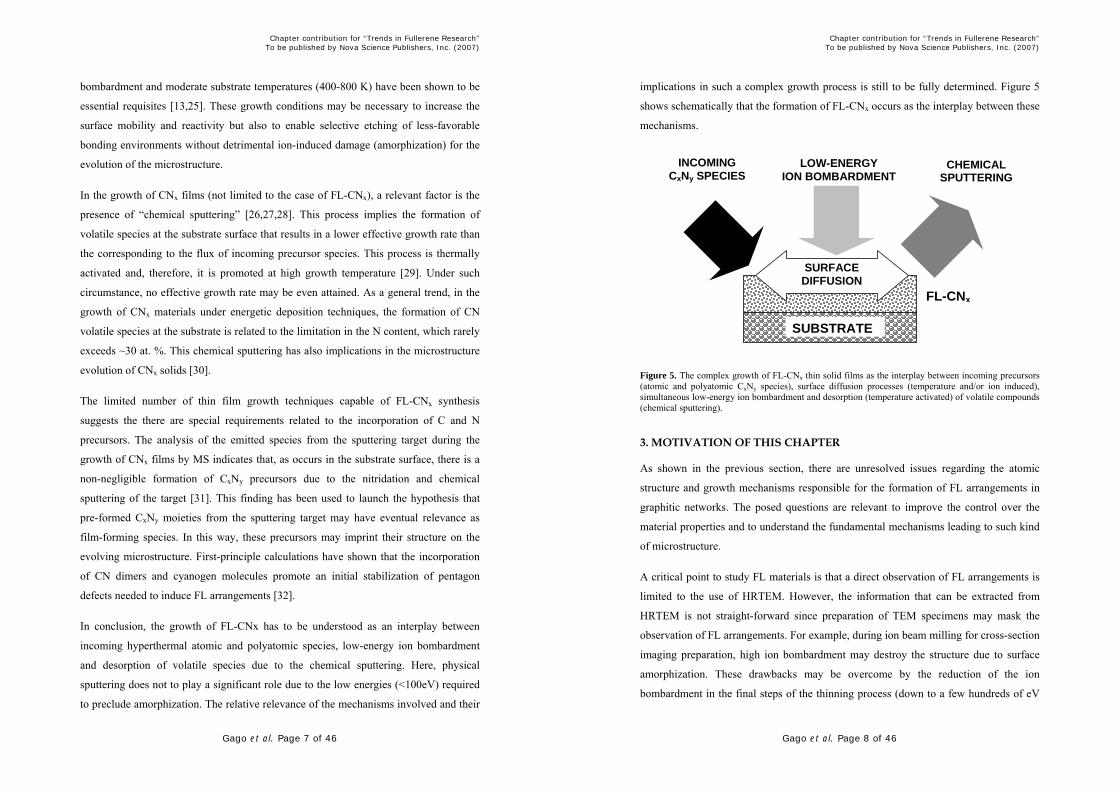
implications in such a complex growth process is still to be fully determined. Figure 5
shows schematically that the formation of FL-CNx occurs as the interplay between these
mechanisms.
Figure 5. The complex growth of FL-CNx thin solid films as the interplay between incoming precursors (atomic and polyatomic CxNy species), surface diffusion processes (temperature and/or ion induced), simultaneous low-energy ion bombardment and desorption (temperature activated) of volatile compounds (chemical sputtering).
3. MOTIVATION OF THIS CHAPTER
As shown in the previous section, there are unresolved issues regarding the atomic
structure and growth mechanisms responsible for the formation of FL arrangements in
graphitic networks. The posed questions are relevant to improve the control over the
material properties and to understand the fundamental mechanisms leading to such kind
of microstructure.
A critical point to study FL materials is that a direct observation of FL arrangements is
limited to the use of HRTEM. However, the information that can be extracted from
HRTEM is not straight-forward since preparation of TEM specimens may mask the
observation of FL arrangements. For example, during ion beam milling for cross-section
imaging preparation, high ion bombardment may destroy the structure due to surface
amorphization. These drawbacks may be overcome by the reduction of the ion
bombardment in the final steps of the thinning process (down to a few hundreds of eV
INCOMING CxNy SPECIES
CHEMICAL SPUTTERING
LOW-ENERGY ION BOMBARDMENT
SUBSTRATE
FL-CNx
SURFACE DIFFUSION
Chapter contribution for “Trends in Fullerene Research” To be published by Nova Science Publishers, Inc. (2007)
Gago et al. Page 9 of 46
instead of several keV) or by studying plan-view specimens when deposition on soluble
substrates is possible [33]. Another problem in HRTEM analysis comes from projection
artifacts, which may preclude the resolution of structural features. This can be partially
solved by considering selective area electron diffraction (SAED), since any overlapping
does not affect the characteristic lattice spacing in the diffraction pattern and
information on the degree of ordering can be derived from the brightness and width of
the diffraction pattern [34]. Finally, an additional drawback of TEM measurements for
studying thin solid films is the destructive character entailed.
Further identification of FL arrangements with additional characterisation tools is
desirable, especially if they are not destructive for the sample. This issue has been
addressed by spectroscopic methods such as nuclear magnetic resonance (NMR)
[19,20,35], x-ray photoemission spectroscopy (XPS) [34], electron energy loss
spectroscopy [36] and x-ray absorption near-edge spectroscopy (XANES) [18,21,37] by
correlation of microstructural features and the promotion of certain local bonding
environments. Among them, NMR and XANES have been proved to be the most
powerful ones in detecting and resolving the various bonding environments present in
CNx solids. NMR has shown clearly that graphitic CNx contain multiple bonding
environments upon N incorporation, including different types of pyridine-like
coordination, nitriles, pyrroles and other organic functionalities [19,20]. The main
drawback of NMR is that it requires detaching and powderizing (i.e., destructive
character) the coating until reaching a relatively large amount of material (a few mg).
XANES, instead, can be performed on a single coating without any sample preparation.
In this chapter, section 4 presents a detail XANES study of the bonding structure of FL-
CNx. In particular, we have studied CNx films grown by DC-MS with varying degree of
FL character (in terms of plane alignment, extension and cross-linking) by tuning the
proper growth parameters. The contribution of the different bonding environments has
been correlated with the formation and promotion of FL arrangements. In this way, we
can get further insight in the mechanisms for buckling of graphene-sheets or cross-
linking sites upon N incorporation.
Regarding the growth mechanism, the relative contribution of the different bonding
configurations and how they assemble will define the final film microstructure and,
Chapter contribution for “Trends in Fullerene Research” To be published by Nova Science Publishers, Inc. (2007)
Gago et al. Page 10 of 46
hence, the material properties. This issue depends strongly on the way that N is
introduced into the C network, i.e. on the CNx synthesis process. Therefore, the
comparison of the different bonding structures for films grown under different
conditions can shed some light on the mechanisms leading to the different
microstructures. In section 5 of this chapter, we present a comparative study with
different CNx growth methods that partially mimic the conditions attained during MS,
mainly in the frame of film precursors and ion assistance during growth. In this way, we
aim at discerning the mechanisms operating during the evolution of FL arrangements.
The identification of spectral signatures related with the formation and promotion of FL
arrangements described in section 4 will be very useful for the conclusions of this study.
4. BONDING STRUCTURE OF FL-CNx BY XANES
4.1. Fundamentals of the XANES technique
X-ray absorption (XAS) features near the adsorption edge, normally referred as XANES
or NEXAFS (near-edge x-ray absorption fine structure) spectroscopy, provide
information about the K-shell structure with elemental sensitivity and, hence, is very
sensitive to local bonding arrangements [38]. XANES detects the transitions from core-
electrons to the conduction band of the solid, providing an image of the density of
unoccupied states. Therefore, XANES provides a similar information to EELS or
ELNES (energy loss near-edge spectroscopy), although at present the energy resolution
of XAS studies is typically in the range of 10 to 100 meV, i.e. ten times better than in
the electron energy loss experiments.
The XANES experiments discussed here were performed in the total electron yield
(TEY) mode, consisting in the measurement of the photocurrent produced when the
sample surface is illuminated with monochromatic x-ray light from a synchrotron ring.
The spectrum is acquired by sweeping the photon energy in the desirable range and
measuring the TEY signal. The XANES-TEY spectrum can be considered as the plot of
the absorbance as a function of energy with good approximation. These experiments
were performed in the SuperACO-LURE (Orsay, France), SSRL (Stanford, CA, USA)
and BESSY-II (Berlin, Germany) synchrotron facilities.
Chapter contribution for “Trends in Fullerene Research” To be published by Nova Science Publishers, Inc. (2007)
Gago et al. Page 11 of 46
4.2. XANES of carbonaceous materials
XANES is very suitable to study carbon-based materials due to the distinct features
obtained for sp2 and sp3 hybrids. For this reason, it is one of the most extended methods
for quantification of the sp2/sp3 ratio in carbonaceous materials. In the case of CNx
solids, the relative contribution of the different hybridizations can be established
independently for C and N atoms, allowing the identification of the different C-C and
C-N bonding environments.
284 288 292 296 300 304
σ* states
π* states CNx
diamond
graphite
C60
C1s
XA
NE
S in
tens
ity (a
rb. u
nits
)
Photon Energy (eV)
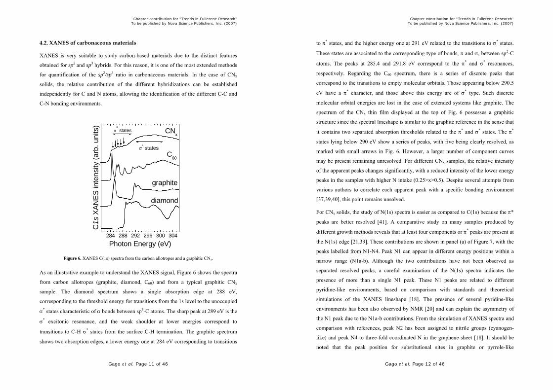
Figure 6. XANES C(1s) spectra from the carbon allotropes and a graphitic CNx.
As an illustrative example to understand the XANES signal, Figure 6 shows the spectra
from carbon allotropes (graphite, diamond, C60) and from a typical graphitic CNx
sample. The diamond spectrum shows a single absorption edge at 288 eV,
corresponding to the threshold energy for transitions from the 1s level to the unoccupied
σ* states characteristic of σ bonds between sp3-C atoms. The sharp peak at 289 eV is the
σ* excitonic resonance, and the weak shoulder at lower energies correspond to
transitions to C-H σ* states from the surface C-H termination. The graphite spectrum
shows two absorption edges, a lower energy one at 284 eV corresponding to transitions
Chapter contribution for “Trends in Fullerene Research” To be published by Nova Science Publishers, Inc. (2007)
Gago et al. Page 12 of 46
to π* states, and the higher energy one at 291 eV related to the transitions to σ* states.
These states are associated to the corresponding type of bonds, π and σ, between sp2-C
atoms. The peaks at 285.4 and 291.8 eV correspond to the π* and σ* resonances,
respectively. Regarding the C60 spectrum, there is a series of discrete peaks that
correspond to the transitions to empty molecular orbitals. Those appearing below 290.5
eV have a π* character, and those above this energy are of σ* type. Such discrete
molecular orbital energies are lost in the case of extended systems like graphite. The
spectrum of the CNx thin film displayed at the top of Fig. 6 possesses a graphitic
structure since the spectral lineshape is similar to the graphite reference in the sense that
it contains two separated absorption thresholds related to the π* and σ* states. The π*
states lying below 290 eV show a series of peaks, with five being clearly resolved, as
marked with small arrows in Fig. 6. However, a larger number of component curves
may be present remaining unresolved. For different CNx samples, the relative intensity
of the apparent peaks changes significantly, with a reduced intensity of the lower energy
peaks in the samples with higher N intake (0.25>x>0.5). Despite several attempts from
various authors to correlate each apparent peak with a specific bonding environment
[37,39,40], this point remains unsolved.
For CNx solids, the study of N(1s) spectra is easier as compared to C(1s) because the π*
peaks are better resolved [41]. A comparative study on many samples produced by
different growth methods reveals that at least four components or π* peaks are present at
the N(1s) edge [21,39]. These contributions are shown in panel (a) of Figure 7, with the
peaks labelled from N1-N4. Peak N1 can appear in different energy positions within a
narrow range (N1a-b). Although the two contributions have not been observed as
separated resolved peaks, a careful examination of the N(1s) spectra indicates the
presence of more than a single N1 peak. These N1 peaks are related to different
pyridine-like environments, based on comparison with standards and theoretical
simulations of the XANES lineshape [18]. The presence of several pyridine-like
environments has been also observed by NMR [20] and can explain the asymmetry of
the N1 peak due to the N1a-b contributions. From the simulation of XANES spectra and
comparison with references, peak N2 has been assigned to nitrile groups (cyanogen-
like) and peak N4 to three-fold coordinated N in the graphene sheet [18]. It should be
noted that the peak position for substitutional sites in graphite or pyrrole-like
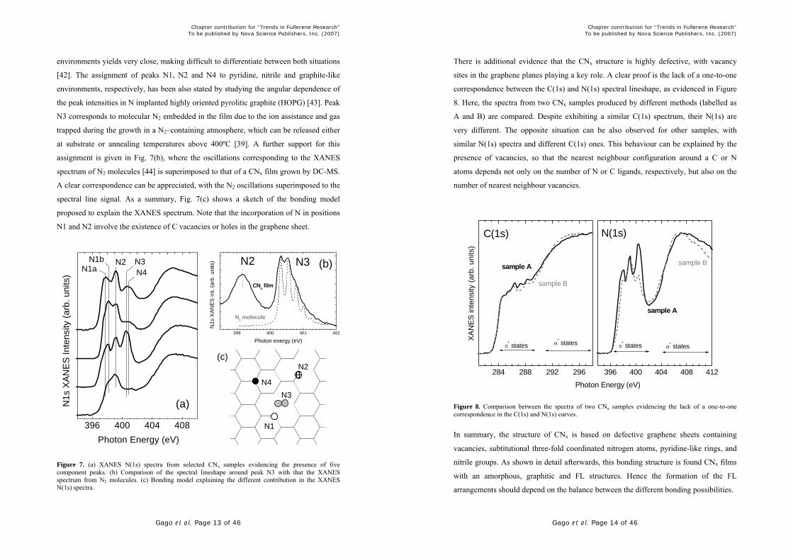
Chapter contribution for “Trends in Fullerene Research” To be published by Nova Science Publishers, Inc. (2007)
Gago et al. Page 13 of 46
environments yields very close, making difficult to differentiate between both situations
[42]. The assignment of peaks N1, N2 and N4 to pyridine, nitrile and graphite-like
environments, respectively, has been also stated by studying the angular dependence of
the peak intensities in N implanted highly oriented pyrolitic graphite (HOPG) [43]. Peak
N3 corresponds to molecular N2 embedded in the film due to the ion assistance and gas
trapped during the growth in a N2–containing atmosphere, which can be released either
at substrate or annealing temperatures above 400ºC [39]. A further support for this
assignment is given in Fig. 7(b), where the oscillations corresponding to the XANES
spectrum of N2 molecules [44] is superimposed to that of a CNx film grown by DC-MS.
A clear correspondence can be appreciated, with the N2 oscillations superimposed to the
spectral line signal. As a summary, Fig. 7(c) shows a sketch of the bonding model
proposed to explain the XANES spectrum. Note that the incorporation of N in positions
N1 and N2 involve the existence of C vacancies or holes in the graphene sheet.
Figure 7. (a) XANES N(1s) spectra from selected CNx samples evidencing the presence of five component peaks. (b) Comparison of the spectral lineshape around peak N3 with that the XANES spectrum from N2 molecules. (c) Bonding model explaining the different contribution in the XANES N(1s) spectra.
N4
N2
N3
N1
(c)
399 400 401 402
N3
Photon energy (eV)
CNx film
N2 molecule
N1s
XA
NES
int.
(arb
. uni
ts)
N2 (b)
396 400 404 408 Photon Energy (eV)
(a)
N1s
XA
NE
S In
tens
ity (a
rb. u
nits
)
N4N3N2N1b
N1a
Chapter contribution for “Trends in Fullerene Research” To be published by Nova Science Publishers, Inc. (2007)
Gago et al. Page 14 of 46
There is additional evidence that the CNx structure is highly defective, with vacancy
sites in the graphene planes playing a key role. A clear proof is the lack of a one-to-one
correspondence between the C(1s) and N(1s) spectral lineshape, as evidenced in Figure
8. Here, the spectra from two CNx samples produced by different methods (labelled as
A and B) are compared. Despite exhibiting a similar C(1s) spectrum, their N(1s) are
very different. The opposite situation can be also observed for other samples, with
similar N(1s) spectra and different C(1s) ones. This behaviour can be explained by the
presence of vacancies, so that the nearest neighbour configuration around a C or N
atoms depends not only on the number of N or C ligands, respectively, but also on the
number of nearest neighbour vacancies.
284 288 292 296 396 400 404 408 412
sample B
sample A
sample A
σ* statesσ* states π* statesπ* states
C(1s)
XA
NES
inte
nsity
(arb
. uni
ts)
Photon Energy (eV)
sample B
N(1s)
Figure 8. Comparison between the spectra of two CNx samples evidencing the lack of a one-to-one correspondence in the C(1s) and N(1s) curves.
In summary, the structure of CNx is based on defective graphene sheets containing
vacancies, subtitutional three-fold coordinated nitrogen atoms, pyridine-like rings, and
nitrile groups. As shown in detail afterwards, this bonding structure is found CNx films
with an amorphous, graphitic and FL structures. Hence the formation of the FL
arrangements should depend on the balance between the different bonding possibilities.
Chapter contribution for “Trends in Fullerene Research” To be published by Nova Science Publishers, Inc. (2007)
Gago et al. Page 15 of 46
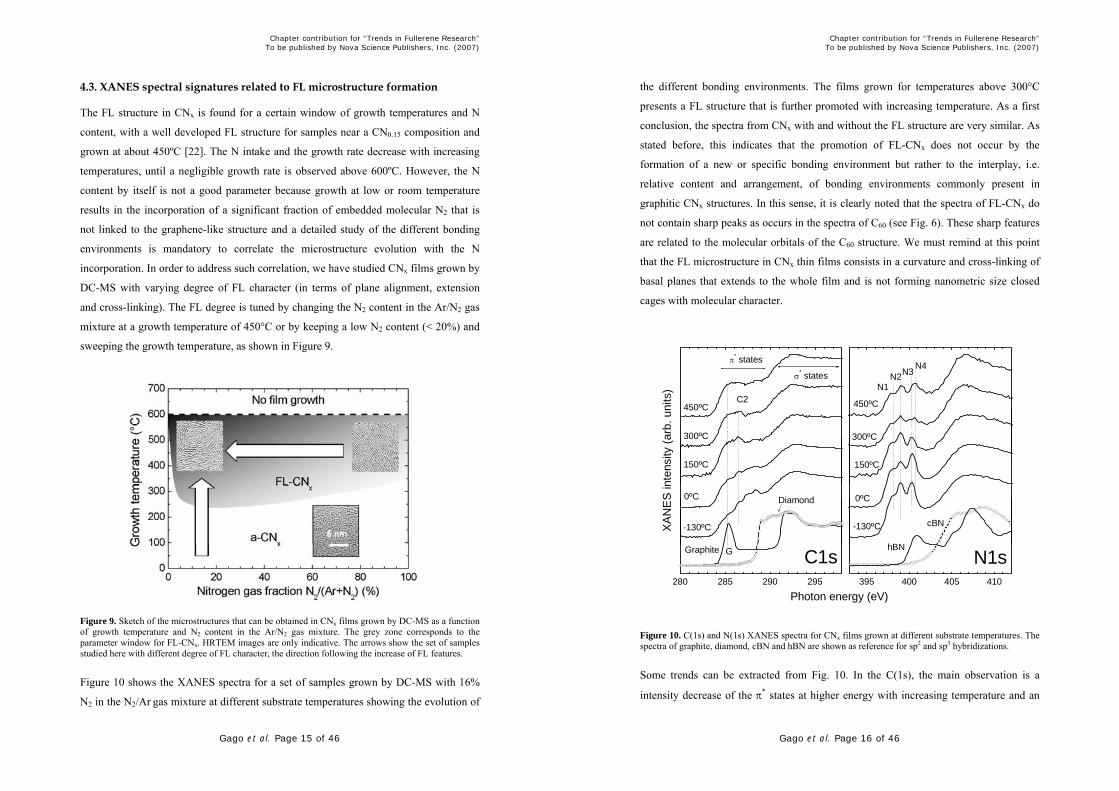
4.3. XANES spectral signatures related to FL microstructure formation
The FL structure in CNx is found for a certain window of growth temperatures and N
content, with a well developed FL structure for samples near a CN0.15 composition and
grown at about 450ºC [22]. The N intake and the growth rate decrease with increasing
temperatures, until a negligible growth rate is observed above 600ºC. However, the N
content by itself is not a good parameter because growth at low or room temperature
results in the incorporation of a significant fraction of embedded molecular N2 that is
not linked to the graphene-like structure and a detailed study of the different bonding
environments is mandatory to correlate the microstructure evolution with the N
incorporation. In order to address such correlation, we have studied CNx films grown by
DC-MS with varying degree of FL character (in terms of plane alignment, extension
and cross-linking). The FL degree is tuned by changing the N2 content in the Ar/N2 gas
mixture at a growth temperature of 450°C or by keeping a low N2 content (< 20%) and
sweeping the growth temperature, as shown in Figure 9.
Figure 9. Sketch of the microstructures that can be obtained in CNx films grown by DC-MS as a function of growth temperature and N2 content in the Ar/N2 gas mixture. The grey zone corresponds to the parameter window for FL-CNx. HRTEM images are only indicative. The arrows show the set of samples studied here with different degree of FL character, the direction following the increase of FL features.
Figure 10 shows the XANES spectra for a set of samples grown by DC-MS with 16%
N2 in the N2/Ar gas mixture at different substrate temperatures showing the evolution of
Chapter contribution for “Trends in Fullerene Research” To be published by Nova Science Publishers, Inc. (2007)
Gago et al. Page 16 of 46
the different bonding environments. The films grown for temperatures above 300°C
presents a FL structure that is further promoted with increasing temperature. As a first
conclusion, the spectra from CNx with and without the FL structure are very similar. As
stated before, this indicates that the promotion of FL-CNx does not occur by the
formation of a new or specific bonding environment but rather to the interplay, i.e.
relative content and arrangement, of bonding environments commonly present in
graphitic CNx structures. In this sense, it is clearly noted that the spectra of FL-CNx do
not contain sharp peaks as occurs in the spectra of C60 (see Fig. 6). These sharp features
are related to the molecular orbitals of the C60 structure. We must remind at this point
that the FL microstructure in CNx thin films consists in a curvature and cross-linking of
basal planes that extends to the whole film and is not forming nanometric size closed
cages with molecular character.
280 285 290 295 395 400 405 410
σ* states
G
π* states
450ºC
450ºC
N4
N1
300ºC
300ºC
150ºC
XA
NE
S in
tens
ity (a
rb. u
nits
)
150ºC
0ºC
0ºC
C2
-130ºC
-130ºC
N2N3
C1s
Diamond
Graphite
Photon energy (eV)
N1s
cBN
hBN
Figure 10. C(1s) and N(1s) XANES spectra for CNx films grown at different substrate temperatures. The spectra of graphite, diamond, cBN and hBN are shown as reference for sp2 and sp3 hybridizations.
Some trends can be extracted from Fig. 10. In the C(1s), the main observation is a
intensity decrease of the π* states at higher energy with increasing temperature and an
Chapter contribution for “Trends in Fullerene Research” To be published by Nova Science Publishers, Inc. (2007)
Gago et al. Page 17 of 46
increase at lower energies (near the graphite reference peak G). At the N(1s) panel,
there is a decrease of the N3 peak corresponding to molecular N2 for temperatures up to
300ºC, with the subsequent appearance of the N4 peak for higher temperatures. Also,
there is a decrease of the overall density of π* states in the N(1s) spectra, which is a
general trend found in the FL-CNx. The latter is made more evident from the spectra
shown in Figure 11 corresponding to samples with a similar N content with FL (FL-
CNx) and planar (g-CNx) arrangements. The density of π* states in the C(1s) spectra,
computed as the area below the spectra between 282-289 eV normalized to the σ* states
area between 292-299 eV, is almost the same in the two samples. However, the density
of π* states at the N(1s) edge, computed as the area between 396-402 eV normalized to
the σ* states area between 405-411 eV, is almost the half for FL-CNx as compared to
planar graphitic structures (g-CNx).
284 288 292 296 396 400 404 408 412
g-CNx
σ* statesσ* states π* statesπ* states
C(1s)
XA
NE
S in
tens
ity (a
rb. u
nits
)
Photon Energy (eV)
FL-CNx
g-CNx
FL-CNx
N(1s)
Figure 11. XANES spectra from a CNx films with FL and graphitic (planar) structures. There is a clear decrease of the intensity of N(1s) π* states in the FL case.
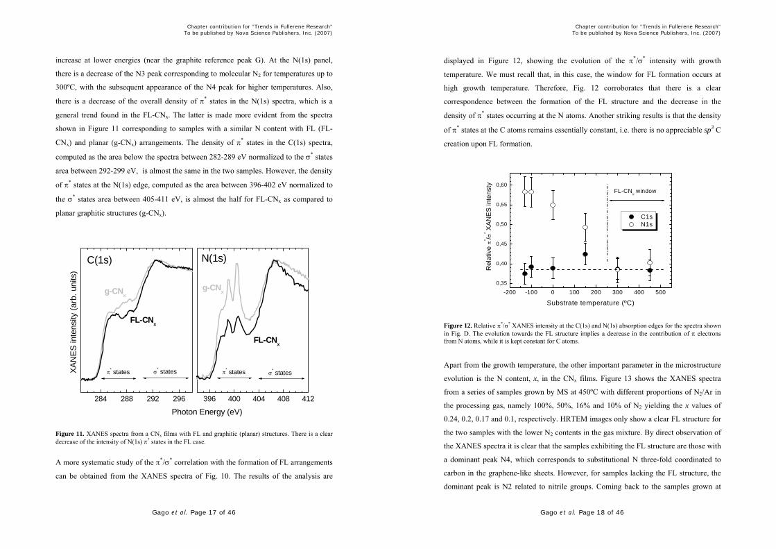
A more systematic study of the π*/σ* correlation with the formation of FL arrangements
can be obtained from the XANES spectra of Fig. 10. The results of the analysis are
Chapter contribution for “Trends in Fullerene Research” To be published by Nova Science Publishers, Inc. (2007)
Gago et al. Page 18 of 46
displayed in Figure 12, showing the evolution of the π*/σ* intensity with growth
temperature. We must recall that, in this case, the window for FL formation occurs at
high growth temperature. Therefore, Fig. 12 corroborates that there is a clear
correspondence between the formation of the FL structure and the decrease in the
density of π* states occurring at the N atoms. Another striking results is that the density
of π* states at the C atoms remains essentially constant, i.e. there is no appreciable sp3 C
creation upon FL formation.
-200 -100 0 100 200 300 400 5000,35
0,40
0,45
0,50
0,55
0,60FL-CNx window
C1s N1s
Rel
ativ
e π* /σ
* XA
NE
S in
tens
ty
Substrate temperature (ºC)
Figure 12. Relative π*/σ* XANES intensity at the C(1s) and N(1s) absorption edges for the spectra shown in Fig. D. The evolution towards the FL structure implies a decrease in the contribution of π electrons from N atoms, while it is kept constant for C atoms.
Apart from the growth temperature, the other important parameter in the microstructure
evolution is the N content, x, in the CNx films. Figure 13 shows the XANES spectra
from a series of samples grown by MS at 450ºC with different proportions of N2/Ar in
the processing gas, namely 100%, 50%, 16% and 10% of N2 yielding the x values of
0.24, 0.2, 0.17 and 0.1, respectively. HRTEM images only show a clear FL structure for
the two samples with the lower N2 contents in the gas mixture. By direct observation of
the XANES spectra it is clear that the samples exhibiting the FL structure are those with
a dominant peak N4, which corresponds to substitutional N three-fold coordinated to
carbon in the graphene-like sheets. However, for samples lacking the FL structure, the
dominant peak is N2 related to nitrile groups. Coming back to the samples grown at
Chapter contribution for “Trends in Fullerene Research” To be published by Nova Science Publishers, Inc. (2007)
Gago et al. Page 19 of 46
different temperatures shown in Fig. 10, the same observation can be made: the sample
with dominant FL structure (i.e. the one grown at 450ºC) has a dominance of peak N4 in
the N(1s) spectrum.
280 285 290 295 300 395 400 405 410 415
x =
0.10
N2
N1
N4
0.17
XA
NE
S in
tens
ity (a
rb. u
nits
)
0.20
C(1s)π* states
σ* states
0.24
σ* states
N(1s)π* states
Photon energy (eV)
Figure 13. C(1s) and N(1s) XANES spectra for CNx films grown with different Ar/N2 gas mixtures at a substrate temperature of 723 K, yielding the different nitrogen contents x indicated.
In summary, the two spectral features related to the FL structure are: (i) a dominant
peak N4 in the N(1s) XANES, and (ii) an overall decrease of the intensity of π* states.
Both observations support that the formation of the FL structure require a dominant
number of substitutional N atoms incorporated with three-fold coordination in the
graphene sheet.
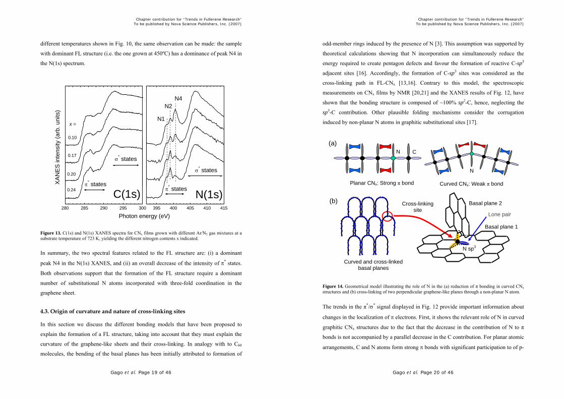
4.3. Origin of curvature and nature of cross-linking sites
In this section we discuss the different bonding models that have been proposed to
explain the formation of a FL structure, taking into account that they must explain the
curvature of the graphene-like sheets and their cross-linking. In analogy with to C60
molecules, the bending of the basal planes has been initially attributed to formation of
Chapter contribution for “Trends in Fullerene Research” To be published by Nova Science Publishers, Inc. (2007)
Gago et al. Page 20 of 46
odd-member rings induced by the presence of N [3]. This assumption was supported by
theoretical calculations showing that N incorporation can simultaneously reduce the
energy required to create pentagon defects and favour the formation of reactive C-sp3
adjacent sites [16]. Accordingly, the formation of C-sp3 sites was considered as the
cross-linking path in FL-CNx [13,16]. Contrary to this model, the spectroscopic
measurements on CNx films by NMR [20,21] and the XANES results of Fig. 12, have
shown that the bonding structure is composed of ~100% sp2-C, hence, neglecting the
sp3-C contribution. Other plausible folding mechanisms consider the corrugation
induced by non-planar N atoms in graphitic substitutional sites [17].
Figure 14. Geometrical model illustrating the role of N in the (a) reduction of π bonding in curved CNx structures and (b) cross-linking of two perpendicular graphene-like planes through a non-planar N atom.
The trends in the π*/σ* signal displayed in Fig. 12 provide important information about
changes in the localization of π electrons. First, it shows the relevant role of N in curved
graphitic CNx structures due to the fact that the decrease in the contribution of N to π
bonds is not accompanied by a parallel decrease in the C contribution. For planar atomic
arrangements, C and N atoms form strong π bonds with significant participation to of p-
(a)
Curved and cross-linked basal planes
N sp3
Basal plane 2
Lone pair
(b)
Basal plane 1
Cross-linking site
Planar CNx: Strong π bond Curved CNx: Weak π bond
C N
N

Chapter contribution for “Trends in Fullerene Research” To be published by Nova Science Publishers, Inc. (2007)
Gago et al. Page 21 of 46
electrons from the respective atoms. Therefore, the π electron cloud is delocalized over
extended areas including both C and N atoms. In the case of CNx corrugated or FL
arrangements, there is a disruption of the conjugation of the π electrons and the π
electron cloud is more localized in regions composed only of C atoms. This geometrical
configuration is illustrated in Figure 14(a), showing a reduced contribution of N atoms
to π bonding. The different localization of π electrons in planar and corrugated CNx
must also affect the elastic properties of the graphene sheets and, therefore, could
explain the outstanding mechanical properties of FL-CNx. Following the approach of
non equivalent sites for C and N in the graphitic network, it has also been proposed that
non-planar N atoms can additionally act as the cross-linking sites between adjacent
sheets [23]. A sketch of this geometrical situation is shown in Figure 14(b), with two
perpendicular planes being cross-linked through a non-planar N(-sp3) atom. Note that
the N atom is located adjacent to a C vacancy, which seems to be requisite for many of
the proposed models of curvature and cross-linking.
There is another model considering a mechanism for curvature that stems from the high
number of vacancies present in the graphene sheets upon N incorporation. Here, the
presence of holes in the structure permits the presence of pentagonal rings without the
need of a neighbour sp3-C atom. Following this argument, it has been proposed that
cross linking occurs at the dangling bond (two-fold coordinated) sites on the perimeter
of a vacancy, a situation especially favourable when the pentagon is placed next to a
single-atom vacancy because it will have a twofold coordinated vertex [20]. At present,
a clear identification of the folding mechanism and cross-linking of CNx planes remains
unclear.
5. ON THE MECHANISMS OF FL-CNx FORMATION
5.1 Comparison of different nitrogen incorporation routes
In this section, the microstructure of CNx films grown under different growth methods
that mimic partially the growth by MS is studied. Namely, ion beam sputtering (IBS),
dual ion beam deposition (DIBD), ion-beam assisted evaporation (IBAE) and
magnetron sputtering (MS). The principles of these methods, together with that of MS,
are illustrated in Figure 15.
Chapter contribution for “Trends in Fullerene Research” To be published by Nova Science Publishers, Inc. (2007)
Gago et al. Page 22 of 46
Figure 15. Different growth methods compared in this study in terms of ion bombardment (white arrows), C fluxes (black arrow) and polyatomic CxNy species (striped arrow): (a) MS, (b) IBAE, (c) IBS and (d) DIBD.
Each one of the methods presented (MS, IBAE, IBS and DIBD) implies different N
incorporation routes. In the case of IBAE, the sole source of C comes from the thermal
evaporation of graphite lumps with an electron evaporator whereas N is incorporated by
low-energy ion assistance (<100 eV) with a mixture of N2+ and N+ ions extracted from
an End-Hall grid-less ion gun [45]. In the case of sputtering from graphite targets by
N2/Ar ions of a few hundreds of eV (MS, IBS, DIBD), C and N atoms can be supplied
trough atomic and polyatomic CxNy species, the latter chemically or physically emitted
from the previously nitrided target [31]. The emitted particles via physical sputtering
have higher energies (in the hyperthermal range up to a few tens of eV) than in the case
of thermal evaporation (in the range of ~0.1 eV) [46,47]. The additional application of
Ar/N2 ion assistance in DIBD (~100 eV) and MS (25-40 eV) represents, together with
the incorporation of CxNy species, an additional source of N during the film growth. The
growth conditions obtained by DIBD are the most similar to MS with the advantage that
the weight of the different effects can be tuned. Finally, during sputtering of the target
reflected ions may also be produced with energies up the initial value of the projectile
(several hundreds of eV) [48]. The high energy of these ions could play a significant
role in the growth, however, their effect can be neglected according to calculations done
with the SRIM code [49].
N2/Arplasma
C target
(a) (b) (c) (d)
Ar-N2 ion beam LE Ar-N2
ion beam
C
C-evaporator C target
Substrate
Chapter contribution for “Trends in Fullerene Research” To be published by Nova Science Publishers, Inc. (2007)
Gago et al. Page 23 of 46
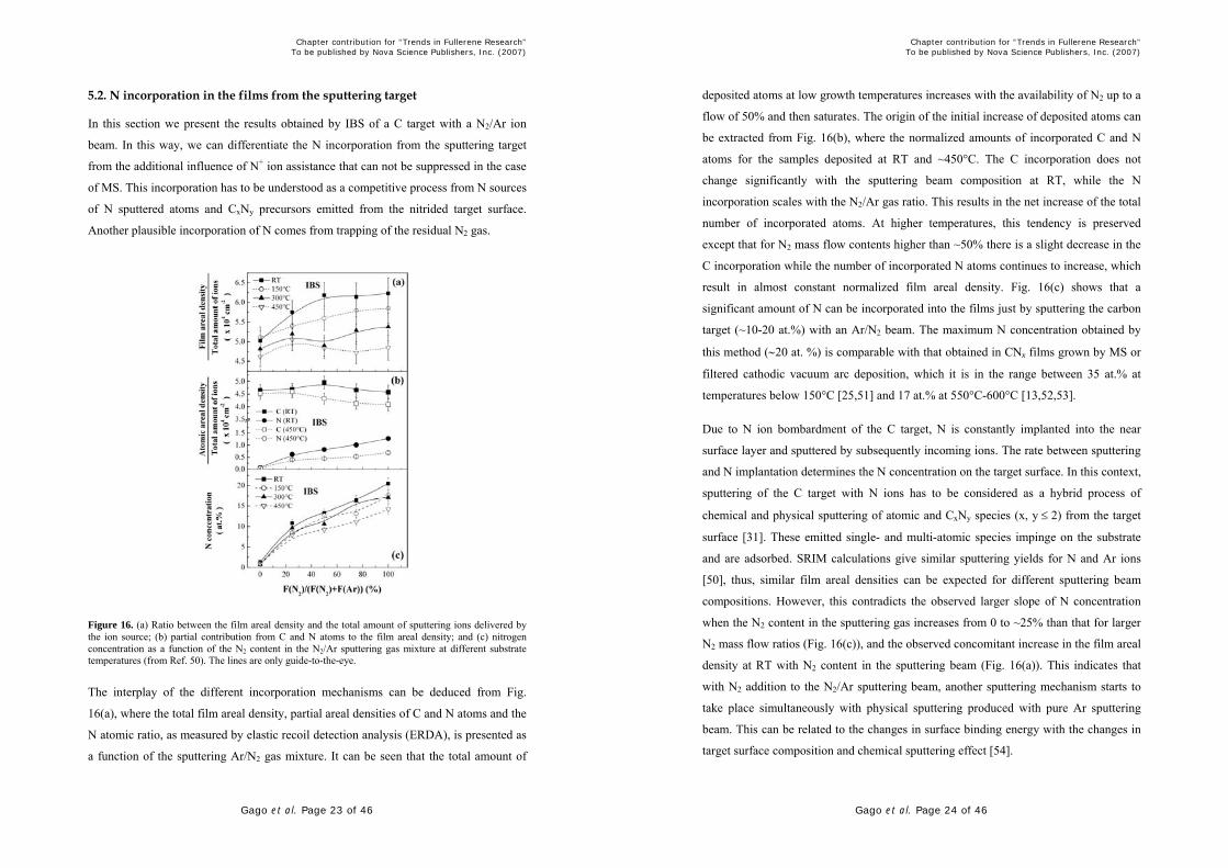
5.2. N incorporation in the films from the sputtering target
In this section we present the results obtained by IBS of a C target with a N2/Ar ion
beam. In this way, we can differentiate the N incorporation from the sputtering target
from the additional influence of N+ ion assistance that can not be suppressed in the case
of MS. This incorporation has to be understood as a competitive process from N sources
of N sputtered atoms and CxNy precursors emitted from the nitrided target surface.
Another plausible incorporation of N comes from trapping of the residual N2 gas.
Figure 16. (a) Ratio between the film areal density and the total amount of sputtering ions delivered by the ion source; (b) partial contribution from C and N atoms to the film areal density; and (c) nitrogen concentration as a function of the N2 content in the N2/Ar sputtering gas mixture at different substrate temperatures (from Ref. 50). The lines are only guide-to-the-eye.
The interplay of the different incorporation mechanisms can be deduced from Fig.
16(a), where the total film areal density, partial areal densities of C and N atoms and the
N atomic ratio, as measured by elastic recoil detection analysis (ERDA), is presented as
a function of the sputtering Ar/N2 gas mixture. It can be seen that the total amount of
Chapter contribution for “Trends in Fullerene Research” To be published by Nova Science Publishers, Inc. (2007)
Gago et al. Page 24 of 46
deposited atoms at low growth temperatures increases with the availability of N2 up to a
flow of 50% and then saturates. The origin of the initial increase of deposited atoms can
be extracted from Fig. 16(b), where the normalized amounts of incorporated C and N
atoms for the samples deposited at RT and ~450°C. The C incorporation does not
change significantly with the sputtering beam composition at RT, while the N
incorporation scales with the N2/Ar gas ratio. This results in the net increase of the total
number of incorporated atoms. At higher temperatures, this tendency is preserved
except that for N2 mass flow contents higher than ~50% there is a slight decrease in the
C incorporation while the number of incorporated N atoms continues to increase, which
result in almost constant normalized film areal density. Fig. 16(c) shows that a
significant amount of N can be incorporated into the films just by sputtering the carbon
target (~10-20 at.%) with an Ar/N2 beam. The maximum N concentration obtained by
this method (∼20 at. %) is comparable with that obtained in CNx films grown by MS or
filtered cathodic vacuum arc deposition, which it is in the range between 35 at.% at
temperatures below 150°C [25,51] and 17 at.% at 550°C-600°C [13,52,53].
Due to N ion bombardment of the C target, N is constantly implanted into the near
surface layer and sputtered by subsequently incoming ions. The rate between sputtering
and N implantation determines the N concentration on the target surface. In this context,
sputtering of the C target with N ions has to be considered as a hybrid process of
chemical and physical sputtering of atomic and CxNy species (x, y ≤ 2) from the target
surface [31]. These emitted single- and multi-atomic species impinge on the substrate
and are adsorbed. SRIM calculations give similar sputtering yields for N and Ar ions
[50], thus, similar film areal densities can be expected for different sputtering beam
compositions. However, this contradicts the observed larger slope of N concentration
when the N2 content in the sputtering gas increases from 0 to ~25% than that for larger
N2 mass flow ratios (Fig. 16(c)), and the observed concomitant increase in the film areal
density at RT with N2 content in the sputtering beam (Fig. 16(a)). This indicates that
with N2 addition to the N2/Ar sputtering beam, another sputtering mechanism starts to
take place simultaneously with physical sputtering produced with pure Ar sputtering
beam. This can be related to the changes in surface binding energy with the changes in
target surface composition and chemical sputtering effect [54].
Chapter contribution for “Trends in Fullerene Research” To be published by Nova Science Publishers, Inc. (2007)
Gago et al. Page 25 of 46
Due to the similar mass of C and N atoms, their physical sputtering yield will be close.
This implies that the N concentration in the film has to be proportional to the N
concentration in the target surface, which should be proportional to the composition of
the sputtering beam. Following this, if there was a saturation of the N concentration at
the target surface for certain beam composition, this would be reflected in the film
composition. On the other hand, if the preformed radicals were sputtered preferentially
in relation to atomic species, then the film composition would reflect not the target
composition but the mean composition of CxNy species. In this case the N concentration
in the film can saturate while the N content at the target surface will still increase with
increasing nitrogen content in the sputtering beam. However, no N saturation at
increasing N2 ratio in the sputtering beam is observed, contrary to the observations with
MS [29,55]. The saturation behavior in MS was interpreted as a result of preformed CNx
species coming from the graphite target which are the main source of incorporated
nitrogen while nitrogen from the reactive plasma does not serve as a direct nitrogen
source [29,55]. This should also apply to the present experiment where the main N
source is the graphite target being irradiated with Ar/N2 ions. However, the observed
concomitant increase in N concentration with the N2 ratio in the sputtering beam implies
that a significant amount of film forming species constitutes of physically sputtered
atomic species. The main difference between MS and IBS is that for the latter technique
there is no plasma assisting the film growth. Therefore, the saturation of the N
concentration during MS has to be related to the N transfer due to surface-plasma
interaction and with some dynamic equilibrium between N gain and N loss and not with
the preformed species.
The main mechanisms responsible for the material loss from the growing film can be
classified in the following way: 1) temperature reduced incorporation of the volatile
molecular species originating from the residual gas or the target; 2) the temperature
induced/enhanced formation and desorption of volatile molecules (mainly, CxNy and N2)
on the surface and in the subsurface layers of the growing film. Both mechanisms can
be expected to act simultaneously. The presence of hydrogen found in the films [50]
indicates about the adsorption of molecular species and their trapping due to incoming
particles, because hydrogen is present mainly in the form of hydrocarbons and water.
The H content decreases concomitantly with temperature which indicates about reduced
Chapter contribution for “Trends in Fullerene Research” To be published by Nova Science Publishers, Inc. (2007)
Gago et al. Page 26 of 46
adsorption of such molecular species on the surface of the growing film. This concerns
also the N2 molecules originating from residual gas or volatile CxNy compounds
originating from the target surface. This correlates well with the results presented in Fig.
14, where the considerable decrease in C areal density is followed by the decrease in N
areal density when the temperature increases from RT to 450°C (see Fig. 14(b)).
However, it also correlates with the nitrogen induced chemical sputtering by forming
volatile compounds with C, mainly C2N2. Their formation rate will depend on the N
availability on the surface and subsurface layers and will result in higher sputtering rate
for higher N concentrations on the surface of the growing film as it is in Fig. Fig. 14(b).
The surface reaction rate is proportional to the mobility of the atomic species, and thus
to the substrate temperature. Besides, the computer simulations of the growth of CNx
films indicated that for N loss through the chemically enhanced mechanism to proceed,
it is necessary that at least one of the reacting atoms has been set into motion
ballistically [54]. This is in agreement with the film growth conditions using IBS where
the incoming particles exhibit some hyperthermal energies.
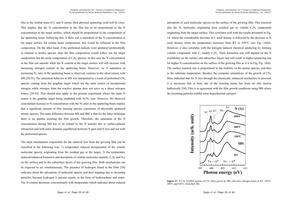
Figure 17. N (1s) XANES spectra of CNx films grown by IBS with pure nitrogen beam at RT, 150°C, 300°C and 450°C (from Ref. 50).
Chapter contribution for “Trends in Fullerene Research” To be published by Nova Science Publishers, Inc. (2007)
Gago et al. Page 27 of 46
5.3. Bonding structure of CNx films grown by IBS
The local nitrogen chemical bonding structure of films grown by IBS is shown in Figure
17. The assignment of the different spectral peaks (N1-N4) was introduced in Section
IV. It can be seen that the contribution of the nitrile-like N (peak N2) increases
concomitantly with temperature. This type of terminating bonding hinders the formation
of the extended basal graphene sheets. As the total number of incorporated N atoms
decreases with increasing temperature, this indicates that the nitrile-like configuration is
the most stable against the temperature induced/enhanced desorption process. On the
other hand, the contribution coming from pyridine-like environments (N1), molecular
nitrogen (N3) and three-folded N (peak N4) decreases. The apparent shift of peak N3
towards higher photon energies with temperature should be interpreted as the decrease
of peak N3 and the emerging of peak N4 due to the desorption of embedded N2
molecules and the promotion of three-fold N. This observations are commonly reported
in graphite-like CNx structures [21,23,37,39].
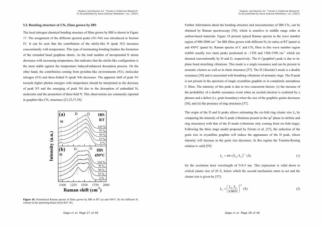
Figure 18. Normalized Raman spectra of films grown by IBS at RT (a) and 450°C (b) for different N2 content in the sputtering beam (from Ref. 56).
Chapter contribution for “Trends in Fullerene Research” To be published by Nova Science Publishers, Inc. (2007)
Gago et al. Page 28 of 46
Further information about the bonding structure and microstructure of IBS CNx can be
obtained by Raman spectroscopy [56], which is sensitive to middle range order in
carbon-based materials. Figure 18 present typical Raman spectra in the wave number
region of 900-2000 cm-1 for IBS films grown with different N2/Ar ratios at RT (panel a)
and 450°C (panel b). Raman spectra of C and CNx films in this wave number region
exhibit usually two main peaks positioned at ~1350 and 1560-1590 cm-1 which are
denoted conventionally by D and G, respectively. The G ('graphite') peak is due to in-
plane bond stretching vibrations. This mode is a single resonance and can be present in
aromatic clusters as well as in chain structures [57]. The D ('disorder') mode is a double
resonance [58] and is associated with breathing vibrations of aromatic rings. The D peak
is not present in the spectrum of single crystalline graphite or in completely amorphous
C films. The intensity of this peak is due to two concurrent factors: (i) the increase of
the probability of a double resonance event when an excited electron is scattered by a
phonon and a defect (i.e. grain boundary) when the size of the graphitic grains decreases
[58], and (ii) the presence of ring structures [57].
The origin of the D and G peaks allows estimating the six-fold ring cluster size La by
comparing the intensity of the G peak (vibrations present in the sp2 phase in olefinic and
ring structures) with that of the D mode (vibrations only coming from six-fold rings).
Following the three stage model proposed by Ferrari et al. [57], the reduction of the
grain size in crystalline graphite will induce the appearance of the D peak, whose
intensity will increase as the grain size decreases. In this regime the Tuinstra-Koenig
relation is valid [59]:
( ) 144 −×= GDa IIL (Å) (1)
for the excitation laser wavelength of 514.5 nm. This expression is valid down to
critical cluster size of 20 Å, below which the second mechanism starts to act and the
cluster size is given by [57]:
21
0055.0⎟⎠⎞
⎜⎝⎛= GD
aII
L (Å) (2)
Chapter contribution for “Trends in Fullerene Research” To be published by Nova Science Publishers, Inc. (2007)
Gago et al. Page 29 of 46
In this regime, six-fold ring clusters become smaller and more disordered. When the
disorder increases, the sp2 phase changes from ring to chain structures, while at the final
stage when sp3 bonds are introduced the sp2 bonds become strongly localized.
D and G peaks can be also observed for the majority of the spectra grown by IBS (Fig.
18) indicating a presence of the sp2 phase, and for some of the spectra a small peak at
~960 cm-1 of the underlying Si substrate could be also seen. For the IBS films grown at
RT, the D peak contribution is very low and can be hardly resolved in the spectra. Two
main observations are the slight increase in the intensity of the D peak with N
incorporation and temperature (see Fig. 18). The former indicates N induced clustering
of the sp2 phase into ring structures, while the second points to a temperature induced
graphitization. All the spectra lack sharp features, except the C film (grown by pure Ar
bombardment) grown at 450°C. However, these sharp features of the D and G peaks are
not present under the same growth conditions when N is incorporated, indicating
increased disorder.
Quantitative information can be extracted by applying certain fitting procedure to the
observed experimental spectra. The combination of a linear background, a symmetric
Lorentzian and and asymmetric Breit-Wigner-Fano (BWF) shape to fit the D and G
peaks, respectively, was found to be a good compromise between the fitting quality and
the capability to fit all spectra. The BWF line shape is described by the following
expression [57,60]:
( ) ( )[ ]( )[ ]20
200
2121
Γ−+
Γ−+=
kkqkkI
kI , (3)
with the maximum positioned at [57]
qkk 20max Γ+= , (4)
where ( )kI is the intensity as a function of wave number k, I0 is the peak intensity, k0,
kmax and Γ are the mean peak position, the peak position at the maximum, and the full
width at half maximum (FWHM), respectively, and q is BWF coupling coefficient. In
the following the position of the G peak will be defined by kmax. In the limit 0→q , the
Chapter contribution for “Trends in Fullerene Research” To be published by Nova Science Publishers, Inc. (2007)
Gago et al. Page 30 of 46
Lorentzian line shape is reproduced. Generally, the G peak position reflects the bonding
strength, and ΓG reflects bond length and angle distortion [14,60,61]. In addition,
implantation and annealing studies of graphite and glassy carbon [60,62] have
established that in the limit 0→Γ qG the in-plane graphene ordering is complete, and
three-dimensional ordering begins. Following this, qGΓ will be used to quantify the
in-plane graphitic order.
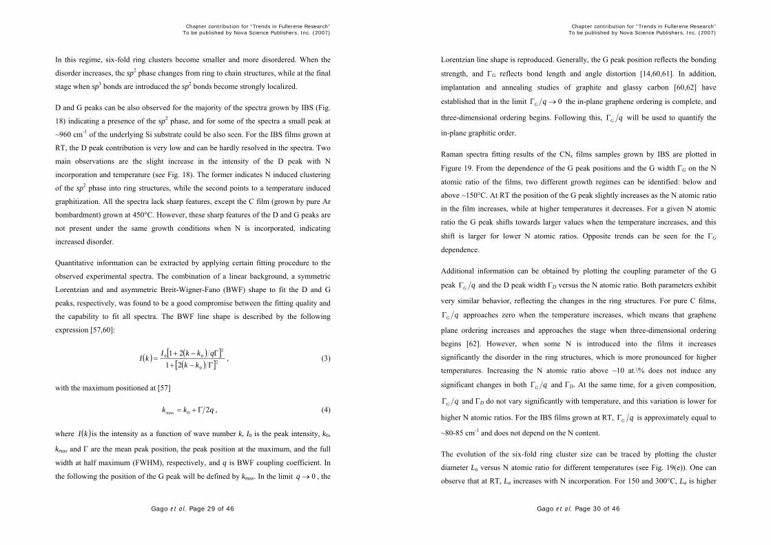
Raman spectra fitting results of the CNx films samples grown by IBS are plotted in
Figure 19. From the dependence of the G peak positions and the G width ΓG on the N
atomic ratio of the films, two different growth regimes can be identified: below and
above ~150°C. At RT the position of the G peak slightly increases as the N atomic ratio
in the film increases, while at higher temperatures it decreases. For a given N atomic
ratio the G peak shifts towards larger values when the temperature increases, and this
shift is larger for lower N atomic ratios. Opposite trends can be seen for the ΓG
dependence.
Additional information can be obtained by plotting the coupling parameter of the G
peak qGΓ and the D peak width ΓD versus the N atomic ratio. Both parameters exhibit
very similar behavior, reflecting the changes in the ring structures. For pure C films,
qGΓ approaches zero when the temperature increases, which means that graphene
plane ordering increases and approaches the stage when three-dimensional ordering
begins [62]. However, when some N is introduced into the films it increases
significantly the disorder in the ring structures, which is more pronounced for higher
temperatures. Increasing the N atomic ratio above ~10 at.\% does not induce any
significant changes in both qGΓ and ΓD. At the same time, for a given composition,
qGΓ and ΓD do not vary significantly with temperature, and this variation is lower for
higher N atomic ratios. For the IBS films grown at RT, qGΓ is approximately equal to
~80-85 cm-1 and does not depend on the N content.
The evolution of the six-fold ring cluster size can be traced by plotting the cluster
diameter La versus N atomic ratio for different temperatures (see Fig. 19(e)). One can
observe that at RT, La increases with N incorporation. For 150 and 300°C, La is higher
Chapter contribution for “Trends in Fullerene Research” To be published by Nova Science Publishers, Inc. (2007)
Gago et al. Page 31 of 46
than that obtained at RT and does not depend on the N content while at 450°C N
incorporation prevents the extension of graphene planes. The last observation indicates
that N incorporated into the C matrix during IBS enters into bonding configurations
which prevent the extension of the graphene planes. According to this, a high quantity
of terminating pyridine-like or nitrile-like configurations could be expected, which is in
agreement with XANES observations shown previously.
Figure 19. Results from the fitting of the Raman spectra of C and CNx films grown by IBS as a function of the N content (from Ref. 56.): (a) position of the G peak; (b) and (d) widths of the G (ΓG) and D (ΓD) peaks, respectively; (c) coupling parameter of the G peak; and (e) cluster diameter, La. The lines are only guide to the eye and the error bars represent the 95\% confidence limits of the fittings.
The results above indicate that N plays a double role creating ordering or disorder
depending on the growth temperature. At RT, an increasing N content in the films
Chapter contribution for “Trends in Fullerene Research” To be published by Nova Science Publishers, Inc. (2007)
Gago et al. Page 32 of 46
induces a decrease in the bond length and angle distortion (see also Refs. 14, 51 and
63). This is related to 2D sp2 ordering and six-fold ring clustering resulting in higher La.
In this regime N incorporation is equivalent to an increase in temperature. When the
films are grown above RT, La increases compared to the films grown at RT. However,
La is nearly independent of both N content and substrate temperature in the 150-300°C
range. At 450°C N incorporation in the C network results in a sharp drop in La yielding
the La values similar to that obtained at 150-300°C. The following N incorporation does
not result in any significant change of La. The fact that La decreases with low N addition
indicates that N is partially positioned at cluster edges and suppresses the temperature
induced cluster growth. This is probably due to formation of pyridine-like sp2 or nitrile-
like sp1 bonds. La becomes relatively low (~13-15 Å), so that relatively large part of the
cluster atoms is assumed to stay at the edges rather than inside the clusters. This means
that a low fraction of N atoms in the terminating configurations can inhibit the cluster
growth. However, the drop in La with N incorporation at ~450°C is accompanied by a
significant change in qGΓ . This may indicate that N substitutes C in six-fold rings,
thus introducing high disorder inside the clusters. Additional N incorporation does not
change qGΓ significantly. This indicates, that the following N addition does not
change the disorder inside the cluster, thus it can again be deduced that N is
accumulating on the perimeter of the aromatic clusters. This corresponds to XANES
observations of IBS CNx films where N was found in the one-, two- and three-fold
bonding configurations [50].
5.4. Effect of simultaneous ion bombardment on the bonding structure
The influence of assisting ion bombardment is very complex. Here, we can test its
influence by adding a secondary ion beam to the IBS process. This method is normally
found in the Literature as dual ion beam deposition (DIBD) (see Fig. 15). First, when N
ions are incorporated in the beam it acts as an additional N source. In fact, the N
concentration of the CNx samples grown by DIBD is almost by a factor 2 higher than
that obtained by IBS with a pure N2 beam [50]. In addition, the N content obtained by
DIBD with N ion assistance and the graphite target sputtered with a N2/Ar beam is
twice higher than that obtained with a N ion beam was used for assistance and a pure Ar
Chapter contribution for “Trends in Fullerene Research” To be published by Nova Science Publishers, Inc. (2007)
Gago et al. Page 33 of 46
beam was employed for carbon target sputtering [64]. Moreover, the nitrogen
concentration of DIBD sample is very similar or higher to those obtained with MS at
similar temperatures [50]. Then, it follows that the N incorporation from the assisting
beam is at the same level as the N source from the nitride graphite target.
Low-energy assisting ion bombardment (<100 eV) can also activate or enhance surface
processes such as diffusion but, it can also introduce some atomic displacements at
sufficient high energy transfer. The displacement energy is of the order of the order of
~40 eV for graphite and diamond [65,66]. These values refer to bulk displacement
energies while those near the surface can be significantly lower due to lower
coordination number (lower binding energy) and lower displacement radius. If the ion
energy is lower than the threshold for atomic displacements, it can still induce bond-
breaking of pre-existing surface configurations [67], thus inducing chemical reactions
which may also involve the incoming particle [68]. The energy threshold for bond
breaking in C-C system is of the order of several eV [69], thus, having more probability
to occur than the displacement event. In addition, molecular dynamics simulations show
that surface processes dominate when the energy of impinging atoms is <30 eV, while
subsurface processes govern the structure formation for higher energies [67].
Sputtering-based methods such as IBS or MS can be considered energetic growth
processes themselves due to the energy of the emitted particles (mostly neutrals) in the
hyperthermal range (from a few eV up to tens of eV) [46] that may activate or enhance
surface processes. Consequently, hyperthermal atoms in the range up to ~20 eV [47,48]
originated from the target due to sputtering provide a non negligible energy input on the
surface of the growing film, which results in the formation of a compact structure at low
deposition temperatures [56,70]. In addition, it can be expected that large amount bond
are broken at the surface under the impingement of emitted particles from the target, as
well as from assisting ions. A majority of preformed CxNy (x,y≤2) radicals coming from
the sputtered target an be expected to be affected by bombardment of energetic target
species and from the assisting plasma/ion beam, making them available for chemical
reactions, so that new atomic configurations can be formed under the influence of
atomic mobility and ion bombardment [32]. It can be related to the fact that different
Chapter contribution for “Trends in Fullerene Research” To be published by Nova Science Publishers, Inc. (2007)
Gago et al. Page 34 of 46
atomic configurations have different damage thresholds [71] that would promote the
preferential evolution of the phase with a higher damage threshold.
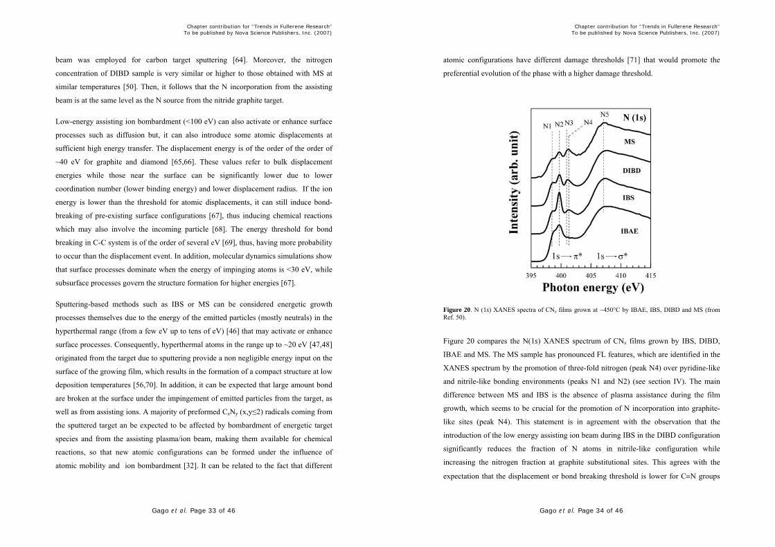
Figure 20. N (1s) XANES spectra of CNx films grown at ~450°C by IBAE, IBS, DIBD and MS (from Ref. 50).
Figure 20 compares the N(1s) XANES spectrum of CNx films grown by IBS, DIBD,
IBAE and MS. The MS sample has pronounced FL features, which are identified in the
XANES spectrum by the promotion of three-fold nitrogen (peak N4) over pyridine-like
and nitrile-like bonding environments (peaks N1 and N2) (see section IV). The main
difference between MS and IBS is the absence of plasma assistance during the film
growth, which seems to be crucial for the promotion of N incorporation into graphite-
like sites (peak N4). This statement is in agreement with the observation that the
introduction of the low energy assisting ion beam during IBS in the DIBD configuration
significantly reduces the fraction of N atoms in nitrile-like configuration while
increasing the nitrogen fraction at graphite substitutional sites. This agrees with the
expectation that the displacement or bond breaking threshold is lower for C≡N groups
Chapter contribution for “Trends in Fullerene Research” To be published by Nova Science Publishers, Inc. (2007)
Gago et al. Page 35 of 46
than for sp2 C and N atoms inside or on the edges of aromatic clusters and, hence, these
groups may be preferentially removed under low-energy ion bombardment. The
removal of C≡N groups at relative low ion damage may explain the higher extension of
grapheme sheets in MS thin films. This mechanism may also partially explain the
formation of the texture with standing graphitic basal planes during MS growth of FL-
CNx films [18] since the compressive stress usually present in such films cannot explain
this phenomenon [72]. However, if the degree of ion bombardment is high enough, then
formation of any ordered atomic configuration may be stopped, which which can lead to
a complete amorphization of the growing film [7] and nitrogen incorporates only at sites
with low coordination number as those observed in the films grown by IBAE [45].
Apart from changes in the local bonding configurations, ion bombardment can
introduce significant material loss due to the (sub)surface displacements and bond
breaking events [45,56] leading in some cases to a complete re-sputtering even at low
ion energies (~25 eV) [25]. The material loss is observed with increasing the degree of
ion bombardment or the substrate temperature, while N/C ratio in the film remains
approximately constant [45,56]. The former indicates that an excess in the N ion to
atom ratio results in a loss of film forming material (C and N) and that C and N losses
are both correlated. This can be explained by ion enhanced/induced formation of
volatile CN compounds via bond splitting and following chemical reactions
[27,37,54,73,74,75].
5.5. Microstructural studies of CNx grown by different methods
In order to correlate the different growth methods (N-incorporation routes) and the
obtained bonding structures with the microstructural evolution, HRTEM investigations
were carried out in representative samples (for more details, see Refs. 45 and 76). In this
case, CNx films grown by IBAE and IBS with a similar content as that obtained in FL-
CNx by DC-MS have been studied. Also, a pure C film grown by IBS and a CNx sample
grown by DIBD were investigated to discern the effect of N incorporation and ion
bombardment effects. The HRTEM micrographs for the samples grown by IBS and
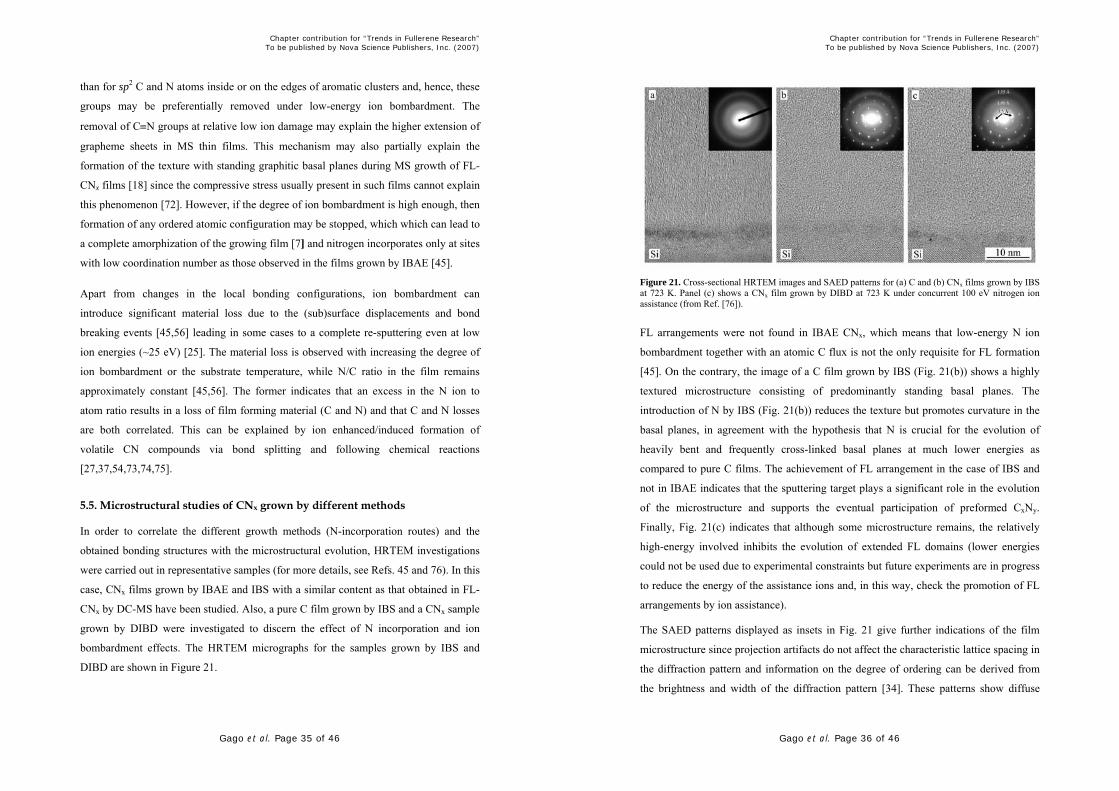
DIBD are shown in Figure 21.
Chapter contribution for “Trends in Fullerene Research” To be published by Nova Science Publishers, Inc. (2007)
Gago et al. Page 36 of 46
Figure 21. Cross-sectional HRTEM images and SAED patterns for (a) C and (b) CNx films grown by IBS at 723 K. Panel (c) shows a CNx film grown by DIBD at 723 K under concurrent 100 eV nitrogen ion assistance (from Ref. [76]).
FL arrangements were not found in IBAE CNx, which means that low-energy N ion
bombardment together with an atomic C flux is not the only requisite for FL formation
[45]. On the contrary, the image of a C film grown by IBS (Fig. 21(b)) shows a highly
textured microstructure consisting of predominantly standing basal planes. The
introduction of N by IBS (Fig. 21(b)) reduces the texture but promotes curvature in the
basal planes, in agreement with the hypothesis that N is crucial for the evolution of
heavily bent and frequently cross-linked basal planes at much lower energies as
compared to pure C films. The achievement of FL arrangement in the case of IBS and
not in IBAE indicates that the sputtering target plays a significant role in the evolution
of the microstructure and supports the eventual participation of preformed CxNy.
Finally, Fig. 21(c) indicates that although some microstructure remains, the relatively
high-energy involved inhibits the evolution of extended FL domains (lower energies
could not be used due to experimental constraints but future experiments are in progress
to reduce the energy of the assistance ions and, in this way, check the promotion of FL
arrangements by ion assistance).
The SAED patterns displayed as insets in Fig. 21 give further indications of the film
microstructure since projection artifacts do not affect the characteristic lattice spacing in
the diffraction pattern and information on the degree of ordering can be derived from
the brightness and width of the diffraction pattern [34]. These patterns show diffuse
Chapter contribution for “Trends in Fullerene Research” To be published by Nova Science Publishers, Inc. (2007)
Gago et al. Page 37 of 46
features indicating the quasi-disordered structure of the film corresponding to lattice
spacing of ∼1.15, 1.95 and 3.5 Å (see labels in the inset of Fig. 21(c)). In the insets of
panels (b) and (c) in Fig. 21, the dot diffraction pattern of the crystalline Si(100)
substrate is also superimposed to indicate the relation of the texture of FL features to the
substrate normal. The rings at ∼1.15 and ∼1.95 Å coincide with those observed for
amorphous allotropes of C and CNx films while the innermost ring at 3.5 Å match with
the inter-plane separation of hexagonal basal planes in graphite (0002). The patterns
show a broad feature at 3.5 Å indicating the presence of defective graphitic basal planes.
The appearance of a broad arc is due to the preferential orientation of the basal planes
perpendicular to the surface normal. Well-structured FL-CNx presents a similar diffuse
pattern but with more distinguishable features and an additional ring at 1.75 Å [34]. The
intensity of this ring correlates with that at 3.5 Å and, therefore, it is attributed to the
inter-plane distance in graphite (0004). The presence and definition of the 3.5 and 1.75
Å rings have been correlated with the evolution of the FL structure, as signatures of the
short/medium range graphitic order [34]. In the case of IBS films, the characteristic 3.5
Å spacing shows similar structured films as those grown by DC-MS, but the diffuse ring
at 1.75 Å is less defined. This feature is only observable in the SAED pattern in Fig.
21(c) as an arc (almost incorporated into the diffuse ring at 1.95 Å) and aligned to the
arc at 3.5 Å. These observations indicate a smaller degree of ordering or extension of
the graphitic arrangements in IBS films as compared to their DC-MS counterparts.
The less structure CNx films grown by IBS with respect to MS (compare the
micrographs of Fig. 21 with those shown in Fig. 1) can be understood by the XANES
and Raman studies presented above. CNx films grown by IBS and DC-MS present in
both cases a significant participation of three-fold nitrogen but a slightly higher relative
content of cyanogen-like bonding environments is attained in IBS (see Fig. 20). The
detrimental role of nitrile sites in FL arrangements is obvious since their terminating
character hinders the further extension of graphene sheets, which could explain the
lower degree of FL character in FL-CNx films grown by IBS with respect to dc-MS.
The introduction of N2 ion assistance (100 eV) during IBS was shown to induce a
significant reduction of the relative content of nitrile bonding environments [50].
Therefore, the less structured films grown by IBS can be partially attributed to the lack
of ion assistance during growth.
Chapter contribution for “Trends in Fullerene Research” To be published by Nova Science Publishers, Inc. (2007)
Gago et al. Page 38 of 46
6. FL CARBON FILMS BY ENCAPSULATION OF METAL CATALYST NANOPARTICLES
In previous sections, we have focused our study on the growth of FL-CNx due to the
lower energy barrier for the formation of such arrangements upon N incorporation. In
this section we present other route for the yield of FL carbon-based thin films by means
of incorporation of metal catalysts nanoparticles during the growth. With the same
argument, the presence of the metal catalysts reduces the energy barrier to induce
curvature in graphitic planes in a similar way than in the process used for CNT growth
and nucleation.
The early investigations of the arc evaporation products based on so-called Krätschmer-
Huffman carbon arc process of composite anode [77] showed that, in addition to the
C60, endohedral fullerenes, nanotubes, carbon onions and carbon soot, there are
additional by-product structures which consist of polyhedral C nanoparticles with
internal cavities filled with metal or metal carbides [78,79,80,81]. Numerous metallic
elements have been reported to be encapsulated in such cage structures [82]. The
discovery of this encapsulation mechanism paved a new research pathway in FL
materials due to two reasons. First, it provides a possibility to study very small amounts
of the encapsulated material which can potentially reveal new properties only available
at the nanoscale [82]. For example, the encapsulated nanoparticles of ferromagnetic
materials are predominantly monodomain and show the full range of nanoparticle
magnetic phenomena such as superparamagnetism and hysteresis below blocking
temperature [83,84]. Second, the protective nature of the encapsulating graphite against
degradation promised applications such as nanowires, magnetic data storage,
ferrofluids, magnetic toner for xerography, or as contrast agents in magnetic resonance
imaging [82,85].
However, the main drawback of the above arc process is that it produces a full spectrum
of carbon nanostructures and the ratio of the carbon encapsulating nanoparticles is low.
In addition, this process provides little control over the particle size, and there is
considerable carbonaceous debris which is difficult to remove. Another arc evaporation
method was introduced by Dravid et al. [86], which permits to control significantly
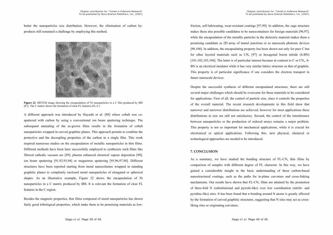
Chapter contribution for “Trends in Fullerene Research” To be published by Nova Science Publishers, Inc. (2007)
Gago et al. Page 39 of 46
better the nanoparticles size distribution. However, the elimination of carbon by-
products still remained a challenge by employing this method.
Figure 22. HRTEM image showing the encapsulation of Ni nanoparticles in a C film produced by IBS [87]. The C matrix shows the formation of clear FL features (FL-C).
A different approach was introduced by Hayashi et al. [88] where cobalt was co-
sputtered with carbon by using a conventional ion beam sputtering technique. The
subsequent annealing of the as-grown films results in the formation of cobalt
nanoparticles wrapped in curved graphitic planes. This approach permits to combine the
protective and the decoupling properties of the carbon in a single film. This work
inspired numerous studies on the encapsulation of metallic nanoparticles in thin films.
Different methods have been later successfully employed to synthesize such films like
filtered cathodic vacuum arc [89], plasma enhanced chemical vapour deposition [90],
ion beam sputtering [91,92,93,94] or magnetron sputtering [95,96,97,98]. Different
structures have been reported starting from metal nanocolumns wrapped in standing
graphitic planes to completely enclosed metal nanoparticles of elongated or spherical
shapes. As an illustrative example, Figure 22 shows the encapsulation of Ni
nanoparticles in a C matrix produced by IBS. It is relevant the formation of clear FL
features in the C region.
Besides the magnetic properties, thin films composed of metal nanoparticles has shown
fairly good tribological properties, which make them to be promising materials as low-
Chapter contribution for “Trends in Fullerene Research” To be published by Nova Science Publishers, Inc. (2007)
Gago et al. Page 40 of 46
friction, self-lubricating, wear-resistant coatings [97,99]. In addition, the cage structure
makes them also possible candidates to be nanocontainers for foreign materials [96,97],
while the encapsulation of the metallic particles in the dielectric material makes them a
promising candidate as 2D array of tunnel junctions or as nanoscale photonic devices
[98,100]. In addition, the encapsulating property has been shown not only for pure C but
for other layered materials such as CNx [97] or hexagonal boron nitride (h-BN)
[101,102,103,104]. The latter is of particular interest because in contrast to C or CNx, h-
BN is an electrical insulator while it has very similar lattice structure as that of graphite.
This property is of particular significance if one considers the electron transport in
future nanoscale devices.
Despite the successful synthesis of different encapsulated structures, there are still
several major challenges which should be overcome for these materials to be considered
for applications. First of all, the control of particle size, since it controls the properties
of the overall material. The recent research developments in this field show that
narrower and narrower distributions are achieved; however for most applications these
distributions in size are still not satisfactory. Second, the control of the interdistance
between nanoparticles or the production of ordered arrays remains a major problem.
This property is not so important for mechanical applications, while it is crucial for
electronical or optical applications. Following this, new physical, chemical or
technological approaches are needed to be introduced.
7. CONCLUSION
As a summary, we have studied the bonding structure of FL-CNx thin films by
comparison of samples with different degree of FL character. In this way, we have
gained a considerable insight in the basic understanding of these carbon-based
nanostructured coatings, such as the paths for in-plane curvature and cross-linking
mechanisms. Our results have shown that FL-CNx films are attained by the promotion
of three-fold N (substitutional and pyrrole-like) over low coordination (nitrile- and
pyridine-like) sites. It has been found that π bonding around N atoms is greatly affected
by the formation of curved graphitic structures, suggesting that N sites may act as cross-
liking sites or originating curvature.
Chapter contribution for “Trends in Fullerene Research” To be published by Nova Science Publishers, Inc. (2007)
Gago et al. Page 41 of 46
By comparing CNx films grown under different methods, we have also obtained
relevant information about the growth mechanisms leading to the formation of FL
arrangements. In particular, we have seen that low-energy ion bombardment is not the
only requisite for the microstructural evolution and that the polyatomic CxNy species
emitted during the sputtering of C targets can significantly participate in the film
growth. Also, the presence of low-energy ion bombardment seems to be necessary for
the development of well-structured FL-CNx films by promotion of favorable sites due to
preferential sputtering or by inducing surface diffusion processes. However, excessive
energetic conditions induce the amorphization and disruption of the growing
microstructure.
Finally, an additional path for the promotion of FL arrangement in pure carbon films is
presented. This process is based on the catalytic character of metal nanoparticles that
induce the formation of carbon nanostructures such as occurs in CNT growth. In this
way, embedding metal catalysts nanoparticles during the growth can lead to the growth
of FL films with new and interesting properties coming from the microstructure and
nanostructuration process.
ACKNOWLEDGMENTS
The work reviewed in this chapter has been supported by the EU and carried out inside
the “Synthesis, structure and properties of new fullerene-like materials” IHP-Network
(Ref: HPRN-CT-2002-00209) and “Fullerene-based Opportunities for Robust
Engineering: Making Optimised Surfaces for Tribology (FOREMOST)” project (Ref:
NMP3-CT-2005-515840). We would like to thank J. Neidhardt and L. Hultman for
providing DC-MS CNx samples and fruitful discussions.
MAIN PUBLICATIONS BY THE AUTHORS RELATED TO THIS CHAPTER
Jiménez, I.; Gago, R.; Albella, J. M.; Caceres, D.; Vergara, I.; “Spectroscopy of p bonding in hard graphitic carbon nitride films: Superstructure of basal planes and hardening mechanisms”, Phys. Rev. B 2000, 62, 4261-4264 (Ref. 23).
Jiménez, I.; Gago, R.; Albella, J.M.; Terminello, L.J. “X-Ray absorption studies of bonding environments in graphitic carbon nitride”, Diam. Relat. Mater. 2001, 10, 1166-1169 (Ref. 39).
Chapter contribution for “Trends in Fullerene Research” To be published by Nova Science Publishers, Inc. (2007)
Gago et al. Page 42 of 46
Gago, R.; Jiménez, I.; Neidhardt, J.; Abendroth, B.; Caretti, I.; Hultman, L.; Möller, W. “Correlation between bonding structure and microstructure in fullerene-like carbon nitride thin films”, Phys. Rev. B 2005, 71, 1254514 (Ref 21).
Gago, R.; Neidhardt, J.; Vinnichenko, M.; Kreissig, U.; Czigány, Zs.; Kolitsch, A.; Hultman, L.; Möller, W. “Synthesis of carbon nitride thin films by low-energy ion beam assisted evaporation: on the mechanisms for fullerene-like microstructure formation”, Thin Solid Films 2005, 483, 89-94 (Ref. 45).
Abrasonis, G.; Gago, R.; Jiménez, I.; Kreissig, U.; Kolitsch, A.; Möller, W. “Nitrogen incorporation in carbon nitride films produced by direct and dual ion beam sputtering”, J. Appl. Phys. 2005, 98, 074907 (Ref. 50).
Gago, R.; Abrasonis, G.; Mücklich, A.; Möller, W.; Czigány Zs.; Radnóczi, G. “Fullerene-like arrangements in carbon nitride thin films grown by direct ion beam sputtering”, Appl. Phys. Lett. 2005, 87, 071901 (Ref 76).
Abrasonis, G.; Gago, R.; Vinnichenko, M.; Kreissig, U.; Kolitsch, A.; Möller, W. ”Six-fold ring clustering in sp2-dominated carbon and carbon nitride thin films: a Raman spectroscopy study”, Phys. Rev. B 2006, 73, 125427 (Ref. 56).
LIST OF REFERENCES 1. Dresselhaus, M.S.; Dresselhaus, G.; Eklund P.C. Science of Fullerenes and
Carbon Nanotubes; Academic Press: San Diego, 1996. 2. Amaratunga, G.A.J., Chhowalla, M.; Kiely, C.J.; Alexandrou, I.; Aharonov, R.;
Devenish, R.M. Nature 1996, 383, 321-323. 3. Sjöström, H.; Stafström, S.; Boman, M.; Sundgren, J.-E. Phys. Rev. Lett. 1995,
75, 1336-1339. 4. Hellgren, N.; Berlin, T.; Gueorguiev, G.K.; Johansson, M.P.; Stafström, S.;
Hultman, L. Mat. Sci. Eng. B 2004, 113, 242-247. 5. Hultman L.; Stafström S.; Czigány Z.; Neidhardt J.; Hellgren N.; Brunell I.F.;
Suenaga K. Phys. Rev. Lett. 2001, 87, 225503. 6. Hultman, L.; Neidhardt, J.; Hellgren, N.; Sjöstrom, H.; Sundgren, J.E. MRS
Bulletin 2003, 28, 194-202. 7. Neidhardt J.; Hultman L.; Broitman E.; Scharf T.W.; Singer I.L. Diam. Rel.
Mater. 2004, 13, 1882-1888. 8. Lin, N.; Hellgren, N.; Johansson, M.P.; Hultman, L.; Erlandsson, R. Phys. Rev. B
2000, 61, 4898-4903. 9. Bogy, D.B.; Fong, W.; Thornton, B.H.; Hong, Z.; Gross, H.M.; Bhatia C.S. IEEE
Magnet. 2002, 38, 1879-1885. 10. Alexandrou, I.; Scheibe, H. J.; Kiely, C. J.; Papworth, A. J.; Amaratuga, G. A. J.;
Schultrich, B. Phys. Rev. B 1999, 60, 10903-10907. 11. Tenne, R. Chem. Eur. J. 2002, 8, 5297-5304. 12. Chhowalla M.; Amaratunga G.A.J. Nature 2000, 407, 164-167.
Chapter contribution for “Trends in Fullerene Research” To be published by Nova Science Publishers, Inc. (2007)
Gago et al. Page 43 of 46
13. Hellgren, N.; Johansson, M.P.; Broitman, E.; Hultman, L.; Sundgren, J.-E. Phys.
Rev. B 1999, 59, 5162-5169. 14. Ferrari, A. C.; Rodil, S. E.; Robertson, J. Phys. Rev. B 2003, 67, 155306. 15. Rodil, S. E. Recent Res. Devel. Appl. Phys. 2003, 6, 391-426. 16. Stafström S. Appl. Phys. Lett. 2000, 77, 3941-3943. 17. dos Santos, M.C.; Alvarez, F. Phys. Rev. B (1998) 58, 13918-13924. 18. Hellgren, N.; Guo, J.; Såthe, C.; Agui, A.; Nordgren, J.; Luo, Y.; Ågren, H.;
Sungren, J.E. Appl. Phys. Lett. 2001, 79, 4348-4350. 19. Gammon, W.J.; Malyarenko, D.I.; Kraft, O.; Hoatson, G.L.; Reilly, A.C.;
Holloway, B.C. Phys. Rev. B 2002, 66 153402. 20. Gammon, W.J.; Hoatson, G.L.; Holloway, B.C.; Vold, R.L.; Reilly, A.C.; Phys.
Rev. B 2003, 68, 195401 21. Gago, R.; Jiménez, I.; Neidhardt, J.; Abendroth, B.; Caretti, I.; Hultman, L.;
Möller, W. Phys. Rev. B 2005, 71, 1254514. 22. Neidhardt, J.; Czigány, Zs.; Brunell, I.F.; Hultman, L. J. Appl. Phys. 2003, 93,
3002-3015. 23. Jiménez, I.; Gago, R.; Albella, J. M.; Caceres, D.; Vergara, I.; Phys. Rev. B 2000,
62, 4261-4264. 24. Voevodin, A.A.; Jones, J.G.; Zabinski, J.S.; Czigány, Zs.; Hultman, L. J. Appl.
Phys. 2002, 92, 4980-4988. 25. Hellgren, N., Macák, K.; Broitman, E.; Johansson, M.P.; Hultman, L.; Sundgren,
J.-E. J. Appl. Phys. 2000, 88, 524-532. 26. Todorov, S.S.; Marton, D.; Boyd, K.J.; Al-Bayati, A.H.; Rabalais, J.W. J. Vac.
Sci. Technol. A 1994, 12, 3192-3199. 27. Hammer, P.; Gissler, W. Diam. Relat. Mater. 1996, 5, 1152-1158. 28. Kaltofen, R.; Sebald, T.; Weise, G. Surf. Coat. Technol. 1997, 97, 131-139. 29. Neidhardt, J.; Högberg, H.; Hultman, L. Thin Solid Films 2005, 478, 34-41. 30. Hellgren, N.; Johansson, M.P.; Broitman, E.; Sandström, P.; Hultman, L.;
Sundgren, J.E. Thin Solid Films 2001, 382, 146-152. 31. Neidhardt, J.; Hultman, L.; Abendroth, B.; Gago, R.; Möller, W. J. Appl. Phys.
2003, 94, 7059-7066. 32. Gueorguiev, G.K.; Neidhardt, J.; Stafström, S.; Hultman, L. Chem. Phys. Lett.
2005, 401, 288-295. 33. Czigány Zs.; Neidhardt J.; Brunell I.F.; Hultman L. Ultramicroscopy 94 (2003)
163-173. 34. Neidhardt, J.; Hultman, L.; Czigány, Zs. Carbon 2004, 42, 2729-2734. 35. Sánchez-López, J.C.; Donnet, C.; Lefèbvre, F.; Fernández-Ramos, C.; Fernández,
A. J. Appl. Phys. 2001, 90, 675-681. 36. Csillag, S.; Rätty, R.; Zou W. Y.; Sjöström, H.; Sundgren, J.-E.; Colliex, C J.
Appl. Phys. 1997, 82, 666-669.
Chapter contribution for “Trends in Fullerene Research” To be published by Nova Science Publishers, Inc. (2007)
Gago et al. Page 44 of 46
37. Hellgren, N.; Guo, J.; Luo, Y.; Såthe, C.; Agui, A.; Kashtanov, S.; Nordgren, J.;
Ågren, H.; Sundgren J.-E. Thin Solid Films 2005, 471, 19-34. 38. Stöhr, J. NEXAFS Spectroscopy; Springer: Berlin, 1992. 39. Jiménez, I.; Gago, R.; Albella, J.M.; Terminello, L.J. Diam. Relat. Mater. 2001,
10, 1166-1169. 40. Ray, S.C.; Pao, C.W.; Chiou, J.W.; Tsai, H.M.; Jan J.C.; Pong, W.F.; McCann, R.;
Roy, S.S.; Papakonstantinou, P.; McLaughlin, J.A. J. Appl. Phys. 2005, 98, 033708.
41. Ripalda, J.M.; Román, E.; Díaz, N.; Galán, L.; Montero, I.; Gomelli, G.; Baraldi, A.; Lizzit, S.; Goldoni, A.; Paolucci, G. Phys. Rev. B 1999, 60, R3705-3708.
42. Zhu, Q.; Money, S.L.; Russell, A.E.; Thomas, K.M. Langmuir 1997, 13, 2149-2157.
43. Shimoyama, I.; Wu, G.; Sekiguchi, T.; Baba, Y. Phys. Rev. B 2000, 62, R3705. 44. Chen, C.T.; Ma Y.; Sette F. Phys. Rev. A 1989, 40, 6737-6740. 45. Gago, R.; Neidhardt, J.; Vinnichenko, M.; Kreissig, U.; Czigány, Zs.; Kolitsch,
A.; Hultman, L.; Möller, W. Thin Solid Films 2005, 483, 89-94. 46. Rossnagel, S. M. J. Vac. Sci. Technol. A 2003, 21, S74-S87. 47. Meyer, K.; Schuller, I. K.; Falco, C. M. J. Appl. Phys. 1981, 52, 5803-5805. 48. Müller, K.H. Phys. Rev. B 1987, 35, 7906-7913. 49. Ziegler J.F.; Biersack J.P.; Littmark U. The Stopping and Range of Ions in Matter;
Pergamon; New York, 1985. 50. Abrasonis, G.; Gago, R.; Jimenez, I.; Kreissig, U.; Kolitsch, A.; Möller, W. J.
Appl. Phys. 2005, 98, 074907. 51. Kleinsorge, B.; Ferrari A. C.; Robertson J.; Milne W. I.; Waidmann S.; Hearne S.
Diam. Rel. Mat. 2000, 9, 643-648. 52. Sjöström, H.; Hultman, L.; Sundgren, J.E.; Hainsworth, S.V.; Page, T.F.;
Theunissen, G.S.A.M. J. Vac. Sci. Technol. A 1996, 14, 56-62. 53. Zheng, W. T.; Sjöström, H.; Ivanov, I.; Xing, K. Z.; Salaneck, W. R.; Greene, J.
E.; Sundgren, J. E. J. Vac. Sci. Technol. A 1996, 14, 2696-2701. 54. Todorov, S. S.; Marton, D.; Boyd, K. J.; Al-Bayati, A. H.; Rabalais, J. W. J. Vac.
Sci. Technol. A 1994, 12, 3192-3199. 55. Neidhardt, J.; Högberg, H.; Hultman, L. Surf. Sci. 2004, 569, L289-L295. 56. Abrasonis, G.; Gago, R.; Vinnichenko, M.; Kreissig, U.; Kolitsch, A.; Möller, W.
Phys. Rev. B 2006, 73, 125427. 57. Ferrari, A. C.; Robertson, J. Phys. Rev. B 2000, 61, 14095-14107. 58. Thomsen C.; Reich, S. Phys. Rev. Lett. 2000, 85, 5214-5217. 59. Tuinstra F.; Koenig, J. L. J. Chem. Phys. 1970, 53, 1126-1130. 60. McCulloch, D. G.; Prawer, S.; Hoffman, A. Phys. Rev. B 1994, 50, 5905-5917. 61. Prawer, S.; Ninio, F.; Blanchonette, I. J. Appl. Phys. 1990, 68, 2361-2366.
Chapter contribution for “Trends in Fullerene Research” To be published by Nova Science Publishers, Inc. (2007)
Gago et al. Page 45 of 46
62. Elman, B. S.; Shayegan, M.; Dresselhaus, M. S.; Mazurek, H.; Dresselhaus, G.
Phys. Rev. B 1982, 25, 4142-4156 63. Rodil, S. E.; Ferrari, A. C.; Robertson, J.; Milne, W. I. J. Appl. Phys. 2001 89,
5425-5430. 64. Hammer, P.; Victoria, N. M.; Alvarez, F. J. Vac. Sci. Technol. A 2000, 18, 2277-
2287. 65. Steffen, H. J.; Marton, D.; Rabalais, J. W. Phys. Rev. Lett. 1992, 68, 1726-1729. 66. Koike, J.; Parkin, D. M.; Mitchell, T. E. Appl. Phys. Lett. 1992, 60, 1450-1452. 67. Uhlmann, S.; Frauenheim, Th.; Lifshitz, Y.; Phys. Rev. Lett. 1998, 81, 641-644. 68. Hopf, C.; von Keudell, A.; Jacob, W. J. Appl. Phys. 2003, 94, 2373-2380. 69. Salonen, E.; Nordlund, K.; Keinonen, J.; Wu, C. H. Phys. Rev. B 2001, 63,
195415. 70. Cuomo, J. J.; Doyle, J. P.; Bruley, J.; Liu, J. C. Appl. Phys. Lett. 1991, 58, 466-
468. 71. Lifshitz, Y.; Kasi, S. R.; Rabalais, J. W. Phys. Rev. Lett. 1989, 62, 1290-1293. 72. McCarty, K. F. J. Vac. Sci. Technol. A 1999, 17, 2749-2752. 73. Hammer, P.; Alvarez, F. Thin Solid Films 2001, 398-399, 116-123. 74. Jacob, W.; Hopf, C.; Schlüter, M. Appl. Phys. Lett. 2005, 86, 204103. 75. Morrison N. A.; Rodil S. E.; Robertson J.; Milne, W. I. J. Appl. Phys. 2001 89,
5754-5759. 76. Gago, R.; Abrasonis, G.; Mücklich, A.; Möller, W.; Czigány Zs.; Radnóczi, G.
Appl. Phys. Lett. 2005, 87, 071901. 77. Krätschmer, W.; Lamb, L. D.; Fostiropoulos, K.; Huffman, D. R. Nature 1990,
347, 354–358. 78. Ajayan, P. M.; Iijima, S. Nature 1993, 361, 333–334. 79. Ruoff, R. S.; Lorents, D. C.; Chan, B.; Malhotra, R.; Subramoney, S. Science
1993, 259, 346–348. 80. Seraphin, S.; Zhou, D.; Jiao, J.; Withers, J. C.; Loutfy, R. Nature 1993, 362, 503-
503. 81. Saito, Y.; Yoshikawa, T.; Inagaki, M.; Tomita, M.; Hayashi, T. Chem. Phys. Lett.
1993 204, 277–282. 82. Seraphin, S.; Zhou, D.; Jiao, J. J. Appl. Phys. 1996, 80, 2097–2104. 83. Majetich, S. A.; Artman, J. O.; McHenry, M. E.; Nuhfer, N. T.; Staley, S. W.
Phys. Rev. B.1993, 48, 16845–16848. 84. McHenry, M. E.; Majetich, S. A.; Artman, J. O.; DeGraef, M.; Staley, S. W. Phys.
Rev. B. 1994, 49, 11358–11363. 85. Scott, J. H. J.; Majetich, S. A. Phys. Rev. B. 1995, 52, 12564–12571. 86. Dravid, V. P.; Host, J. J.; Teng, M. H.; Elliot, B.; Hwang, J. H.; Johnson, D. L.;
Mason, T. O. ; Weertman, J. R. Nature 1995, 374, 602–602. 87. Abrasonis, G.; et al. (unpublished)
Chapter contribution for “Trends in Fullerene Research” To be published by Nova Science Publishers, Inc. (2007)
Gago et al. Page 46 of 46
88. Hayashi, T.; Hirono, S.; Tomita, M.; Umemura, S. Nature 1996, 381, 772–774. 89. Wang, H.; Wong, S. P.; Cheung, W. Y.; Ke, N.; Chiah, M. F.; Liu, H.; Zhang, X.
X. J. Appl. Phys. 2000, 88, 2063–2067. 90. Tsai, S. H. ; Lee, C. L.; Chao, C. W.; Shih, H. C. Carbon 2000, 38, 781–785. 91. Delaunay, J. J.; Hayashi, T.; Tomita, M.; Hirono, S. J. Appl. Phys. 1997, 82,
2200–2208. 92. Babonneau, D.; Cabioc’h, T.; Denanot, M. F.; Naudon, A. Appl. Phys. Lett. 1999,
74, 800–802. 93. Shi, J.; Hashiba, Y.; Nittono, O. J. Mater. Sci. 2001, 36, 343–349. 94. Fonseca, F. C.; Ferlauto, A. S.; Alvarez, F.; Goya, G. F.; Jardim, R. F. J. Appl.
Phys. 2005, 97, 044313. 95. Wang, H. ; Wong, S. P.; Lau, W. F.; Yan, X.; Lu, X.; Cheung, W. Y.; Ke, N. Thin
Solid Films 2001, 382, 133–138. 96. Mamezaki, O.; Adachi, H.; Tomita, S.; Fujii, M.; Hayashi, S. Jpn. J. Appl. Phys.
2000, 39, 6680–6683. 97. Kovacs, G. J.; Safran, G.; Geszti, O.; Ujvari, T.; Bertoti, I.; Radnoczi, G. Surf.
Coat. Technol. 2004, 180-81, 331–334. 98. Sedlackova, K.; Lobotka, P.; Vavra, I.; Radnoczi, G. Carbon 2005, 43, 2192–
2198. 99. Babonneau, D.; Cabioc’h, T.; Naudon, A.; Girard, J. C., Denanot, M. F. Surf. Sci.
1998, 409, 358–371. 100. Kovacs, G. J.; Koos, A.; Bertoni, G.; Safran, G.; Geszti, O.; Serin, V.; Colliex, C.;
Radnoczi, G. J. Appl. Phys. 2005, 98, 034313. 101. Oku, T.; Kusunose, T.; Hirata, T.; Hatakeyama, R.; Sato, N.; Niihara, K.;
Suganuma, K. Diam. Relat. Mat. 2000, 9, 911–915. 102. Kuno, M.; Oku, T.; Suganuma, K. Scripta Mater. 2001, 44, 1583–1586. 103. Kitahara, H.; Oku, T.; Hirano, T.; Suganuma, K. Diam. Relat. Mat. 2001, 10,
1210–1213. 104. Babonneau, D.; Jaouen, M.; Denanot, M. F.; Guerin, P.; Petroff, F. Appl. Phys.
Lett. 2003, 82, 3056–3058.
Copyright © 2022 FDOKUMEN


![Cycloadditions to [60]fullerene using microwave irradiation: A convenient and expeditious procedure](https://static.fdokumen.com/doc/165x107/6321fbfe807dc363600a3a3b/cycloadditions-to-60fullerene-using-microwave-irradiation-a-convenient-and-expeditious.jpg)