Study of photoluminescence properties of nanoscale systems ...
Upload
independentCategory
view
4download
0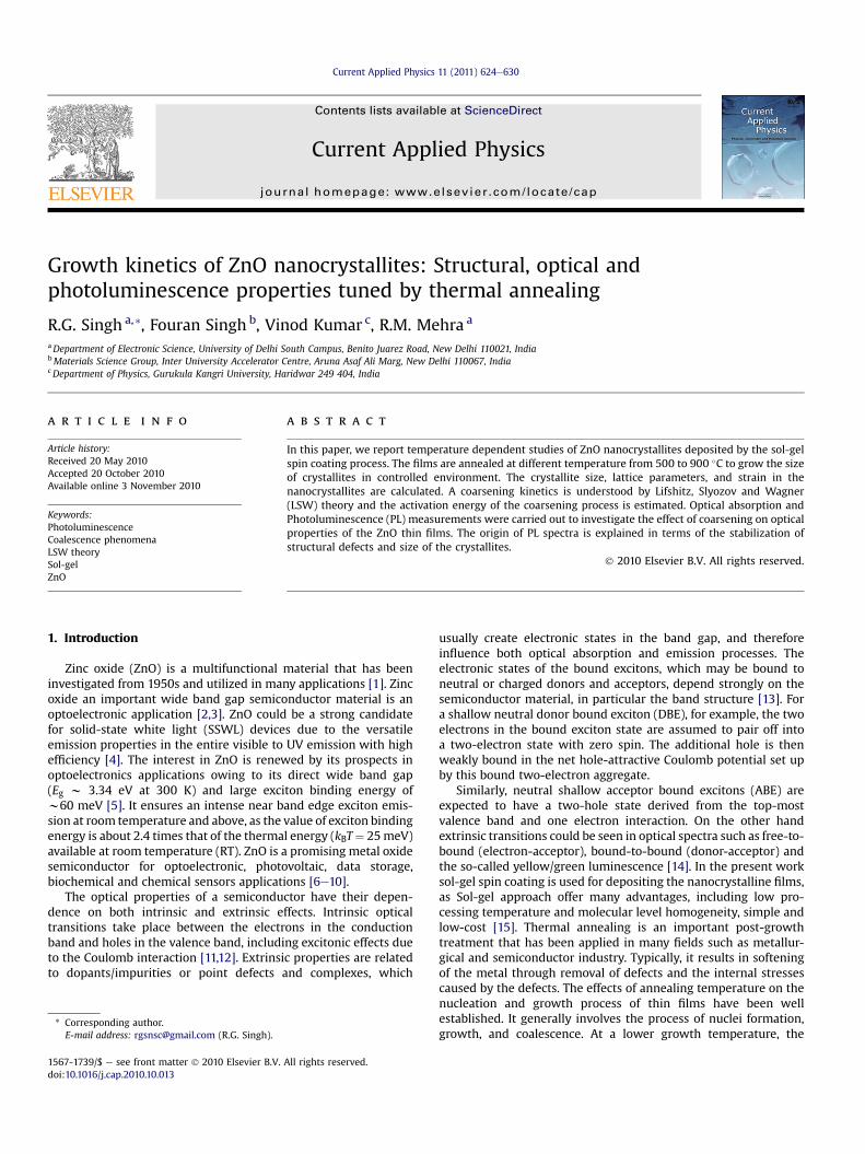
lable at ScienceDirect
Current Applied Physics 11 (2011) 624e630
Contents lists avai
Current Applied Physics
journal homepage: www.elsevier .com/locate/cap
Growth kinetics of ZnO nanocrystallites: Structural, optical andphotoluminescence properties tuned by thermal annealing
R.G. Singh a,*, Fouran Singh b, Vinod Kumar c, R.M. Mehra a
aDepartment of Electronic Science, University of Delhi South Campus, Benito Juarez Road, New Delhi 110021, IndiabMaterials Science Group, Inter University Accelerator Centre, Aruna Asaf Ali Marg, New Delhi 110067, IndiacDepartment of Physics, Gurukula Kangri University, Haridwar 249 404, India
a r t i c l e i n f o
Article history:Received 20 May 2010Accepted 20 October 2010Available online 3 November 2010
Keywords:PhotoluminescenceCoalescence phenomenaLSW theorySol-gelZnO
* Corresponding author.E-mail address: [email protected] (R.G. Singh).
1567-1739/$ e see front matter � 2010 Elsevier B.V.doi:10.1016/j.cap.2010.10.013
a b s t r a c t
In this paper, we report temperature dependent studies of ZnO nanocrystallites deposited by the sol-gelspin coating process. The films are annealed at different temperature from 500 to 900 �C to grow the sizeof crystallites in controlled environment. The crystallite size, lattice parameters, and strain in thenanocrystallites are calculated. A coarsening kinetics is understood by Lifshitz, Slyozov and Wagner(LSW) theory and the activation energy of the coarsening process is estimated. Optical absorption andPhotoluminescence (PL) measurements were carried out to investigate the effect of coarsening on opticalproperties of the ZnO thin films. The origin of PL spectra is explained in terms of the stabilization ofstructural defects and size of the crystallites.
� 2010 Elsevier B.V. All rights reserved.
1. Introduction
Zinc oxide (ZnO) is a multifunctional material that has beeninvestigated from 1950s and utilized in many applications [1]. Zincoxide an important wide band gap semiconductor material is anoptoelectronic application [2,3]. ZnO could be a strong candidatefor solid-state white light (SSWL) devices due to the versatileemission properties in the entire visible to UV emission with highefficiency [4]. The interest in ZnO is renewed by its prospects inoptoelectronics applications owing to its direct wide band gap(Eg w 3.34 eV at 300 K) and large exciton binding energy ofw60 meV [5]. It ensures an intense near band edge exciton emis-sion at room temperature and above, as the value of exciton bindingenergy is about 2.4 times that of the thermal energy (kBT¼ 25meV)available at room temperature (RT). ZnO is a promising metal oxidesemiconductor for optoelectronic, photovoltaic, data storage,biochemical and chemical sensors applications [6e10].
The optical properties of a semiconductor have their depen-dence on both intrinsic and extrinsic effects. Intrinsic opticaltransitions take place between the electrons in the conductionband and holes in the valence band, including excitonic effects dueto the Coulomb interaction [11,12]. Extrinsic properties are relatedto dopants/impurities or point defects and complexes, which
All rights reserved.
usually create electronic states in the band gap, and thereforeinfluence both optical absorption and emission processes. Theelectronic states of the bound excitons, which may be bound toneutral or charged donors and acceptors, depend strongly on thesemiconductor material, in particular the band structure [13]. Fora shallow neutral donor bound exciton (DBE), for example, the twoelectrons in the bound exciton state are assumed to pair off intoa two-electron state with zero spin. The additional hole is thenweakly bound in the net hole-attractive Coulomb potential set upby this bound two-electron aggregate.
Similarly, neutral shallow acceptor bound excitons (ABE) areexpected to have a two-hole state derived from the top-mostvalence band and one electron interaction. On the other handextrinsic transitions could be seen in optical spectra such as free-to-bound (electron-acceptor), bound-to-bound (donor-acceptor) andthe so-called yellow/green luminescence [14]. In the present worksol-gel spin coating is used for depositing the nanocrystalline films,as Sol-gel approach offer many advantages, including low pro-cessing temperature and molecular level homogeneity, simple andlow-cost [15]. Thermal annealing is an important post-growthtreatment that has been applied in many fields such as metallur-gical and semiconductor industry. Typically, it results in softeningof the metal through removal of defects and the internal stressescaused by the defects. The effects of annealing temperature on thenucleation and growth process of thin films have been wellestablished. It generally involves the process of nuclei formation,growth, and coalescence. At a lower growth temperature, the
R.G. Singh et al. / Current Applied Physics 11 (2011) 624e630 625
formation of small crystallites is kinetically favored. The formationof small crystallites reduces the supersaturation and hence thepossibility of the coalescence. During the post-growth by thermalannealing, the grains gain sufficient thermal energy to initiate thecoalescence. Several mass transport mechanisms have beenproposed to account for the coalescence phenomenon, namely,Ostwald ripening, sintering, and cluster migration.
In the Ostwald ripening mechanism, the larger particles grow or“ripen” at the expense of the smaller particles. The size of thesmaller particles will shrink or even disappear due to the netatomic transport to larger particles. The particle size of the ZnOincrease exponentially with increase of temperature due to thecoarsening of precipitates with increasing temperature is typical ofan Ostwald ripening process. Generally, Ostwald ripening is one ofthe coalescence phenomena that is always associated with thermalannealing treatment and has been studied for over a decade.
Lifshitz, Slyozov [16,17] and later Wagner [18] developed ananalytic mean-field theory, which is also known as LSW theory, todescribe the coarsening kinetics. The theory predicts the meanradius of particle increases as
r3ðtÞ � r3ðt0Þ ¼ KLSWðt � t0Þwhere r3(t0) and r3(t) are the mean radius of particles at time t0 andt, respectively, and KLSW is a temperature and material dependenceconstant. The LSW theory also predicts that the particle sizedistribution (PSD) exhibits the self-similarity behavior when it isscaled by themean particle size. Although the LSW theorywas builtwith several assumptions such as spherical shape of particles, nearzero volume fractions and diffusion-growth without convection,but these conditions generally do not affect or alter the power lawof coarsening [19]. In this paper, we are demonstrating the evolu-tion of the morphology of ZnO nanocrystallites by post-growththermal annealing. The structural and optical properties of the ZnOfilms are investigated and correlated to the coarsening [20e22] andthe above described LSW theory is employed to estimate the acti-vation energy of the coarsening process.
Fig. 1. Glancing angle x-ray diffraction (GAXRD) pattern of as-deposited and annealedfilms of ZnO on silicon as a function of annealing temperature, inset shows the full scanGAXRD pattern at the diffraction angle 2q value from 30 to 60� for film annealed at700 �C.
2. Experimental
The ZnO filmswere prepared usingwet chemical route of sol-gelspin coating. In this process zinc acetate dehydrate [Zn (CH3COO)22H2O] was first dissolved into Ethanol solution along with mono-ethanolamine (MEA). MEA is a highly water soluble, non-ionic, andacts as the sol-stabilizers. The homogeneous transparent solutionwith concentration of 0.2 M zinc acetate and 1:1 M ratio of MEA/zinc acetate dehydrate was prepared. This solution was kept forhydrolysis for 48 h. The solution was then spin coated on siliconsubstrate at 3500 rpm. The precursor films were heated at 240 �Cfor 30 min in air in order to remove the volatile component and thesynthesis was carried out by the thermal decomposition of zincacetate into ZnO.
The process of coating and preheating was repeated 10 times fordesired thickness. The annealing of as-deposited films was carriedout in controlled environment of Ar using thermolyne tubularfurnace, at 500, 600, 700, 800 and 900 �C for 30 min. The glancingangle x-ray diffraction (GAXRD) measurements were carried usingBruker-D8 advanced diffractometer and the PL studies were madeusing Mechelle 900 spectrograph under 325 nm excitation ofHeeCd laser. The surface topography of the ZnO films were studiedusing the atomic force microscopy (AFM) by Digital Nanoscope IIIaSPM. The band gap of ZnO deposited on silica substrate wasmeasured by optical absorption using Hitachi UV-3300 doublebeam spectrophotometer.
3. Results and discussion
3.1. Structural analysis
Fig. 1 shows glancing angle X-ray diffraction (GAXRD) pattern ofthe ZnO films as-deposited and annealed at different annealingtemperature. As-deposited film is almost not showing any diffrac-tion peak around preferred orientation of ZnO. After annealing attemperature from 500 �C to 900 �C the diffraction peak corre-sponding to (002) reflection at 34.4� appears in the pattern besidesother reflections corresponding to (100) and (101) planes. The insetin Fig. 1 shows the full scan of the film annealed at 700 �C and itreveals that the ZnO films are of polycrystalline nature withhexagonal wurtzite crystal structure (JCPDS: 36-1451). The crys-tallites of the films are randomly oriented; no diffraction peak ofthe metallic zinc crystallite structure is detected. The diffractionintensity of the (002) peak in GAXRD pattern is keep increases withthe increase of annealing temperature up to 900 �C. This behaviorcan be understood by two competing processes; the increase ofannealing temperature improves the stoichiometry of the films andthe crystal quality.
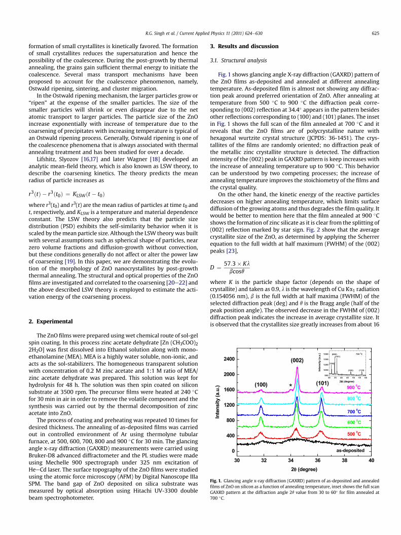
On the other hand, the kinetic energy of the reactive particlesdecreases on higher annealing temperature, which limits surfacediffusion of the growing atoms and thus degrades the film quality. Itwould be better to mention here that the film annealed at 900 �Cshows the formation of zinc silicate as it is clear from the splitting of(002) reflection marked by star sign. Fig. 2 show that the averagecrystallite size of the ZnO, as determined by applying the Scherrerequation to the full width at half maximum (FWHM) of the (002)peaks [23],
D ¼ 57:3� Klbcosq
where K is the particle shape factor (depends on the shape ofcrystallite) and taken as 0.9, l is the wavelength of Cu Ka1 radiation(0.154056 nm), b is the full width at half maxima (FWHM) of theselected diffraction peak (deg) and q is the Bragg angle (half of thepeak position angle). The observed decrease in the FWHM of (002)diffraction peak indicates the increase in average crystallite size. Itis observed that the crystallites size greatly increases from about 16
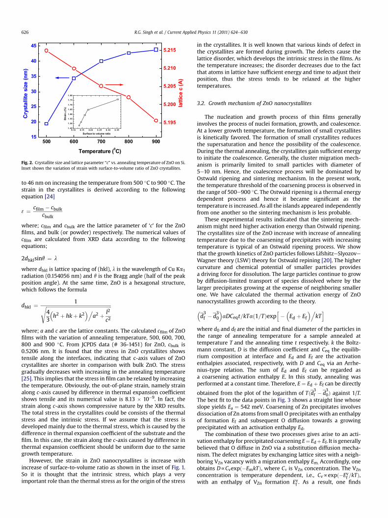
Fig. 2. Crystallite size and lattice parameter “c” vs. annealing temperature of ZnO on Si.Inset shows the variation of strain with surface-to-volume ratio of ZnO crystallites.
R.G. Singh et al. / Current Applied Physics 11 (2011) 624e630626
to 46 nm on increasing the temperature from 500 �C to 900 �C. Thestrain in the crystallites is derived according to the followingequation [24]
3 ¼ cfilm � cbulkcbulk
where; cfilm and cbulk are the lattice parameter of ‘c’ for the ZnOfilms, and bulk (or powder) respectively. The numerical values ofcfilm are calculated from XRD data according to the followingequations;
2dhklsinq ¼ l
where dhkl is lattice spacing of (hkl), l is the wavelength of Cu Ka1radiation (0.154056 nm) and q is the Bragg angle (half of the peakposition angle). At the same time, ZnO is a hexagonal structure,which follows the formula
dhkl ¼ 1ffiffiffiffiffiffiffiffiffiffiffiffiffiffiffiffiffiffiffiffiffiffiffiffiffiffiffiffiffiffiffiffiffiffiffiffiffiffiffiffiffiffiffiffiffiffiffiffiffiffiffiffiffiffiffi43
�h2 þ hkþ k2
�.a2 þ l2
c2
s
where; a and c are the lattice constants. The calculated cfilm of ZnOfilms with the variation of annealing temperature, 500, 600, 700,800 and 900 �C. From JCPDS data (# 36-1451) for ZnO, cbulk is0.5206 nm. It is found that the stress in ZnO crystallites showstensile along the interfaces, indicating that c-axis values of ZnOcrystallites are shorter in comparison with bulk ZnO. The stressgradually decreases with increasing in the annealing temperature[25]. This implies that the stress in film can be relaxed by increasingthe temperature. Obviously, the out-of-plane strain, namely strainalong c-axis caused by difference in thermal expansion coefficientshows tensile and its numerical value is 8.13 � 10�9. In fact, thestrain along c-axis shows compressive nature by the XRD results.The total stress in the crystallites could be consists of the thermalstress and the intrinsic stress. If we assume that the stress isdeveloped mainly due to the thermal stress, which is caused by thedifference in thermal expansion coefficient of the substrate and thefilm. In this case, the strain along the c-axis caused by difference inthermal expansion coefficient should be uniform due to the samegrowth temperature.
However, the strain in ZnO nanocrystallites is increase withincrease of surface-to-volume ratio as shown in the inset of Fig. 1.So it is thought that the intrinsic stress, which plays a veryimportant role than the thermal stress as for the origin of the stress
in the crystallites. It is well known that various kinds of defect inthe crystallites are formed during growth. The defects cause thelattice disorder, which develops the intrinsic stress in the films. Asthe temperature increases; the disorder decreases due to the factthat atoms in lattice have sufficient energy and time to adjust theirposition, thus the stress tends to be relaxed at the highertemperatures.
3.2. Growth mechanism of ZnO nanocrystallites
The nucleation and growth process of thin films generallyinvolves the process of nuclei formation, growth, and coalescence.At a lower growth temperature, the formation of small crystallitesis kinetically favored. The formation of small crystallites reducesthe supersaturation and hence the possibility of the coalescence.During the thermal annealing, the crystallites gain sufficient energyto initiate the coalescence. Generally, the cluster migration mech-anism is primarily limited to small particles with diameter of5e10 nm. Hence, the coalescence process will be dominated byOstwald ripening and sintering mechanism. In the present work,the temperature threshold of the coarsening process is observed inthe range of 500e900 �C. The Ostwald ripening is a thermal energydependent process and hence it became significant as thetemperature is increased. As all the islands appeared independentlyfrom one another so the sintering mechanism is less probable.
These experimental results indicated that the sintering mech-anism might need higher activation energy than Ostwald ripening.The crystallites size of the ZnO increase with increase of annealingtemperature due to the coarsening of precipitates with increasingtemperature is typical of an Ostwald ripening process. We showthat the growth kinetics of ZnO particles follows LifshitzeSlyozoveWagner theory (LSW) theory for Ostwald repining [20]. The highercurvature and chemical potential of smaller particles providesa driving force for dissolution. The large particles continue to growby diffusion-limited transport of species dissolved where by thelarger precipitates growing at the expense of neighboring smallerone. We have calculated the thermal activation energy of ZnOnanocrystallites growth according to the theory.
�d3f � d
30
�aDCeqt=kTað1=TÞexp
h��Ed þ Ef
�.kT
iwhere d0 and df are the initial and final diameter of the particles inthe range of annealing temperature for a sample annealed attemperature T and the annealing time t respectively. k the Boltz-mann constant, D is the diffusion coefficient and Ceq the equilib-rium composition at interface and Ed and Ef are the activationenthalpies associated, respectively, with D and Ceq via an Arrhe-nius-type relation. The sum of Ed and Ef can be regarded asa coarsening activation enthalpy E. In this study, annealing wasperformed at a constant time. Therefore, E ¼ Ed þ Ef can be directly
obtained from the plot of the logarithm of Tðd3f � d30Þ against 1/T.
The best fit to the data points in Fig. 3 shows a straight line whoseslope yields Ea ¼ 542 meV. Coarsening of Zn precipitates involvesdissociation of Zn atoms from small O precipitates with an enthalpyof formation Ef and subsequent O diffusion towards a growingprecipitated with an activation enthalpy Ed.
The combination of these two processes gives arise to an acti-vation enthalpy for precipitated coarsening E¼ Edþ Ef. It is generallybelieved that O diffuse in ZnO via a substitution diffusion mecha-nism. The defect migrates by exchanging lattice sites with a neigh-boring VZn vacancy with a migration enthalpy Em. Accordingly, oneobtains DfCvexpð�EmkTÞ, where Cn is VZn concentration. The VZnconcentration is temperature dependent, i.e., Cvfexpð�Evf =kTÞ,with an enthalpy of VZn formation Evf . As a result, one finds
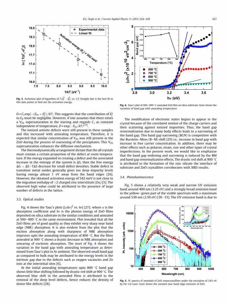
Fig. 4. Tauc’s plot of 500e900 �C annealed ZnO film on silica substrate. Inset shows thevariation of band gap with annealing temperature.
Fig. 5. PL spectra of annealed of ZnO nanocrystallites under the excitation of 3.81 eVby HeeCd Laser. Inset shows the zoomed near band edge emission of ZnO.
7.0 7.5 8.0 8.5 9.0 9.5 10.0
16.8
17.1
17.4
17.7
18.0
18.3
18.6
Activ
atio
nenerg
y(E
a )=
542
meV
d(
T[
nl3
Td
-3
0]
)
1/kT (eV -1
)
Experimental data
Linear fit
Fig. 3. Arrhenius plot of logarithm of Tðd3f � d30Þ vs. 1/T. Straight line is the best fit to
this data points to find out the activation energy.
R.G. Singh et al. / Current Applied Physics 11 (2011) 624e630 627
DfCvexp½�ðEm þ Evf Þ=kT�. This suggests that the contribution of Evfto Ed must be negligible. However, if one assumes that there existsa VZn supersaturation in the starting and regards Cn as constantindependent of temperature, Dfexpð�Em=kTÞ[17].
The ionized antisite defects were still present in these samplesand this increased with annealing temperature. Therefore, it isexpected that similar concentration of VZn was still present in theZnO during the process of coarsening of the precipitates. This VZnsupersaturation enhances the diffusion mechanism.
The thermodynamically arrangement dictate that the all crystalsmust contain a certain proportion of the defect at room tempera-ture. If the energy expanded in creating a defect and the associatedincrease in the entropy of the system is DS, then the free energyDG ¼ DE�TDS decrease for small defect densities. Stable defect intransition metal oxides generally gives too deep impurity levelshaving energy atleast 1 eV away from the band edges [26].However, the obtained activation energy of 542 meV is not close tothemigration enthalpy ofþ2 charged zinc interstitials (Zni) [5]. Theobserved high value could be attributed to the presence of largenumber of defects in the lattice.
3.3. Optical studies
Fig. 4 shows the Tauc’s plots [(ahn)2 vs. hn] [27]; where a is theabsorption coefficient and hn is the photon energy of ZnO filmsdeposited on silica substrate in the similar conditions and annealedat 500e900 �C in the same environment. Plot revealed that all theZnO films are of good quality as they exhibit very sharp near bandedge (NBE) absorption. It is also evident from the plot that theexciton absorption along with sharpness of NBE absorptionimproves upto the annealing temperature of 800 �C. But the filmsannealed at 900 �C shows a drastic decrease in NBE absorption andsmearing of excitonic absorption. The inset of Fig. 4 shows thevariation in the band gap with annealing temperature as deter-mined from Tauc’s plot in Ar ambient. The observed small band gapas-compared to bulk may be attributed to the energy levels in theintrinsic gap due to the defects such as oxygen vacancies and Znions at the interstitial sites [6].
At the initial annealing temperatures upto 800 �C band gapshows little blue shifting followed by drastic red shift at 900 �C. Theobserved blue shift in the annealed films is attributed to theremoval of the deep level defects, hence reduces the density ofdonor-like defects [28].
The modification of electronic states begins to appear in thecrystal because of the correlated motion of the charge carriers andtheir scattering against ionized impurities. Thus, the band gaprenormalization due to many body effects leads to a narrowing ofthe band gap. This band gap narrowing (BGN) is competitive withthe BursteineMoss (BeM) shift [29] i.e., increase in band gap withincrease in free carrier concentration. In addition, there may beother effects such as polaron, strain, size and other types of crystalimperfections. In the present work, we would like to emphasizethat the band gap widening and narrowing is induced by the BMand band gap renormalization effects. The drastic red shift at 900 �Cis attributed to the formation of the zinc silicate the interface ofsubstrate and ZnO crystallites corroborates with XRD results.
3.4. Photoluminescence
Fig. 5 shows a relatively very weak and narrow UV emissionband around 400 nm (3.25 eV) and a strongly broad emission bandin the yellowegreen part of the visible spectrum with a maximumaround 530 nm (2.50 eV) [30e33]. The UV emission band is due to
R.G. Singh et al. / Current Applied Physics 11 (2011) 624e630628
the radiative annihilation of excitons and can still be observed attemperature far above room temperature due to the relatively highexciton binding energy of 60 meV. The visible emission is due toa transition of an electron from a level close to the conduction bandedge to a deeply trapped hole in the bulk V00
0 of the ZnO particle. Itis assumed that the recombination in the bulk is negligiblecompared to non-radiative recombination at the surface of theparticle. The broad visible emission band due to deep level defectsof the annealed ZnO between 420 nm and 900 nm (2.95e1.37 eV). Itwould be better to mention here that the shape of the PL emissionband varies significantly with increase in the annealing tempera-ture. The intensity of the broad PL band increases upto theannealing temperature of 800 �C. But, there is drastic increase inthe intensity observed for the films annealed at 800 �C.
Moreover, the intensity of the orangeered band increases withannealing temperature up to 800 �C. Above this temperature theintensity of visible emission is decreased. The origin of the deeplevel defect related PL band has been investigated for a long time.However, due to the complexity of the microstructure of ZnO, thereis still no satisfactory consensus. Intrinsic defects, such as theoxygen vacancy and zinc vacancy are thought to be responsible forthe green band. For the oxygen vacancy especially, Vanheusdenet al. [34] established a correlation between the green band andsingly ionized oxygen vacancy [7]. The observed increase in thewidth of green band at incremented annealing temperature couldbe due to the increase in the concentration of defects [35]. If it isdue to the extrinsic impurity, the intensity of the peak shouldmainly be determined by the concentration of impurity, and itshould not display such strong temperature dependence.
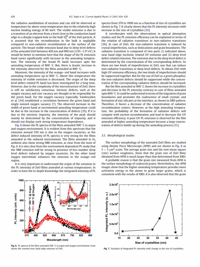
Fig. 6 shows the PL spectra of the films annealed 500 �C in argonand oxygen environment. It is evident from this spectrum that theemission around 550 nm is due to the oxygen vacancies, as thedefect induced intensity of PL spectra is very strong for the filmsannealed in the reduced environment. The films annealed in O2ambient also show strong NBE emission, as clear from the inset ofFig. 6. It is also clear from the environment dependent PL study thatthe NBE emission will be strong in presence of less number deeplevel defects induced by oxygen vacancies. On the other handoxygen interstitials enhances the emission in the orangeeredregion.
It is very important to understand the origin of the variation inthe PL intensity of ZnO films annealed at various temperatures. Inorder to have the in-depth knowledge the integrated intensity of PL
Fig. 6. PL spectra of the films annealed 500 �C in argon and oxygen environment. Insetshows the zoomed near band edge emission of ZnO.
spectra from 370 to 1000 nm as a function of size of crystallites areshown in Fig. 7. It clearly shows that the PL intensity increases withincrease in the size of crystallites [35].
It corroborates with the observations in optical absorptionstudies and the PL emission efficiency can be explained in terms ofthe relation of radiative transitions to non-radiative transitions[36]. In case of ZnO, the non-radiative transition is induced bycrystal imperfection, such as dislocations and grain boundaries. Theradiative transition is composed of two parts (i) indicated above,near band edge excitonic related UV emission and (ii) deep leveldefect related emission. The emission due to the deep level defect isdetermined by the concentration of the corresponding defects. Sothere are two kinds of imperfections in ZnO, one that can inducenon-radiative transitions or deep level defects. To obtain ZnO withhigh UV emission efficiency, the two kinds of imperfections shouldbe suppressed together. But for the use of ZnO as a green phosphor,the non-radiative defects should be suppressed while the concen-tration of the corresponding radiative defects should be increased.
But the film annealed at 900 �C shows the increase in crystallitesand decrease in the PL intensity contrary to case of films annealedupto800 �C. It couldbeunderstood in termsof themigrationof grainboundaries and promotes the coalescence of small crystals, andformation of zinc silicates at the interface, as shown in XRD pattern.Therefore, it favors a decrease of the concentration of radiativerecombination centers. However, at the high annealing tempera-ture, the probability of the formation of radiative defects willcompete with exciton recombination and lead to decrease the UVemission efficiency. A poor UV PL emission is observed for the filmannealed at higher annealing temperature because a large concen-tration of defects builds up during the annealing process [11].
3.5. Morphological studies
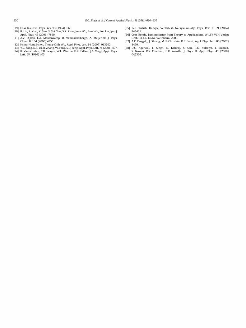
The surface morphology of the annealed ZnO films are studiedusing Atomic Force Microscope (AFM) and are shown in Fig. 8 as5 � 5 mm2 scans. The average grain size and the root mean square(rms) surface roughness, show that the grain size of ZnO filmsobtained from AFM is much larger than that determined from XRD.
A probable reason is that the grain size measured from AFM isthe surface morphology of coalesced grains. Nevertheless, the AFMimages show that the higher annealing temperature provides moreactivation energy to the atoms to grow larger grains, which isconsistent with the results of XRD. It is also observed that the grain
15 20 25 30 35 40 45
0.0
5.0x10⁵
1.0x10⁶
1.5x10⁶
2.0x10⁶
2.5x10⁶
).
u.
a(
yt
is
ne
tn
iL
Pd
et
ar
ge
tn
I
Size of crystallites (nm)
Fig. 7. Variation of integrated PL intensity with change in the size of crystallites.
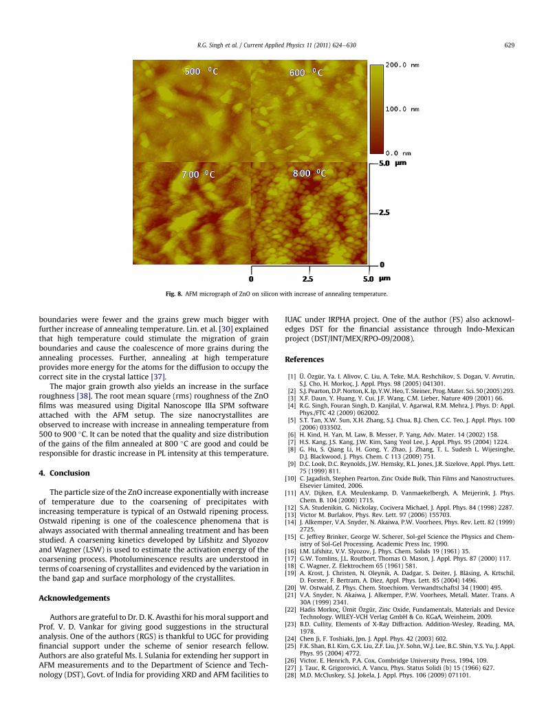
Fig. 8. AFM micrograph of ZnO on silicon with increase of annealing temperature.
R.G. Singh et al. / Current Applied Physics 11 (2011) 624e630 629
boundaries were fewer and the grains grew much bigger withfurther increase of annealing temperature. Lin. et al. [30] explainedthat high temperature could stimulate the migration of grainboundaries and cause the coalescence of more grains during theannealing processes. Further, annealing at high temperatureprovides more energy for the atoms for the diffusion to occupy thecorrect site in the crystal lattice [37].
The major grain growth also yields an increase in the surfaceroughness [38]. The root mean square (rms) roughness of the ZnOfilms was measured using Digital Nanoscope IIIa SPM softwareattached with the AFM setup. The size nanocrystallites areobserved to increase with increase in annealing temperature from500 to 900 �C. It can be noted that the quality and size distributionof the gains of the film annealed at 800 �C are good and could beresponsible for drastic increase in PL intensity at this temperature.
4. Conclusion
The particle size of the ZnO increase exponentially with increaseof temperature due to the coarsening of precipitates withincreasing temperature is typical of an Ostwald ripening process.Ostwald ripening is one of the coalescence phenomena that isalways associated with thermal annealing treatment and has beenstudied. A coarsening kinetics developed by Lifshitz and Slyozovand Wagner (LSW) is used to estimate the activation energy of thecoarsening process. Photoluminescence results are understood interms of coarsening of crystallites and evidenced by the variation inthe band gap and surface morphology of the crystallites.
Acknowledgements
Authors are grateful to Dr. D. K. Avasthi for hismoral support andProf. V. D. Vankar for giving good suggestions in the structuralanalysis. One of the authors (RGS) is thankful to UGC for providingfinancial support under the scheme of senior research fellow.Authors are also grateful Ms. I. Sulania for extending her support inAFM measurements and to the Department of Science and Tech-nology (DST), Govt. of India for providing XRD and AFM facilities to
IUAC under IRPHA project. One of the author (FS) also acknowl-edges DST for the financial assistance through Indo-Mexicanproject (DST/INT/MEX/RPO-09/2008).
References
[1] Ü. Özgür, Ya. I. Alivov, C. Liu, A. Teke, M.A. Reshchikov, S. Dogan, V. Avrutin,S.J. Cho, H. Morkoç, J. Appl. Phys. 98 (2005) 041301.
[2] S.J. Pearton,D.P.Norton, K. Ip, Y.W.Heo, T. Steiner, Prog.Mater. Sci. 50 (2005) 293.[3] X.F. Daun, Y. Huang, Y. Cui, J.F. Wang, C.M. Lieber, Nature 409 (2001) 66.[4] R.G. Singh, Fouran Singh, D. Kanjilal, V. Agarwal, R.M. Mehra, J. Phys. D: Appl.
Phys./FTC 42 (2009) 062002.[5] S.T. Tan, X.W. Sun, X.H. Zhang, S.J. Chua, B.J. Chen, C.C. Teo, J. Appl. Phys. 100
(2006) 033502.[6] H. Kind, H. Yan, M. Law, B. Messer, P. Yang, Adv. Mater. 14 (2002) 158.[7] H.S. Kang, J.S. Kang, J.W. Kim, Sang Yeol Lee, J. Appl. Phys. 95 (2004) 1224.[8] G. Hu, S. Qiang Li, H. Gong, Y. Zhao, J. Zhang, T. L. Sudesh L. Wijesinghe,
D.J. Blackwood, J. Phys. Chem. C 113 (2009) 751.[9] D.C. Look, D.C. Reynolds, J.W. Hemsky, R.L. Jones, J.R. Sizelove, Appl. Phys. Lett.
75 (1999) 811.[10] C. Jagadish, Stephen Pearton, Zinc Oxide Bulk, Thin Films and Nanostructures.
Elsevier Limited, 2006.[11] A.V. Dijken, E.A. Meulenkamp, D. Vanmaekelbergh, A. Meijerink, J. Phys.
Chem. B. 104 (2000) 1715.[12] S.A. Studenikin, G. Nickolay, Cocivera Michael, J. Appl. Phys. 84 (1998) 2287.[13] Victor M. Burlakov, Phys. Rev. Lett. 97 (2006) 155703.[14] J. Alkemper, V.A. Snyder, N. Akaiwa, P.W. Voorhees, Phys. Rev. Lett. 82 (1999)
2725.[15] C. Jeffrey Brinker, George W. Scherer, Sol-gel Science the Physics and Chem-
istry of Sol-Gel Processing. Academic Press Inc, 1990.[16] I.M. Lifshitz, V.V. Slyozov, J. Phys. Chem. Solids 19 (1961) 35.[17] G.W. Tomlins, J.L. Routbort, Thomas O. Mason, J. Appl. Phys. 87 (2000) 117.[18] C. Wagner, Z. Elektrochem 65 (1961) 581.[19] A. Krost, J. Christen, N. Oleynik, A. Dadgar, S. Deiter, J. Bläsing, A. Krtschil,
D. Forster, F. Bertram, A. Diez, Appl. Phys. Lett. 85 (2004) 1496.[20] W. Ostwald, Z. Phys. Chem. Stoechiom. Verwandtschaftsl 34 (1900) 495.[21] V.A. Snyder, N. Akaiwa, J. Alkemper, P.W. Voorhees, Metall. Mater. Trans. A
30A (1999) 2341.[22] Hadis Morkoç, Ümit Özgür, Zinc Oxide, Fundamentals, Materials and Device
Technology. WILEY-VCH Verlag GmbH & Co. KGaA, Weinheim, 2009.[23] B.D. Cullity, Elements of X-Ray Diffraction. Addition-Wesley, Reading, MA,
1978.[24] Chen Ji, F. Toshiaki, Jpn. J. Appl. Phys. 42 (2003) 602.[25] F.K. Shan, B.I. Kim, G.X. Liu, Z.F. Liu, J.Y. Sohn, W.J. Lee, B.C. Shin, Y.S. Yu, J. Appl.
Phys. 95 (2004) 4772.[26] Victor. E. Henrich, P.A. Cox, Combridge University Press, 1994, 109.[27] J. Tauc, R. Grigorovici, A. Vancu, Phys. Status Solidi (b) 15 (1966) 627.[28] M.D. McCluskey, S.J. Jokela, J. Appl. Phys. 106 (2009) 071101.
R.G. Singh et al. / Current Applied Physics 11 (2011) 624e630630
[29] Elias Burstein, Phys. Rev. 93 (1954) 632.[30] B. Lin, Z. Xiao, X. Sun, S. Shi Guo, X.Z. Zhao, Juan Wu, Run Wu, Jing Liu, Jpn. J.
Appl. Phys. 45 (2006) 7860.[31] A.V. Dijken, E.A. Meulenkamp, D. Vanmaekelbergh, A. Meijerink, J. Phys.
Chem. B. 104 (2000) 4355.[32] Hsing-Hung Hsieh, Chung-Chih Wu, Appl. Phys. Lett. 91 (2007) 013502.[33] Y.C. Kong, D.P. Yu, B. Zhang, W. Fang, S.Q. Feng, Appl. Phys. Lett. 78 (2001) 407.[34] K. Vanheusden, C.H. Seager, W.L. Warren, D.R. Tallant, J.A. Voigt, Appl. Phys.
Lett. 68 (1996) 403.
[35] Ilan Shalish, Henryk, Venkatesh Narayanamurty, Phys. Rev. B. 69 (2004)245401.
[36] Cees Ronda, Luminescence from Theory to Applications. WILEY-VCH VerlagGmbH & Co. KGaA, Weinheim, 2009.
[37] A.R. Duggal, J.J. Shiang, M.H. Christain, D.F. Foust, Appl. Phys. Lett. 80 (2002)3470.
[38] D.C. Agarwal, F. Singh, D. Kabiraj, S. Sen, P.K. Kulariya, I. Sulania,S. Nozaki, R.S. Chauhan, D.K. Avasthi, J. Phys. D: Appl. Phys. 41 (2008)045305.
Copyright © 2022 FDOKUMEN