
GM328/GM338/GM398 Mobile Radios - of Manuals
556
GM328/GM338/GM398 Mobile Radios Detailed Service Manual 6804112J18-E December, 2003
-
Upload
khangminh22 -
Category
Documents
-
view
0 -
download
0
Transcript of GM328/GM338/GM398 Mobile Radios - of Manuals
GM328/GM338/GM398Mobile Radios
Detailed Service Manual
6804112J18-E
December, 2003

Computer Software CopyrightsThe Motorola products described in this manual may include copyrighted Motorola computer programs stored in semiconductor memories or other media. Laws in the United States and other countries preserve for Motorola certain exclusive rights for copyrighted computer programs, including the exclusive right to copy or reproduce in any form, the copyrighted computer program. Accordingly, any copyrighted Motorola computer programs contained in the Motorola products described in this manual may not be copied or reproduced in any manner without the express written permission of Motorola. Furthermore, the purchase of Motorola prod-ucts shall not be deemed to grant, either directly or by implication, estoppel or otherwise, any license under the copyrights, patents or patent applications of Motorola, except for the normal non-exclusive royalty-free license to use that arises by operation of law in the sale of a product.

DOCUMENT HISTORY
The following major changes have been implemented in this manual since the previous edition:
Edition Description Date
6804112J18-O Initial edition
6804112J18-E Added Document History section. Dec. 2003
Changed to latest Safety Information (Feb. 2002)
Added GM328 model information to VHF, UHF1 and UHF2 bands.

THIS PAGE INTENTIONALLY LEFT BLANK
December, 2003
GM328/GM338/GM398Mobile Radios
Detailed Service Manual
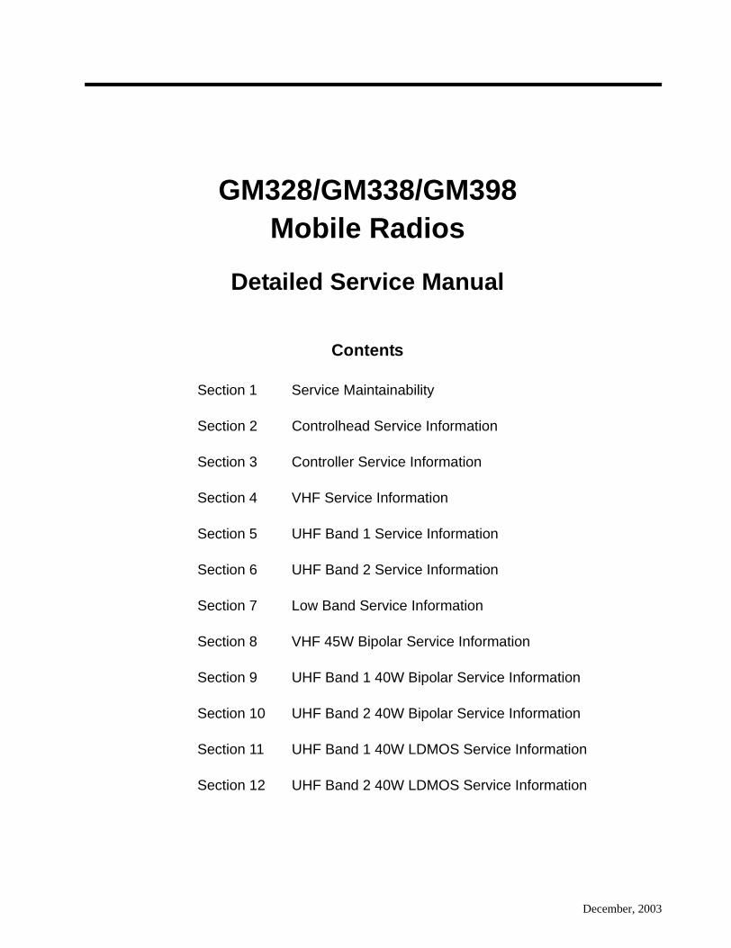
Contents
Section 1 Service Maintainability
Section 2 Controlhead Service Information
Section 3 Controller Service Information
Section 4 VHF Service Information
Section 5 UHF Band 1 Service Information
Section 6 UHF Band 2 Service Information
Section 7 Low Band Service Information
Section 8 VHF 45W Bipolar Service Information
Section 9 UHF Band 1 40W Bipolar Service Information
Section 10 UHF Band 2 40W Bipolar Service Information
Section 11 UHF Band 1 40W LDMOS Service Information
Section 12 UHF Band 2 40W LDMOS Service Information

THIS PAGE INTENTIONALLY LEFT BLANK
GM328/GM338/GM398Mobile Radios
Service Maintainability
Issue: December, 2003

Computer Software CopyrightsThe Motorola products described in this manual may include copyrighted Motorola computer programs stored in semiconductor memories or other media. Laws in the United States and other countries preserve for Motorola certain exclusive rights for copyrighted computer programs, including the exclusive right to copy or reproduce in any form, the copyrighted computer program. Accordingly, any copyrighted Motorola computer programs contained in the Motorola products described in this manual may not be copied or reproduced in any manner without the express written permission of Motorola. Furthermore, the purchase of Motorola products shall not be deemed to grant, either directly or by implication, estoppel or otherwise, any license under the copyrights, patents or patent applications of Motorola, except for the normal non-exclusive royalty-free license to use that arises by operation of law in the sale of a product.

i
SAFETY INFORMATIONProduct Safety and RF Exposure for Mobile Two-Way Radios Installed in Vehicles or as Fixed Site Control Stations
The information provided in this document supersedes the general safety information contained in user guides published prior to February 2002.
RF Energy Exposure Awareness and Control Information, and Operational Instructions for FCC Occupational Use Requirements
NOTICE: This radio is intended for use in occupational/controlled conditions, where users have full knowledge of their exposure and can exercise control over their exposure to meet FCC limits. This radio device is NOT authorized for general population, consumer or any other use.
This 2-way radio uses electromagnetic energy in the radio frequency (RF) spectrum to provide communications between two or more users over a distance. It uses radio frequency (RF) energy or radio waves to send and receive calls. RF energy is one from of electromagnetic energy. Other forms include, but are not limited to, sunlight and x-rays. RF energy, however, should not be confused with these other forms of electromagnetic energy, which when used improperly, can cause biological damage. Very high levels of x-rays, for example, can damage tissues and genetic material.
Experts in science, engineering, medicine, health, and industry work with organizations to develop standards for safe exposure to RF energy. These standards provide recommended levels of RF exposure for both workers and the general public. These recommended RF exposure levels include substantial margins of protection.
All Motorola 2-way radios are designed, manufactured, and tested to ensure they meet government-established RF exposure levels. In addition, manufacturers also recommend specific operating instructions to users of 2-way radios. These instructions are important because they inform users about RF energy exposure and provide simple procedures on how to control it.
Please refer to the following Web sites for more information on what RF energy exposure is and how to control your exposure to assure compliance with established RF exposure limits.http://www.fcc.gov/oet/rfsafety/rf-fags.htmlhttp://www.osha.gov/SLTC/radiofrequencyradiation/index.html
BEFORE USING THIS RADIO, READ THIS BOOKLET WHICH CONTAINS IMPORTANT OPERAT-ING INSTRUCTIONS FOR SAFE USAGE AND RF ENERGY AWARENESS AND CONTROL INFORMATION FOR COMPLIANCE WITH RF ENERGY EXPOSURE LIMITS IN APPLICABLE NATIONAL AND INTERNATIONAL STANDARDS.
ii
Federal Communication Commission (FCC) Regulations
The FCC rules require manufacturers to comply with the FCC RF energy exposure limits for mobile 2-way radios before they can be marketed in the U.S. When 2-way radios are used as a consequence of employment, the FCC requires users to be fully aware of and able to control their exposure to meet occupational requirements. Exposure awareness can be facilitated by the use of a label directing users to specific user awareness information. Your Motorola 2-way radio has a RF exposure product label. Also, your Motorola user manual, or separate safety booklet, includes information and operating instructions required to control your RF exposure and to satisfy compliance requirements.
Compliance with RF Exposure Standard
Your Motorola two-way radio is designed and tested to comply with a number of national and international standards and guidelines (listed below) regarding human exposure to radio frequency electromagnetic energy. This radio complies with the IEEE and ICNIRP exposure limits for occupational/controlled RF exposure environment at duty factors of up to 50% talk–50% listen and is authorized by the FCC for occupational use. In terms of measuring RF energy for compliance with the FCC exposure guidelines, your radio antenna radiates measurable RF energy only while it is transmitting (during talking), not when it is receiving (listening) or in standby mode.
Your Motorola two-way radio complies with the following RF energy exposure standards and guidelines:
• United States Federal Communications Commission, Code of Federal Regulations; 47 CFR part 2 sub-part J
• American National Standards Institute (ANSI) / Institute of Electrical and Electronic Engineers (IEEE) C95. 1-1992
• Institute of Electrical and Electronic Engineers (IEEE) C95.1-1999 Edition• International Commission on Non-Ionizing Radiation Protection (ICNIRP) 1998• Ministry of Health (Canada) Safety Code 6. Limits of Human Exposure to Radiofrequency Elec-
tromagnetic Fields in the Frequency Range from 3 kHz to 300 GHz, 1999• Australian Communications Authority Radiocommunications (Electromagnetic Radiation -
Human Exposure) Standard, 2003• ANATEL, Brasil Regulatory Authority, Resolution 256 (April 11, 2001) “additional requirements
for SMR, cellular and PCS product certification.”
RF Exposure Compliance and Control Guidelines and Operating Instructions
To control exposure to yourself and others and to ensure compliance with the RF exposure limits, always adhere to the following procedures.
Guidelines• User awareness instructions should accompany device when transferred to other users.• Do not use this device if the operational requirements described herein are not met.
Instructions• Transmit no more than the rated duty factor of 50% of the time. To transmit (talk), push the
Push-To-Talk (PTT) button. To receive calls, release the PTT button. Transmitting 50% of the time, or less, is important because this radio generates measurable RF energy exposure only when transmitting (in terms of measuring for standards compliance).
• Transmit only when people outside the vehicle are at least the recommended minimum laterial distance away, as shown in Table 1, from the body of a vehicle with a properly installed antenna. This separation distance will ensure that there is sufficient distance from a

iii
properly installed (according to installation instructions) externally-mounted antenna to satisfy the RF exposure requirements in the standards listed above.
NOTE: Table 1 below lists the recommended lateral distance for bystanders in an uncontrolled environment from the body of a vehicle with an approved, properly installed transmitting antenna (i.e., monopoles overa a ground plane, or dipoles) at several different ranges of rated radio power for mobile radios installed in a vehicle.
NOTE:If you are not sure of the rated power of your radio, contact your Motorola representative or dealer and supply the radio model number found on the radio model label. If you cannot determine the rated power out, then assure 3-feet separation from the body of the vehicle.
Mobile Antenna Installation Guidelines• These mobile antenna installation guidelines are limited to metal body motor vehicles or vehicles
with appropriate ground planes.• Antennas should be installed in the center area of the roof or the trunk lid taking into account the
bystander exposure conditions of backseat passengers and according to the specific instructions and restrictions in the Radio Installation Manual along with the requirements of the antenna sup-plier.
• Trunk lid installations are limited to vehicles with clearly defined flat trunk lide, and in some cases, to specific radio models and antennas. See the Radio Installation Manual for specific information on how and where to install specific types of approved antennas to facilitate recom-mended operating distances to all potentially exposed persons.
• Use only the Motorola-approved, supplied antenna or a Motorola-approved replacement antenna. Unauthorized antennas, modifications, or attachments could damage the radio and may result in non-compliance with RF Safety Standards.
Approved Accessories• This radio has been tested and meets RF Safety Standards when used with the Motorola acces-
sories supplied or designated for this product. Use of other accessories may result in non-compli-ance with RF Safety Standards.
• For a list of Motorola-approved antennas, visit the following Web site, which lists approved accessories for your radio model: http://ap.cgiss.motorola.com/AAD/index.html
Additional Information
For additional information on exposure requirements or other training information, visit http://www.motorola.com/rfhealth.
Table 1: Rated Power of Vehicle-Installed Mobile Two-Way Radio andRecommended Minimum Lateral Distance from Vehicle Body
Mobile Radio Rated Power (see Note)
Minimum Lateral Distance from Vehicle Body
Less than 7 watts 8 inches (20 centimeters)
7 to 15 watts 1 foot (30 centimeters)
16 to 39 watts 2 feet (60 centimeters)
40 to 110 watts 3 feet (90 centimeters)

iv
Compliance and Control Guidelines and Operating Instructions for Mobile Two-Way Radios Installed as Fixed Site Stations
If mobile radio equipment is installed at a fixed location and operated as a control station or as a fixed unit, the antenna installation must comply with the following requirements in order to ensure optimal performance and compliance with the RF energy exposure limits in the standards and guidelines listed on page ii:
• The antenna should be mounted outside the building on the roof or a tower if at all possible.• As with all fixed site antenna installations, it is the responsibility of the licensee to manage the
site in accordance with applicable regulatory requirements and may require additional compli-ance actions such as site survey measurements, signage, and site access restrictions in order to ensure that exposure limits are not exceeded.
Electromagnetic Interference/CompatibilityNOTE:Nearly every electronic device is susceptible to electromagnetic interference (EMI) if
inadequately shielded, designed, or otherwise configured for electromagnetic compatibility. It may be necessary to conduct compatibility testing to determine if any electronic equipment used in or around vehicles or near fixed site antenna is sensitive to external RF energy or if any procedures need to be followed to eliminate or mitigate the potential for interaction between the radio transmitter and the equipment or device.
Facilities
To avoid electromagnetic interference and/or compatibility conflicts, turn off your radio in any facility where posted notices instruct you to do so. Hospitals or health care facilities may be using equipment that is sensitive to external RF energy.
Vehicles
To avoid possible interaction between the radio transmitter and any vehicle electronic control modules, such as ABS, engine, or transmission controls, the radio should be installed only by an experienced installer and the following precautions should be used when installing the radio:
1. Refer to the manufacturer’s instructions or other technical bulletins for recommendations on radio installation.
2. Before installing the radio, determine the location of the electronic control modules and their harnesses in the vehicle.
3. Route all radio wiring, including the antenna transmission line, as far away as possible from the electronic control units and associated wiring.
Driver Safety
Check the laws and regulations on the use of radios in the area where you drive. Always obey them.
When using your radio while driving, please:
• Give full attention to driving and to the road.• Pull off the road and park before making or answering a call if driving conditions so require.
v
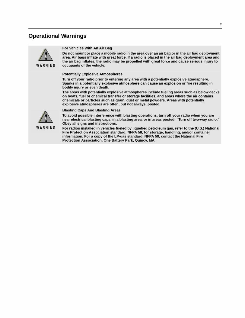
Operational Warnings
For Vehicles With An Air BagDo not mount or place a mobile radio in the area over an air bag or in the air bag deployment area. Air bags inflate with great force. If a radio is placed in the air bag deployment area and the air bag inflates, the radio may be propelled with great force and cause serious injury to occupants of the vehicle.
Potentially Explosive AtmospheresTurn off your radio prior to entering any area with a potentially explosive atmosphere. Sparks in a potentially explosive atmosphere can cause an explosion or fire resulting in bodily injury or even death.The areas with potentially explosive atmospheres include fueling areas such as below decks on boats, fuel or chemical transfer or storage facilities, and areas where the air contains chemicals or particles such as grain, dust or metal powders. Areas with potentially explosive atmospheres are often, but not always, posted.
Blasting Caps And Blasting AreasTo avoid possible interference with blasting operations, turn off your radio when you are near electrical blasting caps, in a blasting area, or in areas posted: “Turn off two-way radio.” Obey all signs and instructions.For radios installed in vehicles fueled by liquefied petroleum gas, refer to the (U.S.) National Fire Protection Association standard, NFPA 58, for storage, handling, and/or container information. For a copy of the LP-gas standard, NFPA 58, contact the National Fire Protection Association, One Battery Park, Quincy, MA.

vi
THIS PAGE INTENTIONALLY LEFT BLANK
vii
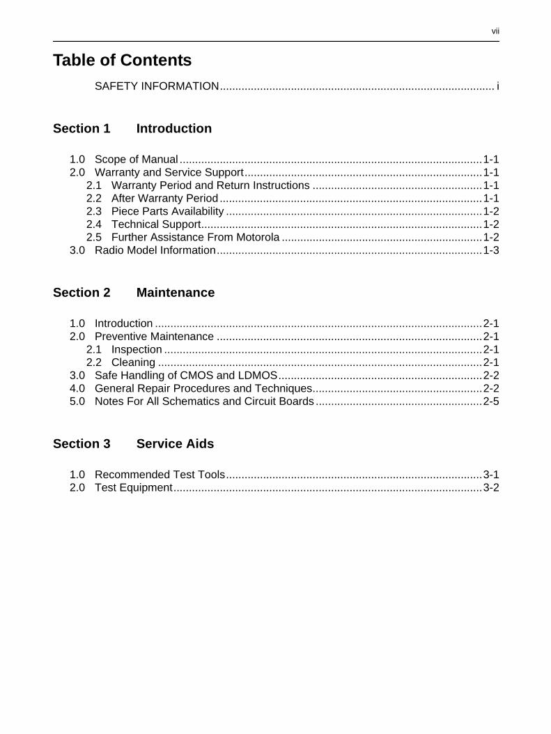
Table of ContentsSAFETY INFORMATION......................................................................................... i
Section 1 Introduction
1.0 Scope of Manual ..................................................................................................1-12.0 Warranty and Service Support.............................................................................1-1
2.1 Warranty Period and Return Instructions .......................................................1-12.2 After Warranty Period .....................................................................................1-12.3 Piece Parts Availability ...................................................................................1-22.4 Technical Support...........................................................................................1-22.5 Further Assistance From Motorola .................................................................1-2
3.0 Radio Model Information......................................................................................1-3
Section 2 Maintenance
1.0 Introduction ..........................................................................................................2-12.0 Preventive Maintenance ......................................................................................2-1
2.1 Inspection .......................................................................................................2-12.2 Cleaning .........................................................................................................2-1
3.0 Safe Handling of CMOS and LDMOS..................................................................2-24.0 General Repair Procedures and Techniques.......................................................2-25.0 Notes For All Schematics and Circuit Boards ......................................................2-5
Section 3 Service Aids
1.0 Recommended Test Tools...................................................................................3-12.0 Test Equipment....................................................................................................3-2

viii
THIS PAGE INTENTIONALLY LEFT BLANK
1-1
Section 1
INTRODUCTION
1.0 Scope of Manual
This manual is intended for use by service technicians familiar with similar types of equipment. It contains service information required for the equipment described and is current as of the printing date. Changes which occur after the printing date may be incorporated by a complete manual revision or alternatively as additions.
2.0 Warranty and Service Support
Motorola offers support which includes: full exchange and/or repair of the product during the warranty period; and service/repair or spare parts support out of warranty. Any “return for exchange” or “return for repair” to an authorized Motorola Dealer must be accompanied by a Warranty Claim Form. Warranty Claim Forms are obtained by contacting an Authorized Motorola Dealer.
2.1 Warranty Period and Return Instructions
The terms and conditions of warranty are defined fully in the Motorola Dealer or Distributor or Reseller contract. These conditions may change from time to time, and the following subsections are for guidance purposes only.
In instances where the product is covered under a “return for replacement” or “return for repair” warranty, a check of the product should be performed prior to shipping the unit back to Motorola. This is to ensure that the product has been correctly programmed or has not been subjected to damage outside the terms of the warranty.
Prior to shipping any radio back to the appropriate Motorola warranty depot, please contact Customer Resources. All returns must be accompanied by a Warranty Claim Form, available from your Customer Resources representative. Products should be shipped back in the original packaging, or correctly packaged to ensure that no damage occurs in transit.
2.2 After Warranty Period
After the Warranty period, Motorola continues to support its products in two ways:
1. Motorola's Accessories and Aftermarket Division (AAD) offers a repair service to both end users and dealers at competitive prices.
2. AAD supplies individual parts and modules that can be purchased by dealers who are techni-cally capable of performing fault analysis and repair.
NOTE Before operating or testing these units, please read the Safety Information section in thefront of this manual.

1-2 Warranty and Service Support
2.3 Piece Parts Availability
Some replacement parts, spare parts, and/or product information can be ordered directly. If a complete Motorola part number is assigned to the part, it is available from Motorola’s Accessories and Aftermarket Division (AAD). If no part number is assigned, the part is not normally available from Motorola. If the part number is appended with an asterisk, the part is serviceable by Motorola Depot only. If a parts list is not included, this generally means that no user-serviceable parts are available for that kit or assembly.
All orders for parts/information should include the complete Motorola identification number. All part orders should be directed to your local AAD office. Please refer to your latest price pages.
2.4 Technical Support
Technical support is available to assist the dealer/distributor in resolving any malfunction which may be encountered. Initial contact should be by telephone wherever possible. When contacting Motorola Technical Support, be prepared to provide the product model number and the unit’s serial number.
2.5 Further Assistance From Motorola
You can also call the CGISS Indirect Business Customer Help Desk number, (604)-6302525 or send an email to [email protected].
1-3 Radio Model Information
3.0 Radio Model Information
The model number and serial number are located on a label attached to the back of your radio. You can determine the RF output power, frequency band, protocols, and physical packages. The example below shows one mobile radio model number and its specific characteristics.
Table 1-1 Radio Model Number (Example: AZM25KHF9AA5)
Type of Unit
Model Series
Freq. Band
Power Level
Physical Packages
Channel Spacing
ProtocolFeature Level
AZ M 25 KVHF(136-
174MHz)
H1-25W
CGM328
9Program-
mable
AAConventional
1GM328
RUHF1(403-
470MHz)
K25-60W
FGM338
5GM338
SUHF2(450-
527MHz)
NGM398
8GM398
BLB, R1(29.7-
36MHz)
CLB, R2
(36-40MHz)
DLB, R3
(42-50MHz)
AZ
= C
ount
ry C
ode
M =
Mob
ile

1-4 Radio Model Information
THIS PAGE INTENTIONALLY LEFT BLANK

2-1
Section 2
MAINTENANCE
1.0 Introduction
This chapter of the manual describes:
• preventive maintenance
• safe handling of CMOS devices
• repair procedures and techniques
2.0 Preventive Maintenance
The radios do not require a scheduled preventive maintenance program; however, periodic visual inspection and cleaning is recommended.
2.1 Inspection
Check that the external surfaces of the radio are clean, and that all external controls and switches are functional. It is not recommended to inspect the interior electronic circuitry.
2.2 Cleaning
The following procedures describe the recommended cleaning agents and the methods to be used when cleaning the external and internal surfaces of the radio. External surfaces include the front cover, housing assembly, and battery case. These surfaces should be cleaned whenever a periodic visual inspection reveals the presence of smudges, grease, and/or grime.
The only recommended agent for cleaning the external radio surfaces is a 0.5% solution of a mild dishwashing detergent in water. The only factory recommended liquid for cleaning the printed circuit boards and their components is isopropyl alcohol (70% by volume).
1. Cleaning External Plastic SurfacesThe detergent-water solution should be applied sparingly with a stiff, non-metallic, short-bris-tled brush to work all loose dirt away from the radio. A soft, absorbent, lintless cloth or tissue should be used to remove the solution and dry the radio. Make sure that no water remains entrapped near the connectors, cracks, or crevices.
NOTE Internal surfaces should be cleaned only when the radio is disassembled for servicing orrepair.
CAUTION: The effects of certain chemicals and their vapors can have harmful results on certain plastics. Aerosol sprays, tuner cleaners, and other chemicals should be avoided.!
2-2 Safe Handling of CMOS and LDMOS
2. Cleaning Internal Circuit Boards and ComponentsIsopropyl alcohol may be applied with a stiff, non-metallic, short-bristled brush to dislodge embedded or caked materials located in hard-to-reach areas. The brush stroke should direct the dislodged material out and away from the inside of the radio. Make sure that controls or tunable components are not soaked with alcohol. Do not use high-pressure air to hasten the drying process since this could cause the liquid to collect in unwanted places. Upon comple-tion of the cleaning process, use a soft, absorbent, lintless cloth to dry the area. Do not brush or apply any isopropyl alcohol to the frame, front cover, or back cover.
3.0 Safe Handling of CMOS and LDMOS
Complementary metal-oxide semiconductor (CMOS) devices are used in this family of radios. CMOS characteristics make them susceptible to damage by electrostatic or high voltage charges. Damage can be latent, resulting in failures occurring weeks or months later. Therefore, special precautions must be taken to prevent device damage during disassembly, troubleshooting, and repair.
Handling precautions are mandatory for CMOS circuits and are especially important in low humidity conditions. DO NOT attempt to disassemble the radio without first referring to the CMOS CAUTION paragraph in the Disassembly and Reassembly section of the manual.
4.0 General Repair Procedures and Techniques
Parts Replacement and Substitution
When damaged parts are replaced, identical parts should be used. If the identical replacement component is not locally available, check the parts list for the proper Motorola part number and order the component from the nearest Motorola Communications parts center listed in the “Piece Parts” section of this manual.
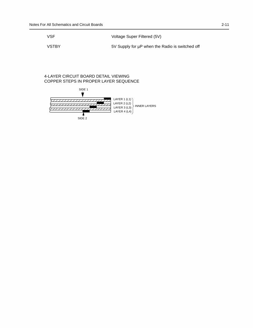
Rigid Circuit Boards
The family of radios uses bonded, multi-layer, printed circuit boards. Since the inner layers are not accessible, some special considerations are required when soldering and unsoldering components. The through-plated holes may interconnect multiple layers of the printed circuit. Therefore, care should be exercised to avoid pulling the plated circuit out of the hole.
When soldering near the 18-pin and 40-pin connectors:
• avoid accidentally getting solder in the connector.
• be careful not to form solder bridges between the connector pins
• closely examine your work for shorts due to solder bridges.
NOTE Always use a fresh supply of alcohol and a clean container to prevent contamination bydissolved material (from previous usage).
General Repair Procedures and Techniques 2-3
Chip Components
Use either the RLN4062 Hot-Air Repair Station or the Motorola 0180381B45 Repair Station for chip component replacement. When using the 0180381B45 Repair Station, select the TJ-65 mini-thermojet hand piece. On either unit, adjust the temperature control to 370 °C (700 °F), and adjust the airflow to a minimum setting. Airflow can vary due to component density.
• To remove a chip component:
1. Use a hot-air hand piece and position the nozzle of the hand piece approximately 0.3 cm (1/8") above the component to be removed.
2. Begin applying the hot air. Once the solder reflows, remove the component using a pair of tweezers.
3. Using a solder wick and a soldering iron or a power desoldering station, remove the excess solder from the pads.
• To replace a chip component using a soldering iron:
1. Select the appropriate micro-tipped soldering iron and apply fresh solder to one of the solder pads.
2. Using a pair of tweezers, position the new chip component in place while heating the fresh solder.
3. Once solder wicks onto the new component, remove the heat from the solder.
4. Heat the remaining pad with the soldering iron and apply solder until it wicks to the compo-nent. If necessary, touch up the first side. All solder joints should be smooth and shiny.
• To replace a chip component using hot air:
1. Use the hot-air hand piece and reflow the solder on the solder pads to smooth it.
2. Apply a drop of solder paste flux to each pad.
3. Using a pair of tweezers, position the new component in place.
4. Position the hot-air hand piece approximately 0.3 cm (1/8” ) above the component and begin applying heat.
5. Once the solder wicks to the component, remove the heat and inspect the repair. All joints should be smooth and shiny.

2-4 General Repair Procedures and Techniques
Shields
Removing and replacing shields will be done with the R1070 station with the temperature control set to approximately 215°C (415°F) [230°C (445°F) maximum].
• To remove the shield:
1. Place the circuit board in the R1070 circuit board holder.
2. Select the proper heat focus head and attach it to the heater chimney.
3. Add solder paste flux around the base of the shield.
4. Position the shield under the heat-focus head.
5. Lower the vacuum tip and attach it to the shield by turning on the vacuum pump.
6. Lower the focus head until it is approximately 0.3 cm (1/8”) above the shield.
7. Turn on the heater and wait until the shield lifts off the circuit board.
8. Once the shield is off, turn off the heat, grab the part with a pair of tweezers, and turn off the vacuum pump.
9. Remove the circuit board from the R1070 circuit board holder.
• To replace the shield:
1. Add solder to the shield if necessary, using a micro-tipped soldering iron.
2. Next, rub the soldering iron tip along the edge of the shield to smooth out any excess solder. Use solder wick and a soldering iron to remove excess solder from the solder pads on the cir-cuit board.
3. Place the circuit board back in the R1070 circuit board holder.
4. Place the shield on the circuit board using a pair of tweezers.
5. Position the heat-focus head over the shield and lower it to approximately 0.3 cm (1/8”) above the shield.
6. Turn on the heater and wait for the solder to reflow.
7. Once complete, turn off the heat, raise the heat-focus head and wait approximately one minute for the part to cool.
8. Remove the circuit board and inspect the repair. No cleaning should be necessary.
Notes For All Schematics and Circuit Boards 2-5
5.0 Notes For All Schematics and Circuit Boards
* Component is frequency sensitive. Refer to the Electrical Parts List for value and usage.
1. Unless otherwise stated, resistances are in Ohms (K = 1000), and capacitances are in picofarads (pF) or microfarads (µF).
2. DC voltages are measured from point indicated to chassis ground using a Motorola DC multimeter or equivalent. Transmitter measurements should be made with a 1.2 µH choke in series with the voltage probe to prevent circuit loading.
3. Interconnect Tie Point Legend:
16_8MHz 16.8MHz Reference Frequency
3V3 Regulated 3.3V Supply Voltage for Voice Storage
5V Regulated 5V Supply Voltage for RF Circuitry
5V Regulated 5V Supply Voltage (Control Head)
5V RF Regulated 5V Supply Voltage for RF Circuitry
5V SOURCE 5V Signal to Switch On Control Head
5VD Regulated 5V Supply Voltage for Digital Circuitry
9V3 Regulated 9.3V Supply Voltage
9V3FLT Filtered 9.3V Supply Voltage
A+ 13.2V Supply Voltage
ADDR µP Address Lines
AN Analog Lines to Analog to Digital Converter
ANALOG INPUT 2 External Keypad Matrix Column Signal
ANALOG INPUT 3 External Keypad Matrix Row Signal
BATTERY VOLTAGE Battery Voltage Sense Line
BL A GREEN Back Light Anode Green
BL A RED Back Light Anode Red
BL GREEN Green Back Light Control
BL K GREEN Back Light Cathode Green
BL K RED Back Light Cathode Red
BL KP Green Green Keypad Back Light Control
2-6 Notes For All Schematics and Circuit Boards
BL KP RED Red Keypad Back Light Control
BL LCD GREEN Green Display Back Light Control
BL LCD RED Red Display Back Light Control
BL RED Red Back Light Control
BOOT CNTRL Bootstrap Mode Enable Signal
BOOT MODE Boot Mode Select
BOOT PWR ON Control Head Switch On Signal
BOOT SCI RX Serial Communication Interface Receive Line
BOOT SCI TX Serial Communication Interface Transmit Line
BOOT VPP Boot Mode Select
BUS+ Bi-directional Serial Communication Line
BWSELECT Signal to select between the Ceramic Filter Pairs
CH ACT Channel Activity Indicator Signal (Fast Squelch)
CH KP ID Control Head Keypad ID (Data) Lines
CH REQUEST Control Head Request from Control Head µP
CLK Clock Signal
CNTLVLTG PA Power Control Voltage
CNTR AUDIO Audio Lines of the Controller
COL x Keypad Matrix Column x
CSX Chip Select Line PCIC / FRACN
DATA Data Signal
DC POWER ON Electronic Switching On or Off of the Radio's Voltage Regulators
DISCAUDIO Audio Output Signal from the Receiver IC
ECLK Clock (not used)
EE CS EEPROM Chip Select
EMERGENCY CONTROL Emergency Line to switch on the Radio's Voltage Regulators
EXP BD REQ Service Request Line from Expansion Board
Notes For All Schematics and Circuit Boards 2-7
EXP1 CS Expansion Board Chip Select 1
EXP2 CS Expansion Board Chip Select 2
EXT KP COL External Keypad Matrix Column Signal
EXT KP ROW External Keypad Matrix Row Signal
EXT MIC External (from Accessory Connector) Microphone Input
EXT SWB+ External Switched 13.2V Supply Voltage
F1200 Interrupt Line from ASFIC CMP
FECTRL 1 Control Voltage for Front End Filter
FECTRL 2 Control Voltage for Front End Attenuator Switch
FLASH CS Flash Chip Select
FLASH OE Flash Output Enable
FLAT RX SND Option Board Audio Output Signal
FLAT TX RTN Flat TX Input from Option Board and Accessory Connector
FLT A+ Filtered 13.2 V Supply Voltage
GP x IN General Purpose Input x
GP x IN ACC y General Purpose Input x from Accessory Connector Pin y
GP x IN OUT ACC y General Purpose Input/Output x from Accessory Connector Pin y
GP x OUT General Purpose Output x
GP x OUT ACC y General Purpose Input x from Accessory Connector Pin y
GPIO General Purpose Input Output Lines
HANDSET AUDIO Handset Audio Output
HOOK Hang-up Switch Input
HSIO High Speed Clock In / Data Out
IF First Intermediate Frequency Signal
IGNITION CONTROL Ignition Line to switch on the Radio's Voltage Regulators
IN 5V RF REG Supply Voltage for 5V Regulator in RF Section
INT KP COL Internal Keypad Matrix Column Signal
2-8 Notes For All Schematics and Circuit Boards
INT KP ROW Internal Keypad Matrix Row Signal
INT MIC Internal (from Control Head) Microphone Input
INT SWB Internal Switched 13.2V Supply Voltage
INT SWB+ Internal Switched 13.2V Supply Voltage
IRQ Interrupt Request from Control Head
K9V1 9.1V in Transmit Mode
KEYPAD ID Keypad Identification Line
LCD A0 LCD Control / Display Data Select
LCD CS LCD Chip Select
LCD DATA LCD Data Lines
LCD E RD LCD Enable Read
LCD RW WR LCD Read Write Control
LED CNTRL LED Control Lines
LED GREEN Green LED Control
LED RED Red LED Control
LED YELLOW Yellow LED Control
LOCK Lock Detect Signal from Synthesizer
LSIO Low Speed Clock In / Data Out
LVZIF CS LVZIF Chip Select (not used)
MIC Microphone Input
MISO Serial Peripheral Interface Receive Line
MODIN Modulation Signal into the Synthesizer
MOSBIAS 2 PA Bias Voltage for second Stage
MOSBIAS 3 PA Bias Voltage for third Stage
NOISE BLNKR Noise Blanker Enable (Low Band only)
ON OFF CONTROL Service Request Line from Control Head / Manual Switching Onof the Radio's Voltage Regulators
ON OFF SENSE (Control Head) On/Off Sense Line to Control Head µP

Notes For All Schematics and Circuit Boards 2-9
ON OFF SENSE (Controller) Service Request Line from Control Head
OPT CS Option Board Chip Select
OPT PTT PTT from Option Board
PA PWR SET ASFIC Output Voltage to set the Transmitter Power
PA SWB Switches Supply Voltage for PA Current Control Circuitry
PA SUPVLTG 13.2 V Supply Voltage of the Transmitter PA
PCIC MOSBIAS 1 PA Bias Voltage for first Stage
PRESC Prescaler Signal from VCO to Synthesizer
PTT IRDEC Microphone PTT Input
PTT IRDECODER Microphone PTT Input
R W Read Write Signal for RAM / Flash
RAM CS RAM Chip Select
RDY Service Request Line from Option Board
REF CS Reference Chip Select (not used)
RESET Reset Line
ROW x Keypad Matrix Row x
RSSI Received Signal Strength Indicator
RX ADAPT Flat TX Path Disable during Transmitter Key-up
RX AUD RTN Option Board Input / Output of Receiver Audio Path
RX FLAT FILTERED AUDIO Flat or Filtered Audio to Accessory Connector
RXIN RF Signal from Antenna Switch into the Receiver
RXINJ RF Signal from the VCO into the Mixer
SCI RX Serial Communication Interface Receive Line
SCI TX Serial Communication Interface Transmit Line
SPI Serial Peripheral Interface Bus
SPKR- Negative Audio PA Speaker Output
SPKR+ Positive Audio PA Speaker Output
2-10 Notes For All Schematics and Circuit Boards
SQ DET Squelch Detect Signal
SYN µP Clock Signal
TEMP SENSE Temperature Sense Line for LCD
TEMPSENSE Temperature Sense Line from PA to µP
TRB TX/RX VCO Switch Signal
TX AUD RTN Option Board Output to Transmit Audio Path
TX AUD SND Microphone Audio to Option Board
TXINJ RF Signal from the VCO into the Transmitter PA
U DRIVER Supply Voltage for PA Driver
U PREDRIVER Supply Voltage for PA Pre-driver
UNSW 5V Permanent 5V Supply
URX SND Filtered Audio Signal to Option Board
VAG 2.5V Reference Voltage for Analog Circuitry
VCOBIAS 1 Switch Signal from Synthesizer
VCOBIAS 2 Switch Signal from Synthesizer
VCOMOD Modulation Signal into VCO
VCTRL VCO Frequency Control Voltage
VDDA Regulated 5V for Digital Circuitry in RF Section
VOLTAGE SENSE Voltage Sense Line from LCD
VOLUME Volume Pot Output
VOX Voice Operated Transmit Level
VPP Boot Mode Select
VS AUDIOSEL Switch Signal to Enable Option Board Audio Output Signal
VS GAINSEL Voice Storage Gain Select Line
VS INT Voice Storage Interrupt Line
VS MIC Voice Storage Audio Signal into Microphone Path
VS RAC Voice Storage Row Address Clock Signal
Notes For All Schematics and Circuit Boards 2-11
VSF Voltage Super Filtered (5V)
VSTBY 5V Supply for µP when the Radio is switched off
4-LAYER CIRCUIT BOARD DETAIL VIEWINGCOPPER STEPS IN PROPER LAYER SEQUENCE
LAYER 1 (L1)
LAYER 2 (L2)LAYER 3 (L3)LAYER 4 (L4)
INNER LAYERS
SIDE 1
SIDE 2

2-12 Notes For All Schematics and Circuit Boards
THIS PAGE INTENTIONALLY LEFT BLANK
3-1
Section 3
SERVICE AIDS
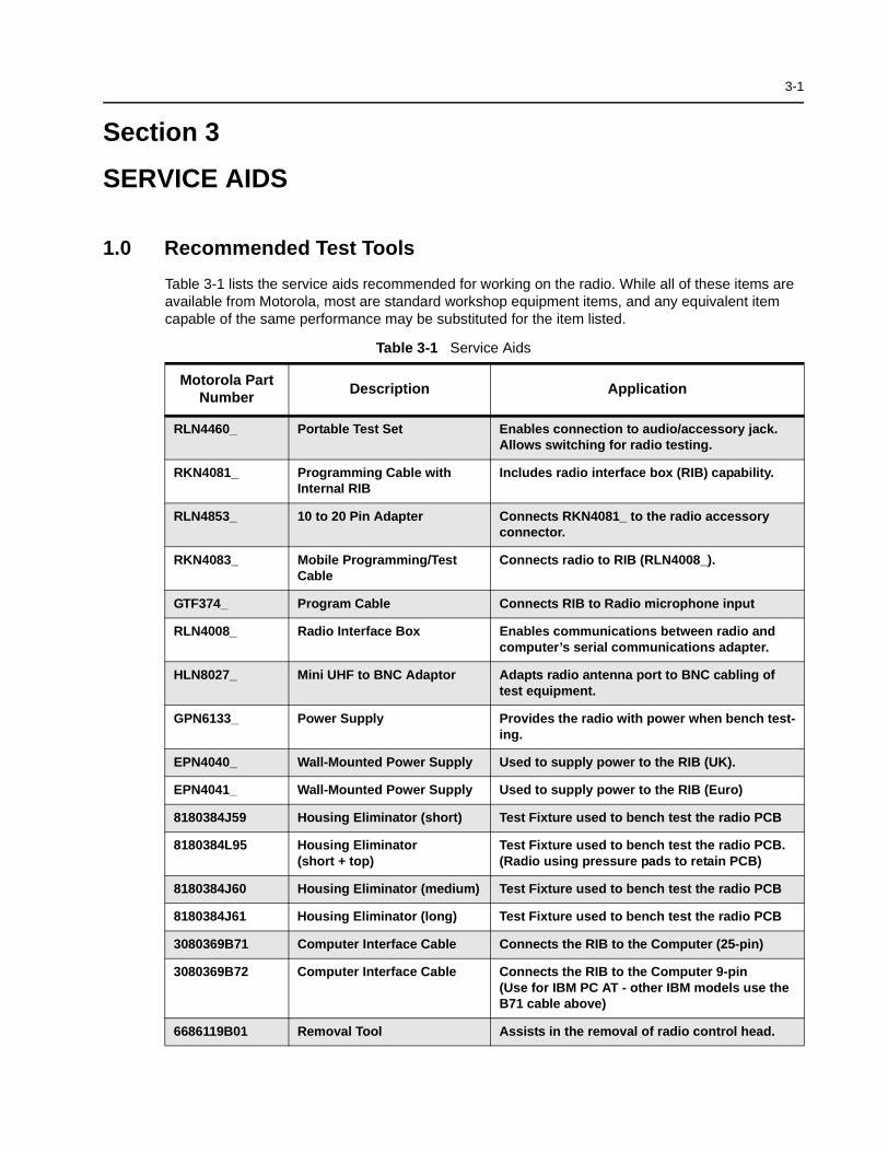
1.0 Recommended Test Tools
Table 3-1 lists the service aids recommended for working on the radio. While all of these items are available from Motorola, most are standard workshop equipment items, and any equivalent item capable of the same performance may be substituted for the item listed.
Table 3-1 Service Aids
Motorola Part Number
Description Application
RLN4460_ Portable Test Set Enables connection to audio/accessory jack. Allows switching for radio testing.
RKN4081_ Programming Cable with Internal RIB
Includes radio interface box (RIB) capability.
RLN4853_ 10 to 20 Pin Adapter Connects RKN4081_ to the radio accessory connector.
RKN4083_ Mobile Programming/Test Cable
Connects radio to RIB (RLN4008_).
GTF374_ Program Cable Connects RIB to Radio microphone input
RLN4008_ Radio Interface Box Enables communications between radio and computer’s serial communications adapter.
HLN8027_ Mini UHF to BNC Adaptor Adapts radio antenna port to BNC cabling of test equipment.
GPN6133_ Power Supply Provides the radio with power when bench test-ing.
EPN4040_ Wall-Mounted Power Supply Used to supply power to the RIB (UK).
EPN4041_ Wall-Mounted Power Supply Used to supply power to the RIB (Euro)
8180384J59 Housing Eliminator (short) Test Fixture used to bench test the radio PCB
8180384L95 Housing Eliminator (short + top)
Test Fixture used to bench test the radio PCB. (Radio using pressure pads to retain PCB)
8180384J60 Housing Eliminator (medium) Test Fixture used to bench test the radio PCB
8180384J61 Housing Eliminator (long) Test Fixture used to bench test the radio PCB
3080369B71 Computer Interface Cable Connects the RIB to the Computer (25-pin)
3080369B72 Computer Interface Cable Connects the RIB to the Computer 9-pin(Use for IBM PC AT - other IBM models use the B71 cable above)
6686119B01 Removal Tool Assists in the removal of radio control head.
3-2 Test Equipment
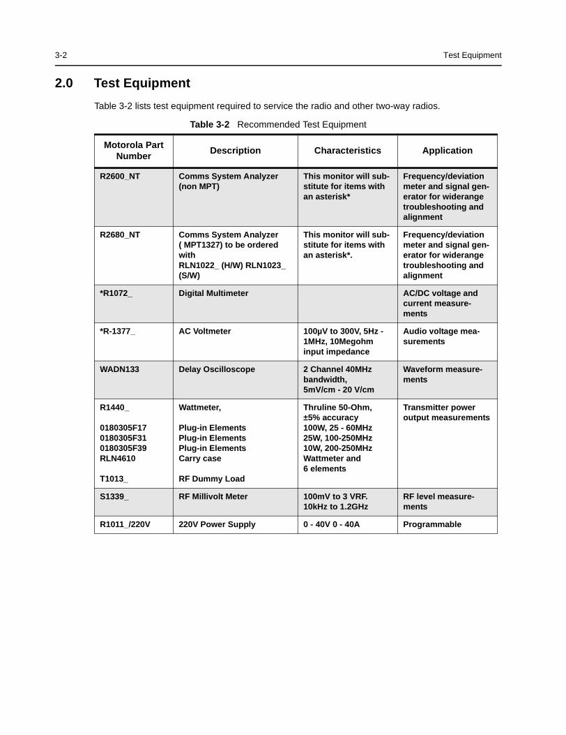
2.0 Test Equipment
Table 3-2 lists test equipment required to service the radio and other two-way radios.
Table 3-2 Recommended Test Equipment
Motorola Part Number
Description Characteristics Application
R2600_NT Comms System Analyzer (non MPT)
This monitor will sub-stitute for items with an asterisk*
Frequency/deviation meter and signal gen-erator for widerange troubleshooting and alignment
R2680_NT Comms System Analyzer ( MPT1327) to be ordered with RLN1022_ (H/W) RLN1023_ (S/W)
This monitor will sub-stitute for items with an asterisk*.
Frequency/deviation meter and signal gen-erator for widerange troubleshooting and alignment
*R1072_ Digital Multimeter AC/DC voltage and current measure-ments
*R-1377_ AC Voltmeter 100µV to 300V, 5Hz - 1MHz, 10Megohm input impedance
Audio voltage mea-surements
WADN133 Delay Oscilloscope 2 Channel 40MHz bandwidth, 5mV/cm - 20 V/cm
Waveform measure-ments
R1440_
0180305F170180305F310180305F39RLN4610
T1013_
Wattmeter,
Plug-in ElementsPlug-in ElementsPlug-in ElementsCarry case
RF Dummy Load
Thruline 50-Ohm,±5% accuracy100W, 25 - 60MHz25W, 100-250MHz10W, 200-250MHzWattmeter and 6 elements
Transmitter power output measurements
S1339_ RF Millivolt Meter 100mV to 3 VRF.10kHz to 1.2GHz
RF level measure-ments
R1011_/220V 220V Power Supply 0 - 40V 0 - 40A Programmable
GM328/GM338/GM398Mobile Radios
Controlhead
Service Information
Issue: December, 2003

Computer Software CopyrightsThe Motorola products described in this manual may include copyrighted Motorola computer programs stored in semiconductor memories or other media. Laws in the United States and other countries preserve for Motorola certain exclusive rights for copyrighted computer programs, including the exclusive right to copy or reproduce in any form, the copyrighted computer program. Accordingly, any copyrighted Motorola computer programs contained in the Motorola products described in this manual may not be copied or reproduced in any manner without the express written permission of Motorola. Furthermore, the purchase of Motorola products shall not be deemed to grant, either directly or by implication, estoppel or otherwise, any license under the copyrights, patents or patent applications of Motorola, except for the normal non-exclusive royalty-free license to use that arises by operation of law in the sale of a product.

i
Table of Contents
Section 1 overview
1.0 GM328 Model (GCN6112_) .................................................................................1-12.0 GM338 Model (GCN6114_) .................................................................................1-23.0 GM398 Model (GCN6115_) .................................................................................1-3
Section 2 Theory of Operation
1.0 Introduction ..........................................................................................................2-12.0 Controlhead Model for GM328.............................................................................2-1
2.1 Power Supplies...............................................................................................2-12.2 Power On / Off................................................................................................2-12.3 Microprocessor Circuit....................................................................................2-22.4 SBEP Serial Interface.....................................................................................2-22.5 Keypad Keys ..................................................................................................2-32.6 Status LED and Back Light Circuit .................................................................2-32.7 Microphone Connector Signals ......................................................................2-32.8 Speaker ..........................................................................................................2-42.9 Electrostatic Transient Protection...................................................................2-4
3.0 Controlhead Model for GM338.............................................................................2-43.1 Power Supplies...............................................................................................2-43.2 Power On / Off................................................................................................2-43.3 Microprocessor Circuit....................................................................................2-53.4 SBEP Serial Interface.....................................................................................2-53.5 Keypad Keys ..................................................................................................2-63.6 Status LED and Back Light Circuit .................................................................2-63.7 Liquid Crystal Display (LCD) ..........................................................................2-73.8 Microphone Connector Signals ......................................................................2-73.9 Speaker ..........................................................................................................2-83.10 Electrostatic Transient Protection...................................................................2-8
4.0 Controlhead Model for GM398.............................................................................2-94.1 Power Supplies...............................................................................................2-94.2 Voltage Regulator Circuit................................................................................2-94.3 Power On / Off................................................................................................2-94.4 Microprocessor Circuit..................................................................................2-104.5 SBEP Serial Interface...................................................................................2-104.6 Keypad Keys ................................................................................................2-114.7 Status LED and Back Light Circuit ...............................................................2-114.8 Liquid Crystal Display (LCD) ........................................................................2-124.9 Microphone Connector Signals ....................................................................2-12

ii
4.10 Speaker (Remote Mount Configuration only) ...............................................2-134.11 Electrostatic Transient Protection.................................................................2-13
Section 3 Troubleshooting Charts
1.0 Controlhead GM328 Troubleshooting Flow Chart ...............................................3-11.1 On/Off ............................................................................................................3-11.2 Microprocessor...............................................................................................3-2
2.0 Controlhead GM338 Troubleshooting Flow Chart ...............................................3-32.1 On/Off ............................................................................................................3-32.2 Microprocessor...............................................................................................3-42.3 Display............................................................................................................3-52.4 Backlight.........................................................................................................3-6
3.0 Controlhead GM398 Troubleshooting Flow Chart ...............................................3-73.1 On/Off ............................................................................................................3-73.2 Microprocessor ..............................................................................................3-83.3 Microprocessor (cont.)....................................................................................3-93.4 Display .........................................................................................................3-103.5 Keypad Backlight .........................................................................................3-113.6 Display Backlight .........................................................................................3-12
Section 4 Controlhead PCBs / Schematics / Parts lists
1.0 Allocation of Schematics and Circuit Boards .......................................................4-12.0 Controlhead GM328 - PCB 8486146B07 / Schematics.......................................4-3
Controlhead GM328 - PCB 8486146B07 ..............................................................4-3Controlhead GM328 - Schematic Sheet 1 of 2.......................................................4-4Controlhead GM328 - Schematic Sheet 2 of 2.......................................................4-5Controlhead PCB 8486146B07 Parts List ..............................................................4-6
3.0 Controlhead GM338 - PCB 8486155B06 / Schematics.......................................4-7Controlhead GM338 - PCB 8486155B06 ..............................................................4-7Controlhead GM338 - Schematic Sheet 1 of 4.......................................................4-8Controlhead GM338 - Schematic Sheet 2 of 4.......................................................4-9Controlhead GM338 - Schematic Sheet 3 of 4.....................................................4-10Controlhead GM338 - Schematic Sheet 4 of 4.....................................................4-11Controlhead PCB 8486155B06 Parts List ............................................................ 4-12
4.0 Controlhead GM398 - PCB 8486178B03 / Schematics.....................................4-13Controlhead GM398 - PCB 8486178B03 .............................................................4-13Controlhead GM398 - Schematic Sheet 1 of 4.....................................................4-14Controlhead GM398 - Schematic Sheet 2 of 4.....................................................4-15Controlhead GM398 - Schematic Sheet 3 of 4.....................................................4-16Controlhead GM398 - Schematic Sheet 4 of 4.....................................................4-17Controlhead PCB 8486178B03 Parts List ............................................................ 4-18

1-1
Section 1
OVERVIEW
1.0 GM328 Model (GCN6112_)
The Controlhead contains the internal speaker, the on/off/volume knob, the microphone connector, several buttons to operate the radio and several indicator Light Emitting Diodes (LED) to inform the user about the radio status. To control the LED’s and to communicate with the host radio the control head uses the Motorola 68HC11E9 microprocessor.
1-2 GM338 Model (GCN6114_)
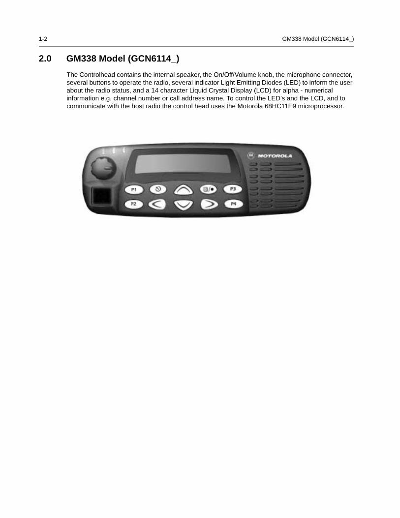
2.0 GM338 Model (GCN6114_)
The Controlhead contains the internal speaker, the On/Off/Volume knob, the microphone connector, several buttons to operate the radio, several indicator Light Emitting Diodes (LED) to inform the user about the radio status, and a 14 character Liquid Crystal Display (LCD) for alpha - numerical information e.g. channel number or call address name. To control the LED’s and the LCD, and to communicate with the host radio the control head uses the Motorola 68HC11E9 microprocessor.

GM398 Model (GCN6115_) 1-3
3.0 GM398 Model (GCN6115_)
The Controlhead contains the On/Off/Volume knob, the microphone connector, several buttons to operate the radio, several indicator Light Emitting Diodes (LED) to inform the user about the radio status, and a Liquid Crystal Display (LCD) with 21 pre - defined symbols and a 32*96 dot matrix for graphical or alpha - numerical information e.g. channel number, select code, call address name. To control the LEDs and the LCD, and to communicate with the host radio the control head uses the Motorola 68HC11K4 microprocessor.

1-4 GM398 Model (GCN6115_)
THIS PAGE INTENTIONALLY LEFT BLANK

2-1
Section 2
THEORY OF OPERATION
1.0 Introduction
This Chapter provides a detailed theory of operation for the Controlhead circuits. For details of the trouble shooting refer to the related Section of this manual.
2.0 Controlhead Model for GM328
The controlhead contains the internal speaker, the On/Off/Volume knob, the microphone connector, several buttons to operate the radio and several indicator Light Emitting Diodes (LED) to inform the user about the radio status. To control the LED’s and to communicate with the host radio the control-head uses the Motorola 68HC11E9 microprocessor.
2.1 Power Supplies
The power supply to the controlhead is taken from the host radio’s FLT A+ voltage via connector J0801 pin 3 and the regulated +5V via connector J0801 pin 7. The voltage FLT A+ is at supply voltage level and is used for the LED’s, the back light and to power up the radio via on / off / volume knob. The stabilized +5 volt is used for the microprocessor and the keypad buttons. The voltage USW 5V derived from the FLT A+ voltage and stabilized by the series combination of R0822, VR0822 is used to buffer the internal RAM of the microprocessor (U0831). C0822 allows the supply voltage level to be disconnected for a couple of seconds without losing RAM parameters. Dual diode D0822 prevents radio circuitry from discharging this capacitor. When the supply voltage is applied to the radio, C0822 is charged via R0822 and D0822. To avoid, that the µP enters the wrong mode when the radio is switched on while the voltage across C0822 is still too low, the regulated 5V charge C0822 via diode D0822.
2.2 Power On / Off
The On/Off/Volume knob when pressed switches the radio’s voltage regulators on by connecting line ON OFF CONTROL to line UNSW 5V via D0821. Additionally, 5 volts at the base of digital transistor Q0822 informs the controlhead’s microprocessor about the pressed knob. The microprocessor asserts pin 62 and line CH REQUEST low to hold line ON OFF CONTROL at 5 volts via Q0823 and D0821. The high line ON OFF CONTROL also informs the host radio, that the controlhead’s microprocessor wants to send data via SBEP bus. When the radio returns a data request message, the microprocessor will inform the radio about the pressed knob. If the radio was switched off, the radio’s µP will switch it on and vice versa. If the On/Off/Volume knob is pressed while the radio is on, the software detects a low state on line ON OFF SENSE, the radio is alerted via line ON OFF CONTROL and sends a data request message. The controlhead µP will inform the radio about the pressed knob and the radio’s µP will switch the radio off.

2-2 Controlhead Model for GM328
2.3 Microprocessor Circuit
The controlhead uses the Motorola 68HC11E9 microprocessor (µP) (U0831) to control the LED’s and to communicate with the host radio. RAM and ROM are contained within the microprocessor itself.
The microprocessor generates it’s clock using the oscillator inside the microprocessor along with a 8 MHz ceramic resonator (U0833) and R0920.
The microprocessor’s RAM is always powered to maintain parameters such as the last operating mode. This is achieved by maintaining 5V at µP pin 25. Under normal conditions, when the radio is off, USW 5V is formed by FLT A+ running to D0822. C0822 allows the battery voltage to be disconnected for a couple of seconds without losing RAM parameters. Diode D0822 prevents radio circuitry from discharging this capacitor.
There are 8 analogue to digital converter ports (A/D) on the µP . They are labeled within the device block as PE0-PE7. These lines sense the voltage level ranging from 0 to 5V of the input line and convert that level to a number ranging from 0 to 255 which can be read by the software to take appropriate action.
Pin VRH is the high reference voltage for the A/D ports on the µP . If this voltage is lower than +5V the A/D readings will be incorrect. Likewise pin VRL is the low reference for the A/D ports. This line is normally tied to ground. If this line is not connected to ground, the A/D readings will be incorrect.
The microprocessor can determine the used keypad type and the controlhead ID by reading the levels at ports PC0 – PC7. Connections JU0852/3/4 are provided by the individual keypads.
The MODB / MODA input of the µP must be at a logic „1" for it to start executing correctly. The XIRQ and the IRQ pins should also be at a logic „1".
Voltage sense device U0832 provides a reset output that goes to 0 volts if the regulated 5 volts goes below 4.5 volts. This is used to reset the controller to prevent improper operation.
2.4 SBEP Serial Interface
The host radio (master) communicates to the controlhead µP (slave) through its SBEP bus. This bus uses only line BUS+ for data transfer. The line is bi-directional meaning that either the radio or the controlhead µP can drive the line. The microprocessor sends serial data via pin 50 and D0831 and it reads serial data via pin 47. Whenever the microprocessor detects activity on the BUS+ line, it starts communication.
When the host radio needs to communicate to the controlhead µP , it sends data via line BUS+. Any transition on this line generates an interrupt and the µP starts communication. The host radio may send data like LED and back light status or it may request the controlhead ID or the keypad ID.
When the controlhead µP wants to communicate to the host radio, the µP brings request line CH REQUEST to a logic „0" via µP pin 62. This switches on Q0823, which pulls line ON OFF CONTROL high through diode D0821. A low to high transition on this line informs the radio, that the controlhead requires service. The host radio then sends a data request message via BUS+ and the controlhead µP replies with the data it wanted to send. This data can be information like which key has been pressed or that the volume knob has been rotated.
The controlhead µP monitors all messages sent via BUS+, but ignores any data communication between host radio and CPS or Universal Tuner.
Controlhead Model for GM328 2-3
2.5 Keypad Keys
The controlhead keypad is a 6-key keypad. All keys are configured as 2 analogue lines read by µP pins 13 and 15 . The voltage on the analogue lines varies between 0 volts and +5 volts depending on which key has been pressed. If no key is pressed, the voltage at both lines will be 5 volts. The key configuration can be thought of as a matrix, where the two lines represent one row and one column. Each line is connected to a resistive divider powered by +5 volts. If a button is pressed, it will connect one specific resistor of each divider line to ground level and thereby reduce the voltages on the analogue lines The voltages of the lines are A/D converted inside the µP (ports PE 0 - 1) and specify the pressed button. To determine which key is pressed, the voltage of both lines must be considered.An additional pair of analogue lines and A/D µP ports (PE 3 – 2) is available to support a keypad microphone, connected to the microphone connector J0811. Any microphone key press is processed the same way as a key press on the controlhead.
2.6 Status LED and Back Light Circuit
All indicator LED’s (red, yellow, green) are driven by current sources. To change the LED status the host radio sends a data message via SBEP bus to the controlhead µP . The controlhead µP determines the LED status from the received message and switches the LED’s on or off via port PB 7 – 0 and port PA4. The LED status is stored in the µP ’s memory. The LED current is determined by the resistor at the emitter of the respective current source transistor.
The back light for the keypad is controlled by the host radio the same way as the indicator LED’s using µP port PA 5. The µP can switch the back light on and off under software control. The keypad back light current is drawn from the FLT A+ source and controlled by 2 current sources. The LED current is determined by the resistor at the emitter of the respective current source transistor.
2.7 Microphone Connector Signals
Signals BUS+, PTT IRDEC, HOOK, MIC, HANDSET AUDIO, FLT A+, +5V and 2 A/D converter inputs are available at the microphone connector J0811. Signal BUS+ (J0811-7) connects to the SBEP bus for communication with the CPS or the Universal Tuner. Line MIC (J0811-5) feeds the audio from the microphone to the radio’s controller via connector J0801-4. Line HANDSET AUDIO (J0811-8) feeds the receiver audio from the controller (J0801-6) to a connected handset. FLT A+, which is at supply voltage level, and +5V are used to supply any connected accessory like a microphone or a handset.
The 2 A/D converter inputs (J0811-9/10) are used for a microphone with keypad. A pressed key will change the dc voltage on both lines. The voltages depend on which key is pressed. The µP determines from the voltage on these lines which key is pressed and sends the information to the host radio.
Line PTT IRDEC (J0811-6) is used to key up the radio’s transmitter. While the PTT button on a connected microphone is released, line PTT IRDEC is pulled to +5 volts level by R0843. Transistor Q0843 is switched on and causes a low at µP port PA2. When the PTT button is pressed, signal PTT IRDEC is pulled to ground level. This switches off Q0843 and the resulting high level at µP port PA2 informs the µP about the pressed PTT button. The µP will inform the host radio about any status change on the PTT IRDEC line via SBEP bus.
When line PTT IRDEC is connected to FLT A+ level, transistor Q0821 is switched on through diode VR0821 and thereby pulls the level on line ON OFF CONTROL to FLT A+ level. This switches on the radio and puts the radio’s µP in bootstrap mode. Bootstrap mode is used to load the firmware into the radio’s flash memory (See controller subsection for more details).

2-4 Controlhead Model for GM338
The HOOK input (J0811-3) is used to inform the µP when the microphone´s hang-up switch is engaged. Dependent on the CPS programming the µP may take actions like turning the audio PA on or off. While the hang up switch is open, line HOOK is pulled to +5 volts level by R0841. Transistor Q0841 is switched on and causes a low at µP port PA1. When the HOOK switch is closed, signal HOOK is pulled to ground level. This switches off R0841and the resulting high level at µP port PA1 informs the µP about the closed hang up switch. The µP will inform the host radio about any status change on the HOOK line via SBEP bus.
2.8 Speaker
The controlhead contains a speaker for the receiver audio. The receiver audio signal from the differential audio output of the audio amplifier located on the radio’s controller is fed via connector J0801-10, 11 to the speaker connector P0801 pin 1 and pin 2. The speaker is connected to the speaker connector P0801. The controlhead speaker can be disconnected if an external speaker, connected on the accessory connector, is used.
2.9 Electrostatic Transient Protection
Electrostatic transient protection is provided for the sensitive components in the controlhead by diodes VR0811 VR00812 VR0816 - VR0817. The diodes limit any transient voltages to tolerable levels. The associated capacitors provide Radio Frequency Interference (RFI) protection.
3.0 Controlhead Model for GM338
The controlhead contains the internal speaker, the On/Off/Volume knob, the microphone connector, several buttons to operate the radio, several indicator Light Emitting Diodes (LED) to inform the user about the radio status, and a 14 character Liquid Crystal Display (LCD) for alpha - numerical information e.g. channel number or call address name. To control the LEDs and the LCD, and to communicate with the host radio the controlhead uses the Motorola 68HC11E9 microprocessor.
3.1 Power Supplies
The power supply to the controlhead is taken from the host radio’s FLT A+ voltage via connector J0801 pin 3 and the regulated +5V via connector J0801 pin 7. The voltage FLT A+ is at battery level and is used for the LEDs, the back light and to power up the radio via On /Off /Volume knob. The stabilized +5 volt is used for the microprocessor, the display, the display driver and the keypad buttons. The voltage USW 5V derived from the FLT A+ voltage and stabilized by the series combination of R0822, VR0822 is used to buffer the internal RAM of the microprocessor (U0831). C0822 allows the battery voltage to be disconnected for a couple of seconds without losing RAM parameters. Dual diode D0822 prevents radio circuitry from discharging this capacitor. When the supply voltage is applied to the radio, C0822 is charged via R0822 and D0822. To avoid that the µP enters the wrong mode when the radio is switched on while the voltage across C0822 is still too low, the regulated 5V charge C0822 via diode D0822.
3.2 Power On / Off
The On/Off/Volume knob when pressed switches the radio’s voltage regulators on by connecting line ON OFF CONTROL to line UNSW 5V via D0821. Additionally, 5 volts at the base of digital transistor Q0822 informs the controlhead’s microprocessor about the pressed knob. The microprocessor asserts pin 62 and line CH REQUEST low to hold line ON OFF CONTROL at 5 volts via Q0823 and D0821. The high line ON OFF CONTROL also informs the host radio, that the
Controlhead Model for GM338 2-5
controlhead’s microprocessor wants to send data via SBEP bus. When the radio returns a data request message, the microprocessor will inform the radio about the pressed knob. If the radio was switched off, the radio’s µP will switch it on and vice versa. If the On/Off/Volume knob is pressed while the radio is on, the software detects a low state on line ON OFF SENSE, the radio is alerted via line ON OFF CONTROL and sends a data request message. The controlhead µP will inform the radio about the pressed knob and the radio’s µP will switch the radio off.
3.3 Microprocessor Circuit
The controlhead uses the Motorola 68HC11E9 microprocessor (µP) (U0831) to control the LEDs and the LCD and to communicate with the host radio. RAM and ROM are contained within the microprocessor itself.
The microprocessor generates it’s clock using the oscillator inside the microprocessor along with a 8 MHz ceramic resonator (U0833) and R0920 .
The microprocessor’s RAM is always powered to maintain parameters such as the last operating mode. This is achieved by maintaining 5V at µP pin 25 . Under normal conditions, when the radio is off, USW 5V is formed by FLT A+ running to D0822. C0822 allows the battery voltage to be disconnected for a couple of seconds without losing RAM parameters. Diode D0822 prevents radio circuitry from discharging this capacitor.
There are 8 analogue to digital converter ports (A/D) on the µP . They are labeled within the device block as PE0-PE7. These lines sense the voltage level ranging from 0 to 5V of the input line and convert that level to a number ranging from 0 to 255 which can be read by the software to take appropriate action.
Pin VRH is the high reference voltage for the A/D ports on the µP . If this voltage is lower than +5V the A/D readings will be incorrect. Likewise pin VRL is the low reference for the A/D ports. This line is normally tied to ground. If this line is not connected to ground, the A/D readings will be incorrect.
The microprocessor can determine the used keypad type and the controlhead ID by reading the levels at ports PC0 – PC7. Connections JU0852/3/4 are provided by the individual keypads.
The MODB / MODA input of the µP must be at a logic “1” for it to start executing correctly. The XIRQ and the IRQ pins should also be at a logic “1”.
Voltage sense device U0832 provides a reset output that goes to 0 volts if the regulated 5 volts goes below 4.5 volts. This is used to reset the controller to prevent improper operation.
3.4 SBEP Serial Interface
The host radio (master) communicates to the controlhead µP (slave) through its SBEP bus. This bus uses only line BUS+ for data transfer. The line is bi-directional, meaning that either the radio or the controlhead µP can drive the line. The microprocessor sends serial data via pin 50 and D0831 and it reads serial data via pin 47. Whenever the microprocessor detects activity on the BUS+ line, it starts communication.
When the host radio needs to communicate to the controlhead µP , it sends data via line BUS+. Any transition on this line generates an interrupt and the µP starts communication. The host radio may send data like display information, LED and back light status or it may request the controlhead ID or the keypad ID.
2-6 Controlhead Model for GM338
When the controlhead µP wants to communicate to the host radio, the µP brings request line CH REQUEST to a logic “0” via µP pin 62. This switches on Q0823, which pulls line ON OFF CONTROL high through diode D0821. A low to high transition on this line informs the radio, that the controlhead requires service. The host radio then sends a data request message via BUS+ and the controlhead µP replies with the data it wanted to send. This data can be information like which key has been pressed or that the volume knob has been rotated.
The controlhead µP monitors all messages sent via BUS+, but ignores any data communication between host radio and CPS or Universal Tuner.
3.5 Keypad Keys
The controlhead keypad is a 6-key kepad (Model B) or a 10- key keypad (model C). All keys are configured as 2 analogue lines read by µP pins 13 and 15. The voltage on the analogue lines varies between 0 volts and +5 volts depending on which key has been pressed. If no key is pressed, the voltage at both lines will be 5 volts. The key configuration can be thought of as a matrix, where the two lines represent one row and one column. Each line is connected to a resistive divider powered by +5 volts. If a button is pressed, it will connect one specific resistor of each divider line to ground level and thereby reduce the voltages on the analogue lines The voltages of the lines are A/D converted inside the µP (ports PE 0 - 1) and specify the pressed button. To determine which key is pressed, the voltage of both lines must be considered.
An additional pair of analogue lines and A/D µP ports (PE 3 – 2) is available to support a keypad microphone, connected to the microphone connector J0811. Any microphone key press is processed the same way as a key press on the controlhead.
3.6 Status LED and Back Light Circuit
All the indicator LEDs (red, yellow, green) are driven by current sources. To change the LED status the host radio sends a data message via SBEP bus to the controlhead µP . The controlhead µP determines the LED status from the received message and switches the LEDs on or off via port PB 7 – 0 and port PA4. The LED status is stored in the µP ’s memory. The LED current is determined by the resistor at the emitter of the respective current source transistor.
The back light for the LCD and the keypad is controlled by the host radio the same way as the indicator LEDs using µP port PA 5. This port is a Pulse Width Modulator (PWM) output. The output signal charges capacitor C0843 through R0847. By changing the pulse width under software control, the dc voltage of C0843 and thereby, the brightness of the back light can be changed in four steps. The keypad back light current is drawn from the FLT A+ source and controlled by transistor Q0933. The current flowing through the LEDs cause a proportional voltage drop across the parallel resistors R0947, R0948. This voltage drop is amplified by the op-amp U0931-2. U0931-2 and Q0934 form a differential amplifier. The voltage difference between the base of Q0934 and the output of U0931-2 determines the current from the base of the LED control transistor Q0933 and in turn the brightness of the LEDs. The µP can control the LEDs by changing the dc level at the base of Q0934. If the base of Q0934 is at ground level, Q0934 is switched off and no current flows through Q0933 and the LEDs. If the base voltage of Q0934 rises a current flows through Q0934 and in turn through Q0933 causing the LEDs to turn on and a rising voltage drop across R0947, R0948. The rising voltage causes the output of the op-amp to rise and to reduce the base to emitter voltage of Q0934. This decreases the current of Q0933 until the loop has settled.
Controlhead Model for GM338 2-7
3.7 Liquid Crystal Display (LCD)
The LCD H0971 uses the display driver U0971. The display is a single layer super twist nematic (STN) LCD display. It has 14 characters with a 5*8 dot matrix for displaying alpha - numerical information and a line with 21 pre - defined icons above the dot matrix
The driver contains a data interface to the µP, an LCD segment driver, an LCD power circuit, an oscillator, data RAM and control logic. At power up the driver’s control logic is reset by a logic “0” at input SR2 (U0971-15). The driver’s internal oscillator is set to about 20 kHz and can be measured at pin 22. The driver’s µP interface is configured to accept 8 bit parallel data input (U0971-D0-D7) from the controlhead µP (U0831 port PC0-PC7).
To write data to the driver’s RAM the µP sets chip select (U0971-20) to logic “0” via U0831-11, RD (U0971-18) to logic “1” via (U0831-10) and WR (U0971-17) to logic “0” via U0831-9. With input A0 (U0971-21) set to logic “0” via U0831-12 the µP writes control data to the driver. Control data includes the RAM start address for the following display data. With input A0 set to logic “1” the µP then writes the display data to the display RAM. When data transfer is complete the µP terminates the chip select, RD and WD activities.
The display driver’s power circuit provides the voltage supply for the display. This circuit consists of a voltage multiplier, voltage regulator and a voltage follower. The external capacitors C0971 - C0973 configure the multiplier to double the supply voltage. In this configuration the multiplier output VOUT (U0971-8) supplies a voltage of -5V (2* -5V below VDD). The multiplied voltage VOUT is sent to the internal voltage regulator. To set the voltage level of the regulator output V5 (U0971-5) this voltage is divided by the resistors R0973 and R0974 and fed back to the reference input VR (U0971-6). In addition the regulator output voltage V5 can be controlled electronically by a control command sent to the driver. With the used configuration the voltage V5 is about –2V. The voltage V5 is resistively divided by the driver’s voltage follower to provide the voltages V1 - V4. These voltages are needed for driving the liquid crystals. The level of V5 can be measured by one of the µP’s analogue to digital converters (U0831-20) via resistive divider R0975, R0976. To stabilize the display brightness over a large temperature range the µP measures the temperature via analogue to digital converter (U0831-18) using temperature sensor U0834. Dependent on the measured temperature the µP adjusts the driver output voltage V5, and in turn the display brightness, via parallel interface.
3.8 Microphone Connector Signals
Signals BUS+, PTT IRDEC, HOOK, MIC, HANDSET AUDIO, FLT A+, +5V and 2 A/D converter inputs are available at the microphone connector J0811. Signal BUS+ (J0811-7) connects to the SBEP bus for communication with the CPS or the Universal Tuner. Line MIC (J0811-5) feeds the audio from the microphone to the radio’s controller via connector J0801-4. Line HANDSET AUDIO (J0811-8) feeds the receiver audio from the controller (J0801-6) to a connected handset. FLT A+, which is at supply voltage level, and +5V are used to supply any connected accessory like a microphone or a handset.
The 2 A/D converter inputs (J0811-9/10) are used for a microphone with keypad. A pressed key will change the dc voltage on both lines. The voltages depend on which key is pressed. The µP determines from the voltage on these lines which key is pressed and sends the information to the host radio.
2-8 Controlhead Model for GM338
Line PTT IRDEC (J0811-6) is used to key up the radio’s transmitter. While the PTT button on a connected microphone is released, line PTT IRDEC is pulled to +5 volts level by R0843. Transistor Q0843 is switched on and causes a low at µP port PA2. When the PTT button is pressed, signal PTT IRDEC is pulled to ground level. This switches off Q0843 and the resulting high level at µP port PA2 informs the µP about the pressed PTT button. The µP will inform the host radio about any status change on the PTT IRDEC line via SBEP bus.
When line PTT IRDEC is connected to FLT A+ level, transistor Q0821 is switched on through diode VR0821 and thereby pulls the level on line ON OFF CONTROL to FLT A+ level. This switches on the radio and puts the radio’s µP in bootstrap mode. Bootstrap mode is used to load the firmware into the radio’s flash memory (See controller sub section for more details).
The HOOK input (J0811-3) is used to inform the µP when the microphone´s hang-up switch is engaged. Dependent on the CPS programming the µP may take actions like turning the audio PA on or off. While the hang up switch is open, line HOOK is pulled to +5 volts level by R0841. Transistor Q0841 is switched on and causes a low at µP port PA1. When the HOOK switch is closed, signal HOOK is pulled to ground level. This switches off R0841 and the resulting high level at µP port PA1 informs the µP about the closed hang up switch. The µP will inform the host radio about any status change on the HOOK line via SBEP bus.
3.9 Speaker
The controlhead contains a speaker for the receiver audio. The receiver audio signal from the differential audio output of the audio amplifier located on the radio’s controller is fed via connector J0801-10, 11 to the speaker connector P0801 pin 1 and pin 2. The speaker is connected to the speaker connector P0801. The controlhead speaker can be disconnected if an external speaker, connected on the accessory connector, is used.
3.10 Electrostatic Transient Protection
Electrostatic transient protection is provided for the sensitive components in the controlhead by diodes VR0811 VR00812 VR0816 - VR0817. The diodes limit any transient voltages to tolerable levels. The associated capacitors provide Radio Frequency Interference (RFI) protection.
Controlhead Model for GM398 2-9
4.0 Controlhead Model for GM398
The controlhead contains the On/Off/Volume knob, the microphone connector, several buttons to operate the radio, several indicator Light Emitting Diodes (LED) to inform the user about the radio status, and a Liquid Crystal Display (LCD) with 21 pre - defined symbols and a 32*96 dot matrix for graphical or alpha - numerical information e.g. channel number, select code, call address name. To control the LEDs and the LCD, and to communicate with the host radio the controlhead uses the Motorola 68HC11K4 microprocessor.
4.1 Power Supplies
The power supply to the controlhead is taken from the host radio’s FLT A+ voltage via connector J0801 pin 3. The voltage FLT A+ is at battery level and is used for the LEDs, the back light, to power up the radio via On/Off/Volume knob and to supply the voltage regulator circuitry. The regulator circuitry provides the stabilized +5 volts which is used for the microprocessor circuitry, the display, the display driver and the keypad buttons. The regulated +5V taken from the host radio via connector J0801 pin 7 (line 5V SOURCE) is only used to switch on or off the voltage regulator in the control-head.
4.2 Voltage Regulator Circuit
Voltage regulator U0861provides 5V for the controlhead. The supply voltage FLT A+ for the voltage regulator is fed via parallel resistors R0861/2 and dual diode D0861 to pin 8 of U0861. The +5 volt output is switched on and off by the host radios’s 5 volt source via line 5V SOURCE and control transistor Q0866. When the host radio is switched off the voltage on line +5V SOURCE is at ground level and switches off transistor Q0866. Pull up resistor R0863 pulls input SHUTDOWN (pin 3) of the voltage regulator U0861 to FLT A+ level and switches off the output of U0861 (pin 1). When the host radio is switched on the voltage on line 5V SOURCE of about +5 volts switches on transistor Q0866 which in turn pulls input SHUTDOWN (pin 3) to ground and switches on the output of U0861. Input and output capacitors (C0861 / C0862 and C0864 / C0865) are used to reduce high frequency noise and provide proper operation during battery transients. Diode D0861 prevents discharge of C0862 by negative spikes on the FLT A+ voltage. This regulator provides a reset output (pin 5) that goes to 0 volts if the regulator output goes out of regulation. This is used to reset the microprocessor (U0871) and the display driver (J0821-5) to prevent improper operation.
The voltage USW 5V derived from voltage FLT A+ is stabilized using resistor R0855 and diode VR0855 This voltage is used to buffer the microprocessor’s internal RAM. C0856 allows the battery voltage to be disconnected for a couple of seconds without losing RAM parameters. Diode D0855 prevents radio circuitry from discharging this capacitor. The +5V at the second anode of D0855 speeds up charging of C0856, when the host radio is turned on by a high level at the ignition input while the supply voltage is applied to the radio. This prevents the microprocessor from accidently entering bootstrap mode.
4.3 Power On / Off
The On/Off/Volume knob when pressed switches the radio’s and the controlhead’s voltage regulators on by connecting line ON OFF CONTROL to line UNSW 5V via D0852. Additionally, 5 volts at the base of digital transistor Q0853 informs the controlhead’s microprocessor about the pressed knob. The microprocessor asserts pin 8 and line CH REQUEST low to hold line ON OFF CONTROL at 5 volts via Q0852 and D0852. The high line ON OFF CONTROL also informs the host radio, that the controlhead’s microprocessor wants to send data via SBEP bus. When the radio returns a data request message, the microprocessor will inform the radio about the pressed knob.
2-10 Controlhead Model for GM398
If the radio was switched off, the radio’s µP will switch it on and vice versa. If the On/Off/Volume knob is pressed while the radio is on, the software detects a low state on line ON OFF SENSE, the radio is alerted via line ON OFF CONTROL and sends a data request message. The controlhead µP will inform the radio about the pressed knob and the radio’s µP will switch the radio off. If the radio is switched on either manually or automatically it’s +5V source switches on the controlhead’s voltage regulator U0861 via line 5 SOURCE and transistor Q0866 and the controlhead’s microprocessor starts execution.
4.4 Microprocessor Circuit
The controlhead uses the Motorola 68HC11K4 microprocessor (µP) (U0871) to control the LEDs and the LCD and to communicate with the host radio. RAM and ROM are contained within the microprocessor itself.
The microprocessor generates it’s clock using the oscillator inside the microprocessor along with a 8 MHz ceramic resonator (U0873) and R0873.
The microprocessor’s RAM is always powered to maintain parameters such as the last operating mode. This is achieved by maintaining 5V at µP pin 76. Under normal conditions, when the radio is off, USW 5V is formed by FLT A+ running to D0855. C0856 allows the battery voltage to be disconnected for a couple of seconds without losing RAM parameters. Diode D0855 prevents radio circuitry from discharging this capacitor.
There are 8 analogue to digital converter ports (A/D) on the µP. They are labeled within the device block as PE0-PE7. These lines sense the voltage level ranging from 0 to 5V of the input line and convert that level to a number ranging from 0 to 255 which can be read by the software to take appropriate action.
Pin VRH is the high reference voltage for the A/D ports on the µP. If this voltage is lower than +5V the A/D readings will be incorrect. Likewise pin VRL is the low reference for the A/D ports. This line is normally tied to ground. If this line is not connected to ground, the A/D readings will be incorrect.
The microprocessor can determine the used keypad type by reading the level at port PE5. Connections S0931 – S0935 are provided by the individual keypads.
The MODB / MODA input of the µP must be at a logic “1” for it to start executing correctly. The XIRQ and the IRQ pins should also be at a logic “1”.
4.5 SBEP Serial Interface
The host radio (master) communicates to the controlhead µP (slave) through its SBEP bus. This bus uses only line BUS+ for data transfer. The line is bi-directional, meaning that either the radio or the controlhead µP can drive the line. The microprocessor sends serial data via pin 79 and D0872 and it reads serial data via pin 78. Whenever the microprocessor detects activity on the BUS+ line, it starts communication.
When the host radio needs to communicate to the controlhead µP, it sends data via line BUS+. Any transition on this line generates an interrupt and the µP starts communication. The host radio may send data like display information, LED and back light status or it may request the controlhead ID or the keypad ID.
Controlhead Model for GM398 2-11
When the controlhead µP wants to communicate to the host radio, the µP brings request line CH REQUEST to a logic “0” via µP pin 8. This switches on Q0852, which pulls line ON OFF CONTROL high through diode D0852. A low to high transition on this line informs the radio, that the controlhead requires service. The host radio then sends a data request message via BUS+ and the controlhead µP replies with the data it wanted to send. This data can be information like which key has been pressed or that the volume knob has been rotated.
The controlhead µP monitors all messages sent via BUS+, but ignores any data communication between host radio and CPS or Universal Tuner.
4.6 Keypad Keys
The controlhead keypad is a 25 - key keypad. All keys are configured as 2 analogue lines read by µP pins 49 and 48. The voltage on the analogue lines varies between 0 volts and +5 volts depending on which key has been pressed. If no key is pressed, the voltage at both lines will be 5 volts. The key configuration can be thought of as a matrix, where the two lines represent one row and one column. Each line is connected to a resistive divider powered by +5 volts. If a button is pressed, it will connect one specific resistor of each divider line to ground level and thereby reduce the voltages on the analogue lines The voltages of the lines are A/D converted inside the µP (ports PE 0 - 1) and specify the pressed button. To determine which key is pressed, the voltage of both lines must be considered.
An additional pair of analogue lines and A/D µP ports (PE 3 – 2) is available to support a keypad microphone, connected to the microphone connector J0811. Any microphone key press is processed the same way as a key press on the controlhead.
4.7 Status LED and Back Light Circuit
All the indicator LEDs (red, yellow, green) are driven by current sources. To change the LED status the host radio sends a data message via SBEP bus to the controlhead µP. The controlhead µP determines the LED status from the received message and switches the LEDs on or off via port PA 6 - 4. The LED status is stored in the µP’s memory. The LED current is determined by the resistor at the emitter of the respective current source transistor.
The back light for keypad is controlled by the host radio the same way as the indicator LEDs using µP port PH 3. This port is a Pulse Width Modulator (PWM) output. The output signal charges capacitor C0943 through R0945. By changing the pulse width under software control, the dc voltage of C0943 and thereby, the brightness of the back light can be changed in 16 steps. The keypad back light current is drawn from the FLT A+ source and controlled by transistor Q0941. The current flowing through the LEDs cause a proportional voltage drop across the parallel resistors R0955, R0957. This voltage drop is amplified by the op-amp U0941-1. U0941-1 and Q0943 form a differential amplifier. The voltage difference between the base of Q0943 and the output of U0941-1 determines the current from the base of the LED control transistor Q0941 and in turn the brightness of the LEDs. The µP can control the LEDs by changing the dc level at the base of Q0943. If the base of Q0943 is at ground level, Q0943 is switched off and no current flows through Q0941 and the LEDs. If the base voltage of Q0943 rises a current flows through Q0943 and in turn through Q0941 causing the LEDs to turn on and a rising voltage drop across R0955, R0957. The rising voltage causes the output of the op-amp to rise and to reduce the base to emitter voltage of Q0943. This decreases the current of Q0941 until the loop has settled.
2-12 Controlhead Model for GM398
The back light for the LCD module uses a similar circuitry. The only differences are that µP port PH2 controls the back light brightness and that the LEDs are located on the LCD module which is connected via J0821. Control line BL A GREEN connects to the anodes and control line BL K GREEN connects to the cathodes of the LEDs.
4.8 Liquid Crystal Display (LCD)
The LCD module consists of the display and the display driver and is connected via connector J0821. The display is a single layer super twist nematic (STN) LCD display. It has a dot matrix of 32 * 96 dots for displaying graphics and alpha - numerical information and a line with 21 pre - defined icons above the dot matrix
The driver contains a data interface to the µP, an LCD segment driver, an LCD power circuit, an oscillator, data RAM and control logic. At power up the driver’s control logic is reset by a logic “0” via pin 5 of J0821. The driver’s µP interface is configured to accept 8 bit parallel data input (J0821-D0-D7) from the controlhead µP (U0871 port PC0-PC7).
To write data to the driver’s RAM the µP sets chip select (J0821-6) to logic “0” via U0871-26, RD (J0821-10) to logic “1” via (U0871-40) and WR (U0821-9) to logic “0” via U0871-33. With input A0 (J0821-8) set to logic “0” via U0871-34 the µP writes control data to the driver. Control data includes the RAM start address for the following display data. With input A0 set to logic “1” the µP then writes the display data to the display RAM. When data transfer is complete the µP terminates the chip select and the clock activities.
The display driver’s power circuit provides the voltage supply for the display. This circuit consists of a voltage multiplier, voltage regulator and a voltage follower. The regulator output voltage for the display can be controlled electronically by a control command sent to the driver. The voltage level can be measured by one of the µP’s analogue to digital converters (U0871-42) via J0821-21. To stabilize the display brightness over a large temperature range the µP measures the temperature via analogue to digital converter (U0871-43) using a temperature sensor on the module (J0821-4). Dependent on the measured temperature the µP adjusts the driver output voltage, and in turn the display brightness, via parallel interface.
4.9 Microphone Connector Signals
Signals BUS+, PTT IRDEC, HOOK, MIC, HANDSET AUDIO, FLT A+, +5V and 2 A/D converter inputs are available at the microphone connector J0811. Signal BUS+ (J0811-7) connects to the SBEP bus for communication with the CPS or the Universal Tuner. Line MIC (J0811-5) feeds the audio from the microphone to the radio’s controller via connector J0801-4. Line HANDSET AUDIO (J0811-8) feeds the receiver audio from the controller (J0801-6) to a connected handset. FLT A+, which is at supply voltage level, and +5V are used to supply any connected accessory like a microphone or a handset.
The 2 A/D converter inputs (J0811-9/10) are used for a microphone with keypad. A pressed key will change the dc voltage on both lines. The voltages depend on which key is pressed. The µP determines from the voltage on these lines which key is pressed and sends the information to the host radio.
Controlhead Model for GM398 2-13
Line PTT IRDEC (J0811-6) is used to key up the radio’s transmitter. While the PTT button on a connected microphone is released, line PTT IRDEC is pulled to +5 volts level by R0880. Transistor Q0871 is switched on and causes a low at µP port PA2. When the PTT button is pressed, signal PTT IRDEC is pulled to ground level. This switches off Q0871 and the resulting high level at µP port PA2 informs the µP about the pressed PTT button. The µP will inform the host radio about any status change on the PTT IRDEC line via SBEP bus.
When line PTT IRDEC is connected to FLT A+ level, transistor Q0851 is switched on through diode VR0851 and thereby pulls the level on line ON OFF CONTROL to FLT A+ level. This switches on the radio and puts the radio’s µP in bootstrap mode. Bootstrap mode is used to load the firmware into the radio’s flash memory (See controller sub section for more details).
The HOOK input (J0811-3) is used to inform the µP when the microphone´s hang-up switch is engaged. Dependent on the CPS programming the µP may take actions like turning the audio PA on or off. While the hang up switch is open, line HOOK is pulled to +5 volts level by R0883. Transistor Q0872 is switched on and causes a low at µP port PA1. When the HOOK switch is closed, signal HOOK is pulled to ground level. This switches off R0883 and the resulting high level at µP port PA1 informs the µP about the closed hang up switch. The µP will inform the host radio about any status change on the HOOK line via SBEP bus.
4.10 Speaker (Remote Mount Configuration only)
The remote mount controlhead contains a speaker for the receiver audio. The receiver audio signal from the differential audio output of the audio amplifier located on the radio’s controller is fed via connector J0801-10,11 to the speaker connector P0801 pin 1 and pin 2. The speaker is connected to the speaker connector P0801. The controlhead speaker can be disconnected if only an external speaker, connected on the accessory connector, should be used. If the controlhead is mounted directly on the radio, an external speaker is required.
4.11 Electrostatic Transient Protection
Electrostatic transient protection is provided for the sensitive components in the controlhead by diodes VR0811 - VR0814. The diodes limit any transient voltages to tolerable levels. The associated capacitors provide Radio Frequency Interference (RFI) protection.

2-14 Controlhead Model for GM398
THIS PAGE INTENTIONALLY LEFT BLANK
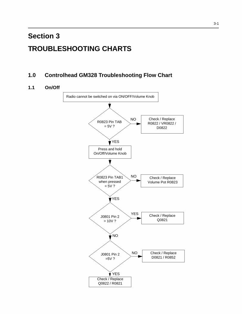
3-1
Section 3
TROUBLESHOOTING CHARTS
1.0 Controlhead GM328 Troubleshooting Flow Chart
1.1 On/Off
Radio cannot be switched on via ON/OFF/Volume Knob
NO
YES
YES
NO
R0823 Pin TAB= 5V ?
R0823 Pin TAB1when pressed
= 5V ?
Check / Replace Volume Pot R0823
Check / ReplaceR0822 / VR0822 /
D0822
NO
YESJ0801 Pin 2
> 10V ?
Check / ReplaceQ0821
Check / ReplaceQ0822 / R0821
YES
NOJ0801 Pin 2=5V ?
Check / ReplaceD0821 / R0852
Press and holdOn/Off/Volume Knob

3-2 Controlhead GM328 Troubleshooting Flow Chart
1.2 Microprocessor
Power Up Alert Tone is OK but volume knob does not operate and no indicator is on
NO
YES
YES
NO
YES
NO
YES
NO
YES
EXTALU0831 Pin 31= 8.00 MHz ?
RESETTP0833
= HIGH ?
Check / ReplaceC0833 / R0832 / U0831
Check radio controllerData Signal
on J0801 Pin 5BUS+ ?
Data Signalon TP0836SCI_RX ?
NO
Data Signalon TP0837SCI_TX ?
Check / ReplaceR0831 / U0833 / U0831
Check / ReplaceR0837 / R0836
Check / ReplaceU0831
Check / ReplaceD0831 / R0838
Measure with scope while rotating Volume Pot
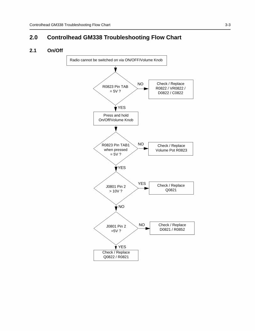
Controlhead GM338 Troubleshooting Flow Chart 3-3
2.0 Controlhead GM338 Troubleshooting Flow Chart
2.1 On/Off
Radio cannot be switched on via ON/OFF/Volume Knob
NO
YES
YES
NO
R0823 Pin TAB= 5V ?
R0823 Pin TAB1when pressed
= 5V ?
Check / Replace Volume Pot R0823
Check / ReplaceR0822 / VR0822 /
D0822 / C0822
NO
YESJ0801 Pin 2
> 10V ?
Check / ReplaceQ0821
Check / ReplaceQ0822 / R0821
YES
NOJ0801 Pin 2=5V ?
Check / ReplaceD0821 / R0852
Press and holdOn/Off/Volume Knob
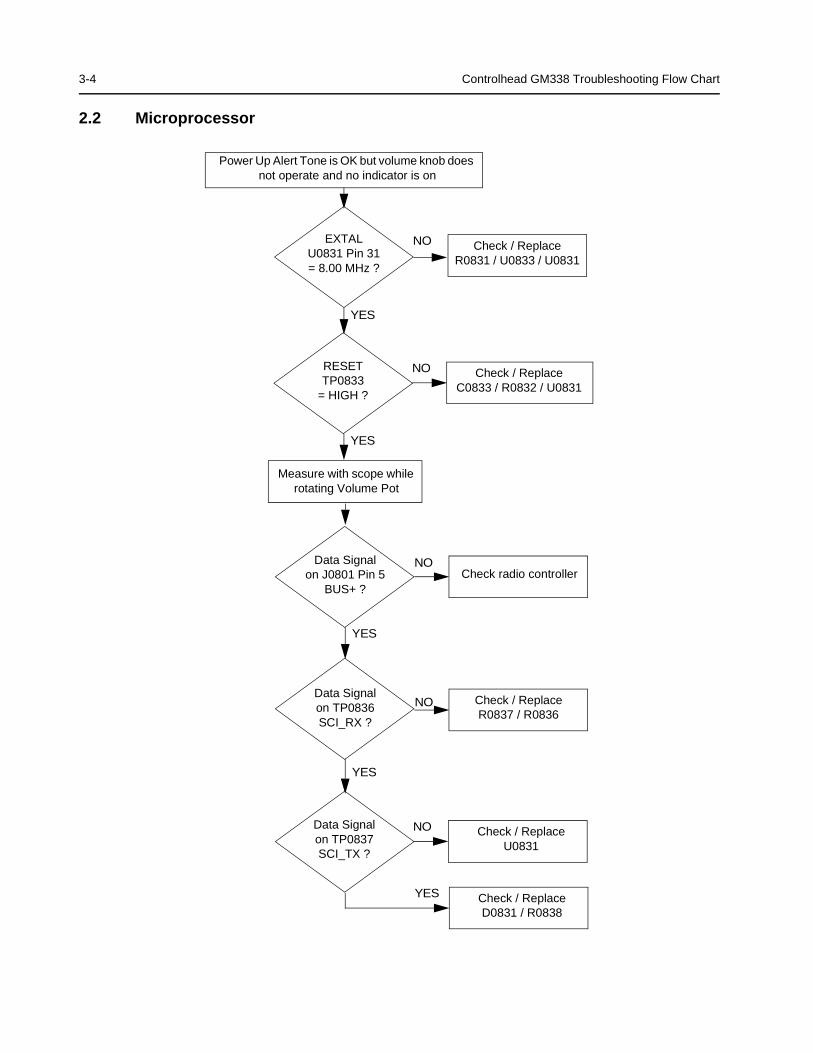
3-4 Controlhead GM338 Troubleshooting Flow Chart
2.2 Microprocessor
Power Up Alert Tone is OK but volume knob does not operate and no indicator is on
NO
YES
YES
NO
YES
NO
YES
NO
YES
EXTALU0831 Pin 31= 8.00 MHz ?
RESETTP0833
= HIGH ?
Check / ReplaceC0833 / R0832 / U0831
Check radio controllerData Signal
on J0801 Pin 5BUS+ ?
Data Signalon TP0836SCI_RX ?
NO
Data Signalon TP0837SCI_TX ?
Check / ReplaceR0831 / U0833 / U0831
Check / ReplaceR0837 / R0836
Check / ReplaceU0831
Check / ReplaceD0831 / R0838
Measure with scope while rotating Volume Pot

Controlhead GM338 Troubleshooting Flow Chart 3-5
2.3 Display
Power Up Alert Tone is OK, volume knob does operate,indicator/backlight is on but nothing on display
YES
NO
YES
NO
V5 (against 5V)TP0973 between
-6V and -7V ?
Activity onAddress & Data lines
A0 / D0..D7 / CS1of U0971?
Check for shortageU0831 / U0971
Check LCD Assembly
Check / ReplaceC0971 / C0973 / R0972R0973 / R0974 / U0971

3-6 Controlhead GM338 Troubleshooting Flow Chart
2.4 Backlight
Power Up Alert Tone is OK, volume knob does operate,indicator/display is on but no backlight
NO
YES
YES
NO
U0831 Pin 58is toggling ?
Base of Q0934
> 0.7V ?
Check / Replace R0847 / C0843 / R0943
Check for shortageU0831
YES
NOCollector ofQ0934
>5V and < 11V ?
Check / ReplaceQ0934 U0931 /R0941 / R0942 / R0944 / R0945
Check / ReplaceQ0933 / R0947 / R0948
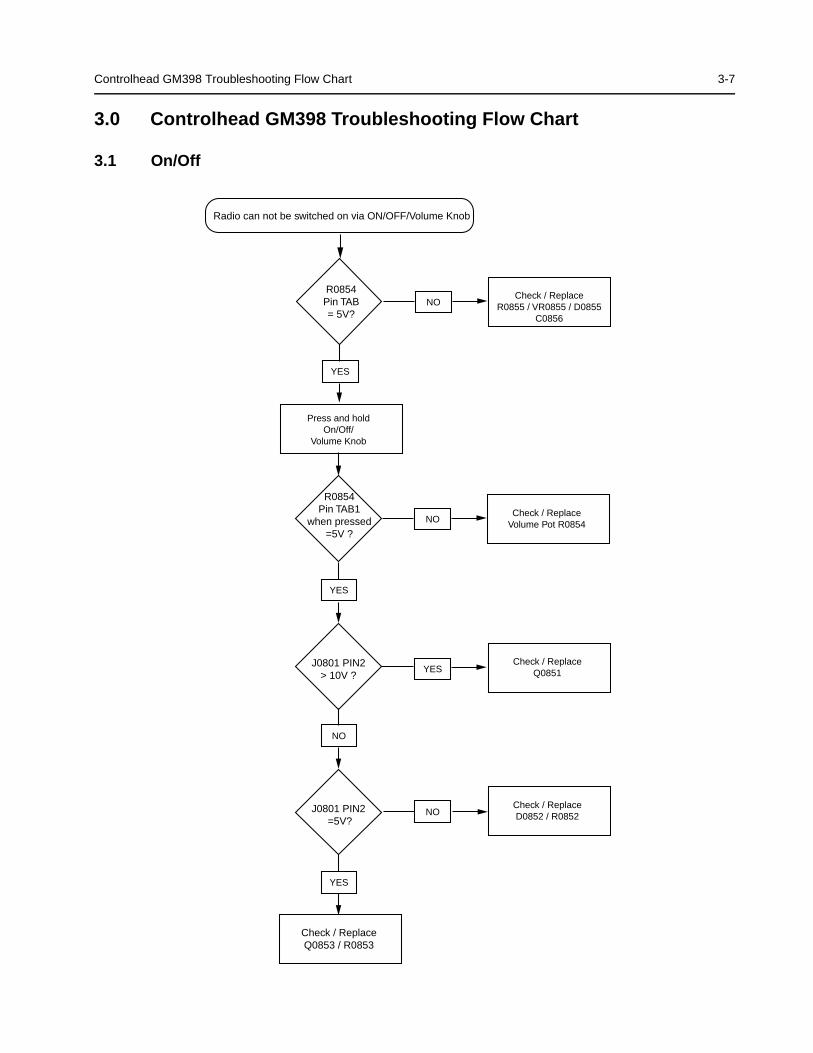
Controlhead GM398 Troubleshooting Flow Chart 3-7
3.0 Controlhead GM398 Troubleshooting Flow Chart
3.1 On/Off
R0854Pin TAB1
when pressed=5V ?
J0801 PIN2> 10V ?
J0801 PIN2 =5V?
Check / ReplaceQ0853 / R0853
YES
NO
YES
NO
YES
NOCheck / ReplaceD0852 / R0852
Check / ReplaceVolume Pot R0854
Check / ReplaceQ0851
Radio can not be switched on via ON/OFF/Volume Knob
YES
R0854Pin TAB= 5V?
NOCheck / Replace
R0855 / VR0855 / D0855C0856
Press and holdOn/Off/
Volume Knob
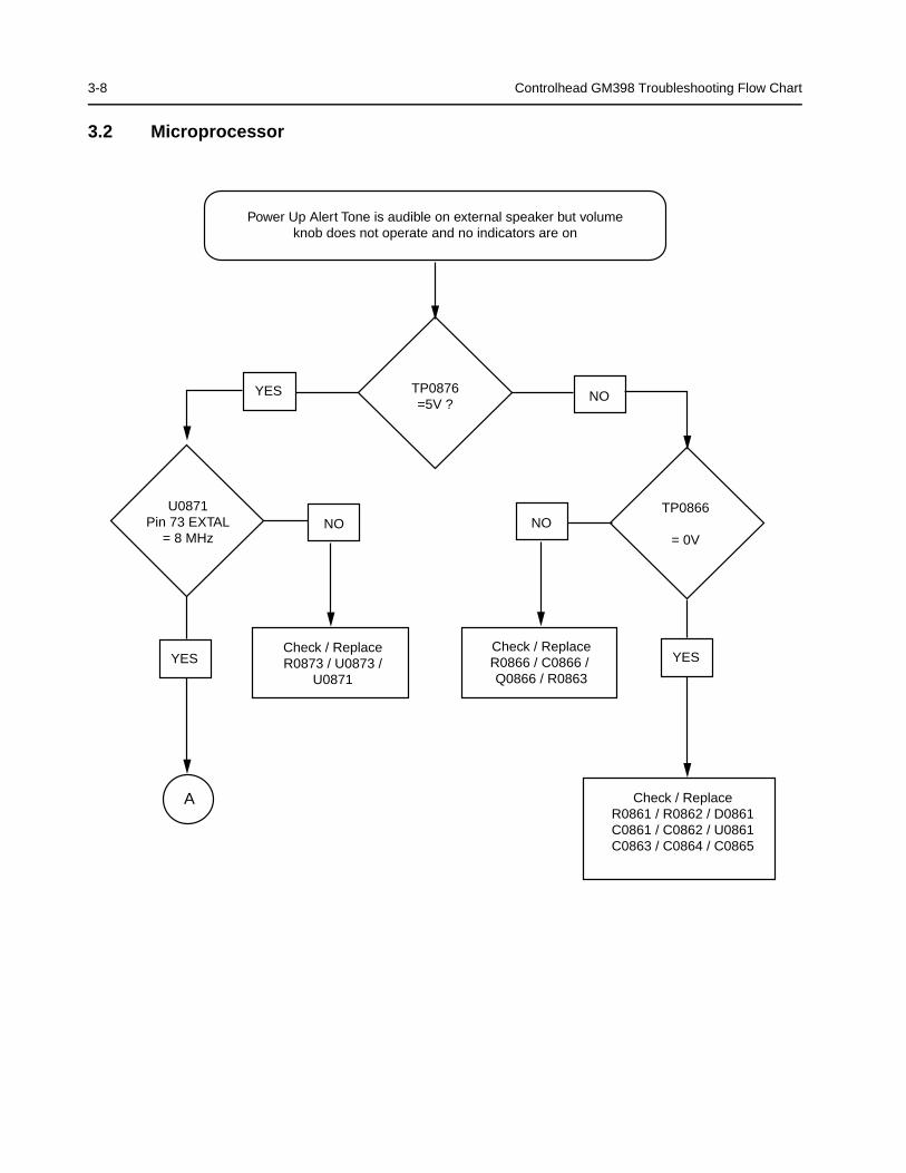
3-8 Controlhead GM398 Troubleshooting Flow Chart
3.2 Microprocessor
Power Up Alert Tone is audible on external speaker but volumeknob does not operate and no indicators are on
TP0876=5V ?
NO
YES
U0871Pin 73 EXTAL
= 8 MHz
TP0866
= 0VNO
Check / ReplaceR0873 / U0873 /
U0871
Check / ReplaceR0866 / C0866 / Q0866 / R0863
Check / ReplaceR0861 / R0862 / D0861C0861 / C0862 / U0861C0863 / C0864 / C0865
NO
YES YES
A
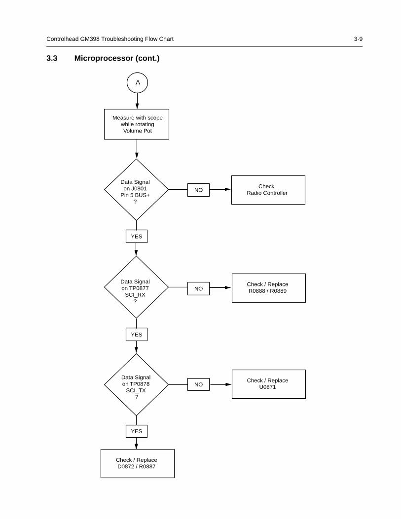
Controlhead GM398 Troubleshooting Flow Chart 3-9
3.3 Microprocessor (cont.)
Data Signalon J0801
Pin 5 BUS+?
Data Signalon TP0877
SCI_RX?
Data Signalon TP0878
SCI_TX ?
Check / ReplaceD0872 / R0887
YES
YES
YES
NO
NO
NOCheck / Replace
U0871
Check Radio Controller
Check / ReplaceR0888 / R0889
Measure with scopewhile rotatingVolume Pot
A
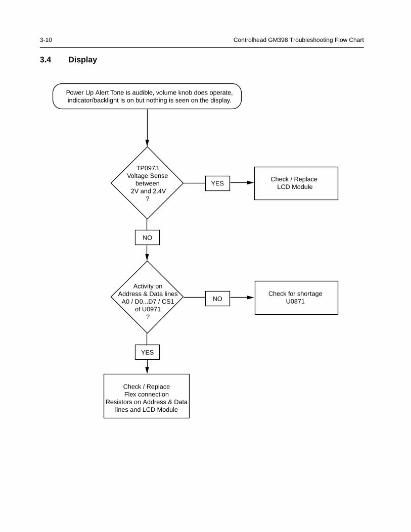
3-10 Controlhead GM398 Troubleshooting Flow Chart
3.4 Display
TP0973Voltage Sense
between 2V and 2.4V
?
Activity onAddress & Data linesA0 / D0...D7 / CS1
of U0971?
NO
YES
YES
NO
Check / ReplaceFlex connection
Resistors on Address & Datalines and LCD Module
Check / Replace LCD Module
Check for shortageU0871
Power Up Alert Tone is audible, volume knob does operate,indicator/backlight is on but nothing is seen on the display.
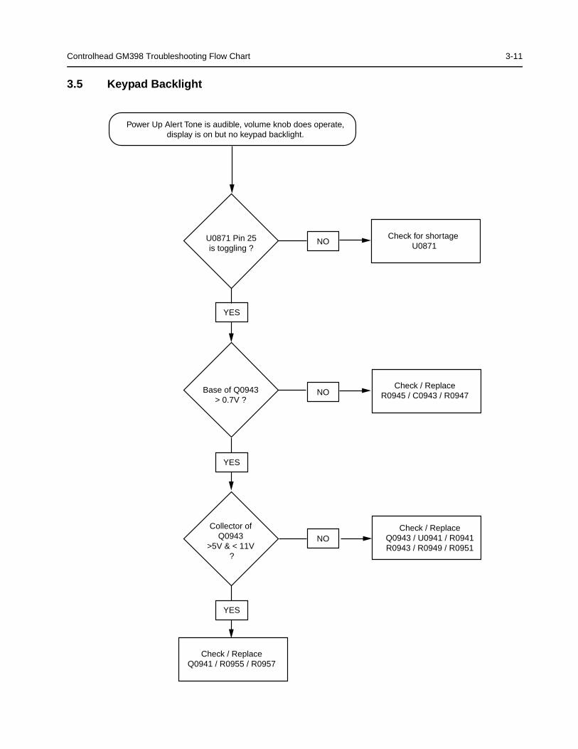
Controlhead GM398 Troubleshooting Flow Chart 3-11
3.5 Keypad Backlight
U0871 Pin 25is toggling ?
Base of Q0943> 0.7V ?
Collector ofQ0943
>5V & < 11V ?
Check / ReplaceQ0941 / R0955 / R0957
YES
YES
YES
NO
NO
NOCheck / Replace
Q0943 / U0941 / R0941R0943 / R0949 / R0951
Check for shortage U0871
Check / ReplaceR0945 / C0943 / R0947
Power Up Alert Tone is audible, volume knob does operate,display is on but no keypad backlight.

3-12 Controlhead GM398 Troubleshooting Flow Chart
3.6 Display Backlight
U0871 Pin 24is toggling ?
Base of Q0963> 0.7V ?
Collector ofQ0963
>5V & < 11V ?
Check / ReplaceQ0961 / R0975 / R0977
YES
YES
YES
NO
NO
NOCheck / Replace
Q0963 / U0941 / R0961R0963 / R0969 / R0971
Check for shortage U0871
Check / ReplaceR0965 / C0963 / R0967
Power Up Alert Tone is audible, volume knob does operate,display is on but no display backlight.
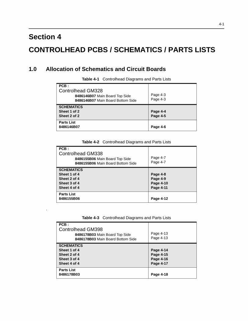
4-1
Section 4
CONTROLHEAD PCBS / SCHEMATICS / PARTS LISTS
1.0 Allocation of Schematics and Circuit Boards
.
Table 4-1 Controlhead Diagrams and Parts Lists
PCB :Controlhead GM328
8486146B07 Main Board Top Side8486146B07 Main Board Bottom Side
Page 4-3Page 4-3
SCHEMATICSSheet 1 of 2Sheet 2 of 2
Page 4-4Page 4-5
Parts List8486146B07 Page 4-6
Table 4-2 Controlhead Diagrams and Parts Lists
PCB :Controlhead GM338
8486155B06 Main Board Top Side8486155B06 Main Board Bottom Side
Page 4-7Page 4-7
SCHEMATICSSheet 1 of 4Sheet 2 of 4Sheet 3 of 4Sheet 4 of 4
Page 4-8Page 4-9Page 4-10Page 4-11
Parts List8486155B06 Page 4-12
Table 4-3 Controlhead Diagrams and Parts Lists
PCB :Controlhead GM398
8486178B03 Main Board Top Side8486178B03 Main Board Bottom Side
Page 4-13Page 4-13
SCHEMATICSSheet 1 of 4Sheet 2 of 4Sheet 3 of 4Sheet 4 of 4
Page 4-14Page 4-15Page 4-16Page 4-17
Parts List8486178B03 Page 4-18

4-2 Allocation of Schematics and Circuit Boards
THIS PAGE INTENTIONALLY LEFT BLANK

Con
trol
head
GM
328
- P
CB
848
6146
B07
/ S
chem
atic
s4-
3
2.0
Co
ntr
olh
ead
GM
328
- P
CB
848
6146
B07
/ S
chem
atic
s
D08
71
D08
72D
0873
D08
74D
0875
D08
76
D08
77D
0878
D08
79
D08
81
D08
84
D08
85
D08
86
D08
87D
0888
2
35
79
86
410
J081
1
JU08
52
JU08
53
JU08
54
4
12
3
5R
0823
S08
61S
0862
S08
63S
0864
S08
65S
0866
ZW
G01
3011
4-A
C08
02
C08
03
C08
04
C08
05
C08
06
C08
08
C08
09
C08
10
C08
11
C0813
C0815
C0816
C0817
C0818
C0819
C08
21
C08
22C
0823
C08
24
C08
31
C08
32
C08
33
C08
43
D0821
D0822
D08
31
12
J080
1
1 2P
0801
Q0821
Q08
22
Q0823
Q0841
Q0843
Q08
71
Q0872
Q0873
Q08
74
Q08
75
Q08
76Q0877
Q0878Q
0879
Q08
81Q0885
R08
10
R08
11
R0812
R0813
R0814
R08
15
R08
16
R08
21
R08
22
R08
24
R08
25
R0831
R08
32
R08
33 R08
34
R08
35
R08
36
R08
37R
0838
R08
39
R08
41
R08
42R
0843
R08
44
R08
45
R08
47
R08
49
R08
52
R08
53R08
54
R08
61R
0862
R08
64
R08
66R
0867
R08
71
R08
72
R08
73
R08
74
R08
75R
0876
R08
77R
0878
R08
79
R08
80
R08
81
R08
85
TP
0831
TP
0832
TP
0833
TP
0834
TP
0835
TP
0836
TP
0837
TP
0838
149
1733
U08
3114
5 8U08
32
3U0833
U0835
VR0811
VR
0816
VR
0817
VR
0821
VR
0822
VR
0823
64
1
1
MOTOROLA c
8486146B07-0
Co
ntr
olh
ead
GM
328
- P
CB
848
6146
B07
ZW
G01
3011
4-A
T
op S
ide
ZW
G01
3011
3-B
B
otto
m S
ide
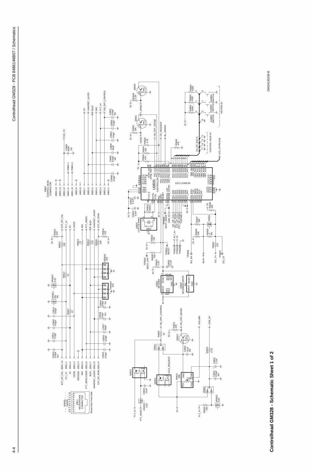
4-4
Con
trol
head
GM
328
- P
CB
848
6146
B07
/ S
chem
atic
s
HO
OK
GR
OU
ND
MIC
10G
M30
0
CO
NT
RO
L H
EA
D
PT
T_I
RD
EC
OD
ER
7
CO
NN
EC
TO
R
8
J080
1
9
MIC
RO
PH
ON
EC
ON
NE
CT
OR
SC
I_R
X
BO
OT
_VP
P
J081
1
RE
SE
TB
OO
T_M
OD
E
WA
RIS
HA
ND
SE
T_A
UD
IO
1
CO
NT
RO
LLE
R
KE
YP
AD
ID
CO
NT
RO
L H
EA
D ID
SC
I_T
X
EX
T_K
P_R
OW
EX
T_K
P_C
OL
FLT
_A+
45
6
BU
S+
23
5V
VR
0822
5.6V
R08
432.
2K
NU
GN
D
INP
UT
RE
SE
T_
7
U08
35M
C33
464N
-45A
TR
J080
1-8
JU08
53S
WIT
CH
C08
33
R08
33
0.1u
F
2
47K
10K
R08
44
55 VDD22 VRH21 VRL
23VSS1VSS2 24
49VSS3
45X
IRQ
33X
TA
L
PE
3_A
N3
19P
E4_
AN
414 16
PE
5_A
N5
PE
6_A
N6
18P
E7_
AN
72043
RE
SE
T
28S
TR
A_A
S30
ST
RB
_RW
*
PD
1_T
XD
50P
D2_
MIS
O51
PD
3_M
OS
I52 53
PD
4_S
CK
PD
5_S
S*
54
PE
0_A
N0
13P
E1_
AN
115
PE
2_A
N2
17P
C1_
AD
136
PC
2_A
D2
37P
C3_
AD
338
PC
4_A
D4
39 40P
C5_
AD
5P
C6_
AD
641
PC
7_A
D7
42
PD
0_R
XD
47P
B1_
A9
11P
B2_
A10
10P
B3_
A11
9P
B4_
A12
8 7P
B5_
A13
PB
6_A
146
PB
7_A
155
PC
0_A
D0
3464P
A1_
IC2
63P
A2_
IC1
62P
A3_
OC
5_O
C1
59P
A4_
OC
4_O
C1
58P
A5_
OC
3_O
C1
57P
A6_
OC
2_O
C1
56P
A7_
PA
1_O
C1
PB
0_A
812
NC3 4NC4 26NC5 32
35 NC644 NC7NC848
60 NC9
1P
A0_
IC3
29C
LK_E
31E
XT
AL
46IR
Q
27M
OD
A_L
IR*
25M
OD
B_V
ST
BY
NC1 2
NC1061
3NC2MC68HC711E9
U08
31
7
J080
1-11
J080
1-7
3T
P08
3250
K
NE
G
PO
ST
AB
TA
B1
VAR
R08
23
4.7K
R08
24
J081
1-5
10
Q08
43
NU
R08
3510
0
0R08
39
R08
47
22
J081
1-4
270
R08
14
R08
15
0.1u
FC
0832
13K
C08
313.
3uF
J081
1-1
1
C08
23.0
1uF
2
06
2
C08
09
NU
82pF
Q08
23
D08
22
10R
0813
1C
1
3C
2
2
GND
4
R08
12
CS
TC
C8.
00M
GU
0833
22
5.6V
5
VR
0821
100K
R08
538
5.6V
VR
0823
J081
1-10
0
P08
01-2 54
J080
1-9
TP
0837
INP
UT
2
NC
13
NC
25
NC
36
NC
47 8
NC
5
RE
SE
T1
U08
32M
C33
064
GN
D4
Q08
21
J081
1-6
J080
1-10
J080
1-6
JU08
52S
WIT
CH
JU08
54
6
1
SW
ITC
H
C08
0447
0pF
0
R08
5210
0K
C08
1782
pF
J081
1-8
7
R08
454.
7K
NU
VR
0811
33V
470p
FN
U47
0pF
C08
18
C08
16
33K
R08
37
NU
C08
0847
0pF
470p
FC
0806
10K
3
R08
41
R08
1151
K
J081
1-3
J081
1-2
1ME
GR
0831
VR
0816
20V
13K
J081
1-9
R08
10
4
TP
0833
10K
R08
21
47K
J080
1-14
R08
49
P08
01-1
2.2K
R08
32
J080
1-3
J080
1-5
TP
0838
TP
0834
NU
470p
FN
U
C08
1047
0pF
32
C08
19
100K
R08
54
61
J080
1-12
R08
3810
K
J081
1-7
R08
34
270
20V
VR
0817
2.2u
F
J080
1-4
C08
2247
0pF
NU
5
13K
C08
21
R08
16
R08
22
51K
470p
FC
0815
C08
1147
0pF
TP
0831
R08
3610
K
TP
0836
J080
1-13
J080
1-1
NU
J080
1-2
470p
FC
0802
C08
0347
0pF
470p
FC
0843
C08
13
TP
0835
470p
F
NU
C08
24.0
1uF
R08
25
1K
D08
21
C08
0582
pF
Q08
22
R08
4247
K
Q08
41
INT
_KP
_RO
WIN
T_K
P_C
OL
US
W_5
V
5V
5V
5V
5VFLT
_A+
BU
S+
EX
T_K
P_R
OW
MIC
EX
T_K
P_C
OL
FLT
_A+ D
0831
5V
CH
_KP
_ID
(0:7
)
LED
_CN
TR
L(0:
8)
CH
_RE
QU
ES
T
5V
CH
_RE
QU
ES
T
5V
5V
5V
5V
PT
T_I
RD
EC
HO
OK
ON
_OF
F_S
EN
SE
ON
_OF
F_C
ON
TR
OL
5V
US
W_5
V
VO
LUM
E
VO
LUM
EE
XT
_KP
_RO
WE
XT
_KP
_CO
L
PT
T_I
RD
EC
FLT
_A+
FLT
_A+
5V
5V
PT
T_I
RD
EC
SC
I_T
X
SC
I_T
X
BU
S+
5V
5V
BL_
GR
EE
N
ON
_OF
F_S
EN
SE
5V
HO
OK
5V 5V
HA
ND
SE
T_A
UD
IO
ON
_OF
F_C
ON
TR
OL
FLT
_A+
MIC
BU
S+
HA
ND
SE
T_A
UD
IO
5V
Sho
wn
from
Fro
nt S
ide
ZW
G01
3023
9-B
Co
ntr
olh
ead
GM
328
- S
chem
atic
Sh
eet
1 o
f 2

Con
trol
head
GM
328
- P
CB
848
6146
B07
/ S
chem
atic
s4-
5
S08
62
LED
5LE
D4
LED
6LE
D1
LED
2LE
D3
F4
P2
F3
P1
F2
F1
F1
F2
F3
F4
P1
P2
LED
1LE
D2
LED
3
1V/1
V
0V/0
V
0V/1
V
LED
4
LED
6LE
D5
S08
64S
0863
S08
61
S08
66S
0865
KE
YP
AD
red
yello
wgr
een
0V/2
V
0V/3
V
1V/0
V
R08
67
gree
nD
0885
13K
gree
nD
0888
D08
86gr
een
gree
nD
0887
gree
nD
0884
gree
nD
0881
270
R08
8527
0R
0881
Q08
851
P1
2P
2
3P
3
4P
45
P5
6P
6
7P
7
8P
88
P8
S08
651
P1
2P
2
3P
3
P4
45P
5
6P
6
7P
7
R08
64
S08
61
43K
R08
66
51K
R08
6151
K
R08
8022
K
7
P8
8
13K
R08
62
P1
1
P2
2
P3
3
P4
4P
55
P6
6
P7
6P
6
7P
7
8P
8
S08
64
1P
1
2P
2
3P
3
P4
45P
5
P5
5
P6
6
P7
7
P8
8
S08
63
P1
1
P2
2
P3
3
P4
4P
44
P5
5
P6
6 7P
7
P8
8
S08
62S
0866
P1
1
P2
2
P3
3
270
gree
n
R08
77
D08
77D
0879
Q08
77
red
270
R08
78
Q08
79Q
0878
yello
wD
0878
Q08
73
R08
7927
0
R08
7127
0
Q08
71Q
0872 8
2
red
D08
76
7
D08
75re
dre
dD
0874
R08
7627
0R
0875
270
R08
74
Q08
76
270
Q08
75Q
0874
6
CH
_Ash
eet 2
5
43
red
Q08
81
D08
72D
0873
red
red
R08
73
D08
71
270
10
R08
72
FLT
_A+
LED
_CN
TR
L(0:
8)
BL_
GR
EE
N
FLT
_A+
FLT
_A+
LED
_CN
TR
L(0:
8)
5V
5V
INT
_KP
_CO
L
INT
_KP
_RO
W
270
Co
ntr
olh
ead
GM
328
- S
chem
atic
Sh
eet
2 o
f 2
ZW
G01
3024
0-A
4-6
Con
trol
head
GM
328
- P
CB
848
6146
B07
/ S
chem
atic
s
Co
ntr
olh
ead
PC
B 8
4861
46B
07 P
arts
Lis
t
* M
otor
ola
Dep
ot S
ervi
cing
onl
y
Ref
eren
ce d
esig
nato
rs w
ith a
n as
teris
k in
dica
te
com
pone
nts
whi
ch a
re n
ot fi
eldr
epla
ceab
le
beca
use
they
nee
d to
be
calib
rate
d w
ith
spec
ializ
ed fa
ctor
y eq
uipm
ent a
fter
inst
alla
tion.
R
adio
s in
whi
ch th
ese
part
s ha
ve b
een
repl
aced
in
the
field
will
be
off f
requ
ency
at t
empe
ratu
re
extr
emes
.
Cir
cuit
R
efM
oto
rola
P
art
No
Des
crip
tio
n
C08
0221
1374
1F17
470p
F 5
0VC
0803
2113
741F
1747
0pF
50V
C08
0421
1374
1F17
470p
F 5
0VC
0805
2113
740F
4982
pF 5
% 5
0VC
0806
2113
741F
1747
0pF
50V
C08
0821
1374
1F17
470p
F 5
0VC
0810
2113
741F
1747
0pF
50V
C08
1121
1374
1F17
470p
F 5
0VC
0813
2113
741F
1747
0pF
50V
C08
1521
1374
1F17
470p
F 5
0VC
0816
2113
741F
1747
0pF
50V
C08
1721
1374
0F49
82pF
5%
50V
C
0818
2113
741F
1747
0pF
50V
C08
2121
1374
1F17
470p
F 5
0VC
0822
2311
049A
40TA
NT
CP
2.2
uF 1
0% 1
0VC
0823
2113
741F
4910
nF 5
0VC
0824
2113
741F
4910
nF 5
0VC
0831
2311
049A
42TA
NT
CP
3.3
uF 1
0% 6
VC
0832
2113
743E
2010
0nF
16V
C08
3321
1374
3E20
100n
F 1
6VC
0843
2113
741F
1747
0pF
50V
D08
2148
1383
3C02
DU
AL
SO
T M
MB
D61
00D
0822
4813
833C
02D
UA
L S
OT
MM
BD
6100
D08
3148
8023
6E05
DIO
DE
CH
IP S
CH
OT
TK
YD
0871
4886
171B
01LE
D R
ED
D08
7248
8617
1B01
LED
RE
DD
0873
4886
171B
01LE
D R
ED
D08
7448
8617
1B01
LED
RE
DD
0875
4886
171B
01LE
D R
ED
D08
7648
8617
1B01
LED
RE
DD
0877
4886
171B
01LE
D R
ED
D08
7848
8617
1B03
LED
YE
LLO
WD
0879
4886
171B
04LE
D G
RE
EN
D08
8148
8617
1B04
LED
GR
EE
ND
0884
4886
171B
04LE
D G
RE
EN
D08
8548
8617
1B04
LED
GR
EE
ND
0886
4886
171B
04LE
D G
RE
EN
D08
8748
8617
1B04
LED
GR
EE
ND
0888
4886
171B
04LE
D G
RE
EN
J080
109
0263
6Y02
CO
NN
EC
TO
R F
LEX
12
PIN
J081
128
6428
7B01
CO
NN
TE
LCO
10
PIN
JA
CK
P08
0128
0992
6G01
CO
NN
1.2
5MM
2P
IN S
UR
MT
Q08
2148
0592
1T02
TS
TR
DU
AL
RO
HM
FM
C2
RH
Q08
2248
8004
8M01
TS
TR
NP
N D
IG 4
7k/4
7kQ
0823
4805
921T
02T
ST
R D
UA
L R
OH
M F
MC
2 R
HQ
0841
4880
048M
01T
ST
R N
PN
DIG
47k
/47k
Q08
4348
8004
8M01
TS
TR
NP
N D
IG 4
7k/4
7kQ
0871
4813
824A
10T
ST
R N
PN
40V
.2A
B=
50-1
50
Q08
7248
1382
4A10
TS
TR
NP
N 4
0V .2
A B
=50
-150
Q08
7348
1382
4A10
TS
TR
NP
N 4
0V .2
A B
=50
-150
Q08
7448
1382
4A10
TS
TR
NP
N 4
0V .2
A B
=50
-150
Q08
7548
1382
4A10
TS
TR
NP
N 4
0V .2
A B
=50
-150
Q08
7648
1382
4A10
TS
TR
NP
N 4
0V .2
A B
=50
-150
Q08
7748
1382
4A10
TS
TR
NP
N 4
0V .2
A B
=50
-150
Q08
7848
1382
4A10
TS
TR
NP
N 4
0V .2
A B
=50
-150
Q08
7948
1382
4A10
TS
TR
NP
N 4
0V .2
A B
=50
-150
Q08
8148
1382
4A10
TS
TR
NP
N 4
0V .2
A B
=50
-150
Q08
8548
1382
4A10
TS
TR
NP
N 4
0V .2
A B
=50
-150
R08
1006
6205
7A76
13k
1/16
W 5
%R
0811
0662
057A
9051
k 1/
16W
5%
R08
1206
6205
7A09
22 1
/16W
5%
R08
1306
6205
7A01
10 1
/16W
5%
R08
1406
6205
7A35
270
1/16
W 5
%R
0815
0662
057A
7613
k 1/
16W
5%
R08
1606
6205
7A90
51k
1/16
W 5
%R
0821
0662
057A
7310
k 1/
16W
5%
R08
2206
6205
7A76
13K
1/1
6W 5
%R
0823
1805
911V
02P
OT
VO
LR
0824
0662
057A
654k
7 1/
16W
5%
R08
2506
6205
7A49
1k 1
/16W
5%
R08
3106
6205
7B22
1M 1
/16W
5%
R08
3206
6205
7A57
2k2
1/16
W 5
%R
0833
0662
057A
8947
k 1/
16W
5%
R08
3406
6205
7A35
270
1/16
W 5
%R
0835
0662
057A
2510
0 1/
16W
5%
R08
3606
6205
7A73
10k
1/16
W 5
%R
0837
0662
057A
8533
k 1/
16W
5%
R08
3806
6205
7A73
10k
1/16
W 5
%R
0841
0662
057A
7310
k 1/
16W
5%
R08
4206
6205
7A89
47k
1/16
W 5
%R
0843
0662
057A
572.
2k 1
/16W
5%
R08
4406
6205
7A73
10k
1/16
W 5
%R
0845
0662
057A
654k
7 1/
16W
5%
R08
4706
6205
7A09
22 1
/16W
5%
R08
4906
6205
7A89
47k
1/16
W 5
%R
0852
0662
057A
9710
0k 1
/16W
R08
5306
6205
7A97
100k
1/1
6WR
0854
0662
057A
9710
0k 1
/16W
R08
6106
6205
7A90
51k
1/16
W 5
%R
0862
0662
057A
7613
k 1/
16W
5%
R08
6406
6205
7A88
43k
1/16
W 5
%R
0866
0662
057A
9051
k 1/
16W
5%
R08
6706
6205
7A76
13k
1/16
W 5
%R
0873
0660
076A
3527
0 5
1/8
R08
7406
6007
6A35
270
5 1/
8R
0875
0660
076A
3527
0 5
1/8
R08
7606
6007
6A35
270
5 1/
8R
0877
0660
076A
3527
0 5
1/8
R08
7806
6007
6A35
270
5 1/
8
Cir
cuit
R
efM
oto
rola
P
art
No
Des
crip
tio
n
R08
7906
6007
6A35
270
5 1/
8R
0880
0662
057A
8122
k 1/
16W
5%
R08
8106
6205
7A35
270
1/16
W 5
%R
0885
0662
057A
3527
0 1/
16W
5%
*U08
3151
1380
2A24
IC 6
8HC
11 W
/SC
I,SP
I,A/D
U08
3251
1381
5A02
IC
U08
3348
8606
1B01
CE
R R
ES
ON
AT
OR
8M
HZ
C
ST
CC
8.00
MG
VR
0816
4805
656W
09D
IOD
E Z
EN
ER
QU
AD
M
MQ
A20
VT
1V
R08
1748
0565
6W09
DIO
DE
ZE
NE
R Q
UA
D
MM
QA
20V
T1
VR
0821
4813
830A
15D
IOD
E 5
.6V
5%
225
mW
VR
0822
4813
830A
15D
IOD
E 5
.6V
5%
225
mW
VR
0823
4813
830A
15D
IOD
E 5
.6V
5%
225
mW
Cir
cuit
R
efM
oto
rola
P
art
No
Des
crip
tio
n
Con
trol
head
GM
338
- P
CB
848
6155
B06
/ S
chem
atic
s4-
7
3.0
Co
ntr
olh
ead
GM
338
- P
CB
848
6155
B06
/ S
chem
atic
s
D08
77D
0879
D08
80
D09
31
D09
32
D09
33
D09
34
D09
35
D09
36D
0937
D09
38
D09
39
D09
40
D09
41
D0942
D09
43
D09
44D
0945
D0946
D09
47
D09
48
D09
49
D09
50D
0951
D09
52D
0953
D09
54
D09
55
D09
56
D09
57
D09
58
D09
61
D09
62
D09
63
D09
64
D09
65
D09
66D
0967
D09
68
D09
69
D09
70
D09
71
D0972
D09
73
D09
74D
0975
D0976
D09
77
D09
78
D09
79
D09
80D
0981
D09
82D
0983
D09
84
D09
85
D09
86
D09
87
D09
88
40
4180
H09
71
2
35
79
86
410
J081
1
4
12
3
5R
0823
S08
52
S08
53
S08
54
S09
01
S09
02
S09
03
S09
04
S09
05
S09
06
S09
07S
0908
S09
09S
0910
U08
34
110
3020 60
7050
1
ZW
G01
3013
6-A
C08
02
C08
03
C08
04
C08
05
C08
06
C08
07 C08
08
C0810
C08
11
C0812
C08
13C
0815
C0816
C08
17 C0818
C08
19
C08
21
C08
22
C08
23C
0831
C08
32
C08
33
C08
42
C0843
C09
31C
0932
C09
33
C09
71
C09
72
C09
73
C09
74C
0975
C09
76C
0977
C09
78C
0979
C09
80C
0981 C09
82
C09
83
C09
84C09
85
D0821
D0822
D0831
12
J080
1
12P08
01
Q0821
Q0822
Q0823
Q0841
Q08
43
Q0877
Q08
78Q
0879
123
4Q
0931
Q09
32
123
4Q
0933
Q0934
R0810
R0811
R08
12R
0813
R08
14
R08
15
R0816
R0817
R08
21R
0822
R08
24
R08
25
R08
31
R08
32
R08
33
R08
34
R08
35
R08
36
R08
37
R08
38
R08
41
R08
42
R08
43
R08
44R
0845
R08
47R
0848
R08
49
R08
50R
0851 R
0852
R08
53
R08
54
R08
55
R08
56
R08
57
R08
58
R08
59
R08
60
R08
61 R08
62
R08
63
R08
64R
0865
R08
77R
0878
R08
79
R09
01
R09
02R
0903
R09
04
R09
05
R09
06R
0907
R09
08
R09
09
R09
10
R09
31
R09
32
R09
33R
0934
R09
35R09
36
R09
37R
0938
R09
41R
0942
R09
43
R09
44R
0945
R09
46R
0947
R09
48
R09
72
R09
73R
0974
R09
75
R09
76R
0977 R 0
978
TP
0831
TP
0832
TP
0833
TP
0834
TP
0835
TP
0836
TP
0837
TP
0838
TP
0971
TP
0972
TP
0973
TP
0974
TP
0975
149
1733
U08
31
14 5
8
U08
32
3U
0833
U0835
145
8
U09
31
128
103
102
65643839
U09
71
VR0811
VR0812
VR0816
VR
0817
VR0821
VR0822
1
1
64
1
MO
TOR
OLA
c84
8615
5B06
-0
Co
ntr
olh
ead
GM
338
- P
CB
848
6155
B06
ZW
G01
3013
6-A
T
op S
ide
ZW
G01
3013
7-B
B
otto
m S
ide
4-8
Con
trol
head
GM
338
- P
CB
848
6155
B06
/ S
chem
atic
s
MIC
PT
T_I
RD
EC
OD
ER
CO
NN
EC
TO
R
C
BU
S+
KE
YP
AD
ID
CO
NT
RO
LLE
R
BN
OT
PLA
CE
D
1
PLA
CE
D
J081
1
VP
P
67
HA
ND
SE
T_A
UD
IO
AN
ALO
G_I
NP
UT
_35V
GM
300
MIC
RO
PH
ON
E
BO
OT
_MO
DE
SC
I_R
X
SC
I_T
X
FLT
_A+
RE
SE
T
TE
MP
_SE
NS
E
CO
NT
RO
L H
EA
D ID
5VG
ND
HO
OK
89
10
WA
RIS
CO
NT
RO
LHE
AD
CO
NN
EC
TO
R
GR
OU
ND
3
AN
ALO
G_I
NP
UT
_2
FLT
_A+
2J0
801
45
J080
1-8
4.7K
R08
64
270
R08
14
R08
1513
K
R08
1013
K
Q08
41
J080
1-5
6
0
R08
3347
K
R08
322.
2K
R08
3733
K
270
R08
77
7
J081
1-8
R08
5247
K
GN
DIN
PU
TR
ES
ET
_
NU
U08
35M
C33
464N
-45A
TR
S08
54S
WIT
CH
SW
ITC
HS
0853
J080
1-3
S08
52S
WIT
CH
J080
1-10
J080
1-13
J081
1-9
J080
1-14
J081
1-10
10
6 7
R08
13
J080
1-7
5.6V
VR
0822
D08
31
Q08
21U
0833
CS
TC
C8.
00M
G
C1
1
C2
3
GND
2
48
J081
1-6
3
J080
1-4
470p
FC
0812
22R
0817
47K
7
NU
R08
51
gree
nD
0879
R08
57
1
1
NU
47K
D08
80ye
llow
47K
NU
R08
54
47K
R08
59
10K
R08
41
2.2K
R08
43
51K
R08
16
J081
1-7
Q08
23
R08
31
TA
B1
VAR
1ME
G
R08
2350
K
NE
G
PO
ST
AB
J080
1-12
J080
1-9
R08
4868
K
C08
31
NU
NC
4N
C5
81R
ES
ET
3.3u
F
MC
3306
4
4
GND
2IN
PU
T
3N
C1
5N
C2
6N
C3
7
U08
32
R08
1222
5
0
R08
7927
0R
0878
270
D08
22
J081
1-5
R08
4410
K
3
R08
654.
7K
100K
R08
60
47K
NU
R08
535
7
0
J080
1-11
4
Q08
22
4.7K
R08
45
C08
42
NU
2.2u
F
Q08
79Q
0878
red
D08
77
R08
11
Q08
77
51K
3
TP
0833
1KR
0825
470p
FC
0804
22K
TP
0836
R08
22
TP
0834
470p
FC
0821
4
NU
VR
0812
5.6V
R08
634.
7K
NU
R08
5047
K
4
R08
5647
K
2
82pF
C08
05 VDD22 VRH21 VRL
23VSS124VSS249VSS3
45X
IRQ
33X
TA
L
19P
E4_
AN
414
PE
5_A
N5
16P
E6_
AN
618
PE
7_A
N7
20
RE
SE
T43
28S
TR
A_A
S30
ST
RB
_RW
*
55
50
PD
2_M
ISO
51P
D3_
MO
SI
52P
D4_
SC
K53
PD
5_S
S*
54
PE
0_A
N0
13P
E1_
AN
115
PE
2_A
N2
17P
E3_
AN
3
36P
C2_
AD
237
PC
3_A
D3
38P
C4_
AD
439
PC
5_A
D5
40P
C6_
AD
641
PC
7_A
D7
42
PD
0_R
XD
47
PD
1_T
XD
11P
B2_
A10
10P
B3_
A11
9P
B4_
A12
8P
B5_
A13
7P
B6_
A14
6P
B7_
A15
5
PC
0_A
D0
34P
C1_
AD
1
PA
1_IC
263
PA
2_IC
162
PA
3_O
C5_
OC
159
PA
4_O
C4_
OC
158
PA
5_O
C3_
OC
157
PA
6_O
C2_
OC
156
PA
7_P
A1_
OC
1
PB
0_A
812
PB
1_A
9
NC326NC432NC5
35 NC644 NC748 NC860 NC9
1P
A0_
IC3
64
CLK
_E
31E
XT
AL
46IR
Q
27M
OD
A_L
IR*
25M
OD
B_V
ST
BY 2NC1
61 NC10
3NC24
4
MC
68H
C71
1E9
U08
3129
J081
1-4
J081
1-3
J081
1-2
1
C08
222.
2uF
R08
3810
K
R08
3610
K
VR
0816
20V
VR
0817
20V
2.2u
FC
0843
0.1u
F
2
C08
32
C08
33
0
0.1u
F
47K
R08
42
VR
0821
10V
C08
19C
0816
NU
470p
F47
0pF
82pF
C08
17
TP
0831
3
P08
01-2
P08
01-1
TP
0835
C08
0647
0pF
47K
NU
R08
49
47K
R08
557
470p
FC
0803
1
R08
4768
K
470p
FC
0813
C08
1547
0pF
47K
C08
07
R08
58
470p
F
Q08
43
VO
UT
D08
21
U08
34LM
50
3G
ND
1 PO
S
2R
0821
10K
6
6
3
5
J080
1-1
270
R08
34
1
0
5
3
2
2
J080
1-6
R08
24
4.7K
NU
470p
FC
0802
470p
FC
0810
VR
0811
33V
NU
C08
11N
U47
0pF
470p
FC
0818
2
NU
100K
R08
62
TP
0837
TP
0832
TP
0838
100
4
R08
35
100K
R08
61
56
J080
1-2
J081
1-1
82pF
C08
08
NU
2
C08
23.0
1uF
BL_
RE
DB
L_G
RE
EN
5V
5V
5V
BU
S+
5V
RE
SE
T
5V
HO
OK
MIC
5VFLT
_A+
5V
SC
I_T
X
5V
VO
LTA
GE
_SE
NS
E
HA
ND
SE
T_A
UD
IO
PT
T_I
RD
EC
BU
S+
AN
(0:4
)
AN
(0:4
)
US
W_5
V
FLT
_A+
5V
CH
_RE
QU
ES
T
ON
_OF
F_C
ON
TR
OL
5V
5V PT
T_I
RD
EC
HO
OK
5V CH
_RE
QU
ES
T
ON
_OF
F_S
EN
SE
5V
SC
I_T
X
5V HA
ND
SE
T_A
UD
IO
BU
S+
MIC
FLT
_A+
ON
_OF
F_C
ON
TR
OL
5V
FLT
_A+
LED
_CN
TR
L(0:
8)
LED
_CN
TR
L(0:
8)
ON
_OF
F_S
EN
SE
PT
T_I
RD
EC
FLT
_A+
5V
AN
(0:4
)
US
W_5
V
FLT
_A+
AN
(0:4
)
CH
_KP
_ID
(0:7
)
5V
CO
NT
RO
LHE
AD
B
NU
NU
N
U
U
SE
D
US
ED
U
SE
D
US
ED
N
U
CO
NT
RO
LHE
AD
C
NU
NU
US
ED
NU
US
ED
U
SE
D
N
U
US
ED
R08
50
R08
51
R08
52
R08
53
R08
55
R08
56
R08
57 R
0858
ZW
G01
3024
1-A
Co
ntr
olh
ead
GM
338
- S
chem
atic
Sh
eet
1 o
f 4
ZW
G01
3024
1-A
Con
trol
head
GM
338
- P
CB
848
6155
B06
/ S
chem
atic
s4-
9
P4
SW
0906
SW
0904
SW
0903
SW
0901
SW
0909
SW
0910
SW
0908
SW
0907
SW
0902
SW
0905
KE
YP
AD
C
SW
0908
SW
0905
SW
0902
P3
P1
P2
P4
P6
7P
7
8P
8
SW
0906
SW
0910
SW
0903
P1
P2
P3
1P
1
2P
2
3P
3
4P
45
P5
6
P5
6P
6
7P
7
8P
8
SW
ITC
HS
0901
1P
1
2P
2
3P
3
4P
454
P4
5P
5
6P
6
7P
7
8P
8 SW
ITC
HS
0905
1P
1
2P
2
3P
3
3P
3
4P
45
P5
6P
6
7P
7
8P
8
SW
ITC
HS
0902
SW
ITC
HS
0910
1P
1
2P
2
2P
2
3P
3
4P
45
P5
6P
6
7P
7
8P
8
P8
SW
ITC
HS
0908
1P
1
1P
1
2P
2
3P
3
4P
45
P5
6P
6
7P
7
87P
7
8P
8
SW
ITC
HS
0906
1P
1
2P
2
3P
3
4P
45
P5
6P
6
SW
ITC
HS
0903
43K
0 1
R09
0943
K
130K
R09
04
130K
NU
R09
10
NU
R09
05
R09
0651
K
R09
0151
K
R09
0822
KR
0903
22K
R09
0213
KR
0907
13K
P4
5P
5
6P
6
7P
7
8P
8
CH
_Csh
eet 2
CH
_B
o
1P
1
2P
2
3P
3
4
P3
4P
45
P5
6P
6
7P
7
8P
8 SW
ITC
HS
0909
1P
1
2P
2
3
P2
3P
3
4P
45
P5
6P
6
7P
7
8P
8 SW
ITC
HS
0907
SW
ITC
HS
0904
1P
1
2
CO
L2
CO
L1
RO
W2
RO
W1
RO
W3
CO
L3
5V
RO
W5
RO
W4
CO
L5
CO
L4
AN
(0:4
)
CO
L3C
OL2
RO
W1
RO
W2
RO
W3
RO
W4
CO
L4
Co
ntr
olh
ead
GM
338
- S
chem
atic
Sh
eet
2 o
f 4
ZW
G01
3024
2-A

4-10
Con
trol
head
GM
338
- P
CB
848
6155
B06
/ S
chem
atic
s
BA
CK
LIG
HT
RE
DB
AC
KLI
GH
T G
RE
EN
NU
Q09
31
D09
80
D09
79
D09
78
R09
46
D09
77
R09
45 10K
33K
10K
R09
42
10K
R09
41
D09
72
R09
44
10
100K
R09
47R
0948
4
10
U09
31-2
MC
3307
2
6 57
8
100K
Q09
33
D09
87
NU
R09
34
D09
86
D09
85
D09
84
10K
R09
35
D09
69N
UD
0951
D09
67
D09
66
D09
64
D09
65
NU
NU
D09
63
D09
70N
UD
0962
D09
71
NU
D09
47N
UD
0943
Q09
34
NU
D09
32
4.7K
NU
D09
31
R09
43
C09
310.
1uF
10R09
38R
0937
10N
UN
U
C09
320.
1uF
R09
3610
K
R09
32N
UD
0949
NU
33K
NU
R09
3110
K
Q09
32 MC
3307
2U
0931
-1
2 31
8 4
NU
D09
42N
U
NU
D09
41
NU
D09
40
NU
D09
38
NU
D09
37
NU
D09
58
NU
D09
57
NU
D09
56
D09
54
D09
53
NU
D09
52
NU
D09
50
NU
NU
D09
75
D09
76
D09
74
D09
73N
UD
0939
NU
D09
35
D09
33
NU
D09
34
NU
0.1u
FC
0933
D09
36
D09
68
NU
D09
88
4.7K NU
R09
33
NU
D09
61
D09
83
D09
82
D09
81D
0955
D09
48
NU
D09
46
NU
NU
D09
44
NU
D09
45
FLT
_A+
FLT
_A+
FLT
_A+
BL_
GR
EE
NB
L_R
ED
FLT
_A+
NU
Co
ntr
olh
ead
GM
338
- S
chem
atic
Sh
eet
3 o
f 4
ZW
G01
3024
3-A
Con
trol
head
GM
338
- P
CB
848
6155
B06
/ S
chem
atic
s4-
11
TH
E L
CD
IS P
AR
T O
F H
AR
DW
AR
EK
ITS
GLN
7358
A (
EU
R)
AN
D G
LN73
59A
(U
S)
R09
741.
8ME
G
R09
731.
2ME
G
R09
72
C09
72
0
NU
1uF
1uF
C09
71
2.2u
FC
0985
.01u
F
1uF
C09
84
C09
73
0.1u
FC
0980
0.1u
FC
0976
C09
750.
1uF
C09
740.
1uF
NU
C09
820.
1uF
0.1u
FC
0981
C09
790.
1uF
NU
0.1u
FC
0977
NU
1
2
NU
34567
0
100K
R09
78
200K
R09
77
NU
NU
1
100K
R09
76
SEG69_C70
SEG6_C7SEG7_C8SEG8_C9SEG9_C10
0
SEG61_C62SEG62_C63SEG63_C64SEG64_C65SEG65_C66SEG66_C67SEG67_C68SEG68_C69
SEG54_C55SEG55_C56SEG56_C57SEG57_C58SEG58_C59SEG59_C60
SEG5_C6
SEG60_C61
SEG47_C48SEG48_C49SEG49_C50
SEG4_C5
SEG50_C51SEG51_C52SEG52_C53SEG53_C54
SEG3_C4
SEG40_C41SEG41_C42SEG42_C43SEG43_C44SEG44_C45SEG45_C46SEG46_C47
SEG32_C33SEG33_C34SEG34_C35SEG35_C36SEG36_C37SEG37_C38SEG38_C39SEG39_C40
SEG25_C26SEG26_C27SEG27_C28SEG28_C29SEG29_C30
SEG2_C3
SEG30_C31SEG31_C32
SEG18_C19SEG19_C20
SEG1_C2
SEG20_C21SEG21_C22SEG22_C23SEG23_C24SEG24_C25
SEG10_C11SEG11_C12SEG12_C13SEG13_C14SEG14_C15SEG15_C16SEG16_C17SEG17_C18
COM3_R4COM4_R5COM5_R6COM6_R7COM7_NC
COMS
NC
SEG0_C1
04B
01H
0971
COM0_R1COM1_R2COM2_R3
5V5
7VDD
8VOUT 6VR
13VSS
17WR
NU
57 SEG858 SEG9
16SR115SR2
1V1 2V2 3V3 4V4
121 SEG72122 SEG73123 SEG74124 SEG75125 SEG76126 SEG77127 SEG78128 SEG79
114 SEG65115 SEG66116 SEG67117 SEG68118 SEG69
56 SEG7
119 SEG70120 SEG71
107 SEG58108 SEG59
55 SEG6
109 SEG60110 SEG61111 SEG62112 SEG63113 SEG64
99 SEG50100 SEG51101 SEG52102 SEG53103 SEG54104 SEG55105 SEG56106 SEG57
92 SEG4393 SEG4494 SEG4595 SEG4696 SEG4797 SEG48
SEG4998
54 SEG5
85 SEG3686 SEG3787 SEG3888 SEG39
53 SEG4
89 SEG4090 SEG4191 SEG42
78 SEG29
52 SEG3
79 SEG3080 SEG3181 SEG3282 SEG3383 SEG3484 SEG35
70 SEG2171 SEG2272 SEG2373 SEG2474 SEG2575 SEG2676 SEG2777 SEG28
63 SEG1464 SEG1565 SEG1666 SEG1767 SEG1868 SEG19
51 SEG2
69 SEG20
14M_S
18RD
49 SEG050 SEG1
59 SEG1060 SEG1161 SEG1262 SEG13
25D1 26D227D328D429D530D631D7
22FR
38 COM639 COM7
40 COM841 COM9
48 COMS
20CS119CS2
24D0
44 COM1245 COM1346 COM1447 COM15
34 COM235 COM336 COM437 COM5
12CAP1_POS
9CAP2_NEG10CAP2_POS
23CL
32 COM033 COM1
42 COM1043 COM11
SE
D15
26F
0A
U09
71
21A0
11CAP1_NEG
C09
780.
1uF
3
TP
0974
TP
0973
1
TP
0975
1
TP
0972
TP
0971
2.2u
FC
0983
200K
R09
75
5V
RE
SE
T5V
CH
_KP
_ID
(0:7
)
LED
_CN
TR
L(0:
8)
5V
VO
LTA
GE
_SE
NS
E
2
Co
ntr
olh
ead
GM
338
- S
chem
atic
Sh
eet
4 o
f 4
ZW
G01
3024
4-A

4-12
Con
trol
head
GM
338
- P
CB
848
6155
B06
/ S
chem
atic
s
Co
ntr
olh
ead
PC
B 8
4861
55B
06 P
arts
Lis
t
* M
otor
ola
Dep
ot S
ervi
cing
onl
y
Ref
eren
ce d
esig
nato
rs w
ith a
n as
teris
k in
dica
te
com
pone
nts
whi
ch a
re n
ot fi
eldr
epla
ceab
le
beca
use
they
nee
d to
be
calib
rate
d w
ith
spec
ializ
ed fa
ctor
y eq
uipm
ent a
fter
inst
alla
tion.
R
adio
s in
whi
ch th
ese
part
s ha
ve b
een
repl
aced
in
the
field
will
be
off f
requ
ency
at t
empe
ratu
re
extr
emes
.
Cir
cuit
R
efM
oto
rola
P
art
No
Des
crip
tio
n
C08
0321
1374
1F17
470p
F 5
0VC
0804
2113
741F
1747
0pF
50V
C08
0521
1374
0F49
82pF
5%
50V
NP
0C
0807
2113
741F
1747
0pF
50V
C08
1121
1374
1F17
470p
F 5
0VC
0812
2113
741F
1747
0pF
50V
C08
1321
1374
1F17
470p
F 5
0VC
0815
2113
741F
1747
0pF
50V
C08
1621
1374
1F17
470p
F 5
0VC
0817
2113
740F
4982
pF 5
% 5
0VC
0822
2311
049A
40TA
NT
CP
2.2
uF 1
0% 1
0VC
0823
2113
741F
4910
nF 5
0VC
0831
2311
049A
42TA
NT
CP
3.3
uF 1
0% 6
VC
0832
2113
743E
2010
0nF
16V
C08
4323
1104
9A40
TAN
T C
P 2
.2uF
10%
10V
C09
3121
1374
3E20
100n
F 1
6VC
0933
2113
743E
2010
0nF
16V
C09
7123
1104
9A07
TAN
T C
P 1
uF 1
0% 1
6VC
0973
2311
049A
07TA
NT
CP
1uF
10%
16V
C09
7421
1374
3E20
100n
F 1
6VC
0975
2113
743E
2010
0nF
16V
C09
7621
1374
3E20
100n
F 1
6VC
0978
2113
743E
2010
0nF
16V
C09
8021
1374
3E20
100n
F 1
6VC
0983
2311
049A
09TA
NT
CP
2.2
uF 1
0% 2
0VC
0984
2113
741F
4910
nF 5
0VC
0985
2311
049A
40TA
NT
CP
2.2
uF 1
0% 1
0VD
0821
4813
833C
02D
IOD
E D
UA
L S
OT
M
MB
D61
00D
0822
4813
833C
02D
IOD
E D
UA
L S
OT
M
MB
D61
00D
0831
4880
236E
05D
IOD
E C
HIP
SC
HO
TT
KY
D08
7748
8617
1B01
LED
RE
DD
0879
4886
171B
04LE
D G
RE
EN
D08
8048
8617
1B03
LED
YE
LLO
WD
0951
4886
171B
02N
ot u
sed
inLE
D O
RA
NG
EC
ontr
olhe
ad B
D09
5248
8617
1B02
Not
use
d in
LED
OR
AN
GE
Con
trol
head
BD
0953
4886
171B
02N
ot u
sed
inLE
D O
RA
NG
EC
ontr
olhe
ad B
D09
5448
8617
1B02
Not
use
d in
LED
OR
AN
GE
Con
trol
head
BD
0965
4886
171B
04LE
D G
RE
EN
D09
6648
8617
1B04
LED
GR
EE
ND
0967
4886
171B
04LE
D G
RE
EN
D09
6848
8617
1B04
LED
GR
EE
ND
0969
4886
171B
04LE
D G
RE
EN
D09
7048
8617
1B04
LED
GR
EE
ND
0971
4886
171B
04LE
D G
RE
EN
D09
7248
8617
1B04
LED
GR
EE
ND
0973
4886
171B
04LE
D G
RE
EN
D09
7448
8617
1B04
LED
GR
EE
ND
0975
4886
171B
04LE
D G
RE
EN
D09
7648
8617
1B04
LED
GR
EE
ND
0977
4886
171B
04LE
D G
RE
EN
D09
7848
8617
1B04
LED
GR
EE
ND
0979
4886
171B
04LE
D G
RE
EN
D09
8048
8617
1B04
LED
GR
EE
ND
0981
4886
171B
04N
ot u
sed
inLE
D G
RE
EN
Con
trol
head
BD
0982
4886
171B
04N
ot u
sed
inLE
D G
RE
EN
Con
trol
head
BD
0983
4886
171B
04N
ot u
sed
inLE
D G
RE
EN
Con
trol
head
BD
0984
4886
171B
04N
ot u
sed
inLE
D G
RE
EN
Con
trol
head
BD
0985
4886
171B
04LE
D G
RE
EN
D09
8648
8617
1B04
LED
GR
EE
ND
0987
4886
171B
04LE
D G
RE
EN
D09
8848
8617
1B04
LED
GR
EE
NJ0
801
0902
636Y
02C
ON
NE
CT
OR
FLE
X 1
2 P
INJ0
811
2864
287B
01C
ON
N T
ELC
O 1
0 P
IN J
AC
KP
0801
2809
926G
01C
ON
N 1
.25M
M 2
PIN
SU
R M
TQ
0821
4805
921T
02T
ST
R D
UA
L R
OH
M F
MC
2 R
HQ
0822
4880
048M
01T
ST
R N
PN
DIG
47k
/47k
Q08
2348
0592
1T02
TS
TR
DU
AL
RO
HM
FM
C2
RH
Q08
4148
8004
8M01
TS
TR
NP
N D
IG 4
7k/4
7kQ
0843
4880
048M
01T
ST
R N
PN
DIG
47k
/47k
Q08
7748
1382
4A10
TS
TR
NP
N 4
0V .2
A B
=50
-150
Q08
7848
1382
4A10
TS
TR
NP
N 4
0V .2
A B
=50
-150
Q08
7948
1382
4A10
TS
TR
NP
N 4
0V .2
A B
=50
-150
Q09
3348
1382
2A08
TS
TR
PN
P 2
5V 5
AM
JD21
0T4
Q09
3448
1382
4A10
TS
TR
NP
N 4
0V .2
A B
=50
-150
R08
1006
6205
7A76
13k
1/16
W 5
%R
0811
0662
057A
9051
k 1/
16W
5%
R08
1206
6205
7A09
22 1
/16W
5%
R08
1306
6205
7A01
10 1
/16W
5%
R08
1406
6205
7A35
270
1/16
W 5
%R
0815
0662
057A
7613
k 1/
16W
5%
R08
1606
6205
7A90
51k
1/16
W 5
%R
0817
0662
057A
0922
1/1
6W 5
%R
0821
0662
057A
7310
k 1/
16W
5%
R08
2206
6205
7A81
22k
1/16
W 5
%R
0823
1805
911V
02P
OT
VO
LR
0824
0662
057A
654k
7 1/
16W
5%
R08
2506
6205
7A49
1k 1
/16W
5%
R08
3106
6205
7B22
1M 1
/16W
5%
R08
3206
6205
7A57
2k2
1/16
W 5
%
Cir
cuit
R
efM
oto
rola
P
art
No
Des
crip
tio
n
R08
3306
6205
7A89
47k
1/16
W 5
%R
0834
0662
057A
3527
0 1/
16W
5%
R08
3506
6205
7A25
100
1/16
W 5
%R
0836
0662
057A
7310
k 1/
16W
5%
R08
3706
6205
7A85
33k
1/16
W 5
%R
0838
0662
057A
7310
k 1/
16W
5%
R08
4106
6205
7A73
10k
1/16
W 5
%R
0842
0662
057A
8947
k 1/
16W
5%
R08
4306
6205
7A57
2.2k
1/1
6W 5
%R
0844
0662
057A
7310
k 1/
16W
5%
R08
4506
6205
7A65
4k7
1/16
W 5
%R
0847
0662
057A
9368
k 1/
16W
5%
R08
4906
6205
7A89
47k
1/16
W 5
%R
0853
0662
057A
8947
k 1/
16W
5%
R08
5506
6205
7A89
47k
1/16
W 5
%R
0856
0662
057A
8947
k 1/
16W
5%
R08
5706
6205
7A89
Not
use
d in
47k
1/16
W 5
%C
ontr
olhe
ad C
R08
5806
6205
7A89
Not
use
d in
47k
1/16
W 5
%C
ontr
olhe
ad B
R08
5906
6205
7A89
47k
1/16
W 5
%R
0860
0662
057A
9710
0k 1
/16W
R08
6106
6205
7A97
100k
1/1
6WR
0862
0662
057A
9710
0k 1
/16W
R08
6306
6205
7A65
4k7
1/16
W 5
%R
0864
0662
057A
654k
7 1/
16W
5%
R08
6506
6205
7A65
4k7
1/16
W 5
%R
0877
0660
076A
3527
0 5
1/8
R08
7806
6007
6A35
270
5 1/
8R
0879
0660
076A
3527
0 5
1/8
R09
0106
6205
7A90
51k
1/16
W 5
%R
0902
0662
057A
7613
k 1/
16W
5%
R09
0306
6205
7A81
22k
1/16
W 5
%R
0904
0662
057A
8843
k 1/
16W
5%
R09
0606
6205
7A90
51k
1/16
W 5
%R
0907
0662
057A
7613
k 1/
16W
5%
R09
0806
6205
7A81
22k
1/16
W 5
%R
0909
0662
057A
88N
ot u
sed
in43
k 1/
16W
5%
Con
trol
head
BR
0935
0662
057A
7310
k 1/
16W
5%
R09
3606
6205
7A73
10k
1/16
W 5
%R
0937
0660
076A
0110
5 1
/8R
0941
0662
057A
7310
k 1/
16W
5%
R09
4206
6205
7A85
33k
1/16
W 5
%R
0943
0662
057A
654k
7 1/
16W
5%
R09
4406
6205
7A97
100k
1/1
6WR
0945
0662
057A
7310
k 1/
16W
5%
R09
4606
6205
7A73
10k
1/16
W 5
%R
0947
0660
076A
0110
5 1
/8R
0948
0660
076A
0110
5 1
/8R
0972
0662
057B
470
1/16
W
Cir
cuit
R
efM
oto
rola
P
art
No
Des
crip
tio
n
R09
7306
6205
7B24
1.2M
1/1
6W 5
%R
0974
0662
057B
281.
8M 1
/16W
5%
R09
7506
6205
7G29
200k
0.1
W 1
%R
0976
0662
057G
1310
0k 0
.1W
1%
*U08
3151
1380
2A24
IC 6
8HC
11 W
/SC
I,SP
I,A/D
U08
3251
1381
5A02
MC
3306
4 U
ND
ER
VLT
G S
EN
SIN
GU
0833
4886
061B
01C
ER
RE
SO
NA
TO
R 8
MH
Z
CS
TC
C8.
00M
GU
0834
5185
963A
15T
EM
P S
EN
SO
R 1
M5
U09
3151
1381
8A03
IC H
IGH
PE
RF
OR
MA
NC
E S
IU
0971
5186
158B
01LC
D D
RIV
ER
SE
D15
26F
0AV
R08
1248
1383
0A15
DIO
DE
5.6
V 5
% 2
25m
WV
R08
1648
0565
6W09
DIO
DE
ZE
NE
R Q
UA
D
MM
QA
20V
T1
VR
0817
4805
656W
09D
IOD
E Z
EN
ER
QU
AD
M
MQ
A20
VT
1V
R08
2148
1383
0A23
DIO
DE
10V
5%
20m
A 3
50m
WV
R08
2248
1383
0A15
DIO
DE
5.6
V 5
% 2
25m
W
Cir
cuit
R
efM
oto
rola
P
art
No
Des
crip
tio
n
Con
trol
head
GM
398
- P
CB
848
6178
B03
/ S
chem
atic
s4-
13
4.0
Co
ntr
olh
ead
GM
398
- P
CB
848
6178
B03
/ S
chem
atic
s
ZW
G01
3036
8-A
D09
41 D09
42
D09
43 D09
44
D09
45 D09
46
D09
47 D09
48
D09
49 D09
50
D09
51 D09
52
D09
53 D09
54
D09
55 D09
56
D09
57 D09
58
D09
59 D09
60
D09
61 D09
62
D09
63 D09
64
D09
65 D09
66
D09
67 D09
68
D09
69 D09
70
D09
71 D09
72
D09
73 D09
74
D09
75 D09
76
D09
77 D09
78
D09
79 D09
80
D09
81 D09
82
D09
83 D09
84
D09
85 D09
86
D09
87 D09
88
D09
89 D09
90
D09
91D
0992
D09
93
2
35
79
86
410
4
12
3
5
S09
01
S09
02
S09
03S
0904
S09
05
S09
06
S09
07
S09
08S
0909
S09
10
S09
11
S09
12
S09
13S
0914
S09
15
S09
16
S09
17
S09
18S
0919
S09
20
S09
21 S09
22
S09
23S
0924
S09
25
S09
31S
0932
S09
33S
0934
S09
35
1
J081
1M
icro
phon
eC
onne
ctor
R08
54V
olum
eP
ot
C08
02
C08
03
C08
04
C08
05
C08
06
C08
07
C08
08
C0810
C0811
C0812C0813
C0815 C0816
C0817 C0818
C0819
C08
23
C08
24
C08
25
C0826
C0827
C0828
C0829
C0830
C0831
C0832
C0833
C0834
C0835
C0836
C0837
C0838
C0840
C08
51
C08
53
C08
55 C08
56
C08
61
C08
62
C08
63
C08
64
C08
65
C08
66
C08
70
C08
71
C08
72
C08
73
C08
74
C08
75
C09
41
C09
42
C09
43
C09
44
C09
45
C09
46
C09
63
C09
64
C09
65
C09
66
C09
91
D0852D08
55
D0861
D0871
D0872
12
241
12P
0801
Q0851
Q08
52
Q0853
Q0866Q0871
Q0872
1 2 3
4
Q09
41
1
2 3
4Q
0942
Q09
43
Q09
44
1
2 3
4Q
0961
1
2 3
4Q
0962
Q09
63
Q09
64
Q0991 Q0992 Q0993
R0811
R0812R0813
R0814
R0815
R0816
R08
17
R0818
R0821
R08
22R
0823
R08
24
R0825
R0826
R0827
R0828
R0831
R0832
R0833R0834
R0835
R0836
R0837
R0838R0840
R08
52
R08
53
R08
55R
0856
R08
61
R08
62
R08
63
R08
66
R08
70
R08
71
R08
72
R08
73
R08
74
R08
75
R08
76
R08
77
R08
78R
0879
R08
80
R08
81
R08
82
R08
83
R08
84R08
85
R08
86
R08
87
R08
88
R08
89
R08
90
R09
01
R09
02
R09
03
R09
04
R09
05
R09
11
R09
12
R09
13
R09
14
R09
15
R0931
R0932
R0933
R0934
R0935
R09
41
R09
42
R09
43
R09
44
R09
45
R09
46
R09
47
R09
48
R09
49
R09
50
R09
51
R09
52
R09
53
R09
54
R09
55
R09
56
R09
57
R09
58
R09
61
R09
62
R09
63
R09
64
R09
65R
0966
R09
67
R09
68
R09
69
R09
70
R09
71
R09
72
R09
73
R09
74
R09
75
R09
76
R09
77
R09
78
R09
91
R09
92
R09
93
R09
95
R09
96
R09
97
SH
0871
SH
0872
TP
0804
TP
0821
TP
0866
TP
0871
TP
0872
TP
0873
TP
0874
TP
0875
TP
0876
TP
0877
TP
0878
145 8U
0861
1
61
214132
17 161
3 U08
73
14 5
8
22218 7
1
145 8U
0941
1 458
U09
42
VR
0811
VR
0812
VR
0813
VR
0814
VR
0851
VR
0855
1
J080
1to
R
adio
Box
J082
1to
LC
D -
Mod
ule
U08
71H
C11
K4
µPU
0872
FLA
SH
U08
74E
EP
RO
M
U08
75S
RA
M
1
MO
TOR
OLA
99
c 84
86
17
8B
03
-T1
Co
ntr
olh
ead
GM
398
- P
CB
848
6178
B03
ZW
G01
3036
8-A
T
op S
ide
ZW
G01
3036
9-B
B
otto
m S
ide

4-14
Con
trol
head
GM
398
- P
CB
848
6178
B03
/ S
chem
atic
s
ZW
G01
3037
0-A
OU
T
CO
NT
RO
LLE
R
OU
T
OU
T
CLO
SE
D
BO
OT
_MO
DE
BO
OT
_VP
P
AR
CH
ITE
CT
UR
E
R08
71
BO
OT
_SC
I_R
X
BO
OT
_SC
I_T
X
BO
OT
_PW
R
BO
OT
_GN
D
RE
SE
T
5V
BO
OT
_PW
R_O
N
OP
EN
R08
72
R08
76
R08
77
R08
78
R08
79
IN IN IN
IN IN INOU
T
OU
T
OU
T
D08
71
0.1u
F
1 2 3 4
8 9
NU
C08
70
1
TP
0876
TP
0871
33K
R08
89
10K
R08
88
10K
R08
87
C08
56
5
1 2
2.2u
F
4
7
NU
0.1u
FC
0875
4.7K
15 16
NU
R08
71
NU
SH
0872
SH
IELD
VC
C
28
6 7
NU
SH
0871
SH
IELD
IO1
11IO
212
IO3
13IO
415
IO5
16IO
617
IO7
18IO
819
A6
4A
73
A8
25A
924
EN
_CS
20E
N_O
E22
EN
_WE
27
GN
D14
A11
23A
122
A13
26A
141
A2
8A
37
A4
6A
55
U08
75
A0
10A
19
A10
21N
U
D08
72
C08
610.
1uF
10uF
C08
62
R08
6610
K
2
0
NU
0.1u
FC
0874
0.1u
F
0
14
29IO
7
8 VC
C
12 13
C08
65
24G
ND
21IO
022
IO1
23IO
225
IO3
26IO
427
IO5
28IO
615
A5
14A
613
A7
3A
82
A9
30E
N_C
E32
EN
_OE
7E
N_W
E
5A
1411
A15
10A
166
A17
9A
18
18A
217
A3
16A
4
20A
019
A1
31A
101
A11
12A
124
A13
10
NU
U08
72
.01u
FC
0851
VR
0851
10V
71
VRH51VRL50
VSS 13VSS1 32
VSS3 70
XIR
Q30
XTAL74
25PH4_CSIO26
PH5_CSGP127PH6_CSGP228
PH7_CSPROG29
RE
SE
T75
VDD12VDD131VDD2
37P
G4_
XA
1736
PG
5_X
A18
35
PG634
PG
7_R
_W*
33
PH0_PW122PH1_PW223PH2_PW324PH3_PW4
56P
F5_
AD
DR
555
PF
6_A
DD
R6
54P
F7_
AD
DR
753
PF
O_A
DD
R0
60
PG
0_X
A13
40P
G1_
XA
1439
PG
2_X
A15
38P
G3_
XA
16
46P
E4_
AN
445
PE
5_A
N5
44P
E6_
AN
643
PE
7_A
N7
42
PF
1_A
DD
R1
59P
F2_
AD
DR
258
PF
3_A
DD
R3
57P
F4_
AD
DR
4
79PD2_MISO 80PD3_MOSI 1PD4_SCK 2PD5_SS* 3
PE
0_A
N0
49P
E1_
AN
148
PE
2_A
N2
47P
E3_
AN
3
63P
C2_
DA
TA
264
PC
3_D
AT
A3
65P
C4_
DA
TA
466
PC
5_D
AT
A5
67P
C6_
DA
TA
668
PC
7_D
AT
A7
69
PD0_RXD 78PD1_TXD
19P
B3_
AD
DR
1118
PB
4_A
DD
R12
17P
B5_
AD
DR
1316
PB
6_A
DD
R14
15P
B7_
AD
DR
1514
PB
O_A
DD
R8
21
PC
0_D
AT
A0
62P
C1_
DA
TA
1
10PA2_IC1 9PA3_IC4_OC5_OC1 8PA4_OC4_OC1 7PA5_OC3_OC1 6PA6_OC2_OC1 5PA7_PA1_OC1 4
PB
1_A
DD
R9
20P
B2_
AD
DR
10
41
AVSS 52
E72
EXTAL73
IRQ
61
MO
DA
_LIR
*77
MO
DB
_VS
TB
Y76
PA0_IC3 11PA1_IC2
MC
68H
C11
K4
U08
71
AVDD
TP
0872
GN
D2
TP
0878
U08
73C
ST
CC
8.00
MG
C1
1
C2
3
R08
8647
K
2.2K
5
R08
70
D08
61
10
R08
62
R08
61
10E
RR
OR
7F
EE
DB
AC
K 4GN
D
8IN
PU
T1
OU
TP
UT
2S
EN
SE
3S
HU
TD
OW
N
LP29
51C
U08
61
65V
_TA
P
5
6C
LK1
CS
7H
OLD
5S
I
2S
O
8 VC
C
4VS
S
3W
P
NU
X25
320_
2.7V
U08
74
Q08
7210
0K
R08
63
R08
770
VR
0855
NU
18
0
0
5.6V
176
14 15 16 17
R08
7547
K
R08
5524
K14
0.1u
F 34 5
NU
C08
72
3 4 5 6 7 0
3
R08
90
270
6
C08
6447
uF
Q08
52
R08
74
3
1 2
R08
81
100
10K
Q08
71
Q08
53
11
R08
52
0 1
1K
0R08
79P
OS
TA
B
TA
B1
VAR
NU
R08
5450
K
NE
G
4.7K
R08
56
NU
C08
5547
0pF
0R08
72
R08
802.
2K
1ME
GR
0873
TP
0866
6
18
C08
730.
1uF
R08
76 0
R08
780
.022
uF
2
0 1 2
C08
63
9 10 11 12 13
NU
.01u
FC
0853
R08
82
4
11 12 13
47K
D08
55
109
10K
R08
83R
0884
10K
0.1u
FT
P08
77C
0866
TP
0873
10K
5 6 7 8
R08
85
7 83 4
5
Q08
66
TP
0875
D08
52
Q08
51
7
3.3u
FC
0871
R08
5310
K
TP
0874
5V
5V
5V
CH
_RE
QU
ES
T
SC
I_T
X
BU
S+
5V
LCD
_RW
_WR
5V
LCD
_DA
TA
_(0:
7)
RE
SE
T
FLT
_A+
ON
_OF
F_C
ON
TR
OL
PT
T_I
RD
EC
VO
LTA
GE
_SE
NS
E
5V
US
W_5
V
KE
YP
AD
_ID
BL_
LCD
_RE
DB
L_K
P_R
ED
BL_
LCD
_GR
EE
NB
L_K
P_G
RE
EN
LCD
_CS
5V
LCD
_A0
LED
_RE
DLE
D_Y
ELL
OW
LED
_GR
EE
N
LCD
_E_R
D
5V
RE
SE
T
5VF
LT_A
+
5V_S
OU
RC
E
INT
_KP
_CO
LIN
T_K
P_R
OW
EX
T_K
P_C
OL
EX
T_K
P_R
OW
VO
LUM
E
TE
MP
_SE
NS
E
PT
T_I
RD
EC
AD
DR
(0:1
8)
5V
5V
FLT
_A+
5V
CH
_RE
QU
ES
T
FLT
_A+
5V
US
W_5
V
VO
LUM
E
HO
OK
5V
ON
_OF
F_S
EN
SE
5V
ON
_OF
F_S
EN
SE
Co
ntr
olh
ead
GM
398
- S
chem
atic
Sh
eet
1 o
f 4
Con
trol
head
GM
398
- P
CB
848
6178
B03
/ S
chem
atic
s4-
15
P6
SW
0924
P7
SW
0925
DO
WN
P3
ME
NU
1S
W09
032
SW
0904
SW
0910
7S
W09
138
SW
0914
SW
0901
SW
0906
1V/1
V
1V/2
V
1V/3
V
3V/2
V
3V/3
V
SW
0917
SW
0911
SW
0912
0V/0
V
3V/4
V
2V/0
V
SW
0918
0S
W09
19
1V/4
V
3V/0
V
RIG
HT
12
P2
LEF
T
4S
W09
085
SW
0909
2V/1
V
2V/2
V
4V/0
V
4V/1
V
4V/2
V
4V/3
V
4V/4
V
78
9
0*
P1
3
4
P2
3S
W09
05
P4
P1
P3
P4
EX
IT
6 9S
W09
15
SW
0902
SW
0907
SW
0916
SW
0921
SW
0922
*
2V/3
V
2V/4
V
UP
5
0V/1
V
0V/2
V
0V/3
V
0V/4
V
1V/0
V
6 #
P5
P6
P7
3V/1
V
#S
W09
20
P5
SW
0923
4P45P5
6P6
7P7
8P8
SW
ITC
HS
0924
1P1
2P2
3P3
S09
331 2
SW
ITC
H
130K
R09
1513
0KN
U
R09
35
P6 6
P7 7
P8 8
S09
17S
WIT
CH
P1 1
P2 2
P3 3
P4 4P5 55P5
6P6
7P7
8P8
SW
ITC
HS
0907
1P1
2P2
3P3
4P4
P3 3
P4 4P5 5
P6 6
P7 7
P8 8
S09
03S
WIT
CH
P1 1
P2 2
2P2
3P3
4P45P5
6P6
7P7
8P8
8P8
SW
ITC
HS
0911
1P1
1P1
2P2
3P3
4P45P5
6P6
7P7
P7 7
P8 8
SW
ITC
HS
0904
P1 1
P2 2
P3 3
P4 4P5 5
P6 6
S09
05S
WIT
CH
R09
33
22K
1 2
R09
1443
K
SW
ITC
HS
0932
R09
34
43K
R09
31
51K
NU
R09
03R
0902
22K
13K
R09
1213
K
R09
32
13K
S09
31S
WIT
CH
1 2
2P2
3P3
4P45P5
6P6
7P7
8P8
SW
ITC
HS
0912
1P1
43K
R09
04R
0905
130K
R09
1151
K
51K
R09
01
R09
1322
K
P2 2
P3 3
P4 4P5 5
P6 6
P7 7
P8 8 8P8
S09
10S
WIT
CH
P1 1 1P1
2P2
3P3
4P45P5
6P6
7P7 P7 7
P8 8
SW
ITC
HS
0915 P1 1
P2 2
P3 3
P4 4P5 5
P6 6
5P5
6P6
7P7
8P8
S09
20S
WIT
CH
S09
25
1P1
2P2
3P3
4P4
6P6
P7 7
8P8
SW
ITC
H
SW
ITC
H
1P1
2P2
3P3
4P45P5
P4 4P5 5
P6 6
P7 7
P8 8
S09
16
S09
06S
WIT
CH
P1 1
P2 2
P3 3
3P3
4P45P5
6P6
7P7
8P8
SW
ITC
HS
0923
1P1
2P2
P1 1
P2 2
P3 3
P4 4P5 5
P6 6
P7 7
P8 8 8P8
S09
09S
WIT
CH
1P1
2P2
3P3
4P45P5
6P6
7P7
P6 6
P7 7
P8 8
SW
ITC
HS
0914
S09
19S
WIT
CH
P1 1
P2 2
P3 3
P4 4P5 5
SW
ITC
HS
0935
1 2
SW
ITC
H1 2
6P6
7P7
8P8
S09
34
1P1
2P2
3P3
4P45P5
P4 4P5 5
P6 6
P7 7
P8 8
SW
ITC
HS
0922
S09
21S
WIT
CH
P1 1
P2 2
P3 3P3 3
P4 4P5 5
P6 6
P7 7
P8 8
S09
01S
WIT
CH
P1 1
P2 2
1P1
2P2
3P3
4P45P5
6P6
7P7
8P8
SW
ITC
HS
0902
P5
6P6
7P7
8P8
1P1
2P2
3P3
4P45
4P45P5
6P6
7P7
8P8
SW
ITC
HS
0908
SW
ITC
HS
0913
1P1
2P2
3P3
2
P3 3
P4 4P5 5
P6 6
P7 7
P8 8
S09
18S
WIT
CH
P1 1
P2
5V
INT
_KP
_RO
W
INT
_KP
_CO
L
5V5V
KE
YP
AD
_ID
Co
ntr
olh
ead
GM
398
- S
chem
atic
Sh
eet
2 o
f 4
ZW
G01
3037
1-A
4-16
Con
trol
head
GM
398
- P
CB
848
6178
B03
/ S
chem
atic
s
NU
Q09
64
MC
3307
2U
0942
-2
6 57
8 4
Q09
62
NU
4.7K
NU
R09
67
100K
R09
69
R09
7710
10R09
75
0.1u
FC
0965
D09
58
D09
46
NU
D09
60
NU
NU
NU
D09
48
10R09
57
D09
81
68K
R09
45
2.2u
FC
0943
R09
49
100K
D09
47
R09
484.
7KR
0950
NU
NU
100K
NU
D09
90N
UD
0988
D09
43
D09
52
D09
86
NU
D09
74
NU
D09
62
NU
D09
50
NU
D09
84
NU
R09
74
NU
NU
10K
NU
R09
7210
K
D09
83
D09
93gr
een
R09
5510
C09
450.
1uF
R09
54
10KR
0952
NU
NU
10K
33K
R09
44
10K
R09
42
NU
Q09
44
NU
U09
42-1
MC
3307
2
2 31
8 4
NU
NU
NU
Q09
42
R09
73
10K10
KR
0971
R09
6433
KN
U
Q09
91
68K
R09
65D
0971
D09
59
D09
77
D09
65
D09
53
D09
41
R09
474.
7K
Q09
92
NU
R09
6210
K
D09
92ye
llow
D09
91re
d
D09
56
D09
44
NU
D09
54
NU
D09
42
NU
D09
89
NU
D09
87
D09
55
D09
67
R09
46
NU
68K
NU
C09
442.
2uF
R09
63
R09
61
33K
10K
6 57
8 4
Q09
63
U09
41-2
MC
3307
2
8 4
Q09
61
MC
3307
2U
0941
-1
2 31
Q09
41
C09
64
C09
41
NU
2.2u
F
0.1u
F
D09
69
D09
57
D09
45
D09
79
NU
D09
72
C09
632.
2uF
CH
_Dsh
eet 3
NU
R09
6668
K
10K
R09
53R09
5110
K
R09
4333
K
10K
Q09
43
R09
41D
0949
D09
61
NU
D09
82
NU
D09
70
C09
9147
0pF
C09
42
NU
D09
75
NU
0.1u
F
D09
63
D09
51
D09
85
D09
73
R09
56C
0946
NU
10N
U0.
1uF
D09
80
D09
68
NU
270
NU
270
R09
91R
0992
R09
5810
D09
78
NU
D09
66
NU
R09
68N
U
NU
4.7K
NU
R09
7010
0K
10R09
78R
0976
10N
U0.
1uF
NU
NU
C09
66
270
R09
93
Q09
93
R09
9747
K47
KR
0996
R09
9547
K
NU
D09
76
NU
D09
64
BL_
KP
_GR
EE
N
BL_
KP
_RE
D
BL_
LCD
_GR
EE
N
BL_
LCD
_RE
D
FLT
_A+
FLT
_A+
FLT
_A+
LED
_RE
DLE
D_Y
ELL
OW
LED
_GR
EE
N
FLT
_A+
BL_
A_G
RE
EN
FLT
_A+
BL_
K_G
RE
EN
BL_
A_R
ED
FLT
_A+
BL_
K_R
ED
FLT
_A+
FLT
_A+
FLT
_A+
ZW
G01
3037
2-A
Co
ntr
olh
ead
GM
398
- S
chem
atic
Sh
eet
3 o
f 4
ZW
G01
3037
2-A

Con
trol
head
GM
398
- P
CB
848
6178
B03
/ S
chem
atic
s4-
17
AN
ALO
G_IN
PU
T_2
J0821
GN
D
VD
D
D0
D1
D2
MIC
Back
light_
Anode G
RE
EN
Back
light_
Anode R
ED
CS
1
CS
2
A0 (
Com
mand)
CO
NN
EC
TO
R
HA
ND
SE
T_A
UD
IO
AN
ALO
G_IN
PU
T_3
D3
D4
D5
CO
NT
RO
LH
EA
DC
ON
NE
CT
OR
GN
D
Volta
ge_S
ense
Back
light_
Cath
ode R
ED
Back
light_
Cath
ode G
RE
EN
GN
D
GN
D
GN
D
HO
OK
GR
OU
ND
Tem
p_S
ense
Rese
t
Tem
p_S
ense
Volta
ge_S
ense
FLT
_A
+
5V
R/W
(W
R)
E (R
D)
PT
T_IR
DE
CO
DE
R
BU
S+
D6
D7
J0801
LC
D M
OD
ULE
R0822
0 NU
470pF
NU
C0804
C0835
100pF
100pF
C0834
NU
100pF
NU
NU
C0833
100pF
C0832
NU
R0815
10
100pF
C0827
C0826
100pF
NU
C0825
NU
J0801-1
4
100pF
J0801-1
J0801-2
J0801-3
J0821-2
5
J0821-2
4
J0821-1
0
R0833
100
R0832
100
J0821-2
1
J0801-5
2
J0821-2
0
J0801-6
J0801-7
100pF
NU
C0816
C0824
J0811-8
470pF
J0811-7
J0811-6
J0821-1
3
J0821-1
1
J0821-1
2
J0801-9
J0801-1
2
P0801-2
NU
P0801-1
NU
J0801-8J0
811-1
0 C0815
470pF
C0813
C0811
470pF
470pF
R0816
270
R0817
13K
R0812
13K
C0805
82pF
VR
0814
20V
VR
0813
20V
R0838
100
100
R0834
R0831
100
R0828
100
J0801-4
R0826
100
R0825
100
R0824
0 NU
J0821-2
3
C0806
470pF
NU
470pF
C0807
60 1 3 4 5
VR
0812
5.6
V
J0801-1
3
470pF
C0812
22
R0814
C0836
NU
C0808
NU
100pF
82pF
R0813
22
J0821-4
J0821-2
J0821-3
J0811-9
C0823
NU
NU
100pF
NU
100pF
C0829
C0828
100pF
R0840
100
J0811-5
R0837
100
R0836
100
R0835
100
C0817
R0818
82pF
51K
R0827
100
J0821-1
8
J0821-1
7
0
J0821-1
6
J0821-1
4
R0821
0R
0823
51K
R0811
7
J0821-5
J0821-1
J0821-9
J0821-7
J0821-8
J0821-6
C0831
100pF
NU
NU
NU
470pF
C0810
NU
470pF
C0819
470pF
C0818
C0830
100pF
NU
NU
J0821-2
2
C0840
100pF
C0838
NU
100pF
NU
100pF
J0821-2
6
C0837
J0811-4
J0811-3
J0811-1
J0811-2
TP
0821
J0821-1
5
TP
0804
VR
0811
33V
NU
J0801-1
0
J0801-1
1
J0821-1
9470pF
C0802
NU
C0803
EX
T_K
P_R
OW
MIC
FLT
_A
+
EX
T_K
P_C
OL
HO
OK
470pF
LC
D_C
S
RE
SE
T
LC
D_D
AT
A_(0
:7)
VO
LT
AG
E_S
EN
SE
TE
MP
_S
EN
SE
BL_A
_G
RE
EN
BL_A
_R
ED
BL_K
_G
RE
EN
BL_K
_R
ED
LC
D_A
0
LC
D_R
W_W
R
LC
D_E
_R
D
5V
5V
PT
T_IR
DE
C
HA
ND
SE
T_A
UD
IO
BU
S+
5V
SC
I_T
X
5V
_S
OU
RC
E
HA
ND
SE
T_A
UD
IO
BU
S+
MIC
FLT
_A
+
ON
_O
FF
_C
ON
TR
OL
5V
5V
43
WA
RIS
9G
M300
MIC
RO
PH
ON
E12
56
78
10
J0811
CO
NN
EC
TO
R
Co
ntr
olh
ead
GM
398
- S
chem
atic
Sh
eet
4 o
f 4
ZW
G01
3037
3-A

4-18
Con
trol
head
GM
398
- P
CB
848
6178
B03
/ S
chem
atic
s
Co
ntr
olh
ead
PC
B 8
4861
78B
03 P
arts
Lis
t
Cir
cuit
R
efM
oto
rola
Par
t N
oD
escr
ipti
on
C08
0321
1374
1F17
470p
F 5
0VC
0804
2113
741F
1747
0pF
50V
C08
0521
1374
0F49
82pF
5%
50V
C08
0721
1374
1F17
470p
F 5
0VC
0811
2113
741F
1747
0pF
50V
C08
1221
1374
1F17
470p
F 5
0VC
0813
2113
741F
1747
0pF
50V
C08
1521
1374
1F17
470p
F 5
0VC
0816
2113
741F
1747
0pF
50V
C08
1721
1374
0F49
82pF
5%
50V
C08
5121
1374
1F49
10nF
50V
C08
5623
1104
9A40
TAN
T C
P 2
.2uF
10%
10V
C08
6121
1374
3E20
100n
F 1
6VC
0862
2311
049A
45TA
NT
CP
10u
F 1
0% 3
5VC
0863
2113
743E
0722
nF 1
6VC
0864
2311
049A
99TA
NT
CP
47u
F 2
0% 1
0VC
0865
2113
743E
2010
0nF
16V
C08
6621
1374
3E20
100n
F 1
6VC
0871
2311
049A
42TA
NT
CP
3.3
uF 1
0% 6
VC
0873
2113
743E
2010
0nF
16V
C09
4121
1374
3E20
100n
F 1
6VC
0942
2113
743E
2010
0nF
16V
C09
4323
1104
9A40
TAN
T C
P 2
.2uF
10%
10V
C09
4423
1104
9A40
TAN
T C
P 2
.2uF
10%
10V
C09
4521
1374
3E20
100n
F 1
6VC
0946
2113
743E
2010
0nF
16V
C09
6323
1104
9A40
TAN
T C
P 2
.2uF
10%
10V
C09
6423
1104
9A40
TAN
T C
P 2
.2uF
10%
10V
C09
6521
1374
3E20
100n
F 1
6VC
0966
2113
743E
2010
0nF
16V
D08
5248
1383
3C02
DU
AL
SO
T M
MB
D61
00D
0855
4813
833C
02D
UA
L S
OT
MM
BD
6100
D08
6148
1383
3C02
DU
AL
SO
T M
MB
D61
00D
0871
4813
833C
02D
UA
L S
OT
MM
BD
6100
D08
7248
8023
6E05
DIO
DE
CH
IP S
CH
OT
TK
YD
0941
4886
171B
04LE
D G
RE
EN
D09
4248
8617
1B01
LED
RE
DD
0943
4886
171B
04LE
D G
RE
EN
D09
4448
8617
1B01
LED
RE
DD
0945
4886
171B
04LE
D G
RE
EN
D09
4648
8617
1B01
LED
RE
DD
0947
4886
171B
04LE
D G
RE
EN
D09
4848
8617
1B01
LED
RE
DD
0949
4886
171B
04LE
D G
RE
EN
D09
5048
8617
1B01
LED
RE
DD
0951
4886
171B
04LE
D G
RE
EN
D09
5248
8617
1B01
LED
RE
DD
0953
4886
171B
04LE
D G
RE
EN
D09
5448
8617
1B01
LED
RE
DD
0955
4886
171B
04LE
D G
RE
EN
D09
5648
8617
1B01
LED
RE
DD
0957
4886
171B
04LE
D G
RE
EN
D09
5848
8617
1B01
LED
RE
DD
0959
4886
171B
04LE
D G
RE
EN
D09
6048
8617
1B01
LED
RE
DD
0961
4886
171B
04LE
D G
RE
EN
D09
6248
8617
1B01
LED
RE
DD
0963
4886
171B
04LE
D G
RE
EN
D09
6448
8617
1B01
LED
RE
DD
0965
4886
171B
04LE
D G
RE
EN
D09
6648
8617
1B01
LED
RE
DD
0967
4886
171B
04LE
D G
RE
EN
D09
6848
8617
1B01
LED
RE
DD
0969
4886
171B
04LE
D G
RE
EN
D09
7048
8617
1B01
LED
RE
DD
0971
4886
171B
04LE
D G
RE
EN
D09
7248
8617
1B01
LED
RE
DD
0973
4886
171B
04LE
D G
RE
EN
D09
7448
8617
1B01
LED
RE
DD
0975
4886
171B
04LE
D G
RE
EN
D09
7648
8617
1B01
LED
RE
DD
0977
4886
171B
04LE
D G
RE
EN
D09
7848
8617
1B01
LED
RE
DD
0979
4886
171B
04LE
D G
RE
EN
D09
8048
8617
1B01
LED
RE
DD
0981
4886
171B
04LE
D G
RE
EN
D09
8248
8617
1B01
LED
RE
DD
0983
4886
171B
04LE
D G
RE
EN
D09
8448
8617
1B01
LED
RE
DD
0985
4886
171B
04LE
D G
RE
EN
D09
8648
8617
1B01
LED
RE
DD
0987
4886
171B
04LE
D G
RE
EN
D09
8848
8617
1B01
LED
RE
DD
0989
4886
171B
04LE
D G
RE
EN
D09
9048
8617
1B01
LED
RE
DD
0991
4886
171B
01LE
D R
ED
D09
9248
8617
1B03
LED
YE
LLO
WD
0993
4886
171B
04LE
D G
RE
EN
J080
109
0263
6Y02
CO
NN
FLE
X 1
2 P
INJ0
811
2864
287B
01C
ON
N T
ELC
O 1
0 P
IN J
AC
KJ0
821
0986
197B
01C
ON
N Z
IF H
OR
24P
INP
0801
2809
926G
01C
ON
N1.
25M
M 2
PIN
SU
R M
TQ
0851
4805
921T
02D
UA
L R
OH
M F
MC
2 R
HQ
0852
4805
921T
02D
UA
L R
OH
M F
MC
2 R
HQ
0853
4880
048M
01N
PN
DIG
47k
/47k
Q08
6648
8004
8M01
NP
N D
IG 4
7k/4
7kQ
0871
4880
048M
01N
PN
DIG
47k
/47k
Q08
7248
8004
8M01
NP
N D
IG 4
7k/4
7kQ
0941
4813
822A
08P
NP
25V
5A
MJD
210T
4
Cir
cuit
R
efM
oto
rola
Par
t N
oD
escr
ipti
on
Q09
4248
1382
2A08
PN
P 2
5V 5
A M
JD21
0T4
Q09
4348
1382
4A10
NP
N 4
0V .2
A B
=50
-150
Q09
4448
1382
4A10
NP
N 4
0V .2
A B
=50
-150
Q09
6148
1382
2A08
PN
P 2
5V 5
A M
JD21
0T4
Q09
6248
1382
2A08
PN
P 2
5V 5
A M
JD21
0T4
Q09
6348
1382
4A10
NP
N 4
0V .2
A B
=50
-150
Q09
6448
1382
4A10
NP
N 4
0V .2
A B
=50
-150
Q09
9148
1382
4A10
NP
N 4
0V .2
A B
=50
-150
Q09
9248
1382
4A10
NP
N 4
0V .2
A B
=50
-150
Q09
9348
1382
4A10
NP
N 4
0V .2
A B
=50
-150
R08
1106
6205
7A90
51k
1/16
W 5
%R
0812
0662
057A
7613
k 1/
16W
5%
R08
1306
6205
7A09
22 1
/16W
5%
R08
1406
6205
7A09
22 1
/16W
5%
R08
1506
6205
7A01
10 1
/16W
5%
R08
1606
6205
7A35
270
1/16
W 5
%R
0817
0662
057A
7613
k 1/
16W
5%
R08
1806
6205
7A90
51k
1/16
W 5
%R
0821
0662
057B
470
1/16
WR
0823
0662
057B
470
1/16
WR
0825
0662
057A
2510
0 1/
16W
5%
R08
2606
6205
7A25
100
1/16
W 5
%R
0827
0662
057A
2510
0 1/
16W
5%
R08
2806
6205
7A25
100
1/16
W 5
%R
0831
0662
057A
2510
0 1/
16W
5%
R08
3206
6205
7A25
100
1/16
W 5
%R
0833
0662
057A
2510
0 1/
16W
5%
R08
3406
6205
7A25
100
1/16
W 5
%R
0835
0662
057A
2510
0 1/
16W
5%
R08
3606
6205
7A25
100
1/16
W 5
%R
0837
0662
057A
2510
0 1/
16W
5%
R08
3806
6205
7A25
100
1/16
W 5
%R
0840
0662
057A
2510
0 1/
16W
5%
R08
5206
6205
7A49
1k 1
/16W
5%
R08
5306
6205
7A73
10k
1/16
W 5
%R
0854
1805
911V
02P
OT
VO
LR
0855
0662
057A
8224
K 1
/16W
5%
R08
5606
6205
7A65
4k7
1/16
W 5
%R
0861
0662
057A
0110
1/1
6W 5
%R
0862
0662
057A
0110
1/1
6W 5
%R
0863
0662
057A
9710
0k 1
/16W
R08
6606
6205
7A73
10k
1/16
W 5
%R
0870
0662
057A
572k
2 1/
16W
5%
R08
7206
6205
7B47
0 1/
16W
R08
7306
6205
7B22
1M 1
/16W
5%
R08
7406
6205
7A25
100
1/16
W 5
%R
0875
0662
057A
8947
k 1/
16W
5%
R08
7606
6205
7B47
0 1/
16W
R08
7806
6205
7B47
0 1/
16W
R08
8006
6205
7A57
2k2
1/16
W 5
%R
0881
0662
057A
7310
k 1/
16W
5%
Cir
cuit
R
efM
oto
rola
Par
t N
oD
escr
ipti
on
R08
8206
6205
7A89
47k
1/16
W 5
%R
0883
0662
057A
7310
k 1/
16W
5%
R08
8406
6205
7A73
10k
1/16
W 5
%R
0885
0662
057A
7310
k 1/
16W
5%
R08
8606
6205
7A89
47k
1/16
W 5
%R
0887
0662
057A
7310
k 1/
16W
5%
R08
8806
6205
7A73
10k
1/16
W 5
%R
0889
0662
057A
8533
k 1/
16W
5%
R08
9006
6205
7A35
270
1/16
W 5
%R
0901
0662
057A
9051
k 1/
16W
5%
R09
0206
6205
7A76
13k
1/16
W 5
%R
0903
0662
057A
8122
k 1/
16W
5%
R09
0406
6205
7A88
43k
1/16
W 5
%R
0905
0662
057B
0113
0K 1
/16W
5%
R09
1106
6205
7A90
51k
1/16
W 5
%R
0912
0662
057A
7613
k 1/
16W
5%
R09
1306
6205
7A81
22k
1/16
W 5
%R
0914
0662
057A
8843
k 1/
16W
5%
R09
1506
6205
7B01
130K
1/1
6W 5
%R
0931
0662
057A
9051
k 1/
16W
5%
R09
3206
6205
7A76
13k
1/16
W 5
%R
0933
0662
057A
8122
k 1/
16W
5%
R09
4106
6205
7A73
10k
1/16
W 5
%R
0942
0662
057A
7310
k 1/
16W
5%
R09
4306
6205
7A85
33k
1/16
W 5
%R
0944
0662
057A
8533
k 1/
16W
5%
R09
4506
6205
7A93
68k
1/16
W 5
%R
0946
0662
057A
9368
k 1/
16W
5%
R09
4706
6205
7A65
4k7
1/16
W 5
%R
0948
0662
057A
654k
7 1/
16W
5%
R09
4906
6205
7A97
100k
1/1
6WR
0950
0662
057A
9710
0k 1
/16W
R09
5106
6205
7A73
10k
1/16
W 5
%R
0952
0662
057A
7310
k 1/
16W
5%
R09
5306
6205
7A73
10k
1/16
W 5
%R
0954
0662
057A
7310
k 1/
16W
5%
R09
5506
6007
6A01
10 5
1/8
R09
5606
6007
6A01
10 5
1/8
R09
5706
6007
6A01
10 5
1/8
R09
5806
6007
6A01
10 5
1/8
R09
6106
6205
7A73
10k
1/16
W 5
%R
0962
0662
057A
7310
k 1/
16W
5%
R09
6306
6205
7A85
33k
1/16
W 5
%R
0964
0662
057A
8533
k 1/
16W
5%
R09
6506
6205
7A93
68k
1/16
W 5
%R
0966
0662
057A
9368
k 1/
16W
5%
R09
6706
6205
7A65
4k7
1/16
W 5
%R
0968
0662
057A
654k
7 1/
16W
5%
R09
6906
6205
7A97
100k
1/1
6WR
0970
0662
057A
9710
0k 1
/16W
R09
7106
6205
7A73
10k
1/16
W 5
%
Cir
cuit
R
efM
oto
rola
Par
t N
oD
escr
ipti
on

Con
trol
head
GM
398
- P
CB
848
6178
B03
/ S
chem
atic
s4-
19
* M
otor
ola
Dep
ot S
ervi
cing
onl
y
Ref
eren
ce d
esig
nato
rs w
ith a
n as
teris
k in
dica
te
com
pone
nts
whi
ch a
re n
ot fi
eldr
epla
ceab
le
beca
use
they
nee
d to
be
calib
rate
d w
ith
spec
ializ
ed fa
ctor
y eq
uipm
ent a
fter
inst
alla
tion.
R
adio
s in
whi
ch th
ese
part
s ha
ve b
een
repl
aced
in
the
field
will
be
off f
requ
ency
at t
empe
ratu
re
extr
emes
.
R09
7206
6205
7A73
10k
1/16
W 5
%R
0973
0662
057A
7310
k 1/
16W
5%
R09
7406
6205
7A73
10k
1/16
W 5
%R
0975
0660
076A
0110
5 1
/8R
0976
0660
076A
0110
5 1
/8R
0977
0660
076A
0110
5 1
/8R
0978
0660
076A
0110
5 1
/8R
0991
0660
076A
3527
0 5
1/8
R09
9206
6007
6A35
270
5 1/
8R
0993
0660
076A
3527
0 5
1/8
R09
9506
6205
7A89
47k
1/16
W 5
%R
0996
0662
057A
8947
k 1/
16W
5%
R09
9706
6205
7A89
47k
1/16
W 5
%U
0861
5105
469E
65IC
VLT
G R
EG
LTR
LP
2951
C*U
0871
5113
802A
3268
HC
11 W
/SC
I SP
I A/D
U08
7348
8606
1B01
CE
R R
ES
ON
AT
OR
8M
HZ
U
0941
5113
818A
03IC
HIG
H P
ER
FO
RM
AN
CE
SI
U09
4251
1381
8A03
IC H
IGH
PE
RF
OR
MA
NC
E S
IV
R08
1248
1383
0A15
DIO
DE
5.6
V 5
% 2
25m
WV
R08
1348
0565
6W09
ZE
NE
R Q
UA
D M
MQ
A20
VT
1V
R08
1448
0565
6W09
ZE
NE
R Q
UA
D M
MQ
A20
VT
1V
R08
5148
1383
0A23
DIO
DE
10V
5%
20m
A 3
50m
WV
R08
5548
1383
0A15
DIO
DE
5.6
V 5
% 2
25m
W
Cir
cuit
R
efM
oto
rola
Par
t N
oD
escr
ipti
on

4-20
Con
trol
head
GM
398
- P
CB
848
6178
B03
/ S
chem
atic
s
TH
IS P
AG
E IN
TE
NT
ION
AL
LY L
EF
T B
LA
NK
GM328/GM338/GM398Mobile Radios
Controller
Service Information
Issue: December, 2003

Computer Software CopyrightsThe Motorola products described in this manual may include copyrighted Motorola computer programs stored in semiconductor memories or other media. Laws in the United States and other countries preserve for Motorola certain exclusive rights for copyrighted computer programs, including the exclusive right to copy or reproduce in any form, the copyrighted computer program. Accordingly, any copyrighted Motorola computer programs contained in the Motorola products described in this manual may not be copied or reproduced in any manner without the express written permission of Motorola. Furthermore, the purchase of Motorola products shall not be deemed to grant, either directly or by implication, estoppel or otherwise, any license under the copyrights, patents or patent applications of Motorola, except for the normal non-exclusive royalty-free license to use that arises by operation of law in the sale of a product.
i
Table of Contents
Section 1 Theory of Operation
1.0 Controller Circuits ................................................................................................1-11.1 Overview.........................................................................................................1-11.2 General...........................................................................................................1-11.3 Radio Power Distribution ................................................................................1-21.4 Electronic ON/OFF .........................................................................................1-41.5 Emergency .....................................................................................................1-41.6 Mechanical ON/OFF.......................................................................................1-51.7 Ignition ............................................................................................................1-51.8 Microprocessor Clock Synthesizer .................................................................1-51.9 Serial Peripheral Interface (SPI).....................................................................1-61.10 SBEP Serial Interface.....................................................................................1-71.11 General Purpose Input/Output........................................................................1-71.12 Normal Microprocessor Operation..................................................................1-81.13 FLASH Electronically Erasable Programmable Memory(FLASH EEPROM)1-101.14 Electrically Erasable Programmable Memory (EEPROM)............................1-101.15 Static Random Access Memory (SRAM)......................................................1-10
2.0 Controller Board Audio and Signalling Circuits ..................................................1-112.1 General - Audio Signalling Filter IC with Compander (ASFIC CMP) ............1-112.2 Transmit Audio Circuits ................................................................................1-112.3 Transmit Signalling Circuits ..........................................................................1-142.4 Receive Audio Circuits .................................................................................1-162.5 Receive Signalling Circuits ...........................................................................1-192.6 Voice Storage (optional) ...............................................................................1-20
Section 2 Troubleshooting Charts
1.0 Controller Troubleshooting Chart.........................................................................2-1

ii
Section 3 Controller Schematics / Parts Lists
1.0 Allocation of Schematics and Circuit Boards .......................................................3-11.1 Controller Circuits...........................................................................................3-11.2 Voice Storage Facility.....................................................................................3-1
2.0 Controller T5 / Schematic Diagrams....................................................................3-3Controller T5 Schematic Diagram - Controller Overall ...........................................3-3Controller T5 Schematic Diagram - Supply Voltage ...............................................3-4Controller T5 Schematic Diagram - Audio ..............................................................3-5Controller T5 Schematic Diagram - I/O ..................................................................3-6Controller T5 Schematic Diagram - Microprocessor...............................................3-7Controller T5 Schematic Diagram - Voice Storage.................................................3-82.1 Controller T5 Parts List...................................................................................3-9
3.0 Controller T7/T9 Schematic Diagrams...............................................................3-12Controller T7/T9 Schematic Diagram - Overall.....................................................3-12Controller T7/T9 Schematic Diagram - Supply Voltage........................................3-13Controller T7/T9 Schematic Diagram - Audio....................................................... 3-14Controller T7 only Schematic Diagram - I/O.........................................................3-15Controller T9 only Schematic Diagram - I/O........................................................3-16Controller T7 only Schematic Diagram - Microprocessor .....................................3-17Controller T9 only Schematic Diagram - Microprocessor .....................................3-18Controller T7/T9 Schematic Diagram - Voice Storage ......................................... 3-193.1 Controller T7 Parts List.................................................................................3-203.2 Controller T9 Parts List.................................................................................3-23
1-1
Section 1
THEORY OF OPERATION
1.0 Controller Circuits
1.1 Overview
This section provides a detailed theory of operation for the radio and its components. The main radio is a single board design, consisting of the transmitter, receiver, and controller circuits. The main board is designed to accept one additional option board. This may provide functions such as secure voice/data, voice storage or signalling decoder.
A controlhead is either mounted directly or connected by an extension cable. The controlhead contains, LED indicators, a microphone connector, buttons and dependant of the radio type, a display and a speaker. These provide the user with interface control over the various features of the radio.
If no controlhead is mounted directly on the front of the radio, an expansion board containing circuitry for special applications can be mounted on the front of the radio. An additional controlhead can be connected by an extension cable.
In addition to the power cable and antenna cable, an accessory cable can be attached to a connector on the rear of the radio. The accessory cable provides the necessary connections for items such as external speaker, emergency switch, foot operated PTT, and ignition sensing, etc.
1.2 General
The radio controller consists of 3 main subsections:
• Digital Control
• Audio Processing
• Voltage Regulation.
The digital control section of the radio is based upon an open architecture controller configuration. It consists of a microprocessor, support memory, support logic, signal MUX ICs, the On/Off circuit, and general purpose Input/Output circuitry.
The controller uses the Motorola 68HC11FL0 microprocessor (U0101). In addition to the microprocessor, the controller has 3 external memory devices. The 3 memory devices consist of a 32KByte SRAM (U0122), a 512KByte FLASH EEPROM (U0121), and a 16KByte EEPROM (U0111).
Note: From this point on the 68HC11FL0 microprocessor will be referred to as µP. References to a controlhead will be to the controlheads with display.

1-2 Controller Circuits
Figure 1-1 Controller Block Diagram
1.3 Radio Power Distribution
The DC power distribution throughout the radio board is shown in Figure 1-2. Voltage regulation for the controller is provided by 4 separate devices; U0651 (MC78M05) +5V, U0641 (LM2941) +9.3V, U0611 (LM2941) SWB+ limited to 16.5V and VSTBY 5V (a combination of R0621 and VR0621). An additional 5V regulator is located on the RF section.
The DC voltage applied to connector J0601 supplies power directly to the electronic on/off control, RF power amplifier, 16.5V limiter, 9.3V regulator, Audio PA and 5.6V stabilization circuit. The 9.3V regulator (U0641) supplies power to the 5V regulator (U0651) and the 6V voltage divider Q0681.
Regulator U0641 is used to generate the 9.3 volts required by some audio circuits, the RF circuitry and power control circuitry. Input and output capacitors (C0641 and C0644 / C0645) are used to reduce high frequency noise. R0642 / R0643 set the output voltage of the regulator. If the voltage at pin 1 is greater than 1.3 volts the regulator output decreases and if the voltage is less than 1.3 volts the regulator output increases. This regulator output is electronically enabled by a 0 volt signal on pin 2. Q0661, Q0641 and R0641 are used to disable the regulator when the radio is turned off.
Voltage regulation providing 5V for the digital circuitry is done by U0651. Operating voltage is from the regulated 9.3V supply. Input and output capacitors (C0651 / C0652 and C0654 / C0655) are used to reduce high frequency noise and provide proper operation during battery transients. Voltage sense device U0652 or alternatively U0653 provides a reset output that goes to 0 volts if the regulator output goes below 4.5 volts. This is used to reset the controller to prevent improper operation. Diode D0651 prevents discharge of C0652 by negative spikes on the 9V3 voltage.
ExternalMicrophone
InternalMicrophone
ExternalSpeaker
InternalSpeaker
SCI to
Controlhead
Audio PA
Audio/Signalling Architecture
To SynthesizerModOut
16.8 MHzReference Clockfrom Synthesizer
Recovered Audio
To RF SectionSPI
DigitalArchitecture
µP Clock
5VRegulator (5VD)
RAM
EEPROM
FLASH
HC11FL0
ASFIC_CMP
Accessory &
5Vfrom SynthesizerSection (5V_RF)
Connector
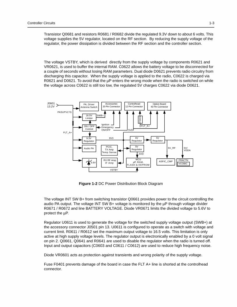
Controller Circuits 1-3
Transistor Q0681 and resistors R0681 / R0682 divide the regulated 9.3V down to about 6 volts. This voltage supplies the 5V regulator, located on the RF section. By reducing the supply voltage of the regulator, the power dissipation is divided between the RF section and the controller section.
The voltage VSTBY, which is derived directly from the supply voltage by components R0621 and VR0621, is used to buffer the internal RAM. C0622 allows the battery voltage to be disconnected for a couple of seconds without losing RAM parameters. Dual diode D0621 prevents radio circuitry from discharging this capacitor. When the supply voltage is applied to the radio, C0622 is charged via R0621 and D0621. To avoid that the µP enters the wrong mode when the radio is switched on while the voltage across C0622 is still too low, the regulated 5V charges C0622 via diode D0621.
Figure 1-2 DC Power Distribution Block Diagram
The voltage INT SW B+ from switching transistor Q0661 provides power to the circuit controlling the audio PA output. The voltage INT SW B+ voltage is monitored by the µP through voltage divider R0671 / R0672 and line BATTERY VOLTAGE. Diode VR0671 limits the divided voltage to 5.6V to protect the µP.
Regulator U0611 is used to generate the voltage for the switched supply voltage output (SWB+) at the accessory connector J0501 pin 13. U0611 is configured to operate as a switch with voltage and current limit. R0611 / R0612 set the maximum output voltage to 16.5 volts. This limitation is only active at high supply voltage levels. The regulator output is electronically enabled by a 0 volt signal on pin 2. Q0661, Q0641 and R0641 are used to disable the regulator when the radio is turned off. Input and output capacitors (C0603 and C0611 / C0612) are used to reduce high frequency noise.
Diode VR0601 acts as protection against transients and wrong polarity of the supply voltage.
Fuse F0401 prevents damage of the board in case the FLT A+ line is shorted at the controlhead connector.
VCOBIC
FRACTN
VSTBY
5V_RF
9V3
FLT_A+
5VD
SWB+
Option Board 40 Pin Connector
PA, Driver Antenna Switch
Controlhead12 Pin Connector
Accessories20 Pin Connector
J0601 13.2V
PASUPVLTG
FLT_A+
16.5VLimiter
ON / OFFControl
ASFIC_CMP5.6V
IgnitionEmergencyON/OFF
9.3VRegulator
Audio PA
6VRegulator
5VRegulator
5VD
5VRegulator
5V/VDDA
MCU µP, RAM,
FLASH & EEPROM
PCIC, TX Amp
Temp Sense
RX RF AmpIF Amp
F04
01
1-4 Controller Circuits
1.4 Electronic ON/OFF
The radio has circuitry which allows radio software and/or external triggers to turn the radio on or off without direct user action. For example, automatic turn on when ignition is sensed and off when ignition is off.
Q0661 is used to provide INT SW B+ to the various radio circuits and to enable the voltage regulators via transistor Q0641. Q0661 contains an pnp and an npn transistor and acts as an electronic on/off switch. The switch is on when the collector of the npn transistor within Q0661 is low. When the radio is off the collector is at supply voltage level. This effectively prevents current flow from emitter to collector of the pnp transistor. When the radio is turned on the voltage at the base of the npn transistor is pulled high and the pnp transistor switches on (saturation). With voltage INT SWB+ now at supply voltage level, transistor Q0641 pulls pin 2 of the voltage regulators U0611 and U 0641 to ground level and thereby enables their outputs. The electronic on/off circuitry can be enabled by the microprocessor (through ASFIC CMP port GCB2, line DC POWER ON), the emergency switch (line EMERGENCY CONTROL), the mechanical On/Off/Volume knob on the controlhead (line ON OFF CONTROL), or the ignition sense circuitry (line IGNITION CONTROL). If any of the 4 paths cause a low at the collector of the npn transistor within Q0661, the electronic "ON" is engaged.
1.5 Emergency
The emergency switch (J0501 pin 9), when engaged, grounds the base of Q0662 via line EMERGENCY CONTROL. This switches Q0662 off and resistor R0662 pulls the collector of Q0662 and the base of Q0663 to levels above 2 volts. Transistor Q0663 switches on and pulls the collector of the npn transistor within Q0661 to ground level and thereby enables the voltage regulators via Q0641. When the emergency switch is released R0541 pulls the base of Q0662 up to 0.6 volts. This causes the collector of transistor Q0662 to go low (0.2V), thereby switching Q0663 off.
While the radio is switched on, the microprocessor monitors the voltage at the emergency input on the accessory connector via pin 60 and line GP5 IN ACC9. Three different conditions are distinguished, no emergency, emergency, and open connection to the emergency switch. If no emergency switch is connected or the connection to the emergency switch is broken, the resistive divider R0541 / R0512 will set the voltage to about 4.7 volts. If an emergency switch is connected, a resistor to ground within the emergency switch will reduce the voltage on line GP5 IN ACC9 to inform the microprocessor that the emergency switch is operational. An engaged emergency switch pulls line GP5 IN ACC9 to ground level. Diode D0179 limits the voltage to protect the microprocessor input.
While EMERGENCY CONTROL is low, INT SW B+ is on, the microprocessor starts execution, reads that the emergency input is active through the voltage level of line GP5 IN ACC9, and sets the DC POWER ON output of the ASFIC CMP pin 13 to a logic high. This high will keep Q0661 and Q0641 switched on. This operation allows a momentary press of the emergency switch to power up the radio. When the microprocessor has finished processing the emergency press, it sets the DC POWER ON line to a logic 0. This turns off Q0661 and the radio turns off. Notice that the microprocessor is alerted to the emergency condition via line GP5 IN ACC9. If the radio was already on when emergency was triggered then DC POWER ON would already be high.

Controller Circuits 1-5
1.6 Mechanical ON/OFF
This refers to the typical On/Off/Volume knob, located on the controlhead, and which turns the radio on and off.If the radio is turned off and the On/Off/Volume knob is pressed, line ON OFF CONTROL (J0401 pin 11) goes high and switches the radio’s voltage regulators on as long as the button is pressed. The microprocessor is alerted through line ON OFF SENSE (U0101 pin 6) which is pulled to low by Q0110 while the On/Off /Volume knob is pressed. In addition, an interrupt is generated at µP pin 96. The µP asserts line DC POWER ON via ASFIC CMP, pin 13 high which keeps Q0661 and Q0641, and in turn the radio, switched on. When the On/Off/Volume knob is released again the controlhead informs the µP via SBEP bus about the knob release. (See SBEP Serial Interface subsection for more details). This informs the µP to keep the radio switched on and continue with normal operation.If the On/Off/Volume knob is pressed while the radio is on, the controlhead informs the µP via SBEP bus about the knob status. (See SBEP Serial Interface subsection for more details). After a short delay time the microprocessor switches the radio off by setting DC POWER ON to low via ASFIC CMP pin 13.
1.7 Ignition
Ignition sense is used to prevent the radio from draining the vehicle’s battery because the engine is not running.
When the IGNITION input (J0501 pin 10) goes above 5 volts Q0661 is turned on via line IGNITION CONTROL. Q0661 turns on INT SW B+ and the voltage regulators by turning on Q0641 and the microprocessor starts execution. The microprocessor is alerted through line GP6 IN ACC10. The voltage at the IGNITION input turns Q0181 on, which pulls microprocessor pin 74 to low. If the software detects a low state it asserts DC POWER ON via ASFIC pin 13 high which keeps Q0661 and Q0641, and in turn the radio switched on.
When the IGNITION input goes below 3 volts, Q0181 switches off and R0181 pulls microprocessor pin 74 to high. This alerts the software to switch off the radio by setting DC POWER ON to low. The next time the IGNITION input goes above 5 volts the above process will be repeated.
1.8 Microprocessor Clock Synthesizer
The clock source for the microprocessor system is generated by the ASFIC CMP (U0221). Upon power-up the synthesizer IC (FRAC-N) generates a 16.8 MHz waveform that is routed from the RF section to the ASFIC CMP pin 34. For the main board controller the ASFIC CMP uses 16.8 MHz as a reference input clock signal for its internal synthesizer. The ASFIC CMP, in addition to audio circuitry, has a programmable synthesizer which can generate a synthesized signal ranging from 1200Hz to 32.769MHz in 1200Hz steps.
When power is first applied, the ASFIC CMP will generate its default 3.6864MHz CMOS square wave UP CLK (on U0221 pin 28) and this is routed to the microprocessor (U0101 pin 90). After the microprocessor starts operation, it reprograms the ASFIC CMP clock synthesizer to a higher UP CLK frequency (usually 7.3728 or 14.7456 MHz) and continues operation.
The ASFIC CMP may be reprogrammed to change the clock synthesizer frequencies at various times depending on the software features that are executing. In addition, the clock frequency of the synthesizer is changed in small amounts if there is a possibility of harmonics of this clock source interfering with the desired radio receive frequency.

1-6 Controller Circuits
The ASFIC CMP synthesizer loop uses C0245, C0246 and R0241 to set the switching time and jitter of the clock output. If the synthesizer cannot generate the required clock frequency it will switch back to its default 3.6864MHz output.
Because the ASFIC CMP synthesizer and the µP system will not operate without the 16.8 MHz reference clock it (and the voltage regulators) should be checked first in debugging the system.
The microprocessor uses XTAL Y0131 and associated components to form a Real Time Clock (RTC). It may be used to display the time on controlheads with display or as time stamp for incoming calls or messages. The real time clock is powered from the voltage VSTBY to keep it running while the radio is switched off. When the radio was disconnected from its supply voltage, the time must be set again.
1.9 Serial Peripheral Interface (SPI)
The µP communicates to many of the ICs through its SPI port. This port consists of SPI TRANSMIT DATA (MOSI) (U0101-100), SPI RECEIVE DATA (MISO) (U0101-99), SPI CLK (U0101-1) and chip select lines going to the various ICs, connected on the SPI PORT (BUS). This BUS is a synchronous bus, in that the timing clock signal CLK is sent while SPI data (SPI TRANSMIT DATA or SPI RECEIVE DATA) is sent. Therefore, whenever there is activity on either SPI TRANSMIT DATA or SPI RECEIVE DATA there should be a uniform signal on CLK. The SPI TRANSMIT DATA is used to send serial from a µP to a device, and SPI RECEIVE DATA is used to send data from a device to a µP.
On the controller there are two ICs on the SPI BUS, ASFIC CMP (U0221-22), and EEPROM (U0111-5). In the RF sections there are 2 ICs on the SPI BUS, the FRAC-N Synthesizer, and the Power Control IC (PCIC). The SPI TRANSMIT DATA and CLK lines going to the RF section are filtered by L0481 / R0481 and L0482 / R0482 to minimize noise. The chip select line CSX from U0101 pin 2 is shared by the ASFIC CMP, FRAC-N Synthesizer and PCIC. Each of these ICs check the SPI data and when the sent address information matches the IC’s address, the following data is processed. The chip select lines for the EEPROM (EE CS), Voice Storage (VS CS), expansion board (EXP1 CS, EXP2 CS) and option board (OPT CS) are decoded by the address decoder U0141.
When the µP needs to program any of these ICs it brings the chip select line CSX to a logic 0 and then sends the proper data and clock signals. The amount of data sent to the various ICs are different, for example the ASFIC CMP can receive up to 19 bytes (152 bits) while the PCIC can receive up to 6 bytes (48 bits). After the data has been sent the chip select line is returned to logic 1.
The Option board interfaces are different in that the µP can also read data back from devices connected.The timing and operation of this interface is specific to the option connected, but generally follows the pattern:
1. an option board device generates a service request via J0551-29, line RDY and µP pin 79,
2. the main board asserts a chip select for that option board device via U0141-14, line OPT CS, J0551-30,
3. the main board µP generates the CLK (J0551-3),
4. the main board µP writes serial data via J0551-15 and reads serial data via J0551-16 and,
5. when data transfer is complete the main board terminates the chip select and CLK activity.
Controller Circuits 1-7
1.10 SBEP Serial Interface
The SBEP serial interface allows the radio to communicate with the Customer Programming Software (CPS), or the Universal Tuner via the Radio Interface Box (RIB). This interface connects to the microphone connector via controlhead connector (J0401-8) and to the accessory connector J0501-17 and comprises BUS+. The line is bidirectional, meaning that either the radio or the RIB can drive the line. The microprocessor sends serial data via pin 98 and D0101 and it reads serial data via pin 97. Whenever the microprocessor detects activity on the BUS+ line, it starts communication.
In addition, the SBEP serial interface is used to communicate with a connected controlhead. When a controlhead key is pressed or the volume knob is rotated, the line ON OFF CONTROL goes high. This turns on transistor Q0110 which pulls line ON OFF SENSE and µP pin 6 to ground level. In addition, an interrupt is generated at µP pin 96. This indicates that the controlhead wants to start SBEP communication. The microprocessor then requests the data from the controlhead. The controlhead starts sending and after all data has been send, the ON OFF CONTROL line goes low. The controlhead ignores any data on BUS+ during SBEP communication with the CPS or Universal Tuner.
1.11 General Purpose Input/Output
The controller provides eight general purpose lines (DIG1 through DIG8) available on the accessory connector J0501 to interface to external options. Lines DIG IN 1,3,5,6, are inputs, DIG OUT 2 is an output and DIG IN OUT 4,7,8 are bidirectional. The software and the hardware configuration of the radio model define the function of each port.
DIG IN 1 can be used as external PTT input, DATA PTT input or others, set by the CPS. The µP reads this port via pin 77 and Q0171.
DIG OUT 2 can be used as normal output or external alarm output, set by the CPS. Transistor Q0173 is controlled by the µP via ASFIC CMP pin 14.
DIG IN 3 is read by µP pin 61 via resistor R0176
DIG IN 5 can be used as normal input or emergency input, set by the CPS. The µP reads this port via R0179 and µP pin 60. Diode D0179 limits the voltage to protect the µP input.
DIG IN 6 can be used as normal input, set by the CPS. The µP reads this port via pin 74 and Q0181.
DIG IN OUT 4,7,8 are bi-directional and use the same circuit configuration. Each port uses an output transistor Q0177, Q0183, Q0185 controlled by µP pins 46, 47, 53. The ports are read by µP pins 75, 54, 76. To use one of the ports as input the µP must turn off the corresponding output transistor.
In addition the signals from DIG IN 1, DIG IN OUT 4 are fed to the option board connector J0551 and the expansion board connector J0451.

1-8 Controller Circuits
1.12 Normal Microprocessor Operation
For this radio, the µP is configured to operate in one of two modes, expanded and bootstrap. In expanded mode the µP uses external memory devices to operate, whereas in bootstrap operation the µP uses only its internal memory. In normal operation of the radio the µP is operating in expanded mode as described below.
In expanded mode on this radio, the µP (U0101) has access to 3 external memory devices; U0121 (FLASH EEPROM), U0122 (SRAM), U0111 (EEPROM). Also, within the µP there are 3 KBytes of internal RAM, as well as logic to select external memory devices.
The external EEPROM (U0111) space contains the information in the radio which is customer specific, referred to as the codeplug. This information consists of items such as: 1) what band the radio operates in, 2) what frequencies are assigned to what channel, and 3) tuning information. (See the particular device subsection for more details.)
The external SRAM (U0122) as well as the µP’s own internal RAM space are used for temporary calculations required by the software during execution. All of the data stored in both of these locations is lost when the radio powers off (See the particular device subsection for more details).
The FLASH EEPROM contains the actual Radio Operating Software. This software is common to all open architecture radios within a given model type. For example Trunking radios may have a different version of software in the FLASH EEPROM than a non Trunking radio (See the particular device subsection for more details).
The µP provides an address bus of 16 address lines (ADDR 0 - ADDR 15), and a data bus of 8 data lines (DATA 0 - DATA 7). There are also 3 control lines; CSPROG (U0101-38) to chip select U0121-30 (FLASH EEPROM), CSGP2 (U0101-41) to chip select U0122-20 (SRAM) and PG7 R W (U0101-4) to select whether to read or to write. The external EEPROM (U0111-1), the OPTION BOARD and EXPANSION BOARD are selected by 3 lines of the µP using address decoder U0141. The chips ASFIC CMP / FRAC-N / PCIC are selected by line CSX (U0101-2).
When the µP is functioning normally, the address and data lines should be toggling at CMOS logic levels. Specifically, the logic high levels should be between 4.8 and 5.0V, and the logic low levels should be between 0 and 0.2V. No other intermediate levels should be observed, and the rise and fall times should be <30ns.
The low-order address lines (ADDR 0 - ADDR 7) and the data lines (DATA 0-DATA 7) should be toggling at a high rate, e. g. , you should set your oscilloscope sweep to 1us/div. or faster to observe individual pulses. High speed CMOS transitions should also be observed on the µP control lines.
On the µP the lines XIRQ (U0101-48), MODA LIR (U0101-58), MODB VSTPY (U0101-57) and RESET (U0101-94) should be high at all times during normal operation. Whenever a data or address line becomes open or shorted to an adjacent line, a common symptom is that the RESET line goes low periodically, with the period being in the order of 20ms. In the case of shorted lines you may also detect the line periodically at an intermediate level, i.e. around 2.5V when 2 shorted lines attempt to drive to opposite rails.
The MODA LIR (U0101-58) and MODB VSTPY (U0101-57) inputs to the µP must be at a logic 1 for it to start executing correctly. After the µP starts execution it will periodically pulse these lines to determine the desired operating mode. While the Central Processing Unit (CPU) is running, MODA LIR is an open-drain CMOS output which goes low whenever the µP begins a new instruction (an instruction typically requires 2-4 external bus cycles, or memory fetches). However, since it is an open-drain output, the waveform rise assumes an exponential shape similar to an RC circuit.

Controller Circuits 1-9
There are 8 analogue to digital converter ports (A/D) on U0101. They are labelled within the device block as PE0-PE7. These lines sense the voltage level ranging from 0 to 5V of the input line and convert that level to a number ranging from 0 to 255 which can be read by the software to take appropriate action.
For example U0101-67 is the battery voltage detect line. R0671 and R0672 form a resistor divider on INT SWB+. With 30K and 10K and a voltage range of 11V to 17V, that A/D port would see 2.74V to 4.24V which would then be converted to ~140 to 217 respectively.
U0101-69 is the high reference voltage for the A/D ports on the µP. Capacitor C0101 filters the +5V reference. If this voltage is lower than +5V the A/D readings will be incorrect. Likewise U0101-68 is the low reference for the A/D ports. This line is normally tied to ground. If this line is not connected to ground, the A/D readings will be incorrect.
1-10 Controller Circuits
1.13 FLASH Electronically Erasable Programmable Memory(FLASH EEPROM)
The 512KByte FLASH EEPROM (U0121) contains the radio’s operating software. This software is common to all open architecture radios within a given model type. For example Trunking radios may have a different version of software in the FLASH EEPROM than a non Trunking radio. This is, as opposed to the codeplug information stored in EEPROM (U0111) which could be different from one user to another in the same company.
In normal operating mode, this memory is only read, not written to. The memory access signals (CE, OE and WE) are generated by the µP.
To upgrade/reprogram the FLASH software, the µP must be set in bootstrap operating mode. This is done by pulling microprocessor pins MODA LIR (U0101-58) and MODB VSTBY (U0101-57) to low during power up. When accessory connector pin 18 is at ground level, diode D0151 will pull both microprocessor pins to low. The same can be done by a level of 12 volts on line ON OFF CONTROL from the controlhead. Q0151 pulls diode D0151 and in turn both microprocessor pins to low. Diode VR0151 prevents entering bootstrap operating mode during normal power up.
In bootstrap operating mode the µP controls the FLASH EN OE (U0121-32) input by µP pin 86. Chip select (U0121-30) and read or write operation (U0121-7) are controlled by µP pins 38 and 4.
The FLASH device may be reprogrammed 1,000 times without issue. It is not recommended to reprogram the FLASH device at a temperature below 0°C.
Capacitor C0121 serves to filter out any AC noise which may ride on +5V at U0121.
1.14 Electrically Erasable Programmable Memory (EEPROM)
The external 16 KByte EEPROM (U0111) contains additional radio operating parameters such as operating frequency and signalling features, commonly know as the codeplug. It is also used to store radio operating state parameters such as current mode and volume. This memory can be written to in excess of 100,000 times and will retain the data when power is removed from the radio. The memory access signals (SI, SO and SCK) are generated by the µP and chip select (CS) is generated by address decoder U0141-15.
1.15 Static Random Access Memory (SRAM)
The SRAM (U0121) contains temporary radio calculations or parameters that can change very frequently, and which are generated and stored by the software during its normal operation. The information is lost when the radio is turned off.
The device allows an unlimited number of write cycles. SRAM accesses are indicated by the CS signal U0122-20 (which comes from U0101-CSGP2) going low. U0122 is commonly referred to as the external RAM as opposed to the internal RAM which is the 3 KBytes of RAM which is part of the 68HC11FL0. Both RAM spaces serve the purpose. However, the internal RAM is used for the calculated values which are accessed most often.
Capacitor C0122 serves to filter out any ac noise which may ride on +5V at U0122.
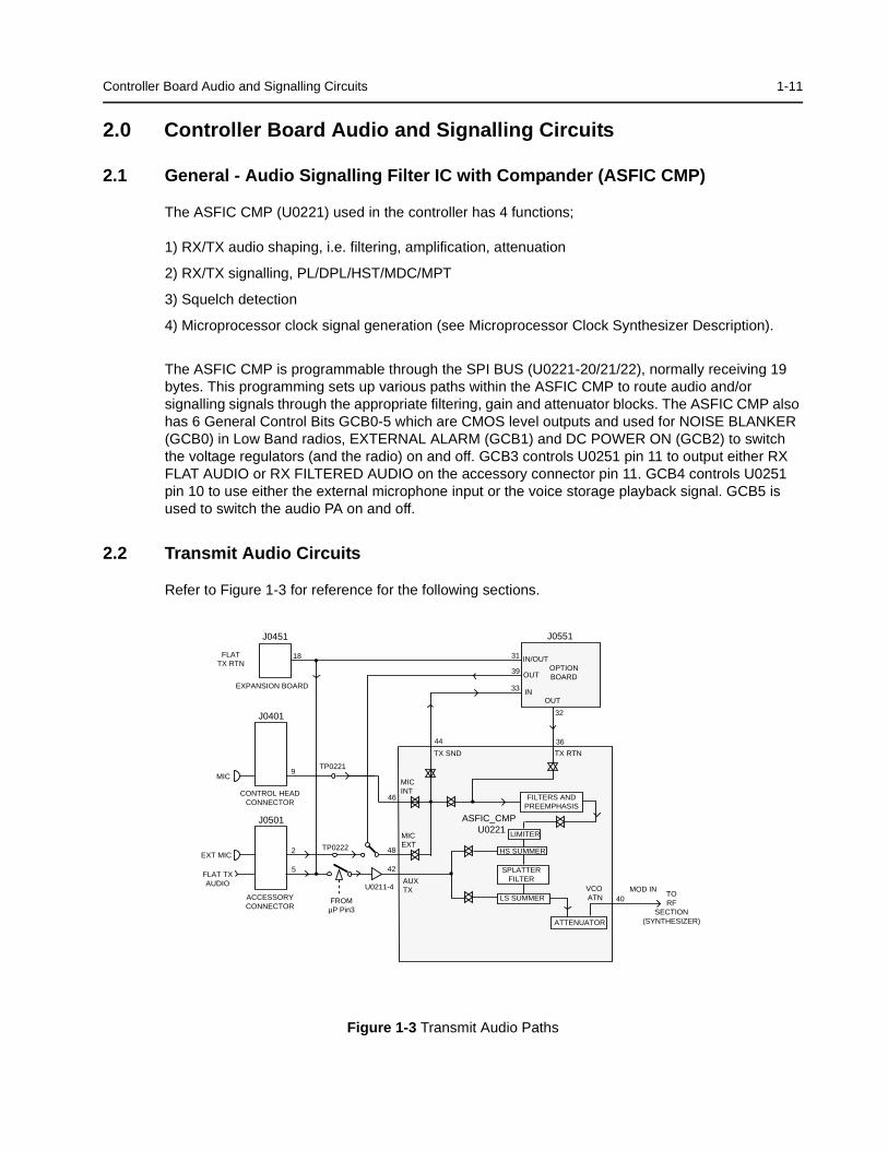
Controller Board Audio and Signalling Circuits 1-11
2.0 Controller Board Audio and Signalling Circuits
2.1 General - Audio Signalling Filter IC with Compander (ASFIC CMP)
The ASFIC CMP (U0221) used in the controller has 4 functions;
1) RX/TX audio shaping, i.e. filtering, amplification, attenuation
2) RX/TX signalling, PL/DPL/HST/MDC/MPT
3) Squelch detection
4) Microprocessor clock signal generation (see Microprocessor Clock Synthesizer Description).
The ASFIC CMP is programmable through the SPI BUS (U0221-20/21/22), normally receiving 19 bytes. This programming sets up various paths within the ASFIC CMP to route audio and/or signalling signals through the appropriate filtering, gain and attenuator blocks. The ASFIC CMP also has 6 General Control Bits GCB0-5 which are CMOS level outputs and used for NOISE BLANKER (GCB0) in Low Band radios, EXTERNAL ALARM (GCB1) and DC POWER ON (GCB2) to switch the voltage regulators (and the radio) on and off. GCB3 controls U0251 pin 11 to output either RX FLAT AUDIO or RX FILTERED AUDIO on the accessory connector pin 11. GCB4 controls U0251 pin 10 to use either the external microphone input or the voice storage playback signal. GCB5 is used to switch the audio PA on and off.
2.2 Transmit Audio Circuits
Refer to Figure 1-3 for reference for the following sections.
Figure 1-3 Transmit Audio Paths
MIC IN
MOD INTORF
SECTION(SYNTHESIZER)
3644
33
40
J0501
ACCESSORYCONNECTOR
J0401
CONTROL HEADCONNECTOR
MIC
EXT MIC
FLAT TXAUDIO
42
32
5
48
46
9
2
INOUT
OPTIONBOARD
FILTERS ANDPREEMPHASIS
HS SUMMER
SPLATTERFILTER
LS SUMMER
LIMITER
ATTENUATOR
VCO ATN
TX RTNTX SND
MICINT
AUX TX
ASFIC_CMP U0221
TP0221
TP0222
MICEXT
J0451 J0551
18FLATTX RTN
EXPANSION BOARD
31 IN/OUT
39 OUT
FROMµP Pin3
U0211-4
1-12 Controller Board Audio and Signalling Circuits
2.2.1 Mic/Data Input Path
The radio supports 2 distinct microphone paths known as internal (from controlhead) and external mic (from accessory connector J0501-2) and an auxiliary path (FLAT TX AUDIO, from accessory connector J0501-5). The microphones used for the radio require a DC biasing voltage provided by a resistive network.
These two microphone audio input paths enter the ASFIC CMP at U0221-48 (external mic) and U0221-46 (internal mic). Following the internal mic path; the microphone is plugged into the radio controlhead and is connected to the controller board via J0401-9.
From here the signal is routed via R0409 and line INT MIC to R0205. R0201 and R0202 provide the 9.3VDC bias. Resistive divider R0205 / R0207 divide the input signal by 5.5 and provide input protection for the CMOS amplifier input. R0202 and C0201 provide a 560 ohm AC path to ground that sets the input impedance for the microphone and determines the gain based on the emitter resistor in the microphone’s amplifier circuit.
C0204 serves as a DC blocking capacitor. The audio signal at U0221-46 (TP0221) should be approximately 14mV for 1.5kHz or 3kHz of deviation with 12.5kHz or 25kHz channel spacing.
The external microphone signal enters the radio on accessory connector J0501 pin 2 and is routed via line EXT MIC to R0206. R0203 and R0204 provide the 9.3VDC bias. Resistive divider R0206 / R0208 divide the input signal by 5.5 and provide input protection for the CMOS amplifier input. R0204 and C0202 provide a 560 ohm AC path to ground that sets the input impedance for the microphone and determines the gain based on the emitter resistor in the microphone’s amplifier circuit.
C0254 serves as a DC blocking capacitor. Multi switch U0251 controlled by ASFIC CMP port GCB4 selects either the external microphone input signal or the voice storage playback signal for entering the ASFIC CMP at pin 48. The audio signal at U0221-48 (TP0222) should be approximately 14mV for 1.5kHz or 3kHz of deviation with 12.5kHz or 25kHz channel spacing.
The FLAT TX AUDIO path is used for transmitting data signals and has therefore no limiter or filters enabled inside the ASFIC CMP. When this path is enabled via CPS and DATA PTT is asserted, any signal on this path is directly fed to the modulator. Signals applied to this path either via accessory connector J0501, expansion board connector J0451 or option board connector J0551 must be filtered and set to the correct level externally or on the option board in order not to exceed the maximum specified transmit deviation and transmitted power in the adjacent channels. The attenuator inside the ASFIC CMP changes the FM deviation of the data signal according to the channel spacing of the active transmit channel.
The FLAT TX AUDIO signal from accessory connector J0501-5 is fed to the ASFIC CMP (U0221) pin 42 through C0541 and line FLAT TX RTN, switch U0251 and buffer U0211-4. When the radio switches from receive to transmit mode the µP opens switch U0251 for a short period to prevent that any applied signal can cause a transmit frequency offset. Buffer U0211-4 sets the correct DC level and ensures a short settle period when the radio is switched on. Inside the ASFIC CMP the signal is routed directly to the attenuator, which sets the FM deviation according to the channel spacing of the active transmit channel and emerges from the ASFIC CMP at U0221-40, at which point it is routed to the RF section.
Controller Board Audio and Signalling Circuits 1-13
The ASFIC has an internal AGC that can control the gain in the mic audio path. The AGC can be disabled / enabled by the µP. Another feature that can be enabled or disabled in the ASFIC is the VOX. This circuit, along with the capacitor at U0221-7, provides a DC voltage that can allow the µP to detect microphone audio. The ASFIC can also be programmed to route the microphone audio to the speaker for public address operation.
2.2.2 PTT Sensing and TX Audio Processing
Microphone PTT coming from the controlhead is sent via SBEP bus to the microprocessor. An external PTT can be generated by grounding pin 3 on the accessory connector if this input is programmed for PTT by the CPS. When microphone PTT is sensed, the µP will always configure the ASFIC CMP for the "internal" mic audio path, and external PTT will result in the external mic audio path being selected.
Inside the ASFIC CMP, the mic audio is filtered to eliminate frequency components outside the 300-3000Hz voice band, and pre-emphasized if pre-emphasis is enabled. The signal is then limited to prevent the transmitter from over deviating. The limited mic audio is then routed through a summer, which is used to add in signalling data, and then to a splatter filter to eliminate high frequency spectral components that could be generated by the limiter. The audio is then routed to an attenuator, which is tuned in the factory or the field to set the proper amount of FM deviation. The TX audio emerges from the ASFIC CMP at U0221-40 MOD IN, at which point it is routed to the RF section.
Dependent on the radio model, input pin 3 on the accessory connector can be programmed for DATA PTT by the CPS. When DATA PTT is sensed, the µP will always configure the ASFIC CMP for the flat TX audio path. Limiter and any filtering will be disabled. The signal is routed directly to the attenuator, which sets the FM deviation according to the channel spacing of the active transmit channel and emerges from the ASFIC CMP at U0221-40, at which point it is routed to the RF section.
2.2.3 TX Secure Audio (optional)
The audio follows the normal transmit audio processing until it emerges from the ASFIC CMP TX SND pin (U0221-44), which is fed to the Secure board residing at option connector J0551-33. The Secure board contains circuitry to amplify, encrypt, and filter the audio. The encrypted signal is then fed back from J0551-32 to the ASFIC CMP TX RTN input (U0221-36). The signal level at this pin should be about 65mVrms. The signal is then routed through the TX path in the ASFIC CMP and emerges at MOD IN pin 40.
2.2.4 Option Board Transmit Audio
The audio follows the normal transmit audio processing until it emerges from the ASFIC CMP TX SND pin (U0221-44), which is fed to the option board residing at option connector J0551-33. The option board contains circuitry to process the audio. The processed signal is then fed back from J0551-32 to the ASFIC CMP TX RTN input (U0221-36). The signal level at this pin should be about 65mVrms. The signal is then routed through the TX path in the ASFIC CMP and emerges at MOD IN pin 40.
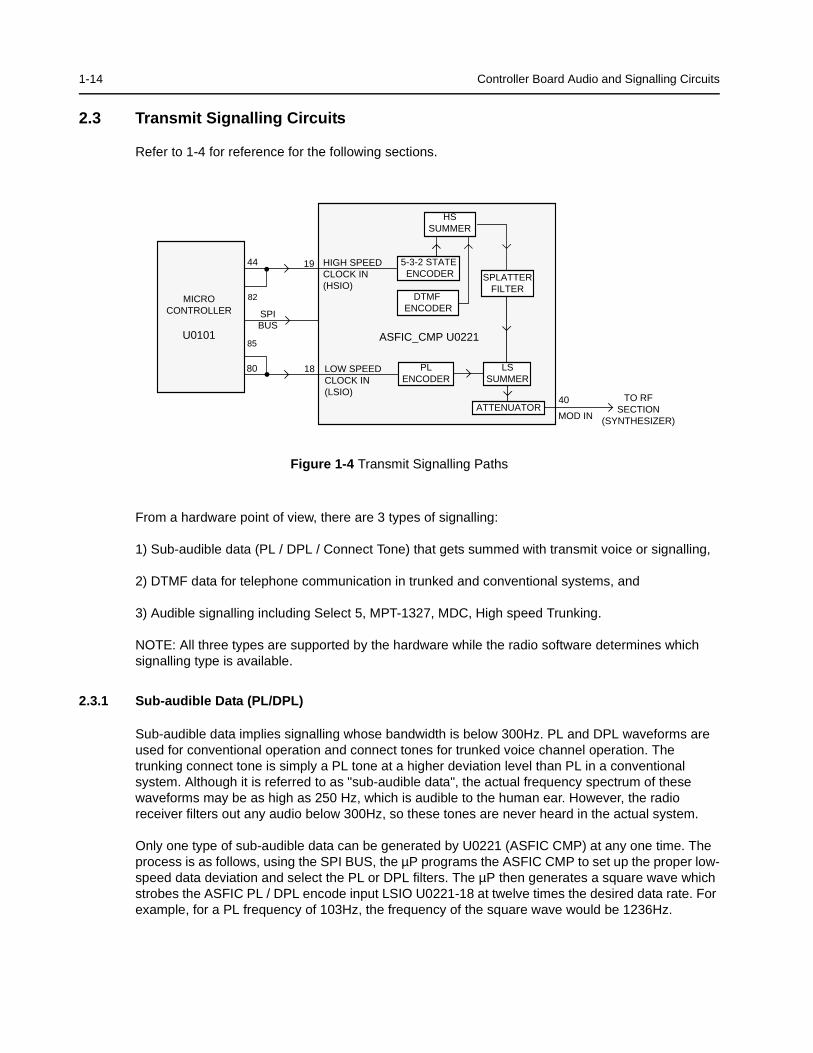
1-14 Controller Board Audio and Signalling Circuits
2.3 Transmit Signalling Circuits
Refer to 1-4 for reference for the following sections.
Figure 1-4 Transmit Signalling Paths
From a hardware point of view, there are 3 types of signalling:
1) Sub-audible data (PL / DPL / Connect Tone) that gets summed with transmit voice or signalling,
2) DTMF data for telephone communication in trunked and conventional systems, and
3) Audible signalling including Select 5, MPT-1327, MDC, High speed Trunking.
NOTE: All three types are supported by the hardware while the radio software determines which signalling type is available.
2.3.1 Sub-audible Data (PL/DPL)
Sub-audible data implies signalling whose bandwidth is below 300Hz. PL and DPL waveforms are used for conventional operation and connect tones for trunked voice channel operation. The trunking connect tone is simply a PL tone at a higher deviation level than PL in a conventional system. Although it is referred to as "sub-audible data", the actual frequency spectrum of these waveforms may be as high as 250 Hz, which is audible to the human ear. However, the radio receiver filters out any audio below 300Hz, so these tones are never heard in the actual system.
Only one type of sub-audible data can be generated by U0221 (ASFIC CMP) at any one time. The process is as follows, using the SPI BUS, the µP programs the ASFIC CMP to set up the proper low-speed data deviation and select the PL or DPL filters. The µP then generates a square wave which strobes the ASFIC PL / DPL encode input LSIO U0221-18 at twelve times the desired data rate. For example, for a PL frequency of 103Hz, the frequency of the square wave would be 1236Hz.
19
18
40
MOD IN
TO RFSECTION
(SYNTHESIZER)
80
44 HIGH SPEEDCLOCK IN(HSIO)
LOW SPEED CLOCK IN(LSIO)
ASFIC_CMP U0221
MICROCONTROLLER
U0101
HSSUMMER
5-3-2 STATE ENCODER
DTMF ENCODER
SPLATTERFILTER
PLENCODER
LSSUMMER
ATTENUATOR
85
82
SPIBUS
Controller Board Audio and Signalling Circuits 1-15
This drives a tone generator inside U0221 which generates a staircase approximation to a PL sine wave or DPL data pattern. This internal waveform is then low-pass filtered and summed with voice or data. The resulting summed waveform then appears on U0221-40 (MOD IN), where it is sent to the RF board as previously described for transmit audio. A trunking connect tone would be generated in the same manner as a PL tone.
2.3.2 High Speed Data
High speed data refers to the 3600 baud data waveforms, known as Inbound Signalling Words (ISWs) used in a trunking system for high speed communication between the central controller and the radio. To generate an ISW, the µP first programs the ASFIC CMP (U0221) to the proper filter and gain settings. It then begins strobing U0221-19 (HSIO) with a pulse when the data is supposed to change states. U0221’s 5-3-2 State Encoder (which is in a 2-state mode) is then fed to the post-limiter summer block and then the splatter filter. From that point it is routed through the modulation attenuators and then out of the ASFIC CMP to the RF board. MPT 1327 and MDC are generated in much the same way as Trunking ISW. However, in some cases these signals may also pass through a data pre-emphasis block in the ASFIC CMP. Also these signalling schemes are based on sending a combination of 1200 Hz and 1800 Hz tones only. Microphone audio is muted during High Speed Data signalling.
2.3.3 Dual Tone Multiple Frequency (DTMF) Data
DTMF data is a dual tone waveform used during phone interconnect operation. It is the same type of tones which are heard when using a "Touch Tone" telephone.
There are seven frequencies, with four in the low group (697, 770, 852, 941Hz) and three in the high group (1209, 1336, 1477Hz).
The high-group tone is generated by the µP (U0101-44) strobing U0221-19 at six times the tone frequency for tones less than 1440Hz or twice the frequency for tones greater than 1440Hz. The low group tone is generated by the ASFIC CMP, controlled by the µP via SPI bus. Inside U0221 the low-group and high-group tones are summed (with the amplitude of the high group tone being approximately 2 dB greater than that of the low group tone) and then pre-emphasized before being routed to the summer and splatter filter. The DTMF waveform then follows the same path as was described for high-speed data.
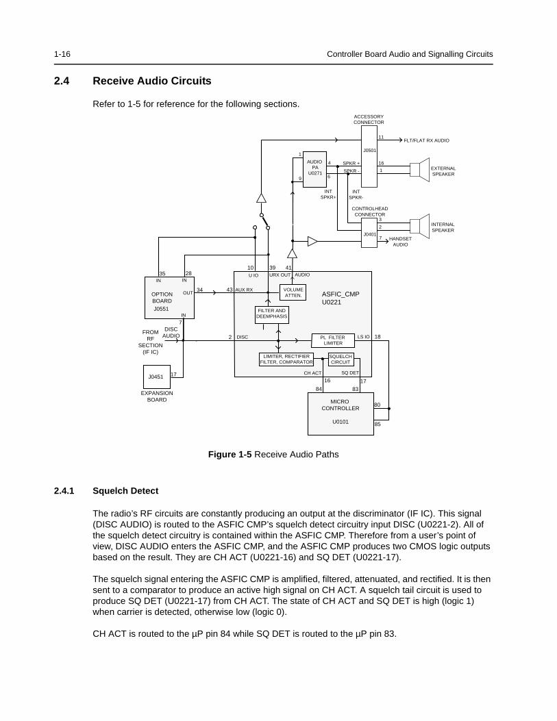
1-16 Controller Board Audio and Signalling Circuits
2.4 Receive Audio Circuits
Refer to 1-5 for reference for the following sections.
Figure 1-5 Receive Audio Paths
2.4.1 Squelch Detect
The radio’s RF circuits are constantly producing an output at the discriminator (IF IC). This signal (DISC AUDIO) is routed to the ASFIC CMP’s squelch detect circuitry input DISC (U0221-2). All of the squelch detect circuitry is contained within the ASFIC CMP. Therefore from a user’s point of view, DISC AUDIO enters the ASFIC CMP, and the ASFIC CMP produces two CMOS logic outputs based on the result. They are CH ACT (U0221-16) and SQ DET (U0221-17).
The squelch signal entering the ASFIC CMP is amplified, filtered, attenuated, and rectified. It is then sent to a comparator to produce an active high signal on CH ACT. A squelch tail circuit is used to produce SQ DET (U0221-17) from CH ACT. The state of CH ACT and SQ DET is high (logic 1) when carrier is detected, otherwise low (logic 0).
CH ACT is routed to the µP pin 84 while SQ DET is routed to the µP pin 83.
FLT/FLAT RX AUDIO
J0501
11
16
1 EXTERNALSPEAKER
INTERNALSPEAKER
ACCESSORYCONNECTOR
CONTROLHEADCONNECTOR
HANDSETAUDIO
7
2
3
J0401
INTSPKR-
SPKR +
SPKR -
1
9
2
J0551
4110
INTSPKR+
4
6
DISC
ASFIC_CMPU0221
AUDIO PA
U0271
IN
OPTIONBOARD
IN
OUTVOLUMEATTEN.
FILTER ANDDEEMPHASIS
17
MICRO CONTROLLER
U0101
80
FROMRF
SECTION(IF IC)
LIMITER, RECTIFIERFILTER, COMPARATOR
SQ DET
SQUELCHCIRCUIT
16
PL FILTER LIMITER
CH ACT
AUX RX43
18LS IO
U IO AUDIO
8384
39URX OUT
17J0451
EXPANSIONBOARD
DISCAUDIO
34
2835
85
IN
7
Controller Board Audio and Signalling Circuits 1-17
SQ DET is used to determine all audio mute / unmute decisions except for Conventional Scan. In this case CH ACT is a pre-indicator as it occurs slightly faster than SQ DET.
2.4.2 Audio Processing and Digital Volume Control
The receiver audio signal enters the controller section from the IF IC on DISC AUDIO. The signal is DC coupled by R0228 and enters the ASFIC CMP via the DISC pin U0221-2.
Inside the ASFIC CMP, the signal goes through 2 paths in parallel, the audio path and the PL/DPL path.
The audio path has a programmable amplifier, whose setting is based on the channel bandwidth being received, then a LPF filter to remove any frequency components above 3000Hz and then an HPF to strip off any sub-audible data below 300Hz. Next, the recovered audio passes through a de-emphasis filter if it is enabled (to compensate for Pre-emphasis which is used to reduce the effects of FM noise). The IC then passes the audio through the 8-bit programmable attenuator whose level is set depending on the value of the volume control. Finally the filtered audio signal passes through an output buffer within the ASFIC CMP. The audio signal exits the ASFIC CMP at pin AUDIO (U0221-41).
The µP programs the attenuator, using the SPI BUS, based on the volume setting. The minimum / maximum settings of the attenuator are set by codeplug parameters.
Since sub-audible signalling is summed with voice information on transmit, it must be separated from the voice information before processing. Any sub-audible signalling enters the ASFIC CMP from the IF IC at DISC U0221-2. Once inside it goes through the PL/DPL path. The signal first passes through one of 2 low pass filters, either PL low pass filter or DPL/LST low pass filter. Either signal is then filtered and goes through a limiter and exits the ASFIC CMP at LSIO (U0221-18). At this point the signal will appear as a square wave version of the sub-audible signal which the radio received. The microprocessor U0101-80 will decode the signal directly to determine if it is the tone / code which is currently active on that mode.
2.4.3 Audio Amplification Speaker (+) Speaker (-)
The output of the ASFIC CMP’s digital volume pot, U0221-41 is routed through DC blocking capacitor C0265 to a buffer formed by U0211-1. Resistors R0265 and R0268 set the correct input level to the audio PA (U0271). This is necessary because the gain of the audio PA is 46 dB, and the ASFIC CMP output is capable of overdriving the PA unless the maximum volume is limited. Resistor R0267 and capacitor C0267 increase frequency components below 350Hz.
The audio then passes through R0269 and C0272 which provides AC coupling and low frequency roll-off. C0273 provides high frequency roll-off as the audio signal is routed to pins 1 and 9 of the audio power amplifier U0271.
The audio power amplifier has one inverted and one non-inverted output that produces the differential audio output SPK+ / SPK- (U0271-4/6). The inputs for each of these amplifiers are pins 1 and 9 respectively; these inputs are both tied to the received audio. The audio PA’s DC biases are not activated until the audio PA is enabled at pin 8.
The audio PA is enabled via the ASFIC CMP (U0221-38). When the base of Q0271 is low, the transistor is off and U0271-8 is high, using pull up resistor R0273, and the Audio PA is ON. The voltage at U0273-8 must be above 8.5VDC to properly enable the device.

1-18 Controller Board Audio and Signalling Circuits
If the voltage is between 3.3 and 6.4V, the device will be active but has its input (U0273-1/9) off. This is a mute condition which is used to prevent an audio pop when the PA is enabled.
The SPK+ and SPK- outputs of the audio PA have a DC bias which varies proportionately with FLT A+ (U0271-7). FLT A+ of 11V yields a DC offset of 5V, and FLT A+ of 17V yields a DC offset of 8.5V. If either of these lines is shorted to ground, it is possible that the audio PA will be damaged. SPK+ and SPK- are routed to the accessory connector (J0501-16 and 1) and to the controlhead (connector J0401-2 and 3).
2.4.4 Handset Audio
Certain hand held accessories have a speaker within them which require a different voltage level than that provided by U0271. For those devices HANDSET AUDIO is available at controlhead connector J0401-7.
The received audio from the output of the ASFIC CMP’s digital volume attenuator and buffered by U0211-1 is also routed to U0211-3 pin 9 where it is amplified 20 dB; this is set by the 10k/100k combination of R0261 and R0262. This signal is routed from the output of the op amp U0211-3 pin 8 to J0401-7. The controlhead sends this signal directly out to the microphone jack. The maximum value of this output is 6.6Vp-p.
2.4.5 Filtered Audio and Flat Audio
The ASFIC CMP has an audio whose output at U0221-39 has been filtered and de-emphasized, but has not gone through the digital volume attenuator. From ASFIC CMP U0221-39 the signal is routed via R0251 through gate U0251-12 and AC coupled to U0211-2. The gate controlled by ASFIC CMP port GCB3 (U0221-35) selects between the filtered audio signal from the ASFIC CMP pin 39 (URXOUT) or the unfiltered (flat) audio signal from the ASFIC CMP pin 10 (UIO). R0251 and R0253 determine the gain of op-amp U0211-2 for the filtered audio while R0252 and R0253 determine the gain for the flat Audio. The output of U0253-7 is then routed to J0501-11 via DC blocking capacitor C0542 and R0531. Note that any volume adjustment of the signal on this path must be done by the accessory
2.4.6 RX Secure Audio (optional)
Discriminator audio, which is now encrypted audio, follows the normal receive audio processing until it emerges from the ASFIC CMP UIO pin (U0221-10), which is fed to the Secure board residing at option connector J0551-35. On the Secure board, the encrypted signal is converted back to normal audio format, and then fed back through (J0551-34) to AUX RX of the ASFIC CMP (U0221-43). From then on it follows a path identical to conventional receive audio, where it is filtered (0.3 - 3kHz) and de-emphasized. The signal URX SND from the ASFIC CMP (U0221-39), also routed to option connector J0551-28, is not used for the Secure board but for other option boards.
2.4.7 Option Board Receive Audio
Unfiltered audio from the ASFIC CMP pin UIO (U0221-10) enters the option board at connector J0551-35. Filtered audio from the ASFIC CMP pin URXOUT (U0221-39) enters the option board at connector J0551-28. On the option board, the signal may be processed, and then fed back through J0551-34 to AUX RX of the ASFIC CMP (U0221-43). From then on it follows a path identical to conventional receive audio, where it may be filtered (0.3 - 3kHz) and de-emphasized.

Controller Board Audio and Signalling Circuits 1-19
2.5 Receive Signalling Circuits
Refer to 1-6 for reference for the following sections.
Figure 1-6 Receive Signalling Paths
2.5.1 Sub-audible (PL/DPL) and High Speed Data Decoder
The ASFIC CMP (U0221) is used to filter and limit all received data. The data enters the ASFIC CMP at input DISC (U0221-2). Inside U0221 the data is filtered according to data type (HS or LS), then it is limited to a 0-5V digital level. The MDC and trunking high speed data appear at U0221-19, where it connects to the µP U0101-82
The low speed limited data output (PL, DPL, and trunking LS) appears at U0221-18, where it connects to the µP U0101-80.
The low speed data is read by the µP at twice the frequency of the sampling waveform; a latch configuration in the ASFIC CMP stores one bit every clock cycle. The external capacitors C0236, and C0244 set the low frequency pole for a zero crossings detector in the limiters for PL and HS data. The hysterisis of these limiters is programmed based on the type of received data.
2.5.2 Alert Tone Circuits
When the software determines that it needs to give the operator an audible feedback (for a good key press, or for a bad key press), or radio status (trunked system busy, phone call, circuit failures), it sends an alert tone to the speaker. It does so by sending SPI BUS data to U0221 which sets up the audio path to the speaker for alert tones. The alert tone itself can be generated in one of two ways: internally by the ASFIC CMP, or externally using the µP and the ASFIC CMP.
The allowable internal alert tones are 304, 608, 911, and 1823Hz. In this case a code contained within the SPI BUS load to the ASFIC CMP sets up the path and determines the tone frequency, and at what volume level to generate the tone. (It does not have to be related to the voice volume setting).
For external alert tones, the µP can generate any tone within the 100-3000Hz audio band. This is accomplished by the µP generating a square wave which enters the ASFIC CMP at U0221-19. Inside the ASFIC CMP this signal is routed to the alert tone generator.
DET AUDIODISCRIMINATOR AUDIO
FROM RF SECTION(IF IC)
19
18
25
2
82
80
DISC
PLCAP2
LSIO
HSIODATA FILTERAND DEEMPHASIS LIMITER
FILTER LIMITER
ASFIC_CMPU0221
MICROCONTROLLER
U0101
85
44
8
PLCAP
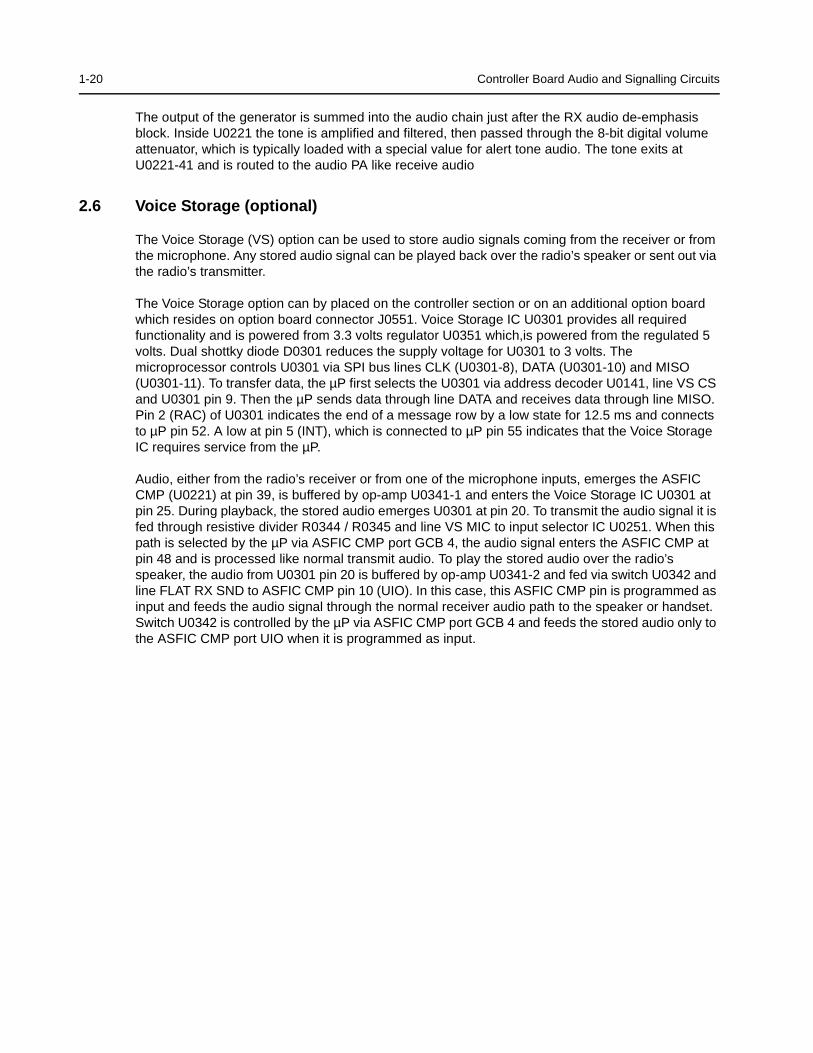
1-20 Controller Board Audio and Signalling Circuits
The output of the generator is summed into the audio chain just after the RX audio de-emphasis block. Inside U0221 the tone is amplified and filtered, then passed through the 8-bit digital volume attenuator, which is typically loaded with a special value for alert tone audio. The tone exits at U0221-41 and is routed to the audio PA like receive audio
2.6 Voice Storage (optional)
The Voice Storage (VS) option can be used to store audio signals coming from the receiver or from the microphone. Any stored audio signal can be played back over the radio’s speaker or sent out via the radio’s transmitter.
The Voice Storage option can by placed on the controller section or on an additional option board which resides on option board connector J0551. Voice Storage IC U0301 provides all required functionality and is powered from 3.3 volts regulator U0351 which,is powered from the regulated 5 volts. Dual shottky diode D0301 reduces the supply voltage for U0301 to 3 volts. The microprocessor controls U0301 via SPI bus lines CLK (U0301-8), DATA (U0301-10) and MISO (U0301-11). To transfer data, the µP first selects the U0301 via address decoder U0141, line VS CS and U0301 pin 9. Then the µP sends data through line DATA and receives data through line MISO. Pin 2 (RAC) of U0301 indicates the end of a message row by a low state for 12.5 ms and connects to µP pin 52. A low at pin 5 (INT), which is connected to µP pin 55 indicates that the Voice Storage IC requires service from the µP.
Audio, either from the radio’s receiver or from one of the microphone inputs, emerges the ASFIC CMP (U0221) at pin 39, is buffered by op-amp U0341-1 and enters the Voice Storage IC U0301 at pin 25. During playback, the stored audio emerges U0301 at pin 20. To transmit the audio signal it is fed through resistive divider R0344 / R0345 and line VS MIC to input selector IC U0251. When this path is selected by the µP via ASFIC CMP port GCB 4, the audio signal enters the ASFIC CMP at pin 48 and is processed like normal transmit audio. To play the stored audio over the radio’s speaker, the audio from U0301 pin 20 is buffered by op-amp U0341-2 and fed via switch U0342 and line FLAT RX SND to ASFIC CMP pin 10 (UIO). In this case, this ASFIC CMP pin is programmed as input and feeds the audio signal through the normal receiver audio path to the speaker or handset. Switch U0342 is controlled by the µP via ASFIC CMP port GCB 4 and feeds the stored audio only to the ASFIC CMP port UIO when it is programmed as input.
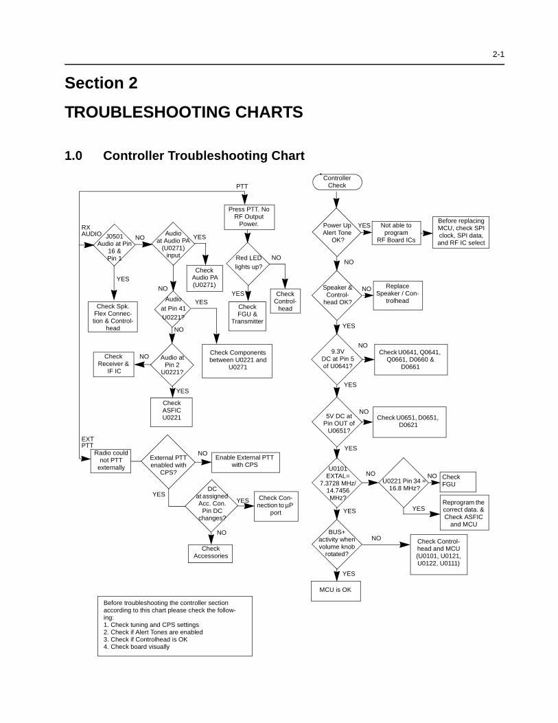
2-1
Section 2
TROUBLESHOOTING CHARTS
1.0 Controller Troubleshooting Chart
Power Up Alert Tone
OK?
Speaker & Control-
head OK?
U0101EXTAL=
7.3728 MHz/ 14.7456 MHz?
BUS+activity when volume knob
rotated?
MCU is OK
Not able to program
RF Board ICs
Before replacing MCU, check SPI clock, SPI data, and RF IC select
Replace Speaker / Con-
trolhead
U0221 Pin 34 = 16.8 MHz?
Check FGU
Reprogram the correct data. & Check ASFIC
and MCU
Check Control-head and MCU (U0101, U0121, U0122, U0111)
Press PTT. No RF Output
Power.
Red LED lights up?
Check Control-
headCheck FGU &
Transmitter
Audio
at Pin 41 U0221?
Enable External PTT with CPS
External PTT enabled with
CPS?
Radio could not PTT
externally
DCat assigned Acc. Con.
Pin DC changes?
Check Components between U0221 and
U0271
Check Con-nection to µP
port
PTT
NO
YES
NO
YESYES
YES
YES
NO
NO
YES
NO
YES
NO
YES
NO
YES
EXTPTT
RXAUDIO
Check Accessories
J0501Audio at Pin
16 & Pin 1
Check Spk. Flex Connec-tion & Control-
head
Audio at Audio PA
(U0271) input
Check ASFIC U0221
Check Audio PA (U0271)
Check Receiver &
IF IC
Audio at Pin 2
U0221?
NO
NO
NO
YES
YES
NO
YES
NO
Before troubleshooting the controller section according to this chart please check the follow-ing:1. Check tuning and CPS settings2. Check if Alert Tones are enabled3. Check if Controlhead is OK4. Check board visually
9.3VDC at Pin 5 of U0641?
YES
NO
5V DC at Pin OUT of
U0651?
YES
NO
Check U0641, Q0641, Q0661, D0660 &
D0661
Check U0651, D0651, D0621
ControllerCheck

2-2 Controller Troubleshooting Chart
THIS PAGE INTENTIONALLY LEFT BLANK
3-1
Section 3
CONTROLLER SCHEMATICS / PARTS LISTS
1.0 Allocation of Schematics and Circuit Boards
1.1 Controller Circuits
This Chapter shows the Schematics and the Parts Lists for the Controller circuits.
1.2 Voice Storage Facility
The Voice Storage is fitted on all MPT radios GM338/GM398 as standard.The schematics, component layout and parts list for these circuits are shown in this chapter. The Voice Storage schematic is shown in Tables below.
.
.
Table 3-1 Controller T5 Diagrams and Parts Lists
Controller T5 used on PCB :8486172B06 VHF, 1-25W
SCHEMATICSController OverallSupply VoltageAudioI/OMicroprocessorVoice Storage (if fitted)
Page 3-3Page 3-4Page 3-5Page 3-6Page 3-7Page 3-8
Parts ListController T5 Page 3-9
Table 3-2 Controller T7 Diagrams and Parts Lists
Controller T7 used on PCB :T7 on 8486172B07 VHF, 1-25WT7 on 8485670Z02 UHF B1, 1-25W
SCHEMATICSController OverallSupply VoltageAudioI/O MicroprocessorVoice Storage (if fitted)
Page 3-12Page 3-13Page 3-14Page 3-15Page 3-17Page 3-19
Parts ListController T7 Page 3-20

3-2 Allocation of Schematics and Circuit Boards
Table 3-3 Controller T9 Diagrams and Parts Lists
Controller T9 used on PCB :T9 on 8485670Z03 UHF B1, 1-25W
SCHEMATICSController OverallSupply VoltageAudioI/O MicroprocessorVoice Storage (if fitted)
Page 3-12Page 3-13Page 3-14Page 3-16Page 3-18Page 3-19
Parts ListController T9 Page 3-23
Con
trol
ler
T5
/ Sch
emat
ic D
iagr
ams
3-3
2.0
Co
ntr
olle
r T
5 / S
chem
atic
Dia
gra
ms
T5
0102
727B
49T
5 01
0272
7B50
T5
0102
727B
51 M
PT
T5
0102
727B
52 S
ELV
/MD
CT
5 01
0272
7B54
SE
L5/M
DC
T5
0102
727B
53 M
PT
T5
0102
727B
55T
3 01
0272
7B39
T3
0102
727B
40 M
PT
P7
0102
727B
13P
7 01
0272
7B14
P7
0102
727B
17 M
PT
P7
0102
727B
18 S
EL5
/MD
C
P6
0102
727B
07P
6 01
0272
7B04
SE
LV/M
DC
P6
0102
727B
03 M
PT
P1
0102
726B
33P
1 01
0272
6B32
P6
0102
727B
02
P4
0102
726B
88
T2
0102
727B
25 S
ELV
/MD
C
P4
0102
726B
87
P6
0102
727B
05 M
PT
P6
0102
727B
06 S
EL5
/MD
C
P6
0102
727B
01
P5
0102
726B
97 S
EL5
/MD
CP
5 01
0272
6B96
P5
0102
726B
95 M
PT
T2
0102
727B
26 M
PT
T2
0102
727B
28
P3
0102
726B
68P
2 01
0272
6B65
P1
0102
726B
30
P7
0102
727B
19
P5
0102
726B
94
P5
0102
726B
93
T3
0102
727B
41 S
ELV
/MD
CT
3 01
0272
7B43
SE
L5/M
DC
P4
0102
726B
86
P4
0102
726B
85P
4 01
0272
6B84
P3
0102
726B
35P
2 01
0272
6B35
T2
0102
727B
22T
2 01
0272
7B23
T2
0102
727B
24 M
PT
T2
0102
727B
27 S
EL5
/MD
CT
3 01
0272
7B38
T3
0102
727B
42 M
PT
IN_5
V_R
F_R
EG
ON
_OF
F_C
ON
TR
OL
PA
SU
PV
LTG
RE
SE
T
VS
TB
Y
T3
0102
727B
44
P2
0102
726B
64
P2
0102
726B
66P
3 01
0272
6B71
P3
0102
726B
70
P3
0102
726B
69
P1
0102
726B
35P
2 01
0272
6B67
P1
0102
726B
31
P7
0102
727B
16 S
ELV
/MD
CP
7 01
0272
7B15
MP
T
T4
0102
727B
50T
4 01
0272
7B49
T4
0102
727B
51 M
PT
T4
0102
727B
52 S
ELV
/MD
CT
4 01
0272
7B54
SE
L5/M
DC
T4
0102
727B
53 M
PT
T4
0102
727B
55
P5
0102
726B
92
TX
_AU
D_S
ND
UR
X_S
ND
VS
_AU
DS
EL
VS
_GA
INS
EL
VS
_IN
T
VS
_MIC
VS
_RA
C
SU
PP
LY_V
OLT
AG
E
5VD
9V3
BA
TT
ER
Y_V
OLT
AG
E
DC
_PO
WE
R_O
N
EM
ER
GE
NC
Y_C
ON
TR
OL
EX
T_S
WB
+
FLT
_A+
IGN
ITIO
N_C
ON
TR
OL
INT
_SW
B+
ON
_OF
F_C
ON
TR
OL
OPT_PTT
PA
SU
PV
LTG
PA
_PW
R_S
ET
RD
Y
RESET
RS
SI
RX
_AD
AP
T
RX
_AU
D_R
TN
RX
_FLA
T_F
ILT
ER
ED
_AU
DIO
SC
I_T
XSPI(0:10)
SP
KR
+S
PK
R-
TE
MP
SE
NS
E
TX
_AU
D_R
TN
GP3_IN_ACC6
GP4_IN_OUT_ACC8
GP5_IN_ACC9
GP6_IN_ACC10
GP7_IN_OUT_ACC12
GP8_IN_OUT_ACC14
HA
ND
SE
T_A
UD
IO
IGN
ITIO
N_C
ON
TR
OL
INT
_MIC
INT
_SW
B+
IN_5
V_R
F_R
EG
LOC
KM
OD
IN
MO
SB
IAS
_2
MO
SB
IAS
_3
NO
ISE
_BLN
KR
5V_R
F9V
3B
OO
T_C
NT
RL
BUS+
CH
_AC
T
CN
TLV
LTG
DIS
CA
UD
IO
EM
ER
GE
NC
Y_C
ON
TR
OL
EX
P_B
D_R
EQ
EX
T_M
IC
EX
T_S
WB
+
FLA
T_R
X_S
ND
FLA
T_T
X_R
TN
FLT
_A+
GP1_IN_ACC3
GP2_OUT_ACC4
TE
MP
SE
NS
E
VS
TB
Y
VS
_GA
INS
EL
VS
_IN
T
VS
_RA
C
VO
ICE
_ST
OR
AG
E
5VD
FLA
T_R
X_S
ND
RX
_AU
D_R
TNSP
I(0:
10)
VS
_AU
DS
EL
VS
_IN
TV
S_M
ICV
S_R
AC
IO
16_8
MH
Z
5VD
GP3_IN_ACC6
GP4_IN_OUT_ACC8
GP5_IN_ACC9
GP6_IN_ACC10
GP7_IN_OUT_ACC12
GP8_IN_OUT_ACC14
GPIO(0:13)
LOC
K
ON
_OF
F_C
ON
TR
OL
OPT_PTT
RD
Y
RESET
RS
SI
RX
_AD
AP
T
SC
I_T
X
SPI(0:10)
TX
_AU
D_R
TN
TX
_AU
D_S
ND
UR
X_S
ND
VS
_AU
DS
EL
VS
_MIC
CO
NT
RO
LLE
R
5VD
BA
TT
ER
Y_V
OLT
AG
E
BO
OT
_CN
TR
L
BUS+
CNTLR_AUDIO(0:7)
CN
TLV
LTG
EX
T_B
D_R
EQ
FLT
_A+
GP1_IN_ACC3
GP2_OUT_ACC4
FLA
T_T
X_R
TN
FLT
_A+
GPIO(0:13) HA
ND
SE
T_A
UD
IO
INT
_MIC
INT
_SW
B+
MO
DIN
MO
SB
IAS
_2
MO
SB
IAS
_3
NO
ISE
_BLN
KR
PA
_PW
R_S
ET
RX
_AU
D_R
TN
RX
_FLA
T_F
ILT
ER
ED
_AU
DIO
SPI(0:10)S
PK
R+
SP
KR
-
EX
T_S
WB
+E
XT
_SW
B+
PA
SU
PV
LTG
PA
SU
PV
LTG
FLT
_A+
FLT
_A+
AU
DIO
16_8
MH
Z
5VD
5V_R
F
9V3
CH
_AC
T
CN
TLR
_AU
DIO
(0:7
)
DC
_PO
WE
R_O
N
DIS
CA
UD
IOE
XT
_MIC
FLA
T_R
X_S
ND
OP
T_P
TT
OP
T_P
TT
CH
_AC
TC
H_A
CT
UR
X_S
ND
UR
X_S
ND
VS
_GA
INS
EL
VS
_GA
INS
EL
MO
SB
IAS
_3M
OS
BIA
S_3
INT
_SW
B+
INT
_SW
B+
EX
T_M
ICE
XT
_MIC
IN_5
V_R
F_R
EG
IN_5
V_R
F_R
EG
SC
I_T
XS
CI_
TX
VS
_MIC
VS
_MIC
5VD
5VD
9V3
9V3
HA
ND
SE
T_A
UD
IOH
AN
DS
ET
_AU
DIO
SP
KR
+S
PK
R+
SP
KR
-S
PK
R-
EM
ER
GE
NC
Y_C
ON
TR
OL
EM
ER
GE
NC
Y_C
ON
TR
OL
IGN
ITIO
N_C
ON
TR
OL
IGN
ITIO
N_C
ON
TR
OL
DC
_PO
WE
R_O
ND
C_P
OW
ER
_ON
ON
_OF
F_C
ON
TR
OL
ON
_OF
F_C
ON
TR
OL
BA
TT
ER
Y_V
OLT
AG
EB
AT
TE
RY
_VO
LTA
GE
VS
TB
YV
ST
BY
RD
YR
DY
PA
_PW
R_S
ET
MO
SB
IAS
_2M
OS
BIA
S_2
MO
DIN
MO
DIN
TX
_AU
D_S
ND
TX
_AU
D_S
ND
FLA
T_R
X_S
ND
FLA
T_R
X_S
ND
16_8
MH
Z16
_8M
HZ
TX
_AU
D_R
TN
TX
_AU
D_R
TN
FLA
T_T
X_R
TN
FLA
T_T
X_R
TN
RX
_AU
D_R
TN
RX
_AU
D_R
TN
DIS
CA
UD
IOD
ISC
AU
DIO
INT
_MIC
INT
_MIC
5V_R
F5V
_RF
RX
_FLA
T_F
ILT
ER
ED
_AU
DIO
RX
_FLA
T_F
ILT
ER
ED
_AU
DIO
GP
1G
P1
EX
P_B
D_R
EQ
EX
P_B
D_R
EQ
BO
OT
_CN
TR
LB
OO
T_C
NT
RL
VS
_AU
DS
EL
VS
_AU
DS
EL
TE
MP
SE
NS
ET
EM
PS
EN
SE
CN
TLV
LTG
CN
TLV
LTG
VS
_RA
CV
S_R
AC
VS
_IN
TV
S_I
NT
RS
SI
RS
SI
LOC
KLO
CK
RX
_AD
AP
TR
X_A
DA
PT
NO
ISE
_BLN
KR
NO
ISE
_BLN
KR
PA
_PW
R_S
ET
CN
TR
L_A
UD
IO(0
:7)
CN
TR
L_A
UD
IO(0
:7)
GP
IO(0
:13)
GP
IO(0
:13)
SP
I(0:
10)
SP
I(0:
10)
BU
S+
BU
S+
RE
SE
TR
ES
ET
GP
8G
P8
GP
7G
P7
GP
6G
P6
GP
5G
P5
GP
4G
P4
GP
3G
P3
GP
2G
P2
ZW
G01
3051
0-O
Co
ntr
olle
r T
5 S
chem
atic
Dia
gra
m -
Co
ntr
olle
r O
vera
ll
3-4
Con
trol
ler
T5
/ Sch
emat
ic D
iagr
ams
470p
F
C066
147
uF
C060
1
R064
27.
5K33
uFC0
641
470p
FC0
644
0.1u
FC0
681
J060
1-2
C061
20.
1uF
R064
1
J060
1-1
10K
R066
2
C066
2.0
1uF
150K
D066
0
R065
2
10
24K
Q06
41
R062
1
GND 3
INPU
T2
RESE
T_1
C065
4
U065
3M
C334
64N-
45AT
R
10uF
U065
1M
C78M
05
GND 2
IN1
3O
UT
TP06
61
C066
30.
1uF
R064
31.
2K
0.1u
FC0
655
D065
1
Q06
61
R061
156
K
NU5.6V
VR06
71
Q06
81 68K
R068
2
18K
R068
1
E063
157
R01
22uF
C061
1
10
R065
1
33uF
C065
2
0.1u
F
NUC065
10.
1uF
C064
5
24V
VR06
01
470p
FC0
621
C062
247
uFNU
6G
ND2
2O
N_O
FF
VIN
4VO
UT5
LM29
41
U064
1 ADJ
1
3GND
1
4.7K
R061
2
D066
1
Q06
62
R067
1
R067
2
30K
3G
ND1
6GND
2
ON_
OFF
24VI
N5
VOUT
10K
U061
1LM
2941
1AD
J
0.1u
FC0
671
J060
1-3
Q06
63
D062
1
C060
310
uF
R066
1
VR06
21
1K
6NC
37
NC4
NC5
81RE
SET
5.6V
MC3
3064
U065
2 4GND
2IN
PUT
3NC
15
NC2
9V3
FLT_
A+
IN_5
V_RF
_REG
RESE
T
5VD
NU
DC_P
OW
ER_O
N
IGNI
TIO
N_CO
NTRO
L
EMER
GEN
CY_C
ONT
ROL
BATT
ERY_
VOLT
AGE
ON_
OFF
_CO
NTRO
L
EXT_
SWB+
INT_
SWB+
PASU
PVLT
G
VSTB
Y
ZWG
0130
506-
O
0V (1
3,8V
DC w
hen
radi
o of
f)
6VDC
5VDC
5VDC
(0VD
C du
ring
rese
t)
5VDC
ZW
G01
3050
6-O
Co
ntr
olle
r T
5 S
chem
atic
Dia
gra
m -
Su
pp
ly V
olt
age

Con
trol
ler
T5
/ Sch
emat
ic D
iagr
ams
3-5
CH_ACTSQ_DETLSIO
F1200SYN
CLK
HSIO
VOX
GP2_OUT
CSX
DATA
R02
5147
K
24K
R02
22
C02
220.
1uF
C02
260.
1uF
R02
6947
0
9
NU
R02
208.
2K
R02
258.
2KR
0224
8.2K
NU
0
C02
4310
0pF
R02
42
144 11
NU
0.1u
FC
0242
MC
3403
U02
11-4
13 12
10uF
C02
02
R02
0310
0
0.1u
FC
0265
D02
015 3
1 2
4
0.1u
F
NU
C02
54
C02
340.
1uF
C02
720.
1uF
3300
pFC
0273
100K
R02
53
C02
5310
0pF
1uF
NU
7
C02
52
M_S
S8
NIN
V1
OU
T1
4
OU
T2
63
RR
VC
C
7T
DA
1519
C
GN
D1
25
GN
D2
INV
9
C02
250.
1uF
U02
71
0.1u
FN
U
C02
74
C02
320.
1uF
1ME
G
R02
27
100
NU
R02
29
C02
440.
1uF
.022
uF
C02
12
C02
35
10uF
NU
1ME
GR
0226
5
1uF
C02
28
10K
R02
75Q
0271
R02
28
0
C02
21
0.1u
F
0.1u
FC
0223
56K
R02
52
C02
61
0.1u
F
R02
127.
5K
R02
117.
5K
.033
uFM
C34
03U
0211
-3
9 108
4 11C
0236
8
10uF
C02
01
MC
3403
U02
11-2
6 57
4 11
11
47uF
C02
75
R02
7324
K
4
R02
06
C02
0510
K
NU
2200
pF
R02
66
NU
C02
660.
1uF
NU
24K
C02
67.0
1uF
1000
pFC
0277
E02
7257
R01
57R
01E
0271
0.1u
FC
0245
C02
410.
1uF
R02
07
TP
0221
14 11
2.2K
MC
3403
U02
11-1
2 3
0.1u
FC
0227
10K
NU
C02
24
NU
R02
74
100p
F
NU
0.22
uFC
0233
2.2u
FC
0237
47K
NU
10KR
0267
R02
65
R02
68
24K
45 VDDRC
27V
DD
SY
N
7V
OX
1
36T
XR
TN
44 TXSND10
UIO
39 URXOUT
1V
DD
A
32V
DD
CP
33V
DD
D
11V
DD
DA
C
46 MICINT
40 MOD
26N
C
8P
LCA
P
25P
LCA
P2
17SQDET9
SQ
IN28
SY
N
31G
ND
D30
GN
DD
0
47 GNDRC
23GNDSYN
19HSIO
LCAP 24
18LSIO
48 MICEXT
29F
1200
15GCB014GCB113GCB2
35G
CB
3
GCB43738 GCB5
3G
ND
A
21CLK
34C
LK16
8
20CSX
6D
AC
G5
DA
CR
DA
CU
4
22DATA
2D
ISC
12A
GC
CA
P41 AUDIO
AUXRX4342 AUXTX
16CHACT
6
U02
2163
A53
2.2K
R02
08
0.1u
FC
0211
R02
04N
U56
0R
0202
560
10K
C02
6282
pF
R02
61
100
R02
01
R02
0510
K
R02
2330
K
TP
0222
1uF
C02
31
15K
R02
76
C02
76
7
1000
pF
2
C02
51
0.1u
F
3
NU
.01u
F
0.1u
FC
0255
C02
71
R02
4147
K
.01u
FC
0246
13X
115
Y
2Y
01
Y1
4Z
5Z
0
Z1
3
10B
9C
6E
N
8
GN
D
16 VCC
7V
EE
14X
12X
0
U02
51M
C14
053B
A11
C02
0322
00pF
0.1u
F
NU
C02
04 R02
21
24K
R02
62
100K
5VD
5V_R
F5V
_RF
5V_R
F
TX
_AU
D_R
TN
5V_R
F
TX
_AU
D_S
ND
5V_R
F
DIS
CA
UD
IO
5V_R
F
9V3
9V3
9V3
MO
DIN
INT
_SW
B+
CH
_AC
T
VA
G
9V3
9V3
9V3
VS
_MIC
MO
SB
IAS
_3
16_8
MH
Z
VA
G
EX
T_M
IC
5V_R
F
5V_R
F
5VD
SP
KR
-
RX
_AU
D_R
TN
INT
_MIC
UR
X_S
ND
FLA
T_R
X_S
ND
DC
_PO
WE
R_O
N
FLT
_A+
5VD
SP
KR
+
5VD
PA
_PW
R_S
ET
MO
SB
IAS
_2
FLA
T_T
X_R
TN
NO
ISE
_BLN
KR
VS
_AU
DS
EL
SP
I(0:
10)
GP
IO(0
:13)
CN
TLR
_AU
DIO
(0:7
)
VA
G
VA
G
HA
ND
SE
T_A
UD
IO
RX
_FLA
T_F
ILT
ER
ED
_AU
DIO
80m
V R
MS
80m
V R
MS
5VD
C (
0VD
C d
uri
ng
rad
io o
ff)
13V
DC
un
mu
ted
5VD
C m
ute
d
300m
V R
MS 20
0mV
RM
S
145m
V R
MS
@25
kHz
72m
V R
MS
@12
.5kH
z5V
DC
RX
Filt
ered
Au
dio
(0V
DC
Fla
t)
630m
V R
X F
ilter
ed33
0mV
Fla
t
0 V
DC
ZW
G01
3050
7-O
Co
ntr
olle
r T
5 S
chem
atic
Dia
gra
m -
Au
dio

3-6
Con
trol
ler
T5
/ Sch
emat
ic D
iagr
ams
NC
RS
T*
7 8
14
INT
_E
XT
_V
dd
NC
7
9
A0
EX
T_
BD
_R
EQ
EX
T_
BD
_C
SG
P4
_IN
_O
UT
SP
I_C
LK
SP
I_M
OS
I
SP
I_M
ISO
RE
SE
T
FL
T_
A+
DIS
CA
UD
IOC
H_
AC
T
26
FL
AT
_T
X_
RT
N
6
CS
X2
9
12
-PIN
CO
NN
EC
TO
R
13
FA
ST
_S
QD
ISC
AU
DIO
PC
B
23
21
GP
IO
DA
TA
EX
P1
_C
S
VS
_A
UD
SE
L
17
GR
OU
ND
SrD
_R
tn
5
DIG
_IN
_5
WIT
H W
AK
EU
P (
EM
ER
GE
NC
Y)
13
37
DIG
_IN
_O
UT
_7
2
EX
P_
BD
_P
TT
DA
TA
36
8
EX
P2
_C
S
BO
OT
_C
NT
RL
Rx_
Au
d_
Sn
dO
N
VS
_IN
T
RX
_A
DA
PT
VS
_R
AC
6
1
20
SC
I_T
X
INT
_M
IC
DIG
_IN
_3
Tx_
Au
d_
Sn
d
8
NC
10
11
Ke
y_R
ow
Ke
y_In
trp
DIG
_IN
_O
UT
_4
9V
3
VS
_M
IC
5V
D
GM
300
SP
EA
KE
R-
CL
K3
0
13
NC
NC
NC
6
NC
DB
6
AC
CE
SS
OR
Y
16
DB
3
19
DB
7
FL
AT
_T
X_
AU
DIO
Op
t_B
d_
En
NC
13
10
33
OP
T_
CS
22
18
40
-PIN
CO
NN
EC
TO
R
DB
5
12
SC
K_
Sn
d
35
NC
NC
DA
TA
VS
_G
AIN
SE
L
Gn
d
11
DB
2
NC
EX
T_
BD
_P
TT
GN
D5
VD
EX
P_
BD
_P
TT
GN
D
CL
KM
ISO
GN
D
16
SP
EA
KE
R+
14
3
2 1
WA
RIS
TO
/FR
OM
RF
7
24
CS
*
3
1
NC
NC
DIG
_O
UT
2 (
EX
TE
RN
AL
_A
LA
RM
)
NC
HA
NS
ET
_A
UD
IO
ON
_O
FF
_C
ON
TR
OL
20
-PIN
CO
NN
EC
TO
R
J05
01
J04
51
DIG
_IN
_6
WIT
H W
AK
EU
P (
IGN
ITIO
N)
FL
AT
/FIL
TE
RE
D_
RX
_A
UD
IO
19
9
VS
_C
S
7
4 11
9
R/W
*
39
38
9
4
GR
OU
ND
DB
11
1 7
17
12
18
RS
SI
NC
J05
52
NC
NC
GR
OU
ND
GR
OU
ND
CL
K
DIG
_IN
1
3
EX
P1
_C
S
5
9V
3
5V
D
EX
T_
BD
_P
TT
EX
T_
MIC
_A
UD
IO
4
VS
_C
S
DB
4
CL
K
1 2
SrD
_S
nd
EX
T_
BD
_P
TT
27
19
De
t_A
ud
_S
nd
12
Rx_
Au
d_
Rtn
NC
1
MIS
O
2
5 6 7 8
LE
D_
EN
NC
8
18
17
20
NC
15
14
16
RD
YO
PT
_P
TT
34
INT
ER
NA
L O
PT
ION
BO
AR
D
25
32
31
SP
EA
KE
R+
BU
S+
4 12
18
-PIN
CO
NN
EC
TO
R
NC
GN
D
1 2 3 5
15
17
15
9
J05
51
28
FL
T_
A+
6
SP
EA
KE
R-
DIG
_IN
_O
UT
_8
SW
B+
20
16
Fla
t_T
x_R
tn
NC
3 4
EX
P_
BD
_R
EQ
EX
T_
BD
_P
TT
EX
T_
BD
_P
TT
5
15
16
17
184
1 2 3 9 10
11
12
13
14
DB
0
DA
TA
11
CO
NT
RO
L H
EA
D
NC
10
OP
T_
CS
NC
Tx_
Au
d_
Rtn
PT
T
18
Vd
dd
2
GR
OU
ND
10
12
14
RE
AR
VIE
W
15
NC
BU
S+
5
6 7 8 9 10
11
12
13
14
6
40
18
-PIN
CO
NN
EC
TO
RR
S2
32
IN
TE
RF
AC
E B
OA
RD
Ke
y_C
ol
TO
/FR
OM
RF
8
3
OF
F_
BA
TT
_D
AT
A_
OU
T
15
16
17
18
J04
01
5
4
EX
PA
NS
ION
BO
AR
D
10
Rd
y/R
eq
DIS
CA
UD
IO_C
NT
LR
_1
0.1
uF
LO
CK
_C
NT
LR
_1
C0
59
1
J04
51
-10
C0
50
94
70
pF
0R0
41
2
47
0p
FC
05
14
VR
05
05
20
V
NU
J04
51
-3
9V
3
C0
55
40
.1u
F
J04
01
-6
C0
42
18
2p
F
INT
_S
WB
_C
NT
LR
_1
47
0p
FC
04
45
CL
K
INT
_S
WB
J04
51
-8
RS
SI_
CN
TL
R_
1
47
0p
FC
04
97
R0
53
1
DA
TA
56
0
47
0p
FC
04
91
J05
51
-13
47
0p
FC
04
83
47
0p
F
J04
01
-1
C0
44
6
47
0p
FC
04
78
0R
04
82
0R
04
81
NU
10
R0
46
8
47
0p
FC
04
43
C0
47
7
2
J04
01
-9
47
0p
F
C0
44
74
70
pF
3
J05
51
-22
16_8M
HZ
J05
51
-1
J04
51
-9
20
VV
R0
50
3
J04
01
-8
CS
X
47
K
R0
52
9
C0
49
5
J05
51
-41
47
0p
FC
04
93
4
J04
01
-11
47
0p
F
J04
51
-5
47
0p
FC
04
31
VR
05
01
20
V
J05
51
-14
VR
05
10
33
V
J05
51
-4
TE
MP
SE
NS
E
9
J04
51
-12
47
0p
FC
05
06
5V
_C
NT
LR
_1
J04
51
-1
C0
59
20
.1u
F
J05
51
-21
J05
51
-24C
04
30
C0
59
30
.1u
F
47
0p
F
PA
SU
PV
LT
G_
CN
TR
L_
1
RE
SE
T_
CN
TL
R_
1
NU
7
L0
48
23
90
nH
J05
51
-18
10
0K
R0
51
1
CS
X_
CN
TL
R_
1J0
55
2-3
J05
52
-8
8
J05
52
-10
J05
52
-9
J05
52
-11
J04
01
-10
J05
51
-40
IN_5V
_R
F_R
EG
IN_
5V
_R
F_
RE
G_C
NT
LR
_1
82
pF
C0
47
2
C0
48
4
DIS
CA
UD
IO
RE
SE
T
47
0p
F
14
VV
R0
54
1
R0
40
71
0
47
0p
F
J05
51
-5
C0
49
6
TE
MP
SE
NS
E_
CN
TL
R_
1 C0
51
04
70
pF
47
0p
FC
05
05
47
0p
F
J05
51
-20
C0
42
9
1
R0
53
82
20
J04
51
-6
C0
48
54
70
pF
R0
40
8
J04
51
-2
10
0
C0
48
8
J05
51
-23
PA
SU
PV
LT
G
47
0p
F
C0
51
34
70
pF
J05
51
-26
1T
P0
53
0
J05
52
-16
DA
TA
_C
NT
LR
_1
J05
52
-18
J05
52
-17
J05
52
-19
R0
46
7
MO
SB
IAS
_2_C
NT
LR
_1
J04
01
-2
10
47
0p
FN
U
C0
44
1
J05
51
-15
J05
51
-19
1K
R0
53
5
C0
51
14
70
pF
C0
51
24
70
pF
CL
K
J05
51
-42
J05
51
-25
J04
51
-13
47
0p
FC
05
15
J05
52
-12
J05
52
-14
J05
52
-13
47
0p
F
J05
52
-15
MO
SB
IAS
_2
C0
50
8
J04
01
-12
0
R0
53
0
VR
05
09
33
V
9V
3_
CN
TL
R_
1
NU
89
47
0p
FC
05
58
TP
04
97
47
0p
FC
04
26
.01
uF
C0
50
1
J04
51
-16
15
KR
05
12
47
0p
FC
04
87
4.7
KR
05
10
47
0p
F
10
0K
R0
52
5
C0
49
2
CL
K_
CN
TL
R_
2
RS
SI
MO
SB
IAS
_3_C
NT
LR
_1
8
J04
51
-18
J04
51
-7
C0
42
2
J04
01
-5
47
0p
F
J05
51
-31
J04
51
-15
R0
53
72
20
J05
51
-38
82
pF
C0
42
8
DA
TA
_C
NT
LR
_2
C0
50
3
J05
52
-1
47
0p
FC
05
02
47
0p
F
1T
P0
48
1
C0
50
44
70
pF
VR
05
04
33
V
J05
51
-9
C0
47
4
J05
51
-27
47
0p
F
CN
TL
VL
TG
J05
51
-28
5V
C0
47
18
2p
F
J05
51
-10
C0
57
54
70
pF
NU
CS
X_
CN
TL
R_
2
47
0p
FC
04
70
R0
54
1
MO
SB
IAS
_3
27
K
J05
51
-2
J05
51
-16
J05
51
-35
J05
51
-30
L0
48
1
NU
J04
51
-14
39
0n
H
NO
ISE
_B
LN
KR
LO
CK
C0
44
84
70
pF
J05
52
-6
CS
X4
70
pF
C0
48
2
J05
52
-7
J05
51
-8
MO
DIN
PA
_P
WR
_S
ET
_1_C
NT
LR
_1
C0
49
04
70
pF
C0
42
74
70
pF
J05
51
-36
C0
51
78
2p
F4
70
pF
C0
51
8
J04
51
-17
10
J05
51
-3
47
0p
FC
04
86
47
0p
F
NU
DA
TA
C0
49
9
J05
51
-29
C0
55
94
70
pF
C0
42
34
70
pF
47
uF
C0
54
2
R0
53
30
PA
_P
WR
_S
ET
J05
51
-37
C0
49
44
70
pF
J05
52
-20
J05
52
-4
J05
52
-2
47
0p
FN
U
J05
52
-5
NU
C0
44
2
0R
04
10
R0
53
9
4.7
K
J05
51
-39
J05
51
-33
TP
04
92
47
0p
FC
05
76
NU
J05
51
-34
R0
40
91
0
NO
ISE
_B
LN
KR
_C
NT
LR
_1
VR
05
37
5.6
V
82
pF
C0
47
3
J04
51
-4
24
KR
05
91
J05
51
-17
47
0p
F
CN
TL
VL
TG
_C
NT
LR
_1
C0
44
9
J04
01
-3
J05
51
-11
47
KR
05
42
NU
47
0p
FC
05
60
NU
0.4
7u
F
R0
44
1
C0
54
1
9
0
J05
51
-6
.01
uF
C0
51
6
MO
DIN
_C
NT
LR
_1
16
_8
MH
Z_C
NT
LR
_1
J05
51
-32
CL
K_
CN
TL
R_
1
J05
51
-7
47
0p
FC
04
76
J04
01
-4
J04
01
-7
R0
59
21
0
22
0R
04
01
J05
51
-12
J04
51
-11
CH
_A
CT
GP
1_
IN_
AC
C3
SP
I_D
AT
AS
PI_
MIS
OS
PI_
CL
KE
XP
_B
D_
RE
Q
5V
D
SP
KR
-S
PK
R+
ON
_O
FF
_C
ON
TR
OL
EX
P_
BD
_R
EQ
GP
1_
IN_
AC
C3
SP
I_C
LK
SP
I_D
AT
A SP
KR
-E
XT
_M
ICG
P1
_IN
_A
CC
3G
P2
_O
UT
_A
CC
4
GP
5_
IN_
AC
C9
GP
6_
IN_
AC
C1
0
GP
7_
IN_
OU
T_
AC
C1
2
GP
8_
IN_
OU
T_
AC
C1
4
SP
KR
+
GP
3_
IN_
AC
C6
GP
4_
IN_
OU
T_
AC
C8
EX
P2
_C
S
EX
P1
_C
SG
P4
_IN
_O
UT
_A
CC
8O
PT
_C
SR
DY
OP
T_
PT
T
EX
P2
_C
S
9V
3
SP
I_M
ISO
DIS
CA
UD
IO
MO
DIN
FL
AT
_T
X_
RT
N
CH
_A
CT
5V
D9
V3
5V
DS
PI_
MIS
OR
ES
ET
FL
T_
A+
DIS
CA
UD
IO
GP
4_
IN_
OU
T_
AC
C8
EX
P1
_C
S
RD
Y
RD
Y
OP
T_P
TT
OP
T_
PT
T
OP
T_
PT
T
INT
_M
ICIN
T_M
IC
INT
_M
ICS
PK
R+
SP
KR
+D
ISC
AU
DIO
DIS
CA
UD
IOH
AN
DS
ET
_A
UD
IOH
AN
DS
ET
_A
UD
IO
HA
ND
SE
T_
AU
DIO
RS
SI
RS
SI
BO
OT
_C
NT
RL
5V
D
IN_
5V
_R
F_
RE
G
BU
S+
GP
1_
IN_
AC
C3
GP
1_
IN_
AC
C3
GP
1_IN
_A
CC
3
INT
_S
WB
+
FL
AT
_T
X_
RT
N
5V
D
GP
4_
IN_
OU
T_
AC
C8
EX
P1
_C
S
EX
P_B
D_R
EQ
EX
P_
BD
_R
EQ
EX
P_
BD
_R
EQ
GP
1_
IN_
AC
C3
CH
_A
CT
CH
_A
CT
CH
_A
CT
DIS
CA
UD
IO
FL
T_
A+
SC
I_T
X
RX
_F
LA
T_
FIL
TE
RE
D_
AU
DIO
EM
ER
GE
NC
Y_
CO
NT
RO
L
FL
T_
A+
RS
SI
EX
T_
SW
B+
RD
Y
16
_8
MH
Z
5V
_R
F
NO
ISE
_B
LN
KR
MO
SB
IAS
_2
PA
_P
WR
_S
ET
EX
P1
_C
S
9V
3
FL
AT
_T
X_
RT
NF
LA
T_T
X_R
TN
GP
4_
IN_
OU
T_
AC
C8
GP
4_IN
_O
UT
_A
CC
8
DIS
CA
UD
IO
SP
I(0
:10
)
RX
_A
DA
PT
MO
SB
IAS
_3
VS
_M
ICV
S_M
IC
FL
T_
A+
BU
S+
BU
S+
RE
SE
TR
ES
ET
ON
_O
FF
_C
ON
TR
OL
ON
_O
FF
_C
ON
TR
OL
FL
AT
_T
X_
RT
N
5V
D5
VD
FLT
_A
+F
LT
_A
+
SP
I_D
AT
A
SP
I_C
LK
SP
I_M
ISO
VS
_C
S
OP
T_
CS
RE
SE
T
EX
T_M
ICE
XT
_M
IC
SP
KR
-S
PK
R-
RE
SE
T
PA
SU
PV
LT
G
BU
S+
TE
MP
SE
NS
E
CN
TL
VL
TG
RS
SI
LO
CK
OP
T_
CS
SP
I_D
AT
A
TX
_A
UD
_R
TN
VS
_C
SV
S_
MIC
SP
I_C
LK
FL
AT
_R
X_
SN
DR
X_
AU
D_
RT
N
UR
X_
SN
D
TX
_A
UD
_S
ND
VS
_IN
T
5V
DV
S_
AU
DS
EL
VS
_G
AIN
SE
LS
PI_
MIS
O
VS
_R
AC
IGN
ITIO
N_
CO
NT
RO
L
FL
T_
A+
J05
01
-3
J05
01
-10
J05
01
-8
J05
01
-7
J05
01
-6J0
50
1-1
5
J05
01
-5J0
50
1-1
6
J05
01
-18
J05
01
-13
J05
01
-1
J05
01
-11
J05
01
-12
J05
01
-2J0
50
1-2
0
J05
01
-19
J05
01
-9
J05
01
-14
J05
01
-4J0
50
1-1
7
ZW
G01
3050
8-O
Co
ntr
olle
r T
5 S
chem
atic
Dia
gra
m -
I/O

Con
trol
ler
T5
/ Sch
emat
ic D
iagr
ams
3-7
HSIO
GP
4_IN
ON
_OF
F_S
EN
SE
GP
8_O
UT
CHACT
HC
138_
A1
HSIO
GP
7_IN
CLK
GP
5_IN
32kx
8bit
OP
T_C
S
LVZ
IF_C
S
16K
x8bi
t
GP
4_O
UT
GP
7_O
UT
(EX
T_B
D_P
TT
& D
AT
A_P
TT
)
EE
_CS
HC
138_
A0
GP
3_IN
GP
8_IN
512k
x8bi
tRA
M
GP
6_IN
GP
6_IN
MISO
EX
P2_
CS
GP
4_O
UT
GP
7_O
UTH
C13
8_A
2
GP
1_IN
GP
8_O
UT
SQ_DET
HC
138_
A1
H/W
-Ver
sion
& M
emor
y si
ze
FLA
SH
RO
M
SYN
HC
138_
A2
GP
2_O
UT
LSIO
MIC
RO
PR
OC
ES
SO
R
DATA
MISO
F1200
GP
4_IN
EE
PR
OM
DATAEE_CS
VS
_CS
EX
P1_
CS
GP
1_IN
CLKCSX
GP
5_IN
GP
4_O
UT
GP
7_O
UT
GP
3_IN
GP
8_IN
PE
6
VOX
LSIO
GP
7_IN
HC
138_
A0
RE
F_C
S
VR
0151
15
9
7
5.6V
Q01
83
14
TP
0104
1514
4
5
0
2
Q01
71
R01
2110
0K
47K
Q01
77
10
R01
86
R01
76
0
6
1
13
0
30K
2N
C3NC
1
4O
UT
1IN
9
XT
AL
Y01
31
38.4
0KH
z
0
R01
12
R01
82
47K
NU
4.7K
4
3
R01
81
5816
R01
7847
K
R01
31
10M
EG
NU
C01
1110
0pF
4.7K
R01
02
100p
FN
U
C01
03
4
C01
3122
pF
D01
01
3.9K
1413
16
5
R01
17
7
2
5
C01
2310
0pF
C01
12
NU
5
0.1u
F
2
0
3
Q01
51
IO1
22IO
223
IO3
25IO
426
IO5
27IO
628
IO7
29
8 VC
C
A7
13A
83
A9
2
EN
_CE
30E
N_O
E32
EN
_WE
7
24G
ND
21IO
0
A16
10A
176
A18
9
A2
18A
317
A4
16 15A
514
A6
A0
20A
119
A10
31A
111
A12
12 4A
13A
145 11
A15
3
U01
21
AT
49F
040
6
6
13
4
5
5
7
R01
0110
K
TP
0101
Q01
10
47K
3
18
NU
R01
07
7
R01
774.
7K
10K
NU
R01
10
9
R01
05
4
2
7
109
C01
0510
0pF
4.7K
NU
110
R01
71
1
8
8
4
11
R01
082.
2K
61
17
3
10
1
4
5
1
7
TP
0151
C01
21
0.1u
F0.
1uF
8
C01
22
18
3
2
TP
0103
R01
84
47K
10K
R01
74
C01
3222
pF
0
Q01
85
SI
5S
O2
VC
C8 VS
S4
WP
3
U01
11X
2512
8-2.
7
CS
1
HO
LD7
SC
K6
.01u
F
Q01
73
C01
51
13
C01
06
1
12
0
NU
100p
F
D01
51
65
12
10
TP
0102
4.7K
R01
85
6
8
2
6
12IO
213
IO3
15IO
416
IO5
17IO
618
IO7
19IO
828 VC
C
3A
725
A8
24A
9
20E
N_C
S22
EN
_OE
27E
N_W
E
GN
D 14
11IO
1
2A
1226
A13
1A
14
8A
27
A3
6A
4A
55 4
A6
63A
21U
0122
10A
09
A1
A10
21 23A
11
11
6
Q01
81
8
66
9
VRL
13VSS
40VSSL87VSSR
XFC93
48X
IRQ
91 XTAL
77P
J678
PJ7
94R
ES
ET
12 VDD
39 VDDL88 VDDR
92 VDDSYN
69 VRH68
PI649PI7
71P
J0_C
SG
P3
72P
J1_C
SG
P4
73P
J274
PJ3
75P
J476
PJ5
41P
H6_
CS
GP
238
PH
7_C
SP
RO
G
56PI055PI154PI253PI352PI451PI550
PG
6_A
S
4P
G7_
R_W
47P
H0_
PW
146
PH
1_P
W2
45P
H2_
PW
344
PH
3_P
W4
43P
H4_
CS
IO42
PH
5_C
SG
P1
22PF7_ADDR7
29PFO_ADDR0
6P
G0_
XA
1316
PG
1_X
A14
20P
G2_
XA
1519
PG
3_X
A16
17P
G4_
XA
1718
PG
5_X
A18
5
61P
E7_
AN
760
28PF1_ADDR127PF2_ADDR226PF3_ADDR325PF4_ADDR424PF5_ADDR523PF6_ADDR6
2 PD5_SSPD6_LVIN3
PE
0_A
N0
67P
E1_
AN
166
PE
2_A
N2
65P
E3_
AN
364
PE
4_A
N4
63P
E5_
AN
562
PE
6_A
N6
PC
5_D
AT
A5
36P
C6_
DA
TA
637
PC
7_D
AT
A7
97 PD0_RXD98 PD1_TXD99 PD2_MISO100 PD3_MOSI1 PD4_SCK
8PB6_ADDR147PB7_ADDR15
14PBO_ADDR8
30P
C0_
DA
TA
031
PC
1_D
AT
A1
32P
C2_
DA
TA
233
PC
3_D
AT
A3
34P
C4_
DA
TA
435
PA5_OC3_OC185 PA6_OC2_OC186 PA7_PA1_OC1
10PB1_ADDR911PB2_ADDR109PB3_ADDR11
21PB4_ADDR1215PB5_ADDR13
LVOUT95
58M
OD
A_L
IR57
MO
DB
_VS
TB
Y
79 PA0_IC380 PA1_IC281 PA2_IC182 PA3_IC4_OC5_OC183 PA4_OC4_OC184
59 AVDD
70AVSS
89E
CLK
90 EXTAL
96IR
Q
U01
01M
C68
HC
11F
L0
NU
100p
FC
0102
100p
FC
0104
0
4
10
NU
R01
79
47K
0
74
NU
R01
16
C01
410.
1uF
7
24K
R01
52
330K
R01
32
Y2
13Y
312
Y4
11Y
510
Y6
9Y
77
12
3
A2
3
EN
_CS
16
EN
_CS
24
EN
_CS
35
GN
D 8
VC
C16
Y0
15Y
114
U01
41M
C74
HC
138A
A0
1A
12
12
6
2
R01
7210
K 10K
7
R01
75
R01
1510
K
R01
110
7
10
1
C01
0110
0pF
1000
pF
90
C01
07
10K
R01
14
10K
R01
04
5
11
R01
7010
K
2
R01
83
1
11
12
3
1
4.7K
10K
R01
13
4
8
3
0
24K
R01
51
2 3
0
13
4.7K
17 9
D01
79
3
R01
73
RA
M_C
S
BU
S+
CN
TLV
LTG
5VD
SC
I_T
X
GP
1_IN
_AC
C3
GP
6_IN
_AC
C10
GP
2_O
UT
_AC
C4
R_W
FLA
SH
_CE
FLA
SH
_OE
5VD
IRQ
IRQ
AD
DR
_BU
S(0
:18)
DA
TA
_BU
S(0
:7)
2
FR
OM
_U01
01_4
7
VS
_RA
C
5VD
VS
_IN
T
GP
4_IN
_OU
T_A
CC
8
5VD
BO
OT
_CN
TR
L
GP
3_IN
_AC
C6
5VD
ON
_OF
F_C
ON
TR
OL
R_W
5VD
5VD
5VD
RE
SE
T
RE
SE
T
5VD
OP
T_P
TT
5VD
GP
5_IN
_AC
C9
5VD
SP
I(0:
10)
SP
I(0:
10)
SP
I(0:
10)
SP
I(0:
10)
SP
I(0:
10)
GP
IO(0
:13)
GP
IO(0
:13)
CN
TLR
_AU
DIO
(0:7
)C
NT
LR_A
UD
IO(0
:7)
CN
TLR
_AU
DIO
(0:7
)C
NT
LR_A
UD
IO(0
:7)
FR
OM
_U01
01_4
7F
RO
M_U
0101
_46
FR
OM
_U01
01_4
6
5VD
5VD
FLT
_A+
TE
MP
SE
NS
E
RA
M_C
S
5VD
VS
_GA
INS
EL
EX
T_B
D_R
EQ
RS
SI
5VD
RX
_AD
AP
T
5VD
5VD
5VD
FLT
_A+
FLT
_A+
FLA
SH
_OE
NC_XTAL
EC
LK
NCNC
LOC
K
RD
Y
ON
_OF
F_C
ON
TR
OL
GP
7_IN
_OU
T_A
CC
12
GP
8_IN
_OU
T_A
CC
14
5VD
5VD
5VD
5VD
FLA
SH
_CE
R_W
VS
TB
Y
5VD
BA
TT
ER
Y_V
OLT
AG
E10
0KU
sed
inst
anda
rd
only
R01
06 0 U
sed
inpr
ime
only
5VD
C (
0VD
C d
uri
ng
On
/Off
pre
ssed
an
d d
uri
ng
hea
d r
equ
est)
5VD
C (
0VD
C d
uri
ng
bo
ot
mo
de)
ZW
G01
3050
9-A
Co
ntr
olle
r T
5 S
chem
atic
Dia
gra
m -
Mic
rop
roce
sso
r
3-8
Con
trol
ler
T5
/ Sch
emat
ic D
iagr
ams
5109
152M
01
VS
_CS
MIS
O
VS
_CS
DA
TA
CLK
0
R03
43
0.1u
F
10
INP
UT
1O
UT
PU
T
2S
EN
SE
3S
HU
TD
OW
N6
VT
AP
C03
02
LP29
51A
CM
M-3
.3U
0351
5E
RR
OR
7F
EE
DB
AC
K
4GN
D
8
0.1u
F
0.1u
F
2
C03
51
C03
05
R03
4747
KC
0341
1uF
R03
23
18K
C03
04
0.1u
F
100p
FC
0303
5.1K
1
VSSA1 17
VSSA2
18VSSA3
12VSSD
6X
CLK
R03
45
19N
C7
21N
C8
23N
C9
2R
AC
8S
CLK
9S
S
26 VC
CA
7V
CC
D
3N
C1
27N
C10
28N
C11
4N
C2
13N
C3
14N
C4
15N
C5
16N
C6
AM
CA
P2224
AN
A_N
EG
25A
NA
_PO
S
20A
UD
OU
T
INT
511M
ISO
10M
OS
I
U03
01
U03
42
CN
TL
4
12
VD
D5 VS
S
3
U03
41-1
LM29
04
2 31
8 4
TC
4S66
F
R03
46
47K
0.1u
FC
0344
10K
6 57
8 4
R03
31
LM29
04U
0341
-2
53
12
4
R03
421.
8K
D03
01
R03
2418
K
8
C03
420.
1uF
C03
43
0.1u
F
R03
44
56K
10K
1uF
C03
01
R03
33
C03
25
9
0.1u
F
C03
5333
uFC
0352
.022
uF
150K
R03
35
0.1u
FC
0354
U03
31-1
74A
HC
T1G
125
A2
OE
1Y4
PW
R_G
ND
U03
31-2
GN
D3VC
C5
2
0.1u
FC
0331
R03
32
10K
0.1u
FC
0324
RX
_AU
D_R
TN
5VD
FLA
T_R
X_S
ND
3V3
SP
I(0:
10)
R03
41
10K
VS
_MIC
VS
_RA
C
3V3
3V3
5VD
5VD
5VD
VS
_IN
T
5VD
5VD
VS
_AU
DS
EL
5VD
ZW
G01
3050
5-O
Co
ntr
olle
r T
5 S
chem
atic
Dia
gra
m -
Vo
ice
Sto
rag
e
ZW
G01
3050
5-O
Con
trol
ler
T5
/ Sch
emat
ic D
iagr
ams
3-9
2.1
Co
ntr
olle
r T
5 P
arts
Lis
t
Cir
cuit
R
efM
oto
rola
P
art
No
Des
crip
tio
n
C01
0121
1374
0F51
100p
F 5
% 5
0V
C01
0721
1374
1F25
1nF
50V
C01
1221
1374
3E20
100n
F 1
6V
C01
2121
1374
3E20
100n
F 1
6V
C01
2221
1374
3E20
100n
F 1
6V
C01
3121
1374
0F35
22pF
5%
50V
C01
3221
1374
0F35
22pF
5%
50V
C01
4121
1374
3E20
100n
F 1
6V
C01
5121
1374
1F49
10nF
50V
C02
0123
1104
9A57
TAN
T C
P 1
0uF
10%
16V
C02
0223
1104
9A57
TAN
T C
P 1
0uF
10%
16V
C02
0421
1374
3E20
100n
F 1
6V
C02
1223
1104
9A57
TAN
T C
P 1
0uF
10%
16V
C02
2121
1374
3E20
100n
F 1
6V
C02
2221
1374
3E20
100n
F 1
6V
C02
2321
1374
3E20
100n
F 1
6V
C02
2421
1374
0F51
100p
F 5
% 5
0V N
P0
C02
2521
1374
3E20
100n
F 1
6V
C02
2621
1374
3E20
100n
F 1
6V
C02
2823
1104
9A07
TAN
T C
P 1
uF 1
0% 1
6V
C02
3121
1374
3B29
1 U
F 1
0% 1
6V
C02
3221
1374
3E20
100n
F 1
6V
C02
3421
1374
3E20
100n
F 1
6V
C02
3521
1374
3E07
22nF
16V
C02
3621
1374
3E10
.033
UF
10%
C02
4121
1374
3E20
100n
F 1
6V
C02
4321
1374
0F51
100p
F 5
% 5
0V
C02
4421
1374
3E20
100n
F 1
6V
C02
4521
1374
3E20
100n
F 1
6V
C02
4621
1374
1F49
10nF
50V
C02
5223
1104
9A07
TAN
T C
P 1
uF 1
0%
C02
5421
1374
3E20
100n
F 1
6V
C02
5521
1374
3E20
100n
F 1
6V
C02
6121
1374
3E20
100n
F 1
6V
C02
6221
1374
0F49
82pF
5%
50V
C02
6521
1374
3E20
100n
F 1
6V
C02
6721
1374
1F49
10nF
50V
C02
7121
1374
1F49
10nF
50V
C02
7221
1374
3E20
100n
F 1
6V
C02
7321
1374
1F37
3.3n
F 5
0V
C02
7523
1104
9A99
TAN
T C
P 4
7uF
20%
10V
C02
7621
1374
1F25
1nF
50V
C02
7721
1374
1F25
1nF
50V
C03
01U
sed
in23
1104
9A07
GM
398
only
1uF
10%
16V
C03
02U
sed
in21
1374
3E20
GM
398
only
100n
F 1
6V
C03
03U
sed
in21
1374
0F51
GM
398
only
100p
F 5
% 5
0V
C03
04U
sed
in21
1374
3E20
GM
398
only
100n
F 1
6V
C03
05U
sed
in21
1374
3E20
GM
398
only
100n
F 1
6V
C03
24U
sed
in21
1374
3E20
GM
398
only
100n
F 1
6V
C03
31U
sed
in21
1374
3E20
GM
398
only
100n
F 1
6V
C03
41U
sed
in23
1104
9A07
GM
398
only
TAN
T C
P 1
uF 1
0% 1
6V
C03
42U
sed
in21
1374
3E20
GM
398
only
100n
F 1
6V
C03
43U
sed
in21
1374
3E20
GM
398
only
100n
F 1
6V
C03
44U
sed
in21
1374
3E20
GM
398
only
100n
F 1
6V
C03
51U
sed
in21
1374
3E20
GM
398
only
100n
F 1
6V
Cir
cuit
R
efM
oto
rola
P
art
No
Des
crip
tio
n
C03
52U
sed
in21
1374
3E07
GM
398
only
22nF
16V
C03
53U
sed
in23
1104
9A97
GM
398
only
TAN
T C
HIP
33
UF
16
C03
54U
sed
in21
1374
3E20
GM
398
only
100n
F 1
6V
C04
2121
1374
3N48
82.0
PF
5%
C04
2221
1374
1F17
470p
F 5
0V
C04
2321
1374
1F17
470p
F 5
0V
C04
2621
1374
3L09
470
PF
10%
C04
2721
1374
3L09
470
PF
10%
C04
2821
1374
3N48
82.0
PF
5%
C04
2921
1374
3L09
470
PF
10%
C04
3021
1374
1F17
470p
F 5
0V
C04
3121
1374
1F17
470p
F 5
0V
C04
4521
1374
3L09
470
PF
10%
C04
4621
1374
3L09
470
PF
10%
C04
4721
1374
3L09
470
PF
10%
C04
4821
1374
3L09
470
PF
10%
C04
4921
1374
3L09
470
PF
10%
C04
7021
1374
3L09
470
PF
10%
C04
7121
1374
3N48
82.0
PF
5%
C04
7221
1374
3N48
82.0
PF
5%
C04
7321
1374
3N48
82.0
PF
5%
C04
7421
1374
3L09
470
PF
10%
C04
7621
1374
3L09
470
PF
10%
C04
7721
1374
3L09
470
PF
10%
C04
7821
1374
3L09
470
PF
10%
C04
8221
1374
3L09
470
PF
10%
C04
8321
1374
3L09
470
PF
10%
C04
8421
1374
1F17
470
pF 5
0V
C04
8521
1374
3L09
470
PF
10%
C04
8621
1374
3L09
470
PF
10%
Cir
cuit
R
efM
oto
rola
P
art
No
Des
crip
tio
n
C04
8721
1374
3L09
470
PF
10%
C04
8821
1374
3L09
470
PF
10%
C04
9021
1374
3L09
470
PF
10%
C04
9121
1374
3L09
470
PF
10%
C04
9221
1374
3L09
470
PF
10%
C04
9321
1374
3L09
470
PF
10%
C04
9421
1374
3L09
470
PF
10%
C04
9521
1374
3L09
470
PF
10%
C04
9621
1374
3L09
470
PF
10%
C04
9721
1374
3L09
470
PF
10%
C04
9921
1374
3L09
470
PF
10%
C05
0121
1374
1F49
10nF
50V
C05
0221
1374
3L09
470
PF
10%
C05
0321
1374
3L09
470
PF
10%
C05
0421
1374
3L09
470
PF
10%
C05
0521
1374
3L09
470
PF
10%
C05
0621
1374
3L09
470
PF
10%
C05
0821
1374
3L09
470
PF
10%
C05
0921
1374
3L09
470
PF
10%
C05
1021
1374
1F17
470
pF 5
0V
C05
1121
1374
3L09
470
PF
10%
C05
1221
1374
3L09
470
PF
10%
C05
1321
1374
1F17
470
pF 5
0V
C05
1421
1374
3L09
470
PF
10%
C05
1521
1374
3L09
470
PF
10%
C05
1621
1374
1F49
10nF
50V
C05
1721
1374
3N48
82.0
PF
5%
C05
1821
1374
3L09
470
PF
10%
C05
4123
1104
9A05
TAN
T C
P 4
70nF
10%
25V
C05
4223
1104
9A99
TAN
T C
P 4
7uF
20%
10V
C05
9121
1374
3E20
100n
F 1
6V
C05
9221
1374
3E20
100n
F 1
6V
Cir
cuit
R
efM
oto
rola
P
art
No
Des
crip
tio
n
3-10
Con
trol
ler
T5
/ Sch
emat
ic D
iagr
ams
C05
9321
1374
1B69
100n
F 5
0V
C06
0121
1374
1F17
470p
F 5
0V
C06
0323
8009
0M24
LYT
10u
F 5
0V 2
0%
C06
1123
1104
9C06
TAN
T C
P 2
2uF
20%
35V
C06
1221
1374
3E20
100n
F 1
6V
C06
2223
1104
9A99
TAN
T C
P 4
7uF
20%
10V
C06
4121
1374
1F17
470p
F 5
0V
C06
4423
1104
9A97
TAN
T C
HIP
33
UF
16
C06
4521
1374
3E20
100n
F 1
6V
C06
5223
1104
9A97
TAN
T C
HIP
33
UF
16
C06
5423
1104
9A57
TAN
T C
P 1
0uF
10%
16V
C06
5521
1374
3E20
100n
F 1
6V
C06
6123
1104
9C05
TAN
T C
P 4
7uF
10%
16V
C06
6221
1374
1F49
10nF
50V
C06
6321
1374
3E20
100n
F 1
6V
C06
7121
1374
3E20
100n
F 1
6V
C06
8121
1374
3E20
100n
F 1
6V
D01
0148
8023
6E05
CH
IP S
CH
OT
TK
Y
D01
5148
1383
3C02
DU
AL
SO
T M
MB
D61
00
D01
7948
1383
3C02
DU
AL
SO
T M
MB
D61
00
D03
01U
sed
in48
0224
5J47
GM
398
only
SC
HO
TT
KY
BA
RR
IER
(R
B47
1E)
D06
2148
1383
3C02
DU
AL
SO
T M
MB
D61
00
D06
5148
1383
3C02
DU
AL
SO
T M
MB
D61
00
D06
6048
1383
3C02
DU
AL
SO
T M
MB
D61
00
D06
6148
1383
3C02
DU
AL
SO
T M
MB
D61
00
E02
7124
8465
7R01
Fer
rite
Bea
d
E02
7224
8465
7R01
Fer
rite
Bea
d
E06
3124
8465
7R01
Fer
rite
Bea
d
J040
109
0263
6Y02
CO
NN
FLE
X 1
2 P
IN
J045
109
0263
6Y01
CO
NN
FLE
X S
IDE
EN
TR
Y
J050
109
8610
5B01
CO
NN
SM
D 2
0 P
IN
Cir
cuit
R
efM
oto
rola
P
art
No
Des
crip
tio
n
J055
109
0550
5Y04
CO
NN
ZIF
HO
RIZ
ON
TAL
J055
209
0550
5Y03
CO
NN
ZIF
18P
IN
J060
109
8616
5B01
DC
PW
R C
ON
N
Q01
1048
8004
8M01
NP
N D
IG 4
7k/4
7k
Q01
5148
8004
8M01
NP
N D
IG 4
7k/4
7k
Q01
7148
8004
8M01
NP
N D
IG 4
7k/4
7k
Q01
7348
8005
2M01
NP
N D
RLN
GT
N M
XTA
Q01
7748
8004
8M01
NP
N D
IG 4
7k/4
7k
Q01
8148
8004
8M01
NP
N D
IG 4
7k/4
7k
Q01
8348
8004
8M01
NP
N D
IG 4
7k/4
7k
Q01
8548
8004
8M01
NP
N D
IG 4
7k/4
7k
Q02
7148
1382
4A10
NP
N 4
0V .2
A
Q06
4148
8004
8M01
NP
N D
IG 4
7k/4
7k
Q06
6148
0592
1T02
DU
AL
RO
HM
FM
C2
RH
Q06
6248
1382
4A10
NP
N 4
0V .2
A B
=50
-150
Q06
6348
8004
8M01
NP
N D
IG 4
7k/4
7k
Q06
8148
8005
2M01
NP
N D
RLN
GT
N M
XTA
R01
0106
6205
7A73
10k
1/16
W 5
%
R01
0206
6205
7A65
4k7
1/16
W 5
%
R01
0406
6205
7A73
10k
1/16
W 5
%
R01
05U
sed
in06
6205
7A97
GM
338
only
100k
1/1
6W
R01
06U
sed
in06
6205
7B47
GM
398
only
0 1/
16W
R01
0806
6205
7A57
2k2
1/16
W 5
%
R01
1106
6205
7B47
0 1/
16W
R01
1306
6205
7A73
10k
1/16
W 5
%
R01
1406
6205
7A73
10k
1/16
W 5
%
R01
1506
6205
7A73
10k
1/16
W 5
%
R01
1706
6205
7A63
3k9
1/16
W 5
%
R01
2106
6205
7A97
100k
1/1
6W
R01
3106
6205
7B46
10.0
ME
G O
HM
S 5
%
R01
3206
6205
7B10
330k
1/1
6W 5
%
Cir
cuit
R
efM
oto
rola
P
art
No
Des
crip
tio
n
R01
5106
6205
7A82
24K
1/1
6W 5
%
R01
5206
6205
7A82
24K
1/1
6W 5
%
R01
7006
6205
7A73
10k
1/16
W 5
%
R01
7106
6205
7A65
4k7
1/16
W 5
%
R01
7206
6205
7A73
10k
1/16
W 5
%
R01
7306
6205
7A65
4k7
1/16
W 5
%
R01
7406
6205
7A73
10k
1/16
W 5
%
R01
7506
6205
7A73
10k
1/16
W 5
%
R01
7606
6205
7A84
30k
1/16
W 5
%
R01
7706
6205
7A65
4k7
1/16
W 5
%
R01
7806
6205
7A89
47k
1/16
W 5
%
R01
7906
6205
7A89
47k
1/16
W 5
%
R01
8106
6205
7A65
4k7
1/16
W 5
%
R01
8206
6205
7A89
47k
1/16
W 5
%
R01
8306
6205
7A65
4k7
1/16
W 5
%
R01
8406
6205
7A89
47k
1/16
W 5
%
R01
8506
6205
7A65
4k7
1/16
W 5
%
R01
8606
6205
7A89
47k
1/16
W 5
%
R02
0106
6205
7A25
100
1/16
W 5
%
R02
0206
6205
7A43
560
1/16
W 5
%
R02
0306
6205
7A25
100
1/16
W 5
%
R02
0406
6205
7A43
560
1/16
W 5
%
R02
0506
6205
7A73
10k
1/16
W 5
%
R02
0606
6205
7A73
10k
1/16
W 5
%
R02
0706
6205
7A57
2k2
1/16
W 5
%
R02
0806
6205
7A57
2k2
1/16
W 5
%
R02
1106
6007
6E70
FIL
M 7
500
R02
1206
6007
6E70
FIL
M 7
500
R02
2106
6205
7A82
24K
1/1
6W 5
%
R02
2206
6205
7A82
24K
1/1
6W 5
%
R02
2306
6205
7A84
30k
1/16
W 5
%
R02
2406
6205
7A71
8k2
1/16
W 5
%
Cir
cuit
R
efM
oto
rola
P
art
No
Des
crip
tio
n
R02
2806
6205
7B47
0 1/
16W
R02
2906
6205
7A25
100
1/16
W 5
%
R02
4106
6205
7A89
47k
1/16
W 5
%
R02
4206
6205
7B47
0 1/
16W
R02
5106
6205
7A89
47k
1/16
W 5
%
R02
5206
6205
7A91
56K
1/1
6W 5
%
R02
5306
6205
7A97
100k
1/1
6W
R02
6106
6205
7A73
10k
1/16
W 5
%
R02
6206
6205
7A97
100k
1/1
6W
R02
6506
6205
7A82
24K
1/1
6W 5
%
R02
6706
6205
7A89
47k
1/16
W 5
%
R02
6806
6205
7A73
10k
1/16
W 5
%
R02
6906
6205
7A41
470
1/16
W 5
%
R02
7306
6205
7A82
24K
1/1
6W 5
%
R02
7506
6205
7A73
10k
1/16
W 5
%
R02
7606
6205
7A77
15k
1/16
W 5
%
R03
23U
sed
in06
6205
7A79
GM
398
only
18k
1/16
W 5
%
R03
24U
sed
in06
6205
7A79
GM
398
only
18k
1/16
W 5
%
R03
31U
sed
in06
6205
7A73
GM
398
only
10k
1/16
W 5
%
R03
32U
sed
in06
6205
7A73
GM
398
only
10k
1/16
W 5
%
R03
33U
sed
in06
6205
7A73
GM
398
only
10k
1/16
W 5
%
R03
35U
sed
in06
6205
7B02
GM
398
only
150k
1/1
6W
R03
41U
sed
in06
6205
7A73
GM
398
only
10k
1/16
W 5
%
R03
42U
sed
in06
6205
7A55
GM
398
only
1k8
1/16
W 5
%
R03
43U
sed
in06
6205
7B47
GM
398
only
0 1/
16W
R03
44U
sed
in06
6205
7A91
GM
398
only
56K
1/1
6W 5
%
Cir
cuit
R
efM
oto
rola
P
art
No
Des
crip
tio
n

Con
trol
ler
T5
/ Sch
emat
ic D
iagr
ams
3-11
* M
otor
ola
Dep
ot S
ervi
cing
onl
y
Ref
eren
ce d
esig
nato
rs w
ith a
n as
teris
k in
dica
te
com
pone
nts
whi
ch a
re n
ot fi
eldr
epla
ceab
le
beca
use
they
nee
d to
be
calib
rate
d w
ith
spec
ializ
ed fa
ctor
y eq
uipm
ent a
fter
inst
alla
tion.
R
adio
s in
whi
ch th
ese
part
s ha
ve b
een
repl
aced
in
the
field
will
be
off f
requ
ency
at t
empe
ratu
re
extr
emes
.
R03
45U
sed
in06
6205
7A66
GM
398
only
5k1
1/16
W 5
%
R03
46U
sed
in06
6205
7A89
GM
398
only
47k
1/16
W 5
%
R03
47U
sed
in06
6205
7A89
GM
398
only
47k
1/16
W 5
%
R04
0106
6205
7A33
220
1/16
W 5
%
R04
0706
6205
7M26
10 5
%
R04
0806
6205
7A25
100
1/16
W 5
%
R04
0906
6205
7M26
10 5
%
R04
1206
6205
7B47
0 1/
16W
R04
4106
6205
7B47
0 1/
16W
R04
6706
6205
7M26
10 5
%
R04
6806
6205
7M26
10 5
%
R04
8106
6205
7B47
0 1/
16W
R04
8206
6205
7B47
0 1/
16W
R05
1006
6205
7A65
4k7
1/16
W 5
%
R05
1106
6205
7A97
100k
1/1
6W
R05
1206
6205
7A77
15k
1/16
W 5
%
R05
2506
6205
7A97
100k
1/1
6W
R05
2906
6205
7A89
47k
1/16
W 5
%
R05
3006
6205
7B47
0 1/
16W
R05
3106
6205
7A43
560
1/16
W 5
%
R05
3306
6205
7B47
0 1/
16W
R05
3506
6205
7A49
1k 1
/16W
R05
3706
6205
7A33
220
1/16
W 5
%
R05
3806
6205
7A33
220
1/16
W 5
%
R05
3906
6205
7A65
4k7
1/16
W 5
%
R05
4106
6205
7A83
27k
1/16
W 5
%
R05
9106
6205
7A82
24K
1/1
6W 5
%
R05
9206
6205
7A01
10 1
/16W
5%
R06
1106
6205
7A91
56K
1/1
6W 5
%
R06
1206
6205
7A65
4k7
1/16
W 5
%
Cir
cuit
R
efM
oto
rola
P
art
No
Des
crip
tio
n
R06
2106
6205
7A82
24K
1/1
6W 5
%
R06
4106
6205
7A73
10k
1/16
W 5
%
R06
4206
6007
6E70
FIL
M 7
500
1 1
R06
4306
6007
6E51
FIL
M 1
200
1 1
R06
5106
6205
7A01
10 1
/16W
5%
R06
5206
6205
7A01
10 1
/16W
5%
R06
6106
6205
7A49
1k 1
/16W
5%
R06
6206
6205
7B02
150k
1/1
6W
R06
7106
6205
7A84
30k
1/16
W 5
%
R06
7206
6205
7A73
10k
1/16
W 5
%
R06
8106
6205
7A79
18k
1/16
W 5
%
R06
8206
6205
7A93
68k
1/16
W 5
%
U01
0151
0222
6J56
MIC
RO
PR
OC
ES
SO
R
MC
68H
C1
* U
0111
5102
463J
64E
EP
RO
M X
2512
8-2.
7 S
O8
* U
0121
5186
137B
01IC
512
KX
8 F
LAS
H R
OM
(A
T49
BV
020)
U01
2251
8596
3A21
IC 3
2K x
8 S
RA
M
U01
4151
1380
5A30
IC 1
0F8
DC
DR
/RE
MU
X
74H
C13
8
U02
1151
8322
2M49
IC Q
UA
D O
PA
MP
__3
403
U02
2151
8596
3A53
AS
FIC
CM
P 0
.5M
M T
QF
P
U02
5151
1380
6A20
MU
X/D
EM
UX
,TR
IPLE
2-
U02
7151
0969
9X01
AU
DIO
PA
TD
A15
19C
U03
01U
sed
in51
0915
2M01
GM
398
only
EE
PR
OM
AN
ALO
G
ISD
3312
0EI
U03
31U
sed
in51
8620
4B01
GM
398
only
BU
FF
ER
/DR
IVE
R
74A
HC
T1G
125
U03
41U
sed
in51
8093
2W01
GM
398
only
LIN
EA
R IC
OP
AM
P
U03
42U
sed
in51
0575
0U28
GM
398
only
SN
GL
AN
ALO
G S
WIT
CH
U03
51U
sed
in51
0246
3J40
GM
398
only
RE
GU
LAT
OR
, 3.3
V
U06
1151
8330
8X01
AD
J V
LTG
RE
G L
M29
41
TO
263
Cir
cuit
R
efM
oto
rola
P
art
No
Des
crip
tio
n
U06
4151
8330
8X01
AD
J V
LTG
RE
G L
M29
41
TO
263
U06
5151
1381
6A07
RE
G 5
V P
OS
500
MA
M
C78
M05
U06
5351
8620
5B01
MC
3346
4N-4
5AT
R
SO
T23
-5-R
B
VR
0151
4813
830A
155.
6V 5
% 2
25m
W
VR
0501
4805
656W
09Z
EN
ER
QU
AD
M
MQ
A20
VT
1
VR
0503
4805
656W
09Z
EN
ER
QU
AD
M
MQ
A20
VT
1
VR
0504
4813
830A
40S
OC
23 A
UT
O S
DN
VR
0505
4805
656W
09Z
EN
ER
QU
AD
M
MQ
A20
VT
1
VR
0509
4813
830A
40S
OC
23 A
UT
O S
DN
VR
0510
4813
830A
40S
OC
23 A
UT
O S
DN
VR
0537
4813
830A
155.
6V 5
% 2
25m
W
VR
0541
4813
830A
2714
V 5
% 2
25M
W
VR
0601
4813
832C
77T
RA
NS
SU
P. 2
4V H
IG-
PW
R
VR
0621
4813
830A
15D
IOD
E 5
.6V
5%
225
mW
Y01
3148
8011
3R19
CR
YS
TAL
38.4
KH
Z
Cir
cuit
R
efM
oto
rola
P
art
No
Des
crip
tio
n

3-12
Con
trol
ler
T7/
T9
Sch
emat
ic D
iagr
ams
3.0
Co
ntr
olle
r T
7/T
9 S
chem
atic
Dia
gra
ms
T2
0102
727B
24 M
PT
T2
0102
727B
27 S
EL5
/MD
CT
3 01
0272
7B38
T3
0102
727B
42 M
PT
T3
0102
727B
44
P2
0102
726B
64
P2
0102
726B
66P
3 01
0272
6B71
P3
0102
726B
70
P3
0102
726B
69P
1 01
0272
6B35
P2
0102
726B
67
P1
0102
726B
31
P7
0102
727B
16 S
ELV
/MD
CP
7 01
0272
7B15
MP
T
T4
0102
727B
50T
4 01
0272
7B49
T4
0102
727B
51 M
PT
T4
0102
727B
52 S
ELV
/MD
CT
4 01
0272
7B54
SE
L5/M
DC
T4
0102
727B
53 M
PT
T4
0102
727B
55
P5
0102
726B
92P
6 01
0272
7B04
SE
LV/M
DC
P6
0102
727B
03 M
PT
P1
0102
726B
33
P1
0102
726B
32
P6
0102
727B
02P
4 01
0272
6B88
T2
0102
727B
25 S
ELV
/MD
C
P4
0102
726B
87
P6
0102
727B
05 M
PT
P6
0102
727B
06 S
EL5
/MD
CP
6 01
0272
7B01
P5
0102
726B
97 S
EL5
/MD
C
P5
0102
726B
96
P5
0102
726B
95 M
PT
T2
0102
727B
26 M
PT
T2
0102
727B
28
P3
0102
726B
68P
2 01
0272
6B65
P1
0102
726B
30
P7
0102
727B
19
P5
0102
726B
94
P5
0102
726B
93
T3
0102
727B
41 S
ELV
/MD
CT
3 01
0272
7B43
SE
L5/M
DC
P4
0102
726B
86
P4
0102
726B
85P
4 01
0272
6B84
P3
0102
726B
35P
2 01
0272
6B35
T2
0102
727B
22T
2 01
0272
7B23
INT
_SW
B+
IN_5
V_R
F_R
EG
ON
_OF
F_C
ON
TR
OL
PA
SU
PV
LTG
RE
SE
T
VS
TB
Y
T7
0102
727B
62T
7 01
0272
7B63
T7
0102
727B
68T
7 01
0272
7B66
ST
AN
DA
RD
T7
0102
727B
65 P
RIM
E
T6
0102
727B
67
one
for
LDM
OS
PA
CH
AS
SIS
and
one
for
BIP
OLA
R P
A C
HA
SS
IS
T5
0102
727B
49T
5 01
0272
7B50
T5
0102
727B
51 M
PT
T5
0102
727B
52 S
ELV
/MD
CT
5 01
0272
7B54
SE
L5/M
DC
T5
0102
727B
53 M
PT
T5
0102
727B
55
T3
0102
727B
39
T3
0102
727B
40 M
PT
P7
0102
727B
13P
7 01
0272
7B14
P7
0102
727B
17 M
PT
P7
0102
727B
18 S
EL5
/MD
CP
6 01
0272
7B07
TX
_AU
D_S
ND
UR
X_S
ND
VS
_AU
DS
EL
VS
_GA
INS
EL
VS
_IN
T
VS
_MIC
VS
_RA
C
SU
PP
LY_V
OLT
AG
E
5VD
9V3
BA
TT
ER
Y_V
OLT
AG
ED
C_P
OW
ER
_ON
EM
ER
GE
NC
Y_C
ON
TR
OL
EX
T_S
WB
+
FLT
_A+
IGN
ITIO
N_C
ON
TR
OL
NO
ISE
_BLN
KR
ON
_OF
F_C
ON
TR
OL
OPT_PTT
PA
SU
PV
LTG
PA
_PW
R_S
ET
RD
Y
RESET
RS
SI
RX
_AU
D_R
TN
RX
_FLA
T_F
ILT
ER
ED
_AU
DIO
SC
I_T
XSPI(0:10)
SP
KR
+
SP
KR
-
TE
MP
SE
NS
E
TX
_AU
D_R
TN
GP2_OUT_ACC4
GP3_IN_ACC6
GP4_IN_OUT_ACC8
GP5_IN_ACC9
GP6_IN_ACC10
GP7_IN_OUT_ACC12
GP8_IN_OUT_ACC14
HA
ND
SE
T_A
UD
IO
IGN
ITIO
N_C
ON
TR
OL
INT
_MIC
INT
_SW
B+
IN_5
V_R
F_R
EG
LOC
KM
OD
IN
MO
SB
IAS
_2
MO
SB
IAS
_3
5VD
5V_R
F
9V3
BO
OT
_CN
TR
L
BUS+
CH
_AC
T
CN
TLV
LTG
DIS
CA
UD
IO
EM
ER
GE
NC
Y_C
ON
TR
OL
EX
P_B
D_R
EQ
EX
T_M
IC
EX
T_S
WB
+
FLA
T_R
X_S
ND
FLA
T_T
X_R
TN
FLT
_A+
GP1_IN_ACC3
SPI(0:10)
TE
MP
SE
NS
E
VS
TB
Y
VS
_GA
INS
EL
VS
_IN
T
VS
_RA
C
VO
ICE
_ST
OR
AG
E
5VD
FLA
T_R
X_S
ND
RX
_AU
D_R
TN
SPI(0:10)
VS
_AU
DS
EL
VS
_IN
TV
S_M
IC
VS
_RA
C
IO
16_8
MH
Z
GP2_OUT_ACC4
GP3_IN_ACC6
GP4_IN_OUT_ACC8
GP5_IN_ACC9
GP6_IN_ACC10
GP7_IN_OUT_ACC12
GP8_IN_OUT_ACC14
GPIO(0:13)
LOC
K
ON
_OF
F_C
ON
TR
OL
OPT_PTT
RD
Y
RESET
RS
SI
RX
_AD
AP
T
SC
I_T
X
SP
KR
+
SP
KR
-
TX
_AU
D_R
TN
TX
_AU
D_S
ND
UR
X_S
ND
VS
_AU
DS
EL
VS
_MIC
CO
NT
RO
LLE
R
5VD
BA
TT
ER
Y_V
OLT
AG
E
BO
OT
_CN
TR
L
BUS+
CNTLR_AUDIO(0:7)
CN
TLV
LTG
EX
T_B
D_R
EQ
FLT
_A+
GP1_IN_ACC3
FLA
T_R
X_S
ND
FLA
T_T
X_R
TN
FLT
_A+
GPIO(0:13)H
AN
DS
ET
_AU
DIO
INT
_MIC
INT
_SW
B+
MO
DIN
MO
SB
IAS
_2
MO
SB
IAS
_3
NO
ISE
_BLN
KR
PA
_PW
R_S
ET
RX
_AD
AP
T
RX
_AU
D_R
TN R
X_F
LAT
_FIL
TE
RE
D_A
UD
IOSPI(0:10)
PA
SU
PV
LTG
PA
SU
PV
LTG
FLT
_A+
FLT
_A+
RX
_AD
AP
TR
X_A
DA
PT
AU
DIO
16_8
MH
Z
5VD
5V_R
F
9V3
CH
_AC
T
CNTLR_AUDIO(0:7) DC
_PO
WE
R_O
N
DIS
CA
UD
IO
EX
T_M
IC
CH
_AC
TC
H_A
CT
UR
X_S
ND
UR
X_S
ND
VS
_GA
INS
EL
VS
_GA
INS
EL
MO
SB
IAS
_3M
OS
BIA
S_3
INT
_SW
B+
INT
_SW
B+
EX
T_M
ICE
XT
_MIC
IN_5
V_R
F_R
EG
IN_5
V_R
F_R
EG
SC
I_T
XS
CI_
TX
VS
_MIC
VS
_MIC
5VD
5VD
9V3
9V3
EX
T_S
WB
+E
XT
_SW
B+
SP
KR
+S
PK
R+
SP
KR
-S
PK
R-
EM
ER
GE
NC
Y_C
ON
TR
OL
EM
ER
GE
NC
Y_C
ON
TR
OL
IGN
ITIO
N_C
ON
TR
OL
IGN
ITIO
N_C
ON
TR
OL
DC
_PO
WE
R_O
ND
C_P
OW
ER
_ON
ON
_OF
F_C
ON
TR
OL
ON
_OF
F_C
ON
TR
OL
BA
TT
ER
Y_V
OLT
AG
EB
AT
TE
RY
_VO
LTA
GE
VS
TB
YV
ST
BY
RD
YR
DY
OP
T_P
TT
OP
T_P
TT
MO
DIN
MO
DIN
TX
_AU
D_S
ND
TX
_AU
D_S
ND
FLA
T_R
X_S
ND
FLA
T_R
X_S
ND
16_8
MH
Z16
_8M
HZ
TX
_AU
D_R
TN
TX
_AU
D_R
TN
FLA
T_T
X_R
TN
FLA
T_T
X_R
TN
RX
_AU
D_R
TN
RX
_AU
D_R
TN
DIS
CA
UD
IOD
ISC
AU
DIO
INT
_MIC
INT
_MIC
5V_R
F5V
_RF
RX
_FLA
T_F
ILT
ER
ED
_AU
DIO
RX
_FLA
T_F
ILT
ER
ED
_AU
DIO
HA
ND
SE
T_A
UD
IOH
AN
DS
ET
_AU
DIO
GP
1G
P1
EX
P_B
D_R
EQ
EX
P_B
D_R
EQ
BO
OT
_CN
TR
LB
OO
T_C
NT
RL
VS
_AU
DS
EL
VS
_AU
DS
EL
TE
MP
SE
NS
ET
EM
PS
EN
SE
CN
TLV
LTG
CN
TLV
LTG
VS
_RA
CV
S_R
AC
VS
_IN
TV
S_I
NT
RS
SI
RS
SI
LOC
KLO
CK
NO
ISE
_BLN
KR
NO
ISE
_BLN
KR
PA
_PW
R_S
ET
PA
_PW
R_S
ET
MO
SB
IAS
_2M
OS
BIA
S_2
DU
MM
Y
CN
TR
L_A
UD
IO(0
:7)
CN
TR
L_A
UD
IO(0
:7)
GP
IO(0
:13)
GP
IO(0
:13)
SP
I(0:
10)
SP
I(0:
10)
BU
S+
BU
S+
RE
SE
TR
ES
ET
GP
8G
P8
GP
7G
P7
GP
6G
P6
GP
5G
P5
GP
4G
P4
GP
3G
P3
GP
2G
P2
ZW
G01
3052
5-O
ZW
G01
3052
5-O
Co
ntr
olle
r T
7/T
9 S
chem
atic
Dia
gra
m -
Ove
rall
Con
trol
ler
T7/
T9
Sch
emat
ic D
iagr
ams
3-13
C06
21
NU
2GN
D
1IN
OU
T3
TP
0661
NU
0.1u
F
NU
NU
J060
1-3
Q06
63
D06
21
C06
0310
uF
R06
61
1K
VR
0621
5.6V
2
NC
13
NC
25
NC
36
NC
47 8
NC
5
RE
SE
T1
U06
52M
C33
064
GN
D4
INP
UT
MC
78M
05U
0651
0.1u
FC
0663
R06
43
0.1u
F
1.2K
C06
51C
0655
0.1u
FC
0645
24V
470p
F
VR
0601
ON
_OF
F24
VIN
5V
OU
T
47uF
C06
22
U06
41LM
2941
1A
DJ
GN
D1
3G
ND
26
Q06
61
R06
1156
K
VR
0671
5.6V
68K
Q06
81 R06
82
R06
8118
K
57R
01E
0631
22uF
C06
11
R06
51
10
C06
5233
uF
R06
124.
7K
D06
61
Q06
62
R06
7130
KR
0671
30K
10K
6
2O
N_O
FF
VIN
4V
OU
T5
R06
72
LM29
41
U06
11 AD
J1
GN
D1 3
GN
D2
0.1u
F
10K
C06
71
R06
41
C06
62
J060
1-1
.01u
F
R06
6215
0K
D06
60
R06
52
R06
21
10
24K
2IN
PU
T1
RE
SE
T_
Q06
41
MC
3346
4N-4
5AT
RU
0653 3GN
D
C06
5410
uF
470p
FC
0601
C06
6147
uF
R06
427.
5K47
0pF
C06
41
33uF
C06
44
D06
51
C06
810.
1uF
J060
1-2
0.1u
FC
0612
9V3
FLT
_A+
IN_5
V_R
F_R
EG
RE
SE
T
5VD
DC
_PO
WE
R_O
N
IGN
ITIO
N_C
ON
TR
OL
EM
ER
GE
NC
Y_C
ON
TR
OL
BA
TT
ER
Y_V
OLT
AG
E
ON
_OF
F_C
ON
TR
OL
EX
T_S
WB
+
INT
_SW
B+
PA
SU
PV
LTG
VS
TB
Y
0V (
13,8
VD
C w
hen
rad
io o
ff)
6VD
C
5VD
C
5VD
C (
0VD
C d
uri
ng
res
et)
5VD
C
ZW
G01
3052
9-A
Co
ntr
olle
r T
7/T
9 S
chem
atic
Dia
gra
m -
Su
pp
ly V
olt
age
3-14
Con
trol
ler
T7/
T9
Sch
emat
ic D
iagr
ams
C02
04
NU
C02
11
NU
C02
372.
2uF
NU
NU
10K
NU
R02
74
C02
27
NU
R02
6624
K
NU
NU
0.1u
FC
0266
NU
NU
R02
27
1ME
G
NU
0.1u
FC
0232
NU
100p
FC
0253
NU
D02
01
8
C02
42
NU
8.2K
R02
25
NU
NU
100p
F
C02
56
NU
SYN
CLK
HSIO
VOX
GP2_OUT
CSX
DATA
CH_ACTSQ_DETLSIO
F1200
TP
0222
30K
R02
23
C02
284,
7uF
R02
75
10K
Q02
71
0
R02
28
0.1u
F
C02
21
0.1u
F
R02
52C
0223
56K
0.1u
F
C02
61
7.5K
R02
12
7.5K
R02
11
.033
uFC
0236
9 108
4 11U
0211
-3M
C34
0347
KR
0267
10K
R02
68
24K
R02
65
VD
DD
AC
11VDDRC45
VD
DS
YN
27
VO
X7
1
SY
N28
TX
RT
N36
TXSND44U
IO10
URXOUT39
VD
DA
1
VD
DC
P32
VD
DD
33
MICEXT48
MICINT46
MOD40
NC
26
PLC
AP
8
PLC
AP
225
SQDET 17
SQ
IN9
GN
DA
3
GN
DD
31G
ND
D0
30
GNDRC47
GNDSYN 23
HSIO 19
LCAP 24
LSIO 18
DIS
C2
F12
0029
GCB0 15GCB1 14GCB2 13
GC
B3
35
GCB437GCB538
CHACT 16
CLK 21
CLK
168
34
CSX 20
DA
CG
6D
AC
R5
DA
CU
4
DATA 22
AG
CC
AP
12
AUDIO41
AUXRX43AUXTX42
63A
53U
0221
VC
C GN
D2
5
9IN
V
8M
_SS
1N
INV
4O
UT
1
6O
UT
2R
R3
7T
DA
1519
CU
0271
2G
ND
1
C02
25
0.1u
FC
0274
0.1u
F
R02
082.
2K
6
0.1u
F
560
R02
04
10K
R02
61
560
R02
02
82pF
C02
62
R02
01
R02
05
100
5
10K
8.2K
R02
20
9
8.2K
R02
24
100p
FC
0243
0R02
42
0.1u
F
C02
0110
uF
6 57
4 11
11
U02
11-2
MC
3403
C02
7547
uF
24K
R02
73
100K
4
R02
53
1uF
C02
52
10K
R02
55
7
C02
0522
00pF
.01u
FC
0267
C02
7710
00pF
57R
01E
0272
57R
01E
0271
0.1u
FC
0245
10R
0229
0.1u
FC
0244
.022
uFC
0235
C02
1210
uF
R02
261M
EG
R02
06
10K
10K
R02
54
1uF
15K
C02
31
1000
pF
R02
76
7
C02
76
2
13 1214
4 11
10uF
U02
11-4
MC
3403
R02
03
C02
02
0.1u
F
100
5 3
1 2
4
C02
65
C02
54
C02
34
0.1u
F
C02
72
0.1u
F
0.1u
F
C02
7333
00pF
24K
R02
21
R02
62
100K
R02
56
2.2K
R02
57
100K
47K
R02
51
R02
2224
K
0.1u
FC
0222
0.1u
FC
0226
470
R02
69
0.1u
FC
0241
TP
0221
2.2K
U02
11-1
MC
3403
2 31
4 11
R02
07
0.1u
F
C02
2410
0pF
C02
330.
22uF
3
0.1u
FC
0251
C02
550.
1uF
C02
71.0
1uF
47K
R02
41
Z1
C02
46
.01u
F
14X
012
X1
13
Y15
Y0
2
Y1
1
Z4
Z0
5 3U02
51
11A B
10
C9
EN
6
GN
D8
VC
C16
VEE 7
X
MC
1405
3B
2200
pFC
0203
TX
_AU
D_R
TN
5V_R
F
TX
_AU
D_S
ND
5V_R
F
DIS
CA
UD
IO
5V_R
F
RX
_AD
AP
T
FLA
T_T
X_R
TN
5V_R
F
0.1u
F
MO
DIN
INT
_SW
B+
CH
_AC
T
VA
G
9V3
9V3
9V3
VS
_MIC
MO
SB
IAS
_3
16_8
MH
Z
VA
G
EX
T_M
IC
5V_R
F
5V_R
F
5VD
5VD
5V_R
F5V
_RF
5V_R
F
SP
KR
-
RX
_AU
D_R
TN
INT
_MIC
UR
X_S
ND
FLA
T_R
X_S
ND
DC
_PO
WE
R_O
N
FLT
_A+
5VD
SP
KR
+
5VD
PA
_PW
R_S
ET
MO
SB
IAS
_2
9V3
9V3
9V3
NO
ISE
_BLN
KR
VS
_AU
DS
EL
SP
I(0:
10)
GP
IO(0
:13)
CN
TLR
_AU
DIO
(0:7
)
VA
G
VA
G
HA
ND
SE
T_A
UD
IO
RX
_FLA
T_F
ILT
ER
ED
_AU
DIO
80m
V R
MS
80m
V R
MS
5VD
C (
0VD
C d
uri
ng
rad
io o
ff)
13V
DC
un
mu
ted
5VD
C m
ute
d
300m
V R
MS 20
0mV
RM
S
145m
V R
MS
@25
kHz
72m
V R
MS
@12
.5kH
z
5VD
C R
X F
ilter
edA
ud
io (
0V D
C F
lat)
630m
V R
X F
ilter
ed33
0mV
Fla
t
0 V
DC
ZW
G01
3052
8-A
Co
ntr
olle
r T
7/T
9 S
chem
atic
Dia
gra
m -
Au
dio
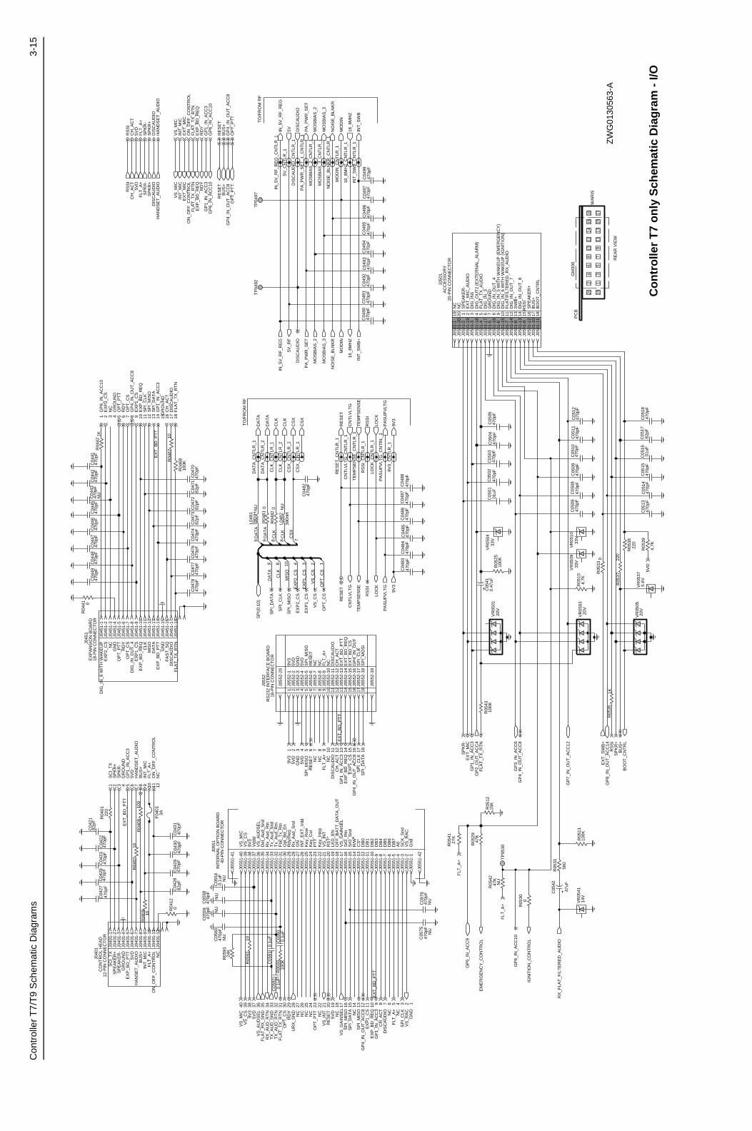
Con
trol
ler
T7/
T9
Sch
emat
ic D
iagr
ams
3-15
470p
FC
0560
NU
R05
42
NU
470p
FC
0576
C04
4247
0pF
NU
C05
5947
0pF
NU
J045
1-14
J055
1-3
NU
C05
58
NU
470p
F
J040
1-2 N
U
390n
H
NU
L048
2
NU
C05
540.
1uF
NU
INT
ER
NA
L O
PT
ION
BO
AR
D
39 38
9
4
VS
_CS
NC
GR
OU
ND
GR
OU
ND
FA
ST
_SQ
DIS
CA
UD
IO
4D
B7
FLA
T_T
X_A
UD
IO
DIG
_IN
_OU
T_4
DA
TA
EX
P1_
CS
11
DB
2
DIG
_IN
1
3
EX
P1_
CS
5
9V3
5VD
EX
T_B
D_P
TT
EX
T_M
IC_A
UD
IO
EX
P_B
D_P
TT
DA
TA
36 21
NC
BO
OT
_CN
TR
L
Rx_
Aud
_Snd
ON
VS
_IN
T
VS
_RA
C
16
DB
3
23 6
1
RS
T*
7 8
14
INT
_EX
T_V
dd
GR
OU
ND
DB
111 717 12
18
RS
SI
NC
J055
2
SP
I_M
ISO
RE
SE
T
FLT
_A+
26
FLA
T_T
X_R
TN
6
CS
X29
12-P
IN C
ON
NE
CT
OR
13
CLK
MIS
O
PC
B
16
20
SC
I_T
X
INT
_MIC
DIG
_IN
_3
Tx_
Aud
_Snd
VS
_AU
DS
EL
17
GR
OU
ND
SrD
_Rtn
5
DIG
_IN
_5 W
ITH
WA
KE
UP
(E
ME
RG
EN
CY
)
13
37
DIG
_IN
_OU
T_7 2
GM
300
SP
EA
KE
R-
CLK
DIS
CA
UD
IOC
H_A
CT
NC
NC
NC
6
NC
DB
6
AC
CE
SS
OR
Y
7
4
19
9
R/W
*
Opt
_Bd_
En
NC
1310
33
NC
7
9
A0
EX
T_B
D_R
EQ
EX
T_B
D_C
SG
P4_
IN_O
UT
SP
I_C
LKS
PI_
MO
SI
DA
TA
VS
_GA
INS
EL
Gnd
8
EX
P2_
CS
NC
EX
T_B
D_P
TT
GN
D5V
D
EX
P_B
D_P
TT
GN
D
RD
YO
PT
_PT
T
GN
D
DB
4
CLK
SP
EA
KE
R+
14
3
2
8
NC
10 11
Key
_Row
Key
_Int
rp
DIG
_IN
_OU
T_4
9V3
VS
_MIC
5VD
DIG
_OU
T2
(EX
TE
RN
AL_
ALA
RM
)
NC
HA
NS
ET
_AU
DIO
30
13
J050
1
J045
1
DIG
_IN
_6 W
ITH
WA
KE
UP
(IG
NIT
ION
)F
LAT
/FIL
TE
RE
D_R
X_A
UD
IO
19
9
VS
_CS
SW
B+
20
11
Fla
t_T
x_R
tn
NC
1 2
SrD
_Snd
EX
T_B
D_P
TT
27
OP
T_C
S22 18
40-P
IN C
ON
NE
CT
OR
DB
5
12
SC
K_S
nd
35
NC
NC
7 8
LED
_EN
ON
_OF
F_C
ON
TR
OL
20-P
IN C
ON
NE
CT
OR
1817
20
NC
15 1416
DIG
_IN
_6 W
ITH
WA
KE
UP
Tx_
Aud
_Rtn
34
18
Vdd
d
2532 31
SP
EA
KE
R+
1
WA
RIS
TO
/FR
OM
RF
7
24
CS
*
3
1
NC
NC
3 5
15
CLK
9
J055
1
28
FLT
_A+
6
SP
EA
KE
R-
DIG
_IN
_OU
T_8
16
3
OF
F_B
AT
T_D
AT
A_O
UT
3 4
EX
P_B
D_R
EQ
EX
T_B
D_P
TT
EX
T_B
D_P
TT
19
Det
_Aud
_Snd
12
Rx_
Aud
_Rtn
NC
1
MIS
O
2
5 6 10 11 12
EX
P2_
CS
8
DB
0
DA
TA
11
CO
NT
RO
L H
EA
D
NC
10
OP
T_C
S
EX
PA
NS
ION
BO
AR
D
10
PT
T
Rdy
/Req
2
GR
OU
ND
1012
14
RE
AR
VIE
W
BU
S+
4 12
18-P
IN C
ON
NE
CT
OR
NC
GN
D
1 2 11 12 13
17
15
6
40
18-P
IN C
ON
NE
CT
OR
RS
232
INT
ER
FA
CE
BO
AR
D
Key
_Col
TO
/FR
OM
RF
8
5
6 7 8 9 10
5
15 16 17 184
1 2 3 9
1413 14 15 16 17 18
J040
1
5
4
15
GN
D
BU
S+
0R
0482
0R
0481
J050
1-8
470p
FC
0443
100K
R04
68
J055
2-20
J055
2-2
J055
2-5
J055
2-4
R05
39
4.7K
J055
1-39
J055
1-33
TP
0492
J055
1-34
82pF
C04
28
DA
TA
_CN
TLR
_2
J045
1-7
J055
2-1
C04
22
J055
1-18
7
470p
F
100K
R05
11
CS
X_C
NT
LR_1
J050
1-15
J055
2-3
VR
0510
33V
8
TE
MP
SE
NS
E
9
J045
1-12
5V_C
NT
LR_1
470p
FC
0506
0.1u
F
J045
1-1
C05
92
470p
FC
0478
15K
R05
12
C04
8747
0pF
R05
10
10
4.7K
NO
ISE
_BLN
KR
_CN
TLR
_1
R04
09
5.6V
VR
0537
C04
7382
pF
8
470p
F
J045
1-18
C05
02
J040
1-5
J055
1-31
J045
1-15
220
R05
37
J055
1-38
RE
SE
T
14V
VR
0541
R04
0710
470p
F
J055
1-5
J050
1-19
C04
96
VR
0504
33V
J055
1-9
J055
1-27
470p
FC
0474
470p
F
J055
1-20
C04
29
.01u
FC
0501
470p
F
J045
1-16
C04
2647
0pF
C04
45
J050
1-10
J045
1-8
RS
SI_
CN
TLR
_147
0pF
C04
97
R05
31
560
DA
TA
C04
2182
pF
R05
25
470p
F
100K
MO
SB
IAS
_3_C
NT
LR_1
C04
92
CLK
_CN
TLR
_2
RS
SI
C04
4647
0pF
IN_5
V_R
F_R
EG
_CN
TLR
_1
J050
1-5
IN_5
V_R
F_R
EG
C04
72
DIS
CA
UD
IO
82pF
470p
FC
0484
100K
R05
4310
0K
R05
93
R04
421K
DIS
CA
UD
IO_C
NT
LR_1
LOC
K_C
NT
LR_1
C05
910.
1uF
TE
MP
SE
NS
E_C
NT
LR_1
C05
1047
0pF
J050
1-16
J045
1-3
J040
1-6
9V3
CLK
INT
_SW
BIN
T_S
WB
_CN
TLR
_1
J055
1-32
CLK
_CN
TLR
_1
J055
1-7
470p
FC
0476
470p
FC
0491
J055
1-13
470p
FC
0483
J045
1-11
J040
1-1
C05
05C
0504
470p
F47
0pF
470p
FC
0503
J055
1-24
C05
930.
1uF
470p
FC
0430
PA
SU
PV
LTG
_CN
TR
L_1
470p
F
J045
1-10
C05
09
0R04
12
C05
1447
0pF
J050
1-3
VR
0505
20V
J055
2-8
J055
2-10
J055
2-9
J055
2-11
J040
1-10
J055
1-40
CS
X
16_8
MH
Z_C
NT
LR_1
R05
29
C04
95
47K
470p
F
J055
1-41
J040
1-4
J040
1-7
10R
0592
R04
0122
0
J055
1-12
16_8
MH
Z
J045
1-9
J055
1-1
VR
0503
J050
1-7
20V
J055
1-21
RE
SE
T_C
NT
LR_1
1
J045
1-6
J050
1-18
C04
8547
0pF
R04
08
C04
77 2
100
J040
1-9
470p
F
470p
FC
0447
J055
1-22
3J0
551-
26
J050
1-13
TP
0530
DA
TA
_CN
TLR
_1
J055
2-17
J055
2-16
J040
1-8
J050
1-6
MO
SB
IAS
_2_C
NT
LR_1
10R
0467
C04
41
J050
1-1
4
J055
1-15
C04
93
J040
1-11
470p
F
J045
1-5
470p
FC
0431
VR
0501
20V
J055
1-14
J055
1-4
J050
1-12
J055
1-25
J050
1-2
470p
FC
0515
J045
1-13
J055
2-12
J055
2-14
J055
2-13
J055
2-15
R05
3822
0
MO
SB
IAS
_2
J050
1-20
R05
30
J040
1-12
J045
1-2
0
C04
88
J055
1-23
PA
SU
PV
LTG
470p
F
C05
13
9V3_
CN
TLR
_1
470p
F
89
TP
0497
470p
F
J055
2-18
J055
1-28
CN
TLV
LTG
J055
2-19
C04
7182
pF
5V
J055
1-10
J055
1-19
1KR
0535
470p
FC
0511
470p
FC
0512
J055
1-42
CLK
J050
1-11
J055
1-16
J055
1-2
J055
1-30
J055
1-35
390n
HL0
481
470p
F
NO
ISE
_BLN
KR
C05
08
C04
4847
0pF
LOC
K
J055
2-6
CS
X47
0pF
C04
82
J055
2-7
VR
0509
33V
C04
9047
0pF
C04
2747
0pF
J055
1-36
J050
1-9
470p
F
J045
1-17
C05
18
10
C05
7547
0pF
CS
X_C
NT
LR_2
470p
FC
0470
27K
R05
41
MO
SB
IAS
_3
J055
1-37
C04
9447
0pF
47K
0.47
uFC
0541
J055
1-8
J050
1-14
MO
DIN
PA
_PW
R_S
ET
_1_C
NT
LR_1
0R
0441
J050
1-4
9
J055
1-6
.01u
FC
0516
J050
1-17
MO
DIN
_CN
TLR
_1
C05
1782
pF
C04
8647
0pF
DA
TA
C04
9947
0pF
J055
1-29
C05
42
C04
2347
0pF
47uF
PA
_PW
R_S
ET
R05
330
J045
1-4
24K
R05
91
CN
TLV
LTG
_CN
TLR
_1J0
551-
17
470p
FC
0449
J055
1-11
J040
1-3
EX
P_B
D_R
EQ
5VD
SP
KR
-S
PK
R+
ON
_OF
F_C
ON
TR
OL
SP
KR
-
GP
6_IN
_AC
C10
FLA
T_T
X_R
TN
GP
6_IN
_AC
C10
GP
6_IN
_AC
C10
GP
6_IN
_AC
C10
FLA
T_T
X_R
TN
SP
I_D
AT
A
EX
T_M
ICG
P1_
IN_A
CC
3G
P2_
OU
T_A
CC
4
GP
5_IN
_AC
C9
GP
7_IN
_OU
T_A
CC
12
GP
8_IN
_OU
T_A
CC
14
SP
KR
+
GP
3_IN
_AC
C6
GP
4_IN
_OU
T_A
CC
8
EX
P2_
CS
EX
P1_
CS
GP
4_IN
_OU
T_A
CC
8O
PT
_CS
RD
YO
PT
_PT
T
EX
P2_
CS
CH
_AC
T
GP
1_IN
_AC
C3
SP
I_D
AT
AS
PI_
MIS
OS
PI_
CLK
9V3
SP
I_M
ISO
DIS
CA
UD
IO
MO
DIN
CH
_AC
T
5VD
9V3
5VD
SP
I_M
ISO
RE
SE
T
FLT
_A+
DIS
CA
UD
IO
GP
4_IN
_OU
T_A
CC
8E
XP
1_C
SE
XP
_BD
_RE
QG
P1_
IN_A
CC
3
SP
I_C
LK
OP
T_P
TT
OP
T_P
TT
OP
T_P
TT
INT
_MIC
INT
_MIC
INT
_MIC
SP
KR
+S
PK
R+
DIS
CA
UD
IOD
ISC
AU
DIO
HA
ND
SE
T_A
UD
IOH
AN
DS
ET
_AU
DIO
HA
ND
SE
T_A
UD
IO
RS
SI
RS
SI
BO
OT
_CN
TR
L
5VD
IN_5
V_R
F_R
EG
BU
S+
GP
1_IN
_AC
C3
GP
1_IN
_AC
C3
GP
1_IN
_AC
C3
INT
_SW
B+
5VD
GP
4_IN
_OU
T_A
CC
8E
XP
1_C
S
EX
P_B
D_R
EQ
EX
P_B
D_R
EQ
EX
P_B
D_R
EQ
GP
1_IN
_AC
C3
CH
_AC
TC
H_A
CT
CH
_AC
TD
ISC
AU
DIO
FLT
_A+
SC
I_T
X
RX
_FLA
T_F
ILT
ER
ED
_AU
DIO
EM
ER
GE
NC
Y_C
ON
TR
OL
FLT
_A+
RS
SI
EX
T_S
WB
+
RD
YR
DY
RD
Y5V
_RF
NO
ISE
_BLN
KR
MO
SB
IAS
_2
PA
_PW
R_S
ET
EX
P1_
CS
9V3
FLA
T_T
X_R
TN
FLA
T_T
X_R
TN
GP
4_IN
_OU
T_A
CC
8G
P4_
IN_O
UT
_AC
C8
DIS
CA
UD
IO
SP
I(0:
10)
MO
SB
IAS
_3
VS
_MIC
VS
_MIC
FLA
T_T
X_R
TN
FLT
_A+
BU
S+
BU
S+
RE
SE
TR
ES
ET
ON
_OF
F_C
ON
TR
OL
ON
_OF
F_C
ON
TR
OL
16_8
MH
Z
5VD
5VD
FLT
_A+
FLT
_A+
SP
I_D
AT
A
SP
I_C
LK
SP
I_M
ISO
VS
_CS
OP
T_C
SR
ES
ET
EX
T_M
ICE
XT
_MIC
SP
KR
-S
PK
R-
RE
SE
T
PA
SU
PV
LTG
BU
S+
TE
MP
SE
NS
E
CN
TLV
LTG
RS
SI
LOC
K
OP
T_C
S
SP
I_D
AT
A
TX
_AU
D_R
TN
VS
_CS
VS
_MIC
SP
I_C
LK
FLA
T_R
X_S
ND
RX
_AU
D_R
TN
UR
X_S
ND
TX
_AU
D_S
ND
VS
_IN
T
5VD
VS
_AU
DS
EL
VS
_GA
INS
EL
SP
I_M
ISO
VS
_RA
C
IGN
ITIO
N_C
ON
TR
OL
FLT
_A+
F04
013A
ZW
G01
3056
3-A
Co
ntr
olle
r T
7 o
nly
Sch
emat
ic D
iag
ram
- I/
O

3-16
Con
trol
ler
T7/
T9
Sch
emat
ic D
iagr
ams
470p
FC
0560
NU
R05
42
NU
470p
FC
0576
C04
4247
0pF
NU
C05
5947
0pF
NU
J045
1-14
J055
1-3
NU
C05
58
NU
470p
F
J040
1-2 N
U
390n
H
NU
L048
2
NU
C05
540.
1uF
NU
INT
ER
NA
L O
PT
ION
BO
AR
D
39 38
9
4
VS
_CS
NC
GR
OU
ND
GR
OU
ND
FA
ST
_SQ
DIS
CA
UD
IO
4D
B7
FLA
T_T
X_A
UD
IO
DIG
_IN
_OU
T_4
DA
TA
EX
P1_
CS
11
DB
2
DIG
_IN
1
3
EX
P1_
CS
5
9V3
5VD
EX
T_B
D_P
TT
EX
T_M
IC_A
UD
IO
EX
P_B
D_P
TT
DA
TA
36 21
NC
BO
OT
_CN
TR
L
Rx_
Aud
_Snd
ON
VS
_IN
T
VS
_RA
C
16
DB
3
23 6
1
RS
T*
7 8
14
INT
_EX
T_V
dd
GR
OU
ND
DB
111 717 12
18
RS
SI
BU
S+
J055
2
SP
I_M
ISO
RE
SE
T
FLT
_A+
26
FLA
T_T
X_R
TN
6
CS
X29
12-P
IN C
ON
NE
CT
OR
13
CLK
MIS
O
PC
B
16
20
SC
I_T
X
INT
_MIC
DIG
_IN
_3
Tx_
Aud
_Snd
VS
_AU
DS
EL
17
GR
OU
ND
SrD
_Rtn
5
DIG
_IN
_5 W
ITH
WA
KE
UP
(E
ME
RG
EN
CY
)
13
37
DIG
_IN
_OU
T_7 2
GM
300
SP
EA
KE
R-
CLK
DIS
CA
UD
IOC
H_A
CT
NC
NC
BU
S+
6
NC
DB
6
AC
CE
SS
OR
Y
7
4
19
9
R/W
*
Opt
_Bd_
En
NC
1310
33
NC
7
9
A0
EX
T_B
D_R
EQ
EX
T_B
D_C
SG
P4_
IN_O
UT
SP
I_C
LKS
PI_
MO
SI
DA
TA
VS
_GA
INS
EL
Gnd
8
EX
P2_
CS
BU
S+
EX
T_B
D_P
TT
GN
D5V
D
EX
P_B
D_P
TT
GN
D
RD
YO
PT
_PT
T
GN
D
DB
4
CLK
SP
EA
KE
R+
14
3
2
8
NC
10 11
Key
_Row
Key
_Int
rp
DIG
_IN
_OU
T_4
9V3
VS
_MIC
5VD
DIG
_OU
T2
(EX
TE
RN
AL_
ALA
RM
)
NC
HA
NS
ET
_AU
DIO
30
13
J050
1
J045
1
DIG
_IN
_6 W
ITH
WA
KE
UP
(IG
NIT
ION
)F
LAT
/FIL
TE
RE
D_R
X_A
UD
IO
19
9
VS
_CS
SW
B+
20
11
Fla
t_T
x_R
tn
NC
1 2
SrD
_Snd
EX
T_B
D_P
TT
27
OP
T_C
S22 18
40-P
IN C
ON
NE
CT
OR
DB
5
12
SC
K_S
nd
35
NC
NC
7 8
LED
_EN
ON
_OF
F_C
ON
TR
OL
20-P
IN C
ON
NE
CT
OR
1817
20
NC
15 1416
DIG
_IN
_6 W
ITH
WA
KE
UP
Tx_
Aud
_Rtn
34
18
Vdd
d
2532 31
SP
EA
KE
R+
1
WA
RIS
TO
/FR
OM
RF
7
24
CS
*
3
1
NC
NC
3 5
15
CLK
9
J055
1
28
FLT
_A+
6
SP
EA
KE
R-
DIG
_IN
_OU
T_8
16
3
OF
F_B
AT
T_D
AT
A_O
UT
3 4
EX
P_B
D_R
EQ
EX
T_B
D_P
TT
EX
T_B
D_P
TT
19
Det
_Aud
_Snd
12
Rx_
Aud
_Rtn
NC
1
MIS
O
2
5 6 10 11 12
EX
P2_
CS
8
DB
0
DA
TA
11
CO
NT
RO
L H
EA
D
NC
10
OP
T_C
S
EX
PA
NS
ION
BO
AR
D
10
PT
T
Rdy
/Req
2
GR
OU
ND
1012
14
RE
AR
VIE
W
BU
S+
4 12
18-P
IN C
ON
NE
CT
OR
NC
GN
D
1 2 11 12 13
17
15
6
40
18-P
IN C
ON
NE
CT
OR
RS
232
INT
ER
FA
CE
BO
AR
D
Key
_Col
TO
/FR
OM
RF
8
5
6 7 8 9 10
5
15 16 17 184
1 2 3 9
1413 14 15 16 17 18
J040
1
5
4
15
GN
D
BU
S+
0R
0482
0R
0481
J050
1-8
470p
FC
0443
100K
R04
68
J055
2-20
J055
2-2
J055
2-5
J055
2-4
R05
39
4.7K
J055
1-39
J055
1-33
TP
0492
J055
1-34
82pF
C04
28
DA
TA
_CN
TLR
_2
J045
1-7
J055
2-1
C04
22
J055
1-18
7
470p
F
100K
R05
11
CS
X_C
NT
LR_1
J050
1-15
J055
2-3
VR
0510
33V
8
TE
MP
SE
NS
E
9
J045
1-12
5V_C
NT
LR_1
470p
FC
0506
0.1u
F
J045
1-1
C05
92
470p
FC
0478
15K
R05
12
C04
8747
0pF
R05
10
10
4.7K
NO
ISE
_BLN
KR
_CN
TLR
_1
R04
09
5.6V
VR
0537
C04
7382
pF
8
470p
F
J045
1-18
C05
02
J040
1-5
J055
1-31
J045
1-15
220
R05
37
J055
1-38
RE
SE
T
14V
VR
0541
R04
0710
470p
F
J055
1-5
J050
1-19
C04
96
VR
0504
33V
J055
1-9
J055
1-27
470p
FC
0474
470p
F
J055
1-20
C04
29
.01u
FC
0501
470p
F
J045
1-16
C04
2647
0pF
C04
45
J050
1-10
J045
1-8
RS
SI_
CN
TLR
_147
0pF
C04
97
R05
31
560
DA
TA
C04
2182
pF
R05
25
470p
F
100K
MO
SB
IAS
_3_C
NT
LR_1
C04
92
CLK
_CN
TLR
_2
RS
SI
C04
4647
0pF
IN_5
V_R
F_R
EG
_CN
TLR
_1
J050
1-5
IN_5
V_R
F_R
EG
C04
72
DIS
CA
UD
IO
82pF
470p
FC
0484
100K
R05
4310
0K
R05
93
R04
421K
DIS
CA
UD
IO_C
NT
LR_1
LOC
K_C
NT
LR_1
C05
910.
1uF
TE
MP
SE
NS
E_C
NT
LR_1
C05
1047
0pF
J050
1-16
J045
1-3
J040
1-6
9V3
CLK
INT
_SW
BIN
T_S
WB
_CN
TLR
_1
J055
1-32
CLK
_CN
TLR
_1
J055
1-7
470p
FC
0476
470p
FC
0491
J055
1-13
470p
FC
0483
J045
1-11
J040
1-1
C05
05C
0504
470p
F47
0pF
470p
FC
0503
J055
1-24
C05
930.
1uF
470p
FC
0430
PA
SU
PV
LTG
_CN
TR
L_1
470p
F
J045
1-10
C05
09
0R04
12
C05
1447
0pF
J050
1-3
VR
0505
20V
J055
2-8
J055
2-10
J055
2-9
J055
2-11
J040
1-10
J055
1-40
CS
X
16_8
MH
Z_C
NT
LR_1
R05
29
C04
95
47K
470p
F
J055
1-41
J040
1-4
J040
1-7
10R
0592
R04
0122
0
J055
1-12
16_8
MH
Z
J045
1-9
J055
1-1
VR
0503
J050
1-7
20V
J055
1-21
RE
SE
T_C
NT
LR_1
1
J045
1-6
J050
1-18
C04
8547
0pF
R04
08
C04
77 2
100
J040
1-9
470p
F
470p
FC
0447
J055
1-22
3J0
551-
26
J050
1-13
TP
0530
DA
TA
_CN
TLR
_1
J055
2-17
J055
2-16
J040
1-8
J050
1-6
MO
SB
IAS
_2_C
NT
LR_1
10R
0467
C04
41
J050
1-1
4
J055
1-15
C04
93
J040
1-11
470p
F
J045
1-5
470p
FC
0431
VR
0501
20V
J055
1-14
J055
1-4
J050
1-12
J055
1-25
J050
1-2
470p
FC
0515
J045
1-13
J055
2-12
J055
2-14
J055
2-13
J055
2-15
R05
3822
0
MO
SB
IAS
_2
J050
1-20
R05
30
J040
1-12
J045
1-2
0
C04
88
J055
1-23
PA
SU
PV
LTG
470p
F
C05
13
9V3_
CN
TLR
_1
470p
F
89
TP
0497
470p
F
J055
2-18
J055
1-28
CN
TLV
LTG
J055
2-19
C04
7182
pF
5V
J055
1-10
J055
1-19
1KR
0535
470p
FC
0511
470p
FC
0512
J055
1-42
CLK
J050
1-11
J055
1-16
J055
1-2
J055
1-30
J055
1-35
390n
HL0
481
470p
F
NO
ISE
_BLN
KR
C05
08
C04
4847
0pF
LOC
K
J055
2-6
CS
X47
0pF
C04
82
J055
2-7
VR
0509
33V
C04
9047
0pF
C04
2747
0pF
J055
1-36
J050
1-9
470p
F
J045
1-17
C05
18
10
C05
7547
0pF
CS
X_C
NT
LR_2
470p
FC
0470
27K
R05
41
MO
SB
IAS
_3
J055
1-37
C04
9447
0pF
47K
0.47
uFC
0541
J055
1-8
J050
1-14
MO
DIN
PA
_PW
R_S
ET
_1_C
NT
LR_1
0R
0441
J050
1-4
9
J055
1-6
.01u
FC
0516
J050
1-17
MO
DIN
_CN
TLR
_1
C05
1782
pF
C04
8647
0pF
DA
TA
C04
9947
0pF
J055
1-29
C05
42
C04
2347
0pF
47uF
PA
_PW
R_S
ET
R05
330
J045
1-4
24K
R05
91
CN
TLV
LTG
_CN
TLR
_1J0
551-
17
470p
FC
0449
J055
1-11
J040
1-3
EX
P_B
D_R
EQ
5VD
SP
KR
-S
PK
R+
ON
_OF
F_C
ON
TR
OL
SP
KR
-
GP
6_IN
_AC
C10
FLA
T_T
X_R
TN
GP
6_IN
_AC
C10
GP
6_IN
_AC
C10
GP
6_IN
_AC
C10
FLA
T_T
X_R
TN
SP
I_D
AT
A
EX
T_M
ICG
P1_
IN_A
CC
3G
P2_
OU
T_A
CC
4
GP
5_IN
_AC
C9
GP
7_IN
_OU
T_A
CC
12
GP
8_IN
_OU
T_A
CC
14
SP
KR
+
GP
3_IN
_AC
C6
GP
4_IN
_OU
T_A
CC
8
EX
P2_
CS
EX
P1_
CS
GP
4_IN
_OU
T_A
CC
8O
PT
_CS
RD
YO
PT
_PT
T
EX
P2_
CS
CH
_AC
T
GP
1_IN
_AC
C3
SP
I_D
AT
AS
PI_
MIS
OS
PI_
CLK
9V3
SP
I_M
ISO
DIS
CA
UD
IO
MO
DIN
CH
_AC
T
5VD
9V3
5VD
SP
I_M
ISO
RE
SE
T
FLT
_A+
DIS
CA
UD
IO
GP
4_IN
_OU
T_A
CC
8E
XP
1_C
SE
XP
_BD
_RE
QG
P1_
IN_A
CC
3
SP
I_C
LK
OP
T_P
TT
OP
T_P
TT
OP
T_P
TT
INT
_MIC
INT
_MIC
INT
_MIC
SP
KR
+S
PK
R+
DIS
CA
UD
IOD
ISC
AU
DIO
HA
ND
SE
T_A
UD
IOH
AN
DS
ET
_AU
DIO
HA
ND
SE
T_A
UD
IO
RS
SI
RS
SI
BO
OT
_CN
TR
L
5VD
IN_5
V_R
F_R
EG
BU
S+
GP
1_IN
_AC
C3
GP
1_IN
_AC
C3
GP
1_IN
_AC
C3
INT
_SW
B+
5VD
GP
4_IN
_OU
T_A
CC
8E
XP
1_C
S
EX
P_B
D_R
EQ
EX
P_B
D_R
EQ
EX
P_B
D_R
EQ
GP
1_IN
_AC
C3
CH
_AC
TC
H_A
CT
CH
_AC
TD
ISC
AU
DIO
FLT
_A+
SC
I_T
X
RX
_FLA
T_F
ILT
ER
ED
_AU
DIO
EM
ER
GE
NC
Y_C
ON
TR
OL
FLT
_A+
RS
SI
EX
T_S
WB
+
RD
YR
DY
RD
Y5V
_RF
NO
ISE
_BLN
KR
MO
SB
IAS
_2
PA
_PW
R_S
ET
EX
P1_
CS
9V3
FLA
T_T
X_R
TN
FLA
T_T
X_R
TN
GP
4_IN
_OU
T_A
CC
8G
P4_
IN_O
UT
_AC
C8
DIS
CA
UD
IO
SP
I(0:
10)
MO
SB
IAS
_3
VS
_MIC
VS
_MIC
FLA
T_T
X_R
TN
FLT
_A+
BU
S+
BU
S+
RE
SE
TR
ES
ET
ON
_OF
F_C
ON
TR
OL
ON
_OF
F_C
ON
TR
OL
16_8
MH
Z
5VD
5VD
FLT
_A+
FLT
_A+
SP
I_D
AT
A
SP
I_C
LK
SP
I_M
ISO
VS
_CS
OP
T_C
SR
ES
ET
EX
T_M
ICE
XT
_MIC
SP
KR
-S
PK
R-
RE
SE
T
PA
SU
PV
LTG
BU
S+
TE
MP
SE
NS
E
CN
TLV
LTG
RS
SI
LOC
K
OP
T_C
S
SP
I_D
AT
A
TX
_AU
D_R
TN
VS
_CS
VS
_MIC
SP
I_C
LK
FLA
T_R
X_S
ND
RX
_AU
D_R
TN
UR
X_S
ND
TX
_AU
D_S
ND
VS
_IN
T
5VD
VS
_AU
DS
EL
VS
_GA
INS
EL
SP
I_M
ISO
VS
_RA
C
IGN
ITIO
N_C
ON
TR
OL
FLT
_A+
ZW
G01
3058
6-O
F04
013A F
use
P/N
6580
542Z
01
100
R05
56
100
R05
56
Co
ntr
olle
r T
9 o
nly
Sch
emat
ic D
iag
ram
- I
/O
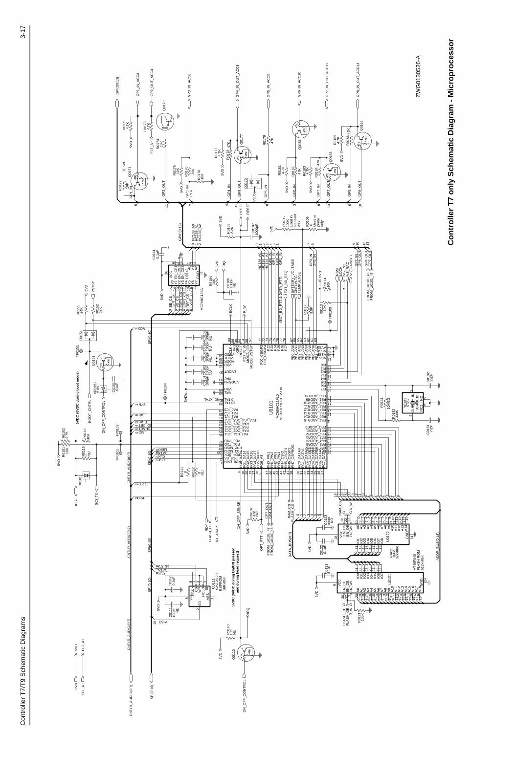
Con
trol
ler
T7/
T9
Sch
emat
ic D
iagr
ams
3-17
4
0
18
100p
FC
0104
NU
C01
0210
0pF
NU
12
0
NU
4.7K
R01
71
NU
R01
1010
K
NU
18
NU
0.1u
F
100p
F
NU
NU
R01
024.
7K
NU
R01
82
NU
816
R01
06 0 U
sed
inpr
ime
only
NU
GP
3_IN
GP
8_IN
PE
6
VOX
LSIO
GP
7_IN
HC
138_
A0
RE
F_C
S
HC
138_
A2
GP
1_IN
GP
8_O
UT
SQ_DET
HC
138_
A1
FLA
SH
RO
M
SYN
HC
138_
A2
GP
2_O
UT
LSIO
MIC
RO
PR
OC
ES
SO
R
DATA
MISO
F1200
GP
4_IN
EE
PR
OM
DATAEE_CS
VS
_CS
EX
P1_
CS
GP
1_IN
CLKCSX
GP
5_IN
GP
4_O
UT
GP
7_O
UT
GP
7_IN
CLK
GP
5_IN
32kx
8bit
OP
T_C
S
LVZ
IF_C
S
16K
x8bi
t
GP
4_O
UT
GP
7_O
UT
(EX
T_B
D_P
TT
& D
AT
A_P
TT
)
EE
_CS
HC
138_
A0
GP
3_IN
GP
8_IN
512k
x8bi
tRA
M
GP
6_IN
GP
6_IN
MISO
EX
P2_
CS
GP
4_O
UT
GP
7_O
UT
HSIO
GP
4_IN
ON
_OF
F_S
EN
SE
GP
8_O
UT
CHACT
HC
138_
A1
HSIO
10K
R01
72
6
2
10K
R01
75
7
R01
11
10K
R01
15
101
0
C01
01
7
9
100p
F
0
1000
pFC
0107
R01
1410
K
R01
0410
K
10K
R01
70
4
10
5
11
0
47K
R01
79
R01
16
0.1u
FC
0141
7
7
R01
5224
K
R01
3233
0K
9Y
67
Y7
12
3
8G
ND16
VC
C15
Y0
14Y
113
Y2
12Y
311
Y4
10Y
5
MC
74H
C13
8A
U01
411
A0
2A
13
A2
6E
N_C
S1
4E
N_C
S2
5E
N_C
S3
5
12
TP
0102
6
6
10
2
6
R01
854.
7K
IO4
15IO
516
IO6
17IO
718
IO8
19
VC
C
28
8
A9
24
EN
_CS
20
EN
_OE
22
EN
_WE
27
14GN
D
IO1
11IO
212
IO3
13
A14
1
A2
8A
37
A4
6 5A
5A
64
A7
3A
825
A0
10A
19 21
A10
A11
23A
122
A13
26
11
6
U01
2263
A21
8
66
9
Q01
81
VSSL 40VSSR 87
93 XFC
XIR
Q48
XTAL91
RE
SE
T94
VDD12
VDDL39VDDR88
VDDSYN92
VRH69VRL68
VSS 13
PJ0
_CS
GP
371
PJ1
_CS
GP
472
PJ2
73P
J374
PJ4
75P
J576
PJ6
77P
J778
56PI1 55PI2 54PI3 53PI4 52PI5 51PI6 50PI7 49
PH
0_P
W1
47P
H1_
PW
246
PH
2_P
W3
45P
H3_
PW
444
PH
4_C
SIO
43P
H5_
CS
GP
142
PH
6_C
SG
P2
41P
H7_
CS
PR
OG
38
PI0
PG
0_X
A13
6
PG
1_X
A14
16P
G2_
XA
1520
PG
3_X
A16
19P
G4_
XA
1717
PG
5_X
A18
18P
G6_
AS
5
PG
7_R
_W4
PF1_ADDR1 28PF2_ADDR2 27PF3_ADDR3 26PF4_ADDR4 25PF5_ADDR5 24PF6_ADDR6 23PF7_ADDR7 22
PFO_ADDR0 29
67P
E0_
AN
066
PE
1_A
N1
65P
E2_
AN
264
PE
3_A
N3
63P
E4_
AN
462
PE
5_A
N5
61P
E6_
AN
660
PE
7_A
N7
PC
7_D
AT
A7
37
PD0_RXD97PD1_TXD98
PD2_MISO99PD3_MOSI100PD4_SCK1
PD5_SS23 PD6_LVIN
PBO_ADDR8 14
PC
0_D
AT
A0
30P
C1_
DA
TA
131
PC
2_D
AT
A2
32P
C3_
DA
TA
333
PC
4_D
AT
A4
34P
C5_
DA
TA
535
PC
6_D
AT
A6
36
PA7_PA1_OC186
PB1_ADDR9 10PB2_ADDR10 11PB3_ADDR11 9PB4_ADDR12 21PB5_ADDR13 15PB6_ADDR14 8PB7_ADDR15 7
MO
DB
_VS
TB
Y57
PA0_IC379PA1_IC280PA2_IC181
PA3_IC4_OC5_OC182PA4_OC4_OC183PA5_OC3_OC184PA6_OC2_OC185
AVDD59
AVSS 70
EC
LK89
EXTAL90
IRQ
96
95 LVOUT
MO
DA
_LIR
58
MC
68H
C11
FL0
U01
01
47K
R01
84
10K
R01
74
22pF
C01
32
0
Q01
85
7H
OLD
6S
CK
5S
I
2S
O
8 VC
C
4VS
S
3W
P X25
128-
2.7
U01
111C
S
.01u
FC
0151
1 13
Q01
73
C01
0610
0pF
D01
51
R01
73
122
3
4.7K
1
8
8
4
6
1
1 17
3
2.2K
R01
08
10
1
4
5
7
TP
0151
C01
210.
1uF
0.1u
FC
0122
TP
0103
8
1103
2
23
11
4.7K
1
11
12
3
1
R01
83
10K
R01
13
R01
5124
K
0
3
0
13
4
8
D01
79
2
6
17 9
10K
R01
01
5
7TP
0101
3
Q01
10
47K
R01
07
7
4.7K
R01
77
99
100K
Use
d in
stan
dard
on
ly
R01
05
4
2
7
10
100p
FC
0105
4
D01
01
3.9K
R01
17
5
1413
16
5
C01
23
7
2
5
C01
12
Q01
51
28IO
629
IO7
VC
C
8
2
0
3
7E
N_W
E
GN
D 24
IO0
21 22IO
123
IO2
25IO
326
IO4
27IO
516
A4
A5
15A
614 13
A7
3A
82
A9
30E
N_C
E32
EN
_OE
A13
4 5A
14A
1511 10
A16
6A
179
A18
18A
217
A3
AT
49F
040
U01
21
20A
019
A1
31A
101
A11
12A
12
4
5
3
1
13
6
13
2
NC
1
3
OU
T4
IN1
9
0
6
38.4
0KH
z
Y01
31X
TA
L NC
R01
12
0
47K
4.7K
R01
81
4
3
R01
78
5
47K
10M
EG
R01
31
100p
FC
0111
100p
FC
0103
22pF
C01
31
15
9
7
VR
0151
5.6V
14
TP
0104
Q01
83
1514
4
5
0
2
Q01
71
100K
R01
21
Q01
77
10
47K
R01
86
R01
76
30K
R_W
RA
M_C
S
BU
S+
CN
TLV
LTG
5VD
SC
I_T
X
GP
1_IN
_AC
C3
GP
6_IN
_AC
C10
GP
2_O
UT
_AC
C4
R_W
FLA
SH
_CE
FLA
SH
_OE
5VD
IRQ
IRQ
AD
DR
_BU
S(0
:18)
DA
TA
_BU
S(0
:7)
0
FR
OM
_U01
01_4
7VS
_RA
C
5VD
VS
_IN
T
GP
4_IN
_OU
T_A
CC
8
5VD
BO
OT
_CN
TR
L
GP
3_IN
_AC
C6
5VD
ON
_OF
F_C
ON
TR
OL
5VD
5VD
5VD
RE
SE
T
RE
SE
T
5VD
OP
T_P
TT
5VD
GP
5_IN
_AC
C9
5VD
SP
I(0:
10)
SP
I(0:
10)
SP
I(0:
10)
SP
I(0:
10)
SP
I(0:
10)
GP
IO(0
:13)
GP
IO(0
:13)
CN
TLR
_AU
DIO
(0:7
)C
NT
LR_A
UD
IO(0
:7)
CN
TLR
_AU
DIO
(0:7
)C
NT
LR_A
UD
IO(0
:7)
FR
OM
_U01
01_4
7F
RO
M_U
0101
_46
FR
OM
_U01
01_4
6
5VD
5VD
FLT
_A+
TE
MP
SE
NS
E
RA
M_C
S
5VD
VS
_GA
INS
EL
EX
T_B
D_R
EQ
RS
SI
5VD
RX
_AD
AP
T
5VD
5VD
5VD
FLT
_A+
FLT
_A+
FLA
SH
_OE
NC_XTAL
EC
LK
LOC
K
RD
Y
ON
_OF
F_C
ON
TR
OL
GP
7_IN
_OU
T_A
CC
12
GP
8_IN
_OU
T_A
CC
14
5VD
5VD
5VD
5VD
FLA
SH
_CE
R_W
VS
TB
Y
5VD
BA
TT
ER
Y_V
OLT
AG
E
5VD
C (
0VD
C d
uri
ng
On
/Off
pre
ssed
an
d d
uri
ng
hea
d r
equ
est)
5VD
C (
0VD
C d
uri
ng
bo
ot
mo
de)
ZW
G01
3052
6-A
Co
ntr
olle
r T
7 o
nly
Sch
emat
ic D
iag
ram
- M
icro
pro
cess
or

3-18
Con
trol
ler
T7/
T9
Sch
emat
ic D
iagr
ams
4
0
18
100p
FC
0104
NU
C01
0210
0pF
NU
12
0
NU
4.7K
R01
71
NU
R01
1010
K
NU
18
NU
0.1u
F
100p
F
NU
NU
R01
024.
7K
NU
R01
82
NU
816
R01
06 0 U
sed
inpr
ime
only
NU
GP
3_IN
GP
8_IN
PE
6
VOX
LSIOG
P7_
IN
HC
138_
A0
RE
F_C
S
HC
138_
A2
GP
1_IN
GP
8_O
UT
SQ_DET
HC
138_
A1
FLA
SH
RO
M
SYN
HC
138_
A2
GP
2_O
UT
LSIO
MIC
RO
PR
OC
ES
SO
R
DATA
MISO
F1200
GP
4_IN
EE
PR
OM
DATAEE_CS
VS
_CS
EX
P1_
CS
GP
1_IN
CLKCSX
GP
5_IN
GP
4_O
UT
GP
7_O
UT
GP
7_IN
CLK
GP
5_IN
32kx
8bit
OP
T_C
S
LVZ
IF_C
S
16K
x8bi
t
GP
4_O
UT
GP
7_O
UT
(EX
T_B
D_P
TT
& D
AT
A_P
TT
)
EE
_CS
HC
138_
A0
GP
3_IN
GP
8_IN
512k
x8bi
tRA
M
GP
6_IN
GP
6_IN
MISO
EX
P2_
CS
GP
4_O
UT
GP
7_O
UT
HSIO
GP
4_IN
ON
_OF
F_S
EN
SE
GP
8_O
UT
CHACT
HC
138_
A1
HSIO
10K
R01
72
6
2
10K
R01
75
7
R01
11
10K
R01
15
101
0C
0101
7
9
100p
F
0
1000
pFC
0107
R01
1410
K
R01
0410
K
10K
R01
70
4
10
5
11
0
47K
R01
79
R01
16
0.1u
FC
0141
7
7
R01
5224
K
R01
3233
0K
9Y
67
Y7
12
3
8G
ND16
VC
C15
Y0
14Y
113
Y2
12Y
311
Y4
10Y
5
MC
74H
C13
8A
U01
411
A0
2A
13
A2
6E
N_C
S1
4E
N_C
S2
5E
N_C
S3
5
12
TP
0102
6
6
10
2
6
R01
854.
7K
IO4
15IO
516
IO6
17IO
718
IO8
19
VC
C
28
8
A9
24
EN
_CS
20
EN
_OE
22
EN
_WE
27
14GN
D
IO1
11IO
212
IO3
13
A14
1
A2
8A
37
A4
6 5A
5A
64
A7
3A
825
A0
10A
19 21
A10
A11
23A
122
A13
26
11
6
U01
2263
A21
8
66
9
Q01
81
VSSL 40VSSR 87
93 XFC
XIR
Q48
XTAL91
RE
SE
T94
VDD12
VDDL39VDDR88
VDDSYN92
VRH69VRL68
VSS 13
PJ0
_CS
GP
371
PJ1
_CS
GP
472
PJ2
73
PJ3
74
PJ4
75
PJ5
76
PJ6
77
PJ7
78
56PI1 55PI2 54PI3 53PI4 52PI5 51PI6 50PI7 49
PH
0_P
W1
47P
H1_
PW
246
PH
2_P
W3
45P
H3_
PW
444
PH
4_C
SIO
43P
H5_
CS
GP
142
PH
6_C
SG
P2
41P
H7_
CS
PR
OG
38
PI0
PG
0_X
A13
6
PG
1_X
A14
16
PG
2_X
A15
20
PG
3_X
A16
19
PG
4_X
A17
17P
G5_
XA
1818
PG
6_A
S5
PG
7_R
_W4
PF1_ADDR1 28PF2_ADDR2 27PF3_ADDR3 26PF4_ADDR4 25PF5_ADDR5 24PF6_ADDR6 23PF7_ADDR7 22
PFO_ADDR0 29
67P
E0_
AN
066
PE
1_A
N1
65P
E2_
AN
264
PE
3_A
N3
63P
E4_
AN
462
PE
5_A
N5
61P
E6_
AN
660
PE
7_A
N7
PC
7_D
AT
A7
37
PD0_RXD97PD1_TXD98
PD2_MISO99PD3_MOSI100PD4_SCK1 PD5_SS2
3 PD6_LVIN
PBO_ADDR8 14
PC
0_D
AT
A0
30P
C1_
DA
TA
131
PC
2_D
AT
A2
32P
C3_
DA
TA
333
PC
4_D
AT
A4
34P
C5_
DA
TA
535
PC
6_D
AT
A6
36
PA7_PA1_OC186
PB1_ADDR9 10PB2_ADDR10 11PB3_ADDR11 9PB4_ADDR12 21PB5_ADDR13 15PB6_ADDR14 8PB7_ADDR15 7
MO
DB
_VS
TB
Y57
PA0_IC379PA1_IC280PA2_IC181
PA3_IC4_OC5_OC182PA4_OC4_OC183PA5_OC3_OC184PA6_OC2_OC185
AVDD59
AVSS 70
EC
LK89
EXTAL90
IRQ
96
95 LVOUT
MO
DA
_LIR
58
MC
68H
C11
FL0
U01
01
47K
R01
84
10K
R01
74
22pF
C01
32
0
Q01
85
7H
OLD
6S
CK
5S
I
2S
O
8 VC
C
4VS
S
3W
P X25
128-
2.7
U01
111C
S
.01u
FC
0151
1 13
Q01
73
C01
0610
0pF
D01
51
R01
73
12
2
3
4.7K
1
8
8
4
6
1
1 17
3
2.2K
R01
08
10
1
4
5
7
TP
0151
C01
210.
1uF
0.1u
FC
0122
TP
0103
8
1103
2
23
11
4.7K
1
11
12
3
1
R01
83
10K
R01
13
R01
5124
K
0
3
0
13
4
8
D01
79
2
6
17 9
10K
R01
01
5
7TP
0101
3
Q01
10
47K
R01
07
7
4.7K
R01
77
99
100K
Use
d in
stan
dard
on
ly
R01
05
4
2
7
10
100p
FC
0105
4
D01
01
3.9K
R01
175
1413
16
5
C01
23
7
2
5
C01
12
Q01
51
28IO
629
IO7
VC
C
8
2
0
3
7E
N_W
E
GN
D 24
IO0
21 22IO
123
IO2
25IO
326
IO4
27IO
516
A4
A5
15A
614 13
A7
3A
82
A9
30E
N_C
E32
EN
_OE
A13
4 5A
14A
1511 10
A16
6A
179
A18
18A
217
A3
AT
49F
040
U01
21
20A
019
A1
31A
101
A11
12A
12
4
5
3
1
13
6
132
NC
1
3
OU
T4
IN1
9
0
6
38.4
0KH
z
Y01
31X
TA
L NC
R01
12
0
47K
4.7K
R01
81
4
3
R01
78
5
47K
10M
EG
R01
31
100p
FC
0111
100p
FC
0103
22pF
C01
31
15
9
7
VR
0151
5.6V
14
TP
0104
Q01
83
1514
4
5
0
2
Q01
71
100K
R01
21
Q01
77
10
47K
R01
86
R01
76
30K
R_W
RA
M_C
S
BU
S+
CN
TLV
LTG
5VD
SC
I_T
X
GP
1_IN
_AC
C3
GP
6_IN
_AC
C10
GP
2_O
UT
_AC
C4
R_W
FLA
SH
_CE
FLA
SH
_OE
5VD
IRQ
IRQ
AD
DR
_BU
S(0
:18)
DA
TA
_BU
S(0
:7)
0
FR
OM
_U01
01_4
7VS
_RA
C
5VD
VS
_IN
T
GP
4_IN
_OU
T_A
CC
8
5VD
BO
OT
_CN
TR
L
GP
3_IN
_AC
C6
5VD
ON
_OF
F_C
ON
TR
OL
5VD
5VD
5VD
RE
SE
T
RE
SE
T
5VD
OP
T_P
TT
5VD
GP
5_IN
_AC
C9
5VD
SP
I(0:
10)
SP
I(0:
10)
SP
I(0:
10)
SP
I(0:
10)
SP
I(0:
10)
GP
IO(0
:13)
GP
IO(0
:13)
CN
TLR
_AU
DIO
(0:7
)C
NT
LR_A
UD
IO(0
:7)
CN
TLR
_AU
DIO
(0:7
)C
NT
LR_A
UD
IO(0
:7)
FR
OM
_U01
01_4
7F
RO
M_U
0101
_46
FR
OM
_U01
01_4
6
5VD
5VD
FLT
_A+
TE
MP
SE
NS
E
RA
M_C
S
5VD
VS
_GA
INS
EL
EX
T_B
D_R
EQ
RS
SI
5VD
RX
_AD
AP
T
5VD
5VD
5VD
FLT
_A+
FLT
_A+
FLA
SH
_OE
NC_XTAL
EC
LK
LOC
K
RD
Y
ON
_OF
F_C
ON
TR
OL
GP
7_IN
_OU
T_A
CC
12
GP
8_IN
_OU
T_A
CC
14
5VD
5VD
5VD
5VD
FLA
SH
_CE
R_W
VS
TB
Y
5VD
BA
TT
ER
Y_V
OLT
AG
E
ZW
G01
3058
5-O
NU
0R
0103
C01
080,
1uF
5VD
C (
0VD
C d
uri
ng
On
/Off
pre
ssed
an
d d
uri
ng
hea
d r
equ
est)
5VD
C (
0VD
C d
uri
ng
bo
ot
mo
de)
Co
ntr
olle
r T
9 o
nly
Sch
emat
ic D
iag
ram
- M
icro
pro
cess
or
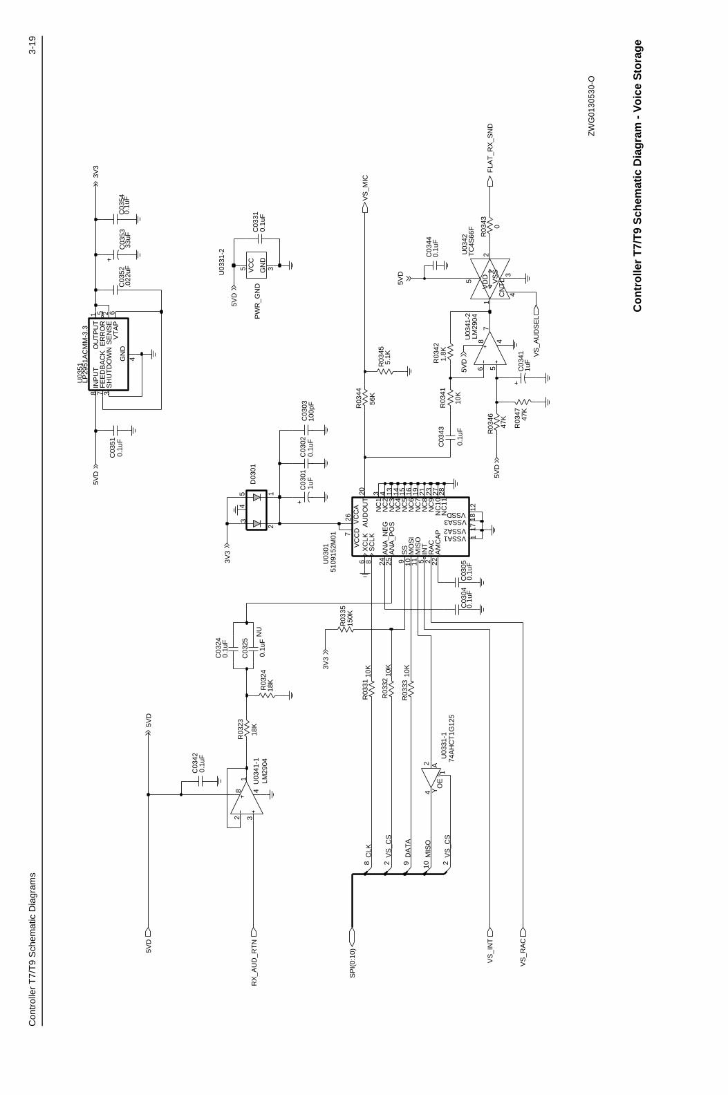
Con
trol
ler
T7/
T9
Sch
emat
ic D
iagr
ams
3-19
9
C03
25
0.1u
FN
U
10K
R03
32
C03
310.
1uF
U03
31-2
PW
R_G
ND
3GN
D
5 VC
C
2
C03
540.
1uF
C03
42
18K
U03
41-2
LM29
046 5
78 4
2
5
VD
D 3
VS
S
6
0.1u
FC
0302
10
R03
43
0
RX
_AU
D_R
TN
5VD
FLA
T_R
X_S
ND
3V3
SP
I(0:
10)
R03
24
C03
0310
0pF
0.1u
FC
0305
0.1u
F
C03
43
0.1u
F
1uF
C03
24
U03
51LP
2951
AC
MM
-3.3
2
C03
510.
1uF
74A
HC
T1G
125
U03
31-1
2 A1
OE
4 Y
33uF
C03
53.0
22uF
C03
52
10K
R03
33S
S9
VC
CA
26V
CC
D7 VSSA1 1
VSSA2 17
VSSA3 18
VSSD 12
XC
LK6
10K
R03
41
D03
01
53
12
48 4
U03
42T
C4S
66F
4CN
TL
1
47K
R03
46 47K
R03
47
1uF
C03
41
0.1u
FC
0304
LM29
04U
0341
-1
2 31
C03
440.
1uF
8
0.1u
F
C03
01
CLK
DA
TA
5109
152M
01
VS
_CS
MIS
O
VS
_CS
56K
R03
44
R03
3515
0K
5.1K
R03
45
NC
414
NC
515
NC
616
NC
719
NC
821
NC
923
RA
C2
SC
LK8
INT
MIS
O11
MO
SI
10
NC
13
NC
1027
NC
1128
NC
24
NC
313
U03
01
22A
MC
AP
AN
A_N
EG
24A
NA
_PO
S25
AU
DO
UT
20
5
10K
R03
31
1.8K
R03
42
ER
RO
R5
FE
ED
BA
CK
7
GN
D4
INP
UT
8O
UT
PU
T1
SE
NS
E2
SH
UT
DO
WN
3V
TA
P
18K
R03
23
VS
_MIC
VS
_RA
C
3V3
3V3
5VD
5VD
5VD
VS
_IN
T
5VD
5VD
VS
_AU
DS
EL
5VD
ZW
G01
3053
0-O
Co
ntr
olle
r T
7/T
9 S
chem
atic
Dia
gra
m -
Vo
ice
Sto
rag
e

3-20
Con
trol
ler
T7/
T9
Sch
emat
ic D
iagr
ams
3.1
Co
ntr
olle
r T
7 P
arts
Lis
t
Cir
cuit
R
efM
oto
rola
P
art
No
Des
crip
tio
n
C01
0121
1374
0F51
100p
F 5
% 5
0V
C01
0721
1374
1F25
1nF
50V
C01
1221
1374
3E20
100n
F 1
6V
C01
2121
1374
3E20
100n
F 1
6V
C01
2221
1374
3E20
100n
F 1
6V
C01
3121
1374
0F35
22pF
5%
50V
C01
3221
1374
0F35
22pF
5%
50V
C01
4121
1374
3E20
100n
F 1
6V
C01
5121
1374
1F49
10nF
50V
C02
0123
1104
9A57
10uF
10%
16V
C02
0223
1104
9A57
10uF
10%
16V
C02
0421
1374
3E20
100n
F 1
6V
C02
1223
1104
9A57
10uF
10%
16V
C02
2121
1374
3E20
100n
F 1
6V
C02
2221
1374
3E20
100n
F 1
6V
C02
2321
1374
3E20
100n
F 1
6V
C02
2421
1374
0F51
100p
F 5
% 5
0V
C02
2521
1374
3E20
100n
F 1
6V
C02
2621
1374
3E20
100n
F 1
6V
C02
2823
1104
9A56
4.7u
F 1
0% 1
6V
C02
3121
1374
3B29
1 U
F 1
0% 1
6V
C02
3221
1374
3E20
100n
F 1
6V
C02
3421
1374
3E20
100n
F 1
6V
C02
3521
1374
3E07
22nF
16V
C02
3621
1374
3E10
.033
UF
10%
C02
4121
1374
3E20
100n
F 1
6V
C02
4321
1374
0F51
100p
F 5
% 5
0V
C02
4421
1374
3E20
100n
F 1
6V
C02
4521
1374
3E20
100n
F 1
6V
C02
4621
1374
1F49
10nF
50V
C02
51U
sed
in21
1374
3E20
100n
F 1
6V
CN
TR
L T
7 on
ly
C02
5223
1104
9A07
1uF
10%
16V
C02
5421
1374
3E20
100n
F 1
6V
C02
5521
1374
3E20
100n
F 1
6V
C02
5621
1374
0F51
100p
F 5
% 5
0V
C02
6121
1374
3E20
100n
F 1
6V
C02
6221
1374
0F49
82pF
5%
50V
NP
0
C02
6521
1374
3E20
100n
F 1
6V
C02
6721
1374
1F49
10nF
50V
C02
7121
1374
1F49
10nF
50V
C02
7221
1374
3E20
100n
F 1
6V
C02
7321
1374
1F37
3.3n
F 5
0V
C02
7523
1104
9A99
47uF
20%
10V
C02
7621
1374
1F25
1nF
50V
X7R
C02
7721
1374
1F25
1nF
50V
X7R
C03
01U
sed
in23
1104
9A07
GM
398
only
TAN
T C
P 1
uF 1
0% 1
6V
C03
02U
sed
in21
1374
3E20
GM
398
only
100n
F 1
6V
C03
03U
sed
in21
1374
0F51
GM
398
only
100p
F 5
% 5
0V
C03
04U
sed
in21
1374
3E20
GM
398
only
100n
F 1
6V
C03
05U
sed
in21
1374
3E20
GM
398
only
100n
F 1
6V
C03
24U
sed
in21
1374
3E20
GM
398
only
100n
F 1
6V
C03
31U
sed
in21
1374
3E20
GM
398
only
100n
F 1
6V
C03
41U
sed
in23
1104
9A07
GM
398
only
TAN
T C
P 1
uF 1
0% 1
6V
C03
42U
sed
in21
1374
3E20
GM
398
only
100n
F 1
6V
C03
43U
sed
in21
1374
3E20
GM
398
only
100n
F 1
6V
Cir
cuit
R
efM
oto
rola
P
art
No
Des
crip
tio
n
C03
44U
sed
in21
1374
3E20
GM
398
only
100n
F 1
6V
C03
51U
sed
in21
1374
3E20
GM
398
only
100n
F 1
6V
C03
52U
sed
in21
1374
3E07
GM
398
only
22nF
16V
C03
53U
sed
in23
1104
9A97
GM
398
only
TAN
T C
HIP
33
UF
C03
54U
sed
in21
1374
3E20
GM
398
only
100n
F 1
6V
C04
2121
1374
3N48
82.0
PF
5%
C04
2221
1374
1F17
470p
F 5
0V
C04
2321
1374
1F17
470p
F 5
0V
C04
2621
1374
3L09
470
PF
10%
C04
2721
1374
3L09
470
PF
10%
C04
2821
1374
3N48
82.0
PF
5%
C04
2921
1374
3L09
470
PF
10%
C04
3021
1374
1F17
470p
F 5
0V
C04
3121
1374
1F17
470p
F 5
0V
C04
4121
1374
3L09
470
PF
10%
C04
4221
1374
3L09
470
PF
10%
C04
4521
1374
3L09
470
PF
10%
C04
4621
1374
3L09
470
PF
10%
C04
4721
1374
3L09
470
PF
10%
C04
4821
1374
3L09
470
PF
10%
C04
4921
1374
3L09
470
PF
10%
C04
7021
1374
3L09
470
PF
10%
C04
7121
1374
3N48
82.0
PF
5%
C04
7221
1374
3N48
82.0
PF
5%
C04
7321
1374
3N48
82.0
PF
5%
C04
7421
1374
3L09
470
PF
10%
C04
7621
1374
3L09
470
PF
10%
C04
7721
1374
3L09
470
PF
10%
C04
7821
1374
3L09
470
PF
10%
Cir
cuit
R
efM
oto
rola
P
art
No
Des
crip
tio
n
C04
8221
1374
3L09
470
PF
10%
C04
8321
1374
3L09
470
PF
10%
C04
8421
1374
1F17
470p
F 5
0V
C04
8521
1374
3L09
470
PF
10%
C04
8621
1374
3L09
470
PF
10%
C04
8721
1374
3L09
470
PF
10%
C04
8821
1374
3L09
470
PF
10%
C04
9021
1374
3L09
470
PF
10%
C04
9121
1374
3L09
470
PF
10%
C04
9221
1374
3L09
470
PF
10%
C04
9321
1374
3L09
470
PF
10%
C04
9421
1374
3L09
470
PF
10%
C04
9521
1374
3L09
470
PF
10%
C04
9621
1374
3L09
470
PF
10%
C04
9721
1374
3L09
470
PF
10%
C04
9921
1374
3L09
470
PF
10%
C05
0121
1374
1F49
10nF
50V
C05
0221
1374
3L09
470p
F 1
0% (
CN
TR
L T
6)
C05
0221
1374
1F17
470p
F 5
0V (
CN
TR
L T
7)
C05
0321
1374
3L09
470p
F 1
0% (
CN
TR
L T
6)
C05
0321
1374
1F17
470p
F 5
0V (
CN
TR
L T
7)
C05
0421
1374
1F17
470p
F 5
0V
C05
0521
1374
3L09
470p
F 1
0% (
CN
TR
L T
6)
C05
0521
1374
1F17
470p
F 5
0V (
CN
TR
L T
7)
C05
0621
1374
3L09
470p
F 1
0% (
CN
TR
L T
6)
C05
0621
1374
1F17
470p
F 5
0V (
CN
TR
L T
7)
C05
0821
1374
3L09
470p
F 1
0% (
CN
TR
L T
6)
C05
0821
1374
1F17
470p
F 5
0V (
CN
TR
L T
7)
C05
0921
1374
3L09
470p
F 1
0% (
CN
TR
L T
6)
C05
0921
1374
1F17
470p
F 5
0V (
CN
TR
L T
7)
C05
1021
1374
1F17
470p
F 5
0V
C05
1121
1374
3L09
470p
F 1
0% (
CN
TR
L T
6)
Cir
cuit
R
efM
oto
rola
P
art
No
Des
crip
tio
n
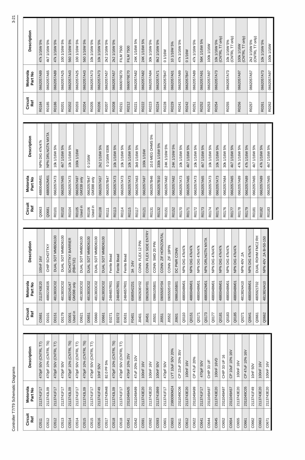
Con
trol
ler
T7/
T9
Sch
emat
ic D
iagr
ams
3-21
C05
1121
1374
1F17
470p
F 5
0V (
CN
TR
L T
7)
C05
1221
1374
3L09
470p
F 1
0% (
CN
TR
L T
6)
C05
1221
1374
1F17
470p
F 5
0V (
CN
TR
L T
7)
C05
1321
1374
1F17
470p
F 5
0V
C05
1421
1374
3L09
470p
F 1
0% (
CN
TR
L T
6)
C05
1421
1374
1F17
470p
F 5
0V (
CN
TR
L T
7)
C05
1521
1374
3L09
470p
F 1
0% (
CN
TR
L T
6)
C05
1521
1374
1F17
470p
F 5
0V (
CN
TR
L T
7)
C05
1621
1374
1F49
10nF
50V
C05
1721
1374
3N48
82.0
PF
5%
C05
1821
1374
3L09
470p
F 1
0% (
CN
TR
L T
6)
C05
1821
1374
1F17
470p
F 5
0V (
CN
TR
L T
7)
C05
4123
1104
9A05
470n
F 1
0% 2
5V
C05
4223
1104
9A99
47uF
20%
10V
C05
9121
1374
3E20
100n
F 1
6V
C05
9221
1374
3E20
100n
F 1
6V
C05
9321
1374
1B69
100n
F 5
0V
C06
0121
1374
1F17
470p
F 5
0V
C06
0323
8009
0M24
LYT
10u
F 5
0V 2
0%
C06
1123
1104
9C06
CP
22u
F 2
0% 3
5V
C06
1221
1374
3E20
100
nF 1
6V
C06
2223
1104
9A99
CP
47u
F 2
0%
C06
4121
1374
1F17
470
pF 5
0V
C06
4423
1104
9A97
CH
IP 3
3 U
F
C06
4521
1374
3E20
100
nF 1
6VD
C06
5223
1104
9A97
CH
IP 3
3 U
F 1
6
C06
5423
1104
9A57
CP
10u
F 1
0% 1
6V
C06
5521
1374
3E20
100
nF 1
6V
C06
6123
1104
9C05
CP
47u
F 1
0% 1
6V
C06
6221
1374
1F49
10nF
50V
C06
6321
1374
3E20
100n
F 1
6V
C06
7121
1374
3E20
100n
F 1
6V
Cir
cuit
R
efM
oto
rola
P
art
No
Des
crip
tio
n
C06
8121
1374
3E20
100n
F 1
6V
D01
0148
8023
6E05
CH
IP S
CH
OT
TK
Y
D01
5148
1383
3C02
DU
AL
SO
T M
MB
D61
00
D01
7948
1383
3C02
DU
AL
SO
T M
MB
D61
00
D03
01U
sed
in48
0224
5J47
GM
398
only
SC
HO
TT
KY
BA
RR
IER
(R
B47
1E)
D06
2148
1383
3C02
DU
AL
SO
T M
MB
D61
00
D06
5148
1383
3C02
DU
AL
SO
T M
MB
D61
00
D06
6048
1383
3C02
DU
AL
SO
T M
MB
D61
00
D06
6148
1383
3C02
DU
AL
SO
T M
MB
D61
00
E02
7124
8465
7R01
Fer
rite
Bea
d
E02
7224
8465
7R01
Fer
rite
Bea
d
E06
3124
8465
7R01
Fer
rite
Bea
d
F04
0165
8054
2Z01
3A 2
4V
J040
109
0263
6Y02
CO
NN
FLE
X 1
2 P
IN
J045
109
0263
6Y01
CO
NN
FLE
X S
IDE
EN
TR
Y
J050
109
8610
5B01
CO
NN
SM
D 2
0 P
IN
J055
109
0550
5Y04
CO
NN
ZIF
HO
RIZ
ON
TAL
J055
209
0550
5Y03
CO
NN
ZIF
18P
IN
J060
109
8616
5B01
DC
PW
R C
ON
N
Q01
1048
8004
8M01
NP
N D
IG 4
7k/4
7k
Q01
5148
8004
8M01
NP
N D
IG 4
7k/4
7k
Q01
7148
8004
8M01
NP
N D
IG 4
7k/4
7k
Q01
7348
8005
2M01
NP
N D
RLN
GT
N M
XTA
Q01
7748
8004
8M01
NP
N D
IG 4
7k/4
7k
Q01
8148
8004
8M01
NP
N D
IG 4
7k/4
7k
Q01
8348
8004
8M01
NP
N D
IG 4
7k/4
7k
Q01
8548
8004
8M01
NP
N D
IG 4
7k/4
7k
Q02
7148
1382
4A10
NP
N 4
0V .2
A
Q06
4148
8004
8M01
NP
N D
IG 4
7k/4
7k
Q06
6148
0592
1T02
DU
AL
RO
HM
FM
C2
RH
Q06
6248
1382
4A10
NP
N 4
0V .2
A B
=50
-150
Cir
cuit
R
efM
oto
rola
P
art
No
Des
crip
tio
n
Q06
6348
8004
8M01
NP
N D
IG 4
7k/4
7k
Q06
8148
8005
2M01
NP
N D
RLN
GT
N M
XTA
R01
0106
6205
7A73
10k
1/16
W 5
%
R01
0206
6205
7A65
4k7
1/16
W 5
%
R01
0406
6205
7A73
10k
1/16
W 5
%
R01
05U
sed
in06
6205
7A97
GM
338
only
100k
1/1
6W
R01
06U
sed
in06
6205
7B47
GM
398
only
0 1/
16W
R01
0806
6205
7A57
2k2
1/16
W 5
%
R01
1106
6205
7B47
0 1
/16W
030
6
R01
1306
6205
7A73
10k
1/16
W 5
%
R01
1406
6205
7A73
10k
1/16
W 5
%
R01
1506
6205
7A73
10k
1/16
W 5
%
R01
1706
6205
7A63
3k9
1/16
W 5
%
R01
2106
6205
7A97
100k
1/1
6W
R01
3106
6205
7B46
10.0
ME
G O
HM
S 5
%
R01
3206
6205
7B10
330k
1/1
6W 5
%
R01
5106
6205
7A82
24K
1/1
6W 5
%
R01
5206
6205
7A82
24K
1/1
6W 5
%
R01
7006
6205
7A73
10k
1/16
W 5
%
R01
7106
6205
7A65
4k7
1/16
W 5
%
R01
7206
6205
7A73
10k
1/16
W 5
%
R01
7306
6205
7A65
4k7
1/16
W 5
%
R01
7406
6205
7A73
10k
1/16
W 5
%
R01
7506
6205
7A73
10k
1/16
W 5
%
R01
7606
6205
7A84
30k
1/16
W 5
%
R01
7706
6205
7A65
4k7
1/16
W 5
%
R01
7806
6205
7A89
47k
1/16
W 5
%
R01
7906
6205
7A89
47k
1/16
W 5
%
R01
8106
6205
7A65
4k7
1/16
W 5
%
R01
8206
6205
7A89
47k
1/16
W 5
%
R01
8306
6205
7A65
4k7
1/16
W 5
%
Cir
cuit
R
efM
oto
rola
P
art
No
Des
crip
tio
n
R01
8406
6205
7A89
47k
1/16
W 5
%
R01
8506
6205
7A65
4k7
1/16
W 5
%
R01
8606
6205
7A89
47k
1/16
W 5
%
R02
0106
6205
7A25
100
1/16
W 5
%
R02
0206
6205
7A43
560
1/16
W 5
%
R02
0306
6205
7A25
100
1/16
W 5
%
R02
0406
6205
7A43
560
1/16
W 5
%
R02
0506
6205
7A73
10k
1/16
W 5
%
R02
0606
6205
7A73
10k
1/16
W 5
%
R02
0706
6205
7A57
2k2
1/16
W 5
%
R02
0806
6205
7A57
2k2
1/16
W 5
%
R02
1106
6007
6E70
FIL
M 7
500
R02
1206
6007
6E70
FIL
M 7
500
R02
2106
6205
7A82
24K
1/1
6W 5
%
R02
2206
6205
7A82
24K
1/1
6W 5
%
R02
2306
6205
7A84
30k
1/16
W 5
%
R02
2406
6205
7A71
8k2
1/16
W 5
%
R02
2806
6205
7B47
0 1/
16W
R02
2906
6205
7A01
10 1
/16W
5%
R02
4106
6205
7A89
47k
1/16
W 5
%
R02
4206
6205
7B47
0 1/
16W
R02
5106
6205
7A89
47k
1/16
W 5
%
R02
5206
6205
7A91
56K
1/1
6W 5
%
R02
5306
6205
7A97
100k
1/1
6W
R02
5406
6205
7A73
10k
1/16
W 5
%(C
NT
RL
T7
only
)
R02
5506
6205
7A73
10k
1/16
W 5
%(C
NT
RL
T7
only
)
R02
5606
6205
7A97
100k
1/1
6W(C
NT
RL
T7
only
)
R02
5706
6205
7A57
2k2
1/16
W 5
%(C
NT
RL
T7
only
)
R02
6106
6205
7A73
10k
1/16
W 5
%
R02
6206
6205
7A97
100k
1/1
6W
Cir
cuit
R
efM
oto
rola
P
art
No
Des
crip
tio
n
3-22
Con
trol
ler
T7/
T9
Sch
emat
ic D
iagr
ams
* M
otor
ola
Dep
ot S
ervi
cing
onl
y
Ref
eren
ce d
esig
nato
rs w
ith a
n as
teris
k in
dica
te
com
pone
nts
whi
ch a
re n
ot fi
eldr
epla
ceab
le
beca
use
they
nee
d to
be
calib
rate
d w
ith
spec
ializ
ed fa
ctor
y eq
uipm
ent a
fter
inst
alla
tion.
R
adio
s in
whi
ch th
ese
part
s ha
ve b
een
repl
aced
in
the
field
will
be
off f
requ
ency
at t
empe
ratu
re
extr
emes
.
R02
6506
6205
7A82
24K
1/1
6W 5
%
R02
6706
6205
7A89
47k
1/16
W 5
%
R02
6806
6205
7A73
10k
1/16
W 5
%
R02
6906
6205
7A41
470
1/16
W 5
%
R02
7306
6205
7A82
24K
1/1
6W 5
%
R02
7506
6205
7A73
10k
1/16
W 5
%
R02
7606
6205
7A77
15k
1/16
W 5
%
R03
23U
sed
in06
6205
7A79
GM
398
only
18k
1/16
W 5
%
R03
24U
sed
in06
6205
7A79
GM
398
only
18k
1/16
W 5
%
R03
31U
sed
in06
6205
7A73
GM
398
only
10k
1/16
W 5
%
R03
32U
sed
in06
6205
7A73
GM
398
only
10k
1/16
W 5
%
R03
33U
sed
in06
6205
7A73
GM
398
only
10k
1/16
W 5
%
R03
35U
sed
in06
6205
7B02
GM
398
only
150k
1/1
6W
R03
41U
sed
in06
6205
7A73
GM
398
only
10k
1/16
W
R03
42U
sed
in06
6205
7A55
GM
398
only
1k8
1/16
W
R03
43U
sed
in06
6205
7B47
GM
398
only
0 1/
16W
R03
44U
sed
in06
6205
7A91
GM
398
only
56K
1/1
6W
R03
45U
sed
in06
6205
7A66
GM
398
only
5k1
1/16
W
R03
46U
sed
in06
6205
7A89
GM
398
only
47k
1/16
W
R03
47U
sed
in06
6205
7A89
GM
398
only
47k
1/16
W
R04
0106
6205
7A33
220
1/16
W
R04
0706
6205
7M26
10 5
% 2
0X40
R04
0806
6205
7A25
100
1/16
W 5
%
R04
0906
6205
7M26
10 5
% 2
0X40
Cir
cuit
R
efM
oto
rola
P
art
No
Des
crip
tio
n
R04
1206
6205
7B47
0 1
/16W
R04
4106
6205
7B47
0 1
/16W
R04
42U
sed
in06
6205
7A49
1k 1
/16W
5%
CN
TR
L T
7 on
ly
R04
6706
6205
7M26
10 5
% 2
0X40
R04
6806
6205
7M26
10 5
% 2
0X40
(C
NT
RL
T6)
R04
6806
6205
7A97
100k
1/1
6W (
CN
TR
L T
7)
R04
8106
6205
7B47
0 1
/16W
R04
8206
6205
7B47
0 1
/16W
R05
1006
6205
7A65
4k7
1/16
W 5
%
R05
1106
6205
7A97
100k
1/1
6W
R05
1206
6205
7A77
15k
1/16
W 5
%
R05
2506
6205
7A97
100k
1/1
6W
R05
2906
6205
7A89
47k
1/16
W 5
%
R05
3006
6205
7B47
0 1
/16W
R05
3106
6205
7A43
560
1/16
W 5
%
R05
3306
6205
7B47
0 1
/16W
R05
3506
6205
7A49
1k 1
/16W
5%
R05
3706
6205
7A33
220
1/16
W 5
%
R05
3806
6205
7A33
220
1/16
W 5
%
R05
3906
6205
7A65
4k7
1/16
W 5
%
R05
4106
6205
7A83
27k
1/16
W 5
%
R05
4306
6205
7A97
100k
1/1
6W(C
NT
RL
T7
only
)
R05
9106
6205
7A82
24K
1/1
6W 5
%
R05
9206
6205
7A01
10 1
/16W
5%
R05
9306
6205
7A97
100k
1/1
6W(C
NT
RL
T7
only
)
R06
1106
6205
7A91
56K
1/1
6W
R06
1206
6205
7A65
4k7
1/16
W
R06
2106
6205
7A82
24K
1/1
6W
R06
4106
6205
7A73
10k
1/16
W
R06
4206
6007
6E70
FIL
M 7
500
Cir
cuit
R
efM
oto
rola
P
art
No
Des
crip
tio
n
R06
4306
6007
6E51
FIL
M 1
200
R06
5106
6205
7A01
10 1
/16W
5%
R06
5206
6205
7A01
10 1
/16W
5%
R06
6106
6205
7A49
1k 1
/16W
5%
R06
6206
6205
7B02
150k
1/1
6W
R06
7106
6205
7A84
30k
1/16
W 5
%
R06
7206
6205
7A73
10k
1/16
W 5
%
R06
8106
6205
7A79
18k
1/16
W 5
%
R06
8206
6205
7A93
68k
1/16
W 5
%
U01
0151
0222
6J56
MIC
RO
PR
OC
ES
SO
R
MC
68H
C1
1FLO
* U
0111
5102
463J
64E
EP
RO
M X
2512
8-2.
7 S
O8
* U
0121
5186
137B
0151
2KX
8 F
LAS
H R
OM
(A
T49
BV
020)
U01
2251
8596
3A21
32K
x 8
SR
AM
U01
4151
1380
5A30
10F
8 D
CD
R/R
EM
UX
74
HC
138
U02
1151
8322
2M49
QU
AD
OP
AM
P _
_340
3
U02
2151
8596
3A53
AS
FIC
CM
P 0
.5M
M T
QF
P
U02
5151
1380
6A20
MU
X/D
EM
UX
,TR
IPLE
2-
U02
7151
0969
9X01
AU
DIO
PA
TD
A15
19C
U03
01U
sed
in51
0915
2M01
GM
398
only
EE
PR
OM
AN
ALO
G
ISD
3312
0EI
U03
31U
sed
in51
8620
4B01
GM
398
only
BU
FF
ER
/DR
IVE
R
74A
HC
T1G
125
U03
41U
sed
in51
8093
2W01
GM
398
only
LIN
EA
R IC
OP
AM
P
U03
42U
sed
in51
0575
0U28
GM
398
only
SN
GL
AN
ALO
G S
WIT
CH
S
MD
U03
51U
sed
in51
0246
3J40
GM
398
only
RE
GU
LAT
OR
, 3.3
V,
LP29
51C
M-3
.3
U06
1151
8330
8X01
AD
J V
LTG
RE
G L
M29
41
TO
263
U06
4151
8330
8X01
AD
J V
LTG
RE
G L
M29
41
TO
263
Cir
cuit
R
efM
oto
rola
P
art
No
Des
crip
tio
n
U06
5151
1381
6A07
RE
G 5
V P
OS
500
MA
M
C78
M05
U06
5251
1381
5A02
MC
3306
4
VR
0151
4813
830A
15 5
.6V
5%
225
mW
VR
0501
4805
656W
09Z
EN
ER
QU
AD
M
MQ
A20
VT
1
VR
0503
4805
656W
09Z
EN
ER
QU
AD
M
MQ
A20
VT
1
VR
0504
4813
830A
40S
OC
23 A
UT
O S
DN
VR
0505
4805
656W
09Z
EN
ER
QU
AD
M
MQ
A20
VT
1
VR
0509
4813
830A
40S
OC
23 A
UT
O S
DN
VR
0510
4813
830A
40S
OC
23 A
UT
O S
DN
VR
0537
4813
830A
155.
6V 5
% 2
25m
W
VR
0541
4813
830A
2714
V 5
% 2
25M
W
VR
0601
4813
832C
77T
RA
NS
SU
P. 2
4V H
IGH
P
OW
ER
VR
0621
4813
830A
155.
6V 5
% 2
25m
W
Y01
3148
8011
3R19
CR
YS
TAL
38.4
KH
z
Cir
cuit
R
efM
oto
rola
P
art
No
Des
crip
tio
n
Con
trol
ler
T7/
T9
Sch
emat
ic D
iagr
ams
3-23
3.2
Co
ntr
olle
r T
9 P
arts
Lis
t
Cir
cuit
R
efM
oto
rola
P
art
No
Des
crip
tio
n
C01
0121
1374
0F51
100p
F
C01
0721
1374
1F25
1000
pF
C01
1221
1374
3E20
10uF
C01
2121
1374
3E20
10uF
C01
2221
1374
3E20
10uF
C01
3121
1374
0F35
22pF
C01
3221
1374
0F35
22pF
C01
4121
1374
3E20
10uF
C01
5121
1374
1F49
10nF
C02
0123
1104
9A57
10uF
C02
0223
1104
9A57
10uF
C02
0421
1374
3E20
10uF
C02
1223
1104
9A57
10uF
C02
2121
1374
3E20
10uF
C02
2221
1374
3E20
10uF
C02
2321
1374
3E20
10uF
C02
2421
1374
0F51
100p
F
C02
2521
1374
3E20
10uF
C02
2621
1374
3E20
10uF
C02
2823
1104
9A56
4.7u
F
C02
3121
1374
3B29
1uF
C02
3221
1374
3E20
10uF
C02
3421
1374
3E20
10uF
C02
3521
1374
3E07
0.02
2uF
C02
3621
1374
3E10
0.03
3uF
C02
4121
1374
3E20
10uF
C02
4321
1374
0F51
100p
F
C02
4421
1374
3E20
10uF
C02
4521
1374
3E20
10uF
C02
4621
1374
1F49
10nF
C02
5121
1374
3E20
10uF
C02
5223
1104
9A07
1uF
C02
5421
1374
3E20
10uF
C02
5521
1374
3E20
10uF
C02
5621
1374
0F51
100p
F
C02
6121
1374
3E20
10uF
C02
6221
1374
0F49
82pF
C02
6521
1374
3E20
10uF
C02
6721
1374
1F49
10nF
C02
7121
1374
1F49
10nF
C02
7221
1374
3E20
10uF
C02
7321
1374
1F37
3300
pF
C02
7523
1104
9A99
47uF
C02
7621
1374
1F25
1000
pF
C02
7721
1374
1F25
1000
pF
C03
0123
1104
9A07
1uF
C03
0221
1374
3E20
10uF
C03
0321
1374
0F51
100p
F
C03
0421
1374
3E20
10uF
C03
0521
1374
3E20
10uF
C03
2421
1374
3E20
10uF
C03
3121
1374
3E20
10uF
C03
4123
1104
9A07
1uF
C03
4221
1374
3E20
10uF
C03
4321
1374
3E20
10uF
C03
4421
1374
3E20
10uF
C03
5121
1374
3E20
10uF
C03
5221
1374
3E07
0.02
2uF
C03
5323
1104
9A97
33uF
C03
5421
1374
3E20
10uF
C04
2121
1374
3N48
82pF
C04
2221
1374
1F17
470p
F
C04
2321
1374
1F17
470p
F
Cir
cuit
R
efM
oto
rola
P
art
No
Des
crip
tio
n
C04
2621
1374
3L09
470p
F
C04
2721
1374
3L09
470p
F
C04
2821
1374
3N48
82pF
C04
2921
1374
3L09
470p
F
C04
3021
1374
1F17
470p
F
C04
3121
1374
1F17
470p
F
C04
4121
1374
3L09
470p
F
C04
4221
1374
3L09
470p
F
C04
4521
1374
3L09
470p
F
C04
4621
1374
3L09
470p
F
C04
4721
1374
3L09
470p
F
C04
4821
1374
3L09
470p
F
C04
4921
1374
3L09
470p
F
C04
7021
1374
3L09
470p
F
C04
7121
1374
3N48
82pF
C04
7221
1374
3N48
82pF
C04
7321
1374
3N48
82pF
C04
7421
1374
3L09
470p
F
C04
7621
1374
3L09
470p
F
C04
7721
1374
3L09
470p
F
C04
7821
1374
3L09
470p
F
C04
82-
C04
8821
1374
3L09
470p
F
C04
90-
C04
9721
1374
3L09
470p
F
C04
9921
1374
3L09
470p
F
C05
0121
1374
1F49
10nF
C05
0221
1374
1F17
470p
F
C05
0321
1374
1F17
470p
F
C05
0421
1374
1F17
470p
F
C05
0521
1374
1F17
470p
F
C05
0621
1374
1F17
470p
F
Cir
cuit
R
efM
oto
rola
P
art
No
Des
crip
tio
n
C05
0821
1374
1F17
470p
F
C05
0921
1374
1F17
470p
F
C05
1021
1374
1F17
470p
F
C05
1121
1374
1F17
470p
F
C05
1221
1374
1F17
470p
F
C05
1321
1374
1F17
470p
F
C05
1421
1374
1F17
470p
F
C05
1521
1374
1F17
470p
F
C05
1621
1374
1F49
10nF
C05
1721
1374
3N48
82pF
C05
1821
1374
1F17
470p
F
C05
4123
1104
9A05
0.47
uF
C05
4223
1104
9A99
47uF
C05
6021
1374
1F25
1000
pF
C05
9121
1374
3E20
10uF
C05
9221
1374
3E20
10uF
C05
9321
1374
1B69
100K
F
C06
0121
1374
1F17
470p
F
C06
0323
8009
0M24
10uF
C06
1123
1104
9C06
47uF
C06
1221
1374
3E20
10uF
C06
2223
1104
9A99
47uF
C06
4121
1374
1F17
470p
F
C06
4423
1104
9A97
33uF
C06
4521
1374
3E20
10uF
C06
5223
1104
9A97
33uF
C06
5423
1104
9A57
10uF
C06
5521
1374
3E20
10uF
C06
6123
1104
9C05
47uF
C06
6221
1374
1F49
10nF
C06
6321
1374
3E20
10uF
C06
7121
1374
3E20
10uF
Cir
cuit
R
efM
oto
rola
P
art
No
Des
crip
tio
n
3-24
Con
trol
ler
T7/
T9
Sch
emat
ic D
iagr
ams
C06
8121
1374
3E20
10uF
D01
0148
1382
5A05
DIO
DE
D01
5148
1383
3C02
DIO
DE
, DU
AL
70V
D01
7948
1383
3C02
DIO
DE
, DU
AL
70V
D03
0148
0224
5J47
DIO
DE
, SC
HO
TT
KY
D06
2148
1383
3C02
DIO
DE
, DU
AL
70V
D06
5148
1383
3C02
DIO
DE
, DU
AL
70V
D06
6048
1383
3C02
DIO
DE
, DU
AL
70V
D06
6148
1383
3C02
DIO
DE
, DU
AL
70V
E02
7124
8465
7R01
Fer
rite
Bea
d
E02
7224
8465
7R01
Fer
rite
Bea
d
E06
3124
8465
7R01
Fer
rite
Bea
d
F04
0165
8054
2Z01
FU
SE
3A
J040
109
0263
6Y02
12 P
OS
. FLE
X C
ON
N
J045
109
0263
6Y01
CO
NN
, FLE
X, S
IDE
E
NT
RY
J050
109
8610
5B01
CO
NN
, SM
D, 2
0 P
in
J055
109
0550
5Y04
CO
NN
ZIF
HO
RIZ
ON
TAL
J055
209
0550
5Y03
CO
NN
ZIF
HO
RIZ
ON
TAL
J060
109
8616
5B01
MO
BIL
E D
C P
WR
CO
NN
Q01
1048
8004
8M01
NP
N
Q01
5148
8004
8M01
NP
N
Q01
7148
8004
8M01
NP
N
Q01
7348
8005
2M01
NP
N D
AR
LIN
GT
ON
Q01
7748
8004
8M01
NP
N
Q01
8148
8004
8M01
NP
N
Q01
8348
8004
8M01
NP
N
Q01
8548
8004
8M01
NP
N
Q02
7148
8021
4G02
NP
N
Q06
4148
8004
8M01
NP
N
Q06
6148
0592
1T02
TR
AN
SIS
TO
R D
UA
L D
IGI-
TAL
NP
N/P
NP
Q06
6248
8021
4G02
NP
N
Cir
cuit
R
efM
oto
rola
P
art
No
Des
crip
tio
n
Q06
6348
8004
8M01
NP
N
Q06
8148
8005
2M01
NP
N D
AR
LIN
GT
ON
R01
0106
6205
7A73
10K
Ohm
R01
0206
6205
7A65
4700
Ohm
R01
0306
6205
7B47
0 O
hm
R01
0406
6205
7A73
10K
Ohm
R01
0606
6205
7B47
0 O
hm
R01
0806
6205
7A57
2200
Ohm
R01
1106
6205
7B47
0 O
hm
R01
1306
6205
7A73
10K
Ohm
R01
1406
6205
7A73
10K
Ohm
R01
1506
6205
7A73
10K
Ohm
R01
1706
6205
7A63
3900
Ohm
R01
2106
6205
7A97
100K
Ohm
R01
3106
6205
7B46
10M
Ohm
R01
3206
6205
7B10
330K
Ohm
R01
5106
6205
7A82
24K
Ohm
R01
5206
6205
7A82
24K
Ohm
R01
7006
6205
7A73
10K
Ohm
R01
7106
6205
7A65
4700
Ohm
R01
7206
6205
7A73
10K
Ohm
R01
7306
6205
7A65
4700
Ohm
R01
7406
6205
7A73
10K
Ohm
R01
7506
6205
7A73
10K
Ohm
R01
7606
6205
7A84
30K
Ohm
R01
7706
6205
7A65
4700
Ohm
R01
7806
6205
7A89
47K
Ohm
R01
7906
6205
7A89
47K
Ohm
R01
8106
6205
7A65
4700
Ohm
R01
8206
6205
7A89
47K
Ohm
R01
8306
6205
7A65
4700
Ohm
R01
8406
6205
7A89
47K
Ohm
Cir
cuit
R
efM
oto
rola
P
art
No
Des
crip
tio
n
R01
8506
6205
7A65
4700
Ohm
R01
8606
6205
7A89
47K
Ohm
R02
0106
6205
7A25
100
Ohm
R02
0206
6205
7A43
560
Ohm
R02
0306
6205
7A25
100
Ohm
R02
0406
6205
7A43
560
Ohm
R02
0506
6205
7A73
10K
Ohm
R02
0606
6205
7A73
10K
Ohm
R02
0706
6205
7A57
2200
Ohm
R02
0806
6205
7A57
2200
Ohm
R02
1106
6007
6E70
7500
Ohm
R02
1206
6007
6E70
7500
Ohm
R02
2106
6205
7A82
24K
Ohm
R02
2206
6205
7A82
24K
Ohm
R02
2306
6205
7A84
30K
Ohm
R02
2406
6205
7A71
8200
Ohm
R02
2806
6205
7B47
0 O
hm
R02
2906
6205
7A01
10 O
hm
R02
4106
6205
7A89
47K
Ohm
R02
4206
6205
7B47
0 O
hm
R02
5106
6205
7A89
47K
Ohm
R02
5206
6205
7A91
56K
Ohm
R02
5306
6205
7A97
100K
Ohm
R02
5406
6205
7A73
10K
Ohm
R02
5506
6205
7A73
10K
Ohm
R02
5606
6205
7A97
100K
Ohm
R02
5706
6205
7A57
2200
Ohm
R02
6106
6205
7A73
10K
Ohm
R02
6206
6205
7A97
100K
Ohm
R02
6506
6205
7A82
24K
Ohm
R02
6706
6205
7A89
47K
Ohm
R02
6806
6205
7A73
10K
Ohm
Cir
cuit
R
efM
oto
rola
P
art
No
Des
crip
tio
n
R02
6906
6205
7A41
470
Ohm
R02
7306
6205
7A82
24K
Ohm
R02
7506
6205
7A73
10K
Ohm
R02
7606
6205
7A77
15K
Ohm
R03
2306
6205
7A79
18K
Ohm
R03
2406
6205
7A79
18K
Ohm
R03
3106
6205
7A73
10K
Ohm
R03
3206
6205
7A73
10K
Ohm
R03
3306
6205
7A73
10K
Ohm
R03
3506
6205
7B02
150K
Ohm
R03
4106
6205
7A73
10K
Ohm
R03
4206
6205
7A55
1800
Ohm
R03
4306
6205
7B47
0 O
hm
R03
4406
6205
7A91
56K
Ohm
R03
4506
6205
7A66
5100
Ohm
R03
4606
6205
7A89
47K
Ohm
R03
4706
6205
7A89
47K
Ohm
R04
0106
6205
7A33
220
Ohm
R04
0706
6205
7M26
10 O
hm
R04
0806
6205
7A25
100
Ohm
R04
0906
6205
7M26
10 O
hm
R04
1206
6205
7B47
0 O
hm
R04
4106
6205
7B47
0 O
hm
R04
4206
6205
7A49
1000
Ohm
R04
6706
6205
7M26
10 O
hm
R04
6806
6205
7A97
100K
Ohm
R04
8106
6205
7B47
0 O
hm
R04
8206
6205
7B47
0 O
hm
R05
1006
6205
7A65
4700
Ohm
R05
1106
6205
7A97
100K
Ohm
R05
1206
6205
7A77
15K
Ohm
R05
2506
6205
7A97
100K
Ohm
Cir
cuit
R
efM
oto
rola
P
art
No
Des
crip
tio
n

Con
trol
ler
T7/
T9
Sch
emat
ic D
iagr
ams
3-25
* M
otor
ola
Dep
ot S
ervi
cing
onl
y
Ref
eren
ce d
esig
nato
rs w
ith a
n as
teris
k in
dica
te
com
pone
nts
whi
ch a
re n
ot fi
eld
repl
acea
ble
beca
use
they
nee
d to
be
calib
rate
d w
ith
spec
ializ
ed fa
ctor
y eq
uipm
ent a
fter
inst
alla
tion.
R
adio
s in
whi
ch th
ese
part
s ha
ve b
een
repl
aced
in
the
field
will
be
off f
requ
ency
at t
empe
ratu
re
extr
emes
.
R05
2906
6205
7A89
47K
Ohm
R05
3006
6205
7B47
0 O
hm
R05
3106
6205
7A43
560
Ohm
R05
3306
6205
7B47
0 O
hm
R05
3506
6205
7A49
1000
Ohm
R05
3706
6205
7A33
220
Ohm
R05
3806
6205
7A33
220
Ohm
R05
3906
6205
7A65
4700
Ohm
R05
4106
6205
7A83
27K
Ohm
R05
4306
6205
7A97
100K
Ohm
R05
5506
6205
7A25
100
Ohm
R05
5606
6205
7A25
100
Ohm
R05
9106
6205
7A82
24K
Ohm
R05
9206
6205
7A01
10 O
hm
R05
9306
6205
7A97
100K
Ohm
R06
1106
6205
7A91
56K
Ohm
R06
1206
6205
7A65
4700
Ohm
R06
2106
6205
7A82
24K
Ohm
R06
4106
6205
7A73
10K
Ohm
R06
4206
6007
6E70
7500
Ohm
R06
4306
6007
6E51
1200
Ohm
R06
5106
6205
7A01
10 O
hm
R06
5206
6205
7A01
10 O
hm
R06
6106
6205
7A49
1000
Ohm
R06
6206
6205
7B02
150K
Ohm
R06
7106
6205
7A84
30K
Ohm
R06
7206
6205
7A73
10K
Ohm
R06
8106
6205
7A79
18K
Ohm
R06
8206
6205
7A93
68K
Ohm
U01
0151
0222
6J56
MIC
RO
PR
OC
ES
SO
R
U01
1151
0246
3J64
EE
PR
OM
U01
2151
8613
7B01
IC, F
LAS
H R
OM
Cir
cuit
R
efM
oto
rola
P
art
No
Des
crip
tio
n
U01
2251
8574
8L01
SR
AM
U01
4151
1380
5A30
IC 1
0F8
DC
DR
/RE
MU
X
74H
C13
8
U02
1151
8322
2M49
IC, Q
UA
D O
PA
MP
U02
2151
8513
0C53
IC, A
SF
IC
U02
5151
8470
4M60
IC-C
MO
S A
NA
LOG
U02
7151
0969
9X01
AU
DIO
PA
U03
0151
0915
2M01
IC, E
EP
RO
M A
NA
LOG
U03
3151
8620
4B01
IC, B
UF
FE
R D
RIV
ER
U03
4151
1381
8A01
LOW
PO
WE
R S
UP
PLY
U03
4251
0575
0U28
IC C
MO
S S
WIT
CH
U03
5151
0246
3J40
RE
GU
LAT
OR
, 3.3
V
U06
1151
8330
8X01
AD
JUS
TAB
LE V
OLT
AG
E
RE
GU
LAT
OR
U06
4151
8330
8X01
AD
JUS
TAB
LE V
OLT
AG
E
RE
GU
LAT
OR
U06
5151
1381
6A07
RE
GU
LAT
OR
, 5V
U06
5251
1381
5A02
UN
DE
RV
OLT
SE
NS
OR
VR
0151
4813
830A
15D
IOD
E, 5
.6V
VR
0501
4805
656W
09D
IOD
E, Z
EN
ER
VR
0503
4805
656W
09D
IOD
E, Z
EN
ER
VR
0504
4813
830A
40D
IOD
E, Z
EN
ER
VR
0505
4805
656W
09D
IOD
E, Z
EN
ER
VR
0509
4813
830A
40D
IOD
E, Z
EN
ER
VR
0510
4813
830A
40D
IOD
E, Z
EN
ER
VR
0537
4813
830A
15D
IOD
E, 5
.6V
VR
0541
4813
830A
27D
IOD
E, 1
4V
VR
0601
4813
832C
77D
IOD
E
VR
0621
4813
830A
15D
IOD
E, 5
.6V
Y01
3148
8011
3R19
CR
YS
TAL
38.4
KH
Z
Cir
cuit
R
efM
oto
rola
P
art
No
Des
crip
tio
n

3-26
Con
trol
ler
T7/
T9
Sch
emat
ic D
iagr
ams
TH
IS P
AG
E IN
TE
NT
ION
AL
LY L
EF
T B
LA
NK
GM328/GM338/GM398Mobile Radios
VHF (136-174MHz)
Service Information
Issue: December, 2003

Computer Software CopyrightsThe Motorola products described in this manual may include copyrighted Motorola computer programs stored in semiconductor memories or other media. Laws in the United States and other countries preserve for Motorola certain exclusive rights for copyrighted computer programs, including the exclusive right to copy or reproduce in any form, the copyrighted computer program. Accordingly, any copyrighted Motorola computer programs contained in the Motorola products described in this manual may not be copied or reproduced in any manner without the express written permission of Motorola. Furthermore, the purchase of Motorola products shall not be deemed to grant, either directly or by implication, estoppel or otherwise, any license under the copyrights, patents or patent applications of Motorola, except for the normal non-exclusive royalty-free license to use that arises by operation of law in the sale of a product.

i
Table of Contents
Section 1 Model Chart and Technical Specifications
1.0 GM328/GM338/GM398 Model Chart ...................................................................1-12.0 Technical Specifications ......................................................................................1-2
Section 2 Theory of Operation
1.0 Introduction ..........................................................................................................2-12.0 VHF (136-174 MHz) Receiver..............................................................................2-1
2.1 Receiver Front-End ........................................................................................2-12.2 Front-End Band-Pass Filters & Pre-Amplifier .................................................2-22.3 First Mixer and High Intermediate Frequency (IF)..........................................2-22.4 Low Intermediate Frequency (IF) and Receiver Back End.............................2-3
3.0 VHF (136-174 MHz) Transmitter Power Amplifier (PA) 25 W..............................2-33.1 First Power Controlled Stage..........................................................................2-43.2 Power Controlled Driver Stage .......................................................................2-43.3 Final Stage .....................................................................................................2-43.4 Directional Coupler .........................................................................................2-53.5 Antenna Switch...............................................................................................2-53.6 Harmonic Filter ...............................................................................................2-53.7 Power Control.................................................................................................2-5
4.0 VHF (136-174 MHz) Frequency Synthesis ..........................................................2-64.1 Reference Oscillator .......................................................................................2-64.2 Fractional-N Synthesizer ................................................................................2-64.3 Voltage Controlled Oscillator (VCO)...............................................................2-74.4 Synthesizer Operation ....................................................................................2-8
Section 3 Troubleshooting Charts
1.0 Troubleshooting Flow Chart for Receiver ............................................................3-12.0 Troubleshooting Flow Chart for 25W Transmitter ................................................3-33.0 Troubleshooting Flow Chart for Synthesizer........................................................3-64.0 Troubleshooting Flow Chart for VCO...................................................................3-7
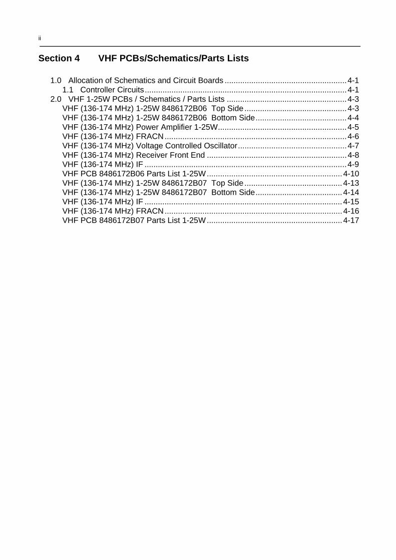
ii
Section 4 VHF PCBs/Schematics/Parts Lists
1.0 Allocation of Schematics and Circuit Boards .......................................................4-11.1 Controller Circuits...........................................................................................4-1
2.0 VHF 1-25W PCBs / Schematics / Parts Lists ......................................................4-3VHF (136-174 MHz) 1-25W 8486172B06 Top Side ..............................................4-3VHF (136-174 MHz) 1-25W 8486172B06 Bottom Side.........................................4-4VHF (136-174 MHz) Power Amplifier 1-25W..........................................................4-5VHF (136-174 MHz) FRACN..................................................................................4-6VHF (136-174 MHz) Voltage Controlled Oscillator.................................................4-7VHF (136-174 MHz) Receiver Front End ...............................................................4-8VHF (136-174 MHz) IF ...........................................................................................4-9VHF PCB 8486172B06 Parts List 1-25W.............................................................4-10VHF (136-174 MHz) 1-25W 8486172B07 Top Side ............................................4-13VHF (136-174 MHz) 1-25W 8486172B07 Bottom Side.......................................4-14VHF (136-174 MHz) IF .........................................................................................4-15VHF (136-174 MHz) FRACN................................................................................4-16VHF PCB 8486172B07 Parts List 1-25W.............................................................4-17
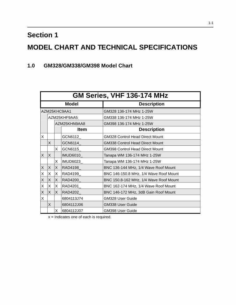
1-1
Section 1
MODEL CHART AND TECHNICAL SPECIFICATIONS
1.0 GM328/GM338/GM398 Model Chart
GM Series, VHF 136-174 MHzModel Description
AZM25KHC9AA1 GM328 136-174 MHz 1-25W
AZM25KHF9AA5 GM338 136-174 MHz 1-25W
AZM25KHN9AA8 GM398 136-174 MHz 1-25W
Item Description
X GCN6112_ GM328 Control Head Direct Mount
X GCN6114_ GM338 Control Head Direct Mount
X GCN6115_ GM398 Control Head Direct Mount
X X IMUD6010_ Tanapa WM 136-174 MHz 1-25W
X IMUD6023_ Tanapa WM 136-174 MHz 1-25W
X X X RAD4198_ BNC 136-144 MHz, 1/4 Wave Roof Mount
X X X RAD4199_ BNC 146-150.8 MHz, 1/4 Wave Roof Mount
X X X RAD4200_ BNC 150.8-162 MHz, 1/4 Wave Roof Mount
X X X RAD4201_ BNC 162-174 MHz, 1/4 Wave Roof Mount
X X X RAD4202_ BNC 146-172 MHz, 3dB Gain Roof Mount
X 6804113J74 GM328 User Guide
X 6804112J06 GM338 User Guide
X 6804112J07 GM398 User Guide
x = Indicates one of each is required.

1-2 Technical Specifications
2.0 Technical Specifications
Data is specified for +25°C unless otherwise stated.
General Specifications
Channel CapacityGM328GM338GM398
4128160
Power Supply 13.2Vdc (10.8 - 15.6Vdc)
Dimensions: H x W x D (mm) Depth excluding knobs GM32856mm x 176mm x 177mm(add 8mm for Volume Knob)
Dimensions: H x W x D (mm) Depth excluding knobs GM33859mm x 179mm x 186mm (1 - 25W)59mm x 179mm x 198mm (25 - 45W)(add 9mm for Volume Knob)
Dimensions: H x W x D (mm) Depth excluding knobs GM39872mm x 185mm x 188mm(add 7mm for Volume Knob)
Weight GM328/GM338 1400 g
Weight GM398 1500 g
Sealing: Withstands rain testing per MIL STD 810 C/D /E and IP54
Shock and Vibration: Protection provided via impactresistant housing exceeding MIL STD 810-C/D /E
Dust, Salt & Fog Protection provided via environment resistant housing exceeding MIL STD 810 C/D /E
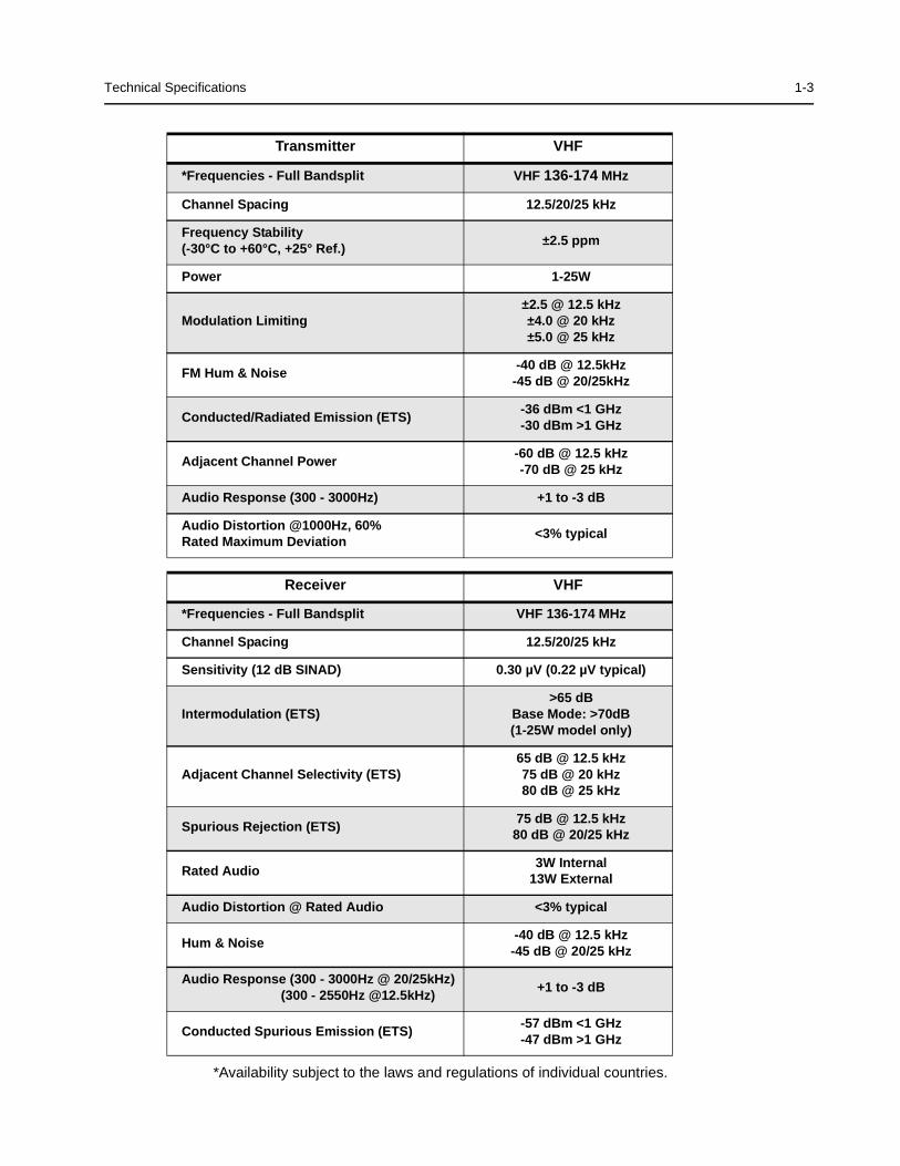
Technical Specifications 1-3
*Availability subject to the laws and regulations of individual countries.
Transmitter VHF
*Frequencies - Full Bandsplit VHF 136-174 MHz
Channel Spacing 12.5/20/25 kHz
Frequency Stability(-30°C to +60°C, +25° Ref.)
±2.5 ppm
Power 1-25W
Modulation Limiting±2.5 @ 12.5 kHz ±4.0 @ 20 kHz±5.0 @ 25 kHz
FM Hum & Noise-40 dB @ 12.5kHz
-45 dB @ 20/25kHz
Conducted/Radiated Emission (ETS)-36 dBm <1 GHz-30 dBm >1 GHz
Adjacent Channel Power-60 dB @ 12.5 kHz-70 dB @ 25 kHz
Audio Response (300 - 3000Hz) +1 to -3 dB
Audio Distortion @1000Hz, 60%Rated Maximum Deviation
<3% typical
Receiver VHF
*Frequencies - Full Bandsplit VHF 136-174 MHz
Channel Spacing 12.5/20/25 kHz
Sensitivity (12 dB SINAD) 0.30 µV (0.22 µV typical)
Intermodulation (ETS)>65 dB
Base Mode: >70dB (1-25W model only)
Adjacent Channel Selectivity (ETS)65 dB @ 12.5 kHz 75 dB @ 20 kHz80 dB @ 25 kHz
Spurious Rejection (ETS)75 dB @ 12.5 kHz
80 dB @ 20/25 kHz
Rated Audio3W Internal
13W External
Audio Distortion @ Rated Audio <3% typical
Hum & Noise-40 dB @ 12.5 kHz
-45 dB @ 20/25 kHz
Audio Response (300 - 3000Hz @ 20/25kHz)(300 - 2550Hz @12.5kHz)
+1 to -3 dB
Conducted Spurious Emission (ETS)-57 dBm <1 GHz-47 dBm >1 GHz

1-4 Technical Specifications
THIS PAGE INTENTIONALLY LEFT BLANK

2-1
Section 2
THEORY OF OPERATION
1.0 Introduction
This Chapter provides a detailed theory of operation for the VHF circuits in the radio. For details of the theory of operation and troubleshooting for the the associated Controller circuits refer to the Controller Section of this manual.
2.0 VHF (136-174 MHz) Receiver
2.1 Receiver Front-End
The receiver is able to cover the VHF range from 136 to 174 MHz. It consists of four major blocks: front-end bandpass filters and pre-amplifier, first mixer, high-IF, low-IF and receiver back-end. Two varactor-tuned bandpass filters perform antenna signal pre-selection. A cross over quad diode mixer converts the signal to the first IF of 44.85 MHz. High-side first injection is used.
Figure 2-1 VHF Receiver Block Diagram
Demodulator
1. Crystal Filter
MixerVaractor Tuned FilterRF AmpVaractor
Tuned Filter
Antenna
Control Voltagefrom PCIC First LO
from FGU
Recovered Audio
RSSI
IF
Second LO
2. Crystal Filter
455kHz Filter(25kHz)
455kHz Filter(25kHz)
455kHz Filter(12.5kHz)
455kHz Filter(12.5kHz)
Sw
itch
Sw
itch
Sw
itch
Sw
itch
Limiter
1. IF Amp
2. IF Amp
Filter Bank Selectionfrom Synthesizer IC
Pin Diode Antenna SwitchRF Jack
Harmonic Filter
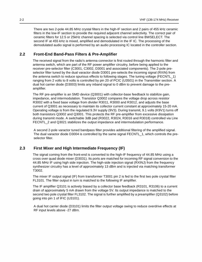
2-2 VHF (136-174 MHz) Receiver
There are two 2-pole 44.85 MHz crystal filters in the high-IF section and 2 pairs of 455 kHz ceramic filters in the low-IF section to provide the required adjacent channel selectivity. The correct pair of ceramic filters for 12.5 or 25kHz channel spacing is selected via control line BWSELECT. The second IF at 455 kHz is mixed, amplified and demodulated in the IF IC. The processing of the demodulated audio signal is performed by an audio processing IC located in the controller section.
2.2 Front-End Band-Pass Filters & Pre-Amplifier
The received signal from the radio’s antenna connector is first routed through the harmonic filter and antenna switch, which are part of the RF power amplifier circuitry, before being applied to the receiver pre-selector filter (C3001, C3002, D3001 and associated components). The 2-pole pre-selector filter tuned by the dual varactor diode D3001 pre-selects the incoming signal (RXIN) from the antenna switch to reduce spurious effects to following stages. The tuning voltage (FECNTL_1) ranging from 2 volts to 8 volts is controlled by pin 20 of PCIC (U3501) in the Transmitter section. A dual hot carrier diode (D3003) limits any inband signal to 0 dBm to prevent damage to the pre-amplifier.
The RF pre-amplifier is an SMD device (Q3001) with collector-base feedback to stabilize gain, impedance, and intermodulation. Transistor Q3002 compares the voltage drop across resistor R3002 with a fixed base voltage from divider R3011, R3000 and R3012, and adjusts the base current of Q3001 as necessary to maintain its collector current constant at approximately 15-20 mA. Operating voltage is from the regulated 9.3V supply (9V3). During transmit, 9.1 volts (K9V1) turns off both transistors Q3002 and Q3001. This protects the RF pre-amplifier from excessive dissipation during transmit mode. A switchable 3dB pad (R3022, R3024, R3016 and R3018) controlled via Line FECNTL_2 and Q3021 stabilizes the output impedance and intermodulation performance.
A second 2-pole varactor tuned bandpass filter provides additional filtering of the amplified signal. The dual varactor diode D3004 is controlled by the same signal FECNTL_1, which controls the pre-selector filter.
2.3 First Mixer and High Intermediate Frequency (IF)
The signal coming from the front-end is converted to the high-IF frequency of 44.85 MHz using a cross over quad diode mixer (D3031). Its ports are matched for incoming RF signal conversion to the 44.85 MHz IF using high side injection. The high-side injection signal (RXINJ) from the frequency synthesizer circuitry has a level of approximately 13 dBm and is injected via matching transformer T3002.
The mixer IF output signal (IF) from transformer T3001 pin 2 is fed to the first two pole crystal filter FL3101. The filter output in turn is matched to the following IF amplifier.
The IF amplifier Q3101 is actively biased by a collector base feedback (R3101, R3106) to a current drain of approximately 5 mA drawn from the voltage 5V. Its output impedance is matched to the second two pole crystal filter FL3102. The signal is further amplified by a preamplifier (Q3102) before going into pin 1 of IFIC (U3101).
A dual hot carrier diode (D3101) limits the filter output voltage swing to reduce overdrive effects at RF input levels above -27 dBm.
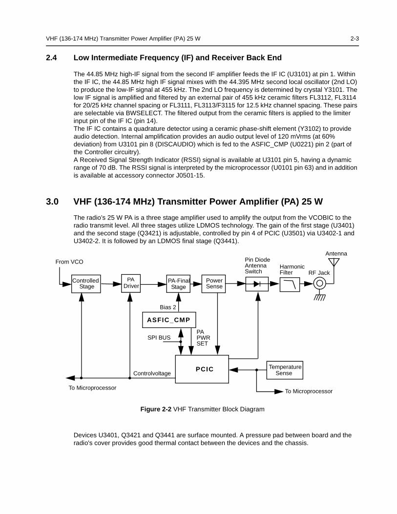
VHF (136-174 MHz) Transmitter Power Amplifier (PA) 25 W 2-3
2.4 Low Intermediate Frequency (IF) and Receiver Back End
The 44.85 MHz high-IF signal from the second IF amplifier feeds the IF IC (U3101) at pin 1. Within the IF IC, the 44.85 MHz high IF signal mixes with the 44.395 MHz second local oscillator (2nd LO) to produce the low-IF signal at 455 kHz. The 2nd LO frequency is determined by crystal Y3101. The low IF signal is amplified and filtered by an external pair of 455 kHz ceramic filters FL3112, FL3114 for 20/25 kHz channel spacing or FL3111, FL3113/F3115 for 12.5 kHz channel spacing. These pairs are selectable via BWSELECT. The filtered output from the ceramic filters is applied to the limiter input pin of the IF IC (pin 14).The IF IC contains a quadrature detector using a ceramic phase-shift element (Y3102) to provide audio detection. Internal amplification provides an audio output level of 120 mVrms (at 60% deviation) from U3101 pin 8 (DISCAUDIO) which is fed to the ASFIC_CMP (U0221) pin 2 (part of the Controller circuitry).A Received Signal Strength Indicator (RSSI) signal is available at U3101 pin 5, having a dynamic range of 70 dB. The RSSI signal is interpreted by the microprocessor (U0101 pin 63) and in addition is available at accessory connector J0501-15.
3.0 VHF (136-174 MHz) Transmitter Power Amplifier (PA) 25 W
The radio’s 25 W PA is a three stage amplifier used to amplify the output from the VCOBIC to the radio transmit level. All three stages utilize LDMOS technology. The gain of the first stage (U3401) and the second stage (Q3421) is adjustable, controlled by pin 4 of PCIC (U3501) via U3402-1 and U3402-2. It is followed by an LDMOS final stage (Q3441).
Figure 2-2 VHF Transmitter Block Diagram
Devices U3401, Q3421 and Q3441 are surface mounted. A pressure pad between board and the radio's cover provides good thermal contact between the devices and the chassis.
PCIC
Pin Diode Antenna Switch RF Jack
Antenna
Harmonic Filter
PowerSense
PA-FinalStage
From VCO
ControlledStage
Controlvoltage
Bias 2
To Microprocessor
TemperatureSense
SPI BUS
ASFIC_CMP
PAPWRSET
To Microprocessor
PADriver
2-4 VHF (136-174 MHz) Transmitter Power Amplifier (PA) 25 W
3.1 First Power Controlled Stage
The first stage (U3401) is a 20dB gain integrated circuit containing two LDMOS FET amplifier stages. It amplifies the RF signal from the VCO (TXINJ). The output power of stage U3401 is controlled by a DC voltage applied to pin 1 from the op-amp U3402-1, pin 1. The control voltage simultaneously varies the bias of two FET stages within U3401. This biasing point determines the overall gain of U3401 and therefore its output drive level to Q3421, which in turn controls the output power of the PA.
Op-amp U3402-1 monitors the drain current of U3401 via resistor R3444 and adjusts the bias voltage of U3401 so that the current remains constant. The PCIC (U3501) provides a DC output voltage at pin 4 (INT) which sets the reference voltage of the current control loop. A raising power output causes the DC voltage from the PCIC to fall, and U3402-1 adjusts the bias voltage for a lower drain current to lower the gain of the stage.In receive mode the DC voltage from PCIC pin 23 (RX) turns on Q3442, which in turn switches off the biasing voltage to U3401.Switch S3440 is a pressure pad with a conductive strip which connects two conductive areas on the board when the radio's cover is properly screwed to the chassis. When the cover is removed, S3440 opens and the resulting high voltage level at the inverting inputs of the current control op-amps U3402-1 & 2 switches off the biasing of U3401 and Q3421. This prevents transmitter key up while the devices do not have proper thermal contact to the chassis.
3.2 Power Controlled Driver Stage
The next stage is an LDMOS device (Q3421) providing a gain of 12dB. This device requires a positive gate bias and a quiescent current flow for proper operation. The bias is set during transmit mode by the drain current control op-amp U3402-2, and fed to the gate of Q3421 via the resistive network R3429, R3418, R3415 and R3416.
Op-amp U3402-2 monitors the drain current of U3421 via resistors R3424-27 and adjusts the bias voltage of Q3421 so that the current remains constant. The PCIC (U3501) provides a DC output voltage at pin 4 (INT) which sets the reference voltage of the current control loop. A raising power output causes the DC voltage from the PCIC to fall, and U3402-2 adjusts the bias voltage for a lower drain current to lower the gain of the stage.In receive mode the DC voltage from PCIC pin 23 (RX) turns on Q3422, which in turn switches off the biasing voltage to Q3421.
3.3 Final Stage
The final stage is an LDMOS device (Q3441) providing a gain of 12dB. This device also requires a positive gate bias and a quiescent current flow for proper operation. The voltage of the line MOSBIAS_2 is set in transmit mode by the ASFIC and fed to the gate of Q3441 via the resistive network R3404, R3406, and R3431-5. This bias voltage is tuned in the factory. If the transistor is replaced, the bias voltage must be tuned using the Customer Programming Software (CPS). Care must be taken not to damage the device by exceeding the maximum allowed bias voltage. In receive mode U3402-2 pulls the bias voltage to low via D3401. The device’s drain current is drawn directly from the radio’s DC supply voltage input, PASUPVLTG, via L3436 and L3437.A matching network consisting of C3441-49, L3443, and two striplines, transforms the impedance to 50 ohms and feeds the directional coupler.
VHF (136-174 MHz) Transmitter Power Amplifier (PA) 25 W 2-5
3.4 Directional Coupler
The directional coupler is a microstrip printed circuit, which couples a small amount of the forward power delivered by Q3441. The coupled signal is rectified by D3451. The DC voltage is proportional to the RF output power and feeds the RFIN port of the PCIC (U3501 pin 1). The PCIC controls the gain of stage U3401 and Q3421 as necessary to hold this voltage constant, thus ensuring the forward power out of the radio to be held to a constant value.
3.5 Antenna Switch
The antenna switch consists of two PIN diodes, D3471 and D3472. In the receive mode, both diodes are off. Signals applied at the antenna jack J3401 are routed, via the harmonic filter, through network L3472, C3474 and C3475, to the receiver input. In the transmit mode, K9V1 turns on Q3471 which enables current sink Q3472, set to 96 mA by R3473 and VR3471. This completes a DC path from PASUPVLTG, through L3437, D3471, L3472, D3472, L3471, R3474 and the current sink, to ground. Both diodes are forward biased into conduction. The transmitter RF from the directional coupler is routed via D3471 to the harmonic filter and antenna jack. D3472 also conducts, shunting RF power and preventing it from reaching the receiver port (RXIN). L3472 is selected to appear as a lambda / 4 wave transmission line, making the short circuit presented by D3472 appear as an open circuit at the junction of D3472 and the receiver path.
3.6 Harmonic Filter
Components L3491-L3493 and L3472, C3491-C3499 form a Chebychev low-pass filter to attenuate harmonic energy of the transmitter to specifications level. R3491 is used to drain electrostatic charge that might otherwise build up on the antenna. The harmonic filter also prevents high level RF signals above the receiver passband from reaching the receiver circuits, improving spurious response rejection.
3.7 Power Control
The transmitter uses the Power Control IC (PCIC, U3501) to control the power output of the radio. A portion of the forward RF power from the transmitter is sampled by the directional coupler and rectified, to provide a DC voltage to the RFIN port of the PCIC (pin 1) which is proportional to the sampled RF power. The ASFIC (U0221) has internal digital to analog converters (DACs) which provide a reference voltage of the control loop to the PCIC via R3505. The reference voltage level is programmable through the SPI line of the PCIC. This reference voltage is proportional to the desired power setting of the transmitter, and is factory programmed at several points across the frequency range of the transmitter to offset frequency response variations of the transmitter’s power detector circuit.The PCIC provides a DC output voltage at pin 4 (INT) which sets the drain current of the first (U3401) and second (Q3421) transmitter stage via current control op-amps U3402-1 and U3402-2. This adjusts the transmitter power output to the intended value. Variations in forward transmitter power cause the DC voltage at pin 1 to change, and the PCIC adjusts the control voltage above or below its nominal value to raise or lower output power. Capacitors C3502-4, in conjunction with resistors and integrators within the PCIC, control the transmitter power-rise (key-up) and power-decay (de-key) characteristic to minimize splatter into adjacent channels. U3502 is a temperature-sensing device, which monitors the circuit board temperature in the vicinity of the transmitter driver and final devices, and provides a DC voltage to the PCIC (TEMP, pin 30) proportional to temperature. If the DC voltage produced exceeds the set threshold in the PCIC, the transmitter output power will be reduced so as to reduce the transmitter temperature.

2-6 VHF (136-174 MHz) Frequency Synthesis
4.0 VHF (136-174 MHz) Frequency Synthesis
The frequency synthesizer subsystem consists of the reference oscillator (Y3261 or Y3263), the Low Voltage Fractional-N synthesizer (LVFRAC-N, U3201), and the voltage-controlled oscillators and buffer amplifiers (U3301, Q3301-2 and associated circuitry).
4.1 Reference Oscillator
The reference oscillator (Y3263) contains a temperature compensated crystal oscillator with a frequency of 16.8 MHz. An analog to digital (A/D) converter internal to U3201 (LVFRAC-N) and controlled by the microprocessor via serial interface (SRL) sets the voltage at the warp output of U3201 (pin 25) to set the frequency of the oscillator. The output of the oscillator (U3263 pin 3) is applied to pin 23 (XTAL1) of U3201 via R3263 and C3235.
In applications were less frequency stability is required, the oscillator inside U3201 is used along with an external crystal Y3261, varactor diode D3261, C3261, C3262 and R3262. In this case, Y3263, R3263, C3235 and C3251 are not used. When Y3263 is used, Y3261, D3261, C3261, C3262 and R3262 are not used, and C3263 is increased to 0.1 uF.
4.2 Fractional-N Synthesizer
The LVFRAC-N synthesizer IC (U3201) consists of a pre-scaler, a programmable loop divider, control divider logic, a phase detector, a charge pump, an A/D converter for low frequency digital modulation, a balance attenuator to balance the high frequency analog modulation and low frequency digital modulation, a 13V positive voltage multiplier, a serial interface for control, and finally a super filter for the regulated 5 volts.
Figure 2-3 VHF Synthesizer Block Diagram
DATA
CLK
CEX
MODIN
VCC, DC5V
XTAL1
XTAL2
WARP
PREIN
VCP
REFERENCEOSCILLATOR
VOLTAGEMULTIPLIER
DATA (U0101 PIN 100)
CLOCK (U0101 PIN 1)
CSX (U0101 PIN 2)
MOD IN (U0221 PIN 40)
+5V (U3211 PIN 1)
7
8
9
10
13, 30
23
24
25
32
47
VMULT2 VMULT1
BIAS1
SFOUT
AUX3
AUX4
IADAPTIOUT
GND
FREFOUT
LOCK 4
19
6, 22, 33, 44
4345
3
2
28
14 15
40
FILTERED 5V
STEERING
LOCK (U0101 PIN 56)
PRESCALER IN
FREF (U0221 PIN 34)
39BIAS2
41
48
5, 20, 34, 36+5V (U3211 PIN 1)
AUX1
VDD, DC5V MODOUT
U3201 LOW VOLTAGEFRACTIONAL-NSYNTHESIZER
AUX2
BW SELECT
TX RF INJECTION(1ST STAGE OF PA)
LO RF INJECTION
VOLTAGE CONTROLLED OSCILLATOR
LINE2-POLELOOP
FILTER
1
TRB
TO IF SECTION
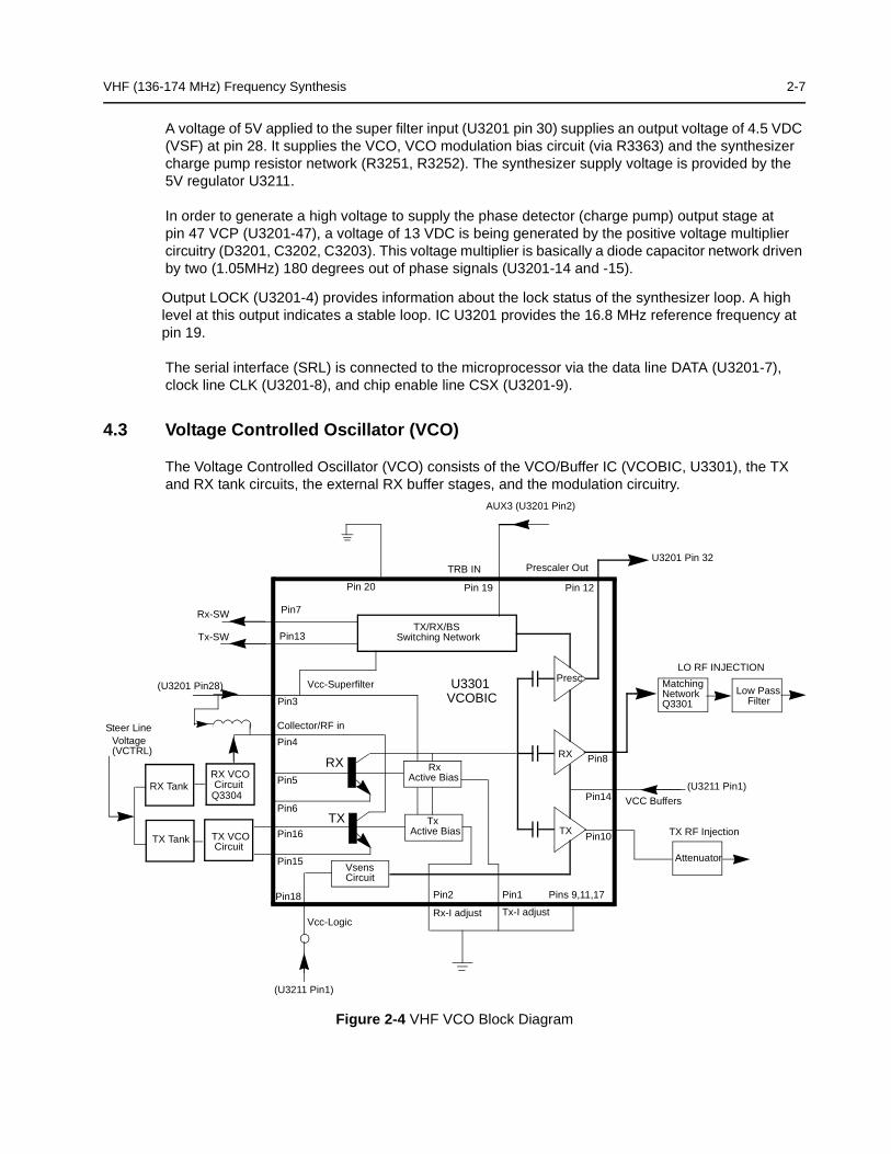
VHF (136-174 MHz) Frequency Synthesis 2-7
A voltage of 5V applied to the super filter input (U3201 pin 30) supplies an output voltage of 4.5 VDC (VSF) at pin 28. It supplies the VCO, VCO modulation bias circuit (via R3363) and the synthesizer charge pump resistor network (R3251, R3252). The synthesizer supply voltage is provided by the 5V regulator U3211.
In order to generate a high voltage to supply the phase detector (charge pump) output stage at pin 47 VCP (U3201-47), a voltage of 13 VDC is being generated by the positive voltage multiplier circuitry (D3201, C3202, C3203). This voltage multiplier is basically a diode capacitor network driven by two (1.05MHz) 180 degrees out of phase signals (U3201-14 and -15).
Output LOCK (U3201-4) provides information about the lock status of the synthesizer loop. A high level at this output indicates a stable loop. IC U3201 provides the 16.8 MHz reference frequency at pin 19.
The serial interface (SRL) is connected to the microprocessor via the data line DATA (U3201-7), clock line CLK (U3201-8), and chip enable line CSX (U3201-9).
4.3 Voltage Controlled Oscillator (VCO)
The Voltage Controlled Oscillator (VCO) consists of the VCO/Buffer IC (VCOBIC, U3301), the TX and RX tank circuits, the external RX buffer stages, and the modulation circuitry.
Figure 2-4 VHF VCO Block Diagram
Presc
RX
TX
MatchingNetwork Low Pass
Filter
Attenuator
Pin8
Pin14
Pin10
(U3211 Pin1)
VCC Buffers
TX RF Injection
U3201 Pin 32
AUX3 (U3201 Pin2)
Prescaler Out
Pin 12Pin 19Pin 20
TX/RX/BSSwitching Network
U3301VCOBIC
RxActive Bias
TxActive Bias
Pin2
Rx-I adjust
Pin1
Tx-I adjust
Pins 9,11,17Pin18
VsensCircuit
Pin15
Pin16
RX VCO Circuit
TX VCO Circuit
RX Tank
TX Tank
Pin7
Vcc-Superfilter
Collector/RF in
Pin4
Pin5
Pin6
RX
TX
(U3201 Pin28)
Rx-SW
Tx-SW
Vcc-Logic
(U3211 Pin1)
Steer Line Voltage (VCTRL)
Pin13
Pin3
TRB IN
LO RF INJECTION
Q3304
Q3301
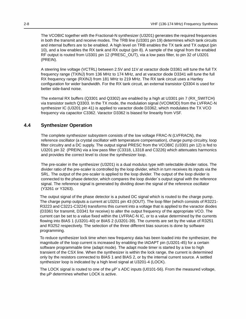
2-8 VHF (136-174 MHz) Frequency Synthesis
The VCOBIC together with the Fractional-N synthesizer (U3201) generates the required frequencies in both the transmit and receive modes. The TRB line (U3301 pin 19) determines which tank circuits and internal buffers are to be enabled. A high level on TRB enables the TX tank and TX output (pin 10), and a low enables the RX tank and RX output (pin 8). A sample of the signal from the enabled RF output is routed from U3301 pin 12 (PRESC_OUT), via a low pass filter, to pin 32 of U3201 (PREIN).
A steering line voltage (VCTRL) between 2.5V and 11V at varactor diode D3361 will tune the full TX frequency range (TXINJ) from 136 MHz to 174 MHz, and at varactor diode D3341 will tune the full RX frequency range (RXINJ) from 181 MHz to 219 MHz. The RX tank circuit uses a Hartley configuration for wider bandwidth. For the RX tank circuit, an external transistor Q3304 is used for better side-band noise.
The external RX buffers (Q3301 and Q3302) are enabled by a high at U3301 pin 7 (RX_SWITCH) via transistor switch Q3303. In the TX mode, the modulation signal (VCOMOD) from the LVFRAC-N synthesizer IC (U3201 pin 41) is applied to varactor diode D3362, which modulates the TX VCO frequency via capacitor C3362. Varactor D3362 is biased for linearity from VSF.
4.4 Synthesizer Operation
The complete synthesizer subsystem consists of the low voltage FRAC-N (LVFRACN), the reference oscillator (a crystal oscillator with temperature compensation), charge pump circuitry, loop filter circuitry and a DC supply. The output signal PRESC from the VCOBIC (U3301 pin 12) is fed to U3201 pin 32 (PREIN) via a low pass filter (C3318, L3318 and C3226) which attenuates harmonics and provides the correct level to close the synthesizer loop.
The pre-scaler in the synthesizer (U3201) is a dual modulus type with selectable divider ratios. The divider ratio of the pre-scaler is controlled by the loop divider, which in turn receives its inputs via the SRL. The output of the pre-scaler is applied to the loop divider. The output of the loop divider is connected to the phase detector, which compares the loop divider´s output signal with the reference signal. The reference signal is generated by dividing down the signal of the reference oscillator (Y3261 or Y3263).
The output signal of the phase detector is a pulsed DC signal which is routed to the charge pump. The charge pump outputs a current at U3201 pin 43 (IOUT). The loop filter (which consists of R3221-R3223 and C3221-C3224) transforms this current into a voltage that is applied to the varactor diodes (D3361 for transmit, D3341 for receive) to alter the output frequency of the appropriate VCO. The current can be set to a value fixed within the LVFRAC-N IC, or to a value determined by the currents flowing into BIAS 1 (U3201-40) or BIAS 2 (U3201-39). The currents are set by the value of R3251 and R3252 respectively. The selection of the three different bias sources is done by software programming.
To reduce synthesizer lock time when new frequency data has been loaded into the synthesizer, the magnitude of the loop current is increased by enabling the IADAPT pin (U3201-45) for a certain software programmable time (adapt mode). The adapt mode timer is started by a low to high transient of the CSX line. When the synthesizer is within the lock range, the current is determined only by the resistors connected to BIAS 1 and BIAS 2, or by the internal current source. A settled synthesizer loop is indicated by a high level signal at U3201-4 (LOCK).
The LOCK signal is routed to one of the µP´s ADC inputs (U0101-56). From the measured voltage, the µP determines whether LOCK is active.

VHF (136-174 MHz) Frequency Synthesis 2-9
In order to modulate the PLL, the two spot modulation method is utilized. Via U3201 pin 10 (MODIN), the audio signal is applied to both the A/D converter (low frequency path) as well as the balance attenuator (high frequency path). The A/D converter changes the low frequency analog modulating signal into a digital code that is applied to the loop divider, thereby causing the carrier to deviate. The balance attenuator is used to adjust the VCO’s deviation sensitivity to high frequency modulating signals. The output of the balance attenuator is present at the MODOUT port (U3201-41) and connected to the VCO modulation diode D3362 via R3364.

2-10 VHF (136-174 MHz) Frequency Synthesis
THIS PAGE INTENTIONALLY LEFT BLANK

3-1
Section 3
TROUBLESHOOTING CHARTS
1.0 Troubleshooting Flow Chart for Receiver (Sheet 1 of 2)
Bad SINADBad 20dB Quieting
No Recovered Audio
START
Audio at pin 8 of U3101 ?
Check Controller(in the case of no audio)
OR ELSE go to “B”
Yes
No
Spray or inject 44.85MHz into XTAL Filter FL3101
Audio heard ?BYes
No
Check 2nd LO (44.395MHz) at C3135
LO present ?BYes
Check voltages on U3101
Biasing OK ?
No
No
A
Yes
Check Q3102 bias for faults
Replace Q3102
Go to B
Yes
No
Check circuitry around U3101.
Replace U3101 if defect
Check circuitry around Y3101. Replace Y3101 if defect
Voltages OK?
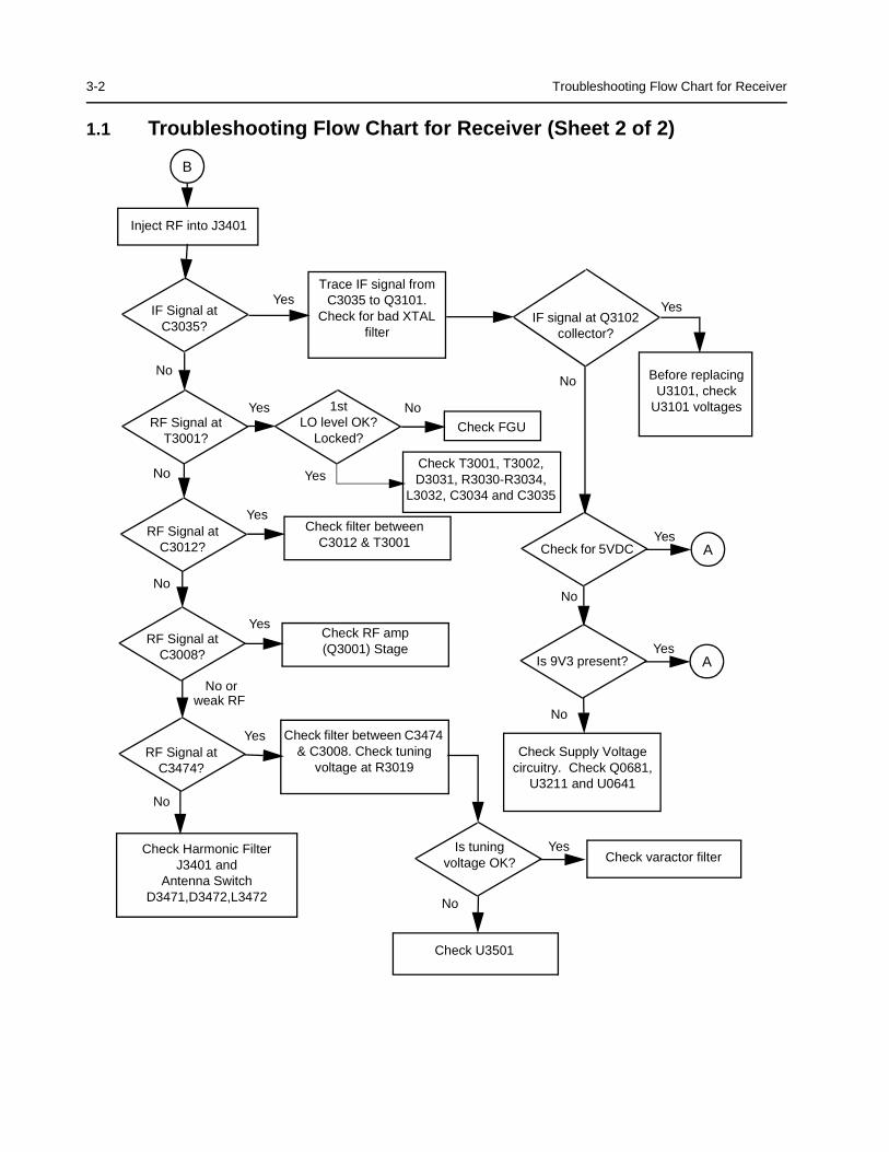
3-2 Troubleshooting Flow Chart for Receiver
1.1 Troubleshooting Flow Chart for Receiver (Sheet 2 of 2)
IF Signal at C3035?
No
RF Signal at T3001?
RF Signal at C3012?
No
RF Signal at C3008?
No
RF Signal at C3474?
No or
Check Harmonic Filter J3401 and
Antenna Switch D3471,D3472,L3472
Check filter between C3474 & C3008. Check tuning
voltage at R3019
Inject RF into J3401
Is tuning voltage OK?
No
Yes
Check RF amp (Q3001) Stage
Check filter between C3012 & T3001
Yes
Check T3001, T3002, D3031, R3030-R3034,
L3032, C3034 and C3035
Yes
1st LO level OK?
Locked?
Yes
Check FGU
Yes
Trace IF signal from C3035 to Q3101.
Check for bad XTAL filter
No
YesIF signal at Q3102
collector?
Before replacing U3101, check
U3101 voltages
Yes
Check for 5VDC
Is 9V3 present?
Check Supply Voltage circuitry. Check Q0681,
U3211 and U0641
No
No
No
Check U3501
Check varactor filter
No
Yes
Yes
Yes
A
A
B
weak RF

Troubleshooting Flow Chart for 25W Transmitter 3-3
2.0 Troubleshooting Flow Chart for 25W Transmitter (Sheet 1 of 3)
Current increase
when keyed?
NO
YES
START
Check if Pressure Pad closes S3440
Check Components between Q3441 and RF Output,
Antenna Switch D3471,D3472,Q3472
VR3471,Q3471
>500mA & <4A>4A
<500mA
Check PA StagesControl Volt-
age at TP3402
>1V
Short TP3403 to Ground
NO
YES
Voltage at TP3402 rises?
Check PA Stages NO
YES
PCIC U3501 Pin 14 9.3V
DC?
Check 9.3 V Regulator U0641
NO
YES
PCIC U3501 Pin 16 >4V
DC
Replace PCIC U3501
NO
YES
TP3404 9.1V DC
If U3201 Pin 2 is high, replace PCIC
U3501,otherwise check controller and
FGU
YES
NO
TP3403 >0.5V DC?
Replace PCIC U3501
Check Forward Power Sense Circuit (D3451)
Check Forward Power Sense Circuit (D3451)
NO
YES
PCIC U3501 Pin 5 > 1V
DC?
Check Power Setting, Tuning & Components between PCIC Pin 5 and ASFIC (U0221)
Pin 4 before replacing ASFIC
No or too low Power when keyed
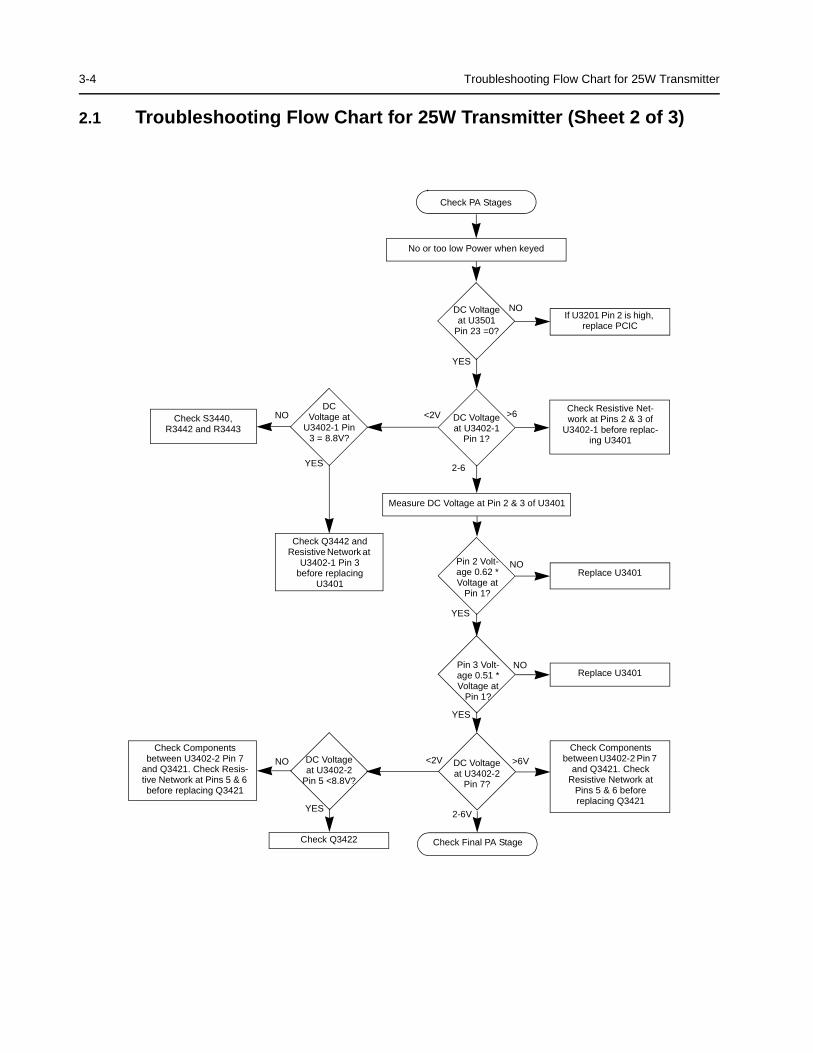
3-4 Troubleshooting Flow Chart for 25W Transmitter
2.1 Troubleshooting Flow Chart for 25W Transmitter (Sheet 2 of 3)
Check PA Stages
No or too low Power when keyed
Measure DC Voltage at Pin 2 & 3 of U3401
>6
YES
DC Voltage at U3501
Pin 23 =0?
2-6
DC Voltage at U3402-1
Pin 1?
YES
Pin 2 Volt-age 0.62 * Voltage at
Pin 1?
If U3201 Pin 2 is high, replace PCIC
NOReplace U3401
YES
NODC
Voltage at U3402-1 Pin
3 = 8.8V?
Check S3440, R3442 and R3443
YES
Pin 3 Volt-age 0.51 * Voltage at
Pin 1?
NOReplace U3401
<2V DC Voltage at U3402-2
Pin 7?
>6V
Check Components between U3402-2 Pin 7
and Q3421. Check Resistive Network at
Pins 5 & 6 before replacing Q3421
YES
DC Voltage at U3402-2
Pin 5 <8.8V?
Check Components between U3402-2 Pin 7
and Q3421. Check Resis-tive Network at Pins 5 & 6 before replacing Q3421
NO
Check Q3422
NO
Check Final PA Stage
2-6V
<2VCheck Resistive Net-work at Pins 2 & 3 of
U3402-1 before replac-ing U3401
Check Q3442 and Resistive Network at
U3402-1 Pin 3 before replacing
U3401

Troubleshooting Flow Chart for 25W Transmitter 3-5
2.2 Troubleshooting Flow Chart for 25W Transmitter (Sheet 3 of 3)
Check Final PA Stage
NO
0V
1-4V
Bias 2 DC Voltage at TP3406?
YES
RF Voltage at TP3401 >100mV?
YES
RF Voltage U3401 Pin 6
>3V?
Supply
Replace Q3441
Check FGU (U3301)
NO Check Components between TP3401 &
C3417
NO
YES ASFIC U0221 Pin 6 1-4V DC?
Check Bias Tuning before replacing ASFIC
U0221
Check Components between ASFIC and
Q3441 before replacing Q3441
YES
RF Voltage Q3421 Gate
>1V?
NO Check Components between C3417 &
Q3421
YES
RF Voltage Q3441 Gate
>4V?
NO Check Components between Q3421 &
Q3441
Check Components between Q3441 & Antenna Connector
Voltage
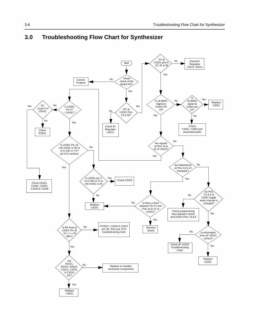
3-6 Troubleshooting Flow Chart for Synthesizer
3.0 Troubleshooting Flow Chart for Synthesizer
+5V at U3201 Pins
13 & 30?
5V at pin 6 of
D3201
Is informationfrom µP U0101
correct?
Is U3201 Pin 47
= 13VDC ?
Is U3301 Pin 19<40 mVDC in RX &>4.5 VDC in TX? (at VCO section)
Start
Visual check of the Board OK?
CorrectProblem
Check 5VRegulator
U3211
Is 16.8MHzSignal at
U3201 Pin 19?
CheckY3261, Y3263 and associated parts
Are signalsat Pins 14 &
15 of U3201?
Check R3201
Check C3319Is U3201 pin 2
>4.5 VDC in Tx & <40 mVDC in Rx
Replace U3201
RemoveShorts
Is there a shortbetween Pin 47 and
Pins 14 & 15 ofU3201?
Replace or resoldernecessary components
Is RF level atU3201 Pin 32 -12 < x <-25
dBm?
Are R3221,
R3222, R3223, C3221, C3222,
& C3224 OK?
Replace U3201
If R3227, C3226 & C3227are OK, then see VCOtroubleshooting chart
Are Waveformsat Pins 14 & 15
triangular?
Do Pins 7,8 & 9 of
U3201 togglewhen channel is
changed?
Check programminglines between U0101
and U3201 Pins 7,8 & 9
Replace U3201
Check µP U0101Troubleshooting
Chart
No
Yes
No
Yes
No
Yes
No
No
No
Yes
Yes
No
Yes
Yes
No
Yes
Yes
Yes
No
No
No
No
Yes
No
Yes
Yes
Check D3201, C3202, C3203, C3205 & C3206
5V at U3201 pins 5, 20, 34 & 36
Check 5V Regulator
U3211, R3211
Is 16.8MHz signal at
U3201 pin 23?
Replace U3201
Yes
No
No
Yes
No
Yes
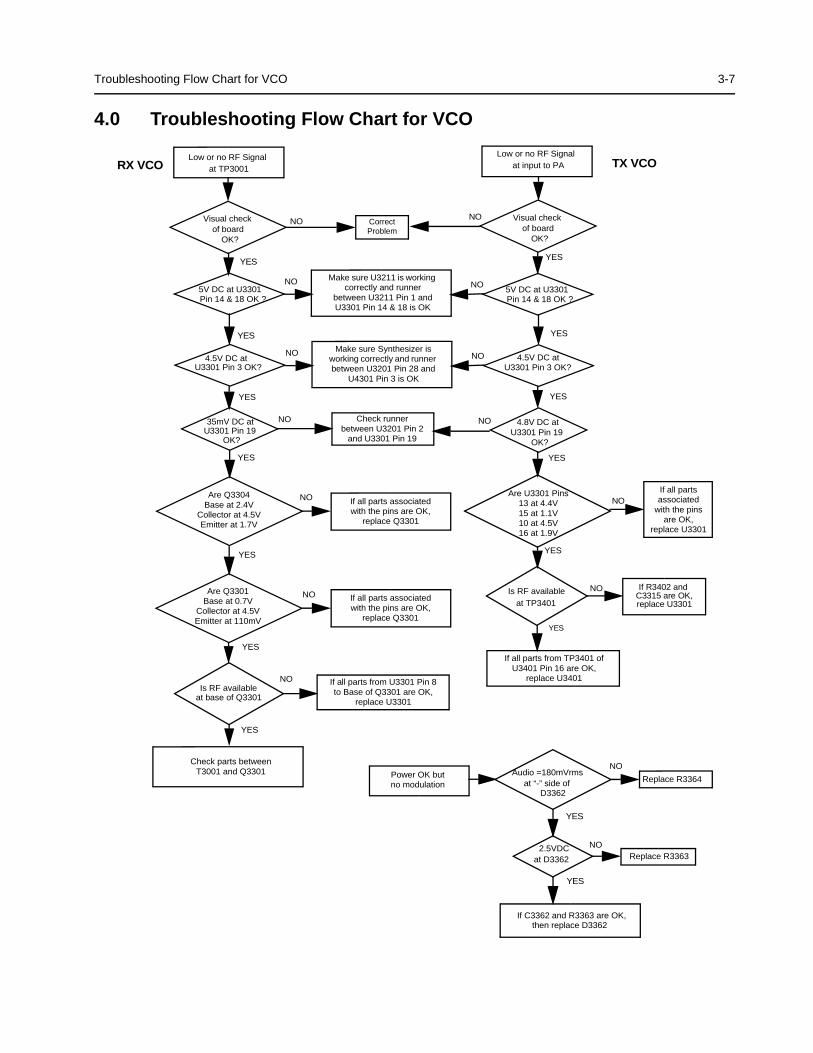
Troubleshooting Flow Chart for VCO 3-7
4.0 Troubleshooting Flow Chart for VCO
Are Q3301Base at 0.7V
Collector at 4.5V Emitter at 110mV
Are Q3304Base at 2.4V
Collector at 4.5V Emitter at 1.7V
Are U3301 Pins13 at 4.4V15 at 1.1V10 at 4.5V16 at 1.9V
Low or no RF Signalat TP3001
Visual checkof board
OK?
35mV DC atU3301 Pin 19
NO
YES
at base of Q3301
NO
NO
NO
NO
NO
YES
YES
YES
YES
YES
Low or no RF Signalat input to PA
5V DC at U3301Pin 14 & 18 OK ?
4.8V DC atU3301 Pin 19
Is RF available at TP3401
YES
YES
YES
YES
YES
NO
NO
NO
NO
NO
Audio =180mVrmsat “-” side of
D3362
2.5VDCat D3362
If C3362 and R3363 are OK, then replace D3362
Replace R3363
Replace R3364
NO
NO
YES
YES
If R3402 and C3315 are OK,replace U3301
TX VCORX VCO
CorrectProblem
Visual checkof board
OK?
Make sure U3211 is working correctly and runner
between U3211 Pin 1 and U3301 Pin 14 & 18 is OK
Check runner between U3201 Pin 2
and U3301 Pin 19
Is RF available If all parts from U3301 Pin 8to Base of Q3301 are OK,
replace U3301
If all parts associated with the pins are OK,
replace Q3301
Check parts between T3001 and Q3301 Power OK but
no modulation
If all parts from TP3401 of U3401 Pin 16 are OK,
replace U3401
If all parts associated
with the pins are OK,
replace U3301
4.5V DC atU3301 Pin 3 OK?
YES
NO 4.5V DC atU3301 Pin 3 OK?
YES
NOMake sure Synthesizer is
working correctly and runner between U3201 Pin 28 and
U4301 Pin 3 is OK
5V DC at U3301Pin 14 & 18 OK ?
OK? OK?
If all parts associated with the pins are OK,
replace Q3301

3-8 Troubleshooting Flow Chart for VCO
THIS PAGE INTENTIONALLY LEFT BLANK
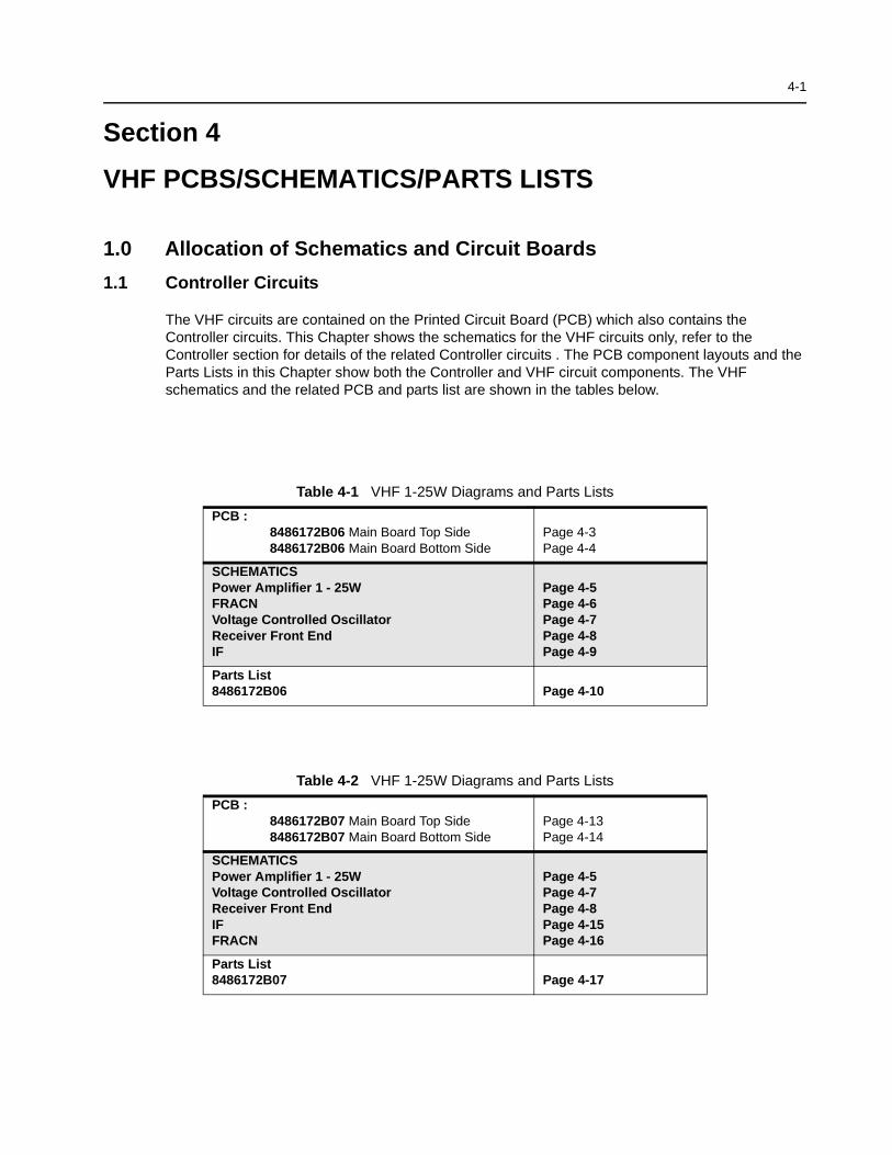
4-1
Section 4
VHF PCBS/SCHEMATICS/PARTS LISTS
1.0 Allocation of Schematics and Circuit Boards
1.1 Controller Circuits
The VHF circuits are contained on the Printed Circuit Board (PCB) which also contains the Controller circuits. This Chapter shows the schematics for the VHF circuits only, refer to the Controller section for details of the related Controller circuits . The PCB component layouts and the Parts Lists in this Chapter show both the Controller and VHF circuit components. The VHF schematics and the related PCB and parts list are shown in the tables below.
Table 4-1 VHF 1-25W Diagrams and Parts Lists
PCB :8486172B06 Main Board Top Side8486172B06 Main Board Bottom Side
Page 4-3Page 4-4
SCHEMATICSPower Amplifier 1 - 25WFRACNVoltage Controlled OscillatorReceiver Front EndIF
Page 4-5Page 4-6Page 4-7Page 4-8Page 4-9
Parts List8486172B06 Page 4-10
Table 4-2 VHF 1-25W Diagrams and Parts Lists
PCB :8486172B07 Main Board Top Side8486172B07 Main Board Bottom Side
Page 4-13Page 4-14
SCHEMATICSPower Amplifier 1 - 25WVoltage Controlled OscillatorReceiver Front EndIFFRACN
Page 4-5Page 4-7Page 4-8Page 4-15Page 4-16
Parts List8486172B07 Page 4-17

4-2 Allocation of Schematics and Circuit Boards
THIS PAGE INTENTIONALLY LEFT BLANK
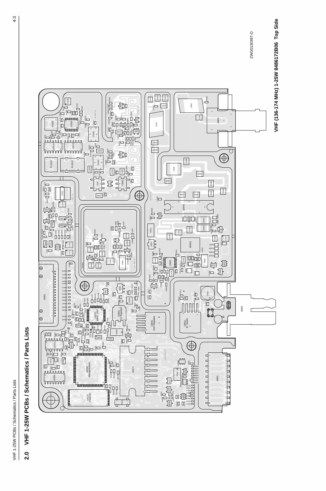
VH
F 1
-25W
PC
Bs
/ Sch
emat
ics
/ Par
ts L
ists
4-3
2.0
VH
F 1
-25W
PC
Bs
/ Sch
emat
ics
/ Par
ts L
ists
VCO-REV-T3
PA-REV-T1
FE-REV-T3
IF-REV-T4
FRAC-T4
CNTL-REV-T6
C01
01C
0102
C01
04
C01
06
C01
07
C01
31
C01
32
C02
11
C02
12
C02
21
C02
22
C02
23
C02
24
C02
25
C02
26
C02
27
C0228
C0231
C02
32
C 0
233
C02
34C02
35
C02
36
C0237
C02
41 C02
42
C02
43 C02
44
C02
45
C02
46
C02
51
C02
52
C02
53
C02
61
C02
62C02
67
C04
21
C04
41
C 0442
C 0443
C 0445
C 0446
C 0447
C 0448
C 0449
C 0470
C 0471
C 0472
C 0473C 0474
C 0476
C 0477
C 0478
C04
82
C04
83
C04
84
C04
86C04
87
C04
88
C04
90
C04
93C
0494
C04
95
C04
96
C05
01
C0502C0503C0504C0505C0506C0508
C0509
C0510
C0511
C0512
C 0513
C0514
C0515
C 0516
C0517
C0518
C05
42
C06
01
C06
03
C06
12
C06
51
C06
52
C06
54
C06
55
C06
81
C30
02
C30
04C
3005
C30
06C
3007
C30
08
C30
09
C30
10
C30
11C
3012
C30
13
C30
14
C30
15
C30
16
C30
17
C30
18
C30
19
C30
20
C30
21
C30
27C
3028
C30
32
C30
34
C31
00
C31
01C
3102
C31
03
C31
14
C31
15
C31
31
C31
32
C31
33
C31
34
C31
35
C31
36
C31
37
C31
39
C31
40 C31
41
C31
42
C31
43
C31
45 C31
48
C32
10
C32
11
C32
13
C32
14C
3215
C32
21C
3222
C32
23C
3224
C32
26
C32
27C
3229
C32
31
C32
32
C3233
C32
34
C32
40
C32
42
C32
43
C32
44
C32
45
C32
46
C32
52
C3253
C32
54
C32
55
C33
24
C33
36
C33
37
C33
41
C33
42
C33
44
C33
45
C33
46C
3347
C33
57C
3361
C33
62C
3363
C33
64
C33
65
C34
00C34
01C
3403
C34
04C
3410
C34
11C
3412
C34
17C
3418
C34
19
C34
20
C34
22
C34
23
C34
24
C34
25
C34
26
C34
28
C34
31 C34
32
C34
33
C34
34C
3435
C34
41C
3442
C34
43
C3444
C3445
C34
46
C3447
C3448C3449
C34
53
C34
72
C34
73
C34
74
C34
97
C35
07C
3508
C35
09
D02
01
D0651
D30
01
D30
03
D30
04
D30
31
D3221
D3341
D3361
D33
62
D34
01
D3471
D3472
23 4
56
FL3
101
23 4
56
FL3
102
432
FL3
112
FL3
114
181
J045
1
201110
J050
1
J060
1
23
J340
1
L048
1
L048
2
L3002
L303
1
L303
2
L3034
L310
0
L3101
L320
1
L323
2
L333
3
L334
1
L334
3L3
344
L334
6
L336
1
L336
2
L336
3
L336
4
L340
1
L340
3
L341
1
L341
2
L341
3
L341
4
L342
2
L344
3
L347
1
L347
2
L349
3M
3421
Q01
10
Q01
77Q
0181
Q01
85
Q06
81
Q3001
Q3021
Q3221
Q33
04
Q34
11
Q34
22
2
3 4
5 6
7 8
Q34
41
Q3442
Q3471
Q34
72
R01
01
R01
02
R01
04
R01
05
R01
06
R01
08
R01
10
R01
14
R01
15
R01
16
R01
31
R01
32
R01
70
R01
81
R01
82
R01
85
R01
86
R02
11
R02
12
R02
20
R02
21
R02
22
R02
23
R02
24
R02
25
R02
26
R02
27
R02
28R
0229
R02
41
R02
42
R02
51
R02
52
R02
53
R02
61R
0262
R02
67
R02
68 R02
69
R05
10
R05
33R
0535
R05
38
R05
39
R06
11R
0612
R06
51
R06
52
R06
81
R06
82
R30
01R
3002
R30
03
R30
04
R30
09
R30
13
R30
14
R30
15
R30
16
R30
24
R30
25R
3026
R30
27
R30
28
R30
31
R31
01
R31
06R
3111
R31
17
R31
30 R31
32
R31
35R
3142
R31
44
R31
45
R32
11
R32
21
R32
22
R32
23
R32
24
R32
25
R32
27
R32
42
R32
51 R32
52
R33
35
R33
36
R33
41
R33
42
R33
61
R33
62
R33
63R
3364
R34
00
R34
01R34
02
R34
03
R34
04
R34
05
R34
06
R34
14
R34
15
R34
16
R3424
R3425
R3426
R3427
R34
31R
3432
R34
33
R 3
434
R34
35
R34
71
R34
73
R34
91
R35
05
R35
06
R35
07
R35
08
R35
09
SH
3301
3 461
2
T30
01
346 1
2
T30
02
TP
3401
1 765126
321716
1
871
14
U02
11
137 25
13
161 8
9
U02
51
9
U02
71
1
6
5
1
6
5
3
2
1
11
120
10
U31
01
87 1
14
U31
11
87 1
14U31
15
U32
11
116
89
U34
01
U35
02
VR
0501
VR
0503
VR
0505
VR
0510
234
Y01
31
2
Y31
02
1
1
100
1
1
1
1
U01
01M
icro
proc
esso
rU
0121
Fla
shro
m
U02
21A
SF
IC C
MP
U06
11B
+ S
witc
h
U06
419,
6V R
egul
ator
U06
515V
Reg
ulat
or
1
45
ZW
G01
3039
7-O
ZW
G01
3039
7-O
VH
F (
136-
174
MH
z) 1
-25W
848
6172
B06
To
p S
ide
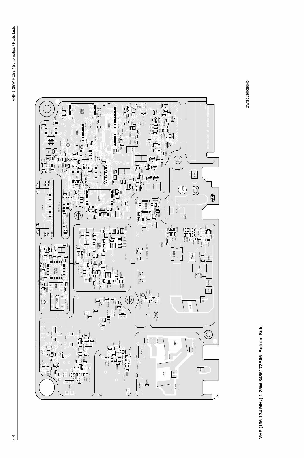
4-4
VH
F 1
-25W
PC
Bs
/ Sch
emat
ics
/ Par
ts L
ists
C01
03
C01
05
C01
11
C01
12
C01
21
C01
22C
0123
C01
41
C01
51
C02
01
C02
02
C02
03
C02
04
C02
05
C02
54
C02
55
C02
65
C02
66
C02
71
C02
72
C02
73
C02
74C
0275
C02
76C
0277
C0301
C03
02
C03
03
C03
04
C03
05
C03
24C
0325
C03
31
C0341
C03
42
C03
43
C03
44
C03
51
C03
52
C03
53
C03
54
C04
22
C04
23
C 0426
C 0427
C 0428
C 0429
C04
30C
0431
C04
85
C04
91
C04
92
C04
97
C04
99
C05
41
C05
54
C05
58
C05
59
C05
60C
0575
C05
76C
0591
C05
92C
0593
C06
11
C06
21
C06
22
C06
41
C06
44
C06
45
C06
61
C06
62C
0663
C06
71
C30
00
C30
01
C30
03C
3022
C30
23C30
24
C30
25
C30
26
C30
29
C30
30
C30
31
C30
33
C30
35
C30
36
C31
04
C31
10C
3111
C31
12
C31
13
C31
16
C31
21
C31
22C
3123
C31
44
C31
46C
3147
C31
51
C31
52
C32
02
C32
03
C32
05
C32
06
C32
07
C32
08
C32
09
C32
25
C32
28
C32
35
C32
41
C32
51
C32
61C
3262
C32
63
C33
01
C33
02
C33
03
C33
04
C33
05
C33
06C
3311
C33
12
C3313
C33
14
C33
15
C33
16
C33
17
C33
18
C33
19
C33
31
C33
32
C33
33C
3334
C33
35
C33
48
C33
51 C3352
C33
55
C33
56
C34
02
C34
05C
3406
C34
13C34
14C
3415
C34
16
C34
21
C34
27
C34
36C
3437
C34
38
C34
39
C34
40
C34
50
C34
51
C34
52
C34
71
C34
75C
3491
C34
92
C34
93
C34
94
C34
95C
3496
C34
98
C34
99
C 3
501
C35
02
C35
03
C35
04
C3505
C35
06
C35
10
D0101
D01
51
D01
79
D0301
D0621
D0660D0661
D30
00
D3011
D31
01
D32
01D
3261
D34
51
E02
71E
0272
E06
31
43 2
FL3
111
FL3
113
43 2
FL3
115
12
J040
1
140
J055
1
118
J055
2
L3025
L3111
L311
2
L323
1
L330
1
L330
2
L3311
L331
7
L331
8
L333
1
L333
2
L334
5L335
1
L340
2
L342
1
L343
6
L343
7
L349
1
L349
2
Q0151
Q01
71
Q01
73Q
0183
Q02
71Q
0641
Q0661 Q06
62Q
0663
Q3002
Q31
01Q
3102
Q3141
Q31
51
Q31
52
Q33
01
Q33
02 43
Q33
03
12
3
Q34
21
R01
07
R01
11R
0112
R01
13
R01
17
R01
21
R01
51R
0152
R01
71
R01
72
R01
73
R01
74
R0175
R0176
R0177
R0178
R01
79
R01
83
R01
84
R02
01
R02
02
R02
03
R02
04
R02
05
R02
06
R02
07
R02
08
R02
65
R02
66
R02
73
R02
74
R02
75
R02
76
R03
23
R03
24
R03
31
R03
32
R03
33
R03
35
R03
41
R03
42
R03
43
R03
44
R03
45
R03
46
R03
47
R04
01
R04
07
R04
08
R04
09R
0410
R04
12 R04
41
R04
67R
0468
R04
81
R04
82
R05
11
R05
12R
0525
R05
29
R05
30
R05
31R
0537
R05
41
R05
42
R05
91
R05
92
R06
21
R06
41
R06
42R
0643
R06
61
R06
62R
0671
R06
72
R30
00
R30
06R30
10
R30
11
R30
12
R30
18
R30
19
R30
21
R30
23R
3030R30
32
R30
33
R30
34R30
35
R30
36
R31
02
R31
04R
3105
R31
07R
3108
R31
12
R31
13
R31
14
R31
15
R31
16R
3118
R31
33
R31
34
R31
41
R31
46R
3147
R31
51
R31
52
R31
53
R31
54
R32
01
R32
03
R32
04
R32
06
R32
26R32
28
R32
41
R32
61R
3262
R32
63
R33
01
R33
02
R33
03
R33
04
R33
05
R33
06R
3307
R33
08R33
11
R33
12
R33
13
R3314
R3315
R33
16
R33
17
R33
18
R3319
R33
21
R33
23
R33
31
R33
43
R33
51 R3352
R3353
R3354
R33
55
R33
56 R34
11
R34
12
R34
13
R34
17
R34
18
R34
21 R34
22
R34
23R34
28
R34
29
R34
40
R34
41
R34
42R
3443
R34
44
R34
45
R34
46
R34
50
R34
52
R34
54
R34
55
R34
57R
3474
R34
75
R35
01
R35
02R
3504
S34
40
TP
0101
TP
0102
TP
0103
TP
0104
TP
0151
TP
0221
TP
0222
TP
0481
TP
0492
TP
0497
TP
0530
TP
0661
TP
3001TP
3201
TP
3202
TP
3402
TP
3403
TP
3404
TP
3405
TP
3406
14 5
8
U01
11
22 2187
1
1618 9
U01
41
2815 14
1
U03
01
U03
31
1 458
U03
41
U03
42
458 U
0351
145
8
U06
52
U0653
13725
13
11
120
10
14 5
8
U34
02
1
17
9
25
U35
01
VR0151
VR
0504
VR
0509
VR
0537
VR
0541
VR
0601
VR0621
VR
0671
VR
3471
432
Y31
01
6
43 1
Y32
61
2 34
Y32
63
1
1
1
1
1
48
U01
22R
AM
U32
01F
RA
CN
U33
01V
CO
IC
15
8486172B06_T1
VCO-REV-T3
PA-REV-T1
C99
FE-REV-T3
IF-REV-T4
FRAC-T4
CNTL-REV-T6
WA
RIS
VH
F R
F 1
-25W
Bot
Sid
e84
8617
2B06
-T1
BO
T S
IDE
CH
EC
KO
NE
(
)
ILLU
STR
ATO
RD
AT
EE
NG
INE
ER
DA
TE
PR
OG
RA
MD
ISK
DW
G. N
O.
Illus
trat
orR
K15
. Oct
200
0
ZW
G01
3039
8
ZW
G01
3039
8-O
ZW
G01
3003
98-O
VH
F (
136-
174
MH
z) 1
-25W
848
6172
B06
Bo
tto
m S
ide

VH
F 1
-25W
PC
Bs
/ Sch
emat
ics
/ Par
ts L
ists
4-5
RX
IN_V
HF
_PA
_1
NU
NU
17nH
L343
7
NU
NU
0
R34
40
NU
C34
27
56pF
NU
39K
10K
NU
6.8K
R34
11
NU
R35
0610
K
NU
C35
08
C3443120pF
C3444
6.2p
F
C35
09
1uF
C34
23
0.8x
25
wid
th 2
.032
1.54
2x4
2.21
6xJ3
401
7.5
R34
27
R34
26
2.7
2.7
2.7
R34
28
R34
25
C35
0622
00pF
2.4K
120
R34
14
2.4K
R35
0239
K
MO
SB
IAS
_2_V
HF
_PA
_1 R34
45
L341
2
C34
32
15nH
C34
04
33pF
2200
pF
C34
10.0
22uF
PA
SU
PV
LTG
_VH
F_P
A_1
C34
7327
0pF
R34
15 100
330p
FC
3426
Q34
21
R34
17
39K
R34
43
10K
R34
91
R34
41
C34
1633
0pF
100p
F
330p
F
C34
00
C35
07
R34
00
470
RE
SE
T_V
HF
_PA
_1
51R34
32
.033
uFC
3437
L343
657
R01
C35
04.0
1uF
470p
FC
3503
470p
FC
3419
TP
3402
TP
3403
57R
01
L340
2
C34
0647
0pF
R34
0130
0
C34
28F
EC
NT
L_2
C34
35
2200
pF
C3449
330p
F
120pF
C35
0222
00pF
25nH
L344
3
10K
R35
04
470
R34
71Q
3472
C34
34.0
1uF
MO
SB
IAS
_247
K
R34
04
47pF
RE
SE
T
C34
31
C34
21.0
33uF
CLK
51R
3431
R34
352.
7
INT
_SW
B
C34
25.0
22uF
U35
023GN
D
PO
S1
2V
OU
T
C34
92
68pF
LM50
C34
936.
8pF
DA
TA
_VH
F_P
A_1
2.2K
20pF
C34
45
R34
42
C34
2233
0pF
1
R34
444.
7
5.6V
VR
3471 2
3
39K
R34
21
DA
TA
C35
051u
F
33pF
C34
03
6.8p
FC
3475
TE
MP
SE
NS
ET
EM
PS
EN
SE
_CN
TLR
_1
1K
R35
0720
K
PA
_PW
R_S
ET
R35
09
C34
5110
00pF
.022
uFC
3471
C34
95
C34
97
CS
X
3.3p
F
C34
74
220p
F
65
784
TX
INJ_
VH
F_P
A_1
18pF
LM29
04U
3402
-2
470p
F
R34
13
3.3K
9V3
C35
0122
00pF
FE
CN
TL_
2_V
HF
_PA
_1IN
T_S
WB
_VH
F_P
A_1
D34
01
CS
X_V
HF
_PA
_1
D34
72
33pF
C3446100pF
C34
18
D34
51
51nH
L349
3
R34
74
51
L341
168
nH
R34
7351
C34
9115
pF
.022
uFC
3411
D34
71
R34
0330
0
470p
FC
3405
L347
1
1.2u
H
100K
R34
06
51nH
R35
0810
0K
L349
1
11.0
3nH
5.6K
R34
12
L341
3
R35
05
300K
270p
F
120pFC3448
C34
72
2.7
R34
24
47pF
C34
17
C34
3947
0pF
0
R34
46
150pF
C34
96
C3442
R34
55
36pF
C35
10
100K
CN
TLV
LTG
_VH
F_P
A_1
470p
F
PA
_PW
R_S
ET
_VH
F_P
A_1
470p
FC
3453
10uF
C34
36
R34
2922
0
R34
332.
7
C34
3356
pF
R35
01
L349
251
nH
6.8K
22K
R34
18
231
84
C34
40
1000
pF
RX
IN
U34
02-1
LM29
04
13pF
C34
94
20 VAR1
18 VAR2
24 VAR3
VG
15
6VL19 VLIM
TX
INJ
21 RS
31R
SE
T
23 RX 2T1
30T
EM
P
14V
10
16V
45
17 V5EXT
9F
168
8GND1
25G
ND
2
4INT22 NA
11Q
10Q
X
1RFIN
29C
EX
3CI
5CJ
7CL
26C
LK
12C
QC
QX
1328
DA
TA
H99
S-4
U35
01
32A
NO
27B
PO
S
FE
CN
TL_
1_V
HF
_PA
_1
Q34
42
R34
02
16pF
C34
47
15
39K
R34
23
Q34
11
TP
3406
CLK
_VH
F_P
A_1
470p
F
TP
3401
L342
213
.85n
H
470p
F
470p
FC
3424
30K
C34
38
R34
52R
3454
12K
R34
0510
0
330p
F
C34
01R
FIN
16R
FO
UT
16
RF
OU
T2
7
VC
NT
RL
1
VD
114
2V
G1
VG
23
GND1 4
GND2 5
GND3 12GND4 13
NC
18
NC
29
NC
310
NC
415
09Z
67
U34
01
G2
11
C34
9813
pF
CN
TLV
LTG
16pF
C34
99
470p
FC
3450
470
R34
50
TP
3405
PA
SU
PV
LTG
100
L340
3
R34
16
Q34
22
68nH
330p
F
9V3_
VH
F_P
A_1
C34
12
SW
ITC
HS
34407.66
nH
L341
4
C34
13.0
22uF
C3441150pF
R34
342.
7
10K
R34
75
R34
57
R34
22
120
2.2K
51nH
L347
2
Q34
71
57R
01
L342
1
330p
FC
3414
12pF
C34
52
K9V
1K
9V1_
VH
F_P
A_1
D
G
GN
D1
GN
D2
S1S2S3S4
Q34
41
.022
uFC
3415
TP
3404
100p
F
C34
20
FE
CN
TL_
1
C34
02.0
22uF
NC
PA
_SW
B
A+L3
401
4.22
nH
9V3F
LT
NC
9V3F
LT
U_D
RIV
ER
9V3F
LT
PA
_SW
B
U_D
RIV
ER
9V3F
LT
9V3F
LT
A+
U_P
RE
DR
IVE
R
NC
PA
_SW
B
A+
NC
9V3F
LT
U_P
RE
DR
IVE
R
9V3F
LT9V
3FLT
MO
SB
IAS
_1
NC
NC
NC
NC
NC
NC
NC
NC
2
NU
ZW
G01
3039
2-A
VH
F (
136-
174
MH
z) P
ow
er A
mp
lifie
r 1-
25W

4-6
VH
F 1
-25W
PC
Bs
/ Sch
emat
ics
/ Par
ts L
ists
SO
UR
CE
)
3.63
VD
C
Tem
p.C
omp.
Xta
l
Ref
.Osz
.
R32
03
A1
5A
2
4A
3
K1
1K
22
K3
3
47
D32
01
6
47K
NU
TR
BL3
232
2.2u
HN
U
R32
28
C32
31
C32
25
.01u
F
L320
139
0nH
0.1u
F
C32
02.0
1uF
100
R32
23
C32
29
D32
21
0.1u
F
.047
uF
CLK
C32
51
C32
07
22pF
NU
47K
VC
OB
IAS
_2
R32
25
C32
268.
2pF
MO
DIN
_VH
F_F
N_1
TP
3201
R32
52
VC
OB
IAS
_1_V
HF
_FN
_1
330K
16_8
MH
z_V
HF
_FN
_1
PR
ES
C_V
HF
_FN
_1
R32
420
100
R32
41
VS
F_V
HF
_FN
_1
DA
TA
VC
OM
OD
_VH
F_F
N_1
CS
X_V
HF
_FN
_1
100p
F
C32
27
22pF NU
CS
X
IN_5
V_R
F_R
EG
_VH
F_F
N_1
C32
40
NU
1G
ND
4G
ND
1
3O
UT
6IN
16.8
MH
z75
Z04
Y32
61
100K
R32
27
0.1u
FC
3254
C32
08
0.1u
F
NU
.01u
FC
3232
47K
R32
26
PR
ES
C
C32
142.
2uF
C32
210.
1uF
1uF
C32
24
C32
630.
1uF
VM
ULT
11514
VM
ULT
212
VM
ULT
311
VM
ULT
4
VRO 13
25
WA
RP
23X
TA
L1X
TA
L224
27S
FB
AS
E26
SF
CA
P
30S
FIN
28S
FO
UT
37T
ES
T1
38T
ES
T2
21V
BP
AS
S
47
VC
P
31N
C3
44PD_GND
PD_VDD 5
PR
EIN
32
33 PRE_GND 34PRE_VDD
35P
VR
EF
18R
EF
SE
L45
IAD
AP
T
16IN
DM
ULT
43IO
UT
LOC
K4
10M
OD
IN41
MO
DO
UT
17N
C1
29N
C2
39B
IAS
2
42C
CO
MP
9C
EX
8C
LK
7D
AT
A
DGND6 36DVDD
19F
RE
FO
UT
46A
DA
PT
SW
22 AGND
48A
UX
1
1A
UX
22
AU
X3
3A
UX
4
20AVDD
40B
IAS
1
VC
OB
IAS
_1
63A
27
U32
01
47
R32
01
VS
F
C32
22
0
R32
11
0.1u
F
L323
1
0.1u
FC
3211
TP
3202
1
2.2u
H
C32
4322
0pF
16_8
MH
z
VD
DA
VD
DA
_VH
F_F
N_1
VC
OB
IAS
_2_V
HF
_FN
_1
0.1u
FC
3209
C32
4622
0pF
NU
C32
0610
uF
5V_V
HF
_FN
_2
33K
R32
06
Q32
21
R32
5118
0K
.01u
F
C32
280.
1uF
C32
35
2.2u
FC
3210
VC
TR
L_V
HF
_FN
_1
R32
04
LOC
K_V
HF
_FN
_1
47
1uF
C32
23
NU
220p
F
R32
62 NU
C32
45
BW
SE
LEC
T
6.2K
C32
15
R32
24
47K
C32
13
2.2u
F
1G
ND
5IN
2N
R
4O
UT
3S
D
2.2u
F
VCC
4
VC
NT
L
1
AD
P33
00U
3211
6E
RR
Y32
63T
TS
05V
16.8
MH
z
GND
2
OU
T 3
MO
DIN
VC
TR
L
C32
55
DA
TA
_VH
F_F
N_1
220p
FC
3242
2.2u
F
5V_V
HF
_FN
_1
.01u
F
R32
2268
0
TR
B_V
HF
_FN
_1
C32
05
C32
6233
0pF
NU
NU
VC
OM
OD
C32
4156
pF
R32
6147
K
2.2u
FC
3233
R32
21
CLK
_VH
F_F
N_1
C32
52
390
1000
pF
.01u
FC
3234
C32
534.
7uF
NU
IN_5
V_R
F_R
EG
5V
D32
61C
3261
NU
LOC
K
C32
44
39pF
BW
SE
LEC
T_V
HF
_FN
_1
220p
F
C32
03
4,7k
.01u
F
NC
5V
5V
R32
63
NC
NC
NC
NC
NC
NC
NC
NC
NC
NC
VD
DA
VD
DA
NC
NC
NC
In c
ase
Y32
61 is
use
d in
stea
d of
Y32
63,
repl
acem
ent o
f the
follo
win
g pa
rts
req
uire
s
new
tem
pera
ture
com
pens
atio
n of
the
freq
uenc
y:
Y32
61, U
3201
, R32
61, R
3262
, C32
62, D
3261
5VD
C
-2 to
+7d
Bm
13.3
0VD
C6.
83V
DC
4.52
VD
C (
R)
+1d
Bm
0VD
C (
R)
4.95
VD
C (
R)
2.90
VD
C3.
42V
DC
2.5V
DC
1.1-
4.1V
DC
0VD
C (
T)
2.62
VD
C (
T)
4.91
VD
C (
T)
11.2
8VD
C
4.97
VD
C
2.5-
11V
DC
5VD
C (
LOC
KE
D)
0VD
C (
UN
LOC
KE
D)
3.63
VD
C
0VD
C5V
DC
HF
(13
6-17
4 M
Hz)
FR
AC
N
ZW
G01
3039
3-A
VH
F 1
-25W
PC
Bs
/ Sch
emat
ics
/ Par
ts L
ists
4-7
4.22VDC (T)
0VD
C (
R)
1.92
VD
C (
T)
4.52
VD
C (
R)
2.62
VD
C (
T)
4.52
VD
C (
R)
0VD
C (
T)
1.42
VD
C (
R)
0VD
C (
T)
4.97
VD
C
4.40
VD
C
1.53
VD
C (
R)
0VD
C (
T)
0.92
VD
C (
R)
0VD
C (
T)
0VD
C (
R)
0-5d
Bm
(T
)
7.44
VD
C (
R)
9.14
VD
C (
R)
0VD
C (
T)
0VD
C (
T)
11-1
4dB
m (
R)
-2 to
7dB
m
0VD
C (
T)
2.18
VD
C (
R)
0VD
C (
T)
1.49
VD
C (
R)
2.56VDC (R)
0VD
C (
R)
2.5-
11V
DC
4.54
VD
C
0VD
C (
T)
4.78VDC (R)
2.66VDC (T)
4.52
VD
C (
T)
WA
RIS
MO
BIL
E V
HF
_VC
O
4.78VDC (R)4.27VDC (T)
4.91
VD
C (
T)
9.21
VD
C
3.83
VD
C (
R)
L333
3
R33
5612
K
VC
OB
IAS
_2_V
HF
_VC
O_1
1uH
D33
61
R33
35 33
9V3_
VH
F_V
CO
_2
220
R33
61
C33
31
VD
DA
_VH
F_V
CO
_1
10KN
U10
pF
35.5
nHR
3321
15K
L334
6
L333
168
nH
R33
36
100n
H
NU
C33
120.
1uF
10T
X_O
UT
13T
X_S
WIT
CH
14V
CC
_BU
FF
ER
S
18V
CC
_LO
GIC
NU
L331
1
2R
X_I
AD
J8
RX
_OU
T
7R
X_S
WIT
CH
3S
UP
ER
_FLT
R
TR
B_I
N1916
TX
_BA
SE
15T
X_E
MIT
TE
R
1T
X_I
AD
J
4C
OLL
_RF
IN
20F
LIP
_IN
11GN
D_B
UF
FE
RS
9GN
D_F
LAG
GN
D_L
OG
IC
17
12P
RE
SC
_OU
T5
RX
_BA
SE
6R
X_E
MIT
TE
R
U33
0150
U54
R33
62
47
NU
330p
F
C33
04
R33
54
150K
RX
INJ
VC
OM
OD
_VH
F_V
CO
_1
C33
6368
pF
L331
733
nH33
pFC
3317
C33
577.
5pF
1uH
L335
1
100
R33
11
10K
R33
1722R
3318
NU
L334
4
1uH
C33
625.
6pF
100n
HL3
332
22
R33
06
0R
3316
NU
18nH
L330
1
C33
441.
8pF
Q33
01
L331
8
100n
H
C33
11.0
22uF
6.8p
F
C33
14
C33
15.0
1uF
C33
03
15pF
20K
R33
51
Q33
04B
FQ
67W
NU
47K
R33
19
3.3p
FC
3316
56nH
L336
1
0R33
08
TR
B_V
HF
_VC
O_1
1uH
L336
4
C33
51
.01u
F12
KR
3352
PR
ES
C
VC
OM
OD
VC
OB
IAS
_1_V
HF
_VC
O_1
R33
23
1K
VC
TR
L
C33
47.0
1uF
C33
370.
1uF
NU
R33
0722
0
D33
41
VC
OB
IAS
_1
RX
INJ_
VH
F_V
CO
_1
100K
R33
53
C33
24.0
1uF
L330
210
0nH
VC
OB
IAS
_2
2.2K
R33
03C
3345
20pF
L336
268
nH
15pF
C33
64
8nH
L334
1
C33
330.
1uF
56nH
L336
3
100
0.1u
FC
3332
NU
R33
12
.022
uFC
3352
C33
05
VD
DA
NU
5.6p
F
TR
B
100
R33
43
C33
34
VS
F_V
HF
_VC
O_1
.022
uF
.01u
F
C33
55
VS
F
C33
423p
F
D33
62
1KR33
13
C33
36.0
1uF
NU
C33
35.0
1uF
R33
41
220
R33
5520
K
NU
R33
63
39K
9V3_
VH
F_V
CO
_19V
3
VC
TR
L_V
HF
_VC
O_1
PR
ES
C_V
HF
_VC
O_175
6.8p
F
R33
01
C33
02
C33
065.
1pF
NU
15pF
C33
01
NU
330p
FC
3313
47
R33
31
3
C33
1910
00pF
UM
C5N
2
4
1
C33
46
Q33
03
C33
41
.01u
F
1000
pF
39
R33
42
NU
Q33
02
TX
INJ_
VH
F_V
CO
_1T
XIN
J
5.6p
FC
3318
220
R33
15
9V3_
VH
F_V
CO
_3
NU
C33
61
C33
56.0
22uF
1000
pF
180n
H
1KR33
04
R33
02
L334
3
220
100
NU
R33
05
C33
6510
00pF
R33
14
R33
64
47K
NU10
C33
48.0
1uF
VS
F
1uH
L334
5
VS
F
VS
F
NC
NC
NC
VH
F (
136-
174
MH
z) V
olt
age
Co
ntr
olle
d O
scill
ato
r
ZW
G01
3039
4-O
4-8
VH
F 1
-25W
PC
Bs
/ Sch
emat
ics
/ Par
ts L
ists
3
120p
F
C30
21
D30
041
2
RX
INJ
FE
CN
TL_
1
SP
_3_1
1000
pFC
3020
100p
FC
3016
1.5K
R30
00
SP
_4_2
IF_V
HF
_FE
_1
D30
03
12
3
SP
_3_2
C30
14
D30
01
7.5p
F
R30
16
104 6
3 1210
00pF
C30
36
XF
MR
T30
02
3300
pFC
3003
4.7K
R30
11
RX
IN
K9V
1__V
HF
_FE
_1
NU
R30
30 10
SP
_4_3
NU
150n
HL3
025
820
R30
34
D30
001 2
3
NU
1000
pFC
3019
FE
CN
TL_
1_V
HF
_FE
_1V
LTG
C30
06
3300
pFC
3000
56pF
13pF
C30
32
1.5K
R30
25
NU
220
RX
INJ_
VH
F_F
E_1
R30
18
3300
pFC
3011
FE
CN
TL_
2
R30
31
51
SP
_4_1
330p
F
C30
09
C30
01
9V3
C30
13
4.7p
F
Q30
02
56pF
SP
_3_3
100K
R30
09
9V3_
VH
F_F
E_2
R30
02
1KR30
03
18pF
560
R30
32
C30
35
C30
24
NU
820
NU
3300
pF
NU
R30
23
0
C30
05
NU
4.7p
FC
3018
100p
F
C30
3010
00pF
NU
330p
FC
3023
C30
27.0
1uF
R30
2839
0
560n
H
L303
1
56pF
C30
04
SP
_1_2
R30
121K
NU
33nH
L303
4
Q30
21
NU
0R30
351.
5KR
3004
0R30
33
3300
pFC
3007
330p
FC
3029
K9V
1
390
R30
24
NU
.01u
FC
3028
10K
1KR30
36
R30
06
R30
26
NU
SP
_2_2
10K
R30
14
SP
_2_1
51C
3015
C30
02
9.1p
F
56pF
82pF
C30
34
NU
18pF
C30
31
IO3
IO4
5.1p
FC
3033
D30
31
IO1
IO2
560
R30
21
10R30
15
1000
pFC
3008
SP
_1_1
.01u
FC
3022
680
R30
10
C30
17
150n
HL3
032
43pF
1000
pF
IF
FE
CN
TL_
2_V
HF
_FE
_1
Q30
01
SP
_1_3
SP
_2_3
R30
13
R30
27
3.3K
47K
R30
19
10K
L300
2
2.7p
F
470n
H
NU
C30
25 TP
3001
100K
R30
01
C30
26
D30
11
4 6
3 12
0.1u
F
RX
IN_V
HF
_FE
_1X
FM
RT
3001
9V3_
VH
F_F
E_1
9V3
330p
FC
3010
NC
NC
_D30
11_2
9V3
3.0-
7.5V
3.6V
DC
C30
12
VH
F (
136-
174
MH
z) R
ecei
ver
Fro
nt
En
d
ZW
G01
3039
5-A
VH
F 1
-25W
PC
Bs
/ Sch
emat
ics
/ Par
ts L
ists
4-9
9180
469V
03
3.9V
DC
12.
5kH
z 0
VD
C20
/25k
Hz
5V
DC
0.75
VD
C
0.75
VD
C3V
DC
9180
469V
06
9180
469V
04
9180
468v
04
9180
468V
06
3VD
C6.
8K
R31
07
9V3
R31
351.
2K
390
1GND1GND2 2GND3 4
5GND4
3IN
6O
UT
R31
15
FL3
101
12R
16
R31
1727
K
Q31
02
Q31
51
680
R31
46
620n
HL3
111
620
R31
08
R31
18
6.8K
R31
1112
K
C31
01
5V_V
HF
_IF
_1
GND2 4
1IN
2O
UT
NU
2.2p
F
FL3
111
3
GND1
U31
15-1
CN
TL 13
12
VD
D
14
VS
S 7
DIS
CA
UD
IO_V
HF
_IF
_1
15K
R31
32
0.1u
FC
3144
120p
FC
3143
C31
39
C31
410.
1uF
0.1u
F
13
12
VD
D
14
VS
S 7
Q31
41
U31
11-1
CN
TL
R31
1633
0
10
9V3_
VH
F_I
F_2
3GN
D
1IN
2O
UT
R31
02
C31
10
27pF
FL3
113
0.1u
FC
3142
9.1p
F
IFIN
_VH
F_I
F_1
100
R31
04
NU
C31
13
12GND2 4GND3
GND4 5
IN3
OU
T6
NU
DIS
CA
UD
IO
12R
16F
L310
2
GND1
1000
pF
R31
51
C31
00
C31
400.
1uF
10K
1110
VD
D
14 VS
S
7
3
14
VD
D 7
VS
S
U31
11-4
CN
TL
12
U31
15-2
5
CN
TL
4
Q31
52C
3152
.01u
F
.01u
FC
3151
R31
338.
2K
4700
pFC
3146
27K
R31
06
C31
12
390
R31
41
82pF
10R
3112
1.8K
R31
42
R31
5410
K
C31
22
.039
uF
Q31
01
6 VC
C33
0R
3113
20MIXOUT4 OSCIN
3OSCOUT
10 QUADIN
1 RFIN
2RFIN_DEC
5RSSIOUT
9 RSSI_FEED
15
18 IFAMPIN 16IFAMPOUT
19 IFAMP_DEC1
17IFA
MP
_DE
C2
14 LIMIN11LIMOUT 13LIM_DEC1 12LIM_DEC2
SA
616
U31
01
8AUDIOOUT
7 AUDIO_FEED
GND
51
44.3
95M
Hz
12R
17Y
3101
2G
ND
4G
ND
1
3O
UT
1IN
R31
30
C31
3630
pF
C31
35
33pF
12K
R31
01
R31
47
12K
C31
3310
uF
C31
15
100
R31
05
22pF
620n
HL3
100
0.1u
F
NU
C31
37.0
39uF
C31
34
455K
Hz
3
21
BW
SE
LEC
T_V
HF
_IF
_1 BW
SE
LEC
T
45B
02
Y31
02
C31
03
33pF
C31
320.
1uF
10K
R31
52
0.1u
FC
3111
U31
15-3
6CN
TL
89
14 VD
D 7VS
S
18pF
C31
14L3
112
620n
H
9V3_
VH
F_I
F_1
5V
D31
01
RS
SI_
VH
F_I
F_1
OU
T
.039
uFC
3123
FL3
112
3
GND1
GND2
4
1IN
2
R31
1410
0
R31
34
10K
NU
2.4K
R31
44
U31
11-2
5
CN
TL
43
14 VD
D 7
VS
S
3.3K
R31
45
C31
45
C31
470.
1uF
620n
HL3
101
0.1u
F22
0pF
C31
48
NU
10V
DD
14 VS
S
7
NU
1pF
C31
31
U31
15-4
CN
TL
12
11
C31
210.
1uF
FL3
115
GND1
34
GND2
IN1
OU
T2
15pF
C31
02
NU
U31
11-3
6CN
TL
89
14
VD
D
7VS
S
3G
ND
1IN
2O
UT
RS
SI
C31
16
FL3
114
0.1u
F0.
1uF
R31
53
C31
04
5V
10K
5V
9V3
9V3
9V3
9V3
9V3
5V
9V3
5V
9V3
VH
F (
136-
174
MH
z) IF
ZW
G01
3039
6-O
4-10
VH
F 1
-25W
PC
Bs
/ Sch
emat
ics
/ Par
ts L
ists
VH
F P
CB
848
6172
B06
Par
ts L
ist
1-25
W
Circ
uit
Ref
Mot
orol
a P
art
No.
Des
crip
tion
C30
0021
1374
1F37
3.3n
F 5
0VC
3001
2113
740F
194.
7pF
5%
C30
0221
1374
0F26
9.1p
F 5
%C
3003
2113
741F
373.
3nF
50V
C30
0421
1374
0F45
56pF
5%
C30
0521
1374
0F51
100p
F 5
%C
3006
2113
740F
4556
pF 5
%C
3007
2113
741F
373.
3nF
50V
C30
0821
1374
1F25
1nF
50V
C30
0921
1374
1F13
330p
F 5
0VC
3010
2113
741F
1333
0pF
50V
C30
1121
1374
1F37
3.3n
F 5
0VC
3012
2113
741F
251n
F 5
0VC
3013
2113
740F
4556
pF 5
%C
3014
2113
740F
247.
5pF
5%
C30
1521
1374
0F45
56pF
5%
C30
1621
1374
0F51
100p
F 5
% 5
0VC
3017
2113
740F
4243
pF 5
% 5
0VC
3019
2113
741F
251n
F 5
0VC
3020
2113
741F
251n
F 5
0VC
3021
2113
740F
5312
0pF
5%
50V
C30
2221
1374
1F49
10nF
50V
C30
2621
1374
3E20
100n
F 1
6VC
3027
2113
741F
4910
nF 5
0VC
3028
2113
741F
4910
nF 5
0VC
3030
2113
741F
251n
F 5
0VC
3033
2113
740F
205.
1pF
5%
50V
C30
3421
1374
0F49
82pF
5%
50V
C30
3521
1374
0F33
18pF
5%
50V
C30
3621
1374
1F25
1nF
50V
C31
0021
1374
1F25
1nF
50V
C31
0221
1374
0F31
15pF
5%
50V
C31
0321
1374
0F39
33pF
5%
50V
C31
0421
1374
3E20
100n
F 1
6VC
3110
2113
740F
3727
pF 5
% 5
0VC
3111
2113
743E
2010
0nF
16V
C31
1221
1374
0F49
82pF
5%
50V
C31
1421
1374
0F33
18pF
5%
50V
C31
1521
1374
0F35
22pF
5%
50V
C31
1621
1374
3E20
100n
F 1
6VC
3121
2113
743E
2010
0nF
16V
C31
2221
1374
3E11
39nF
10%
C31
2321
1374
3E11
39nF
10%
C31
3221
1374
3E20
100n
F 1
6VC
3133
2311
049A
57TA
NT
CP
10u
F 1
0% 1
6VC
3134
2113
743E
2010
0nF
16V
C31
3521
1374
0L30
33pF
2%
C31
3621
1374
0L29
30pF
2%
C31
3721
1374
3E11
39nF
10%
C31
3921
1374
3E20
100n
F 1
6V
C31
4021
1374
3E20
100n
F 1
6VC
3141
2113
743E
2010
0nF
16V
C31
4221
1374
3E20
100n
F 1
6VC
3143
2113
740F
5312
0pF
5%
50V
C31
4421
1374
3E20
100n
F 1
6VC
3145
2113
743E
2010
0nF
16V
C31
4621
1374
1F41
4.7n
F 5
0VC
3147
2113
743E
2010
0nF
16V
C31
5121
1374
1F49
10nF
50V
C31
5221
1374
1F49
10nF
50V
C32
0221
1374
1F49
10nF
50V
C32
0321
1374
1F49
10nF
50V
C32
0521
1374
1F49
10nF
50V
C32
0623
1104
9A57
TAN
T C
P 1
0uF
10%
16V
C32
0821
1374
3E20
100n
F 1
6VC
3209
2113
743E
2010
0nF
16V
C32
1023
1104
9A40
TAN
T C
P 2
.2uF
10%
10V
C32
1121
1374
3E20
100n
F 1
6VC
3213
2311
049A
40TA
NT
CP
2.2
uF 1
0% 1
0VC
3214
2311
049A
09TA
NT
CP
2.2
uF 1
0% 2
0VC
3215
2311
049A
09TA
NT
CP
2.2
uF 1
0% 2
0VC
3221
2113
743E
2010
0nF
16V
C32
2221
1374
3E20
100n
F 1
6VC
3224
0882
422W
23F
ILM
SM
1.0
uF 1
5V 5
%C
3225
2113
743E
2010
0nF
16V
C32
2621
1374
0F25
8.2p
F 5
% 5
0VC
3227
2113
740F
5110
0pF
5%
50V
C32
2821
1374
3E20
100n
F 1
6VC
3229
2113
743E
1247
nF 1
0%C
3231
2113
741F
4910
nF 5
0VC
3232
2113
741F
4910
nF 5
0VC
3233
2311
049A
40TA
NT
CP
2.2
uF 1
0%C
3234
2113
741F
4910
nF 5
0VC
3235
2113
741F
4910
nF 5
0VC
3242
2113
740F
5922
0pF
5%
50V
C32
4321
1374
0F59
220p
F 5
% 5
0VC
3244
2113
740F
5922
0pF
5%
50V
C32
4521
1374
0F59
220p
F 5
% 5
0VC
3246
2113
740F
5922
0pF
5%
50V
C32
5121
1374
3E20
100n
F 1
6VC
3252
2113
741F
251n
F 5
0VC
3253
2311
049A
56TA
NT
CP
4.7
uF 2
0% 1
0VC
3254
2113
743E
2010
0nF
16V
C32
5523
1104
9A40
TAN
T C
P 2
.2uF
10%
10V
C32
6321
1374
3E20
100n
F 1
6VC
3302
2113
740F
236.
8pF
5%
50V
C33
0321
1374
1F49
10nF
50V
C33
0621
1374
0F20
5.1p
F 5
% 5
0VC
3311
2113
743E
0722
nF 1
6VC
3314
2113
740F
236.
8pF
5%
50V
C33
1521
1374
0F31
15pF
5%
50V
Circ
uit
Ref
Mot
orol
a P
art
No.
Des
crip
tion
C33
1621
1374
0F15
3.3p
F 5
% 5
0VC
3317
2113
740F
3933
pF 5
% 5
0VC
3318
2113
740F
215.
6pF
5%
50V
C33
1921
1374
1F25
1nF
50V
C33
2421
1374
1F49
10nF
50V
C33
3221
1374
3E20
100n
F 1
6VC
3333
2113
743E
2010
0nF
16V
C33
3421
1374
3E07
22nF
16V
C33
3521
1374
1F49
10nF
50V
C33
3621
1374
1F49
10nF
50V
C33
3721
1374
3E20
100n
F 1
6VC
3341
2113
741F
251n
F 5
0VC
3342
2113
740L
053.
0pF
+-0
.1pF
C33
4421
1374
0F09
1.8p
F 5
% 5
0VC
3345
2113
740L
2520
pF +
-0.2
5pF
C33
4621
1374
1F49
10nF
50V
C33
4721
1374
1F49
10nF
50V
C33
4821
1374
1F49
10nF
50V
C33
5121
1374
1F49
10nF
50V
C33
5221
1374
3E07
22nF
16V
C33
5521
1374
1F49
10nF
50V
C33
5621
1374
3E07
22nF
16V
C33
5721
1374
0F24
7.5p
F 5
% 5
0VC
3361
2113
741F
251n
F 5
0VC
3362
2113
740F
215.
6pF
5%
50V
C33
6321
1374
0F47
68pF
5%
50V
C33
6421
1374
0F31
15pF
5%
50V
C33
6521
1374
1F25
1nF
50V
C34
0021
1374
0F63
330p
F 5
% 5
0VC
3401
2113
740F
6333
0pF
5%
50V
C34
0221
1374
3E07
22nF
16V
C34
0321
1374
0F39
33pF
5%
50V
C34
0421
1374
0F39
33pF
5%
50V
C34
0521
1374
0F67
470p
F 5
% 5
0VC
3406
2113
740F
6747
0pF
5%
50V
C34
1021
1374
3E07
22nF
16V
C34
1121
1374
3E07
22nF
16V
C34
1221
1374
0F63
330p
F 5
% 5
0VC
3414
2113
740F
6333
0pF
5%
50V
C34
1521
1374
3E07
22nF
16V
C34
1621
1374
0F63
330p
F 5
% 5
0VC
3417
2113
740F
4347
pF 5
% 5
0VC
3418
2113
740F
3933
pF 5
% 5
0VC
3419
2113
740F
5718
0pF
5%
50V
C34
2021
1374
0F57
180p
F 5
% 5
0VC
3421
2113
741A
5733
nF 5
0VC
3422
2113
740A
6733
0pF
5%
50V
C34
2323
1104
9A08
TA
NT
CP
1uF
10%
35V
C34
2421
1374
0F67
470p
F 5
% 5
0VC
3425
2113
743E
0722
nF 1
6VC
3426
2113
740F
6333
0pF
5%
50V
Circ
uit
Ref
Mot
orol
a P
art
No.
Des
crip
tion
C34
2721
1374
1F33
2.2n
F 5
0VC
3428
2113
741F
332.
2nF
50V
C34
3121
1107
8B34
HQ
47p
F 5
%C
3433
2111
078B
36H
Q 5
6pF
5%
C34
3421
1374
1A45
10nF
50V
C34
3521
1374
0A67
330p
F 5
% 5
0VC
3436
2311
049A
45TA
NT
CP
10u
F 1
0% 3
5VC
3437
2113
741A
5733
nF 5
0VC
3438
2111
078B
59H
Q 4
70pF
5%
C34
3921
1107
8B59
HQ
470
pF 5
%C
3440
2113
741F
251n
F 5
0VC
3441
2111
078B
47H
Q 1
50pF
5%
C34
4221
1107
8B47
HQ
150
pF 5
%C
3445
2111
078B
21H
Q 2
0pF
5%
C34
4621
1107
8B42
HQ
100
pF 5
%C
3447
2111
078B
19H
Q 1
6pF
5%
C34
4821
1107
8B44
HQ
120
pF 5
%C
3449
2111
078B
44H
Q 1
20pF
5%
C34
5021
1374
0F67
470p
F 5
% 5
0VC
3451
2113
741F
251n
F 5
0VC
3452
2113
740F
2912
pF 5
% 5
0VC
3453
2113
740F
6747
0pF
5%
50V
C34
7121
1374
3E07
22nF
16V
C34
7221
1107
8B53
HQ
270
pF 5
%C
3473
2111
078B
53H
Q 2
70pF
5%
C34
7421
1374
0F59
220p
F 5
% 5
0VC
3475
2113
740F
236.
8pF
5%
50V
C34
9121
1107
8B18
HQ
15p
F 5
%C
3492
2111
078B
38H
Q 6
8pF
5%
C34
9321
1107
8B09
HQ
6.8
pF 5
%C
3494
2111
078B
16H
Q 1
3pF
5%
C34
9521
1107
8B01
HQ
3.3
pF 5
%C
3496
2111
078B
31H
Q 3
6pF
5%
C34
9821
1107
8B16
HQ
13p
F 5
%C
3499
2111
078B
19H
Q 1
6pF
5%
C35
0121
1374
1F33
2.2n
F 5
0VC
3502
2113
741F
332.
2nF
50V
C35
0321
1374
0F67
470p
F 5
% 5
0VC
3504
2113
741F
4910
nF 5
0VC
3505
2311
049A
07TA
NT
CP
1uF
10%
16V
C35
0621
1374
1F33
2.2n
F 5
0V X
7RC
3507
2113
740F
5110
0pF
5%
50V
C35
0821
1374
0F67
470p
F 5
% 5
0VC
3510
2113
740F
6747
0pF
5%
50V
D30
0048
1383
3C02
DU
AL
SO
T M
MB
D61
00D
3001
4805
649Q
13V
CT
R 1
SV
228
SO
T23
D30
0348
8015
4K03
DU
AL
SC
HO
TT
KY
SO
T23
D30
0448
0564
9Q13
VC
TR
1S
V22
8 S
OT
23D
3011
4880
142L
01P
IND
3031
4886
143B
01M
IXE
R D
IOD
E C
RO
SS
OV
ER
D31
0148
8015
4K03
DIO
DE
DU
AL
SC
HO
TT
KY
Circ
uit
Ref
Mot
orol
a P
art
No.
Des
crip
tion
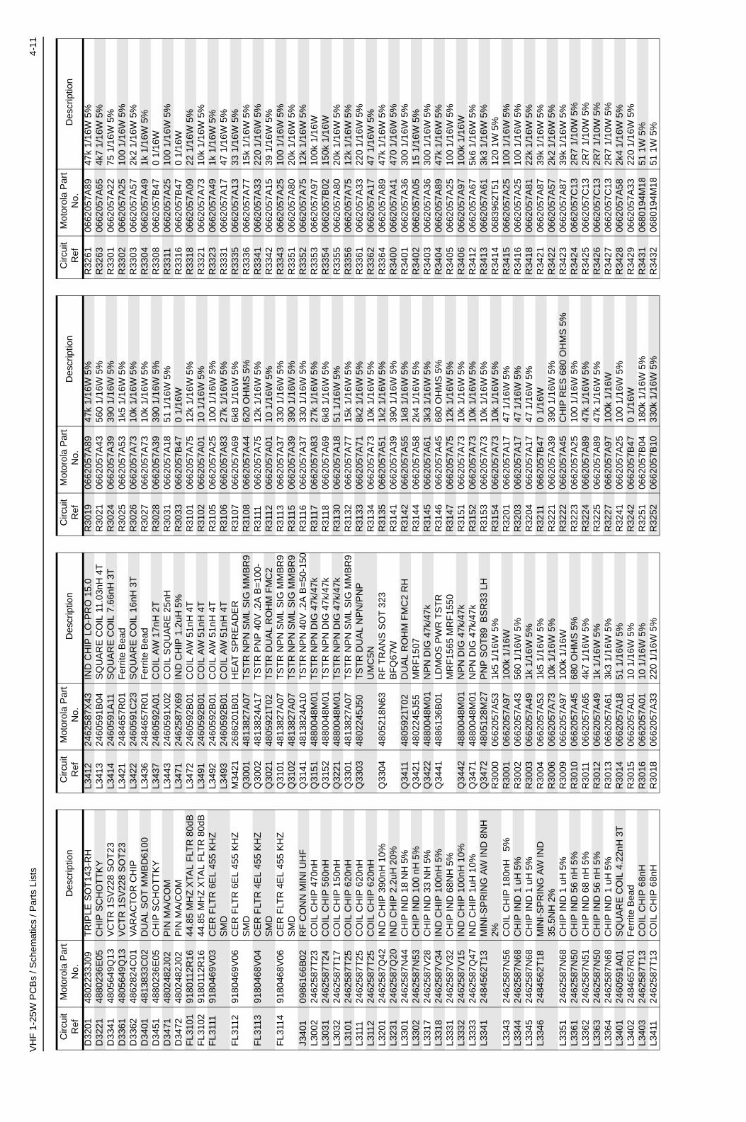
VH
F 1
-25W
PC
Bs
/ Sch
emat
ics
/ Par
ts L
ists
4-11
D32
0148
0223
3J09
TR
IPLE
SO
T14
3-R
HD
3221
4880
236E
05C
HIP
SC
HO
TT
KY
D33
4148
0564
9Q13
VC
TR
1S
V22
8 S
OT
23D
3361
4805
649Q
13V
CT
R 1
SV
228
SO
T23
D33
6248
6282
4C01
VA
RA
CT
OR
CH
IPD
3401
4813
833C
02D
UA
L S
OT
MM
BD
6100
D34
5148
8023
6E05
CH
IP S
CH
OT
TK
YD
3471
4802
482J
02P
IN M
A/C
OM
D34
7248
0248
2J02
PIN
MA
/CO
MF
L310
191
8011
2R16
44.8
5 M
HZ
XTA
L F
LTR
80d
BF
L310
291
8011
2R16
44.8
5 M
HZ
XTA
L F
LTR
80d
BF
L311
191
8046
9V03
CE
R F
LTR
6E
L 45
5 K
HZ
S
MD
FL3
112
9180
469V
06C
ER
FLT
R 6
EL
455
KH
Z
SM
DF
L311
391
8046
8V04
CE
R F
LTR
4E
L 45
5 K
HZ
S
MD
FL3
114
9180
468V
06C
ER
FLT
R 4
EL
455
KH
Z
SM
DJ3
401
0986
166B
02R
F C
ON
N M
INI U
HF
L300
224
6258
7T23
CO
IL C
HIP
470
nHL3
031
2462
587T
24C
OIL
CH
IP 5
60nH
L303
224
6258
7T17
CO
IL C
HIP
150
nHL3
101
2462
587T
25C
OIL
CH
IP 6
20nH
L311
124
6258
7T25
CO
IL C
HIP
620
nHL3
112
2462
587T
25C
OIL
CH
IP 6
20nH
L320
124
6258
7Q42
IND
CH
IP 3
90nH
10%
L323
124
6258
7Q20
IND
CH
IP 2
.2uH
20%
L330
124
6258
7N44
CH
IP IN
D 1
8 N
H 5
%L3
302
2462
587N
53C
HIP
IND
100
nH
5%
L331
724
6258
7V28
CH
IP IN
D 3
3 N
H 5
%L3
318
2462
587V
34IN
D C
HIP
100
nH 5
%L3
331
2462
587V
32C
HIP
IND
68N
H 5
%L3
332
2462
587V
15IN
D C
HIP
100
nH 1
0%L3
333
2462
587Q
47IN
D C
HIP
1uH
10%
L334
124
8456
2T13
MIN
I-S
PR
ING
AW
IND
8N
H
2%L3
343
2462
587N
56C
OIL
CH
IP 1
80nH
5%
L334
424
6258
7N68
CH
IP IN
D 1
uH
5%
L334
524
6258
7N68
CH
IP IN
D 1
uH
5%
L334
624
8456
2T18
MIN
I-S
PR
ING
AW
IND
35
.5N
H 2
%L3
351
2462
587N
68C
HIP
IND
1 u
H 5
%L3
361
2462
587N
50C
HIP
IND
56
nH 5
%L3
362
2462
587N
51C
HIP
IND
68
nH 5
%L3
363
2462
587N
50C
HIP
IND
56
nH 5
%L3
364
2462
587N
68C
HIP
IND
1 u
H 5
%L3
401
2460
591A
01S
QU
AR
E C
OIL
4.2
2nH
3T
L340
224
8465
7R01
Fer
rite
Bea
dL3
403
2462
587T
13C
OIL
CH
IP 6
8nH
L341
124
6258
7T13
CO
IL C
HIP
68n
H
Circ
uit
Ref
Mot
orol
a P
art
No.
Des
crip
tion
L341
224
6258
7X43
IND
CH
IP L
O-P
RO
15.
0L3
413
2460
591B
04S
QU
AR
E C
OIL
11.
03nH
4T
L341
424
6059
1A11
SQ
UA
RE
CO
IL 7
.66n
H 3
TL3
421
2484
657R
01F
errit
e B
ead
L342
224
6059
1C23
SQ
UA
RE
CO
IL 1
6nH
3T
L343
624
8465
7R01
Fer
rite
Bea
dL3
437
2460
592A
01C
OIL
AW
17n
H 2
TL3
443
2460
591X
02C
OIL
SQ
UA
RE
25n
HL3
471
2462
587X
69IN
D C
HIP
1.2
uH 5
%L3
472
2460
592B
01C
OIL
AW
51n
H 4
TL3
491
2460
592B
01C
OIL
AW
51n
H 4
TL3
492
2460
592B
01C
OIL
AW
51n
H 4
TL3
493
2460
592B
01C
OIL
AW
51n
H 4
TM
3421
2686
201B
01H
EA
T S
PR
EA
DE
RQ
3001
4813
827A
07T
ST
R N
PN
SM
L S
IG M
MB
R9
Q30
0248
1382
4A17
TS
TR
PN
P 4
0V .2
A B
=10
0-Q
3021
4805
921T
02T
ST
R D
UA
L R
OH
M F
MC
2Q
3101
4813
827A
07T
ST
R N
PN
SM
L S
IG M
MB
R9
Q31
0248
1382
7A07
TS
TR
NP
N S
ML
SIG
MM
BR
9Q
3141
4813
824A
10T
ST
R N
PN
40V
.2A
B=
50-1
50Q
3151
4880
048M
01T
ST
R N
PN
DIG
47k
/47k
Q31
5248
8004
8M01
TS
TR
NP
N D
IG 4
7k/4
7kQ
3221
4880
048M
01T
ST
R N
PN
DIG
47k
/47k
Q33
0148
1382
7A07
TS
TR
NP
N S
ML
SIG
MM
BR
9Q
3303
4802
245J
50T
ST
R D
UA
L N
PN
/PN
P
UM
C5N
Q33
0448
0521
8N63
RF
TR
AN
S S
OT
323
B
FQ
67W
Q34
1148
0592
1T02
DU
AL
RO
HM
FM
C2
RH
Q34
2148
0224
5J55
MR
F15
07Q
3422
4880
048M
01N
PN
DIG
47k
/47k
Q34
4148
8613
6B01
LDM
OS
PW
R T
ST
R
MR
F15
65 M
RF
1550
Q34
4248
8004
8M01
NP
N D
IG 4
7k/4
7kQ
3471
4880
048M
01N
PN
DIG
47k
/47k
Q34
7248
0512
8M27
PN
P S
OT
89 B
SR
33 L
HR
3000
0662
057A
531k
5 1/
16W
5%
R30
0106
6205
7A97
100k
1/1
6WR
3002
0662
057A
4356
0 1/
16W
5%
R30
0306
6205
7A49
1k 1
/16W
5%
R30
0406
6205
7A53
1k5
1/16
W 5
%R
3006
0662
057A
7310
k 1/
16W
5%
R30
0906
6205
7A97
100k
1/1
6WR
3010
0662
057A
4568
0 O
HM
S 5
%R
3011
0662
057A
654k
7 1/
16W
5%
R30
1206
6205
7A49
1k 1
/16W
5%
R30
1306
6205
7A61
3k3
1/16
W 5
%R
3014
0662
057A
1851
1/1
6W 5
%R
3015
0662
057A
0110
1/1
6W 5
%R
3016
0662
057A
0110
1/1
6W 5
%R
3018
0662
057A
3322
0 1/
16W
5%
Circ
uit
Ref
Mot
orol
a P
art
No.
Des
crip
tion
R30
1906
6205
7A89
47k
1/16
W 5
%R
3021
0662
057A
4356
0 1/
16W
5%
R30
2406
6205
7A39
390
1/16
W 5
%R
3025
0662
057A
531k
5 1/
16W
5%
R30
2606
6205
7A73
10k
1/16
W 5
%R
3027
0662
057A
7310
k 1/
16W
5%
R30
2806
6205
7A39
390
1/16
W 5
%R
3031
0662
057A
1851
1/1
6W 5
%R
3033
0662
057B
470
1/16
W
R31
0106
6205
7A75
12k
1/16
W 5
%R
3102
0662
057A
0110
1/1
6W 5
%R
3105
0662
057A
2510
0 1/
16W
5%
R31
0606
6205
7A83
27k
1/16
W 5
%R
3107
0662
057A
696k
8 1/
16W
5%
R31
0806
6205
7A44
620
OH
MS
5%
R31
1106
6205
7A75
12k
1/16
W 5
%
R31
1206
6205
7A01
10 1
/16W
5%
R31
1306
6205
7A37
330
1/16
W 5
%R
3115
0662
057A
3939
0 1/
16W
5%
R31
1606
6205
7A37
330
1/16
W 5
%R
3117
0662
057A
8327
k 1/
16W
5%
R31
1806
6205
7A69
6k8
1/16
W 5
%R
3130
0662
057A
1851
1/1
6W 5
%R
3132
0662
057A
7715
k 1/
16W
5%
R31
3306
6205
7A71
8k2
1/16
W 5
%R
3134
0662
057A
7310
k 1/
16W
5%
R31
3506
6205
7A51
1k2
1/16
W 5
%R
3141
0662
057A
3939
0 1/
16W
5%
R31
4206
6205
7A55
1k8
1/16
W 5
%R
3144
0662
057A
582k
4 1/
16W
5%
R31
4506
6205
7A61
3k3
1/16
W 5
%R
3146
0662
057A
4568
0 O
HM
S 5
%R
3147
0662
057A
7512
k 1/
16W
5%
R31
5106
6205
7A73
10k
1/16
W 5
%R
3152
0662
057A
7310
k 1/
16W
5%
R31
5306
6205
7A73
10k
1/16
W 5
%R
3154
0662
057A
7310
k 1/
16W
5%
R32
0106
6205
7A17
47 1
/16W
5%
R32
0306
6205
7A17
47 1
/16W
5%
R32
0406
6205
7A17
47 1
/16W
5%
R32
1106
6205
7B47
0 1/
16W
R32
2106
6205
7A39
390
1/16
W 5
%R
3222
0662
057A
45C
HIP
RE
S 6
80 O
HM
S 5
%R
3223
0662
057A
2510
0 1/
16W
5%
R32
2406
6205
7A89
47k
1/16
W 5
%R
3225
0662
057A
8947
k 1/
16W
5%
R32
2706
6205
7A97
100k
1/1
6WR
3241
0662
057A
2510
0 1/
16W
5%
R32
4206
6205
7B47
0 1/
16W
R32
5106
6205
7B04
180k
1/1
6W 5
%R
3252
0662
057B
1033
0k 1
/16W
5%
Circ
uit
Ref
Mot
orol
a P
art
No.
Des
crip
tion
R32
6106
6205
7A89
47k
1/16
W 5
%R
3263
0662
057A
654k
7 1/
16W
5%
R33
0106
6205
7A22
75 1
/16W
5%
R33
0206
6205
7A25
100
1/16
W 5
%R
3303
0662
057A
572k
2 1/
16W
5%
R33
0406
6205
7A49
1k 1
/16W
5%
R33
0806
6205
7B47
0 1/
16W
R33
1106
6205
7A25
100
1/16
W 5
%R
3316
0662
057B
470
1/16
WR
3318
0662
057A
0922
1/1
6W 5
%R
3321
0662
057A
7310
k 1/
16W
5%
R33
2306
6205
7A49
1k 1
/16W
5%
R33
3106
6205
7A17
47 1
/16W
5%
R33
3506
6205
7A13
33 1
/16W
5%
R33
3606
6205
7A77
15k
1/16
W 5
%R
3341
0662
057A
3322
0 1/
16W
5%
R33
4206
6205
7A15
39 1
/16W
5%
R33
4306
6205
7A25
100
1/16
W 5
%R
3351
0662
057A
8020
k 1/
16W
5%
R33
5206
6205
7A75
12k
1/16
W 5
%R
3353
0662
057A
9710
0k 1
/16W
R33
5406
6205
7B02
150k
1/1
6WR
3355
0662
057A
8020
k 1/
16W
5%
R33
5606
6205
7A75
12k
1/16
W 5
%R
3361
0662
057A
3322
0 1/
16W
5%
R33
6206
6205
7A17
47 1
/16W
5%
R33
6406
6205
7A89
47k
1/16
W 5
%R
3400
0662
057A
4147
0 1/
16W
5%
R34
0106
6205
7A36
300
1/16
W 5
%R
3402
0662
057A
0515
1/1
6W 5
%R
3403
0662
057A
3630
0 1/
16W
5%
R34
0406
6205
7A89
47k
1/16
W 5
%R
3405
0662
057A
2510
0 1/
16W
5%
R34
0606
6205
7A97
100k
1/1
6WR
3412
0662
057A
675k
6 1/
16W
5%
R34
1306
6205
7A61
3k3
1/16
W 5
%R
3414
0683
962T
5112
0 1W
5%
R34
1506
6205
7A25
100
1/16
W 5
%R
3416
0662
057A
2510
0 1/
16W
5%
R34
1806
6205
7A81
22k
1/16
W 5
%R
3421
0662
057A
8739
k 1/
16W
5%
R34
2206
6205
7A57
2k2
1/16
W 5
%R
3423
0662
057A
8739
k 1/
16W
5%
R34
2406
6205
7C13
2R7
1/10
W 5
%R
3425
0662
057C
132R
7 1/
10W
5%
R34
2606
6205
7C13
2R7
1/10
W 5
%R
3427
0662
057C
132R
7 1/
10W
5%
R34
2806
6205
7A58
2k4
1/16
W 5
%R
3429
0662
057A
3322
0 1/
16W
5%
R34
3106
8019
4M18
51 1
W 5
%R
3432
0680
194M
1851
1W
5%
Circ
uit
Ref
Mot
orol
a P
art
No.
Des
crip
tion

4-12
VH
F 1
-25W
PC
Bs
/ Sch
emat
ics
/ Par
ts L
ists
* M
otor
ola
Dep
ot S
ervi
cing
onl
y
Ref
eren
ce d
esig
nato
rs w
ith a
n as
teris
k in
dica
te
com
pone
nts
whi
ch a
re n
ot fi
eldr
epla
ceab
le
beca
use
they
nee
d to
be
calib
rate
d w
ith
spec
ializ
ed fa
ctor
y eq
uipm
ent a
fter
inst
alla
tion.
R
adio
s in
whi
ch th
ese
part
s ha
ve b
een
repl
aced
in
the
field
will
be
off f
requ
ency
at t
empe
ratu
re
extr
emes
.
R34
3306
6205
7C13
2R7
1/10
W 5
%R
3434
0662
057C
132R
7 1/
10W
5%
R34
3506
6205
7C13
2R7
1/10
W 5
%R
3441
0662
057A
8739
k 1/
16W
5%
R34
4206
6205
7A57
2k2
1/16
W 5
%R
3443
0662
057A
8739
k 1/
16W
5%
R34
4406
6205
7C19
4R7
1/10
W 5
%R
3445
0662
057A
582k
4 1/
16W
5%
R34
4606
6205
7B47
0 1/
16W
R34
5006
6205
7A41
470
1/16
W 5
%R
3452
0662
057A
7512
k 1/
16W
5%
R34
5406
6205
7A84
30k
1/16
W 5
%R
3455
0662
057A
9710
0k 1
/16W
R34
5706
8396
2T51
120
1W 5
%R
3471
0662
057A
4147
0 1/
16W
5%
R34
7306
8019
4M18
51 1
W 5
%R
3474
0680
194M
1851
1W
5%
R34
7506
6205
7A73
10k
1/16
W 5
%R
3491
0662
057A
7310
k 1/
16W
5%
R35
0106
6205
7A69
6k8
1/16
W 5
%R
3502
0662
057A
8739
k 1/
16W
5%
R35
0406
6205
7A73
10k
1/16
W 5
%R
3505
0662
057B
0930
0k 1
/16W
5%
R35
0706
6205
7A80
20k
1/16
W 5
%R
3508
0662
057A
9710
0k 1
/16W
R35
0906
6205
7A49
1k 1
/16W
5%
T30
0125
0839
6X02
TR
AN
SF
OR
ME
RT
3002
2508
397X
02T
RA
NS
FO
RM
ER
U31
0151
8614
4B01
FM
IF IC
SA
616
U31
1151
1380
5A86
IC Q
UA
D A
NA
LOG
MU
X/
DE
MU
XU
3115
5113
805A
86IC
QU
AD
AN
ALO
G M
UX
/D
EM
UX
U32
0151
8596
3A27
IC T
ES
TE
D A
T25
016
48 P
IN
GF
PU
3211
5105
739X
05IC
SO
T 5
V H
I-P
RE
CIS
ION
R
EG
ULA
TU
3301
5105
750U
54V
CO
BU
FF
ER
PK
G D
IEU
3401
5105
109Z
67LD
MO
S D
RIV
ER
VH
F/U
HF
U34
0251
8093
2W01
LIN
EA
R IC
OP
AM
PU
3501
5185
765B
01IC
PO
WE
R C
ON
TR
OL
U35
0251
8596
3A15
TE
MP
SE
NS
OR
1M
5V
R34
7148
1383
0A15
5.6V
5%
225
mW
Y31
0148
8060
6B09
CR
YS
TAL
44.3
95 M
HZ
Y31
0291
8614
5B02
CE
RA
MIC
DIS
CR
IMIN
AT
OR
45
5kH
zY
3263
4886
182B
01V
CT
CX
O 1
6.8M
Hz
2ppm
T
TS
O5V
* Y
3261
Not
Use
d16
.8M
Hz
75Z
04
Circ
uit
Ref
Mot
orol
a P
art
No.
Des
crip
tion
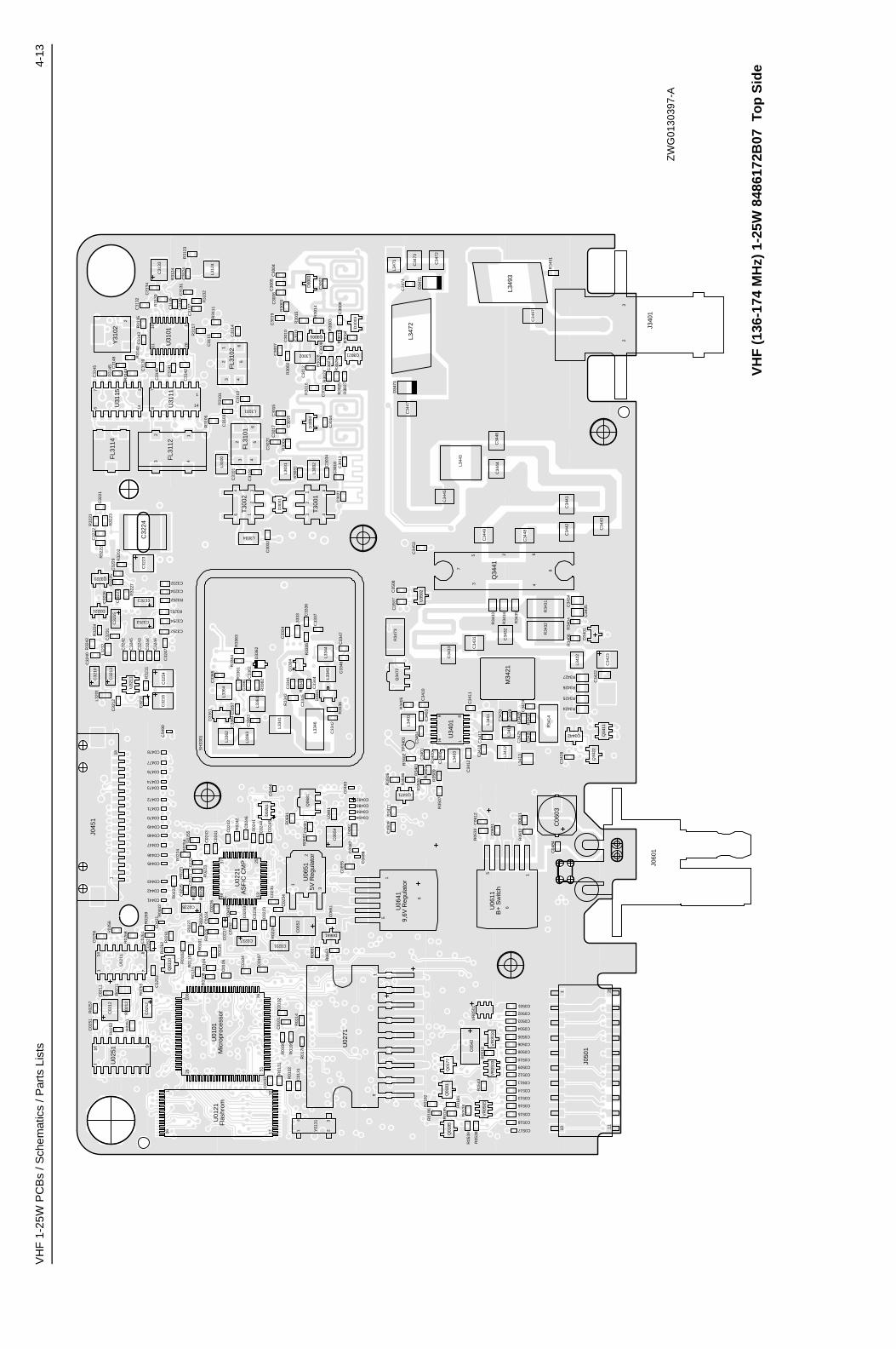
VH
F 1
-25W
PC
Bs
/ Sch
emat
ics
/ Par
ts L
ists
4-13
C01
01C
0102
C01
04
C01
06 C01
07
C01
31
C01
32
C02
11
C02
12
C02
21C
0222
C02
23
C02
24
C02
25
C02
26
C02
27
C0228
C0231
C02
32
C02
33
C02
34C02
35
C02
36
C0237
C02
41
C02
42
C02
43 C02
44
C02
45
C02
46
C02
51
C02
52
C02
53
C02
56
C02
61C
0262
C04
21
C0441
C0442
C0443
C0445
C0446
C0447
C0448
C0449
C0470
C0471
C0472
C0473C0474
C0476
C0477
C0478
C0482C0483
C04
84
C04
86
C04
87
C0488
C04
90
C04
93
C0494
C04
95
C04
96
C0501
C0502
C0503
C0504
C0505
C0506
C0508
C0509
C0510
C0511
C0512
C0513
C0514
C0515
C0516
C0517
C0518
C05
42
C06
01 C06
03
C06
12
C06
51
C06
52
C06
54
C06
55
C06
81
C30
02
C30
04C
3005
C30
06C
3007
C30
08
C30
09
C30
10
C30
11
C30
12
C30
13
C30
14
C30
15
C30
16
C30
17
C30
18
C30
19C
3020
C30
21
C30
27C
3028
C30
32
C30
34
C31
00
C31
01C
3102
C31
03
C31
14
C31
15
C31
24C
3131
C31
32
C31
33
C31
34
C31
35
C31
36
C31
37
C31
39
C31
40
C31
41
C31
42
C31
43
C31
45 C31
48
C32
10
C32
11
C32
12C
3213
C32
15
C32
21
C32
22
C32
23C
3224
C32
26
C 3
227
C32
29C
3231
C3232
C3233
C3234
C32
40
C32
42
C32
43
C32
44
C32
45
C32
46
C32
47
C3252
C3253 C3254
C32
55
C33
24
C33
36
C33
37
C33
41
C33
42
C33
44
C33
45
C33
46C
3347
C33
57
C33
61C
3362
C33
63
C33
64
C33
65
C34
00
C34
01C
3403
C34
04
C34
10
C34
11C
3412
C34
17C
3418
C34
19
C34
20
C34
22
C34
23
C34
24C
3425
C34
26
C34
28
C34
31 C34
32
C34
33
C34
34
C34
35
C34
41C
3442 C34
43
C34
44
C34
45
C34
46
C34
47
C34
48
C34
49
C34
53
C34
72
C34
73
C34
74
C34
97
C35
07C
3508
C35
09
D02
01
D0651
D30
01
D30
03
D30
04
D30
31
D3221
D33
41
D33
61
D33
62
D34
01
D34
71
D34
72
23 4
56
FL3
101
23 4
56
FL3
102
432
FL3
112
FL3
114
181
201110
J060
1
23
J340
1
L048
1
L048
2
L3002
L303
1
L303
2
L3034
L310
0
L3101
L312
4
L320
1
L323
2
L333
3
L334
1
L334
3L3
344
L334
6
L336
1
L336
2
L336
3
L336
4
L340
1
L340
3
L341
1
L341
2
L341
3
L341
4
L342
2
L344
3
L347
1
L347
2
L349
3M
3421
Q01
10
Q01
77Q
0181
Q01
85
Q06
81
Q3001
Q3021
Q3221
Q33
04
Q34
11
Q34
22
2
3 4
5 6
7 8
Q34
41
Q3442
Q3471
Q34
72
R01
01
R01
02
R01
04
R01
05
R01
06
R01
08
R01
10
R01
14
R01
15
R01
16
R01
31
R01
32
R01
70
R01
81
R01
82
R01
85
R01
86
R02
11
R 0
212
R 0
220
R02
21
R02
22
R02
23
R02
24
R02
25
R02
26
R02
27
R02
28R
022
9
R02
41
R02
42
R02
51
R02
52
R02
53
R02
54 R02
55
R02
56
R02
57
R02
61R
0262
R02
68
R02
69 R04
42
R05
10
R05
33
R05
35
R05
38
R05
39
R05
43
R06
11R
0612
R06
51
R06
52
R06
81
R06
82
R30
01
R30
02
R30
03
R30
04
R30
09
R 3
013
R30
14
R30
15
R30
16
R30
24
R30
25R
3026
R30
27
R30
28
R30
31
R31
01
R31
06
R31
11
R31
17
R31
23
R31
24
R31
30
R31
32
R31
35R
3142
R31
44
R31
45
R32
02
R32
11
R32
21
R32
22
R32
23
R32
24
R32
25
R32
27
R32
42
R3251
R3252
R33
35
R33
36
R 3
341
R33
42
R33
61
R33
62
R33
63R
3364
R34
00
R34
01R34
02
R34
03
R34
04
R34
05
R34
06
R34
14
R34
15
R34
16
R3424
R3425
R3426
R3427
R34
31R
3432
R34
33
R34
34
R34
35
R34
71
R34
73
R34
91
R35
05
R35
06
R35
07
R35
08 R35
09
SH
3301
3 461
2
T30
01
346 1
2
T30
02
TP
3401
1 765126
321716
1
871
14
U02
11
137 25
13
161 8
9
9
1
6
5
1
6
5
3
2
1
11
120
10
U31
01
87
1
14U31
11
87 1
14U31
15
U32
11
116
89
U34
01
U35
02
VR
0501
VR
0503
VR
0505
VR
0510
234
Y01
31
2
Y31
02
1
1
100
1
C32
14
1
148
J045
1
J050
1
U02
51
U02
71
U01
01M
icro
proc
esso
rU
0121
Fla
shro
m
U02
21A
SF
IC C
MP
U06
11B
+ S
witc
h
U06
419,
6V R
egul
ator
U06
515V
Reg
ulat
or
ZW
G01
3039
7-A
VH
F (
136-
174
MH
z) 1
-25W
848
6172
B07
To
p S
ide
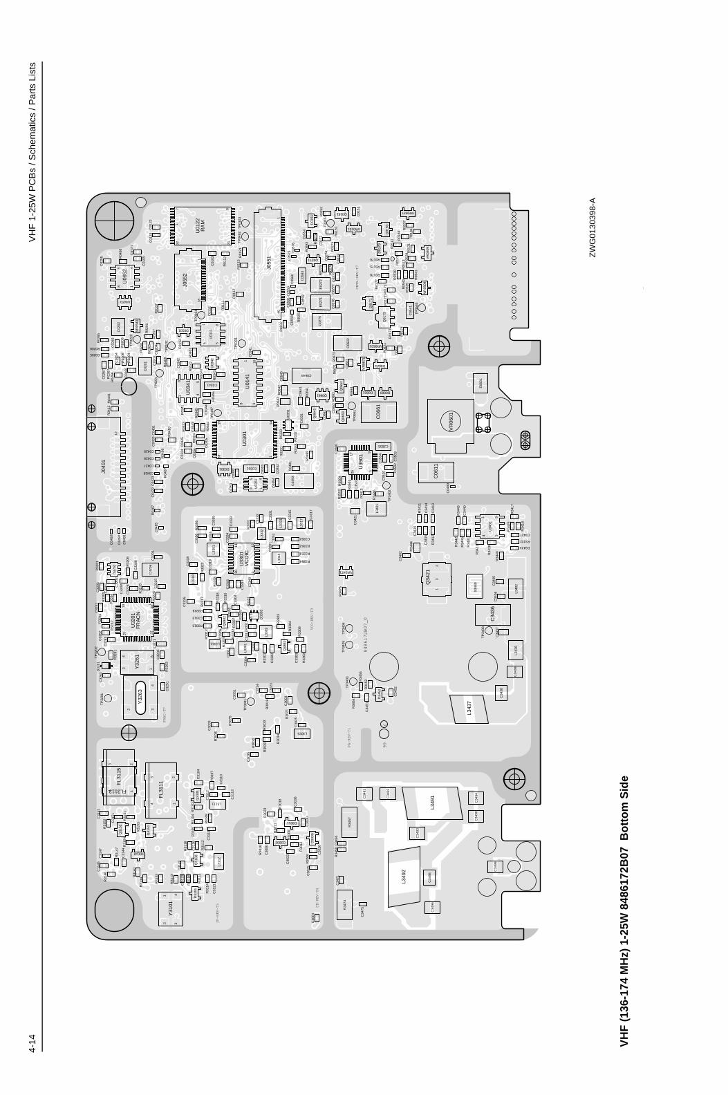
4-14
VH
F 1
-25W
PC
Bs
/ Sch
emat
ics
/ Par
ts L
ists
C01
03
C01
05
C01
11
C01
12
C01
21
C01
22C
0123
C01
41
C01
51
C02
01
C02
02
C02
03C
0204
C0205
C02
54
C02
55
C02
65
C02
66
C02
67
C02
71
C02
72
C02
73
C02
74
C02
75
C02
76C
0277
C0301
C03
02
C03
03
C03
04
C03
05
C03
24C
0325
C03
31
C0341
C03
42
C03
43
C03
44
C03
51
C03
52
C03
53
C03
54
C04
22C
0423
C0426
C0427
C0428
C0429
C04
30C
0431
C04
85
C04
91
C04
92
C04
97
C04
99
C05
41
C05
54
C05
58C
0559
C05
60C
0575 C
0576
C05
91
C05
92C
0593
C06
11
C06
21C06
22
C06
41
C0644
C06
45
C06
61
C06
62 C06
63
C06
71
C30
00
C30
01
C30
03C
3022
C30
23
C30
24
C30
25
C30
26
C30
29C
3030
C30
31
C30
33
C30
35
C30
36
C31
04
C31
10
C31
11C
3112
C31
13
C31
16
C31
21
C31
22C
312
3
C31
44
C31
46C
3147
C31
51
C31
52
C32
02
C32
03
C32
05C
3206
C32
07
C32
08
C32
09
C32
25
C32
28
C32
35
C32
41
C32
51
C32
61C32
62C
3263
C33
01
C33
02
C33
03
C33
04
C33
05
C33
06C
3311
C33
12
C3313
C33
14
C33
15
C33
16
C33
17
C33
18
C33
19
C33
31
C33
32
C33
33C
3334
C33
35
C33
48
C33
51 C3352
C33
55
C33
56
C34
02
C34
05C
3406
C34
13
C34
14C
3415
C34
16
C34
21
C3427
C34
36C
3437
C34
38
C34
39
C34
40
C34
50
C34
51
C34
52
C34
71
C34
75C
3491
C34
92
C34
93
C34
94
C34
95C
3496
C34
98
C34
99
C35
01
C35
02C
3503
C35
04
C3505
C35
06
C35
10
D0101
D01
51
D01
79
D0301
D0621
D0660D0661
D30
00
D3011
D31
01
D32
01
D32
61
D34
51
E02
71E
0272
E06
31
43 2
FL3
111
FL311343 2
FL3
115
12
J040
1
140
J055
1118
J055
2
L3025
L3111
L311
2
L323
1
L330
1
L330
2
L3311
L331
7
L331
8
L333
1
L333
2
L334
5L335
1
L340
2
L342
1
L343
6
L343
7
L349
1
L349
2
Q0151
Q01
71
Q01
73Q
0183
Q0271
Q06
41
Q0661
Q06
62Q
0663
Q3002
Q31
01Q
3102
Q3141
Q31
51
Q31
52
Q33
01
Q33
02 43
Q33
03
12
3
Q34
21
R01
07
R01
11R
0112
R01
13R
0117
R01
21
R01
51
R01
52
R01
71R
0172
R01
73
R01
74
R0175
R0176
R01
77
R0178
R01
79R
0183
R01
84
R02
01
R02
02R02
03
R02
04
R02
05
R02
06
R02
07
R0208
R02
65
R02
66R
0267
R02
73
R 0
274
R02
75R
027
6
R03
23
R03
24
R03
31
R03
32
R03
33
R03
35
R03
41
R03
42
R03
43
R03
44
R03
45
R03
46
R03
47
R04
01
R04
07R
0408
R04
09
R04
10
R04
12R
0441
R04
67
R04
68
R04
81
R04
82
R05
11
R05
12R
0525
R05
29
R05
30
R05
31R
0537
R05
41
R05
42
R05
91
R05
92
R05
93
R06
21
R06
41
R06
42R
0643
R06
61
R06
62R
0671
R06
72
R30
00
R30
06
R30
10
R30
11
R30
12
R30
18
R30
19
R30
21
R30
23R
3030R30
32
R30
33
R30
34
R30
35
R30
36
R31
02R
3104
R31
05
R31
07
R31
08R
3112
R31
13
R31
14
R31
15
R 3
116
R31
18
R31
33
R31
34
R31
41
R31
46
R31
47
R31
51
R31
52
R31
53
R31
54
R32
01
R32
03
R32
04
R32
06
R32
26R32
28
R32
41
R32
61R
3262
R32
63
R33
01
R33
02
R33
03
R33
04
R33
05
R33
06R
3307
R33
08R33
11
R33
12
R33
13R33
14
R3315
R33
16
R33
17
R33
18
R3319
R33
21
R33
23
R33
31
R33
43
R33
51 R3352
R3353
R3354
R33
55
R33
56
R34
11
R34
12
R34
13
R34
17
R34
18
R34
21
R3422
R3423
R34
28
R34
29
R34
40
R34
41
R34
42R
3443
R34
44
R34
45
R34
46
R34
50
R34
52
R34
54
R34
55
R34
57R
3474
R34
75
R35
01
R35
02R
3504
S34
40
TP
0101
TP
0102
TP
0103
TP
0104
TP
0151
TP
0221
TP
0222
TP
0492
TP
0497
TP
0530
TP
0661
TP
3001
TP
3201
TP
3202
TP
3402
TP
3403
TP
3404
TP
3405
TP
3406
14 5
8
U01
11
22 2187
1
1618 9
U01
41
2815 14
1
U03
01
U03
31
1 458
U03
41
U03
42
458 U
0351
145
8
U06
52
U0653
13725
13
11
120
10
14 5
8
U34
02
1
17
9
25
U35
01
VR0151
VR
0504
VR
0509
VR0537
VR
0541
VR
0601
VR0621
VR
0671
VR3471
432
Y31
01
643 1Y
3261
2 34
Y32
63
1
48
1
1
1
U01
22R
AM
U32
01F
RA
CN
U33
01V
CO
IC
ZW
G01
3039
8-A
8486172B07_0
C99
CNTL-REV-T7
PA-REV-T1
VCO-REV-T3
IF-REV-T5
FE-REV-T4
FRAC-T7
ZW
G01
3039
8-A
VH
F (
136-
174
MH
z) 1
-25W
848
6172
B07
Bo
tto
m S
ide

VH
F 1
-25W
PC
Bs
/ Sch
emat
ics
/ Par
ts L
ists
4-15
ZW
G01
3056
5-O
9180
469V
03
3.9V
DC
12.
5kH
z 0
VD
C20
/25k
Hz
5V
DC
0.75
VD
C
0.75
VD
C3V
DC
9180
469V
06
9180
469V
04
9180
468v
04
9180
468V
06
3VD
C6.
8K
R31
07
9V3
R31
351.
2K
390
1GND1GND2 2GND3 4
5GND4
3IN
6O
UT
R31
15
FL3
101
12R
16
R31
1727
K
Q31
02
Q31
51
680
R31
46
620n
HL3
111
620
R31
08
R31
18
6.8K
R31
1112
K
C31
01
5V_V
HF
_IF
_1
GND2 4
1IN
2O
UT
NU
2.2p
F
FL3
111
3
GND1
U31
15-1
CN
TL 13
12
VD
D
14
VS
S 7
DIS
CA
UD
IO_V
HF
_IF
_1
15K
R31
32
0.1u
FC
3144
120p
FC
3143
C31
39
C31
410.
1uF
0.1u
F
13
12
VD
D
14
VS
S 7
Q31
41
U31
11-1
CN
TL
R31
1633
0
10
9V3_
VH
F_I
F_2
3GN
D
1IN
2O
UT
R31
02
C31
10
27pF
FL3
113
0.1u
FC
3142
9.1p
F
IFIN
_VH
F_I
F_1
100
R31
04
NU
C31
1312GND2 4GND3
GND4 5
IN3
OU
T6
NU
DIS
CA
UD
IO
12R
16F
L310
2
GND1
1000
pF
R31
51
C31
00
C31
400.
1uF
10K
1110
VD
D
14 VS
S
7
3
14
VD
D 7
VS
S
U31
11-4
CN
TL
12
U31
15-2
5
CN
TL
4
Q31
52C
3152
.01u
F
.01u
FC
3151
R31
338.
2K
4700
pFC
3146
27K
R31
06
C31
12
390
R31
41
82pF
10R
3112
1.8K
R31
42
R31
5410
K
C31
22
.039
uF
Q31
01
6 VC
C33
0R
3113
20MIXOUT4 OSCIN
3OSCOUT
10 QUADIN
1 RFIN
2RFIN_DEC
5RSSIOUT
9 RSSI_FEED
15
18 IFAMPIN 16IFAMPOUT
19 IFAMP_DEC1
17IFA
MP
_DE
C2
14 LIMIN11LIMOUT 13LIM_DEC1 12LIM_DEC2
SA
616
U31
01
8AUDIOOUT
7 AUDIO_FEED
GND
51
44.3
95M
Hz
12R
17Y
3101
2G
ND
4G
ND
1
3O
UT
1IN
R31
30
C31
3630
pF
C31
35
33pF
12K
R31
01
R31
47
12K
C31
3310
uF
C31
15
100
R31
05
22pF
620n
HL3
100
0.1u
F
NU
C31
37.0
39uF
C31
34
455K
Hz
3
21
BW
SE
LEC
T_V
HF
_IF
_1 BW
SE
LEC
T
45B
02
Y31
02
C31
03
33pF
C31
320.
1uF
10K
R31
52
0.1u
FC
3111
U31
15-3
6CN
TL
89
14 VD
D 7VS
S
18pF
C31
14L3
112
620n
H
9V3_
VH
F_I
F_1
5V
D31
01
RS
SI_
VH
F_I
F_1
OU
T
.039
uFC
3123
FL3
112
3
GND1
GND2
4
1IN
2
R31
1410
0
R31
34
10K
NU
2.4K
R31
44
U31
11-2
5
CN
TL
43
14 VD
D 7
VS
S
3.3K
R31
45
C31
45
C31
470.
1uF
620n
HL3
101
0.1u
F22
0pF
C31
48
NU
10V
DD
14 VS
S
7
NU
1pF
C31
31
U31
15-4
CN
TL
12
11
C31
210.
1uF
FL3
115
GND1
34
GND2
IN1
OU
T2
15pF
C31
02
NU
U31
11-3
6CN
TL
89
14
VD
D
7VS
S
3G
ND
1IN
2O
UT
RS
SI
C31
16
FL3
114
0.1u
F0.
1uF
R31
53
C31
04
5V
10K
5V
9V3
9V3
9V3
9V3
9V3
5V
9V3
5V
9V3
0R
3123
1uH
NU
L312
4
33pF
C31
24820
R31
24
VH
F (
136-
174
MH
z) IF
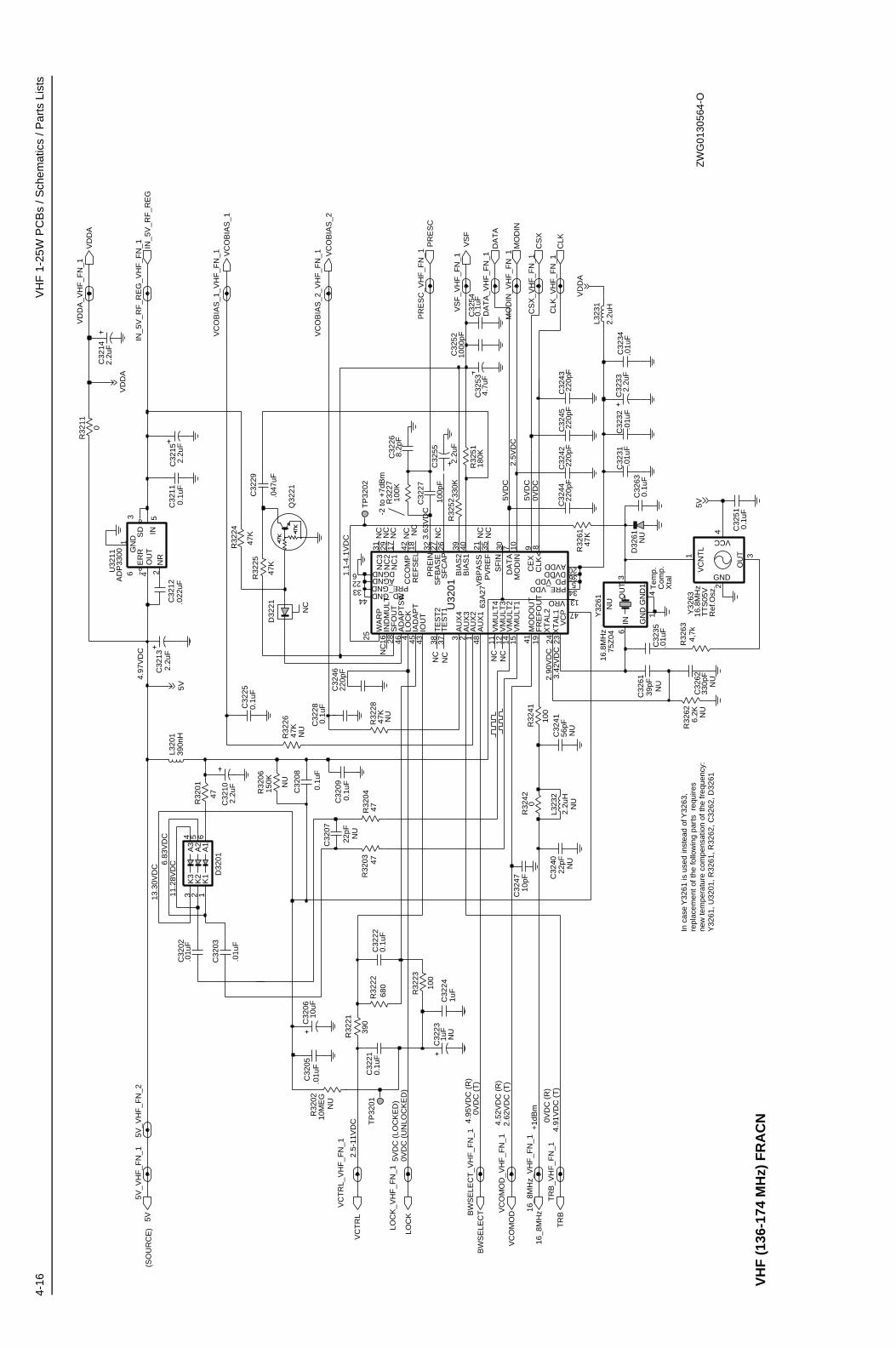
4-16
VH
F 1
-25W
PC
Bs
/ Sch
emat
ics
/ Par
ts L
ists
0VD
C5V
DC
5VD
C
(SO
UR
CE
)
-2 to
+7d
Bm
13.3
0VD
C6.
83V
DC
4.52
VD
C (
R)
+1d
Bm
0VD
C (
R)
4.95
VD
C (
R)
2.90
VD
C3.
42V
DC
3.63
VD
C
2.5V
DC
1.1-
4.1V
DC
0VD
C (
T)
2.62
VD
C (
T)
4.91
VD
C (
T)
Tem
p.C
omp.
Xta
l
Ref
.Osz
.
11.2
8VD
C
4.97
VD
C
2.5-
11V
DC
5VD
C (
LOC
KE
D)
0VD
C (
UN
LOC
KE
D)
R32
03
A1
5A
2
4A
3
K1
1K
22
K3
3
47
D32
01
6
47K
NU
TR
BL3
232
2.2u
HN
U
R32
28
C32
31
C32
25
.01u
F
L320
139
0nH
0.1u
F
C32
02.0
1uF
100
R32
23
C32
29
D32
21
0.1u
F
.047
uF
CLK
C32
51
C32
07
22pF
NU
47K
VC
OB
IAS
_2
R32
25
C32
268.
2pF
MO
DIN
_VH
F_F
N_1
TP
3201
R32
52
VC
OB
IAS
_1_V
HF
_FN
_1
330K
16_8
MH
z_V
HF
_FN
_1
PR
ES
C_V
HF
_FN
_1
R32
420
100
R32
41
VS
F_V
HF
_FN
_1
DA
TA
VC
OM
OD
_VH
F_F
N_1
CS
X_V
HF
_FN
_1
100p
F
C32
27
22pF NU
CS
X
IN_5
V_R
F_R
EG
_VH
F_F
N_1
C32
40
NU
1G
ND
4G
ND
1
3O
UT
6IN
16.8
MH
z75
Z04
Y32
61
100K
R32
27
0.1u
FC
3254
C32
08
0.1u
F
NU
.01u
FC
3232
47K
R32
26
PR
ES
C
C32
142.
2uF
C32
210.
1uF
1uF
C32
24
C32
630.
1uF
VM
ULT
11514
VM
ULT
212
VM
ULT
311
VM
ULT
4
VRO 13
25
WA
RP
23X
TA
L1X
TA
L224
27S
FB
AS
E26
SF
CA
P
30S
FIN
28S
FO
UT
37T
ES
T1
38T
ES
T2
21V
BP
AS
S
47
VC
P
31N
C3
44PD_GND
PD_VDD 5
PR
EIN
32
33 PRE_GND 34PRE_VDD
35P
VR
EF
18R
EF
SE
L45
IAD
AP
T
16IN
DM
ULT
43IO
UT
LOC
K4
10M
OD
IN41
MO
DO
UT
17N
C1
29N
C2
39B
IAS
2
42C
CO
MP
9C
EX
8C
LK
7D
AT
A
DGND6 36DVDD
19F
RE
FO
UT
46A
DA
PT
SW
22 AGND
48A
UX
1
1A
UX
22
AU
X3
3A
UX
4
20AVDD
40B
IAS
1
VC
OB
IAS
_1
63A
27
U32
01
47
R32
01
VS
F
C32
22
0
R32
11
0.1u
F
L323
1
0.1u
FC
3211
TP
3202
2.2u
H
C32
4322
0pF
16_8
MH
z
VD
DA
VD
DA
_VH
F_F
N_1
VC
OB
IAS
_2_V
HF
_FN
_1
0.1u
FC
3209
C32
4622
0pF
NU
C32
0610
uF
5V_V
HF
_FN
_2
150K
R32
06
Q32
21
R32
5118
0K
.01u
F
C32
280.
1uF
C32
35
2.2u
FC
3210
VC
TR
L_V
HF
_FN
_1
R32
04
LOC
K_V
HF
_FN
_1
47
1uF
C32
23
NU
220p
F
R32
62 NU
C32
45
BW
SE
LEC
T
6.2K
C32
15
R32
24
47K
C32
13
2.2u
F
1G
ND
5IN
2N
R
4O
UT
3S
D
2.2u
F
VCC
4
VC
NT
L
1
AD
P33
00U
3211
6E
RR
Y32
63
TT
S05
V16
.8M
Hz
GND
2
OU
T 3
MO
DIN
VC
TR
L
C32
55
DA
TA
_VH
F_F
N_1
220p
FC
3242
2.2u
F
5V_V
HF
_FN
_1
.01u
F
R32
2268
0
TR
B_V
HF
_FN
_1
C32
05
C32
6233
0pF
NU
NU
VC
OM
OD
C32
4156
pF
R32
6147
K
2.2u
FC
3233
R32
21
CLK
_VH
F_F
N_1
C32
52
390
1000
pF
.01u
FC
3234
C32
534.
7uF
NU
IN_5
V_R
F_R
EG
5V
D32
61C
3261
NU
LOC
K
C32
44
39pF
BW
SE
LEC
T_V
HF
_FN
_1
220p
F
C32
03
4,7k
.01u
F
NC
5V
5V
R32
63
NC
NC
NC
NC
NC
NCNC
NC
NC
NC
VD
DA
VD
DA
NC
NC
NC
.022
uFC
3212
R32
0210
ME
G
NU
10pF
C32
47
In c
ase
Y32
61 is
use
d in
stea
d of
Y32
63,
repl
acem
ent o
f the
follo
win
g pa
rts
req
uire
s
new
tem
pera
ture
com
pens
atio
n of
the
freq
uenc
y:
Y32
61, U
3201
, R32
61, R
3262
, C32
62, D
3261
ZW
G01
3056
4-O
VH
F (
136-
174
MH
z) F
RA
CN
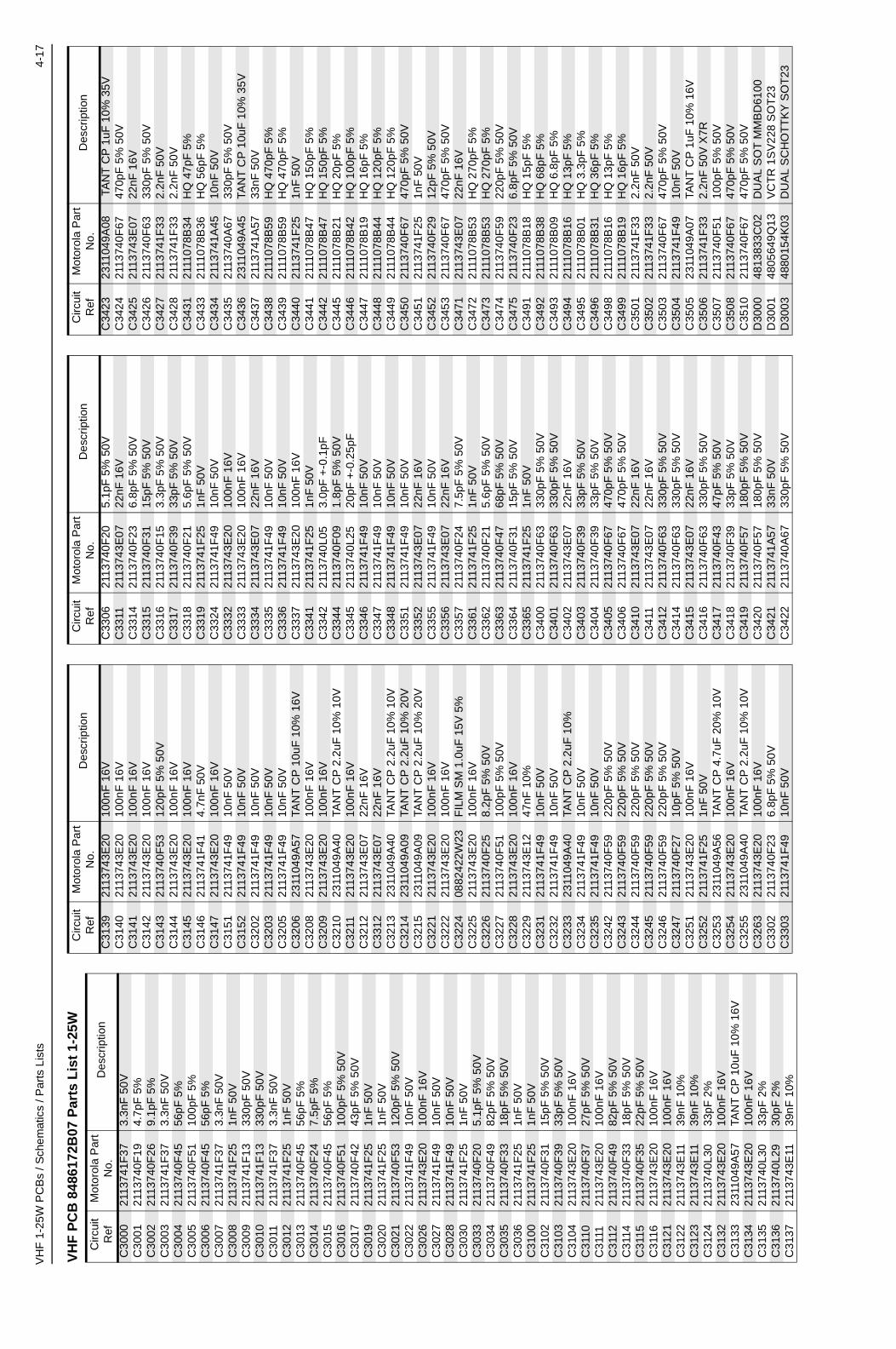
VH
F 1
-25W
PC
Bs
/ Sch
emat
ics
/ Par
ts L
ists
4-17
VH
F P
CB
848
6172
B07
Par
ts L
ist
1-25
W
Circ
uit
Ref
Mot
orol
a P
art
No.
Des
crip
tion
C30
0021
1374
1F37
3.3n
F 5
0VC
3001
2113
740F
194.
7pF
5%
C30
0221
1374
0F26
9.1p
F 5
%C
3003
2113
741F
373.
3nF
50V
C30
0421
1374
0F45
56pF
5%
C30
0521
1374
0F51
100p
F 5
%C
3006
2113
740F
4556
pF 5
%C
3007
2113
741F
373.
3nF
50V
C30
0821
1374
1F25
1nF
50V
C30
0921
1374
1F13
330p
F 5
0VC
3010
2113
741F
1333
0pF
50V
C30
1121
1374
1F37
3.3n
F 5
0VC
3012
2113
741F
251n
F 5
0VC
3013
2113
740F
4556
pF 5
%C
3014
2113
740F
247.
5pF
5%
C30
1521
1374
0F45
56pF
5%
C30
1621
1374
0F51
100p
F 5
% 5
0VC
3017
2113
740F
4243
pF 5
% 5
0VC
3019
2113
741F
251n
F 5
0VC
3020
2113
741F
251n
F 5
0VC
3021
2113
740F
5312
0pF
5%
50V
C30
2221
1374
1F49
10nF
50V
C30
2621
1374
3E20
100n
F 1
6VC
3027
2113
741F
4910
nF 5
0VC
3028
2113
741F
4910
nF 5
0VC
3030
2113
741F
251n
F 5
0VC
3033
2113
740F
205.
1pF
5%
50V
C30
3421
1374
0F49
82pF
5%
50V
C30
3521
1374
0F33
18pF
5%
50V
C30
3621
1374
1F25
1nF
50V
C31
0021
1374
1F25
1nF
50V
C31
0221
1374
0F31
15pF
5%
50V
C31
0321
1374
0F39
33pF
5%
50V
C31
0421
1374
3E20
100n
F 1
6VC
3110
2113
740F
3727
pF 5
% 5
0VC
3111
2113
743E
2010
0nF
16V
C31
1221
1374
0F49
82pF
5%
50V
C31
1421
1374
0F33
18pF
5%
50V
C31
1521
1374
0F35
22pF
5%
50V
C31
1621
1374
3E20
100n
F 1
6VC
3121
2113
743E
2010
0nF
16V
C31
2221
1374
3E11
39nF
10%
C31
2321
1374
3E11
39nF
10%
C31
2421
1374
0L30
33pF
2%
C31
3221
1374
3E20
100n
F 1
6VC
3133
2311
049A
57TA
NT
CP
10u
F 1
0% 1
6VC
3134
2113
743E
2010
0nF
16V
C31
3521
1374
0L30
33pF
2%
C31
3621
1374
0L29
30pF
2%
C31
3721
1374
3E11
39nF
10%
C31
3921
1374
3E20
100n
F 1
6VC
3140
2113
743E
2010
0nF
16V
C31
4121
1374
3E20
100n
F 1
6VC
3142
2113
743E
2010
0nF
16V
C31
4321
1374
0F53
120p
F 5
% 5
0VC
3144
2113
743E
2010
0nF
16V
C31
4521
1374
3E20
100n
F 1
6VC
3146
2113
741F
414.
7nF
50V
C31
4721
1374
3E20
100n
F 1
6VC
3151
2113
741F
4910
nF 5
0VC
3152
2113
741F
4910
nF 5
0VC
3202
2113
741F
4910
nF 5
0VC
3203
2113
741F
4910
nF 5
0VC
3205
2113
741F
4910
nF 5
0VC
3206
2311
049A
57TA
NT
CP
10u
F 1
0% 1
6VC
3208
2113
743E
2010
0nF
16V
C32
0921
1374
3E20
100n
F 1
6VC
3210
2311
049A
40TA
NT
CP
2.2
uF 1
0% 1
0VC
3211
2113
743E
2010
0nF
16V
C32
1221
1374
3E07
22nF
16V
C33
1221
1374
3E07
22nF
16V
C32
1323
1104
9A40
TAN
T C
P 2
.2uF
10%
10V
C32
1423
1104
9A09
TAN
T C
P 2
.2uF
10%
20V
C32
1523
1104
9A09
TAN
T C
P 2
.2uF
10%
20V
C32
2121
1374
3E20
100n
F 1
6VC
3222
2113
743E
2010
0nF
16V
C32
2408
8242
2W23
FIL
M S
M 1
.0uF
15V
5%
C32
2521
1374
3E20
100n
F 1
6VC
3226
2113
740F
258.
2pF
5%
50V
C32
2721
1374
0F51
100p
F 5
% 5
0VC
3228
2113
743E
2010
0nF
16V
C32
2921
1374
3E12
47nF
10%
C32
3121
1374
1F49
10nF
50V
C32
3221
1374
1F49
10nF
50V
C32
3323
1104
9A40
TAN
T C
P 2
.2uF
10%
C32
3421
1374
1F49
10nF
50V
C32
3521
1374
1F49
10nF
50V
C32
4221
1374
0F59
220p
F 5
% 5
0VC
3243
2113
740F
5922
0pF
5%
50V
C32
4421
1374
0F59
220p
F 5
% 5
0VC
3245
2113
740F
5922
0pF
5%
50V
C32
4621
1374
0F59
220p
F 5
% 5
0VC
3247
2113
740F
2710
pF 5
% 5
0VC
3251
2113
743E
2010
0nF
16V
C32
5221
1374
1F25
1nF
50V
C32
5323
1104
9A56
TAN
T C
P 4
.7uF
20%
10V
C32
5421
1374
3E20
100n
F 1
6VC
3255
2311
049A
40TA
NT
CP
2.2
uF 1
0% 1
0VC
3263
2113
743E
2010
0nF
16V
C33
0221
1374
0F23
6.8p
F 5
% 5
0VC
3303
2113
741F
4910
nF 5
0V
Circ
uit
Ref
Mot
orol
a P
art
No.
Des
crip
tion
C33
0621
1374
0F20
5.1p
F 5
% 5
0VC
3311
2113
743E
0722
nF 1
6VC
3314
2113
740F
236.
8pF
5%
50V
C33
1521
1374
0F31
15pF
5%
50V
C33
1621
1374
0F15
3.3p
F 5
% 5
0VC
3317
2113
740F
3933
pF 5
% 5
0VC
3318
2113
740F
215.
6pF
5%
50V
C33
1921
1374
1F25
1nF
50V
C33
2421
1374
1F49
10nF
50V
C33
3221
1374
3E20
100n
F 1
6VC
3333
2113
743E
2010
0nF
16V
C33
3421
1374
3E07
22nF
16V
C33
3521
1374
1F49
10nF
50V
C33
3621
1374
1F49
10nF
50V
C33
3721
1374
3E20
100n
F 1
6VC
3341
2113
741F
251n
F 5
0VC
3342
2113
740L
053.
0pF
+-0
.1pF
C33
4421
1374
0F09
1.8p
F 5
% 5
0VC
3345
2113
740L
2520
pF +
-0.2
5pF
C33
4621
1374
1F49
10nF
50V
C33
4721
1374
1F49
10nF
50V
C33
4821
1374
1F49
10nF
50V
C33
5121
1374
1F49
10nF
50V
C33
5221
1374
3E07
22nF
16V
C33
5521
1374
1F49
10nF
50V
C33
5621
1374
3E07
22nF
16V
C33
5721
1374
0F24
7.5p
F 5
% 5
0VC
3361
2113
741F
251n
F 5
0VC
3362
2113
740F
215.
6pF
5%
50V
C33
6321
1374
0F47
68pF
5%
50V
C33
6421
1374
0F31
15pF
5%
50V
C33
6521
1374
1F25
1nF
50V
C34
0021
1374
0F63
330p
F 5
% 5
0VC
3401
2113
740F
6333
0pF
5%
50V
C34
0221
1374
3E07
22nF
16V
C34
0321
1374
0F39
33pF
5%
50V
C34
0421
1374
0F39
33pF
5%
50V
C34
0521
1374
0F67
470p
F 5
% 5
0VC
3406
2113
740F
6747
0pF
5%
50V
C34
1021
1374
3E07
22nF
16V
C34
1121
1374
3E07
22nF
16V
C34
1221
1374
0F63
330p
F 5
% 5
0VC
3414
2113
740F
6333
0pF
5%
50V
C34
1521
1374
3E07
22nF
16V
C34
1621
1374
0F63
330p
F 5
% 5
0VC
3417
2113
740F
4347
pF 5
% 5
0VC
3418
2113
740F
3933
pF 5
% 5
0VC
3419
2113
740F
5718
0pF
5%
50V
C34
2021
1374
0F57
180p
F 5
% 5
0VC
3421
2113
741A
5733
nF 5
0VC
3422
2113
740A
6733
0pF
5%
50V
Circ
uit
Ref
Mot
orol
a P
art
No.
Des
crip
tion
C34
2323
1104
9A08
TA
NT
CP
1uF
10%
35V
C34
2421
1374
0F67
470p
F 5
% 5
0VC
3425
2113
743E
0722
nF 1
6VC
3426
2113
740F
6333
0pF
5%
50V
C34
2721
1374
1F33
2.2n
F 5
0VC
3428
2113
741F
332.
2nF
50V
C34
3121
1107
8B34
HQ
47p
F 5
%C
3433
2111
078B
36H
Q 5
6pF
5%
C34
3421
1374
1A45
10nF
50V
C34
3521
1374
0A67
330p
F 5
% 5
0VC
3436
2311
049A
45TA
NT
CP
10u
F 1
0% 3
5VC
3437
2113
741A
5733
nF 5
0VC
3438
2111
078B
59H
Q 4
70pF
5%
C34
3921
1107
8B59
HQ
470
pF 5
%C
3440
2113
741F
251n
F 5
0VC
3441
2111
078B
47H
Q 1
50pF
5%
C34
4221
1107
8B47
HQ
150
pF 5
%C
3445
2111
078B
21H
Q 2
0pF
5%
C34
4621
1107
8B42
HQ
100
pF 5
%C
3447
2111
078B
19H
Q 1
6pF
5%
C34
4821
1107
8B44
HQ
120
pF 5
%C
3449
2111
078B
44H
Q 1
20pF
5%
C34
5021
1374
0F67
470p
F 5
% 5
0VC
3451
2113
741F
251n
F 5
0VC
3452
2113
740F
2912
pF 5
% 5
0VC
3453
2113
740F
6747
0pF
5%
50V
C34
7121
1374
3E07
22nF
16V
C34
7221
1107
8B53
HQ
270
pF 5
%C
3473
2111
078B
53H
Q 2
70pF
5%
C34
7421
1374
0F59
220p
F 5
% 5
0VC
3475
2113
740F
236.
8pF
5%
50V
C34
9121
1107
8B18
HQ
15p
F 5
%C
3492
2111
078B
38H
Q 6
8pF
5%
C34
9321
1107
8B09
HQ
6.8
pF 5
%C
3494
2111
078B
16H
Q 1
3pF
5%
C34
9521
1107
8B01
HQ
3.3
pF 5
%C
3496
2111
078B
31H
Q 3
6pF
5%
C34
9821
1107
8B16
HQ
13p
F 5
%C
3499
2111
078B
19H
Q 1
6pF
5%
C35
0121
1374
1F33
2.2n
F 5
0VC
3502
2113
741F
332.
2nF
50V
C35
0321
1374
0F67
470p
F 5
% 5
0VC
3504
2113
741F
4910
nF 5
0VC
3505
2311
049A
07TA
NT
CP
1uF
10%
16V
C35
0621
1374
1F33
2.2n
F 5
0V X
7RC
3507
2113
740F
5110
0pF
5%
50V
C35
0821
1374
0F67
470p
F 5
% 5
0VC
3510
2113
740F
6747
0pF
5%
50V
D30
0048
1383
3C02
DU
AL
SO
T M
MB
D61
00D
3001
4805
649Q
13V
CT
R 1
SV
228
SO
T23
D30
0348
8015
4K03
DU
AL
SC
HO
TT
KY
SO
T23
Circ
uit
Ref
Mot
orol
a P
art
No.
Des
crip
tion
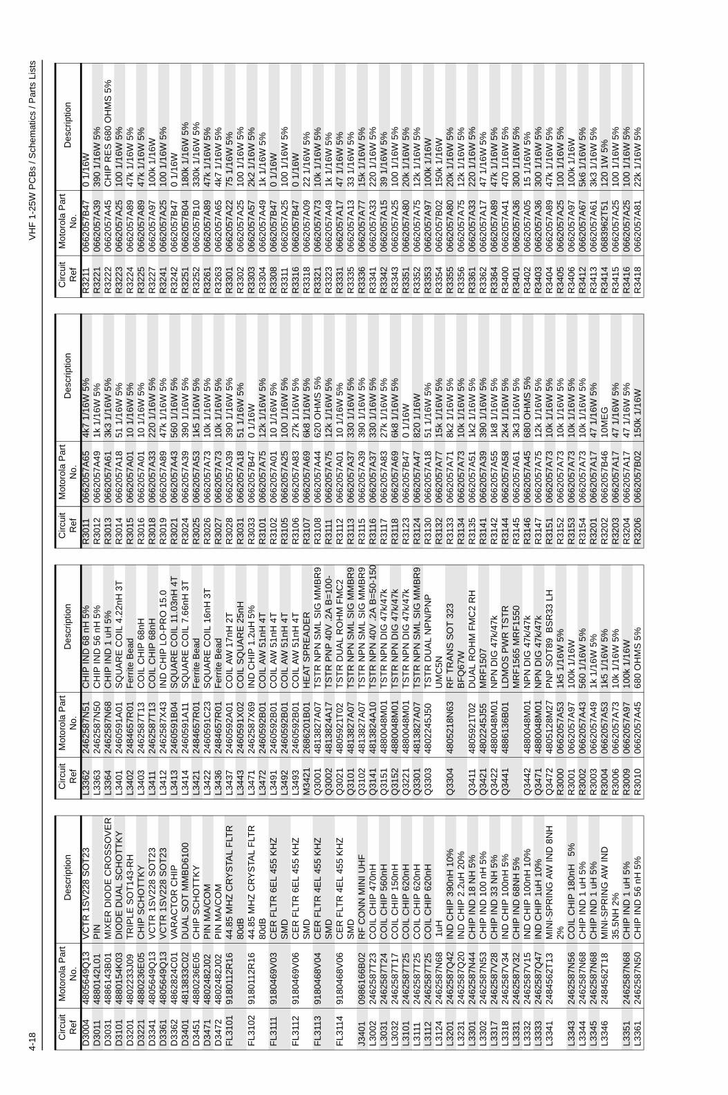
4-18
VH
F 1
-25W
PC
Bs
/ Sch
emat
ics
/ Par
ts L
ists
D30
0448
0564
9Q13
VC
TR
1S
V22
8 S
OT
23D
3011
4880
142L
01P
IND
3031
4886
143B
01M
IXE
R D
IOD
E C
RO
SS
OV
ER
D31
0148
8015
4K03
DIO
DE
DU
AL
SC
HO
TT
KY
D32
0148
0223
3J09
TR
IPLE
SO
T14
3-R
HD
3221
4880
236E
05C
HIP
SC
HO
TT
KY
D33
4148
0564
9Q13
VC
TR
1S
V22
8 S
OT
23D
3361
4805
649Q
13V
CT
R 1
SV
228
SO
T23
D33
6248
6282
4C01
VA
RA
CT
OR
CH
IPD
3401
4813
833C
02D
UA
L S
OT
MM
BD
6100
D34
5148
8023
6E05
CH
IP S
CH
OT
TK
YD
3471
4802
482J
02P
IN M
A/C
OM
D34
7248
0248
2J02
PIN
MA
/CO
MF
L310
191
8011
2R16
44.8
5 M
HZ
CR
YS
TAL
FLT
R
80dB
FL3
102
9180
112R
1644
.85
MH
Z C
RY
STA
L F
LTR
80
dBF
L311
191
8046
9V03
CE
R F
LTR
6E
L 45
5 K
HZ
S
MD
FL3
112
9180
469V
06C
ER
FLT
R 6
EL
455
KH
Z
SM
DF
L311
391
8046
8V04
CE
R F
LTR
4E
L 45
5 K
HZ
S
MD
FL3
114
9180
468V
06C
ER
FLT
R 4
EL
455
KH
Z
SM
DJ3
401
0986
166B
02R
F C
ON
N M
INI U
HF
L300
224
6258
7T23
CO
IL C
HIP
470
nHL3
031
2462
587T
24C
OIL
CH
IP 5
60nH
L303
224
6258
7T17
CO
IL C
HIP
150
nHL3
101
2462
587T
25C
OIL
CH
IP 6
20nH
L311
124
6258
7T25
CO
IL C
HIP
620
nHL3
112
2462
587T
25C
OIL
CH
IP 6
20nH
L312
424
6258
7N68
1uH
L320
124
6258
7Q42
IND
CH
IP 3
90nH
10%
L323
124
6258
7Q20
IND
CH
IP 2
.2uH
20%
L330
124
6258
7N44
CH
IP IN
D 1
8 N
H 5
%L3
302
2462
587N
53C
HIP
IND
100
nH
5%
L331
724
6258
7V28
CH
IP IN
D 3
3 N
H 5
%L3
318
2462
587V
34IN
D C
HIP
100
nH 5
%L3
331
2462
587V
32C
HIP
IND
68N
H 5
%L3
332
2462
587V
15IN
D C
HIP
100
nH 1
0%L3
333
2462
587Q
47IN
D C
HIP
1uH
10%
L334
124
8456
2T13
MIN
I-S
PR
ING
AW
IND
8N
H
2%L3
343
2462
587N
56C
OIL
CH
IP 1
80nH
5%
L334
424
6258
7N68
CH
IP IN
D 1
uH
5%
L334
524
6258
7N68
CH
IP IN
D 1
uH
5%
L334
624
8456
2T18
MIN
I-S
PR
ING
AW
IND
35
.5N
H 2
%L3
351
2462
587N
68C
HIP
IND
1 u
H 5
%L3
361
2462
587N
50C
HIP
IND
56
nH 5
%
Circ
uit
Ref
Mot
orol
a P
art
No.
Des
crip
tion
L336
224
6258
7N51
CH
IP IN
D 6
8 nH
5%
L336
324
6258
7N50
CH
IP IN
D 5
6 nH
5%
L336
424
6258
7N68
CH
IP IN
D 1
uH
5%
L340
124
6059
1A01
SQ
UA
RE
CO
IL 4
.22n
H 3
TL3
402
2484
657R
01F
errit
e B
ead
L340
324
6258
7T13
CO
IL C
HIP
68n
HL3
411
2462
587T
13C
OIL
CH
IP 6
8nH
L341
224
6258
7X43
IND
CH
IP L
O-P
RO
15.
0L3
413
2460
591B
04S
QU
AR
E C
OIL
11.
03nH
4T
L341
424
6059
1A11
SQ
UA
RE
CO
IL 7
.66n
H 3
TL3
421
2484
657R
01F
errit
e B
ead
L342
224
6059
1C23
SQ
UA
RE
CO
IL 1
6nH
3T
L343
624
8465
7R01
Fer
rite
Bea
dL3
437
2460
592A
01C
OIL
AW
17n
H 2
TL3
443
2460
591X
02C
OIL
SQ
UA
RE
25n
HL3
471
2462
587X
69IN
D C
HIP
1.2
uH 5
%L3
472
2460
592B
01C
OIL
AW
51n
H 4
TL3
491
2460
592B
01C
OIL
AW
51n
H 4
TL3
492
2460
592B
01C
OIL
AW
51n
H 4
TL3
493
2460
592B
01C
OIL
AW
51n
H 4
TM
3421
2686
201B
01H
EA
T S
PR
EA
DE
RQ
3001
4813
827A
07T
ST
R N
PN
SM
L S
IG M
MB
R9
Q30
0248
1382
4A17
TS
TR
PN
P 4
0V .2
A B
=10
0-Q
3021
4805
921T
02T
ST
R D
UA
L R
OH
M F
MC
2Q
3101
4813
827A
07T
ST
R N
PN
SM
L S
IG M
MB
R9
Q31
0248
1382
7A07
TS
TR
NP
N S
ML
SIG
MM
BR
9Q
3141
4813
824A
10T
ST
R N
PN
40V
.2A
B=
50-1
50Q
3151
4880
048M
01T
ST
R N
PN
DIG
47k
/47k
Q31
5248
8004
8M01
TS
TR
NP
N D
IG 4
7k/4
7kQ
3221
4880
048M
01T
ST
R N
PN
DIG
47k
/47k
Q33
0148
1382
7A07
TS
TR
NP
N S
ML
SIG
MM
BR
9Q
3303
4802
245J
50T
ST
R D
UA
L N
PN
/PN
P
UM
C5N
Q33
0448
0521
8N63
RF
TR
AN
S S
OT
323
B
FQ
67W
Q34
1148
0592
1T02
DU
AL
RO
HM
FM
C2
RH
Q34
2148
0224
5J55
MR
F15
07Q
3422
4880
048M
01N
PN
DIG
47k
/47k
Q34
4148
8613
6B01
LDM
OS
PW
R T
ST
R
MR
F15
65 M
RF
1550
Q34
4248
8004
8M01
NP
N D
IG 4
7k/4
7kQ
3471
4880
048M
01N
PN
DIG
47k
/47k
Q34
7248
0512
8M27
PN
P S
OT
89 B
SR
33 L
HR
3000
0662
057A
531k
5 1/
16W
5%
R30
0106
6205
7A97
100k
1/1
6WR
3002
0662
057A
4356
0 1/
16W
5%
R30
0306
6205
7A49
1k 1
/16W
5%
R30
0406
6205
7A53
1k5
1/16
W 5
%R
3006
0662
057A
7310
k 1/
16W
5%
R30
0906
6205
7A97
100k
1/1
6WR
3010
0662
057A
4568
0 O
HM
S 5
%
Circ
uit
Ref
Mot
orol
a P
art
No.
Des
crip
tion
R30
1106
6205
7A65
4k7
1/16
W 5
%R
3012
0662
057A
491k
1/1
6W 5
%R
3013
0662
057A
613k
3 1/
16W
5%
R30
1406
6205
7A18
51 1
/16W
5%
R30
1506
6205
7A01
10 1
/16W
5%
R30
1606
6205
7A01
10 1
/16W
5%
R30
1806
6205
7A33
220
1/16
W 5
%R
3019
0662
057A
8947
k 1/
16W
5%
R30
2106
6205
7A43
560
1/16
W 5
%R
3024
0662
057A
3939
0 1/
16W
5%
R30
2506
6205
7A53
1k5
1/16
W 5
%R
3026
0662
057A
7310
k 1/
16W
5%
R30
2706
6205
7A73
10k
1/16
W 5
%R
3028
0662
057A
3939
0 1/
16W
5%
R30
3106
6205
7A18
51 1
/16W
5%
R30
3306
6205
7B47
0 1/
16W
R
3101
0662
057A
7512
k 1/
16W
5%
R31
0206
6205
7A01
10 1
/16W
5%
R31
0506
6205
7A25
100
1/16
W 5
%R
3106
0662
057A
8327
k 1/
16W
5%
R31
0706
6205
7A69
6k8
1/16
W 5
%R
3108
0662
057A
4462
0 O
HM
S 5
%R
3111
0662
057A
7512
k 1/
16W
5%
R
3112
0662
057A
0110
1/1
6W 5
%R
3113
0662
057A
3733
0 1/
16W
5%
R31
1506
6205
7A39
390
1/16
W 5
%R
3116
0662
057A
3733
0 1/
16W
5%
R31
1706
6205
7A83
27k
1/16
W 5
%R
3118
0662
057A
696k
8 1/
16W
5%
R31
2306
6205
7B47
0 1/
16W
R
3124
0662
057A
4782
0 1/
16W
R
3130
0662
057A
1851
1/1
6W 5
%R
3132
0662
057A
7715
k 1/
16W
5%
R31
3306
6205
7A71
8k2
1/16
W 5
%R
3134
0662
057A
7310
k 1/
16W
5%
R31
3506
6205
7A51
1k2
1/16
W 5
%R
3141
0662
057A
3939
0 1/
16W
5%
R31
4206
6205
7A55
1k8
1/16
W 5
%R
3144
0662
057A
582k
4 1/
16W
5%
R31
4506
6205
7A61
3k3
1/16
W 5
%R
3146
0662
057A
4568
0 O
HM
S 5
%R
3147
0662
057A
7512
k 1/
16W
5%
R31
5106
6205
7A73
10k
1/16
W 5
%R
3152
0662
057A
7310
k 1/
16W
5%
R31
5306
6205
7A73
10k
1/16
W 5
%R
3154
0662
057A
7310
k 1/
16W
5%
R32
0106
6205
7A17
47 1
/16W
5%
R32
0206
6205
7B46
10M
EG
R32
0306
6205
7A17
47 1
/16W
5%
R32
0406
6205
7A17
47 1
/16W
5%
R32
0606
6205
7B02
150k
1/1
6W
Circ
uit
Ref
Mot
orol
a P
art
No.
Des
crip
tion
R32
1106
6205
7B47
0 1/
16W
R32
2106
6205
7A39
390
1/16
W 5
%R
3222
0662
057A
45C
HIP
RE
S 6
80 O
HM
S 5
%R
3223
0662
057A
2510
0 1/
16W
5%
R32
2406
6205
7A89
47k
1/16
W 5
%R
3225
0662
057A
8947
k 1/
16W
5%
R32
2706
6205
7A97
100k
1/1
6WR
3241
0662
057A
2510
0 1/
16W
5%
R32
4206
6205
7B47
0 1/
16W
R32
5106
6205
7B04
180k
1/1
6W 5
%R
3252
0662
057B
1033
0k 1
/16W
5%
R32
6106
6205
7A89
47k
1/16
W 5
%R
3263
0662
057A
654k
7 1/
16W
5%
R33
0106
6205
7A22
75 1
/16W
5%
R33
0206
6205
7A25
100
1/16
W 5
%R
3303
0662
057A
572k
2 1/
16W
5%
R33
0406
6205
7A49
1k 1
/16W
5%
R33
0806
6205
7B47
0 1/
16W
R33
1106
6205
7A25
100
1/16
W 5
%R
3316
0662
057B
470
1/16
WR
3318
0662
057A
0922
1/1
6W 5
%R
3321
0662
057A
7310
k 1/
16W
5%
R33
2306
6205
7A49
1k 1
/16W
5%
R33
3106
6205
7A17
47 1
/16W
5%
R33
3506
6205
7A13
33 1
/16W
5%
R33
3606
6205
7A77
15k
1/16
W 5
%R
3341
0662
057A
3322
0 1/
16W
5%
R33
4206
6205
7A15
39 1
/16W
5%
R33
4306
6205
7A25
100
1/16
W 5
%R
3351
0662
057A
8020
k 1/
16W
5%
R33
5206
6205
7A75
12k
1/16
W 5
%R
3353
0662
057A
9710
0k 1
/16W
R33
5406
6205
7B02
150k
1/1
6WR
3355
0662
057A
8020
k 1/
16W
5%
R33
5606
6205
7A75
12k
1/16
W 5
%R
3361
0662
057A
3322
0 1/
16W
5%
R33
6206
6205
7A17
47 1
/16W
5%
R33
6406
6205
7A89
47k
1/16
W 5
%R
3400
0662
057A
4147
0 1/
16W
5%
R34
0106
6205
7A36
300
1/16
W 5
%R
3402
0662
057A
0515
1/1
6W 5
%R
3403
0662
057A
3630
0 1/
16W
5%
R34
0406
6205
7A89
47k
1/16
W 5
%R
3405
0662
057A
2510
0 1/
16W
5%
R34
0606
6205
7A97
100k
1/1
6WR
3412
0662
057A
675k
6 1/
16W
5%
R34
1306
6205
7A61
3k3
1/16
W 5
%R
3414
0683
962T
5112
0 1W
5%
R34
1506
6205
7A25
100
1/16
W 5
%R
3416
0662
057A
2510
0 1/
16W
5%
R34
1806
6205
7A81
22k
1/16
W 5
%
Circ
uit
Ref
Mot
orol
a P
art
No.
Des
crip
tion
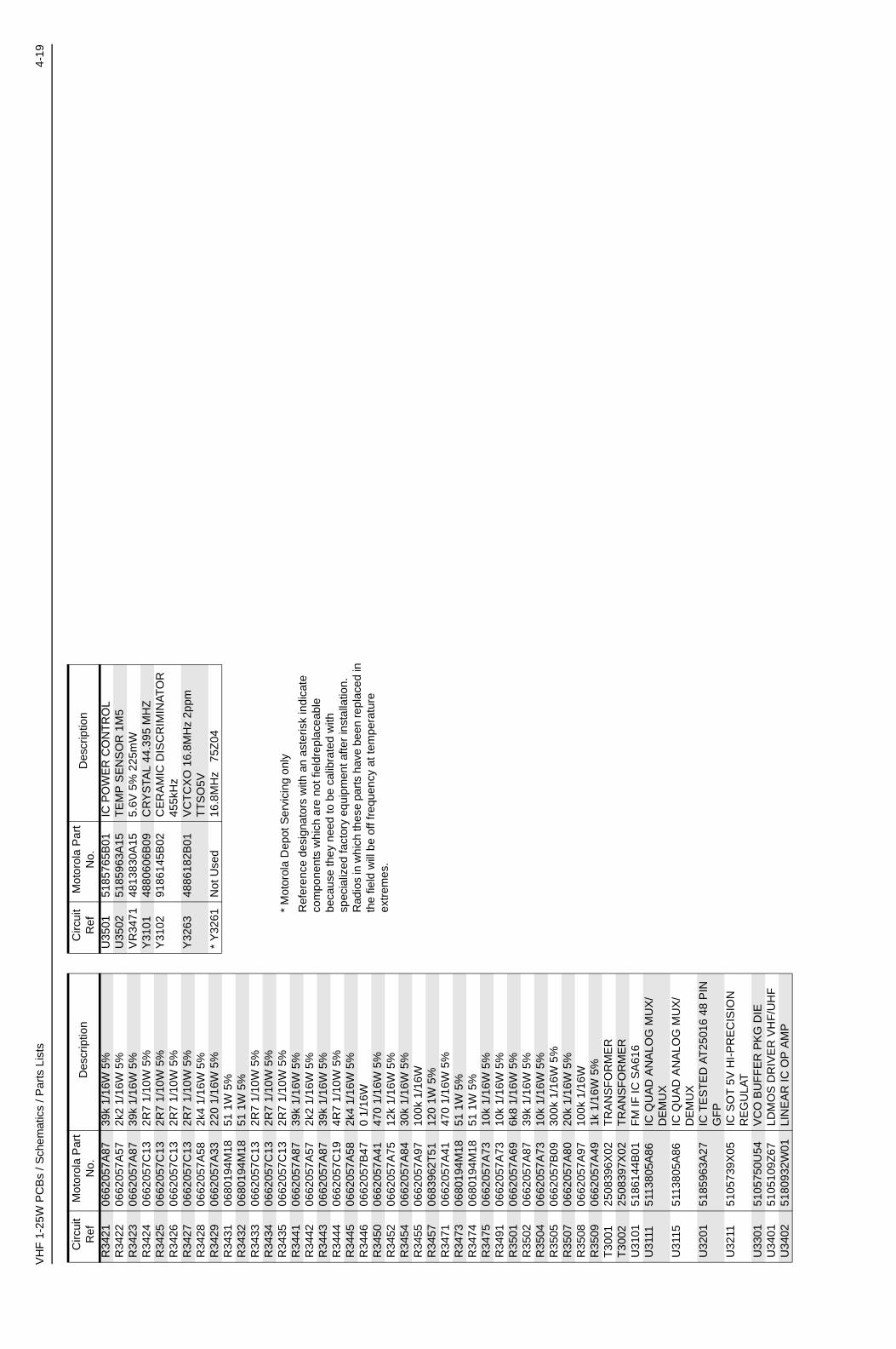
VH
F 1
-25W
PC
Bs
/ Sch
emat
ics
/ Par
ts L
ists
4-19
* M
otor
ola
Dep
ot S
ervi
cing
onl
y
Ref
eren
ce d
esig
nato
rs w
ith a
n as
teris
k in
dica
te
com
pone
nts
whi
ch a
re n
ot fi
eldr
epla
ceab
le
beca
use
they
nee
d to
be
calib
rate
d w
ith
spec
ializ
ed fa
ctor
y eq
uipm
ent a
fter
inst
alla
tion.
R
adio
s in
whi
ch th
ese
part
s ha
ve b
een
repl
aced
in
the
field
will
be
off f
requ
ency
at t
empe
ratu
re
extr
emes
.
R34
2106
6205
7A87
39k
1/16
W 5
%R
3422
0662
057A
572k
2 1/
16W
5%
R34
2306
6205
7A87
39k
1/16
W 5
%R
3424
0662
057C
132R
7 1/
10W
5%
R34
2506
6205
7C13
2R7
1/10
W 5
%R
3426
0662
057C
132R
7 1/
10W
5%
R34
2706
6205
7C13
2R7
1/10
W 5
%R
3428
0662
057A
582k
4 1/
16W
5%
R34
2906
6205
7A33
220
1/16
W 5
%R
3431
0680
194M
1851
1W
5%
R34
3206
8019
4M18
51 1
W 5
%R
3433
0662
057C
132R
7 1/
10W
5%
R34
3406
6205
7C13
2R7
1/10
W 5
%R
3435
0662
057C
132R
7 1/
10W
5%
R34
4106
6205
7A87
39k
1/16
W 5
%R
3442
0662
057A
572k
2 1/
16W
5%
R34
4306
6205
7A87
39k
1/16
W 5
%R
3444
0662
057C
194R
7 1/
10W
5%
R34
4506
6205
7A58
2k4
1/16
W 5
%R
3446
0662
057B
470
1/16
WR
3450
0662
057A
4147
0 1/
16W
5%
R34
5206
6205
7A75
12k
1/16
W 5
%R
3454
0662
057A
8430
k 1/
16W
5%
R34
5506
6205
7A97
100k
1/1
6WR
3457
0683
962T
5112
0 1W
5%
R34
7106
6205
7A41
470
1/16
W 5
%R
3473
0680
194M
1851
1W
5%
R34
7406
8019
4M18
51 1
W 5
%R
3475
0662
057A
7310
k 1/
16W
5%
R34
9106
6205
7A73
10k
1/16
W 5
%R
3501
0662
057A
696k
8 1/
16W
5%
R35
0206
6205
7A87
39k
1/16
W 5
%R
3504
0662
057A
7310
k 1/
16W
5%
R35
0506
6205
7B09
300k
1/1
6W 5
%R
3507
0662
057A
8020
k 1/
16W
5%
R35
0806
6205
7A97
100k
1/1
6WR
3509
0662
057A
491k
1/1
6W 5
%T
3001
2508
396X
02T
RA
NS
FO
RM
ER
T30
0225
0839
7X02
TR
AN
SF
OR
ME
RU
3101
5186
144B
01F
M IF
IC S
A61
6U
3111
5113
805A
86IC
QU
AD
AN
ALO
G M
UX
/D
EM
UX
U31
1551
1380
5A86
IC Q
UA
D A
NA
LOG
MU
X/
DE
MU
XU
3201
5185
963A
27IC
TE
ST
ED
AT
2501
6 48
PIN
G
FP
U32
1151
0573
9X05
IC S
OT
5V
HI-
PR
EC
ISIO
N
RE
GU
LAT
U33
0151
0575
0U54
VC
O B
UF
FE
R P
KG
DIE
U34
0151
0510
9Z67
LDM
OS
DR
IVE
R V
HF
/UH
FU
3402
5180
932W
01LI
NE
AR
IC O
P A
MP
Circ
uit
Ref
Mot
orol
a P
art
No.
Des
crip
tion
U35
0151
8576
5B01
IC P
OW
ER
CO
NT
RO
LU
3502
5185
963A
15T
EM
P S
EN
SO
R 1
M5
VR
3471
4813
830A
155.
6V 5
% 2
25m
WY
3101
4880
606B
09C
RY
STA
L 44
.395
MH
ZY
3102
9186
145B
02C
ER
AM
IC D
ISC
RIM
INA
TO
R
455k
Hz
Y32
6348
8618
2B01
VC
TC
XO
16.
8MH
z 2p
pm
TT
SO
5V*
Y32
61N
ot U
sed
16.8
MH
z 7
5Z04
Circ
uit
Ref
Mot
orol
a P
art
No.
Des
crip
tion

4-20
VH
F 1
-25W
PC
Bs
/ Sch
emat
ics
/ Par
ts L
ists
TH
IS P
AG
E IN
TE
NT
ION
AL
LY L
EF
T B
LA
NK
GM328/GM338/GM398Mobile Radios
UHF (403-470MHz)
Service Information
Issue: December, 2003

Computer Software CopyrightsThe Motorola products described in this manual may include copyrighted Motorola computer programs stored in semiconductor memories or other media. Laws in the United States and other countries preserve for Motorola certain exclusive rights for copyrighted computer programs, including the exclusive right to copy or reproduce in any form, the copyrighted computer program. Accordingly, any copyrighted Motorola computer programs contained in the Motorola products described in this manual may not be copied or reproduced in any manner without the express written permission of Motorola. Furthermore, the purchase of Motorola products shall not be deemed to grant, either directly or by implication, estoppel or otherwise, any license under the copyrights, patents or patent applications of Motorola, except for the normal non-exclusive royalty-free license to use that arises by operation of law in the sale of a product.

i
Table of Contents
Section 1 Model Chart and Technical Specifications
1.0 GM328/GM338/GM398 Model Chart ...................................................................1-12.0 Technical Specifications ......................................................................................1-2
Section 2 Theory of Operation
1.0 Introduction ..........................................................................................................2-12.0 UHF (403-470 MHz) Receiver .............................................................................2-1
2.1 Receiver Front-End ........................................................................................2-12.2 Front-End Band-Pass Filters & Pre-Amplifier .................................................2-22.3 First Mixer and High Intermediate Frequency (IF)..........................................2-22.4 Low Intermediate Frequency (IF) and Receiver Back End.............................2-3
3.0 UHF (403-470 MHz) Transmitter Power Amplifier (PA) 25 W..............................2-33.1 First Power Controlled Stage..........................................................................2-43.2 Power Controlled Driver Stage .......................................................................2-43.3 Final Stage .....................................................................................................2-43.4 Directional Coupler .........................................................................................2-53.5 Antenna Switch...............................................................................................2-53.6 Harmonic Filter ...............................................................................................2-53.7 Power Control.................................................................................................2-5
4.0 UHF (403-470 MHz) Frequency Synthesis ..........................................................2-64.1 Reference Oscillator .......................................................................................2-64.2 Fractional-N Synthesizer ................................................................................2-74.3 Voltage Controlled Oscillator (VCO)...............................................................2-84.4 Synthesizer Operation ....................................................................................2-9
Section 3 Troubleshooting Charts
1.0 Troubleshooting Flow Chart for Receiver ............................................................3-12.0 Troubleshooting Flow Chart for 25W Transmitter ................................................3-33.0 Troubleshooting Flow Chart for Synthesizer........................................................3-64.0 Troubleshooting Flow Chart for VCO...................................................................3-7
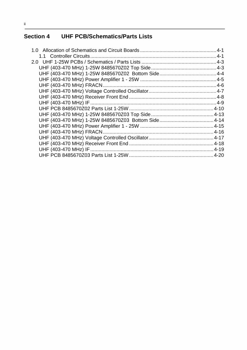
ii
Section 4 UHF PCB/Schematics/Parts Lists
1.0 Allocation of Schematics and Circuit Boards .......................................................4-11.1 Controller Circuits...........................................................................................4-1
2.0 UHF 1-25W PCBs / Schematics / Parts Lists ......................................................4-3UHF (403-470 MHz) 1-25W 8485670Z02 Top Side ...............................................4-3UHF (403-470 MHz) 1-25W 8485670Z02 Bottom Side.........................................4-4UHF (403-470 MHz) Power Amplifier 1 - 25W .......................................................4-5UHF (403-470 MHz) FRACN..................................................................................4-6UHF (403-470 MHz) Voltage Controlled Oscillator.................................................4-7UHF (403-470 MHz) Receiver Front End ...............................................................4-8UHF (403-470 MHz) IF ...........................................................................................4-9UHF PCB 8485670Z02 Parts List 1-25W.............................................................4-10UHF (403-470 MHz) 1-25W 8485670Z03 Top Side .............................................4-13UHF (403-470 MHz) 1-25W 8485670Z03 Bottom Side.......................................4-14UHF (403-470 MHz) Power Amplifier 1 - 25W .....................................................4-15UHF (403-470 MHz) FRACN................................................................................4-16UHF (403-470 MHz) Voltage Controlled Oscillator...............................................4-17UHF (403-470 MHz) Receiver Front End .............................................................4-18UHF (403-470 MHz) IF .........................................................................................4-19UHF PCB 8485670Z03 Parts List 1-25W.............................................................4-20
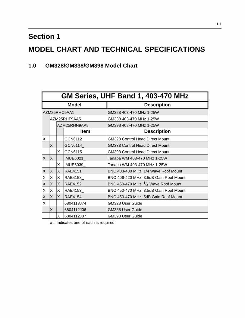
1-1
Section 1
MODEL CHART AND TECHNICAL SPECIFICATIONS
1.0 GM328/GM338/GM398 Model Chart
GM Series, UHF Band 1, 403-470 MHzModel Description
AZM25RHC9AA1 GM328 403-470 MHz 1-25W
AZM25RHF9AA5 GM338 403-470 MHz 1-25W
AZM25RHN9AA8 GM398 403-470 MHz 1-25W
Item Description
X GCN6112_ GM328 Control Head Direct Mount
X GCN6114_ GM338 Control Head Direct Mount
X GCN6115_ GM398 Control Head Direct Mount
X X IMUE6021_ Tanapa WM 403-470 MHz 1-25W
X IMUE6039_ Tanapa WM 403-470 MHz 1-25W
X X X RAE4151_ BNC 403-430 MHz, 1/4 Wave Roof Mount
X X X RAE4158_ BNC 406-420 MHz, 3.5dB Gain Roof Mount
X X X RAE4152_ BNC 450-470 MHz, 1/4 Wave Roof Mount
X X X RAE4153_ BNC 450-470 MHz, 3.5dB Gain Roof Mount
X X X RAE4154_ BNC 450-470 MHz, 5dB Gain Roof Mount
X 6804113J74 GM328 User Guide
X 6804112J06 GM338 User Guide
X 6804112J07 GM398 User Guide
x = Indicates one of each is required.
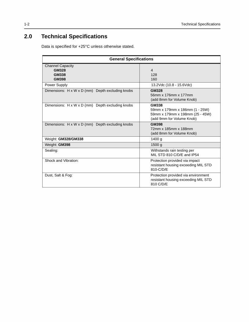
1-2 Technical Specifications
2.0 Technical Specifications
Data is specified for +25°C unless otherwise stated.
General Specifications
Channel CapacityGM328GM338GM398
4128160
Power Supply 13.2Vdc (10.8 - 15.6Vdc)
Dimensions: H x W x D (mm) Depth excluding knobs GM32856mm x 176mm x 177mm(add 8mm for Volume Knob)
Dimensions: H x W x D (mm) Depth excluding knobs GM33859mm x 179mm x 186mm (1 - 25W)59mm x 179mm x 198mm (25 - 45W)(add 9mm for Volume Knob)
Dimensions: H x W x D (mm) Depth excluding knobs GM39872mm x 185mm x 188mm(add 8mm for Volume Knob)
Weight: GM328/GM338 1400 g
Weight: GM398 1500 g
Sealing: Withstands rain testing per MIL STD 810 C/D/E and IP54
Shock and Vibration: Protection provided via impactresistant housing exceeding MIL STD 810-C/D/E
Dust, Salt & Fog: Protection provided via environment resistant housing exceeding MIL STD 810 C/D/E

Technical Specifications 1-3
Transmitter UHF
*Frequencies - Full Bandsplit UHF 403-470 MHz
Channel Spacing 12.5/20/25 kHz
Frequency Stability(-30°C to +60°C, +25° Ref.)
±2.0 ppm
Power 1-25W
Modulation Limiting±2.5 @ 12.5 kHz ±4.0 @ 20 kHz±5.0 @ 25 kHz
FM Hum & Noise-40 dB @ 12.5kHz-45 dB @ 20/25kHz
Conducted/Radiated Emission (ETS)-36 dBm <1 GHz-30 dBm >1 GHz
Adjacent Channel Power-60 dB @ 12.5 kHz-70 dB @ 25 kHz
Audio Response (300 - 3000 Hz) +1 to -3 dB
Audio Distortion @1000Hz, 60%Rated Maximum Deviation
<3% typical
Receiver UHF
*Frequencies - Full Bandsplit UHF 403-470 MHz
Channel Spacing 12.5/20/25 kHz
Sensitivity (12 dB SINAD) 0.30 µV (0.22 µV typical)
Intermodulation (ETS)>65 dB
Base Mode: >70dB (1-25W model only)
Adjacent Channel Selectivity (ETS)65 dB @ 12.5 kHz 70 dB @ 20 kHz75 dB @ 25 kHz
Spurious Rejection (ETS)70 dB @ 12.5 kHz75 dB @ 20/25 kHz
Rated Audio3W Internal
13W External
Audio Distortion @ Rated Audio <3% typical
Hum & Noise-40 dB @ 12.5 kHz
-45 dB @ 20/25 kHz
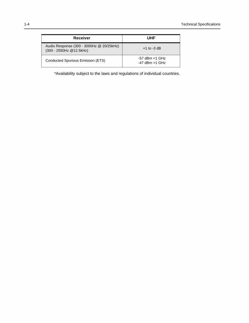
1-4 Technical Specifications
*Availability subject to the laws and regulations of individual countries.
Audio Response (300 - 3000Hz @ 20/25kHz)(300 - 2550Hz @12.5kHz)
+1 to -3 dB
Conducted Spurious Emission (ETS)-57 dBm <1 GHz-47 dBm >1 GHz
Receiver UHF

2-1
Section 2
THEORY OF OPERATION
1.0 Introduction
This Chapter provides a detailed theory of operation for the UHF circuits in the radio. For details of the theory of operation and troubleshooting for the the associated Controller circuits refer to the Controller Section of this manual.
2.0 UHF (403-470 MHz) Receiver
2.1 Receiver Front-End
The receiver is able to cover the UHF range from 403 to 470 MHz. It consists of four major blocks: front-end bandpass filters and pre-amplifier, first mixer, high-IF, low-IF and receiver back-end . Two varactor-tuned bandpass filters perform antenna signal pre-selection. A cross over quad diode mixer converts the signal to the first IF of 44.85 MHz. Low-side first injection is used.
Figure 2-1 UHF Receiver Block Diagram
Demodulator
1. Crystal Filter
MixerVaractor Tuned Filter
RF AmpVaractor Tuned Filter
Pin Diode Antenna SwitchRF Jack
Antenna
Control Voltagefrom PCIC First LO
from FGU
Recovered Audio
RSSI
Second LO
2. Crystal Filter
455kHz Filter(25kHz)
455kHz Filter(25kHz)
455kHz Filter(12.5kHz)
455kHz Filter(12.5kHz)
Sw
itch
Sw
itch
Sw
itch
Sw
itch
Limiter
1. IF Amp
2. IF Amp
Filter Bank Selectionfrom Synthesizer IC
Harmonic Filter
BWSELECT
2-2 UHF (403-470 MHz) Receiver
There are two 2-pole 44.85 MHz crystal filters in the high-IF section and 2 pairs of 455 kHz ceramic filters in the low-IF section to provide the required adjacent channel selectivity .The correct pair of ceramic filters for 12.5 or 25KHz channel spacing is selected via control line BWSELECT. The second IF at 455 kHz is mixed, amplified and demodulated in the IF IC. The processing of the demodulated audio signal is performed by an audio processing IC located in the controller section.
2.2 Front-End Band-Pass Filters & Pre-Amplifier
The received signal from the radio’s antenna connector is first routed through the harmonic filter and antenna switch, which are part of the RF power amplifier circuitry, before being applied to the receiver pre-selector filter (C4001, C4002, D4001 and associated components). The 2-pole pre-selector filter tuned by the varactor diodes D4001 and D4002 pre-selects the incoming signal (RXIN) from the antenna switch to reduce spurious effects to following stages. The tuning voltage (FECTRL_1) ranging from 2 volts to 8 volts is controlled by pin 20 of PCIC (U4501) in the Transmitter section. A dual hot carrier diode (D4003) limits any inband signal to 0 dBm to prevent damage to the pre-amplifier.
The RF pre-amplifier is an SMD device (Q4003) with collector base feedback to stabilize gain, impedance, and intermodulation. The collector current of approximately 11-16 mA is drawn from the voltage 9V3 via L4003 and R4002. A switchable 3dB pad (R4066,R4007,R4063, R4064 and R4070), controlled via line FECTRL_2 and Q4004 stabilizes the output impedance and intermodulation performance.
A second 2-pole varactor tuned bandpass filter provides additional filtering of the amplified signal. The varactor diodes D4004 and D4005 are controlled by the same signal FECTRL_1, which controls the pre-selector filter. A following 1 dB pad (R4013 - R4015) stabilizes the output impedance and intermodulation performance.
2.3 First Mixer and High Intermediate Frequency (IF)
The signal coming from the front-end is converted to the first IF (44.85 MHz) using a cross over quad diode mixer (D4051). Its ports are matched for incoming RF signal conversion to the 44.85 MHz IF using low side injection via matching transformers T4051 and T4052. The injection signal (RXINJ) coming from the RX VCO buffer (Q4332) is filtered by the lowpass filter consisting of (L4053, L4054, C4053 - C4055) followed by a matching transformer T4052 and has a level of approximately 15dBm.
The mixer IF output signal (IF) from transformer T4501pin 2 is fed to the first two pole crystal filter FL3101. The filter output in turn is matched to the following IF amplifier.
The IF amplifier Q3101 is actively biased by a collector base feedback (R3101, R3106) to a current drain of approximately 5 mA drawn from the voltage 5V. Its output impedance is matched to the second two pole crystal filter FL3102. The signal is further amplified by a preamplifier (Q3102) before going into pin 1 of IFIC (U3101).
A dual hot carrier diode (D3101) limits the filter output voltage swing to reduce overdrive effects at RF input levels above -27 dBm.
UHF (403-470 MHz) Transmitter Power Amplifier (PA) 25 W 2-3
2.4 Low Intermediate Frequency (IF) and Receiver Back End
The 44.85 high IF signal from the second IF amplifier feeds the IF IC (U3101) at pin1. Within the IF IC the 44.85 MHz high IF signal mixes with the 44.395 MHz second local oscillator (2nd LO) to produce the low IF signal at 455 kHz. The 2nd LO frequency is determined by crystal Y3101. The low IF signal is amplified and filtered by an external pair of 455 kHz ceramic filters FL3112, FL3114 for 20/25 kHz channel spacing or FL3111,FL3113/F3115 for 12.5 kHz channel spacing. These pairs are selectable via BWSELECT. The filtered output from the ceramic filters is applied to the limiter input pin of the IF IC (pin 14).
The IF IC contains a quadrature detector using a ceramic phase-shift element (Y3102) to provide audio detection. Internal amplification provides an audio output level of 120 mV rms (at 60% deviation) from U3103 pin 8 (DISCAUDIO) which is fed to the ASFIC_CMP (U0221) pin 2 (part of the Controller circuitry).
A Received Signal Strength Indicator (RSSI) signal is available at U3101 pin 5, having a dynamic range of 70 dB. The RSSI signal is interpreted by the microprocessor (U0101 pin 63) and in addition is available at accessory connector J0501-15.
3.0 UHF (403-470 MHz) Transmitter Power Amplifier (PA) 25 W
The radio’s 25W PA is a three stage amplifier used to amplify the output from the VCOBIC to the radio transmit level. All three stages utilize LDMOS technology. The gain of the first stage (U4401) is adjustable, controlled by pin 4 of PCIC (U4501) via U4402-1. It is followed by an LDMOS stage (Q4421) and LDMOS final stage (Q4441).
Figure 2-2 UHF Transmitter Block Diagram
Devices U4401, Q4421 and Q4441 are surface mounted. A pressure pad between board and the radio's cover provides good thermal contact between the devices and the chassis.
PCIC
Pin Diode Antenna Switch RF Jack
Antenna
Harmonic Filter
PowerSense
PA-FinalStage
From VCO
ControlledStage
Vcontrol
Bias 1
Bias 2
To Microprocessor
TemperatureSense
SPI BUS
ASFIC_CMP
PAPWRSET
To Microprocessor
PADriver

2-4 UHF (403-470 MHz) Transmitter Power Amplifier (PA) 25 W
3.1 First Power Controlled Stage
The first stage (U4401) is a 20dB gain integrated circuit containing two LDMOS FET amplifier stages. It amplifies the RF signal from the VCO (TXINJ). The output power of stage U4401 is controlled by a DC voltage applied to pin 1 from the op-amp U4402-1, pin 1. The control voltage simultaneously varies the bias of two FET stages within U4401. This biasing point determines the overall gain of U4401 and therefore its output drive level to Q4421, which in turn controls the output power of the PA.Op-amp U4402-1 monitors the drain current of U4401 via resistor R4444 and adjusts the bias voltage of U4401 so that the current remains constant. The PCIC (U4501) provides a DC output voltage at pin 4 (INT) which sets the reference voltage of the current control loop. A raising power output causes the DC voltage from the PCIC to fall, and U4402-1 adjusts the bias voltage for a lower drain current to lower the gain of the stage.In receive mode the DC voltage from PCIC pin 23 (RX) turns on Q4442, which in turn switches off the biasing voltage to U4401.
Switch S5440 is a pressure pad with a conductive strip which connects two conductive areas on the board when the radio's cover is properly screwed to the chassis. When the cover is removed, S5440 opens and the resulting high voltage level at the inverting inputs of the current control op-amps U4402-1 & 2 switches off the biasing of U4401 and Q4421. This prevents transmitter key up while the devices do not have proper thermal contact to the chassis.
3.2 Power Controlled Driver Stage
The next stage is an LDMOS device (Q4421) providing a gain of 12dB. This device requires a positive gate bias and a quiescent current flow for proper operation. The bias is set during transmit mode by the drain current control op-amp U4402-2, and fed to the gate of Q4421 via the resistive network R4429, R4418, R4415 and R4416.Op-amp U4402-2 monitors the drain current of U4421 via resistors R4424-27 and adjusts the bias voltage of Q4421 so that the current remains constant. The PCIC (U4501) provides a DC output voltage at pin 4 (INT) which sets the reference voltage of the current control loop. A raising power output causes the DC voltage from the PCIC to fall, and U4402-2 adjusts the bias voltage for a lower drain current to lower the gain of the stage.In receive mode the DC voltage from PCIC pin 23 (RX) turns on Q4422, which in turn switches off the biasing voltage to Q4421.
3.3 Final Stage
The final stage is an LDMOS device (Q4441) providing a gain of 12dB. This device also requires a positive gate bias and a quiescent current flow for proper operation. The voltage of the line MOSBIAS_2 is set in transmit mode by the ASFIC and fed to the gate of Q4441 via the resistive network R4404, R4406, and R4431-2. This bias voltage is tuned in the factory. If the transistor is replaced, the bias voltage must be tuned using the Global Tuner. Care must be taken not to damage the device by exceeding the maximum allowed bias voltage. The device’s drain current is drawn directly from the radio’s DC supply voltage input, PASUPVLTG, via L4436 and L4437.A matching network consisting of C4441-49 and striplines transforms the impedance to 50 ohms and feeds the directional coupler.
UHF (403-470 MHz) Transmitter Power Amplifier (PA) 25 W 2-5
3.4 Directional Coupler
The directional coupler is a microstrip printed circuit, which couples a small amount of the forward power delivered by Q4441. The coupled signal is rectified by D4451. The DC voltage is proportional to the RF output power and feeds the RFIN port of the PCIC (U4501 pin 1). The PCIC controls the gain of stages U4401 and Q4421 as necessary to hold this voltage constant, thus ensuring the forward power out of the radio to be held to a constant value.
3.5 Antenna Switch
The antenna switch consists of two PIN diodes, D4471 and D4472. In the receive mode, both diodes are off. Signals applied at the antenna jack J4401 are routed, via the harmonic filter, through network L4472, C4474 and C4475, to the receiver input. In the transmit mode, K9V1 turns on Q4471 which enables current sink Q4472, set to 96 mA by R4473 and VR4471. This completes a DC path from PASUPVLTG, through L4437, D4471, L4472, D4472, L4471, R4474 and the current sink, to ground. Both diodes are forward biased into conduction. The transmitter RF from the directional coupler is routed via D4471 to the harmonic filter and antenna jack. D4472 also conducts, shunting RF power and preventing it from reaching the receiver port (RXIN). L4472 is selected to appear as a broadband lambda/4 wave transmission line, making the short circuit presented by D4472 appear as an open circuit at the junction of D4472 and the receiver path.
3.6 Harmonic Filter
Components L4491-L4493 and L4472, C4491, C4496-98 form a Butterworth low-pass filter to attenuate harmonic energy of the transmitter to specifications level. R4491 is used to drain electrostatic charge that might otherwise build up on the antenna. The harmonic filter also prevents high level RF signals above the receiver passband from reaching the receiver circuits, improving spurious response rejection.
3.7 Power Control
The transmitter uses the Power Control IC (PCIC, U4501) to control the power output of the radio. A portion of the forward RF power from the transmitter is sampled by the directional coupler and rectified, to provide a DC voltage to the RFIN port of the PCIC (pin 1) which is proportional to the sampled RF power.
The ASFIC (U0221) has internal digital to analog converters (DACs) which provide a reference voltage of the control loop to the PCIC via R4505. The reference voltage level is programmable through the SPI line of the PCIC. This reference voltage is proportional to the desired power setting of the transmitter, and is factory programmed at several points across the frequency range of the transmitter to offset frequency response variations of the transmitter’s power detector circuit.
The PCIC provides a DC output voltage at pin 4 (INT) which sets the drain current of the first (U4401) and second (Q4421) transmitter stage via current control op-amps U3402-1 and U3402-2. This adjusts the transmitter power output to the intended value. Variations in forward transmitter power cause the DC voltage at pin 1 to change, and the PCIC adjusts the control voltage above or below its nominal value to raise or lower output power.
Capacitors C4502-4, in conjunction with resistors and integrators within the PCIC, control the transmitter power-rise (key-up) and power-decay (de-key) characteristic to minimize splatter into adjacent channels.

2-6 UHF (403-470 MHz) Frequency Synthesis
U4502 is a temperature-sensing device, which monitors the circuit board temperature in the vicinity of the transmitter driver and final devices, and provides a DC voltage to the PCIC (TEMP, pin 30) proportional to temperature. If the DC voltage produced exceeds the set threshold in the PCIC, the transmitter output power will be reduced so as to reduce the transmitter temperature.
4.0 UHF (403-470 MHz) Frequency Synthesis
The synthesizer subsystem consists of the reference oscillator (Y4261 or Y4262), the Low Voltage Fractional-N synthesizer (LVFRAC-N, U4201), and the Voltage Controlled Oscillator VCO.
4.1 Reference Oscillator
The reference oscillator (Y4262) contains a temperature compensated crystal oscillator with a frequency of 16.8 MHz. An Analogue to Digital (A/D) converter internal to U4201 (LVFRAC-N) and controlled by the microprocessor via serial interface (SRL) sets the voltage at the warp output of U4201 pin 25 to set the frequency of the oscillator. The output of the oscillator (pin 3 of Y4262) is applied to pin 23 (XTAL1) of U4201 via a RC series combination.
In applications where less frequency stability is required the oscillator inside U4201 is used along with an external crystal Y4261, varactor diode D4261, C4261, C4262 and R4262. In this case, Y4262, R4263, C4235 and C4251 are not used. When Y4262 is used, Y4261, D4261, C4261, C4262 and R4262 are not used, and C4263 is increased to 0.1 uF.

UHF (403-470 MHz) Frequency Synthesis 2-7
4.2 Fractional-N Synthesizer
The LVFRAC-N synthesizer IC (U4201) consists of a pre-scaler, a programmable loop divider, control divider logic, a phase detector, a charge pump, an A/D converter for low frequency digital modulation, a balance attenuator to balance the high frequency analogue modulation and low frequency digital modulation, a 13V positive voltage multiplier, a serial interface for control, and finally a super filter for the regulated 5 volts.
Figure 2-3 UHF Synthesizer Block Diagram
A voltage of 5V applied to the super filter input (U4201 pin 30) supplies an output voltage of 4.5 VDC(VSF) at pin 28. It supplies the VCO, VCO modulation bias circuit (via R4322) and the synthesizer charge pump resistor network (R4251, R4252). The synthesizer supply voltage is provided by the 5V regulator U4211.
In order to generate a high voltage to supply the phase detector (charge pump) output stage at pin 47 VCP (U4201-47), a voltage of 13 VDC is being generated by the positive voltage multiplier circuitry (D4201, C4202, C4203). This voltage multiplier is basically a diode capacitor network driven by two (1.05MHz) 180 degrees out of phase signals (U4201-14 and -15).
Output LOCK (U4201-4) provides information about the lock status of the synthesizer loop. A high level at this output indicates a stable loop. IC U4201 provides the 16.8 MHz reference frequency at pin 19.
The serial interface (SRL) is connected to the microprocessor via the data line DATA (U4201-7), clock line CLK (U4201-8), and chip enable line CSX (U4201-9).
DATA
CLK
CEX
MODIN
VCC, DC5V
XTAL1
XTAL2
WARP
PREIN
VCP
REFERENCEOSCILLATOR
VOLTAGEMULTIPLIER
DATA (U0101 PIN 100)
CLOCK (U0101 PIN 1)
CSX (U0101 PIN 2)
MOD IN (U0221 PIN 40)
+5V (U4211 PIN 1)
7
8
9
10
13, 30
23
24
25
32
47
VMULT2 VMULT1
BIAS1
SFOUT
AUX3
AUX4
IADAPTIOUT
GND
FREFOUT
LOCK 4
19
6, 22, 33, 44
4345
3
2
28
14 15
40
FILTERED 5V
STEERING
LOCK (U0101 PIN 56)
PRESCALER IN
FREF (U0221 PIN 34)
39BIAS2
41
48
5, 20, 34, 36+5V (U4211 PIN 1)
AUX1
VDD, DC5V MODOUT
U4201 LOW VOLTAGEFRACTIONAL-NSYNTHESIZER
AUX2 1 (NU)
BWSELECT
VCO Bias
TRB
To IFSection
TX RF INJECTION(1ST STAGE OF PA)
LO RF INJECTION
VOLTAGE CONTROLLED OSCILLATOR
LINE2-POLELOOP
FILTER
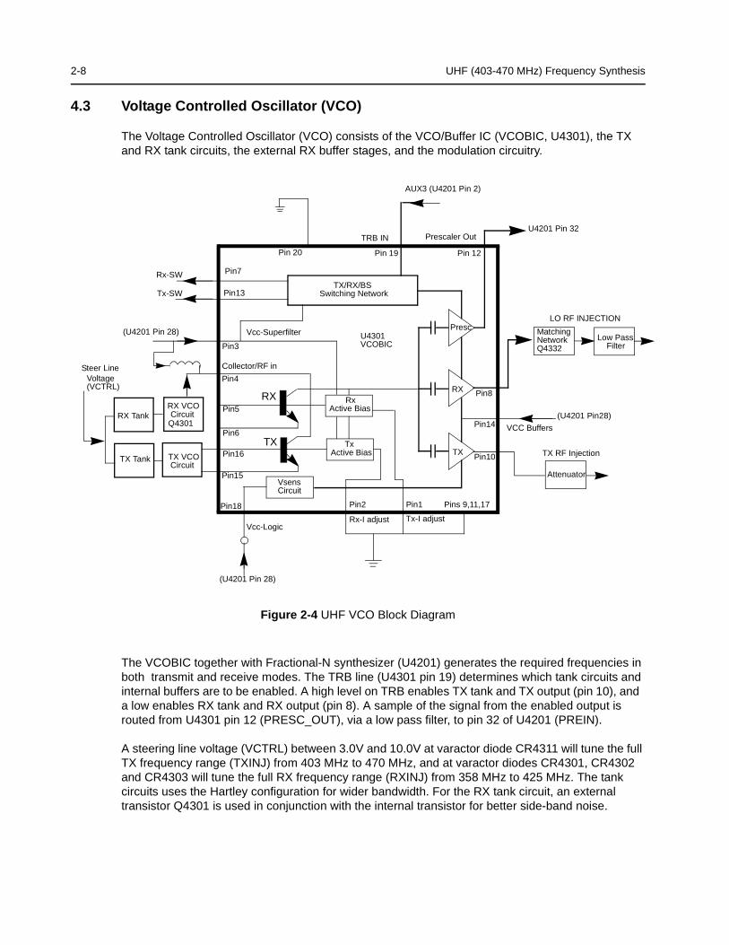
2-8 UHF (403-470 MHz) Frequency Synthesis
4.3 Voltage Controlled Oscillator (VCO)
The Voltage Controlled Oscillator (VCO) consists of the VCO/Buffer IC (VCOBIC, U4301), the TX and RX tank circuits, the external RX buffer stages, and the modulation circuitry.
Figure 2-4 UHF VCO Block Diagram
The VCOBIC together with Fractional-N synthesizer (U4201) generates the required frequencies in both transmit and receive modes. The TRB line (U4301 pin 19) determines which tank circuits and internal buffers are to be enabled. A high level on TRB enables TX tank and TX output (pin 10), and a low enables RX tank and RX output (pin 8). A sample of the signal from the enabled output is routed from U4301 pin 12 (PRESC_OUT), via a low pass filter, to pin 32 of U4201 (PREIN).
A steering line voltage (VCTRL) between 3.0V and 10.0V at varactor diode CR4311 will tune the full TX frequency range (TXINJ) from 403 MHz to 470 MHz, and at varactor diodes CR4301, CR4302 and CR4303 will tune the full RX frequency range (RXINJ) from 358 MHz to 425 MHz. The tank circuits uses the Hartley configuration for wider bandwidth. For the RX tank circuit, an external transistor Q4301 is used in conjunction with the internal transistor for better side-band noise.
Presc
RX
TX
MatchingNetwork Low Pass
Filter
Attenuator
Pin8
Pin14
Pin10
(U4201 Pin28)
VCC Buffers
TX RF Injection
U4201 Pin 32
AUX3 (U4201 Pin 2)
Prescaler Out
Pin 12Pin 19Pin 20
TX/RX/BSSwitching Network
U4301VCOBIC
RxActive Bias
TxActive Bias
Pin2
Rx-I adjust
Pin1
Tx-I adjust
Pins 9,11,17Pin18
VsensCircuit
Pin15
Pin16
RX VCO Circuit
TX VCO Circuit
RX Tank
TX Tank
Pin7
Vcc-Superfilter
Collector/RF in
Pin4
Pin5
Pin6
RX
TX
(U4201 Pin 28)
Rx-SW
Tx-SW
Vcc-Logic
(U4201 Pin 28)
Steer Line Voltage (VCTRL)
Pin13
Pin3
TRB IN
LO RF INJECTION
Q4301
Q4332

UHF (403-470 MHz) Frequency Synthesis 2-9
The external RX buffers (Q4332) are enabled by a high at U4201 pin 3 (AUX4) via transistor switch Q4333. In TX mode the modulation signal (VCOMOD) from the LVFRAC-N synthesizer IC (U4201 pin41) is applied modulation circuitry CR4321, R4321, R4322 and C4324, which modulates the TX VCO frequency via coupling capacitor C4321. Varactor CR4321 is biased for linearity from VSF.
4.4 Synthesizer Operation
The complete synthesizer subsystem comprises mainly of low voltage FRAC-N (LVFRACN) IC, Reference Oscillator (crystal oscillator with temperature compensation), charge pump circuitry, loop filter circuitry and DC supply. The output signal PRESC_OUT of the VCOBIC (U4301 pin 12) is fed to pin 32 of U4201 (PREIN) via a low pass filter (C4229, L4225) which attenuates harmonics and provides the correct level to close the synthesizer loop.The pre-scaler in the synthesizer (U4201) is basically a dual modulus pre-scaler with selectable divider ratios. This divider ratio of the pre-scaler is controlled by the loop divider, which in turn receives its inputs via the SRL. The output of the pre-scaler is applied to the loop divider. The output of the loop divider is connected to the phase detector, which compares the loop divider´s output signal with the reference signal.The reference signal is generated by dividing down the signal of the reference oscillator (Y4261 or Y4262).The output signal of the phase detector is a pulsed DC signal which is routed to the charge pump. The charge pump outputs a current at pin 43 of U4201 (IOUT). The loop filter (which consists of R4221-R4223, C4221-C4225,L4221) transforms this current into a voltage that is applied to the varactor diodes CR4311 for transmit, CR4301, CR4302 & CR4303 for receive and alters the output frequency of the VCO .The current can be set to a value fixed in the LVFRAC-N IC or to a value determined by the currents flowing into BIAS 1 (U4201-40) or BIAS 2 (U4201-39). The currents are set by the value of R4251 or R4252 respectively. The selection of the three different bias sources is done by software programming.To reduce synthesizer lock time when new frequency data has been loaded into the synthesizer the magnitude of the loop current is increased by enabling the IADAPT (U4201-45) for a certain software programmable time (Adapt Mode). The adapt mode timer is started by a low to high transient of the CSX line. When the synthesizer is within the lock range the current is determined only by the resistors connected to BIAS 1, BIAS 2, or the internal current source. A settled synthesizer loop is indicated by a high level of signal LOCK (U4201-4). The LOCK (U4201-4) signal is routed to one of the µP´s ADCs input U101-56. From the voltage the µP determines whether LOCK is active. In order to modulate the PLL the two spot modulation method is utilized. Via pin 10 (MODIN) on U4201 the audio signal is applied to both the A/D converter (low freq path) as well as the balance attenuator (high freq path). The A/D converter converts the low frequency analogue modulating signal into a digital code that is applied to the loop divider, thereby causing the carrier to deviate. The balance attenuator is used to adjust the VCO’s deviation sensitivity to high frequency modulating signals. The output of the balance attenuator is present at the MODOUT port (U4201-41) and connected to the VCO modulation diode CR4321 via R4321, C4325.

2-10 UHF (403-470 MHz) Frequency Synthesis
THIS PAGE INTENTIONALLY LEFT BLANK

3-1
Section 3
TROUBLESHOOTING CHARTS
1.0 Troubleshooting Flow Chart for Receiver (Sheet 1 of 2)
Bad SINADBad 20dB Quieting
No Recovered Audio
START
Audio at pin 8 of U3101 ?
Check Controller(in the case of no audio)
OR ELSE go to “B”
Yes
No
Spray or inject 44.85MHz into XTAL Filter FL3101
Audio heard ?BYes
No
Check 2nd LO (44.395MHz) at C3135
LO present ?BYes
Check voltages on U3101
Biasing OK ?
No
No
A
Yes
Check Q3102 bias for faults
Replace Q3102
Go to B
Yes
No
Check circuitry around U3101.
Replace U3101 if defect
Check circuitry around Y3101. Replace Y3101 if defect
Voltages
OK?

3-2 Troubleshooting Flow Chart for Receiver
1.1 Troubleshooting Flow Chart for Receiver (Sheet 2 of 2)
IF Signal at C3101?
No
RF Signal at T4051?
RFSignal at C4015?
No
No
RFSignal at C4025?
No or
Check harmonic filterL4491-L4493, C4492, J4401
and ant. switchD4471, D4472, L4472.
Check filter between C4025 & C4009.
Check tuning voltage at R4060.
Inject RF into J4401
Istuning voltage
OK?
No
Yes
Check RF amp (Q4003) Stage.
Check filter between C4015 & T4051.
Yes
Check T4051, T4052, D4051, R4052, L4008.
Yes
1st LO level OK?
Locked?
Yes
Check FGU
Yes
Trace IF signal from C3101 to
Q3101. Check for bad XTAL filter.
No
Yes IFsignal at Q3102
collector?
Before replacing U3101, check
U3101 voltages.
Yes
Check for 5VDC
Is 9V3 present?
Check Supply Voltage circuitry. Check Q0681,
U4211 and U0641.
No
No
No
Check U4501.
Check varactor filter.
No
Yes
Yes
Yes
A
A
B
weak RF
RFSignal at C4009?

Troubleshooting Flow Chart for 25W Transmitter 3-3
2.0 Troubleshooting Flow Chart for 25W Transmitter (Sheet 1 of 3)
Current increase
when keyed?
NO
YES
START
Check if Pressure Pad closes S5440
Check Components between Q4441 and RF Output,
Antenna Switch D4471,D4472,Q4472,
VR3471,Q3471
>500mA & <4A>4A
<500mA
Check PA StagesControl Volt-
age at TP4402
>1V
Short TP4403 to Ground
NO
YES
Voltage at TP4402 rises?
Check PA Stages NO
YES
PCIC U4501 Pin 14 9.3V
DC?
Check 9.3 V Regulator U0641
NO
YES
PCIC U4501 Pin 16 >4V
DC
Replace PCIC U4501
NO
YES
TP4404 9.1V DC
If U4201 Pin 2 is high, replace PCIC
U4501,otherwise check controller and
FGU
YES
NO
TP4403 >0.5V DC?
Replace PCIC U4501
Check Forward Power Sense Circuit (D4451)
Check Forward Power Sense Circuit (D4451)
NO
YES
PCIC U4501 Pin 5 > 1V
DC?
Check Power Setting, Tuning & Components between PCIC Pin 5 and ASFIC (U0221)
Pin 4 before replacing ASFIC
No or too low Power when keyed

3-4 Troubleshooting Flow Chart for 25W Transmitter
2.1 Troubleshooting Flow Chart for 25W Transmitter (Sheet 2 of 3)
Check PA Stages
No or too low Power when keyed
Measure DC Voltage at Pin 2 & 3 of U4401
>6
YES
DC Voltage at U4501
Pin 23 =0?
2-6
DC Voltage at U4402-1
Pin 1?
YES
Pin 2Voltage 0.62 * Voltage at
Pin 1?
If U4201 Pin 2 is high, replace PCIC
NOReplace U4401
YES
NODC
Voltage at U4402-1 Pin
3 = 8.8V?
Check S4440, R4442 and R4443
YES
Pin 3 Voltage 0.51 * Voltage at
Pin 1?
NOReplace U4401
<2VDC
Voltage at U4402-2 Pin 7?
>6V
Check Components between U4402-2 Pin 7
and Q4421. Check Resistive Network at
Pins 5 & 6 before replacing Q4421
YES
DC Voltage at
U4402-2 Pin 5 <8.8V?
Check Components between U4402-2 Pin 7
and Q4421. Check Resis-tive Network at Pins 5 & 6 before replacing Q4421
NO
Check Q4422
NO
Check Final PA Stage
2-6V
<2VCheck Resistive Net-work at Pins 2 & 3 of
U4402-1 before replac-ing U4401
Check Q4442 and Resistive Network at
U4402-1 Pin 3 before replacing
U4401

Troubleshooting Flow Chart for 25W Transmitter 3-5
2.2 Troubleshooting Flow Chart for 25W Transmitter (Sheet 3 of 3)
Check Final PA Stage
NO
0V
1-4V
Bias 2 DC Voltage at TP4406?
YES
RF Voltage at TP4401 >100mV?
YES
RF Voltage U4401 Pin 6
>3V?
Supply
Replace Q4441
Check FGU (U4301)
NO Check Components between
TP4401 &C4417
NO
YES ASFIC U0221 Pin 6 1-4V DC?
Check Bias Tuning before replacing ASFIC
U0221
Check Components between ASFIC and
Q4441 before replacing Q4441
YES
RF Voltage Q4421 Gate
>1V?
NO Check Components between
C4417 & Q4421
YES
RF Voltage Q4441 Gate
>4V?
NO Check Components between
Q4421 & Q4441
Check Components between Q4441 & Antenna Connector
Voltage
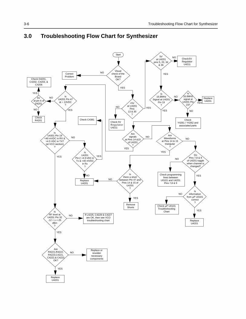
3-6 Troubleshooting Flow Chart for Synthesizer
3.0 Troubleshooting Flow Chart for Synthesizer
5V at pin 6 of
D4201
Isinformation
from µP U0101correct
?
IsU4201 Pin 47at = 13VDC
?
IsU4301 Pin 19
<40 mVDC in RX &>4.5 VDC in TX? (at VCO section)
?
Start
Visual check of the
BoardOK?
CorrectProblem
Check 5VRegulatorU4211
+5Vat U4201
Pins13 & 30
?
Is16.8MHz
Signal at U4201 Pin 19
?
CheckY4261 / Y4262 and
associated parts
Aresignals
at Pins 14 &15 of U4201
?
Check R4201 Check C4381
IsU4201
Pin 2 >4.5 VDC in Tx & <40 mVDC
in Rx?
Replace U4201
RemoveShorts
Isthere a short
between Pin 47 andPins 14 & 15 of
U4201?
Replace orresolder
necessarycomponents
IsRF level at
U4201 Pin 32 -12 < x <-25
dBm?
AreR4221,R4222,R4223,C4221,
C4222,& C4223 OK?
Replace U4201
If L4225, C4229 & C4227are OK, then see VCOtroubleshooting chart
AreWaveforms
at Pins 14 & 15triangular
?
DoPins 7,8 & 9
of U4201 togglewhen channel is
changed?
Check programminglines between
U0101 and U4201Pins 7,8 & 9
Replace U4201
Check µP U0101Troubleshooting
Chart
NO
YES
NO
YES
NO
YES
NO
NO
NO
YES
YES
NO
YES
YES
NO
YES
YESYESNO
NO
NO
NO
YES
NO
YES
YES
Check D4201, C4202, C4203, &
C4206
5V at U4201
pins 5, 20, 34 & 36
Check 5V Regulator
U4211
Is 16.8MHz signal at
U4201 Pin 23?
Replace U4201
YES
NO
NO
YES
NO
YES
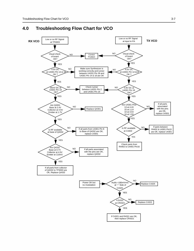
Troubleshooting Flow Chart for VCO 3-7
4.0 Troubleshooting Flow Chart for VCO
Are Q4332Base at 0.7V
Collector at 4.5V Emitter at 110mV
Are Q4301Base at 2.4V
Collector at 4.5V Emitter at 1.7V
Are U4301 Pins13 at 4.4V15 at 1.1V10 at 4.5V16 at 1.9V
Low or no RF Signalat TP4003
Visual checkof board
OK?
35mV DC atU4301 Pin 19
NO
YES
Replace Q4301
at base of Q4332
NO
NO
NO
NO
YES
YES
YES
YES
Low or no RF Signalat input to PA
4.8V DC atU4301 Pin 19
Is RF available at C4402
YES
YES
YES
YES
NO
NO
NO
NO
NO
Audio =180mVrmsat “-” Side of
4.5VDCat CR4321
If C4321 and R4321 are OK, then replace CR4321
Replace C4322
Replace C4325
NO
NO
YES
YES
If parts between R4402 & U4301 Pin10are OK, replace U4301
TX VCORX VCO
CorrectProblem
Visual checkof board
OK?
Check runner between U4201 Pin 2
and U4301 Pin 19
Is RF available If all parts from U4301 Pin 8to Base of Q4332 are OK,
replace U4301
If all parts associated with the pins are OK,
replace Q4332
If all parts from collectorof Q4332 to TP4003 are
OK, Replace Q4332
Power OK but no modulation
Check parts fromR4402 to U4401 Pin16
If all parts associated
with the pins are OK,
replace U4301
YES YES
Make sure Synthesizer is working correctly and runner between U4201 Pin 28 and U4301 Pin 14 & 18 are OK
4.5V DC
OK ?
OK? OK?
C4325
at U4301 Pin 14 & 18 4.5V DC
OK ?at U4301 Pin 14 &18
NO

3-8 Troubleshooting Flow Chart for VCO
THIS PAGE INTENTIONALLY LEFT BLANK

4-1
Section 4
UHF PCB/SCHEMATICS/PARTS LISTS
1.0 Allocation of Schematics and Circuit Boards
1.1 Controller Circuits
The UHF circuits are contained on the Printed Circuit Board (PCB) which also contains the Controller circuits. This Chapter shows the schematics for the UHF circuits only, refer to the Controller section for details of the related Controller circuits . The PCB component layouts and the Parts Lists in this Chapter show both the Controller and UHF circuit components. The UHF schematics and the related PCB and parts list are shown in the tables below.
Table 4-1 UHF 1-25W Diagrams and Parts Lists
PCB :8485670z02 Main Board Top Side8485670z02 Main Board Bottom Side
Page 4-3Page 4-4
SCHEMATICSPower Amplifier 1 - 25WFRACNVoltage Controlled OscillatorReceiver Front EndIF
Page 4-5Page 4-6Page 4-7Page 4-8Page 4-9
Parts List8485670z02 Page 4-10
Table 4-2 UHF 1-25W Diagrams and Parts Lists
PCB :8485670Z03 Main Board Top Side8485670Z03 Main Board Bottom Side
Page 4-13Page 4-14
SCHEMATICSPower Amplifier 1 - 25WFRACNVoltage Controlled OscillatorReceiver Front EndIF
Page 4-15Page 4-16Page 4-17Page 4-18Page 4-19
Parts List8485670Z03 Page 4-20

4-2 Allocation of Schematics and Circuit Boards
THIS PAGE INTENTIONALLY LEFT BLANK
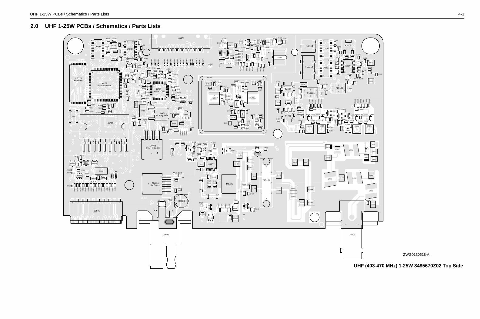
4-3
TOP METAL
C3101C3102
C3103
C3114
C3115
C3124C3131
C3132
C3133
C3134
C3135
C3136
C3137
C3139
C3140
C3141
C3142
C3143
C3145
C3148
C4001C4002
C40
03
C40
04
C40
05
C40
06
C40
07
C40
08
C4009
C4014
C4015
C4016
C4017C4018
C40
19
C40
20
C40
21
C40
22
C40
23
C4026C4027C4029C4030
C4051
C4052
C4065
C4068
C4441
C4442
C4443
C4444
C4445
C4446
C4447
C4472
C4473
C4474
C4491
C4492
C4496
C4497
C4498
D4001D4002
D4003
D4004D4005 D40
06
1
D4471
D4472
23
45
6FL3101
23
45
6
FL3102
4
3 2
FL3112
FL3114
2 3
J4401
L3100
L310
1
L3124
L4001L4002
L400
3
L4004L4005
L400
6
L400
8
L4051
L4471
L4472
L4491L4492
L4493
Q40
01
Q40
03
R3101
R3106
R3111
R3117 R3123
R3124
R3130
R3132
R3135R3142
R3144
R3145
R3148
R4001
R4003
R4004
R4005
R4007
R4012
R4013
R4014
R4015
R4020
R4022
R4051
R4064
R4066
R4491
1
5
1
4
3
2
11
120
10
U3101
8 7
114
U3111
8 7
114
U3115 2
Y3102
1
1
1
1
UHF (403-470 MHz) 1-25W 8485670Z02 Top Side
ZWG0130518-A
UHF 1-25W PCBs / Schematics / Parts Lists
2.0 UHF 1-25W PCBs / Schematics / Parts Lists
C0101C0102
C0104
C0106
C0107
C0131
C0132
C0211
C0212
C0221 C0222
C0223
C0224
C0225
C0226
C0227
C02
28
C02
31
C0232
C0233
C0234
C0235
C0236
C02
37
C0241
C0242
C0243
C0244
C0245
C0246
C0251
C0252 C0253
C0256
C0261C0262
C0421 C04
41
C04
42
C04
43
C04
45
C04
46
C04
47
C04
48
C04
49
C04
70
C04
71
C04
72
C04
73
C04
74
C04
76
C04
77
C04
78
C04
82
C04
83
C0484
C0486
C0487
C04
88
C0490
C0493
C04
94
C0495
C0496
C05
01
C05
02
C05
03
C05
04
C05
05
C05
06
C05
08
C05
09
C05
10
C05
11
C05
12
C05
13
C05
14
C05
15
C05
16
C0517
C05
18
C0542
C0601
C0603
C0612
C0651
C0652
C0654
C0655
C0681
C4031
C4053
C4054
C4055
C4210
C4212
C4213
C4214C4215
C4216
C4221
C42
22
C4223
C4224
C4225
C4226
C4227
C4229
C4230
C4231
C42
32
C42
33
C42
34
C4236
C4242
C4243
C4244
C4245
C4246
C4251
C42
52
C42
53C
4254
C42
55
C4289
C4308 C4309
C4317C4318
C4322
C4323
C4325
C4331
C4332
C4335
C4337
C4339
C4351 C4352
C4353
C4354
C4355
C4371C4372
C4373 C4374
C4375
C4382C4383
C4401
C4402
C4403
C4404
C4407
C4417
C4418
C4419
C4420
C4422
C4423
C4424
C4425
C4426
C4428
C4431
C4432
C4434C4435
C4448
C4449
C4454
C4455
C4457
C4458
C45
05
C4507C4508
C4509
D0201
D06
51
D405
D42
21D
4401
181
J0451
2011
10
J0501
J0601
L0481
L0482
L4053
L4054
L4201L4221
L422
5
L4303
L430
4L4
305
1
3
L4312L4313
L4331
L437
1
L4401
L4403
L4411
L4422
M3421
Q0110
Q0177Q0181Q0185
Q0681
Q42
21
Q4301
4 3Q4333
Q4411
Q4422
2
3
4
5
6
7
8
Q4441
Q44
42
Q44
71
R0101
R0102
R0104
R0105
R0106
R0108
R0110
R0114
R0115
R0116
R0131
R0132
R0170
R0181
R0182
R0185
R0186
R02
11
R0212
R0220
R0221
R0222
R0223
R0224
R0225
R0226
R0227
R0228
R0229
R0241
R0242
R0251
R0252
R0253
R0254
R0255
R0256
R0257
R0261R0262
R0268
R0269
R0442
R0510
R0533
R0535
R0538
R0539
R0543
R0611R0612
R0651
R0652
R0681
R0682
R4211
R4221R4222
R4223R4224
R4225
R42
51
R42
52
R4301
R4302
R4305
R4311
R4312
R4321
R4331
R4332R4333
R4337
R4341 R4343
R4345
R4346
R4401
R4402
R4403
R4404
R4406
R4415
R4416
R44
24
R44
25
R44
26
R44
27
R4431R4432
R4450
R4471
R4475
R4505
R4506
R4507
R4508
R4509
SH4301
2
4
3
T405
21
5
T405
TP4401
1
7651
26
U0101Microprocessor
3217
16 1
U0121Flashrom
87
1 14
U0211
1 37
2513
U0221ASFIC CMP
161
8 9
U0251
9
U0271
1
6
5
U0611
1
6
5
U06419,6V Regulator
3
2
1
U06515V Regulator
45
8
U4211
9
8
16
1
U4401
U4502
VR
0501
VR0503
VR0505
VR0510
VR
4471
2 3
4
Y0131
48
1
1
1
16
1
100
B+ Switch
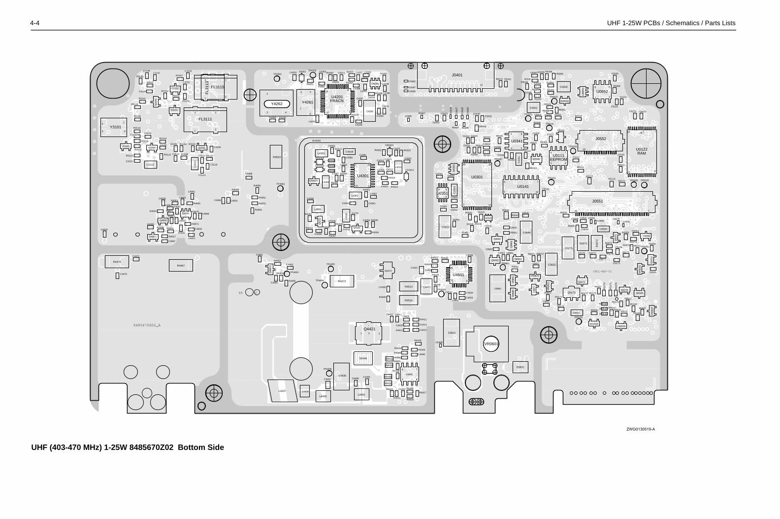
4-4 UHF 1-25W PCBs / Schematics / Parts Lists
C0103
C0105
C0111
C0112
C0121
C0122C0123
C0141
C0151
C0201
C0202
C0203 C0204
C0205
C0254
C0255
C0265
C0266
C0267
C0271
C0272
C0273
C0274C0275
C0276 C0277
0305
0325
C0331
C03
41
C0342
C0343
C0344
C0430C0431
C0541
C0554
C0558 C0559C0560
C0575C0576
C0591
C0592 C0593
C0621
C0622
C0641
C0644
C0645
C0661
C0662
C0663
C0671
3
4
6
D0101
D0151
D0179
D06
21
D06
60D
0661
E0271
E02
72
E0631
12
140
J0551
118
J0552
Q01
51
Q0171
Q0173 Q0183
Q02
71
Q0641
Q06
61
Q0662Q0663
R0107
R0111R0112
R0113R0117
R0121
R0151R0152
R0171R0172
R0173
R0174
R01
75
R01
76
R0177
R01
78
R0179R0183
R0184
R0201
R0202
R0203
R0204
R0205
R0206
R0207
R0208R0265
R0266R0267
R0273 R0274
R0275R0276
R0323
R0324
R0332
R0333
35
R0341
R0342
R0343
R0344
R0345
R0346
R0347
R0401
R0408
R0410
R0412 R0441
R0468
R0511
R0512R0525 R0529
R 0530
R0531R0537
R 0541
R 0542
R0591
R0592
R0593
R0621
R0641
R0642
R0643
R0661
R0662 R0671 R0672
TP0101
TP0102
TP0103
TP0104
TP0151
TP0221
TP0222
TP0492
TP0497
TP0530
TP0661
14
5 8
U0111EEPROM
22
21 8
71
U0122RAM
16
18
9
U0141
15
14
U0301
U0331
1
4 5
8
U0341
U0342
1 4
58
U0652
U06
53
VR
0151
VR0504VR0509
VR
0537
VR0541
VR0601
VR
0621
VR0671
28
ZWG0130519-A
CNTL-REV-T2
ZWG01305
U
C0301
C0302
C0303
C0304
C
C0324 C
C0351
C0352
C0353
C0354
C0422
C0423 C04
26
C04
27
C04
28
C04
29
C0485
C0491
C0492
C0497
C0499
C0611
C3104
C3110
C3111C3112
C3113
C3116
C3121
C3122C3123
C3144
C3146C3147
C3151
C3152
C4010
C4011
C4012
C4013
C4024
C4025
C4028C4060
C4061
C4062
C4064
C4066
C4067
C4069
C4201
C4202
C4203
C4204
C4205
C4206
C4207
C4208
C4209
C4211
C4228
C4235
C4241
C4261
C4262C4263
C4287
C4288
C4301
C 4302
C 4303
C 4304
C4305
C4306
C4307
C4311
C4312
C4313
C4314
C4315
C4316
C4321
C4324
C4333
C4334
C4336
C4338
C4361
C4362
C4363
C4381
C4400
C4405C4406
C4411C4412
C4413
C4414C4415
C4416
C4421
C4427
C4436C4437
C4439
C4440
C4451
C4452
C4453
C4471
C4475
C4501
C4502C450
C450
C450
C4510
CR4301
CR4302
CR4303
CR4311
CR4321
D03
01
D3101
D4007
D4201
D4261
D44
51
4 3
2
FL3111
FL3
113
4 3
2
FL3115
J0401
L311
1
L3112
L4231
L4301
L4302
L4311
L433
2
L4333
L4361
L4402
L4421
L4436
L4437
Q3101Q3102
Q31
41
Q3151
Q3152
Q4002
Q4004
Q4331
Q43
32
1 23
Q4421
Q4472
R0331
R03
R0407 R0409
R0467
R0481
R0482
R3102R3104R3105
R3107R3108R3112
R3113
R3114
R3115
R3116R3118
R3133
R3134
R3141
R3146
R3147
R3151
R3152
R3153
R3154
R4002
R4016
R4017
R4018
R4019
R4052
R4053
R4054
R4055
R4060
R4061R4062
R4063
R4068R4069
R4070
R4071
R4072
R4201R4203
R4204
R4206
R4228
R4241R4261
R4262
R4263
R4303
R4304
R4313
R4314
R4315 R4322 R4323
R4334
R4335
R4336
R4338R4339
R4340
R4342
R4344
R4347
R4361
R4400
R4411
R4412
R4413
R4417
R4418
R4421
R4422
R4423
R4428
R4429
R4440
R4441
R4442R4443
R4444
R4445
R4446
R4452
R4454
R4455
R4457
R4473
R4474R4501
R4502 R4504
R4510
R4511
R4512
R4513
R4514
S5440
SH4302
TP4003
TP4201
TP4202
TP4402
TP4403
TP4404
TP4405
TP4406
28
1
4
58
U0351
137
2513
U4201
11
1 20
10
U4301
14
5 8
U4402
1
17
9
25
U4501
43
2
Y3101
6
43
1
Y4261
2
3 4
Y4262
1
1
1
1
32
1
FRACN
C99
8485670Z02_A
HF (403-470 MHz) 1-25W 8485670Z02 Bottom Side

UH
F 1
-25W
PC
Bs
/ Sch
emat
ics
/ Par
ts L
ists
4-5
ZW
G01
3052
0-B
NU
NU
NU
NU
NU
wid
th 2
.032
0.8x
251.
542x
4
2.21
6x__
J440
1 -
BN
C
7.5
NU
A
NU
NU
RX
IN
9V3
NU
NU
INT
_SW
B_U
HF
_PA
_1
L443
717
nH
8.2pF
R44
7510
K
C4441
15
100
R44
02
2.7
R44
32
R44
27
2.7
R44
25
R45
01
6.8K
2200
pFC
4427
C44
2415
pFC
4453
100p
F
39K
R44
43
MO
SB
IAS
_2
22pF
C44
31
C45
0622
00pF
100p
FC
4406
36pF
C44
72
1uF
C45
05
C44
13N
U
C44
34
C44
5513
pF
0.1u
F
10K
R44
54
FE
CT
RL_
2_U
HF
_PA
_1
2.7K
R44
52
R44
21
27K
L440
2
57R
01
0.1u
FC
4425
20K
R45
07
C44
231u
F
LM50
GN
D 3
1 PO
S
VO
UT
2
FE
CT
RL_
2
U45
02
DA
TA
_UH
F_P
A_1
J440
1-1
L440
1
C44453.3pF
11.0
3nH
100p
FC
4439
120
R44
57
RE
SE
T_U
HF
_PA
_1
MO
SB
IAS
_2_U
HF
_PA
_1
C44
3610
uF
C45
0347
0pF
NU
100
R45
06
CLK
R44
31
9V3_
UH
F_P
A_1
2.4K
100p
FC
4412
R44
28
Q44
42
100p
F
C44
92
R44
17
CN
TLV
LTG
_UH
F_P
A_1
PA
_PW
R_S
ET
_UH
F_P
A_1
R44
223.
6K
R44
04
10K
8.2p
FC
4454
C44
40
100p
FC
4416
1000
pF
C44
00
470p
F
3.3K
R44
13
NU
C44
19
C44
2822
00pF
L447
217
nH
C44
9611
pF
PA
SU
PV
LTG
2.7
R44
26
L440
347
nH
U44
02-2
MC
3307
2
657
84
C44
3222
pF
C4444
J440
1-3
8.2pF
17nH
L449
2
300
L449
3
17nH
R44
01
RE
SE
T
51
R44
00
C44
04
51pF
100p
F
C44
17
Q44
21
16
V5EXT17
VAR120
VAR218
VAR324
15V
G
VL 6VLIM19
10
RFIN 1
RS21
RS
ET
31
RX23 T1 2
TE
MP
30
V10
14V
45
CQ
XD
AT
A28
F16
89
GND1 8
GN
D2
25
INT 4NA22
Q11
QX
32
BP
OS
27
CE
X29
CI 3
CJ 5
CL 7
CLK
26
CQ
1213U
4501
H99
S-4
AN
O
C44
2018
pF
.033
uFC
4421
100p
FC
4435
R44
46 0
9.1p
F
C44
03
Q44
11
C44
0510
0pF
TP
4406
Q44
22
TP
4403
15pF
C45
04
FE
CT
RL_
1F
EC
TR
L_1_
UH
F_P
A_1
TX
INJ
R45
0410
K
CLK
_UH
F_P
A_1
INT
_SW
B
TP
4401
R44
5510
0K
2pF
C44
75
D44
72
CS
X_U
HF
_PA
_1
D44
01
Kit_
0102
727B
46
11pF
C44
98
CN
TLV
LTG
C44
5756
pF
.022
uFC
4402
C44
975.
6pF
R45
05
NU
300K
R44
11
C44
15.0
22uF
C45
01
C44
52
2200
pF
13pF
51R45
14
17nH
L449
1
R44
71
470
51
R44
74
DA
TA
36pF
C44
7312
pF
C44
74
PA
SU
PV
LTG
_UH
F_P
A_1
51R
4415
NUC4443
C444943pF
100p
F
TE
MP
SE
NS
E
C44
14
R44
2339
K
C44
2610
0pF
PA
_PW
R_S
ET
1KR45
09
1000
pFC
4451
22K
R44
18
231
84
TP
4402
MC
3307
2
U44
02-1
R44
242.
7
C44
0710
0pF
R44
73
J440
1-5
51
J440
1-4
K9V
1_U
HF
_PA
_1
6.61
nHL4
422
C4442
43pFC4448
22pF
C44
5856
pF
C45
1010
0pF
6.8p
FC
4491
.022
uFC
4411
D44
71
300
R44
03C
4418
57R
01
4.3p
F
L442
1
51R
4416
C4446
TX
INJ_
UH
F_P
A_1
R44
12
C45
0810
0pF
15N
C4
16R
FIN
6R
FO
UT
17
RF
OU
T2
1V
CN
TR
L
14V
D1
VG
12 3
VG
211
G2
4GND15GND2
12GND313GND4
8N
C1
9N
C2
10N
C3
30C
65U
4401
17EP
51R45
13
43.6
7nH
L447
1
R45
10
C44
37.0
33uF
23 1
57R
01L4
436
VR
4471
5.6V
L441
1
R44
44
47nH
C45
0710
0pF
RX
IN_U
HF
_PA
_1
R44
9110
K
Q44
72
100p
F
12
C44
01
R44
41
S54
40S
WIT
CH
39K
2.2K
R44
42
C44
7110
0pF
TP
4404
NU
470p
FC
4509
100p
FC
4422
R44
40
Kit_
0102
727B
46
K9V
1
HE
AT
SIN
KP
OS
1M
3421
C4447
10R
4450
10R
4511
R45
12
TP
4405
Q44
71 CS
X
1KR
4429
R44
0622
K
100K
R45
08
J440
1-2
U45
08
D44
51
3300pFC4502
S2S3S4
Q44
41
D
G
GN
D1
GN
D2
S1
100K
R45
02
R44
45
9V3F
LT
U_P
RE
DR
IVE
R
9V3F
LT
2.4K
PA
_SW
B
U_D
RIV
ER
9V3F
LT
9V3F
LT
A+
U_P
RE
DR
IVE
R
NC
PA
_SW
B
NC
PA
_SW
B
A+
9V3F
LT
9V3F
LT
NC
9V3F
LT
U_D
RIV
ER
A+
9V3F
LT
MO
SB
IAS
_1N
CN
C
NC NC
NC
NC
NC
NC
9V3F
LT
NC
NU
UH
F (
403-
470
MH
z) P
ow
er A
mp
lifie
r 1
- 25
W
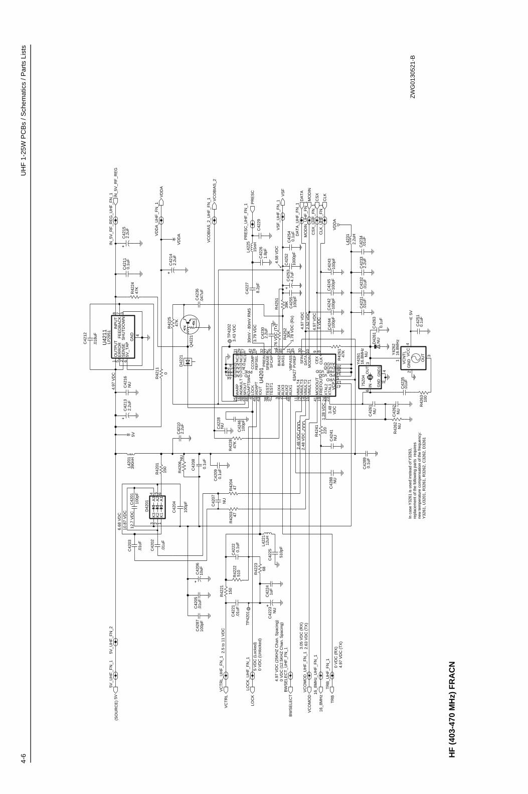
4-6
UH
F 1
-25W
PC
Bs
/ Sch
emat
ics
/ Par
ts L
ists
NU
0 V
DC
(R
X)
NU
NU
3.43
VD
C
3.05
VD
C (
RX
)
NU
4.97
VD
C2.
48 V
DC
NU
NU
4.58
VD
C
3.79
VD
C
2.48
VD
C
4.97
VD
C (
25K
HZ
Cha
n. S
paci
ng)
1.78
VD
C (
Rx)
4.97
VD
C (
TX
)
5 V
DC
(Lo
cked
)
10.8
7 V
DC
1.28
VD
C
NU
NU
NU
0 V
DC
(U
nloc
ked)
2.63
VD
C (
TX
)
VD
C
4.97
VD
C
NU
0 V
DC
(12
.5K
HZ
Cha
n. S
paci
ng)
2.52
VD
C
2.5
to 1
1 V
DC
1.76
VD
C (
Tx)
30m
V -
80m
V R
MS
12.7
VD
C
0 V
DC
4.97
VD
C
NU
1.8p
F
(SO
UR
CE
)
NU
3.48
6.68
VD
C
TP
4201
C42
04
100p
F
R42
0447
2.2u
FC
4214
INP
UT
8O
UT
PU
T1
SE
NS
E2
SH
UT
DO
WN
3
U42
11LP
2951
5V_T
AP
6
ER
RO
R5
FE
ED
BA
CK
7
GN
D 4
TR
B_U
HF
_FN
_1
D42
01
A1
6A
25
A3
4
1K
12
K2
3K
3
16.8
MH
z
GN
D2
OU
T 3
4V
CC
1
VC
NT
L
C42
11
Y42
62
C42
28
0.1u
F
.01u
FC
4205
VC
TR
L
47R
4203
C42
16
5V
C42
241u
F
DA
TA
C42
36.0
47uF
VC
OM
OD
_UH
F_F
N_1
IN_5
V_R
F_R
EG
0.1u
F
C42
08
C42
332.
2uF
R42
2847
K
10uF
C42
06
C42
540.
1uF
VC
OB
IAS
_2_U
HF
_FN
_1
C42
26
C42
090.
1uF
47K
R42
61
.01u
F
C42
03
VC
TR
L_U
HF
_FN
_1
C42
102.
2uF
100
R42
63
39K
R42
51
510
R42
22
C42
0110
0pF
R42
5230
K
16_8
MH
z
C42
32.0
1uF
R42
2447
K
C42
23
R42
62
100p
FC
4245
2.2u
H
C42
29
L423
1
R42
01
150
C42
62
CLK
_UH
F_F
N_1
150
PR
ES
C
R42
21
16_8
MH
z_U
HF
_FN
_1
100p
F
VC
OB
IAS
_2
VS
F
C42
44
D42
61
.01u
FC
4231
PR
ES
C_U
HF
_FN
_1
.018
uF
C42
12
390n
HL4
201
C42
4210
0pF
4.7u
FC
4253
BW
SE
LEC
T_U
HF
_FN
_1
MO
DIN
VC
OM
OD
.01u
FC
4221
0
C42
220.
1uF
R42
11
2.2u
FC
4215
C42
07
12uH
L422
1
0.1u
FC
4251
100p
FC
4241
C42
43
1000
pF
VS
F_U
HF
_FN
_1
C42
52
.01u
FC
4235
LOC
K
2.2u
FC
4213
C42
61
MO
DIN
_UH
F_F
N_1
XT
AL1
2324X
TA
L2
5V_U
HF
_FN
_1
VB
PA
SS
21
VC
P 47
15V
MU
LT1
VM
ULT
214
VM
ULT
312
VM
ULT
411
13VRO
WA
RP
25
PV
RE
F35
RE
FS
EL
18
SF
BA
SE
27S
FC
AP
26
SF
IN30
SF
OU
T28
TE
ST
137
TE
ST
238
NC
117
NC
229
NC
331
PD_GND44 5PD_VDD
32P
RE
IN
PRE_GND33 PRE_VDD 34
DGNDDVDD 36
FR
EF
OU
T19
IAD
AP
T45
IND
MU
LT16
IOU
T434
LOC
K
MO
DIN
10
MO
DO
UT
41
AVDD20B
IAS
140
BIA
S2
39
CC
OM
P42
CE
X9
CLK
8
DA
TA
7
6
AD
AP
TS
W46
AGND22
AU
X1
48A
UX
21
AU
X3
2A
UX
43
U42
01
63A
27
R42
06
VD
DA
_UH
F_F
N_1
5V_U
HF
_FN
_2
R42
25
47K
100p
FC
4246
C42
25
510p
F
LOC
K_U
HF
_FN
_1
D42
21
.01u
F
C42
02
L422
5
15nHIN
_5V
_RF
_RE
G_U
HF
_FN
_1
2.2u
FC
4230
100p
FC
4255
CS
X
R42
23
68
CS
X_U
HF
_FN
_1
DA
TA
_UH
F_F
N_1
OU
T3
IN6
VD
DA
Y42
6175
Z04
16.8
MH
z
1G
ND
4G
ND
10.
1uF
C42
63
TR
B
CLK
R42
41
220
C42
34.0
1uF
C42
27
8.2p
F
C42
88
TP
4202
BW
SE
LEC
T
Q42
21
C42
8710
0pF
C42
89
5V
5V
0.1u
F
VD
DA
VD
DA
In c
ase
Y32
61 is
use
d in
stea
d of
Y32
63,
repl
acem
ent o
f the
follo
win
g pa
rts
req
uire
s
new
tem
pera
ture
com
pens
atio
n of
the
freq
uenc
y:
Y32
61, U
3201
, R32
61, R
3262
, C32
62, D
3261
HF
(40
3-47
0 M
Hz)
FR
AC
N
ZW
G01
3052
1-B

UH
F 1
-25W
PC
Bs
/ Sch
emat
ics
/ Par
ts L
ists
4-7
NU
NU
NU
0 V
DC
(T
x)
NU
NU
NU
NU
2.5
- 11
VD
C
0 V
DC
(R
x)
4.58
VD
C
4.58
VD
C
NU
NU
13.5
to 1
6 dB
m
NU
0 V
DC
(T
x)
3.1
VD
C (
Rx)
0 V
DC
(T
x)4.
7 V
DC
(R
x)
NU
(Tx)
4.54
VD
C0
VD
C (
Tx)
2.35
VD
C
NU
0 V
DC
(R
x)
4.42
VD
C (
Rx)
NU
NU
NU
NU
NU
NU
NU
NU
NU
NU
NU
NU
NU
NU
NU
NU
4.97
VD
C (
Tx)
-18
to -
16 d
Bm
(R
x)-1
6 to
-11
dB
m (
Tx)
4 to
6 d
Bm
4.54
VD
C
4.54
VD
C (
Tx)
2.6
VD
C (
Tx)
1.91
VD
C (
Tx)
0 V
DC
(R
x)
2.45
VD
C (
Rx)
(Rx)
2.43
VD
C (
Rx)
NU
NU
GN
D
C43
0110
0pF
30R43
13
C43
72
VC
TR
L_U
HF
_VC
O
L433
133
nH
VS
F_U
HF
_VC
0
C43
180.
1uF
Q43
01
R43
6118
0
C43
0551
pF
C43
37R
4332
CR
4303
C43
82
VC
OB
IAS
_2
5V_U
HF
_VC
O
C43
32
0
R43
15
CR
4311
C43
81
C43
13
.022
uFC
4336
R43
45
SH
4301
SH
IELD
R43
0210
K
C43
83
C43
63
R43
33
R43
125.
6K
C43
09
100p
F
C43
1510
0pF
19T
RB
_IN
16T
X_B
AS
E15
TX
_EM
ITT
ER
1T
X_I
AD
J10
TX
_OU
T
13T
X_S
WIT
CH
14
VC
C_B
UF
FE
RS
18
VC
C_L
OG
IC
GN
D_L
OG
IC17
12P
RE
SC
_OU
T5
RX
_BA
SE
6R
X_E
MIT
TE
R
2R
X_I
AD
J8
RX
_OU
T
7R
X_S
WIT
CH
3S
UP
ER
_FLT
R
U43
01
4C
OLL
_RF
IN
20F
LIP
_IN
11
GN
D_B
UF
FE
RS
9
GN
D_F
LAG
R43
46
10K
50U
54
L431
2
RE
SO
NA
TO
R
1P
1 2 P2
3P
3
C43
141.
5pF
C43
07
100p
F
C43
520.
1uF
C43
21
Q43
31
1pF
4
1 3
CR
4301
Q43
33
2
6
C43
39
C43
75
L433
2
L436
139
0nH
VC
TR
L
0
R43
41
C43
242.
4pF
2.2K
R43
42
6.8p
F
TR
B_U
HF
_VC
O
C43
31
C43
043.
9pF
C43
33
C43
74
C43
35
100p
F
270
R43
14
7.5K
R43
11
TX
INJ_
UH
F_V
CO
R43
34
R43
01 L430
139
0nH
R43
23
5.6K
100K
1KR
4343
C43
530.
1uF
C43
12
12pF
390n
HL4
305
C43
23
R43
37
C43
17
PR
ES
C
Q43
32
68nH
L433
339
0nH
L437
1
56K
R43
21
R43
05
C43
16
10
0
5V
0.1u
F
R43
47C
4338
R43
36
51pF
2.2u
FC
4354
C43
5110
0pF
22
R43
31
C43
73
R43
39
PR
ES
C_U
HF
_VC
O
390n
H
L431
1
R43
35
180
R43
04
CR
4321
10K
R43
22
100p
F
C43
1110
0pF
C43
61
30
R43
03
L430
239
0nH
C43
62
C43
038.
2pF
R43
38
RX
INJ
RX
INJ_
UH
F_V
CO
L430
3R
ES
ON
AT
OR
1P
1
2 P2
3P
3
0.1u
FC
4371
TX
INJ
390n
HL4
313
SH
IELD
SH
4302
TR
B
C43
34
C43
06
2pF
C43
552.
2uF
VS
F
VC
OB
IAS
_2_U
HF
_VC
O
VC
OM
OD
C43
08
0.1u
F
390n
HL4
304
C43
028.
2pF
CR
4302
10R43
44
C43
22
4.7u
F
C43
25V
CO
MO
D_U
HF
_VC
O
GR
OU
ND
R43
40
5V
VS
F
TX
SW
TX
SW
RX
SW
RX
SW
VS
F
ZW
G01
3052
3-A
UH
F (
403-
470
MH
z) V
olt
age
Co
ntr
olle
d O
scill
ato
r
ZW
G01
3052
3-A
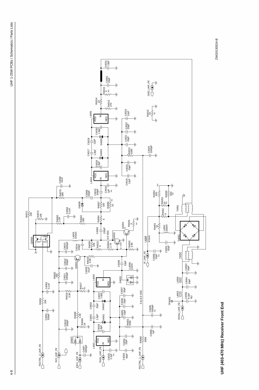
4-8
UH
F 1
-25W
PC
Bs
/ Sch
emat
ics
/ Par
ts L
ists
R40
66
C40
69R
4070
.01u
F
C40
6810
0pF
C40
65
390
C40
640.
1uF
010
0pF
390
R40
64
R40
621.
5K
R40
63R40
7210
K
R40
71
10K
C40
620.
1uF
R40
61
10K
C40
6133
0pF
R40
691K
R40
68
C40
66
1.5K
C40
6733
00pF
R40
54
R40
55
R40
53R
4052
0
C40
60
R40
60
330K
L400
8
470n
H
R40
22
L400
6
0
R40
20
C40
51
15nH
10pF
L405
4
C40
3113
pF
15nH
L405
327
nH
C40
556.
2pF
NU
C40
5416
pFC
4053
R40
51
16pF
C40
52
51
L405
1
82pF
150n
H
L400
5L4
001
L400
2L4
004
C40
10
1.8p
F
330p
F
C40
29C
4027
C40
301.
8pF
1.8p
F1.
8pF
C40
26
R40
13
R40
15
270
C40
161p
F
C40
19
R40
19
12pF
C40
0336
pF
C40
25
R40
17
3.3K
R40
16
R40
18C
4028
.01u
F
C40
2033
pF
3.3K
C40
0433
pFC
4005
1.8p
F33
pF
C40
01C
4002 C
4006
33pF
C40
07
FE
CT
RL_
1_U
HF
_FE
30pF
100K
R40
01
C40
09
10pF
R40
033.
9K
R40
042.
7K
D40
07
10K
IF_U
HF
_FE
R40
05
C40
1410
0pF
470n
HK
9V1_
UH
F_F
E
L400
3
R40
07
100
RX
IN_U
HF
_FE
330p
F33
00pF
C40
12C
4013
100p
FC
4015
GN
D_U
HF
_FE
C40
1133
00pF
330
RX
INJ_
UH
F_F
E
R40
02
Q40
04
33pF
C40
21
T40
52
C40
17
D40
51
1.8p
F12
pF
Q40
03
Q40
01
C40
18
C40
2233
pF
T40
51
TP
4003
12pF
100K
C40
23
D40
0510
R40
12
R40
14
C40
0810
00pF
1000
pF
D40
01
C40
24
33pF
NU
NU
NU
NU
NU
3 to
6.5
VD
C
NU
NU
NU
NU
NU
NU
0.7
VD
C
4.6
VD
C
NU
NU
Q40
02D
4006
D40
04
9V3_
UH
F_F
E
D40
03
D40
02
FE
CT
RL_
2_U
HF
_FE
10
10
0
820
820
10
0
0
20pF
2.2p
F
1pF
IN
NE
G
PO
S
IN
NE
G
PO
S
IN
NE
G
PO
S
IN
NE
G
PO
S
UH
F (
403-
470
MH
z) R
ecei
ver
Fro
nt
En
d
ZW
G01
3052
4-B
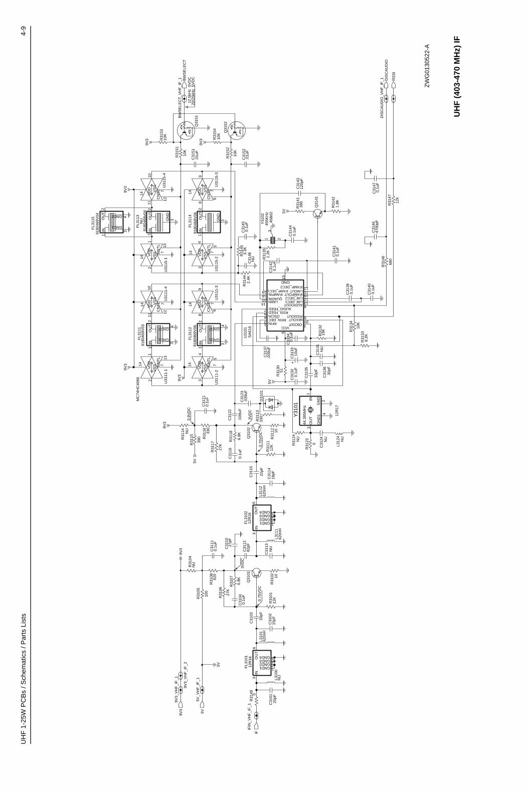
UH
F 1
-25W
PC
Bs
/ Sch
emat
ics
/ Par
ts L
ists
4-9
9180
468v
04
9180
468V
06
3.9V
DC
12.
5kH
z 0
VD
C20
/25k
Hz
5V
DC
9180
469V
03
3VD
C
9180
469V
06
9180
469V
04
0.75
VD
C0.
75V
DC
3VD
C
R31
17
27K
Q31
02 10R
3112
IF
1.8K
R31
42
10K
27pF
R31
54
C31
400.
1uF
C31
10
620n
HL3
111
620
R31
085
CN
TL
43
14 VD
D 7
VS
S
C31
44
U31
15-2
C31
430.
1uF
120p
F
R31
15
390
R31
18
6.8K
R31
1112
K
5V_V
HF
_IF
_1Q
3151
NU
C31
13
NU
R31
04
22pF
C31
15
VD
D
14
VS
S 7
Q31
41
MC
74H
C40
66
U31
11-1
CN
TL 13
12
R31
16 330
82pF
C31
12
Q31
52
R31
351.
2K
DIS
CA
UD
IO_V
HF
_IF
_1
BW
SE
LEC
T_V
HF
_IF
_1
R31
01
IFIN
_VH
F_I
F_1
12K
C31
3310
uF
C31
52.0
1uF
0.1u
FC
3142
DIS
CA
UD
IO
R31
3215
K
680
R31
46
10K
R31
51
0.1u
FC
3139
C31
320.
1uF
10K
R31
52
0.1u
FC
3111
20pF
C31
01
3
GND1
GND2 4
1IN
2O
UT
FL3
111
C31
410.
1uF
GND3 45GND4
3IN
6O
UT
R31
338.
2K
FL3
101
12R
16
1GND1GND2 2
0
7
R31
48
U31
11-4
CN
TL
12
1110
VD
D
14 VS
S
9V3_
VH
F_I
F_2
R31
02 10
FL3
113
3GN
D
1IN
2O
UT
27K
R31
06
R31
4139
0
14
VD
D
7
VS
S
2.4K
R31
44
U31
11-2
5
CN
TL
43
NU
C31
31
C31
22
.039
uF
R31
07
5RSSIOUT9 RSSI_FEED
6
VCC
6.8K
13LIM_DEC112LIM_DEC2
20MIXOUT4 OSCIN
3OSCOUT
10 QUADIN
1 RFIN2 RFIN_DEC
AUDIO_FEED
GND15
18 IFAMPIN 16IFAMPOUT19 IFAMP_DEC1
17IFAMP_DEC2
14LIMIN
11LIMOUT
SA
616
U31
01
8AUDIOOUT
7
CN
TL 13
12
VD
D
14 VS
S 7
5V
U31
15-1
R31
05
L310
0
100
0.1u
F
9V3
NU
3
21
C31
34
BW
SE
LEC
T
45B
02
Y31
0245
5KH
z
C31
03
33pF
C31
470.
1uF
0.1u
FC
3145
620n
HL3
101
6CN
TL
89
14 VD
D 7VS
S9
14 VD
D 7VS
S
U31
11-3
U31
15-3
6CN
TL
8
GND1 12GND24GND3
GND4 5
IN3
OU
T6
30pF
12R
16F
L310
2
33pF
C31
36
C31
35
NU
L312
4
NU
C31
24NU
R31
24
C31
1418
pF
C31
040.
1uF
C31
210.
1uF
Q31
01.0
39uF
C31
23
.01u
FC
3151
51
4700
pFC
3146
R31
30
10K
R31
53
C31
48
R31
47
NU
D31
01
0
R31
23
330
R31
13
15pF
C31
02
3.3K
R31
45
C31
37.0
39uF
3GN
D
1IN
2O
UT
RS
SI
FL3
114
10V
DD
14
VS
S
7
0.1u
F
C31
16
2O
UT
U31
15-4
CN
TL
12
11
FL3
112
3
GND1
GND2 4
1IN
R31
14
R31
34
10K
NU
FL3
115
GND1
34
GND2
IN1
OU
T2
NU
9V3_
VH
F_I
F_1
L311
262
0nH
Y31
01
2G
ND
4G
ND
1
3O
UT
1IN
5V
44.3
95M
Hz
12R
17
5V
9V3
9V3
9V3
9V3
9V3
5V
9V3
5V
9V3
12k
ZW
G01
3052
2-A
UH
F (
403-
470
MH
z) IF

4-10
UH
F 1
-25W
PC
Bs
/ Sch
emat
ics
/ Par
ts L
ists
UH
F P
CB
848
5670
Z02
Par
ts L
ist
1-25
W
Cir
cuit
R
efM
oto
rola
P
art
No
.D
escr
ipti
on
C30
0021
1374
1F37
3.3n
F 5
0VC
3001
2113
740F
194.
7pF
5%
C30
0221
1374
0F26
9.1p
F 5
%C
3003
2113
741F
373.
3nF
50V
C30
0421
1374
0F45
56pF
5%
C30
0521
1374
0F51
100p
F 5
%C
3006
2113
740F
4556
pF 5
%C
3007
2113
741F
373.
3nF
50V
C30
0821
1374
1F25
1nF
50V
C30
0921
1374
1F13
330p
F 5
0VC
3010
2113
741F
1333
0pF
50V
C30
1121
1374
1F37
3.3n
F 5
0VC
3012
2113
741F
251n
F 5
0VC
3013
2113
740F
4556
pF 5
%C
3014
2113
740F
247.
5pF
5%
C30
1521
1374
0F45
56pF
5%
C30
1621
1374
0F51
100p
F 5
% 5
0VC
3017
2113
740F
4243
pF 5
% 5
0VC
3019
2113
741F
251n
F 5
0VC
3020
2113
741F
251n
F 5
0VC
3021
2113
740F
5312
0pF
5%
50V
C30
2221
1374
1F49
10nF
50V
C30
2621
1374
3E20
100n
F 1
6VC
3027
2113
741F
4910
nF 5
0VC
3028
2113
741F
4910
nF 5
0VC
3030
2113
741F
251n
F 5
0VC
3033
2113
740F
205.
1pF
5%
50V
C30
3421
1374
0F49
82pF
5%
50V
C30
3521
1374
0F33
18pF
5%
50V
C30
3621
1374
1F25
1nF
50V
C31
0021
1374
1F25
1nF
50V
C31
0221
1374
0F31
15pF
5%
50V
C31
0321
1374
0F39
33pF
5%
50V
C31
0421
1374
3E20
100n
F 1
6VC
3110
2113
740F
3727
pF 5
% 5
0VC
3111
2113
743E
2010
0nF
16V
C31
1221
1374
0F49
82pF
5%
50V
C31
1421
1374
0F33
18pF
5%
50V
C31
1521
1374
0F35
22pF
5%
50V
C31
1621
1374
3E20
100n
F 1
6VC
3121
2113
743E
2010
0nF
16V
C31
2221
1374
3E11
39nF
10%
C31
2321
1374
3E11
39nF
10%
C31
3221
1374
3E20
100n
F 1
6VC
3133
2311
049A
57TA
NT
CP
10u
F 1
0% 1
6VC
3134
2113
743E
2010
0nF
16V
C31
3521
1374
0L30
33pF
2%
C31
3621
1374
0L29
30pF
2%
C31
3721
1374
3E11
39nF
10%
C31
3921
1374
3E20
100n
F 1
6V
C31
4021
1374
3E20
100n
F 1
6VC
3141
2113
743E
2010
0nF
16V
C31
4221
1374
3E20
100n
F 1
6VC
3143
2113
740F
5312
0pF
5%
50V
C31
4421
1374
3E20
100n
F 1
6VC
3145
2113
743E
2010
0nF
16V
C31
4621
1374
1F41
4.7n
F 5
0VC
3147
2113
743E
2010
0nF
16V
C31
5121
1374
1F49
10nF
50V
C31
5221
1374
1F49
10nF
50V
C32
0221
1374
1F49
10nF
50V
C32
0321
1374
1F49
10nF
50V
C32
0521
1374
1F49
10nF
50V
C32
0623
1104
9A57
TAN
T C
P 1
0uF
10%
16V
C32
0821
1374
3E20
100n
F 1
6VC
3209
2113
743E
2010
0nF
16V
C32
1023
1104
9A40
TAN
T C
P 2
.2uF
10%
10V
C32
1121
1374
3E20
100n
F 1
6VC
3213
2311
049A
40TA
NT
CP
2.2
uF 1
0% 1
0VC
3214
2311
049A
09TA
NT
CP
2.2
uF 1
0% 2
0VC
3215
2311
049A
09TA
NT
CP
2.2
uF 1
0% 2
0VC
3221
2113
743E
2010
0nF
16V
C32
2221
1374
3E20
100n
F 1
6VC
3224
0882
422W
23F
ILM
SM
1.0
uF 1
5V 5
%C
3225
2113
743E
2010
0nF
16V
C32
2621
1374
0F25
8.2p
F 5
% 5
0VC
3227
2113
740F
5110
0pF
5%
50V
C32
2821
1374
3E20
100n
F 1
6VC
3229
2113
743E
1247
nF 1
0%C
3231
2113
741F
4910
nF 5
0VC
3232
2113
741F
4910
nF 5
0VC
3233
2311
049A
40TA
NT
CP
2.2
uF 1
0%C
3234
2113
741F
4910
nF 5
0VC
3235
2113
741F
4910
nF 5
0VC
3242
2113
740F
5922
0pF
5%
50V
C32
4321
1374
0F59
220p
F 5
% 5
0VC
3244
2113
740F
5922
0pF
5%
50V
C32
4521
1374
0F59
220p
F 5
% 5
0VC
3246
2113
740F
5922
0pF
5%
50V
C32
5121
1374
3E20
100n
F 1
6VC
3252
2113
741F
251n
F 5
0VC
3253
2311
049A
56TA
NT
CP
4.7
uF 2
0% 1
0VC
3254
2113
743E
2010
0nF
16V
C32
5523
1104
9A40
TAN
T C
P 2
.2uF
10%
10V
C32
6321
1374
3E20
100n
F 1
6VC
3302
2113
740F
236.
8pF
5%
50V
C33
0321
1374
1F49
10nF
50V
C33
0621
1374
0F20
5.1p
F 5
% 5
0VC
3311
2113
743E
0722
nF 1
6VC
3314
2113
740F
236.
8pF
5%
50V
C33
1521
1374
0F31
15pF
5%
50V
Cir
cuit
R
efM
oto
rola
P
art
No
.D
escr
ipti
on
C33
1621
1374
0F15
3.3p
F 5
% 5
0VC
3317
2113
740F
3933
pF 5
% 5
0VC
3318
2113
740F
215.
6pF
5%
50V
C33
1921
1374
1F25
1nF
50V
C33
2421
1374
1F49
10nF
50V
C33
3221
1374
3E20
100n
F 1
6VC
3333
2113
743E
2010
0nF
16V
C33
3421
1374
3E07
22nF
16V
C33
3521
1374
1F49
10nF
50V
C33
3621
1374
1F49
10nF
50V
C33
3721
1374
3E20
100n
F 1
6VC
3341
2113
741F
251n
F 5
0VC
3342
2113
740L
053.
0pF
+-0
.1pF
C33
4421
1374
0F09
1.8p
F 5
% 5
0VC
3345
2113
740L
2520
pF +
-0.2
5pF
C33
4621
1374
1F49
10nF
50V
C33
4721
1374
1F49
10nF
50V
C33
4821
1374
1F49
10nF
50V
C33
5121
1374
1F49
10nF
50V
C33
5221
1374
3E07
22nF
16V
C33
5521
1374
1F49
10nF
50V
C33
5621
1374
3E07
22nF
16V
C33
5721
1374
0F24
7.5p
F 5
% 5
0VC
3361
2113
741F
251n
F 5
0VC
3362
2113
740F
215.
6pF
5%
50V
C33
6321
1374
0F47
68pF
5%
50V
C33
6421
1374
0F31
15pF
5%
50V
C33
6521
1374
1F25
1nF
50V
C34
0021
1374
0F63
330p
F 5
% 5
0VC
3401
2113
740F
6333
0pF
5%
50V
C34
0221
1374
3E07
22nF
16V
C34
0321
1374
0F39
33pF
5%
50V
C34
0421
1374
0F39
33pF
5%
50V
C34
0521
1374
0F67
470p
F 5
% 5
0VC
3406
2113
740F
6747
0pF
5%
50V
C34
1021
1374
3E07
22nF
16V
C34
1121
1374
3E07
22nF
16V
C34
1221
1374
0F63
330p
F 5
% 5
0VC
3414
2113
740F
6333
0pF
5%
50V
C34
1521
1374
3E07
22nF
16V
C34
1621
1374
0F63
330p
F 5
% 5
0VC
3417
2113
740F
4347
pF 5
% 5
0VC
3418
2113
740F
3933
pF 5
% 5
0VC
3419
2113
740F
5718
0pF
5%
50V
C34
2021
1374
0F57
180p
F 5
% 5
0VC
3421
2113
741A
5733
nF 5
0VC
3422
2113
740A
6733
0pF
5%
50V
C34
2323
1104
9A08
TA
NT
CP
1uF
10%
35V
C34
2421
1374
0F67
470p
F 5
% 5
0VC
3425
2113
743E
0722
nF 1
6VC
3426
2113
740F
6333
0pF
5%
50V
Cir
cuit
R
efM
oto
rola
P
art
No
.D
escr
ipti
on
C34
2721
1374
1F33
2.2n
F 5
0VC
3428
2113
741F
332.
2nF
50V
C34
3121
1107
8B34
HQ
47p
F 5
%C
3433
2111
078B
36H
Q 5
6pF
5%
C34
3421
1374
1A45
10nF
50V
C34
3521
1374
0A67
330p
F 5
% 5
0VC
3436
2311
049A
45TA
NT
CP
10u
F 1
0% 3
5VC
3437
2113
741A
5733
nF 5
0VC
3438
2111
078B
59H
Q 4
70pF
5%
C34
3921
1107
8B59
HQ
470
pF 5
%C
3440
2113
741F
251n
F 5
0VC
3441
2111
078B
47H
Q 1
50pF
5%
C34
4221
1107
8B47
HQ
150
pF 5
%C
3445
2111
078B
21H
Q 2
0pF
5%
C34
4621
1107
8B42
HQ
100
pF 5
%C
3447
2111
078B
19H
Q 1
6pF
5%
C34
4821
1107
8B44
HQ
120
pF 5
%C
3449
2111
078B
44H
Q 1
20pF
5%
C34
5021
1374
0F67
470p
F 5
% 5
0VC
3451
2113
741F
251n
F 5
0VC
3452
2113
740F
2912
pF 5
% 5
0VC
3453
2113
740F
6747
0pF
5%
50V
C34
7121
1374
3E07
22nF
16V
C34
7221
1107
8B53
HQ
270
pF 5
%C
3473
2111
078B
53H
Q 2
70pF
5%
C34
7421
1374
0F59
220p
F 5
% 5
0VC
3475
2113
740F
236.
8pF
5%
50V
C34
9121
1107
8B18
HQ
15p
F 5
%C
3492
2111
078B
38H
Q 6
8pF
5%
C34
9321
1107
8B09
HQ
6.8
pF 5
%C
3494
2111
078B
16H
Q 1
3pF
5%
C34
9521
1107
8B01
HQ
3.3
pF 5
%C
3496
2111
078B
31H
Q 3
6pF
5%
C34
9821
1107
8B16
HQ
13p
F 5
%C
3499
2111
078B
19H
Q 1
6pF
5%
C35
0121
1374
1F33
2.2n
F 5
0VC
3502
2113
741F
332.
2nF
50V
C35
0321
1374
0F67
470p
F 5
% 5
0VC
3504
2113
741F
4910
nF 5
0VC
3505
2311
049A
07TA
NT
CP
1uF
10%
16V
C35
0621
1374
1F33
2.2n
F 5
0V X
7RC
3507
2113
740F
5110
0pF
5%
50V
C35
0821
1374
0F67
470p
F 5
% 5
0VC
3510
2113
740F
6747
0pF
5%
50V
D30
0048
1383
3C02
DU
AL
SO
T M
MB
D61
00D
3001
4805
649Q
13V
CT
R 1
SV
228
SO
T23
D30
0348
8015
4K03
DU
AL
SC
HO
TT
KY
SO
T23
D30
0448
0564
9Q13
VC
TR
1S
V22
8 S
OT
23D
3011
4880
142L
01P
IND
3031
4886
143B
01M
IXE
R D
IOD
E C
RO
SS
OV
ER
D31
0148
8015
4K03
DIO
DE
DU
AL
SC
HO
TT
KY
Cir
cuit
R
efM
oto
rola
P
art
No
.D
escr
ipti
on
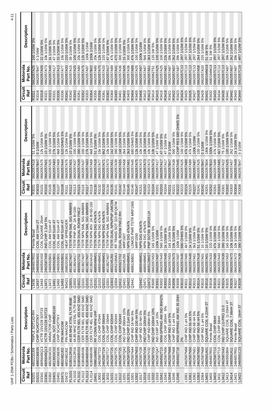
UH
F 1
-25W
PC
Bs
/ Sch
emat
ics
/ Par
ts L
ists
4-11
D32
0148
0223
3J09
TR
IPLE
SO
T14
3-R
HD
3221
4880
236E
05C
HIP
SC
HO
TT
KY
D33
4148
0564
9Q13
VC
TR
1S
V22
8 S
OT
23D
3361
4805
649Q
13V
CT
R 1
SV
228
SO
T23
D33
6248
6282
4C01
VA
RA
CT
OR
CH
IPD
3401
4813
833C
02D
UA
L S
OT
MM
BD
6100
D34
5148
8023
6E05
CH
IP S
CH
OT
TK
YD
3471
4802
482J
02P
IN M
A/C
OM
D34
7248
0248
2J02
PIN
MA
/CO
MF
L310
191
8011
2R16
44.8
5 M
HZ
XTA
L F
LTR
80d
BF
L310
291
8011
2R16
44.8
5 M
HZ
XS
TAL
FLT
R 8
0dB
FL3
111
9180
469V
03C
ER
FLT
R 6
EL
455
KH
Z S
MD
FL3
112
9180
469V
06C
ER
FLT
R 6
EL
455
KH
Z S
MD
FL3
113
9180
468V
04C
ER
FLT
R 4
EL
455
KH
Z S
MD
FL3
114
9180
468V
06C
ER
FLT
R 4
EL
455
KH
Z S
MD
J340
109
8616
6B02
RF
CO
NN
MIN
I UH
FL3
002
2462
587T
23C
OIL
CH
IP 4
70nH
L303
124
6258
7T24
CO
IL C
HIP
560
nHL3
032
2462
587T
17C
OIL
CH
IP 1
50nH
L310
124
6258
7T25
CO
IL C
HIP
620
nHL3
111
2462
587T
25C
OIL
CH
IP 6
20nH
L311
224
6258
7T25
CO
IL C
HIP
620
nHL3
201
2462
587Q
42IN
D C
HIP
390
nH 1
0%L3
231
2462
587Q
20IN
D C
HIP
2.2
uH 2
0%L3
301
2462
587N
44C
HIP
IND
18
NH
5%
L330
224
6258
7N53
CH
IP IN
D 1
00 n
H 5
%L3
317
2462
587V
28C
HIP
IND
33
NH
5%
L331
824
6258
7V34
IND
CH
IP 1
00nH
5%
L333
124
6258
7V32
CH
IP IN
D 6
8NH
5%
L333
224
6258
7V15
IND
CH
IP 1
00nH
10%
L333
324
6258
7Q47
IND
CH
IP 1
uH 1
0%L3
341
2484
562T
13M
INI-
SP
RIN
G A
W IN
D 8
NH
2%L3
343
2462
587N
56C
OIL
CH
IP 1
80nH
5%
L334
424
6258
7N68
CH
IP IN
D 1
uH
5%
L334
524
6258
7N68
CH
IP IN
D 1
uH
5%
L334
624
8456
2T18
MIN
I-S
PR
ING
AW
IND
35.
5NH
2%
L335
124
6258
7N68
CH
IP IN
D 1
uH
5%
L336
124
6258
7N50
CH
IP IN
D 5
6 nH
5%
L336
224
6258
7N51
CH
IP IN
D 6
8 nH
5%
L336
324
6258
7N50
CH
IP IN
D 5
6 nH
5%
L336
424
6258
7N68
CH
IP IN
D 1
uH
5%
L340
124
6059
1A01
SQ
UA
RE
CO
IL 4
.22n
H 3
TL3
402
2484
657R
01F
errit
e B
ead
L340
324
6258
7T13
CO
IL C
HIP
68n
HL3
411
2462
587T
13C
OIL
CH
IP 6
8nH
L341
224
6258
7X43
IND
CH
IP L
O-P
RO
15.
0L3
413
2460
591B
04S
QU
AR
E C
OIL
11.
03nH
4T
L341
424
6059
1A11
SQ
UA
RE
CO
IL 7
.66n
H 3
TL3
421
2484
657R
01F
errit
e B
ead
L342
224
6059
1C23
SQ
UA
RE
CO
IL 1
6nH
3T
Cir
cuit
R
efM
oto
rola
P
art
No
.D
escr
ipti
on
L343
624
8465
7R01
Fer
rite
Bea
dL3
437
2460
592A
01C
OIL
AW
17n
H 2
TL3
443
2460
591X
02C
OIL
SQ
UA
RE
25n
HL3
471
2462
587X
69IN
D C
HIP
1.2
uH 5
%L3
472
2460
592B
01C
OIL
AW
51n
H 4
TL3
491
2460
592B
01C
OIL
AW
51n
H 4
TL3
492
2460
592B
01C
OIL
AW
51n
H 4
TL3
493
2460
592B
01C
OIL
AW
51n
H 4
TM
3421
2686
201B
01H
EA
T S
PR
EA
DE
RQ
3001
4813
827A
07T
ST
R N
PN
SM
L S
IG M
MB
R9
Q30
0248
1382
4A17
TS
TR
PN
P 4
0V .2
A B
=10
0-Q
3021
4805
921T
02T
ST
R D
UA
L R
OH
M F
MC
2Q
3101
4813
827A
07T
ST
R N
PN
SM
L S
IG M
MB
R9
Q31
0248
1382
7A07
TS
TR
NP
N S
ML
SIG
MM
BR
9Q
3141
4813
824A
10T
ST
R N
PN
40V
.2A
B=
50-1
50Q
3151
4880
048M
01T
ST
R N
PN
DIG
47k
/47k
Q31
5248
8004
8M01
TS
TR
NP
N D
IG 4
7k/4
7kQ
3221
4880
048M
01T
ST
R N
PN
DIG
47k
/47k
Q33
0148
1382
7A07
TS
TR
NP
N S
ML
SIG
MM
BR
9Q
3303
4802
245J
50T
ST
R D
UA
L N
PN
/PN
P U
MC
5NQ
3304
4805
218N
63R
F T
RA
NS
SO
T 3
23 B
FQ
67W
Q34
1148
0592
1T02
DU
AL
RO
HM
FM
C2
RH
Q34
2148
0224
5J55
MR
F15
07Q
3422
4880
048M
01N
PN
DIG
47k
/47k
Q34
4148
8613
6B01
LDM
OS
PW
R T
ST
R M
RF
1565
M
RF
1550
Q34
4248
8004
8M01
NP
N D
IG 4
7k/4
7kQ
3471
4880
048M
01N
PN
DIG
47k
/47k
Q34
7248
0512
8M27
PN
P S
OT
89 B
SR
33 L
HR
3000
0662
057A
531k
5 1/
16W
5%
R30
0106
6205
7A97
100k
1/1
6WR
3002
0662
057A
4356
0 1/
16W
5%
R30
0306
6205
7A49
1k 1
/16W
5%
R30
0406
6205
7A53
1k5
1/16
W 5
%R
3006
0662
057A
7310
k 1/
16W
5%
R30
0906
6205
7A97
100k
1/1
6WR
3010
0662
057A
4568
0 O
HM
S 5
%R
3011
0662
057A
654k
7 1/
16W
5%
R30
1206
6205
7A49
1k 1
/16W
5%
R30
1306
6205
7A61
3k3
1/16
W 5
%R
3014
0662
057A
1851
1/1
6W 5
%R
3015
0662
057A
0110
1/1
6W 5
%R
3016
0662
057A
0110
1/1
6W 5
%R
3018
0662
057A
3322
0 1/
16W
5%
R30
1906
6205
7A89
47k
1/16
W 5
%R
3021
0662
057A
4356
0 1/
16W
5%
R30
2406
6205
7A39
390
1/16
W 5
%R
3025
0662
057A
531k
5 1/
16W
5%
R30
2606
6205
7A73
10k
1/16
W 5
%R
3027
0662
057A
7310
k 1/
16W
5%
R30
2806
6205
7A39
390
1/16
W 5
%
Cir
cuit
R
efM
oto
rola
P
art
No
.D
escr
ipti
on
R30
3106
6205
7A18
51 1
/16W
5%
R30
3306
6205
7B47
0 1/
16W
R
3101
0662
057A
7512
k 1/
16W
5%
R31
0206
6205
7A01
10 1
/16W
5%
R31
0506
6205
7A25
100
1/16
W 5
%R
3106
0662
057A
8327
k 1/
16W
5%
R31
0706
6205
7A69
6k8
1/16
W 5
%R
3108
0662
057A
4462
0 O
HM
S 5
%R
3111
0662
057A
7512
k 1/
16W
5%
R
3112
0662
057A
0110
1/1
6W 5
%R
3113
0662
057A
3733
0 1/
16W
5%
R31
1506
6205
7A39
390
1/16
W 5
%R
3116
0662
057A
3733
0 1/
16W
5%
R31
1706
6205
7A83
27k
1/16
W 5
%R
3118
0662
057A
696k
8 1/
16W
5%
R31
3006
6205
7A18
51 1
/16W
5%
R31
3206
6205
7A77
15k
1/16
W 5
%R
3133
0662
057A
718k
2 1/
16W
5%
R31
3406
6205
7A73
10k
1/16
W 5
%R
3135
0662
057A
511k
2 1/
16W
5%
R31
4106
6205
7A39
390
1/16
W 5
%R
3142
0662
057A
551k
8 1/
16W
5%
R31
4406
6205
7A58
2k4
1/16
W 5
%R
3145
0662
057A
613k
3 1/
16W
5%
R31
4606
6205
7A45
680
OH
MS
5%
R31
4706
6205
7A75
12k
1/16
W 5
%R
3151
0662
057A
7310
k 1/
16W
5%
R31
5206
6205
7A73
10k
1/16
W 5
%R
3153
0662
057A
7310
k 1/
16W
5%
R31
5406
6205
7A73
10k
1/16
W 5
%R
3201
0662
057A
1747
1/1
6W 5
%R
3203
0662
057A
1747
1/1
6W 5
%R
3204
0662
057A
1747
1/1
6W 5
%R
3211
0662
057B
470
1/16
WR
3221
0662
057A
3939
0 1/
16W
5%
R32
2206
6205
7A45
CH
IP R
ES
680
OH
MS
5%
R32
2306
6205
7A25
100
1/16
W 5
%R
3224
0662
057A
8947
k 1/
16W
5%
R32
2506
6205
7A89
47k
1/16
W 5
%R
3227
0662
057A
9710
0k 1
/16W
R32
4106
6205
7A25
100
1/16
W 5
%R
3242
0662
057B
470
1/16
WR
3251
0662
057B
0418
0k 1
/16W
5%
R32
5206
6205
7B10
330k
1/1
6W 5
%R
3261
0662
057A
8947
k 1/
16W
5%
R32
6306
6205
7A65
4k7
1/16
W 5
%R
3301
0662
057A
2275
1/1
6W 5
%R
3302
0662
057A
2510
0 1/
16W
5%
R33
0306
6205
7A57
2k2
1/16
W 5
%R
3304
0662
057A
491k
1/1
6W 5
%R
3308
0662
057B
470
1/16
W
Cir
cuit
R
efM
oto
rola
P
art
No
.D
escr
ipti
on
R33
1106
6205
7A25
100
1/16
W 5
%R
3316
0662
057B
470
1/16
WR
3318
0662
057A
0922
1/1
6W 5
%R
3321
0662
057A
7310
k 1/
16W
5%
R33
2306
6205
7A49
1k 1
/16W
5%
R33
3106
6205
7A17
47 1
/16W
5%
R33
3506
6205
7A13
33 1
/16W
5%
R33
3606
6205
7A77
15k
1/16
W 5
%R
3341
0662
057A
3322
0 1/
16W
5%
R33
4206
6205
7A15
39 1
/16W
5%
R33
4306
6205
7A25
100
1/16
W 5
%R
3351
0662
057A
8020
k 1/
16W
5%
R33
5206
6205
7A75
12k
1/16
W 5
%R
3353
0662
057A
9710
0k 1
/16W
R33
5406
6205
7B02
150k
1/1
6WR
3355
0662
057A
8020
k 1/
16W
5%
R33
5606
6205
7A75
12k
1/16
W 5
%R
3361
0662
057A
3322
0 1/
16W
5%
R33
6206
6205
7A17
47 1
/16W
5%
R33
6406
6205
7A89
47k
1/16
W 5
%R
3400
0662
057A
4147
0 1/
16W
5%
R34
0106
6205
7A36
300
1/16
W 5
%R
3402
0662
057A
0515
1/1
6W 5
%R
3403
0662
057A
3630
0 1/
16W
5%
R34
0406
6205
7A89
47k
1/16
W 5
%R
3405
0662
057A
2510
0 1/
16W
5%
R34
0606
6205
7A97
100k
1/1
6WR
3412
0662
057A
675k
6 1/
16W
5%
R34
1306
6205
7A61
3k3
1/16
W 5
%R
3414
0683
962T
5112
0 1W
5%
R34
1506
6205
7A25
100
1/16
W 5
%R
3416
0662
057A
2510
0 1/
16W
5%
R34
1806
6205
7A81
22k
1/16
W 5
%R
3421
0662
057A
8739
k 1/
16W
5%
R34
2206
6205
7A57
2k2
1/16
W 5
%R
3423
0662
057A
8739
k 1/
16W
5%
R34
2406
6205
7C13
2R7
1/10
W 5
%R
3425
0662
057C
132R
7 1/
10W
5%
R34
2606
6205
7C13
2R7
1/10
W 5
%R
3427
0662
057C
132R
7 1/
10W
5%
R34
2806
6205
7A58
2k4
1/16
W 5
%R
3429
0662
057A
3322
0 1/
16W
5%
R34
3106
8019
4M18
51 1
W 5
%R
3432
0680
194M
1851
1W
5%
R34
3306
6205
7C13
2R7
1/10
W 5
%R
3434
0662
057C
132R
7 1/
10W
5%
R34
3506
6205
7C13
2R7
1/10
W 5
%R
3441
0662
057A
8739
k 1/
16W
5%
R34
4206
6205
7A57
2k2
1/16
W 5
%R
3443
0662
057A
8739
k 1/
16W
5%
R34
4406
6205
7C19
4R7
1/10
W 5
%
Cir
cuit
R
efM
oto
rola
P
art
No
.D
escr
ipti
on
4-12
UH
F 1
-25W
PC
Bs
/ Sch
emat
ics
/ Par
ts L
ists
* M
otor
ola
Dep
ot S
ervi
cing
onl
y
Ref
eren
ce d
esig
nato
rs w
ith a
n as
teris
k in
dica
te
com
pone
nts
whi
ch a
re n
ot fi
eld
repl
acea
ble
beca
use
they
nee
d to
be
calib
rate
d w
ith
spec
ializ
ed fa
ctor
y eq
uipm
ent a
fter
inst
alla
tion.
R
adio
s in
whi
ch th
ese
part
s ha
ve b
een
repl
aced
in
the
field
will
be
off f
requ
ency
at t
empe
ratu
re
extr
emes
.
R34
4506
6205
7A58
2k4
1/16
W 5
%R
3446
0662
057B
470
1/16
WR
3450
0662
057A
4147
0 1/
16W
5%
R34
5206
6205
7A75
12k
1/16
W 5
%R
3454
0662
057A
8430
k 1/
16W
5%
R34
5506
6205
7A97
100k
1/1
6WR
3457
0683
962T
5112
0 1W
5%
R34
7106
6205
7A41
470
1/16
W 5
%R
3473
0680
194M
1851
1W
5%
R34
7406
8019
4M18
51 1
W 5
%R
3475
0662
057A
7310
k 1/
16W
5%
R34
9106
6205
7A73
10k
1/16
W 5
%R
3501
0662
057A
696k
8 1/
16W
5%
R35
0206
6205
7A87
39k
1/16
W 5
%R
3504
0662
057A
7310
k 1/
16W
5%
R35
0506
6205
7B09
300k
1/1
6W 5
%R
3507
0662
057A
8020
k 1/
16W
5%
R35
0806
6205
7A97
100k
1/1
6WR
3509
0662
057A
491k
1/1
6W 5
%T
3001
2508
396X
02T
RA
NS
FO
RM
ER
T30
0225
0839
7X02
TR
AN
SF
OR
ME
RU
3101
5186
144B
01F
M IF
IC S
A61
6U
3111
5113
805A
86IC
QU
AD
AN
ALO
G M
UX
/D
EM
UX
U31
1551
1380
5A86
IC Q
UA
D A
NA
LOG
MU
X/
DE
MU
XU
3201
5185
963A
27IC
TE
ST
ED
AT
2501
6 48
PIN
G
FP
U32
1151
0573
9X05
IC S
OT
5V
HI-
PR
EC
ISIO
N
RE
GU
LAT
U33
0151
0575
0U54
VC
O B
UF
FE
R P
KG
DIE
U34
0151
0510
9Z67
LDM
OS
DR
IVE
R V
HF
/UH
FU
3402
5180
932W
01LI
NE
AR
IC O
P A
MP
U35
0151
8576
5B01
IC P
OW
ER
CO
NT
RO
LU
3502
5185
963A
15T
EM
P S
EN
SO
R 1
M5
VR
3471
4813
830A
155.
6V 5
% 2
25m
WY
3101
4880
606B
09C
RY
STA
L 44
.395
MH
ZY
3102
9186
145B
02C
ER
AM
IC D
ISC
RIM
INA
TO
R
455k
Hz
Y32
6348
8618
2B01
VC
TC
XO
16.
8MH
z 2p
pm
TT
SO
5V
Cir
cuit
R
efM
oto
rola
P
art
No
.D
escr
ipti
on

UH
F 1
-25W
PC
B /
Sch
emat
ics
/ Par
ts L
ist
4-13
TOP METALTOP METAL
C01
01C
0102
C01
04C01
06
C01
07
C01
08
C01
31
C01
32
C02
11
C02
12
C0221
C0222
C02
23
C02
24
C02
25
C02
26
C02
27
C0228
C0231C02
32
C02
33
C02
34C02
35
C02
36
C0237
C02
41 C02
42
C02
43
C02
44
C02
45
C02
46
C02
51
C02
52C
0253
C02
56
C02
61
C02
62C
0421
C0441
C0442
C0443
C0445
C0446
C0447
C0448
C0449
C0470
C0471
C0472
C0473C0474
C0476
C0477 C04
78
C0482C0483
C04
84
C04
86C04
87
C0488
C04
90
C04
93
C0494
C0495
C04
96
C0501C0502C0503
C0504
C0505C0506C0508
C0509
C0510
C0511
C0512
C0513C0514
C0515
C0516
C05
17
C0518
C05
42
C06
01
C06
03
C06
12
C06
51
C06
52
C06
54C
0655
C06
81
C31
01C
3102
C31
03
C31
14
C31
15
C31
24
C31
31
C31
32
C31
33
C31
34
C31
35
C31
36
C31
37
C31
39
C31
40
C31
41
C31
42
C31
43
C31
45 C31
48
C40
01C
4002
C4003C4004
C4005
C4006
C4007
C4008
C40
09C
4014
C40
15
C40
16
C40
17C
4018
C4019
C4020
C4021
C4022
C40
23
C40
26C
4027
C40
29C
4030
C40
31
C40
51C40
52
C40
53
C40
54
C40
55C
4065
C40
68
C42
10
C42
13
C4214
C4215
C42
16C
4217
C42
21
C4222
C4223
C42
24
C42
25
C42
26
C42
27
C42
29
C42
30C
4231
C4232
C4233
C4234
C42
36C
4242
C42
43
C42
44
C42
45
C42
46
C42
51
C4252
C4253C4254
C4255
C42
89
C43
08C
4309
C43
17C
4318
C43
22
C43
23
C43
25
C43
31
C43
32
C43
35
C43
37
C43
39
C43
51C
4352C
4353
C43
54
C43
55 C43
71
C43
72C
4373
C43
74
C43
75
C43
82
C43
83
C44
01
C44
02
C44
03
C44
04
C44
07 C44
17
C44
18
C44
19
C44
20C
4422
C44
23
C44
24
C44
25
C44
26
C44
28
C4431
C44
34
C44
35
C44
41
C44
42
C44
43
C4444
C4446
C4448C4449
C4455 C44
57
C44
58
C44
72
C44
73
C44
74
C44
91
C4492
C44
96
C44
97
C4498
C45
05
C45
07C
4508
C45
09
D02
01
D0651
D40
01
D40
02
D40
03
D40
04D
4005
D4006
D40
51
D4221
D44
01
D44
71
D44
72
23 4
56
FL3
101
23 4
56
FL3
102
432
FL3
112
FL3
114
181
J045
1
201110
J050
1
J060
1
23
J440
1
L048
1
L048
2
L310
0
L3101
L312
4
L400
1L4
002
L4003
L400
4L4
005
L400
6
L4008 L405
1
L405
3
L405
4
L420
1
L4221
1 3
L430
3
L4304L4305
1 3
L431
2L4
313 L4
331
L4371
L440
1
L440
3
L441
1
L4422
L447
1
L447
2
L449
1
L449
3
M34
21
Q01
10
Q01
77Q
0181
Q01
85
Q06
81
Q4001
Q4003
Q4221
Q43
01
43
Q43
33
Q44
11
Q44
22
2
3 4
5 6
7 8
Q44
41
Q4442
Q4471
R01
01
R01
02
R01
03
R01
04
R01
05R01
06
R01
08
R01
10
R01
14
R01
15
R01
16
R01
31
R01
32
R01
70
R01
81
R01
82
R01
85
R01
86
R02
11
R02
12
R02
20
R02
21R
0222
R0223
R02
24
R02
25
R02
26R02
27
R02
28
R02
29
R02
41
R02
42
R02
51
R02
52
R02
53
R02
54
R02
55
R02
56
R02
57
R02
61R
0262R
0268
R02
69
R04
42
R05
10
R05
33R
0535
R05
38
R05
39
R06
11R
0612
R06
51
R06
52
R06
81
R06
82
R31
01
R31
06R
3111
R31
17
R31
23
R31
24
R31
30
R31
32
R31
35R
3142
R31
44
R31
45
R31
48
R40
01
R40
03
R40
04
R4005
R40
07
R40
12
R40
13R
4014
R40
15
R40
20 R40
22
R40
51
R40
64
R40
66
R42
11
R42
21R
4222
R42
23
R42
24
R42
25
R42
27
R4251
R4252
R43
01
R43
02
R43
05
R43
11
R43
12
R43
21
R43
31
R43
32R
4333
R43
37R43
41R
4343
R43
45
R43
46
R44
01
R44
02
R44
03
R44
04
R44
06
R44
15
R44
16
R44
24
R44
25
R44
26
R44
27R
4431
R44
71
R44
75
R44
91
R45
05 R45
06
R45
07
R45
08
R45
09
SH
4301
21 5
43
T40
51
215
4 3T
4052
TP
4401
1 765126
321716
1
871
14
U02
11
137 25
13
161 8
9
U02
51
9
U02
71
1
6
5
U06
11
1
6
5
3
2
1
11
120
10
U31
01
87 1
14
U31
11
87 1
14U31
15
U4211
116
89
U44
01
U45
02
VR
0501
VR
0503
VR
0505
VR
0510
VR
4471
234 Y0131
2Y
3102
1
1
1
1
100
U01
01M
icro
proc
esso
r
U01
21F
lash
rom
U02
21A
SF
IC C
MP
U06
419,
6V R
egul
ator
U06
515V
Reg
ulat
or
B+
Sw
itch
UH
F (
403-
470
MH
z) 1
-25W
848
5670
Z03
To
p S
ide
ZW
G01
3062
6-O

4-14
UH
F 1
-25W
PC
B /
Sch
emat
ics
/ Par
ts L
ist
C01
03
C01
05
C01
11
C01
12
C01
21C
0122
C01
23
C01
41
C01
51
C02
01
C02
02
C02
03C
0204
C02
05
C02
54
C02
55
C02
65
C02
66
C02
67
C02
71
C02
72
C02
73C02
74
C0275
C02
76
C02
77
C0301
C03
02
C03
03C03
04C
0305
C03
24C
0325 C03
31
C0341
C03
42
C03
43
C03
44
C03
51
C03
52
C03
53
C03
54
C0422
C0423
C0426
C0427
C0428
C0429
C0430
C0431
C04
85
C04
91
C04
92
C04
97
C04
99
C05
41
C05
54
C05
58C
0559
C05
60C
0575
C05
76C
0591
C05
92C
0593
C06
11
C06
21
C0622
C06
41
C0644
C06
45
C06
61
C06
62C
0663
C06
71
C31
04
C31
10
C31
11C
3112
C31
13
C31
16
C31
21
C31
22C
3123C
3144
C31
46
C31
47
C31
51
C31
52
C40
10
C40
11
C40
12C
4013
C40
24
C40
25
C40
28C
4060
C40
61
C40
62
C40
64
C40
66
C40
67
C40
69
C42
01
C42
02
C42
03
C42
04
C42
05
C4206
C42
07
C4208C4209
C42
11
C42
28C
4235
C4241
C42
61
C42
62C
4263
C42
87
C42
88
C43
01
C43
02
C43
03
C43
04
C43
05
C43
06
C4307
C43
11
C43
12
C43
13
C43
14
C43
15
C43
16
C43
19
C43
21
C43
24
C43
33C
4334
C43
36 C43
38
C43
61
C43
62
C43
63
C43
64C
4365
C43
81
C44
00
C44
05C
4406
C44
08
C44
11C
4412
C44
13
C44
14C
4415
C44
16
C44
21
C44
27
C4436
C44
37
C4439
C44
40
C44
51
C44
52
C44
53
C44
59
C44
71
C44
75
C45
01
C45
02C
4503
C45
04
C45
06
C45
10
CR
4301
CR
4302
CR
4303
CR
4311
CR
4321
D0101
D01
51
D01
79
D0301
D0621
D0660D0661
D31
01
D40
07
D42
01
D42
61
D44
51
E0271
E0272
E06
31
F04
01
43 2
FL3
111FL3113
43 2
FL3
115
12
J040
1
140
J055
1118
J055
2
L3111
L311
2
L423
1
L430
1 L4302
L4311
L4332
L433
3
L436
1L4
362
L440
2
L442
1
L443
6
L443
7
Q0151
Q01
71
Q01
73Q
0183
Q0271
Q06
41
Q0661 Q06
62Q
0663
Q31
01Q
3102
Q3141
Q31
51
Q31
52
Q40
02
Q40
04
Q43
31
Q43321
23Q44
21
Q4472
R01
07
R01
11R
0112
R01
13R
0117
R01
21
R01
51
R01
52
R0171
R01
72R
0173
R01
74
R0175
R0176
R0177R0178
R01
79R
0183
R01
84
R02
01R
0202R02
03
R02
04 R02
05
R02
06
R02
07
R02
08R
0265
R02
66R02
67
R02
73
R02
74
R02
75
R02
76
R03
23
R03
24
R03
31
R03
32
R03
33
R03
35
R03
41
R03
42
R03
43
R03
44
R03
45
R03
46
R03
47
R04
01
R04
07
R04
08
R04
09
R0412
R0441
R04
67
R04
68
R04
81 R04
82
R05
11
R05
12R
0525
R05
29
R05
30
R05
31
R05
37
R05
41
R05
42
R05
43
R05
55
R05
56
R05
91
R05
92
R05
93
R06
21
R06
41
R06
42R
0643
R06
61
R06
62R
0671
R06
72
R31
02
R31
04R
3105
R31
07R
3108
R31
12
R31
13
R31
14
R31
15
R31
16R
3118
R31
33
R31
34
R31
41
R31
46
R31
47
R31
51
R31
52
R31
53
R31
54
R40
02R
4016
R40
17
R40
18
R40
19
R40
52
R40
53
R40
54
R40
55R
4060
R40
61R
4062
R40
63
R40
68R
4069
R40
70
R40
71
R40
72
R42
01R
4203
R42
04
R42
06
R42
28
R4241
R42
61
R4262
R42
63
R43
03
R43
04R
4313
R43
14
R43
15R
4322
R43
23
R43
34
R43
35R
4336
R43
38
R43
39
R43
40
R43
42
R43
44
R43
47
R43
60R43
61 R43
62R
4363
R43
81
R44
00
R44
11
R44
12
R44
13
R44
17
R44
18
R44
21
R44
22
R44
23R44
28
R44
29
R44
40
R44
41R44
42R
4443
R44
45
R44
46
R44
52
R44
54
R44
55
R44
57R
4458
R44
73
R44
74R
4501
R45
02R
4504
R45
11
S54
40
SH
4302
TP
0101
TP
0102
TP
0103
TP
0104
TP
0151
TP
0221
TP
0222
TP
0492
TP
0497
TP
0530
TP
0661
TP
4003
TP
4201
TP
4202
TP
4402
TP
4403
TP
4404TP
4405
TP
4406
14 5
8
22 2187
1
1618 9
U01
41
2815 14
1
U03
01
U03
31
1 458
U03
41
U03
42
458 U
0351
145
8
U06
52
U0653
13725
13
U42
01
11
120
10U43
01
14 5
8U
4402
1
17
9
25
U45
01V
R01
51
VR
0504
VR
0509
VR
0537
VR
0541
VR
0601
VR
0621
VR
0671
432
Y31
01
643
1Y42
61
2 34
Y42
62
1
1
1
1
1
1
U01
11E
EP
RO
M
U01
22R
AM
FR
AC
N
C99
CNTL-REV-T9
8485670Z03_B
ZW
G01
3062
7-O
UH
F (
403-
470
MH
z) 1
-25W
848
5670
Z03
Bo
tto
m S
ide
ZW
G01
3062
7-O

UH
F 1
-25W
PC
B /
Sch
emat
ics
/ Par
ts L
ist
4-15
ZW
G01
3052
0-B
1.54
2x4
2.21
6x??
wid
th 2
.032
7.5
J340
1 -
BN
C/m
iniU
HF
0.8x
25N
U
NU
NU
NU
NU
NU
NU
R44
17
NU
17nH
L447
2
NU
11pF
J440
1-5
NU
470p
F
C44
00
NU
C44
13.0
22uF
C45
05
NU
51
RE
SE
T
NU
R44
0022
pF
L442
24.
22nH
C45
09
470p
F 470p
FC
4503
R44
11
R45
05
R44
13
3.3K
C44
469.
1pF
DA
TA
100p
FC
4473
36pF
PA
SU
PV
LTG
_UH
F_P
A_1
C44
74R
4415 51
C44
98
10K
R44
91
J440
1-3
J440
1-2
51R44
73
C44
58
CN
TLV
LTG
D44
01
TE
MP
SE
NS
E
33pF
17nH
L449
1
R44
422.
2K
C44
25.0
1uF
R45
07
20K
30pF
C44
55C
4459
100p
F
FE
CT
RL_
2
470
R44
58
GN
D
PO
S
1
2V
OU
T
DA
TA
_UH
F_P
A_1
LM50
U45
02
3
L440
1
11.0
3nH
C44
3910
0pF
J440
1-1
C44
14
17nH
L449
3
100p
F
RX
IN
C44
92
39pF
L443
7
INT
_SW
B_U
HF
_PA
_1
17nH
33pF
C44
49
57R
01
L440
2
C44
27
15pF
C44
24
3300
pF
100p
FC
4453
39K
1uF
R44
43
C44
36
R44
01
10uF
9V3
300
C44
4833
pF12
0pF
C44
43
R44
24
C44
07
2.7
100p
F
470
R44
71
51
D44
51
R44
74
33pF
C44
57
47K
R44
04
R44
28
100p
F
2.4K
1000
pF
C44
16
39K
C44
40
R45
02
C44
35
C44
21.0
33uF
R44
46
100p
F
13pF
0
C44
03
C44
52
9.1p
F
Q44
11
100p
FC
4405
100p
FC
4471
Q44
22
TP
4406
TP
4403
Q44
42
5.6p
FC
4497
57R
01
L442
1
R44
1651
9.1p
FC
4441
R45
01
MO
SB
IAS
_2
100p
F
6.8K
C45
0622
00pF
C44
31
100p
FC
4406
.033
uFC
4437
C44
7236
pF
L443
657
R01
5.6V
VR
4471
2
3 1
L441
118
nH
C45
0710
0pF
RX
IN_U
HF
_PA
_1
D44
71
R44
0330
0
120
R44
57
K9V
1_U
HF
_PA
_1
23
184
C44
42
TP
4402
U44
02-1
LM29
04
CN
TLV
LTG
_UH
F_P
A_1
PA
_PW
R_S
ET
_UH
F_P
A_1
TP
4401
2.2K
R44
22
U45
08
INT
_SW
B
2200
pF
G
GN
D1
GN
D2
S1S2S3S4
C45
02
Q44
41
D
10K
FE
CT
RL_
2_U
HF
_PA
_1
R44
54
12K
R44
52
39K
R44
21
18nH
L440
3
TP
4404
FE
CT
RL_
1
18pF
C44
20
R45
0610
K
CLK
51R
4431
10K
R44
75
15R44
02
C44
23
R44
27
1uF
2.7
2.7
R44
25C
4415
C44
448.
2pF
1P
OS
.022
uF
HE
AT
SIN
KM
3421
R45
114.
7
C44
04
100p
F
4.3p
F
TP
4405
RE
SE
T_U
HF
_PA
_1
C44
18
MO
SB
IAS
_2_U
HF
_PA
_1
100K
R44
06
2.7K
100K
R45
08
100K
R44
55
5.6p
FC
4475
D44
72
CS
X_U
HF
_PA
_1
PA
SU
PV
LTG
C44
34.0
1uF
R44
26
FE
CT
RL_
1_U
HF
_PA
_1
2.4K
2.7
R44
45
Q44
72
12
100p
F
C44
01
39K
SW
ITC
HS
5440
R44
41
65
784
C44
919.
1pF
2200
pF
LM29
04U
4402
-2
C44
96
C45
01
VAR3
VG
15
6VL19 VLIM
6.2p
F
RX 2T1
30T
EM
P
14V
10
16V
45
17 V5EXT
20 VAR1
18 VAR2
24 GN
D2
4INT22 NA
11Q
10Q
X
1RFIN
21 RS
31R
SE
T
23
CJ
7CL
26C
LK
12C
QC
QX
1328
DA
TA
9F
168
8GN
D1
25U
4501
32A
NO
27B
PO
S
29C
EX
3CI
5
9V3_
UH
F_P
A_1
H99
S-4
C44
1210
0pF
C44
2210
0pF
.022
uF
K9V
1
C44
02
Q44
21
22pF
C44
17
300K
6.8K
100p
FC
4408
CS
X
L447
1
390n
H
Q44
71
100p
FC
4510
39K
R44
23
.022
uFC
4411
TX
INJ
J440
1-4
CLK
_UH
F_P
A_1
10KR45
04
2.7K
C44
26
R44
29
1K
100p
F
PA
_PW
R_S
ET
R45
09
C44
5110
00pF
2.7K
R44
18
C45
04.0
1uF
39pF
C44
19
2200
pFC
4428
R44
40
0
R44
12
TX
INJ_
UH
F_P
A_1
C45
08
6.8K
VC
NT
RL
1
VD
114
2V
G1
VG
23
100p
F
GND4 13
NC
18
NC
29
NC
310
NC
415
RF
IN16
RF
OU
T1
6
RF
OU
T2
7
EP 17
G2
11GND1 4GND2 5GND3 12
9V3F
LT
U44
0130
C65
PA
_SW
B
A+
U_P
RE
DR
IVE
R
9V3F
LT
9V3F
LT
U_D
RIV
ER
PA
_SW
B
U_D
RIV
ER
9V3F
LT
9V3F
LT
A+
U_P
RE
DR
IVE
R
NC
_D34
01_2
PA
_SW
B
A+
9V3F
LT
9V3F
LT
MO
SB
IAS
_1 9V3F
LT
ZW
G01
3062
1-O
UH
F (
403-
470
MH
z) P
ow
er A
mp
lifie
r 1
- 25
W
4-16
UH
F 1
-25W
PC
B /
Sch
emat
ics
/ Par
ts L
ist
2.63
VD
C (
TX
)
4.97
VD
C (
TX
)
4.97
VD
C (
25K
HZ
Cha
n. S
paci
ng)
4.97
VD
C
0 V
DC
(12
.5K
HZ
Cha
n. S
paci
ng)
4.97
VD
C
0 V
DC
(U
nloc
ked)
(SO
UR
CE
)
2.48
VD
C
0 V
DC
4.97
VD
C
3.48
5 V
DC
(Lo
cked
)
10.8
7 V
DC
1.28
VD
C
12.7
VD
C
2.5
to 1
1 V
DC
1.76
VD
C (
Tx)
3.05
VD
C (
RX
)
6.68
VD
C
VD
C
1.78
VD
C (
Rx)
4.58
VD
C
2.52
VD
C
2.48
VD
C
0 V
DC
(R
X)
NU
NU
TR
B
CLK
220
R42
41
.01u
FC
4234
TP
4202
10pF
C42
27
NU
0.1u
FC
4288
Q42
2110
0pF
C42
87
BW
SE
LEC
T
C42
890.
1uF
C42
510.
1uF
VC
OB
IAS
_2_U
HF
_FN
_1
C42
5510
0pF
CS
X_U
HF
_FN
_1
0.1u
FC
4209
VC
TR
L_U
HF
_FN
_1
R42
6147
K
R42
6310
0
39K
R42
51
R42
2251
0
100p
FC
4201
16_8
MH
z
30K
R42
52
C42
32
47K
R42
24
.01u
F
R42
62
NU
C42
23
100p
F
NU
6.2K
C42
29
C42
45
NU
2pF
2.2u
H
L423
1
100p
F
C42
04
100p
FC
4243
C42
142.
2uF
TR
B_U
HF
_FN
_1
DA
TA
_UH
F_F
N_1
C42
110.
1uF
VD
DA
C42
280.
1uF
Y42
61
GN
D 1G
ND
14
3O
UT
6IN
NU
0.1u
F
NU
16.8
MH
z75
Z04
VC
TR
L
C42
63
C42
05.0
1uF
5V
47R
4203
C42
16.0
1uF
1uF
C42
24
.047
uFC
4236
VC
OM
OD
_UH
F_F
N_1
IN_5
V_R
F_R
EG
DA
TA
C42
08
0.1u
F
2.2u
FC
4233
R42
2810
K
CLK
_UH
F_F
N_1
C42
0610
uF
150
R42
21
C42
262.
4pF
C42
6233
0pF
C42
03
NU
100p
FC
4244
.01u
F
C42
10
VS
F
2.2u
F
NU
D42
61
PR
ES
C_U
HF
_FN
_1
.01u
FC
4231
150
R42
01L420
139
0nH
C42
42
C42
534.
7uF
100p
F
MO
DIN
VC
OM
OD
BW
SE
LEC
T_U
HF
_FN
_1
C42
21.0
1uF
0
R42
11
0.1u
FC
4222
2.2u
FC
4215
NU
C42
07
100p
F
L422
112
uH
?XE
RR
?X GND
?XIN
?XN
R?X
OU
T?X
SD
TP
4201
AD
P33
00U
4211
R42
04
PR
ES
C
47
C42
52
VS
F_U
HF
_FN
_1
6A
1
5A
2
4A
3
K1
1K
22
K3
3
1000
pF
VC
NT
L
1
D42
01
16.8
MH
zY
4262
TT
S05
V
2G
ND
3O
UT
VC
C4
C42
35.0
1uF
2.2u
FC
4213
C42
6133
pF
XT
AL2
24
5V_U
HF
_FN
_1
NU
47
VC
P
VM
ULT
11514
VM
ULT
212
VM
ULT
311
VM
ULT
4
VRO 13
25W
AR
P
23X
TA
L1
18R
EF
SE
L
27S
FB
AS
E26
SF
CA
P
30S
FIN
28S
FO
UT
37T
ES
T1
38T
ES
T2
21V
BP
AS
S
29N
C2
31N
C3
44 PD_GND
PD_VDD 5
PR
EIN
32
33 PRE_GND34PRE_VDD
35P
VR
EF
19F
RE
FO
UT
45IA
DA
PT
16IN
DM
ULT
43IO
UT
LOC
K4
10M
OD
IN
41M
OD
OU
T
17N
C1
40B
IAS
139
BIA
S2
42C
CO
MP
9C
EX
8C
LK
7D
AT
A
DGND6
36DVDD
46A
DA
PT
SW
22 AGND
48A
UX
11
AU
X2
2A
UX
33
AU
X4
20AVDD
63A
27
U42
01
VD
DA
_UH
F_F
N_1
33K
R42
06
5V_U
HF
_FN
_2
47K
R42
25
C42
4610
0pF
LOC
K_U
HF
_FN
_1
510p
F
C42
25
D42
21
C42
02
.01u
F
100p
F
IN_5
V_R
F_R
EG
_UH
F_F
N_1
NU
C42
41
C42
30
CS
X
2.2u
F
0.1u
FC
4254
68
R42
23
.01u
F
C42
17
100K
R42
27
VC
OB
IAS
_2
LOC
K
16_8
MH
z_U
HF
_FN
_1
5V
MO
DIN
_UH
F_F
N_1
5V
VD
DA VD
DA
HF
(40
3-47
0 M
Hz)
FR
AC
N
ZW
G01
3062
2-O
UH
F 1
-25W
PC
B /
Sch
emat
ics
/ Par
ts L
ist
4-17
C43
07
1pF
NU
Q43
31M
MB
R94
1N
U
100p
FC
4372
NU
2pF
R43
34
NU
0 R43
35
L437
1 1pF
NU
C43
73
R43
37
NU
C43
31
6.8p
F
C43
3451
pF
NU
C43
35
0.1u
FC
4332
C43
37
1pF
C43
39
NU
R43
38
NU
220
R43
4022
0
NU
22
NU
R43
44
R43
450
NU
R43
36
NU
1KNU
1pF
C43
13
NU
0.1u
FC
4381
NU
22K
R43
32
R43
3310
K
NU
10
R43
62
NU
L436
2
33nH
NU
470
R43
81
1pF
C43
74
NU
100p
FN
U
C43
8210
0pF
NU
C43
1710
0pF
NU
C43
750.
1uF
NU
1pF
C43
63
NU
NU
100p
FC
4322
C43
23
NU
0.22
uF
NU
0 V
DC
(T
x)
2.35
VD
C
0 V
DC
(T
x)
4.42
VD
C (
Rx)
NU
NU
(Tx)
4.54
VD
C
-16
to -
11 d
Bm
(T
x)
4 to
6 d
Bm
4.54
VD
C
4.54
VD
C (
Tx)
2.6
VD
C (
Tx)
1.91
VD
C (
Tx)
0 V
DC
(R
x)
2.45
VD
C (
Rx)
(Rx)
2.43
VD
C (
Rx)
NU0 V
DC
(T
x)4.
7 V
DC
(R
x)
0 V
DC
(T
x)
3.1
VD
C (
Rx)
NU
0 V
DC
(R
x)
2.5
- 11
VD
C
0 V
DC
(R
x)
4.58
VD
C
4.58
VD
C
13.5
to 1
6 dB
m
4.97
VD
C (
Tx)
-18
to -
16 d
Bm
(R
x)
TR
B
VC
OM
OD
VS
F
CR
4302
RE
SO
NA
TO
RL4
303
P1
1
P2
2
P3
3
RX
INJ_
UH
F_V
CO
_1
SH
4302
SH
IELD
VC
OM
OD
_UH
F_V
CO
R43
117.
5K
R43
125.
6K
L430
139
0nH
390n
H
C43
0110
0pF
8.2p
F
L430
2
Q43
32
C43
02
12pF
C43
12
R43
13 30R43
1427
0
PR
ES
C
C43
04C
4303
8.2p
F
C43
05
3.9p
F
100p
F
180
R43
04
CR
4321
PR
ES
C_U
HF
_VC
O
RX
INJ
30
R43
03
1.5p
F
100p
FC
4315
5.6K
C43
14
L430
439
0nH
R43
01
VC
OB
IAS
_2_U
HF
_VC
O
TX
INJ
1 3
TR
B_U
HF
_VC
O
Q43
33
2
6 4
CR
4301
VC
TR
L
390n
H
TX
INJ_
UH
F_V
CO
C43
08
0.1u
FL4
305
C43
09
100p
F10
R43
05
C43
5110
0pF
C43
530.
1uF
Q43
01
VS
F_U
HF
_VC
0
VC
OB
IAS
_2
5V
GN
D
2.2u
FC
4354
R43
6118
0
L436
110
00pF
C43
61
L433
1
33nH
C43
52
33nH
0.1u
F
10
TX
_SW
ITC
H13
VC
C_B
UF
FE
RS
14V
CC
_LO
GIC
18
SH
IELD
SH
4301
2R
X_O
UT
8
RX
_SW
ITC
H7
SU
PE
R_F
LTR
3
TR
B_I
N19
TX
_BA
SE
16T
X_E
MIT
TE
R15
TX
_IA
DJ
1T
X_O
UT
4
FLI
P_I
N20
GN
D_B
UF
FE
RS
11G
ND
_FLA
G9
17G
ND
_LO
GIC
PR
ES
C_O
UT
12R
X_B
AS
E5
RX
_EM
ITT
ER
6
RX
_IA
DJ
U43
0150
U54
CO
LL_R
FIN
P2
2
P3
3
CR
4311
RE
SO
NA
TO
RL4
312
P1
1
10
5V_U
HF
_VC
O
10K
C43
06
R43
31
R43
02
22
390n
H
L431
1
390n
H
100p
FC
4311
15nH
L433
2
L433
3
R43
43
10
1K
R43
39
2.2K
R43
42
.022
uFC
4336
51pF
C43
38
51pF
C43
33
51pF
100p
F
0
0
R43
41
1pF
VC
TR
L_U
HF
_VC
O
68nH
56K
C43
21
R43
21
C43
62
CR
4303
R43
46
10K
1000
pF
R43
47
0
L431
3
C43
180.
1uF
C43
83
390n
H
3.9p
FC
4319
3.3p
FC
4365
1K
R43
63
C43
645.
6pF
R43
6027
0
C43
242.
4pF
C43
25
4.7u
F
R43
2310
0K
2.2u
FC
4355
0.1u
FC
4316
0.1u
FC
4371
R43
22
10K
R43
15
0
TX
SW
GR
OU
ND
VS
F
5V
VS
F
TX
SW
RX
SW
RX
SW
VS
F
UH
F (
403-
470
MH
z) V
olt
age
Co
ntr
olle
d O
scill
ato
r
ZW
G01
3062
4-O
4-18
UH
F 1
-25W
PC
B /
Sch
emat
ics
/ Par
ts L
ist
C40
601p
F
NU
R40
66
10
NU
NU
100p
F
NU
R40
15
NU
L405
4
R40
5482
0N
U
0
NU
R40
19
NU
12pF
NU
16pF
1pF
NU
Q40
01N
U
0
R40
20
NU
2.2p
FC
4025
NU
RX
INJ
NU
NU
3 to
6.5
VD
C
0.7 VDC
4.6
VD
C
D40
05
3300
pFC
4067
D40
06
R40
61
10K
K9V
1
C40
6133
0pF
1KR40
69
D40
04
10pF
C40
09
100K
54
R40
01
XF
MR
T40
52
123
51R
4051
C40
51
C40
04
10pF
33pF
330
R40
02
3.9K
R40
03
10R40
14
K9V
1_U
HF
_FE
IF_U
HF
_FE
D40
02R
XIN
1000
pFC
4024
L400
8
470n
H
C40
1133
00pF
6.2p
FC
4055
C40
14
10K
R40
05
33pF
C40
20
R40
5310
33pF
C40
22
FE
CT
RL_
2F
EC
TR
L_2_
UH
F_F
E
150n
HL4
051
Q40
04
C40
620.
1uF
C40
1233
0pF
C40
01
470n
HL4
003
1.8p
F
C40
640.
1uF
12pF
R40
64
0
C40
18
12pF
C40
23
0
D40
07
IN
NE
G
PO
SR
4022
R40
17
TB
DL4
005
R40
163.
3K
3.3K
C40
28.0
1uF
R40
18
Q40
02
1.8p
F
9V3_
UH
F_F
E
C40
26
9V3
15nH
Q40
03
R40
042.
7KC
4031
13pF
0
IN NE
G
PO
S
D40
03
L400
4T
BD
C40
0730
pF
33pF TP
4003
IF
C40
06
R40
60
1 2 3
5 4
330K
XF
MR
T40
51
C40
69.0
1uF
FE
CT
RL_
1_U
HF
_FE
1.8p
F
0
C40
27
20pF
C40
66
R40
52
C40
19
R40
7210
K
R40
71
10K
FE
CT
RL_
1
R40
7039
0
RX
IN_U
HF
_FE
D40
01
C40
05
10
33pF
1.8p
F
100p
F
C40
65C
4029
GN
D_U
HF
_FE
R40
6339
0
R40
621.
5K
NE
G
PO
S
GN
D
TB
DL4
002
IN
C40
52
RX
INJ_
UH
F_F
E
330p
F
82pF
C40
10
36pF
C40
03
100p
F
C40
15
R40
1327
0
R40
1210
0K
3300
pF
15nH
C40
13
1.5K
R40
68
L400
6
C40
21
C40
301.
8pF
33pF
100
L400
1
IN
NE
G
PO
SR
4007
27nH
L405
3
TB
D
C40
16
1000
pF
C40
54IO
22
IO33
IO4
4
C40
08
D40
51
IO1
116
pFC
4053
C40
17
1.8p
F
R40
55
820
C40
6810
0pF
C40
02
9V3
9V3
33pF
UH
F (
403-
470
MH
z) R
ecei
ver
Fro
nt
En
d
ZW
G01
3062
5-O

UH
F 1
-25W
PC
B /
Sch
emat
ics
/ Par
ts L
ist
4-19
9180
469V
03
3VD
C
3.9V
DC
12.
5kH
z 0
VD
C20
/25k
Hz
5V
DC
9180
469V
06
9180
469V
04
0.75
VD
C0.
75V
DC
3VD
C
9180
468v
04
9180
468V
06
U31
11-1
CN
TL 13
12
VD
D
14
VS
S 7
R31
1633
0
MC
74H
C40
66
82pF
C31
12Q
3152
R31
351.
2K
BW
SE
LEC
T_U
HF
_IF
_1
R31
32
DIS
CA
UD
IO_U
HF
_IF
_1
15K
680
R31
46
10K
R31
51
0.1u
FC
3139
C31
320.
1uF
R31
17
27K
IF
Q31
02 10R
3112
1.8K
R31
42
R31
5410
K
C31
1027
pF
C31
400.
1uF
620n
HL3
111
VD
D
7
VS
S
620
R31
08U
3115
-2
MC
74H
C40
66
5
CN
TL
43
14
0.1u
FC
3144
FL3
111
CF
WC
455G
3GND1
GND2 4
1IN
2O
UT
C31
410.
1uF
R31
338.
2K
1GND1GND2 2GND3 4
5GND4
3IN
6O
UT
FL3
101
12R
16R
3148
0
120p
FC
3143
R31
15
390
R31
18
6.8K
R31
1112
K
5V_U
HF
_IF
_1Q
3151
1IN
2O
UT
R31
02 10
NU
FL3
113
CF
UC
J455
F
3
GND
27K
R31
06
390
R31
41
2.4K
R31
44
R31
04
NU
C31
13
NU
Q31
41
22pF
C31
15
C31
22
.039
uF
R31
07
RFIN_DEC 5RSSIOUT9 RSSI_FEED
6V
CC
6.8K
13LIM_DEC112LIM_DEC2
20MIXOUT
4 OSCIN
3OSCOUT
10 QUADIN
1 RFIN
2
AUDIOOUT7 AUDIO_FEED
GND
15
18 IFAMPIN 16IFAMPOUT
19 IFAMP_DEC1 17IFAMP_DEC2
14 LIMIN
11LIMOUT
7
SA
616
U31
01
8
MC
74H
C40
66
U31
15-1
CN
TL 13
12
VD
D
14
VS
S
12K
R31
01
IFIN
_U H
F_I
F_1
C31
3310
uF
C31
52.0
1uF
0.1u
FC
3142
DIS
CA
UD
IO
L310
0
0.1u
F
9V3
NU
455K
Hz
3
21
C31
34
33pF
BW
SE
LEC
T
Y31
02
C31
03
R31
52
C31
470.
1uF
10K
0.1u
FC
3111
OU
T6
20pF
C31
01
GND1 12GND24GND3
GND4 5
IN3
30pF
12R
16F
L310
2
33pF
C31
36
C31
35
NU
L312
4
CN
TL
12
1110
VD
D
14 VS
S
7U
3111
-4
.039
uFC
3123
9V3_
VH
F_I
F_2
.01u
FC
3151
51
4700
pFC
3146
R31
30
10K
R31
53
12K
C31
48
R31
47
5
CN
TL
43
14 VD
D
7
VS
S
NU
U31
11-2
MC
74H
C40
66
NU
C31
31
C31
37.0
39uF
3
GND
1IN
2O
UT
RS
SI
FL3
114
CF
UC
J455
D
1110
VD
D14
VS
S
7
0.1u
F
C31
16
1IN
2O
UT
MC
74H
C40
66U
3115
-4
CN
TL
12
5V
FL3
112
CF
WC
455D
3
GND1
GND2 4
100
R31
05
NU
R31
14
2
R31
34
10K
CF
WC
455F
FL3
115
GND1
34GND2
IN1
OU
T
620n
H
1IN
9V3_
UH
F_I
F_1
L311
2
44.3
95M
Hz
Y31
01
2G
ND
4
GN
D1
3O
UT
0.1u
FC
3145
620n
HL3
101
6CN
TL
89
14
VD
D 7VS
S
RS
SI_
UH
F_I
F_1
9
14 VD
D 7VS
S
U31
11-3
U31
15-3
MC
74H
C40
66
6CN
TL
8
NU
C31
24NU
R31
24
C31
1418
pF
C31
04
0.1u
F
C31
210.
1uF
Q31
01
D31
01
0
R31
23
330
R31
13
15pF
C31
02
R31
45
5V
3.3K
5V
9V3
9V3
9V3
9V3
9V3
5V
9V3
5V
9V3
UH
F (
403-
470
MH
z) IF
ZW
G01
3062
3-O

4-20
UH
F 1
-25W
PC
B /
Sch
emat
ics
/ Par
ts L
ist
UH
F P
CB
848
5670
Z03
Par
ts L
ist
1-25
W
Cir
cuit
R
efM
oto
rola
P
art
No
.D
escr
ipti
on
C31
0121
1374
0F34
20pF
C31
0221
1374
0F31
15pF
C31
0321
1374
0F39
33pF
C31
0421
1374
3E20
10uF
C31
1021
1374
0F37
27pF
C31
1121
1374
3E20
10uF
C31
1221
1374
0F49
82pF
C31
1421
1374
0F33
18pF
C31
1521
1374
0F35
22pF
C31
1621
1374
3E20
10uF
C31
2121
1374
3E20
10uF
C31
2221
1374
3E11
0.03
9uF
C31
2321
1374
3E11
0.03
9uF
C31
3221
1374
3E20
10uF
C31
3323
1104
9A57
10uF
C31
3421
1374
3E20
10uF
C31
3521
1374
0L30
33pF
C31
3621
1374
0L29
30pF
C31
3721
1374
3E11
0.03
9uF
C31
3921
1374
3E20
10uF
C31
4021
1374
3E20
10uF
C31
4121
1374
3E20
10uF
C31
4221
1374
3E20
10uF
C31
4321
1374
0F53
120p
FC
3144
2113
743E
2010
uFC
3145
2113
743E
2010
uFC
3146
2113
741F
4147
00pF
C31
4721
1374
3E20
10uF
C31
5121
1374
1F49
10nF
C31
5221
1374
1F49
10nF
C40
0121
1374
0F09
1.8p
FC
4002
2113
740F
3933
pFC
4003
2113
740F
4036
pFC
4004
2113
740F
3933
pFC
4005
2113
740F
3933
pFC
4006
2113
740F
3933
pFC
4007
2113
740F
3830
pFC
4008
2113
741F
2510
00pF
C40
0921
1374
0F27
10pF
C40
1021
1374
1F13
330p
FC
4011
2113
741F
3733
00pF
C40
1221
1374
1F13
330p
FC
4013
2113
741F
3733
00pF
C40
1421
1374
0F51
100p
FC
4015
2113
740F
5110
0pF
C40
1721
1374
0F09
1.8p
FC
4018
2113
740F
2912
pFC
4019
2113
740F
2912
pFC
4020
2113
740F
3933
pFC
4021
2113
740F
3933
pF
C40
2221
1374
0F39
33pF
C40
2321
1374
0F29
12pF
C40
2421
1374
1F25
1000
pFC
4026
2113
740F
091.
8pF
C40
2721
1374
0F09
1.8p
FC
4028
2113
741F
4910
nFC
4029
2113
740F
091.
8pF
C40
3021
1374
0F09
1.8p
FC
4031
2113
740F
3013
pFC
4051
2113
740F
2710
pFC
4052
2113
740F
4982
pFC
4053
2113
740F
3216
pFC
4054
2113
740F
3216
pFC
4061
2113
740F
6333
0pF
C40
6221
1374
3E20
10uF
C40
6421
1374
3E20
10uF
C40
6521
1374
0F51
100p
FC
4067
2113
741F
3733
00pF
C40
6821
1374
0F51
100p
FC
4069
2113
741F
4910
nFC
4201
2113
740F
5110
0pF
C42
0221
1374
1F49
10nF
C42
0321
1374
1F49
10nF
C42
0421
1374
0F51
100p
FC
4205
2113
741F
4910
nFC
4206
2311
049J
2510
uFC
4208
2113
743E
2010
uFC
4209
2113
743E
2010
uFC
4210
2104
993J
022.
2uF
C42
1121
1374
3E20
10uF
C42
1323
1104
9A09
2.2u
FC
4214
2311
049A
092.
2uF
C42
1523
1104
9A09
2.2u
FC
4217
2113
741F
4910
nFC
4221
2109
720D
010.
01uF
C42
2221
0972
0D14
0.1u
FC
4224
0882
422W
231u
FC
4225
2113
741F
1851
0pF
C42
2621
1374
0L03
2.4p
FC
4227
2113
740F
2710
pFC
4230
2104
993J
022.
2uF
C42
3121
1374
1F49
10nF
C42
3221
1374
1F49
10nF
C42
3321
0499
3J02
2.2u
FC
4234
2113
741F
4910
nFC
4235
2113
741F
4910
nFC
4236
2113
743E
120.
047u
FC
4242
2113
740F
5110
0pF
C42
4321
1374
0F51
100p
FC
4244
2113
740F
5110
0pF
C42
4521
1374
0F51
100p
F
Cir
cuit
R
efM
oto
rola
P
art
No
.D
escr
ipti
on
C42
4621
1374
0F51
100p
FC
4251
2113
743E
2010
uFC
4252
2113
741F
2510
00pF
C42
5323
1104
9A56
4.7u
FC
4254
2113
743E
2010
uFC
4255
2113
740F
5110
0pF
C42
6321
1374
3E20
10uF
C42
8721
1374
0F51
100p
FC
4289
2113
743E
2010
uFC
4301
2113
740F
5110
0pF
C43
0221
1374
0L16
8.2p
FC
4303
2113
740L
168.
2pF
C43
0421
1374
0L08
3.9p
FC
4306
2113
740L
012p
FC
4307
2113
740F
5110
0pF
C43
0821
1374
3E20
10uF
C43
0921
1374
0F51
100p
FC
4311
2113
740F
5110
0pF
C43
1221
1374
0F29
12pF
C43
1421
1374
0F07
1.5p
FC
4315
2113
740F
5110
0pF
C43
1621
0972
0D14
0.1u
FC
4318
2113
743E
2010
uFC
4321
2113
740F
031p
FC
4324
2113
740L
032.
4pF
C43
2523
1104
9A56
4.7u
FC
4331
2113
740L
146.
8pF
C43
3521
1374
0F51
100p
FC
4336
2113
743E
070.
022u
FC
4337
2113
740F
4451
pFC
4338
2113
740F
4451
pFC
4351
2113
740F
5110
0pF
C43
5221
1374
3E20
10uF
C43
5321
1374
3E20
10uF
C43
5421
0499
3J02
2.2u
FC
4355
2104
993J
022.
2uF
C43
6121
1374
1F25
1000
pFC
4364
2113
740F
215.
6pF
C43
6521
1374
0F07
1.5p
FC
4371
2113
743E
2010
uFC
4400
2113
740F
6747
0pF
C44
0121
1374
0F51
100p
FC
4402
2113
741F
3733
00pF
C44
0321
1374
0F23
6.8p
FC
4404
2113
740F
5110
0pF
C44
0521
1374
0F51
100p
FC
4406
2113
740F
5110
0pF
C44
0721
1374
0F51
100p
FC
4408
2113
740F
5110
0pF
C44
1121
1374
1F37
3300
pFC
4412
2113
740F
5110
0pF
Cir
cuit
R
efM
oto
rola
P
art
No
.D
escr
ipti
on
C44
1421
1374
0F51
100p
FC
4415
2113
743E
070.
022u
FC
4416
2113
740F
5110
0pF
C44
1721
1374
0F38
30pF
C44
1921
1374
0F33
18pF
C44
2021
1374
0F28
11pF
C44
2121
1374
1A57
33K
FC
4422
2113
740A
5510
0pF
C44
2323
1104
9A08
1uF
C44
2521
1374
1F49
10nF
C44
2621
1374
0F51
100p
FC
4427
2113
741F
3733
00pF
C44
2821
1374
1F33
2200
pFC
4431
2111
078B
2324
pFC
4434
2113
741F
4910
nFC
4435
2113
740A
5510
0pF
C44
3623
1104
9A45
10uF
C44
3721
1374
1A57
33K
FC
4439
2111
078B
4210
0pF
C44
4021
1374
1F25
1000
pFC
4441
2111
078B
1815
pFC
4446
2111
078B
096.
8pF
C44
4821
1107
8B29
33pF
C44
4921
1107
8B29
33pF
C44
5121
1374
1F25
1000
pFC
4452
2113
740F
3013
pFC
4453
2113
740F
5110
0pF
C44
5521
1107
8B12
9.1p
FC
4457
2111
078B
2730
pFC
4458
2111
078B
3239
pFC
4459
2113
740F
5110
0pF
C44
7121
1374
0F51
100p
FC
4472
2111
078B
3136
pFC
4473
2111
078B
3136
pFC
4474
2113
740F
5110
0pF
C44
7521
1374
0F21
5.6p
FC
4491
2111
078B
129.
1pF
C44
9221
1107
8B32
39pF
C44
9621
1107
8B09
6.8p
FC
4497
2111
078B
075.
6pF
C45
0121
1374
1F33
2200
pFC
4502
2113
741F
3322
00pF
C45
0321
1374
0F67
470p
FC
4504
2113
741F
4910
nFC
4505
2311
049A
071u
FC
4506
2113
741F
3322
00pF
C45
0721
1374
0F51
100p
FC
4508
2113
740F
5110
0pF
C45
1021
1374
0F51
100p
FC
R43
0148
0564
9Q13
DIO
DE
, VA
RA
CT
OR
CR
4302
4862
824C
01D
IOD
E, V
AR
AC
TO
R
Cir
cuit
R
efM
oto
rola
P
art
No
.D
escr
ipti
on
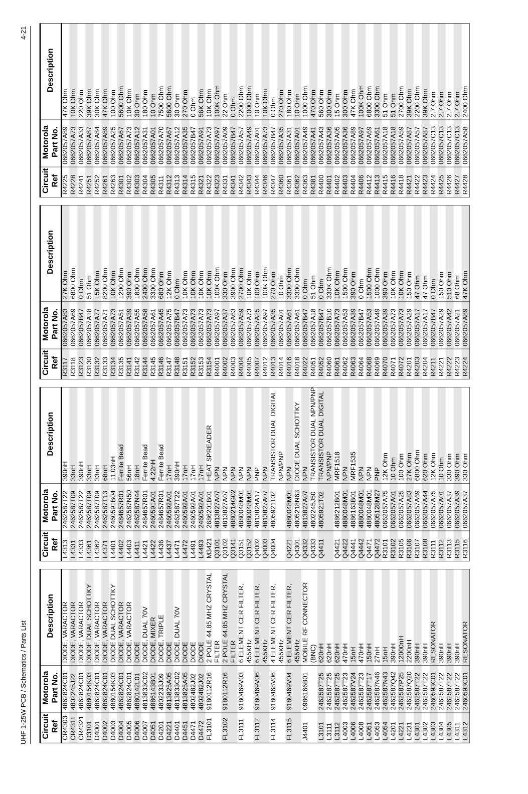
UH
F 1
-25W
PC
B /
Sch
emat
ics
/ Par
ts L
ist
4-21
CR
4303
4862
824C
01D
IOD
E, V
AR
AC
TO
RC
R43
1148
0224
5J22
DIO
DE
, VA
RA
CT
OR
CR
4321
4862
824C
01D
IOD
E, V
AR
AC
TO
RD
3101
4880
154K
03D
IOD
E D
UA
L S
CH
OT
TK
YD
4001
4862
824C
01D
IOD
E, V
AR
AC
TO
RD
4002
4862
824C
01D
IOD
E, V
AR
AC
TO
RD
4003
4880
154K
03D
IOD
E D
UA
L S
CH
OT
TK
YD
4004
4862
824C
01D
IOD
E, V
AR
AC
TO
RD
4005
4862
824C
01D
IOD
E, V
AR
AC
TO
RD
4006
4880
142L
01D
IOD
ED
4007
4813
833C
02D
IOD
E, D
UA
L 70
VD
4051
4886
143B
01D
IOD
E, M
IXE
RD
4201
4802
233J
09D
IOD
E, T
RIP
LED
4221
4813
825A
05D
IOD
ED
4401
4813
833C
02D
IOD
E, D
UA
L 70
VD
4451
4813
825A
05D
IOD
ED
4471
4802
482J
02D
IOD
ED
4472
4802
482J
02D
IOD
EF
L310
191
8011
2R16
2 P
OLE
44.
85 M
HZ
CR
YS
TAL
FIL
TE
RF
L310
291
8011
2R16
2 P
OLE
44.
85 M
HZ
CR
YS
TAL
FIL
TE
RF
L311
191
8046
9V03
6 E
LEM
EN
T C
ER
FIL
TE
R,
455K
Hz
FL3
112
9180
469V
066
ELE
ME
NT
CE
R F
ILT
ER
, 45
5KH
zF
L311
491
8046
8V06
4 E
LEM
EN
T C
ER
FIL
TE
R,
455K
Hz
FL3
115
9180
469V
046
ELE
ME
NT
CE
R F
ILT
ER
, 45
5KH
zJ4
401
0986
166B
01M
OB
ILE
RF
CO
NN
EC
TO
R
(BN
C)
L310
124
6258
7T25
620n
HL3
111
2462
587T
2562
0nH
L311
224
6258
7T25
620n
HL4
003
2462
587T
2347
0nH
L400
624
6258
7V24
15nH
L400
824
6258
7T23
470n
HL4
051
2462
587T
1715
0nH
L405
324
6258
7N46
27nH
L405
424
6258
7N43
15nH
L420
124
6258
7Q42
390n
HL4
221
2462
587P
2512
000n
HL4
231
2462
587Q
2022
00nH
L430
124
6258
7T22
390n
HL4
302
2462
587T
2239
0nH
L430
324
6059
3C01
RE
SO
NA
TO
RL4
304
2462
587T
2239
0nH
L430
524
6258
7T22
390n
HL4
311
2462
587T
2239
0nH
L431
224
6059
3C01
RE
SO
NA
TO
R
Cir
cuit
R
efM
oto
rola
P
art
No
.D
escr
ipti
on
L431
324
6258
7T22
390n
HL4
331
2462
587T
0933
nHL4
333
2462
587T
2239
0nH
L436
124
6258
7T09
33nH
L436
224
6258
7T09
33nH
L437
124
6258
7T13
68nH
L440
124
6059
1B04
11.0
3nH
L440
224
8465
7R01
Fer
rite
Bea
dL4
403
2462
587N
5056
nHL4
411
2462
587N
4418
nHL4
421
2484
657R
01F
errit
e B
ead
L442
224
6059
1A01
4.22
nHL4
436
2484
657R
01F
errit
e B
ead
L443
724
6059
2A01
17nH
L447
124
6258
7T22
390n
HL4
472
2460
592A
0117
nHL4
491
2460
592A
0117
nHL4
493
2460
592A
0117
nHM
3421
2686
201B
01H
EA
T S
PR
EA
DE
RQ
3101
4813
827A
07N
PN
Q31
0248
1382
7A07
NP
NQ
3141
4880
214G
02N
PN
Q31
5148
8004
8M01
NP
NQ
3152
4880
048M
01N
PN
Q40
0248
1382
4A17
PN
PQ
4003
4813
827A
07N
PN
Q40
0448
0592
1T02
TR
AN
SIS
TO
R D
UA
L D
IGIT
AL
NP
N/P
NP
Q42
2148
8004
8M01
NP
NQ
4301
4805
218N
63D
IOD
E D
UA
L S
CH
OT
TK
YQ
4332
4813
827A
07N
PN
Q43
3348
0224
5J50
TR
AN
SIS
TO
R D
UA
L N
PN
/PN
PQ
4411
4805
921T
02T
RA
NS
IST
OR
DU
AL
DIG
ITA
L N
PN
/PN
PQ
4421
4886
212B
01M
RF
1518
Q44
2248
8004
8M01
NP
NQ
4441
4886
163B
01M
RF
1535
Q44
4248
8004
8M01
NP
NQ
4471
4880
048M
01N
PN
Q44
7248
0512
8M27
PN
PR
3101
0662
057A
7512
K O
hmR
3102
0662
057A
0110
Ohm
R31
0506
6205
7A25
100
Ohm
R31
0606
6205
7A83
27K
Ohm
R31
0706
6205
7A69
6800
Ohm
R31
0806
6205
7A44
620
Ohm
R31
1106
6205
7A75
12K
Ohm
R31
1206
6205
7A01
10 O
hmR
3113
0662
057A
3733
0 O
hmR
3115
0662
057A
3939
0 O
hmR
3116
0662
057A
3733
0 O
hm
Cir
cuit
R
efM
oto
rola
P
art
No
.D
escr
ipti
on
R31
1706
6205
7A83
27K
Ohm
R31
1806
6205
7A69
6800
Ohm
R31
2306
6205
7B47
0 O
hmR
3130
0662
057A
1851
Ohm
R31
3206
6205
7A77
15K
Ohm
R31
3306
6205
7A71
8200
Ohm
R31
3406
6205
7A73
10K
Ohm
R31
3506
6205
7A51
1200
Ohm
R31
4106
6205
7A39
390
Ohm
R31
4206
6205
7A55
1800
Ohm
R31
4406
6205
7A58
2400
Ohm
R31
4506
6205
7A61
3300
Ohm
R31
4606
6205
7A45
680
Ohm
R31
4706
6205
7A75
12K
Ohm
R31
4806
6205
7B47
0 O
hmR
3151
0662
057A
7310
K O
hmR
3152
0662
057A
7310
K O
hmR
3153
0662
057A
7310
K O
hmR
3154
0662
057A
7310
K O
hmR
4001
0662
057A
9710
0K O
hmR
4002
0662
057A
3733
0 O
hmR
4003
0662
057A
6339
00 O
hmR
4004
0662
057A
5927
00 O
hmR
4005
0662
057A
7310
K O
hmR
4007
0662
057A
2510
0 O
hmR
4012
0662
057A
9710
0K O
hmR
4013
0662
057A
3527
0 O
hmR
4014
0662
057A
0110
Ohm
R40
1606
6205
7A61
3300
Ohm
R40
1806
6205
7A61
3300
Ohm
R40
2206
6205
7B47
0 O
hmR
4051
0662
057A
1851
Ohm
R40
5206
6205
7B47
0 O
hmR
4060
0662
057B
1033
0K O
hmR
4061
0662
057A
7310
K O
hmR
4062
0662
057A
5315
00 O
hmR
4063
0662
057A
3939
0 O
hmR
4064
0662
057B
470
Ohm
R40
6806
6205
7A53
1500
Ohm
R40
6906
6205
7A49
1000
Ohm
R40
7006
6205
7A39
390
Ohm
R40
7106
6205
7A73
10K
Ohm
R40
7206
6205
7A73
10K
Ohm
R42
0106
6205
7A29
150
Ohm
R42
0306
6205
7A17
47 O
hmR
4204
0662
057A
1747
Ohm
R42
1106
6205
7B47
0 O
hmR
4221
0662
057A
2915
0 O
hmR
4222
0662
057A
4251
0 O
hmR
4223
0662
057A
2168
Ohm
R42
2406
6205
7A89
47K
Ohm
Cir
cuit
R
efM
oto
rola
P
art
No
.D
escr
ipti
on
R42
2506
6205
7A89
47K
Ohm
R42
2806
6205
7A73
10K
Ohm
R42
4106
6205
7A33
220
Ohm
R42
5106
6205
7A87
39K
Ohm
R42
5206
6205
7A84
30K
Ohm
R42
6106
6205
7A89
47K
Ohm
R42
6306
6205
7A25
100
Ohm
R43
0106
6205
7A67
5600
Ohm
R43
0206
6205
7A73
10K
Ohm
R43
0306
6205
7A12
30 O
hmR
4304
0662
057A
3118
0 O
hmR
4305
0662
057A
0110
Ohm
R43
1106
6205
7A70
7500
Ohm
R43
1206
6205
7A67
5600
Ohm
R43
1306
6205
7A12
30 O
hmR
4314
0662
057A
3527
0 O
hmR
4315
0662
057B
470
Ohm
R43
2106
6205
7A91
56K
Ohm
R43
2206
6205
7A73
10K
Ohm
R43
2306
6205
7A97
100K
Ohm
R43
3106
6205
7A09
22 O
hmR
4341
0662
057B
470
Ohm
R43
4206
6205
7A57
2200
Ohm
R43
4306
6205
7A49
1000
Ohm
R43
4406
6205
7A01
10 O
hmR
4346
0662
057A
7310
K O
hmR
4347
0662
057B
470
Ohm
R43
6006
6205
7A35
270
Ohm
R43
6106
6205
7A31
180
Ohm
R43
6206
6205
7A01
10 O
hmR
4363
0662
057A
4910
00 O
hmR
4381
0662
057A
4147
0 O
hmR
4400
0662
057A
4356
0 O
hmR
4401
0662
057A
3630
0 O
hmR
4402
0662
057A
0515
Ohm
R44
0306
6205
7A36
300
Ohm
R44
0406
6205
7A89
47K
Ohm
R44
0606
6205
7A97
100K
Ohm
R44
1206
6205
7A69
6800
Ohm
R44
1306
6205
7A61
3300
Ohm
R44
1506
6205
7A18
51 O
hmR
4416
0662
057A
1851
Ohm
R44
1806
6205
7A59
2700
Ohm
R44
2106
6205
7A87
39K
Ohm
R44
2206
6205
7A57
2200
Ohm
R44
2306
6205
7A87
39K
Ohm
R44
2406
6205
7C13
2.7
Ohm
R44
2506
6205
7C13
2.7
Ohm
R44
2606
6205
7C13
2.7
Ohm
R44
2706
6205
7C13
2.7
Ohm
R44
2806
6205
7A58
2400
Ohm
Cir
cuit
R
efM
oto
rola
P
art
No
.D
escr
ipti
on

4-22
UH
F 1
-25W
PC
B /
Sch
emat
ics
/ Par
ts L
ist
* M
otor
ola
Dep
ot S
ervi
cing
onl
y
Ref
eren
ce d
esig
nato
rs w
ith a
n as
teris
k in
dica
te
com
pone
nts
whi
ch a
re n
ot fi
eld
repl
acea
ble
beca
use
they
nee
d to
be
calib
rate
d w
ith
spec
ializ
ed fa
ctor
y eq
uipm
ent a
fter
inst
alla
tion.
R
adio
s in
whi
ch th
ese
part
s ha
ve b
een
repl
aced
in
the
field
will
be
off f
requ
ency
at t
empe
ratu
re
extr
emes
.
R44
2906
6205
7A59
2700
Ohm
R44
3106
8019
4M18
51 O
hmR
4441
0662
057A
8739
K O
hmR
4442
0662
057A
5722
00 O
hmR
4443
0662
057A
8739
K O
hmR
4445
0662
057A
5824
00 O
hmR
4446
0662
057B
470
Ohm
R44
5206
6205
7A75
12K
Ohm
R44
5406
6205
7A73
10K
Ohm
R44
5506
6205
7A97
100K
Ohm
R44
5706
8396
2T51
120
Ohm
R44
5806
6205
7A41
470
Ohm
R44
7106
6205
7A41
470
Ohm
R44
7306
8019
4M18
51 O
hmR
4474
0680
194M
1851
Ohm
R44
7506
6205
7A73
10K
Ohm
R44
9106
6205
7A73
10K
Ohm
R45
0106
6205
7A69
6800
Ohm
R45
0206
6205
7A83
27K
Ohm
R45
0406
6205
7A73
10K
Ohm
R45
0506
6205
7B09
300K
Ohm
R45
0706
6205
7A80
20K
Ohm
R45
0806
6205
7A97
100K
Ohm
R45
0906
6205
7A49
1000
Ohm
R45
1106
6205
7C19
4.7
Ohm
SH
4301
2602
641Y
02S
HIE
LDS
H43
0226
0264
1Y02
SH
IELD
T40
5125
0551
5V03
XF
MR
MIX
ER
4:1
T40
5225
0551
5V04
XM
FR
MIX
ER
5:1
U31
0151
8614
4B01
IC, I
FU
3111
5102
463J
52Q
UA
D A
NA
LOG
SW
ITC
HU
3115
5102
463J
52Q
UA
D A
NA
LOG
SW
ITC
HU
4201
5185
963A
27IC
FR
AC
TN
U42
1151
0573
9X05
IC, V
OLT
AG
E R
EG
ULA
TO
RU
4301
5105
750U
54IC
, VC
OU
4401
5185
130C
65IC
LD
MO
S D
RIV
ER
U44
0251
1381
8A01
LOW
PO
WE
R S
UP
PLY
U45
0151
8576
5B28
IC P
OW
ER
CO
NT
RO
L U
4502
5185
963A
15IC
TE
MP
ER
AT
UR
E S
EN
SO
RV
R44
7148
1383
0A15
DIO
DE
, 5.6
VY
3101
4880
606B
092N
D O
SC
XTA
L 44
.395
MH
ZY
3102
9186
145B
0245
5KH
z D
ISC
RIM
INA
TO
RY
4262
4886
182B
01T
CX
O 1
6.8M
HZ
Cir
cuit
R
efM
oto
rola
P
art
No
.D
escr
ipti
on

GM328/GM338/GM398Mobile Radios
UHF Band 2 (450-527MHz)
Service Information
Issue: December, 2003

Computer Software CopyrightsThe Motorola products described in this manual may include copyrighted Motorola computer programs stored in semiconductor memories or other media. Laws in the United States and other countries preserve for Motorola certain exclusive rights for copyrighted computer programs, including the exclusive right to copy or reproduce in any form, the copyrighted computer program. Accordingly, any copyrighted Motorola computer programs contained in the Motorola products described in this manual may not be copied or reproduced in any manner without the express written permission of Motorola. Furthermore, the purchase of Motorola products shall not be deemed to grant, either directly or by implication, estoppel or otherwise, any license under the copyrights, patents or patent applications of Motorola, except for the normal non-exclusive royalty-free license to use that arises by operation of law in the sale of a product.

i
Table of Contents
Section 1 Model Chart and Technical Specifications
1.0 GM328/GM338/GM398 Model Chart ...................................................................1-12.0 Technical Specifications ......................................................................................1-2
Section 2 Theory of Operation
1.0 Introduction ..........................................................................................................2-12.0 UHF (450-527 MHz) Receiver .............................................................................2-1
2.1 Receiver Front-End ........................................................................................2-12.2 Front-End Band-Pass Filters & Pre-Amplifier .................................................2-22.3 First Mixer and High Intermediate Frequency (IF)..........................................2-22.4 Low Intermediate Frequency (IF) and Receiver Back End.............................2-3
3.0 UHF (450-527 MHz) Transmitter Power Amplifier (PA) 25 W..............................2-33.1 First Power Controlled Stage..........................................................................2-43.2 Power Controlled Driver Stage .......................................................................2-43.3 Final Stage .....................................................................................................2-43.4 Directional Coupler .........................................................................................2-53.5 Antenna Switch...............................................................................................2-53.6 Harmonic Filter ...............................................................................................2-53.7 Power Control.................................................................................................2-5
4.0 UHF (450-527 MHz) Frequency Synthesis ..........................................................2-64.1 Reference Oscillator .......................................................................................2-64.2 Fractional-N Synthesizer ................................................................................2-74.3 Voltage Controlled Oscillator (VCO)...............................................................2-84.4 Synthesizer Operation ....................................................................................2-9
Section 3 Troubleshooting Charts
1.0 Troubleshooting Flow Chart for Receiver ............................................................3-12.0 Troubleshooting Flow Chart for 25W Transmitter ................................................3-33.0 Troubleshooting Flow Chart for Synthesizer........................................................3-64.0 Troubleshooting Flow Chart for VCO...................................................................3-7
ii
Section 4 UHF PCB/Schematics/Parts Lists
1.0 Allocation of Schematics and Circuit Boards .......................................................4-11.1 Controller Circuits...........................................................................................4-1
2.0 UHF Band 2 1-25W PCBs / Schematics / Parts List............................................4-3UHF Band 2 (450-527 MHz) 1-25W 8485671Z03 Top Side...................................4-3UHF Band 2 (450-527 MHz) 1-25W 8485671Z03 Bottom Side ............................4-4UHF Band 2 (450-527 MHz) Power Amplifier 1 - 25W...........................................4-5UHF Band 2 (450-527 MHz) FRACN .....................................................................4-6UHF Band 2 (450-527 MHz) Voltage Controlled Oscillator ....................................4-7UHF Band 2 (450-527 MHz) Receiver Front End...................................................4-8UHF Band 2 (450-527 MHz) IF...............................................................................4-9UHF Band 2 PCB 8485671Z03 Parts List 1-25W................................................4-10
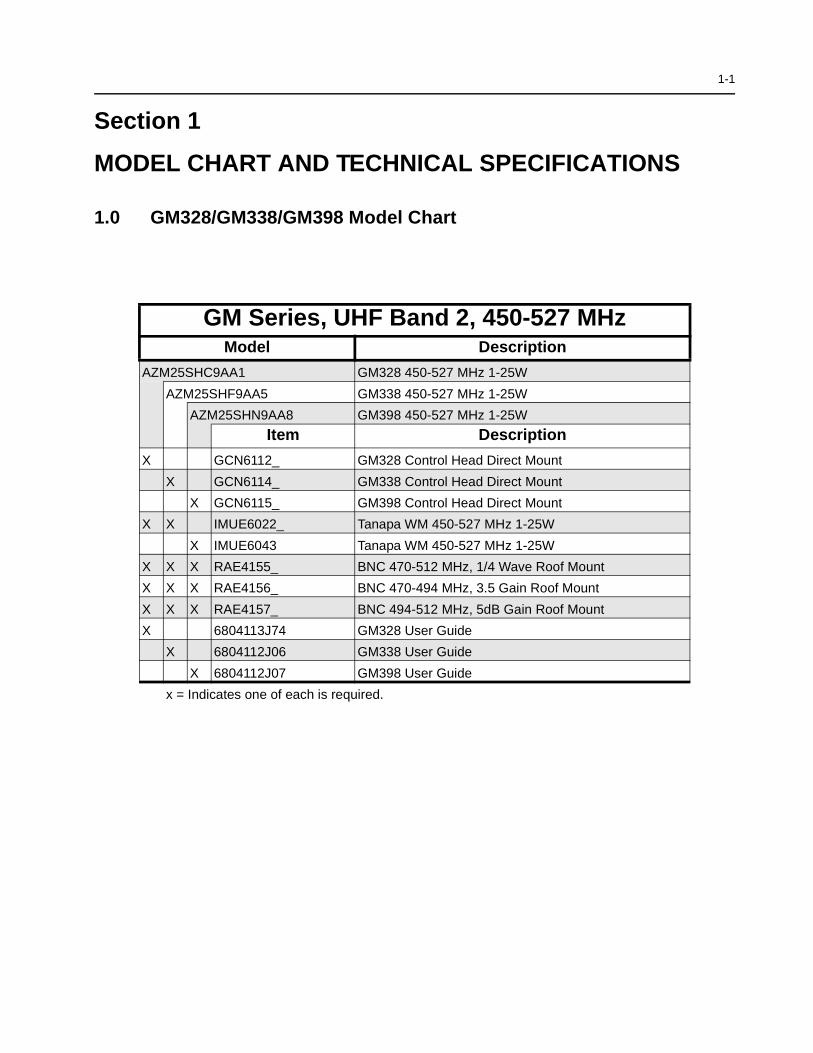
1-1
Section 1
MODEL CHART AND TECHNICAL SPECIFICATIONS
1.0 GM328/GM338/GM398 Model Chart
GM Series, UHF Band 2, 450-527 MHzModel Description
AZM25SHC9AA1 GM328 450-527 MHz 1-25W
AZM25SHF9AA5 GM338 450-527 MHz 1-25W
AZM25SHN9AA8 GM398 450-527 MHz 1-25W
Item Description
X GCN6112_ GM328 Control Head Direct Mount
X GCN6114_ GM338 Control Head Direct Mount
X GCN6115_ GM398 Control Head Direct Mount
X X IMUE6022_ Tanapa WM 450-527 MHz 1-25W
X IMUE6043 Tanapa WM 450-527 MHz 1-25W
X X X RAE4155_ BNC 470-512 MHz, 1/4 Wave Roof Mount
X X X RAE4156_ BNC 470-494 MHz, 3.5 Gain Roof Mount
X X X RAE4157_ BNC 494-512 MHz, 5dB Gain Roof Mount
X 6804113J74 GM328 User Guide
X 6804112J06 GM338 User Guide
X 6804112J07 GM398 User Guide
x = Indicates one of each is required.

1-2 Technical Specifications
2.0 Technical Specifications
Data is specified for +25°C unless otherwise stated.
General Specifications
Channel CapacityGM328GM338GM398
4128160
Power Supply 13.2Vdc (10.8 - 15.6Vdc)
Dimensions: H x W x D (mm) Depth excluding knobs GM32856mm x 176mm x 177mm(add 8mm for Volume Knob)
Dimensions: H x W x D (mm) Depth excluding knobs GM33859mm x 179mm x 186mm (1 - 25W)59mm x 179mm x 198mm (25 - 45W)(add 9mm for Volume Knob)
Dimensions: H x W x D (mm) Depth excluding knobs GM39872mm x 185mm x 188mm(add 8mm for Volume Knob)
Weight GM328/GM338 1400 g
Weight GM398 1500 g
Sealing: Withstands rain testing per MIL STD 810 C/D/E and IP54
Shock and Vibration: Protection provided via impactresistant housing exceeding MIL STD 810-C/D/E
Dust, Salt & Fog: Protection provided via environment resistant housing exceeding MIL STD 810 C/D/E
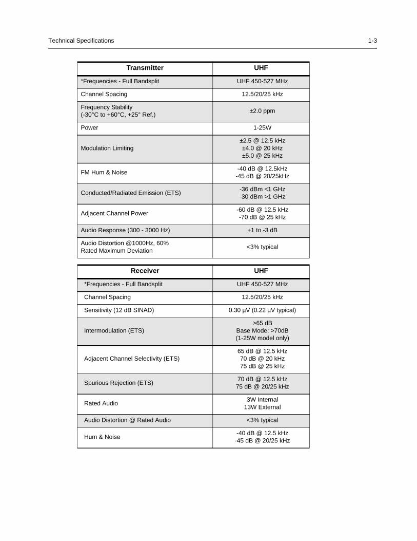
Technical Specifications 1-3
Transmitter UHF
*Frequencies - Full Bandsplit UHF 450-527 MHz
Channel Spacing 12.5/20/25 kHz
Frequency Stability(-30°C to +60°C, +25° Ref.)
±2.0 ppm
Power 1-25W
Modulation Limiting±2.5 @ 12.5 kHz ±4.0 @ 20 kHz±5.0 @ 25 kHz
FM Hum & Noise-40 dB @ 12.5kHz-45 dB @ 20/25kHz
Conducted/Radiated Emission (ETS)-36 dBm <1 GHz-30 dBm >1 GHz
Adjacent Channel Power-60 dB @ 12.5 kHz-70 dB @ 25 kHz
Audio Response (300 - 3000 Hz) +1 to -3 dB
Audio Distortion @1000Hz, 60%Rated Maximum Deviation
<3% typical
Receiver UHF
*Frequencies - Full Bandsplit UHF 450-527 MHz
Channel Spacing 12.5/20/25 kHz
Sensitivity (12 dB SINAD) 0.30 µV (0.22 µV typical)
Intermodulation (ETS)>65 dB
Base Mode: >70dB (1-25W model only)
Adjacent Channel Selectivity (ETS)65 dB @ 12.5 kHz 70 dB @ 20 kHz75 dB @ 25 kHz
Spurious Rejection (ETS)70 dB @ 12.5 kHz75 dB @ 20/25 kHz
Rated Audio3W Internal
13W External
Audio Distortion @ Rated Audio <3% typical
Hum & Noise-40 dB @ 12.5 kHz
-45 dB @ 20/25 kHz

1-4 Technical Specifications
*Availability subject to the laws and regulations of individual countries.
Audio Response (300 - 3000Hz @ 20/25kHz)(300 - 2550Hz @12.5kHz)
+1 to -3 dB
Conducted Spurious Emission (ETS)-57 dBm <1 GHz-47 dBm >1 GHz
Receiver UHF
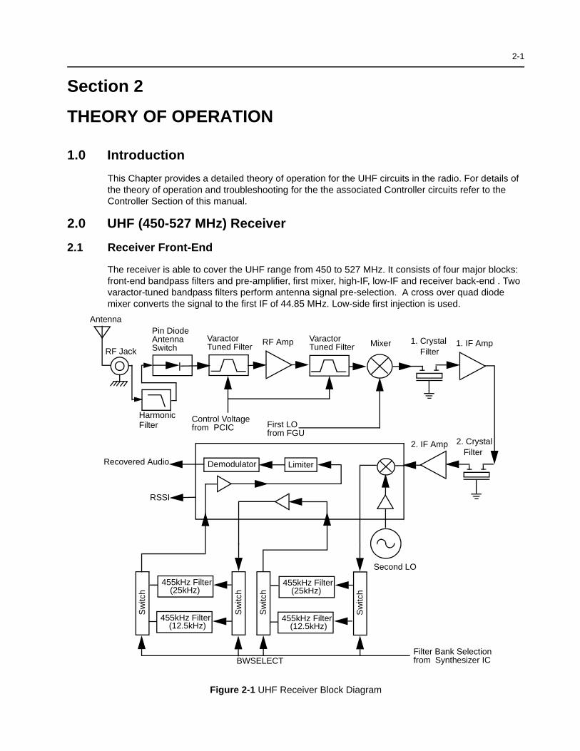
2-1
Section 2
THEORY OF OPERATION
1.0 Introduction
This Chapter provides a detailed theory of operation for the UHF circuits in the radio. For details of the theory of operation and troubleshooting for the the associated Controller circuits refer to the Controller Section of this manual.
2.0 UHF (450-527 MHz) Receiver
2.1 Receiver Front-End
The receiver is able to cover the UHF range from 450 to 527 MHz. It consists of four major blocks: front-end bandpass filters and pre-amplifier, first mixer, high-IF, low-IF and receiver back-end . Two varactor-tuned bandpass filters perform antenna signal pre-selection. A cross over quad diode mixer converts the signal to the first IF of 44.85 MHz. Low-side first injection is used.
Figure 2-1 UHF Receiver Block Diagram
Demodulator
1. Crystal Filter
MixerVaractor Tuned Filter
RF AmpVaractor Tuned Filter
Pin Diode Antenna SwitchRF Jack
Antenna
Control Voltagefrom PCIC First LO
from FGU
Recovered Audio
RSSI
Second LO
2. Crystal Filter
455kHz Filter(25kHz)
455kHz Filter(25kHz)
455kHz Filter(12.5kHz)
455kHz Filter(12.5kHz)
Sw
itch
Sw
itch
Sw
itch
Sw
itch
Limiter
1. IF Amp
2. IF Amp
Filter Bank Selectionfrom Synthesizer IC
Harmonic Filter
BWSELECT

2-2 UHF (450-527 MHz) Receiver
There are two 2-pole 44.85 MHz crystal filters in the high-IF section and 2 pairs of 455 kHz ceramic filters in the low-IF section to provide the required adjacent channel selectivity .The correct pair of ceramic filters for 12.5 or 25 kHz channel spacing is selected via control line BWSELECT. The second IF at 455 kHz is mixed, amplified and demodulated in the IF IC. The processing of the demodulated audio signal is performed by an audio processing IC located in the controller section.
2.2 Front-End Band-Pass Filters & Pre-Amplifier
The received signal from the radio’s antenna connector is first routed through the harmonic filter and antenna switch, which are part of the RF power amplifier circuitry, before being applied to the receiver pre-selector filter (C5001, C5002, D5001 and associated components). The 2-pole pre-selector filter tuned by the varactor diodes D5001 and D5002 pre-selects the incoming signal (RXIN) from the antenna switch to reduce spurious effects to following stages. The tuning voltage (FECTRL_1) ranging from 2 volts to 8 volts is controlled by pin 20 of PCIC (U5501) in the Transmitter section. A dual hot carrier diode (D5003) limits any inband signal to 0 dBm to prevent damage to the pre-amplifier.
The RF pre-amplifier is an SMD device (Q5003) with collector base feedback to stabilize gain, impedance, and intermodulation. The collector current of approximately 11-16 mA is drawn from the voltage 9V3 via L5003 and R5002. A switchable 3dB pad (R5066,R5007,R5063, R5064 and R5070), controlled via line FECTRL_2 and Q5004 stabilizes the output impedance and intermodulation performance.
A second 2-pole varactor tuned bandpass filter provides additional filtering of the amplified signal. The varactor diodes D5004 and D5005 are controlled by the same signal FECTRL_1, which controls the pre-selector filter. A following 1 dB pad (R5013 - R5015) stabilizes the output impedance and intermodulation performance.
2.3 First Mixer and High Intermediate Frequency (IF)
The signal coming from the front-end is converted to the first IF (44.85 MHz) using a cross over quad diode mixer (D5051). Its ports are matched for incoming RF signal conversion to the 44.85 MHz IF using low side injection via matching transformers T5051 and T5052. The injection signal (RXINJ) coming from the RX VCO buffer (Q5332) is filtered by the lowpass filter consisting of (L5053, L5054, C5053 - C5055) followed by a matching transformer T5052 and has a level of approximately 15dBm.
The mixer IF output signal (IF) from transformer T5501 pin 2 is fed to the first two pole crystal filter FL3101. The filter output in turn is matched to the following IF amplifier.
The IF amplifier Q3101 is actively biased by a collector base feedback (R3101, R3106) to a current drain of approximately 5 mA drawn from the voltage 5V. Its output impedance is matched to the second two pole crystal filter FL3102. The signal is further amplified by a preamplifier (Q3102) before going into pin 1 of IFIC (U3101).
A dual hot carrier diode (D3101) limits the filter output voltage swing to reduce overdrive effects at RF input levels above -27 dBm.

UHF (450-527 MHz) Transmitter Power Amplifier (PA) 25 W 2-3
2.4 Low Intermediate Frequency (IF) and Receiver Back End
The 44.85 high IF signal from the second IF amplifier feeds the IF IC (U3101) at pin1. Within the IF IC the 44.85 MHz high IF signal mixes with the 44.395 MHz second local oscillator (2nd LO) to produce the low IF signal at 455 kHz. The 2nd LO frequency is determined by crystal Y3101. The low IF signal is amplified and filtered by an external pair of 455 kHz ceramic filters FL3112, FL3114 for 20/25 kHz channel spacing or FL3111,FL3113/F3115 for 12.5 kHz channel spacing. These pairs are selectable via BWSELECT. The filtered output from the ceramic filters is applied to the limiter input pin of the IF IC (pin 14).
The IF IC contains a quadrature detector using a ceramic phase-shift element (Y3102) to provide audio detection. Internal amplification provides an audio output level of 120 mV rms (at 60% deviation) from U3103 pin 8 (DISCAUDIO) which is fed to the ASFIC_CMP (U0221) pin 2 (part of the Controller circuitry).
A Received Signal Strength Indicator (RSSI) signal is available at U3101 pin 5, having a dynamic range of 70 dB. The RSSI signal is interpreted by the microprocessor (U0101 pin 63) and in addition is available at accessory connector J0501-15.
3.0 UHF (450-527 MHz) Transmitter Power Amplifier (PA) 25 W
The radio’s 25W PA is a three stage amplifier used to amplify the output from the VCOBIC to the radio transmit level. All three stages utilize LDMOS technology. The gain of the first stage (U5401) is adjustable, controlled by pin 4 of PCIC (U5501) via U5402-1. It is followed by an LDMOS stage (Q5421) and LDMOS final stage (Q5441).
Figure 2-2 UHF Transmitter Block Diagram
Devices U5401, Q5421 and Q5441 are surface mounted. A pressure pad between board and the radio's cover provides good thermal contact between the devices and the chassis.
PCIC
Pin Diode Antenna Switch RF Jack
Antenna
Harmonic Filter
PowerSense
PA-FinalStage
From VCO
ControlledStage
Vcontrol
Bias 1
Bias 2
To Microprocessor
TemperatureSense
SPI BUS
ASFIC_CMP
PAPWRSET
To Microprocessor
PADriver
2-4 UHF (450-527 MHz) Transmitter Power Amplifier (PA) 25 W
3.1 First Power Controlled Stage
The first stage (U5401) is a 20dB gain integrated circuit containing two LDMOS FET amplifier stages. It amplifies the RF signal from the VCO (TXINJ). The output power of stage U5401 is controlled by a DC voltage applied to pin 1 from the op-amp U5402-1, pin 1. The control voltage simultaneously varies the bias of two FET stages within U5401. This biasing point determines the overall gain of U5401 and therefore its output drive level to Q5421, which in turn controls the output power of the PA.Op-amp U5402-1 monitors the drain current of U5401 via resistor R5444 and adjusts the bias voltage of U5401 so that the current remains constant. The PCIC (U5501) provides a DC output voltage at pin 4 (INT) which sets the reference voltage of the current control loop. A raising power output causes the DC voltage from the PCIC to fall, and U5402-1 adjusts the bias voltage for a lower drain current to lower the gain of the stage.In receive mode the DC voltage from PCIC pin 23 (RX) turns on Q5442, which in turn switches off the biasing voltage to U5401.
Switch S5440 is a pressure pad with a conductive strip which connects two conductive areas on the board when the radio's cover is properly screwed to the chassis. When the cover is removed, S5440 opens and the resulting high voltage level at the inverting inputs of the current control op-amps U5402-1 & 2 switches off the biasing of U5401 and Q5421. This prevents transmitter key up while the devices do not have proper thermal contact to the chassis.
3.2 Power Controlled Driver Stage
The next stage is an LDMOS device (Q5421) providing a gain of 12dB. This device requires a positive gate bias and a quiescent current flow for proper operation. The bias is set during transmit mode by the drain current control op-amp U5402-2, and fed to the gate of Q5421 via the resistive network R5429, R5418, R5415 and R5416.Op-amp U5402-2 monitors the drain current of U5421 via resistors R5424-27 and adjusts the bias voltage of Q5421 so that the current remains constant. The PCIC (U5501) provides a DC output voltage at pin 4 (INT) which sets the reference voltage of the current control loop. A raising power output causes the DC voltage from the PCIC to fall, and U5402-2 adjusts the bias voltage for a lower drain current to lower the gain of the stage.In receive mode the DC voltage from PCIC pin 23 (RX) turns on Q5422, which in turn switches off the biasing voltage to Q5421.
3.3 Final Stage
The final stage is an LDMOS device (Q5441) providing a gain of 12dB. This device also requires a positive gate bias and a quiescent current flow for proper operation. The voltage of the line MOSBIAS_2 is set in transmit mode by the ASFIC and fed to the gate of Q5441 via the resistive network R5404, R5406, and R5431-2. This bias voltage is tuned in the factory. If the transistor is replaced, the bias voltage must be tuned using the Global Tuner. Care must be taken not to damage the device by exceeding the maximum allowed bias voltage. The device’s drain current is drawn directly from the radio’s DC supply voltage input, PASUPVLTG, via L5436 and L5437.A matching network consisting of C5441-49 and striplines transforms the impedance to 50 ohms and feeds the directional coupler.

UHF (450-527 MHz) Transmitter Power Amplifier (PA) 25 W 2-5
3.4 Directional Coupler
The directional coupler is a microstrip printed circuit, which couples a small amount of the forward power delivered by Q5441. The coupled signal is rectified by D5451. The DC voltage is proportional to the RF output power and feeds the RFIN port of the PCIC (U5501 pin 1). The PCIC controls the gain of stages U5401 and Q5421 as necessary to hold this voltage constant, thus ensuring the forward power out of the radio to be held to a constant value.
3.5 Antenna Switch
The antenna switch consists of two PIN diodes, D5471 and D5472. In the receive mode, both diodes are off. Signals applied at the antenna jack J5401 are routed, via the harmonic filter, through network L5472, C5474 and C5475, to the receiver input. In the transmit mode, K9V1 turns on Q5471 which enables current sink Q5472, set to 96 mA by R5473 and VR5471. This completes a DC path from PASUPVLTG, through L5437, D5471, L5472, D5472, L5471, R5474 and the current sink, to ground. Both diodes are forward biased into conduction. The transmitter RF from the directional coupler is routed via D5471 to the harmonic filter and antenna jack. D5472 also conducts, shunting RF power and preventing it from reaching the receiver port (RXIN). L5472 is selected to appear as a broadband lambda/4 wave transmission line, making the short circuit presented by D5472 appear as an open circuit at the junction of D5472 and the receiver path.
3.6 Harmonic Filter
Components L5491-L5493 and L5472, C5491, C5496-98 form a Butterworth low-pass filter to attenuate harmonic energy of the transmitter to specifications level. R5491 is used to drain electrostatic charge that might otherwise build up on the antenna. The harmonic filter also prevents high level RF signals above the receiver passband from reaching the receiver circuits, improving spurious response rejection.
3.7 Power Control
The transmitter uses the Power Control IC (PCIC, U5501) to control the power output of the radio. A portion of the forward RF power from the transmitter is sampled by the directional coupler and rectified, to provide a DC voltage to the RFIN port of the PCIC (pin 1) which is proportional to the sampled RF power.
The ASFIC (U0221) has internal digital to analog converters (DACs) which provide a reference voltage of the control loop to the PCIC via R5505. The reference voltage level is programmable through the SPI line of the PCIC. This reference voltage is proportional to the desired power setting of the transmitter, and is factory programmed at several points across the frequency range of the transmitter to offset frequency response variations of the transmitter’s power detector circuit.
The PCIC provides a DC output voltage at pin 4 (INT) which sets the drain current of the first (U5401) and second (Q5421) transmitter stage via current control op-amps U5402-1 and U5402-2. This adjusts the transmitter power output to the intended value. Variations in forward transmitter power cause the DC voltage at pin 1 to change, and the PCIC adjusts the control voltage above or below its nominal value to raise or lower output power.
Capacitors C5502-4, in conjunction with resistors and integrators within the PCIC, control the transmitter power-rise (key-up) and power-decay (de-key) characteristic to minimize splatter into adjacent channels.

2-6 UHF (450-527 MHz) Frequency Synthesis
U5502 is a temperature-sensing device, which monitors the circuit board temperature in the vicinity of the transmitter driver and final devices, and provides a DC voltage to the PCIC (TEMP, pin 30) proportional to temperature. If the DC voltage produced exceeds the set threshold in the PCIC, the transmitter output power will be reduced so as to reduce the transmitter temperature.
4.0 UHF (450-527 MHz) Frequency Synthesis
The synthesizer subsystem consists of the reference oscillator (Y5261 or Y5262), the Low Voltage Fractional-N synthesizer (LVFRAC-N, U5201), and the Voltage Controlled Oscillator VCO.
4.1 Reference Oscillator
The reference oscillator (Y5262) contains a temperature compensated crystal oscillator with a frequency of 16.8 MHz. An Analogue to Digital (A/D) converter internal to U5201 (LVFRAC-N) and controlled by the microprocessor via serial interface (SRL) sets the voltage at the warp output of U5201 pin 25 to set the frequency of the oscillator. The output of the oscillator (pin 3 of Y5262) is applied to pin 23 (XTAL1) of U5201 via a RC series combination.
In applications where less frequency stability is required the oscillator inside U5201 is used along with an external crystal Y5261, varactor diode D5261, C5261, C5262 and R5262. In this case, Y5262, R5263, C5235 and C5251 are not used. When Y5262 is used, Y5261, D5261, C5261, C5262 and R5262 are not used, and C5263 is increased to 0.1 uF.
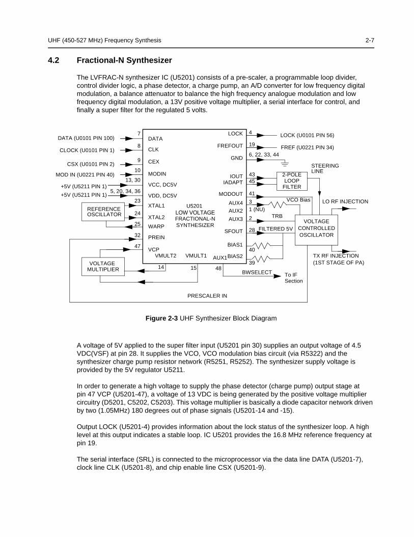
UHF (450-527 MHz) Frequency Synthesis 2-7
4.2 Fractional-N Synthesizer
The LVFRAC-N synthesizer IC (U5201) consists of a pre-scaler, a programmable loop divider, control divider logic, a phase detector, a charge pump, an A/D converter for low frequency digital modulation, a balance attenuator to balance the high frequency analogue modulation and low frequency digital modulation, a 13V positive voltage multiplier, a serial interface for control, and finally a super filter for the regulated 5 volts.
Figure 2-3 UHF Synthesizer Block Diagram
A voltage of 5V applied to the super filter input (U5201 pin 30) supplies an output voltage of 4.5 VDC(VSF) at pin 28. It supplies the VCO, VCO modulation bias circuit (via R5322) and the synthesizer charge pump resistor network (R5251, R5252). The synthesizer supply voltage is provided by the 5V regulator U5211.
In order to generate a high voltage to supply the phase detector (charge pump) output stage at pin 47 VCP (U5201-47), a voltage of 13 VDC is being generated by the positive voltage multiplier circuitry (D5201, C5202, C5203). This voltage multiplier is basically a diode capacitor network driven by two (1.05MHz) 180 degrees out of phase signals (U5201-14 and -15).
Output LOCK (U5201-4) provides information about the lock status of the synthesizer loop. A high level at this output indicates a stable loop. IC U5201 provides the 16.8 MHz reference frequency at pin 19.
The serial interface (SRL) is connected to the microprocessor via the data line DATA (U5201-7), clock line CLK (U5201-8), and chip enable line CSX (U5201-9).
DATA
CLK
CEX
MODIN
VCC, DC5V
XTAL1
XTAL2
WARP
PREIN
VCP
REFERENCEOSCILLATOR
VOLTAGEMULTIPLIER
DATA (U0101 PIN 100)
CLOCK (U0101 PIN 1)
CSX (U0101 PIN 2)
MOD IN (U0221 PIN 40)
+5V (U5211 PIN 1)
7
8
9
10
13, 30
23
24
25
32
47
VMULT2 VMULT1
BIAS1
SFOUT
AUX3
AUX4
IADAPTIOUT
GND
FREFOUT
LOCK 4
19
6, 22, 33, 44
4345
3
2
28
14 15
40
FILTERED 5V
STEERING
LOCK (U0101 PIN 56)
PRESCALER IN
FREF (U0221 PIN 34)
39BIAS2
41
48
5, 20, 34, 36+5V (U5211 PIN 1)
AUX1
VDD, DC5V MODOUT
U5201 LOW VOLTAGEFRACTIONAL-NSYNTHESIZER
AUX2 1 (NU)
BWSELECT
VCO Bias
TRB
To IFSection
TX RF INJECTION(1ST STAGE OF PA)
LO RF INJECTION
VOLTAGE CONTROLLED OSCILLATOR
LINE2-POLELOOP
FILTER

2-8 UHF (450-527 MHz) Frequency Synthesis
4.3 Voltage Controlled Oscillator (VCO)
The Voltage Controlled Oscillator (VCO) consists of the VCO/Buffer IC (VCOBIC, U5301), the TX and RX tank circuits, the external RX buffer stages, and the modulation circuitry.
Figure 2-4 UHF VCO Block Diagram
The VCOBIC together with Fractional-N synthesizer (U5201) generates the required frequencies in both transmit and receive modes. The TRB line (U5301 pin 19) determines which tank circuits and internal buffers are to be enabled. A high level on TRB enables TX tank and TX output (pin 10), and a low enables RX tank and RX output (pin 8). A sample of the signal from the enabled output is routed from U5301 pin 12 (PRESC_OUT), via a low pass filter, to pin 32 of U5201 (PREIN).
A steering line voltage (VCTRL) between 3.0V and 10.0V at varactor diode CR5311 will tune the full TX frequency range (TXINJ) from 450 MHz to 527 MHz, and at varactor diodes CR5301, CR5302 and CR5303 will tune the full RX frequency range (RXINJ) from 405 MHz to 482 MHz. The tank circuits uses the Hartley configuration for wider bandwidth. For the RX tank circuit, an external transistor Q5301 is used in conjunction with the internal transistor for better side-band noise. Similarly, an external transistor Q5311 is used in the Tx tank circuit.
Presc
RX
TX
MatchingNetwork Low Pass
Filter
Attenuator
Pin8
Pin14
Pin10
(U5201 Pin28)
VCC Buffers
TX RF Injection
U5201 Pin 32
AUX3 (U5201 Pin 2)
Prescaler Out
Pin 12Pin 19Pin 20
TX/RX/BSSwitching Network
U5301VCOBIC
RxActive Bias
TxActive Bias
Pin2
Rx-I adjust
Pin1
Tx-I adjust
Pins 9,11,17Pin18
VsensCircuit
Pin15
Pin16
RX VCO Circuit
TX VCO Circuit
RX Tank
TX Tank
Pin7
Vcc-Superfilter
Collector/RF in
Pin4
Pin5
Pin6
RX
TX
(U5201 Pin 28)
Rx-SW
Tx-SW
Vcc-Logic
(U5201 Pin 28)
Steer Line Voltage (VCTRL)
Pin13
Pin3
TRB IN
LO RF INJECTION
Q5301
Q5332

UHF (450-527 MHz) Frequency Synthesis 2-9
The external RX buffers (Q5332) are enabled by a high at U5201 pin 3 (AUX4) via transistor switch Q5333. In TX mode the modulation signal (VCOMOD) from the LVFRAC-N synthesizer IC (U5201 pin41) is applied modulation circuitry CR5321, R5321, R5322 and C5324, which modulates the TX VCO frequency via coupling capacitor C5321. Varactor CR5321 is biased for linearity from VSF.
4.4 Synthesizer Operation
The complete synthesizer subsystem comprises mainly of low voltage FRAC-N (LVFRACN) IC, Reference Oscillator (crystal oscillator with temperature compensation), charge pump circuitry, loop filter circuitry and DC supply. The output signal PRESC_OUT of the VCOBIC (U5301 pin 12) is fed to pin 32 of U5201 (PREIN) via a low pass filter (C5229, L5225) which attenuates harmonics and provides the correct level to close the synthesizer loop.The pre-scaler in the synthesizer (U5201) is basically a dual modulus pre-scaler with selectable divider ratios. This divider ratio of the pre-scaler is controlled by the loop divider, which in turn receives its inputs via the SRL. The output of the pre-scaler is applied to the loop divider. The output of the loop divider is connected to the phase detector, which compares the loop divider´s output signal with the reference signal.The reference signal is generated by dividing down the signal of the reference oscillator (Y5261 or Y5262).The output signal of the phase detector is a pulsed DC signal which is routed to the charge pump. The charge pump outputs a current at pin 43 of U5201 (IOUT). The loop filter (which consists of R5221-R5223, C5221-C5225,L5221) transforms this current into a voltage that is applied to the varactor diodes CR5311 for transmit, CR5301, CR5302 & CR5303 for receive and alters the output frequency of the VCO .The current can be set to a value fixed in the LVFRAC-N IC or to a value determined by the currents flowing into BIAS 1 (U5201-40) or BIAS 2 (U5201-39). The currents are set by the value of R5251 or R5252 respectively. The selection of the three different bias sources is done by software programming.To reduce synthesizer lock time when new frequency data has been loaded into the synthesizer the magnitude of the loop current is increased by enabling the IADAPT (U5201-45) for a certain software programmable time (Adapt Mode). The adapt mode timer is started by a low to high transient of the CSX line. When the synthesizer is within the lock range the current is determined only by the resistors connected to BIAS 1, BIAS 2, or the internal current source. A settled synthesizer loop is indicated by a high level of signal LOCK (U5201-4). The LOCK (U5201-4) signal is routed to one of the µP´s ADCs input U101-56. From the voltage the µP determines whether LOCK is active. In order to modulate the PLL the two spot modulation method is utilized. Via pin 10 (MODIN) on U5201 the audio signal is applied to both the A/D converter (low freq path) as well as the balance attenuator (high freq path). The A/D converter converts the low frequency analogue modulating signal into a digital code that is applied to the loop divider, thereby causing the carrier to deviate. The balance attenuator is used to adjust the VCO’s deviation sensitivity to high frequency modulating signals. The output of the balance attenuator is present at the MODOUT port (U5201-41) and connected to the VCO modulation diode CR5321 via R5321, C5325.

2-10 UHF (450-527 MHz) Frequency Synthesis
THIS PAGE INTENTIONALLY LEFT BLANK

3-1
Section 3
TROUBLESHOOTING CHARTS
1.0 Troubleshooting Flow Chart for Receiver (Sheet 1 of 2)
Bad SINADBad 20dB Quieting
No Recovered Audio
START
Audio at pin 8 of U3101 ?
Check Controller(in the case of no audio)
OR ELSE go to “B”
Yes
No
Spray or inject 44.85MHz into XTAL Filter FL3101
Audio heard ?BYes
No
Check 2nd LO (44.395MHz) at C3135
LO present ?BYes
Check voltages on U3101
Biasing OK ?
No
No
A
Yes
Check Q3102 bias for faults
Replace Q3102
Go to B
Yes
No
Check circuitry around U3101.
Replace U3101 if defect
Check circuitry around Y3101. Replace Y3101 if defect
Voltages
OK?
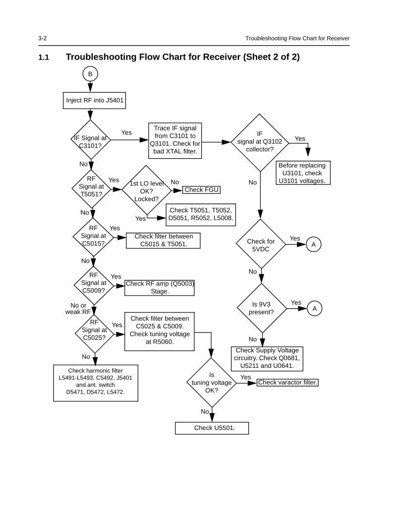
3-2 Troubleshooting Flow Chart for Receiver
1.1 Troubleshooting Flow Chart for Receiver (Sheet 2 of 2)
IF Signal at C3101?
No
RF Signal at T5051?
RFSignal at C5015?
No
No
RFSignal at C5025?
No or
Check harmonic filterL5491-L5493, C5492, J5401
and ant. switchD5471, D5472, L5472.
Check filter between C5025 & C5009.
Check tuning voltage at R5060.
Inject RF into J5401
Istuning voltage
OK?
No
Yes
Check RF amp (Q5003) Stage.
Check filter between C5015 & T5051.
Yes
Check T5051, T5052, D5051, R5052, L5008.
Yes
1st LO level OK?
Locked?
Yes
Check FGU
Yes
Trace IF signal from C3101 to
Q3101. Check for bad XTAL filter.
No
Yes IFsignal at Q3102
collector?
Before replacing U3101, check
U3101 voltages.
Yes
Check for 5VDC
Is 9V3 present?
Check Supply Voltage circuitry. Check Q0681,
U5211 and U0641.
No
No
No
Check U5501.
Check varactor filter.
No
Yes
Yes
Yes
A
A
B
weak RF
RFSignal at C5009?
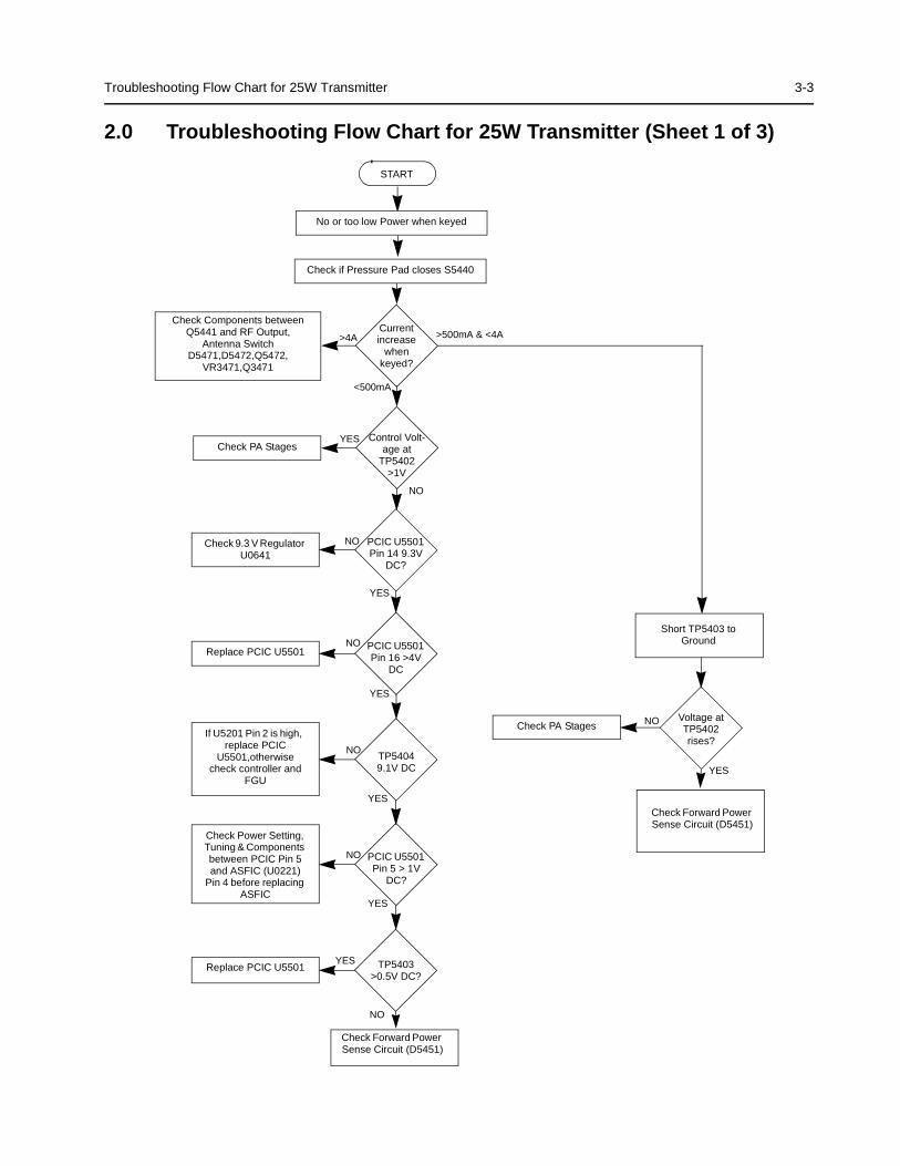
Troubleshooting Flow Chart for 25W Transmitter 3-3
2.0 Troubleshooting Flow Chart for 25W Transmitter (Sheet 1 of 3)
Current increase
when keyed?
NO
YES
START
Check if Pressure Pad closes S5440
Check Components between Q5441 and RF Output,
Antenna Switch D5471,D5472,Q5472,
VR3471,Q3471
>500mA & <4A>4A
<500mA
Check PA StagesControl Volt-
age at TP5402
>1V
Short TP5403 to Ground
NO
YES
Voltage at TP5402 rises?
Check PA Stages NO
YES
PCIC U5501 Pin 14 9.3V
DC?
Check 9.3 V Regulator U0641
NO
YES
PCIC U5501 Pin 16 >4V
DC
Replace PCIC U5501
NO
YES
TP5404 9.1V DC
If U5201 Pin 2 is high, replace PCIC
U5501,otherwise check controller and
FGU
YES
NO
TP5403 >0.5V DC?
Replace PCIC U5501
Check Forward Power Sense Circuit (D5451)
Check Forward Power Sense Circuit (D5451)
NO
YES
PCIC U5501 Pin 5 > 1V
DC?
Check Power Setting, Tuning & Components between PCIC Pin 5 and ASFIC (U0221)
Pin 4 before replacing ASFIC
No or too low Power when keyed

3-4 Troubleshooting Flow Chart for 25W Transmitter
2.1 Troubleshooting Flow Chart for 25W Transmitter (Sheet 2 of 3)
Check PA Stages
No or too low Power when keyed
Measure DC Voltage at Pin 2 & 3 of U5401
>6
YES
DC Voltage at U5501
Pin 23 =0?
2-6
DC Voltage at U5402-1
Pin 1?
YES
Pin 2Voltage 0.62 * Voltage at
Pin 1?
If U5201 Pin 2 is high, replace PCIC
NOReplace U5401
YES
NODC
Voltage at U5402-1 Pin
3 = 8.8V?
Check S5440, R5442 and R5443
YES
Pin 3 Voltage 0.51 * Voltage at
Pin 1?
NOReplace U5401
<2VDC
Voltage at U5402-2 Pin 7?
>6V
Check Components between U5402-2 Pin 7
and Q5421. Check Resistive Network at
Pins 5 & 6 before replacing Q5421
YES
DC Voltage at
U5402-2 Pin 5 <8.8V?
Check Components between U5402-2 Pin 7
and Q5421. Check Resis-tive Network at Pins 5 & 6 before replacing Q5421
NO
Check Q5422
NO
Check Final PA Stage
2-6V
<2VCheck Resistive Net-work at Pins 2 & 3 of
U5402-1 before replac-ing U5401
Check Q5442 and Resistive Network at
U5402-1 Pin 3 before replacing
U5401
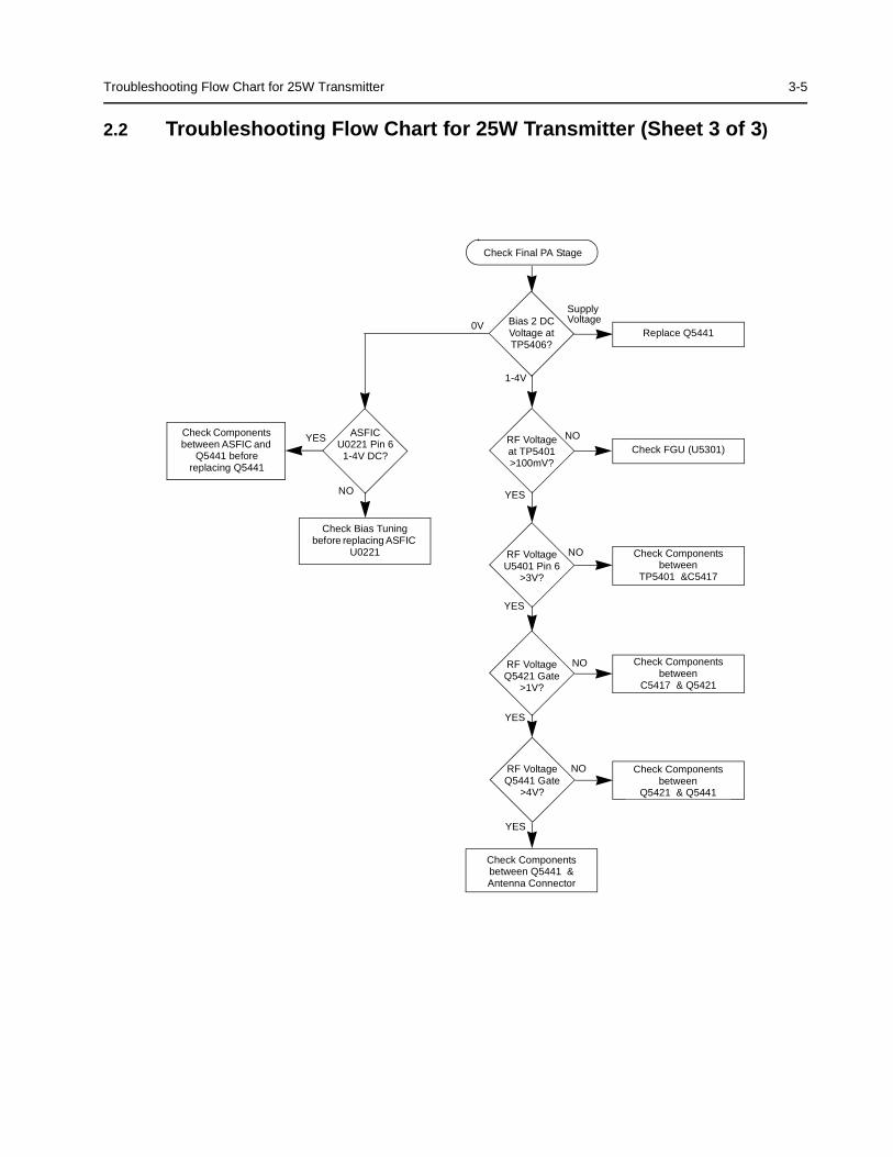
Troubleshooting Flow Chart for 25W Transmitter 3-5
2.2 Troubleshooting Flow Chart for 25W Transmitter (Sheet 3 of 3)
Check Final PA Stage
NO
0V
1-4V
Bias 2 DC Voltage at TP5406?
YES
RF Voltage at TP5401 >100mV?
YES
RF Voltage U5401 Pin 6
>3V?
Supply
Replace Q5441
Check FGU (U5301)
NO Check Components between
TP5401 &C5417
NO
YES ASFIC U0221 Pin 6 1-4V DC?
Check Bias Tuning before replacing ASFIC
U0221
Check Components between ASFIC and
Q5441 before replacing Q5441
YES
RF Voltage Q5421 Gate
>1V?
NO Check Components between
C5417 & Q5421
YES
RF Voltage Q5441 Gate
>4V?
NO Check Components between
Q5421 & Q5441
Check Components between Q5441 & Antenna Connector
Voltage

3-6 Troubleshooting Flow Chart for Synthesizer
3.0 Troubleshooting Flow Chart for Synthesizer
5V at pin 6 of
D5201
Isinformation
from µP U0101correct
?
IsU5201 Pin 47at = 13VDC
?
IsU5301 Pin 19
<40 mVDC in RX &>4.5 VDC in TX? (at VCO section)
?
Start
Visual check of the
BoardOK?
CorrectProblem
Check 5VRegulatorU5211
+5Vat U5201
Pins13 & 30
?
Is16.8MHz
Signal at U5201 Pin 19
?
CheckY5261 / Y5262 and
associated parts
Aresignals
at Pins 14 &15 of U5201
?
Check R5201 Check C5381
IsU5201
Pin 2 >4.5 VDC in Tx & <40 mVDC
in Rx?
Replace U5201
RemoveShorts
Isthere a short
between Pin 47 andPins 14 & 15 of
U5201?
Replace orresolder
necessarycomponents
IsRF level at
U5201 Pin 32 -12 < x <-25
dBm?
AreR5221,R5222,R5223,C5221,
C5222,& C5223 OK?
Replace U5201
If C5227is OK, then see VCOtroubleshooting chart
AreWaveforms
at Pins 14 & 15triangular
?
DoPins 7,8 & 9
of U5201 togglewhen channel is
changed?
Check programminglines between
U0101 and U5201Pins 7,8 & 9
Replace U5201
Check µP U0101Troubleshooting
Chart
NO
YES
NO
YES
NO
YES
NO
NO
NO
YES
YES
NO
YES
YES
NO
YES
YESYESNO
NO
NO
NO
YES
NO
YES
YES
Check D5201, C5202, C5203, &
C5206
5V at U5201
pins 5, 20, 34 & 36
Check 5V Regulator
U5211
Is 16.8MHz signal at
U5201 Pin 23?
Replace U5201
YES
NO
NO
YES
NO
YES

Troubleshooting Flow Chart for VCO 3-7
4.0 Troubleshooting Flow Chart for VCO
Are Q5332Base at 0.7V
Collector at 4.5V Emitter at 110mV
Are Q5301Base at 2.4V
Collector at 4.5V Emitter at 1.7V
Are Q5311 Base = 1.9V
Collector = 4.5VEmitter = 1.3V
Low or no RF Signalat TP5003
Visual checkof board
OK?
35mV DC atU5301 Pin 19
NO
YES
Replace Q5301
at base of Q5332
NO
NO
NO
NO
YES
YES
YES
YES
Low or no RF Signalat input to PA
4.8V DC atU5301 Pin 19
Is RF available at U5401
YES
YES
YES
YES
NO
NO
NO
NO
NO
Audio =180mVrmsat “-” Side of
4.5VDCat CR5321
If C5321 and R5321 are OK, then replace CR5321
Replace C5322
Replace C5325
NO
NO
YES
YES
TX VCORX VCO
CorrectProblem
Visual checkof board
OK?
Check runner between U5201 Pin 2
and U5301 Pin 19
Is RF available If all parts from U5301 Pin 8to Base of Q5332 are OK,
replace U5301
If all parts associated with the pins are OK,
replace Q5332
If all parts from collectorof Q5332 to TP5003 are
OK, Replace U5301
Power OK but no modulation
If all parts from U5301 Pin 10U5401 Pin 16 are OK,
replace U5301
Replace Q5311
YES YES
Make sure Synthesizer is working correctly and runner between U5201 Pin 28 and U5301 Pin 14 & 18 are OK
4.5V DC
OK ?
OK? OK?
C5325
at U5301 Pin 14 & 18 4.5V DC
OK ?at U5301 Pin 14 &18
NO
Pin 16
If R5361 and L5361 are OK, replace U5301

3-8 Troubleshooting Flow Chart for VCO
THIS PAGE INTENTIONALLY LEFT BLANK
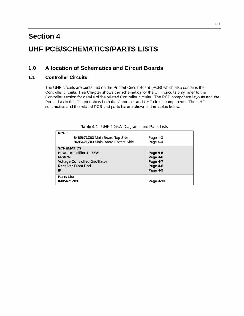
4-1
Section 4
UHF PCB/SCHEMATICS/PARTS LISTS
1.0 Allocation of Schematics and Circuit Boards
1.1 Controller Circuits
The UHF circuits are contained on the Printed Circuit Board (PCB) which also contains the Controller circuits. This Chapter shows the schematics for the UHF circuits only, refer to the Controller section for details of the related Controller circuits . The PCB component layouts and the Parts Lists in this Chapter show both the Controller and UHF circuit components. The UHF schematics and the related PCB and parts list are shown in the tables below.
Table 4-1 UHF 1-25W Diagrams and Parts Lists
PCB :8485671Z03 Main Board Top Side8485671Z03 Main Board Bottom Side
Page 4-3Page 4-4
SCHEMATICSPower Amplifier 1 - 25WFRACNVoltage Controlled OscillatorReceiver Front EndIF
Page 4-5Page 4-6Page 4-7Page 4-8Page 4-9
Parts List8485671Z03 Page 4-10

4-2 Allocation of Schematics and Circuit Boards
THIS PAGE INTENTIONALLY LEFT BLANK

UH
F B
and
2 1-
25W
PC
Bs
/ Sch
emat
ics
/ Par
ts L
ist
4-3
2.0
UH
F B
and
2 1
-25W
PC
Bs
/ Sch
emat
ics
/ Par
ts L
ist
ZM
Y01
3067
7-O
U02
51
98
116
R01
03C
0108
C02
52
R02
51R
0212
R02
57
R02
52
C02
51
C02
12
141
78
U02
11R
0211
R02
53
C02
11
R02
56
R02
68
C02
56
R0269
C0261
C02
62C
0253
U01
21
116 17
32
U01
01
26 51761
R01
32
R01
31
R01
05
R01
14R
0170
R01
06
C0101
C0102
C01
31
C01
32
132537
1
U02
21
Q01
10
R02
21
R02
22
R02
20
R0224
R02
25
R02
41
R0108
R0223
R02
26
R02
27
R02
29
R0442
R02
62
R01
01R
0104
R01
10R
0115
R0254R0255
R02
61
R01
16
R0228
R02
42
R01
02
C02
36
C0221
C0222
C02
23
C02
25
C02
26
C02
27C
0232
C0234
C02
41 C02
42 C02
44C
0245
C0231
C0235C0228
C02
33
C0237
C0441
C0442
C0443
C0445
C0446
C0447
C0448
C0449
C0495
C04
21
C02
46
C0104C0106
C0224
C02
43
C0107
Q06
81
R06
81D02
01
C06
81
C04
96
R06
82U
0651
12
3R
0651
C06
52
C0470
C0474C0476
C0477
C0478
C0490
C0471
C0472
C0473
U06
41
5
6
1
U02
71
9
R0652
D0651
C0651
Q01
77Q
0181
C05
42
4 32Y01
31
Q01
85
R0182
R0186
R05
38
R05
35R0181
R0185
R05
39
VR
0505
R05
10
VR
0503
VR
0510
J050
1
10 1120
VR
0501
C0502C0503C0504
C0505C0506C0508
C0509
C0510
C0511
C0512
C0513C0514
C0515
C0518C0517
C0501
C0516
L048
1
L048
2
C0655
C06
54
C0482C0483
C0486C0487
C0488
C0493
C0494
U54
01
916 1
Q5471
R55
07
R54
71
R55
09
R55
06
R55
08
R55
05R
5401
R54
03
R54
02
TP5401
L540
1
L540
3
C5505
C54
03
C54
01
C54
04
C54
07C
5509
8
R54
75V
R54
71
C54
02
M34
21R
5415
R54
16
L541
1
C54
25C54
17
C54
26
C54
18
C54
19
U06
11
5
6
1R
0611
R0533R
0612
C0612
C06
01
C04
84C
0603
J060
1
C54
22Q
5422
Q54
42
Q54
11
R5424
R5425
R5426
R5427
R54
50
L542
2
C54
28
C54
23
C54
24C
5420
C54
35
R54
31R
5432
C54
34C54
58
C54
31
C54
54 C54
57
C54
55
C54
32
87
65
43
2Q
5431
C54
48
C54
49
R5404R5406
D54
01
U55
02
C55
07C
5508
C54
41
C54
61
C54
46C
5443
C54
45C
5447
C54
42
C54
44
L549
1
C54
91
C54
62L5
472
D54
71C
5492
C54
96C
5498
32
J540
1
R54
91
C54
97
L549
3
L500
2L5
001
Q50
01Q
5003
R5020
R5021
R5007
R50
01
R5005
R50
22
R5064
R5003
R50
04
L500
6
L5003
D50
03
D5002
C50
09
C5014
C5033
C5034
C5065
C5003
C5008
C50
01C5004
C5005C5006
C5007
C5026
C5027
C50
02
L500
4
R5066
D5004
C50
15
C5068
C50
17
C50
16
C5029
D50
06
D5005
C5030
C50
18
R50
12
C5020
C5022
C5023
C5019
C5021
L500
5R
5013
L500
9C50
32
R50
15
R50
51
L505
1
C50
52
L547
1
D54
72
C54
72
C54
73
C54
74
D5001
65
432
FL3
101
R31
48L310
0
C31
01
2
T50
5216
4 3
D50
51L5
008
L505
3
L505
4
C50
53
C50
54
3 451
T50
51
2
C50
31
C50
55
65
432
FL3
102
R31
06
R31
01
L310
1
C31
02
C31
03
141
78 U
3111
141
78 U
3115
2Y
3102
R31
32
R31
42
R31
17
R31
23
R31
24
R31
30
R31
35R
3144
R31
45
R31
11L3
124
U31
01
10
201
11
C31
32
C31
34C
3139
C31
40
C31
41
C31
42
C31
45
C31
33
C31
15
C31
31
C31
48
C31
37C
3124
C31
35
C31
43
C31
36F
L311
2
23 4
FL3
114
C31
14
C52
24
Q5221
R52
24
R5225
R52
27
R52
23
R5222 R52
21
L5221
D5221
C5251
C52
53
C52
31
C5225
C52
29
C52
21
C5230
C5236
C52
23
C52
26
C52
27
C5222
R5252
R5251C5254
C5232
C5234
C5255
C5252
C5233
R52
11
L520
1
U52
11
C52
42
C52
43
C52
44
C52
45
C52
46
C52
13
C52
14C
5215
C52
10
C52
16
C5289C5217
1
J045
1
18
Q53
333
4R
5346
C53
75
L530
3
3
L531
2
3
Q53
01Q
5311
R5321
R5305
R53
02
R5301
R53
11
R53
12
L5304L5305
L531
3
C5308
C5352
C53
53
C53
25
C5309
C5317
C5322
C5351
C5372
C5382
C5383
C53
23
C5373
C5374
C53
55
C5318
C5371
L5371
SH
5301
R53
43
R53
33
R53
37R53
41
R53
45
R53
32R
5331
C53
32
C53
35C
5339
C53
31
C53
37
UH
F B
and
2 (
450-
527
MH
z) 1
-25W
848
5671
Z03
To
p S
ide
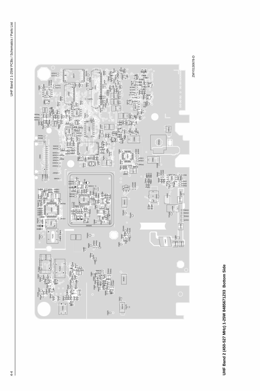
4-4
UH
F B
and
2 1-
25W
PC
Bs
/ Sch
emat
ics
/ Par
ts L
ist
ZM
Y01
3067
8-D
Y31
012 3
4
Q31
02
R31
12R
3114
R31
15
R31
13
R31
16R
3118
L311
2
D31
01C
3116
C31
21
C31
22C
3123
Q31
41
Q31
51
Q31
52
R31
33
R31
34
R31
51
R31
52
R31
53R
3154
R31
41R31
47
R31
46
C31
44
C31
47
C31
51
C31
52C
3146
FL3
111
2
34
FL3
115
234
FL3
113
Q31
01R
3102
R31
04R
3105
R31
08R
3107
L311
1
C31
04
C31
1111
C3112C3110
C3113R
5474
C54
71
C50
25
C54
75
R54
57
Q50
04
Q50
02R
5069
R50
62
R50
68
R50
61
R50
71
R50
72
R50
63
R5070
R50
17R5002
R50
16
R50
18
D50
07
C50
62
C50
64
C50
11
C5013
C50
67
C50
28
C5069
C50
61 C50
10C5012
R50
53
R50
60
R50
52
R50
54
R50
55T
P50
03
C50
66
C50
24C
5060
R50
19
R54
55R
5454
R54
52T
P54
03
D54
51C
5453
C54
51
C54
52
TP
5404
TP
5405
S5440
L540
2L5
436
TP
5406
L543
7
C5406
C54
38C5421
C5437
C54
81
C54
39C5482
C54
36
C54
05
32
Q54
21
1R
5420
C54
29
R54
42 R54
29
R5417
R54
40
R54
21 R5423R54
41
R54
43
R54
28
R54
45
R54
11
R54
18
R5422
R54
12
R55
11
854
1U
5402
C5411
C54
13C
5415
C04
99
C5427
C5412
C54
14
C54
16
C54
40
C06
11
432
Y52
62
R5228
R52
61
R5241
R52
63
R52
03
R52
04
R5201
R5206
R5262
Y52
61
134
6
TP
5201
TP
5202
L5231
1325 37
1
U52
01
D52
01
D5261
C5208C5209C5211
C52
28
C5263
C52
88
C52
02
C52
03
C5205
C52
35
C5201 C52
04
C5207
C5241
C5287
C52
06
C5262C5261
Q5472 R54
00
R54
73
C54
00
R55
02R
5504
R5446R5413
R55
01
L542
1
TP5402
25
917
U55
011
C55
01
C5502
C55
06
C55
03
C5510
C5483
C55
04
12
J040
1
R0407
R0409
R0467
R0412
R0441
F0401
C0426
C0427
C0429
C0485C04
91
C04
92
C04
97
C0422
C0423
C0430
C0431
C0428
R03
44
R03
23
R0324
R03
45
R03
41
C0304
C0305
C0324
C0325
C03
43
U03
518
5 4
U03
01
11415
28D
0301
C03
02C
0351 C03
54C
0352C0301
C03
03
U03
31 Q06
41
R06
42
R03
35
R06
43
R0331
R0332
R0333
R06
41
R04
81
R04
82
C03
31
C06
45
C03
53
C06
44
C06
41
C06
62
U01
4198
1
16
TP
0101
C0141
R04
68
R05
43R
0593
85 4
1U
0652
C02
55
C0121
C0122
C0105
C0123
U01
2217 8
2122
R0117
R01
21R01
R01
11R
011212
TP
0103
TP
0104
TP
0492
J055
2
181 C
0103
C01
11
8 54
1 U03
41
R0346
R0347R0342
R0343
TP
0497
U03
42
C0342
C0344
C0341
R04
01
D0101
C01
12
854
1U
0111
E06
31
VR
0601
R5315R5304
R53
03
L530
2
L530
1
10
CR
5302
CR
5303
CR
5301
C5301C5307
C5305 C5306
C53
16
C53
04
C53
02
C53
03
U53
01201
11
R5381
R53
14
R5323
R5322
R53
13L531
1
CR
5311
CR5321
C5381
C53
11
C53
15
C53
13C
5321
C53
12C
5314
C5324
Q53
31
Q5332
R53
42
R5335
R53
44
R53
62
R5338
R5340
R5336
R53
63
R53
34R
5347
R53
39
R53
60
R5361
L533
3
L536
1
L533
2
L5362
L533
1
C53
36C
5361
C53
63
C53
54
C5365
C53
64
C53
33
C5334
C53
38
C53
62
SH5302
Q06
62
Q06
63
Q0661
R0671
R0662 R06
61T
P06
61
D06
21
D06
60
D06
61
VR
0671
C0663
C06
71
C06
61R
0621
R0672
VR
0621
C06
22
C06
21R
0174
R01
73
Q01
71
Q01
73
R0178
R0176
R0172
R0175
R0171
R0177
R0512
R0529
R05
42
R05
41R
0525
R05
30
TP
0530
VR
0504
C05
41
Q01
83
R0179
R0184
R05
31
R0537
R0511
R0183
D01
79
VR0537
VR
0509
Q02
71
R01
51R
0152
R02
73
R05
91
R02
76
R05
92
R05
56
13
R02
74
E02
71E
0272
D01
51
40
J055
1
1
C02
72C
0274
C05
54
C05
91
C05
92
C02
75
C05
58
C0559C0560
C05
75C
0576
C05
93
Q01
51
R02
75T
P01
51
VR
0151
C02
73
C01
51
C02
71C
0276
C02
77
U06
53
R0265
R02
66
R01
07
R02
67
R02
07
R0208
R02
02
R02
04
R02
01
R02
03
R04
08R
0555
R02
05
R02
06
TP
0102
TP
0221
TP
0222
VR
0541
C02
04
C02
54C
0265
C02
66 C02
03
C0205
C02
01
C02
02
C02
67
UH
F B
and
2 (
450-
527
MH
z) 1
-25W
848
5671
Z03
Bo
tto
m S
ide
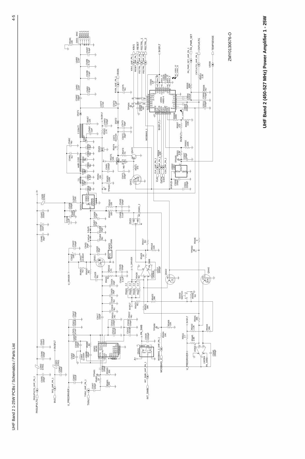
UH
F B
and
2 1-
25W
PC
Bs
/ Sch
emat
ics
/ Par
ts L
ist
4-5
ZM
Y01
3067
6-O
L540
257
R01
PA
SU
PV
LTG
_UH
F_P
A_1
100p
FC
5405
100p
FC
5406
.033
uFC
5421
PA
SU
PV
LTG
C54
83.0
33uF
9V3
L542
157
R01
9V3_
UH
F_P
A_1
9V3F
LT
U_P
RE
DR
IVE
R
R54
0215
300
R54
03
C54
0710
0pF
TP
5401
1
C54
0110
0pF
TX
INJ_
UH
F_P
A_1.0
22uF
C54
02
300
R54
01
TX
INJ
100p
FC
5404
47nH
L540
347
nHL5
411
C54
11.0
22uF
C54
0018
0pF
100p
FC
5412
11.0
3nH
L540
1
82R
5400
C54
036.
8pF
VG
2
NC
315
NC
4
16R
FIN
6R
FO
UT
17
RF
OU
T2
1V
CN
TR
L14
VD
1V
G1
2 3
EP
11G
24
GND1 5GND2 12GND3 13GND4
8N
C1
9N
C2
10
30C
65U
5401
17N
UR
5411
24pF
C54
20C
5418
C54
1410
0pF
10pF
C54
2451R54
16
.022
uFC
5413
C54
19N
UN
U
C54
250.
1uF
C54
2610
0pF
51R
5415
100p
FC
5417
Q54
11
NC_Q3411_1
A+
C54
2822
00pF
INT
_SW
B_U
HF
_PA
_1
PA
_SW
B
C54
15.0
22uF
C54
1610
0pF
10K
R54
04M
OS
BIA
S_2
1M
OS
BIA
S_2
_UH
F_P
A_1
R54
0622
K
TP
5406
39K
R54
43
2.7
R55
11
84
LM29
04
U54
02-1 23
1
39K
R54
41
1000
pFC
5440
R54
452.
4K2.
2KR
5442
9V3F
LTU
_PR
ED
RIV
ER
PA
_SW
B
R54
40
SW
ITC
HS
5440
NU
12
Q54
42
47K
47K
INT
_SW
B
R54
22
22K
R54
18
R54
242.
2
R54
2139
K
R54
12
R54
272.
2
2.2
R54
25
C54
2733
00pF
U54
02-2
LM29
04
657
84
R54
262.
2
R54
2339
K
R54
28
R54
291K
R54
17
PA
_SW
B
U_D
RIV
ER
9V3F
LTN
U
NU
NU
NU
Q54
22
0.8x
251.
542x
424
pFC
5431
C54
54C
5455
20pF
C54
5847
pFC
5457
47pF
NU
Q54
21C
5432
33pF
100p
FC
5422
L542
213
.85n
H
R54
20
C54
29
C54
231u
F
R54
50
U_D
RIV
ER
NU
NU
NU
M34
21H
EA
TS
INK
PO
S1
C54
3510
0pF
100
R54
3110
0R
5432
0.1u
FC
5434
D54
01
NC
_D34
01_2
100p
FC
5439
L543
717
nH
1uF
C54
38
C54
81.0
33uF
S3S4
Q54
31
D
G
GN
D1
GN
D2
S1S2
2.21
6x??
wid
th 2
.032
C54
61N
UC
5462
NU
R54
7510
K
C54
5310
0pF
10K
R54
54
2.7K
R54
52
R54
5510
0K
51R
5474
D54
72
TP
54031
1000
pFC
5451
43.6
7nH
L547
1
D54
519V
3FLT
A+
30pF
C54
7330
pFC
5472
C54
5211
pF12
0R
5457
R54
7351
5.6V
23 1
C54
7110
0pF
VR
3471
NC
Q54
72
R54
7147
0
Q54
71
47K 47
K
MO
SB
IAS
_1
1TP
5402
R54
46 0
C54
37.0
33uF
C54
3610
uF57
R01
L543
6C
5482
30pF
A+
J340
1 -
BN
C
J540
1-2
L549
317
nHJ5
401-
1
J540
1-5
J540
1-4
J540
1-3
C54
975.
6pF
10K
R54
91
4.7p
FC
5496
17nH
L547
2
17nH
L549
1
3.3p
FC
5498
100p
FC
5492
6.8p
FC
5491
D54
71
RE
SE
T_U
HF
_PA
_1K
9V1
FE
CT
RL_
2
FE
CT
RL_
1_U
HF
_PA
_1
FE
CT
RL_
2_U
HF
_PA
_1F
EC
TR
L_1
K9V
1_U
HF
_PA
_1
RE
SE
T
9V3F
LT
RX
IN_U
HF
_PA
_1
C54
75
5.1p
FC
5474
RX
IN
NU
1
TP
5404
C55
09
NU
470p
F
24
19
23
17
20
18
2221NC_U3501_22
NC_U3501_19
47K
R55
07
9V3F
LT
3.9K
R55
09
R55
0820
0K
C55
0222
00pF
NC
_U35
01_2
.015
uFC
5504
300K
R55
05
2200
pFC
5506
VAR3
15V
G
VL 6VLIM
RX T1 2
TE
MP
30
14V
10
V45
16
V5EXT
VAR1
VAR2
GN
D2
25
INT 4NA
Q11
QX
10
RFIN 1
RS
RS
ET
31
CJ 5
CL 7
CLK
26
CQ
1213C
QX
DA
TA28
F16
89
GND1 8
U55
01H
99S
-4
AN
O32
BP
OS
27C
EX
29
CI 3
C55
051u
F
NC
_U35
01_1
5
NC
_U35
01_1
3 NC
_U35
01_1
2N
C_U
3501
_11
NC
_U35
01_1
0N
C_U
3501
_9
9V3F
LT10
KR
5504
CLK
DA
TA_U
HF
_PA
_1
CLK
_UH
F_P
A_1
CS
X_U
HF
_PA
_1
DA
TAC
SX
CN
TLV
LTG
CN
TLV
LTG
_UH
F_P
A_1
R54
133.
3K
PA
_PW
R_S
ET
_UH
F_P
A_1 P
A_P
WR
_SE
T
TE
MP
SE
NS
E
NU
R55
06
U55
08
C55
0347
0pF
100p
FC
5510
1POS V
OU
T2
U55
02LM
50
GND 3
100p
FC
5507
100K
R55
02
1
TP
5405
6.8K
R55
01C
5508
100p
F
2200
pFC
5501
9V3F
LT
7.5
C54
47
C54
414.
7pF
7.5p
FC
5445
C54
43N
U30
pFC
5448
C54
4927
pF
C54
46
C54
44C
5442
18pF
NU
NU
NU
UH
F B
and
2 (
450-
527
MH
z) P
ow
er A
mp
lifie
r 1
- 25
W
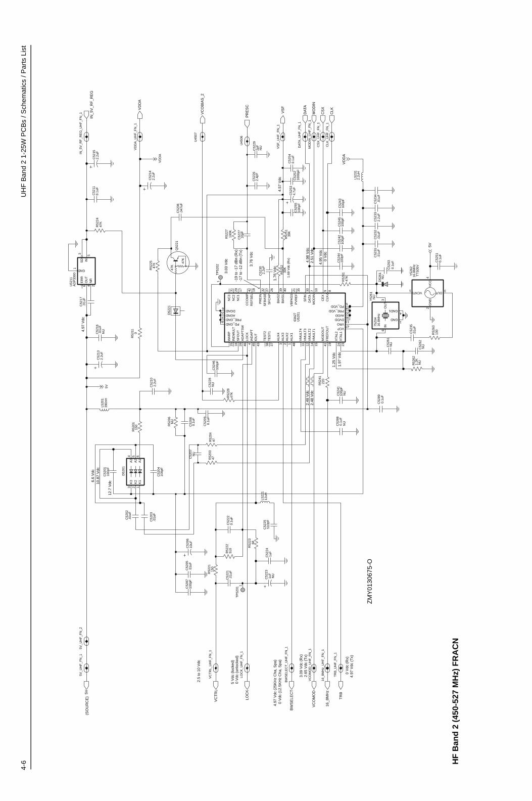
4-6
UH
F B
and
2 1-
25W
PC
Bs
/ Sch
emat
ics
/ Par
ts L
ist
5V_U
HF
_FN
_25V
_UH
F_F
N_1
5V(S
OU
RC
E)
C52
0410
0pF
C52
0110
0pF
6A
25
A3
4
1K
1
2K
2
3K
3
D
5201
A1
6.6
Vdc
10.8
7 V
dc
12.7
Vdc
C52
03.0
1uF
.01u
FC
5202
150
R52
01
LOC
K
LOC
K_U
HF
_FN
_1
VC
TR
L
VC
TR
L_U
HF
_FN
_1
2.5
to 1
0 V
dc
5 V
dc (
lock
ed)
0 V
dc (
unlo
cked
)1
TP
5201
150
R52
21
.01u
FC
5221
510
R52
22
C52
8710
0pF
.01u
FC
5205
C52
231u
FC
5224
1uF
NU
R52
2368
C52
2551
0pF
C52
220.
1uF
12uH
L522
1
VC
OM
OD
_UH
F_F
N_1
TR
B_U
HF
_FN
_1
TR
B
BW
SE
LEC
T_U
HF
_FN
_1
BW
SE
LEC
T
16_8
MH
z
VC
OM
OD
16_8
MH
z_U
HF
_FN
_1
4.97
Vdc
(25
KH
z C
ha, S
pa)
0 V
dc (
12.5
KH
z C
ha, S
pa)
3.09
Vdc
(R
x)2.
65 V
dc (
Tx)
0 V
dc (
Rx)
4.97
Vdc
(T
x)
10uF
C52
06
47R52
04
C52
07
R52
0347
NU
0.1u
FC
5208
R52
06N
U
C52
090.
1uF
C52
132.
2uF
390n
HL5
201
5V 2.2u
FC
5210
R52
11 0
.01u
FC
5217
C52
16.0
1uF
OU
T
3S
D
AD
P33
00U
5211
6E
RR
1 GND
5IN
2N
R4
NU4.
97 V
dc
R52
2447
K
IN_5
V_R
F_R
EG
IN_5
V_R
F_R
EG
_UH
F_F
N_1
C52
152.
2uF
C52
110.
1uF
47K
R52
28
C52
28C
5246
100p
FN
U
D52
21
WA
RP
25
27S
FC
AP
26
SF
OU
T28
TE
ST
137
TE
ST
238
VB
PA
SS
21
PD_GND44
32P
RE
IN
PRE_GND33
RE
FS
EL
18
SF
BA
SE
IND
MU
LT16
IOU
T434
LOC
K
NC
117
NC
229
NC
331
CC
OM
P42
6DGND
IAD
AP
T45
AGND22
AU
X1
48
AU
X2
1
AU
X3
2
AU
X4
3B
IAS
140
BIA
S2
39
AD
AP
TS
W46
VM
ULT
1V
MU
LT2
14
VM
ULT
312
VM
ULT
411
13VRO
XTA
L12324
XTA
L2
SF
IN30
VCP47
15
5PD_VDDPRE_VDD
34
PV
RE
F35
MO
DIN
10
MO
DO
UT
41C
EX
9C
LK8
DA
TA7
DVDD36
FR
EF
OU
T19
AVDD20
U52
0163
A27
C52
4410
0pF
100p
FC
5242
4.98
Vdc
2.51
Vdc
4.95
Vdc
0 V
dc
47K
R52
61
R52
4122
0
1.25
Vdc
1.97
Vdc
C52
4110
0pF
NU
2.48
Vdc
2.48
Vdc
0.1u
FC
5289
C52
880.
1uF
NU
C52
62
1GND
4GND1
3O
UT
6IN16
.8M
Hz
C52
61
R52
6310
0
R52
621.
2K
.01u
FD
5261
C52
510.
1uF
2G
ND
3OUT
4V
CC
1VCNTL
16.8
MH
zT
TS
05V
Y52
62.0
1uF
C52
35
C52
63 0.
1uF
5V
NU
NU
NU
NU
75Z
04Y
5261
NU
C52
34.0
1uF
C
5231
C52
32.0
1uF
2.2u
FC
5233
Q52
21C
5236
.047
uF
R52
2547
K
47K
47K
R52
5230
K
C52
302.
2uF
1T
P52
02
C52
2710
pF
100K
R52
27
39K
R52
51
3.03
Vdc
-19
to -
17 d
Bn
(Rx)
-17
to -
12 d
Bn
(Tx)
3.76
Vdc
1.76
Vdc
1.69
Vdc
(R
x)
4.7u
FC
5253
C52
540.
1uF
C52
5210
00pF
10
0pF
C52
55
4.57
VdcC
5226
2.4p
F2p
FC
5229U
4506
NU
2.2u
HL5
231
10
0pF
C52
43C
5245
100p
FV
DD
A
MO
DIN
_UH
F_F
N_1
DA
TA_U
HF
_FN
_1
CS
X
VS
F_U
HF
_FN
_1
CS
X_U
HF
_FN
_1
VS
F
CLK
DA
TA
MO
DIN
CLK
_UH
F_F
N_1
VC
OB
IAS
_2
VD
DA
PR
ES
C
VD
DA
_UH
F_F
N_1
U45
07
2.2u
FC
5214
VD
DA
ZM
Y01
3067
5-O
HF
Ban
d 2
(45
0-52
7 M
Hz)
FR
AC
N

UH
F B
and
2 1-
25W
PC
Bs
/ Sch
emat
ics
/ Par
ts L
ist
4-7
ZM
Y01
3067
4-O
R53
015.
6KR
XS
W4.2
Vdc
(R
x)0
Vdc
(T
x)
R53
0210
K0.
22uF
C53
71C
5372
100p
FN
U
C53
05N
UC
5306
2pF
L530
439
0nH
4.3p
FC
5303
C53
045.
6pF
C53
024.
3pF
CR
5302
CR
5303
220n
HL5
302 C
R53
01L5
301
68nH
68nH
L531
1
C53
1710
0pF
100p
FC
5301
NU
VC
TR
L_U
HF
_VC
OR
5315
0
2.5
to 1
0 V
dc
100p
FC
5311
CR
5311
C53
160.
1uF
15pF
C53
12
VC
OM
ODV
CO
MO
D_U
HF
_VC
O4.
7uF
C53
25
VC
TR
L
C53
2310
00pF
56K
R53
21
C53
2210
0pF
NU
NU
C53
211p
F
R53
226.
8K
CR
5321
3pF
C53
24R
5323
10K
VS
F
NU
4.5
Vdc
P22
P3
3
RE
SO
NA
TO
RL5
303
P1
1
R53
0330
R53
0415
0
100p
FC
5307
R53
11
TX
SW
0 V
dc (
Rx)
4.5
Vdc
(T
x)
7.5K
0.22
uFC
5318
L531
339
0nH
R53
127.
5K
3pF
C53
14
100p
FC
5315
R53
1422
0
Q53
11
0 V
dc (
Rx)
1.9
Vdc
(T
x)
P1
1
P22
P3
3
RE
SO
NA
TO
RL5
312
C53
13N
UR
5313
30
C53
8210
0pF
0.1u
FC
5381
TX
SW
0 V
dc (
Rx)
4.5
Vdc
(T
x)
NU
TR
B_U
HF
_VC
OR
5381
470
TR
B
0 V
dc (
Rx)
4.5
Vdc
(T
x)
TX
_OU
T
TX
_SW
ITC
H
VCC_BUFFERS14
VCC_LOGIC18
RX
_IA
DJ
2R
X_O
UT
RX
_SW
ITC
H
SU
PE
R_F
LTR
3
TR
B_I
N19
TX
_BA
SE
16
TX
_EM
ITT
ER
15
TX
_IA
DJ
1
CO
LL_R
FIN
4
FLI
P_I
N20
GND_BUFFERS11GND_FLAG9
17GND_LOGIC
PR
ES
C_O
UT
RX
_BA
SE
5
RX
_EM
ITT
ER
6U
5301
50U
54
10 138 7124.
5 V
dc (
Rx)
2.58
Vdc
(T
x)
100p
FC
5383
39nH
C53
65L536
2
3.3p
FR
XS
W
NU
4.2
Vdc
(R
x)0
Vdc
(T
x)
10R53
35
PR
ES
C
PR
ES
C_U
HF
_VC
ON
U
NU
R53
470
R53
3310
KR
5334
0
C53
3451
pF
NU
NU
0.1u
FC
5308
L530
539
0nH
C53
0910
0pF
R53
0510
VS
FV
SF
_UH
F_V
C0
VS
F
4.5
Vdc
Q53
01
2.3
Vdc
(R
x)0
Vdc
(T
x)
100p
FC
5351
0.1u
FC
5352
2.2u
FC
5354
2.2u
FC
5355
C53
6110
0pF
0.1u
FC
5353
33nH
L533
1
R53
6118
0
390n
HL5
361
0.22
uFC
5362
270
R53
60C
5364
5.6p
FNU
1KR
5363
VS
F
C53
74
C53
63
NUN
U
NU
C53
73
L537
168
nH5.
6pF
C53
314
dBn
(Tx)
R53
6210
C53
320.
1uF
C53
33
22K
R53
32L5
332
15nH
R53
361K
NU
NU
NU
NU
51pF
NU
TX
INJ_
UH
F_V
CO
Q53
31R
5331
22
TX
INJ
NU
R53
370 N
U
5V_U
HF
_VC
O
VC
OB
IAS
_2_U
HF
_VC
O
C53
7510
KR
5346
VC
OB
IAS
_2
5VN
U
Q53
33
0R
5341
4.7K
47K
47K 10
K4.
5 V
dc (
Rx)
0 V
dc (
Tx)
51pF
C53
37
R53
422.
2KL5
333
390n
H
C53
36.0
22uF
R53
4410
22R
5339
R53
431K
220
R53
38
100p
FC
5335
Q53
32
NU
NU
51pF
C53
38
220
R53
40
NU
R53
45C
5339
RX
INJ
RX
INJ_
UH
F_V
CO
>14
dB
n (R
x)
NU
NU
SH
IELD
SH
5302
1
SH
IELD
SH
5301
1
GN
D
UH
F B
and
2 (
450-
527
MH
z) V
olt
age
Co
ntr
olle
d O
scill
ato
r

4-8
UH
F B
and
2 1-
25W
PC
Bs
/ Sch
emat
ics
/ Par
ts L
ist
ZM
Y01
3067
2-O
FE
CT
RL_
2
9V3
RX
IN
K9V
1
9V3
C50
6733
00pF
K9V
1_U
HF
_FE
RX
IN_U
HF
_FE
9V3_
UH
F_F
E
D50
07
IN
NEGPOS
C50
25N
U
TB
DL5
001
C50
261p
F
1KR50
69
C50
011.
5pF1.
5KR
5068
C50
1033
0pF
C50
0233
pF
D50
02D
5001
1pF
C50
27
FE
CT
RL_
2_U
HF
_FE
10K
R50
61
C50
620.
1uF
330p
FC
5061
3.3K
R50
16
TB
D IN
NEGPOSL500
2
R50
17N
U
C50
0322
pFC
5005
16pF
C50
0416
pFC
5006
16pF
100K
R50
0116
pFC
5007
FE
CT
RL_
1F
EC
TR
L_1_
UH
F_F
E33
0KR
5060
C50
60C
5008
1000
pFN
U
RX
INJ
RX
INJ_
UH
F_F
E15
nH15
nHL5
054
L505
3
16pF
C50
54C
5053
6.8p
FC
5055
TP
5003 N
U
T50
52X
FM
R
4 6
3 12
1IO
12
IO2
3IO3
4IO4
D50
51T
5051
XF
MR
1 2 3
5 4
C50
5282
pF
R50
5151
470n
HL5
008
C50
66
IF_U
HF
_FE
L505
115
0nH
IF
NU
0R50
52R
5053 R
5055
R50
54N
U
NU
NU
0.7
VD
C4.6
VD
C
L500
615
nH
2.7K
R50
04
C50
098.
2pF
D50
03
R50
034.
7K
100p
FC
5034
Q50
01
R50
2010
R50
21C
5033
1010
0pF
Q50
03C
5020
16pF
C50
1927
pFC
5021
18pF
C50
2216
pFC
5023
R50
1210
0KN
U
1000
pFC
5024
R50
19N
UG
ND
_UH
F_F
E
GN
D
Q50
02
270n
HL5
003
.01u
FC
5028
R50
183.
3K
C50
1333
00pF
330p
FC
5012
0R50
22
330
R50
02
3300
pFC
501
100p
FC
5014
10K
R50
05
0R
5064
R50
6339
0
C50
6510
0pF
R50
0710
0
R50
66
D50
06
NU
L500
4
IN
NEGPOS
TB
D10
0pF
C50
68
C50
16
C50
1510
0pF
NU
C50
291p
F
D50
04
1.5p
FC
5017
D50
05
C50
1833
pF
1pF
C50
30
TB
D IN
NEGPOSL500
5
8.2p
FC
5032
L500
915
nHR
5015
R50
13N
UN
U8.
2pF
C50
31
Q50
04
1.5K
R50
62
0.1u
FC
5064
10K
R50
7210K
R50
71
.01u
FC
5069
390
R50
70
9V3
3 to
6.5
VD
C
UH
F B
and
2 (
450-
527
MH
z) R
ecei
ver
Fro
nt
En
d
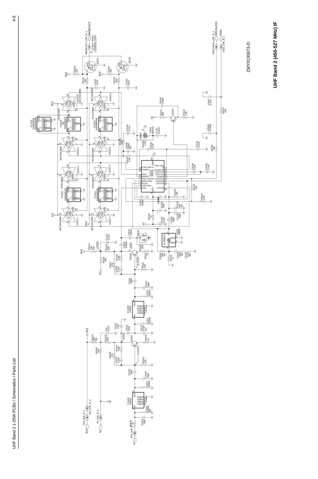
UH
F B
and
2 1-
25W
PC
Bs
/ Sch
emat
ics
/ Par
ts L
ist
4-9
ZM
Y01
3067
3-O
5V_V
HF
_IF
_1
9V3
9V3_
VH
F_I
F_2
5V
9V3_
VH
F_I
F_1
5V
IFIF
IN_V
HF
_IF
_13
IN6
OU
T
FL3
101
12R
16
1GND1GND2 2
GND3 45GND4
620n
HL3
100
NU
20pF
C31
01
R31
480
C31
0333
pF
15pF
C31
02L3
101
620n
H
R31
0112
K
3VD
C
0.75
VD
C
620
R31
08
R31
0210
27K
R31
06
6.8K
R31
07
Q31
01
0.1u
FC
3104
0.1u
FC
31
GND1 12GND2 4GND3
GND4 5
IN3
OU
T6
12R
16F
L310
2C
3112
82pFC31
1027
pF
620n
HL3
111
NU
C31
139.
1pF
22pF
C31
15
L311
262
0nH
18pF
C31
14
R31
1727
K
6.8K
R31
180.
1uF
C31
16
3VD
CQ
3102
0.75
VD
C
12K
R31
11
C31
22.0
39uF
10R
3112
.039
uFC
3123
D31
01
330
R31
133.9V
DC
330
R31
16R
3115
390
NU
R31
1410
0
0.1u
FC
3121
5V
9V3
9180
469V
03
3GND1
GND2 4
1IN
2O
UT
FL3
111
CF
WC
455G
CN
TL 131
2V
DD14
VS
S 7
MC
74H
C40
66
U31
11-1
VS
S
7 U31
11-4
CN
TL
12
VD
D
14
11
5
CN
TL4
3
14
VD
D 7
VS
S
U31
12-1
MC
74H
C40
66
9V3
9180
469V
062
OU
T
FL3
112
CF
WC
455D
3GND1
GND2 4
1IN
U31
11-3
6CN
TL14 V
DD
7VS
S8
910
MC
74H
C40
66
U31
15-1
CN
TL 131
2V
DD14
VS
S 7
U31
15-2
5
CN
TL4
3
14
VD
D 7
VS
S
MC
74H
C40
66
9180
468V
06
3GND
1IN
OU
T
FL3
114
2.0
1uF
C31
51C
FU
CJ4
55D
U31
15-3
MC
74H
C40
66
6CN
TL
14
VD
D
7VS
S8
9
10K
R31
51
9180
468v
042
OU
T
FL3
113C
FU
CJ4
55F
3GND
1IN
NU
10V
DD
14
VS
S
7
MC
74H
C40
66U
3115
-4
CN
TL
12
11
10K
R31
53
9V3
9V3
20/2
5kH
z 5
VD
C 1
2.5k
Hz
0V
DC
BW
SE
LEC
T_V
HF
_IF
_1
BW
SE
LEC
T
R31
5410
K
Q31
51
Q31
52C
3152
.01u
F10K
R31
52
9V3
47K
47K47
K
47K
100
R31
04
NU
R31
0510
0
9V3
L312
4
NU
1uH
0R
3123 C31
24
R31
24 NU
33pF
NU
820
Y31
01
2GND
4GND1
3O
UT
1IN
44.3
95M
Hz 06
B09
C31
320.
1uF
C31
34
30pF
C31
36
51R
3130
NU
1pF
C31
31
C31
3310
uF
C31
3533
pF
5RSSIOUT9 RSSI_FEED
6V
CC
13LIM_DEC112LIM_DEC2
20MIXOUT
4 OSCIN 3OSCOUT
10 QUADIN
1 RFIN2 RFIN_DEC
AUDIO_FEED
GN
D
18 IF AMPIN 16IFAMPOUT19 IF AMP_DEC1 17IF
AMP_DEC2
14 LIMIN
11LIMOUTSA
616
U31
01
8AUDIOOUT7
0.1u
F
C31
37.0
39uF
15K
R31
32
15
C31
440.
1uF
R31
351.
2K
0.1u
FC
3142
345
B02
Y31
0245
5KH
z
2
Q31
41
R31
4139
0
5V
120p
FC
3143
1.8K
R31
42
C31
410.
1uF
0.1u
FC
3139
0.1u
FC
3140
C31
4647
00pF
680
R31
46
12K
R31
47
5V
R31
338.
2K
R31
3410
K
9V3
2.4K
R31
44
3.3K
220p
FC
3148
NU
0.1u
FC
3145
R31
45
9180
469V
04 4GND2
IN1
OU
T2
CF
WC
455F
FL3
115
GND13
C31
470.
1uF
DIS
CA
UD
IO_V
HF
_IF
_1D
ISC
AU
DIO
RS
SI
RS
SI_
VH
F_I
F_1
UH
F B
and
2 (
450-
527
MH
z) IF
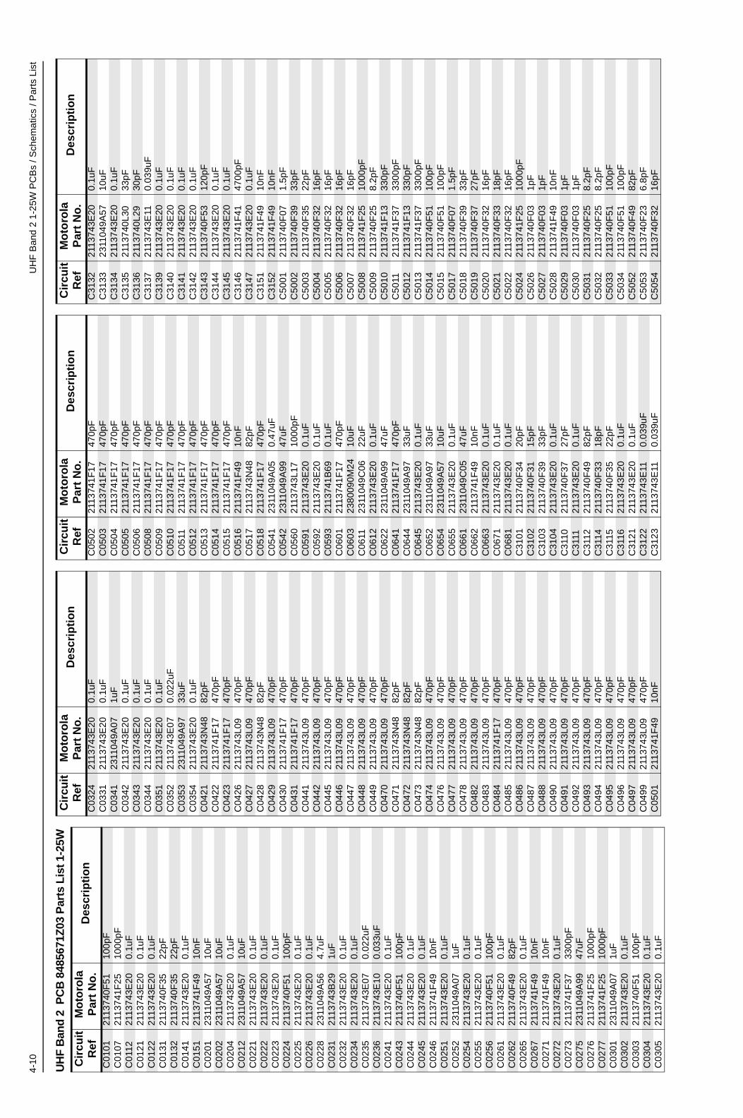
4-10
UH
F B
and
2 1-
25W
PC
Bs
/ Sch
emat
ics
/ Par
ts L
ist
UH
F B
and
2 P
CB
848
5671
Z03
Par
ts L
ist 1
-25W
Cir
cuit
R
efM
oto
rola
P
art
No
.D
escr
ipti
on
C01
0121
1374
0F51
100p
FC
0107
2113
741F
2510
00pF
C01
1221
1374
3E20
0.1u
FC
0121
2113
743E
200.
1uF
C01
2221
1374
3E20
0.1u
FC
0131
2113
740F
3522
pFC
0132
2113
740F
3522
pFC
0141
2113
743E
200.
1uF
C01
5121
1374
1F49
10nF
C02
0123
1104
9A57
10uF
C02
0223
1104
9A57
10uF
C02
0421
1374
3E20
0.1u
FC
0212
2311
049A
5710
uFC
0221
2113
743E
200.
1uF
C02
2221
1374
3E20
0.1u
FC
0223
2113
743E
200.
1uF
C02
2421
1374
0F51
100p
FC
0225
2113
743E
200.
1uF
C02
2621
1374
3E20
0.1u
FC
0228
2311
049A
564.
7uF
C02
3121
1374
3B29
1uF
C02
3221
1374
3E20
0.1u
FC
0234
2113
743E
200.
1uF
C02
3521
1374
3E07
0.02
2uF
C02
3621
1374
3E10
0.03
3uF
C02
4121
1374
3E20
0.1u
FC
0243
2113
740F
5110
0pF
C02
4421
1374
3E20
0.1u
FC
0245
2113
743E
200.
1uF
C02
4621
1374
1F49
10nF
C02
5121
1374
3E20
0.1u
FC
0252
2311
049A
071u
FC
0254
2113
743E
200.
1uF
C02
5521
1374
3E20
0.1u
FC
0256
2113
740F
5110
0pF
C02
6121
1374
3E20
0.1u
FC
0262
2113
740F
4982
pFC
0265
2113
743E
200.
1uF
C02
6721
1374
1F49
10nF
C02
7121
1374
1F49
10nF
C02
7221
1374
3E20
0.1u
FC
0273
2113
741F
3733
00pF
C02
7523
1104
9A99
47uF
C02
7621
1374
1F25
1000
pFC
0277
2113
741F
2510
00pF
C03
0123
1104
9A07
1uF
C03
0221
1374
3E20
0.1u
FC
0303
2113
740F
5110
0pF
C03
0421
1374
3E20
0.1u
FC
0305
2113
743E
200.
1uF
C03
2421
1374
3E20
0.1u
FC
0331
2113
743E
200.
1uF
C03
4123
1104
9A07
1uF
C03
4221
1374
3E20
0.1u
FC
0343
2113
743E
200.
1uF
C03
4421
1374
3E20
0.1u
FC
0351
2113
743E
200.
1uF
C03
5221
1374
3E07
0.02
2uF
C03
5323
1104
9A97
33uF
C03
5421
1374
3E20
0.1u
FC
0421
2113
743N
4882
pFC
0422
2113
741F
1747
0pF
C04
2321
1374
1F17
470p
FC
0426
2113
743L
0947
0pF
C04
2721
1374
3L09
470p
FC
0428
2113
743N
4882
pFC
0429
2113
743L
0947
0pF
C04
3021
1374
1F17
470p
FC
0431
2113
741F
1747
0pF
C04
4121
1374
3L09
470p
FC
0442
2113
743L
0947
0pF
C04
4521
1374
3L09
470p
FC
0446
2113
743L
0947
0pF
C04
4721
1374
3L09
470p
FC
0448
2113
743L
0947
0pF
C04
4921
1374
3L09
470p
FC
0470
2113
743L
0947
0pF
C04
7121
1374
3N48
82pF
C04
7221
1374
3N48
82pF
C04
7321
1374
3N48
82pF
C04
7421
1374
3L09
470p
FC
0476
2113
743L
0947
0pF
C04
7721
1374
3L09
470p
FC
0478
2113
743L
0947
0pF
C04
8221
1374
3L09
470p
FC
0483
2113
743L
0947
0pF
C04
8421
1374
1F17
470p
FC
0485
2113
743L
0947
0pF
C04
8621
1374
3L09
470p
FC
0487
2113
743L
0947
0pF
C04
8821
1374
3L09
470p
FC
0490
2113
743L
0947
0pF
C04
9121
1374
3L09
470p
FC
0492
2113
743L
0947
0pF
C04
9321
1374
3L09
470p
FC
0494
2113
743L
0947
0pF
C04
9521
1374
3L09
470p
FC
0496
2113
743L
0947
0pF
C04
9721
1374
3L09
470p
FC
0499
2113
743L
0947
0pF
C05
0121
1374
1F49
10nF
Cir
cuit
R
efM
oto
rola
P
art
No
.D
escr
ipti
on
C05
0221
1374
1F17
470p
FC
0503
2113
741F
1747
0pF
C05
0421
1374
1F17
470p
FC
0505
2113
741F
1747
0pF
C05
0621
1374
1F17
470p
FC
0508
2113
741F
1747
0pF
C05
0921
1374
1F17
470p
FC
0510
2113
741F
1747
0pF
C05
1121
1374
1F17
470p
FC
0512
2113
741F
1747
0pF
C05
1321
1374
1F17
470p
FC
0514
2113
741F
1747
0pF
C05
1521
1374
1F17
470p
FC
0516
2113
741F
4910
nFC
0517
2113
743N
4882
pFC
0518
2113
741F
1747
0pF
C05
4123
1104
9A05
0.47
uFC
0542
2311
049A
9947
uFC
0560
2113
743L
1710
00pF
C05
9121
1374
3E20
0.1u
FC
0592
2113
743E
200.
1uF
C05
9321
1374
1B69
0.1u
FC
0601
2113
741F
1747
0pF
C06
0323
8009
0M24
10uF
C06
1123
1104
9C06
22uF
C06
1221
1374
3E20
0.1u
FC
0622
2311
049A
9947
uFC
0641
2113
741F
1747
0pF
C06
4423
1104
9A97
33uF
C06
4521
1374
3E20
0.1u
FC
0652
2311
049A
9733
uFC
0654
2311
049A
5710
uFC
0655
2113
743E
200.
1uF
C06
6123
1104
9C05
47uF
C06
6221
1374
1F49
10nF
C06
6321
1374
3E20
0.1u
FC
0671
2113
743E
200.
1uF
C06
8121
1374
3E20
0.1u
FC
3101
2113
740F
3420
pFC
3102
2113
740F
3115
pFC
3103
2113
740F
3933
pFC
3104
2113
743E
200.
1uF
C31
1021
1374
0F37
27pF
C31
1121
1374
3E20
0.1u
FC
3112
2113
740F
4982
pFC
3114
2113
740F
3318
pFC
3115
2113
740F
3522
pFC
3116
2113
743E
200.
1uF
C31
2121
1374
3E20
0.1u
FC
3122
2113
743E
110.
039u
FC
3123
2113
743E
110.
039u
F
Cir
cuit
R
efM
oto
rola
P
art
No
.D
escr
ipti
on
C31
3221
1374
3E20
0.1u
FC
3133
2311
049A
5710
uFC
3134
2113
743E
200.
1uF
C31
3521
1374
0L30
33pF
C31
3621
1374
0L29
30pF
C31
3721
1374
3E11
0.03
9uF
C31
3921
1374
3E20
0.1u
FC
3140
2113
743E
200.
1uF
C31
4121
1374
3E20
0.1u
FC
3142
2113
743E
200.
1uF
C31
4321
1374
0F53
120p
FC
3144
2113
743E
200.
1uF
C31
4521
1374
3E20
0.1u
FC
3146
2113
741F
4147
00pF
C31
4721
1374
3E20
0.1u
FC
3151
2113
741F
4910
nFC
3152
2113
741F
4910
nFC
5001
2113
740F
071.
5pF
C50
0221
1374
0F39
33pF
C50
0321
1374
0F35
22pF
C50
0421
1374
0F32
16pF
C50
0521
1374
0F32
16pF
C50
0621
1374
0F32
16pF
C50
0721
1374
0F32
16pF
C50
0821
1374
1F25
1000
pFC
5009
2113
740F
258.
2pF
C50
1021
1374
1F13
330p
FC
5011
2113
741F
3733
00pF
C50
1221
1374
1F13
330p
FC
5013
2113
741F
3733
00pF
C50
1421
1374
0F51
100p
FC
5015
2113
740F
5110
0pF
C50
1721
1374
0F07
1.5p
FC
5018
2113
740F
3933
pFC
5019
2113
740F
3727
pFC
5020
2113
740F
3216
pFC
5021
2113
740F
3318
pFC
5022
2113
740F
3216
pFC
5024
2113
741F
2510
00pF
C50
2621
1374
0F03
1pF
C50
2721
1374
0F03
1pF
C50
2821
1374
1F49
10nF
C50
2921
1374
0F03
1pF
C50
3021
1374
0F03
1pF
C50
3121
1374
0F25
8.2p
FC
5032
2113
740F
258.
2pF
C50
3321
1374
0F51
100p
FC
5034
2113
740F
5110
0pF
C50
5221
1374
0F49
82pF
C50
5321
1374
0F23
6.8p
FC
5054
2113
740F
3216
pF
Cir
cuit
R
efM
oto
rola
P
art
No
.D
escr
ipti
on
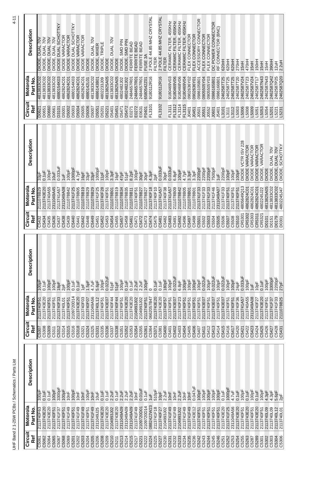
UH
F B
and
2 1-
25W
PC
Bs
/ Sch
emat
ics
/ Par
ts L
ist
4-11
C50
6121
1374
0F63
330p
FC
5062
2113
743E
200.
1uF
C50
6421
1374
3E20
0.1u
FC
5065
2113
740F
5110
0pF
C50
6721
1374
1F37
3300
pFC
5068
2113
740F
5110
0pF
C50
6921
1374
1F49
10nF
C52
0121
1374
0F51
100p
FC
5202
2113
741F
4910
nFC
5203
2113
741F
4910
nFC
5204
2113
740F
5110
0pF
C52
0521
1374
1F49
10nF
C52
0623
1104
9J25
10uF
C52
0821
1374
3E20
0.1u
FC
5209
2113
743E
200.
1uF
C52
1021
0499
3J02
2.2u
FC
5211
2113
743E
200.
1uF
C52
1323
1104
9A09
2.2u
FC
5214
2311
049A
092.
2uF
C52
1523
1104
9A09
2.2u
FC
5217
2113
741F
4910
nFC
5221
2109
720D
010.
01uF
C52
2221
0972
0D14
0.1u
FC
5224
0882
422W
231u
FC
5225
2113
741F
1851
0pF
C52
2721
1374
0F27
10pF
C52
3021
0499
3J02
2.2u
FC
5231
2113
741F
4910
nFC
5232
2113
741F
4910
nFC
5233
2104
993J
022.
2uF
C52
3421
1374
1F49
10nF
C52
3521
1374
1F49
10nF
C52
3621
1374
3E12
0.04
7uF
C52
4221
1374
0F51
100p
FC
5243
2113
740F
5110
0pF
C52
4421
1374
0F51
100p
FC
5245
2113
740F
5110
0pF
C52
4621
1374
0F51
100p
FC
5251
2113
743E
200.
1uF
C52
5221
1374
1F25
1000
pFC
5253
2311
049A
564.
7uF
C52
5421
1374
3E20
0.1u
FC
5255
2113
740F
5110
0pF
C52
6321
1374
3E20
0.1u
FC
5287
2113
740F
5110
0pF
C52
8921
1374
3E20
0.1u
FC
5301
2113
740F
5110
0pF
C53
0221
1374
0L09
4.3p
FC
5303
2113
740L
094.
3pF
C53
0421
1374
0L12
5.6p
FC
5306
2113
740L
012p
F
Cir
cuit
R
efM
oto
rola
P
art
No
.D
escr
ipti
on
C53
0721
1374
0F51
100p
FC
5308
2113
743E
200.
1uF
C53
0921
1374
0F51
100p
FC
5311
2113
740F
5110
0pF
C53
1221
1374
0F33
18pF
C53
1421
1374
0L01
2pF
C53
1521
1374
0F51
100p
FC
5316
2109
720D
140.
1uF
C53
1821
1374
3E20
0.1u
FC
5321
2113
740F
031p
FC
5324
2113
740F
071.
5pF
C53
2523
1104
9A56
4.7u
FC
5331
2113
740L
125.
6pF
C53
3521
1374
0F51
100p
FC
5336
2113
743E
070.
022u
FC
5337
2113
740F
4451
pFC
5338
2113
740F
4451
pFC
5351
2113
740F
5110
0pF
C53
5221
1374
3E20
0.1u
FC
5353
2113
743E
200.
1uF
C53
5421
0499
3J02
2.2u
FC
5355
2104
993J
022.
2uF
C53
6121
1374
0F51
100p
FC
5364
0662
057B
470
C53
7121
1374
3E20
0.1u
FC
5381
2113
743E
200.
1uF
C54
0021
1374
0F57
180p
FC
5401
2113
740F
5110
0pF
C54
0221
1374
3E07
0.02
2uF
C54
0321
1374
0F23
6.8p
FC
5404
2113
740F
5110
0pF
C54
0521
1374
0F51
100p
FC
5406
2113
740F
5110
0pF
C54
0721
1374
0F51
100p
FC
5411
2113
743E
070.
022u
FC
5412
2113
740F
5110
0pF
C54
1321
1374
3E07
0.02
2uF
C54
1421
1374
0F51
100p
FC
5415
2113
743E
070.
022u
FC
5416
2113
740F
5110
0pF
C54
1721
1374
0F51
100p
FC
5420
2113
740F
3624
pFC
5421
2113
741A
570.
033u
FC
5422
2113
740A
5510
0pF
C54
2323
1104
9A08
1uF
C54
2421
1374
0F27
10pF
C54
2521
1374
3E20
0.1u
FC
5426
2113
740F
5110
0pF
C54
2721
1374
1F37
3300
pFC
5428
2113
741F
3322
00pF
C54
3121
1107
8B25
27pF
Cir
cuit
R
efM
oto
rola
P
art
No
.D
escr
ipti
on
C54
3221
1107
8B29
33pF
C54
3421
1374
3E20
0.1u
FC
5435
2113
740A
5510
0pF
C54
3623
1104
9A45
10uF
C54
3721
1374
1A57
0.03
3uF
C54
3823
1104
9A08
1uF
C54
3921
1107
8B42
100p
FC
5440
2113
741F
2510
00pF
C54
4121
1107
8B05
4.7p
FC
5442
2111
078B
1916
pFC
5448
2111
078B
2933
pFC
5449
2111
078B
2933
pFC
5451
2113
741F
2510
00pF
C54
5221
1374
0F28
11pF
C54
5321
1374
0F51
100p
FC
5454
2111
078B
013.
3pF
C54
5521
1107
8B19
16pF
C54
5721
1107
8B34
47pF
C54
5821
1107
8B35
51pF
C54
6121
1107
8B11
8.2p
FC
5471
2113
740F
5110
0pF
C54
7221
1107
8B27
30pF
C54
7321
1107
8B27
30pF
C54
7421
1374
0F18
4.3p
FC
5475
2113
740F
102p
FC
5481
2113
741A
570.
033u
FC
5482
2113
740F
3830
pFC
5483
2113
741A
570.
033u
FC
5491
2111
078B
096.
8pF
C54
9221
1107
8B42
100p
FC
5496
2111
078B
054.
7pF
C54
9721
1107
8B01
3.3p
FC
5498
2111
078B
013.
3pF
C55
0121
1374
1F33
2200
pFC
5502
2113
741F
3322
00pF
C55
0321
1374
1F33
2200
pFC
5504
2113
741F
4675
00pF
C55
0523
1104
9A07
1uF
C55
0621
1374
1F33
2200
pFC
5507
2113
740F
5110
0pF
C55
0821
1374
0F51
100p
FC
5510
2113
740F
5110
0pF
CR
5301
4805
649Q
13D
IOD
E V
CT
R IS
V 2
28C
R53
0248
6282
4C01
DIO
DE
VA
RA
CT
OR
CR
5303
4862
824C
01D
IOD
E V
AR
AC
TO
RC
R53
1148
6282
4C01
DIO
DE
VA
RA
CT
OR
CR
5321
4802
245J
22D
IOD
E, V
AR
AC
TO
RD
0101
4813
825A
05D
IOD
ED
0151
4813
833C
02D
IOD
E, D
UA
L 70
VD
0179
4813
833C
02D
IOD
E, D
UA
L 70
VD
0301
4802
245J
47D
IOD
E, S
CH
OT
TK
Y
Cir
cuit
R
efM
oto
rola
P
art
No
.D
escr
ipti
on
D06
2148
1383
3C02
DIO
DE
, DU
AL
70V
D06
5148
1383
3C02
DIO
DE
, DU
AL
70V
D06
6048
1383
3C02
DIO
DE
, DU
AL
70V
D06
6148
1383
3C02
DIO
DE
, DU
AL
70V
D31
0148
8015
4K03
DIO
DE
DU
AL
SC
HO
TT
KY
D50
0148
6282
4C01
DIO
DE
VA
RA
CT
OR
D50
0248
6282
4C01
DIO
DE
VA
RA
CT
OR
D50
0348
8015
4K03
DIO
DE
DU
AL
SC
HO
TT
KY
D50
0448
6282
4C01
DIO
DE
VA
RA
CT
OR
D50
0548
6282
4C01
DIO
DE
VA
RA
CT
OR
D50
0648
8014
2L01
DIO
DE
D50
0748
1383
3C02
DIO
DE
, DU
AL
70V
D50
5148
8614
3B01
DIO
DE
, MIX
ER
D52
0148
0223
3J09
DIO
DE
, TR
IPLE
D52
2148
1382
5A05
DIO
DE
D54
0148
1383
3C02
DIO
DE
, DU
AL
70V
D54
5148
1382
5A05
DIO
DE
D54
7148
0248
2J02
DIO
DE
, SM
D P
IND
5472
4802
482J
02D
IOD
E, S
MD
PIN
E02
7124
8465
7R01
FE
RR
ITE
BE
AD
E02
7224
8465
7R01
FE
RR
ITE
BE
AD
E06
3124
8465
7R01
FE
RR
ITE
BE
AD
F04
0165
8054
2Z01
FU
SE
3A
FL3
101
9180
112R
162
PO
LE 4
4.85
MH
Z C
RY
STA
L F
ILT
ER
FL3
102
9180
112R
162
PO
LE 4
4.85
MH
Z C
RY
STA
L F
ILT
ER
FL3
111
9180
469V
03C
ER
AM
IC F
ILT
ER
, 455
KH
zF
L311
291
8046
9V06
CE
RA
MIC
FIL
TE
R, 4
55K
Hz
FL3
114
9180
468V
06C
ER
AM
IC F
ILT
ER
, 455
KH
zF
L311
591
8046
9V04
CE
RA
MIC
FIL
TE
R, 4
55K
Hz
J040
109
0263
6Y02
FLE
X C
ON
NE
CT
OR
J045
109
0263
6Y01
FLE
X C
ON
NE
CT
OR
J050
109
8610
5B01
AC
CE
SS
OR
Y C
ON
NE
CT
OR
J055
109
0550
5Y04
FLE
X C
ON
NE
CT
OR
J055
209
0550
5Y03
FLE
X C
ON
NE
CT
OR
J060
109
8616
5B01
DC
PO
WE
R C
ON
NE
CT
OR
J540
109
8616
6B01
RF
CO
NN
EC
TO
R (
BN
C)
L310
124
6258
7T25
620n
HL3
111
2462
587T
2562
0nH
L311
224
6258
7T25
620n
HL5
003
2462
587T
2027
0nH
L500
624
6258
7V24
15nH
L500
824
6258
7T23
470n
HL5
009
2462
587V
2415
nHL5
051
2462
587T
1715
0nH
L505
324
6258
7N43
15nH
L505
424
6258
7N43
15nH
L520
124
6258
7Q42
390n
HL5
221
2462
587P
2512
uHL5
231
2462
587Q
202.
2uH
Cir
cuit
R
efM
oto
rola
P
art
No
.D
escr
ipti
on

4-12
UH
F B
and
2 1-
25W
PC
Bs
/ Sch
emat
ics
/ Par
ts L
ist
L530
124
6258
7T13
68nH
L530
224
6258
7T19
220n
HL5
303
2460
593C
03R
ES
ON
AT
OR
L530
424
6258
7T22
390n
HL5
305
2462
587T
2239
0nH
L531
124
6258
7T22
390n
HL5
312
2460
593C
03R
ES
ON
AT
OR
L531
324
6258
7T22
390n
HL5
331
2462
587T
0933
nHL5
333
2462
587T
2239
0nH
L536
124
6258
7T22
390n
HL5
362
2462
587T
3822
nHL5
371
2462
587T
1368
nHL5
401
2460
591B
0411
.03n
HL5
402
2484
657R
01F
ER
RIT
E B
EA
DL5
403
2462
587T
1147
nHL5
411
2462
587T
1147
nHL5
421
2484
657R
01F
ER
RIT
E B
EA
DL5
422
2460
591C
2313
.85n
HL5
436
2484
657R
01F
ER
RIT
E B
EA
DL5
437
2460
592A
0117
nHL5
471
2460
591N
3643
.67n
HL5
472
2460
592A
0117
nHL5
491
2460
592A
0117
nHL5
493
2460
592A
0117
nHM
3421
2686
201B
01H
EA
T S
PR
EA
DE
RQ
0110
4880
048M
01N
PN
Q01
5148
8004
8M01
NP
NQ
0171
4880
048M
01N
PN
Q01
7348
8005
2M01
NP
N D
AR
LIN
GT
ON
Q01
7748
8004
8M01
NP
NQ
0181
4880
048M
01N
PN
Q01
8348
8004
8M01
NP
NQ
0185
4880
048M
01N
PN
Q02
7148
8021
4G02
NP
NQ
0641
4880
048M
01N
PN
Q06
6148
0592
1T02
DU
AL
NP
N/P
NP
Q06
6248
8021
4G02
NP
NQ
0663
4880
048M
01N
PN
Q06
8148
8005
2M01
NP
N D
AR
LIN
GT
ON
Q31
0148
1382
7A07
NP
NQ
3102
4813
827A
07N
PN
Q31
4148
8021
4G02
NP
NQ
3151
4880
048M
01N
PN
Q31
5248
8004
8M01
NP
NQ
5001
4813
827A
07N
PN
Q50
0248
1382
4A17
PN
PQ
5003
4813
827A
07N
PN
Q50
0448
0592
1T02
DU
AL
NP
N/P
NP
Q52
2148
8004
8M01
NP
NQ
5301
4805
218N
63D
IOD
E D
UA
L S
CH
OT
TK
Y
Cir
cuit
R
efM
oto
rola
P
art
No
.D
escr
ipti
on
Q53
1148
0521
8N63
DIO
DE
DU
AL
SC
HO
TT
KY
Q53
3248
1382
7A07
NP
NQ
5333
4802
245J
50D
UA
L N
PN
/PN
PQ
5411
4805
921T
02D
UA
L N
PN
/PN
PQ
5421
4886
212B
01P
OW
ER
TR
AN
SIS
TO
R -
M
RF
1518
Q54
2248
8004
8M01
NP
NQ
5431
4886
163B
01P
OW
ER
TR
AN
SIS
TO
R -
M
RF
1535
Q54
4248
8004
8M01
NP
NQ
5471
4880
048M
01N
PN
Q54
7248
0512
8M27
PN
PR
0101
0662
057A
7310
KR
0102
0662
057A
654.
7KR
0103
0662
057B
470
R01
0406
6205
7A73
10K
R01
0506
6205
7A97
10K
(us
ed in
GM
338
only
)R
0106
0662
057B
470
(use
d in
GM
398
only
)R
0108
0662
057A
572.
2KR
0111
0662
057B
470
R01
1306
6205
7A73
10K
R01
1406
6205
7A73
10K
R01
1506
6205
7A73
10K
R01
1706
6205
7A63
3.9K
R01
2106
6205
7A97
100K
R01
3106
6205
7B46
10M
R01
3206
6205
7B10
330K
R01
5106
6205
7A82
24K
R01
5206
6205
7A82
24K
R01
7006
6205
7A73
10K
R01
7106
6205
7A65
4.7K
R01
7206
6205
7A73
10K
R01
7306
6205
7A65
4.7K
R01
7406
6205
7A73
10K
R01
7506
6205
7A73
10K
R01
7606
6205
7A84
30K
R01
7706
6205
7A65
4.7K
R01
7806
6205
7A89
47K
R01
7906
6205
7A89
47K
R01
8106
6205
7A65
4.7K
R01
8206
6205
7A89
47K
R01
8306
6205
7A65
4.7K
R01
8406
6205
7A89
47K
R01
8506
6205
7A65
4.7K
R01
8606
6205
7A89
47K
R02
0106
6205
7A25
100
R02
0206
6205
7A43
560
R02
0306
6205
7A25
100
R02
0406
6205
7A43
560
R02
0506
6205
7A73
10K
R02
0606
6205
7A73
10K
Cir
cuit
R
efM
oto
rola
P
art
No
.D
escr
ipti
on
R02
0706
6205
7A57
2.2K
R02
0806
6205
7A57
2.2K
R02
1106
6007
6E70
7.5K
R02
1206
6007
6E70
7.5K
R02
2106
6205
7A82
24K
R02
2206
6205
7A82
24K
R02
2306
6205
7A84
30K
R02
2406
6205
7A71
8.2K
R02
2806
6205
7B47
0R
0229
0662
057A
0110
R02
4106
6205
7A89
47K
R02
4206
6205
7B47
0R
0251
0662
057A
8947
KR
0252
0662
057A
9156
KR
0253
0662
057A
9710
0KR
0254
0662
057A
7310
KR
0255
0662
057A
7310
KR
0256
0662
057A
9710
0KR
0257
0662
057A
572.
2KR
0261
0662
057A
7310
KR
0262
0662
057B
0827
0KR
0265
0662
057A
8224
KR
0267
0662
057A
8947
KR
0268
0662
057A
7310
KR
0269
0662
057A
4147
0R
0273
0662
057A
8224
KR
0275
0662
057A
7310
KR
0276
0662
057A
7715
KR
0323
0662
057A
7918
KR
0324
0662
057A
7918
KR
0331
0662
057A
7310
KR
0332
0662
057A
7310
KR
0333
0662
057A
7310
KR
0335
0662
057B
0215
0KR
0341
0662
057A
7310
KR
0342
0662
057A
551.
8KR
0343
0662
057B
470
R03
4406
6205
7A91
56K
R03
4506
6205
7A66
5.1K
R03
4606
6205
7A89
47K
R03
4706
6205
7A89
47K
R04
0106
6205
7A33
220
R04
0706
6205
7M26
10R
0408
0662
057A
2510
0R
0409
0662
057M
2610
R04
1206
6205
7B47
0R
0441
0662
057B
470
R04
4206
6205
7A49
1KR
0467
0662
057M
2610
R04
6806
6205
7A97
100K
R04
8106
6205
7B47
0
Cir
cuit
R
efM
oto
rola
P
art
No
.D
escr
ipti
on
R04
8206
6205
7B47
0R
0510
0662
057A
654.
7KR
0511
0662
057A
9710
0KR
0512
0662
057A
7715
KR
0525
0662
057A
9710
0KR
0529
0662
057A
8947
KR
0530
0662
057B
470
R05
3106
6205
7A43
560
R05
3306
6205
7B47
0R
0535
0662
057A
491K
R05
3706
6205
7A33
220
R05
3806
6205
7A33
220
R05
3906
6205
7A65
4.7K
R05
4106
6205
7A83
27K
R05
4306
6205
7A97
100K
R05
5506
6205
7A25
100
R05
5606
6205
7A25
100
R05
9106
6205
7A82
24K
R05
9206
6205
7A01
10R
0593
0662
057A
9710
0KR
0611
0662
057A
9156
KR
0612
0662
057A
654.
7KR
0621
0662
057A
8224
KR
0641
0662
057A
7310
KR
0642
0660
076E
707.
5KR
0643
0660
076E
511.
2KR
0651
0662
057A
0110
R06
5206
6205
7A01
10R
0661
0662
057A
491K
R06
6206
6205
7B02
150K
R06
7106
6205
7A84
30K
R06
7206
6205
7A73
10K
R06
8106
6205
7A79
18K
R06
8206
6205
7A93
68K
R31
0106
6205
7A75
12K
R31
0206
6205
7A01
10R
3105
0662
057A
2510
0R
3106
0662
057A
8327
KR
3107
0662
057A
696.
8KR
3108
0662
057A
4462
0R
3111
0662
057A
7512
KR
3112
0662
057A
0110
R31
1306
6205
7A37
330
R31
1506
6205
7A39
390
R31
1606
6205
7A37
330
R31
1706
6205
7A83
27K
R31
1806
6205
7A69
6.8K
R31
2306
6205
7B47
0R
3130
0662
057A
1851
R31
3206
6205
7A77
15K
R31
3306
6205
7A71
8.2K
Cir
cuit
R
efM
oto
rola
P
art
No
.D
escr
ipti
on

UH
F B
and
2 1-
25W
PC
Bs
/ Sch
emat
ics
/ Par
ts L
ist
4-13
* M
otor
ola
Dep
ot S
ervi
cing
onl
y
Ref
eren
ce d
esig
nato
rs w
ith a
n as
teris
k in
dica
te
com
pone
nts
whi
ch a
re n
ot fi
eld
repl
acea
ble
beca
use
they
nee
d to
be
calib
rate
d w
ith
spec
ializ
ed fa
ctor
y eq
uipm
ent a
fter
inst
alla
tion.
R
adio
s in
whi
ch th
ese
part
s ha
ve b
een
repl
aced
in
the
field
will
be
off f
requ
ency
at t
empe
ratu
re
extr
emes
.
R31
3406
6205
7A73
10K
R31
3506
6205
7A51
1.2K
R31
4106
6205
7A39
390
R31
4206
6205
7A55
1.8K
R31
4406
6205
7A58
2.4K
R31
4506
6205
7A61
3.3K
R31
4606
6205
7A45
680
R31
4706
6205
7A75
12K
R31
4806
6205
7B47
0R
3151
0662
057A
7310
KR
3152
0662
057A
7310
KR
3153
0662
057A
7310
KR
3154
0662
057A
7310
KR
5001
0662
057A
9710
0KR
5002
0662
057A
3733
0R
5003
0662
057A
654.
7KR
5004
0662
057A
592.
7KR
5005
0662
057A
7310
KR
5007
0662
057A
2510
0R
5012
0662
057A
9710
0KR
5016
0662
057A
613.
3KR
5018
0662
057A
613.
3KR
5020
0662
057A
0110
R50
2106
6205
7A01
10R
5022
0662
057B
470
R50
5106
6205
7A18
51R
5052
0662
057B
470
R50
6006
6205
7B10
330K
R50
6106
6205
7A73
10K
R50
6206
6205
7A53
1.5K
R50
6306
6205
7A39
390
R50
6406
6205
7B47
0R
5068
0662
057A
531.
5KR
5069
0662
057A
491K
R50
7006
6205
7A39
390
R50
7106
6205
7A73
10K
R50
7206
6205
7A73
10K
R52
0106
6205
7A29
150
R52
0306
6205
7A17
47R
5204
0662
057A
1747
R52
1106
6205
7B47
0R
5221
0662
057A
2915
0R
5222
0662
057A
4251
0R
5223
0662
057A
2168
R52
2406
6205
7A89
47K
R52
2506
6205
7A89
47K
R52
2806
6205
7A89
47K
R52
4106
6205
7A33
220
R52
5106
6205
7A87
39K
R52
5206
6205
7A84
30K
R52
6106
6205
7A89
47K
Cir
cuit
R
efM
oto
rola
P
art
No
.D
escr
ipti
on
R52
6306
6205
7A25
100
R53
0106
6205
7A67
5.6K
R53
0206
6205
7A73
10K
R53
0306
6205
7A12
30R
5304
0662
057A
2915
0R
5305
0662
057A
0110
R53
1106
6205
7A70
7.5K
R53
1206
6205
7A70
7.5K
R53
1306
6205
7A12
30R
5314
0662
057A
3322
0R
5315
0662
057B
470
R53
2106
6205
7A91
56K
R53
2206
6205
7A69
6.8K
R53
2306
6205
7A97
100K
R53
3106
6205
7A09
22R
5341
0662
057B
470
R53
4206
6205
7A57
2.2K
R53
4306
6205
7A49
1KR
5344
0662
057A
0110
R53
4606
6205
7A73
10K
R53
4706
6205
7B47
0R
5361
0662
057A
3118
0R
5362
0662
057A
0110
R53
6306
6205
7A49
1KR
5381
0662
057A
4147
0R
5400
0662
057A
2382
R54
0106
6205
7A36
300
R54
0206
6205
7A05
15R
5403
0662
057A
3630
0R
5404
0662
057A
7310
KR
5406
0662
057A
8122
KR
5411
0662
057A
675.
6KR
5413
0662
057A
613.
3KR
5415
0662
057A
1851
R54
1606
6205
7A18
51R
5418
0662
057A
572.
2KR
5421
0662
057A
8636
KR
5422
0662
057A
582.
4KR
5423
0662
057A
8739
KR
5424
0662
057C
112.
2R
5425
0662
057C
112.
2R
5426
0662
057C
112.
2R
5427
0662
057C
112.
2R
5428
0662
057A
582.
4KR
5429
0662
057A
491K
R54
3106
6205
7C51
100
R54
3206
6205
7C51
100
R54
4106
6205
7A87
39K
R54
4206
6205
7A57
2.2K
R54
4306
6205
7A87
39K
R54
4506
6205
7A58
2.4K
Cir
cuit
R
efM
oto
rola
P
art
No
.D
escr
ipti
on
R54
4606
6205
7B47
0R
5452
0662
057A
592.
7KR
5454
0662
057A
7310
KR
5455
0662
057A
9710
0KR
5457
0683
962T
5112
0R
5471
0662
057A
4147
0R
5473
0680
194M
1851
R54
7406
8019
4M18
51R
5475
0662
057A
7310
KR
5491
0662
057A
7310
KR
5501
0662
057A
696.
8KR
5502
0662
057A
9710
0KR
5504
0662
057A
7310
KR
5505
0662
057B
0930
0KR
5507
0662
057A
8947
KR
5508
0662
057B
0520
0KR
5509
0662
057A
633.
9KR
5511
0662
057C
132.
7S
H53
0126
0264
1Y02
SH
IELD
SH
5302
2602
641Y
02S
HIE
LDT
5051
2505
515V
03T
RA
NS
FO
RM
ER
4:1
T50
5225
0839
7X02
TR
AN
SF
OR
ME
R 1
:1U
0101
5102
226J
56M
ICR
OP
RO
CE
SS
OR
U01
1151
0246
3J64
EE
PR
OM
U01
2151
8613
7B01
IC, F
LAS
H R
OM
U01
2251
8574
8L01
SR
AM
U01
4151
1380
5A30
RE
MU
XU
0211
5183
222M
49IC
, QU
AD
OP
AM
PU
0221
5185
130C
53IC
, AS
FIC
U02
5151
8470
4M60
IC-C
MO
S A
NA
LOG
U02
7151
0969
9X01
AU
DIO
PA
U03
0151
0915
2M01
EE
PR
OM
AN
ALO
GU
0331
5186
204B
01B
UF
FE
R /
DR
IVE
RU
0341
5113
818A
01LI
NE
AR
IC O
P A
MP
U03
4251
0575
0U28
IC C
MO
S S
WIT
CH
U03
5151
0246
3J40
RE
GU
LAT
OR
, 3.3
VU
0611
5183
308X
01A
DJU
STA
BLE
VO
LTA
GE
RE
G-
ULA
TO
RU
0641
5183
308X
01A
DJU
STA
BLE
VO
LTA
GE
RE
G-
ULA
TO
RU
0651
5113
816A
07R
EG
ULA
TO
R, 5
V
U06
5251
1381
5A02
UN
DE
RV
OLT
SE
NS
OR
U31
0151
8614
4B01
IC, I
FU
3111
5102
463J
52Q
UA
D A
NA
LOG
SW
ITC
HU
3115
5102
463J
52Q
UA
D A
NA
LOG
SW
ITC
HU
5201
5185
963A
27IC
FR
AC
TN
U52
1151
0573
9X05
IC, V
OLT
AG
E R
EG
ULA
TO
RU
5301
5105
750U
54IC
, VC
OU
5401
5185
130C
65IC
LD
MO
S D
RIV
ER
U54
0251
1381
8A01
DU
AL
OP
-AM
PU
5501
5185
765B
28IC
PO
WE
R C
ON
TR
OL
Cir
cuit
R
efM
oto
rola
P
art
No
.D
escr
ipti
on
U55
0251
8596
3A15
IC T
EM
PE
RA
TU
RE
SE
NS
OR
VR
0151
4813
830A
15D
IOD
E, 5
.6V
VR
0501
4805
656W
09D
IOD
E, Z
EN
ER
VR
0503
4805
656W
09D
IOD
E, Z
EN
ER
VR
0504
4813
830A
40D
IOD
E, Z
EN
ER
VR
0505
4805
656W
09D
IOD
E, Z
EN
ER
VR
0509
4813
830A
40D
IOD
E, Z
EN
ER
VR
0510
4813
830A
40D
IOD
E, Z
EN
ER
VR
0537
4813
830A
15D
IOD
E, 5
.6V
VR
0541
4813
830A
27D
IOD
E, 1
4VV
R06
0148
1383
2C77
DIO
DE
VR
0621
4813
830A
15D
IOD
E, 5
.6V
VR
5471
4813
830A
15D
IOD
E, 5
.6V
Y01
3148
8011
3R19
CR
YS
TAL
38.4
KH
ZY
3101
4880
606B
092N
D O
SC
XTA
L 44
.395
MH
ZY
3102
9186
145B
0245
5KH
z D
ISC
RIM
INA
TO
RY
5262
4886
182B
01T
CX
O 1
6.8M
HZ
Cir
cuit
R
efM
oto
rola
P
art
No
.D
escr
ipti
on

4-14
UH
F B
and
2 1-
25W
PC
Bs
/ Sch
emat
ics
/ Par
ts L
ist
TH
IS P
AG
E IN
TE
NT
ION
AL
LY L
EF
T B
LA
NK
GM338/GM398Mobile Radios
Low Band
Service Information
Issue: December, 2003

Computer Software CopyrightsThe Motorola products described in this manual may include copyrighted Motorola computer programs stored in semiconductor memories or other media. Laws in the United States and other countries preserve for Motorola certain exclusive rights for copyrighted computer programs, including the exclusive right to copy or reproduce in any form, the copyrighted computer program. Accordingly, any copyrighted Motorola computer programs contained in the Motorola products described in this manual may not be copied or reproduced in any manner without the express written permission of Motorola. Furthermore, the purchase of Motorola products shall not be deemed to grant, either directly or by implication, estoppel or otherwise, any license under the copyrights, patents or patent applications of Motorola, except for the normal non-exclusive royalty-free license to use that arises by operation of law in the sale of a product.
i
Table of Contents
Section 1 Model Chart and Technical Specifications
1.0 GM338 Model Chart.............................................................................................1-12.0 Technical Specifications ......................................................................................1-2
Section 2 Theory of Operation
1.0 Introduction ..........................................................................................................2-12.0 Low Band Receiver..............................................................................................2-1
2.1 Receiver Front-End ........................................................................................2-12.2 Front-End Band-Pass Filters and Pre-Amplifier .............................................2-22.3 First Mixer and High Intermediate Frequency (IF)..........................................2-22.4 High Intermediate Frequency (IF) and Blanker Switches ...............................2-22.5 Low Intermediate Frequency (IF) and Receiver Back End.............................2-32.6 “Extender” (Noise Blanker) .............................................................................2-3
3.0 Transmitter Power Amplifier (PA) 60 W...............................................................2-43.1 Power Controlled Stage..................................................................................2-43.2 Driver Stage....................................................................................................2-53.3 Final Stage .....................................................................................................2-53.4 Antenna Switch...............................................................................................2-53.5 Harmonic Filter ...............................................................................................2-53.6 Power Control.................................................................................................2-63.7 TX Safety Switch ............................................................................................2-6
4.0 Frequency Synthesis ...........................................................................................2-74.1 Fractional-N Synthesizer ................................................................................2-74.2 Voltage Controlled Oscillator (VCO) and Buffers ...........................................2-84.3 Synthesizer Operation ....................................................................................2-9
Section 3 Troubleshooting Charts
1.0 Troubleshooting Flow Chart for Receiver (Sheet 1 of 2)......................................3-12.0 Troubleshooting Flow Chart for Transmitter ........................................................3-33.0 Troubleshooting Flow Chart for Synthesizer........................................................3-44.0 Troubleshooting Flow Chart for VCO...................................................................3-5
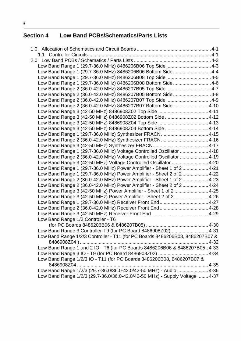
ii
Section 4 Low Band PCBs/Schematics/Parts Lists
1.0 Allocation of Schematics and Circuit Boards .......................................................4-11.1 Controller Circuits...........................................................................................4-1
2.0 Low Band PCBs / Schematics / Parts Lists .........................................................4-3Low Band Range 1 (29.7-36.0 MHz) 8486206B06 Top Side .................................4-3Low Band Range 1 (29.7-36.0 MHz) 8486206B06 Bottom Side ............................4-4Low Band Range 1 (29.7-36.0 MHz) 8486206B08 Top Side .................................4-5Low Band Range 1 (29.7-36.0 MHz) 8486206B08 Bottom Side ............................4-6Low Band Range 2 (36.0-42.0 MHz) 8486207B05 Top Side .................................4-7Low Band Range 2 (36.0-42.0 MHz) 8486207B05 Bottom Side ............................4-8Low Band Range 2 (36.0-42.0 MHz) 8486207B07 Top Side .................................4-9Low Band Range 2 (36.0-42.0 MHz) 8486207B07 Bottom Side ..........................4-10Low Band Range 3 (42-50 MHz) 8486908Z02 Top Side .....................................4-11Low Band Range 3 (42-50 MHz) 8486908Z02 Bottom Side ................................ 4-12Low Band Range 3 (42-50 MHz) 8486908Z04 Top Side .....................................4-13Low Band Range 3 (42-50 MHz) 8486908Z04 Bottom Side ................................ 4-14Low Band Range 1 (29.7-36.0 MHz) Synthesizer FRACN...................................4-15Low Band Range 2 (36.0-42.0 MHz) Synthesizer FRACN...................................4-16Low Band Range 3 (42-50 MHz) Synthesizer FRACN......................................... 4-17Low Band Range 1 (29.7-36.0 MHz) Voltage Controlled Oscillator .....................4-18Low Band Range 2 (36.0-42.0 MHz) Voltage Controlled Oscillator .....................4-19Low Band Range 3 (42-50 MHz) Voltage Controlled Oscillator ........................... 4-20Low Band Range 1 (29.7-36.0 MHz) Power Amplifier - Sheet 1 of 2 ...................4-21Low Band Range 1 (29.7-36.0 MHz) Power Amplifier - Sheet 2 of 2 ...................4-22Low Band Range 2 (36.0-42.0 MHz) Power Amplifier - Sheet 1 of 2 ...................4-23Low Band Range 2 (36.0-42.0 MHz) Power Amplifier - Sheet 2 of 2 ...................4-24Low Band Range 3 (42-50 MHz) Power Amplifier - Sheet 1 of 2 .........................4-25Low Band Range 3 (42-50 MHz) Power Amplifier - Sheet 2 of 2 .........................4-26Low Band Range 1 (29.7-36.0 MHz) Receiver Front End ....................................4-27Low Band Range 2 (36.0-42.0 MHz) Receiver Front End ....................................4-28Low Band Range 3 (42-50 MHz) Receiver Front End ..........................................4-29Low Band Range 1/2 Controller - T6
(for PC Boards 8486206B06 & 8486207B05) .............................................. 4-30Low Band Range 3 Controller-T9 (for PC Board 8486908Z02)............................4-31Low Band Range 1/2/3 Controller - T11 (for PC Boards 8486206B08, 8486207B07 &
8486908Z04 ) ...............................................................................................4-32Low Band Range 1 and 2 IO - T6 (for PC Boards 8486206B06 & 8486207B05..4-33Low Band Range 3 IO - T9 (for PC Board 8486908Z02) .....................................4-34Low Band Range 1/2/3 IO - T11 (for PC Boards 8486206B08, 8486207B07 &
8486908Z04 ................................................................................................. 4-35Low Band Range 1/2/3 (29.7-36.0/36.0-42.0/42-50 MHz) - Audio .......................4-36Low Band Range 1/2/3 (29.7-36.0/36.0-42.0/42-50 MHz) - Supply Voltage ........4-37

iii
Low Band Range 1/2/3 - IF sheet 1 of 2 (for PC Boards 8486206B06, 8486207B05 & 8486908Z02) ................................................................................................4-38
Low Band Range 1/2/3 - IF sheet 2 of 2 (for PC Boards 8486206B06, 8486207B05 & 8486908Z02) ................................................................................................4-39
Low Band Range 1/2/3 - IF sheet 1 of 2 (for PC Boards 8486206B08, 8486207B07 & 8486908Z04) ................................................................................................4-40
Low Band Range 1/2/3 - IF sheet 2 of 2 (for PC Boards 8486206B08, 8486207B07 & 8486908Z04) ................................................................................................4-41
Low Band Range 1/2/3 (29.7-36.0/36.0-42.0/42-50 MHz) - Noise Blanker ..........4-42Low Band Range 1 PCB 8486206B06 Parts List .................................................4-43Low Band Range 2 PCB 8486207B05 Parts List ................................................4-49Low Band Range 3 PCB 8486908Z02 Parts List .................................................4-54Low Band Range 1 PCB 8486206B08 Parts List .................................................4-60Low Band Range 2 PCB 8486207B07 Parts List .................................................4-66Low Band Range 3 PCB 8486908Z04 Parts Lis ..................................................4-72

iv
THIS PAGE INTENTIONALLY LEFT BLANK
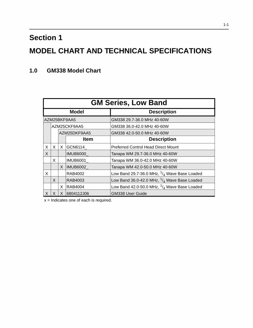
1-1
Section 1
MODEL CHART AND TECHNICAL SPECIFICATIONS
1.0 GM338 Model Chart
GM Series, Low Band Model Description
AZM25BKF9AA5 GM338 29.7-36.0 MHz 40-60W
AZM25CKF9AA5 GM338 36.0-42.0 MHz 40-60W
AZM25DKF9AA5 GM338 42.0-50.0 MHz 40-60W
Item Description
X X X GCN6114_ Preferred Control Head Direct Mount
X IMUB6000_ Tanapa WM 29.7-36.0 MHz 40-60W
X IMUB6001_ Tanapa WM 36.0-42.0 MHz 40-60W
X IMUB6002_ Tanapa WM 42.0-50.0 MHz 40-60W
X RAB4002 Low Band 29.7-36.0 MHz, 1/4 Wave Base Loaded
X RAB4003 Low Band 36.0-42.0 MHz, 1/4 Wave Base Loaded
X RAB4004 Low Band 42.0-50.0 MHz, 1/4 Wave Base Loaded
X X X 6804112J06 GM338 User Guide
x = Indicates one of each is required.

1-2 Technical Specifications
2.0 Technical Specifications
Data is specified for +25°C unless otherwise stated.
General Specifications
Channel CapacityGM338 128
Power Supply 13.2Vdc (10.8 - 15.6Vdc)
Dimensions: H x W x D (mm) Depth excluding knobs GM33860mm x 179mm x 250mm (45 - 60W)
Weight GM338 2064 g
Sealing: Withstands rain testing per MIL STD 810 C/D /E and IP54
Shock and Vibration: Protection provided via impactresistant housing exceeding MIL STD 810-C/D /E
Dust, Salt & Fog Protection provided via environment resistant housing exceeding MIL STD 810 C/D /E
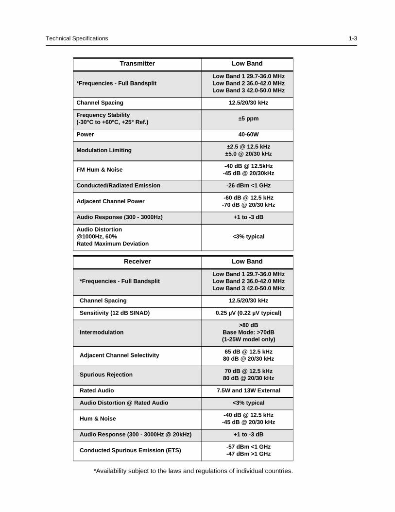
Technical Specifications 1-3
*Availability subject to the laws and regulations of individual countries.
Transmitter Low Band
*Frequencies - Full BandsplitLow Band 1 29.7-36.0 MHzLow Band 2 36.0-42.0 MHzLow Band 3 42.0-50.0 MHz
Channel Spacing 12.5/20/30 kHz
Frequency Stability(-30°C to +60°C, +25° Ref.)
±5 ppm
Power 40-60W
Modulation Limiting±2.5 @ 12.5 kHz
±5.0 @ 20/30 kHz
FM Hum & Noise-40 dB @ 12.5kHz
-45 dB @ 20/30kHz
Conducted/Radiated Emission -26 dBm <1 GHz
Adjacent Channel Power-60 dB @ 12.5 kHz
-70 dB @ 20/30 kHz
Audio Response (300 - 3000Hz) +1 to -3 dB
Audio Distortion@1000Hz, 60%Rated Maximum Deviation
<3% typical
Receiver Low Band
*Frequencies - Full BandsplitLow Band 1 29.7-36.0 MHzLow Band 2 36.0-42.0 MHzLow Band 3 42.0-50.0 MHz
Channel Spacing 12.5/20/30 kHz
Sensitivity (12 dB SINAD) 0.25 µV (0.22 µV typical)
Intermodulation >80 dB
Base Mode: >70dB (1-25W model only)
Adjacent Channel Selectivity 65 dB @ 12.5 kHz
80 dB @ 20/30 kHz
Spurious Rejection 70 dB @ 12.5 kHz
80 dB @ 20/30 kHz
Rated Audio 7.5W and 13W External
Audio Distortion @ Rated Audio <3% typical
Hum & Noise-40 dB @ 12.5 kHz
-45 dB @ 20/30 kHz
Audio Response (300 - 3000Hz @ 20kHz) +1 to -3 dB
Conducted Spurious Emission (ETS)-57 dBm <1 GHz-47 dBm >1 GHz

1-4 Technical Specifications
THIS PAGE INTENTIONALLY LEFT BLANK

2-1
Section 2
THEORY OF OPERATION
1.0 Introduction
This Chapter provides a detailed theory of operation for the Low Band circuits in the radio. For details of the theory of operation and troubleshooting for the the associated Controller circuits refer to the Controller Section of this manual.
2.0 Low Band Receiver
2.1 Receiver Front-End
The low band receiver, shown in Figure 2-1, is bandsplit into three ranges depending on radio model, covering frequencies from 29.7 to 36.0 MHz, 36.0 to 42.0 MHz, or 42.0 to 50.0 MHz. The circuitry of the three models is identical except for component value differences. The receiver consists of five major blocks: front-end bandpass filters and pre-amplifier, first mixer, high-IF and blanker switches, low-IF and receiver back-end, and “Extender” (noise blanker). Two fixed-tuned bandpass filters perform antenna signal pre-selection. A cross over quad diode mixer converts the signal to the high-IF of 10.7 MHz. High-side first injection is used.
Figure 2-1 Low Band Receiver Block Diagram
Demodulator
Delay Filter
MixerFixed
Tuned FilterRF Amp
Tuned Filter
Pin Diode Antenna SwitchRF Jack
Antenna
First LORXINJ
Recovered Audio
RSSI
IF
Second LO
Crystal Filter
455kHz Filter455kHz Filter
455kHz Filter(12.5kHz)
455kHz Filter(12.5kHz)
Swit
ch
Swit
ch
Switc
h
Swit
ch
Limiter
IF Amp
IF Amp
Filter Bank Selectionfrom Synthesizer IC
BlankerNoise
Blanking Pulses
Gate
Buffer
Enable
1stFixed
(25/20kHz)
BWSELECT
(U1201 Pin 48)
4-pole
(25/20kHz)
2-2 Low Band Receiver
There are two 2-pole 10.7 MHz crystal filters in the high-IF section and two switched pairs of 455 kHz ceramic filters in the low-IF section to provide the required adjacent channel selectivity.The second IF at 455 kHz is mixed, amplified and demodulated in the IF IC. The processing of the demodulated audio signal is performed by an audio processing IC located in the controller section.
2.2 Front-End Band-Pass Filters and Pre-Amplifier
The received signal from the radio’s antenna connector is first routed through the harmonic filter and antenna switch, which are part of the RF power amplifier circuits, before being applied to the receiver 5-pole antenna filter (L1001-L1005 and associated components). This filter configuration provides more rapid attenuation above the passband to provide better rejection of the half-IF spurious response. A dual hot carrier diode (D1001) limits any inband signal to 0 dBm to prevent damage to the RF pre-amplifier.
The RF pre-amplifier is an SMD device (Q1001) with collector-base feedback to stabilize gain, impedance, and intermodulation. Transistor Q1002 compares the voltage drop across resistor R1005 with a fixed base voltage from divider R1006 and R1007, and adjusts the base current of Q1001 as necessary to maintain its collector current constant at 25 mA. Operating voltage is from the regulated 9.3V supply (9V3). During transmit, 9.1 volts (9T1) turns on both transistors in U1001, turning off Q1003 and therefore Q1001-2. This protects the RF pre-amplifier from excessive dissipation during transmit mode.
A second 5-pole fixed-tuned bandpass filter provides additional filtering of the amplified signal. This filter configuration also provides steeper attenuation above its passband for best half-IF attenuation.
2.3 First Mixer and High Intermediate Frequency (IF)
The signal coming from the front-end is converted to the high-IF frequency of 10.7 MHz using a cross over quad diode mixer (U1051). The high-side injection signal (RXINJ) from the frequency synthesizer circuitry is filter by a 7-pole low-pass filter (L1012-14 and associated circuitry) which removes second harmonic content from the injection signal and improves half-IF rejection. The 50-ohm output of the first mixer is applied to the input of the high-IF circuit block.
2.4 High Intermediate Frequency (IF) and Blanker Switches
The first mixer IF output signal (IF) is applied to diplexer network consisting of L1101, L1111 and associated components. This network has three functions: it terminates the mixer output at frequencies other than 10.7 MHz into 51-ohm resistor R1101; it matches the 50-ohm mixer output to the first IF amplifier (Q1101) input; and it provides bandpass filtering at 10.7 MHz to prevent the 5.35 MHz half-IF component of the mixer output from creating a second harmonic at 10.7 MHz in Q1101, which degrades half-IF rejection.
The IF amplifier Q1101 uses ac and dc feedback to stabilize gain and quiescent current (approximately 28 mA). Operating voltage is from the regulated 9.3V supply (9V3). Its output is applied to a 10.7 MHz ceramic filter FL1101 which has a 3 dB bandwidth of 270 kHz and provides a time delay of 2.6 usec. This delay allows enough time for the “Extender” to respond to impulse noise present at the input of Q1101 and operate the blanker switches Q1102 and Q1103, muting the IF signal for the duration of the noise pulse. L1104 and L1105 also provide additional selectivity and time delay. Operation of the “Extender” circuit is explained in Section 1.0.5 below.
When the blanker switches turn “on” to mute the IF signal, they momentarily change the impedance of resonant circuits L1104 and L1105 from high to very low. This abrupt impedance change, if

Low Band Receiver 2-3
presented to the high-Q crystal filter FL1102, would cause ringing of the filter response, stretching an otherwise narrow impulse into a long and audible output waveform. Therefore, source follower stage Q1104 isolates the blanker switches from the crystal filters, providing a consistent source impedance via matching network L1106, L1107 and associated components. Q1104 has unity voltage gain in this configuration.
Crystal filter F1102 is a module which consists of two 2-pole, 10.7 MHz units configured to provide an overall 4-pole response having a 3 dB bandwidth of approximately 12 kHz. The output is amplified by second IF amplifier Q1106 and applied to the low-IF circuitry, pin 1 of IF IC (U1103). A dual hot carrier diode (D1101) limits the amplifier output voltage swing to prevent overdriving the IF IC at RF input levels above -27 dBm.
2.5 Low Intermediate Frequency (IF) and Receiver Back End
The 10.7 MHz high-IF signal from the second IF amplifier feeds the IF IC (U1103) at pin 1. Within the IF IC, the 10.7 MHz high-IF signal mixes with the 10.245 MHz second local oscillator (2nd LO) to produce the low-IF signal at 455 kHz. The 2nd LO frequency is determined by crystal Y1101. The low-IF signal is amplified and filtered by external pairs of 455 kHz ceramic filters (FL1105 and FL1107 for 20kHz channel spacing, or FL1104 and FL1106 for 12.5 kHz channel spacing). Selection of the appropriate filter pair is accomplished by U1101 and U1102, controlled by the BWSELECT line from pin 48 of the synthesizer IC U1201. The filtered output from the ceramic filters is applied to the limiter input pin of the IF IC (pin 14).
The IF IC contains a quadrature detector using a ceramic phase-shift element (Y1102) to provide audio detection. Internal amplification provides an audio output level of 120 mV rms (at 60% deviation) from U1103 pin 8 (AUDIOOUT) which is fed to the ASFIC_CMP (U0221) pin 2 (part of the Controller circuitry).
A received signal strength indicator (RSSI) signal is available at U1103 pin 5, having a dynamic range of 70 dB. The RSSI is interpreted by the microprocessor (U0101 pin 63) and in addition is available at accessory connector J0501-15.
2.6 “Extender” (Noise Blanker)
The 10.7 MHz output from the first mixer, which is present at the input of the first IF amp Q1101, is also routed to the input of the “Extender” (noise blanker) circuitry and amplified by FET Q1610. The high input impedance of the FET stage minimizes loading of the signal in the receiver path. The output of Q1610 is further amplified by U1601, which is a wide-bandwidth, high gain differential amplifier (used in a single-ended configuration) incorporating an AGC gain control input. This gain block provides linear amplification of the instantaneous amplitude of the 10.7 MHz signal at the first mixer output. The output of U1601 is coupled to biased-detector Q1603. The bias is set so that noise impulses of a significant amplitude cause Q1603 to conduct. The following stages (Q1604 through Q1606) provide additional gain and pulse shaping which slows the turn-on and turn-off waveform applied to IF blanker switches Q1102 and Q1103. The result is that, for each noise impulse, the IF signal is smoothly ramped off and then on again, preventing the pulse from reaching the narrow IF selectivity, where ringing would cause an objectionable spike at the detector of a much longer duration than the original impulse.
If the repetition rate of noise impulses is so rapid that the noise blanker can no longer blank them individually, as indicated by a large increase in high-frequency content at the output of Q1604, stage Q1607 amplifies this level and turns on level detector Q1609. Its output is highly filtered into a DC voltage level which is proportional to the repetition rate of noise impulses, and this is applied to the
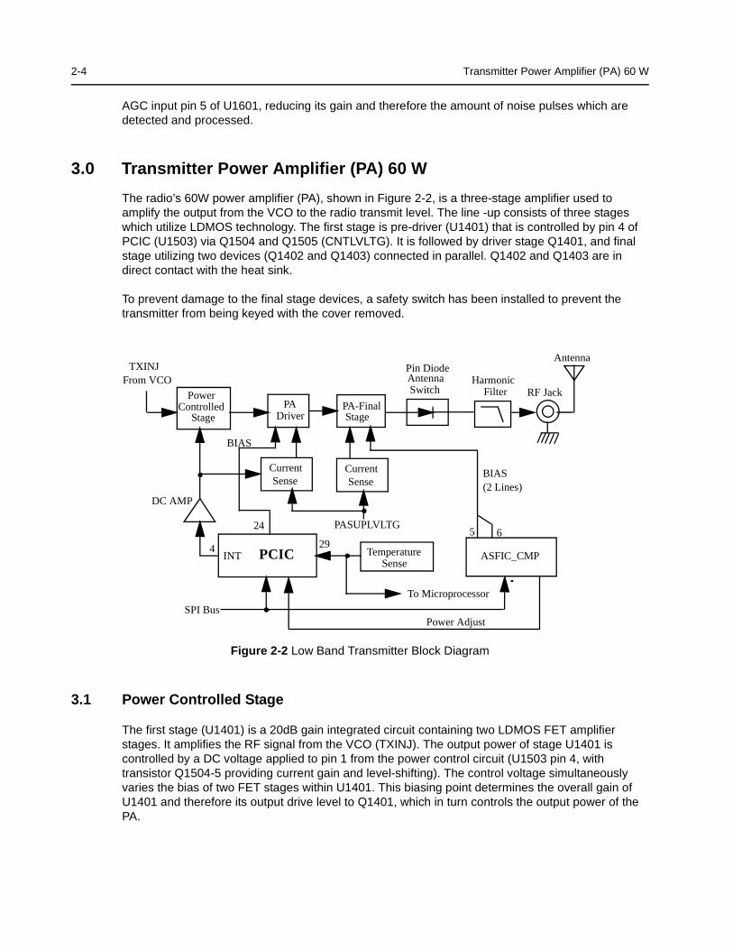
2-4 Transmitter Power Amplifier (PA) 60 W
AGC input pin 5 of U1601, reducing its gain and therefore the amount of noise pulses which are detected and processed.
3.0 Transmitter Power Amplifier (PA) 60 W
The radio’s 60W power amplifier (PA), shown in Figure 2-2, is a three-stage amplifier used to amplify the output from the VCO to the radio transmit level. The line -up consists of three stages which utilize LDMOS technology. The first stage is pre-driver (U1401) that is controlled by pin 4 of PCIC (U1503) via Q1504 and Q1505 (CNTLVLTG). It is followed by driver stage Q1401, and final stage utilizing two devices (Q1402 and Q1403) connected in parallel. Q1402 and Q1403 are in direct contact with the heat sink.
To prevent damage to the final stage devices, a safety switch has been installed to prevent the transmitter from being keyed with the cover removed.
Figure 2-2 Low Band Transmitter Block Diagram
3.1 Power Controlled Stage
The first stage (U1401) is a 20dB gain integrated circuit containing two LDMOS FET amplifier stages. It amplifies the RF signal from the VCO (TXINJ). The output power of stage U1401 is controlled by a DC voltage applied to pin 1 from the power control circuit (U1503 pin 4, with transistor Q1504-5 providing current gain and level-shifting). The control voltage simultaneously varies the bias of two FET stages within U1401. This biasing point determines the overall gain of U1401 and therefore its output drive level to Q1401, which in turn controls the output power of the PA.
Pin Diode Antenna Switch RF Jack
Antenna
Harmonic Filter
PA-FinalStage
PADriver
From VCO
ControlledStage
BIAS
To Microprocessor
TemperatureSense
DC AMP
PASUPLVLTG
(2 Lines)
SPI Bus
TXINJ
SenseCurrent
SenseCurrent
ASFIC_CMPPCICINT
24
4 295 6
BIAS
Power
Power Adjust
Transmitter Power Amplifier (PA) 60 W 2-5
3.2 Driver Stage
The next stage is an LDMOS device (Q1401) providing a gain of 13dB. This device requires a positive gate bias and a quiescent current flow for proper operation. The voltage of the line MOSBIAS_1 is set during transmit mode by the PCIC pin 24, and fed to the gate of Q1401 via resistors R1402, R1447, R1449, R1458, R1459, and R1463. The bias voltage is tuned in the factory.
The circuitry associated with U1402-2 and Q1404 limits the variation in the output power of the driver stage resulting from changes in the input impedance of the final stage due to changes at the antenna of the radio. The variation in the driver’s output power is limited by controlling its DC current. The driver’s DC current is monitored by measuring the voltage drop across current-sense resistors R1473-6, and this voltage is compared to a reference voltage on pin 6 of U1402-2. If the current through the sense resistors decreases, the circuit increases the bias voltage on the gate of Q1401 via Q1404. If the current increases, then the bias voltage decreases in order to keep the driver’s current constant. Since the current must increase with increasing control voltage, an input path is provided to U1402-2 pin 5 from control line VCNTRL to enable this.
3.3 Final Stage
The final stage uses two LDMOS FET devises operating in parallel. Each device has its own adjustable gate bias voltage, MOSBIAS_2 and MOSBIAS_3, obtained from D/A outputs of the ASFIC. These bias voltages are also factory-tuned. If these transistors are replaced, the bias voltage must be tuned using the Tuner software. Care must be taken not to damage the device by exceeding the maximum allowed bias current. The device’s drain current is drawn directly from the radio’s DC supply voltage input, PASUPVLTG, via current-measurement resistor R1409.
A matching network combines the output of the two devices and provides a 50-ohm source for the antenna switch and harmonic filter.
3.4 Antenna Switch
The antenna switch is operated by the 9T1 voltage source which forward biases diodes D1401 and D1402 during transmit, causing them to appear as low impedance. D1401 allows the RF output from final stages Q1402 and Q1403 to be applied to the input of the low-pass harmonic filter (L1421-3 and associated components). D1402 appears as a short circuit at the input of the receiver (RXINJ), preventing transmitter RF power from entering the receiver. L1420 and C1456 appears as a broadband-wave transmission line, making the short circuit presented by D1402 appear as open circuit at the junction of D1401 and the harmonic filter input.
During receive mode, the 9T1 voltage is not present, and D1401 and D1402 do not conduct and appear as open circuits. This allows signals from the antenna jack to pass to the receiver input, and disconnects the transmitter final stages from this path.
3.5 Harmonic Filter
Components L1421- L1423 and C1449-C1455 form a seven-pole elliptic low-pass filter to attenuate harmonic energy of the transmitter to specifications level. R1411 is used to drain electrostatic charge that might otherwise build up on the antenna. The harmonic filter also prevents high level RF signals above the receiver passband from reaching the receiver circuits, improving spurious response rejection.
2-6 Transmitter Power Amplifier (PA) 60 W
3.6 Power Control
The transmitter uses the Power Control IC (PCIC, U1503) to control the power output of the radio. A differential DC amplifier U1502-1 compares the voltage drop across current-measuring resistor R1409, which is proportional to the transmitter final stage DC current, with the voltage drop across resistors R1508 and R1535, which is proportional to the current through transistor Q1503. This transistor is controlled by the output of the differential amplifier, which varies the transistor Q1503. This transistor is controlled by the output of the differential amplifier, which varies the transistor current until equilibrium of the two compared voltages is reached. The current through Q1503 develops a voltage across R1513 which is exactly proportional to the DC current of the final stages. This voltage is applied to the RF IN port of the PCIC (pin 1).
The PCIC has internal digital to analog converters (DACs) which provide a reference voltage of the control loop. The reference voltage level is programmable through the SPI line of the PCIC. This reference voltage is proportional to the desired power setting of the transmitter, and is factory programmed at several points across the frequency range of the transmitter to offset frequency response variations of the transmitter’s power detector circuitry.
The PCIC provides a DC output voltage at pin 4 (INT) which is amplified and shifted in DC level by stages Q1504 and Q1505. The 0 to 4 volt DC range at pin 4 of U1503 is transferred to a 0 to 8 volt DC range at the output of Q1505, and applied as VCNTRL to the power-adjust input pin of the first transmitter stage U1401. This adjusts the transmitter power output to the intended value. Variations in antenna impedance cause variations in the DC current of the final stages, and the PCIC adjust the control voltage above or below its normal value to reduce power if current drain increases, or raise power if current drain decreases.
Capacitors C1503-4 and C1525, in conjunction with resistors and integrators within the PCIC, control the transmitter power-rise (key-up) and power-decay (de-key) characteristic to minimize splatter into adjacent channels.
U1501 is a temperature-sensing device which monitors the circuit board temperature in the vicinity of the transmitter circuits and provide a dc voltage to the PCIC (TEMP, pin 29) proportional to temperature. If the DC voltage produced exceeds the set threshold in the PCIC, the transmitter output power will be reduced so as to reduce the transmitter temperature.
3.7 TX Safety Switch
The TX Safety Switch consists of S1501, Q1506, and diode pairs D1502 and D1503 providing protection to the final stage divices Q1402 and Q1403. These final stage devices can be degraded or destroyed if the radio is keyed without the cover in place due to the lack of a good thermal path to the chassis.
Switch S1501 is closed when the radio’s cover is screwed in place by means of the carbonized reqion on the cover’s pressure pad making contact with the finger plating on the radio’s PCB. With the cover in place, transistor Q1506 is off, back-biasing diodes D1502 and D1503, enabling proper transmitter operation. When the cover is not in place, S1501 opens, causing Q1506 to rurn on, pulling the cathodes of D1502 and D1503 to ground, resulting in the shorting of the transmitter’s bias lines and control voltage.

Frequency Synthesis 2-7
4.0 Frequency Synthesis
The frequency synthesizer subsystem, shown in Figure 2-3, consists of the reference oscillator crystal (Y1201), the Low Voltage Fractional-N synthesizer (LVFRAC-N, U1201), and the receive and transmit VCOs and buffers (Q1303 through Q1308 and associated components).
Figure 2-3 Low Band Synthesizer Block Diagram
4.1 Fractional-N Synthesizer
The LVFRAC-N synthesizer IC (U1201) consists of a reference oscillator, pre-scaler, a programmable loop divider, control divider logic, phase detector, a charge pump, A/D converter for low frequency digital modulation, a balance attenuator to balance the high frequency analog modulation and low frequency digital modulation, a 13V positive voltage multiplier, a serial interface for control, and finally a super filter for the regulated 9.3 volt supply.
Regulated 9.3 volts DC applied to the super filter input (U1201, pin 30) delivers a very low noise output voltage of 8.3 volts DC (VSF) at pin 28. External device Q1201 allows greater current sourcing capability. The VSF source supplies the receive and transmit VCOs and first buffer stages. The synthesizer IC supply voltage is provided by a dedicated 5V regulator (U1250) to minimize power supply noise.
In order to generate a high voltage to supply the phase detector (charge pump) output stage at pin VCP (U1201 pin 47), a capacitive voltage multiplier circuit (CR1202 and C1209) generates a voltage
DATA
CLK
CEX
MODIN
SFIN
XTAL1
XTAL2
WARP
PREIN
VCP
REFERENCEOSCILLATOR
VOLTAGEMULTIPLIER
DATA (U0101 PIN 100)
CLOCK (U0101 PIN 1)
CSX (U0101 PIN 2)
MOD IN (U0221 PIN 40)
9,3V (U641 PIN 5)
7
8
9
10
30
23
24
25
32
47
VMULT2 VMULT1
BIAS1
SFOUT
AUX3
AUX4
IADAPTIOUT
GND
FREFOUT
LOCK 4
19
6, 22, 33, 44
4345
3
2
28
14 15
40
FILTERED 8,3V
STEERING
LOCK (U0101 PIN 56)
PRESCALER IN
FREF (U0221 PIN 34)
39BIAS2
41
48
5, 13, 20, 34, 36+5V (U3211 PIN 1)
AUX1
VDD, DC5V MODOUT
U1201
LOW VOLTAGEFRACTIONAL-N
SYNTHESIZER
AUX2
TX RF INJECTION(1ST STAGE OF PA)
LO RF INJECTION
VOLTAGE CONTROLLED OSCILLATOR
LINE2-POLELOOP
FILTER
1
Q1202
BUFFER
BWSELECT
VCTRL
N.C.N.C.
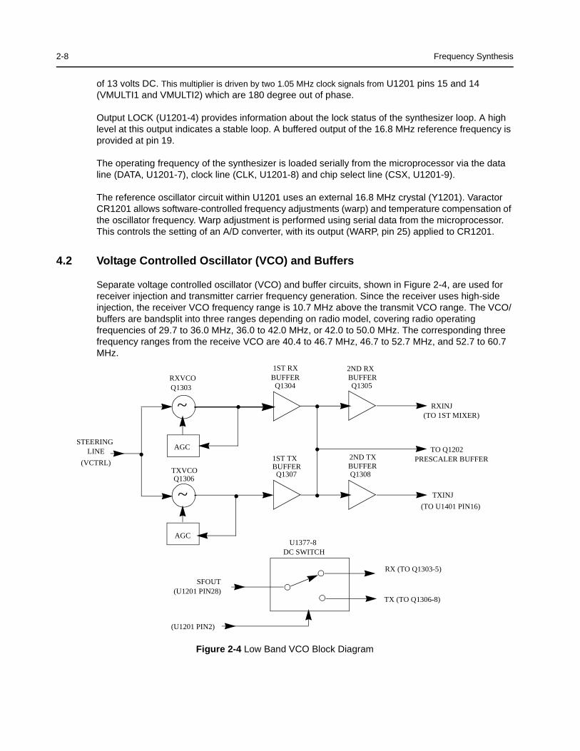
2-8 Frequency Synthesis
of 13 volts DC. This multiplier is driven by two 1.05 MHz clock signals from U1201 pins 15 and 14 (VMULTI1 and VMULTI2) which are 180 degree out of phase.
Output LOCK (U1201-4) provides information about the lock status of the synthesizer loop. A high level at this output indicates a stable loop. A buffered output of the 16.8 MHz reference frequency is provided at pin 19.
The operating frequency of the synthesizer is loaded serially from the microprocessor via the data line (DATA, U1201-7), clock line (CLK, U1201-8) and chip select line (CSX, U1201-9).
The reference oscillator circuit within U1201 uses an external 16.8 MHz crystal (Y1201). Varactor CR1201 allows software-controlled frequency adjustments (warp) and temperature compensation of the oscillator frequency. Warp adjustment is performed using serial data from the microprocessor. This controls the setting of an A/D converter, with its output (WARP, pin 25) applied to CR1201.
4.2 Voltage Controlled Oscillator (VCO) and Buffers
Separate voltage controlled oscillator (VCO) and buffer circuits, shown in Figure 2-4, are used for receiver injection and transmitter carrier frequency generation. Since the receiver uses high-side injection, the receiver VCO frequency range is 10.7 MHz above the transmit VCO range. The VCO/buffers are bandsplit into three ranges depending on radio model, covering radio operating frequencies of 29.7 to 36.0 MHz, 36.0 to 42.0 MHz, or 42.0 to 50.0 MHz. The corresponding three frequency ranges from the receive VCO are 40.4 to 46.7 MHz, 46.7 to 52.7 MHz, and 52.7 to 60.7 MHz.
Figure 2-4 Low Band VCO Block Diagram
STEERINGLINE
(VCTRL)
RXVCOQ1303
Q1306TXVCO
AGC
AGC
Q1304
Q1307 Q1308
Q1305BUFFER BUFFER
BUFFERBUFFER
1ST RX 2ND RX
2ND TX1ST TX
TXINJ
RXINJ
TO Q1202PRESCALER BUFFER
(TO 1ST MIXER)
(TO U1401 PIN16)
SFOUT(U1201 PIN28)
U1377-8DC SWITCH
RX (TO Q1303-5)
TX (TO Q1306-8)
(U1201 PIN2)
~
~
Frequency Synthesis 2-9
The VCOs, together with Fractional-N synthesizer U1201, generates the required frequencies for transmit and receive modes. The TRB line (U1201, pin 2) determines which VCO/buffer circuit is to be enabled. A high level on TRB will turn on the transistors in U1378 to turn on via R1376, applying the 8.3 volt VSF source to the receiver VCO and first buffer. The second buffer in each string operates from the 9V3 source and become active when RF is applied to their inputs.
The RF signal at the bases of the second buffers are combined and fed back to the Fractional-N synthesizer via PRE_IN where it is compared to the reference frequency as described below in “Synthesizer Operation”. The Fractional-N IC provides a DC steering voltage VCTRL to adjust and maintain the VCO at the correct frequency.
With a steering voltage from 2.5V to 11V at the appropriate varactor diode (CR1302 for the RX VCO, or CR1310 for the TX VCO), the full VCO tuning range is obtained. Each VCO uses and AGC circuit to maintain a constant VCO output level across the frequency band. A diode (CR1306 in the receive VCO, or CR1314 in the transmit VCO) is configured as a voltage doubler which rectifies the RF level sampled at the VCO drain and applies a proportional negative DC voltage to the VCO gate. Increased RF level reduces the VCO gain to compensate.
The VCO output is taken from the source and applied to the first buffer transistor (Q1304 receive, Q1307 transmit). The first buffer output is further amplified by the second buffer transistor (Q1305 receive, Q1308 transmit) before being applied to the receiver first mixer or transmitter first stage input.
In TX mode the modulation signal coming from the LVFRAC-N synthesizer IC (MODOUT, U1201 pin 41) is superimposed on the DC steering line voltage by capacitive divider C1215, C1208 and C1212, causing modulation of the TX VCO using the same varactor as used for frequency control.
4.3 Synthesizer Operation
The complete synthesizer subsystem comprises mainly of low voltage LVFRAC-N synthesizer IC, Reference Oscillator (crystal oscillator with temperature compensation), charge pump circuitry, loop filter circuitry, and voltage controlled-controlled oscillators and buffers. A sample of the VCO operating signal PRE_IN is amplified by feedback buffer Q1202, low-pass filtered by L1205, C1222 and C1224, and fed to U1201 pin 32 (PREIN).
The pre-scaler in the synthesizer (U1201) is basically a dual modulus pre-scaler with selectable divider ratios. The divider ratio of the pre-scaler is controlled by the loop divider, which in turn receives its inputs via the serial interface to the microprocessor. The output of the pre-scaler is applied to the loop divider. The output of the loop divider is connected to the phase detector, which compares the loop divider´s output signal with the reference signal.The reference signal is generated by dividing down the signal of the reference oscillator, whose frequency is controlled by Y1201.
The output signal of the phase detector is a pulsed DC signal which is routed to the charge pump. The charge pump outputs a current at pin 43 of U1201 (IOUT). The loop filter (consisting of R1205-6, R1208, and C1212-14) transforms this current into a voltage that is applied to varactor diodes (CR1310 for transmit, CR1302, for receive) and alters the output frequency of the appropriate VCO.The current can be set to a value fixed in the LVFRAC-N IC or to a value determined by the currents flowing into BIAS 1 (U1201-40) or BIAS 2 (U1201-39). The currents are set by the value of R1211 or R1207 respectively. The selection of the three different bias sources is done by software programming.
2-10 Frequency Synthesis
To reduce synthesizer lock time when new frequency data has been loaded into the synthesizer the magnitude of the loop current is increased by enabling the IADAPT (U1201-45) for a certain software programmable time (Adapt Mode). The adapt mode timer is started by a low to high transient of the CSX line. When the synthesizer is within the lock range, the current is determined only by the resistors connected to BIAS 1, BIAS 2, or the internal current source. A settled synthesizer loop is indicated by a high level of signal LOCK (U1201-4).
In order to modulate the PLL the two-spot modulation method is utilized. Via pin 10 (MODIN) on U1201, the audio signal is applied to both the A/D converter (low frequency path) and the balanced attenuator (high frequency path). The A/D converter converts the low frequency analog modulating signal into a digital code that is applied to the loop divider, thereby causing the carrier to deviate. The balance attenuator is used to adjust the VCO’s deviation sensitivity to high frequency modulating signals. The output of the balance attenuator is present at the MODOUT port (U1201-41) and superimposed on the VCO steering line voltage by a divider consisting of C1215, C1208 and C1212.
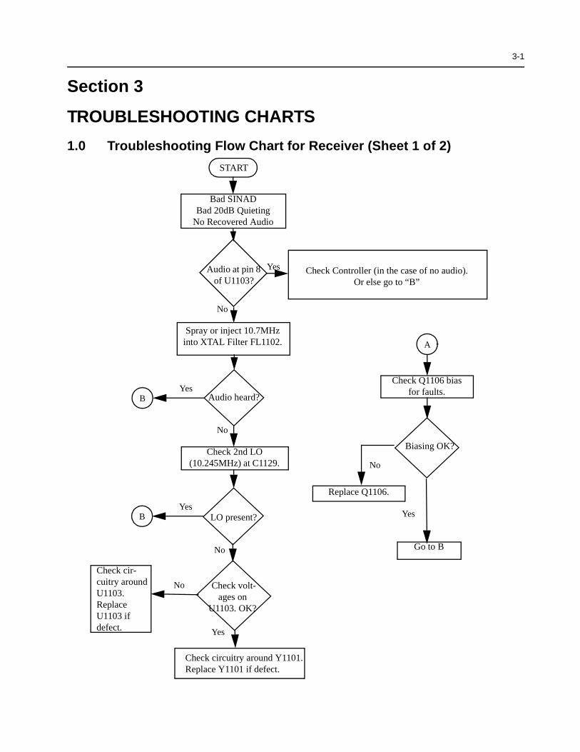
3-1
Section 3
TROUBLESHOOTING CHARTS
1.0 Troubleshooting Flow Chart for Receiver (Sheet 1 of 2)
Bad SINADBad 20dB Quieting
No Recovered Audio
START
Audio at pin 8 of U1103?
Check Controller (in the case of no audio).Or else go to “B”
Yes
No
Spray or inject 10.7MHz into XTAL Filter FL1102.
Audio heard?BYes
No
Check 2nd LO (10.245MHz) at C1129.
LO present?BYes
Check volt-ages on
U1103. OK?
Biasing OK?
No
No
A
Yes
Check Q1106 bias for faults.
Replace Q1106.
Go to B
Yes
No
Check cir-cuitry around U1103. Replace U1103 if defect.
Check circuitry around Y1101. Replace Y1101 if defect.

3-2 Troubleshooting Flow Chart for Receiver (Sheet 1 of 2)
1.1 Troubleshooting Flow Chart for Receiver (Sheet 2 of 2)
IF Signal at pin 2 of U1051
No
RF Signal at pin 3 of U1051?
RF Signal at C1017?
No
RF Signal at C1013?
No
RF Signal at C1002?
No or
Check harmonic filters J1401 and ant.switch
Check preselector and RF amp.
Inject RF into J1401
No
Yes
Check RF amp (Q1001) Stage.
Check filter between C1017 & mixer U1051
Yes
Check for detailed mixer.
Yes
1st LO level OK?
Locked?
Yes
Check FGU
Yes
Trace IF signal from C1036 to Q1106.
Check for bad XTAL filter.
No
Yes IF signal at Q1106 collec-
tor?
Before replacing U1103, check
U1103 voltages.
Yes
Is 9V3 present?
Check Supply Voltage cir-cuitry. Check U0681, U3211 and U0641.
No
No
YesA
B
weak RF
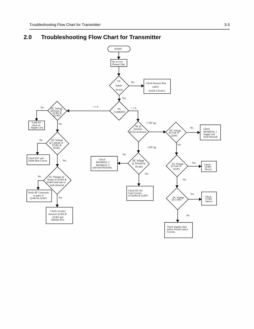
Troubleshooting Flow Chart for Transmitter 3-3
2.0 Troubleshooting Flow Chart for Transmitter
No
DC Voltage@ Gate of
Q1401
No
Yes
START
No or Low
TX DC Voltage
@Drains of
Q1402 &Q1403
@ Cathode of D1401 &D1402
DC Voltage
Drains of Q1402 &AC Voltages @
Q1403 both sine orboth distorted
Check 9T1 andDiode Bias Circuit
Verify RF Continuity
to gates of
Q1402 & Q1403
Check circuitrybetween Q1402 &
Q1403 and Antenna Port
CheckMOSBIAS_1Supply andFeed Network
No
<<18V pp
Yes
No
Yes
< 1 A
No
CheckQ1401Device
Yes
CURRENT
RF @Junction
R1413 & R1414
DC Voltage@ TP1402 &
TP1403
Yes
CheckMOSBIAS_2MOSBIAS_3
and Feed Networks
Check DC/ACGate Circuitsof Q1402 & Q1403
Check Supply Feedand/or PowerControlCircuits.
No
>18V pp
CheckU1401Device
AC Voltage@ Gate of
Q1401
Yes
DC Voltage@ U1401
Yes
No
Power Out
> 1 A
Look for
short on
Supply Line
Check Pressure Pad
and/or
Switch Circuitry
Yes
NoTX
Safefy
Switch
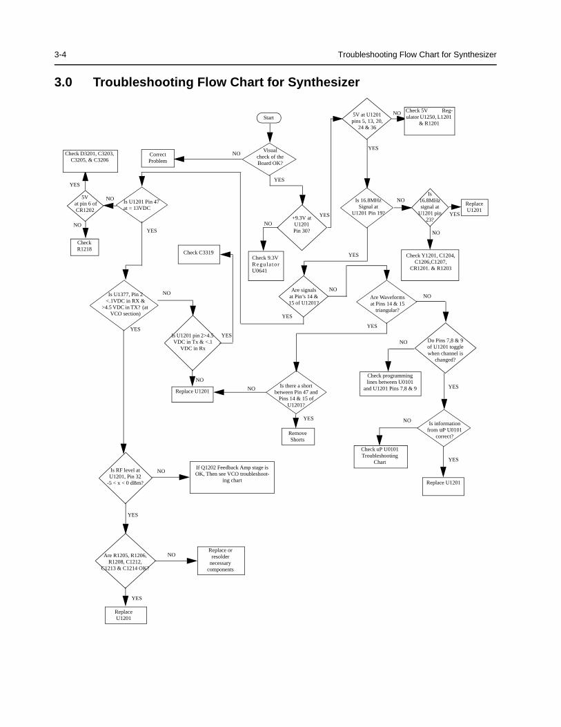
3-4 Troubleshooting Flow Chart for Synthesizer
3.0 Troubleshooting Flow Chart for Synthesizer
5V at pin 6 of CR1202
Is informationfrom uP U0101
correct?
Is U1201 Pin 47at = 13VDC
Is U1377, Pin 2<.1VDC in RX &
>4.5 VDC in TX? (at VCO section)
Start
Visual check of the Board OK?
CorrectProblem
Check 9.3VR e gu la to rU0641
+9.3V at U1201Pin 30?
Is 16.8MHzSignal at
U1201 Pin 19?
Check Y1201, C1204, C1206,C1207,
CR1201. & R1203
Are signalsat Pin’s 14 &15 of U1201?
Check R1218
Check C3319
Is U1201 pin 2>4.5 VDC in Tx & <.1
VDC in Rx
Replace U1201
RemoveShorts
Is there a shortbetween Pin 47 and
Pins 14 & 15 ofU1201?
Replace orresolder
necessarycomponents
Is RF level atU1201, Pin 32
-5 < x < 0 dBm?
Are R1205, R1206, R1208, C1212,
C1213 & C1214 OK?
Replace U1201
If Q1202 Feedback Amp stage is OK, Then see VCO troubleshoot-
ing chart
Are Waveformsat Pins 14 & 15
triangular?
Do Pins 7,8 & 9of U1201 togglewhen channel is
changed?
Check programminglines between U0101
and U1201 Pins 7,8 & 9
Replace U1201
Check uP U0101Troubleshooting
Chart
NO
YES
NO
YES
NO
YES
NO
NO
NO
YES
YES
NO
YES
YES
NO
YES
YES
YES
NO
NO
NO
NO
YES
NO
YES
YES
Check D3201, C3203, C3205, & C3206
5V at U1201 pins 5, 13, 20,
24 & 36
Check 5V Reg-ulator U1250, L1201
& R1201
Is 16.8MHz signal at
U1201 pin 23?
Replace U1201
YES
NO
NO
YES
NO
YES
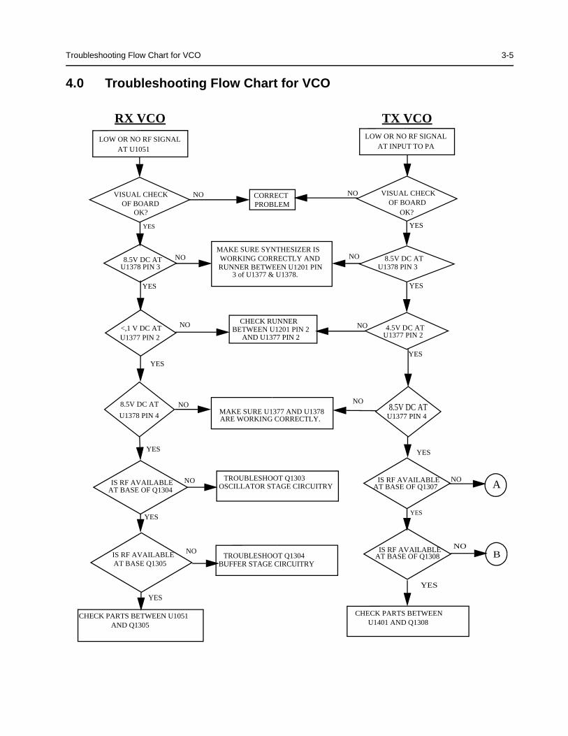
Troubleshooting Flow Chart for VCO 3-5
4.0 Troubleshooting Flow Chart for VCO
LOW OR NO RF SIGNAL AT U1051
VISUAL CHECKOF BOARD
OK?
8.5V DC AT U1378 PIN 3
<,1 V DC ATU1377 PIN 2
8.5V DC AT
U1378 PIN 4
CORRECTPROBLEM
NO
YES
MAKE SURE SYNTHESIZER ISWORKING CORRECTLY ANDRUNNER BETWEEN U1201 PIN
3 of U1377 & U1378.
CHECK RUNNERBETWEEN U1201 PIN 2
AND U1377 PIN 2
IS RF AVAILABLE AT BASE OF Q1304
TROUBLESHOOT Q1303 OSCILLATOR STAGE CIRCUITRY
IS RF AVAILABLE
CHECK PARTS BETWEEN U1051
NO
NO
NO
NO
NO
YES
YES
YES
YES
YES
RX VCOLOW OR NO RF SIGNAL
AT INPUT TO PA
VISUAL CHECKOF BOARD
OK?
8.5V DC ATU1378 PIN 3
4.5V DC ATU1377 PIN 2
8.5V DC ATU1377 PIN 4
IS RF AVAILABLE AT BASE OF Q1307
YES
YES
YES
YES
YES
NO
NO
NO
NO
NO
TX VCO
AND Q1305
AT BASE Q1305TROUBLESHOOT Q1304
BUFFER STAGE CIRCUITRY
MAKE SURE U1377 AND U1378ARE WORKING CORRECTLY.
IS RF AVAILABLEAT BASE OF Q1308
A
BNO
YES
CHECK PARTS BETWEENU1401 AND Q1308

3-6 Troubleshooting Flow Chart for VCO
THIS PAGE INTENTIONALLY LEFT BLANK
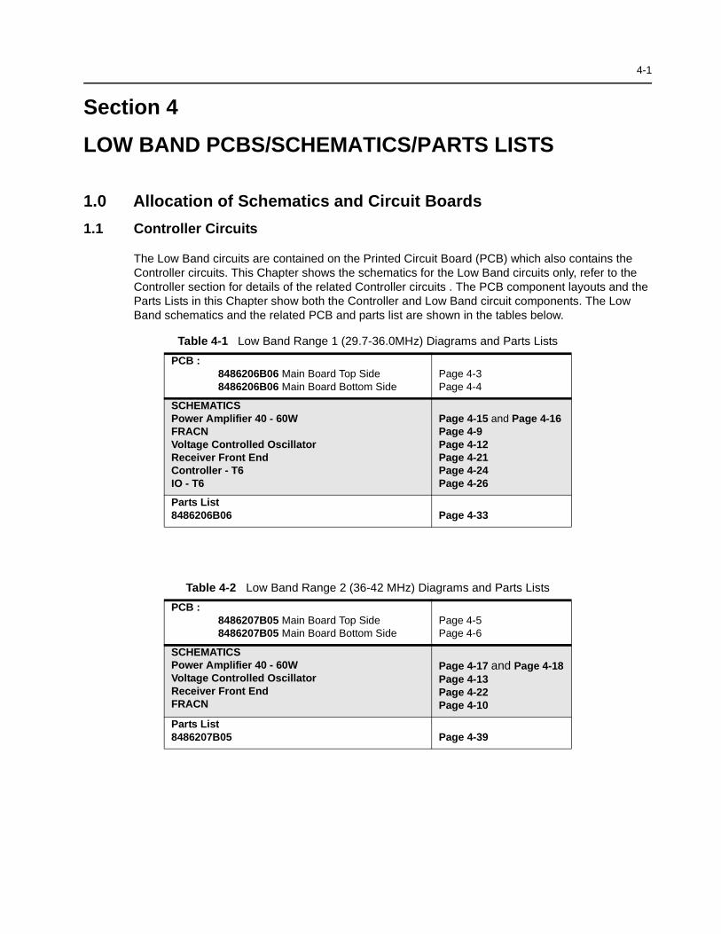
4-1
Section 4
LOW BAND PCBS/SCHEMATICS/PARTS LISTS
1.0 Allocation of Schematics and Circuit Boards
1.1 Controller Circuits
The Low Band circuits are contained on the Printed Circuit Board (PCB) which also contains the Controller circuits. This Chapter shows the schematics for the Low Band circuits only, refer to the Controller section for details of the related Controller circuits . The PCB component layouts and the Parts Lists in this Chapter show both the Controller and Low Band circuit components. The Low Band schematics and the related PCB and parts list are shown in the tables below.
Table 4-1 Low Band Range 1 (29.7-36.0MHz) Diagrams and Parts Lists
PCB :8486206B06 Main Board Top Side8486206B06 Main Board Bottom Side
Page 4-3Page 4-4
SCHEMATICSPower Amplifier 40 - 60WFRACNVoltage Controlled OscillatorReceiver Front EndController - T6IO - T6
Page 4-15 and Page 4-16Page 4-9Page 4-12Page 4-21Page 4-24Page 4-26
Parts List8486206B06 Page 4-33
Table 4-2 Low Band Range 2 (36-42 MHz) Diagrams and Parts Lists
PCB :8486207B05 Main Board Top Side8486207B05 Main Board Bottom Side
Page 4-5Page 4-6
SCHEMATICSPower Amplifier 40 - 60WVoltage Controlled OscillatorReceiver Front EndFRACN
Page 4-17 and Page 4-18Page 4-13Page 4-22Page 4-10
Parts List8486207B05 Page 4-39

4-2 Allocation of Schematics and Circuit Boards
Table 4-3 Low Band Range 3 (42-50MHz) Diagrams and Parts Lists
PCB :848608Z02 Main Board Top Side848608Z02 Main Board Bottom Side
Page 4-7Page 4-8
SCHEMATICSPower Amplifier 40 - 60WVoltage Controlled OscillatorReceiver Front EndController - T9FRACNIO - T9
Page 4-19 and Page 4-20Page 4-14Page 4-23Page 4-25Page 4-11Page 4-27
Parts List848608Z02 Page 4-44

Low
Ban
d P
CB
s / S
chem
atic
s / P
arts
Lis
ts4-
3
2.0
Lo
w B
and
PC
Bs
/ Sch
emat
ics
/ Par
ts L
ists
C01
01C
0102
C01
04
C01
05
C01
06 C01
07
C01
21 C01
31
C01
32
C02
11
C02
12
C02
21C
0222
C02
23
C02
25
C02
26C
0227
C0228
C0231
C02
32 C02
33
C02
34C
0235
C02
36
C0237
C02
41 C02
42
C02
43
C02
44
C02
45
C02
46
C02
51
C02
52
C02
53
C02
54
C02
55
C02
56
C02
61
C02
62
C02
75
C02
90
C02
91
C02
92C
0293
C03
31
C0401
C0441
C0442
C0443
C04
45
C0446
C0447
C0448
C0449
C0451C0452C0453
C0455C0456C0457C0458C0459C0460
C0461C0462C0463C0464
C0466C0467C0468
C0470
C0471
C0472
C0473
C04
74C
0476
C04
77C
0478
C04
82
C04
83
C04
84
C04
86C
0487
C04
88
C04
90C
0493
C04
94
C0495
C04
96
C0501C0502C0503C0504C0505C0506C0508
C0509C0510
C0511C0512
C0513C0514
C0515C0516
C05
17C0518
C06
01
C06
03
C06
12
C06
51
C06
52
C06
54C
0655
C06
81
C10
01C
1002
C10
03
C10
04
C10
06
C10
07
C10
08C
1009
C10
10
C10
11C
1012C10
15
C10
19
C10
20
C10
21
C10
22
C10
23
C10
24
C10
25
C10
37C
1038
C10
39
C10
40
C10
41C10
42
C1101
C1103
C11
06
C11
07
C11
09
C11
10
C11
11
C11
25
C11
29C
1130
C11
31
C11
33 C11
34
C11
36
C1137
C11
38
C11
39
C11
41C
1142
C11
45
C11
49
C11
53
C12
12
C12
13C
1214
C1215
C1216
C12
17
C12
18
C12
24
C12
25
C12
26C
1227
C12
28
C1229 C12
30C12
50
C12
51
C12
52
C1253
C12
54
C13
04 C13
05
C13
06
C13
07
C13
08
C13
09
C13
11
C13
12C13
14
C13
15
C13
16
C13
40
C13
44
C13
45 C13
46
C13
47C
1348
C13
49
C13
50
C13
51
C13
52
C1356
C1360
C14
03
C14
04
C14
05
C14
06
C14
07
C14
08
C14
10
C14
14
C14
19
C14
20
C14
21
C14
22
C14
23
C14
24
C14
25 C1426
C1427 C1428C1429 C1430
C14
31
C14
32
C14
33
C14
34
C14
35
C14
36
C14
68C
1473
C14
75
C14
77
C14
78
C14
82
C14
84
C14
85
C15
01
C15
05
C15
10
C15
11
C15
12
C15
25
C15
26
C15
27
C15
28
C15
29
C15
30C15
31
C16
01
C16
02
C16
03
C16
04
C16
05
C16
18
C16
19C
1620
C16
21
C16
22
C16
23
C16
24
C1628
C1631
C16
33
CR
1202
58 1
4C
R13
02
CR
1306
D02
01
D06
51
D10
01
D1501
D15
02
D16
01
E14
01
FL1101
ING
ND
AG
ND
BO
UT
FL1
102
FL1
104
432
FL1
106
181
J045
1
201110
J050
1
J060
1
32
J140
1
L048
1L0
482
L100
1
L100
3
L100
5
L100
6
L100
8
L101
0
L1101
L110
3
L110
4
L110
7
L1112
L120
4
L120
6
L120
7
L130
2
L130
3
L130
4
L130
5
L130
6L1
318
L132
1
L132
2
L132
4
L140
2
L140
3
L140
6
L141
3
L141
4
L141
8
L142
0
L142
1
L142
2
L142
3
L1601
L160
2
L1603
L1604
L1606
L160
7
M14
01
Q01
10
Q01
77
Q01
81Q01
85
Q06
81
Q10
01
Q11
02
Q12
01
Q13
03
Q13
07
Q13
08
2
3 4
5 6
7 8
Q14
02
2
3 4
5 6
7 8
Q14
03
Q15
01
Q15
02
Q15
04
Q15
05
Q16
01
Q16
09
R01
01
R01
02
R01
04
R01
05
R01
06
R01
08
R01
10
R01
14
R01
15
R01
16
R01
31
R01
32
R01
70
R01
81R
0182
R01
86
R02
11R
021
2
R02
20
R02
21R
0222
R02
23
R02
24
R02
25
R02
26
R02
27
R02
28
R02
29
R02
41
R02
42
R02
51
R02
52
R02
53
R02
56
R02
61R
0262
R02
69
R03
43
R0441
R05
10
R05
33
R06
51
R06
52R
0681 R
0682
R10
01
R10
02
R10
03
R10
10
R10
11
R1101
R1102R11
08
R11
10R11
13
R11
14
R11
22
R11
23
R11
27
R11
31
R11
36
R11
37
R12
04
R12
05R12
06
R12
07
R12
08
R12
09R
1210
R12
11R
1216
R12
17
R12
18R
1219
R1220
R13
06
R13
07R
1308
R13
09R
1311
R13
31
R13
32
R13
33
R13
34R
1335
R13
36
R13
37
R13
38
R13
39
R13
44R
1345
R13
46 R13
47
R14
02
R14
04
R14
05
R14
06
R14
07
R14
11
R14
13
R14
15
R14
17
R14
19
R14
21
R14
23
R14
25
R14
44
R14
45
R14
46R
1447
R14
48R
1449
R14
57
R14
63
R14
64
R14
65R
1466
R14
67R
1468
R14
71
R14
72
R14
73
R14
74
R14
75
R14
76
R14
77R
1478
R14
79
R14
81R
1482
R14
83
R14
84
R15
01R
1502
R15
03R
1504
R15
07
R15
10
R15
14
R15
16
R15
17R
1518
R15
19
R15
24
R15
25 R15
26
R15
27
R15
28
R15
32R
1533
R15
37R
1541
R16
01R
1602
R16
04
R16
26
R16
27R16
28
R16
29
R16
30
R16
38
SH
1201
SH
1301
1 765126
U01
01
321716
1
U01
21
871
14 U0211
137 25
13
U02
21
161 8
9U0251
9
U02
71
1
6
5
U06
11
1
6
5
U06
413
2
1
U06
51
871 14
U11
01
871 14
U11
02
11
1
20
10
U11
03
458 U12
50
43U
1377
14 5
8U
1402
U15
01
14 5
8U
1502
145 8
U1601
VR
0501
VR
0503
VR
0504
VR
0505
VR
0510
234 Y0131
Y11
01
2 Y11
02
1
1
1
1
1
1
ZW
G01
3059
3-O
Lo
w B
and
Ran
ge
1 (2
9.7-
36.0
MH
z) 8
4862
06B
06 T
op
Sid
e
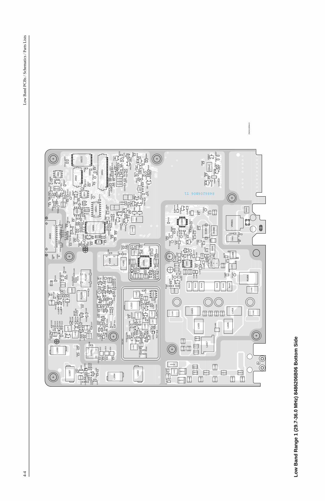
4-4
Low
Ban
d PC
Bs
/ Sch
emat
ics
/ Par
ts L
ists
C01
03
C01
11
C01
12
C01
22C
0123
C01
41
C01
51
C02
01
C0202
C02
03C
0204
C02
05
C02
24
C02
65
C02
66C
0267
C02
71
C02
72
C02
73C
0274
C02
76C
0277
C0301
C03
02
C03
03
C0304
C0305
C03
24C
0325
C0341
C03
42
C03
43
C0344
C03
51
C03
52
C03
53
C03
54
C04
02C04
03 C04
06
C0407C0408C0409C0410
C04
11C
0421
C04
22
C04
23
C0426
C0427
C0428
C0429
C04
30C
0431
C04
85
C04
91
C04
92
C04
97 C04
99
C05
41
C05
42
C05
54
C05
58
C05
59C
0560
C05
75 C05
76
C05
91
C05
92C
0593
C06
11
C06
21
C06
22
C06
41
C06
44
C06
45
C06
61
C06
62
C0663
C06
71
C10
13
C10
14
C10
16
C10
17
C10
26C
1027
C10
28
C10
29
C10
30
C10
31
C10
32 C10
33
C10
34
C10
35
C10
36
C11
02C
1104
C11
05
C11
08
C11
12
C11
13
C11
14
C11
15C
1116
C11
19
C11
20
C11
21C
1122
C11
23
C11
24C
1126
C1127
C11
28
C11
35
C11
40
C11
43
C11
44
C1146
C11
47
C11
48
C11
50C
1151
C11
52
C12
01C
1202
C12
03
C12
04
C12
05
C12
06C
1207
C12
08
C12
09C
1210
C12
11
C12
19
C12
20
C12
21
C1222
C12
23
C12
31
C12
32
C12
33C12
34
C13
13
C13
17 C13
18
C13
19C
1320
C13
21
C13
23
C13
25
C13
26C
1333
C13
34
C13
35
C13
36
C13
37
C13
38
C13
39
C13
41 C13
42
C13
43C
1354
C13
61C
1362
C14
01
C14
02
C14
13
C14
15
C14
16
C14
17C
1418
C14
37
C14
38
C14
39
C14
40
C1441
C14
42
C14
43
C14
44
C14
45
C14
46
C1447
C1448
C14
49
C1450
C14
51
C1452
C14
53
C1454
C14
55C14
56C
1457
C14
58
C14
59
C14
60
C14
61
C14
62
C14
63
C14
64
C14
65
C1466
C14
67
C14
69
C14
70
C14
71
C14
72
C14
74
C14
76
C1479
C1480
C14
81C
1486
C14
91
C15
02
C15
03
C15
04 C15
06
C15
07
C15
08
C15
09
C16
06 C16
07
C16
08
C16
09
C16
10
C16
11
C1612
C16
13
C16
14
C16
15C
1616
C16
25
C16
26
C16
27
C16
29C
1632
C16
34
CR
1201
581
4 CR
1310
CR
1314
D01
01
D01
51
D01
79
D03
01
D06
21
D06
60
D06
61
D11
01
D1401
D1402
D15
03
E0271
E0272
E06
31
E14
03
F04
01
FL1
105
432
FL1
107
12
J040
1
140
J055
1118
J055
2
L100
2
L100
4
L100
7
L100
9
L101
1
L101
2
L101
3
L101
4
L110
2
L110
5
L110
6
L110
8
L110
9
L111
0
L111
1
L120
1
L120
2
L120
5
L130
7
L130
9
L131
0
L131
1L1
313
L131
4
L131
5
L131
6
L131
7
L140
1
L140
4
L140
5
L140
8
L141
5
L141
6
L141
7
L141
9
L142
4
L142
5
L142
6
L160
5
Q01
51
Q01
71
Q01
73
Q01
83
Q02
71Q
0641
Q06
61 Q06
62Q
0663
Q10
02
Q10
03
Q1101
Q11
03Q11
04
Q11
05
Q1106
Q12
02
Q13
04
Q13
05
Q13
06
12 3Q
1401
Q14
04
Q15
03
Q15
06
Q16
02
Q1603
Q16
04
Q1605
Q1606
Q1607
Q1610
R01
07
R01
11
R01
12
R01
13
R01
17R
0121
R01
51R
0152
R01
71R
0172
R01
73
R01
74
R0175
R0176
R01
77R
0178
R01
79
R01
83R
0184
R01
85
R02
01
R02
02R
0203
R02
04
R02
05
R02
06
R02
07
R02
08
R02
54
R02
55R
0257
R02
65
R02
66R
0267
R02
68
R02
73
R02
74R
0275
R02
76
R03
23
R0324
R03
31R
0332 R
0333
R03
35
R03
41
R03
42
R03
44
R03
45R
0346
R0347
R04
01
R04
07R
0408 R
0409
R04
12
R04
42
R04
67
R04
68
R04
81R
0482
R05
11
R05
12
R05
25
R05
29
R05
30
R05
31R
0535
R05
37
R05
38
R05
39
R05
41
R05
42
R05
43
R05
91
R05
92
R05
93
R0611
R06
12
R06
21
R06
41
R06
42R
0643
R06
61
R0662
R0671R0672
R10
04R1005R1006
R10
07R
1008
R10
09R
1103
R11
04
R11
06
R11
07
R11
09
R11
11
R11
15R
1116
R11
17R
1118
R11
19
R11
20
R11
21
R11
24
R11
25
R11
26
R11
28 R11
29
R11
30
R11
32R
1133
R11
34R
1135
R11
38
R11
39
R12
01
R12
02
R1203R1212
R1213
R12
14
R12
15
R12
21
R12
22
R13
12
R13
13
R13
14
R13
15
R1316
R13
17
R13
18
R13
19
R13
20
R13
25
R13
26
R13
27
R13
28
R13
30
R13
40R
1341
R13
42
R13
43
R13
76
R14
09
R1410
R14
12
R14
14
R14
16
R14
18
R14
20
R14
22
R14
24
R14
40 R14
41
R14
42
R14
43
R14
50
R1451
R14
53
R1454
R14
55
R14
58R
1459
R14
60
R14
69
R14
70
R14
80
R15
05R
1506
R15
08
R15
09
R15
11R
1512
R15
13R
1515
R15
22
R15
23
R15
35
R15
42
R15
43R
1544
R15
45
R16
05R
1606
R16
07 R16
08
R16
09
R16
10R
1611
R16
12R
1613
R16
14R1615
R16
16
R16
17
R16
20
R16
21R
1622
R16
31
R16
32
R16
33R16
35
R16
36R
1637
S15
01
SH
1202
SH
1302
TP
0101
TP
0102
TP
0103
TP
0104
TP
0151
TP
0221
TP
0222
TP
0492
TP
0497
TP
0530
TP
0661
TP
1201
TP
1401
TP
1402
TP
1403
TP
1501
TP
1502
TP
1503
TP
1505
TP
1601
TP
1602
14 5
8U
0111
22 2187
1
U01
22
1618 9
U01
41
2815 14
1
U03
01
U03
31
1 458
U03
41
U03
42
458 U
0351
145
8 U06
52
U06
53
43
U10
01
164
3
U10
51
13725
13
U12
01
4 3U
1378
16
89U
1401
1
179
25
U15
03
VR
0151
VR
0509
VR
0537
VR
0541
VR
0601
VR
0621
VR
0671
Y12
01
234
Y12
02
1
1
1
1
1
8486206B06 T1
ZW
G01
3059
4-O
Lo
w B
and
Ran
ge
1 (2
9.7-
36.0
MH
z) 8
4862
06B
06 B
ott
om
Sid
e
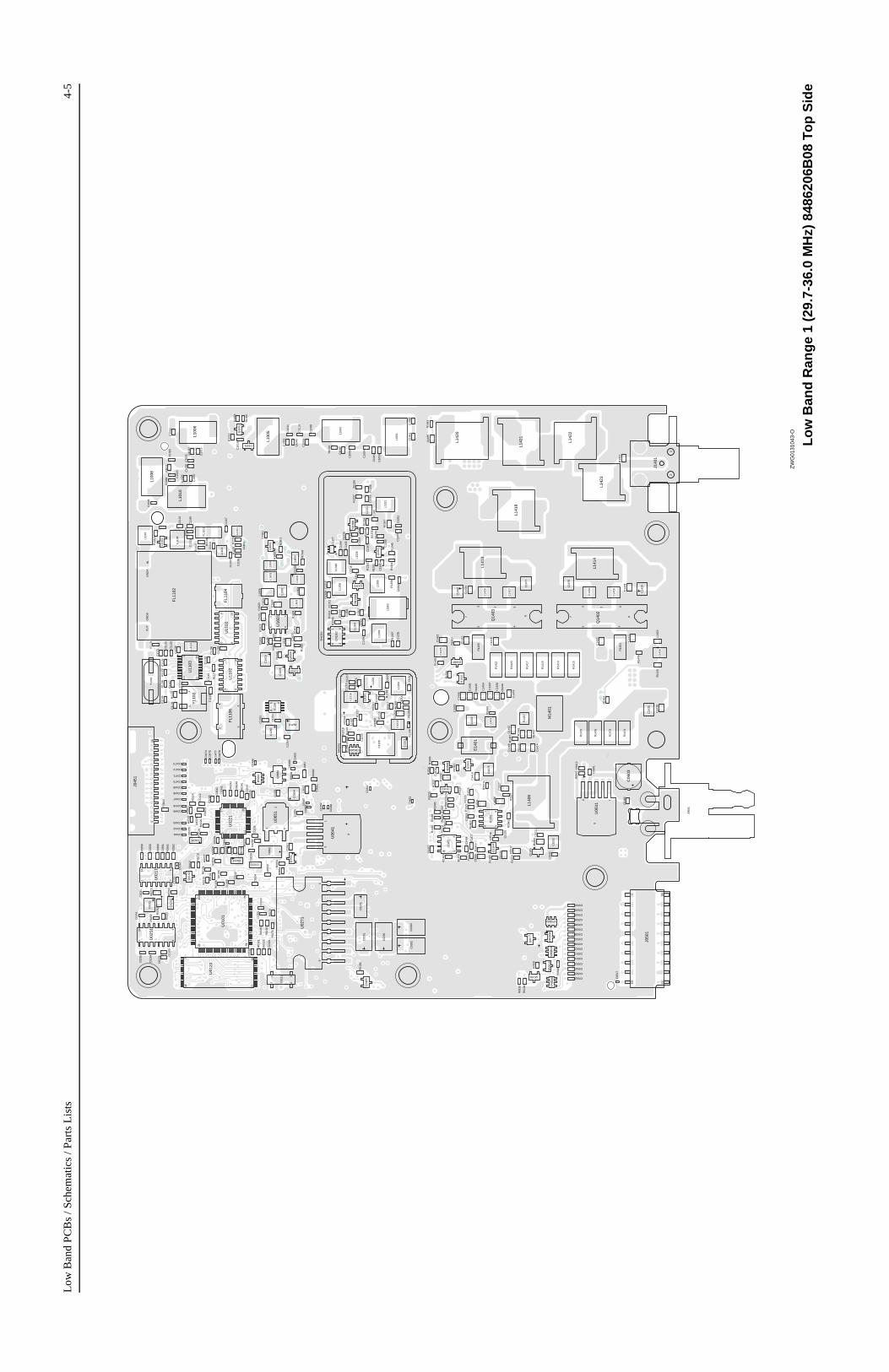
Low
Ban
d P
CB
s / S
chem
atic
s / P
arts
Lis
ts4-
5
1
1
C01
01C
0102
C01
04
C01
05
C01
06
C01
07
C01
21
C01
31
C01
32
C02
11
C02
12
C02
21C
0222
C02
23
C02
25
C02
26
C02
27
C0228
C0231
C02
32
C02
33
C02
34C
0235
C02
36
C0237
C02
41
C02
42
C02
43
C02
44C
0245
C02
46
C02
51
C02
52C
0253
C02
54
C02
55
C02
56
C02
61
C02
62
C02
75
C02
90
C02
91
C02
92C
0293
C03
31
C0441
C0442
C0443
C0445
C0446
C0447
C0448
C0449
C0470
C0471
C0472
C0473
C04
74C
0476
C04
77C
0478
C04
82
C04
83
C04
84
C04
86C
0487
C04
88
C04
90
C04
93
C04
94
C04
95
C04
96
C0501
C0502
C0503
C0504
C0505
C0506
C0508
C0509
C0510
C0511
C0512
C0513
C0514
C0515
C0516
C05
17
C0518
C06
01
C06
03
C06
12
C06
51
C06
52
C06
54C
0655
C06
81
C10
01C
1002
C10
03C10
04
C10
06
C10
07
C10
08
C10
09
C10
10
C10
11C
1012
C10
15
C10
19
C10
20
C10
21C10
22
C10
23
C10
24
C10
25
C10
37C
1038
C10
39 C10
40
C10
41
C10
42
C11
01
C11
03
C11
06
C11
07
C11
09
C11
10
C11
11
C11
25
C11
29C
1130
C11
31
C11
33
C11
34
C11
36
C11
37
C11
38
C11
39
C11
41C
1142
C11
45
C11
49
C11
53
C12
12
C12
13
C12
14
C12
15
C12
16C
1217
C12
18
C12
24
C12
25
C12
26
C12
27
C12
28
C12
29
C12
30C12
50
C12
51
C12
52
C1253
C12
54
C13
04 C13
05
C13
06C
1307
C13
08
C13
09
C13
11
C13
12
C13
14
C13
15
C13
16
C13
40
C13
44
C13
45
C13
46
C13
47
C13
48
C13
49
C13
50
C13
51
C13
52
C13
56
C13
60
C14
03
C14
04
C14
05
C14
06
C14
07
C14
08
C14
10
C14
14
C14
19
C14
20
C14
21
C14
22
C14
23 C14
24
C14
25
C14
26
C14
27
C14
28
C14
29
C14
30 C14
31
C14
32
C14
33
C14
34
C14
35
C14
36
C14
68
C14
73
C14
75
C14
77
C14
78
C14
82
C14
84
C14
85
C15
01
C15
05
C15
10 C15
11
C15
12
C15
25
C15
26
C15
27
C15
28
C15
29
C15
30
C15
31
C15
32
C16
01
C16
02
C16
03
C16
04
C16
05
C16
18
C16
19
C16
20C
1621
C16
22
C16
23 C16
24
C16
28C
1631
C16
33
CR1202
58 1
4C
R13
02
CR
1306
D02
01
D06
51
D1001
D1501
D1502
D1601
E14
01
FL1
101
ING
ND
AG
ND
BO
UT
FL1
102
FL1
104
432
FL1
106
181
J045
1
201110
J050
1
J060
1
32
J140
1
L048
1L0
482
L100
1L100
3
L100
5
L100
6
L100
8
L101
0
L110
1
L110
3
L110
4
L110
7
L111
2
L120
4
L120
6
L120
7
L130
2
L130
3L130
4
L130
5
L130
6L1
318
L132
1 L132
2
L132
4
L140
2
L140
3
L140
6
L141
3
L141
4
L141
8
L142
0
L142
1
L142
2
L142
3
L160
1
L160
2
L160
3
L160
4
L160
6
L160
7
M14
01
Q01
10
Q01
77
Q0181
Q01
85
Q06
81
Q10
01
Q11
02
Q12
01
Q1303
Q13
07
Q13
08
2
3 4
5 6
7 8
Q14
02
2
3 4
5 6
7 8
Q14
03
Q15
01
Q15
02
Q15
04
Q15
05
Q16
01
Q16
09
R01
01R01
02
R01
04
R01
05
R01
06
R01
08
R01
10
R01
14
R01
15 R01
16
R01
31
R01
32
R01
70
R01
81
R01
82
R01
86
R02
11
R02
12
R02
20
R02
21R
0222
R02
23
R02
24
R02
25
R02
26
R02
27
R02
28
R02
29
R02
41
R02
42
R02
51
R02
52
R02
53
R02
56
R02
61
R02
62
R02
69
R03
43
R04
41
R05
08
R05
10
R05
33
R06
51R
0652
R06
81
R06
82
R10
01
R10
02
R10
03
R10
10
R10
11
R11
01R
1102
R11
08
R11
10
R11
13
R11
22
R11
23
R11
27
R11
31
R11
36
R11
37
R12
04
R12
05
R12
06
R12
07
R12
08
R12
09
R12
10
R12
11
R12
16
R12
17
R12
18
R12
19
R12
20
R13
06
R13
07R
1308
R13
09R
1311
R13
31
R13
32R
1333
R13
34
R13
35
R13
36
R13
37
R13
38R13
39
R13
44R
1345
R13
46
R13
47
R14
02
R14
04
R14
05
R14
06
R14
07
R14
11
R14
13
R14
15
R14
17
R14
19
R14
21
R14
23
R14
25
R14
44
R14
45
R14
46
R14
47
R14
48R
1449
R14
57
R14
63
R14
64
R14
65R
1466
R14
67R
1468
R14
71R
1472
R14
73
R14
74
R14
75
R14
76
R14
77R
1478
R14
79
R14
81
R14
82
R14
83
R14
84
R15
01
R15
02
R15
03R
1504
R15
07
R15
10
R15
14
R15
16
R15
17R
1518
R15
19
R15
24
R15
25R
1526
R15
27R
1528
R15
32
R15
33
R15
37R
1541
R15
44
R16
01
R16
02
R16
04
R16
26
R16
27R16
28
R16
29
R16
30
R16
38
SH
1201
SH
1301
1 765126
U01
01
321716
1
U01
21
871
14
U02
11
137 25
13
U02
21
161 8
9
U02
51
9
U02
71
1
6
5
U06
11
1
6
5
U06
413
2
1
U06
51
871 14
U11
01
871 14
U11
02
11
1 20
10
U11
03
458 U
1250
43
U13
77
14 5
8
U14
02
U15
01
14 5
8
U15
02
145 8U
1601
VR0501
VR
0503
VR
0504
VR
0505
VR
0510
234
Y01
31
Y11
01
2
Y11
02
1
1
100
1
ZW
G01
3104
3-O
Lo
w B
and
Ran
ge
1 (2
9.7-
36.0
MH
z) 8
4862
06B
08 T
op
Sid
e
4-6
Low
Ban
d PC
Bs
/ Sch
emat
ics
/ Par
ts L
ists
C01
03
C01
08
C01
11
C01
12
C01
22C
0123
C01
41
C01
51
C02
01
C02
02
C02
03C
0204
C02
05
C02
24
C02
65
C02
66C
0267
C02
71C02
72
C02
73
C02
74
C02
76C
0277
C0301
C03
02
C03
03
C03
04C
0305
C03
24C
0325
C0341
C03
42
C03
43
C03
44
C03
51
C03
52
C03
53
C03
54
C04
21
C04
22
C04
23
C04
26C
0427C
0428
C04
29C
0430
C04
31
C04
85
C04
91
C04
92
C04
97
C04
99
C0541
C05
42
C05
54
C05
58
C05
59C
0560
C05
75C
0576
C05
91
C05
92C
0593
C06
11
C06
21C06
22
C06
41
C06
44
C06
45
C06
61
C06
62
C06
63
C06
71
C10
13
C10
14
C10
16
C10
17
C10
26C
1027
C10
28
C10
29
C10
30
C10
31
C10
32
C10
33
C10
34
C10
35
C10
36
C11
02C
1104
C11
05
C11
08
C11
12
C11
13
C11
14
C11
15
C11
16C
1119
C11
20
C 1
121
C11
22
C 1
123
C11
24
C11
26
C11
27
C11
28
C11
35
C11
40
C11
43
C11
44
C11
46
C11
47
C11
48
C11
50
C11
51
C11
52
C 1
201
C12
02
C12
03
C12
04
C12
05
C12
06C
1207
C12
08
C12
09C
1210
C12
11
C12
19
C12
20
C12
21
C1222
C12
23
C12
31
C12
32
C12
33
C12
34
C13
13
C13
17 C13
18
C13
19
C13
20
C13
21
C13
23C13
25
C13
26C
1333
C13
34 C13
35
C13
36
C13
37
C13
38
C13
39
C13
41
C13
42
C13
43C
1354
C13
61
C13
62
C14
01
C 1
402
C14
13
C14
15
C14
16
C14
17C
1418
C14
37
C14
38
C14
39
C14
40
C14
41
C14
42
C14
43
C14
44
C14
45
C14
46
C14
47C
1448
C14
49
C14
50
C14
51
C14
52
C14
53
C14
54
C14
55C14
56C
1457
C14
58
C14
59
C14
60
C14
61
C14
62
C14
63
C14
64
C1465
C1466 C14
67
C14
69C
1470
C14
71
C14
72
C1474
C14
76
C14
79C
1480
C14
81
C14
86
C14
91
C15
02
C15
03
C15
04
C15
06
C15
07
C15
08
C15
09
C16
06 C16
07C16
08
C16
09
C16
10
C16
11
C16
12
C16
13
C16
14
C16
15
C16
16
C16
25
C16
26
C16
27
C16
29C
1632
C16
34
CR
1201
581
4
CR
1310
CR
1314
D0101
D01
51
D01
79
D0301
D0621
D0660D0661
D1101
D14
01D
1402
D15
03
E02
71E
0272
E06
31
E14
03
F04
01
FL1
105
432
FL1
107
12
J040
1
140
J055
1
118
J055
2
L100
2
L100
4
L100
7
L100
9
L101
1
L101
2
L101
3
L101
4
L110
2
L110
5
L110
6
L110
8
L110
9
L111
0
L111
1
L120
1
L120
2
L120
5
L130
7
L130
9
L131
0
L131
1L1
313
L131
4
L131
5
L131
6
L131
7
L140
1
L140
4 L140
5
L140
8
L141
5
L141
6
L141
7
L141
9
L142
4
L142
5
L142
6
L160
5
Q01
51
Q0171
Q01
73Q
0183
Q02
71Q
0641
Q0661
Q06
62Q
0663
Q10
02
Q1003
Q1101
Q1103
Q11
04
Q11
05
Q1106
Q11
07
Q12
02
Q13
04
Q13
05
Q1306
12 3
Q14
01
Q14
04
Q15
03
Q15
06
Q16
02
Q1603
Q16
04
Q1605
Q1606
Q1607
Q1610
R01
03
R01
07 R01
11
R01
12
R01
13R
0117
R01
21
R01
51
R01
52
R01
71
R01
72R
0173
R01
74
R01
75
R01
76
R01
77R
0178
R01
79
R01
83R
0184
R01
85
R02
01R
0202
R02
03R
0204
R02
05
R02
06
R02
07
R02
08
R02
54
R02
55R
0257
R02
65
R02
66R
0267
R02
68
R02
73
R02
74R
0275
R02
76
R03
23
R03
24
R03
31
R03
32R03
33
R03
35
R03
41R
0342
R03
44
R03
45
R03
46R
0347
R04
01
R04
07R
0408
R04
09
R04
12
R04
42
R04
67 R04
68
R04
81R
0482
R05
09 R05
11
R05
12
R05
25
R05
29
R05
30
R05
31R
0535
R05
37
R05
38
R05
39
R05
41
R05
42
R05
43
R05
55
R05
56
R05
91
R05
92
R05
93
R06
11
R06
12
R06
21
R06
41
R06
42R
0643
R06
61
R06
62R
0671
R06
72
R10
04
R10
05 R10
06
R10
07
R10
08
R10
09R
1103
R11
04
R11
06
R11
07
R11
09
R11
11
R11
15
R11
16
R 1
117
R11
18
R11
19
R11
20
R11
21
R11
24
R11
25
R11
26
R11
28
R11
29
R11
30
R11
32R
1133
R11
34R
1135
R11
38
R11
39
R11
40 R11
41
R12
01
R12
02
R1203
R1212
R1213
R12
14
R1215
R12
21
R12
22
R13
12R
1313
R13
14
R13
15
R13
16
R13
17
R13
18
R13
19
R13
20
R13
25
R13
26
R13
27
R13
28
R13
30
R13
40R
1341
R13
42
R13
43
R13
76
R14
09
R14
10
R14
12
R14
14
R14
16
R14
18
R14
20
R14
22
R14
24
R14
40
R14
41
R14
42
R14
43
R14
50
R14
51
R14
53
R14
54
R14
55
R14
58
R14
59
R14
60
R14
69
R14
70
R14
80
R15
05R
1506
R15
08
R15
09
R15
11R
1512
R 1
513
R15
15
R15
22
R15
23
R15
35
R15
42
R15
43
R15
45
R16
05
R16
06
R16
07R
1608
R16
09
R16
10
R16
11
R16
12
R16
13R
1614R16
15
R16
16
R16
17
R16
20
R16
21R
1622
R16
31
R16
32
R16
33
R16
35
R16
36R
1637
S15
01
SH
1202
SH
1302
TP
0101
TP
0102
TP
0103
TP
0104
TP
0151
TP
0221
TP
0222
TP
0492
TP
0497
TP
0530
TP
0661
TP
1201
TP
1401
TP
1402 TP
1403
TP
1501
TP
1502
TP
1503
TP
1505
TP
1601
TP
1602
14 5
8
U01
11
22 2187
1
U01
22
1618 9
U01
41
2815 14
1
U03
01
U03
31
1 458
U03
41
U03
42
458 U
0351
145
8
U06
52
U0653
43
U10
01
164
3
U10
51
13725
13
U12
01
4 3U
1378
116
89
U14
01
1
179
25
U15
03
VR
0151
VR0509
VR0537
VR
0541
VR
0601
VR0621
VR
0671
Y12
01
234
Y12
02
32
1
28
1
1
48
1
ZW
G01
3104
4-O
Lo
w B
and
Ran
ge
1 (2
9.7-
36.0
MH
z) 8
4862
06B
08 B
ott
om
Sid
e

Low
Ban
d P
CB
s / S
chem
atic
s / P
arts
Lis
ts4-
7
C01
01
C01
02
C01
04
C01
05
C01
06 C01
07
C01
21
C01
31
C01
32
C02
11
C02
12
C02
21C
0222
C02
23
C02
25
C02
26C
0227
C0228
C0231
C02
32 C02
33
C02
34C
0235
C02
36
C0237
C02
41 C02
42
C02
43
C02
44
C02
45
C02
46
C02
51
C02
52
C02
53
C02
54
C02
55
C02
56
C02
61
C02
62
C02
75
C02
90
C02
91
C02
92C
0293
C03
31
C0401
C0441
C0442
C0443
C0445
C0446
C0447
C0448
C0449
C04
51
C0452C0453
C0455
C0456C0457C0458C0459C0460
C0461C0462C0463C0464
C0466C0467C0468
C0470
C0471
C0472
C0473
C04
74C
0476
C04
77C
0478
C04
82
C04
83
C04
84
C04
86C04
87
C04
88
C04
90C
0493
C04
94
C0495
C04
96
C0501C0502C0503C0504C0505C0506C0508
C0509C0510
C0511C0512
C0513C0514
C0515C0516
C05
17
C0518
C06
01
C06
03
C06
12
C06
51
C0652
C06
54C
0655
C06
81
C10
01C
1002
C10
03
C10
04
C10
06
C10
07
C10
08
C10
09C
1010
C10
11C
1012
C10
15
C10
19
C10
20
C10
21C10
22
C10
23
C10
24
C10
25
C10
37
C10
38
C10
39 C10
40
C1101
C1103
C11
06
C11
07
C11
09
C11
10
C11
11
C11
25
C11
29C
1130
C11
31
C11
33
C11
34
C11
36
C1137
C11
38
C11
39
C11
41C
1142
C11
45
C11
49
C11
53
C12
12
C1213
C12
14
C1215
C1216
C12
17
C12
18
C12
24
C12
25
C12
26C
1227
C12
28
C12
29 C12
30
C12
50
C12
51
C12
52
C1253
C12
54
C13
04 C13
05
C13
06C
1307
C13
08
C13
09C13
11
C13
12
C13
14
C13
15
C13
16
C13
40
C13
44
C13
45
C13
46
C13
47
C13
48
C13
49
C13
50
C13
51
C13
52
C1356
C13
60
C14
03
C14
04
C14
05
C14
06
C14
07
C14
08
C14
10
C14
14
C14
19
C14
20
C14
21
C14
22
C14
23C
1425
C14
26
C14
27
C14
28
C14
29
C14
30
C14
31
C14
32
C14
33
C14
34
C14
35
C14
36
C14
68C
1473
C14
75
C14
77
C14
78
C14
82
C14
84
C15
01
C15
05
C1510
C15
11
C15
12
C15
25
C1526
C15
27
C1528
C15
29
C15
30
C15
31
C16
01
C16
02
C16
03
C16
04
C16
05
C16
18
C16
19
C16
20C
1621
C16
22
C16
23
C16
24
C16
28
C1631
C16
33
CR
1202
58 1
4C
R13
02
CR
1306
D02
01
D06
51
D10
01
D1501
D15
02
D16
01
E14
01
FL1101
ING
ND
AG
ND
BO
UT
FL1
102
FL1
104
432
FL1
106
181
J045
1
201110
J050
1
J060
1
32
J140
1
L048
1L0
482
L100
1
L100
3
L100
5
L100
6
L100
8
L101
0
L1101
L110
3
L110
4
L110
7
L1112
L120
4
L120
6
L120
7
L130
2
L130
3
L130
4
L130
5
L130
6L1
318
L132
1
L132
2
L132
4
L140
2
L140
3
L140
6
L141
3
L141
4
L141
8
L142
0
L142
1
L142
2
L142
3
L1601
L160
2
L1603
L1604
L1606
L160
7
M14
01
Q01
10
Q01
77
Q01
81
Q01
85
Q06
81
Q10
01
Q11
02
Q12
01
Q1303
Q13
07
Q13
08
2
3 4
5 6
7 8
Q14
02
2
3 4
5 6
7 8
Q14
03
Q15
01
Q15
02
Q15
04
Q15
05
Q16
01
Q16
09
R01
01R01
02
R01
04
R01
05R01
06
R01
08
R01
10
R01
14
R01
15
R01
16
R01
31R
0132
R01
70
R01
81R
0182
R01
86
R02
11R
0212
R02
20
R02
21R
0222
R02
23
R02
24
R02
25
R02
26
R02
27
R02
28
R02
29
R02
41
R02
42
R02
51
R02
52
R02
53
R02
56
R02
61R
0262
R02
69
R03
43
R0441
R05
10
R05
33
R06
51
R06
52R
0681 R
0682
R10
01
R10
02
R10
03
R10
10
R10
11
R1101
R1102
R1108R1110
R11
13
R11
14R
1122
R11
23
R11
27
R11
31
R11
36
R11
37
R12
04 R12
05
R12
06
R12
07
R12
08
R12
09R
1210R
1211
R12
16
R12
17
R12
18R
1219
R12
20
R13
06
R13
07R
1308
R13
09R
1311
R13
31R
1332
R13
33
R13
34
R13
35
R13
36
R13
37
R13
38
R13
39
R13
44R
1345
R13
46
R13
47
R14
02
R14
04
R14
05
R14
06
R14
07
R14
11
R14
13
R14
15
R14
17
R14
19
R14
21
R14
23
R14
25
R14
44
R14
45
R14
46
R14
47
R14
48R
1449
R14
57
R14
63
R14
64
R14
65
R1466
R14
67
R1468R1471
R1472
R14
73
R14
74
R14
75
R14
76
R14
77R
1478
R14
79
R1482
R14
83
R14
84
R15
01
R15
02
R15
03R
1504
R1507
R15
10
R15
14
R15
16
R15
17R
1518
R15
19
R15
24
R15
25R
1526
R1527R1528
R15
32R
1533
R15
39
R15
40
R16
01R
1602
R16
04
R16
26
R16
27R
1628
R16
29
R16
30
R16
38
SH
1201
SH
1301
1 765126
U01
01
321716
1
U01
21
871
14
U02
11
137 25
13
U02
21
161 8
9
U02
51
9
U02
71
1
6
5
U06
11
1
6
5
U06
413
2
1 U06
51
871 14
U11
01
871 14
U11
02
11
1 20
10U
1103
458
U12
50
43U
1377
14 5
8U
1402
U15
01
14 5
8U
1502
145 8U
1601
VR
0501
VR
0503
VR
0504
VR
0505
VR
0510
234 Y0131
Y11
01
2 Y11
02
1
1
1
1
1
1
ZW
G01
3059
5-O
Lo
w B
and
Ran
ge
2 (3
6.0-
42.0
MH
z) 8
4862
07B
05 T
op
Sid
e
4-8
Low
Ban
d PC
Bs
/ Sch
emat
ics
/ Par
ts L
ists
C01
03
C01
11
C01
12
C01
22C
0123
C01
41
C01
51
C02
01
C02
02
C02
03C
0204
C02
05
C0224
C02
65C
0266C
0267
C02
71
C02
72
C02
73C02
74
C02
76C
0277
C0301
C03
02
C03
03
C0304
C0305
C03
24C
0325
C0341
C03
42
C03
43
C0344
C03
51
C03
52
C03
53
C03
54
C0402C0403
C0406
C0407C0408C0409C0410C0411
C0421
C04
22
C04
23
C0426
C0427
C0428
C0429
C04
30C
0431
C04
85
C04
91
C04
92
C04
97 C04
99
C0541
C05
42
C05
54
C05
58
C05
59 C05
60C
0575
C05
76
C05
91
C05
92C
0593
C06
11
C06
21
C0622
C06
41
C0644
C06
45
C06
61
C06
62
C0663
C06
71
C10
13C
1014
C10
16
C10
17
C10
26C
1027
C10
28
C10
29
C10
30
C10
31
C10
32
C10
33
C10
34 C10
35
C10
36
C11
02C
1104
C11
05
C11
08
C11
12
C11
13
C11
14
C11
15C
1116
C11
19C11
20
C11
21
C11
22C
1123
C1124
C11
26
C1127
C11
28
C11
35
C11
40
C11
43
C11
44
C1146
C11
47
C11
48
C11
50C
1151
C11
52
C12
01C
1202
C12
03
C12
04
C12
05C
1206
C12
07
C12
08
C12
09C
1210
C12
11
C12
19
C12
20
C12
21
C1222
C12
23
C12
31
C12
32
C12
33
C12
34
C13
13
C1317C1318
C13
19
C13
20
C13
21
C13
23
C13
25
C13
26C
1333
C13
34
C13
35
C13
36
C13
37
C13
38
C13
39
C1341 C13
42
C1343
C13
54
C13
61
C13
62
C14
01
C14
02
C14
09
C14
12
C14
13
C14
15
C14
16
C14
17
C14
18
C14
37
C14
38
C14
39
C14
40
C14
41
C14
42
C14
43
C14
44
C14
45
C14
46
C1447
C1448
C14
49
C1450
C14
51
C1452
C14
53
C1454
C14
55C14
56C
1457
C14
58
C14
59
C14
60
C14
61
C14
62
C14
63
C14
64
C14
65
C1466
C14
67
C1469
C14
70
C14
71
C14
72
C14
74
C14
76
C14
79
C1480
C1481
C14
85
C15
02
C15
03
C15
04
C15
06
C15
07
C15
08
C15
09
C16
06 C16
07
C16
08
C16
09C
1610
C16
11
C1612
C16
13
C16
14
C16
15C
1616
C16
25
C16
26
C16
27
C16
29C
1632
C16
34
CR
1201
581
4 CR
1310
CR
1314
D01
01
D01
51
D01
79
D03
01
D06
21
D06
60
D06
61
D1101
D14
01D
1402
D15
03
E0271
E0272
E06
31
E14
03
F04
01
FL1
105
432
FL1
107
12
J040
1
140
J055
1118
J055
2
L100
2
L100
4
L100
7
L100
9
L101
1
L101
2
L101
3
L101
4
L110
2
L110
5
L110
6
L110
8
L110
9
L111
0
L111
1
L120
1
L120
2
L120
5
L130
7
L130
9
L131
0
L131
1L1
313
L131
4
L131
5
L131
6
L131
7
L140
1
L140
4
L140
5
L141
5
L141
6
L141
7
L141
9
L142
4
L142
5
L142
6
L160
5
Q01
51
Q01
71
Q01
73
Q01
83
Q02
71Q
0641
Q06
61 Q06
62Q
0663
Q10
02
Q1003
Q1101
Q1103
Q11
04
Q11
05
Q1106
Q12
02
Q13
04
Q13
05
Q1306
12 3Q
1401
Q14
04
Q15
03
Q15
06
Q16
02Q
1603
Q16
04
Q16
05
Q16
06
Q16
07
Q16
10
R01
07
R01
11
R01
12
R01
13R
0117
R01
21 R01
51
R01
52
R01
71R
0172
R01
73
R01
74
R0175R0176
R01
77R01
78
R01
79R
0183
R01
84
R01
85
R02
01R
0202
R02
03R
0204
R02
05
R02
06
R02
07
R02
08
R02
54
R02
55R
0257
R02
65
R02
66
R02
67
R02
68
R02
73
R02
74R
0275
R02
76
R03
23
R0324
R03
31R
0332 R
0333
R03
35
R03
41
R03
42
R03
44
R03
45R
0346
R0347
R04
01
R04
07 R04
08
R04
09
R04
12
R04
42
R04
67
R04
68
R04
81R
0482
R05
11
R05
12
R05
25
R05
29
R05
30
R05
31R
0535
R05
37
R05
38
R05
39
R05
41
R05
42
R05
43
R05
91
R05
92
R05
93
R0611
R06
12
R06
21
R06
41
R06
42R
0643
R06
61
R0662
R0671R0672
R10
04R1005R1006
R10
07R
1008
R10
09R
1103
R11
04
R11
06
R11
07
R11
09
R11
11
R11
15R
1116
R11
17
R1118
R11
19
R11
20
R11
21
R11
24
R11
25
R11
26
R11
28
R11
29
R11
30
R11
32R
1133
R11
34R
1135
R11
38
R11
39
R12
01
R12
02
R1203R1212R1213
R12
14
R1215
R12
21
R12
22
R13
12
R13
13
R13
14
R13
15R13
16
R13
17
R13
18
R13
19
R13
20
R13
25
R13
26
R13
27
R13
28
R13
30
R13
40R
1341
R13
42
R13
43
R13
76
R14
09
R1410
R14
12
R14
14
R14
16
R14
18
R14
20
R14
22
R14
24
R14
40
R14
41
R14
42
R14
43
R14
50
R1451
R14
53
R1454
R14
55
R14
58
R14
59
R14
60
R14
69
R14
70
R14
80
R15
05R
1506
R15
08
R15
09R
1511
R15
12
R15
13R
1515
R15
22
R15
23
R15
35
R15
42
R15
43R
1544
R15
45
R16
05R
1606
R16
07
R16
08
R16
09
R16
10
R16
11
R16
12R
1613
R16
14R1615
R16
16
R16
17
R16
20
R16
21R
1622
R16
31
R16
32R
1633
R16
35
R16
36R
1637
S15
01
SH
1202
SH
1302
TP
0101
TP
0102
TP
0103
TP
0104
TP
0151
TP
0221
TP
0222
TP
0492
TP
0497
TP
0530
TP
0661
TP
1201
TP
1401
TP
1402
TP
1403
TP
1501
TP
1502
TP
1503
TP
1505
TP
1601
TP
1602
14 5
8U
0111
22 2187
1
U01
22
1618 9
U01
41
2815 14
1
U03
01
U03
31
1 458
U03
41
U03
42
458 U03
51
145
8 U06
52
U06
53
43U
1001
164
3
U10
51
13725
13
U12
01
4 3U
1378
116
89
U14
01
1
179
25
U15
03
VR
0151
VR
0509
VR
0537
VR
0541
VR
0601
VR
0621
VR
0671
Y12
01
234
Y12
02
1
1
8486207B05 T1
ZW
G01
3059
6-O
Lo
w B
and
Ran
ge
2 (3
6.0-
42.0
MH
z) 8
4862
07B
05 B
ott
om
Sid
e
Low
Ban
d P
CB
s / S
chem
atic
s / P
arts
Lis
ts4-
9
C01
01C
0102
C01
04
C01
05
C01
06
C01
07
C01
21 C01
31
C01
32
C02
11
C02
12
C02
21C
0222
C02
23
C02
25
C02
26
C02
27
C0228
C0231
C02
32
C02
33
C02
34C
0235
C02
36C
0237
C02
41 C02
42
C02
43
C02
44
C02
45
C02
46
C02
51
C02
52C
0253
C02
54
C02
55
C02
56
C02
61
C02
62
C02
75
C02
90
C02
91
C02
92C
0293
C03
31
C0441
C0442
C0443
C0445
C0446
C0447
C0448
C0449
C0470
C0471
C0472
C0473
C04
74C
0476
C04
77C
0478
C04
82
C04
83
C04
84
C04
86C
0487
C04
88
C04
90C
0493
C04
94
C04
95
C04
96
C0501
C0502
C0503
C0504
C0505
C0506
C0508
C0509
C0510
C0511
C0512
C0513
C0514
C0515
C0516
C05
17
C0518
C06
01
C06
03
C06
12
C06
51
C06
52
C06
54C
0655
C06
81
C10
01C
1002
C10
03
C10
04
C10
06
C10
07
C10
08C
1009
C10
10
C10
11C
1012C
1015
C10
19
C10
20
C10
21C10
22
C10
23
C10
24
C10
25
C10
37C
1038
C10
39
C10
40
C11
01
C11
03
C11
06
C11
07
C11
09
C11
10
C11
11
C11
25
C11
29C
1130
C11
31
C11
33
C11
34
C11
36
C11
37
C11
38
C11
39
C11
41C
1142
C11
45
C11
49
C11
53
C12
12
C12
13
C12
14C
1215
C12
16C
1217
C12
18
C12
24
C12
25
C12
26C
1227 C12
28
C12
29 C12
30C12
50
C12
51
C12
52
C12
53
C12
54
C13
04 C13
05
C13
06C
1307
C13
08
C13
09
C13
11
C13
12
C13
14
C13
15
C13
16
C13
40
C13
44
C13
45 C13
46
C13
47C
1348
C13
49
C13
50
C13
51
C13
52
C13
56
C13
60
C14
03
C14
04
C14
05
C14
06
C14
07
C14
08
C14
10
C14
14
C14
19
C14
20
C14
21
C14
22
C14
23
C14
24
C14
25
C14
26
C14
27
C14
28
C14
29
C14
30 C14
31
C14
32
C14
33
C14
34
C14
35
C14
36
C14
68C
1473
C14
75
C14
77
C14
78
C14
82
C14
84
C15
01
C15
05
C15
10 C15
11
C15
12
C15
25
C15
26
C15
27C
1528
C15
29
C15
30
C15
31
C15
32
C16
01
C16
02
C16
03
C16
04
C16
05
C16
18
C16
19
C16
20C
1621
C16
22
C16
23 C16
24
C16
28C
1631
C16
33
CR1202
58 1
4
CR
1302
CR
1306
D02
01
D06
51
D1001
D1501
D1502
D1601
E14
01
FL1
101
ING
ND
AG
ND
BO
UT
FL1
102
FL1
104
432
FL1
106
181
J045
1
201110
J050
1
J060
1
32
J140
1
L048
1L0
482
L100
1
L100
3
L100
5
L100
6
L100
8
L101
0
L110
1
L110
3
L110
4
L110
7
L111
2
L120
4
L120
6
L120
7
L130
2
L130
3L130
4
L130
5
L130
6
L131
8
L132
1 L132
2
L132
4
L140
2
L140
3
L140
6
L141
3
L141
4
L141
8
L142
0
L142
1
L142
2
L142
3
L160
1
L160
2
L160
3
L160
4
L1606
L160
7
M14
01
Q01
10
Q01
77
Q0181
Q01
85
Q06
81
Q10
01
Q11
02
Q12
01
Q1303
Q13
07
Q13
08
2
3 4
5 6
7 8
Q14
02
2
3 4
5 6
7 8
Q14
03
Q15
01
Q15
02
Q15
04
Q1505
Q16
01
Q16
09
R01
01R01
02
R01
04
R01
05
R01
06
R01
08
R01
10
R01
14
R01
15
R01
16
R01
31
R01
32
R01
70
R01
81
R01
82
R01
86
R02
11
R02
12
R02
20
R02
21R
0222
R02
23
R02
24
R02
25
R02
26
R02
27
R02
28
R02
29
R02
41
R02
42
R02
51
R02
52
R02
53
R02
56
R02
61
R02
62
R02
69
R03
43
R04
41
R05
08
R05
10
R05
33
R06
51R
0652
R06
81 R06
82
R10
01
R10
02
R10
03
R10
10
R10
11
R11
01R
1102
R11
08
R11
10R11
13
R11
14R
1122
R11
23
R11
27
R11
31
R11
36
R11
37
R12
04
R12
05R12
06
R12
07
R12
08R12
09
R12
10
R12
11
R12
16
R12
17
R12
18R
1219
R12
20
R13
06
R13
07R
1308
R13
09R
1311
R13
31
R13
32
R13
33
R13
34
R13
35
R13
36
R13
37
R13
38
R13
39
R13
44R
1345
R13
46
R13
47
R14
02
R14
04
R14
05
R14
06
R14
07
R14
11
R14
13
R14
15
R14
17
R14
19
R14
21
R14
23
R14
25
R14
44
R14
45
R14
46
R14
47
R14
48
R14
49
R14
57
R14
63
R14
64
R14
65R
1466
R14
67R
1468
R14
71
R14
72
R14
73
R14
74
R14
75
R14
76
R14
77R
1478R
1479
R14
82
R14
83
R14
84
R15
01
R15
02R
1503
R15
04
R15
07
R15
10R15
14
R15
16
R15
17R
1518
R15
19
R15
24
R15
25R
1526
R15
27R
1528
R15
32R
1533
R15
39
R15
40
R15
44
R16
01
R16
02
R16
04
R16
26
R16
27R16
28
R16
29
R16
30
R16
38
SH
1201
SH
1301
1 765126
U01
01
321716
1
U01
21
871
14
U02
11
137 25
13
U02
21
161 8
9
U02
51
9
U02
71
1
6
5
U06
11
1
6
5
U06
41
3
2
1
U06
51
871 14
U11
01
871 14
U11
02
11
1 20
10
U11
03
458 U12
50
43U
1377
14 5
8
U14
02
U15
01
14 5
8
U15
02
145 8U
1601
VR
0501
VR
0503
VR
0504
VR
0505
VR
0510
234
Y01
31
Y11
01
2
Y11
02
1
1
48
1
1
1
1
100
ZW
G01
3104
5-O
Lo
w B
and
Ran
ge
2 (3
6.0-
42.0
MH
z) 8
4862
07B
07 T
op
Sid
e
4-10
Low
Ban
d PC
Bs
/ Sch
emat
ics
/ Par
ts L
ists
ZW
G01
3104
6-O
C01
03
C01
08
C01
11
C01
12
C01
22C
0123
C01
41
C01
51
C02
01
C02
02
C02
03C
0204
C02
05
C02
24
C02
65
C02
66C
0267
C02
71C02
72
C02
73
C02
74
C02
76C
0277
C0301
C03
02
C03
03
C03
04C
0305
C03
24C
0325
C0341
C03
42
C03
43
C03
44
C03
51
C03
52
C03
53
C03
54
C04
21
C04
22
C04
23
C0426
C0427
C0428
C0429
C04
30C
0431
C04
85
C04
91
C04
92
C04
97
C04
99
C0541
C05
42
C05
54
C05
58
C05
59C
0560
C05
75C
0576
C05
91
C05
92C
0593
C06
11
C06
21
C06
22
C06
41
C06
44
C06
45
C06
61
C06
62
C06
63
C06
71
C10
13
C10
14
C10
16
C10
17
C10
26C
1027
C10
28
C10
29
C10
30
C10
31
C10
32
C10
33
C10
34
C10
35
C10
36
C11
02C
1104
C11
05
C11
08
C11
12
C11
13
C11
14
C11
15
C11
16C
1119
C11
20
C11
21
C11
22
C11
23C
1124
C11
26
C11
27
C11
28
C11
35
C11
40
C11
43
C11
44
C11
46
C11
47
C11
48
C11
50C
1151
C11
52
C12
01C
1202
C12
03
C12
04
C12
05
C12
06C
1207
C12
08
C12
09C
1210
C12
11
C12
19
C12
20
C12
21
C12
22
C12
23
C12
31
C12
32
C12
33
C12
34
C13
13
C13
17C13
18
C13
19 C13
20
C13
21
C13
23C13
25
C13
26C
1333
C13
34
C13
35
C13
36
C13
37
C13
38
C13
39
C13
41 C13
42
C13
43C
1354
C13
61C
1362
C14
01
C 1
402
C14
09C
1412
C14
13
C14
15
C14
16
C14
17
C14
18
C14
37
C14
38
C14
39
C14
40
C14
41
C14
42
C14
43
C14
44
C14
45
C14
46
C14
47C
1448
C14
49
C14
50
C14
51
C14
52
C14
53
C14
54
C14
55
C14
56C
1457
C14
58
C14
59
C14
60
C14
61
C14
62
C14
63
C14
64
C14
65C
1466
C14
67
C14
69C
1470
C14
71
C14
72
C14
74
C14
76
C14
79
C14
80
C14
81
C14
85
C15
02
C15
03
C15
04
C15
06
C15
07
C15
08
C15
09
C16
06
C16
07
C16
08
C16
09
C16
10
C16
11
C16
12
C16
13
C16
14
C16
15
C16
16
C16
25
C16
26
C 1
627
C16
29C
1632
C 1
634
CR
1201
581
4
CR
1310
CR
1314
D0101
D01
51
D01
79
D0301
D0621
D0660D0661
D1101
D14
01D
1402
D15
03
E02
71E
0272
E06
31
E14
03
F04
01
FL1
105
432
FL1
107
12
J040
1
140
J055
1
118
J055
2
L100
2
L100
4
L100
7
L100
9
L101
1
L101
2
L101
3
L101
4
L110
2
L110
5
L110
6
L110
8
L110
9
L111
0
L111
1
L120
1
L120
2
L120
5
L130
7
L130
9
L131
0
L131
1L1
313
L131
4
L131
5
L131
6
L131
7
L140
1
L140
4
L140
5
L141
5
L141
6
L141
7
L141
9
L142
4
L142
5
L142
6
L160
5
Q01
51
Q0171
Q01
73Q
0183
Q02
71Q
0641
Q0661
Q06
62Q
0663
Q10
02
Q1003
Q1101
Q1103
Q11
04
Q11
05
Q1106
Q11
07 Q12
02
Q13
04
Q13
05
Q1306
12 3
Q14
01
Q14
04
Q15
03
Q15
06
Q16
02
Q1603
Q16
04
Q1605
Q1606
Q1607
Q1610
R01
03
R01
07 R01
11
R01
12
R01
13R
0117
R01
21
R01
51R
0152
R01
71
R01
72R
0173
R01
74
R01
75 R01
76
R01
77R
0178
R01
79
R01
83R
0184
R01
85
R02
01R
0202
R02
03
R02
04
R02
05
R02
06
R02
07
R02
08
R02
54
R02
55R
0257
R02
65
R02
66R
0267
R02
68
R02
73
R02
74R
0275
R02
76
R03
23
R03
24
R03
31R
0332
R03
33R
0335
R03
41
R03
42
R03
44
R03
45
R03
46
R03
47
R04
01
R04
07 R04
08
R04
09R04
12
R04
42
R04
67
R04
68
R04
81R
0482
R05
09
R05
11
R05
12
R05
25
R05
29
R05
30
R05
31R
0535
R05
37
R05
38
R05
39
R05
41
R05
42
R05
43
R05
55
R05
56
R05
91
R05
92
R05
93
R06
11
R06
12
R06
21
R06
41
R06
42R
0643
R06
61
R06
62R
0671
R06
72
R10
04
R10
05
R10
06
R10
07
R10
08
R10
09
R11
03
R11
04
R11
06
R11
07
R11
09
R11
11
R11
15
R11
16
R11
17
R11
18
R11
19
R11
20
R11
21
R11
24
R11
25
R11
26
R11
28
R11
29
R11
30
R11
32R
1133
R11
34R
1135
R11
38
R11
39
R11
40
R11
41
R12
01
R12
02
R1203
R12
12
R12
13
R12
14
R12
15
R12
21
R12
22
R13
12
R 1
313
R13
14
R13
15
R13
16
R13
17
R13
18
R13
19
R13
20
R13
25
R13
26
R13
27
R13
28
R13
30
R13
40R
1341
R13
42
R13
43
R13
76
R14
09
R14
10
R14
12
R14
14
R14
16
R14
18
R14
20
R14
22
R14
24
R14
40
R14
41
R14
42
R14
43
R14
50
R14
51
R14
53
R14
54
R14
55
R 1
458
R 1
459
R14
60
R14
69
R14
70
R14
80
R15
05R
1506
R15
08R15
09
R15
11R
1512
R15
13R
1515
R15
22
R15
23
R15
35
R15
42
R15
43
R15
45
R16
05
R16
06
R16
07
R16
08
R16
09
R16
10
R16
11
R16
12
R16
13R
1614
R16
15
R16
16
R16
17
R16
20
R16
21
R16
22
R16
31
R16
32
R16
33
R16
35
R16
36R
1637
S15
01
SH
1202
TP
0101
TP
0102
TP
0103
TP
0104
TP
0151
TP
0221
TP
0222
TP
0492
TP
0497
TP
0530
TP
0661
TP
1201
TP
1401
TP
1402 TP
1403
TP
1501
TP
1502
TP
1503
TP
1505
TP
1601
TP
1602
14 5
8
U01
11
22 2187
1
U01
22
1618 9
U01
41
2815 14
1
U03
01
U03
31
1 458
U03
41
U03
42
458 U
0351
145
8
U06
52
U0653
43U
1001
164
3
U10
51
13725
13
U12
01
4 3
U13
78
116
89
U14
01
1
179
25
U15
03
VR
0151
VR0509
VR0537
VR
0541
VR
0601
VR0621
VR
0671
Y12
01
234
Y12
02 48
1
1
32
Lo
w B
and
Ran
ge
2 (3
6.0-
42.0
MH
z) 8
4862
07B
07 B
ott
om
Sid
e
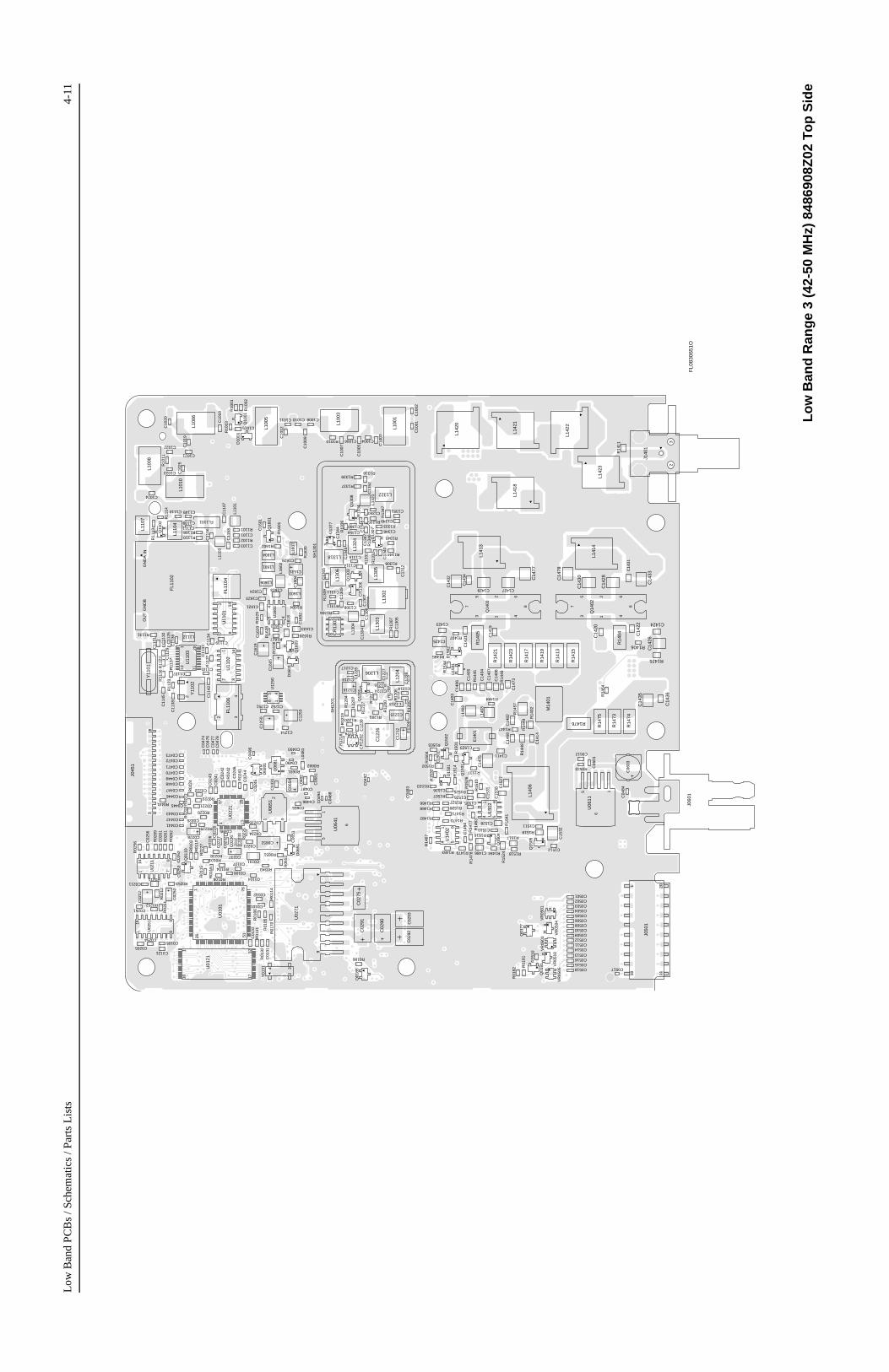
Low
Ban
d P
CB
s / S
chem
atic
s / P
arts
Lis
ts4-
11
C0101
C0102
C0104
C0105
C0106
C0107
C0121
C01
31
C01
32
C0211
C02
12
C0221
C0222
C0223
C0225
C02
26C
0227
C0228
C0231
C02
32
C02
33
C0234
C0235
C02
36
C0237
C02
41 C02
42
C02
43
C02
44
C02
45
C02
46
C0251
C02
52C
0253
C0254
C0255
C02
56
C02
61
C02
62
C02
75
C02
90
C02
91
C02
92C
0293
C03
31
C0441
C0442C0443
C0445
C0446
C0447
C0448C0449C0470C0471
C0472C0473
C04
74C
0476
C04
77C
0478
C04
82
C04
83
C04
84
C0486
C0487
C04
88
C0490
C0493
C04
94
C0495
C04
96
C0501C0502C0503C0504C0505C0506C0508
C0509C0510
C0511C0512
C0513C0514
C0515C0516
C0517C0518
C06
01
C06
03
C0612
C06
51
C0652
C06
54
C0655
C06
81
C10
01C
1002
C10
03C1004
C10
05
C1006
C10
07
C1008
C10
09
C1010C1011
C10
12
C1015
C10
18
C10
19
C10
20
C1021
C1022
C1023
C1024
C10
25
C1101
C1103
C11
06
C11
07
C1109
C1110
C1111
C11
25C
1129
C11
30
C11
31
C11
33C
1134
C11
36
C1137
C11
38
C1139
C1141
C11
42
C11
45
C1149
C11
53
C12
12
C1213
C1214
C1215
C1216
C1217
C1218
C1224
C12
25
C12
26C
1227
C12
28
C1229 C12
30
C12
50
C1251 C1252
C12
53
C1254
C13
04
C13
05C13
06C
1307
C1308
C13
09C1311
C13
12
C1314
C13
15
C1316
C13
40
C13
44
C13
45
C1346
C13
47C
1348
C1349
C1350 C1351
C13
52
C1356
C1360
C14
03
C14
04
C14
05
C14
06
C14
07
C14
08
C1410
C14
14
C14
19
C14
20
C14
21
C14
22
C1423 C1424
C1425
C14
26
C1427 C14
28
C1429 C14
30
C14
31
C14
32
C14
33
C14
34
C14
35
C14
36
C14
68
C14
73
C14
75
C14
77
C14
78
C14
82
C14
84
C1486
C15
01
C1505
C1510C1511
C1512
C1523
C1525
C1526 C15
27
C1528
C15
30
C15
31
C15
32
C16
01
C16
02
C1603 C16
04
C16
05
C16
18
C16
19C
1620
C1621
C1622
C1623
C1624
C1628
C1631
C1633
CR
1202
58 1
4C
R13
02
CR
1306
D02
01
D06
51
D10
01
D15
01D
1502
D16
01
E14
01
FL1101
ING
ND
AG
ND
BO
UT
FL1
102
FL1
104
432
FL1
106
181
J045
1
201110
1
J050
1
J060
1
32
J140
1
L048
1L0
482
L100
1
L100
3
L100
5
L100
6
L100
8
L101
0
L110
1
L110
3
L110
4
L110
7
L1112
L120
4L1206
L120
7
L130
2L1
303
L130
4
L130
5
L130
6
L1318
L132
1
L1322
L132
4
L140
2
L140
3
L140
6
L141
3
L141
4
L141
8
L142
0
L142
1
L142
2
L142
3
L1601
L160
2
L1603
L1604
L1606
L160
7
M14
01
Q01
10
Q01
77
Q01
81
Q01
85
Q06
81
Q10
01
Q11
02
Q12
01
Q13
03
Q13
07
Q13
08
213 4
5 6
7 8
Q14
02
213 4
5 6
7 8
Q14
03
Q15
01
Q15
02
Q15
04
Q15
05
Q16
01
Q16
09
R0101
R01
02
R0104
R01
05
R01
06
R0108
R01
10
R01
14
R01
15
R01
16
R01
31R
0132
R01
70
R01
81
R01
82
R0186
R0211
R02
12
R0220
R02
21R
0222
R0223
R02
24
R02
25
R02
26
R02
27
R0228
R0229
R02
41
R02
42
R02
51R0252
R0253
R02
56
R02
61R
0262
R02
69
R0343
R0441
R05
10
R0533
R0651
R06
52
R0681R0682
R10
01
R10
02
R10
03
R1010
R10
11
R1101
R1102
R1108R1110
R11
13
R11
14
R11
22
R11
23
R11
27
R1131
R11
36
R11
37
R12
04
R12
05
R12
06
R12
07
R12
08
R1209
R12
10R12
11
R1216
R12
17
R12
18R
1219 R1220
R1306
R13
07
R1308
R13
09
R1311
R13
31
R13
32
R1333
R13
34
R1335
R13
36
R1337
R1338R1339
R1344
R1345
R13
46
R13
47
R14
02
R14
04
R14
05
R1406
R1407
R14
11
R14
13
R14
15
R14
17
R14
19
R14
21
R14
23
R1425
R1444
R14
45
R14
46
R1447
R14
48R
1449
R14
57
R14
63
R14
64
R1465
R1466
R14
67
R1468R1471
R1472
R14
73
R14
74
R14
75
R1476
R14
77R
1478
R1479
R1482
R1483 R1484
R15
01
R1502
R1503
R15
04
R1507
R15
10
R15
14
R1516R1517
R1518
R1519
R15
24
R1525 R15
26
R1527R1528
R15
32
R1533
R1537
R15
41
R15
44
R16
01
R1602
R1604
R1626R1627R
1628
R16
29
R16
30
R16
38
SH
1201
SH
1301
1 765126
U01
01
321716
1
U01
21
871
14
U02
11
137 25
13
U02
21
161 8
9
U02
51
9
U02
71
1
6
5
U06
11
1
6
5
U06
413
2
1U
0651
871 14
U11
01
871 14
U11
02
11
1 20
10U
1103
41
58
U12
50
43U
1377
14 5
8U
1402
U15
01
14 5
8U
1502
145 8U
1601
VR
0501
VR
0503
VR
0504
VR
0505
VR
0510
234
Y01
31
Y11
01
2Y
1102
FL0
8306
51O
Lo
w B
and
Ran
ge
3 (4
2-50
MH
z) 8
4869
08Z
02 T
op
Sid
e
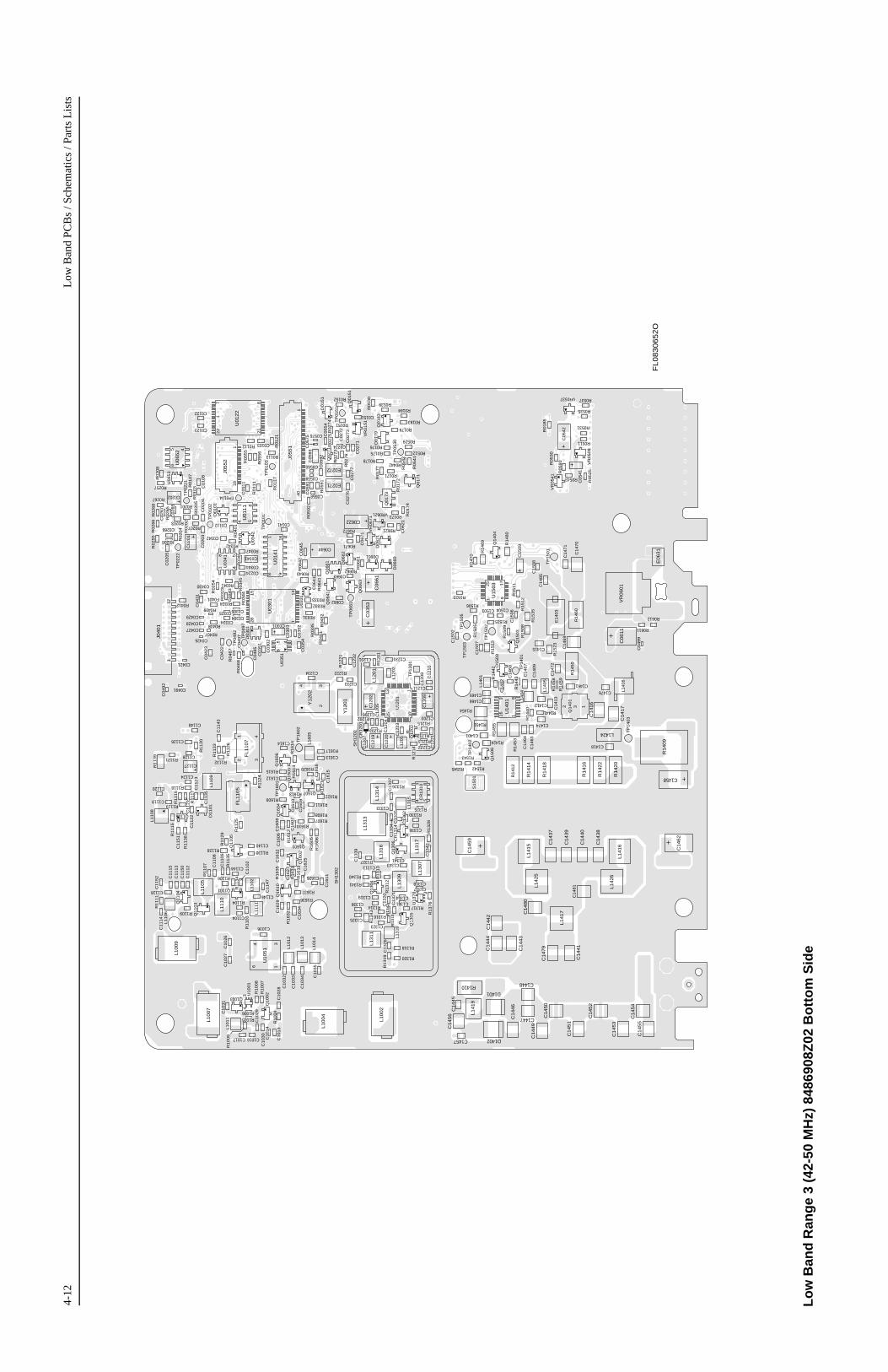
4-12
Low
Ban
d PC
Bs
/ Sch
emat
ics
/ Par
ts L
ists
C0103
C0
10
8
C0
11
1
C0112
C0122
C0123
C0141
C0151
C0
20
1
C0202
C0
20
3C
02
04
C0
20
5
C0224
C0
26
5
C0266
C0
26
7
C0
27
1C0
27
2
C0
27
3
C0274
C0
27
6C
02
77
C0301
C0
30
2
C0
30
3
C0304
C0305
C0324
C0325
C0341
C0342
C0
34
3
C0344
C0
35
1
C0
35
2
C0353
C0
35
4
C0421
C0
42
2
C0
42
3
C0426
C0427C0428C0429
C0430
C0
43
1
C0
48
5
C0491
C0
49
2
C0
49
7
C0
49
9
C0
54
1
C0
54
2
C0
55
4
C0558
C0559
C0560
C0
57
5
C0576
C0
59
1
C0
59
2
C0
59
3
C0611
C0
62
1C0622
C0
64
1
C0644
C0
64
5
C0661
C0662
C0663
C0
67
1
C1
01
3
C1
01
4
C1016C1017
C1
02
6C
10
27
C1
02
8
C1
02
9
C1
03
0
C1
03
1
C1
03
2
C1
03
3
C1
03
4 C1
03
5
C1036
C1
10
2
C1104
C1
10
5
C1
10
8
C1
11
2
C1
11
3
C1
11
4
C1
11
5
C1116
C1119
C1120
C1
12
1C
11
22
C1
12
3
C1124
C1126
C1127
C1128
C1
13
5
C1140
C1
14
3
C1144
C1146
C1
14
7
C1148
C1
15
0C
11
51
C1
15
2
C1201
C1
20
2
C1203
C1
20
4
C1
20
5
C1206
C1
20
7
C1
20
8C
12
09
C1
21
0
C1211
C1
21
9
C1
22
0
C1
22
1
C1222
C1
22
3
C1231
C1
23
2
C1233
C1234
C1313
C1317C1318
C1319
C1
32
0
C1
32
1
C1323
C1325
C1
32
6
C1333
C1
33
4C
13
35
C1336
C1
33
7
C1338
C1
33
9
C1341
C1
34
2
C1343
C1354C1361
C1
36
2
C1401
C1
40
2
C1
40
9
C1412
C1
41
3
C1415
C1416
C1417
C1418
C1437
C1438
C1439
C1440
C1441
C1442
C1443
C1444
C1445
C1446
C1447
C1448
C1449
C1450
C1451
C1452
C1453
C1454
C1455
C1456
C1457
C1458
C1459
C1
46
0
C1461
C1462
C1
46
3
C1
46
4
C1465C1466
C1
46
7
C1
46
9
C1
47
0
C1
47
1
C1
47
2
C1474
C1476
C1479
C1480
C1
48
1
C1
48
5
C1
50
2
C1503 C1504
C1
50
6
C1
50
7
C1
50
8
C1
50
9
C1
60
6
C1
60
7
C1
60
8
C1
60
9
C1
61
0
C1
61
1
C1612
C1613
C1614
C1
61
5
C1
61
6
C1
62
5
C1626
C1
62
7
C1
62
9C
16
32
C1
63
4
CR
12
01
581
4 CR
13
10
CR
13
14
D0
10
1
D0
15
1
D0
17
9
D0
30
1
D0
62
1
D0
66
0
D0661
D1
10
1
D1401
D1402
D1
50
3
E0271
E0272
E0631
E1
40
3
F0401
FL1105
432
1
F
L1107
12
1
J0401
14
0
J05511
18
J05
52
L1002
L1004
L1007
L1009
L1
01
1
L1
01
2
L1
01
3
L1
01
4
L1
10
2
L1105
L1
10
6
L1
10
8
L1
10
9
L1110
L1
11
1
L1201
L1
20
2
L1
20
5
L1307
L1309
L1
31
0
L1311
L1313
L1314
L1
31
5
L1316
L1317
L1
40
1
L1
40
4 L1
40
5
L1
40
8
L1415
L1416
L1417
L1419
L1424
L1425
L1426
L1
60
5
Q0
15
1
Q0
17
1
Q0
17
3
Q0
18
3
Q0
27
1Q
06
41
Q0
66
1 Q0
66
2
Q0
66
3
Q1
00
2
Q1003
Q1101
Q1
10
3Q1
10
4
Q1
10
5
Q1106
Q1
20
2
Q1
30
4
Q1
30
5
Q1
30
6
12 3Q
14
01
Q1
40
4
Q1
50
3
Q1
50
6
Q1
60
2
Q1603
Q1
60
4
Q1
60
5
Q1
60
6
Q1607
Q1
61
0
R0
10
3R0
10
7
R0
11
1
R0112
R0113
R0
11
7R
01
21
R0151
R0152
R0171
R0
17
2
R0173 R0
17
4
R0175R0176
R0
17
7
R0178
R0179
R0183
R0184
R0
18
5
R0201
R0
20
2R0203
R0
20
4
R0
20
5
R0206
R0207
R0
20
8
R0
25
4
R0
25
5
R0257
R0
26
5
R0
26
6
R0267
R0
26
8
R0
27
3R
02
74
R0
27
5
R0
27
6
R0
32
3
R0324
R0331
R0332R0333
R0
33
5
R0341
R0342
R0
34
4R
03
45
R0346
R0347
R0
40
1
R0407
R0408
R0409R0412
R0442
R0
46
7
R0
46
8
R0
48
1R
04
82
R0511
R0512
R0
52
5
R0529
R0
53
0
R0531
R0535
R0537
R0
53
8
R0539
R0
54
1
R0
54
2
R0543
R0
55
5
R0
55
6
R0
59
1
R0
59
2
R0
59
3
R0611
R0612
R0621
R0
64
1
R0
64
2
R0643
R0
66
1
R0662
R0671
R0672
R1
00
4
R1005R1006
R1
00
7R
10
08
R1
00
9
R1
10
3
R1104
R1106R1
10
7
R1109
R1
11
1
R1
11
5R
11
16
R1
11
7
R1118
R1119
R1
12
0
R1121
R1
12
4
R1
12
5
R1
12
6
R1128
R1
12
9
R1130
R1132
R1
13
3
R1
13
4
R1
13
5
R1
13
8
R1
13
9
R1
20
1
R1202
R1203R1212
R1213
R1
21
4
R1215
R1
22
1
R1222
R1
31
2
R1
31
3
R1314
R1
31
5R1316
R1317
R1318
R1
31
9 R1320
R1325
R1326
R1327
R1
32
8
R1330
R1340
R1341
R1
34
2
R1
34
3
R1
37
6
R1409
R1410
R1
41
2
R1414
R1416
R1418
R1420
R1422
R1424
R1
44
0 R1441
R1
44
2
R1
44
3
R1
45
0
R1451
R1
45
3
R1454
R1
45
5
R1
45
8
R1
45
9
R1
46
0
R1
46
9
R1
47
0
R1
48
0
R1
50
5
R1506
R1
50
8
R1
50
9
R1
51
1
R1
51
2
R1
51
3
R1515
R1522
R1
52
3
R1
53
5
R1542
R1543
R1545
R1
60
5R
16
06
R1607R1608
R1609
R1610
R1611
R1
61
2
R1613
R1
61
4
R1615
R1
61
6
R1617
R1620
R1
62
1
R1622
R1
63
1R
16
32
R1
63
3
R1
63
5
R1636
R1637S
15
01
SH
12
02
SH
13
02
TP
01
01
TP
01
02
TP
01
03
TP0104
TP
01
51
TP
02
21
TP
02
22
TP
04
92
TP
04
97
TP
05
30
TP
06
61
TP
12
01
TP
14
01
TP
14
02
TP
14
03
TP
15
01
TP
15
02
TP
15
03
TP
15
05
TP
16
01
TP
16
02
14 5
8U
01
11
22 21
871
U0
12
2
161
8 9U
0141
28
15 14
1
U0301
U0
33
1
1 458
U0
34
1
U0
34
2
458
U0
35
1
458 U
0652
U0
65
3
43 U
10
01
164 3
U1051
13
7
25
13
U1
20
1
4 3
U1
37
8
116
89
U1401
1
17
9
25
U1503
VR
01
51
VR
05
09
VR0537
VR
05
41
VR
0601
VR0621
VR
06
71
Y1201
234
Y1202
FL0830652O
Lo
w B
and
Ran
ge
3 (4
2-50
MH
z) 8
4869
08Z
02 B
ott
om
Sid
e

Low
Ban
d P
CB
s / S
chem
atic
s / P
arts
Lis
ts4-
13
1
1
1
1 1
1
C01
01C
0102
C01
04
C01
05
C01
06
C01
07
C01
21 C01
31
C01
32
C02
11
C02
12
C02
21
C02
22
C02
23
C02
25
C02
26
C02
27
C0228
C0231
C02
32
C 0
233
C02
34C
0235
C02
36
C0237
C02
41
C02
42
C02
43
C02
44
C02
45
C02
46
C02
51
C02
52C
0253
C02
54
C02
55
C02
56
C02
61
C02
62
C02
75
C02
90
C02
91
C02
92C
0293
C03
31
C0441
C0442
C0443
C0445
C0446
C0447
C0448
C0449
C0470
C0471
C0472
C0473
C04
74C
0476
C04
77C
0478
C04
82
C04
83
C04
84
C04
86C
0487
C04
88
C04
90 C04
93
C04
94
C04
95
C04
96
C0501
C0502
C0503
C0504
C0505
C0506
C0508
C0509
C0510
C0511
C0512
C0513
C0514
C0515
C0516
C05
17
C0518
C06
01
C06
03
C06
12
C06
51
C0652
C06
54C
0655
C06
81
C10
01C
1002
C10
03C10
04
C10
05
C10
06
C10
07
C10
08
C10
09
C10
10
C10
11C
1012
C10
15
C10
18
C10
19
C10
20
C10
21
C10
22C
1023
C10
24
C10
25
C11
01
C11
03
C11
06
C11
07
C11
09
C11
10
C11
11
C11
25
C11
29C
1130
C11
31
C11
33
C11
34
C11
36
C11
37
C11
38
C11
39
C11
41C
1142
C11
45
C11
49
C11
53
C12
12
C12
13
C12
14
C12
15
C12
16C
1217
C12
18
C12
24
C12
25
C12
26
C12
27
C12
28
C12
29 C12
30C12
50
C12
51
C12
52
C12
53
C12
54
C13
04 C13
05
C13
06
C13
07
C13
08C
1309
C13
11
C13
12
C13
14
C13
15
C13
16 C13
40
C13
44
C13
45
C13
46
C13
47
C13
48
C13
49
C13
50
C13
51
C13
52
C13
56 C13
60
C14
03
C14
04
C14
05
C14
06
C14
07
C14
08C
1410
C14
14
C14
19
C14
20
C14
21
C14
22
C14
23
C14
24
C14
25
C14
26
C14
27
C14
28
C14
29
C14
30 C14
31
C14
32
C14
33
C14
34
C14
35
C14
36
C14
68C
1473
C14
75
C14
77
C14
78
C14
82
C14
84
C14
86
C15
01
C15
05
C15
10 C15
11
C15
12
C15
23
C15
25
C15
26 C15
27C
1528
C15
30
C15
31
C15
32
C16
01
C16
02
C16
03
C16
04
C16
05
C16
18
C16
19
C16
20C
1621
C16
22
C16
23 C16
24
C16
28C
1631
C16
33
CR1202
58 1
4
CR
1302
CR
1306
D02
01
D06
51
D1001
D1501
D1502
D1601
E14
01
FL1
101
ING
ND
AG
ND
BO
UT
FL1
102
FL1
104
432
FL1
106
181
J045
1
201110
J050
1
J060
1
32
J140
1
L048
1L0
482
L100
1
L100
3
L100
5
L100
6
L100
8
L101
0
L110
1
L110
3
L110
4
L110
7
L111
2
L120
4
L120
6
L120
7
L130
2
L130
3L130
4
L130
5
L130
6
L131
8
L132
1 L132
2
L132
4
L140
2
L140
3
L140
6
L141
3
L141
4
L141
8
L142
0
L142
1
L142
2
L142
3
L160
1
L160
2
L160
3
L160
4
L1606
L160
7
M14
01
Q01
10
Q01
77Q
0181Q
0185
Q06
81
Q10
01
Q11
02
Q12
01
Q13
03
Q13
07
Q13
08
2
3 4
5 6
7 8
Q14
02
2
3 4
5 6
7 8
Q14
03
Q15
01Q15
02
Q15
04
Q1505
Q16
01
Q16
09
R01
01
R01
02
R01
04
R01
05
R01
06
R01
08
R01
10
R01
14
R01
15 R01
16
R01
31
R01
32
R01
70
R01
81
R01
82
R01
86
R02
11
R 0
212
R02
20
R02
21R
0222
R02
23R
0224
R02
25
R02
26
R02
27
R02
28
R02
29
R02
41
R02
42
R02
51
R02
52
R02
53
R02
56
R02
61
R02
62
R02
69
R03
43
R04
41
R05
08
R05
10
R05
33
R06
51R
0652
R06
81 R06
82
R10
01
R10
02
R10
03
R10
10
R10
11
R11
01R
1102
R11
08
R11
10R11
13
R11
14
R11
22
R11
23
R11
27
R11
31
R11
36
R11
37
R12
04
R12
05R12
06
R12
07
R12
08R12
09 R12
10
R12
11
R12
16
R12
17
R12
18R
1219 R
1220
R13
06
R13
07
R13
08
R13
09R
1311
R13
31
R13
32R
1333
R13
34
R13
35
R13
36
R13
37
R13
38
R13
39
R13
44R
1345
R13
46
R13
47
R14
02
R14
04
R14
05
R14
06
R14
07
R14
11
R14
13
R14
15
R14
17
R14
19
R14
21
R14
23
R14
25
R14
44
R14
45
R14
46
R14
47
R14
48R
1449
R14
57
R14
63
R14
64
R14
65R
1466
R14
67
R14
68
R14
71R
1472
R14
73
R14
74
R14
75
R14
76
R14
77R
1478
R14
79
R14
82
R14
83
R14
84
R15
01
R15
02
R15
03R
1504
R15
07
R15
10R15
14
R15
16
R15
17
R15
18
R15
19
R15
24
R15
25 R15
26
R15
27R
1528
R15
32
R15
33
R15
37
R15
41
R15
44
R16
01R
1602
R16
04R
1626
R16
27R16
28
R16
29
R16
30
R16
38
SH
1201
SH
1301
1 765126
U01
01
321716
1
U01
21
871
14
U02
11
137 25
13
U02
21
161 8
9
U02
51
9
U02
71
1
6
5
U06
11
1
6
5
U06
413
2
1
U06
51
871 14
U11
01
871 14
U11
02
11
1 20
10
U11
03
458 U
1250
43U13
77
14 5
8
U14
02
U15
01
14 5
8
U15
02
145 8
U16
01
VR0501
VR
0503
VR
0504
VR
0505
VR
0510
234
Y01
31
Y11
01
2
Y11
02
1
48
100
ZW
G01
3104
7-O
Lo
w B
and
Ran
ge
3 (4
2-50
MH
z) 8
4869
08Z
04 T
op
Sid
e
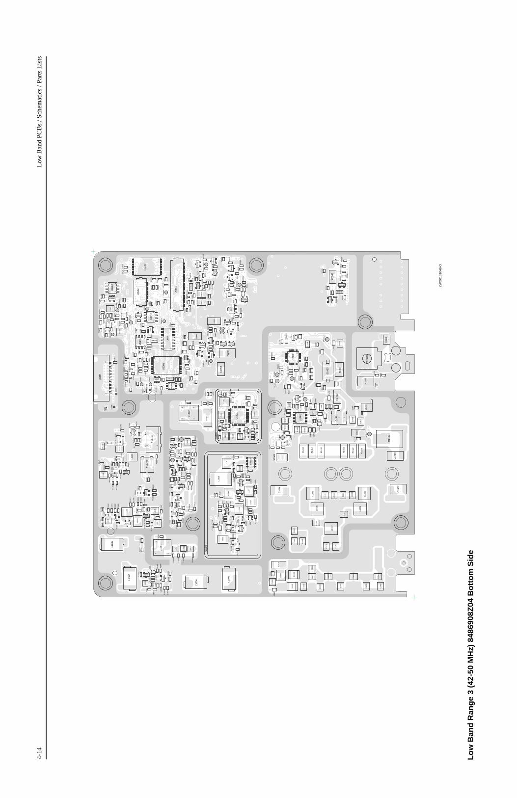
4-14
Low
Ban
d PC
Bs
/ Sch
emat
ics
/ Par
ts L
ists
C01
03
C01
08
C01
11
C01
12
C01
22C
0123
C01
41
C01
51
C02
01
C02
02
C02
03C
0204
C02
05
C02
24
C02
65
C02
66C02
67
C02
71
C02
72
C02
73
C02
74
C02
76C
0277
C0301
C03
02
C03
03
C03
04
C03
05
C03
24C
0325
C0341
C03
42
C03
43
C03
44
C03
51
C03
52
C03
53
C03
54
C04
21
C04
22
C04
23
C04
26C
0427 C
0428
C04
29C
0430
C04
31
C04
85
C04
91
C04
92
C04
97
C04
99
C0541
C05
42
C05
54
C05
58
C05
59C
0560
C05
75C
0576
C05
91
C05
92C
0593
C06
11
C06
21
C06
22
C06
41
C06
44
C06
45
C06
61
C06
62
C06
63
C06
71
C10
13
C10
14
C10
16C10
17
C10
26C
1027
C10
28
C10
29
C10
30
C10
31
C10
32
C10
33
C10
34
C10
35
C10
36
C11
02C
1104
C11
05
C11
08
C11
12
C11
13
C11
14
C11
15
C11
16C
1119
C11
20
C11
21
C11
22
C11
23C
1124
C11
26
C11
27
C11
28
C11
35
C11
40
C11
43
C11
44
C11
46
C11
47
C11
48
C11
50C
1151
C11
52
C 1
201
C12
02
C12
03
C12
04
C12
05
C12
06C
1207
C12
08
C12
09C
1210
C12
11
C12
19
C12
20
C12
21
C12
22
C12
23
C12
31
C12
32
C12
33
C12
34
C13
13
C13
17C13
18
C13
19
C13
20
C13
21
C13
23C13
25
C13
26C
1333
C13
34 C13
35
C13
36
C13
37
C13
38
C13
39
C13
41 C13
42
C13
43
C13
54
C13
61
C13
62
C14
01
C 1
402
C14
09C
1412
C14
13
C14
15
C14
16
C14
17
C14
18
C14
37
C14
38
C14
39
C14
40
C14
41
C14
42
C14
43
C14
44
C14
45
C14
46
C14
47C
1448
C14
49
C14
50
C14
51
C14
52
C14
53
C14
54
C14
55
C14
56C
1457
C14
58
C14
59
C14
60
C14
61
C14
62
C14
63
C14
64
C14
65C
1466
C14
67
C14
69C
1470
C14
71
C14
72
C14
74
C14
76
C14
79
C14
80
C14
81
C14
85
C15
02
C15
03
C15
04
C15
06
C15
07
C15
08
C15
09
C16
06
C16
07
C16
08
C16
09
C16
10
C16
11
C16
12
C16
13
C16
14
C16
15
C16
16
C16
25
C16
26
C 1
627
C16
29C
1632
C16
34
CR
1201
581
4C
R13
10
CR
1314
D0101
D01
51
D01
79
D0301
D0621
D0660D0661
D1101
D14
01D
1402
D15
03
E02
71E
0272
E06
31
E14
03
F04
01
FL1
105
432
FL1
107
12
J040
1
140
J055
1
118
J055
2
L100
2
L100
4L100
7
L100
9
L101
1
L101
2
L101
3
L101
4
L110
2
L110
5
L110
6
L110
8
L110
9
L111
0
L111
1
L120
1
L120
2
L120
5
L130
7
L130
9
L131
0
L131
1
L131
3
L131
4
L131
5
L131
6
L131
7
L140
1
L140
4
L140
5
L140
8
L141
5
L141
6
L141
7
L141
9
L142
4
L142
5
L142
6
L160
5
Q01
51
Q0171
Q01
73Q
0183
Q02
71Q
0641
Q0661
Q06
62Q
0663
Q10
02
Q1003
Q1101
Q1103
Q11
04
Q11
05
Q1106
Q11
07
Q12
02
Q13
04
Q13
05
Q1306
12 3
Q14
01
Q14
04
Q15
03
Q15
06
Q16
02
Q1603
Q16
04
Q1605
Q1606
Q1607
Q1610
R01
03
R01
07
R01
11
R01
12
R01
13R
0117
R01
21
R01
51R
0152
R01
71
R01
72R
0173
R01
74
R01
75 R01
76
R01
77R
0178
R01
79R
0183
R01
84
R01
85
R02
01R
0202
R02
03
R02
04
R02
05
R02
06
R02
07
R02
08
R02
54
R02
55R
0257
R02
65
R02
66R
0267
R02
68
R02
73
R02
74R
0275
R02
76
R03
23
R03
24
R03
31R
0332
R03
33R
0335
R03
41R
0342
R03
44R
0345
R03
46
R03
47
R04
01
R04
07 R04
08
R04
09
R04
12
R04
42
R04
67
R04
68
R04
81R
0482
R05
09 R05
11
R05
12
R05
25
R05
29
R05
30
R05
31R
0535
R05
37
R05
38
R05
39
R05
41
R05
42
R05
43
R05
55
R05
56
R05
91
R05
92
R05
93
R06
11
R06
12
R06
21
R06
41
R06
42R
0643
R06
61R
0662
R06
71R
0672
R10
04
R10
05 R10
06
R10
07
R10
08
R10
09R
1103
R11
04
R11
06
R11
07
R11
09
R11
11
R11
15
R11
16
R11
17
R11
18
R11
19
R11
20
R11
21
R11
24
R11
25
R11
26
R11
28
R11
29
R11
30
R11
32R
1133
R11
34R
1135
R11
38
R11
39
R11
40
R11
41
R12
01
R12
02
R1203
R12
12
R12
13
R12
14
R12
15
R12
21
R12
22
R13
12
R13
13
R13
14
R13
15
R13
16
R13
17
R13
18
R13
19
R13
20
R13
25
R13
26
R13
27
R13
28
R13
30
R13
40R
1341
R13
42
R13
43
R13
76
R14
09
R14
10
R14
12
R14
14
R14
16
R14
18
R14
20
R14
22
R14
24
R14
40
R14
41
R14
42
R14
43
R14
50
R14
51
R14
53
R14
54
R14
55
R 1
458
R 1
459
R14
60
R14
69
R14
70
R14
80
R15
05R
1506
R15
08
R15
09
R15
11R
1512
R15
13R
1515
R15
22
R15
23
R15
35
R15
42
R15
43
R15
45
R16
05
R16
06
R16
07R
1608
R16
09
R16
10
R16
11
R16
12
R16
13R
1614
R16
15
R16
16
R16
17
R16
20
R16
21
R16
22
R16
31
R16
32
R16
33
R16
35
R16
36R
1637
S15
01
SH
1202
SH
1302
TP
0101TP
0102
TP
0103
TP
0104
TP
0151
TP
0221
TP
0222
TP
0492
TP
0497
TP
0530
TP
0661
TP
1201 TP
1401
TP
1402
TP
1403
TP
1501
TP
1502
TP
1503
TP
1505
TP
1601
TP
1602
14 5
8U
0111
22 2187
1
U01
22
1618 9
U01
41
2815 14
1
U03
01
U03
31
1 458
U03
41
U03
42
458 U
0351
145
8
U06
52
U0653
43U
1001
164
3
U10
51
13725
13
U12
01
4 3
U13
78
116
89
U14
01
1
179
25
U15
03
VR
0151
VR0509
VR0537
VR
0541
VR
0601
VR0621
VR
0671
Y12
01
234
Y12
02
1
1
1
1
32
ZW
G01
3104
8-O
Lo
w B
and
Ran
ge
3 (4
2-50
MH
z) 8
4869
08Z
04 B
ott
om
Sid
e
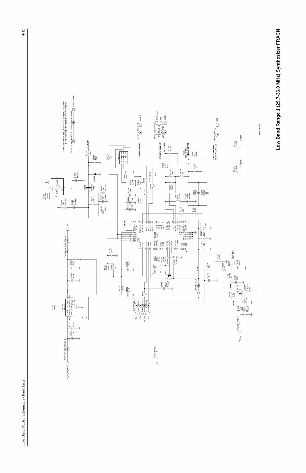
Low
Ban
d P
CB
s / S
chem
atic
s / P
arts
Lis
ts4-
15
Com
men
t: T
he N
OIS
E_B
LNK
R li
ne is
req
uire
d be
caus
e it
is r
oute
d th
roug
h th
e F
racN
from
the
Con
trol
ler.
2.2V
DC
1.5V
DC
7.6V
DC
-5 t
o 0
dB
m
8.7V
DC
13.1
VD
C
2 -
3 V
DC
2.9V
DC
, 0.4
6Vp
p
0VD
C (
R),
4.7
VD
C (
T)
2.5
- 11
VD
C
2.5
- 11
VD
C
4.9V
DC
(L
OC
KE
D)
0VD
C (
UN
LO
CK
ED
)
FN
0:N
P
C12
32
.039
uFF
N0:
NP
820K
R12
07
21
.01u
FC
1254
.033
uF
16.8
MH
zX
TA
L
Y12
01
C12
14
R12
19
47
1uF
9V3
9V3_
FR
AC
N_1
CLK
_FR
AC
N_1
FN
0:N
P
C12
26
LOC
K_F
RA
CN
_1
C12
23
FN
0:N
P
1pF
C12
05
5V_F
RA
CN
_2
.01u
F
R12
0851
L120
72.
2uH
1.6K
R12
14
LOC
K
FN
0:N
P
VM
ULT
312
VM
ULT
411
13 VRO
WA
RP
25
XT
AL1
23
XT
AL2
24
SF
IN30
SF
OU
T28
TE
ST
137
TE
ST
238
VB
PA
SS
21
VCP47 VM
ULT
115
VM
ULT
214
5 PD_VDD
PR
EIN
32
PRE_GND 33
PRE_VDD34
PV
RE
F35
RE
FS
EL
18
SF
BA
SE
27S
FC
AP
26
IOU
T43 4
LOC
K
MO
DIN
10
MO
DO
UT
41
NC
117
NC
229
NC
331
PD_GND 44
42
CE
X9
CLK
8
DA
TA
7
DGND 6
DVDD36
FR
EF
OU
T19
IAD
AP
T45
IND
MU
LT16
AU
X1
48
AU
X2
1
AU
X3
2
AU
X4
3
AVDD20
BIA
S1
40
BIA
S2
39
CC
OM
P
U12
0163
A27
AD
AP
TS
W46
AGND 22
2.2u
H
L120
2
FN
0:N
P27
uHL1
204
K1
K2
K3
C12
31.0
1uF
CR
1202
A1
A2
A3
680
R12
1310
0
R12
12
C12
11
.01u
F
220p
F
IN_5
V_R
F_R
EG
IN_5
V_R
F_R
EG
_FR
AC
N_1
C12
04
C12
17
.01u
F
PR
E_I
N
4.7u
F
C12
16
FN
0:N
P
SH
1201
SH
IELD
MO
DIN
R12
04
0
SH
1202
SH
IELD
16_8
MH
Z_F
RA
CN
_1
5V_F
RA
CN
_1
CLK
FN
0:N
P
1pF
C12
21
FN
0:N
P
16_8
MH
Z
C12
0910
uF
.01u
FC
1225
C12
010.
1uF
R12
1022
0
R12
0568
0
L120
1
C12
180.
1uF
1uF
27uH
C12
12
.01u
F
C12
30.0
1uF
C12
29
R12
18
47
CR
1201
TR
B_F
RA
CN
_1
0
R12
01
5V
680n
HL1
205
100
R12
17
TP
1201
TE
ST
_PO
INT
Q12
01
VC
TR
L_F
RA
CN
_1
CS
X
100p
FC
1224
C12
10
0.1u
F
C12
0662
pF
.01u
FC
1227
4.7u
F
4.7u
FC
1253
C12
19
PR
E_I
N_F
RA
CN
_1
C12
51
0.1u
FN
OIS
E_B
LNK
R_F
RA
CN
_2N
OIS
E_B
LNK
R
BW
SE
LEC
T_F
RA
CN
_1
NO
ISE
_BLN
KR
_FR
AC
N_1
Q12
02
4.7u
FC
1220
R12
06
470
51R12
16
R12
03
150K
27pF
C12
22
0
R12
21
DA
TA
.01u
F
C12
2820
0pF
C12
03
VS
F_F
RA
CN
_1
FN
0:N
P
MO
DIN
_FR
AC
N_1
R12
20
47
2.2u
F
C12
50
C12
1568
00pF
16.8
MH
z
GN
D2
OU
T3
4
VC
C
1V
CN
TL
L120
6
VC
TR
L
FN
0:N
PT
TS
05V
Y12
02
R12
02
FN
0:N
P
27uH
1O
UT
PU
T
2S
EN
SE
3S
HU
TD
OW
N
1.2K
U12
50LP
2951
65V
_TA
P
5E
RR
OR
7F
EE
DB
AC
K
GN
D 4
8IN
PU
T.018
uFC
1252
CS
X_F
RA
CN
_1
C12
024.
7uF
470K
BW
SE
LEC
TR
1211
68R12
15
TR
B
C12
0815
00pF
FN
0:N
P
R12
2210
0
C12
340.
1uF
FN
0:N
P
C12
33.0
1uF
FN
0:N
P
DA
TA
_FR
AC
N_1
3.3K
R12
09
VS
F
1.5p
FC
1207
C12
130.
22uF
FL0
8306
85O
Lo
w B
and
Ran
ge
1 (2
9.7-
36.0
MH
z) S
ynth
esiz
er F
RA
CN
4-16
Low
Ban
d PC
Bs
/ Sch
emat
ics
/ Par
ts L
ists
8.7V
DC
2.2V
DC
7.6V
DC
1.5V
DC
-5 to
0 d
Bm
4.9V
DC
(LO
CK
ED
)0V
DC
(U
NLO
CK
ED
)
2.5
- 11
VD
C
2.5
- 11
VD
C
0VD
C (
R),
4.7
VD
C (
T)
2.9V
DC
, 0.4
6Vpp
13.1
VD
C
2 -
3 V
DC
CO
MM
EN
T: T
HE
NO
ISE
_BLN
KR
LIN
E IS
RE
QU
IRE
D B
EC
AU
SE
IT
IS R
OU
TE
D T
HR
OU
GH
TH
E F
racN
FR
OM
TH
E C
ON
TR
OLL
ER
.
4.7u
FC
1202
BW
SE
LEC
T
TR
B
470K
R12
11
R12
1568
FN
0:N
P2
GN
D
3O
UT
4
VC
C
1V
CN
TL
FN
0:N
P
16.8
MH
zT
TS
05V
Y12
02
C12
08
100
R12
22
DA
TA
_FR
AC
N_1
1500
pF
R12
093.
3K
1.5p
F
VS
F
C12
07
R12
06
0.22
uFC
1213
470
R12
1651
150K
R12
03
DA
TA
C12
2224
pF
R12
21
0
.01u
FC
1203
VS
F_F
RA
CN
_1
200p
FC
1228
FN
0:N
P
MO
DIN
_FR
AC
N_1
47
R12
20
2.2u
F
C12
15
C12
50
FN
0:N
P
6800
pF
FN
0: N
P0.
1uF
C12
34
VC
TR
L
.01u
FC
1233
1.2K
L120
627
uH
SE
NS
E2
SH
UT
DO
WN
3
FN
0:N
P
R12
02
5V_T
AP
6
ER
RO
R5
FE
ED
BA
CK
7
4GND
INP
UT
8O
UT
PU
T1
C12
52.0
18uF
LP29
51U
1250
CS
X_F
RA
CN
_1
L120
556
0nH
5V
MM
BT
3906
Q12
01
R12
17
100
TE
ST
_PO
INT
TP
1201
VC
TR
L_F
RA
CN
_1
CS
X
C12
2482
pF
0.1u
F
C12
10
62pF
C12
06
C12
27.0
1uF
C12
19
4.7u
F
4.7u
F
PR
E_I
N_F
RA
CN
_1
C12
530.
1uF
C12
51
NO
ISE
_BLN
KR
_FR
AC
N_2
NO
ISE
_BLN
KR
BW
SE
LEC
T_F
RA
CN
_1
NO
ISE
_BLN
KR
_FR
AC
N_1
Q12
02
MM
BR
951
PR
E_I
N
C12
204.
7uF
.01u
FC
1217
FN
0:N
P
C12
164.
7uF
R12
04
SH
IELD
SH
1201
16_8
MH
Z_F
RA
CN
_1
MO
DIN
0
SH
IELD
SH
1202
FN
0:N
P
16_8
MH
Z
5V_F
RA
CN
_1
CLK
FN
0:N
P
C12
211p
F
10uF
C12
09
C12
25.0
1uF
0.1u
FC
1201
220
R12
10
680
R12
05
0.1u
FC
1218
27uH
C12
12
L120
1
.01u
F
1uF
.01u
FC
1230
47
R12
18
C12
29
TR
B_F
RA
CN
_1
CR
1201
R12
01
0
.039
uFC
1232
FN
0: N
P
R12
0782
0K
FN
0:N
P
1
C12
54.0
1uF
Y12
01
XT
AL
16.8
MH
z
2
.033
uFC
1214
9V3_
FR
AC
N_1
47
R12
19
C12
26
FN
0:N
OT
PLA
CE
D
9V3
CLK
_FR
AC
N_1
1uF
FN
0:N
P
LOC
K_F
RA
CN
_1
C12
051p
F
5V_F
RA
CN
_2
C12
23
.01u
F
R12
08
L120
7
FN
0:N
P
51
1.6K
LOC
K
2.2u
H
VM
ULT
311
VM
ULT
4
VRO13
25W
AR
P
23X
TA
L124
XT
AL2
R12
14
SF
IN
28S
FO
UT
37T
ES
T1
38T
ES
T2
21V
BP
AS
S
47 VCP
15V
MU
LT1
14V
MU
LT2
12
5
32P
RE
IN
33PRE_GND
34 PRE_VDD
35P
VR
EF
18R
EF
SE
L
27S
FB
AS
E
26S
FC
AP
30
IOU
T
LOC
K4
10M
OD
IN
41M
OD
OU
T
17N
C1
29N
C2
31N
C3
44PD_GND
PD_VDD
CE
X
8C
LK
7D
AT
A
6DGND
36 DVDD
19F
RE
FO
UT
45IA
DA
PT
16IN
DM
ULT
43
AU
X1
1A
UX
22
AU
X3
3A
UX
4
20 AVDD
40B
IAS
139
BIA
S2
42C
CO
MP
9
63A
27U
1201
46A
DA
PT
SW
22AGND
48
L120
2
2.2u
H
L120
427
uHF
N0:
NP
K2
K3
.01u
FC
1231
CR
1202
A1
A2
A3
K1
R12
1368
0
R12
1210
0
C12
11
C12
04
.01u
F
IN_5
V_R
F_R
EG
IN_5
V_R
F_R
EG
_FR
AC
N_1
220p
F
FL0
8306
08O
Lo
w B
and
Ran
ge
2 (3
6.0-
42.0
MH
z) S
ynth
esiz
er F
RA
CN
Low
Ban
d P
CB
s / S
chem
atic
s / P
arts
Lis
ts4-
17
Com
men
t: T
he N
OIS
E_B
LNK
R li
ne is
req
uire
d be
caus
e it
is r
oute
d th
roug
h th
e F
racN
from
the
Con
trol
ler.
-5 t
o 0
dB
m
8.7V
DC
7.6V
DC
1.5V
DC
2.2V
DC
13.1
VD
C
2-3
VD
C
2.5
- 11
VD
C
0VD
C (
R),
4.7
VD
C (
T)
2.5
- 11
VD
C
4.9V
DC
(L
OC
KE
D)
0VD
C (
UN
LO
CK
ED
)
4.9V
DC
2.9V
DC
, 0.4
6Vp
p
C12
11
.01u
F
C12
04
220p
F
IN_5
V_R
F_R
EG
IN_5
V_R
F_R
EG
_FR
AC
N_1
FN
0:N
P
16_8
MH
Z
5V_F
RA
CN
_1
1pF
C12
21
FN
0:N
P
C12
0910
uF
OU
TP
UT
2S
EN
SE
3S
HU
TD
OW
N
1500
pF
C12
08
U12
50LP
2951
65V
_TA
P
5E
RR
OR
7F
EE
DB
AC
K GND 4
8IN
PU
T1
680
R12
13
CS
X_F
RA
CN
_1
L120
5
5V
100
FN
0:N
P
330n
H
0.1u
FF
N0:
NP
R12
22
.01u
FF
N0:
NP
C12
34
16.8
MH
z
FN
0:N
PG
ND
VC
C
VC
NT
L
2
OU
T3
4
1
C12
33
TT
S05
V
Y12
02
100
R12
17
TP
1201
Q12
01
16.8
MH
zX
TA
L
Y12
01
21
C12
14.0
33uF
R12
19
47
9V3
9V3_
FR
AC
N_1
CLK
_FR
AC
N_1
FN
0:N
P
C12
261u
F
82pF
C12
24
CS
X
VC
TR
L_F
RA
CN
_1
C12
10
0.1u
F
C12
02
4.7u
F
BW
SE
LEC
TR
1211
470K
68R12
15
TR
B
5V_F
RA
CN
_2
R12
0851
FN
0:N
P
L120
72.
2uH
1.6KR12
14
LOC
K
VM
ULT
115
VM
ULT
214
VM
ULT
312
VM
ULT
411
13 VRO
WA
RP
25
XT
AL1
23
XT
AL2
24
SF
BA
SE
27S
FC
AP
26
SF
IN30
SF
OU
T28
TE
ST
137
TE
ST
238
VB
PA
SS
21
VCP47
NC
331
PD_GND 44
5 PD_VDD
PR
EIN
32
PRE_GND33
PRE_VDD34
PV
RE
F35
RE
FS
EL
18IA
DA
PT
45
IND
MU
LT16
IOU
T43 4
LOC
K
MO
DIN
10
MO
DO
UT
41
NC
117
NC
229
BIA
S2
39
CC
OM
P42
CE
X9
CLK
8
DA
TA
7
DGND 6
DVDD36
FR
EF
OU
T19
AD
AP
TS
W46
AGND22
AU
X1
48
AU
X2
1
AU
X3
2
AU
X4
3
AVDD20
BIA
S1
40
U12
0163
A27
L120
4
2.2u
H
L120
2
FN
0:N
P27
uH
A2
A3
K1
K2
K3
C12
31.0
1uF
CR
1202
A1
FN
0:N
P
SH
1201
SH
IELD
MO
DIN
R12
04
0
SH
1202
SH
IELD
16_8
MH
Z_F
RA
CN
_1
MO
DIN
_FR
AC
N_1
CLK
FN
0:N
P
.01u
FC
1225
C12
010.
1uF
R12
1022
0
680
R12
05
R12
12
.018
uFC
1252
L120
6
VC
TR
L
100
FN
0:N
P
27uH
1.2K
R12
02
.01u
F
C12
30.0
1uF
C12
29
TR
B_F
RA
CN
_1
R12
18
47
CR
1201
0
R12
01
FN
0:N
P
C12
32.0
39uF
FN
0:N
P
820K
R12
07
.01u
FC
1254
0
R12
21
DA
TA
C12
03.0
1uF
C12
2820
0pF
VS
F_F
RA
CN
_1
FN
0:N
P
0.1u
F
PR
E_I
N_F
RA
CN
_1
62pF
C12
51
C12
27
C12
06
.01u
F
C12
194.
7uF
4.7u
FC
1253
LOC
K_F
RA
CN
_1
C12
23
FN
0:N
P1p
FC
1205
NO
ISE
_BLN
KR
_FR
AC
N_2
NO
ISE
_BLN
KR
.01u
F
NO
ISE
_BLN
KR
_FR
AC
N_1
Q12
02
BW
SE
LEC
T_F
RA
CN
_14.
7uF
C12
20
.01u
F
PR
E_I
N
C12
16C
1217
R12
20
47
4.7u
F
C12
50
6800
pF
2.2u
F
C12
15
L120
1
C12
180.
1uF
1uF
27uH
C12
12
DA
TA
_FR
AC
N_1
C12
07
3.3K
R12
09
VS
F
1.5p
F
C12
130.
22uF
R12
06
470
51R12
16
R12
03
150K
36pF
C12
22
FL0
8306
93O
Lo
w B
and
Ran
ge
3 (4
2-50
MH
z) S
ynth
esiz
er F
RA
CN

4-18
Low
Ban
d PC
Bs
/ Sch
emat
ics
/ Par
ts L
ists
2.5
- 11
VD
C
8.2V
DC
(R
) -2.2
VD
C (
R)
2.4V
DC
(R
)
0VD
C (
R)
4.7V
DC
(T
)
8.5V
DC
(R
)0V
DC
(T
)
+14
dB
m (
R)
4.8V
DC
(R
)
0.5V
DC
(R
)
0.7V
DC
(R
)
3.4V
DC
(R
)
-1.9
VD
C (
T)
2.4V
DC
(T
)
4.3V
DC
(T
)3.
5VD
C (
T) 0.7V
DC
(T
)
3.7V
DC
(T
)4VD
C (
R)
8.2V
DC
(T
)
0.5V
DC
(T
)
+3 d
Bm
(T
)
C13
18
.01u
F
.01u
F
C13
12 C13
13
2
4
1 3
.01u
F
U13
77
R13
26
C13
4156
pF
C13
33
56
10K
56pF
R13
11
1.2K
R13
13
23
1
Q13
05
4.7p
FC
R13
14
L131
633
uH
C13
35
L132
233
uH
D S
PR
E_I
N
TX
INJ_
VC
O_1
Q13
06
PR
E_I
N_V
CO
_1
R13
41
100
.01u
FC
1339
RX
INJ
TR
B_V
CO
_1
6
48
C13
51.0
1uF
CR
1302
15
273
22R13
36
.01u
FC
1347
Q13
08
C13
4256
pF
C13
56C
1360
FN
0:N
P3.
9pF
FN
0:N
P3.
9pF
L130
2
FN
0:N
P3.
9pF
C13
61
L131
3
491n
HR
XIN
J_V
CO
_1
491n
H
R13
3582
0
R13
07
56
L130
3
27uH
C13
16
3.3p
F
C13
15
.01u
FC
1311
51pF
C13
37.0
1uF
FN
0:N
P
C13
1451
pF
36
48
.01u
FC
1305
CR
1310
15
27
L130
727
uH
L131
733
uH
9V3_
VC
O_1
L130
627
uH
FN
0:N
P
C13
624.
7pF
VC
TR
L_V
CO
_1
C13
2313
pF
C13
360.
1uF
Q13
07
C13
20
.01u
F
R13
2847
0
C13
0616
pF
L131
0
390n
H
47pF
R13
46
100
100
C13
07
C13
04
R13
42
FN
0:N
P
.01u
F
C13
44.0
1uF
10
R13
19
R13
4315
0V
CT
RL
9V3
470
R13
18
FN
0:N
P3.
9pF
C13
54
C13
450.
1uF
C13
38.0
1uF
SH
1301
SH
IELD
FN
0:N
P
L131
1
SH
1302
SH
IELD
27uH
100
R13
45
D S
R13
27
56
Q13
03
R13
0947
0
470
R13
20F
N0:
NP
4.7p
FC
1309
C13
46.0
1uF
.01u
FC
1319
R13
1433
0
VS
F_V
CO
_1
Q13
04
3.3K
R13
34
C13
3456
pF
U13
78
2
4
1 3
L130
527
uH
R13
401K
56
R13
08
R13
121.
2K
C13
084.
7pF
.01u
F
C13
40
TR
B
3.9p
FC
1348
1.2K
R13
31
R13
06 0R
1315
3.3K
TX
INJ
22
75
R13
17
75R
1339
3.9p
F
R13
37
680
C13
21
820n
H
R13
16
150
L130
4
L131
4
33uH
R13
47
10K
R13
30
1KR13
44
120
R13
38
.01u
F
C13
5015
pF
C13
52
270n
H
CR
1306
23
1
L132
1L1
324
33uH
1.2u
HL1
315
R13
321.
2K
VS
F
L131
8
33uH
4.7K
4.7K
4.7K
47K
47K 10
K
47K
47K 10
K
C13
43
R13
76
R13
33
3.3p
F
0.1u
FC
1317
330
C13
49
R13
25
0.1u
F
FN
0:N
P
0
.01u
FC
1325
L130
927
uH
C13
26
.01u
F
TX
_8.5
V
TX
_8.5
V
FL0
8306
86O
Lo
w B
and
Ran
ge
1 (2
9.7-
36.0
MH
z) V
olt
age
Co
ntr
olle
d O
scill
ato
r
Low
Ban
d P
CB
s / S
chem
atic
s / P
arts
Lis
ts4-
19
+14
dB
m (
R)
8.5V
DC
(R
)0V
DC
(T
)
8.2V
DC
(T
)
-2.4
VD
C (
T)
2.4V
DC
(T
)
4.3V
DC
(T
)3.
5VD
C (
T)
3.7V
DC
(T
)
0.7V
DC
(T
)
+3d
Bm
(T
)
0.5V
DC
(T
)
2.5
- 11
VD
C
8.2V
DC
(R
)
2.3V
DC
(R
)
-2.3
VD
C (
R)
0VD
C (
R)
4.7V
DC
(T
)
3.4V
DC
(R
)
4VD
C (
R)
4.8V
DC
(R
)
0.5V
DC
(R
)
0.7V
DC
(R
)
SH
IELD
SH
1302
SH
IELD
SH
1301
L131
127
uH
R13
45
100
56R13
27
D S
R13
09
Q13
03
R13
2047
0
470
4.7p
FF
N0:
NP
L131
7
C13
09
L130
6
33uH
9V3_
VC
O_1
27uH
4.7p
FC
1362
FN
0:N
P
13pF
C13
23
C13
36
VC
TR
L_V
CO
_1
Q13
07
0.1u
F
.01u
F
C13
20
470
R13
28
16pF
C13
06
390n
H
L131
0
100
R13
46
C13
483.
9pF
R13
311.
2K
0
R13
06
R13
15
TX
INJ
R13
17
3.3K
22
75R13
39
C13
21
75R13
37
R13
163.9p
F
820n
HL1
304
680
150
R13
47
.01u
FC
1351
15
2736
4
8
22
CR
1302
R13
36
Q13
08
C13
47
.01u
F
C13
42
FN
0: N
P
56pF
FN
0: N
PC
1356
3.9p
F
C13
603.
9pF
C13
613.
9pF
FN
0:N
P
R13
32
VS
F
33uH
L131
8
1.2K
4.7K
4.7K
4.7K
47K
47K
47K
47K
10K
10K
R13
76
C13
43
3.3p
F
R13
3333
0
0.1u
F
0.1u
F
C13
17
0
C13
49
27uH
L130
9
R13
25
C13
25.0
1uF
.01u
F
C13
26
C13
18.0
1uF
.01u
FC
1313
C13
12.0
1uF
U13
77
2
4
1 3
56pF
C13
41
R13
26
56
C13
3327
pF
10K
R13
11R
1313
1.2K
1
Q13
05
CR
1314
23
4.7p
FC
1335
33uH
L131
6
33uH
L132
2
10K
33uH
L131
4
1K
R13
30
R13
44
C13
52
R13
38
120
C13
50
.01u
F
15pF
23
1
270n
H
L132
1
CR
1306
33uH
L132
4S
PR
E_I
N
L131
51.
2uH
Q13
06D
PR
E_I
N_V
CO
_1 TX
INJ_
VC
O_1
100
R13
41
C13
39.0
1uF
.01u
FC
1346
TR
B_V
CO
_1
C13
19.0
1uF
330
R13
14
Q13
04
3.3K
VS
F_V
CO
_1
C13
34
R13
34
2
4
1 3
56pF
L130
5
U13
78
27uH
1KR13
40
R13
08
56
C13
081.
2KR
1312
TR
B
4.7p
F49
1nH
C13
40
.01u
F
491n
H
L130
2
RX
INJ_
VC
O_1
L131
3
820
R13
35
L130
3
56
R13
073.
3pF
C13
16
27uH
.01u
F
24pF
C13
11
.01u
FC
1337
FN
0: N
P
FN
0: N
PF
N0:
NP
C13
15
24pF
C13
14
736
48
FN
0:N
P
C13
05.0
1uF
CR
1310
15
2
27uH
L130
7
24pF
C13
07
FN
0:N
P10
0
R13
42
C13
44
C13
04.0
1uF
.01u
F
R13
19
10
150
R13
43
VC
TR
L
9V3
R13
1847
0
C13
543.
9pF
FN
0:N
OT
PLA
CE
D
0.1u
FC
1345
.01u
FC
1338
TX
_8.5
V
TX
_8.5
V
FL0
8306
09O
Lo
w B
and
Ran
ge
2 (3
6.0-
42.0
MH
z) V
olt
age
Co
ntr
olle
d O
scill
ato
r

4-20
Low
Ban
d PC
Bs
/ Sch
emat
ics
/ Par
ts L
ists
3.4V
DC
(R
)
8.5V
DC
(R
)0V
DC
(T
)
0VD
C (
R)
4.7V
DC
(T
)
4.8V
DC
(R
)
0.45
VD
C (
R)
0.68
VD
C (
R)
4VD
C (
R)
+14
dB
m (
R)
+3 d
Bm
(T
)
0.54
VD
C (
T)
0.65
VD
C (
T)
3.5V
DC
(T
)4.
25V
DC
(T
)
8.2V
DC
(T
)
-2.6
VD
C (
T)
2.8V
DC
(T
)
2.5
- 11
VD
C
8.2V
DC
(R
)
-2.4
VD
C (
R)
1.5V
DC
(R
)
3.7V
DC
(T
)
L130
2
491n
HL1
313
491n
HR
XIN
J_V
CO
_1
R13
3582
0
R13
07
56
L130
3
18uH
C13
11
C13
16
3.3p
F
C13
15
.01u
F
.01u
F
13pF
13pF
FN
0:N
P
C13
37
C13
05
FN
0:N
P
C13
14
36
48
.01u
F
CR
1310
15
27
L130
718
uHC
1307
13pF
R13
42
100
FN
0:N
P
.01u
FC
1304
C13
44
.01u
F
10
R13
19
R13
4315
0
9V3
470
R13
18
3.9p
FC
1354
VC
TR
L
C13
450.
1uF
FN
0:N
P
.01u
F
D S
PR
E_I
N
C13
38T
XIN
J_V
CO
_1
Q13
06
PR
E_I
N_V
CO
_1
R13
41
100
.01u
FC
1339
RX
INJ
TR
B_V
CO
_1
C13
46
.01u
F
.01u
FC
1319
R13
1433
0
VS
F_V
CO
_1
Q13
04
R13
34
36pF
3.3K
2
4
1 3
C13
34
18uH
U13
78
R13
401K
L130
5
56
R13
08
R13
121.
2KC
1308
4.7p
F
.01u
F
C13
40
TR
B
.01u
FC
1318
C13
13
.01u
F
.01u
FC
1312
U13
77
2
4
47K 10
K47
K 10K
47K
4.7K
47K
4.7K
1 3
36pF
56
R13
26
C13
41
C13
33
R13
1110
K
22pF
R13
13
Q13
05
1.2K
CR
1314
23
1
C13
354.
7pF
L131
6
27uH
L132
227
uH
L131
4
27uH
10K
R13
30
1KR13
44
120
R13
38C
1352
.01u
F
C13
5015
pF
2
3
1
L132
1
270n
H
CR
1306
L132
427
uH
820n
HL1
315
36
48
C13
51.0
1uF
CR
1302
15
27
22R13
36
.01u
FC
1347
Q13
08
C13
4236
pF
C13
56C
1360
FN
0:N
P3.
9pF
FN
0:N
P3.
9pF
VS
F
FN
0:N
P3.
9pF
C13
61
R13
321.
2K
L131
8
27uH
R13
764.
7K
3.3p
F
C13
43
330
R13
33
0.1u
FC
1317
0.1u
FC
1349
0
R13
25
L130
918
uH
.01u
FC
1325
27uH
C13
26
.01u
F
18uH
L131
7
9V3_
VC
O_1
L130
6
C13
624.
7pF
C13
2313
pF
FN
0:N
P
VC
TR
L_V
CO
_1
C13
360.
1uF
.01u
F
Q13
07
R13
2847
0
C13
20
16pF
390n
H
C13
06
100
L131
0
C13
48
R13
46
R13
31
3.9p
F
0
1.2K
3.3K
TX
INJ
R13
06
22
R13
15
R13
17
R13
3975
R13
3775
680
C13
213.
9pF
R13
16
150
L130
482
0nH
FN
0:N
P
R13
47
SH
1302
SH
IELD
SH
1301
SH
IELD
18uH
L131
1
100
R13
45
R13
27
56
Q13
03
D S
R13
0947
0
470
R13
20
C13
09
TX
_8.5
V
TX
_8.5
V
FN
0:N
P4.
7pF
FL0
8306
94O
Lo
w B
and
Ran
ge
3 (4
2-50
MH
z) V
olt
age
Co
ntr
olle
d O
scill
ato
r
Low
Ban
d P
CB
s / S
chem
atic
s / P
arts
Lis
ts4-
21
1.8V
-2.2
V
1.8-
2.2V
1.75
Vp
p
1.8V
-2.2
V
12V
pp
J140
1
L142
3
430p
F
124.
327n
H
130p
F
C14
81
C14
22
FN
0:N
OT
PLA
CE
D
C14
49
4.7u
H
.01u
F
16R
FIN
6R
FO
UT
17
RF
OU
T2
1V
CN
TR
L14
VD
12
VG
13
VG
2
L140
2
4GND1 5GND2
12GND3
13GND4
8N
C1
9N
C2
10N
C3
15N
C4
U14
0130
C65
17EP
11G
2
C14
13
.01u
F
L142
456
nHF
N0:
NP
1uF
C14
25
10
R14
21
.01u
F
C14
05
10uF
C14
58
75pF
C14
8656pF
180
R14
54
1uF
C14
52
C14
71
C14
69
.01u
FC
1468
.01u
F
0
C14
331u
F
27V
pp
78V
pp
2Vd
c
143V
pp
189V
pp
186V
pp
27V
pp
R14
82
0.1u
F
C14
02
C15
29
.01u
FC
1423
.01u
F
100p
FC
1480
FN
0:N
P
R14
4110
KF
N0:
NP
C14
3047
0pF
217.
576n
HL1
421
C14
9110
00pF
FN
0:N
P
FN
0:N
P
FN
0:N
P
R14
7210
K
R14
5118
0
0.1u
FC
1472
R14
48
150K
R14
78
10K
R14
69
0
L140
3T
XIN
J_P
A_1
4.7u
H
51
100p
FC
1456
27uH
R14
04
6.2K
L141
9
.01u
F
R14
45
TX
INJ
C14
20
220
R14
44
R14
793.
3K
R14
17
10
FN
0:N
P
C14
4120
0pF
C14
21
DE
VIC
E N
EA
R IN
SID
E O
F R
AD
IO
DE
VIC
E N
EA
R O
UT
SID
E O
F R
AD
IO
.01u
F
470p
F
C14
48
6 57
8 4
C14
42
Pea
k-to
-Pea
k vo
ltage
s (V
pp)
are
typi
cal v
alue
s w
hich
wou
ld b
em
easu
red
by a
n os
cillo
scop
e un
der
the
follo
win
g co
ndito
ns:
1) B
atte
ry V
olta
ge =
13.
6V2)
Pou
t =66
W a
t 33M
Hz
75pF
MC
3307
2 U14
02
R14
40
C14
2747
0pF
100
C14
08
TP
1402
56pF
C14
54
FN
0:N
P
FN
0:N
P
330p
F
C14
82
220p
F
1uF
C14
51
250.
974n
HL1
420
D14
01
10
R14
57
FN
0:N
P6.
8nH
L140
1
L142
213
9.75
0nH
R14
14
1010R
1412
.01u
FC
1445
C14
3947
0pF
FN
0:N
P
0.1u
FC
1460
MO
SB
IAS
_3
Q14
04
R1442
FN
0:N
P
FN
0:N
P
100
0
R14
1510
FN
0:N
P
R14
47
180
R14
55
L140
812
0nH
PA
SU
PV
LTG
_PA
_1
E14
01
.01u
F
MO
SB
IAS
_2_P
A_1
C14
59
C14
85
R14
13
10uF
10
10
10R14
74
R14
75
88.4
70nH
L141
4
C14
46
82pF
.01
C14
43
470p
F
C14
44
R14
09
.01u
F
470p
F
C14
75
PA
SU
PV
LTG
C14
01
R14
77
1uF
1uF
3.3K
C14
67
C14
26
E14
03
82pF
C14
31.0
1uF
G
GN
D1
GN
D2
S1S2S3S4
Q14
02
D
88.4
70nH
C14
6210
uF
L141
3
470p
FC
1477
820
R14
50
13V
pp
1.6V
pp
R14
63
.01u
F
12K
41nH
L141
5
C14
66
D14
02
39K
FN
0:N
P
RX
IN_P
A_1
R14
67
L141
641
nH
390
R14
5818
0nH
L140
4
10K
R14
11
1KR14
43
470p
FC
1429
C14
1675
pF
470p
F
C14
47
R14
8324
0
.01u
FC
1434
FN
0:N
P
R14
465.
6K
MO
SB
IAS
_3_P
A_1
130
R14
10
.01u
F
Q14
01
C14
53
C14
04
160p
F
C14
55
3.3K
R14
64
18pF
C14
70
C14
76.0
1uF
1%0.1
1uF
10
R14
60
R14
65
R14
16
3.3K
TP
1403
TS
EN
SE
C14
07
.01u
F
470p
FC
1428
U14
02M
C33
072
231
84
120n
HF
N0:
NP
10
R14
20
L140
5
R14
23
10
180
R14
53
.01u
F
390
R14
49
C14
19
1K
.01u
F
R14
84
M14
01H
EA
TS
INK
PO
S
C14
14
R14
18
51K
10
MO
SB
IAS
_2
R14
81
FN
0:N
P
470p
FC
1440
R14
702.
4K
L142
641
nH
L142
541
nH
.01u
FC
1461
10K
R14
06
180p
FC
1479
184.
518n
HL1
418
RX
IN
0.1u
FC
1410
C14
18
.01u
F
C14
24.0
1uF
72.4
62nH
L141
7
.01u
FC
1474
C14
730.
1uF
330p
FC
1406
470p
FC
1437
10R
1476
R14
7310
10
R14
19
51R14
05
R14
5939
0
R14
6639
KF
N0:
NP
C14
3847
0pF
FN
0:N
P
1uF
C14
32
C14
50
3pF
.01u
F
C14
57
C14
7847
0pF
FN
0:N
P
C14
036.
2pF
FN
0:N
P
1uF
C14
35
FN
0:N
P
R14
71
0
R14
682.
2K
2200
pFC
1484
R14
22
10
1000
pFC
1417
.01u
F
C14
64
R14
80
27K
TP
1401
27K
R14
25
10K
R14
07
.01u
FC
1436
R14
0239
0
C14
65
1uF
1uF
C14
63
.01u
F
R14
24
C14
15
250.
974n
H
27K
GN
D2
S1S2S3S4
L140
6
Q14
03
D
G
GN
D1
9V3
PA
SU
PV
LTG
VC
NT
RL
FS
WB
2
Vin
t
U_P
RE
DR
IVE
R
U_D
RIV
ER
PA
SU
PV
LTG
U_P
RE
DR
IVE
R
MO
SB
IAS
_2_S
W
MO
SB
IAS
_3_S
W
MO
SB
IAS
_1_S
W
PA
SU
PV
LTG
U_D
RIV
ER
FS
WB
PC
IC_M
OS
BIA
S_1
9T1
FL0
8306
87O
Lo
w B
and
Ran
ge
1 (2
9.7-
36.0
MH
z) P
ow
er A
mp
lifie
r -
Sh
eet
1 o
f 2
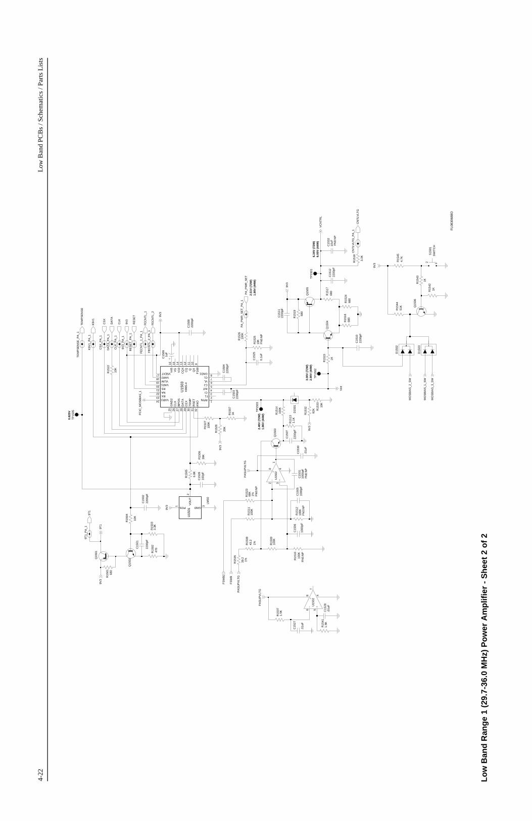
4-22
Low
Ban
d PC
Bs
/ Sch
emat
ics
/ Par
ts L
ists
6.00
V (
44W
)
3.00
V (
72W
)2.
90V
(44
W)
2.46
V (
72W
)1.
86V
(44
W)
6.34
V (
72W
)
2.51
V (
72W
)1.
90V
(44
W)
0.82
5V
9V3
Q15
04
Q15
02
R15
08
1%43.2
D15
03
D15
02R
1545
4.7K
Q15
06
C15
3210
uF
TP
1505
680
CS
X
TE
MP
SE
NS
E_P
A_1
R15
37
R15
01
1000
pFC
1531
1.5K
39.2
1%
R15
35
.01u
F
C15
30
R15
15
R15
24
1K
680
100K
R15
10
1.5K
R15
41
R15
1110
0K
1000
pFC
1505
100K
R15
12
Q15
03
82K
R15
32
R15
0247
0
U15
02
2 31
8 4
CLK
_PA
_1D
AT
A
78 4
FE
CN
TL_
1_P
A_1
9T1_
PA
_1
U15
02
6 5
9V3_
PA
_1
R15
0910
0K
C15
12
R15
22
10K
1uF
C15
09
2200
pF
1K
R15
23
R15
07
FN
0:N
P
FN
0:N
PF
N0:
NP
FN
0:N
P
68K
1%
FE
CN
TL_
1
C15
2610
0pF
12R
1542
1KVAR1
18 VAR2
24 VAR3
VG
15
VL 6VLIM19
S15
01S
WIT
CH
21
31R
SE
T
RX23 T1 2
TE
MP
30
V10
14
V45
16
17 V5EXT
20
9
GND1 8
GN
D2
25
INT 422 NA
Q11
QX
10
1RFIN
RS
29
CI 3
CJ 5
CL 7
CLK
26
CQ
12C
QX
13D
AT
A28
F16
8
U15
03H
99S
-4
AN
O32
BP
OS
27
CE
X
CS
X_P
A_1
R15
06
R15
05
6.8K
R15
16
39K
680
C15
25
0.1u
F
R15
033.
3K
C15
1022
00pF
1K
R15
43
Q15
05
R15
4451
K
R15
2710
0K
R15
3310
K
FE
CN
TL_
2_P
A_1
.01u
FC
1528
C15
27
.01u
F
20K
R15
28
PA
_PW
R_S
ET
_PA
_1
PA
_PW
R_S
ET
Q15
01
100K
R15
26
10K
R15
25
FN
0:N
P
2200
pF
C15
01
R15
1410
0K
2200
pFC
1503
R15
04
10K
2200
pF
RE
SE
T
2200
pF
C15
04
1.1K
C15
08
TP
1503
R15
13
2200
pFC
1502
TE
MP
SE
NS
E
TP
1502
DA
TA
_PA
_1
K9V
1K
9V1_
PA
_1
FE
CN
TL_
2
2200
pF
C15
07
2200
pF
TP
1501
CN
TLV
LTG
C15
11
9T1
CN
TLV
LTG
_PA
_1
680
R15
19
680
R15
17
R15
18
3.3K
CLK
D15
01C
1506
1000
pF
LM50
GND 31 POS VO
UT
2
RE
SE
T_P
A_1
9V3
Vin
t
PA
SU
PV
LTG
9V3
PA
SU
PV
LTG
PA
SU
PV
LTG
FS
WB
2
9V3
MO
SB
IAS
_2_S
W
MO
SB
IAS
_1_S
W
MO
SB
IAS
_3_S
W
U15
01
9V3
FS
WB
9V3
VC
NT
RL
9V3
PC
IC_M
OS
BIA
S_1
9T1
9V3
FN
0:N
P
FL0
8306
88O
Lo
w B
and
Ran
ge
1 (2
9.7-
36.0
MH
z) P
ow
er A
mp
lifie
r -
Sh
eet
2 o
f 2

Low
Ban
d P
CB
s / S
chem
atic
s / P
arts
Lis
ts4-
23
J140
1
1.8V
-2.2
V
1.8V
-2.2
V
470p
FC
1443
MO
SB
IAS
_2_P
A_1
0.1u
F
C14
2847
0pF
R14
48
C14
72
C14
66
.01u
F
FN
O: N
P15
0K
30pF
C14
52
C14
55
C14
69
27pF
C14
02
.01u
F
1uF
C14
01.0
1uF
1K
R14
84
.01u
FC
1414
R14
14
10F
NO
: NP
10
100
R14
12
1.8V
-2.2
VT
P14
02
R14
40
R14
18
10
C14
48
240p
F
130p
F
C14
42
.01u
F
33 V
pp
33 V
pp
58 V
pp
169
Vpp
C14
31
R14
64
3.3K
R14
45
RX
IN
TP
1403
10
6.2K
R14
57
2.1V
pp
L142
4
C14
3743
0pF
82nH
390
R14
02
.01u
FC
1434
C14
600.
1uF
10
R14
15F
NO
: NP
16 V
pp
.01u
FC
1476
18 V
pp
L142
3
175
Vpp
78.7
27nH
R14
19
10
C14
32
1uF
FN
O: N
P
3pF
C14
50
R14
76 10
R14
2427
K
R14
65
3.3K
TX
INJ
.01u
F
0
R14
82
C14
68
MO
SB
IAS
_3_P
A_1
U14
02
MC
3307
2
6 57
8 4
C14
57
.01u
F
C14
2943
0pF
L140
6
1uF
C14
26
250.
974n
H
C14
47
240p
F
150p
FC
1417
FN
O: N
P
R14
63
12K
240p
F
C14
41
96 V
pp
C14
70
PE
AK
-TO
-PE
AK
VO
LTA
GE
S (
Vpp
) A
RE
TY
PIC
AL
VA
LUE
SW
HIC
H W
OU
LD B
E M
EA
SU
RE
D B
Y A
N O
SC
ILLO
SC
OP
EU
ND
ER
TH
E F
OLL
OW
ING
CO
ND
ITIO
NS
:1)
BA
TT
ER
Y V
OLT
AG
E =
13.
6V2)
PO
UT
= 6
6W A
T 3
9MH
z
1uF
10R14
75R
1474
10
D14
01M
OS
BIA
S_2
D14
02
10uF
C14
62
C14
54
62pF
25nH
L141
6
C14
5391
pFR
1405
DE
VIC
E N
EA
R IN
SID
E O
F R
AD
IO
51
C14
821u
F
47pF
C14
67
FN
O: N
P12
0nH
L140
5
R14
50
820
E14
01
PA
SU
PV
LTG
_PA
_1
C14
61.0
1uF
88.4
70nH
L141
3
C14
19
L141
4
88.4
7nH
C14
38
.01u
F
1043
0pF
330p
FF
NO
: NP
C14
06
R14
20
.01u
FC
1412
27K
C14
08
FN
O: N
P
R14
25
.01u
F
330p
F
470p
FC
1427
C14
740.
1uF
C14
73
FN
O: N
P
Q14
04
560p
FC
1418
RX
IN_P
A_1
FN
O: N
P39
KR
1466
R14
07
10K
1uF
C14
33
68pF
FN
O: N
P
C14
09
25nH
L142
6C
1480
300p
F
.01u
F
300p
FC
1481
C14
45
470p
FC
1439
FN
O: N
P
C14
1675
pF
10
R14
17
R14
77
3.3K
C14
8422
00pF
R14
13
10
R14
04
E14
03
C14
51
51
DE
VIC
E N
EA
R O
UT
SID
E O
F R
AD
IO
L140
4
180p
F
RF
OU
T2
7V
CN
TR
L1
VD
114
VG
12
VG
23
180n
H
GND312
GND413
NC
18
NC
29
NC
310
NC
415
RF
IN16
RF
OU
T1
6
30C
65U
1401
17EP
G2
11
GND14
GND25
27K
R14
80
C14
7710
0pF
C14
22.0
1uF
4.7u
HL1
402
FN
O: N
P
R14
21
10
R1442
0
C14
100.
1uF
D
G
GN
D1
GN
D2
S1S2S3S4
Q14
03
PO
S
L141
888
.470
nH
C14
4624
pF
HE
AT
SIN
KM
1401
.01u
F
C14
20
FN
O: N
P
L142
2
10K
R14
72
133.
304n
H
C14
5810
uF
L141
525
nH
MO
SB
IAS
_3
R14
431K
R14
06
10K
R14
4939
0
.01u
F
C14
04
C14
5910
uF
L142
5C14
351u
F
25nH
C14
65
1uF
C14
71
.01u
F
10
R14
16
R14
60
L140
34.
7uH
2.5V
pp
0.1
1%
FN
O: N
P
240
R14
83
6.2p
FC
1403
C14
23.0
1uF
L142
115
0.49
9nH
180p
FC
1449
C14
25
1uF
.01
R14
09
L142
019
6.87
6nH
10R14
22
C14
4447
0pF
FN
0: N
P0
R14
71
FN
O: N
P2.
2KR
1468
.01u
FC
1424
L141
725
nH
.01u
F
C14
64
180
R14
54
R14
5839
0
3.3K
R14
79
.01u
F
C14
13
10R14
73
10K
FN
O: N
P
G
GN
D1
GN
D2
S1S2S3S4
R14
41
Q14
02
D
R14
67
TP
1401
FN
O: N
P
39K
TX
INJ_
PA
_1
R14
46
FN
O: N
P5.
6K
C14
63
1uF
R14
70
C14
40
470p
F
FN
O: N
P2.
4K
FN
O: N
P
430p
FC
1430
R14
4447
0
C14
7924
0pF
100p
FC
1478
10
R14
23
0.1u
FC
1529
180
C14
05
FN
O: N
P
R14
51
.01u
F
.01u
F
10K
C14
07
R14
11
75pF
27uH
2 V
dc
L141
9
1uF
PA
SU
PV
LTG
C14
56
C14
75
130
FN
O: N
P.0
1uF
C14
21
C14
15
R14
10
Q14
01
0.1u
F
R14
59
R14
47
390
C14
36.0
1uF
0
R14
78
0
R14
69
10K
.01u
F23
184
C14
85
6.8n
HF
NO
: NP
MC
3307
2U
1402
180
R14
55
L140
1 180
R14
53
9V3
PA
SU
PV
LTG
VC
NT
RL
FS
WB
2
Vin
t
U_P
RE
DR
IVE
R
U_D
RIV
ER
PA
SU
PV
LTG
U_P
RE
DR
IVE
R
MO
SB
IAS
_2_S
W
MO
SB
IAS
_3_S
W
MO
SB
IAS
_1_S
W
PA
SU
PV
LTG
U_D
RIV
ER
FS
WB
PC
IC_M
OS
BIA
S_1
9T1
FL0
8306
07A
Lo
w B
and
Ran
ge
2 (3
6.0-
42.0
MH
z) P
ow
er A
mp
lifie
r -
Sh
eet
1 o
f 2

4-24
Low
Ban
d PC
Bs
/ Sch
emat
ics
/ Par
ts L
ists
LM61
42
6.20
V (
72W
)F
N0:
NP
FN
0:N
P
LM61
42
5.86
V (
44W
)2.
95V
(72
W)
2.85
V (
44W
)
2.48
V (
72W
)1.
85V
(44
W)
2.51
V (
72W
)1.
86V
(44
W)
0.82
5V
FN
0:N
OT
PLA
CE
D
R15
1768
0
R15
23
1%68K
CN
TLV
LTG
100K
R15
27
C15
04
CN
TLV
LTG
_PA
_1
C15
08
2200
pF
R15
13
2200
pF
FE
CN
TL_
1
RE
SE
T
1.1K
FE
CN
TL_
1_P
A_1
Q15
02
CS
X_P
A_1
680
R15
01
3.3K
R15
18
1000
pF
C15
06
CLK
1
2V
OU
T
RE
SE
T_P
A_1
LM50
U15
01 3GND
PO
S
R15
1010
0K
10K
R15
33
CS
X
9T1_
PA
_1
FE
CN
TL_
2_P
A_1
R15
08
9T1
R15
09
43.2
1% 100K
C15
27
9V3_
PA
_1
.01u
F.0
1uF
C15
28
FN
0: N
P
FN
0:N
OT
PLA
CE
D
R15
2510
K
C15
3110
00pF
.01u
FC
1530
D15
03
D15
02R
1545
Q15
06M
MB
T39
04
4.7K
R15
43
1K
51K
R15
44
100K
R15
11
1000
pFR
1512
100K
C15
05
Q15
03
R15
32
82K
100p
FC
1526
R15
28
20K
PA
_PW
R_S
ET
_PA
_1
PA
_PW
R_S
ET
Q15
01
U15
026 5
78 4
TP
1505
DA
TA
_PA
_1
K9V
1K
9V1_
PA
_1
R15
05
C15
07
2200
pF
6.8K
R15
0639
K
R15
1668
0
6VL19 VLIM
0.1u
F
C15
25
30T
EM
P
14V
10
16V
45
V5EXT17
VAR120
VAR218
VAR324
15V
G
NA22
11Q
10Q
X
RFIN1
21 RS
RS
ET
31
23 RX 2T1
26C
LK
12C
Q
13C
QX
28D
AT
A
9F
168
8GND1
25G
ND
2
4INT
32A
NO
27B
PO
S
29C
EX
3CI
5CJ
7CL
2200
pFC
1510
H99
S-4
U15
03
Q15
05
2200
pFC
1511
1KR15
42
SW
ITC
HS
1501
12
TP
1503
39.2
1%R15
35
R15
2468
0
C15
0222
00pF
DA
TA
TP
1502
C15
01
2200
pF
100K
R15
14
1.5K
R15
40
2 31
8 4
R15
391.
5K
U15
02
R15
19
680
1KR15
07
470
R15
02
R15
2610
0K
R15
03
R15
15
1K
3.3K
10K
R15
22
C15
1222
00pF
TE
MP
SE
NS
E_P
A_1
C15
09
1uF
TE
MP
SE
NS
E
D15
01
C15032200pF
10K
R15
04
TP
1501
FE
CN
TL_
2
9V3
Q15
04
9V3
Vin
t
9V3
PA
SU
PV
LTG
FS
WB
2
9V3
MO
SB
IAS
_2_S
W
MO
SB
IAS
_1_S
W
MO
SB
IAS
_3_S
W
PA
SU
PV
LTG
CLK
_PA
_1
9V3
FS
WB
PA
SU
PV
LTG
9V3
VC
NT
RL
9V3
PC
IC_M
OS
BIA
S_1
9T1
9V3
FL0
8306
07O
SH
EE
T 2
Lo
w B
and
Ran
ge
2 (3
6.0-
42.0
MH
z) P
ow
er A
mp
lifie
r -
Sh
eet
2 o
f 2
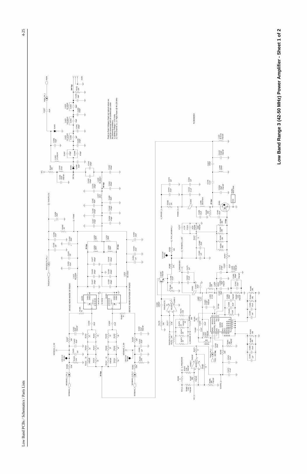
Low
Ban
d P
CB
s / S
chem
atic
s / P
arts
Lis
ts4-
25
20 V
pp
18 V
pp
25 V
pp
25 V
pp
190
Vpp
180
Vp
p
J140
1
1.8V
-2.1
V
1.8V
-2.1
V
3.7V
-3.9
V
2.5
Vp
p
5 V
pp
90 V
pp
10 V
pp
Pea
k-to
-Pea
k V
olta
ges
(Vpp
) ar
e ty
pica
l val
ues
asco
uld
be m
easu
red
with
an
osci
llosc
ope
unde
rth
e fo
llow
ing
cond
ition
s:1.
) B
atte
ry V
olta
ge =
13.
6 V
olts
2.)
Tes
t Cha
nnel
11,
i.e.
Hig
h P
ower
@ 4
6.12
5 M
Hz
DE
VIC
E N
EA
R IN
SID
E O
F R
AD
IO
DE
VIC
E N
EA
R O
UT
SID
E O
F R
AD
IO
0
E14
03
R14
69
C14
04.0
1uF
C14
760.
1uF
C14
1630
pF
137.
876n
HL1
421
FN
0:N
P
D14
02
1uF
C14
25
10
R14
21
3.3K
R14
64
120n
HF
N0:
NP
R14
83
240
L140
5
R14
04 51
R14
23
10
10uF
33pF
C14
54
C14
62
220
R14
44
3.3K
0.1u
F
C14
60
R14
79
C14
58
C14
730.
1uF
10uF
300p
F
180p
F
MO
SB
IAS
_2_P
A_1
C14
78
C14
51
10uF
C14
59
C14
27
240p
F
180
R14
53
PA
SU
PV
LTG
3.3K
R14
77
R14
49
TP
1402
390
430p
FC
1417
390
R14
5827
0pF
C14
12
27K
R14
25
C14
331u
F
300p
F
C14
77
R14
45
6.2K
L142
618
nH
MC
3307
2 U14
02-2
6 57
8 4
27K
R14
24
1uF
C14
75
10K
RX
IN_P
A_1
C14
28
R14
78
U14
02-1
MC
3307
2
231
84
240p
F
.01u
F
100
R14
40
C14
24
C14
48
Q14
04F
N0:
NP
470p
F
R14
841K
220p
FC
1479
C14
06
470p
FC
1437
FN
0:N
P
330p
F
C14
07.0
1uF
24pF
C14
691u
F
C14
52
R14
7310
R14
57
10
R14
63
12K
L141
927
uH
R14
4110
KF
N0:
NP
16pF
C14
55
470p
F
C14
47
FN
0:N
P
L142
436
.54n
H
R14
14
10
10R
1412
FN
0:N
P
.01u
F
C14
61
C14
85
10K
R14
06
.01u
F
D14
01M
OS
BIA
S_2
.01u
F
C14
57
R14
11
L140
625
0.97
4nH
10K
C14
14
.01u
F
10K
R14
07
L141
618
nH
R14
1510
FN
0:N
P
C14
66
.01u
F
51pF
C14
56
R14
82
0
R14
16
10
.01u
F
C14
05
1uF
C14
32
3pF
R14
465.
6K
C14
50
C14
01.0
1uF
FN
0:N
P
68pF
C14
67
180
R14
55
MO
SB
IAS
_3
TP
1403
470p
FC
1440
R14
702.
4KF
N0:
NP
R14
22
1010
R14
20
R14
5118
0
C14
70R
1460
1%0.1
1uF
88.4
70nH
L141
4
180
R14
54
C14
26
1uF
.01u
FC
1422
FN
0:N
P
C14
13
.01u
F
L141
388
.470
nH
C14
30
240p
F
.01u
FC
1434
C14
19
.01u
F
R14
48
150K
FN
0:N
P
10
R14
18
39K
FN
0:N
P
C14
86
R14
66
C14
08
0.1u
F
FN
0:N
P
330p
F
PA
SU
PV
LTG
_PA
_1
E14
01
RX
IN
.01u
FC
1471
.01u
FC
1468
R14
17
1018
nHL1
415
C14
4313
0pF
130p
FC
1444
172.
891n
HL1
420
C14
31.0
1uF
R14
7510
R1442
10R14
19
100
.01u
F
24pF
C14
46
66.3
89nH
L141
8
C14
20
C14
036.
2pF
R14
43
FN
0:N
P
FN
0:N
P
1K
C14
21.0
1uF
820
R14
50
C14
4212
0pF
R14
0239
0
10
R14
13
R14
682.
2KF
N0:
NP
TP
1401
2200
pFC
1484
R14
47
0L1
402
4.7u
H
S3S4
.01u
F
C14
02
Q14
02
D
G
GN
D1
GN
D2
S1S2
MO
SB
IAS
_3_P
A_1
0.1u
F
C14
72
82pF
C14
80
C14
8182
pF
C14
4911
0pF
1uF
C14
82
1uF
C14
63
1uF
C14
35
.01u
FC
1445
FN
0:N
P
C14
3947
0pF
R14
6739
K
FN
0:N
P
FN
0:N
P6.
8nH
L140
1
L142
211
5.58
1nH
R14
7210
K
C14
3847
0pF
C14
4122
0pF
M14
01H
EA
TS
INK
PO
S
.01u
FC
1474TX
INJ_
PA
_1
R14
09.0
1
18nH
L141
7
R14
7410
100p
FC
1453
51R14
05
R14
76 10
3V
G2
81.9
30nH
L142
3
10N
C3
15N
C4
16R
FIN
6R
FO
UT
17
RF
OU
T2
1V
CN
TR
L14
VD
12
VG
1 EP 17
11G
2
4GND15GND2
12GND313GND4
8N
C1
9N
C2
U14
0130
C65
.01u
F
C14
64
R14
5939
0
L140
3
C14
65
1uF
180n
H
4.7u
H
L140
812
0nH
L140
4
FN
0:N
PR
1471
0
FN
0:N
P
130
R14
10
C14
0968
pF
.01u
FC
1436
240p
F
C14
29
.01u
FC
1423
S4
FN
0:N
P
C14
1851
0pF
D
G
GN
D1
GN
D2
S1S2S3
0.1u
F
Q14
03
C14
150.
1uF
C14
10
Q14
01
18nH
27K
L142
5
R14
80
3.3K
R14
65
PC
IC_M
OS
BIA
S_1
9V3
PA
SU
PV
LTG
VC
NT
RL
FS
WB
2
Vin
t
U_P
RE
DR
IVE
R
U_D
RIV
ER
PA
SU
PV
LTG
MO
SB
IAS
_2_S
W
MO
SB
IAS
_3_S
W
MO
SB
IAS
_1_S
W
TX
INJ
PA
SU
PV
LTG
U_D
RIV
ER
U_P
RE
DR
IVE
R
FS
WB
9T1
FL0
8306
95O
Lo
w B
and
Ran
ge
3 (4
2-50
MH
z) P
ow
er A
mp
lifie
r -
Sh
eet
1 o
f 2
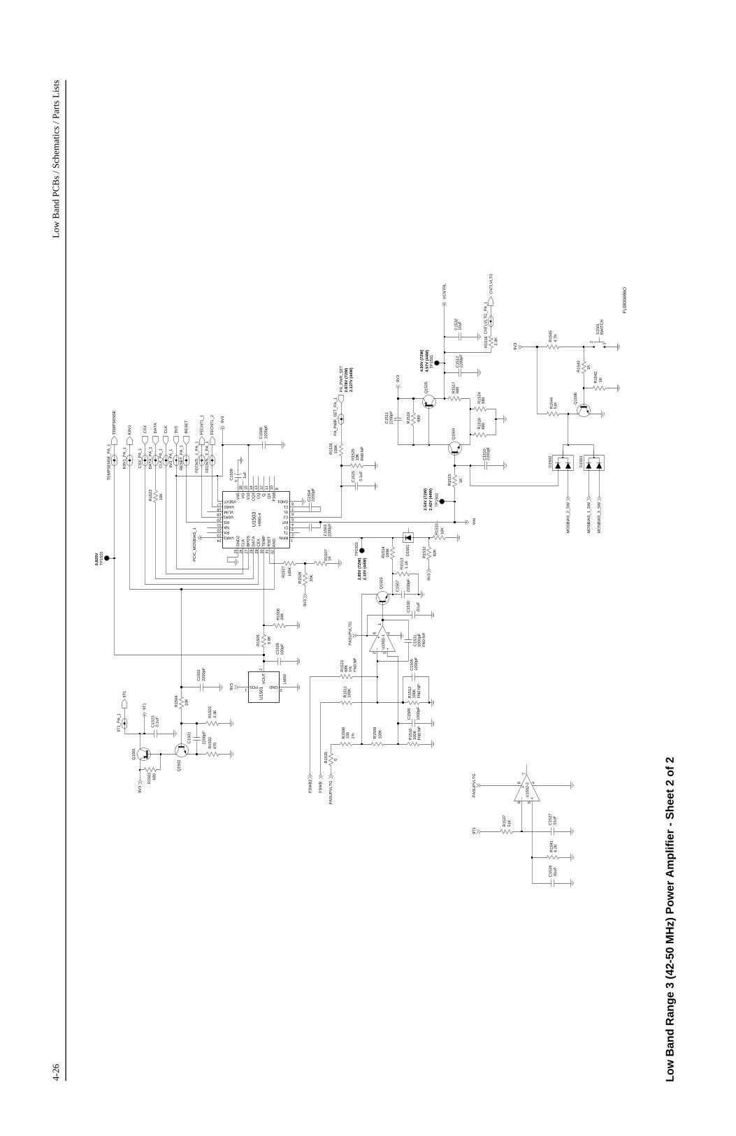
4-26
Low
Ban
d PC
Bs
/ Sch
emat
ics
/ Par
ts L
ists
2.10
V (
44W
)
2.87
8V (
72W
)2.
137V
(44
W)
4.57
V (
44W
)2.
54V
(72
W)
2.42
V (
44W
)
2.85
V (
72W
)
0.82
5V
4.93
V (
72W
)
R15
2610
0K
680
R15
01
R15
2468
0
10K
R15
04
C15
27.0
1uF
470
R15
02
51K
1K
R15
37
R15
42
Q15
01
RE
SE
T_P
A_1
0
R15
35
R15
32
82K
Q15
02
FE
CN
TL_
1_P
A_1
DA
TA
_PA
_1
R15
19
680
TP
1502
6.2K
R15
41
Q15
03
Q15
04
2200
pFC
1504
2200
pFC
1508
1.1K
R15
13
R15
1768
0
6 57
8 4
DA
TA
C15
25
U15
02-2
VAR218
VAR324
15V
G
6VL19
VLIM
0.1u
F
RS
ET
31
23RX 2T1
30T
EM
P
14V
10
16V
45
V5EXT17
VAR120
8GND1
25G
ND
2
4INTNA
22
11Q
10Q
X
RFIN1
21RS
3CI
5CJ
7CL
26C
LK
12C
Q13
CQ
X28
DA
TA
9F
168
H99
S-4
U15
03
32A
NO
27B
PO
S
29C
EX
2200
pFC
1510
Q15
05
2200
pFC
1511
12
CS
X_P
A_1
C15
06
S15
01S
WIT
CH
1000
pF
C15
230.
1uF
100K
R15
09
TP
1505
PA
_PW
R_S
ET
9V3_
PA
_1
TE
MP
SE
NS
ET
EM
PS
EN
SE
_PA
_1
C15
0322
00pF
D15
03
D15
02R
1545
4.7K
Q15
06
1K
R15
43
R15
4451
K
R15
33
CS
X
CN
TLV
LTG
_PA
_1C
NT
LVLT
G
10K
100K
R15
11
1000
pF
FE
CN
TL_
2
CLK
_PA
_1
9V3
C15
05
K9V
19T
19T
1_P
A_1
680
K9V
1_P
A_1
10uF
C15
32
R15
16
100K
FN
0:N
P
1K
R15
1210
0KF
N0:
NP
R15
15
C15
26
R15
10
.01u
F
100p
F
FE
CN
TL_
2_P
A_1
C15
28
PA
_PW
R_S
ET
_PA
_1
CLK
FE
CN
TL_
1
1
2V
OU
T
D15
01
LM50
U15
01
3GNDPOS
C15
0222
00pF
3.3K
R15
03
FN
0:N
P10
00pF
C15
31
C15
30
.01u
F
3.3K
R15
18
RE
SE
TC
1501
2200
pF
100K
R15
14
20K
2 31
8 4
R15
28
U15
02-1
C15
1222
00pF
FN
0:N
P
C15
09
1uF
R15
23
1%68K
100K
R15
27
FN
0:N
P
R15
2510
K
10K
R15
22
100
1%R15
08
C15
07
2200
pF
TP
1501
TP
1503
1KR15
07
6.8K
R15
05
R15
0639
K
9V3
Vin
t9T
1P
AS
UP
VLT
G
9T1
PA
SU
PV
LTG
FS
WB
2
MO
SB
IAS
_2_S
W
MO
SB
IAS
_1_S
W
MO
SB
IAS
_3_S
W
9V3
PA
SU
PV
LTG
VC
NT
RL
9V3
FS
WB
9V3
9V3
PC
IC_M
OS
BIA
S_1
9V3
9V3
FL0
8306
96O
Lo
w B
and
Ran
ge
3 (4
2-50
MH
z) P
ow
er A
mp
lifie
r -
Sh
eet
2 o
f 2
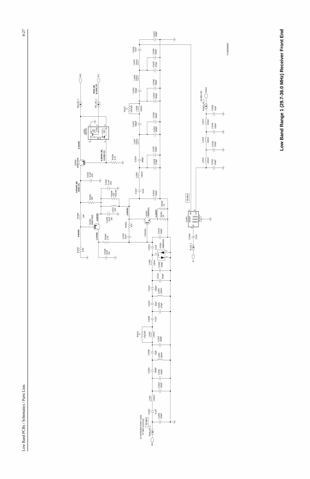
Low
Ban
d P
CB
s / S
chem
atic
s / P
arts
Lis
ts4-
27
AT
AN
TE
NN
A P
OR
T J
1401
-47
dBm
(1m
Vrm
s)
-50
dBm
-38
dBm
+14
dB
m (
R)
9.1V
DC
(T
)0V
DC
(R
)
9.14
VD
C
8.36
VD
C (
R)
9.1V
DC
(T
)
9.03
VD
C (
R)
0VD
C (
T)
4.60
VD
C
4.00
VD
C
1.47
VD
C
4.56
VD
C
0.18
VD
C
0.94
VD
C
C10
41
L100
3
9V3
220p
F
10%
0.1u
F
130n
H
300p
F
C10
31
L100
4
C10
22
RX
IN_F
E_1
130n
H
C10
15.0
1uF
360p
FC
1021
L100
913
0nH
130p
F
C10
34
C10
26.0
1uF
9T1_
FE
_1
C10
1620
0pF
C10
24
C10
35
330p
F
9T1
91pF
L101
4
C10
0322
0pF
C10
06
220n
H
C10
13
91pF
0.1u
F
C10
17
.01u
F
270p
F
130n
H
L100
8
220p
F
C10
250.
1uF
C10
12
RX
INJ_
FE
_1
C10
02
220p
FC
1042
180p
F
C10
11
390p
FC
1039
C10
3739
0pF
C10
38
300p
F
300p
F
XIN
C10
07
R10
03
470
360p
F
C10
20
C10
04
130n
H
L100
6
L100
2
160p
F
130n
H
R10
08
C10
2336
0pF
5GND3
2IF
6LO
3R
F
4.7K
4.7K
47K
47K
10K
MIX
ER
U10
51
1GND1
4GND2
FN
0:N
P10
0R
1009
C10
36
0.1u
F
120p
FC
1033
C10
1927
0pF
FN
0:N
P
R10
100
300p
FC
1040
Q10
02M
MB
T39
06
RX
INJ
130n
H
L100
5
IF_F
E_1
Q10
01M
MB
R95
1
L100
713
0nH
220p
F27
0pF
C10
09C
1014
130n
H
L100
1
C10
29 5%.0
1uF
82pF
C10
10
U10
01U
MC
5N
2
6 4
1 3
R10
07
8.2K
L101
013
0nH
D10
01M
MB
D35
3
2
3
1
180p
FC
1027
15R10
02
C10
32
100p
F
R10
06
10K
R10
01
R10
042.
7K
15
C10
28
5%.01u
F
330n
H
L101
3
FN
0:N
P
9V3_
FE
_1
IF
0R
1011
L101
11u
H
C10
0122
0pF
0.1u
F10
%
C10
30
R10
0518
0
220n
H
L101
2
0.1u
F
C10
08
Q10
03M
MB
T39
06
FL0
8306
89O
Lo
w B
and
Ran
ge
1 (2
9.7-
36.0
MH
z) R
ecei
ver
Fro
nt
En
d

4-28
Low
Ban
d PC
Bs
/ Sch
emat
ics
/ Par
ts L
ists
4.61
VD
C
0.90
VD
C
0.15
VD
C
AT
AN
TE
NN
A P
OR
T J
1401
-47
dBm
(1m
Vrm
s)
-50
dBm
-38
dBm
+14
dB
m (
R)
4.64
VD
C
4.05
VD
C
1.33
VD
C
9.03
VD
C (
R)
0VD
C (
T)
8.36
VD
C (
R)
9.1V
DC
(T
)
9.14
VD
C
9.1V
DC
(T
)0V
DC
(R
)
300p
FC
1021
150p
F
9T1_
FE
_1
C10
16
9T1
62pF
C10
35
62pF
C10
10
C10
2524
0pF
220p
F
C10
24
C10
02
.01u
F
220n
H
L101
4
C10
28
5%.01u
F
330n
H
L101
3
4
1 3
RX
INJ_
FE
_1
9V3_
FE
_1
U10
01U
MC
5N
2
6
100p
F
C10
34
R10
07
8.2K
L101
11u
H
C10
0116
0pF
0.1u
F10
%
C10
30
C10
3275
pF
R10
06
10K
10R10
01
Q10
03M
MB
T39
06
91pF
C10
33
9V3
C10
15
.01u
F
1GND1 4GND2 5GND3
2IF
6LO
3R
FM
IXE
R
U10
51
FN
0:N
P
FN
0:N
P10
0R
1009
IF
0
R10
11
FN
0:N
P
R10
10
0
120p
F
C10
04
R10
0518
0Q
1002
MM
BT
3906
C10
11
120p
F
IF_F
E_1
RX
INJ
L100
7
130n
H22
0pF
C10
20
L100
4
C10
22
220p
F
RX
IN
130n
H
R10
03
470
C10
1416
0pF
240p
FC
1009
C10
13
0.1u
F
C10
36
.01u
F
C10
17
1200
pF13
0nH
L100
6
150p
FC
1027
Q10
01M
MB
R95
1 R10
0215
R10
042.
7K
1200
pF13
0nH
L100
8
300p
F
C10
26
300p
FC
1012
300p
FC
1039
C10
0330
0pF
C10
3822
0pF
C10
37C
1019
240p
F10
00pF
C10
08
220n
H
L101
2
RX
IN_F
E_1
130n
H
L100
3
C10
31
10%
0.1u
F
L100
1
C10
0724
0pF
130n
H13
0nH
5%.0
1uF
L100
5C
1006
C10
29
L100
262
pFC
1040
130n
H
130n
H
220p
F
D10
01M
MB
D35
32
3
1
L101
0
130n
H
300p
F
L100
9
4.7K
4.7K
47K
47K
10K
R10
08
C10
23
FL0
8305
99A
Lo
w B
and
Ran
ge
2 (3
6.0-
42.0
MH
z) R
ecei
ver
Fro
nt
En
d
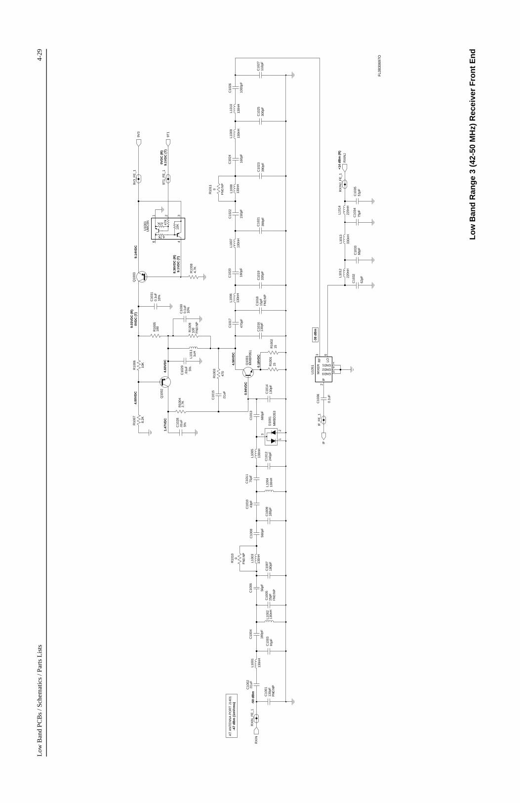
Low
Ban
d P
CB
s / S
chem
atic
s / P
arts
Lis
ts4-
29
-47
dB
m (
1mV
rms)
0.94
VD
C
4.56
VD
C
1.47
VD
C4.
60V
DC
4.00
VD
C9.
03V
DC
(R
)
8.36
VD
C (
R)
9.14
VD
C
9.1V
DC
(T
)0V
DC
(R
)
+14
dB
m (
R)
-38
dB
m
9.1V
DC
(T
)
0VD
C (
T)
-50
dB
m
AT
AN
TE
NN
A P
OR
T J
1401
0.18
VD
C
9V3
.01u
F
C10
15
MM
BR
951
Q10
01
RX
INJ
IF_F
E_1
160p
F13
0nH
L100
7C
1022
C10
20
150p
F
RX
IN_F
E_1
L100
413
0nH
130p
FC
1014
C10
0918
0pF
L100
1
130n
H13
0nH
L100
5
470p
F
C10
17L1
006
130n
H
3
1
FN
0:N
P15
pFC
1005
MM
BD
353
D10
01
2
C10
2711
0pF
R10
0215
2.7K
R10
04
LO6
RF
3
R10
084.
7K
4.7K
47K
47K
10K
U10
51
MIX
ER
GND11
GND24
GND35
IF2
R10
0910
0F
N0:
NP
L100
8
130n
H
330p
FC
1019
0R
1010
FN
0:N
P
180p
F
Q10
02
C10
04
C10
36
0.1u
F
240p
FC
1012
9T1
C10
3551
pF
75pF
C10
11
C10
3475
pF
300p
FC
1025
C10
24
160p
F
91pF
C10
03
L101
4
220n
H
.01u
F5%C
1028
L101
3
330n
H
.01u
FC
1002
2
6 4
1 3
RX
INJ_
FE
_1
43pF
UM
C5N
U10
01
9V3_
FE
_1
C10
10
1uH
L101
1
FN
0:N
P13
0pF
C10
01
8.2K
R10
07
62pF
C10
32
10K
R10
06
C10
30
10%
0.1u
F
Q10
03
C10
3368
pF
R10
0115
R10
110
180
R10
05
IF
FN
0:N
P
L101
2
220n
H
130n
H
C10
08
560p
F
C10
31
L100
3
C10
07
0.1u
F10
%
R10
03
RX
IN
180p
F
C10
29
470
56pF
.01u
F5%
C10
06C
1013
680p
F
L100
213
0nH
FN
0:N
P15
pFC
1018
130n
H
L101
0L1
009
C10
2139
0pF
C10
23
130n
H
390p
FC
1016
1000
pF
C10
26
9T1_
FE
_1
130p
F
FL0
8306
97O
Lo
w B
and
Ran
ge
3 (4
2-50
MH
z) R
ecei
ver
Fro
nt
En
d
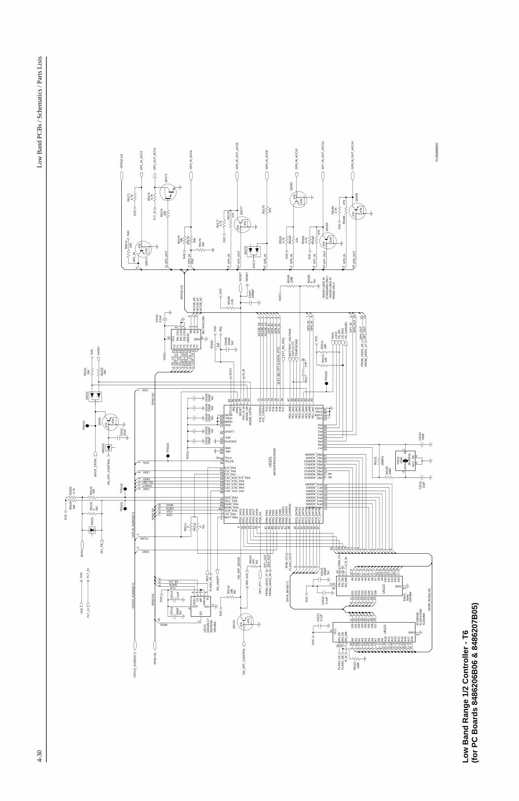
4-30
Low
Ban
d PC
Bs
/ Sch
emat
ics
/ Par
ts L
ists
HSIO
GP
4_O
UT
GP
7_O
UT
HC
138_
A2
GP
1_IN
GP
8_O
UT
EX
P1_
CS
EE_CS
HSIO
GP
7_IN
CLK
GP
5_IN
GP
1_IN
CLKCSX
- R
0105
US
ED
INS
TA
ND
AR
D O
NLY
- R
0106
US
ED
INP
RIM
E O
NLY
GP
7_O
UT
VOX
LSIO
GP
7_IN
HC
138_
A0
RE
F_C
S
MISO
EX
P2_
CS
512k
x8bi
t
RA
M
GP
6_IN
GP
6_IN
HC
138_
A0
GP
3_IN
GP
8_IN
GP
3_IN
GP
8_IN
PE
6LV
ZIF
_CS
GP
4_IN
SQ_DET
HC
138_
A1
FLA
SH
RO
M
SYN
HC
138_
A2
GP
2_O
UT
LSIO
MIC
RO
PR
OC
ES
SO
R
DATA
MISO
F1200
GP
4_IN
GP
5_IN
GP
4_O
UT
VS
_CS
ON
_OF
F_S
EN
SE
GP
8_O
UT
EE
PR
OM
DATA
32kx
8bit
OP
T_C
S
HC
138_
A1
CHACT
16K
x8bi
t
GP
4_O
UT
GP
7_O
UT
(EX
T_B
D_P
TT
& D
AT
A_P
TT
)
EE
_CS
47K
47K
47K
47K
47K 47
K
47K
R01
79
0R01
16
NU
4
R01
5224
K
R01
3233
0K
R01
72
2
10K R
0175
6
7
10K
R01
15
0R
0111
10K
7
101
100p
FC
0101
C01
07
90
1000
pF
11
6
R01
1410
K
10K
R01
04
69VRL68
VSS 13
VSSL 40VSSR 87
93XFC
XIR
Q48
XTAL91
76
PJ6
77
PJ7
78
RE
SE
T94
VDD12
VDDL39VDDR88
VDDSYN92
VRH
51PI6 50PI7 49
PJ0
_CS
GP
371
PJ1
_CS
GP
472
PJ2
73
PJ3
74
PJ4
75
PJ5
42
PH
6_C
SG
P2
41
PH
7_C
SP
RO
G38
PI0 56PI1 55PI2 54PI3 53PI4 52PI5
18
PG
6_A
S5
PG
7_R
_W4
PH
0_P
W1
47
PH
1_P
W2
46
PH
2_P
W3
45
PH
3_P
W4
44
PH
4_C
SIO
43
PH
5_C
SG
P1
23PF7_ADDR7 22
PFO_ADDR0 29
PG
0_X
A13
6
PG
1_X
A14
16
PG
2_X
A15
20
PG
3_X
A16
19
PG
4_X
A17
17
PG
5_X
A18
PE
5_A
N5
61P
E6_
AN
660
PE
7_A
N7
PF1_ADDR1 28PF2_ADDR2 27PF3_ADDR3 26PF4_ADDR4 25PF5_ADDR5 24PF6_ADDR6
1PD5_SS2
3 PD6_LVIN
67P
E0_
AN
066
PE
1_A
N1
65P
E2_
AN
264
PE
3_A
N3
63P
E4_
AN
462
34
PC
5_D
AT
A5
35
PC
6_D
AT
A6
36
PC
7_D
AT
A7
37
PD0_RXD97PD1_TXD98
PD2_MISO99PD3_MOSI100PD4_SCK
15PB6_ADDR14 8PB7_ADDR15 7
PBO_ADDR8 14
PC
0_D
AT
A0
30
PC
1_D
AT
A1
31
PC
2_D
AT
A2
32
PC
3_D
AT
A3
33
PC
4_D
AT
A4
83PA5_OC3_OC184PA6_OC2_OC185PA7_PA1_OC186
PB1_ADDR9 10PB2_ADDR10 11PB3_ADDR11 9PB4_ADDR12 21PB5_ADDR13
96
95 LVOUT
MO
DA
_LIR
58
MO
DB
_VS
TB
Y57
PA0_IC379PA1_IC280PA2_IC181
PA3_IC4_OC5_OC182PA4_OC4_OC1
U01
01
AVDD59
AVSS 70
EC
LK89
EXTAL90
IRQ
R01
70
5
11
10K
0
4
10
3W
P
1C
S
7H
OLD
6S
CK
5S
I
2S
O
8VCC 4VSS
X25
128-
2.7
U01
11
.01u
FC
0151
47K 47
K
0.1u
FC
0141
7
1
7
C01
0610
0pF
NU
12
3
0
15Y
014
Y1
13Y
212
Y3
11Y
410
Y5
9Y
67
Y7
1A
02
A1
3A
2
6E
N_C
S1
4E
N_C
S2
5E
N_C
S3
8GND
16
VC
C
12
MC
74H
C13
8A
U01
41
TP
0102
65
6
10
R01
854.
7K
IO6
17
IO7
18
IO8
19
VCC
28
8
2
6
EN
_OE
22
EN
_WE
27
14GND
IO1
11
IO2
12
IO3
13
IO4
15
IO5
16A
37
A4
6 5A
5A
64
A7
3
A8
25
A9
24
EN
_CS
20
A0
10
A1
9 21A
10A
1123
A12
2
A13
26
A14
1
A2
8
6
U01
22
63A
21
2.2K
R01
08
8
17
3 9
Q01
81
10
66
0.1u
F
7
TP
0151
C01
21
C01
0210
0pF
NU
NU
18
C01
0410
0pF
47K
R01
84
10K
47K
47K
R01
74
22pF
C01
32
Q01
85
012
3
1
R01
834.
7K
11
413
Q01
73
12013
D01
51
R01
73
122
3
4.7K
1
8
8
4
18
R01
10
NU
7
4.7K
R01
77
10K
9
1
4
5
1
1
C01
22
7
109
8
0.1u
F
3
2
TP
0103
3
11110
7
2
1
2
C01
23
NU
0.1u
F
100p
F
C01
12
10K
R01
13
R01
5124
K
2
80
22IO
123
IO2
25IO
326
IO4
27IO
528
IO6
29IO
7
VC
C8
13A
73
A8
2A
9
30E
N_C
E32
EN
_OE
7E
N_W
E
GND24
IO0
21
10A
166
A17
9A
18
18A
217
A3
16A
4A
515
A6
1420A
019
A1
31A
101
A11
12A
12A
134 5
A14
A15
11
3
AT
49F
040
U01
21
D01
79
2 3
17 9
5
6
7
10K
R01
01
TP
0101
Q01
10
47K 47
KR
0107
NU
3
47K
4.7K
R01
81
4
3
100K
R01
05
R01
78
5
47K
47K 47
K
10M
EG
R01
31
NU
4
2
100p
FC
0105
4.7K
R01
71
4
D01
01
3.9K
R01
17
15
5
1413
16
5
Q01
71
100K
5
R01
21
3
Q01
51
Q01
77
0
R01
86
30K
10
47K
0
R01
76
13
6
13
4
5
IN1
9
0
6
1
38.4
0KH
z
Y01
31X
TA
L NC 2
NC
1 3
OU
T4
NU
R01
12
0
47K
R01
82
0 NU
816
R01
06
100p
F
C01
11
NU
C01
03
NU
R01
024.
7K
100p
F
22pF
C01
31
15 7
VR
0151
14
9
Q01
83
4
5
0
2
R_W
RA
M_C
SBU
S+
CN
TLV
LTG
5VD
SC
I_T
X
GP
1_IN
_AC
C3
GP
6_IN
_AC
C10
GP
2_O
UT
_AC
C4
R_W
FLA
SH
_CE
FLA
SH
_OE
5VD
IRQ
IRQ
AD
DR
_BU
S(0
:18)
DA
TA
_BU
S(0
:7)
14
FR
OM
_U01
01_4
7
VS
_RA
C
5VD VS
_IN
T
GP
4_IN
_OU
T_A
CC
8
5VD
BO
OT
_CN
TR
L
GP
3_IN
_AC
C6
5VD
TP
0104
ON
_OF
F_C
ON
TR
OL
5VD
5VD
5VD
RE
SE
T
RE
SE
T
5VD
OP
T_P
TT
5VD
GP
5_IN
_AC
C9
5VD
SP
I(0:
10)
SP
I(0:
10)
SP
I(0:
10)
SP
I(0:
10)
GP
IO(0
:13)
GP
IO(0
:13)
CN
TLR
_AU
DIO
(0:7
)C
NT
LR_A
UD
IO(0
:7)
CN
TLR
_AU
DIO
(0:7
)
FR
OM
_U01
01_4
7F
RO
M_U
0101
_46
FR
OM
_U01
01_4
6
5VD
5VD
FLT
_A+
TE
MP
SE
NS
E
RA
M_C
S
5VD
VS
_GA
INS
EL
EX
T_B
D_R
EQ R
SS
I
5VD
RX
_AD
AP
T
5VD
5VD
5VD
FLT
_A+
FLT
_A+
FLA
SH
_OE
NC
EC
LK
NCNC
LOC
K
RD
Y
ON
_OF
F_C
ON
TR
OL
GP
7_IN
_OU
T_A
CC
12
GP
8_IN
_OU
T_A
CC
14
5VD
5VD
5VD
5VD
FLA
SH
_CE
R_W
VS
TB
Y
5VD
BA
TT
ER
Y_V
OLT
AG
E
FL0
8306
83O
Lo
w B
and
Ran
ge
1/2
Co
ntr
olle
r -
T6
(fo
r P
C B
oar
ds
8486
206B
06 &
848
6207
B05
)
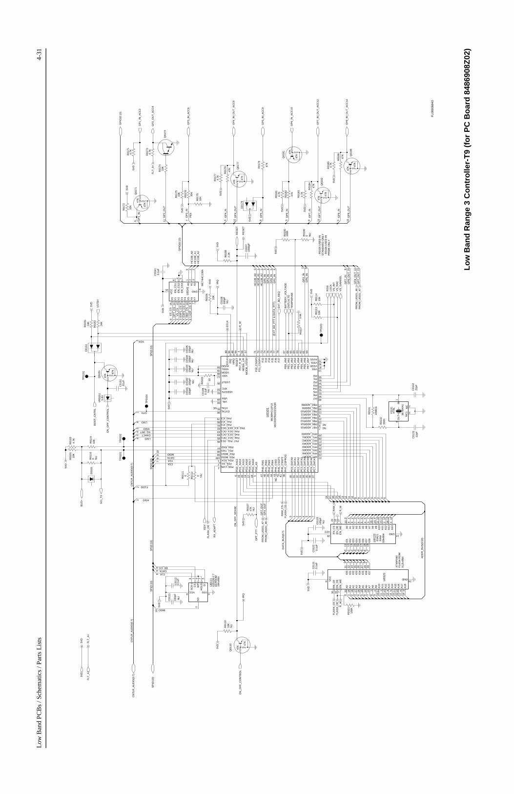
Low
Ban
d P
CB
s / S
chem
atic
s / P
arts
Lis
ts4-
31
ON
_OF
F_S
EN
SE
GP
5_IN
GP
4_O
UT
VS
_CS
EX
P1_
CS
GP
1_IN
CLKCSX
HC
138_
A1
OP
T_C
S
32kx
8bit
- R
0105
US
ED
INS
TA
ND
AR
D O
NLY
- R
0106
US
ED
INP
RIM
E O
NLY
GP
7_O
UT
CLK
GP
5_IN
GP
8_IN
GP
4_IN
GP
3_IN
GP
8_IN
PE
6LV
ZIF
_CS
512k
x8bi
t
RA
M
GP
6_IN
GP
6_IN
HSIO
GP
4_O
UT
GP
7_O
UT
DATA
EE
PR
OM
HC
138_
A2
SYN
HC
138_
A2
GP
2_O
UT
LSIO
MIC
RO
PR
OC
ES
SO
R
DATA
MISO
F1200
GP
4_IN
GP
8_O
UT
VOX
LSIO
GP
7_IN
HC
138_
A0
RE
F_C
S
MISO
EX
P2_
CS
GP
1_IN
GP
8_O
UT
SQ_DET
HC
138_
A1
FLA
SH
RO
M
NU
EE_CS
HSIO
GP
7_IN
CHACT
16K
x8bi
t
GP
4_O
UT
GP
7_O
UT
(EX
T_B
D_P
TT
& D
AT
A_P
TT
)
EE
_CS
HC
138_
A0
GP
3_IN
8
0R01
06
C01
080.
1uF
NU
R01
03
10
NU
C01
11
100p
F
NU
4.7K
R01
02
C01
0310
0pF
22pF
15
C01
31
7
5.6V
VR
0151
Q01
83
14
9
14
4
5
0
2 15
5
0.1u
FC
0112
Q01
71
100K
R01
21
Q01
77
0
3
47K
10
R01
86
0
30K
R01
76
13
6
13
4
5
1IN
9
0
6
1
38.4
0KH
z 2
NC
3
NC
1
4O
UT
NU
XT
AL
Y01
31
0
R01
12
R01
82
47K
47K
47K
47K
47K 47
K
47K
R01
814.
7K
NU
4
3
R01
1010
K
47K
47K
100K
16 5
R01
05
R01
78
47K
47K 47
K
10M
EG
4
2
R01
31
C01
0510
0pF
NU
R01
714.
7K
4
D01
01
R01
173.
9K
5
1413
16
5
100p
FN
U
7
2
11
C01
23R
0113
10K
Q01
51
2
8
22
IO2
23
IO3
25
IO4
26
IO5
27
IO6
28
IO7
29
8 VC
C
13
A8
3
A9
2
EN
_CE
30
EN
_OE
32
EN
_WE
7
24GND
21IO
0IO
1
10
A17
6
A18
9
A2
18
A3
17
A4
16 15A
514
A6
A7
20
A1
19
A10
31
A11
1
A12
12 4A
13A
145 11
A15
A16
3
U01
21
AT
49F
040
A0
2 3
17 9
D01
79
5
6
7
R01
0110
K
TP
0101
Q01
10
NU
3
18
R01
0747
K
R01
774.
7K
1
4
1 17
7
7
1099
8
C01
220.
1uF
2
TP
0103
3
11110
3
1
2
4.7K
R01
83
12
3
1
0
24K
R01
51
013
413
12
12
D01
51
R01
734.
7K
8
8
4
2
3
6
1
3
R01
082.
2K
66
5
1
8
TP
0151
10
C01
21
7
NU
0.1u
F
100p
FC
0102
100p
FC
0104
NU
47K
18
R01
84
R01
7410
K
22pF
Q01
85
C01
32
3
0
CS
1
HO
LD7
SC
K6
SI
5
SO
2
VCC8
VSS4
WP U01
11X
2512
8-2.
7
C01
51
47K
47K
.01u
F
Q01
73
74
1
7
100p
FC
0106
NU
9
Y7
7
12
3
0
8
VC
C
16
Y0
15
Y1
14
Y2
13
Y3
12
Y4
11
Y5
10
Y6
A0
1
A1
2
A2
3
EN
_CS
16
EN
_CS
24
EN
_CS
35
GND
5
12
U01
41
MC
74H
C13
8A
6
6
10
TP
0102
2
6
4.7K
R01
85
15IO
416
IO5
17IO
618
IO7
19IO
8
28
VCC
8
24A
9
20E
N_C
S22
EN
_OE
27E
N_W
E
GND14
11IO
112
IO2
13IO
3
1A
14
8A
27
A3
6A
4A
55 4
A6
3A
725
A8
U01
22
10A
09
A1
A10
21 23A
112
A12
26A
13
11
6
63A
21
Q01
81
9
R01
04
10K
40VSSL
87VSSR
XFC93
48X
IRQ
91 XTAL
94R
ES
ET
12 VDD
39VDDL
88 VDDR
92 VDDSYN
69 VRH
68 VRL
13VSS
71P
J0_C
SG
P3
72P
J1_C
SG
P4
73P
J274
PJ3
75P
J476
PJ5
77P
J678
PJ7
56PI0
55PI1
54PI2
53PI3
52PI4
51PI5
50PI6
49PI7
47P
H0_
PW
146
PH
1_P
W2
45P
H2_
PW
344
PH
3_P
W4
43P
H4_
CS
IO42
PH
5_C
SG
P1
41P
H6_
CS
GP
238
PH
7_C
SP
RO
G
6P
G0_
XA
1316
PG
1_X
A14
20P
G2_
XA
1519
PG
3_X
A16
17P
G4_
XA
1718
PG
5_X
A18
5P
G6_
AS
4P
G7_
R_W
28PF1_ADDR1
27PF2_ADDR2
26PF3_ADDR3
25PF4_ADDR4
24PF5_ADDR5
23PF6_ADDR6
22PF7_ADDR7
29PFO_ADDR0
PE
0_A
N0
67
PE
1_A
N1
66
PE
2_A
N2
65
PE
3_A
N3
64
PE
4_A
N4
63
PE
5_A
N5
62
PE
6_A
N6
61
PE
7_A
N7
60
37P
C7_
DA
TA
7
97 PD0_RXD
98 PD1_TXD
99 PD2_MISO
100 PD3_MOSI
1 PD4_SCK
2 PD5_SSPD6_LVIN3
14PBO_ADDR8
30P
C0_
DA
TA
031
PC
1_D
AT
A1
32P
C2_
DA
TA
233
PC
3_D
AT
A3
34P
C4_
DA
TA
435
PC
5_D
AT
A5
36P
C6_
DA
TA
6
86 PA7_PA1_OC1
10PB1_ADDR9
11PB2_ADDR10
9PB3_ADDR11
21PB4_ADDR12
15PB5_ADDR13
8PB6_ADDR14
7PB7_ADDR15
57M
OD
B_V
ST
BY
79 PA0_IC3
80 PA1_IC2
81 PA2_IC1
82 PA3_IC4_OC5_OC1
83 PA4_OC4_OC1
84 PA5_OC3_OC1
85 PA6_OC2_OC1
59 AVDD
70AVSS
89E
CLK
90 EXTAL
96IR
Q
LVOUT95
58M
OD
A_L
IR
U01
01M
C68
HC
11F
L0
R01
7010
K
4
10
5
11
0
47K
NU
R01
79
R01
160
C01
410.
1uF
24K
R01
52
330K
R01
32
R01
72
10K
47K
47K
10K
6
2 7
R01
75
R01
1510
K
7
101
R01
110
100p
F
9
C01
01
0
C01
0710
00pF
10K
R01
14
RA
M_C
S
BU
S+
CN
TLV
LTG
5VD
SC
I_T
X
GP
1_IN
_AC
C3
GP
6_IN
_AC
C10
GP
2_O
UT
_AC
C4
R_W
FLA
SH
_CE
FLA
SH
_OE
5VD
IRQ
IRQ
AD
DR
_BU
S(0
:18)
DA
TA
_BU
S(0
:7)
5VD
TP
0104
FR
OM
_U01
01_4
7
VS
_RA
C
5VD VS
_IN
T
GP
4_IN
_OU
T_A
CC
8
5VD
BO
OT
_CN
TR
L
GP
3_IN
_AC
C6
ON
_OF
F_C
ON
TR
OL
R_W
5VD
5VD
5VD
RE
SE
T
RE
SE
T
5VD
OP
T_P
TT
5VD
GP
5_IN
_AC
C9
5VD
SP
I(0:
10)
SP
I(0:
10)
SP
I(0:
10)
SP
I(0:
10)
SP
I(0:
10)
GP
IO(0
:13)
GP
IO(0
:13)
CN
TLR
_AU
DIO
(0:7
)C
NT
LR_A
UD
IO(0
:7)
CN
TLR
_AU
DIO
(0:7
)
FR
OM
_U01
01_4
7F
RO
M_U
0101
_46
FR
OM
_U01
01_4
6
5VD
5VD
FLT
_A+
TE
MP
SE
NS
E
RA
M_C
S
5VD
VS
_GA
INS
EL
EX
T_B
D_R
EQ
RS
SI
5VD
RX
_AD
AP
T
5VD
5VD
5VD
FLT
_A+
FLT
_A+
FLA
SH
_OE
NC
EC
LK
NCNC
LOC
K
RD
Y
ON
_OF
F_C
ON
TR
OL
NC
GP
7_IN
_OU
T_A
CC
12
GP
8_IN
_OU
T_A
CC
14
5VD
5VD
5VD
5VD
FLA
SH
_CE
R_W
VS
TB
Y
5VD
BA
TT
ER
Y_V
OLT
AG
E
FL0
8306
84O
Lo
w B
and
Ran
ge
3 C
on
tro
ller-
T9
(fo
r P
C B
oar
d 8
4869
08Z
02)
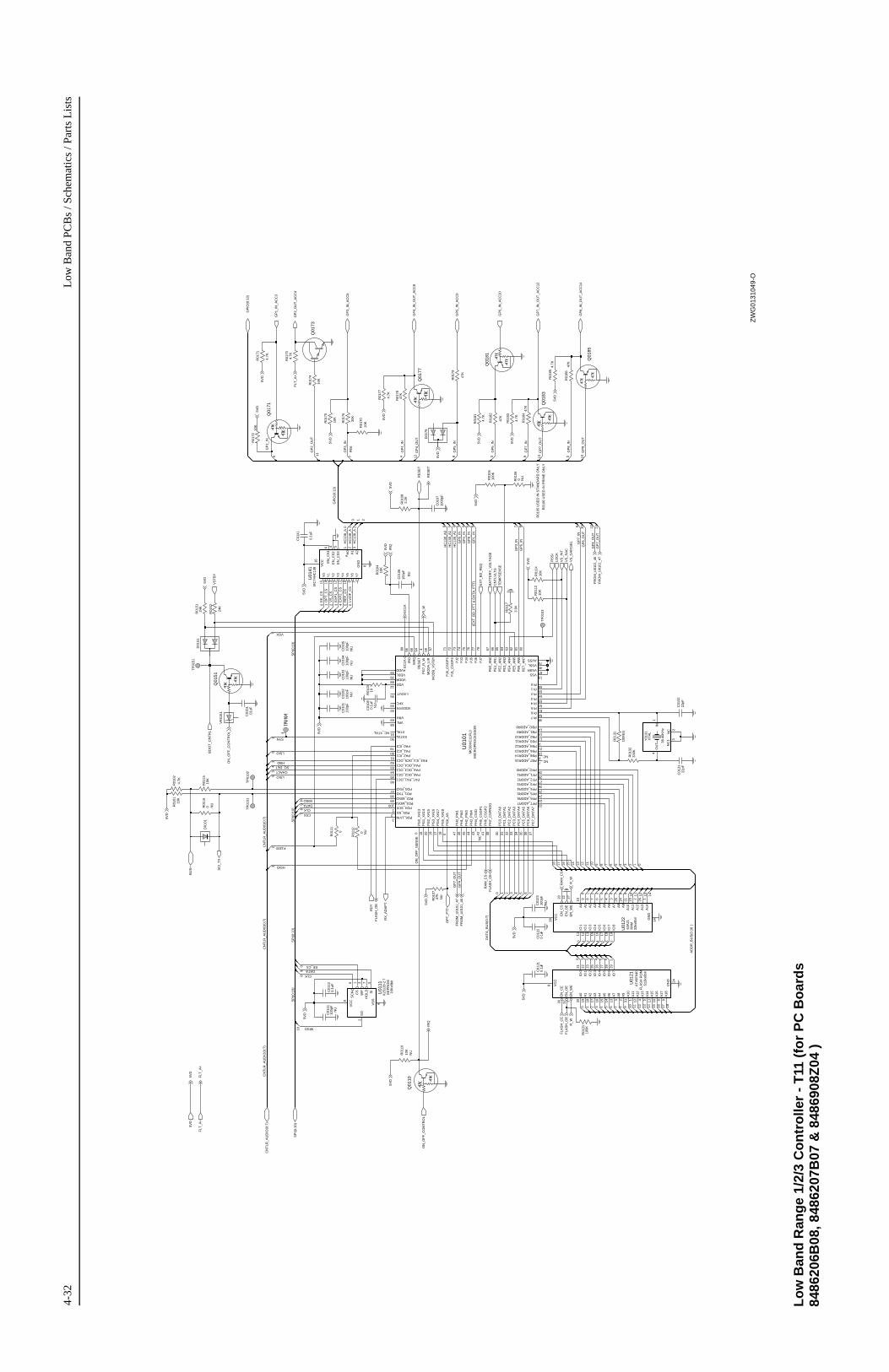
4-32
Low
Ban
d PC
Bs
/ Sch
emat
ics
/ Par
ts L
ists
GP
3_IN
GP
8_IN
PE
6LV
ZIF
_CS
ON
_OF
F_S
EN
SE
GP
5_IN
GP
4_O
UT
VS
_CS
EX
P1_
CS
HC
138_
A2
SYN
HC
138_
A1
GP
2_O
UT
LSIO
MIC
RO
PR
OC
ES
SO
R
CLK
GP
5_IN
CSX
HC
138_
A1
OP
T_C
S
32kx
8bit
R01
05 U
SE
D IN
ST
AN
DA
RD
ON
LY
GP
7_O
UT
GP
8_O
UT
SQ_DET
HC
138_
A1
R01
06 U
SE
D IN
PR
IME
ON
LY
FLA
SH
RO
M
NU
EE_CS
HSIO
GP
8_IN
GP
4_IN
EE
_CS
HC
138_
A0
GP
3_IN
512k
x8bi
t
RA
M
GP
6_IN
GP
6_IN
HSIO
GP
4_O
UT
GP
7_O
UT
DATA
EE
PR
OM
HC
138_
A0
RE
F_C
S
MISO
EX
P2_
CS
GP
1_IN
DATA
MISO
F1200
GP
4_IN
GP
8_O
UT
VOX
LSIO
GP
7_IN
GP
1_IN
CLK
GP
7_IN
CHACT
16K
x8bi
t
GP
4_O
UT
GP
7_O
UT
(EX
T_B
D_P
TT
& D
AT
A_P
TT
)
0
R01
12
NU
4.7K
R01
81
0R01
06
0.1u
FN
U
8
10C
0108
NU
R01
03
C01
1110
0pF
4.7K
R01
02
100p
FN
U
C01
03
15
C01
3122
pF
VR
0151
14
9
7
Q01
83
0
2 15141413
4
5
7
2
5
0.1u
FC
0112
Q01
71
100K
R01
21
0
3
47K
Q01
77
10
R01
86
R01
76
6
13
4
5
0
30K
0
6
1
13
2
NC
3
NC
1
4O
UT
1IN
9
XT
AL
Y01
31
38.4
0KH
z
Q01
10
R01
82
47K
NU
4
3
18
R01
1010
K
16 5
R01
0510
0K
R01
7847
K
4
2
R01
31
10M
EG
C01
0510
0pF
NU
4.7K
4
R01
71
D01
01
16
5
R01
17
3.9K
R01
83
5
2
1
4.7K
C01
2310
0pF
NU
11
R01
1310
K
Q01
51
IO6
28
IO7
29
8 VC
C
2
8
EN
_WE
7
24
GN
D
21IO
0IO
122
IO2
23
IO3
25
IO4
26
IO5
27A
416 15
A5
14A
6A
713
A8
3
A9
2
EN
_CE
30
EN
_OE
32
4A
13A
145 11
A15
A16
10
A17
6
A18
9
A2
18
A3
17
A0
20
A1
19
A10
31
A11
1
A12
12
2 3
3
U01
21A
T49
F04
0
6
17 9
D01
79
10K
5
7
R01
01
3
8
TP
0101
47K
NU
2.2K
6
R01
07
R01
08
R01
77
4.7K
1
4
1 17
7
7
1099
8
C01
220.
1uF
TP
0103
3
11110
3
2
1
0
CS
1
HO
LD7
SC
K6
SI
5
SO
2
VC
C8
VS
S
4
WP
3
3
U01
11X
2512
8-2.
7
12
13
0
24K
R01
51
12013
4
D01
51
4.7K
12
3
R01
73
1
2
6
8
4
2
3
6
10
66
5
1 87
TP
0151
C01
21
C01
02
NU
0.1u
F
100p
F10
0pF
C01
04
NU
47K
18
R01
84
R01
74
10K
22pF
Q01
85
C01
32
R01
79
47K
74
C01
51.0
1uF
Q01
73
C01
06
NU
1
7
0
100p
F
12
Y4
11
Y5
10
Y6
9
Y7
7
12
3
6
EN
_CS
24
EN
_CS
35
GN
D
8VC
C16
Y0
15
Y1
14
Y2
13
Y3
A0
1
A1
2
A2
3
EN
_CS
1
65
12
U01
41M
C74
HC
138
A
10
TP
0102
4.7K
R01
85
6
80
C01
0710
00pF
12IO
213
IO3
15IO
416
IO5
17IO
618
IO7
19IO
8
28 VC
C
3A
725
A8
24A
9
20E
N_C
S22
EN
_OE
27E
N_W
E
GN
D
14
11IO
1
2A
1226
A13
1A
14
8A
27
A3
6A
4A
55 4
A6
63A
21U
0122
10A
09
A1
A10
21 23A
11
11
10K
R01
14
Q01
81
9
R01
0410
K
13VSS
40VSSL
87VSSR
XFC93
48X
IRQ
91XTAL
PJ6
78P
J7
94R
ES
ET
12VDD
39VDDL
88VDDR
92VDDSYN
69VRH
68VRL
PI6
49PI7
71P
J0_C
SG
P3
72P
J1_C
SG
P4
73P
J274
PJ3
75P
J476
PJ5
77
PH
6_C
SG
P2
38P
H7_
CS
PR
OG
56PI0
55PI1
54PI2
53PI3
52PI4
51PI5
50
4P
G7_
R_W
47P
H0_
PW
146
PH
1_P
W2
45P
H2_
PW
344
PH
3_P
W4
43P
H4_
CS
IO42
PH
5_C
SG
P1
41
PF7_ADDR7
29PFO_ADDR0
6P
G0_
XA
1316
PG
1_X
A14
20P
G2_
XA
1519
PG
3_X
A16
17P
G4_
XA
1718
PG
5_X
A18
5P
G6_
AS
PE
7_A
N7
60
28PF1_ADDR1
27PF2_ADDR2
26PF3_ADDR3
25PF4_ADDR4
24PF5_ADDR5
23PF6_ADDR6
22
PD5_SSPD6_LVIN
3
PE
0_A
N0
67
PE
1_A
N1
66
PE
2_A
N2
65
PE
3_A
N3
64
PE
4_A
N4
63
PE
5_A
N5
62
PE
6_A
N6
61
36P
C6_
DA
TA
637
PC
7_D
AT
A7
97PD0_RXD
98PD1_TXD
99PD2_MISO
100PD3_MOSI
1PD4_SCK
2
PB6_ADDR14
7PB7_ADDR15
14PBO_ADDR8
30P
C0_
DA
TA
031
PC
1_D
AT
A1
32P
C2_
DA
TA
233
PC
3_D
AT
A3
34P
C4_
DA
TA
435
PC
5_D
AT
A5
85PA6_OC2_OC1
86PA7_PA1_OC1
10PB1_ADDR9
11PB2_ADDR10
9PB3_ADDR11
21PB4_ADDR12
15PB5_ADDR13
8
95
58M
OD
A_L
IR57
MO
DB
_VS
TB
Y
79PA0_IC3
80PA1_IC2
81PA2_IC1
82PA3_IC4_OC5_OC1
83PA4_OC4_OC1
84PA5_OC3_OC1
59AVDD
70AVSS
89E
CLK
90EXTAL
96IR
O
LVOUT
U01
01M
C68
HC
11F
L0
11
R01
7010
K
0
4
10
5
NU
R01
160
C01
41
0.1u
F
24K
R01
52
330K
R01
32
6
2
R01
7210
K
R01
75
10K
7
R01
1510
K
R01
11
0
7
10
1
C01
0110
0pF
RA
M_C
SBU
S+
CN
TLV
LTG
5VD
SC
I_T
X
GP
1_IN
_AC
C3
GP
6_IN
_AC
C10
GP
2_O
UT
_AC
C4
R_W
FLA
SH
_CE
FLA
SH
_OE
5VD
IRQ
IRQ
AD
DR
_BU
S(0
:18
)
DA
TA
_BU
S(0
:7)
5VD
9
FR
OM
_U01
01_4
7
VS
_RA
C
5VD VS
_IN
T
GP
4_IN
_OU
T_A
CC
8
5VD
BO
OT
_CN
TR
L
GP
3_IN
_AC
C6
ON
_OF
F_C
ON
TR
OL
R_W
5VD
5VD
5VD
RE
SE
T
RE
SE
T
5VD
OP
T_P
TT
5VD
GP
5_IN
_AC
C9
5VD
SP
I(0:
10)
SP
I(0:
10)
SP
I(0:
10)
SP
I(0:
10)
SP
I(0:
10)
GP
IO(0
:13)
GP
IO(0
:13)
CN
TLR
_AU
DIO
(0:7
)C
NT
LR_A
UD
IO(0
:7)
CN
TLR
_AU
DIO
(0:7
)C
NT
LR_A
UD
IO(0
:7)
FR
OM
_U01
01_4
7F
RO
M_U
0101
_46
FR
OM
_U01
01_4
6
5VD
5VD
FLT
_A+
TE
MP
SE
NS
E
RA
M_C
S
5VD
VS
_GA
INS
EL
EX
T_B
D_R
EQ
RS
SI
5VD
RX
_AD
AP
T
5VD
5VD
5VD
FLT
_A+
FLT
_A+
FLA
SH
_OE
NC_XTAL
EC
LK
NCNC
LOC
K
RD
Y
ON
_OF
F_C
ON
TR
OL
NC
GP
7_IN
_OU
T_A
CC
12
GP
8_IN
_OU
T_A
CC
14
5VD
5VD
5VD
5VD
FLA
SH
_CE
R_W
VS
TB
Y
5VD
BA
TT
ER
Y_V
OLT
AG
E
ZW
G01
3104
9-O
Lo
w B
and
Ran
ge
1/2/
3 C
on
tro
ller
- T
11 (
for
PC
Bo
ard
s 84
8620
6B08
, 848
6207
B07
& 8
4869
08Z
04 )

Low
Ban
d P
CB
s / S
chem
atic
s / P
arts
Lis
ts4-
33
13
EX
T_B
D_P
TT
EX
T_B
D_P
TT
NC
FLA
T/F
ILT
ER
ED
_RX
_AU
DIO
4
14
RE
AR
VIE
W
15
4
RS
232
INT
ER
FA
CE
BO
AR
D
18-P
IN C
ON
NE
CT
OR
NC
12
31
SP
EA
KE
R+
DIG
_OU
T2
(EX
TE
RN
AL_
ALA
RM
)
DA
TA
NC
10
5VD
Key
_Row
13
37
DIG
_IN
_OU
T_7
CS
*
GN
D
BU
S+
5
6 7 8 9
2 1
OP
T_C
S
VS
_RA
C
6
1
RS
T*
7 8
12
INT
_EX
T_V
dd
4
GR
OU
ND
GN
D
5
15 1416
RD
Y
40
18-P
IN C
ON
NE
CT
OR
11
DIG
_IN
_OU
T_4
18
1 2
2
SrD
_Snd
DIG
_IN
_OU
T_8
SW
B+
2016
Fla
t_T
x_R
tn
NC
1
10
BO
OT
_CN
TR
L
10 11
36
8
EX
P2_
CS
NC
174
1 2
2
EX
T_B
D_P
TT
GN
D
12
J040
1
5
GR
OU
ND
17 18
10
EX
T_B
D_P
TT
13
FA
ST
_SQ
DIS
CA
UD
IO
PC
B
23 21
14
38
9
Rx_
Aud
_Snd
5
Det
_Aud
_Snd
1517
15
6
MIS
O
2
5 6GR
OU
ND
GR
OU
ND
OP
T_P
TT
34
INT
ER
NA
L O
PT
ION
BO
AR
D
FLT
_A+
SP
EA
KE
R-
FLT
_A+
DIS
CA
UD
IOC
H_A
CT
NC
NC
NC
6
NC
9
VS
_CS
7
BU
S+
11
1
14 15 16
3
1
NC
NC
3 910
EX
PA
NS
ION
BO
AR
D
10
Rdy
/Req
2
15 16
NC
5VD
DB
3
MIS
O
GN
D
16
20
SC
I_T
X
39
DIG
_IN
_3
Tx_
Aud
_Snd
8
DB
1
22
12
Rx_
Aud
_Rtn
NC
12
SC
K_S
nd
35
NC
NC
18
8
LED
_EN
CLK
9
J055
1
28
11
CO
NT
RO
L H
EA
D
6
RE
SE
T
WA
RIS
TO
/FR
OM
RF
7
24
RS
SI
NC
J055
2
1932
EX
T_B
D_P
TT
EX
T_B
D_R
EQ
EX
T_B
D_C
S
717 12
Key
_Int
rp
13
DIG
_IN
_OU
T_4
9V3
VS
_MIC
3
NC
HA
NS
ET
_AU
DIO
11 12 13 14
20
NC
9V3
J055
2-1
J055
2-2
J055
2-3
J055
2-4
J055
2-5
J055
2-6
J055
2-7
J055
2-8
J055
2-9
J055
2-10
J055
2-11
J055
2-12
J055
2-13
J055
2-14
J055
2-15
J055
2-16
J055
2-17
J055
2-18
16
EX
P1_
CS
VS
_AU
DS
EL
26
FLA
T_T
X_R
TN
6
CS
X29
INT
_MIC
DA
TA
ON
VS
_IN
T
CLK
EX
P_B
D_P
TT
18
40-P
IN C
ON
NE
CT
OR
DB
5
SP
I_M
ISO
EX
T_M
IC_A
UD
IO
4
VS
_CS
DB
4
7
VS
_GA
INS
EL
Gnd
EX
P2_
CS
8
DB
0
DA
TA
EX
P1_
CS
5
SrD
_Rtn
19
19
DIG
_IN
_6 W
ITH
WA
KE
UP
CLK
Tx_
Aud
_Rtn
PT
T
18
Vdd
d
25
FLA
T_T
X_A
UD
IO
3
10
33
OP
T_C
S
GP
4_IN
_OU
TS
PI_
CLK
SP
I_M
OS
I
J055
2-19
J055
2-20
NC
TO
/FR
OM
RF
8
DA
TA
GM
300
SP
EA
KE
R-
ON
_OF
F_C
ON
TR
OL
20-P
IN C
ON
NE
CT
OR
1817
J045
1
DIG
_IN
_6 W
ITH
WA
KE
UP
(IG
NIT
ION
)
AC
CE
SS
OR
Y
Opt
_Bd_
En
Key
_Col
3 4
EX
P_B
D_R
EQ
NC
NC
DB
6
5VD
3
OF
F_B
AT
T_D
AT
A_O
UT
CLK
30
13
J050
1
4 11
9
R/W
*
EX
P_B
D_P
TT
SP
EA
KE
R+
14
11
DB
2
DIG
_IN
1
3
17
GR
OU
ND
27
DB
7
GN
D
A0
7
9D
IG_I
N_5
WIT
H W
AK
EU
P (
EM
ER
GE
NC
Y)
5
12-P
IN C
ON
NE
CT
OR
J055
1-36
82pF
C05
17
J040
1-1
10
CN
TLV
LTG
_CN
TLR
_1
J055
1-3
IN_5
V_R
F_R
EG
_CN
TLR
_1
J040
1-12
470p
F
C04
57
MO
SB
IAS
_3
NU
NU
L048
139
0nH
470p
F
C04
49
C04
30
470p
F
J055
1-37
J050
1-20
RE
SE
T_C
NT
LR_1
PA
SU
PV
LTG
_CN
TR
L_1
J050
1-6
J040
1-2
VR
0503
CLK
_CN
TLR
_1
CS
X
C05
18
J045
1-17
470p
F
82pF
NU
C04
61
J045
1-3
9V3
NU
0.1u
F
C05
54
470p
F
C05
02
C04
53
NU
470p
F
R05
104.
7K
J055
1-20
C04
09
J045
1-10
NU
470p
F
C05
09
470p
F
J055
1-5
470p
F
C04
96
J045
1-13
470p
F
C05
15
J055
1-25
J040
1-11
VR
0501
J055
1-4
J055
1-14
J050
1-2
J055
1-31
82pF
C04
72
R04
12
3A
047
0pF
J045
1-5
C04
31
10R
0592
J055
1-23
J055
1-18
R05
1110
0K
CS
X_C
NT
LR_1
J040
1-5
J055
1-27
J045
1-12
VR
0510
TE
MP
SE
NS
E
9
C05
06
470p
F
5V_C
NT
LR_1
470p
F
C04
29
82pF
C04
71
5V
J055
1-19
R05
1215
K
C04
26
470p
F
C05
01
.01u
F
C04
68
NU
470p
F
470p
F
C05
14
J050
1-3
VR
0505
J055
1-12
J040
1-6
J055
1-6
J055
1-10
NU
470p
F
C05
7547
0pF
C04
87
470p
F
C04
64
J055
1-34
NU
10R
0409
J045
1-2
470p
F
C05
11
CLK
C05
12
470p
F
J055
1-42
J050
1-12
J050
1-11
7
TP
0497
TP
0530
16_8
MH
Z
J055
1-1
J045
1-9
J050
1-17
16_8
MH
Z_C
NT
LR_1
J055
1-32
DA
TA
_CN
TLR
_2
470p
F
C05
03
NU
C04
62
82pF
C04
86
470p
F
470p
F
C04
99
CS
X_C
NT
LR_2
C04
70
470p
F
27K
R05
41
470p
F
C04
10
J045
1-1
NU
0.1u
FC
0592
J055
1-21
NU
470p
F
C04
03
1KR
0442
2
J050
1-8
470p
F
DIS
CA
UD
IO_C
NT
LR_1
C04
77
LOC
K_C
NT
LR_1
0.1u
FC
0591
R05
2947
K
C04
95
470p
F
J055
1-41
470p
F
C04
92R
SS
I
MO
SB
IAS
_3_C
NT
LR_1
470p
F
C04
56
470p
FN
UN
U
C04
55
R04
6710
J050
1-7
J055
1-9
470p
F
470p
F
C04
27
C04
82
J055
1-38
CS
X
82pF
C04
28J0
451-
18
8C
LK_C
NT
LR_2
J045
1-7
470p
F47
0pF
C04
52C
0422
INT
_SW
B_C
NT
LR_1
NU
470p
F
CLK
INT
_SW
B
NU
C04
07
J045
1-8
220
R05
38
J045
1-6
1
100K
R05
43
C04
85
470p
F
C04
7847
0pF
R04
82
00
R04
6810
0K
R04
81
470p
FN
U
C04
43
470p
F
J050
1-9
C04
74
CN
TLV
LTG
J055
1-28
9
9V3_
CN
TLR
_1
470p
F
8
NU
C05
58
82pF
C04
21
J045
1-16
R04
0710
MO
SB
IAS
_2
470p
F
C05
08
J055
1-7
470p
F
C04
76
J055
1-33
TP
0492
NU
C05
76
470p
F
C05
410.
47uF
9
R04
410
J050
1-4
100
J055
1-15
R04
08
470p
F
C04
66
C04
08
82pF
NU
J055
1-40
NU
DA
TA
_CN
TLR
_1
NU
390n
H
L048
2
J055
1-22
C04
47
470p
F
3
C04
88
470p
F 470p
F
PA
SU
PV
LTG
C05
13
470p
F
1K
NU
C04
60
R05
35
J050
1-18
J050
1-19
470p
F
C05
04
R05
93
VR
0504
100K
MO
DIN
J055
1-8
J050
1-14
PA
_PW
R_S
ET
_1_C
NT
LR_1
J055
1-2
J055
1-16
470p
F
C04
41
J050
1-1
VR
0541
RE
SE
T
J040
1-4
J040
1-10
J040
1-9
J040
1-7
J040
1-3
J040
1-8
470p
F
C04
23
J055
1-29
47uF
C05
42
PA
_PW
R_S
ET
0R
0533
C04
90
470p
F
J055
1-30
J055
1-35
J045
1-14
J045
1-4
24K
J055
1-17
R05
91
4
C04
93
470p
F
R05
31
560
DA
TA
IN_5
V_R
F_R
EG
J050
1-10
C04
45
470p
F47
0pF
C04
46
82pF
C04
63
C04
51
NU
NU
470p
F
NO
ISE
_BLN
KR
_CN
TLR
_1
82pF
C04
01
J055
1-24
NU
0.1u
FC
0593
C04
06
NU
470p
F
DIS
CA
UD
IO
J050
1-5
C04
84
470p
F
470p
F
C04
58C
0459
NU
NU
470p
F
R05
2510
0K
470p
F
C04
91
J055
1-13
470p
F
C04
83
NO
ISE
_BLN
KR
C04
48
LOC
K
470p
F
220
R04
01
J045
1-11
J055
1-11
470p
F
C04
67
C05
59
DA
TA
NU
NU
470p
F
C05
60
470p
FN
U
VR
0509
MO
SB
IAS
_2_C
NT
LR_1
470p
F
C04
94
MO
DIN
_CN
TLR
_1
C05
16
.01u
F
RS
SI_
CN
TLR
_1C
0497
470p
F
470p
FN
U
C04
11
NU
470p
F
C04
02
470p
F
C04
42
F04
01
4.7K
R05
39
J055
1-39
J055
1-26
J050
1-13
R05
3722
0
J045
1-15
47K
NU
R05
42
VR
0537
82pF
C04
73
R05
3022
K
TE
MP
SE
NS
E_C
NT
LR_1
C05
10
470p
F
470p
F
J050
1-16
J050
1-15
C05
05
8
SP
KR
+
FLT
_A+
5VD
GP
1_IN
_AC
C3
ON
_OF
F_C
ON
TR
OL
EX
P1_
CS
EX
P_B
D_R
EQ
GP
1_IN
_AC
C3
SP
I_C
LKS
PI_
DA
TA
SP
KR
-E
XT
_MIC
GP
1_IN
_AC
C3
GP
2_O
UT
_AC
C4
GP
5_IN
_AC
C9
GP
7_IN
_OU
T_A
CC
12
GP
8_IN
_OU
T_A
CC
14
SP
KR
+
GP
3_IN
_AC
C6
GP
4_IN
_OU
T_A
CC
8
EX
P2_
CS
FLA
T_T
X_R
TN
FLA
T_T
X_R
TN
GP
6_IN
_AC
C10
GP
6_IN
_AC
C10
GP
6_IN
_AC
C10
GP
6_IN
_AC
C10
SP
KR
-
INT
_SW
B+
9V3
SP
I_M
ISO
DIS
CA
UD
IO
MO
DIN
CH
_AC
T
5VD
9V3
5VD
SP
I_M
ISO
RE
SE
T
FLT
_A+
DIS
CA
UD
IO
GP
4_IN
_OU
T_A
CC
8
RD
Y
RD
Y
OP
T_P
TT
OP
T_P
TT
OP
T_P
TT
OP
T_P
TT
INT
_MIC
INT
_MIC
INT
_MIC
SP
KR
+S
PK
R+
DIS
CA
UD
IOD
ISC
AU
DIO
HA
ND
SE
T_A
UD
IOH
AN
DS
ET
_AU
DIO
HA
ND
SE
T_A
UD
IO
EX
P2_
CS
RS
SI
RS
SI
BO
OT
_CN
TR
L
5VD
IN_5
V_R
F_R
EG
BU
S+
GP
1_IN
_AC
C3
GP
1_IN
_AC
C3
GP
1_IN
_AC
C3
FLA
T_T
X_R
TN
5VD
P4_
IN_O
UT
_AC
C8
EX
P1_
CS
EX
P_B
D_R
EQ
EX
P_B
D_R
EQ
EX
P_B
D_R
EQ
GP
1_IN
_AC
C3
CH
_AC
TC
H_A
CT
CH
_AC
TD
ISC
AU
DIO
FLT
_A+
SC
I_T
X
RX
_FLA
T_F
ILT
ER
ED
_AU
DIO
EM
ER
GE
NC
Y_C
ON
TR
OL
RS
SI
EX
T_S
WB
+
RD
Y
GP
4_IN
_OU
T_A
CC
8G
P4_
IN_O
UT
_AC
C8
CH
_AC
T
SP
I_D
AT
AS
PI_
MIS
O
EX
P_B
D_R
EQ
EX
P1_
CS
OP
T_C
SR
DY
GP
4_IN
_OU
T_A
CC
8
SP
I_C
LK
DIS
CA
UD
IO
SP
I(0:
10)
MO
SB
IAS
_3
VS
_MIC
VS
_MIC
16_8
MH
Z
5V_R
F
NO
ISE
_BLN
KR
MO
SB
IAS
_2
PA
_PW
R_S
ET
EX
P1_
CS
9V3
FLA
T_T
X_R
TN
FLA
T_T
X_R
TN
RE
SE
T
PA
SU
PV
LTG
BU
S+
FLT
_A+
BU
S+
BU
S+
RE
SE
TR
ES
ET
ON
_OF
F_C
ON
TR
OL
ON
_OF
F_C
ON
TR
OL
CN
TLV
LTG
RS
SI
LOC
K
5VD
5VD
FLT
_A+
FLT
_A+
SP
I_D
AT
A
SP
I_C
LK
SP
I_M
ISO
VS
_CS
OP
T_C
SR
ES
ET
EX
T_M
ICE
XT
_MIC
SP
KR
-S
PK
R-
TE
MP
SE
NS
E
OP
T_C
S
SP
I_D
AT
A
TX
_AU
D_R
TN
VS
_CS
VS
_MIC
SP
I_C
LK
FLA
T_R
X_S
ND
RX
_AU
D_R
TN
UR
X_S
ND
TX
_AU
D_S
ND
VS
_IN
T
5VD
VS
_AU
DS
EL
VS
_GA
INS
EL
SP
I_M
ISO
VS
_RA
C
IGN
ITIO
N_C
ON
TR
OL
FLT
_A+
FL0
8306
81O
Lo
w B
and
Ran
ge
1 an
d 2
IO -
T6
(fo
rP
C B
oar
ds
8486
206B
06 &
848
6207
B05
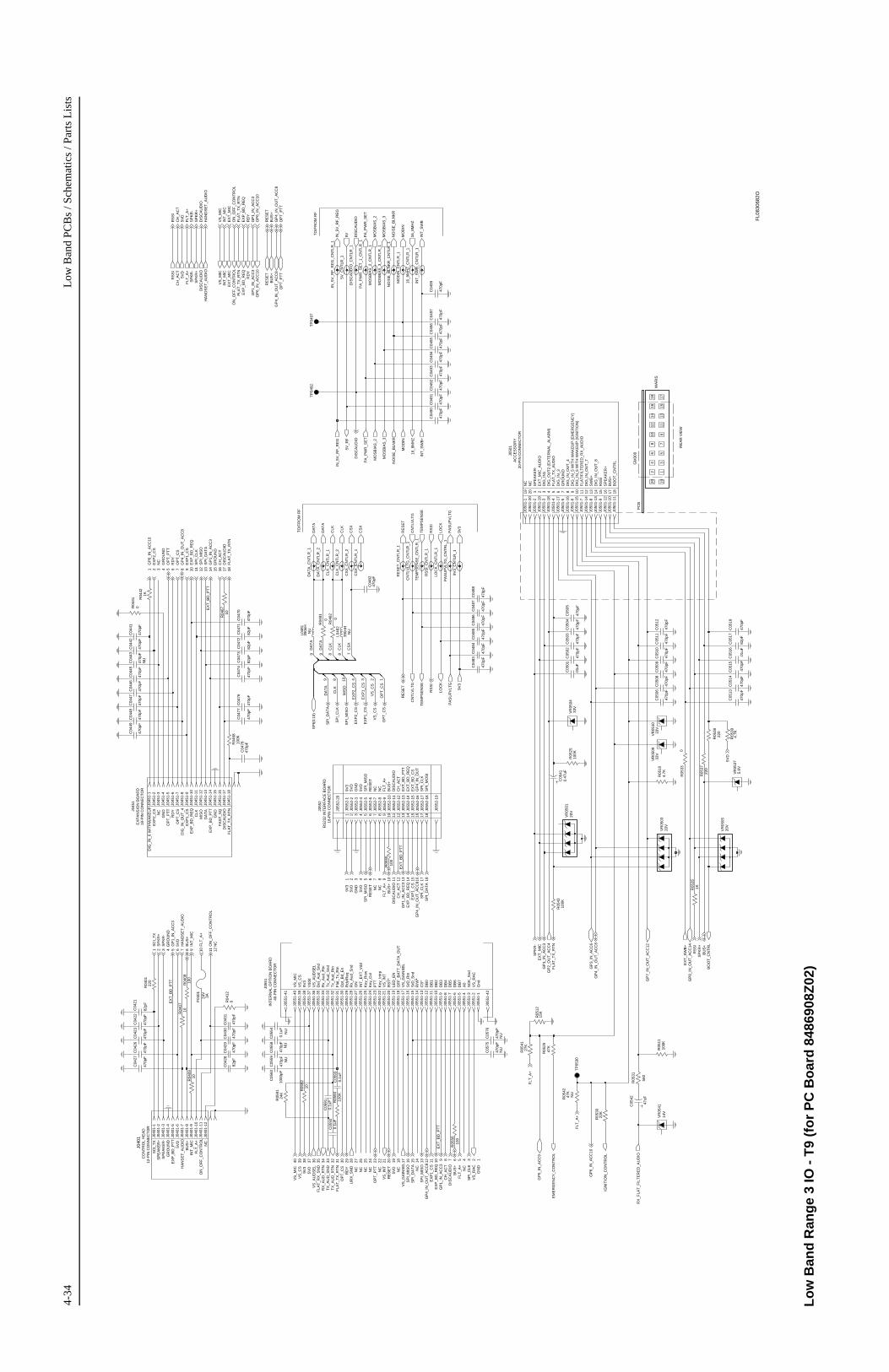
4-34
Low
Ban
d PC
Bs
/ Sch
emat
ics
/ Par
ts L
ists
NC
BU
S+
10
9V3
VS
_MIC
DA
TA
GM
300
SP
EA
KE
R-
CLK
30
13
J050
1
J045
1
DIG
_IN
_6 W
ITH
WA
KE
UP
(IG
NIT
ION
)F
LAT
/FIL
TE
RE
D_R
X_A
UD
IO
15 14
NC
7
VS
_GA
INS
EL
Gnd
11
DB
2
DIG
_IN
1
3
EX
P1_
CS
5 6
SP
EA
KE
R-
DIG
_IN
_OU
T_8
SW
B+
CLK
9
CS
*
24
DIS
CA
UD
IO
9
R/W
*
6
NC
13
DIG
_IN
_OU
T_4
GN
D
5
1517
15
6
40
18-P
IN C
ON
NE
CT
OR
RS
232
INT
ER
FA
CE
BO
AR
D
GN
D
BU
S+
5
NC
RS
SI
16
1
PC
B
23 21
SP
I_C
LKS
PI_
MO
SI
SC
K_S
nd
35
NC
3 4
EX
P_B
D_R
EQ
NC
NC
DB
6
AC
CE
SS
OR
Y
16
DB
3
MIS
O
NC
9 10 11
14
Rdy
/Req
2
GR
OU
ND
10
6
19
9
VS
_CS
RD
Y
EX
T_B
D_R
EQ
EX
T_B
D_C
S
12
18
Opt
_Bd_
En
61 2
13 14 15 16 17 18
RE
AR
VIE
W
15
16
34
INT
ER
NA
L O
PT
ION
BO
AR
D
39 38
GN
D
J055
2
NC
GR
OU
ND
GR
OU
ND
NC
BO
OT
_CN
TR
L
20
GR
OU
ND
DB
1
22
GP
4_IN
_OU
T
TO
/FR
OM
RF
8
SP
I_M
ISO
5VD
3
OF
F_B
AT
T_D
AT
A_O
UT
EX
T_B
D_P
TT
GN
D5V
D9V
3
5VD
EX
T_B
D_P
TT
13
10
Fla
t_T
x_R
tn
NC
1 2
SrD
_Snd
12 13
EX
T_B
D_P
TT
12
Rx_
Aud
_Rtn
12
31
4 12
18-P
IN C
ON
NE
CT
OR
717
1 2
7
9 11 12
20
NC
NC
10
OP
T_C
S
VS
_RA
C
8
RS
T*
7 8
14
INT
_EX
T_V
dd
4
EX
T_B
D_P
TT
9
2 1
NC
CLK
7
4 11
J055
1
28
FLT
_A+
Key
_Col
DIG
_OU
T2
(EX
TE
RN
AL_
ALA
RM
)
DA
TA
8
EX
P2_
CS
FA
ST
_SQ
CO
NT
RO
L H
EA
DJ0
401
5
4
EX
PA
NS
ION
BO
AR
D
OP
T_P
TT
16
20
SC
I_T
X
INT
_MIC
DIG
_IN
_3
Tx_
Aud
_Snd
Rx_
Aud
_Snd
SP
EA
KE
R+
BU
S+
11
10 11
NC
1
14 15 16 174
NC
HA
NS
ET
_AU
DIO
3
20-P
IN C
ON
NE
CT
OR
1817
GR
OU
ND
SrD
_Rtn
RE
SE
T
FLT
_A+
DIS
CA
UD
IOC
H_A
CT
DIG
_IN
_OU
T_4
DA
TA
EX
P1_
CS
VS
_AU
DS
EL
26
FLA
T_T
X_R
TN
8
5
Det
_Aud
_Snd
18
40-P
IN C
ON
NE
CT
OR
DB
5
EX
P_B
D_P
TT
GN
D
13
37
DIG
_IN
_OU
T_7
2
LED
_EN
EX
P2_
CS
36
DB
0
DA
TA
11
CLK
Tx_
Aud
_Rtn
PT
T
18
8
Vdd
d
2532
EX
T_B
D_P
TT
27O
N
VS
_IN
T
DIG
_IN
_5 W
ITH
WA
KE
UP
(E
ME
RG
EN
CY
)
5
Key
_Row
Key
_Int
rp
3
1
NC
NC
3
7 10
A0
EX
T_M
IC_A
UD
IO
4
VS
_CS
DB
4
EX
P_B
D_P
TT
SP
EA
KE
R+
14
3
ON
_OF
F_C
ON
TR
OL
33
OP
T_C
S
17
12-P
IN C
ON
NE
CT
OR
FLA
T_T
X_A
UD
IO
DB
7
19
DIG
_IN
_6 W
ITH
WA
KE
UP
7
9
6
CS
X29
12
MIS
O
2
5 6
18
8
19
WA
RIS
TO
/FR
OM
RF
10
TE
MP
SE
NS
E_C
NT
LR_1
J050
1-16
C05
05
470p
F
MO
DIN
J055
1-8
20V
VR
0505
CLK
_CN
TLR
_1
C05
18
470p
F
33V
VR
0509
470p
F
C04
23
J050
1-20
1000
pF
C05
60
J040
1-11
J050
1-17
PA
_PW
R_S
ET
16_8
MH
Z_C
NT
LR_1
470p
F
PA
SU
PV
LTG
C04
88
C05
13
470p
F
470p
F
DIS
CA
UD
IO
C04
84
NU
R05
4247
K
5.6V
VR
0537
82pF
C05
17
CN
TLV
LTG
_CN
TLR
_1
J040
1-1
J050
1-4
9
J055
1-3
J055
1-10
470p
F
C05
10
470p
F
C04
87
C04
31
470p
F
10R
0592
J045
1-5
J050
1-14
470p
F
C05
14
J050
1-3
R05
2510
0K
PA
_PW
R_S
ET
_1_C
NT
LR_1
J055
1-25
220
R05
38
20V
VR
0501
J055
1-4
J055
1-14
C05
42
47uF
0R
0533
J045
1-11
220
R04
01
J055
1-11
J055
1-37
NO
ISE
_BLN
KR
_CN
TLR
_1
3A24V
F04
01
470p
F
J050
1-5
J055
1-41
C04
95
J055
1-32
J045
1-1
J055
1-36
R05
3022
K
J040
1-7
J040
1-10
470p
F
RS
SI_
CN
TLR
_1C
0497
R04
410
470p
F
C05
75
C05
41
NU
0.47
uF
DA
TA
_CN
TLR
_1
J055
1-40
R04
120
J055
1-20
3
J045
1-10
C05
09
J045
1-17
470p
F
82pF
J050
1-2
C04
72
J050
1-12
J050
1-11
J045
1-6
1
100K
R05
43
J055
1-23
100K
J055
1-18
R05
11
CS
X_C
NT
LR_1
DA
TA
J040
1-5
470p
F
C05
59
R05
2947
K
NU
J055
1-19
470p
F
C04
26
C05
01
.01u
F
J045
1-16
82pF
C04
21
82pF
C04
73
J055
1-21
J040
1-4
J040
1-9
J040
1-3
J040
1-8
470p
F
DIS
CA
UD
IO_C
NT
LR_1
C04
77
LOC
K_C
NT
LR_1
0.1u
FC
0591
C04
47
470p
F
MO
DIN
_CN
TLR
_1
J055
1-22
J045
1-4
R05
9124
K
J055
1-31
C05
12
470p
F
CLK
MO
SB
IAS
_2_C
NT
LR_1
J055
1-42
470p
F
C04
42
IN_5
V_R
F_R
EG
_CN
TLR
_1
J040
1-12
470p
F
C04
85
J045
1-12
33V
VR
0510
J055
1-27
TE
MP
SE
NS
E
9
470p
F
C04
29
J050
1-15
15K
R05
12
80.
1uF
C05
92
R04
07
5V
560
10
IN_5
V_R
F_R
EG
R05
31
J055
1-12
J050
1-8
CLK
_CN
TLR
_2
2
J045
1-18
8L0
482
J045
1-7
NU
390n
H
470p
F
C04
94
C05
16
.01u
F
100
J055
1-15
R04
08
470p
F
7
C05
11
J055
1-29
4.7K
R05
39
J055
1-39
R05
104.
7K
J055
1-13
470p
F
C04
83
J050
1-1
470p
F
5V_C
NT
LR_1
C05
06V
R05
4114
V
RE
SE
T
C04
41
470p
F
470p
F
4C
SX
C04
93
DA
TA
TP
0530
J050
1-13
J055
1-26
J055
1-6
J040
1-6
J055
1-34
470p
F
82pF
C04
71
C04
22
C04
7847
0pF
0R
0482
R04
810
R04
6810
0K
NU
C04
43
470p
F
J055
1-17
J055
1-30
470p
F
J050
1-9
C04
74
470p
F
CN
TLV
LTG
C04
91
NU
L048
139
0nH
C04
49
MO
SB
IAS
_3
470p
F1K
R04
42
DA
TA
_CN
TLR
_2
C05
03
470p
F
PA
SU
PV
LTG
_CN
TR
L_1
J050
1-6
J040
1-2
VR
0503
20V
TP
0497
TP
0492
220
R05
37
CLK
J045
1-15
INT
_SW
B
J045
1-8
10R
0409
J045
1-2
0.1u
FC
0593
470p
F
C05
08
J050
1-10
MO
SB
IAS
_2
C04
90
9V3
470p
F
J055
1-35
J045
1-14
J055
1-1
J055
1-28
J045
1-9
1KR05
35
J050
1-19
C04
30
470p
F
VR
0504
33V
100K
R05
93
R05
5610
0
J045
1-13
C05
15
470p
F
470p
F
470p
F
C04
99
C04
86
CS
X_C
NT
LR_2
RE
SE
T_C
NT
LR_1
C04
76
470p
F
470p
F
J055
1-33
C04
82
C05
76
470p
F
9
9V3_
CN
TLR
_1
NU
470p
FN
U
C05
58
J055
1-24
NO
ISE
_BLN
KR
INT
_SW
B_C
NT
LR_1
LOC
K
RS
SI
MO
SB
IAS
_3_C
NT
LR_1
J055
1-2
J055
1-16
C04
70
470p
F
R05
4127
K
470p
F
C05
02
C04
92
470p
F
J050
1-18
470p
F
C05
04
J055
1-5
C04
96
470p
F
16_8
MH
Z
CS
X
J055
1-7
J055
1-38
82pF
8
C04
28
470p
F
C04
48
470p
F
C04
46C
0445
470p
F
0.1u
F
C05
54
J045
1-3
NU
R04
6710
J050
1-7
J055
1-9
SP
I_C
LK
EX
P1_
CS
GP
4_IN
_OU
T_A
CC
8O
PT
_CS
RD
YO
PT
_PT
T
EX
P2_
CS
EX
P_B
D_R
EQ
5VD
SP
KR
-S
PK
R+
ON
_OF
F_C
ON
TR
OL
BU
S+
BU
S+
470p
F
C04
27
GP
2_O
UT
_AC
C4
GP
5_IN
_AC
C9
GP
7_IN
_OU
T_A
CC
12
GP
8_IN
_OU
T_A
CC
14
SP
KR
+
GP
3_IN
_AC
C6
GP
4_IN
_OU
T_A
CC
8
EX
P2_
CS
FLA
T_T
X_R
TN
FLA
T_T
X_R
TN
GP
6_IN
_AC
C10
GP
6_IN
_AC
C10
GP
6_IN
_AC
C10
GP
6_IN
_AC
C10
GP
1_IN
_AC
C3
FLT
_A+
CH
_AC
T
GP
1_IN
_AC
C3
SP
I_D
AT
AS
PI_
MIS
O
9V3
SP
I_M
ISO
DIS
CA
UD
IO
MO
DIN
CH
_AC
T
5VD
9V3
5VD
SP
I_M
ISO
RE
SE
T
FLT
_A+
R05
5510
0D
ISC
AU
DIO
GP
4_IN
_OU
T_A
CC
8E
XP
1_C
SE
XP
_BD
_RE
QG
P1_
IN_A
CC
3
SP
I_C
LKS
PI_
DA
TA
SP
KR
-E
XT
_MIC
GP
1_IN
_AC
C3
INT
_MIC
INT
_MIC
INT
_MIC
SP
KR
+S
PK
R+
DIS
CA
UD
IOD
ISC
AU
DIO
HA
ND
SE
T_A
UD
IOH
AN
DS
ET
_AU
DIO
HA
ND
SE
T_A
UD
IO
RS
SI
RS
SI
BO
OT
_CN
TR
L
5VD
IN_5
V_R
F_R
EG
BU
S+
GP
1_IN
_AC
C3
GP
1_IN
_AC
C3
INT
_SW
B+
GP
4_IN
_OU
T_A
CC
8E
XP
1_C
S
EX
P_B
D_R
EQ
EX
P_B
D_R
EQ
EX
P_B
D_R
EQ
GP
1_IN
_AC
C3
CH
_AC
TC
H_A
CT
CH
_AC
TD
ISC
AU
DIO
FLT
_A+
SC
I_T
X
RX
_FLA
T_F
ILT
ER
ED
_AU
DIO
EM
ER
GE
NC
Y_C
ON
TR
OL
RS
SI
EX
T_S
WB
+
RD
YR
DY
RD
Y
OP
T_P
TT
OP
T_P
TT
OP
T_P
TT
NO
ISE
_BLN
KR
MO
SB
IAS
_2
PA
_PW
R_S
ET
EX
P1_
CS
9V3
FLA
T_T
X_R
TN
FLA
T_T
X_R
TN
GP
4_IN
_OU
T_A
CC
8G
P4_
IN_O
UT
_AC
C8
DIS
CA
UD
IO
SP
I(0:
10)
MO
SB
IAS
_3
VS
_MIC
VS
_MIC
FLA
T_T
X_R
TN
5VD
FLT
_A+
BU
S+
BU
S+
RE
SE
TR
ES
ET
ON
_OF
F_C
ON
TR
OL
ON
_OF
F_C
ON
TR
OL
16_8
MH
Z
5V_R
F
5VD
5VD
FLT
_A+
FLT
_A+
SP
I_D
AT
A
SP
I_C
LK
SP
I_M
ISO
VS
_CS
OP
T_C
SR
ES
ET
EX
T_M
ICE
XT
_MIC
SP
KR
-S
PK
R-
RE
SE
T
PA
SU
PV
LTG
BU
S+
TE
MP
SE
NS
E
CN
TLV
LTG
RS
SI
LOC
K
OP
T_C
S
SP
I_D
AT
A
TX
_AU
D_R
TN
VS
_CS
VS
_MIC
SP
I_C
LK
FLA
T_R
X_S
ND
RX
_AU
D_R
TN
UR
X_S
ND
TX
_AU
D_S
ND
VS
_IN
T
5VD
VS
_AU
DS
EL
VS
_GA
INS
EL
SP
I_M
ISO
VS
_RA
C
IGN
ITIO
N_C
ON
TR
OL
FLT
_A+
J055
2-1
J055
2-2
J055
2-3
J055
2-4
J055
2-5
J055
2-6
J055
2-7
J055
2-8
J055
2-9
J055
2-10
J055
2-11
J055
2-12
J055
2-13
J055
2-14
J055
2-15
J055
2-16
J055
2-17
J055
2-18
J055
2-19
J055
2-20
FL0
8306
82O
Lo
w B
and
Ran
ge
3 IO
- T
9 (f
or
PC
Bo
ard
848
6908
Z02
)
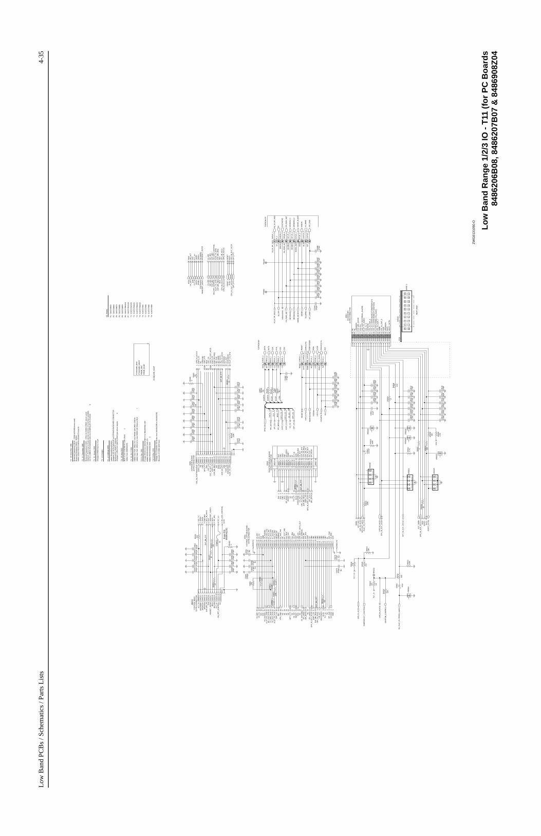
Low
Ban
d P
CB
s / S
chem
atic
s / P
arts
Lis
ts4-
35
R/W
*
Cha
nged
C05
93 b
ack
to 0
.1uF
SP
I_M
OS
I
T7
17.
Feb
ruar
200
0
Cha
nged
C05
xx fr
om 0
402
to 0
603
type
whe
re r
equi
red
NC
NC
7
T8
29.
May
200
0
Add
ed F
use
6580
542Z
01
T9
24.
JU
LY 2
000
Add
ed tr
ace
from
J05
51-6
to n
ew R
0556
100
Ohm
s to
BU
S+
Add
ed tr
ace
from
J05
52-1
0 to
new
R05
55 1
00 O
hms
to B
US
+
T8
010
2727
B68
T9
010
2727
B68
P5
010
2726
B94
CLK
9
Fus
e P
/N65
8054
2Z01
P2
010
2726
B66
CS
*
T6
010
2727
B64
T3
010
2727
B40
/41
24
DIS
CA
UD
IO
NC
BU
S+
Bac
k to
one
con
trol
ler
for
both
cha
ssi
s
10
T4
18.
Nov
embe
r 19
99
Rem
oved
Cap
acito
rs C
0519
- C
0540
&C
0498
(ne
ver
used
)
DIG
_IN
_OU
T_4
9
18
9V3
VS
_MIC
13
2G
ND
5
DA
TA
GM
300
SP
EA
KE
R-
CLK
30
13
J050
1
J045
1
DIG
_IN
_6 W
ITH
WA
KE
UP
(IG
NIT
ION
)F
LAT
/FIL
TE
RE
D_R
X_A
UD
IO
15 1416
1
PC
B
23 21
Add
ed J
0552
RS
232
Inte
rfac
e B
oard
Con
nect
orR
emov
ed R
esis
tors
R05
21 -
R05
24
T5
21.
Dec
embe
r 19
99
Rem
oved
Cap
acito
rs C
0401
- C
0411
& C
0451
-C04
68 (
neve
r us
ed)
Atte
ntio
n: F
rom
now
on
ther
e ar
e tw
o ve
rsio
ns o
f con
trol
lers
ava
ilabl
e,on
e fo
r LD
MO
S P
A C
HA
SS
IS a
nd o
ne fo
r B
IPO
LAR
PA
CH
AS
SI
S
T5
21.
Jan
uar
2000
SP
I_C
LK
8
Add
ed R
0442
/R05
43/R
0593
Rem
oved
RX
_AD
AP
T T
estp
oint
35
OF
F_B
AT
T_D
AT
A_O
UT
3 4
VS
_GA
INS
EL
Gnd
11
DB
2
DIG
_IN
1
3
EX
P1_
CS
5 6
SP
EA
KE
R-
DIG
_IN
_OU
T_8
SW
B+
14
Rdy
/Req
2
GR
OU
ND
10
6
19
9
VS
_CS
RD
Y
EX
T_B
D_R
EQ
EX
T_B
D_C
S
12
2
6
NC
1
12 13 14
1517
15
6
40
18-P
IN C
ON
NE
CT
OR
RS
232
INT
ER
FA
CE
BO
AR
D
GN
D
BU
S+
5
NC
RS
SI
GN
D
J055
2
NC
GR
OU
ND
GR
OU
ND
NC
BO
OT
_CN
TR
L
20
GR
OU
ND
DB
1
22
GP
4_IN
_OU
T
TO
/FR
OM
RF
DA
TA
Ass
igne
d G
P W
ITH
WA
KE
UP
on
EX
PA
NS
ION
BO
AR
D C
ON
NE
CT
OR
SC
K_S
nd
3
FA
ST
_SQ
EX
T_B
D_P
TT
GN
D
EX
P_B
D_R
EQ
NC
NC
DB
6
AC
CE
SS
OR
Y
16
DB
3
MIS
O
NC
9 10 11 12 13
EX
T_B
D_P
TT
12
Rx_
Aud
_Rtn
12
31
4 12
18-P
IN C
ON
NE
CT
OR
717
1
HA
NS
ET
_AU
DIO
Opt
_Bd_
En
6
11
17
20
NC
15 16 17 18
RE
AR
VIE
W
15
16
34
INT
ER
NA
L O
PT
ION
BO
AR
D
P6
010
2727
B03
/04
39 38
9
2 1
NC
CLK
7
4 11
J055
1
28
FLT
_A+
Key
_Col
DIG
_OU
T2
(EX
TE
RN
AL_
ALA
RM
)
EX
P2_
CS
SP
I_M
ISO
5VD
EX
P2_
CS
11
CO
NT
RO
L H
EA
DJ0
401
5VD
9V3
5VD
EX
T_B
D_P
TT
13
10
Fla
t_T
x_R
tn
NC
1 2
SrD
_Snd
P4
010
2726
B86
SP
EA
KE
R+
BU
S+
11
10 11
NC
1
14 15 16 174
NC
33
7
9
18
17
GR
OU
ND
SrD
_Rtn
NC
10
OP
T_C
S
VS
_RA
C
8
RS
T*
7 8
14
INT
_EX
T_V
dd
4
EX
T_B
D_P
TT
5
Det
_Aud
_Snd
18
40-P
IN C
ON
NE
CT
OR
DB
5
EX
P_B
D_P
TT
GN
D
P3
010
2726
B70
13
37
DIG
_IN
_OU
T_7
2
LED
_EN
Add
ed R
0508
066
2057
A41
470
T4
010
2727
B51
/52
8
DA
TA
DIG
_IN
_6 W
ITH
WA
KE
UP
CLK
Tx_
Aud
_Rtn
P1
010
2726
B32
5
4
EX
PA
NS
ION
BO
AR
D
OP
T_P
TT
16
20
SC
I_T
X
INT
_MIC
DIG
_IN
_3
Tx_
Aud
_Snd
Rx_
Aud
_Snd
ON
VS
_IN
T
T2
010
2727
B24
/25
DIG
_IN
_5 W
ITH
WA
KE
UP
(E
ME
RG
EN
CY
)
5
Key
_Row
Key
_Int
rp
3
1
NC
NC
3
ON
_OF
F_C
ON
TR
OL
T10
21.
Feb
. 200
1
3
20-P
IN C
ON
NE
CT
OR
OP
T_C
S
12-P
IN C
ON
NE
CT
OR
FLA
T_T
X_A
UD
IO
DB
7
RE
SE
T
FLT
_A]
DIS
CA
UD
IOC
H_A
CT
DIG
_IN
_OU
T_4
DA
TA
I/O H
isto
ry
EX
P1_
CS
VS
_AU
DS
EL
26
FLA
T_T
X_R
TN
8
7
9
6
CS
X29
12
MIS
O
2
5 6
18
8
Cha
nge
R05
30 fr
om 0
6620
57B
47 0
to 0
6620
57A
81 2
2K
Cha
nge
T11
Con
trol
ler
I/O K
it N
o: fr
om 0
1040
12J9
6 to
010
4013
J52
Bec
ause
of C
0560
(60
3 S
ize)
Add
ed R
0509
066
2057
B47
0
36
DB
0
19
PTT
18
8
T5
010
2727
B51
/52
T7
010
2727
B68
T6
no
chan
ges
Vdd
d
25
P7
010
2727
B15
/16
32
EX
T_B
D_P
TT
27
19W
AR
IS
TO
/FR
OM
RF
7 10
A0
EX
T_M
IC_A
UD
IO
4
VS
_CS
DB
4
EX
P_B
D_P
TT
SP
EA
KE
R+
14
3
PA
_PW
R_S
ET
CO
NT
RO
LLE
R B
IPO
LAR
PA
Kla
us-D
iete
r D
eman
t
WA
RIS
MO
BIL
E
INT
ER
FA
CE
/ C
ON
NE
CT
OR
S4
1 3 A
?
3
5
T9
08.1
2.18
12:3
6:17
pm
Mon
day,
Feb
ruar
y 26
, 200
1P
rase
thy
Lee,
IL26
Kla
us-D
iete
r D
eman
t
T10
23.
May
. 200
1
470p
F
PA
SU
PV
LTG
C05
13
TE
MP
SE
NS
E_C
NT
LR_1
J050
1-16
10
C05
0547
0pF
MO
DIN
J055
1-8
VR
0505
CLK
_CN
TLR
_1
C05
1847
0pF
VR
0509
C04
8747
0pF
C04
3147
0pF
470p
FC
0423
470p
FC
0514
J050
1-3
J050
1-20
C05
6010
00pF
J040
1-11
J050
1-17
J045
1-11
16_8
MH
Z_C
NT
LR_1
220
R04
01
J055
1-11
C04
8847
0pF
3A
F04
01
J050
1-5
C04
9547
0pF
470p
F
DIS
CA
UD
IO
47K
C04
84
NU
R05
42
VR
0537
J040
1-1
82pF
C05
17
CN
TLV
LTG
_CN
TLR
_1
J050
1-4
9
J055
1-3
J055
1-10
470p
FC
0510
0.47
uFC
0541
J055
1-40
10R
0592
J045
1-5
J050
1-14
3
J055
1-20
R05
2510
0K
PA
_PW
R_S
ET
_1_C
NT
LR_1
J055
1-25
220
R05
38
VR
0501
J055
1-4
J055
1-14
C05
42
47uF
R05
33
J055
1-23
0
J055
1-18
R05
1110
0K
CS
X_C
NT
LR_1
J055
1-37
NO
ISE
_BLN
KR
_CN
TLR
_1
R05
29
47K
J055
1-19
J055
1-41
J045
1-1
J055
1-36
J055
1-32
R05
30
22K
J040
1-10
J040
1-7
470p
F
RS
SI_
CN
TLR
_1
C04
97
R04
410
470p
F
NU
470p
FC
0575
DIS
CA
UD
IO_C
NT
LR_1
C04
77
DA
TA
_CN
TLR
_1
LOC
K_C
NT
LR_1
0R04
12
C04
4747
0pF
J055
1-22
MO
DIN
_CN
TLR
_1
J045
1-10
470p
FC
0509
J045
1-17
J050
1-2
C04
7282
pF
J050
1-11
J045
1-6
1
J050
1-12
100K
R05
43
J045
1-12
VR
0510
DA
TA
J040
1-5
NU
470p
FC
0559
470p
FC
0429
J050
1-15
R05
1215
K
C04
2647
0pF
C05
01.0
1uF
C04
21
J045
1-16
82pF
82pF
C04
73
J040
1-4
J055
1-21
J040
1-9
J040
1-3
J040
1-8
J045
1-18
8C
LK_C
NT
LR_2
0.1u
FC
0591
470p
FC
0494
C05
16.0
1uF
J045
1-4
R05
9124
K
J055
1-31
470p
F
CLK
C05
12
MO
SB
IAS
_2_C
NT
LR_1
J055
1-42
470p
FC
0442
IN_5
V_R
F_R
EG
_CN
TLR
_1
C04
85
J040
1-12
J055
1-13
470p
FC
0483
9
470p
F
J055
1-27
TE
MP
SE
NS
E
RE
SE
T
VR
0541
470p
FC
0441
80.
1uF
C05
92
R04
07
5V
560
10
IN_5
V_R
F_R
EG
R05
31
J055
1-12
2
J050
1-8
L048
2
J045
1-7
NU
390n
H
C04
7847
0pF
J055
1-15
R04
0810
0
470p
FC
0511
7
R05
39
J055
1-29
4.7K
J055
1-39
R05
104.
7K
NU
L048
139
0nH
J050
1-1
C05
0647
0pF
C04
49
5V_C
NT
LR_1
MO
SB
IAS
_3
470p
F1K
R04
42
ST
AN
DA
RD
_MU
HF
PR
IME
_MU
HF
PR
IME
_BN
CS
TA
ND
AR
D_M
UH
F
ST
AN
DA
RD
_BN
C
o
4
C04
9347
0pF
DA
TA
TP
0530
CS
X
J055
1-26
J050
1-13
J040
1-6
CLK
J055
1-6
J045
1-8
J055
1-34
470p
F
82pF
C04
71
C04
22
0.1u
FC
0593
R04
820
R04
810
R04
6810
0K
C04
4347
0pF
J055
1-17
NU
J055
1-30
C04
7447
0pF
J050
1-9
470p
F
CN
TLV
LTG
J045
1-9
C04
91
100K
R05
93
VR
0504
J045
1-13
C05
1547
0pF
DA
TA
_CN
TLR
_2
C05
0347
0pF
PA
SU
PV
LTG
_CN
TR
L_1
J050
1-6
J040
1-2
VR
0503
TP
0492
TP
0497
R05
3722
0
J045
1-15
470p
F
INT
_SW
B
NU
C05
58
10R
0409
J045
1-2
LOC
K
RS
SI
MO
SB
IAS
_3_C
NT
LR_1
MO
SB
IAS
_2
470p
FC
0508
J050
1-10
C04
90
9V3
470p
F
J055
1-35
J045
1-14
J055
1-1
J055
1-28
C04
9247
0pF
R05
351K
J050
1-19
470p
F
J055
1-5
C04
30
C04
9647
0pF
470p
FC
0486
470p
FC
0499
RE
SE
T_C
NT
LR_1
CS
X_C
NT
LR_2
C04
7647
0pF
J055
1-33
C04
8247
0pF
NU
C05
7647
0pF
9
9V3_
CN
TLR
_1
C05
54
J045
1-3
NU
0.1u
F
J055
1-24
NO
ISE
_BLN
KR
INT
_SW
B_C
NT
LR_1
10R
0467
J055
1-9
J050
1-7
470p
FC
0427
J055
1-2
J055
1-16
C04
7047
0pF
R05
4127
K
470p
FC
0502
J050
1-18
470p
FC
0504
0
R05
09
470
R05
08
J055
1-7
16_8
MH
Z
J055
1-38
CS
X
8
C04
2882
pF
C04
4847
0pF
C04
4547
0pF
470p
FC
0446
GP
4_IN
_OU
T_A
CC
8O
PT
_CS
RD
YO
PT
_PT
T
EX
P2_
CS
EX
P_B
D_R
EQ
5VD
SP
KR
-S
PK
R+
ON
_OF
F_C
ON
TR
OL
BU
S+
BU
S+
GP
6_IN
_AC
C10
GP
5_IN
_AC
C9
GP
2_O
UT
_AC
C4
GP
7_IN
_OU
T_A
CC
12
GP
8_IN
_OU
T_A
CC
14
SP
KR
+
GP
3_IN
_AC
C6
GP
4_IN
_OU
T_A
CC
8
EX
P2_
CS
FLA
T_T
X_R
TN
FLA
T_T
X_R
TN
GP
6_IN
_AC
C10
GP
6_IN
_AC
C10
GP
6_IN
_AC
C10
GP
1_IN
_AC
C3
FLT
_A+
CH
_AC
T
GP
1_IN
_AC
C3
SP
I_D
AT
AS
PI_
MIS
OS
PI_
CLK
EX
P1_
CS
9V3
SP
I_M
ISO
DIS
CA
UD
IO
MO
DIN
CH
_AC
T
5VD
9V3
5VD
SP
I_M
ISO
RE
SE
T
FLT
_A+
DIS
CA
UD
IO
GP
4_IN
_OU
T_A
CC
8E
XP
1_C
SE
XP
_BD
_RE
QG
P1_
IN_A
CC
3
SP
I_C
LKS
PI_
DA
TA
SP
KR
-E
XT
_MIC
GP
1_IN
_AC
C3
INT
_MIC
INT
_MIC
INT
_MIC
SP
KR
+S
PK
R+
DIS
CA
UD
IOIS
CA
UD
IOH
AN
DS
ET
_AU
DIO
HA
ND
SE
T_A
UD
IO
RS
SI
RS
SI
BO
OT
_CN
TR
L
5VD
IN_5
V_R
F_R
EG
BU
S+
GP
1_IN
_AC
C3
GP
1_IN
_AC
C3
INT
_SW
B+
GP
4_IN
_OU
T_A
CC
8E
XP
1_C
S
EX
P_B
D_R
EQ
EX
P_B
D_R
EQ
EX
P_B
D_R
EQ
GP
1_IN
_AC
C3
CH
_AC
TC
H_A
CT
CH
_AC
TD
ISC
AU
DIO
FLT
_A+
SC
I_T
X
RX
_FLA
T_F
ILT
ER
ED
_AU
DIO
EM
ER
GE
NC
Y_C
ON
TR
OL
RS
SI
EX
T_S
WB
+
RD
YR
DY
RD
Y
OP
T_P
TT
OP
T_P
TT
OP
T_P
TT
NO
ISE
_BLN
KR
MO
SB
IAS
_2
PA
_PW
R_S
ET
EX
P1_
CS
9V3
FLA
T_T
X_R
TN
FLA
T_T
X_R
TN
GP
4_IN
_OU
T_A
CC
8G
P4_
IN_O
UT
_AC
C8
DIS
CA
UD
IO
SP
I(0:
10)
MO
SB
IAS
_3
VS
_MIC
VS
_MIC
FLA
T_T
X_R
TN
5VD
FLT
_A+
BU
S+
BU
S+
RE
SE
TR
ES
ET
ON
_OF
F_C
ON
TR
OL
ON
_OF
F_C
ON
TR
OL
16_8
MH
Z
5V_R
F
5VD
5VD
FLT
_A+
SP
I_D
AT
A
SP
I_C
LK
SP
I_M
ISO
VS
_CS
OP
T_C
SR
ES
ET
EX
T_M
ICE
XT
_MIC
SP
KR
-S
PK
R-
RE
SE
T
PA
SU
PV
LTG
BU
S+
TE
MP
SE
NS
E
CN
TLV
LTG
RS
SI
LOC
K
OP
T_C
S
SP
I_D
AT
A
TX
_AU
D_R
TN
VS
_CS
VS
_MIC
SP
I_C
LK
FLA
T_R
X_S
ND
RX
_AU
D_R
TN
UR
X_S
ND
TX
_AU
D_S
ND
VS
_IN
T
5VD
VS
_AU
DS
EL
VS
_GA
INS
EL
SP
I_M
ISO
VS
_RA
C
IGN
ITIO
N_C
ON
TR
OL
FLT
_A+
FLT
_A+
HA
ND
SE
T_A
UD
IO
ZW
G01
3105
0-O
Lo
w B
and
Ran
ge
1/2/
3 IO
- T
11 (
for
PC
Bo
ard
s84
8620
6B08
, 848
6207
B07
& 8
4869
08Z
04

4-36
Low
Ban
d PC
Bs
/ Sch
emat
ics
/ Par
ts L
ists
LSIO
F1200SYN
Che
ck P
IN V
alue
s on
IC
CLK
GP2_OUT
CSX
DATA
VOX
CH_ACT
HSIO
SQ_DET
4
0.1u
FC
0251
C02
550.
1uF
1
1
VD
DC
P32
VD
DD
33
VD
DD
AC
SQ
CA
P
11 12
VDDRC45
VD
DS
YN
27
VO
X7
SQDET 17
SQ
IN9
SY
N28
TX
RT
N36
TXSND44
UIO
10
VD
DA
LSIO 18
MICEXT48
MICINT46
MOD40
NC
26
PLC
AP
8
PLC
AP
225
GCB5RXSND
AUXTNRXRTN
3839
GN
DA
3
GN
DD
GN
DD
0
31 30
GNDRC47
GNDSYN23
HSIO 19
24LCAP
DATA22
DIS
C2
F12
0029
GCB0 15GCB1 14GCB2 13
GC
B3
35
37GCB4
CHACT 16
CLK21
CLK
168
34
CSX 20
DA
CG
6D
AC
R54
DA
CU
63A
53U
0221
AUDIO414243
R02
06
10K
C02
05
2200
pFN
U
0.1u
FC
0266
NU
C02
67
C02
31
1uF
.01u
F
6 57
4 11
11
Y1
1
Z4
Z0
5 3Z
1
U02
11-2
MC
3403
GND8
VCC16
VEE7
X14
X0
12
X1
13
Y15
Y0
2
U02
51
11A B
10
C9
EN
6
R02
08
2.2K
6
MC
1405
3B
NU
C02
110.
1uF
NU
9
R02
6624
K
C02
24
100p
F
C02
37
2.2u
FN
U
47K
R02
67
10K
R02
68
10uF
C02
02
10uF
C02
12
0.1u
F
C02
25
C02
7547
uF
24K
R02
73
10uF
C02
01
23
8
NU
8.2K
R02
258.
2KR
0224
100p
FC
0243
R02
42 0.1u
F
NU
0
1214
4 11
C02
42
U02
11-4
MC
3403
13
560
C02
44
R02
04
C02
35
0.1u
F
C02
71
.022
uF
.01u
F
47K
R02
41.0
1uF
100p
FC
0256
C02
46
R02
56
100K
10K
R02
5410
K
R02
55
0.1u
FC
0241
TP
0221
57R
01E
0272
8.2K
R02
20
NU
C02
45
0.1u
F
100
R02
03
C02
33
0.22
uFN
U
15K
1000
pF
R02
76
7VCC
C02
76
GND1
GND25
9IN
V
8M
_SS
1N
INV
4O
UT
1
6O
UT
2R
R3
TD
A15
19C
U02
71
2
10K
R02
61
0.1u
FC
0274
NU
C02
32
0.1u
F
R02
271M
EG
NU
9 108
4 11U
0211
-3M
C34
03
5
0.1u
FC
0222
100K
R02
53
100p
FC
0253
NU
1uF
C02
52
7
C02
9110
uF
C02
90
10uF
NUR
0207
2.2K
R02
261M
EG
0.1u
F NU
10uF
C02
27
C02
9210
uF
C02
93
C02
21
0.1u
F
0.1u
F
R02
52C
0223
56K
30K
R02
23
0.1u
F
C02
61
R02
12
R02
11
7.5K
C02
36
7.5K
.033
uF
R02
6524
K
C02
65
0.1u
F
NU
5 3
1 2
4
D02
01
0.1u
FC
0254
C02
34
7
0.1u
F
TP
0222
C02
7333
00pF
47K
R02
51
2.2K
R02
57
C02
284.
7uF
10K
Q02
71
R02
75
R02
28
C02
72
0
0.1u
F
560
R02
02
C02
62
R02
22
82pF
24K
0.1u
F
C02
26
470
NU
R02
69
2200
pF
C02
03
10R
0229
0.1u
F
C02
04 R02
21
24K
270K
R02
62
C02
7710
00pF
U02
11-1
MC
3403
2 31
4 11
57R
01E
0271
R02
74
NU
10K
R02
01
R02
05
100
5V_R
F5V
_RF
TX
_AU
D_R
TN
5V_R
F
TX
_AU
D_S
ND
5V_R
F
DIS
CA
UD
IO
5V_R
F
5V_R
F
RX
_AD
AP
T
FLA
T_T
X_R
TN
10K
9V3
9V3
MO
DIN
INT
_SW
B+
CH
_AC
T
VA
G
9V3
9V3
9V3
VS
_MIC
MO
SB
IAS
_3
16_8
MH
Z
VA
G
EX
T_M
IC
5V_R
F
5V_R
F
5VD
5VD
5V_R
F
SP
KR
-
RX
_AU
D_R
TN
INT
_MIC
UR
X_S
ND
FLA
T_R
X_S
ND
DC
_PO
WE
R_O
N
FLT
_A+
5VD
SP
KR
+
5VD
PA
_PW
R_S
ET
MO
SB
IAS
_2
9V3
NO
ISE
_BLN
KR
VS
_AU
DS
EL
SP
I(0:
10)
GP
IO(0
:13)
CN
TLR
_AU
DIO
(0:7
)
VA
G
VA
G
HA
ND
SE
T_A
UD
IO
RX
_FLA
T_F
ILT
ER
ED
_AU
DIO
FL0
8306
80O
Lo
w B
and
Ran
ge
1/2/
3 (2
9.7-
36.0
/36.
0-42
.0/4
2-50
MH
z) -
Au
dio
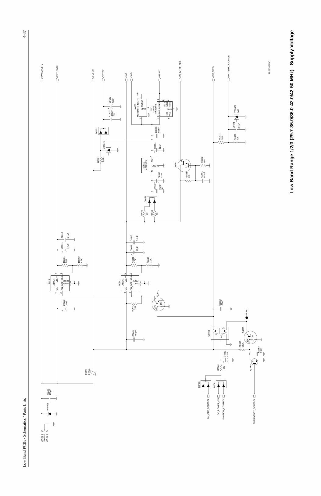
Low
Ban
d P
CB
s / S
chem
atic
s / P
arts
Lis
ts4-
37
10
22uF
C06
11
R06
51
C06
5233
uF
R06
124.
7K
D06
61
Q06
62
R06
7130
K
10K
VIN
4V
OU
T5
R06
72
LM29
41
U06
11 AD
J1
GND1 3
GND2 6
2O
N_O
FF
10K
47K 47
K
C06
71
0.1u
F
R06
41
J060
1-1
.01u
FC
0662
R06
6215
0KQ
0663
47K
47K
D06
21
C06
03
R06
61
1K
10uF
RE
SE
T
RE
SE
T 1
VR
0621
GNDGND 4
INP
UT
22N
P
NC
1
3
NC
25
NC
36
NC
47 8
NC
5
U06
52M
C33
064
2
GND
1IN
OU
T3
TP
0661
C06
63
MC
78M
05U
0651
0.1u
F
R06
43
0.1u
F
1.2K
C06
51C
0655
NU
0.1u
F
0.1u
F
C06
45
470p
F
VR
0601
NU
C06
21
4V
IN5
VO
UT
47uF
C06
22
U06
41
LM29
41
1A
DJ
GND13
GND26
ON
_OF
F2
Q06
61
R06
1156
K
VR
0671
NU
Q06
81 R06
8268
K
R06
8118
K
57R
01E
0631
470p
FC
0601
47uF
C06
61
R06
427.
5K47
0pF
C06
41C
0644
33uF
D06
51
0.1u
F
J060
1-2
C06
81
C06
12
0.1u
F
J060
1-3
D06
60
R06
52
R06
21
10
24K
Q06
41
MC
3346
4N-4
5AT
RU
0653
NU
10uF
9V3
FLT
_A+
IN_5
V_R
F_R
EG
RE
SE
T
5VD
C06
54
DC
_PO
WE
R_O
N
IGN
ITIO
N_C
ON
TR
OL
EM
ER
GE
NC
Y_C
ON
TR
OL
BA
TT
ER
Y_V
OLT
AG
E
ON
_OF
F_C
ON
TR
OL
EX
T_S
WB
+
INT
_SW
B+
PA
SU
PV
LTG
VS
TB
Y
FL0
8306
79O
Lo
w B
and
Ran
ge
1/2/
3 (2
9.7-
36.0
/36.
0-42
.0/4
2-50
MH
z) -
Su
pp
ly V
olt
age
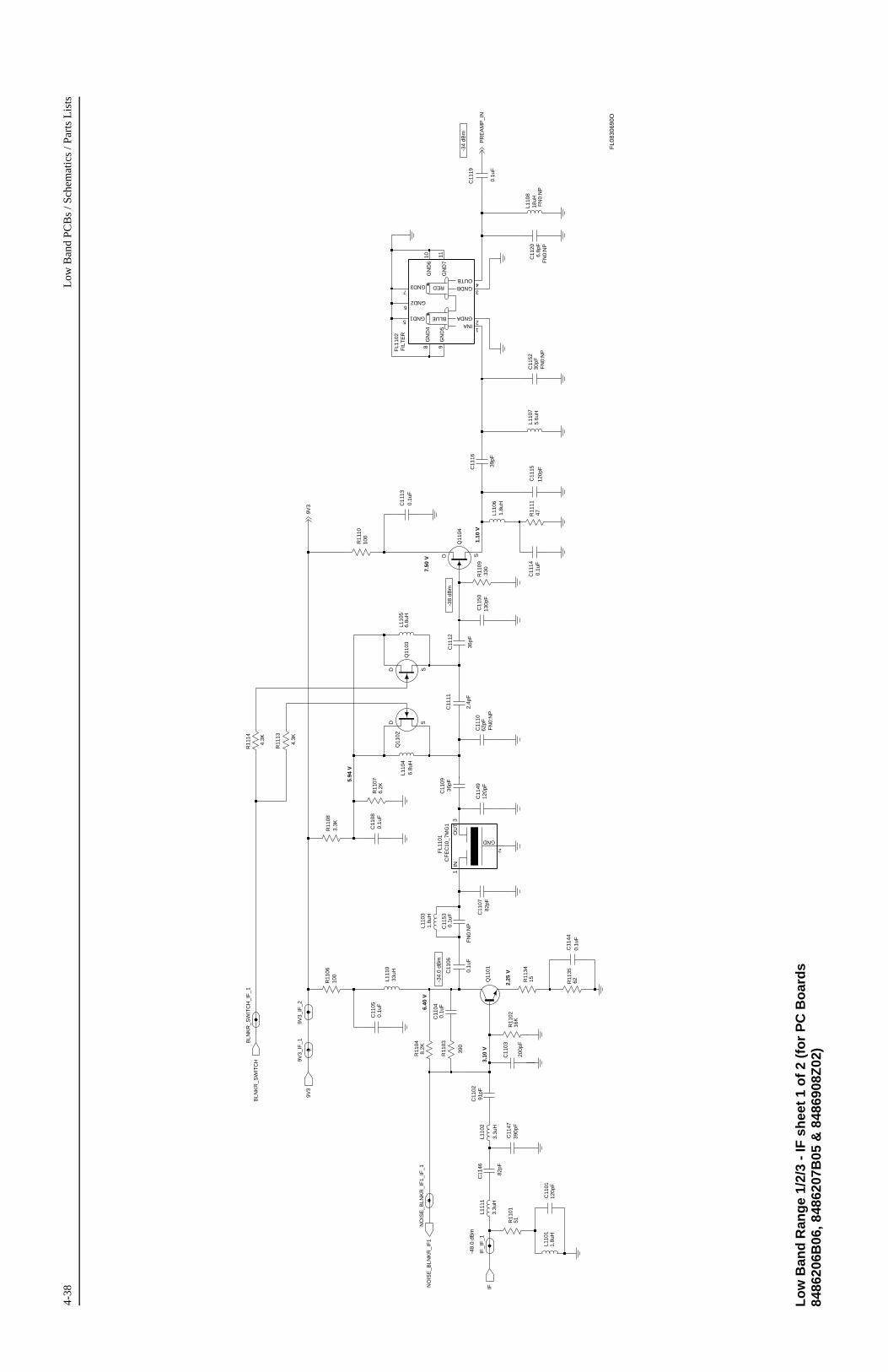
4-38
Low
Ban
d PC
Bs
/ Sch
emat
ics
/ Par
ts L
ists
-48.
0 dB
m
-34.
0 dB
m
-38
dBm
-34
dBm
3.10
V
2.25
V
5.94
V
7.50
V
1.10
V
6.40
V
R11
0933
0
36pF
C11
15
120p
F
C11
12
R11
35
R11
083.
3K
62
BLN
KR
_SW
ITC
H_I
F_1
R11
1147
FN
0:N
P
L110
818
uH
R11
048.
2K
15R11
34
33uH
L111
0
100
R11
06
S
L110
46.
8uH
Q11
04
D
120p
FC
1149
9V3_
IF_1
200p
F
C11
03
L110
56.
8uH
NO
ISE
_BLN
KR
_IF
1
3.3u
H
L110
2
D S
C11
0291
pFC
1110
FN
0:N
P
Q11
02
S
BLN
KR
_SW
ITC
H
62pF
Q11
03
D
Q11
0182
pFC
1107
C11
16
39pF
9V3
0.1u
FC
1114
36pF
C11
09
L110
31.
8uH
R11
1010
0
FN
0:N
P6.
8pF
C11
20
C11
130.
1uF
390p
FC
1147
C11
5230
pFF
N0:
NP
4.3K
R11
14
FL1
101
CF
EC
10_7
MG
1
GND
2
IN1
OU
T3
16K
R11
02
R11
03
390
0.1u
FC
1105
L110
75.
6uH
C11
06
0.1u
F
C11
040.
1uF
R11
13
4.3K
L111
1
3.3u
H
GN
D7
11
GNDA2
GNDB3
INA1
OUTB4
IF
9V3_
IF_2
GND15
6GND2
7GND3
GN
D4
BLUE
RED
8
GN
D5
9
GN
D6
10
0.1u
FC
1144
FL1
102
FIL
TE
R
R11
076.
2K
IF_I
F_1
NO
ISE
_BLN
KR
_IF
1_IF
_1
51R11
01
C11
46
82pF
C11
19
0.1u
F
C11
530.
1uF
FN
0:N
P
L110
112
0pF
C11
011.
8uH
0.1u
FC
1108
2.4p
F
C11
5013
0pF
L110
6
C11
11
9V3
PR
EA
MP
_IN
1.8u
H
FL0
8306
90O
Lo
w B
and
Ran
ge
1/2/
3 -
IF s
hee
t 1
of
2 (f
or
PC
Bo
ard
s 84
8620
6B06
, 848
6207
B05
& 8
4869
08Z
02)
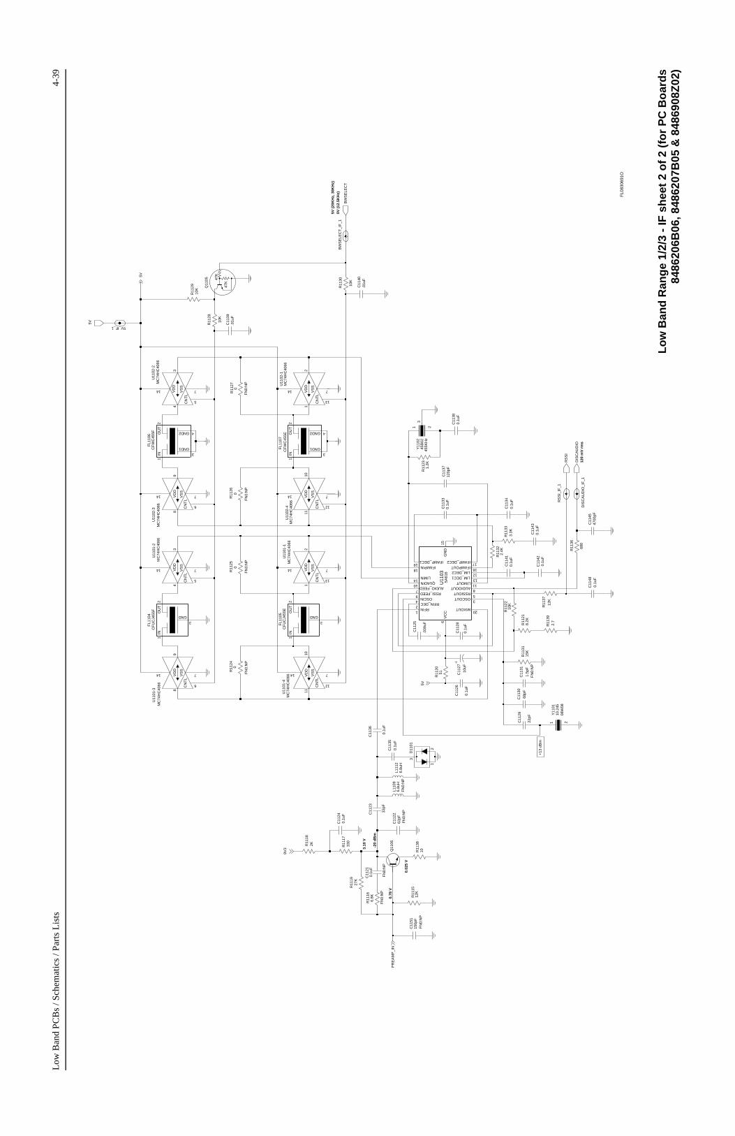
Low
Ban
d P
CB
s / S
chem
atic
s / P
arts
Lis
ts4-
39
3.10
V
5V (
20K
Hz,
30K
Hz)
0V (
12.5
KH
z)
+13
dB
m
120
mV
rm
s
0.78
V
0.02
5 V
-20
dB
m
RS
SI_
IF_1
U11
01-3
MC
74H
C40
66 6
CN
TL
89
14
VD
D
7
VS
S
R11
37
12K
C11
29
22pF
R11
20
10K
R11
30
51
.01u
F
R11
24
FN
0:N
P
C11
40
1110
14
VD
D
7
VS
S
0
U11
02-4
MC
74H
C40
66 12
CN
TL
R11
29
47K
47K
DIS
CA
UD
IO
C11
39
10K
680
.01u
F
0.1u
F
R11
36
C11
30
C11
35
0.1u
F
68pF
R11
21
C11
48
GND13
GND2 4
1IN
2O
UT
8.2K
R11
32
CF
WC
455F
FL1
106
R11
31
2.4K
Q11
05
15K
3.3K
R11
33
0R
1126
FN
0:N
P
0R
1125
FN
0:N
P
2
3
1
120p
F
D11
01
Y11
01
08W
0810
.245
21
C11
37
0R
1127
FN
0:N
P
GND13
4GND2
1IN
2O
UT
CF
WC
455E
FL1
107
R11
19
C11
27
10uF
C11
26
27K
1.2K
0.1u
F
R11
23
Q11
06
FN
0:N
P
C11
210.
1uF
C11
340.
1uF
6.8u
HL1
112
10R11
38
62pF
C11
22
CN
TL
5
43
VD
D
14
VS
S
7
FN
0:N
P
14
VD
D
7
VS
S
MC
74H
C40
66U
1102
-2
U11
02-1
MC
74H
C40
66
13
CN
TL
12
0.1u
FC
1142
3
21
DIS
CA
UD
IO_I
F_1
R11
15
455K
Hz
45B
02Y
1102
R11
22
12K
C11
31
10K
C11
41
FN
0:N
P1.
5pF
C11
24
0.1u
F
C11
36
0.1u
F
0.1u
F
C11
33
.039
uF
C11
25
0.1u
F
QUADIN10
RFIN1
RFIN_DEC2
RSSIOUT5
RSSI_FEED9
6V
CC
IFAMP_DEC217
LIMIN14
LIMOUT11
LIM_DEC113
LIM_DEC212
20MIXOUT
OSCIN4
OSCOUT3
AUDIOOUT8
AUDIO_FEED7
GN
D15
IFAMPIN18
IFAMPOUT16
IFAMP_DEC119
U11
03S
A61
6
GND
3
IN1
OU
T2
R11
28
10K
FL1
104
CF
UC
J455
F
10V
DD
14
VS
S
7
BW
SE
LEC
T
R11
392.
7
MC
74H
C40
66U
1101
-4
CN
TL
12
11
C11
28
0.1u
F
6
CN
TL
89
14 VD
D
7
VS
S
GND
3
IN1
OU
T2
U11
02-3
MC
74H
C40
66
R11
17
FL1
105
CF
UC
J455
E
43
14 VD
D
7
VS
S
330
C11
38
U11
01-2
MC
74H
C40
66
5
CN
TL
0.
1uF
6.8K
R11
16
BW
SE
LEC
T_I
F_1
5V_IF_1
5V
FN
0:N
P
FN
0:N
P
L110
96.
8uH
FN
0:N
P15
0pF
C11
51
C11
23
33pF
VD
D
14
VS
S
7
2KR11
18
MC
74H
C40
66U
1101
-1
CN
TL
13
12
C11
4547
00pF
RS
SI
0.1u
FC
1143
5V
5V
9V3
PR
EA
MP
_IN
FL0
8306
91O
Lo
w B
and
Ran
ge
1/2/
3 -
IF s
hee
t 2
of
2 (f
or
PC
Bo
ard
s84
8620
6B06
, 848
6207
B05
& 8
4869
08Z
02)
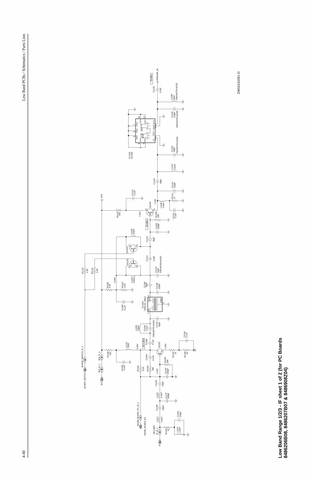
4-40
Low
Ban
d PC
Bs
/ Sch
emat
ics
/ Par
ts L
ists
G
G
G
G
6.40
V
-48.
0 dB
m
-34.
0 dB
m
-38
dBm
-34
dBm
3.10
V
2.25
V
5.94
V
7.50
V
1.10
V
L110
7
C11
06
5.6u
H
0.1u
F
R11
13
0.1u
F
C11
04
L111
1
4.3K
9V3_
IF_2
3.3u
H
8G
ND
4
9G
ND
5
10G
ND
6
11G
ND
7
2GN
DA
3
GN
DB
1
INA
4OU
TB
IF
FIL
TE
RF
L110
2
5G
ND
1G
ND
2
6G
ND
3
7
C11
440.
1uF
6.2K
R11
07
IF_I
F_1
NO
ISE
_BLN
KR
_IF
1_IF
_1
R11
01 51
82pF
C11
46
0.1u
F
C11
19F
N0:
NO
TP
LAC
ED
0.1u
FC
1153
L110
11.
8uH
C11
0112
0pF
0.1u
FC
1108
130p
FC
1150
2.4p
F
C11
11
1.8u
H91
pF
C11
02
L110
6
Q11
02D S
C11
1062
pF
D S
BLN
KR
_SW
ITC
H
FN
0:N
OT
PLA
CE
D
Q11
03
Q11
01C
1107
82pF
39pF
C11
16
9V3
C11
140.
1uF
C11
0936
pF
R11
10
1.8u
HL1
103
6.8p
FF
N0:
NO
TP
LAC
ED
100
C11
20
0.1u
FC
1113
C11
4739
0pF
FN
0:N
OT
PLA
CE
D30
pFC
1152
1IN
3O
UT
R11
14
4.3K
CF
EC
10_7
MG
1F
L110
1
2GN
D
R11
0216
K
390
R11
03
C11
050.
1uF
330
R11
09
120p
FC
1115
36pF
C11
12
3.3K
R11
08
R11
35 62
47R11
1118
uHL1
108
FN
0:N
OT
PLA
CE
D
BLN
KR
_SW
ITC
H_I
F_1
8.2K
R11
04
R11
34 15
L111
033
uH
R11
0610
0
6.8u
HL1
104
Q11
04
D SC
1149
120p
F
C11
0320
0pF
NO
ISE
_BLN
KR
_IF
1
9V3_
IF_1
6.8u
HL1
105
9V3
PR
EA
MP
_IN
3.3u
H
L110
2
ZW
G01
3105
1-O
Lo
w B
and
Ran
ge
1/2/
3 -
IF s
hee
t 1
of
2 (f
or
PC
Bo
ard
s 84
8620
6B08
, 848
6207
B07
& 8
4869
08Z
04)

Low
Ban
d P
CB
s / S
chem
atic
s / P
arts
Lis
ts4-
41
G
G
G
G
0V (
12.5
KH
z)
+13
dB
m
120
mV
rm
s
0.78
V
0.02
5V
-20
dBm
3.10
V
5V (
20K
Hz,
30K
Hz)
1IN
2O
UT
10K
R11
28
CF
UC
J455
FF
L110
4
3
GND
7
VS
S
BW
SE
LEC
T
2.7
R11
39
U11
01-4
MC
74H
C40
66
12
CN
TL
1110
14
VD
D
0.1u
FC
1128
9V
DD
14
VS
S
7
1IN
2O
UT
MC
74H
C40
66U
1102
-3
CN
TL
6
8
CF
UC
J455
EF
L110
5
3
GND
VD
D14
VS
S
7
R11
1733
0
MC
74H
C40
66
U11
01-2
CN
TL
5
43
0.1u
F
6.8K
FN
0:N
OT
PLA
CE
D
C11
38
BW
SE
LEC
T_I
F_1
5V
R11
16
6.8u
HL1
109
FN
0:N
OT
PLA
CE
D
C11
5115
0pF
FN
0:N
OT
PLA
CE
D
33pF
C11
23
VS
SR
1118
2K
U11
01-1
MC
74H
C40
66
13
CN
TL
12
14
VD
D
7
4700
pFC
1145
RS
SI
0.1u
F
C11
21
FN
0:N
OT
PLA
CE
D
C11
43
C11
34
0.1u
F
0.1u
F
L111
26.
8uH
R11
3810
C11
2262
pFF
N0:
NO
TP
LAC
ED
5
CN
TL
43
14
VD
D 7
VS
S
13
12
VD
D
14
VS
S
7
U11
02-2
MC
74H
C40
66
MC
74H
C40
66U
1102
-1
CN
TL
DIS
CA
UD
IO_I
F_1
C11
420.
1uF
Y11
0245
B02
455K
Hz
3
R11
1512
K
10K
1.5p
F
FN
0:N
OT
PLA
CE
D
R11
22C
1141
0.1u
FC
1131
C11
240.
1uF
0.1u
F
C11
36
C11
330.
1uF
C11
25.0
39uF
4OSCIN
3OSCOUT
10QUADIN
1RFIN
2RFIN_DEC
5RSSIOUT
9RSSI_FEED
VC
C6
16IFAMPOUT
19IFAMP_DEC1
17IFAMP_DEC2
14LIMIN
11LIMOUT
13LIM_DEC1
12LIM_DEC2
MIXOUT20
SA
616
U11
03
8AUDIOOUT
7AUDIO_FEED
15G
ND
18IFAMPIN
CN
TL
12
1110
VD
D
14
VS
S
7
DIS
CA
UD
IO
5V_IF_1
MC
74H
C40
66U
1102
-4
R11
2910
K
C11
39.0
1uF
680
R11
36
0.1u
FC
1135
C11
3068
pF
0.1u
FC
1148
OU
T2
R11
218.
2K
FL1
106
CF
WC
455F
3
GND1
4GND2
IN1
R11
322.
4K
R11
3115
K
Q11
05
R11
333.
3K
FN
0:N
OT
PLA
CE
D
R11
26
0F
N0:
NO
TP
LAC
ED
R11
25
0
D11
01
2
3
1
1
120p
FC
1137
10.2
4508
W08
Y11
01
2
IN1
OU
T2
FN
0:N
OT
PLA
CE
D
R11
27
0
FL1
107
CF
WC
455E
3
GND1
GND2 4
10uF
C11
27
R11
1927
K
C11
260.
1uF
R11
23
Q11
06
1.2K
R11
41
390
R11
40
1.8K
Q11
07
14
VS
S
7
RS
SI_
IF_1
MC
74H
C40
66U
1101
-3
CN
TL
6
89
VD
D
12K
R11
37
22pF
C11
29
R11
2051
R11
30
10K
.01u
FC
1140
FN
0:N
OT
PLA
CE
D
R11
24
0
5V
5V
9V3
PR
EA
MP
_IN
5V
1 2
ZW
G01
3105
2-O
Lo
w B
and
Ran
ge
1/2/
3 -
IF s
hee
t 2
of
2 (f
or
PC
Bo
ard
s84
8620
6B08
, 848
6207
B07
& 8
4869
08Z
04)

4-42
Low
Ban
d PC
Bs
/ Sch
emat
ics
/ Par
ts L
ists
3.8V
0V
9.1V
9.1V
0.45
V
VA
GC
1.5V
C16
10
4700
pF
0.1u
FC
1628
C16
07
100p
F
Q16
09
0.22
uFC
1608
R16
0110
K
R16
281.
8K
R16
221K
220p
FC
1626
9V3_
NO
ISE
_BLN
KR
_2
L160
71u
H
0.1u
FC
1632
Q16
02
47K
47K
0.22
uF
C16
27
3300
pFC
1624
C16
3110
uF
TP
1601
4.7K
R16
02
51
L160
5
R16
26
130p
FC
1613
22uH22
00pF
C16
12
L160
4
9V3_
NO
ISE
_BLN
KR
_1
R16
27
47uH
R16
06
NO
ISE
_BLN
KR
_IF
1
10K
L160
3
150K
0.1u
F
1uH
R16
04
C16
01
0.22
uF
1K
36pF
C16
04
R16
09
C16
16
D16
013
21
R16
13
10K
FN
0:N
P
2.7K
9V3
R16
3327
K
1.5K
R16
30
Q16
07
750K
2.2K
R16
17
TP
1602
R16
07
5.6K
R16
29
R16
082.
2K
Q16
04
C16
0510
uF
0.22
uFC
1633
R16
350
Q16
10
D S
47uH
L160
1
C16
030.
22uF
1KR16
14
510
Q16
06
33pF
R16
36
C16
29
2VCC
2.7K
R16
37
5A
GC
IN
7GND
4IN
16
IN2
3N
C_G
ND
8O
UT
11
OU
T2
NO
ISE
_BLN
KR
MC
1350
U16
01
1.2K
Q16
05
.01u
F
R16
20
R16
111K
C16
34
NO
ISE
_BLN
KR
_IF
1_N
OIS
E_B
LNK
R_1
C16
0222
0pF
Q16
01
220p
FC
1606
R16
3224
K
L160
2
47uH
R16
15
1K
C16
22
0.1u
F
10uF
C16
19
BLN
KR
_SW
ITC
H_N
OIS
E_B
LNK
R_1
C16
2324
0pF
L160
61u
H
C16
11
NO
ISE
_BLN
KR
_NO
ISE
_BLN
KR
_1
0.1u
F
FN
0:N
P51R16
310.
22uF
C16
21
100
R16
12
6.2K
910p
FC
1614
Q16
03
R16
21
R16
10
24K
20pF
C16
09
C16
25
C16
2010
00pF
12pF
C16
180.
22uF
R16
38
1.8K
R16
1622
0
R16
0533
0K
BLN
KR
_SW
ITC
H
20pF
C16
15
FN
0:N
P
FL0
8306
92O
Lo
w B
and
Ran
ge
1/2/
3 (2
9.7-
36.0
/36.
0-42
.0/4
2-50
MH
z) -
No
ise
Bla
nke
r

Low
Ban
d P
CB
s / S
chem
atic
s / P
arts
Lis
ts4-
43
Low
Ban
d R
ange
1 P
CB
848
6206
B06
Par
ts L
ist
Cir
cuit
R
efM
oto
rola
P
art
No
.D
escr
ipti
on
C01
0121
1374
0F51
CA
P, 1
00pF
C01
02N
OT
PLA
CE
DC
0103
NO
T P
LAC
ED
C01
04N
OT
PLA
CE
DC
0105
NO
T P
LAC
ED
C01
06N
OT
PLA
CE
DC
0107
2113
741F
25C
AP,
100
0pF
C01
11N
OT
PLA
CE
DC
0112
2113
743E
20C
AP,
0.1
uFC
0121
2113
743E
20C
AP,
0.1
uFC
0122
2113
743E
20C
AP,
0.1
uFC
0123
NO
T P
LAC
ED
C01
3121
1374
0F35
CA
P, 2
2pF
C01
3221
1374
0F35
CA
P, 2
2pF
C01
4121
1374
3E20
CA
P, 0
.1uF
C01
5121
1374
1F49
CA
P, .0
1uF
C02
0123
1104
9A57
CA
PP,
10u
FC
0202
2311
049A
57C
AP
P, 1
0uF
C02
03N
OT
PLA
CE
DC
0204
2113
743E
20C
AP,
0.1
uFC
0205
NO
T P
LAC
ED
C02
11N
OT
PLA
CE
DC
0212
2311
049A
57C
AP
P, 1
0uF
C02
2121
1374
3E20
CA
P, 0
.1uF
C02
2221
1374
3E20
CA
P, 0
.1uF
C02
2321
1374
3E20
CA
P, 0
.1uF
C02
2421
1374
0F51
CA
P, 1
00pF
C02
2521
1374
3E20
CA
P, 0
.1uF
C02
2621
1374
3E20
CA
P, 0
.1uF
C02
27N
OT
PLA
CE
DC
0228
2311
049A
56C
AP
P, 4
.7uF
C02
3121
1374
3B29
CA
P, 1
uFC
0232
2113
743E
20C
AP,
0.1
uFC
0233
NO
T P
LAC
ED
C02
3421
1374
3E20
CA
P, 0
.1uF
C02
3521
1374
3E07
CA
P, .0
22uF
C02
3621
1374
1F49
CA
P, .0
1uF
C02
37N
OT
PLA
CE
DC
0241
2113
743E
20C
AP,
0.1
uFC
0242
NO
T P
LAC
ED
C02
4321
1374
0F51
CA
P, 1
00pF
C02
4421
1374
3E20
CA
P, 0
.1uF
C02
4521
1374
3E20
CA
P, 0
.1uF
C02
4621
1374
1F49
CA
P, .0
1uF
‘C
0251
2113
743E
20C
AP,
0.1
uFC
0252
2311
049A
07C
AP
P, 1
uFC
0253
NO
T P
LAC
ED
C02
5421
1374
3E20
CA
P, 0
.1uF
C02
5521
1374
3E20
CA
P, 0
.1uF
C02
5621
1374
0F51
CA
P, 1
00pF
C02
6121
1374
3E20
CA
P, 0
.1uF
C02
6221
1374
0F49
CA
P, 8
2pF
C02
6521
1374
3E20
CA
P, 0
.1uF
C02
66N
OT
PLA
CE
DC
0267
2113
741F
49C
AP,
.01u
FC
0271
2113
741F
49C
AP,
.01u
FC
0272
2113
743E
20C
AP,
0.1
uFC
0273
2113
741F
37C
AP,
3300
pFC
0274
NO
T P
LAC
ED
C02
7523
1104
9A99
CA
PP,
47uF
C02
7621
1374
1F25
CA
P, 1
000p
FC
0277
2113
741F
25C
AP,
100
0pF
C02
9023
1104
9C01
CA
PP,
10u
FC
0291
2311
049C
01C
AP
P, 1
0uF
C02
9223
1104
9C01
CA
PP,
10u
FC
0293
2311
049C
01C
AP
P, 1
0uF
C04
01N
OT
PLA
CE
DC
0402
NO
T P
LAC
ED
C04
03N
OT
PLA
CE
DC
0406
NO
T P
LAC
ED
C04
07N
OT
PLA
CE
DC
0408
NO
T P
LAC
ED
C04
09N
OT
PLA
CE
DC
0410
NO
T P
LAC
ED
C04
11N
OT
PLA
CE
DC
0421
2113
743N
48C
AP,
82p
FC
0422
2113
741F
17C
AP,
470
pFC
0423
2113
741F
17C
AP,
470
pFC
0426
2113
743L
09C
AP,
470
pFC
0427
2113
743L
09C
AP,
470
pFC
0428
2113
743N
48C
AP,
82p
FC
0429
2113
743L
09C
AP,
470
pFC
0430
2113
741F
17C
AP,
470
pFC
0431
2113
741F
17C
AP,
470
pFC
0441
2113
743L
09C
AP,
470
pFC
0442
2113
743L
09C
AP,
470
pFC
0443
NO
T P
LAC
ED
C04
4521
1374
3L09
CA
P, 4
70pF
C04
4621
1374
3L09
CA
P, 4
70pF
C04
4721
1374
3L09
CA
P, 4
70pF
C04
4821
1374
3L09
CA
P, 4
70pF
C04
4921
1374
3L09
CA
P, 4
70pF
C04
51N
OT
PLA
CE
DC
0452
NO
T P
LAC
ED
C04
53N
OT
PLA
CE
DC
0455
NO
T P
LAC
ED
C04
56N
OT
PLA
CE
DC
0457
NO
T P
LAC
ED
C04
58N
OT
PLA
CE
DC
0459
NO
T P
LAC
ED
Cir
cuit
R
efM
oto
rola
P
art
No
.D
escr
ipti
on
C04
60N
OT
PLA
CE
DC
0461
NO
T P
LAC
ED
C04
62N
OT
PLA
CE
DC
0463
NO
T P
LAC
ED
C04
64N
OT
PLA
CE
DC
0466
NO
T P
LAC
ED
C04
67N
OT
PLA
CE
DC
0468
NO
T P
LAC
ED
C04
7021
1374
3L09
CA
P, 4
70pF
C04
7121
1374
3N48
CA
P, 8
2pF
C04
7221
1374
3N48
CA
P, 8
2pF
C04
7321
1374
3N48
CA
P, 8
2pF
C04
7421
1374
3L09
CA
P, 4
70pF
C04
7621
1374
3L09
CA
P, 4
70pF
C04
7721
1374
3L09
CA
P, 4
70pF
C04
7821
1374
3L09
CA
P, 4
70pF
C04
8221
1374
3L09
CA
P, 4
70pF
C04
8321
1374
3L09
CA
P, 4
70pF
C04
8421
1374
1F17
CA
P, 4
70pF
C04
8521
1374
3L09
CA
P, 4
70pF
C04
8621
1374
3L09
CA
P, 4
70pF
C04
8721
1374
3L09
CA
P, 4
70pF
C04
8821
1374
3L09
CA
P, 4
70pF
C04
9021
1374
3L09
CA
P, 4
70pF
C04
9121
1374
3L09
CA
P, 4
70pF
C04
9221
1374
3L09
CA
P, 4
70pF
C04
9321
1374
3L09
CA
P, 4
70pF
C04
9421
1374
3L09
CA
P, 4
70pF
C04
9521
1374
3L09
CA
P, 4
70pF
C04
9621
1374
3L09
CA
P, 4
70pF
C04
9721
1374
3L09
CA
P, 4
70pF
C04
9921
1374
3L09
CA
P, 4
70pF
C05
0121
1374
1F49
CA
P, .0
1uF
C05
0221
1374
3L09
CA
P, 4
70pF
C05
0321
1374
3L09
CA
P, 4
70pF
C05
0421
1374
3L09
CA
P, 4
70pF
C05
0521
1374
3L09
CA
P, 4
70pF
C05
0621
1374
3L09
CA
P, 4
70pF
C05
0821
1374
3L09
CA
P, 4
70pF
C05
0921
1374
3L09
CA
P, 4
70pF
C05
1021
1374
1F17
CA
P, 4
70pF
C05
1121
1374
3L09
CA
P, 4
70pF
C05
1221
1374
3L09
CA
P, 4
70pF
C05
1321
1374
1F17
CA
P, 4
70pF
C05
1421
1374
3L09
CA
P, 4
70pF
C05
1521
1374
3L09
CA
P, 4
70pF
C05
1621
1374
1F49
CA
P, .0
1uF
C05
1721
1374
3N48
CA
P, 8
2pF
C05
1821
1374
3L09
CA
P, 4
70pF
C05
4123
1104
9A05
CA
PP,
0.4
7uF
C05
4223
1104
9A99
CA
PP,
47u
F
Cir
cuit
R
efM
oto
rola
P
art
No
.D
escr
ipti
on
C05
54N
OT
PLA
CE
DC
0558
NO
T P
LAC
ED
C05
59N
OT
PLA
CE
DC
0560
NO
T P
LAC
ED
C05
75N
OT
PLA
CE
DC
0576
NO
T P
LAC
ED
C05
9121
1374
3E20
CA
P, 0
.1uF
C05
9221
1374
3E20
CA
P, 0
.1uF
C05
9321
1374
1B69
CA
P, 0
.1uF
C06
0121
1374
1F17
CA
P, 4
70pF
C06
0323
8009
0M24
CA
PP,
10u
FC
0611
2311
049C
06C
AP
P, 2
2uF
C06
1221
1374
3E20
CA
P, 0
.1uF
C06
21N
OT
PLA
CE
DC
0622
2311
049A
99C
AP
P, 4
7uF
C06
4121
1374
1F17
CA
P, 4
70pF
C06
4423
1104
9A97
CA
PP,
33u
FC
0645
2113
743E
20C
AP,
0.1
uFC
0651
NO
T P
LAC
ED
C06
5223
1104
9A97
CA
PP,
33u
FC
0654
2311
049A
57C
AP
P, 1
0uF
C06
5521
1374
3E20
CA
P, 0
.1uF
C06
6123
1104
9C05
CA
PP,
47u
FC
0662
2113
741F
49C
AP,
.01u
FC
0663
2113
743E
20C
AP,
0.1
uFC
0671
2113
743E
20C
AP,
0.1
uFC
0681
2113
743E
20C
AP,
0.1
uFC
1001
2113
740F
59C
AP,
220
pFC
1002
2113
743E
20C
AP,
0.1
uFC
1003
2113
740F
59C
AP,
220
pFC
1004
2113
740F
56C
AP,
160
pFC
1006
2113
740F
50C
AP,
91p
FC
1007
2113
740F
62C
AP,
300
pFC
1008
2113
743E
20C
AP,
0.1
uFC
1009
2113
740F
61C
AP,
270
pFC
1010
2113
740F
49C
AP,
82p
FC
1011
2113
740F
57C
AP,
180
pFC
1012
2113
740F
59C
AP,
220
pFC
1013
2113
743E
20C
AP,
0.1
uFC
1014
2113
740F
59C
AP,
220
pFC
1015
2113
741F
49C
AP,
.01u
FC
1016
2113
740F
58C
AP,
200
pFC
1017
2113
741F
49C
AP,
.01u
FC
1019
2113
740F
61C
AP,
270
pFC
1020
2113
740F
64C
AP,
360
pFC
1021
2113
740F
64C
AP,
360
pFC
1022
2113
740F
62C
AP,
300
pFC
1023
2113
740F
64C
AP,
360
pFC
1024
2113
740F
63C
AP,
330
pFC
1025
2113
740F
61C
AP,
270
pFC
1026
2113
741F
49C
AP,
.01u
F
Cir
cuit
R
efM
oto
rola
P
art
No
.D
escr
ipti
on
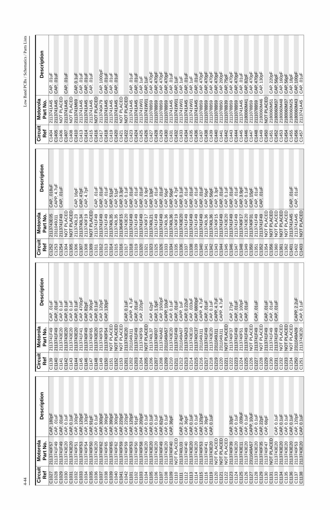
4-44
Low
Ban
d PC
Bs
/ Sch
emat
ics
/ Par
ts L
ists
C10
2721
1374
0F57
CA
P, 1
80pF
C10
2821
1374
1F49
CA
P, .0
1uF
C10
2921
1374
1F49
CA
P, .0
1uF
C10
3021
1374
3E20
CA
P, 0
.1uF
C10
3121
1374
3E20
CA
P, 0
.1uF
C10
3221
1374
0F51
CA
P, 1
00pF
C10
3321
1374
0F53
CA
P, 1
20pF
C10
3421
1374
0F54
CA
P, 1
30pF
C10
3521
1374
0F50
CA
P, 9
1pF
C10
3621
1374
3E20
CA
P, 0
.1uF
C10
3721
1374
0F62
CA
P, 3
00pF
C10
3821
1374
0F65
CA
P, 3
90pF
C10
3921
1374
0F65
CA
P, 3
90pF
C10
4021
1374
0F62
CA
P, 3
00pF
C10
4121
1374
0F59
CA
P, 2
20pF
C10
4221
1374
0F59
CA
P, 2
20pF
C11
0121
1374
0F53
CA
P, 1
20pF
C11
0221
1374
0F50
CA
P, 9
1pF
C11
0321
1374
0F58
CA
P, 2
00pF
C11
0421
1374
3E20
CA
P, 0
.1uF
C11
0521
1374
3E20
CA
P, 0
.1uF
C11
0621
1374
3E20
CA
P, 0
.1uF
C11
0721
1374
0F49
CA
P, 8
2pF
C11
0821
1374
3E20
CA
P, 0
.1uF
C11
0921
1374
0F40
CA
P, 3
6pF
C11
10N
OT
PLA
CE
DC
1111
2113
740L
03C
AP,
2.4
pFC
1112
2113
740F
40C
AP,
36p
FC
1113
2113
743E
20C
AP,
0.1
uFC
1114
2113
743E
20C
AP,
0.1
uFC
1115
2113
740F
53C
AP,
120
pFC
1116
2113
740F
41C
AP,
39p
FC
1119
2113
743E
20C
AP,
0.1
uFC
1120
NO
T P
LAC
ED
C11
21N
OT
PLA
CE
DC
1122
NO
T P
LAC
ED
C11
2321
1374
0F39
CA
P, 3
3pF
C11
2421
1374
3E20
CA
P, 0
.1uF
C11
2521
1374
3E11
CA
P, .0
39uF
C11
2621
1374
3E20
CA
P, 0
.1uF
C11
2723
1104
9A57
CA
PP,
10u
FC
1128
2113
743E
20C
AP,
0.1
uFC
1129
2113
740F
35C
AP,
22p
FC
1130
2113
740F
47C
AP,
68p
FC
1131
NO
T P
LAC
ED
C11
3321
1374
3E20
CA
P, 0
.1uF
C11
3421
1374
3E20
CA
P, 0
.1uF
C11
3521
1374
3E20
CA
P, 0
.1uF
C11
3621
1374
3E20
CA
P, 0
.1uF
C11
3721
1374
0F53
CA
P, 1
20pF
C11
3821
1374
3E20
CA
P, 0
.1uF
Cir
cuit
R
efM
oto
rola
P
art
No
.D
escr
ipti
on
C11
3921
1374
1F49
CA
P, .0
1uF
C11
4021
1374
1F49
CA
P, .0
1uF
C11
4121
1374
3E20
CA
P, 0
.1uF
C11
4221
1374
3E20
CA
P, 0
.1uF
C11
4321
1374
3E20
CA
P, 0
.1uF
C11
4421
1374
3E20
CA
P, 0
.1uF
C11
4521
1374
1F41
CA
P, 4
700p
FC
1146
2113
740F
49C
AP,
82p
FC
1147
2113
740F
65C
AP,
390
pFC
1148
2113
743E
20C
AP,
0.1
uFC
1149
2113
740F
53C
AP,
120
pFC
1150
2113
740F
54C
AP,
130
pFC
1151
NO
T P
LAC
ED
C11
52N
OT
PLA
CE
DC
1153
NO
T P
LAC
ED
C12
0121
1374
3E20
CA
P, 0
.1uF
C12
0223
1104
9J11
CA
PP,
4.7
uFC
1203
2113
741F
49C
AP,
.01u
FC
1204
2113
740F
59C
AP,
220
pFC
1205
NO
T P
LAC
ED
C12
0621
1374
0L37
CA
P, 6
2pF
C12
0721
1374
0F07
CA
P, 1
.5pF
C12
0821
1374
0A82
CA
P, 1
500p
FC
1209
2311
049A
57C
AP
P, 1
0uF
C12
1021
1374
3E20
CA
P, 0
.1uF
C12
1121
1374
1F49
CA
P, .0
1uF
C12
1223
1104
9A07
CA
PP,
1uF
C12
1321
1374
3A23
CA
P, 0
.22u
FC
1214
2113
743E
10C
AP,
.033
uFC
1215
2113
740C
37C
AP,
680
0pF
C12
1623
1104
9J11
CA
PP,
4.7
uFC
1217
2113
741F
49C
AP,
.01u
FC
1218
2113
743E
20C
AP,
0.1
uFC
1219
2311
049J
11C
AP
P, 4
.7uF
C12
2023
1104
9J11
CA
PP,
4.7
uFC
1221
NO
T P
LAC
ED
C12
2221
1374
0F37
CA
P, 2
7pF
C12
2321
1374
1F49
CA
P, .0
1uF
C12
2421
1374
0F51
CA
P, 1
00pF
C12
2521
1374
1F49
CA
P, .0
1uF
C12
26N
OT
PLA
CE
DC
1227
2113
741F
49C
AP,
.01u
FC
1228
NO
T P
LAC
ED
C12
2921
1374
1F49
CA
P, .0
1uF
C12
3021
1374
1F49
CA
P, .0
1uF
C12
3121
1374
1F49
CA
P, .0
1uF
C12
32N
OT
PLA
CE
DC
1233
NO
T P
LAC
ED
C12
34N
OT
PLA
CE
DC
1250
2311
049A
09C
AP
P, 2
.2uF
C12
5121
1374
3E20
CA
P, 0
.1uF
Cir
cuit
R
efM
oto
rola
P
art
No
.D
escr
ipti
on
C12
5221
1374
3E05
CA
P, .0
18uF
C12
5323
1104
9J11
CA
PP,
4.7
uFC
1254
2113
741F
49C
AP,
.01u
FC
1304
NO
T P
LAC
ED
C13
05N
OT
PLA
CE
DC
1306
2113
740L
23C
AP,
16p
FC
1307
2113
740L
34C
AP,
47p
FC
1308
2113
740F
19C
AP,
4.7
pFC
1309
NO
T P
LAC
ED
C13
1121
1374
1F49
CA
P, .0
1uF
C13
1221
1374
1F49
CA
P, .0
1uF
C13
1321
1374
1F49
CA
P, .0
1uF
C13
1421
1374
0L35
CA
P, 5
1pF
C13
1521
1374
0L35
CA
P, 5
1pF
C13
1621
1364
0F15
CA
P, 3
.3pF
C13
1721
1374
3E20
CA
P, 0
.1uF
C13
1821
1374
1F49
CA
P, .0
1uF
C13
1921
1374
1F49
CA
P, .0
1uF
C13
2021
1374
1F49
CA
P, .0
1uF
C13
2121
1374
0F17
CA
P, 3
.9pF
C13
2321
1374
0L21
CA
P, 1
3pF
C13
2521
1374
1F49
CA
P, .0
1uF
C13
2621
1374
1F49
CA
P, .0
1uF
C13
3321
1374
0L36
CA
P, 5
6pF
C13
3421
1374
0L36
CA
P, 5
6pF
C13
3521
1374
0F19
CA
P, 4
.7pF
C13
3621
1374
3E20
CA
P, 0
.1uF
C13
3721
1374
1F49
CA
P, .0
1uF
C13
3821
1374
1F49
CA
P, .0
1uF
C13
3921
1374
1F49
CA
P, .0
1uF
C13
4021
1374
1F49
CA
P, .0
1uF
C13
4121
1374
0L36
CA
P, 5
6pF
C13
4221
1374
0L36
CA
P, 5
6pF
C13
4321
1374
0F15
CA
P, 3
.3pF
C13
4421
1374
1F49
CA
P, .0
1uF
C13
4521
1374
3E20
CA
P, 0
.1uF
C13
4621
1374
1F49
CA
P, .0
1uF
C13
4721
1374
1F49
CA
P, .0
1uF
C13
4821
1374
0F17
CA
P, 3
.9pF
C13
4921
1374
3E20
CA
P, 0
.1uF
C13
5021
1374
0F31
CA
P, 1
5pF
C13
5121
1374
1F49
CA
P, .0
1uF
C13
5221
1374
1F49
CA
P, .0
1uF
C13
54N
OT
PLA
CE
DC
1356
NO
T P
LAC
ED
C13
60N
OT
PLA
CE
DC
1361
NO
T P
LAC
ED
C13
62N
OT
PLA
CE
DC
1401
2113
741A
45C
AP,
.01u
FC
1402
2113
741A
45C
AP,
.01u
FC
1403
NO
T P
LAC
ED
Cir
cuit
R
efM
oto
rola
P
art
No
.D
escr
ipti
on
C14
0421
1374
1A45
CA
P, .0
1uF
C14
0521
1374
1A45
CA
P, .0
1uF
C14
06N
OT
PLA
CE
DC
1407
2113
741A
45C
AP,
.01u
FC
1408
NO
T P
LAC
ED
C14
1021
1374
1M69
CA
P, 0
.1uF
C14
1321
1374
1A45
CA
P, .0
1uF
C14
1421
1374
1A45
CA
P, .0
1uF
C14
1521
1374
1A45
CA
P, .0
1uF
C14
16N
OT
PLA
CE
DC
1417
2113
740A
79C
AP,
100
0pF
C14
1821
1374
1A45
CA
P, .0
1uF
C14
1921
1374
1A45
CA
P, .0
1uF
C14
2021
1374
1A45
CA
P, .0
1uF
C14
21N
OT
PLA
CE
DC
1422
NO
T P
LAC
ED
C14
2321
1374
1A45
CA
P, .0
1uF
C14
2421
1374
1A45
CA
P, .0
1uF
C14
2521
1374
1W01
CA
P, 1
uFC
1426
2113
741W
01C
AP,
1uF
C14
2721
1107
8B59
CA
P, 4
70pF
C14
2821
1107
8B59
CA
P, 4
70pF
C14
2921
1107
8B59
CA
P, 4
70pF
C14
3021
1107
8B59
CA
P, 4
70pF
C14
3121
1374
1A45
CA
P, .0
1uF
C14
3221
1374
1W01
CA
P, 1
uFC
1433
2113
741W
01C
AP,
1uF
C14
3421
1374
1A45
CA
P, .0
1uF
C14
3521
1374
1W01
CA
P, 1
uFC
1436
2113
741A
45C
AP,
.01u
FC
1437
2111
078B
59C
AP,
470
pFC
1438
2111
078B
59C
AP,
470
pFC
1439
2111
078B
59C
AP,
470
pFC
1440
2111
078B
59C
AP,
470
pFC
1441
2111
078B
50C
AP,
200
pFC
1442
2111
078B
39C
AP,
75p
FC
1443
2111
078B
59C
AP,
470
pFC
1444
2111
078B
59C
AP,
470
pFC
1445
2113
741A
45C
AP,
.01u
FC
1446
2180
060M
41C
AP,
82p
FC
1447
2111
078B
59C
AP,
470
pFC
1448
2111
078B
59C
AP,
470
pFC
1449
2180
060M
46C
AP,
130
pFC
1450
NO
T P
LAC
ED
C14
5121
8006
0M51
CA
P, 2
20pF
C14
5221
8006
0M37
CA
P, 5
6pF
C14
5321
8006
0M48
CA
P, 1
60pF
C14
5421
8006
0M37
CA
P, 5
6pF
C14
5521
8006
0M25
CA
P, 1
8pF
C14
5621
8006
0M43
CA
P, 1
00pF
C14
5721
1374
1A45
CA
P, .0
1uF
Cir
cuit
R
efM
oto
rola
P
art
No
.D
escr
ipti
on
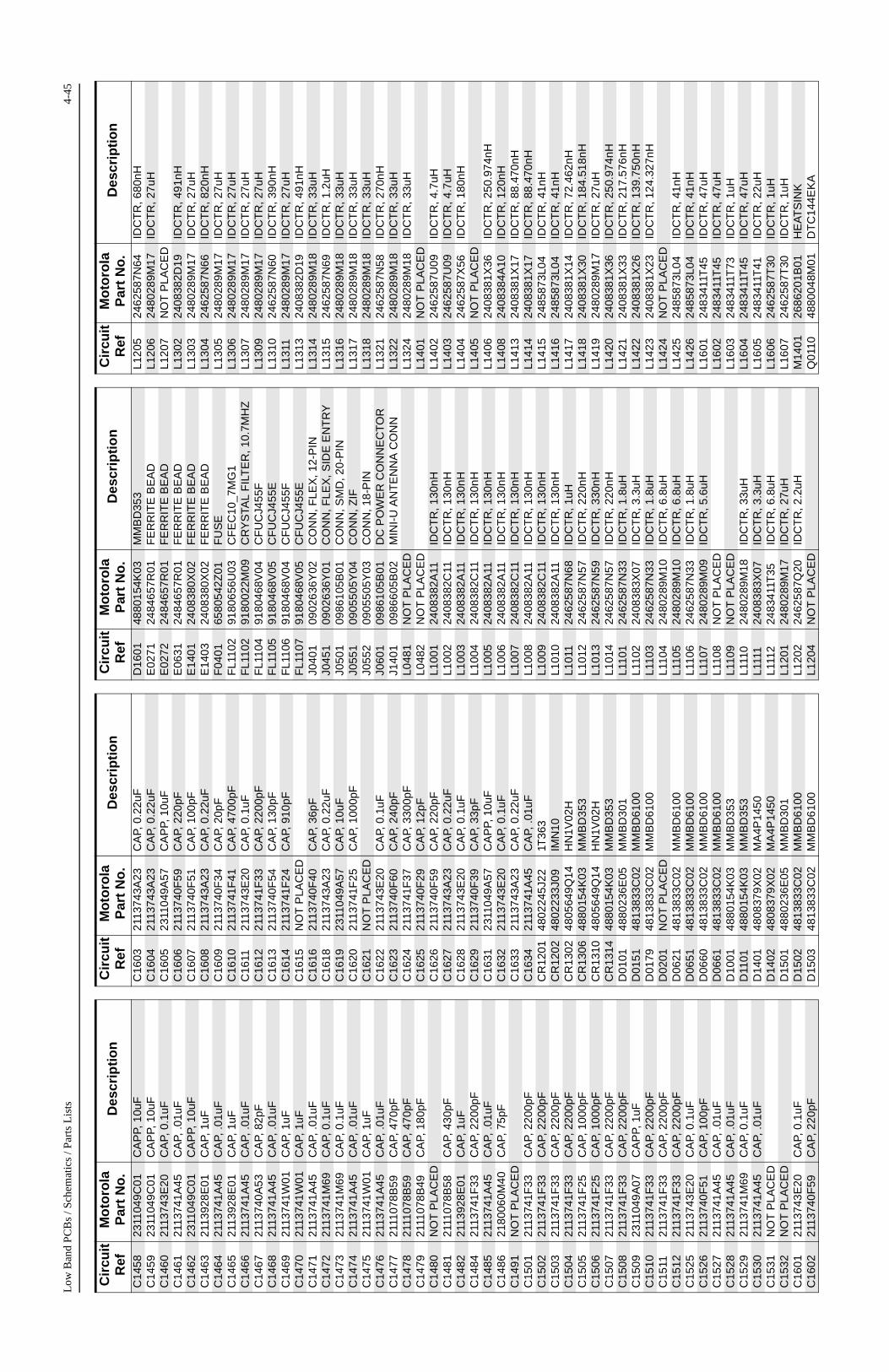
Low
Ban
d P
CB
s / S
chem
atic
s / P
arts
Lis
ts4-
45
C14
5823
1104
9C01
CA
PP,
10u
FC
1459
2311
049C
01C
AP
P, 1
0uF
C14
6021
1374
3E20
CA
P, 0
.1uF
C14
6121
1374
1A45
CA
P, .0
1uF
C14
6223
1104
9C01
CA
PP,
10u
FC
1463
2113
928E
01C
AP,
1uF
C14
6421
1374
1A45
CA
P, .0
1uF
C14
6521
1392
8E01
CA
P, 1
uFC
1466
2113
741A
45C
AP,
.01u
FC
1467
2113
740A
53C
AP,
82p
FC
1468
2113
741A
45C
AP,
.01u
FC
1469
2113
741W
01C
AP,
1uF
C14
7021
1374
1W01
CA
P, 1
uFC
1471
2113
741A
45C
AP,
.01u
FC
1472
2113
741M
69C
AP,
0.1
uFC
1473
2113
741M
69C
AP,
0.1
uFC
1474
2113
741A
45C
AP,
.01u
FC
1475
2113
741W
01C
AP,
1uF
C14
7621
1374
1A45
CA
P, .0
1uF
C14
7721
1107
8B59
CA
P, 4
70pF
C14
7821
1107
8B59
CA
P, 4
70pF
C14
7921
1107
8B49
CA
P, 1
80pF
C14
80N
OT
PLA
CE
DC
1481
2111
078B
58C
AP,
430
pFC
1482
2113
928E
01C
AP,
1uF
C14
8421
1374
1F33
CA
P, 2
200p
FC
1485
2113
741A
45C
AP,
.01u
FC
1486
2180
060M
40C
AP,
75p
FC
1491
NO
T P
LAC
ED
C15
0121
1374
1F33
CA
P, 2
200p
FC
1502
2113
741F
33C
AP,
220
0pF
C15
0321
1374
1F33
CA
P, 2
200p
FC
1504
2113
741F
33C
AP,
220
0pF
C15
0521
1374
1F25
CA
P, 1
000p
FC
1506
2113
741F
25C
AP,
100
0pF
C15
0721
1374
1F33
CA
P, 2
200p
FC
1508
2113
741F
33C
AP,
220
0pF
C15
0923
1104
9A07
CA
PP,
1uF
C15
1021
1374
1F33
CA
P, 2
200p
FC
1511
2113
741F
33C
AP,
220
0pF
C15
1221
1374
1F33
CA
P, 2
200p
FC
1525
2113
743E
20C
AP,
0.1
uFC
1526
2113
740F
51C
AP,
100
pFC
1527
2113
741A
45C
AP,
.01u
FC
1528
2113
741A
45C
AP,
.01u
FC
1529
2113
741M
69C
AP,
0.1
uFC
1530
2113
741A
45C
AP,
.01u
FC
1531
NO
T P
LAC
ED
C15
32N
OT
PLA
CE
DC
1601
2113
743E
20C
AP,
0.1
uFC
1602
2113
740F
59C
AP,
220
pF
Cir
cuit
R
efM
oto
rola
P
art
No
.D
escr
ipti
on
C16
0321
1374
3A23
CA
P, 0
.22u
FC
1604
2113
743A
23C
AP,
0.2
2uF
C16
0523
1104
9A57
CA
PP,
10u
FC
1606
2113
740F
59C
AP,
220
pFC
1607
2113
740F
51C
AP,
100
pFC
1608
2113
743A
23C
AP,
0.2
2uF
C16
0921
1374
0F34
CA
P, 2
0pF
C16
1021
1374
1F41
CA
P, 4
700p
FC
1611
2113
743E
20C
AP,
0.1
uFC
1612
2113
741F
33C
AP,
220
0pF
C16
1321
1374
0F54
CA
P, 1
30pF
C16
1421
1374
1F24
CA
P, 9
10pF
C16
15N
OT
PLA
CE
DC
1616
2113
740F
40C
AP,
36p
FC
1618
2113
743A
23C
AP,
0.2
2uF
C16
1923
1104
9A57
CA
P, 1
0uF
C16
2021
1374
1F25
CA
P, 1
000p
FC
1621
NO
T P
LAC
ED
C16
2221
1374
3E20
CA
P, 0
.1uF
C16
2321
1374
0F60
CA
P, 2
40pF
C16
2421
1374
1F37
CA
P, 3
300p
FC
1625
2113
740F
29C
AP,
12p
FC
1626
2113
740F
59C
AP,
220
pFC
1627
2113
743A
23C
AP,
0.2
2uF
C16
2821
1374
3E20
CA
P, 0
.1uF
C16
2921
1374
0F39
CA
P, 3
3pF
C16
3123
1104
9A57
CA
PP,
10u
FC
1632
2113
743E
20C
AP,
0.1
uFC
1633
2113
743A
23C
AP,
0.2
2uF
C16
3421
1374
1A45
CA
P, .0
1uF
CR
1201
4802
245J
221T
363
CR
1202
4802
233J
09IM
N10
CR
1302
4805
649Q
14H
N1V
02H
CR
1306
4880
154K
03M
MB
D35
3C
R13
1048
0564
9Q14
HN
1V02
HC
R13
1448
8015
4K03
MM
BD
353
D01
0148
8023
6E05
MM
BD
301
D01
5148
1383
3C02
MM
BD
6100
D01
7948
1383
3C02
MM
BD
6100
D02
01N
OT
PLA
CE
DD
0621
4813
833C
02M
MB
D61
00D
0651
4813
833C
02M
MB
D61
00D
0660
4813
833C
02M
MB
D61
00D
0661
4813
833C
02M
MB
D61
00D
1001
4880
154K
03M
MB
D35
3D
1101
4880
154K
03M
MB
D35
3D
1401
4808
379X
02M
A4P
1450
D14
0248
0837
9X02
MA
4P14
50D
1501
4880
236E
05M
MB
D30
1D
1502
4813
833C
02M
MB
D61
00D
1503
4813
833C
02M
MB
D61
00
Cir
cuit
R
efM
oto
rola
P
art
No
.D
escr
ipti
on
D16
0148
8015
4K03
MM
BD
353
E02
7124
8465
7R01
FE
RR
ITE
BE
AD
E02
7224
8465
7R01
FE
RR
ITE
BE
AD
E06
3124
8465
7R01
FE
RR
ITE
BE
AD
E14
0124
0838
0X02
FE
RR
ITE
BE
AD
E14
0324
0838
0X02
FE
RR
ITE
BE
AD
F04
0165
8054
2Z01
FU
SE
FL1
102
9180
656U
03C
FE
C10
_7M
G1
FL1
102
9180
022M
09C
RY
STA
L F
ILT
ER
, 10.
7MH
ZF
L110
491
8046
8V04
CF
UC
J455
FF
L110
591
8046
8V05
CF
UC
J455
EF
L110
691
8046
8V04
CF
UC
J455
FF
L110
791
8046
8V05
CF
UC
J455
EJ0
401
0902
636Y
02C
ON
N, F
LEX
, 12-
PIN
J045
109
0263
6Y01
CO
NN
, FLE
X, S
IDE
EN
TR
YJ0
501
0986
105B
01C
ON
N, S
MD
, 20-
PIN
J055
109
0550
5Y04
CO
NN
, ZIF
J055
209
0550
5Y03
CO
NN
, 18-
PIN
J060
109
8610
5B01
DC
PO
WE
R C
ON
NE
CT
OR
J140
109
8660
5B02
MIN
I-U
AN
TE
NN
A C
ON
NL0
481
NO
T P
LAC
ED
L048
2N
OT
PLA
CE
DL1
001
2408
382A
11ID
CT
R, 1
30nH
L100
224
0838
2C11
IDC
TR
, 130
nHL1
003
2408
382A
11ID
CT
R, 1
30nH
L100
424
0838
2C11
IDC
TR
, 130
nHL1
005
2408
382A
11ID
CT
R, 1
30nH
L100
624
0838
2A11
IDC
TR
, 130
nHL1
007
2408
382C
11ID
CT
R, 1
30nH
L100
824
0838
2A11
IDC
TR
, 130
nHL1
009
2408
382C
11ID
CT
R, 1
30nH
L101
024
0838
2A11
IDC
TR
, 130
nHL1
011
2462
587N
68ID
CT
R, 1
uHL1
012
2462
587N
57ID
CT
R, 2
20nH
L101
324
6258
7N59
IDC
TR
, 330
nHL1
014
2462
587N
57ID
CT
R, 2
20nH
L110
124
6258
7N33
IDC
TR
, 1.8
uHL1
102
2408
383X
07ID
CT
R, 3
.3uH
L110
324
6258
7N33
IDC
TR
, 1.8
uHL1
104
2480
289M
10ID
CT
R, 6
.8uH
L110
524
8028
9M10
IDC
TR
, 6.8
uHL1
106
2462
587N
33ID
CT
R, 1
.8uH
L110
724
8028
9M09
IDC
TR
, 5.6
uHL1
108
NO
T P
LAC
ED
L110
9N
OT
PLA
CE
DL1
110
2480
289M
18ID
CT
R, 3
3uH
L111
124
0838
3X07
IDC
TR
, 3.3
uHL1
112
2483
411T
35ID
CT
R, 6
.8uH
L120
124
8028
9M17
IDC
TR
, 27u
HL1
202
2462
587Q
20ID
CT
R, 2
.2uH
L120
4N
OT
PLA
CE
D
Cir
cuit
R
efM
oto
rola
P
art
No
.D
escr
ipti
on
L120
524
6258
7N64
IDC
TR
, 680
nHL1
206
2480
289M
17ID
CT
R, 2
7uH
L120
7N
OT
PLA
CE
DL1
302
2408
382D
19ID
CT
R, 4
91nH
L130
324
8028
9M17
IDC
TR
, 27u
HL1
304
2462
587N
66ID
CT
R, 8
20nH
L130
524
8028
9M17
IDC
TR
, 27u
HL1
306
2480
289M
17ID
CT
R, 2
7uH
L130
724
8028
9M17
IDC
TR
, 27u
HL1
309
2480
289M
17ID
CT
R, 2
7uH
L131
024
6258
7N60
IDC
TR
, 390
nHL1
311
2480
289M
17ID
CT
R, 2
7uH
L131
324
0838
2D19
IDC
TR
, 491
nHL1
314
2480
289M
18ID
CT
R, 3
3uH
L131
524
6258
7N69
IDC
TR
, 1.2
uHL1
316
2480
289M
18ID
CT
R, 3
3uH
L131
724
8028
9M18
IDC
TR
, 33u
HL1
318
2480
289M
18ID
CT
R, 3
3uH
L132
124
6258
7N58
IDC
TR
, 270
nHL1
322
2480
289M
18ID
CT
R, 3
3uH
L132
424
8028
9M18
IDC
TR
, 33u
HL1
401
NO
T P
LAC
ED
L140
224
6258
7U09
IDC
TR
, 4.7
uHL1
403
2462
587U
09ID
CT
R, 4
.7uH
L140
424
6258
7X56
IDC
TR
, 180
nHL1
405
NO
T P
LAC
ED
L140
624
0838
1X36
IDC
TR
, 250
.974
nHL1
408
2408
384A
10ID
CT
R, 1
20nH
L141
324
0838
1X17
IDC
TR
, 88.
470n
HL1
414
2408
381X
17ID
CT
R, 8
8.47
0nH
L141
524
8587
3L04
IDC
TR
, 41n
HL1
416
2485
873L
04ID
CT
R, 4
1nH
L141
724
0838
1X14
IDC
TR
, 72.
462n
HL1
418
2408
381X
30ID
CT
R, 1
84.5
18nH
L141
924
8028
9M17
IDC
TR
, 27u
HL1
420
2408
381X
36ID
CT
R, 2
50.9
74nH
L142
124
0838
1X33
IDC
TR
, 217
.576
nHL1
422
2408
381X
26ID
CT
R, 1
39.7
50nH
L142
324
0838
1X23
IDC
TR
, 124
.327
nHL1
424
NO
T P
LAC
ED
L142
524
8587
3L04
IDC
TR
, 41n
HL1
426
2485
873L
04ID
CT
R, 4
1nH
L160
124
8341
1T45
IDC
TR
, 47u
HL1
602
2483
411T
45ID
CT
R, 4
7uH
L160
324
8341
1T73
IDC
TR
, 1uH
L160
424
8341
1T45
IDC
TR
, 47u
HL1
605
2483
411T
41ID
CT
R, 2
2uH
L160
624
6258
7T30
IDC
TR
, 1uH
L160
724
6258
7T30
IDC
TR
, 1uH
M14
0126
8620
1B01
HE
AT
SIN
KQ
0110
4880
048M
01D
TC
144E
KA
Cir
cuit
R
efM
oto
rola
P
art
No
.D
escr
ipti
on
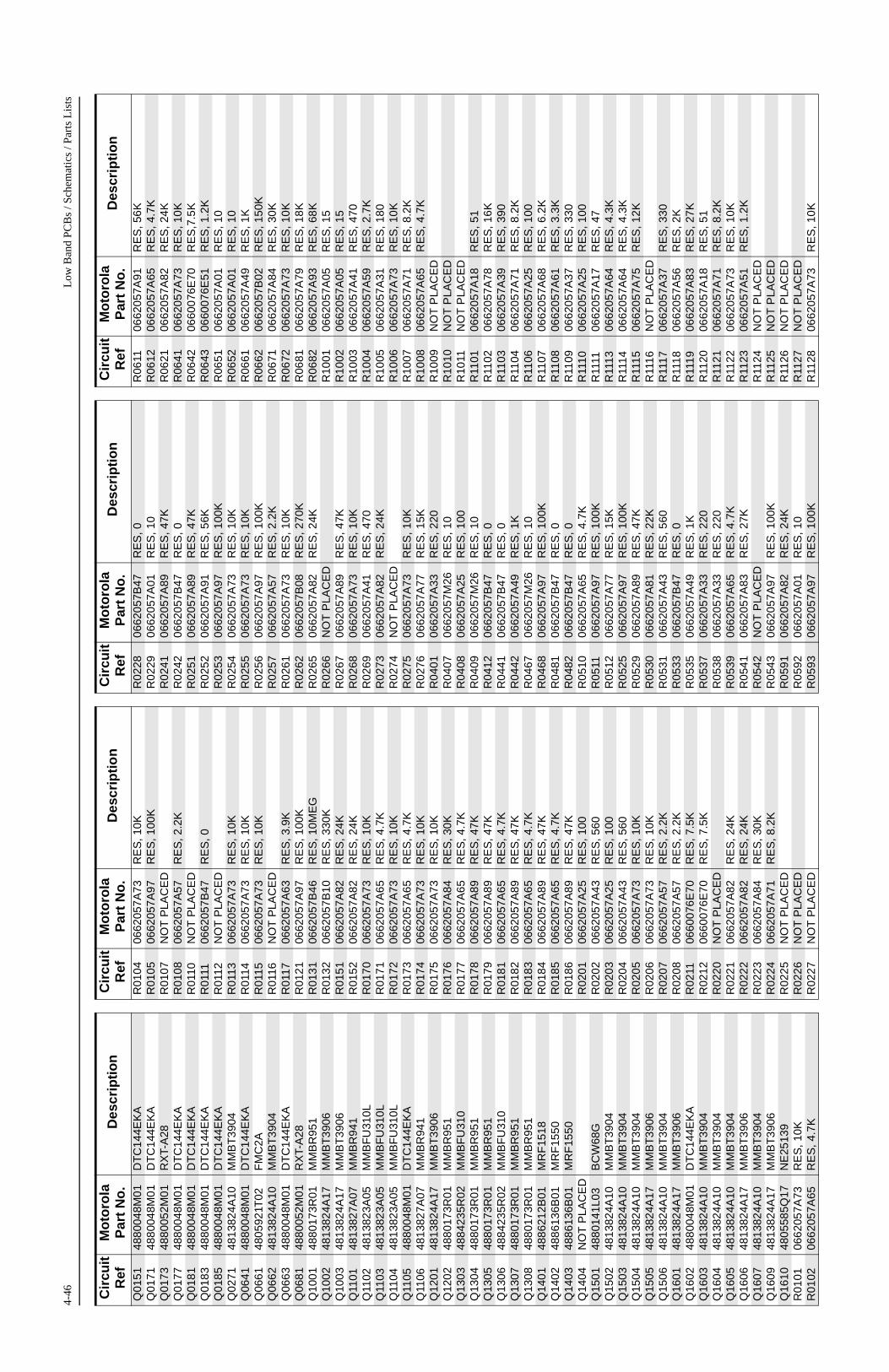
4-46
Low
Ban
d PC
Bs
/ Sch
emat
ics
/ Par
ts L
ists
Q01
5148
8004
8M01
DT
C14
4EK
AQ
0171
4880
048M
01D
TC
144E
KA
Q01
7348
8005
2M01
RX
T-A
28Q
0177
4880
048M
01D
TC
144E
KA
Q01
8148
8004
8M01
DT
C14
4EK
AQ
0183
4880
048M
01D
TC
144E
KA
Q01
8548
8004
8M01
DT
C14
4EK
AQ
0271
4813
824A
10M
MB
T39
04Q
0641
4880
048M
01D
TC
144E
KA
Q06
6148
0592
1T02
FM
C2A
Q06
6248
1382
4A10
MM
BT
3904
Q06
6348
8004
8M01
DT
C14
4EK
AQ
0681
4880
052M
01R
XT-
A28
Q10
0148
8017
3R01
MM
BR
951
Q10
0248
1382
4A17
MM
BT
3906
Q10
0348
1382
4A17
MM
BT
3906
Q11
0148
1382
7A07
MM
BR
941
Q11
0248
1382
3A05
MM
BF
U31
0LQ
1103
4813
823A
05M
MB
FU
310L
Q11
0448
1382
3A05
MM
BF
U31
0LQ
1105
4880
048M
01D
TC
144E
KA
Q11
0648
1382
7A07
MM
BR
941
Q12
0148
1382
4A17
MM
BT
3906
Q12
0248
8017
3R01
MM
BR
951
Q13
0348
8423
5R02
MM
BF
U31
0Q
1304
4880
173R
01M
MB
R95
1Q
1305
4880
173R
01M
MB
R95
1Q
1306
4884
235R
02M
MB
FU
310
Q13
0748
8017
3R01
MM
BR
951
Q13
0848
8017
3R01
MM
BR
951
Q14
0148
8621
2B01
MR
F15
18Q
1402
4886
136B
01M
RF
1550
Q14
0348
8613
6B01
MR
F15
50Q
1404
NO
T P
LAC
ED
Q15
0148
8014
1L03
BC
W68
GQ
1502
4813
824A
10M
MB
T39
04Q
1503
4813
824A
10M
MB
T39
04Q
1504
4813
824A
10M
MB
T39
04Q
1505
4813
824A
17M
MB
T39
06Q
1506
4813
824A
10M
MB
T39
04Q
1601
4813
824A
17M
MB
T39
06Q
1602
4880
048M
01D
TC
144E
KA
Q16
0348
1382
4A10
MM
BT
3904
Q16
0448
1382
4A10
MM
BT
3904
Q16
0548
1382
4A10
MM
BT
3904
Q16
0648
1382
4A17
MM
BT
3906
Q16
0748
1382
4A10
MM
BT
3904
Q16
0948
1382
4A17
MM
BT
3906
Q16
1048
0558
5Q17
NE
2513
9R
0101
0662
057A
73R
ES
, 10K
R01
0206
6205
7A65
RE
S, 4
.7K
Cir
cuit
R
efM
oto
rola
P
art
No
.D
escr
ipti
on
R01
0406
6205
7A73
RE
S, 1
0KR
0105
0662
057A
97R
ES
, 100
KR
0107
NO
T P
LAC
ED
R01
0806
6205
7A57
RE
S, 2
.2K
R01
10N
OT
PLA
CE
DR
0111
0662
057B
47R
ES
, 0R
0112
NO
T P
LAC
ED
R01
1306
6205
7A73
RE
S, 1
0KR
0114
0662
057A
73R
ES
, 10K
R01
1506
6205
7A73
RE
S, 1
0KR
0116
NO
T P
LAC
ED
R01
1706
6205
7A63
RE
S, 3
.9K
R01
2106
6205
7A97
RE
S, 1
00K
R01
3106
6205
7B46
RE
S, 1
0ME
GR
0132
0662
057B
10R
ES
, 330
KR
0151
0662
057A
82R
ES
, 24K
R01
5206
6205
7A82
RE
S, 2
4KR
0170
0662
057A
73R
ES
, 10K
R01
7106
6205
7A65
RE
S, 4
.7K
R01
7206
6205
7A73
RE
S, 1
0KR
0173
0662
057A
65R
ES
, 4.7
KR
0174
0662
057A
73R
ES
, 10K
R01
7506
6205
7A73
RE
S, 1
0KR
0176
0662
057A
84R
ES
, 30K
R01
7706
6205
7A65
RE
S, 4
.7K
R01
7806
6205
7A89
RE
S, 4
7KR
0179
0662
057A
89R
ES
, 47K
R01
8106
6205
7A65
RE
S, 4
.7K
R01
8206
6205
7A89
RE
S, 4
7KR
0183
0662
057A
65R
ES
, 4.7
KR
0184
0662
057A
89R
ES
, 47K
R01
8506
6205
7A65
RE
S, 4
.7K
R01
8606
6205
7A89
RE
S, 4
7KR
0201
0662
057A
25R
ES
, 100
R02
0206
6205
7A43
RE
S, 5
60R
0203
0662
057A
25R
ES
, 100
R02
0406
6205
7A43
RE
S, 5
60R
0205
0662
057A
73R
ES
, 10K
R02
0606
6205
7A73
RE
S, 1
0KR
0207
0662
057A
57R
ES
, 2.2
KR
0208
0662
057A
57R
ES
, 2.2
KR
0211
0660
076E
70R
ES
, 7.5
KR
0212
0660
076E
70R
ES
, 7.5
KR
0220
NO
T P
LAC
ED
R02
2106
6205
7A82
RE
S, 2
4KR
0222
0662
057A
82R
ES
, 24K
R02
2306
6205
7A84
RE
S, 3
0KR
0224
0662
057A
71R
ES
, 8.2
KR
0225
NO
T P
LAC
ED
R02
26N
OT
PLA
CE
DR
0227
NO
T P
LAC
ED
Cir
cuit
R
efM
oto
rola
P
art
No
.D
escr
ipti
on
R02
2806
6205
7B47
RE
S, 0
R02
2906
6205
7A01
RE
S, 1
0R
0241
0662
057A
89R
ES
, 47K
R02
4206
6205
7B47
RE
S, 0
R02
5106
6205
7A89
RE
S, 4
7KR
0252
0662
057A
91R
ES
, 56K
R02
5306
6205
7A97
RE
S, 1
00K
R02
5406
6205
7A73
RE
S, 1
0KR
0255
0662
057A
73R
ES
, 10K
R02
5606
6205
7A97
RE
S, 1
00K
R02
5706
6205
7A57
RE
S, 2
.2K
R02
6106
6205
7A73
RE
S, 1
0KR
0262
0662
057B
08R
ES
, 270
KR
0265
0662
057A
82R
ES
, 24K
R02
66N
OT
PLA
CE
DR
0267
0662
057A
89R
ES
, 47K
R02
6806
6205
7A73
RE
S, 1
0KR
0269
0662
057A
41R
ES
, 470
R02
7306
6205
7A82
RE
S, 2
4KR
0274
NO
T P
LAC
ED
R02
7506
6205
7A73
RE
S, 1
0KR
0276
0662
057A
77R
ES
, 15K
R04
0106
6205
7A33
RE
S, 2
20R
0407
0662
057M
26R
ES
, 10
R04
0806
6205
7A25
RE
S, 1
00R
0409
0662
057M
26R
ES
, 10
R04
1206
6205
7B47
RE
S, 0
R04
4106
6205
7B47
RE
S, 0
R04
4206
6205
7A49
RE
S, 1
KR
0467
0662
057M
26R
ES
, 10
R04
6806
6205
7A97
RE
S, 1
00K
R04
8106
6205
7B47
RE
S, 0
R04
8206
6205
7B47
RE
S, 0
R05
1006
6205
7A65
RE
S, 4
.7K
R05
1106
6205
7A97
RE
S, 1
00K
R05
1206
6205
7A77
RE
S, 1
5KR
0525
0662
057A
97R
ES
, 100
KR
0529
0662
057A
89R
ES
, 47K
R05
3006
6205
7A81
RE
S, 2
2KR
0531
0662
057A
43R
ES
, 560
R05
3306
6205
7B47
RE
S, 0
R05
3506
6205
7A49
RE
S, 1
KR
0537
0662
057A
33R
ES
, 220
R05
3806
6205
7A33
RE
S, 2
20R
0539
0662
057A
65R
ES
, 4.7
KR
0541
0662
057A
83R
ES
, 27K
R05
42N
OT
PLA
CE
DR
0543
0662
057A
97R
ES
, 100
KR
0591
0662
057A
82R
ES
, 24K
R05
9206
6205
7A01
RE
S, 1
0R
0593
0662
057A
97R
ES
, 100
K
Cir
cuit
R
efM
oto
rola
P
art
No
.D
escr
ipti
on
R06
1106
6205
7A91
RE
S, 5
6KR
0612
0662
057A
65R
ES
, 4.7
KR
0621
0662
057A
82R
ES
, 24K
R06
4106
6205
7A73
RE
S, 1
0KR
0642
0660
076E
70R
ES
,7.5
KR
0643
0660
076E
51R
ES
, 1.2
KR
0651
0662
057A
01R
ES
, 10
R06
5206
6205
7A01
RE
S, 1
0R
0661
0662
057A
49R
ES
, 1K
R06
6206
6205
7B02
RE
S, 1
50K
R06
7106
6205
7A84
RE
S, 3
0KR
0672
0662
057A
73R
ES
, 10K
R06
8106
6205
7A79
RE
S, 1
8KR
0682
0662
057A
93R
ES
, 68K
R10
0106
6205
7A05
RE
S, 1
5R
1002
0662
057A
05R
ES
, 15
R10
0306
6205
7A41
RE
S, 4
70R
1004
0662
057A
59R
ES
, 2.7
KR
1005
0662
057A
31R
ES
, 180
R10
0606
6205
7A73
RE
S, 1
0KR
1007
0662
057A
71R
ES
, 8.2
KR
1008
0662
057A
65R
ES
, 4.7
KR
1009
NO
T P
LAC
ED
R10
10N
OT
PLA
CE
DR
1011
NO
T P
LAC
ED
R11
0106
6205
7A18
RE
S, 5
1R
1102
0662
057A
78R
ES
, 16K
R11
0306
6205
7A39
RE
S, 3
90R
1104
0662
057A
71R
ES
, 8.2
KR
1106
0662
057A
25R
ES
, 100
R11
0706
6205
7A68
RE
S, 6
.2K
R11
0806
6205
7A61
RE
S, 3
.3K
R11
0906
6205
7A37
RE
S, 3
30R
1110
0662
057A
25R
ES
, 100
R11
1106
6205
7A17
RE
S, 4
7R
1113
0662
057A
64R
ES
, 4.3
KR
1114
0662
057A
64R
ES
, 4.3
KR
1115
0662
057A
75R
ES
, 12K
R11
16N
OT
PLA
CE
DR
1117
0662
057A
37R
ES
, 330
R11
1806
6205
7A56
RE
S, 2
KR
1119
0662
057A
83R
ES
, 27K
R11
2006
6205
7A18
RE
S, 5
1R
1121
0662
057A
71R
ES
, 8.2
KR
1122
0662
057A
73R
ES
, 10K
R11
2306
6205
7A51
RE
S, 1
.2K
R11
24N
OT
PLA
CE
DR
1125
NO
T P
LAC
ED
R11
26N
OT
PLA
CE
DR
1127
NO
T P
LAC
ED
R11
2806
6205
7A73
RE
S, 1
0K
Cir
cuit
R
efM
oto
rola
P
art
No
.D
escr
ipti
on
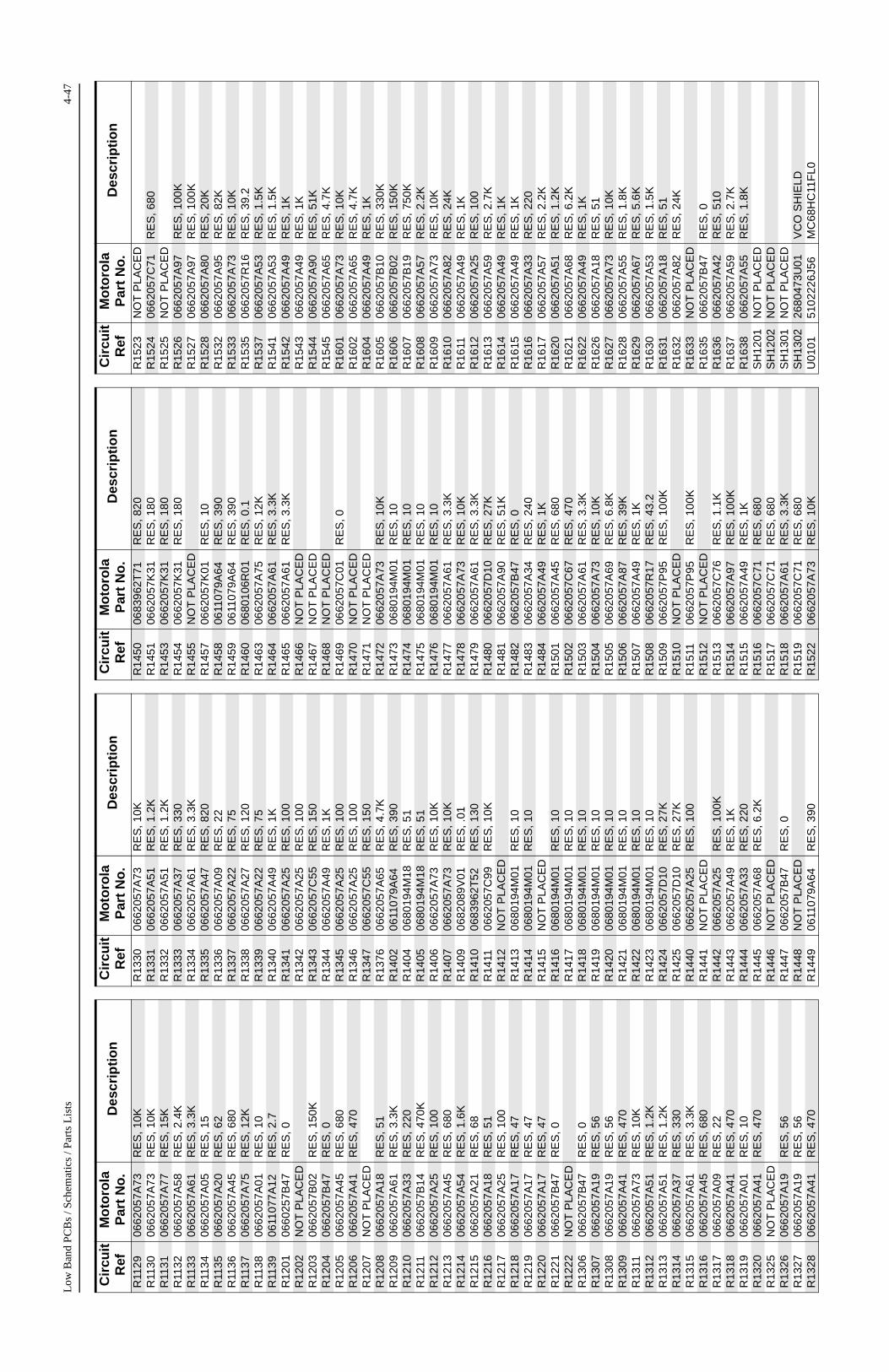
Low
Ban
d P
CB
s / S
chem
atic
s / P
arts
Lis
ts4-
47
R11
2906
6205
7A73
RE
S, 1
0KR
1130
0662
057A
73R
ES
, 10K
R11
3106
6205
7A77
RE
S, 1
5KR
1132
0662
057A
58R
ES
, 2.4
KR
1133
0662
057A
61R
ES
, 3.3
KR
1134
0662
057A
05R
ES
, 15
R11
3506
6205
7A20
RE
S, 6
2R
1136
0662
057A
45R
ES
, 680
R11
3706
6205
7A75
RE
S, 1
2KR
1138
0662
057A
01R
ES
, 10
R11
3906
1107
7A12
RE
S, 2
.7R
1201
0660
257B
47R
ES
, 0R
1202
NO
T P
LAC
ED
R12
0306
6205
7B02
RE
S, 1
50K
R12
0406
6205
7B47
RE
S, 0
R12
0506
6205
7A45
RE
S, 6
80R
1206
0662
057A
41R
ES
, 470
R12
07N
OT
PLA
CE
DR
1208
0662
057A
18R
ES
, 51
R12
0906
6205
7A61
RE
S, 3
.3K
R12
1006
6205
7A33
RE
S, 2
20R
1211
0662
057B
14R
ES
, 470
KR
1212
0662
057A
25R
ES
, 100
R12
1306
6205
7A45
RE
S, 6
80R
1214
0662
057A
54R
ES
, 1.6
KR
1215
0662
057A
21R
ES
, 68
R12
1606
6205
7A18
RE
S, 5
1R
1217
0662
057A
25R
ES
, 100
R12
1806
6205
7A17
RE
S, 4
7R
1219
0662
057A
17R
ES
, 47
R12
2006
6205
7A17
RE
S, 4
7R
1221
0662
057B
47R
ES
, 0R
1222
NO
T P
LAC
ED
R13
0606
6205
7B47
RE
S, 0
R13
0706
6205
7A19
RE
S, 5
6R
1308
0662
057A
19R
ES
, 56
R13
0906
6205
7A41
RE
S, 4
70R
1311
0662
057A
73R
ES
, 10K
R13
1206
6205
7A51
RE
S, 1
.2K
R13
1306
6205
7A51
RE
S, 1
.2K
R13
1406
6205
7A37
RE
S, 3
30R
1315
0662
057A
61R
ES
, 3.3
KR
1316
0662
057A
45R
ES
, 680
R13
1706
6205
7A09
RE
S, 2
2R
1318
0662
057A
41R
ES
, 470
R13
1906
6205
7A01
RE
S, 1
0R
1320
0662
057A
41R
ES
, 470
R13
25N
OT
PLA
CE
DR
1326
0662
057A
19R
ES
, 56
R13
2706
6205
7A19
RE
S, 5
6R
1328
0662
057A
41R
ES
, 470
Cir
cuit
R
efM
oto
rola
P
art
No
.D
escr
ipti
on
R13
3006
6205
7A73
RE
S, 1
0KR
1331
0662
057A
51R
ES
, 1.2
KR
1332
0662
057A
51R
ES
, 1.2
KR
1333
0662
057A
37R
ES
, 330
R13
3406
6205
7A61
RE
S, 3
.3K
R13
3506
6205
7A47
RE
S, 8
20R
1336
0662
057A
09R
ES
, 22
R13
3706
6205
7A22
RE
S, 7
5R
1338
0662
057A
27R
ES
, 120
R13
3906
6205
7A22
RE
S, 7
5R
1340
0662
057A
49R
ES
, 1K
R13
4106
6205
7A25
RE
S, 1
00R
1342
0662
057A
25R
ES
, 100
R13
4306
6205
7C55
RE
S, 1
50R
1344
0662
057A
49R
ES
, 1K
R13
4506
6205
7A25
RE
S, 1
00R
1346
0662
057A
25R
ES
, 100
R13
4706
6205
7C55
RE
S, 1
50R
1376
0662
057A
65R
ES
, 4.7
KR
1402
0611
079A
64R
ES
, 390
R14
0406
8019
4M18
RE
S, 5
1R
1405
0680
194M
18R
ES
, 51
R14
0606
6205
7A73
RE
S, 1
0KR
1407
0662
057A
73R
ES
, 10K
R14
0906
8208
9V01
RE
S, .
01R
1410
0683
962T
52R
ES
, 130
R14
1106
6205
7C99
RE
S, 1
0KR
1412
NO
T P
LAC
ED
R14
1306
8019
4M01
RE
S, 1
0R
1414
0680
194M
01R
ES
, 10
R14
15N
OT
PLA
CE
DR
1416
0680
194M
01R
ES
, 10
R14
1706
8019
4M01
RE
S, 1
0R
1418
0680
194M
01R
ES
, 10
R14
1906
8019
4M01
RE
S, 1
0R
1420
0680
194M
01R
ES
, 10
R14
2106
8019
4M01
RE
S, 1
0R
1422
0680
194M
01R
ES
, 10
R14
2306
8019
4M01
RE
S, 1
0R
1424
0662
057D
10R
ES
, 27K
R14
2506
6205
7D10
RE
S, 2
7KR
1440
0662
057A
25R
ES
, 100
R14
41N
OT
PLA
CE
DR
1442
0662
057A
25R
ES
, 100
KR
1443
0662
057A
49R
ES
, 1K
R14
4406
6205
7A33
RE
S, 2
20R
1445
0662
057A
68R
ES
, 6.2
KR
1446
NO
T P
LAC
ED
R14
4706
6205
7B47
RE
S, 0
R14
48N
OT
PLA
CE
DR
1449
0611
079A
64R
ES
, 390
Cir
cuit
R
efM
oto
rola
P
art
No
.D
escr
ipti
on
R14
5006
8396
2T71
RE
S, 8
20R
1451
0662
057K
31R
ES
, 180
R14
5306
6205
7K31
RE
S, 1
80R
1454
0662
057K
31R
ES
, 180
R14
55N
OT
PLA
CE
DR
1457
0662
057K
01R
ES
, 10
R14
5806
1107
9A64
RE
S, 3
90R
1459
0611
079A
64R
ES
, 390
R14
6006
8010
6R01
RE
S, 0
.1R
1463
0662
057A
75R
ES
, 12K
R14
6406
6205
7A61
RE
S, 3
.3K
R14
6506
6205
7A61
RE
S, 3
.3K
R14
66N
OT
PLA
CE
DR
1467
NO
T P
LAC
ED
R14
68N
OT
PLA
CE
DR
1469
0662
057C
01R
ES
, 0R
1470
NO
T P
LAC
ED
R14
71N
OT
PLA
CE
DR
1472
0662
057A
73R
ES
, 10K
R14
7306
8019
4M01
RE
S, 1
0R
1474
0680
194M
01R
ES
, 10
R14
7506
8019
4M01
RE
S, 1
0R
1476
0680
194M
01R
ES
, 10
R14
7706
6205
7A61
RE
S, 3
.3K
R14
7806
6205
7A73
RE
S, 1
0KR
1479
0662
057A
61R
ES
, 3.3
KR
1480
0662
057D
10R
ES
, 27K
R14
8106
6205
7A90
RE
S, 5
1KR
1482
0662
057B
47R
ES
, 0R
1483
0662
057A
34R
ES
, 240
R14
8406
6205
7A49
RE
S, 1
KR
1501
0662
057A
45R
ES
, 680
R15
0206
6205
7C67
RE
S, 4
70R
1503
0662
057A
61R
ES
, 3.3
KR
1504
0662
057A
73R
ES
, 10K
R15
0506
6205
7A69
RE
S, 6
.8K
R15
0606
6205
7A87
RE
S, 3
9KR
1507
0662
057A
49R
ES
, 1K
R15
0806
6205
7R17
RE
S, 4
3.2
R15
0906
6205
7P95
RE
S, 1
00K
R15
10N
OT
PLA
CE
DR
1511
0662
057P
95R
ES
, 100
KR
1512
NO
T P
LAC
ED
R15
1306
6205
7C76
RE
S, 1
.1K
R15
1406
6205
7A97
RE
S, 1
00K
R15
1506
6205
7A49
RE
S, 1
KR
1516
0662
057C
71R
ES
, 680
R15
1706
6205
7C71
RE
S, 6
80R
1518
0662
057A
61R
ES
, 3.3
KR
1519
0662
057C
71R
ES
, 680
R15
2206
6205
7A73
RE
S, 1
0K
Cir
cuit
R
efM
oto
rola
P
art
No
.D
escr
ipti
on
R15
23N
OT
PLA
CE
DR
1524
0662
057C
71R
ES
, 680
R15
25N
OT
PLA
CE
DR
1526
0662
057A
97R
ES
, 100
KR
1527
0662
057A
97R
ES
, 100
KR
1528
0662
057A
80R
ES
, 20K
R15
3206
6205
7A95
RE
S, 8
2KR
1533
0662
057A
73R
ES
, 10K
R15
3506
6205
7R16
RE
S, 3
9.2
R15
3706
6205
7A53
RE
S, 1
.5K
R15
4106
6205
7A53
RE
S, 1
.5K
R15
4206
6205
7A49
RE
S, 1
KR
1543
0662
057A
49R
ES
, 1K
R15
4406
6205
7A90
RE
S, 5
1KR
1545
0662
057A
65R
ES
, 4.7
KR
1601
0662
057A
73R
ES
, 10K
R16
0206
6205
7A65
RE
S, 4
.7K
R16
0406
6205
7A49
RE
S, 1
KR
1605
0662
057B
10R
ES
, 330
KR
1606
0662
057B
02R
ES
, 150
KR
1607
0662
057B
19R
ES
, 750
KR
1608
0662
057A
57R
ES
, 2.2
KR
1609
0662
057A
73R
ES
, 10K
R16
1006
6205
7A82
RE
S, 2
4KR
1611
0662
057A
49R
ES
, 1K
R16
1206
6205
7A25
RE
S, 1
00R
1613
0662
057A
59R
ES
, 2.7
KR
1614
0662
057A
49R
ES
, 1K
R16
1506
6205
7A49
RE
S, 1
KR
1616
0662
057A
33R
ES
, 220
R16
1706
6205
7A57
RE
S, 2
.2K
R16
2006
6205
7A51
RE
S, 1
.2K
R16
2106
6205
7A68
RE
S, 6
.2K
R16
2206
6205
7A49
RE
S, 1
KR
1626
0662
057A
18R
ES
, 51
R16
2706
6205
7A73
RE
S, 1
0KR
1628
0662
057A
55R
ES
, 1.8
KR
1629
0662
057A
67R
ES
, 5.6
KR
1630
0662
057A
53R
ES
, 1.5
KR
1631
0662
057A
18R
ES
, 51
R16
3206
6205
7A82
RE
S, 2
4KR
1633
NO
T P
LAC
ED
R16
3506
6205
7B47
RE
S, 0
R16
3606
6205
7A42
RE
S, 5
10R
1637
0662
057A
59R
ES
, 2.7
KR
1638
0662
057A
55R
ES
, 1.8
KS
H12
01N
OT
PLA
CE
DS
H12
02N
OT
PLA
CE
DS
H13
01N
OT
PLA
CE
DS
H13
0226
8047
3U01
VC
O S
HIE
LDU
0101
5102
226J
56M
C68
HC
11F
L0
Cir
cuit
R
efM
oto
rola
P
art
No
.D
escr
ipti
on

4-48
Low
Ban
d PC
Bs
/ Sch
emat
ics
/ Par
ts L
ists
U01
1151
0246
3J64
EE
PR
OM
U01
2151
8613
7B01
FLA
SH
RO
MU
0122
5185
963A
21S
RA
MU
0141
5113
805A
30R
EM
UX
U02
1151
8322
2M49
MC
3403
U02
2151
8513
0C53
AS
FIC
CO
MP
AN
DE
RU
0251
5113
806A
20M
UX
/DE
MU
XU
0271
5109
699X
01A
UD
IO P
AU
0611
5183
308X
01LM
2941
U06
4151
8330
8X01
LM29
41U
0651
5113
816A
07M
C78
M05
U06
5251
1381
5A02
MC
3306
4U
0653
NO
T P
LAC
ED
U10
0148
0224
5J50
UM
C5N
U10
5151
0827
8X01
MIX
ER
U11
0151
1380
5A86
MC
74H
C40
66U
1102
5113
805A
86M
C74
HC
4066
U11
0351
8614
4B01
SA
616
U12
0151
8596
3A27
FR
AC
N S
YN
TH
ES
IZE
RU
1250
5185
963A
33LP
2951
U13
7748
0224
5J50
UM
C5N
U13
7848
0224
5J50
UM
C5N
U14
0151
8513
0C65
LDM
OS
PR
ED
RIV
ER
ICU
1402
5113
818A
03M
C33
072
U15
0151
8596
3A15
LM50
U15
0251
0973
1C21
LM61
42B
IMU
1503
5185
765B
28P
OW
ER
CO
NT
OL
ICU
1601
5180
929W
01M
C13
50V
R01
5148
1383
0A15
MM
BZ
5232
BV
R05
0148
0565
6W09
MM
QA
20V
T1
VR
0503
4805
656W
09M
MQ
A20
VT
1V
R05
0448
1383
0A40
MM
BZ
5257
BV
R05
0548
0565
6W09
MM
QA
20V
T1
VR
0509
4813
830A
40M
MB
Z52
57B
VR
0510
4813
830A
40M
MB
Z52
57B
VR
0537
4813
830A
15M
MB
Z52
32B
VR
0541
4813
830A
27M
MB
Z52
44B
VR
0601
4813
832C
77T
RA
NS
IEN
T S
UP
PR
ES
SO
RV
R06
2148
1383
0A15
MM
BZ
5232
BV
R06
71N
OT
PLA
CE
DY
0131
4880
113R
19C
RY
STA
L, 3
8.4K
HZ
Y11
0148
8090
8W08
CR
YS
TAL,
10.
245
MH
ZY
1102
9186
145B
02D
ISC
RIM
INA
TO
R, 4
55K
HZ
Y12
0148
8011
4R04
CR
YS
TAL,
16.
8MH
ZY
1202
NO
T P
LAC
ED
Cir
cuit
R
efM
oto
rola
P
art
No
.D
escr
ipti
on
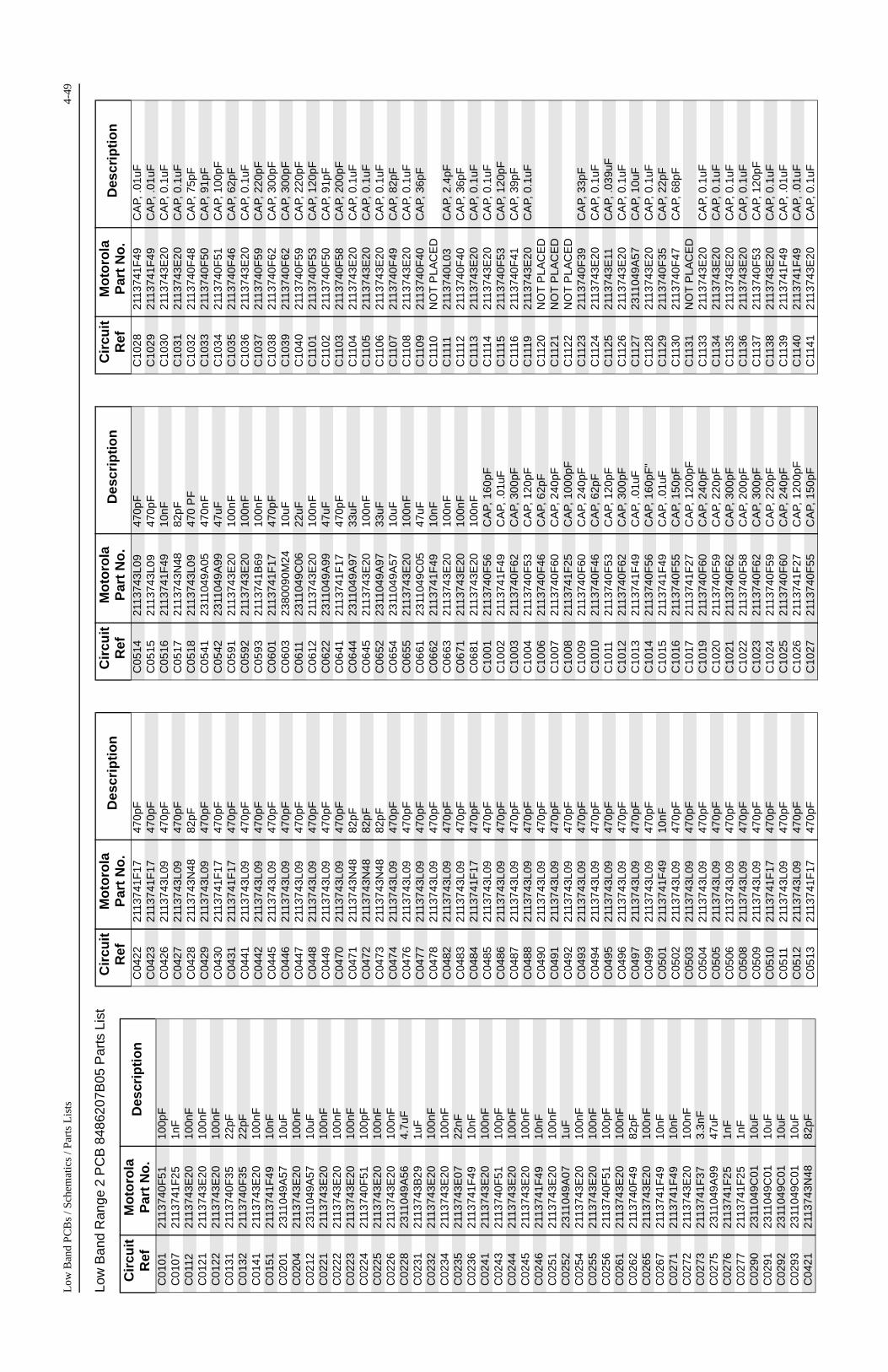
Low
Ban
d P
CB
s / S
chem
atic
s / P
arts
Lis
ts4-
49
Low
Ban
d R
ange
2 P
CB
848
6207
B05
Par
ts L
ist
Cir
cuit
R
efM
oto
rola
P
art
No
.D
escr
ipti
on
C01
0121
1374
0F51
100p
F
C01
0721
1374
1F25
1nF
C
0112
2113
743E
2010
0nF
C
0121
2113
743E
2010
0nF
C
0122
2113
743E
2010
0nF
C
0131
2113
740F
3522
pF
C01
3221
1374
0F35
22pF
C
0141
2113
743E
2010
0nF
C
0151
2113
741F
4910
nF
C02
0123
1104
9A57
10uF
C
0204
2113
743E
2010
0nF
C
0212
2311
049A
5710
uF
C02
2121
1374
3E20
100n
F
C02
2221
1374
3E20
100n
F
C02
2321
1374
3E20
100n
F
C02
2421
1374
0F51
100p
F
C02
2521
1374
3E20
100n
F
C02
2621
1374
3E20
100n
F
C02
2823
1104
9A56
4.7u
FC
0231
2113
743B
291u
F
C02
3221
1374
3E20
100n
F
C02
3421
1374
3E20
100n
F
C02
3521
1374
3E07
22nF
C
0236
2113
741F
4910
nF
C02
4121
1374
3E20
100n
F
C02
4321
1374
0F51
100p
F
C02
4421
1374
3E20
100n
F
C02
4521
1374
3E20
100n
F
C02
4621
1374
1F49
10nF
C
0251
2113
743E
2010
0nF
C
0252
2311
049A
071u
F
C02
5421
1374
3E20
100n
F
C02
5521
1374
3E20
100n
F
C02
5621
1374
0F51
100p
F
C02
6121
1374
3E20
100n
F
C02
6221
1374
0F49
82pF
C
0265
2113
743E
2010
0nF
C
0267
2113
741F
4910
nFC
0271
2113
741F
4910
nF
C02
7221
1374
3E20
100n
F
C02
7321
1374
1F37
3.3n
F
C02
7523
1104
9A99
47uF
C
0276
2113
741F
251n
F
C02
7721
1374
1F25
1nF
C
0290
2311
049C
0110
uFC
0291
2311
049C
0110
uFC
0292
2311
049C
0110
uFC
0293
2311
049C
0110
uFC
0421
2113
743N
4882
pF
C04
2221
1374
1F17
470p
F
C04
2321
1374
1F17
470p
F
C04
2621
1374
3L09
470p
F
C04
2721
1374
3L09
470p
F
C04
2821
1374
3N48
82pF
C
0429
2113
743L
0947
0pF
C
0430
2113
741F
1747
0pF
C04
3121
1374
1F17
470p
FC
0441
2113
743L
0947
0pF
C
0442
2113
743L
0947
0pF
C
0445
2113
743L
0947
0pF
C
0446
2113
743L
0947
0pF
C
0447
2113
743L
0947
0pF
C
0448
2113
743L
0947
0pF
C
0449
2113
743L
0947
0pF
C
0470
2113
743L
0947
0pF
C
0471
2113
743N
4882
pF
C04
7221
1374
3N48
82pF
C
0473
2113
743N
4882
pF
C04
7421
1374
3L09
470p
F
C04
7621
1374
3L09
470p
F
C04
7721
1374
3L09
470p
F
C04
7821
1374
3L09
470p
F
C04
8221
1374
3L09
470p
F
C04
8321
1374
3L09
470p
FC
0484
2113
741F
1747
0pF
C
0485
2113
743L
0947
0pF
C04
8621
1374
3L09
470p
FC
0487
2113
743L
0947
0pF
C04
8821
1374
3L09
470p
FC
0490
2113
743L
0947
0pF
C04
9121
1374
3L09
470p
FC
0492
2113
743L
0947
0pF
C
0493
2113
743L
0947
0pF
C04
9421
1374
3L09
470p
F
C04
9521
1374
3L09
470p
FC
0496
2113
743L
0947
0pF
C
0497
2113
743L
0947
0pF
C04
9921
1374
3L09
470p
FC
0501
2113
741F
4910
nFC
0502
2113
743L
0947
0pF
C
0503
2113
743L
0947
0pF
C
0504
2113
743L
0947
0pF
C
0505
2113
743L
0947
0pF
C05
0621
1374
3L09
470p
FC
0508
2113
743L
0947
0pF
C05
0921
1374
3L09
470p
FC
0510
2113
741F
1747
0pF
C05
1121
1374
3L09
470p
FC
0512
2113
743L
0947
0pF
C
0513
2113
741F
1747
0pF
Cir
cuit
R
efM
oto
rola
P
art
No
.D
escr
ipti
on
C05
1421
1374
3L09
470p
FC
0515
2113
743L
0947
0pF
C
0516
2113
741F
4910
nFC
0517
2113
743N
4882
pFC
0518
2113
743L
0947
0 P
F
C05
4123
1104
9A05
470n
F
C05
4223
1104
9A99
47uF
C05
9121
1374
3E20
100n
FC
0592
2113
743E
2010
0nF
C05
9321
1374
1B69
100n
F
C06
0121
1374
1F17
470p
FC
0603
2380
090M
2410
uFC
0611
2311
049C
0622
uF
C06
1221
1374
3E20
100n
FC
0622
2311
049A
9947
uFC
0641
2113
741F
1747
0pF
C
0644
2311
049A
9733
uF
C06
4521
1374
3E20
100n
FC
0652
2311
049A
9733
uF
C06
5423
1104
9A57
10uF
C06
5521
1374
3E20
100n
FC
0661
2311
049C
0547
uFC
0662
2113
741F
4910
nFC
0663
2113
743E
2010
0nF
C
0671
2113
743E
2010
0nF
C
0681
2113
743E
2010
0nF
C10
0121
1374
0F56
CA
P, 1
60pF
C10
0221
1374
1F49
CA
P, .0
1uF
C10
0321
1374
0F62
CA
P, 3
00pF
C10
0421
1374
0F53
CA
P, 1
20pF
C10
0621
1374
0F46
CA
P, 6
2pF
C10
0721
1374
0F60
CA
P, 2
40pF
C10
0821
1374
1F25
CA
P, 1
000p
FC
1009
2113
740F
60C
AP,
240
pFC
1010
2113
740F
46C
AP,
62p
FC
1011
2113
740F
53C
AP,
120
pFC
1012
2113
740F
62C
AP,
300
pFC
1013
2113
741F
49C
AP,
.01u
FC
1014
2113
740F
56C
AP,
160
pF"
C10
1521
1374
1F49
CA
P, .0
1uF
C10
1621
1374
0F55
CA
P, 1
50pF
C10
1721
1374
1F27
CA
P, 1
200p
FC
1019
2113
740F
60C
AP,
240
pFC
1020
2113
740F
59C
AP,
220
pFC
1021
2113
740F
62C
AP,
300
pFC
1022
2113
740F
58C
AP,
200
pFC
1023
2113
740F
62C
AP,
300
pFC
1024
2113
740F
59C
AP,
220
pFC
1025
2113
740F
60C
AP,
240
pFC
1026
2113
741F
27C
AP,
120
0pF
C10
2721
1374
0F55
CA
P, 1
50pF
Cir
cuit
R
efM
oto
rola
P
art
No
.D
escr
ipti
on
C10
2821
1374
1F49
CA
P, .0
1uF
C10
2921
1374
1F49
CA
P, .0
1uF
C10
3021
1374
3E20
CA
P, 0
.1uF
C10
3121
1374
3E20
CA
P, 0
.1uF
C10
3221
1374
0F48
CA
P, 7
5pF
C10
3321
1374
0F50
CA
P, 9
1pF
C10
3421
1374
0F51
CA
P, 1
00pF
C10
3521
1374
0F46
CA
P, 6
2pF
C10
3621
1374
3E20
CA
P, 0
.1uF
C10
3721
1374
0F59
CA
P, 2
20pF
C10
3821
1374
0F62
CA
P, 3
00pF
C10
3921
1374
0F62
CA
P, 3
00pF
C10
4021
1374
0F59
CA
P, 2
20pF
C11
0121
1374
0F53
CA
P, 1
20pF
C11
0221
1374
0F50
CA
P, 9
1pF
C11
0321
1374
0F58
CA
P, 2
00pF
C11
0421
1374
3E20
CA
P, 0
.1uF
C11
0521
1374
3E20
CA
P, 0
.1uF
C11
0621
1374
3E20
CA
P, 0
.1uF
C11
0721
1374
0F49
CA
P, 8
2pF
C11
0821
1374
3E20
CA
P, 0
.1uF
C11
0921
1374
0F40
CA
P, 3
6pF
C11
10N
OT
PLA
CE
DC
1111
2113
740L
03C
AP,
2.4
pFC
1112
2113
740F
40C
AP,
36p
FC
1113
2113
743E
20C
AP,
0.1
uFC
1114
2113
743E
20C
AP,
0.1
uFC
1115
2113
740F
53C
AP,
120
pFC
1116
2113
740F
41C
AP,
39p
FC
1119
2113
743E
20C
AP,
0.1
uFC
1120
NO
T P
LAC
ED
C11
21N
OT
PLA
CE
DC
1122
NO
T P
LAC
ED
C11
2321
1374
0F39
CA
P, 3
3pF
C11
2421
1374
3E20
CA
P, 0
.1uF
C11
2521
1374
3E11
CA
P, .0
39uF
C11
2621
1374
3E20
CA
P, 0
.1uF
C11
2723
1104
9A57
CA
P, 1
0uF
C11
2821
1374
3E20
CA
P, 0
.1uF
C11
2921
1374
0F35
CA
P, 2
2pF
C11
3021
1374
0F47
CA
P, 6
8pF
C11
31N
OT
PLA
CE
DC
1133
2113
743E
20C
AP,
0.1
uFC
1134
2113
743E
20C
AP,
0.1
uFC
1135
2113
743E
20C
AP,
0.1
uFC
1136
2113
743E
20C
AP,
0.1
uFC
1137
2113
740F
53C
AP,
120
pFC
1138
2113
743E
20C
AP,
0.1
uFC
1139
2113
741F
49C
AP,
.01u
FC
1140
2113
741F
49C
AP,
.01u
FC
1141
2113
743E
20C
AP,
0.1
uF
Cir
cuit
R
efM
oto
rola
P
art
No
.D
escr
ipti
on
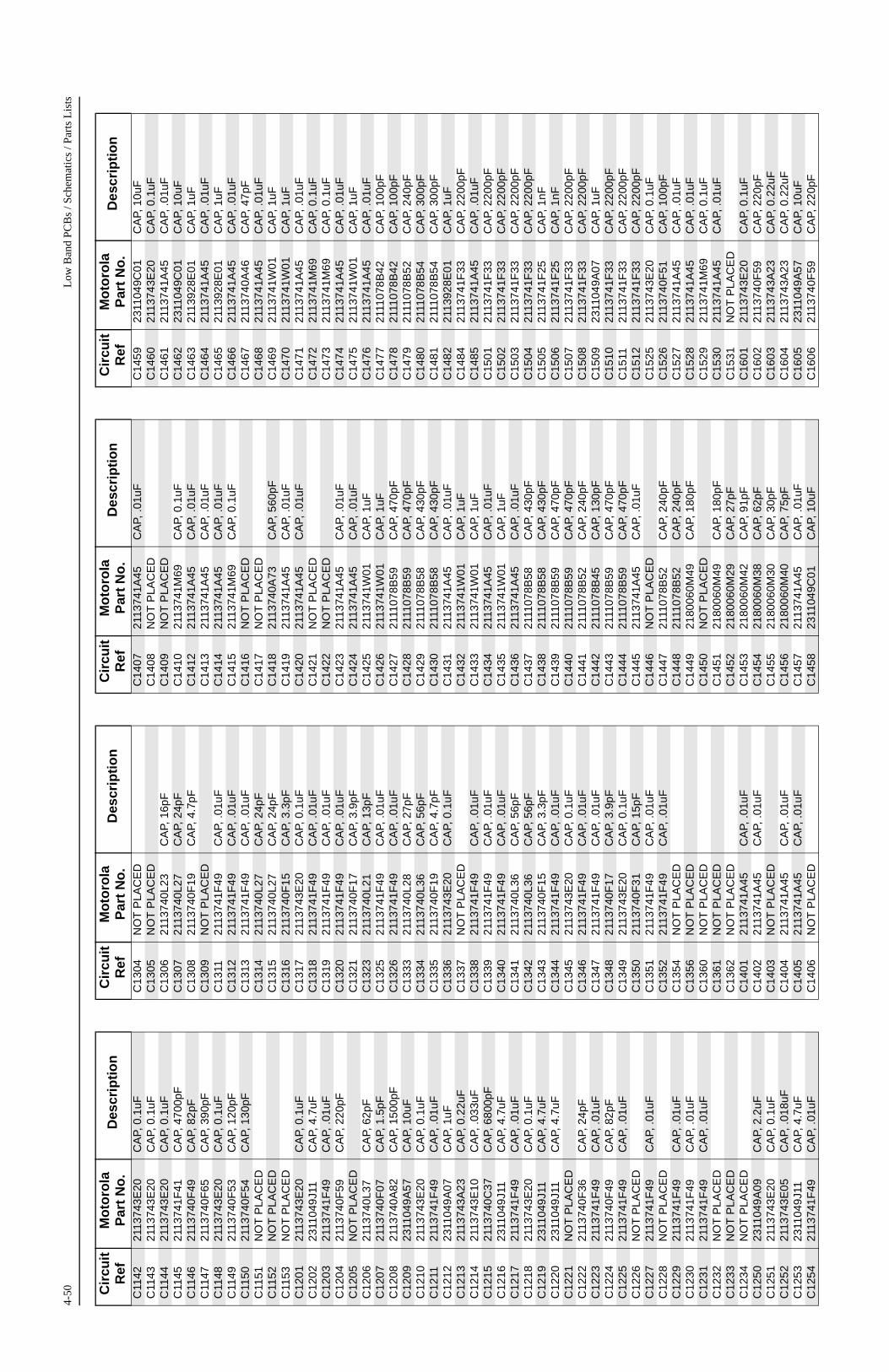
4-50
Low
Ban
d PC
Bs
/ Sch
emat
ics
/ Par
ts L
ists
C11
4221
1374
3E20
CA
P, 0
.1uF
C11
4321
1374
3E20
CA
P, 0
.1uF
C11
4421
1374
3E20
CA
P, 0
.1uF
C11
4521
1374
1F41
CA
P, 4
700p
FC
1146
2113
740F
49C
AP,
82p
FC
1147
2113
740F
65C
AP,
390
pFC
1148
2113
743E
20C
AP,
0.1
uFC
1149
2113
740F
53C
AP,
120
pFC
1150
2113
740F
54C
AP,
130
pFC
1151
NO
T P
LAC
ED
C11
52N
OT
PLA
CE
DC
1153
NO
T P
LAC
ED
C12
0121
1374
3E20
CA
P, 0
.1uF
C12
0223
1104
9J11
CA
P, 4
.7uF
C12
0321
1374
1F49
CA
P, .0
1uF
C12
0421
1374
0F59
CA
P, 2
20pF
C12
05N
OT
PLA
CE
DC
1206
2113
740L
37C
AP,
62p
FC
1207
2113
740F
07C
AP,
1.5
pFC
1208
2113
740A
82C
AP,
150
0pF
C12
0923
1104
9A57
CA
P, 1
0uF
C12
1021
1374
3E20
CA
P, 0
.1uF
C12
1121
1374
1F49
CA
P, .0
1uF
C12
1223
1104
9A07
CA
P, 1
uFC
1213
2113
743A
23C
AP,
0.2
2uF
C12
1421
1374
3E10
CA
P, .0
33uF
C12
1521
1374
0C37
CA
P, 6
800p
FC
1216
2311
049J
11C
AP,
4.7
uFC
1217
2113
741F
49C
AP,
.01u
FC
1218
2113
743E
20C
AP,
0.1
uFC
1219
2311
049J
11C
AP,
4.7
uFC
1220
2311
049J
11C
AP,
4.7
uFC
1221
NO
T P
LAC
ED
C12
2221
1374
0F36
CA
P, 2
4pF
C12
2321
1374
1F49
CA
P, .0
1uF
C12
2421
1374
0F49
CA
P, 8
2pF
C12
2521
1374
1F49
CA
P, .0
1uF
C12
26N
OT
PLA
CE
DC
1227
2113
741F
49C
AP,
.01u
FC
1228
NO
T P
LAC
ED
C12
2921
1374
1F49
CA
P, .0
1uF
C12
3021
1374
1F49
CA
P, .0
1uF
C12
3121
1374
1F49
CA
P, .0
1uF
C12
32N
OT
PLA
CE
DC
1233
NO
T P
LAC
ED
C12
34N
OT
PLA
CE
DC
1250
2311
049A
09C
AP,
2.2
uFC
1251
2113
743E
20C
AP,
0.1
uFC
1252
2113
743E
05C
AP,
.018
uFC
1253
2311
049J
11C
AP,
4.7
uFC
1254
2113
741F
49C
AP,
.01u
F
Cir
cuit
R
efM
oto
rola
P
art
No
.D
escr
ipti
on
C13
04N
OT
PLA
CE
DC
1305
NO
T P
LAC
ED
C13
0621
1374
0L23
CA
P, 1
6pF
C13
0721
1374
0L27
CA
P, 2
4pF
C13
0821
1374
0F19
CA
P, 4
.7pF
C13
09N
OT
PLA
CE
DC
1311
2113
741F
49C
AP,
.01u
FC
1312
2113
741F
49C
AP,
.01u
FC
1313
2113
741F
49C
AP,
.01u
FC
1314
2113
740L
27C
AP,
24p
FC
1315
2113
740L
27C
AP,
24p
FC
1316
2113
740F
15C
AP,
3.3
pFC
1317
2113
743E
20C
AP,
0.1
uFC
1318
2113
741F
49C
AP,
.01u
FC
1319
2113
741F
49C
AP,
.01u
FC
1320
2113
741F
49C
AP,
.01u
FC
1321
2113
740F
17C
AP,
3.9
pFC
1323
2113
740L
21C
AP,
13p
FC
1325
2113
741F
49C
AP,
.01u
FC
1326
2113
741F
49C
AP,
.01u
FC
1333
2113
740L
28C
AP,
27p
FC
1334
2113
740L
36C
AP,
56p
FC
1335
2113
740F
19C
AP,
4.7
pFC
1336
2113
743E
20C
AP,
0.1
uFC
1337
NO
T P
LAC
ED
C13
3821
1374
1F49
CA
P, .0
1uF
C13
3921
1374
1F49
CA
P, .0
1uF
C13
4021
1374
1F49
CA
P, .0
1uF
C13
4121
1374
0L36
CA
P, 5
6pF
C13
4221
1374
0L36
CA
P, 5
6pF
C13
4321
1374
0F15
CA
P, 3
.3pF
C13
4421
1374
1F49
CA
P, .0
1uF
C13
4521
1374
3E20
CA
P, 0
.1uF
C13
4621
1374
1F49
CA
P, .0
1uF
C13
4721
1374
1F49
CA
P, .0
1uF
C13
4821
1374
0F17
CA
P, 3
.9pF
C13
4921
1374
3E20
CA
P, 0
.1uF
C13
5021
1374
0F31
CA
P, 1
5pF
C13
5121
1374
1F49
CA
P, .0
1uF
C13
5221
1374
1F49
CA
P, .0
1uF
C13
54N
OT
PLA
CE
DC
1356
NO
T P
LAC
ED
C13
60N
OT
PLA
CE
DC
1361
NO
T P
LAC
ED
C13
62N
OT
PLA
CE
DC
1401
2113
741A
45C
AP,
.01u
FC
1402
2113
741A
45C
AP,
.01u
FC
1403
NO
T P
LAC
ED
C14
0421
1374
1A45
CA
P, .0
1uF
C14
0521
1374
1A45
CA
P, .0
1uF
C14
06N
OT
PLA
CE
D
Cir
cuit
R
efM
oto
rola
P
art
No
.D
escr
ipti
on
C14
0721
1374
1A45
CA
P, .0
1uF
C14
08N
OT
PLA
CE
DC
1409
NO
T P
LAC
ED
C14
1021
1374
1M69
CA
P, 0
.1uF
C14
1221
1374
1A45
CA
P, .0
1uF
C14
1321
1374
1A45
CA
P, .0
1uF
C14
1421
1374
1A45
CA
P, .0
1uF
C14
1521
1374
1M69
CA
P, 0
.1uF
C14
16N
OT
PLA
CE
DC
1417
NO
T P
LAC
ED
C14
1821
1374
0A73
CA
P, 5
60pF
C14
1921
1374
1A45
CA
P, .0
1uF
C14
2021
1374
1A45
CA
P, .0
1uF
C14
21N
OT
PLA
CE
DC
1422
NO
T P
LAC
ED
C14
2321
1374
1A45
CA
P, .0
1uF
C14
2421
1374
1A45
CA
P, .0
1uF
C14
2521
1374
1W01
CA
P, 1
uFC
1426
2113
741W
01C
AP,
1uF
C14
2721
1107
8B59
CA
P, 4
70pF
C14
2821
1107
8B59
CA
P, 4
70pF
C14
2921
1107
8B58
CA
P, 4
30pF
C14
3021
1107
8B58
CA
P, 4
30pF
C14
3121
1374
1A45
CA
P, .0
1uF
C14
3221
1374
1W01
CA
P, 1
uFC
1433
2113
741W
01C
AP,
1uF
C14
3421
1374
1A45
CA
P, .0
1uF
C14
3521
1374
1W01
CA
P, 1
uFC
1436
2113
741A
45C
AP,
.01u
FC
1437
2111
078B
58C
AP,
430
pFC
1438
2111
078B
58C
AP,
430
pFC
1439
2111
078B
59C
AP,
470
pFC
1440
2111
078B
59C
AP,
470
pFC
1441
2111
078B
52C
AP,
240
pFC
1442
2111
078B
45C
AP,
130
pFC
1443
2111
078B
59C
AP,
470
pFC
1444
2111
078B
59C
AP,
470
pFC
1445
2113
741A
45C
AP,
.01u
FC
1446
NO
T P
LAC
ED
C14
4721
1107
8B52
CA
P, 2
40pF
C14
4821
1107
8B52
CA
P, 2
40pF
C14
4921
8006
0M49
CA
P, 1
80pF
C14
50N
OT
PLA
CE
DC
1451
2180
060M
49C
AP,
180
pFC
1452
2180
060M
29C
AP,
27p
FC
1453
2180
060M
42C
AP,
91p
FC
1454
2180
060M
38C
AP,
62p
FC
1455
2180
060M
30C
AP,
30p
FC
1456
2180
060M
40C
AP,
75p
FC
1457
2113
741A
45C
AP,
.01u
FC
1458
2311
049C
01C
AP,
10u
F
Cir
cuit
R
efM
oto
rola
P
art
No
.D
escr
ipti
on
C14
5923
1104
9C01
CA
P, 1
0uF
C14
6021
1374
3E20
CA
P, 0
.1uF
C14
6121
1374
1A45
CA
P, .0
1uF
C14
6223
1104
9C01
CA
P, 1
0uF
C14
6321
1392
8E01
CA
P, 1
uFC
1464
2113
741A
45C
AP,
.01u
FC
1465
2113
928E
01C
AP,
1uF
C14
6621
1374
1A45
CA
P, .0
1uF
C14
6721
1374
0A46
CA
P, 4
7pF
C14
6821
1374
1A45
CA
P, .0
1uF
C14
6921
1374
1W01
CA
P, 1
uFC
1470
2113
741W
01C
AP,
1uF
C14
7121
1374
1A45
CA
P, .0
1uF
C14
7221
1374
1M69
CA
P, 0
.1uF
C14
7321
1374
1M69
CA
P, 0
.1uF
C14
7421
1374
1A45
CA
P, .0
1uF
C14
7521
1374
1W01
CA
P, 1
uFC
1476
2113
741A
45C
AP,
.01u
FC
1477
2111
078B
42C
AP,
100
pFC
1478
2111
078B
42C
AP,
100
pFC
1479
2111
078B
52C
AP,
240
pFC
1480
2111
078B
54C
AP,
300
pFC
1481
2111
078B
54C
AP,
300
pFC
1482
2113
928E
01C
AP,
1uF
C14
8421
1374
1F33
CA
P, 2
200p
FC
1485
2113
741A
45C
AP,
.01u
FC
1501
2113
741F
33C
AP,
220
0pF
C15
0221
1374
1F33
CA
P, 2
200p
FC
1503
2113
741F
33C
AP,
220
0pF
C15
0421
1374
1F33
CA
P, 2
200p
FC
1505
2113
741F
25C
AP,
1nF
C15
0621
1374
1F25
CA
P, 1
nFC
1507
2113
741F
33C
AP,
220
0pF
C15
0821
1374
1F33
CA
P, 2
200p
FC
1509
2311
049A
07C
AP,
1uF
C15
1021
1374
1F33
CA
P, 2
200p
FC
1511
2113
741F
33C
AP,
220
0pF
C15
1221
1374
1F33
CA
P, 2
200p
FC
1525
2113
743E
20C
AP,
0.1
uFC
1526
2113
740F
51C
AP,
100
pFC
1527
2113
741A
45C
AP,
.01u
FC
1528
2113
741A
45C
AP,
.01u
FC
1529
2113
741M
69C
AP,
0.1
uFC
1530
2113
741A
45C
AP,
.01u
FC
1531
NO
T P
LAC
ED
C16
0121
1374
3E20
CA
P, 0
.1uF
C16
0221
1374
0F59
CA
P, 2
20pF
C16
0321
1374
3A23
CA
P, 0
.22u
FC
1604
2113
743A
23C
AP,
0.2
2uF
C16
0523
1104
9A57
CA
P, 1
0uF
C16
0621
1374
0F59
CA
P, 2
20pF
Cir
cuit
R
efM
oto
rola
P
art
No
.D
escr
ipti
on

Low
Ban
d P
CB
s / S
chem
atic
s / P
arts
Lis
ts4-
51
C16
0721
1374
0F51
CA
P, 1
00pF
C16
0821
1374
3A23
CA
P, 0
.22u
FC
1609
2113
740F
34C
AP,
20p
FC
1610
2113
741F
41C
AP,
470
0pF
C16
1121
1374
3E20
CA
P, 0
.1uF
C16
1221
1374
1F33
CA
P, 2
200p
FC
1613
2113
740F
54C
AP,
130
pFC
1614
2113
741F
24C
AP,
910
pFC
1615
NO
T P
LAC
ED
C16
1621
1374
0F40
CA
P, 3
6pF
C16
1821
1374
3A23
CA
P, 0
.22u
FC
1619
2311
049A
57C
AP,
10u
FC
1620
2113
741F
25C
AP,
100
0pF
C16
21N
OT
PLA
CE
DC
1622
2113
743E
20C
AP,
0.1
uFC
1623
2113
740F
60C
AP,
240
pFC
1624
2113
741F
37C
AP,
330
0pF
C16
2521
1374
0F29
CA
P, 1
2pF
C16
2621
1374
0F59
CA
P, 2
20pF
C16
2721
1374
3A23
CA
P, 0
.22u
FC
1628
2113
743E
20C
AP,
0.1
uFC
1629
2113
740F
39C
AP,
33p
FC
1631
2311
049A
57C
AP,
10u
FC
1632
2113
743E
20C
AP,
0.1
uFC
1633
2113
743A
23C
AP,
0.2
2uF
C16
3421
1374
1A45
CA
P, .0
1uF
CR
1201
4802
245J
221T
363
CR
1202
4802
233J
09IM
N10
CR
1302
4805
649Q
14H
N1V
02H
CR
1306
4880
154K
03M
MB
D35
3C
R13
1048
0564
9Q14
HN
1V02
HC
R13
1448
8015
4K03
MM
BD
353
D01
0148
8023
6E05
Sch
ottk
yD
0151
4813
833C
02D
ual
D01
7948
1383
3C02
Dua
lD
0621
4813
833C
02D
ual
D06
5148
1383
3C02
Dua
lD
0660
4813
833C
02D
ual
D06
6148
1383
3C02
Dua
lD
1001
4880
154K
03M
MB
D35
3D
1101
4880
154K
03M
MB
D35
3D
1401
4808
379X
02M
A4P
1450
D14
0248
0837
9X02
MA
4P14
50D
1501
4880
236E
05M
MB
D30
1D
1502
4813
833C
02M
MB
D61
00D
1503
4813
833C
02M
MB
D61
00D
1601
4880
154K
03M
MB
D35
3E
0271
2484
657R
01F
errit
e B
ead
E02
7224
8465
7R01
Fer
rite
Bea
dE
0631
2484
657R
01F
errit
e B
ead
E14
0124
0838
0X02
2773
0374
46
Cir
cuit
R
efM
oto
rola
P
art
No
.D
escr
ipti
on
E14
0324
0838
0X02
2773
0374
46F
0401
0658
0542
Z01
FU
SE
FL1
101
9180
656U
03C
FE
C10
_7M
G1
FL1
102
9180
022M
09F
ILT
ER
FL1
104
9180
468V
04C
FU
CJ4
55F
FL1
105
9180
468V
05C
FU
CJ4
55E
FL1
106
9180
469V
04C
FW
C45
5FF
L110
791
8046
9V05
CF
WC
455E
J040
109
0263
6Y02
Con
nect
or, F
lex,
12-
pin
J045
109
0263
6Y01
Con
n, F
lex,
Sid
e E
ntry
J050
109
8610
5B01
Con
nect
or, S
MD
, 20-
pin
J055
109
0550
5Y04
Con
n, Z
IF
J055
209
0550
5Y03
Con
n, 1
8-P
inJ0
601
0986
165B
01D
C P
ower
Con
nect
orJ1
401
0986
166B
02C
ON
N_J
L100
124
0838
2A11
IDC
TR
, 130
nHL1
002
2408
382C
11ID
CT
R, 1
30nH
L100
324
0838
2A11
IDC
TR
, 130
nHL1
004
2408
382C
11ID
CT
R, 1
30nH
L100
524
0838
2A11
IDC
TR
, 130
nHL1
006
2408
382A
11ID
CT
R, 1
30nH
L100
724
0838
2C11
IDC
TR
, 130
nHL1
008
2408
382A
11ID
CT
R, 1
30nH
L100
924
0838
2C11
IDC
TR
, 130
nHL1
010
2408
382A
11ID
CT
R, 1
30nH
L101
124
6258
7N68
IDC
TR
, 1uH
L101
224
6258
7N57
IDC
TR
, 220
nHL1
013
2462
587N
59ID
CT
R, 3
30nH
L101
424
6258
7N57
IDC
TR
, 220
nHL1
101
2462
587N
33ID
CT
R, 1
.8uH
L110
224
0838
3X07
IDC
TR
, 3.3
uHL1
103
2462
587N
33ID
CT
R, 1
.8uH
L110
424
8028
9M10
IDC
TR
, 6.8
uHL1
105
2480
289M
10ID
CT
R, 6
.8uH
L110
624
6258
7N33
IDC
TR
, 1.8
uHL1
107
2480
289M
09ID
CT
R, 5
.6uH
L110
8N
OT
PLA
CE
DL1
109
NO
T P
LAC
ED
L111
024
8028
9M18
IDC
TR
, 33u
HL1
111
2408
383X
07ID
CT
R, 3
.3uH
L111
224
8341
1T35
IDC
TR
, 6.8
uHL1
201
2480
289M
17ID
CT
R, 2
7uH
L120
224
6258
7Q20
IDC
TR
, 2.2
uHL1
204
NO
T P
LAC
ED
L120
524
6258
7N62
IDC
TR
, 560
nHL1
206
2480
289M
17ID
CT
R, 2
7uH
L120
7N
OT
PLA
CE
DL1
302
2408
382D
19ID
CT
R, 4
91nH
L130
324
8028
9M17
IDC
TR
, 27u
H"
L130
424
6258
7N66
IDC
TR
, 820
nHL1
305
2480
289M
17ID
CT
R, 2
7uH
Cir
cuit
R
efM
oto
rola
P
art
No
.D
escr
ipti
on
L130
624
8028
9M17
IDC
TR
, 27u
HL1
307
2480
289M
17ID
CT
R, 2
7uH
L130
924
8028
9M17
IDC
TR
, 27u
HL1
310
2462
587N
60ID
CT
R, 3
90nH
L131
124
8028
9M17
IDC
TR
, 27u
HL1
313
2408
382D
19ID
CT
R, 4
91nH
L131
424
8028
9M18
IDC
TR
, 33u
HL1
315
2462
587N
69ID
CT
R, 1
.2uH
L131
624
8028
9M18
IDC
TR
, 33u
HL1
317
2480
289M
18ID
CT
R, 3
3uH
L131
824
8028
9M18
IDC
TR
, 33u
HL1
321
2462
587N
58ID
CT
R, 2
70nH
L132
224
8028
9M18
IDC
TR
, 33u
HL1
324
2480
289M
18ID
CT
R, 3
3uH
L140
1N
OT
PLA
CE
DL1
402
2462
587U
09ID
CT
R, 4
.7uH
L140
324
6258
7U09
IDC
TR
, 4.7
uHL1
404
2462
587N
56ID
CT
R, 1
80nH
L140
5N
OT
PLA
CE
DL1
406
2408
381X
36ID
CT
R, 2
50.9
74nH
L141
324
0838
1X17
IDC
TR
, 88.
470n
HL1
414
2408
381X
17ID
CT
R, 8
8.47
0nH
L141
524
6059
1X02
IDC
TR
, 25n
HL1
416
2460
591X
02ID
CT
R, 2
5nH
L141
724
6059
1X02
IDC
TR
, 25n
HL1
418
2408
381X
17ID
CT
R, 8
8.47
0nH
L141
924
8028
9M17
IDC
TR
, 27u
HL1
420
2408
381X
31ID
CT
R, 1
96.8
76nH
L142
124
0838
1X27
IDC
TR
, 150
.499
nHL1
422
2408
381X
24ID
CT
R, 1
33.3
04nH
L142
324
0838
1X15
IDC
TR
, 78.
727n
HL1
424
2408
384A
08ID
CT
R, 8
2nH
L142
524
6059
1X02
IDC
TR
, 25n
HL1
426
2460
591X
02ID
CT
R, 2
5nH
L160
124
8341
1T45
IDC
TR
, 47u
HL1
602
2483
411T
45ID
CT
R, 4
7uH
L160
324
8341
1T73
IDC
TR
, 1uH
L160
424
8341
1T45
IDC
TR
, 47u
HL1
605
2483
411T
41ID
CT
R, 2
2uH
L160
624
6258
7T30
IDC
TR
, 1uH
L160
724
6258
7T30
IDC
TR
, 1uH
M14
0126
8620
1B01
HE
AT
SIN
KQ
0110
4880
048M
01N
PN
Q01
5148
8004
8M01
NP
N
Q01
7148
8004
8M01
NP
NQ
0173
4880
052M
01N
PN
Q01
7748
8004
8M01
NP
NQ
0181
4880
048M
01N
PN
Q01
8348
8004
8M01
NP
NQ
0185
4880
048M
01N
PN
Q02
7148
1382
4A10
NP
N
Cir
cuit
R
efM
oto
rola
P
art
No
.D
escr
ipti
on
Q06
4148
8004
8M01
NP
N
Q06
6148
0592
1T02
DU
AL
Q06
6248
1382
4A10
NP
N
Q06
6348
8004
8M01
NP
NQ
0681
4880
052M
01N
PN
Q
1001
4880
173R
01M
MB
R95
1Q
1002
4813
824A
17M
MB
T39
06Q
1003
4813
824A
17M
MB
T39
06Q
1101
4813
827A
07M
MB
R94
1Q
1102
4813
823A
05M
MB
FU
310L
Q11
0348
1382
3A05
MM
BF
U31
0LQ
1104
4813
823A
05M
MB
FU
310L
Q11
0548
8004
8M01
DT
C14
4EK
AQ
1106
4813
827A
07M
MB
R94
1Q
1201
4813
824A
17M
MB
T39
06Q
1202
4880
173R
01M
MB
R95
1Q
1303
4884
235R
02M
MB
FU
310
Q13
0448
8017
3R01
MM
BR
951
Q13
0548
8017
3R01
MM
BR
951
Q13
0648
8423
5R02
MM
BF
U31
0Q
1307
4880
173R
01M
MB
R95
1Q
1308
4880
173R
01M
MB
R95
1Q
1401
4886
212B
01M
RF
1518
Q14
0248
8613
6B01
36B
01Q
1403
4886
136B
0136
B01
Q14
04N
OT
PLA
CE
DQ
1501
4880
141L
03B
CW
68G
Q15
0248
1382
4A10
MM
BT
3904
Q15
0348
1382
4A10
MM
BT
3904
Q15
0448
1382
4A10
MM
BT
3904
Q15
0548
1382
4A17
MM
BT
3906
Q15
0648
1382
4A10
MM
BT
3904
Q16
0148
1382
4A17
MM
BT
3906
Q16
0248
8004
8M01
DT
C14
4EK
AQ
1603
4813
824A
10M
MB
T39
04Q
1604
4813
824A
10M
MB
T39
04Q
1605
4813
824A
10M
MB
T39
04Q
1606
4813
824A
17M
MB
T39
06Q
1607
4813
824A
10M
MB
T39
04Q
1609
4813
824A
17M
MB
T39
06Q
1610
4805
585Q
17N
E25
139
R01
0106
6205
7A73
10K
R01
0206
6205
7A65
4.7K
R01
0406
6205
7A73
10K
R01
0506
6205
7A97
100K
R01
0806
6205
7A57
2.2K
R01
1106
6205
7B47
0 R
0113
0662
057A
7310
K
R01
1406
6205
7A73
10K
R01
1506
6205
7A73
10K
R01
1706
6205
7A63
3.9K
Cir
cuit
R
efM
oto
rola
P
art
No
.D
escr
ipti
on
4-52
Low
Ban
d PC
Bs
/ Sch
emat
ics
/ Par
ts L
ists
R01
2106
6205
7A97
100K
R01
3106
6205
7B46
10.0
MR
0132
0662
057B
1033
0KR
0151
0662
057A
8224
KR
0152
0662
057A
8224
KR
0170
0662
057A
7310
KR
0171
0662
057A
654.
7KR
0172
0662
057A
7310
KR
0173
0662
057A
654.
7KR
0174
0662
057A
7310
KR
0175
0662
057A
7310
KR
0176
0662
057A
8430
KR
0177
0662
057A
654.
7KR
0178
0662
057A
8947
KR
0179
0662
057A
8947
KR
0181
0662
057A
654.
7KR
0182
0662
057A
8947
KR
0183
0662
057A
654.
7KR
0184
0662
057A
8947
KR
0185
0662
057A
654.
7KR
0186
0662
057A
8947
KR
0201
0662
057A
2510
0 R
0202
0662
057A
4356
0 R
0203
0662
057A
2510
0 R
0204
0662
057A
4356
0 R
0205
0662
057A
7310
KR
0206
0662
057A
7310
KR
0207
0662
057A
572.
2KR
0208
0662
057A
572.
2KR
0211
0660
076E
707.
5KR
0212
0660
076E
707.
5KR
0221
0662
057A
8224
K
R02
2206
6205
7A82
24K
R
0223
0662
057A
8430
KR
0224
0662
057A
718.
2KR
0228
0662
057B
470
R02
2906
6205
7A01
10R
0241
0662
057A
8947
KR
0242
0662
057B
470
R02
5106
6205
7A89
47K
R02
5206
6205
7A91
56K
R02
5306
6205
7A97
100K
R02
5406
6205
7A73
10K
R02
5506
6205
7A73
10K
R05
5606
6205
7A97
100K
R02
5706
6205
7A57
2.2K
R02
6106
6205
7A73
10K
R02
6206
6205
7A97
100K
R02
6506
6205
7A82
24K
R02
6706
6205
7A89
47K
R02
6806
6205
7A73
10K
Cir
cuit
R
efM
oto
rola
P
art
No
.D
escr
ipti
on
R02
6906
6205
7A41
470
R02
7306
6205
7A82
24K
R02
7506
6205
7A73
10K
R02
7606
6205
7A77
15K
R04
0106
6205
7A33
220
R04
0706
6205
7M26
10R
0408
0662
057A
2510
0 R
0409
0662
057M
2610
R04
1206
6205
7B47
0R
0441
0662
057B
470
R02
4206
6205
7A49
1KR
0467
0662
057M
2610
R
0468
0662
057M
2610
R04
8106
6205
7B47
0R
0482
0662
057B
470
R05
1006
6205
7A65
4.7K
R05
1106
6205
7A97
100K
R05
1206
6205
7A77
15K
R05
2506
6205
7A97
100K
R05
2906
6205
7A89
47K
R05
3006
6205
7B47
0R
0531
0662
057A
4356
0R
0533
0662
057B
470
R05
3506
6205
7A49
1KR
0537
0662
057A
3322
0 R
0538
0662
057A
3322
0R
0539
0662
057A
654.
7KR
0541
0662
057A
8327
KR
0543
0662
057A
9710
0KR
0591
0662
057A
8224
KR
0592
0662
057A
0110
R05
9306
6205
7A97
100K
R06
1106
6205
7A91
56K
R06
1206
6205
7A65
4.7K
R06
2106
6205
7A82
24K
R06
4106
6205
7A73
10K
R06
4206
6007
6E70
7.5K
R06
4306
6007
6E51
1.2K
R06
5106
6205
7A01
10R
0652
0662
057A
0110
R
0661
0662
057A
491K
R06
6206
6205
7B02
150K
R06
7106
6205
7A84
30K
R06
7206
6205
7A73
10K
R06
8106
6205
7A79
18K
R06
8206
6205
7A93
68K
R10
0106
6205
7A05
RE
S, 1
5R
1002
0662
057A
05R
ES
, 15
R10
0306
6205
7A41
RE
S, 4
70R
1004
0662
057A
59R
ES
, 2.7
KR
1005
0662
057A
31R
ES
, 180
Cir
cuit
R
efM
oto
rola
P
art
No
.D
escr
ipti
on
R10
0606
6205
7A73
RE
S, 1
0KR
1007
0662
057A
71R
ES
, 8.2
KR
1008
0662
057A
65R
ES
, 4.7
KR
1009
NO
T P
LAC
ED
R10
10N
OT
PLA
CE
DR
1011
NO
T P
LAC
ED
R11
0106
6205
7A18
RE
S, 5
1R
1102
0662
057A
78R
ES
, 16K
R11
0306
6205
7A39
RE
S, 3
90R
1104
0662
057A
71R
ES
, 8.2
KR
1106
0662
057A
25R
ES
, 100
R11
0706
6205
7A68
RE
S, 6
.2K
R11
0806
6205
7A61
RE
S, 3
.3K
R11
0906
6205
7A37
RE
S, 3
30R
1110
0662
057A
25R
ES
, 100
R11
1106
6205
7A17
RE
S, 4
7R
1113
0662
057A
64R
ES
, 4.3
KR
1114
0662
057A
64R
ES
, 4.3
KR
1115
0662
057A
75R
ES
, 12K
R11
16N
OT
PLA
CE
DR
1117
0662
057A
37R
ES
, 330
R11
1806
6205
7A56
RE
S, 2
KR
1119
0662
057A
83R
ES
, 27K
R11
2006
6205
7A18
RE
S, 5
1R
1121
0662
057A
71R
ES
, 8.2
KR
1122
0662
057A
73R
ES
, 10K
R11
2306
6205
7A51
RE
S, 1
.2K
R11
24N
OT
PLA
CE
DR
1125
NO
T P
LAC
ED
R11
26N
OT
PLA
CE
DR
1127
NO
T P
LAC
ED
R11
2806
6205
7A73
RE
S, 1
0KR
1129
0662
057A
73R
ES
, 10K
R11
3006
6205
7A73
RE
S, 1
0KR
1131
0662
057A
77R
ES
, 15K
R11
3206
6205
7A58
RE
S, 2
.4K
R11
3306
6205
7A61
RE
S, 3
.3K
R11
3406
6205
7A05
RE
S, 1
5R
1135
0662
057A
20R
ES
, 62
R11
3606
6205
7A45
RE
S, 6
80R
1137
0662
057A
75R
ES
, 12K
R11
3806
6205
7A01
RE
S, 1
0R
1139
0611
077A
12R
ES
, 2.7
R12
0106
6205
7B47
RE
S, 0
R12
02N
OT
PLA
CE
DR
1203
0662
057B
02R
ES
, 150
KR
1204
0662
057B
47R
ES
, 0R
1205
0662
057A
45R
ES
, 680
R12
0606
6205
7A41
RE
S, 4
70R
1207
NO
T P
LAC
ED
R12
0806
6205
7A18
RE
S, 5
1
Cir
cuit
R
efM
oto
rola
P
art
No
.D
escr
ipti
on
R12
0906
6205
7A61
RE
S, 3
.3K
R12
1006
6205
7A33
RE
S, 2
20R
1211
0662
057B
14R
ES
, 470
KR
1212
0662
057A
25R
ES
, 100
R12
1306
6205
7A45
RE
S, 6
80R
1214
0662
057A
54R
ES
, 1.6
KR
1215
0662
057A
21R
ES
, 68
R12
1606
6205
7A18
RE
S, 5
1R
1217
0662
057A
25R
ES
, 100
R12
1806
6205
7A17
RE
S, 4
7R
1219
0662
057A
17R
ES
, 47
R12
2006
6205
7A17
RE
S, 4
7R
1221
0662
057B
47R
ES
, 0R
1222
NO
T P
LAC
ED
R13
0606
6205
7B47
RE
S, 0
R13
0706
6205
7A19
RE
S, 5
6R
1308
0662
057A
19R
ES
, 56
R13
0906
6205
7A41
RE
S, 4
70R
1311
0662
057A
73R
ES
, 10K
R13
1206
6205
7A51
RE
S, 1
.2K
R13
1306
6205
7A51
RE
S, 1
.2K
R13
1406
6205
7A37
RE
S, 3
30R
1315
0662
057A
61R
ES
, 3.3
KR
1316
0662
057A
45R
ES
, 680
R13
1706
6205
7A09
RE
S, 2
2R
1318
0662
057A
41R
ES
, 470
R13
1906
6205
7A01
RE
S, 1
0R
1320
0662
057A
41R
ES
, 470
R13
2506
6205
7B47
RE
S, 0
R13
2606
6205
7A19
RE
S, 5
6R
1327
0662
057A
19R
ES
, 56
R13
2806
6205
7A41
RE
S, 4
70R
1330
0662
057A
73R
ES
, 10K
R13
3106
6205
7A51
RE
S, 1
.2K
R13
3206
6205
7A51
RE
S, 1
.2K
R13
3306
6205
7A37
RE
S, 3
30R
1334
0662
057A
61R
ES
, 3.3
KR
1335
0662
057A
47R
ES
, 820
R13
3606
6205
7A09
RE
S, 2
2R
1337
0662
057A
22R
ES
, 75
R13
3806
6205
7A27
RE
S, 1
20R
1339
0662
057A
22R
ES
, 75
R13
4006
6205
7A49
RE
S, 1
KR
1341
0662
057A
25R
ES
, 100
R13
4206
6205
7A25
RE
S, 1
00R
1343
0662
057C
55R
ES
, 150
R13
4406
6205
7A49
RE
S, 1
KR
1345
0662
057A
25R
ES
, 100
R13
4606
6205
7A25
RE
S, 1
00R
1347
0662
057C
55R
ES
, 150
R13
7606
6205
7A65
RE
S, 4
.7K
Cir
cuit
R
efM
oto
rola
P
art
No
.D
escr
ipti
on

Low
Ban
d P
CB
s / S
chem
atic
s / P
arts
Lis
ts4-
53
*Mot
orol
a D
epot
Ser
vici
ng o
nly
Ref
eren
ce d
esig
nato
rs w
ith
an a
ster
isk
indi
cate
com
pone
nts
whi
ch a
re n
ot f
ield
rep
lace
able
bec
ause
they
nee
d to
be
cali
-br
ated
wit
h sp
ecia
lize
d fa
ctor
y eq
uipm
ent a
fter
inst
alla
tion
. R
adio
s in
whi
ch th
ese
part
s ha
ve b
een
repl
aced
in th
e fi
eld
wil
l be
off
fre
quen
cy a
t tem
pera
ture
ext
rem
es.
R14
0206
1107
9A64
RE
S, 3
90R
1404
0680
194M
18R
ES
, 51
R14
0506
8019
4M18
RE
S, 5
1R
1406
0662
057A
73R
ES
, 10K
R14
0706
6205
7A73
RE
S, 1
0KR
1409
0682
089V
01R
ES
, .01
R14
1006
8396
2T52
RE
S, 1
30R
1411
0662
057C
99R
ES
, 10K
R14
12N
OT
PLA
CE
DR
1413
0680
194M
01R
ES
, 10
R14
1406
8019
4M01
RE
S, 1
0R
1415
NO
T P
LAC
ED
R14
1606
8019
4M01
RE
S, 1
0R
1417
0680
194M
01R
ES
, 10
R14
1806
8019
4M01
RE
S, 1
0R
1419
0680
194M
01R
ES
, 10
R14
2006
8019
4M01
RE
S, 1
0R
1421
0680
194M
01R
ES
, 10
R14
2206
8019
4M01
RE
S, 1
0R
1423
0680
194M
01R
ES
, 10
R14
2406
6205
7D10
RE
S, 2
7KR
1425
0662
057D
10R
ES
, 27K
R14
4006
6205
7A25
RE
S, 1
00R
1441
NO
T P
LAC
ED
R14
4206
6205
7B47
RE
S, 0
R14
4306
6205
7A49
RE
S, 1
KR
1444
0662
057A
33R
ES
, 220
R14
4506
6205
7A68
RE
S, 6
.2K
R14
46N
OT
PLA
CE
DR
1447
0662
057B
47R
ES
, 0R
1448
NO
T P
LAC
ED
R14
4906
1107
9A64
RE
S, 3
90R
1450
0683
962T
71R
ES
, 820
R14
51N
OT
PLA
CE
DR
1453
0662
057K
31R
ES
, 180
R14
5406
6205
7K31
RE
S, 1
80R
1455
0662
057K
31R
ES
, 180
R14
5706
6205
7K01
RE
S, 1
0R
1458
0611
079A
64R
ES
, 390
R14
5906
1107
9A64
RE
S, 3
90R
1460
0680
106R
01R
ES
, 0.1
R14
6306
6205
7A75
RE
S, 1
2KR
1464
0662
057A
61R
ES
, 3.3
KR
1465
0662
057A
61R
ES
, 3.3
KR
1466
NO
T P
LAC
ED
R14
67N
OT
PLA
CE
DR
1468
NO
T P
LAC
ED
R14
6906
6205
7C01
RE
S, 0
R14
70N
OT
PLA
CE
DR
1471
NO
T P
LAC
ED
R14
7206
6205
7A73
RE
S, 1
0K
Cir
cuit
R
efM
oto
rola
P
art
No
.D
escr
ipti
on
R14
7306
8019
4M01
RE
S, 1
0R
1474
0680
194M
01R
ES
, 10"
R14
7506
8019
4M01
RE
S, 1
0R
1476
0680
194M
01R
ES
, 10
R14
7706
6205
7A61
RE
S, 3
.3K
R14
7806
6205
7A73
RE
S, 1
0KR
1479
0662
057A
61R
ES
, 3.3
KR
1480
0662
057D
10R
ES
, 27K
R14
8206
6205
7B47
RE
S, 0
R14
8306
6205
7A34
RE
S, 2
40R
1484
0662
057A
49R
ES
, 1K
R15
0106
6205
7A45
RE
S, 6
80R
1502
0662
057C
67R
ES
, 470
R15
0306
6205
7A61
RE
S, 3
.3K
R15
0406
6205
7A73
RE
S, 1
0KR
1505
0662
057A
69R
ES
, 6.8
KR
1506
0662
057A
87R
ES
, 39K
R15
0706
6205
7A49
RE
S, 1
KR
1508
0662
057R
17R
ES
, 43.
2R
1509
0662
057P
95R
ES
, 100
KR
1510
NO
T P
LAC
ED
R15
1106
6205
7P95
RE
S, 1
00K
R15
12N
OT
PLA
CE
DR
1513
0662
057C
76R
ES
, 1.1
KR
1514
0662
057A
97R
ES
, 100
KR
1515
0662
057A
49R
ES
, 1K
R15
1606
6205
7C71
RE
S, 6
80R
1517
0662
057C
71R
ES
, 680
R15
1806
6205
7A61
RE
S, 3
.3K
R15
1906
6205
7C71
RE
S, 6
80R
1522
0662
057A
73R
ES
, 10K
R15
23N
OT
PLA
CE
DR
1524
0662
057C
71R
ES
, 680
R15
25N
OT
PLA
CE
DR
1526
0662
057A
97R
ES
, 100
KR
1527
0662
057A
97R
ES
, 100
KR
1528
0662
057A
80R
ES
, 20K
R15
3206
6205
7A95
RE
S, 8
2KR
1533
0662
057A
73R
ES
, 10K
R15
3506
6205
7R16
RE
S, 3
9.2
R15
3906
6205
7A53
RE
S, 1
.5K
R15
4006
6205
7A53
RE
S, 1
.5K
R15
4206
6205
7A49
RE
S, 1
KR
1543
0662
057A
49R
ES
, 1K
R15
4406
6205
7A90
RE
S, 5
1KR
1545
0662
057A
65R
ES
, 4.7
KR
1601
0662
057A
73R
ES
, 10K
R16
0206
6205
7A65
RE
S, 4
.7K
R16
0406
6205
7A49
RE
S, 1
KR
1605
0662
057B
10R
ES
, 330
KR
1606
0662
057B
02R
ES
, 150
K
Cir
cuit
R
efM
oto
rola
P
art
No
.D
escr
ipti
on
R16
0706
6205
7B19
RE
S, 7
50K
R16
0806
6205
7A57
RE
S, 2
.2K
R16
0906
6205
7A73
RE
S, 1
0KR
1610
0662
057A
82R
ES
, 24K
R16
1106
6205
7A49
RE
S, 1
KR
1612
0662
057A
25R
ES
, 100
R16
1306
6205
7A59
RE
S, 2
.7K
R16
1406
6205
7A49
RE
S, 1
KR
1615
0662
057A
49R
ES
, 1K
R16
1606
6205
7A33
RE
S, 2
20R
1617
0662
057A
57R
ES
, 2.2
KR
1620
0662
057A
51R
ES
, 1.2
KR
1621
0662
057A
68R
ES
, 6.2
KR
1622
0662
057A
49R
ES
, 1K
R16
2606
6205
7A18
RE
S, 5
1R
1627
0662
057A
73R
ES
, 10K
R16
2806
6205
7A55
RE
S, 1
.8K
R16
2906
6205
7A67
RE
S, 5
.6K
R16
3006
6205
7A53
RE
S, 1
.5K
R16
3106
6205
7A18
RE
S, 5
1R
1632
0662
057A
82R
ES
, 24K
R16
33N
OT
PLA
CE
DR
1635
0662
057B
47R
ES
, 0R
1636
0662
057A
42R
ES
, 510
R16
3706
6205
7A59
RE
S, 2
.7K
R16
3806
6205
7A55
RE
S, 1
.8K
SH
1201
NO
T P
LAC
ED
SH
1202
NO
T P
LAC
ED
SH
1301
NO
T P
LAC
ED
SH
1302
NO
T P
LAC
ED
U01
0151
0222
6J56
Mic
ropr
oces
sor_
* U
0111
5102
463J
64E
EP
RO
M*
U01
2151
8613
7B01
Fla
sh R
OM
U01
2251
8596
3A21
SR
AM
U01
4151
1380
5A30
Rem
uxU
0211
5183
222M
49O
pera
tiona
l Am
plifi
erU
0221
5109
731C
21A
SF
IC C
ompa
nder
U02
5151
1380
6A20
Mux
/Dem
uxU
0271
5109
699X
01A
udio
PA
U06
1151
8330
8X01
Vol
tage
Reg
ulat
or
U06
4151
8330
8X01
Vol
tage
Reg
ulat
or
U06
5151
1381
6A07
Vol
tage
Reg
ulat
orU
0652
5113
815A
02U
nder
volta
ge S
enso
rU
1001
4802
245J
50U
MC
5NU
1051
5108
278X
01M
IXE
RU
1101
5113
805A
86M
C74
HC
4066
U11
0251
1380
5A86
MC
74H
C40
66U
1103
5186
144B
01S
A61
6U
1201
5185
963A
2763
A27
U12
5051
8596
3A33
LP29
51U
1377
4802
245J
50U
MC
5N
Cir
cuit
R
efM
oto
rola
P
art
No
.D
escr
ipti
on
U13
7848
0224
5J50
UM
C5N
U14
0151
8513
0C65
30C
65U
1402
5113
818A
03M
C33
072
U15
0151
8596
3A15
LM50
U15
0251
0973
1C21
LM61
42U
1503
5185
765B
28H
99S
-4U
1601
5180
929W
01M
C13
50Y
1101
4880
908W
0808
W08
Y11
0291
8614
5B02
45B
02V
R01
5148
1383
0A15
5.6V
V
R05
0148
0565
6W09
Zen
er Q
uad
VR
0503
4805
656W
09Z
ener
Qua
dV
R05
0448
1383
0A40
Aut
o S
hutd
own
VR
0505
4805
656W
09Z
ener
Qua
dV
R05
0948
1383
0A40
Aut
o S
hutd
own
VR
0510
4813
830A
40A
uto
Shu
tdow
nV
R05
3748
1383
0A15
5.6V
VR
0541
4813
830A
2714
VV
R06
0148
1383
2C77
Tra
nsie
nt S
uppr
esor
VR
0621
4813
830A
155.
6VY
0131
4880
113R
19C
ryst
al 3
8.4K
HZ
Y12
0148
8011
4R04
XTA
LY
1202
NO
T P
LAC
ED
Cir
cuit
R
efM
oto
rola
P
art
No
.D
escr
ipti
on

4-54
Low
Ban
d PC
Bs
/ Sch
emat
ics
/ Par
ts L
ists
Low
Ban
d R
ange
3 P
CB
848
6908
Z02
Par
ts L
ist
Cir
cuit
R
efM
oto
rola
P
art
No
.D
escr
ipti
on
C01
0121
1374
0F51
CA
P, 1
00pF
C01
02N
OT
PLA
CE
DC
0103
NO
T P
LAC
ED
C01
04N
OT
PLA
CE
DC
0105
NO
T P
LAC
ED
C01
06N
OT
PLA
CE
DC
0107
2113
741F
25C
AP,
100
0pF
C01
08N
OT
PLA
CE
DC
0111
NO
T P
LAC
ED
C01
1221
1374
3E20
CA
P, 0
.1uF
C01
2121
1374
3E20
CA
P, 0
.1uF
C01
2221
1374
3E20
CA
P, 0
.1uF
C01
23N
OT
PLA
CE
DC
0131
2113
740F
35C
AP,
22p
FC
0132
2113
740F
35C
AP,
22p
FC
0141
2113
743E
20C
AP,
0.1
uFC
0151
2113
741F
49C
AP,
.01u
FC
0201
2311
049A
57C
AP
P, 1
0uF
C02
0223
1104
9A57
CA
PP,
10u
FC
0203
NO
T P
LAC
ED
C02
0421
1374
3E20
CA
P, 0
.1uF
C02
05N
OT
PLA
CE
DC
0211
NO
T P
LAC
ED
C02
1223
1104
9A57
CA
PP,
10u
FC
0221
2113
743E
20C
AP,
0.1
uFC
0222
2113
743E
20C
AP,
0.1
uFC
0223
2113
743E
20C
AP,
0.1
uFC
0224
2113
740F
51C
AP,
100
pFC
0225
2113
743E
20C
AP,
0.1
uFC
0226
2113
743E
20C
AP,
0.1
uFC
0227
NO
T P
LAC
ED
C02
2823
1104
9A56
CA
PP,
4.7
uFC
0231
2113
743B
29C
AP,
1uF
C02
3221
1374
3E20
CA
P, 0
.1uF
C02
33N
OT
PLA
CE
DC
0234
2113
743E
20C
AP,
0.1
uFC
0235
2113
743E
07C
AP,
.022
uFC
0236
2113
743E
10C
AP,
.033
uFC
0237
NO
T P
LAC
ED
C02
4121
1374
3E20
CA
P, 0
.1uF
C02
42N
OT
PLA
CE
DC
0243
2113
740F
51C
AP,
100
pFC
0244
2113
743E
20C
AP,
0.1
uFC
0245
2113
743E
20C
AP,
0.1
uFC
0246
2113
741F
49C
AP,
.01u
F‘
C02
5121
1374
3E20
CA
P, 0
.1uF
C02
5223
1104
9A07
CA
PP,
1uF
C02
53N
OT
PLA
CE
DC
0254
2113
743E
20C
AP,
0.1
uF
C02
5521
1374
3E20
CA
P, 0
.1uF
C02
5621
1374
0F51
CA
P, 1
00pF
C02
6121
1374
3E20
CA
P, 0
.1uF
C02
6221
1374
0F49
CA
P, 8
2pF
C02
6521
1374
3E20
CA
P, 0
.1uF
C02
66N
OT
PLA
CE
DC
0267
2113
741F
49C
AP,
.01u
FC
0271
2113
741F
49C
AP,
.01u
FC
0272
2113
743E
20C
AP,
0.1
uFC
0273
2113
741F
37C
AP,
3300
pFC
0274
NO
T P
LAC
ED
C02
7523
1104
9A99
CA
PP,
47uF
C02
7621
1374
1F25
CA
P, 1
000p
FC
0277
2113
741F
25C
AP,
100
0pF
C02
9023
1104
9C01
CA
PP,
10u
FC
0291
2311
049C
01C
AP
P, 1
0uF
C02
9223
1104
9C01
CA
PP,
10u
FC
0293
2311
049C
01C
AP
P, 1
0uF
C03
25N
OT
PLA
CE
DC
0421
2113
743N
48C
AP,
82p
FC
0422
2113
741F
17C
AP,
470
pFC
0423
2113
741F
17C
AP,
470
pFC
0426
2113
743L
09C
AP,
470
pFC
0427
2113
743L
09C
AP,
470
pFC
0428
2113
743N
48C
AP,
82p
FC
0429
2113
743L
09C
AP,
470
pFC
0430
2113
741F
17C
AP,
470
pFC
0431
2113
741F
17C
AP,
470
pFC
0441
2113
743L
09C
AP,
470
pFC
0442
2113
743L
09C
AP,
470
pFC
0443
NO
T P
LAC
ED
C04
4521
1374
3L09
CA
P, 4
70pF
C04
4621
1374
3L09
CA
P, 4
70pF
C04
4721
1374
3L09
CA
P, 4
70pF
C04
4821
1374
3L09
CA
P, 4
70pF
C04
4921
1374
3L09
CA
P, 4
70pF
C04
7021
1374
3L09
CA
P, 4
70pF
C04
7121
1374
3N48
CA
P, 8
2pF
C04
7221
1374
3N48
CA
P, 8
2pF
C04
7321
1374
3N48
CA
P, 8
2pF
C04
7421
1374
3L09
CA
P, 4
70pF
C04
7621
1374
3L09
CA
P, 4
70pF
C04
7721
1374
3L09
CA
P, 4
70pF
C04
7821
1374
3L09
CA
P, 4
70pF
C04
8221
1374
3L09
CA
P, 4
70pF
C04
8321
1374
3L09
CA
P, 4
70pF
C04
8421
1374
1F17
CA
P, 4
70pF
C04
8521
1374
3L09
CA
P, 4
70pF
C04
8621
1374
3L09
CA
P, 4
70pF
C04
8721
1374
3L09
CA
P, 4
70pF
C04
8821
1374
3L09
CA
P, 4
70pF
Cir
cuit
R
efM
oto
rola
P
art
No
.D
escr
ipti
on
C04
9021
1374
3L09
CA
P, 4
70pF
C04
9121
1374
3L09
CA
P, 4
70pF
C04
9221
1374
3L09
CA
P, 4
70pF
C04
9321
1374
3L09
CA
P, 4
70pF
C04
9421
1374
3L09
CA
P, 4
70pF
C04
9521
1374
3L09
CA
P, 4
70pF
C04
9621
1374
3L09
CA
P, 4
70pF
C04
9721
1374
3L09
CA
P, 4
70pF
C04
9921
1374
3L09
CA
P, 4
70pF
C05
0121
1374
1F49
CA
P, .0
1uF
C05
0221
1374
1F17
CA
P, 4
70pF
C05
0321
1374
1F17
CA
P, 4
70pF
C05
0421
1374
1F17
CA
P, 4
70pF
C05
0521
1374
1F17
CA
P, 4
70pF
C05
0621
1374
1F17
CA
P, 4
70pF
C05
0821
1374
1F17
CA
P, 4
70pF
C05
0921
1374
1F17
CA
P, 4
70pF
C05
1021
1374
1F17
CA
P, 4
70pF
C05
1121
1374
1F17
CA
P, 4
70pF
C05
1221
1374
1F17
CA
P, 4
70pF
C05
1321
1374
1F17
CA
P, 4
70pF
C05
1421
1374
1F17
CA
P, 4
70pF
C05
1521
1374
1F17
CA
P, 4
70pF
C05
1621
1374
1F49
CA
P, .0
1uF
C05
1721
1374
3N48
CA
P, 8
2pF
C05
1821
1374
1F17
CA
P, 4
70pF
C05
4123
1104
9A05
CA
PP,
0.4
7uF
C05
4223
1104
9A99
CA
PP,
47u
FC
0554
NO
T P
LAC
ED
C05
58N
OT
PLA
CE
DC
0559
NO
T P
LAC
ED
C05
60N
OT
PLA
CE
DC
0575
NO
T P
LAC
ED
C05
76N
OT
PLA
CE
DC
0591
2113
743E
20C
AP,
0.1
uFC
0592
2113
743E
20C
AP,
0.1
uFC
0593
2113
741B
69C
AP,
0.1
uFC
0601
2113
741F
17C
AP,
470
pFC
0603
2380
090M
24C
AP
P, 1
0uF
C06
1123
1104
9C06
CA
PP,
22u
FC
0612
2113
743E
20C
AP,
0.1
uFC
0621
NO
T P
LAC
ED
C06
2223
1104
9A99
CA
PP,
47u
FC
0641
2113
741F
17C
AP,
470
pFC
0644
2311
049A
97C
AP
P, 3
3uF
C06
4521
1374
3E20
CA
P, 0
.1uF
C06
51N
OT
PLA
CE
DC
0652
2311
049A
97C
AP
P, 3
3uF
C06
5423
1104
9A57
CA
PP,
10u
FC
0655
2113
743E
20C
AP,
0.1
uFC
0661
2311
049C
05C
AP
P, 4
7uF
Cir
cuit
R
efM
oto
rola
P
art
No
.D
escr
ipti
on
C06
6221
1374
1F49
CA
P, .0
1uF
C06
6321
1374
3E20
CA
P, 0
.1uF
C06
7121
1374
3E20
CA
P, 0
.1uF
C06
8121
1374
3E20
CA
P, 0
.1uF
C10
01N
OT
PLA
CE
DC
1002
2113
741F
49C
AP,
.01u
FC
1003
2113
740F
50C
AP,
91p
FC
1004
2113
740F
57C
AP,
180
pFC
1005
NO
T P
LAC
ED
C10
0621
1374
0F45
CA
P, 5
6pF
C10
0721
1374
0F57
CA
P, 1
80pF
C10
0821
1374
0F69
CA
P, 5
60pF
C10
0921
1374
0F57
CA
P, 1
80pF
C10
1021
1374
0F42
CA
P, 4
3pF
C10
1121
1374
0F48
CA
P, 7
5pF
C10
1221
1374
0F60
CA
P, 2
40pF
C10
1321
1374
1F21
CA
P, 6
80pF
C10
1421
1374
0F54
CA
P, 1
30pF
C10
1521
1374
1F49
CA
P, .0
1uF
C10
1621
1374
0F54
CA
P, 1
30pF
C10
1721
1374
0F67
CA
P, 4
70pF
C10
18N
OT
PLA
CE
DC
1019
2113
740F
63C
AP,
330
pFC
1020
2113
740F
56C
AP,
160
pFC
1021
2113
740F
65C
AP,
390
pFC
1022
2113
740F
55C
AP,
150
pFC
1023
2113
740F
65C
AP,
390
pFC
1024
2113
740F
56C
AP,
160
pFC
1025
2113
740F
62C
AP,
300
pFC
1026
2113
741F
25C
AP,
100
0pF
C10
2721
1374
0F52
CA
P, 1
10pF
C10
2821
1374
1F49
CA
P, .0
1uF
C10
2921
1374
1F49
CA
P, .0
1uF
C10
3021
1374
3E20
CA
P, 0
.1uF
C10
3121
1374
3E20
CA
P, 0
.1uF
C10
3221
1374
0F46
CA
P, 6
2pF
C10
3321
1374
0F47
CA
P, 6
8pF
C10
3421
1374
0F48
CA
P, 7
5pF
C10
3521
1374
0F44
CA
P, 5
1pF
C10
3621
1374
3E20
CA
P, 0
.1uF
C10
3721
1374
0F62
CA
P, 3
00pF
C10
3821
1374
0F65
CA
P, 3
90pF
C10
3921
1374
0F65
CA
P, 3
90pF
C10
4021
1374
0F62
CA
P, 3
00pF
C10
4121
1374
0F59
CA
P, 2
20pF
C10
4221
1374
0F59
CA
P, 2
20pF
C11
0121
1374
0F53
CA
P, 1
20pF
C11
0221
1374
0F50
CA
P, 9
1pF
C11
0321
1374
0F58
CA
P, 2
00pF
C11
0421
1374
3E20
CA
P, 0
.1uF
C11
0521
1374
3E20
CA
P, 0
.1uF
Cir
cuit
R
efM
oto
rola
P
art
No
.D
escr
ipti
on
Low
Ban
d P
CB
s / S
chem
atic
s / P
arts
Lis
ts4-
55
C11
0621
1374
3E20
CA
P, 0
.1uF
C11
0721
1374
0F49
CA
P, 8
2pF
C11
0821
1374
3E20
CA
P, 0
.1uF
C11
0921
1374
0F40
CA
P, 3
6pF
C11
10N
OT
PLA
CE
DC
1111
2113
740L
03C
AP,
2.4
pFC
1112
2113
740F
40C
AP,
36p
FC
1113
2113
743E
20C
AP,
0.1
uFC
1114
2113
743E
20C
AP,
0.1
uFC
1115
2113
740F
53C
AP,
120
pFC
1116
2113
740F
41C
AP,
39p
FC
1119
2113
743E
20C
AP,
0.1
uFC
1120
NO
T P
LAC
ED
C11
21N
OT
PLA
CE
DC
1122
NO
T P
LAC
ED
C11
2321
1374
0F39
CA
P, 3
3pF
C11
2421
1374
3E20
CA
P, 0
.1uF
C11
2521
1374
3E11
CA
P, .0
39uF
C11
2621
1374
3E20
CA
P, 0
.1uF
C11
2723
1104
9A57
CA
PP,
10u
FC
1128
2113
743E
20C
AP,
0.1
uFC
1129
2113
740F
35C
AP,
22p
FC
1130
2113
740F
47C
AP,
68p
FC
1131
NO
T P
LAC
ED
C11
3321
1374
3E20
CA
P, 0
.1uF
C11
3421
1374
3E20
CA
P, 0
.1uF
C11
3521
1374
3E20
CA
P, 0
.1uF
C11
3621
1374
3E20
CA
P, 0
.1uF
C11
3721
1374
0F53
CA
P, 1
20pF
C11
3821
1374
3E20
CA
P, 0
.1uF
C11
3921
1374
1F49
CA
P, .0
1uF
C11
4021
1374
1F49
CA
P, .0
1uF
C11
4121
1374
3E20
CA
P, 0
.1uF
C11
4221
1374
3E20
CA
P, 0
.1uF
C11
4321
1374
3E20
CA
P, 0
.1uF
C11
4421
1374
3E20
CA
P, 0
.1uF
C11
4521
1374
1F41
CA
P, 4
700p
FC
1146
2113
740F
49C
AP,
82p
FC
1147
2113
740F
65C
AP,
390
pFC
1148
2113
743E
20C
AP,
0.1
uFC
1149
2113
740F
53C
AP,
120
pFC
1150
2113
740F
54C
AP,
130
pFC
1151
NO
T P
LAC
ED
C11
52N
OT
PLA
CE
DC
1153
NO
T P
LAC
ED
C12
0121
1374
3E20
CA
P, 0
.1uF
C12
0223
1104
9J11
CA
PP,
4.7
uFC
1203
2113
741F
49C
AP,
.01u
FC
1204
2113
740F
59C
AP,
220
pFC
1205
NO
T P
LAC
ED
C12
0621
1374
0L37
CA
P, 6
2pF
Cir
cuit
R
efM
oto
rola
P
art
No
.D
escr
ipti
on
C12
0721
1374
0F07
CA
P, 1
.5pF
C12
08N
OT
PLA
CE
DC
1209
2311
049A
57C
AP
P, 1
0uF
C12
1021
1374
3E20
CA
P, 0
.1uF
C12
1121
1374
1F49
CA
P, .0
1uF
C12
1223
1104
9A07
CA
PP,
1uF
C12
1321
1374
3A23
CA
P, 0
.22u
FC
1214
2113
743E
10C
AP,
.033
uFC
1215
2113
740C
37C
AP,
680
0pF
C12
1623
1104
9J11
CA
PP,
4.7
uFC
1217
2113
741F
49C
AP,
.01u
FC
1218
2113
743E
20C
AP,
0.1
uFC
1219
2311
049J
11C
AP
P, 4
.7uF
C12
2023
1104
9J11
CA
PP,
4.7
uFC
1221
NO
T P
LAC
ED
C12
2221
1374
0F40
CA
P, 3
6pF
C12
2321
1374
1F49
CA
P, .0
1uF
C12
2421
1374
0F49
CA
P, 8
2pF
C12
2521
1374
1F49
CA
P, .0
1uF
C12
26N
OT
PLA
CE
DC
1227
2113
741F
49C
AP,
.01u
FC
1228
NO
T P
LAC
ED
C12
2921
1374
1F49
CA
P, .0
1uF
C12
3021
1374
1F49
CA
P, .0
1uF
C12
3121
1374
1F49
CA
P, .0
1uF
C12
32N
OT
PLA
CE
DC
1233
NO
T P
LAC
ED
C12
34N
OT
PLA
CE
DC
1250
2311
049A
09C
AP
P, 2
.2uF
C12
5121
1374
3E20
CA
P, 0
.1uF
C12
5221
1374
3E05
CA
P, .0
18uF
C12
5323
1104
9J11
CA
PP,
4.7
uFC
1254
2113
741F
49C
AP,
.01u
FC
1304
NO
T P
LAC
ED
C13
05N
OT
PLA
CE
DC
1306
2113
740L
23C
AP,
16p
FC
1307
2113
740L
21C
AP,
13p
FC
1308
2113
740F
19C
AP,
4.7
pFC
1309
NO
T P
LAC
ED
C13
1121
1374
1F49
CA
P, .0
1uF
C13
1221
1374
1F49
CA
P, .0
1uF
C13
1321
1374
1F49
CA
P, .0
1uF
C13
1421
1374
0L21
CA
P, 1
3pF
C13
1521
1374
0L21
CA
P, 1
3pF
C13
1621
1364
0F15
CA
P, 3
.3pF
C13
1721
1374
3E20
CA
P, 0
.1uF
C13
1821
1374
1F49
CA
P, .0
1uF
C13
1921
1374
1F49
CA
P, .0
1uF
C13
2021
1374
1F49
CA
P, .0
1uF
C13
2121
1374
0F17
CA
P, 3
.9pF
C13
2321
1374
0L21
CA
P, 1
3pF
Cir
cuit
R
efM
oto
rola
P
art
No
.D
escr
ipti
on
C13
2521
1374
1F49
CA
P, .0
1uF
C13
2621
1374
1F49
CA
P, .0
1uF
C13
3321
1374
0L26
CA
P, 2
2pF
C13
3421
1374
0L31
CA
P, 3
6pF
C13
3521
1374
0F19
CA
P, 4
.7pF
C13
3621
3374
3E20
CA
P, 0
.1uF
C13
37N
OT
PLA
CE
DC
1338
2113
741F
49C
AP,
.01u
FC
1339
2113
741F
49C
AP,
.01u
FC
1340
2113
741F
49C
AP,
.01u
FC
1341
2113
740L
31C
AP,
36p
FC
1342
2113
740L
31C
AP,
36p
FC
1343
2113
740F
15C
AP,
3.3
pFC
1344
2113
741F
49C
AP,
.01u
FC
1345
2113
743E
20C
AP,
0.1
uFC
1346
2113
741F
49C
AP,
.01u
FC
1347
2113
741F
49C
AP,
.01u
FC
1348
2113
740F
17C
AP,
3.9
pFC
1349
2113
743E
20C
AP,
0.1
uFC
1350
2113
740F
31C
AP,
15p
FC
1351
2113
741F
49C
AP,
.01u
FC
1352
2113
741F
49C
AP,
.01u
FC
1354
NO
T P
LAC
ED
C13
56N
OT
PLA
CE
DC
1360
NO
T P
LAC
ED
C13
61N
OT
PLA
CE
DC
1362
NO
T P
LAC
ED
C14
0121
1374
1A45
CA
P, .0
1uF
C14
0221
1374
1A45
CA
P, .0
1uF
C14
03N
OT
PLA
CE
DC
1404
2113
741A
45C
AP,
.01u
FC
1405
2113
741A
45C
AP,
.01u
FC
1406
NO
T P
LAC
ED
C14
0721
1374
1A45
CA
P, .0
1uF
C14
08N
OT
PLA
CE
DC
1409
NO
T P
LAC
ED
C14
1021
1374
1M69
CA
P, 0
.1uF
C14
1221
1374
0A65
CA
P, 2
70pF
C14
1321
1374
1A45
CA
P, .0
1uF
C14
1421
1374
1A45
CA
P, .0
1uF
C14
1521
1374
1M69
CA
P, 0
.1uF
C14
16N
OT
PLA
CE
DC
1417
2111
078B
58C
AP,
430
pFC
1418
NO
T P
LAC
ED
C14
1921
1374
1A45
CA
P, .0
1uF
C14
2021
1374
1A45
CA
P, .0
1uF
C14
21N
OT
PLA
CE
DC
1422
NO
T P
LAC
ED
C14
2321
1374
1A45
CA
P, .0
1uF
C14
2421
1374
1A45
CA
P, .0
1uF
C14
2521
1374
1W01
CA
P, 1
uF
Cir
cuit
R
efM
oto
rola
P
art
No
.D
escr
ipti
on
C14
2621
1374
1W01
CA
P, 1
uFC
1427
2111
078B
52C
AP,
240
pFC
1428
2111
078B
52C
AP,
240
pFC
1429
2111
078B
52C
AP,
240
pFC
1430
2111
078B
52C
AP,
240
pFC
1431
2113
741A
45C
AP,
.01u
FC
1432
2113
741W
01C
AP,
1uF
C14
3321
1374
1W01
CA
P, 1
uFC
1434
2113
741A
45C
AP,
.01u
FC
1435
2113
741W
01C
AP,
1uF
C14
3621
1374
1A45
CA
P, .0
1uF
C14
3721
1107
8B59
CA
P, 4
70pF
C14
3821
1107
8B59
CA
P, 4
70pF
C14
3921
1107
8B59
CA
P, 4
70pF
C14
4021
1107
8B59
CA
P, 4
70pF
C14
4121
1107
8B51
CA
P, 2
20pF
C14
4221
1107
8B44
CA
P, 1
20pF
C14
4321
1107
8B45
CA
P, 1
30pF
C14
4421
1107
8B45
CA
P, 1
30pF
C14
45N
OT
PLA
CE
DC
1446
2180
060M
28C
AP,
24p
FC
1447
2111
078B
59C
AP,
470
pFC
1448
2111
078B
59C
AP,
470
pFC
1449
2180
060M
44C
AP,
110
pFC
1450
2180
060M
05C
AP,
3pF
C14
5121
8006
0M49
CA
P, 1
80pF
C14
5221
8006
0M28
CA
P, 2
4pF
C14
5321
8006
0M43
CA
P, 1
00pF
C14
5421
8006
0M31
CA
P, 3
3pF
C14
5521
8006
0M24
CA
P, 1
6pF
C14
5621
8006
0M36
CA
P, 5
1pF
C14
5721
1374
1A45
CA
P, .0
1uF
C14
5823
1104
9C01
CA
PP,
10u
FC
1459
2311
049C
01C
AP
P, 1
0uF
C14
6021
1374
3E20
CA
P, 0
.1uF
C14
6121
1374
1A45
CA
P, .0
1uF
C14
6223
1104
9C01
CA
PP,
10u
FC
1463
2113
828E
01C
AP,
1uF
C14
6421
1374
1A45
CA
P, .0
1uF
C14
6521
1382
8E01
CA
P, 1
uFC
1466
2113
741A
45C
AP,
.01u
FC
1467
2113
740A
53C
AP,
82p
FC
1468
2113
741A
51C
AP,
68p
FC
1469
2113
741W
01C
AP,
1uF
C14
7021
1374
1W01
CA
P, 1
uFC
1471
2113
741A
45C
AP,
.01u
FC
1472
2113
741M
69C
AP,
0.1
uFC
1473
2113
741M
69C
AP,
0.1
uFC
1474
2113
741A
45C
AP,
.01u
FC
1475
2113
741W
01C
AP,
1uF
C14
7621
1374
1M69
CA
P, 0
.1uF
Cir
cuit
R
efM
oto
rola
P
art
No
.D
escr
ipti
on
4-56
Low
Ban
d PC
Bs
/ Sch
emat
ics
/ Par
ts L
ists
C14
7721
1107
8B54
CA
P, 3
00pF
C14
7821
1107
8B54
CA
P, 3
00pF
C14
7921
1107
8B51
CA
P, 2
20pF
C14
8021
1107
8B40
CA
P, 8
2pF
C14
8121
1107
8B40
CA
P, 8
2pF
C14
8221
1392
8E01
CA
P, 1
uFC
1484
2113
741F
33C
AP,
220
0pF
C14
8521
1374
1A45
CA
P, .0
1uF
C14
8621
1374
1M69
CA
P, 0
.1uF
C14
91N
OT
PLA
CE
DC
1501
2113
741F
33C
AP,
220
0pF
C15
0221
1374
1F33
CA
P, 2
200p
FC
1503
2113
741F
33C
AP,
220
0pF
C15
0421
1374
1F33
CA
P, 2
200p
FC
1505
2113
741F
25C
AP,
100
0pF
C15
0621
1374
1F25
CA
P, 1
000p
FC
1507
2113
741F
33C
AP,
220
0pF
C15
0821
1374
1F33
CA
P, 2
200p
FC
1509
2311
049A
07C
AP
P, 1
uFC
1510
2113
741F
33C
AP,
220
0pF
C15
1121
1374
1F33
CA
P, 2
200p
FC
1512
2113
741F
33C
AP,
220
0pF
C15
2321
1374
3E20
CA
P, 0
.1uF
C15
2521
1374
3E20
CA
P, 0
.1uF
C15
2621
1374
0F51
CA
P, 1
00pF
C15
2721
1374
1A45
CA
P, .0
1uF
C15
2821
1374
1A45
CA
P, .0
1uF
C15
2921
1374
1M69
CA
P, 0
.1uF
C15
3021
1374
1A45
CA
P, .0
1uF
C15
31N
OT
PLA
CE
DC
1532
2113
743T
19C
AP,
10u
FC
1601
2113
743E
20C
AP,
0.1
uFC
1602
2113
740F
59C
AP,
220
pFC
1603
2113
743A
23C
AP,
0.2
2uF
C16
0421
1374
3A23
CA
P, 0
.22u
FC
1605
2311
049A
57C
AP
P, 1
0uF
C16
0621
1374
0F59
CA
P, 2
20pF
C16
0721
1374
0F51
CA
P, 1
00pF
C16
0821
1374
3A23
CA
P, 0
.22u
FC
1609
2113
740F
34C
AP,
20p
FC
1610
2113
741F
41C
AP,
470
0pF
C16
1121
1374
3E20
CA
P, 0
.1uF
C16
1221
1374
1F33
CA
P, 2
200p
FC
1613
2113
740F
54C
AP,
130
pFC
1614
2113
741F
24C
AP,
910
pFC
1615
NO
T P
LAC
ED
C16
1621
1374
0F40
CA
P, 3
6pF
C16
1821
1374
3A23
CA
P, 0
.22u
FC
1619
2311
049A
57C
AP,
10u
FC
1620
2113
741F
25C
AP,
100
0pF
C16
21N
OT
PLA
CE
D
Cir
cuit
R
efM
oto
rola
P
art
No
.D
escr
ipti
on
C16
2221
1374
3E20
CA
P, 0
.1uF
C16
2321
1374
0F60
CA
P, 2
40pF
C16
2421
1374
1F37
CA
P, 3
300p
FC
1625
2113
740F
29C
AP,
12p
FC
1626
2113
740F
59C
AP,
220
pFC
1627
2113
743A
23C
AP,
0.2
2uF
C16
2821
1374
3E20
CA
P, 0
.1uF
C16
2921
1374
0F39
CA
P, 3
3pF
C16
3123
1104
9A57
CA
PP,
10u
FC
1632
2113
743E
20C
AP,
0.1
uFC
1633
2113
743A
23C
AP,
0.2
2uF
C16
3421
1374
1A45
CA
P, .0
1uF
CR
1201
4802
245J
221T
363
CR
1202
4802
233J
09IM
N10
CR
1302
4805
649Q
14H
N1V
02H
CR
1306
4880
154K
03M
MB
D35
3C
R13
1048
0564
9Q14
HN
1V02
HC
R13
1448
8015
4K03
MM
BD
353
D01
0148
8023
6E05
MM
BD
301
D01
5148
1383
3C02
MM
BD
6100
D01
7948
1383
3C02
MM
BD
6100
D02
01N
OT
PLA
CE
DD
0621
4813
833C
02M
MB
D61
00D
0651
4813
833C
02M
MB
D61
00D
0660
4813
833C
02M
MB
D61
00D
0661
4813
833C
02M
MB
D61
00D
1001
4880
154K
03M
MB
D35
3D
1101
4880
154K
03M
MB
D35
3D
1401
4808
379X
02M
A4P
1450
D14
0248
0837
9X02
MA
4P14
50D
1501
4880
236E
05M
MB
D30
1D
1502
4813
833C
02M
MB
D61
00D
1503
4813
833C
02M
MB
D61
00D
1601
4880
154K
03M
MB
D35
3E
0271
2484
657R
01F
ER
RIT
E B
EA
DE
0272
2484
657R
01F
ER
RIT
E B
EA
DE
0631
2484
657R
01F
ER
RIT
E B
EA
DE
1401
2408
380X
02F
ER
RIT
E B
EA
DE
1403
2408
380X
02F
ER
RIT
E B
EA
DF
0401
6580
542Z
01F
US
EF
L110
291
8065
6U03
CF
EC
10_7
MG
1F
L110
291
8002
2M09
CR
YS
TAL
FIL
TE
R, 1
0.7M
HZ
FL1
104
9180
468V
04C
FU
CJ4
55F
FL1
105
9180
468V
05C
FU
CJ4
55E
FL1
106
9180
468V
04C
FU
CJ4
55F
FL1
107
9180
468V
05C
FU
CJ4
55E
J040
109
0263
6Y02
CO
NN
, FLE
X, 1
2-P
INJ0
451
0902
636Y
01C
ON
N, F
LEX
, SID
E E
NT
RY
J050
109
8610
5B01
CO
NN
, SM
D, 2
0-P
INJ0
551
0905
505Y
04C
ON
N, Z
IFJ0
552
0905
505Y
03C
ON
N, 1
8-P
IN
Cir
cuit
R
efM
oto
rola
P
art
No
.D
escr
ipti
on
J060
109
8610
5B01
DC
PO
WE
R C
ON
NE
CT
OR
J140
109
8616
6B02
MIN
I-U
AN
TE
NN
A C
ON
NL0
481
NO
T P
LAC
ED
L048
2N
OT
PLA
CE
DL1
001
2408
382A
11ID
CT
R, 1
30nH
L100
224
0838
2C11
IDC
TR
, 130
nHL1
003
2408
382A
11ID
CT
R, 1
30nH
L100
424
0838
2C11
IDC
TR
, 130
nHL1
005
2408
382A
11ID
CT
R, 1
30nH
L100
624
0838
2A11
IDC
TR
, 130
nHL1
007
2408
382C
11ID
CT
R, 1
30nH
L100
824
0838
2A11
IDC
TR
, 130
nHL1
009
2408
382C
11ID
CT
R, 1
30nH
L101
024
0838
2A11
IDC
TR
, 130
nHL1
011
2462
587N
68ID
CT
R, 1
uHL1
012
2462
587N
57ID
CT
R, 2
20nH
L101
324
6258
7N59
IDC
TR
, 330
nHL1
014
2462
587N
57ID
CT
R, 2
20nH
L110
124
6258
7N33
IDC
TR
, 1.8
uHL1
102
2408
383X
07ID
CT
R, 3
.3uH
L110
324
6258
7N33
IDC
TR
, 1.8
uHL1
104
2480
289M
10ID
CT
R, 6
.8uH
L110
524
8028
9M10
IDC
TR
, 6.8
uHL1
106
2462
587N
33ID
CT
R, 1
.8uH
L110
724
8028
9M09
IDC
TR
, 5.6
uHL1
108
NO
T P
LAC
ED
L110
9N
OT
PLA
CE
DL1
110
2480
289M
18ID
CT
R, 3
3uH
L111
124
0838
3X07
IDC
TR
, 3.3
uHL1
112
2483
411T
35ID
CT
R, 6
.8uH
L120
124
8028
9M17
IDC
TR
, 27u
HL1
202
2462
587Q
20ID
CT
R, 2
.2uH
L120
4N
OT
PLA
CE
DL1
205
2462
587N
59ID
CT
R, 3
30nH
L120
624
8028
9M17
IDC
TR
, 27u
HL1
207
NO
T P
LAC
ED
L130
224
0838
2D19
IDC
TR
, 491
nHL1
303
2480
289M
15ID
CT
R, 1
8uH
L130
424
6258
7N66
IDC
TR
, 820
nHL1
305
2480
289M
15ID
CT
R, 1
8uH
L130
624
8028
9M15
IDC
TR
, 18u
HL1
307
2480
289M
15ID
CT
R, 1
8uH
L130
924
8028
9M15
IDC
TR
, 18u
HL1
310
2462
587N
60ID
CT
R, 3
90nH
L131
124
8028
9M15
IDC
TR
, 18u
HL1
313
2408
382D
19ID
CT
R, 4
91nH
L131
424
8028
9M17
IDC
TR
, 27u
HL1
315
2462
587N
66ID
CT
R, 8
20uH
L131
624
8028
9M17
IDC
TR
, 18u
HL1
317
2480
289M
17ID
CT
R, 1
8uH
L131
824
8028
9M17
IDC
TR
, 18u
H
Cir
cuit
R
efM
oto
rola
P
art
No
.D
escr
ipti
on
L132
124
6258
7N58
IDC
TR
, 270
nHL1
322
2480
289M
17ID
CT
R, 1
8uH
L132
424
8028
9M17
IDC
TR
, 18u
HL1
401
NO
T P
LAC
ED
L140
224
6258
7U09
IDC
TR
, 4.7
uHL1
403
2462
587U
09ID
CT
R, 4
.7uH
L140
424
6258
7N56
IDC
TR
, 180
nHL1
405
NO
T P
LAC
ED
L140
624
0838
1X36
IDC
TR
, 250
.974
nHL1
408
2408
384A
10ID
CT
R, 1
20nH
L141
324
0838
1X17
IDC
TR
, 88.
470n
HL1
414
2408
381X
17ID
CT
R, 8
8.47
0nH
L141
524
6059
1X01
IDC
TR
, 18n
HL1
416
2460
591X
01ID
CT
R, 1
8nH
L141
724
6059
1X01
IDC
TR
, 18n
HL1
418
2408
381X
12ID
CT
R, 6
6.38
9nH
L141
924
8028
9M17
IDC
TR
, 27u
HL1
420
2408
381X
29ID
CT
R, 1
72.8
9nH
L142
124
0838
1X25
IDC
TR
, 137
.876
nHL1
422
2408
381X
22ID
CT
R, 1
15.5
81nH
L142
324
0838
1X16
IDC
TR
, 81.
930n
HL1
424
NO
T P
LAC
ED
L142
524
6059
1X01
IDC
TR
, 18n
HL1
426
2460
591X
01ID
CT
R, 1
8nH
L160
124
8341
1T45
IDC
TR
, 47u
HL1
602
2483
411T
45ID
CT
R, 4
7uH
L160
324
8341
1T73
IDC
TR
, 1uH
L160
424
8341
1T45
IDC
TR
, 47u
HL1
605
2483
411T
41ID
CT
R, 2
2uH
L160
624
6258
7T30
IDC
TR
, 1uH
L160
724
6258
7T30
IDC
TR
, 1uH
M14
0126
8620
1B01
HE
AT
SIN
KQ
0110
4880
048M
01D
TC
144E
KA
Q01
5148
8004
8M01
DT
C14
4EK
AQ
0171
4880
048M
01D
TC
144E
KA
Q01
7348
8005
2M01
RX
T-A
28Q
0177
4880
048M
01D
TC
144E
KA
Q01
8148
8004
8M01
DT
C14
4EK
AQ
0183
4880
048M
01D
TC
144E
KA
Q01
8548
8004
8M01
DT
C14
4EK
AQ
0271
4813
824A
10M
MB
T39
04Q
0641
4880
048M
01D
TC
144E
KA
Q06
6148
0592
1T02
FM
C2A
Q06
6248
1382
4A10
MM
BT
3904
Q06
6348
8004
8M01
DT
C14
4EK
AQ
0681
4880
052M
01R
XT-
A28
Q10
0148
8017
3R01
MM
BR
951
Q10
0248
1382
4A17
MM
BT
3906
Q10
0348
1382
4A17
MM
BT
3906
Q11
0148
1382
7A07
MM
BR
941
Q11
0248
1382
3A05
MM
BF
U31
0L
Cir
cuit
R
efM
oto
rola
P
art
No
.D
escr
ipti
on
Low
Ban
d P
CB
s / S
chem
atic
s / P
arts
Lis
ts4-
57
Q11
0348
1382
3A05
MM
BF
U31
0LQ
1104
4813
823A
05M
MB
FU
310L
Q11
0548
8004
8M01
DT
C14
4EK
AQ
1106
4813
827A
07M
MB
R94
1Q
1201
4813
824A
17M
MB
T39
06Q
1202
4880
173R
01M
MB
R95
1Q
1303
4884
235R
02M
MB
FU
310
Q13
0448
8017
3R01
MM
BR
951
Q13
0548
8017
3R01
MM
BR
951
Q13
0648
8423
5R02
MM
BF
U31
0Q
1307
4880
173R
01M
MB
R95
1Q
1308
4880
173R
01M
MB
R95
1Q
1401
4886
212B
01M
RF
1518
Q14
0248
8613
6B01
MR
F15
50Q
1403
4886
136B
01M
RF
1550
Q14
04N
OT
PLA
CE
DQ
1501
4880
141L
03B
CW
68G
Q15
0248
1382
4A10
MM
BT
3904
Q15
0348
1382
4A10
MM
BT
3904
Q15
0448
1382
4A10
MM
BT
3904
Q15
0548
1382
4A17
MM
BT
3906
Q15
0648
1382
4A10
MM
BT
3904
Q16
0148
1382
4A17
MM
BT
3906
Q16
0248
8004
8M01
DT
C14
4EK
AQ
1603
4813
824A
10M
MB
T39
04Q
1604
4813
824A
10M
MB
T39
04Q
1605
4813
824A
10M
MB
T39
04Q
1606
4813
824A
17M
MB
T39
06Q
1607
4813
824A
10M
MB
T39
04Q
1609
4813
824A
17M
MB
T39
06Q
1610
4805
585Q
17N
E25
139
R01
0106
6205
7A73
RE
S, 1
0KR
0102
0662
057A
65R
ES
, 4.7
KR
0102
0662
057A
01R
ES
, 10
R01
0406
6205
7A73
RE
S, 1
0KR
0105
0662
057A
97R
ES
, 100
KR
0107
NO
T P
LAC
ED
R01
0806
6205
7A57
RE
S, 2
.2K
R01
10N
OT
PLA
CE
DR
0111
0662
057B
47R
ES
, 0R
0112
NO
T P
LAC
ED
R01
1306
6205
7A73
RE
S, 1
0KR
0114
0662
057A
73R
ES
, 10K
R01
1506
6205
7A73
RE
S, 1
0KR
0116
NO
T P
LAC
ED
R01
1706
6205
7A63
RE
S, 3
.9K
R01
2106
6205
7A97
RE
S, 1
00K
R01
3106
6205
7B46
RE
S, 1
0ME
GR
0132
0662
057B
10R
ES
, 330
KR
0151
0662
057A
82R
ES
, 24K
R01
5206
6205
7A82
RE
S, 2
4K
Cir
cuit
R
efM
oto
rola
P
art
No
.D
escr
ipti
on
R01
7006
6205
7A73
RE
S, 1
0KR
0171
0662
057A
65R
ES
, 4.7
KR
0172
0662
057A
73R
ES
, 10K
R01
7306
6205
7A65
RE
S, 4
.7K
R01
7406
6205
7A73
RE
S, 1
0KR
0175
0662
057A
73R
ES
, 10K
R01
7606
6205
7A84
RE
S, 3
0KR
0177
0662
057A
65R
ES
, 4.7
KR
0178
0662
057A
89R
ES
, 47K
R01
7906
6205
7A89
RE
S, 4
7KR
0181
0662
057A
65R
ES
, 4.7
KR
0182
0662
057A
89R
ES
, 47K
R01
8306
6205
7A65
RE
S, 4
.7K
R01
8406
6205
7A89
RE
S, 4
7KR
0185
0662
057A
65R
ES
, 4.7
KR
0186
0662
057A
89R
ES
, 47K
R02
0106
6205
7A25
RE
S, 1
00R
0202
0662
057A
43R
ES
, 560
R02
0306
6205
7A25
RE
S, 1
00R
0204
0662
057A
43R
ES
, 560
R02
0506
6205
7A73
RE
S, 1
0KR
0206
0662
057A
73R
ES
, 10K
R02
0706
6205
7A57
RE
S, 2
.2K
R02
0806
6205
7A57
RE
S, 2
.2K
R02
1106
6007
6E70
RE
S, 7
.5K
R02
1206
6007
6E70
RE
S, 7
.5K
R02
20N
OT
PLA
CE
DR
0221
0662
057A
82R
ES
, 24K
R02
2206
6205
7A82
RE
S, 2
4KR
0223
0662
057A
84R
ES
, 30K
R02
2406
6205
7A71
RE
S, 8
.2K
R02
25N
OT
PLA
CE
DR
0226
NO
T P
LAC
ED
R02
27N
OT
PLA
CE
DR
0228
0662
057B
47R
ES
, 0R
0229
0662
057A
01R
ES
, 10
R02
4106
6205
7A89
RE
S, 4
7KR
0242
0662
057B
47R
ES
, 0R
0251
0662
057A
89R
ES
, 47K
R02
5206
6205
7A91
RE
S, 5
6KR
0253
0662
057A
97R
ES
, 100
KR
0254
0662
057A
73R
ES
, 10K
R02
5506
6205
7A73
RE
S, 1
0KR
0256
0662
057A
97R
ES
, 100
KR
0257
0662
057A
57R
ES
, 2.2
KR
0261
0662
057A
73R
ES
, 10K
R02
6206
6205
7B08
RE
S, 2
70K
R02
6506
6205
7A82
RE
S, 2
4KR
0266
NO
T P
LAC
ED
R02
6706
6205
7A89
RE
S, 4
7KR
0268
0662
057A
73R
ES
, 10K
Cir
cuit
R
efM
oto
rola
P
art
No
.D
escr
ipti
on
R02
6906
6205
7A41
RE
S, 4
70R
0273
0662
057A
82R
ES
, 24K
R02
74N
OT
PLA
CE
DR
0275
0662
057A
73R
ES
, 10K
R02
7606
6205
7A77
RE
S, 1
5KR
0401
0662
057A
33R
ES
, 220
R04
0706
6205
7M26
RE
S, 1
0R
0408
0662
057A
25R
ES
, 100
R04
0906
6205
7M26
RE
S, 1
0R
0412
0662
057B
47R
ES
, 0R
0441
0662
057B
47R
ES
, 0R
0442
0662
057A
49R
ES
, 1K
R04
6706
6205
7M26
RE
S, 1
0R
0468
0662
057A
97R
ES
, 100
KR
0481
0662
057B
47R
ES
, 0R
0482
0662
057B
47R
ES
, 0R
0510
0662
057A
65R
ES
, 4.7
KR
0511
0662
057A
97R
ES
, 100
KR
0512
0662
057A
77R
ES
, 15K
R05
2506
6205
7A97
RE
S, 1
00K
R05
2906
6205
7A89
RE
S, 4
7KR
0530
0662
057A
81R
ES
, 22K
R05
3106
6205
7A43
RE
S, 5
60R
0533
0662
057B
47R
ES
, 0R
0535
0662
057A
49R
ES
, 1K
R05
3706
6205
7A33
RE
S, 2
20R
0538
0662
057A
33R
ES
, 220
R05
3906
6205
7A65
RE
S, 4
.7K
R05
4106
6205
7A83
RE
S, 2
7KR
0542
NO
T P
LAC
ED
R05
4306
6205
7A97
RE
S, 1
00K
R05
5506
6205
7A25
RE
S, 1
00R
0556
0662
057A
25R
ES
, 100
R05
9106
6205
7A82
RE
S, 2
4KR
0592
0662
057A
01R
ES
, 10
R05
9306
6205
7A97
RE
S, 1
00K
R06
1106
6205
7A91
RE
S, 5
6KR
0612
0662
057A
65R
ES
, 4.7
KR
0621
0662
057A
82R
ES
, 24K
R06
4106
6205
7A73
RE
S, 1
0KR
0642
0660
076E
70R
ES
,7.5
KR
0643
0660
076E
51R
ES
, 1.2
KR
0651
0662
057A
01R
ES
, 10
R06
5206
6205
7A01
RE
S, 1
0R
0661
0662
057A
49R
ES
, 1K
R06
6206
6205
7B02
RE
S, 1
50K
R06
7106
6205
7A84
RE
S, 3
0KR
0672
0662
057A
73R
ES
, 10K
R06
8106
6205
7A79
RE
S, 1
8KR
0682
0662
057A
93R
ES
, 68K
R10
0106
6205
7A05
RE
S, 1
5
Cir
cuit
R
efM
oto
rola
P
art
No
.D
escr
ipti
on
R10
0206
6205
7A01
RE
S, 1
5R
1003
0662
057A
41R
ES
, 470
R10
0406
6205
7A59
RE
S, 2
.7K
R10
0506
6205
7A31
RE
S, 1
80R
1006
0662
057A
73R
ES
, 10K
R10
0706
6205
7A71
RE
S, 8
.2K
R10
0806
6205
7A65
RE
S, 4
.7K
R10
09N
OT
PLA
CE
DR
1010
NO
T P
LAC
ED
R10
11N
OT
PLA
CE
DR
1101
0662
057A
18R
ES
, 51
R11
0206
6205
7A78
RE
S, 1
6KR
1103
0662
057A
39R
ES
, 390
R11
0406
6205
7A71
RE
S, 8
.2K
R11
0606
6205
7A25
RE
S, 1
00R
1107
0662
057A
68R
ES
, 6.2
KR
1108
0662
057A
61R
ES
, 3.3
KR
1109
0662
057A
37R
ES
, 330
R11
1006
6205
7A25
RE
S, 1
00R
1111
0662
057A
17R
ES
, 47
R11
1306
6205
7A64
RE
S, 4
.3K
R11
1406
6205
7A64
RE
S, 4
.3K
R11
1506
6205
7A75
RE
S, 1
2KR
1116
NO
T P
LAC
ED
R11
1706
6205
7A37
RE
S, 3
30R
1118
0662
057A
56R
ES
, 2K
R11
1906
6205
7A83
RE
S, 2
7KR
1120
0662
057A
18R
ES
, 51
R11
2106
6205
7A71
RE
S, 8
.2K
R11
2206
6205
7A73
RE
S, 1
0KR
1123
0662
057A
51R
ES
, 1.2
KR
1124
NO
T P
LAC
ED
R11
25N
OT
PLA
CE
DR
1126
NO
T P
LAC
ED
R11
27N
OT
PLA
CE
DR
1128
0662
057A
73R
ES
, 10K
R11
2906
6205
7A73
RE
S, 1
0KR
1130
0662
057A
73R
ES
, 10K
R11
3106
6205
7A77
RE
S, 1
5KR
1132
0662
057A
58R
ES
, 2.4
KR
1133
0662
057A
61R
ES
, 3.3
KR
1134
0662
057A
05R
ES
, 15
R11
3506
6205
7A20
RE
S, 6
2R
1136
0662
057A
45R
ES
, 680
R11
3706
6205
7A75
RE
S, 1
2KR
1138
0662
057A
01R
ES
, 10
R11
3906
1107
7A12
RE
S, 2
.7R
1201
0660
257B
47R
ES
, 0R
1202
NO
T P
LAC
ED
R12
0306
6205
7B02
RE
S, 1
50K
R12
0406
6205
7B47
RE
S, 0
Cir
cuit
R
efM
oto
rola
P
art
No
.D
escr
ipti
on
4-58
Low
Ban
d PC
Bs
/ Sch
emat
ics
/ Par
ts L
ists
R12
0506
6205
7A45
RE
S, 6
80R
1206
0662
057A
41R
ES
, 470
R12
07N
OT
PLA
CE
DR
1208
0662
057A
18R
ES
, 51
R12
0906
6205
7A61
RE
S, 3
.3K
R12
1006
6205
7A33
RE
S, 2
20R
1211
0662
057B
14R
ES
, 470
KR
1212
0662
057A
25R
ES
, 100
R12
1306
6205
7A45
RE
S, 6
80R
1214
0662
057A
54R
ES
, 1.6
KR
1215
0662
057A
21R
ES
, 68
R12
1606
6205
7A18
RE
S, 5
1R
1217
0662
057A
25R
ES
, 100
R12
1806
6205
7A17
RE
S, 4
7R
1219
0662
057A
17R
ES
, 47
R12
2006
6205
7A17
RE
S, 4
7R
1221
0662
057B
47R
ES
, 0R
1222
NO
T P
LAC
ED
R13
0606
6205
7B47
RE
S, 0
R13
0706
6205
7A19
RE
S, 5
6R
1308
0662
057A
19R
ES
, 56
R13
0906
6205
7A41
RE
S, 4
70R
1311
0662
057A
73R
ES
, 10K
R13
1206
6205
7A51
RE
S, 1
.2K
R13
1306
6205
7A51
RE
S, 1
.2K
R13
1406
6205
7A37
RE
S, 3
30R
1315
0662
057A
61R
ES
, 3.3
KR
1316
0662
057A
45R
ES
, 680
R13
1706
6205
7A09
RE
S, 2
2R
1318
0662
057A
41R
ES
, 470
R13
1906
6205
7A01
RE
S, 1
0R
1320
0662
057A
41R
ES
, 470
R13
2506
6205
7B47
RE
S, 0
R13
2606
6205
7A19
RE
S, 5
6R
1327
0662
057A
19R
ES
, 56
R13
2806
6205
7A41
RE
S, 4
70R
1330
0662
057A
73R
ES
, 10K
R13
3106
6205
7A51
RE
S, 1
.2K
R13
3206
6205
7A51
RE
S, 1
.2K
R13
3306
6205
7A37
RE
S, 3
30R
1334
0662
057A
61R
ES
, 3.3
KR
1335
0662
057A
47R
ES
, 820
R13
3606
6205
7A09
RE
S, 2
2R
1337
0662
057A
22R
ES
, 75
R13
3806
6205
7A27
RE
S, 1
20R
1339
0662
057A
22R
ES
, 75
R13
4006
6205
7A49
RE
S, 1
KR
1341
0662
057A
25R
ES
, 100
R13
4206
6205
7A25
RE
S, 1
00R
1343
0662
057C
55R
ES
, 150
R13
4406
6205
7A49
RE
S, 1
K
Cir
cuit
R
efM
oto
rola
P
art
No
.D
escr
ipti
on
R13
4506
6205
7A25
RE
S, 1
00R
1346
0662
057A
25R
ES
, 100
R13
4706
6205
7C55
RE
S, 1
50R
1376
0662
057A
65R
ES
, 4.7
KR
1402
0611
079A
64R
ES
, 390
R14
0406
8019
4M18
RE
S, 5
1R
1405
0680
194M
18R
ES
, 51
R14
0606
6205
7A73
RE
S, 1
0KR
1407
0662
057A
73R
ES
, 10K
R14
0906
8208
9V01
RE
S, .
01R
1410
0683
962T
52R
ES
, 130
R14
1106
6205
7C99
RE
S, 1
0KR
1412
NO
T P
LAC
ED
R14
1306
8019
4M01
RE
S, 1
0R
1414
0680
194M
01R
ES
, 10
R14
15N
OT
PLA
CE
DR
1416
0680
194M
01R
ES
, 10
R14
1706
8019
4M01
RE
S, 1
0R
1418
0680
194M
01R
ES
, 10
R14
1906
8019
4M01
RE
S, 1
0R
1420
0680
194M
01R
ES
, 10
R14
2106
8019
4M01
RE
S, 1
0R
1422
0680
194M
01R
ES
, 10
R14
2306
8019
4M01
RE
S, 1
0R
1424
0662
057D
10R
ES
, 27K
R14
2506
6205
7D10
RE
S, 2
7KR
1440
0662
057A
25R
ES
, 100
R14
41N
OT
PLA
CE
DR
1442
0662
057A
25R
ES
, 100
KR
1443
0662
057A
49R
ES
, 1K
R14
4406
6205
7A33
RE
S, 2
20R
1445
0662
057A
68R
ES
, 6.2
KR
1446
NO
T P
LAC
ED
R14
4706
6205
7B47
RE
S, 0
R14
48N
OT
PLA
CE
DR
1449
0611
079A
64R
ES
, 390
R14
5006
8396
2T71
RE
S, 8
20R
1451
0662
057K
31R
ES
, 180
R14
5306
6205
7K31
RE
S, 1
80R
1454
0662
057K
31R
ES
, 180
R14
5506
6205
7K31
RE
S, 1
80R
1457
0662
057K
01R
ES
, 10
R14
5806
1107
9A64
RE
S, 3
90R
1459
0611
079A
64R
ES
, 390
R14
6006
8010
6R01
RE
S, 0
.1R
1463
0662
057A
75R
ES
, 12K
R14
6406
6205
7A61
RE
S, 3
.3K
R14
6506
6205
7A61
RE
S, 3
.3K
R14
66N
OT
PLA
CE
DR
1467
NO
T P
LAC
ED
R14
68N
OT
PLA
CE
D
Cir
cuit
R
efM
oto
rola
P
art
No
.D
escr
ipti
on
R14
6906
6205
7C01
RE
S, 0
R14
70N
OT
PLA
CE
DR
1471
NO
T P
LAC
ED
R14
7206
6205
7A73
RE
S, 1
0KR
1473
0680
194M
01R
ES
, 10
R14
7406
8019
4M01
RE
S, 1
0R
1475
0680
194M
01R
ES
, 10
R14
7606
8019
4M01
RE
S, 1
0R
1477
0662
057A
61R
ES
, 3.3
KR
1478
0662
057A
73R
ES
, 10K
R14
7906
6205
7A61
RE
S, 3
.3K
R14
8006
6205
7D10
RE
S, 2
7KR
1481
0662
057A
90R
ES
, 51K
R14
8206
6205
7B47
RE
S, 0
R14
8306
6205
7A34
RE
S, 2
40R
1484
0662
057A
49R
ES
, 1K
R15
0106
6205
7A45
RE
S, 6
80R
1502
0662
057C
67R
ES
, 470
R15
0306
6205
7A61
RE
S, 3
.3K
R15
0406
6205
7A73
RE
S, 1
0KR
1505
0662
057A
69R
ES
, 6.8
KR
1506
0662
057A
87R
ES
, 39K
R15
0706
6205
7A49
RE
S, 1
KR
1508
0662
057R
19R
ES
, 100
R15
0906
6205
7P95
RE
S, 1
00K
R15
10N
OT
PLA
CE
DR
1511
0662
057P
95R
ES
, 100
KR
1512
NO
T P
LAC
ED
R15
1306
6205
7C76
RE
S, 1
.1K
R15
1406
6205
7A97
RE
S, 1
00K
R15
1506
6205
7A49
RE
S, 1
KR
1516
0662
057C
71R
ES
, 680
R15
1706
6205
7C71
RE
S, 6
80R
1518
0662
057A
61R
ES
, 3.3
KR
1519
0662
057C
71R
ES
, 680
R15
2206
6205
7A73
RE
S, 1
0KR
1523
NO
T P
LAC
ED
R15
2406
6205
7C71
RE
S, 6
80R
1525
NO
T P
LAC
ED
R15
2606
6205
7A97
RE
S, 1
00K
R15
2706
6205
7A97
RE
S, 1
00K
R15
2806
6205
7A80
RE
S, 2
0KR
1532
0662
057A
95R
ES
, 82K
R15
3306
6205
7A73
RE
S, 1
0KR
1535
0662
057C
01R
ES
, 0R
1537
0662
057A
90R
ES
, 51K
R15
4106
6205
7A68
RE
S, 6
.2K
R15
4206
6205
7A49
RE
S, 1
KR
1543
0662
057A
49R
ES
, 1K
R15
4406
6205
7A90
RE
S, 5
1KR
1545
0662
057A
65R
ES
, 4.7
K
Cir
cuit
R
efM
oto
rola
P
art
No
.D
escr
ipti
on
R16
0106
6205
7A73
RE
S, 1
0KR
1602
0662
057A
65R
ES
, 4.7
KR
1604
0662
057A
49R
ES
, 1K
R16
0506
6205
7B10
RE
S, 3
30K
R16
0606
6205
7B02
RE
S, 1
50K
R16
0706
6205
7B19
RE
S, 7
50K
R16
0806
6205
7A57
RE
S, 2
.2K
R16
0906
6205
7A73
RE
S, 1
0KR
1610
0662
057A
82R
ES
, 24K
R16
1106
6205
7A49
RE
S, 1
KR
1612
0662
057A
25R
ES
, 100
R16
1306
6205
7A59
RE
S, 2
.7K
R16
1406
6205
7A49
RE
S, 1
KR
1615
0662
057A
49R
ES
, 1K
R16
1606
6205
7A33
RE
S, 2
20R
1617
0662
057A
57R
ES
, 2.2
KR
1620
0662
057A
51R
ES
, 1.2
KR
1621
0662
057A
68R
ES
, 6.2
KR
1622
0662
057A
49R
ES
, 1K
R16
2606
6205
7A18
RE
S, 5
1R
1627
0662
057A
73R
ES
, 10K
R16
2806
6205
7A55
RE
S, 1
.8K
R16
2906
6205
7A67
RE
S, 5
.6K
R16
3006
6205
7A53
RE
S, 1
.5K
R16
3106
6205
7A18
RE
S, 5
1R
1632
0662
057A
82R
ES
, 24K
R16
33N
OT
PLA
CE
DR
1635
0662
057B
47R
ES
, 0R
1636
0662
057A
42R
ES
, 510
R16
3706
6205
7A59
RE
S, 2
.7K
R16
3806
6205
7A55
RE
S, 1
.8K
SH
1201
NO
T P
LAC
ED
SH
1202
NO
T P
LAC
ED
SH
1301
NO
T P
LAC
ED
SH
1302
2680
473U
01V
CO
SH
IELD
U01
0151
0222
6J56
MC
68H
C11
FL0
U01
1151
0246
3J64
EE
PR
OM
U01
2151
8613
7B01
FLA
SH
RO
MU
0122
5185
963A
21S
RA
MU
0141
5113
805A
30R
EM
UX
U02
1151
8322
2M49
MC
3403
U02
2151
8513
0C53
AS
FIC
CO
MP
AN
DE
RU
0251
5113
806A
20M
UX
/DE
MU
XU
0271
5109
699X
01A
UD
IO P
AU
0611
5183
308X
01LM
2941
U06
4151
8330
8X01
LM29
41U
0651
5113
816A
07M
C78
M05
U06
5251
1381
5A02
MC
3306
4U
0653
NO
T P
LAC
ED
U10
0148
0224
5J50
UM
C5N
U10
5151
0827
8X01
MIX
ER
Cir
cuit
R
efM
oto
rola
P
art
No
.D
escr
ipti
on

Low
Ban
d P
CB
s / S
chem
atic
s / P
arts
Lis
ts4-
59
U11
0151
1380
5A86
MC
74H
C40
66U
1102
5113
805A
86M
C74
HC
4066
U11
0351
8614
4B01
SA
616
U12
0151
8596
3A27
FR
AC
N S
YN
TH
ES
IZE
RU
1250
5185
963A
33LP
2951
U13
7748
0224
5J50
UM
C5N
U13
7848
0224
5J50
UM
C5N
U14
0151
8513
0C65
LDM
OS
PR
ED
RIV
ER
ICU
1402
5113
818A
03M
C33
072
U15
0151
8596
3A15
LM50
U15
0251
0973
1C21
LM61
42B
IMU
1503
5185
765B
28P
OW
ER
CO
NT
OL
ICU
1601
5180
929W
01M
C13
50V
R01
5148
1383
0A15
MM
BZ
5232
BV
R05
0148
0565
6W09
MM
QA
20V
T1
VR
0503
4805
656W
09M
MQ
A20
VT
1V
R05
0448
1383
0A40
MM
BZ
5257
BV
R05
0548
0565
6W09
MM
QA
20V
T1
VR
0509
4813
830A
40M
MB
Z52
57B
VR
0510
4813
830A
40M
MB
Z52
57B
VR
0537
4813
830A
15M
MB
Z52
32B
VR
0541
4813
830A
27M
MB
Z52
44B
VR
0601
4813
832C
77T
RA
NS
IEN
T S
UP
PR
ES
SO
RV
R06
2148
1383
0A15
MM
BZ
5232
BV
R06
71N
OT
PLA
CE
DY
0131
4880
113R
19C
RY
STA
L, 3
8.4K
HZ
Y11
0148
8090
8W08
CR
YS
TAL,
10.
245
MH
ZY
1102
9186
145B
02D
ISC
RIM
INA
TO
R, 4
55K
HZ
Y12
0148
8011
4R04
CR
YS
TAL,
16.
8MH
ZY
1202
NO
T P
LAC
ED
Cir
cuit
R
efM
oto
rola
P
art
No
.D
escr
ipti
on
4-60
Low
Ban
d PC
Bs
/ Sch
emat
ics
/ Par
ts L
ists
Low
Ban
d R
ange
1 P
CB
848
6206
B08
Par
ts L
ist
Cir
cuit
R
efM
oto
rola
P
art
No
.D
escr
ipti
on
C01
0121
1374
0F51
CA
P, 1
00pF
C01
02N
ot P
lace
dC
0103
Not
Pla
ced
C01
04N
ot P
lace
dC
0105
Not
Pla
ced
C01
06N
ot P
lace
dC
0107
2113
741F
25C
AP,
100
0pF
C01
08N
ot P
lace
dC
0111
Not
Pla
ced
C01
1221
1374
3E20
CA
P, 0
.1uF
C01
2121
1374
3E20
CA
P, 0
.1uF
C01
2221
1374
3E20
CA
P, 0
.1uF
C01
23N
ot P
lace
dC
0131
2113
740F
35C
AP,
22p
FC
0132
2113
740F
35C
AP,
22p
FC
0141
2113
743E
20C
AP,
0.1
uFC
0151
2113
741F
49C
AP,
.01u
FC
0201
2311
049A
57C
AP
P, 1
0uF
C02
0223
1104
9A57
CA
PP,
10u
FC
0203
Not
Pla
ced
C02
0421
1374
3E20
CA
P, 0
.1uF
C02
05N
ot P
lace
dC
0211
Not
Pla
ced
C02
1223
1104
9A57
CA
PP,
10u
FC
0221
2113
743E
20C
AP,
0.1
uFC
0222
2113
743E
20C
AP,
0.1
uFC
0223
2113
743E
20C
AP,
0.1
uFC
0224
2113
740F
51C
AP,
100
pFC
0225
2113
743E
20C
AP,
0.1
uFC
0226
2113
743E
20C
AP,
0.1
uFC
0227
Not
Pla
ced
C02
2823
1104
9A56
CA
PP,
4.7
uFC
0231
2113
743B
29C
AP,
1uF
C02
3221
1374
3E20
CA
P, 0
.1uF
C02
33N
ot P
lace
dC
0234
2113
743E
20C
AP,
0.1
uFC
0235
2113
743E
07C
AP,
.022
uFC
0236
2113
743E
10C
AP,
.033
uFC
0237
Not
Pla
ced
C02
4121
1374
3E20
CA
P, 0
.1uF
C02
42N
ot P
lace
dC
0243
2113
740F
51C
AP,
100
pFC
0244
2113
743E
20C
AP,
0.1
uFC
0245
2113
743E
20C
AP,
0.1
uFC
0246
2113
741F
49C
AP,
.01u
FC
0251
2113
743E
20C
AP,
0.1
uFC
0252
2311
049A
07C
AP
P, 1
uFC
0253
Not
Pla
ced
C02
5421
1374
3E20
CA
P, 0
.1uF
C02
5521
1374
3E20
CA
P, 0
.1uF
C02
5621
1374
0F51
CA
P, 1
00pF
C02
6121
1374
3E20
CA
P, 0
.1uF
C02
6221
1374
0F49
CA
P, 8
2pF
C02
6521
1374
3E20
CA
P, 0
.1uF
C02
66N
ot P
lace
dC
0267
2113
741F
49C
AP,
.01u
FC
0271
2113
741F
49C
AP,
.01u
FC
0272
2113
743E
20C
AP,
0.1
uFC
0273
2113
741F
37C
AP,
330
0pF
C02
74N
ot P
lace
dC
0275
2311
049A
99C
AP
P, 4
7uF
C02
7621
1374
1F25
CA
P, 1
000p
FC
0277
2113
741F
25C
AP,
100
0pF
C02
9023
1104
9C01
CA
PP,
10u
FC
0291
2311
049C
01C
AP
P, 1
0uF
C02
9223
1104
9C01
CA
PP,
10u
FC
0293
2311
049C
01C
AP
P, 1
0uF
C03
01N
ot P
lace
dC
0302
Not
Pla
ced
C03
03N
ot P
lace
dC
0304
Not
Pla
ced
C03
05N
ot P
lace
dC
0324
Not
Pla
ced
C03
25N
ot P
lace
dC
0331
Not
Pla
ced
C03
41N
ot P
lace
dC
0342
Not
Pla
ced
C03
43N
ot P
lace
dC
0344
Not
Pla
ced
C03
51N
ot P
lace
dC
0352
Not
Pla
ced
C03
53N
ot P
lace
dC
0354
Not
Pla
ced
C04
2121
1374
3N48
CA
P, 8
2pF
C04
2221
1374
1F17
CA
P, 4
70pF
C04
2321
1374
1F17
CA
P, 4
70pF
C04
2621
1374
3L09
CA
P, 4
70pF
C04
2721
1374
3L09
CA
P, 4
70pF
C04
2821
1374
3N48
CA
P, 8
2pF
C04
2921
1374
3L09
CA
P, 4
70pF
C04
3021
1374
1F17
CA
P, 4
70pF
C04
3121
1374
1F17
CA
P, 4
70pF
C04
4121
1374
3L09
CA
P, 4
70pF
C04
4221
1374
3L09
CA
P, 4
70pF
C04
43N
ot P
lace
dC
0445
2113
743L
09C
AP,
470
pFC
0446
2113
743L
09C
AP,
470
pFC
0447
2113
743L
09C
AP,
470
pFC
0448
2113
743L
09C
AP,
470
pFC
0449
2113
743L
09C
AP,
470
pF
Cir
cuit
R
efM
oto
rola
P
art
No
.D
escr
ipti
on
C04
7021
1374
3L09
CA
P, 4
70pF
C04
7121
1374
3N48
CA
P, 8
2pF
C04
7221
1374
3N48
CA
P, 8
2pF
C04
7321
1374
3N48
CA
P, 8
2pF
C04
7421
1374
3L09
CA
P, 4
70pF
C04
7621
1374
3L09
CA
P, 4
70pF
C04
7721
1374
3L09
CA
P, 4
70pF
C04
7821
1374
3L09
CA
P, 4
70pF
C04
8221
1374
3L09
CA
P, 4
70pF
C04
8321
1374
3L09
CA
P, 4
70pF
C04
8421
1374
1F17
CA
P, 4
70pF
C04
8521
1374
3L09
CA
P, 4
70pF
C04
8621
1374
3L09
CA
P, 4
70pF
C04
8721
1374
3L09
CA
P, 4
70pF
C04
8821
1374
3L09
CA
P, 4
70pF
C04
9021
1374
3L09
CA
P, 4
70pF
C04
9121
1374
3L09
CA
P, 4
70pF
C04
9221
1374
3L09
CA
P, 4
70pF
C04
9321
1374
3L09
CA
P, 4
70pF
C04
9421
1374
3L09
CA
P, 4
70pF
C04
9521
1374
3L09
CA
P, 4
70pF
C04
9621
1374
3L09
CA
P, 4
70pF
C04
9721
1374
3L09
CA
P, 4
70pF
C04
9921
1374
3L09
CA
P, 4
70pF
C05
0121
1374
1F49
CA
P, .0
1uF
C05
0221
1374
1F17
CA
P, 4
70pF
C05
0321
1374
1F17
CA
P, 4
70pF
C05
0421
1374
1F17
CA
P, 4
70pF
C05
0521
1374
1F17
CA
P, 4
70pF
C05
0621
1374
1F17
CA
P, 4
70pF
C05
0821
1374
1F17
CA
P, 4
70pF
C05
0921
1374
1F17
CA
P, 4
70pF
C05
1021
1374
1F17
CA
P, 4
70pF
C05
1121
1374
1F17
CA
P, 4
70pF
C05
1221
1374
1F17
CA
P, 4
70pF
C05
1321
1374
1F17
CA
P, 4
70pF
C05
1421
1374
1F17
CA
P, 4
70pF
C05
1521
1374
1F17
CA
P, 4
70pF
C05
1621
1374
1F49
CA
P, .0
1uF
C05
1721
1374
3N48
CA
P, 8
2pF
C05
1821
1374
1F17
CA
P, 4
70pF
C05
4123
1104
9A05
CA
PP,
0.4
7uF
C05
4223
1104
9A99
CA
PP,
47u
FC
0554
Not
Pla
ced
C05
58N
ot P
lace
dC
0559
Not
Pla
ced
C05
6021
1374
1F25
CA
P, 1
000p
FC
0575
Not
Pla
ced
C05
76N
ot P
lace
dC
0591
2113
743E
20C
AP,
0.1
uFC
0592
2113
743E
20C
AP,
0.1
uF
Cir
cuit
R
efM
oto
rola
P
art
No
.D
escr
ipti
on
C05
9321
1374
1B69
CA
P, 0
.1uF
C06
0121
1374
1F17
CA
P, 4
70pF
C06
0323
8009
0M24
CA
PP,
10u
FC
0611
2311
049C
06C
AP
P, 2
2uF
C06
1221
1374
3E20
CA
P, 0
.1uF
C06
21N
ot P
lace
dC
0622
2311
049A
99C
AP
P, 4
7uF
C06
4121
1374
1F17
CA
P, 4
70pF
C06
4423
1104
9A97
CA
PP,
33u
FC
0645
2113
743E
20C
AP,
0.1
uFC
0651
Not
Pla
ced
C06
5223
1104
9A97
CA
PP,
33u
FC
0654
2311
049A
57C
AP
P, 1
0uF
C06
5521
1374
3E20
CA
P, 0
.1uF
C06
6123
1104
9C05
CA
PP,
47u
FC
0662
2113
741F
49C
AP,
.01u
FC
0663
2113
743E
20C
AP,
0.1
uFC
0671
2113
743E
20C
AP,
0.1
uFC
0681
2113
743E
20C
AP,
0.1
uFC
1001
2113
740F
59C
AP,
220
pFC
1002
2113
743E
20C
AP,
0.1
uFC
1003
2113
740F
59C
AP,
220
pFC
1004
2113
740F
56C
AP,
160
pFC
1006
2113
740F
50C
AP,
91p
FC
1007
2113
740F
62C
AP,
300
pFC
1008
2113
743E
20C
AP,
0.1
uFC
1009
2113
740F
61C
AP,
270
pFC
1010
2113
740F
49C
AP,
82p
FC
1011
2113
740F
57C
AP,
180
pFC
1012
2113
740F
59C
AP,
220
pFC
1013
2113
743E
20C
AP,
0.1
uFC
1014
2113
740F
59C
AP,
220
pFC
1015
2113
741F
49C
AP,
.01u
FC
1016
2113
740F
58C
AP,
200
pFC
1017
2113
741F
49C
AP,
.01u
FC
1019
2113
740F
61C
AP,
270
pFC
1020
2113
740F
64C
AP,
360
pFC
1021
2113
740F
64C
AP,
360
pFC
1022
2113
740F
62C
AP,
300
pFC
1023
2113
740F
64C
AP,
360
pFC
1024
2113
740F
63C
AP,
330
pFC
1025
2113
740F
61C
AP,
270
pFC
1026
2113
741F
49C
AP,
.01u
FC
1027
2113
740F
57C
AP,
180
pFC
1028
2113
741F
49C
AP,
.01u
FC
1029
2113
741F
49C
AP,
.01u
FC
1030
2113
743E
20C
AP,
0.1
uFC
1031
2113
743E
20C
AP,
0.1
uFC
1032
2113
740F
51C
AP,
100
pFC
1033
2113
740F
53C
AP,
120
pFC
1034
2113
740F
54C
AP,
130
pF
Cir
cuit
R
efM
oto
rola
P
art
No
.D
escr
ipti
on
Low
Ban
d P
CB
s / S
chem
atic
s / P
arts
Lis
ts4-
61
C10
3521
1374
0F50
CA
P, 9
1pF
C10
3621
1374
3E20
CA
P, 0
.1uF
C10
3721
1374
0F62
CA
P, 3
00pF
C10
3821
1374
0F65
CA
P, 3
90pF
C10
3921
1374
0F65
CA
P, 3
90pF
C10
4021
1374
0F62
CA
P, 3
00pF
C10
4121
1374
0F59
CA
P, 2
20pF
C10
4221
1374
0F59
CA
P, 2
20pF
C11
0121
1374
0F53
CA
P, 1
20pF
C11
0221
1374
0F50
CA
P, 9
1pF
C11
0321
1374
0F58
CA
P, 2
00pF
C11
0421
1374
3E20
CA
P, 0
.1uF
C11
0521
1374
3E20
CA
P, 0
.1uF
C11
0621
1374
3E20
CA
P, 0
.1uF
C11
0721
1374
0F49
CA
P, 8
2pF
C11
0821
1374
3E20
CA
P, 0
.1uF
C11
0921
1374
0F40
CA
P, 3
6pF
C11
10N
ot P
lace
dC
1111
2113
740L
03C
AP,
2.4
pFC
1112
2113
740F
40C
AP,
36p
FC
1113
2113
743E
20C
AP,
0.1
uFC
1114
2113
743E
20C
AP,
0.1
uFC
1115
2113
740F
53C
AP,
120
pFC
1116
2113
740F
41C
AP,
39p
FC
1119
2113
743E
20C
AP,
0.1
uFC
1120
Not
Pla
ced
C11
21N
ot P
lace
dC
1122
Not
Pla
ced
C11
2321
1374
0F39
CA
P, 3
3pF
C11
2421
1374
3E20
CA
P, 0
.1uF
C11
2521
1374
3E11
CA
P, .0
39uF
C11
2621
1374
3E20
CA
P, 0
.1uF
C11
2723
1104
9A57
CA
PP,
10u
FC
1128
2113
743E
20C
AP,
0.1
uFC
1129
2113
740F
35C
AP,
22p
FC
1130
2113
740F
47C
AP,
68p
FC
1131
Not
Pla
ced
C11
3321
1374
3E20
CA
P, 0
.1uF
C11
3421
1374
3E20
CA
P, 0
.1uF
C11
3521
1374
3E20
CA
P, 0
.1uF
C11
3621
1374
3E20
CA
P, 0
.1uF
C11
3721
1374
0F53
CA
P, 1
20pF
C11
3821
1374
3E20
CA
P, 0
.1uF
C11
3921
1374
1F49
CA
P, .0
1uF
C11
4021
1374
1F49
CA
P, .0
1uF
C11
4121
1374
3E20
CA
P, 0
.1uF
C11
4221
1374
3E20
CA
P, 0
.1uF
C11
4321
1374
3E20
CA
P, 0
.1uF
C11
4421
1374
3E20
CA
P, 0
.1uF
C11
4521
1374
1F41
CA
P, 4
700p
FC
1146
2113
740F
49C
AP,
82p
F
Cir
cuit
R
efM
oto
rola
P
art
No
.D
escr
ipti
on
C11
4721
1374
0F65
CA
P, 3
90pF
C11
4821
1374
3E20
CA
P, 0
.1uF
C11
4921
1374
0F53
CA
P, 1
20pF
C11
5021
1374
0F54
CA
P, 1
30pF
C11
51N
ot P
lace
dC
1152
Not
Pla
ced
C11
53N
ot P
lace
dC
1201
2113
743E
20C
AP,
0.1
uFC
1202
2311
049J
11C
AP
P, 4
.7uF
C12
0321
1374
1F49
CA
P, .0
1uF
C12
0421
1374
0F59
CA
P, 2
20pF
C12
05N
ot P
lace
dC
1206
2113
740L
37C
AP,
62p
FC
1207
2113
740F
07C
AP,
1.5
pFC
1208
2113
740A
82C
AP,
150
0pF
C12
0923
1104
9A57
CA
PP,
10u
FC
1210
2113
743E
20C
AP,
0.1
uFC
1211
2113
741F
49C
AP,
.01u
FC
1212
2311
049A
07C
AP
P, 1
uFC
1213
2113
743A
23C
AP,
0.2
2uF
C12
1421
1374
3E10
CA
P, .0
33uF
C12
1521
1374
0C37
CA
P, 6
800p
FC
1216
2311
049J
11C
AP
P, 4
.7uF
C12
1721
1374
1F49
CA
P, .0
1uF
C12
1821
1374
3E20
CA
P, 0
.1uF
C12
1923
1104
9J11
CA
PP,
4.7
uFC
1220
2311
049J
11C
AP
P, 4
.7uF
C12
21N
ot P
lace
dC
1222
2113
740F
37C
AP,
27p
FC
1223
2113
741F
49C
AP,
.01u
FC
1224
2113
740F
51C
AP,
100
pFC
1225
2113
741F
49C
AP,
.01u
FC
1226
Not
Pla
ced
C12
2721
1374
1F49
CA
P, .0
1uF
C12
28N
ot P
lace
dC
1229
2113
741F
49C
AP,
.01u
FC
1230
2113
741F
49C
AP,
.01u
FC
1231
2113
741F
49C
AP,
.01u
FC
1232
Not
Pla
ced
C12
33N
ot P
lace
dC
1234
Not
Pla
ced
C12
5023
1104
9A09
CA
PP,
2.2
uFC
1251
2113
743E
20C
AP,
0.1
uFC
1252
2113
743E
05C
AP,
.018
uFC
1253
2311
049J
11C
AP
P, 4
.7uF
C12
5421
1374
1F49
CA
P, .0
1uF
C13
04N
ot P
lace
dC
1305
Not
Pla
ced
C13
0621
1374
0L23
CA
P, 1
6pF
C13
0721
1374
0L34
CA
P, 4
7pF
C13
0821
1374
0F19
CA
P, 4
.7pF
Cir
cuit
R
efM
oto
rola
P
art
No
.D
escr
ipti
on
C13
09N
ot P
lace
dC
1311
2113
741F
49C
AP,
.01u
FC
1312
2113
741F
49C
AP,
.01u
FC
1313
2113
741F
49C
AP,
.01u
FC
1314
2113
740L
35C
AP,
51p
FC
1315
2113
740L
35C
AP,
51p
FC
1316
2113
740F
15C
AP,
3.3
pFC
1317
2113
743E
20C
AP,
0.1
uFC
1318
2113
741F
49C
AP,
.01u
FC
1319
2113
741F
49C
AP,
.01u
FC
1320
2113
741F
49C
AP,
.01u
FC
1321
2113
740F
17C
AP,
3.9
pFC
1323
2113
740L
21C
AP,
13p
FC
1325
2113
741F
49C
AP,
.01u
FC
1326
2113
741F
49C
AP,
.01u
FC
1333
2113
740L
36C
AP,
56p
FC
1334
2113
740L
36C
AP,
56p
FC
1335
2113
740F
19C
AP,
4.7
pFC
1336
2113
743E
20C
AP,
0.1
uFC
1337
2113
741F
49C
AP,
.01u
FC
1338
2113
741F
49C
AP,
.01u
FC
1339
2113
741F
49C
AP,
.01u
FC
1340
2113
741F
49C
AP,
.01u
FC
1341
2113
740L
36C
AP,
56p
FC
1342
2113
740L
36C
AP,
56p
FC
1343
2113
740F
15C
AP,
3.3
pFC
1344
2113
741F
49C
AP,
.01u
FC
1345
2113
743E
20C
AP,
0.1
uFC
1346
2113
741F
49C
AP,
.01u
FC
1347
2113
741F
49C
AP,
.01u
FC
1348
2113
740F
17C
AP,
3.9
pFC
1349
2113
743E
20C
AP,
0.1
uFC
1350
2113
740F
31C
AP,
15p
FC
1351
2113
741F
49C
AP,
.01u
FC
1352
2113
741F
49C
AP,
.01u
FC
1354
Not
Pla
ced
C13
56N
ot P
lace
dC
1360
Not
Pla
ced
C13
61N
ot P
lace
dC
1362
Not
Pla
ced
C14
0121
1374
1A45
CA
P, .0
1uF
C14
0221
1374
1A45
CA
P, .0
1uF
C14
03N
ot P
lace
dC
1404
2113
741A
45C
AP,
.01u
FC
1405
2113
741A
45C
AP,
.01u
FC
1406
Not
Pla
ced
C14
0721
1374
1A45
CA
P, .0
1uF
C14
08N
ot P
lace
dC
1410
2113
741M
69C
AP,
0.1
uFC
1413
2113
741A
45C
AP,
.01u
FC
1414
2113
741A
45C
AP,
.01u
F
Cir
cuit
R
efM
oto
rola
P
art
No
.D
escr
ipti
on
C14
1521
1374
1A45
CA
P, .0
1uF
C14
16N
ot P
lace
dC
1417
2113
740A
79C
AP,
100
0pF
C14
1821
1374
1A45
CA
P, .0
1uF
C14
1921
1374
1A45
CA
P, .0
1uF
C14
2021
1374
1A45
CA
P, .0
1uF
C14
21N
ot P
lace
dC
1422
Not
Pla
ced
C14
2321
1374
1A45
CA
P, .0
1uF
C14
2421
1374
1A45
CA
P, .0
1uF
C14
2521
1374
1W01
CA
P, 1
uFC
1426
2113
741W
01C
AP,
1uF
C14
2721
1107
8B59
CA
P, 4
70pF
C14
2821
1107
8B59
CA
P, 4
70pF
C14
2921
1107
8B59
CA
P, 4
70pF
C14
3021
1107
8B59
CA
P, 4
70pF
C14
3121
1374
1A45
CA
P, .0
1uF
C14
3221
1374
1W01
CA
P, 1
uFC
1433
2113
741W
01C
AP,
1uF
C14
3421
1374
1A45
CA
P, .0
1uF
C14
3521
1374
1W01
CA
P, 1
uFC
1436
2113
741A
45C
AP,
.01u
FC
1437
2111
078B
59C
AP,
470
pFC
1438
2111
078B
59C
AP,
470
pFC
1439
2111
078B
59C
AP,
470
pFC
1440
2111
078B
59C
AP,
470
pFC
1441
2111
078B
50C
AP,
200
pFC
1442
2111
078B
39C
AP,
75p
FC
1443
2111
078B
59C
AP,
470
pFC
1444
2111
078B
59C
AP,
470
pFC
1445
2113
741A
45C
AP,
.01u
FC
1446
2180
060M
41C
AP,
82p
FC
1447
2111
078B
59C
AP,
470
pFC
1448
2111
078B
59C
AP,
470
pFC
1449
2180
060M
46C
AP,
130
pFC
1450
Not
Pla
ced
C14
5121
8006
0M51
CA
P, 2
20pF
C14
5221
8006
0M37
CA
P, 5
6pF
C14
5321
8006
0M48
CA
P, 1
60pF
C14
5421
8006
0M37
CA
P, 5
6pF
C14
5521
8006
0M25
CA
P, 1
8pF
C14
5621
8006
0M43
CA
P, 1
00pF
C14
5721
1374
1A45
CA
P, .0
1uF
C14
5823
1104
9C01
CA
PP,
10u
FC
1459
2311
049C
01C
AP
P, 1
0uF
C14
6021
1374
3E20
CA
P, 0
.1uF
C14
6121
1374
1A45
CA
P, .0
1uF
C14
6223
1104
9C01
CA
PP,
10u
FC
1463
2113
928E
01C
AP,
1uF
C14
6421
1374
1A45
CA
P, .0
1uF
C14
6521
1392
8E01
CA
P, 1
uF
Cir
cuit
R
efM
oto
rola
P
art
No
.D
escr
ipti
on
4-62
Low
Ban
d PC
Bs
/ Sch
emat
ics
/ Par
ts L
ists
C14
6621
1374
1A45
CA
P, .0
1uF
C14
6721
1374
0A53
CA
P, 8
2pF
C14
6821
1374
1A45
CA
P, .0
1uF
C14
6921
1374
1W01
CA
P, 1
uFC
1470
2113
741W
01C
AP,
1uF
C14
7121
1374
1A45
CA
P, .0
1uF
C14
7221
1374
1M69
CA
P, 0
.1uF
C14
7321
1374
1M69
CA
P, 0
.1uF
C14
7421
1374
1A45
CA
P, .0
1uF
C14
7521
1374
1W01
CA
P, 1
uFC
1476
2113
741A
45C
AP,
.01u
FC
1477
2111
078B
59C
AP,
470
pFC
1478
2111
078B
59C
AP,
470
pFC
1479
2111
078B
49C
AP,
180
pFC
1480
Not
Pla
ced
C14
8121
1107
8B58
CA
P, 4
30pF
C14
8221
1392
8E01
CA
P, 1
uFC
1484
2113
741F
33C
AP,
220
0pF
C14
8521
1374
1A45
CA
P, .0
1uF
C14
8621
8006
0M40
CA
P, 7
5pF
C14
91N
ot P
lace
dC
1501
2113
741F
33C
AP,
220
0pF
C15
0221
1374
1F33
CA
P, 2
200p
FC
1503
2113
741F
33C
AP,
220
0pF
C15
0421
1374
1F33
CA
P, 2
200p
FC
1505
2113
741F
25C
AP,
100
0pF
C15
0621
1374
1F25
CA
P, 1
000p
FC
1507
2113
741F
33C
AP,
220
0pF
C15
0821
1374
1F33
CA
P, 2
200p
FC
1509
2311
049A
07C
AP
P, 1
uFC
1510
2113
741F
33C
AP,
220
0pF
C15
1121
1374
1F33
CA
P, 2
200p
FC
1512
2113
741F
33C
AP,
220
0pF
C15
2521
1374
3E20
CA
P, 0
.1uF
C15
2621
1374
0F51
CA
P, 1
00pF
C15
2721
1374
1A45
CA
P, .0
1uF
C15
2821
1374
1A45
CA
P, .0
1uF
C15
2921
1374
1M69
CA
P, 0
.1uF
C15
3021
1374
1A45
CA
P, .0
1uF
C15
31N
ot P
lace
dC
1532
Not
Pla
ced
C16
0121
1374
3E20
CA
P, 0
.1uF
C16
0221
1374
0F59
CA
P, 2
20pF
C16
0321
1374
3A23
CA
P, 0
.22u
FC
1604
2113
743A
23C
AP,
0.2
2uF
C16
0523
1104
9A57
CA
PP,
10u
FC
1606
2113
740F
59C
AP,
220
pFC
1607
2113
740F
51C
AP,
100
pFC
1608
2113
743A
23C
AP,
0.2
2uF
C16
0921
1374
0F34
CA
P, 2
0pF
C16
1021
1374
1F41
CA
P, 4
700p
F
Cir
cuit
R
efM
oto
rola
P
art
No
.D
escr
ipti
on
C16
1121
1374
3E20
CA
P, 0
.1uF
C16
1221
1374
1F33
CA
P, 2
200p
FC
1613
2113
740F
54C
AP,
130
pFC
1614
2113
741F
24C
AP,
910
pFC
1615
Not
Pla
ced
C16
1621
1374
0F40
CA
P, 3
6pF
C16
1821
1374
3A23
CA
P, 0
.22u
FC
1619
2311
049A
57C
AP
P, 1
0uF
C16
2021
1374
1F25
CA
P, 1
000p
FC
1621
Not
Pla
ced
C16
2221
1374
3E20
CA
P, 0
.1uF
C16
2321
1374
0F60
CA
P, 2
40pF
C16
2421
1374
1F37
CA
P, 3
300p
FC
1625
2113
740F
29C
AP,
12p
FC
1626
2113
740F
59C
AP,
220
pFC
1627
2113
743A
23C
AP,
0.2
2uF
C16
2821
1374
3E20
CA
P, 0
.1uF
C16
2921
1374
0F39
CA
P, 3
3pF
C16
3123
1104
9A57
CA
PP,
10u
FC
1632
2113
743E
20C
AP,
0.1
uFC
1633
2113
743A
23C
AP,
0.2
2uF
C16
3421
1374
1A45
CA
P, .0
1uF
CR
1201
4862
824C
031S
V23
2C
R12
0248
0223
3J09
IMN
10C
R13
0248
0564
9Q14
HN
1V02
HC
R13
0648
8015
4K03
MM
BD
353
CR
1310
4805
649Q
14H
N1V
02H
CR
1314
4880
154K
03M
MB
D35
3D
0101
4813
825A
05M
MB
D30
1D
0151
4813
833C
02M
MB
D61
00D
0179
4813
833C
02M
MB
D61
00D
0201
Not
Pla
ced
D03
01N
ot P
lace
dD
0621
4813
833C
02M
MB
D61
00D
0651
4813
833C
02M
MB
D61
00D
0660
4813
833C
02M
MB
D61
00D
0661
4813
833C
02M
MB
D61
00D
1001
4880
154K
03M
MB
D35
3D
1101
4880
154K
03M
MB
D35
3D
1401
4808
379X
02M
A4P
1450
D14
0248
0837
9X02
MA
4P14
50D
1501
4813
825A
05M
MB
D30
1D
1502
4813
833C
02M
MB
D61
00D
1503
4813
833C
02M
MB
D61
00D
1601
4880
154K
03M
MB
D35
3E
0271
2484
657R
01F
ER
RIT
E B
EA
DE
0272
2484
657R
01F
ER
RIT
E B
EA
DE
0631
2484
657R
01F
ER
RIT
E B
EA
DE
1401
2408
380X
02F
ER
RIT
E B
EA
DE
1403
2408
380X
02F
ER
RIT
E B
EA
DF
0401
6580
542Z
01F
US
E
Cir
cuit
R
efM
oto
rola
P
art
No
.D
escr
ipti
on
FL1
101
9180
656U
03C
FE
C10
_7M
G1
FL1
102
9180
022M
09C
RY
STA
L F
ILT
ER
, 10.
7 M
Hz
FL1
104
9180
468V
04C
FU
CJ4
55F
FL1
105
9180
468V
05C
FU
CJ4
55E
FL1
106
9180
469V
04C
FW
C45
5FF
L110
791
8046
9V05
CF
WC
455E
J040
109
0263
6Y02
CO
NN
, 12-
PIN
, CO
NT
RO
L H
EA
DJ0
451
0902
636Y
01C
ON
N, 1
8-P
IN, E
XP
AN
SIO
N
BO
AR
DJ0
501
0986
105B
01C
ON
N, 2
0-P
IN, A
CC
ES
SO
RY
J055
109
0550
5Y04
CO
NN
, 40-
PIN
, IN
TE
RN
AL
OP
TIO
NJ0
552
0905
505Y
03C
ON
N, 1
8-P
IN, R
S23
2J0
601
0986
165B
01D
C P
OW
ER
CO
NN
EC
TO
RJ1
401
0986
166B
02M
INI-
U A
NT
EN
NA
CO
NN
EC
-T
OR
L048
1N
ot P
lace
dL0
482
Not
Pla
ced
L100
124
0838
2A11
IDC
TR
, 130
nHL1
002
2408
382C
11ID
CT
R, 1
30nH
L100
324
0838
2A11
IDC
TR
, 130
nHL1
004
2408
382C
11ID
CT
R, 1
30nH
L100
524
0838
2A11
IDC
TR
, 130
nHL1
006
2408
382A
11ID
CT
R, 1
30nH
L100
724
0838
2C11
IDC
TR
, 130
nHL1
008
2408
382A
11ID
CT
R, 1
30nH
L100
924
0838
2C11
IDC
TR
, 130
nHL1
010
2408
382A
11ID
CT
R, 1
30nH
L101
124
6258
7N68
IDC
TR
, 1uH
L101
224
6258
7N57
IDC
TR
, 220
nHL1
013
2462
587N
59ID
CT
R, 3
30nH
L101
424
6258
7N57
IDC
TR
, 220
nHL1
101
2462
587N
33ID
CT
R, 1
.8uH
L110
224
0838
3X07
IDC
TR
, 3.3
uHL1
103
2462
587N
33ID
CT
R, 1
.8uH
L110
424
8028
9M10
IDC
TR
, 6.8
uHL1
105
2480
289M
10ID
CT
R, 6
.8uH
L110
624
6258
7N33
IDC
TR
, 1.8
uHL1
107
2480
289M
09ID
CT
R, 5
.6uH
L110
8N
ot P
lace
dL1
109
Not
Pla
ced
L111
024
8028
9M18
IDC
TR
, 33u
HL1
111
2408
383X
07ID
CT
R, 3
.3uH
L111
224
8341
1T35
IDC
TR
, 6.8
uHL1
201
2480
289M
17ID
CT
R, 2
7uH
L120
224
6258
7Q20
IDC
TR
, 2.2
uHL1
204
Not
Pla
ced
L120
524
6258
7N64
IDC
TR
, 680
nHL1
206
2480
289M
17ID
CT
R, 2
7uH
L120
7N
ot P
lace
d
Cir
cuit
R
efM
oto
rola
P
art
No
.D
escr
ipti
on
L130
224
0838
2D19
IDC
TR
, 491
nHL1
303
2480
289M
17ID
CT
R, 2
7uH
L130
424
6258
7N66
IDC
TR
, 820
nHL1
305
2480
289M
17ID
CT
R, 2
7uH
L130
624
8028
9M17
IDC
TR
, 27u
HL1
307
2480
289M
17ID
CT
R, 2
7uH
L130
924
8028
9M17
IDC
TR
, 27u
HL1
310
2462
587N
60ID
CT
R, 3
90nH
L131
124
8028
9M17
IDC
TR
, 27u
HL1
313
2408
382D
19ID
CT
R, 4
91nH
L131
424
8028
9M18
IDC
TR
, 33u
HL1
315
2462
587N
69ID
CT
R, 1
.2uH
L131
624
8028
9M18
IDC
TR
, 33u
HL1
317
2480
289M
18ID
CT
R, 3
3uH
L131
824
8028
9M18
IDC
TR
, 33u
HL1
321
2462
587N
58ID
CT
R, 2
70nH
L132
224
8028
9M18
IDC
TR
, 33u
HL1
324
2480
289M
18ID
CT
R, 3
3uH
L140
1N
ot P
lace
dL1
402
2462
587U
09ID
CT
R, 4
.7uH
L140
324
6258
7U09
IDC
TR
, 4.7
uHL1
404
2462
587N
56ID
CT
R, 1
80nH
L140
5N
ot P
lace
dL1
406
2408
381X
36ID
CT
R, 2
50.9
74nH
L140
824
0838
4A10
IDC
TR
, 120
nHL1
413
2408
381X
17ID
CT
R, 8
8.47
0nH
L141
424
0838
1X17
IDC
TR
, 88.
470n
HL1
415
2485
873L
04ID
CT
R, 4
1nH
L141
624
8587
3L04
IDC
TR
, 41n
HL1
417
2408
381X
14ID
CT
R, 7
2.46
2nH
L141
824
0838
1X30
IDC
TR
, 184
.518
nHL1
419
2480
289M
17ID
CT
R, 2
7uH
L142
024
0838
1X36
IDC
TR
, 250
.974
nHL1
421
2408
381X
33ID
CT
R, 2
17.5
76nH
L142
224
0838
1X26
IDC
TR
, 139
.750
nHL1
423
2408
381X
23ID
CT
R, 1
24.3
27nH
L142
4N
ot P
lace
dL1
425
2485
873L
04ID
CT
R, 4
1nH
L142
624
8587
3L04
IDC
TR
, 41n
HL1
601
2483
411T
45ID
CT
R, 4
7uH
L160
224
8341
1T45
IDC
TR
, 47u
HL1
603
2483
411T
73ID
CT
R, 1
uHL1
604
2483
411T
45ID
CT
R, 4
7uH
L160
524
8341
1T41
IDC
TR
, 22u
HL1
606
2462
587T
30ID
CT
R, 1
uHL1
607
2462
587T
30ID
CT
R, 1
uHM
1401
2686
201B
01H
EA
TS
INK
Q01
1048
8004
8M01
DT
C14
4EK
AQ
0151
4880
048M
01D
TC
144E
KA
Q01
7148
8004
8M01
DT
C14
4EK
AQ
0173
4880
052M
01R
XT-
A28
Cir
cuit
R
efM
oto
rola
P
art
No
.D
escr
ipti
on
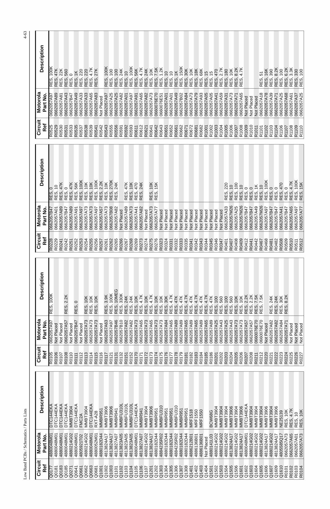
Low
Ban
d P
CB
s / S
chem
atic
s / P
arts
Lis
ts4-
63
Q01
7748
8004
8M01
DT
C14
4EK
AQ
0181
4880
048M
01D
TC
144E
KA
Q01
8348
8004
8M01
DT
C14
4EK
AQ
0185
4880
048M
01D
TC
144E
KA
Q02
7148
8021
4G02
MM
BT
3904
Q06
4148
8004
8M01
DT
C14
4EK
AQ
0661
4805
921T
02F
MC
2AQ
0662
4880
214G
02M
MB
T39
04Q
0663
4880
048M
01D
TC
144E
KA
Q06
8148
8005
2M01
RX
T-A
28Q
1001
4880
182D
44M
MB
R95
1Q
1002
4813
824A
17M
MB
T39
06Q
1003
4813
824A
17M
MB
T39
06Q
1101
4813
827A
07M
MB
R94
1Q
1102
4813
823A
05M
MB
FU
310L
Q11
0348
1382
3A05
MM
BF
U31
0LQ
1104
4813
823A
05M
MB
FU
310L
Q11
0548
8004
8M01
DT
C14
4EK
AQ
1106
4813
827A
07M
MB
R94
1Q
1107
4880
214G
02M
MB
T39
04Q
1201
4813
824A
17M
MB
T39
06Q
1202
4880
182D
44M
MB
R95
1Q
1303
4884
235R
02M
MB
FU
310
Q13
0448
8018
2D44
MM
BR
951
Q13
0548
8018
2D44
MM
BR
951
Q13
0648
8423
5R02
MM
BF
U31
0Q
1307
4880
182D
44M
MB
R95
1Q
1308
4880
182D
44M
MB
R95
1Q
1401
4886
212B
01M
RF
1518
Q14
0248
8613
6B01
MR
F15
50Q
1403
4886
136B
01M
RF
1550
Q14
04N
ot P
lace
dQ
1501
4880
141L
03B
CW
68G
Q15
0248
8021
4G02
MM
BT
3904
Q15
0348
8021
4G02
MM
BT
3904
Q15
0448
8021
4G02
MM
BT
3904
Q15
0548
1382
4A17
MM
BT
3906
Q15
0648
8021
4G02
MM
BT
3904
Q16
0148
1382
4A17
MM
BT
3906
Q16
0248
8004
8M01
DT
C14
4EK
AQ
1603
4880
214G
02M
MB
T39
04Q
1604
4880
214G
02M
MB
T39
04Q
1605
4880
214G
02M
MB
T39
04Q
1606
4813
824A
17M
MB
T39
06Q
1607
4880
214G
02M
MB
T39
04Q
1609
4813
824A
17M
MB
T39
06Q
1610
4805
585Q
17N
E25
139
R01
0106
6205
7A73
RE
S, 1
0KR
0102
0662
057A
65R
ES
, 4.7
KR
0103
0662
057A
01R
ES
, 10
R01
0406
6205
7A73
RE
S, 1
0K
Cir
cuit
R
efM
oto
rola
P
art
No
.D
escr
ipti
on
R01
0506
6205
7A97
RE
S, 1
00K
R01
06N
ot P
lace
dR
0107
Not
Pla
ced
R01
0806
6205
7A57
RE
S, 2
.2K
R01
10N
ot P
lace
dR
0111
0662
057B
47R
ES
, 0R
0112
Not
Pla
ced
R01
1306
6205
7A73
RE
S, 1
0KR
0114
0662
057A
73R
ES
, 10K
R01
1506
6205
7A73
RE
S, 1
0KR
0116
Not
Pla
ced
R01
1706
6205
7A63
RE
S, 3
.9K
R01
2106
6205
7A97
RE
S, 1
00K
R01
3106
6205
7B46
RE
S, 1
0ME
GR
0132
0662
057B
10R
ES
, 330
KR
0151
0662
057A
82R
ES
, 24K
R01
5206
6205
7A82
RE
S, 2
4KR
0170
0662
057A
73R
ES
, 10K
R01
7106
6205
7A65
RE
S, 4
.7K
R01
7206
6205
7A73
RE
S, 1
0KR
0173
0662
057A
65R
ES
, 4.7
KR
0174
0662
057A
73R
ES
, 10K
R01
7506
6205
7A73
RE
S, 1
0KR
0176
0662
057A
84R
ES
, 30K
R01
7706
6205
7A65
RE
S, 4
.7K
R01
7806
6205
7A89
RE
S, 4
7KR
0179
0662
057A
89R
ES
, 47K
R01
8106
6205
7A65
RE
S, 4
.7K
R01
8206
6205
7A89
RE
S, 4
7KR
0183
0662
057A
65R
ES
, 4.7
KR
0184
0662
057A
89R
ES
, 47K
R01
8506
6205
7A65
RE
S, 4
.7K
R01
8606
6205
7A89
RE
S, 4
7KR
0201
0662
057A
25R
ES
, 100
R02
0206
6205
7A43
RE
S, 5
60R
0203
0662
057A
25R
ES
, 100
R02
0406
6205
7A43
RE
S, 5
60R
0205
0662
057A
73R
ES
, 10K
R02
0606
6205
7A73
RE
S, 1
0KR
0207
0662
057A
57R
ES
, 2.2
KR
0208
0662
057A
57R
ES
, 2.2
KR
0211
0660
076E
70R
ES
, 7.5
KR
0212
0660
076E
70R
ES
, 7.5
KR
0220
Not
Pla
ced
R02
2106
6205
7A82
RE
S, 2
4KR
0222
0662
057A
82R
ES
, 24K
R02
2306
6205
7A84
RE
S, 3
0KR
0224
0662
057A
71R
ES
, 8.2
KR
0225
Not
Pla
ced
R02
26N
ot P
lace
dR
0227
Not
Pla
ced
Cir
cuit
R
efM
oto
rola
P
art
No
.D
escr
ipti
on
R02
2806
6205
7B47
RE
S, 0
R02
2906
6205
7A01
RE
S, 1
0R
0241
0662
057A
89R
ES
, 47K
R02
4206
6205
7B47
RE
S, 0
R02
5106
6205
7A89
RE
S, 4
7KR
0252
0662
057A
91R
ES
, 56K
R02
5306
6205
7A97
RE
S, 1
00K
R02
5406
6205
7A73
RE
S, 1
0KR
0255
0662
057A
73R
ES
, 10K
R02
5606
6205
7A97
RE
S, 1
00K
R02
5706
6205
7A57
RE
S, 2
.2K
R02
6106
6205
7A73
RE
S, 1
0KR
0262
0662
057B
08R
ES
, 270
KR
0265
0662
057A
82R
ES
, 24K
R02
66N
ot P
lace
dR
0267
0662
057A
89R
ES
, 47K
R02
6806
6205
7A73
RE
S, 1
0KR
0269
0662
057A
41R
ES
, 470
R02
7306
6205
7A82
RE
S, 2
4KR
0274
Not
Pla
ced
R02
7506
6205
7A73
RE
S, 1
0KR
0276
0662
057A
77R
ES
, 15K
R03
23N
ot P
lace
dR
0324
Not
Pla
ced
R03
31N
ot P
lace
dR
0332
Not
Pla
ced
R03
33N
ot P
lace
dR
0335
Not
Pla
ced
R03
41N
ot P
lace
dR
0342
Not
Pla
ced
R03
43N
ot P
lace
dR
0344
Not
Pla
ced
R03
45N
ot P
lace
dR
0346
Not
Pla
ced
R03
47N
ot P
lace
dR
0401
0662
057A
33R
ES
, 220
R04
0706
6205
7M26
RE
S, 1
0R
0408
0662
057A
25R
ES
, 100
R04
0906
6205
7M26
RE
S, 1
0R
0412
0662
057B
47R
ES
, 0R
0441
0662
057B
47R
ES
, 0R
0442
0662
057A
49R
ES
, 1K
R04
6706
6205
7M26
RE
S, 1
0R
0468
0662
057A
97R
ES
, 100
KR
0481
0662
057B
47R
ES
, 0R
0482
0662
057B
47R
ES
, 0R
0508
0662
057A
41R
ES
, 470
R05
0906
6205
7B47
RE
S, 0
R05
1006
6205
7A65
RE
S, 4
.7K
R05
1106
6205
7A97
RE
S, 1
00K
R05
1206
6205
7A77
RE
S, 1
5K
Cir
cuit
R
efM
oto
rola
P
art
No
.D
escr
ipti
on
R05
2506
6205
7A97
RE
S, 1
00K
R05
2906
6205
7A89
RE
S, 4
7KR
0530
0662
057A
81R
ES
, 22K
R05
3106
6205
7A43
RE
S, 5
60R
0533
0662
057B
47R
ES
, 0R
0535
0662
057A
49R
ES
, 1K
R05
3706
6205
7A33
RE
S, 2
20R
0538
0662
057A
33R
ES
, 220
R05
3906
6205
7A65
RE
S, 4
.7K
R05
4106
6205
7A83
RE
S, 2
7KR
0542
Not
Pla
ced
R05
4306
6205
7A97
RE
S, 1
00K
R05
5506
6205
7A25
RE
S, 1
00R
0556
0662
057A
25R
ES
, 100
R05
9106
6205
7A82
RE
S, 2
4KR
0592
0662
057A
01R
ES
, 10
R05
9306
6205
7A97
RE
S, 1
00K
R06
1106
6205
7A91
RE
S, 5
6KR
0612
0662
057A
65R
ES
, 4.7
KR
0621
0662
057A
82R
ES
, 24K
R06
4106
6205
7A73
RE
S, 1
0KR
0642
0660
076E
70R
ES
, 7.5
KR
0643
0660
076E
51R
ES
, 1.2
KR
0651
0662
057A
01R
ES
, 10
R06
5206
6205
7A01
RE
S, 1
0R
0661
0662
057A
49R
ES
, 1K
R06
6206
6205
7B02
RE
S, 1
50K
R06
7106
6205
7A84
RE
S, 3
0KR
0672
0662
057A
73R
ES
, 10K
R06
8106
6205
7A79
RE
S, 1
8KR
0682
0662
057A
93R
ES
, 68K
R10
0106
6205
7A05
RE
S, 1
5R
1002
0662
057A
05R
ES
, 15
R10
0306
6205
7A41
RE
S, 4
70R
1004
0662
057A
59R
ES
, 2.7
KR
1005
0662
057A
31R
ES
, 180
R10
0606
6205
7A73
RE
S, 1
0KR
1007
0662
057A
71R
ES
, 8.2
KR
1008
0662
057A
65R
ES
, 4.7
KR
1009
Not
Pla
ced
R10
10N
ot P
lace
dR
1011
Not
Pla
ced
R11
0106
6205
7A18
RE
S, 5
1R
1102
0662
057A
78R
ES
, 16K
R11
0306
6205
7A39
RE
S, 3
90R
1104
0662
057A
71R
ES
, 8.2
KR
1106
0662
057A
25R
ES
, 100
R11
0706
6205
7A68
RE
S, 6
.2K
R11
0806
6205
7A61
RE
S, 3
.3K
R11
0906
6205
7A37
RE
S, 3
30R
1110
0662
057A
25R
ES
, 100
Cir
cuit
R
efM
oto
rola
P
art
No
.D
escr
ipti
on

4-64
Low
Ban
d PC
Bs
/ Sch
emat
ics
/ Par
ts L
ists
R11
1106
6205
7A17
RE
S, 4
7R
1113
0662
057A
64R
ES
, 4.3
KR
1114
0662
057A
64R
ES
, 4.3
KR
1115
0662
057A
75R
ES
, 12K
R11
16N
ot P
lace
dR
1117
0662
057A
37R
ES
, 330
R11
1806
6205
7A56
RE
S, 2
KR
1119
0662
057A
83R
ES
, 27K
R11
2006
6205
7A18
RE
S, 5
1R
1121
0662
057A
71R
ES
, 8.2
KR
1122
0662
057A
73R
ES
, 10K
R11
2306
6205
7A51
RE
S, 1
.2K
R11
24N
ot P
lace
dR
1125
Not
Pla
ced
R11
26N
ot P
lace
dR
1127
Not
Pla
ced
R11
2806
6205
7A73
RE
S, 1
0KR
1129
0662
057A
73R
ES
, 10K
R11
3006
6205
7A73
RE
S, 1
0KR
1131
0662
057A
77R
ES
, 15K
R11
3206
6205
7A58
RE
S, 2
.4K
R11
3306
6205
7A61
RE
S, 3
.3K
R11
3406
6205
7A05
RE
S, 1
5R
1135
0662
057A
20R
ES
, 62
R11
3606
6205
7A45
RE
S, 6
80R
1137
0662
057A
75R
ES
, 12K
R11
3806
6205
7A01
RE
S, 1
0R
1139
0611
077A
12R
ES
, 2.7
R11
4006
6205
7A39
RE
S, 3
90R
1141
0662
057A
55R
ES
, 1.8
KR
1201
0662
057B
47R
ES
, 0R
1202
Not
Pla
ced
R12
0306
6205
7B02
RE
S, 1
50K
R12
0406
6205
7B47
RE
S, 0
R12
0506
6205
7A45
RE
S, 6
80R
1206
0662
057A
41R
ES
, 470
R12
07N
ot P
lace
dR
1208
0662
057A
18R
ES
, 51
R12
0906
6205
7A61
RE
S, 3
.3K
R12
1006
6205
7A33
RE
S, 2
20R
1211
0662
057B
14R
ES
, 470
KR
1212
0662
057A
25R
ES
, 100
R12
1306
6205
7A45
RE
S, 6
80R
1214
0662
057A
54R
ES
, 1.6
KR
1215
0662
057A
21R
ES
, 68
R12
1606
6205
7A18
RE
S, 5
1R
1217
0662
057A
25R
ES
, 100
R12
1806
6205
7A17
RE
S, 4
7R
1219
0662
057A
17R
ES
, 47
R12
2006
6205
7A17
RE
S, 4
7R
1221
0662
057B
47R
ES
, 0
Cir
cuit
R
efM
oto
rola
P
art
No
.D
escr
ipti
on
R12
22N
ot P
lace
dR
1306
0662
057B
47R
ES
, 0R
1307
0662
057A
19R
ES
, 56
R13
0806
6205
7A19
RE
S, 5
6R
1309
0662
057A
41R
ES
, 470
R13
1106
6205
7A73
RE
S, 1
0KR
1312
0662
057A
51R
ES
, 1.2
KR
1313
0662
057A
51R
ES
, 1.2
KR
1314
0662
057A
37R
ES
, 330
R13
1506
6205
7A61
RE
S, 3
.3K
R13
1606
6205
7A45
RE
S, 6
80R
1317
0662
057A
09R
ES
, 22
R13
1806
6205
7A41
RE
S, 4
70R
1319
0662
057A
01R
ES
, 10
R13
2006
6205
7A41
RE
S, 4
70R
1325
Not
Pla
ced
R13
2606
6205
7A19
RE
S, 5
6R
1327
0662
057A
19R
ES
, 56
R13
2806
6205
7A41
RE
S, 4
70R
1330
0662
057A
73R
ES
, 10K
R13
3106
6205
7A51
RE
S, 1
.2K
R13
3206
6205
7A51
RE
S, 1
.2K
R13
3306
6205
7A37
RE
S, 3
30R
1334
0662
057A
61R
ES
, 3.3
KR
1335
0662
057A
47R
ES
, 820
R13
3606
6205
7A09
RE
S, 2
2R
1337
0662
057A
22R
ES
, 75
R13
3806
6205
7A27
RE
S, 1
20R
1339
0662
057A
22R
ES
, 75
R13
4006
6205
7A49
RE
S, 1
KR
1341
0662
057A
25R
ES
, 100
R13
4206
6205
7A25
RE
S, 1
00R
1343
0662
057C
55R
ES
, 150
R13
4406
6205
7A49
RE
S, 1
KR
1345
0662
057A
25R
ES
, 100
R13
4606
6205
7A25
RE
S, 1
00R
1347
0662
057C
55R
ES
, 150
R13
7606
6205
7A65
RE
S, 4
.7K
R14
0206
1107
9A64
RE
S, 3
90R
1404
0680
194M
18R
ES
, 51
R14
0506
8019
4M18
RE
S, 5
1R
1406
0662
057A
73R
ES
, 10K
R14
0706
6205
7A73
RE
S, 1
0KR
1409
0682
089V
01R
ES
, .01
R14
1006
8396
2T52
RE
S, 1
30R
1411
0662
057C
99R
ES
, 10K
R14
12N
ot P
lace
dR
1413
0680
194M
01R
ES
, 10
R14
1406
8019
4M01
RE
S, 1
0R
1415
Not
Pla
ced
R14
1606
8019
4M01
RE
S, 1
0
Cir
cuit
R
efM
oto
rola
P
art
No
.D
escr
ipti
on
R14
1706
8019
4M01
RE
S, 1
0R
1418
0680
194M
01R
ES
, 10
R14
1906
8019
4M01
RE
S, 1
0R
1420
0680
194M
01R
ES
, 10
R14
2106
8019
4M01
RE
S, 1
0R
1422
0680
194M
01R
ES
, 10
R14
2306
8019
4M01
RE
S, 1
0R
1424
0662
057D
10R
ES
, 27K
R14
2506
6205
7D10
RE
S, 2
7KR
1440
0662
057A
25R
ES
, 100
R14
41N
ot P
lace
dR
1442
0662
057A
25R
ES
, 100
R14
4306
6205
7A49
RE
S, 1
KR
1444
0662
057A
33R
ES
, 220
R14
4506
6205
7A68
RE
S, 6
.2K
R14
46N
ot P
lace
dR
1447
0662
057B
47R
ES
, 0R
1448
Not
Pla
ced
R14
4906
1107
9A64
RE
S, 3
90R
1450
0683
962T
71R
ES
, 820
R14
5106
6205
7K31
RE
S, 1
80R
1453
0662
057K
31R
ES
, 180
R14
5406
6205
7K31
RE
S, 1
80R
1455
Not
Pla
ced
R14
5706
6205
7K01
RE
S, 1
0R
1458
0611
079A
64R
ES
, 390
R14
5906
1107
9A64
RE
S, 3
90R
1460
0680
106R
01R
ES
, 0.1
R14
6306
6205
7A75
RE
S, 1
2KR
1464
0662
057A
61R
ES
, 3.3
KR
1465
0662
057A
61R
ES
, 3.3
KR
1466
Not
Pla
ced
R14
67N
ot P
lace
dR
1468
Not
Pla
ced
R14
6906
6205
7C01
RE
S, 0
R14
70N
ot P
lace
dR
1471
Not
Pla
ced
R14
7206
6205
7A73
RE
S, 1
0KR
1473
0680
194M
01R
ES
, 10
R14
7406
8019
4M01
RE
S, 1
0R
1475
0680
194M
01R
ES
, 10
R14
7606
8019
4M01
RE
S, 1
0R
1477
0662
057A
61R
ES
, 3.3
KR
1478
0662
057A
73R
ES
, 10K
R14
7906
6205
7A61
RE
S, 3
.3K
R14
8006
6205
7D10
RE
S, 2
7KR
1481
0662
057A
90R
ES
, 51K
R14
8206
6205
7B47
RE
S, 0
R14
8306
6205
7A34
RE
S, 2
40R
1484
0662
057A
49R
ES
, 1K
R15
0106
6205
7A45
RE
S, 6
80
Cir
cuit
R
efM
oto
rola
P
art
No
.D
escr
ipti
on
R15
0206
6205
7C67
RE
S, 4
70R
1503
0662
057A
61R
ES
, 3.3
KR
1504
0662
057A
73R
ES
, 10K
R15
0506
6205
7A69
RE
S, 6
.8K
R15
0606
6205
7A87
RE
S, 3
9KR
1507
0662
057A
49R
ES
, 1K
R15
0806
6205
7R17
RE
S, 4
3.2
R15
0906
6205
7P95
RE
S, 1
00K
R15
10N
ot P
lace
dR
1511
0662
057P
95R
ES
, 100
KR
1512
Not
Pla
ced
R15
1306
6205
7C76
RE
S, 1
.1K
R15
1406
6205
7A97
RE
S, 1
00K
R15
1506
6205
7A49
RE
S, 1
KR
1516
0662
057C
71R
ES
, 680
R15
1706
6205
7C71
RE
S, 6
80R
1518
0662
057A
61R
ES
, 3.3
KR
1519
0662
057C
71R
ES
, 680
R15
2206
6205
7A73
RE
S, 1
0KR
1523
Not
Pla
ced
R15
2406
6205
7C71
RE
S, 6
80R
1525
Not
Pla
ced
R15
2606
6205
7A97
RE
S, 1
00K
R15
2706
6205
7A97
RE
S, 1
00K
R15
2806
6205
7A80
RE
S, 2
0KR
1532
0662
057A
95R
ES
, 82K
R15
3306
6205
7A73
RE
S, 1
0KR
1535
0662
057R
16R
ES
, 39.
2R
1537
0662
057A
53R
ES
, 1.5
KR
1541
0662
057A
53R
ES
, 1.5
KR
1542
0662
057A
49R
ES
, 1K
R15
4306
6205
7A49
RE
S, 1
KR
1544
0662
057A
90R
ES
, 51K
R15
4506
6205
7A65
RE
S, 4
.7K
R16
0106
6205
7A73
RE
S, 1
0KR
1602
0662
057A
65R
ES
, 4.7
KR
1604
0662
057A
49R
ES
, 1K
R16
0506
6205
7B10
RE
S, 3
30K
R16
0606
6205
7B02
RE
S, 1
50K
R16
0706
6205
7B19
RE
S, 7
50K
R16
0806
6205
7A57
RE
S, 2
.2K
R16
0906
6205
7A73
RE
S, 1
0KR
1610
0662
057A
82R
ES
, 24K
R16
1106
6205
7A49
RE
S, 1
KR
1612
0662
057A
25R
ES
, 100
R16
1306
6205
7A59
RE
S, 2
.7K
R16
1406
6205
7A49
RE
S, 1
KR
1615
0662
057A
49R
ES
, 1K
R16
1606
6205
7A33
RE
S, 2
20R
1617
0662
057A
57R
ES
, 2.2
KR
1620
0662
057A
51R
ES
, 1.2
K
Cir
cuit
R
efM
oto
rola
P
art
No
.D
escr
ipti
on

Low
Ban
d P
CB
s / S
chem
atic
s / P
arts
Lis
ts4-
65
R16
2106
6205
7A68
RE
S, 6
.2K
R16
2206
6205
7A49
RE
S, 1
KR
1626
0662
057A
18R
ES
, 51
R16
2706
6205
7A73
RE
S, 1
0KR
1628
0662
057A
55R
ES
, 1.8
KR
1629
0662
057A
67R
ES
, 5.6
KR
1630
0662
057A
53R
ES
, 1.5
KR
1631
0662
057A
18R
ES
, 51
R16
3206
6205
7A82
RE
S, 2
4KR
1633
Not
Pla
ced
R16
3506
6205
7B47
RE
S, 0
R16
3606
6205
7A42
RE
S, 5
10R
1637
0662
057A
59R
ES
, 2.7
KR
1638
0662
057A
55R
ES
, 1.8
KS
H12
01N
ot P
lace
dS
H12
02N
ot P
lace
dS
H13
01N
ot P
lace
dS
H13
0226
8047
3U01
VC
O S
HIE
LDU
0101
5102
226J
56M
C68
HC
11F
L0U
0111
5102
463J
64E
EP
RO
MU
0121
5186
137B
01F
LAS
H R
OM
U01
2251
8574
8L01
SR
AM
U01
4151
1380
5A30
RE
MU
XU
0211
5183
222M
49M
C34
03U
0221
5185
130C
53A
SF
IC C
OM
PA
ND
ER
ICU
0251
5184
704M
60M
UX
/DE
MU
XU
0271
5109
699X
01A
UD
IO P
AU
0301
Not
Pla
ced
U03
31N
ot P
lace
dU
0341
Not
Pla
ced
U03
42N
ot P
lace
dU
0351
Not
Pla
ced
U06
1151
8330
8X01
LM29
41U
0641
5183
308X
01LM
2941
U06
5151
1381
6A07
MC
78M
05U
0652
5113
815A
02M
C33
064
U06
53N
ot P
lace
dU
1001
4809
939C
05U
MC
5NU
1051
5108
278X
01M
IXE
RU
1101
5102
463J
52M
C74
HC
4066
U11
0251
0246
3J52
MC
74H
C40
66U
1103
5186
144B
01S
A61
6U
1201
5185
963A
27F
RA
CN
SY
NT
HE
SIZ
ER
ICU
1250
5185
963A
33LP
2951
U13
7748
0993
9C05
UM
C5N
U13
7848
0993
9C05
UM
C5N
U14
0151
8513
0C65
LDM
OS
PR
ED
RIV
ER
ICU
1402
5113
818A
03M
C33
072
U15
0151
8596
3A15
LM50
U15
0251
0973
1C21
LM61
42B
IMU
1503
5185
765B
26P
OW
ER
CO
NT
RO
L IC
Cir
cuit
R
efM
oto
rola
P
art
No
.D
escr
ipti
on
U16
0151
8092
9W01
MC
1350
VR
0151
4813
830A
15M
MB
Z52
32B
VR
0501
4805
656W
09M
MQ
A20
VT
1V
R05
0348
0565
6W09
MM
QA
20V
T1
VR
0504
4813
830A
40M
MB
Z52
57B
VR
0505
4805
656W
09M
MQ
A20
VT
1V
R05
0948
1383
0A40
MM
BZ
5257
BV
R05
1048
1383
0A40
MM
BZ
5257
BV
R05
3748
1383
0A15
MM
BZ
5232
BV
R05
4148
1383
0A27
MM
BZ
5244
BV
R06
0148
1383
2C77
TR
AN
SIE
NT
SU
PP
RE
SS
OR
VR
0621
4813
830A
15M
MB
Z52
32B
VR
0671
Not
Pla
ced
Y01
3148
8011
3R19
CR
YS
TAL,
38.
4 K
HZ
Y11
0148
8090
8W08
CR
YS
TAL,
10.
245
MH
ZY
1102
9186
145B
02D
ISC
RIM
INA
TO
R, 4
55 K
HZ
Y12
0148
8011
4R04
CR
YS
TAL,
16.
8 M
HZ
Y12
02N
ot P
lace
d
Cir
cuit
R
efM
oto
rola
P
art
No
.D
escr
ipti
on

4-66
Low
Ban
d PC
Bs
/ Sch
emat
ics
/ Par
ts L
ists
Low
Ban
d R
ange
2 P
CB
848
6207
B07
Par
ts L
ist
Cir
cuit
R
efM
oto
rola
P
art
No
.D
escr
ipti
on
C01
0121
1374
0F51
CA
P, 1
00pF
C01
02N
ot P
lace
dC
0103
Not
Pla
ced
C01
04N
ot P
lace
dC
0105
Not
Pla
ced
C01
06N
ot P
lace
dC
0107
2113
741F
25C
AP,
100
0pF
C01
08N
ot P
lace
dC
0111
Not
Pla
ced
C01
1221
1374
3E20
CA
P, 0
.1uF
C01
2121
1374
3E20
CA
P, 0
.1uF
C01
2221
1374
3E20
CA
P, 0
.1uF
C01
23N
ot P
lace
dC
0131
2113
740F
35C
AP,
22p
FC
0132
2113
740F
35C
AP,
22p
FC
0141
2113
743E
20C
AP,
0.1
uFC
0151
2113
741F
49C
AP,
.01u
FC
0201
2311
049A
57C
AP
P, 1
0uF
C02
0223
1104
9A57
CA
PP,
10u
FC
0203
Not
Pla
ced
C02
0421
1374
3E20
CA
P, 0
.1uF
C02
05N
ot P
lace
dC
0211
Not
Pla
ced
C02
1223
1104
9A57
CA
PP,
10u
FC
0221
2113
743E
20C
AP,
0.1
uFC
0222
2113
743E
20C
AP,
0.1
uFC
0223
2113
743E
20C
AP,
0.1
uFC
0224
2113
740F
51C
AP,
100
pFC
0225
2113
743E
20C
AP,
0.1
uFC
0226
2113
743E
20C
AP,
0.1
uFC
0227
Not
Pla
ced
C02
2823
1104
9A56
CA
PP,
4.7
uFC
0231
2113
743B
29C
AP,
1uF
C02
3221
1374
3E20
CA
P, 0
.1uF
C02
33N
ot P
lace
dC
0234
2113
743E
20C
AP,
0.1
uFC
0235
2113
743E
07C
AP,
.022
uFC
0236
2113
743E
10C
AP,
.033
uFC
0237
Not
Pla
ced
C02
4121
1374
3E20
CA
P, 0
.1uF
C02
42N
ot P
lace
dC
0243
2113
740F
51C
AP,
100
pFC
0244
2113
743E
20C
AP,
0.1
uFC
0245
2113
743E
20C
AP,
0.1
uFC
0246
2113
741F
49C
AP,
.01u
FC
0251
2113
743E
20C
AP,
0.1
uFC
0252
2311
049A
07C
AP
P, 1
uFC
0253
Not
Pla
ced
C02
5421
1374
3E20
CA
P, 0
.1uF
C02
5521
1374
3E20
CA
P, 0
.1uF
C02
5621
1374
0F51
CA
P, 1
00pF
C02
6121
1374
3E20
CA
P, 0
.1uF
C02
6221
1374
0F49
CA
P, 8
2pF
C02
6521
1374
3E20
CA
P, 0
.1uF
C02
66N
ot P
lace
dC
0267
2113
741F
49C
AP,
.01u
FC
0271
2113
741F
49C
AP,
.01u
FC
0272
2113
743E
20C
AP,
0.1
uFC
0273
2113
741F
37C
AP,
330
0pF
C02
74N
ot P
lace
dC
0275
2311
049A
99C
AP
P, 4
7uF
C02
7621
1374
1F25
CA
P, 1
000p
FC
0277
2113
741F
25C
AP,
100
0pF
C02
9023
1104
9C01
CA
PP,
10u
FC
0291
2311
049C
01C
AP
P, 1
0uF
C02
9223
1104
9C01
CA
PP,
10u
FC
0293
2311
049C
01C
AP
P, 1
0uF
C03
01N
ot P
lace
dC
0302
Not
Pla
ced
C03
03N
ot P
lace
dC
0304
Not
Pla
ced
C03
05N
ot P
lace
dC
0324
Not
Pla
ced
C03
25N
ot P
lace
dC
0331
Not
Pla
ced
C03
41N
ot P
lace
dC
0342
Not
Pla
ced
C03
43N
ot P
lace
dC
0344
Not
Pla
ced
C03
51N
ot P
lace
dC
0352
Not
Pla
ced
C03
53N
ot P
lace
dC
0354
Not
Pla
ced
C04
2121
1374
3N48
CA
P, 8
2pF
C04
2221
1374
1F17
CA
P, 4
70pF
C04
2321
1374
1F17
CA
P, 4
70pF
C04
2621
1374
3L09
CA
P, 4
70pF
C04
2721
1374
3L09
CA
P, 4
70pF
C04
2821
1374
3N48
CA
P, 8
2pF
C04
2921
1374
3L09
CA
P, 4
70pF
C04
3021
1374
1F17
CA
P, 4
70pF
C04
3121
1374
1F17
CA
P, 4
70pF
C04
4121
1374
3L09
CA
P, 4
70pF
C04
4221
1374
3L09
CA
P, 4
70pF
C04
43N
ot P
lace
dC
0445
2113
743L
09C
AP,
470
pFC
0446
2113
743L
09C
AP,
470
pFC
0447
2113
743L
09C
AP,
470
pFC
0448
2113
743L
09C
AP,
470
pFC
0449
2113
743L
09C
AP,
470
pF
Cir
cuit
R
efM
oto
rola
P
art
No
.D
escr
ipti
on
C04
7021
1374
3L09
CA
P, 4
70pF
C04
7121
1374
3N48
CA
P, 8
2pF
C04
7221
1374
3N48
CA
P, 8
2pF
C04
7321
1374
3N48
CA
P, 8
2pF
C04
7421
1374
3L09
CA
P, 4
70pF
C04
7621
1374
3L09
CA
P, 4
70pF
C04
7721
1374
3L09
CA
P, 4
70pF
C04
7821
1374
3L09
CA
P, 4
70pF
C04
8221
1374
3L09
CA
P, 4
70pF
C04
8321
1374
3L09
CA
P, 4
70pF
C04
8421
1374
1F17
CA
P, 4
70pF
C04
8521
1374
3L09
CA
P, 4
70pF
C04
8621
1374
3L09
CA
P, 4
70pF
C04
8721
1374
3L09
CA
P, 4
70pF
C04
8821
1374
3L09
CA
P, 4
70pF
C04
9021
1374
3L09
CA
P, 4
70pF
C04
9121
1374
3L09
CA
P, 4
70pF
C04
9221
1374
3L09
CA
P, 4
70pF
C04
9321
1374
3L09
CA
P, 4
70pF
C04
9421
1374
3L09
CA
P, 4
70pF
C04
9521
1374
3L09
CA
P, 4
70pF
C04
9621
1374
3L09
CA
P, 4
70pF
C04
9721
1374
3L09
CA
P, 4
70pF
C04
9921
1374
3L09
CA
P, 4
70pF
C05
0121
1374
1F49
CA
P, .0
1uF
C05
0221
1374
1F17
CA
P, 4
70pF
C05
0321
1374
1F17
CA
P, 4
70pF
C05
0421
1374
1F17
CA
P, 4
70pF
C05
0521
1374
1F17
CA
P, 4
70pF
C05
0621
1374
1F17
CA
P, 4
70pF
C05
0821
1374
1F17
CA
P, 4
70pF
C05
0921
1374
1F17
CA
P, 4
70pF
C05
1021
1374
1F17
CA
P, 4
70pF
C05
1121
1374
1F17
CA
P, 4
70pF
C05
1221
1374
1F17
CA
P, 4
70pF
C05
1321
1374
1F17
CA
P, 4
70pF
C05
1421
1374
1F17
CA
P, 4
70pF
C05
1521
1374
1F17
CA
P, 4
70pF
C05
1621
1374
1F49
CA
P, .0
1uF
C05
1721
1374
3N48
CA
P, 8
2pF
C05
1821
1374
1F17
CA
P, 4
70pF
C05
4123
1104
9A05
CA
PP,
0.4
7uF
C05
4223
1104
9A99
CA
PP,
47u
FC
0554
Not
Pla
ced
C05
58N
ot P
lace
dC
0559
Not
Pla
ced
C05
6021
1374
1F25
CA
P, 1
000p
FC
0575
Not
Pla
ced
C05
76N
ot P
lace
dC
0591
2113
743E
20C
AP,
0.1
uFC
0592
2113
743E
20C
AP,
0.1
uF
Cir
cuit
R
efM
oto
rola
P
art
No
.D
escr
ipti
on
C05
9321
1374
1B69
CA
P, 0
.1uF
C06
0121
1374
1F17
CA
P, 4
70pF
C06
0323
8009
0M24
CA
PP,
10u
FC
0611
2311
049C
06C
AP
P, 2
2uF
C06
1221
1374
3E20
CA
P, 0
.1uF
C06
21N
ot P
lace
dC
0622
2311
049A
99C
AP
P, 4
7uF
C06
4121
1374
1F17
CA
P, 4
70pF
C06
4423
1104
9A97
CA
PP,
33u
FC
0645
2113
743E
20C
AP,
0.1
uFC
0651
Not
Pla
ced
C06
5223
1104
9A97
CA
PP,
33u
FC
0654
2311
049A
57C
AP
P, 1
0uF
C06
5521
1374
3E20
CA
P, 0
.1uF
C06
6123
1104
9C05
CA
PP,
47u
FC
0662
2113
741F
49C
AP,
.01u
FC
0663
2113
743E
20C
AP,
0.1
uFC
0671
2113
743E
20C
AP,
0.1
uFC
0681
2113
743E
20C
AP,
0.1
uFC
1001
2113
740F
56C
AP,
160
pFC
1002
2113
741F
49C
AP,
.01u
FC
1003
2113
740F
62C
AP,
300
pFC
1004
2113
740F
53C
AP,
120
pFC
1006
2113
740F
46C
AP,
62p
FC
1007
2113
740F
60C
AP,
240
pFC
1008
2113
741F
25C
AP,
100
0pF
C10
0921
1374
0F60
CA
P, 2
40pF
C10
1021
1374
0F46
CA
P, 6
2pF
C10
1121
1374
0F53
CA
P, 1
20pF
C10
1221
1374
0F62
CA
P, 3
00pF
C10
1321
1374
1F49
CA
P, .0
1uF
C10
1421
1374
0F56
CA
P, 1
60pF
C10
1521
1374
1F49
CA
P, .0
1uF
C10
1621
1374
0F55
CA
P, 1
50pF
C10
1721
1374
1F27
CA
P, 1
200p
FC
1019
2113
740F
60C
AP,
240
pFC
1020
2113
740F
59C
AP,
220
pFC
1021
2113
740F
62C
AP,
300
pFC
1022
2113
740F
59C
AP,
220
pFC
1023
2113
740F
62C
AP,
300
pFC
1024
2113
740F
59C
AP,
220
pFC
1025
2113
740F
60C
AP,
240
pFC
1026
2113
741F
27C
AP,
120
0pF
C10
2721
1374
0F55
CA
P, 1
50pF
C10
2821
1374
1F49
CA
P, .0
1uF
C10
2921
1374
1F49
CA
P, .0
1uF
C10
3021
1374
3E20
CA
P, 0
.1uF
C10
3121
1374
3E20
CA
P, 0
.1uF
C10
3221
1374
0F48
CA
P, 7
5pF
C10
3321
1374
0F50
CA
P, 9
1pF
C10
3421
1374
0F51
CA
P, 1
00pF
Cir
cuit
R
efM
oto
rola
P
art
No
.D
escr
ipti
on

Low
Ban
d P
CB
s / S
chem
atic
s / P
arts
Lis
ts4-
67
C10
3521
1374
0F46
CA
P, 6
2pF
C10
3621
1374
3E20
CA
P, 0
.1uF
C10
3721
1374
0F59
CA
P, 2
20pF
C10
3821
1374
0F62
CA
P, 3
00pF
C10
3921
1374
0F62
CA
P, 3
00pF
C10
4021
1374
0F59
CA
P, 2
20pF
C11
0121
1374
0F53
CA
P, 1
20pF
C11
0221
1374
0F50
CA
P, 9
1pF
C11
0321
1374
0F58
CA
P, 2
00pF
C11
0421
1374
3E20
CA
P, 0
.1uF
C11
0521
1374
3E20
CA
P, 0
.1uF
C11
0621
1374
3E20
CA
P, 0
.1uF
C11
0721
1374
0F49
CA
P, 8
2pF
C11
0821
1374
3E20
CA
P, 0
.1uF
C11
0921
1374
0F40
CA
P, 3
6pF
C11
10N
ot P
lace
dC
1111
2113
740L
03C
AP,
2.4
pFC
1112
2113
740F
40C
AP,
36p
FC
1113
2113
743E
20C
AP,
0.1
uFC
1114
2113
743E
20C
AP,
0.1
uFC
1115
2113
740F
53C
AP,
120
pFC
1116
2113
740F
41C
AP,
39p
FC
1119
2113
743E
20C
AP,
0.1
uFC
1120
Not
Pla
ced
C11
21N
ot P
lace
dC
1122
Not
Pla
ced
C11
2321
1374
0F39
CA
P, 3
3pF
C11
2421
1374
3E20
CA
P, 0
.1uF
C11
2521
1374
3E11
CA
P, .0
39uF
C11
2621
1374
3E20
CA
P, 0
.1uF
C11
2723
1104
9A57
CA
PP,
10u
FC
1128
2113
743E
20C
AP,
0.1
uFC
1129
2113
740F
35C
AP,
22p
FC
1130
2113
740F
47C
AP,
68p
FC
1131
Not
Pla
ced
C11
3321
1374
3E20
CA
P, 0
.1uF
C11
3421
1374
3E20
CA
P, 0
.1uF
C11
3521
1374
3E20
CA
P, 0
.1uF
C11
3621
1374
3E20
CA
P, 0
.1uF
C11
3721
1374
0F53
CA
P, 1
20pF
C11
3821
1374
3E20
CA
P, 0
.1uF
C11
3921
1374
1F49
CA
P, .0
1uF
C11
4021
1374
1F49
CA
P, .0
1uF
C11
4121
1374
3E20
CA
P, 0
.1uF
C11
4221
1374
3E20
CA
P, 0
.1uF
C11
4321
1374
3E20
CA
P, 0
.1uF
C11
4421
1374
3E20
CA
P, 0
.1uF
C11
4521
1374
1F41
CA
P, 4
700p
FC
1146
2113
740F
49C
AP,
82p
FC
1147
2113
740F
65C
AP,
390
pFC
1148
2113
743E
20C
AP,
0.1
uF
Cir
cuit
R
efM
oto
rola
P
art
No
.D
escr
ipti
on
C11
4921
1374
0F53
CA
P, 1
20pF
C11
5021
1374
0F54
CA
P, 1
30pF
C11
51N
ot P
lace
dC
1152
Not
Pla
ced
C11
53N
ot P
lace
dC
1201
2113
743E
20C
AP,
0.1
uFC
1202
2311
049J
11C
AP
P, 4
.7uF
C12
0321
1374
1F49
CA
P, .0
1uF
C12
0421
1374
0F59
CA
P, 2
20pF
C12
05N
ot P
lace
dC
1206
2113
740L
37C
AP,
62p
FC
1207
2113
740F
07C
AP,
1.5
pFC
1208
2113
740A
82C
AP,
150
0pF
C12
0923
1104
9A57
CA
PP,
10u
FC
1210
2113
743E
20C
AP,
0.1
uFC
1211
2113
741F
49C
AP,
.01u
FC
1212
2311
049A
07C
AP
P, 1
uFC
1213
2113
743A
23C
AP,
0.2
2uF
C12
1421
1374
3E10
CA
P, .0
33uF
C12
1521
1374
0C37
CA
P, 6
800p
FC
1216
2311
049J
11C
AP
P, 4
.7uF
C12
1721
1374
1F49
CA
P, .0
1uF
C12
1821
1374
3E20
CA
P, 0
.1uF
C12
1923
1104
9J11
CA
PP,
4.7
uFC
1220
2311
049J
11C
AP
P, 4
.7uF
C12
21N
ot P
lace
dC
1222
2113
740F
36C
AP,
24p
FC
1223
2113
741F
49C
AP,
.01u
FC
1224
2113
740F
49C
AP,
82p
FC
1225
2113
741F
49C
AP,
.01u
FC
1226
Not
Pla
ced
C12
2721
1374
1F49
CA
P, .0
1uF
C12
28N
ot P
lace
dC
1229
2113
741F
49C
AP,
.01u
FC
1230
2113
741F
49C
AP,
.01u
FC
1231
2113
741F
49C
AP,
.01u
FC
1232
Not
Pla
ced
C12
33N
ot P
lace
dC
1234
Not
Pla
ced
C12
5023
1104
9A09
CA
PP,
2.2
uFC
1251
2113
743E
20C
AP,
0.1
uFC
1252
2113
743E
05C
AP,
.018
uFC
1253
2311
049J
11C
AP
P, 4
.7uF
C12
5421
1374
1F49
CA
P, .0
1uF
C13
04N
ot P
lace
dC
1305
Not
Pla
ced
C13
0621
1374
0L23
CA
P, 1
6pF
C13
0721
1374
0L27
CA
P, 2
4pF
C13
0821
1374
0F19
CA
P, 4
.7pF
C13
09N
ot P
lace
dC
1311
2113
741F
49C
AP,
.01u
F
Cir
cuit
R
efM
oto
rola
P
art
No
.D
escr
ipti
on
C13
1221
1374
1F49
CA
P, .0
1uF
C13
1321
1374
1F49
CA
P, .0
1uF
C13
1421
1374
0L27
CA
P, 2
4pF
C13
1521
1374
0L27
CA
P, 2
4pF
C13
1621
1374
0F15
CA
P, 3
.3pF
C13
1721
1374
3E20
CA
P, 0
.1uF
C13
1821
1374
1F49
CA
P, .0
1uF
C13
1921
1374
1F49
CA
P, .0
1uF
C13
2021
1374
1F49
CA
P, .0
1uF
C13
2121
1374
0F17
CA
P, 3
.9pF
C13
2321
1374
0L21
CA
P, 1
3pF
C13
2521
1374
1F49
CA
P, .0
1uF
C13
2621
1374
1F49
CA
P, .0
1uF
C13
3321
1374
0L28
CA
P, 2
7pF
C13
3421
1374
0L36
CA
P, 5
6pF
C13
3521
1374
0F19
CA
P, 4
.7pF
C13
3621
1374
3E20
CA
P, 0
.1uF
C13
37N
ot P
lace
dC
1338
2113
741F
49C
AP,
.01u
FC
1339
2113
741F
49C
AP,
.01u
FC
1340
2113
741F
49C
AP,
.01u
FC
1341
2113
740L
36C
AP,
56p
FC
1342
2113
740L
36C
AP,
56p
FC
1343
2113
740F
15C
AP,
3.3
pFC
1344
2113
741F
49C
AP,
.01u
FC
1345
2113
743E
20C
AP,
0.1
uFC
1346
2113
741F
49C
AP,
.01u
FC
1347
2113
741F
49C
AP,
.01u
FC
1348
2113
740F
17C
AP,
3.9
pFC
1349
2113
743E
20C
AP,
0.1
uFC
1350
2113
740F
31C
AP,
15p
FC
1351
2113
741F
49C
AP,
.01u
FC
1352
2113
741F
49C
AP,
.01u
FC
1354
Not
Pla
ced
C13
56N
ot P
lace
dC
1360
Not
Pla
ced
C13
61N
ot P
lace
dC
1362
Not
Pla
ced
C14
0121
1374
1A45
CA
P, .0
1uF
C14
0221
1374
1A45
CA
P, .0
1uF
C14
03N
ot P
lace
dC
1404
2113
741A
45C
AP,
.01u
FC
1405
2113
741A
45C
AP,
.01u
FC
1406
Not
Pla
ced
C14
0721
1374
1A45
CA
P, .0
1uF
C14
08N
ot P
lace
dC
1409
Not
Pla
ced
C14
1021
1374
1M69
CA
P, 0
.1uF
C14
1221
1374
1A45
CA
P, .0
1uF
C14
1321
1374
1A45
CA
P, .0
1uF
C14
1421
1374
1A45
CA
P, .0
1uF
Cir
cuit
R
efM
oto
rola
P
art
No
.D
escr
ipti
on
C14
1521
1374
1M69
CA
P, 0
.1uF
C14
16N
ot P
lace
dC
1417
Not
Pla
ced
C14
1821
1374
0A73
CA
P, 5
60pF
C14
1921
1374
1A45
CA
P, .0
1uF
C14
2021
1374
1A45
CA
P, .0
1uF
C14
21N
ot P
lace
dC
1422
Not
Pla
ced
C14
2321
1374
1A45
CA
P, .0
1uF
C14
2421
1374
1A45
CA
P, .0
1uF
C14
2521
1374
1W01
CA
P, 1
uFC
1426
2113
741W
01C
AP,
1uF
C14
2721
1107
8B59
CA
P, 4
70pF
C14
2821
1107
8B59
CA
P, 4
70pF
C14
2921
1107
8B58
CA
P, 4
30pF
C14
3021
1107
8B58
CA
P, 4
30pF
C14
3121
1374
1A45
CA
P, .0
1uF
C14
3221
1374
1W01
CA
P, 1
uFC
1433
2113
741W
01C
AP,
1uF
C14
3421
1374
1A45
CA
P, .0
1uF
C14
3521
1374
1W01
CA
P, 1
uFC
1436
2113
741A
45C
AP,
.01u
FC
1437
2111
078B
58C
AP,
430
pFC
1438
2111
078B
58C
AP,
430
pFC
1439
2111
078B
59C
AP,
470
pFC
1440
2111
078B
59C
AP,
470
pFC
1441
2111
078B
52C
AP,
240
pFC
1442
2111
078B
45C
AP,
130
pFC
1443
2111
078B
59C
AP,
470
pFC
1444
2111
078B
59C
AP,
470
pFC
1445
2113
741A
45C
AP,
.01u
FC
1446
Not
Pla
ced
C14
4721
1107
8B52
CA
P, 2
40pF
C14
4821
1107
8B52
CA
P, 2
40pF
C14
4921
8006
0M49
CA
P, 1
80pF
C14
50N
ot P
lace
dC
1451
2180
060M
49C
AP,
180
pFC
1452
2180
060M
29C
AP,
27p
FC
1453
2180
060M
42C
AP,
91p
FC
1454
2180
060M
38C
AP,
62p
FC
1455
2180
060M
30C
AP,
30p
FC
1456
2180
060M
40C
AP,
75p
FC
1457
2113
741A
45C
AP,
.01u
FC
1458
2311
049C
01C
AP
P, 1
0uF
C14
5923
1104
9C01
CA
PP,
10u
FC
1460
2113
743E
20C
AP,
0.1
uFC
1461
2113
741A
45C
AP,
.01u
FC
1462
2311
049C
01C
AP
P, 1
0uF
C14
6321
1392
8E01
CA
P, 1
uFC
1464
2113
741A
45C
AP,
.01u
FC
1465
2113
928E
01C
AP,
1uF
Cir
cuit
R
efM
oto
rola
P
art
No
.D
escr
ipti
on
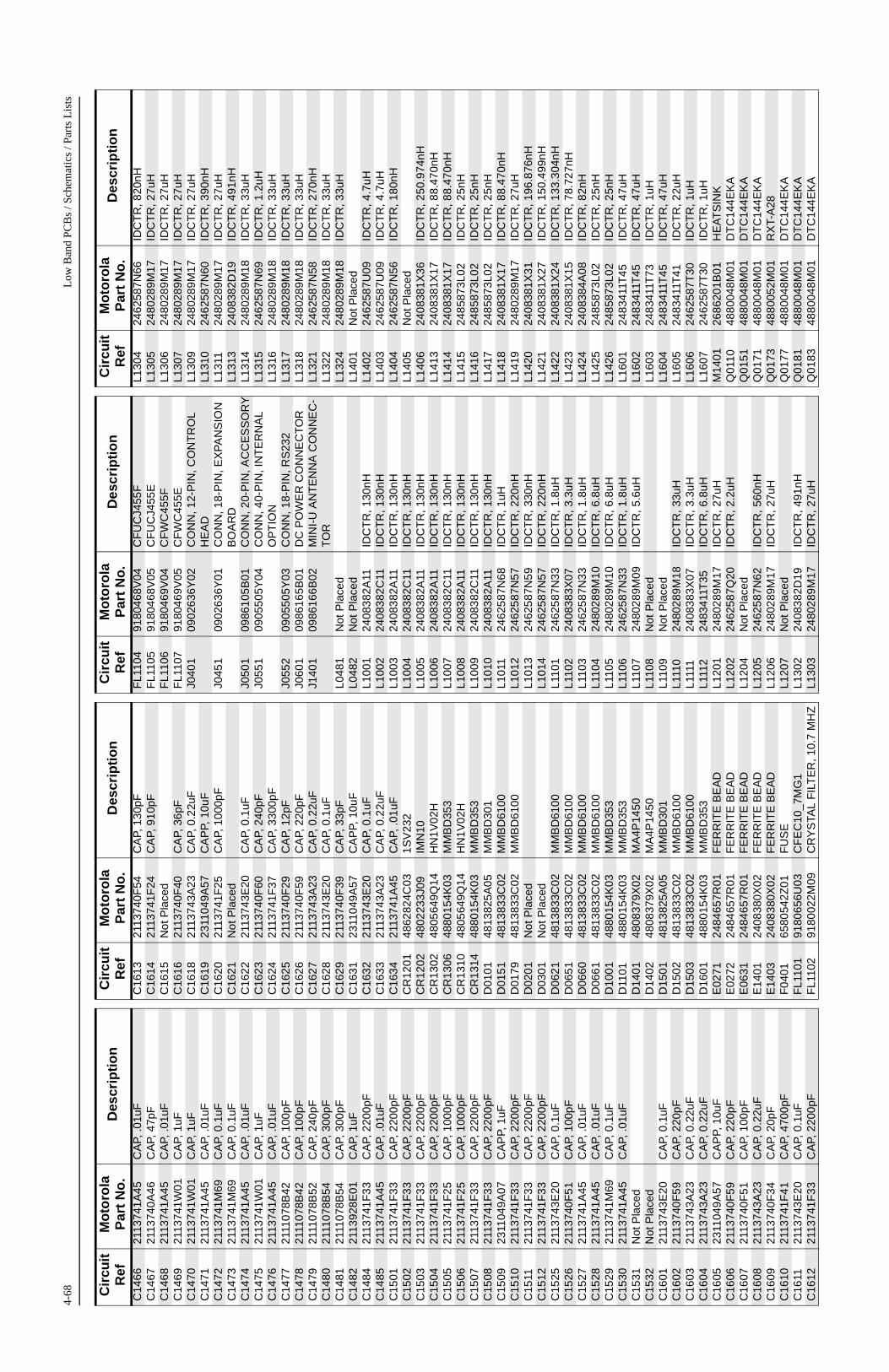
4-68
Low
Ban
d PC
Bs
/ Sch
emat
ics
/ Par
ts L
ists
C14
6621
1374
1A45
CA
P, .0
1uF
C14
6721
1374
0A46
CA
P, 4
7pF
C14
6821
1374
1A45
CA
P, .0
1uF
C14
6921
1374
1W01
CA
P, 1
uFC
1470
2113
741W
01C
AP,
1uF
C14
7121
1374
1A45
CA
P, .0
1uF
C14
7221
1374
1M69
CA
P, 0
.1uF
C14
7321
1374
1M69
CA
P, 0
.1uF
C14
7421
1374
1A45
CA
P, .0
1uF
C14
7521
1374
1W01
CA
P, 1
uFC
1476
2113
741A
45C
AP,
.01u
FC
1477
2111
078B
42C
AP,
100
pFC
1478
2111
078B
42C
AP,
100
pFC
1479
2111
078B
52C
AP,
240
pFC
1480
2111
078B
54C
AP,
300
pFC
1481
2111
078B
54C
AP,
300
pFC
1482
2113
928E
01C
AP,
1uF
C14
8421
1374
1F33
CA
P, 2
200p
FC
1485
2113
741A
45C
AP,
.01u
FC
1501
2113
741F
33C
AP,
220
0pF
C15
0221
1374
1F33
CA
P, 2
200p
FC
1503
2113
741F
33C
AP,
220
0pF
C15
0421
1374
1F33
CA
P, 2
200p
FC
1505
2113
741F
25C
AP,
100
0pF
C15
0621
1374
1F25
CA
P, 1
000p
FC
1507
2113
741F
33C
AP,
220
0pF
C15
0821
1374
1F33
CA
P, 2
200p
FC
1509
2311
049A
07C
AP
P, 1
uFC
1510
2113
741F
33C
AP,
220
0pF
C15
1121
1374
1F33
CA
P, 2
200p
FC
1512
2113
741F
33C
AP,
220
0pF
C15
2521
1374
3E20
CA
P, 0
.1uF
C15
2621
1374
0F51
CA
P, 1
00pF
C15
2721
1374
1A45
CA
P, .0
1uF
C15
2821
1374
1A45
CA
P, .0
1uF
C15
2921
1374
1M69
CA
P, 0
.1uF
C15
3021
1374
1A45
CA
P, .0
1uF
C15
31N
ot P
lace
dC
1532
Not
Pla
ced
C16
0121
1374
3E20
CA
P, 0
.1uF
C16
0221
1374
0F59
CA
P, 2
20pF
C16
0321
1374
3A23
CA
P, 0
.22u
FC
1604
2113
743A
23C
AP,
0.2
2uF
C16
0523
1104
9A57
CA
PP,
10u
FC
1606
2113
740F
59C
AP,
220
pFC
1607
2113
740F
51C
AP,
100
pFC
1608
2113
743A
23C
AP,
0.2
2uF
C16
0921
1374
0F34
CA
P, 2
0pF
C16
1021
1374
1F41
CA
P, 4
700p
FC
1611
2113
743E
20C
AP,
0.1
uFC
1612
2113
741F
33C
AP,
220
0pF
Cir
cuit
R
efM
oto
rola
P
art
No
.D
escr
ipti
on
C16
1321
1374
0F54
CA
P, 1
30pF
C16
1421
1374
1F24
CA
P, 9
10pF
C16
15N
ot P
lace
dC
1616
2113
740F
40C
AP,
36p
FC
1618
2113
743A
23C
AP,
0.2
2uF
C16
1923
1104
9A57
CA
PP,
10u
FC
1620
2113
741F
25C
AP,
100
0pF
C16
21N
ot P
lace
dC
1622
2113
743E
20C
AP,
0.1
uFC
1623
2113
740F
60C
AP,
240
pFC
1624
2113
741F
37C
AP,
330
0pF
C16
2521
1374
0F29
CA
P, 1
2pF
C16
2621
1374
0F59
CA
P, 2
20pF
C16
2721
1374
3A23
CA
P, 0
.22u
FC
1628
2113
743E
20C
AP,
0.1
uFC
1629
2113
740F
39C
AP,
33p
FC
1631
2311
049A
57C
AP
P, 1
0uF
C16
3221
1374
3E20
CA
P, 0
.1uF
C16
3321
1374
3A23
CA
P, 0
.22u
FC
1634
2113
741A
45C
AP,
.01u
FC
R12
0148
6282
4C03
1SV
232
CR
1202
4802
233J
09IM
N10
CR
1302
4805
649Q
14H
N1V
02H
CR
1306
4880
154K
03M
MB
D35
3C
R13
1048
0564
9Q14
HN
1V02
HC
R13
1448
8015
4K03
MM
BD
353
D01
0148
1382
5A05
MM
BD
301
D01
5148
1383
3C02
MM
BD
6100
D01
7948
1383
3C02
MM
BD
6100
D02
01N
ot P
lace
dD
0301
Not
Pla
ced
D06
2148
1383
3C02
MM
BD
6100
D06
5148
1383
3C02
MM
BD
6100
D06
6048
1383
3C02
MM
BD
6100
D06
6148
1383
3C02
MM
BD
6100
D10
0148
8015
4K03
MM
BD
353
D11
0148
8015
4K03
MM
BD
353
D14
0148
0837
9X02
MA
4P14
50D
1402
4808
379X
02M
A4P
1450
D15
0148
1382
5A05
MM
BD
301
D15
0248
1383
3C02
MM
BD
6100
D15
0348
1383
3C02
MM
BD
6100
D16
0148
8015
4K03
MM
BD
353
E02
7124
8465
7R01
FE
RR
ITE
BE
AD
E02
7224
8465
7R01
FE
RR
ITE
BE
AD
E06
3124
8465
7R01
FE
RR
ITE
BE
AD
E14
0124
0838
0X02
FE
RR
ITE
BE
AD
E14
0324
0838
0X02
FE
RR
ITE
BE
AD
F04
0165
8054
2Z01
FU
SE
FL1
101
9180
656U
03C
FE
C10
_7M
G1
FL1
102
9180
022M
09C
RY
STA
L F
ILT
ER
, 10.
7 M
HZ
Cir
cuit
R
efM
oto
rola
P
art
No
.D
escr
ipti
on
FL1
104
9180
468V
04C
FU
CJ4
55F
FL1
105
9180
468V
05C
FU
CJ4
55E
FL1
106
9180
469V
04C
FW
C45
5FF
L110
791
8046
9V05
CF
WC
455E
J040
109
0263
6Y02
CO
NN
, 12-
PIN
, CO
NT
RO
L H
EA
DJ0
451
0902
636Y
01C
ON
N, 1
8-P
IN, E
XP
AN
SIO
N
BO
AR
DJ0
501
0986
105B
01C
ON
N, 2
0-P
IN, A
CC
ES
SO
RY
J055
109
0550
5Y04
CO
NN
, 40-
PIN
, IN
TE
RN
AL
OP
TIO
NJ0
552
0905
505Y
03C
ON
N, 1
8-P
IN, R
S23
2J0
601
0986
165B
01D
C P
OW
ER
CO
NN
EC
TO
RJ1
401
0986
166B
02M
INI-
U A
NT
EN
NA
CO
NN
EC
-T
OR
L048
1N
ot P
lace
dL0
482
Not
Pla
ced
L100
124
0838
2A11
IDC
TR
, 130
nHL1
002
2408
382C
11ID
CT
R, 1
30nH
L100
324
0838
2A11
IDC
TR
, 130
nHL1
004
2408
382C
11ID
CT
R, 1
30nH
L100
524
0838
2A11
IDC
TR
, 130
nHL1
006
2408
382A
11ID
CT
R, 1
30nH
L100
724
0838
2C11
IDC
TR
, 130
nHL1
008
2408
382A
11ID
CT
R, 1
30nH
L100
924
0838
2C11
IDC
TR
, 130
nHL1
010
2408
382A
11ID
CT
R, 1
30nH
L101
124
6258
7N68
IDC
TR
, 1uH
L101
224
6258
7N57
IDC
TR
, 220
nHL1
013
2462
587N
59ID
CT
R, 3
30nH
L101
424
6258
7N57
IDC
TR
, 220
nHL1
101
2462
587N
33ID
CT
R, 1
.8uH
L110
224
0838
3X07
IDC
TR
, 3.3
uHL1
103
2462
587N
33ID
CT
R, 1
.8uH
L110
424
8028
9M10
IDC
TR
, 6.8
uHL1
105
2480
289M
10ID
CT
R, 6
.8uH
L110
624
6258
7N33
IDC
TR
, 1.8
uHL1
107
2480
289M
09ID
CT
R, 5
.6uH
L110
8N
ot P
lace
dL1
109
Not
Pla
ced
L111
024
8028
9M18
IDC
TR
, 33u
HL1
111
2408
383X
07ID
CT
R, 3
.3uH
L111
224
8341
1T35
IDC
TR
, 6.8
uHL1
201
2480
289M
17ID
CT
R, 2
7uH
L120
224
6258
7Q20
IDC
TR
, 2.2
uHL1
204
Not
Pla
ced
L120
524
6258
7N62
IDC
TR
, 560
nHL1
206
2480
289M
17ID
CT
R, 2
7uH
L120
7N
ot P
lace
dL1
302
2408
382D
19ID
CT
R, 4
91nH
L130
324
8028
9M17
IDC
TR
, 27u
H
Cir
cuit
R
efM
oto
rola
P
art
No
.D
escr
ipti
on
L130
424
6258
7N66
IDC
TR
, 820
nHL1
305
2480
289M
17ID
CT
R, 2
7uH
L130
624
8028
9M17
IDC
TR
, 27u
HL1
307
2480
289M
17ID
CT
R, 2
7uH
L130
924
8028
9M17
IDC
TR
, 27u
HL1
310
2462
587N
60ID
CT
R, 3
90nH
L131
124
8028
9M17
IDC
TR
, 27u
HL1
313
2408
382D
19ID
CT
R, 4
91nH
L131
424
8028
9M18
IDC
TR
, 33u
HL1
315
2462
587N
69ID
CT
R, 1
.2uH
L131
624
8028
9M18
IDC
TR
, 33u
HL1
317
2480
289M
18ID
CT
R, 3
3uH
L131
824
8028
9M18
IDC
TR
, 33u
HL1
321
2462
587N
58ID
CT
R, 2
70nH
L132
224
8028
9M18
IDC
TR
, 33u
HL1
324
2480
289M
18ID
CT
R, 3
3uH
L140
1N
ot P
lace
dL1
402
2462
587U
09ID
CT
R, 4
.7uH
L140
324
6258
7U09
IDC
TR
, 4.7
uHL1
404
2462
587N
56ID
CT
R, 1
80nH
L140
5N
ot P
lace
dL1
406
2408
381X
36ID
CT
R, 2
50.9
74nH
L141
324
0838
1X17
IDC
TR
, 88.
470n
HL1
414
2408
381X
17ID
CT
R, 8
8.47
0nH
L141
524
8587
3L02
IDC
TR
, 25n
HL1
416
2485
873L
02ID
CT
R, 2
5nH
L141
724
8587
3L02
IDC
TR
, 25n
HL1
418
2408
381X
17ID
CT
R, 8
8.47
0nH
L141
924
8028
9M17
IDC
TR
, 27u
HL1
420
2408
381X
31ID
CT
R, 1
96.8
76nH
L142
124
0838
1X27
IDC
TR
, 150
.499
nHL1
422
2408
381X
24ID
CT
R, 1
33.3
04nH
L142
324
0838
1X15
IDC
TR
, 78.
727n
HL1
424
2408
384A
08ID
CT
R, 8
2nH
L142
524
8587
3L02
IDC
TR
, 25n
HL1
426
2485
873L
02ID
CT
R, 2
5nH
L160
124
8341
1T45
IDC
TR
, 47u
HL1
602
2483
411T
45ID
CT
R, 4
7uH
L160
324
8341
1T73
IDC
TR
, 1uH
L160
424
8341
1T45
IDC
TR
, 47u
HL1
605
2483
411T
41ID
CT
R, 2
2uH
L160
624
6258
7T30
IDC
TR
, 1uH
L160
724
6258
7T30
IDC
TR
, 1uH
M14
0126
8620
1B01
HE
AT
SIN
KQ
0110
4880
048M
01D
TC
144E
KA
Q01
5148
8004
8M01
DT
C14
4EK
AQ
0171
4880
048M
01D
TC
144E
KA
Q01
7348
8005
2M01
RX
T-A
28Q
0177
4880
048M
01D
TC
144E
KA
Q01
8148
8004
8M01
DT
C14
4EK
AQ
0183
4880
048M
01D
TC
144E
KA
Cir
cuit
R
efM
oto
rola
P
art
No
.D
escr
ipti
on

Low
Ban
d P
CB
s / S
chem
atic
s / P
arts
Lis
ts4-
69
Q01
8548
8004
8M01
DT
C14
4EK
AQ
0271
4880
214G
02M
MB
T39
04Q
0641
4880
048M
01D
TC
144E
KA
Q06
6148
0592
1T02
FM
C2A
Q06
6248
8021
4G02
MM
BT
3904
Q06
6348
8004
8M01
DT
C14
4EK
AQ
0681
4880
052M
01R
XT-
A28
Q10
0148
8018
2D44
MM
BR
951
Q10
0248
1382
4A17
MM
BT
3906
Q10
0348
1382
4A17
MM
BT
3906
Q11
0148
1382
7A07
MM
BR
941
Q11
0248
1382
3A05
MM
BF
U31
0LQ
1103
4813
823A
05M
MB
FU
310L
Q11
0448
1382
3A05
MM
BF
U31
0LQ
1105
4880
048M
01D
TC
144E
KA
Q11
0648
1382
7A07
MM
BR
941
Q11
0748
8021
4G02
MM
BT
3904
Q12
0148
1382
4A17
MM
BT
3906
Q12
0248
8018
2D44
MM
BR
951
Q13
0348
8423
5R02
MM
BF
U31
0Q
1304
4880
182D
44M
MB
R95
1Q
1305
4880
182D
44M
MB
R95
1Q
1306
4884
235R
02M
MB
FU
310
Q13
0748
8018
2D44
MM
BR
951
Q13
0848
8018
2D44
MM
BR
951
Q14
0148
8621
2B01
MR
F15
18Q
1402
4886
136B
01M
RF
1550
Q14
0348
8613
6B01
MR
F15
50Q
1404
Not
Pla
ced
Q15
0148
8014
1L03
BC
W68
GQ
1502
4880
214G
02M
MB
T39
04Q
1503
4880
214G
02M
MB
T39
04Q
1504
4880
214G
02M
MB
T39
04Q
1505
4813
824A
17M
MB
T39
06Q
1506
4880
214G
02M
MB
T39
04Q
1601
4813
824A
17M
MB
T39
06Q
1602
4880
048M
01D
TC
144E
KA
Q16
0348
8021
4G02
MM
BT
3904
Q16
0448
8021
4G02
MM
BT
3904
Q16
0548
8021
4G02
MM
BT
3904
Q16
0648
1382
4A17
MM
BT
3906
Q16
0748
8021
4G02
MM
BT
3904
Q16
0948
1382
4A17
MM
BT
3906
Q16
1048
0558
5Q17
NE
2513
9R
0101
0662
057A
73R
ES
, 10K
R01
0206
6205
7A65
RE
S, 4
.7K
R01
0306
6205
7A01
RE
S, 1
0R
0104
0662
057A
73R
ES
, 10K
R01
0506
6205
7A97
RE
S, 1
00K
R01
06N
ot P
lace
dR
0107
Not
Pla
ced
Cir
cuit
R
efM
oto
rola
P
art
No
.D
escr
ipti
on
R01
0806
6205
7A57
RE
S, 2
.2K
R01
10N
ot P
lace
dR
0111
0662
057B
47R
ES
, 0R
0112
Not
Pla
ced
R01
1306
6205
7A73
RE
S, 1
0KR
0114
0662
057A
73R
ES
, 10K
R01
1506
6205
7A73
RE
S, 1
0KR
0116
Not
Pla
ced
R01
1706
6205
7A63
RE
S, 3
.9K
R01
2106
6205
7A97
RE
S, 1
00K
R01
3106
6205
7B46
RE
S, 1
0ME
GR
0132
0662
057B
10R
ES
, 330
KR
0151
0662
057A
82R
ES
, 24K
R01
5206
6205
7A82
RE
S, 2
4KR
0170
0662
057A
73R
ES
, 10K
R01
7106
6205
7A65
RE
S, 4
.7K
R01
7206
6205
7A73
RE
S, 1
0KR
0173
0662
057A
65R
ES
, 4.7
KR
0174
0662
057A
73R
ES
, 10K
R01
7506
6205
7A73
RE
S, 1
0KR
0176
0662
057A
84R
ES
, 30K
R01
7706
6205
7A65
RE
S, 4
.7K
R01
7806
6205
7A89
RE
S, 4
7KR
0179
0662
057A
89R
ES
, 47K
R01
8106
6205
7A65
RE
S, 4
.7K
R01
8206
6205
7A89
RE
S, 4
7KR
0183
0662
057A
65R
ES
, 4.7
KR
0184
0662
057A
89R
ES
, 47K
R01
8506
6205
7A65
RE
S, 4
.7K
R01
8606
6205
7A89
RE
S, 4
7KR
0201
0662
057A
25R
ES
, 100
R02
0206
6205
7A43
RE
S, 5
60R
0203
0662
057A
25R
ES
, 100
R02
0406
6205
7A43
RE
S, 5
60R
0205
0662
057A
73R
ES
, 10K
R02
0606
6205
7A73
RE
S, 1
0KR
0207
0662
057A
57R
ES
, 2.2
KR
0208
0662
057A
57R
ES
, 2.2
KR
0211
0660
076E
70R
ES
, 7.5
KR
0212
0660
076E
70R
ES
, 7.5
KR
0220
Not
Pla
ced
R02
2106
6205
7A82
RE
S, 2
4KR
0222
0662
057A
82R
ES
, 24K
R02
2306
6205
7A84
RE
S, 3
0KR
0224
0662
057A
71R
ES
, 8.2
KR
0225
Not
Pla
ced
R02
26N
ot P
lace
dR
0227
Not
Pla
ced
R02
2806
6205
7B47
RE
S, 0
R02
2906
6205
7A01
RE
S, 1
0R
0241
0662
057A
89R
ES
, 47K
Cir
cuit
R
efM
oto
rola
P
art
No
.D
escr
ipti
on
R02
4206
6205
7B47
RE
S, 0
R02
5106
6205
7A89
RE
S, 4
7KR
0252
0662
057A
91R
ES
, 56K
R02
5306
6205
7A97
RE
S, 1
00K
R02
5406
6205
7A73
RE
S, 1
0KR
0255
0662
057A
73R
ES
, 10K
R02
5606
6205
7A97
RE
S, 1
00K
R02
5706
6205
7A57
RE
S, 2
.2K
R02
6106
6205
7A73
RE
S, 1
0KR
0262
0662
057B
08R
ES
, 270
KR
0265
0662
057A
82R
ES
, 24K
R02
66N
ot P
lace
dR
0267
0662
057A
89R
ES
, 47K
R02
6806
6205
7A73
RE
S, 1
0KR
0269
0662
057A
41R
ES
, 470
R02
7306
6205
7A82
RE
S, 2
4KR
0274
Not
Pla
ced
R02
7506
6205
7A73
RE
S, 1
0KR
0276
0662
057A
77R
ES
, 15K
R03
23N
ot P
lace
dR
0324
Not
Pla
ced
R03
31N
ot P
lace
dR
0332
Not
Pla
ced
R03
33N
ot P
lace
dR
0335
Not
Pla
ced
R03
41N
ot P
lace
dR
0342
Not
Pla
ced
R03
43N
ot P
lace
dR
0344
Not
Pla
ced
R03
45N
ot P
lace
dR
0346
Not
Pla
ced
R03
47N
ot P
lace
dR
0401
0662
057A
33R
ES
, 220
R04
0706
6205
7M26
RE
S, 1
0R
0408
0662
057A
25R
ES
, 100
R04
0906
6205
7M26
RE
S, 1
0R
0412
0662
057B
47R
ES
, 0R
0441
0662
057B
47R
ES
, 0R
0442
0662
057A
49R
ES
, 1K
R04
6706
6205
7M26
RE
S, 1
0R
0468
0662
057A
97R
ES
, 100
KR
0481
0662
057B
47R
ES
, 0R
0482
0662
057B
47R
ES
, 0R
0508
0662
057A
41R
ES
, 470
R05
0906
6205
7B47
RE
S, 0
R05
1006
6205
7A65
RE
S, 4
.7K
R05
1106
6205
7A97
RE
S, 1
00K
R05
1206
6205
7A77
RE
S, 1
5KR
0525
0662
057A
97R
ES
, 100
KR
0529
0662
057A
89R
ES
, 47K
R05
3006
6205
7A81
RE
S, 2
2K
Cir
cuit
R
efM
oto
rola
P
art
No
.D
escr
ipti
on
R05
3106
6205
7A43
RE
S, 5
60R
0533
0662
057B
47R
ES
, 0R
0535
0662
057A
49R
ES
, 1K
R05
3706
6205
7A33
RE
S, 2
20R
0538
0662
057A
33R
ES
, 220
R05
3906
6205
7A65
RE
S, 4
.7K
R05
4106
6205
7A83
RE
S, 2
7KR
0542
Not
Pla
ced
R05
4306
6205
7A97
RE
S, 1
00K
R05
5506
6205
7A25
RE
S, 1
00R
0556
0662
057A
25R
ES
, 100
R05
9106
6205
7A82
RE
S, 2
4KR
0592
0662
057A
01R
ES
, 10
R05
9306
6205
7A97
RE
S, 1
00K
R06
1106
6205
7A91
RE
S, 5
6KR
0612
0662
057A
65R
ES
, 4.7
KR
0621
0662
057A
82R
ES
, 24K
R06
4106
6205
7A73
RE
S, 1
0KR
0642
0660
076E
70R
ES
, 7.5
KR
0643
0660
076E
51R
ES
, 1.2
KR
0651
0662
057A
01R
ES
, 10
R06
5206
6205
7A01
RE
S, 1
0R
0661
0662
057A
49R
ES
, 1K
R06
6206
6205
7B02
RE
S, 1
50K
R06
7106
6205
7A84
RE
S, 3
0KR
0672
0662
057A
73R
ES
, 10K
R06
8106
6205
7A79
RE
S, 1
8KR
0682
0662
057A
93R
ES
, 68K
R10
0106
6205
7A01
RE
S, 1
0R
1002
0662
057A
05R
ES
, 15
R10
0306
6205
7A41
RE
S, 4
70R
1004
0662
057A
59R
ES
, 2.7
KR
1005
0662
057A
31R
ES
, 180
R10
0606
6205
7A73
RE
S, 1
0KR
1007
0662
057A
71R
ES
, 8.2
KR
1008
0662
057A
65R
ES
, 4.7
KR
1009
Not
Pla
ced
R10
10N
ot P
lace
dR
1011
Not
Pla
ced
R11
0106
6205
7A18
RE
S, 5
1R
1102
0662
057A
78R
ES
, 16K
R11
0306
6205
7A39
RE
S, 3
90R
1104
0662
057A
71R
ES
, 8.2
KR
1106
0662
057A
25R
ES
, 100
R11
0706
6205
7A68
RE
S, 6
.2K
R11
0806
6205
7A61
RE
S, 3
.3K
R11
0906
6205
7A37
RE
S, 3
30R
1110
0662
057A
25R
ES
, 100
R11
1106
6205
7A17
RE
S, 4
7R
1113
0662
057A
64R
ES
, 4.3
KR
1114
0662
057A
64R
ES
, 4.3
K
Cir
cuit
R
efM
oto
rola
P
art
No
.D
escr
ipti
on

4-70
Low
Ban
d PC
Bs
/ Sch
emat
ics
/ Par
ts L
ists
R11
1506
6205
7A75
RE
S, 1
2KR
1116
Not
Pla
ced
R11
1706
6205
7A37
RE
S, 3
30R
1118
0662
057A
56R
ES
, 2K
R11
1906
6205
7A83
RE
S, 2
7KR
1120
0662
057A
18R
ES
, 51
R11
2106
6205
7A71
RE
S, 8
.2K
R11
2206
6205
7A73
RE
S, 1
0KR
1123
0662
057A
51R
ES
, 1.2
KR
1124
Not
Pla
ced
R11
25N
ot P
lace
dR
1126
Not
Pla
ced
R11
27N
ot P
lace
dR
1128
0662
057A
73R
ES
, 10K
R11
2906
6205
7A73
RE
S, 1
0KR
1130
0662
057A
73R
ES
, 10K
R11
3106
6205
7A77
RE
S, 1
5KR
1132
0662
057A
58R
ES
, 2.4
KR
1133
0662
057A
61R
ES
, 3.3
KR
1134
0662
057A
05R
ES
, 15
R11
3506
6205
7A20
RE
S, 6
2R
1136
0662
057A
45R
ES
, 680
R11
3706
6205
7A75
RE
S, 1
2KR
1138
0662
057A
01R
ES
, 10
R11
3906
1107
7A12
RE
S, 2
.7R
1140
0662
057A
39R
ES
, 390
R11
4106
6205
7A55
RE
S, 1
.8K
R12
0106
6205
7B47
RE
S, 0
R12
02N
ot P
lace
dR
1203
0662
057B
02R
ES
, 150
KR
1204
0662
057B
47R
ES
, 0R
1205
0662
057A
45R
ES
, 680
R12
0606
6205
7A41
RE
S, 4
70R
1207
Not
Pla
ced
R12
0806
6205
7A18
RE
S, 5
1R
1209
0662
057A
61R
ES
, 3.3
KR
1210
0662
057A
33R
ES
, 220
R12
1106
6205
7B14
RE
S, 4
70K
R12
1206
6205
7A25
RE
S, 1
00R
1213
0662
057A
45R
ES
, 680
R12
1406
6205
7A54
RE
S, 1
.6K
R12
1506
6205
7A21
RE
S, 6
8R
1216
0662
057A
18R
ES
, 51
R12
1706
6205
7A25
RE
S, 1
00R
1218
0662
057A
17R
ES
, 47
R12
1906
6205
7A17
RE
S, 4
7R
1220
0662
057A
17R
ES
, 47
R12
2106
6205
7B47
RE
S, 0
R12
22N
ot P
lace
dR
1306
0662
057B
47R
ES
, 0R
1307
0662
057A
19R
ES
, 56
Cir
cuit
R
efM
oto
rola
P
art
No
.D
escr
ipti
on
R13
0806
6205
7A19
RE
S, 5
6R
1309
0662
057A
41R
ES
, 470
R13
1106
6205
7A73
RE
S, 1
0KR
1312
0662
057A
51R
ES
, 1.2
KR
1313
0662
057A
51R
ES
, 1.2
KR
1314
0662
057A
37R
ES
, 330
R13
1506
6205
7A61
RE
S, 3
.3K
R13
1606
6205
7A45
RE
S, 6
80R
1317
0662
057A
09R
ES
, 22
R13
1806
6205
7A41
RE
S, 4
70R
1319
0662
057A
01R
ES
, 10
R13
2006
6205
7A41
RE
S, 4
70R
1325
0662
057B
47R
ES
, 0R
1326
0662
057A
19R
ES
, 56
R13
2706
6205
7A19
RE
S, 5
6R
1328
0662
057A
41R
ES
, 470
R13
3006
6205
7A73
RE
S, 1
0KR
1331
0662
057A
51R
ES
, 1.2
KR
1332
0662
057A
51R
ES
, 1.2
KR
1333
0662
057A
37R
ES
, 330
R13
3406
6205
7A61
RE
S, 3
.3K
R13
3506
6205
7A47
RE
S, 8
20R
1336
0662
057A
09R
ES
, 22
R13
3706
6205
7A22
RE
S, 7
5R
1338
0662
057A
27R
ES
, 120
R13
3906
6205
7A22
RE
S, 7
5R
1340
0662
057A
49R
ES
, 1K
R13
4106
6205
7A25
RE
S, 1
00R
1342
0662
057A
25R
ES
, 100
R13
4306
6205
7C55
RE
S, 1
50R
1344
0662
057A
49R
ES
, 1K
R13
4506
6205
7A25
RE
S, 1
00R
1346
0662
057A
25R
ES
, 100
R13
4706
6205
7C55
RE
S, 1
50R
1376
0662
057A
65R
ES
, 4.7
KR
1402
0611
079A
64R
ES
, 390
R14
0406
8019
4M18
RE
S, 5
1R
1405
0680
194M
18R
ES
, 51
R14
0606
6205
7A73
RE
S, 1
0KR
1407
0662
057A
73R
ES
, 10K
R14
0906
8208
9V01
RE
S, .
01R
1410
0683
962T
52R
ES
, 130
R14
1106
6205
7C99
RE
S, 1
0KR
1412
Not
Pla
ced
R14
1306
8019
4M01
RE
S, 1
0R
1414
0680
194M
01R
ES
, 10
R14
15N
ot P
lace
dR
1416
0680
194M
01R
ES
, 10
R14
1706
8019
4M01
RE
S, 1
0R
1418
0680
194M
01R
ES
, 10
R14
1906
8019
4M01
RE
S, 1
0
Cir
cuit
R
efM
oto
rola
P
art
No
.D
escr
ipti
on
R14
2006
8019
4M01
RE
S, 1
0R
1421
0680
194M
01R
ES
, 10
R14
2206
8019
4M01
RE
S, 1
0R
1423
0680
194M
01R
ES
, 10
R14
2406
6205
7D10
RE
S, 2
7KR
1425
0662
057D
10R
ES
, 27K
R14
4006
6205
7A25
RE
S, 1
00R
1441
Not
Pla
ced
R14
4206
6205
7B47
RE
S, 0
R14
4306
6205
7A49
RE
S, 1
KR
1444
0662
057A
33R
ES
, 220
R14
4506
6205
7A68
RE
S, 6
.2K
R14
46N
ot P
lace
dR
1447
0662
057B
47R
ES
, 0R
1448
Not
Pla
ced
R14
4906
1107
9A64
RE
S, 3
90R
1450
0683
962T
71R
ES
, 820
R14
51N
ot P
lace
dR
1453
0662
057K
31R
ES
, 180
R14
5406
6205
7K31
RE
S, 1
80R
1455
0662
057K
31R
ES
, 180
R14
5706
6205
7K01
RE
S, 1
0R
1458
0611
079A
64R
ES
, 390
R14
5906
1107
9A64
RE
S, 3
90R
1460
0680
106R
01R
ES
, 0.1
R14
6306
6205
7A75
RE
S, 1
2KR
1464
0662
057A
61R
ES
, 3.3
KR
1465
0662
057A
61R
ES
, 3.3
KR
1466
Not
Pla
ced
R14
67N
ot P
lace
dR
1468
Not
Pla
ced
R14
6906
6205
7C01
RE
S, 0
R14
70N
ot P
lace
dR
1471
Not
Pla
ced
R14
7206
6205
7A73
RE
S, 1
0KR
1473
0680
194M
01R
ES
, 10
R14
7406
8019
4M01
RE
S, 1
0R
1475
0680
194M
01R
ES
, 10
R14
7606
8019
4M01
RE
S, 1
0R
1477
0662
057A
61R
ES
, 3.3
KR
1478
0662
057A
73R
ES
, 10K
R14
7906
6205
7A61
RE
S, 3
.3K
R14
8006
6205
7D10
RE
S, 2
7KR
1482
0662
057B
47R
ES
, 0R
1483
0662
057A
34R
ES
, 240
R14
8406
6205
7A49
RE
S, 1
KR
1501
0662
057A
45R
ES
, 680
R15
0206
6205
7C67
RE
S, 4
70R
1503
0662
057A
61R
ES
, 3.3
KR
1504
0662
057A
73R
ES
, 10K
R15
0506
6205
7A69
RE
S, 6
.8K
Cir
cuit
R
efM
oto
rola
P
art
No
.D
escr
ipti
on
R15
0606
6205
7A87
RE
S, 3
9KR
1507
0662
057A
49R
ES
, 1K
R15
0806
6205
7R17
RE
S, 4
3.2
R15
0906
6205
7P95
RE
S, 1
00K
R15
10N
ot P
lace
dR
1511
0662
057P
95R
ES
, 100
KR
1512
Not
Pla
ced
R15
1306
6205
7C76
RE
S, 1
.1K
R15
1406
6205
7A97
RE
S, 1
00K
R15
1506
6205
7A49
RE
S, 1
KR
1516
0662
057C
71R
ES
, 680
R15
1706
6205
7C71
RE
S, 6
80R
1518
0662
057A
61R
ES
, 3.3
KR
1519
0662
057C
71R
ES
, 680
R15
2206
6205
7A73
RE
S, 1
0KR
1523
Not
Pla
ced
R15
2406
6205
7C71
RE
S, 6
80R
1525
Not
Pla
ced
R15
2606
6205
7A97
RE
S, 1
00K
R15
2706
6205
7A97
RE
S, 1
00K
R15
2806
6205
7A80
RE
S, 2
0KR
1532
0662
057A
95R
ES
, 82K
R15
3306
6205
7A73
RE
S, 1
0KR
1535
0662
057R
16R
ES
, 39.
2R
1539
0662
057A
53R
ES
, 1.5
KR
1540
0662
057A
53R
ES
, 1.5
KR
1542
0662
057A
49R
ES
, 1K
R15
4306
6205
7A49
RE
S, 1
KR
1544
0662
057A
90R
ES
, 51K
R15
4506
6205
7A65
RE
S, 4
.7K
R16
0106
6205
7A73
RE
S, 1
0KR
1602
0662
057A
65R
ES
, 4.7
KR
1604
0662
057A
49R
ES
, 1K
R16
0506
6205
7B10
RE
S, 3
30K
R16
0606
6205
7B02
RE
S, 1
50K
R16
0706
6205
7B19
RE
S, 7
50K
R16
0806
6205
7A57
RE
S, 2
.2K
R16
0906
6205
7A73
RE
S, 1
0KR
1610
0662
057A
82R
ES
, 24K
R16
1106
6205
7A49
RE
S, 1
KR
1612
0662
057A
25R
ES
, 100
R16
1306
6205
7A59
RE
S, 2
.7K
R16
1406
6205
7A49
RE
S, 1
KR
1615
0662
057A
49R
ES
, 1K
R16
1606
6205
7A33
RE
S, 2
20R
1617
0662
057A
57R
ES
, 2.2
KR
1620
0662
057A
51R
ES
, 1.2
KR
1621
0662
057A
68R
ES
, 6.2
KR
1622
0662
057A
49R
ES
, 1K
R16
2606
6205
7A18
RE
S, 5
1R
1627
0662
057A
73R
ES
, 10K
Cir
cuit
R
efM
oto
rola
P
art
No
.D
escr
ipti
on

Low
Ban
d P
CB
s / S
chem
atic
s / P
arts
Lis
ts4-
71
R16
2806
6205
7A55
RE
S, 1
.8K
R16
2906
6205
7A67
RE
S, 5
.6K
R16
3006
6205
7A53
RE
S, 1
.5K
R16
3106
6205
7A18
RE
S, 5
1R
1632
0662
057A
82R
ES
, 24K
R16
33N
ot P
lace
dR
1635
0662
057B
47R
ES
, 0R
1636
0662
057A
42R
ES
, 510
R16
3706
6205
7A59
RE
S, 2
.7K
R16
3806
6205
7A55
RE
S, 1
.8K
SH
1201
Not
Pla
ced
SH
1202
Not
Pla
ced
SH
1301
Not
Pla
ced
SH
1302
2680
473U
01V
CO
SH
IELD
U01
0151
0222
6J56
MC
68H
C11
FL0
U01
1151
0246
3J64
EE
PR
OM
U01
2151
8613
7B01
FLA
SH
RO
MU
0122
5185
748L
01S
RA
MU
0141
5113
805A
30R
EM
UX
U02
1151
8322
2M49
MC
3403
U02
2151
8513
0C53
AS
FIC
CO
MP
AN
DE
R IC
U02
5151
8470
4M60
MU
X/D
EM
UX
U02
7151
0969
9X01
AU
DIO
PA
U03
01N
ot P
lace
dU
0331
Not
Pla
ced
U03
41N
ot P
lace
dU
0342
Not
Pla
ced
U03
51N
ot P
lace
dU
0611
5183
308X
01LM
2941
U06
4151
8330
8X01
LM29
41U
0651
5113
816A
07M
C78
M05
U06
5251
1381
5A02
MC
3306
4U
0653
Not
Pla
ced
U10
0148
0993
9C05
UM
C5N
U10
5151
0827
8X01
MIX
ER
U11
0151
0246
3J52
MC
74H
C40
66U
1102
5102
463J
52M
C74
HC
4066
U11
0351
8614
4B01
SA
616
U12
0151
8596
3A27
FR
AC
N S
YN
TH
ES
IZE
R IC
U12
5051
8596
3A33
LP29
51U
1377
4809
939C
05U
MC
5NU
1378
4809
939C
05U
MC
5NU
1401
5185
130C
65LD
MO
S P
RE
DR
IVE
R IC
U14
0251
1381
8A03
MC
3307
2U
1501
5185
963A
15LM
50U
1502
5109
731C
21LM
6142
BIM
U15
0351
8576
5B26
PO
WE
R C
ON
TR
OL
ICU
1601
5180
929W
01M
C13
50V
R01
5148
1383
0A15
MM
BZ
5232
BV
R05
0148
0565
6W09
MM
QA
20V
T1
VR
0503
4805
656W
09M
MQ
A20
VT
1
Cir
cuit
R
efM
oto
rola
P
art
No
.D
escr
ipti
on
VR
0504
4813
830A
40M
MB
Z52
57B
VR
0505
4805
656W
09M
MQ
A20
VT
1V
R05
0948
1383
0A40
MM
BZ
5257
BV
R05
1048
1383
0A40
MM
BZ
5257
BV
R05
3748
1383
0A15
MM
BZ
5232
BV
R05
4148
1383
0A27
MM
BZ
5244
BV
R06
0148
1383
2C77
TR
AN
SIE
NT
SU
PP
RE
SS
OR
VR
0621
4813
830A
15M
MB
Z52
32B
VR
0671
Not
Pla
ced
Y01
3148
8011
3R19
CR
YS
TAL,
38.
4 K
HZ
Y11
0148
8090
8W08
CR
YS
TAL,
10.
245
MH
ZY
1102
9186
145B
02D
ISC
RIM
INA
TO
R, 4
55 K
HZ
Y12
0148
8011
4R04
CR
YS
TAL,
16.
8 M
HZ
Y12
02N
ot P
lace
d
Cir
cuit
R
efM
oto
rola
P
art
No
.D
escr
ipti
on

4-72
Low
Ban
d PC
Bs
/ Sch
emat
ics
/ Par
ts L
ists
Low
Ban
d R
ange
3 P
CB
848
6908
Z04
Par
ts L
is
Cir
cuit
R
efM
oto
rola
P
art
No
.D
escr
ipti
on
C01
0121
1374
0F51
CA
P, 1
00pF
C01
02N
ot P
lace
dC
0103
Not
Pla
ced
C01
04N
ot P
lace
dC
0105
Not
Pla
ced
C01
06N
ot P
lace
dC
0107
2113
741F
25C
AP,
100
0pF
C01
08N
ot P
lace
dC
0111
Not
Pla
ced
C01
1221
1374
3E20
CA
P, 0
.1uF
C01
2121
1374
3E20
CA
P, 0
.1uF
C01
2221
1374
3E20
CA
P, 0
.1uF
C01
23N
ot P
lace
dC
0131
2113
740F
35C
AP,
22p
FC
0132
2113
740F
35C
AP,
22p
FC
0141
2113
743E
20C
AP,
0.1
uFC
0151
2113
741F
49C
AP,
.01u
FC
0201
2311
049A
57C
AP
P, 1
0uF
C02
0223
1104
9A57
CA
PP,
10u
FC
0203
Not
Pla
ced
C02
0421
1374
3E20
CA
P, 0
.1uF
C02
05N
ot P
lace
dC
0211
Not
Pla
ced
C02
1223
1104
9A57
CA
PP,
10u
FC
0221
2113
743E
20C
AP,
0.1
uFC
0222
2113
743E
20C
AP,
0.1
uFC
0223
2113
743E
20C
AP,
0.1
uFC
0224
2113
740F
51C
AP,
100
pFC
0225
2113
743E
20C
AP,
0.1
uFC
0226
2113
743E
20C
AP,
0.1
uFC
0227
Not
Pla
ced
C02
2823
1104
9A56
CA
PP,
4.7
uFC
0231
2113
743B
29C
AP,
1uF
C02
3221
1374
3E20
CA
P, 0
.1uF
C02
33N
ot P
lace
dC
0234
2113
743E
20C
AP,
0.1
uFC
0235
2113
743E
07C
AP,
.022
uFC
0236
2113
743E
10C
AP,
.033
uFC
0237
Not
Pla
ced
C02
4121
1374
3E20
CA
P, 0
.1uF
C02
42N
ot P
lace
dC
0243
2113
740F
51C
AP,
100
pFC
0244
2113
743E
20C
AP,
0.1
uFC
0245
2113
743E
20C
AP,
0.1
uFC
0246
2113
741F
49C
AP,
.01u
FC
0251
2113
743E
20C
AP,
0.1
uFC
0252
2311
049A
07C
AP
P, 1
uFC
0253
Not
Pla
ced
C02
5421
1374
3E20
CA
P, 0
.1uF
C02
5521
1374
3E20
CA
P, 0
.1uF
C02
5621
1374
0F51
CA
P, 1
00pF
C02
6121
1374
3E20
CA
P, 0
.1uF
C02
6221
1374
0F49
CA
P, 8
2pF
C02
6521
1374
3E20
CA
P, 0
.1uF
C02
66N
ot P
lace
dC
0267
2113
741F
49C
AP,
.01u
FC
0271
2113
741F
49C
AP,
.01u
FC
0272
2113
743E
20C
AP,
0.1
uFC
0273
2113
741F
37C
AP,
330
0pF
C02
74N
ot P
lace
dC
0275
2311
049A
99C
AP
P, 4
7uF
C02
7621
1374
1F25
CA
P, 1
000p
FC
0277
2113
741F
25C
AP,
100
0pF
C02
9023
1104
9C01
CA
PP,
10u
FC
0291
2311
049C
01C
AP
P, 1
0uF
C02
9223
1104
9C01
CA
PP,
10u
FC
0293
2311
049C
01C
AP
P, 1
0uF
C03
01N
ot P
lace
dC
0302
Not
Pla
ced
C03
03N
ot P
lace
dC
0304
Not
Pla
ced
C03
05N
ot P
lace
dC
0324
Not
Pla
ced
C03
25N
ot P
lace
dC
0331
Not
Pla
ced
C03
41N
ot P
lace
dC
0342
Not
Pla
ced
C03
43N
ot P
lace
dC
0344
Not
Pla
ced
C03
51N
ot P
lace
dC
0352
Not
Pla
ced
C03
53N
ot P
lace
dC
0354
Not
Pla
ced
C04
2121
1374
3N48
CA
P, 8
2pF
C04
2221
1374
1F17
CA
P, 4
70pF
C04
2321
1374
1F17
CA
P, 4
70pF
C04
2621
1374
3L09
CA
P, 4
70pF
C04
2721
1374
3L09
CA
P, 4
70pF
C04
2821
1374
3N48
CA
P, 8
2pF
C04
2921
1374
3L09
CA
P, 4
70pF
C04
3021
1374
1F17
CA
P, 4
70pF
C04
3121
1374
1F17
CA
P, 4
70pF
C04
4121
1374
3L09
CA
P, 4
70pF
C04
4221
1374
3L09
CA
P, 4
70pF
C04
43N
ot P
lace
dC
0445
2113
743L
09C
AP,
470
pFC
0446
2113
743L
09C
AP,
470
pFC
0447
2113
743L
09C
AP,
470
pFC
0448
2113
743L
09C
AP,
470
pFC
0449
2113
743L
09C
AP,
470
pF
Cir
cuit
R
efM
oto
rola
P
art
No
.D
escr
ipti
on
C04
7021
1374
3L09
CA
P, 4
70pF
C04
7121
1374
3N48
CA
P, 8
2pF
C04
7221
1374
3N48
CA
P, 8
2pF
C04
7321
1374
3N48
CA
P, 8
2pF
C04
7421
1374
3L09
CA
P, 4
70pF
C04
7621
1374
3L09
CA
P, 4
70pF
C04
7721
1374
3L09
CA
P, 4
70pF
C04
7821
1374
3L09
CA
P, 4
70pF
C04
8221
1374
3L09
CA
P, 4
70pF
C04
8321
1374
3L09
CA
P, 4
70pF
C04
8421
1374
1F17
CA
P, 4
70pF
C04
8521
1374
3L09
CA
P, 4
70pF
C04
8621
1374
3L09
CA
P, 4
70pF
C04
8721
1374
3L09
CA
P, 4
70pF
C04
8821
1374
3L09
CA
P, 4
70pF
C04
9021
1374
3L09
CA
P, 4
70pF
C04
9121
1374
3L09
CA
P, 4
70pF
C04
9221
1374
3L09
CA
P, 4
70pF
C04
9321
1374
3L09
CA
P, 4
70pF
C04
9421
1374
3L09
CA
P, 4
70pF
C04
9521
1374
3L09
CA
P, 4
70pF
C04
9621
1374
3L09
CA
P, 4
70pF
C04
9721
1374
3L09
CA
P, 4
70pF
C04
9921
1374
3L09
CA
P, 4
70pF
C05
0121
1374
1F49
CA
P, .0
1uF
C05
0221
1374
1F17
CA
P, 4
70pF
C05
0321
1374
1F17
CA
P, 4
70pF
C05
0421
1374
1F17
CA
P, 4
70pF
C05
0521
1374
1F17
CA
P, 4
70pF
C05
0621
1374
1F17
CA
P, 4
70pF
C05
0821
1374
1F17
CA
P, 4
70pF
C05
0921
1374
1F17
CA
P, 4
70pF
C05
1021
1374
1F17
CA
P, 4
70pF
C05
1121
1374
1F17
CA
P, 4
70pF
C05
1221
1374
1F17
CA
P, 4
70pF
C05
1321
1374
1F17
CA
P, 4
70pF
C05
1421
1374
1F17
CA
P, 4
70pF
C05
1521
1374
1F17
CA
P, 4
70pF
C05
1621
1374
1F49
CA
P, .0
1uF
C05
1721
1374
3N48
CA
P, 8
2pF
C05
1821
1374
1F17
CA
P, 4
70pF
C05
4123
1104
9A05
CA
PP,
0.4
7uF
C05
4223
1104
9A99
CA
PP,
47u
FC
0554
Not
Pla
ced
C05
58N
ot P
lace
dC
0559
Not
Pla
ced
C05
6021
1374
1F25
CA
P, 1
000p
FC
0575
Not
Pla
ced
C05
76N
ot P
lace
dC
0591
2113
743E
20C
AP,
0.1
uFC
0592
2113
743E
20C
AP,
0.1
uF
Cir
cuit
R
efM
oto
rola
P
art
No
.D
escr
ipti
on
C05
9321
1374
1B69
CA
P, 0
.1uF
C06
0121
1374
1F17
CA
P, 4
70pF
C06
0323
8009
0M24
CA
PP,
10u
FC
0611
2311
049C
06C
AP
P, 2
2uF
C06
1221
1374
3E20
CA
P, 0
.1uF
C06
21N
ot P
lace
dC
0622
2311
049A
99C
AP
P, 4
7uF
C06
4121
1374
1F17
CA
P, 4
70pF
C06
4423
1104
9A97
CA
PP,
33u
FC
0645
2113
743E
20C
AP,
0.1
uFC
0651
Not
Pla
ced
C06
5223
1104
9A97
CA
PP,
33u
FC
0654
2311
049A
57C
AP
P, 1
0uF
C06
5521
1374
3E20
CA
P, 0
.1uF
C06
6123
1104
9C05
CA
PP,
47u
FC
0662
2113
741F
49C
AP,
.01u
FC
0663
2113
743E
20C
AP,
0.1
uFC
0671
2113
743E
20C
AP,
0.1
uFC
0681
2113
743E
20C
AP,
0.1
uFC
1001
Not
Pla
ced
C10
0221
1374
1F49
CA
P, .0
1uF
C10
0321
1374
0F50
CA
P, 9
1pF
C10
0421
1374
0F57
CA
P, 1
80pF
C10
05N
ot P
lace
dC
1006
2113
740F
45C
AP,
56p
FC
1007
2113
740F
57C
AP,
180
pFC
1008
2113
740F
69C
AP,
560
pFC
1009
2113
740F
57C
AP,
180
pFC
1010
2113
740F
42C
AP,
43p
FC
1011
2113
740F
48C
AP,
75p
FC
1012
2113
740F
60C
AP,
240
pFC
1013
2113
741F
21C
AP,
680
pFC
1014
2113
740F
54C
AP,
130
pFC
1015
2113
741F
49C
AP,
.01u
FC
1016
2113
740F
54C
AP,
130
pFC
1017
2113
740F
67C
AP,
470
pFC
1018
Not
Pla
ced
C10
1921
1374
0F63
CA
P, 3
30pF
C10
2021
1374
0F56
CA
P, 1
60pF
C10
2121
1374
0F65
CA
P, 3
90pF
C10
2221
1374
0F55
CA
P, 1
50pF
C10
2321
1374
0F65
CA
P, 3
90pF
C10
2421
1374
0F56
CA
P, 1
60pF
C10
2521
1374
0F62
CA
P, 3
00pF
C10
2621
1374
1F25
CA
P, 1
000p
FC
1027
2113
740F
52C
AP,
110
pFC
1028
2113
741F
49C
AP,
.01u
FC
1029
2113
741F
49C
AP,
.01u
FC
1030
2113
743E
20C
AP,
0.1
uFC
1031
2113
743E
20C
AP,
0.1
uFC
1032
2113
740F
46C
AP,
62p
F
Cir
cuit
R
efM
oto
rola
P
art
No
.D
escr
ipti
on
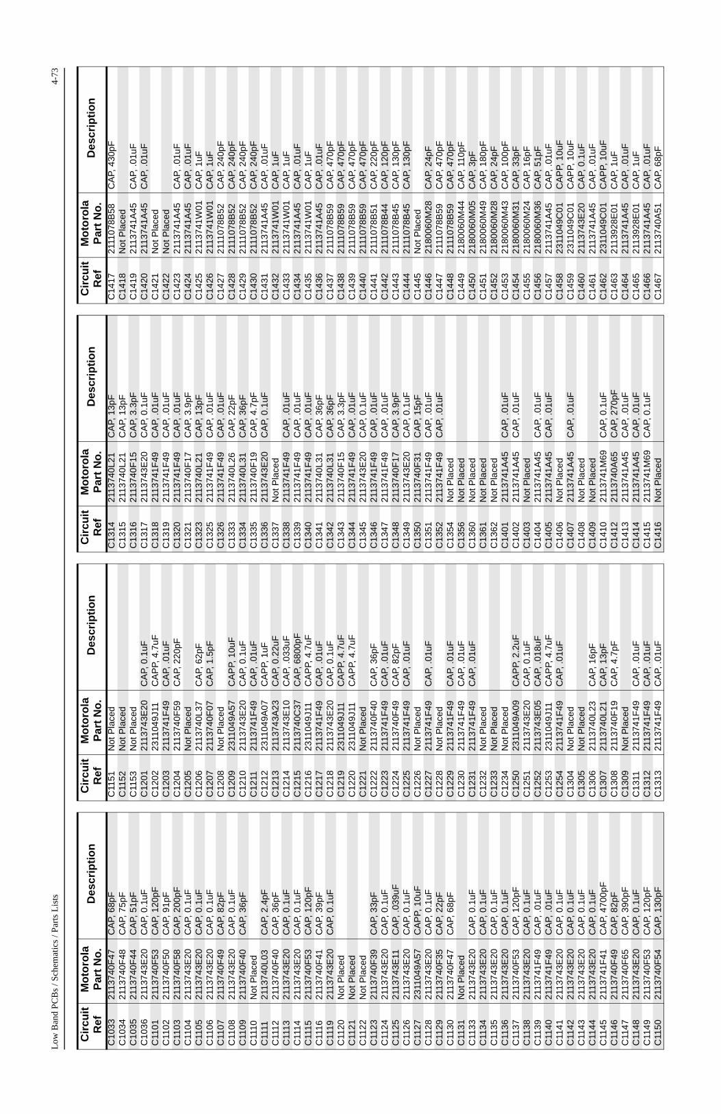
Low
Ban
d P
CB
s / S
chem
atic
s / P
arts
Lis
ts4-
73
C10
3321
1374
0F47
CA
P, 6
8pF
C10
3421
1374
0F48
CA
P, 7
5pF
C10
3521
1374
0F44
CA
P, 5
1pF
C10
3621
1374
3E20
CA
P, 0
.1uF
C11
0121
1374
0F53
CA
P, 1
20pF
C11
0221
1374
0F50
CA
P, 9
1pF
C11
0321
1374
0F58
CA
P, 2
00pF
C11
0421
1374
3E20
CA
P, 0
.1uF
C11
0521
1374
3E20
CA
P, 0
.1uF
C11
0621
1374
3E20
CA
P, 0
.1uF
C11
0721
1374
0F49
CA
P, 8
2pF
C11
0821
1374
3E20
CA
P, 0
.1uF
C11
0921
1374
0F40
CA
P, 3
6pF
C11
10N
ot P
lace
dC
1111
2113
740L
03C
AP,
2.4
pFC
1112
2113
740F
40C
AP,
36p
FC
1113
2113
743E
20C
AP,
0.1
uFC
1114
2113
743E
20C
AP,
0.1
uFC
1115
2113
740F
53C
AP,
120
pFC
1116
2113
740F
41C
AP,
39p
FC
1119
2113
743E
20C
AP,
0.1
uFC
1120
Not
Pla
ced
C11
21N
ot P
lace
dC
1122
Not
Pla
ced
C11
2321
1374
0F39
CA
P, 3
3pF
C11
2421
1374
3E20
CA
P, 0
.1uF
C11
2521
1374
3E11
CA
P, .0
39uF
C11
2621
1374
3E20
CA
P, 0
.1uF
C11
2723
1104
9A57
CA
PP,
10u
FC
1128
2113
743E
20C
AP,
0.1
uFC
1129
2113
740F
35C
AP,
22p
FC
1130
2113
740F
47C
AP,
68p
FC
1131
Not
Pla
ced
C11
3321
1374
3E20
CA
P, 0
.1uF
C11
3421
1374
3E20
CA
P, 0
.1uF
C11
3521
1374
3E20
CA
P, 0
.1uF
C11
3621
1374
3E20
CA
P, 0
.1uF
C11
3721
1374
0F53
CA
P, 1
20pF
C11
3821
1374
3E20
CA
P, 0
.1uF
C11
3921
1374
1F49
CA
P, .0
1uF
C11
4021
1374
1F49
CA
P, .0
1uF
C11
4121
1374
3E20
CA
P, 0
.1uF
C11
4221
1374
3E20
CA
P, 0
.1uF
C11
4321
1374
3E20
CA
P, 0
.1uF
C11
4421
1374
3E20
CA
P, 0
.1uF
C11
4521
1374
1F41
CA
P, 4
700p
FC
1146
2113
740F
49C
AP,
82p
FC
1147
2113
740F
65C
AP,
390
pFC
1148
2113
743E
20C
AP,
0.1
uFC
1149
2113
740F
53C
AP,
120
pFC
1150
2113
740F
54C
AP,
130
pF
Cir
cuit
R
efM
oto
rola
P
art
No
.D
escr
ipti
on
C11
51N
ot P
lace
dC
1152
Not
Pla
ced
C11
53N
ot P
lace
dC
1201
2113
743E
20C
AP,
0.1
uFC
1202
2311
049J
11C
AP
P, 4
.7uF
C12
0321
1374
1F49
CA
P, .0
1uF
C12
0421
1374
0F59
CA
P, 2
20pF
C12
05N
ot P
lace
dC
1206
2113
740L
37C
AP,
62p
FC
1207
2113
740F
07C
AP,
1.5
pFC
1208
Not
Pla
ced
C12
0923
1104
9A57
CA
PP,
10u
FC
1210
2113
743E
20C
AP,
0.1
uFC
1211
2113
741F
49C
AP,
.01u
FC
1212
2311
049A
07C
AP
P, 1
uFC
1213
2113
743A
23C
AP,
0.2
2uF
C12
1421
1374
3E10
CA
P, .0
33uF
C12
1521
1374
0C37
CA
P, 6
800p
FC
1216
2311
049J
11C
AP
P, 4
.7uF
C12
1721
1374
1F49
CA
P, .0
1uF
C12
1821
1374
3E20
CA
P, 0
.1uF
C12
1923
1104
9J11
CA
PP,
4.7
uFC
1220
2311
049J
11C
AP
P, 4
.7uF
C12
21N
ot P
lace
dC
1222
2113
740F
40C
AP,
36p
FC
1223
2113
741F
49C
AP,
.01u
FC
1224
2113
740F
49C
AP,
82p
FC
1225
2113
741F
49C
AP,
.01u
FC
1226
Not
Pla
ced
C12
2721
1374
1F49
CA
P, .0
1uF
C12
28N
ot P
lace
dC
1229
2113
741F
49C
AP,
.01u
FC
1230
2113
741F
49C
AP,
.01u
FC
1231
2113
741F
49C
AP,
.01u
FC
1232
Not
Pla
ced
C12
33N
ot P
lace
dC
1234
Not
Pla
ced
C12
5023
1104
9A09
CA
PP,
2.2
uFC
1251
2113
743E
20C
AP,
0.1
uFC
1252
2113
743E
05C
AP,
.018
uFC
1253
2311
049J
11C
AP
P, 4
.7uF
C12
5421
1374
1F49
CA
P, .0
1uF
C13
04N
ot P
lace
dC
1305
Not
Pla
ced
C13
0621
1374
0L23
CA
P, 1
6pF
C13
0721
1374
0L21
CA
P, 1
3pF
C13
0821
1374
0F19
CA
P, 4
.7pF
C13
09N
ot P
lace
dC
1311
2113
741F
49C
AP,
.01u
FC
1312
2113
741F
49C
AP,
.01u
FC
1313
2113
741F
49C
AP,
.01u
F
Cir
cuit
R
efM
oto
rola
P
art
No
.D
escr
ipti
on
C13
1421
1374
0L21
CA
P, 1
3pF
C13
1521
1374
0L21
CA
P, 1
3pF
C13
1621
1374
0F15
CA
P, 3
.3pF
C13
1721
1374
3E20
CA
P, 0
.1uF
C13
1821
1374
1F49
CA
P, .0
1uF
C13
1921
1374
1F49
CA
P, .0
1uF
C13
2021
1374
1F49
CA
P, .0
1uF
C13
2121
1374
0F17
CA
P, 3
.9pF
C13
2321
1374
0L21
CA
P, 1
3pF
C13
2521
1374
1F49
CA
P, .0
1uF
C13
2621
1374
1F49
CA
P, .0
1uF
C13
3321
1374
0L26
CA
P, 2
2pF
C13
3421
1374
0L31
CA
P, 3
6pF
C13
3521
1374
0F19
CA
P, 4
.7pF
C13
3621
1374
3E20
CA
P, 0
.1uF
C13
37N
ot P
lace
dC
1338
2113
741F
49C
AP,
.01u
FC
1339
2113
741F
49C
AP,
.01u
FC
1340
2113
741F
49C
AP,
.01u
FC
1341
2113
740L
31C
AP,
36p
FC
1342
2113
740L
31C
AP,
36p
FC
1343
2113
740F
15C
AP,
3.3
pFC
1344
2113
741F
49C
AP,
.01u
FC
1345
2113
743E
20C
AP,
0.1
uFC
1346
2113
741F
49C
AP,
.01u
FC
1347
2113
741F
49C
AP,
.01u
FC
1348
2113
740F
17C
AP,
3.9
pFC
1349
2113
743E
20C
AP,
0.1
uFC
1350
2113
740F
31C
AP,
15p
FC
1351
2113
741F
49C
AP,
.01u
FC
1352
2113
741F
49C
AP,
.01u
FC
1354
Not
Pla
ced
C13
56N
ot P
lace
dC
1360
Not
Pla
ced
C13
61N
ot P
lace
dC
1362
Not
Pla
ced
C14
0121
1374
1A45
CA
P, .0
1uF
C14
0221
1374
1A45
CA
P, .0
1uF
C14
03N
ot P
lace
dC
1404
2113
741A
45C
AP,
.01u
FC
1405
2113
741A
45C
AP,
.01u
FC
1406
Not
Pla
ced
C14
0721
1374
1A45
CA
P, .0
1uF
C14
08N
ot P
lace
dC
1409
Not
Pla
ced
C14
1021
1374
1M69
CA
P, 0
.1uF
C14
1221
1374
0A65
CA
P, 2
70pF
C14
1321
1374
1A45
CA
P, .0
1uF
C14
1421
1374
1A45
CA
P, .0
1uF
C14
1521
1374
1M69
CA
P, 0
.1uF
C14
16N
ot P
lace
d
Cir
cuit
R
efM
oto
rola
P
art
No
.D
escr
ipti
on
C14
1721
1107
8B58
CA
P, 4
30pF
C14
18N
ot P
lace
dC
1419
2113
741A
45C
AP,
.01u
FC
1420
2113
741A
45C
AP,
.01u
FC
1421
Not
Pla
ced
C14
22N
ot P
lace
dC
1423
2113
741A
45C
AP,
.01u
FC
1424
2113
741A
45C
AP,
.01u
FC
1425
2113
741W
01C
AP,
1uF
C14
2621
1374
1W01
CA
P, 1
uFC
1427
2111
078B
52C
AP,
240
pFC
1428
2111
078B
52C
AP,
240
pFC
1429
2111
078B
52C
AP,
240
pFC
1430
2111
078B
52C
AP,
240
pFC
1431
2113
741A
45C
AP,
.01u
FC
1432
2113
741W
01C
AP,
1uF
C14
3321
1374
1W01
CA
P, 1
uFC
1434
2113
741A
45C
AP,
.01u
FC
1435
2113
741W
01C
AP,
1uF
C14
3621
1374
1A45
CA
P, .0
1uF
C14
3721
1107
8B59
CA
P, 4
70pF
C14
3821
1107
8B59
CA
P, 4
70pF
C14
3921
1107
8B59
CA
P, 4
70pF
C14
4021
1107
8B59
CA
P, 4
70pF
C14
4121
1107
8B51
CA
P, 2
20pF
C14
4221
1107
8B44
CA
P, 1
20pF
C14
4321
1107
8B45
CA
P, 1
30pF
C14
4421
1107
8B45
CA
P, 1
30pF
C14
45N
ot P
lace
dC
1446
2180
060M
28C
AP,
24p
FC
1447
2111
078B
59C
AP,
470
pFC
1448
2111
078B
59C
AP,
470
pFC
1449
2180
060M
44C
AP,
110
pFC
1450
2180
060M
05C
AP,
3pF
C14
5121
8006
0M49
CA
P, 1
80pF
C14
5221
8006
0M28
CA
P, 2
4pF
C14
5321
8006
0M43
CA
P, 1
00pF
C14
5421
8006
0M31
CA
P, 3
3pF
C14
5521
8006
0M24
CA
P, 1
6pF
C14
5621
8006
0M36
CA
P, 5
1pF
C14
5721
1374
1A45
CA
P, .0
1uF
C14
5823
1104
9C01
CA
PP,
10u
FC
1459
2311
049C
01C
AP
P, 1
0uF
C14
6021
1374
3E20
CA
P, 0
.1uF
C14
6121
1374
1A45
CA
P, .0
1uF
C14
6223
1104
9C01
CA
PP,
10u
FC
1463
2113
928E
01C
AP,
1uF
C14
6421
1374
1A45
CA
P, .0
1uF
C14
6521
1392
8E01
CA
P, 1
uFC
1466
2113
741A
45C
AP,
.01u
FC
1467
2113
740A
51C
AP,
68p
F
Cir
cuit
R
efM
oto
rola
P
art
No
.D
escr
ipti
on

4-74
Low
Ban
d PC
Bs
/ Sch
emat
ics
/ Par
ts L
ists
C14
6821
1374
1A45
CA
P, .0
1uF
C14
6921
1374
1W01
CA
P, 1
uFC
1470
2113
741W
01C
AP,
1uF
C14
7121
1374
1A45
CA
P, .0
1uF
C14
7221
1374
1M69
CA
P, 0
.1uF
C14
7321
1374
1M69
CA
P, 0
.1uF
C14
7421
1374
1A45
CA
P, .0
1uF
C14
7521
1374
1W01
CA
P, 1
uFC
1476
2113
741M
69C
AP,
0.1
uFC
1477
2111
078B
54C
AP,
300
pFC
1478
2111
078B
54C
AP,
300
pFC
1479
2111
078B
51C
AP,
220
pFC
1480
2111
078B
40C
AP,
82p
FC
1481
2111
078B
40C
AP,
82p
FC
1482
2113
928E
01C
AP,
1uF
C14
8421
1374
1F33
CA
P, 2
200p
FC
1485
2113
741A
45C
AP,
.01u
FC
1486
2113
741M
69C
AP,
0.1
uFC
1501
2113
741F
33C
AP,
220
0pF
C15
0221
1374
1F33
CA
P, 2
200p
FC
1503
2113
741F
33C
AP,
220
0pF
C15
0421
1374
1F33
CA
P, 2
200p
FC
1505
2113
741F
25C
AP,
100
0pF
C15
0621
1374
1F25
CA
P, 1
000p
FC
1507
2113
741F
33C
AP,
220
0pF
C15
0821
1374
1F33
CA
P, 2
200p
FC
1509
2311
049A
07C
AP
P, 1
uFC
1510
2113
741F
33C
AP,
220
0pF
C15
1121
1374
1F33
CA
P, 2
200p
FC
1512
2113
741F
33C
AP,
220
0pF
C15
2321
1374
3E20
CA
P, 0
.1uF
C15
2521
1374
3E20
CA
P, 0
.1uF
C15
2621
1374
0F51
CA
P, 1
00pF
C15
2721
1374
1A45
CA
P, .0
1uF
C15
2821
1374
1A45
CA
P, .0
1uF
C15
3021
1374
1A45
CA
P, .0
1uF
C15
31N
ot P
lace
dC
1532
2113
743T
19C
AP,
10u
FC
1601
2113
743E
20C
AP,
0.1
uFC
1602
2113
740F
59C
AP,
220
pFC
1603
2113
743A
23C
AP,
0.2
2uF
C16
0421
1374
3A23
CA
P, 0
.22u
FC
1605
2311
049A
57C
AP
P, 1
0uF
C16
0621
1374
0F59
CA
P, 2
20pF
C16
0721
1374
0F51
CA
P, 1
00pF
C16
0821
1374
3A23
CA
P, 0
.22u
FC
1609
2113
740F
34C
AP,
20p
FC
1610
2113
741F
41C
AP,
470
0pF
C16
1121
1374
3E20
CA
P, 0
.1uF
C16
1221
1374
1F33
CA
P, 2
200p
FC
1613
2113
740F
54C
AP,
130
pF
Cir
cuit
R
efM
oto
rola
P
art
No
.D
escr
ipti
on
C16
1421
1374
1F24
CA
P, 9
10pF
C16
15N
ot P
lace
dC
1616
2113
740F
40C
AP,
36p
FC
1618
2113
743A
23C
AP,
0.2
2uF
C16
1923
1104
9A57
CA
PP,
10u
FC
1620
2113
741F
25C
AP,
100
0pF
C16
21N
ot P
lace
dC
1622
2113
743E
20C
AP,
0.1
uFC
1623
2113
740F
60C
AP,
240
pFC
1624
2113
741F
37C
AP,
330
0pF
C16
2521
1374
0F29
CA
P, 1
2pF
C16
2621
1374
0F59
CA
P, 2
20pF
C16
2721
1374
3A23
CA
P, 0
.22u
FC
1628
2113
743E
20C
AP,
0.1
uFC
1629
2113
740F
39C
AP,
33p
FC
1631
2311
049A
57C
AP
P, 1
0uF
C16
3221
1374
3E20
CA
P, 0
.1uF
C16
3321
1374
3A23
CA
P, 0
.22u
FC
1634
2113
741A
45C
AP,
.01u
FC
R12
0148
6282
4C03
1SV
232
CR
1202
4802
233J
09IM
N10
CR
1302
4805
649Q
14H
N1V
02H
CR
1306
4880
154K
03M
MB
D35
3C
R13
1048
0564
9Q14
HN
1V02
HC
R13
1448
8015
4K03
MM
BD
353
D01
0148
1382
5A05
MM
BD
301
D01
5148
1383
3C02
MM
BD
6100
D01
7948
1383
3C02
MM
BD
6100
D02
01N
ot P
lace
dD
0301
Not
Pla
ced
D06
2148
1383
3C02
MM
BD
6100
D06
5148
1383
3C02
MM
BD
6100
D06
6048
1383
3C02
MM
BD
6100
D06
6148
1383
3C02
MM
BD
6100
D10
0148
8015
4K03
MM
BD
353
D11
0148
8015
4K03
MM
BD
353
D14
0148
0837
9X02
MA
4P14
50D
1402
4808
379X
02M
A4P
1450
D15
0148
1382
5A05
MM
BD
301
D15
0248
1383
3C02
MM
BD
6100
D15
0348
1383
3C02
MM
BD
6100
D16
0148
8015
4K03
MM
BD
353
E02
7124
8465
7R01
FE
RR
ITE
BE
AD
E02
7224
8465
7R01
FE
RR
ITE
BE
AD
E06
3124
8465
7R01
FE
RR
ITE
BE
AD
E14
0124
0838
0X02
FE
RR
ITE
BE
AD
E14
0324
0838
0X02
FE
RR
ITE
BE
AD
F04
0165
8054
2Z01
FU
SE
FL1
101
9180
656U
03C
FE
C10
_7M
G1
FL1
102
9180
022M
09C
RY
STA
L F
ILT
ER
, 10.
7 M
HZ
FL1
104
9180
468V
04C
FU
CJ4
55F
Cir
cuit
R
efM
oto
rola
P
art
No
.D
escr
ipti
on
FL1
105
9180
468V
05C
FU
CJ4
55E
FL1
106
9180
469V
04C
FW
C45
5FF
L110
791
8046
9V05
CF
WC
455E
J040
109
0263
6Y02
CO
NN
, 12-
PIN
, CO
NT
RO
L H
EA
DJ0
451
0902
636Y
01C
ON
N, 1
8-P
IN, E
XP
AN
SIO
N
BO
AR
DJ0
501
0986
105B
01C
ON
N, 2
0-P
IN, A
CC
ES
SO
RY
J055
109
0550
5Y04
CO
NN
, 40-
PIN
, IN
TE
RN
AL
OP
TIO
NJ0
552
0905
505Y
03C
ON
N, 1
8-P
IN, R
S23
2J0
601
0986
165B
01D
C P
OW
ER
CO
NN
EC
TO
RJ1
401
0986
166B
02M
INI-
U A
NT
EN
NA
CO
NN
EC
-T
OR
L048
1N
ot P
lace
dL0
482
Not
Pla
ced
L100
124
0838
2A11
IDC
TR
, 130
nHL1
002
2408
382C
11ID
CT
R, 1
30nH
L100
324
0838
2A11
IDC
TR
, 130
nHL1
004
2408
382C
11ID
CT
R, 1
30nH
L100
524
0838
2A11
IDC
TR
, 130
nHL1
006
2408
382A
11ID
CT
R, 1
30nH
L100
724
0838
2C11
IDC
TR
, 130
nHL1
008
2408
382A
11ID
CT
R, 1
30nH
L100
924
0838
2C11
IDC
TR
, 130
nHL1
010
2408
382A
11ID
CT
R, 1
30nH
L101
124
6258
7N68
IDC
TR
, 1uH
L101
224
6258
7N57
IDC
TR
, 220
nHL1
013
2462
587N
59ID
CT
R, 3
30nH
L101
424
6258
7N57
IDC
TR
, 220
nHL1
101
2462
587N
33ID
CT
R, 1
.8uH
L110
224
0838
3X07
IDC
TR
, 3.3
uHL1
103
2462
587N
33ID
CT
R, 1
.8uH
L110
424
8028
9M10
IDC
TR
, 6.8
uHL1
105
2480
289M
10ID
CT
R, 6
.8uH
L110
624
6258
7N33
IDC
TR
, 1.8
uHL1
107
2480
289M
09ID
CT
R, 5
.6uH
L110
8N
ot P
lace
dL1
109
Not
Pla
ced
L111
024
8028
9M18
IDC
TR
, 33u
HL1
111
2408
383X
07ID
CT
R, 3
.3uH
L111
224
8341
1T35
IDC
TR
, 6.8
uHL1
201
2480
289M
17ID
CT
R, 2
7uH
L120
224
6258
7Q20
IDC
TR
, 2.2
uHL1
204
Not
Pla
ced
L120
524
6258
7N59
IDC
TR
, 330
nHL1
206
2480
289M
17ID
CT
R, 2
7uH
L120
7N
ot P
lace
dL1
302
2408
382D
19ID
CT
R, 4
91nH
L130
324
8028
9M15
IDC
TR
, 18u
HL1
304
2462
587N
66ID
CT
R, 8
20nH
Cir
cuit
R
efM
oto
rola
P
art
No
.D
escr
ipti
on
L130
524
8028
9M15
IDC
TR
, 18u
HL1
306
2480
289M
15ID
CT
R, 1
8uH
L130
724
8028
9M15
IDC
TR
, 18u
HL1
309
2480
289M
15ID
CT
R, 1
8uH
L131
024
6258
7N60
IDC
TR
, 390
nHL1
311
2480
289M
15ID
CT
R, 1
8uH
L131
324
0838
2D19
IDC
TR
, 491
nHL1
314
2480
289M
17ID
CT
R, 2
7uH
L131
524
6258
7N66
IDC
TR
, 820
nHL1
316
2480
289M
17ID
CT
R, 2
7uH
L131
724
8028
9M17
IDC
TR
, 27u
HL1
318
2480
289M
17ID
CT
R, 2
7uH
L132
124
6258
7N58
IDC
TR
, 270
nHL1
322
2480
289M
17ID
CT
R, 2
7uH
L132
424
8028
9M17
IDC
TR
, 27u
HL1
401
Not
Pla
ced
L140
224
6258
7U09
IDC
TR
, 4.7
uHL1
403
2462
587U
09ID
CT
R, 4
.7uH
L140
424
6258
7N56
IDC
TR
, 180
nHL1
405
Not
Pla
ced
L140
624
0838
1X36
IDC
TR
, 250
.974
nHL1
408
2408
384A
10ID
CT
R, 1
20nH
L141
324
0838
1X17
IDC
TR
, 88.
470n
HL1
414
2408
381X
17ID
CT
R, 8
8.47
0nH
L141
524
6059
1X01
IDC
TR
, 18n
HL1
416
2460
591X
01ID
CT
R, 1
8nH
L141
724
6059
1X01
IDC
TR
, 18n
HL1
418
2408
381X
12ID
CT
R, 6
6.38
9nH
L141
924
8028
9M17
IDC
TR
, 27u
HL1
420
2408
381X
29ID
CT
R, 1
72.8
91nH
L142
124
0838
1X25
IDC
TR
, 137
.876
nHL1
422
2408
381X
22ID
CT
R, 1
15.5
81nH
L142
324
0838
1X16
IDC
TR
, 81.
930n
HL1
424
Not
Pla
ced
L142
524
6059
1X01
IDC
TR
, 18n
HL1
426
2460
591X
01ID
CT
R, 1
8nH
L160
124
8341
1T45
IDC
TR
, 47u
HL1
602
2483
411T
45ID
CT
R, 4
7uH
L160
324
8341
1T73
IDC
TR
, 1uH
L160
424
8341
1T45
IDC
TR
, 47u
HL1
605
2483
411T
41ID
CT
R, 2
2uH
L160
624
6258
7T30
IDC
TR
, 1uH
L160
724
6258
7T30
IDC
TR
, 1uH
M14
0126
8620
1B01
HE
AT
SIN
KQ
0110
4880
048M
01D
TC
144E
KA
Q01
5148
8004
8M01
DT
C14
4EK
AQ
0171
4880
048M
01D
TC
144E
KA
Q01
7348
8005
2M01
RX
T-A
28Q
0177
4880
048M
01D
TC
144E
KA
Q01
8148
8004
8M01
DT
C14
4EK
AQ
0183
4880
048M
01D
TC
144E
KA
Cir
cuit
R
efM
oto
rola
P
art
No
.D
escr
ipti
on
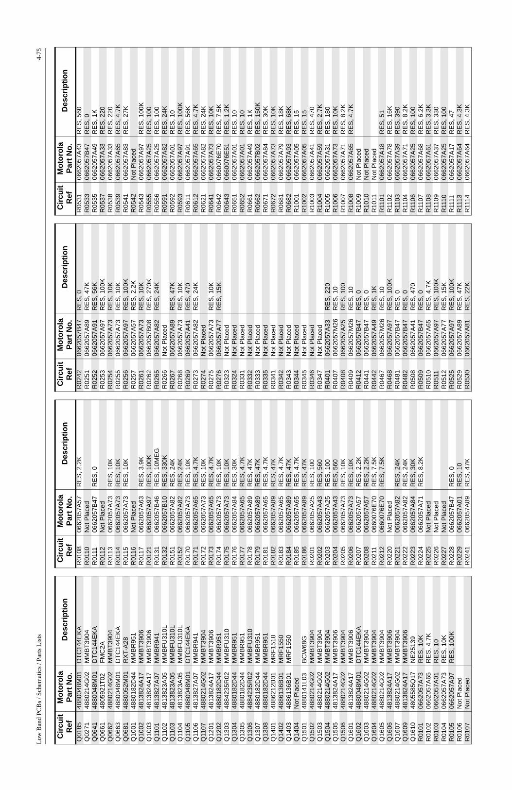
Low
Ban
d P
CB
s / S
chem
atic
s / P
arts
Lis
ts4-
75
Q01
8548
8004
8M01
DT
C14
4EK
AQ
0271
4880
214G
02M
MB
T39
04Q
0641
4880
048M
01D
TC
144E
KA
Q06
6148
0592
1T02
FM
C2A
Q06
6248
8021
4G02
MM
BT
3904
Q06
6348
8004
8M01
DT
C14
4EK
AQ
0681
4880
052M
01R
XT-
A28
Q10
0148
8018
2D44
MM
BR
951
Q10
0248
1382
4A17
MM
BT
3906
Q10
0348
1382
4A17
MM
BT
3906
Q11
0148
1382
7A07
MM
BR
941
Q11
0248
1382
3A05
MM
BF
U31
0LQ
1103
4813
823A
05M
MB
FU
310L
Q11
0448
1382
3A05
MM
BF
U31
0LQ
1105
4880
048M
01D
TC
144E
KA
Q11
0648
1382
7A07
MM
BR
941
Q11
0748
8021
4G02
MM
BT
3904
Q12
0148
1382
4A17
MM
BT
3906
Q12
0248
8018
2D44
MM
BR
951
Q13
0348
8423
5R02
MM
BF
U31
0Q
1304
4880
182D
44M
MB
R95
1Q
1305
4880
182D
44M
MB
R95
1Q
1306
4884
235R
02M
MB
FU
310
Q13
0748
8018
2D44
MM
BR
951
Q13
0848
8018
2D44
MM
BR
951
Q14
0148
8621
2B01
MR
F15
18Q
1402
4886
136B
01M
RF
1550
Q14
0348
8613
6B01
MR
F15
50Q
1404
Not
Pla
ced
Q15
0148
8014
1L03
BC
W68
GQ
1502
4880
214G
02M
MB
T39
04Q
1503
4880
214G
02M
MB
T39
04Q
1504
4880
214G
02M
MB
T39
04Q
1505
4813
824A
17M
MB
T39
06Q
1506
4880
214G
02M
MB
T39
04Q
1601
4813
824A
17M
MB
T39
06Q
1602
4880
048M
01D
TC
144E
KA
Q16
0348
8021
4G02
MM
BT
3904
Q16
0448
8021
4G02
MM
BT
3904
Q16
0548
8021
4G02
MM
BT
3904
Q16
0648
1382
4A17
MM
BT
3906
Q16
0748
8021
4G02
MM
BT
3904
Q16
0948
1382
4A17
MM
BT
3906
Q16
1048
0558
5Q17
NE
2513
9R
0101
0662
057A
73R
ES
, 10K
R01
0206
6205
7A65
RE
S, 4
.7K
R01
0306
6205
7A01
RE
S, 1
0R
0104
0662
057A
73R
ES
, 10K
R01
0506
6205
7A97
RE
S, 1
00K
R01
06N
ot P
lace
dR
0107
Not
Pla
ced
Cir
cuit
R
efM
oto
rola
P
art
No
.D
escr
ipti
on
R01
0806
6205
7A57
RE
S, 2
.2K
R01
10N
ot P
lace
dR
0111
0662
057B
47R
ES
, 0R
0112
Not
Pla
ced
R01
1306
6205
7A73
RE
S, 1
0KR
0114
0662
057A
73R
ES
, 10K
R01
1506
6205
7A73
RE
S, 1
0KR
0116
Not
Pla
ced
R01
1706
6205
7A63
RE
S, 3
.9K
R01
2106
6205
7A97
RE
S, 1
00K
R01
3106
6205
7B46
RE
S, 1
0ME
GR
0132
0662
057B
10R
ES
, 330
KR
0151
0662
057A
82R
ES
, 24K
R01
5206
6205
7A82
RE
S, 2
4KR
0170
0662
057A
73R
ES
, 10K
R01
7106
6205
7A65
RE
S, 4
.7K
R01
7206
6205
7A73
RE
S, 1
0KR
0173
0662
057A
65R
ES
, 4.7
KR
0174
0662
057A
73R
ES
, 10K
R01
7506
6205
7A73
RE
S, 1
0KR
0176
0662
057A
84R
ES
, 30K
R01
7706
6205
7A65
RE
S, 4
.7K
R01
7806
6205
7A89
RE
S, 4
7KR
0179
0662
057A
89R
ES
, 47K
R01
8106
6205
7A65
RE
S, 4
.7K
R01
8206
6205
7A89
RE
S, 4
7KR
0183
0662
057A
65R
ES
, 4.7
KR
0184
0662
057A
89R
ES
, 47K
R01
8506
6205
7A65
RE
S, 4
.7K
R01
8606
6205
7A89
RE
S, 4
7KR
0201
0662
057A
25R
ES
, 100
R02
0206
6205
7A43
RE
S, 5
60R
0203
0662
057A
25R
ES
, 100
R02
0406
6205
7A43
RE
S, 5
60R
0205
0662
057A
73R
ES
, 10K
R02
0606
6205
7A73
RE
S, 1
0KR
0207
0662
057A
57R
ES
, 2.2
KR
0208
0662
057A
57R
ES
, 2.2
KR
0211
0660
076E
70R
ES
, 7.5
KR
0212
0660
076E
70R
ES
, 7.5
KR
0220
Not
Pla
ced
R02
2106
6205
7A82
RE
S, 2
4KR
0222
0662
057A
82R
ES
, 24K
R02
2306
6205
7A84
RE
S, 3
0KR
0224
0662
057A
71R
ES
, 8.2
KR
0225
Not
Pla
ced
R02
26N
ot P
lace
dR
0227
Not
Pla
ced
R02
2806
6205
7B47
RE
S, 0
R02
2906
6205
7A01
RE
S, 1
0R
0241
0662
057A
89R
ES
, 47K
Cir
cuit
R
efM
oto
rola
P
art
No
.D
escr
ipti
on
R02
4206
6205
7B47
RE
S, 0
R02
5106
6205
7A89
RE
S, 4
7KR
0252
0662
057A
91R
ES
, 56K
R02
5306
6205
7A97
RE
S, 1
00K
R02
5406
6205
7A73
RE
S, 1
0KR
0255
0662
057A
73R
ES
, 10K
R02
5606
6205
7A97
RE
S, 1
00K
R02
5706
6205
7A57
RE
S, 2
.2K
R02
6106
6205
7A73
RE
S, 1
0KR
0262
0662
057B
08R
ES
, 270
KR
0265
0662
057A
82R
ES
, 24K
R02
66N
ot P
lace
dR
0267
0662
057A
89R
ES
, 47K
R02
6806
6205
7A73
RE
S, 1
0KR
0269
0662
057A
41R
ES
, 470
R02
7306
6205
7A82
RE
S, 2
4KR
0274
Not
Pla
ced
R02
7506
6205
7A73
RE
S, 1
0KR
0276
0662
057A
77R
ES
, 15K
R03
23N
ot P
lace
dR
0324
Not
Pla
ced
R03
31N
ot P
lace
dR
0332
Not
Pla
ced
R03
33N
ot P
lace
dR
0335
Not
Pla
ced
R03
41N
ot P
lace
dR
0342
Not
Pla
ced
R03
43N
ot P
lace
dR
0344
Not
Pla
ced
R03
45N
ot P
lace
dR
0346
Not
Pla
ced
R03
47N
ot P
lace
dR
0401
0662
057A
33R
ES
, 220
R04
0706
6205
7M26
RE
S, 1
0R
0408
0662
057A
25R
ES
, 100
R04
0906
6205
7M26
RE
S, 1
0R
0412
0662
057B
47R
ES
, 0R
0441
0662
057B
47R
ES
, 0R
0442
0662
057A
49R
ES
, 1K
R04
6706
6205
7M26
RE
S, 1
0R
0468
0662
057A
97R
ES
, 100
KR
0481
0662
057B
47R
ES
, 0R
0482
0662
057B
47R
ES
, 0R
0508
0662
057A
41R
ES
, 470
R05
0906
6205
7B47
RE
S, 0
R05
1006
6205
7A65
RE
S, 4
.7K
R05
1106
6205
7A97
RE
S, 1
00K
R05
1206
6205
7A77
RE
S, 1
5KR
0525
0662
057A
97R
ES
, 100
KR
0529
0662
057A
89R
ES
, 47K
R05
3006
6205
7A81
RE
S, 2
2K
Cir
cuit
R
efM
oto
rola
P
art
No
.D
escr
ipti
on
R05
3106
6205
7A43
RE
S, 5
60R
0533
0662
057B
47R
ES
, 0R
0535
0662
057A
49R
ES
, 1K
R05
3706
6205
7A33
RE
S, 2
20R
0538
0662
057A
33R
ES
, 220
R05
3906
6205
7A65
RE
S, 4
.7K
R05
4106
6205
7A83
RE
S, 2
7KR
0542
Not
Pla
ced
R05
4306
6205
7A97
RE
S, 1
00K
R05
5506
6205
7A25
RE
S, 1
00R
0556
0662
057A
25R
ES
, 100
R05
9106
6205
7A82
RE
S, 2
4KR
0592
0662
057A
01R
ES
, 10
R05
9306
6205
7A97
RE
S, 1
00K
R06
1106
6205
7A91
RE
S, 5
6KR
0612
0662
057A
65R
ES
, 4.7
KR
0621
0662
057A
82R
ES
, 24K
R06
4106
6205
7A73
RE
S, 1
0KR
0642
0660
076E
70R
ES
, 7.5
KR
0643
0660
076E
51R
ES
, 1.2
KR
0651
0662
057A
01R
ES
, 10
R06
5206
6205
7A01
RE
S, 1
0R
0661
0662
057A
49R
ES
, 1K
R06
6206
6205
7B02
RE
S, 1
50K
R06
7106
6205
7A84
RE
S, 3
0KR
0672
0662
057A
73R
ES
, 10K
R06
8106
6205
7A79
RE
S, 1
8KR
0682
0662
057A
93R
ES
, 68K
R10
0106
6205
7A05
RE
S, 1
5R
1002
0662
057A
05R
ES
, 15
R10
0306
6205
7A41
RE
S, 4
70R
1004
0662
057A
59R
ES
, 2.7
KR
1005
0662
057A
31R
ES
, 180
R10
0606
6205
7A73
RE
S, 1
0KR
1007
0662
057A
71R
ES
, 8.2
KR
1008
0662
057A
65R
ES
, 4.7
KR
1009
Not
Pla
ced
R10
10N
ot P
lace
dR
1011
Not
Pla
ced
R11
0106
6205
7A18
RE
S, 5
1R
1102
0662
057A
78R
ES
, 16K
R11
0306
6205
7A39
RE
S, 3
90R
1104
0662
057A
71R
ES
, 8.2
KR
1106
0662
057A
25R
ES
, 100
R11
0706
6205
7A68
RE
S, 6
.2K
R11
0806
6205
7A61
RE
S, 3
.3K
R11
0906
6205
7A37
RE
S, 3
30R
1110
0662
057A
25R
ES
, 100
R11
1106
6205
7A17
RE
S, 4
7R
1113
0662
057A
64R
ES
, 4.3
KR
1114
0662
057A
64R
ES
, 4.3
K
Cir
cuit
R
efM
oto
rola
P
art
No
.D
escr
ipti
on
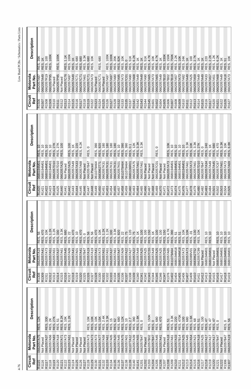
4-76
Low
Ban
d PC
Bs
/ Sch
emat
ics
/ Par
ts L
ists
R11
1506
6205
7A75
RE
S, 1
2KR
1116
Not
Pla
ced
R11
1706
6205
7A37
RE
S, 3
30R
1118
0662
057A
56R
ES
, 2K
R11
1906
6205
7A83
RE
S, 2
7KR
1120
0662
057A
18R
ES
, 51
R11
2106
6205
7A71
RE
S, 8
.2K
R11
2206
6205
7A73
RE
S, 1
0KR
1123
0662
057A
51R
ES
, 1.2
KR
1124
Not
Pla
ced
R11
25N
ot P
lace
dR
1126
Not
Pla
ced
R11
27N
ot P
lace
dR
1128
0662
057A
73R
ES
, 10K
R11
2906
6205
7A73
RE
S, 1
0KR
1130
0662
057A
73R
ES
, 10K
R11
3106
6205
7A77
RE
S, 1
5KR
1132
0662
057A
58R
ES
, 2.4
KR
1133
0662
057A
61R
ES
, 3.3
KR
1134
0662
057A
05R
ES
, 15
R11
3506
6205
7A20
RE
S, 6
2R
1136
0662
057A
45R
ES
, 680
R11
3706
6205
7A75
RE
S, 1
2KR
1138
0662
057A
01R
ES
, 10
R11
3906
1107
7A12
RE
S, 2
.7R
1140
0662
057A
39R
ES
, 390
R11
4106
6205
7A55
RE
S, 1
.8K
R12
0106
6205
7B47
RE
S, 0
R12
02N
ot P
lace
dR
1203
0662
057B
02R
ES
, 150
KR
1204
0662
057B
47R
ES
, 0R
1205
0662
057A
45R
ES
, 680
R12
0606
6205
7A41
RE
S, 4
70R
1207
Not
Pla
ced
R12
0806
6205
7A18
RE
S, 5
1R
1209
0662
057A
61R
ES
, 3.3
KR
1210
0662
057A
33R
ES
, 220
R12
1106
6205
7B14
RE
S, 4
70K
R12
1206
6205
7A25
RE
S, 1
00R
1213
0662
057A
45R
ES
, 680
R12
1406
6205
7A54
RE
S, 1
.6K
R12
1506
6205
7A21
RE
S, 6
8R
1216
0662
057A
18R
ES
, 51
R12
1706
6205
7A25
RE
S, 1
00R
1218
0662
057A
17R
ES
, 47
R12
1906
6205
7A17
RE
S, 4
7R
1220
0662
057A
17R
ES
, 47
R12
2106
6205
7B47
RE
S, 0
R12
22N
ot P
lace
dR
1306
0662
057B
47R
ES
, 0R
1307
0662
057A
19R
ES
, 56
Cir
cuit
R
efM
oto
rola
P
art
No
.D
escr
ipti
on
R13
0806
6205
7A19
RE
S, 5
6R
1309
0662
057A
41R
ES
, 470
R13
1106
6205
7A73
RE
S, 1
0KR
1312
0662
057A
51R
ES
, 1.2
KR
1313
0662
057A
51R
ES
, 1.2
KR
1314
0662
057A
37R
ES
, 330
R13
1506
6205
7A61
RE
S, 3
.3K
R13
1606
6205
7A45
RE
S, 6
80R
1317
0662
057A
09R
ES
, 22
R13
1806
6205
7A41
RE
S, 4
70R
1319
0662
057A
01R
ES
, 10
R13
2006
6205
7A41
RE
S, 4
70R
1325
0662
057B
47R
ES
, 0R
1326
0662
057A
19R
ES
, 56
R13
2706
6205
7A19
RE
S, 5
6R
1328
0662
057A
41R
ES
, 470
R13
3006
6205
7A73
RE
S, 1
0KR
1331
0662
057A
51R
ES
, 1.2
KR
1332
0662
057A
51R
ES
, 1.2
KR
1333
0662
057A
37R
ES
, 330
R13
3406
6205
7A61
RE
S, 3
.3K
R13
3506
6205
7A47
RE
S, 8
20R
1336
0662
057A
09R
ES
, 22
R13
3706
6205
7A22
RE
S, 7
5R
1338
0662
057A
27R
ES
, 120
R13
3906
6205
7A22
RE
S, 7
5R
1340
0662
057A
49R
ES
, 1K
R13
4106
6205
7A25
RE
S, 1
00R
1342
0662
057A
25R
ES
, 100
R13
4306
6205
7C55
RE
S, 1
50R
1344
0662
057A
49R
ES
, 1K
R13
4506
6205
7A25
RE
S, 1
00R
1346
0662
057A
25R
ES
, 100
R13
4706
6205
7C55
RE
S, 1
50R
1376
0662
057A
65R
ES
, 4.7
KR
1402
0611
079A
64R
ES
, 390
R14
0406
8019
4M18
RE
S, 5
1R
1405
0680
194M
18R
ES
, 51
R14
0606
6205
7A73
RE
S, 1
0KR
1407
0662
057A
73R
ES
, 10K
R14
0906
8208
9V01
RE
S, .
01R
1410
0683
962T
52R
ES
, 130
R14
1106
6205
7C99
RE
S, 1
0KR
1412
Not
Pla
ced
R14
1306
8019
4M01
RE
S, 1
0R
1414
0680
194M
01R
ES
, 10
R14
15N
ot P
lace
dR
1416
0680
194M
01R
ES
, 10
R14
1706
8019
4M01
RE
S, 1
0R
1418
0680
194M
01R
ES
, 10
R14
1906
8019
4M01
RE
S, 1
0
Cir
cuit
R
efM
oto
rola
P
art
No
.D
escr
ipti
on
R14
2006
8019
4M01
RE
S, 1
0R
1421
0680
194M
01R
ES
, 10
R14
2206
8019
4M01
RE
S, 1
0R
1423
0680
194M
01R
ES
, 10
R14
2406
6205
7D10
RE
S, 2
7KR
1425
0662
057D
10R
ES
, 27K
R14
4006
6205
7A25
RE
S, 1
00R
1441
Not
Pla
ced
R14
4206
6205
7A25
RE
S, 1
00R
1443
0662
057A
49R
ES
, 1K
R14
4406
6205
7A33
RE
S, 2
20R
1445
0662
057A
68R
ES
, 6.2
KR
1446
Not
Pla
ced
R14
4706
6205
7B47
RE
S, 0
R14
48N
ot P
lace
dR
1449
0611
079A
64R
ES
, 390
R14
5006
8396
2T71
RE
S, 8
20R
1451
0662
057K
31R
ES
, 180
R14
5306
6205
7K31
RE
S, 1
80R
1454
0662
057K
31R
ES
, 180
R14
5506
6205
7K31
RE
S, 1
80R
1457
0662
057K
01R
ES
, 10
R14
5806
1107
9A64
RE
S, 3
90R
1459
0611
079A
64R
ES
, 390
R14
6006
8010
6R01
RE
S, 0
.1R
1463
0662
057A
75R
ES
, 12K
R14
6406
6205
7A61
RE
S, 3
.3K
R14
6506
6205
7A61
RE
S, 3
.3K
R14
66N
ot P
lace
dR
1467
Not
Pla
ced
R14
68N
ot P
lace
dR
1469
0662
057C
01R
ES
, 0R
1470
Not
Pla
ced
R14
71N
ot P
lace
dR
1472
0662
057A
73R
ES
, 10K
R14
7306
8019
4M01
RE
S, 1
0R
1474
0680
194M
01R
ES
, 10
R14
7506
8019
4M01
RE
S, 1
0R
1476
0680
194M
01R
ES
, 10
R14
7706
6205
7A61
RE
S, 3
.3K
R14
7806
6205
7A73
RE
S, 1
0KR
1479
0662
057A
61R
ES
, 3.3
KR
1480
0662
057D
10R
ES
, 27K
R14
8206
6205
7B47
RE
S, 0
R14
8306
6205
7A34
RE
S, 2
40R
1484
0662
057A
49R
ES
, 1K
R15
0106
6205
7A45
RE
S, 6
80R
1502
0662
057C
67R
ES
, 470
R15
0306
6205
7A61
RE
S, 3
.3K
R15
0406
6205
7A73
RE
S, 1
0KR
1505
0662
057A
69R
ES
, 6.8
K
Cir
cuit
R
efM
oto
rola
P
art
No
.D
escr
ipti
on
R15
0606
6205
7A87
RE
S, 3
9KR
1507
0662
057A
49R
ES
, 1K
R15
0806
6205
7R19
RE
S, 1
00R
1509
0662
057P
95R
ES
, 100
KR
1510
Not
Pla
ced
R15
1106
6205
7P95
RE
S, 1
00K
R15
12N
ot P
lace
dR
1513
0662
057C
76R
ES
, 1.1
KR
1514
0662
057A
97R
ES
, 100
KR
1515
0662
057A
49R
ES
, 1K
R15
1606
6205
7C71
RE
S, 6
80R
1517
0662
057C
71R
ES
, 680
R15
1806
6205
7A61
RE
S, 3
.3K
R15
1906
6205
7C71
RE
S, 6
80R
1522
0662
057A
73R
ES
, 10K
R15
23N
ot P
lace
dR
1524
0662
057C
71R
ES
, 680
R15
25N
ot P
lace
dR
1526
0662
057A
97R
ES
, 100
KR
1527
0662
057A
97R
ES
, 100
KR
1528
0662
057A
80R
ES
, 20K
R15
3206
6205
7A95
RE
S, 8
2KR
1533
0662
057A
73R
ES
, 10K
R15
3506
6205
7C01
RE
S, 0
R15
3706
6205
7A90
RE
S, 5
1KR
1541
0662
057A
68R
ES
, 6.2
KR
1542
0662
057A
49R
ES
, 1K
R15
4306
6205
7A49
RE
S, 1
KR
1544
0662
057A
90R
ES
, 51K
R15
4506
6205
7A65
RE
S, 4
.7K
R16
0106
6205
7A73
RE
S, 1
0KR
1602
0662
057A
65R
ES
, 4.7
KR
1604
0662
057A
49R
ES
, 1K
R16
0506
6205
7B10
RE
S, 3
30K
R16
0606
6205
7B02
RE
S, 1
50K
R16
0706
6205
7B19
RE
S, 7
50K
R16
0806
6205
7A57
RE
S, 2
.2K
R16
0906
6205
7A73
RE
S, 1
0KR
1610
0662
057A
82R
ES
, 24K
R16
1106
6205
7A49
RE
S, 1
KR
1612
0662
057A
25R
ES
, 100
R16
1306
6205
7A59
RE
S, 2
.7K
R16
1406
6205
7A49
RE
S, 1
KR
1615
0662
057A
49R
ES
, 1K
R16
1606
6205
7A33
RE
S, 2
20R
1617
0662
057A
57R
ES
, 2.2
KR
1620
0662
057A
51R
ES
, 1.2
KR
1621
0662
057A
68R
ES
, 6.2
KR
1622
0662
057A
49R
ES
, 1K
R16
2606
6205
7A18
RE
S, 5
1R
1627
0662
057A
73R
ES
, 10K
Cir
cuit
R
efM
oto
rola
P
art
No
.D
escr
ipti
on
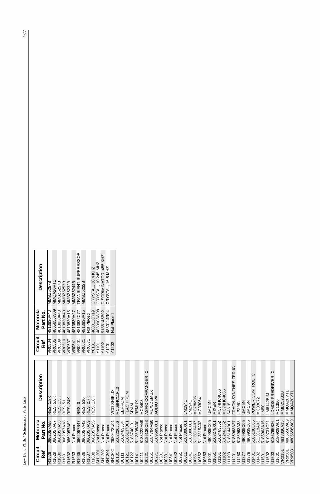
Low
Ban
d P
CB
s / S
chem
atic
s / P
arts
Lis
ts4-
77
R16
2806
6205
7A55
RE
S, 1
.8K
R16
2906
6205
7A67
RE
S, 5
.6K
R16
3006
6205
7A53
RE
S, 1
.5K
R16
3106
6205
7A18
RE
S, 5
1R
1632
0662
057A
82R
ES
, 24K
R16
33N
ot P
lace
dR
1635
0662
057B
47R
ES
, 0R
1636
0662
057A
42R
ES
, 510
R16
3706
6205
7A59
RE
S, 2
.7K
R16
3806
6205
7A55
RE
S, 1
.8K
SH
1201
Not
Pla
ced
SH
1202
Not
Pla
ced
SH
1301
Not
Pla
ced
SH
1302
2680
473U
01V
CO
SH
IELD
U01
0151
0222
6J56
MC
68H
C11
FL0
U01
1151
0246
3J64
EE
PR
OM
U01
2151
8613
7B01
FLA
SH
RO
MU
0122
5185
748L
01S
RA
MU
0141
5113
805A
30R
EM
UX
U02
1151
8322
2M49
MC
3403
U02
2151
8513
0C53
AS
FIC
CO
MP
AN
DE
R IC
U02
5151
8470
4M60
MU
X/D
EM
UX
U02
7151
0969
9X01
AU
DIO
PA
U03
01N
ot P
lace
dU
0331
Not
Pla
ced
U03
41N
ot P
lace
dU
0342
Not
Pla
ced
U03
51N
ot P
lace
dU
0611
5183
308X
01LM
2941
U06
4151
8330
8X01
LM29
41U
0651
5113
816A
07M
C78
M05
U06
5251
1381
5A02
MC
3306
4U
0653
Not
Pla
ced
U10
0148
0993
9C05
UM
C5N
U10
5151
0827
8X01
MIX
ER
U11
0151
0246
3J52
MC
74H
C40
66U
1102
5102
463J
52M
C74
HC
4066
U11
0351
8614
4B01
SA
616
U12
0151
8596
3A27
FR
AC
N S
YN
TH
ES
IZE
R IC
U12
5051
8596
3A33
LP29
51U
1377
4809
939C
05U
MC
5NU
1378
4809
939C
05U
MC
5NU
1401
5185
130C
65P
OW
ER
CO
NT
RO
L IC
U14
0251
1381
8A03
MC
3307
2U
1501
5185
963A
15LM
50U
1502
5109
731C
21LM
6142
BIM
U15
0351
8576
5B26
LDM
OS
PR
ED
RIV
ER
ICU
1601
5180
929W
01M
C13
50V
R01
5148
1383
0A15
MM
BZ
5232
BV
R05
0148
0565
6W09
MM
QA
20V
T1
VR
0503
4805
656W
09M
MQ
A20
VT
1
Cir
cuit
R
efM
oto
rola
P
art
No
.D
escr
ipti
on
VR
0504
4813
830A
40M
MB
Z52
57B
VR
0505
4805
656W
09M
MQ
A20
VT
1V
R05
0948
1383
0A40
MM
BZ
5257
BV
R05
1048
1383
0A40
MM
BZ
5257
BV
R05
3748
1383
0A15
MM
BZ
5232
BV
R05
4148
1383
0A27
MM
BZ
5244
BV
R06
0148
1383
2C77
TR
AN
SIE
NT
SU
PP
RE
SS
OR
VR
0621
4813
830A
15M
MB
Z52
32B
VR
0671
Not
Pla
ced
Y01
3148
8011
3R19
CR
YS
TAL,
38.
4 K
HZ
Y11
0148
8090
8W08
CR
YS
TAL,
10.
245
MH
ZY
1102
9186
145B
02D
ISC
RIM
INA
TO
R, 4
55 K
HZ
Y12
0148
8011
4R04
CR
YS
TAL,
16.
8 M
HZ
Y12
02N
ot P
lace
d
Cir
cuit
R
efM
oto
rola
P
art
No
.D
escr
ipti
on
4-78
Low
Ban
d PC
Bs
/ Sch
emat
ics
/ Par
ts L
ists
TH
IS P
AG
E IN
TE
NT
ION
AL
LY L
EF
T B
LA
NK

GM338Mobile Radios
VHF 45W Bipolar (136-174MHz)
Service Information
Issue: December, 2003

Computer Software CopyrightsThe Motorola products described in this manual may include copyrighted Motorola computer programs stored in semiconductor memories or other media. Laws in the United States and other countries preserve for Motorola certain exclusive rights for copyrighted computer programs, including the exclusive right to copy or reproduce in any form, the copyrighted computer program. Accordingly, any copyrighted Motorola computer programs contained in the Motorola products described in this manual may not be copied or reproduced in any manner without the express written permission of Motorola. Furthermore, the purchase of Motorola products shall not be deemed to grant, either directly or by implication, estoppel or otherwise, any license under the copyrights, patents or patent applications of Motorola, except for the normal non-exclusive royalty-free license to use that arises by operation of law in the sale of a product.

i
Table of Contents
Section 1 Model Chart and Technical Specifications
1.0 GM338 Model Chart.............................................................................................1-12.0 Technical Specifications ......................................................................................1-1
Section 2 Theory of Operation
1.0 Introduction ..........................................................................................................2-12.0 VHF (136-174 MHz) Receiver..............................................................................2-1
2.1 Receiver Front-End ........................................................................................2-12.2 Front-End Band-Pass Filters & Pre-Amplifier .................................................2-22.3 First Mixer and 1st Intermediate Frequency (IF) ............................................2-22.4 2nd Intermediate Frequency (IF) and Receiver Back End .............................2-3
3.0 Transmitter Power Amplifier (PA) 45 W...............................................................2-33.1 Power Controlled Stage..................................................................................2-43.2 Pre Driver Stage .............................................................................................2-43.3 Driver Stage....................................................................................................2-43.4 Final Stage .....................................................................................................2-43.5 Directional Coupler .........................................................................................2-43.6 Antenna Switch...............................................................................................2-53.7 Harmonic Filter ...............................................................................................2-53.8 Power Control.................................................................................................2-5
4.0 Frequency Synthesis ...........................................................................................2-64.1 Reference Oscillator .......................................................................................2-64.2 Fractional-N Synthesizer ................................................................................2-64.3 Voltage Controlled Oscillator (VCO)...............................................................2-74.4 Synthesizer Operation ....................................................................................2-8
Section 3 Troubleshooting Charts
1.0 Troubleshooting Flow Chart for Receiver ............................................................3-12.0 Troubleshooting Flow Chart for 45W Transmitter ................................................3-33.0 Troubleshooting Flow Chart for Synthesizer........................................................3-54.0 Troubleshooting Flow Chart for VCO...................................................................3-6

ii
Section 4 VHF PCB/Schematics/Parts List
1.0 Allocation of Schematics and Circuit Boards .......................................................4-11.1 Controller Circuits...........................................................................................4-1
2.0 VHF 25-45W PCB / Schematics / Parts List ........................................................4-3VHF (136-174 MHz) 25-45W 8486140B13 Top Side .............................................4-3VHF (136-174 MHz) 25-45W 8486140B13 Bottom Side.......................................4-4VHF (136-174 MHz) Power Amplifier 25-45W........................................................4-5VHF (136-174 MHz) FRACN..................................................................................4-6VHF (136-174 MHz) Voltage Controlled Oscillator.................................................4-7VHF (136-174 MHz) Receiver Front End ...............................................................4-8VHF (136-174 MHz) IF ...........................................................................................4-9VHF PCB 8486140B13 Parts List 25-45W...........................................................4-10
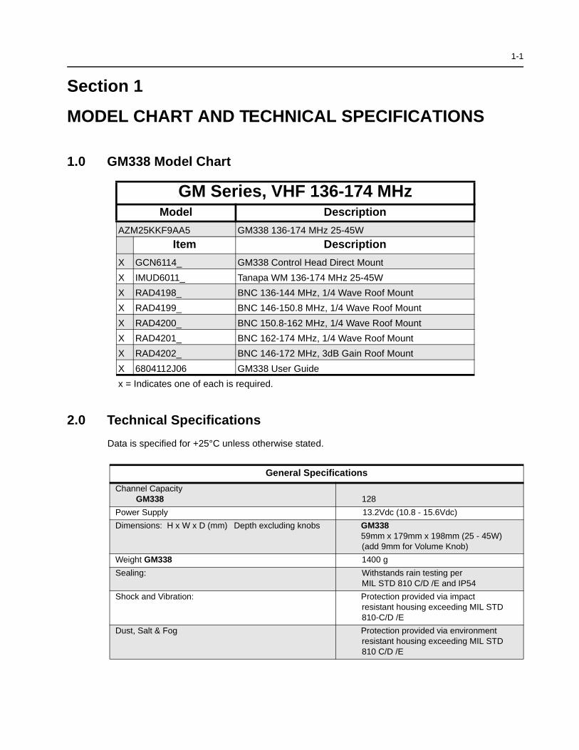
1-1
Section 1
MODEL CHART AND TECHNICAL SPECIFICATIONS
1.0 GM338 Model Chart
2.0 Technical Specifications
Data is specified for +25°C unless otherwise stated.
GM Series, VHF 136-174 MHzModel Description
AZM25KKF9AA5 GM338 136-174 MHz 25-45W
Item Description
X GCN6114_ GM338 Control Head Direct Mount
X IMUD6011_ Tanapa WM 136-174 MHz 25-45W
X RAD4198_ BNC 136-144 MHz, 1/4 Wave Roof Mount
X RAD4199_ BNC 146-150.8 MHz, 1/4 Wave Roof Mount
X RAD4200_ BNC 150.8-162 MHz, 1/4 Wave Roof Mount
X RAD4201_ BNC 162-174 MHz, 1/4 Wave Roof Mount
X RAD4202_ BNC 146-172 MHz, 3dB Gain Roof Mount
X 6804112J06 GM338 User Guide
x = Indicates one of each is required.
General Specifications
Channel CapacityGM338 128
Power Supply 13.2Vdc (10.8 - 15.6Vdc)
Dimensions: H x W x D (mm) Depth excluding knobs GM33859mm x 179mm x 198mm (25 - 45W)(add 9mm for Volume Knob)
Weight GM338 1400 g
Sealing: Withstands rain testing per MIL STD 810 C/D /E and IP54
Shock and Vibration: Protection provided via impactresistant housing exceeding MIL STD 810-C/D /E
Dust, Salt & Fog Protection provided via environment resistant housing exceeding MIL STD 810 C/D /E
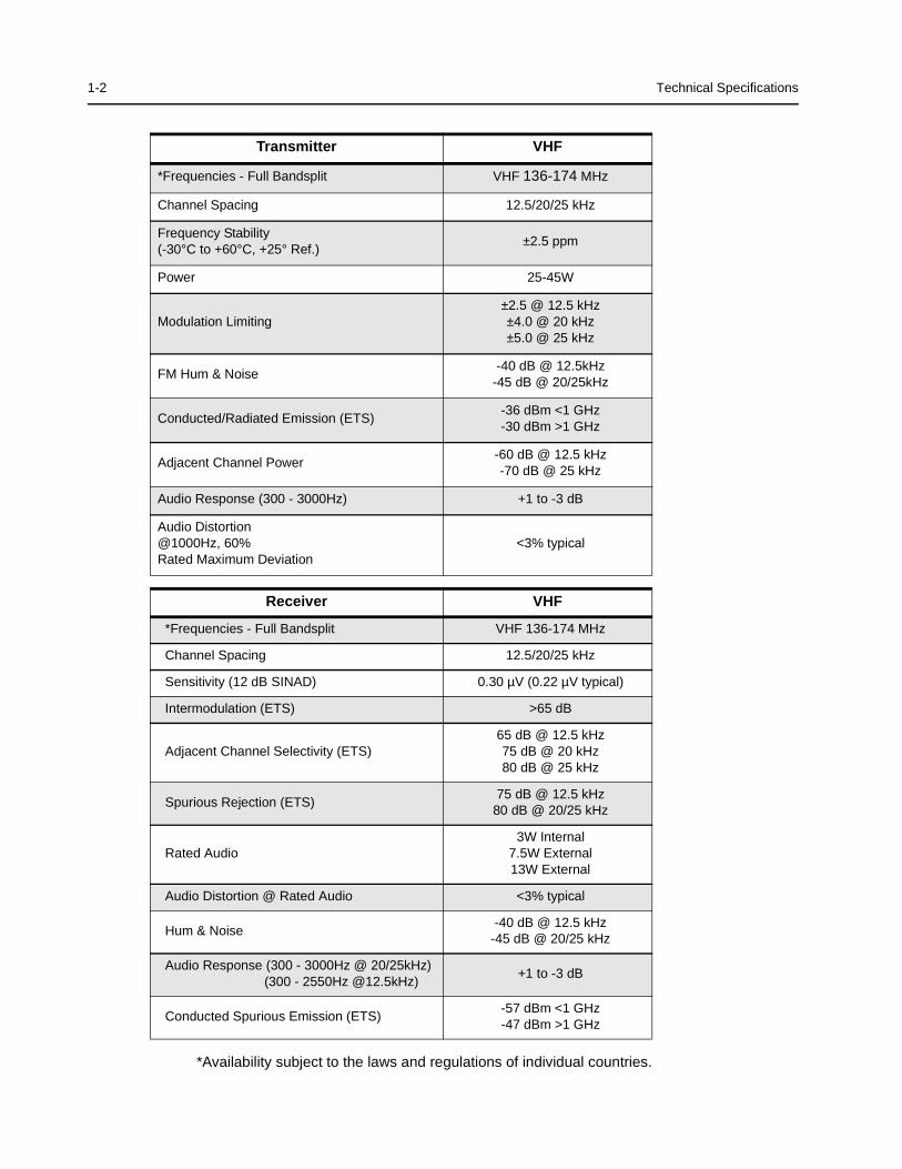
1-2 Technical Specifications
*Availability subject to the laws and regulations of individual countries.
Transmitter VHF
*Frequencies - Full Bandsplit VHF 136-174 MHz
Channel Spacing 12.5/20/25 kHz
Frequency Stability(-30°C to +60°C, +25° Ref.)
±2.5 ppm
Power 25-45W
Modulation Limiting±2.5 @ 12.5 kHz ±4.0 @ 20 kHz±5.0 @ 25 kHz
FM Hum & Noise-40 dB @ 12.5kHz
-45 dB @ 20/25kHz
Conducted/Radiated Emission (ETS)-36 dBm <1 GHz-30 dBm >1 GHz
Adjacent Channel Power-60 dB @ 12.5 kHz-70 dB @ 25 kHz
Audio Response (300 - 3000Hz) +1 to -3 dB
Audio Distortion@1000Hz, 60%Rated Maximum Deviation
<3% typical
Receiver VHF
*Frequencies - Full Bandsplit VHF 136-174 MHz
Channel Spacing 12.5/20/25 kHz
Sensitivity (12 dB SINAD) 0.30 µV (0.22 µV typical)
Intermodulation (ETS) >65 dB
Adjacent Channel Selectivity (ETS)65 dB @ 12.5 kHz 75 dB @ 20 kHz80 dB @ 25 kHz
Spurious Rejection (ETS)75 dB @ 12.5 kHz
80 dB @ 20/25 kHz
Rated Audio3W Internal
7.5W External13W External
Audio Distortion @ Rated Audio <3% typical
Hum & Noise-40 dB @ 12.5 kHz
-45 dB @ 20/25 kHz
Audio Response (300 - 3000Hz @ 20/25kHz)(300 - 2550Hz @12.5kHz)
+1 to -3 dB
Conducted Spurious Emission (ETS)-57 dBm <1 GHz-47 dBm >1 GHz
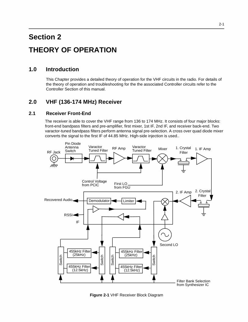
2-1
Section 2
THEORY OF OPERATION
1.0 Introduction
This Chapter provides a detailed theory of operation for the VHF circuits in the radio. For details of the theory of operation and troubleshooting for the the associated Controller circuits refer to the Controller Section of this manual.
2.0 VHF (136-174 MHz) Receiver
2.1 Receiver Front-End
The receiver is able to cover the VHF range from 136 to 174 MHz. It consists of four major blocks: front-end bandpass filters and pre-amplifier, first mixer, 1st IF, 2nd IF, and receiver back-end. Two varactor-tuned bandpass filters perform antenna signal pre-selection. A cross over quad diode mixer converts the signal to the first IF of 44.85 MHz. High-side injection is used..
Figure 2-1 VHF Receiver Block Diagram
Demodulator
1. Crystal Filter
MixerVaractor Tuned FilterRF AmpVaractor
Tuned Filter
Pin Diode Antenna SwitchRF Jack
Control Voltagefrom PCIC First LO
from FGU
Recovered Audio
RSSI
IF
Second LO
2. Crystal Filter
455kHz Filter(25kHz)
455kHz Filter(25kHz)
455kHz Filter(12.5kHz)
455kHz Filter(12.5kHz)
Sw
itch
Sw
itch
Sw
itch
Sw
itch
Limiter
1. IF Amp
2. IF Amp
Filter Bank Selectionfrom Synthesizer IC

2-2 VHF (136-174 MHz) Receiver
There are two 2-pole 44.85 MHz crystal filters in the 1st IF section and 2 pairs of 455 kHz ceramic filters in the 2nd IF section to provide the required adjacent channel selectivity. The correct pair of ceramic filters for 12.5 or 25kHz channel spacing is selected via control line BWSELECT. The second IF at 455 kHz is mixed, amplified and demodulated in the IF IC. The processing of the demodulated audio signal is performed by an audio processing IC located in the controller section.
2.2 Front-End Band-Pass Filters & Pre-Amplifier
The received signal from the radio’s antenna connector is first routed through the harmonic filter and antenna switch, which are part of the RF power amplifier circuits, before being applied to the receiver pre-selector filter (C3001, C3002, D3001 and associated components). The 2-pole pre-selector filter tuned by the dual varactor diode D3001 pre-selects the incoming signal (RXIN) from the antenna switch to reduce spurious effects to following stages. The tuning voltage (FECTRL_1) ranging from 2 volts to 8 volts is controlled by pin 20 of PCIC (U3501) in the Transmitter section. A dual hot carrier diode (D3003) limits any inband signal to 0 dBm to prevent damage to the pre-amplifier.
The RF pre-amplifier is a surface mount device (SMD) Q3001 with collector-base feedback to stabilize gain, impedance, and intermodulation. Transistor Q3002 compares the voltage drop across resistor R3002 with a fixed base voltage from divider R3011, R3000 and R3012, and adjusts the base current of Q3001 as necessary to maintain its collector current constant at approximately 15-20 mA. Operating voltage is from the regulated 9.3V supply (9V3). During transmit, 9.1 volts (K9V1) turns off both transistors Q3002 and Q3001. This protects the RF pre-amplifier from excessive dissipation during transmit mode. A following 3dB pad (R3006 – R3008 and R3016 – R3018) stabilizes the output impedance and intermodulation performance.
A second 2-pole varactor tuned bandpass filter provides additional filtering of the amplified signal. The dual varactor diode D3004 is controlled by the same signal FECTRL_1, which controls the pre-selector filter.
2.3 First Mixer and 1st Intermediate Frequency (IF)
The signal coming from the front-end is converted to the 1st IF frequency of 44.85 MHz using a cross over quad diode mixer (D3031). Its ports are matched for incoming RF signal conversion to the 44.85 MHz IF using high side injection. The high-side injection signal (RXINJ) from the frequency synthesizer circuit has a level of approximately +13 dBm and is injected via matching transformer T3002.
The IF output signal (IF) from transformer T3001 pin 2 is fed to the first 2- pole crystal filter FL3101. The filter output in turn is matched to IF amplifier Q3101 which is actively biased by a collector base feedback (R3101, R3106) to a current drain of approximately 5 mA drawn from the 5 volt supply. Its output impedance is matched to the second 2-pole crystal filter FL3102. The signal is further amplified by a preamplifier (Q3102) before going into pin 1 of IFIC (U3101).
A dual hot carrier diode (D3101) limits the filter output voltage swing to reduce overdrive effects at RF input levels above -27 dBm.
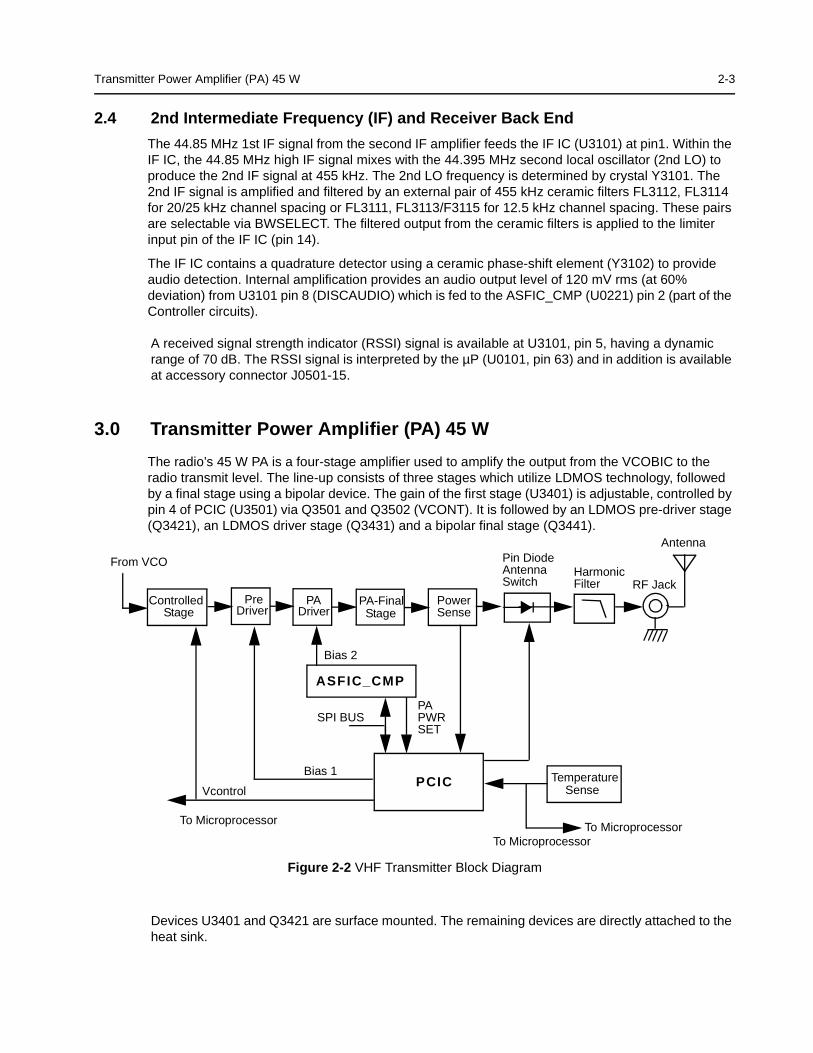
Transmitter Power Amplifier (PA) 45 W 2-3
2.4 2nd Intermediate Frequency (IF) and Receiver Back End
The 44.85 MHz 1st IF signal from the second IF amplifier feeds the IF IC (U3101) at pin1. Within the IF IC, the 44.85 MHz high IF signal mixes with the 44.395 MHz second local oscillator (2nd LO) to produce the 2nd IF signal at 455 kHz. The 2nd LO frequency is determined by crystal Y3101. The 2nd IF signal is amplified and filtered by an external pair of 455 kHz ceramic filters FL3112, FL3114 for 20/25 kHz channel spacing or FL3111, FL3113/F3115 for 12.5 kHz channel spacing. These pairs are selectable via BWSELECT. The filtered output from the ceramic filters is applied to the limiter input pin of the IF IC (pin 14).
The IF IC contains a quadrature detector using a ceramic phase-shift element (Y3102) to provide audio detection. Internal amplification provides an audio output level of 120 mV rms (at 60% deviation) from U3101 pin 8 (DISCAUDIO) which is fed to the ASFIC_CMP (U0221) pin 2 (part of the Controller circuits).
A received signal strength indicator (RSSI) signal is available at U3101, pin 5, having a dynamic range of 70 dB. The RSSI signal is interpreted by the µP (U0101, pin 63) and in addition is available at accessory connector J0501-15.
3.0 Transmitter Power Amplifier (PA) 45 W
The radio’s 45 W PA is a four-stage amplifier used to amplify the output from the VCOBIC to the radio transmit level. The line-up consists of three stages which utilize LDMOS technology, followed by a final stage using a bipolar device. The gain of the first stage (U3401) is adjustable, controlled by pin 4 of PCIC (U3501) via Q3501 and Q3502 (VCONT). It is followed by an LDMOS pre-driver stage (Q3421), an LDMOS driver stage (Q3431) and a bipolar final stage (Q3441).
Figure 2-2 VHF Transmitter Block Diagram
Devices U3401 and Q3421 are surface mounted. The remaining devices are directly attached to the heat sink.
Antenna
To Microprocessor
PCIC
Pin Diode Antenna Switch RF Jack
Harmonic Filter
PowerSense
PA-FinalStage
PADriver
From VCO
ControlledStage
Vcontrol
Bias 1
Bias 2
To Microprocessor
TemperatureSense
SPI BUS
ASFIC_CMP
PAPWRSET
To Microprocessor
PreDriver

2-4 Transmitter Power Amplifier (PA) 45 W
3.1 Power Controlled Stage
The first stage (U3401) is a 20 dB gain integrated circuit containing two LDMOS FET amplifier stages. It amplifies the RF signal from the VCO (TXINJ). The output power of stage U3401 is controlled by a dc voltage applied to pin 1 from the power control circuit (U3501 pin 4, with transistors Q3501 and Q3502 providing current gain and level-shifting). The control voltage simultaneously varies the bias of two FET stages within U3401. This biasing point determines the overall gain of U3401 and therefore its output drive level to Q3421, which in turn controls the output power of the PA.
In receive mode the voltage control line is at ground level and turns off Q3501-2, which in turn switches off the biasing voltage to U3401.
3.2 Pre Driver Stage
The next stage is an LDMOS device (Q3421) providing a gain of +13 dB. This device requires a positive gate bias and a quiescent current flow for proper operation. The voltage of the line PCIC_MOSBIAS_1 is set during transmit mode by the PCIC pin 24, and fed to the gate of Q3421 via the resistive network R3410, R3415, and R3416. The bias voltage is factory tuned.
3.3 Driver Stage
The following stage is an enhancement-mode N-Channel MOSFET device (Q3431) providing a gain of 10 dB. This device also requires a positive gate bias and a quiescent current flow for proper operation. The voltage of the line MOSBIAS_2 is set in transmit mode by the ASFIC and fed to the gate of Q3431 via the resistive network R3404, R3406, and R3431-5. This bias voltage is also tuned in the factory. If the transistor is replaced, the bias voltage must be tuned using the Customer Programming Software (CPS). Care must be taken not to damage the device by exceeding the maximum allowed bias voltage. The device’s drain current is drawn directly from the radio’s dc supply voltage input, PASUPVLTG, via L3431 and L3432.
3.4 Final Stage
The final stage uses bipolar device Q3441. The device’s collector current is also drawn from the radio’s dc supply voltage input. To maintain class C operation, the base is dc-grounded by a series inductor (L3441) and a bead (L3442). A matching network consisting of C3446-52, C3467, L3444-5, and two striplines, transforms the impedance to approximately 50 ohms and feeds the directional coupler.
3.5 Directional Coupler
The directional coupler is a microstrip printed circuit, which couples a small amount of the forward and reflected power delivered by Q3441. The coupled signals are rectified by D3451-2 and combined by R3463-4. The resulting dc voltage is proportional to RF output power and feeds the RFIN port of the PCIC (U3501, pin 1). The PCIC controls the gain of stage U3401 as necessary to hold this voltage constant, thus ensuring the forward power out of the radio to be held to a constant value.
An abnormally high reflected power level, such as may be caused by a damaged antenna, also causes the dc voltage applied to the PCIC to increase, and this will cause a reduction in the gain of U3401, reducing transmitter output power to prevent damage to the final device due to an improper load.
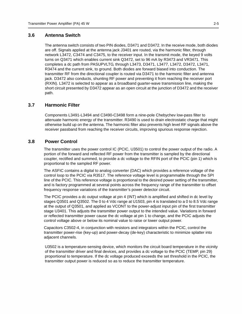
Transmitter Power Amplifier (PA) 45 W 2-5
3.6 Antenna Switch
The antenna switch consists of two PIN diodes, D3471 and D3472. In the receive mode, both diodes are off. Signals applied at the antenna jack J3401 are routed, via the harmonic filter, through network L3472, C3474 and C3475, to the receiver input. In the transmit mode, the keyed 9 volts turns on Q3471 which enables current sink Q3472, set to 96 mA by R3473 and VR3471. This completes a dc path from PASUPVLTG, through L3473, D3471, L3477, L3472, D3472, L3471, R3474 and the current sink, to ground. Both diodes are forward biased into conduction. The transmitter RF from the directional coupler is routed via D3471 to the harmonic filter and antenna jack. D3472 also conducts, shunting RF power and preventing it from reaching the receiver port (RXIN). L3472 is selected to appear as a broadband guarter-wave transmission line, making the short circuit presented by D3472 appear as an open circuit at the junction of D3472 and the receiver path.
3.7 Harmonic Filter
Components L3491-L3494 and C3490-C3498 form a nine-pole Chebychev low-pass filter to attenuate harmonic energy of the transmitter. R3490 is used to drain electrostatic charge that might otherwise build up on the antenna. The harmonic filter also prevents high level RF signals above the receiver passband from reaching the receiver circuits, improving spurious response rejection.
3.8 Power Control
The transmitter uses the power control IC (PCIC, U3501) to control the power output of the radio. A portion of the forward and reflected RF power from the transmitter is sampled by the directional coupler, rectified and summed, to provide a dc voltage to the RFIN port of the PCIC (pin 1) which is proportional to the sampled RF power.
The ASFIC contains a digital to analog converter (DAC) which provides a reference voltage of the control loop to the PCIC via R3517. The reference voltage level is programmable through the SPI line of the PCIC. This reference voltage is proportional to the desired power setting of the transmitter, and is factory programmed at several points across the frequency range of the transmitter to offset frequency response variations of the transmitter’s power detector circuit.
The PCIC provides a dc output voltage at pin 4 (INT) which is amplified and shifted in dc level by stages Q3501 and Q3502. The 0 to 4 Vdc range at U1503, pin 4 is translated to a 0 to 8.5 Vdc range at the output of Q3501, and applied as VCONT to the power-adjust input pin of the first transmitter stage U3401. This adjusts the transmitter power output to the intended value. Variations in forward or reflected transmitter power cause the dc voltage at pin 1 to change, and the PCIC adjusts the control voltage above or below its nominal value to raise or lower output power.
Capacitors C3502-4, in conjunction with resistors and integrators within the PCIC, control the transmitter power-rise (key-up) and power-decay (de-key) characteristic to minimize splatter into adjacent channels.
U3502 is a temperature-sensing device, which monitors the circuit board temperature in the vicinity of the transmitter driver and final devices, and provides a dc voltage to the PCIC (TEMP, pin 29) proportional to temperature. If the dc voltage produced exceeds the set threshold in the PCIC, the transmitter output power is reduced so as to reduce the transmitter temperature.
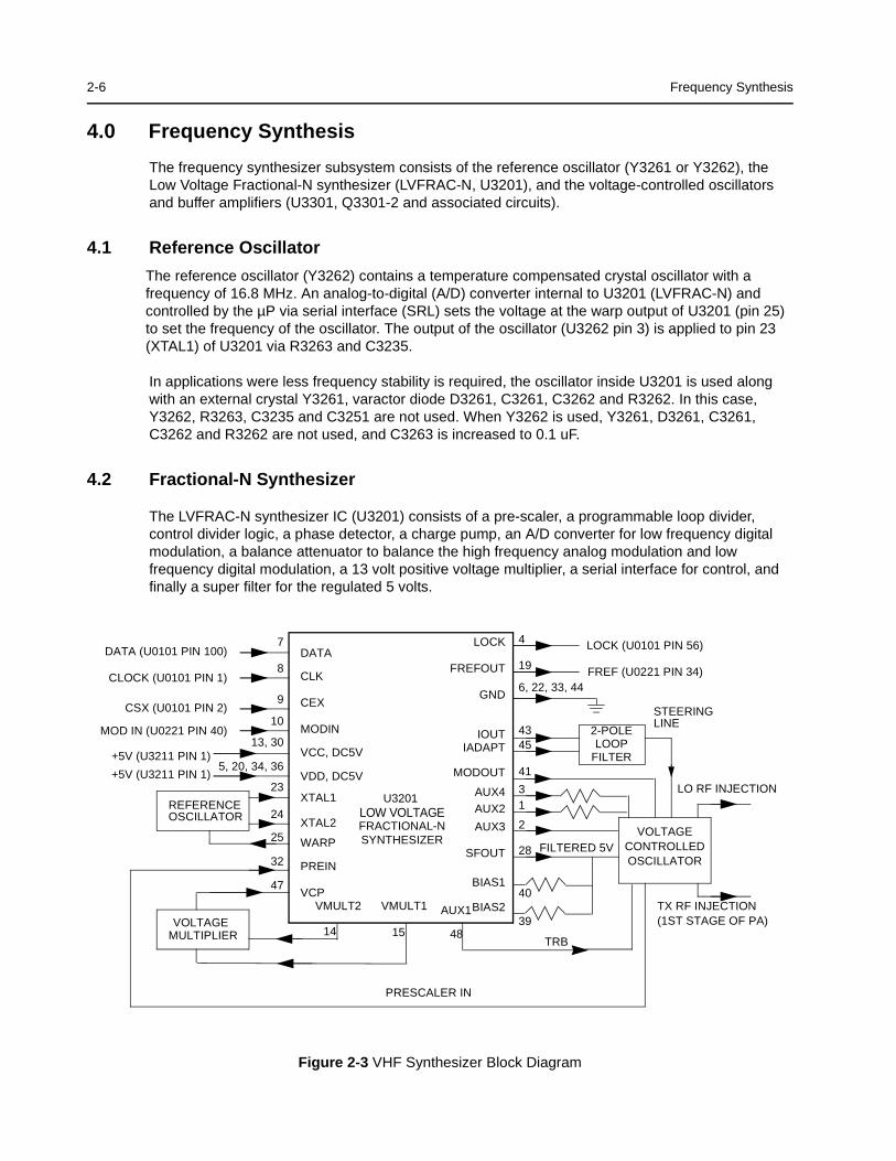
2-6 Frequency Synthesis
4.0 Frequency Synthesis
The frequency synthesizer subsystem consists of the reference oscillator (Y3261 or Y3262), the Low Voltage Fractional-N synthesizer (LVFRAC-N, U3201), and the voltage-controlled oscillators and buffer amplifiers (U3301, Q3301-2 and associated circuits).
4.1 Reference Oscillator
The reference oscillator (Y3262) contains a temperature compensated crystal oscillator with a frequency of 16.8 MHz. An analog-to-digital (A/D) converter internal to U3201 (LVFRAC-N) and controlled by the µP via serial interface (SRL) sets the voltage at the warp output of U3201 (pin 25) to set the frequency of the oscillator. The output of the oscillator (U3262 pin 3) is applied to pin 23 (XTAL1) of U3201 via R3263 and C3235.
In applications were less frequency stability is required, the oscillator inside U3201 is used along with an external crystal Y3261, varactor diode D3261, C3261, C3262 and R3262. In this case, Y3262, R3263, C3235 and C3251 are not used. When Y3262 is used, Y3261, D3261, C3261, C3262 and R3262 are not used, and C3263 is increased to 0.1 uF.
4.2 Fractional-N Synthesizer
The LVFRAC-N synthesizer IC (U3201) consists of a pre-scaler, a programmable loop divider, control divider logic, a phase detector, a charge pump, an A/D converter for low frequency digital modulation, a balance attenuator to balance the high frequency analog modulation and low frequency digital modulation, a 13 volt positive voltage multiplier, a serial interface for control, and finally a super filter for the regulated 5 volts.
Figure 2-3 VHF Synthesizer Block Diagram
DATA
CLK
CEX
MODIN
VCC, DC5V
XTAL1
XTAL2
WARP
PREIN
VCP
REFERENCEOSCILLATOR
VOLTAGEMULTIPLIER
DATA (U0101 PIN 100)
CLOCK (U0101 PIN 1)
CSX (U0101 PIN 2)
MOD IN (U0221 PIN 40)
+5V (U3211 PIN 1)
7
8
9
10
13, 30
23
24
25
32
47
VMULT2 VMULT1
BIAS1
SFOUT
AUX3
AUX4
IADAPTIOUT
GND
FREFOUT
LOCK 4
19
6, 22, 33, 44
4345
3
2
28
14 15
40
FILTERED 5V
STEERING
LOCK (U0101 PIN 56)
PRESCALER IN
FREF (U0221 PIN 34)
39BIAS2
41
48
5, 20, 34, 36+5V (U3211 PIN 1)
AUX1
VDD, DC5V MODOUT
U3201 LOW VOLTAGEFRACTIONAL-NSYNTHESIZER
AUX2
TRB
TX RF INJECTION(1ST STAGE OF PA)
LO RF INJECTION
VOLTAGE CONTROLLED OSCILLATOR
LINE2-POLELOOP
FILTER
1
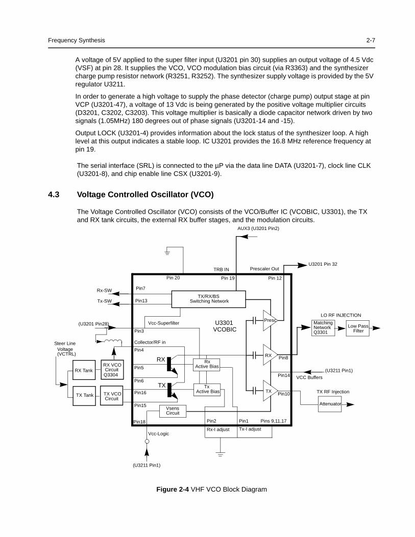
Frequency Synthesis 2-7
A voltage of 5V applied to the super filter input (U3201 pin 30) supplies an output voltage of 4.5 Vdc (VSF) at pin 28. It supplies the VCO, VCO modulation bias circuit (via R3363) and the synthesizer charge pump resistor network (R3251, R3252). The synthesizer supply voltage is provided by the 5V regulator U3211.
In order to generate a high voltage to supply the phase detector (charge pump) output stage at pin VCP (U3201-47), a voltage of 13 Vdc is being generated by the positive voltage multiplier circuits (D3201, C3202, C3203). This voltage multiplier is basically a diode capacitor network driven by two signals (1.05MHz) 180 degrees out of phase signals (U3201-14 and -15).
Output LOCK (U3201-4) provides information about the lock status of the synthesizer loop. A high level at this output indicates a stable loop. IC U3201 provides the 16.8 MHz reference frequency at pin 19.
The serial interface (SRL) is connected to the µP via the data line DATA (U3201-7), clock line CLK (U3201-8), and chip enable line CSX (U3201-9).
4.3 Voltage Controlled Oscillator (VCO)
The Voltage Controlled Oscillator (VCO) consists of the VCO/Buffer IC (VCOBIC, U3301), the TX and RX tank circuits, the external RX buffer stages, and the modulation circuits.
Figure 2-4 VHF VCO Block Diagram
Presc
RX
TX
MatchingNetwork Low Pass
Filter
Attenuator
Pin8
Pin14
Pin10
(U3211 Pin1)
VCC Buffers
TX RF Injection
U3201 Pin 32
AUX3 (U3201 Pin2)
Prescaler Out
Pin 12Pin 19Pin 20
TX/RX/BSSwitching Network
U3301VCOBIC
RxActive Bias
TxActive Bias
Pin2
Rx-I adjust
Pin1
Tx-I adjust
Pins 9,11,17Pin18
VsensCircuit
Pin15
Pin16
RX VCO Circuit
TX VCO Circuit
RX Tank
TX Tank
Pin7
Vcc-Superfilter
Collector/RF in
Pin4
Pin5
Pin6
RX
TX
(U3201 Pin28)
Rx-SW
Tx-SW
Vcc-Logic
(U3211 Pin1)
Steer Line Voltage (VCTRL)
Pin13
Pin3
TRB IN
LO RF INJECTION
Q3304
Q3301
2-8 Frequency Synthesis
The VCOBIC together with the Fractional-N synthesizer (U3201) generates the required frequencies in both the transmit and receive modes. The TRB line (U3301, pin 19) determines which tank circuits and internal buffers are to be enabled. A high level on TRB enables the TX tank and TX output (pin 10), and a low enables the RX tank and RX output (pin 8). A sample of the signal from the enabled RF output is routed from U3301, pin 12 (PRESC_OUT), via a low pass filter, to U3201, pin 32 (PREIN).
A steering line voltage (VCTRL) between 2.5 volts and 11 volts at varactor diode D3361 tune the full TX frequency range (TXINJ) from 136 MHz to 174 MHz, and varactor diode D3341 tunes the full RX frequency range (RXINJ) from 181 MHz to 219 MHz. The RX tank circuit uses a Hartley configuration for wider bandwidth. For the RX tank circuit, an external transistor Q3304 is used for better side-band noise.
The external RX buffers (Q3301 and Q3302) are enabled by a high at U3301, pin 7 (RX_SWITCH) via transistor switch Q3303. In the TX mode, the modulation signal (VCOMOD) from the LVFRAC-N synthesizer IC (U3201 pin 41) is applied to varactor diode D3362, which modulates the TX VCO frequency via capacitor C3362. Varactor D3362 is biased for linearity from the VSF.
4.4 Synthesizer Operation
The complete synthesizer subsystem consists of the low voltage FRAC-N (LVFRACN), reference oscillator (a crystal oscillator with temperature compensation), charge pump circuit, loop filter circuit and a dc supply. The output signal PRESC from the VCOBIC (U3301 pin 12) is fed to U3201 pin 32 (PREIN) via a low pass filter (C3318, L3318 and C3226) which attenuates harmonics and provides the correct level to close the synthesizer loop.
The pre-scaler in the synthesizer (U3201) is a dual modulus type with selectable divider ratios. The divider ratio of the pre-scaler is controlled by the loop divider, which in turn receives its inputs via the SRL. The output of the pre-scaler is applied to the loop divider. The output of the loop divider is connected to the phase detector, which compares the loop divider´s output signal with the reference signal. The reference signal is generated by dividing down the signal of reference oscillator Y3261 or Y3262.
The output signal of the phase detector is a pulsed dc signal which is routed to the charge pump. The charge pump outputs a current at U3201 pin 43 (IOUT). The loop filter (which consists of R3221-R3223 and C3221-C3224) transforms this current into a voltage that is applied to the varactor diodes (D3361 for transmit, D3341 for receive) to alter the output frequency of the appropriate VCO. The current can be set to a value fixed within the LVFRAC-N IC, or to a value determined by the currents flowing into BIAS 1 (U3201-40) or BIAS 2 (U3201-39). The currents are set by the value of R3251 and R3252 respectively. The selection of the three different bias sources is done by software programming.
To reduce synthesizer lock time when new frequency data has been loaded into the synthesizer, the magnitude of the loop current is increased by enabling the IADAPT pin (U3201-45) for a certain software programmable time (adapt mode). The adapt mode timer is started by a low to high transient of the CSX line. When the synthesizer is within the lock range, the current is determined only by the resistors connected to BIAS 1 and BIAS 2, or by the internal current source. A settled synthesizer loop is indicated by a high level signal at U3201-4 (LOCK).
The LOCK signal is routed to one of the µP´s ADC inputs (U0101-56). From the measured voltage, the µP determines whether LOCK is active.
To modulate the PLL, the two spot modulation method is utilized. Via U3201, pin 10 (MODIN), the audio signal is applied to both the A/D converter (low frequency path) as well as the balance attenuator (high frequency path). The A/D converter changes the low frequency analog modulating signal into a digital code that is applied to the loop divider, thereby causing the carrier to deviate. The balance attenuator is used to adjust the VCO’s deviation sensitivity to high frequency modulating signals. The output of the balance attenuator is present at the MODOUT port (U3201-41) and connected to the VCO modulation diode D3362 via R3364.
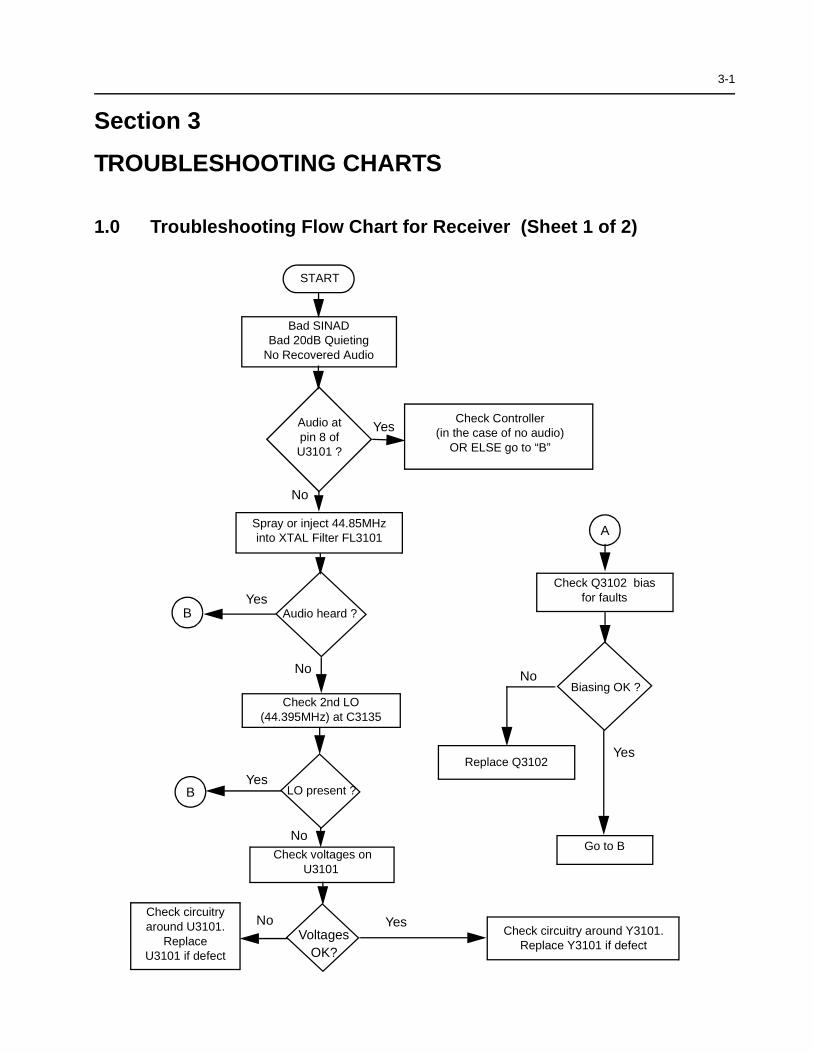
3-1
Section 3
TROUBLESHOOTING CHARTS
1.0 Troubleshooting Flow Chart for Receiver (Sheet 1 of 2)
Bad SINADBad 20dB Quieting
No Recovered Audio
START
Audio at pin 8 of U3101 ?
Check Controller(in the case of no audio)
OR ELSE go to “B”
Yes
No
Spray or inject 44.85MHz into XTAL Filter FL3101
Audio heard ?BYes
No
Check 2nd LO (44.395MHz) at C3135
LO present ?BYes
Check voltages on U3101
Biasing OK ?
No
No
A
Yes
Check Q3102 bias for faults
Replace Q3102
Go to B
Yes
No
Check circuitry around U3101.
Replace U3101 if defect
Check circuitry around Y3101. Replace Y3101 if defect
Voltages OK?

3-2 Troubleshooting Flow Chart for Receiver
1.1 Troubleshooting Flow Chart for Receiver (Sheet 2 of 2)
IF Signal at C3035?
No
RF Signal at T3001?
RF Signal at C3012?
No
RF Signal at C3008?
No
RF Signal at C3474?
No or
Check Harmonic Filter J3401 and
Antenna Switch D3471,D3472,L3472
Check filter between C3474 & C3008. Check tuning
voltage at R3019
Inject RF into J3401
Is tuning voltage OK?
No
Yes
Check RF amp (Q3001) Stage
Check filter between C3012 & T3001
Yes
Check T3001, T3002, D3031, R3030-R3034,
L3032, C3034 and C3035
Yes
1st LO level OK?
Locked?
Yes
Check FGU
Yes
Trace IF signal from C3035 to Q3101.
Check for bad XTAL filter
No
YesIF signal at Q3102
collector?
Before replacing U3101, check
U3101 voltages
Yes
Check for 5VDC
Is 9V3 present?
Check Supply Voltage circuitry. Check Q0681,
U3211 and U0641
No
No
No
Check U3501
Check varactor filter
No
Yes
Yes
Yes
A
A
B
weak RF
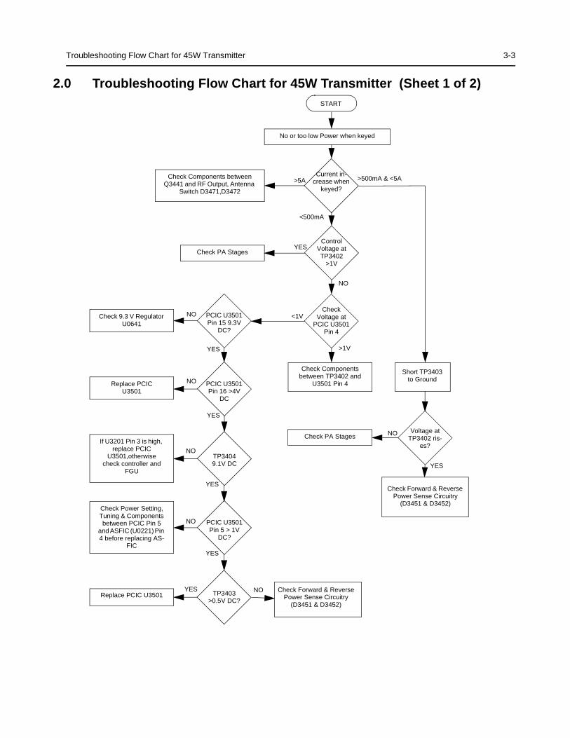
Troubleshooting Flow Chart for 45W Transmitter 3-3
2.0 Troubleshooting Flow Chart for 45W Transmitter (Sheet 1 of 2)
Current in-crease when
keyed?
NO
YES
START
No or too low Power when keyed
Check Components between Q3441 and RF Output, Antenna
Switch D3471,D3472
>500mA & <5A>5A
<500mA
Check PA Stages
Control Voltage at TP3402
>1V
>1V
<1VCheck
Voltage at PCIC U3501
Pin 4
Check Components between TP3402 and
U3501 Pin 4
Short TP3403to Ground
NO
YES
Voltage at TP3402 ris-
es?Check PA Stages NO
YES
PCIC U3501 Pin 15 9.3V
DC?
Check 9.3 V Regulator U0641
NO
YES
PCIC U3501 Pin 16 >4V
DC
Replace PCICU3501
NO
YES
TP3404 9.1V DC
If U3201 Pin 3 is high, replace PCIC
U3501,otherwise check controller and
FGU
YES NOTP3403 >0.5V DC?
Replace PCIC U3501Check Forward & Reverse
Power Sense Circuitry (D3451 & D3452)
Check Forward & Reverse Power Sense Circuitry
(D3451 & D3452)
NO
YES
PCIC U3501 Pin 5 > 1V
DC?
Check Power Setting, Tuning & Components between PCIC Pin 5
and ASFIC (U0221) Pin 4 before replacing AS-
FIC
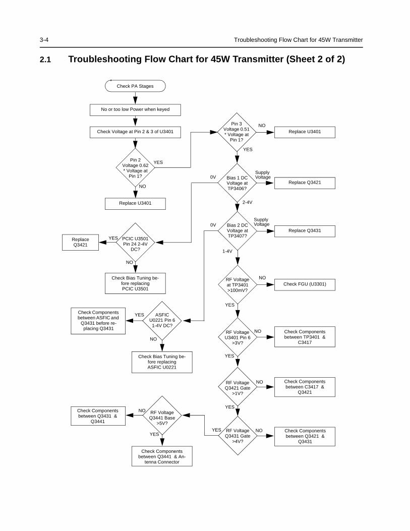
3-4 Troubleshooting Flow Chart for 45W Transmitter
2.1 Troubleshooting Flow Chart for 45W Transmitter (Sheet 2 of 2)
Pin 2 Voltage 0.62 * Voltage at
Pin 1?
NO
YES
Check PA Stages
No or too low Power when keyed
NO
YES
Replace U3401
Pin 3 Voltage 0.51 * Voltage at
Pin 1?
2-4V
Supply0V Bias 1 DC
Voltage at TP3406?
NO
YES PCIC U3501 Pin 24 2-4V
DC?
Check Bias Tuning be-fore replacing PCIC U3501
Check Voltage at Pin 2 & 3 of U3401
Replace U3401
Replace Q3421
NO
0V
1-4V
Bias 2 DC Voltage at TP3407?
YES
RF Voltage at TP3401 >100mV?
YES
RF Voltage U3401 Pin 6
>3V?
Replace Q3421
Supply
Replace Q3431
Check FGU (U3301)
NO Check Components between TP3401 &
C3417NO
YES ASFIC U0221 Pin 6
1-4V DC?
Check Bias Tuning be-fore replacing ASFIC U0221
Check Components between ASFIC and
Q3431 before re-placing Q3431
YES
RF Voltage Q3421 Gate
>1V?
NO Check Components between C3417 &
Q3421
YES RF Voltage Q3431 Gate
>4V?
NO Check Components between Q3421 &
Q3431
YES
RF Voltage Q3441 Base
>5V?
Check Components between Q3431 &
Q3441
NO
Check Components between Q3441 & An-
tenna Connector
Voltage
Voltage
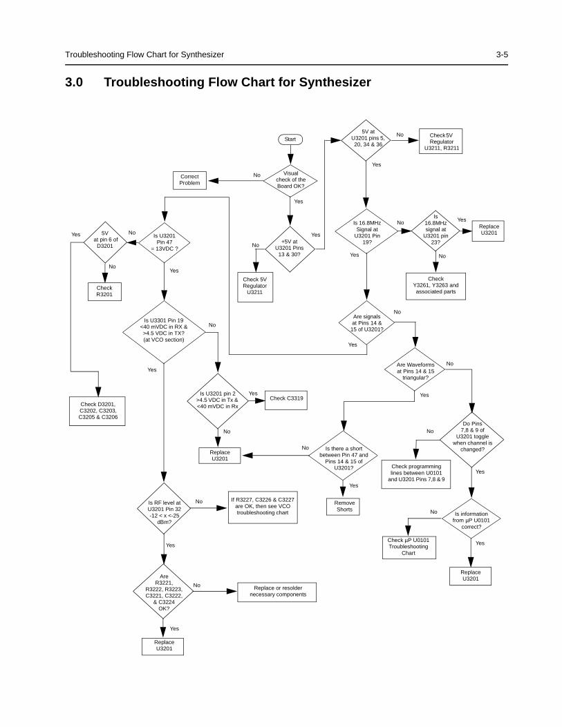
Troubleshooting Flow Chart for Synthesizer 3-5
3.0 Troubleshooting Flow Chart for Synthesizer
+5V at U3201 Pins
13 & 30?
5V at pin 6 of
D3201
Is informationfrom µP U0101
correct?
Is U3201 Pin 47
= 13VDC ?
Is U3301 Pin 19<40 mVDC in RX &>4.5 VDC in TX? (at VCO section)
Start
Visual check of the Board OK?
CorrectProblem
Check 5VRegulator
U3211
Is 16.8MHzSignal at
U3201 Pin 19?
CheckY3261, Y3263 and associated parts
Are signalsat Pins 14 &
15 of U3201?
Check R3201
Check C3319Is U3201 pin 2
>4.5 VDC in Tx & <40 mVDC in Rx
Replace U3201
RemoveShorts
Is there a shortbetween Pin 47 and
Pins 14 & 15 ofU3201?
Replace or resoldernecessary components
Is RF level atU3201 Pin 32 -12 < x <-25
dBm?
Are R3221,
R3222, R3223, C3221, C3222,
& C3224 OK?
Replace U3201
If R3227, C3226 & C3227are OK, then see VCOtroubleshooting chart
Are Waveformsat Pins 14 & 15
triangular?
Do Pins 7,8 & 9 of
U3201 togglewhen channel is
changed?
Check programminglines between U0101
and U3201 Pins 7,8 & 9
Replace U3201
Check µP U0101Troubleshooting
Chart
No
Yes
No
Yes
No
Yes
No
No
No
Yes
Yes
No
Yes
Yes
No
Yes
Yes
Yes
No
No
No
No
Yes
No
Yes
Yes
Check D3201, C3202, C3203, C3205 & C3206
5V at U3201 pins 5, 20, 34 & 36
Check 5V Regulator
U3211, R3211
Is 16.8MHz signal at
U3201 pin 23?
Replace U3201
Yes
No
No
Yes
No
Yes

3-6 Troubleshooting Flow Chart for VCO
4.0 Troubleshooting Flow Chart for VCO
Are Q3301Base at 0.7V
Collector at 4.5V Emitter at 110mV
Are Q3304Base at 2.4V
Collector at 4.5V Emitter at 1.7V
Are U3301 Pins13 at 4.4V15 at 1.1V10 at 4.5V16 at 1.9V
Low or no RF Signalat TP3001
Visual checkof board
OK?
35mV DC atU3301 Pin 19
NO
YES
at base of Q3301
NO
NO
NO
NO
NO
YES
YES
YES
YES
YES
Low or no RF Signalat input to PA
5V DC at U3301Pin 14 & 18 OK ?
4.8V DC atU3301 Pin 19
Is RF available at TP3401
YES
YES
YES
YES
YES
NO
NO
NO
NO
NO
Audio =180mVrmsat “-” side of
D3362
2.5VDCat D3362
If C3362 and R3363 are OK, then replace D3362
Replace R3363
Replace R3364
NO
NO
YES
YES
If R3402 and C3315 are OK,replace U3301
TX VCORX VCO
CorrectProblem
Visual checkof board
OK?
Make sure U3211 is working correctly and runner
between U3211 Pin 1 and U3301 Pin 14 & 18 is OK
Check runner between U3201 Pin 2
and U3301 Pin 19
Is RF available If all parts from U3301 Pin 8to Base of Q3301 are OK,
replace U3301
If all parts associated with the pins are OK,
replace Q3301
Check parts between T3001 and Q3301 Power OK but
no modulation
If all parts from TP3401 of U3401 Pin 16 are OK,
replace U3401
If all parts associated
with the pins are OK,
replace U3301
4.5V DC atU3301 Pin 3 OK?
YES
NO 4.5V DC atU3301 Pin 3 OK?
YES
NOMake sure Synthesizer is
working correctly and runner between U3201 Pin 28 and
U4301 Pin 3 is OK
5V DC at U3301Pin 14 & 18 OK ?
OK? OK?
If all parts associated with the pins are OK,
replace Q3301
4-1
Section 4
VHF PCB/SCHEMATICS/PARTS LIST
1.0 Allocation of Schematics and Circuit Boards
1.1 Controller Circuits
The VHF circuits are contained on the Printed Circuit Board (PCB) which also contains the Controller circuits. This Chapter shows the schematics for the VHF circuits only, refer to the Controller section for details of the related Controller circuits . The PCB component layouts and the Parts Lists in this Chapter show both the Controller and VHF circuit components. The VHF schematics and the related PCB and parts list are shown in the tables below.
Table 4-1 VHF 25-45W Diagrams and Parts Lists
PCB :8486140B13 Main Board Top Side8486140B13 Main Board Bottom Side
Page 4-3Page 4-4
SCHEMATICSPower Amplifier 25 - 45WFRACNVoltage Controlled OscillatorReceiver Front EndIF
Page 4-5Page 4-6Page 4-7Page 4-8Page 4-9
Parts List8486140B13 Page 4-10

4-2 Allocation of Schematics and Circuit Boards
THIS PAGE INTENTIONALLY LEFT BLANK
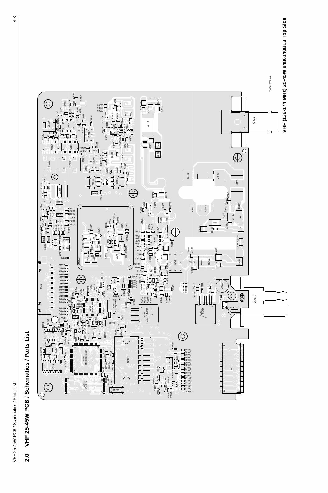
VH
F 2
5-45
W P
CB
/ S
chem
atic
s / P
arts
Lis
t4-
3
2.0
VH
F 2
5-45
W P
CB
/ S
chem
atic
s / P
arts
Lis
t
C01
01C
0102
C01
04
C01
06
C01
07
C01
08
C01
31
C01
32
C02
11
C02
12
C0221
C0222
C02
23C02
24
C02
25
C02
26
C02
27
C0228
C02
31
C02
32
C02
33
C02
34C02
35
C02
36
C0237
C02
41 C02
42
C02
43
C02
44
C02
45
C02
46
C02
51
C02
52
C02
53
C02
56
C0261
C02
62
C0421
C0441
C0442
C0443
C0445C0446
C0447
C0448C0449C0470
C0471
C0472
C0473C0474
C0476
C0477
C0478
C0482C0483
C04
84
C04
86C04
87
C0488
C0490
C0493
C0494
C0495
C04
96
C0501C0502C0503C0504C0505C0506C0508
C0509
C0510
C0511
C0512
C0513C0514
C0515C0516
C0517C0518
C05
42
C06
01
C06
03
C06
12
C06
51
C0652
C06
54C
0655
C06
81
C30
02
C3004C3005C3006
C30
07
C30
08
C3009
C30
10
C30
11C
3012
C30
13C
3014
C3015C3016C3017
C30
18
C30
19C
3020
C30
21
C30
27C
3028
C30
32
C30
34
C31
00
C31
01
C31
02
C3103
C31
14
C31
15
C31
24
C31
31
C31
32
C31
33
C31
34
C31
35C
3136
C31
37
C31
39
C31
40
C31
41
C31
42
C31
43
C31
45 C31
48
C32
10
C32
11
C32
13 C3214
C3215
C32
21C
3222
C3223
C32
24
C32
26
C32
27C
3229
C32
31
C3232
C3233
C3234
C32
40
C32
42
C32
43C
3244
C32
45
C32
46
C32
47
C3252C3253 C3254
C32
55
C33
24
C33
36
C33
37
C33
41
C33
42
C33
44
C33
45
C33
46C
3347
C33
57C
3361 C33
62
C3363C3364
C33
65
C3400
C3401
C34
02
C3403
C3404
C34
07
C3408
C34
09C
3410
C34
11C
3412
C34
13C
3414
C34
17
C34
18
C34
20
C34
22 C34
23
C3425
C3426
C34
28
C34
34
C34
35
C34
36
C34
37
C34
38C
3439
C34
40
C34
41
C34
43
C34
44
C34
45
C34
46
C34
47
C34
55
C34
56
C34
58
C34
72
C34
73C
3474
C34
75
C34
78
C34
91C
3492
C35
01
C35
06
C35
07
C35
08
C35
09
C35
10
D02
01
D06
51
D30
01
D30
03
D30
04
D30
31
D32
21
D3341
D33
61
D33
62
D34
71
D34
72
23 4
56
FL3
101
23 4
56
FL3
102
432
FL3
112
FL3
114
181
J045
1
201110
J050
1
J060
1
23
J340
1
L048
1
L048
2
L3002
L303
1
L303
2
L3034
L310
0
L3101
L312
4
L320
1L3
232
L333
3
L334
1
L334
3L3
344
L334
6
L336
1
L336
2
L336
3
L336
4
L340
1
L340
3
L341
1L3
412
L341
3L3
414
L342
1
L3422
L343
1
L3432
L343
3
L344
3L3
444
L347
1
L347
2
L347
4
L347
7
Q01
10
Q01
77Q
0181
Q01
85
Q06
81Q
3001
Q30
21
Q32
21
Q33
04
5
2 6
813
7
4Q
3421
Q34
71
Q35
01Q
350
2
R01
01
R01
02
R01
03
R01
04
R01
05R
0106
R01
08
R01
10
R01
14
R01
15
R01
16
R01
31R
0132
R01
70
R01
81
R01
82
R01
85
R01
86
R02
11
R02
12
R02
20
R02
21R
0222 R0223
R02
24
R02
25
R02
26
R02
27
R02
28R
0229
R02
41
R02
42
R02
51
R02
52
R02
53
R02
54 R02
55
R02
56
R02
57
R02
61R
0262
R0268
R02
69
R0442
R05
10
R05
33
R05
35R
0538
R05
39
R06
11R
0612
R06
51
R06
52
R06
81
R0682
R30
01R
3002
R30
03
R30
04
R30
09
R30
13
R30
14
R30
15R
3016
R30
24
R30
25R
3026
R30
27
R30
28
R30
31
R3101
R31
06R
3111
R31
17
R31
23
R31
24
R31
30 R31
32
R31
35
R31
42
R31
44
R31
45
R32
11
R32
21R
3222
R32
23
R32
24
R32
25
R32
27
R32
42
R3251
R3252
R33
35
R33
36
R33
41
R33
42
R33
61
R33
62
R33
63R
3364
R3400
R3401
R3402
R3403
R34
04
R34
05
R34
06
R3408
R34
09
R3410
R34
11
R34
13
R34
15
R34
16R
3418
R34
19R
3424
R34
25
R34
31
R34
32
R34
58R
3461
R34
71
R35
05
R35
06
R35
07
R35
08
R35
12
R35
13
R35
14 R35
15
R35
16
SH
3301
3 461
2T
3001
346 1
2T
3002
1 765126
321716
1
871
14
U02
11
137 25
13
161 8
9
U02
51
9
U02
71
1
6
5
1
6
5
3
2
1
11
120
10
U31
01
87 1
14U31
11
87 1
14U31
15
U32
11
116
89
U34
01
U35
02
VR
0501
VR
0503
VR
0505
VR
0510
234 Y0131
2Y
3102
1
1
1
1
1
1
U01
21F
lash
rom
U01
01M
icro
proc
esso
r
U02
21A
SF
IC C
MP
U06
515V
Reg
ulat
or
U06
419,
6V R
egul
ator
U06
11B
+ S
witc
h
ZW
G01
3058
9-O
VH
F (
136-
174
MH
z) 2
5-45
W 8
4861
40B
13 T
op
Sid
e
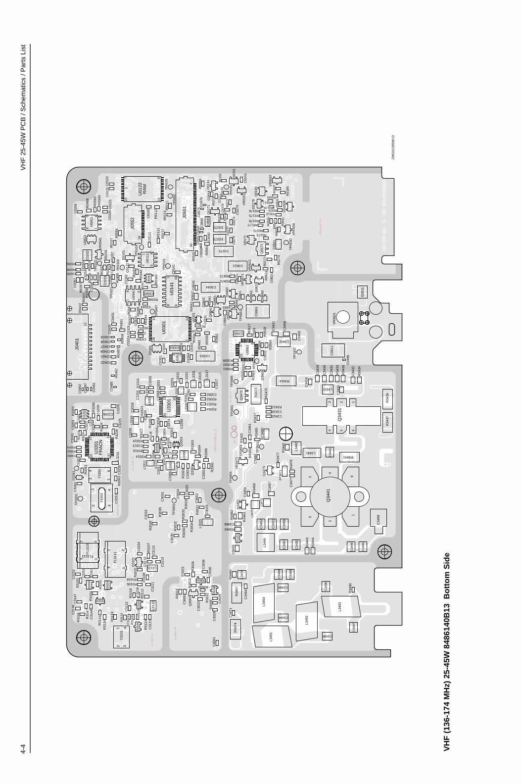
4-4
VH
F 2
5-45
W P
CB
/ S
chem
atic
s / P
arts
Lis
t
C01
03
C01
05
C01
11
C01
12
C01
21C
0122
C01
23
C01
41
C01
51
C02
01
C02
02
C02
03C
0204
C0205
C02
54
C02
55
C02
65
C02
66
C02
67
C02
71
C02
72
C02
73
C02
74
C0275
C02
76
C02
77
C0301
C03
02
C03
03
C0304
C0305
C03
24C
0325
C03
31
C0341
C03
42
C03
43
C0344
C03
51
C03
52
C0353
C03
54
C0422
C0423
C0426
C0427C0428C0429 C
0430
C04
31C
0485
C04
91
C04
92
C04
97
C04
99
C05
41
C05
54
C05
58C
0559
C05
60C
0575
C05
76C
0591
C05
92C
0593
C06
11
C06
21
C0622
C06
41
C0644
C06
45
C06
61
C06
62
C0663
C06
71
C30
00
C30
01
C30
03C
3022
C30
23
C30
24
C30
25
C30
26
C30
29C
3030
C30
31
C30
33
C30
35
C30
36
C31
04
C31
10C
3111
C31
12
C31
13
C31
16
C31
21
C31
22C
3123C
3144C31
46C
3147
C31
51
C31
52C
3202
C32
03
C32
05
C3206
C32
07C
3208
C32
09
C32
25
C32
28
C32
35
C32
41
C32
51
C32
61
C3262
C32
63
C33
01
C33
02
C33
03
C33
04
C33
05
C33
06
C3311
C33
12
C3313
C33
14
C33
15
C33
16
C33
17
C33
18
C33
19
C33
31
C33
32
C33
33C
3334
C33
35
C33
48
C33
51 C3352
C33
55
C33
56
C34
05
C34
06
C3415C3416
C34
21
C34
24
C34
29
C34
30
C34
31
C34
32
C34
33
C34
42
C34
48
C34
49
C34
50
C34
51
C34
52
C34
53 C34
57
C34
59
C34
60
C34
61C
3464
C34
65
C3466
C34
67C
3468
C34
71
C34
77C
3488
C34
89
C3490
C3494
C34
96
C34
97
C3498
C35
02
C35
03
C35
04
C3505
D01
01
D01
51
D01
79
D03
01
D06
21
D06
60
D06
61
D30
00
D3011
D31
01
D32
01
D32
61
D34
51D
3452
D34
55
E0271
E0272
E06
31
F04
01
43 2
FL3
111FL3113
43 2
FL3
115
12
J040
1
140
J055
1
118
J055
2
L302
5
L3111
L311
2
L323
1
L330
1
L330
2
L331
1
L331
7
L331
8
L333
1
L333
2
L334
5L335
1
L3402
L3423
L3441L344
2
L344
5L3
473
L347
5
L347
6
L349
1
L349
2
L349
3
L349
4
Q01
51
Q01
71
Q01
73
Q01
83
Q02
71Q
0641
Q06
61 Q06
62Q
0663
Q30
02
Q31
01
Q31
02
Q3141
Q31
51
Q31
52
Q33
01
Q33
02 43
Q33
03
6543 2 1
Q34
31
6
5
4
3
2
1
Q34
41
Q34
72
Q34
73
R01
07
R01
11R
0112
R01
13R
0117
R01
21
R01
51R
0152
R0171R0172
R01
73
R01
74
R0175R0176
R0177R0178
R0179
R0183 R01
84
R02
01R
0202
R02
03
R02
04 R02
05
R02
06
R02
07
R0208
R0265
R02
66R02
67
R02
73
R02
74
R02
75R
0276
R03
23
R0324
R03
31
R0332
R0333
R03
35
R03
41
R03
42
R03
43
R03
44
R03
45
R0346
R03
47
R04
01
R04
07R
0408
R04
09
R04
12R
0441
R04
67
R04
68
R04
81 R04
82
R0511
R0512
R05
25
R0529
R05
30
R05
31R
0537
R05
41
R05
42
R05
43
R05
55
R05
56
R05
91
R05
92
R05
93
R06
21
R06
41R06
42R
0643
R06
61R
0662
R0671
R0672
R3000
R30
06
R30
10
R30
11
R30
12
R30
18
R30
19
R30
21
R30
23R
3030R
3032
R30
33
R30
34
R30
35
R30
36
R31
02
R3104R3105
R31
07R
3108
R31
12
R31
13
R31
14
R31
15
R31
16R
3118
R31
33
R31
34R31
41
R31
46
R31
47R
3151
R31
52
R31
53
R31
54
R32
01
R32
03R
3204
R32
06
R32
26R32
28
R3241
R32
61
R3262
R32
63 R33
01 R33
02
R33
03
R33
04
R33
05
R33
06R
3307
R33
08R3311
R33
12
R33
13
R3314
R3315
R33
16
R33
17
R33
18
R3319
R33
21
R33
23
R33
31
R33
43
R33
51 R3352
R3353
R3354
R33
55R33
56
R3412
R3414
R34
17
R34
33
R34
34
R34
35
R34
36R
3437
R3441
R34
42
R34
43
R34
44
R34
53
R34
55
R34
57
R34
59
R34
60R
3462
R34
63
R3464R
3465
R34
73
R34
74
R34
75
R34
76R34
77
R34
90
R3501R3502
R35
03
R35
04
R3509
R35
10R
3511
R35
17
R35
18R
T34
60
RT
3471
TP
0101
TP
0102
TP
0103
TP
0104
TP
0151
TP
0221
TP
0222
TP
0492
TP
0497
TP
0530
TP
0661
TP
3001T
P32
01
TP
3401
TP
3402
TP
3403
TP
3404
TP
3406
TP
3407
TP
3501
14 5
8U
0111
22 2187
1
1618 9
U01
41
2815 14
1
U03
01
U03
31
1
4
58
U03
41
U03
42
458 U03
51
145
8U
0652
U06
53
13725
13
11
120
10
U33
01
1
17
9
25
U35
01V
R01
51
VR
0504
VR
0509
VR
0537
VR
0541
VR
0601
VR
0621
VR
0671
VR
3471
432
Y31
01
643 1
Y32
61
2 34
Y32
63
1
1
1
11
5
U01
22R
AM
U32
01F
RA
CN
1
8486140B13_C C
00
CNTL-REV-T6
PA-REV-C
VCO-REV-T3
IF-REV-T5
FE-REV-T4
FRACN-T6
ZW
G01
3059
0-O
VH
F (
136-
174
MH
z) 2
5-45
W 8
4861
40B
13 B
ott
om
Sid
e
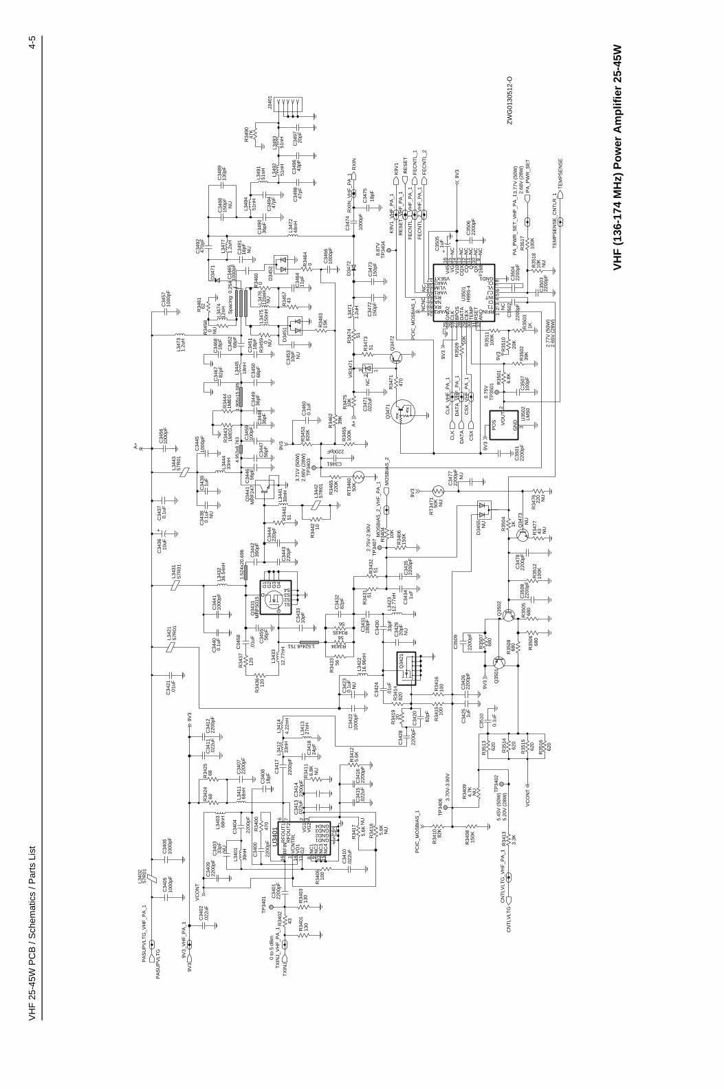
VH
F 2
5-45
W P
CB
/ S
chem
atic
s / P
arts
Lis
t4-
5
4.95
3x8.
763
0 to
5 d
Bm
J340
1
1.524x8.751
Spa
cing
: 0.2
54
2.68
V (
28W
)
0.75
V
3.77
V (
50W
)
8.87
V
2.77
V (
50W
)2.
65V
(28
W)
5.20
V (
28W
)5.
45V
(50
W)
3.70
V-3
.90V
2.75
V-2
.90V
2.66
V (
28W
)3.
71V
(50
W)
1.52
4x20
.696
1.90
5x15
.685
C34
8913
0pF
.022
uFC
3471
C34
09
390p
FC
3442
2200
pF
NU
RT
3471
50K N
U
R34
7622
0
Q34
71
NU
R34
59 0
NU
R34
094.
7K
DA
TA
R35
0910
K
C34
9247
0pF
R34
4151
150K
R34
08
C34
2920
pF
C34
5118
pF
NU
C34
30
33pF
1000
pFC
3466
5.6K
R34
17
NU
11pF
C34
64
D34
51
C34
6818
pF
82K
5.6K
R34
10
220p
FC
3444
NU
R34
18
620
R34
53
R35
15
0.1u
F82
0K
2200pF
C34
60
C3461
R35
1210
0K
62R
3461
D34
52
120
R34
37
10pF
56pF
C34
33
1.2u
HL3
477
C34
47
L341
168
nH
2200
pFC
3414
51nH
C34
94
NU
Q34
73
Q34
41M
RF
247
2200
pFC
3478
L349
1
47pF
Q34
72
2200
pFC
3407
470
R34
00
.022
uFC
3411
680
R35
07
R35
1810
K
1ME
G
NU
R34
431M
EG
R34
44
C34
341u
F
R34
55
G4
S1S2S3S4
100K
D
G
G1
G2
G3
180p
F
MR
F50
15Q
3431
C34
31
12.7
7nH
43R34
57
DA
TA
_VH
F_P
A_1
L343
3
TP
3402
68pF
C34
50
L347
31.
2uH
1000
pFC
3457
R34
32
30nH
L344
1
57R
01
51
1000
pF
L342
1
0.1u
FC
3422
L342
216
.96n
H
NU
C34
23
L347
5
L344
357
R01
150n
H
C34
380.
1uF
C34
391u
FN
U
C34
9116
pF
L347
2
NU
RX
IN
48nH
9V3_
VH
F_P
A_1
C34
7215
0pF
C34
77
10K
R34
75
NU
2200
pF
C35
10
C34
4656
pF
0.1u
F
RE
SE
T
D34
71
D34
72
150p
FC
3473
150p
F
R34
74
NU
C34
88
51
Q34
21
220p
FC
3443
R34
1482
0
MO
SB
IAS
_2_V
HF
_PA
_1
20K
R35
10
CS
X
NU
120n
HL3
476
PA
_PW
R_S
ET
_VH
F_P
A_1
CLK
_VH
F_P
A_1
PA
SU
PV
LTG
_VH
F_P
A_1
10R
3442
L340
257
R01
R35
1110
0K
R34
01
68R34
25
130
47pF
TX
INJ
9V3
Q35
01
C34
98
C35
09
K9V
1
2200
pF
L340
368
nH
NU
10pF
C34
53
2200
pFC
3416
56
R3435
L341
4
L341
327
nH
4.22
nH
C35
02
2200
pF
1uF
C35
05R3434
56
R35
02
6.8K
R35
01
39K
1.2u
H
36pF
L347
1
36pF
C34
49
R34
31
C34
48
23 1
51
.022
uF
VR
3471
R34
73
C34
02
51
TE
MP
SE
NS
E
K9V
1_V
HF
_PA
_1
CS
X_V
HF
_PA
_1
CN
TLV
LTG
_VH
F_P
A_1
R34
13
3.3K
51nH
L349
3
TP
3404
L349
2
51nH
C34
10.0
22uF
R35
0668
0
68R34
24
C34
0818
pF
C34
13.0
22uF
.022
uFC
3415
FE
CN
TL_
2
Q35
02
D34
55
FE
CN
TL_
1
R34
71
NU
470
2200
pF
C34
28
C34
2622
00pF
C34
251u
F
100
R34
16R
3415
100
82pF
C34
20
20R
3419
82pF
C34
41
C34
32
C35
0622
00pF
1000
pFL3
432
36.5
4nH
1KR35
03
C34
1824
pF
C34
17
2200
pF
1000
pF
L342
312
.77n
H
C34
5556
pF
C34
06
MO
SB
IAS
_2
R34
62
39K
2200
pFC
3435
R34
6315
K
2V
OU
T
C34
1222
00pF
LM50
U35
023GN
D
PO
S
CLK
0R
3460
5.6K
R34
12
6.8K
R34
11
100
R34
05N
U
CN
TLV
LTG
TX
INJ_
VH
F_P
A_1
TP
3501
R35
0868
0
R35
17R
3505
680
100K
R34
04
10K
82pF
C34
67
R34
3612
0
18 VAR2
24 VAR3
VG
15
6
VL19 VLIM
18pF
C34
75
31R
SE
T23 RX
2
T1
30T
EM
P
14V
10
16V
45
17 V5EXT
20 VAR1
8
GND1
25G
ND
2
4
INT22 NA
11Q
10Q
X
1
RFIN
21 RS
3
CI
5
CJ
7
CL
26C
LK
12C
QC
QX
1328
DA
TA
9F
168
U35
01
32A
NO
27B
PO
S29
CE
X
43
H99
S-4
33pF
R34
02
NU
C34
03
6
RF
OU
T2
7V
CN
TR
L1
VD
114
2V
G1
VG
23
C34
0122
00pF
GND3 12GND4 13
NC
18
NC
29
NC
310
NC
415
RF
IN16
RF
OU
T1
U34
01
G2
11
GND1 4GND2 5
L343
157
R01
C35
0422
00pF
C34
400.
1uF
2200
pFC
3503
C35
0710
0pF
.01u
F
C34
24
R34
9047
K
1000
pF
C34
4510
00pF
620
C34
56
R35
16
R35
13
620
R34
58
1000
pFC
3465
12nH
NU0
2200
pF
L347
4
FE
CN
TL_
2_V
HF
_PA
_1
C34
04
FE
CN
TL_
1_V
HF
_PA
_1
620
RE
SE
T_V
HF
_PA
_1
TE
MP
SE
NS
E_C
NT
LR_1
R35
14
2200
pF
C34
00
L340
1
1K
39nH
C34
58
R35
04
C34
9036
pF
.01u
F
C34
36
0R34
64
10uF
TP
3406
PA
SU
PV
LTG
RT
3460
50K
220K
R34
65
C35
0122
00pF
C34
74
1000
pF
33nH
L341
2
L349
4
51nH
L344
257
R01
1000
pF
TP
3407
C34
05
L344
5
18nH
68pF
C34
52
TP
3403
.01u
FC
3421
TP
3401
56
PA
_PW
R_S
ET
R34
33
100p
FC
3459
R34
0313
0
0.1u
FC
3437
20pF
C34
9743
pFC
3496
NU
R34
7743
33nH
L344
4
C35
08
RX
IN_V
HF
_PA
_1
150K
R34
06
2200
pF
9V3
9V3
A+
9V3
PC
IC_M
OS
BIA
S_1
PC
IC_M
OS
BIA
S_1
9V3
VC
ON
T
9V3
VC
ON
T
9V3
NC
9V3
9V3
A+
NC
NC
NC
NC
NC
NC
NC
NC
NC
NC
ZW
G01
3051
2-O
VH
F (
136-
174
MH
z) P
ow
er A
mp
lifie
r 25
-45W
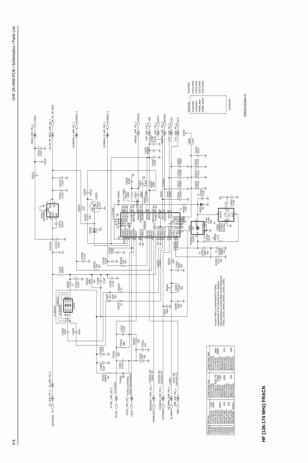
4-6
VH
F 2
5-45
W P
CB
/ S
chem
atic
s / P
arts
Lis
t
0VD
C5V
DC
5VD
C
(SO
UR
CE
)
-2 to
+7d
Bm
13.3
0VD
C6.
83V
DC
4.52
VD
C (
R)
+1d
Bm
0VD
C (
R)
4.95
VD
C (
R)
2.90
VD
C3.
42V
DC
3.63
VD
C
2.5V
DC
1.1-
4.1V
DC
0VD
C (
T)
2.62
VD
C (
T)
4.91
VD
C (
T)
Tem
p.C
omp.
Xta
l
Ref
.Osz
.
11.2
8VD
C
4.97
VD
C
2.5-
11V
DC
5VD
C (
LOC
KE
D)
0VD
C (
UN
LOC
KE
D)
R32
03
A1
5A
2
4A
3
K1
1K
22
K3
3
47
D32
01
6
47K
NU
TR
BL3
232
2.2u
HN
U
R32
28
C32
31
C32
25
.01u
F
L320
139
0nH
0.1u
F
C32
02.0
1uF
100
R32
23
C32
29
D32
21
0.1u
F
.047
uF
CLK
C32
51
C32
07
22pF
NU
47K
VC
OB
IAS
_2
R32
25
C32
268.
2pF
MO
DIN
_VH
F_F
N_1
TP
3201
R32
52
VC
OB
IAS
_1_V
HF
_FN
_1
330K
16_8
MH
z_V
HF
_FN
_1
PR
ES
C_V
HF
_FN
_1
R32
420
100
R32
41
VS
F_V
HF
_FN
_1
DA
TA
VC
OM
OD
_VH
F_F
N_1
CS
X_V
HF
_FN
_1
100p
F
C32
27
22pF NU
CS
X
IN_5
V_R
F_R
EG
_VH
F_F
N_1
C32
40
NU
1G
ND
4G
ND
1
3O
UT
6IN
16.8
MH
z75
Z04
Y32
61
100K
R32
27
0.1u
FC
3254
C32
08
0.1u
F
NU
.01u
FC
3232
47K
R32
26
PR
ES
C
C32
142.
2uF
C32
210.
1uF
1uF
C32
24
C32
630.
1uF
VM
ULT
11514
VM
ULT
212
VM
ULT
311
VM
ULT
4 VRO 13
25
WA
RP
23X
TA
L1X
TA
L224
27S
FB
AS
E26
SF
CA
P
30S
FIN
28S
FO
UT
37T
ES
T1
38T
ES
T2
21V
BP
AS
S
47
VC
P
31N
C3
44PD_GND
PD_VDD 5
PR
EIN
32
33 PRE_GND 34PRE_VDD
35P
VR
EF
18R
EF
SE
L45
IAD
AP
T
16IN
DM
ULT
43IO
UT
LOC
K4
10M
OD
IN41
MO
DO
UT
17N
C1
29N
C2
39B
IAS
2
42C
CO
MP
9C
EX
8C
LK
7D
AT
A
DGND6 36DVDD
19F
RE
FO
UT
46A
DA
PT
SW
22 AGND
48A
UX
1
1A
UX
22
AU
X3
3A
UX
4
20AVDD
40B
IAS
1
VC
OB
IAS
_1
63A
27
U32
01
47
R32
01
VS
F
C32
22
0
R32
11
0.1u
F
L323
1
0.1u
FC
3211
TP
3202
2.2u
H
C32
4322
0pF
16_8
MH
z
VD
DA
VD
DA
_VH
F_F
N_1
VC
OB
IAS
_2_V
HF
_FN
_1
0.1u
FC
3209
C32
4622
0pF
NU
C32
0610
uF
5V_V
HF
_FN
_2
150K
R32
06
Q32
21
R32
5118
0K
.01u
F
C32
280.
1uF
C32
35
2.2u
FC
3210
VC
TR
L_V
HF
_FN
_1
R32
04
LOC
K_V
HF
_FN
_1
47
1uF
C32
23
NU
220p
F
R32
62 NU
C32
45
BW
SE
LEC
T
6.2K
C32
15
R32
24
47K
C32
13
2.2u
F
1G
ND
5IN
2N
R
4O
UT
3S
D
2.2u
F
VCC
4
VC
NT
L
1
AD
P33
00U
3211
6E
RR
Y32
63
TT
S05
V16
.8M
Hz
GND
2
OU
T 3
MO
DIN
VC
TR
L
C32
55
DA
TA
_VH
F_F
N_1
220p
FC
3242
2.2u
F
5V_V
HF
_FN
_1
.01u
F
R32
2268
0
TR
B_V
HF
_FN
_1
C32
05
C32
6233
0pF
NU
NU
VC
OM
OD
C32
4156
pF
R32
6147
K
2.2u
FC
3233
R32
21
CLK
_VH
F_F
N_1
C32
52
390
1000
pF
.01u
FC
3234
C32
534.
7uF
NU
IN_5
V_R
F_R
EG
5V
D32
61C
3261
NU
LOC
K
C32
44
39pF
BW
SE
LEC
T_V
HF
_FN
_1
220p
F
C32
03
4,7k
.01u
F
NC
5V
5V
R32
63
NC
NC
NC
NC
NC
NCNC
NC
NC
NC
VD
DA
VD
DA
NC
NC
NC
.022
uFC
3212
R32
0210
ME
G
NU
10pF
C32
47
In c
ase
Y32
61 is
use
d in
stea
d of
Y32
63,
repl
acem
ent o
f the
follo
win
g pa
rts
req
uire
s
new
tem
pera
ture
com
pens
atio
n of
the
freq
uenc
y:
Y32
61, U
3201
, R32
61, R
3262
, C32
62, D
3261
ZW
G01
3056
4-O
(*)
(*)
(*)
(*)
(*)
(*)
(*)
(*)
(*)
0662
057A
89N
OT
PLA
CE
DN
OT
PLA
CE
D
NO
TP
LAC
ED
4805
875Z
04
39pF
330p
F
47K
Xta
lN
OT
PLA
CE
D48
8618
2B01
C32
62N
OT
PLA
CE
D
100n
F
100n
F
47K
100
NO
TP
LAC
ED
NO
TP
LAC
ED
NO
TP
LAC
ED
NO
TP
LAC
ED
NO
TP
LAC
ED
2113
740L
37
2113
740F
0721
1374
0F59
4802
245J
2206
6205
7B02
4880
114R
04
62pF
2%
220p
F1.
5pF
150K Xta
lR
efO
sc
Tem
p.C
omp.
new
NO
TP
LAC
ED
NO
TP
LAC
ED
2113
740F
4121
1374
0F63
NO
TP
LAC
ED
4862
824C
03
Ref
.Osz
.T
emp.
Com
p. o
rg.
Ref
.No.
C32
35C
3251
C32
61
C32
63
2113
741F
4910
nF21
1374
3E20
NO
TP
LAC
ED
2113
743E
20D
3261
R32
61R
3262
R32
63Y
3261
Y32
62
NO
TP
LAC
ED
0662
057A
89N
OT
PLA
CE
D06
6205
7A25
0102
727B
34
0102
727B
3401
0272
7B34
0102
727B
34
Boa
rd K
itsA
ssem
blie
s
PR
IME
_MU
HF
PR
IME
_BN
C
GU
D63
38A
GU
D63
36A
GU
D63
38A
HF
(13
6-17
4 M
Hz)
FR
AC
N
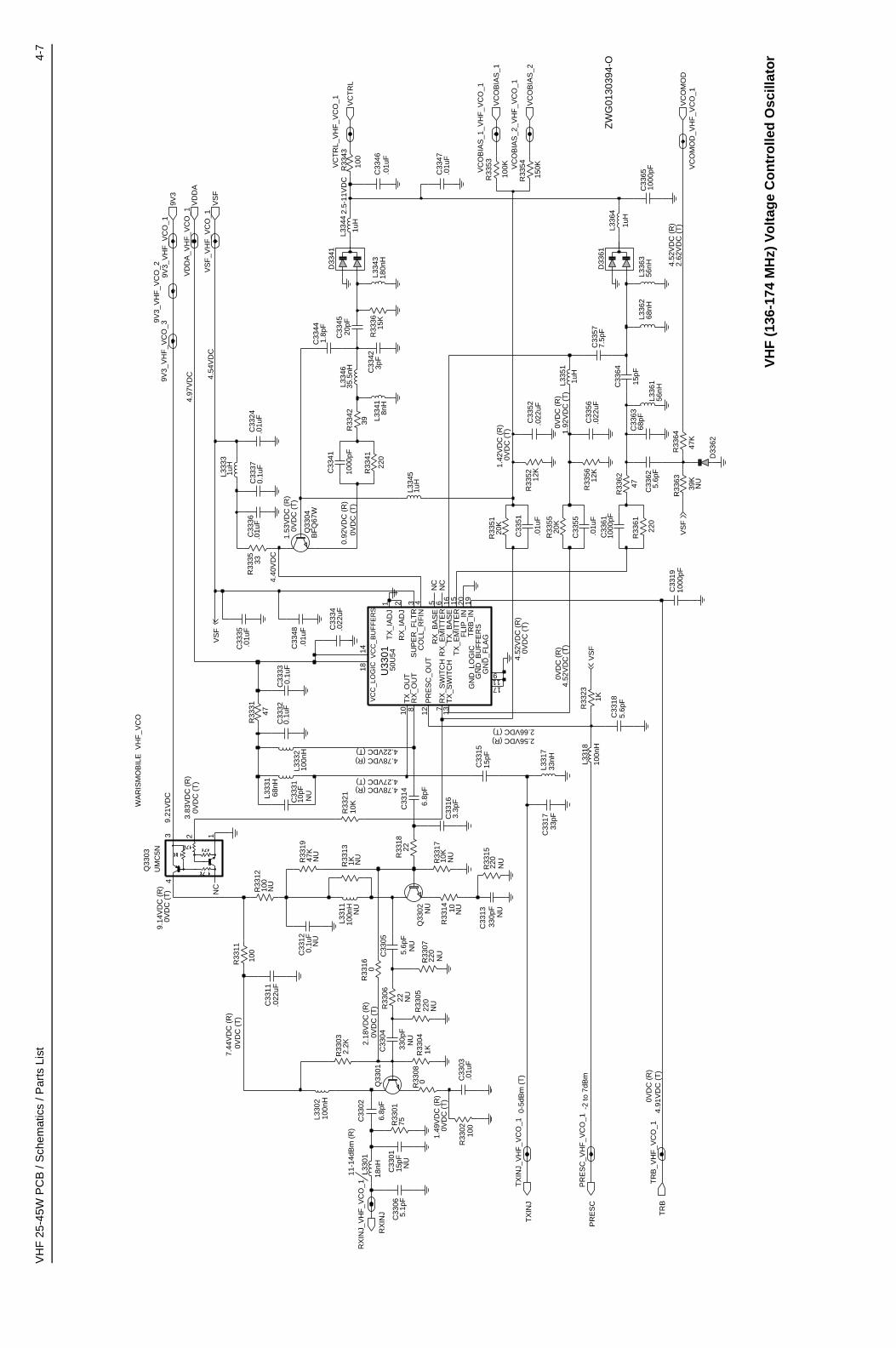
VH
F 2
5-45
W P
CB
/ S
chem
atic
s / P
arts
Lis
t4-
7
4.22VDC (T)
0VD
C (
R)
1.92
VD
C (
T)
4.52
VD
C (
R)
2.62
VD
C (
T)
4.52
VD
C (
R)
0VD
C (
T)
1.42
VD
C (
R)
0VD
C (
T)
4.97
VD
C
4.40
VD
C
1.53
VD
C (
R)
0VD
C (
T)
0.92
VD
C (
R)
0VD
C (
T)
0VD
C (
R)
0-5d
Bm
(T
)
7.44
VD
C (
R)
9.14
VD
C (
R)
0VD
C (
T)
0VD
C (
T)
11-1
4dB
m (
R)
-2 to
7dB
m
0VD
C (
T)
2.18
VD
C (
R)
0VD
C (
T)
1.49
VD
C (
R)
2.56VDC (R)
0VD
C (
R)
2.5-
11V
DC
4.54
VD
C
0VD
C (
T)
4.78VDC (R)
2.66VDC (T)
4.52
VD
C (
T)
WA
RIS
MO
BIL
E V
HF
_VC
O
4.78VDC (R)4.27VDC (T)
4.91
VD
C (
T)
9.21
VD
C
3.83
VD
C (
R)
L333
3
R33
5612
K
VC
OB
IAS
_2_V
HF
_VC
O_1
1uH
D33
61
R33
35 33
9V3_
VH
F_V
CO
_2
220
R33
61
C33
31
VD
DA
_VH
F_V
CO
_1
10KN
U10
pF
35.5
nHR
3321
15K
L334
6
L333
168
nH
R33
36
100n
H
NU
C33
120.
1uF
10T
X_O
UT
13T
X_S
WIT
CH
14V
CC
_BU
FF
ER
S
18V
CC
_LO
GIC
NU
L331
1
2R
X_I
AD
J8
RX
_OU
T
7R
X_S
WIT
CH
3S
UP
ER
_FLT
R
TR
B_I
N1916
TX
_BA
SE
15T
X_E
MIT
TE
R
1T
X_I
AD
J
4C
OLL
_RF
IN
20F
LIP
_IN
11GN
D_B
UF
FE
RS
9GN
D_F
LAG
GN
D_L
OG
IC
17
12P
RE
SC
_OU
T5
RX
_BA
SE
6R
X_E
MIT
TE
R
U33
0150
U54
R33
62
47
NU
330p
F
C33
04
R33
54
150K
RX
INJ
VC
OM
OD
_VH
F_V
CO
_1
C33
6368
pF
L331
733
nH33
pFC
3317
C33
577.
5pF
1uH
L335
1
100
R33
11
10K
R33
1722R
3318
NU
L334
4
1uH
C33
625.
6pF
100n
HL3
332
22
R33
06
0R
3316
NU
18nH
L330
1
C33
441.
8pF
Q33
01
L331
8
100n
H
C33
11.0
22uF
6.8p
F
C33
14
C33
15.0
1uF
C33
03
15pF
20K
R33
51
Q33
04B
FQ
67W
NU
47K
R33
19
3.3p
FC
3316
56nH
L336
1
0R33
08
TR
B_V
HF
_VC
O_1
1uH
L336
4
C33
51
.01u
F12
KR
3352
PR
ES
C
VC
OM
OD
VC
OB
IAS
_1_V
HF
_VC
O_1
R33
23
1K
VC
TR
L
C33
47.0
1uF
C33
370.
1uF
NU
R33
0722
0
D33
41
VC
OB
IAS
_1
RX
INJ_
VH
F_V
CO
_1
100K
R33
53
C33
24.0
1uF
L330
210
0nH
VC
OB
IAS
_2
2.2K
R33
03C
3345
20pF
L336
268
nH
15pF
C33
64
8nH
L334
1
C33
330.
1uF
56nH
L336
3
100
0.1u
FC
3332
NU
R33
12
.022
uFC
3352
C33
05
VD
DA
NU
5.6p
F
TR
B
100
R33
43
C33
34
VS
F_V
HF
_VC
O_1
.022
uF
.01u
F
C33
55
VS
F
C33
423p
F
D33
62
1KR33
13
C33
36.0
1uF
NU
C33
35.0
1uF
R33
41
220
R33
5520
K
NU
R33
63
39K
9V3_
VH
F_V
CO
_19V
3
VC
TR
L_V
HF
_VC
O_1
PR
ES
C_V
HF
_VC
O_175
6.8p
F
R33
01
C33
02
C33
065.
1pF
NU
15pF
C33
01
NU
330p
FC
3313
47
R33
31
3
C33
1910
00pF
UM
C5N
2
4
1
C33
46
Q33
03
C33
41
.01u
F
1000
pF
39
R33
42
NU
Q33
02
TX
INJ_
VH
F_V
CO
_1T
XIN
J
5.6p
FC
3318
220
R33
15
9V3_
VH
F_V
CO
_3
NU
C33
61
C33
56.0
22uF
1000
pF
180n
H
1KR33
04
R33
02
L334
3
220
100
NU
R33
05
C33
6510
00pF
R33
14
R33
64
47K
NU10
C33
48.0
1uF
VS
F
1uH
L334
5
VS
F
VS
F
NC
NC
NC
ZW
G01
3039
4-O
VH
F (
136-
174
MH
z) V
olt
age
Co
ntr
olle
d O
scill
ato
r
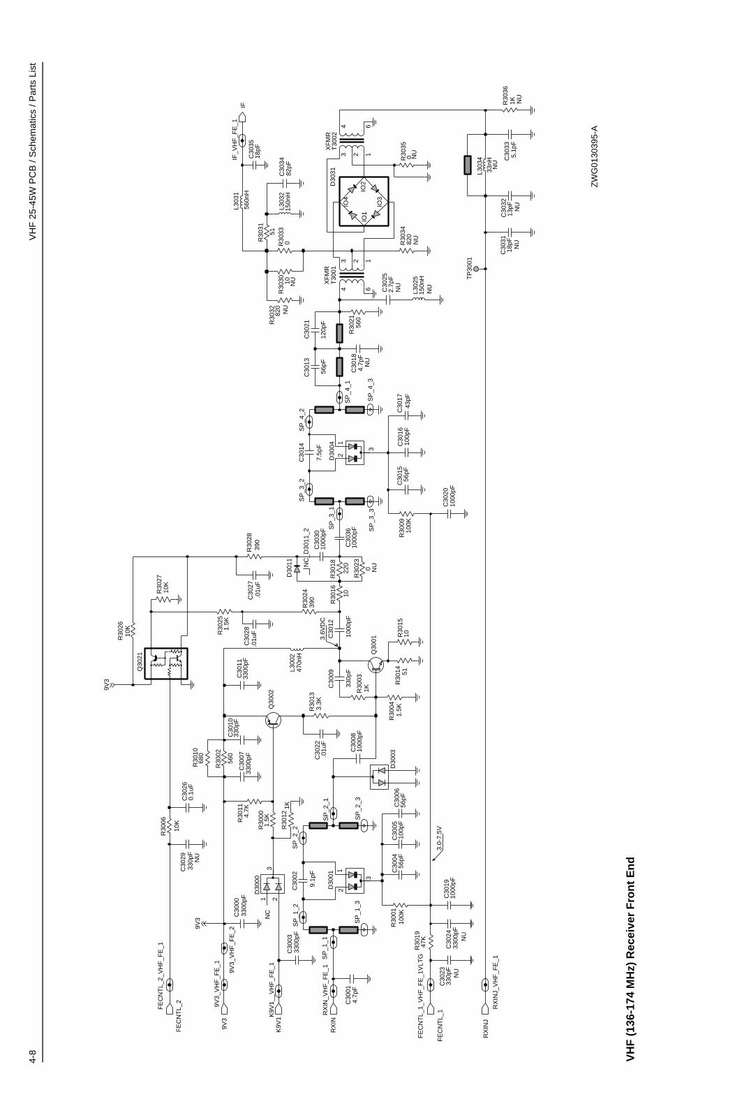
4-8
VH
F 2
5-45
W P
CB
/ S
chem
atic
s / P
arts
Lis
t
3
120p
F
C30
21
D30
041
2
RX
INJ
FE
CN
TL_
1
SP
_3_1
1000
pFC
3020
100p
FC
3016
1.5K
R30
00
SP
_4_2
IF_V
HF
_FE
_1
D30
03
12
3
SP
_3_2
C30
14
D30
01
7.5p
F
R30
16
104 6
3 1210
00pF
C30
36
XF
MR
T30
02
3300
pFC
3003
4.7K
R30
11
RX
IN
K9V
1__V
HF
_FE
_1
NU
R30
30 10
SP
_4_3
NU
150n
HL3
025
820
R30
34
D30
001 2
3
NU
1000
pFC
3019
FE
CN
TL_
1_V
HF
_FE
_1V
LTG
C30
06
3300
pFC
3000
56pF
13pF
C30
32
1.5K
R30
25
NU
220
RX
INJ_
VH
F_F
E_1
R30
18
3300
pFC
3011
FE
CN
TL_
2
R30
31
51
SP
_4_1
330p
F
C30
09
C30
01
9V3
C30
13
4.7p
F
Q30
02
56pF
SP
_3_3
100K
R30
09
9V3_
VH
F_F
E_2
R30
02
1KR30
03
18pF
560
R30
32
C30
35
C30
24
NU
820
NU
3300
pF
NU
R30
23
0
C30
05
NU
4.7p
FC
3018
100p
F
C30
3010
00pF
NU
330p
FC
3023
C30
27.0
1uF
R30
2839
0
560n
H
L303
1
56pF
C30
04
SP
_1_2
R30
121K
NU
33nH
L303
4
Q30
21
NU
0R30
351.
5KR
3004
0R30
33
3300
pFC
3007
330p
FC
3029
K9V
1
390
R30
24
NU
.01u
FC
3028
10K
1KR30
36
R30
06
R30
26
NU
SP
_2_2
10K
R30
14
SP
_2_1
51C
3015
C30
02
9.1p
F
56pF
82pF
C30
34
NU
18pF
C30
31
IO3
IO4
5.1p
FC
3033
D30
31
IO1
IO2
560
R30
21
10R30
15
1000
pFC
3008
SP
_1_1
.01u
FC
3022
680
R30
10
C30
17
150n
HL3
032
43pF
1000
pF
IF
FE
CN
TL_
2_V
HF
_FE
_1
Q30
01
SP
_1_3
SP
_2_3
R30
13
R30
27
3.3K
47K
R30
19
10K
L300
2
2.7p
F
470n
H
NU
C30
25 TP
3001
100K
R30
01
C30
26
D30
11
4 6
3 12
0.1u
F
RX
IN_V
HF
_FE
_1X
FM
RT
3001
9V3_
VH
F_F
E_1
9V3
330p
FC
3010
NC
NC
_D30
11_2
9V3
ZW
G01
3039
5-A
3.0-
7.5V
3.6V
DC
C30
12
VH
F (
136-
174
MH
z) R
ecei
ver
Fro
nt
En
d

VH
F 2
5-45
W P
CB
/ S
chem
atic
s / P
arts
Lis
t4-
9
9180
469V
03
3.9V
DC
12.
5kH
z 0
VD
C20
/25k
Hz
5V
DC
0.75
VD
C
0.75
VD
C3V
DC
9180
469V
06
9180
469V
04
9180
468v
04
9180
468V
06
3VD
C6.
8K
R31
07
9V3
R31
351.
2K
390
1GND1GND2 2GND3 4
5GND4
3IN
6O
UT
R31
15
FL3
101
12R
16
R31
1727
K
Q31
02
Q31
51
680
R31
46
620n
HL3
111
620
R31
08
R31
18
6.8K
R31
1112
K
C31
01
5V_V
HF
_IF
_1
GND2 4
1IN
2O
UT
NU
2.2p
F
FL3
111
3
GND1
U31
15-1
CN
TL 13
12
VD
D
14
VS
S 7
DIS
CA
UD
IO_V
HF
_IF
_1
15K
R31
32
0.1u
FC
3144
120p
FC
3143
C31
39
C31
410.
1uF
0.1u
F
13
12
VD
D
14
VS
S 7
Q31
41
U31
11-1
CN
TL
R31
1633
0
10
9V3_
VH
F_I
F_2
3GN
D
1IN
2O
UT
R31
02
C31
10
27pF
FL3
113
0.1u
FC
3142
9.1p
F
IFIN
_VH
F_I
F_1
100
R31
04
NU
C31
1312GND2 4GND3
GND4 5
IN3
OU
T6
NU
DIS
CA
UD
IO
12R
16F
L310
2
GND1
1000
pF
R31
51
C31
00
C31
400.
1uF
10K
1110
VD
D
14 VS
S
7
3
14
VD
D 7
VS
S
U31
11-4
CN
TL
12
U31
15-2
5
CN
TL
4
Q31
52C
3152
.01u
F
.01u
FC
3151
R31
338.
2K
4700
pFC
3146
27K
R31
06
C31
12
390
R31
41
82pF
10R
3112
1.8K
R31
42
R31
5410
K
C31
22
.039
uF
Q31
01
6 VC
C33
0R
3113
20MIXOUT4 OSCIN
3OSCOUT
10 QUADIN
1 RFIN
2RFIN_DEC
5RSSIOUT
9 RSSI_FEED
15
18 IFAMPIN 16IFAMPOUT
19 IFAMP_DEC1
17IFA
MP
_DE
C2
14 LIMIN11LIMOUT 13LIM_DEC1 12LIM_DEC2
SA
616
U31
01
8AUDIOOUT
7 AUDIO_FEED
GND
51
44.3
95M
Hz
12R
17Y
3101
2G
ND
4G
ND
1
3O
UT
1IN
R31
30
C31
3630
pF
C31
35
33pF
12K
R31
01
R31
47
12K
C31
3310
uF
C31
15
100
R31
05
22pF
620n
HL3
100
0.1u
F
NU
C31
37.0
39uF
C31
34
455K
Hz
3
21
BW
SE
LEC
T_V
HF
_IF
_1 BW
SE
LEC
T
45B
02
Y31
02
C31
03
33pF
C31
320.
1uF
10K
R31
52
0.1u
FC
3111
U31
15-3
6CN
TL
89
14 VD
D 7VS
S
18pF
C31
14L3
112
620n
H
9V3_
VH
F_I
F_1
5V
D31
01
RS
SI_
VH
F_I
F_1
OU
T
.039
uFC
3123
FL3
112
3
GND1
GND2
4
1IN
2
R31
1410
0
R31
34
10K
NU
2.4K
R31
44
U31
11-2
5
CN
TL
43
14 VD
D 7
VS
S
3.3K
R31
45
C31
45
C31
470.
1uF
620n
HL3
101
0.1u
F22
0pF
C31
48
NU
10V
DD
14 VS
S
7
NU
1pF
C31
31
U31
15-4
CN
TL
12
11
C31
210.
1uF
FL3
115
GND1
34
GND2
IN1
OU
T2
15pF
C31
02
NU
U31
11-3
6CN
TL
89
14
VD
D
7VS
S
3G
ND
1IN
2O
UT
RS
SI
C31
16
FL3
114
0.1u
F0.
1uF
R31
53
C31
04
5V
10K
5V
9V3
9V3
9V3
9V3
9V3
5V
9V3
5V
9V3
0R
3123
1uH
NU
L312
4
33pF
C31
24820
R31
24
ZW
G01
3056
5-O
VH
F (
136-
174
MH
z) IF
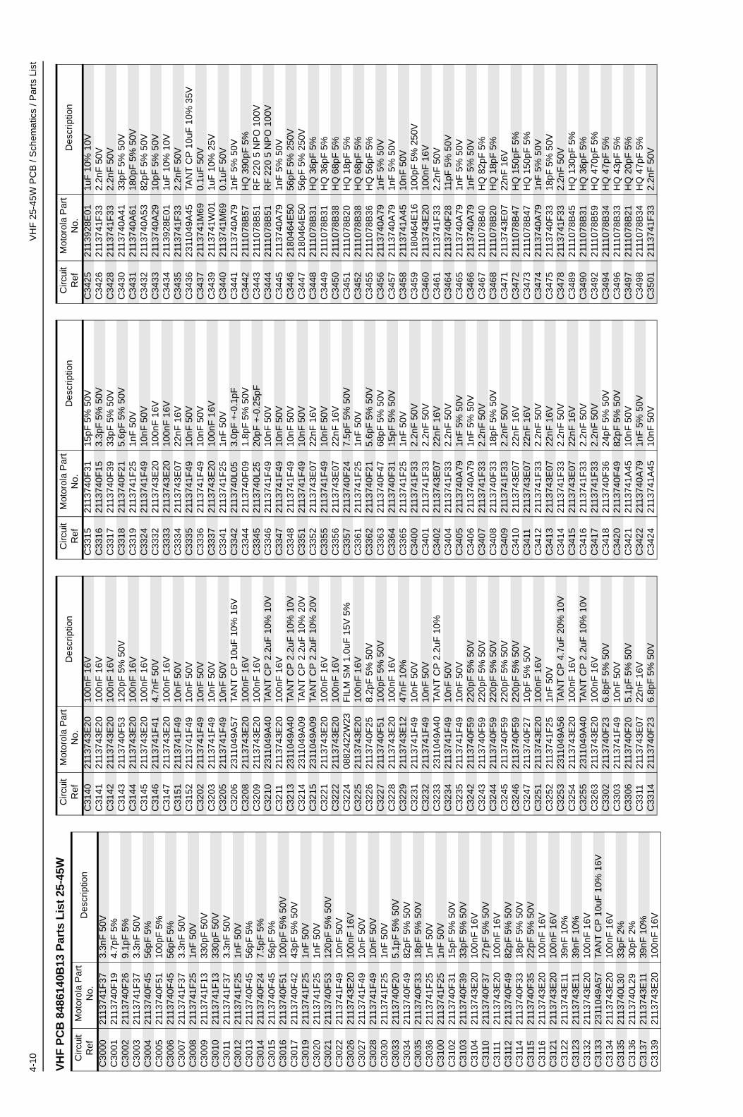
4-10
VH
F 2
5-45
W P
CB
/ S
chem
atic
s / P
arts
Lis
t
VH
F P
CB
848
6140
B13
Par
ts L
ist
25-4
5W
Circ
uit
Ref
Mot
orol
a P
art
No.
Des
crip
tion
C30
0021
1374
1F37
3.3n
F 5
0VC
3001
2113
740F
194.
7pF
5%
C30
0221
1374
0F26
9.1p
F 5
%C
3003
2113
741F
373.
3nF
50V
C30
0421
1374
0F45
56pF
5%
C30
0521
1374
0F51
100p
F 5
%C
3006
2113
740F
4556
pF 5
%C
3007
2113
741F
373.
3nF
50V
C30
0821
1374
1F25
1nF
50V
C30
0921
1374
1F13
330p
F 5
0VC
3010
2113
741F
1333
0pF
50V
C30
1121
1374
1F37
3.3n
F 5
0VC
3012
2113
741F
251n
F 5
0VC
3013
2113
740F
4556
pF 5
%C
3014
2113
740F
247.
5pF
5%
C30
1521
1374
0F45
56pF
5%
C30
1621
1374
0F51
100p
F 5
% 5
0VC
3017
2113
740F
4243
pF 5
% 5
0VC
3019
2113
741F
251n
F 5
0VC
3020
2113
741F
251n
F 5
0VC
3021
2113
740F
5312
0pF
5%
50V
C30
2221
1374
1F49
10nF
50V
C30
2621
1374
3E20
100n
F 1
6VC
3027
2113
741F
4910
nF 5
0VC
3028
2113
741F
4910
nF 5
0VC
3030
2113
741F
251n
F 5
0VC
3033
2113
740F
205.
1pF
5%
50V
C30
3421
1374
0F49
82pF
5%
50V
C30
3521
1374
0F33
18pF
5%
50V
C30
3621
1374
1F25
1nF
50V
C31
0021
1374
1F25
1nF
50V
C31
0221
1374
0F31
15pF
5%
50V
C31
0321
1374
0F39
33pF
5%
50V
C31
0421
1374
3E20
100n
F 1
6VC
3110
2113
740F
3727
pF 5
% 5
0VC
3111
2113
743E
2010
0nF
16V
C31
1221
1374
0F49
82pF
5%
50V
C31
1421
1374
0F33
18pF
5%
50V
C31
1521
1374
0F35
22pF
5%
50V
C31
1621
1374
3E20
100n
F 1
6VC
3121
2113
743E
2010
0nF
16V
C31
2221
1374
3E11
39nF
10%
C31
2321
1374
3E11
39nF
10%
C31
3221
1374
3E20
100n
F 1
6VC
3133
2311
049A
57TA
NT
CP
10u
F 1
0% 1
6VC
3134
2113
743E
2010
0nF
16V
C31
3521
1374
0L30
33pF
2%
C31
3621
1374
0L29
30pF
2%
C31
3721
1374
3E11
39nF
10%
C31
3921
1374
3E20
100n
F 1
6V
C31
4021
1374
3E20
100n
F 1
6VC
3141
2113
743E
2010
0nF
16V
C31
4221
1374
3E20
100n
F 1
6VC
3143
2113
740F
5312
0pF
5%
50V
C31
4421
1374
3E20
100n
F 1
6VC
3145
2113
743E
2010
0nF
16V
C31
4621
1374
1F41
4.7n
F 5
0VC
3147
2113
743E
2010
0nF
16V
C31
5121
1374
1F49
10nF
50V
C31
5221
1374
1F49
10nF
50V
C32
0221
1374
1F49
10nF
50V
C32
0321
1374
1F49
10nF
50V
C32
0521
1374
1F49
10nF
50V
C32
0623
1104
9A57
TAN
T C
P 1
0uF
10%
16V
C32
0821
1374
3E20
100n
F 1
6VC
3209
2113
743E
2010
0nF
16V
C32
1023
1104
9A40
TAN
T C
P 2
.2uF
10%
10V
C32
1121
1374
3E20
100n
F 1
6VC
3213
2311
049A
40TA
NT
CP
2.2
uF 1
0% 1
0VC
3214
2311
049A
09TA
NT
CP
2.2
uF 1
0% 2
0VC
3215
2311
049A
09TA
NT
CP
2.2
uF 1
0% 2
0VC
3221
2113
743E
2010
0nF
16V
C32
2221
1374
3E20
100n
F 1
6VC
3224
0882
422W
23F
ILM
SM
1.0
uF 1
5V 5
%C
3225
2113
743E
2010
0nF
16V
C32
2621
1374
0F25
8.2p
F 5
% 5
0VC
3227
2113
740F
5110
0pF
5%
50V
C32
2821
1374
3E20
100n
F 1
6VC
3229
2113
743E
1247
nF 1
0%C
3231
2113
741F
4910
nF 5
0VC
3232
2113
741F
4910
nF 5
0VC
3233
2311
049A
40TA
NT
CP
2.2
uF 1
0%C
3234
2113
741F
4910
nF 5
0VC
3235
2113
741F
4910
nF 5
0VC
3242
2113
740F
5922
0pF
5%
50V
C32
4321
1374
0F59
220p
F 5
% 5
0VC
3244
2113
740F
5922
0pF
5%
50V
C32
4521
1374
0F59
220p
F 5
% 5
0VC
3246
2113
740F
5922
0pF
5%
50V
C32
4721
1374
0F27
10pF
5%
50V
C32
5121
1374
3E20
100n
F 1
6VC
3252
2113
741F
251n
F 5
0VC
3253
2311
049A
56TA
NT
CP
4.7
uF 2
0% 1
0VC
3254
2113
743E
2010
0nF
16V
C32
5523
1104
9A40
TAN
T C
P 2
.2uF
10%
10V
C32
6321
1374
3E20
100n
F 1
6VC
3302
2113
740F
236.
8pF
5%
50V
C33
0321
1374
1F49
10nF
50V
C33
0621
1374
0F20
5.1p
F 5
% 5
0VC
3311
2113
743E
0722
nF 1
6VC
3314
2113
740F
236.
8pF
5%
50V
Circ
uit
Ref
Mot
orol
a P
art
No.
Des
crip
tion
C33
1521
1374
0F31
15pF
5%
50V
C33
1621
1374
0F15
3.3p
F 5
% 5
0VC
3317
2113
740F
3933
pF 5
% 5
0VC
3318
2113
740F
215.
6pF
5%
50V
C33
1921
1374
1F25
1nF
50V
C33
2421
1374
1F49
10nF
50V
C33
3221
1374
3E20
100n
F 1
6VC
3333
2113
743E
2010
0nF
16V
C33
3421
1374
3E07
22nF
16V
C33
3521
1374
1F49
10nF
50V
C33
3621
1374
1F49
10nF
50V
C33
3721
1374
3E20
100n
F 1
6VC
3341
2113
741F
251n
F 5
0VC
3342
2113
740L
053.
0pF
+-0
.1pF
C33
4421
1374
0F09
1.8p
F 5
% 5
0VC
3345
2113
740L
2520
pF +
-0.2
5pF
C33
4621
1374
1F49
10nF
50V
C33
4721
1374
1F49
10nF
50V
C33
4821
1374
1F49
10nF
50V
C33
5121
1374
1F49
10nF
50V
C33
5221
1374
3E07
22nF
16V
C33
5521
1374
1F49
10nF
50V
C33
5621
1374
3E07
22nF
16V
C33
5721
1374
0F24
7.5p
F 5
% 5
0VC
3361
2113
741F
251n
F 5
0VC
3362
2113
740F
215.
6pF
5%
50V
C33
6321
1374
0F47
68pF
5%
50V
C33
6421
1374
0F31
15pF
5%
50V
C33
6521
1374
1F25
1nF
50V
C34
0021
1374
1F33
2.2n
F 5
0VC
3401
2113
741F
332.
2nF
50V
C34
0221
1374
3E07
22nF
16V
C34
0421
1374
1F33
2.2n
F 5
0VC
3405
2113
740A
791n
F 5
% 5
0VC
3406
2113
740A
791n
F 5
% 5
0VC
3407
2113
741F
332.
2nF
50V
C34
0821
1374
0F33
18pF
5%
50V
C34
0921
1374
1F33
2.2n
F 5
0VC
3410
2113
743E
0722
nF 1
6VC
3411
2113
743E
0722
nF 1
6VC
3412
2113
741F
332.
2nF
50V
C34
1321
1374
3E07
22nF
16V
C34
1421
1374
1F33
2.2n
F 5
0VC
3415
2113
743E
0722
nF 1
6VC
3416
2113
741F
332.
2nF
50V
C34
1721
1374
1F33
2.2n
F 5
0VC
3418
2113
740F
3624
pF 5
% 5
0VC
3420
2113
740F
4982
pF 5
% 5
0VC
3421
2113
741A
4510
nF 5
0VC
3422
2113
740A
791n
F 5
% 5
0VC
3424
2113
741A
4510
nF 5
0V
Circ
uit
Ref
Mot
orol
a P
art
No.
Des
crip
tion
C34
2521
1392
8E01
1uF
10%
10V
C34
2621
1374
1F33
2.2n
F 5
0VC
3428
2113
741F
332.
2nF
50V
C34
3021
1374
0A41
33pF
5%
50V
C34
3121
1374
0A61
180p
F 5
% 5
0VC
3432
2113
740A
5382
pF 5
% 5
0VC
3433
2113
740A
2910
pF 5
% 5
0VC
3434
2113
928E
011u
F 1
0% 1
0VC
3435
2113
741F
332.
2nF
50V
C34
3623
1104
9A45
TAN
T C
P 1
0uF
10%
35V
C34
3721
1374
1M69
0.1u
F 5
0VC
3439
2113
741W
011u
F 1
0% 2
5VC
3440
2113
741M
690.
1uF
50V
C34
4121
1374
0A79
1nF
5%
50V
C34
4221
1107
8B57
HQ
390
pF 5
%C
3443
2111
078B
51R
F 2
20 5
NP
O 1
00V
C34
4421
1107
8B51
RF
220
5 N
PO
100
VC
3445
2113
740A
791n
F 5
% 5
0VC
3446
2180
464E
5056
pF 5
% 2
50V
C34
4721
8046
4E50
56pF
5%
250
VC
3448
2111
078B
31H
Q 3
6pF
5%
C34
4921
1107
8B31
HQ
36p
F 5
%C
3450
2111
078B
38H
Q 6
8pF
5%
C34
5121
1107
8B20
HQ
18p
F 5
%C
3452
2111
078B
38H
Q 6
8pF
5%
C34
5521
1107
8B36
HQ
56p
F 5
%C
3456
2113
740A
791n
F 5
% 5
0VC
3457
2113
740A
791n
F 5
% 5
0VC
3458
2113
741A
4510
nF 5
0VC
3459
2180
464E
1610
0pF
5%
250
VC
3460
2113
743E
2010
0nF
16V
C34
6121
1374
1F33
2.2n
F 5
0VC
3464
2113
740F
2811
pF 5
% 5
0VC
3465
2113
740A
791n
F 5
% 5
0VC
3466
2113
740A
791n
F 5
% 5
0VC
3467
2111
078B
40H
Q 8
2pF
5%
C34
6821
1107
8B20
HQ
18p
F 5
%C
3471
2113
743E
0722
nF 1
6VC
3472
2111
078B
47H
Q 1
50pF
5%
C34
7321
1107
8B47
HQ
150
pF 5
%C
3474
2113
740A
791n
F 5
% 5
0VC
3475
2113
740F
3318
pF 5
% 5
0VC
3478
2113
741F
332.
2nF
50V
C34
8921
1107
8B45
HQ
130
pF 5
%C
3490
2111
078B
31H
Q 3
6pF
5%
C34
9221
1107
8B59
HQ
470
pF 5
%C
3494
2111
078B
34H
Q 4
7pF
5%
C34
9621
1107
8B33
HQ
43p
F 5
%C
3497
2111
078B
21H
Q 2
0pF
5%
C34
9821
1107
8B34
HQ
47p
F 5
%C
3501
2113
741F
332.
2nF
50V
Circ
uit
Ref
Mot
orol
a P
art
No.
Des
crip
tion
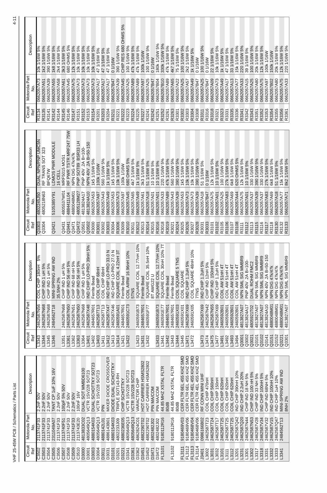
VH
F 2
5-45
W P
CB
/ S
chem
atic
s / P
arts
Lis
t4-
11
C35
0221
1374
1F33
2.2n
F 5
0VC
3503
2113
741F
332.
2nF
50V
C35
0421
1374
1F33
2.2n
F 5
0VC
3505
2311
049A
07TA
NT
CP
1uF
10%
16V
C35
0621
1374
1F33
2.2n
F 5
0VC
3507
2113
740F
5110
0pF
5%
50V
C35
0821
1374
1F33
2.2n
F 5
0VC
3509
2113
741F
332.
2nF
50V
C35
1021
1374
3E20
100n
F 1
6VD
3000
4813
833C
02D
UA
L S
OT
MM
BD
6100
D30
0148
0564
9Q13
VC
TR
1S
V22
8 S
OT
23D
3003
4880
154K
03D
UA
L S
CH
OT
TK
Y S
OT
23D
3004
4805
649Q
13V
CT
R 1
SV
228
SO
T23
D30
1148
8014
2L01
PIN
D30
3148
8614
3B01
MIX
ER
DIO
DE
CR
OS
SO
VE
RD
3101
4880
154K
03D
IOD
E D
UA
L S
CH
OT
TK
YD
3201
4802
233J
09T
RIP
LE S
OT
143-
RH
D32
2148
8023
6E05
CH
IP S
CH
OT
TK
YD
3341
4805
649Q
13V
CT
R 1
SV
228
SO
T23
D33
6148
0564
9Q13
VC
TR
1S
V22
8 S
OT
23D
3362
4862
824C
01V
AR
AC
TO
R C
HIP
D34
5148
8229
0T02
HO
T C
AR
RIE
R H
SM
S28
02D
3452
4882
290T
02H
OT
CA
RR
IER
HS
MS
2802
D34
7148
0248
2J02
PIN
MA
/CO
MD
3472
4802
482J
02P
IN M
A/C
OM
FL3
101
9180
112R
1644
.85
MH
Z X
STA
L F
LTR
80
dBF
L310
291
8011
2R16
44.8
5 M
HZ
XS
TAL
FLT
R
80dB
FL3
111
9180
469V
03C
ER
FLT
R 6
EL
455
KH
Z S
MD
FL3
112
9180
469V
06C
ER
FLT
R 6
EL
455
KH
Z S
MD
FL3
113
9180
468V
04C
ER
FLT
R 4
EL
455
KH
Z S
MD
FL3
114
9180
468V
06C
ER
FLT
R 4
EL
455
KH
Z S
MD
J340
109
8616
6B02
RF
CO
NN
MIN
I UH
FL3
002
2462
587T
23C
OIL
CH
IP 4
70nH
L303
124
6258
7T24
CO
IL C
HIP
560
nHL3
032
2462
587T
17C
OIL
CH
IP 1
50nH
L310
124
6258
7T25
CO
IL C
HIP
620
nHL3
111
2462
587T
25C
OIL
CH
IP 6
20nH
L311
224
6258
7T25
CO
IL C
HIP
620
nHL3
201
2462
587Q
42IN
D C
HIP
390
nH 1
0%L3
231
2462
587Q
20IN
D C
HIP
2.2
uH 2
0%L3
301
2462
587N
44C
HIP
IND
18
NH
5%
L330
224
6258
7N53
CH
IP IN
D 1
00 n
H 5
%L3
317
2462
587V
28C
HIP
IND
33
NH
5%
L331
824
6258
7V34
IND
CH
IP 1
00nH
5%
L333
124
6258
7V32
CH
IP IN
D 6
8NH
5%
L333
224
6258
7V15
IND
CH
IP 1
00nH
10%
L333
324
6258
7Q47
IND
CH
IP 1
uH 1
0%L3
341
2484
562T
13M
INI-
SP
RIN
G A
W IN
D8N
H 2
%
Circ
uit
Ref
Mot
orol
a P
art
No.
Des
crip
tion
L334
324
6258
7N56
CO
IL C
HIP
180
nH
5%L3
344
2462
587N
68C
HIP
IND
1 u
H 5
%L3
345
2462
587N
68C
HIP
IND
1 u
H 5
%L3
346
2484
562T
18M
INI-
SP
RIN
G A
W IN
D
35.5
NH
2%
L335
124
6258
7N68
CH
IP IN
D 1
uH
5%
L336
124
6258
7N50
CH
IP IN
D 5
6 nH
5%
L336
224
6258
7N51
CH
IP IN
D 6
8 nH
5%
L336
324
6258
7N50
CH
IP IN
D 5
6 nH
5%
L336
424
6258
7N68
CH
IP IN
D 1
uH
5%
L340
124
6258
7X48
IND
CH
IP L
O-P
RO
39n
H 5
%L3
402
2484
657R
01F
errit
e B
ead
L340
324
6258
7T13
CO
IL C
HIP
68n
HL3
411
2462
587T
13C
OIL
CH
IP 6
8nH
L341
224
6258
7X47
IND
CH
IP L
O-P
RO
33.
0 N
L341
324
6258
7X46
IND
CH
IP L
O-P
RO
27.
0 N
L341
424
6059
1A01
SQ
UA
RE
CO
IL 4
.22n
H 3
TL3
421
2484
657R
01F
errit
e B
ead
L342
224
6059
1C73
CO
IL A
IRW
16.
96nH
10%
5T
NS
L342
324
6059
1B73
SQ
UA
RE
CO
IL 1
2.77
nH 1
0%L3
431
2484
657R
01F
errit
e B
ead
L343
224
6059
1F77
SQ
UA
RE
CO
IL 3
5.5n
H 1
0%
8T A
WG
22 U
L343
324
6059
1B73
SQ
UA
RE
CO
IL 1
2.77
nH 1
0%L3
441
2460
591E
77S
QU
AR
E C
OIL
30n
H 1
0% 7
TL3
442
2484
657R
01F
errit
e B
ead
L344
324
8465
7R01
Fer
rite
Bea
dL3
444
2460
591X
03C
OIL
SQ
UA
RE
5 T
NS
L344
524
6059
1X01
CO
IL S
QU
AR
EL3
471
2462
587X
69IN
D C
HIP
1.2
uH 5
%L3
472
2460
591X
05C
OIL
SQ
UA
RE
48n
H 1
0%
7TN
SL3
473
2462
587X
69IN
D C
HIP
1.2
uH 5
%L3
474
2462
587N
42C
HIP
IND
12n
H 5
%L3
475
2462
587N
55C
HIP
IND
150
nH 5
%L3
477
2462
587X
69IN
D C
HIP
1.2
uH 5
%L3
491
2460
592B
01C
OIL
AW
51n
H 4
TL3
492
2460
592B
01C
OIL
AW
51n
H 4
TL3
493
2460
592B
01C
OIL
AW
51n
H 4
TL3
494
2460
592B
01C
OIL
AW
51n
H 4
TQ
3001
4813
827A
07N
PN
SM
L S
IG M
MB
R9
Q30
0248
1382
4A17
PN
P 4
0V .2
A B
=10
0-Q
3021
4805
921T
02D
UA
L R
OH
M F
MC
2Q
3101
4813
827A
07N
PN
SM
L S
IG M
MB
R9
Q31
0248
1382
7A07
NP
N S
ML
SIG
MM
BR
9Q
3141
4813
824A
10N
PN
40V
.2A
B=
50-1
50Q
3151
4880
048M
01N
PN
DIG
47k
/47k
Q31
5248
8004
8M01
NP
N D
IG 4
7k/4
7kQ
3221
4880
048M
01N
PN
DIG
47k
/47k
Q33
0148
1382
7A07
NP
N S
ML
SIG
MM
BR
9
Circ
uit
Ref
Mot
orol
a P
art
No.
Des
crip
tion
Q33
0348
0224
5J50
DU
AL
NP
N/P
NP
UM
C5N
Q33
0448
0521
8N63
RF
TR
AN
S S
OT
323
B
FQ
67W
Q34
2151
0538
5Y91
LDM
OS
PW
R M
OD
ULE
16
CE
LLQ
3431
4805
537W
01M
RF
5015
MO
S1
Q34
4148
8441
1L04
RF
PW
R T
ST
R M
RF
247
75W
Q34
7148
8004
8M01
NP
N D
IG 4
7k/4
7kQ
3472
4805
128M
27P
NP
SO
T89
BS
R33
LH
Q35
0148
1382
4A17
PN
P 4
0V .2
A B
=10
0-Q
3502
4813
824A
10N
PN
40V
.2A
B=
50-1
50R
3000
0662
057A
531k
5 1/
16W
5%
R30
0106
6205
7A97
100k
1/1
6WR
3002
0662
057A
4356
0 1/
16W
5%
R30
0306
6205
7A49
1k 1
/16W
5%
R30
0406
6205
7A53
1k5
1/16
W 5
%R
3006
0662
057A
7310
k 1/
16W
5%
R30
0906
6205
7A97
100k
1/1
6WR
3010
0662
057A
4568
0 O
HM
S 5
%R
3011
0662
057A
654k
7 1/
16W
5%
R30
1206
6205
7A49
1k 1
/16W
5%
R30
1306
6205
7A61
3k3
1/16
W 5
%R
3014
0662
057A
1851
1/1
6W 5
%R
3015
0662
057A
0110
1/1
6W 5
%R
3016
0662
057A
0110
1/1
6W 5
%R
3018
0662
057A
3322
0 1/
16W
5%
R30
1906
6205
7A89
47k
1/16
W 5
%R
3021
0662
057A
4356
0 1/
16W
5%
R30
2406
6205
7A39
390
1/16
W 5
%R
3025
0662
057A
531k
5 1/
16W
5%
R30
2606
6205
7A73
10k
1/16
W 5
%R
3027
0662
057A
7310
k 1/
16W
5%
R30
2806
6205
7A39
390
1/16
W 5
%R
3031
0662
057A
1851
1/1
6W 5
%R
3033
0662
057B
470
1/16
W
R31
0106
6205
7A75
12k
1/16
W 5
%R
3102
0662
057A
0110
1/1
6W 5
%R
3105
0662
057A
2510
0 1/
16W
5%
R31
0606
6205
7A83
27k
1/16
W 5
%R
3107
0662
057A
696k
8 1/
16W
5%
R31
0806
6205
7A44
620
OH
MS
5%
R31
1106
6205
7A75
12k
1/16
W 5
%
R31
1206
6205
7A01
10 1
/16W
5%
R31
1306
6205
7A37
330
1/16
W 5
%R
3115
0662
057A
3939
0 1/
16W
5%
R31
1606
6205
7A37
330
1/16
W 5
%R
3117
0662
057A
8327
k 1/
16W
5%
R31
1806
6205
7A69
6k8
1/16
W 5
%R
3130
0662
057A
1851
1/1
6W 5
%R
3132
0662
057A
7715
k 1/
16W
5%
R31
3306
6205
7A71
8k2
1/16
W 5
%
Circ
uit
Ref
Mot
orol
a P
art
No.
Des
crip
tion
R31
3406
6205
7A73
10k
1/16
W 5
%R
3135
0662
057A
511k
2 1/
16W
5%
R31
4106
6205
7A39
390
1/16
W 5
%R
3142
0662
057A
551k
8 1/
16W
5%
R31
4406
6205
7A58
2k4
1/16
W 5
%R
3145
0662
057A
613k
3 1/
16W
5%
R31
4606
6205
7A45
680
OH
MS
5%
R31
4706
6205
7A75
12k
1/16
W 5
%R
3151
0662
057A
7310
k 1/
16W
5%
R31
5206
6205
7A73
10k
1/16
W 5
%R
3153
0662
057A
7310
k 1/
16W
5%
R31
5406
6205
7A73
10k
1/16
W 5
%R
3201
0662
057A
1747
1/1
6W 5
%R
3203
0662
057A
1747
1/1
6W 5
%R
3204
0662
057A
1747
1/1
6W 5
%R
3211
0662
057B
470
1/16
WR
3221
0662
057A
3939
0 1/
16W
5%
R32
2206
6205
7A45
CH
IP R
ES
680
OH
MS
5%
R32
2306
6205
7A25
100
1/16
W 5
%R
3224
0662
057A
8947
k 1/
16W
5%
R32
2506
6205
7A89
47k
1/16
W 5
%R
3227
0662
057A
9710
0k 1
/16W
R32
4106
6205
7A25
100
1/16
W 5
%R
3242
0662
057B
470
1/16
WR
3251
0662
057B
0418
0k 1
/16W
5%
R32
5206
6205
7B10
330k
1/1
6W 5
%R
3261
0662
057A
8947
k 1/
16W
5%
R32
6306
6205
7A65
4k7
1/16
W 5
%R
3301
0662
057A
2275
1/1
6W 5
%R
3302
0662
057A
2510
0 1/
16W
5%
R33
0306
6205
7A57
2k2
1/16
W 5
%R
3304
0662
057A
491k
1/1
6W 5
%R
3308
0662
057B
470
1/16
WR
3311
0662
057A
2510
0 1/
16W
5%
R33
1606
6205
7B47
0 1/
16W
R33
1806
6205
7A09
22 1
/16W
5%
R33
2106
6205
7A73
10k
1/16
W 5
%R
3323
0662
057A
491k
1/1
6W 5
%R
3331
0662
057A
1747
1/1
6W 5
%R
3335
0662
057A
1333
1/1
6W 5
%R
3336
0662
057A
7715
k 1/
16W
5%
R33
4106
6205
7A33
220
1/16
W 5
%R
3342
0662
057A
1539
1/1
6W 5
%R
3343
0662
057A
2510
0 1/
16W
5%
R33
5106
6205
7A80
20k
1/16
W 5
%R
3352
0662
057A
7512
k 1/
16W
5%
R33
5306
6205
7A97
100k
1/1
6WR
3354
0662
057B
0215
0k 1
/16W
R33
5506
6205
7A80
20k
1/16
W 5
%R
3356
0662
057A
7512
k 1/
16W
5%
R33
6106
6205
7A33
220
1/16
W 5
%
Circ
uit
Ref
Mot
orol
a P
art
No.
Des
crip
tion

4-12
VH
F 2
5-45
W P
CB
/ S
chem
atic
s / P
arts
Lis
t
* M
otor
ola
Dep
ot S
ervi
cing
onl
y
Ref
eren
ce d
esig
nato
rs w
ith a
n as
teris
k in
dica
te
com
pone
nts
whi
ch a
re n
ot fi
eldr
epla
ceab
le
beca
use
they
nee
d to
be
calib
rate
d w
ith
spec
ializ
ed fa
ctor
y eq
uipm
ent a
fter
inst
alla
tion.
R
adio
s in
whi
ch th
ese
part
s ha
ve b
een
repl
aced
in
the
field
will
be
off f
requ
ency
at t
empe
ratu
re
extr
emes
.
R33
6206
6205
7A17
47 1
/16W
5%
R33
6406
6205
7A89
47k
1/16
W 5
%R
3400
0662
057A
4147
0 1/
16W
5%
R34
0106
6205
7A28
130
1/16
W 5
%R
3402
0662
057A
1643
1/1
6WR
3403
0662
057A
2813
0 1/
16W
R34
0406
6205
7A73
10k
1/16
WR
3405
0662
057A
2510
0 1/
16W
R34
0606
6205
7B02
150k
1/1
6WR
3408
0662
057B
0215
0k 1
/16W
R34
1006
6205
7A95
82k
1/16
W 5
%R
3412
0662
057A
675k
6 1/
16W
5%
R34
1306
6205
7A61
3k3
1/16
W 5
%R
3414
0683
962T
7182
0 1W
5%
R34
1506
6205
7A25
100
1/16
W 5
%R
3416
0662
057A
2510
0 1/
16W
5%
R34
1906
6205
7C34
20 1
/10W
5%
R34
2406
6205
7K21
68 5
% 1
210
R34
2506
6205
7K21
68 5
% 1
210
R34
3106
8019
4M18
51 1
W 5
%R
3432
0680
194M
1851
1W
5%
R34
3306
6205
7C45
56 1
/10W
5%
R34
3406
6205
7C45
56 1
/10W
5%
R34
3506
6205
7C45
56 1
/10W
5%
R34
3606
8396
2T51
120
1W 5
%R
3437
0683
962T
5112
0 1W
5%
R34
4106
8019
4M18
51 1
W 5
%R
3442
0662
057C
2710
R 1
/10W
5%
R34
4306
6205
7D48
1M 1
/10W
5%
R34
4406
6205
7D48
1M 1
/10W
5%
R34
5306
6205
7B20
820K
1/1
6W 5
%R
3455
0662
057A
9710
0k 1
/16W
R34
5706
8019
4M16
xx 1
W 5
%R
3460
0662
057C
010
1/10
W 5
%R
3461
0680
194M
2062
1W
5%
R34
6206
6205
7A87
39k
1/16
W 5
%R
3463
0662
057D
0415
kK 1
/10W
5%
R34
6406
6205
7C01
0 1/
10W
5%
R34
6506
6205
7B06
220k
1/1
6WR
3471
0662
057A
4147
0 1/
16W
5%
R34
7306
8019
4M18
51 1
W 5
%R
3474
0680
194M
1851
1W
5%
R34
7506
6205
7A73
10k
1/16
W 5
%R
3490
0662
057A
8947
k 1/
16W
5%
R35
0106
6205
7A69
6k8
1/16
W 5
%R
3502
0662
057A
8739
k 1/
16W
5%
R35
0306
6205
7A49
1k 1
/16W
5%
R35
0406
6205
7A49
1k 1
/16W
5%
R35
0506
6205
7C71
680
1/10
W 5
%R
3506
0662
057C
7168
0 1/
10W
5%
R35
0706
6205
7C71
680
1/10
W 5
%
Circ
uit
Ref
Mot
orol
a P
art
No.
Des
crip
tion
R35
0806
6205
7C71
680
1/10
W 5
%R
3509
0662
057A
7310
k 1/
16W
5%
R35
1006
6205
7A80
20k
1/16
W 5
%R
3511
0662
057A
9710
0k 1
/16W
R35
1206
6205
7A97
100k
1/1
6WR
3513
0611
079A
696k
8 1/
16W
5%
R35
1406
1107
9A69
6k8
1/16
W 5
%R
3515
0611
079A
696k
8 1/
16W
5%
R35
1606
1107
9A69
6k8
1/16
W 5
%R
3517
0662
057A
9710
0k 1
/16W
RT
3460
0605
621T
02T
HE
RM
IST
OR
CH
IPT
3001
2508
396X
02T
RA
NS
FO
RM
ER
T30
0225
0839
7X02
TR
AN
SF
OR
ME
RU
3101
5186
144B
01F
M IF
IC S
A61
6U
3111
5113
805A
86IC
QU
AD
AN
ALO
G M
UX
/D
EM
UX
U31
1551
1380
5A86
IC Q
UA
D A
NA
LOG
MU
X/
DE
MU
XU
3201
5185
963A
27IC
TE
ST
ED
AT
2501
6 48
PIN
G
FP
U32
1151
0573
9X05
IC S
OT
5V
HI-
PR
EC
ISIO
N
RE
GU
LAT
U33
0151
0575
0U54
VC
O B
UF
FE
R P
KG
DIE
U34
0151
8513
0C65
IC V
HF
/UH
F/8
00M
Hz
LDM
OS
DR
IVE
RU
3501
5185
765B
01IC
PO
WE
R C
ON
TR
OL
U35
0251
8596
3A15
TE
MP
SE
NS
OR
1M
5V
R34
7148
1383
0A15
5.6V
5%
225
mW
Y31
0148
8060
6B09
CR
YS
TAL
44.3
95 M
HZ
Y31
0291
8614
5B02
CE
RA
MIC
DIS
CR
IMIN
AT
OR
45
5kH
zY
3263
4886
182B
01V
CT
CX
O 1
6.8M
Hz
2ppm
T
TS
O5V
* Y
3261
Not
Use
d16
.8M
Hz
75Z
04
Circ
uit
Ref
Mot
orol
a P
art
No.
Des
crip
tion

GM338Mobile Radios
UHF1 40W Bipolar (403-470MHz)
Service Information
Issue: December, 2003

Computer Software CopyrightsThe Motorola products described in this manual may include copyrighted Motorola computer programs stored in semiconductor memories or other media. Laws in the United States and other countries preserve for Motorola certain exclusive rights for copyrighted computer programs, including the exclusive right to copy or reproduce in any form, the copyrighted computer program. Accordingly, any copyrighted Motorola computer programs contained in the Motorola products described in this manual may not be copied or reproduced in any manner without the express written permission of Motorola. Furthermore, the purchase of Motorola products shall not be deemed to grant, either directly or by implication, estoppel or otherwise, any license under the copyrights, patents or patent applications of Motorola, except for the normal non-exclusive royalty-free license to use that arises by operation of law in the sale of a product.
i
Table of Contents
Section 1 Model Chart and Technical Specifications
1.0 GM338 Model Chart.............................................................................................1-12.0 Technical Specifications ......................................................................................1-1
Section 2 Theory of Operation
1.0 Introduction ..........................................................................................................2-12.0 UHF (403-470 MHz) Receiver .............................................................................2-1
2.1 Receiver Front-End ........................................................................................2-12.2 Front-End Band-Pass Filters & Pre-Amplifier .................................................2-22.3 First Mixer and 1st Intermediate Frequency (IF) ............................................2-22.4 2nd Intermediate Frequency (IF) and Receiver Back End .............................2-3
3.0 Transmitter Power Amplifier (PA) 40 W...............................................................2-33.1 Power Controlled Stage..................................................................................2-43.2 Pre Driver Stage .............................................................................................2-43.3 Driver Stage....................................................................................................2-43.4 Final Stage .....................................................................................................2-43.5 Bi-Directional Coupler.....................................................................................2-53.6 Antenna Switch...............................................................................................2-53.7 Harmonic Filter ...............................................................................................2-53.8 Power Control.................................................................................................2-5
4.0 Frequency Synthesis ...........................................................................................2-64.1 Reference Oscillator .......................................................................................2-64.2 Fractional-N Synthesizer ................................................................................2-74.3 Voltage Controlled Oscillator (VCO)...............................................................2-84.4 Synthesizer Operation ....................................................................................2-9
Section 3 Troubleshooting Charts
1.0 Troubleshooting Flow Chart for Receiver ............................................................3-12.0 Troubleshooting Flow Chart for 40W Transmitter ................................................3-33.0 Troubleshooting Flow Chart for Synthesizer........................................................3-44.0 Troubleshooting Flow Chart for VCO...................................................................3-5
ii
Section 4 UHF PCB/Schematics/Parts Lists
1.0 Allocation of Schematics and Circuit Boards .......................................................4-11.1 Controller Circuits...........................................................................................4-1
2.0 UHF 25-40W PCB / Schematics / Parts List ........................................................4-3UHF (403-470 MHz) 25-40W 8480643Z06 Top Side .............................................4-3UHF (403-470 MHz) 25-40W 8480643Z06 Bottom Side.......................................4-4UHF (403-470 MHz) Power Amplifier 25-40W .......................................................4-5UHF (403-470 MHz) FRACN..................................................................................4-6UHF (403-470 MHz) Voltage Controlled Oscillator.................................................4-7UHF (403-470 MHz) Receiver Front End ...............................................................4-8UHF (403-470 MHz) IF ...........................................................................................4-9UHF PCB 8480643Z06 Parts List 25-40W...........................................................4-10
1-1
Section 1
MODEL CHART AND TECHNICAL SPECIFICATIONS
1.0 GM338 Model Chart
2.0 Technical Specifications
Data is specified for +25°C unless otherwise stated.
GM Series, UHF Band 1, 403-470 MHzModel Description
AZM25RKF9AA5 GM338 403-470 MHz 25-40W Conv Pref (Bipolar)
Item Description
X GCN6114_ GM338 Control Head Direct Mount
X IMUE6012_ Tanapa WM 403-470 MHz 25-40W
X RAE4151_ BNC 403-430 MHz, 1/4 Wave Roof Mount
X RAE4152_ BNC 450-470 MHz, 1/4 Wave Roof Mount
X RAE4153_ BNC 450-470 MHz, 3.5dB Gain Roof Mount
X RAE4154_ BNC 450-470 MHz, 5dB Gain Roof Mount
X RAE4158_ BNC 406-420 MHz, 3.5dB Gain Roof Mount
X 6804112J06 GM338 User Guide
x = Indicates one of each is required.
General Specifications
Channel CapacityGM338 128
Power Supply 13.2Vdc (10.8 - 15.6Vdc)
Dimensions: H x W x D (mm) Depth excluding knobs GM33859mm x 179mm x 198mm (25 - 40W)(add 9mm for Volume Knob)
Weight GM338 1400 g
Sealing: Withstands rain testing per MIL STD 810 C/D/E and IP54
Shock and Vibration: Protection provided via impactresistant housing exceeding MIL STD 810-C/D/E
Dust, Salt & Fog: Protection provided via environment resistant housing exceeding MIL STD 810 C/D/E
1-2 Technical Specifications
*Availability subject to the laws and regulations of individual countries.
Transmitter UHF
*Frequencies - Full Bandsplit UHF 403-470 MHz
Channel Spacing 12.5/20/25 kHz
Frequency Stability(-30°C to +60°C, +25° Ref.) ±2.0 ppm
Power 25-40W
Modulation Limiting±2.5 @ 12.5 kHz ±4.0 @ 20 kHz±5.0 @ 25 kHz
FM Hum & Noise -40 dB @ 12.5kHz-45 dB @ 20/25kHz
Conducted/Radiated Emission (ETS) -36 dBm <1 GHz-30 dBm >1 GHz
Adjacent Channel Power -60 dB @ 12.5 kHz-70 dB @ 25 kHz
Audio Response (300 - 3000 Hz) +1 to -3 dB
Audio Distortion@1000Hz, 60%Rated Maximum Deviation
<3% typical
Receiver UHF
*Frequencies - Full Bandsplit UHF 403-470 MHz
Channel Spacing 12.5/20/25 kHz
Sensitivity (12 dB SINAD) 0.30 µV (0.22 µV typical)
Intermodulation (ETS) >65 dB
Adjacent Channel Selectivity (ETS)65 dB @ 12.5 kHz 70 dB @ 20 kHz75 dB @ 25 kHz
Spurious Rejection (ETS)70 dB @ 12.5 kHz
75 dB @ 20/25 kHz
Rated Audio3W Internal
7.5W External13W External
Audio Distortion @ Rated Audio <3% typical
Hum & Noise-40 dB @ 12.5 kHz
-45 dB @ 20/25 kHz
Audio Response (300 - 3000Hz @ 20/25kHz)(300 - 2550Hz @12.5kHz)
+1 to -3 dB
Conducted Spurious Emission (ETS)-57 dBm <1 GHz-47 dBm >1 GHz
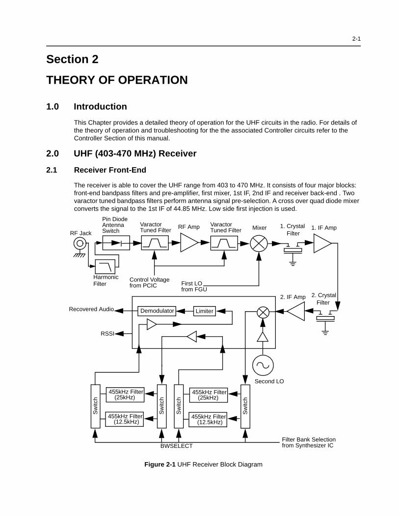
2-1
Section 2
THEORY OF OPERATION
1.0 Introduction
This Chapter provides a detailed theory of operation for the UHF circuits in the radio. For details of the theory of operation and troubleshooting for the the associated Controller circuits refer to the Controller Section of this manual.
2.0 UHF (403-470 MHz) Receiver
2.1 Receiver Front-End
The receiver is able to cover the UHF range from 403 to 470 MHz. It consists of four major blocks: front-end bandpass filters and pre-amplifier, first mixer, 1st IF, 2nd IF and receiver back-end . Two varactor tuned bandpass filters perform antenna signal pre-selection. A cross over quad diode mixer converts the signal to the 1st IF of 44.85 MHz. Low side first injection is used.
Figure 2-1 UHF Receiver Block Diagram
Demodulator
1. Crystal Filter
MixerVaractor Tuned Filter
RF AmpVaractor Tuned Filter
Pin Diode Antenna SwitchRF Jack
Control Voltagefrom PCIC First LO
from FGU
Recovered Audio
RSSI
Second LO
2. Crystal Filter
455kHz Filter(25kHz)
455kHz Filter(25kHz)
455kHz Filter(12.5kHz)
455kHz Filter(12.5kHz)
Sw
itch
Sw
itch
Sw
itch
Sw
itch
Limiter
1. IF Amp
2. IF Amp
Filter Bank Selectionfrom Synthesizer IC
Harmonic Filter
BWSELECT

2-2 UHF (403-470 MHz) Receiver
The 2-pole 44.85 MHz crystal filters in the 1st IF section and two pairs of 455 kHz ceramic filters in the 2nd IF section provide the required adjacent channel selectivity. The correct pair of ceramic filters for 12.5 or 25 kHz channel spacing is selected via control line BWSELECT. The 2nd IF at 455 kHz is mixed, amplified, and demodulated in the IF IC. The processing of the demodulated audio signal is performed by an audio processing IC located in the controller section.
2.2 Front-End Band-Pass Filters & Pre-Amplifier
The received signal from the radio’s antenna connector is first routed through the harmonic filter and antenna switch, which are part of the RF power amplifier circuits, before being applied to the receiver pre-selector filter (C4001, C4002, D4001 and associated components). The 2-pole pre-selector filter tuned by the varactor diodes D4001 and D4002 pre-selects the incoming signal (RXIN) from the antenna switch to reduce spurious effects to following stages. The tuning voltage (FECTRL_1) ranging from 2 volts to 8 volts is controlled by pin 20 of PCIC (U4501) in the Transmitter section. A dual hot carrier diode (D4003) limits any inband signal to 0 dBm to prevent damage to the pre-amplifier.
The RF pre-amplifier is an SMD device (Q4003) with collector base feedback to stabilize gain, impedance, and intermodulation. The collector current of approximately 11-16 mA is drawn from the 9.3 volt supply via L4003 and R4002. A 3dB pad (R4006,R4007,R4011 and R4008 - R4010) stabilizes the output impedance and intermodulation performance.
A second 2-pole varactor tuned bandpass filter provides additional filtering of the amplified signal. The varactor diodes D4004 and D4005 are controlled by the same signal FECTRL_1, which controls the pre-selector filter. A following 1 dB pad (R4013 - R4015) stabilizes the output impedance and intermodulation performance.
2.3 First Mixer and 1st Intermediate Frequency (IF)
The signal coming from the front-end is converted to the first IF (44.85 MHz) using a cross over quad diode mixer (D4051). Its ports are matched for incoming RF signal conversion to the 44.85 MHz IF using low side injection via matching transformers T4051 and T4052. The injection signal (RXINJ) coming from the RX VCO buffer (Q4332) is filtered by the lowpass filter consisting of (L4053, L4054, C4053 - C4055) followed by a matching transformer T4052 and has a level of approximately 15dBm.
The mixer IF output signal (IF) from transformer T4501pin 2 is fed to the first two pole crystal filter FL3101. The filter output in turn is matched to the following IF amplifier.
The IF amplifier Q3101 is actively biased by a collector base feedback (R3101, R3106) to a current drain of approximately 5 mA drawn from the 5 volt supply. Its output impedance is matched to the second two pole crystal filter FL3102. The signal is further amplified by a preamplifier (Q3102) before going into pin 1 of IFIC (U3101).
A dual hot carrier diode (D3101) limits the filter output voltage swing to reduce overdrive effects at RF input levels above -27 dBm.
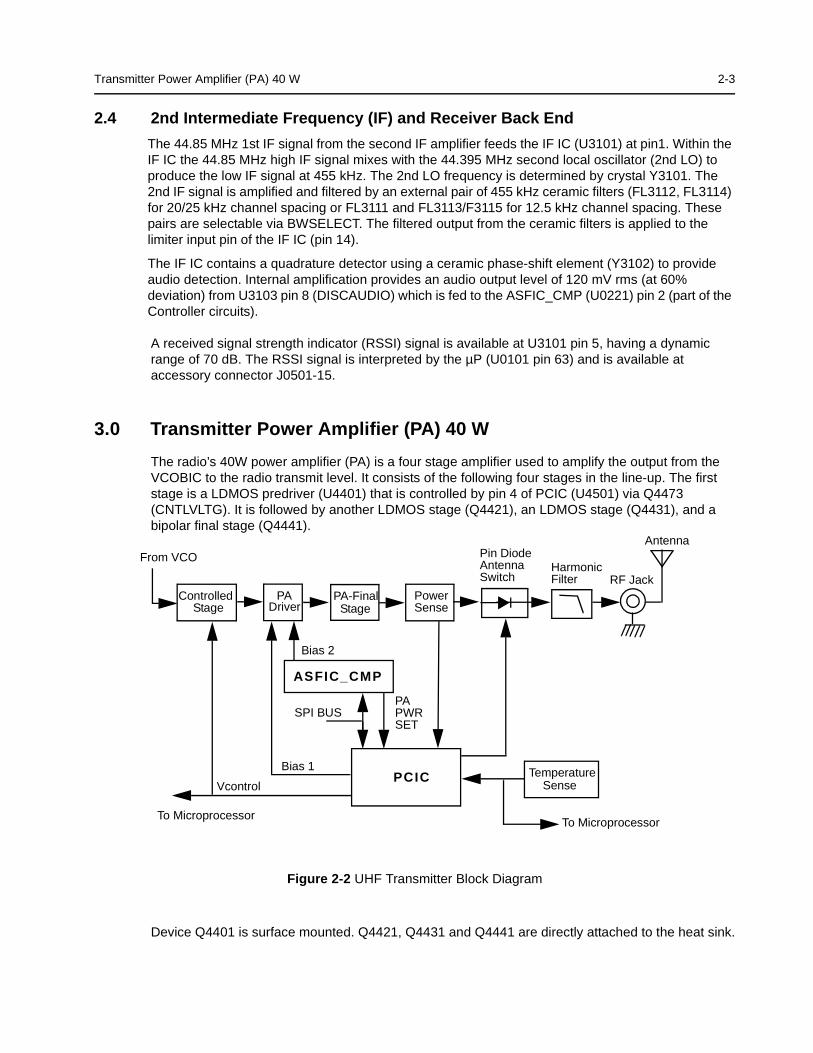
Transmitter Power Amplifier (PA) 40 W 2-3
2.4 2nd Intermediate Frequency (IF) and Receiver Back End
The 44.85 MHz 1st IF signal from the second IF amplifier feeds the IF IC (U3101) at pin1. Within the IF IC the 44.85 MHz high IF signal mixes with the 44.395 MHz second local oscillator (2nd LO) to produce the low IF signal at 455 kHz. The 2nd LO frequency is determined by crystal Y3101. The 2nd IF signal is amplified and filtered by an external pair of 455 kHz ceramic filters (FL3112, FL3114) for 20/25 kHz channel spacing or FL3111 and FL3113/F3115 for 12.5 kHz channel spacing. These pairs are selectable via BWSELECT. The filtered output from the ceramic filters is applied to the limiter input pin of the IF IC (pin 14).
The IF IC contains a quadrature detector using a ceramic phase-shift element (Y3102) to provide audio detection. Internal amplification provides an audio output level of 120 mV rms (at 60% deviation) from U3103 pin 8 (DISCAUDIO) which is fed to the ASFIC_CMP (U0221) pin 2 (part of the Controller circuits).
A received signal strength indicator (RSSI) signal is available at U3101 pin 5, having a dynamic range of 70 dB. The RSSI signal is interpreted by the µP (U0101 pin 63) and is available at accessory connector J0501-15.
3.0 Transmitter Power Amplifier (PA) 40 W
The radio’s 40W power amplifier (PA) is a four stage amplifier used to amplify the output from the VCOBIC to the radio transmit level. It consists of the following four stages in the line-up. The first stage is a LDMOS predriver (U4401) that is controlled by pin 4 of PCIC (U4501) via Q4473 (CNTLVLTG). It is followed by another LDMOS stage (Q4421), an LDMOS stage (Q4431), and a bipolar final stage (Q4441).
Figure 2-2 UHF Transmitter Block Diagram
Device Q4401 is surface mounted. Q4421, Q4431 and Q4441 are directly attached to the heat sink.
PCIC
Pin Diode Antenna Switch RF Jack
Antenna
Harmonic Filter
PowerSense
PA-FinalStage
PADriver
From VCO
ControlledStage
Vcontrol
Bias 1
Bias 2
To Microprocessor
TemperatureSense
SPI BUS
ASFIC_CMP
PAPWRSET
To Microprocessor
2-4 Transmitter Power Amplifier (PA) 40 W
3.1 Power Controlled Stage
The first stage (U4401) amplifies the RF signal from the VCO (TXINJ) and controls the output power of the PA. The output power of the transistor U4401 is controlled by a voltage control line feed from the PCIC pin4(U4501). The control voltage simultaneously varies the bias of two FET stages within U4401. This biasing point determines the overall gain of U4401 and therefore its output drive level to Q4421, which in turn controls the output power of the PA.
In receive mode the voltage control line is at ground level and turns off Q4473 which in turn switches off the biasing voltage to U4401.
3.2 Pre Driver Stage
The next stage is a 13dB gain LDMOS device (Q4421) which requires a positive gate bias and a quiescent current flow for proper operation. The voltage of the line PCIC_MOSBIAS_1 is set in transmit mode by PCIC pin 24 and fed to the gate of Q4421 via the resistive network R4407, R4408, R4416 and R4415. The bias voltage is tuned in the factory.
3.3 Driver Stage
The following stage is an enhancement-mode N-Channel MOSFET device (Q4431) providing a gain of 10dB. This device also requires a positive gate bias and a quiescent current flow for proper operation. The voltage of the line Bias_2_UHF_PA_1 is set in transmit mode by the ASFIC and fed to the gate of Q4431 via the resistive network R4630, R4631, and R4632. This bias voltage is also tuned in the factory. If the transistor is replaced, the bias voltage must be tuned using the Customer Programming Software (CPS). Care must be taken not to damage the device by exceeding the maximum allowed bias voltage. The device’s drain current is drawn directly from the radio’s dc supply voltage input, A+, via L4421.
3.4 Final Stage
The final stage uses the bipolar device Q4441. The device’s collector current is also drawn from the radio’s dc supply voltage input. To maintain class C operation, the base is dc-grounded by a series inductor (L4441) and a bead (L4440). A matching network consisting of C5541-C5544 and two striplines transform the impedance to 50 Ohms and feeds the directional coupler.
Transmitter Power Amplifier (PA) 40 W 2-5
3.5 Bi-Directional Coupler
The Bi-directional coupler is a microstrip printed circuit, which couples a small amount of the forward and reverse power of the RF power from Q4441. The coupled signal is rectified to an output power proportional dc voltage by the diodes D4451 & D4452 and sent to the RFIN of the PCIC. The PCIC controls the gain of stage U4401 as necessary to hold this voltage constant. This ensures the forward power out of the radio is held to a constant value.
3.6 Antenna Switch
The antenna switch utilizes the existing dc feed (A+) to the last stage device (Q4441). Basic operation is to have both PIN diodes D4471 and D4472 turns on during key-up by forward biasing them. It is achieve by pulling down the voltage at the cathode end of D4472 to around 11.8V (0.7V drop across each diode). The current through the diodes needs to be set around 80mA to fully open the transmit path through resistor R4496. Q4472 is a current source controlled by Q4471 and is eventually connected to pin ANO of PCIC. VR4471 ensures the voltage at the resistor R4511 never exceeds 5.6V.
3.7 Harmonic Filter
Inductors L4491, L4492, L4493 and capacitors C4448, C4493,C4494, C4496 and C4498 form a low-pass filter to attenuate harmonic energy from the transmitter. R4491 is used to drain any electrostatic charges that might otherwise build up on the antenna. The harmonic filter also prevents high level RF signals above the receiver passband from reaching the receiver circuits, improving spurious response rejection.
3.8 Power Control
The transmitter uses the Power Control IC (PCIC, U4501) to control the power output of the radio. A portion of the forward RF power from the transmitter is sampled by the bi-directional coupler and rectified, to provide a dc voltage to the RFIN port of the PCIC (pin 1) which is proportional to the sampled RF power.
The PCIC has internal digital to analog converters (DACs) which provide the reference voltage of the control loop. The reference voltage level is programmable through the SPI line of the PCIC. This reference voltage is proportional to the desired power setting of the transmitter, and is factory programmed at several points across the frequency range of the transmitter to offset frequency response variations of the transmitter’s power detector circuits.
2-6 Frequency Synthesis
The PCIC provides a dc output voltage at pin 4 (INT) and applied as CNTLVLTG to the power-adjust input pin of the first transmitter stage U4401. This adjusts the transmitter power output to the intended value. Variations in forward or reflected transmitter power cause the dc voltage at pin 1 to change, and the PCIC adjusts the control voltage above or below its nominal value to raise or lower output power.
Capacitors C4502-4, in conjunction with resistors and integrators within the PCIC, control the transmitter power-rise (key-up) and power-decay (de-key) characteristic to minimize splatter into adjacent channels.
U4502 is a temperature-sensing device, which monitors the circuit board temperature in the vicinity of the transmitter driver and final devices, and provides a dc voltage to the PCIC (TEMP, pin 29) proportional to temperature. If the dc voltage produced exceeds the set threshold in the PCIC, the transmitter output power is reduced so as to reduce the transmitter temperature.
4.0 Frequency Synthesis
The synthesizer subsystem consists of the reference oscillator (Y4261 or Y4262), the low voltage fractional-N synthesizer (LVFRAC-N, U4201), and the Voltage Controlled Oscillator VCO.
4.1 Reference Oscillator
The reference oscillator (Y4262) contains a temperature compensated crystal oscillator with a frequency of 16.8 MHz. An Analog-to-Digital (A/D) converter internal to U4201 (LVFRAC-N) and controlled by the µP via serial interface (SRL) sets the voltage at the warp output of U4201, pin 25 to set the frequency of the oscillator. The output of the oscillator (pin 3 of Y4262) is applied to pin 23 (XTAL1) of U4201 via an RC series combination.
In applications where less frequency stability is required the oscillator inside U4201 is used along with an external crystal Y4261, varactor diode D4261, C4261, C4262 and R4262. In this case, Y4262, R4263, C4235 and C4251 are not used. When Y4262 is used, Y4261, D4261, C4261, C4262 and R4262 are not used, and C4263 is increased to 0.1 uF.

Frequency Synthesis 2-7
4.2 Fractional-N Synthesizer
The LVFRAC-N synthesizer IC (U4201) consists of a pre-scaler, a programmable loop divider, control divider logic, a phase detector, a charge pump, an A/D converter for low frequency digital modulation, a balanced attenuator to balance the high frequency analog modulation and low frequency digital modulation, a 13V positive voltage multiplier, a serial interface for control, and finally a super filter for the regulated 5 volts.
A voltage of 5V applied to the super filter input (U4201 pin 30) supplies an output voltage of 4.5 Vdc (VSF) at pin 28. It supplies the VCO, VCO modulation bias circuit (via R4322) and the synthesizer charge pump resistor network (R4251, R4252). The synthesizer supply voltage is provided by the 5V regulator U4211.
In order to generate a high voltage to supply the phase detector (charge pump) output stage at pin VCP (U5701-32), a voltage of 13 Vdc is being generated by the positive voltage multiplier circuitry (D4201, C4202, C4203). This voltage multiplier is basically a diode capacitor network driven by two signals (1.05MHz) 180 degrees out of phase (U4201-14 and -15).
Figure 2-3 UHF Synthesizer Block Diagram
Output LOCK (U4201-4) provides information about the lock status of the synthesizer loop. A high level at this output indicates a stable loop. IC U4201 provides the 16.8 MHz reference frequency at pin 19.
The serial interface (SRL) is connected to the µP via the data line DATA (U4201-7), clock line CLK (U4201-8), and chip enable line CSX (U4201-9).
DATA
CLK
CEX
MODIN
VCC, DC5V
XTAL1
XTAL2
WARP
PREIN
VCP
REFERENCEOSCILLATOR
VOLTAGEMULTIPLIER
DATA (U0101 PIN 100)
CLOCK (U0101 PIN 1)
CSX (U0101 PIN 2)
MOD IN (U0221 PIN 40)
+5V (U4211 PIN 1)
7
8
9
10
13, 30
23
24
25
32
47
VMULT2 VMULT1
BIAS1
SFOUT
AUX3
AUX4
IADAPTIOUT
GND
FREFOUT
LOCK 4
19
6, 22, 33, 44
4345
3
2
28
14 15
40
FILTERED 5V
STEERING
LOCK (U0101 PIN 56)
PRESCALER IN
FREF (U0221 PIN 34)
39BIAS2
41
48
5, 20, 34, 36+5V (U4211 PIN 1)
AUX1
VDD, DC5V MODOUT
U4201 LOW VOLTAGEFRACTIONAL-NSYNTHESIZER
AUX2 1 (NU)
BWSELECT
VCO Bias
TRB
To IFSection
TX RF INJECTION(1ST STAGE OF PA)
LO RF INJECTION
VOLTAGE CONTROLLED OSCILLATOR
LINE2-POLELOOP
FILTER

2-8 Frequency Synthesis
4.3 Voltage Controlled Oscillator (VCO)
The Voltage Controlled Oscillator (VCO) consists of the VCO buffer IC (VCOBIC, U4301), the TX and RX tank circuits, the external RX buffer stages, and the modulation circuits.
The VCOBIC together with Fractional-N synthesizer (U4201) generates the required frequencies in both transmit and receive modes. The TRB line (U4301 pin 19) determines which tank circuits and internal buffers are to be enabled. A high level on TRB enables TX tank and TX output (pin 10), and a low enables RX tank and RX output (pin 8). A sample of the signal from the enabled output is routed from U4301 pin 12 (PRESC_OUT), via a low pass filter, to pin 32 of U4201 (PREIN).
A steering line voltage (VCTRL) between 3.0V and 10.0V at varactor diode CR4311 will tune the full TX frequency range (TXINJ) from 403 MHz to 470 MHz, and at varactor diodes CR4301, CR4302 and CR4303 will tune the full RX frequency range (RXINJ) from 358 MHz to 425 MHz. The tank circuits uses the Hartley configuration for wider bandwidth. For the RX tank circuit, an external transistor Q4301 is used in conjunction with the internal transistor for better side-band noise.
Figure 2-4 UHF VCO Block Diagram
The external RX buffers (Q4332) are enabled by a high at U4201 pin 3 (AUX4) via transistor switch Q4333. In TX mode the modulation signal (VCOMOD) from the LVFRAC-N synthesizer IC (U4201 pin41) is applied to the modulation circuits CR4321, R4321, R4322 and C4324. These modulate the TX VCO frequency via coupling capacitor C4321. Varactor CR4321 is biased for linearity from the VSF.
Presc
RX
TX
MatchingNetwork Low Pass
Filter
Attenuator
Pin8
Pin14
Pin10
(U4201 Pin28)
VCC Buffers
TX RF Injection
U4201 Pin 32
AUX3 (U4201 Pin2)
Prescaler Out
Pin 12Pin 19Pin 20
TX/RX/BSSwitching Network
U4301VCOBIC
RxActive Bias
TxActive Bias
Pin2
Rx-I adjust
Pin1
Tx-I adjust
Pins 9,11,17Pin18
VsensCircuit
Pin15
Pin16
RX VCO Circuit
TX VCO Circuit
RX Tank
TX Tank
Pin7
Vcc-Superfilter
Collector/RF in
Pin4
Pin5
Pin6
RX
TX
(U4201 Pin28)
Rx-SW
Tx-SW
Vcc-Logic
(U4201 Pin28)
Steer Line Voltage (VCTRL)
Pin13
Pin3
TRB IN
LO RF INJECTION
Q4301
Q4332
Frequency Synthesis 2-9
4.4 Synthesizer Operation
The complete synthesizer subsystem comprises mainly of a low voltage FRAC-N (LVFRACN) IC, Reference Oscillator (crystal oscillator with temperature compensation), charge pump circuits, loop filter circuits, and dc supply. The output signal (PRESC_OUT) of the VCOBIC (U4301, pin12) is fed to of U4201, pin 32 (PREIN) via a low pass filter (C4229,L4225,C4226) which attenuates harmonics and provides correct level to close the synthesizer loop.
The pre-scaler in the synthesizer (U4201) is basically a dual modulus pre-scaler with selectable divider ratios. The divider ratio of the pre-scaler is controlled by the loop divider, which in turn receives its inputs via the SRL. The output of the pre-scaler is applied to the loop divider. The output of the loop divider is connected to the phase detector, which compares the loop divider´s output signal with the reference signal.The reference signal is generated by dividing down the signal of the reference oscillator (Y4261 or Y4262).
The output signal of the phase detector is a pulsed dc signal which is routed to the charge pump. The charge pump outputs a current at pin 43 of U4201 (IOUT). The loop filter (which consists of R4221-R4223, C4221-C4225,L4221) transforms this current into a voltage that is applied to the varactor diodes CR4311 for transmit, CR4301, CR4302 & CR4303 for receive and alters the output frequency of the VCO.The current can be set to a value fixed in the LVFRAC-N IC or to a value determined by the currents flowing into BIAS 1 (U4201-40) or BIAS 2 (U4201-39). The currents are set by the value of R4251 or R4252 respectively. The selection of the three different bias sources is done by software programming.
To reduce synthesizer lock time when new frequency data has been loaded into the synthesizer the magnitude of the loop current is increased by enabling the IADAPT (U4201-45) for a certain software programmable time (Adapt Mode). The adapt mode timer is started by a low to high transient of the CSX line. When the synthesizer is within the lock range the current is determined only by the resistors connected to BIAS 1, BIAS 2, or the internal current source. A settled synthesizer loop is indicated by a high level of signal LOCK (U4201-4).
LOCK (U4201-4) signal is routed to one of the µP´s ADCs input U101-56. From the voltage the µP determines whether LOCK is active.
In order to modulate the PLL the two spot modulation method is utilized Via pin 10 (MODIN) on U4201. The audio signal is applied to both the A/D converter (low frequency path) as well as the balanced attenuator (high frequency path). The A/D converter converts the low frequency analog modulating signal into a digital code which is applied to the loop divider, thereby causing the carrier to deviate. The balance attenuator is used to adjust the VCO’s deviation sensitivity to high frequency modulating signals. The output of the balance attenuator is present at the MODOUT port (U4201-41) and connected to the VCO modulation diode CR4321 via R4321, C4325.

2-10 Frequency Synthesis
THIS PAGE INTENTIONALLY LEFT BLANK

3-1
Section 3
TROUBLESHOOTING CHARTS
1.0 Troubleshooting Flow Chart for Receiver (Sheet 1 of 2)
Bad SINADBad 20dB Quieting
No Recovered Audio
START
Audio at pin 8 of U3101 ?
Check Controller(in the case of no audio)
OR ELSE go to “B”
Yes
No
Spray or inject 44.85MHz into XTAL Filter FL3101
Audio heard ?BYes
No
Check 2nd LO (44.395MHz) at C3135
LO present ?BYes
Check voltages on U3101
Biasing OK ?
No
No
A
Yes
Check Q3102 bias for faults
Replace Q3102
Go to B
Yes
No
Check circuitry around U3101.
Replace U3101 if defect
Check circuitry around Y3101. Replace Y3101 if defect
Voltages
OK?
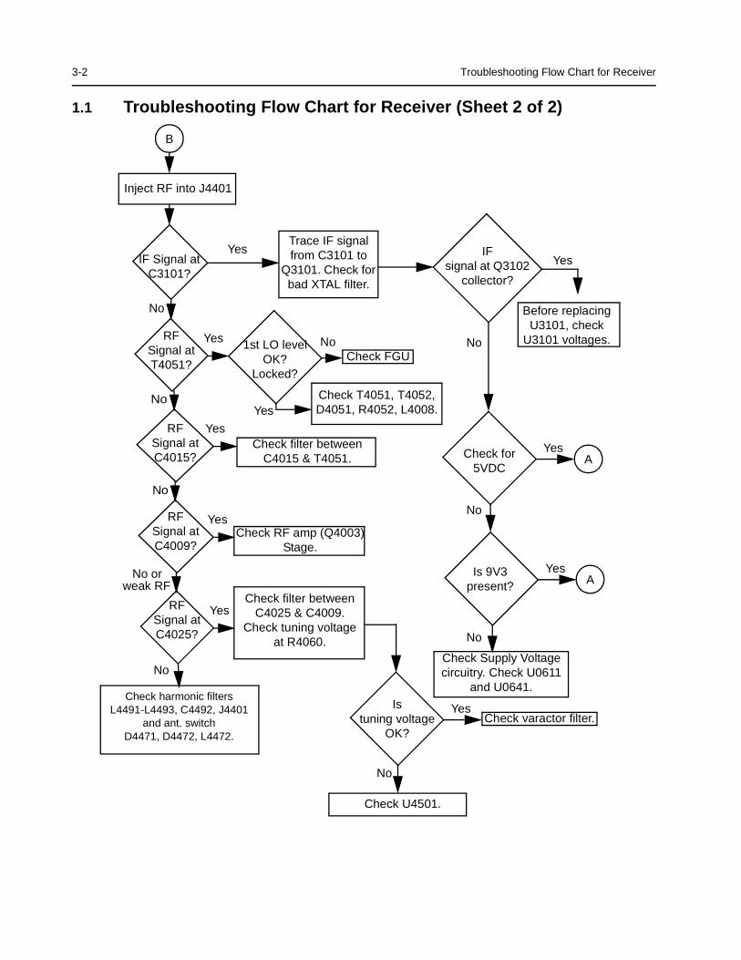
3-2 Troubleshooting Flow Chart for Receiver
1.1 Troubleshooting Flow Chart for Receiver (Sheet 2 of 2)
IF Signal at C3101?
No
RF Signal at T4051?
RFSignal at C4015?
No
No
RFSignal at C4025?
No or
Check harmonic filtersL4491-L4493, C4492, J4401
and ant. switchD4471, D4472, L4472.
Check filter between C4025 & C4009.
Check tuning voltage at R4060.
Inject RF into J4401
Istuning voltage
OK?
No
Yes
Check RF amp (Q4003) Stage.
Check filter between C4015 & T4051.
Yes
Check T4051, T4052, D4051, R4052, L4008.
Yes
1st LO level OK?
Locked?
Yes
Check FGU
Yes
Trace IF signal from C3101 to
Q3101. Check for bad XTAL filter.
No
Yes IFsignal at Q3102
collector?
Before replacing U3101, check
U3101 voltages.
Yes
Check for 5VDC
Is 9V3 present?
Check Supply Voltage circuitry. Check U0611
and U0641.
No
No
No
Check U4501.
Check varactor filter.
No
Yes
Yes
Yes
A
A
B
weak RF
RFSignal at C4009?
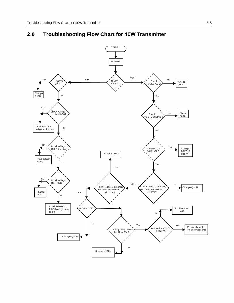
Troubleshooting Flow Chart for 40W Transmitter 3-3
2.0 Troubleshooting Flow Chart for 40W Transmitter
No
Is Q4441 OK ?
YesIs drive from VCO >+4dBm?
No
Is voltage drop across R4497 >4.5V ?
No
Check Q4431 gate(open)and drain resistances (11kohm)
NoCheck Q4421 gate(open)and drain resistances (11kohm)
No
CheckPCIC_MOSBIAS_1
No
No
ChangeQ4573
START
No power
Is Vctrlthere?
Is Q4573 OK?
Check voltageon pin 4 U4501
Check voltageon pin 5 U4501
Check R4422-5and go back to top
TroubleshootASFIC
Check voltageon TP4531
ChangePCIC
Check R4409 &
R4473 and go backto top
CheckMOSBIAS_2
CheckASFIC
Are D4471 &D4472 OK?
ChangeD4471 &D4472
NoNoNoNo No
Yes
Yes
YesYes
Yes
YesYes
Yes
No
No CheckPCIC
Yes
Change Q4421
Change Q4431
Yes
Change U4401
YesDo visual checkon all components
No
Change Q4441
Troubleshoot VCO
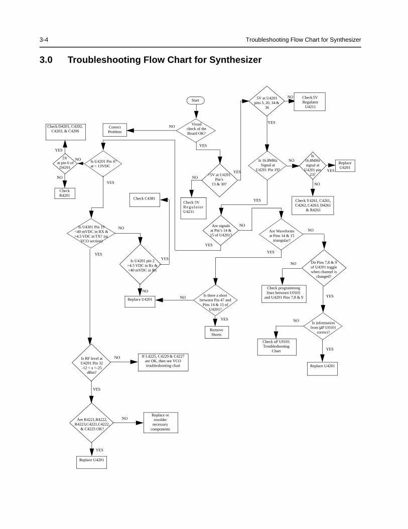
3-4 Troubleshooting Flow Chart for Synthesizer
3.0 Troubleshooting Flow Chart for Synthesizer
5V at pin 6 of
D4201
Is informationfrom µP U0101
correct?
Is U4201 Pin 47at = 13VDC
Is U4301 Pin 19<40 mVDC in RX &>4.5 VDC in TX? (at
VCO section)
Start
Visual check of the Board OK?
CorrectProblem
Check 5VR e gu la to rU4211
+5V at U4201Pin’s
13 & 30?
Is 16.8MHzSignal at
U4201 Pin 19?
Check Y4261, C4261, C4262, C4263, D4261
& R4261
Are signalsat Pin’s 14 &15 of U4201?
Check R4201
Check C4381
Is U4201 pin 2 >4.5 VDC in Rx & <40 mVDC in Rx
Replace U4201
RemoveShorts
Is there a shortbetween Pin 47 and
Pins 14 & 15 ofU4201?
Replace orresolder
necessarycomponents
Is RF level atU4201 Pin 32 -12 < x <-25
dBm?
Are R4221,R4222,R4223,C4221,C4222,
& C4223 OK?
Replace U4201
If L4225, C4229 & C4227are OK, then see VCOtroubleshooting chart
Are Waveformsat Pins 14 & 15
triangular?
Do Pins 7,8 & 9of U4201 togglewhen channel is
changed?
Check programminglines between U0101
and U4201 Pins 7,8 & 9
Replace U4201
Check uP U0101Troubleshooting
Chart
NO
YES
NO
YES
NO
YES
NO
NO
NO
YES
YES
NO
YES
YES
NO
YES
YES
YESNO
NO
NO
NO
YES
NO
YES
YES
Check D4201, C4202, C4203, & C4206
5V at U4201 pins 5, 20, 34 &
36
Check 5V Regulator
U4211
Is 16.8MHz signal at
U4201 pin 23?
Replace U4201
YES
NO
NO
YES
NO
YES

Troubleshooting Flow Chart for VCO 3-5
4.0 Troubleshooting Flow Chart for VCO
Are Q4332Base at 0.7V
Collector at 4.5V Emitter at 110mV
Are Q4301Base at 2.4V
Collector at 4.5V Emitter at 1.7V
Are U4301 Pins13 at 4.4V15 at 1.1V10 at 4.5V16 at 1.9V
Low or no RF Signalat TP4003
Visual checkof board
OK?
35mV DC atU4301 Pin 19
NO
YES
Replace Q4301
at base of Q4332
NO
NO
NO
NO
YES
YES
YES
YES
Low or no RF Signalat input to PA
4.8V DC atU4301 Pin 19
Is RF available at C4402
YES
YES
YES
YES
NO
NO
NO
NO
NO
Audio =180mVrmsat “-” Side of
4.5VDCat CR4321
If C4321 and R4321 are OK, then replace CR4321
Replace C4322
Replace C4325
NO
NO
YES
YES
If parts between R4402 & U4301 Pin10are OK, replace U4301
TX VCORX VCO
CorrectProblem
Visual checkof board
OK?
Check runner between U4201 Pin 2
and U4301 Pin 19
Is RF available If all parts from U4301 Pin 8to Base of Q4332 are OK,
replace U4301
If all parts associated with the pins are OK,
replace Q4332
If all parts from collectorof Q4332 to TP4003 are
OK, Replace Q4332
Power OK but no modulation
Check parts fromR4402 to U4401 Pin16
If all parts associated
with the pins are OK,
replace U4301
YES YES
Make sure Synthesizer is working correctly and runner between U4201 Pin 28 and U4301 Pin 14 & 18 are OK
4.5V DC
OK ?
OK? OK?
C4325
at U4301 Pin 14 & 18 4.5V DC
OK ?at U4301 Pin 14 &18
NO

3-6 Troubleshooting Flow Chart for VCO
THIS PAGE INTENTIONALLY LEFT BLANK

4-1
Section 4
UHF PCB/SCHEMATICS/PARTS LISTS
1.0 Allocation of Schematics and Circuit Boards
1.1 Controller Circuits
The UHF circuits are contained on the Printed Circuit Board (PCB) which also contains the Controller circuits. This Chapter shows the schematics for the UHF circuits only, refer to the Controller section for details of the related Controller circuits . The PCB component layouts and the Parts Lists in this Chapter show both the Controller and UHF circuit components. The UHF schematics and the related PCB and parts list are shown in the tables below.
Table 4-1 UHF 25-40W Diagrams and Parts Lists
PCB :8480643Z06 Main Board Top Side8480643Z06 Main Board Bottom Side
Page 4-3Page 4-4
SCHEMATICSPower Amplifier 25 - 40WFRACNVoltage Controlled OscillatorReceiver Front EndIF
Page 4-5Page 4-6Page 4-7Page 4-8Page 4-9
Parts List8480643Z06 Page 4-10

4-2 Allocation of Schematics and Circuit Boards
THIS PAGE INTENTIONALLY LEFT BLANK
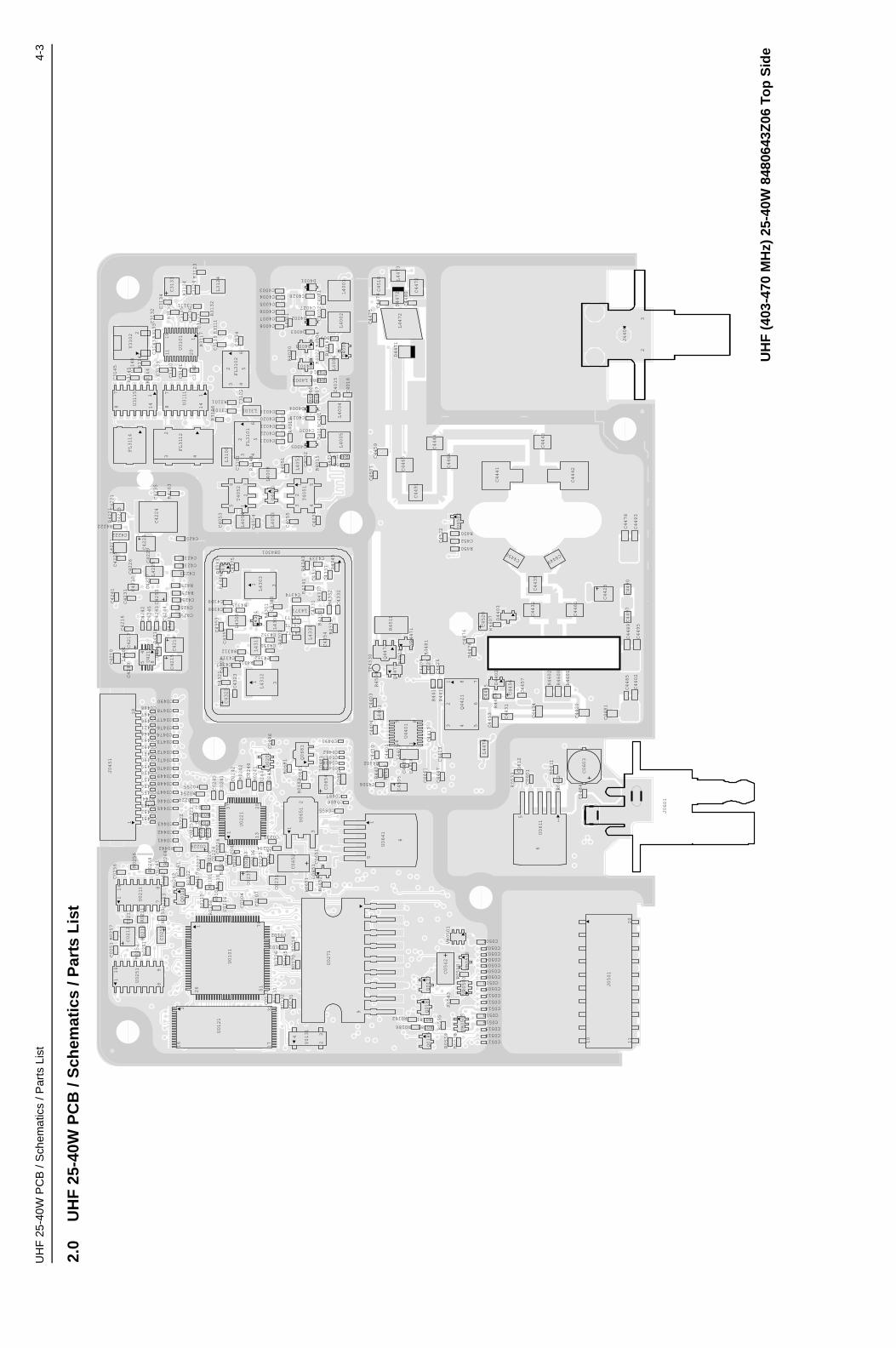
UH
F 2
5-40
W P
CB
/ S
chem
atic
s / P
arts
Lis
t4-
3
2.0
UH
F 2
5-40
W P
CB
/ S
chem
atic
s / P
arts
Lis
t
16
1
89
U0251
C0211
C0212
C0251
R0211
R0212
R0251
R0252
R0257
C0252R0253
C0262
87
114
U0211
C0256 R0256
R0268
C0253
Q0110R0102
R0261
R0262C0261 R0269
18
1
J0451
C0421
C0451C0452C0453
C0455C0456C0457
C0458C0459C0460C0461C0462
C0463C0464
C0466C0467C0468
R0441
C0441
C0442
C0443
C0445
C0446
C0447
C0448
C0449
C0470
C0471
C0472
C0473
C0474
C0476
C0477
C0478
C0490
C0221
C0222
C0225
C0241
C0243
R0220
R0221
R0223
R0224
R0229
R0254
R0255
R0222
R0442
C0242
C0244
C0245
C0246
C0496
D0201
R0241
R0242
137
25
13
U0221
3
2
1
U0651
C0681
Q0681
R0681
R0682
C0482C0483
C0486C0487
C0488
C0493
C0494
C0654
C0655
L0481
L0482
C0223
C0224
C0226
C0227
C0228
C0232
C0233
C0234
C0235
C0236C0495
R0225
R0226
R0227
R0228
C0231
C0237
C0652
R0101
R0104
R0108
R0110
R0115
R0116
C0104
C0106
C0107
C0101
C0102
C0132
R0106
R0131
R0132
1 76
51
26
U0101
32
17
16
1
U0121
C0131
R0105 R0114
R0170
9
U0271
234
Y0131
C0501
C0502C0503C0504C0505C0506C0508
C0509C0510
C0511C0512
C0513C0514
C0515C0516
C0517C0518
C0542
Q0177
Q0181
Q0185
R0181R0182
R0185R0186
R0510
R0535
R0538
R0539
R0543
VR0501
VR0503
VR0505
VR0510
20
11
10
J0501
C0651
D0651
R0651
R0652
1
6
5
U0641
1
6
5
U0611
C0484
C0601 C0603
C0612
R0533 R0611
R0612
J0601
C4210
C4212C4213
C4214
C4215
C4216
C4225
C4226
C4227
C4229
C4230
C4231
C4241
C4242
C4243
C4244
C4245
C4246
C4253
C4289L4201
L4225
R4211
45 8U4211
C4221
C4222
C4223
C4224
C4235
L4221
R4221
R4222 R4223
R4263
32
J4401
C4444
C4459
C4465
C4466
C4491
C4507
C4521
C4522 R4501
R4502
U4502
C4423
C4432
C4435
C4449C4450
C4460
C4478
C4490
C4497
C4520
D4403
R4607
C4420
C4481
C4485
C4489
C4495
C4602
R4600
R4601
R4602
C4431
C4434
C4453
C4455
C4456
C4457
D4402
R4459
C4476
5
2 6
813
7
4Q4421
R4476
L4474
C4401
C4403
C4404
C4410
C4417
C4419
C4447
C4461
C4486
C4488
C4505
C4506
L4401
L4403
R4401
R4402
R4403
116
89
U4401
C4425
C4426
Q4471
Q4472
R4408
R4415
R4416
R4481
R4504
R4511
R4512
TP4530
VR4471
1 3
L4312
C4322
C4323
C4325R4321
C4317C4318
C4351
C4352C4353
C4355
C4382
L4304
L4305
L4313
Q4301
R4311
R4312
C4383
R4301
R4302
C4308
C4309
C4375
1 3
L4303
43
Q4333
R4305
R4346
SH4301
C4331 C4332
C4335
C4337
C4339
C4354
C4371
C4372
C4373
C4374
L4331
L4371
R4331
R4332
R4333
R4337
R4341
R4343
R4345
C4493
C4441
C4442
C4443
FL3114
FL3112
432
C3139
C3145
C3148
R3142
R3144
R3145
87
114U3115
2Y3102
C3143R3135
C3140
C3141
87 1
14U3111
C3142
U3101
R3117
11
120
10
C3124
C3131
C3132
C3133
C3134
C3135
C3136
C3137
L3124
R3111
R3123
R3124
R3130
R3132
C3115
C3114
23 4
56
FL3102
C3101
C3102
C3103
23 4
56
FL3101
L3100
L3101
R3101
R3106
R3148
L4008
C4001
C4002
C4003C4004
C4005
C4006
C4007
C4008
C4009
C4014
C4015
C4016
C4026
C4027
D4001
D4002
D4003
L4001
L4002
L4003
L4006
Q4001
Q4003R4001
R4003 R4004
R4005
R4007
R4018
R4020
R4022
R4066
C4017
C4018
C4019
C4020
C4021
C4022
C4023
C4029
C4030
C4051
C4052
D4004
D4005
L4004
L4005
L4051
R4012
R4013
R4014
R4015
R4051
D4051
21 5
43
T4051
C4031
C4055
L4053
C4053
C4054
L4054
215
4 3
T4052
C4472
C4474
C4475
C4480C4510
D4471
D4472
L4472
L4473
C4232
C4233
C4234
C4251
C4252
C4254
C4255
R4251
R4252U
HF
(40
3-47
0 M
Hz)
25-
40W
848
0643
Z06
To
p S
ide
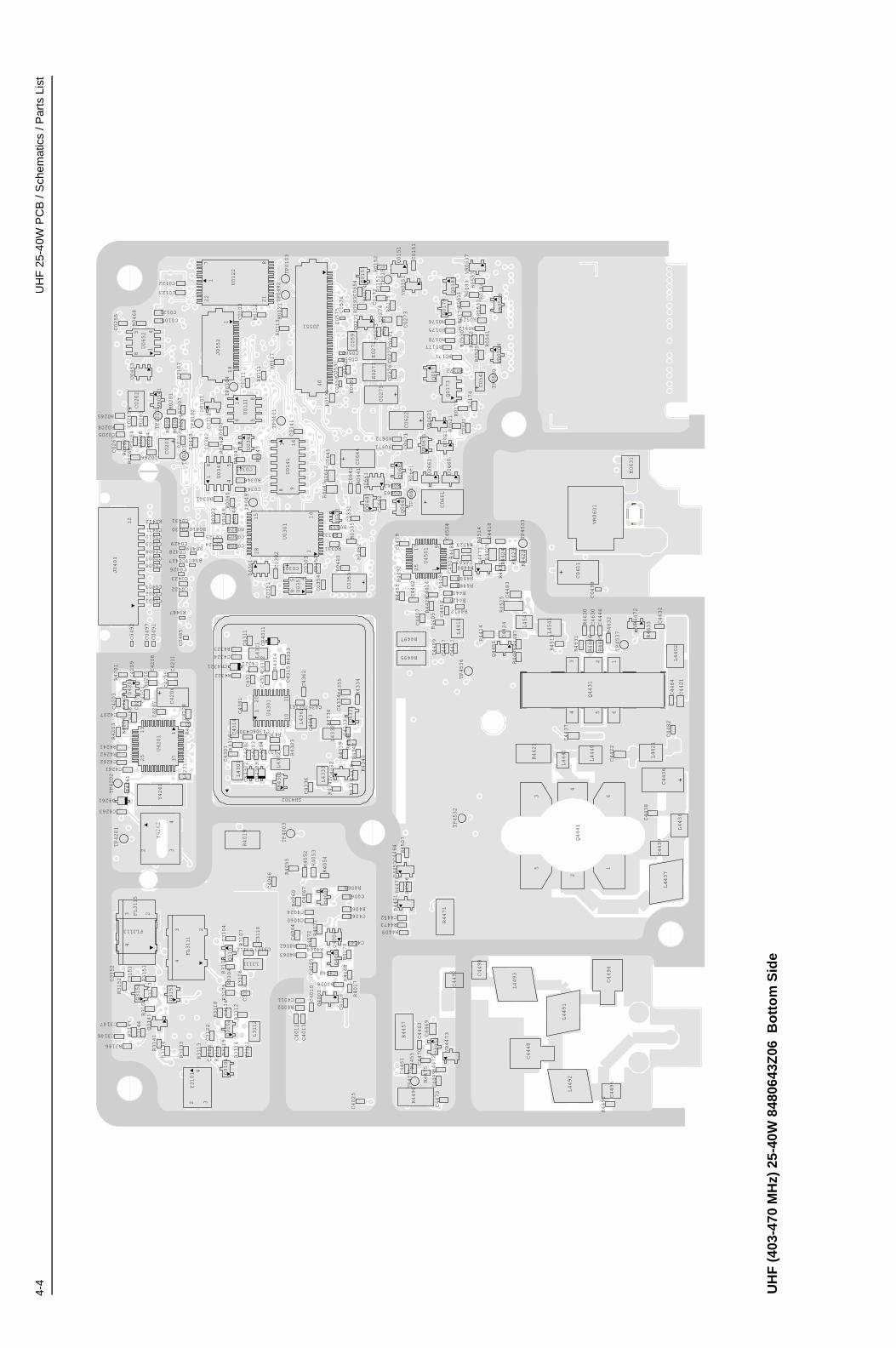
4-4
UH
F 2
5-40
W P
CB
/ S
chem
atic
s / P
arts
Lis
t
C3144
C3146
C3147
Q3141
R3134
R3141
R3146
R3147
R3154
R3113
R3133
C3151
C3152
Q3152R3151
R3152
R3153
Q3151
43 2
FL3111
FL3113
43 2FL3115
C4263
D4261
R4261
TP4201
TP4202
Y4261
2 34
Y4262
C4261
C4262
R4241
R4262
137
25
13
U4201
C4201
C4202
C4203
C4204 C4205
C4206
C4208
C4209
C4211
C4287
D4201R4201
R4206
C4207
C4288
R4203
R4204 C4228
L4231
R4228
C0485
4
32Y3101
C3116
C3121
C3122
C3123
D3101
L3112
Q3102
R3112
R3114
R3115
R3116
R3118
C3104
C3110
C3111
C3112 C3113
L3111Q3101
R3102
R3104
R3105
R3107
R3108
C4010
C4011
C4012
C4013
C4024
C4028
C4060
C4061
C4062
C4064
C4065
C4066
C4067
C4068
C4069
D4006
D4007
Q4002
Q4004
R4002
R4016
R4017
R4052
R4053
R4054
R4055
R4060
R4061
R4062
R4063R4064
R4068
R4069
R4070
R4071
R4072
C0401C0402C0403
C0406C0407C0408
C0409C0410C0411
C0422
C0423
C0426
C0427
C0428
C0429
C0430
C0431
C0491
C0492
C0497
12
J0401 R0407
R0409
R0410
R0412
R0467
C0301C0302
C0303
C0351
C0352
C0354D0301
28
15 14
1
U0301
458 U0351
C0304
C0305
C0324C0325
C0343
R0323
R0324
R0344
R0341
R0345
C0341
C0342
C0344
R0342
R0343
R0346
R0347
1
458
U0341
U0342 C0141
161
8 9U0141
TP0101
TP0497
C0201
C0202
C0203C0204
C0205
C0254C0265
C0266
C0267
R0107
R0201
R0202
R0203
R0204 R0205
R0206
R0207
R0208
R0265
R0266
R0267
R0408
TP0102
TP0221
TP0222
U0653
VR0541
C0103
C0111
C0112D0101
118
J0552
R0111
R0112
R0113
R0117
R0121
R0401
TP0103
TP0104
TP0492
14 5
8U0111
22
21
871
U0122
C0105
C0121
C0122
C0123
C0255
R0468
145
8U0652
R4019
TP4003
C4301
C4302
C4303
C4304
C4305 C4306
C4307
C4316
C4336
C4361
C4362
C4363
C4381
CR4301
CR4302
CR4303
L4301
L4302
L4333
L4361
R4303
R4304
R4315
R4361
SH4302
11
120
10U4301
C4311
C4312
C4313
C4314
C4315
C4321C4324
CR4311
CR4321
L4311
R4313
R4314
R4322
R4323
C4025
C4451
C4463
C4469
C4470
C4473C4499
D4452
R4455
R4457
R4472
R4475
R4496TP4531
VR4473
C4333
C4334
C4338
L4332
Q4331
Q4332
R4334
R4335
R4336
R4338
R4339
R4340
R4342
R4344
R4347
C4452
C4464
D4451
D4453
R4409
R4471
R4473
R4474
R4506
R4507
TP4532
C4492 C4498
C4448
C4496
L4491
L4492
R4491
C4494
L4493
1
24
6
Q4441
C4436
C4438
C4439
C4482
L4421
L4436
L4437
C4422
C4437
L4440
L4441
R4421
6543 2 1
Q4431
35
C4632
L4402
R4633
TP4537
VR4472
C4421
C4484
C0499
C0611
C4446
C4630
R4485
R4486
R4630
R4631
R4632
C4424
L4541
L4543
Q4451R4414
R4487
R4488 R4513
R4525 C4483
C4407
C4409
C4412
C4414
C4416
C4462
C4487
L4411
R4405
R4411
R4412
R4427
R4428
R4495
R4497
TP4536
R4433
C4479
C4502 C4503
C4504
R4480
R4482
R4483
R4484R4492
R4503
R4523
1
17 9
25
U4501
C4418
Q4473
R4422
R4423
R4424
R4425
R4431
R4514
TP4533
E0631
VR0601
C0331
C0353
R0331
R0332
R0333
R0335
R0481 R0482
U0331
C0641C0644
C0645
R0641
R0642
R0643
C0662
Q0641
Q0661
C0661
C0663
D0660
D0661
Q0662
Q0663
R0661
R0662
TP0661
C0622
C0671
R0671
R0672
VR0671
C0541
C0621
D0621
Q0171
Q0173
R0172
R0173
R0174
R0621
TP0530
VR0621
D0179
R0171
R0175
R0176
R0177R0178
R0179
R0183
R0184
R0511
R0512
R0525
R0529
R0530
R0531
R0541
R0542
VR0151
VR0504
VR0509
Q0183
R0537VR0537
C0271
C0275
C0276C0277
C0558
C0559C0560
C0591
C0592
C0593
E0271
E0272
R0591
R0592
C0151
C0272
C0273
C0274
C0554
C0575 C0576
D0151
Q0151
Q0271
R0151R0152
R0273
R0274
R0275
R0276
R0593
TP01511
40
J0551
UH
F (
403-
470
MH
z) 2
5-40
W 8
4806
43Z
06 B
ott
om
Sid
e
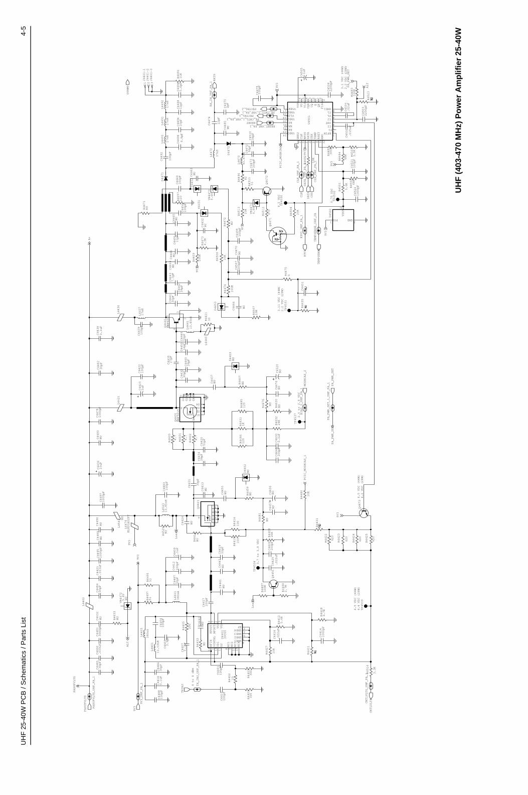
UH
F 2
5-40
W P
CB
/ S
chem
atic
s / P
arts
Lis
t4-
5
PASUPVLTG
PASUPVLTG_UHF_PA_1
PASUPVLTG
NU
NU
NU
NU
NU
NU
R4633
C4632
30pF
C4485
3000pF
C4481
C4602
.033uF ALT
L4402
5.6V
VR4472
30pF
C4484
.033uF
C4421
C4490
1000pF
C4495
C4489
C4436
10uF
1000pF
C4478
C4493
C4497
1000pF
L4421
C4423
1uF
C4422
100pF
30pF
C4482
100pF
C4439
L4436
0.1uF
C4438
17nH
L4437
9V3
100pF
C4488
C4486
30pF
C4404
100pF
390nH
L4403
9V3_UHF_PA_1
11.03nH
L4401
C4418
0.1uF
3.9pF
C4403
4 to 6 dBm
C4407
0.1uF
TXINJ
R4405
200
TX_INJ_UHF_PA_1
R4433
NU
NU
NU
NU
NU
NU
NU
NU NU
NU
NU
NU
NU
NU
NU
NU
NU
NU
NU
NU
NU
NU
NUNU
NU
NU
NU
NU
NU
NU
NU
NU
C4462
VD1
14
VG12
VG23
NC1
8
NC2
9
NC3
10
NC4
15
RFIN
16
RFOUT16
RFOUT27
VCNTRL
1
U4401
30C65
EP17
G2
11
GND14
GND25
GND312
GND413
300
R4401
300
R4403
15
R4402
C4410
100pF
C4401
100pF
51
R4495
100pF
C4412
R4497
51 L4411
390nH
C4417
100pF
C4487
30pF
0.1uF
C4409
9V3
33pF
C4419
C4461
C4447
C4453
6
2
134578
Q4421
BLM31A02PT
L4474
R4414
C4483
100pF
R4525
C4431
30pF
L4541
C4424
L4543
13.85nH
9V3
Load
51pF
C4420
C4434
39pF
4.7
R4600
4.7
R4602
R4601
4.7
C4630
0.1uF
R4486
120
R4632
24K
100pF
C4446
R4631
1K
120
R4485
R4476
R4480
10K
PCIC_MOSBIAS_1
2.4 to 2.6 VDC
TP4537
MOSBIAS_2
BIAS_2_UHF_PA_1C4476
C4520
C4456
C4457
R4481
D4402
R4459
C4455
C4437
D4403
R4607
G17
G28
G39 10
G4
S1S2S3S4
Q4431
MRF5015
D
G
39pF
C4460
4
2
1
3
MRF650
Q4441
27pF
C4435
30pF
C4432
16pF
C4450C4449
33pF
13.85nH
L4441
L4440
10
R4421
39pF
C4442
C4441
30pF
C4470
D4453
C4464
C4499
100pF
100pF
C4507
R4474
100K
10K
R4507
10K
R4506
100K
R4409
4.3K
R4473
9V3
D4452
D4451
D4471
C4465
11pF
C4491
100pF
C4469
5.6V
VR4473
C4444
C4452
C4466
C4459
100pF
C4443
7.5pF
120
R4457
R4472
C4463
C4498
6.8pF
L4493
17nH
C4492
100pF
R4471
R4491
11K
J4401-1
1
L4491
17nH
L4492
17nH
C4448
12pF
J4401-3
3
10pF
C4494
5.6pF
C4496
J4401-2
2
DUMMY
12pF
C4474
2pF
C4475
17nH
L4472
RX_IN_VHF_PA_1RXIN
C4480
D4472
FECTRL_1
FECTRL_2
C4479
100pF
RESETFE_CNTL_1_VHF_PA_1
FE_CNTL_2_VHF_PA_1
RESET_VHF_PA_1
9V3
36pF
C4472
43.67nH
L4473
C4510
36pF
R4496
82
100pF
C4473
Q4472
51
R4511
PCIC_MOSBIAS_1
CSX
DATA
CSX_VHF_PA_1
DATA_VHF_PA_1
VLIM
TEMP
30
V1014
V4516
V5EXT
VAR1
VAR2
VAR3
15
VG
NA
Q11
QX
10
RS
31RSET
RX
CLK
26
CQ
12
13
CQX
DATA
28
F1689
GND2
25
ANO
32
BPOS
27
CEX
29
U4501
1uF
C4505
R4492
10K
CLK
CLK_VHF_PA_1
9V3
19
17
20
18
24
2221
23
VL
RFINT1
GND1
INTCI
CJ
CL
3.1 VDC (44W)
2.2 VDC (28W)
0.75 VDC
R4484
68K300K
R4482
TP4532 R4501
5.6K
C4521
100pF
6
12
8
43
5
7
.02uF
C4504
R4502
R4523
68K
C4503
2200pF
C4506
2200pF
R4483
100K
.015uF
C4502
1000pF
C4522
R4503
3.9K
ALT
PA_PWR_SET
9V3
10K
R4504
K9V1_UHF_PA_1
TEMPSENSE
TEMPSENSE_UHF_PA
K9V1
3GND
1POS
VOUT2
U4502
9V3
100K
R4487
Q4451
R4488
2.7K
Load
3.7 to 3.9 VDC
C4426
100pF
TP4536
C4425
.022uF
R4408
20K
4.5 VDC (44W)
4.4 VDC (28W)
4.7K
R4428
R4411
C4414
1000pF
TP4533
620
R4424
620
620
R4422
R4425
620
R4423
6.2 VDC (28W)
6.5 VDC (44W)
Q4473
R4431
9V3
5.6K
R4412
C4416
.022uF
R4427
10K
CNTLVLTG_UHF_PA_1 3.3K
R4514
CNTLVLTG
PA_PWR_SET_1_UHF_PA_1
PA_PWR_SET
PA_PWR_SET
R4630
2.2 VDC (28W)
3.11 VDC (44W)
TP4531
R4455
C4451
0R4475
9.2 VDC
470
R4512
Q4471
10K
R4513
TP4530
VR4471
5.6V
A+
100
R4415
100
R4416
A+
UH
F (
403-
470
MH
z) P
ow
er A
mp
lifie
r 25
-40W
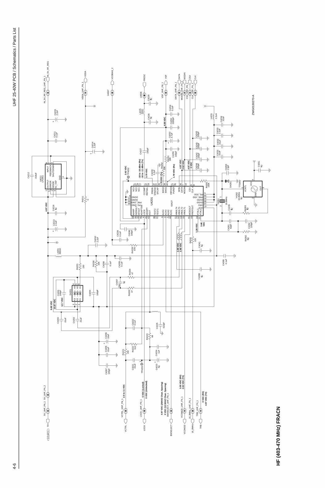
4-6
UH
F 2
5-40
W P
CB
/ S
chem
atic
s / P
arts
Lis
t
C42
6222
0pF
C42
51
C42
280.
1uF
C42
52
R42
21
1000
pF
150
TP
4202
1
C42
534.
7uF
IN_5
V_R
F_R
EG
TR
B
D42
61
2.2u
FC
4213
R42
41
MO
DIN
220
C42
21.0
1uF
C42
27LO
CK
_UH
F_F
N_1
100p
F
100p
FC
4243
U45
07
C42
02
.01u
F
BW
SE
LEC
T
100p
F
VS
F_U
HF
_FN
_1
C42
55
0.1u
FC
4209
2.2u
FC
4210
16_8
MH
z_U
HF
_FN
_1
C42
04
5V_U
HF
_FN
_1
100p
F
R42
22 510
VC
OM
OD
C42
4610
0pF
100p
FC
4287
C42
41
CLK
_UH
F_F
N_1
C42
42
VD
DA
100p
F
C42
23
0.1u
FC
4222
CS
X_U
HF
_FN
_1
C42
07
C42
890.
1uF
Vac
VC
TR
L
R42
63
C42
44
47R42
04
CLKVS
F
100p
F
5V
.01u
F
C42
03
30KR42
52
C42
12
.018
uF
1514V
MU
LT2
12V
MU
LT3
11V
MU
LT4
VRO13
25W
AR
P
23X
TA
L1X
TA
L224
SF
BA
SE
26S
FC
AP
30S
FIN
28S
FO
UT
37T
ES
T1
38T
ES
T2
21V
BP
AS
S
47VCP
VM
ULT
1
31N
C3
44PD_GND
PD_VDD5
PR
EIN
32
33PRE_GND
34PRE_VDD
35P
VR
EF
18R
EF
SE
L
27
45IA
DA
PT
16IN
DM
ULT
43IO
UT
LOC
K4
10M
OD
IN
41M
OD
OU
T
17N
C1
29N
C2
39B
IAS
2
42C
CO
MP
9C
EX
8C
LK
7D
AT
A
DGND6
36DVDD
19F
RE
FO
UT
46A
DA
PT
SW
22AGND
48A
UX
1
1A
UX
2
2A
UX
3
3A
UX
4
20AVDD
40B
IAS
1
63A
27
U42
01
C42
31
DA
TA
.01u
F
VD
DA
_UH
F_F
N_1
L420
139
0nH
.01u
FC
4232
BW
SE
LEC
T_U
HF
_FN
_1
2.2u
FC
4233
VC
OM
OD
_UH
F_F
N_1
510p
F
C42
25
C42
08
0.1u
F
0.1u
FC
4254
TP
4201
1
C42
0610
uF
R42
6115
0K
33K
R42
06
C42
631.
5pF
L423
1
PR
ES
C
CS
X
2.2u
H
MO
DIN
_UH
F_F
N_1
C42
6162
pF
5V_U
HF
_FN
_2
DA
TA
_UH
F_F
N_1
C42
142.
2uF
VC
OB
IAS
_2
C42
05.0
1uF
150
R42
01
C42
88
IN_5
V_R
F_R
EG
_UH
F_F
N_1
16_8
MH
z
2G
ND
3O
UT
VC
C4
VC
NT
L1
16.8
MH
zY
4262
TT
S05
V
C42
110.
1uF
R42
62
C42
35
2.2u
FC
4230
68
R42
23
3
TR
B_U
HF
_FN
_1
6A
1
5A
2
4A
3
K1
1K
22
K3
D42
01
65V
_TA
P
5E
RR
OR
7F
EE
DB
AC
K
4
GN
D
8IN
PU
T1
OU
TP
UT
2S
EN
SE
3S
HU
TD
OW
N
LP29
51U
4211
U45
06
VC
TR
L_U
HF
_FN
_1
.01u
FC
4234
R42
11
0
R42
2847
K
2.2u
FC
4215
R42
51
R42
03
39K
47
C42
26
C42
24
LOC
K
1uF
21
C42
16
16.8
MH
z
Y42
61
100p
FC
4245
L422
533
nH
C42
29
C42
0110
0pF
ZW
G01
3027
0-A
2.63
VD
C (
TX
)
4.97
VD
C (
25K
HZ
Ch
an. S
pac
ing
)
0 V
DC
(12
.5K
HZ
Ch
an. S
pac
ing
)
5 V
DC
(L
ock
ed)
0 V
DC
(U
nlo
cked
)
10.8
7 V
DC
-16
to -
11 d
Bm
(T
x)
12.7
VD
C
4.97
VD
C
6.68
VD
C
2.5
to 1
1 V
DC
1.76
VD
C (
Tx)
1.78
VD
C (
Rx)
3.79
VD
C
2.48
VD
C
3.43
VD
C
-18
to -
16 d
Bm
(R
x)
2.48
VD
C
1.28
VD
C
3.48
V
DC
0 V
DC
(R
X)
4.97
VD
C (
TX
)
3.05
VD
C (
RX
)
0 V
DC
4.97
VD
C
2.52
VD
C4.
97 V
DC
4.58
VD
C
HF
(40
3-47
0 M
Hz)
FR
AC
N
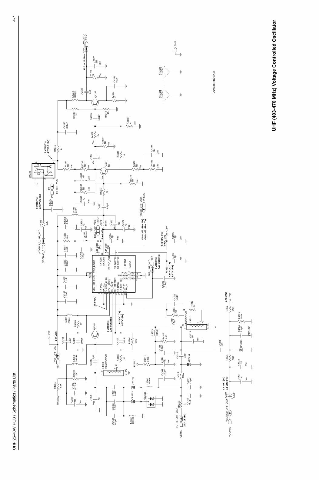
UH
F 2
5-40
W P
CB
/ S
chem
atic
s / P
arts
Lis
t4-
7
CR
4302
R43
6118
0
CR
4301
0
R43
15
L433
2
Vac
GN
D
RX
INJ
VC
OB
IAS
_2
100p
F
VC
TR
L_U
HF
_VC
OC
4312
12pF
C43
09
R43
11
390n
H
7.5K
Vac
L436
1
.022
uFC
4336
R43
33
C43
05V
acC
4339
Vac
CR
4303
R43
0210
K
R43
46
10K
1pF
C43
21
C43
141.
5pF
5V_U
HF
_VC
O
C43
180.
22uF
C43
810.
1uF
1KR
4343
C43
23
Vac
30R43
13
R43
4410Q
4332
0.1u
F
CR
4311
100p
F
C43
52
C43
63
Vac
C43
01
C43
33V
ac
C43
72
Vac
SH
4301
SH
IELD
R43
32
Vac
4.7u
F
C43
25
0
RX
INJ_
UH
F_V
CO
1P
1
2 P2
3P
3
R43
47
TX
INJ_
UH
F_V
CO
L431
2
RE
SO
NA
TO
R
L433
133
nH
L430
139
0nH
TR
B_U
HF
_VC
O
C43
1510
0pF
Vac
22
R43
31
C43
13
TX
_EM
ITT
ER
1T
X_I
AD
J10
TX
_OU
T
13T
X_S
WIT
CH
14
VC
C_B
UF
FE
RS
18 VC
C_L
OG
IC
RX
_BA
SE
6R
X_E
MIT
TE
R
2R
X_I
AD
J8
RX
_OU
T
7R
X_S
WIT
CH
3S
UP
ER
_FLT
R
19T
RB
_IN
16T
X_B
AS
E15 14
CO
LL_R
FIN
20F
LIP
_IN
11GND_BUFFERS
9GND_FLAG
GND_LOGIC17
12P
RE
SC
_OU
T5
50U
54
U43
01
C43
34
Vac
Q43
01
R43
41
100p
F
0
2.4p
F
C43
07
68nH
C43
24
56K
R43
21
L437
1
R43
23
6.8p
F
100K
C43
31
R43
39V
ac
C43
5110
0pF
VC
OM
OD
390n
H
L431
1
C43
552.
2uF
C43
62
Vac
CR
4321
C43
22
Vac
SH
IELD
SH
4302
Vac
C43
74
Vac
R43
37
270
R43
14
C43
73V
ac
C43
062p
F
C43
1110
0pF
C43
710.
1uF
0.22
uF
100p
F
C43
08
0.1u
FC
4316
C43
35
Vac
Vac
R43
45
C43
83
Vac
R43
36
8.2p
F
C43
37
C43
03
C43
54
51pF
C43
82
Vac
2.2u
F
R43
125.
6K
30
R43
03
390n
H
R43
38
Vac
L433
3
R43
34
Vac
8.2p
F
2.2K
R43
42
C43
02
390n
H
C43
32
Vac P
RE
SC
L430
2
R43
22
10K
2
6 4
1 3
C43
6110
0pF
TX
INJ
Q43
33
VC
OB
IAS
_2_U
HF
_VC
O
C43
750.
1uF
Q43
31
Vac
10
R43
0539
0nH
L430
4
390n
HL4
305
R43
35
Vac
VacV
SF
_UH
F_V
C0
3.9p
F
C43
17
VC
OM
OD
_UH
F_V
CO
TR
B
C43
04
5.6K
R43
01
51pF
C43
38
VS
F
3P
3
5V
C43
530.
1uF
L430
3R
ES
ON
AT
OR
1P
1
2P
2
R43
40
Vac
180
R43
04
390n
H
L431
3
GR
OU
ND
VC
TR
L
PR
ES
C_U
HF
_VC
O
5V
VS
F
TX
SW
TX
SW
RX
SW
RX
SW
VS
F
ZW
G01
3027
2-0
0 V
DC
(T
x)
4.58
VD
C
4.58
VD
C
13.5
to
16
dB
m
0 V
DC
(T
x)4.
7 V
DC
(R
x)
2.5
- 11
VD
C
0 V
DC
(R
x)4.
97 V
DC
(T
x)
-18
to -
16 d
Bm
(R
x)-1
6 to
-11
dB
m (
Tx)
4 to
6 d
Bm
4.54
VD
C
4.54
VD
C (
Tx)
0 V
DC
(R
x)
4.42
VD
C (
Rx)
0 V
DC
(T
x)
3.1
VD
C (
Rx)
2.6
VD
C (
Tx)
1.91
VD
C (
Tx)
0 V
DC
(R
x)
2.45
VD
C (
Rx)
0 V
DC
(T
x)
2.35
VD
C
(Tx)
4.54
VD
C(R
x)
2.43
VD
C (
Rx)
UH
F (
403-
470
MH
z) V
olt
age
Co
ntr
olle
d O
scill
ato
r

4-8
UH
F 2
5-40
W P
CB
/ S
chem
atic
s / P
arts
Lis
t
GN
D
51
R40
51
C40
09
100p
F
33
R40
08
D40
05
VacR40
17
XF
MR
T40
51
1 2 3
5 4
43pF
C40
04
TB
DL4
004
IN
NE
G
PO
S
39pF
Q40
01V
ac
C40
07
270
R40
11
C40
2410
00pF
33pF
C40
02
100K
NE
G
PO
S
R40
01
TB
D
L400
5 IN
Vac
Q40
02
FE
CT
RL_
1_U
HF
_FE
Q40
03
27nH
L405
3
100K
R40
1239
pFC
4003
3300
pF
TP
4003
IF
C40
13
470n
HL4
003
Vac
150n
HL4
051
3300
pF
R40
15
C40
11
3
54
L400
6
Vac
XF
MR
T40
52
12
1.8p
F
C40
17
D40
04
C40
28
Vac
R40
60
330K
C40
261.
8pF
Vac
22pF
R40
53
C40
19
R40
20V
ac
15nH
L405
4
68
R40
07
D40
02
R40
19V
ac
12pF
C40
18
R40
55V
ac
36pF
C40
01
C40
20
1.8p
F
330p
FC
4010 43
pFC
4005
1.8p
FD
4001
C40
27
36pF
330p
F
C40
22
C40
12
D40
51
IO1
1IO
22
IO3
3 IO4
4
470n
H
Vac
L400
8
R40
16
RX
IN
16pF
C40
53
1.8p
FC
4029
Vac
C40
16
IF_U
HF
_FE
IN
NE
G
PO
S
R40
52 0
TB
D
L400
2
TP
4001
R40
033.
9K
Vac
C40
25
C40
14
100p
F
IN
NE
G
PO
ST
BD
L400
1
R40
02
330
Vac
150
R40
54
R40
09
9V3_
UH
F_F
E
13pF
C40
31
RX
INJ
100p
F
C40
15
270
R40
13
36pF
TP
4002
C40
21
270
9V3
R40
06
GN
D_U
HF
_FE
150
R40
10
C40
51
C40
5416
pF
10pF
D40
03
R40
05
10K
0
Vac
R40
22
R40
18
9V3
RX
IN_U
HF
_FE
RX
INJ_
UH
F_F
E
43pF
FE
CT
RL_
1
C40
06
R40
14
10
C40
55
Vac
C40
301.
8pF
82pF
C40
52
1000
pFC
4008
C40
60
Vac
2.7K
22pF
R40
04
C40
23
ZW
G01
3026
9-O
4.6
VD
C
3 to
6.5
VD
C
0.7
VD
C
UH
F (
403-
470
MH
z) R
ecei
ver
Fro
nt
En
d

UH
F 2
5-40
W P
CB
/ S
chem
atic
s / P
arts
Lis
t4-
9
9186
176B
01
9180
469V
04
9180
469V
03
9180
469V
0691
8046
8V06
R31
442.
4K
BW
SE
LEC
T_V
HF
_IF
_1
9V3_
VH
F_I
F_2
C31
139.
1pF
NU
R31
0410
0N
U
10
0
620n
HN
U
R31
05
R31
30L3
100
14
VD
D
7
VS
S
51
U31
11-1
MC
74H
C40
66
13
CN
TL1
2
C31
16
L311
2
0.
1uF
620n
H
9V3_
VH
F_I
F_1
10
uF
C31
33
0.1
uF
C31
32
.01u
F
C31
51
OU
T2
C31
37.0
39
uF
CF
WC
45
5D
FL3
112
GN
D1
34
GN
D2
IN1
620n
H
C31
21
L310
1
0.1u
F
R31
0112
K
12
K
R31
47
15pF
DIS
CA
UD
IO
C31
02
C31
52.0
1uF
0.1u
F C
3139
7
VS
S
0.1
uF
C31
41
U31
15-1
MC
74
HC
40
66
MC
74H
C40
66
13
CN
TL1
2
14
VD
D
DIS
CA
UD
IO_V
HF
_IF
_1
62
0n
H
620
L311
1
R31
08
27
pF
C31
10
0.
1uF
C31
47C31
55
9V3
.01u
F
NU
Q31
55
FL3
115
3GN
D1
GN
D2 4
1IN
2O
UT
BW
SE
LEC
T
GND3
45
GND4
3IN
6O
UT
C
FW
C45
5F
12
R16
FL3
102
1GND1GND2
2
GND1
12
GND2 4
GND3GND4
5
IN3
OU
T6
12R
16F
L310
1
7
C31
4 2
0.1u
F
MC
74H
C40
66
CN
TL
6
89
VD
D14
VS
S
GN
D
3
IN1
OU
T2
RS
SI
U31
11-3
FL3
114
CF
UC
J455
D
4700
pFC
3146
27K
GN
D1
34
GN
D2
IN1
OU
T2
R31
06
OU
T3
IN1
FL3
111
CF
WC
455G
Y31
011
2R
17
44.3
95M
Hz
GN
D2
GN
D1
4C
3131
1pF
NU
0.1u
FC
3145
5V_V
HF
_IF
_1
IF
IN_V
HF
_IF
_1IF
330
R31
16
10K
R
3134
0.1
uF
C31
44
18pF
C31
14
10K
R31
55
R31
51
VD
D
7VS
S
NU
1.2K
U31
11-4
MC
74H
C40
66
12CN
TL14
CN
TL
5
43
VD
D
14
VS
S 7
U31
15-2
MC
74H
C40
66
0.1
uF
C31
04
C31
35
33pF
12CN
TL
11
14 VD
D
7VS
S
7
U31
15-4
MC
74H
C40
66
MC
74H
C40
66
CN
TL
5
43
VD
D
14
VS
S
3.3
K
U31
11-2
R31
45
0.1
uF
C31
40
39
0
R31
15
Q31
52
32
2p
FY
3102
455K
Hz
45B
02
C31
15
82pF
C31
12C
3123
.03
9u
F
R31
12 10
0102
727B
45
0R
3148
0.1u
F C31
11
Q31
51
27
K
R31
17
Q31
02
8.2K
R31
33
Q31
01
C31
363
0p
F
20pF
R31
02C
3101
33pF
10
C31
03
C31
340
.1u
F
R
SS
I_V
HF
_IF
_1
6.
8K
R31
18
R31
11
12K
C31
22
.039
uF6.
8K
R31
07
NU
100
R31
14
R31
54
5V
10K
10
K R
3153
D31
01
120p
F
C31
43
R31
52
10K
1.2
K
CN
TL
6
VD
D
14 VS
S 7
R31
35
U31
15-3
MC
74H
C40
66
680
R31
46R
3160
0
R31
321
5K
FL3
113
CS
455G
2N
U
GN
D
3
IN1
OU
T2
9V3
5V
5V
9V3
9V3
9V3
9V3
9V3
5V
9V3
8910
1110
OSCIN4 OSCOUT 3
QUADIN10
RFIN1
RFIN_DEC2
RSSIOUT 5RSSI_FEED9
VC
C6
IFAMPOUT 16
IFAMP_DEC119
IFAMP_DEC2
17
LIMIN14
LIMOUT 11
LIM_DEC1 13
LIM_DEC2 12
MIXOUT 20
SA
61
6
SA
616
AUDIOOUT 8AUDIO_FEED7
GN
D15
IFAMPIN18
U31
01
ZW
G01
3036
7-0
UH
F (
403-
470
MH
z) IF
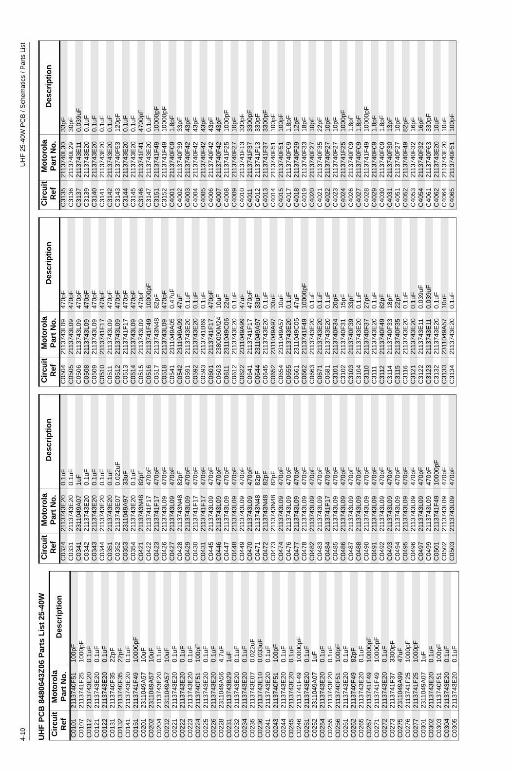
4-10
UH
F 2
5-40
W P
CB
/ S
chem
atic
s / P
arts
Lis
t
UH
F P
CB
848
0643
Z06
Par
ts L
ist
25-4
0W
Cir
cuit
R
efM
oto
rola
P
art
No
.D
escr
ipti
on
C01
0121
1374
0F51
100p
FC
0107
2113
741F
2510
00pF
C01
1221
1374
3E20
0.1u
FC
0121
2113
743E
200.
1uF
C01
2221
1374
3E20
0.1u
FC
0131
2113
740F
3522
pFC
0132
2113
740F
3522
pFC
0141
2113
743E
200.
1uF
C01
5121
1374
1F49
1000
0pF
C02
0123
1104
9A57
10uF
C02
0223
1104
9A57
10uF
C02
0421
1374
3E20
0.1u
FC
0212
2311
049A
5710
uFC
0221
2113
743E
200.
1uF
C02
2221
1374
3E20
0.1u
FC
0223
2113
743E
200.
1uF
C02
2421
1374
0F51
100p
FC
0225
2113
743E
200.
1uF
C02
2621
1374
3E20
0.1u
FC
0228
2311
049A
564.
7uF
C02
3121
1374
3B29
1uF
C02
3221
1374
3E20
0.1u
FC
0234
2113
743E
200.
1uF
C02
3521
1374
3E07
0.02
2uF
C02
3621
1374
3E10
0.03
3uF
C02
4121
1374
3E20
0.1u
FC
0243
2113
740F
5110
0pF
C02
4421
1374
3E20
0.1u
FC
0245
2113
743E
200.
1uF
C02
4621
1374
1F49
1000
0pF
C02
5121
1374
3E20
0.1u
FC
0252
2311
049A
071u
FC
0254
2113
743E
200.
1uF
C02
5521
1374
3E20
0.1u
FC
0256
2113
740F
5110
0pF
C02
6121
1374
3E20
0.1u
FC
0262
2113
740F
4982
pFC
0265
2113
743E
200.
1uF
C02
6721
1374
1F49
1000
0pF
C02
7121
1374
1F49
1000
0pF
C02
7221
1374
3E20
0.1u
FC
0273
2113
741F
3733
00pF
C02
7523
1104
9A99
47uF
C02
7621
1374
1F25
1000
pFC
0277
2113
741F
2510
00pF
C03
0123
1104
9A07
1uF
C03
0221
1374
3E20
0.1u
FC
0303
2113
740F
5110
0pF
C03
0421
1374
3E20
0.1u
FC
0305
2113
743E
200.
1uF
C03
2421
1374
3E20
0.1u
FC
0331
2113
743E
200.
1uF
C03
4123
1104
9A07
1uF
C03
4221
1374
3E20
0.1u
FC
0343
2113
743E
200.
1uF
C03
4421
1374
3E20
0.1u
FC
0351
2113
743E
200.
1uF
C03
5221
1374
3E07
0.02
2uF
C03
5323
1104
9A97
33uF
C03
5421
1374
3E20
0.1u
FC
0421
2113
743N
4882
pFC
0422
2113
741F
1747
0pF
C04
2321
1374
1F17
470p
FC
0426
2113
743L
0947
0pF
C04
2721
1374
3L09
470p
FC
0428
2113
743N
4882
pFC
0429
2113
743L
0947
0pF
C04
3021
1374
1F17
470p
FC
0431
2113
741F
1747
0pF
C04
4521
1374
3L09
470p
FC
0446
2113
743L
0947
0pF
C04
4721
1374
3L09
470p
FC
0448
2113
743L
0947
0pF
C04
4921
1374
3L09
470p
FC
0470
2113
743L
0947
0pF
C04
7121
1374
3N48
82pF
C04
7221
1374
3N48
82pF
C04
7321
1374
3N48
82pF
C04
7421
1374
3L09
470p
FC
0476
2113
743L
0947
0pF
C04
7721
1374
3L09
470p
FC
0478
2113
743L
0947
0pF
C04
8221
1374
3L09
470p
FC
0483
2113
743L
0947
0pF
C04
8421
1374
1F17
470p
FC
0485
2113
743L
0947
0pF
C04
8621
1374
3L09
470p
FC
0487
2113
743L
0947
0pF
C04
8821
1374
3L09
470p
FC
0490
2113
743L
0947
0pF
C04
9121
1374
3L09
470p
FC
0492
2113
743L
0947
0pF
C04
9321
1374
3L09
470p
FC
0494
2113
743L
0947
0pF
C04
9521
1374
3L09
470p
FC
0496
2113
743L
0947
0pF
C04
9721
1374
3L09
470p
FC
0499
2113
743L
0947
0pF
C05
0121
1374
1F49
1000
0pF
C05
0221
1374
3L09
470p
FC
0503
2113
743L
0947
0pF
Cir
cuit
R
efM
oto
rola
P
art
No
.D
escr
ipti
on
C05
0421
1374
3L09
470p
FC
0505
2113
743L
0947
0pF
C05
0621
1374
3L09
470p
FC
0508
2113
743L
0947
0pF
C05
0921
1374
3L09
470p
FC
0510
2113
741F
1747
0pF
C05
1121
1374
3L09
470p
FC
0512
2113
743L
0947
0pF
C05
1321
1374
1F17
470p
FC
0514
2113
743L
0947
0pF
C05
1521
1374
3L09
470p
FC
0516
2113
741F
4910
000p
FC
0517
2113
743N
4882
pFC
0518
2113
743L
0947
0pF
C05
4123
1104
9A05
0.47
uFC
0542
2311
049A
9947
uFC
0591
2113
743E
200.
1uF
C05
9221
1374
3E20
0.1u
FC
0593
2113
741B
690.
1uF
C06
0121
1374
1F17
470p
FC
0603
2380
090M
2410
uFC
0611
2311
049C
0622
uFC
0612
2113
743E
200.
1uF
C06
2223
1104
9A99
47uF
C06
4121
1374
1F17
470p
FC
0644
2311
049A
9733
uFC
0645
2113
743E
200.
1uF
C06
5223
1104
9A97
33uF
C06
5423
1104
9A57
10uF
C06
5521
1374
3E20
0.1u
FC
0661
2311
049C
0547
uFC
0662
2113
741F
4910
000p
FC
0663
2113
743E
200.
1uF
C06
7121
1374
3E20
0.1u
FC
0681
2113
743E
200.
1uF
C31
0121
1374
0F34
20pF
C31
0221
1374
0F31
15pF
C31
0321
1374
0F39
33pF
C31
0421
1374
3E20
0.1u
FC
3110
2113
740F
3727
pFC
3111
2113
743E
200.
1uF
C31
1221
1374
0F49
82pF
C31
1421
1374
0F33
18pF
C31
1521
1374
0F35
22pF
C31
1621
1374
3E20
0.1u
FC
3121
2113
743E
200.
1uF
C31
2221
1374
3E11
0.03
9uF
C31
2321
1374
3E11
0.03
9uF
C31
3221
1374
3E20
0.1u
FC
3133
2311
049A
5710
uFC
3134
2113
743E
200.
1uF
Cir
cuit
R
efM
oto
rola
P
art
No
.D
escr
ipti
on
C31
3521
1374
0L30
33pF
C31
3621
1374
0L29
30pF
C31
3721
1374
3E11
0.03
9uF
C31
3921
1374
3E20
0.1u
FC
3140
2113
743E
200.
1uF
C31
4121
1374
3E20
0.1u
FC
3142
2113
743E
200.
1uF
C31
4321
1374
0F53
120p
FC
3144
2113
743E
200.
1uF
C31
4521
1374
3E20
0.1u
FC
3146
2113
741F
4147
00pF
C31
4721
1374
3E20
0.1u
FC
3151
2113
741F
4910
000p
FC
3152
2113
741F
4910
000p
FC
4001
2113
740F
091.
8pF
C40
0221
1374
0F39
33pF
C40
0321
1374
0F42
43pF
C40
0421
1374
0F42
43pF
C40
0521
1374
0F42
43pF
C40
0621
1374
0F42
43pF
C40
0721
1374
0F42
43pF
C40
0821
1374
1F25
1000
pFC
4009
2113
740F
2710
pFC
4010
2113
741F
1333
0pF
C40
1121
1374
1F37
3300
pFC
4012
2113
741F
1333
0pF
C40
1321
1374
1F37
3300
pFC
4014
2113
740F
5110
0pF
C40
1521
1374
0F51
100p
FC
4017
2113
740F
091.
8pF
C40
1821
1374
0F29
12pF
C40
1921
1374
0F33
18pF
C40
2021
1374
0F27
10pF
C40
2121
1374
0F35
22pF
C40
2221
1374
0F27
10pF
C40
2321
1374
0F27
10pF
C40
2421
1374
1F25
1000
pFC
4026
2113
740F
091.
8pF
C40
2721
1374
0F09
1.8p
FC
4028
2113
741F
4910
000p
FC
4029
2113
740F
091.
8pF
C40
3021
1374
0F09
1.8p
FC
4031
2113
740F
3013
pFC
4051
2113
740F
2710
pFC
4052
2113
740F
4982
pFC
4053
2113
740F
3216
pFC
4054
2113
740F
3216
pFC
4061
2113
740F
6333
0pF
C40
6221
1374
3E20
10uF
C40
6421
1374
3E20
10uF
C40
6521
1374
0F51
100p
F
Cir
cuit
R
efM
oto
rola
P
art
No
.D
escr
ipti
on
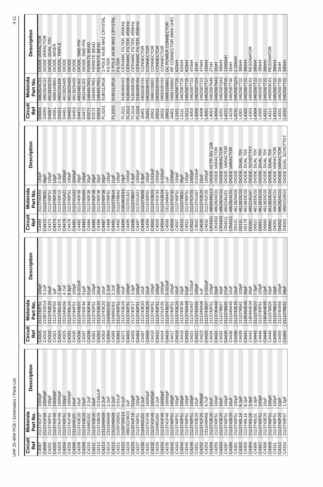
UH
F 2
5-40
W P
CB
/ S
chem
atic
s / P
arts
Lis
t4-
11
C40
6721
1374
1F37
3300
pFC
4069
2113
741F
4910
000p
FC
4201
2113
740F
5110
0pF
C42
0221
1374
1F49
1000
0pF
C42
0321
1374
1F49
1000
0pF
C42
0421
1374
0F51
100p
FC
4205
2113
741F
4910
000p
FC
4206
2311
049J
2510
uFC
4208
2113
743E
2010
uFC
4209
2113
743E
2010
uFC
4210
2104
993J
022.
2uF
C42
1121
1374
3E20
10uF
C42
1221
1374
3E05
0.01
8uU
FC
4213
2311
049A
092.
2uF
C42
1423
1104
9A09
2.2u
FC
4215
2311
049A
092.
2uF
C42
2121
0972
0D01
0.01
uFC
4222
2109
720D
140.
1uF
C42
2408
8242
2W23
1uF
C42
2521
1374
1F18
510p
FC
4227
2113
740F
5110
0pF
C42
3021
0499
3J02
2.2u
FC
4231
2113
741F
4910
000p
FC
4232
2113
741F
4910
000p
FC
4233
2104
993J
022.
2uF
C42
3421
1374
1F49
1000
0pF
C42
3521
1374
1F49
1000
0pF
C42
4221
1374
0F51
100p
FC
4243
2113
740F
5110
0pF
C42
4421
1374
0F51
100p
FC
4245
2113
740F
5110
0pF
C42
4621
1374
0F51
100p
FC
4251
2113
743E
2010
uFC
4252
2113
741F
2510
00pF
C42
5323
1104
9A56
4.7u
FC
4254
2113
743E
2010
uFC
4255
2113
740F
5110
0pF
C42
6321
1374
3E20
10uF
C42
8721
1374
0F51
100p
FC
4289
2113
743E
2010
uFC
4301
2113
740F
5110
0pF
C43
0221
1374
0L16
8.2p
FC
4303
2113
740L
168.
2pF
C43
0421
1374
0L08
3.9p
FC
4306
2113
740L
012.
0pF
C43
0721
1374
0F51
100p
FC
4308
2113
743E
2010
uFC
4309
2113
740F
5110
0pF
C43
1121
1374
0F51
100p
FC
4312
2113
740F
2912
pFC
4314
2113
740F
071.
5pF
Cir
cuit
R
efM
oto
rola
P
art
No
.D
escr
ipti
on
C43
1521
1374
0F51
100p
FC
4316
2109
720D
140.
1uF
C43
1821
1374
3E20
10uF
C43
2121
1374
0F03
1pF
C43
2421
1374
0L03
2.4p
FC
4325
2311
049A
564.
7uF
C43
3121
1374
0L14
6.8p
FC
4335
2113
740F
5110
0pF
C43
3621
1374
3E07
0.02
2uF
C43
3721
1374
0F44
51pF
C43
3821
1374
0F44
51pF
C43
5121
1374
0F51
100p
FC
4352
2113
743E
2010
uFC
4353
2113
743E
2010
uFC
4354
2104
993J
022.
2uF
C43
5521
0499
3J02
2.2u
FC
4361
2113
740F
5110
0pF
C43
7121
1374
3E20
10uF
C44
0121
1374
0F51
100p
FC
4403
2113
740F
173.
9pF
C44
0421
1374
0F51
100p
FC
4407
2113
743E
2010
uFC
4409
2113
743E
2010
uFC
4410
2113
740F
5110
0pF
C44
1221
1374
0F51
100p
FC
4414
2113
741F
2510
00pF
C44
1621
1374
3E07
0.02
2uF
C44
1721
1374
0F51
100p
FC
4418
2113
743E
2010
uFC
4419
2113
740F
3933
pFC
4420
2113
740A
4851
pFC
4421
2113
741A
570.
033u
FC
4422
2113
740A
5510
0pF
C44
2323
1104
9A08
1uF
C44
2521
1374
3E07
0.02
2uF
C44
2621
1374
0F51
100p
FC
4431
2113
740A
4030
pFC
4432
2111
078B
2730
pFC
4435
2111
078B
2527
pFC
4436
2311
049A
4510
uFC
4438
2113
743E
2010
uFC
4439
2111
078B
4210
0pF
C44
4121
8046
4E40
30pF
C44
4221
8046
4E34
39pF
C44
4321
1107
8B10
7.5p
FC
4446
2113
740F
5110
0pF
C44
4821
8046
4E65
12pF
C44
4921
1107
8B29
33pF
C44
5021
1107
8B19
16pF
C44
5921
1374
0A55
100p
FC
4460
2111
078B
3239
pF
Cir
cuit
R
efM
oto
rola
P
art
No
.D
escr
ipti
on
C44
6921
1374
0A55
100p
FC
4472
2111
078B
3136
pFC
4473
2113
740F
5110
0pF
C44
7421
1374
0F29
12pF
C44
7521
1374
0F10
2.0p
FC
4478
2113
741A
2110
00pF
C44
7921
1374
0F51
100p
FC
4481
2113
741A
3230
00pF
C44
8221
1374
0F38
30pF
C44
8321
1374
0A55
100p
FC
4484
2113
740F
3830
pFC
4485
2113
740F
3830
pFC
4486
2113
740F
3830
pFC
4487
2113
740F
3830
pFC
4488
2113
740F
5110
0pF
C44
9121
1107
8B14
11pF
C44
9221
1107
8B42
100p
FC
4494
2180
464E
6310
pFC
4495
2113
741A
2110
00pF
C44
9621
1107
8B07
5.6p
FC
4497
2113
741A
2110
00pF
C44
9821
1107
8B09
6.8p
FC
4499
2113
740F
5110
0pF
C45
0221
1374
3E03
0.01
5uF
C45
0321
1374
1F33
2200
pFC
4504
2113
743E
060.
020u
FC
4505
2311
049A
071u
FC
4506
2113
741F
3322
00pF
C45
0721
1374
0F51
100p
FC
4510
2111
078B
3136
pFC
4521
2113
740F
5110
0pF
C45
2221
1374
1F25
1000
pFC
4602
2113
741A
570.
033u
FC
4630
2113
743E
2010
uFC
4632
2113
741F
2510
00pF
CR
4301
4805
649Q
13D
IOD
E V
CT
R IS
V 2
28C
R43
0248
6282
4C01
DIO
DE
VA
RA
CT
OR
CR
4303
4862
824C
01D
IOD
E V
AR
AC
TO
RC
R43
1148
0224
5J22
DIO
DE
, VA
RA
CT
OR
CR
4321
4862
824C
01D
IOD
E V
AR
AC
TO
RD
0101
4813
825A
05D
IOD
ED
0151
4813
833C
02D
IOD
E, D
UA
L 70
VD
0179
4813
833C
02D
IOD
E, D
UA
L 70
VD
0301
4802
245J
47D
IOD
E, S
CH
OT
TK
YD
0621
4813
833C
02D
IOD
E, D
UA
L 70
VD
0651
4813
833C
02D
IOD
E, D
UA
L 70
VD
0660
4813
833C
02D
IOD
E, D
UA
L 70
VD
0661
4813
833C
02D
IOD
E, D
UA
L 70
VD
4001
4862
824C
01D
IOD
E V
AR
AC
TO
RD
4002
4862
824C
01D
IOD
E V
AR
AC
TO
RD
4003
4880
154K
03D
IOD
E D
UA
L S
CH
OT
TK
Y
Cir
cuit
R
efM
oto
rola
P
art
No
.D
escr
ipti
on
D40
0448
6282
4C01
DIO
DE
VA
RA
CT
OR
D40
0548
6282
4C01
DIO
DE
VA
RA
CT
OR
D40
0748
1383
3C02
DIO
DE
, DU
AL
70V
D40
5148
8614
3B01
DIO
DE
, MIX
ER
D42
0148
0223
3J09
DIO
DE
, TR
IPLE
D44
5148
1382
5A05
DIO
DE
D44
5248
1382
5A05
DIO
DE
D44
5348
1382
5A05
DIO
DE
D44
7148
0248
2J02
DIO
DE
, SM
D P
IND
4472
4802
482J
02D
IOD
E, S
MD
PIN
E02
7124
8465
7R01
FE
RR
ITE
BE
AD
E02
7224
8465
7R01
FE
RR
ITE
BE
AD
E06
3124
8465
7R01
FE
RR
ITE
BE
AD
FL3
101
9180
112R
162
PO
LE 4
4.85
MH
Z C
RY
STA
L F
ILT
ER
FL3
102
9180
112R
162
PO
LE 4
4.85
MH
Z C
RY
STA
L F
ILT
ER
FL3
111
9180
469V
03C
ER
AM
IC F
ILT
ER
, 455
KH
zF
L311
291
8046
9V06
CE
RA
MIC
FIL
TE
R, 4
55K
Hz
FL3
114
9180
468V
06C
ER
AM
IC F
ILT
ER
, 455
KH
zF
L311
591
8046
9V04
CE
RA
MIC
FIL
TE
R, 4
55K
Hz
J040
109
0263
6Y02
CO
NN
EC
TO
RJ0
451
0902
636Y
01C
ON
NE
CT
OR
J050
109
8610
5B01
CO
NN
EC
TO
RJ0
551
0905
505Y
04C
ON
NE
CT
OR
J055
209
0550
5Y03
CO
NN
EC
TO
RJ0
601
0986
165B
01D
C P
OW
ER
CO
NN
EC
TO
RJ4
401
0986
166B
02R
F C
ON
NE
CT
OR
(M
INI U
HF
)L3
101
2462
587T
2562
0nH
L311
124
6258
7T25
620n
HL3
112
2462
587T
2562
0nH
L400
324
6258
7T23
470n
HL4
006
2462
587V
2415
nHL4
008
2462
587T
2347
0nH
L405
124
6258
7T17
150n
HL4
053
2462
587N
4627
nHL4
054
2462
587N
4315
nHL4
201
2462
587Q
4239
0nH
L422
124
6258
7P25
1200
0nH
L422
524
6258
7T40
33nH
L423
124
6258
7Q20
2,20
0nH
L430
124
6258
7T22
390n
HL4
302
2462
587T
2239
0nH
L430
324
6059
3C01
RE
SO
NA
TO
RL4
304
2462
587T
2239
0nH
L430
524
6258
7T22
390n
HL4
311
2462
587T
2239
0nH
L431
224
6059
3C01
RE
SO
NA
TO
RL4
313
2462
587T
2239
0nH
L433
124
6258
7T09
33nH
L433
324
6258
7T22
390n
H
Cir
cuit
R
efM
oto
rola
P
art
No
.D
escr
ipti
on
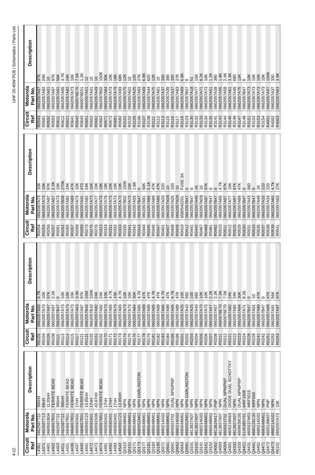
4-12
UH
F 2
5-40
W P
CB
/ S
chem
atic
s / P
arts
Lis
t
L436
124
6258
7T22
390n
HL4
371
2462
587T
1368
nHL4
401
2460
591B
0411
.03n
HL4
402
2484
657R
01F
ER
RIT
E B
EA
DL4
403
2462
587T
2239
0nH
L441
124
6258
7T22
390n
HL4
421
2484
657R
01F
ER
RIT
E B
EA
DL4
436
2484
657R
01F
ER
RIT
E B
EA
DL4
437
2460
592A
0117
nHL4
440
2484
657R
01F
ER
RIT
E B
EA
DL4
441
2460
591C
2313
.85n
HL4
472
2460
592A
0117
nHL4
473
2460
591N
3643
.67n
HL4
474
2480
067M
01F
ER
RIT
E B
EA
DL4
491
2460
592A
0117
nHL4
492
2460
592A
0117
nHL4
493
2460
592A
0117
nHL4
543
2460
591C
2313
.85n
HQ
0110
4880
048M
01N
PN
Q01
5148
8004
8M01
NP
NQ
0171
4880
048M
01N
PN
Q01
7348
8005
2M01
NP
N D
AR
LIN
GT
ON
Q01
7748
8004
8M01
NP
NQ
0181
4880
048M
01N
PN
Q01
8348
8004
8M01
NP
NQ
0185
4880
048M
01N
PN
Q02
7148
8021
4G02
NP
NQ
0641
4880
048M
01N
PN
Q06
6148
0592
1T02
DU
AL
NP
N/P
NP
Q06
6248
8021
4G02
NP
NQ
0663
4880
048M
01N
PN
Q06
8148
8005
2M01
NP
N D
AR
LIN
GT
ON
Q31
0148
1382
7A07
NP
NQ
3102
4813
827A
07N
PN
Q31
4148
8021
4G02
NP
NQ
3151
4880
048M
01N
PN
Q31
5248
8004
8M01
NP
NQ
4002
4813
824A
17P
NP
Q40
0348
1382
7A07
NP
NQ
4004
4805
921T
02D
UA
L N
PN
/PN
PQ
4301
4805
218N
63D
IOD
E D
UA
L S
CH
OT
TK
YQ
4332
4813
827A
07N
PN
Q43
3348
0993
9C05
DU
AL
NP
N/P
NP
Q44
2151
0538
5Y91
MR
F15
08Q
4431
4805
537W
01M
RF
5015
Q44
4148
8022
5C30
MR
F65
0Q
4451
4880
214G
02N
PN
Q44
7148
8004
8M01
NP
NQ
4472
4805
128M
27P
NP
Q44
7348
8021
4G02
NP
NR
0101
0662
057A
7310
K
Cir
cuit
R
efM
oto
rola
P
art
No
.D
escr
ipti
on
R01
0206
6205
7A65
4.7K
R01
0406
6205
7A73
10K
R01
0506
6205
7A97
97K
R01
0806
6205
7A57
2.2K
R01
1106
6205
7B47
0R
0113
0662
057A
7310
KR
0114
0662
057A
7310
KR
0115
0662
057A
7310
KR
0117
0662
057A
633.
9KR
0121
0662
057A
9797
KR
0131
0662
057B
4610
MR
0132
0662
057B
1033
0KR
0151
0662
057A
8224
KR
0152
0662
057A
8224
KR
0170
0662
057A
7310
KR
0171
0662
057A
654.
7KR
0172
0662
057A
7310
KR
0173
0662
057A
654.
7KR
0174
0662
057A
7310
KR
0175
0662
057A
7310
KR
0176
0662
057A
8430
KR
0177
0662
057A
654.
7KR
0178
0662
057A
8947
KR
0179
0662
057A
8947
KR
0181
0662
057A
654.
7KR
0182
0662
057A
8947
KR
0183
0662
057A
654.
7KR
0184
0662
057A
8947
KR
0185
0662
057A
654.
7KR
0186
0662
057A
8947
KR
0201
0662
057A
2510
0R
0202
0662
057A
4356
0R
0203
0662
057A
2510
0R
0204
0662
057A
4356
0R
0205
0662
057A
7310
KR
0206
0662
057A
7310
KR
0207
0662
057A
572.
2KR
0208
0662
057A
572.
2KR
0211
0660
076E
707.
5KR
0212
0660
076E
707.
5KR
0221
0662
057A
8224
KR
0222
0662
057A
8224
KR
0223
0662
057A
8430
KR
0224
0662
057A
718.
2KR
0228
0662
057B
470
R02
2906
6205
7A01
10R
0241
0662
057A
8947
KR
0242
0662
057B
470
R02
5106
6205
7A89
47K
R02
5206
6205
7A91
56K
R02
5306
6205
7A97
97K
Cir
cuit
R
efM
oto
rola
P
art
No
.D
escr
ipti
on
R02
5406
6205
7A73
10K
R02
5506
6205
7A73
10K
R02
5606
6205
7A97
97K
R02
5706
6205
7A57
2.2K
R02
6106
6205
7A73
10K
R02
6206
6205
7B08
270K
R02
6506
6205
7A82
24K
R02
6706
6205
7A89
47K
R02
6806
6205
7A73
10K
R02
6906
6205
7A41
470
R02
7306
6205
7A82
24K
R02
7506
6205
7A73
10K
R02
7606
6205
7A77
15K
R03
2306
6205
7A79
18K
R03
2406
6205
7A79
18K
R03
3106
6205
7A73
10K
R03
3206
6205
7A73
10K
R03
3306
6205
7A73
10K
R03
3506
6205
7B02
150K
R03
4106
6205
7A73
10K
R03
4206
6205
7A55
1.8K
R03
4306
6205
7B47
0R
0344
0662
057A
9156
KR
0345
0662
057A
665.
1KR
0346
0662
057A
8947
KR
0347
0662
057A
8947
KR
0401
0662
057A
3322
0R
0407
0662
057M
2610
R04
0806
6205
7A25
100
R04
0906
6205
7M26
10R
0410
6580
542Z
01F
US
E 3
AR
0412
0662
057B
470
R04
4106
6205
7B47
0R
0442
0662
057A
491K
R04
6706
6205
7M26
10R
0468
0662
057A
9797
KR
0481
0662
057B
470
R04
8206
6205
7B47
0R
0510
0662
057A
654.
7KR
0511
0662
057A
9797
KR
0512
0662
057A
7715
KR
0525
0662
057A
9797
KR
0529
0662
057A
8947
KR
0530
0662
057B
470
R05
3106
6205
7A43
560
R05
3306
6205
7B47
0R
0535
0662
057A
491K
R05
3706
6205
7A33
220
R05
3806
6205
7A33
220
R05
3906
6205
7A65
4.7K
R05
4106
6205
7A83
27K
Cir
cuit
R
efM
oto
rola
P
art
No
.D
escr
ipti
on
R05
4306
6205
7A97
97K
R05
9106
6205
7A82
24K
R05
9206
6205
7A01
10R
0593
0662
057A
9797
KR
0611
0662
057A
9156
KR
0612
0662
057A
654.
7KR
0621
0662
057A
8224
KR
0641
0662
057A
7310
KR
0642
0660
076E
707.
5KR
0643
0660
076E
511.
2KR
0651
0662
057A
0110
R06
5206
6205
7A01
10R
0661
0662
057A
491K
R06
6206
6205
7B02
150K
R06
7106
6205
7A84
30K
R06
7206
6205
7A73
10K
R06
8106
6205
7A79
18K
R06
8206
6205
7A93
68K
R31
0106
6205
7A75
12K
R31
0206
6205
7A01
10R
3105
0662
057A
2510
0R
3106
0662
057A
8327
KR
3107
0662
057A
696.
8KR
3108
0662
057A
4462
0R
3111
0662
057A
7512
KR
3112
0662
057A
0110
R31
1306
6205
7A37
330
R31
1506
6205
7A39
390
R31
1606
6205
7A37
330
R31
1706
6205
7A83
27K
R31
1806
6205
7A69
6.8K
R31
2306
6205
7B47
0R
3130
0662
057A
1851
R31
3206
6205
7A77
15K
R31
3306
6205
7A71
8.2K
R31
3406
6205
7A73
10K
R31
3506
6205
7A51
1.2K
R31
4106
6205
7A39
390
R31
4206
6205
7A55
1.8K
R31
4406
6205
7A58
2.4K
R31
4506
6205
7A61
3.3K
R31
4606
6205
7A45
680
R31
4706
6205
7A75
12K
R31
4806
6205
7B47
0R
3151
0662
057A
7310
KR
3152
0662
057A
7310
KR
3153
0662
057A
7310
KR
3154
0662
057A
7310
KR
4001
0662
057A
9710
0KR
4002
0662
057A
3733
0R
4003
0662
057A
633.
9K
Cir
cuit
R
efM
oto
rola
P
art
No
.D
escr
ipti
on

UH
F 2
5-40
W P
CB
/ S
chem
atic
s / P
arts
Lis
t4-
13
* M
otor
ola
Dep
ot S
ervi
cing
onl
y
Ref
eren
ce d
esig
nato
rs w
ith a
n as
teris
k in
dica
te
com
pone
nts
whi
ch a
re n
ot fi
eld
repl
acea
ble
beca
use
they
nee
d to
be
calib
rate
d w
ith
spec
ializ
ed fa
ctor
y eq
uipm
ent a
fter
inst
alla
tion.
R
adio
s in
whi
ch th
ese
part
s ha
ve b
een
repl
aced
in
the
field
will
be
off f
requ
ency
at t
empe
ratu
re
extr
emes
.
R40
0406
6205
7A59
2.7K
R40
0506
6205
7A73
10K
R40
0706
6205
7A18
51R
4012
0662
057A
9710
0KR
4013
0662
057A
3527
0R
4014
0662
057A
0110
R40
1606
6205
7A61
3.3K
R40
1806
6205
7A61
3.3K
R40
2206
6205
7B47
0R
4051
0662
057A
1851
R40
5206
6205
7B47
0R
4060
0662
057B
1033
0KR
4061
0662
057A
7310
KR
4062
0662
057A
531.
5KR
4064
0662
057B
470
R40
6806
6205
7A53
1.5K
R40
6906
6205
7A49
1KR
4070
0662
057A
3939
0R
4071
0662
057A
7310
KR
4072
0662
057A
7310
KR
4201
0662
057A
2915
0R
4203
0662
057A
1747
R42
0406
6205
7A17
47R
4211
0662
057B
470
R42
2106
6205
7A29
150
R42
2206
6205
7A42
510
R42
2306
6205
7A21
68R
4228
0662
057A
8947
KR
4241
0662
057A
3322
0R
4251
0662
057A
8739
KR
4252
0662
057A
8430
KR
4261
0662
057A
8947
KR
4263
0662
057A
2510
0R
4301
0662
057A
675.
6KR
4302
0662
057A
7310
KR
4303
0662
057A
1230
R43
0406
6205
7A31
180
R43
0506
6205
7A01
10R
4311
0662
057A
707.
5KR
4312
0662
057A
675.
6KR
4313
0662
057A
1230
R43
1406
6205
7A35
270
R43
1506
6205
7B47
0R
4321
0662
057A
9156
KR
4322
0662
057A
7310
KR
4323
0662
057A
9710
0KR
4331
0662
057A
0922
R43
4106
6205
7B47
0R
4342
0662
057A
572.
2KR
4343
0662
057A
491K
R43
4406
6205
7A01
10
Cir
cuit
R
efM
oto
rola
P
art
No
.D
escr
ipti
on
R43
4606
6205
7A73
10K
R43
4706
6205
7B47
0R
4361
0662
057A
3118
0R
4401
0662
057A
3630
0R
4402
0662
057A
0515
R44
0306
6205
7A36
300
R44
0506
6205
7A32
200
R44
0806
6205
7A80
20K
R44
0906
6205
7A97
100K
R44
1206
6205
7A67
5.6K
R44
1506
6205
7A25
100
R44
1606
6205
7A25
100
R44
2106
8019
4M01
10R
4422
0611
079A
6962
0R
4423
0611
079A
6962
0R
4424
0611
079A
6962
0R
4425
0611
079A
6962
0R
4427
0662
057A
7310
KR
4428
0662
057A
654.
7KR
4457
0683
962T
5112
0R
4473
0662
057A
644.
3KR
4474
0662
057A
9710
0KR
4475
0662
057B
470
R44
8006
6205
7A73
10K
R44
8206
6205
7B09
300K
R44
8306
6205
7A97
100K
R44
8406
6205
7A93
68K
R44
8506
6205
7C53
120
R44
8606
6205
7C53
120
R44
8706
6205
7A97
100K
R44
8806
6205
7A59
2.7K
R44
9106
6205
7A74
11K
R44
9206
6205
7A73
10K
R44
9506
8019
5M18
51R
4496
0680
194M
2382
R44
9706
8019
5M18
51R
4501
0662
057A
675.
6KR
4502
0662
057A
9368
KR
4503
0662
057A
633.
9KR
4504
0662
057A
7310
KR
4506
0662
057A
7310
KR
4507
0662
057A
7310
KR
4511
0680
194M
1851
R45
1206
6205
7A41
470
R45
1306
6205
7A73
10K
R45
1406
6205
7A61
3.3K
R46
0006
6205
7C19
4.7
R46
0106
6205
7C19
4.7
R46
0206
6205
7C19
4.7
R46
3106
6205
7A49
1KR
4632
0662
057A
8224
K
Cir
cuit
R
efM
oto
rola
P
art
No
.D
escr
ipti
on
SH
4301
2602
641Y
02S
HIE
LDS
H43
0226
0264
1Y02
SH
IELD
T40
5125
0551
5V03
TR
AN
SF
OR
ME
R 4
:1T
4052
2505
515V
04T
RA
NS
FO
RM
ER
5:1
U01
0151
0222
6J56
MIC
RO
PR
OC
ES
SO
RU
0111
5102
463J
64E
EP
RO
MU
0121
5186
137B
01IC
, FLA
SH
RO
MU
0122
5185
748L
01S
RA
MU
0141
5113
805A
30R
EM
UX
U02
1151
8322
2M49
IC, Q
UA
D O
PA
MP
U02
2151
8513
0C53
IC, A
SF
ICU
0251
5184
704M
60IC
-CM
OS
AN
ALO
GU
0271
5109
699X
01A
UD
IO P
AU
0301
5109
152M
01E
EP
RO
M A
NA
LOG
U03
3151
8620
4B01
BU
FF
ER
/ D
RIV
ER
U03
4151
1381
8A01
LIN
EA
R IC
OP
AM
PU
0342
5105
750U
28IC
CM
OS
SW
ITC
HU
0351
5102
463J
40R
EG
ULA
TO
R, 3
.3V
U06
1151
8330
8X01
AD
JUS
TAB
LE V
OLT
AG
E
RE
GU
LAT
OR
U06
4151
8330
8X01
AD
JUS
TAB
LE V
OLT
AG
E
RE
GU
LAT
OR
U06
5151
1381
6A07
RE
GU
LAT
OR
, 5V
U
0652
5113
815A
02U
ND
ER
VO
LT S
EN
SO
RU
3101
5186
144B
01IC
, IF
U31
1151
0246
3J52
QU
AD
AN
ALO
G S
WIT
CH
U31
1551
0246
3J52
QU
AD
AN
ALO
G S
WIT
CH
U42
0151
8596
3A27
IC F
RA
CT
NU
4211
5185
963A
33IC
, VO
LTA
GE
RE
GU
LAT
OR
U43
0151
0575
0U54
IC, V
CO
U44
0151
8513
0C65
IC L
DM
OS
DR
IVE
RU
4501
5185
765B
26IC
PO
WE
R C
ON
TR
OL
U45
0251
8596
3A15
IC T
EM
PE
RA
TU
RE
SE
NS
OR
VR
0151
4813
830A
15D
IOD
E, 5
.6V
VR
0501
4805
656W
09D
IOD
E, Z
EN
ER
VR
0503
4805
656W
09D
IOD
E, Z
EN
ER
VR
0504
4813
830A
40D
IOD
E, Z
EN
ER
VR
0505
4805
656W
09D
IOD
E, Z
EN
ER
VR
0509
4813
830A
40D
IOD
E, Z
EN
ER
VR
0510
4813
830A
40D
IOD
E, Z
EN
ER
VR
0537
4813
830A
15D
IOD
E, 5
.6V
VR
0541
4813
830A
27D
IOD
E, 1
4VV
R06
0148
1383
2C77
DIO
DE
VR
0621
4813
830A
15D
IOD
E, 5
.6V
VR
4471
4813
830A
15D
IOD
E, 5
.6V
VR
4473
4813
830A
15D
IOD
E, 5
.6V
Y01
3148
8011
3R19
CR
YS
TAL
38.4
KH
ZY
3101
4880
606B
092N
D O
SC
XTA
L 44
.395
MH
ZY
3102
9186
145B
0245
5KH
z D
ISC
RIM
INA
TO
RY
4262
4886
182B
01T
CX
O 1
6.8M
HZ
Cir
cuit
R
efM
oto
rola
P
art
No
.D
escr
ipti
on

4-14
UH
F 2
5-40
W P
CB
/ S
chem
atic
s / P
arts
Lis
t
TH
IS P
AG
E IN
TE
NT
ION
AL
LY L
EF
T B
LA
NK
GM338Mobile Radios
UHF2 40W Bipolar (450-520MHz)
Service Information
Issue: December, 2003

Computer Software CopyrightsThe Motorola products described in this manual may include copyrighted Motorola computer programs stored in semiconductor memories or other media. Laws in the United States and other countries preserve for Motorola certain exclusive rights for copyrighted computer programs, including the exclusive right to copy or reproduce in any form, the copyrighted computer program. Accordingly, any copyrighted Motorola computer programs contained in the Motorola products described in this manual may not be copied or reproduced in any manner without the express written permission of Motorola. Furthermore, the purchase of Motorola products shall not be deemed to grant, either directly or by implication, estoppel or otherwise, any license under the copyrights, patents or patent applications of Motorola, except for the normal non-exclusive royalty-free license to use that arises by operation of law in the sale of a product.

i
Table of Contents
Section 1 Model Chart and Technical Specifications
1.0 GM338 Model Chart.............................................................................................1-12.0 Technical Specifications ......................................................................................1-1
Section 2 Theory of Operation
1.0 Introduction ..........................................................................................................2-12.0 UHF (450-520 MHz) Receiver .............................................................................2-1
2.1 Receiver Front-End ........................................................................................2-12.2 Front-End Band-Pass Filters & Pre-Amplifier .................................................2-22.3 First Mixer and High Intermediate Frequency (IF)..........................................2-22.4 Low Intermediate Frequency (IF) and Receiver Back End.............................2-3
3.0 Transmitter Power Amplifier (PA) 40W................................................................2-33.1 Power Controlled Stage..................................................................................2-43.2 Pre-Driver Stage.............................................................................................2-43.3 Driver Stage....................................................................................................2-43.4 Final Stage .....................................................................................................2-43.5 Bi-Directional Coupler.....................................................................................2-43.6 Antenna Switch...............................................................................................2-53.7 Harmonic Filter ...............................................................................................2-53.8 Power Control.................................................................................................2-5
4.0 Frequency Synthesis ...........................................................................................2-64.1 Reference Oscillator .......................................................................................2-64.2 Fractional-N Synthesizer ................................................................................2-64.3 Voltage Controlled Oscillator (VCO)...............................................................2-84.4 Synthesizer Operation ....................................................................................2-9
Section 3 Troubleshooting Charts
1.0 Troubleshooting Flow Chart for Receiver ............................................................3-12.0 Troubleshooting Flow Chart for 40W Transmitter ................................................3-33.0 Troubleshooting Flow Chart for Synthesizer........................................................3-44.0 Troubleshooting Flow Chart for VCO...................................................................3-5

ii
Section 4 UHF PCB/Schematics/Parts Lists
1.0 Allocation of Schematics and Circuit Boards .......................................................4-11.1 Controller Circuits...........................................................................................4-1
2.0 UHF Band 2 25-40W PCB / Schematics / Parts List ...........................................4-3UHF Band 2 (450-520 MHz) 40W 8480645Z04 Top Side......................................4-3UHF Band 2 (450-520 MHz) 40W 8480645Z04 Bottom Side................................4-4UHF Band 2 (450-520 MHz) Power Amplifier 40W ................................................4-5UHF Band 2 (450-520 MHz) FRACN .....................................................................4-6UHF Band 2 (450-520 MHz) Voltage Controlled Oscillator ....................................4-7UHF Band 2 (450-520 MHz) Receiver Front End...................................................4-8UHF Band 2 (450-520 MHz) IF...............................................................................4-9UHF Band 2 PCB 8480645Z04 Parts List 25-40W.............................................. 4-10

1-1
Section 1
MODEL CHART AND TECHNICAL SPECIFICATIONS
1.0 GM338 Model Chart
2.0 Technical Specifications
Data is specified for +25°C unless otherwise stated.
GM Series, UHF Band 2, 450-520 MHzModel Description
AZM25SKF9AA5 GM338 450-520 MHz 25-40W
Item Description
X GCN6114_ GM338 Control Head Direct Mount
X IMUE6019_ Tanapa WM 450-520 MHz 25-40W
X RAE4155_ BNC 470-512 MHz, 1/4 Wave Roof Mount
X RAE4156_ BNC 470-494 MHz, 3.5 Gain Roof Mount
X RAE4157_ BNC 494-512 MHz, 5dB Gain Roof Mount
X 6804112J06 GM338 User Guide
x = Indicates one of each is required.
General Specifications
Channel CapacityGM338 128
Power Supply 13.2Vdc (10.8 - 15.6Vdc)
Dimensions: H x W x D (mm) Depth excluding knobs GM33859mm x 179mm x 198mm (25 - 40W)(add 9mm for Volume Knob)
Weight GM338 1400 g
Sealing: Withstands rain testing per MIL STD 810 C/D/E and IP54
Shock and Vibration: Protection provided via impactresistant housing exceeding MIL STD 810-C/D/E
Dust, Salt & Fog: Protection provided via environment resistant housing exceeding MIL STD 810 C/D/E

1-2 Technical Specifications
*Availability subject to the laws and regulations of individual countries.
Transmitter UHF
*Frequencies - Full Bandsplit UHF 450-520 MHz
Channel Spacing 12.5/20/25 kHz
Frequency Stability(-30°C to +60°C, +25° Ref.)
±2.0 ppm
Power 25-40W
Modulation Limiting±2.5 @ 12.5 kHz ±4.0 @ 20 kHz±5.0 @ 25 kHz
FM Hum & Noise-40 dB @ 12.5kHz
-45 dB @ 20/25kHz
Conducted/Radiated Emission (ETS)-36 dBm <1 GHz-30 dBm >1 GHz
Adjacent Channel Power-60 dB @ 12.5 kHz-70 dB @ 25 kHz
Audio Response (300 - 3000 Hz) +1 to -3 dB
Audio Distortion@1000Hz, 60%Rated Maximum Deviation
<3% typical
Receiver UHF
*Frequencies - Full Bandsplit UHF 450-520 MHz
Channel Spacing 12.5/20/25 kHz
Sensitivity (12 dB SINAD) 0.30 µV (0.22 µV typical)
Intermodulation (ETS) >65 dB
Adjacent Channel Selectivity (ETS)65 dB @ 12.5 kHz 70 dB @ 20 kHz75 dB @ 25 kHz
Spurious Rejection (ETS)70 dB @ 12.5 kHz
75 dB @ 20/25 kHz
Rated Audio3W Internal
7.5W External13W External
Audio Distortion @ Rated Audio <3% typical
Hum & Noise-40 dB @ 12.5 kHz
-45 dB @ 20/25 kHz
Audio Response (300 - 3000Hz @ 20/25kHz)(300 - 2550Hz @12.5kHz)
+1 to -3 dB
Conducted Spurious Emission (ETS)-57 dBm <1 GHz-47 dBm >1 GHz

2-1
Section 2
THEORY OF OPERATION
1.0 Introduction
This Chapter provides a detailed theory of operation for the UHF circuits in the radio. For details of the theory of operation and troubleshooting for the associated Controller circuits refer to the Controller Section of this manual.
2.0 UHF (450-520 MHz) Receiver
2.1 Receiver Front-End
The UHF receiver, shown in Figure 2-1, is able to cover the UHF range from 450 to 520 MHz. It consists of four major blocks: front-end bandpass filters and pre-amplifier, first mixer, high-IF, low-IF and receiver back-end . Two varactor-tuned bandpass filters perform antenna signal pre-selection. A cross over quad diode mixer converts the signal to the first IF of 44.85 MHz. Low-side first injection is used.
Figure 2-1 UHF Receiver Block Diagram
Demodulator
1. Crystal Filter
MixerVaractor Tuned Filter
RF AmpVaractor Tuned Filter
Pin Diode Antenna SwitchRF Jack
Control Voltagefrom PCIC First LO
from FGU
Recovered Audio
RSSI
Second LO
2. Crystal Filter
455kHz Filter(25kHz)
455kHz Filter(25kHz)
455kHz Filter(12.5kHz)
455kHz Filter(12.5kHz)
Sw
itch
Sw
itch
Sw
itch
Sw
itch
Limiter
1. IF Amp
2. IF Amp
Filter Bank Selectionfrom Synthesizer IC
Harmonic Filter
BWSELECT

2-2 UHF (450-520 MHz) Receiver
The two 2-pole 44.85 MHz crystal filters in the high-IF section and two pairs of 455 kHz ceramic filters in the low-IF section provide the required adjacent channel selectivity .The correct pair of ceramic filters for 12.5 or 25KHz channel spacing is selected via control line BWSELECT. The second IF at 455 kHz is mixed, amplified, and demodulated in the IF IC. The processing of the demodulated audio signal is performed by an audio processing IC located in the controller section.
2.2 Front-End Band-Pass Filters & Pre-Amplifier
The received signal from the radio’s antenna connector is first routed through the harmonic filter and antenna switch, which are part of the RF power amplifier circuits, before being applied to the receiver pre-selector filter (C5001, C5002, D5001, and related components). The 2-pole pre-selector filter, tuned by the varactor diodes D5001 and D5002, pre-select the incoming signal (RXIN) from the antenna switch to reduce spurious effects to the stages that follow. The tuning voltage (FECTRL_1), ranging from 2 volts to 8 volts, is controlled by pin 20 of PCIC (U5501) in the transmitter section. A dual hot carrier diode (D5003) limits any inband signal to 0 dBm to prevent damage to the pre-amplifier.
The RF pre-amplifier is an SMD device (Q5003) with collector base feedback to stabilize gain, impedance, and intermodulation. The collector current of approximately 11-16 mA is drawn from the 9.3 volt supply via L5003 and R5002. A 3dB pad (R5006,R5007, R5011, and R5008 - R5010) stabilizes the output impedance and intermodulation performance.
A second 2-pole varactor tuned bandpass filter provides additional filtering of the amplified signal. Varactor diodes D5004 and D5005 are controlled by the same signal, FECTRL_1, which controls the pre-selector filter. A following 1 dB pad (R5013 - R5015) stabilizes the output impedance and intermodulation performance.
2.3 First Mixer and High Intermediate Frequency (IF)
The signal from the front-end is converted to the first IF (44.85 MHz) using cross-over, quad diode mixer D5051. Its ports are matched for incoming RF signal conversion to the 44.85 MHz IF using low side injection via matching transformers T5051 and T5052. The injection signal (RXINJ) coming from the RX VCO buffer (Q5332) is filtered by the lowpass filter consisting of L5053, L5054, and C5053 - C5055 followed by matching transformer T5052 which has a level of approximately 15dBm.
The mixer IF output signal from transformer T5501, pin 2 is fed to the first two-pole crystal filter (FL3101). The filter output in turn is matched to IF amplifier Q3101 which is actively biased using collector-base feedback resistors R3101and R3106 to provide a current drain of approximately 5 mA drawn from the 5 volt supply. The output impedance of this device is matched to the second two-pole crystal filter FL3102. The signal is further amplified by a preamplifier Q3102 before going to pin 1 of IFIC (U3101).
A dual, hot carrier diode (D3101) limits the filter output voltage swing to reduce overdrive effects at RF input levels above -27 dBm.

Transmitter Power Amplifier (PA) 40W 2-3
2.4 Low Intermediate Frequency (IF) and Receiver Back End
The 44.85 MHz first IF signal from the second IF amplifier feeds the IF IC (U3101) at pin1. Within the IF IC the 44.85 MHz high IF signal mixes with the 44.395 MHz second local oscillator to produce a low IF signal of 455 kHz. The second LO frequency is determined by crystal Y3101. The second IF signal is amplified and filtered by an external pair of 455 kHz ceramic filters (FL3112 and FL3114) for 20/25 kHz channel spacing, or FL3111 and FL3113/F3115 for 12.5 kHz channel spacing. These pairs are selectable via BWSELECT. The filtered output from the ceramic filters is applied to the limiter input pin of the IF IC (pin 14).
The IF IC contains a quadrature detector using a ceramic phase-shift element (Y3102) to provide audio detection. Internal amplification provides an audio output level of 120 mV rms (at 60% deviation) from U3103, pin 8 (DISCAUDIO) which is fed to ASFIC_CMP U0221, pin 2 (part of the controller circuits).
A received signal strength indicator (RSSI) signal is available at U3101, pin 5, which has a dynamic range of 70 dB. The RSSI signal is interpreted by the µP (U0101, pin 63) and is available at accessory connector J0501-15.
3.0 Transmitter Power Amplifier (PA) 40W
The radio’s 40W power amplifier (PA), shown in Figure 2-2, is a four-stage amplifier used to amplify the output from the VCOBIC to the radio transmit level. The first stage is an LDMOS predriver (U5401) controlled by pin 4 of PCIC (U5501) via Q5473 (CNTLVLTG). This stage is followed by another LDMOS stage (Q5421), LDMOS stage Q5431, and a bipolar final stage (Q5441). Device Q5401 is surface mounted and Q5421, Q5431, and Q5441 are directly attached to the heat sink.
Figure 2-2 UHF Transmitter Block Diagram
PCIC
Pin Diode Antenna Switch RF Jack
Antenna
Harmonic Filter
PowerSense
PA-FinalStage
PADriver
From VCO
ControlledStage
Vcontrol
Bias 1
Bias 2
To Microprocessor
TemperatureSense
SPI BUS
ASFIC_CMP
PAPWRSET
To Microprocessor

2-4 Transmitter Power Amplifier (PA) 40W
3.1 Power Controlled Stage
The first stage (U5401) amplifies the RF signal from the VCO (TXINJ) and controls the output power of the PA. The output power of the transistor U5401 is controlled by a voltage control line feed from the PCIC (U5501, pin 4). The control voltage simultaneously varies the bias of two FET stages within U5401. This biasing point determines the overall gain of U5401 and therefore its output drive level to Q5421, which in turn controls the output power of the PA.
In receive mode, the voltage control line is at ground level and turns off Q5473, which in turn switches off the biasing voltage to U5401.
3.2 Pre-Driver Stage
The next stage is a 13dB gain LDMOS device (Q5421) which requires a positive gate bias and a quiescent current flow for proper operation. The voltage of the line PCIC_MOSBIAS_1 is set in transmit mode by PCIC, pin 24 and fed to the gate of Q5421 via the resistive network R5407, R5408, R5416, and R5415. The bias voltage is factory tuned.
3.3 Driver Stage
This stage is an enhancement-mode N-Channel MOSFET device (Q5431) providing a gain of 10dB. This device also requires a positive gate bias and a quiescent current flow for proper operation. The voltage of the line Bias_2_UHF_PA_1 is set in transmit mode by the ASFIC and fed to the gate of Q5431 via resistive network R5630, R5631, and R5632. This bias voltage is also factory tuned.
If the transistor is replaced, the bias voltage must be tuned using the Customer Programming Software (CPS). Care must be taken not to damage the device by exceeding the maximum allowed bias voltage. The device’s drain current is drawn directly from the radio’s dc supply voltage input, A+ via L5421.
3.4 Final Stage
The final stage uses bipolar device Q5441 whose collector current is also drawn from the radio’s dc supply voltage input. To maintain class C operation, the base is dc-grounded by series inductor L5441 and bead L5440. A matching network consisting of C5541-C5544 and two striplines transform the impedance to 50 ohms and also feed the directional coupler.
3.5 Bi-Directional Coupler
The bi-directional coupler is a microstrip printed circuit, which couples a small amount of the forward and reverse power of the RF power from Q5441. The coupled signal is rectified to an output power proportional dc voltage by diodes D5451 and D5452 before being sent to the RFIN input of the PCIC. The PCIC controls the gain of stage U5401 as necessary to hold this voltage constant. This ensures the forward power out of the radio is held to a constant value.

Transmitter Power Amplifier (PA) 40W 2-5
3.6 Antenna Switch
The antenna switch utilizes the existing dc feed (A+) to the last stage device (Q5441). Basic operation is to have both PIN diodes (D5471 and D5472) turned on during key-up by forward biasing them. This is achieved by pulling down the voltage at the cathode end of D5472 to around 11.8V (0.7V drop across each diode). The current through the diodes needs to be set around 80mA to fully open the transmit path through resistor R5496. Q5472 is a current source controlled by Q5471 and is eventually connected to pin ANO of PCIC. VR5471 ensures the voltage at resistor R4511 never exceeds 5.6V.
3.7 Harmonic Filter
Inductors L5491, L5492, and L4493 along with capacitors C5448, C5493, C5494, C5496, and C5498 form a low-pass filter to attenuate harmonic energy from the transmitter. Resistor R5491 drains any electrostatic charges that might otherwise build up on the antenna. The harmonic filter also prevents high level RF signals above the receiver passband from reaching the receiver circuits to improve spurious response rejection.
3.8 Power Control
The transmitter uses the power control IC (PCIC, U5501) to control the power output of the radio. A portion of the forward RF power from the transmitter is sampled by the bi-directional coupler and rectified to provide a dc voltage to the RFIN port of the PCIC (pin 1) that is proportional to the sampled RF power.
The PCIC has internal digital-to-analog converters (DACs) which provide a reference voltage to the control loop. The reference voltage level is programmable through the SPI line of the PCIC and is proportional to the desired power setting of the transmitter. Factory programming at several points across the frequency range of the transmitter is used to offset frequency response variations of the transmitter’s power detector circuits.
The PCIC provides a dc output voltage at pin 4 (INT) and applied as CNTLVLTG to the power-adjust input pin of the first transmitter stage U5401. This adjusts the transmitter power output to the intended value. Variations in forward or reflected transmitter power cause the dc voltage at pin 1 to change, and the PCIC adjusts the control voltage above or below its nominal value to raise or lower output power.
Capacitor C5502-4, in conjunction with resistors and integrators within the PCIC, control the transmitter power rise (key-up) and power decay (de-key) characteristic to minimize splatter into adjacent channels.
U5502 is a temperature-sensing device, which monitors the circuit board temperature in the vicinity of the transmitter driver and final devices, and provides a dc voltage to the PCIC (TEMP, pin 29) proportional to temperature. If the dc voltage produced exceeds the set threshold in the PCIC, the transmitter output power is reduced to decrease the transmitter temperature.
2-6 Frequency Synthesis
4.0 Frequency Synthesis
The synthesizer, shown in Figure 2-3, consists of a reference oscillator (Y5261 or Y5262), low voltage LVFRAC-N synthesizer (U5201), and a voltage controlled oscillator (VCO).
4.1 Reference Oscillator
The reference oscillator (Y5262) contains a temperature compensated crystal oscillator with a frequency of 16.8 MHz. An analog-to-digital (A/D) converter internal to U5201 (LVFRAC-N) and controlled by the µP via serial interface (SRL) sets the voltage at the warp output of U5201, pin 25 to set the frequency of the oscillator. The output of the oscillator (Y5262, pin 3) is applied to pin 23 (XTAL1) of U5201 via an RC series combination.
In applications where less frequency stability is required, the oscillator inside U5201 is used along with external crystal Y5261, varactor diode D5261, C5261, C5262, and R5262. In this case, Y5262, R5263, C5235 and C5251 are not used. When Y5262 is used, Y5261, D5261, C5261, C5262 and R5262 are not used, and C5263 is increased to 0.1 uF.
4.2 Fractional-N Synthesizer
The LVFRAC-N synthesizer IC (U5201) consists of a pre-scaler, programmable loop divider, control divider logic, phase detector, charge pump, A/D converter for low frequency digital modulation, balanced attenuator used to balance the high frequency analog modulation and low frequency digital modulation, 13V positive voltage multiplier, serial interface for control, and a super filter for the regulated 5 volts.
A voltage of 5V applied to the super filter input (U5201, pin 30) supplies an output voltage of 4.5 Vdc (VSF) at pin 28. It supplies the VCO, VCO modulation bias circuit (via R5322), and synthesizer charge pump resistor network (R5251, R5252). The synthesizer supply voltage is provided by 5V regulator, U5211.
To generate a high voltage to supply the phase detector (charge pump) output stage at pin VCP (U5701-32), a voltage of 13 Vdc is generated by the positive voltage multiplier circuit (D5201, C5202, and C5203). This voltage multiplier is basically a diode capacitor network driven by two signals (1.05MHz) 180 degrees out of phase (U5201, pins 14 and 15).

Frequency Synthesis 2-7
Figure 2-3 UHF Synthesizer Block Diagram
Output LOCK (U5201-4) provides information about the lock status of the synthesizer loop. A high level at this output indicates a stable loop. IC U5201 provides the 16.8 MHz reference frequency at pin 19.
The serial interface (SRL) is connected to the µP via data line DATA (U5201-7), clock line CLK (U5201-8), and chip enable line CSX (U5201-9).
DATA
CLK
CEX
MODIN
VCC, DC5V
XTAL1
XTAL2
WARP
PREIN
VCP
REFERENCEOSCILLATOR
VOLTAGEMULTIPLIER
DATA (U0101 PIN 100)
CLOCK (U0101 PIN 1)
CSX (U0101 PIN 2)
MOD IN (U0221 PIN 40)
+5V (U4211 PIN 1)
7
8
9
10
13, 30
23
24
25
32
47
VMULT2 VMULT1
BIAS1
SFOUT
AUX3
AUX4
IADAPTIOUT
GND
FREFOUT
LOCK 4
19
6, 22, 33, 44
4345
3
2
28
14 15
40
FILTERED 5V
STEERING
LOCK (U0101 PIN 56)
PRESCALER IN
FREF (U0221 PIN 34)
39BIAS2
41
48
5, 20, 34, 36+5V (U4211 PIN 1)
AUX1
VDD, DC5V MODOUT
U5201 LOW VOLTAGEFRACTIONAL-NSYNTHESIZER
AUX2 1 (NU)
BWSELECT
VCO Bias
TRB
To IFSection
TX RF INJECTION(1ST STAGE OF PA)
LO RF INJECTION
VOLTAGE CONTROLLED OSCILLATOR
LINE2-POLELOOP
FILTER
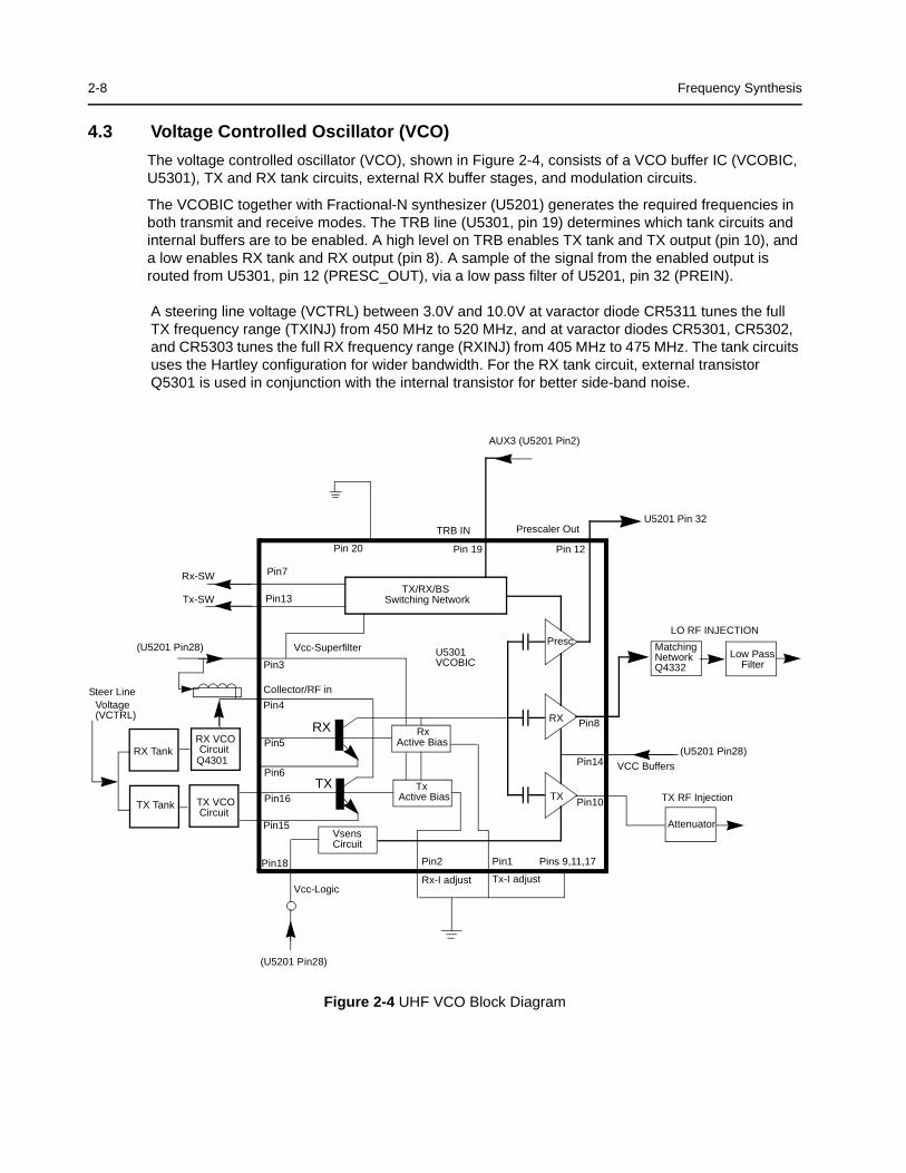
2-8 Frequency Synthesis
4.3 Voltage Controlled Oscillator (VCO)
The voltage controlled oscillator (VCO), shown in Figure 2-4, consists of a VCO buffer IC (VCOBIC, U5301), TX and RX tank circuits, external RX buffer stages, and modulation circuits.
The VCOBIC together with Fractional-N synthesizer (U5201) generates the required frequencies in both transmit and receive modes. The TRB line (U5301, pin 19) determines which tank circuits and internal buffers are to be enabled. A high level on TRB enables TX tank and TX output (pin 10), and a low enables RX tank and RX output (pin 8). A sample of the signal from the enabled output is routed from U5301, pin 12 (PRESC_OUT), via a low pass filter of U5201, pin 32 (PREIN).
A steering line voltage (VCTRL) between 3.0V and 10.0V at varactor diode CR5311 tunes the full TX frequency range (TXINJ) from 450 MHz to 520 MHz, and at varactor diodes CR5301, CR5302, and CR5303 tunes the full RX frequency range (RXINJ) from 405 MHz to 475 MHz. The tank circuits uses the Hartley configuration for wider bandwidth. For the RX tank circuit, external transistor Q5301 is used in conjunction with the internal transistor for better side-band noise.
Figure 2-4 UHF VCO Block Diagram
Presc
RX
TX
MatchingNetwork Low Pass
Filter
Attenuator
Pin8
Pin14
Pin10
(U5201 Pin28)
VCC Buffers
TX RF Injection
U5201 Pin 32
AUX3 (U5201 Pin2)
Prescaler Out
Pin 12Pin 19Pin 20
TX/RX/BSSwitching Network
U5301VCOBIC
RxActive Bias
TxActive Bias
Pin2
Rx-I adjust
Pin1
Tx-I adjust
Pins 9,11,17Pin18
VsensCircuit
Pin15
Pin16
RX VCO Circuit
TX VCO Circuit
RX Tank
TX Tank
Pin7
Vcc-Superfilter
Collector/RF in
Pin4
Pin5
Pin6
RX
TX
(U5201 Pin28)
Rx-SW
Tx-SW
Vcc-Logic
(U5201 Pin28)
Steer Line Voltage (VCTRL)
Pin13
Pin3
TRB IN
LO RF INJECTION
Q4301
Q4332
Frequency Synthesis 2-9
The external RX buffers (Q5332) are enabled by a high at U5201, pin 3 (AUX4) via transistor switch Q5333. In TX mode, the modulation signal (VCOMOD) from the LVFRAC-N synthesizer IC (U5201, pin 41) is applied to the modulation circuits CR5321, R5321, R5322, and C5324. These modulate the TX VCO frequency via coupling capacitor C5321. Varactor CR5321 is biased for linearity from the VSF.
4.4 Synthesizer Operation
The synthesizer consists of a low voltage FRAC-N (LVFRACN) IC, reference oscillator (crystal oscillator with temperature compensation), charge pump circuits, loop filter circuits, and dc supply. The output signal (PRESC_OUT) of the VCOBIC (U5301, pin12) is fed to of U5201, pin 32 (PREIN) via a low pass filter (C5229,L5225,and C5226) which attenuates harmonics and provides correct level to close the synthesizer loop.
The pre-scaler in the synthesizer (U5201) is a dual modulus pre-scaler with selectable divider ratios. The divider ratio of the pre-scaler is controlled by the loop divider, which in turn receives its inputs via the SRL. The output of the pre-scaler is applied to the loop divider. The output of the loop divider is connected to the phase detector, which compares the loop divider´s output signal with the reference signal.The reference signal is generated by dividing down the signal of the reference oscillator (Y5261 or Y5262).
The output signal of the phase detector is a pulsed dc signal routed to the charge pump. The charge pump outputs a current at U5201, pin 43 (IOUT). The loop filter (consisting of R5221-R5223, C5221-C5225, and L5221) transforms this current into a voltage that is applied to varactor diodes CR5311 for transmit, CR5301, CR5302 and CR5303 for receive and alters the output frequency of the VCO.The current can be set to a value fixed in the LVFRAC-N IC or to a value determined by the currents flowing into BIAS 1 (U5201-40) or BIAS 2 (U5201-39). The currents are set by the value of R5251 or R5252 respectively. The selection of the three different bias sources is done by software programming.
To reduce synthesizer lock time, when new frequency data has been loaded into the synthesizer, the magnitude of the loop current is increased by enabling the IADAPT (U5201-45) for a certain software programmable time (Adapt Mode). The adapt mode timer is started by a low to high transistion of the CSX line. When the synthesizer is within the lock range, the current is determined only by the resistors connected to BIAS 1, BIAS 2, or the internal current source. A settled synthesizer loop is indicated by a high level of signal LOCK (U5201-4) which is routed to one of the µP´s ADCs input U101-56. From the voltage the µP determines whether LOCK is active.
To modulate the PLL, the two-spot modulation method is utilized via pin 10 (MODIN) on U5201. The audio signal is applied to both the A/D converter (low frequency path) and the balanced attenuator (high frequency path). The A/D converter converts the low frequency analog modulating signal into a digital code which is applied to the loop divider, thereby causing the carrier to deviate. The balance attenuator is used to adjust the VCO’s deviation sensitivity to high frequency modulating signals. The output of the balance attenuator is present at the MODOUT port (U5201-41) and connected to the VCO modulation diode CR5321 via R5321 and C5325.

2-10 Frequency Synthesis
THIS PAGE INTENTIONALLY LEFT BLANK

3-1
Section 3
TROUBLESHOOTING CHARTS
1.0 Troubleshooting Flow Chart for Receiver (Sheet 1 of 2)
Bad SINADBad 20dB Quieting
No Recovered Audio
START
Audio at pin 8 of U3101 ?
Check Controller(in the case of no audio)
OR ELSE go to “B”
Yes
No
Spray or inject 44.85MHz into XTAL Filter FL3101
Audio heard ?BYes
No
Check 2nd LO (44.395MHz) at C3135
LO present ?BYes
Check voltages on U3101
Biasing OK ?
No
No
A
Yes
Check Q3102 bias for faults
Replace Q3102
Go to B
Yes
No
Check circuitry around U3101.
Replace U3101 if defect
Check circuitry around Y3101. Replace Y3101 if defect
Voltages
OK?

3-2 Troubleshooting Flow Chart for Receiver
1.1 Troubleshooting Flow Chart for Receiver (Sheet 2 of 2)
IF Signal at C3101?
No
RF Signal at T5051?
RFSignal at C5015?
No
No
RFSignal at C5025?
No or
Check harmonic filterL5491-L5493, C5492, J5401
and ant. switchD5471, D5472, L5472.
Check filter between C5025 & C5009.
Check tuning voltage at R5060.
Inject RF into J5401
Istuning voltage
OK?
No
Yes
Check RF amp (Q5003) Stage.
Check filter between C5015 & T5051.
Yes
Check T5051, T5052, D5051, R5052, L5008.
Yes
1st LO level OK?
Locked?
Yes
Check FGU
Yes
Trace IF signal from C3101 to
Q3101. Check for bad XTAL filter.
No
Yes IFsignal at Q3102
collector?
Before replacing U3101, check
U3101 voltages.
Yes
Check for 5VDC
Is 9V3 present?
Check Supply Voltage circuitry. Check Q0681,
U5211 and U0641.
No
No
No
Check U5501.
Check varactor filter.
No
Yes
Yes
Yes
A
A
B
weak RF
RFSignal at C5009?
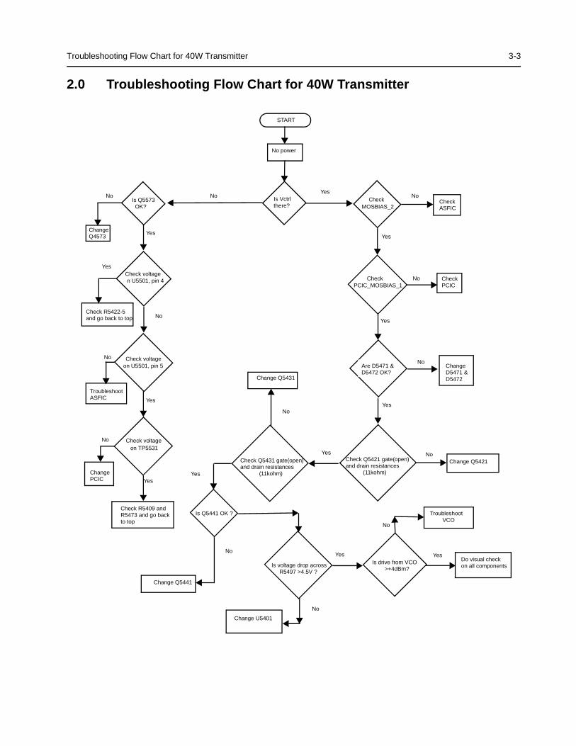
Troubleshooting Flow Chart for 40W Transmitter 3-3
2.0 Troubleshooting Flow Chart for 40W Transmitter
No
Is Q5441 OK ?
YesIs drive from VCO >+4dBm?
No
Is voltage drop across R5497 >4.5V ?
No
Check Q5431 gate(open)and drain resistances (11kohm)
NoCheck Q5421 gate(open)and drain resistances (11kohm)
No
PCIC_MOSBIAS_1 Check
No
No
ChangeQ4573
START
No power
Is Vctrlthere?
Is Q5573 OK?
Check voltagen U5501, pin 4
Check voltageon U5501, pin 5
Check R5422-5and go back to top
TroubleshootASFIC
ChangePCIC
Check R5409 and
R5473 and go backto top
CheckMOSBIAS_2
CheckASFIC
Are D5471 &D5472 OK?
ChangeD5471 &D5472
NoNo No
Yes
Yes
YesYes
Yes
YesYes
Yes
No
No CheckPCIC
Yes
Change Q5421
Change Q5431
Yes
Change U5401
YesDo visual checkon all components
No
Change Q5441
Troubleshoot VCO
Check voltageon TP5531

3-4 Troubleshooting Flow Chart for Synthesizer
3.0 Troubleshooting Flow Chart for Synthesizer
5V at pin 6 of
D5201
Isinformation
from µP U0101correct
?
IsU5201 Pin 47at = 13VDC
?
IsU5301 Pin 19
<40 mVDC in RX &>4.5 VDC in TX? (at VCO section)
?
Start
Visual check of the
BoardOK?
CorrectProblem
Check 5VRegulatorU5211
+5Vat U5201
Pins13 & 30
?
Is16.8MHz
Signal at U5201 Pin 19
?
CheckY5261 / Y5262 and
associated parts
Aresignals
at Pins 14 &15 of U5201
?
Check R5201 Check C5381
IsU5201
Pin 2 >4.5 VDC in Tx & <40 mVDC
in Rx?
Replace U5201
RemoveShorts
Isthere a short
between Pin 47 andPins 14 & 15 of
U5201?
Replace orresolder
necessarycomponents
IsRF level at
U5201 Pin 32 -12 < x <-25
dBm?
AreR5221,R5222,R5223,C5221,
C5222,& C5223 OK?
Replace U5201
If C5227is OK, then see VCOtroubleshooting chart
AreWaveforms
at Pins 14 & 15triangular
?
DoPins 7,8 & 9
of U5201 togglewhen channel is
changed?
Check programminglines between
U0101 and U5201Pins 7,8 & 9
Replace U5201
Check µP U0101Troubleshooting
Chart
NO
YES
NO
YES
NO
YES
NO
NO
NO
YES
YES
NO
YES
YES
NO
YES
YESYESNO
NO
NO
NO
YES
NO
YES
YES
Check D5201, C5202, C5203, &
C5206
5V at U5201
pins 5, 20, 34 & 36
Check 5V Regulator
U5211
Is 16.8MHz signal at
U5201 Pin 23?
Replace U5201
YES
NO
NO
YES
NO
YES
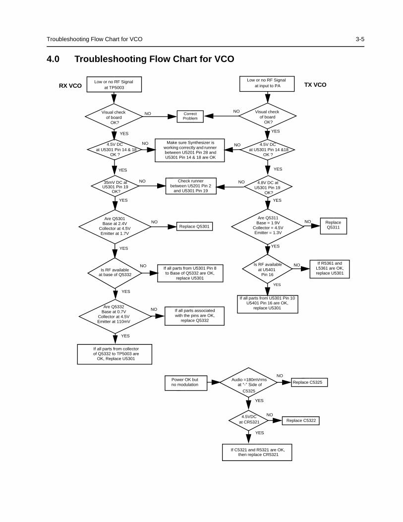
Troubleshooting Flow Chart for VCO 3-5
4.0 Troubleshooting Flow Chart for VCO
Are Q5332Base at 0.7V
Collector at 4.5V Emitter at 110mV
Are Q5301Base at 2.4V
Collector at 4.5V Emitter at 1.7V
Are Q5311 Base = 1.9V
Collector = 4.5VEmitter = 1.3V
Low or no RF Signalat TP5003
Visual checkof board
OK?
35mV DC atU5301 Pin 19
NO
YES
Replace Q5301
at base of Q5332
NO
NO
NO
NO
YES
YES
YES
YES
Low or no RF Signalat input to PA
4.8V DC atU5301 Pin 19
Is RF available at U5401
YES
YES
YES
YES
NO
NO
NO
NO
NO
Audio =180mVrmsat “-” Side of
4.5VDCat CR5321
If C5321 and R5321 are OK, then replace CR5321
Replace C5322
Replace C5325
NO
NO
YES
YES
TX VCORX VCO
CorrectProblem
Visual checkof board
OK?
Check runner between U5201 Pin 2
and U5301 Pin 19
Is RF available If all parts from U5301 Pin 8to Base of Q5332 are OK,
replace U5301
If all parts associated with the pins are OK,
replace Q5332
If all parts from collectorof Q5332 to TP5003 are
OK, Replace U5301
Power OK but no modulation
If all parts from U5301 Pin 10U5401 Pin 16 are OK,
replace U5301
Replace Q5311
YES YES
Make sure Synthesizer is working correctly and runner between U5201 Pin 28 and U5301 Pin 14 & 18 are OK
4.5V DC
OK ?
OK? OK?
C5325
at U5301 Pin 14 & 18 4.5V DC
OK ?at U5301 Pin 14 &18
NO
Pin 16
If R5361 and L5361 are OK, replace U5301

3-6 Troubleshooting Flow Chart for VCO
THIS PAGE INTENTIONALLY LEFT BLANK

4-1
Section 4
UHF PCB/SCHEMATICS/PARTS LISTS
1.0 Allocation of Schematics and Circuit Boards
1.1 Controller Circuits
The UHF circuits are contained on the Printed Circuit Board (PCB) which also contains the Controller circuits. This Chapter shows the schematics for the UHF circuits only, refer to the Controller section for details of the related Controller circuits . The PCB component layouts and the Parts Lists in this Chapter show both the Controller and UHF circuit components. The UHF schematics and the related PCB and parts list are shown in the tables below.
Table 4-1 UHF B2 40W Diagrams and Parts Lists
PCB :8480645Z04 Main Board Top Side8480645Z04 Main Board Bottom Side
Page 4-3Page 4-4
SCHEMATICSPower Amplifier 40WFRACNVoltage Controlled OscillatorReceiver Front EndIF
Page 4-5Page 4-6Page 4-7Page 4-8Page 4-9
Parts List8480645Z04 Page 4-10

4-2 Allocation of Schematics and Circuit Boards
THIS PAGE INTENTIONALLY LEFT BLANK

UH
F B
and
2 25
-40W
PC
B /
Sch
emat
ics
/ Par
ts L
ist
4-3
2.0
UH
F B
and
2 2
5-40
W P
CB
/ S
chem
atic
s / P
arts
Lis
t
C0211
C0212
C0251
C0252
R0211
R0212
R0251
R0252
R0253
R0257
16
1 89
U0251
C0253
C0256 C0261
C0262
R0256R0268
R0269
871
14
U0211
J0451
1
C0421
C0451
C0452
C0453
C0455
C0456
C0457
C0458
C0459
C0460
C0461
C0462
C0463
C0464
C0466
C0467
R0441
C0468
18
32
17
16
1
U0121
C0132
R0131
51
26
U0101
1 76
R0106
C0106
R0101R0102
R0104
R0108
R0110
R0115
R0116
C0224
R0226
R0227
R0228
Q0110
R0261
R0262
R0442
C0441
C0442
C0443
C0445
C0446
C0447
C0448
C0449
C0470
C0471
C0472
C0473
C0221
C0222
C0225
C0228
C0243
R0220
R0221 R0223
R0224
R0229
R0254
R0255
R0222
C0101
C0102
R0105
R0114
R0170
C0131
R0132
234
Y0131
C0104 C0107
C0237
C0223
C0227
C0232
C0233
C0236
R0225C0226
C0495C0234
C0235
C0231
9
U0271
C0542
Q0177
Q0181
Q0185
R0181R0182
R0185R0186
R0510
R0535
R0538
R0539
R0543
VR0501
VR0503
VR0505
VR0510
20
11
10
J0501
C0484
C0601
C0603
C0612
R0533 R0611
R0612
1
6
5
U0611
J0601
C0651
C0652
D0651
R0651
R0652
3
2
1
U0651
C0241 C0242
C0244
C0245
C0246
R0241
R0242
137 25
13
U0221
C0496
D0201
C0482
C0483
C0486C0487
C0488
C0493
C0494
C0654
C0655
C0681
L0481
L0482
Q0681
R0681
R0682
1
6
5
U0641
C5401
C5403
C5404
C5410
C5417
C5419
C5447
C5461
C5486
C5488
C5505
C5506
L5401
L5403
23
R5401
R5402
R5403
9 8
16 1
U5401
C5425
C5426
1
R5408
R5415
R5416
R5481
Q5471
Q5472
R5504
R5511
R5512
TP5530
VR5471
C5431
C5434
C5453
C5455
C5456
C5457
D5402
56
8 7
4Q5421
R5459
C5476
R5476
L5474
R5600
R5601
R5602
C5420
C0474
C0476
C0477
C0478
C0490
C5472
C5474
C5475
C5480
C5510
D5471
D5472
L5472
L5473
C5432
C5435
C5449C5
450
C5460
C5520
D5403
R5607
C5423
C5481
C5485
C5489
C5490
C5495
C5497
C5602
C5478
C5493
C5444
C5465
C5466
C5491
C5521
C5522 R5501
R5502
U5502
C5459
C5507
32
J5401
C5441
C5442
C5443
C3124
C3131
C3132
C3133
C3134
C3135
C3136
C3137
L3124
R3123
R3124
R3130
R3132
C3115R3111
R3117
11
120
10
U3101
C3143
R3135
C3139
C3140
C3141
C3142
C3145 C3148
R3142
R3144
R3145
87 1
14U3115
2
Y3102
87 1
14
U3111
432
FL3112
FL3114
C3101
23 4
56
FL3101
L3100
R3148
C3102
C3103
L3101R3101
R3106
23 4
56
FL3102
C3114
C5031
C5052
C5053
C5054
C5055
D5051
L5008 L5051
L5053
L5054
R5015
R5051
21 5
43
T5051
346 1
2
T5052
C5017
C5018
C5019
C5020
C5021
C5022
C5023
C5029
C5030
D5004
D5005
R5012
C5001
C5002
C5003
C5004
C5005
C5006
C5007
C5008
C5009
C5014
C5026
C5027
C5033
C5034
D5001
D5002
D5003
L5001
L5002
L5003
L5006
Q5001
Q5003
R5001
R5003
R5004
R5005
R5018
R5020
R5021
R5022
C5015 C5016
L5004
R5007
R5066
C5032
L5005
L5009
R5013
C5210 C5212C5213
C5214
C5215
C5216 C5242
C5243
C5244
C5245
C5246
C5289L5201
R5211
45 8U5211
C5222
C5223
C5225
C5226
C5227
C5229
C5230
C5231
C5241
C5253
L5221
L5225
C5221
R5221
R5222
R5223
C5232
C5233
C5234
C5251
C5252
C5254
C5255
R5251
R5252
C5224
C5235 R5263
C5317
C5318
C5322
C5323
C5325
C5351
C5352
C5382
3
L5312
L5313
R5311
R5312
R5321
C5308
C5309
C5353
C5355
C5383
L5304
L5305
Q5301
Q5311
R5301
R5302
R5305 C5331
C5332
C5371
C5372
C5373
C5374
L5371
R5331
R5332
R5333
R5337
R5341
C5375
L5303
43
Q5333
R5346
3
SH5301
C5335
C5337
C5339R5343
R5345
C0504
C0505
C0506
C0508
C0509
C0510
C0511
C0512
C0513
C0514
C0515
C0516
C0517
C0518
C0501
C0502
C0503
UH
F B
and
2 (
450-
520
MH
z) 4
0W 8
4806
45Z
04 T
op
Sid
e
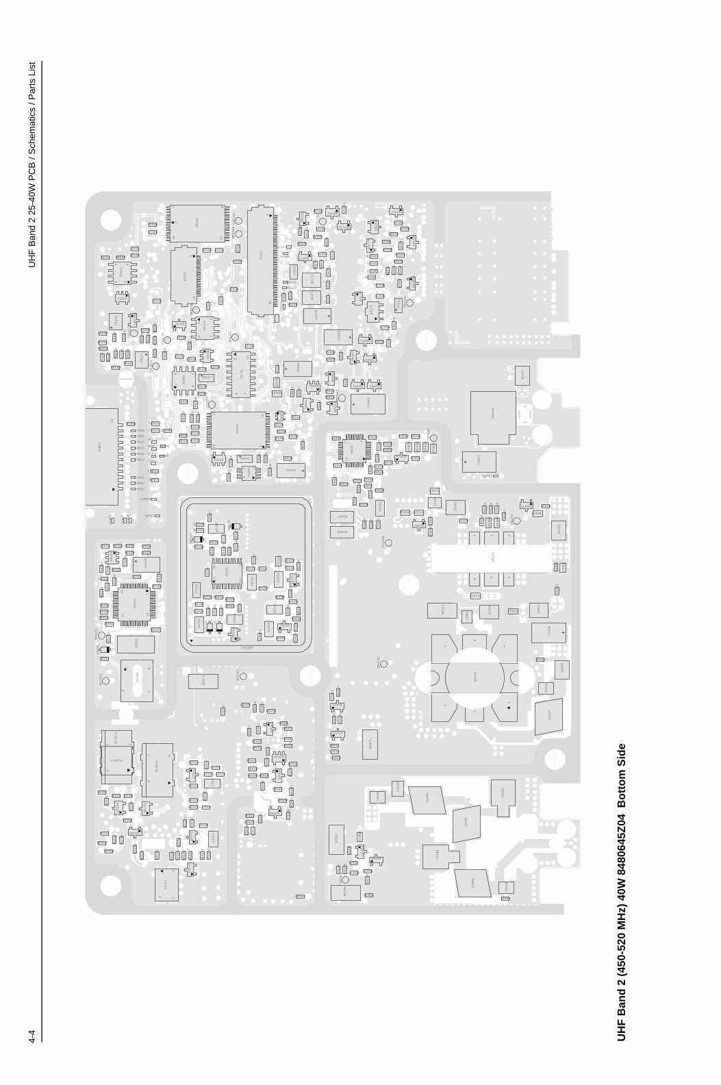
4-4
UH
F B
and
2 25
-40W
PC
B /
Sch
emat
ics
/ Par
ts L
ist
C
99
CNTL-REV-T6
C3144
C3146
C3147
C3151C3152
Q3141
Q3151
Q3152
R3134R3141
R3146
R3147
R3151
R3152
R3153
R3154
R3133
432
Y3101
C3122
C3123
R3113
R3116
D3101
R3115
Q3102
C3116
R3118
C3111
R3104
R3105
R3108
R3102
C3104
C3110
C3112 C3113
L3111Q3101
R3107
C3121
L3112
R3112
R3114
43 2
FL3111
FL3113
43 2
FL3115
C5028
C5068
Q5002
R5016
R5017
R5068
C5010C5011
C5012
C5013
R5002
C5064
C5065
C5069
D5006
Q5004
R5062
R5063 R5064
R5070
R5072
C5024
C5060
C5067
R5052
R5053
R5054
R5055
R5060
R5071
TP5003
C5061
C5062
D5007
R5061
R5069
C5451
C5463
C5469
C5470
C5473
C5499
D5452
D5454
R5455
R5457
R5472R5475
R5496
TP5531
C5025
C5452
C5464
D5451
D5453
R5409
R5471
R5473
R5474
R5506
R5507
C5448
C5492 C5498
L5491
L5493
L5492
C5496
R5491
C5494
C5263
D5261
L5231
R5261
TP5201
TP5202
Y5261
2 34
Y5262
C5261
C5262
R5241
R5262
137
25
13
U5201
C5228C5287
R5228
C5201
C5202
C5203 C5204
C5205
C5206
C5207
C5208C5209 C5211
C5288
D5201
R5201
R5203 R5204
R5206
C5066
R5019
C5301
C5302
C5303
C5304
C5305 C5306
C5307
C5316
CR5301
CR5302
CR5303
L5301
L5302
R5303
R5304
R5315
C5381 11
120
10
U5301
C5311
C5312
C5313
C5314
C5315
C5321
C5324
CR5311
CR5321
L5311
R5313
R5314
R5322
R5323
C5336 C5338
L5332
L5333 Q5332
R5336
R5338
R5339
R5340
R5342
R5344
R5347
SH5302
C5333C5363
C5334
C5354
C5361
C5362
L5331
L5361
Q5331
R5334
R5335
R5361
6
5
4
3
2
1
Q5441
C5437L5440
L5441
654
R5421
C5422
C5436
C5482
L5421
C5438
C5439
L5436
L5437
TP5532
C0401
C0402
C0403
C0406
C0407
C0408
C0409
C0410
C0411
R041212
C5407
C5409
C5412
C5414
C5416
C5462
C5487
L5411R5405
R5411
R5412
R5427
R5428R5433
R5495
R5497
TP5536
C5424
C5483
L5541
L5543
Q5451
R5414
R5487
R5488
R5513
C5446
C5630
3 2 1
R5485
R5486
R5630
R5631
R5632
TP5537
C5632
R5633
VR5472
C5421
C5484
L5402
Q5431
C0499
C0611
VR0601
C5418C5479
C5502
C5503
C5504
Q5473
R5422
R5423
R5424
R5425
R5431R5480
R5482
R5483
R5484
R5492 R5503
R5514
R5523
TP5533
1
17 9
25
U5501
C0422
C0423
C0485
R0467
C0491
C0492
C0497
C0301
C0303
C0352
C0354
1
458
U0351
C0302
C0351
D0301
28
15
C0304
C0305
C0324
C0325
C0343
R0323
R0324
R0344
C0426
C0427
C0428
C0429
C0430
C0431
R0407
R0409
R0410
C0353
R0331
R0332
R0333
R0335
R0481
R0482
J0401
C0201
C0202
C0203
C0204
C0205
C0254
C0265
C0266C0267
R0201
R0202
R0203
R0204
R0205
R0206
R0207
R0208
R0265
R0266
R0267
TP0221
TP0222
VR0541
14
U0301
C0341
C0344
R0341
R0345
R0346
TP0497
1
458
U0341
C0141
TP0101
16
18 9
U0141
C0342R0342
R0343R0347
U0342
C0331
C0641
C0644
C0645
C0662
Q0641
Q0661
R0641
R0642
R0643
U0331
C0661
C0663
D0660D0661
Q0662
Q0663
R0661
R0662
TP0661
C0622
C0671
D0621R0671
R0672
VR0621
VR0671
C0621
R0621
C0541Q0171
Q0173
R0171
R0172
R0173 R0174
R0175
R0176
R0177
R0178
R0179
R0512
R0525
R0529
R0530
R0541
R0542
R0408
TP0102
C0111
C0112
D0101
R0111
R0401
TP0104
14 5
8
U0111
118
J0552
R0107
C0105
C0121
C0255 R0468
145
8
U0652
U0653
C0103 R0112
R0113
R0117
R0121
TP0103
TP0492
22
21
871
U0122
C0122
C0123
C0558
C0559
C0560
C0575
C0576
C0591
C0592
C0593
40
J0551
R0591
R0592
C0271
C0275
C0276
C0277
E0271
E0272
Q0271
R0273
R0276
C0151
C0272
C0273
C0274
C0554
D0151 Q0151
R0151
R0152
R0274
R0275
R0593
TP0151
VR0151
D0179
Q0183
R0183
R0184
R0511
R0531
R0537
VR0509
VR0537
TP0530
VR0504
E0631
1
UH
F B
and
2 (
450-
520
MH
z) 4
0W 8
4806
45Z
04 B
ott
om
Sid
e
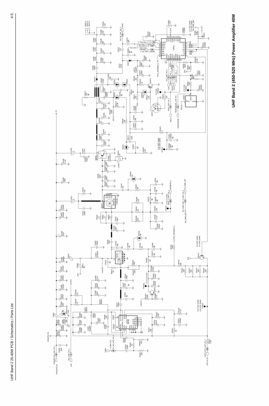
UH
F B
and
2 25
-40W
PC
B /
Sch
emat
ics
/ Par
ts L
ist
4-5
9V3
PA
SU
PV
LTG
PA
SU
PV
LTG
_UH
F_P
A_1
9V3_
UH
F_P
A_1
C54
8530
pF
5.6V
VR
5472
R56
3382
0K
C56
02.0
33uF
L540
2
C54
8130
00pF
C56
3210
00pF
ALT
PA
SU
PV
LTG
C54
8430
pF.0
33uF
C54
21C
5497
1000
pF30
00pF
C54
8910
00pF
C54
95C
5436
10uF
C54
9330
00pF
C54
9030
00pF L5
541
C54
7810
00pF
C54
8230
pF
L542
1
0.1u
FC
5438
L543
6
A+
C54
8630
pFC
5418
0.1u
F10
0pF
C54
88
L540
111
.03n
H
C54
0410
0pF
390n
HL5
403
1.8p
FC
5403
C54
070.
1uF
R54
0520
0
30pF
C54
870.
1uF
C54
0910
0pF
C54
12
Load
L541
139
0nH
> 4
dB
m (
Tx)
TX
INJ TX
_IN
J_U
HF
_PA
_1
51R54
97R
5495
51
9V3
L547
4
57R
019V
3
300
R54
01
C54
1010
0pF
C54
0110
0pF
R54
03 300
R54
0215
6
RF
OU
T2
7V
CN
TR
L1
VD
114
VG
12
VG
23
5
GND3 12
GND4 13
NC
18
NC
29
NC
310
NC
415
RF
IN16
RF
OU
T1
U54
0130
C65
EP 17
G2
11
GND1 4
GND2
C54
62R
5433
C54
1710
0pF
C54
61
R54
15 100
C54
477.
5pF
36pF
C54
19
R54
1610
0
C54
53
47pF
C54
31
C54
8310
0pF
13.8
5nH
L554
3
R54
14
C54
24
8
Q54
21
6
2
13457
C54
55
Load
3.7
to 3
.9 V
DC
Q54
51TP
5536
R54
8710
0K
R54
0820
0KC
5425
.022
uFR
5488
2.7K
100p
FC
5426
C54
56C
5457
R54
81
D54
02R
5459
R54
8512
012
0R
5486
1KR56
31R
5607
R54
76
C55
20C
5476
R56
3224
KC
5446
100p
F
C56
300.
1uF
R56
30
2.4
to 2
.6 V
DC
BIA
S_2
_UH
F_P
A_1
MO
SB
IAS
_2
TP
5537
R54
125.
6K
C54
16.0
22uF
10K
R54
27
R54
11
C54
1410
00pF
4.7K
R54
28
100K
R54
80
PC
IC_M
OS
BIA
S_1
6.5
VD
C (
44W
)6.
2 V
DC
(28
W)
R54
2462
0
R54
2362
0
R54
31
620
R54
22
Q54
73
9V3
R54
2562
0
R55
143.
3K
CN
TLV
LTG
_UH
F_P
A_1
CN
TLV
LTG
4.57
VD
C (
44W
)4.
32 V
DC
(28
W)
TP
5533
PA
_PW
R_S
ET
_1_U
HF
_PA
_1P
A_P
WR
_SE
TP
A_P
WR
_SE
T
C54
2039
pF16
pFC
5434
R56
014.
7
4.7
R56
00
R56
024.
7
100p
FC
5422
C54
231u
F
G4
S1S2S3S4
D
G
G1
7
G2
8
G3
9 10
Q54
31M
RF
5015
15pF
C54
32
20pF
C54
35
20pF
C54
5039
pFC
5460
C54
4920
pF
C54
37
L544
0
D54
03
10R54
21
13.8
5nH
L544
1
3
MR
F65
0Q
5441 4
2
1N
U
NU
NU
NU
C54
43
C54
44
C54
66
C54
65
7.5p
FC
5491
30pF
C54
42
C54
4127
pFC
5459
100p
F
D54
71
R54
5712
0
C54
6910
0pF
120
R54
71
D54
52
D54
54
D54
51
C54
52
R54
734.
3K
9V3
R55
0610
K
100K
R54
09
D54
53
C54
6410
0K
R54
74
C54
3910
0pF
L543
717
nH
2.20
VD
C (
28W
)3.
11 V
DC
(44
W)
0R54
75
1000
pFC
5451
100K
R54
55
TP
5531
10K
R55
07
K9V
1
TE
MP
SE
NS
E_U
HF
_PA
1POSU
5502
K9V
1_U
HF
_PA
_1
TE
MP
SE
NS
E
R55
04
10K
9V3
100p
FC
5499
C54
7010
0pF
C55
07
A+
VR
5471
5.6V
R54
72
10K
R55
13
470
R55
12
9.2
VD
C
Q54
71
TP
5530
3J5
401-
3
9pF
C54
48
J540
1-2
2
C54
947p
FL549
117
nH
1J5
401-
1
100p
FC
5492
17nH
L549
217
nHL5
493
4.7p
FC
5498
3.3p
FC
5496
R54
9111
K
C54
63
RX
INR
X_I
N_V
HF
_PA
_117
nHL5
472
C54
7412
pF
D54
72C
5480
2pF
2pF
C54
75
C54
7910
0pF
51R55
1182R
5496
Q54
72
C54
7230
pF
30pF
C55
10
100p
FC
547343
.67n
HL5
473
CLK
CLK
_VH
F_P
A_1
CS
X_V
HF
_PA
_1
DA
TA
CS
X
DA
TA
_VH
F_P
A_1
10K
R54
929V3
0.75
VD
C R55
015.
6K
100p
FC
5521
1000
pF
TP
5532
C55
22
3GNDVO
UT
2
R55
0268
K
300K
R54
82
68K
R54
84
9V3
R55
033.
9K
3.1
VD
C (
44W
)2.
2 V
DC
(28
W)
R55
23R54
8310
0K
ALT
PA
_PW
R_S
ET
C55
0322
00pF
.02u
FC
5504
.015
uFC
5502
2200
pFC
5506
VLIM19
30
V10
14
V45
16
17V5EXT
20VAR1
18 VAR2
24VAR3
15V
G
VL 6
Q11
QX
10
1RFIN
RS21
31R
SE
T
RX23
T1 2
TE
MP
26
CQ
1213C
QX
DA
TA
28
F16
89
GND1 8
GN
D2
25
INT 422
NA
AN
O32
BP
OS
27
CE
X29
CI 3
CJ 5
CL 7
CLK
U55
01
1uF
C55
05
PC
IC_M
OS
BIA
S_1
9V3
RESET
FE_CNTL_2_VHF_PA_1FECTRL_2
FE_CNTL_1_VHF_PA_1FECTRL_1
RESET_VHF_PA_1
UH
F B
and
2 (
450-
520
MH
z) P
ow
er A
mp
lifie
r 40
W

4-6
UH
F B
and
2 25
-40W
PC
B /
Sch
emat
ics
/ Par
ts L
ist
16_8
MH
z
C52
02.0
1uF
IN_5
V_R
F_R
EG
_UH
F_F
N_1
TR
B
MO
DIN
220
R52
41
C52
510.
1uF
TP
5202
1
.01u
FC
5232
LOC
K_U
HF
_FN
_1
C
5243
100p
F
R52
2251
0
C52
534.
7uF
o
2.2u
FC
5213
C52
09
0.1u
F
U45
06
.01u
FC
5231
CLK
_UH
F_F
N_1
L522
112
uH
47K
R52
28
1000
pFC
5252
150
R52
21
R52
6115
0K
100
R52
63
VD
DA
CLK
16.8
MH
z
XT
AL
Y52
61
1uF
C52
23
VC
NT
L
1
VS
F_U
HF
_FN
_1
Y52
62T
TS
05V
16.8
MH
z
GN
D2
OU
T 3
VC
C4
M
OD
IN_U
HF
_FN
_1
2.2u
F
C52
14
0.1u
FC
5254
D 5
261
5V_U
HF
_FN
_1
150
R52
01
C52
88
0.1u
F
DA
TA
100p
F
C52
27
VD
DA
_UH
F_F
N_1
C52
4610
0pF
C52
05.0
1uF
1.5p
F
C52
63
68
R52
23
C52
35.0
1uF
C52
5510
0pF
C52
22
0.1u
F
1.2K
R52
62
C52
4510
0pF
C52
44
47nH
L522
5
100p
F
T
RB
_UH
F_F
N_1
U
4507
16_8
MH
z_U
HF
_FN
_1C
SX
_UH
F_F
N_1
C52
04
0
R52
11
100p
F
B
WS
ELE
CT
_UH
F_F
N_1
C52
07
100p
FC
5228
0.1u
F
5V
_UH
F_F
N_2
VS
F
C52
110.
1uF
2.4p
F
C52
26
C52
0610
uF
2.2u
FC
5210
220p
FC
5262
47
R52
03
LOC
K
C52
08
0.1u
F
1uF
C52
24
510p
F
C52
25
R52
04
R52
06
47
33K
C52
16.0
1uF
LP29
51U
5211
VC
OB
IAS
_2
C52
12
.018
uF
100p
FC
5287
100p
F
C52
01
2p
FC
5229
C52
30
2.2u
F
2.2u
FC
5233
0.1u
F
C52
89
39K
R52
51
VC
TR
L
T
P52
01
C52
42
PR
ES
C
CS
X
100p
F
L523
1
VC
OM
OD
_UH
F_F
N_1
IN_5
V_R
F_R
EG
2.2u
H
C52
4110
0pF
5A
24
A3
K1
1K
22
K3
3
DA
TA
_UH
F_F
N_1
6A
1
D52
01
C52
21.0
1uF
.01u
F
C52
03
R52
52
30K
VC
TR
L_U
HF
_FN
_1
.01u
FC
5234
L520
139
0nH
62pF
C52
61
5V
5V
2.2u
FC
5215 V
DD
A
VD
DA
U52
014.
57 V
DC
-19
to -
17 d
Bm
(R
x)-1
7 to
-12
dB
m (
Tx)
4.98
VD
C
0 V
DC
(R
x)
3.09
VD
c (R
x)2.
65 V
DC
(T
x)
4.97
VD
C (
25K
Hz
Cha
n. S
paci
ng)
4.97
VD
C (
Tx)
2.48
VD
C
1.76
VD
C (
Tx)
1.69
VD
C (
Rx)
0 V
Dc
(12.
5KH
z C
han.
Spa
cing
)
5 V
DC
(Lo
cked
)0
VD
C (
Unl
ocke
d)
2.5
to 1
0 V
dc
6.6
VD
C10
.87
VD
C
12.7
VD
C
4.97
VD
C
3.03
VD
C
3.76
VD
C
2.51
VD
C
4.95
VD
C0
VD
C
2.48
VD
C
1.25
VD
C
1.97
V
DC
5V
VC
OM
OD
BW
SE
LEC
T
23X
TA
L1X
TA
L224
21V
BP
AS
S
47VCP
VM
ULT
11514
VM
ULT
2
12V
MU
LT3
11V
MU
LT4
VRO 13
25W
AR
P
35P
VR
EF
18R
EF
SE
L
27S
FB
AS
E26
SF
CA
P
30S
FIN
28S
FO
UT
37T
ES
T1
38T
ES
T2
17N
C1
29N
C2
31N
C3
44 PD_GND
PD_VDD 5PR
EIN
32
33 PRE_GND34PRE_VDD
36DVDD
19F
RE
FO
UT
45IA
DA
PT
16IN
DM
ULT
43IO
UT
LOC
K4
10M
OD
IN
41M
OD
OU
T
20AVDD
40B
IAS
1
39B
IAS
2
42C
CO
MP
9C
EX
8C
LK
7D
AT
A
DGND6
46A
DA
PT
SW
22 AGND
48A
UX
1
1A
UX
2
2A
UX
3
3A
UX
4
INP
UT
1O
UT
PU
T
2S
EN
SE
3S
HU
TD
OW
N6
5V_T
AP
5E
RR
OR
7F
EE
DB
AC
K
4
GN
D
8
ZW
G01
3036
4-0
HF
Ban
d 2
(45
0-52
0 M
Hz)
FR
AC
N
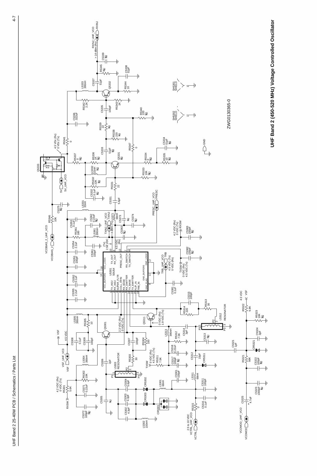
UH
F B
and
2 25
-40W
PC
B /
Sch
emat
ics
/ Par
ts L
ist
4-7
3pF
Q53
31
VC
OM
OD
C53
14
CR
5303
R53
45
C53
34
C53
034.
3pF
220
51pF
100p
F
R53
40
C53
23
C53
15
RX
INJ
1000
pF
VS
F_U
HF
_VC
0
CR
5301
R53
6118
0
GN
D
C53
1710
0pF
0R53
37
VC
OB
IAS
_2
R53
117.
5K
390n
HL5
304
C53
810.
1uF
C53
5110
0pF
C53
530.
1uF
L531
3
L533
133
nH
0.1u
F
390n
H
C53
08
0.1u
F
C53
5239
0nH
L530
5
CR
5311
1
R53
04
RX
INJ_
UH
F_V
CO
PR
ES
C_U
HF
_VC
O
150
R53
127.
5K
4.7u
F
C53
25
Q53
33
10R53
35
10K
100p
F
R53
33
L530
168
nH
C53
09
C53
024.
3pF
C53
37
0
R53
41
51pF
51pF
C53
38
R53
46
10K
SH
IELD
SH
5301
1
VC
OB
IAS
_2_U
HF
_VC
O
56K
R53
21
30
R53
03
R53
14
SH
IELD
122
0
.022
uFC
5336
SH
5302
1K
TX
INJ
390n
H
R53
36
C53
13
L533
3
C53
31
5.6p
F
VC
TR
L_U
HF
_VC
O
C53
73
0.1u
FC
5332
R53
0210
K
390n
H
TR
B_U
HF
_VC
O
TX
INJ_
UH
F_V
CO
L536
1
CR
5321
2.2u
FC
5354
C53
045.
6pF
C53
74
C53
0110
0pF
Q53
01
30R53
13
P2
3P
3
L530
222
0nH
L530
3R
ES
ON
AT
OR
P1
2
C53
39
51pF
10
R53
05
R53
34C53
33
TR
B
0
220
R53
38
5V
100p
FC
5382
100p
FC
5383
15nH
L533
2
PR
ES
C
C53
1110
0pF
10K
R53
23
C53
05
VS
F
C53
75
0.1u
FC
5316
2.2K
R53
42
2.2u
F
C53
63
C53
55
22K
R53
32C
5361
100p
F
6.8K
R53
22
1pF
C53
21
22
R53
31
1P
1
2P2
3P
3
Q53
32
L531
2
RE
SO
NA
TO
R
50U
54U
5301
C53
07
100p
F
CR
5302
5.6K
R53
01
C53
06
2pF
R53
47
0
0.22
uFC
5371
C53
180.
22uF
10R53
44
15pF
R53
3922
R53
15C
5312
VC
OM
OD
_UH
F_V
CO
0
1KR
5343
0.22
uFC
5362
5V_U
HF
_VC
O
68nH
L531
1
100p
F
C53
72
C53
35
68nH
100p
F
C53
24
L537
1
VC
TR
L
3pF
100p
FC
5322
Q53
11
VS
F
TX
SW
$P
TX
SW
RX
SW
RX
SW
VS
F
ZW
G01
3036
5-0
4.2
VD
C (
Rx)
0 V
DC
(T
x)
0 V
DC
(R
x)4.
5 V
DC
(T
x)
4.2
VD
C (
Rx)
0 V
DC
(T
x)
4.5
VD
C 2.3
VD
C (
Rx)
0 V
DC
(T
x)
2.5
to 1
0 V
DC
4.5
VD
C
0 V
DC
(R
x)4.
5 V
DC
(T
x)
4.5
VD
C (
Tx)
0 V
DC
(R
x)
0 V
DC
(R
x)1.
9 V
DC
(T
x)
4.5
VD
c (R
x)0
VD
c (T
x)
> 1
4 dB
m (
Rx)
> 4
dB
m (
Tx)
2.58
VD
C
4.5
VD
C (
Rx)
TX
_SW
ITC
H
14
VC
C_B
UF
FE
RS
18 VC
C_L
OG
IC
RX
_OU
T
7R
X_S
WIT
CH
3S
UP
ER
_FLT
R
19T
RB
_IN
16T
X_B
AS
E15
TX
_EM
ITT
ER
1T
X_I
AD
J10
TX
_OU
T
13
FLI
P_I
N
11
GN
D_B
UF
FE
RS
9G
ND
_FLA
GG
ND
_LO
GIC
17
12P
RE
SC
_OU
T5
RX
_BA
SE
6R
X_E
MIT
TE
R
2R
X_I
AD
J8
4C
OLL
_RF
IN
20
(Tx)
UH
F B
and
2 (
450-
520
MH
z) V
olt
age
Co
ntr
olle
d O
scill
ato
r

4-8
UH
F B
and
2 25
-40W
PC
B /
Sch
emat
ics
/ Par
ts L
ist
C50
55
L505
3
C50
02
15nH
33pF
16pF
8.2p
FC
5031
C50
20
Q50
02
GN
D
15nH
L505
4
C50
2410
00pF
D50
02
C50
261p
F
GN
D_U
HF
_FE
1000
pFC
5008
R50
15
100K
R50
01
R50
17
330K
R50
60
3300
pF
RX
INJ
C50
11
C50
2124
pF
L500
4
IN
NE
G
TB
D
C50
25
D50
04
82pF
C50
52
150
R50
19
R50
10
8.2p
FC
5032
33
R50
08
15nH
L500
6
4
C50
30 1pF
XF
MR
T50
51
1 2 3
5
R50
220
270
R50
06
1.5p
FC
5017
RX
IN_U
HF
_FE
9V3
C50
16
D50
01
C50
66
TP
5003
TB
DL5
005
IN
NE
G
TB
DL5
001
IN
NE
G
150n
HL5
051
L500
8
470n
H
10K
9V3
2
R50
05
T50
52X
FM
R
4 6
3 1
100K
27pF
R50
12C
5007
68
R50
07
270
TB
DL5
002
IN
NE
G
R50
11
Q50
01
FE
CT
RL_
1_U
HF
_FE
1pF
C50
29
R50
20 10
C50
60
R50
16
C50
23
C50
5416
pF
C50
098.
2pF
IF
D50
03
0.1u
FC
5034
FE
CT
RL_
1
C50
0416
pFC
5006
Q50
03
L500
9
10R
5021
R50
51
15nH
51
20pF
C50
03
330
R50
02
C50
1333
00pF
0R50
52
270n
H
R50
54
RX
IN
L500
3
330p
FC
5012
C50
271p
F
R50
18
R50
53
R50
034.
7K
R50
13
150
R50
09
C50
28
100p
F
C50
15
R50
55
9V3_
UH
F_F
E
IF_U
HF
_FE
C50
011.
5pF 18
pFC
5005
100p
FC
5014
6.8p
FC
5053
R50
042.
7K
C50
33
TP
5001
0.1u
F
RX
INJ_
UH
F_F
E
16pF
C50
22
TP
5002
C50
1833
pF
D50
51
IO1
1IO
22
IO3
3 IO4
4
C50
1924
pF
330p
FC
5010
D50
05
GR
OU
ND
PO
S
15pF
PO
S
PO
SP
OS
3.4
VD
C @
450
MH
z4.
7 V
DC
@ 4
50M
Hz
6.5
VD
C @
450
MH
z
0.7
VD
C
4.6
VD
C
UH
F B
and
2 (
450-
520
MH
z) R
ecei
ver
Fro
nt
En
d

UH
F B
and
2 25
-40W
PC
B /
Sch
emat
ics
/ Par
ts L
ist
4-9
9186
176B
01
9180
469V
04
9180
469V
03
9180
469V
0691
8046
8V06
R31
442.
4K
BW
SE
LEC
T_V
HF
_IF
_1
9V3_
VH
F_I
F_2
C31
139.
1pF
NU
R31
0410
0N
U
10
0
620n
HN
U
R31
05
R31
30L3
100
14
VD
D
7
VS
S
51
U31
11-1
MC
74H
C40
66
13
CN
TL1
2
C31
16
L311
2
0.
1uF
620n
H
9V3_
VH
F_I
F_1
10
uF
C31
33
0.1
uF
C31
32
.01u
F
C31
51
OU
T2
C31
37.0
39
uF
CF
WC
45
5D
FL3
112
GN
D1
34
GN
D2
IN1
620n
H
C31
21
L310
1
0.1u
F
R31
0112
K
12
K
R31
47
15pF
DIS
CA
UD
IO
C31
02
C31
52.0
1uF
0.1u
F C
3139
7
VS
S
0.1
uF
C31
41
U31
15-1
MC
74
HC
40
66
MC
74H
C40
66
13
CN
TL1
2
14
VD
D
DIS
CA
UD
IO_V
HF
_IF
_1
62
0n
H
620
L311
1
R31
08
27
pF
C31
10
0.
1uF
C31
47C31
55
9V3
.01u
F
NU
Q31
55
FL3
115
3GN
D1
GN
D2 4
1IN
2O
UT
BW
SE
LEC
T
GND3
45
GND4
3IN
6O
UT
C
FW
C45
5F
12
R16
FL3
102
1GND1GND2
2
GND1
12
GND2 4
GND3GND4
5
IN3
OU
T6
12R
16F
L310
1
7
C31
4 2
0.1u
F
MC
74H
C40
66
CN
TL
6
89
VD
D14
VS
S
GN
D
3
IN1
OU
T2
RS
SI
U31
11-3
FL3
114
CF
UC
J455
D
4700
pFC
3146
27K
GN
D1
34
GN
D2
IN1
OU
T2
R31
06
OU
T3
IN1
FL3
111
CF
WC
455G
Y31
011
2R
17
44.3
95M
Hz
GN
D2
GN
D1
4C
3131
1pF
NU
0.1u
FC
3145
5V_V
HF
_IF
_1
IF
IN_V
HF
_IF
_1IF
330
R31
16
10K
R
3134
0.1
uF
C31
44
18pF
C31
14
10K
R31
55
R31
51
VD
D
7VS
S
NU
1.2K
U31
11-4
MC
74H
C40
66
12CN
TL14
CN
TL
5
43
VD
D
14
VS
S 7
U31
15-2
MC
74H
C40
66
0.1
uF
C31
04
C31
35
33pF
12CN
TL
11
14 VD
D
7VS
S
7
U31
15-4
MC
74H
C40
66
MC
74H
C40
66
CN
TL
5
43
VD
D
14
VS
S
3.3
K
U31
11-2
R31
45
0.1
uF
C31
40
39
0
R31
15
Q31
52
32
2p
FY
3102
455K
Hz
45B
02
C31
15
82pF
C31
12C
3123
.03
9u
F
R31
12 10
0102
727B
45
0R
3148
0.1u
F C31
11
Q31
51
27
K
R31
17
Q31
02
8.2K
R31
33
Q31
01
C31
363
0p
F
20pF
R31
02C
3101
33pF
10
C31
03
C31
340
.1u
F
R
SS
I_V
HF
_IF
_1
6.
8K
R31
18
R31
11
12K
C31
22
.039
uF6.
8K
R31
07
NU
100
R31
14
R31
54
5V
10K
10
K R
3153
D31
01
120p
F
C31
43
R31
52
10K
1.2
K
CN
TL
6
VD
D
14 VS
S 7
R31
35
U31
15-3
MC
74H
C40
66
680
R31
46R
3160
0
R31
321
5K
FL3
113
CS
455G
2N
U
GN
D
3
IN1
OU
T2
9V3
5V
5V
9V3
9V3
9V3
9V3
9V3
5V
9V3
8910
1110
OSCIN4 OSCOUT 3
QUADIN10
RFIN1
RFIN_DEC2
RSSIOUT 5RSSI_FEED9
VC
C6
IFAMPOUT 16
IFAMP_DEC119
IFAMP_DEC2
17
LIMIN14
LIMOUT 11
LIM_DEC1 13
LIM_DEC2 12
MIXOUT 20
SA
61
6
SA
616
AUDIOOUT 8AUDIO_FEED7
GN
D15
IFAMPIN18
U31
01
ZW
G01
3036
7-0
UH
F B
and
2 (
450-
520
MH
z) IF
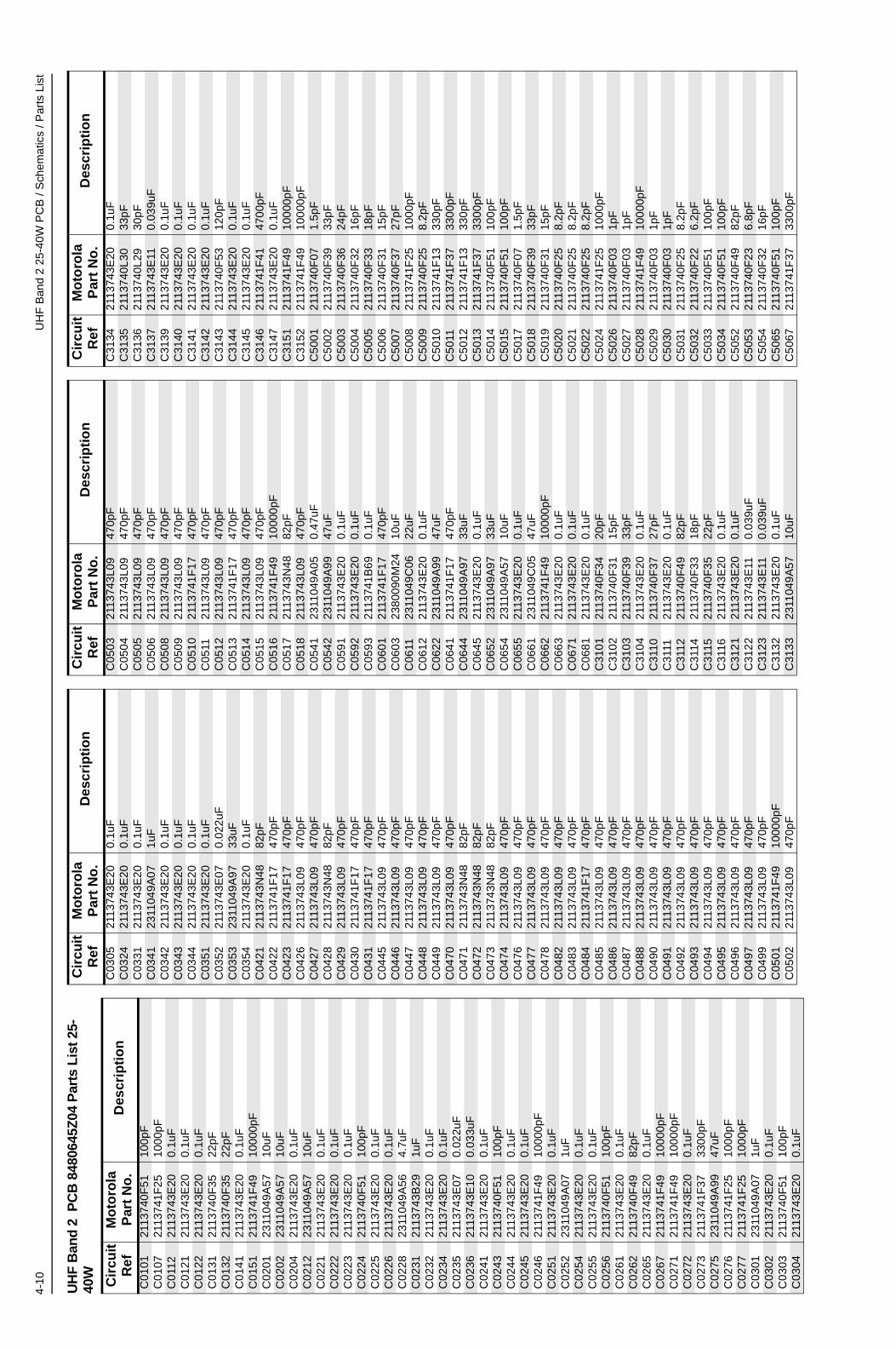
4-10
UH
F B
and
2 25
-40W
PC
B /
Sch
emat
ics
/ Par
ts L
ist
UH
F B
and
2 P
CB
848
0645
Z04
Par
ts L
ist 2
5-40
W
Cir
cuit
R
efM
oto
rola
P
art
No
.D
escr
ipti
on
C01
0121
1374
0F51
100p
FC
0107
2113
741F
2510
00pF
C01
1221
1374
3E20
0.1u
FC
0121
2113
743E
200.
1uF
C01
2221
1374
3E20
0.1u
FC
0131
2113
740F
3522
pFC
0132
2113
740F
3522
pFC
0141
2113
743E
200.
1uF
C01
5121
1374
1F49
1000
0pF
C02
0123
1104
9A57
10uF
C02
0223
1104
9A57
10uF
C02
0421
1374
3E20
0.1u
FC
0212
2311
049A
5710
uFC
0221
2113
743E
200.
1uF
C02
2221
1374
3E20
0.1u
FC
0223
2113
743E
200.
1uF
C02
2421
1374
0F51
100p
FC
0225
2113
743E
200.
1uF
C02
2621
1374
3E20
0.1u
FC
0228
2311
049A
564.
7uF
C02
3121
1374
3B29
1uF
C02
3221
1374
3E20
0.1u
FC
0234
2113
743E
200.
1uF
C02
3521
1374
3E07
0.02
2uF
C02
3621
1374
3E10
0.03
3uF
C02
4121
1374
3E20
0.1u
FC
0243
2113
740F
5110
0pF
C02
4421
1374
3E20
0.1u
FC
0245
2113
743E
200.
1uF
C02
4621
1374
1F49
1000
0pF
C02
5121
1374
3E20
0.1u
FC
0252
2311
049A
071u
FC
0254
2113
743E
200.
1uF
C02
5521
1374
3E20
0.1u
FC
0256
2113
740F
5110
0pF
C02
6121
1374
3E20
0.1u
FC
0262
2113
740F
4982
pFC
0265
2113
743E
200.
1uF
C02
6721
1374
1F49
1000
0pF
C02
7121
1374
1F49
1000
0pF
C02
7221
1374
3E20
0.1u
FC
0273
2113
741F
3733
00pF
C02
7523
1104
9A99
47uF
C02
7621
1374
1F25
1000
pFC
0277
2113
741F
2510
00pF
C03
0123
1104
9A07
1uF
C03
0221
1374
3E20
0.1u
FC
0303
2113
740F
5110
0pF
C03
0421
1374
3E20
0.1u
F
C03
0521
1374
3E20
0.1u
FC
0324
2113
743E
200.
1uF
C03
3121
1374
3E20
0.1u
FC
0341
2311
049A
071u
FC
0342
2113
743E
200.
1uF
C03
4321
1374
3E20
0.1u
FC
0344
2113
743E
200.
1uF
C03
5121
1374
3E20
0.1u
FC
0352
2113
743E
070.
022u
FC
0353
2311
049A
9733
uFC
0354
2113
743E
200.
1uF
C04
2121
1374
3N48
82pF
C04
2221
1374
1F17
470p
FC
0423
2113
741F
1747
0pF
C04
2621
1374
3L09
470p
FC
0427
2113
743L
0947
0pF
C04
2821
1374
3N48
82pF
C04
2921
1374
3L09
470p
FC
0430
2113
741F
1747
0pF
C04
3121
1374
1F17
470p
FC
0445
2113
743L
0947
0pF
C04
4621
1374
3L09
470p
FC
0447
2113
743L
0947
0pF
C04
4821
1374
3L09
470p
FC
0449
2113
743L
0947
0pF
C04
7021
1374
3L09
470p
FC
0471
2113
743N
4882
pFC
0472
2113
743N
4882
pFC
0473
2113
743N
4882
pFC
0474
2113
743L
0947
0pF
C04
7621
1374
3L09
470p
FC
0477
2113
743L
0947
0pF
C04
7821
1374
3L09
470p
FC
0482
2113
743L
0947
0pF
C04
8321
1374
3L09
470p
FC
0484
2113
741F
1747
0pF
C04
8521
1374
3L09
470p
FC
0486
2113
743L
0947
0pF
C04
8721
1374
3L09
470p
FC
0488
2113
743L
0947
0pF
C04
9021
1374
3L09
470p
FC
0491
2113
743L
0947
0pF
C04
9221
1374
3L09
470p
FC
0493
2113
743L
0947
0pF
C04
9421
1374
3L09
470p
FC
0495
2113
743L
0947
0pF
C04
9621
1374
3L09
470p
FC
0497
2113
743L
0947
0pF
C04
9921
1374
3L09
470p
FC
0501
2113
741F
4910
000p
FC
0502
2113
743L
0947
0pF
Cir
cuit
R
efM
oto
rola
P
art
No
.D
escr
ipti
on
C05
0321
1374
3L09
470p
FC
0504
2113
743L
0947
0pF
C05
0521
1374
3L09
470p
FC
0506
2113
743L
0947
0pF
C05
0821
1374
3L09
470p
FC
0509
2113
743L
0947
0pF
C05
1021
1374
1F17
470p
FC
0511
2113
743L
0947
0pF
C05
1221
1374
3L09
470p
FC
0513
2113
741F
1747
0pF
C05
1421
1374
3L09
470p
FC
0515
2113
743L
0947
0pF
C05
1621
1374
1F49
1000
0pF
C05
1721
1374
3N48
82pF
C05
1821
1374
3L09
470p
FC
0541
2311
049A
050.
47uF
C05
4223
1104
9A99
47uF
C05
9121
1374
3E20
0.1u
FC
0592
2113
743E
200.
1uF
C05
9321
1374
1B69
0.1u
FC
0601
2113
741F
1747
0pF
C06
0323
8009
0M24
10uF
C06
1123
1104
9C06
22uF
C06
1221
1374
3E20
0.1u
FC
0622
2311
049A
9947
uFC
0641
2113
741F
1747
0pF
C06
4423
1104
9A97
33uF
C06
4521
1374
3E20
0.1u
FC
0652
2311
049A
9733
uFC
0654
2311
049A
5710
uFC
0655
2113
743E
200.
1uF
C06
6123
1104
9C05
47uF
C06
6221
1374
1F49
1000
0pF
C06
6321
1374
3E20
0.1u
FC
0671
2113
743E
200.
1uF
C06
8121
1374
3E20
0.1u
FC
3101
2113
740F
3420
pFC
3102
2113
740F
3115
pFC
3103
2113
740F
3933
pFC
3104
2113
743E
200.
1uF
C31
1021
1374
0F37
27pF
C31
1121
1374
3E20
0.1u
FC
3112
2113
740F
4982
pFC
3114
2113
740F
3318
pFC
3115
2113
740F
3522
pFC
3116
2113
743E
200.
1uF
C31
2121
1374
3E20
0.1u
FC
3122
2113
743E
110.
039u
FC
3123
2113
743E
110.
039u
FC
3132
2113
743E
200.
1uF
C31
3323
1104
9A57
10uF
Cir
cuit
R
efM
oto
rola
P
art
No
.D
escr
ipti
on
C31
3421
1374
3E20
0.1u
FC
3135
2113
740L
3033
pFC
3136
2113
740L
2930
pFC
3137
2113
743E
110.
039u
FC
3139
2113
743E
200.
1uF
C31
4021
1374
3E20
0.1u
FC
3141
2113
743E
200.
1uF
C31
4221
1374
3E20
0.1u
FC
3143
2113
740F
5312
0pF
C31
4421
1374
3E20
0.1u
FC
3145
2113
743E
200.
1uF
C31
4621
1374
1F41
4700
pFC
3147
2113
743E
200.
1uF
C31
5121
1374
1F49
1000
0pF
C31
5221
1374
1F49
1000
0pF
C50
0121
1374
0F07
1.5p
FC
5002
2113
740F
3933
pFC
5003
2113
740F
3624
pFC
5004
2113
740F
3216
pFC
5005
2113
740F
3318
pFC
5006
2113
740F
3115
pFC
5007
2113
740F
3727
pFC
5008
2113
741F
2510
00pF
C50
0921
1374
0F25
8.2p
FC
5010
2113
741F
1333
0pF
C50
1121
1374
1F37
3300
pFC
5012
2113
741F
1333
0pF
C50
1321
1374
1F37
3300
pFC
5014
2113
740F
5110
0pF
C50
1521
1374
0F51
100p
FC
5017
2113
740F
071.
5pF
C50
1821
1374
0F39
33pF
C50
1921
1374
0F31
15pF
C50
2021
1374
0F25
8.2p
FC
5021
2113
740F
258.
2pF
C50
2221
1374
0F25
8.2p
FC
5024
2113
741F
2510
00pF
C50
2621
1374
0F03
1pF
C50
2721
1374
0F03
1pF
C50
2821
1374
1F49
1000
0pF
C50
2921
1374
0F03
1pF
C50
3021
1374
0F03
1pF
C50
3121
1374
0F25
8.2p
FC
5032
2113
740F
226.
2pF
C50
3321
1374
0F51
100p
FC
5034
2113
740F
5110
0pF
C50
5221
1374
0F49
82pF
C50
5321
1374
0F23
6.8p
FC
5054
2113
740F
3216
pFC
5065
2113
740F
5110
0pF
C50
6721
1374
1F37
3300
pF
Cir
cuit
R
efM
oto
rola
P
art
No
.D
escr
ipti
on
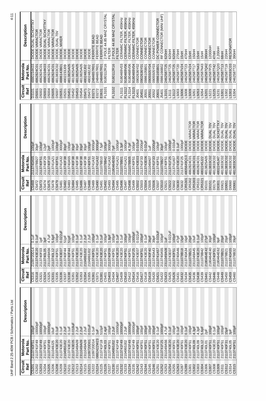
UH
F B
and
2 25
-40W
PC
B /
Sch
emat
ics
/ Par
ts L
ist
4-11
C52
0121
1374
0F51
100p
FC
5202
2113
741F
4910
000p
FC
5203
2113
741F
4910
000p
FC
5204
2113
740F
5110
0pF
C52
0521
1374
1F49
1000
0pF
C52
0623
1104
9J25
10uF
C52
0821
1374
3E20
0.1u
FC
5209
2113
743E
200.
1uF
C52
1021
0499
3J02
2.2u
FC
5211
2113
743E
200.
1uF
C52
1221
1374
3E05
0.01
8uF
C52
1323
1104
9A09
2.2u
FC
5214
2311
049A
092.
2uF
C52
1523
1104
9A09
2.2u
FC
5221
2109
720D
010.
01uF
C52
2221
0972
0D14
0.1u
FC
5224
0882
422W
231u
FC
5225
2113
741F
1851
0pF
C52
2621
1374
0L03
2.4p
FC
5227
2113
740F
5110
0pF
C52
3021
0499
3J02
2.2u
FC
5231
2113
741F
4910
000p
FC
5232
2113
741F
4910
000p
FC
5233
2104
993J
022.
2uF
C52
3421
1374
1F49
1000
0pF
C52
3521
1374
1F49
1000
0pF
C52
4221
1374
0F51
100p
FC
5243
2113
740F
5110
0pF
C52
4421
1374
0F51
100p
FC
5245
2113
740F
5110
0pF
C52
4621
1374
0F51
100p
FC
5251
2113
743E
200.
1uF
C52
5221
1374
1F25
1000
pFC
5253
2311
049A
564.
7uF
C52
5421
1374
3E20
0.1u
FC
5255
2113
740F
5110
0pF
C52
6321
1374
3E20
0.1u
FC
5287
2113
740F
5110
0pF
C52
8921
1374
3E20
0.1u
FC
5301
2113
740F
5110
0pF
C53
0221
1374
0L09
4.3p
FC
5303
2113
740L
094.
3pF
C53
0421
1374
0L12
5.6p
FC
5306
2113
740L
012p
FC
5307
2113
740F
5110
0pF
C53
0821
1374
3E20
0.1u
FC
5309
2113
740F
5110
0pF
C53
1121
1374
0F51
100p
FC
5312
2113
740F
3115
pFC
5314
2113
740L
053p
FC
5315
2113
740F
5110
0pF
Cir
cuit
R
efM
oto
rola
P
art
No
.D
escr
ipti
on
C53
1621
0972
0D14
0.1u
FC
5318
2113
743E
200.
1uF
C53
2121
1374
0F03
1pF
C53
2421
1374
0L05
3pF
C53
2523
1104
9A56
4.7u
FC
5331
2113
740L
125.
6pF
C53
3521
1374
0F51
100p
FC
5336
2113
743E
070.
022u
FC
5337
2113
740F
4451
pFC
5338
2113
740F
4451
pFC
5351
2113
740F
5110
0pF
C53
5221
1374
3E20
0.1u
FC
5353
2113
743E
200.
1uF
C53
5421
0499
3J02
2.2u
FC
5355
2104
993J
022.
2uF
C53
6121
1374
0F51
100p
FC
5371
2113
743E
200.
1uF
C53
8121
1374
3E20
0.1u
FC
5401
2113
740F
5110
0pF
C54
0321
1374
0F09
1.8p
FC
5404
2113
740F
5110
0pF
C54
0721
1374
3E20
0.1u
FC
5409
2113
743E
200.
1uF
C54
1021
1374
0F51
100p
FC
5412
2113
740F
5110
0pF
C54
1421
1374
1F25
1000
pFC
5416
2113
743E
070.
022u
FC
5417
2113
740F
5110
0pF
C54
1821
1374
3E20
0.1u
FC
5419
2113
740F
4036
pFC
5420
2113
740A
4339
pFC
5421
2113
741A
570.
033u
FC
5422
2113
740A
5510
0pF
C54
2323
1104
9A08
1uF
C54
2521
1374
3E07
0.02
2uF
C54
2621
1374
0F51
100p
FC
5431
2113
740A
4647
pFC
5432
2111
078B
1815
pFC
5434
2113
740A
3416
pFC
5435
2111
078B
2120
pFC
5436
2311
049A
4510
uFC
5438
2113
743E
200.
1uF
C54
3921
1107
8B42
100p
FC
5441
2180
464E
4227
pFC
5442
2180
464E
4030
pFC
5446
2113
740F
5110
0pF
C54
4821
8046
4E62
9pF
C54
4921
1107
8B21
20pF
C54
5021
1107
8B21
20pF
C54
5921
1374
0A55
100p
FC
5460
2111
078B
3239
pF
Cir
cuit
R
efM
oto
rola
P
art
No
.D
escr
ipti
on
C54
6921
1374
0A55
100p
FC
5472
2111
078B
2730
pFC
5473
2113
740F
5110
0pF
C54
7421
1374
0F29
12pF
C54
7521
1374
0F10
2pF
C54
7821
1374
1A21
1000
pFC
5479
2113
740F
5110
0pF
C54
8121
1374
1A32
3000
pFC
5482
2113
740F
3830
pFC
5483
2113
740A
5510
0pF
C54
8421
1374
0F38
30pF
C54
8521
1374
0F38
30pF
C54
8621
1374
0F38
30pF
C54
8721
1374
0F38
30pF
C54
8821
1374
0F51
100p
FC
5489
2113
741A
3230
00pF
C54
9021
1374
1A32
3000
pFC
5491
2111
078B
107.
5pF
C54
9221
1107
8B42
100p
FC
5493
2113
741A
3230
00pF
C54
9421
8046
4E60
7pF
C54
9521
1374
1A21
1000
pFC
5496
2111
078B
013.
3pF
C54
9721
1374
1A21
1000
pFC
5498
2111
078B
054.
7pF
C54
9921
1374
0F51
100p
FC
5502
2113
743E
030.
015u
FC
5503
2113
741F
3322
00pF
C55
0421
1374
3E06
0.02
uFC
5505
2311
049A
071u
FC
5506
2113
741F
3322
00pF
C55
0721
1374
0F51
100p
FC
5510
2111
078B
2730
pFC
5521
2113
740F
5110
0pF
C55
2221
1374
1F25
1000
pFC
5602
2113
741A
570.
033u
FC
5630
2113
743E
200.
1uF
C56
3221
1374
1F25
1000
pFC
R53
0148
0564
9Q13
DIO
DE
CR
5302
4862
824C
01D
IOD
E V
AR
AC
TO
RC
R53
0348
6282
4C01
DIO
DE
VA
RA
CT
OR
CR
5311
4862
824C
01D
IOD
E V
AR
AC
TO
RC
R53
2148
0224
5J22
DIO
DE
VA
RA
CT
OR
D01
0148
1382
5A05
DIO
DE
D01
5148
1383
3C02
DIO
DE
, DU
AL
70V
D01
7948
1383
3C02
DIO
DE
, DU
AL
70V
D03
0148
0224
5J47
DIO
DE
, SC
HO
TT
KY
D06
2148
1383
3C02
DIO
DE
, DU
AL
70V
D06
5148
1383
3C02
DIO
DE
, DU
AL
70V
D06
6048
1383
3C02
DIO
DE
, DU
AL
70V
D06
6148
1383
3C02
DIO
DE
, DU
AL
70V
Cir
cuit
R
efM
oto
rola
P
art
No
.D
escr
ipti
on
D31
0148
8015
4K03
DIO
DE
DU
AL
SC
HO
TT
KY
D50
0148
6282
4C01
DIO
DE
VA
RA
CT
OR
D50
0248
6282
4C01
DIO
DE
VA
RA
CT
OR
D50
0348
8015
4K03
DIO
DE
DU
AL
SC
HO
TT
KY
D50
0448
6282
4C01
DIO
DE
VA
RA
CT
OR
D50
0548
6282
4C01
DIO
DE
VA
RA
CT
OR
D50
0748
1383
3C02
DIO
DE
, DU
AL
70V
D50
5148
8614
3B01
DIO
DE
, MIX
ER
D52
0148
0223
3J09
DIO
DE
D54
5148
1382
5A05
DIO
DE
D54
5248
1382
5A05
DIO
DE
D54
5348
1382
5A05
DIO
DE
D54
5448
1382
5A05
DIO
DE
D54
7148
0248
2J02
DIO
DE
D54
7248
0248
2J02
DIO
DE
E02
7124
8465
7R01
FE
RR
ITE
BE
AD
E02
7224
8465
7R01
FE
RR
ITE
BE
AD
E06
3124
8465
7R01
FE
RR
ITE
BE
AD
FL3
101
9180
112R
162
PO
LE 4
4.85
MH
Z C
RY
STA
L F
ILT
ER
FL3
102
9180
112R
162
PO
LE 4
4.85
MH
Z C
RY
STA
L F
ILT
ER
FL3
111
9180
469V
03C
ER
AM
IC F
ILT
ER
, 455
KH
zF
L311
291
8046
9V06
CE
RA
MIC
FIL
TE
R, 4
55K
Hz
FL3
114
9180
468V
06C
ER
AM
IC F
ILT
ER
, 455
KH
zF
L311
591
8046
9V04
CE
RA
MIC
FIL
TE
R, 4
55K
Hz
J040
109
0263
6Y02
CO
NN
EC
TO
RJ0
451
0902
636Y
01C
ON
NE
CT
OR
J050
109
8610
5B01
CO
NN
EC
TO
RJ0
551
0905
505Y
04C
ON
NE
CT
OR
J055
209
0550
5Y03
CO
NN
EC
TO
RJ0
601
0986
165B
01D
C P
OW
ER
CO
NN
EC
TO
RJ5
401
0986
166B
02R
F C
ON
NE
CT
OR
(M
INI U
HF
)L3
101
2462
587T
2562
0nH
L311
124
6258
7T25
620n
HL3
112
2462
587T
2562
0nH
L500
324
6258
7T20
270n
HL5
006
2462
587V
2415
nHL5
008
2462
587T
2347
0nH
L500
924
6258
7V24
15nH
L505
124
6258
7T17
150n
HL5
053
2462
587N
4315
nHL5
054
2462
587N
4315
nHL5
201
2462
587Q
4239
0nH
L522
124
6258
7P25
1200
0nH
L522
524
6258
7T42
47nH
L523
124
6258
7Q20
2,20
0nH
L530
124
6258
7T13
68nH
L530
224
6258
7T19
220n
HL5
303
2460
593C
03R
ES
ON
AT
OR
L530
424
6258
7T22
390n
H
Cir
cuit
R
efM
oto
rola
P
art
No
.D
escr
ipti
on
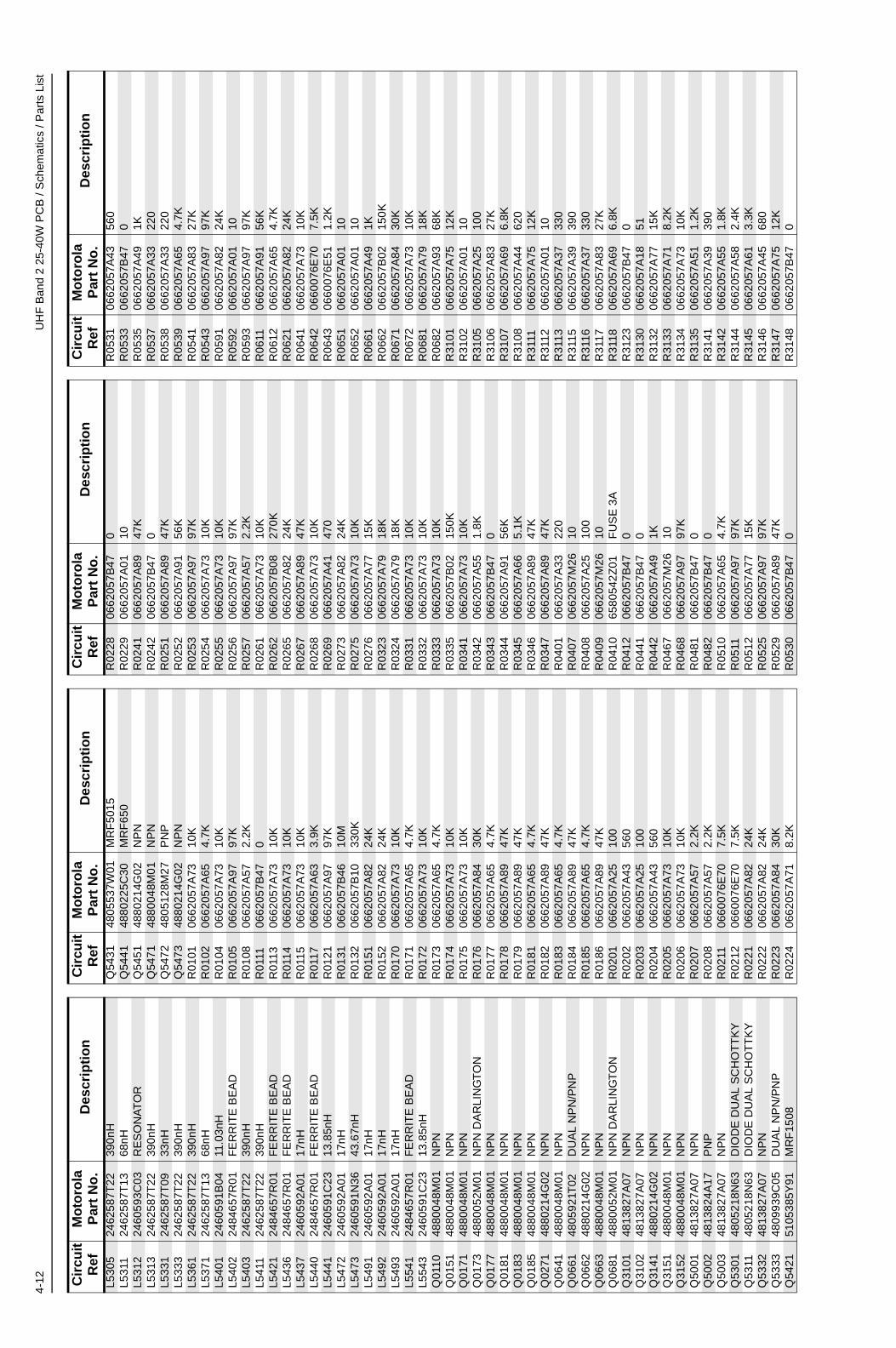
4-12
UH
F B
and
2 25
-40W
PC
B /
Sch
emat
ics
/ Par
ts L
ist
L530
524
6258
7T22
390n
HL5
311
2462
587T
1368
nHL5
312
2460
593C
03R
ES
ON
AT
OR
L531
324
6258
7T22
390n
HL5
331
2462
587T
0933
nHL5
333
2462
587T
2239
0nH
L536
124
6258
7T22
390n
HL5
371
2462
587T
1368
nHL5
401
2460
591B
0411
.03n
HL5
402
2484
657R
01F
ER
RIT
E B
EA
DL5
403
2462
587T
2239
0nH
L541
124
6258
7T22
390n
HL5
421
2484
657R
01F
ER
RIT
E B
EA
DL5
436
2484
657R
01F
ER
RIT
E B
EA
DL5
437
2460
592A
0117
nHL5
440
2484
657R
01F
ER
RIT
E B
EA
DL5
441
2460
591C
2313
.85n
HL5
472
2460
592A
0117
nHL5
473
2460
591N
3643
.67n
HL5
491
2460
592A
0117
nHL5
492
2460
592A
0117
nHL5
493
2460
592A
0117
nHL5
541
2484
657R
01F
ER
RIT
E B
EA
DL5
543
2460
591C
2313
.85n
HQ
0110
4880
048M
01N
PN
Q01
5148
8004
8M01
NP
NQ
0171
4880
048M
01N
PN
Q01
7348
8005
2M01
NP
N D
AR
LIN
GT
ON
Q01
7748
8004
8M01
NP
NQ
0181
4880
048M
01N
PN
Q01
8348
8004
8M01
NP
NQ
0185
4880
048M
01N
PN
Q02
7148
8021
4G02
NP
NQ
0641
4880
048M
01N
PN
Q06
6148
0592
1T02
DU
AL
NP
N/P
NP
Q06
6248
8021
4G02
NP
NQ
0663
4880
048M
01N
PN
Q06
8148
8005
2M01
NP
N D
AR
LIN
GT
ON
Q31
0148
1382
7A07
NP
NQ
3102
4813
827A
07N
PN
Q31
4148
8021
4G02
NP
NQ
3151
4880
048M
01N
PN
Q31
5248
8004
8M01
NP
NQ
5001
4813
827A
07N
PN
Q50
0248
1382
4A17
PN
PQ
5003
4813
827A
07N
PN
Q53
0148
0521
8N63
DIO
DE
DU
AL
SC
HO
TT
KY
Q53
1148
0521
8N63
DIO
DE
DU
AL
SC
HO
TT
KY
Q53
3248
1382
7A07
NP
NQ
5333
4809
939C
05D
UA
L N
PN
/PN
PQ
5421
5105
385Y
91M
RF
1508
Cir
cuit
R
efM
oto
rola
P
art
No
.D
escr
ipti
on
Q54
3148
0553
7W01
MR
F50
15Q
5441
4880
225C
30M
RF
650
Q54
5148
8021
4G02
NP
NQ
5471
4880
048M
01N
PN
Q54
7248
0512
8M27
PN
PQ
5473
4880
214G
02N
PN
R01
0106
6205
7A73
10K
R01
0206
6205
7A65
4.7K
R01
0406
6205
7A73
10K
R01
0506
6205
7A97
97K
R01
0806
6205
7A57
2.2K
R01
1106
6205
7B47
0R
0113
0662
057A
7310
KR
0114
0662
057A
7310
KR
0115
0662
057A
7310
KR
0117
0662
057A
633.
9KR
0121
0662
057A
9797
KR
0131
0662
057B
4610
MR
0132
0662
057B
1033
0KR
0151
0662
057A
8224
KR
0152
0662
057A
8224
KR
0170
0662
057A
7310
KR
0171
0662
057A
654.
7KR
0172
0662
057A
7310
KR
0173
0662
057A
654.
7KR
0174
0662
057A
7310
KR
0175
0662
057A
7310
KR
0176
0662
057A
8430
KR
0177
0662
057A
654.
7KR
0178
0662
057A
8947
KR
0179
0662
057A
8947
KR
0181
0662
057A
654.
7KR
0182
0662
057A
8947
KR
0183
0662
057A
654.
7KR
0184
0662
057A
8947
KR
0185
0662
057A
654.
7KR
0186
0662
057A
8947
KR
0201
0662
057A
2510
0R
0202
0662
057A
4356
0R
0203
0662
057A
2510
0R
0204
0662
057A
4356
0R
0205
0662
057A
7310
KR
0206
0662
057A
7310
KR
0207
0662
057A
572.
2KR
0208
0662
057A
572.
2KR
0211
0660
076E
707.
5KR
0212
0660
076E
707.
5KR
0221
0662
057A
8224
KR
0222
0662
057A
8224
KR
0223
0662
057A
8430
KR
0224
0662
057A
718.
2K
Cir
cuit
R
efM
oto
rola
P
art
No
.D
escr
ipti
on
R02
2806
6205
7B47
0R
0229
0662
057A
0110
R02
4106
6205
7A89
47K
R02
4206
6205
7B47
0R
0251
0662
057A
8947
KR
0252
0662
057A
9156
KR
0253
0662
057A
9797
KR
0254
0662
057A
7310
KR
0255
0662
057A
7310
KR
0256
0662
057A
9797
KR
0257
0662
057A
572.
2KR
0261
0662
057A
7310
KR
0262
0662
057B
0827
0KR
0265
0662
057A
8224
KR
0267
0662
057A
8947
KR
0268
0662
057A
7310
KR
0269
0662
057A
4147
0R
0273
0662
057A
8224
KR
0275
0662
057A
7310
KR
0276
0662
057A
7715
KR
0323
0662
057A
7918
KR
0324
0662
057A
7918
KR
0331
0662
057A
7310
KR
0332
0662
057A
7310
KR
0333
0662
057A
7310
KR
0335
0662
057B
0215
0KR
0341
0662
057A
7310
KR
0342
0662
057A
551.
8KR
0343
0662
057B
470
R03
4406
6205
7A91
56K
R03
4506
6205
7A66
5.1K
R03
4606
6205
7A89
47K
R03
4706
6205
7A89
47K
R04
0106
6205
7A33
220
R04
0706
6205
7M26
10R
0408
0662
057A
2510
0R
0409
0662
057M
2610
R04
1065
8054
2Z01
FU
SE
3A
R04
1206
6205
7B47
0R
0441
0662
057B
470
R04
4206
6205
7A49
1KR
0467
0662
057M
2610
R04
6806
6205
7A97
97K
R04
8106
6205
7B47
0R
0482
0662
057B
470
R05
1006
6205
7A65
4.7K
R05
1106
6205
7A97
97K
R05
1206
6205
7A77
15K
R05
2506
6205
7A97
97K
R05
2906
6205
7A89
47K
R05
3006
6205
7B47
0
Cir
cuit
R
efM
oto
rola
P
art
No
.D
escr
ipti
on
R05
3106
6205
7A43
560
R05
3306
6205
7B47
0R
0535
0662
057A
491K
R05
3706
6205
7A33
220
R05
3806
6205
7A33
220
R05
3906
6205
7A65
4.7K
R05
4106
6205
7A83
27K
R05
4306
6205
7A97
97K
R05
9106
6205
7A82
24K
R05
9206
6205
7A01
10R
0593
0662
057A
9797
KR
0611
0662
057A
9156
KR
0612
0662
057A
654.
7KR
0621
0662
057A
8224
KR
0641
0662
057A
7310
KR
0642
0660
076E
707.
5KR
0643
0660
076E
511.
2KR
0651
0662
057A
0110
R06
5206
6205
7A01
10R
0661
0662
057A
491K
R06
6206
6205
7B02
150K
R06
7106
6205
7A84
30K
R06
7206
6205
7A73
10K
R06
8106
6205
7A79
18K
R06
8206
6205
7A93
68K
R31
0106
6205
7A75
12K
R31
0206
6205
7A01
10R
3105
0662
057A
2510
0R
3106
0662
057A
8327
KR
3107
0662
057A
696.
8KR
3108
0662
057A
4462
0R
3111
0662
057A
7512
KR
3112
0662
057A
0110
R31
1306
6205
7A37
330
R31
1506
6205
7A39
390
R31
1606
6205
7A37
330
R31
1706
6205
7A83
27K
R31
1806
6205
7A69
6.8K
R31
2306
6205
7B47
0R
3130
0662
057A
1851
R31
3206
6205
7A77
15K
R31
3306
6205
7A71
8.2K
R31
3406
6205
7A73
10K
R31
3506
6205
7A51
1.2K
R31
4106
6205
7A39
390
R31
4206
6205
7A55
1.8K
R31
4406
6205
7A58
2.4K
R31
4506
6205
7A61
3.3K
R31
4606
6205
7A45
680
R31
4706
6205
7A75
12K
R31
4806
6205
7B47
0
Cir
cuit
R
efM
oto
rola
P
art
No
.D
escr
ipti
on
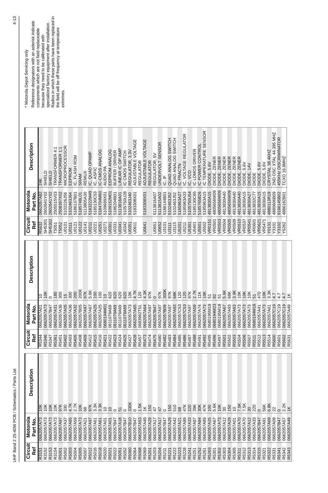
UH
F B
and
2 25
-40W
PC
B /
Sch
emat
ics
/ Par
ts L
ist
4-13
* M
otor
ola
Dep
ot S
ervi
cing
onl
y
Ref
eren
ce d
esig
nato
rs w
ith a
n as
teris
k in
dica
te
com
pone
nts
whi
ch a
re n
ot fi
eld
repl
acea
ble
beca
use
they
nee
d to
be
calib
rate
d w
ith
spec
ializ
ed fa
ctor
y eq
uipm
ent a
fter
inst
alla
tion.
R
adio
s in
whi
ch th
ese
part
s ha
ve b
een
repl
aced
in
the
field
will
be
off f
requ
ency
at t
empe
ratu
re
extr
emes
.
R31
5106
6205
7A73
10K
R31
5206
6205
7A73
10K
R31
5306
6205
7A73
10K
R31
5406
6205
7A73
10K
R50
0106
6205
7A97
97K
R50
0206
6205
7A37
330
R50
0306
6205
7A65
4.7K
R50
0406
6205
7A59
2.7K
R50
0506
6205
7A73
10K
R50
0706
6205
7A21
68R
5012
0662
057A
9797
KR
5016
0662
057A
613.
3KR
5018
0662
057A
613.
3KR
5020
0662
057A
0110
R50
2106
6205
7A01
10R
5022
0662
057B
470
R50
5106
6205
7A18
51R
5052
0662
057B
470
R50
6006
6205
7B10
330K
R50
6406
6205
7B47
0R
5068
0662
057A
531.
5KR
5069
0662
057A
491K
R52
0106
6205
7A29
150
R52
0306
6205
7A17
47R
5204
0662
057A
1747
R52
1106
6205
7B47
0R
5221
0662
057A
2915
0R
5222
0662
057A
4251
0R
5223
0662
057A
2168
R52
2806
6205
7A89
47K
R52
4106
6205
7A33
220
R52
5106
6205
7A87
39K
R52
5206
6205
7A84
30K
R52
6106
6205
7A89
47K
R52
6306
6205
7A25
100
R53
0106
6205
7A67
5.6K
R53
0206
6205
7A73
10K
R53
0306
6205
7A12
30R
5304
0662
057A
2915
0R
5305
0662
057A
0110
R53
1106
6205
7A70
7.5K
R53
1206
6205
7A70
7.5K
R53
1306
6205
7A12
30R
5314
0662
057A
3322
0R
5315
0662
057B
470
R53
2106
6205
7A91
56K
R53
2206
6205
7A69
6.8K
R53
3106
6205
7A09
22R
5341
0662
057B
470
R53
4206
6205
7A57
2.2K
R53
4306
6205
7A49
1K
Cir
cuit
R
efM
oto
rola
P
art
No
.D
escr
ipti
on
R53
4406
6205
7A01
10R
5346
0662
057A
7310
KR
5347
0662
057B
470
R53
6106
6205
7A31
180
R54
0106
6205
7A36
300
R54
0206
6205
7A05
15R
5403
0662
057A
3630
0R
5405
0662
057A
3220
0R
5408
0662
057B
0520
0KR
5409
0662
057A
9797
KR
5412
0662
057A
675.
6KR
5415
0662
057A
2510
0R
5416
0662
057A
2510
0R
5421
0680
194M
0110
R54
2206
1107
9A69
620
R54
2306
1107
9A69
620
R54
2406
1107
9A69
620
R54
2506
1107
9A69
620
R54
2706
6205
7A73
10K
R54
2806
6205
7A65
4.7K
R54
5706
8396
2T51
120
R54
7306
6205
7A64
4.3K
R54
7406
6205
7A97
97K
R54
7506
6205
7B47
0R
5480
0662
057A
9797
KR
5482
0662
057B
0930
0KR
5483
0662
057A
9797
KR
5484
0662
057A
9368
KR
5485
0662
057C
5312
0R
5486
0662
057C
5312
0R
5487
0662
057A
9797
KR
5488
0662
057A
592.
7KR
5491
0662
057A
7411
KR
5492
0662
057A
7310
KR
5495
0680
195M
1851
R54
9606
8019
4M23
82R
5497
0680
195M
1851
R55
0106
6205
7A67
5.6K
R55
0206
6205
7A93
68K
R55
0306
6205
7A63
3.9K
R55
0406
6205
7A73
10K
R55
0606
6205
7A73
10K
R55
0706
6205
7A73
10K
R55
1106
8019
4M18
51R
5512
0662
057A
4147
0R
5513
0662
057A
7310
KR
5514
0662
057A
613.
3KR
5600
0662
057C
194.
7R
5601
0662
057C
194.
7R
5602
0662
057C
194.
7R
5631
0662
057A
491K
Cir
cuit
R
efM
oto
rola
P
art
No
.D
escr
ipti
on
R56
3206
6205
7A82
24K
SH
5301
2602
641Y
02S
HIE
LDS
H53
0226
0264
1Y02
SH
IELD
T50
5125
0551
5V03
TR
AN
SF
OR
ME
R 4
:1T
5052
2508
397X
02T
RA
NS
FO
RM
ER
1:1
U01
0151
0222
6J56
MIC
RO
PR
OC
ES
SO
RU
0111
5102
463J
64E
EP
RO
MU
0121
5186
137B
01IC
, FLA
SH
RO
MU
0122
5185
748L
01S
RA
MU
0141
5113
805A
30R
EM
UX
U02
1151
8322
2M49
IC, Q
UA
D O
PA
MP
U02
2151
8513
0C53
IC, A
SF
ICU
0251
5184
704M
60IC
-CM
OS
AN
ALO
GU
0271
5109
699X
01A
UD
IO P
AU
0301
5109
152M
01E
EP
RO
M A
NA
LOG
U03
3151
8620
4B01
BU
FF
ER
/ D
RIV
ER
U03
4151
1381
8A01
LIN
EA
R IC
OP
AM
PU
0342
5105
750U
28IC
CM
OS
SW
ITC
HU
0351
5102
463J
40R
EG
ULA
TO
R, 3
.3V
U06
1151
8330
8X01
AD
JUS
TAB
LE V
OLT
AG
E
RE
GU
LAT
OR
U06
4151
8330
8X01
AD
JUS
TAB
LE V
OLT
AG
E
RE
GU
LAT
OR
U06
5151
1381
6A07
RE
GU
LAT
OR
, 5V
U
0652
5113
815A
02U
ND
ER
VO
LT S
EN
SO
RU
3101
5186
144B
01IC
, IF
U31
1151
0246
3J52
QU
AD
AN
ALO
G S
WIT
CH
U31
1551
0246
3J52
QU
AD
AN
ALO
G S
WIT
CH
U52
0151
8596
3A27
IC F
RA
CT
NU
5211
5185
963A
33IC
, VO
LTA
GE
RE
GU
LAT
OR
U53
0151
0575
0U54
IC, V
CO
U54
0151
8513
0C65
IC L
DM
OS
DR
IVE
RU
5501
5185
765B
26IC
PO
WE
R C
ON
TR
OL
U55
0251
8596
3A15
IC T
EM
PE
RA
TU
RE
SE
NS
OR
VR
0151
4813
830A
15D
IOD
E, 5
.6V
VR
0501
4805
656W
09D
IOD
E, Z
EN
ER
VR
0503
4805
656W
09D
IOD
E, Z
EN
ER
VR
0504
4813
830A
40D
IOD
E, Z
EN
ER
VR
0505
4805
656W
09D
IOD
E, Z
EN
ER
VR
0509
4813
830A
40D
IOD
E, Z
EN
ER
VR
0510
4813
830A
40D
IOD
E, Z
EN
ER
VR
0537
4813
830A
15D
IOD
E, 5
.6V
VR
0541
4813
830A
27D
IOD
E, 1
4VV
R06
0148
1383
2C77
DIO
DE
VR
0621
4813
830A
15D
IOD
E, 5
.6V
VR
5471
4813
830A
15D
IOD
E, 5
.6V
Y01
3148
8011
3R19
CR
YS
TAL
38.4
KH
ZY
3101
4880
606B
092N
D O
SC
XTA
L 44
.395
MH
ZY
3102
9186
145B
0245
5KH
z D
ISC
RIM
INA
TO
RY
5262
4886
182B
01T
CX
O 1
6.8M
HZ
Cir
cuit
R
efM
oto
rola
P
art
No
.D
escr
ipti
on

4-14
UH
F B
and
2 25
-40W
PC
B /
Sch
emat
ics
/ Par
ts L
ist
TH
IS P
AG
E IN
TE
NT
ION
AL
LY L
EF
T B
LA
NK
GM338Mobile Radio
UHF B1 HIGH POWER LDMOS
(403-470MHz)
Service Information
Issue: December, 2003

Computer Software CopyrightsThe Motorola products described in this manual may include copyrighted Motorola computer programs stored in semiconductor memories or other media. Laws in the United States and other countries preserve for Motorola certain exclusive rights for copyrighted computer programs, including the exclusive right to copy or reproduce in any form, the copyrighted computer program. Accordingly, any copyrighted Motorola computer programs contained in the Motorola products described in this manual may not be copied or reproduced in any manner without the express written permission of Motorola. Furthermore, the purchase of Motorola products shall not be deemed to grant, either directly or by implication, estoppel or otherwise, any license under the copyrights, patents or patent applications of Motorola, except for the normal non-exclusive royalty-free license to use that arises by operation of law in the sale of a product.
i
Table of Contents
Section 1 Model Chart and Technical Specifications
1.0 GM338 Model Chart.............................................................................................1-12.0 Technical Specifications ......................................................................................1-1
Section 2 Theory of Operation
1.0 Introduction ..........................................................................................................2-12.0 UHF (403-470 MHz) Receiver .............................................................................2-1
2.1 Receiver Front-End ........................................................................................2-12.2 Front-End Band-Pass Filters & Pre-Amplifier .................................................2-22.3 First Mixer and High Intermediate Frequency (IF)..........................................2-22.4 Low Intermediate Frequency (IF) and Receiver Back End.............................2-3
3.0 UHF (403-470 MHz) Transmitter Power Amplifier (PA) 40 W..............................2-33.1 First Power Controlled Stage..........................................................................2-43.2 Power Controlled Driver Stage .......................................................................2-43.3 Final Stage .....................................................................................................2-43.4 Directional Coupler .........................................................................................2-53.5 Antenna Switch...............................................................................................2-53.6 Harmonic Filter ...............................................................................................2-53.7 Power Control.................................................................................................2-5
4.0 UHF (403-470 MHz) Frequency Synthesis ..........................................................2-64.1 Reference Oscillator .......................................................................................2-64.2 Fractional-N Synthesizer ................................................................................2-74.3 Voltage Controlled Oscillator (VCO)...............................................................2-84.4 Synthesizer Operation ....................................................................................2-9
Section 3 Troubleshooting Charts
1.0 Troubleshooting Flow Chart for Receiver ............................................................3-12.0 Troubleshooting Flow Chart for 40W Transmitter ................................................3-33.0 Troubleshooting Flow Chart for Synthesizer........................................................3-54.0 Troubleshooting Flow Chart for VCO...................................................................3-6
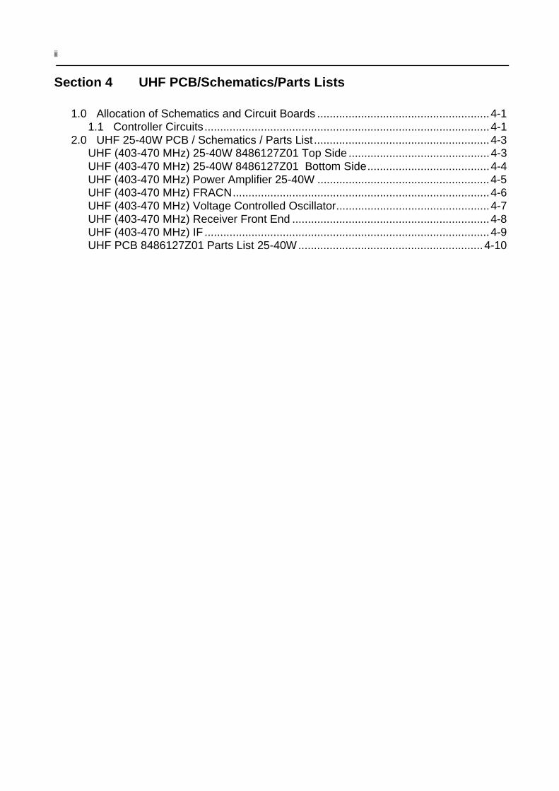
ii
Section 4 UHF PCB/Schematics/Parts Lists
1.0 Allocation of Schematics and Circuit Boards .......................................................4-11.1 Controller Circuits...........................................................................................4-1
2.0 UHF 25-40W PCB / Schematics / Parts List ........................................................4-3UHF (403-470 MHz) 25-40W 8486127Z01 Top Side .............................................4-3UHF (403-470 MHz) 25-40W 8486127Z01 Bottom Side.......................................4-4UHF (403-470 MHz) Power Amplifier 25-40W .......................................................4-5UHF (403-470 MHz) FRACN..................................................................................4-6UHF (403-470 MHz) Voltage Controlled Oscillator.................................................4-7UHF (403-470 MHz) Receiver Front End ...............................................................4-8UHF (403-470 MHz) IF ...........................................................................................4-9UHF PCB 8486127Z01 Parts List 25-40W...........................................................4-10
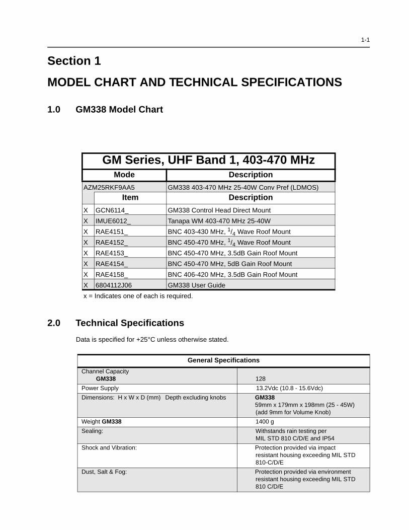
1-1
Section 1
MODEL CHART AND TECHNICAL SPECIFICATIONS
1.0 GM338 Model Chart
2.0 Technical Specifications
Data is specified for +25°C unless otherwise stated.
GM Series, UHF Band 1, 403-470 MHzMode Description
AZM25RKF9AA5 GM338 403-470 MHz 25-40W Conv Pref (LDMOS)
Item Description
X GCN6114_ GM338 Control Head Direct Mount
X IMUE6012_ Tanapa WM 403-470 MHz 25-40W
X RAE4151_ BNC 403-430 MHz, 1/4 Wave Roof Mount
X RAE4152_ BNC 450-470 MHz, 1/4 Wave Roof Mount
X RAE4153_ BNC 450-470 MHz, 3.5dB Gain Roof Mount
X RAE4154_ BNC 450-470 MHz, 5dB Gain Roof Mount
X RAE4158_ BNC 406-420 MHz, 3.5dB Gain Roof Mount
X 6804112J06 GM338 User Guide
x = Indicates one of each is required.
General Specifications
Channel CapacityGM338 128
Power Supply 13.2Vdc (10.8 - 15.6Vdc)
Dimensions: H x W x D (mm) Depth excluding knobs GM33859mm x 179mm x 198mm (25 - 45W)(add 9mm for Volume Knob)
Weight GM338 1400 g
Sealing: Withstands rain testing per MIL STD 810 C/D/E and IP54
Shock and Vibration: Protection provided via impactresistant housing exceeding MIL STD 810-C/D/E
Dust, Salt & Fog: Protection provided via environment resistant housing exceeding MIL STD 810 C/D/E
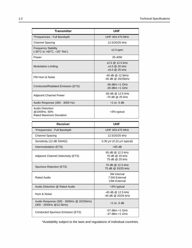
1-2 Technical Specifications
*Availability subject to the laws and regulations of individual countries.
Transmitter UHF
*Frequencies - Full Bandsplit UHF 403-470 MHz
Channel Spacing 12.5/20/25 kHz
Frequency Stability(-30°C to +60°C, +25° Ref.)
±2.0 ppm
Power 25-40W
Modulation Limiting±2.5 @ 12.5 kHz ±4.0 @ 20 kHz±5.0 @ 25 kHz
FM Hum & Noise-40 dB @ 12.5kHz
-45 dB @ 20/25kHz
Conducted/Radiated Emission (ETS)-36 dBm <1 GHz-30 dBm >1 GHz
Adjacent Channel Power-60 dB @ 12.5 kHz-70 dB @ 25 kHz
Audio Response (300 - 3000 Hz) +1 to -3 dB
Audio Distortion@1000Hz, 60%Rated Maximum Deviation
<3% typical
Receiver UHF
*Frequencies - Full Bandsplit UHF 403-470 MHz
Channel Spacing 12.5/20/25 kHz
Sensitivity (12 dB SINAD) 0.30 µV (0.22 µV typical)
Intermodulation (ETS) >65 dB
Adjacent Channel Selectivity (ETS)65 dB @ 12.5 kHz 70 dB @ 20 kHz75 dB @ 25 kHz
Spurious Rejection (ETS)70 dB @ 12.5 kHz
75 dB @ 20/25 kHz
Rated Audio3W Internal
7.5W External13W External
Audio Distortion @ Rated Audio <3% typical
Hum & Noise-40 dB @ 12.5 kHz
-45 dB @ 20/25 kHz
Audio Response (300 - 3000Hz @ 20/25kHz)(300 - 2550Hz @12.5kHz)
+1 to -3 dB
Conducted Spurious Emission (ETS)-57 dBm <1 GHz-47 dBm >1 GHz

2-1
Section 2
THEORY OF OPERATION
1.0 Introduction
This Chapter provides a detailed theory of operation for the UHF circuits in the radio. For details of the theory of operation and troubleshooting for the the associated Controller circuits refer to the Controller Section of this manual.
2.0 UHF (403-470 MHz) Receiver
2.1 Receiver Front-End
The receiver is able to cover the UHF range from 403 to 470 MHz. It consists of four major blocks: front-end bandpass filters and pre-amplifier, first mixer, high-IF, low-IF and receiver back-end . Two varactor-tuned bandpass filters perform antenna signal pre-selection. A cross over quad diode mixer converts the signal to the first IF of 44.85 MHz. Low-side first injection is used.
Figure 2-1 UHF Receiver Block Diagram
Demodulator
1. Crystal Filter
MixerVaractor Tuned Filter
RF AmpVaractor Tuned Filter
Pin Diode Antenna SwitchRF Jack
Antenna
Control Voltagefrom PCIC First LO
from FGU
Recovered Audio
RSSI
Second LO
2. Crystal Filter
455kHz Filter(25kHz)
455kHz Filter(25kHz)
455kHz Filter(12.5kHz)
455kHz Filter(12.5kHz)
Sw
itch
Sw
itch
Sw
itch
Sw
itch
Limiter
1. IF Amp
2. IF Amp
Filter Bank Selectionfrom Synthesizer IC
Harmonic Filter
BWSELECT

2-2 UHF (403-470 MHz) Receiver
There are two 2-pole 44.85 MHz crystal filters in the high-IF section and 2 pairs of 455 kHz ceramic filters in the low-IF section to provide the required adjacent channel selectivity .The correct pair of ceramic filters for 12.5 or 25KHz channel spacing is selected via control line BWSELECT. The second IF at 455 kHz is mixed, amplified and demodulated in the IF IC. The processing of the demodulated audio signal is performed by an audio processing IC located in the controller section.
2.2 Front-End Band-Pass Filters & Pre-Amplifier
The received signal from the radio’s antenna connector is first routed through the harmonic filter and antenna switch, which are part of the RF power amplifier circuitry, before being applied to the receiver pre-selector filter (C4001, C4002, D4001 and associated components). The 2-pole pre-selector filter tuned by the varactor diodes D4001 and D4002 pre-selects the incoming signal (RXIN) from the antenna switch to reduce spurious effects to following stages. The tuning voltage (FECTRL_1) ranging from 2 volts to 8 volts is controlled by pin 20 of PCIC (U4501) in the Transmitter section. A dual hot carrier diode (D4003) limits any inband signal to 0 dBm to prevent damage to the pre-amplifier.
The RF pre-amplifier is an SMD device (Q4003) with collector base feedback to stabilize gain, impedance, and intermodulation. The collector current of approximately 11-16 mA is drawn from the voltage 9V3 via L4003 and R4002. A switchable 3dB pad (R4066,R4007,R4063, R4064 and R4070), controlled via line FECTRL_2 and Q4004 stabilizes the output impedance and intermodulation performance.
A second 2-pole varactor tuned bandpass filter provides additional filtering of the amplified signal. The varactor diodes D4004 and D4005 are controlled by the same signal FECTRL_1, which controls the pre-selector filter. A following 1 dB pad (R4013 - R4015) stabilizes the output impedance and intermodulation performance.
2.3 First Mixer and High Intermediate Frequency (IF)
The signal coming from the front-end is converted to the first IF (44.85 MHz) using a cross over quad diode mixer (D4051). Its ports are matched for incoming RF signal conversion to the 44.85 MHz IF using low side injection via matching transformers T4051 and T4052. The injection signal (RXINJ) coming from the RX VCO buffer (Q4332) is filtered by the lowpass filter consisting of (L4053, L4054, C4053 - C4055) followed by a matching transformer T4052 and has a level of approximately 15dBm.
The mixer IF output signal (IF) from transformer T4501pin 2 is fed to the first two pole crystal filter FL3101. The filter output in turn is matched to the following IF amplifier.
The IF amplifier Q3101 is actively biased by a collector base feedback (R3101, R3106) to a current drain of approximately 5 mA drawn from the voltage 5V. Its output impedance is matched to the second two pole crystal filter FL3102. The signal is further amplified by a preamplifier (Q3102) before going into pin 1 of IFIC (U3101).
A dual hot carrier diode (D3101) limits the filter output voltage swing to reduce overdrive effects at RF input levels above -27 dBm.

UHF (403-470 MHz) Transmitter Power Amplifier (PA) 40 W 2-3
2.4 Low Intermediate Frequency (IF) and Receiver Back End
The 44.85 high IF signal from the second IF amplifier feeds the IF IC (U3101) at pin1. Within the IF IC the 44.85 MHz high IF signal mixes with the 44.395 MHz second local oscillator (2nd LO) to produce the low IF signal at 455 kHz. The 2nd LO frequency is determined by crystal Y3101. The low IF signal is amplified and filtered by an external pair of 455 kHz ceramic filters FL3112, FL3114 for 20/25 kHz channel spacing or FL3111,FL3113/F3115 for 12.5 kHz channel spacing. These pairs are selectable via BWSELECT. The filtered output from the ceramic filters is applied to the limiter input pin of the IF IC (pin 14).
The IF IC contains a quadrature detector using a ceramic phase-shift element (Y3102) to provide audio detection. Internal amplification provides an audio output level of 120 mV rms (at 60% deviation) from U3103 pin 8 (DISCAUDIO) which is fed to the ASFIC_CMP (U0221) pin 2 (part of the Controller circuitry).
A Received Signal Strength Indicator (RSSI) signal is available at U3101 pin 5, having a dynamic range of 70 dB. The RSSI signal is interpreted by the microprocessor (U0101 pin 63) and in addition is available at accessory connector J0501-15.
3.0 UHF (403-470 MHz) Transmitter Power Amplifier (PA) 40 W
The radio’s 40W PA is a three stage amplifier used to amplify the output from the VCOBIC to the radio transmit level. All three stages utilize LDMOS technology. The gain of the first stage (U4401) is adjustable, controlled by pin 4 of PCIC (U4501). It is followed by an LDMOS stage (Q4421) and LDMOS final stage (Q4441).
Figure 2-2 UHF Transmitter Block Diagram
Devices U4401, Q4421 and Q4441 are surface mounted. A pressure pad between board and the radio's cover provides good thermal contact between the devices and the chassis.
PCIC
Pin Diode Antenna Switch RF Jack
Antenna
Harmonic Filter
PowerSense
PA-FinalStage
From VCO
ControlledStage
Vcontrol
Bias 1
Bias 2 & Bias 3
To Microprocessor
TemperatureSense
SPI BUS
ASFIC_CMP
PAPWRSET
To Microprocessor
PADriver
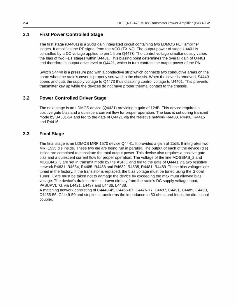
2-4 UHF (403-470 MHz) Transmitter Power Amplifier (PA) 40 W
3.1 First Power Controlled Stage
The first stage (U4401) is a 20dB gain integrated circuit containing two LDMOS FET amplifier stages. It amplifies the RF signal from the VCO (TXINJ). The output power of stage U4401 is controlled by a DC voltage applied to pin 1 from Q4473. The control voltage simultaneously varies the bias of two FET stages within U4401. This biasing point determines the overall gain of U4401 and therefore its output drive level to Q4421, which in turn controls the output power of the PA.
Switch S4440 is a pressure pad with a conductive strip which connects two conductive areas on the board when the radio's cover is properly screwed to the chassis. When the cover is removed, S4440 opens and cuts the supply voltage to Q4473 thus disabling control voltage to U4401. This prevents transmitter key up while the devices do not have proper thermal contact to the chassis.
3.2 Power Controlled Driver Stage
The next stage is an LDMOS device (Q4421) providing a gain of 12dB. This device requires a positive gate bias and a quiescent current flow for proper operation. The bias is set during transmit mode by U4501-24 and fed to the gate of Q4421 via the resistive network R4480, R4408, R4415 and R4416.
3.3 Final Stage
The final stage is an LDMOS MRF 1570 device Q4441. It provides a gain of 11dB. It integrates two MRF1535 die inside. These two die are being run in parallel. The output of each of the device (die) inside are combined to constitute the total output power. This device also requires a positive gate bias and a quiescent current flow for proper operation. The voltage of the line MOSBIAS_2 and MOSBIAS_3 are set in transmit mode by the ASFIC and fed to the gate of Q4441 via two resistive network R4631, R4634, R4485, R4486 and R4632, R4635, R4481, R4489. These bias voltages are tuned in the factory. If the transistor is replaced, the bias voltage must be tuned using the Global Tuner. Care must be taken not to damage the device by exceeding the maximum allowed bias voltage. The device’s drain current is drawn directly from the radio’s DC supply voltage input, PASUPVLTG, via L4421, L4437 and L4436, L4438.A matching network consisting of C4440-45, C4466-67, C4476-77, C4487, C4491, C4489, C4490, C4455-56, C4449-50 and striplines transforms the impedance to 50 ohms and feeds the directional coupler.

UHF (403-470 MHz) Transmitter Power Amplifier (PA) 40 W 2-5
3.4 Directional Coupler
The directional coupler is a microstrip printed circuit, which couples a small amount of the forward power delivered by Q4441. The coupled signal is rectified by D4451. The DC voltage is proportional to the RF output power and feeds the RFIN port of the PCIC (U4501 pin 1). The PCIC controls the gain of stage U4401 as necessary to hold this voltage constant, thus ensuring the forward power out of the radio to be held to a constant value.
3.5 Antenna Switch
The antenna switch consists of two PIN diodes, D4471 and D4472. In the receive mode, both diodes are off. Signals applied at the antenna jack J4401 are routed, via the harmonic filter, through network L4472, C4474 and C4475, to the receiver input. In the transmit mode, K9V1 turns on Q4471 which enables current sink Q4472, set to 96 mA by R4512 and VR4471. This completes a DC path from PASUPVLTG, through L4437, D4471, L4472, D4472, L4473, R4496 and the current sink, to ground. Both diodes are forward biased into conduction. The transmitter RF from the directional coupler is routed via D4471 to the harmonic filter and antenna jack. D4472 also conducts, shunting RF power and preventing it from reaching the receiver port (RXIN). L4472 is selected to appear as a broadband lambda/4 wave transmission line, making the short circuit presented by D4472 appear as an open circuit at the junction of D4472 and the receiver path.
3.6 Harmonic Filter
Components L4491-L4493 and L4472, C4448, C4494, C4496 and C4498 form a Butterworth low-pass filter to attenuate harmonic energy of the transmitter to specifications level. R4491 is used to drain electrostatic charge that might otherwise build up on the antenna. The harmonic filter also prevents high level RF signals above the receiver passband from reaching the receiver circuits, improving spurious response rejection.
3.7 Power Control
The transmitter uses the Power Control IC (PCIC, U4501) to control the power output of the radio. A portion of the forward RF power from the transmitter is sampled by the directional coupler and rectified, to provide a DC voltage to the RFIN port of the PCIC (pin 1) which is proportional to the sampled RF power.
The ASFIC (U0221) has internal digital to analog converters (DACs) which provide a reference voltage of the control loop to the PCIC via R4483. The reference voltage level is programmable through the SPI line of the PCIC. This reference voltage is proportional to the desired power setting of the transmitter, and is factory programmed at several points across the frequency range of the transmitter to offset frequency response variations of the transmitter’s power detector circuit.
The PCIC provides a DC output voltage at pin 4 (INT) which sets the drain current of the first (U4401). This adjusts the transmitter power output to the intended value. Variations in forward transmitter power cause the DC voltage at pin 1 to change, and the PCIC adjusts the control voltage above or below its nominal value to raise or lower output power.
Capacitors C4502-4, in conjunction with resistors and integrators within the PCIC, control the transmitter power-rise (key-up) and power-decay (de-key) characteristic to minimize splatter into adjacent channels.
2-6 UHF (403-470 MHz) Frequency Synthesis
U4502 is a temperature-sensing device, which monitors the circuit board temperature in the vicinity of the transmitter driver and final devices, and provides a DC voltage to the PCIC (TEMP, pin 30) proportional to temperature. If the DC voltage produced exceeds the set threshold in the PCIC, the transmitter output power will be reduced so as to reduce the transmitter temperature.
4.0 UHF (403-470 MHz) Frequency Synthesis
The synthesizer subsystem consists of the reference oscillator (Y4261 or Y4262), the Low Voltage Fractional-N synthesizer (LVFRAC-N, U4201), and the Voltage Controlled Oscillator VCO.
4.1 Reference Oscillator
The reference oscillator (Y4262) contains a temperature compensated crystal oscillator with a frequency of 16.8 MHz. An Analogue to Digital (A/D) converter internal to U4201 (LVFRAC-N) and controlled by the microprocessor via serial interface (SRL) sets the voltage at the warp output of U4201 pin 25 to set the frequency of the oscillator. The output of the oscillator (pin 3 of Y4262) is applied to pin 23 (XTAL1) of U4201 via a RC series combination.
In applications where less frequency stability is required the oscillator inside U4201 is used along with an external crystal Y4261, varactor diode D4261, C4261, C4262 and R4262. In this case, Y4262, R4263, C4235 and C4251 are not used. When Y4262 is used, Y4261, D4261, C4261, C4262 and R4262 are not used, and C4263 is increased to 0.1 uF.

UHF (403-470 MHz) Frequency Synthesis 2-7
4.2 Fractional-N Synthesizer
The LVFRAC-N synthesizer IC (U4201) consists of a pre-scaler, a programmable loop divider, control divider logic, a phase detector, a charge pump, an A/D converter for low frequency digital modulation, a balance attenuator to balance the high frequency analogue modulation and low frequency digital modulation, a 13V positive voltage multiplier, a serial interface for control, and finally a super filter for the regulated 5 volts.
Figure 2-3 UHF Synthesizer Block Diagram
A voltage of 5V applied to the super filter input (U4201 pin 30) supplies an output voltage of 4.5 VDC(VSF) at pin 28. It supplies the VCO, VCO modulation bias circuit (via R4322) and the synthesizer charge pump resistor network (R4251, R4252). The synthesizer supply voltage is provided by the 5V regulator U4211.
In order to generate a high voltage to supply the phase detector (charge pump) output stage at pin 47 VCP (U4201-47), a voltage of 13 VDC is being generated by the positive voltage multiplier circuitry (D4201, C4202, C4203). This voltage multiplier is basically a diode capacitor network driven by two (1.05MHz) 180 degrees out of phase signals (U4201-14 and -15).
Output LOCK (U4201-4) provides information about the lock status of the synthesizer loop. A high level at this output indicates a stable loop. IC U4201 provides the 16.8 MHz reference frequency at pin 19.
The serial interface (SRL) is connected to the microprocessor via the data line DATA (U4201-7), clock line CLK (U4201-8), and chip enable line CSX (U4201-9).
DATA
CLK
CEX
MODIN
VCC, DC5V
XTAL1
XTAL2
WARP
PREIN
VCP
REFERENCEOSCILLATOR
VOLTAGEMULTIPLIER
DATA (U0101 PIN 100)
CLOCK (U0101 PIN 1)
CSX (U0101 PIN 2)
MOD IN (U0221 PIN 40)
+5V (U4211 PIN 1)
7
8
9
10
13, 30
23
24
25
32
47
VMULT2 VMULT1
BIAS1
SFOUT
AUX3
AUX4
IADAPTIOUT
GND
FREFOUT
LOCK 4
19
6, 22, 33, 44
4345
3
2
28
14 15
40
FILTERED 5V
STEERING
LOCK (U0101 PIN 56)
PRESCALER IN
FREF (U0221 PIN 34)
39BIAS2
41
48
5, 20, 34, 36+5V (U4211 PIN 1)
AUX1
VDD, DC5V MODOUT
U4201 LOW VOLTAGEFRACTIONAL-NSYNTHESIZER
AUX2 1 (NU)
BWSELECT
VCO Bias
TRB
To IFSection
TX RF INJECTION(1ST STAGE OF PA)
LO RF INJECTION
VOLTAGE CONTROLLED OSCILLATOR
LINE2-POLELOOP
FILTER

2-8 UHF (403-470 MHz) Frequency Synthesis
4.3 Voltage Controlled Oscillator (VCO)
The Voltage Controlled Oscillator (VCO) consists of the VCO/Buffer IC (VCOBIC, U4301), the TX and RX tank circuits, the external RX buffer stages, and the modulation circuitry.
Figure 2-4 UHF VCO Block Diagram
The VCOBIC together with Fractional-N synthesizer (U4201) generates the required frequencies in both transmit and receive modes. The TRB line (U4301 pin 19) determines which tank circuits and internal buffers are to be enabled. A high level on TRB enables TX tank and TX output (pin 10), and a low enables RX tank and RX output (pin 8). A sample of the signal from the enabled output is routed from U4301 pin 12 (PRESC_OUT), via a low pass filter, to pin 32 of U4201 (PREIN).
A steering line voltage (VCTRL) between 3.0V and 10.0V at varactor diode CR4311 will tune the full TX frequency range (TXINJ) from 403 MHz to 470 MHz, and at varactor diodes CR4301, CR4302 and CR4303 will tune the full RX frequency range (RXINJ) from 358 MHz to 425 MHz. The tank circuits uses the Hartley configuration for wider bandwidth. For the RX tank circuit, an external transistor Q4301 is used in conjunction with the internal transistor for better side-band noise.
Presc
RX
TX
MatchingNetwork Low Pass
Filter
Attenuator
Pin8
Pin14
Pin10
(U4201 Pin28)
VCC Buffers
TX RF Injection
U4201 Pin 32
AUX3 (U4201 Pin 2)
Prescaler Out
Pin 12Pin 19Pin 20
TX/RX/BSSwitching Network
U4301VCOBIC
RxActive Bias
TxActive Bias
Pin2
Rx-I adjust
Pin1
Tx-I adjust
Pins 9,11,17Pin18
VsensCircuit
Pin15
Pin16
RX VCO Circuit
TX VCO Circuit
RX Tank
TX Tank
Pin7
Vcc-Superfilter
Collector/RF in
Pin4
Pin5
Pin6
RX
TX
(U4201 Pin 28)
Rx-SW
Tx-SW
Vcc-Logic
(U4201 Pin 28)
Steer Line Voltage (VCTRL)
Pin13
Pin3
TRB IN
LO RF INJECTION
Q4301
Q4332

UHF (403-470 MHz) Frequency Synthesis 2-9
The external RX buffers (Q4332) are enabled by a high at U4201 pin 3 (AUX4) via transistor switch Q4333. In TX mode the modulation signal (VCOMOD) from the LVFRAC-N synthesizer IC (U4201 pin41) is applied modulation circuitry CR4321, R4321, R4322 and C4324, which modulates the TX VCO frequency via coupling capacitor C4321. Varactor CR4321 is biased for linearity from VSF.
4.4 Synthesizer Operation
The complete synthesizer subsystem comprises mainly of low voltage FRAC-N (LVFRACN) IC, Reference Oscillator (crystal oscillator with temperature compensation), charge pump circuitry, loop filter circuitry and DC supply. The output signal PRESC_OUT of the VCOBIC (U4301 pin 12) is fed to pin 32 of U4201 (PREIN) via a low pass filter (C4229, L4225) which attenuates harmonics and provides the correct level to close the synthesizer loop.The pre-scaler in the synthesizer (U4201) is basically a dual modulus pre-scaler with selectable divider ratios. This divider ratio of the pre-scaler is controlled by the loop divider, which in turn receives its inputs via the SRL. The output of the pre-scaler is applied to the loop divider. The output of the loop divider is connected to the phase detector, which compares the loop divider´s output signal with the reference signal.The reference signal is generated by dividing down the signal of the reference oscillator (Y4261 or Y4262).The output signal of the phase detector is a pulsed DC signal which is routed to the charge pump. The charge pump outputs a current at pin 43 of U4201 (IOUT). The loop filter (which consists of R4221-R4223, C4221-C4225,L4221) transforms this current into a voltage that is applied to the varactor diodes CR4311 for transmit, CR4301, CR4302 & CR4303 for receive and alters the output frequency of the VCO .The current can be set to a value fixed in the LVFRAC-N IC or to a value determined by the currents flowing into BIAS 1 (U4201-40) or BIAS 2 (U4201-39). The currents are set by the value of R4251 or R4252 respectively. The selection of the three different bias sources is done by software programming.To reduce synthesizer lock time when new frequency data has been loaded into the synthesizer the magnitude of the loop current is increased by enabling the IADAPT (U4201-45) for a certain software programmable time (Adapt Mode). The adapt mode timer is started by a low to high transient of the CSX line. When the synthesizer is within the lock range the current is determined only by the resistors connected to BIAS 1, BIAS 2, or the internal current source. A settled synthesizer loop is indicated by a high level of signal LOCK (U4201-4). The LOCK (U4201-4) signal is routed to one of the µP´s ADCs input U101-56. From the voltage the µP determines whether LOCK is active. In order to modulate the PLL the two spot modulation method is utilized. Via pin 10 (MODIN) on U4201 the audio signal is applied to both the A/D converter (low freq path) as well as the balance attenuator (high freq path). The A/D converter converts the low frequency analogue modulating signal into a digital code that is applied to the loop divider, thereby causing the carrier to deviate. The balance attenuator is used to adjust the VCO’s deviation sensitivity to high frequency modulating signals. The output of the balance attenuator is present at the MODOUT port (U4201-41) and connected to the VCO modulation diode CR4321 via R4321, C4325.

2-10 UHF (403-470 MHz) Frequency Synthesis
THIS PAGE INTENTIONALLY LEFT BLANK
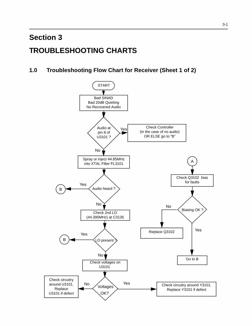
3-1
Section 3
TROUBLESHOOTING CHARTS
1.0 Troubleshooting Flow Chart for Receiver (Sheet 1 of 2)
Bad SINADBad 20dB Quieting
No Recovered Audio
START
Audio at pin 8 of U3101 ?
Check Controller(in the case of no audio)
OR ELSE go to “B”
Yes
No
Spray or inject 44.85MHz into XTAL Filter FL3101
Audio heard ?BYes
No
Check 2nd LO (44.395MHz) at C3135
LO present ?BYes
Check voltages on U3101
Biasing OK ?
No
No
A
Yes
Check Q3102 bias for faults
Replace Q3102
Go to B
Yes
No
Check circuitry around U3101.
Replace U3101 if defect
Check circuitry around Y3101. Replace Y3101 if defect
Voltages
OK?

3-2 Troubleshooting Flow Chart for Receiver
1.1 Troubleshooting Flow Chart for Receiver (Sheet 2 of 2)
IF Signal at C3101?
No
RF Signal at T4051?
RFSignal at C4015?
No
No
RFSignal at C4025?
No or
Check harmonic filterL4491-L4493, C4492, J4401
and ant. switchD4471, D4472, L4472.
Check filter between C4025 & C4009.
Check tuning voltage at R4060.
Inject RF into J4401
Istuning voltage
OK?
No
Yes
Check RF amp (Q4003) Stage.
Check filter between C4015 & T4051.
Yes
Check T4051, T4052, D4051, R4052, L4008.
Yes
1st LO level OK?
Locked?
Yes
Check FGU
Yes
Trace IF signal from C3101 to
Q3101. Check for bad XTAL filter.
No
Yes IFsignal at Q3102
collector?
Before replacing U3101, check
U3101 voltages.
Yes
Check for 5VDC
Is 9V3 present?
Check Supply Voltage circuitry. Check Q0681,
U4211 and U0641.
No
No
No
Check U4501.
Check varactor filter.
No
Yes
Yes
Yes
A
A
B
weak RF
RFSignal at C4009?

Troubleshooting Flow Chart for 40W Transmitter 3-3
2.0 Troubleshooting Flow Chart for 40W Transmitter (Sheet 1 of 2)
Control Volt-age at
TP4533>1V
Current increase
when keyed?
NOYES
START
Check if Pressure Pad closes S5440
Check Components between Q4441 and RF Output,
Antenna Switch D4471,D4472,Q4472,
VR4471,Q4471
>500mA & <6A>6A
<500mA
Check PA Stages
Short TP4531 to Ground
NO
NO
Voltage at TP4533 rises?
Check PA Stages YES
YES
PCIC U4501 Pin 14 9.3V
DC?
Check 9.3 V Regulator U0641
NO
YES
PCIC U4501 Pin 16 >4V
DC
Replace PCIC U4501
NO
YES
TP4530 9.1V DC
If U4201 Pin 2 is high, replace PCIC
U4501,otherwise check controller and
FGU
YES
NO
TP4531 >0.5V DC?
Replace PCIC U4501
Check Forward Power Sense Circuit (D4451)
Check Forward Power Sense Circuit (D4451)NO
YES
PCIC U4501 Pin 5 > 1V
DC?
Check Power Setting, Tuning & Components between PCIC Pin 5 and ASFIC (U0221)
Pin 4 before replacing ASFIC
No or too low Power when keyed
Put in pressure pad
YES
NO
1
Is Q4473 OK?
Change Q4473
NO
YES
Check voltage on pin 4 U4501
NO
YES
Check R4422-5 and go back to top
1
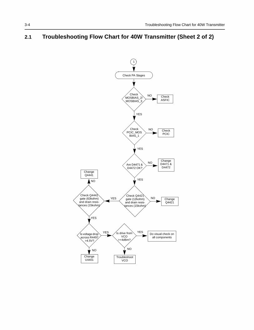
3-4 Troubleshooting Flow Chart for 40W Transmitter
2.1 Troubleshooting Flow Chart for 40W Transmitter (Sheet 2 of 2)
Check PA Stages
YES
Check MOSBIAS_2/MOSBIAS_3
YES
Are D4471 & D4472 OK?
Check ASFIC
NO
YES
Check Q4421 gate (12kohm) and drain resis-tances (15kohm)
NO Change Q4421
Is drive from VCO
>+4dBm?
Do visual check on all components
YES
Is voltage drop across R4497
>4.5V?
NO
1
Check PCIC_MOS
BIAS_1
Check PCIC
Change D4471 & D4472
Check Q4441 gate (63kohm) and drain resis-tances (15kohm)
NO
YES
Change Q4441
NO
Change U4401
YESYES
NO
NO
Troubleshoot VCO
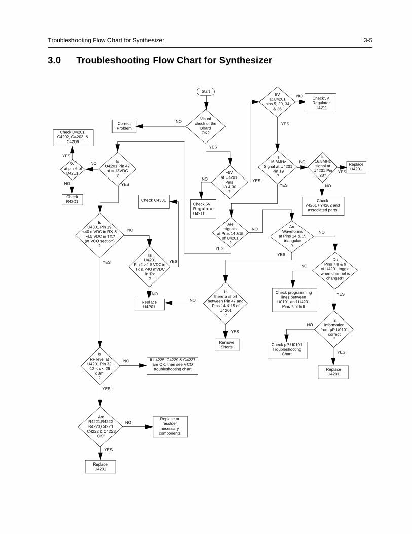
Troubleshooting Flow Chart for Synthesizer 3-5
3.0 Troubleshooting Flow Chart for Synthesizer
5V at pin 6 of
D4201
Isinformation
from µP U0101correct
?
IsU4201 Pin 47at = 13VDC
?
IsU4301 Pin 19
<40 mVDC in RX &>4.5 VDC in TX? (at VCO section)
?
Start
Visual check of the
BoardOK?
CorrectProblem
Check 5VRegulatorU4211
+5Vat U4201
Pins13 & 30
?
Is16.8MHz
Signal at U4201 Pin 19
?
CheckY4261 / Y4262 and
associated parts
Aresignals
at Pins 14 &15 of U4201
?
Check R4201 Check C4381
IsU4201
Pin 2 >4.5 VDC in Tx & <40 mVDC
in Rx?
Replace U4201
RemoveShorts
Isthere a short
between Pin 47 andPins 14 & 15 of
U4201?
Replace orresolder
necessarycomponents
IsRF level at
U4201 Pin 32 -12 < x <-25
dBm?
AreR4221,R4222,R4223,C4221,
C4222 & C4223 OK?
Replace U4201
If L4225, C4229 & C4227are OK, then see VCOtroubleshooting chart
AreWaveforms
at Pins 14 & 15triangular
?
DoPins 7,8 & 9
of U4201 togglewhen channel is
changed?
Check programminglines between
U0101 and U4201Pins 7, 8 & 9
Replace U4201
Check µP U0101Troubleshooting
Chart
NO
YES
NO
YES
NO
YES
NO
NO
NO
YES
YES
NO
YES
YES
NO
YES
YESYESNO
NO
NO
NO
YES
NO
YES
YES
Check D4201, C4202, C4203, &
C4206
5V at U4201
pins 5, 20, 34 & 36
Check 5V Regulator
U4211
Is 16.8MHz signal at
U4201 Pin 23?
Replace U4201
YES
NO
NO
YES
NO
YES

3-6 Troubleshooting Flow Chart for VCO
4.0 Troubleshooting Flow Chart for VCO
Are Q4332Base at 0.7V
Collector at 4.5V Emitter at 110mV
Are Q4301Base at 2.4V
Collector at 4.5V Emitter at 1.7V
Are U4301 Pins13 at 4.4V15 at 1.1V10 at 4.5V16 at 1.9V
Low or no RF Signalat TP4003
Visual checkof board
OK?
35mV DC atU4301 Pin 19
NO
YES
Replace Q4301
at base of Q4332
NO
NO
NO
NO
YES
YES
YES
YES
Low or no RF Signalat input to PA
4.8V DC atU4301 Pin 19
Is RF available at C4402
YES
YES
YES
YES
NO
NO
NO
NO
NO
Audio =180mVrmsat “-” Side of
4.5VDCat CR4321
If C4321 and R4321 are OK, then replace CR4321
Replace C4322
Replace C4325
NO
NO
YES
YES
If parts between R4402 & U4301 Pin10are OK, replace U4301
TX VCORX VCO
CorrectProblem
Visual checkof board
OK?
Check runner between U4201 Pin 2
and U4301 Pin 19
Is RF available If all parts from U4301 Pin 8to Base of Q4332 are OK,
replace U4301
If all parts associated with the pins are OK,
replace Q4332
If all parts from collectorof Q4332 to TP4003 are
OK, Replace Q4332
Power OK but no modulation
Check parts fromR4402 to U4401 Pin16
If all parts associated
with the pins are OK,
replace U4301
YES YES
Make sure Synthesizer is working correctly and runner between U4201 Pin 28 and U4301 Pin 14 & 18 are OK
4.5V DC
OK ?
OK? OK?
C4325
at U4301 Pin 14 & 18 4.5V DC
OK ?at U4301 Pin 14 &18
NO

4-1
Section 4
UHF PCB/SCHEMATICS/PARTS LISTS
1.0 Allocation of Schematics and Circuit Boards
1.1 Controller Circuits
The UHF circuits are contained on the Printed Circuit Board (PCB) which also contains the Controller circuits. This Chapter shows the schematics for the UHF circuits only, refer to the Controller section for details of the related Controller circuits . The PCB component layouts and the Parts Lists in this Chapter show both the Controller and UHF circuit components. The UHF schematics and the related PCB and parts list are shown in the tables below.
Table 4-1 UHF 25-40W Diagrams and Parts Lists
PCB :8486127Z01 Main Board Top Side8486127Z01 Main Board Bottom Side
Page 4-3Page 4-4
SCHEMATICSPower Amplifier 25 - 40WFRACNVoltage Controlled OscillatorReceiver Front EndIF
Page 4-5Page 4-6Page 4-7Page 4-8Page 4-9
Parts List8486127Z01 Page 4-10

4-2 Allocation of Schematics and Circuit Boards
THIS PAGE INTENTIONALLY LEFT BLANK
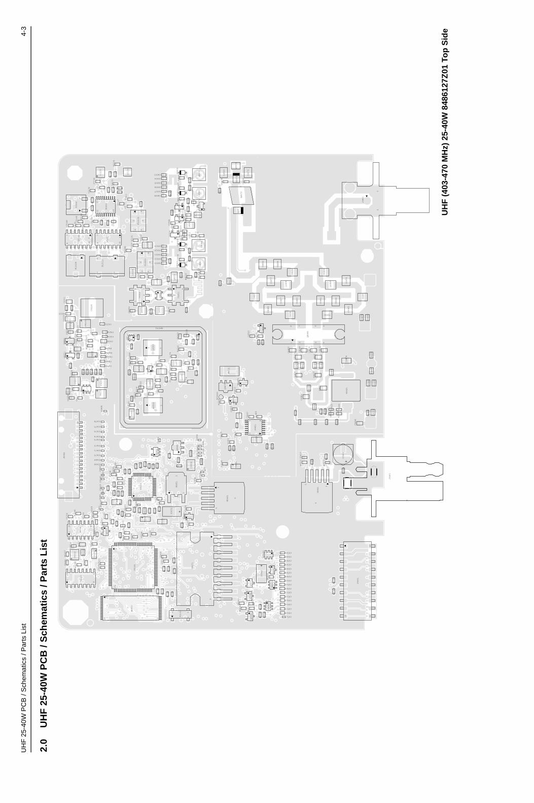
UH
F 2
5-40
W P
CB
/ S
chem
atic
s / P
arts
Lis
t4-
3
2.0
UH
F 2
5-40
W P
CB
/ S
chem
atic
s / P
arts
Lis
t
C0108
C0211
C0212
C0251
C0252
R0103
R0211
R0212
R0251
R0252
R0253
R0257
16
1
89
U0251
C0253
C0256
C0261
C0262
R0256
R0268 R0269
87
114
U0211
C0421
C0441 C0442C0443
C0445 C0446C0447
Q0110
R0222
R0261
R0262
R0442
C0104
C0106
C0224 C0226
C0227
C0228
C0232
C0233
C0236
C0237
C0495
R0101
R0102
R0104
R0108
R0110
R0115
R0116
R0226
R0227
R0228
C0221
C0222
C0225
C0241
C0243
R0220
R0221
R0223
R0224
R0229
R0254 R0255
C0235
C0242
C0244
C0245
C0246
C0496
D0201
R0241
R0242
137 25
13
U0221
R0681
C0101C0102
C0131
C0132
R0105
R0106
R0114
R0131
R0132
R0170
51
32
17
4
Y0131
16
1
U0121
126
U0101
C0223
C0231
C0234
C0651
C0652
D0651
R0225
R0651
R0652
3
2
1
U0651
C0482
C0483
C0487
C0488
C0493
C0494
C0654C0681
L0481
L0482
Q0681
R0682
C0486
C0655
C0542
Q0177
Q0181
Q0185
R0181
R0182
R0185
R0186
R0510
R0535
R0538
R0539
VR0501
VR0503
VR0505
VR0510
C0501
C0502
C0503
C0504
C0505
C0506
C0508
C0509
C0510
C0511
C0512
C0513
C0514
C0515
C0516
C0517
C0518U0271
76 20
11
10
J0501
R0508
R0509
J0601C0484
C0601
C0603
C0612
R0533
R0611
R0612
1
6
5
U0611
C4417
C4419
C4425
C4426
C4431
C4447
C4453
C4454
C4457
C4461
C4462
C4481
M3421
R4408 R4415
R4416
R4480
C4420
C4427
C4428
C4429
C4430
C4432
C4433
C4434
C4435
C4440
C4441
C4446
C4458
L4474
321 45678
Q4441
R4417
R4418
C4485
C4489
C4490
C4495
C4497
C4602
C4442
C4443
C4449
C4466
C4476
C4478
C4491
C4493
L4489
C4401
C4403
C4404
C4407
C4410
C4418
C4488
C4505
C4506
L4401
L4403
Q4471
R4401R4402
R4403
R4405
R4504TP4530
116
89
U4401
Q4472
R4511
R4512
VR4471
C4444
C4445
C4450
C4455
C4456
C4467
C4477
C4487
C4521
C4522
L4490
R4501
R4502
U4502
C4459
C4507
18
1
J0451
C0448
C0449
C0470
C0471
C0472
C0473
C0474
C0476
C0477
C0478
C0490
C4472
C4474
C4475
C4480
C4510
D4471
D4472
L4472
L4473
C4001
C4002
C4009
C4014
C4026
C4027
D4001
D4002
D4003
L4001
L4002
L4006
Q4001
Q4003R4003
R4004
R4020
R4022
C4317 C4318
C4322
C4323
C4325
C4351C4352
C4355
C4382
1 3
L4312
L4313
R4302
R4311
R4312
R4321
C4308C4309
C4353
C4383
1 3
L4303
L4304
L4305
Q4301 R4301
R4305
R4346
C4375
43
Q4333
C4331
C4332
C4335
C4337
C4339
C4354
C4371
C4372
C4373
C4374
L4331
L4371
R4331 R4332
R4333
R4337R4341
R4343
R4345
SH4301
C4031
C4053
C4054
C4055
D4051
L4008
L4053
L4054
R4051
21 5
43
T4051
215
4 3
T4052
C3101
23 4
5
FL3101
L3100
R3148
C4051
C4052
L4051 R4013
R4014
R4015
C4015
C4016
C4017
C4018
C4019
C4020
C4021
C4022
C4023
C4029
C4030
C4065
C4068
D4004
D4005
D4006
L4003
L4004
L4005
R4005
R4007
R4012
R4064
R4066
C4003
C4004
C4005
C4006
C4007
C4008
6
C3102
C3103
23 4
56
FL3102
L3101
R3101
R3106
C3114
C3115
C3124
C3131
C3132
C3133
C3134
C3135
C3136
C3137
C3143
L3124
R3111
R3117
R3124
R3130
R3132
R3135
11
120
10
U3101
R3123
C3140
C3141
C3142
87
114U3111
2
C3139
R4001
C3145 C3148
43
FL3112
FL3114
R3142
R3144
R3145
87
114
U3115
2
Y3102
C4221
C4222
C4223
C4224
C4225
C4226
C4227
C4229
C4230
C4231
C4236
C4253
D4221
L4221
Q4221
R4221
R4222
R4223
R4224
R4225
R4227
C4210
C4213
C4216
C4217
C4242
C4243
C4245
C4289
L4201
R4211
U4211 C4214
C4215
C4244
C4246
C4232
C4233
C4234
C4251
C4252
C4254
C4255
R4251
R4252
23
9
1
6
5
U0641
C0107
32
J4401
UH
F (
403-
470
MH
z) 2
5-40
W 8
4861
27Z
01 T
op
Sid
e

4-4
UH
F 2
5-40
W P
CB
/ S
chem
atic
s / P
arts
Lis
t
432
Y3101
C3122
C3123
D3101
Q3102
R3113
R3114
R3115R3116
R3133
C3116
R3118
C3121
L3112
R3112
C3104
C3110
C3111
C3112
C3113
L3111Q3101
R3102
R3104
R3105
R3107
R3108
C3144
C3146C3147
C3151
C3152
Q3141
Q3151
Q3152
R3134
R3141
R3146
R3147
R3151
R3152
R3153
R3154
43 2
FL3111
FL3113
43 2FL3115
C4261
C4262
C4263D4261
R4261
TP4201
TP4202
43 1
Y4261
2 34
Y4262
6
C4235
R4263
L4231
C4201
C4202
C4203
C4204 C4205
C4206
C4207
C4208
C4209
C4211
C4228
C4241
C4287
C4288
D4201
R4201
R4203
R4204
R4206
R4228
R4241
R4262
137
25
13
U4201
C0422C0423 C0426C0427 C0428C0429
C0485
C0491
C0492
C0497
J0401
R0407R0409
R0467
12
C0430 C0431
F0401
R0412R0441
C0201
C0202
C0203
C0204
C0205
C0254
C0265
C0266
C0267
R0201
R0202
R0203
R0204
R0205
R0206
R0207
R0208
R0265
R0266R0267
R0408
TP0102
TP0221
TP0222
VR0541
C0105C0121
C0122
C0123
C0255
R0107
R0468 R0543
R0555
R0593
145
8U0652
U0653
C4301
C4302
C4303
C4304
C4305
C4306
C4307
C4316
CR4301
CR4302
CR4303
L4301
L4302
R4303
R4304
R4315
11
120
10
U4301
C4311
C4312
C4313
C4314
C4315
C4319
C4321C4324
C4381
CR4311
CR4321 L4311
R4313
R4314
R4322
R4323
R4381
C4010
C4011
C4012
C4013
C4028
C4061
C4062
C4064
C4067
C4069
D4007
Q4002
Q4004
R4002
R4016
R4017
R4018
R4061
R4062
R4063
R4068
R4069
R4070
R4071
R4072
C4025
C4024
C4060
C4066 R4052
R4053
R4054
R4055
R4060
C4451
C4463
C4469
C4470
C4473
C4499
D4452
R4455
R4457
R4472
R4475
R4496
TP4531
VR4473
C4494
C4498
L4491
L4493
C4448
C4496
L4492
R4491
C4452
C4464
D4451
D4453
R4409R4473
R4474
R4506
R4507
R4471
TP4532
C4492
C4336 L4333
R4019
SH4302
TP4003
C4333
C4334
C4338
C4361
C4362
C4363
C4364
C4365
L4332
L4361
L4362
Q4331
Q4332
R4334R4335
R4336
R4338
R4339
R4340
R4342
R4344
R4347
R4360
R4361
R4362
R4363
C4422
C4423
C4437
C4439
L4421
L4436
L4437
L4438
C4424
C4629
C4630
C4631
C4632
Q4451
R4414
R4440
R4481
R4485
R4486
R4487
R4488
R4489
R4630
R4631
R4632
R4634
R4635
S4440
TP4537
TP4538
C4421
C4436
C4438
C4483
C4484
L4402
L4541
L4543
12
3
Q4421
R4513
R4525
TP4536
C0499
C0611
E0631
VR0601
R4495
R4497
C4402
C4405
C4409
C4412
C4413
C4414
C4415
C4416
L4404
L4411
Q4473
R4412R4428
R4431
R4482
R4484
R4503
TP4533
C4502
C4503
R4422
R4423
R4424R4425
R4483
R4514
R4523
C4504
C4479
1
17 9
25
U4501
R4492
C0304C0305
C0324C0325
C0343
R0323
R0324
R0341
R0344
R0345
TP0497
28
15
C0331
C0353
C0354
C0641
C0644
C0645
C0662 C0663
C0671
Q0641
Q0661
Q0662
Q0663
R0331 R0332R0333
R0335
R0481
R0482
R0641
R0642
R0643
R0661
R0662
R0671R0672
TP0661
U0331
C0301
C0302
C0303
C0351
C0352
D0301
14
1
U0301
458 U0351
C0344R0346
1
458
U0341
C0111
C0112
C0141
C0341
C0342
D0101
R0342
R0343
R0347
R0401 TP0101
TP0104
14 5
8
U0111
161
U0141
U0342
8 9
R0111
R0117
C0103
118
J0552
R0112
R0113
R0121
TP0103
TP0492
21
8
U0122
22
71
C0151
C0271
C0272
C0273
C0274
C0554
C0593
D0151
Q0151
Q0271
R0151
R0152
R0273
R0274
R0275
R0276
TP0151
VR0151
C0558
C0559 C0560
C0591
C0592
R0591
R0592
C0575 C0576
C0275
C0276
C0277
E0271
E0272
140
J0551
C0621C0622
C0661
D0621
D0660
D0661
R0173
R0174
R0621
VR0621
VR0671
C0541
D0179
Q0171
Q0173
Q0183
R0171
R0172
R0175R0176
R0177 R0178
R0179
R0183
R0184
R0511
R0512
R0525
R0529
R0530
R0531
R0537
R0541
R0542
TP0530
VR0504
VR0509
VR0537
R0556
UH
F (
403-
470
MH
z) 2
5-40
W 8
4861
27Z
01 B
ott
om
Sid
e
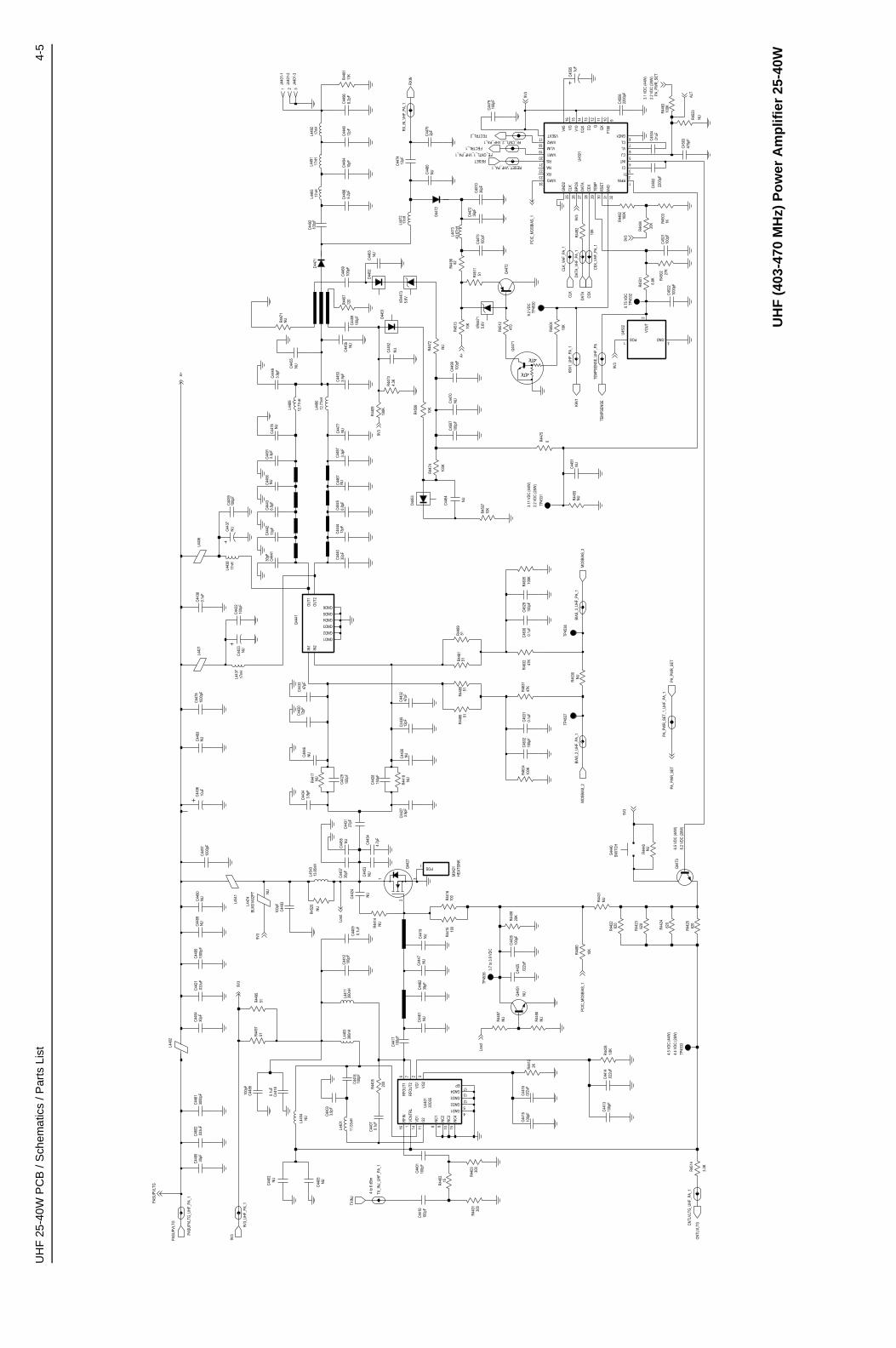
UH
F 2
5-40
W P
CB
/ S
chem
atic
s / P
arts
Lis
t4-
5
PA
SU
PV
LTG
_UH
F_P
A_1
PA
SU
PV
LTG
PA
SU
PV
LTG
9V3
9V3_
UH
F_P
A_1
C46
02
.033
uF30
00pF
C44
81C
4485
30pF
L440
2
30pF
C44
84
.033
uF
C44
21
1000
pF
C44
95
NU
NU
C44
90
1000
pF
C44
97
C44
89
BLM
31A
02P
T
L447
4
L454
1
NU
C44
9310
00pF
C44
78C
4436
10uF
NU
0.1u
F
C44
38
17nH
L443
7
L442
1
C44
2310
0pF
C44
22N
U10
0pF
C44
39L4
438
17nH
C44
37
L443
6
NU
NU
13pF
C44
42C
4466
30pF
C44
416.
8pF
C44
43C
4491
3.3p
FC
4476
NU
NU
C44
45
6.8p
F3.
3pF
C44
8713
pFC
4444
C44
67C
4440
30pF
C44
77
100K
R44
09
9V3
L449
0
12.7
7nH
12.7
7nH
L448
9
NU
C44
55
C44
49
3.9p
F
NU
R44
71
NU
C44
50
3.9p
FC
4456
120
R44
57
100p
F
C44
5910
0pF
C44
69
D44
71
C44
9210
0pF
17nH
L449
2L4
491
17nH
17nH
L449
3
10pF
C44
94C
4448
12pF
6.2p
FC
4498
C44
96
6.2p
F
R44
91
11K
RX
IN
RX
_IN
_VH
F_P
A_1
NU
12pF
C44
74
C44
802p
FC
4475
L447
217
nH
D44
72
NU
5.6V
VR
4473
D44
52C
4463
D44
51
NU
R44
73
4.3K
C44
52
NU
NU
100p
F
C44
99
R44
72
100p
F
C45
07
R45
06
10K
10K
R45
13
C44
70
A+
9.2
VD
CT
P45
30
CLK
R45
04
10K
Q44
71
K9V
1_U
HF
_PA
_1
470
R45
12
K9V
1
TE
MP
SE
NS
E
0R44
75
TE
MP
SE
NS
E_U
HF
_PA
9V3
1POS
VO
UT
2
U45
02
3GND
NU
NU
C44
05
C44
02
TX
INJ
NU
L440
4 3.9p
FC
4403
L440
1
11.0
3nH
C44
0410
0pF
0.1u
FC
4407
R44
05
200
4 to
6 d
Bm
TX
_IN
J_U
HF
_PA
_1
100p
F
C44
1010
0pF
C44
01
R44
0215
300
R44
0130
0R
4403
CN
TLV
LTGCN
TLV
LTG
_UH
F_P
A_1
3.3K
R45
14
C44
180.
1uF
51R44
97
C44
8810
0pF
390n
HL4
403
100p
FC
4412
390n
HL4
411
NU
NU
NU
NU
NU
C44
09
0.1u
F
1
C44
3127
pF
L454
313
.85n
H
C44
53
R45
25
C44
24
C44
54
4.7p
FR
4414
C44
58C
4457
36pF
Load
POS1
Q44
21
2
3
NU
C44
83
100p
F
9V3
1
VD
114
VG
12
VG
23
13
NC
18
NC
29
NC
310
NC
415
RF
IN16
RF
OU
T1
6
RF
OU
T2
7V
CN
TR
L
U44
01
30C
65
EP17
G2
11
GND14
GND25
GND312
GND4
C44
1710
0pF
NU
NU
NU
C44
47C
4419
C44
61C
4462
39pF
100
R44
15R
4416
100
M34
21
HE
AT
SIN
K
.022
uFC
4416
.022
uF
C44
14
100p
F
C44
15
100p
F
C44
13
1.8K
R44
28
R44
12
2K
3.7
to 3
.9 V
DC
NU
NU
NU
Q44
51
.022
uF
C44
2520
K
R44
08
100p
F
C44
26
R44
88
R44
87
TP
4536
Load
10K
R44
80
PC
IC_M
OS
BIA
S_1
620
R44
24
620
R44
23
620
R44
22
NU
R44
31
R44
25
620
6.2
VD
C (
28W
)
6.5
VD
C (
44W
)Q
4473
R44
40N
U
S44
40
SW
ITC
H
9V3
PA
_PW
R_S
ET
PA
_PW
R_S
ET
_1_U
HF
_PA
_1
PA
_PW
R_S
ET
NU
BIA
S_2
_UH
F_P
A_1
TP
4537
R46
30
MO
SB
IAS
_2
100p
F
C46
32
0.1u
F
C46
3110
0K
R46
34
4.4
VD
C (
28W
)
4.5
VD
C (
44W
)
TP
4533
NU
NU
C44
34
3.9p
FC
4446
150p
F
R44
17
C44
29
C44
33
47pF
12pF
C44
20
51R44
95
9V3
NU
NU
3.9p
FC
4427
C44
3512
pFC
4430
R44
18
150p
F
C44
28
47pF
C44
32
51R
4485
R44
8651
51R
4481
R44
89
51
C46
30
0.1u
F
R46
35
100p
F10
0K
C46
2947
K
R46
31
47K
R46
32
MO
SB
IAS
_3
BIA
S_3
_UH
F_P
A_1
TP
4538
GND5
GND6
IN1
IN2
OU
T1
OU
T2
Q44
41
GND1
GND2
GND3
GND4
NU
D44
53
C44
6410
0K
R44
74
R45
07
10K
NU
2.2
VD
C (
28W
)
3.11
VD
C (
44W
)
NU
TP
4531
R44
55C
4451
36pF
C44
72
C45
10
36pF
82R
4496
C44
73
100p
F51R45
11V
R44
71
5.6V
43.6
7nH
L447
3
Q44
72
PC
IC_M
OS
BIA
S_1
CS
X
DA
TA
DA
TA
_VH
F_P
A_1
10K
R44
92
CS
X_V
HF
_PA
_1
CLK
_VH
F_P
A_1
9V3
0.75
VD
CT
P45
32
R45
01
24VAR3
15V
G
VL6
VLIM19
RX23
T12
TE
MP
30
V10
14
V45
16
17V5EXT
20VAR1
18VAR2
GN
D2
25
INT4
22NA
Q11
QX
10
1RFIN
RS21
31R
SE
T
CJ5
CL7
CLK
26
CQ
1213C
QX
DA
TA
28
F16
89
GND18
U45
01
AN
O32
BP
OS
27
CE
X29
CI3
C45
22
1000
pF
20K
R44
84
100p
FC
4521
6.8K
27K
R45
02R
4503
1K
100K
R44
82
9V3
NU
3.1
VD
C (
44W
)
2.2
VD
C (
28W
)
R44
8310
0K
R45
23
C45
03
470p
F
2200
pF
C45
02
.0
1uF
C45
04
ALTPA
_PW
R_S
ET
C45
0622
00pF
1uF
C45
05
9V3
C44
7910
0pF
FE_CNTL_1_VHF_PA_1
RESET
FECTRL_1
RESET_VHF_PA_1
FE_CNTL_2_VHF_PA_1
FECTRL_2
J440
1-3
3
J440
1-2
2
J440
1-1
1
A+
UH
F (
403-
470
MH
z) P
ow
er A
mp
lifie
r 25
-40W

4-6
UH
F 2
5-40
W P
CB
/ S
chem
atic
s / P
arts
Lis
t
NU
0 V
DC
(R
X)
NU
NU
3.43
VD
C
3.05
VD
C (
RX
)
NU
4.97
VD
C2.
48 V
DC
NU
NU
4.58
VD
C
3.79
VD
C
2.48
VD
C
4.97
VD
C (
25K
HZ
Cha
n. S
paci
ng)
1.78
VD
C (
Rx)
4.97
VD
C (
TX
)
5 V
DC
(Lo
cked
)
10.8
7 V
DC
1.28
VD
C
NU
NU
NU
0 V
DC
(U
nloc
ked)
2.63
VD
C (
TX
)
VD
C
4.97
VD
C
NU
0 V
DC
(12
.5K
HZ
Cha
n. S
paci
ng)
2.52
VD
C
2.5
to 1
1 V
DC
1.76
VD
C (
Tx)
30m
V -
80m
V R
MS
12.7
VD
C
0 V
DC
4.97
VD
C
NU
1.8p
F
(SO
UR
CE
)
NU
3.48
6.68
VD
C
TP
4201
C42
04
100p
F
R42
0447
2.2u
FC
4214
INP
UT
8O
UT
PU
T1
SE
NS
E2
SH
UT
DO
WN
3
U42
11LP
2951
5V_T
AP
6
ER
RO
R5
FE
ED
BA
CK
7
GN
D 4
TR
B_U
HF
_FN
_1
D42
01
A1
6A
25
A3
4
1K
12
K2
3K
3
16.8
MH
z
GN
D2
OU
T 3
4V
CC
1
VC
NT
L
C42
11
Y42
62
C42
28
0.1u
F
.01u
FC
4205
VC
TR
L
47R
4203
C42
16
5V
C42
241u
F
DA
TA
C42
36.0
47uF
VC
OM
OD
_UH
F_F
N_1
IN_5
V_R
F_R
EG
0.1u
F
C42
08
C42
332.
2uF
R42
2847
K
10uF
C42
06
C42
540.
1uF
VC
OB
IAS
_2_U
HF
_FN
_1
C42
26
C42
090.
1uF
47K
R42
61
.01u
F
C42
03
VC
TR
L_U
HF
_FN
_1
C42
102.
2uF
100
R42
63
39K
R42
51
510
R42
22
C42
0110
0pF
R42
5230
K
16_8
MH
z
C42
32.0
1uF
R42
2447
K
C42
23
R42
62
100p
FC
4245
2.2u
H
C42
29
L423
1
R42
01
150
C42
62
CLK
_UH
F_F
N_1
150
PR
ES
C
R42
21
16_8
MH
z_U
HF
_FN
_1
100p
F
VC
OB
IAS
_2
VS
F
C42
44
D42
61
.01u
FC
4231
PR
ES
C_U
HF
_FN
_1
.018
uF
C42
12
390n
HL4
201
C42
4210
0pF
4.7u
FC
4253
BW
SE
LEC
T_U
HF
_FN
_1
MO
DIN
VC
OM
OD
.01u
FC
4221
0
C42
220.
1uF
R42
11
2.2u
FC
4215
C42
07
12uH
L422
1
0.1u
FC
4251
100p
FC
4241
C42
43
1000
pF
VS
F_U
HF
_FN
_1
C42
52
.01u
FC
4235
LOC
K
2.2u
FC
4213
C42
61
MO
DIN
_UH
F_F
N_1
XT
AL1
2324X
TA
L2
5V_U
HF
_FN
_1
VB
PA
SS
21
VC
P 47
15V
MU
LT1
VM
ULT
214
VM
ULT
312
VM
ULT
411
13VRO
WA
RP
25
PV
RE
F35
RE
FS
EL
18
SF
BA
SE
27S
FC
AP
26
SF
IN30
SF
OU
T28
TE
ST
137
TE
ST
238
NC
117
NC
229
NC
331
PD_GND44 5PD_VDD
32P
RE
IN
PRE_GND33 PRE_VDD 34
DGNDDVDD 36
FR
EF
OU
T19
IAD
AP
T45
IND
MU
LT16
IOU
T434
LOC
K
MO
DIN
10
MO
DO
UT
41
AVDD20B
IAS
140
BIA
S2
39
CC
OM
P42
CE
X9
CLK
8
DA
TA
7
6
AD
AP
TS
W46
AGND22
AU
X1
48A
UX
21
AU
X3
2A
UX
43
U42
01
63A
27
R42
06
VD
DA
_UH
F_F
N_1
5V_U
HF
_FN
_2
R42
25
47K
100p
FC
4246
C42
25
510p
F
LOC
K_U
HF
_FN
_1
D42
21
.01u
F
C42
02
L422
5
15nHIN
_5V
_RF
_RE
G_U
HF
_FN
_1
2.2u
FC
4230
100p
FC
4255
CS
X
R42
23
68
CS
X_U
HF
_FN
_1
DA
TA
_UH
F_F
N_1
OU
T3
IN6
VD
DA
Y42
6175
Z04
16.8
MH
z
1G
ND
4G
ND
10.
1uF
C42
63
TR
B
CLK
R42
41
220
C42
34.0
1uF
C42
27
8.2p
F
C42
88
TP
4202
BW
SE
LEC
T
Q42
21
C42
8710
0pF
C42
89
5V
5V
0.1u
F
VD
DA
VD
DA
In c
ase
Y32
61 is
use
d in
stea
d of
Y32
63,
repl
acem
ent o
f the
follo
win
g pa
rts
req
uire
s
new
tem
pera
ture
com
pens
atio
n of
the
freq
uenc
y:
Y32
61, U
3201
, R32
61, R
3262
, C32
62, D
3261
HF
(40
3-47
0 M
Hz)
FR
AC
N
ZW
G01
3052
1-B
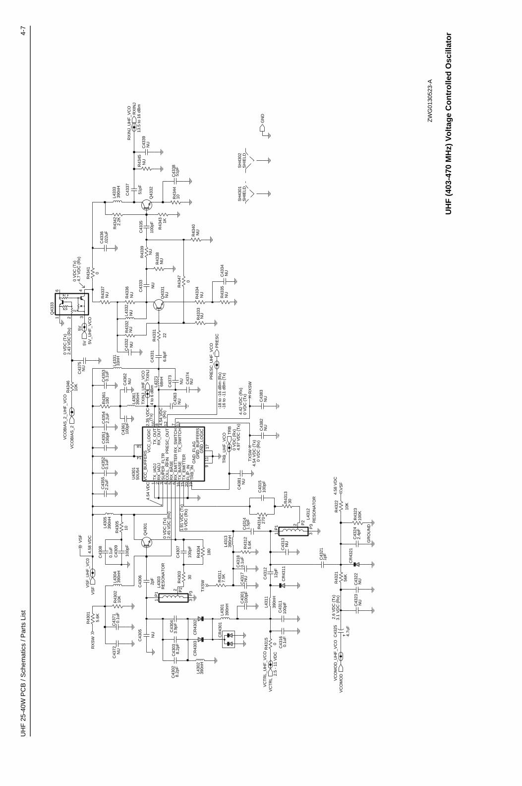
UH
F 2
5-40
W P
CB
/ S
chem
atic
s / P
arts
Lis
t4-
7
NU
NU
NU
0 V
DC
(T
x)
NU
NU
NU
NU
2.5
- 11
VD
C
0 V
DC
(R
x)
4.58
VD
C
4.58
VD
C
NU
NU
13.5
to 1
6 dB
m
NU
0 V
DC
(T
x)
3.1
VD
C (
Rx)
0 V
DC
(T
x)4.
7 V
DC
(R
x)
NU
(Tx)
4.54
VD
C0
VD
C (
Tx)
2.35
VD
C
NU
0 V
DC
(R
x)
4.42
VD
C (
Rx)
NU
NU
NU
NU
NU
NU
NU
NU
NU
NU
NU
NU
NU
NU
NU
NU
4.97
VD
C (
Tx)
-18
to -
16 d
Bm
(R
x)-1
6 to
-11
dB
m (
Tx)
4 to
6 d
Bm
4.54
VD
C
4.54
VD
C (
Tx)
2.6
VD
C (
Tx)
1.91
VD
C (
Tx)
0 V
DC
(R
x)
2.45
VD
C (
Rx)
(Rx)
2.43
VD
C (
Rx)
NU
NU
GN
D
C43
0110
0pF
30R43
13
C43
72
VC
TR
L_U
HF
_VC
O
L433
133
nH
VS
F_U
HF
_VC
0
C43
180.
1uF
Q43
01
R43
6118
0
C43
0551
pF
C43
37R
4332
CR
4303
C43
82
VC
OB
IAS
_2
5V_U
HF
_VC
O
C43
32
0
R43
15
CR
4311
C43
81
C43
13
.022
uFC
4336
R43
45
SH
4301
SH
IELD
R43
0210
K
C43
83
C43
63
R43
33
R43
125.
6K
C43
09
100p
F
C43
1510
0pF
19T
RB
_IN
16T
X_B
AS
E15
TX
_EM
ITT
ER
1T
X_I
AD
J10
TX
_OU
T
13T
X_S
WIT
CH
14
VC
C_B
UF
FE
RS
18
VC
C_L
OG
IC
GN
D_L
OG
IC17
12P
RE
SC
_OU
T5
RX
_BA
SE
6R
X_E
MIT
TE
R
2R
X_I
AD
J8
RX
_OU
T
7R
X_S
WIT
CH
3S
UP
ER
_FLT
R
U43
01
4C
OLL
_RF
IN
20F
LIP
_IN
11
GN
D_B
UF
FE
RS
9
GN
D_F
LAG
R43
46
10K
50U
54
L431
2
RE
SO
NA
TO
R
1P
1 2 P2
3P
3
C43
141.
5pF
C43
07
100p
F
C43
520.
1uF
C43
21
Q43
31
1pF
4
1 3
CR
4301
Q43
33
2
6
C43
39
C43
75
L433
2
L436
139
0nH
VC
TR
L
0
R43
41
C43
242.
4pF
2.2K
R43
42
6.8p
F
TR
B_U
HF
_VC
O
C43
31
C43
043.
9pF
C43
33
C43
74
C43
35
100p
F
270
R43
14
7.5K
R43
11
TX
INJ_
UH
F_V
CO
R43
34
R43
01 L430
139
0nH
R43
23
5.6K
100K
1KR
4343
C43
530.
1uF
C43
12
12pF
390n
HL4
305
C43
23
R43
37
C43
17
PR
ES
C
Q43
32
68nH
L433
339
0nH
L437
1
56K
R43
21
R43
05
C43
16
10
0
5V
0.1u
F
R43
47C
4338
R43
36
51pF
2.2u
FC
4354
C43
5110
0pF
22
R43
31
C43
73
R43
39
PR
ES
C_U
HF
_VC
O
390n
H
L431
1
R43
35
180
R43
04
CR
4321
10K
R43
22
100p
F
C43
1110
0pF
C43
61
30
R43
03
L430
239
0nH
C43
62
C43
038.
2pF
R43
38
RX
INJ
RX
INJ_
UH
F_V
CO
L430
3R
ES
ON
AT
OR
1P
1
2 P2
3P
3
0.1u
FC
4371
TX
INJ
390n
HL4
313
SH
IELD
SH
4302
TR
B
C43
34
C43
06
2pF
C43
552.
2uF
VS
F
VC
OB
IAS
_2_U
HF
_VC
O
VC
OM
OD
C43
08
0.1u
F
390n
HL4
304
C43
028.
2pF
CR
4302
10R43
44
C43
22
4.7u
F
C43
25V
CO
MO
D_U
HF
_VC
O
GR
OU
ND
R43
40
5V
VS
F
TX
SW
TX
SW
RX
SW
RX
SW
VS
F
ZW
G01
3052
3-A
UH
F (
403-
470
MH
z) V
olt
age
Co
ntr
olle
d O
scill
ato
r
ZW
G01
3052
3-A

4-8
UH
F 2
5-40
W P
CB
/ S
chem
atic
s / P
arts
Lis
t
R40
66
C40
69R
4070
.01u
F
C40
6810
0pF
C40
65
390
C40
640.
1uF
010
0pF
390
R40
64
R40
621.
5K
R40
63R40
7210
K
R40
71
10K
C40
620.
1uF
R40
61
10K
C40
6133
0pF
R40
691K
R40
68
C40
66
1.5K
C40
6733
00pF
R40
54
R40
55
R40
53R
4052
0
C40
60
R40
60
330K
L400
8
470n
H
R40
22
L400
6
0
R40
20
C40
51
15nH
10pF
L405
4
C40
3113
pF
15nH
L405
327
nH
C40
556.
2pF
NU
C40
5416
pFC
4053
R40
51
16pF
C40
52
51
L405
1
82pF
150n
H
L400
5L4
001
L400
2L4
004
C40
10
1.8p
F
330p
F
C40
29C
4027
C40
301.
8pF
1.8p
F1.
8pF
C40
26
R40
13
R40
15
270
C40
161p
F
C40
19
R40
19
12pF
C40
0336
pF
C40
25
R40
17
3.3K
R40
16
R40
18C
4028
.01u
F
C40
2033
pF
3.3K
C40
0433
pFC
4005
1.8p
F33
pF
C40
01C
4002 C
4006
33pF
C40
07
FE
CT
RL_
1_U
HF
_FE
30pF
100K
R40
01
C40
09
10pF
R40
033.
9K
R40
042.
7K
D40
07
10K
IF_U
HF
_FE
R40
05
C40
1410
0pF
470n
HK
9V1_
UH
F_F
E
L400
3
R40
07
100
RX
IN_U
HF
_FE
330p
F33
00pF
C40
12C
4013
100p
FC
4015
GN
D_U
HF
_FE
C40
1133
00pF
330
RX
INJ_
UH
F_F
E
R40
02
Q40
04
33pF
C40
21
T40
52
C40
17
D40
51
1.8p
F12
pF
Q40
03
Q40
01
C40
18
C40
2233
pF
T40
51
TP
4003
12pF
100K
C40
23
D40
0510
R40
12
R40
14
C40
0810
00pF
1000
pF
D40
01
C40
24
33pF
NU
NU
NU
NU
NU
3 to
6.5
VD
C
NU
NU
NU
NU
NU
NU
0.7
VD
C
4.6
VD
C
NU
NU
Q40
02D
4006
D40
04
9V3_
UH
F_F
E
D40
03
D40
02
FE
CT
RL_
2_U
HF
_FE
10
10
0
820
820
10
0
0
20pF
2.2p
F
1pF
IN
NE
G
PO
S
IN
NE
G
PO
S
IN
NE
G
PO
S
IN
NE
G
PO
S
UH
F (
403-
470
MH
z) R
ecei
ver
Fro
nt
En
d
ZW
G01
3052
4-B

UH
F 2
5-40
W P
CB
/ S
chem
atic
s / P
arts
Lis
t4-
9
9180
468v
04
9180
468V
06
3.9V
DC
12.
5kH
z 0
VD
C20
/25k
Hz
5V
DC
9180
469V
03
3VD
C
9180
469V
06
9180
469V
04
0.75
VD
C0.
75V
DC
3VD
C
R31
17
27K
Q31
02 10R
3112
IF
1.8K
R31
42
10K
27pF
R31
54
C31
400.
1uF
C31
10
620n
HL3
111
620
R31
085
CN
TL
43
14 VD
D 7
VS
S
C31
44
U31
15-2
C31
430.
1uF
120p
F
R31
15
390
R31
18
6.8K
R31
1112
K
5V_V
HF
_IF
_1Q
3151
NU
C31
13
NU
R31
04
22pF
C31
15
VD
D
14
VS
S 7
Q31
41
MC
74H
C40
66
U31
11-1
CN
TL 13
12
R31
16 330
82pF
C31
12
Q31
52
R31
351.
2K
DIS
CA
UD
IO_V
HF
_IF
_1
BW
SE
LEC
T_V
HF
_IF
_1
R31
01
IFIN
_VH
F_I
F_1
12K
C31
3310
uF
C31
52.0
1uF
0.1u
FC
3142
DIS
CA
UD
IO
R31
3215
K
680
R31
46
10K
R31
51
0.1u
FC
3139
C31
320.
1uF
10K
R31
52
0.1u
FC
3111
20pF
C31
01
3
GND1
GND2 4
1IN
2O
UT
FL3
111
C31
410.
1uF
GND3 45GND4
3IN
6O
UT
R31
338.
2K
FL3
101
12R
16
1GND1GND2 2
0
7
R31
48
U31
11-4
CN
TL
12
1110
VD
D
14 VS
S
9V3_
VH
F_I
F_2
R31
02 10
FL3
113
3GN
D
1IN
2O
UT
27K
R31
06
R31
4139
0
14
VD
D
7
VS
S
2.4K
R31
44
U31
11-2
5
CN
TL
43
NU
C31
31
C31
22
.039
uF
R31
07
5RSSIOUT9 RSSI_FEED
6
VCC
6.8K
13LIM_DEC112LIM_DEC2
20MIXOUT4 OSCIN
3OSCOUT
10 QUADIN
1 RFIN2 RFIN_DEC
AUDIO_FEED
GND15
18 IFAMPIN 16IFAMPOUT19 IFAMP_DEC1
17IFAMP_DEC2
14LIMIN
11LIMOUT
SA
616
U31
01
8AUDIOOUT
7
CN
TL 13
12
VD
D
14 VS
S 7
5V
U31
15-1
R31
05
L310
0
100
0.1u
F
9V3
NU
3
21
C31
34
BW
SE
LEC
T
45B
02
Y31
0245
5KH
z
C31
03
33pF
C31
470.
1uF
0.1u
FC
3145
620n
HL3
101
6CN
TL
89
14 VD
D 7VS
S9
14 VD
D 7VS
S
U31
11-3
U31
15-3
6CN
TL
8
GND1 12GND24GND3
GND4 5
IN3
OU
T6
30pF
12R
16F
L310
2
33pF
C31
36
C31
35
NU
L312
4
NU
C31
24NU
R31
24
C31
1418
pF
C31
040.
1uF
C31
210.
1uF
Q31
01.0
39uF
C31
23
.01u
FC
3151
51
4700
pFC
3146
R31
30
10K
R31
53
C31
48
R31
47
NU
D31
01
0
R31
23
330
R31
13
15pF
C31
02
3.3K
R31
45
C31
37.0
39uF
3GN
D
1IN
2O
UT
RS
SI
FL3
114
10V
DD
14
VS
S
7
0.1u
F
C31
16
2O
UT
U31
15-4
CN
TL
12
11
FL3
112
3
GND1
GND2 4
1IN
R31
14
R31
34
10K
NU
FL3
115
GND1
34
GND2
IN1
OU
T2
NU
9V3_
VH
F_I
F_1
L311
262
0nH
Y31
01
2G
ND
4G
ND
1
3O
UT
1IN
5V
44.3
95M
Hz
12R
17
5V
9V3
9V3
9V3
9V3
9V3
5V
9V3
5V
9V3
12k
ZW
G01
3052
2-A
UH
F (
403-
470
MH
z) IF

4-10
UH
F 2
5-40
W P
CB
/ S
chem
atic
s / P
arts
Lis
t
UH
F P
CB
848
6127
Z01
Par
ts L
ist
25-4
0W
Cir
cuit
R
efM
oto
rola
P
art
No
.D
escr
ipti
on
C01
0121
1374
0F51
100p
FC
0107
2113
741F
2510
00pF
C01
1221
1374
3E20
0.1u
FC
0121
2113
743E
200.
1uF
C01
2221
1374
3E20
0.1u
FC
0131
2113
740F
3522
pFC
0132
2113
740F
3522
pFC
0141
2113
743E
200.
1uF
C01
5121
1374
1F49
10nF
C02
0123
1104
9A57
10uF
C02
0223
1104
9A57
10uF
C02
0421
1374
3E20
0.1u
FC
0212
2311
049A
5710
uFC
0221
2113
743E
200.
1uF
C02
2221
1374
3E20
0.1u
FC
0223
2113
743E
200.
1uF
C02
2421
1374
0F51
100p
FC
0225
2113
743E
200.
1uF
C02
2621
1374
3E20
0.1u
FC
0228
2311
049A
564.
7uF
C02
3121
1374
3B29
1uF
C02
3221
1374
3E20
0.1u
FC
0234
2113
743E
200.
1uF
C02
3521
1374
3E07
0.02
2uF
C02
3621
1374
3E10
0.03
3uF
C02
4121
1374
3E20
0.1u
FC
0243
2113
740F
5110
0pF
C02
4421
1374
3E20
0.1u
FC
0245
2113
743E
200.
1uF
C02
4621
1374
1F49
10nF
C02
5121
1374
3E20
0.1u
FC
0252
2311
049A
071u
FC
0254
2113
743E
200.
1uF
C02
5521
1374
3E20
0.1u
FC
0256
2113
740F
5110
0pF
C02
6121
1374
3E20
0.1u
FC
0262
2113
740F
4982
pFC
0265
2113
743E
200.
1uF
C02
6721
1374
1F49
10nF
C02
7121
1374
1F49
10nF
C02
7221
1374
3E20
0.1u
FC
0273
2113
741F
3733
00pF
C02
7523
1104
9A99
47uF
C02
7621
1374
1F25
1000
pFC
0277
2113
741F
2510
00pF
C03
0123
1104
9A07
1uF
C03
0221
1374
3E20
0.1u
FC
0303
2113
740F
5110
0pF
C03
0421
1374
3E20
0.1u
FC
0305
2113
743E
200.
1uF
C03
2421
1374
3E20
0.1u
FC
0331
2113
743E
200.
1uF
C03
4123
1104
9A07
1uF
C03
4221
1374
3E20
0.1u
FC
0343
2113
743E
200.
1uF
C03
4421
1374
3E20
0.1u
FC
0351
2113
743E
200.
1uF
C03
5221
1374
3E07
0.02
2uF
C03
5323
1104
9A97
33uF
C03
5421
1374
3E20
0.1u
FC
0421
2113
743N
4882
PF
C04
2221
1374
1F17
470p
FC
0423
2113
741F
1747
0pF
C04
2621
1374
3L09
470p
FC
0427
2113
743L
0947
0pF
C04
2821
1374
3N48
82pF
C04
2921
1374
3L09
470p
FC
0430
2113
741F
1747
0pF
C04
3121
1374
1F17
470p
FC
0441
2113
743L
0947
0pF
C04
4221
1374
3L09
470p
FC
0445
2113
743L
0947
0pF
C04
4621
1374
3L09
470p
FC
0447
2113
743L
0947
0pF
C04
4821
1374
3L09
470p
FC
0449
2113
743L
0947
0pF
C04
7021
1374
3L09
470p
FC
0471
2113
743N
4882
pFC
0472
2113
743N
4882
pFC
0473
2113
743N
4882
pFC
0474
2113
743L
0947
0pF
C04
7621
1374
3L09
470p
FC
0477
2113
743L
0947
0pF
C04
7821
1374
3L09
470p
FC
0482
2113
743L
0947
0pF
C04
8321
1374
3L09
470p
FC
0484
2113
741F
1747
0pF
C04
8521
1374
3L09
470p
FC
0486
2113
743L
0947
0pF
C04
8721
1374
3L09
470p
FC
0488
2113
743L
0947
0pF
C04
9021
1374
3L09
470p
FC
0491
2113
743L
0947
0pF
C04
9221
1374
3L09
470p
FC
0493
2113
743L
0947
0pF
C04
9421
1374
3L09
470p
FC
0495
2113
743L
0947
0pF
C04
9621
1374
3L09
470p
FC
0497
2113
743L
0947
0pF
C04
9921
1374
3L09
470p
FC
0501
2113
741F
4910
nF
Cir
cuit
R
efM
oto
rola
P
art
No
.D
escr
ipti
on
C05
0221
1374
1F17
470p
FC
0503
2113
741F
1747
0pF
C05
0421
1374
1F17
470p
FC
0505
2113
741F
1747
0pF
C05
0621
1374
1F17
470p
FC
0508
2113
741F
1747
0pF
C05
0921
1374
1F17
470p
FC
0510
2113
741F
1747
0pF
C05
1121
1374
1F17
470p
FC
0512
2113
741F
1747
0pF
C05
1321
1374
1F17
470p
FC
0514
2113
741F
1747
0pF
C05
1521
1374
1F17
470p
FC
0516
2113
741F
4910
nFC
0517
2113
743N
4882
pFC
0518
2113
741F
1747
0pF
C05
4123
1104
9A05
0.47
uFC
0542
2311
049A
9947
uFC
0560
2113
743L
1710
00pF
C05
9121
1374
3E20
0.1u
FC
0592
2113
743E
200.
1uF
C05
9321
1374
1B69
0.1u
FC
0601
2113
741F
1747
0pF
C06
0323
8009
0M24
10uF
C06
1123
1104
9C06
22uF
C06
1221
1374
3E20
0.1u
FC
0622
2311
049A
9947
uFC
0641
2113
741F
1747
0pF
C06
4423
1104
9A97
33uF
C06
4521
1374
3E20
0.1u
FC
0652
2311
049A
9733
uFC
0654
2311
049A
5710
uFC
0655
2113
743E
200.
1uF
C06
6123
1104
9C05
47uF
C06
6221
1374
1F49
10nF
C06
6321
1374
3E20
0.1u
FC
0671
2113
743E
200.
1uF
C06
8121
1374
3E20
0.1u
FC
3101
2113
740F
3420
pFC
3102
2113
740F
3115
pFC
3103
2113
740F
3933
pFC
3104
2113
743E
200.
1uF
C31
1021
1374
0F37
27pF
C31
1121
1374
3E20
0.1u
FC
3112
2113
740F
4982
pFC
3114
2113
740F
3318
pFC
3115
2113
740F
3522
pFC
3116
2113
743E
200.
1uF
C31
2121
1374
3E20
0.1u
FC
3122
2113
743E
110.
039u
FC
3123
2113
743E
110.
039u
F
Cir
cuit
R
efM
oto
rola
P
art
No
.D
escr
ipti
on
C31
3221
1374
3E20
0.1u
FC
3133
2311
049A
5710
uFC
3134
2113
743E
200.
1uF
C31
3521
1374
0L30
33pF
C31
3621
1374
0L29
30pF
C31
3721
1374
3E11
0.03
9uF
C31
3921
1374
3E20
0.1u
FC
3140
2113
743E
200.
1uF
C31
4121
1374
3E20
0.1u
FC
3142
2113
743E
200.
1uF
C31
4321
1374
0F53
120p
FC
3144
2113
743E
200.
1uF
C31
4521
1374
3E20
0.1u
FC
3146
2113
741F
4147
00pF
C31
4721
1374
3E20
0.1u
FC
3151
2113
741F
4910
nFC
3152
2113
741F
4910
nFC
4001
2113
740F
091.
8pF
C40
0221
1374
0F39
33pF
C40
0321
1374
0F40
36pF
C40
0421
1374
0F39
33pF
C40
0521
1374
0F39
33pF
C40
0621
1374
0F39
33pF
C40
0721
1374
0F38
30pF
C40
0821
1374
1F25
1000
pFC
4009
2113
740F
2710
pFC
4010
2113
741F
1333
0pF
C40
1121
1374
1F37
3300
pFC
4012
2113
741F
1333
0pF
C40
1321
1374
1F37
3300
pFC
4014
2113
740F
5110
0pF
C40
1521
1374
0F51
100p
FC
4017
2113
740F
091.
8pF
C40
1821
1374
0F29
12pF
C40
1921
1374
0F29
12pF
C40
2021
1374
0F39
33pF
C40
2121
1374
0F39
33pF
C40
2221
1374
0F39
33pF
C40
2321
1374
0F29
12pF
C40
2421
1374
1F25
1000
pFC
4026
2113
740F
091.
8pF
C40
2721
1374
0F09
1.8p
FC
4028
2113
741F
4910
nFC
4029
2113
740F
091.
8pF
C40
3021
1374
0F09
1.8p
FC
4031
2113
740F
3013
pFC
4051
2113
740F
2710
pFC
4052
2113
740F
4982
pFC
4053
2113
740F
3216
pFC
4054
2113
740F
3216
pFC
4061
2113
740F
6333
0pF
Cir
cuit
R
efM
oto
rola
P
art
No
.D
escr
ipti
on
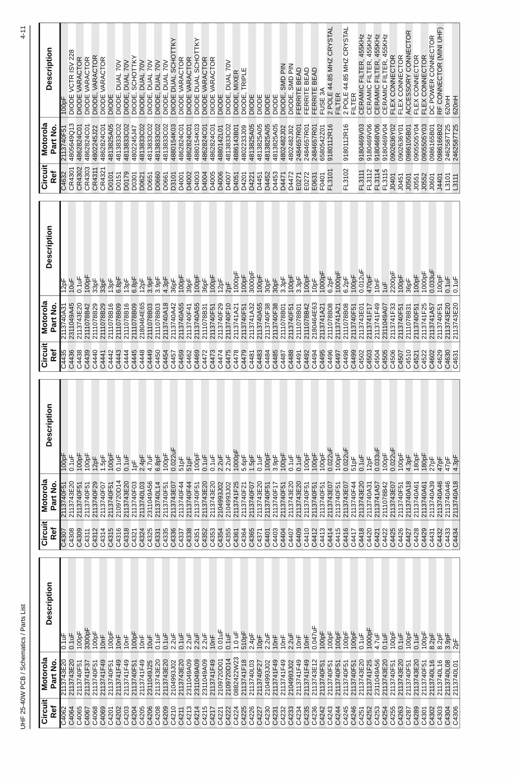
UH
F 2
5-40
W P
CB
/ S
chem
atic
s / P
arts
Lis
t4-
11
C40
6221
1374
3E20
0.1u
FC
4064
2113
743E
200.
1uF
C40
6521
1374
0F51
100p
FC
4067
2113
741F
3733
00pF
C40
6821
1374
0F51
100p
FC
4069
2113
741F
4910
nFC
4201
2113
740F
5110
0pF
C42
0221
1374
1F49
10nF
C42
0321
1374
1F49
10nF
C42
0421
1374
0F51
100p
FC
4205
2113
741F
4910
nFC
4206
2311
049J
2510
uFC
4208
2113
743E
200.
1uF
C42
0921
1374
3E20
0.1u
FC
4210
2104
993J
022.
2uF
C42
1121
1374
3E20
0.1u
FC
4213
2311
049A
092.
2uF
C42
1423
1104
9A09
2.2u
FC
4215
2311
049A
092.
2uF
C42
1721
1374
1F49
10nF
C42
2121
0972
0D01
0.01
uFC
4222
2109
720D
140.
1uF
C42
2408
8242
2W23
1.0
uFC
4225
2113
741F
1851
0pF
C42
2621
1374
0L03
2.4p
FC
4227
2113
740F
2710
pFC
4230
2104
993J
022.
2uF
C42
3121
1374
1F49
10nF
C42
3221
1374
1F49
10nF
C42
3321
0499
3J02
2.2u
FC
4234
2113
741F
4910
nFC
4235
2113
741F
4910
nFC
4236
2113
743E
120.
047u
FC
4242
2113
740F
5110
0pF
C42
4321
1374
0F51
100p
FC
4244
2113
740F
5110
0pF
C42
4521
1374
0F51
100p
FC
4246
2113
740F
5110
0pF
C42
5121
1374
3E20
0.1u
FC
4252
2113
741F
2510
00pF
C42
5323
1104
9A56
4.7u
FC
4254
2113
743E
200.
1uF
C42
5521
1374
0F51
100p
FC
4263
2113
743E
200.
1uF
C42
8721
1374
0F51
100p
FC
4289
2113
743E
200.
1uF
C43
0121
1374
0F51
100p
FC
4302
2113
740L
168.
2pF
C43
0321
1374
0L16
8.2p
FC
4304
2113
740L
083.
9pF
C43
0621
1374
0L01
2pF
Cir
cuit
R
efM
oto
rola
P
art
No
.D
escr
ipti
on
C43
0721
1374
0F51
100p
FC
4308
2113
743E
200.
1uF
C43
0921
1374
0F51
100p
FC
4311
2113
740F
5110
0pF
C43
1221
1374
0F29
12pF
C43
1421
1374
0F07
1.5p
FC
4315
2113
740F
5110
0pF
C43
1621
0972
0D14
0.1u
FC
4318
2113
743E
200.
1uF
C43
2121
1374
0F03
1pF
C43
2421
1374
0L03
2.4p
FC
4325
2311
049A
564.
7uF
C43
3121
1374
0L14
6.8p
FC
4335
2113
740F
5110
0pF
C43
3621
1374
3E07
0.02
2uF
C43
3721
1374
0F44
51pF
C43
3821
1374
0F44
51pF
C43
5121
1374
0F51
100p
FC
4352
2113
743E
200.
1uF
C43
5321
1374
3E20
0.1u
FC
4354
2104
993J
022.
2uF
C43
5521
0499
3J02
2.2u
FC
4361
2113
741F
2510
00pF
C43
6421
1374
0F21
5.6p
FC
4365
2113
740F
071.
5pF
C43
7121
1374
3E20
0.1u
FC
4401
2113
740F
5110
0pF
C44
0321
1374
0F17
3.9p
FC
4404
2113
740F
5110
0pF
C44
0721
1374
3E20
0.1u
FC
4409
2113
743E
200.
1uF
C44
1021
1374
0F51
100p
FC
4412
2113
740F
5110
0pF
C44
1321
1374
0F51
100p
FC
4414
2113
743E
070.
022u
FC
4415
2113
740F
5110
0pF
C44
1621
1374
3E07
0.02
2uF
C44
1721
1374
0F44
51pF
C44
1821
1374
3E20
0.1u
FC
4420
2113
740A
3112
pFC
4421
2113
741A
570.
033u
FC
4422
2111
078B
4210
0pF
C44
2521
1374
3E07
0.02
2uF
C44
2621
1374
0F51
100p
FC
4427
2113
740A
184.
3pF
C44
2821
1374
0A61
180p
FC
4429
2113
740A
6118
0pF
C44
3121
1374
0A39
27pF
C44
3221
1374
0A46
47pF
C44
3321
1374
0A46
47pF
C44
3421
1374
0A18
4.3p
F
Cir
cuit
R
efM
oto
rola
P
art
No
.D
escr
ipti
on
C44
3521
1374
0A31
12pF
C44
3623
1104
9A45
10uF
C44
3821
1374
3E20
0.1u
FC
4439
2111
078B
4210
0pF
C44
4021
1107
8B29
33pF
C44
4121
1107
8B29
33pF
C44
4221
1107
8B16
13pF
C44
4321
1107
8B09
6.8p
FC
4444
2111
078B
1613
pFC
4445
2111
078B
096.
8pF
C44
4821
8046
4E65
12pF
C44
4921
1107
8B03
3.9p
FC
4450
2111
078B
033.
9pF
C44
5421
1374
0A18
4.3p
FC
4457
2113
740A
4236
pFC
4459
2113
740A
5510
0pF
C44
6221
1374
0F41
39pF
C44
6921
1374
0A55
100p
FC
4472
2111
078B
3136
pFC
4473
2113
740F
5110
0pF
C44
7421
1374
0F29
12pF
C44
7521
1374
0F10
2pF
C44
7821
1374
1A21
1000
pFC
4479
2113
740F
5110
0pF
C44
8121
1374
1A32
3000
pFC
4483
2113
740A
5510
0pF
C44
8421
1374
0F38
30pF
C44
8521
1374
0F38
30pF
C44
8721
1107
8B01
3.3p
FC
4488
2113
740F
5110
0pF
C44
9121
1107
8B01
3.3p
FC
4492
2111
078B
4210
0pF
C44
9421
8046
4E63
10pF
C44
9521
1374
1A21
1000
pFC
4496
2111
078B
086.
2pF
C44
9721
1374
1A21
1000
pFC
4498
2111
078B
086.
2pF
C44
9921
1374
0F51
100p
FC
4502
2113
743E
010.
012u
FC
4503
2113
741F
1747
0pF
C45
0421
1374
1F49
10nF
C45
0523
1104
9A07
1uF
C45
0621
1374
1F33
2200
pFC
4507
2113
740F
5110
0pF
C45
1021
1107
8B31
36pF
C45
2121
1374
0F51
100p
FC
4522
2113
741F
2510
00pF
C46
0221
1374
1A57
0.03
3uF
C46
2921
1374
0F51
100p
FC
4630
2113
743E
200.
1uF
C46
3121
1374
3E20
0.1u
F
Cir
cuit
R
efM
oto
rola
P
art
No
.D
escr
ipti
on
C46
3221
1374
0F51
100p
FC
R43
0148
0564
9Q13
DIO
DE
VC
TR
ISV
228
CR
4302
4862
824C
01D
IOD
E V
AR
AC
TO
RC
R43
0348
6282
4C01
DIO
DE
VA
RA
CT
OR
CR
4311
4802
245J
22D
IOD
E, V
AR
AC
TO
RC
R43
2148
6282
4C01
DIO
DE
VA
RA
CT
OR
D01
0148
1382
5A05
DIO
DE
D01
5148
1383
3C02
DIO
DE
, DU
AL
70V
D01
7948
1383
3C02
DIO
DE
, DU
AL
70V
D03
0148
0224
5J47
DIO
DE
, SC
HO
TT
KY
D06
2148
1383
3C02
DIO
DE
, DU
AL
70V
D06
5148
1383
3C02
DIO
DE
, DU
AL
70V
D06
6048
1383
3C02
DIO
DE
, DU
AL
70V
D06
6148
1383
3C02
DIO
DE
, DU
AL
70V
D31
0148
8015
4K03
DIO
DE
DU
AL
SC
HO
TT
KY
D40
0148
6282
4C01
DIO
DE
VA
RA
CT
OR
D40
0248
6282
4C01
DIO
DE
VA
RA
CT
OR
D40
0348
8015
4K03
DIO
DE
DU
AL
SC
HO
TT
KY
D40
0448
6282
4C01
DIO
DE
VA
RA
CT
OR
D40
0548
6282
4C01
DIO
DE
VA
RA
CT
OR
D40
0648
8014
2L01
DIO
DE
D40
0748
1383
3C02
DIO
DE
, DU
AL
70V
D40
5148
8614
3B01
DIO
DE
, MIX
ER
D42
0148
0223
3J09
DIO
DE
, TR
IPLE
D42
2148
1382
5A05
DIO
DE
D44
5148
1382
5A05
DIO
DE
D44
5248
1382
5A05
DIO
DE
D44
5348
1382
5A05
DIO
DE
D44
7148
0248
2J02
DIO
DE
, SM
D P
IND
4472
4802
482J
02D
IOD
E, S
MD
PIN
E02
7124
8465
7R01
FE
RR
ITE
BE
AD
E02
7224
8465
7R01
FE
RR
ITE
BE
AD
E06
3124
8465
7R01
FE
RR
ITE
BE
AD
F04
0165
8054
2Z01
FU
SE
3A
FL3
101
9180
112R
162
PO
LE 4
4.85
MH
Z C
RY
STA
L F
ILT
ER
FL3
102
9180
112R
162
PO
LE 4
4.85
MH
Z C
RY
STA
L F
ILT
ER
FL3
111
9180
469V
03C
ER
AM
IC F
ILT
ER
, 455
KH
zF
L311
291
8046
9V06
CE
RA
MIC
FIL
TE
R, 4
55K
Hz
FL3
114
9180
468V
06C
ER
AM
IC F
ILT
ER
, 455
KH
zF
L311
591
8046
9V04
CE
RA
MIC
FIL
TE
R, 4
55K
Hz
J040
109
0263
6Y02
FLE
X C
ON
NE
CT
OR
J045
109
0263
6Y01
FLE
X C
ON
NE
CT
OR
J050
109
8610
5B01
AC
CE
SS
OR
Y C
ON
NE
CT
OR
J055
109
0550
5Y04
FLE
X C
ON
NE
CT
OR
J055
209
0550
5Y03
FLE
X C
ON
NE
CT
OR
J060
109
8616
5B01
DC
PO
WE
R C
ON
NE
CT
OR
J440
109
8616
6B02
RF
CO
NN
EC
TO
R (
MIN
I UH
F)
L310
124
6258
7T25
620n
HL3
111
2462
587T
2562
0nH
Cir
cuit
R
efM
oto
rola
P
art
No
.D
escr
ipti
on

4-12
UH
F 2
5-40
W P
CB
/ S
chem
atic
s / P
arts
Lis
t
L311
224
6258
7T25
620n
HL4
003
2462
587T
2347
0nH
L400
624
6258
7V24
15nH
L400
824
6258
7T23
470n
HL4
051
2462
587T
1715
0nH
L405
324
6258
7N46
27nH
L405
424
6258
7N43
15nH
L420
124
6258
7Q42
390n
HL4
221
2462
587P
2512
uHL4
231
2462
587Q
202.
2uH
L430
124
6258
7T22
390n
HL4
302
2462
587T
2239
0nH
L430
324
6059
3C01
RE
SO
NA
TO
RL4
304
2462
587T
2239
0nH
L430
524
6258
7T22
390n
HL4
311
2462
587T
2239
0nH
L431
224
6059
3C01
RE
SO
NA
TO
RL4
313
2462
587T
2239
0nH
L433
124
6258
7T09
33nH
L433
324
6258
7T22
390n
HL4
361
2462
587T
0933
nHL4
362
2462
587T
0933
nHL4
371
2462
587T
1368
nHL4
401
2460
591B
0411
.03n
HL4
402
2484
657R
01F
ER
RIT
E B
EA
DL4
403
2462
587T
2239
0nH
L441
124
6258
7T22
390n
HL4
421
2484
657R
01F
ER
RIT
E B
EA
DL4
436
2484
657R
01F
ER
RIT
E B
EA
DL4
437
2460
592A
0117
nHL4
438
2460
592A
0117
nHL4
472
2460
592A
0117
nHL4
473
2460
591N
3643
.67n
HL4
489
2460
591B
7713
.9nH
L449
024
6059
1B77
13.9
nHL4
491
2460
592A
0117
nHL4
492
2460
592A
0117
nHL4
493
2460
592A
0117
nHL4
541
2484
657R
01F
ER
RIT
E B
EA
DL4
543
2460
591C
2313
.85n
HM
3421
2686
201B
01H
EA
T S
PR
EA
DE
RQ
0110
4880
048M
01N
PN
Q01
5148
8004
8M01
NP
NQ
0171
4880
048M
01N
PN
Q01
7348
8005
2M01
NP
N D
AR
LIN
GT
ON
Q01
7748
8004
8M01
NP
NQ
0181
4880
048M
01N
PN
Q01
8348
8004
8M01
NP
NQ
0185
4880
048M
01N
PN
Q02
7148
8021
4G02
NP
NQ
0641
4880
048M
01N
PN
Cir
cuit
R
efM
oto
rola
P
art
No
.D
escr
ipti
on
Q06
6148
0592
1T02
DU
AL
NP
N/P
NP
Q06
6248
8021
4G02
NP
NQ
0663
4880
048M
01N
PN
Q06
8148
8005
2M01
NP
N D
AR
LIN
GT
ON
Q31
0148
1382
7A07
NP
NQ
3102
4813
827A
07N
PN
Q31
4148
8021
4G02
NP
NQ
3151
4880
048M
01N
PN
Q31
5248
8004
8M01
NP
NQ
4002
4813
824A
17P
NP
Q40
0348
1382
7A07
NP
NQ
4004
4805
921T
02D
UA
L N
PN
/PN
PQ
4221
4880
048M
01N
PN
Q43
0148
0521
8N63
DIO
DE
DU
AL
SC
HO
TT
KY
Q43
3248
1382
7A07
NP
NQ
4333
4809
939C
05D
UA
L N
PN
/PN
PQ
4421
4886
212B
01P
OW
ER
TR
AN
SIS
TO
R -
M
RF
1518
Q44
4148
1382
8C32
PO
WE
R T
RA
NS
IST
OR
-
MR
F15
70Q
4471
4880
048M
01N
PN
Q44
7248
0512
8M27
PN
PQ
4473
4880
214G
02N
PN
R01
0106
6205
7A73
10K
R01
0206
6205
7A65
4.7K
R01
0306
6205
7A01
10R
0104
0662
057A
7310
KR
0106
0662
057B
470
R01
0806
6205
7A57
2.2K
R01
1106
6205
7B47
0R
0113
0662
057A
7310
KR
0114
0662
057A
7310
KR
0115
0662
057A
7310
KR
0117
0662
057A
633.
9KR
0121
0662
057A
9710
0KR
0131
0662
057B
4610
MR
0132
0662
057B
1033
0KR
0151
0662
057A
8224
KR
0152
0662
057A
8224
KR
0170
0662
057A
7310
KR
0171
0662
057A
654.
7KR
0172
0662
057A
7310
KR
0173
0662
057A
654.
7KR
0174
0662
057A
7310
KR
0175
0662
057A
7310
KR
0176
0662
057A
8430
KR
0177
0662
057A
654.
7KR
0178
0662
057A
8947
KR
0179
0662
057A
8947
KR
0181
0662
057A
654.
7KR
0182
0662
057A
8947
K
Cir
cuit
R
efM
oto
rola
P
art
No
.D
escr
ipti
on
R01
8306
6205
7A65
4.7K
R01
8406
6205
7A89
47K
R01
8506
6205
7A65
4.7K
R01
8606
6205
7A89
47K
R02
0106
6205
7A25
100
R02
0206
6205
7A43
560
R02
0306
6205
7A25
100
R02
0406
6205
7A43
560
R02
0506
6205
7A73
10K
R02
0606
6205
7A73
10K
R02
0706
6205
7A57
2.2K
R02
0806
6205
7A57
2.2K
R02
1106
6007
6E70
7.5K
R02
1206
6007
6E70
7.5K
R02
2106
6205
7A82
24K
R02
2206
6205
7A82
24K
R02
2306
6205
7A84
30K
R02
2406
6205
7A71
8.2K
R02
2806
6205
7B47
0R
0229
0662
057A
0110
R02
4106
6205
7A89
47K
R02
4206
6205
7B47
0R
0251
0662
057A
8947
KR
0252
0662
057A
9156
KR
0253
0662
057A
9710
0KR
0254
0662
057A
7310
KR
0255
0662
057A
7310
KR
0256
0662
057A
9710
0KR
0257
0662
057A
572.
2KR
0261
0662
057A
7310
KR
0262
0662
057B
0827
0KR
0265
0662
057A
8224
KR
0267
0662
057A
8947
KR
0268
0662
057A
7310
KR
0269
0662
057A
4147
0R
0273
0662
057A
8224
KR
0275
0662
057A
7310
KR
0276
0662
057A
7715
KR
0323
0662
057A
7918
KR
0324
0662
057A
7918
KR
0331
0662
057A
7310
KR
0332
0662
057A
7310
KR
0333
0662
057A
7310
KR
0335
0662
057B
0215
0KR
0341
0662
057A
7310
KR
0342
0662
057A
551.
8KR
0343
0662
057B
470
R03
4406
6205
7A91
56K
R03
4506
6205
7A66
5.1K
R03
4606
6205
7A89
47K
R03
4706
6205
7A89
47K
Cir
cuit
R
efM
oto
rola
P
art
No
.D
escr
ipti
on
R04
0106
6205
7A33
220
R04
0706
6205
7M26
10R
0408
0662
057A
2510
0R
0409
0662
057M
2610
R04
1206
6205
7B47
0R
0441
0662
057B
470
R04
4206
6205
7A49
1KR
0467
0662
057M
2610
R04
6806
6205
7A97
100K
R04
8106
6205
7B47
0R
0482
0662
057B
470
R05
0806
6205
7A41
470
R05
0906
6205
7B47
0R
0510
0662
057A
654.
7KR
0511
0662
057A
9710
0KR
0512
0662
057A
7715
KR
0525
0662
057A
9710
0KR
0529
0662
057A
8947
KR
0530
0662
057A
8122
KR
0531
0662
057A
4356
0R
0533
0662
057B
470
R05
3506
6205
7A49
1KR
0537
0662
057A
3322
0R
0538
0662
057A
3322
0R
0539
0662
057A
654.
7KR
0541
0662
057A
8327
KR
0543
0662
057A
9710
0KR
0555
0662
057A
2510
0R
0556
0662
057A
2510
0R
0591
0662
057A
8224
KR
0592
0662
057A
0110
R05
9306
6205
7A97
100K
R06
1106
6205
7A91
56K
R06
1206
6205
7A65
4.7K
R06
2106
6205
7A82
24K
R06
4106
6205
7A73
10K
R06
4206
6007
6E70
7.5K
R06
4306
6007
6E51
1.2K
R06
5106
6205
7A01
10R
0652
0662
057A
0110
R06
6106
6205
7A49
1KR
0662
0662
057B
0215
0KR
0671
0662
057A
8430
KR
0672
0662
057A
7310
KR
0681
0662
057A
7918
KR
0682
0662
057A
9368
KR
3101
0662
057A
7512
KR
3102
0662
057A
0110
R31
0506
6205
7A25
100
R31
0606
6205
7A83
27K
R31
0706
6205
7A69
6.8K
Cir
cuit
R
efM
oto
rola
P
art
No
.D
escr
ipti
on
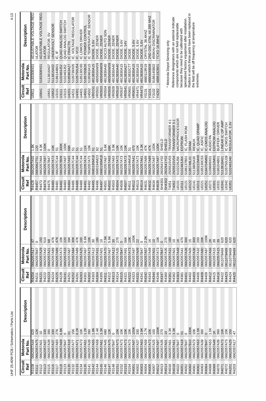
UH
F 2
5-40
W P
CB
/ S
chem
atic
s / P
arts
Lis
t4-
13
* M
otor
ola
Dep
ot S
ervi
cing
onl
y
Ref
eren
ce d
esig
nato
rs w
ith a
n as
teris
k in
dica
te
com
pone
nts
whi
ch a
re n
ot fi
eld
repl
acea
ble
beca
use
they
nee
d to
be
calib
rate
d w
ith
spec
ializ
ed fa
ctor
y eq
uipm
ent a
fter
inst
alla
tion.
R
adio
s in
whi
ch th
ese
part
s ha
ve b
een
repl
aced
in
the
field
will
be
off f
requ
ency
at t
empe
ratu
re
extr
emes
.
R31
0806
6205
7A44
620
R31
1106
6205
7A75
12K
R31
1206
6205
7A01
10R
3113
0662
057A
3733
0R
3115
0662
057A
3939
0R
3116
0662
057A
3733
0R
3117
0662
057A
8327
KR
3118
0662
057A
696.
8KR
3123
0662
057B
470
R31
3006
6205
7A18
51R
3132
0662
057A
7715
KR
3133
0662
057A
718.
2KR
3134
0662
057A
7310
KR
3135
0662
057A
511.
2KR
3141
0662
057A
3939
0R
3142
0662
057A
551.
8KR
3144
0662
057A
582.
4KR
3145
0662
057A
613.
3KR
3146
0662
057A
4568
0R
3147
0662
057A
7512
KR
3148
0662
057B
470
R31
5106
6205
7A73
10K
R31
5206
6205
7A73
10K
R31
5306
6205
7A73
10K
R31
5406
6205
7A73
10K
R40
0106
6205
7A97
100K
R40
0206
6205
7A37
330
R40
0306
6205
7A63
3.9K
R40
0406
6205
7A59
2.7K
R40
0506
6205
7A73
10K
R40
0706
6205
7A25
100
R40
1206
6205
7A97
100K
R40
1306
6205
7A35
270
R40
1406
6205
7A01
10R
4016
0662
057A
613.
3KR
4018
0662
057A
613.
3KR
4022
0662
057B
470
R40
5106
6205
7A18
51R
4052
0662
057B
470
R40
6006
6205
7B10
330K
R40
6106
6205
7A73
10K
R40
6206
6205
7A53
1.5K
R40
6306
6205
7A39
390
R40
6406
6205
7B47
0R
4068
0662
057A
531.
5KR
4069
0662
057A
491K
R40
7006
6205
7A39
390
R40
7106
6205
7A73
10K
R40
7206
6205
7A73
10K
R42
0106
6205
7A29
150
R42
0306
6205
7A17
47
Cir
cuit
R
efM
oto
rola
P
art
No
.D
escr
ipti
on
R42
0406
6205
7A17
47R
4211
0662
057B
470
R42
2106
6205
7A29
150
R42
2206
6205
7A42
510
R42
2306
6205
7A21
68R
4224
0662
057A
8947
KR
4225
0662
057A
8947
KR
4228
0662
057A
7310
KR
4241
0662
057A
3322
0R
4251
0662
057A
8739
KR
4252
0662
057A
8430
KR
4261
0662
057A
8947
KR
4263
0662
057A
2510
0R
4301
0662
057A
675.
6KR
4302
0662
057A
7310
KR
4303
0662
057A
1230
R43
0406
6205
7A31
180
R43
0506
6205
7A01
10R
4311
0662
057A
707.
5KR
4312
0662
057A
675.
6KR
4313
0662
057A
1230
R43
1406
6205
7A35
270
R43
1506
6205
7B47
0R
4321
0662
057A
9156
KR
4322
0662
057A
7310
KR
4323
0662
057A
9710
0KR
4331
0662
057A
0922
R43
4106
6205
7B47
0R
4342
0662
057A
572.
2KR
4343
0662
057A
491K
R43
4406
6205
7A01
10R
4346
0662
057A
7310
KR
4347
0662
057B
470
R43
6006
6205
7A35
270
R43
6106
6205
7A31
180
R43
6206
6205
7A01
10R
4363
0662
057A
491K
R43
8106
6205
7A41
470
R44
0106
6205
7A36
300
R44
0206
6205
7A05
15R
4403
0662
057A
3630
0R
4405
0662
057A
3220
0R
4408
0662
057A
8020
KR
4409
0662
057A
9710
0KR
4412
0662
057A
562K
R44
1506
6205
7A15
39R
4416
0662
057A
1539
R44
2206
1107
9A69
620
R44
2306
1107
9A69
620
R44
2406
1107
9A69
620
R44
2506
1107
9A69
620
Cir
cuit
R
efM
oto
rola
P
art
No
.D
escr
ipti
on
R44
2806
6205
7A55
1.8K
R44
5706
8396
2T51
120
R44
7306
6205
7A64
4.3K
R44
7406
6205
7A97
100K
R44
7506
6205
7B47
0R
4480
0662
057A
7310
KR
4481
0662
057C
4451
R44
8206
6205
7B09
300K
R44
8306
6205
7A97
100K
R44
8406
6205
7A93
68K
R44
8506
6205
7C44
51R
4486
0662
057C
4451
R44
8906
6205
7C44
51R
4491
0662
057A
7411
KR
4492
0662
057A
7310
KR
4495
0680
195M
1851
R44
9606
8019
4M23
82R
4497
0680
195M
1851
R45
0106
6205
7A67
5.6K
R45
0206
6205
7A93
68K
R45
0306
6205
7A63
3.9K
R45
0406
6205
7A73
10K
R45
0606
6205
7A73
10K
R45
0706
6205
7A73
10K
R45
1106
8019
4M18
51R
4512
0662
057A
4147
0R
4513
0662
057A
7310
KR
4514
0662
057A
613.
3KR
4631
0662
057A
8947
KR
4632
0662
057A
8947
KR
4634
0662
057A
9710
0KR
4635
0662
057A
9710
0KS
H43
0126
0264
1Y02
SH
IELD
SH
4302
2602
641Y
02S
HIE
LDT
4051
2505
515V
03T
RA
NS
FO
RM
ER
4:1
T40
5225
0551
5V04
TR
AN
SF
OR
ME
R 5
:1U
0101
5102
226J
56M
ICR
OP
RO
CE
SS
OR
U01
1151
0246
3J64
EE
PR
OM
U01
2151
8613
7B01
IC, F
LAS
H R
OM
U01
2251
8574
8L01
SR
AM
U01
4151
1380
5A30
RE
MU
XU
0211
5183
222M
49IC
, QU
AD
OP
AM
PU
0221
5185
130C
53IC
, AS
FIC
U02
5151
8470
4M60
IC-C
MO
S A
NA
LOG
U02
7151
0969
9X01
AU
DIO
PA
U03
0151
0915
2M01
EE
PR
OM
AN
ALO
GU
0331
5186
204B
01B
UF
FE
R /
DR
IVE
RU
0341
5113
818A
01LI
NE
AR
IC O
P A
MP
U03
4251
0575
0U28
IC C
MO
S S
WIT
CH
U03
5151
0246
3J40
RE
GU
LAT
OR
, 3.3
V
Cir
cuit
R
efM
oto
rola
P
art
No
.D
escr
ipti
on
U06
1151
8330
8X01
AD
JUS
TAB
LE V
OLT
AG
E R
EG
-U
LAT
OR
U06
4151
8330
8X01
AD
JUS
TAB
LE V
OLT
AG
E R
EG
-U
LAT
OR
U06
5151
1381
6A07
RE
GU
LAT
OR
, 5V
U
0652
5113
815A
02U
ND
ER
VO
LT S
EN
SO
RU
3101
5186
144B
01IC
, IF
U31
1151
0246
3J52
QU
AD
AN
ALO
G S
WIT
CH
U31
1551
0246
3J52
QU
AD
AN
ALO
G S
WIT
CH
U42
0151
8596
3A27
IC F
RA
CT
NU
4211
5105
739X
05IC
, VO
LTA
GE
RE
GU
LAT
OR
U43
0151
0575
0U54
IC, V
CO
U44
0151
8513
0C65
IC L
DM
OS
DR
IVE
RU
4501
5185
765B
26IC
PO
WE
R C
ON
TR
OL
U45
0251
8596
3A15
IC T
EM
PE
RA
TU
RE
SE
NS
OR
VR
0151
4813
830A
15D
IOD
E, 5
.6V
VR
0501
4805
656W
09D
IOD
E, Z
EN
ER
VR
0503
4805
656W
09D
IOD
E, Z
EN
ER
VR
0504
4813
830A
40S
OC
23 A
UT
O S
DN
VR
0505
4805
656W
09D
IOD
E, Z
EN
ER
VR
0509
4813
830A
40D
IOD
E, Z
EN
ER
VR
0510
4813
830A
40D
IOD
E, Z
EN
ER
VR
0537
4813
830A
15D
IOD
E, 5
.6V
VR
0541
4813
830A
27D
IOD
E, 1
4VV
R06
0148
1383
2C77
DIO
DE
VR
0621
4813
830A
15D
IOD
E, 5
.6V
VR
4471
4813
830A
15D
IOD
E, 5
.6V
VR
4473
4813
830A
15D
IOD
E, 5
.6V
Y01
3148
8011
3R19
CR
YS
TAL
38.4
KH
ZY
3101
4880
606B
092N
D O
SC
XTA
L 44
.395
MH
ZY
3102
9186
145B
0245
5KH
z D
ISC
RIM
INA
TO
RY
4262
4886
182B
01T
CX
O 1
6.8M
HZ
Cir
cuit
R
efM
oto
rola
P
art
No
.D
escr
ipti
on

4-14
UH
F 2
5-40
W P
CB
/ S
chem
atic
s / P
arts
Lis
t
TH
IS P
AG
E IN
TE
NT
ION
AL
LY L
EF
T B
LA
NK
GM338Mobile Radios
UHF B2 HIGH POWER LDMOS (450-520 MHz)
Service Information
Issue: December, 2003

Computer Software CopyrightsThe Motorola products described in this manual may include copyrighted Motorola computer programs stored in semiconductor memories or other media. Laws in the United States and other countries preserve for Motorola certain exclusive rights for copyrighted computer programs, including the exclusive right to copy or reproduce in any form, the copyrighted computer program. Accordingly, any copyrighted Motorola computer programs contained in the Motorola products described in this manual may not be copied or reproduced in any manner without the express written permission of Motorola. Furthermore, the purchase of Motorola products shall not be deemed to grant, either directly or by implication, estoppel or otherwise, any license under the copyrights, patents or patent applications of Motorola, except for the normal non-exclusive royalty-free license to use that arises by operation of law in the sale of a product.

i
Table of Contents
Section 1 Model Chart and Technical Specifications
1.0 GM338 Model Chart.............................................................................................1-12.0 Technical Specifications ......................................................................................1-1
Section 2 Theory of Operation
1.0 Introduction ..........................................................................................................2-12.0 UHF (450-520 MHz) Receiver .............................................................................2-1
2.1 Receiver Front-End ........................................................................................2-12.2 Front-End Band-Pass Filters & Pre-Amplifier .................................................2-22.3 First Mixer and High Intermediate Frequency (IF)..........................................2-22.4 Low Intermediate Frequency (IF) and Receiver Back End.............................2-3
3.0 UHF (450-520 MHz) Transmitter Power Amplifier (PA) 40W...............................2-33.1 First Power Controlled Stage..........................................................................2-43.2 Power Controlled Driver Stage .......................................................................2-43.3 Final Stage .....................................................................................................2-43.4 Directional Coupler .........................................................................................2-43.5 Antenna Switch...............................................................................................2-53.6 Harmonic Filter ...............................................................................................2-53.7 Power Control.................................................................................................2-5
4.0 UHF (450-520 MHz) Frequency Synthesis ..........................................................2-64.1 Reference Oscillator .......................................................................................2-64.2 Fractional-N Synthesizer ................................................................................2-64.3 Voltage Controlled Oscillator (VCO)...............................................................2-84.4 Synthesizer Operation ....................................................................................2-9
Section 3 Troubleshooting Charts
1.0 Troubleshooting Flow Chart for Receiver ............................................................3-12.0 Troubleshooting Flow Chart for 40W Transmitter ................................................3-33.0 Troubleshooting Flow Chart for Synthesizer........................................................3-44.0 Troubleshooting Flow Chart for VCO...................................................................3-5

ii
Section 4 UHF PCB/Schematics/Parts Lists
1.0 Allocation of Schematics and Circuit Boards .......................................................4-11.1 Controller Circuits...........................................................................................4-1
2.0 UHF Band 2 25-40W PCB / Schematics / Parts List ...........................................4-3UHF Band 2 (450-520 MHz) 40W 8486250Z02 Top Side......................................4-3UHF Band 2 (450-520 MHz) 40W 8486250Z02 Bottom Side................................4-4UHF Band 2 (450-520 MHz) Power Amplifier 40W ................................................4-5UHF Band 2 (450-520 MHz) FRACN .....................................................................4-6UHF Band 2 (450-520 MHz) Voltage Controlled Oscillator ....................................4-7UHF Band 2 (450-520 MHz) Receiver Front End...................................................4-8UHF Band 2 (450-520 MHz) IF...............................................................................4-9UHF Band 2 PCB 8486250Z02 Parts List 25-40W.............................................. 4-10
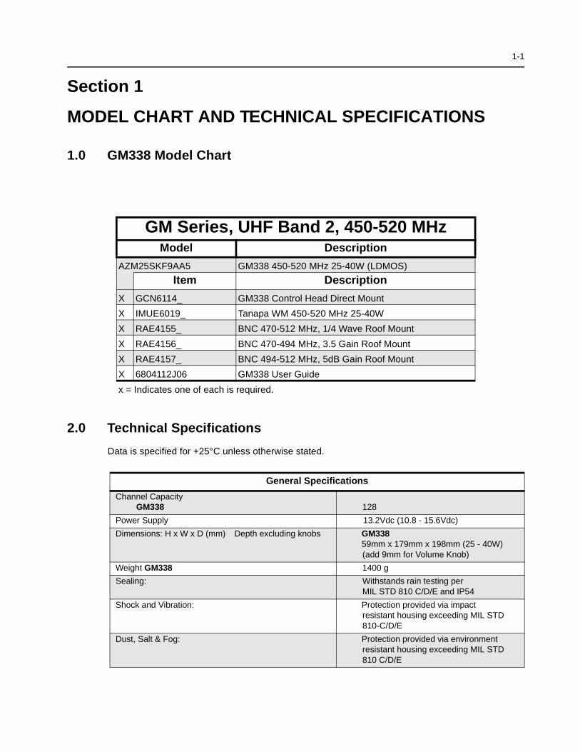
1-1
Section 1
MODEL CHART AND TECHNICAL SPECIFICATIONS
1.0 GM338 Model Chart
2.0 Technical Specifications
Data is specified for +25°C unless otherwise stated.
GM Series, UHF Band 2, 450-520 MHzModel Description
AZM25SKF9AA5 GM338 450-520 MHz 25-40W (LDMOS)
Item Description
X GCN6114_ GM338 Control Head Direct Mount
X IMUE6019_ Tanapa WM 450-520 MHz 25-40W
X RAE4155_ BNC 470-512 MHz, 1/4 Wave Roof Mount
X RAE4156_ BNC 470-494 MHz, 3.5 Gain Roof Mount
X RAE4157_ BNC 494-512 MHz, 5dB Gain Roof Mount
X 6804112J06 GM338 User Guide
x = Indicates one of each is required.
General Specifications
Channel CapacityGM338 128
Power Supply 13.2Vdc (10.8 - 15.6Vdc)
Dimensions: H x W x D (mm) Depth excluding knobs GM33859mm x 179mm x 198mm (25 - 40W)(add 9mm for Volume Knob)
Weight GM338 1400 g
Sealing: Withstands rain testing per MIL STD 810 C/D/E and IP54
Shock and Vibration: Protection provided via impactresistant housing exceeding MIL STD 810-C/D/E
Dust, Salt & Fog: Protection provided via environment resistant housing exceeding MIL STD 810 C/D/E

1-2 Technical Specifications
*Availability subject to the laws and regulations of individual countries.
Transmitter UHF
*Frequencies - Full Bandsplit UHF 450-520 MHz
Channel Spacing 12.5/20/25 kHz
Frequency Stability(-30°C to +60°C, +25° Ref.)
±2.0 ppm
Power 25-40W
Modulation Limiting±2.5 @ 12.5 kHz ±4.0 @ 20 kHz±5.0 @ 25 kHz
FM Hum & Noise-40 dB @ 12.5kHz
-45 dB @ 20/25kHz
Conducted/Radiated Emission (ETS)-36 dBm <1 GHz-30 dBm >1 GHz
Adjacent Channel Power-60 dB @ 12.5 kHz-70 dB @ 25 kHz
Audio Response (300 - 3000 Hz) +1 to -3 dB
Audio Distortion@1000Hz, 60%Rated Maximum Deviation
<3% typical
Receiver UHF
*Frequencies - Full Bandsplit UHF 450-520 MHz
Channel Spacing 12.5/20/25 kHz
Sensitivity (12 dB SINAD) 0.30 µV (0.22 µV typical)
Intermodulation (ETS) >65 dB
Adjacent Channel Selectivity (ETS)65 dB @ 12.5 kHz 70 dB @ 20 kHz75 dB @ 25 kHz
Spurious Rejection (ETS)70 dB @ 12.5 kHz
75 dB @ 20/25 kHz
Rated Audio3W Internal
7.5W External13W External
Audio Distortion @ Rated Audio <3% typical
Hum & Noise-40 dB @ 12.5 kHz
-45 dB @ 20/25 kHz
Audio Response (300 - 3000Hz @ 20/25kHz)(300 - 2550Hz @12.5kHz)
+1 to -3 dB
Conducted Spurious Emission (ETS)-57 dBm <1 GHz-47 dBm >1 GHz

2-1
Section 2
THEORY OF OPERATION
1.0 Introduction
This Chapter provides a detailed theory of operation for the UHF circuits in the radio. For details of the theory of operation and troubleshooting for the associated Controller circuits refer to the Controller Section of this manual.
2.0 UHF (450-520 MHz) Receiver
2.1 Receiver Front-End
The UHF receiver, shown in Figure 2-1, is able to cover the UHF range from 450 to 520 MHz. It consists of four major blocks: front-end bandpass filters and pre-amplifier, first mixer, high-IF, low-IF and receiver back-end . Two varactor-tuned bandpass filters perform antenna signal pre-selection. A cross over quad diode mixer converts the signal to the first IF of 44.85 MHz. Low-side first injection is used.
Figure 2-1 UHF Receiver Block Diagram
Demodulator
1. Crystal Filter
MixerVaractor Tuned Filter
RF AmpVaractor Tuned Filter
Pin Diode Antenna SwitchRF Jack
Control Voltagefrom PCIC First LO
from FGU
Recovered Audio
RSSI
Second LO
2. Crystal Filter
455kHz Filter(25kHz)
455kHz Filter(25kHz)
455kHz Filter(12.5kHz)
455kHz Filter(12.5kHz)
Sw
itch
Sw
itch
Sw
itch
Sw
itch
Limiter
1. IF Amp
2. IF Amp
Filter Bank Selectionfrom Synthesizer IC
Harmonic Filter
BWSELECT
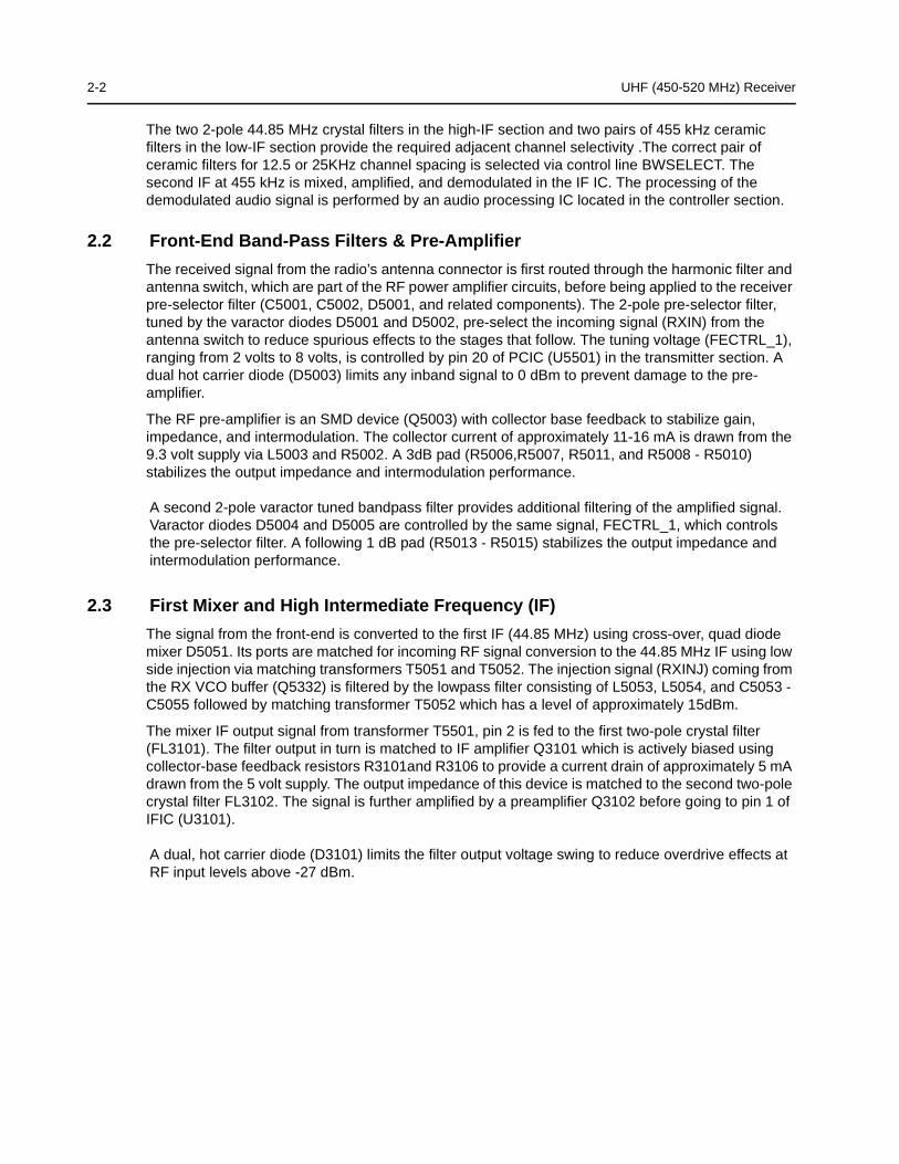
2-2 UHF (450-520 MHz) Receiver
The two 2-pole 44.85 MHz crystal filters in the high-IF section and two pairs of 455 kHz ceramic filters in the low-IF section provide the required adjacent channel selectivity .The correct pair of ceramic filters for 12.5 or 25KHz channel spacing is selected via control line BWSELECT. The second IF at 455 kHz is mixed, amplified, and demodulated in the IF IC. The processing of the demodulated audio signal is performed by an audio processing IC located in the controller section.
2.2 Front-End Band-Pass Filters & Pre-Amplifier
The received signal from the radio’s antenna connector is first routed through the harmonic filter and antenna switch, which are part of the RF power amplifier circuits, before being applied to the receiver pre-selector filter (C5001, C5002, D5001, and related components). The 2-pole pre-selector filter, tuned by the varactor diodes D5001 and D5002, pre-select the incoming signal (RXIN) from the antenna switch to reduce spurious effects to the stages that follow. The tuning voltage (FECTRL_1), ranging from 2 volts to 8 volts, is controlled by pin 20 of PCIC (U5501) in the transmitter section. A dual hot carrier diode (D5003) limits any inband signal to 0 dBm to prevent damage to the pre-amplifier.
The RF pre-amplifier is an SMD device (Q5003) with collector base feedback to stabilize gain, impedance, and intermodulation. The collector current of approximately 11-16 mA is drawn from the 9.3 volt supply via L5003 and R5002. A 3dB pad (R5006,R5007, R5011, and R5008 - R5010) stabilizes the output impedance and intermodulation performance.
A second 2-pole varactor tuned bandpass filter provides additional filtering of the amplified signal. Varactor diodes D5004 and D5005 are controlled by the same signal, FECTRL_1, which controls the pre-selector filter. A following 1 dB pad (R5013 - R5015) stabilizes the output impedance and intermodulation performance.
2.3 First Mixer and High Intermediate Frequency (IF)
The signal from the front-end is converted to the first IF (44.85 MHz) using cross-over, quad diode mixer D5051. Its ports are matched for incoming RF signal conversion to the 44.85 MHz IF using low side injection via matching transformers T5051 and T5052. The injection signal (RXINJ) coming from the RX VCO buffer (Q5332) is filtered by the lowpass filter consisting of L5053, L5054, and C5053 - C5055 followed by matching transformer T5052 which has a level of approximately 15dBm.
The mixer IF output signal from transformer T5501, pin 2 is fed to the first two-pole crystal filter (FL3101). The filter output in turn is matched to IF amplifier Q3101 which is actively biased using collector-base feedback resistors R3101and R3106 to provide a current drain of approximately 5 mA drawn from the 5 volt supply. The output impedance of this device is matched to the second two-pole crystal filter FL3102. The signal is further amplified by a preamplifier Q3102 before going to pin 1 of IFIC (U3101).
A dual, hot carrier diode (D3101) limits the filter output voltage swing to reduce overdrive effects at RF input levels above -27 dBm.

UHF (450-520 MHz) Transmitter Power Amplifier (PA) 40W 2-3
2.4 Low Intermediate Frequency (IF) and Receiver Back End
The 44.85 MHz first IF signal from the second IF amplifier feeds the IF IC (U3101) at pin1. Within the IF IC the 44.85 MHz high IF signal mixes with the 44.395 MHz second local oscillator to produce a low IF signal of 455 kHz. The second LO frequency is determined by crystal Y3101. The second IF signal is amplified and filtered by an external pair of 455 kHz ceramic filters (FL3112 and FL3114) for 20/25 kHz channel spacing, or FL3111 and FL3113/F3115 for 12.5 kHz channel spacing. These pairs are selectable via BWSELECT. The filtered output from the ceramic filters is applied to the limiter input pin of the IF IC (pin 14).
The IF IC contains a quadrature detector using a ceramic phase-shift element (Y3102) to provide audio detection. Internal amplification provides an audio output level of 120 mV rms (at 60% deviation) from U3103, pin 8 (DISCAUDIO) which is fed to ASFIC_CMP U0221, pin 2 (part of the controller circuits).
A received signal strength indicator (RSSI) signal is available at U3101, pin 5, which has a dynamic range of 70 dB. The RSSI signal is interpreted by the µP (U0101, pin 63) and is available at accessory connector J0501-15.
3.0 UHF (450-520 MHz) Transmitter Power Amplifier (PA) 40W
The radio’s 40W PA is a three stage amplifier used to amplify the output from the VCOBIC to the radio transmit level. All three stages utilize LDMOS technology. The gain of the first stage (U5401) is adjustable, controlled by pin 4 of PCIC (U5501). It is followed by an LDMOS stage (Q5421) and LDMOS final stage (Q5441).
Figure 2-2 UHF Transmitter Block Diagram
Devices U5401, Q5421 and Q5441 are surface mounted. A pressure pad between board and the radio’s cover provides good thermal contact between the devices and the chassis.
PCIC
Pin Diode Antenna Switch RF Jack
Antenna
Harmonic Filter
PowerSense
PA-FinalStage
PADriver
From VCO
ControlledStage
Vcontrol
Bias 1
Bias 2
To Microprocessor
TemperatureSense
SPI BUS
ASFIC_CMP
PAPWRSET
To Microprocessor
& Bias 3

2-4 UHF (450-520 MHz) Transmitter Power Amplifier (PA) 40W
3.1 First Power Controlled Stage
The first stage (U5401) is a 20dB gain integrated circuit containing two LDMOS FET amplifier stages. It amplifies the RF signal from the VCO (TXINJ). The output power of stage U5401 is controlled by a DC voltage applied to pin 1 from Q5473. The control voltage simultaneously varies the bias of two FET stages within U5401. This biasing point determines the overall gain of U5401 and therefore its output drive level to Q5421, which in turn controls the output power of the PA.
Switch S5440 is a pressure pad with a conductive strip which connects two conductive areas on the board when the radio's cover is properly screwed to the chassis. When the cover is removed, S5440 opens and cuts the supply voltage to Q5473 thus disabling control voltage to U5401. This prevents transmitter key up while the devices do not have proper thermal contact to the chassis.
3.2 Power Controlled Driver Stage
The next stage is an LDMOS device (Q5421) providing a gain of 12dB. This device requires a positive gate bias and a quiescent current flow for proper operation. The bias is set during transmit mode by U5501-24 and fed to the gate of Q5421 via the resistive network R5480, R5408, R5415 and R5416.
3.3 Final Stage
The final stage is an LDMOS MRF1570 device Q5441. It provides a gain of 11dB. It integrates two MRF1535 die inside. These two die are being run in parallel. The output of each of the device (die) inside are combined to constitute the total output power. This device also requires a positive gate bias and a quiescent current flow for proper operation. The voltage of the line MOSBIAS_2 and MOSBIAS_3 are set in transmit mode by the ASFIC and fed to the gate of Q5441 via two resistive network R5631, R5634, R5485, R5486 and R5632, R5635, R5481, R5489. These bias voltages are tuned in the factory. If the transistor is replaced, the bias voltage must be tuned using the Global Tuner. Care must be taken not to damage the device by exceeding the maximum allowed bias voltage. The device’s drain current is drawn directly from the radio’s DC supply voltage input, PASUPVLTG, via L5421, L5437 and L5436, L5438.A matching network consisting of C5440-45, C5466-67, C5476-77, C5487, C5491, C5455-56, C5449-50, C5465, C5468 and striplines transforms the impedance to 50 ohms and feeds the directional coupler.
3.4 Directional Coupler
The directional coupler is a microstrip printed circuit, which couples a small amount of the forward power delivered by Q5441. The coupled signal is rectified by D5451. The DC voltage is proportional to the RF output power and feeds the RFIN port of the PCIC (U5501 pin 1). The PCIC controls the gain of stage U5401 as necessary to hold this voltage constant, thus ensuring the forward power out of the radio to be held to a constant value.
UHF (450-520 MHz) Transmitter Power Amplifier (PA) 40W 2-5
3.5 Antenna Switch
The antenna switch consists of two PIN diodes, D5471 and D5472. In the receive mode, both diodes are off. Signals applied at the antenna jack J5401 are routed, via the harmonic filter, through network L5472, C5474 and C5475, to the receiver input. In the transmit mode, K9V1 turns on Q5471 which enables current sink Q5472, set to 96 mA by R5512 and VR5471. This completes a DC path from PASUPVLTG, through L5437, D5471, L5472, D5472, L5473, R5496 and the current sink to ground. Both diodes are forward biased into conduction. The transmitter RF from the directional coupler is routed via D5471 to the harmonic filter and antenna jack. D5472 also conducts, shunting RF power and preventing it from reaching the receiver port (RXIN). L5472 is selected to appear as a broadband lambda/4 wave transmission line, making the short circuit presented by D5472 appear as an open circuit at the junction of D5472 and the receiver path.
3.6 Harmonic Filter
Components L5491-L5493 and L5472, C5448, C5494, C5496 and C5498 form a Butterworth low-pass filter to attenuate harmonic energy of the transmitter to specifications level. R5491 is used to drain electrostatic charge that might otherwise build up on the antenna. The harmonic filter also prevents high level RF signals above the receiver passband from reaching the receiver circuits, improving spurious response rejection.
3.7 Power Control
The transmitter uses the power control IC (PCIC, U5501) to control the power output of the radio. A portion of the forward RF power from the transmitter is sampled by the bi-directional coupler and rectified to provide a dc voltage to the RFIN port of the PCIC (pin 1) that is proportional to the sampled RF power.
The ASFIC (U0221) has internal digital to analog converters (DACs) which provide a reference voltage of the control loop to the PCIC via R5483. The reference voltage level is programmable through the SPI line of the PCIC. This reference voltage is proportional to the desired power setting of the transmitter, and is factory programmed at several points across the frequency range of the transmitter to offset frequency response variations of the transmitter’s power detector circuit.
The PCIC provides a DC output voltage at pin 4 (INT) which sets the drain current of the first (U5401). This adjusts the transmitter power output to the intended value. Variations in forward transmitter power cause the DC voltage at pin 1 to change, and the PCIC adjusts the control voltage above or below its nominal value to raise or lower output power.
Capacitors C5502-4, in conjunction with resistors and integrators within the PCIC, control the transmitter power rise (key-up) and power decay (de-key) characteristic to minimize splatter into adjacent channels.
U5502 is a temperature-sensing device, which monitors the circuit board temperature in the vicinity of the transmitter driver and final devices, and provides a DC voltage to the PCIC (TEMP, pin 30) proportional to temperature. If the DC voltage produced exceeds the set threshold in the PCIC, the transmitter output power will be reduced so as to decrease the transmitter temperature.

2-6 UHF (450-520 MHz) Frequency Synthesis
4.0 UHF (450-520 MHz) Frequency Synthesis
The synthesizer subsystem shown in Figure 2-3, consists of the reference oscillator (Y5261 or Y5262), the Low Voltage Fractional-N synthesizer (LVFRAC-N, U5201), and the Voltage Controlled Oscillator (VCO).
4.1 Reference Oscillator
The reference oscillator (Y5262) contains a temperature compensated crystal oscillator with a frequency of 16.8 MHz. An Analog-to-Digital (A/D) converter internal to U5201 (LVFRAC-N) and controlled by the µP via serial interface (SRL) sets the voltage at the warp output of U5201, pin 25 to set the frequency of the oscillator. The output of the oscillator (Y5262, pin 3) is applied to pin 23 (XTAL1) of U5201 via an RC series combination.
In applications where less frequency stability is required, the oscillator inside U5201 is used along with external crystal Y5261, varactor diode D5261, C5261, C5262, and R5262. In this case, Y5262, R5263, C5235 and C5251 are not used. When Y5262 is used, Y5261, D5261, C5261, C5262 and R5262 are not used, and C5263 is increased to 0.1 uF.
4.2 Fractional-N Synthesizer
The LVFRAC-N synthesizer IC (U5201) consists of a pre-scaler, programmable loop divider, control divider logic, phase detector, charge pump, A/D converter for low frequency digital modulation, balanced attenuator used to balance the high frequency analog modulation and low frequency digital modulation, 13V positive voltage multiplier, serial interface for control, and a super filter for the regulated 5 volts.
A voltage of 5V applied to the super filter input (U5201, pin 30) supplies an output voltage of 4.5 Vdc (VSF) at pin 28. It supplies the VCO, VCO modulation bias circuit (via R5322), and synthesizer charge pump resistor network (R5251, R5252). The synthesizer supply voltage is provided by 5V regulator, U5211.
To generate a high voltage to supply the phase detector (charge pump) output stage at pin VCP (U5701-32), a voltage of 13 Vdc is generated by the positive voltage multiplier circuit (D5201, C5202, and C5203). This voltage multiplier is basically a diode capacitor network driven by two signals (1.05MHz) 180 degrees out of phase (U5201, pins 14 and 15).
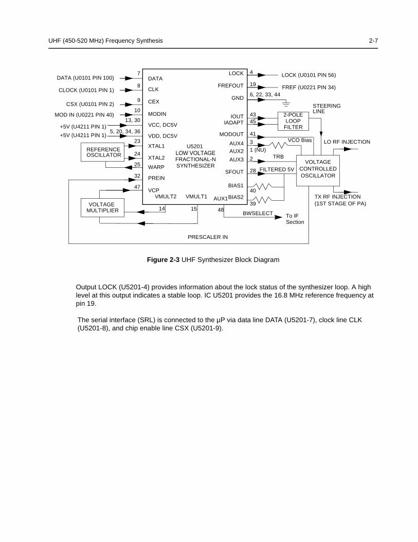
UHF (450-520 MHz) Frequency Synthesis 2-7
Figure 2-3 UHF Synthesizer Block Diagram
Output LOCK (U5201-4) provides information about the lock status of the synthesizer loop. A high level at this output indicates a stable loop. IC U5201 provides the 16.8 MHz reference frequency at pin 19.
The serial interface (SRL) is connected to the µP via data line DATA (U5201-7), clock line CLK (U5201-8), and chip enable line CSX (U5201-9).
DATA
CLK
CEX
MODIN
VCC, DC5V
XTAL1
XTAL2
WARP
PREIN
VCP
REFERENCEOSCILLATOR
VOLTAGEMULTIPLIER
DATA (U0101 PIN 100)
CLOCK (U0101 PIN 1)
CSX (U0101 PIN 2)
MOD IN (U0221 PIN 40)
+5V (U4211 PIN 1)
7
8
9
10
13, 30
23
24
25
32
47
VMULT2 VMULT1
BIAS1
SFOUT
AUX3
AUX4
IADAPTIOUT
GND
FREFOUT
LOCK 4
19
6, 22, 33, 44
4345
3
2
28
14 15
40
FILTERED 5V
STEERING
LOCK (U0101 PIN 56)
PRESCALER IN
FREF (U0221 PIN 34)
39BIAS2
41
48
5, 20, 34, 36+5V (U4211 PIN 1)
AUX1
VDD, DC5V MODOUT
U5201 LOW VOLTAGEFRACTIONAL-NSYNTHESIZER
AUX2 1 (NU)
BWSELECT
VCO Bias
TRB
To IFSection
TX RF INJECTION(1ST STAGE OF PA)
LO RF INJECTION
VOLTAGE CONTROLLED OSCILLATOR
LINE2-POLELOOP
FILTER

2-8 UHF (450-520 MHz) Frequency Synthesis
4.3 Voltage Controlled Oscillator (VCO)
The voltage controlled oscillator (VCO), shown in Figure 2-4, consists of a VCO buffer IC (VCOBIC, U5301), TX and RX tank circuits, external RX buffer stages, and modulation circuits.
The VCOBIC together with Fractional-N synthesizer (U5201) generates the required frequencies in both transmit and receive modes. The TRB line (U5301, pin 19) determines which tank circuits and internal buffers are to be enabled. A high level on TRB enables TX tank and TX output (pin 10), and a low enables RX tank and RX output (pin 8). A sample of the signal from the enabled output is routed from U5301, pin 12 (PRESC_OUT), via a low pass filter of U5201, pin 32 (PREIN).
A steering line voltage (VCTRL) between 3.0V and 10.0V at varactor diode CR5311 tunes the full TX frequency range (TXINJ) from 450 MHz to 520 MHz, and at varactor diodes CR5301, CR5302, and CR5303 tunes the full RX frequency range (RXINJ) from 405 MHz to 475 MHz. The tank circuits uses the Hartley configuration for wider bandwidth. For the RX tank circuit, external transistor Q5301 is used in conjunction with the internal transistor for better side-band noise.
Figure 2-4 UHF VCO Block Diagram
Presc
RX
TX
MatchingNetwork Low Pass
Filter
Attenuator
Pin8
Pin14
Pin10
(U5201 Pin28)
VCC Buffers
TX RF Injection
U5201 Pin 32
AUX3 (U5201 Pin2)
Prescaler Out
Pin 12Pin 19Pin 20
TX/RX/BSSwitching Network
U5301VCOBIC
RxActive Bias
TxActive Bias
Pin2
Rx-I adjust
Pin1
Tx-I adjust
Pins 9,11,17Pin18
VsensCircuit
Pin15
Pin16
RX VCO Circuit
TX VCO Circuit
RX Tank
TX Tank
Pin7
Vcc-Superfilter
Collector/RF in
Pin4
Pin5
Pin6
RX
TX
(U5201 Pin28)
Rx-SW
Tx-SW
Vcc-Logic
(U5201 Pin28)
Steer Line Voltage (VCTRL)
Pin13
Pin3
TRB IN
LO RF INJECTION
Q4301
Q4332

UHF (450-520 MHz) Frequency Synthesis 2-9
The external RX buffers (Q5332) are enabled by a high at U5201, pin 3 (AUX4) via transistor switch Q5333. In TX mode, the modulation signal (VCOMOD) from the LVFRAC-N synthesizer IC (U5201, pin 41) is applied to the modulation circuits CR5321, R5321, R5322, and C5324. These modulate the TX VCO frequency via coupling capacitor C5321. Varactor CR5321 is biased for linearity from the VSF.
4.4 Synthesizer Operation
The synthesizer consists of a low voltage FRAC-N (LVFRACN) IC, reference oscillator (crystal oscillator with temperature compensation), charge pump circuits, loop filter circuits, and dc supply. The output signal (PRESC_OUT) of the VCOBIC (U5301, pin12) is fed to of U5201, pin 32 (PREIN) via a low pass filter (C5229,L5225,and C5226) which attenuates harmonics and provides correct level to close the synthesizer loop.
The pre-scaler in the synthesizer (U5201) is a dual modulus pre-scaler with selectable divider ratios. The divider ratio of the pre-scaler is controlled by the loop divider, which in turn receives its inputs via the SRL. The output of the pre-scaler is applied to the loop divider. The output of the loop divider is connected to the phase detector, which compares the loop divider´s output signal with the reference signal.The reference signal is generated by dividing down the signal of the reference oscillator (Y5261 or Y5262).
The output signal of the phase detector is a pulsed dc signal routed to the charge pump. The charge pump outputs a current at U5201, pin 43 (IOUT). The loop filter (consisting of R5221-R5223, C5221-C5225, and L5221) transforms this current into a voltage that is applied to varactor diodes CR5311 for transmit, CR5301, CR5302 and CR5303 for receive and alters the output frequency of the VCO.The current can be set to a value fixed in the LVFRAC-N IC or to a value determined by the currents flowing into BIAS 1 (U5201-40) or BIAS 2 (U5201-39). The currents are set by the value of R5251 or R5252 respectively. The selection of the three different bias sources is done by software programming.
To reduce synthesizer lock time, when new frequency data has been loaded into the synthesizer, the magnitude of the loop current is increased by enabling the IADAPT (U5201-45) for a certain software programmable time (Adapt Mode). The adapt mode timer is started by a low to high transistion of the CSX line. When the synthesizer is within the lock range, the current is determined only by the resistors connected to BIAS 1, BIAS 2, or the internal current source. A settled synthesizer loop is indicated by a high level of signal LOCK (U5201-4) which is routed to one of the µP´s ADCs input U101-56. From the voltage the µP determines whether LOCK is active.
To modulate the PLL, the two-spot modulation method is utilized via pin 10 (MODIN) on U5201. The audio signal is applied to both the A/D converter (low frequency path) and the balanced attenuator (high frequency path). The A/D converter converts the low frequency analog modulating signal into a digital code which is applied to the loop divider, thereby causing the carrier to deviate. The balance attenuator is used to adjust the VCO’s deviation sensitivity to high frequency modulating signals. The output of the balance attenuator is present at the MODOUT port (U5201-41) and connected to the VCO modulation diode CR5321 via R5321 and C5325.

2-10 UHF (450-520 MHz) Frequency Synthesis
THIS PAGE INTENTIONALLY LEFT BLANK
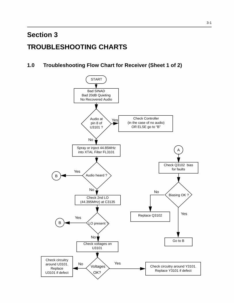
3-1
Section 3
TROUBLESHOOTING CHARTS
1.0 Troubleshooting Flow Chart for Receiver (Sheet 1 of 2)
Bad SINADBad 20dB Quieting
No Recovered Audio
START
Audio at pin 8 of U3101 ?
Check Controller(in the case of no audio)
OR ELSE go to “B”
Yes
No
Spray or inject 44.85MHz into XTAL Filter FL3101
Audio heard ?BYes
No
Check 2nd LO (44.395MHz) at C3135
LO present ?BYes
Check voltages on U3101
Biasing OK ?
No
No
A
Yes
Check Q3102 bias for faults
Replace Q3102
Go to B
Yes
No
Check circuitry around U3101.
Replace U3101 if defect
Check circuitry around Y3101. Replace Y3101 if defect
Voltages
OK?

3-2 Troubleshooting Flow Chart for Receiver
1.1 Troubleshooting Flow Chart for Receiver (Sheet 2 of 2)
IF Signal at C3101?
No
RF Signal at T5051?
RFSignal at C5015?
No
No
RFSignal at C5025?
No or
Check harmonic filterL5491-L5493, C5492, J5401
and ant. switchD5471, D5472, L5472.
Check filter between C5025 & C5009.
Check tuning voltage at R5060.
Inject RF into J5401
Istuning voltage
OK?
No
Yes
Check RF amp (Q5003) Stage.
Check filter between C5015 & T5051.
Yes
Check T5051, T5052, D5051, R5052, L5008.
Yes
1st LO level OK?
Locked?
Yes
Check FGU
Yes
Trace IF signal from C3101 to
Q3101. Check for bad XTAL filter.
No
Yes IFsignal at Q3102
collector?
Before replacing U3101, check
U3101 voltages.
Yes
Check for 5VDC
Is 9V3 present?
Check Supply Voltage circuitry. Check Q0681,
U5211 and U0641.
No
No
No
Check U5501.
Check varactor filter.
No
Yes
Yes
Yes
A
A
B
weak RF
RFSignal at C5009?
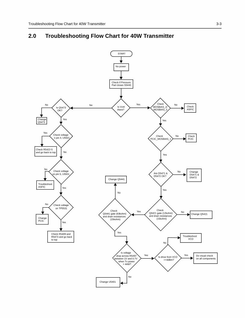
Troubleshooting Flow Chart for 40W Transmitter 3-3
2.0 Troubleshooting Flow Chart for 40W Transmitter
Q5441 gate (63kohm)and drain resistances (15kohm)
Check
No
YesIs drive from VCO >+4dBm?
Is voltagedrop across R5497
between 1V and 0.7Vwhen Tx power
= 44W?
No
NoQ5421 gate (12kohm)and drain resistances (15kohm)
Check
No
PCIC_MOSBIAS_1 Check
No
No
ChangeQ5473
START
No power
Is Vctrl
there? Is Q5473 OK?
Check voltagen pin 4, U5501
Check voltageon pin 5, U5501
Check R5422-5and go back to top
TroubleshootASFIC
ChangePCIC
Check R5409 and
R5473 and go backto top
Check
MOSBIAS_2/MOSBIAS_3
CheckASFIC
Are D5471 &D5472 OK?
ChangeD5471 &D5472
NoNo No
Yes
Yes
YesYes
Yes
Yes Yes
Yes
No
No CheckPCIC
Yes
Change Q5421
Change Q5441
Change U5401
Yes Do visual checkon all components
No
Troubleshoot VCO
Check voltageon TP5531
Check if Pressure Pad closes S5440
Yes
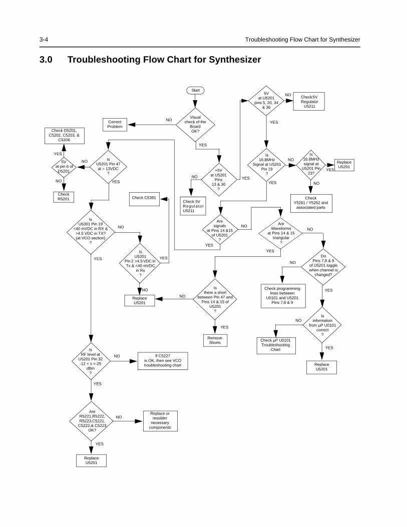
3-4 Troubleshooting Flow Chart for Synthesizer
3.0 Troubleshooting Flow Chart for Synthesizer
5V at pin 6 of
D5201
Isinformation
from µP U0101correct
?
IsU5201 Pin 47at = 13VDC
?
IsU5301 Pin 19
<40 mVDC in RX &>4.5 VDC in TX? (at VCO section)
?
Start
Visual check of the
BoardOK?
CorrectProblem
Check 5VRegulatorU5211
+5Vat U5201
Pins13 & 30
?
Is16.8MHz
Signal at U5201 Pin 19
?
CheckY5261 / Y5262 and
associated parts
Aresignals
at Pins 14 &15 of U5201
?
Check R5201 Check C5381
IsU5201
Pin 2 >4.5 VDC in Tx & <40 mVDC
in Rx?
Replace U5201
RemoveShorts
Isthere a short
between Pin 47 andPins 14 & 15 of
U5201?
Replace orresolder
necessarycomponents
IsRF level at
U5201 Pin 32 -12 < x <-25
dBm?
AreR5221,R5222,R5223,C5221,
C5222,& C5223 OK?
Replace U5201
If C5227is OK, then see VCOtroubleshooting chart
AreWaveforms
at Pins 14 & 15triangular
?
DoPins 7,8 & 9
of U5201 togglewhen channel is
changed?
Check programminglines between
U0101 and U5201Pins 7,8 & 9
Replace U5201
Check µP U0101Troubleshooting
Chart
NO
YES
NO
YES
NO
YES
NO
NO
NO
YES
YES
NO
YES
YES
NO
YES
YESYESNO
NO
NO
NO
YES
NO
YES
YES
Check D5201, C5202, C5203, &
C5206
5V at U5201
pins 5, 20, 34 & 36
Check 5V Regulator
U5211
Is 16.8MHz signal at
U5201 Pin 23?
Replace U5201
YES
NO
NO
YES
NO
YES

Troubleshooting Flow Chart for VCO 3-5
4.0 Troubleshooting Flow Chart for VCO
Are Q5332Base at 0.7V
Collector at 4.5V Emitter at 110mV
Are Q5301Base at 2.4V
Collector at 4.5V Emitter at 1.7V
Are Q5311 Base = 1.9V
Collector = 4.5VEmitter = 1.3V
Low or no RF Signalat TP5003
Visual checkof board
OK?
35mV DC atU5301 Pin 19
NO
YES
Replace Q5301
at base of Q5332
NO
NO
NO
NO
YES
YES
YES
YES
Low or no RF Signalat input to PA
4.8V DC atU5301 Pin 19
Is RF available at U5401
YES
YES
YES
YES
NO
NO
NO
NO
NO
Audio =180mVrmsat “-” Side of
4.5VDCat CR5321
If C5321 and R5321 are OK, then replace CR5321
Replace C5322
Replace C5325
NO
NO
YES
YES
TX VCORX VCO
CorrectProblem
Visual checkof board
OK?
Check runner between U5201 Pin 2
and U5301 Pin 19
Is RF available If all parts from U5301 Pin 8to Base of Q5332 are OK,
replace U5301
If all parts associated with the pins are OK,
replace Q5332
If all parts from collectorof Q5332 to TP5003 are
OK, Replace U5301
Power OK but no modulation
If all parts from U5301 Pin 10U5401 Pin 16 are OK,
replace U5301
Replace Q5311
YES YES
Make sure Synthesizer is working correctly and runner between U5201 Pin 28 and U5301 Pin 14 & 18 are OK
4.5V DC
OK ?
OK? OK?
C5325
at U5301 Pin 14 & 18 4.5V DC
OK ?at U5301 Pin 14 &18
NO
Pin 16
If R5361 and L5361 are OK, replace U5301

3-6 Troubleshooting Flow Chart for VCO
THIS PAGE INTENTIONALLY LEFT BLANK
4-1
Section 4
UHF PCB/SCHEMATICS/PARTS LISTS
1.0 Allocation of Schematics and Circuit Boards
1.1 Controller Circuits
The UHF circuits are contained on the Printed Circuit Board (PCB) which also contains the Controller circuits. This Chapter shows the schematics for the UHF circuits only, refer to the Controller section for details of the related Controller circuits . The PCB component layouts and the Parts Lists in this Chapter show both the Controller and UHF circuit components. The UHF schematics and the related PCB and parts list are shown in the tables below.
Table 4-1 UHF B2 40W Diagrams and Parts Lists
PCB :8486250Z02 Main Board Top Side8486250Z02 Main Board Bottom Side
Page 4-3Page 4-4
SCHEMATICSPower Amplifier 40WFRACNVoltage Controlled OscillatorReceiver Front EndIF
Page 4-5Page 4-6Page 4-7Page 4-8Page 4-9
Parts List8486250Z02 Page 4-10

4-2 Allocation of Schematics and Circuit Boards
THIS PAGE INTENTIONALLY LEFT BLANK
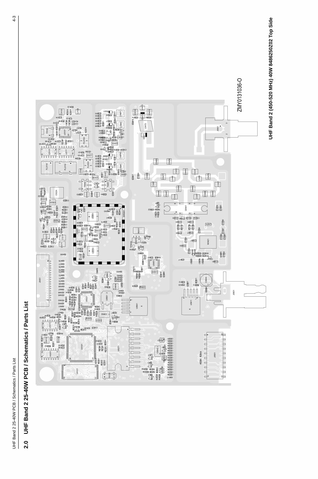
UH
F B
and
2 25
-40W
PC
B /
Sch
emat
ics
/ Par
ts L
ist
4-3
2.0
UH
F B
and
2 2
5-40
W P
CB
/ S
chem
atic
s / P
arts
Lis
t
ZMY0131036-O
321716
1
U01
21
1 765126
U01
01
161 8
9
U02
51
C0108
C0211
C02
12
C02
51
C02
52
R0103
R0211
R02
12R
0251
R0252
R0253
R02
57
87
114
U02
11
C0256R0256
R0268
181
J045
1
Q01
10
C02
53
C0261
C02
62
C0421
R01
02R
0110
R01
15R
0227
R02
61
R0262
R0269
C0441
C0442
C0443
C0445C0446
C0447
C0448
R0442
R02
22
C01
31
C01
32
R01
31
R01
32
234
Y01
31
C0101
C0102
R01
05R
0106
R01
14R
0170
R0101
C0104C0106
C0107R0104
R0108
R01
16
C02
23C0224
C02
26C
0227
C0231
C02
32
C02
33
C0234C0235
C02
36
C0237
C0495
R02
25
R0228
R02
26
C0228
137 25
13
U02
21
3
2
1
U06
51
C02
41 C02
42
C02
43 C02
44C
0245
C02
46R
0241
R02
42
R0254R0255
C0221
C0222
C02
25R
0220
R02
21 R0223
R0224
R02
29
C04
96
C06
81D02
01 Q06
81
R06
81
R0682
9
U02
71
C0651C0652
D0651
R06
51 R0652
1
6
5
U06
41
C0482C0483
C0486C0487
C0488
C0493
C0494
C06
54
C0655
L048
1
L048
2C0449C0470
C0471
C0472
C0473C0474
C0476
C0477
C0478
C0490
C0502C0503C0504C0505C0506C0508
C0509
C0510C0512
C05
42
Q01
77Q
0181
Q01
85
R0181R0182
R0185R0186
R0510
R05
35R
0538
R05
39
VR0501
VR
0503
VR
0505
VR
0510
C0501
C0511
C0513C0514
C0515C0516
C0517C0518
201110
J050
1
R05
08R
0509
C04
84
C06
01 C06
03
C0612
R0533 R06
11R0612
1
6
5
U06
11
J060
1
C5417
C54
19
C5420
C5425C5426
C5427
C54
28
C54
29
C5430
C54
31
C5432C5433
C5434
C5435
C5446
C5447
C5453
C54
54
C5457
C54
58
C54
61
C54
62 C5481
C54
85C
5489
C54
90C
5495
C54
97C
5602
L5474
M34
21
R54
08
R5415R5416
R54
17
R54
18
R54
80321 4
5678
Q54
41
C54
78
C54
93
C54
01
C5403
C54
04
C5407
C54
10
C54
18
C54
88
C5505C5506
L540
1
L5403
Q5471
Q54
72R
5401
R5402
R54
03
R5405
R5504
R55
11
R5512
TP
5530
116
89U
5401
VR5471
32
J540
1
C54
40
C54
41
C54
42
C54
43
C54
44
C54
45
C54
49
C54
50
C54
55
C54
56
C54
59
C54
65
C54
66
C54
67
C54
68
C54
76
C54
77
C54
87
C54
91
C55
07
C55
21
C5522
L548
9
L549
0
R5501
R55
02U
5502
C54
72
C5474
C54
75
C5480
C55
10
D54
71D
5472
L547
2
L547
3
L500
1L5
002
C52
10 C52
13
C52
14C
5215
C5216
C5217
C5221
C5222
C5223
C52
24
C5225
C5226
C52
27 C52
29
C5230
C52
31
C5232
C5233
C5234C5236
C52
42
C52
43C
5244
C52
45
C52
46
C5251
C5252
C5253C5254
C5255
C5289
D5221
L5201
L5221
Q5221
R52
11
R52
21
R5222 R52
23R
5224
R5225
R52
27
R5251R5252
U52
11
C31
24
C31
33
L312
4
R3123
R31
24
2Y
3102
23 4
56
FL3
102
23 4
56
FL3
101
346 1
2T
5052
21 5
43T
5051
C5308C5309
C5317C5318
C5322
C53
23
C53
25
C53
53
C53
55C
5375
L530
3
L5305
L531
2
L531
3
Q53
01
Q5311
43
Q53
33
R5305
R5311
R53
12
R5321
R53
46
3
C5331
C53
32
C53
35
C53
37
C5339
C5351
C5352
C5371C5372
C5373
C5374
C5382
C5383
3
L5304
L5371R5301
R53
02
R5331 R53
32R
5333
R53
37
R5341
R5343
R53
45
SH
5301
C50
31
C5053
C50
54 C5055
D50
51L5
053
L505
4
L505
1
R50
51
L5008
C3101 R3148L310
0
C50
52
R5015
C5014
C5015 C5016
C50
17C
5018
C5019C5020C5021C5022C5023
C5029
C5030
C50
32
C5034
C5065
C5068
D5004
D5005
D5006
L5003
L500
4L5
005
L5006
L5009
Q5001 R5005
R5007
R50
12
R5013
R5020
R5064
R5066
C50
01C
5002
C5003C5004C5005C5006C5007C5008
C5009
C5026
C5027
C5033
D5001
D5002
D50
03
Q5003
R50
01
R5003
R50
04
R5021
R50
22
C3102
C3103 L3101
R3101
R3106
C31
14
C3115
C3131
C3132
C3134
C31
35
C31
36 C3137
C31
43
R3111R3117
R3130 R3132
R31
35
11
120
10
U31
01
C3139
C31
40
C31
41 C3142
C3145C3148
432
FL3
112
FL3
114
R3142
R3144R3145
87
114U
3111
87
114U
3115
UH
F B
and
2 (
450-
520
MH
z) 4
0W 8
4862
50Z
02 T
op
Sid
e

4-4
UH
F B
and
2 25
-40W
PC
B /
Sch
emat
ics
/ Par
ts L
ist
ZMY0131037-O
C31
44
C3146
C3147
C3151C3152
43
FL3
111
FL3113
43 2F
L311
5
Q3141
Q31
51
Q31
52
R31
33
R31
34R31
41
R3146
R31
47
R3151
R31
52
R31
53
R3154
C3104C3110
C3111
C3112 C3113
C31
16
C31
21
C31
22C
3123
D31
01
2
L3111
L311
2
Q31
01Q
3102
R3102
R3104R3105
R31
07R
3108
R3112
R31
13
R31
14
R31
15R
3116
R31
18
432
Y31
01
C5024C5060
C50
66
R5019
R50
52R
5053
R5054
R5055
R50
60
TP
5003
C50
10C
5011
C5012C5013
C5028
C5061
C5062
C50
64
C50
67C5069
D50
07
Q50
02
Q50
04
R5002R
5016
R50
17
R50
18
R50
61
R5062
R50
63
R50
68
R50
69
R5070
R50
71
R50
72
C5025
C54
48
C54
51
C54
63
C54
69
C5470
C5473
C54
92
C54
94
C54
96
C54
98
C54
99D
5452
L549
1
L549
2
L549
3
R54
55R
5457
R5472R5475
R54
91
R5496
TP5531
VR5473
C54
22
C54
39
L542
1
L543
7
L543
8
C5452
C54
64
D5451
D5453
R5409
R54
71
R5473
R54
74R
5506
R55
07
TP
5532
C54
21
C54
24
C5436
C5438
C5483
C54
84
C5629
C5630C5631
C5632
L540
2L5
436
L5541
L554
3
1
2
3Q5421
Q54
51
R54
14
R54
40
R5481
R5485
R5486
R5487R5488
R5489
R55
13
R55
25
R5630
R56
31
R56
32
R56
34
R56
35
S54
40
TP5537
TP5538
TP5536
C0499
C06
11
E06
31
VR
0601
C0105C0121
C0255 R0468 R05
43R
0593
145
8U
0652
C0122C0123
22 2187
1
U01
22
12
J040
1
R0412R0441
C0205
C02
67
R0208
R0265
R02
67
R0266 C02
01
C02
02
C02
03C
0204
C02
54C
0265
C0266
R01
07
R0201
R02
02R02
03R
0204 R
0205
R02
06
R02
07
R04
08R
0555
TP
0102
TP
0221
TP
0222
U0653
VR
0541
118
J055
2
C0103 R0112
R0113
R01
21T
P01
03T
P04
92
C01
11
C0112
D0101
R01
11
R0117
R04
01 TP
0101
TP
0104
14 5
8U
0111
C0342R0342 U
0342
R0343R0347
C0422
C0423
C0426
C0427C0428C0429
C0430C0431
F0401
R0407
R0409
R0467
C0304
C0305
C0324C0325
C0341
C03
43
C0344
R03
23
R0324
R0341
R03
44R
0345
R0346
TP0497
2815
1
458
U03
41
C0141
1618 9
U01
41
C04
91
C04
92
C04
97 C0485
R5495
R5497
C5402C5405
C54
09C
5412
C54
13C
5414
C54
15C
5416
C5479
C5502
C5503
C5504
L5404
L541
1
Q5473
R5412
R5422
R5423
R5424
R5425
R5428
R54
31
R54
82
R54
83
R5484
R5492
R5503
R5514
R5523
TP
5533
1
17 9
25
U55
01
C0301
C03
02
C03
03
C0331
C03
51
C03
52
C0353
C03
54
C06
41
C0644
C06
45
C06
62
C0663
C06
71
D0301
Q06
41
Q0661 Q06
62Q
0663
R0331
R0332R0333
R0335
R0481
R04
82R
0641R
0642
R0643 R0662
R0671R0672
141
U03
01
U03
31
458 U
0351
C0275
C06
21
C0622
C06
61
D0621
D0660D0661
Q01
73
R0173
R01
74
R0621
R06
61T
P06
61
VR0621
VR
0671
Q01
71
C05
41
D01
79
Q01
83
R0171
R0172
R0175R0176
R0177R0178
R0179
R0183R0184
R0511
R0512
R05
25
R0529
R05
30
R05
31
R0537
R05
41
R05
42
TP
0530
VR
0504
VR
0509
VR0537C01
51
C02
71
C0272
C02
73C0274
C02
76C
0277
C05
54
C05
58
C0559C0560
C0575C0576
C05
91
C05
92C
0593
D01
51
E0271
E0272
140
J055
1
Q0151
Q0271
R0151
R0152
R02
73R
0274
R02
75
R02
76
R05
56
R0591
R05
92
TP
0151
VR0151
C5201
C52
02C
5203
C52
04
C5205
C5206
C5207
C5208C5209 C5211
C52
28C
5235
C5241
C5261C5262
C5263
C5287
C52
88D
5201
D5261
L5231
R5201
R52
03R
5204
R5206
R5228
R5241
R52
61
R5262
R52
63
TP
5201
TP5202
13725
13
U52
01
64
1
3 Y52
612 3
4
Y52
62
C5301
C53
02C
5303
C53
04
C5305 C5306
C5307
C53
11
C53
12
C53
13
C53
14C
5315
C53
16
C5321
C5324
C53
33
C5334
C53
36
C53
38
C53
54
C53
61C
5362
C53
63C
5364
C5365
C5381
CR
5301
CR
5302
CR
5303
CR5311
CR5321
L530
1 L5302
L5311
L533
1
L5332
L533
3
L536
1
L5362
Q53
31
Q5332
R53
03
R5304
R53
13R
5314
R5315
R5322
R5323
R53
34
R5335
R5336R5338
R53
39
R5340
R5342 R5344
R53
47
R53
60
R5361
R53
62
R53
63
R5381
SH5302
11
120
10
U53
01
UH
F B
and
2 (
450-
520
MH
z) 4
0W 8
4862
50Z
02 B
ott
om
Sid
e
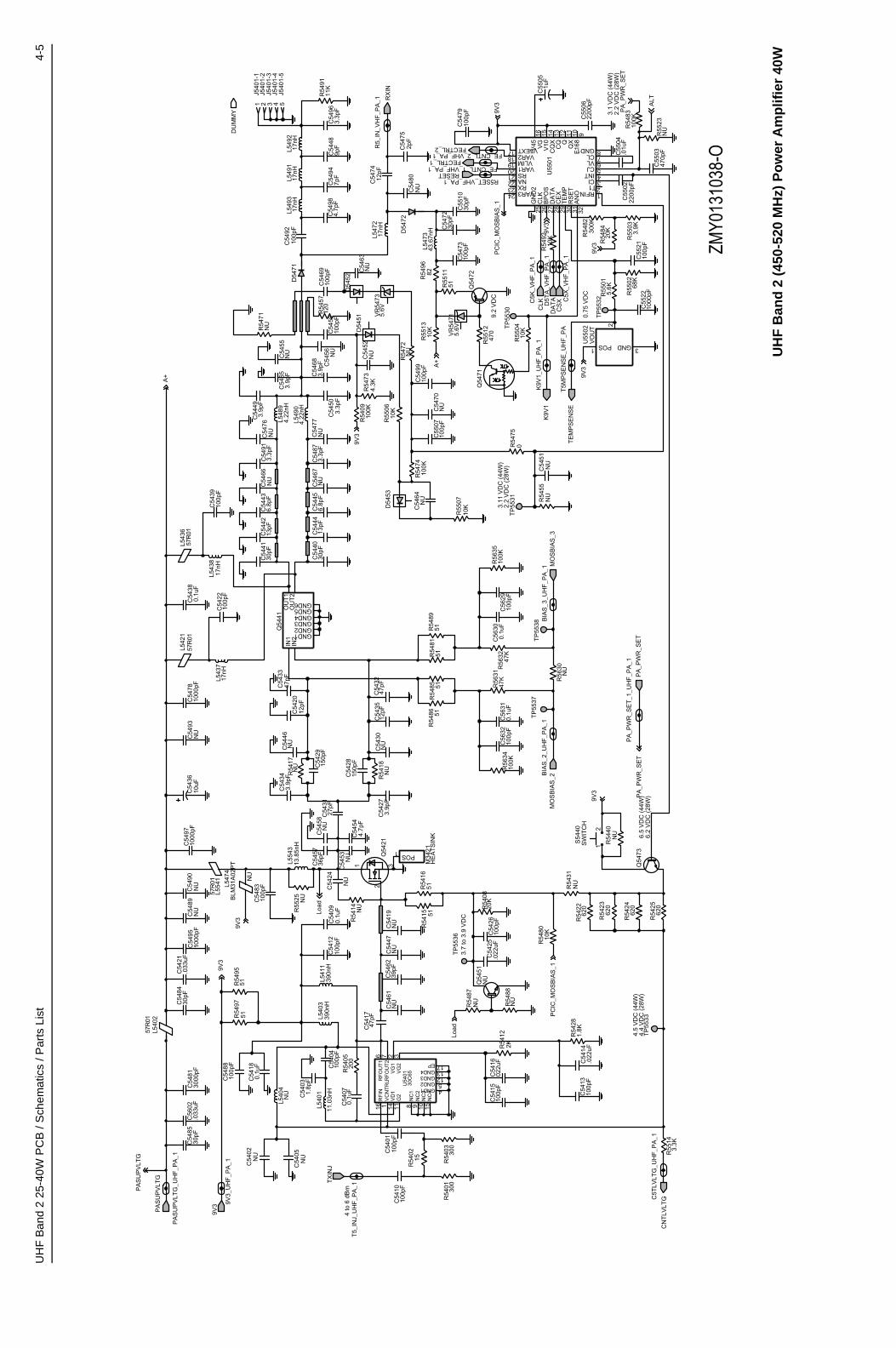
UH
F B
and
2 25
-40W
PC
B /
Sch
emat
ics
/ Par
ts L
ist
4-5
ZMY0131038-O
PA
SU
PV
LTG
9V3
C54
8130
00pF
C56
02.0
33uF
PA
SU
PV
LTG
_UH
F_P
A_1
C54
8530
pF
PA
SU
PV
LTG
9V3_
UH
F_P
A_1
L540
257
R01
C54
21.0
33uF
30pF
C54
84
NU
NU
C54
9510
00pF
C54
9710
00pF
C54
90
L554
157
R01
C54
89C
5436
10uF
NU
L547
4B
LM31
A02
PT
100p
FC
5483
9V3
51R54
959V3
51R54
97
390n
HL5
403
390n
HL5
411
C54
1210
0pF
NU
NU
R54
14R55
25
C54
090.
1uFLo
adC
5457
36pF
C54
24
L554
313
.85n
H
NU
NU
1C54
53
NU
C54
58C
5431
27pF
C54
544.
7pF
NU
NU
C54
46R
5417
3.9p
FC
5434
150p
FC
5429
150p
FC
5428
C54
3347
pFC
5420
12pF
IN2
OU
T1
OU
T2
GND1GND2GND3GND4GND5GND6
IN1
Q54
41
NU
NU
R54
18C
5430
3.9p
FC
5427
C54
3247
pFC
5435
12pF
51R54
89R
5481
5151
R54
86R
5485 51
NU
NU
NU
C54
47C
5419
C54
6139
pFC
5462
R54
15 51
3 HE
AT
SIN
KM
34211 POSQ54
212 R54
1651
C54
1747
pF
Load
NU
R54
87
2KR54
12
NU
NU
3.7
to 3
.9 V
DC
R54
88
TP
5536
20K
R54
08C
5426
100p
F.0
22uF
C54
25
Q54
51
100p
FC
5415
C54
16.0
22uF
R54
01 300
C54
1010
0pF
R54
03
R54
02 300
15
100p
FC
5401
7R
FO
UT
21
VC
NT
RL
14V
D1
2V
G1
3V
G2
12GND313GND4
8N
C1
9N
C2
10N
C3
15N
C4
16R
FIN
6R
FO
UT
1
U54
01
17EP
11G
2
4GND15GND2
30C
65
4 to
6 d
Bm
TX
INJ
T5_
INJ_
UH
F_P
A_1
NU
C54
0410
0pF
200
R54
05
L540
4
C54
070.
1uF
C54
031.
8pF
L540
1
11.0
3nH
NU
NU
C54
05
C54
02
100p
FC
5488
0.1u
FC
5418
CN
TLV
LTG
3.3K
R55
14
C5T
LVLT
G_U
HF
_PA
_1
R54
281.
8K
100p
FC
5413
.022
uFC
5414
4.5
VD
C (
44W
)4.
4 V
DC
(28
W)
TP
5533
PC
IC_M
OS
BIA
S_1
R54
8010
K
R54
2462
0
R54
2262
0
620
R54
25
620
R54
23
NU
R54
31
6.2
VD
C (
28W
)6.
5 V
DC
(44
W)
Q54
73
2
NU
R54
40
SW
ITC
HS
5440
19V
3
PA
_PW
R_S
ET
_1_U
HF
_PA
_1
PA
_PW
R_S
ET
PA
_PW
R_S
ET
NU
MO
SB
IAS
_2R
5630
TP
5537
BIA
S_2
_UH
F_P
A_1
R56
3410
0K
47K
R56
3110
0KR
5635
100p
FC
5632
R56
3247
K
C56
300.
1uF
100p
FC
5629
C56
310.
1uF
MO
SB
IAS
_3B
IAS
_3_U
HF
_PA
_1T
P55
38
NU
C54
93C
5478
1000
pF
17nH
L543
7
57R
01L5
421
C54
2210
0pF
L543
657
R01
C54
380.
1uF
100p
FC
5439
17nH
L543
8
NU
NU
C54
76
C54
493.
9pF
3.3p
FC
5491
C54
6613
pFC
5442
30pF
C54
41C
5443
6.8p
F
L548
94.
22nH
4.22
nHL5
490
NU
NU
C54
873.
3pF
C54
4413
pFC
5477
C54
4030
pFC
5445
6.8p
FC
5467
3.3p
FC
5450
R54
0910
0K
9V3
D54
53R
5506
10K
NU
C54
64R
5474
100K
NU
C54
70
100p
F
C55
0710
0pF
C54
99
NU
4.3K
R54
73C
5452
D54
51
NU
100p
FC
5459
120
R54
57C
5468
3.9p
F C54
56 NU
R54
72
A+
NU
3.9p
FC
5465
C54
55
NU
R54
71
D54
71
C54
6910
0pF
D54
52
VR
5473
5.6V
NU
C54
63
C54
9210
0pF
R55
1310
K
L549
317
nH17
nHL5
491
17nH
L549
2
DU
MM
Y
2J5
401-
2J5
401-
33 5
J540
1-4
4J5
401-
5
1J5
401-
1
C54
984.
7pF
3.3p
FC
5496
C54
489p
FC
5494
7pF
11K
R54
91
R5_
IN_V
HF
_PA
_1L5
472
17nH
C54
7412
pFR
XIN
100p
FC
5479 9V
3
2pF
C54
75
NU
C54
80D
5472
C55
1030
pF
C54
7230
pF
Q54
72
R55
1151
L547
343
.67n
H
C54
7310
0pF
R54
9682
5.6V
VR
5471
Q54
71
470
R55
129.
2 V
DC
PC
IC_M
OS
BIA
S_1
T5M
PS
EN
SE
_UH
F_P
A
K9V
1_U
HF
_PA
_1
TE
MP
SE
NS
E
K9V
1
9V3
TP
5530
10K
R55
04
CLK
CS
XD
AT
A
0.75
VD
C R55
0268
K
TP
5532
U55
02
GND 3POS1
2
VO
UT
C55
2210
00pFR
5501
5.
6K
R54
8230
0K
R54
8420
K
9V3
3.9K
R55
03
100p
FC
5521
31302825 3227 292610
KR
5492
D5T
A_V
HF
_PA
_1
C5K
_VH
F_P
A_1
C5X
_VH
F_P
A_1
9V3
16V
45 V5EXT17
VAR120
VAR218
VAR324
VG
15
6VL19 VLIM
10Q
X
RFIN 1
21 RS
RS
ET23 RX 2T1
TE
MP
14V
10C
QX
13D
AT
A
9F
168
8GND1
GN
D2
4INTNA22
11Q
AN
O
BP
OS
CE
X
3CI
5CJ
7CL
CLK
12C
QU
5501
C55
0222
00pF
C55
04.0
1uF
C55
051u
F
2200
pFC
5506
2.2
VD
C (
28W
)3.
1 V
DC
(44
W)
100K
R54
83P
A_P
WR
_SE
T
NU
R55
2347
0pF
C55
03A
LT
R55
0710
K 2.2
VD
C (
28W
)3.
11 V
DC
(44
W)
TP
5531
0R54
75
NU
NU
R54
55C
5451
FECTRL_2FE_CNTL_2_VHF_PA_1
RESET
FECTRL_1FE_CNTL_1_VHF_PA_1
R5SET_VHF_PA_1
A+
UH
F B
and
2 (
450-
520
MH
z) P
ow
er A
mp
lifie
r 40
W
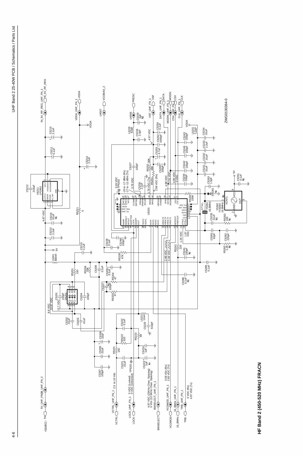
4-6
UH
F B
and
2 25
-40W
PC
B /
Sch
emat
ics
/ Par
ts L
ist
16_8
MH
z
C52
02.0
1uF
IN_5
V_R
F_R
EG
_UH
F_F
N_1
TR
B
MO
DIN
220
R52
41
C52
510.
1uF
TP
5202
1
.01u
FC
5232
LOC
K_U
HF
_FN
_1
C
5243
100p
F
R52
2251
0
C52
534.
7uF
o
2.2u
FC
5213
C52
09
0.1u
F
U45
06
.01u
FC
5231
CLK
_UH
F_F
N_1
L522
112
uH
47K
R52
28
1000
pFC
5252
150
R52
21
R52
6115
0K
100
R52
63
VD
DA
CLK
16.8
MH
z
XT
AL
Y52
61
1uF
C52
23
VC
NT
L
1
VS
F_U
HF
_FN
_1
Y52
62T
TS
05V
16.8
MH
z
GN
D2
OU
T 3
VC
C4
M
OD
IN_U
HF
_FN
_1
2.2u
F
C52
14
0.1u
FC
5254
D 5
261
5V_U
HF
_FN
_1
150
R52
01
C52
88
0.1u
F
DA
TA
100p
F
C52
27
VD
DA
_UH
F_F
N_1
C52
4610
0pF
C52
05.0
1uF
1.5p
F
C52
63
68
R52
23
C52
35.0
1uF
C52
5510
0pF
C52
22
0.1u
F
1.2K
R52
62
C52
4510
0pF
C52
44
47nH
L522
5
100p
F
T
RB
_UH
F_F
N_1
U
4507
16_8
MH
z_U
HF
_FN
_1C
SX
_UH
F_F
N_1
C52
04
0
R52
11
100p
F
B
WS
ELE
CT
_UH
F_F
N_1
C52
07
100p
FC
5228
0.1u
F
5V
_UH
F_F
N_2
VS
F
C52
110.
1uF
2.4p
F
C52
26
C52
0610
uF
2.2u
FC
5210
220p
FC
5262
47
R52
03
LOC
K
C52
08
0.1u
F
1uF
C52
24
510p
F
C52
25
R52
04
R52
06
47
33K
C52
16.0
1uF
LP29
51U
5211
VC
OB
IAS
_2
C52
12
.018
uF
100p
FC
5287
100p
F
C52
01
2p
FC
5229
C52
30
2.2u
F
2.2u
FC
5233
0.1u
F
C52
89
39K
R52
51
VC
TR
L
T
P52
01
C52
42
PR
ES
C
CS
X
100p
F
L523
1
VC
OM
OD
_UH
F_F
N_1
IN_5
V_R
F_R
EG
2.2u
H
C52
4110
0pF
5A
24
A3
K1
1K
22
K3
3
DA
TA
_UH
F_F
N_1
6A
1
D52
01
C52
21.0
1uF
.01u
F
C52
03
R52
52
30K
VC
TR
L_U
HF
_FN
_1
.01u
FC
5234
L520
139
0nH
62pF
C52
61
5V
5V
2.2u
FC
5215 V
DD
A
VD
DA
U52
014.
57 V
DC
-19
to -
17 d
Bm
(R
x)-1
7 to
-12
dB
m (
Tx)
4.98
VD
C
0 V
DC
(R
x)
3.09
VD
c (R
x)2.
65 V
DC
(T
x)
4.97
VD
C (
25K
Hz
Cha
n. S
paci
ng)
4.97
VD
C (
Tx)
2.48
VD
C
1.76
VD
C (
Tx)
1.69
VD
C (
Rx)
0 V
Dc
(12.
5KH
z C
han.
Spa
cing
)
5 V
DC
(Lo
cked
)0
VD
C (
Unl
ocke
d)
2.5
to 1
0 V
dc
6.6
VD
C10
.87
VD
C
12.7
VD
C
4.97
VD
C
3.03
VD
C
3.76
VD
C
2.51
VD
C
4.95
VD
C0
VD
C
2.48
VD
C
1.25
VD
C
1.97
V
DC
5V
VC
OM
OD
BW
SE
LEC
T
23X
TA
L1X
TA
L224
21V
BP
AS
S
47VCP
VM
ULT
11514
VM
ULT
2
12V
MU
LT3
11V
MU
LT4
VRO 13
25W
AR
P
35P
VR
EF
18R
EF
SE
L
27S
FB
AS
E26
SF
CA
P
30S
FIN
28S
FO
UT
37T
ES
T1
38T
ES
T2
17N
C1
29N
C2
31N
C3
44 PD_GND
PD_VDD 5PR
EIN
32
33 PRE_GND34PRE_VDD
36DVDD
19F
RE
FO
UT
45IA
DA
PT
16IN
DM
ULT
43IO
UT
LOC
K4
10M
OD
IN
41M
OD
OU
T
20AVDD
40B
IAS
1
39B
IAS
2
42C
CO
MP
9C
EX
8C
LK
7D
AT
A
DGND6
46A
DA
PT
SW
22 AGND
48A
UX
1
1A
UX
2
2A
UX
3
3A
UX
4
INP
UT
1O
UT
PU
T
2S
EN
SE
3S
HU
TD
OW
N6
5V_T
AP
5E
RR
OR
7F
EE
DB
AC
K
4
GN
D
8
ZW
G01
3036
4-0
HF
Ban
d 2
(45
0-52
0 M
Hz)
FR
AC
N

UH
F B
and
2 25
-40W
PC
B /
Sch
emat
ics
/ Par
ts L
ist
4-7
ZM
Y01
3067
4-O
R53
015.
6KR
XS
W4.2
Vdc
(R
x)0
Vdc
(T
x)
R53
0210
K0.
22uF
C53
71C
5372
100p
FN
U
C53
05N
UC
5306
2pF
L530
439
0nH
4.3p
FC
5303
C53
045.
6pF
C53
024.
3pF
CR
5302
CR
5303
220n
HL5
302 C
R53
01L5
301
68nH
68nH
L531
1
C53
1710
0pF
100p
FC
5301
NU
VC
TR
L_U
HF
_VC
OR
5315
0
2.5
to 1
0 V
dc
100p
FC
5311
CR
5311
C53
160.
1uF
15pF
C53
12
VC
OM
ODV
CO
MO
D_U
HF
_VC
O4.
7uF
C53
25
VC
TR
L
C53
2310
00pF
56K
R53
21
C53
2210
0pF
NU
NU
C53
211p
F
R53
226.
8K
CR
5321
3pF
C53
24R
5323
10K
VS
F
NU
4.5
Vdc
P22
P3
3
RE
SO
NA
TO
RL5
303
P1
1
R53
0330
R53
0415
0
100p
FC
5307
R53
11
TX
SW
0 V
dc (
Rx)
4.5
Vdc
(T
x)
7.5K
0.22
uFC
5318
L531
339
0nH
R53
127.
5K
3pF
C53
14
100p
FC
5315
R53
1422
0
Q53
11
0 V
dc (
Rx)
1.9
Vdc
(T
x)
P1
1
P22
P3
3
RE
SO
NA
TO
RL5
312
C53
13N
UR
5313
30
C53
8210
0pF
0.1u
FC
5381
TX
SW
0 V
dc (
Rx)
4.5
Vdc
(T
x)
NU
TR
B_U
HF
_VC
OR
5381
470
TR
B
0 V
dc (
Rx)
4.5
Vdc
(T
x)
TX
_OU
T
TX
_SW
ITC
H
VCC_BUFFERS14
VCC_LOGIC18
RX
_IA
DJ
2R
X_O
UT
RX
_SW
ITC
H
SU
PE
R_F
LTR
3
TR
B_I
N19
TX
_BA
SE
16
TX
_EM
ITT
ER
15
TX
_IA
DJ
1
CO
LL_R
FIN
4
FLI
P_I
N20
GND_BUFFERS11GND_FLAG9
17GND_LOGIC
PR
ES
C_O
UT
RX
_BA
SE
5
RX
_EM
ITT
ER
6U
5301
50U
54
10 138 7124.
5 V
dc (
Rx)
2.58
Vdc
(T
x)
100p
FC
5383
39nH
C53
65L536
2
3.3p
FR
XS
W
NU
4.2
Vdc
(R
x)0
Vdc
(T
x)
10R53
35
PR
ES
C
PR
ES
C_U
HF
_VC
ON
U
NU
R53
470
R53
3310
KR
5334
0
C53
3451
pF
NU
NU
0.1u
FC
5308
L530
539
0nH
C53
0910
0pF
R53
0510
VS
FV
SF
_UH
F_V
C0
VS
F
4.5
Vdc
Q53
01
2.3
Vdc
(R
x)0
Vdc
(T
x)
100p
FC
5351
0.1u
FC
5352
2.2u
FC
5354
2.2u
FC
5355
C53
6110
0pF
0.1u
FC
5353
33nH
L533
1
R53
6118
0
390n
HL5
361
0.22
uFC
5362
270
R53
60C
5364
5.6p
FNU
1KR
5363
VS
F
C53
74
C53
63
NUN
U
NU
C53
73
L537
168
nH5.
6pF
C53
314
dBn
(Tx)
R53
6210
C53
320.
1uF
C53
33
22K
R53
32L5
332
15nH
R53
361K
NU
NU
NU
NU
51pF
NU
TX
INJ_
UH
F_V
CO
Q53
31R
5331
22
TX
INJ
NU
R53
370 N
U
5V_U
HF
_VC
O
VC
OB
IAS
_2_U
HF
_VC
O
C53
7510
KR
5346
VC
OB
IAS
_2
5VN
U
Q53
33
0R
5341
4.7K
47K
47K 10
K4.
5 V
dc (
Rx)
0 V
dc (
Tx)
51pF
C53
37
R53
422.
2KL5
333
390n
H
C53
36.0
22uF
R53
4410
22R
5339
R53
431K
220
R53
38
100p
FC
5335
Q53
32
NU
NU
51pF
C53
38
220
R53
40
NU
R53
45C
5339
RX
INJ
RX
INJ_
UH
F_V
CO
>14
dB
n (R
x)
NU
NU
SH
IELD
SH
5302
1
SH
IELD
SH
5301
1
GN
D
UH
F B
and
2 (
450-
520
MH
z) V
olt
age
Co
ntr
olle
d O
scill
ato
r
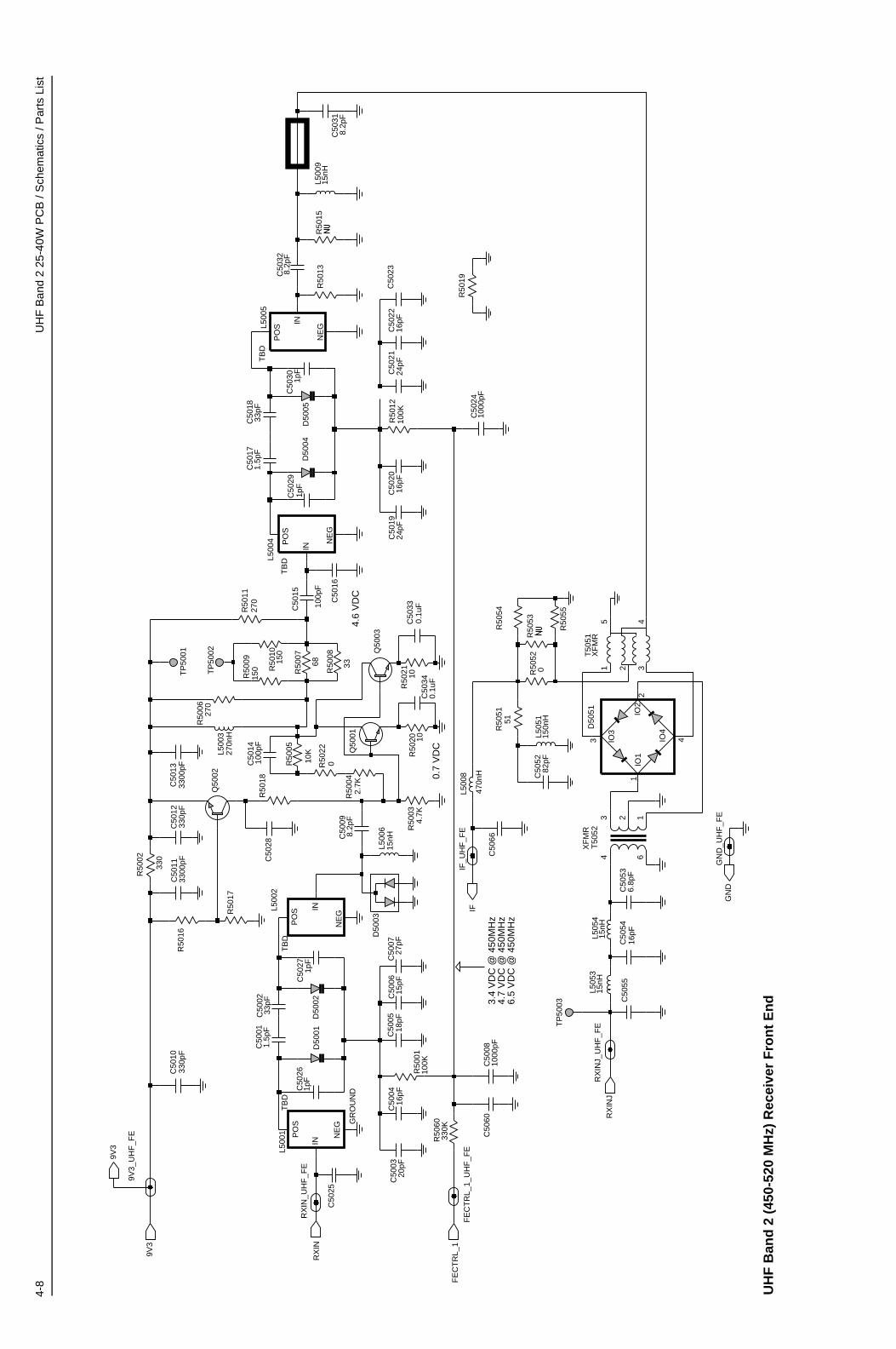
4-8
UH
F B
and
2 25
-40W
PC
B /
Sch
emat
ics
/ Par
ts L
ist
C50
55
L505
3
C50
02
15nH
33pF
16pF
8.2p
FC
5031
C50
20
Q50
02
GN
D
15nH
L505
4
C50
2410
00pF
D50
02
C50
261p
F
GN
D_U
HF
_FE
1000
pFC
5008
R50
15
100K
R50
01
R50
17
330K
R50
60
3300
pF
RX
INJ
C50
11
C50
2124
pF
L500
4
IN
NE
G
TB
D
C50
25
D50
04
82pF
C50
52
150
R50
19
R50
10
8.2p
FC
5032
33
R50
08
15nH
L500
6
4
C50
30 1pF
XF
MR
T50
51
1 2 3
5
R50
220
270
R50
06
1.5p
FC
5017
RX
IN_U
HF
_FE
9V3
C50
16
D50
01
C50
66
TP
5003
TB
DL5
005
IN
NE
G
TB
DL5
001
IN
NE
G
150n
HL5
051
L500
8
470n
H
10K
9V3
2
R50
05
T50
52X
FM
R
4 6
3 1
100K
27pF
R50
12C
5007
68
R50
07
270
TB
DL5
002
IN
NE
G
R50
11
Q50
01
FE
CT
RL_
1_U
HF
_FE
1pF
C50
29
R50
20 10
C50
60
R50
16
C50
23
C50
5416
pF
C50
098.
2pF
IF
D50
03
0.1u
FC
5034
FE
CT
RL_
1
C50
0416
pFC
5006
Q50
03
L500
9
10R
5021
R50
51
15nH
51
20pF
C50
03
330
R50
02
C50
1333
00pF
0R50
52
270n
H
R50
54
RX
IN
L500
3
330p
FC
5012
C50
271p
F
R50
18
R50
53
R50
034.
7K
R50
13
150
R50
09
C50
28
100p
F
C50
15
R50
55
9V3_
UH
F_F
E
IF_U
HF
_FE
C50
011.
5pF 18
pFC
5005
100p
FC
5014
6.8p
FC
5053
R50
042.
7K
C50
33
TP
5001
0.1u
F
RX
INJ_
UH
F_F
E
16pF
C50
22
TP
5002
C50
1833
pF
D50
51
IO1
1IO
22
IO3
3 IO4
4
C50
1924
pF
330p
FC
5010
D50
05
GR
OU
ND
PO
S
15pF
PO
S
PO
SP
OS
3.4
VD
C @
450
MH
z4.
7 V
DC
@ 4
50M
Hz
6.5
VD
C @
450
MH
z
0.7
VD
C
4.6
VD
C
UH
F B
and
2 (
450-
520
MH
z) R
ecei
ver
Fro
nt
En
d
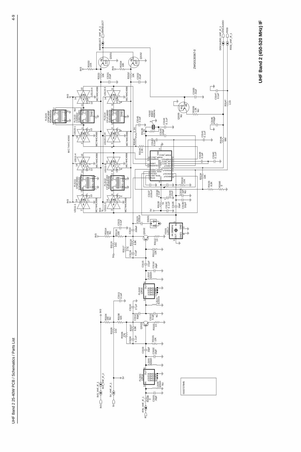
UH
F B
and
2 25
-40W
PC
B /
Sch
emat
ics
/ Par
ts L
ist
4-9
9186
176B
01
9180
469V
04
9180
469V
03
9180
469V
0691
8046
8V06
R31
442.
4K
BW
SE
LEC
T_V
HF
_IF
_1
9V3_
VH
F_I
F_2
C31
139.
1pF
NU
R31
0410
0N
U
10
0
620n
HN
U
R31
05
R31
30L3
100
14
VD
D
7
VS
S
51
U31
11-1
MC
74H
C40
66
13
CN
TL1
2
C31
16
L311
2
0.
1uF
620n
H
9V3_
VH
F_I
F_1
10
uF
C31
33
0.1
uF
C31
32
.01u
F
C31
51
OU
T2
C31
37.0
39
uF
CF
WC
45
5D
FL3
112
GN
D1
34
GN
D2
IN1
620n
H
C31
21
L310
1
0.1u
F
R31
0112
K
12
K
R31
47
15pF
DIS
CA
UD
IO
C31
02
C31
52.0
1uF
0.1u
F C
3139
7
VS
S
0.1
uF
C31
41
U31
15-1
MC
74
HC
40
66
MC
74H
C40
66
13
CN
TL1
2
14
VD
D
DIS
CA
UD
IO_V
HF
_IF
_1
62
0n
H
620
L311
1
R31
08
27
pF
C31
10
0.
1uF
C31
47C31
55
9V3
.01u
F
NU
Q31
55
FL3
115
3GN
D1
GN
D2 4
1IN
2O
UT
BW
SE
LEC
T
GND3
45
GND4
3IN
6O
UT
C
FW
C45
5F
12
R16
FL3
102
1GND1GND2
2
GND1
12
GND2 4
GND3GND4
5
IN3
OU
T6
12R
16F
L310
1
7
C31
4 2
0.1u
F
MC
74H
C40
66
CN
TL
6
89
VD
D14
VS
S
GN
D
3
IN1
OU
T2
RS
SI
U31
11-3
FL3
114
CF
UC
J455
D
4700
pFC
3146
27K
GN
D1
34
GN
D2
IN1
OU
T2
R31
06
OU
T3
IN1
FL3
111
CF
WC
455G
Y31
011
2R
17
44.3
95M
Hz
GN
D2
GN
D1
4C
3131
1pF
NU
0.1u
FC
3145
5V_V
HF
_IF
_1
IF
IN_V
HF
_IF
_1IF
330
R31
16
10K
R
3134
0.1
uF
C31
44
18pF
C31
14
10K
R31
55
R31
51
VD
D
7VS
S
NU
1.2K
U31
11-4
MC
74H
C40
66
12CN
TL14
CN
TL
5
43
VD
D
14
VS
S 7
U31
15-2
MC
74H
C40
66
0.1
uF
C31
04
C31
35
33pF
12CN
TL
11
14 VD
D
7VS
S
7
U31
15-4
MC
74H
C40
66
MC
74H
C40
66
CN
TL
5
43
VD
D
14
VS
S
3.3
K
U31
11-2
R31
45
0.1
uF
C31
40
39
0
R31
15
Q31
52
32
2p
FY
3102
455K
Hz
45B
02
C31
15
82pF
C31
12C
3123
.03
9u
F
R31
12 10
0102
727B
45
0R
3148
0.1u
F C31
11
Q31
51
27
K
R31
17
Q31
02
8.2K
R31
33
Q31
01
C31
363
0p
F
20pF
R31
02C
3101
33pF
10
C31
03
C31
340
.1u
F
R
SS
I_V
HF
_IF
_1
6.
8K
R31
18
R31
11
12K
C31
22
.039
uF6.
8K
R31
07
NU
100
R31
14
R31
54
5V
10K
10
K R
3153
D31
01
120p
F
C31
43
R31
52
10K
1.2
K
CN
TL
6
VD
D
14 VS
S 7
R31
35
U31
15-3
MC
74H
C40
66
680
R31
46R
3160
0
R31
321
5K
FL3
113
CS
455G
2N
U
GN
D
3
IN1
OU
T2
9V3
5V
5V
9V3
9V3
9V3
9V3
9V3
5V
9V3
8910
1110
OSCIN4 OSCOUT 3
QUADIN10
RFIN1
RFIN_DEC2
RSSIOUT 5RSSI_FEED9
VC
C6
IFAMPOUT 16
IFAMP_DEC119
IFAMP_DEC2
17
LIMIN14
LIMOUT 11
LIM_DEC1 13
LIM_DEC2 12
MIXOUT 20
SA
61
6
SA
616
AUDIOOUT 8AUDIO_FEED7
GN
D15
IFAMPIN18
U31
01
ZW
G01
3036
7-0
UH
F B
and
2 (
450-
520
MH
z) IF

4-10
UH
F B
and
2 25
-40W
PC
B /
Sch
emat
ics
/ Par
ts L
ist
UH
F B
and
2 P
CB
848
6250
Z02
Par
ts L
ist 2
5-40
W
Cir
cuit
R
efM
oto
rola
P
art
No
.D
escr
ipti
on
C01
0121
1374
0F51
100p
FC
0107
2113
741F
2510
00pF
C01
1221
1374
3E20
0.1u
FC
0121
2113
743E
200.
1uF
C01
2221
1374
3E20
0.1u
FC
0131
2113
740F
3522
pFC
0132
2113
740F
3522
pFC
0141
2113
743E
200.
1uF
C01
5121
1374
1F49
10nF
C02
0123
1104
9A57
10uF
C02
0223
1104
9A57
10uF
C02
0421
1374
3E20
0.1u
FC
0212
2311
049A
5710
uFC
0221
2113
743E
200.
1uF
C02
2221
1374
3E20
0.1u
FC
0223
2113
743E
200.
1uF
C02
2421
1374
0F51
100p
FC
0225
2113
743E
200.
1uF
C02
2621
1374
3E20
0.1u
FC
0228
2311
049A
564.
7uF
C02
3121
1374
3B29
1uF
C02
3221
1374
3E20
0.1u
FC
0234
2113
743E
200.
1uF
C02
3521
1374
3E07
0.02
2uF
C02
3621
1374
3E10
0.03
3uF
C02
4121
1374
3E20
0.1u
FC
0243
2113
740F
5110
0pF
C02
4421
1374
3E20
0.1u
FC
0245
2113
743E
200.
1uF
C02
4621
1374
1F49
10nF
C02
5121
1374
3E20
0.1u
FC
0252
2311
049A
071u
FC
0254
2113
743E
200.
1uF
C02
5521
1374
3E20
0.1u
FC
0256
2113
740F
5110
0pF
C02
6121
1374
3E20
0.1u
FC
0262
2113
740F
4982
pFC
0265
2113
743E
200.
1uF
C02
6721
1374
1F49
10nF
C02
7121
1374
1F49
10nF
C02
7221
1374
3E20
0.1u
FC
0273
2113
741F
3733
00pF
C02
7523
1104
9A99
47uF
C02
7621
1374
1F25
1000
pFC
0277
2113
741F
2510
00pF
C03
0123
1104
9A07
1uF
C03
0221
1374
3E20
0.1u
FC
0303
2113
740F
5110
0pF
C03
0421
1374
3E20
0.1u
F
C03
0521
1374
3E20
0.1u
FC
0324
2113
743E
200.
1uF
C03
3121
1374
3E20
0.1u
FC
0341
2311
049A
071u
FC
0342
2113
743E
200.
1uF
C03
4321
1374
3E20
0.1u
FC
0344
2113
743E
200.
1uF
C03
5121
1374
3E20
0.1u
FC
0352
2113
743E
070.
022u
FC
0353
2311
049A
9733
uFC
0354
2113
743E
200.
1uF
C04
2121
1374
3N48
82pF
C04
2221
1374
1F17
470p
FC
0423
2113
741F
1747
0pF
C04
2621
1374
3L09
470p
FC
0427
2113
743L
0947
0pF
C04
2821
1374
3N48
82pF
C04
2921
1374
3L09
470p
FC
0430
2113
741F
1747
0pF
C04
3121
1374
1F17
470p
FC
0441
2113
743L
0947
0pF
C04
4221
1374
3L09
470p
FC
0445
2113
743L
0947
0pF
C04
4621
1374
3L09
470p
FC
0447
2113
743L
0947
0pF
C04
4821
1374
3L09
470p
FC
0449
2113
743L
0947
0pF
C04
7021
1374
3L09
470p
FC
0471
2113
743N
4882
pFC
0472
2113
743N
4882
pFC
0473
2113
743N
4882
pFC
0474
2113
743L
0947
0pF
C04
7621
1374
3L09
470p
FC
0477
2113
743L
0947
0pF
C04
7821
1374
3L09
470p
FC
0482
2113
743L
0947
0pF
C04
8321
1374
3L09
470p
FC
0484
2113
741F
1747
0pF
C04
8521
1374
3L09
470p
FC
0486
2113
743L
0947
0pF
C04
8721
1374
3L09
470p
FC
0488
2113
743L
0947
0pF
C04
9021
1374
3L09
470p
FC
0491
2113
743L
0947
0pF
C04
9221
1374
3L09
470p
FC
0493
2113
743L
0947
0pF
C04
9421
1374
3L09
470p
FC
0495
2113
743L
0947
0pF
C04
9621
1374
3L09
470p
FC
0497
2113
743L
0947
0pF
C04
9921
1374
3L09
470p
F
Cir
cuit
R
efM
oto
rola
P
art
No
.D
escr
ipti
on
C05
0121
1374
1F49
10nF
C05
0221
1374
1F17
470p
FC
0503
2113
741F
1747
0pF
C05
0421
1374
1F17
470p
FC
0505
2113
741F
1747
0pF
C05
0621
1374
1F17
470p
FC
0508
2113
741F
1747
0pF
C05
0921
1374
1F17
470p
FC
0510
2113
741F
1747
0pF
C05
1121
1374
1F17
470p
FC
0512
2113
741F
1747
0pF
C05
1321
1374
1F17
470p
FC
0514
2113
741F
1747
0pF
C05
1521
1374
1F17
470p
FC
0516
2113
741F
4910
nFC
0517
2113
743N
4882
pFC
0518
2113
741F
1747
0pF
C05
4123
1104
9A05
0.47
uFC
0542
2311
049A
9947
uFC
0560
2113
743L
1710
00pF
C05
9121
1374
3E20
0.1u
FC
0592
2113
743E
200.
1uF
C05
9321
1374
1B69
0.1u
FC
0601
2113
741F
1747
0pF
C06
0323
8009
0M24
10uF
C06
1123
1104
9C06
22uF
C06
1221
1374
3E20
0.1u
FC
0622
2311
049A
9947
uFC
0641
2113
741F
1747
0pF
C06
4423
1104
9A97
33uF
C06
4521
1374
3E20
0.1u
FC
0652
2311
049A
9733
uFC
0654
2311
049A
5710
uFC
0655
2113
743E
200.
1uF
C06
6123
1104
9C05
47uF
C06
6221
1374
1F49
10nF
C06
6321
1374
3E20
0.1u
FC
0671
2113
743E
200.
1uF
C06
8121
1374
3E20
0.1u
FC
3101
2113
740F
3420
pFC
3102
2113
740F
3115
pFC
3103
2113
740F
3933
pFC
3104
2113
743E
200.
1uF
C31
1021
1374
0F37
27pF
C31
1121
1374
3E20
0.1u
FC
3112
2113
740F
4982
pFC
3114
2113
740F
3318
pFC
3115
2113
740F
3522
pFC
3116
2113
743E
200.
1uF
C31
2121
1374
3E20
0.1u
FC
3122
2113
743E
110.
039u
F
Cir
cuit
R
efM
oto
rola
P
art
No
.D
escr
ipti
on
C31
2321
1374
3E11
0.03
9uF
C31
2421
1374
0L30
33pF
C31
3221
1374
3E20
0.1u
FC
3133
2311
049A
5710
uFC
3134
2113
743E
200.
1uF
C31
3521
1374
0L30
33pF
C31
3621
1374
0F35
22pF
C31
3721
1374
3E11
0.03
9uF
C31
3921
1374
3E20
0.1u
FC
3140
2113
743E
200.
1uF
C31
4121
1374
3E20
0.1u
FC
3142
2113
743E
200.
1uF
C31
4321
1374
0F53
120p
FC
3144
2113
743E
200.
1uF
C31
4521
1374
3E20
0.1u
FC
3146
2113
741F
4147
00pF
C31
4721
1374
3E20
0.1u
FC
3151
2113
741F
4910
nFC
3152
2113
741F
4910
nFC
5001
2113
740F
071.
5pF
C50
0221
1374
0F39
33pF
C50
0321
1374
0F35
22pF
C50
0421
1374
0F32
16pF
C50
0521
1374
0F32
16pF
C50
0621
1374
0F32
16pF
C50
0721
1374
0F32
16pF
C50
0821
1374
1F25
1000
pFC
5009
2113
740F
258.
2pF
C50
1021
1374
1F13
330p
FC
5011
2113
741F
3733
00pF
C50
1221
1374
1F13
330p
FC
5013
2113
741F
3733
00pF
C50
1421
1374
0F51
100p
FC
5015
2113
740F
5110
0pF
C50
1721
1374
0F07
1.5p
FC
5018
2113
740F
3933
pFC
5019
2113
740F
3727
pFC
5020
2113
740F
3216
pFC
5021
2113
740F
3318
pFC
5022
2113
740F
3216
pFC
5024
2113
741F
2510
00pF
C50
2621
1374
0F03
1pF
C50
2721
1374
0F03
1pF
C50
2821
1374
1F49
10nF
C50
2921
1374
0F03
1pF
C50
3021
1374
0F03
1pF
C50
3121
1374
0F25
8.2p
FC
5032
2113
740F
258.
2pF
C50
3321
1374
0F51
100p
FC
5034
2113
740F
5110
0pF
C50
5221
1374
0F49
82pF
Cir
cuit
R
efM
oto
rola
P
art
No
.D
escr
ipti
on

UH
F B
and
2 25
-40W
PC
B /
Sch
emat
ics
/ Par
ts L
ist
4-11
C50
5321
1374
0F23
6.8p
FC
5054
2113
740F
3216
pFC
5061
2113
740F
6333
0pF
C50
6221
1374
3E20
0.1u
FC
5064
2113
743E
200.
1uF
C50
6521
1374
0F51
100p
FC
5067
2113
741F
3733
00pF
C50
6821
1374
0F51
100p
FC
5069
2113
741F
4910
nFC
5201
2113
740F
5110
0pF
C52
0221
1374
1F49
10nF
C52
0321
1374
1F49
10nF
C52
0421
1374
0F51
100p
FC
5205
2113
741F
4910
nFC
5206
2311
049J
2510
uFC
5208
2113
743E
200.
1uF
C52
0921
1374
3E20
0.1u
FC
5210
2104
993J
022.
2uF
C52
1121
1374
3E20
0.1u
FC
5213
2311
049A
092.
2uF
C52
1423
1104
9A09
2.2u
FC
5215
2311
049A
092.
2uF
C52
1721
1374
1F49
10nF
C52
2121
0972
0D01
0.01
uFC
5222
2109
720D
140.
1uF
C52
2408
8242
2W23
1uF
C52
2521
1374
1F18
510p
FC
5227
2113
740F
2710
pFC
5230
2104
993J
022.
2uF
C52
3121
1374
1F49
10nF
C52
3221
1374
1F49
10nF
C52
3321
0499
3J02
2.2u
FC
5234
2113
741F
4910
nFC
5235
2113
741F
4910
nFC
5236
2113
743E
120.
047u
FC
5242
2113
740F
5110
0pF
C52
4321
1374
0F51
100p
FC
5244
2113
740F
5110
0pF
C52
4521
1374
0F51
100p
FC
5246
2113
740F
5110
0pF
C52
5121
1374
3E20
0.1u
FC
5252
2113
741F
2510
00pF
C52
5323
1104
9A56
4.7u
FC
5254
2113
743E
200.
1uF
C52
5521
1374
0F51
100p
FC
5263
2113
743E
200.
1uF
C52
8721
1374
0F51
100p
FC
5289
2113
743E
200.
1uF
C53
0121
1374
0F51
100p
FC
5302
2113
740L
094.
3pF
C53
0321
1374
0L09
4.3p
F
Cir
cuit
R
efM
oto
rola
P
art
No
.D
escr
ipti
on
C53
0421
1374
0L12
5.6p
FC
5306
2113
740L
012p
FC
5307
2113
740F
5110
0pF
C53
0821
1374
3E20
0.1u
FC
5309
2113
740F
5110
0pF
C53
1121
1374
0F51
100p
FC
5312
2113
740F
3318
pFC
5314
2113
740L
012p
FC
5315
2113
740F
5110
0pF
C53
1621
0972
0D14
0.1u
FC
5318
2113
743K
160.
22uF
C53
2121
1374
0F03
1pF
C53
2421
1374
0F07
1.5p
FC
5325
2311
049A
564.
7uF
C53
3121
1374
0L12
5.6p
FC
5335
2113
740F
5110
0pF
C53
3621
1374
3E07
0.02
2uF
C53
3721
1374
0F44
51pF
C53
3821
1374
0F44
51pF
C53
5121
1374
0F51
100p
FC
5352
2113
743E
200.
1uF
C53
5321
1374
3E20
0.1u
FC
5354
2104
993J
022.
2uF
C53
5521
0499
3J02
2.2u
FC
5361
2113
740F
5110
0pF
C53
6406
6205
7B47
0C
5371
2113
743K
160.
22uF
C53
8121
1374
3E20
0.1u
FC
5401
2113
740F
5110
0pF
C54
0421
1374
0F51
100p
FC
5407
2113
743E
200.
1uF
C54
0921
1374
3E20
0.1u
FC
5410
2113
740F
5110
0pF
C54
1221
1374
0F51
100p
FC
5413
2113
740F
5110
0pF
C54
1421
1374
3E07
0.02
2uF
C54
1521
1374
0F51
100p
FC
5416
2113
743E
070.
022u
FC
5417
2113
740F
4347
pFC
5418
2113
743E
200.
1uF
C54
2021
1374
0A36
20pF
C54
2121
1374
1A57
0.03
3uF
C54
2221
1107
8B42
100p
FC
5425
2113
743E
070.
022u
FC
5426
2113
740F
5110
0pF
C54
2721
1374
0A23
6.2p
FC
5428
2113
740A
5510
0pF
C54
2921
1374
0A55
100p
FC
5431
2113
740A
3927
pFC
5432
2113
740A
4133
pFC
5433
2113
740A
4133
pF
Cir
cuit
R
efM
oto
rola
P
art
No
.D
escr
ipti
on
C54
3421
1374
0A23
6.2p
FC
5435
2113
740A
3620
pFC
5436
2380
090M
2410
uFC
5438
2113
743E
200.
1uF
C54
3921
1107
8B42
100p
FC
5440
2111
078B
2933
pFC
5441
2111
078B
2933
pFC
5447
2113
740F
4243
pFC
5448
2180
464E
629p
FC
5449
2111
078B
033.
9pF
C54
5021
1107
8B01
3.3p
FC
5457
2113
740A
4236
pFC
5458
2113
740A
184.
3pF
C54
5921
1374
0A55
100p
FC
5466
2111
078B
096.
8pF
C54
6721
1107
8B09
6.8p
FC
5469
2113
740A
5510
0pF
C54
7221
1107
8B27
30pF
C54
7321
1374
0F51
100p
FC
5474
2113
740F
184.
3pF
C54
7521
1374
0F10
2pF
C54
7821
1374
1A21
1000
pFC
5479
2113
740F
5110
0pF
C54
8121
1374
1A32
3000
pFC
5483
2113
740A
5510
0pF
C54
8421
1374
0F38
30pF
C54
8521
1374
0F38
30pF
C54
8821
1374
0F51
100p
FC
5492
2111
078B
4210
0pF
C54
9421
8046
4E60
7pF
C54
9521
1374
1A21
1000
pFC
5496
2111
078B
013.
3pF
C54
9721
1374
1A21
1000
pFC
5498
2111
078B
013.
3pF
C54
9921
1374
0F51
100p
FC
5502
2113
741F
3322
00pF
C55
0321
1374
1F17
470p
FC
5504
2113
741F
4910
nFC
5505
2311
049A
071u
FC
5506
2113
741F
3322
00pF
C55
0721
1374
0F51
100p
FC
5510
2111
078B
2730
pFC
5602
2113
741A
570.
033u
FC
5629
2113
740F
5110
0pF
C56
3021
1374
3E20
0.1u
FC
5631
2113
743E
200.
1uF
C56
3221
1374
0F51
100p
FC
R53
0148
0564
9Q13
DIO
DE
VC
TR
ISV
228
CR
5302
4862
824C
01D
IOD
E V
AR
AC
TO
RC
R53
0348
6282
4C01
DIO
DE
VA
RA
CT
OR
CR
5311
4862
824C
01D
IOD
E V
AR
AC
TO
R
Cir
cuit
R
efM
oto
rola
P
art
No
.D
escr
ipti
on
CR
5321
4802
245J
22D
IOD
E, V
AR
AC
TO
RD
0101
4813
825A
05D
IOD
ED
0151
4813
833C
02D
IOD
E, D
UA
L 70
VD
0179
4813
833C
02D
IOD
E, D
UA
L 70
VD
0301
4802
245J
47D
IOD
E, S
CH
OT
TK
YD
0621
4813
833C
02D
IOD
E, D
UA
L 70
VD
0651
4813
833C
02D
IOD
E, D
UA
L 70
VD
0660
4813
833C
02D
IOD
E, D
UA
L 70
VD
0661
4813
833C
02D
IOD
E, D
UA
L 70
VD
3101
4880
154K
03D
IOD
E D
UA
L S
CH
OT
TK
YD
5001
4862
824C
01D
IOD
E V
AR
AC
TO
RD
5002
4862
824C
01D
IOD
E V
AR
AC
TO
RD
5003
4880
154K
03D
IOD
E D
UA
L S
CH
OT
TK
YD
5004
4862
824C
01D
IOD
E V
AR
AC
TO
RD
5005
4862
824C
01D
IOD
E V
AR
AC
TO
RD
5006
4880
142L
01D
IOD
ED
5007
4813
833C
02D
IOD
E, D
UA
L 70
VD
5051
4886
143B
01D
IOD
E, M
IXE
RD
5201
4802
233J
09D
IOD
E, T
RIP
LED
5221
4813
825A
05D
IOD
ED
5451
4813
825A
05D
IOD
ED
5452
4813
825A
05D
IOD
ED
5453
4813
825A
05D
IOD
ED
5471
4802
482J
02D
IOD
E, S
MD
PIN
D54
7248
0248
2J02
DIO
DE
, SM
D P
INE
0271
2484
657R
01F
ER
RIT
E B
EA
DE
0272
2484
657R
01F
ER
RIT
E B
EA
DE
0631
2484
657R
01F
ER
RIT
E B
EA
DF
0401
6580
542Z
01F
US
E 3
AF
L310
191
8011
2R16
2 P
OLE
44.
85 M
HZ
CR
YS
TAL
FIL
TE
RF
L310
291
8011
2R16
2 P
OLE
44.
85 M
HZ
CR
YS
TAL
FIL
TE
RF
L311
191
8046
9V03
CE
RA
MIC
FIL
TE
R, 4
55K
Hz
FL3
112
9180
469V
06C
ER
AM
IC F
ILT
ER
, 455
KH
zF
L311
491
8046
8V06
CE
RA
MIC
FIL
TE
R, 4
55K
Hz
FL3
115
9180
469V
04C
ER
AM
IC F
ILT
ER
, 455
KH
zJ0
401
0902
636Y
02F
LEX
CO
NN
EC
TO
RJ0
451
0902
636Y
01F
LEX
CO
NN
EC
TO
RJ0
501
0986
105B
01A
CC
ES
SO
RY
CO
NN
EC
TO
RJ0
551
0905
505Y
04F
LEX
CO
NN
EC
TO
RJ0
552
0905
505Y
03F
LEX
CO
NN
EC
TO
RJ0
601
0986
165B
01D
C P
OW
ER
CO
NN
EC
TO
RJ5
401
0986
166B
02R
F C
ON
NE
CT
OR
(M
INI U
HF
)L3
101
2462
587T
2562
0nH
L311
124
6258
7T25
620n
HL3
112
2462
587T
2562
0nH
L312
424
6258
7N68
1uH
L500
324
6258
7T20
270n
HL5
006
2462
587V
2415
nHL5
008
2462
587T
2347
0nH
Cir
cuit
R
efM
oto
rola
P
art
No
.D
escr
ipti
on
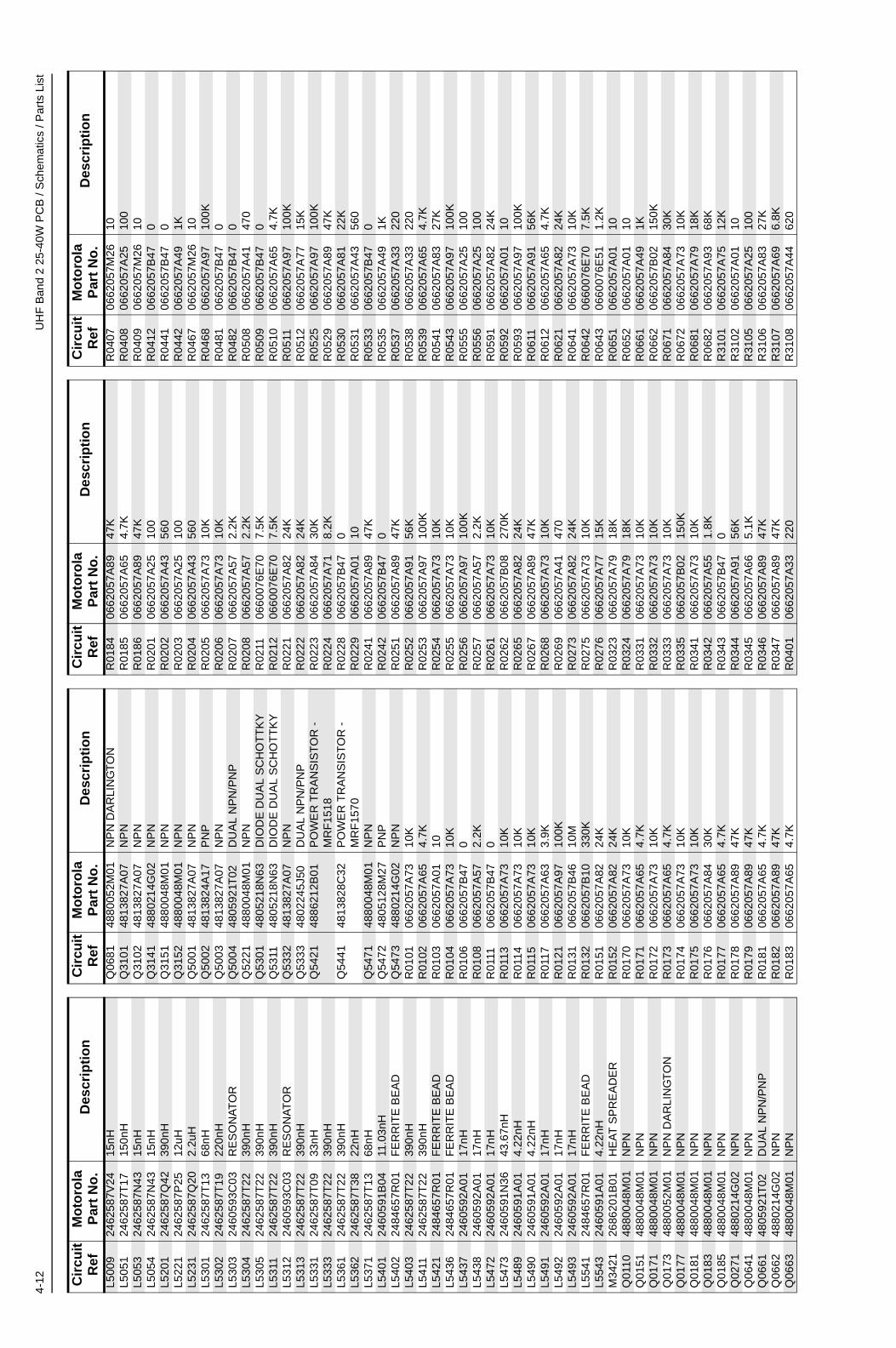
4-12
UH
F B
and
2 25
-40W
PC
B /
Sch
emat
ics
/ Par
ts L
ist
L500
924
6258
7V24
15nH
L505
124
6258
7T17
150n
HL5
053
2462
587N
4315
nHL5
054
2462
587N
4315
nHL5
201
2462
587Q
4239
0nH
L522
124
6258
7P25
12uH
L523
124
6258
7Q20
2.2u
HL5
301
2462
587T
1368
nHL5
302
2462
587T
1922
0nH
L530
324
6059
3C03
RE
SO
NA
TO
RL5
304
2462
587T
2239
0nH
L530
524
6258
7T22
390n
HL5
311
2462
587T
2239
0nH
L531
224
6059
3C03
RE
SO
NA
TO
RL5
313
2462
587T
2239
0nH
L533
124
6258
7T09
33nH
L533
324
6258
7T22
390n
HL5
361
2462
587T
2239
0nH
L536
224
6258
7T38
22nH
L537
124
6258
7T13
68nH
L540
124
6059
1B04
11.0
3nH
L540
224
8465
7R01
FE
RR
ITE
BE
AD
L540
324
6258
7T22
390n
HL5
411
2462
587T
2239
0nH
L542
124
8465
7R01
FE
RR
ITE
BE
AD
L543
624
8465
7R01
FE
RR
ITE
BE
AD
L543
724
6059
2A01
17nH
L543
824
6059
2A01
17nH
L547
224
6059
2A01
17nH
L547
324
6059
1N36
43.6
7nH
L548
924
6059
1A01
4.22
nHL5
490
2460
591A
014.
22nH
L549
124
6059
2A01
17nH
L549
224
6059
2A01
17nH
L549
324
6059
2A01
17nH
L554
124
8465
7R01
FE
RR
ITE
BE
AD
L554
324
6059
1A01
4.22
nHM
3421
2686
201B
01H
EA
T S
PR
EA
DE
RQ
0110
4880
048M
01N
PN
Q01
5148
8004
8M01
NP
NQ
0171
4880
048M
01N
PN
Q01
7348
8005
2M01
NP
N D
AR
LIN
GT
ON
Q01
7748
8004
8M01
NP
NQ
0181
4880
048M
01N
PN
Q01
8348
8004
8M01
NP
NQ
0185
4880
048M
01N
PN
Q02
7148
8021
4G02
NP
NQ
0641
4880
048M
01N
PN
Q06
6148
0592
1T02
DU
AL
NP
N/P
NP
Q06
6248
8021
4G02
NP
NQ
0663
4880
048M
01N
PN
Cir
cuit
R
efM
oto
rola
P
art
No
.D
escr
ipti
on
Q06
8148
8005
2M01
NP
N D
AR
LIN
GT
ON
Q31
0148
1382
7A07
NP
NQ
3102
4813
827A
07N
PN
Q31
4148
8021
4G02
NP
NQ
3151
4880
048M
01N
PN
Q31
5248
8004
8M01
NP
NQ
5001
4813
827A
07N
PN
Q50
0248
1382
4A17
PN
PQ
5003
4813
827A
07N
PN
Q50
0448
0592
1T02
DU
AL
NP
N/P
NP
Q52
2148
8004
8M01
NP
NQ
5301
4805
218N
63D
IOD
E D
UA
L S
CH
OT
TK
YQ
5311
4805
218N
63D
IOD
E D
UA
L S
CH
OT
TK
YQ
5332
4813
827A
07N
PN
Q53
3348
0224
5J50
DU
AL
NP
N/P
NP
Q54
2148
8621
2B01
PO
WE
R T
RA
NS
IST
OR
-
MR
F15
18Q
5441
4813
828C
32P
OW
ER
TR
AN
SIS
TO
R -
M
RF
1570
Q54
7148
8004
8M01
NP
NQ
5472
4805
128M
27P
NP
Q54
7348
8021
4G02
NP
NR
0101
0662
057A
7310
KR
0102
0662
057A
654.
7KR
0103
0662
057A
0110
R01
0406
6205
7A73
10K
R01
0606
6205
7B47
0R
0108
0662
057A
572.
2KR
0111
0662
057B
470
R01
1306
6205
7A73
10K
R01
1406
6205
7A73
10K
R01
1506
6205
7A73
10K
R01
1706
6205
7A63
3.9K
R01
2106
6205
7A97
100K
R01
3106
6205
7B46
10M
R01
3206
6205
7B10
330K
R01
5106
6205
7A82
24K
R01
5206
6205
7A82
24K
R01
7006
6205
7A73
10K
R01
7106
6205
7A65
4.7K
R01
7206
6205
7A73
10K
R01
7306
6205
7A65
4.7K
R01
7406
6205
7A73
10K
R01
7506
6205
7A73
10K
R01
7606
6205
7A84
30K
R01
7706
6205
7A65
4.7K
R01
7806
6205
7A89
47K
R01
7906
6205
7A89
47K
R01
8106
6205
7A65
4.7K
R01
8206
6205
7A89
47K
R01
8306
6205
7A65
4.7K
Cir
cuit
R
efM
oto
rola
P
art
No
.D
escr
ipti
on
R01
8406
6205
7A89
47K
R01
8506
6205
7A65
4.7K
R01
8606
6205
7A89
47K
R02
0106
6205
7A25
100
R02
0206
6205
7A43
560
R02
0306
6205
7A25
100
R02
0406
6205
7A43
560
R02
0506
6205
7A73
10K
R02
0606
6205
7A73
10K
R02
0706
6205
7A57
2.2K
R02
0806
6205
7A57
2.2K
R02
1106
6007
6E70
7.5K
R02
1206
6007
6E70
7.5K
R02
2106
6205
7A82
24K
R02
2206
6205
7A82
24K
R02
2306
6205
7A84
30K
R02
2406
6205
7A71
8.2K
R02
2806
6205
7B47
0R
0229
0662
057A
0110
R02
4106
6205
7A89
47K
R02
4206
6205
7B47
0R
0251
0662
057A
8947
KR
0252
0662
057A
9156
KR
0253
0662
057A
9710
0KR
0254
0662
057A
7310
KR
0255
0662
057A
7310
KR
0256
0662
057A
9710
0KR
0257
0662
057A
572.
2KR
0261
0662
057A
7310
KR
0262
0662
057B
0827
0KR
0265
0662
057A
8224
KR
0267
0662
057A
8947
KR
0268
0662
057A
7310
KR
0269
0662
057A
4147
0R
0273
0662
057A
8224
KR
0275
0662
057A
7310
KR
0276
0662
057A
7715
KR
0323
0662
057A
7918
KR
0324
0662
057A
7918
KR
0331
0662
057A
7310
KR
0332
0662
057A
7310
KR
0333
0662
057A
7310
KR
0335
0662
057B
0215
0KR
0341
0662
057A
7310
KR
0342
0662
057A
551.
8KR
0343
0662
057B
470
R03
4406
6205
7A91
56K
R03
4506
6205
7A66
5.1K
R03
4606
6205
7A89
47K
R03
4706
6205
7A89
47K
R04
0106
6205
7A33
220
Cir
cuit
R
efM
oto
rola
P
art
No
.D
escr
ipti
on
R04
0706
6205
7M26
10R
0408
0662
057A
2510
0R
0409
0662
057M
2610
R04
1206
6205
7B47
0R
0441
0662
057B
470
R04
4206
6205
7A49
1KR
0467
0662
057M
2610
R04
6806
6205
7A97
100K
R04
8106
6205
7B47
0R
0482
0662
057B
470
R05
0806
6205
7A41
470
R05
0906
6205
7B47
0R
0510
0662
057A
654.
7KR
0511
0662
057A
9710
0KR
0512
0662
057A
7715
KR
0525
0662
057A
9710
0KR
0529
0662
057A
8947
KR
0530
0662
057A
8122
KR
0531
0662
057A
4356
0R
0533
0662
057B
470
R05
3506
6205
7A49
1KR
0537
0662
057A
3322
0R
0538
0662
057A
3322
0R
0539
0662
057A
654.
7KR
0541
0662
057A
8327
KR
0543
0662
057A
9710
0KR
0555
0662
057A
2510
0R
0556
0662
057A
2510
0R
0591
0662
057A
8224
KR
0592
0662
057A
0110
R05
9306
6205
7A97
100K
R06
1106
6205
7A91
56K
R06
1206
6205
7A65
4.7K
R06
2106
6205
7A82
24K
R06
4106
6205
7A73
10K
R06
4206
6007
6E70
7.5K
R06
4306
6007
6E51
1.2K
R06
5106
6205
7A01
10R
0652
0662
057A
0110
R06
6106
6205
7A49
1KR
0662
0662
057B
0215
0KR
0671
0662
057A
8430
KR
0672
0662
057A
7310
KR
0681
0662
057A
7918
KR
0682
0662
057A
9368
KR
3101
0662
057A
7512
KR
3102
0662
057A
0110
R31
0506
6205
7A25
100
R31
0606
6205
7A83
27K
R31
0706
6205
7A69
6.8K
R31
0806
6205
7A44
620
Cir
cuit
R
efM
oto
rola
P
art
No
.D
escr
ipti
on
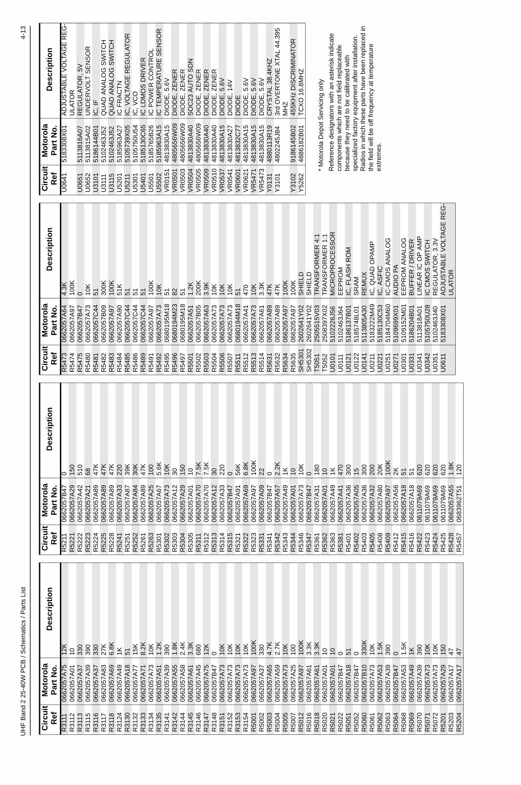
UH
F B
and
2 25
-40W
PC
B /
Sch
emat
ics
/ Par
ts L
ist
4-13
* M
otor
ola
Dep
ot S
ervi
cing
onl
y
Ref
eren
ce d
esig
nato
rs w
ith a
n as
teris
k in
dica
te
com
pone
nts
whi
ch a
re n
ot fi
eld
repl
acea
ble
beca
use
they
nee
d to
be
calib
rate
d w
ith
spec
ializ
ed fa
ctor
y eq
uipm
ent a
fter
inst
alla
tion.
R
adio
s in
whi
ch th
ese
part
s ha
ve b
een
repl
aced
in
the
field
will
be
off f
requ
ency
at t
empe
ratu
re
extr
emes
.
R31
1106
6205
7A75
12K
R31
1206
6205
7A01
10R
3113
0662
057A
3733
0R
3115
0662
057A
3939
0R
3116
0662
057A
3733
0R
3117
0662
057A
8327
KR
3118
0662
057A
696.
8KR
3124
0662
057A
491K
R31
3006
6205
7A18
51R
3132
0662
057A
7715
KR
3133
0662
057A
718.
2KR
3134
0662
057A
7310
KR
3135
0662
057A
511.
2KR
3141
0662
057A
3939
0R
3142
0662
057A
551.
8KR
3144
0662
057A
582.
4KR
3145
0662
057A
613.
3KR
3146
0662
057A
4568
0R
3147
0662
057A
7512
KR
3148
0662
057B
470
R31
5106
6205
7A73
10K
R31
5206
6205
7A73
10K
R31
5306
6205
7A73
10K
R31
5406
6205
7A73
10K
R50
0106
6205
7A97
100K
R50
0206
6205
7A37
330
R50
0306
6205
7A65
4.7K
R50
0406
6205
7A59
2.7K
R50
0506
6205
7A73
10K
R50
0706
6205
7A25
100
R50
1206
6205
7A97
100K
R50
1606
6205
7A61
3.3K
R50
1806
6205
7A61
3.3K
R50
2006
6205
7A01
10R
5021
0662
057A
0110
R50
2206
6205
7B47
0R
5051
0662
057A
1851
R50
5206
6205
7B47
0R
5060
0662
057B
1033
0KR
5061
0662
057A
7310
KR
5062
0662
057A
531.
5KR
5063
0662
057A
3939
0R
5064
0662
057B
470
R50
6806
6205
7A53
1.5K
R50
6906
6205
7A49
1KR
5070
0662
057A
3939
0R
5071
0662
057A
7310
KR
5072
0662
057A
7310
KR
5201
0662
057A
2915
0R
5203
0662
057A
1747
R52
0406
6205
7A17
47
Cir
cuit
R
efM
oto
rola
P
art
No
.D
escr
ipti
on
R52
1106
6205
7B47
0R
5221
0662
057A
2915
0R
5222
0662
057A
4251
0R
5223
0662
057A
2168
R52
2406
6205
7A89
47K
R52
2506
6205
7A89
47K
R52
2806
6205
7A89
47K
R52
4106
6205
7A33
220
R52
5106
6205
7A87
39K
R52
5206
6205
7A84
30K
R52
6106
6205
7A89
47K
R52
6306
6205
7A25
100
R53
0106
6205
7A67
5.6K
R53
0206
6205
7A73
10K
R53
0306
6205
7A12
30R
5304
0662
057A
2915
0R
5305
0662
057A
0110
R53
1106
6205
7A70
7.5K
R53
1206
6205
7A70
7.5K
R53
1306
6205
7A12
30R
5314
0662
057A
3322
0R
5315
0662
057B
470
R53
2106
6205
7A91
56K
R53
2206
6205
7A69
6.8K
R53
2306
6205
7A97
100K
R53
3106
6205
7A09
22R
5341
0662
057B
470
R53
4206
6205
7A57
2.2K
R53
4306
6205
7A49
1KR
5344
0662
057A
0110
R53
4606
6205
7A73
10K
R53
4706
6205
7B47
0R
5361
0662
057A
3118
0R
5362
0662
057A
0110
R53
6306
6205
7A49
1KR
5381
0662
057A
4147
0R
5401
0662
057A
3630
0R
5402
0662
057A
0515
R54
0306
6205
7A36
300
R54
0506
6205
7A32
200
R54
0806
6205
7A80
20K
R54
0906
6205
7A97
100K
R54
1206
6205
7A56
2KR
5415
0662
057A
1851
R54
1606
6205
7A18
51R
5422
0611
079A
6962
0R
5423
0611
079A
6962
0R
5424
0611
079A
6962
0R
5425
0611
079A
6962
0R
5428
0662
057A
551.
8KR
5457
0683
962T
5112
0
Cir
cuit
R
efM
oto
rola
P
art
No
.D
escr
ipti
on
R54
7306
6205
7A64
4.3K
R54
7406
6205
7A97
100K
R54
7506
6205
7B47
0R
5480
0662
057A
7310
KR
5481
0662
057C
4451
R54
8206
6205
7B09
300K
R54
8306
6205
7A97
100K
R54
8406
6205
7A90
51K
R54
8506
6205
7C44
51R
5486
0662
057C
4451
R54
8906
6205
7C44
51R
5491
0662
057A
9710
0KR
5492
0662
057A
7310
KR
5495
0680
195M
1851
R54
9606
8019
4M23
82R
5497
0680
195M
1851
R55
0106
6205
7A51
1.2K
R55
0206
6205
7B05
200K
R55
0306
6205
7A63
3.9K
R55
0406
6205
7A73
10K
R55
0606
6205
7A73
10K
R55
0706
6205
7A73
10K
R55
1106
8019
4M18
51R
5512
0662
057A
4147
0R
5513
0662
057A
7310
KR
5514
0662
057A
613.
3KR
5631
0662
057A
8947
KR
5632
0662
057A
8947
KR
5634
0662
057A
9710
0KR
5635
0662
057A
9710
0KS
H53
0126
0264
1Y02
SH
IELD
SH
5302
2602
641Y
02S
HIE
LDT
5051
2505
515V
03T
RA
NS
FO
RM
ER
4:1
T50
5225
0839
7X02
TR
AN
SF
OR
ME
R 1
:1U
0101
5102
226J
56M
ICR
OP
RO
CE
SS
OR
U01
1151
0246
3J64
EE
PR
OM
U01
2151
8613
7B01
IC, F
LAS
H R
OM
U01
2251
8574
8L01
SR
AM
U01
4151
1380
5A30
RE
MU
XU
0211
5183
222M
49IC
, QU
AD
OP
AM
PU
0221
5185
130C
53IC
, AS
FIC
U02
5151
8470
4M60
IC-C
MO
S A
NA
LOG
U02
7151
0969
9X01
AU
DIO
PA
U03
0151
0915
2M01
EE
PR
OM
AN
ALO
GU
0331
5186
204B
01B
UF
FE
R /
DR
IVE
RU
0341
5113
818A
01LI
NE
AR
IC O
P A
MP
U03
4251
0575
0U28
IC C
MO
S S
WIT
CH
U03
5151
0246
3J40
RE
GU
LAT
OR
, 3.3
VU
0611
5183
308X
01A
DJU
STA
BLE
VO
LTA
GE
RE
G-
ULA
TO
R
Cir
cuit
R
efM
oto
rola
P
art
No
.D
escr
ipti
on
U06
4151
8330
8X01
AD
JUS
TAB
LE V
OLT
AG
E R
EG
-U
LAT
OR
U06
5151
1381
6A07
RE
GU
LAT
OR
, 5V
U
0652
5113
815A
02U
ND
ER
VO
LT S
EN
SO
RU
3101
5186
144B
01IC
, IF
U31
1151
0246
3J52
QU
AD
AN
ALO
G S
WIT
CH
U31
1551
0246
3J52
QU
AD
AN
ALO
G S
WIT
CH
U52
0151
8596
3A27
IC F
RA
CT
NU
5211
5105
739X
05IC
, VO
LTA
GE
RE
GU
LAT
OR
U53
0151
0575
0U54
IC, V
CO
U54
0151
8513
0C65
IC L
DM
OS
DR
IVE
RU
5501
5185
765B
26IC
PO
WE
R C
ON
TR
OL
U55
0251
8596
3A15
IC T
EM
PE
RA
TU
RE
SE
NS
OR
VR
0151
4813
830A
15D
IOD
E, 5
.6V
VR
0501
4805
656W
09D
IOD
E, Z
EN
ER
VR
0503
4805
656W
09D
IOD
E, Z
EN
ER
VR
0504
4813
830A
40S
OC
23 A
UT
O S
DN
VR
0505
4805
656W
09D
IOD
E, Z
EN
ER
VR
0509
4813
830A
40D
IOD
E, Z
EN
ER
VR
0510
4813
830A
40D
IOD
E, Z
EN
ER
VR
0537
4813
830A
15D
IOD
E, 5
.6V
VR
0541
4813
830A
27D
IOD
E, 1
4VV
R06
0148
1383
2C77
DIO
DE
VR
0621
4813
830A
15D
IOD
E, 5
.6V
VR
5471
4813
830A
15D
IOD
E, 5
.6V
VR
5473
4813
830A
15D
IOD
E, 5
.6V
Y01
3148
8011
3R19
CR
YS
TAL
38.4
KH
ZY
3101
4802
245J
843r
d O
VE
RT
ON
E X
TAL
44.3
95
MH
ZY
3102
9186
145B
0245
5KH
z D
ISC
RIM
INA
TO
RY
5262
4886
182B
01T
CX
O 1
6.8M
HZ
Cir
cuit
R
efM
oto
rola
P
art
No
.D
escr
ipti
on

4-14
UH
F B
and
2 25
-40W
PC
B /
Sch
emat
ics
/ Par
ts L
ist
TH
IS P
AG
E IN
TE
NT
ION
AL
LY L
EF
T B
LA
NK

Technical Information UpdatesAs we continue to make engineering enhancements to our products, the information in our Service Manuals need to be updated accordingly. If you wish to be informed of these updates, kindly fill in and fax us your details.
Manual No.: 6804112J18
Kindly complete the Service Manual Feedback Form on the next page to help us ensure that you receive the most accurate and complete information.
Fax to: 6-04-6124944
The Technical Publications Coordinator,Media and Communications,R&D Department,Motorola Penang.
Your Details
Name/Contact Person:
Company Name:
Address:
Telephone No.:
Fax No.:
Email Address:
How would you like to receive the update notification?Through: o mail o email o fax

Service Manual Feedback FormWe believe that reports from users provide valuable information for producing quality manuals. Kindly take a few moments to provide feedback on this manual. Thank you for your cooperation.
1. Please check all the appropriate boxes:
2. How do you rate this particular Service Manual?o excellent o very good o good o fair o poor
3. Did this Service manual provide you with the information necessary to service and maintain the specific equipment?o very much so o generally yes o to some extent o no
4. We would appreciate any corrections or recommendations for improving this manual. Please include the specific page number(s) of the diagram or procedure in question.
5. General comments/suggestions:
Manual No.: 6804112J18
Fax to: 6-04-6124944
The Technical Publications Coordinator,Media and Communications,R&D Department,Motorola Penang.
Com
plet
e
Inco
mpl
ete
Cor
rect
Inco
rrec
t
Cle
ar
Con
fusi
ng
Size
Ade
quat
e
Size
Too
Smal
l
Not
Cov
ered
in th
is M
anua
l
Disassembly Pro-cedures
AlignmentProcedures
ExplodedViews
SchematicDiagrams
Circuit Board Details
Electrical Parts List
Exploded View Parts List