14000 Series Repeater Transmitter Install & User Guide 14340
Upload
khangminh22Category
view
1download
0
UHF FM TRANSCEIVER
TK-385© 2000-6 PRINTED IN JAPANB51-8531-00(S) 821
SERVICE MANUAL
GENERAL ................................................................................. 2
SYSTEM SET-UP ..................................................................... 2
OPERATING FEATURES ......................................................... 3
REALIGNMENT ........................................................................ 4
CIRCUIT DESCRIPTION .......................................................... 6
SEMICONDUCTOR DATA ..................................................... 11
DESCRIPTION OF COMPONENTS ....................................... 13
PARTS LIST............................................................................ 14
EXPLODED VIEW .................................................................. 21
PACKING ................................................................................ 22
ADJUSTMENT ........................................................................ 23
TERMINAL FUNCTION .......................................................... 32
PC BOARD VIEWS
DISPLAY UNIT (X54-3210-12) .......................................... 33
TX-RX UNIT (X57-6200-10) .............................................. 39
SCHEMATIC DIAGRAM ......................................................... 45
BLOCK DIAGRAM .................................................................. 49
LEVEL DIAGRAM ................................................................... 51
OPTIONS ................................................................................ 52
SPECIFICATIONS ...............................................BACK COVER
CONTENTS
Knob (ENC)(K29-5232-03)
Knob (VOL)(K29-5231-03)
Cabinet assy(A02-2055-53)(16 keys)
Badge(B43-1106-14)
Packing(G53-0896-02)(16 keys)
Panel assy(A62-0535-04)
Knob (PTT etc)(K29-5157-03)
Whip antenna (KRA-15)(T90-0682-05):K(OPTION)
CAUTION
When using an external power connector, please use
with maximum final module protection of 9V.Photo is K type with KRA-15

TK-385
2
GENERAL / SYSTEM SET-UP
INTRODUCTIONSCOPE OF THIS MANUAL
This manual is intended for use by experienced techniciansfamiliar with similar types of commercial grade communicationsequipment. It contains all required service information for theequipment and is current as of the publication data. Changeswhich may occur after publication are covered by either ServiceBulletins or Manual Revisions. These are issued as required.
ORDERING REPLACEMENT PARTSWhen ordering replacement parts or equipment information,
the full part identification number should be included. Thisapplies to all parts : components, kits, or chassis. If the partnumber is not known, include the chassis or kit number of whichit is a part, and a sufficient description of the requiredcomponent for proper identification.
PERSONNEL SAFETYThe following precautions are recommended for personnel
safety: DO NOT transmit until all RF connectors are verified secure
and any open connectors are properly terminated.
Unit
Model &TX-RX unit Display unit Frequency range Remarks Charger Battery
destination
TK-385 K X57-6200-10 X54-3210-12 450~470MHzIF1 : 44.85MHz
OP OPLOC : 44.395MHz
SYSTEM SET-UPMerchandise received
Choose the type of transceiver
Transceiver programming
Delivery
Are you using the speaker microphone?
TX/RX 450~470 4.0W TK-385 K
Frequency range (MHz) RF power Type
A personal computer (IBM PC or compatible), programminginterface (KPG-36), and programming software (KPG-62D)are required for programming.(The frequency, conventional system features, TX power HI/LOW, and signalling data are programmed for the transceiver.)
YES
NO
KMC-25Speaker microphone
(Option)
SHUT OFF and DO NOT operate this equipment nearelectrical blasting caps or in an explosive atmosphere.
This equipment should be serviced by a qualified technician only.
SERVICEThis radio is designed for easy servicing. Refer to the
schematic diagrams, printed circuit board views, and alignmentprocedures contained within.

TK-385
3
1. Operation FeaturesThe TK-385 is a UHF FM Radio designed in both Trunking
Mode and Conventional Mode.
2. Transceiver Controls and Indicators2-1. Physical Layout
2-2. Panel controlsThe key on the top and front panel is momentary-type push
buttons. The functions of these keys and knob are explainedbelow.
1 Antenna connectorConnect the antenna here.
2 Rotary encoder
3 POWER switch/ VOLUME controlTurn clockwise to switch ON the transceiver. Rotate toadjust the volume. Turn conterclockwise fully to switch OFFthe transceiver.
4 Auxiliary (orange) key
5 Battery pack release latchPull back on this latch to release the battery pack.
6 Call key
7 PTT (Push-To-Talk) switch
8 Clear key
9 Transmit/ Receive indicator
0 A key
- B key
= 2 C key
~ D 3 key
! DTMF keypad
@ Universal connectorConnect the (optional KMC-25) speaker/ microphone here.Otherwise, keep the supplied cover in place.
eq w
r
t
o
!5
!0
!4
i
u
y
!1!2!3
SpeakerMicrophone
2-3. Key functionsTrunking mode
2 Rotary encoderRotate this encoder to select your desired call address(voice calls) ot status (status calls).
4 Auxiliary (orange) key (default setting: None )Press to activate its auxiliary function.
6 Call keyPress to call the displayed call address.
7 PTT (Push-To-Talk) switchPress to transmit. Also press to initiate a call if “PTT toInitiate Call” has been programmed.
8 Clear keyPress to end the current call.
9 Transmit indicatorLights red while transmitting.
0 A key (default setting: Status/ Stack )Press to activate its auxiliary function.
- B key (default setting: Redial )Press to activate its auxiliary function.
= 2 C key (default setting: None )Press to activate its auxiliary function. Also press to scrollleft while viewing stack entries.
~ D 3 key (default setting: None )Press to activate its auxiliary function. Also press to scrollright while viewing stack entries.
! DTMF keypadPress to input a call address or dialing function.
Conventional mode
2 Rotary encoderRotate this encoder to select your desired channel.
6 Call keyPress to turn the monitor function ON in order to monitoryour selected channel.
7 PTT (Push-To-Talk) switchPress this switch, then speak into the microphone to call astation.
8 Clear keyPress to return to Trunking mode.
9 Transmit/ Receive indicatorLights green while receiving a signal. Lights red whiletransmitting.
0 A keyPress to turn Scan ON (or OFF).
- B keyPress to add/delete channel(s) to/from Scan list.
~ D 3 keyPress to turn the display and keypad backlight ON.The backlight remains ON for 5 seconds.
OPERATING FEATURES

TK-385
4
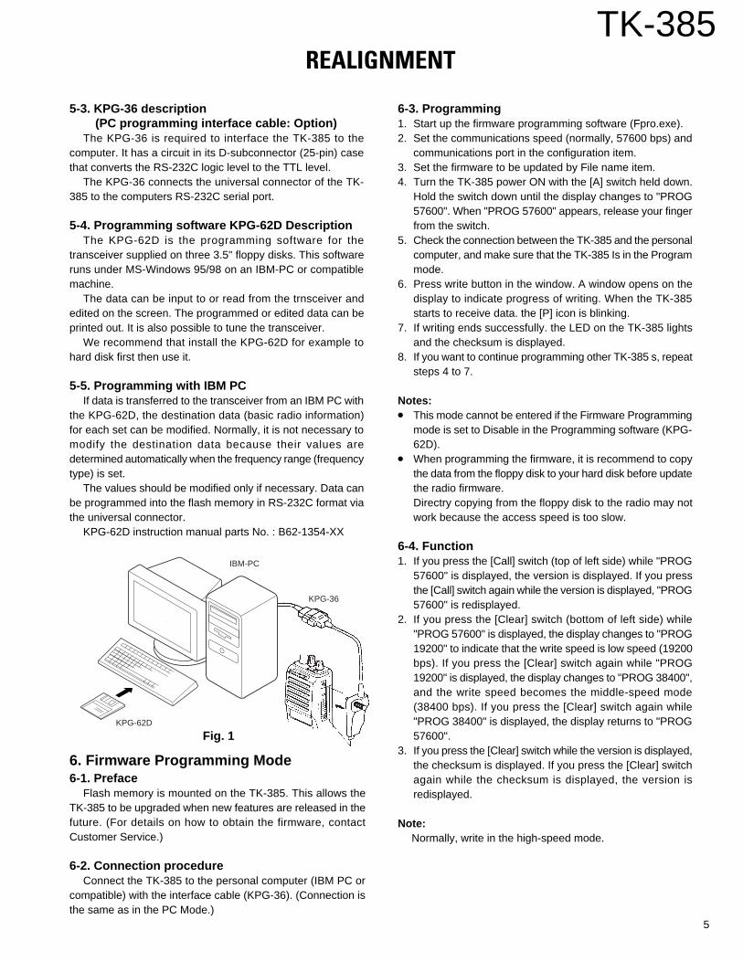
5. PC Mode5-1. Preface
The TK-385 transceiver is programmed by using a personalcomputer, programming interface (KPG-36) and programmingsoftware (KPG-62D).
The programming software can be used with an IBM PC orcompatible. Figure 1 shows the setup of an IBM PC forprogramming.
5-2. Connection procedure1. Connect the TK-385 to the personal computer with the
interface cable.2. When the POWER switch on, user mode can be entered
immediately. When PC sends command the radio enter PCmode, and “PROGRAM” is displayed on the LCD.When data transmitting from transceiver, the red LED isblinking.When data receiving to transceiver, the green LED is blinking.
Notes:• The data stored in the personal computer must match model
type, when it is written into the flash memory.• Change the TK-385 to PC mode, then attach the interface
cable.
Mode FunctionUser mode For normal use.Panel test mode Used by the dealer to check the
fundamental characteristics.Panel tuning mode Used by the dealer to tune the radio.PC mode Used for communication between the
radio and PC (IBM compatible).Data program- Used to read and write frequency dataming mode and other features to and from the radio.PC test mode Used to check the radio using the PC.
This feature is included in the FPU.See panel tuning.
Firmware program- Used when changing the mainming mode program of the flash memory.
3. Panel Test ModeSetting method refer to ADJUSTMENT.
4. Panel Tuning ModeSetting method refer to ADJUSTMENT.
2. How to Enter Each ModeMode Operation
User mode Power ONPanel test mode [B]+Power ONPC mode Received commands from PCPanel tuning mode [Panel test mode]+[A]Firmware programming mode [A]+Power ON
REALIGNMENT
1. Modes
User mode
Panel test mode
PC mode
Firmwareprogramming mode
Panel tuning mode
PC test mode
Data programmingmode
PC tuning mode
OPERATING FEATURES / REALIGNMENT
2-4. Display
1 Sub display displays the strength of received signals.
2 Programming indicator P appears while in AUX A or Scrambler is being activated.
3 MON (Monitor) indicatorMON appears while you are monitoring a channel by pressingthe Call key. (Conventional Mode only)
4 SVC (Service) indicatorSVC appears when a control channel is found. It flasheswhile the transceiver is searching for a control channel.
5 SCN (Scan) indicatorSCN appears while you are scanning. (Conventional Modeonly)
6 LO indicatorThis icon blinks while in battery warning, if “Always” or“Always W/beep” is selected in the battery warning settings.
7 Handset indicator flashes when you activate call diversion.
8 MAIL indicatorappears while there is data in the stack. It flashes when
there is new data in the stack.
9 Alphanumeric displaydisplays call addresses, the call
duration timer, data messages, and the current operatingstatus of the transceiver.
SVCMON SCN LO
1 2 3 4 5
9
6 7 8
TK-385
5
6-3. Programming1. Start up the firmware programming software (Fpro.exe).2. Set the communications speed (normally, 57600 bps) and
communications port in the configuration item.3. Set the firmware to be updated by File name item.4. Turn the TK-385 power ON with the [A] switch held down.
Hold the switch down until the display changes to "PROG57600". When "PROG 57600" appears, release your fingerfrom the switch.
5. Check the connection between the TK-385 and the personalcomputer, and make sure that the TK-385 Is in the Programmode.
6. Press write button in the window. A window opens on thedisplay to indicate progress of writing. When the TK-385starts to receive data. the [P] icon is blinking.
7. If writing ends successfully. the LED on the TK-385 lightsand the checksum is displayed.
8. If you want to continue programming other TK-385 s, repeatsteps 4 to 7.
Notes: This mode cannot be entered if the Firmware Programming
mode is set to Disable in the Programming software (KPG-62D).
When programming the firmware, it is recommend to copythe data from the floppy disk to your hard disk before updatethe radio firmware.Directry copying from the floppy disk to the radio may notwork because the access speed is too slow.
6-4. Function1. If you press the [Call] switch (top of left side) while "PROG
57600" is displayed, the version is displayed. If you pressthe [Call] switch again while the version is displayed, "PROG57600" is redisplayed.
2. If you press the [Clear] switch (bottom of left side) while"PROG 57600" is displayed, the display changes to "PROG19200" to indicate that the write speed is low speed (19200bps). If you press the [Clear] switch again while "PROG19200" is displayed, the display changes to "PROG 38400",and the write speed becomes the middle-speed mode(38400 bps). If you press the [Clear] switch again while"PROG 38400" is displayed, the display returns to "PROG57600".
3. If you press the [Clear] switch while the version is displayed,the checksum is displayed. If you press the [Clear] switchagain while the checksum is displayed, the version isredisplayed.
Note:Normally, write in the high-speed mode.
5-3. KPG-36 description(PC programming interface cable: Option)
The KPG-36 is required to interface the TK-385 to thecomputer. It has a circuit in its D-subconnector (25-pin) casethat converts the RS-232C logic level to the TTL level.
The KPG-36 connects the universal connector of the TK-385 to the computers RS-232C serial port.
5-4. Programming software KPG-62D DescriptionThe KPG-62D is the programming software for the
transceiver supplied on three 3.5" floppy disks. This softwareruns under MS-Windows 95/98 on an IBM-PC or compatiblemachine.
The data can be input to or read from the trnsceiver andedited on the screen. The programmed or edited data can beprinted out. It is also possible to tune the transceiver.
We recommend that install the KPG-62D for example tohard disk first then use it.
5-5. Programming with IBM PCIf data is transferred to the transceiver from an IBM PC with
the KPG-62D, the destination data (basic radio information)for each set can be modified. Normally, it is not necessary tomodify the destination data because their values aredetermined automatically when the frequency range (frequencytype) is set.
The values should be modified only if necessary. Data canbe programmed into the flash memory in RS-232C format viathe universal connector.
KPG-62D instruction manual parts No. : B62-1354-XX
6. Firmware Programming Mode6-1. Preface
Flash memory is mounted on the TK-385. This allows theTK-385 to be upgraded when new features are released in thefuture. (For details on how to obtain the firmware, contactCustomer Service.)
6-2. Connection procedureConnect the TK-385 to the personal computer (IBM PC or
compatible) with the interface cable (KPG-36). (Connection isthe same as in the PC Mode.)
KPG-36
IBM-PC
KPG-62D
Fig. 1
REALIGNMENT

TK-385
6
CIRCUIT DESCRIPTION
1. OverviewThis transceiver is UHF/FM portable transceiver designed
to operate in the frequency range of 450 to 470MHz (K).
2. Circuit Configuration by FrequencyThe receiver is a double-conversion superheterodyne with
a first intermediate frequency (IF) of 44.85MHz and a secondIF of 455kHz. Incoming signals from the antenna are mixedwith the local signal from the PLL to produce the first IF of44.85MHz.
This is then mixed with the 44.395MHz second localoscillator output to produce the 455kHz second IF. This isdetected to give the demodulated signal.
The transmit signal frequency is generated by the PLL VCO,and modulated by the signal from the microphone. It is thenamplified and sent to the antenna.
ANTTX/RX : 450~470MHz : K
ANTSW
RFAMP
PAAMP
TXAMP
1st MIX MCF
44.85MHz
CF455kHz
FM IFSYSTEM
AFAMP
SP
44.395MHz
405.15~425.15MHz : KPLLVCO
MICAMP MIC
450~470MHz : K
Fig. 1 Frequency configuration
3. Receiver System3-1. RF unit
An incoming RF signal from the antenna terminal is passedthrough the antenna switch (D12, D14. D15 and D401 are off)and then the bandpass filter (L47,48,49,51,52,54,55,56). Thebandpass filter is adjusted by a variable capacitor. The inputvoltage to the variable capacitor is regulated by the voltageoutput from the D/A converter (IC8). The signal is amplified byRF amplifier Q24, and passed through the bandpass filter(L29,31,33,34,36) and band-eliminate filter (L27) to removethe spurious signal again. The resulting signal is applied to thefirst mixer (IC18), where it is mixed with the first local oscillatorsignal output from the frequency synthesizer to produce thefirst IF (44.85MHz). The 1st mixer uses the GaAs IC.
3-2. IF unitThe first IF signal is passed through a crystal filter (XF1) to
remove a adjacent channel signal. The filtered first IF signal isamplified by the first IF amplifier (Q12) and then applied to thelF system IC (IC12). The IF system IC provides a second mixer,second local oscillator, limiting amplifier, quadrature detectorand RSSI (Received Signal Strength Indicator). The secondmixer mixes the first IF signal with the 44.395MHz of secondlocal oscillator output (crystal unit X2) and produces the secondIF signal of 455kHz.
The second IF signal is passed through the ceramic filter(CF2) to more remove the adjacent channel signal. The filteredsecond IF signal is amplified by the limiting amplifier anddemodulated by the quadrature detector with ceramicdiscriminator (CD1). The demodulated signal is routed to theaudio circuit.
Fig. 2 Receiver section
IC12 MIX, DET, IF SW
Q15
DMDM
IC4 (2/2)AF AMP
5DE-EMP MUTEEXP
HPF LPF HPF BEFIC13 2 1
VOL
IC8IC7 (2/2)AF AMP
41VC1
VC2
Q310
SSW
INT.SP
EXT.SP
2nd localOSC
X2
AF AFSW
IC300AF PA
ANTSW
L40,42,43
L47,48,49,51,52,54,55,56BPF
D12,14D15,401
Q24RF
AMP
ANT
IC181st MIX
Q121st IF
L27BEF
L29,31,33,34,36
BPFXF1MCF
1st LocalOSC (PLL)
CF1 : Wide,
CF2 : NarrowSemi wide

TK-385
7
3-5. Squelch circuitThe output from IC12 enters FM IC again, then passed
through a band-pass filter. The noise component output fromIC12 is amplified by Q4 and rectified by D4 to produce a DCvoltage corresponding to the noise level. The DC voltage issent to the analog port of the CPU (IC19). And IC12 outputs aDC voltage (RSSI) corresponding to the input of the IF amplifier.The CPU reads the RSSI signal via pin 93.
IC19 determines whether to output sounds from the speakerby comparing the input voltage of pin 91 and pin 93 with thepreset value.
Fig. 4 Squelch circuit
12
DETBPFAMP
DET
RSSI NOISEAMP
IC19CPU
IF AMP
7
91
93
IC12 : FM IF IC
Q4 D4
Fig. 5 Squelch and RSSI voltage vs ANT input level
SQ close
1
5
9SQ open
ANT input level
SQ
vo
ltag
e
ANT input level
RS
SI v
olt
age
SQ
leve
l
Preset value
4. Transmitter System4-1. Microphone amplifier
The signal from the internal microphone goes through themute switch (Q300).
When the SP-MIC is not attached, the microphone switchingterminal (MSW) on the universal connector becomes High, andmute switch (Q300) is turned ON. When the SP-MIC isattached, MSW is connected to GND at inside of SP-MIC. Forthis reason, Q300 is turned OFF, the internal microphone ismuted, and only the input of the external microphone is suppliedto the microphone amplifier of the TX-RX unit.
The signal from microphone passes through the limittercircuit in D8, Mic mute switch (Q17 is off in TX) and throughthe low-pass filter (IC25 : 1/2), the high-pass filter, the ALCcircuit, the low-pass filter, the high-pass filter, and pre-emphasis/IDC circuit in IC13. When encoding DTMF, muteswitch (Q13) is turned OFF for muting the microphone inputsignal.
The signal passes through the D/A converter (IC8) for themaximum deviation adjustment, and enters the summingamplifier consisting of IC7 (1/2), and is mixed with the low speeddata from the CPU (IC19) and 9600bps DATA from OptionalBoard Terminal.
Fig. 3 Audio amplifier circuit
3-3. Audio amplifier circuitThe demodulated signal from IC12 goes through the mute
switch (Q15) and is amplified by IC4 (2/2), high-pass filtered,low-pass filtered, high-pass filtered, band-eliminate filtered, andde-emphasized by IC13.
The signal then goes through an AF amplifier IC7 (2/2), anelectronic volume control (IC8), and an AF switch (Q310 ison), and is routed to audio power amplifier (IC300), where it isamplified and output to the internal speaker.
The audio mute signal (AM) from the shift register becomesLow in the standby and Q304, Q305 which are power supplycircuit for IC300 turn off. Also, IC13 is set to the power downmode according to data from microprocessor, and the AF signalis muted. When the audio is output, AM becomes High to turnQ304, Q305 ON, and voltage is supplied to power terminal VPof IC300. Also, IC13 is canceled out of the power down mode.
The speaker is switched by the logic of speaker switchingterminal SSW on the universal connector. When SP-MIC isnot attached, the logic of SSW becomes High and SW (Q310)is turned ON, and the AF signal is input to both amplifiers ofIC300.
When SP-MIC is attached, SSW is connected to GND atinside of SP-MIC. For this reason, Q310 is turned OFF, andthe AF signal is input only to amplifier for EXT SP of IC300.
Change of INT/EXT SP refer to Fig. 3.
AM SSW VC1 VC2 SPH H H L INTH L L H EXTL H L L MUTEL L L L MUTE
SW
IC300
2
8
AM
AF
SSW
INT.SP
EXT.SP
Q305
Q304
SB
VP 5
VC1
VC2Q308
Q301
CIRCUIT DESCRIPTION

TK-385
8
5. Frequency Synthesizer Unit5-1. Frequency synthesizer
The frequency synthesizer consists of the VCXO (X1), VCO(A1), PLL IC(IC14) and buffer amplifiers.
The VCXO generates 16.8MHz. The frequency stability is1.5ppm within the temperature range of -30 to +60˚C. Thefrequency tuning and modulation of the VCXO are done toapply a voltage to pin 1 of the VCXO. The output of the VCXOis applied to pin 8 of the PLL IC.
The TK-385’s VCO consists of 2VCO and covers a dual rangeof the 405.15~425.15MHz and the 450~470MHz. The VCOgenerates 405.15~425.15MHz for providing to the first local signalin receive. In TX, the pin 3 of the VCO goes low and the VCOgenerates 450~470MHz.
The output of the VCO is amplified by the buffer amplifier(Q16) and routed to the pin 5 of the PLL IC. Also the output ofthe VCO is amplified by the buffer amplifier (Q18) and routedto the next stage according to T/R switch (D9, D23).
The PLL IC consists of a prescaler, fractional divider,reference divider, phase comparator, charge pump. This PLLIC is fractional-N type synthesizer and performs in the 40.50or 60kHz reference signal which is eighth of the channel step(6.25kHz). The input signal from the pins 5 and 8 of the PLL ICis divided down to the 50kHz and compared at phasecomparator. The pulsed output signal of the phase comparatoris applied to the charge pump and transformed into DC signalin the loop filter (LPF). The DC signal is applied to the pin 1 ofthe VCO and locked to keep the VCO frequency constant.
PLL data is output from DT (pin 75). CP (pin 19) and EP(pin 47) of the microprocessor (IC19). The data are input tothe PLL IC when the channel is changed or when transmissionis changed to reception and vice versa.
Fig. 8 PLL block diagram
T/R(TX : Low)
T/RA1
VCO
CV
5
IC14
PLL8
BUFF
BUFF
LPF
DT,CP,EPCPU
UL
IC19
VCXO IC1
FC
BAL
Q18
SW
D9Todriveamp
Q16
X1
To mixer
SW
MB
D23
18
CIRCUIT DESCRIPTION
The output signal from the summing amplifier passesthrough the D/A converter (IC8) again and goes to the VCOmodulation input.
The other output signal from the summing amplifier passesthrough the D/A converter (IC8) again for the BAL adjustment,and the buffer amplifier (IC1 (2/2)), and goes to the VCXOmodulation input.
4-2. Drive and Final amplifierThe signal from the T/R switch (D9 is on) is amplified by the
pre-drive (Q18) and drive amplifier (Q20) to 50mW.The output of the drive amplifier is amplified by the RF power
amplifier (IC100) to 4.0W (1W when the power is low). The RFpower amplifier consists of two stages MOS FET transistor.The output of the RF power amplifier is then passed throughthe harmonic filter (LPF) and antenna switch (D12, D401 ison) and applied to the antenna terminal.
Fig. 6 Microphone amplifier
Fig. 7 Drive and final amplifier and APC circuit
12HPF LPF HPF IDCPRE
EMPALC COMP
SW
LIMITSWMIC
Q300 D8
LPF
IC25 (1/2)MIC
EXT.MIC
Q301
IC13 15 16 18 19
Q13MUTE DTMF
9 8
6
D/A
D/A
IC8
IC8 IC1
I5 O5
I1 O1
D/AIC8
I2 O2
LSD DI9
IC7 (1/2)
SUMAMP
BUFFAMP VCXO
VCO
A1
X1
MICMUTE
Q17
PTTMSW
FromT/R SW
(D9)
Pre-DRIVEAMP
DRIVEAMP
RFPOWER AMP LPFANT
SW
D12,D401
ANT
VGG
Q18 Q20 IC100
VDD
R245
R247
R249
+B
IC23(1/2)
IC23(2/2)REF
VOL(IC8)
4-3. APC circuitThe APC circuit always monitors the current flowing through
the RF power amplifier (IC100) and keeps a constant current.The voltage drop at R245, R247 and R249 is caused by thecurrent flowing through the RF power amplifier and this voltageis applied to the differential amplifier (IC23 1/2).
IC23(2/2) compares the output voltage of IC23(1/2) withthe reference voltage from IC8, and the output of IC23(2/2)controls the VGG of the RF power amplifier to make the bothvoltages to same voltage.
The change of power high/low is carried out by the changeof the reference voltage. Q22,23 and 25 are turned on intransmit and the APC circuit is active.

TK-385
9
6-2. Low battery warningThe battery voltage is monitored by the microprocessor
(IC19). When the battery voltage falls below the voltage set bythe Low Battery Warning adjustment, the red LED flashes tonotify the operator that it is time to replace the battery. If thebattery voltage falls even more (approx. 5.8V), a beep soundsand transmission is stopped.
6-3. Key inputIf the clock is supplied to CLK terminal when the RES
terminal (CPU pin 78) of the decade counter (IC301) is set toLow, Q0 to Q7 become High sequentially. Normally, KI1 andKI2 are Low (pulled down). When any key is pressed, KI1 orKI2 become High. The CPU detects which key is pressed,according to the voltage of KI1 and Kl2 and clock timing.
Low battery warning
The red LED flashes duringtransmission
The red LED flashes andcontinuous beep soundswhile PTT pressed
Battery condition
The battery voltage is low butthe transceiver is still usable.
The battery voltage is low andthe transceiver is not usableto make calls.
Fig. 10 Key inputRESET
CLOCK
Q0
Q1
Q2
Q3
Q4
Q5
Q6
Q7
Q8
Q9
CLOCKINHIBIT
CARRYOUT
Fig. 11 Decade counter timing chart
IC19CPU
Q5Q1Q0Q2Q6Q7Q3Vss
VddRESCLK
CLCAQ9Q4Q8
KI1
KI2
CK
KRST
IC301
16 keys
CIRCUIT DESCRIPTION
6. Control CircuitThe control circuit consists of microprocessor (IC19) and
its peripheral circuits. It controls the TX-RX unit and transfersdata to and from the display unit. IC19 mainly performs thefollowing;
1) Switching between transmission and reception by PTTsignal input.
2) Reading system, group, frequency, and program datafrom the memory circuit.
3) Sending frequency program data to the PLL.4) Controlling squelch on/off by the DC voltage from the
squelch circuit.5) Controlling the audio mute circuit by decode data input.6) Transmitting tone and encode data.
6-1. Memory circuitMemory circuit consists of the CPU (IC19) and a flash
memory (IC17).A flash memory has a capacity of 2M bits and contains the
transceiver control program for the CPU and the data foroperating features.
This program can be easily downloaded from an externaldevice.
Flash MemoryNote : The flash memory stores the data containing the FPU(KPG-62D) program, Security Number (MPT Serial Number)and firmware program (User mode, Test mode, Tuning mode,etc.).This data must be reinstalled when replacing the flash memory.
EEPROMNote : The EEPROM stores tuning data (Deviation, Squelch,etc.).Realign the transceiver after replacing the EEPROM.
Fig. 9 Memory circuit
IC19
IC17
CPU
IC20
EEPROM
FLASH

TK-385
10
Fig. 13 Decode
IC13AF IC
IC4AMP IC11
LPFLSD IN
AF RDTIN
IC19CPU
21
23
7-2. Decode Low-speed data (QT,DQT)
The demodulated signal from the IF IC (IC12) is amplifiedby IC4 (2/2) and passes through a low-pass filter (IC11) toremove audio components. The signal is input to pin 95 of theCPU.
The CPU digitizes this signal, performs processing such asDC restoration, and decodes the signal.
FFSKThe FFSK input signal from the IF IC is amplified by IC4
(1/ 2) and goes to pin 5 of IC13. The signal is demodulated byFFSK demodulator in IC13. The demodulated data goes tothe CPU for processing.
8. Power Supply CircuitBattery +B is supplied via a 3A fuse from the battery terminal
connected to the TX-RX unit. After passing through the powerswitch, power supply (SB) is applied to the three AVRs. IC5supplies 5V (5M) to the control circuit, and IC9 supplies 5V(5C) to common circuits. IC6 supplies to the TX circuit, the RXcircuit and common circuits of needless save mode. Duringtransmission, 5TC becomes Low and Q3 is turned ON to supply5V (5T) to the TX circuit. During reception, 5RC becomes Lowand Q2 is turned ON to supply 5V (5R) to the RX Circuit.
Fig. 14 Power supply circuit
Display unit
Q2
5RC
5TC
5R
5T
5CNS
IC6
IC9
IC5
Q3
RF power amp (IC100)+BF1
SB
ON/OFFVOL
5M
5C
CIRCUIT DESCRIPTION
7. Signalling Circuit7-1. Encode Low-speed data (QT,DQT)
Low-speed data is output from pin 1 of the CPU. The signalpasses through a low-pass CR filter, and goes to the summingamplifier (IC7 1/2). The signal is mixed with the audio signaland goes to the VCO (A1) and VCXO (X1) modulation inputafter passing through the D/A converter (IC8) for BALadjustment.
High-speed data (DTMF)High-speed data is output from pin 2 of the CPU. The signal
passes through a low-pass filter consisting of IC10, andprovides a TX HSD tone and a RX HSD tone TX HSD deviationmaking an adjustment by microprocessor is passed throughthe D/A convertor (IC8), and then applied to the audio processor(IC13).
The signal is mixed with the audio signal and goes to theVCO and VCXO, the RX HSD tone is passed a summingamplifier (IC7 2/2), the D/A converter (IC8) for audio control,audio power amplifier and then to the speaker.
FFSKESN utilizes 1200bps FFSK signal. FFSK signal is output
from pin 6 of IC13. The signal passes through the D/A converter(IC8) for the FFSK deviation adjustment. and is routed to theVCO. When encoding FFSK, the microphone input signal ismuted.
Fig. 12 Encode
SUM
SUM
IC7(1/2)
SUM
R166 R162
C17
5
C16
9
R13
7
1
LSDOUT
HSDOUT
IC19CPU
O5
O2
O3
O6
I2
I5
IC8D/A (ADJ)
VCOMD
A1
RX Audio
MIC IN
IC132
LPFIC10
I6
I3
VCXOX1
MB
AFAMP
IC7 (2/2)
O1 BUFFAMP
IC1

TK-385
11
9. Optional Board TerminalTerminals for mounting the option board are provided at
the bottom edge of the TX-RX unit. The table below shows thecorrespondence between the board and terminals. R37, R69,R250, R259, R260, R276, R280 may have to be removeddepending on the type of option board being used.
Name FunctionSB Battery (7.5V)GND GroundTXD Serial dataRXD Serial dataSQ Busy: highLOK Link acquired : low (TX mode)DI/ANI Modulation (ANI) inputDEO Detect outputTXAI/MUTE Modulation output from board or mic mute: lowTXAO Modulation input to boardRXAI Received signal input to boardRXAO Received signal output from boardD1 Binary 1D2 Binary 2OPT Scramble, Emergency:lowPTTIN PTT switch signal input to board (TX:low)5CNS Battery (5V)DI9 9600 bps data inputRXEMAO Received signal output from board (after de-
emphasis)RXEMAI Received signal input to board (after de-
emphasis)PTTOUT PTT switch signal output from board (TX:low)MONI Busy:lowLAMP Busy:lowAAC Audio Amp Control signal output from board
(Busy:high)Audio Beep Beep signal output from board.AUX TXD Serial dataAUX RXD Serial data/Option switch port/EXT SW
Table 1 Terminal name and function
Microprocesser : 30620M8A-394GP(TX-RX UNIT : IC19)
Pin function
1 LSDOUT O Low speed data output.2 HSDOUT O High speed data output.3 HSDIN I High speed data input.4 DTMSTD I DTMF decode IC data detect input.5 SELF I Self programming mode input.6 BYTE I +5V.7 CNVSS I GND.8 SFTOE O Shift register output enable.9 LCDCS O LCD driver chip select output.
10 RESET I Microcomputer reset input.11 XOUT - 9.8304MHz (System clock).12 VSS - GND.13 XIN - 9.8304MHz (System clock).14 VCC - +5V15 AUX I AUX switch input.16 AFTRD I FFSK modulation data output timing pulse
input.17 AFRTM I FFSK demodulation data input timing pulse
input.18 EN2 I Encoder pulse input 2.19 PLLCLK O PLL IC clock output.20 BEEP O Beep data output.21 AFRDT I FFSK demodulation data input.22 AFREG1 O AF IC register switching data output 1.23 AFREG2 O AF IC register switching data output 2.24 EEPDAT O EEPROM data output.25 DACSTB O D/A converter IC data strobe output.26 AFCLR O FFSK flame reset output.27 SAVE O Battery save output.28 LAMP I LAMP switch input.29 AUXTXD O External Serial interface output.30 AUXRXD I External Serial interface input.31 PLLUL I PLL unlock detect input.32 AFFFSKE O FFSK modulation enable (Enable active “H”).33 TXD O Serial interface output (ex. PC).34 RXD I Serial interface input (ex. PC).35 AFDAT O FFSK data output.36 PTT I PTT switch input.37 RDY - Not used.38 ALE - Not used.39 HOLD - Not used.40 HLDA - Not used.41 BLCK - Not used.42 RD - Flash memory RD bus.43 BHE - Not used.44 WR - Flash memory WR bus.45 DTMCLK O DTMF decode IC clock output.46 CNTCLK O Common clock output.47 PLLSTB O PLL IC data strobe output.48 CS0 O Flash memory chip enable.49 A19 - Not used.
Pin Port I/O FunctionNo. Name
CIRCUIT DESCRIPTION / SEMICONDUCTOR DATA

TK-385
12
PLL System : SA7025DK (TX-RX Unit : IC14) Block diagram
1 CLOCK Serial clock input.2 DATA Serial data input.3 STROBE Serial strobe input.4 Vss Digital ground.5 RFIN Prescaler positive input.6 RFIN Prescaler negative input.7 VccP Prescaler positive Supply voltage. This pin supplies
power to the prescaler and RF input buffer.8 REFIN Reference divider input.9 RA Auxiliary current setting; resistor to VSSA.
10 AUXIN AuxIliary divider input.11 PHA Auxiliary phase detector output.12 VSSA analog ground.13 PHI Integral phase detector output.14 PHP Proportional phase detector output.15 VDDA Analog supply voltage. This pin supplies power
to the charge pumps, Auxiliary prescaler.Auxiliary and Reference buffers.
16 RN Main current setting; resistor to VSSA.17 RF Fractional compensation current setting;
resistor to VSSA.18 LOCK Lock detector output.19 TEST Test pin; connect to VDD.20 VDD Digital supply voltage. This pin supplies power
to the CMOS digital part of the device.
Pin No. Symbol Description
Pin description
SEMICONDUCTOR DATA
Pin Port I/O FunctionNo. Name50~59 A9~A18 - Flash memory address bus.
60 VCC - +5V61 A8 - Flash memory address bus.62 VSS - GND.
63~70 A0~A7 - Flash memory address bus.71 MONI I Monitor switch input.72 EN4 I Encoder pulse input 4.73 EN3 I Encoder pulse input 3.74 EN1 I Encoder pulse input 1.75 MINDAT O Common data output.76 KEY2 I Key scan input 2.77 KEY1 I Key scan input 1.78 RESET O Key scan IC reset output..
79~86 D0~D7 - Flash memory data bus.87 DTMDAT I DTMF decode IC data input.88 PF I PF switch input.89 VOL I Volume level input.90 BATT I Battery voltage input.91 ANLSQL I Squelch level input.92 TEMP I Thermistor input.93 RSSI I Received signal strength indicator input
(RSSI).94 AVSS - GND.95 LSDIN I Low speed data input.96 VREF - +5V97 AVCC - +5V98 SFTSTB1 O Shift register data strobe output.99 W/N O Wide/Narrow switching output.100 AFSTB O AF IC data strobe output.

TK-385
13
DESCRIPTION OF COMPONENTS
IC1,2 IC Buffer amplifier
IC3 IC Voltage detector / Reset
IC4 IC Buffer amplifier
IC5 IC Voltage regulator / 5M
IC6 IC Voltage regulator / 5V
IC7 IC Buffer amplifier
IC8 IC D/A converter (Adjustment)
IC9 IC Voltage regulator / 5C
IC10 IC Active filter / For HSDout
IC11 IC Active filter / For LSDin
IC12 IC FM IF system
IC13 IC Audio processor
IC14 IC PLL system
IC16 IC DTMF decoder
IC17 IC Flash memory
IC18 IC Active DBM
IC19 IC Microprocessor
IC20 IC EEPROM
IC21,22 IC Shift register / Output expander
IC23 IC Comparator (APC)
IC24 IC Analog switch
IC25 IC Active filter
Q1 Transistor Switch
Q2 FET DC switch / 5R
Q3 Transistor DC switch / 5T
Q4 Transistor Noise amplifier / Squelch
Q5 FET DC switch / Save
Q6 Transistor 2nd IF W/N switch sets to on when Narrow
DISPLAY UNIT (X54-3210-12)
Q7 Transistor 2nd IF W/N switch sets to on when Wide
Q8 Transistor Ripple filter
Q9 Transistor DC switch / W/N audio amplitude adjust
Q10 Transistor AF mute switch
Q11 FET Mute switch
Q12 Transistor IF amplifier
Q13 FET Mute switch / MIC line mute
Q14 FET DC switch
Q15 FET DET mute
Q16 Transistor PLL IC fin amplifier
Q17,18 Transistor Buffer amplifier
Q19 Transistor Clock frequency shift
Q20 Transistor RF amplifier / TX driver
Q21 FET DC switch
Q22 Transistor DC switch
Q23 FET DC switch
Q24 FET RF amplifier
Q25 Transistor DC switch
Q26 FET Mute switch / MIC line mute
D1 Diode Reverse protection
D2 Diode Overload protection
D3 Diode Reverse current protection
D4 Diode Noise detection
D5 Diode RF switch (2nd IF wide/narrow)
D6 Diode Current steering
D7 Diode RF switch (2nd IF wide/narrow)
D8 Diode Voltage clamp
D9 Diode TX/RX switch
D10 Diode Overload protection
D11 Diode Speed up
D12,14,15 Diode ANT switch
D16 Diode Overload protection
D17,18 Diode Surge absorption
D20,22 Diode Varactor tuning
D23 Diode Voltage drop
D24,25 Diode ANT switch
D401 Diode ANT switch
D402 Diode Discharge
IC300 IC Audio power amplifier
IC301 IC Counter /Key scan
Q300 FET DC switch / INT MIC on/off
Q301 FET DC switch
Q302 Transistor DC switch / LED (Red) driver
Q303 Transistor DC switch / LED (Green) driver
Q304 Transistor DC switch
Q305 Transistor Current driver / Audio amp AVR
Q306 Transistor DC switch
Q307 Transistor Current driver / LCD back light LED AVR
Q308 FET DC switch / SP INT/EXT
Q309 Transistor Temperature compensation
Q310 FET Mute switch
D300 Zener diode Surge absorption
D301 LED LED / Red, Green
D302 Diode Quick discharge /AF mute
D303 Zener diode Voltage reference
D304 Diode Voltage reference
D305~310 LED LCD back light
D315~318 Diode Reverse current prevention
D319~321 Zener diode Surge absorption
Ref. No. Use/Function Operation/Condition
Ref. No. Use/Function Operation/Condition
TX-RX UNIT (X57-6200-10)
Ref. No. Use/Function Operation/Condition
Q50 FET VCO oscillation
Q51 FET DC switch
Q52 FET VCO oscillation
Q53 Transistor DC switch
Q54 Transistor RF Buffer amplifier
D50-D57 Diode Frequency control
D58 Diode TX modulation
Ref. No. Use/Function Operation/Condition
SUB UNIT (X58-4592-71)

TK-385PARTS LIST
Parts No. DescriptionAddress NewpartsDestination DestinationRef. No. Parts No. DescriptionAddress New
parts Ref. No.
TK-385
∗ New Parts. indicates safety critical components.Parts without Parts No. are not supplied.Les articles non mentionnes dans le Parts No. ne sont pas fournis.Teile ohne Parts No. werden nicht geliefert.TK-385DISPLAY UNIT (X54-3210-12)
L: Scandinavia K: USA P: CanadaY: PX (Far East, Hawaii) T: England E: EuropeY: AAFES (Europe) X: Australia M: Other Areas
14
!
51 1B K29-5231-03 KNOB (VOL)52 1B K29-5232-03 KNOB (ENC)
A 3B N14-0569-04 CIRCULAR NUT (VOL,ENC)B 3B N30-2604-46 PAN HEAD MACHINE SCREW(ANT)C 3A N30-2610-46 PAN HEAD MACHINE SCREW(CASE)D 2B N67-2606-46 PAN HEAD SEMS SCREW W(P-MODULE)E 3A,3B N79-2025-46 PAN HEAD TAPTITE SCREW(TERMINAL)
F 2A,2B N83-2005-46 PAN HEAD TAPTITE SCREW(UNIT)53 2C N99-2004-05 SCREW SET ACSY
54 3B R31-0617-05 VARIABLE RESISTOR(POWER SW/VOL)
55 2B S70-0414-05 TACT SWITCH
SP 1B T07-0714-05 SPEAKERMIC 2B T91-0579-05 MIC ELEMENT
IC100 2B M68732HA IC(POWER MODULE)
56 3B W02-1814-05 ENCODER57 3A G13-1794-04 CUSHION(MCF)
X54-3210-12 DISPLAY UNITD301 B30-2019-05 LED(RE/GR)D305-310 B30-2171-05 LED
C301 CC73GCH1H470J CHIP C 47PF JC302 C92-0560-05 CHIP-TAN 10UF 6.3WVC304 CK73FB1C474K CHIP C 0.47UF KC305 CC73GCH1H101J CHIP C 100PF JC307 CK73GB1C104K CHIP C 0.10UF K
C308 CC73GCH1H101J CHIP C 100PF JC309 CK73FB1C474K CHIP C 0.47UF KC310 CK73GB1C104K CHIP C 0.10UF KC311 CC73GCH1H470J CHIP C 47PF JC312 CK73GB1C104K CHIP C 0.10UF K
C313 C92-0628-05 CHIP-TAN 10UF 10WVC314 C92-0647-05 TAN C 3.3UF 4WVC315 CC73GCH1H101J CHIP C 100PF JC316,317 CC73GCH1H470J CHIP C 47PF JC318 CC73GCH1H101J CHIP C 100PF J
C321-333 CC73GCH1H470J CHIP C 47PF JC335-339 CC73GCH1H470J CHIP C 47PF JC340 CK73GB1E153K CHIP C 0.015UF KC341-344 CC73GCH1H470J CHIP C 47PF J
CN300 E40-5891-05 FLAT CABLE CONNECTOR(24P)CN301 E40-5892-05 FLAT CABLE CONNECTOR(14P)CN302 E40-5662-05 PIN ASSY SOCKET(2P:SP)CN303 E40-5887-05 PIN ASSY(4P:PTT)CN304 E40-5823-05 FLAT CABLE CONNECTOR(10P:LCD)
L300,301 L92-0141-05 FERRITE CHIPL302,303 L92-0138-05 FERRITE CHIPL304,305 L92-0141-05 FERRITE CHIPL306,307 L92-0138-05 FERRITE CHIPL308,309 L92-0141-05 FERRITE CHIP
1 1A A02-2055-53 CABINET ASSY (16KEYS)2 3B A62-0535-04 PANEL ASSY
3 2C B09-0363-03 CAP (SP/MIC) ACSY4 2A B38-0834-05 LCD ASSY5 1B B43-1106-14 BADGE (KENWOOD)7 2C ∗ B62-1264-00 INSTRUCTION MANUAL ACSY8 3B ∗ B72-1718-04 MODEL NAME PLATE
9 3B E04-0416-05 RF COAXIAL RECEPTACLE(SMA)10 2B E23-1104-04 TERMINAL (ANT)11 3A,3B E23-1166-04 RELAY TERMINAL12 2B E37-0672-05 FLAT CABLE13 3A E37-0673-05 LEAD WIRE WITH CONNECTOR(PTT)
14 1B E37-0674-15 LEAD WIRE WITH CONNECTOR(SP)15 3B E58-0440-05 SQUARE SOCKET (SP/MIC)16 3B ∗ E72-0412-13 TERMINAL BLOCK
17 2B F10-2272-03 SHIELDING CASE (DBM)18 2A F10-2310-03 SHIELDING PLATE(LCD)19 2A F10-2340-03 SHIELDING CASE (VCO-OUT)20 3B F10-2353-14 SHIELDING PLATE(P-MODULE)21 2B F10-2360-03 SHIELDING CASE (FRONT END)
22 2B ∗ F10-2373-14 SHIELDING CASE23 2B F20-1181-04 INSULATING SHEET24 2B F20-3303-04 INSULATING SHEET(MIC/GND)
25 1A G01-0881-04 COIL SPRING26 1B G09-0418-05 KNOB SPRING (MIC,ENC)27 1B G10-0799-04 FIBROUS SHEET (SP)28 3A G11-2544-04 SHEET (CHASSIS)29 3A G11-2590-04 SHEET (PTT)
30 2A G13-1731-04 CUSHION (LCD)31 2A G13-1736-04 CUSHION32 3B G13-1762-04 CUSHION (VOL/CHASSIS)33 3A,3B G13-1791-14 CUSHION (TERMINAL)34 3B G53-0811-03 PACKING (TOP)
35 1B G53-0896-02 PACKING (16KEYS)36 G53-1510-04 PACKING (BATT+)37 3B G53-1520-24 PACKING (TERMINAL)
38 2D H12-3014-02 PACKING FIXTURE39 1D H13-1072-04 CARTON BOARD40 3D ∗ H52-1576-02 ITEM CARTON CASE
41 1A J19-1572-04 HOLDER42 2B J21-8398-03 HARDWARE FIXTURE(P-MODULE)43 2C J29-0658-05 HOOK ACSY44 3B J30-1263-04 SPACER (TERMINAL-)45 2A J30-1264-04 SPACER (TERMINAL+)
46 3B J82-0045-05 FPC (VOL,ENC)47 3B J82-0066-05 FPC (SQUARE SOCKET)
48 1A K29-5157-03 KNOB (PTT)49 1A K29-5158-03 KEY TOP (PTT)50 1A K29-5165-03 LEVER KNOB
DISPLAY UNIT (X54-3210-12)

TK-385PARTS LIST
15
Ref. No. Parts No. DescriptionAddress NewpartsRef. No. Parts No. DescriptionAddress New
parts Destination Destination
CP300,301 R90-0723-05 MULTI-COMP 47K X2CP302,303 R90-0724-05 MULTI-COMP 1K X4R300 RK73GB1J103J CHIP R 10K J 1/16WR301 RK73FB2A101J CHIP R 100 J 1/10WR302 RK73GB1J470J CHIP R 47 J 1/16W
R303 RK73GB1J471J CHIP R 470 J 1/16WR304 RK73GB1J182J CHIP R 1.8K J 1/16WR305 RK73GB1J104J CHIP R 100K J 1/16WR306 R92-1252-05 CHIP R 0 OHMR307 RK73GB1J821J CHIP R 820 J 1/16W
R308 RK73GB1J153J CHIP R 15K J 1/16WR309 R92-1252-05 CHIP R 0 OHMR310 RK73GB1J331J CHIP R 330 J 1/16WR311 RK73GB1J102J CHIP R 1.0K J 1/16WR312 RK73GB1J104J CHIP R 100K J 1/16W
R313,314 RK73GB1J102J CHIP R 1.0K J 1/16WR315 RK73GB1J104J CHIP R 100K J 1/16WR316 RK73GB1J473J CHIP R 47K J 1/16WR317 RK73GB1J472J CHIP R 4.7K J 1/16WR318 RK73GB1J104J CHIP R 100K J 1/16W
R319-321 RK73GB1J820J CHIP R 82 J 1/16WR324,325 RK73GB1J102J CHIP R 1.0K J 1/16WR326 RK73GB1J124J CHIP R 120K J 1/16WR327 RK73GB1J563J CHIP R 56K J 1/16WR328 RK73GB1J124J CHIP R 120K J 1/16W
R331 RK73GB1J103J CHIP R 10K J 1/16WR332 RK73GB1J272J CHIP R 2.7K J 1/16WR333 RK73GB1J103J CHIP R 10K J 1/16WR336 R92-1252-05 CHIP R 0 OHMR337 RK73GB1J472J CHIP R 4.7K J 1/16W
R338-341 RK73GB1J101J CHIP R 100 J 1/16W
S301-303 S70-0457-05 TACT SWITCH(PTT)
D300 NNCD6.8G ZENER DIODED302 1SS373 DIODED303 015AZ2.4-X ZENER DIODED304 MA2S111 DIODED315 IMN10 DIODE
D316,317 MA2S111 DIODED318 IMN10 DIODED319-321 015AZ6.8 ZENER DIODEIC300 TDA7053AT IC(AUDIO AMP)IC301 MC74HC4017F IC(COUNTER)
Q300 2SJ243 FETQ301 UPA672T FETQ302-304 2SC4617(S) TRANSISTORQ305 2SB798(DL,DK) TRANSISTORQ306 2SC4617(S) TRANSISTOR
Q307 2SB1132(Q,R) TRANSISTORQ308 UPA672T FETQ309 2SC4617(S) TRANSISTORQ310 2SK1824 FETTH300 TN10-3S154JT THERMISTOR
C1 CK73GB1H471K CHIP C 470PF KC2 ,3 CK73GB1E103K CHIP C 0.010UF KC4 -6 CK73GB1H471K CHIP C 470PF KC7 CK73GB1C104K CHIP C 0.10UF KC9 CK73GB1C104K CHIP C 0.10UF K
C10 CK73GB1E103K CHIP C 0.010UF KC11 CK73GB1H471K CHIP C 470PF KC12 CK73GB1E103K CHIP C 0.010UF KC13 CC73GCH1H101J CHIP C 100PF JC14 C92-0628-05 CHIP-TAN 10UF 10WV
C15 C92-0592-05 CHIP-TAN 4.7UF 6.3WVC16 CK73GB1H471K CHIP C 470PF KC17 C92-0650-05 TANTAL 10UF 6.3WVC18 CK73FB1C334K CHIP C 0.33UF KC19 C92-0628-05 CHIP-TAN 10UF 10WV
C20 CK73GB1C104K CHIP C 0.10UF KC21 C92-0592-05 CHIP-TAN 4.7UF 6.3WVC22 CK73GB1H331K CHIP C 330PF KC23 C92-0592-05 CHIP-TAN 4.7UF 6.3WVC24 ,25 CK73GB1H471K CHIP C 470PF K
C26 CK73GB1E223K CHIP C 0.022UF KC27 -29 CK73GB1H471K CHIP C 470PF KC30 CK73GB1H102K CHIP C 1000PF KC31 CK73GB1C104K CHIP C 0.10UF KC32 CK73FB1A105K CHIP C 1.0UF K
C33 ,34 CK73GB1H471K CHIP C 470PF KC35 CK73GB1E103K CHIP C 0.010UF KC36 CK73GB1C104K CHIP C 0.10UF KC37 CK73GB1H471K CHIP C 470PF KC38 CK73GB1H102K CHIP C 1000PF K
C39 ,40 CK73GB1C104K CHIP C 0.10UF KC41 C92-0713-05 TAN C 10UF 6.3WVC42 CK73GB1H102K CHIP C 1000PF KC43 CK73GB1C333K CHIP C 0.033UF KC44 CK73GB1H471K CHIP C 470PF K
C45 CC73GCH1H100D CHIP C 10PF DC46 CC73GCH1H121J CHIP C 120PF JC47 CK73GB1C104K CHIP C 0.10UF KC48 CK73GB1H471K CHIP C 470PF KC49 CK73GB1C104K CHIP C 0.10UF K
C50 CC73GCH1H100D CHIP C 10PF DC51 CK73GB1E103K CHIP C 0.010UF KC52 CC73GCH1H271J CHIP C 270PF JC53 CK73GB1H102K CHIP C 1000PF KC54 CK73GB1E103K CHIP C 0.010UF K
C55 CK73GB1C104K CHIP C 0.10UF KC56 C92-0662-05 CHIP-TAN 15UF 6.3WVC57 CK73GB1H472K CHIP C 4700PF KC58 CK73GB1H471K CHIP C 470PF KC59 CK73GB1H222K CHIP C 2200PF K
C60 CK73GB1C273K CHIP C 0.027UF KC61 CK73GB1C104K CHIP C 0.10UF KC62 CK73GB1E123K CHIP C 0.012UF KC63 CK73GB1H122K CHIP C 1200PF KC64 CK73GB1H102K CHIP C 1000PF K
TX-RX UNIT (X57-6200-10)
DISPLAY UNIT (X54-3210-12)TX-RX UNIT (X57-6200-10)

TK-385PARTS LIST
16
Ref. No. Parts No. DescriptionAddress NewpartsRef. No. Parts No. DescriptionAddress New
parts Destination Destination
C65 ,66 CC73GCH1H820J CHIP C 82PF JC67 CK73GB1C104K CHIP C 0.10UF KC68 ,69 CK73GB1E103K CHIP C 0.010UF KC70 CK73GB1C104K CHIP C 0.10UF KC71 CC73GCH1H220J CHIP C 22PF J
C72 CK73GB1C683K CHIP C 0.068UF KC73 CC73GCH1H100D CHIP C 10PF DC74 CK73GB1C104K CHIP C 0.10UF KC75 CK73GB1E103K CHIP C 0.010UF KC76 CK73GB1C104K CHIP C 0.10UF K
C77 C92-0773-05 TAN C 15UF 6.3WVC78 CK73GB1H562J CHIP C 5600PF JC79 C92-0713-05 TAN C 10UF 6.3WVC80 CC73HCH1H101J CHIP C 100PF JC81 CK73GB1H471K CHIP C 470PF K
C82 CK73GB1C333K CHIP C 0.033UF KC84 CK73GB1H562J CHIP C 5600PF JC85 CK73GB1H471K CHIP C 470PF KC86 CK73GB1H562J CHIP C 5600PF JC87 CK73GB1C333K CHIP C 0.033UF K
C88 CK73GB1C104K CHIP C 0.10UF KC89 CC73GCH1H820J CHIP C 82PF JC90 CC73GCH1H470J CHIP C 47PF JC91 CK73GB1H471K CHIP C 470PF KC92 C92-0773-05 TAN C 15UF 6.3WV
C93 CK73GB1H272J CHIP C 2700PF JC95 CK73GB1H471K CHIP C 470PF KC96 CC73GCH1H330J CHIP C 33PF JC97 CC73GCH1H030B CHIP C 3.0PF BC98 ,99 CK73GB1H272J CHIP C 2700PF J
C100 CK73GB1C104K CHIP C 0.10UF KC101 C92-0656-05 TAN C 2.2UF 6.3WVC102 CK73GB1C104K CHIP C 0.10UF KC103 CC73GCH1H151J CHIP C 150PF JC104 CK73GB1H152J CHIP C 1500PF J
C105 CK73GB1H102K CHIP C 1000PF KC106 CK73GB1E103K CHIP C 0.010UF KC107 CC73GCH1H030B CHIP C 3.0PF BC108 C92-0650-05 TANTAL 10UF 6.3WVC109 C92-0714-05 TAN C 4.7UF 6.3WV
C110 CK73GB1C104K CHIP C 0.10UF KC111 CK73GB1H471K CHIP C 470PF KC112 C92-0713-05 TAN C 10UF 6.3WVC113,114 CK73GB1C104K CHIP C 0.10UF KC117,118 CK73GB1C104K CHIP C 0.10UF K
C119 CC73GCH1H181J CHIP C 180PF JC120 CK73GB1C473K CHIP C 0.047UF KC121,122 CK73GB1C104K CHIP C 0.10UF KC123 CK73GB1E103K CHIP C 0.010UF KC124,125 CK73GB1C104K CHIP C 0.10UF K
C126 C92-0504-05 CHIP-TAN 0.68UF 20WVC127 C92-0714-05 TAN C 4.7UF 6.3WVC128 CK73GB1C104K CHIP C 0.10UF KC129 CK73GB1H562J CHIP C 5600PF JC130 CK73GB1H102K CHIP C 1000PF K
C131 CK73GB1H562J CHIP C 5600PF J
C133 CC73GCH1H050B CHIP C 5.0PF BC134 CK73GB1E153K CHIP C 0.015UF KC135 CK73GB1E103K CHIP C 0.010UF KC136 CK73GB1E393J CHIP C 0.039UF JC137 CK73GB1E103K CHIP C 0.010UF K
C138 CC73GCH1H030B CHIP C 3.0PF BC139 CK73GB1H471K CHIP C 470PF KC140 CC73GCH1H050B CHIP C 5.0PF BC141 C92-0592-05 CHIP-TAN 4.7UF 6.3WVC142 CK73GB1H471K CHIP C 470PF K
C143 CC73GCH1H100D CHIP C 10PF DC144 C92-0714-05 TAN C 4.7UF 6.3WVC145 CK73FB1H563K CHIP C 0.056UF KC146,147 CK73GB1H102K CHIP C 1000PF KC149 CK73GB1H471K CHIP C 470PF K
C150 CC73GCH1H050B CHIP C 5.0PF BC152 CC73GCH1H330J CHIP C 33PF JC155 CK73GB1H471K CHIP C 470PF KC157 CK73GB1H471K CHIP C 470PF KC159 CK73HB1C103K CHIP C 0.010UF K
C160 CK73GB1C104K CHIP C 0.10UF KC161 CC73GCH1H040B CHIP C 4.0PF BC162 CK73GB1H471K CHIP C 470PF KC165 CK73GB1E103K CHIP C 0.010UF KC166 CK73HB1C103K CHIP C 0.010UF K
C167 CC73GCH1H040B CHIP C 4.0PF BC168 CC73GCH1H120J CHIP C 12PF JC169 CK73GB1E103K CHIP C 0.010UF KC170 CK73HB1C103K CHIP C 0.010UF KC171 CC73GCH1H070B CHIP C 7.0PF B
C172 CC73GCH1H050B CHIP C 5.0PF BC173 CK73GB1H471K CHIP C 470PF KC174 CK73GB1C104K CHIP C 0.10UF KC175 CK73GB1H472K CHIP C 4700PF KC176-180 CK73GB1H471K CHIP C 470PF K
C181 CK73GB1E103K CHIP C 0.010UF KC182 CC73GCH1H060B CHIP C 6.0PF BC183 CC73GCH1H270J CHIP C 27PF JC184 CC73GCH1H680J CHIP C 68PF JC185 CK73GB1H471K CHIP C 470PF K
C186 CC73GCH1H270J CHIP C 27PF JC188,189 CK73GB1H471K CHIP C 470PF KC190 CK73HB1C103K CHIP C 0.010UF KC191,192 CK73GB1H471K CHIP C 470PF KC193 CC73GCH1H100D CHIP C 10PF D
C194 CC73GCH1H4R5B CHIP C 4.5PF BC195 CK73HB1H471K CHIP C 470PF KC196 CC73GCH1H390J CHIP C 39PF JC197 CK73FB1C474K CHIP C 0.47UF KC198 CC73GCH1H070B CHIP C 7.0PF B
C199 CC73GCH1H101J CHIP C 100PF JC200 C92-0565-05 CHIP-TAN 6.8UF 10WVC201 CC73GCH1H2R5B CHIP C 2.5PF BC202 CK73GB1H471K CHIP C 470PF KC203 CC73GCH1H050B CHIP C 5.0PF B
C204 CC73GCH1H010B CHIP C 1.0PF B
TX-RX UNIT (X57-6200-10)

TK-385PARTS LIST
17
Ref. No. Parts No. DescriptionAddress NewpartsRef. No. Parts No. DescriptionAddress New
parts Destination Destination
C205 CC73GCH1H101J CHIP C 100PF JC206 CC73GCH1H2R5B CHIP C 2.5PF BC207 CC73GCH1H030B CHIP C 3.0PF BC208 CK73GB1E103K CHIP C 0.010UF KC209 CK73GB1H471K CHIP C 470PF K
C210 CC73GCH1H030B CHIP C 3.0PF BC211 CK73FB1C474K CHIP C 0.47UF KC213 CC73GCH1H101J CHIP C 100PF JC214 CC73GCH1H020B CHIP C 2.0PF BC215,216 CC73GCH1H050B CHIP C 5.0PF B
C217 CC73GCH1H040B CHIP C 4.0PF BC218,219 CC73GCH1H120J CHIP C 12PF JC220 CC73GCH1H040B CHIP C 4.0PF BC221 CK73GB1H471K CHIP C 470PF KC222 CC73GCH1H080B CHIP C 8.0PF B
C223 CC73GCH1H030B CHIP C 3.0PF BC225 CC73GCH1H101J CHIP C 100PF JC226 CK73GB1H471K CHIP C 470PF KC230 CC73GCH1H010B CHIP C 1.0PF BC231 CK73GB1H471K CHIP C 470PF K
C232 CC73GCH1H470J CHIP C 47PF JC233 CK73GB1H471K CHIP C 470PF KC234 CC73GCH1H100D CHIP C 10PF DC236 CC73GCH1H470J CHIP C 47PF JC237 CC73GCH1H010B CHIP C 1.0PF B
C238 CK73GB1E103K CHIP C 0.010UF KC239 CK73GB1H471K CHIP C 470PF KC241 CC73GCH1H130J CHIP C 13PF JC242,243 CK73GB1H471K CHIP C 470PF KC245 CC73GCH1H030B CHIP C 3.0PF B
C247 CK73GB1H471K CHIP C 470PF KC248 CC73GCH1H1R5B CHIP C 1.5PF BC249,250 CK73GB1H471K CHIP C 470PF KC251 CK73GB1H471K CHIP C 470PF KC252,253 CK73GB1H471K CHIP C 470PF K
C254 CC73GCH1H060B CHIP C 6.0PF BC255 CC73GCH1H020B CHIP C 2.0PF BC256 CC73GCH1H060B CHIP C 6.0PF BC257,258 CK73GB1H471K CHIP C 470PF KC259 CC73GCH1H101J CHIP C 100PF J
C261,262 CK73HB1C103K CHIP C 0.010UF KC263 CK73GB1H103K CHIP C 0.010UF KC264 CC73GCH1H120J CHIP C 12PF JC265 CK73GB1H103K CHIP C 0.010UF KC269 CC73GCH1H030B CHIP C 3.0PF B
C401 CK73GB1C104K CHIP C 0.10UF KC402 CK73GB1H561K CHIP C 560PF KC403 CC73GCH1H390J CHIP C 39PF JC404 CC73GCH1H101J CHIP C 100PF JC405 C92-0602-05 CHIP-TAN 1.0UF 10WV
C407 C92-0714-05 TAN C 4.7UF 6.3WVC408 CK73HB1A104K CHIP C 0.10UF K
CN1 E40-5823-05 FLAT CABLE CONNECTOR(10P)CN2 E40-9517-05 PIN ASSY SOCKET(4P)CN3 E40-5890-05 FLAT CABLE CONNECTOR(24P)CN4 E23-0342-05 TEST TERMINAL
CN5 -12 E23-1081-05 TERMINAL
F1 F53-0130-05 FUSE(3A)
CD1 L79-1072-05 TUNING COILCF1 L72-0962-05 CERAMIC FILTER(455KHZ)CF2 L72-0963-05 CERAMIC FILTER(455KHZ)L1 L92-0149-05 FERRITE CHIPL2 L92-0138-05 FERRITE CHIP
L3 L40-4791-37 SMALL FIXED INDUCTOR(4.7UH)L4 L40-1091-37 SMALL FIXED INDUCTOR(1.0UH)L5 ,6 L92-0138-05 FERRITE CHIPL9 L40-1271-36 SMALL FIXED INDUCTOR(12NH)L10 L40-3971-36 SMALL FIXED INDUCTOR(39NH)
L11 ,12 L92-0138-05 FERRITE CHIPL13 L40-2271-36 SMALL FIXED INDUCTOR(22NH)L14 L40-1081-36 SMALL FIXED INDUCTOR(100NH)L15 L40-1571-36 SMALL FIXED INDUCTOR(15NH)L17 L40-1571-36 SMALL FIXED INDUCTOR(15NH)
L18 L39-1272-05 TOROIDAL COILL19 L92-0138-05 FERRITE CHIPL20 L40-1571-36 SMALL FIXED INDUCTOR(15NH)L21 ,22 L39-1272-05 TOROIDAL COILL24 L92-0138-05 FERRITE CHIP
L25 L40-2771-36 SMALL FIXED INDUCTOR(27NH)L26 L92-0138-05 FERRITE CHIPL27 L40-3378-67 SMALL FIXED INDUCTOR(33NH)L28 L92-0138-05 FERRITE CHIPL29 L40-1578-67 SMALL FIXED INDUCTOR(15NH)
L30 L92-0149-05 FERRITE CHIPL31 L40-1878-67 SMALL FIXED INDUCTOR(18NH)L32 L34-4564-05 AIR-CORE COIL(4T)L33 L40-2278-67 SMALL FIXED INDUCTOR(22NH)L34 L40-3378-67 SMALL FIXED INDUCTOR(33NH)
L35 L40-1085-34 SMALL FIXED INDUCTOR(100NH)L36 L40-3378-67 SMALL FIXED INDUCTOR(33NH)L37 L34-4564-05 AIR-CORE COIL(4T)L38 L40-1878-67 SMALL FIXED INDUCTOR(18NH)L39 L40-1871-36 SMALL FIXED INDUCTOR(18NH)
L40 L34-4564-05 AIR-CORE COIL(4T)L41 L40-1071-36 SMALL FIXED INDUCTOR(10NH)L42 ,43 L34-4564-05 AIR-CORE COIL(4T)L44 L40-2278-67 SMALL FIXED INDUCTOR(22NH)L45 L40-1092-81 SMALL FIXED INDUCTOR
L46 L40-6878-67 SMALL FIXED INDUCTOR(68NH)L47 L40-3378-67 SMALL FIXED INDUCTOR(33NH)L48 -52 L34-4564-05 AIR-CORE COIL(4T)L53 L92-0138-05 FERRITE CHIPL55 ,56 L40-2771-36 SMALL FIXED INDUCTOR(27NH)
L457,458 L34-4567-05 AIR-CORE COIL(7T)X1 L77-1789-05 TCXO (16.8MHZ)X2 L77-1760-15 CRYSTAL RESONATOR(44.395MHZ)X3 L77-1708-05 CRYSTAL RESONATOR(3.579545MHZ)X4 L78-0462-05 RESONATOR (9.8304MHz)
XF1 L71-0572-05 MCF (44.85MHZ)
CP1 R90-0724-05 MULTI-COMP 1K X4
TX-RX UNIT (X57-6200-10)

TK-385PARTS LIST
18
Ref. No. Parts No. DescriptionAddress NewpartsRef. No. Parts No. DescriptionAddress New
parts Destination Destination
CP2 R90-0718-05 MULTI-COMP 4.7K X4CP4 ,5 R90-0743-05 MULTIPLE RESISTOR 47K X2CP6 -21 R90-0741-05 MULTIPLE RESISTOR 1K X2CP22-24 R90-0743-05 MULTIPLE RESISTOR 47K X2
R1 RK73GB1J103J CHIP R 10K J 1/16WR2 RK73GB1J473J CHIP R 47K J 1/16WR3 RK73GB1J154J CHIP R 150K J 1/16WR4 RK73GB1J104J CHIP R 100K J 1/16WR5 RK73HB1J103J CHIP R 10K J 1/16W
R6 ,7 RK73GB1J104J CHIP R 100K J 1/16WR8 R92-1368-05 CHIP R 0 OHMR9 RK73HB1J474J CHIP R 470K J 1/16WR10 RK73HB1J103J CHIP R 10K J 1/16WR11 RK73GB1J104J CHIP R 100K J 1/16W
R12 RK73GB1J184J CHIP R 180K J 1/16WR13 RK73GB1J104J CHIP R 100K J 1/16WR14 R92-1252-05 CHIP R 0 OHMR15 RK73GB1J104J CHIP R 100K J 1/16WR16 ,17 RK73GB1J473J CHIP R 47K J 1/16W
R18 RK73GB1J154J CHIP R 150K J 1/16WR19 RK73GB1J104J CHIP R 100K J 1/16WR20 RK73HB1J104J CHIP R 100K J 1/16WR21 RK73GB1J563J CHIP R 56K J 1/16WR22 ,23 RK73GB1J823J CHIP R 82K J 1/16W
R24 RK73GB1J473J CHIP R 47K J 1/16WR25 RK73GB1J472J CHIP R 4.7K J 1/16WR26 RK73GB1J473J CHIP R 47K J 1/16WR27 RK73GB1J332J CHIP R 3.3K J 1/16WR28 RK73GB1J474J CHIP R 470K J 1/16W
R29 RK73GB1J184J CHIP R 180K J 1/16WR30 RK73GB1J334J CHIP R 330K J 1/16WR31 RK73GB1J102J CHIP R 1.0K J 1/16WR32 RK73GB1J104J CHIP R 100K J 1/16WR33 RK73GB1J184J CHIP R 180K J 1/16W
R34 RK73GB1J683J CHIP R 68K J 1/16WR35 RK73GB1J220J CHIP R 22 J 1/16WR36 RK73GB1J154J CHIP R 150K J 1/16WR37 R92-1252-05 CHIP R 0 OHMR38 RK73GB1J101J CHIP R 100 J 1/16W
R39 RK73GB1J472J CHIP R 4.7K J 1/16WR40 ,41 RK73GB1J334J CHIP R 330K J 1/16WR42 ,43 RK73GB1J223J CHIP R 22K J 1/16WR44 RK73GB1J473J CHIP R 47K J 1/16WR45 RK73GB1J472J CHIP R 4.7K J 1/16W
R46 ,47 RK73GB1J223J CHIP R 22K J 1/16WR48 R92-1252-05 CHIP R 0 OHMR49 RK73GB1J223J CHIP R 22K J 1/16WR50 RN73GH1J913D CHIP R 91K D 1/16WR51 RN73GH1J683D CHIP R 68K D 1/16W
R52 RN73GH1J913D CHIP R 91K D 1/16WR53 RK73GB1J473J CHIP R 47K J 1/16WR54 RK73GB1J123J CHIP R 12K J 1/16WR55 RN73GH1J333D CHIP R 33K D 1/16WR56 RK73GB1J472J CHIP R 4.7K J 1/16W
R57 RK73GB1J183J CHIP R 18K J 1/16WR58 RK73GB1J184J CHIP R 180K J 1/16W
R59 RK73GB1J564J CHIP R 560K J 1/16WR60 RK73GB1J123J CHIP R 12K J 1/16WR61 RK73GB1J103J CHIP R 10K J 1/16WR62 RN73GH1J913D CHIP R 91K D 1/16WR63 RK73GB1J474J CHIP R 470K J 1/16W
R64 RK73GB1J153J CHIP R 15K J 1/16WR65 RK73GB1J103J CHIP R 10K J 1/16WR66 R92-1252-05 CHIP R 0 OHMR67 RN73GH1J274D CHIP R 270K D 1/16WR68 RK73GB1J223J CHIP R 22K J 1/16W
R69 R92-1252-05 CHIP R 0 OHMR70 RN73GH1J682D CHIP R 6.8K D 1/16WR71 RK73GB1J183J CHIP R 18K J 1/16WR72 RK73GB1J155J CHIP R 1.5M J 1/16WR73 RK73GB1J393J CHIP R 39K J 1/16W
R74 RK73GB1J183J CHIP R 18K J 1/16WR75 RN73GH1J683D CHIP R 68K D 1/16WR76 RK73GB1J474J CHIP R 470K J 1/16WR78 RN73GH1J682D CHIP R 6.8K D 1/16WR79 RK73GB1J101J CHIP R 100 J 1/16W
R80 RK73GB1J152J CHIP R 1.5K J 1/16WR81 RK73GB1J220J CHIP R 22 J 1/16WR83 RK73GB1J184J CHIP R 180K J 1/16WR85 RK73GB1J103J CHIP R 10K J 1/16WR86 RK73GB1J223J CHIP R 22K J 1/16W
R89 RK73GB1J102J CHIP R 1.0K J 1/16WR90 RK73GB1J153J CHIP R 15K J 1/16WR91 RK73GB1J473J CHIP R 47K J 1/16WR93 RK73GB1J183J CHIP R 18K J 1/16WR94 RK73GB1J153J CHIP R 15K J 1/16W
R95 RK73GB1J394J CHIP R 390K J 1/16WR96 RK73GB1J222J CHIP R 2.2K J 1/16WR97 RK73GB1J151J CHIP R 150 J 1/16WR100 R92-1252-05 CHIP R 0 OHMR101 RK73GB1J560J CHIP R 56 J 1/16W
R102 RK73GB1J333J CHIP R 33K J 1/16WR104 RK73GB1J102J CHIP R 1.0K J 1/16WR106 RK73GB1J470J CHIP R 47 J 1/16WR107 RK73GB1J473J CHIP R 47K J 1/16WR109 R92-1252-05 CHIP R 0 OHM
R110 RK73GB1J220J CHIP R 22 J 1/16WR114 R92-1252-05 CHIP R 0 OHMR115 RK73GB1J184J CHIP R 180K J 1/16WR116 RK73GB1J103J CHIP R 10K J 1/16WR117 RK73GB1J184J CHIP R 180K J 1/16W
R118 RK73GB1J331J CHIP R 330 J 1/16WR119 RK73GB1J102J CHIP R 1.0K J 1/16WR120 RK73GB1J104J CHIP R 100K J 1/16WR121 RK73GB1J222J CHIP R 2.2K J 1/16WR122 RK73GB1J331J CHIP R 330 J 1/16W
R125 RK73GB1J124J CHIP R 120K J 1/16WR126 RK73GB1J470J CHIP R 47 J 1/16WR127 RK73GB1J103J CHIP R 10K J 1/16WR128 R92-1252-05 CHIP R 0 OHMR129 RK73HB1J104J CHIP R 100K J 1/16W
R130 R92-1252-05 CHIP R 0 OHM
TX-RX UNIT (X57-6200-10)

TK-385PARTS LIST
19
Ref. No. Parts No. DescriptionAddress NewpartsRef. No. Parts No. DescriptionAddress New
parts Destination Destination
R131 RK73GB1J470J CHIP R 47 J 1/16WR132 RK73GB1J684J CHIP R 680K J 1/16WR133,134 R92-1368-05 CHIP R 0 OHMR135 RK73GB1J272J CHIP R 2.7K J 1/16WR136 RK73GB1J122J CHIP R 1.2K J 1/16W
R137 RK73GB1J103J CHIP R 10K J 1/16WR138 RK73HB1J103J CHIP R 10K J 1/16WR140,141 RK73HB1J473J CHIP R 47K J 1/16WR142 RK73HB1J102J CHIP R 1.0K J 1/16WR143 RK73HB1J102J CHIP R 1.0K J 1/16W
R144 R92-1252-05 CHIP R 0 OHMR145-152 RK73HB1J102J CHIP R 1.0K J 1/16WR154 RK73GB1J183J CHIP R 18K J 1/16WR156 RK73GB1J102J CHIP R 1.0K J 1/16WR160 RK73GB1J682J CHIP R 6.8K J 1/16W
R162 RK73GB1J103J CHIP R 10K J 1/16WR163 RK73HB1J103J CHIP R 10K J 1/16WR166 RK73GB1J223J CHIP R 22K J 1/16WR167 R92-1252-05 CHIP R 0 OHMR168 RK73GB1J680J CHIP R 68 J 1/16W
R177 RK73GB1J101J CHIP R 100 J 1/16WR180 RK73GB1J473J CHIP R 47K J 1/16WR184 RK73GB1J102J CHIP R 1.0K J 1/16WR185 RK73GB1J220J CHIP R 22 J 1/16WR189 RK73HB1J473J CHIP R 47K J 1/16W
R190 RK73GB1J472J CHIP R 4.7K J 1/16WR195 RK73GB1J222J CHIP R 2.2K J 1/16WR199 RK73HB1J102J CHIP R 1.0K J 1/16WR202 RK73GB1J271J CHIP R 270 J 1/16WR210 RK73GB1J561J CHIP R 560 J 1/16W
R216 RK73GB1J152J CHIP R 1.5K J 1/16WR218 RK73HB1J473J CHIP R 47K J 1/16WR219 RK73GB1J180J CHIP R 18 J 1/16WR221 RK73HB1J102J CHIP R 1.0K J 1/16WR241 RK73GB1J331J CHIP R 330 J 1/16W
R242 R92-1252-05 CHIP R 0 OHMR244 RK73GB1J180J CHIP R 18 J 1/16WR245 RK73EB2ER39K CHIP R 0.39 K 1/4WR247 RK73EB2ER39K CHIP R 0.39 K 1/4WR248 R92-1252-05 CHIP R 0 OHM
R249 RK73EB2ER39K CHIP R 0.39 K 1/4WR250 R92-1252-05 CHIP R 0 OHMR251-253 RN73GH1J154D CHIP R 150K D 1/16WR254 RK73GB1J271J CHIP R 270 J 1/16WR255-257 RN73GH1J154D CHIP R 150K D 1/16W
R258 RK73GB1J271J CHIP R 270 J 1/16WR259,260 R92-1252-05 CHIP R 0 OHMR261 RK73GB1J103J CHIP R 10K J 1/16WR262 RK73GB1J470J CHIP R 47 J 1/16WR263,264 RK73GB1J104J CHIP R 100K J 1/16W
R265 RK73GB1J473J CHIP R 47K J 1/16WR266 R92-1252-05 CHIP R 0 OHMR267 RK73GB1J181J CHIP R 180 J 1/16WR268 RK73GB1J105J CHIP R 1.0M J 1/16WR269 RK73GB1J682J CHIP R 6.8K J 1/16W
R270 R92-1252-05 CHIP R 0 OHM
R271 RK73GB1J222J CHIP R 2.2K J 1/16WR272 R92-1252-05 CHIP R 0 OHMR273 RK73GB1J223J CHIP R 22K J 1/16WR274 RK73GB1J332J CHIP R 3.3K J 1/16WR276 R92-1252-05 CHIP R 0 OHM
R277 RK73GB1J223J CHIP R 22K J 1/16WR279 R92-1252-05 CHIP R 0 OHMR280 R92-1252-05 CHIP R 0 OHMR282 RK73GB1J223J CHIP R 22K J 1/16WR283 RK73GB1J472J CHIP R 4.7K J 1/16W
R284 RK73GB1J221J CHIP R 220 J 1/16WR285 R92-1252-05 CHIP R 0 OHMR296 RK73GB1J102J CHIP R 1.0K J 1/16WR297,298 RK73HB1J473J CHIP R 47K J 1/16WR299 RK73GB1J101J CHIP R 100 J 1/16W
R401 RK73GB1J224J CHIP R 220K J 1/16WR402,403 RK73GB1J394J CHIP R 390K J 1/16WR404,405 RK73GB1J104J CHIP R 100K J 1/16WR406,407 RK73GB1J331J CHIP R 330 J 1/16WR408 RK73HB1J473J CHIP R 47K J 1/16W
R410 RK73GB1J183J CHIP R 18K J 1/16WR411 RK73GB1J472J CHIP R 4.7K J 1/16WR412 RK73GB1J394J CHIP R 390K J 1/16WR413 RK73HB1J102J CHIP R 1.0K J 1/16WR414 RK73HB1J331J CHIP R 330 J 1/16W
R415 RK73HB1J184J CHIP R 180K J 1/16WR416 RK73GB1J474J CHIP R 470K J 1/16WR417 RK73GB1J474J CHIP R 470K J 1/16W
D1 1SR154-400 DIODED2 ,3 MA2S111 DIODED4 RB706F-40 DIODED5 DAN222 DIODED6 MA2S111 DIODE
D7 DAN222 DIODED8 RB706F-40 DIODED9 MA2S077 DIODED10 HZU5ALL DIODED11 MA742 DIODE
D12,14,15 HVC131 DIODED16 HSM88AS DIODED17 ,18 DA221 DIODED20 HVC372B VARIABLE CAPACITANCE DIODED22 HVC372B VARIABLE CAPACITANCE DIODE
D23 1SS373 DIODED24 ,25 MA2S077 DIODED401 HVC131 DIODED402 MA2S111 DIODEIC1 ,2 TC75W51FU IC(BUFFER AMP)
IC3 RN5VL42C IC(VOLTAGE DETECTOR)IC4 TC75W51FU IC(BUFFER AMP)IC5 S-81350HG-KD IC(VOLTAGE REGULATOR/5M)IC6 NJU7201U50 IC(VOLTAGE REGULATOR/5V)IC7 TC75W51FU IC(BUFFER AMP)
IC8 M62364FP IC(D/A CONVERTER)IC9 TK11250BM IC(VOLTAGE REGULATOR/5C)IC10 TC75S51F IC(ACTIVE FILTER)
TX-RX UNIT (X57-6200-10)

TK-385PARTS LIST
20
Ref. No. Parts No. DescriptionAddress NewpartsRef. No. Parts No. DescriptionAddress New
parts Destination Destination
IC11 TC75W51FU IC(ACTIVE FILTER)IC12 TA31136FN IC(FM IF)IC13 TC35453F IC(AUDIO PROCESSOR)IC14 SA7025DK IC(PLL SYSTEM)IC16 LC73872M IC(DTMF DECODER)
IC17 AT29C020-90TI IC(FLASH MEMORY)IC18 GN2011(Q) IC(ACTIVE DBM)IC19 30620M8-394GP IC(CPU)IC20 AT2416N10SI2.5 IC(EEPROM)IC21,22 BU4094BCFV IC(SHIFT REGISTER)
IC23 NJM2904V IC(APC)IC24 TC7S66FU IC(ANALOG SWITCH)IC25 TC75W51FU IC(ACTIVE FILTER)Q1 DTC144EE DIGITAL TRANSISTORQ2 2SJ243 FET
Q3 2SA1745(6,7) TRANSISTORQ4 2SC4617(S) TRANSISTORQ5 2SJ243 FETQ6 DTA144EE DIGITAL TRANSISTORQ7 DTC144EE DIGITAL TRANSISTOR
Q8 2SC4617(S) TRANSISTORQ9 ,10 DTC144EE DIGITAL TRANSISTORQ11 2SK1824 FETQ12 2SC5108(Y) TRANSISTORQ13 -15 2SK1824 FET
Q16 -18 2SC5108(Y) TRANSISTORQ19 2SC4619 TRANSISTORQ20 2SC4988 TRANSISTORQ21 ,22 DTC114EE DIGITAL TRANSISTORQ23 2SK1824 FET
Q24 3SK239A FETQ25 DTA144EE DIGITAL TRANSISTORQ26 2SK1824 FETTH1 157-302-65801 THERMISTORTH401 157-104-65001 THERMISTOR
A1 X58-4592-71 SUB UNIT
C50 CC73HCH1H330J CHIP C 33PF JC51 CC73HCH1H040B CHIP C 4.0PF BC53 CC73HCH1H0R5B CHIP C 0.5PF BC54 CC73HCH1H030B CHIP C 3.0PF BC55 CC73HCH1H040B CHIP C 4.0PF B
C56 CC73HCH1H060B CHIP C 6.0PF BC57 CK73HB1H102K CHIP C 1000PF KC58 CC73HCH1H0R5B CHIP C 0.5PF BC59 CK73HB1H471K CHIP C 470PF KC60 CC73HCH1H060B CHIP C 6.0PF B
C61 ,62 CK73HB1H102K CHIP C 1000PF KC63 CK73HB1H471K CHIP C 470PF KC64 CC73HCH1H101J CHIP C 100PF JC65 CK73HB1H102K CHIP C 1000PF KC66 CC73HCH1H470J CHIP C 47PF J
C67 CC73HCH1H040B CHIP C 4.0PF BC68 CC73HCH1H030B CHIP C 3.0PF B
C69 CC73HCH1H060B CHIP C 6.0PF BC70 CC73HCH1H100B CHIP C 10PF BC71 CC73HCH1H0R5B CHIP C 0.5PF BC74 CC73HCH1H040B CHIP C 4.0PF B
TC50,51 C05-0384-05 CERAMIC TRIMMER CAP(10P/8)
CN50,51 E40-5622-05 PIN ASSY(3P)
L50 -53 L40-3391-37 SMALL FIXED INDUCTOR(3.3UH)L56 L34-4573-05 AIR-CORE COILL57 L34-4574-05 AIR-CORE COILL58 ,59 L40-1085-44 SMALL FIXED INDUCTOR(100.0NH)L60 ,61 L40-3391-37 SMALL FIXED INDUCTOR(3.3UH)
L62 L92-0138-05 FERRITE CHIPL63 L40-1875-44 SMALL FIXED INDUCTOR(18.0NH)
R50 RK73HB1J473J CHIP R 47K J 1/16WR51 RK73HB1J103J CHIP R 10K J 1/16WR52 RK73HB1J473J CHIP R 47K J 1/16WR53 ,54 RK73HB1J101J CHIP R 100 J 1/16WR55 RK73HB1J104J CHIP R 100K J 1/16W
R56 RK73HB1J181J CHIP R 180 J 1/16WR57 RK73HB1J151J CHIP R 150 J 1/16WR58 RK73HB1J224J CHIP R 220K J 1/16WR59 RK73HB1J101J CHIP R 100 J 1/16W
D50 -57 HVC350B VARIABLE CAPACITANCE DIODED58 HVC351 VARIABLE CAPACITANCE DIODEQ50 2SK508NV(K52) FETQ51 2SJ243 FETQ52 2SK508NV(K52) FET
Q53 UMC4 TRANSISTORQ54 2SC5108(Y) TRANSISTOR
A1:SUB UNIT (VCO) (X58-4592-71)The A1 is replaceable as a unit assembly so individual partsare not kept in stock.
TX-RX UNIT (X57-6200-10)SUB UNIT (X58-4592-71)

TK-385
21
A B
1
2
3
EXPLODED VIEW
Parts with the exploded numbers larger than 700 are not supplied.
52
51
26
27
51
25
41
50
49
48
14SP
35
Display unit (A/2)
F
F
4
18
31 24
12
D
D
IC100
42
F
Sub unit
TX-RX unit
29
13
36
11
16
57
E
2333
20 5654
46
9
Bx2
32
8
37
28
33
11EC
C
701(CHASSIS)
47
S/NO label (ESN)
S/NO label
15
34
2
AA
Display unit (B/2)
F
F
F
55
21
17
10
F
22
19
MIC Fx2
Fx2
Fx2
30
A NUT :N14-0569-04B M2.6x4 :N30-2604-46C M2.6x10 :N30-2610-46D M2.6x6 :N67-2606-46E :N79-2025-46F M2x5 :N83-2005-46
45
44

TK-385
22
C D
1
2
3
PACKING
40 Item carton case(H52-1576-02)
UPC code label
43 Hook(J29-0685-05)
3 Cap(B09-0363-03)
7 Instrution manual(B62-1264-00)
39 Carton board(H13-1072-04)
38 Packing fixture(H12-3014-02)
53 Screw set(N99-2004-05)
S/NO label (ESN)
702 Warranty card

TK-385
23
ADJUSTMENT
Test Equipment Required for AlignmentTest Equipment Major Specifications
1. Standard Signal Generator Frequency Range 400 to 470MHz
(SSG) Modulation Frequency modulation and external modulation.
Output -127dBm/0.1µV to greater than -47dBm/1mV
2. Power Meter Input Impedance 50Ω.
Operation Frequency 400 to 470MHz or more.
Measurement Range Vicinity of 10W
3. Deviation Meter Frequency Range 400 to 470MHz.
4. Digital Volt Meter Measuring Range 10mV to 10V DC
(DVM) Input Impedance High input impedance for minimum circuit loading.
5. Oscilloscope DC through 30MHz.
6. High Sensitivity Frequency Range 10Hz to 1000MHz.
Frequency Counter Frequency Stability 0.2ppm or less.
7. Ammeter 5A.
8. AF Volt Meter Frequency Range 50Hz to 10kHz.
(AF VTVM) Voltage Range 1mV to 10V.
9. Audio Generator (AG) Frequency Range 50Hz to 5kHz or more.
Output 0 to 1V.
10. Distortion Meter Capability 3% or less at 1kHz.
Input Level 50mV to 10Vrms.
11. Spectrum Analyzer Measuring Range DC to 1GHz or more
12. Tracking Generator Center frequency 50kHz to 600MHz
Output Voltage 100mV or more
13. 16Ω Dummy Load Approx. 16Ω, 3W.
14. Regulated Power Supply 5V to 10V, approx. 5A
Useful if ammeter equipped.
The following parts are required for adjustment
1. Antenna connector adapterThe antenna connector of this radio uses an SMA terminal.Use an antenna connector adapter [SMA(f) – BNC(f) or
SMA(f) – N(f)] for adjustment. (The adapter is not provided asan option, so buy a commercially-available one.)
NoteWhen the antenna connector adapter touches the knob,
draw out the knob to mount the connector.
2. Universal connectorUse the interface cable (KPG-36) for PC tuning or the lead
wire with plug (E30-3287-18) and screw (N08-0535-08) forpanel tuning. Connect the plug to the universal connector ofthe radio and tighten the screw.
The lead wire with plug (E30-3287-18) and screw (N08-0535-08) terminals are as follows. Numbers are universalconnector terminal numbers.
Caution1. When connecting the plug to the universal connector of
the radio, a short circuit may occur. To provent this, besure to turn the radio POWER switch off.
2. Since the RX AF output is a BTL output, there is a DCcomponent. Isolate this with a capacitor or transformer asshown in the figure.
3. Do not connct an instrument between red or black and GND.
• Universal connector
1: SSW
3: SP–
5: EMC
7: PTT
9: NC
11: 5M
13: RXD
2: SP+
4: MSW
6: ME
8: PF
10: E
12: TXD
14: E

TK-385
24
ADJUSTMENT
Repair Jig (Chassis)Use jig (part No.: W05-0825-00) for repairing the TK-385.
Place the TX-RX unit on the jig and fit it with 7 screws.
The jig facilitates the voltage check and protects the modulewhen the voltage on the flow side of the TX-RX unit is checkedduring repairs.
How to Remove the Flat Cable1. Gently draw out both sides of the connector lever uniformly
in the direction of the arrow with tweezers.(CN300, CN301)
Tweezers
Lever
Flat cable
Flat cable
Lever
Regular screwdriver
• Panel tuning
• PC tuningConnect the wires to the PCB in the connector case of
interface cable.For output the wires out of the connector case, need to
process the connector case.
11: GREEN (5M)
TUBE
SCREW
8: YELLOW (PF SW)
2: RED (RX AF OUTPUT)
3: BLACK (RX AF OUTPUT)
10: BROWN (GND)
6: BROWN (MIC GND)
5: WHITE (MIC INPUT)
7: BLUE (PTT SW) GND → ON
RED (2)
BLK (3)
+
+
100µ 10V
100µ 10V
16Ω
WHT(5)
BRN (6)
BLU (7)
BRN (10)
PTT SWTo Radio
AF Voltmeter
Audio generator+
10µ 10V
Connector case
KPG-36
PCB lay
Remove thescrew
PCB layout
Shield
AF voltmeter
Audio generator
100 µ 10 V
100 µ 10 V
10 µ 10 V
+
+
+
16 Ω
2. Gently rise up the connector lever in the direction of thearrow with a fine regular screwdriver or tweezers.(CN1, CN3, CN304)
Jig
Powermodule
Battery terminal (+)
TX-RX unit

TK-385
25
• ControlsControls “FNC” appears “FNC” not appears
[PTT] Used when making a Used when makingtransmission. a transmission.
[AUX] Release FNC Unused[Call] Release FNC Monitor ON and OFF.[Clear] Lamp ON/OFF No Func[A] FFSK 1200bps Sets to the Tuning
and 2400bps mode.[B] Release FNC FNC ON.[C] Compander function RF power HIGH and
ON and OFF. LOW.[D] Beat shift ON and OFF Changes signalling.[O] to [9], No Func No Funcand [#], [∗][ENCODER] Release FNC Changes channel.
ADJUSTMENT
Test Mode Test mode operating features
This transceiver has a test mode. To enter test mode, press[B] key and turn power on. Hold [B] key until test channelNo. and test signalling No. appears on LCD. Test modecan be inhibited by programming. To exit test mode, switchthe power on again. The following functions are available intest mode.
• LCD indicator“SCN” Unused“ ” Lights at Compander ON.“LO” Lights at RF Power Low.“P” Unused“MON” Lights at moniter ON.“SVC” Unlock“ ” Lights at FFSK 2400bps.
• LED indicatorRed LED Lights during transmission. Blinks at the low
battery voltage warning.Green LED Lights when there is a carrier.
• Sub LCD indicator“FNC” appears at Function ON.
Frequency and signallingThe set has been adjusted for the frequencies shown in the
following table. When required. re-adjust them following theadjustment procedure to obtain the frequencies you want inactual operation.
Frequency (MHz) (K type)
Channel No. RX frequency TX frequency1 455.05000 455.100002 440.05000 440.100003 469.95000 469.900004 460.00000 460.000005 460.20000 460.200006 460.40000 460.40000
7 ~ 16
NoteYou must adjust the frequencies in all channels as shown
above, even though the channel frequencies in the 2 row arebelow the specifications of the TK-385.
Signalling
Signalling No. RX TX1 None None2 None 100Hz Square wave3 QT 67.0Hz QT 67.0Hz4 QT 151.4Hz QT 151.4Hz5 QT 210.7Hz QT 210.7Hz6 QT 250.3Hz QT 250.3Hz7 DQT 023N DQT 023N8 DQT 754I DQT 754I9 None DTMF tone 910 None Single Tone 1600Hz
(HSD OUT)11 None Single Tone 1200Hz
(MODEM OUT)12 None Single Tone 1800Hz
(MODEM OUT)13 None FFSK(PN pattern)14 FFSK(CODE) FFSK(CODE)
• Preparations for tuning the transceiverBefore attempting to tune the transceiver, connect the unit
to a suitable power supply.Whenever the transmitter is turned, the unit must be
connected to a suitable dummy load (i.e. power meter).The speaker output connector must be terminated with a
16Ω dummy load and connected to an AC voltmeter and anaudio distortion meter or a SINAD measurement meter at alltimes during tuning.
• Transceiver tuning(To place transceiver in tuning mode)Channel appears on LCD. Set channel according to tuning
requirements.

TK-385
26
ADJUSTMENT
Press [A], now in tuning mode. Use [2 C] button to writetuning data through tuning modes, and channel selector knobto adjust tuning requirements (1 to 256 appears on LCD).
Use [D 3] button to select the adjustment item through tuningmodes. Use [B] button to adjust 3 or 5 point tuning.
Panel Tuning Mode (K Type)
Adjustment item Adjustment (1~256)
FREQ 1LCD display (Tuning mode)LCD display (Test mode)
TEST Ch RX frequency (MHz) TX frequency (MHz)L 440.05000 440.10000L2 447.55000 447.60000C 455.05000 455.10000
H2 462.55000 462.60000H 469.95000 469.90000
channel No. Signalling No.
1 1
BAL xxx
MAX xxx
QT xxx
DQT xxx
DTMF xxx
SENS xxx
TONE xxx
FFSK xxx
FREQ xxx
(5-point tuning)
(5-point tuning)
(3-point tuning)
(3-point tuning)
(3-point tuning)
(3-point tuning)
(3-point tuning)
(3-point tuning)
(3-point tuning)
5-point tuning ex.RF Power High
3-point tuning ex.Max Deviation
HPOW xxx
[D][B]
[D][B]
[D][B]
[D][B]
[D][B]
[D][B]
[D]
[D]
[D]
[D][B]
[D][B]
[D][B]
[D][B]
[D]
[D]
LPOW xxx
LRSI xxx
SQL xxx Squelch Level
RSSI Low Level
(3-point tuning) HRSI xxx
BATT xxx
RSSI High Level
HPOW xxx
[B][D]
L HPOW xxx
[B][D]
L2 HPOW xxx
[B][D]
C HPOW xxx
[B][D]
H2 HPOW xxx
[B][D]
[D]
H HPOW xxx
MAX xxx
[B][D]
L MAX xxx
[B][D]
C MAX xxx[D]
[D]
[B]
H MAX xxx
Tuning mode
NoteYou must adjust the frequencies in all test channels as
shown above, even though the test channel frequencies in theL and L2 rows are below the specifications of the TK-385.

TK-385
27
Common Section
Item ConditionMeasurement Adjustment Specifications/
Test equipment Unit Terminal Unit Parts Method Remark
1. Setting 1) BATT terminal voltage:7.5V
2) SSG Standard modulation
MOD:1kHz, DEV:1.5kHz
2. VCO lock [Panel Test Mode]
voltage 1) CH-Sig:2-1 Power meter Panel ANT Check 0.8V or more
RX 2) CH-Sig:3-1 DVM TX-RX CV (CN14) 4.4V or less
TX 3) CH-Sig:2-1 0.8V or more
PTT:ON
4) CH-Sig:3-1 4.4V or less
PTT:ON
Transmitter Section [Panel Tuning Mode except when Panel TEST Mode is specified.]
Item ConditionMeasurement Adjustment Specifications/
Test equipment Unit Terminal Unit Parts Method Remark
ADJUSTMENT
1. Frequency 1) Adj item [FREQ] Power meter Panel ANT Panel Encoder Center frequency ± 100Hz
Adjust Adjust [∗∗∗] Am meter knob (Note:)After replacing the TCXO
PTT:ON (X1), align using KPG-62D.
2. Max Power 1) Adj item [HPOW] Check 4.3W or more
Check Adjust [256]
2) Adj item
[L HPOW] [L2 HPOW] [C HPOW] [H2 HPOW] [H HPOW]
Adjust [256]
PTT:ON
3. High Power 1) Adj item [HPOW] Encoder 4.0W ±0.1W
Adjust Adjust [∗∗∗] knob 2.2A or less
2) Adj item
[L HPOW] [L2 HPOW] [C HPOW] [H2 HPOW] [H HPOW]
Adjust [∗∗∗]
PTT:ON
4. High Power [Panel Test Mode]
Check 1) CH-Sig:1-1 Check 3.8~4.2W
PTT:ON 2.3A or less
2) CH-Sig:2-1
PTT:ON
3) CH-Sig:3-1
PTT:ON
5. Low Power 1) Adj item [LPOW] Panel Encoder 0.8W ±0.1W
Adjust Adjust [∗∗∗] knob 1.0A or less
2) Adj item
[L LPOW] [L2 LPOW] [C LPOW] [H2 LPOW] [H LPOW]
Adjust [∗∗∗]
PTT:ON
6. Low Power [Panel Test Mode]
Check 1) CH-Sig:1-1 Check 0.5~1.5W
Set low power (Push [C]) 1.2A or less
PTT:ON
2) CH-Sig:2-1
PTT:ON
3) CH-Sig:3-1
PTT:ON

TK-385
28
ADJUSTMENT
Item ConditionMeasurement Adjustment Specifications/
Test equipment Unit Terminal Unit Parts Method Remark
Transmitter Section [Panel Tuning Mode except when Panel TEST Mode is specified.]
7. DQT Balance 1) Adj item [BAL] Power meter Panel ANT Panel Encoder Make the
Adjust Adjust [∗∗∗] Dev meter universal knob demodulation
LPF:3kHz Oscilloscope connector waves into
HPF:OFF AG square waves.
2) Adj item AF VTVM
[L BAL] [C BAL] [H BAL]
Adjust [∗∗∗]
PTT:ON
8. Max DEV 1) Adj item [MAX] 1.85kHz ±50Hz
Adjust Adjust [∗∗∗] (According to
AG:1kHz / 80mV the larger +,-)
Dev meter filter
LPF:15kHz
HPF:OFF
2) Adj item
[L MAX] [C MAX] [H MAX]
Adjust [∗∗∗]
PTT:ON
9. MIC [Panel Test Mode] Check 1.2~2.0kHz
Sensitivity 1) CH-Sig: 1-1
Check AG:1kHz / 8mV
LPF:15kHz
PTT:ON
10.QT Deviation 1) Adj item [QT] Panel ANT Panel Encoder 0.35kHz ±50Hz
Adjust Adjust [∗∗∗] universal knob
LPF:3kHz connector
HPF:OFF
2) Adj item
[L QT] [C QT] [H QT]
Adjust [∗∗∗]
PTT:ON
11.DQT 1) Adj item [DQT]
Devition Adjust [∗∗∗]
Adjust LPF:3kHz
HPF:OFF
2) Adj item
[L DQT] [C DQT] [H DQT]
Adjust [∗∗∗]
PTT:ON
12.DTMF 1) Adj item [DTMF] 1.45kHz ±0.05kHz
Deviation Adjust [∗∗∗]
Adjust LPF:15kHz
HPF:OFF
PTT:ON
13.FFSK 1) Adj item [FFSK] 1.45kHz ±0.05kHz
Deviation Adjust [∗∗∗]
Adjust LPF:15kHz
HPF:OFF
PTT:ON

TK-385
29
ADJUSTMENT
Item ConditionMeasurement Adjustment Specifications/
Test equipment Unit Terminal Unit Parts Method Remark
Transmitter Section [Panel Tuning Mode except when Panel TEST Mode is specified.]
14.TONE 1) Adj item [TONE] Power meter Panel ANT Panel Encoder 1.45kHz ±0.05kHz
Deviation Adjust [∗∗∗] Dev meter universal knob
Adjust LPF:15kHz Oscilloscope connector
HPF:OFF AG
PTT:ON AF VTVM
15.BATT 1) Adj item [BATT] Power meter Panel ANT Panel Encoder After pressing BATT terminal
Detection Adjust [∗∗∗] DVM BATT knob the PTT switch, voltage:6.2V
Writing PTT:ON terminal confirm that
one predeter-
mined numeric
in the range 1
to 256 appears
and then press
[C] key. That
numeric will be
stored in memory.
16.BATT [Panel Test Mode] Check No blinking of LED
Detection 1) CH-Sig:1-1
Check BATT terminal voltage:6.5V
PTT:ON
2) BATT terminal voltage:5.7V Blinking of LED
PTT:ON

TK-385
30
ADJUSTMENT
Receiver Section [Panel Tuning Mode except when Panel TEST Mode is specified.]
Item ConditionMeasurement Adjustment Specifications/
Test equipment Unit Terminal Unit Parts Method Remark
L C Hf →440 455 470 MHz
(K)
1. Sensitivity 1) Adj item [SENS] Tracking Panel ANT Panel Encoder Adjustment
Adjust Adjust [∗∗∗] (K) generator knob Low-edge·f
(BPF Turn a knob
characteristic) 2) Low-edge frequency Specturm TX-RX TP (CN13) and make
Adj item [L SENS] analyzer Need couple peak point.
Spe-Ana setting capacitor
Center·f : 455MHz (1000PF) Adjustment
Span : 200MHz Center·f
RBW : 300kHz Turn a knob
VBW : 10kHz and make
REF level : -10dBm peak point.
ATT : 0dB
Tra-G setting
Input level:-30dBm
3) Center frequency Adjustment
Adj item [C SENS] High-edge·f
4) High-edge frequency Turn a knob
Adj item [H SENS] and make
peak point.
2. Sensitivity [Panel Test Mode] SSG Panel ANT
Check 1) CH-Sig:1-1 AF VTVM Universal Check 12dB SINAD or
SSG OUT Oscilloscope connector more
-117dBm (0.316µV)
(MOD:1kHz / ±1.5kHz)
3. Squelch 1) Adj item [SQL] Encoder Adjust to point
(Preset) Adjust [∗∗∗] knob of opening
Adjust SSG OUT: squelch.
12dB SINAD level
2) Adj item
[L SQL] [C SQL] [H SQL]
Adjust [∗∗∗]
4. RSSI 1) Adj item [LRSI] After input
(Low) Adjust [∗∗∗] signal from
Adjust SSG OUT: SSG,press
12dB SINAD level [D] key.
2) Adj item That
[L LRSI] [C LRSI] [H LRSI] numeric will
Adjust [∗∗∗] be stored
in memory.
5. Squelch [Panel Test Mode] Check Squelch must
(Preset) 1) CH-Sig:1-1 be opened.
Check SSG OUT:
12dB SINAD level
2) SSG OUT:OFF Squelch must
be closed.
Band Pass Filter Characteristic (K)

TK-385
31
ADJUSTMENT
Item ConditionMeasurement Adjustment Specifications/
Test equipment Unit Terminal Unit Parts Method Remark
6. RSSI 1) Adj item [HRSI] SSG Panel ANT After input
(High) Adjust [∗∗∗] AF VTVM Universal signal from
Adjust SSG OUT: Oscilloscope connector SSG,press
-70dBm (70.7µV) [D] key.
2) Adj item That
[L HRSI] [C HRSI] [H HRSI] numeric will
Adjust [∗∗∗] be stored
in memory.
Adjustment pointsTX-RX unit (X57-6200-10)component side view

TK-385
32
TERMINAL FUNCTION
CN1 1 B O Power input after passing throughthe fuse.
2 B O Power input after passing through the fuse.
3 SB I Power output after power switch.4 SB I Power output after power switch.5 5M O 5V.6 VOL I Volume level input for audio control.7 E - GND8 EN2 I Encoder pulse input.9 E - GND10 EN1 I Encoder pulse input.
CN2 1 MON I Normally; 5V. MON when connected GND.for X54- 2 LAMP I Normally; 5V. LAMP when connected GND.SW 3 PTT I Normally; 5V. transmit when connected GND.section 4 GND - GNDCN3 1 AF O Audio output.
2 AFE - Audio GND.for 3 NC - Not use.X54- 4 PF I External PF signal input.Display 5 CK O Clock data output.unit 6 RXD I Serial control signal input.
7 TXD O Serial control signal output.8 DT O Data output for LCD driver/decade
counter.9 KRS O Key scan IC reset output.10 KI1 I KEY input11 KI2 I KEY input12 GND - GND13 5M O 5V.14 AM O Audio mute signal output.
Mute: “L”. Unmute: “H”15 CS O LCD driver chip select output.16 NC - Not use.17 PTT I PTT signal input.18 AUX I AUX key input.19 LR O TX LED control. Normally: 0V, lighting: 5V.20 LG O RX LED control. Normally: 0V, lighting: 5V.21 LBL O Backlight LED control.
Normally: 0V, lighting: 5V.22 ME - MIC GND.23 MIC I MIC signal input.24 SB O Power output after power switch.
CN300 1 SB I Power input after power switch.2 MIC O MIC signal output.
for 3 ME - MIC GND.X57- 4 LBL I Backlight LED control.TX-RX Normally: 0V, lighting: 5V.unit 5 LG I RX LED control. Normally: 0V, lighting: 5V.
6 LR I TX LED control. Normally: 0V, lighting: 5V.7 AUX O AUX key output.8 PTT O PTT signal output.9 NC - Not use.10 CS I LCD driver chip select input.11 AM I Audio mute signal input.
Mute: “L”, Unmute: “H”12 5M I 5V.
CN No. Pin No. Name I/O Function
DISPLAY UNIT (X54-3210-12 A/2) : DISPLAY section
TX-RX UNIT (X57-6200-10): TX-RX section 13 GND - GND14 KI2 O KEY output15 KI1 O KEY output16 KRS I Key scan IC reset input17 DT I Data input for LCD driver/decade counter.18 TXD I Serial control signal input.19 RXD O Serial control signal output.20 CK I Clock data input.21 PF O External PF signal output.22 NC - Not use.23 AFE - Audio GND.24 AF I Audio input.
CN301 1 SSW I EXT/INT speaker switch input.2 SP+ O BTL output + for external speaker.3 SP- O BTL output - for external speaker.4 MSW I EXT/INT MIC switch input.5 EMC I External microphone input.6 ME - External microphone ground.7 PTT I External PTT input.8 PF I Programmable function key input.9 NC - Not use.
10 E - GND11 5M O 5V output12 TXD O Serial data output.13 RXD I Serial data input.14 NC (E) - Not use (GND)
CN302 1 SP O Output for internal speaker.2 E - GND
CN304 1 NC - Not use.2 LEDK I Backlight LED control.3 LEDA O Backlight LED control.4 VCI O LCD power supply.5 SOD O Serial data output for LCD driver.6 SID I Serial data input for LCD driver.7 SCLK O Clock data output for LCD driver.8 CS O LCD driver chip select output.9 Vcc O 5V
10 GND - GND
CN303 1 MON O Normally; 5V.,MON when connected GND.For X57- 2 LAMP O Normally; 5V, LAMP when connected GND.TX-RX 3 PTT O Normally; 5V, transmit when connected GND.unit 4 GND - GND
CN No. Pin No. Name I/O Function
DISPLAY UNIT (X54-3210-12 B/2) : SW section

A B C D E F G H I J K L M N O P Q R S
1
3
4
5
6
7
8
9
10
11
12
13
14
2
33 34
TK-385
DISPLAY UNIT (X54-3210-12) Component Side View
Component side
Foil side
Pattern 1
Pattern 2Pattern 3Pattern 4
DISPLAY UNIT(X54-3210-12)
PC BOARD VIEW
S301MON
S302PTT
S303LAMP
CN302
C329
C330
D305
D306
C3
2
1
6
5
4
9
8
7
#
0
∗
B
A
S
D307
D308
D309
D310
C337
C338
MIC
LCD ASSY
X54-3210-12 (A/2)J72-0517-22
X54-3210-12 (B/2)J72-0517-22
+
–
C317
C316
SP
+ 1
SP
– 2
C336
D301
.oN.feR sserddA103D C9503D L8603D L6703D N8803D N6903D Q8013D Q6

A B C D E F G H I J K L M N O P Q R S
1
3
4
5
6
7
8
9
10
11
12
13
14
2
3635
TK-385
Component side
Foil side
Pattern 1
Pattern 2Pattern 3Pattern 4
DISPLAY UNIT (X54-3210-12) Foil Side View
DISPLAY UNIT(X54-3210-12)
PC BOARD VIEW
2SC4617
B
C
E
2SB1132
B CE
2SB798
CEB
UPA672T
2SJ2432SK1824
S
G
D
TDA7053AT
9
16
8
1
MC74HC4017F
X54-3210-12 (A/2)J72-0517-22
X54-3210-12 (B/2)J72-0517-22
Q306
Q304
Q303
Q302
Q307E
C
B
Q305
ECB
C308C310
C305
C318
C315
+MICD304
D316
D317
R317
R321
R320
R319
R303R305
R304
R311 R312
R313
R308
R309
R306
R307
R302
R316
R315
R318
24 1
R314
R300
R325
R324
L301SP+
SP–L300
Q3011
3
6
4
SBAM
5M
Q308
13
64
Q300
C302
CP
301
CP300
C309
D302
CN300
IC300
1
8
16
9
1
8
16
9
CN304
CS
1 10
CN303
MO
N
LAM
P
PT
T
GN
D
14
R331
C301
AUX
ME
SSW
EMC
C314
C322
C323
C324
C325
C326
C327
C328C331
C332 N
CR
XD
TX
D5M EN
C PF
PT
TM
EE
MC
NC
LED
KLE
DA
VC
IS
OD
SID
SC
LKC
SV
CC
GN
D
MS
WS
P–
SP
+S
SW
CP
302
CP
303
D300
L302
L303
R332
R326
R327
R328
R333
TH
300
C321
L304
L305
C313
Q309
R301
MSW
C339
Q310
R337
D315D318
C312
S300
C304
L306L307
C307
D303
R338
R339
C340
D320
R340PTTR341
D319
R336
D321
C333
C344
L308
L309
C343
C342
C341
IC301
C311
C335
CN301
114
SB
MIC
ME
LBL
LGLRA
UX
PT
TN
CC
SA
M5MG
ND
K12
K11
KR
SD
TT
XD
RX
DC
KP
FN
CA
EA
F
R310
.oN.feR sserddA003D L6203D G8303D H8403D H9513D F8613D G8713D F8813D F8913D K5023D H6
003CI H7103CI F7003Q N5103Q H6203Q P01303Q P9403Q G9503Q H8603Q H01703Q G01803Q G6
013Q G7
123D N4
903Q I9

A B C D E F G H I J K L M N O P Q R S
1
3
4
5
6
7
8
9
10
11
12
13
14
2
3837
TK-385
Component side
Foil side
Pattern 1
Pattern 2Pattern 3Pattern 4
DISPLAY UNIT (X54-3210-12) Component Side + Foil Side View
DISPLAY UNIT(X54-3210-12)
Connect 1 and 4.
PC BOARD VIEW
2SC4617
B
C
E
2SB1132
B CE
2SB798
CEB
UPA672T
2SJ2432SK1824
S
G
D
TDA7053AT
9
16
8
1
MC74HC4017F
Q306
Q304
Q303
Q302
Q307E
C
B
Q305
E C B
C308 C310
C305
C318
C315
+MIC D304
D316
D317
R317
R321
R320
R319
R303 R305
R304
R311R312
R313
R308
R309
R306
R307
R310
R302
R316
R315
R318
241
R314
R300
R325
R324
L301SP+
SP– L300
Q3011
3
6
4
SB AM
5M
Q308
1 3
6 4
Q300
C302
CP
301
CP300
C309
D302
CN300
IC300
1
8
16
9
1
8
16
9
CN304
CS
110
CN303
MO
N
LAM
P
PT
T
GN
D
1 4
R331
C301
AUX
ME
SSW
EMC
C314
C322
C323
C324
C325
C326
C327
C328 C331
C332N
CR
XD
TX
D5MEN
CPF
PT
TM
EE
MC
NC
LED
KLE
DA
VC
IS
OD
SID
SC
LKC
SV
CC
GN
D
MS
WS
P–
SP
+S
SW
CP
302
CP
303
D300
L302
L303
R332
R326
R327
R328
R333
TH
300
C321
L304
L305
C313
Q309
R301
MSW
C339
Q310
R337
D315 D318
C312
S300
C304
L306L307
C307
D303
R338
R339
C340
D320
R340PTT R341
D319
R336
D321
C333
C344
L308
L309
C343
C342
C341
IC301
C311
C335
CN301
1 14
SB
MIC
ME
LBL
LG LRA
UX
PT
TN
CC
SA
M 5MG
ND
K12
K11
KR
SD
TT
XD
RX
DC
KP
FN
CA
EA
F
S301MON
S302PTT
S303LAMP
CN302
C329
C330
D305
D306
C3
2
1
6
5
4
9
8
7
#
0
∗
B
A
S
D307
D308
D309
D310
C337
C338
MIC
LCD ASSY
X54-3210-12 (A/2)J72-0517-22
X54-3210-12 (B/2)J72-0517-22
+
–
C317
C316
SP
+ 1
SP
– 2
C336
D301
.oN.feR sserddA003D H6103D C9203D M8303D L8403D L9503D L8603D L6703D N8803D N6903D Q8013D Q6513D N8613D M8713D N8813D N8913D I5023D L6
D321 4F
103CI N7003Q F5103Q L6203Q D01303Q D9403Q M9503Q L8603Q L01
Q307 10M
903Q K9013Q M7
003CI L7
Q308 6M

A B C D E F G H I J K L M N O P Q R S
1
3
4
5
6
7
8
9
10
11
12
13
14
2
4039
TX-RX UNIT (X57-6200-10) Component Side View
TX-RX UNIT(X57-6200-10)
TK-385 PC BOARD VIEW
Component side
Foil side
Pattern 1
Pattern 2Pattern 3Pattern 4Pattern 5Pattern 6
DTA144EEDTC144EE
B
C
E
2SJ2432SK1824
S
G
D
S-81350HG-KD
M62364FP
24
13
12
1
TC75W51FU
5
8
1
4
RN5VL42C
GN2011
6
4
3
1
DA221HSM88AS
MA742
.oN.feR sserddA2D P85D I77D I801D L5
21D O441D P451D Q561D P671D F881D F802D O722D O532D P852D L6
1CI G42CI H53CI P84CI I65CI Q87CI F78CI G511CI H781CI N7
5Q P76Q I87Q I79Q I531Q F541Q F551Q I6
11D I5
D401 4O
D402 7Q
R260
R11
D402
5M
R34
R21
R22
R33
R417
R32
R28
R29
R36
R40
R41
R68
R110
R416
R106
R415
GND
MONI
LAMP
DEO
D2
OPT
LOK
RXEMAI
RXD
AUXRXD / EXT SW
SB
SQ
D1
5CNS
AAC
RXEMAO
TXD
AUXTXD
AUDIOBEEP
R3
R23
R13
R12
R2
R4
R7
R6R156
R14
R26
C50
CV
C11
C245
C12
C102
C55
C36
C43
C46
C118
C124DI9
RXAO
RXAI
PTTOUT
RS
SI
TXAO
PTTIN
TXAI / MUTE
DI / ANI
C125
C139C20
C39
C6
C169
C29
C24
C27
C77
R73
D11
C127
C141
C21
R247R
245
R249
IC3
1 3
5 4
IC4
IC11IC7
1
4
8
5
IC1
IC8
L1 B
L30
F1
D2
C211
D10
R406
IC5
O
G
ICD1
CN2
14
CN3
C242
C238
C243
C233
MO
N
LAM
P
PT
T
GN
D
R69
C232
1
AF
AF
EN
CP
FC
KR
XD
TX
DD
TK
RS
KI1
KI2
GN
D5M A
MC
SN
CP
TT
AU
XLR LG LB
LM
EM
ICS
B
24
C236
C239
R137
R184
C62
C59
R20
R58
R64
C22
C61
R107
R115
C72
C13
C34
C80
C1
L3
C45
C42
CF
2
CF
1
L21
L18
L22
IC18
1 3
6 4
D5
D7
C49
5R R56 R46
R43
R42
R47
R39C51
C47
Q6
Q7
R35
C92
R71
R74
VC
OX
58-459
R266
R270
L17L15
R167
C171
C168
C161
C178
R127
C155
D25
X1
5C
C208
C200
TP
C199
C197
IC2
R10
1 12
24 13
C404
R5 R9
R24
R8
C7
Q5
Q9
D23
C35
R37
C10
R17
C17
C19
C223
C215
C230
C2
C237
C234
L42
C241
D12
D401
D22
C220
R272
C225
L45
L40
L39
D14
D15
C3
C4
1 10
+B
+B
SB
SB
5M VO
LE E
N2
E EN
1
R1
C205
C204
R202
C185
R195
C179
R177
C176
L19
C174
R250
C53
R259
CN1
CN4
Q13
Q14
C1414
85
14
85
58
41
58
41
C119
R128
C9
D17 C
90
D18
Q15
C100R
117
L32
IC100
L37
L43
X57-6200-10 J72-0735-12
C255
C254
C269
D16
C247
C259
C256
R282
C257
D20
L52
L55
L51
L56
C251
R279L47 L50
L44
R277
C253
L49
L48

A B C D E F G H I J K L M N O P Q R S
1
3
4
5
6
7
8
9
10
11
12
13
14
2
41 42
TX-RX UNIT (X57-6200-10) Foil Side View
TX-RX UNIT(X57-6200-10)
TK-385PC BOARD VIEW
Component side
Foil side
Pattern 1
Pattern 2Pattern 3Pattern 4
Pattern 5Pattern 6
DTA144EEDTC114EEDTC144EE2SA17452SC46172SC46192SC5108
B
C
E
2SC4988
3SK239A
2SJ2432SK1824
S
G
D
TC7S66FUTC75S54F
TK11250BM
TC35453F
SA7025DK
NJU7201U50
.oN.feR sserddA1D L63D L74D L76D J68D O89D H642D H66CI D69CI D701CI N821CI J831CI N641CI J561CI M3
91CI Q702CI Q312CI P322CI Q332CI F542CI M4
1Q E52Q D53Q D64Q K78Q J601Q M711Q I721Q I961Q J671Q I681Q H691Q Q802Q H512Q G522Q F532Q G542Q E8
62Q N852Q G5
71CI Q4
52CI M8
R18 R
412
R410R411
TH
401
R19
R130
C16
R60
R54
R57
R185
R89
R116
R91
R90
R100
R79
R271R414
R70
R67
R50
R51
R55
R52
R59
R121
R86
R80
R27
R78 R85
R76R72
R75
R83
R66
R102
R95
R62
R16R
63
R81
R125
R126
R96
R38
R45
R265
R263
Q21
R261
R264
R268
R216 R210
R219 R407
R120
R93
R94
R109
R104
C44
C58
C64
C71 C73
C66
C65
C135
C128
C120
C114
C137 C117
C78
C76
C63
C68
C69
C67
C105
C74
C82
C70
C134
C111
C104
C86
C99
C75
C131
C129
C93
C110
C103
C98
C84
C97
C107
C28
C25
C87
C106
C89
C57
C157
C152
C150
C130
C226
C209
C213
C408
C193
C231
C202
C195
R413
C198
C407
C264
C263
R118
L457
C265
L14
L458
R122
C192
C189
C136
C149
C138
C33
C40
C37
L5
L25
L13
C15
C108
R257
R256
R255
R251
R252
R253
IC16
1
7
14
8
CP
2
TH
1
IC13
1 11
33 23
12
22
44
34
D1
D9
IC6
OI
G
C32
IC23
1
4
8
5
Q20
EC
B
IC9
R274
1
3
6
4
IC12
1
8
16
9
C5
R30
R241
C143
R97
C91
C95
C85
C122
C121
C140
C162
C258
C167
C173
IC14
1 10
20 11
R168
R131
X3
R49
C38
C31
C26
C30
R31 C18
D3R15
C88
C145
L2
R53C
60R65
R44
IC25
C405
Q26
R405R144 R404
1
4
8
5
R61
C54
R402
C402
C401
C403
R403
R401
C142
C52
IC10
13
54
R273
R269
R267
C252
C250
C165
C219
C222
C216
C217
C214
C207
L36
L34
L33
L31
L29
C203
C210 C206
C201
L27
XF1
C96
C182
C109
C177
D24
C191
R244
L20
R160
C79
L6
L11
C56
CP
1
D6
C48
L10
R284
L9 C133
C81
R101
R119Q3
R283
C146
Q1
Q2 R
285
C194
C123 X2
C112
Q25
C126
Q17
C41
C23
R136
C180
C248
C218
L35R
254
R258
AN
T
C188
R262
C221
C144
R114
C147
CN
50
CV
MO
D
T R
CN
51
OU
T
GN
D
VC
C
R296
Q22
L24
IC21
IC20
14
85
IC22
1 8
16 9
1 8
16 9C
P22 L53 C261IC17
1
16
32
17
IC19
1 25
75 51
26
50
100
76
CP
15
CP
14
CP
16
CP
13
CP
17
CP
19
C190
CP
11
CP
12
CP
18
CP
23
CP21
R145
R147
R142
CP
10
R221
R146
R148 CP
8C
P9
R152
R149
R298
R297R151R150
CP
7
R134
R133
CP
6C159L12
R166
C166
CP
4
CP
5
R218
C170
R129
C262
C181
R189R
163 R199
C175
R162
C160
L28
R180
R248
C186
R138
R190
C183
R141R140
CP
20
CP
24
D4
D8
L4
L26
Q4
Q8
Q11
Q16
Q18Q23
R48
X4
Q19
R276
R280
C113
IC241
3
5
4
R143
Q12
R135
R132 C184
Q24
DS
G2G1
L46
L38
C249
R242
CN
11
CN10
CN
5
5R
CN6
CN
7
CN
12R408
CN
8CN9
C101
R25
R154
Q10
C196
C172
L41
R299
X57-6200-10 J72-0735-12
BU4094BCFV
NJM2904V
LC73872M
TA31136FN
30620M8-
394GP
AT2416N10SI2.5
1
4
5
8
AT29C020-90TI
TC75W51FU
5
8
1
4

A B C D E F G H I J K L M N O P Q R S
1
3
4
5
6
7
8
9
10
11
12
13
14
2
Component side
Foil side
Pattern 1
Pattern 2Pattern 3Pattern 4
Pattern 5Pattern 6
43
TX-RX UNIT (X57-6200-10) Component Side + Foil Side View
Connect 1 and 6.
TX-RX UNIT(X57-6200-10)
TK-385 PC BOARD VIEW.oN.feR sserddA
1D H62D P83D H74D H75D I76D J67D I88D F89D L601D L5
21D O441D P451D Q561D P671D F881D F802D O722D Q432D P842D L652D L6
1CI G42CI H53CI P84CI I65CI Q86CI P67CI F78CI G59CI P601CI F611CI H721CI J831CI F641CI J561CI G6
81CI N791CI C702CI C312CI D622CI C332CI N542CI G4
1Q O52Q O53Q P64Q I75Q P76Q I87Q I78Q J69Q I501Q G711Q K721Q K931Q F541Q F551Q I661Q J671Q K681Q L691Q C602Q L512Q M522Q N532Q M542Q O8
62Q F9
11D I5
D401 4OD402 7Q
71CI C4
52Q M5
52CI G9
44
DTA144EEDTC114EEDTC144EE2SA17452SC46172SC46192SC5108
B
C
E
2SC4988
3SK239A
2SJ2432SK1824
S
G
D
TC7S66FUTC75S51F
S-81350HG-KD
TK11250BM
AT29C020-90TI
TC35453F
SA7025DK
NJU7201U50
BU4094BCFV
NJM2904V
M62364FP
24
13
12
1
TC75W51FU
5
8
1
4
RN5VL42C
LC73872M
GN2011
6
4
3
1
R18R
412
R410 R411
TH
401
R19
R130
C16
R60
R54
R57
R185
R89
R116
R91
R90
R100
R79
R271R414
R70
R67
R50
R51
R55
R52
R59
R121
R86
R80
R27
R78R85
R76 R72
R75
R83
R66
R102
R95
R62
R16 R
63
R81
R125
R126
R96
R38
R45
R265
R263
Q21
R261
R264
R268
R216R210
R219R407
R120
R93
R94
R109
R104
C44
C58
C64
C71C73
C66
C65
C135
C128
C120C114 C137
C117
C78
C76
C63
C68
C69
C67
C105
C74
C82
C70
C134
C111
C104
C86
C99
C75
C131
C129
C93
C110
C103
C98
C84
C97
C107
C28
C25
C87
C106
C89
C57
C157
C152
C150
C130
C226
C209
C213
C408
C193
C231
C202
C195
R413
C198
C407
C264
C263
R118
L457
C265
L14L458
R122
C192
C189
C136
C149
C138
C33
C40
C37
L5
L25
L13
C15
C108
R257
R256
R255
R251
R252
R253
IC16
1
7
14
8
CP
2
TH
1
IC13
111
3323
12
22
44
34
D1
D9
IC6
OI
G
C32
IC23
1
4
8
5
Q20
EC
B
IC9
R274
1
3
6
4
IC121
8
16
9
C5
R30
R241
C143
R97
C91
C95
C85
C122
C121
C140
C162
C258
C167
C173
IC14
110
2011
R168
R131
X3
R49
C38
C31
C26
C30
R31
C18
D3R15
C88
C145
L2
R53 C
60
R65
R44
IC25
C405
Q26
R405
R144R404
1
4
8
5
R61C
54
R402
C402
C401
C403
R403
R401
C142
C52
IC10
1 3
5 4
R273
R269
R267
C252
C250
C165
C219
C222
C216
C217
C214
C207
L36
L34
L33L31
L29
C203
C210C206
C201
L27
XF1
C96
C182
C109
C177
D24
C191
R244
L20
R160
C79
L6
L11
C56
CP
1
D6
C48
L10R284
L9C133
C81
R101
R119Q3
R283
C146
Q1
Q2
R285
C194
C123X2
C112
Q25
C126
Q17
C41
C23
R136
C180
C248
C218
L35R
254
R258
AN
T
C188
R262
C221
C144
R114
C147
CN
50
CV
MO
D
T R
CN
51
OU
T
GN
D
VC
C
R296
Q22
L24
IC21
IC20
1 4
8 5
IC22
18
169
18
169C
P22L53C261 IC17
1
16
32
17
IC19
125
7551
26
50
100
76
CP
15
CP
14
CP
16
CP
13
CP
17
CP
19
C190
CP
11
CP
12
CP
18
CP
23
CP21
R145
R147
R142
CP
10
R221
R146
R148
CP
8C
P9
R152
R149
R298
R297 R151R150
CP
7 R134
R133
CP
6 C159L12
R166
C166
CP
4
CP
5
R218
C170
R129
C262
C181
R189 R
163
R199
C175
R162
C160
L28
R180
R248
C186
R138
R190
C183
R141R140
CP
20
CP
24
D4
D8
L4
L26
Q4
Q8
Q11
Q16
Q18Q23
R48
X4
Q19
R276
R280
C113
IC241
3
5
4
R143
Q12
R135
R132C184
Q24
D S
G2 G1
L46
L38
C249
R242
CN
11
CN10
CN
55R
CN6
CN
7
CN
12
R408
CN
8
CN9
C101
R25
R154
Q10
C196
C172
L41
R299
R260
R11
D402
5M
R34
R21
R22
R33
R417
R32
R28
R29
R36
R40
R41
R68
R110
R416
R106
R415
GND
MONI
LAMP
DEO
D2
OPT
LOK
RXEMAI
RXD
AUXRXD / EXT SW
SB
SQ
D1
5CNS
AAC
RXEMAO
TXD
AUXTXD
AUDIOBEEP
R3
R23
R13
R12
R2
R4
R7
R6R156
R14
R26
C50
CV
C11
C245
C12
C102
C55
C36
C43
C46
C118
C124DI9
RXAO
RXAI
PTTOUT
RS
SI
TXAO
PTTIN
TXAI / MUTE
DI / ANI
C125
C139C20
C39
C6
C169
C29
C24
C27
C77
R73
D11
C127
C141
C21
R247R
245
R249
IC3
1 3
5 4
IC4
IC11IC7
1
4
8
5
IC1
IC8
L1 B
L30
F1
D2
C211
D10
R406
IC5
O
G
ICD1
CN2
14
CN3
C242
C238
C243
C233
MO
N
LAM
P
PT
T
GN
D
R69
C232
1
AF
AF
EN
CP
FC
KR
XD
TX
DD
TK
RS
KI1
KI2
GN
D5M A
MC
SN
CP
TT
AU
XLR LG LB
LM
EM
ICS
B
24
C236
C239
R137
R184
C62
C59
R20
R58
R64
C22
C61
R107
R115
C72
C13
C34
C80
C1
L3
C45
C42
CF
2
CF
1
L21
L18
L22
IC18
1 3
6 4
D5
D7
C49
5R R56 R46
R43
R42
R47
R39C51
C47
Q6
Q7
R35
C92
R71
R74
VC
OX
58-459
R266
R270
L17L15
R167
C171
C168
C161
C178
R127
C155
D25
X1
5C
C208
C200
TP
C199
C197
IC2
R10
1 12
24 13
C404
R5 R9
R24
R8
C7
Q5
Q9
D23
C35
R37
C10
R17
C17
C19
C223
C215
C230
C2
C237
C234
L42
C241
D12
D401
D22
C220
R272
C225
L45
L40
L39
D14
D15
C3
C4
1 10
+B
+B
SB
SB
5M VO
LE E
N2
E EN
1
R1
C205
C204
R202
C185
R195
C179
R177
C176
L19
C174
R250
C53
R259
CN1
CN4
Q13
Q14
C1414
85
14
85
58
41
58
41
C119
R128
C9
D17 C
90
D18
Q15
C100R
117
L32
IC100
L37
L43
X57-6200-10 J72-0735-12
C255
C254
C269
D16
C247
C259
C256
R282
C257
D20
L52
L55
L51
L56
C251
R279L47 L50
L44
R277
C253
L49
L48
DA221HSM88AS
MA742

A B C D E F G IH J K L M ON P Q SR
1
2
3
4
5
6
7
TK-385SCHEMATIC DIAGRAM
Note) • Ref. No. : Parts of pattern 1.
SVCMON SCN LO

FM IF
SY
ST
EM
L39
IC18
Q24
–119
.0d
Bm
–124
.6d
Bm
–126
.4d
Bm
–108
.4d
Bm
–112
.3d
Bm
–108
.9d
Bm
–118
.7d
Bm
–99.
3dB
m23
5mV
rms
254.
7mV
rms
XF1
C14
6Q
12C
196
IC4
AF0
54
341
IC13
IC8
DA
C
500m
W(B
TL)
SP
IC30
0
197.
2mV
rms
476m
Vrm
s14
7.0m
Vrm
s24
.0m
Vrm
s
IC8
DA
C12
13
ALC
CO
MP
SW
IDC
6
98
1918
1516
C10
2
6.5m
Vrm
s11
.7m
Vrm
s22
.7m
Vrm
s291m
Vrm
s27
8mV
rms
270m
Vrm
s40
9mV
rms
174m
Vrm
s
MIC
IC13
IC7
Q20
+14.
4dB
m
C19
1L2
2C
222
RF
(Cen
ter
freq
uen
cy)
IF1
(44.
85M
Hz)
IF2
(455
kHz)
AF
(1kH
z)
IC7
C55
C98
C34
3
A1
VC
O
C15
2
PLL
Q17
C16
7C
144
AF
(1kH
z)
RF
(Cen
ter
freq
uen
cy)
RX
LOD23D
9
+0.6
dB
m
C19
3P
ow
er M
od
ule
4.0W
L18
RF
(Cen
ter
freq
uen
cy)
AF
(1kH
z)
IC8
DA
C
RX TX
C24
5
Q18
+4.0
dB
m
C18
2
TK-385 TK-385 TK-385 TK-385
51 52
KNB-16A/17A (Ni-Cd BATTERY) / KPG-36 (PROGRAMMING INTER-FACE CABLE) / KSC-19 (CHARGER) / KRA-15 (WHIP ANTENNA)
KNB-16AExternal View
KNB-17AExternal View
KNB-16ACircuit Diagram
KNB-17ACircuit Diagram
KPG-36 External View
KSC-19 External View
KNB-16A Specifications
KNB-17A Specifications
KSC-19 ChargingVoltage .........................................7.2V (1.2V x 6)Charging current ..........................1100mAhDimensions (mm).........................58 W x 110.8 H x 17.2 D
(Projections included)Charger and charging time
KSC-19 (Normal Charger) ...... Approx. 8 hoursKSC-20 (Rapid Charger) ........ Approx. 1 hour
Weight .......................................... 180g
Voltage .........................................7.2V (1.2V x 6)Charging current ..........................1500mAhDimensions (mm).........................58.0 W x 110.8 H x 20.0 D
(Projections included)Charger and charging time
KSC-19 (Normal Charger) ...... Approx. 8 hoursKSC-20 (Rapid Charger) ........ Approx. 1.3 hour
Weight .......................................... 220g
KNB-16AVoltage ....................................7.2VBattery capacity ......................1100mAhCharging time..........................Approx. 8 hours
KNB-17AVoltage ....................................7.2VBattery capacity ......................1500mAhCharging time..........................Approx. 8 hours
LEVEL DIAGRAMBLOCK DIAGRAM
T T
Discharge pin side
Charge pin side
ThermisterDiode
Breaker(80±5˚C)
Broaker(70±5˚C)
Discharge pin side
Charge pin side
ThermisterDiode
Breaker(80±5˚C)
Broaker(70±5˚C)
To m
ake
mea
sure
men
ts in
the
AF
sec
tion,
con
-
nect
the
AC
leve
l met
er. (
AN
T in
put
: -53
dBm
,
1kH
z F
M, 1
.5kH
z D
EV.
)
In t
he R
F s
ectio
n, u
se a
100
0pF
cou
plin
g ca
-
paci
tor.
(The
dis
play
sho
ws
the
SS
G in
put v
alue
requ
ired
to o
btai
n 12
dB S
INA
D.)
AG
is s
et to
the
MIC
inpu
t bec
omes
1.5
kHz
DE
V.
at 1
kHz
MO
D.
To m
ake
mea
sure
men
ts in
the
AF
sec
tion,
con
-
nect
the
AC
leve
l met
er.
In t
he R
F s
ectio
n, u
se a
100
0pF
cou
plin
g ca
-
paci
tor.
49 50
KRA-15 External View

TK-385
53
Circuit Diagram
KMC-25 (SPEAKER MICROHONE)
SpecificationsMicrophone
Impedance ..............................2kΩSensitivity ................................ -65dB±4.0dB at 1kHz
SpeakerImpedance ..............................16ΩInput ........................................0.5WMaximum input ........................1.5W
Dimensions ..................................62W x 81 H x 29 D (mm)Weight (With plug cord) ...............Approx. 0.17kg
External View

TK-385
54
GeneralFrequency RangeRX, TX.............................................................................. K : 450 to 470MHzChannel Spacing .............................................................. 12.5kHz (PLL channel stepping 6.25kHz)Battery Voltage................................................................. DC 7.5V ±20%Battery Life ....................................................................... More than 8 hours at 5-5-90 duty cycle with KNB-16A battery
More than 10 hours at 5-5-90 duty cycle with KNB-17A batteryTemprature Range ........................................................... –30˚C to +60˚C (-22˚F to + 140˚F)Dimension and Weight
With KNB-16A (1100mAh battery) ................................ 5.33” (135mm) H x 2.29” (58mm) W x 1.34” (34mm) D 1.01lbs (460g)(Dimensions not including protrusions, weight includes antenna and belt hook)
Receiver (Measurements made per TIA/EIA-603)
RF Input Impedance......................................................... 50ΩSensitivity
12dB SINAD .................................................................. 0.28µVSelectivity ......................................................................... 62dBIntermodulation ................................................................ 62dBSpurious (Except for IF 1/2) ............................................. 70dBFrequency Stability ........................................................... ±0.00025% (-30˚C to +60˚C)Channel Spread ............................................................... 20MHz : KAudio Power Output ......................................................... 500mW at 16Ω less than 5% distortion
Transmitter (Measurements made per TIA/EIA-603)
RF Power OutputHi ................................................................................... 4WLow ................................................................................ 1W
RF Output Impedance ...................................................... 50ΩSpurious ........................................................................... -70dBModulation........................................................................ 11K0F3E, 10K5F2DFM Noise .......................................................................... -40dBAudio Distortion ................................................................ Less than 3%Frequency Stability ........................................................... ±0.00025% (-30˚C to +60˚C)Channel Spread ............................................................... 20MHz : K
SPECIFICATIONS
KENWOOD CORPORATION14-6, Dogenzaka 1-chome, Shibuya-ku, Tokyo 150-8501, Japan
KENWOOD SERVICE CORPORATIONP.O. BOX 22745, 2201 East Dominguez Street, Long Beach, CA 90801-5745,U.S.A.
KENWOOD ELECTRONICS CANADA INC.6070 Kestrel Road, Mississauga, Ontario, Canada L5T 1S8
KENWOOD ELECTRONICS DEUTSCHLAND GMBHRembrücker Str. 15, 63150 Heusenstamm, Germany
KENWOOD ELECTRONICS BELGIUM N.V.Mechelsesteenweg 418 B-1930 Zaventem, Belgium
KENWOOD ELECTRONICS FRANCE S.A.13, Boulevard Ney, 75018 Paris, France
KENWOOD ELECTRONICS U.K. LIMITEDKENWOOD House, Dwight Road, Watford, Herts., WD1 8EB United Kingdom
KENWOOD ELECTRONICS EUROPE B.V.Amsterdamseweg 37, 1422 AC Uithoorn, The Netherlands
KENWOOD ELECTRONICS ITALIA S.p.A.Via G. Sirtori, 7/9 20129 Milano, Italy
KENWOOD IBERICA S.A.Bolivia, 239-08020 Barcelona, Spain
KENWOOD ELECTRONICS AUSTRALIA PTY. LTD.(A.C.N. 001 499 074)16 Giffnock Avenue, North Ryde, N.S.W. 2113, Australia
KENWOOD ELECTRONICS (HONG KONG) LTD.Unit 3712-3724, Level 37, Tower one Metroplaza, 223 Hing Fong Road, Kwai Fong, N.T.,Hong Kong
KENWOOD ELECTRONICS TECHNOLOGIES(S) PTE LTD.Sales Marketing Division1 Ang Mo Kio Street 63, Singapore 569110
Copyright © 2022 FDOKUMEN