Ge quantum dots growth on nanopatterned Si(001) surface: Morphology and stress relaxation study
7
Ge quantum dots growth on nanopatterned Si(0 0 1) surface: Morphology and stress relaxation study A. Pascale a,b, * , P. Gentile a , J. Eymery a , J. Mezie `re b , A. Bavard a,b , T.U. Schu ¨lli a , F. Fournel b a CEA-DRFMC/SP2M - CEA/GRE- 17, rue des Martyrs, 38 054 Grenoble Cedex 9, France b CEA-DRT-LETI - CEA/GRE - 17, rue des Martyrs, 38 054 Grenoble Cedex 9, France Received 13 March 2006; accepted for publication 6 June 2006 Available online 27 June 2006 Abstract The self-organized growth of germanium quantum dots on square nanopatterned Si(0 0 1) substrates is investigated by scanning tun- nelling microscopy (STM) and grazing incidence X-ray diffraction (GIXRD) techniques. A regular surface patterning in the 10–100 nm period range is obtained by etching an interface dislocation network obtained by the controlled molecular bonding of Si substrates. The depth of the silicon surface profile is increased by a double etching process. Growth experiments are performed by solid source molecular beam epitaxy (MBE), and for deep trenches, germanium growth conditions are optimized to obtain one Ge dot per Si mesa. It is shown that the trench depth and the mesa profile strongly affect the dot size and its coincidence with the initial regular surface network. Anom- alous GIXRD measurements are performed to highlight the Ge elastic relaxation and intermixing during heteroepitaxial growth. We report a significant modification in the stress state of Ge dots as a function of thermal annealing after growth. Ó 2006 Elsevier B.V. All rights reserved. Keywords: Ge; Quantum dots; Growth; Si(0 0 1); nanopatterning; STM; GIXRD; Self-organization; Molecular bonding 1. Introduction One of the main objectives of surface nanopatterning is to achieve the control of size, density and position of nano- objects in order to satisfy the requirements of several fields like microelectronics, magnetism, fundamental physics, molecular electronics, or biology. These needs result from a constant desire of improvement in terms of size, design, fabrication and performance of elementary components. However, several limits of the standard device technology will be reached in the next years. In this context, many new ways are being explored to organize regular nanostruc- tures using spontaneous or driven organization on natural [1–3] and artificial [4–6] pre-structured substrates. To steer the self-organization, the driving force generally comes from strain fields [7,8] or molecular self-assembly [9]. These solutions do not completely fulfil the very acute necessities of future microelectronics. Particular difficulties will be faced in the realization of dense and homogeneous assemblies of regular nanostructures on very large surfaces (i.e., the wafer size). Indeed, spontaneous self-organization is limited by the distribution broadness of nanostructures, and lithographic techniques can only obtain nanometric sizes at the expense of long processing time. It has been proposed to use strain relaxation during heteroepitaxy to spontaneously obtain the formation of a dislocation net- work, regularly distributed at the interface between the substrate and the deposited material. These misfit disloca- tions locally disturb the crystal lattice by introducing a quasi periodic deformation leading to preferential nucle- ation sites and narrower size distributions [10]. However, the main problem is to control the strength and periodicity 0039-6028/$ - see front matter Ó 2006 Elsevier B.V. All rights reserved. doi:10.1016/j.susc.2006.06.004 * Corresponding author. Address: CEA-DRFMC/SP2M - CEA/GRE- 17, rue des Martyrs, 38 054 Grenoble Cedex 9, France. E-mail addresses: [email protected], [email protected] (A. Pas- cale). www.elsevier.com/locate/susc Surface Science 600 (2006) 3187–3193
-
Upload
independent -
Category
Documents
-
view
1 -
download
0
Transcript of Ge quantum dots growth on nanopatterned Si(001) surface: Morphology and stress relaxation study
www.elsevier.com/locate/susc
Surface Science 600 (2006) 3187–3193
Ge quantum dots growth on nanopatterned Si(001)surface: Morphology and stress relaxation study
A. Pascale a,b,*, P. Gentile a, J. Eymery a, J. Meziere b, A. Bavard a,b,T.U. Schulli a, F. Fournel b
a CEA-DRFMC/SP2M - CEA/GRE- 17, rue des Martyrs, 38 054 Grenoble Cedex 9, Franceb CEA-DRT-LETI - CEA/GRE - 17, rue des Martyrs, 38 054 Grenoble Cedex 9, France
Received 13 March 2006; accepted for publication 6 June 2006Available online 27 June 2006
Abstract
The self-organized growth of germanium quantum dots on square nanopatterned Si(001) substrates is investigated by scanning tun-nelling microscopy (STM) and grazing incidence X-ray diffraction (GIXRD) techniques. A regular surface patterning in the 10–100 nmperiod range is obtained by etching an interface dislocation network obtained by the controlled molecular bonding of Si substrates. Thedepth of the silicon surface profile is increased by a double etching process. Growth experiments are performed by solid source molecularbeam epitaxy (MBE), and for deep trenches, germanium growth conditions are optimized to obtain one Ge dot per Si mesa. It is shownthat the trench depth and the mesa profile strongly affect the dot size and its coincidence with the initial regular surface network. Anom-alous GIXRD measurements are performed to highlight the Ge elastic relaxation and intermixing during heteroepitaxial growth. Wereport a significant modification in the stress state of Ge dots as a function of thermal annealing after growth.� 2006 Elsevier B.V. All rights reserved.
Keywords: Ge; Quantum dots; Growth; Si(001); nanopatterning; STM; GIXRD; Self-organization; Molecular bonding
1. Introduction
One of the main objectives of surface nanopatterning isto achieve the control of size, density and position of nano-objects in order to satisfy the requirements of several fieldslike microelectronics, magnetism, fundamental physics,molecular electronics, or biology. These needs result froma constant desire of improvement in terms of size, design,fabrication and performance of elementary components.However, several limits of the standard device technologywill be reached in the next years. In this context, manynew ways are being explored to organize regular nanostruc-tures using spontaneous or driven organization on natural
0039-6028/$ - see front matter � 2006 Elsevier B.V. All rights reserved.
doi:10.1016/j.susc.2006.06.004
* Corresponding author. Address: CEA-DRFMC/SP2M - CEA/GRE-17, rue des Martyrs, 38 054 Grenoble Cedex 9, France.
E-mail addresses: [email protected], [email protected] (A. Pas-cale).
[1–3] and artificial [4–6] pre-structured substrates. To steerthe self-organization, the driving force generally comesfrom strain fields [7,8] or molecular self-assembly [9].
These solutions do not completely fulfil the very acutenecessities of future microelectronics. Particular difficultieswill be faced in the realization of dense and homogeneousassemblies of regular nanostructures on very large surfaces(i.e., the wafer size). Indeed, spontaneous self-organizationis limited by the distribution broadness of nanostructures,and lithographic techniques can only obtain nanometricsizes at the expense of long processing time. It has beenproposed to use strain relaxation during heteroepitaxy tospontaneously obtain the formation of a dislocation net-work, regularly distributed at the interface between thesubstrate and the deposited material. These misfit disloca-tions locally disturb the crystal lattice by introducing aquasi periodic deformation leading to preferential nucle-ation sites and narrower size distributions [10]. However,the main problem is to control the strength and periodicity
3188 A. Pascale et al. / Surface Science 600 (2006) 3187–3193
of the elastic fields; these are mainly imposed by the choiceof the heteroepitaxial system.
In order to steer efficiently the self-organisation processand in particular the size and spatial distributions ofdeposited nanostructures, we used a spontaneous-but tune-able-buried array of dislocations artificially created bymolecular bonding of two Si surfaces (obtained by anion-splitting of a single wafer [11]). Before bonding, the ini-tial transferred top layer thickness is controlled by ellips-ometry. The bonded substrate is then thinned bystandard mechanical and chemical microelectronics pro-cesses until a top layer thickness of about 10 nm is ob-tained. The periodicity of the dislocation network is onlydetermined by the twist-bonding angle W.
Bonded silicon substrates can be used in two differentways for nanostructures organization. The first way con-sists of using flat substrates as a template for germaniumgrowth after homogeneous thinning by sacrificial thermaloxidation [12]. The second way relies on selective etchingof strained areas on substrate such as dislocation lines[13,14]. This solution allows transfer of the periodic dislo-cation features to the surface morphology at the nanometerscale, with almost perfect control of pattern sizes and den-sities over large surfaces [15].
In this paper, we focus on the control of nano-objectpositioning on such nanopatterned surfaces. The impor-tance of the surface profile, resulting from the optimisationof the chemical etching conditions, will be stressed in orderto localize a single germanium quantum dot on top of asingle mesa. The Ge relaxation state will be analysed justafter the deposition and/or annealing steps.
2. Surface nanopatterning and Ge deposition
2.1. Single-step etching method
In order to obtain a patterned surface morphology inrelation with the dislocation network (DN), chemical etch-ing must be sensitive to the dislocations strain field for bur-ied networks and/or to the dislocation cores [15]. In thisstudy, the bonding of twin (00 1) surfaces induces a squarenetwork of screw dislocations with h1 10i Burgers vectors.The residual dislocation (mixed, loops or edge) density isvery low due to the bonding of twin surfaces coming froma single wafer (see the details of the process in [11]). Thescrew dislocation network periodicity k, is directly relatedto the bonding rotation angle w, through Frank’s relation:k ¼ a=ð2
ffiffiffi
2p
sinðw=2ÞÞ, where a is the silicon lattice param-eter. w is accurately controlled during the bonding processwithin less than 0.005�. To first order, this small error on waffects the k target value as: Dk/k = �D w/2tg(w/2).
Several samples with different periodicities k = 100, 50,20, 10 nm (corresponding to 0.22, 0.44, 1.1 and 2.2� rota-tion angles) have been studied. The chemical solution usedto perform the selective etching of these surfaces is a mod-ified version of the Yang etch-process [14,16] containing amixture of hydrofluoric acid (HF), chromium oxide
(CrO3) and water. For these samples, the DN depth refer-enced to the surface (noted zi hereafter) is evaluated by cal-ibrating the solution etch-rate. This rate is obtained by thethinning of a reference SOI sample (silicon on insulatorstructure) laying in the same etching solution. Thanks tothe buried oxide layer, the silicon etching film can be easilymeasured by spectroscopic ellipsometry. To overcome thiscalibration step, we have also considered the direct bond-ing of two silicon on insulator (SOI) wafers to initiate theinterfacial dislocation network. This solution allows anaccurate measurement of the remaining Si layer on top ofthe buried oxide and will be discussed in a futurepublication.
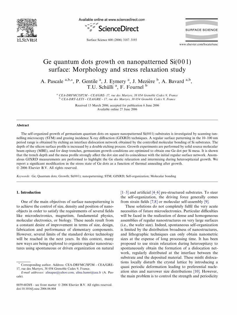
The surface morphologies for different periodicities, butwith similar etching conditions (under the initial bondingplane) have been studied by scanning tunnelling micro-scopy (VT-Omicron STM). Fig. 1 shows typical images(500 nm · 500 nm) of nanopatterned surfaces, validatingthe method for the 10–100 nm period range. The surfacepositions referenced to the initial bonding interface (zi)are estimated considering the etching rate measured onthe SOI reference (as described above) to be: zi = �14.4 nm(Fig. 1a), zi = �14.8 nm (Fig. 1b), zi = �14.4 nm (Fig. 1c)and zi = �14.3 nm (Fig. 1d), under the bonding interface.For these samples, the upper Si crystal is supposed to be re-moved (this point can be checked by grazing incidence X-ray diffraction (GIXRD)), and the absolute value of thedepth is strongly dependent on the etching rate calibration.The surface profile analysis shows large roughness on thetop of the Si mesa (see the insets of Fig. 1a and b) and alow trench depth (about 1.5 nm) compared to the top mesaroughness. The trenche orientations are related to the aver-age h11 0i directions of an interfacial DN layer (i.e., to thedislocation line directions). This orientation is rotated byw/2 with respect to the lower crystal (the substrate).
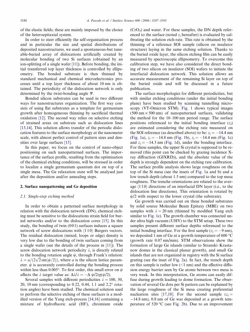
Ge growth was carried out on these bonded substratesby solid source Molecular Beam Epitaxy (MBE) on twosamples with k = 20 nm (thinned by modified Yang etchsimilar to Fig. 1c). The growth chamber was connected un-der ultra high vacuum (UHV) to the STM setup. These twosamples present different surface depths referenced to theinitial bonding interface. For the first sample (zi = �9 nm),we deposited 1 nm of Ge at a growth temperature of 600 �C(growth rate 0.07 nm/min). STM observations show theformation of large Ge islands (similar to Stranski–Krasta-now domes in the classical planar growth), and small Geislands that are not organized in registry with the Si surfacegrating (see the inset of Fig. 2a). In fact, the trench depthon this sample is rather low (<1 nm) and the effective diffu-sion energy barrier seen by Ge atoms between two mesa isvery weak. In this interpretation, Ge atoms can easily dif-fuse during growth leading to dome formation. The obser-vation of several Ge dots per Si pattern can be explained bythe large roughness of the Si mesa creating preferentialnucleation sites [17,18]. For the second sample (zi =�14.8 nm), 0.8 nm of Ge was deposited at a growth tem-perature of 520 �C (see Fig. 2b). Due to an improvement
Fig. 1. STM images (scale: 500 · 500 nm2) of nanopatterned Si surfaces obtained by etching a buried DN. The mesa periodicities are: (a) 100 nm(zi = �14.4 nm); (b) 50 nm (zi = �14.8 nm); (c) 20 nm (zi = �14.4 nm); (d) 10 nm (zi = �14.3 nm). The insets give surface line profiles, marked by a line oneach image. The average h110i directions between the two initial crystals are given by the trenches orientations.
Fig. 2. STM images (scale: 2000 · 2000 nm2) of a Si (001) bonded surface after a modified Yang etching and a Ge deposition of: (a) 1 nm at a growthtemperature of 600 �C (etching depth zi = �9 nm); (b) 0.8 nm at a growth temperature of 520 �C (etching depth zi = �14.8 nm). The insets correspond toSTM scans of 200 · 200 nm2.
A. Pascale et al. / Surface Science 600 (2006) 3187–3193 3189
in trench depth (�2 nm), corresponding to longer etchingtime, the effective energy barrier is sufficient to preventthe formation of large Ge islands (domes), whereas the Simesa roughness still induces the formation of 4 to 5 Gedots per pattern [18]. An interesting detail on Fig. 2b isthe presence of the footprint of a residual mixed dislocationline leading to a surface step (�2 nm). On both sides of thisline, the square network is shifted by half a period [19].This is typical of the interaction of a mixed dislocation linewith the square screw dislocation network.
2.2. Two-step etching method
We have shown up to now that selective etching using aCrO3/HF mixture results in good homogeneity but that thetrenches are not deep enough. Therefore, controlling theposition of dots cannot be optimized with such a process.In order to obtain perfect Ge island organization, animprovement in the chemical etching conditions is re-quired. For this purpose, a new preferential selectivechemical process was proposed. The first step consists of
3190 A. Pascale et al. / Surface Science 600 (2006) 3187–3193
using the modified Yang etch (CrO3/HF) to reveal the sur-face nanostructures, and second, to etch the sample with amixture of hydrofluoric, nitric and acetic acids (calledDash-etch in literature) which acts preferentially on dislo-cations lines, the etching rate of the top surface being verylow (about 2 A/min). Experimental observations haveshown that the second etching gives better surface gratingswhen the first step is stopped close to the bonding interface.
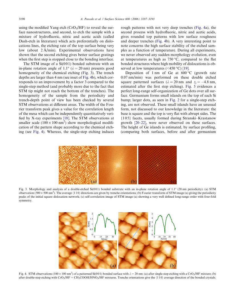
The STM image of a Si(001) bonded substrate with anin-plane rotation angle of 1.1� (k = 20 nm) presents goodhomogeneity of the chemical etching (Fig. 3). The trenchdepths are larger than 4 nm (see inset of Fig. 4b), which cor-responds to an improvement by a factor 3 compared to thesingle-step method (and probably more due to the fact thatSTM tip might not reach the bottom of the trenches). Thehomogeneity of the sample from the periodicity andtrench-depth point of view has been checked by severalSTM observations at different areas. The width of the Fou-rier transform peak gives a value for the correlation lengthof the mesa which can be independently quantitatively veri-fied by X-ray experiments [18]. The STM observations atsmaller scale (100 · 100 nm2) show morphological modifi-cation of the pattern shape according to the chemical etch-ing (see Fig. 4). Whereas, the single-step etching induces
Fig. 3. Morphology and analysis of a double-etched Si(001) bonded substraobservation (500 · 500 nm2). The average h110i directions are given by trenchepeaks of the initial square dislocation network; (c) self-correlation image of STsymmetry.
Fig. 4. STM observations (100 · 100 nm2) of a patterned Si(001) bonded surfacafter double-step etching with CrO3/HF + CH3COOH/HNO3/HF mixtures. Tr
rough patterns with not very deep trenches (Fig. 4a), thesecond process with hydrofluoric, nitric and acetic acids,gives rounded top patterns with low surface roughnessand deeper trenches (Fig. 4b). A very interesting point tonote concerns the high surface stability of the etched sam-ples as a function of temperature. During all experiments,we never observed any sudden morphology evolution, evenat temperatures as high as 750 �C, compared to the flatbonded structures where high mobility of dislocations is ob-served at low temperatures (<450 �C) [19].
Deposition of 1 nm of Ge at 600 �C (growth rate0.07 nm/min) was performed on these double etchedsquare patterned surfaces (k = 20 nm and zi = �4.8 nm,estimated after the first step etching). Fig. 5 evidences aperfect long-range self-organization of Ge dots over all sur-face. Germanium forms small islands on the top of each Sibump; larger dots, as seen in Fig. 2 for a single-step etch-ing, are not observed. These small islands have an unusualform, not discussed to our knowledge in the literature: thebase is square and the top is very flat with abrupt sides. The{105} facets, usually formed during Stranski–Krastanowgrowth [20–22], were never observed on these surfaces.The height of Ge islands is estimated, by surface profiling,(comparing both surfaces, before and after germanium
te with an in-plane rotation angle of 1.1� (20 nm periodicity): (a) STMorientations; (b) Fourier transform of STM image (a) giving the periodicityM image (a) showing a very well defined long-range order with four-fold
e with k = 20 nm: (a) after single-step etching with a CrO3/HF mixture; (b)enche orientations give the h110i average direction of the bonded crystals.
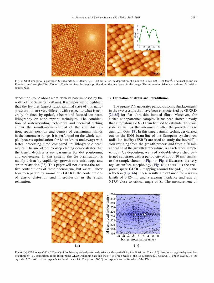
Fig. 5. STM images of a patterned Si substrate (k = 20 nm, zi = �4.8 nm) after the deposition of 1 nm of Ge. (a) 1000 · 1000 nm2. The inset shows itsFourier transform. (b) 200 · 200 nm2. The inset gives the height profile along the line drawn in the image. The germanium islands are almost flat with asquare base.
A. Pascale et al. / Surface Science 600 (2006) 3187–3193 3191
deposition) to be about 4 nm, with its base imposed by thewidth of the Si pattern (20 nm). It is important to highlightthat the features (aspect ratio, minimal size) of this nano-structuration are very different with respect to what is gen-erally obtained by optical, e-beam and focused ion beamlithography or nano-imprint techniques. The combina-tion of wafer-bonding techniques and chemical etchingallows the simultaneous control of the size distribu-tion, spatial position and density of germanium islandsin the nanometer range. It is performed on the whole sam-ple (process optimization for 800 wafers is underway) withfaster processing time compared to lithographic tech-niques. The use of double-step etching demonstrates thatthe trench depth is a key parameter for dot positioningand coalescence. In this system, the Ge organization ismainly driven by capillarity, growth rate anisotropy andstrain relaxation [23]. This paper will not discuss the rela-tive contributions of these phenomena, but we will showhow to separate by anomalous GIXRD the contributionsof elastic distortion and interdiffusion in the strainrelaxation.
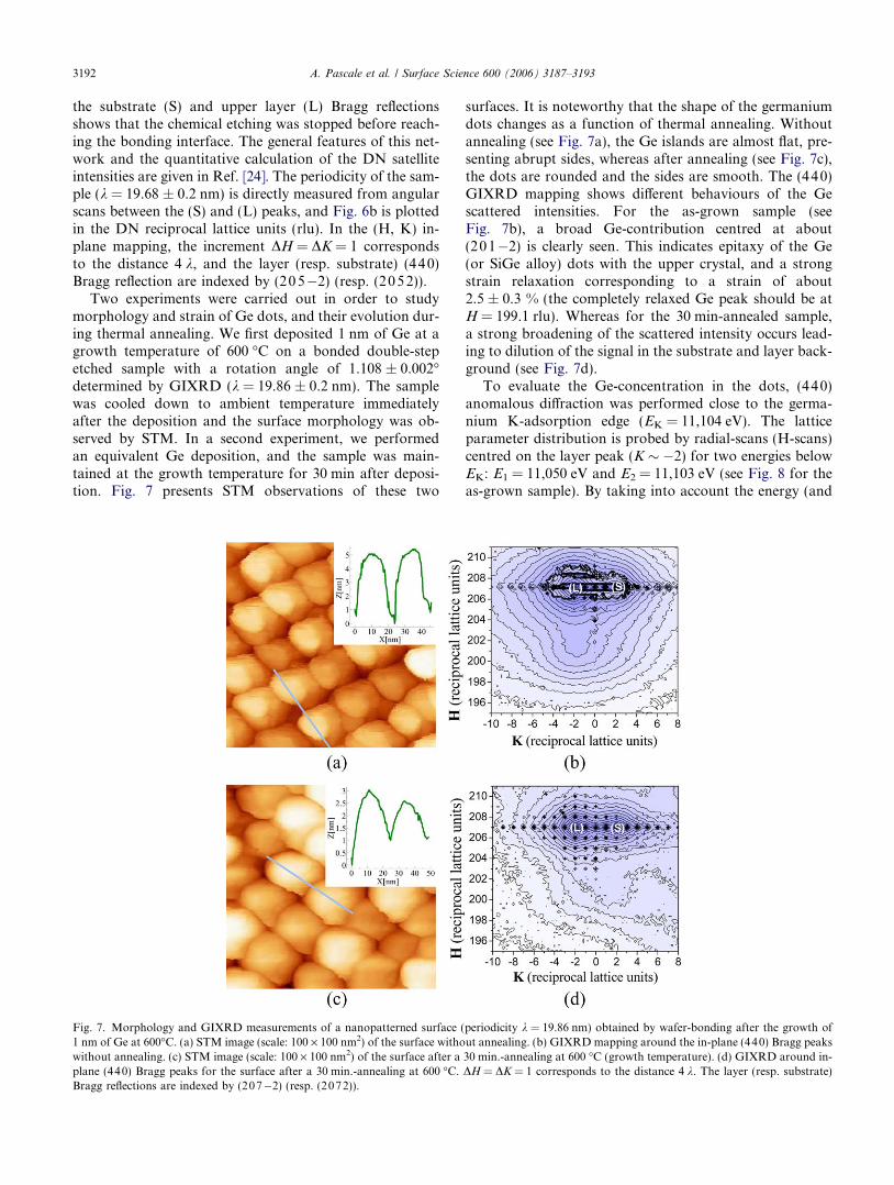
Fig. 6. (a) STM image (200 · 200 nm2) of double-step etched patterned surfaceorientations (i.e., dislocation lines); (b) in-plane GIXRD mapping around the (crystals. DH = DK = 1 corresponds to the distance 4 k. The point (2050) corr
3. Estimation of strain and interdiffusion
The square DN generates periodic atomic displacementsin the two crystals that have been characterized by GIXRD[24,25] for flat ultra-thin bonded films. Moreover, foretched nanopatterned samples, it has been shown alreadythat anomalous GIXRD can be used to estimate the strainstate as well as the intermixing after the growth of Gequantum dots [18]. In this paper, similar techniques carriedout on the ID01 beam-line of the European synchrotronradiation facility (ESRF) are used to study the interdiffu-sion resulting from the growth process and from a 30 minannealing at the growth temperature. As a reference samplewithout Ge deposition, we used a double-step etched pat-terned substrate, with a periodicity of about 20 nm, similarto the sample shown in Fig. 4b. Fig. 6 illustrates the veryregular surface morphology (Fig. 6a), as well as the reci-procal space GIXRD mapping around the (440) in-planereflection (Fig. 6b). These results are obtained for a wave-length of 0.124 nm and a grazing incidence and exit of0.175� close to critical angle of Si. The measurement of
with a periodicity k � 19.68 nm. The h110i directions are given by trenches440) Bragg peaks of the (S) substrate (2052) and (L) upper layer (205�2)esponds to the 0-order of the DN.
3192 A. Pascale et al. / Surface Science 600 (2006) 3187–3193
the substrate (S) and upper layer (L) Bragg reflectionsshows that the chemical etching was stopped before reach-ing the bonding interface. The general features of this net-work and the quantitative calculation of the DN satelliteintensities are given in Ref. [24]. The periodicity of the sam-ple (k = 19.68 ± 0.2 nm) is directly measured from angularscans between the (S) and (L) peaks, and Fig. 6b is plottedin the DN reciprocal lattice units (rlu). In the (H, K) in-plane mapping, the increment DH = DK = 1 correspondsto the distance 4 k, and the layer (resp. substrate) (440)Bragg reflection are indexed by (20 5�2) (resp. (205 2)).
Two experiments were carried out in order to studymorphology and strain of Ge dots, and their evolution dur-ing thermal annealing. We first deposited 1 nm of Ge at agrowth temperature of 600 �C on a bonded double-stepetched sample with a rotation angle of 1.108 ± 0.002�determined by GIXRD (k = 19.86 ± 0.2 nm). The samplewas cooled down to ambient temperature immediatelyafter the deposition and the surface morphology was ob-served by STM. In a second experiment, we performedan equivalent Ge deposition, and the sample was main-tained at the growth temperature for 30 min after deposi-tion. Fig. 7 presents STM observations of these two
Fig. 7. Morphology and GIXRD measurements of a nanopatterned surface (1 nm of Ge at 600�C. (a) STM image (scale: 100 · 100 nm2) of the surface withowithout annealing. (c) STM image (scale: 100 · 100 nm2) of the surface after aplane (440) Bragg peaks for the surface after a 30 min.-annealing at 600 �C.Bragg reflections are indexed by (207�2) (resp. (2072)).
surfaces. It is noteworthy that the shape of the germaniumdots changes as a function of thermal annealing. Withoutannealing (see Fig. 7a), the Ge islands are almost flat, pre-senting abrupt sides, whereas after annealing (see Fig. 7c),the dots are rounded and the sides are smooth. The (440)GIXRD mapping shows different behaviours of the Gescattered intensities. For the as-grown sample (seeFig. 7b), a broad Ge-contribution centred at about(20 1�2) is clearly seen. This indicates epitaxy of the Ge(or SiGe alloy) dots with the upper crystal, and a strongstrain relaxation corresponding to a strain of about2.5 ± 0.3 % (the completely relaxed Ge peak should be atH = 199.1 rlu). Whereas for the 30 min-annealed sample,a strong broadening of the scattered intensity occurs lead-ing to dilution of the signal in the substrate and layer back-ground (see Fig. 7d).
To evaluate the Ge-concentration in the dots, (440)anomalous diffraction was performed close to the germa-nium K-adsorption edge (EK = 11,104 eV). The latticeparameter distribution is probed by radial-scans (H-scans)centred on the layer peak (K � �2) for two energies belowEK: E1 = 11,050 eV and E2 = 11,103 eV (see Fig. 8 for theas-grown sample). By taking into account the energy (and
periodicity k = 19.86 nm) obtained by wafer-bonding after the growth ofut annealing. (b) GIXRD mapping around the in-plane (440) Bragg peaks30 min.-annealing at 600 �C (growth temperature). (d) GIXRD around in-DH = DK = 1 corresponds to the distance 4 k. The layer (resp. substrate)
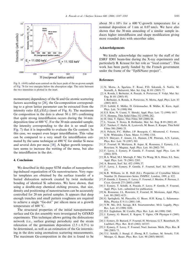
Fig. 8. (440) radial-scan centred on the layer peak of the as-grown sampleof Fig. 7b for two energies below the absorption edge. The ratio betweenthe two intensities is plotted in the inset.
A. Pascale et al. / Surface Science 600 (2006) 3187–3193 3193
momentum) dependency of the Si and Ge atomic scatteringfactors according to [26], the Ge-composition correspond-ing to a given lattice parameter can be extracted from theintensity ratio I(E1)/I(E2) (inset of Fig. 8). The maximumGe composition in the dots is about 50 ± 10% confirmingthat quite strong interdiffusion occurs during the 14 min.deposition time at 600 �C. For the 30 min annealed sample,the intensity corresponding to the dot is so small (seeFig. 7) that it is impossible to evaluate the Ge content. Inthis case, we suspect even larger interdiffusion. This valuecan be compared to a very small Ge interdiffusion esti-mated by the same technique at 490 �C for similar Si mesaand several dots per mesa [18]. A higher growth tempera-ture seems to increase the wetting of the mesa, but alsothe interdiffusion in the dot.
4. Conclusions
We described in this paper STM studies of nanopattern-ing-induced organization of Ge nanostructures. Very regu-lar templates are obtained by the surface transfer of aburied dislocation network created by twist molecularbonding of identical Si substrates. We have shown, thatusing a double-step chemical etching process, that size,density and positioning of nanostructures can be accuratelycontrolled for 20 nm period samples. It appears that deepenough trenches and small pattern roughness are requiredto achieve a single ‘‘Ge-dot’’ per silicon mesa at a growthtemperature of 600 �C.
The structural properties of the initial nanopatternedsurface and Ge dot assembly were investigated by GIXRDexperiments. This technique allows getting the dislocationsnetwork (i.e., surface grating) periodicity and the strainrelaxation of the germanium deposition (2.5 ± 0.3%) tobe determined, as well as an estimation of the Ge intermix-ing in the dots using anomalous scattering measurements.The maximum Ge-composition in the dot is found to be
about 50 ± 10% for a 600 �C-growth temperature for anominal deposition of 1 nm at 0.07 nm/s. We have alsoshown that the 30 min annealing of a similar sample in-duces higher interdiffusion and shape modification givingmore rounded dots with smoother sides.
Acknowledgements
We kindly acknowledge the support by the staff of theESRF ID01 beam-line during the X-ray experiments andparticularly B. Krause for her role as ‘‘local contact’’. Thiswork has been partly funded by the French governmentunder the frame of the ‘‘EpiSiNano project’’.
References
[1] N. Motta, A. Sgarlata, F. Rosei, P.D. Szkutnik, S. Nufris, M.Scarselli, A. Balzarotti, Mat. Sci. Eng. B 101 (2003) 77.
[2] A. Ronda, I. Berbezier, A. Pascale, A. Portavoce, F. Volpi, Mat. Sci.Eng. B 101 (2003) 95;I. Berbezier, A. Ronda, A. Portavoce, N. Motta, Appl. Phys. Lett. 83(2003) 4833.
[3] O. Leifeld, E. Muller, D. Grutzmacher, B. Muller, K. Kern, Appl.Phys. Lett. 74 (1999) 994.
[4] E.S. Kim, N. Usami, Y. Shiraki, Appl. Phys. Lett. 72 (1998) 1617.[5] Y. Homma, Thin Solid Films 332 (1998) 262.[6] H. Omi, T. Ogino, Thin Films 369 (2000) 88.[7] L. Vescan, T. Stoica, B. Hollander, Mat. Sci. Eng. B 89 (2002) 49.[8] C. Teichert, C. Hafer, K. Lyutovich, M. Bauer, E. Kasper, Thin Solid
Films 380 (2000) 25.[9] S. Palacin, P.C. Hidber, J.P. Bourgoin, C. Miramond, C. Fermon,
G.M. Whitesides, Chem. Mater. 8 (1996) 1316.[10] S.Y. Shiryaev, F. Jensen, J.L. Hansen, J.W. Petersen, A.N. Larsen,
Phys. Rev. Lett. 78 (1997) 503.[11] F. Fournel, H. Moriceau, B. Aspar, K. Rousseau, J. Eymery, J.-L.
Rouviere, N. Magnea, Appl. Phys. Lett. 80 (2002) 793.[12] F. Leroy, J. Eymery, P. Gentile, F. Fournel, Appl. Phys. Lett. 80
(2002) 3078.[13] R.A. Wind, M.J. Murtagh, F. Mei, Yu Wang, M.A. Hines, S.L. Sass,
Appl. Phys. Lett. 78 (2001) 2205.[14] A. Bourret, Surf. Sci. 432 (1999) 37.[15] F. Leroy, J. Eymery, P. Gentile, F. Fournel, Surf. Sci. 545 (2003)
211.[16] K.R. Williams, in: R. Hull (Ed.), Properties of Crystalline Silicon
Number 20, Datareviews Series, INSPEC, London, 1999, p. 822.[17] P. Gentile, J. Eymery, F. Leroy, F. Fournel, J. Meziere, P. Perreau, J.
Cryst. Growth 275 (2005) e1609.[18] J. Eymery, T. Schulli, A. Pascale, F. Leroy, P. Gentile, F. Fournel,
Appl. Phys. Lett., submitted for publication.[19] K. Rousseau, J.L. Rouviere, F. Fournel, H. Moriceau, Appl. Phys.
Lett. 80 (2002) 4121.[20] G. Springholz, M. Pinczolits, G. Bauer, H.H. Kang, L. Salamanca-
Riba, Physica E 9 (1) (2001) 149.[21] Y.W. Mo, D.E. Savage, B.S. Swartzentruber, M.G. Lagally, Phys.
Rev. Lett. 65 (1990) 1020.[22] D.J. Eaglesham, M. Cerullo, Phys. Rev. Lett. 64 (1990) 1943.[23] J. Eymery, G. Biasiol, E. Kapon, T. Ogino, CR Physique 6 (2005)
105.[24] J. Eymery, D. Buttard, F. Fournel, H. Moriceau, G.T. Baumbach, D.
Luebbert, Phys. Rev. B 65 (2002) 165337.[25] J. Eymery, F. Leroy, F. Fournel, Nucl. Instrum. Meth. Phys. Res. B
200 (2003) 73.[26] T.U. Schulli, J. Stangl, Z. Zhong, R.T. Lechner, M. Sztucki, T.H.
Metzger, G. Bauer, Phys. Rev. Lett. 90 (2003) 066105.