PARASITIC FLATWORMS (PLATYHELMINTHES: MONOGENEA, DIGENEA, CESTODA) OF FISHES FROM THE ADRIATIC SEA
Upload
khangminh22Category
view
0download
0
Extrinsic Parameter and Parasitic Elements in III-V HBT and HEMT ModelingSonja Nedeljkovic, Joseph Gering, Faramarz Kharabi, John McMacken, Bill Clausen, Paul Partyka, Scott Parker

• General modeling flow for single and multi-cell array device modeling
• Analysis of test structures with corresponding calibration techniques
• De-embedding
• Methods for extrinsic parameter extraction used in HBT and pHEMT modeling
• Parasitics modeling for large area devices
• Scaling for multi-cell arrays
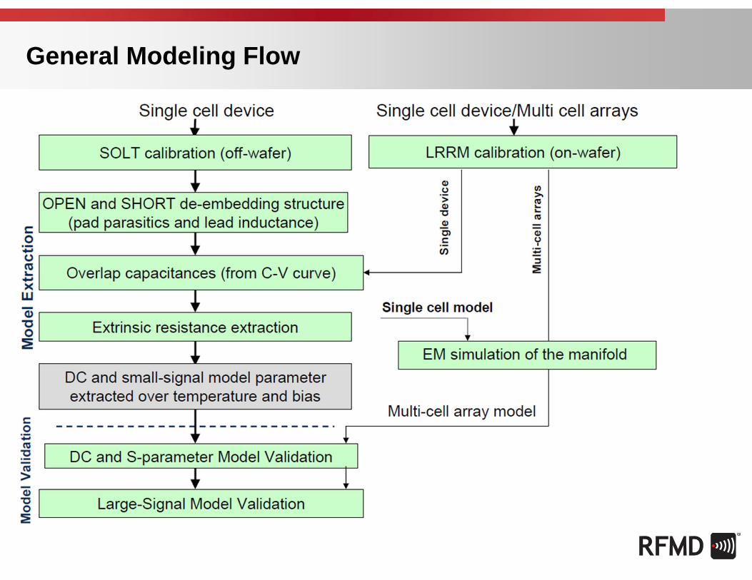
General Modeling Flow
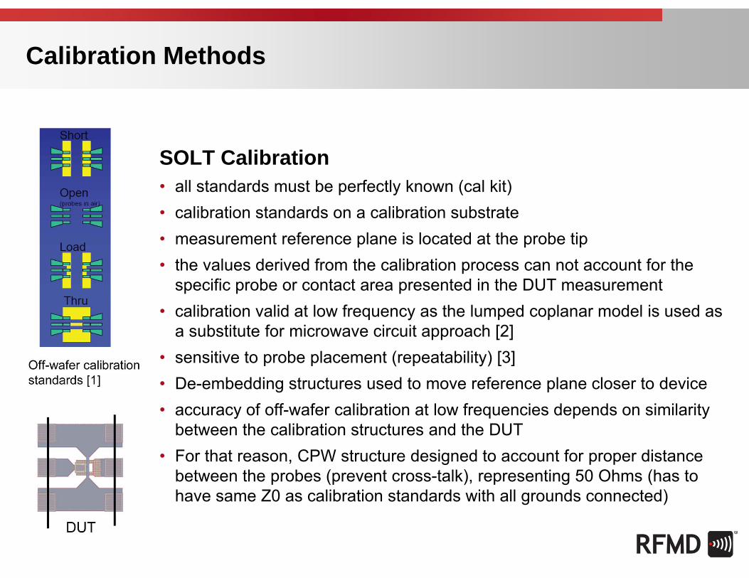
Calibration Methods
SOLT Calibration• all standards must be perfectly known (cal kit)• calibration standards on a calibration substrate• measurement reference plane is located at the probe tip• the values derived from the calibration process can not account for the
specific probe or contact area presented in the DUT measurement• calibration valid at low frequency as the lumped coplanar model is used as
a substitute for microwave circuit approach [2]• sensitive to probe placement (repeatability) [3]• De-embedding structures used to move reference plane closer to device• accuracy of off-wafer calibration at low frequencies depends on similarity
between the calibration structures and the DUT• For that reason, CPW structure designed to account for proper distance
between the probes (prevent cross-talk), representing 50 Ohms (has to have same Z0 as calibration standards with all grounds connected)
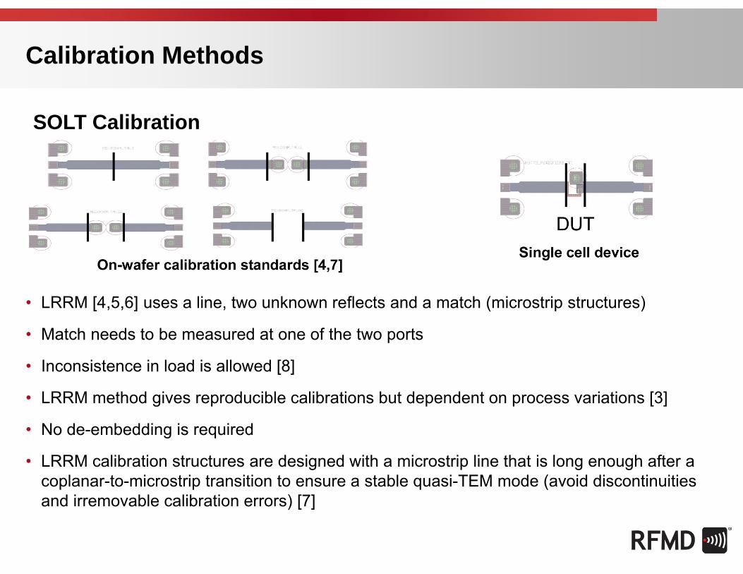
Calibration Methods
• LRRM [4,5,6] uses a line, two unknown reflects and a match (microstrip structures)
• Match needs to be measured at one of the two ports
• Inconsistence in load is allowed [8]
• LRRM method gives reproducible calibrations but dependent on process variations [3]
• No de-embedding is required
• LRRM calibration structures are designed with a microstrip line that is long enough after a coplanar-to-microstrip transition to ensure a stable quasi-TEM mode (avoid discontinuities and irremovable calibration errors) [7]
SOLT Calibration
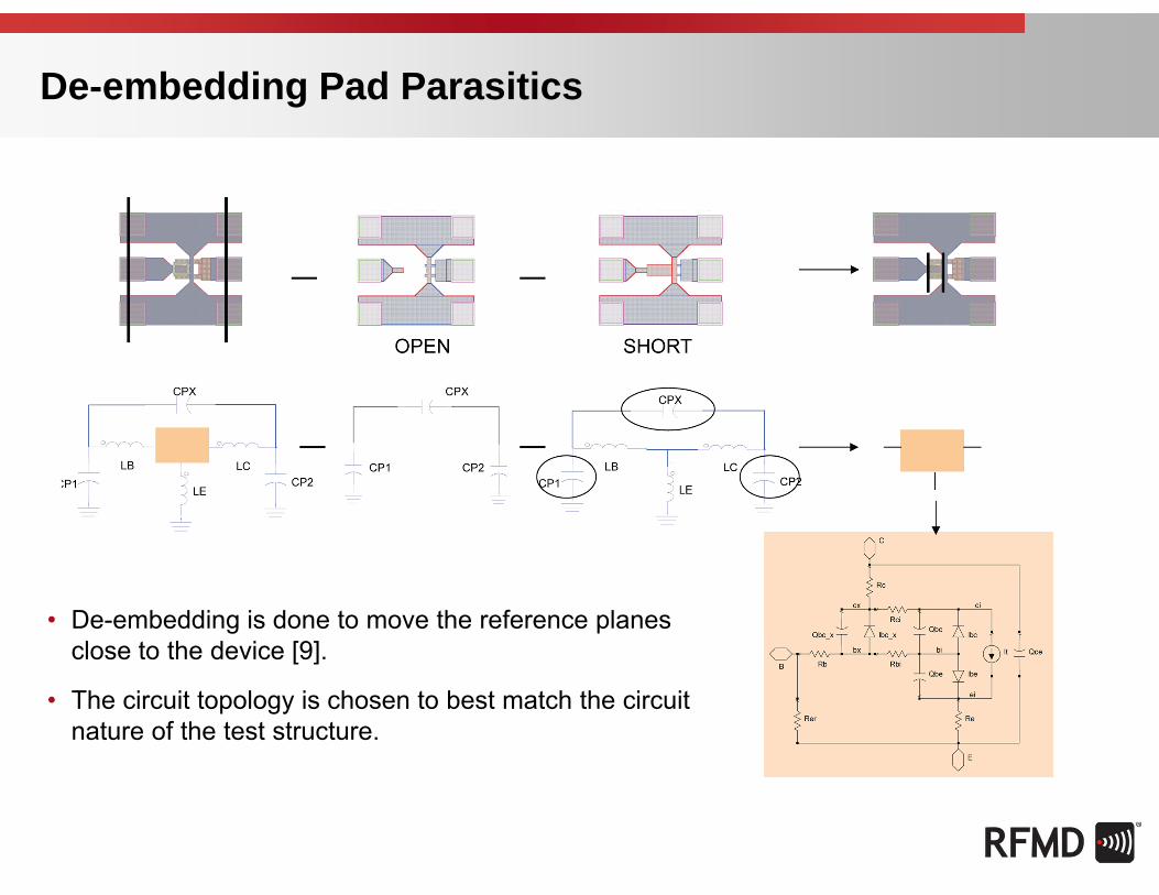
De-embedding Pad Parasitics
• De-embedding is done to move the reference planes close to the device [9].
• The circuit topology is chosen to best match the circuit nature of the test structure.
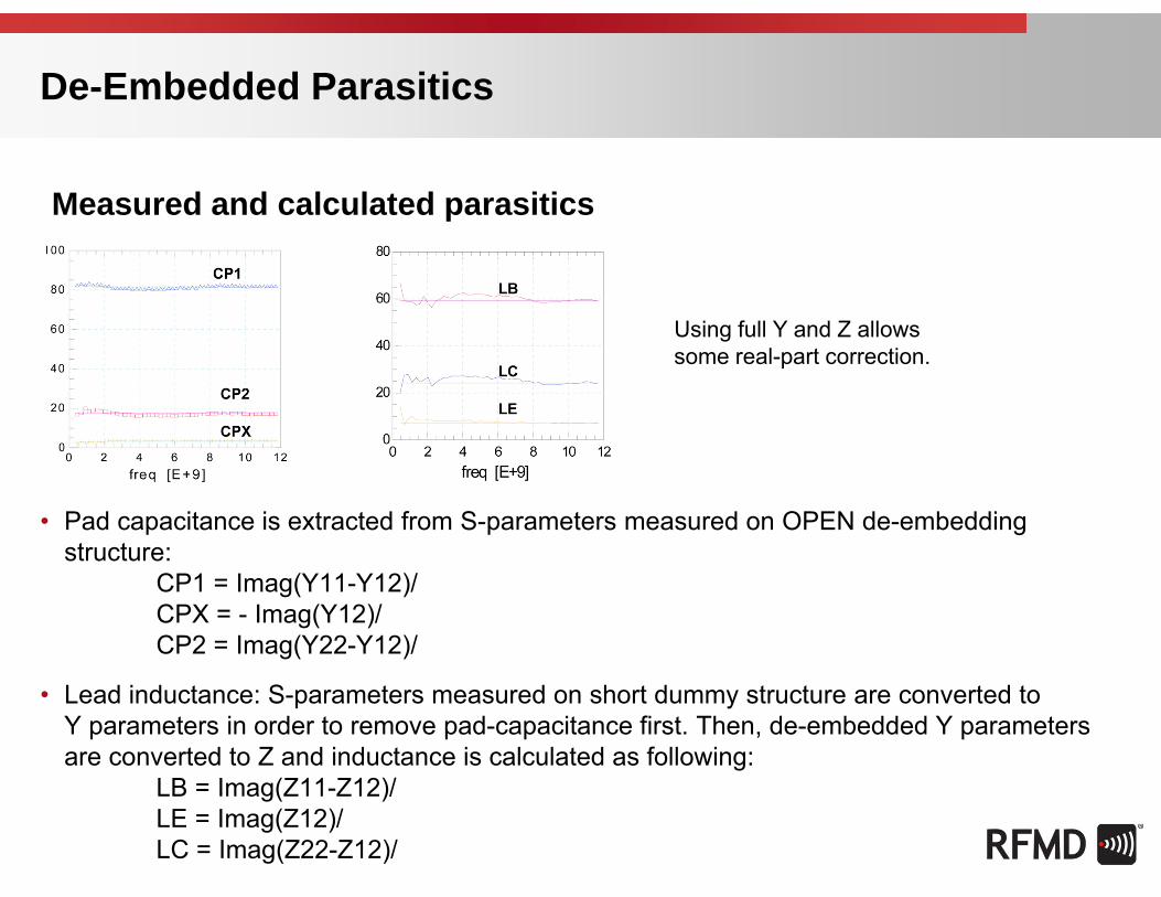
De-Embedded Parasitics
• Pad capacitance is extracted from S-parameters measured on OPEN de-embedding structure:
CP1 = Imag(Y11-Y12)/�CPX = - Imag(Y12)/�CP2 = Imag(Y22-Y12)/�
• Lead inductance: S-parameters measured on short dummy structure are converted to Y parameters in order to remove pad-capacitance first. Then, de-embedded Y parameters are converted to Z and inductance is calculated as following:
LB = Imag(Z11-Z12)/�LE = Imag(Z12)/�LC = Imag(Z22-Z12)/�
Using full Y and Z allowssome real-part correction.
Measured and calculated parasitics
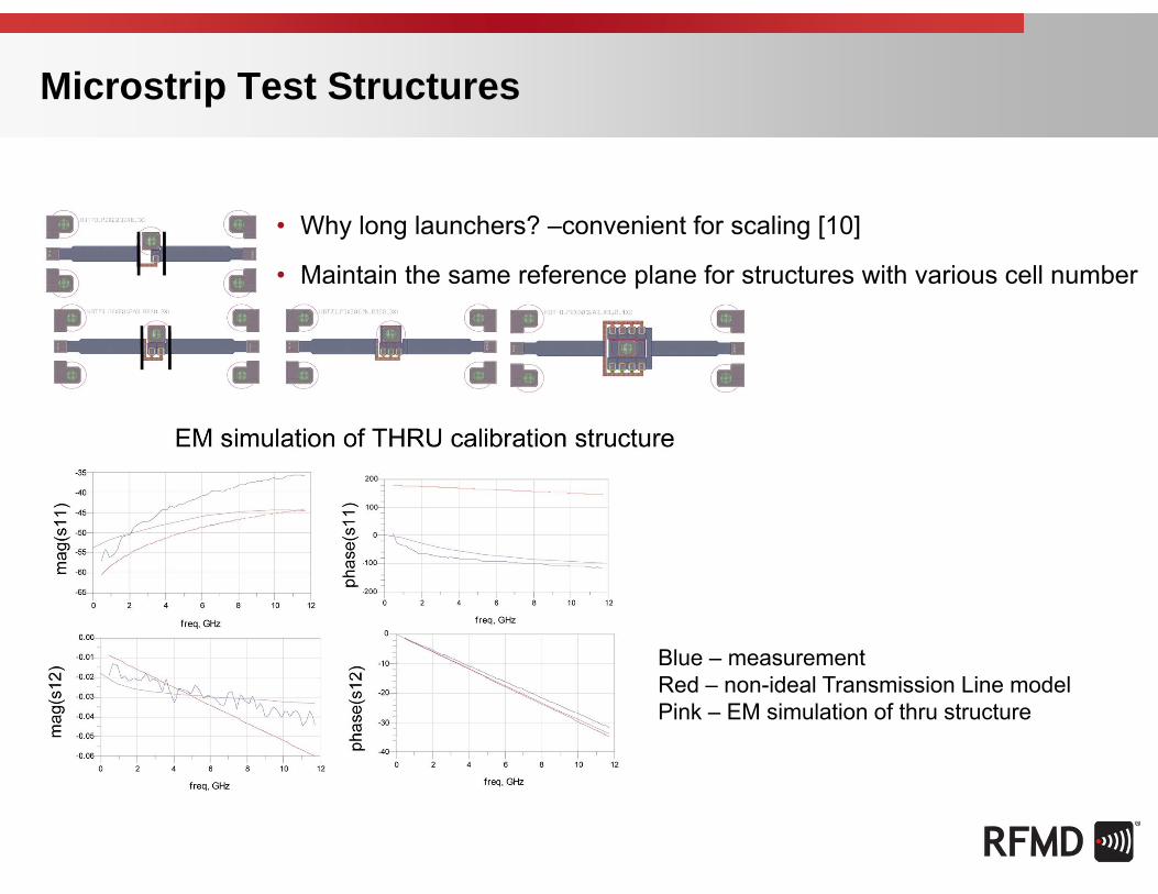
Microstrip Test Structures
• Why long launchers? –convenient for scaling [10]
• Maintain the same reference plane for structures with various cell number
Blue – measurementRed – non-ideal Transmission Line modelPink – EM simulation of thru structure

Extraction of Overlap Capacitance
• Overlap capacitance is bias independent and can be extracted from C-V curves (S-parameter measurement) by de-embedding the pad capacitance and separating the bias dependent capacitance from measured data [11]
• Capacitances calculated from Y parameters when both junctions are reversed biased are averaged over the measured frequency range and extraction is done for narrow frequency range (1-3GHz).
C(V )�C _ const�C* f (V) Cbcj + Cpx = -(1/�)*Imag(Y12)Cbej + Cp1 = (1/�)*Imag(Y11+Y12)Cp2 + Cce = (1/�)*Imag(Y22+Y12)
• Cce –emitter - collector overlap capacitance. Depending on backend process, other overlap capacitances should be accounted for.
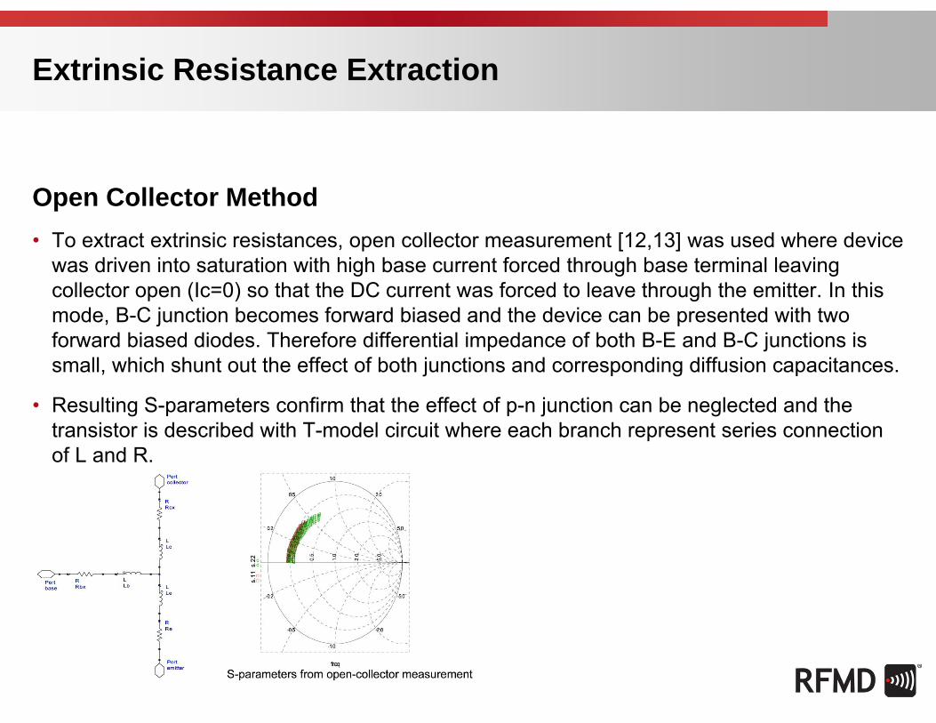
Extrinsic Resistance Extraction
Open Collector Method• To extract extrinsic resistances, open collector measurement [12,13] was used where device
was driven into saturation with high base current forced through base terminal leaving collector open (Ic=0) so that the DC current was forced to leave through the emitter. In this mode, B-C junction becomes forward biased and the device can be presented with two forward biased diodes. Therefore differential impedance of both B-E and B-C junctions is small, which shunt out the effect of both junctions and corresponding diffusion capacitances.
• Resulting S-parameters confirm that the effect of p-n junction can be neglected and the transistor is described with T-model circuit where each branch represent series connection of L and R.
Extrinsic Resistance Extraction
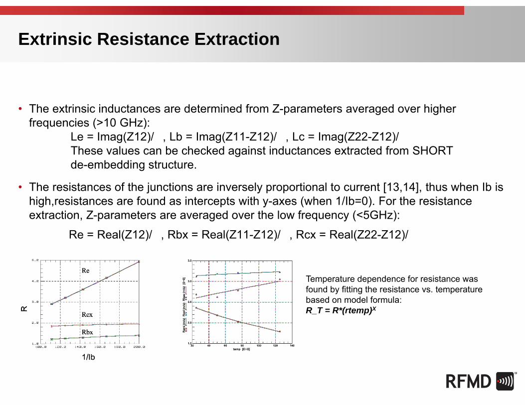
• The extrinsic inductances are determined from Z-parameters averaged over higher frequencies (>10 GHz):
Le = Imag(Z12)/�, Lb = Imag(Z11-Z12)/�, Lc = Imag(Z22-Z12)/�These values can be checked against inductances extracted from SHORT de-embedding structure.
• The resistances of the junctions are inversely proportional to current [13,14], thus when Ib ishigh,resistances are found as intercepts with y-axes (when 1/Ib=0). For the resistanceextraction, Z-parameters are averaged over the low frequency (<5GHz):
Re = Real(Z12)/�, Rbx = Real(Z11-Z12)/�, Rcx = Real(Z22-Z12)/�
Temperature dependence for resistance was found by fitting the resistance vs. temperature based on model formula:R_T = R*(rtemp)X
Extrinsic Resistance Extraction
Advantages:
1) Open collector measurement can provide values for all external resistances and if it is done over temperature, the temperature dependence of external R’s is extracted
2) Resistance extraction in most cases will give uniquely solutions which is not the case with DC fly-back method.
3) Inductance extraction can be used to crosscheck measurements on short dummy structure
Disadvantages:
1) In some cases, forcing high base current can damage device
2) The current flow in open collector measurement is different compared to active regime. It will not produce error in Rbx extraction, but Re value should be compared against Gm value from the S-parameters measurement or employing some other method [14].
Values for extrinsic resistances also could be obtained from PCM data, which should be used as a starting values in HBT modeling.
Summary
Extrinsic Parameter Extraction: InP HBTs
• Although the majority of model parameter are extracted at mid-range frequencies (up to 25GHz), model validation has to be done up to higher frequencies (100GHz)
• Modeling of InP HBT device relies on accurate calibration and parasitic de-embedding:
1) Parasitic capacitance de-embedding for the devices with small internal capacitance can be challenging as the parasitic will be in order of intrinsiccapacitance
2) Parasitic inductance de-embedding can impact the extracted value of the cut-off frequency (fT) which is a very important figure of merit for high frequency devices.
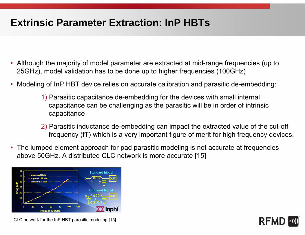
• The lumped element approach for pad parasitic modeling is not accurate at frequencies above 50GHz. A distributed CLC network is more accurate [15]
Extrinsic Parameter Extraction: InP HBTs
• Emitter resistance extraction: There have been cases reported [16] when the emitter band gap engineering employed in order to achieve good device performance at higher currents.
• Resistance extraction in open collector measurement relies on extrapolation of Re when Ib→�. If the relationship between Re and 1/Ie is not linear than the emitter resistance in the low current region will increase more than the dynamic emitter resistance component that is proportional to 1/Ie.
• To account for this in model, there are two possibilities:1) Customize Re current dependence equation in the model code2) Add external element (SDD in ADS) that will account for this behavior
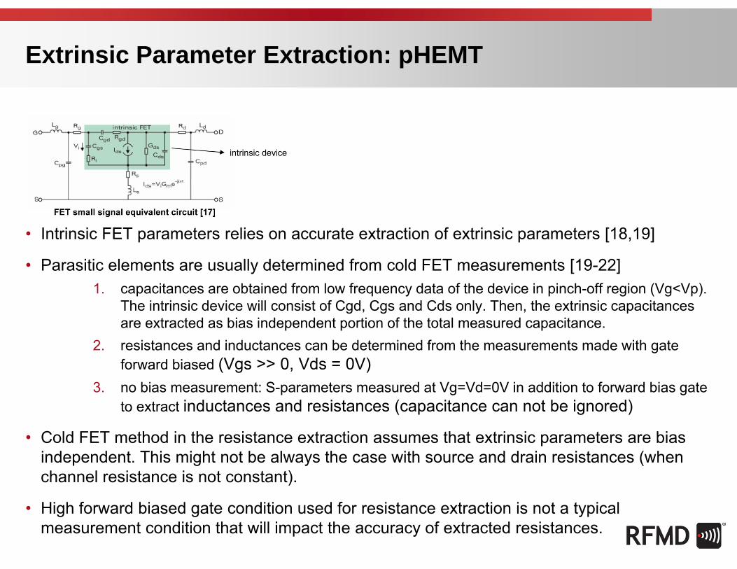
Extrinsic Parameter Extraction: pHEMT
• Intrinsic FET parameters relies on accurate extraction of extrinsic parameters [18,19]
• Parasitic elements are usually determined from cold FET measurements [19-22]1. capacitances are obtained from low frequency data of the device in pinch-off region (Vg<Vp).
The intrinsic device will consist of Cgd, Cgs and Cds only. Then, the extrinsic capacitances are extracted as bias independent portion of the total measured capacitance.
2. resistances and inductances can be determined from the measurements made with gate forward biased (Vgs >> 0, Vds = 0V)
3. no bias measurement: S-parameters measured at Vg=Vd=0V in addition to forward bias gate to extract inductances and resistances (capacitance can not be ignored)
• Cold FET method in the resistance extraction assumes that extrinsic parameters are bias independent. This might not be always the case with source and drain resistances (when channel resistance is not constant).
• High forward biased gate condition used for resistance extraction is not a typical measurement condition that will impact the accuracy of extracted resistances.
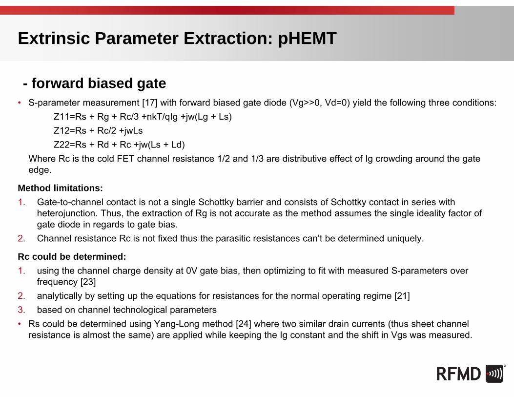
Extrinsic Parameter Extraction: pHEMT
• S-parameter measurement [17] with forward biased gate diode (Vg>>0, Vd=0) yield the following three conditions:Z11=Rs + Rg + Rc/3 +nkT/qIg +jw(Lg + Ls)Z12=Rs + Rc/2 +jwLsZ22=Rs + Rd + Rc +jw(Ls + Ld)
Where Rc is the cold FET channel resistance 1/2 and 1/3 are distributive effect of Ig crowding around the gateedge.
Method limitations:1. Gate-to-channel contact is not a single Schottky barrier and consists of Schottky contact in series with
heterojunction. Thus, the extraction of Rg is not accurate as the method assumes the single ideality factor of gate diode in regards to gate bias.
2. Channel resistance Rc is not fixed thus the parasitic resistances can’t be determined uniquely.
Rc could be determined:1. using the channel charge density at 0V gate bias, then optimizing to fit with measured S-parameters over
frequency [23]2. analytically by setting up the equations for resistances for the normal operating regime [21]3. based on channel technological parameters• Rs could be determined using Yang-Long method [24] where two similar drain currents (thus sheet channel
resistance is almost the same) are applied while keeping the Ig constant and the shift in Vgs was measured.
- forward biased gate

Extrinsic Parameter Extraction: pHEMT
Forward Biased Gate
- Cold FET measurement and extraction with forward bias is represented by the circuit below [17].
The input and output S-parameters below show the representation of the real part for the resistance and the phase for the inductance extracted to the right.

Extrinsic Parameter Extraction: pHEMT
Device in pinch-off• Cold FET measurement and extraction below pinch-off is
represented by the circuit below [25]. The parasitic capacitances are measured by suppressing the conductivity of the channel.
• In the equivalent circuit, Cb is the fringing capacitance due to a depleted layer extension at each side of the gate.
• For the frequencies up to a few GHz, inductances and resistances have no influence on the Imag(Y).
• The input and output S-parameters below show the representation phase for the capacitance extracted to the right.
• The extraction formula is shown below
Im(Y11) = w(Cpg+2Cb)Im(Y12) = -w(Cb)Im(Y22) = w(Cpd+Cb)
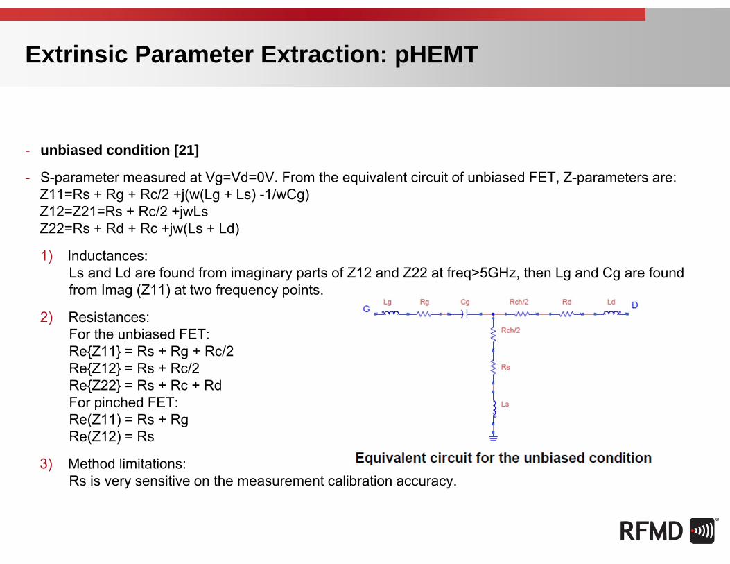
- unbiased condition [21]
- S-parameter measured at Vg=Vd=0V. From the equivalent circuit of unbiased FET, Z-parameters are:Z11=Rs + Rg + Rc/2 +j(w(Lg + Ls) -1/wCg)Z12=Z21=Rs + Rc/2 +jwLsZ22=Rs + Rd + Rc +jw(Ls + Ld)
1) Inductances:Ls and Ld are found from imaginary parts of Z12 and Z22 at freq>5GHz, then Lg and Cg are foundfrom Imag (Z11) at two frequency points.
2) Resistances:For the unbiased FET:Re{Z11} = Rs + Rg + Rc/2Re{Z12} = Rs + Rc/2Re{Z22} = Rs + Rc + RdFor pinched FET:Re(Z11) = Rs + RgRe(Z12) = Rs
3) Method limitations:Rs is very sensitive on the measurement calibration accuracy.
Extrinsic Parameter Extraction: pHEMT
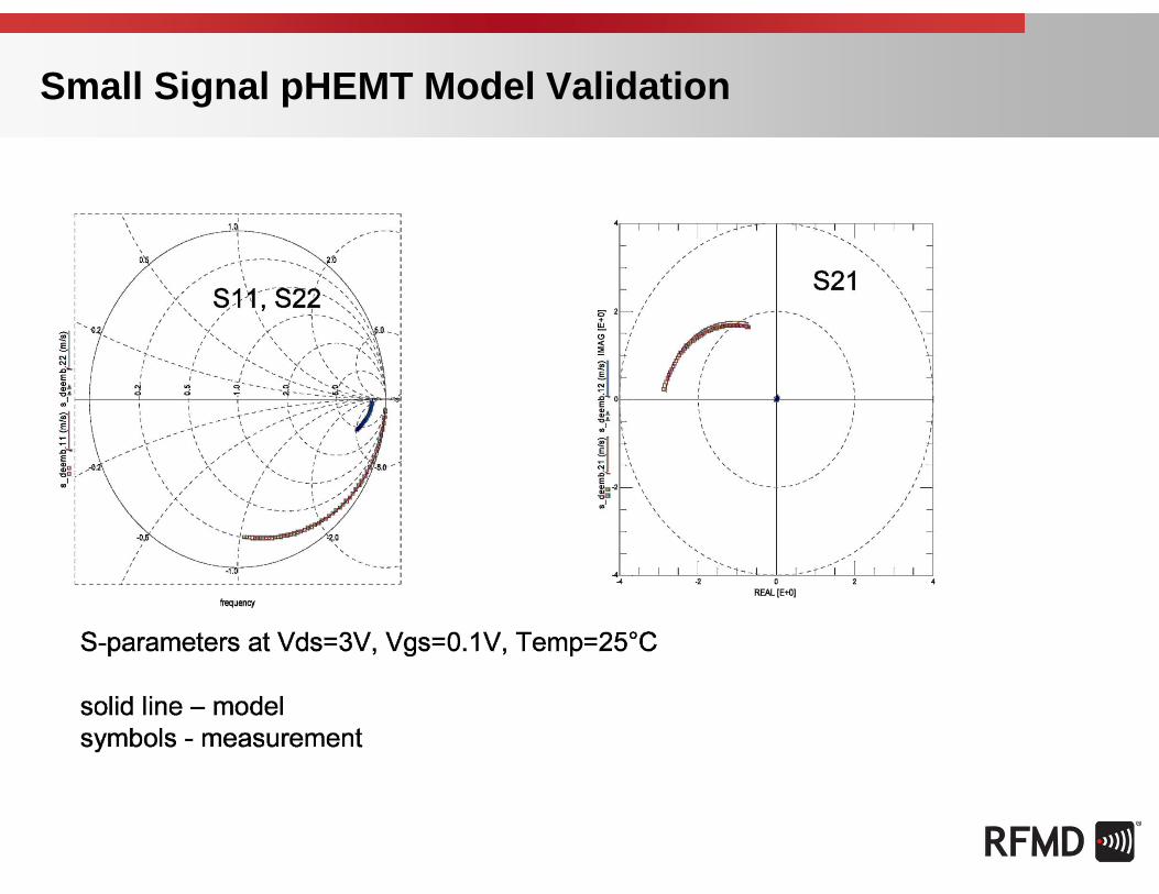
Small Signal pHEMT Model Validation
EM Support: pHEMT
• In modeling discrete transistors, parasitics are accounted for through lumped element model which can not be used for modeling of distributed effects and coupling phenomena that become very pronounced in large area devices.
• Parameters of lumped equivalent circuits are scaled with device size and number of fingers using simple linear rules or empirical relations.
• The simplified approaches have frequency limitations which will impact model accuracy
• Lumped element approach is layout dependent and since it’s not possible to predict how the array of discrete devices will be connected in the design, it poses the serious limit in modeling.
• To overcome the limitations in modeling of large area devices, EM simulation of the manifold is recommended [19, 26]
EM Support: HBTs
Validate EM simulation in simple structures:1. THRU structure from the LRRM on-wafer cal set2. OPEN dummy of a single cell device
Next step: use EM simulation for multi-cell arrays
1. Possible simplification to cut down on the number of ports and reduce simulation time? [10, 27]
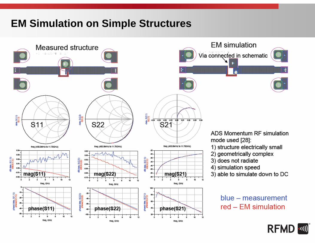
EM Simulation on Simple Structures
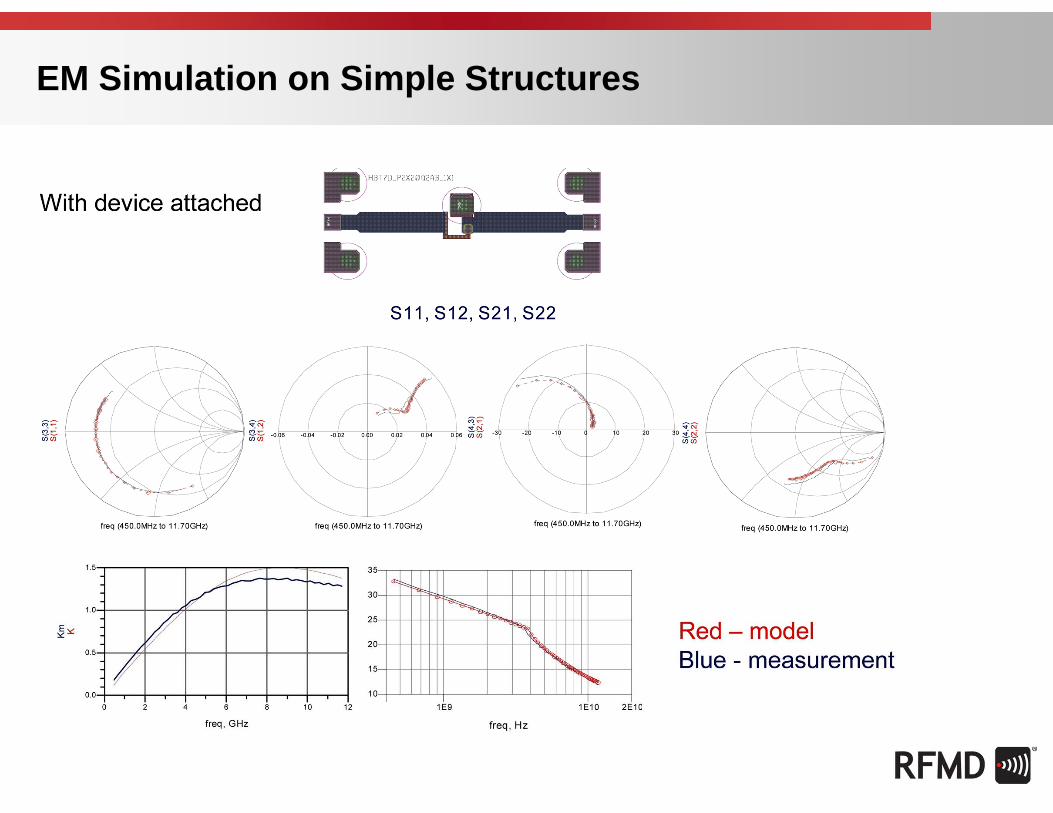
EM Simulation on Simple Structures
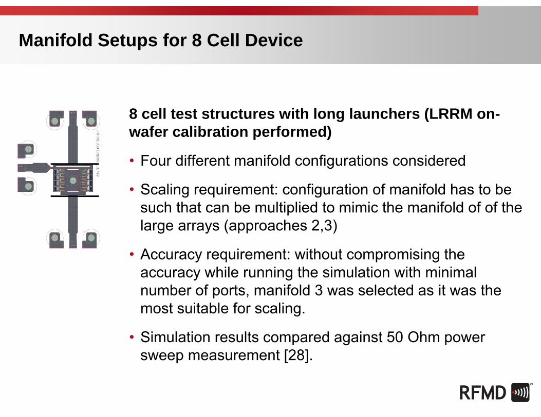
Manifold Setups for 8 Cell Device
8 cell test structures with long launchers (LRRM on-wafer calibration performed)
• Four different manifold configurations considered
• Scaling requirement: configuration of manifold has to be such that can be multiplied to mimic the manifold of of the large arrays (approaches 2,3)
• Accuracy requirement: without compromising the accuracy while running the simulation with minimal number of ports, manifold 3 was selected as it was the most suitable for scaling.
• Simulation results compared against 50 Ohm power sweep measurement [28].

Manifold Setups for 8 Cell Device
1) complete manifold (all ports and DC line included)
2) with DC line but included via in EM simulation, number of ports reduced
3) without DC line, via implemented as lumped element, number of ports reduced
4) with DC line, lumped element via, number of ports reduced
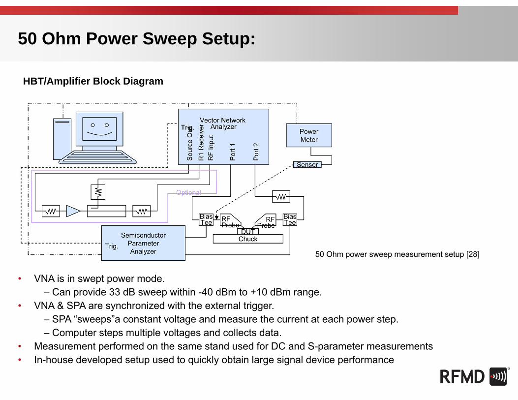
50 Ohm Power Sweep Setup:
HBT/Amplifier Block Diagram
• VNA is in swept power mode.– Can provide 33 dB sweep within -40 dBm to +10 dBm range.
• VNA & SPA are synchronized with the external trigger.– SPA “sweeps”a constant voltage and measure the current at each power step.– Computer steps multiple voltages and collects data.
• Measurement performed on the same stand used for DC and S-parameter measurements• In-house developed setup used to quickly obtain large signal device performance
50 Ohm power sweep measurement setup [28]
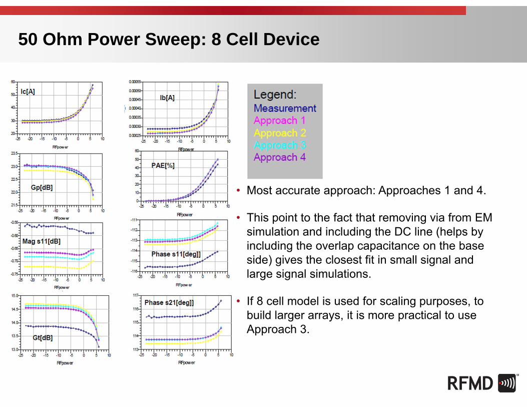
50 Ohm Power Sweep: 8 Cell Device
• Most accurate approach: Approaches 1 and 4.
• This point to the fact that removing via from EM simulation and including the DC line (helps by including the overlap capacitance on the base side) gives the closest fit in small signal and large signal simulations.
• If 8 cell model is used for scaling purposes, to build larger arrays, it is more practical to use Approach 3.

8 Cell Device: S-parameters
Temp=25C
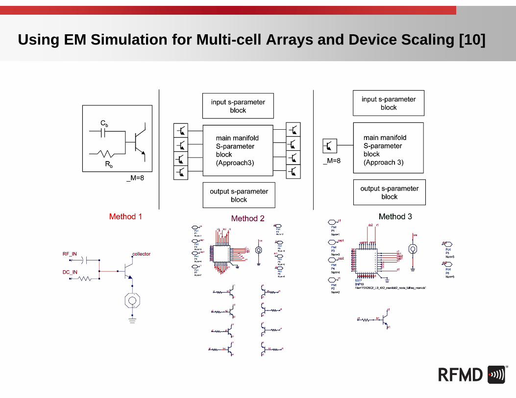
Using EM Simulation for Multi-cell Arrays and Device Scaling [10]
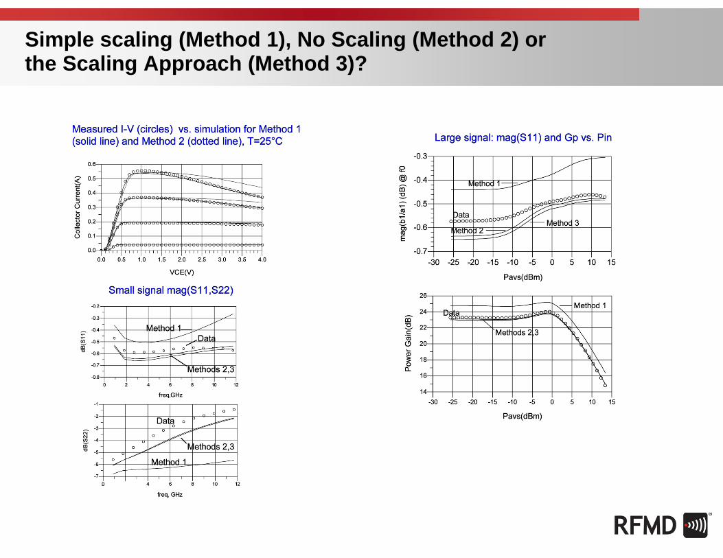
Simple scaling (Method 1), No Scaling (Method 2) or the Scaling Approach (Method 3)?
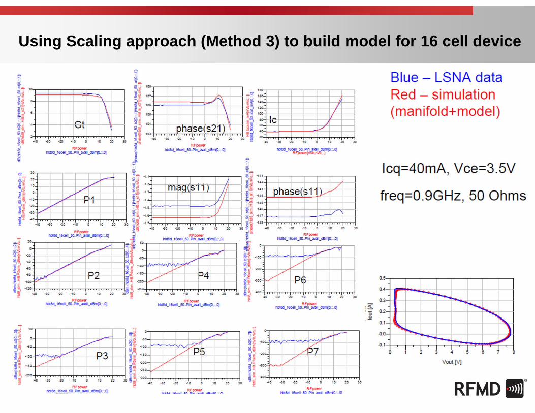
Using Scaling approach (Method 3) to build model for 16 cell device

Comparing Method 1 to Measured Data for 16 Cell Device
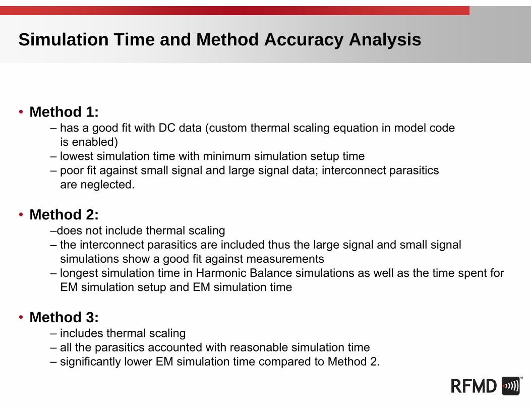
Simulation Time and Method Accuracy Analysis
• Method 1:– has a good fit with DC data (custom thermal scaling equation in model code
is enabled)– lowest simulation time with minimum simulation setup time– poor fit against small signal and large signal data; interconnect parasitics
are neglected.
• Method 2:–does not include thermal scaling– the interconnect parasitics are included thus the large signal and small signal
simulations show a good fit against measurements– longest simulation time in Harmonic Balance simulations as well as the time spent for
EM simulation setup and EM simulation time
• Method 3:– includes thermal scaling– all the parasitics accounted with reasonable simulation time– significantly lower EM simulation time compared to Method 2.
References
[1] A. Loyd, “Advanced RF Calibration Techniques”, Cascade Microtech Europe[2] R.Marks, ”On-wafer Millimeter-Wave Characterization”, GAAS 98 Amsterdam 1998[3] A.Loyd,“Comparing the Accuracy and Repeatability of On-Wafer Calibration techniques to 110GHz”, Cascade Microtech Europe, Vol.3,
Munich, October 1999[4] R.Marks, “Wafer-Level ANA Calibration at NIST”, ARFTG Conference Digest-Winter, 34th, Vol.16, pp.11-25, Ft. Lauderdale 1989[5] D.F.Wulliams, R.B.Marks, “Comparison of On-Wafer Calibrations”, ARFTG Conference Digest-Winter, 38th, Vol.20, pp.68-81, San Diego
1991[6] A.Davidson, E.Strid, K.Jones, “Achieving greater on-wafer S-Parameter accuracy with LRM calibration technique”, ARFTG Conference
Digest-Winter, 34th, Vol.16, pp.61-66, Ft. Lauderdale 1989[7] J.C.Rautio, “A Possible Source of Error in On-Wafer Calibration”, ARFTG Conference Digest-Winter, 34th, Vol.16, pp.118-126, Ft.
Lauderdale 1989[8] A.Davidson, K.Jones, E.Strid, “LRM and LRRM Calibrations with Automatic Determination of Load Inductance”, ARFTG Conference
Digest-Winter, 36th, Vol.18, pp.57-63, Monterey 1990[9] F.Sischka, “IC-CAP Characterization and Modeling Handbook”Agilent, 2002[10] S.Nedeljkovic,J.McMacken, J.Gering, D.Halchin, “A Scalable Compact Model for III-V Heterojunction Bipolar Transistors”, Microwave
Symposium Digest, 2008 IEEE MTT-S International, pp. 479-482, June 2008[11] Y.Gobert, P.J.Tasker,K.H.Bachem, “A Physical, Yet Simple, Small-Signal equivalent Circuit for the Heterojunction Bipolar Transistor”,
IEEE Transactions on Microwave Theory and Techniques, Vol.45, No.1, January 1997[12] C.J.Wei, J.C.M.Hwang, “Direct Extraction of Equivalent circuit Parameters for Heterojunction Bipolar Transistors”, IEEE
Transactions on Microwave Theory and Techniques, Vol.43, No.5, September 1995[13] M.Rudolph, “Introduction to Modeling HBTs”, 2006 Artech House[14] S.A.Maas, D.Tait, “Parameter-Extraction Method for Heterojunction Bipolar Transistors”, IEEE Microwave and Guided Wave Letters, Vol.2,
No.12, December 1992[15] “High-Frequency IC Design and Test Webinar, Part 1”, Inphi Corporation, June, 2003[16] Y.Ohkubo, T.Matsumoto, Y.Amano, A.tagaki, Y.Matsuka, “High Performance Self-Aligned InP/InGaAs DHBTs with a Passivation Ledge
Utilizing a Thin Etching Stop Layer”
References
[17] G.Dambrine, A.Cappy, F.Heliodore, E.Playez, “A New Method for Determining the FET Small-Signal Equivalent Circuit”, IEEE Transactions on Microwave Theory and Techniques, Vol. 36, No.7, July 1988
[18] P.Walters, R.Pollard, J.Richardson, P.Gamand, P.Suchet, “On-Wafer Measurment Uncertainity for 3-Terminal Active Millimetre-Wave Devices”, GaAs IC Symposium, 1992
[19] P.Aaen, J.A.Pla, J.Wood, “Modeling and Characterization of RF and Microwave Power FETs’, Cambridge University Press, 2007[20] W.N.Mwema, G.Kompa, “A New Simplified and Reliable HEMT Modeling Approach Using Pinched Cold FET SParameters”, IEEE MTT
Digest, 2000[21] R.Tayrani, J.E.gerber, T.Daniel, R.S.Pengelly, U.L.Rohde, “A New and Reliable Direct Parasitic Extraction Method for MESFETs and
HEMTs”[22] B.S.Kim, “Existence of Optimum Cold FET Intrinsic Reference Plane for Active FET Small Signal Modeling”, IEEE Microwave and Wireless
Components Letters, Vol.11, No.7, July 2001[23] J.Wood,D.E.Root, “Bias-Dependent Linear Scalable Millimeter-Wave FET Model”, IEEE Transactions on Microwave Theory and
Techniques, Vol.48,No.12, December 2000[24] L.Yang,S.I.Long, “New Method to Measure the Source and Drain Resistance of the GaAs MESFET”, IEEE Electron Device Letters, Vol.7,
No.2, February 1986[25] P.M.White, R.M.Healy, “Improved Equivalent Circuit for Determination of MESFET and HEMT Parasitic Capacitances from “Coldfet”
Measurements”, IEEE Microwave and Guided Wave Letters, Vol.3, No.12, December 1993[26] D.Resca, A. Santarelli, A.Raffo, R.Cignani, G.Vannini, F.Filicori, D.M.M.-P.Schreurs, “Scalable Nonlinear FET Model Based on a Distributed
Parasitic Network”, IEEE Transactions on Microwave Theory and Techniques, Vol.56,No.4, April 2008[27] S.Nedeljkovic, J.McMacken, P.Partykam J,Gering, “A Custom III-V Heterojunction Bipolar Transistor’, Microwave Journal, April 2009[28] Advanced Design System 2008 Documentation, Agilent: http://edocs.soco.agilent.com/display/ads2008U2/Home[29] J.Gering, S.Nedeljkovic, F.Kharabi, J.McMacken, D.Halchin, “Transistor Model Validation through 50 Ohm, Vector Network Analyzer Power
Sweeps”, High Power RF Measurement Techniques, 70th ARFTG Conference 2007
Copyright © 2022 FDOKUMEN