Power-Extraction Circuits for Piezoelectric Energy Harvesters ...
Upload
khangminh22Category
view
0download
0
Journal of Mechanics, 2020, 37, 134–148DOI: 10.1093/jom/ufaa022Regular Article
Parasitic extraction and power loss estimation of powerdevices
H.-C. Cheng 1,∗, Y.-H. Shen2 andW.-H. Chen21Department of Aerospace and Systems Engineering, Feng Chia University, Taichung, Taiwan, Republic of China
2Department of Power Mechanical Engineering, National Tsing Hua University, Hsinchu, Taiwan, Republic of China∗Corresponding author: [email protected]
ABSTRACT
This study aims to characterize the switching transients and power losses of silicon (Si) power metal–oxide–semiconductor field-effect transis-tor (MOSFET) in an SOT-227 package (hereinafter named “power MOSFET package”) and Si power MOSFET-based three-phase MOSFETinverter during load cycles through numerical modeling and experimental validation. The three-phase inverter comprises six power MOSFETpackages as switches for brushless direct current motor drive. First of all, three-dimensional electromagnetic analyses are performed to extractthe parasitic parameters of these two power devices. Subsequently, the device model and the previously derived package model of the powerMOSFET are combined together in circuit simulation of a double pulse test (DPT). The calculated waveform profiles and switching times arecompared with those obtained from the DPT experiment. Likewise, an effective compact circuit simulation model of the three-phase six-switchinverter, considering the parasitic effects, is developed for the switching loss estimation in the first switching interval of the six-step switchingsequence. At last, parametric study is performed to explore, respectively, the influences of some crucial factors on the parasitic inductances andswitching transients of the power MOSFET package and the switching losses of the three-phase inverter.
KEYWORDS: three-phase power MOSFET inverter, parasitic parameter extraction, power losses, double pulse test
1. INTRODUCTIONNowadays, there is a rapid advancement in power semicon-ductor devices, such as bipolar junction transistors, metal–oxide–semiconductor field-effect transistors (MOSFETs) andinsulated-gate bipolar transistors (IGBTs), and even wide-bandgap power electronics such as gallium nitride, silicon car-bide (SiC), etc. This has made them usable for a wide rangeof engineering applications ranging from renewable power gen-eration, electric drives, high-voltage direct current transmissionto power supplies. As compared to IGBTs, MOSFETs have asmaller switching loss and a higher switching speed largely be-cause of no storage delay induced by minority carriers, and thusare more advantageous for use in high switching frequency ap-plications such as transformers, rectifiers, inverters [1] and di-rect current–direct current (DC–DC) converters [2]. Inverters,also named direct current–alternate current (DC–AC) convert-ers, have been broadly applied in many industrial applications,including induction motor drives, traction, standby power sup-plies and uninterruptible AC supplies. The input DC voltage ofthe inverters supplied from the transformation of the AC powercould be from either an independent power source such as bat-tery, fuel cell or solar cell, or the rectified output of a powersupply. Typically, inverters can be classified into two categories:current source inverter and voltage source inverter. Of these twocategories of inverters, themostwidely used is the voltage sourceinverter, which is applied to supply a three-phase induction
motor with variable frequency and variable voltage for variablespeed control.Three-phase bridge inverters that control three-phase asyn-
chronous induction motors are extensively used in high-powerapplications, such as AC motor drives and general AC supplies.In three-phase bridge inverters, the device junction tempera-ture oscillates significantly owing to the considerable change inthe fundamental frequency and phase currents during the loadcycles. In general, power electronics has a junction tempera-ture limit because the power handling ability of power devicesis mainly restricted to the maximum junction temperature rat-ing [3]. Thus, an accurate estimate of the junction tempera-ture becomes extremely critical for a safe and complete oper-ation of power devices. To date, the market growing demandsfor high power capacity, high switching frequency operation andminiaturization are pushing the boundaries of power semicon-ductor devices/modules toward high power density [4]. Highpower density operation of power electronics unavoidably in-duces great loss of power, including conduction loss resultingfrom the on-state resistance and switching loss resulting from si-multaneous current and voltage waveforms during the switch-ing state and the influences of input/output capacitance and in-ductance. Note that high power losses are the main heat sourcesof power electronics. The generation of massive heat togetherwith an extreme operating condition leads to high temperature,which would, in turn, accelerate the loss of power. The processwould eventually cause thermal instability [5] and eventually
Received: 22 September 2020; Accepted: 23 November 2020© The Author(s) 2020. Published by Oxford University Press on behalf of Society of Theoretical and Applied Mechanics of the Republic of China, Taiwan. This is an Open Accessarticle distributed under the terms of the Creative Commons Attribution License (http://creativecommons.org/licenses/by/4.0/), which permits unrestricted reuse, distribution,and reproduction in any medium, provided the original work is properly cited.
Dow
nloaded from https://academ
ic.oup.com/jom
/article/doi/10.1093/jom/ufaa022/6042104 by guest on 28 July 2022

Parasitic extraction and power loss estimation of power devices • 135
chip breakdown if the heat dissipation capability is not suffi-cient. Besides, high temperature might also bring about otherthermal/mechanical issues, such as warpage (see e.g. [6,7]) andeven thermal fatigue reliability [8].Accordingly, highpowerden-sity applications face many tough challenges. To enhance thethermal performanceof powerdevices, additional passive/activecooling systems could be straightforward and effective, but thetrade-off is increased cost and system size. Additionally, powerloss minimization and thermal management can be a viable al-ternative to lessen the device junction temperature. Minimiza-tion of power losses, including conduction and switching, canbe made through the application of power semiconductors withlow on-state resistances and capacitances. Alternatively, conduc-tion loss can also be minimized through an increased die size;however, this would increase switching losses due to an increasein the input capacitance. On the other hand, switching loss isstrongly governed by the turn-on/turn-off delay time, drain cur-rent, drain–source voltage, switching frequency and even tem-perature. The minimization of switching losses continues tobe a key challenge for power device design. Prior to effectivecharacterization of the junction temperature of power devicesand even minimization of power losses, it is essential to havea more insightful understanding of their switching characteris-tics and power losses during the load cycle. In general, the de-vice datasheet provides the switching loss data at certain loadconditions (supply voltage, gate resistance, drain current andgate–source voltage). However, in an actual inverter, switchinglossmay be considerably affected by parasitic parameters, supplyvoltage and gate resistance in the current loop. Because it is notlikely that the current design has the same specifications as thosein the datasheet, directly implementing the switching character-istics given in the spec sheet, such as switching time or switchinglosses, into the power lossmodel will bring about significant pre-diction errors [9].In recent years, there has been an extensive study on switch-
ing loss estimation using experimental, analytical and numericalmodels [10–26]. For example, Spaziani [11] introduceda simpleanalytical model for switching loss calculation based on piece-wise linear turn-on and turn-off waveforms. Clearly, the sourceinductance and the nonlinearity of the device capacitances arenot included in the switching loss calculation; as a result, thepredicted results considerably disagree with the experimentalresults, especially for high-frequency applications. To improvethe prediction accuracy, Tabisz et al. [13] and Xiong et al. [14]developed a mathematical model that considers the effects ofgate–drain and gate–source parasitic capacitances to calculatethe switching losses of power MOSFET devices. Presently, dueto the lesseningof theparasitic capacitance in thenewgenerationof MOSFETs, the extent of the influence of parasitic inductanceon switchingwaveforms is gradually increasing. Illustratively, Baiet al. [15] introduced an effectivemodel forMOSFET switchingloss estimation by accounting for the effects of drain and sourceparasitic inductances. Ren et al. [16] proposed a more accurateanalyticalMOSFETswitching lossmodel that takes into accountthe nonlinear characteristics of the capacitor of the device andthe parasitic inductance in the circuit. In particular, the currentand voltage ringing effects observed in the switching transients,which are usually ignored in the previous studies, are included.
Chen et al. [19] performed parametric analysis on the effectsof the drain, source and gate inductances on the voltage spikeand switching loss of a power MOSFET in a TO-247 package.It was found that the voltage spike would be substantially re-lated to the drain and gate inductances, whereas the source in-ductance would influence the switching losses. It is clear fromthe above literature that parasitic effects are essential for an accu-rate prediction of the switching transients and switching losses;thus, there is a critical need of comprehensive characterizationof the parasitic parameters. As an illustration, Chen et al. [20]extracted the parasitic elements of integrated power electron-ics modules using Maxwell Q3D Extractor. Together with thedevice model and the derived parasitic inductances and capac-itances, the impedance curves are calculated using Saber. Yuanet al. [21] explored the parasitic parameters of an IGBT-basedvoltage source inverter using Ansoft Q3D Extractor. The char-acterized parasitic parameters are implemented in an equivalentcircuit model built in PSPICE with the appropriate switch de-vicemodels for circuit simulation, and their results are comparedwith the experimental results. Temperature also has a certain im-pact on the switching losses of power devices, depending on thetype of power semiconductors. The effects of temperature onthe switching transients and power losses of power devices havebeen extensively addressed in the literature. For instance, Sang[22] found that both the conduction loss of Si power MOS-FET and the turn-on loss due to reverse-recovery loss of boostdiode have a positive temperature coefficient.Wang [23] discov-ered that the turn-on and turn-off losses of Si power MOSFETrise slightly with temperature, unlike Si IGBT whose switchinglosses vary importantly with junction temperature. Ravi [24]performed power loss analysis of an SiCMOSFET-based powerelectronic converter, and evaluated the dependences of switch-ing losses on load current andheat sink temperature. Itwas foundthat switching losses are positively dependent on load currentbut negatively proportional to heat sink temperature. Qi et al.[26] investigated the influence of temperature on the switchinglosses of twoSiCpowerMOSFETs andoneSi IGBT.They foundthat the Si IGBT’s switching losses have a strong positive tem-perature correlation, but the SiC power MOSFETs have a weaknegative temperature dependence. This result is consistent withthat ofWang [23] for Si MOSFET, but to a much greater extent,and that of Ravi [24] for SiCMOSFET.Based on the above literature review, most of the previous
works focus on investigating the temperature dependence ofswitching losses of SiC power MOSFETs and Si IGBT-basedpower devices. Relatively, there are limited studies on the switch-ing features and switching losses of an SOT-227 packaged powerMOSFET-based three-phase inverter. In this study, we deal witha numerical and an experimental investigation of the switchingtransients and power losses of power devices, namely Si powerMOSFET in an SOT-227 package (hereinafter named “powerMOSFET package”) and Si power MOSFET-based three-phaseMOSFET inverter for brushless DC motor drive during loadcycles. This inverter consists of three phase legs or six powerMOSFET packages as switches. To take account of the para-sitic effects due to packaging on the switching transients andso switching losses of the power devices, the study starts fromthree-dimensional (3D) electromagnetic (EM) simulations of
Dow
nloaded from https://academ
ic.oup.com/jom
/article/doi/10.1093/jom/ufaa022/6042104 by guest on 28 July 2022

136 • Journal of Mechanics, 2020, Vol. 37
Figure 1The power MOSFET-based three-phase inverter system: (a) three-phase bridge inverter and (b) power MOSFET package.
Figure 2 (a) The three-phase bridge circuit and (b) PWM signal sequence.
the power devices using ANSYS® Q3D Extractor. Next, thecharacterized parasitic inductances from the 3D EM simula-tion and the nonlinear drain–source voltage-dependent parasiticcapacitances and output characteristics provided in the devicedatasheet are combined in circuit simulation of a double pulsetest (DPT) in ANSYS Simplorer to derive the switching fea-tures and switching losses.The validity of theproposed electricalcircuit simulation is demonstrated by comparing the calculatedwaveform profiles and switching times with those of the DPTexperiment. Furthermore, a compact circuit simulation modelof the three-phase six-switch inverter is developed, which inte-grates thepowerMOSFETdevicemodel that consists of the out-put characteristics and the power MOSFET’s parasitic capaci-tances, and the inverter’s package model. The electrical circuitsimulation of the three-phase inverter during the first switch-ing state of the six-step switching sequence is undertaken, bywhich the corresponding switching losses are obtained. Finally,the dependences of the parasitic inductances and switching tran-sients of the power MOSFET package on the device geometry,duty cycle and operating temperature, and those of the switch-ing losses of the three-phase inverter on the switching frequency,resistive load, parasitic inductance and gate resistance are ad-dressed through parametric study. The analysis gives a better in-sight into the switching features and switching losses of powerdevices.
2. POWER MOSFET PACKAGE ANDTHREE-PHASE BRIDGE INVERTER
The three-phase inverter, as plotted in Fig. 1a, under investiga-tion contains three legs (one leg for one phase), and each legcomprises two power MOSFET switching devices (one upperside switch and one lower side switch) in a three-phase (U, V,W) bridge topology (Fig. 1b). These two switches in the same
leg operate in a complementary fashion as they could not besimultaneously turned on to prevent from shorting the inputvoltage. In total, there are six powerMOSFET switching devices(i.e. 100 V/350 A power MOSFET), namely three upper sideswitches (Q1, Q3, Q5) and three lower side switches (Q2, Q4,Q6),mountedonto an aluminum(Al) heat spreader for heat dis-sipation to form the three-phase bridge circuit with six switch-ing arms that can drive and block the current, as displayed inFig. 2a. For 120° commutation of a BLDC motor, the commu-tation sequence with pulse-width modulation (PWM) is con-trolledusing a three-phasebridge inverter.At any switching state,only two of the six switches, i.e. one of the upper side switchesand one of the lower side switches, are switched on to supplycurrents to two of the three-phase windings. The three-phasesix-arm design constitutes a six-step switching operation in eachperiodic cycle, schematically plotted in Fig. 2b. The conduc-tion order of the entire switching operation is Q1Q4–Q1Q6–Q3Q6–Q3Q2–Q5Q2–Q5Q4, and the corresponding currentstate is UV, UW, VW, VU, WU and WV. In this investigation,the switching signal of these upper side switches is PWM “on”whereas that of the lower side switches is continuous “on” [27].The power MOSFET packages, as shown in Fig. 1b, are em-
bedded with three parallel-connected Si power MOSFET chipsto increase the current rating [23]. Furthermore, the typicalPWM technique via a waveform generator is applied for control-ling the power MOSFETs. A microcontroller is applied to pro-vide gate pulses to the switches. Current or voltage is supplied tothe power MOSFET devices, and is further regulated by rapidlyturning on and off the switch via PWM. If the turn-on time pe-riod is longer than the turn-off timeperiod in aPWMcycle,moreelectrical power is provided to the devices. A duty cycle is de-fined as the ratio of the turn-on time pulse width to the switch-ing cycle time.The load conditionsof the inverter are 50Vpowersupply voltageVDD, a square-wave PWMswitching frequency of10 kHz with a duty cycle of 50% (see Fig. 2b) and 55 Hz output
Dow
nloaded from https://academ
ic.oup.com/jom
/article/doi/10.1093/jom/ufaa022/6042104 by guest on 28 July 2022

Parasitic extraction and power loss estimation of power devices • 137
Figure 3Output characteristics of the power MOSFET: (a) on resistance; (b) diode characteristic; (c) output characteristic; and (d) transfercharacteristic.
Figure 4 (a) Equivalent circuit model of power MOSFET and (b) the three parasitic capacitances as a function of drain–source voltage (Vds).
frequency.Theoutput characteristics of the powerMOSFETareshown in Fig. 3. The maximum drain voltage and current of thepowerMOSFET are 100 V and 350 A, respectively. It is straight-forward to see from Fig. 3a that the on-state resistance Rds(on)shows great temperature (T) dependence with a positive slopecoefficient. In addition, the equivalent circuit model of powerMOSFET is schematically presented in Fig. 4a.The powerMOSFET package has four terminals, i.e. one gate,
one drain and two sources, for electrical connections. In ad-dition, it primarily consists of Si power MOSFET chips, Albond wires, Al pads, Cu terminal leads, an Al2O3-based directbonded copper (DBC) substrate, a Cu base plate, a polypheny-lene sulfide (PPS) housing, a quick-drying rubber-based adhe-sive (cement) used to fill the space between the housing and theDBC/Cu terminal leads for insulation, and three layers of Sn–3.0Ag–0.5Cu (SAC305) solder that are applied to bind the Sipower MOSFET chips and the Cu terminal leads, the Cu termi-nal leads and the DBC substrate, and the DBC substrate and theCu base plate. The thicknesses of the chips, pads, terminal leads,
DBC substrate, base plate and those three solder layers are 0.33,0.01, 0.8, 0.45, 2.0, 0.05, 0.1 and 0.1 (mm). In total, there are12 Al bond wires bonded onto the Al pads of these three powerMOSFET chips.
3. POWER LOSS PREDICTIONDuring operation, the power dissipation in aMOSFET includesconduction, switching and current leakage losses, and conduc-tion and reverse-recovery losses of a body diode. Due to thefact that leakage current loss in a power semiconductor deviceis generally far less than conduction loss [23], it is neglectedin this study. However, for high-frequency switching, the effectmay not be negligible. The conduction and switching losses of aMOSFET, i.e.WC andWS, respectively, during switching transi-tion can be estimated in the following.
3.1 Conduction loss ofMOSFETAs a MOSFET is switched on with a drain–source current Ids,conduction loss arises in a way of Joule’s heating primarily as a
Dow
nloaded from https://academ
ic.oup.com/jom
/article/doi/10.1093/jom/ufaa022/6042104 by guest on 28 July 2022

138 • Journal of Mechanics, 2020, Vol. 37
Figure 5 Switching transients of power MOSFET: (a) turn-on waveform and (b) turn-off waveform.
result of the drain–source on-state resistance Rds(on). The con-duction loss canbe simply characterized fromthe static I–V char-acteristics of semiconductor devices. During one switching pe-riod tsw, the conduction loss can be roughly described by theconduction dissipation:
WC = 1tsw
∫ tsw
0Rds(on)(T )I2ds(t )dt . (1)
Clearly, the temperature dependence of conduction loss is con-sidered due to the high temperature-dependent on-state resis-tance, as shown in Fig. 3a. For a duty cycle, the conduction losspresented in Eq. (1) needs to be corrected by multiplying theduty cycle value.
3.2 Switching losses ofMOSFETPower MOSFETs during the switching transient would induceswitching losses as a result of the turn-on (Pon) and turn-off(Poff) energydissipations.The former is primarily due to the cur-rent growth of the power semiconductor devices from the triv-ial leakage current up to the drain–source current Ids, andmean-while, the voltage drops from the off-state voltage to the on-statevoltage. The latter is owing to the current drop from the on-statecurrent to the leakage current, and in the meantime, the voltagegains from the on-state voltage to the off-state voltage. In addi-tion, switching energy losses are positively linearly dependenton switching frequency and, consequently, tend to become ex-cessive for high switching applications. Switching losses showstrong dependence on both circuit parameters, including deviceparasitics (capacitance, inductance and resistance), gate drivecurrent, reverse-recovery current and device parameters. Dur-ing switching operations, typical turn-on and turn-off transientsare shown in Fig. 5, where the nonlinear curves are simply ap-proximatedby apiecewise-linear function [11].These switchingtransients mainly depend on the parasitic drain inductance Ld,source inductance Ls and gate inductance Lg, and also the par-asitic gate–drain Cgd capacitance, gate–source capacitance Cgsand drain–source capacitance Cds. These parasitic capacitancesconstitute the input capacitance Ciss, output capacitance Cossand reverse transfer capacitance Crss:
Ciss = Cgs +Cgd, (2)
Coss = Cgd +Cds, (3)
Crss = Cgd. (4)
Basically, they are closely related to the drain–source voltage(Vds).Ciss,Coss andCrss for the applied powerMOSFET are dis-played in Fig. 4b, where the output capacitanceCoss presents thegreatest dependence on Vds, principally due to Cds.The total switching energy loss PS is the sum of the turn-on
and turn-off energy dissipations:
PS = Pon + Poff =∫ tonsw
0Ids(t )Vds(t )dt +
∫ toffsw
0Ids(t )Vds(t )dt,
(5)
where tonsw and toffsw are the turn-on and turn-off switching periods,respectively. The total switching loss is the sum of the turn-onand turn-off energy dissipations:
WS = fSPS, (6)
where fs is the switching frequency.The following gives a brief introduction of the turn-on and
turn-off characteristics. Start from the turn-on transients. As theswitch is turned on at t = 0, Cgs starts to charge, and the gate–source voltage Vgs gradually increases. As Vgs at t = t1 attains athreshold voltage VTH, Ids commences to flow into the drain. Att > t1, Cgs continues to charge, Vgs increases and also Ids con-tinually rises. At t = t2, Ids gets to the on-state current value IDSand Vgs attains the gate plateau voltage Vgp. At t> t2, Ids and Vgsremain at IDS and Vgp, respectively, while Vds undergoes a sharpdrop from the supply voltage VDD. Clearly, there is a large cur-rent spike (overshoot) Ipeak mainly due to the reverse-recoverystress of the body diode from the high-side powerMOSFET (ina DPT circuit), which would likely cause an increased switchingloss. At the phase, Ids stays at IDS, and hence, Vgs remains at thegate plateau voltage Vgp. At t= t3, Vds falls down to the low con-duction voltage VON, which is equivalent to IDSRds(on). On theother hand, in the beginning phase of the turn-off transients,Vgscommences to fall from the gate drive voltage VGS, and the de-vice capacitances Cgs and Cgd begin to discharge via Rg and Ls.At this phase, Ids and Vds would still stay constant, namely IDSand VON, respectively, until Vgs goes down to Vgp at t = t4. Att > t4, Vds starts to increase. Typically, Ids would remain at IDS,andVgs atVgp. OnceVds attains the supply voltageVDD at t= t5,Ids and Vgs gradually decrease from IDS and Vgp, respectively,
Dow
nloaded from https://academ
ic.oup.com/jom
/article/doi/10.1093/jom/ufaa022/6042104 by guest on 28 July 2022
Parasitic extraction and power loss estimation of power devices • 139
until Ids becomes zero andVgs reachesVTH at t= t6. At this phase(t5 < t < t6), Ids commences to fall, and as a result of the para-sitic inductance, the power MOSFET would experience a highvoltage spike. In general, the time increments t2 − t1 and t6 −t5 are alternatively called the rise time tir and fall time tif of theon-state current Ids, respectively, and the time increments t3 −t2 and t5 − t4 are termed the fall time tvf and rise time tvr of thedrain–source voltage Vds, respectively. In principle, the turn-onswitching period tonsw is equal to t3 − t1, and the turn-off switchingtime toffsw is equal to t6 − t4.
3.3 Power losses of body diodeThe body diode may cause great conduction loss and reverse-recovery loss. Perhaps, it may be the main source of the totalpower loss due to its poor performance. The conduction lossis induced when the MOSFET is turned off and the currentflows through the complementary power MOSFET (more in-dicatively, the body diode in the power MOSFET) in the sameleg [12], and the instantaneous value of the diode conductionlosses can be expressed as
WDiodeC (t ) = IS(t )VSD(t ) = IS(t )VSD0 + I2S (t )RD(t ), (7)
where IS(t) is the current through the diode, VSD0 is the diodeon-state zero-current voltage and RD(t) is the diode on-state re-sistance. These parameters can be derived from the diagrams inthe device datasheet. The total diode conduction losses acrossthe turn-on switch period tonsw can be written as
WDiodeC = 1
tsw
∫ tsw
0WDiode
C (t )dt
= 1tsw
∫ tsw
0
(IS(t )VSD0 + I2S (t )RD(t )
)dt. (8)
On the other hand, the reverse-recovery loss is due to the releaseof the charge of the capacitanceCds of the complementary powerMOSFETbetween the drain and source during the second turn-on of the power MOSFET. The loss of a single turn-on can becalculated as
Err = 14QrrVrr, (9)
where Qrr is the reverse-recovery charge and Vrr is the voltageacross the diode during reverse recovery. For the worst-case cal-culation,Vrr canbe roughly equivalent to the supply voltageVDD.It isworth noting that the switching losses are calculated throughthe product of the voltage and current waveforms across theturn-on and turn-off periods. Since the reverse-recovery effecthas been included in the output current waveform during theMOSFET turn-on period, it would not be particularly addressedin this study.
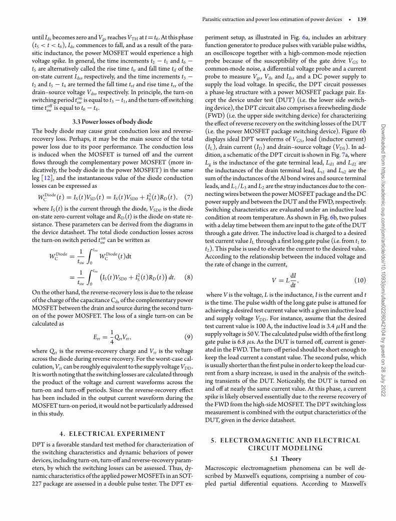
4. ELECTRICAL EXPERIMENTDPT is a favorable standard test method for characterization ofthe switching characteristics and dynamic behaviors of powerdevices, including turn-on, turn-off and reverse-recovery param-eters, by which the switching losses can be assessed. Thus, dy-namic characteristics of the appliedpowerMOSFETs in anSOT-227 package are assessed in a double pulse tester. The DPT ex-
periment setup, as illustrated in Fig. 6a, includes an arbitraryfunction generator to produce pulses with variable pulse widths,an oscilloscope together with a high-common-mode rejectionprobe because of the susceptibility of the gate drive VGS tocommon-mode noise, a differential voltage probe and a currentprobe to measure Vgs, Vds and Ids, and a DC power supply tosupply the load voltage. In specific, the DPT circuit possessesa phase-leg structure with a power MOSFET package pair. Ex-cept the device under test (DUT) (i.e. the lower side switch-ing device), theDPTcircuit also comprises a freewheeling diode(FWD) (i.e. the upper side switching device) for characterizingthe effect of reverse recovery on the switching losses of theDUT(i.e. the power MOSFET package switching device). Figure 6bdisplays ideal DPT waveforms of VGS, load (inductor current)(IL), drain current (ID) and drain–source voltage (VDS). In ad-dition, a schematic of the DPT circuit is shown in Fig. 7a, whereLg is the inductance of the gate terminal lead, Ld1 and Ld2 arethe inductances of the drain terminal lead, Ls1 and Ls2 are thesum of the inductances of the Al bondwires and source terminalleads, andL1/L3 andL2 are the stray inductances due to the con-nectingwires between the powerMOSFETpackage and theDCpower supply and between theDUT and the FWD, respectively.Switching characteristics are evaluated under an inductive loadcondition at room temperature. As shown in Fig. 6b, two pulseswith a delay time between them are input to the gate of theDUTthrough a gate driver. The inductive load is charged to a desiredtest current value IL through a first long gate pulse (i.e. from t1 tot2). This pulse is used to elevate the current to the desired value.According to the relationship between the induced voltage andthe rate of change in the current,
V = LdIdt
, (10)
where V is the voltage, L is the inductance, I is the current and tis the time. The pulse width of the long gate pulse is attuned forachieving a desired test current value with a given inductive loadand supply voltage VDD. For instance, assume that the desiredtest current value is 100 A, the inductive load is 3.4μH and thesupply voltage is 50V.The calculated pulsewidth of the first longgate pulse is 6.8 μs. As the DUT is turned off, current is gener-ated in the FWD. The turn-off period should be short enough tokeep the load current a constant value. The second pulse, whichis usually shorter than thefirst pulse in order to keep the load cur-rent from a sharp increase, is used in the analysis of the switch-ing transients of the DUT. Noticeably, the DUT is turned onand off at nearly the same current value. At this phase, a currentspike is likely observed essentially due to the reverse recovery ofthe FWD from the high-sideMOSFET. TheDPT switching lossmeasurement is combined with the output characteristics of theDUT, given in the device datasheet.
5. ELECTROMAGNETIC AND ELECTRICALCIRCUIT MODELING
5.1 TheoryMacroscopic electromagnetism phenomena can be well de-scribed by Maxwell’s equations, comprising a number of cou-pled partial differential equations. According to Maxwell’s
Dow
nloaded from https://academ
ic.oup.com/jom
/article/doi/10.1093/jom/ufaa022/6042104 by guest on 28 July 2022

140 • Journal of Mechanics, 2020, Vol. 37
equations, when a conductor is subjected to a direct current[28], the differential form is represented by the following formu-las:
∇ · D = ρv, (11)
∇ · B = 0, (12)
∇ × E = −∂B∂t
, (13)
∇ × H = Jf + ∂D∂t
, (14)
where D is the electric flux vector, B is the magnetic intensityvector, E is the electric field vector, ρv is the volume charge den-sity,H is the magnetic intensity vector and Jf is the current den-sity vector. The Ampère equation (Eq. 14) is also called theMaxwell–Ampère equation.As the current produces a steady-state electric field on the
surface of the conductor, we can take the divergence of thevector∇ ×H in Eq. (14):
∇ · (∇ × H) = ∇ · Jf + ∇ · ∂D∂t
= 0. (15)
Thus,
∇ · Jf = −∇ · ∂D∂t
= −∂ (∇ · D)∂t
= −∂ρv
∂t. (16)
Figure 6 (a) DPT experimental setup and prototype and (b) ideal DPT waveforms.
Figure 7DPT circuit and inverter circuit with parasitic elements: (a) power MOSFET package and (b) three-phase inverter.
Dow
nloaded from https://academ
ic.oup.com/jom
/article/doi/10.1093/jom/ufaa022/6042104 by guest on 28 July 2022

Parasitic extraction and power loss estimation of power devices • 141
Figure 8 3D EMmodels for (a) the power MOSFET package and (b) inverter and the assigned nets and their identification number.
The equation is the continuity equation derived from the princi-ple of conservation of charge. Under the condition of stable cur-rent, the charge density does not change with time, ∂ρv/∂t = 0,and Eq. (16) can be rewritten as
∇ · Jf = 0. (17)
According to the Ohm’s law, Jf = σE and E = −∇V, Eq. (17)can thus be expressed as
∇ · [σ (−∇V )] = 0. (18)
When the conductivity σ of the conductor material is constantand evenly distributed, Eq. (18) can be reduced to
∇2V = 0, (19)
which is the steady-state electric field governing equation.
5.2 3DEManalysis for parasitic parameter extraction3D quasi-static EM analysis using the ANSYS® Q3D extractiontool is performed to extract the parasitic parameters of the singlepower MOSFET package and the three-phase inverter with var-ious assigned conducting nets, and also explore their effects onthe power losses. The 3D parasitic extraction tool applies meth-ods of moments and finite element methods to solve the EMproblems. The parasitic extraction simulation between two ter-minals is performed by first defining a current conductive paththrough assigning a source and a sink terminal, where the for-mer serves as a current injector and the latter gathers the current.Moreover, an adaptivemeshing scheme is applied in the ANSYSQ3D for adaptively adjusting/refining the mesh. To extract theparasitics at different frequencies, a discretized frequency sweepis performed. For the power MOSFET package, the Al bondwires andCu terminal leads (namely, one gate, onedrain and twosources) would be the root cause of the parasitic effects. Accord-ingly, the aimof theparasitic analysis is to determine theparasiticinductances of the drain, gate and source leads, i.e. Ld, Lg and Ls.The geometry of the power MOSFET package is imported intoANSYSQ3D, includingMOSFET chips, Al bondwires, Al pads,Cu terminal leads, a DBC substrate, a Cu base plate and solderlayers. In other words, the PPS housing and the filling material(i.e. the quick-drying rubber-based adhesive) are not included.The geometry model for parasitic inductance extraction of thepower MOSFET package is shown in Fig. 8a. The EM simula-tion model consists of 68 742 finite elements. In addition, three
Table 1 Electrical properties of the materials in the power devices.
Materials εr μr σa (S/m) tan δ
Si (die) 11.9 1.0 0.0e+ 00 0.0Cu (lead/DBC) 1.0 1.0 5.8e+ 07 0.0Al (wire/pad) 1.0 1.0 3.8e+ 07 0.0
SAC305 (solder) 1.0 1.0 7.0e+ 06 0.0Alumina (DBC) 9.8 1.0 0.0e+ 00 0.0
conducting nets associatedwith the drain, source and gate of thepower MOSFET package are assigned for the parasitic analysis,and then, the inputs/outputs of each net are defined. The work-ing frequency is set to be 20 kHz. It is noted that the conduct-ing net associated with the source includes the source terminalleads and Al wires, as plotted in Fig. 8a; hence, the calculated Lsincludes two parts: one is the parasitic inductance of the sourceterminal leads and the other is that of these Al wires.Figure 8b displays the geometry model of the three-phase in-
verter and the defined conducting nets that describe the currentpaths and their identification number. In total, 12 critical con-ducting nets in the inverter, as illustrated in the figure, are as-signed in accordancewith the switching sequence of the inverter.Ld andLs of the powerMOSFET in an SOT-227 package are de-fined as Nets 8 and 9, respectively, as shown in Fig. 8b. In fact,they are determined from the preceding parasitic parameter ex-traction of the single powerMOSFETpackage. Take an exampleof the first switching state in the six-step switching sequence, in-volving Q1 and Q4. The major current conductive paths duringthe first switching state include the DC bus+ to the drain of Q1(Net 1), the drain terminal of Q1 (Net 8), the source terminal ofQ1 (including Al wires) (Net 9), the source of Q1 to the motorload (Net 10), the motor load to the drain of Q4 (Net 11), thedrain terminal of Q4 (Net 8), the source terminal of Q4 (includ-ing Al wires) (Net 9), the Cu bridge (Net 5) and the Cu bridgeto theDCbus− (Net 7). Likewise, the housing and other insula-tion materials are not considered in the modeling. The workingfrequency is set to be 10 kHz. The electrical properties of themain component materials, namely bulk conductivity (σ a), di-electric loss tangent (tan δ), relative permeability (μr) and rela-tive permittivity (εr), are shown in Table 1, which are given bythe material library inside the reference manual of the ANSYSQ3D Extractor.
Dow
nloaded from https://academ
ic.oup.com/jom
/article/doi/10.1093/jom/ufaa022/6042104 by guest on 28 July 2022

142 • Journal of Mechanics, 2020, Vol. 37
5.3 Electrical circuit analysisDynamic characteristics of the power MOSFET in an SOT-227package are characterized in the inductive DPT circuit shown inFig. 7a, where the inductive load L (i.e. 3.4 μH), the extractedparasitic inductances (i.e. Ld, Lg, Ls) from the EM analysis,the stray inductances of the connection Cu wires (L1, L2, L3)and the parasitic capacitances from the device datasheet arealso listed. Subsequently, they are exported into the ANSYSSimplorer circuit analysis model to simulate the inductive DPTcircuit. The other required parameters, namely temperature-dependent output characteristics of the power MOSFET andbody diode, transfer characteristics and on-state conductionresistance, are given in the device datasheet, as illustrated inFig. 3. The absolute maximum ratings of the power MOSFETare also provided in the device datasheet. Moreover, the nonlin-ear dependences of these parasitic capacitances shown in Fig. 4bon the drain–source voltage Vds are also accounted for in thecalculation. To precisely address such nonlinearity in the circuitcalculation is not straightforward. The effect of the nonlinearityis often approximated using the two-point method approach[12]. For simplicity and better computational efficiency, it isinstead approximated using a multiple-point averaging approx-imation in this work, where the parasitic capacitance curves inthe range of the low conduction voltage (VON) to the supplyvoltage (VDD) are divided into five even regions using six evenlyspaced points, and the capacitances at these Vds points areaveraged. The average value is taken as the parasitic capacitance.The DPT simulation is done under 50 V DC bus voltage, 100A load current and room temperature. Figure 7b displays theequivalent circuit of the three-phase inverter that takes accountof the parasitic effects and the three-phase motor loads, i.e. aseries connection of inductor and resistor (RU, LU; RV, LV; RW,LW). For these three phases, the equivalent motor load consistsof 0.125� resistor, in series with a 20μH inductor.
6. RESULTS AND DISCUSSION6.1 Parasitic extractions and power loss estimation of power
MOSFETpackage6.1.1 Parasitic parameter extraction
EM simulation is first performed on the single power MOSFETpackage for parasitic extraction. The simulated parasitic induc-tances associated with the drain and source terminals for both
Table 2Modeled and measured rise and fall times of voltage and cur-rent.
Switching time (ns) Experiment Simulation
tvf 201.0 226.0tir 154.0 160.0tvr 161.6 156.0tif 212.0 210.0
the FWD (Ld1, Ls1) and DUT (Ld2, Ls2) are plotted in Fig. 7a,where they are 5.47 and 7.53 nH, respectively. As noted ear-lier, Ls comprises the parasitic inductances of the source termi-nal leads and Al wires, and their values are 5.92 and 1.61 nH,respectively. In addition, the gate inductance of the DUT (Lg)is 8.60 nH, also shown in Fig. 7a. The stray inductances of theconnection Cu wires used in the DPT experiment (i.e. L1, L2,and L3 in Fig. 7a) are also taken into consideration. The con-nection Cu wires for L1 and L3 are 10 mm long with a diame-ter of 1 mm and that for L2 is 30 mm long with a diameter of 2mm. The calculated stray inductances of these three connectionCu wires from the EMmodeling are∼4.76,∼16.24 and∼4.76nH, as also shown in Fig. 7a. Besides, by using themultiple-pointaveraging approximation scheme, the average capacitance val-ues of Ciss, Coss and Crss across the drain–source voltage range[0, 50 V] are 22 498.97, 28 209.04 and 8614.84 pF. Accordingto Eqs (2)–(4), the average capacitance values of Cgs, Cds andCgd can be found, which are 13 884.13, 19 594.20 and 8614.84pF. These capacitance values are also listed in Fig. 7a.With these parasitic parameters, circuit simulation is per-
formed on the power MOSFET package using ANSYS Sim-plorer. The modeled and measured switching waveforms of thepowerMOSFET inaDPTcircuitwithVDD =50Vand ID =100A are presented in Fig. 9. The corresponding switching times,i.e. the fall time tvf and the rise time tvr of the drain–sourcevoltage, and the fall time tif and the rise time tir of the on-statecurrent, are listed in Table 2. Clearly, a fair consistency in themodeled and experimental waveform profiles is observed eventhough some discrepancies can be found in the current and volt-age overshoots and oscillations. The fair discrepancies could bemainly attributed to a concern about the accuracy of the powerMOSFET parasitic capacitance values provided in the devicedatasheet. Moreover, the calculated switching times show a verygood agreement with the experimental values. According to thecurrent and voltage waveforms, the total turn-on switching time
Figure 9 (a) Modeled and (b) measured switching waveforms of the power MOSFET in an SOT-227 package.
Dow
nloaded from https://academ
ic.oup.com/jom
/article/doi/10.1093/jom/ufaa022/6042104 by guest on 28 July 2022

Parasitic extraction and power loss estimation of power devices • 143
Figure 10Modeled turn-on transient waveforms at (a) 25°C and (b) 125°C.
(tvf + tir) and turn-off switching time (tif + tvr) and so theswitching losses of the single power MOSFET package can beobtained.
6.1.2 Effect of temperature on switching transientBesides the conduction loss, the switching losses of powerMOS-FETs could also be temperature dependent because it is a func-tion of the temperature-sensitive gate resistance and thresholdvoltage [23]. It will be confirmed later that a smaller gate resis-tancewould result inhigher turn-on and turn-off speeds and thusa lower switching loss. As a consequence, the temperature de-pendenceof the switchingwaveforms and so the switching lossesof the power MOSFET package are assessed through the induc-tive DPT circuit simulation using ANSYS Simplorer at two dif-ferent ambient temperatures, i.e. 25 and 125°C. The modeledwaveforms of turn-on transient at these two ambient tempera-tures are shown in Fig. 10. It is clearly seen that the drain cur-rent waveform Id would not vary with temperature; however,temperature has a great influence on the drain–source voltagewaveform Vds. This suggests that the turn-on switching loss in-creases with temperature, mainly due to amuchmore significantoscillation in the drain–source voltage waveform. A similar re-sult can also be found in the turn-off switching loss. That is tosay, temperature has a positive temperature correlation. The re-sult is consistent with Wang’s prediction [23] for Si MOFET,and also with Qi et al.’s result [26] for Si IGBT, but the degreeof this effect is not as important as that of Si IGBT. Moreover,the result has a distinct trend from those of SiC MOSFET (seee.g. [24–26]).
6.1.3 Estimation of power lossesThe calculated conduction and switching losses of the powerMOSFET and the conduction loss of the body diode in a singleload step with a duration of 1 s at a PWMduty cycle of 50% andswitching frequency of 10 kHz are shown in Fig. 11a. The circuitsimulation is performed at the room temperature (i.e. 25°C). Itcan be seen from the figure that the switching loss of the powerMOSFET is ∼1.81 times the conduction loss, implying that itcould not be negligible in the power loss estimation. Besides,the turn-off switching loss considerably outperforms the turn-on one. It is important to note that the conduction loss of thebody diode in the FWD is much greater than the total powerloss (sum of the conduction and switching losses) of the powerMOSFET transistors in the DUT. Thus, in order to reduce thetotal power loss, the first priority is to lower the conduction lossof the body diode. This can be achieved by use of either a near-zerodead time, thoughnot verypractical, or anexternal Schottkydiode that is connected in parallel with the power MOSFET toshunt the body diode, though it has increased inefficiency andcost. In general, the forward voltage drop of a Schottky diode issmaller than that of a typical PN junction diode, thereby leadingto a less conduction loss.
6.1.4 Dependence of power losses on duty cycleThe effect of duty cycle on the power losses of the powerMOS-FET and the conduction loss of the body diode in a single loadstepwith a durationof 1 s at 10 kHzPWMfrequency and variousPWM duty cycles is explored. The duty cycles considered are10%, 30%, 50%, 70% and 90%. The parametric analysis results
Figure 11 (a) Calculated power losses of power MOSFET package in a single load step with a duration of 1 s and (b) effect of duty cycle onpower losses.
Dow
nloaded from https://academ
ic.oup.com/jom
/article/doi/10.1093/jom/ufaa022/6042104 by guest on 28 July 2022

144 • Journal of Mechanics, 2020, Vol. 37
Figure 12 (a) Two different source terminal designs (left: original design; right: novel design) and (b) definition of Al wire loop height andpitch.
are shown in Fig. 11b. The figure shows that the conduction lossand so the total power loss of the power MOSFET package (i.e.DUT in the DPT circuit) would increase significantly with dutycycle,mainlydue to an increase in the “ONtime”of the signal buta decrease in the “OFF time”. On the other hand, it is surprisingto see that an increasing duty cycle greatly reduces the conduc-tion loss of the body diode. This is mainly due to a smaller timeinterval where the diode is conducting with the increase of dutycycle. Indicatively, the duration of the interval is a function of theduty cycle and the dead time of the gate signal. A similar resultcan be found in Kumar [29] for an Si IGBT inverter. Since thediode’s conduction loss is the major power loss source, the totalpower loss would correspondingly decrease with an increase inthe duty cycle accordingly.
6.1.5 A novel source terminal design for reduced parasitic inductanceIn order to reduce the parasitic inductance associated with thesource, a new source terminal design is proposed, as presentedin Fig. 12a, where the two source leads are bonded together.
As compared to the original design (Fig. 12a), where thesetwo source leads are separated, the new design demonstratesa larger conduction cross-sectional area and a smaller conduc-tion length. The parasitic simulation reveals that the source par-asitic inductance of the novel design reduces from 5.92 down to2.59 nH, and asmuch as∼44% reduction in parasitic inductanceis achieved.
6.1.6 Parametric study of parasitic inductanceThe effects of theAlwire diameter, loop geometry (loopheight),pitch and amount on their parasitic inductances are examined.The Al loop height and pitch are defined in Fig. 12b. In the para-metric study, theAlwirediameter, loopheight, pitch andamountrange from0.1 to 0.5mm, 0.5 to 2.5mm, 1 to 2mmand3 to 5, re-spectively. It is noted that an increase in the Al wire diameter andloop height increases the wire area and length. The parametricresults are presented in Fig. 13. It demonstrates that the Al wireloop height and amount tend to have a greater impact on their
Figure 13 Effects of (a) Al wire diameter, (b) loop height, (c) pitch and (d) amount on the parasitic inductances of power MOSFET package.
Dow
nloaded from https://academ
ic.oup.com/jom
/article/doi/10.1093/jom/ufaa022/6042104 by guest on 28 July 2022

Parasitic extraction and power loss estimation of power devices • 145
Table 3 Parasitic inductances (nH) of the assigned conducting nets and the effect of switching frequency (kHz).
Frequency L1 L2 L3 L4 L5 L6 L7 L10 L11 L12
0 27.07 16.56 29.52 30.99 7.00 4.10 68.15 19.79 19.52 19.7810 23.34 14.74 25.52 31.31 6.93 3.67 54.89 19.79 19.52 19.7820 22.10 14.37 25.06 29.49 5.31 3.64 53.81 19.79 19.52 19.78
parasitic inductances. Moreover, a decreasing Al wire diameter,pitch and amount and an increasing Al wire loop height wouldlead to a greater parasitic inductance. It will be confirmed in thefollowing section that a lower parasitic inductance would mini-mize the switching loss.
6.2 Parasitic extraction and switching loss prediction ofthree-phase inverter
6.2.1 Parasitic parameter extractionIn the three-phase inverter, the parasitic inductances of theassigned conducting nets are extracted using ANSYS Q3D, ascan be seen in Figs 7b and 8b. The effects of switching frequencyon the parasitic inductances are also examined. A total of threedifferent switching frequencies, namely 0 (DC), 10 and 20kHz, are considered. Note again that Ld and Ls of the powerMOSFET in an SOT-227 package, identified as Nets 8 and 9,respectively, are extracted from thepreceding inductiveDPTcir-cuit simulation, and they are 5.47 and 7.53 nH, respectively. Thecalculated parasitic inductances of the remaining 10 conductingnets (L1–L7, L10–L12) as a function of switching frequency areshown in Table 3. Among these 10 assigned conducting nets,Net 7 (L7), i.e. from the Cu bridge to the DC bus−, holds thelargest parasitic inductance value because of possessing thelongest conducting channel and relatively smaller conductingcross-sectional area, while Nets 5 (L5) and 6 (L6), i.e. the Cubridges, yield the smallest parasitic inductance. Moreover, allthese parasitic inductances, except L4 and L10–L12, tend toslightly decrease with an increasing switching frequency from0 to 20 kHz. This result is very consistent with the literaturefindings (see e.g. [30]). The exception for the former (L4) isprobably due to the computational accuracy of the EM finiteelement analysis, and that for the latter (L10–L12) is becauseof the insignificant switching frequency variation range. The
parasitic inductances at 10 kHz switching frequency are appliedin the subsequent circuit simulation of the three-phase inverter.
6.2.2 Parametric analysis of switching lossThe following investigates the effects of several key factors onthe switching losses of the three-phase inverter duringonePWMcycle at the first switching step of the six-step switching control.The considered factors are parasitic inductance, gate resistance,resistive load and switching frequency. Figure 14 shows theinverter circuit at the first switching step of the six-step switchingcontrol and its current loops. In total, three switches are involvedin this switching step: Q1, Q2 and Q4, where the Q2 switch isused as an FWD in the commutation step. As mentioned earlier,Q1 is a PWM power MOSFET, whereas Q4 is a commutationpowerMOSFET. As can be seen in Fig. 14, this switching opera-tion consists of two current loops: one is when the Q1 switch isturned on during a PWM switching cycle, i.e. PWM “on”, andthe other is when the Q1 switch is turned off, i.e. PWM “off”.The first current loop involves the following conductive paths:Net 1, Net 8, Net 9, Net 10, Net 11, Net 8, Net 9, Net 5 and Net7, and the other Net 11, Net 8, Net 9, Net 4, Net 9 Net 8 andNet 10. The mutual inductances of these two current loops arealso calculated using the proposed EM simulation. The mutualinductances of these two current loops are found to be 16.42and 1.02 nH. Since the switching loss is only generated at theQ1 switch, the first current loop, i.e. when the Q1 switch ison, is simply considered in the simulation. The total induc-tance of the series chain in the first current loop is found bysimply summing all the individual inductances of these series-connected inductors. According to Table 3, it is around 150.47nH, which is much larger than the corresponding mutual induc-tance. Subsequently, circuit simulation of the three-phased in-verter is carried out. The equivalent circuit of the three-phase in-verter is shown in Fig. 7b. A simple and effective compact circuit
Figure 14The inverter circuit at the first switching step of the six-step switching control together with the corresponding current loops: (a) Q1in PWM onmode and (b) Q1 in PWM offmode.
Dow
nloaded from https://academ
ic.oup.com/jom
/article/doi/10.1093/jom/ufaa022/6042104 by guest on 28 July 2022

146 • Journal of Mechanics, 2020, Vol. 37
Figure 15 Effects of (a) parasitic inductance, (b) gate resistance, (c) resistive load and (d) switching frequency on the switching losses.
simulation model for the three-phase inverter is developed us-ing ANSYS Simplorer, where the power MOSFET packages areapproximated as resistors. The above-characterized parasitic el-ements and other components, such as load resistor and load in-ductor, are also used in the circuit simulation. It is noted thatthe effect ofmutual inductance among these resistors is not con-sidered because the mutual inductance is much smaller than theself-inductance. In addition, the switching frequency, gate resis-tance, gate voltage, gate inductance, inductive load and resistiveload are set to 10 kHz, 1.6�, 10 V, 8.6 nH, 20μH and 0.125�,respectively.A huge spike of voltage between the drain and source during
the turn-off transientmay be generated due to circuit inductanceand stray inductance. Accordingly, the effects of the total induc-tance of the series-connected inductors in the first current loopon the turn-on, turn-off and total switching energy losses are firstexamined and the results are shown in Fig. 15a. The nominal in-ductance value (theoriginal design) is 150.47nH, i.e. the total in-ductance of the series chain. In the parametric analysis, the totalparasitic inductance varies from 75.27 to 225.74 nH, i.e. ±50%of the nominal value, which implies that the inductance of eachnet in the current loop would also change ±50% of the originalvalue. The figure shows that the turn-off energy loss markedlyoutperforms the turn-on energy loss. In addition, the turn-offand total switching energy losses risewith the growthof parasiticinductance, whereas an increasing parasitic inductance tends toslightly lower the turn-on loss. The former is probably due to thefact that a smaller parasitic inductance brings about a lower volt-age spike in the turn-off transient, thereby leasing to a less switch-ing loss. In addition, the parasitic inductance has a more impor-tant impact on the turn-off energy loss than turn-off one.Switching time can be controlled by means of gate resistance.
The gate resistance is typically within the range of 1–3 �; as a
result, in the parametric analysis, the variation of the gate resis-tance is in the range of 0.8–2.4 �. Note that the nominal gateresistance value is 1.6 �. Figure 15b exhibits the dependenceof the switching energy losses of the inverter on the gate resis-tance. It is found that the increase in gate resistance raises allthese switching energy losses, namely the turn-on, turn-off andtotal. This result can be attributed to the fact that a smaller gateresistance results in a shorter switching time and faster switch-ing speed, thereby diminishing these switching losses. Similar tothe parasitic inductance, the gate resistance also plays a muchmore significant role in the turn-off energy loss than the turn-on. It should be noted that even though the switching time be-comes shorter with a smaller gate resistance, the voltage spike inthe turn-off transient may reversely increase in magnitude. Spe-cial attention needs to be also taken when the drain–source volt-age exceeds the voltage rating or breakdown voltage of the powerdevice since it may cause a false switching event, which wouldmake the power device extremely vulnerable to permanentdamage.The influence of the resistive load on the switching energy
losses is examined. The resistive load varies±50% from its nom-inal value, i.e. 0.125 �. The variations of the switching energylosses with these resistive loads are presented in Fig. 15c. Thefigure reveals that all these switching losses decrease with theresistive load. This can be explained by the fact that a smaller re-sistive load would result in a larger drain current, thereby caus-ing a greater switching loss. It is also found that a greater resistiveloadwould not only bring about a less current fluctuation ampli-tude during the switching operation but also take more time toreach the specified load current, i.e. 100 A in this investigation.According to the slope of these curves, the resistive load showsa much greater impact on the switching loss, as compared to theparasitic inductance and gate resistance. Likewise, the resistive
Dow
nloaded from https://academ
ic.oup.com/jom
/article/doi/10.1093/jom/ufaa022/6042104 by guest on 28 July 2022

Parasitic extraction and power loss estimation of power devices • 147
load demonstrates a greater influence on the turn-off energy lossthan the turn-on one.The switching losses of the inverter as a function of the PWM
frequency are assessed and the results are displayed in Fig. 15d.For avoiding noise, most commercial inverters would not be op-erated at switching frequencies <5 kHz. As a consequence, inthis investigation, three different switching frequencies are con-sidered, namely 5, 10 and 15 kHz. From the figure, it is not sur-prising to see that these switching losses elevate with switchingfrequency. Besides, in termsof noise and switching loss, a switch-ing frequency of 5 kHz could be a preferred option.
7. CONCLUSIONSThis study utilizes both experimental and numerical methods toexplore the switching transients and power losses of a Si powerMOSFET-based three-phase MOSFET inverter for brushlessDCmotor drive during the load cycles. EM simulations are per-formed using the 3D EM simulator to explore the parasitic in-ductances of the power MOSFET package and three-phase in-verter. A compact circuit simulation model that combines thedevice model and package model is constructed for the powerMOSFETpackage and three-phase inverter. The switching tran-sients of the powerMOSFET package are experimentally testedand numerically evaluated with the DPT circuit. Despite hav-ing certain discrepancies in the overshoots and oscillations ofcurrent and voltage, the experimental results in terms of wave-form profiles and switching times are found to be appropriatelyconsistent with the simulated ones. They could be probably at-tributed to insufficient accuracyof theparasitic capacitancespro-vided in the device datasheet. Finally, a design guideline for re-duced parasitic inductances and decreased switching losses issought through parametric study. Some essential remarks arebriefed below:
1. The results show that temperature has a little impact onthe drain currentwaveformbut an important effect on thedrain–source voltage waveform. In other words, the turn-on and turn-off switching losses and so the total switchingloss all have a positive temperature coefficient, mostly be-cause of the increased voltage ringing. The result agreeswell with the literature findings for Si power MOSFETdevices while being opposite to those for SiC MOSFET.Besides, the extent of temperature effect for Si powerMOSFET devices is not as significant as that for Si IGBTdevices.
2. TheDPT simulation demonstrates that the switching lossof the power MOSFET package greatly outperforms itsconduction loss, indicating that the effectof switching losscould not be neglected in the power loss analysis. More-over, the turn-off switching loss turns out to be muchgreater than the turn-on one.
3. Themajorpower loss source in thepowerMOSFETpack-age is the conduction loss of the body diode, which can begreatly reduced by use of an external Schottky diode, fol-lowed by the switching loss and conduction loss of powerMOSFETs.
4. It is interesting to see that the total power loss decreaseswith the increase of duty cycle, mainly because the con-duction loss of the body diode decreases with duty cycle,eventually leading to a reduced total power loss. This canbe explained by the fact that the increase of duty cycle up-grades the signal’s “ON time” but lowers the signal’s “OFFtime”.
5. It is interesting to find that the proposed novel source ter-minal design can extensively help to reduce the parasiticinductance, thereby allowing for a lower switching loss.Furthermore, as compared towire pitch and diameter, theloop height and number of wires have a relatively large ef-fect on their parasitic inductance. Besides, the parametricanalysis reveals that a lower parasitic inductance in the Alwires canbe achievedbyuse of a largerwire diameter,wirepitch and number of wires, and a smaller loop height.
6. Parasitic parameter extraction of the three-phase inverterdemonstrates that among the assigned nets, the conduc-tive path from the Cu bridge to the DC bus− (Net 7)yields the largest value of parasitic inductance becauseof having the longest conducting channel and relativelysmaller conducting cross-sectional area. On the otherhand, the Cu bridges, i.e. Nets 5 and 6, possess the low-est parasitic inductance. In addition, the parasitic induc-tances have a minor negative influence on the switchingfrequency as it varies from 0 to 20 kHz.
7. Parametric study of the switching energy losses of thethree-phase inverter demonstrates that the turn-off andtotal switching losses during the first switching step ofthe six-step switching sequence tend to reduce with a de-creased parasitic inductance, gate resistance and switch-ing frequency, and an increased resistive load.
ACKNOWLEDGEMENTThisworkwaspartially supportedby theMinistry of Science andTechnology, Taiwan, Republic of China, under grants MOST106-2221-E-035-052-MY3 and MOST 109-2221-E-035-004-MY3.
REFERENCES1. Samavatian V, Masoumian A, Mafi M, Lakzaei M, Ghaderi D.
Influence of directional random vibration on the fatigue life ofsolder joints in a power module. IEEE Transactions on Com-ponents, Packaging and Manufacturing Technology 2019;9(2):262–268.
2. CaillaudR,ButtayC,MradR,Leslé JL,Morel F,DegrenneN,MollovSV. Thermal considerations of a power converter with componentsembedded in printed circuit boards. IEEE Transactions on Com-ponents, Packaging and Manufacturing Technology 2020;10(2):230–239.
3. Chou PC, Cheng S. Design and characterization of a 200 V, 45 Aall-GaN HEMT-based power module. Applied Thermal Engineering2013;61:20–27.
4. Kanata T, Nishiwaki K, Hamada K. Development trends of powersemiconductors for hybrid vehicles. In: Proceedings of the Interna-tional Power Electronics Conference (IPEC), 2010, 778–782.
5. Cheng H-C, Wu C-H, Lin S-Y. Thermal and electrical characteriza-tion of powerMOSFETmodule using coupled field analysis. Journalof Mechanics 2019;35(5):641–655.
Dow
nloaded from https://academ
ic.oup.com/jom
/article/doi/10.1093/jom/ufaa022/6042104 by guest on 28 July 2022

148 • Journal of Mechanics, 2020, Vol. 37
6. Cheng H-C, Liu Y-C. Warpage characterization of molded wafer forfan-out wafer-level packaging. Journal of Electronic Packaging, ASMETransactions 2020;142(1):011004.
7. ChengH-C,WuZ-D, LiuY-C.Viscoelasticwarpagemodeling of fan-out wafer level packaging. IEEE Transactions on Components, Packag-ing and Manufacturing Technology 2020;10(7):1240–1250.
8. Liao LL,ChiangKN.Material shear strength assessment of Au/20Sninterconnection for high temperature applications. Journal of Me-chanics 2019;35(1):81–91.
9. YangK. Transient electro-thermal analysis of traction inverters.Mas-ter thesis in applied science, McMaster University, Hamilton, On-tario, Canada, 2015.
10. Merienne F, Roudet J, Schanen JL. Switching disturbance due tosource inductance for a power MOSFET: analysis and solutions. In:Proceedings of the IEEE Power Electronics Specialists Conference, Vol. 2,1996, 1743–1747.
11. Spaziani L. A study of MOSFET performance in processor targetedbuck and synchronous rectifier buck converters. In:Proceedings of theHigh Frequency Power Conversion (HFPC), 1996, 123–137.
12. Graovac D, Purschel M, Kiep A. MOSFET power losses calculationusing the data-sheet parameters. Infineon Application Note, 2006.
13. Tabisz WA, Lee FC, Chen DY. A MOSFET resonant synchronousrectifier for high-frequencyDC/DCconverters. In: Proceedings of theIEEE Power Electronics Specialists Conference, 1990, 769–779.
14. Xiong Y, Sun S, Jia H, Shea P, Shen ZJ. New physical insights onpower MOSFET switching losses. IEEE Transactions on Power Elec-tronics 2009;24(2):525–531.
15. Bai Y, Meng Y, Huang AQ, Lee FC. A novel model for MOSFETswitching loss calculation. In: Proceedings of the IEEE Power Electron-ics and Motion Control Conference, Vol. 3, 2004, 1669–1672.
16. Ren Y, XuM, Zhou J, Lee FC. Analytical loss model of powerMOS-FET. IEEE Transactions on Power Electronics 2006;21(2):310–319.
17. Rodríguez M, Rodríguez A, Miaja PF, Lamar DG, Zúniga JS. Aninsight into the switching process of power MOSFETs: an im-proved analytical losses model. IEEE Transactions on Power Electron-ics 2010;25(6):1626–1640.
18. Klein J. Synchronous buck MOSFET loss calculations with Excelmodel. Fairchild Semiconductor Application Note AN-6005, 2006.
19. Chen Z, Boroyevich D, Burgos R. Experimental parametric study ofthe parasitic inductance influence onMOSFET switching character-istics. In: Proceedings of the International Power Electronics Conference(IPEC), 2010, 164–169.
20. Chen JZ, Yang L, Boroyevich D, Odendaal WG.Modeling and mea-surements of parasitic parameters for integrated power electronicsmodules. In: Proceedings of the Applied Power Electronics Conferenceand Exposition, Vol. 1, 2004, 522–525.
21. YuanL, YuH,WangX,ZhaoZ.Design, simulation and analysis of thelow stray inductance bus bar for voltage source inverters. In: Proceed-ings of the International Conference on Electrical Machines and Systems,2011, 1–5.
22. Sang T. Integrated electro-thermal design methodology in dis-tributed power systems (DPS). Master thesis in electrical engineer-ing, Virginia Polytechnic Institute and State University, Blacksburg,VA, 2003.
23. Wang H. Investigation of power semiconductor devices for high fre-quency high density power converters. Doctoral thesis in electri-cal engineering, Virginia Polytechnic Institute and State University,Blacksburg, VA, 2007.
24. Ravi L. Characterization and loss modeling of silicon carbide basedpower electronic converters. Master thesis in electrical engineering,University of Minnesota, Minneapolis, MN, 2015.
25. Marzoughi AR, Burgos R, Boroyevich D. Comparing the state-of-the-art SiCMOSFETs: test results reveal characteristics of fourmajormanufacturers? 900-V and 1.2-kV SiC devices. IEEE Power Electron-ics Magazine 2017;4:36–45.
26. Qi J, Yang X, Li X, Tian K, Mao Z, Yang S, Song W. Temperaturedependence of dynamic performance characterization of 1.2-kV SiCpower MOSFETS compared with Si IGBTs for wide temperatureapplications. IEEE Transactions on Power Electronics 2019;34:9105–9117.
27. Chen H-C, Tsai T-Y, Huang C-K. Comparisons of six-step square-wave PWMs in ultra-low-power SOC integration. In: Proceedings ofthe IEEE International Symposium on Industrial Electronics (ISIE),Seoul, South Korea, 5–8 June 2009.
28. Inan US. Engineering Electromagnetics. India: Pearson Education,1998.
29. Kumar K. High efficiency power converters for vehicular applica-tions. Doctoral thesis, Doctoral School of Space Sciences, Tech-nologies and Measurements, University of Padova, Padova, Italy,2016.
30. Cao D. Modularized multilevel and Z-source power converter asrenewable energy interface for vehicle and grid-connected applica-tions. Doctoral thesis in electrical engineering, Michigan State Uni-versity, East Lansing, MI, 2012.
Dow
nloaded from https://academ
ic.oup.com/jom
/article/doi/10.1093/jom/ufaa022/6042104 by guest on 28 July 2022
Copyright © 2022 FDOKUMEN