
Experimental Results for the Single Capacitor Single Inductor Active Snubber
6
Experimental Results for the Single Capacitor Single Inductor Active Snubber Gerardo Ceglia, Victor Guzmain, Maria I. Gimenez de Guzmain, Julio Walter. Simon Bolivar University, Electronic and Circuit Department, Caracas, Venezuela Abstract-In this work the practical results obtained with the Single Capacitor Single Inductor Active Snubber (SCSIAS) circuit using the Diode Bridge Switch Configuration are presented, proving the advantages of this proposed topology, which can be implemented with minimum component count. The SCSIAS configuration ensures that the main power devices undergo a ZVS off- commutation and a ZCS on-commutation, minimizing commutation losses in all operating conditions. Snubber topology also ensures that most auxiliary commutations take place under zero voltage/zero current conditions. I. INTRODUCTION The Single Capacitor Single Inductor Active Snubber (SCSIAS) circuit (SCSIAS) was proposed by the authors in [1]. In that work the initial analysis and simulation results using ORCAD-PSPICE were presented. The SCSIAS circuit is derived from the Single Capacitor Split Inductor Passive Snubber [2] and [3]. It requires only two passive components (one capacitor and one inductor), and depending on the particular configuration, includes two auxiliary switches [4-8] and two diodes (Antiparallel switch, Common Emitter switch and Opposed Emitter switch) or one auxiliary switch and four rectifier diodes (Diode Bridge switch) [1]. All the components can be located in a small single-side printed circuit board, that can be directly bolted to the main power switches module, keeping the circuit topology as simple as possible. Further size reduction can be achieved if the auxiliary switch gate drive is integrated in the firing board controlling the main switching devices. Fig. 1 presents the SCSIAS Diode Bridge Switch Configuration, which is the one to be used to obtain the experimental results. In order to simplify the control circuit design the auxiliary switch is closed only when the snubber is active, and control pulse duration can be preset. There is another strategy where the auxiliary switch must be closed again when the snubber capacitor voltage reaches its final value. This time is load dependant and can not be preset, hence a feedback signal is required to control the auxiliary switch, increasing circuit complexity. II. SCSIAS CIRCUIT OPERATION In the SCSIAS circuit, as in all Single Capacitor Single Inductor (SCSI) configurations, operation is strongly influenced by load current direction and level. The SCSIAS circuit first quadrant operation analysis, that is, when the power delivered to the load is positive just before the turn-off commutation process for IGBTd is started, was presented by the authors in [1]. For this condition, two Modes were defined, depending on the value reached by the capacitor voltage, Vcs, at the end of the interlock time delay, td, defined as the time interval between one main device goes off and the other goes on. In this work, the most relevant ideas are repeated, and a special case is discussed: Mode 2.a, which occurs when the load current is zero. In the circuit shown in fig. 1, the components IGBTU, IGBTd and their anti-parallel diodes are enclosed in the half bridge module; stray inductances in the connectors are considered much smaller than the snubber inductor L, and a highly inductive load is considered, ensuring that load current remains constant during snubber operation. The auxiliary switch will be turned on at taon, and turned off at taoff, selected to occur between 0.1 and 1 [ts before than the turn on signal for the main incoming device is applied. The auxiliary switch conduction time is identified as ta In this analysis only the lower main power device (IGBTd) turn-off commutation will be considered. Due to circuit symmetry, the obtained results apply also to the upper main power device (IGBTu) turn-off commutation with the corresponding changes in voltage and current polarities. A. Mode 1. In this Mode, the current magnitude is enough to change the snubber capacitor voltage, Vcs, from its maximun negative value to its maximum positive value in the snubber time interval ts, which is equal or less than the delay time, td. Initially IGBTd is on. The commutation process is started triggering the auxiliary switch at time taon, as shown in fig. 2. At this moment the inductor current is zero, therefore the inductor can be short-circuited without modifying other circuit variables. The load current IK is circulating through IGBTd to node N. The snubber capacitor voltage Vcs is -Vd,/2 and node A is at zero volts. 1-4244-0121-6/06/$20.00 C2006 IEEE 710 EPE-PEMC 2006, Portoro2, Slovenia
Transcript of Experimental Results for the Single Capacitor Single Inductor Active Snubber
Experimental Results for the Single CapacitorSingle Inductor Active Snubber
Gerardo Ceglia, Victor Guzmain, Maria I. Gimenez de Guzmain, Julio Walter.Simon Bolivar University, Electronic and Circuit Department, Caracas, Venezuela
Abstract-In this work the practical results obtained withthe Single Capacitor Single Inductor Active Snubber(SCSIAS) circuit using the Diode Bridge SwitchConfiguration are presented, proving the advantages of thisproposed topology, which can be implemented withminimum component count. The SCSIAS configurationensures that the main power devices undergo a ZVS off-commutation and a ZCS on-commutation, minimizingcommutation losses in all operating conditions. Snubbertopology also ensures that most auxiliary commutations takeplace under zero voltage/zero current conditions.
I. INTRODUCTIONThe Single Capacitor Single Inductor Active Snubber
(SCSIAS) circuit (SCSIAS) was proposed by the authorsin [1]. In that work the initial analysis and simulationresults using ORCAD-PSPICE were presented.
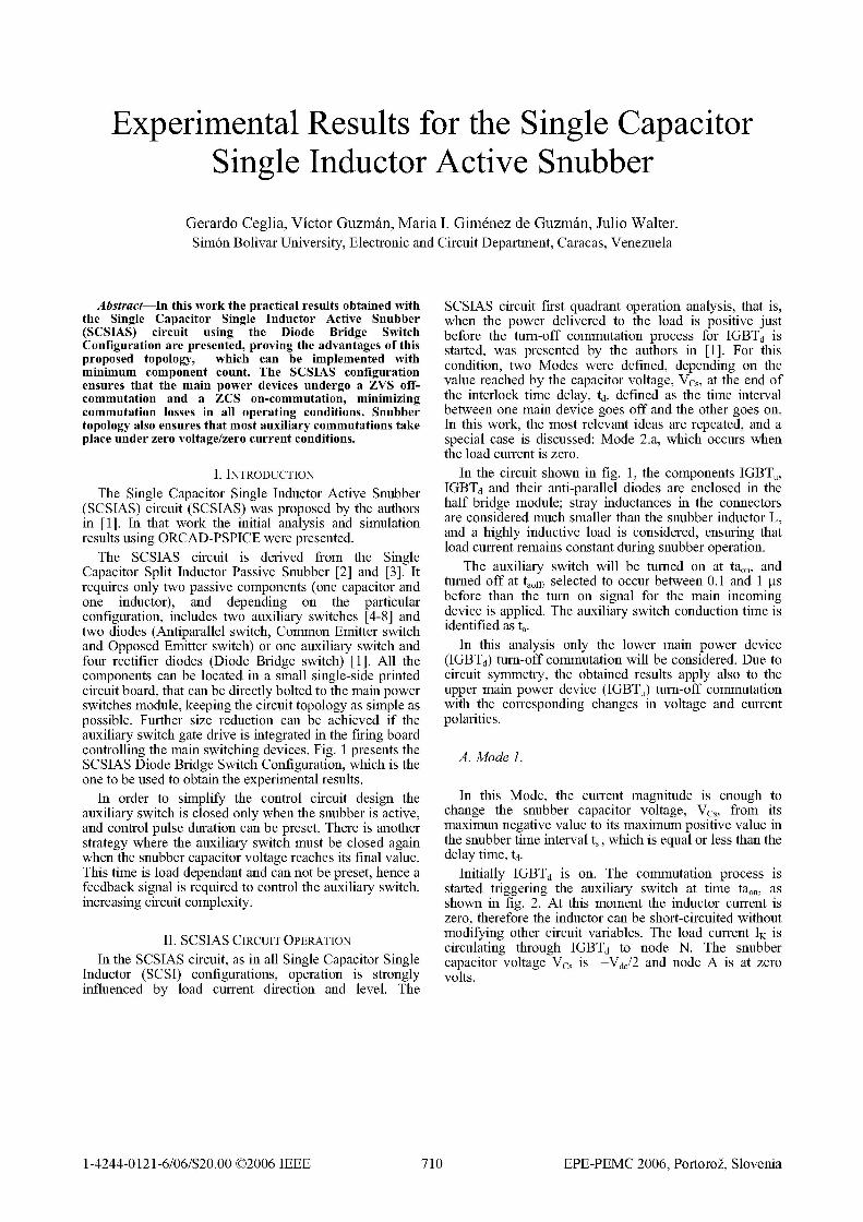
The SCSIAS circuit is derived from the SingleCapacitor Split Inductor Passive Snubber [2] and [3]. Itrequires only two passive components (one capacitor andone inductor), and depending on the particularconfiguration, includes two auxiliary switches [4-8] andtwo diodes (Antiparallel switch, Common Emitter switchand Opposed Emitter switch) or one auxiliary switch andfour rectifier diodes (Diode Bridge switch) [1]. All thecomponents can be located in a small single-side printedcircuit board, that can be directly bolted to the main powerswitches module, keeping the circuit topology as simple aspossible. Further size reduction can be achieved if theauxiliary switch gate drive is integrated in the firing boardcontrolling the main switching devices. Fig. 1 presents theSCSIAS Diode Bridge Switch Configuration, which is theone to be used to obtain the experimental results.
In order to simplify the control circuit design theauxiliary switch is closed only when the snubber is active,and control pulse duration can be preset. There is anotherstrategy where the auxiliary switch must be closed againwhen the snubber capacitor voltage reaches its final value.This time is load dependant and can not be preset, hence afeedback signal is required to control the auxiliary switch,increasing circuit complexity.
II. SCSIAS CIRCUIT OPERATIONIn the SCSIAS circuit, as in all Single Capacitor Single
Inductor (SCSI) configurations, operation is stronglyinfluenced by load current direction and level. The
SCSIAS circuit first quadrant operation analysis, that is,when the power delivered to the load is positive justbefore the turn-off commutation process for IGBTd isstarted, was presented by the authors in [1]. For thiscondition, two Modes were defined, depending on thevalue reached by the capacitor voltage, Vcs, at the end ofthe interlock time delay, td, defined as the time intervalbetween one main device goes off and the other goes on.In this work, the most relevant ideas are repeated, and aspecial case is discussed: Mode 2.a, which occurs whenthe load current is zero.
In the circuit shown in fig. 1, the components IGBTU,IGBTd and their anti-parallel diodes are enclosed in thehalf bridge module; stray inductances in the connectorsare considered much smaller than the snubber inductor L,and a highly inductive load is considered, ensuring thatload current remains constant during snubber operation.
The auxiliary switch will be turned on at taon, andturned off at taoff, selected to occur between 0.1 and 1 [tsbefore than the turn on signal for the main incomingdevice is applied. The auxiliary switch conduction time isidentified as ta
In this analysis only the lower main power device(IGBTd) turn-off commutation will be considered. Due tocircuit symmetry, the obtained results apply also to theupper main power device (IGBTu) turn-off commutationwith the corresponding changes in voltage and currentpolarities.
A. Mode 1.
In this Mode, the current magnitude is enough tochange the snubber capacitor voltage, Vcs, from itsmaximun negative value to its maximum positive value inthe snubber time interval ts, which is equal or less than thedelay time, td.
Initially IGBTd is on. The commutation process isstarted triggering the auxiliary switch at time taon, asshown in fig. 2. At this moment the inductor current iszero, therefore the inductor can be short-circuited withoutmodifying other circuit variables. The load current IK iscirculating through IGBTd to node N. The snubbercapacitor voltage Vcs is -Vd,/2 and node A is at zerovolts.
1-4244-0121-6/06/$20.00 C2006 IEEE 710 EPE-PEMC 2006, Portoro2, Slovenia
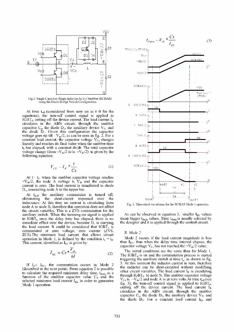
Fig. 1. Single Capacitor Single Inductor Active Snubber (SCSIAS)using the Diode Bridge Switch Configuration.
At time toff (considered from now on as t=O for theequations), the turn-off control signal is applied toIGBTd, cutting off the device current. The load current IKcirculates in the ABN circuit, through the snubbercapacitor Cs, the diode D2, the auxiliary device VT, andthe diode D4. Given this configuration the capacitorvoltage goes up till +Vd. 2, as can be seen in fig. 2. For aconstant load current, the capacitor voltage Vcs changeslinearly and reaches its final value when the snubber timets has elapsed, with a constant dv/dt. The total capacitorvoltage change (from -Vd,/2 to is -Vd,/2) is given by thefollowing equation:
VCS = IK CsCs
(1)
At t= t1, when the snubber capacitor voltage reaches+Vd. 2, the node A voltage is Vd, and the capacitorcurrent is zero. The load current is transferred to diodeDu, connecting node A to the upper bar.
At taoff the auxiliary commutator is turned off,eliminating the short-circuit impossed over theinductance. At this time no current is circulating fromnode A to node B, therefore this operation does not affectthe circuit variables. This is a ZVS commutation for theauxiliary switch. When the turnning-on signal is appliedto IGBTU once the delay time has elapsed, there is noinmediate effect over the device, because Du is carryingthe load current. It could be considered that IGBTU iscommutated at zero voltage, zero current (ZVS,ZCS).The minimum load current, that allows circuitoperation in Mode 1, is defined by the condition t, = td.This current, identified as IKL is given by:
I =Cs* VdcKL td ~~~~~~~(2)If IK< IKL, the commutation occurs in Mode 2
(described in the next point). From equation 2 is possibleto calculate the required minimum delay time, tdmin as afunction of the snubber capacitor value Cs and theselected minimum load current IKL in order to guaranteeMode 1 operation.
td min VdcKL
7Cs (t), VA(t)zVdc-
Vdc/2 -
(3)
VA (t)
VCs ( )
..6 t
-Vdc 2^
VCEd (t)
Tur-((ZVS)
/
Dff
i IGBTd(t)i(
i L ( t)
i Dd (t)
Du ( t ).
i c (t)i~~~~~~~~~~~~~~~~~~~
!IK* L1~~~~
i IGBTu (t)
!~~~~~VCEu (t) dc,
. i\;tff ti t2
ts >
td y
tataonrtaoff
Fig. 2. Theoretical waveforms for the SCSIAS Mode 1 operation.
As can be observed in equation 3, smaller IKL valuesmean bigger tdmin values. Time tdmin is usually selected bythe designer and it is applied through the control circuit.
B. Mode 2.Mode 2 occurs if the load current magnitude is less
than IKL, thus when the delay time interval elapses, thecapacitor voltage Vcs has not reached the +Vd. 2 value.
The initial conditions are the same than for Mode 1.The IGBTd is on and the commutation process is startedtriggering the auxiliary switch at time tx, as shown in fig.3. At this moment the inductor current is zero, thereforethe inductor can be short-circuited without modifyingother circuit variables. The load current IK is circulatingthrough IGBTd to node N. The snubber capacitor voltageVCs is -Vd,2 and node A is at zero volts.At time toff (seefig. 3), the turn-off control signal is applied to IGBTd,cutting off the device current. The load current IKcirculates in the ABN circuit, through the snubbercapacitor Cs, the diode D2, the auxiliary device VT1 andthe diode D4. For a constant load current IK, and
711
OR-- 1~~~~~~~~-
t
'IK-r-; t- .li
I~~~~~~~~~~~~~~
.
. ,
//
/
/
/

considering toff as the intial time (t=0), the capacitorvoltage Vcs is given by the following equation:
ItVcs(t)= 1 ficsdt+Vcs(O) (4)
Cs 0
Where iC,(O) = Ik and Vc,(O) = -Vdc/2.. The solution is:
IKVcs (t) t-Cs
Vdc2 (5)
At time instant taoff, the auxiliary switch is turned off,freeing the inductance L. This is a ZVS commutation forthis auxiliary switch. The snubber inductor is connectedin series with the snubber capacitor. Since at this momentcurrent in L will be zero, this cuts the current paththrough the snubber branch, forcing the load current intodiode Du (fig. 3). Du turns on, connecting point A directlyto the upper supply rail Vd, and initiating load energyrecovery. Since the snubber capacitor voltage at thismoment, VCs(taoff) is lower than Vd,/2 (the exact value canbe calculated in each case using eq. 3) and cannot changeinstantly, a voltage equal to Vd,/2- VCs(taoff) will appearacross the snubber inductor, L. This voltage will induce acurrent in L, initiating a sinusoidal oscillation in thesnubber branch (fig. 3). This resetting snubber current,ics(t), will circulate simultaneously with the current in Du,taking part of the load current IK from the upper free-wheeling diode (fig. 3). Snubber capacitor voltage, Vcs(t),will rise following a cosine curve. Solving the newcircuit, eqs. 5 and 6 describe the time evolution of thesnubber current, ics(t), and snubber capacitor voltage,Vcs(t).
(Vdc _ViCs( C -V0 ALsen(wo)
vcs (t) Vdc dc -V )cos(cot)
(6)
(7)
When the delay time has elapsed, IGBTU is turned on,but no current will flow through this device for as long asDu is conducting. Supposing that the peak value of thesnubber resetting current is higher than IK, diode Ducurrent will reach zero when ics= IK. From this pointonwards the resetting snubber current, ics (t), will flowthrough IGBTU. Once the snubber resetting current goespass its peak value and stars falling down, IGBTU willstop conducting when the snubber capacitor currentreaches again the IK value. From here onwards, theresetting snubber current will flow again through Du.Note that if the snubber resetting circuit is underdamped,this situation may repeat itself a number of times tillsnubber capacitor voltage stabilizes in its final value,Vd,/2. Note than all these current transfers are driven by aresonant LC circuit, hence all commutations are ZCS andtherefore produce no increases in power losses.
C. Mode 2. a.Mode 2.a occurs when the load current is zero before
the commutation process is started. The auxiliary switchis commutated at time tx, but as in the other two Modes,the inductor current is zero, therefore the inductor can be
short-circuited without modifying other circuit variables.The snubber capacitor voltage Vcs is -Vd,/2.
VCs(t),VA(t), \
Vdc VA(t)Vdc/2 - Vo_7_ VCs(t)
Vdc/2Vo
-Vdc/2
VCEd(t) Vd
I'T,, Turn-offVdc/2 +V (ZVS)
i IGBTd(t)
IK~ ~~~~ILt) tIL(t)~~~~~~~~~~~~~~~
i Dd(t) t
i Du(t) k IK
~~xti c(t) - XIK < ~~Icp
i IGBTu(t)~~~~IK:!'
VCEu(t)VdcVi
Vdc/2 Vo
!IItoff Iltii I~~ti t2ts
Ntd \
ta ytr \n /K
L-VCL U I ItaoffFig. 3. Theoretical waveforms for the SCSIAS Mode 2 operation.
When the turn-off control signal is applied to IGBTd,no current will circulate through the snubber circuit,therefore the snubber capacitor voltage will not change.The auxiliary switch turn off does not introduce anycircuit changes either. When the to IGBTU is fired, the LCsnubber resonant circuit is stablished, with ics(O) = 0 andvcs(O) = -Vd,2. Fig. 4 shows the circuit waveforms forthis operation mode. These are the same voltage andcurrent waveforms obtained for the splitted inductorsingle capacitor circuit presented in [1], therefore thecurrent and voltage ecuations are:
Vdc V SSen(cot)iL (t) = ic (t) = (- VO)Se(L
Vcs LVdC V) 0) CS(1-cos(Wot)) +J12 L
(8)
(9)
The snubber time ts ends when the capacitor voltage isequal to Vd,/2.
712
f
t>Lt-
t-mnr

III. SCSIAS SNUBBER CIRCUIT EXPERIMENTAL RESULTS
The experimental tests were performed with a halfbridge inverter with the SCSIAS snubber shown in fig. 1,driven by a square waveform control signal. The firingpulses were generated using a FPGA typeEPF1OK20RC240 from ALTERA. Table 1 shows thepower circuit components list.
TABLE 1 Experimental Inverter components.
ty
Snubber capacitor 1
Auxiliary switching 4diodes
IGBTs module(Half bridge)
Auxiliary switching 1transistor
Inductance 1
Vdc
Puanti Type
Ceramic
Value
I OOnF
Fast Recovery 10 A
Eupec 50/40 ABSM50GB12 1200V
ODLC
IRGPH40F 17A0Ferrite 40gH
120V
All the following waveforms were obtained from theinverter with ths SCSIAS snubber.
Fig. 5 shows the colector-emitter voltages for bothIGBTs, plus the capacitor voltage a current waveformsrelated to Mode 1. All these signals are similar to thoseshown in fig. 2, validating the theoretical development.For this experiment the load current is equal to IKL (5Amp) which produces a snubber time equal to the delaytime (2 hts).
Fig. 6 and 7 present a comparison between the IGBTUturn off losses (summarized in waveform c) when theinverter is operated in Mode 1 with and without thesnubber circuit. As can be observed, the snubber actionreduces significantly the IGBT turn off losses.
Fig. 8 shows the turn on losses for IGBTU whenoperating in Mode 1. As for the turn off process, thelosses are negligible.
Fig. 9 presents the colector-emitter voltages for bothIGBTs, plus the capacitor voltage a current waveformsrelated to Mode 2. In this case, the experimental capacitorcurrent does not go down to zero when the auxiliaryswitch is turned off as predicted by the theory, becausethe device commutations are not instantaneous, andtherefore some currents go up while others go downduring the transient intervals, producing the ics waveformshown in the figure. The other waveforms agree with thetheoretical ones.
Fig. 10 and 11 show the IGBTU turn on and turn offlosses when operating in Mode 2. As can be seen, the turnon process is a ZVS, and the LC current oscilation occurswhen the colector-emitter has reached zero volts,reducing the losses to a minimum. The turn off process isa ZCS, and the losses are also negligible.
Finally, fig. 12 and 13 presents the turn on waveformsfor IGBTU when the SCSIAS operates in Mode 2.a. Ascan be seen, this is a ZCS commutation, and the lossesare equally negligible, proving the good performance ofthis snubber circuit.As can be observed, the ics LC pulse does not start till
IGBTU is fully on. The maximum ics value is about 5 A.
VCs(t),VA(t),
Vdc-
Vdc/2-
VA (t)
.I v I
-Vdc/2
VCEd (t) Vdc
, ~~~~Turn- o:. ~~~(ZVS),~ ,Is
IGBTd(t)
,iL\
i Dd(t)
i Du(t)
c(t)cp
i Lu (t)/\lp
IGBTu (t)Icp
VCEu (t)' Vdc
ts
td t\/r\!\ ~~/\ /
tata- taof f
Fig. 4. Theoretical waveforms for the SCSIAS Mode 2.a operation.
.. .......f...... _ ___ r~~~~~~~1)
(4)p
Fig. 5. Experimental Waveforms measured in the inverter inMode 1 (1 gs/div):(a)VCEd(25 V/div), (b)VcEU (25 V/div), (c)Vcs (50
V/div),(d)Ics(5 A/div)
713
-I-,
ZA'
.9.
i
...oJ0/
_-

....
... .... Rw s s w t W * AC W~~~(-I
}z. ~~... ... .
~~~ _..,. {b} .~~~~~4
I(C)
Fig. 6. Experimental Waveforms measured in the inverter duringthe turn off operating in Mode 1 (I gs/div): (a)VCEU(25 V/div), (b)IIGBTU
(2 A/div), (C)VCEU*IIGBTU
(b) _
(C)
Fig. 7. Experimental Waveforms measured in the inverter duringthe turn off operating in Mode 1 (Whithout snubber): (a)VCEU(25 V/div),
(b)IIGBTU (2 A/div), (C)VCEU*IIGBTU
... ., .. E
(::ib) ;S.................. .~~~(c
-
Fig. 9. Experimental Waveforms measured in the inverter inMode 2 (I gs/div): (a)VCEd(25 V/div), (b)VcEU (25 V/div), (c)Vcs (50
V/div), (d)Ics(2 A/div)
.. i .. ..../ ~ ~ ~~tra__ F~~~~~~~~~~~~~~~~~~~~~~~~~~~~~~~
(C)
Fig. 10. Experimental Waveforms measured in the inverterduring the turn on operating in Mode 2 (1 ts/div): (a)VCEu(25 V/div),
(b)IIGBTu (1 A/div), (c) VCEU*IIGBTU
........ : 3.
jb)
(c
Fig. 8. Experimental Waveforms measured in the inverter duringthe turn on operating in Mode 1 (I gs/div): (a)VCEu(25 V/div), (b)IIGBTu
(5 A/div), (c) VCEU*IIGBTU.
Fig. 11. Experimental Waveforms measured in the inverterduring the turn off operating in Mode 2: (I gs/div): (a)VCEu(25 V/div),
(b)IIGBTU (1 A/div), (c) VCEU*IIGBTU
714
rrrT!7.1.i.
IV
.. .:.: :... a..
p

4LO~~~~~~~~~~~a....
~~~~.... ,.r.. ... 11. .,
^'' '', -.,..,, ,.,,,.,.,,,,.( ..
jr ~~~~~C
(d.
Fig. 12. Experimental Waveforms measured in the inverterduring Mode 2.a, (1 ts/div) (a)VCEd(25 V/div), (b)VCEU (25 V/div),
(c)Vcs (50 V/div), (d)Ics(2 A/div)
(C)
Fig. 13. Experimental Waveforms measured in the inverterduring the turn on operating in Mode 2.a (I gs/div): (a)IIGBTU (2 A/div),
(b)VCEU(25 V/div), (c) VCEU*IIGBTU
IV. CONCULSIONS.
The experimental results probe that the SingleCapacitor Single Inductor Active Snubber (SCSIAS)operates as described by the theoretical analysis presentedin this work, and also that a very important reduction inthe commutation losses are possible when thisconfiguration is used in an inverter circuit, since allcommutations take place in almost ideal ZVS and ZCSconditions.
V. REFERENCES.[1] Gerardo Ceglia, Victor M. Guzman A., Maria I. Gimenez de
Guzman "A Simple Active Single Capacitor Single Inductor SnubberFor Inverter Circuits", Proceedings of the EPE-PEMC 2004, Riga,Letonia. Septiembre 2004.
[2] Gerardo Ceglia, Victor M. Guzman A., Maria I. Gimenez deGuzman "Disefno de circuitos amortiguadores de alta eficiencia enconfiguraciones inversoras con m6dulos IGBTs", Memorias delSeminario Anual de Automatica, Electr6nica Industrial eInstrumentaci6n SAAEI-2001, ponencia 01 -002.pdf, CD, Matanzas,Cuba, Septiembre 2001.
[3] Gerardo Ceglia, Victor M. Guzman A., Maria I. Gimenez deGuzman "Una configuraci6n de recuperaci6n de energia simplificadapara el snubber de inductancia dividida y condensador compartido.",Memorias del Seminario Anual de Automatica, Electr6nica Industrial eInstrumentaci6n SAAEI-2002, ponencia 223.pdf, CD, Alacala deHenares, Madrid, Espafia, Septiembre 2002.
[4] Jose Eduardo Baggio and Jose Renes Pinheiro, "A simple ActiveAuxiliary Conmutation Circuit for three-Level PWM Single-PhaseInverters", IEEE Trans. On Industry Electronics, vol. 48, No. 6, pp.1166-1173, Decemberl 2001
[5] Guichao Hua and Fred C. Lee, "Soft-Switching Techniques inPWM Converter," IEEE Trans. On Industry Applications, vol. 42, No.6, pp. 595-603, December 1995
[6] Jochen Mahlein, Manfred Brukmann and Michael Braun,"Passive Protection Strategy for a Drive System With a MatrixConverter and an Inductive Machine", IEEE Trans. On IndustryElectronics, vol. 49, No. 2, pp. 297-303, April 2002
[7] Patrick W.Wheeler, Jose Rodriguez, Jon C. Clare, LeeEmpringham and Alejandro Weinstein, "Matrix Converters: ATechnology Review", IEEE Trans. On Industry Electronics, vol. 49, No.2, pp. 276-287, April 2002
[8] Peter Nielsen, Frede Blaabjerg and John K. Pedersen, "NewProtection Issues of a Matrix Converter: Design Cpnsiderations forAdjustable-Speed Drives", IEEE Trans. On Industry Applications, vol.35, No. 5, pp. 1150-1161, September/October 1999.
715