Experimental investigation of the kink effect and the low frequency noise properties in...
8
Experimental investigation of the kink effect and the low frequency noise properties in pseudomorphic HEMTÕs F. Principato a, * , A. Caddemi b , G. Ferrante a a Dipartimento di Fisica e Tecnologie Relative and INFM Unita ` di Palermo, Universita ` di Palermo, Viale delle Scienze, Edificio 18, 90128 Palermo, Italy b Dipartimento di Fisica della Materia e Tecnologie Fisiche Avanzate and INFM Unita ` di Messina, Universita ` di Messina-Contrada Sperone, 31-S. Agata, 98166 Messina, Italy Received 14 July 2004; received in revised form 20 March 2005; accepted 21 March 2005 The review of this paper was arranged by Prof. S. Cristoloveanu Abstract The kink effect in low-noise pseudomorphic (AlGaAs/InGaAs) HEMTÕs has been examined in detail by investigating the steady- state and pulsed I–V characteristics, the behavior of the output conductance dispersion and the performance of the gate leakage current to understand its origin. No clear evidence of impact ionization occurrence in the InGaAs channel at kink bias conditions (V DS,kink = 1.5 V) has been found, thus suggesting that the predominant mechanism should be attributed to trap-related phenom- ena. A significant rise of the gate current has been found at very high drain voltages (far from V DS,kink ) associated with low drain current values which is probably due to impact ionization onset within the channel. In addition, the low frequency gate and drain noise has been measured at bias conditions below and above the kink to analyze its correlation with the processes involving discrete energy trap states. A Lorentzian noise contribution has been found in the drain noise spectrum traced at kink bias V DS,kink with a corner frequency corresponding to that exhibited by the output conductance dispersion curve at the same bias. Thus, the devices under test classified as short-channel low-voltage GaAsFETÕs exhibit a marked kink effect whose origin is likely to be due trapping mechanisms. Ó 2005 Elsevier Ltd. All rights reserved. Keywords: Kink; PHEMT; LF noise; Frequency dispersion 1. Introduction The kink effect (also known as soft breakdown) is a very common feature of the I–V characteristics of either AlGaAs/InGaAs/GaAs and InAlAs/InGaAs/InP sub- micron gate HEMTÕs consisting of a sudden current rise even at low drain voltage values. Firstly, the main underlying mechanisms were attrib- uted to charge release from traps associated to deep lev- els (DX centers) in the donor or buffer layers after hot electron injection [1,2]. More recently, accurate experi- mental investigation of impact ionization effects have pointed out a direct correlation with anomalous conduc- tion aspects such as the kink in the output current and the bell-shaped curve of the gate leakage current, espe- cially in InP-based structures [3]. The impact ionization hypothesis may also explain the light emission observed when the FET is biased at the kink voltage and another kink-related effect which consists of a reduction of the source resistance value [4,5]. A comprehensive physical and circuit model for the kink in InAlAs/InGaAs HEMTÕs calls for field-generated 0038-1101/$ - see front matter Ó 2005 Elsevier Ltd. All rights reserved. doi:10.1016/j.sse.2005.03.021 * Corresponding author. Tel.: +39 91 661 5027; fax: +39 91 661 5063. E-mail address: [email protected] (F. Principato). www.elsevier.com/locate/sse Solid-State Electronics 49 (2005) 915–922
Transcript of Experimental investigation of the kink effect and the low frequency noise properties in...

www.elsevier.com/locate/sse
Solid-State Electronics 49 (2005) 915–922
Experimental investigation of the kink effect and the lowfrequency noise properties in pseudomorphic HEMT�s
F. Principato a,*, A. Caddemi b, G. Ferrante a
a Dipartimento di Fisica e Tecnologie Relative and INFMUnita di Palermo, Universita di Palermo, Viale delle Scienze, Edificio 18, 90128 Palermo, Italyb Dipartimento di Fisica della Materia e Tecnologie Fisiche Avanzate and INFM Unita di Messina, Universita di Messina-Contrada Sperone,
31-S. Agata, 98166 Messina, Italy
Received 14 July 2004; received in revised form 20 March 2005; accepted 21 March 2005
The review of this paper was arranged by Prof. S. Cristoloveanu
Abstract
The kink effect in low-noise pseudomorphic (AlGaAs/InGaAs) HEMT�s has been examined in detail by investigating the steady-
state and pulsed I–V characteristics, the behavior of the output conductance dispersion and the performance of the gate leakage
current to understand its origin. No clear evidence of impact ionization occurrence in the InGaAs channel at kink bias conditions
(VDS,kink = 1.5 V) has been found, thus suggesting that the predominant mechanism should be attributed to trap-related phenom-
ena. A significant rise of the gate current has been found at very high drain voltages (far from VDS,kink) associated with low drain
current values which is probably due to impact ionization onset within the channel. In addition, the low frequency gate and drain
noise has been measured at bias conditions below and above the kink to analyze its correlation with the processes involving discrete
energy trap states. A Lorentzian noise contribution has been found in the drain noise spectrum traced at kink bias VDS,kink with a
corner frequency corresponding to that exhibited by the output conductance dispersion curve at the same bias. Thus, the devices
under test classified as short-channel low-voltage GaAsFET�s exhibit a marked kink effect whose origin is likely to be due trapping
mechanisms.
� 2005 Elsevier Ltd. All rights reserved.
Keywords: Kink; PHEMT; LF noise; Frequency dispersion
1. Introduction
The kink effect (also known as soft breakdown) is a
very common feature of the I–V characteristics of either
AlGaAs/InGaAs/GaAs and InAlAs/InGaAs/InP sub-
micron gate HEMT�s consisting of a sudden current rise
even at low drain voltage values.
Firstly, the main underlying mechanisms were attrib-uted to charge release from traps associated to deep lev-
els (DX centers) in the donor or buffer layers after hot
0038-1101/$ - see front matter � 2005 Elsevier Ltd. All rights reserved.
doi:10.1016/j.sse.2005.03.021
* Corresponding author. Tel.: +39 91 661 5027; fax: +39 91 661 5063.
E-mail address: [email protected] (F. Principato).
electron injection [1,2]. More recently, accurate experi-
mental investigation of impact ionization effects have
pointed out a direct correlation with anomalous conduc-
tion aspects such as the kink in the output current and
the bell-shaped curve of the gate leakage current, espe-
cially in InP-based structures [3].
The impact ionization hypothesis may also explain
the light emission observed when the FET is biased atthe kink voltage and another kink-related effect which
consists of a reduction of the source resistance value
[4,5].
A comprehensive physical and circuit model for the
kink in InAlAs/InGaAs HEMT�s calls for field-generated
1x10⁻⁸
1x10⁻⁷
1x10⁻⁶
]| 20
30
]
916 F. Principato et al. / Solid-State Electronics 49 (2005) 915–922
hole accumulation under the source end of the gate and a
related channel potential shift that varies the threshold
voltage of the device. Therefore, the kink current would
be caused by either the additional drive and the charges
directly generated by the impact ionization process [6].
In the present paper, we report the results of ourinvestigation on packaged AlGaAs/InGaAs low-noise
pseudomorphic HEMT�s exhibiting a strongly tempera-
ture-dependent kink [7]. We have carefully examined the
device performance at room temperature by investigat-
ing the steady-state and pulsed I–V characteristics, the
transconductance and output conductance dispersion
behavior and the gate leakage current performance to
understand its origin. In addition, we have measuredthe low frequency gate and drain noise over the bias
conditions below and above VDS,kink to analyze the rela-
tionship with the mechanisms generating the kink since
the occurrence of trap-assisted generation-recombina-
tion processes is well tracked by LF noise spectra versus
bias [8].
-1 -0.8 -0.6 -0.4 -0.2 01x10-11
1x10⁻¹⁰
1x10⁻⁹
|I GS[
A
0
10
I DS[
mA
VDS
VGS[V]
2. DC characterization
The devices employed in this study are commercial
AlGaAs/InGaAs/GaAs Schottky gate FET�s (MGF
4919, by Mitsubishi) enclosed in a ceramic short lead
package. Their precise structure is unknown, but from
the results of their electrical DC and microwave perfor-
mance we reasonably believe to deal with 0.25 lm-gatelength and 200 lm-gate width devices [9].
0 0.5 1 1.5 2 2.5 3 3.5
0
10
20
30
40
I DS[
mA]
VDS[V]
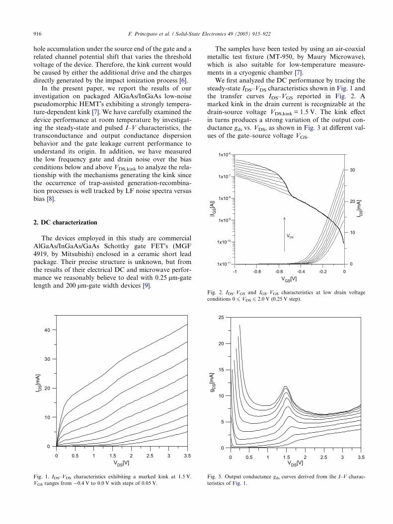
Fig. 1. IDS–VDS characteristics exhibiting a marked kink at 1.5 V.
VGS ranges from �0.4 V to 0.0 V with steps of 0.05 V.
The samples have been tested by using an air-coaxial
metallic test fixture (MT-950, by Maury Microwave),
which is also suitable for low-temperature measure-
ments in a cryogenic chamber [7].
We first analyzed the DC performance by tracing the
steady-state IDS–VDS characteristics shown in Fig. 1 andthe transfer curves IDS–VGS reported in Fig. 2. A
marked kink in the drain current is recognizable at the
drain-source voltage VDS,kink = 1.5 V. The kink effect
in turns produces a strong variation of the output con-
ductance gds vs. VDS, as shown in Fig. 3 at different val-
ues of the gate–source voltage VGS.
Fig. 2. IDS–VGS and IGS–VGS characteristics at low drain voltage
conditions 0 6 VDS 6 2.0 V (0.25 V step).
0 0.5 1 1.5 2 2.5 3 3.5
0
5
10
15
20
25
g DS[
mA]
VDS[V]
Fig. 3. Output conductance gds curves derived from the I–V charac-
teristics of Fig. 1.

F. Principato et al. / Solid-State Electronics 49 (2005) 915–922 917
The question arises as far as the physical origin of this
kink behavior is concerned. According to the hypothesis
of the onset of an impact ionization process sustaining
the drain current rising, we would expect concurrently
a prominent rise in the gate current due to the impact
ionization-generated holes which are collected at thegate electrode. The link between a kink effect and the
impact ionization mechanism is well tracked by a bell-
shaped curve of the gate leakage current [3,4,10].
We have thus measured the input characteristics IGS–
VGS at different drain voltage values below and after
VDS,kink (0 6 VDS 6 2.0 V, 0.25 V step). These devices
feature very low values of the gate leakage current (in
the range of 10�10 to 10�7 A), but as shown in Fig. 2no current rise has been found to occur over the VDS
and VGS voltage ranges investigated.
Therefore, the absence of any variation in the gate
current should rule out the onset of an impact ionisation
process in the channel as the predominant cause of the
observed kink.
We extended the analysis of the gate current behaviour
up to high drain voltage values (i.e. in the pre-breakdownregion) by concurrently reducing the gate-source voltage
to comply with the maximum voltage ratings of the de-
vices under test. We then examined the input characteris-
tics in the �0.4 V 6 VGS 6 0 V, 2.0 V 6 VDS 6 3.75 V
source and drain voltage ranges. The relevant curves are
reported in Fig. 4 where a significant rise of IGS can
now be seen asVDS is increased beyond 3.0 V, which sup-
ports the hypothesis of an impact ionisation regime. This,however, does not cause any sudden variation in the out-
put characteristics.
-0.4 -0.3 -0.2 -0.1 0
0x100
2x10⁻⁶
4x10⁻⁶
6x10⁻⁶
VDS
|I GS[
A]|
VGS[V]
Fig. 4. IGS–VGS characteristics at high drain voltage conditions
2.0 V 6 VDS 6 3.75 V (0.25 V step).
The shape of the gate current curve, where the peak
occurs, is not smooth and the corresponding drain cur-
rent values are moderately low (IDS 6 5.0 mA). As VGS
moves toward less negative values, the gate current
decreases and again exhibits a monotonic behaviour
thus indicating that its rise is driven by a field-inducedprocess.
At this point of our experimental tests performed on
the MGF 4919 HEMT�s, we attribute the drain current
kink to the role played by deep-level trap (DX center)
processes occurring in the AlGaAs donor layer. The car-
riers trapped after hot electron injection, could have
been released by a deep-level impact ionisation which
would not imply hole generation, i.e. gate currentvariations.
The kink effect is enhanced as VGS increases since the
trapping and de-trapping mechanisms are controlled by
a lower gate-to-drain potential. In addition, the reduc-
tion of IDS and the more pronounced kink seen in the
I–V characteristics of these devices down to 50 K
may also be explained by trap-assisted processes in the
AlGaAs layer [7].
3. Sinusoidal and transient excitation measurements
Being related to trapping mechanisms, the previous
described current anomaly is expected to be inherently
a low-frequency process. The dispersion behavior of
the kink can be analyzed in a variety of ways to fullyunderstand its behavior [2,11].
In our work, the dispersion of the output conduc-
tance gds has been analyzed by measurements performed
at different values of VDS below and above VDS,kink. To
accomplish that, the drain terminal is connected trough
a resistor R to the output of an amplifier which sums a
sinusoidal signal to a constant voltage giving the drain
bias. By measuring with the digital scope the sinusoidalsignal vR across the resistor and the drain voltage vDS
the output conductance is obtained as gds = vDSR/vR.
The sinusoidal signal amplitude is 100 mV and the fre-
quency ranges from 1 Hz up to 100 kHz. The dispersion
of the output conductance at fixed VGS = �0.1 V as a
function of the drain voltage is shown in Fig. 5. The
experimental results show a smooth trend of the gdscurves at high frequencies, all converging to a final valueof about 7.0 mS. A significant difference between low
frequency and high frequency values is exhibited by
the curve traced at VDS,kink with a transition frequency
around 100 Hz. Previous investigation of frequency dis-
persion of the output conductance in InP-based
HEMT�s led to different results with stronger anomalies
in its behavior vs. frequency and bias [2,11]. In Fig. 6 we
reported the frequency dispersion of gds at VDS,kink as afunction of the drain bias current (i.e. at different VGS).
The dispersion diminishes as the drain current decreases

1x100 1x101 1x10² 1x10³ 1x10⁴ 1x10⁵
0
2
4
6
8
10
12
14
g ds[m
S]
VDS2.00 V1.75 V1.50 V1.25 V1.00 V0.75 V
f [Hz]
Fig. 5. Frequency dispersion of gds at VGS = �0.1 V for different
values of the drain–source voltage.
1x100 1x101 1x10² 1x10³ 1x10⁴ 1x10⁵
f [Hz]
0
2
4
6
8
10
12
14 IDS
2 mA1 mA
5 mA10 mA20 mA
500 µA
g ds[m
S]
Fig. 6. Frequency dispersion of gds at VDS,kink for different values of
the drain current.
0 0.25 0.5 0.75 1 1.25 1.5 1.75 2 2.25
0
5
10
15
20
25
30
35
I DS[
mA]
100 ms
10 ms
1 ms
100 µs
DC
VGS=0.0V
VDS[V]
Fig. 7. Pulsed I–V measurements of the output characteristics with
pulse duration varied in the range 100 ls–100 ms with 10% duty cycle.
Also shown is the DC I–V curve.
918 F. Principato et al. / Solid-State Electronics 49 (2005) 915–922
and completely disappears at IDS � 1.0 mA (VGS ��0.34 V). This result corresponds to that found for the
DC output conductance of this device where the peak
at VDS,kink disappears at the same value of IDS(VGS).
By comparing these results with those obtained in [2]
where the dispersion of the output conductance occurs
even at drain bias different from the VDS,kink, we here
note that the dispersion takes place only at VDS,kink witha characteristic transition frequency. Again, this may
suggest that in our device few trapping mechanisms
are involved in the kink effect.
As a second step, we analyzed the output characteris-
tics by pulsed I–V measurements. In such tests a DC
power supply is connected to the gate and a pulse volt-
age generator with varying amplitude is used as thedrain stimulus. The pulse generator is connected to the
drain of the device under test through a load resistor.
The drain current is determined by measuring the pulsed
drain-source voltage and the voltage at load resistor by
using a digital oscilloscope. The pulse duration varies in
the 100 ls–100 ms range with a variable duty cycle. In
the relevant curves plotted in Fig. 7 are the results
obtained at VGS = 0 V are compared with the staticI–V curve. It is clearly seen the difference between the
DC and the pulsed curves, and that the kink disappears
for pulse duration shorter than 10 ms. The duty cycle in
this case is 10% and we observed a slight change in the
I–V curve by using lower duty cycle. The disappearence
of the kink at pulse duration lower than 10 ms is consis-
tent with the previous observation on the transition fre-
quency of the gds dispersion around 100 Hz. Moreover,we note that the pulsed IDS value exceeds the DC value
and this effect is more pronounced below the VDS,kink.
The frequency dispersion of the device transconduc-
tance gm was also monitored. Its frequency-dependent
value was extracted by applying a 50 mV sinusoidal sig-
nal vgs superimposed to the offset bias voltage and by
measuring the variable voltage signal vR across the resis-
tor R placed in series with the drain. The transconduc-tance is obtained as gm = (1/R + gds)vR/vgs, where gds is

1x10-19
1x10-18
1x10-17
F. Principato et al. / Solid-State Electronics 49 (2005) 915–922 919
the measured output conductance. The frequency range
extends from 1 Hz up to 100 KHz. The values of the
transconductance gm were measured at the same bias
of the output conductance and they do not exhibits
any significant frequency dispersion even at VDS,kink.
1x10⁻⁹ 1x10⁻⁸ 1x10⁻⁷ 1x10⁻⁶ 1x10⁻⁵
1x10-26
1x10-25
1x10-24
1x10-23
1x10-22
1x10-21
1x10-20
VDS
1.0 V1.5 V2.0 V
IG2
IG[A]
S IG[A
2 /H
z]
Fig. 8. Gate current noise spectral density at 1 Hz as a function of the
gate current for different drain biases.
4. Low frequency noise measurements
Noise measurements were performed with the device
placed in common source configuration. The noise sig-
nals of the gate and drain are both measured indepen-
dently and simultaneously. The device is biased by
means of batteries and wire-wound resistors. The gatecurrent is amplified by a low-noise current amplifier
(SR570, by Stanford Research System), which also pro-
vides the bias of the gate-source voltage. The amplifier
operates with 0.01 Hz cut-off frequency of the high-pass
filter and the frequency range, which depends on the
used sensitivity of the amplifier, varies from 15 Hz to
2 kHz. The drain noise current is measured by amplify-
ing the voltage across the drain load resistance RL byusing a low-noise voltage amplifier (SR560, by Stanford
Research System) with variable gain and 0.1 Hz–
1.0 MHz frequency bandwidth. Both amplifiers are sup-
plied with batteries and the whole system is enclosed in a
shielded box. The two amplified noise signals are mea-
sured with a computer based instrument operating in
FFT analyser mode (DSA4551, by National Instru-
ments). The auto power spectrum of each channel andthe coherence between them is monitored under LAB-
VIEW software control. All the spectra are obtained
by averaging over 100 measurements.
Noise measurements of the gate current IG have been
performed at different reversed gate-source voltages and
at constant VDS below and above the kink. The investi-
gated frequency range 1 Hz–500 Hz, which is imposed
by the highest sensitivity of the current amplifier used.The current noise spectrum SIG(f) exhibits a 1/f c law,
with c ffi 1, for all the investigated values of the voltage
drain bias VDS = 1.0, 1.5 and 2.0 V. White noise due to
the thermal noise of the leakage conductance and due to
shot noise 2eIG was not been observed in the investi-
gated frequency range. In Fig. 8 the spectral density
SIG is shown, evaluated at 1 Hz, plotted against IG cur-
rent. At lower values of the gate current, which areobtained only at VDS = 1.0 V, the gate current noise var-
ies as I3G, whereas for higher values of the gate current
the variation is approximately as I2G. The power spectraare rather insensitive to the value of the VDS. This
behavior is observed in similar devices and the quadratic
dependence of the noise gate current is typical for 1/f
noise in Schottky junction [12,13]. By fitting the gate
current noise spectral density for gate current above50 nA with the empirical relation SIG ¼ A� I2G, we
found an average value of 4.5 · 10�7 Hz�1 over the dif-
ferent VDS which is comparable to that reported for InP
based HEMT [14]. Thus the main contribution to the
noise spectrum of the gate current is certainly located
in the Schottky barrier and seems to be not related with
the mechanisms responsible of the kink.The output voltage noise is measured at constant
drain voltage with the gate–source junction reverse
biased and the drain current varying from 10 lA up to
20 mA. The higher bound of the frequency range is
90 kHz. We investigated the drain current noise SID
which is related to the measured output drain voltage
noise SV0 by the following relation
SIDðf Þ ¼ SV0ðf ÞGL þ gdsðf Þ
A
� �2
ð1Þ
where A is the gain of the amplifier and GL is the
dynamic load conductance. In the above relation the
output conductance gds(f ) is a function of the frequency
as determined by the direct measurements previously
described. Thus the estimated drain current noise is
not affected by the circuit effect of the output conduc-tance dispersion. Generally, we found two different spec-
tra for the drain current noise according to drain voltage
below or above the kink. At VDS = 1.0 V (pre-kink) the
power spectra SID are 1/f c-like (with c close to 1) with
superimposed Lorentzian components at high bias cur-
rent drain (>1.0 mA) with the corner frequency greater
than 10 kHz. No white noise component is observed.
The intensity of the spectral density SID at 1 Hz versusthe drain current shows a quadratic dependence at low
drain currents, which tends to level off at higher bias.
This dependence is different from that reported in [15]
although there is no general model to explain the drain

920 F. Principato et al. / Solid-State Electronics 49 (2005) 915–922
current 1/f noise in the saturation regime. The noise
spectral density SID measured at the drain bias of
1.5 V (VDS,kink) and 2.0 V has a different shape with re-
spect to the pre-kink regime showing the appearance of
Lorentzian components. At VDS,kink the Lorentzian
component is superimposed on the 1/f c-like spectrum,with c ffi 0.5, and the corner frequency increases with
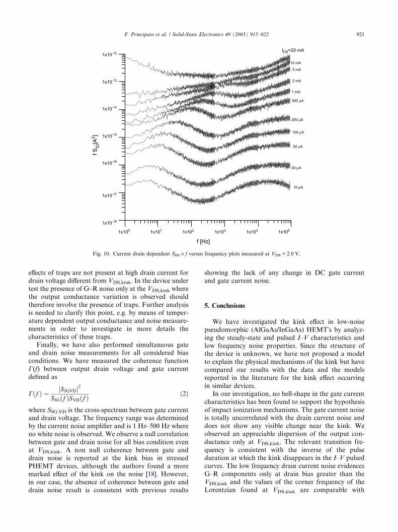
the drain current. We report in Fig. 9 the SID · f product
versus the measured frequency f at different values of the
drain current, in order to improve the determination of
the corner frequency fc. The Lorentzian component is
present over all bias conditions and its corner frequency
fc increases from 4 Hz at IDS = 10 lA (VGS = �0.54 V)
up to 75 Hz at IDS = 20 mA (VGS = �0.06 V). The highfrequency peak at low drain current is the cut-off due to
the high RC constant of the measurement set-up. The
presence of a Lorentzian spectrum is due to genera-
tion–recombination (G–R) noise generated by traps lo-
cated in the device with activation energy that can be
evaluated by means of temperature dependent measure-
ments [16,17]. The corner frequency fc of the G–R noise
is comparable to the transition frequency of the outputconductance gds found at the drain bias associated to
the kink, although its value is not exactly defined. Thus
it is likely that the traps responsible for the G–R noise
are also involved in the mechanisms that generate the
1x100 1x101 1x10²
1x10-18
1x10-17
1x10-16
1x10-15
1x10-14
1x10-13
1x10-12
f [
f SID
[A2 ]
Fig. 9. Current drain dependent SID · f versus fre
kink. As reported in [16], the values of the activation
energies associated with the traps for InP HEMT�s as
determined from drain current noise measurements
compared well to those related to output resistance dis-
persion measurements observed in [2]. As evidenced by
the plots of the Fig. 9, a Lorentzian spectrum occurseven at bias currents lower than 2.0 mA, where the effect
of the output conductance disappears. Moreover, the
shift of the corner frequency approaches approximately
the value of the transition frequency of the gdsdispersion.
The transformed values of the current noise spectrum
SID · f at fixed VDS = 2.0 V, i.e. above the kink, are
shown in Fig. 10. The Lorentzian peak occurs at draincurrents lower than 5.0 mA and disappears at higher
values of the drain bias current. We note that the corner
frequencies at VDS = 2.0 V are higher than those
observed at VDS,kink and the difference increases as the
drain current is higher. The presence of the kink in
MESFET�s has been associated to the presence of G–
R noise traps for all values of VDS below and above
the kink, and the corner frequency has found to dependon the values of VDS only above the kink [8]. This
behavior is consistent with an impact ionisation mecha-
nism responsible of both G–R noise and kink effect. This
mechanism seems to be not valid in our case where the
1x10³ 1x10⁴ 1x10⁵
500 µA
200 µA
100 µA
50 µA
20 µA
10 µA
10 mA
IDS=20 mA
5 mA
2 mA
1 mA
Hz]
quency plots measured at the kink VDS,kink.
IDS=20 mA
1x100 1x101 1x10² 1x10³ 1x10⁴ 1x10⁵
1x10-18
1x10-17
1x10-16
1x10-15
1x10-14
1x10-13
1x10-12
f [Hz]
f SID
[A2 ]
500 µA
200 µA
100 µA
50 µA
20 µA
10 µA
5 mA
10 mA
2 mA
1 mA
Fig. 10. Current drain dependent SID · f versus frequency plots measured at VDS = 2.0 V.
F. Principato et al. / Solid-State Electronics 49 (2005) 915–922 921
effects of traps are not present at high drain current for
drain voltage different from VDS,kink. In the device undertest the presence of G–R noise only at the VDS,kink where
the output conductance variation is observed should
therefore involve the presence of traps. Further analysis
is needed to clarify this point, e.g. by means of temper-
ature dependent output conductance and noise measure-
ments in order to investigate in more details the
characteristics of these traps.
Finally, we have also performed simultaneous gateand drain noise measurements for all considered bias
conditions. We have measured the coherence function
C(f) between output drain voltage and gate current
defined as
Cðf Þ ¼ jSIGVDj2
SIGðf ÞSVDðf Þð2Þ
where SIG,VD is the cross-spectrum between gate current
and drain voltage. The frequency range was determined
by the current noise amplifier and is 1 Hz–500 Hz where
no white noise is observed. We observe a null correlation
between gate and drain noise for all bias condition even
at VDS,kink. A non null coherence between gate anddrain noise is reported at the kink bias in stressed
PHEMT devices, although the authors found a more
marked effect of the kink on the noise [18]. However,
in our case, the absence of coherence between gate and
drain noise result is consistent with previous results
showing the lack of any change in DC gate current
and gate current noise.
5. Conclusions
We have investigated the kink effect in low-noise
pseudomorphic (AlGaAs/InGaAs) HEMT�s by analyz-
ing the steady-state and pulsed I–V characteristics and
low frequency noise properties. Since the structure ofthe device is unknown, we have not proposed a model
to explain the physical mechanisms of the kink but have
compared our results with the data and the models
reported in the literature for the kink effect occurring
in similar devices.
In our investigation, no bell-shape in the gate current
characteristics has been found to support the hypothesis
of impact ionization mechanisms. The gate current noiseis totally uncorrelated with the drain current noise and
does not show any visible change near the kink. We
observed an appreciable dispersion of the output con-
ductance only at VDS,kink. The relevant transition fre-
quency is consistent with the inverse of the pulse
duration at which the kink disappears in the I–V pulsed
curves. The low frequency drain current noise evidences
G–R components only at drain bias greater than theVDS,kink and the values of the corner frequency of the
Lorentzian found at VDS,kink are comparable with

922 F. Principato et al. / Solid-State Electronics 49 (2005) 915–922
the transition frequency of the output conductance dis-
persion. Thus, we may conclude that the kink occuring
in the MGF 4919 PHEMT device is not caused by an
impact ionization based phenomena but is likely to be
generated by generation-recombination processes.
Acknowledgement
This work is supported by Italian Ministry of Univer-
sity and Research (MIUR) and by the National Institute
for the Physics of Matter (I.N.F.M.). Additional sup-
port from the C.N.R. MADESS II Project is also
acknowledged.
References
[1] Huang JB, Tasker PJ, Wang GW, Chen YK, Eastman LF, Aina
OA, et al. Kink effect in sub-micrometer gate MBE-grown
InAlAs/InGaAs/InAlAs heterojunction MESFET�s. IEEE Elec-
tron Dev Lett 1988;9(12):630–2.
[2] Kruppa W, Brad Boos J. Examination of the kink effect in
InAlAs/InGaAs/InP HEMTs using sinusoidal and transient exci-
tation. IEEE Trans Electron Dev 1995;42(10):1717–23.
[3] Somerville MH, Del Alamo JA, Hoke W. Direct correlation
between impact ionization and the kink effect in InAlAs/InGaAs
HEMT�s. IEEE Electron Dev Lett 1996;17(10):473–5.
[4] Cova P, Fantini F, Manfredi M. Correlation between light
emission and currents in pseudomorphic HEMT�s. Microelectron
Reliab 1998;38(4):507–10.
[5] Suemitsu T, Enoki T, Sano N, Tomizawa M, Ishii Y. An analysis
of the kink phenomena in InAlAs/InGaAs HEMT�s using two-
dimensional device simulation. IEEE Trans Electron Dev
1998;45(12):2390–9.
[6] Somerville MH, Ernst A, Del Alamo JA. A physical model for the
kink effect in InAlAs/InGaAs HEMT�s. IEEE Trans Electron Dev
2000;47(5):922–30.
[7] Ferrante G, Principato G, Caddemi G, Donato N, Tuccari G.
DC and 1/f noise characterization of cryogenically cooled
pseudomorphic HEMT�s. Journal de Physique IV, Pr3 2002;8:
117–20.
[8] O�Connor HTA, Jones BK. The noise associated with the kink
effect in GaAs FET�s. In Proc Int Conf on Noise in Physical
Systems and 1/f Fluctuations 1997:20–3.
[9] Plana R et al. Noise in AlGaAs/InGaAs/GaAs pseudomorphic
HEMT�s from 10 Hz to 18 GHz. IEEE Trans Electron Dev
1993;40(5):852–8.
[10] Tedesco C et al. Impact ionization and light emission in high-
power pseudomorphic AlGaAs/InGaAs HEMT�s. IEEE Trans
Electron Dev 1993;40(7):1211–4.
[11] Klepser BUH, Patrick W. Frequency analysis of the kink effect in
AlInAs/GaInAs HEMT�s. In Proc Int Conf on InP and Related
Materials 1995;389–92.
[12] Vildeuil JC, Valenza M, Rigaud D. Low frequency noise in gate
and drain of PHEMT�s and related correlation. Microelectron
Reliab 2000;40:1915–20.
[13] Meva�a C, Letartre X, Rojo-Romeo P, Viktorovitch P. Low
temperature MBE grown AlInAs: investigation of current voltage
and low frequency noise behaviour of Schottky diodes. Solid-State
Electron 1997;41(6):857–64.
[14] Simeon E, van Meer H, Valenza M, van der Zanden, De Raedt W.
Low-frequency gate current noise of InP based HEMTs. Solid-
State Electron 1999;43(9):1797–800.
[15] van Meer H, Simeon E, Valenza M, van der Zanden K, De Raedt
W. Low-frequency drain current noise behavior of InP based
MODFET�s in the linear and saturation regime. IEEE Trans
Electron Dev 1998;45(12):2475–82.
[16] Duran HC, Ren L, Beck M, Py MA, Begems M, Bachtold W.
Low-frequency noise properties of selectively dry etched InP
HEMT�s. IEEE Trans Electron Dev 1998;45(6):1219–25.
[17] Chan Y-J, Pavlidis D. Trap studies in GaInP/GaAs and AlGaAs/
GaAs HEMT�s by means of low-frequency noise and transcon-
ductance dispersion characterizations. IEEE Trans Electron Dev
1994;41(5):637–42.
[18] Jones BK, Graham CN, Konczakowska A, Hasse L. The
coherence of the gate and drain noise in stressed AlGaAs–
InAlGaAs PHEMTs. Microelectron Reliab 2001;41:87–97.