Cyclops: in situ image sensing and interpretation in wireless sensor networks
Upload
khangminh22Category
view
0download
0
Lund University - Faculty ofEngineering
Department of Measurement Technology
and Industrial Electrical EngineeringDivision of Electrical Measurements
Master’s Thesis
Evaluation and Characterization ofa Logarithmic Image Sensor
Author:Sebastian Fors
Supervisors:Department of Measurement Technology and Industrial Electrical
Engineering, Division of Electrical Measurements
Pelle Ohlsson
Axis Communications AB
Per Wilhelmsson
Niclas Svensson
Filip Johansson
July 9, 2013

Abstract
In this thesis, issued by Axis Communications AB, a CMOS-type image sensor with
a logarithmic response and wide dynamic range capabilities was evaluated and char-
acterized with respect to signal response and noise characteristics. The evaluation
was performed in the context of the need for wide dynamic range imaging in video
surveillance. Noise characteristics were thoroughly evaluated with measurements
performed with an integrating sphere. Additionally some aspects of temperature
dependence of the device were investigated. The dynamic range was measured with
a laser diffraction setup. The capability of the sensor to accurately capture motion
was also investigated.
1

Acknowledgements
This thesis would not have been possible without the guidance and support of some
of the people that I have met along the way. A sincere thanks to Per Wilhelmsson,
Niclas Svensson and Filip Johansson, for initializing the thesis and for their support,
guidance and great discussions.
I would also like to thank Anders Johannesson, for support, guidance and for shar-
ing his knowledge in worthwhile discussions and comments, and Henrik Eliasson for
valuable comments during the work with the thesis.
I want to thank my supervisor Pelle Ohlsson for valuable comments and for putting
up with a somewhat chaotic hand-in schedule.
Finally a special thanks to all the people at Axis Communications that I have met
while I have been working on this thesis and especially the people at the Department
of Fixed Cameras/Fixed Domes for their companionship and support.
2

Contents
1 Introduction 8
1.1 Background . . . . . . . . . . . . . . . . . . . . . . . . . . . . . . . . 8
1.2 CMOS Image Sensors . . . . . . . . . . . . . . . . . . . . . . . . . . 9
1.3 Dynamic Range and Dynamic Range Extension
Techniques. . . . . . . . . . . . . . . . . . . . . . . . . . . . . . . . . 13
1.4 Logarithmic CMOS Sensors . . . . . . . . . . . . . . . . . . . . . . . 15
1.5 Method and Approach . . . . . . . . . . . . . . . . . . . . . . . . . . 17
2 Measurement Setup 17
2.1 Sensor and Data Acquisition . . . . . . . . . . . . . . . . . . . . . . 18
2.2 Integrating Sphere . . . . . . . . . . . . . . . . . . . . . . . . . . . . 19
2.3 Climate Chamber . . . . . . . . . . . . . . . . . . . . . . . . . . . . . 22
2.4 Laser Diffraction . . . . . . . . . . . . . . . . . . . . . . . . . . . . . 22
2.5 Blinking LED . . . . . . . . . . . . . . . . . . . . . . . . . . . . . . . 23
3 Measurement Theory 23
3.1 Signal Characteristics . . . . . . . . . . . . . . . . . . . . . . . . . . 23
3.1.1 Dark Signal Characteristics . . . . . . . . . . . . . . . . . . . 23
3.1.2 Illumination Response . . . . . . . . . . . . . . . . . . . . . . 24
3.2 Noise Characteristics . . . . . . . . . . . . . . . . . . . . . . . . . . . 26
3.2.1 Temporal Noise . . . . . . . . . . . . . . . . . . . . . . . . . . 27
3.2.2 Fixed Pattern Noise . . . . . . . . . . . . . . . . . . . . . . . 27
3.3 Signal-to-noise Ratio . . . . . . . . . . . . . . . . . . . . . . . . . . . 31
3.4 Dynamic Range . . . . . . . . . . . . . . . . . . . . . . . . . . . . . . 32
3.5 Transient Response . . . . . . . . . . . . . . . . . . . . . . . . . . . . 34
4 Results and Discussion 36
4.1 Signal Characteristics . . . . . . . . . . . . . . . . . . . . . . . . . . 36
4.1.1 Dark Signal Characteristics . . . . . . . . . . . . . . . . . . . 36
4.1.2 Illumination Response . . . . . . . . . . . . . . . . . . . . . . 41
4.1.3 Temperature dependence . . . . . . . . . . . . . . . . . . . . 42
4.2 Noise Characteristics . . . . . . . . . . . . . . . . . . . . . . . . . . . 48
4.2.1 Temporal Noise . . . . . . . . . . . . . . . . . . . . . . . . . . 48
4.2.2 Fixed Pattern Noise . . . . . . . . . . . . . . . . . . . . . . . 49
4.3 Signal-to-noise Ratio . . . . . . . . . . . . . . . . . . . . . . . . . . . 52
4.4 Dynamic Range . . . . . . . . . . . . . . . . . . . . . . . . . . . . . . 53
4.5 Transient Response . . . . . . . . . . . . . . . . . . . . . . . . . . . . 55
5 Conclusions and Future Work 59
3

A Appendix A - Measurement Specifications 64
A.1 Sphere Measurement Specifications. . . . . . . . . . . . . . . . . . . 64
4

Acronyms
ADC analog-to-digital converter
ADU analog-to-digital units
CMOS complementary metal oxide semiconductor
DSNU dark signal non-uniformity
FFC flat-field correction
FPN fixed pattern noise
LED light emitting diode
MOSFET metal–oxide–semiconductor field-effect transistor
ND neutral density
PRNU photo response non-uniformity
RMS root mean square
ROI region of interest
SNR signal-to-noise ratio
WDR wide dynamic range
5

List of Figures
1 Left: WDR Camera, right: traditional Camera . . . . . . . . . . . . 8
2 Traditional CMOS-type integrating pixel. . . . . . . . . . . . . . . . 9
3 Image sensor readout timing signals. . . . . . . . . . . . . . . . . . . 10
4 Integrating pixel read out signal as a function of illumination. . . . . 10
5 Picture of moving fan, shows rolling shutter effect [1]. . . . . . . . . 11
6 Schematic of the color filter array pattern. . . . . . . . . . . . . . . . 12
7 Picture of scene with high dynamic range. . . . . . . . . . . . . . . . 13
8 Picture of object rotating a 30 rpm, left: one exposure, right: multiple
exposures. . . . . . . . . . . . . . . . . . . . . . . . . . . . . . . . . . 14
9 Logarithmic pixel utilizing photodiode in photovoltaic mode [27]. . . 16
10 Schematic of basic measurement setup. . . . . . . . . . . . . . . . . . 18
11 Schematic of integrating sphere. . . . . . . . . . . . . . . . . . . . . . 19
12 Light meter response as a function of photometer response. . . . . . 20
13 Light meter response as a function of radiometer response. . . . . . . 21
14 Schematic of laser diffraction measurement setup. . . . . . . . . . . . 22
15 Schematic of LED flicker setup. . . . . . . . . . . . . . . . . . . . . . 23
16 Schematic of color channel separation. . . . . . . . . . . . . . . . . . 24
17 Schematic of row level, column level and pixel level FPN. . . . . . . 26
18 Overview of how offset and gain variations affect the fixed pattern
noise (FPN) measures. . . . . . . . . . . . . . . . . . . . . . . . . . . 28
19 Theoretical intensity as a function of angle, λ = 532nm, a = 50µm. . 32
20 Dynamic Range as a function of peak number, λ = 532nm, a = 50µm. 33
21 Schematic of the transient response of an integrating image sensor. . 34
22 Map of outlier pixels, ambient temperature: 25◦C. . . . . . . . . . . 36
23 Histogram of average dark frame, ambient temperature: 25◦C. . . . 37
24 Average row at 25◦C . . . . . . . . . . . . . . . . . . . . . . . . . . . 38
25 Average column at 25◦C . . . . . . . . . . . . . . . . . . . . . . . . . 39
26 The average sensor signal with dark offset removed, plotted against
the illumination, ROI1, measurement A.1. . . . . . . . . . . . . . . . 41
27 The average sensor signal with dark offset removed, with fitted loga-
rithm and line, ROI1, measurement A.1. . . . . . . . . . . . . . . . . 42
28 Average dark signal versus the ambient temperature, ROI1. . . . . . 43
29 Temporal noise versus the ambient temperature, ROI1. . . . . . . . . 44
30 FPN versus the ambient temperature, ROI1. . . . . . . . . . . . . . 45
31 Normalized average row at two different temperatures, ROI1. . . . . 46
32 Normalized average column at two different temperatures, ROI1. . . 46
33 The sensor temporal noise plotted versus the illuminance, measure-
ment A.1. . . . . . . . . . . . . . . . . . . . . . . . . . . . . . . . . . 48
6

34 The FPN versus illumination per color channel measurement, ROI1
A.1. . . . . . . . . . . . . . . . . . . . . . . . . . . . . . . . . . . . . 49
35 Normalized average column of green pixels on red rows, two illumi-
nations levels, ROI1 A.1. . . . . . . . . . . . . . . . . . . . . . . . . . 50
36 Normalized average row of green pixels on red rows, two illuminations
levels, ROI1 A.1. . . . . . . . . . . . . . . . . . . . . . . . . . . . . . 50
37 SNR comparison of logarithmic sensor and traditional integrating sen-
sor. . . . . . . . . . . . . . . . . . . . . . . . . . . . . . . . . . . . . . 52
38 Averaged image taken during laser diffraction test. . . . . . . . . . . 53
39 SNR of row intersecting the main peak of the diffraction pattern. . . 54
40 Average rows for three consecutive frames, for LED on and off. . . . 55
41 Normalized rise response versus read out row. . . . . . . . . . . . . . 56
42 Normalized fall response versus read out row. . . . . . . . . . . . . . 57
43 Images of object rotating at 30rpm at different illumination levels.
Comparison with integrating sensor. . . . . . . . . . . . . . . . . . . 58
7

1 Introduction
1.1 Background
Axis Communications AB is a company that develops solutions for digital network
based surveillance. These solutions include digital surveillance cameras. For a given
surveillance scene you want to be able to capture all of the information in the scene,
regardless of how dark or bright different parts of the scene are.
The differences between dark and bright parts of the scene make up the dynamic
range. For instance, starlight amounts to an illuminance1 of 10−3 lux while direct
sunlight amounts to an illuminance of 105 lux [19].
Now, of course a scene with some parts lit by starlight and some by direct sunlight
seems highly improbable. However in surveillance, it’s not uncommon with scenes
that encapsulates both dark indoor parts and bright outdoor parts. For instance,
the entrance to a bank or a store. An example of such a scene rendered with a wide
dynamic range (WDR) camera and a traditional camera can be seen in figure 1.
Figure 1: Left: WDR Camera, right: traditional Camera
The objects outside the entrance are illuminated by direct sunlight at 15000 lux,
at the entrance the illuminance is 3000 lux and at the position close to the camera
the illuminance is 300 lux. It’s apparent from the image that the traditional camera
struggles to render the entire scene accurately. To avoid overexposing the bright
part, a fairly short exposure time is used which renders the dark parts noisy. The
WDR camera manages to capture more of the information in the scene without over-
or underexposing.
The aim of this thesis is to provide some insight into different methods of WDR
imaging, particularly the use of complementary metal oxide semiconductor (CMOS)
sensors with a logarithmic response in comparison to the use of multiple exposures.
1Wavelength-weighted measure that correlates with the wavelength-sensitivity of the eye.
8

1.2 CMOS Image Sensors
The CMOS-type image sensors commonly used today consists of a matrix of inde-
pendent pixels. These pixels respond to light and give an analog electric output.
This output is amplified and converted to a digital value with an analog-to-digital
converter (ADC). The digital output of all pixels are sampled which provides the
image data. The basic image sensor and pixel layout can be seen in figure 2.
Figure 2: Traditional CMOS-type integrating pixel.
This pixel design is known as a 3T active pixel [16]. The basic operation is that the
pixel is reset by a reset signal RST to an initial voltage VRST . The photocurrent
induced by illuminating the photodiode in the pixel discharges the photodiode ca-
pacitance. The residual voltage on the capacitance is then buffered and amplified
by the second transistor Msf . When the third transistor Msel is activated via the
selection signal SEL, the buffered voltage is read out to a column buffer where it
can be amplified further and converted to a digital signal via an ADC. Additionally
the active pixel usually allows for what is known as double sampling, sampling right
after the reset to have a known reference signal used for noise subtraction.
9

In a CMOS-type sensor with a rolling shutter the sensor is read out pixel by
pixel one row at the time. The selection signal SEL is then formed by three different
signals, know as Pixel Clock, HSync and VSync. A schematic of these signals can
be seen in figure 3.
Figure 3: Image sensor readout timing signals.
The pixel clock is a high frequency pulse train that determines when a specific
pixel is read out. The HSync signal determines when a certain row is read out and
the VSync signal determines when a frame is active [3].
Additionally there is a reset signal that determines when the integration of a pixel is
restarted. The active period of a pixel is known as the exposure time and it is during
the exposure that the photocurrent discharges the pixel. If the pixel is completely
discharged during the exposure time it has reached what is known as the pixel ”full
well” capacity. By changing the exposure time the pixel can be allowed to operate in
different illumination conditions since the illumination determines how fast a pixel
reaches its full well capacity [15]. A schematic of the read out pixel signal as a
function of illumination can be seen in figure 4.
Figure 4: Integrating pixel read out signal as a function of illumination.
10

The pixel has a constant sensitivity to light but the exposure time allows control
of the response in different conditions. A long exposure time means a high volt-
age, even at very low illumination levels. The downside is of course that full well
is reached at a low illumination level. This means that the resulting image will be
”burnt out” if parts of the scene illuminate the pixel to full well capacity.
However, if the exposure time is shortened, the illumination response will be less
and even bright parts will be correctly represented in the final image but since the
signal is small at low illumination levels, noise induced in the read out chain will
affect the signal and in turn the resulting image.
For scenes with a dynamic range higher than the sensor is able to handle at a certain
exposure level a choice has to be made by either burning out bright parts or having
noisy dark parts.
Rolling Shutter The read out scheme described in the previous section is known
as a rolling shutter. This scheme has the effect that different parts of the sensor are
exposed and read out at different times, usually in rows from top to bottom of the
sensor.
This results in that a fast moving object might be captured incorrectly and the
object will be distorted in the image, since some parts of the object are captured at
different times than other parts. An example of this can be seen in figure 5.
Figure 5: Picture of moving fan, shows rolling shutter effect [1].
11

Color Filter Array The most common way of achieving color imaging is by the
use of a color filter array. The different pixels are covered with red,green and blue
color filters in a pattern, usually a pattern known as the Bayer pattern, shown in
figure 6. The color filter changes the pixel response to only respond to certain wave-
lengths. The missing colors for each pixel are then interpolated from the surrounding
pixels to form the final color image [15].
R1 GR1
B1
R2
R3 R4
GB1
GR3
GB3 GB4
GR4
GR2
GB2
B3 B4
B2
Figure 6: Schematic of the color filter array pattern.
12

1.3 Dynamic Range and Dynamic Range Extension
Techniques.
As mentioned in section 1.2, a CMOS-type image sensor is usually limited in how
much difference between bright and dark parts of a scene that can be captured
simultaneously. This limitation is known as the sensor dynamic range. The dynamic
range mostly quoted for traditional CMOS sensors is somewhere in the range of 55-
70dB [7] where the dynamic range is calculated according to equation (1),
DR = 20log
(S
N
)(1)
where:
DR is the dynamic range in dB,
S is the saturation limit, i.e. voltage or digital Unit,
N is the noise floor, i.e. voltage or digital Unit.
Additionally, the ISO 15739 standard defines dynamic range as: ”The ratio of the
maximum luminance that receives a unique coded representation (the “saturation”
luminance) to the lowest luminance for which the signal to noise ratio (SNR) is at
least 1.0. This is based on the very arbitrary assumption that detail recorded with
a SNR of 1.0 or above is useful and that recorded with an SNR less than 1.0 is not.”
[14]. Only temporal noise is considered for this measure.
When the dynamic range of a scene is very high an image sensor with a dynamic
range in the range of 55-70dB can’t capture all of the information in the scene and
gives a picture with either burnt out parts or noisy and dark parts. This can be seen
in figure 7.
Figure 7: Picture of scene with high dynamic range.
13

Dynamic Range Extension To remedy this limitation, a number of techniques
and alternative pixel designs have been suggested [4, 22, 24, 26]. Specifically dual
sampling [24] or even multiple sampling [4, 26] are techniques that have achieved
some success and found its way into commercial products.
The basic principle is that each pixel is sampled multiple times with different expo-
sure times that then are combined to provide an extended dynamic range.
This technique can provide excellent dynamic range but there are also drawbacks.
Since we use multiple exposures, fast moving object might not be captured properly
and ”motion artifacts” can appear in the image. An example of this can be seen in
figure 8.
Figure 8: Picture of object rotating a 30 rpm, left: one exposure, right: multiple
exposures.
Furthermore, as shown by Yang and Gamal [25] the signal-to-noise ratio contains
dips at certain points due to the use of multiple samples. This can cause different
parts of the image having different noise characteristics, and even bright parts hav-
ing more noise than dark parts.
Another technique that has been suggested is the use of sensors with a non-linear re-
sponse, usually a logarithmic response. This technique has sometimes been described
as a sensor technique that mimics the response of the human eye [21]. Section 1.4
covers the current state of logarithmic image sensors.
14

1.4 Logarithmic CMOS Sensors
MOSFET-based design
The concept of an image sensor with a logarithmic response is not new and is de-
scribed in the literature [5, 20]. Most attempts in creating logarithmic image sensors
share a common trait. They all achieve the logarithmic response by utilizing the
characteristics of a metal–oxide–semiconductor field-effect transistor (MOSFET) in
subthreshold mode.
The basic principle is the following. A photodiode is illuminated which induces
a photocurrent. This photocurrent is converted into a logarithmically compressed
voltage using a MOSFET in subthreshold mode which is then read out with a scheme
similar to the one described in section 1.2. In most designs, the photocurrent is read
out directly without any integration.
This design has been plagued by a number of inherent problems i.e. the lack of
a zero reference, which means that when there is no photocurrent there is still a
nonzero gate voltage on the MOSFET. Without any means of resetting the pixel
before read out, variations of the pixels offset voltage have led to a very high FPN
[13]. Additionally, residual charge on the photodiode from earlier readouts can cause
image lag2.
Design based on photodiode in photovoltaic mode
A different way of achieving a logarithmic pixel response, is to utilize the properties
of a photodiode in photovoltaic mode. The proposed pixel design can be seen in
figure 9.
The voltage on the photodiode is given by equation (2),
Vpd =kT
qln(
Iλ + IsIs
) (2)
where:
Vpd is the open circuit voltage on the photodiode,
k is Boltzmann’s constant,
T is the temperature,
q is the elementary charge,
Iλ is the photocurrent,
Is is the junction saturation current.
2Information from previous frames is present in the current frame even though the captured
scene has changed.
15

Figure 9: Logarithmic pixel utilizing photodiode in photovoltaic mode [27].
This design allows the pixel to be reset using the transistor denoted as MRST in
figure 9. The purpose of the reset is to remove residual charge on the photo diode,
preventing image lag and to provide a reference signal use to subtract FPN from
the output. The FPN subtraction is achieved by sampling the voltage before and
after reset, the voltages are transferred to two column buffers and read out through
a differential amplifier. This to remove offset variations in the pixel response.
Another effect of this design is the time it takes for the photo diode voltage to sta-
bilize after the pixel reset. This is dependent on the illumination level and exposure
time, giving a linear response at low illumination levels or short exposure times [27].
This linear response is given by equation (3),
Vpd =IλCD
t (3)
where:
CD is the photodiode junction capacitance,
Iλ is the photocurrent,
t is the exposure time.
The promises of this design is, much reduced FPN, increased low light sensitivity
and no image lag [27].
16

1.5 Method and Approach
The goal of this thesis was to characterize and evaluate an image sensor with the
photodiode-based pixel design described in section 1.4. The evaluation consisted of
several parts, investigating the sensor performance from different perspectives. At
the start of the thesis work, a number of hypotheses and suggestions for evaluations
were put forward to be used as a basis for the measurements.
• What does the sensor response look like, at what illumination does the sensor
saturate?
• Do the noise improvements claimed for the pixel design hold true?
• Is there a visible transition between logarithmic mode and linear mode?
• How does the sensor low light performance compare to traditional sensors?
• How do motion and light flicker in different lighting affect the sensor?
• How does this sensor compare to a multi-exposure solution for WDR imaging?
This thesis attempts to address and if possible answer these questions and hypotheses
by measuring the sensor performance during different circumstances.
2 Measurement Setup
This section covers the measurement equipment used during the tests and the eval-
uation of the sensor. An integrating sphere was used to measure the sensor response
and noise characteristics when illuminated. A climate chamber was used to char-
acterize the sensor behavior when exposed to different ambient temperatures. A
setup with a diode laser was used for dynamic range measurements. Another setup
with a light emitting diode (LED) controlled by a micro controller was used to in-
vestigate the time-dependent behavior of the image sensor. For scene illumination
measurements and sphere calibration, a light meter was used (Konica Minolta T-10).
17

2.1 Sensor and Data Acquisition
A sensor evaluation kit was obtained from the manufacturer. This kit contains the
sensor with all the necessary electronics, including a 14-bit ADC, mounted off-chip
but on the evaluation kit allowing the direct delivery of digital image data. The
evaluation kit has a standard CS lens mount for use with different lenses. The
evaluation kit utilizes a standard serial interface, CameraLink, which provides high-
speed access to the image sensor data.
The sensor data was acquired using a PC laptop and frame grabber extension card
with the same CameraLink interface. The frame grabber software allows for the
capture of snapshots or image sequences of raw image data directly from the sensor
evaluation kit. The images were acquired in 16-bit RAW format, using two bytes
representing each pixel value. All measurements, except regular images for viewing
purposes, were performed without optics. Figure 10 shows an overview of the basic
setup.
FrameGrabber
PC Laptop
CameraLink
Sensor Evaluation Kit
Removable Optics
Image Sensor
Figure 10: Schematic of basic measurement setup.
Processing of the image data was done in Python 2.5.2 [23] using the SciPy 0.6.0
[11], NumPy 1.1.0 [17] and Matplotlib 0.98.1 [10] modules.
18

2.2 Integrating Sphere
To evaluate the characteristics of an image sensor, the sensor must be uniformly
illuminated with high precision and repeatability. This was accomplished by using
an integrating sphere from SphereOptics. The integrating sphere was invented in
1892 by the British scientist W. E. Sumpner and provides a spatially uniform source
of radiance3 [18]. Figure 11 shows a schematic overview of the basic principle of
the integrating sphere. Since the illuminance only depends on the sphere radius,
different sensors can be mounted on the sphere and all measure the same amount of
radiant light or illuminance.
Light Source
Image sensor
Attenuator
Radiometer
Photometer
Figure 11: Schematic of integrating sphere.
The light source of the integrating sphere is a white halogen bulb. There are two
ways of changing the amount of light entering the sphere. One way is to change the
amount of current for the light source, although it is important to note that this
changes the spectrum which in turn changes the photometer and radiometer values,
since they have a certain spectral response. The second way to change the amount of
light entering the sphere is via an attenuator with very fine control. The attenuator
can be adjusted from fully open to fully closed with an accuracy of 0.001%.
3A measure of the amount of electromagnetic radiation leaving or arriving at a point on a
surface.
19
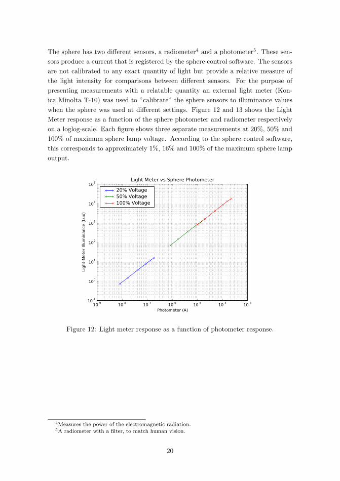
The sphere has two different sensors, a radiometer4 and a photometer5. These sen-
sors produce a current that is registered by the sphere control software. The sensors
are not calibrated to any exact quantity of light but provide a relative measure of
the light intensity for comparisons between different sensors. For the purpose of
presenting measurements with a relatable quantity an external light meter (Kon-
ica Minolta T-10) was used to ”calibrate” the sphere sensors to illuminance values
when the sphere was used at different settings. Figure 12 and 13 shows the Light
Meter response as a function of the sphere photometer and radiometer respectively
on a loglog-scale. Each figure shows three separate measurements at 20%, 50% and
100% of maximum sphere lamp voltage. According to the sphere control software,
this corresponds to approximately 1%, 16% and 100% of the maximum sphere lamp
output.
10-9 10-8 10-7 10-6 10-5 10-4 10-3
Photometer (A)
10-1
100
101
102
103
104
105
Ligh
t-Met
er Il
lum
inan
ce (L
ux)
Light Meter vs Sphere Photometer
20% Voltage50% Voltage100% Voltage
Figure 12: Light meter response as a function of photometer response.
4Measures the power of the electromagnetic radiation.5A radiometer with a filter, to match human vision.
20

10-7 10-6 10-5 10-4 10-3
Radiometer (A)
10-1
100
101
102
103
104
105
Ligh
t-Met
er Il
lum
inan
ce (L
ux)
Light Meter vs Sphere Radiometer
20% Voltage50% Voltage100% Voltage
Figure 13: Light meter response as a function of radiometer response.
As can be seen in figure 12 the photometer response is linear with the light
meter response over the different settings. The radiometer response seen in figure
13 is linear within the different measurements but the response is different when the
sphere lamp voltage changes. Due to the higher signal values for the radiometer,
for this thesis, the measured relations between the light meter illuminance and the
radiometer current will be used to convert the measured light intensity to illuminance
values.
21

2.3 Climate Chamber
For the purpose of evaluating how products perform in different temperatures, Axis
Communications owns a number of climate chambers. The climate chamber used
for temperature measurements in this thesis allows for temperatures in the range of
5◦C to 60◦C with a step size of 0.1◦C.
When performing temperature measurements, it is important to make sure that the
temperature of the device under test is stable when data is acquired. This was ac-
complished by mounting a temperature probe on the evaluation kit and logging the
temperature during one measurement.
The temperature dependence of both dark signal and noise characteristics was mea-
sured. The sensor was completely covered by mounting the optics with a closed
iris and covering the entire evaluation kit with a piece of dark cloth. The sensor
temperature was allowed to stabilize for two hours at each temperature level. Only
completely dark frames were acquired.
2.4 Laser Diffraction
To measure the dynamic range of the image sensor, a setup that allows for both
incredibly bright and very dark illumination of the sensor at the same time, is
needed. This might be hard to achieve accurately in a lab setup with conventional
lighting of a scene. Wang et al. [7] have suggested an alternative approach utilizing
Fraunhofer diffraction from a circular aperture.
Laser
Pinhole Aperture
Image Sensor
Diffraction Pattern
Figure 14: Schematic of laser diffraction measurement setup.
Figure 14 shows a schematic of the setup.
The test setup consists of: A laser, in this case a green laser with a wavelength of
532nm and an output power of 5mW and a pinhole aperture with a radius of 50µm.
The pinhole aperture is placed in front of the sensor which is then illuminated by
the laser beam. This creates a diffraction pattern with known theoretical properties
that can be used to determine the dynamic range of the sensor.
22

2.5 Blinking LED
For the purpose of evaluating the sensor response to flickering illumination and fast
transitions between dark and bright illumination, a small setup with a LED and a
micro-controller was built. This setup can be seen in figure 15.
LEDMicrocontroller
Natural Density Filter
Image Sensor
Figure 15: Schematic of LED flicker setup.
The entire setup was covered when measurements were performed to eliminate ex-
ternal light sources that might affect the result. For the purpose of changing the
amount of light reaching the sensor the setup allows for the placement of neutral
density (ND) filters between the LED and the sensor.
3 Measurement Theory
3.1 Signal Characteristics
3.1.1 Dark Signal Characteristics
A common starting point for image sensor evaluations is to acquire a number of com-
pletely dark images, by covering the sensor and making sure that no light reaches
it. This data can then be used to evaluate a number of different parameters.
Firstly, the data can be used to exclude pixels with a vastly different response and/or
behavior than all the other pixels, since the main interest is the average behavior of
the image sensor. It is also important to make sure that the evaluation sample is in
working condition and not defect in any way.
Secondly, the data can be used to assess the characteristics of the dark signal. If
there is any offset from zero or if the signal is clipped at a certain level.
23

3.1.2 Illumination Response
When evaluating the signal characteristics of an image sensor, there are several
important aspects to consider. Since the main function of the image sensor is to
convert light into a digital signal, detailed measurements of the response to changes
in the amount of light reaching the sensor needs to be performed.
This can be achieved using the integrating sphere setup described in section 2.2.
The basic procedure is to mount the sensor to the integrating sphere, making sure
that the only light illuminating the sensor is the light from the sphere.
The amount of light reaching the sensor is changed by gradually closing the sphere
attenuator. At each discrete light level a number of frames are captured from the
sensor. For a detailed description of the number of frames and illuminance levels
used for the measurements in this thesis, please find Appendix A.
When performing measurements with illumination it is important to consider the
effect of the image sensor’s color filters described in section 1.2. Since all light
sources have a certain spectral distribution and the color filters have different spectral
response the response over the different color channels might differ. To account for
this the different color channels can be separated according to figure 16.
R1 GR1
B1
R2
R3 R4
GB1
GR3
GB3 GB4
GR4
GR2
GB2
B3 B4
B2
R1 R2
R3 R4
GR1 GR2
GR3 GR4
B1 B2
B3 B4
GB1 GB2
GB3 GB4
Figure 16: Schematic of color channel separation.
Theoretically the response of the green pixels on rows with blue and red pixels
should be the same. Usually they are still treated as independent channels since the
response might differ due to optical and/or electrical pixel crosstalk6.
6Neighboring pixels influencing the response of a certain pixel.
24
The response can either be presented as the averages of the different color channels
or as the average of all color channels. Additionally to measure the average response,
both temporal noise and FPN described in section 3.2 must be reduced to achieve an
accurate measure. This is done by a combination of spatial and temporal averaging.
First, a number of consecutive frames are averaged in time as described by equation
(4). This gives a single frame with reduced temporal noise:
p̄N (x, y) =1
N
N∑i=1
p(x, y, i) (4)
where:
N is the number of averaged frames,
p(x, y, i) is the pixel value at pixel, (x, y) in frame i.
Secondly the FPN is reduced by averaging over the region of interest in the sin-
gle frame according to equation (5),
p̄N,ROI =1
Mxy
∑x
∑y
p̄N (x, y), {x, y ∈ ROI} (5)
where:
N is the number of averaged frames,
p̄N (x, y) is given by (4),
ROI is the set of pixel coordinates of the region of interest used,
Mxy is the total number of pixels in the region of interest.
To be able to calculate a signal without the dark signal offset, after each sphere
measurement a set of dark frames were acquired. The average dark signal was cal-
culated in the same way as the average signal.
25

3.2 Noise Characteristics
The noise in an image sensor is comprised of two main parts that will be referred to
as temporal noise and FPN.
As the name implies, temporal noise is noise that changes from frame to frame.
Common sources of this are: pixel reset noise and MOS device noise. Additionally
in integrating sensors, photon shot noise is another source of temporal noise [2].
Visually in the image, temporal noise can be seen as flickering pixels in a stream of
images.
Fixed pattern noise is noise that is stationary with respect to time. FPN is vis-
ible as patterns in otherwise homogeneous areas in the image, either in a random
fashion or as vertical or horizontal lines due to mismatches between pixels or mis-
matches between different signal parts of the readout chain [2]. A schematic of how
this can appear in the final picture can be seen in figure 17.
Without FPN
Column FPN Pixel FPNRow FPN
Figure 17: Schematic of row level, column level and pixel level FPN.
26

3.2.1 Temporal Noise
A common way of measuring the temporal noise, or root mean square (RMS) noise
as it is also referred to, is to record two frames, subtract them and calculate the
standard deviation with a correction factor [8]. To improve the statistics one may
instead measure the average variations of all pixels on a frame to frame basis. Such
a measure can be defined as:
σ̄temporal =1
Mxy
∑x
∑y
σtemporal(x, y), {x, y ∈ ROI} (6)
σtemporal(x, y) =
√√√√ 1
N
N∑i=1
(p(x, y, i)− p̄N (x, y))2 (7)
where:
N is the number of captured frames,
p(x, y, i) is the pixel value at pixel (x, y) in frame i,
p̄N (x, y) is the average value at pixel (x, y) over N frames,
ROI is the set of pixel coordinates of the region of interest used,
Mxy is the total number of pixels in the region of interest,
This measure describes the average pixel to pixel variations of the sensor in the
region of interest.
3.2.2 Fixed Pattern Noise
The simplest way of modelling FPN is to assume a simple gain/offset variation type
model which can be defined according to equation (8),
p(x, y) = a(x, y) + b(x, y)f(i) (8)
where:
p(x, y) is the response of a pixel at coordinates (x, y),
a(x, y) is the offset of the pixel at coordinate (x, y),
b(x, y) is the gain of the pixel at coordinate (x, y),
f(i) is a function describing the ideal pixel response to illumination i.
The pixel offset is known as dark signal non-uniformity (DSNU) and the pixel gain
is known as photo response non-uniformity (PRNU).
27

If the model described in equation (8) holds true, the standard deviation of two
different pixels as a function of the average signal will take the form described in
figure 18.
Pixel response
Pixel response
Average Signal
Average Signal
Pixel response vs Signal Pixel standard deviation vs Signal
Average Signal
Average Signal
Pixel Average
Pixel Average
Offset variations Offset variations
Gain variations Gain variations
Figure 18: Overview of how offset and gain variations affect the FPN measures.
As can be seen in figure 18, if two different pixels have the same response but a
difference in offset, the standard deviation of the pixels as a function of the average
signal will be constant but different from zero.
If the pixels have a different response but no offset, the standard deviation will
increase linearly as function of the average signal. A combination of both offset
and gain variations will therefore result in an increasing standard deviation with a
constant offset from zero. All FPN measures defined in this report relies on the use
of standard deviation. Therefore if the model described in equation (8) holds, the
measured FPN will show the same behavior as shown in figure 18.
28

To measure the FPN, the temporal noise must be removed. This is done by
averaging in the same fashion as described in section 3.1.2.
Total Fixed Pattern Noise There are different measures for the FPN, the sim-
plest one includes all types of FPN in a single measure and is defined as:
σTotalFPN =
√1
Mxy
∑x
∑y
(p̄N (x, y)− p̄N,ROI)2, {x, y ∈ ROI} (9)
where:
N is the number of averaged frames,
p̄N (x, y) is the average pixel value over N frames at pixel, (x, y), given by (4),
p̄N,ROI is the average pixel value of the region of interest over N frames,
ROI is the set of pixel coordinates of the region of interest used,
Mxy is the total number of pixels in the region of interest.
This measure gives a value of the total variations of the pixels of the sensor.
Row and Column FPN Another FPN measure is to measure the variations on
a column basis, this can be defined as:
σColumnFPN =
√1
Mx
∑x
(p̄N,y(x)− p̄N,y)2, {x, y ∈ ROI} (10)
p̄N,y(x) =1
My
∑y
p̄N (x, y), {x, y ∈ ROI} (11)
where:
N is the number of averaged frames,
p̄N (x, y) is the average pixel value over N frames at pixel, (x, y), given by (4),
p̄N,y is the average value of the average column p̄N,y(x) over N frames,
ROI is the set of pixel coordinates of the region of interest used,
Mx is the total number of rows in the region of interest,
My is the total number of columns in the region of interest.
This measure gives a value of the variations among the columns of the sensor.
29

Similarly the row FPN can be defined by exchanging the row and column indices:
σRowFPN =
√1
My
∑y
(p̄N,x(y)− p̄N,x)2, {x, y ∈ ROI} (12)
p̄N,x(y) =1
Mx
∑x
p̄N (x, y), {x, y ∈ ROI} (13)
where:
N is the number of averaged frames,
p̄N (x, y) is the average pixel value over N frames at pixel, (x, y), given by (4),
p̄N,x is the average value of the average row p̄N,x(y) over N frames,
ROI is the set of pixel coordinates of the region of interest used,
Mx is the total number of rows in the region of interest,
My is the total number of columns in the region of interest.
This measure gives a value of the variations among the rows of the sensor.
Pixel FPN The remaining FPN component not included in either the row or
column FPN is the pixel FPN . This is the variations in pixel gain and offset that
can’t be accounted for by row and/or column variations. To measure this quantity
the column and row FPN must be removed. This is done by averaging all rows with
respect to an average row and all columns to an average column. Since this removes
all row and column variations the remaining pixel FPN can be calculated in the
same fashion as the total FPN given in equation (9). This gives the pixel FPN as:
σPixelFPN =
√1
Mxy
∑x
∑y
(p̄N,norm(x, y)− p̄N,norm,ROI)2, {x, y ∈ ROI} (14)
p̄N (x, y)norm =
(p̄N (x, y) · p̄N,x
p̄N,x(y)
)· p̄N,yp̄N,y(x)
(15)
where:
N is the number of averaged frames,
p̄N,norm,ROI is the average pixel value of the region of interest over N frames nor-
malized with respect to column and row variations,
p̄N,y is the average value of the average column p̄N,y(x) over N frames,
p̄N,x is the average value of the average row p̄N,x(y) over N frames,
p̄N,y(x) is given by (11),
p̄N,x(y) is given by (13),
ROI is the set of pixel coordinates of the region of interest used,
Mx is the total number of rows in the region of interest,
My is the total number of columns in the region of interest.
30

3.3 Signal-to-noise Ratio
The signal-to-noise ratio (SNR) is a common measure of how high quality the output
of certain system is. This can be used as a comparative measure between different
imaging systems and is defined as:
SNR =s
σ(16)
where:
s is the average signal,
σ is the temporal noise, in this case the standard deviation of the signal.
The SNR is often expressed as a power ratio according to:
SNR = 20log10
( sσ
)(17)
31

3.4 Dynamic Range
Using the setup described in section 2.4, a diffraction pattern can be projected onto
the image sensor surface. The intensity distribution of this diffraction pattern is
given by equation (18) [9],
I(θ) = I0
(2J1(ka · sin(θ)
ka · sin(θ)
)2
(18)
where:
I0 is the intensity of the main peak,
J1 is the first order Bessel function,
k =2π
λis the wavenumber, where λ is the wavelength,
a is the radius of the aperture,
θ is the angle of observation.
This relation allows us to theoretically calculate the relative intensities of the peaks
in diffraction pattern. This information can then be used to determine the dynamic
range of the sensor.
0.0 0.1 0.2 0.3 0.4 0.5 0.6 0.7 0.8Angle (Radians)
0
50
100
150
200
250
300
Rela
tive
Inte
nsity
(dB)
Fraunhofer Diffraction Pattern Relative Intensity as a function of viewing angle
Figure 19: Theoretical intensity as a function of angle, λ = 532nm, a = 50µm.
Figure 19 shows the normalized intensity distribution as a function of the angle of
observation θ. The angular distribution is however not of any importance when it
comes to measure the dynamic range.
32

Instead we want to know the relative intensity dynamic range as a function of the
peak number. This can be seen in figure 20.
0 20 40 60 80 100 120 140Peak Number
0
20
40
60
80
100
120
140
160
Dyn
amic
Ran
ge (d
B)
Dynamic Range as a function of Peak Number
Figure 20: Dynamic Range as a function of peak number, λ = 532nm, a = 50µm.
The measurement is carried out by changing the laser intensity to a point just below
sensor saturation. The dynamic range is then given by the smallest detectable peak
in the image. Wang et al. [7] proposes this to be done by observation of the image.
An alternative approach is to use the ISO definition of dynamic range mentioned in
1.3.
33

3.5 Transient Response
The image sensor under evaluation is not an integrating sensor as a traditional image
sensor described in section 1.2. Therefore it might be interesting to try to character-
ize the transient response when an LED is turned on and off. The measurements can
be used to reason about the sensor behavior in different situations and how the final
image might be affected. As a comparison the response of a traditional integrating
image sensor can be seen in figure 21.
Time
Illumination LED ON LED OFF
Time
Sensor Output
0 1 2 0 1 2 0 1 2 0 1
Row 0 integration
Row 1 integration
Row 2 integration
Row readout
0
Max
Figure 21: Schematic of the transient response of an integrating image sensor.
For simplicity a theoretical line sensor with only 3 different rows is assumed. The
upper part of the figure shows how the rows are read out after each other in a rolling
shutter type fashion as described in section 1.2. The illumination as a function of
time is also shown as an LED is turned on and off.
The lower part shows the values when the rows are read out. Since the rows are
integrating the light during the integration period, the final value is only dependent
on the how long the LED was lit during the integration period. This leads to the
read out response seen in the lower part of the figure.
If a shorter integration/exposure time was used, the slope of the output signal would
be steeper. If a longer integration/exposure time was used, the slope would be flat-
ter. This, since a longer integration/exposure time would mean more pixels being
active during the illumination increase and vice versa, assuming that the read out
time is constant. This is also assuming that the LED response is fast enough to be
considered step-like.
34

The transient behavior of the logarithmic sensor under evaluation was unknown
and was measured and compared to the response of a traditional integrating sensors.
The measurement was done by using the setup described in section 2.5. The LED
was turned on and off repeatedly and at the same time a number of frames were
recorded. The frames that were recorded during the LED on and off periods were
extracted from the data set.
To reduce the amount of data and remove noise, the pixel response was averaged
for each row and the rows were then plotted after each other leading to an output
form identical to the one in figure 21. Additionally the rows were normalized with
respect to the illumination profile and the maximum value. This since the response
time is the main point of interest. Additionally the row response was filtered with
a median filter and an averaging filter to provide a more clear signal without noise.
As mentioned in section 1.4 the response of the pixel in the logarithmic sensor under
evaluation is illumination dependent. Therefor the response with different ND filters
was investigated.
ND filters are usually quantified by their optical density which is defined according
to equation (19),
d = −log10(I
I0
)(19)
where:
d is the optical density,
I is the intensity after the filter,
I0 is the incident intensity.
35

4 Results and Discussion
This section contains all the measurement results from the measurements performed
as described in section 3.
4.1 Signal Characteristics
4.1.1 Dark Signal Characteristics
As described in section 3.1.1, the sensor evaluation kit was completely covered and
100 frames were acquired.
Outliers
Figure 22: Map of outlier pixels, ambient temperature: 25◦C.
Figure 22 shows a map of outlier pixels. The temporal noise has been removed by
averaging in accordance with section 3.1.2. As can been seen in the figure, there are
rows and columns at the edges of the sensor which contain pixels that are more than
3 standard deviations above or below the sensor mean. For this reason, a centered
region of interest (ROI) denoted ROI1 of 710 rows and 1270 columns was selected
for use in some of the measurements. This was done to avoid that ”bad” rows and
columns influence the measurements to much. In the figure it can also be seen that
there are scattered pixels with values above or below 2 standard deviations, these
were not excluded from the measurements.
36

Histogram
8600 8620 8640 8660 8680 8700 8720 8740 8760Pixel Value (ADU)
0
100
200
300
400
500
600
700
Num
ber of pix
els
Average Dark Frame - Histogram
Figure 23: Histogram of average dark frame, ambient temperature: 25◦C.
As can be seen in figure 23 there is no clipping of the histogram and the pixel
values seem to be more or less evenly distributed around the mean.
37

Average Row and Column
0 200 400 600 800 1000 1200Column Number
8620
8630
8640
8650
8660
8670
8680
8690
8700
8710
Signal Value (ADU)
Average Row
Figure 24: Average row at 25◦C
Figure 24 shows the values of a representative row. What this actually shows
are the variations of the different columns of the image sensor. As can be seen there
seems to be consistent variations between different columns that have the effect of
creating two separated populations of column values. Additionally there seems to
be a small gradient across the columns. Also the first few columns seem to have a
different offset than the other ones, although these will be excluded when ROI1 is
used.
38

0 100 200 300 400 500 600 700Row Number
8620
8630
8640
8650
8660
8670
8680
8690
8700
8710Signal Value (ADU)
Average Column
Figure 25: Average column at 25◦C
Figure 25 shows the values of a representative column. This shows the variations
of the different rows of the image sensor. The scale is the same as in figure 24 and
it’s apparent that the variations from row to row is less than the column to column
variations seen in figure 24. Additionally a small gradient across the rows can be
seen. The first and last rows seem to have a different offset then most of the other
rows, these are excluded in ROI1.
39

Noise measures
Using the measures defined in section 3.1.2 and section 3.2 and ROI1 the signal and
noise without any illumination at an ambient temperature of 25◦C can be seen in
table 1.
Signal Total FPN Column FPN Row FPN Pixel FPN Temporal Noise
8650.95 (ADU) 5.85 (ADU) 3.79 (ADU) 3.23 (ADU) 3.07 (ADU) 10.08 (ADU)
Table 1: Table of signal and noise measurements of dark frames, ROI1.
As can be seen in table 1 the average signal of a completely dark frame is 8650.95
analog-to-digital units (ADU). This seems to be a quite high offset value considering
that a 14-bit ADC is used on the evaluation kit. Essentially this means that only
half the ADC range is used. Depending on the signal response this still leaves about
8000 digital steps remaining of the ADC output which should be enough for most
applications.
Furthermore the FPN values cited in table 1 is essentially the DSNU since the sensor
is not illuminated. The values seem quite low, especially considering the high offset
values usually quoted for logarithmic image sensors. It is apparent that the presence
of a reset as described in section 1.4 is an effective way of removing pixel offset. The
row and column FPN is about the same, although the row FPN is dominated by a
gradient and the column FPN is dominated by column to column variations.
The temporal noise is about 10 ADU which clearly dominates over the FPN at
no illumination.
40

4.1.2 Illumination Response
As described in section 3.1.2 the illumination response measurements were performed
using the integrating sphere setup described in section 2.2.
10-1 100 101 102 103 104
Illuminance (lux)
0
500
1000
1500
2000
2500
Sign
al (A
DU)
Signal response
RedBlueGreen (R)Green (B)Average
Figure 26: The average sensor signal with dark offset removed, plotted against the
illumination, ROI1, measurement A.1.
Figure 26 shows the signal response in a plot with a logarithmic x-scale. The
responses of the different color channels are similar although a bit offset from each
other due to different amounts of attenuation and the spectral distribution of the
sphere light source.
41

Figure 27 shows the average signal of all color channels versus illumination with
a line fitted to the 25 first datapoints and logarithm fitted to the last 15 data points.
10-1 100 101 102 103 104
Illuminance (lux)
�500
0
500
1000
1500
2000
2500
Sign
al (A
DU)
Average Response
Average SignalFitted logarithmFitted line
100 1010100200300400500600700800
Figure 27: The average sensor signal with dark offset removed, with fitted logarithm
and line, ROI1, measurement A.1.
As can be seen in figure 27 at light levels above 10-20 lux the average response
follows an almost perfect logarithmic relationsship with respect to illumination. At
illumination levels below 2-3 lux the relationship between signal and illumination
instead follows a linear relationship.
As can be seen in the zoomed in section of the plot, the transition between linear
and logarithmic mode seem to happen somewhere between 3-10 lux. Although in
this range the response is neither perfectly linear nor perfectly logarithmic.
4.1.3 Temperature dependence
The temperature dependence of the noise and dark signal was measured in accor-
dance with section 2.3. At each temperature, 100 frames were acquired. Two sep-
arate measurements were performed to verify the consistency of the temperature
dependent behavior.
42

0 10 20 30 40 50 60Ambient Temperature (deg C)
7000
7500
8000
8500
9000
9500Sig
nal (A
DU)
Average Dark Signal vs Temperature
Figure 28: Average dark signal versus the ambient temperature, ROI1.
Dark Signal
Figure 28 shows the average dark signal versus temperature. The apparent offset
between the two measurements could be due to a slight difference in the stabilization
time allowed. Another possible factor is the way the evaluation kit was covered with
cloth, since this could possibly isolate the evaluation kit more or less.
As can be seen there is a substantial decrease in the average signal when the tem-
perature is increased. This is a problematic result from an implementation point of
view, since surveillance cameras need to be able to operate in different environments
and in varying temperatures. The dark signal determines what is black in the image
and if a predefined offset is used, the error could become quite large if the tempera-
ture changes, thus affecting the final image quality.
The average signal almost seems to decrease linearly with the signal so it is possible
that a temperature dependent offset correction could be implemented.
43

Noise
0 10 20 30 40 50 60Ambient Temperature (deg C)
9.8
9.9
10.0
10.1
10.2
10.3
10.4
Tem
pora
l Nois
e (ADU)
Temporal Noise vs Temperature
Figure 29: Temporal noise versus the ambient temperature, ROI1.
Figure 29 shows the temporal noise versus temperature. As in the previous
section, there is a slight offset between the two measurements. Observing the y-axis
one can see that the variations of the temporal noise are incredibly small, and more
or less constant over the entire temperature range. From an implementation point
of view, this is a very good result since it means no apparent increase in temporal
noise will be seen in the final image even at high temperatures.
44

0 10 20 30 40 50 60Ambient Temperature (deg C)
0
5
10
15
20
25FP
N (ADU)
FPN vs Temperature
Total FPNRow FPNColumn FPN
Figure 30: FPN versus the ambient temperature, ROI1.
Figure 30 shows the total FPN and the row FPN versus the ambient temperature.
Again the same offset between the measurements as before is visible. The FPN
increases when the temperature increases. And as can be seen in the figure, the row
FPN seems to be the dominant factor in the increase.
To determine the behavior of the FPN, the average row and column at 0◦C and
60◦C can be seen in figure 31 and 32.
45
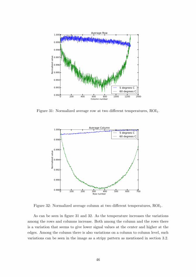
0 200 400 600 800 1000 1200 1400Column number
0.992
0.993
0.994
0.995
0.996
0.997
0.998
0.999
1.000
Norm
alized value
Average Row
5 degrees C60 degrees C
Figure 31: Normalized average row at two different temperatures, ROI1.
0 100 200 300 400 500 600 700Row number
0.988
0.990
0.992
0.994
0.996
0.998
1.000
Norm
alized value
Average Column
5 degrees C60 degrees C
Figure 32: Normalized average column at two different temperatures, ROI1.
As can be seen in figure 31 and 32. As the temperature increases the variations
among the rows and columns increase. Both among the column and the rows there
is a variation that seems to give lower signal values at the center and higher at the
edges. Among the column there is also variations on a column to column level, such
variations can be seen in the image as a stripy pattern as mentioned in section 3.2.
46

Summary
The temperature dependence measurements show both positive and negative results
from an implementation point of view. The large change in dark signal is as men-
tioned problematic for a stable implementation. The constant temporal noise is a
good result since this type of noise is hard to completely remove in the final image.
The FPN increases with temperature but is still relatively low and if needed some
form of correction scheme including temperature could potentially be devised.
47

4.2 Noise Characteristics
4.2.1 Temporal Noise
The temporal noise was measured in accordance with the description in section 3.2.
10-1 100 101 102 103 104
Illuminance (lux)
10.0
10.1
10.2
10.3
10.4
10.5
10.6
Nois
e (A
DU)
Temporal Noise
Figure 33: The sensor temporal noise plotted versus the illuminance, measurement
A.1.
Figure 33 shows the temporal noise versus the illumination. The noise does seem
to remain fairly constant with the illumination as the variations are extremely small.
Possibly a slight increase can be observed up to 10 lux.
One data point at 90 lux seems to be a bit off from the others, although it is still
within one ADU of the other data points.
48

4.2.2 Fixed Pattern Noise
The FPN was measured in accordance with the description in section 3.2.2.
0 500 1000 1500 2000 2500Signal (ADU)
05
10152025303540
FPN
(AD
U)
Total FPNRedBlueGreen (R)Green (B)
0 500 1000 1500 2000 2500Signal (ADU)
05
10152025303540
FPN
(AD
U)
Column FPNRedBlueGreen (R)Green (B)
0 500 1000 1500 2000 2500Signal (ADU)
05
10152025303540
FPN
(AD
U)
Row FPNRedBlueGreen (R)Green (B)
0 500 1000 1500 2000 2500Signal (ADU)
05
10152025303540
FPN
(AD
U)Pixel FPN
RedBlueGreen (R)Green (B)
Figure 34: The FPN versus illumination per color channel measurement, ROI1 A.1.
Figure 34 shows the FPN versus the sensor’s average signal, for each color chan-
nel. The FPN model described in 3.2.2 seems to hold, as the FPN increases more or
less linearly with the signal. The overall FPN is also fairly small compared with the
signal which increases much faster. Since the row and column FPN, and in particu-
lar the row FPN seems to influence the total FPN the most it might be interesting
to study the average row and column profiles at different illumination levels to see
how the noise increases. This can be seen in figure 35 and 36.
49

0 100 200 300 400 500 600 700row number
0.988
0.990
0.992
0.994
0.996
0.998
1.000
Norm
aliz
ed s
igna
l val
ue
Average Column - G(R) Channel
0 lux1445 lux
Figure 35: Normalized average column of green pixels on red rows, two illuminations
levels, ROI1 A.1.
0 200 400 600 800 1000 1200 1400Column number
0.992
0.993
0.994
0.995
0.996
0.997
0.998
0.999
1.000
Norm
aliz
ed s
igna
l val
ue
Average Row - G(R) Channel
0 lux1445 lux
Figure 36: Normalized average row of green pixels on red rows, two illuminations
levels, ROI1 A.1.
As can be seen in figure 36 and 35, apart from a small horizontal and vertical
gradient when the sensor is illuminated there seems to be a certain profile of the
sensor response, with higher values in the middle, and lower at the edges. This is
known as shading and usually refer to low frequency spatial variations in the sensors
output. Potential sources include shading from the microlenses7 [15].
This obviously affects the measured FPN, since the measure includes all spatial
variation of the sensor response. Figure 36 shows an average row and apart from the
shading component there is visible increase in the variability of the pixel response.
This variability is what would appear as a stripy pattern as described in section 3.2.
7Tiny lenses on each pixel, used to increase the light collection efficiency.
50

Summary
The promise of a logarithmic image sensor with low FPN seems to hold true as the
measurements show that the FPN is indeed quite small. The linear behavior also
facilitates the use of flat-field correction (FFC) [6] to compensate for pixel gain and
offset variations.
The temporal noise remains more or less constant when the illumination changes.
The temporal noise is usually reduced by temporal averaging although it still limits
the SNR at low illumination, this shown in section 4.3
51

4.3 Signal-to-noise Ratio
The aquired signal and temporal noise data from section 4.1.2 and section 4.2 was
combined in order to plot the SNR as defined in section 3.3 as a function of illumi-
nation. This was also done using simulated data for a commercial integrating pixel
type sensor at 1/33 s exposure time. A comparison of the respective SNR behaviors
can be seen in figure 37.
0.0 0.5 1.0 1.5 2.0 2.5 3.0 3.5 4.0illuminance (lux)
�40
�30
�20
�10
0
10
20
30
40
50
SNR
(dB)
SNR comparison
Simulated, Integrating pixel sensorLogarithmic pixel sensor
Figure 37: SNR comparison of logarithmic sensor and traditional integrating sensor.
As can be seen in figure 37, the SNR rises much faster for the traditional integrating
linear pixel. This means that at low illumination levels the amount of noise will be
higher for the logarithmic sensors, thus resulting in worse image quality.
52

4.4 Dynamic Range
The measurement was performed in accordance with the description in section 3.4.
To remove both temporal noise and to compensate for intensity variations of the
laser. 1000 images of the diffraction pattern were captured and averaged.
One issue during this test was that the laser was not able to saturate the sensor.
Therefore it was not possible to measure the exact dynamic range, but only a lower
bound of the dynamic range. Figure 38 shows a gray scale image of the diffraction
pattern.
0 200 400 600 800 1000 1200column
0
100
200
300
400
500
600
700
row
Diffraction pattern
Figure 38: Averaged image taken during laser diffraction test.
In the full scale image, 46 individual rings were counted which would lead to
a dynamic range of 121.9dB. Alternatively a row intersecting the main peak can
be extracted from figure 38. Assuming a constant temporal noise level of at most
11 (10.55) ADU as measured in section 4.2, the SNR of the extracted row can be
plotted. This can be seen in figure 39.
53

0 200 400 600 800 1000 1200 1400Column number
�10
0
10
20
30
40
50
60SN
R (d
B)SNR vs Peak
Figure 39: SNR of row intersecting the main peak of the diffraction pattern.
As can be seen in figure 39 all peaks appear to have a SNR above 1 (0dB). There
are 58 peaks in total which would mean a dynamic range of 127.9dB.
To conclude, the sensor has a dynamic range of at lest 121.9dB or 127.9dB de-
pending on what measure is used. However since the sensor didn’t saturate it is not
possible to state the total dynamic range, only a lower bound can be established.
For comparison, the data from a similar measurement performed on a multi-exposure
type camera was received from Axis Communications AB, quoting a dynamic range
of 110dB. This is clearly less, although it’s not possible to claim that one is better
than the other on dynamic range alone since this measure doesn’t specify ”where”
the dynamic range is. For instance, in some circumstances it might be more impor-
tant with low light sensitivity than a high saturation point.
54

4.5 Transient Response
As mentioned in section 3.5. A number of frames were acquired as the image sensor
was illuminated using the setup described in section 2.5. The LED was repeatedly
turned on and off to facilitate the recording of frames during the led illumination
changes. The row averages were then computed for all frames. The resulting row
averages for three consecutive frames at the point of the LED illuminations changes
can be seen in figure 40.
Figure 40: Average rows for three consecutive frames, for LED on and off.
The respective responses for when the LED was turned on and off were extracted
for a number of different illumination levels. This can be seen in figure 41 and 42.
Two different ND filter were used in the measurements, one with an optical density
of 0.1 corresponding to approximately 80% transmittance, and one with an optical
density of 0.5 corresponding to approximately 32% transmittance.
55

0 100 200 300 400 500 600 700 800 900Row Number
0.0
0.2
0.4
0.6
0.8
1.0Norm
aliz
ed resp
onse
Normalized response vs row number
OD: 0.1OD: 0.5
Figure 41: Normalized rise response versus read out row.
Figure 41 shows the read out row normalized with respect to the maximum read
out value and the illumination profile of the LED. This was done with two different
ND filters with an optical density of 0.1 and 0.5 respectively. As can be seen in the
figure, the response of the measurement with the slightly less dark filter seems to
reach the maximum illumination a bit faster.
The ”rows” with value zero in the middle of the pictured response is what is known
as Vblank, and is the time corresponding to a certain number of ”empty” lines that
are read out between frames. The fact that the Vblank appears to coincide for the
two measurements is due to selection for easier comparison.
56

0 100 200 300 400 500 600 700 800 900Row Number
0.0
0.2
0.4
0.6
0.8
1.0Norm
aliz
ed resp
onse
Normalized response vs row number
OD: 0.1OD: 0.5
Figure 42: Normalized fall response versus read out row.
Figure 42 shows the read out row normalized with respect to the maximum read
out value and the illumination profile of the LED. This was done with two different
ND filter with an optical density of 0.1 and 0.5 respectively. Here the response is
much more similar and it is not possible to conclude that one is faster than the
other.
Summary
Studying the response when a LED was turned on, it seems that one can conclude
that the response is indeed faster when the illumination level is higher.
It is also apparent that the response is different from the response of a traditional
integrating image sensors described in section 3.5. Particularly in the sense that it
is not symmetrical with respect to when the LED is turned on and off.
Since the read out signal is affected by both the rolling shutter effect and the pixel
response, it is hard to conclude exactly how the different effects contribute to the
response.
It is possible that the different response might render motion slightly different in
some circumstances, especially in low light when the response is slower. This was
evaluated with a simple test of imaging a rotating object at different illumination
levels. This can be seen in figure 43.
57

Figure 43: Images of object rotating at 30rpm at different illumination levels. Com-
parison with integrating sensor.
The images to the left were taken at 1/25 s exposure and as can be seen, the
motion blur is independent of illumination and only depends on the exposure time.
For the logarithmic sensor to the right, there is almost no motion blur at all at
20 000 lux but there is visible blur when the illumination is decreased. Additionally
the rotating object is rotating counter clockwise and there seems to be more motion
blur after the object than before it when captured by the logarithmic sensor. This
could potentially be explained by the response seen in figure 41 and 42 as the fall
response seems slower than the rise response.
With a linear integrating sensor the amount of motion blur can be regulated by
choosing longer or shorter exposure times, altough there is always a tradeoff be-
tween the amount of noise and motion blur. With the logarithmic sensor it is not
possible to choose between motion blur or noise, low illumination will always lead
to motion blur.
58

5 Conclusions and Future Work
Conclusions
Reiterating the questions set up in section 1.5, the following results are worth calling
attention to:
The sensor response does indeed follow a logarithmic law at high illumination levels.
As the sensor was not saturated even by a laser it is probably fair to say that satu-
ration of the sensor is not a problem when using a logarithmic sensor with this design.
As measured in section 4.2.2 the FPN is quite low, especially in the context of
logarithmic CMOS sensors. This shows that the new design and the presence of a
reset vastly improves the sensor performance. The temporal noise remains constant
although it is quite high compared to common integrating sensors as shown in sec-
tion 4.3. This limits the low light performance of the logarithmic sensor.
From the data in section 4.1.2, no obvious transition between linear and logarithmic
mode can be seen and the response seems to be smooth over the entire usable range.
As shown in section 4.5, the fact that the sensor is not integrating does change
certain behaviors, for instance motion blur. This thesis does not address all possi-
ble motion-related behavior differences and this is an area that might warrant more
investigation.
The temperature measurements in section 2.3 have shown that the temporal noise
stays constant and there is an increase in FPN. More alarming though, the dark sig-
nal seems extremely unstable with regard to temperature and would make a stable
implementation hard to achive.
Aditional work is needed to fully understand the temperature dependent behavior
of the sensor.
59

Outlook and Future Work
The prospect of using this type of logarithmic image sensors as an alternative WDR
solution instead of various multiple exposures methods is interesting. The use of
only one exposure or read out is an obvious advantage compared to the use of mul-
tiple exposure since it eliminates the issue of accurate motion representation.
Additionally there is no need for an exposure-algorithm that changes the exposures
in different situations which is a nice feature, reducing the complexity of the imaging
system.
The logarithmic response does present a number of challenges with regard to image
processing though. Little or no work in the field of tone mapping8 has been done
specifically for the use with logarithmic image sensors. Some work related to correct
color representation has been done [12] suggesting that this should be possible.
8Techniques for how to compress WDR images without loosing information.
60

References
[1] Key differences between rolling shutter and frame (global) shutter. http://
www.ptgrey.com/support/kb/index.asp?a=4&q=115. Accessed: 2012-06-26.
[2] Noise sources in cmos image sensors. http://www.stw.tu-ilmenau.de/~ff/
beruf_cc/megatek/noise.pdf, jan 1998. Accessed: 2012-06-26.
[3] Digital camera basics. http://www.ni.com/white-paper/3287/en, February
2012. Accessed: 2012-06-26.
[4] P.M. Acosta-Serafini, I. Masaki, and C.G. Sodini. A 1/3” vga linear wide
dynamic range cmos image sensor implementing a predictive multiple sampling
algorithm with overlapping integration intervals. Solid-State Circuits, IEEE
Journal of, 39(9):1487 – 1496, sept. 2004.
[5] S.G. Chamberlain and J.P.Y. Lee. A novel wide dynamic range silicon pho-
todetector and linear imaging array. Electron Devices, IEEE Transactions on,
31(2):175 – 182, feb 1984.
[6] Justin C. Dunlap, William C. Porter, Erik Bodegom, and Ralf Widenhorn. Dark
current in an active pixel complementary metal-oxide-semiconductor sensor.
Journal of Electronic Imaging, 20(1):013005, 2011.
[7] Yibing (Michelle) Wang et al. A high dynamic range cmos aps image sen-
sor. http://www.ericfossum.com/Publications/Papers/2001%20Program%
20A%20High%20Dynamic%20Range%20CMOS%20APS%20Image%20Sensor.pdf.
Accessed: 2012-06-26.
[8] David Gardner. Characterizing digital cameras with the photon transfer curve.
http://www.couriertronics.com/docs/notes/cameras_application_
notes/Photon_Transfer_Curve_Charactrization_Method.pdf. Accessed:
2012-06-26.
[9] E. Hecht. Optics. Addison-Wesley, 2002.
[10] John D. Hunter. Matplotlib: A 2d graphics environment. Computing In Science
& Engineering, 9(3):90–95, May-Jun 2007.
[11] Eric Jones, Travis Oliphant, Pearu Peterson, et al. SciPy: Open source scientific
tools for Python. http://www.scipy.org/, 2001–. Accessed: 2012-06-26.
[12] D. Joseph and S. Collins. Modelling, calibration and rendition of colour loga-
rithmic cmos image sensors. In Instrumentation and Measurement Technology
Conference, 2002. IMTC/2002. Proceedings of the 19th IEEE, volume 1, pages
49 – 54 vol.1, 2002.
61

[13] S. Kavadias, B. Dierickx, D. Scheffer, A. Alaerts, D. Uwaerts, and J. Bogaerts.
A logarithmic response cmos image sensor with on-chip calibration. Solid-State
Circuits, IEEE Journal of, 35(8):1146 –1152, aug 2000.
[14] A. D Kerr. The iso definition of the dynamic range of a digital still cam-
era. http://dougkerr.net/Pumpkin/articles/ISO_Dynamic_range.pdf, feb
2008. Accessed: 2012-06-26.
[15] J. Nakamura. Image Sensors and Signal Processing for Digital Still Cameras.
Optical Science and Engineering. Taylor & Francis, 2006.
[16] P.J.W. Noble. Self-scanned silicon image detector arrays. Electron Devices,
IEEE Transactions on, 15(4):202 – 209, apr 1968.
[17] Travis E. Oliphant. Guide to NumPy. Provo, UT, March 2006.
[18] J.M. Palmer and B.G. Grant. The Art of Radiometry. [Press monograph. SPIE
Press, 2010.
[19] E. Reinhard. High Dynamic Range Imaging: Acquisition, Display, and Image-
Based Lighting. Morgan Kaufmann Series in Computer Graphics and Geometric
Modeling. Elsevier, 2006.
[20] N. Ricquier and B. Dierickx. Pixel structure with logarithmic response for
intelligent and flexible imager architectures. In Solid State Device Research
Conference, 1992. ESSDERC ’92. 22nd European, pages 631 –634, sept. 1992.
[21] Orit Skorka and Dileepan Joseph. Toward a digital camera to rival the human
eye. Journal of Electronic Imaging, 20(3):033009, 2011.
[22] S. Sugawa, N. Akahane, S. Adachi, K. Mori, T. Ishiuchi, and K. Mizobuchi. A
100 db dynamic range cmos image sensor using a lateral overflow integration
capacitor. In Solid-State Circuits Conference, 2005. Digest of Technical Papers.
ISSCC. 2005 IEEE International, pages 352 –603 Vol. 1, feb. 2005.
[23] G. van Rossum and F.L. Drake (eds). Python Reference Manual. Virginia,
USA, 2001.
[24] O. Yadid-Pecht and E.R. Fossum. Wide intrascene dynamic range cmos aps
using dual sampling. Electron Devices, IEEE Transactions on, 44(10):1721 –
1723, oct 1997.
[25] David X. D. Yang and Abbas El Gamal. Comparative analysis of snr for image
sensors with enhanced dynamic range. volume 3649, pages 197–211. SPIE, 1999.
62

[26] D.X.D. Yang, A.E. Gamal, B. Fowler, and H. Tian. A 640 times;512 cmos image
sensor with ultrawide dynamic range floating-point pixel-level adc. Solid-State
Circuits, IEEE Journal of, 34(12):1821 –1834, dec 1999.
[27] Bogdan Arion Yang Ni, YiMing Zhu. A 768x576 logarithmic image sensor with
photodiode in solar cell mode. Accessed: 2012-06-26, 2011.
63

A Appendix A - Measurement Specifications
A.1 Sphere Measurement Specifications.
This measurement was conducted using the Integrating Sphere described in section
11.
Environment temperature: 23◦C
Sphere lamp intensity: 16%
1. The image sensor was mounted on the sphere without any optics or filter.
2. The image sensor was turned on and allowed to run for 60 minutes to reach a
stable operating temperature.
3. The integrating sphere attenuator was gradually closed. At each setting 100
frames were grabbed from the image sensor and the sphere radiometer values
were recorded. After each frame grab of illuminated frames, the sphere lamp
was turned off and 100 completely dark frames were captured. This, to be able
to correct for black level drift due to temperature variations.
Attenuator (%) Radiometer (A)
100 9.2718e-5
75 6.7899e-5
50 4.5414e-5
36 3.2704e-5
25 2.2751e-5
19 1.7286e-5
12 1.0951e-5
9 8.2250e-6
6 5.4958e-6
4 3.6706e-6
3 2.7561e-6
2 1.8414e-6
1 9.2425e-7
0.9 8.3150e-7
0.8 7.3943e-7
0.7 6.4775e-7
0.6 5.5537e-7
0.5 4.6283e-7
0.4 3.7076e-7
0.3 2.7818e-7
0.29 2.6884e-7
0.28 2.5956e-7
0.27 2.5038e-7
0.26 2.4125e-7
0.25 2.3198e-7
Attenuator (%) Radiometer (A)
0.24 2.2275e-7
0.23 2.1345e-7
0.22 2.0414e-7
0.21 1.9486e-7
0.20 1.8561e-7
0.19 1.7640e-7
0.18 1.6712e-7
0.17 1.5797e-7
0.16 1.4879e-7
0.15 1.3955e-7
0.14 1.3020e-7
0.13 1.2096e-7
0.12 1.1174e-7
0.11 1.0248e-7
0.10 9.3221e-8
0.09 8.3938e-8
0.08 7.4599e-8
0.07 6.5365e-8
0.06 5.6052e-8
0.05 4.6741e-8
0.04 3.7429e-8
0.03 2.8102e-8
0.02 1.8776e-8
0.01 9.4255e-9
0 0
64
Copyright © 2022 FDOKUMEN