A column-based pixel-gain-adaptive CMOS image sensor for low-light-level imaging
10
ISSCC 2003 / SESSION 12 / CMOS IMAGERS, SENSORS AND DISPLAYS / PAPER 12.7 12.7 A Column-Based Pixel-Gain-Adaptive CMOS Image Sensor for Low-Light-Level Imaging Shoji Kawahito 1 , Masaki Sakakibara 1 , Dwi Handoko 2 , Nobuo Nakamura 3 , Hiroki Satoh 3 , Mizuho Higashi 3 , Keiji Mabuchi 3 , Hirofumi Sumi 3 1 Research Institute of Electronics, Shizuoka University, Shizuoka, Japan 2 National Agency for Assessment and Application of Technology, Jakarta, Indonesia 3 Semiconductor Network Company, Sony, Atsugi, Japan The advantages of CMOS over CCD image sensors are low-power consumption, single supply voltage, and on-chip system integra- tion. However, CMOS image quality is below that of CCD, espe- cially for low light level imaging. This CMOS image sensor uses high-gain adaptive column amplifiers and pinned photodiode technology with an enhanced pixel driving technique. The dynamic range determined by the random noise, the fixed pat- tern noise and the saturation signal levels are shown to be com- parable to the standard CCD image sensor. Figure 12.7.1 is the block diagram of the CMOS image sensor developed. The major random noise sources in low light level are the reset noise, the dark current shot noise, and the read ampli- fier noise. Among these, the reset noise and the dark current shot noise are suppressed by a pinned photo diode technology [1- 3]. To suppress the read amplifier noise and the fixed pattern noise, this image sensor has low-noise high-gain column ampli- fiers. To avoid saturation of the amplifiers when the pixel output voltage is large, an adaptive-gain technique is used. The gain of 1 or 8 is adapted to the sensor output depending on its ampli- tude. If the sensor output is less than one-tenth of the saturation level, the gain of 8 is used to enhance the sensitivity and to reduce the total read noise. Otherwise, the gain is set to 1. A similar technique is used for a high-dynamic range CMOS image sensor enhanced to high light level [4]. In this case the technique is applied for the 3-transistor type active pixel sensor and is not intended for low-light-level imaging because the reset noise becomes dominant even though the random noise of readout cir- cuits is reduced. Figures 12.7.2 and 12.7.3 show the circuit of the adaptive-gain column amplifier and the timing diagram, respec- tively. The gain is set by the ratio of the input capacitor (8C) to the feedback capacitor (1C or 8C). The reset level of the sensor output is first sampled at the input capacitor (8C). Before the control signal TX opens the transfer gate of the pixel, the switch controlled by φ 2 is turned off to separate the input capacitor from the sensor output. The signal level appearing at the sensor out- put when the transfer gate is opened is compared with a refer- ence voltage by the comparator. The reference voltage is a little smaller than one-eighth the saturation voltage of the sensor out- put, so that precision comparators are not necessary. The results of comparison are read out as a one-bit digital code of the applied gain and are also used to set the gain of the column amplifiers. The amplified signals are sampled and held for horizontal scan- ning. One possible problem in 4-transistor active pixel circuits with in-pixel charge transfer is the reduction of the saturation voltage. To increase the saturation voltage proper timing of the pixel selection signal SV is used in which it is raised a little later than the falling edge of the reset control signal R. This boot- straps the reset level of the floating diffusion node to a higher voltages and the resulting saturation voltage is enhanced to 1000mV. The use of high-gain column amplifiers causes fixed-pattern noise of vertical stripes due to the offset and the gain deviations. The fixed pattern noise is removed with the circuits shown in Fig. 12.7.4. The gain and the offset deviations are measured with the zero input and a constant voltage for both gains of 1 and 8. The corrected output Y c is given by Y c = Y (1 - E G ) - E O where Y is the output before the correction, E o is the offset cor- rection coefficient and E G is given by E G = ∆G /G with the gain G and the gain deviation ∆G. The gain correction coefficients E G and the offset correction coefficients E O for the gains of 1 and 8 are memorized in four 1H (364) memories. The precision of the digital correction method deteriorates if the ana- log interface circuits have non-linear response. To achieve the high linearity in the switched capacitor column amplifier, the open-loop gain of the amplifier has to be sufficiently large. The designed gain-boosted cascode amplifier shown in Fig. 12.7.2b has an open-loop gain of 96dB. MOS transistors with low thresh- old voltage are partially used to attain sufficient linear range of 1.1Vp-p with 2.5V supply voltage. The recent advance in analog- to-digital converter (ADC) technology, makes a high-resolution high-speed ADC available. The 14b 10MS/s ADC used has the resolution of 122µV with the 2Vp-p fullscale. The input-referred resolution when the gain of 8 is applied is 15µV. The hardware required for this digital correction is a 14 x 7b multiplier, two 14b adders and four 1H x 7b memories. A CIF-size image sensor chip with the area of 4.3(H) mm x 5.0 mm (V) is fabricated in 0.25µm 2P 3M CMOS with a pinned pho- todiode technology (Fig. 12.7.5). A sample image is shown in Fig. 12.7.6. As shown in the Fig. 12.7.7, the CMOS image sensor has the rms noise voltage of 360µV with the saturation voltage of 1000mV, and the resulting dynamic range is 69dB. This noise voltage includes all the possible random noise components. The column-to-column rms FPN in the dark condition is reduced to 55µV with G=8 using only the digital FPN correction for the off- set term. Without the digital FPN correction, the column-to-col- umn rms FPN is 1.7mV. Acknowledgments The authors wish to thank Mr. Tadakuni Narabu and Takeshi Sasaki of Sony Corporation for helpful discussions. References [1] R. M. Guidash et al., “A 0.6µm CMOS Pinned Photo Diode Color Imager Technology,” IEDM Technical Digest, pp. 927-929, Dec. 1997. [2] K. Yonemoto, H. Sumi, R. Suzuki, T. Ueno, “A CMOS Image Sensor with a FPN-Reduction Technology and a Hole Accumulated Diode,” Dig. Tech. Papers, ISSCC, pp. 102-103, Feb. 2000. [3] I. Inoue, H. Nozaki, H. Yamashita, T. Yamaguchi, H. Ishiwata, H. Ihara, R. Miyagawa, H. Miura, N. Nakamura, Y. Egawa and Y. Matsunaga, “New LV-BPD(Low Voltage Buried Photo-Diode) for CMOS Imager,” IEDM, Technical Digest, No.36.5, Dec. 1999. [4] M. Schanz, C. Nitta, A. Busmann, B. J. Hosticka, R. K Werthimer, “ A High-Dynamic Range CMOS Image Sensor for Automotive Applications,” IEEE J. Solid-State Circuits, vol. 35, no. 7, pp. 932-938, July 2000. • 2003 IEEE International Solid-State Circuits Conference 0-7803-7707-9/03/$17.00 ©2003 IEEE
-
Upload
independent -
Category
Documents
-
view
2 -
download
0
Transcript of A column-based pixel-gain-adaptive CMOS image sensor for low-light-level imaging
ISSCC 2003 / SESSION 12 / CMOS IMAGERS, SENSORS AND DISPLAYS / PAPER 12.7
12.7 A Column-Based Pixel-Gain-Adaptive CMOS Image Sensor for Low-Light-Level Imaging
Shoji Kawahito1, Masaki Sakakibara1, Dwi Handoko2, Nobuo Nakamura3, Hiroki Satoh3, Mizuho Higashi3, Keiji Mabuchi3,Hirofumi Sumi3
1Research Institute of Electronics, Shizuoka University, Shizuoka, Japan2National Agency for Assessment and Application of Technology, Jakarta, Indonesia3Semiconductor Network Company, Sony, Atsugi, Japan
The advantages of CMOS over CCD image sensors are low-powerconsumption, single supply voltage, and on-chip system integra-tion. However, CMOS image quality is below that of CCD, espe-cially for low light level imaging. This CMOS image sensor useshigh-gain adaptive column amplifiers and pinned photodiodetechnology with an enhanced pixel driving technique. Thedynamic range determined by the random noise, the fixed pat-tern noise and the saturation signal levels are shown to be com-parable to the standard CCD image sensor.
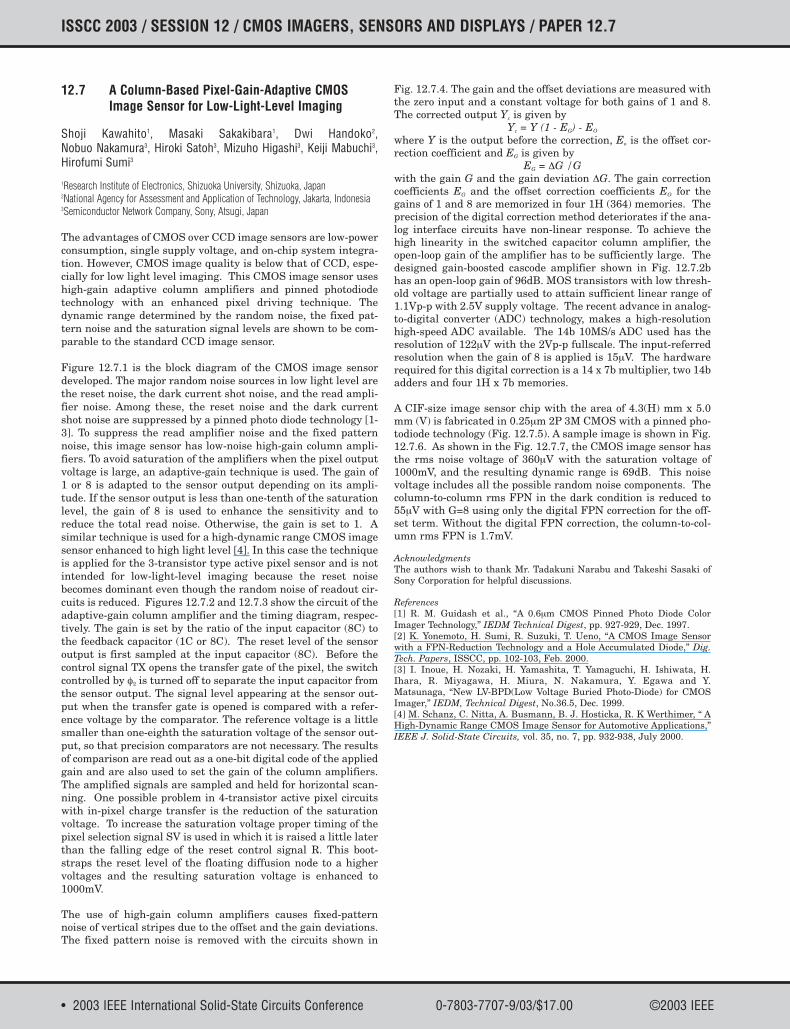
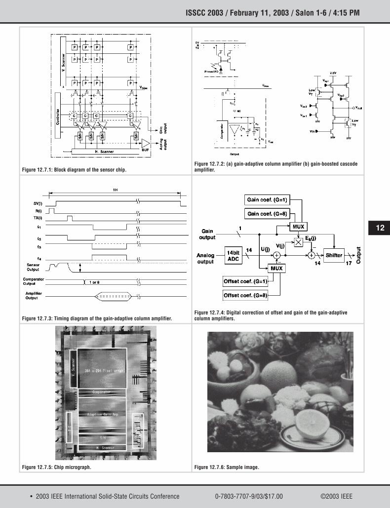
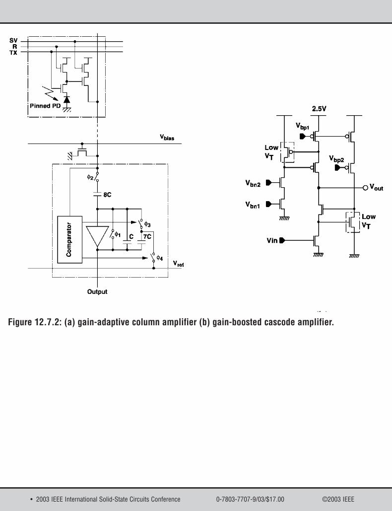
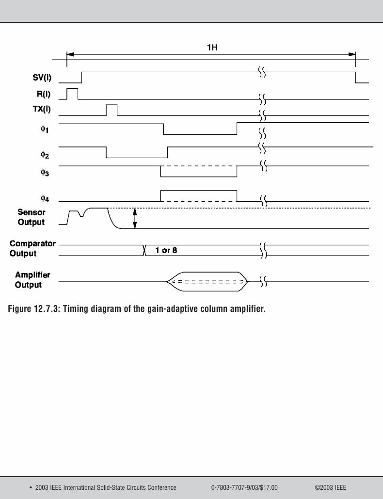
Figure 12.7.1 is the block diagram of the CMOS image sensordeveloped. The major random noise sources in low light level arethe reset noise, the dark current shot noise, and the read ampli-fier noise. Among these, the reset noise and the dark currentshot noise are suppressed by a pinned photo diode technology [1-3]. To suppress the read amplifier noise and the fixed patternnoise, this image sensor has low-noise high-gain column ampli-fiers. To avoid saturation of the amplifiers when the pixel outputvoltage is large, an adaptive-gain technique is used. The gain of1 or 8 is adapted to the sensor output depending on its ampli-tude. If the sensor output is less than one-tenth of the saturationlevel, the gain of 8 is used to enhance the sensitivity and toreduce the total read noise. Otherwise, the gain is set to 1. Asimilar technique is used for a high-dynamic range CMOS imagesensor enhanced to high light level [4]. In this case the techniqueis applied for the 3-transistor type active pixel sensor and is notintended for low-light-level imaging because the reset noisebecomes dominant even though the random noise of readout cir-cuits is reduced. Figures 12.7.2 and 12.7.3 show the circuit of theadaptive-gain column amplifier and the timing diagram, respec-tively. The gain is set by the ratio of the input capacitor (8C) tothe feedback capacitor (1C or 8C). The reset level of the sensoroutput is first sampled at the input capacitor (8C). Before thecontrol signal TX opens the transfer gate of the pixel, the switchcontrolled by φ2 is turned off to separate the input capacitor fromthe sensor output. The signal level appearing at the sensor out-put when the transfer gate is opened is compared with a refer-ence voltage by the comparator. The reference voltage is a littlesmaller than one-eighth the saturation voltage of the sensor out-put, so that precision comparators are not necessary. The resultsof comparison are read out as a one-bit digital code of the appliedgain and are also used to set the gain of the column amplifiers.The amplified signals are sampled and held for horizontal scan-ning. One possible problem in 4-transistor active pixel circuitswith in-pixel charge transfer is the reduction of the saturationvoltage. To increase the saturation voltage proper timing of thepixel selection signal SV is used in which it is raised a little laterthan the falling edge of the reset control signal R. This boot-straps the reset level of the floating diffusion node to a highervoltages and the resulting saturation voltage is enhanced to1000mV.
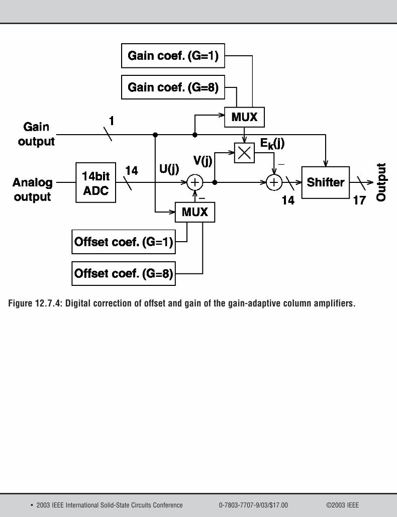
The use of high-gain column amplifiers causes fixed-patternnoise of vertical stripes due to the offset and the gain deviations.The fixed pattern noise is removed with the circuits shown in
Fig. 12.7.4. The gain and the offset deviations are measured withthe zero input and a constant voltage for both gains of 1 and 8.The corrected output Yc is given by
Yc = Y (1 - EG) - EO
where Y is the output before the correction, Eo is the offset cor-rection coefficient and EG is given by
EG = ∆G /Gwith the gain G and the gain deviation ∆G. The gain correctioncoefficients EG and the offset correction coefficients EO for thegains of 1 and 8 are memorized in four 1H (364) memories. Theprecision of the digital correction method deteriorates if the ana-log interface circuits have non-linear response. To achieve thehigh linearity in the switched capacitor column amplifier, theopen-loop gain of the amplifier has to be sufficiently large. Thedesigned gain-boosted cascode amplifier shown in Fig. 12.7.2bhas an open-loop gain of 96dB. MOS transistors with low thresh-old voltage are partially used to attain sufficient linear range of1.1Vp-p with 2.5V supply voltage. The recent advance in analog-to-digital converter (ADC) technology, makes a high-resolutionhigh-speed ADC available. The 14b 10MS/s ADC used has theresolution of 122µV with the 2Vp-p fullscale. The input-referredresolution when the gain of 8 is applied is 15µV. The hardwarerequired for this digital correction is a 14 x 7b multiplier, two 14badders and four 1H x 7b memories.
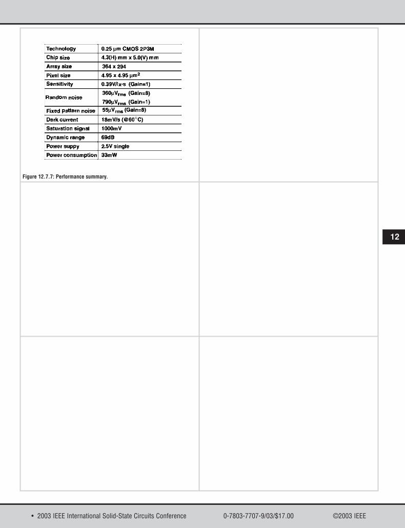
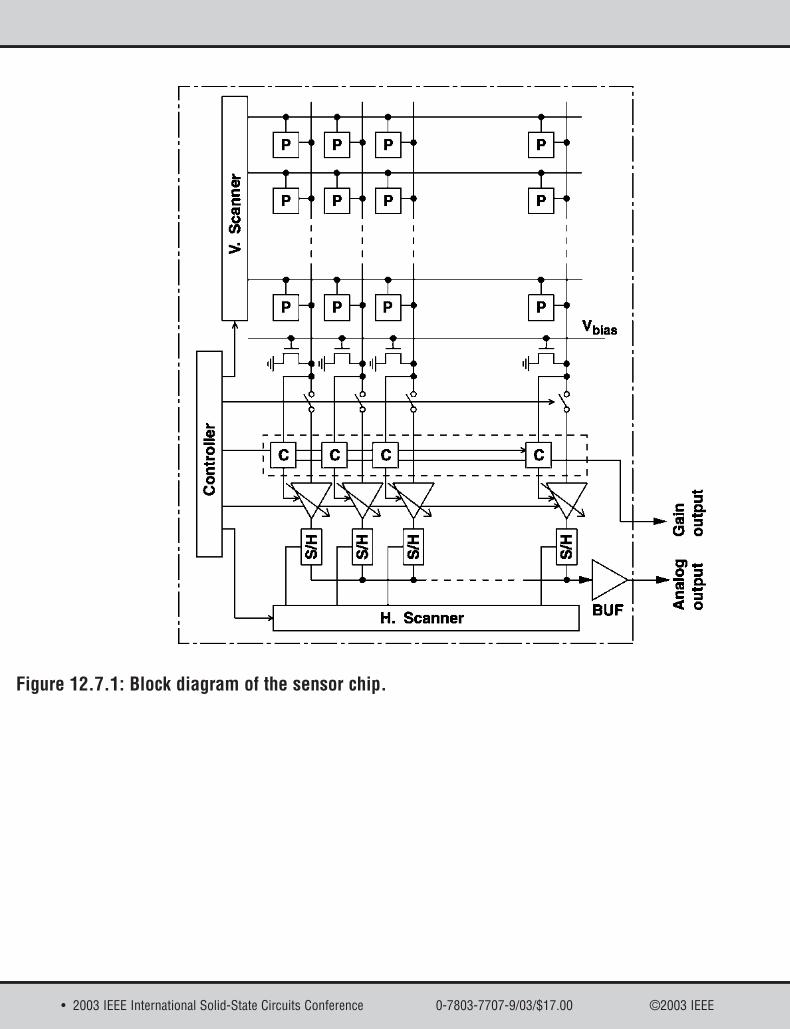
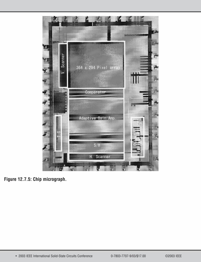
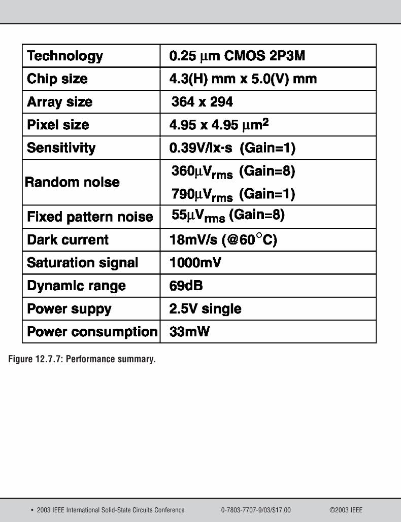
A CIF-size image sensor chip with the area of 4.3(H) mm x 5.0mm (V) is fabricated in 0.25µm 2P 3M CMOS with a pinned pho-todiode technology (Fig. 12.7.5). A sample image is shown in Fig.12.7.6. As shown in the Fig. 12.7.7, the CMOS image sensor hasthe rms noise voltage of 360µV with the saturation voltage of1000mV, and the resulting dynamic range is 69dB. This noisevoltage includes all the possible random noise components. Thecolumn-to-column rms FPN in the dark condition is reduced to55µV with G=8 using only the digital FPN correction for the off-set term. Without the digital FPN correction, the column-to-col-umn rms FPN is 1.7mV.
AcknowledgmentsThe authors wish to thank Mr. Tadakuni Narabu and Takeshi Sasaki ofSony Corporation for helpful discussions.
References[1] R. M. Guidash et al., “A 0.6µm CMOS Pinned Photo Diode ColorImager Technology,” IEDM Technical Digest, pp. 927-929, Dec. 1997. [2] K. Yonemoto, H. Sumi, R. Suzuki, T. Ueno, “A CMOS Image Sensorwith a FPN-Reduction Technology and a Hole Accumulated Diode,” Dig.Tech. Papers, ISSCC, pp. 102-103, Feb. 2000. [3] I. Inoue, H. Nozaki, H. Yamashita, T. Yamaguchi, H. Ishiwata, H.Ihara, R. Miyagawa, H. Miura, N. Nakamura, Y. Egawa and Y.Matsunaga, “New LV-BPD(Low Voltage Buried Photo-Diode) for CMOSImager,” IEDM, Technical Digest, No.36.5, Dec. 1999.[4] M. Schanz, C. Nitta, A. Busmann, B. J. Hosticka, R. K Werthimer, “ AHigh-Dynamic Range CMOS Image Sensor for Automotive Applications,”IEEE J. Solid-State Circuits, vol. 35, no. 7, pp. 932-938, July 2000.
• 2003 IEEE International Solid-State Circuits Conference 0-7803-7707-9/03/$17.00 ©2003 IEEE
ISSCC 2003 / February 11, 2003 / Salon 1-6 / 4:15 PM
12
Figure 12.7.1: Block diagram of the sensor chip.
Figure 12.7.3: Timing diagram of the gain-adaptive column amplifier.
Figure 12.7.5: Chip micrograph. Figure 12.7.6: Sample image.
���
Figure 12.7.4: Digital correction of offset and gain of the gain-adaptivecolumn amplifiers.
Figure 12.7.2: (a) gain-adaptive column amplifier (b) gain-boosted cascodeamplifier.
• 2003 IEEE International Solid-State Circuits Conference 0-7803-7707-9/03/$17.00 ©2003 IEEE
12
• 2003 IEEE International Solid-State Circuits Conference 0-7803-7707-9/03/$17.00 ©2003 IEEE
Figure 12.7.7: Performance summary.
• 2003 IEEE International Solid-State Circuits Conference 0-7803-7707-9/03/$17.00 ©2003 IEEE
Figure 12.7.1: Block diagram of the sensor chip.
• 2003 IEEE International Solid-State Circuits Conference 0-7803-7707-9/03/$17.00 ©2003 IEEE
���Figure 12.7.2: (a) gain-adaptive column amplifier (b) gain-boosted cascode amplifier.
• 2003 IEEE International Solid-State Circuits Conference 0-7803-7707-9/03/$17.00 ©2003 IEEE
Figure 12.7.3: Timing diagram of the gain-adaptive column amplifier.
• 2003 IEEE International Solid-State Circuits Conference 0-7803-7707-9/03/$17.00 ©2003 IEEE
Figure 12.7.4: Digital correction of offset and gain of the gain-adaptive column amplifiers.
• 2003 IEEE International Solid-State Circuits Conference 0-7803-7707-9/03/$17.00 ©2003 IEEE
Figure 12.7.5: Chip micrograph.

• 2003 IEEE International Solid-State Circuits Conference 0-7803-7707-9/03/$17.00 ©2003 IEEE
Figure 12.7.6: Sample image.
• 2003 IEEE International Solid-State Circuits Conference 0-7803-7707-9/03/$17.00 ©2003 IEEE
Figure 12.7.7: Performance summary.