Off-line signature recognition using morphological pixel variance analysis
Layout techniques to enhance the radiation tolerance of standard CMOS technologies demonstrated on a...
12
* Corresponding author. E-mail address: walter.snoeys@cern.ch (W. Snoeys) 1 Now with Philips, Eindhoven, The Netherlands. 2 Now with Motorola, Geneva, Switzerland. 3 Now with Stanford University, Stanford, CA, USA. Nuclear Instruments and Methods in Physics Research A 439 (2000) 349}360 Layout techniques to enhance the radiation tolerance of standard CMOS technologies demonstrated on a pixel detector readout chip W. Snoeys!,*, F. Faccio!, M. Burns!, M. Campbell!, E. Cantatore!, N. Carrer", L. Casagrande#, A. Cavagnoli $, C. Dachs%,1, S. Di Liberto$, F. Formenti!, A. Giraldo!,", E.H.M. Heijne!, P. Jarron!, M. Letheren!, A. Marchioro!, P. Martinengo!, F. Meddi$, B. Mikulec!, M. Morando", M. Morel!, E. Noah!, A. Paccagnella", I. Ropotar!, S. Saladino!,&, W. Sansen', F. Santopietro$, F. Scarlassara", G.F. Segato", P.M. Signe!,2, F. Soramel", L. Vannucci), K. Vleugels!,',3 !EP Division, MIC Group, CERN, 1211 Geneva 23, Switzerland "University and INFN Padova, Italy #LIP, Lisboa, Portugal $University La Sapienza and INFN Rome, Italy %University of Montpellier II, Montpellier, France &University and INFN Bari, Italy 'Katholieke Universiteit Leuven, Leuven, Belgium )INFN Legnaro, Italy Abstract A new pixel readout prototype has been developed at CERN for high-energy physics applications. This full mixed mode circuit has been implemented in a commercial 0.5 lm CMOS technology. Its radiation tolerance has been enhanced by designing all NMOS transistors in enclosed geometry and introducing guardrings wherever necessary. The technique is explained and its e!ectiveness demonstrated on various irradiation measurements on individual transistors and on the prototype. Circuit performance started to degrade only after a total dose of 600 krad}1.7 Mrad depending on the type of radiation. 10 keV X-rays, 60Co gamma-rays, 6.5 MeV protons, and minimum ionizing particles were used. Implications of this layout approach on the circuit design and perspectives for even deeper submicron technologies are discussed. ( 2000 Elsevier Science B.V. All rights reserved. 0168-9002/00/$ - see front matter ( 2000 Elsevier Science B.V. All rights reserved. PII: S 0 1 6 8 - 9 0 0 2 ( 9 9 ) 0 0 8 9 9 - 2 III. READOUT ELECTRONICS . . .
Transcript of Layout techniques to enhance the radiation tolerance of standard CMOS technologies demonstrated on a...
*Corresponding author.E-mail address: [email protected] (W. Snoeys)1Now with Philips, Eindhoven, The Netherlands.2Now with Motorola, Geneva, Switzerland.3Now with Stanford University, Stanford, CA, USA.
Nuclear Instruments and Methods in Physics Research A 439 (2000) 349}360
Layout techniques to enhance the radiation toleranceof standard CMOS technologies demonstrated
on a pixel detector readout chip
W. Snoeys!,*, F. Faccio!, M. Burns!, M. Campbell!, E. Cantatore!, N. Carrer",L. Casagrande#, A. Cavagnoli$, C. Dachs%,1, S. Di Liberto$, F. Formenti!,A. Giraldo!,", E.H.M. Heijne!, P. Jarron!, M. Letheren!, A. Marchioro!,
P. Martinengo!, F. Meddi$, B. Mikulec!, M. Morando", M. Morel!, E. Noah!,A. Paccagnella", I. Ropotar!, S. Saladino!,&, W. Sansen', F. Santopietro$,
F. Scarlassara", G.F. Segato", P.M. Signe!,2, F. Soramel",L. Vannucci), K. Vleugels!,',3
!EP Division, MIC Group, CERN, 1211 Geneva 23, Switzerland"University and INFN Padova, Italy
#LIP, Lisboa, Portugal$University La Sapienza and INFN Rome, Italy
%University of Montpellier II, Montpellier, France&University and INFN Bari, Italy
'Katholieke Universiteit Leuven, Leuven, Belgium)INFN Legnaro, Italy
Abstract
A new pixel readout prototype has been developed at CERN for high-energy physics applications. This full mixedmode circuit has been implemented in a commercial 0.5 lm CMOS technology. Its radiation tolerance has beenenhanced by designing all NMOS transistors in enclosed geometry and introducing guardrings wherever necessary. Thetechnique is explained and its e!ectiveness demonstrated on various irradiation measurements on individual transistorsand on the prototype. Circuit performance started to degrade only after a total dose of 600 krad}1.7 Mrad depending onthe type of radiation. 10 keV X-rays, 60Co gamma-rays, 6.5 MeV protons, and minimum ionizing particles were used.Implications of this layout approach on the circuit design and perspectives for even deeper submicron technologies arediscussed. ( 2000 Elsevier Science B.V. All rights reserved.
0168-9002/00/$ - see front matter ( 2000 Elsevier Science B.V. All rights reserved.PII: S 0 1 6 8 - 9 0 0 2 ( 9 9 ) 0 0 8 9 9 - 2 III. READOUT ELECTRONICS . . .
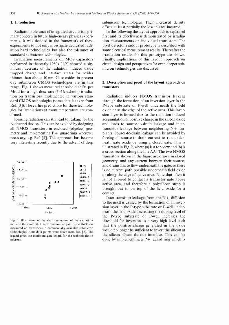
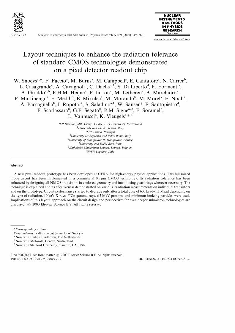
Fig. 1. Illustration of the sharp reduction of the radiation-induced threshold shift as a function of gate oxide thicknessmeasured on transistors in commercially available submicrontechnologies. Four data points were taken from Ref. [3]. Thelegend gives the minimum gate length for the technologies inmicrons.
1. Introduction
Radiation tolerance of integrated circuits is a pri-mary concern in future high-energy physics experi-ments. It was decided in the framework of theseexperiments to not only investigate dedicated radi-ation hard technologies, but also the tolerance ofstandard submicron technologies.
Irradiation measurements on MOS capacitorsperformed in the early 1980s [1,2] showed a sig-ni"cant decrease of the radiation induced oxidetrapped charge and interface states for oxidesthinner than about 10 nm. Gate oxides in presentday submicron CMOS technologies are in thisrange. Fig. 1 shows measured threshold shifts perMrad for a high dose-rate (3}4 krad/min) irradia-tion on transistors implemented in various stan-dard CMOS technologies (some data is taken fromRef. [3]). The earlier predictions for these technolo-gies for irradiations at room temperature are con-"rmed.
Ionizing radiation can still lead to leakage for theN-channel devices. This can be avoided by designingall NMOS transistors in enclosed (edgeless) geo-metry and implementing P# guardrings wherevernecessary, e.g. Ref. [4]. This approach has becomevery interesting recently due to the advent of deep
submicron technologies. Their increased densityo!sets at least partially the loss in area incurred.
In the following the layout approach is explained"rst and its e!ectiveness demonstrated by irradia-tion measurements on individual transistors. Thepixel detector readout prototype is described withsome electrical measurement results. Thereafter theirradiation results for this prototype are shown.Finally, implications of this layout approach oncircuit design and perspectives for even deeper sub-micron technologies are discussed.
2. Description and proof of the layout approach on
transistors
Radiation induces NMOS transistor leakagethrough the formation of an inversion layer in theP-type substrate or P-well underneath the "eldoxide or at the edge of the active area. This inver-sion layer is formed due to the radiation-inducedaccumulation of positive charge in the silicon oxideand leads to source-to-drain leakage and inter-transistor leakage between neighboring N# im-plants. Source-to-drain leakage can be avoided byforcing all source-to-drain current to run under-neath gate oxide by using a closed gate. This isillustrated in Fig. 2, where (a) is a top view and (b) isa cross-section along the line AA@. The two NMOStransistors shown in the "gure are drawn in closedgeometry, and any current between their sourcesand drains has to #ow underneath the gate, so thereis no current path possible underneath "eld oxideor along the edge of active area. Note that often itis not allowed to contact a transistor gate aboveactive area, and therefore a polysilicon strap isbrought out to on top of the "eld oxide for acontact.
Inter-transistor leakage (from one N# di!usionto the next) is caused by the formation of an inver-sion layer in the P-type substrate or P-well under-neath the "eld oxide. Increasing the doping level ofthe P-type substrate or P-well increases thethreshold for inversion to a very high level suchthat the positive charge generated in the oxidewould no longer be su$cient to invert the silicon atthe silicon}silicon dioxide interface. This can bedone by implementing a P# guard ring which is
350 W. Snoeys et al. / Nuclear Instruments and Methods in Physics Research A 439 (2000) 349}360
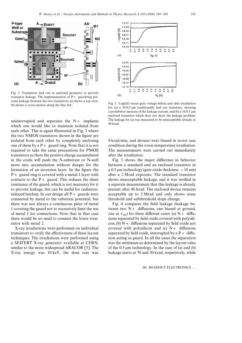
Fig. 2. Transistors laid out in enclosed geometry to preventtransistor leakage. The implementation of P# guardring pre-vents leakage between the two transistors: (a) shows a top view;(b) shows a cross-section along the line AA@. Fig. 3. Log(Id) versus gate voltage before and after irradiation
for: (a) a 10/0.5 lm traditionally laid out transistor, showinga prohibitive increase of the leakage current, and (b) a 10/0.5 lmenclosed transistor which does not show the leakage problem.The leakage for (a) was measured to be unacceptable already at40 krad.
uninterrupted and separates the N# implantswhich one would like to maintain isolated fromeach other. This is again illustrated in Fig. 2 wherethe two NMOS transistors shown in the "gure areisolated from each other by completely enclosingone of them by a P# guard ring. Note that it is notrequired to take the same precautions for PMOStransistors as there the positive charge accumulatedin the oxide will push the N-substrate or N-wellmore into accumulation without danger for theformation of an inversion layer. In the "gure theP# guard ring is covered with a metal 1 layer withcontacts to the P# guard. This reduces the sheetresistance of the guard, which is not necessary for itto prevent leakage, but can be useful for radiation-induced latchup. In our design all P# guards wereconnected by metal to the substrate potential, butthere was not always a continuous piece of metal1 covering the guard not to excessively limit the useof metal 1 for connections. Note that in that casethere would be no need to connect the lower tran-sistor with metal 2.
X-ray irradiations were performed on individualtransistors to verify the e!ectiveness of these layouttechniques. The irradiations were performed usinga SEIFERT X-ray generator available at CERN,similar to the more widespread ARACOR [5]. TheX-ray energy was 10 keV, the dose rate was
4 krad/min, and devices were biased in worst casecondition during the room temperature irradiation.The measurements were carried out immediatelyafter the irradiation.
Fig. 3 shows the major di!erence in behaviorbetween a standard and an enclosed transistor ina 0.5 lm technology (gate oxide thickness &10 nm)after a 2 Mrad exposure. The standard transistorshows unacceptable leakage, and it was veri"ed ina separate measurement that this leakage is alreadypresent after 40 krad. The enclosed device remainsacceptable up to 2 Mrad and only shows somethreshold and subthreshold slope change.
Fig. 4 compares the "eld leakage (leakage be-tween two N# di!usions, one biased at ground,one at <
$$) for three di!erent cases: (a) N# di!u-
sions separated by "eld oxide covered with polysili-con, (b) N# di!usions separated by "eld oxide notcovered with polysilicon and (c) N# di!usionsseparated by "eld oxide, interrupted by a P# di!u-sion acting as guard. In all the cases the separationwas the minimum as determined by the layout rulesof the 0.5 lm technology. In the case of (a) and (b)leakage starts at 70 and 30 krad, respectively, while
W. Snoeys et al. / Nuclear Instruments and Methods in Physics Research A 439 (2000) 349}360 351
III. READOUT ELECTRONICS . . .
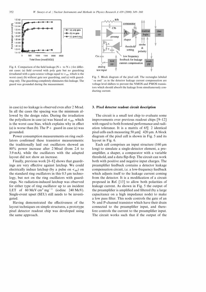
Fig. 4. Comparison of the "eld leakage (N# to N#) for di!er-ent cases: (a) "eld covered with poly gate but no guardring(irradiated with a gate-source voltage equal to <
$$, which is the
worst case); (b) without gate nor guardring, and (c) with guard-ring only. The guardring completely eliminates this leakage. Theguard was grounded during the measurement.
Fig. 5. Block diagram of the pixel cell. The rectangles labeled`xa and `ya in the detector leakage current compensation arevoltage level shifters to prevent the NMOS and PMOS transis-tors which should absorb the leakage from simultaneously con-ducting current.
in case (c) no leakage is observed even after 2 Mrad.In all the cases the spacing was the minimum al-lowed by the design rules. During the irradiationthe polysilicon in case (a) was biased at <
$$, which
is the worst case bias, which explains why in e!ect(a) is worse than (b). The P# guard in case (c) wasgrounded.
Power consumption measurements on ring oscil-lators con"rmed these transistor measurements:the traditionally laid out oscillators showed an80% power increase after 2 Mrad (from 2.4 to3.9 mA), while the oscillators with the adaptedlayout did not show an increase.
Finally, previous work [6}8] shows that guardr-ings are very e!ective against latchup. We couldelectrically induce latchup (by a pulse on <
$$) on
the standard ring oscillators in this 0.5 lm techno-logy, but not on the ring oscillators with guard-rings. No radiation-induced latchup was observedfor either type of ring oscillator up to an incidentLET of 60 MeV cm2 mg~1 (iodine 240 MeV).Single-event upset (SEU) still needs to be investi-gated.
Having demonstrated the e!ectiveness of thelayout techniques on simple structures, a prototypepixel detector readout chip was developed usingthe same approach.
3. Pixel detector readout circuit description
The circuit is a small test chip to evaluate someimprovements over previous readout chips [9}12]with regard to both frontend performance and radi-ation tolerance. It is a matrix of 65] 2 identicalpixel cells each measuring 50 lm] 420 lm. A blockdiagram of the pixel cell is shown in Fig. 5 and itslayout in Fig. 6.
Each cell comprises an input structure (160 lmlong) to simulate a single-detector element, a pre-ampli"er, a shaper, a comparator with a variablethreshold, and a data #ip-#op. The circuit can workboth with positive and negative input charges. Thepreampli"er feedback contains a detector leakagecompensation circuit, i.e. a low-frequency feedbackwhich adjusts itself to the leakage current comingfrom the detector. It is a modi"cation of a circuitproposed in Ref. [13] to allow both polarities ofleakage current. As shown in Fig. 5 the output ofthe preampli"er is ampli"ed and "ltered (by a largecapacitance on a high impedance node) to makea low pass "lter. This node controls the gate of anN- and P-channel transistor which have their drainconnected to the preampli"er input, and there-fore controls the current to the preampli"er input.The circuit works such that if the output of the
352 W. Snoeys et al. / Nuclear Instruments and Methods in Physics Research A 439 (2000) 349}360

Fig. 6. Layout of one cell consisting of an input structure simulating detector capacitance and leakage current of about 160 lm long (tothe left of the "gure), and the pixel cell itself, which measures about 420 lm] 50 lm long. A very large currentmirror of three NMOS devices in enclosed geometry (about 100 by 35 lm) is visible towards the right of the "gure in the center of thepixel cell (see Fig. 7).
Fig. 7. Diagram of the shaper circuit. The transfer function ofthe shaper (i
065/v
*/) is !g
.q4(1#q
4)~2. The shaper output
current is presented to a current comparator. The comparatorthreshold is dependent on the accuracy of the current sources.The NMOS current mirror had to be made very large foraccuracy (see Fig. 6).
preampli"er starts to drift due to a change in de-tector leakage current, the voltage on the highimpedance node will change, and the current in theN- and P-channel devices will change to absorbthe change in leakage current. This scheme has theadvantage that not all detector leakage current hasto pass through the feedback resistor. In the orig-inal scheme only the NMOS was implemented toabsorb only one sign of leakage current. Here weimplemented a PMOS transistor as well to alsoabsorb the other sign of leakage current. In thedesign voltage level shifters (source followers, whichare schematically represented in Fig. 5 by squareblocks, labeled `xa and `ya) have been includedbetween the high impedance node and the gates ofthe N- and P-channel devices to guarantee thatboth devices cannot conduct current simulta-neously as it would be detrimental for the parallelnoise. Note also that to minimize the parallel noiseit is desirable to use long and narrow devices toabsorb the leakage current. This was done for thePMOS, but was unfortunately not possible for theNMOS which had to be designed in closed ge-ometry (see also Sections 4 and 6).
To minimize the noise contribution of large de-tector leakage currents the shaping time of the"rst-order semi-Gaussian shaper was reduced to23 ns. The schematic of the shaper "lter is illus-trated in Fig. 7. The transfer function of the shaperis !g
.q4(1#q
4)~2, where the di!erentiation
q4(1#q
4)~1 is realized by the input transistor of the
shaper and the capacitance at its source, andthe second pole is associated with the drain of theshaper input transistor. The shaper output currentis presented to a current comparator. The com-parator threshold is dependent on the accuracy of
the current sources. The lower current source isimplemented by a large NMOS current mirror alsovisible in the layout in Fig. 6: it takes about35] 105 lm2.
The contents of the test #ip-#op determineswhether or not an analog input signal is appliedto the preampli"er input across an injection capaci-tance. Changing the test #ip-#op pattern allows toaddress one or several pixels simultaneously in anarbitrary way during testing. A mask #ip-#opallows to disable a pixel should it be noisy orcompletely non-functional. If the comparator out-put changes polarity when the strobe or triggersignal is high a one is written into the data #ip-#op(a #ag tells the readout logic which polarity of thecomparator output corresponds to a logic one,
W. Snoeys et al. / Nuclear Instruments and Methods in Physics Research A 439 (2000) 349}360 353
III. READOUT ELECTRONICS . . .
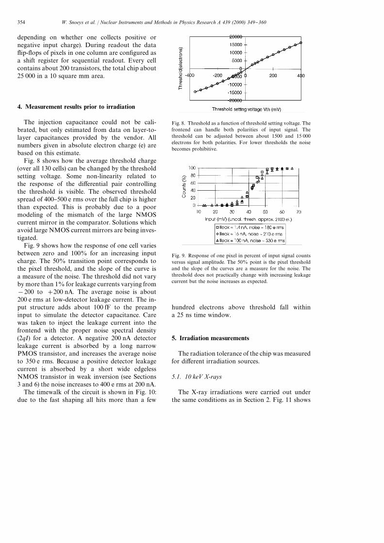
Fig. 8. Threshold as a function of threshold setting voltage. Thefrontend can handle both polarities of input signal. Thethreshold can be adjusted between about 1500 and 15 000electrons for both polarities. For lower thresholds the noisebecomes prohibitive.
Fig. 9. Response of one pixel in percent of input signal countsversus signal amplitude. The 50% point is the pixel thresholdand the slope of the curves are a measure for the noise. Thethreshold does not practically change with increasing leakagecurrent but the noise increases as expected.
depending on whether one collects positive ornegative input charge). During readout the data#ip-#ops of pixels in one column are con"gured asa shift register for sequential readout. Every cellcontains about 200 transistors, the total chip about25 000 in a 10 square mm area.
4. Measurement results prior to irradiation
The injection capacitance could not be cali-brated, but only estimated from data on layer-to-layer capacitances provided by the vendor. Allnumbers given in absolute electron charge (e) arebased on this estimate.
Fig. 8 shows how the average threshold charge(over all 130 cells) can be changed by the thresholdsetting voltage. Some non-linearity related tothe response of the di!erential pair controllingthe threshold is visible. The observed thresholdspread of 400}500 e rms over the full chip is higherthan expected. This is probably due to a poormodeling of the mismatch of the large NMOScurrent mirror in the comparator. Solutions whichavoid large NMOS current mirrors are being inves-tigated.
Fig. 9 shows how the response of one cell variesbetween zero and 100% for an increasing inputcharge. The 50% transition point corresponds tothe pixel threshold, and the slope of the curve isa measure of the noise. The threshold did not varyby more than 1% for leakage currents varying from!200 to #200 nA. The average noise is about200 e rms at low-detector leakage current. The in-put structure adds about 100 fF to the preampinput to simulate the detector capacitance. Carewas taken to inject the leakage current into thefrontend with the proper noise spectral density(2qI) for a detector. A negative 200 nA detectorleakage current is absorbed by a long narrowPMOS transistor, and increases the average noiseto 350 e rms. Because a positive detector leakagecurrent is absorbed by a short wide edgelessNMOS transistor in weak inversion (see Sections3 and 6) the noise increases to 400 e rms at 200 nA.
The timewalk of the circuit is shown in Fig. 10:due to the fast shaping all hits more than a few
hundred electrons above threshold fall withina 25 ns time window.
5. Irradiation measurements
The radiation tolerance of the chip was measuredfor di!erent irradiation sources.
5.1. 10 keV X-rays
The X-ray irradiations were carried out underthe same conditions as in Section 2. Fig. 11 shows
354 W. Snoeys et al. / Nuclear Instruments and Methods in Physics Research A 439 (2000) 349}360
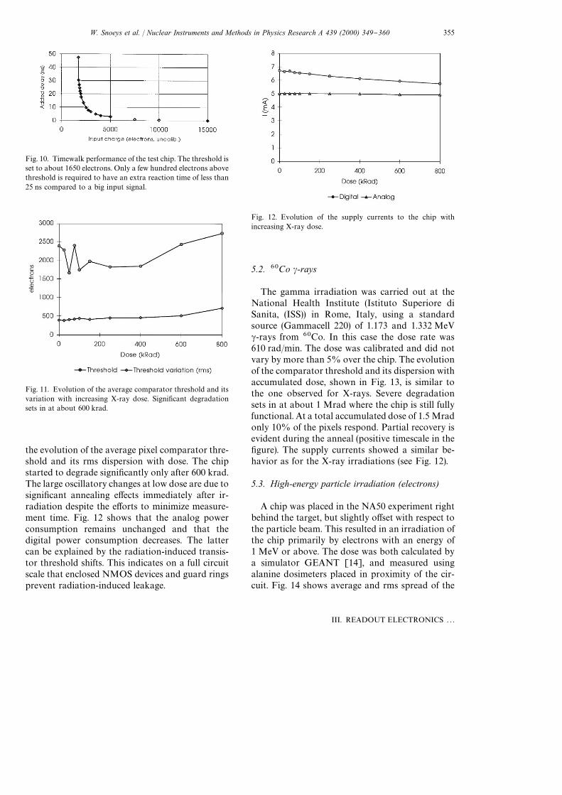
Fig. 10. Timewalk performance of the test chip. The threshold isset to about 1650 electrons. Only a few hundred electrons abovethreshold is required to have an extra reaction time of less than25 ns compared to a big input signal.
Fig. 11. Evolution of the average comparator threshold and itsvariation with increasing X-ray dose. Signi"cant degradationsets in at about 600 krad.
Fig. 12. Evolution of the supply currents to the chip withincreasing X-ray dose.
the evolution of the average pixel comparator thre-shold and its rms dispersion with dose. The chipstarted to degrade signi"cantly only after 600 krad.The large oscillatory changes at low dose are due tosigni"cant annealing e!ects immediately after ir-radiation despite the e!orts to minimize measure-ment time. Fig. 12 shows that the analog powerconsumption remains unchanged and that thedigital power consumption decreases. The lattercan be explained by the radiation-induced transis-tor threshold shifts. This indicates on a full circuitscale that enclosed NMOS devices and guard ringsprevent radiation-induced leakage.
5.2. 60Co c-rays
The gamma irradiation was carried out at theNational Health Institute (Istituto Superiore diSanita, (ISS)) in Rome, Italy, using a standardsource (Gammacell 220) of 1.173 and 1.332 MeVc-rays from 60Co. In this case the dose rate was610 rad/min. The dose was calibrated and did notvary by more than 5% over the chip. The evolutionof the comparator threshold and its dispersion withaccumulated dose, shown in Fig. 13, is similar tothe one observed for X-rays. Severe degradationsets in at about 1 Mrad where the chip is still fullyfunctional. At a total accumulated dose of 1.5 Mradonly 10% of the pixels respond. Partial recovery isevident during the anneal (positive timescale in the"gure). The supply currents showed a similar be-havior as for the X-ray irradiations (see Fig. 12).
5.3. High-energy particle irradiation (electrons)
A chip was placed in the NA50 experiment rightbehind the target, but slightly o!set with respect tothe particle beam. This resulted in an irradiation ofthe chip primarily by electrons with an energy of1 MeV or above. The dose was both calculated bya simulator GEANT [14], and measured usingalanine dosimeters placed in proximity of the cir-cuit. Fig. 14 shows average and rms spread of the
W. Snoeys et al. / Nuclear Instruments and Methods in Physics Research A 439 (2000) 349}360 355
III. READOUT ELECTRONICS . . .

Fig. 13. Irradiations with 60Co: (a) The discriminator thresholdvalue and its dispersion during the irradiations are reported asa function of the cumulated dose. (b) The same information isnow reported as a function of time. The time equal to zero corre-sponds to the end of the irradiation or the beginning of theanneal.
Fig. 14. Irradiation in the NA50 experiment (mainly electrons):evolution of (a) average and spread of pixel threshold, (b) aver-age and spread of pixel noise, and (c) number of pixels respon-ding to an input signal below 20 000 electrons as a function ofirradiation dose. After 52 h, corresponding to about 1.7 Mrad,the chip starts to degrade signi"cantly. After 43 h the beam waso! for a couple of hours and some recovery is evident.
threshold and noise, average and rms noise, as wellas the number of pixels responding below 20 000electrons. The drop in the number of respondingpixels from 130 to 126 and the rise back to 130 is anartifact due to the timing problem in the experi-mental setup. The drop to zero after 55 h is real.The degradation after 1.7 Mrad (52 h) is evident,some recovery can be observed immediately after43 h when the beam was o! for a couple of hours.The irradiation was continued up to 2.6 Mrads wellbeyond the moment when no pixels were respon-ding below 20 000 electrons. Fig. 15 shows theannealing under bias: after one week at room tem-perature some pixels start to respond again. Aftera month at room temperature the average thre-shold has come down again to about 7500 elec-
trons, and the average noise to about 500 electrons.The last week of annealing was carried out at 1003Cand caused the threshold to drop to about 5000electrons.
5.4. 6.5 MeV protons
The tolerance to charged hadronic particles wasinvestigated using 6.5 MeV protons at the Van deGraa! accelerator in the National Laboratory ofLegnaro, Italy. The dose was calibrated and did notvary by more than 10% over the chip area. Thecombination of the proton #ux with the energy losson the chip (for electromagnetic processes only)[15] is used to evaluate the total dose. We onlyquote the dose corresponding to the Rutherfordpeak, the background contribution is estimated tobe about 20% of the dose quoted. The estimateddose rate is about 12 krad/min. Fig. 16 shows theevolution of average and dispersion of the pixelthreshold. Serious degradation occurs above1 Mrad and partial recovery is evident again during
356 W. Snoeys et al. / Nuclear Instruments and Methods in Physics Research A 439 (2000) 349}360
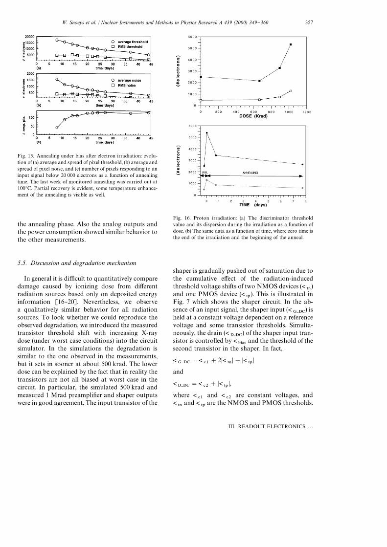
Fig. 15. Annealing under bias after electron irradiation: evolu-tion of (a) average and spread of pixel threshold, (b) average andspread of pixel noise, and (c) number of pixels responding to aninput signal below 20 000 electrons as a function of annealingtime. The last week of monitored annealing was carried out at1003C. Partial recovery is evident, some temperature enhance-ment of the annealing is visible as well.
Fig. 16. Proton irradiation: (a) The discriminator thresholdvalue and its dispersion during the irradiation as a function ofdose. (b) The same data as a function of time, where zero time isthe end of the irradiation and the beginning of the anneal.
the annealing phase. Also the analog outputs andthe power consumption showed similar behavior tothe other measurements.
5.5. Discussion and degradation mechanism
In general it is di$cult to quantitatively comparedamage caused by ionizing dose from di!erentradiation sources based only on deposited energyinformation [16}20]. Nevertheless, we observea qualitatively similar behavior for all radiationsources. To look whether we could reproduce theobserved degradation, we introduced the measuredtransistor threshold shift with increasing X-raydose (under worst case conditions) into the circuitsimulator. In the simulations the degradation issimilar to the one observed in the measurements,but it sets in sooner at about 500 krad. The lowerdose can be explained by the fact that in reality thetransistors are not all biased at worst case in thecircuit. In particular, the simulated 500 krad andmeasured 1 Mrad preampli"er and shaper outputswere in good agreement. The input transistor of the
shaper is gradually pushed out of saturation due tothe cumulative e!ect of the radiation-inducedthreshold voltage shifts of two NMOS devices (<
5/)
and one PMOS device (<51
). This is illustrated inFig. 7 which shows the shaper circuit. In the ab-sence of an input signal, the shaper input (<
G}DC) is
held at a constant voltage dependent on a referencevoltage and some transistor thresholds. Simulta-neously, the drain (<
D}DC) of the shaper input tran-
sistor is controlled by <"*!4
and the threshold of thesecond transistor in the shaper. In fact,
<G}DC
"<#1
#2D<5/
D!D<51
D
and
<D}DC
"<#2
#D<51
D,
where <#1
and <#2
are constant voltages, and<
5/and <
51are the NMOS and PMOS thresholds.
W. Snoeys et al. / Nuclear Instruments and Methods in Physics Research A 439 (2000) 349}360 357
III. READOUT ELECTRONICS . . .

Fig. 17. Schematic view of a transistor in enclosed layout. As-suming a square shape for the equipotential lines in the channela simple expression for the transistor current can be derived.
Therefore, the margin for the shaper inputtransistor to remain in saturation equals:
<G}DC
!<51
!<D}DC
"<G}DC
#D<51
D!<D}DC
"<#1
!<#2
#2D<5/
D!D<51
D.
As D<5/
D decreases and D<51
D increases with increas-ing radiation dose, this margin is gradually de-creased to zero at which point the transistor entersthe linear region. This degrades the shaper gainvery quickly leading to a very high e!ective pixelthreshold and ultimately to a non-functional front-end. The partial recovery can be explained by thefact that the <
5shift of the NMOS transistors
readily anneals out. There is an irreversible e!ectbecause the PMOS <
5-shift is not cured by an
anneal. This was further con"rmed by varying<
"*!4(see Fig. 7): a one-to-one correlation between
the irradiation dose and the margin for the inputtransistor to remain in saturation was found. Infact, one could even recover functionality fordevices which were irradiated just beyond failureby decreasing <
"*!4. However, this could only be
done over a limited range as lowering <"*!4
toomuch created other problems in the circuit. There-fore, beyond a certain dose the failure was irrevers-ible. Note that since the operating margin of thiscircuit depends on some transistor thresholds, ran-dom transistor threshold variations will have a di-rect impact on the dispersion of radiation tolerancebetween di!erent chips.
In conclusion, the use of NMOS devices in en-closed geometry and guardrings brought the totalionizing dose tolerance of this prototype in stan-dard CMOS up to about 0.6}1.7 Mrad dependingon the radiation source. These are much highervalues than for its predecessor LHC1 [9], imple-mented without enclosed transistors and guard-rings, which typically shows excessive leakage andpower consumption after about 30 krad. The fail-ure mechanism is no longer the leakage, but theradiation-induced transistor <
5shifts. This again
points to the promise of deep submicron technolo-gies for this application.
6. Layout for radiation tolerance:
design implications
Fig. 17 shows a schematic view of a transistorlaid out in enclosed geometry. Assuming that theequipotential lines under the gate are square, thecurrent voltage equation for this enclosed devicecan be derived in a similar way as for a traditionaltransistor. The assumption about the square shapeis very crude and far from the truth especially forlarge devices, but it serves to point to some implica-tions of the use of enclosed transistors in a verysimple way. Assuming in addition that the de-pletion depth is constant underneath the channeland that the gradual channel approximation isvalid the following equation for the current I cross-ing the equipotential line holds:
I"8xkC
09(<
'!< (x)!<
T)d< (x)dx
.
Rewriting this in integral form yields
IPW2 @2
W1 @2
dx
x
"8kC
09PV$
V4
(<'!< (x)!<
T) d< (x).
If <$'<
'!<
T, the device is in saturation. An
expression for the drain current can be obtained by
358 W. Snoeys et al. / Nuclear Instruments and Methods in Physics Research A 439 (2000) 349}360

setting <$
to <'!<
Tin the integral. Comparison
with the traditional expressions for the drain cur-rent in both the linear and the saturated case yieldsan &e!ective' = /¸ ratio:
A=¸B%&&
" 8ln(=
2/=
1)
dependent only logarithmically on the transistordimensions. This implies prohibitively large tran-sistor sizes (or large =
2to =
1ratios) are required
to obtain enclosed transistors with a small e!ective= /¸. Therefore accurate NMOS current mirrorsfor low current are impossible to design. Inaddition, our results on pixel threshold dispersionindicate that enclosed transistors exhibit highermismatch than standard devices. More extensivemodeling of enclosed transistors and their match-ing is highly desirable. Moreover, as these circuitsare intended for use in radiation environments, allparameters need to be characterized both beforeand after irradiation. For example, we studied thenoise of PMOS and enclosed NMOS transistors,and its evolution with total dose for several 0.5 lmtechnologies. Only the white noise of the PMOStransistor increases by about 10% after 1 Mrad, its1/f noise remaining unchanged, as well as the wholenoise spectrum of the NMOS.
If circuit topologies relying on accurate NMOScurrent mirrors are avoided, no signi"cant densitypenalty is incurred for analog circuitry. For digitalcircuitry the use of deep submicron technologiescompared to the more coarse traditional radiationtolerant technologies will o!set the area penalty bythe "ner linewidth and the availability of moreinterconnect layers. In fact, for the digital circuitryin the pixel circuit prototype implemented in0.5 lm with enclosed NMOS devices, the areataken is about the same as in the traditionally laidout version of its predecessor, LHC1 [9] (imple-mented in the SACMOS 1 lm technology witha density equivalent to that of a standard 0.6 lmCMOS technology). This is because of the avail-ability of one more metal layer in the 0.5 lmtechnology.
Another important implication is that standardlibraries cannot be used, and that extraction and
veri"cation routines need to be updated for thesedevices.
7. Conclusions
The e!ectiveness of the use of enclosed geometryNMOS devices and guardrings to eliminate radi-ation-induced leakage has been demonstrated onindividual transistors and on a pixel detector circuit.This full-mixed mode circuit was implemented ina standard 0.5 lm CMOS process. Irradiationmeasurements established that the circuit toleratedup to between 600 krad and 1.7 Mrad depending onthe type of radiation. No radiation-induced leakagecurrent was observed, and the circuit failed ultimate-ly because of radiation-induced transistor thresholdshifts. Some implications of these layout techniqueson circuit design were discussed and the need forfurther modeling of enclosed transistors was pointedout. In addition to density and power}speed perfor-mance arguments, the measurements also illustratethe promise of commercial deep submicron tech-nologies for application in radiation environments.
Acknowledgements
We gratefully acknowledge the collaborationand "nancial support of our partners in the RD19,RD49, Alice, and NA50 projects. In particular, wethank Peter Sonderegger for suggesting and help-ing with the on-line irradiation in the P61 beam,and the NA50 team as well as Yannick Lese'ne'chalfor help with installation and data taking. We ac-knowledge the collaboration of the University ofMontpellier, where a 252Cf source irradiation forsingle event latchup took place, and of the Frenchspace agency CNES for giving us access to the IPNTandem accelerator for the other latchup measure-ments. R. Eco!et, from CNES, and S. Duzellier andL. Guibert from ONERA-CERT contributed sig-ni"cantly to these measurements. L. Casagrandewas funded by a European Community fellowshipin the framework of the TMR program under con-tract number ERBFMBICT961204. We would alsolike to thank all the foundries for providing transis-tor samples for this work.
W. Snoeys et al. / Nuclear Instruments and Methods in Physics Research A 439 (2000) 349}360 359
III. READOUT ELECTRONICS . . .
References
[1] N.S. Saks, M.G. Ancona, J.A. Modolo, IEEE Trans. Nucl.Sci. NS-31 (1984) 1249.
[2] N.S. Saks, M.G. Ancona, J.A. Modolo, IEEE Trans. Nucl.Sci. NS-33 (1986) 1185.
[3] R.C. Lacoe et al., Total dose hardness of CMOS commer-cial microelectronics, Presented at 1997 RADECS Confer-ence, Nucl. Instr. and Meth., 1999, to be published.
[4] D.R. Alexander, Design issues for radiation tolerantmicrocircuits for space, short course, Presented at the 1996NSREC Conference, Indian Wells, CA.
[5] J.L. Pakuti, J.J. LePage, IEEE Trans. Nucl. Sci. NS-29(1982) 1832.
[6] T. Aoki, IEEE Trans. El. Dev. ED-35 (1988) 1885.[7] R. Menozzi et al., IEEE Trans. El. Dev. ED-35 (1988) 1988.[8] J.W. Gambles, A path toward low cost rad-tolerant digital
CMOS, Sixth NASA Symposium on VLSI design, 1997.[9] E.H.M. Heijne et al., Nucl. Instr. and Meth. A 383 (1996)
55.
[10] M. Campbell et al., Nucl. Instr. and Meth. A 290 (1990)149.
[11] F. Anghinol" et al., IEEE Trans. Nucl. Sci. NS-39 (1992)654.
[12] M. Campbell et al., Nucl. Instr. and Meth. A 342 (1994) 52.[13] F. Krummenacher, Nucl. Instr. and Meth. A 305 (1991) 527.[14] GEANT Detector Description and Simulation Tool,
CERN Program Library Long Writeup W5013.[15] J.F. Ziegler, Stopping Cross-Section for Energetic Ions in
all Elements, Vol. 5, Pergamon Press, Oxford.[16] R.D. Evans, The Atomic Nucleus, McGraw-Hill, New
York, 1955.[17] T.R. Oldham, J.M. Mcgarrity, IEEE Trans. Nucl. Sci.
NS-30 (1983) 4377.[18] G.J. Brucker et al., IEEE Trans. Nucl. Sci. NS-30 (1983)
4157.[19] G.J. Brucker et al., IEEE Trans. Nucl. Sci. NS-29 (1982)
1966.[20] E.G. Staninopulos et al., IEEE Trans. Nucl. Sci. NS-30
(1983) 4363.
360 W. Snoeys et al. / Nuclear Instruments and Methods in Physics Research A 439 (2000) 349}360