Estimating radiating current from digital PCB's with attached wire
6
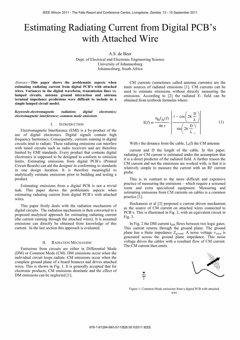
Estimating Radi w Dept. o Abstract—This paper shows the problema estimating radiating current from digital PC wires. Variances in the digital waveform, tra lumped circuits, antenna ground interact terminal impedance predictions were difficu simple lumped circuit model. Keywords-electromagnetic radiation; dig electromagnetic interference; common mode em I. INTRODUCTION Electromagnetic Interference (EMI) is a use of digital electronics. Digital signa frequency harmonics. Consequently, currents circuits tend to radiate. These radiating emis with tuned circuits such as radio receivers limited by EMI standards. Every product th electronics is supposed to be designed to co limits. Estimating emissions from digital Circuit Boards) can aid the designer in confor in one design iteration. It is therefore analytically estimate emissions prior to buil product. Estimating emissions from a digital PC task. This paper shows the problemati estimating radiating current from digital PC wires. This paper firstly deals with the radiati digital circuits. The radiation mechanism is t proposed analytical approach for estimating (the current running through the attached wi emissions can directly be obtained from k current. In the last section this approach is ev II. RADIATION MECHANI Emissions from circuits are either in D (DM) or Common Mode (CM). DM emissio individual circuit loops radiate. CM emission complete ground plane of a board bounces a wires. This is shown in Fig. 1. It is generally electronic products, CM emissions dominate DM emissions can be neglected [1]. ating Current from Dig with Attached Wire A.S. de Beer of Electrical and Electronic Engineering Science University of Johannesburg Johannesburg, South Africa atic aspects when CB’s with attached ansmission lines vs. tion and antenna ult to include in a gital electronics; missions by-product of the als contain high s running in digital sions can interfere and are therefore hat contains digital nform to emission l PCB’s (Printed rming to standards e meaningful to ding and testing a CB is not a trivial ic aspects when CB’s with attached ion mechanism of then converted to a g radiating current ires). It is assumed knowledge of this valuated. SM Differential Mode ons occur when the ns occur when the and drives attached y accepted that for e and the effect of CM currents (sometimes c main sources of radiated emis used to estimate emissions w emissions. According to [2] obtained from textbook formula With r the distance from the current and D the length radiating or CM current is estim it is a direct predictor of the rad CM current and not the emissio relatively simple to measure t probe. This is in contrast to the practice of measuring the emiss room and extra specialized estimating emissions from CM practice [1]. Hockanson et al [3] propos as the source of CM current o PCB’s. This is illustrated in Fig Fig. 3. In Fig. 2 the DM current i DM This current returns through plane has a finite impedance Z generated across the ground voltage drives the cables with The CM current then emits. Ef () η 0 I A f () 4π r 1 ⋅ Figure 1: Common Mode emission wi gital PCB’s called antenna currents) are the ssions [1]. CM currents can be without directly measuring the the radiated E- field can be as where: e cable, I A (f) the CM antenna h of the cable. In this paper, mated under the assumption that diated field. A further reason the ons are worked with, is that it is the current with an RF current e more difficult and expensive sions – which require a screened d equipment. Measuring and currents on cables is a common sed a current driven mechanism on attached wires connected to g. 2, with an equivalent circuit in M flows between two logic gates. the ground plane. The ground Z ground . A noise voltage v noise is plane impedance. This noise a resultant flow of CM current. (1) 1 cos 2π D λ ⎛ ⎜ ⎝ ⎞ ⎟ ⎠ − sin 2π D λ ⎛ ⎜ ⎝ ⎞ ⎟ ⎠ ns from a digital PCB with attached ire IEEE Africon 2011 - The Falls Resort and Conference Centre, Livingstone, Zambia, 13 - 15 September 2011 978-1-61284-993-5/11/$26.00 ©2011 IEEE
-
Upload
johannesburg -
Category
Documents
-
view
5 -
download
0
Transcript of Estimating radiating current from digital PCB's with attached wire
Estimating Radiw
Dept. o
Abstract—This paper shows the problemaestimating radiating current from digital PCwires. Variances in the digital waveform, tralumped circuits, antenna ground interactterminal impedance predictions were difficusimple lumped circuit model.
Keywords-electromagnetic radiation; digelectromagnetic interference; common mode em
I. INTRODUCTION Electromagnetic Interference (EMI) is a
use of digital electronics. Digital signafrequency harmonics. Consequently, currentscircuits tend to radiate. These radiating emiswith tuned circuits such as radio receivers limited by EMI standards. Every product thelectronics is supposed to be designed to colimits. Estimating emissions from digitalCircuit Boards) can aid the designer in conforin one design iteration. It is thereforeanalytically estimate emissions prior to builproduct.
Estimating emissions from a digital PCtask. This paper shows the problematiestimating radiating current from digital PCwires.
This paper firstly deals with the radiatidigital circuits. The radiation mechanism is tproposed analytical approach for estimating(the current running through the attached wiemissions can directly be obtained from kcurrent. In the last section this approach is ev
II. RADIATION MECHANI
Emissions from circuits are either in D(DM) or Common Mode (CM). DM emissioindividual circuit loops radiate. CM emissioncomplete ground plane of a board bounces awires. This is shown in Fig. 1. It is generallyelectronic products, CM emissions dominateDM emissions can be neglected [1].
ating Current from Digwith Attached Wire
A.S. de Beer of Electrical and Electronic Engineering Science
University of Johannesburg Johannesburg, South Africa
atic aspects when CB’s with attached ansmission lines vs. tion and antenna ult to include in a
gital electronics; missions
by-product of the als contain high s running in digital sions can interfere and are therefore
hat contains digital nform to emission l PCB’s (Printed rming to standards e meaningful to ding and testing a
CB is not a trivial ic aspects when
CB’s with attached
ion mechanism of then converted to a g radiating current ires). It is assumed knowledge of this valuated.
SM Differential Mode
ons occur when the ns occur when the
and drives attached y accepted that for e and the effect of
CM currents (sometimes cmain sources of radiated emisused to estimate emissions wemissions. According to [2] obtained from textbook formula
With r the distance from the
current and D the lengthradiating or CM current is estimit is a direct predictor of the radCM current and not the emissiorelatively simple to measure tprobe.
This is in contrast to thepractice of measuring the emissroom and extra specializedestimating emissions from CM practice [1].
Hockanson et al [3] proposas the source of CM current oPCB’s. This is illustrated in FigFig. 3.
In Fig. 2 the DM current iDMThis current returns through plane has a finite impedance Zgenerated across the ground voltage drives the cables with The CM current then emits.
E f( )η0IA f( )
4π r
1⋅
Figure 1: Common Mode emissionwi
gital PCB’s
called antenna currents) are the ssions [1]. CM currents can be without directly measuring the
the radiated E- field can be as where:
e cable, IA(f) the CM antenna
h of the cable. In this paper, mated under the assumption that diated field. A further reason the ons are worked with, is that it is the current with an RF current
e more difficult and expensive sions – which require a screened d equipment. Measuring and
currents on cables is a common
sed a current driven mechanism on attached wires connected to g. 2, with an equivalent circuit in
M flows between two logic gates. the ground plane. The ground Zground. A noise voltage vnoise is
plane impedance. This noise a resultant flow of CM current.
(1)1 cos 2π
Dλ
⎛⎜⎝
⎞⎟⎠
−
sin 2πDλ
⎛⎜⎝
⎞⎟⎠
ns from a digital PCB with attached ire
IEEE Africon 2011 - The Falls Resort and Conference Centre, Livingstone, Zambia, 13 - 15 September 2011
978-1-61284-993-5/11/$26.00 ©2011 IEEE
III. EQUIVALENT CIRCUI
Based on Fig. 2, one should be able to anthe radiated emissions by use of the following
• Obtain the voltage of the driving logic g• Calculate the impedance of the digital c• Calculate the DM current iDM that flows
logic gates. • Determine the impedance Zground (mostl
the ground plane. • Calculate the antenna driving voltage (v• Obtain the impedance of the antenna (c
to ground. • Calculate the capacitance between circu• Calculate current iCM running on the ant• Estimate the radiated emissions from th
This procedure is partially based on whaused in the estimation of “Common-ModePrinted Circuit Boards.” A representative cFig. 4.
Figure 2: Common Mode emissions from a digital noise voltage across the ground plan
Figure 3: Equivalent for Common Mode emissions with attached wire
IT nalytically estimate g procedure:
gate. circuit line. s between the two
ly inductive) of
vnoise). able) with respect
uit and ground tenna.
he cable.
at Carobbi et al [2] e Emissions from ircuit is shown in
IV. CURREN
Following the procedure sebased on the equivalent circuit(iCM) was estimated and compar
A. Practical Circuit The practical circuit consi
line driver, driving a microstloads were chosen: 10pF anddriving capability of the CMOexternally with the power leadsthe board emissions. Fig. 5 iscircuit. The microstrip is 13cm
B. Driving Voltage The driving voltage is a di
cycle. The extent of the frequevoltage is primarily a function first problematic aspect when eThe rise and fall time of the loads. For the 10pF load, it waload. Both these values weestimation, yielding two driving
PCB driven by a ne.
from a digital PCB
Figure 4: Equivalent Circuit for eDi
Figure 5: Pr
NT ESTIMATION t out in the previous section and t of Fig. 4, the radiation current red to a practical circuit.
sts of an oscillator and CMOS trip with capacitive load. Two d 100pF, which are within the
OS driver. The board is powered s filtered as to not interfere with s an illustration of the practical in length.
igital square wave of 50% duty encies generated by the driving of rise and fall time. This is the estimating the radiating current. driver is different for different
as 3.5ns and 12ns for the 100pF ere included in the analytical g spectra.
estimating Common Mode current from a igital PCB.
ractical Circuit.
IEEE Africon 2011 - The Falls Resort and Conference Centre, Livingstone, Zambia, 13 - 15 September 2011
978-1-61284-993-5/11/$26.00 ©2011 IEEE
C. Microstrip Line Impedance Once the driving voltage spectra are obtained, the
microstrip line impedance needs to be determined so that the DM current can be calculated. This leads to the second problematic aspect in estimating the radiating current. Working up to 1GHz, the 13cm microstrip becomes electrically long and becomes a transmission line. Furthermore the line becomes lossy at higher frequencies. The input impedance to the line is estimated with:
Where:
is the load impedance, lth the length of the line and:
The characteristic impedance is frequency dependent with:
where L and C is the inductance and capacitance per unit length respectively. R(f) was estimated using a commercial SI (Signal Integrity) package.
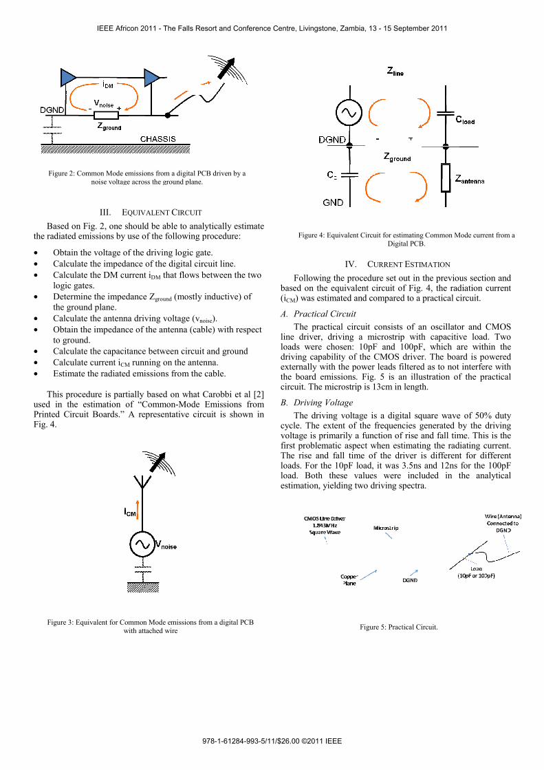
D. Differential Mode Current The DM current is calculated using the Fourier coefficients
of the driving voltage divided by the line input impedance at every frequency component. The result (in the frequency domain) is shown in Fig. 6 for the two load capacitances of 10pF and 100pF.
If the line impedance was a lumped element, the current of Fig. 6 could correctly be equated as iDM. Using the input current to a transmission line as equal to iDM is an assumption. This is due to the fact that the return path of the current is distributed along the microstrip transmission line.
E. Ground Plane Inductance From [4], the ground plane inductance (in H/m) was taken
as:
where h is the height of the microstrip from the plane and w the plane width. The total plane inductance for the 13cm microstrip was 2.1nH.
F. Antenna Driving Voltage The antenna driving voltage (vnoise in Fig. 4) is calculated
as:
where Iin is the current drawn by the microstrip transmission line and Lground is from (6). From Fig. 4 it can be seen that this voltage drives a circuit loop with Zantenna and Cc in series.
(2)
(3)
(4)
(5)
(6)
(7)
Zin f CL, ( ) Z0 f( )ZL f CL, ( ) j Z0 f( )⋅ tanh γ f( ) lth⋅( )( )⋅+
Z0 f( ) j ZL f CL, ( )⋅ tanh γ f( ) lth⋅( )( )⋅+⋅:=
ZL f CL, ( ) j−1
2 π⋅ f⋅ CL⋅⋅:=
γ f( ) R f( ) j 2⋅ π f⋅ L⋅+( ) j 2⋅ π⋅ f⋅ C⋅( )⋅:=
Z0 f( )R f( ) j 2⋅ π f L⋅+
j 2⋅ π⋅ f⋅ C⋅:=
Lground4 μ⋅
π 2
hw
⋅
Vnoise Iin j⋅ ω⋅ Lground⋅
1 10 6× 1 10 7× 1 10 8× 1 10 9×1 10 7−×
1 10 6−×
1 10 5−×
1 10 4−×
1 10 3−×
0.01Input Current Drawn by Microstrip
Frequency (Hz)
Cur
rent
Am
plitu
de (A
)
I10pF i
I100pF i
i
M
1
ts⋅
Figure 6: Spectrum of current drawn by the line
IEEE Africon 2011 - The Falls Resort and Conference Centre, Livingstone, Zambia, 13 - 15 September 2011
978-1-61284-993-5/11/$26.00 ©2011 IEEE
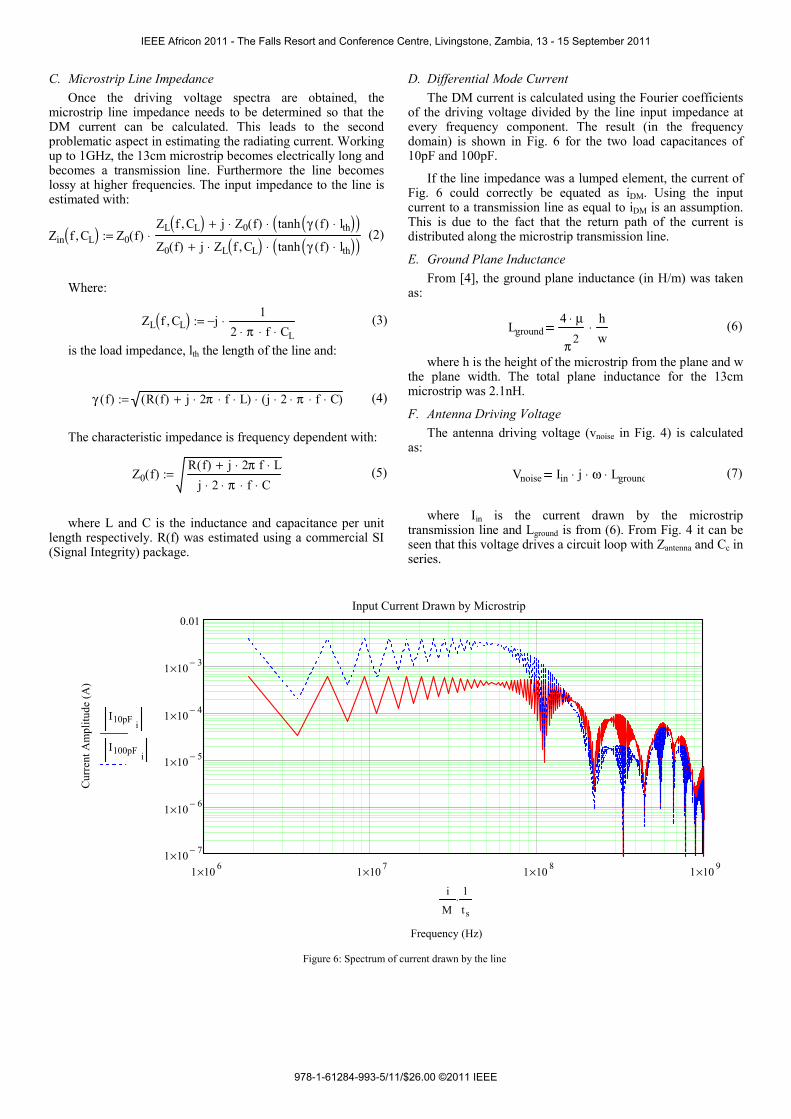
G. Antenna Impdance The antenna is 1.3m long and was assumed to be a
monopole over ground. This is an assumption as the practical circuit board is not at ground potential. It is somewhat removed with a capacitance between ground and the board as shown in Figures 1 – 4.
The antenna terminal impedance was calculated from equations in [5]. This is another problematic aspect in estimating the radiating current. The antenna terminal impedance varies a lot over the frequency range. Furthermore, there are different equations for the terminal impedance over such a wide frequency range. The equations used from [5] are convenient as they have a closed form, but should be considered an assumption. Especially the large values are different than proposed by Elliot in [6].
H. Radiating Current The radiating (antenna) current was calculated as:
where Cc is the capacitance from the circuit board to ground and appears in series with the antenna impedance.
(8)
Iantennavnoise
Zantenna1
jωCc+
1 106× 1 107× 1 108× 1 109×1 10 3−×
0.01
0.1
1
10
100
1 103×
1 104×Antenna Terminal Impedance (Real Part)
Frequency (Hz)
Impe
danc
e (o
hms)
Re Z 0.00012 π⋅ f⋅
c, ⎛⎜
⎝⎞⎟⎠
⎛⎜⎝
⎞⎟⎠
f
1 106× 1 107× 1 108× 1 109×1− 104×
5− 103×
0
5 103×
Antenna Terminal Impedance (Imaginary Part)
Frequency (Hz)
Impe
danc
e (o
hms)
Im Z 0.00012 π⋅ f⋅
c, ⎛⎜
⎝⎞⎟⎠
⎛⎜⎝
⎞⎟⎠
f
Figure 7: Real and imaginary parts of the antenna terminal impedance
IEEE Africon 2011 - The Falls Resort and Conference Centre, Livingstone, Zambia, 13 - 15 September 2011
978-1-61284-993-5/11/$26.00 ©2011 IEEE

Another problematic aspect in estimating the radiating
1 106× 1 107× 1 108× 1 109×25−
15−
5−
5
15
25
35Antenna Current
Frequency (Hz)
Cur
rent
Am
plitu
de (A
)
20 logIA_10pFi
10 6−
⎛⎜⎜⎝
⎞⎟⎟⎠
20 logIA_100pFi
10 6−
⎛⎜⎜⎝
⎞⎟⎟⎠
i
M
1
ts⋅
Figure 8: Estimated radiating (antenna) current for a 10pF and 100pF load.
Figure 9: Measured radiating (antenna) current for a 10pF and 100pF load.
IEEE Africon 2011 - The Falls Resort and Conference Centre, Livingstone, Zambia, 13 - 15 September 2011
978-1-61284-993-5/11/$26.00 ©2011 IEEE

Another problematic issue with the radiating (antenna) current is its dependence on Cc. Carobbi et al [2] reported that their results was not significantly influenced by the magnitude of this capacitance. It was found however, that when Cc is in the order of pF’s it does play a significant role in the amplitude of the radiating current. It was found that for a Cc of 4pF, the estimated radiating current (Fig. 8) correlate the best with the measured results (Fig. 9).
V. CONCLUSION This paper shows the problematic aspects when estimating
radiating current from digital PCB’s with attached wires. The estimation was obtained by calculating voltages and currents from a simplified lumped circuit (Fig. 4). Although this approach has yielded satisfactory results in the past [2], it is shown that several problematic aspects render this approach ineffective. This include:
• Different spectra for the digital driving voltage waveform due to the change in rise/fall times. The rise and fall times change under different DM load conditions.
• The fact that the DM line can be electrically long and therefore a transmission line. This is opposed to a lumped approach [2] where all the current in the DM circuit return via a single inductor.
• The PCB is assumed to be at ground potential when the attached wire is modeled as a monopole over ground. The introduction of a capacitor to model PCB coupling to
ground introduces huge differences (in tens of dB’s) in estimating the antenna current.
• Obtaining a correct model for the attach wire is problematic as closed form formulae for antenna terminal impedances vary in their predictions.
Some correlation was found between the estimated radiating current and measured antenna (attached wire) current. It is however overall an unsatisfactory result and future work should include clarification on the problematic aspects.
REFERENCES
[1] C.R. Paul, Introduction to Electromagnetic Compatibility, 2nd ed., Hoboken , New Yesrsey: John Wiley & Sons, 2006, pp.504-532.
[2] C.F.M. Carobbi, L.M. Millanta and M. Polignano, “Common Mode Emissions from Printed Circuit Boards – Simplified Models, Analysis and Experiments,” IEEE Int Symp on Electromagnetic Compatibility, vol. 2, pp. 806 – 810, August 1999.
[3] D.M. Hockanson, J.L. Drewniak, T.H. Hubing, T.P. Van Doren, F. Sha and M.J. Wilhelm, “Investigation of Fundamental EMI Source Mechanisms Driving Common-Mode Radiation from Printed Circuit Boards with Attached Cables,” IEEE Trans on Electromagnetic Compatibility, vol. 38, no. 4, pp. 557-566, Nov. 1996.
[4] .M. Hockanson, J.L. Drewniak, T.H. Hubing, T.P. Van Doren, F. Sha, C-W Lam and L Rubin, “Quantifying EMI Resulting from Finite-Impedance Reference Planes,” IEEE Trans on Electromagnetic Compatibility, vol. 39, no. 4, pp. 286-297, Nov. 1997.
[5] K.L. Kaiser, Electromagnetic Compatibility Handbook, Boca Raton, Florida: CRC Press, 2005, pp. 30-12 – 30-13.
[6] R.S. Elliot, Antenna Theory and Design, Revised Ed., Hoboken , New Yesrsey: John Wiley & Sons, 2003.
IEEE Africon 2011 - The Falls Resort and Conference Centre, Livingstone, Zambia, 13 - 15 September 2011
978-1-61284-993-5/11/$26.00 ©2011 IEEE