Enhancing the performance of solar cells via luminescent down-shifting of the incident spectrum: A...
26
1 Enhancing the performance of solar cells via luminescent down-shifting of the incident spectrum: A review Efthymios Klampaftis a , David Ross a , Keith R. McIntosh b and Bryce S. Richards a * a School of Engineering and Physical Sciences, Heriot-Watt University, Edinburgh, EH14 4AS, UK b Centre for Sustainable Energy Systems, Australian National University, Canberra, ACT 2000, Australia Submitted 20 October 2008 Abstract The application of a luminescent down-shifting (LDS) layer has been proposed as a method for improving the poor spectral response of solar cells to short-wavelength light. The LDS layer absorbs photons, typically in the 300 – 500 nm range, and re-emits them at a longer wavelength where the photovoltaic (PV) device exhibits a significantly better response. This paper reviews the progress in this area over the last three decades, starting from early experiments that yielded promising results but being limited by the luminescent materials available at the time, to modern materials that exhibit higher luminescent quantum efficiencies and better photostability. The candidate materials are considered and their potential is reviewed for a wide range of PV technologies. A particular opportunity is the ability to use the existing polymer encapsulation layer of certain PV technologies as a LDS layer as well. 2008 Elsevier B.V. All rights reserved. Keywords: Photovoltaics; Luminescent materials; Down-shifting; Efficiency. * Corresponding Author. Tel.: +44 (0) 131 451 3614 Fax: +44 131 451 3129 E-mail address: [email protected]
Transcript of Enhancing the performance of solar cells via luminescent down-shifting of the incident spectrum: A...
1
Enhancing the performance of solar cells via luminescent down-shifting of the incident spectrum: A review
Efthymios Klampaftisa, David Rossa, Keith R. McIntoshb and Bryce S. Richardsa * aSchool of Engineering and Physical Sciences, Heriot-Watt University, Edinburgh, EH14 4AS, UK
bCentre for Sustainable Energy Systems, Australian National University, Canberra, ACT 2000, Australia
Submitted 20 October 2008
Abstract
The application of a luminescent down-shifting (LDS) layer has been proposed as a method for improving the poor spectral response of solar cells to short-wavelength light. The LDS layer absorbs photons, typically in the 300 – 500 nm range, and re-emits them at a longer wavelength where the photovoltaic (PV) device exhibits a significantly better response. This paper reviews the progress in this area over the last three decades, starting from early experiments that yielded promising results but being limited by the luminescent materials available at the time, to modern materials that exhibit higher luminescent quantum efficiencies and better photostability. The candidate materials are considered and their potential is reviewed for a wide range of PV technologies. A particular opportunity is the ability to use the existing polymer encapsulation layer of certain PV technologies as a LDS layer as well. 2008 Elsevier B.V. All rights reserved.
Keywords: Photovoltaics; Luminescent materials; Down-shifting; Efficiency.
*Corresponding Author. Tel.: +44 (0) 131 451 3614 Fax: +44 131 451 3129 E-mail address: [email protected]
Bryce
Text Box
Solar Energy Materials & Solar Cells 93 (2009) 1182 -1194
2
1. Introduction
Fundamental spectral losses, which arise from the limited spectral response (SR) of solar cells to the wideband solar spectrum, constitute the largest proportion of losses in every developed PV technology. Transparency losses arise from both sub-bandgap (Eg) photons (E<Eg) that are not able to be absorbed by the semiconducting material of the solar cell, while the excess energy of high energy photons (E>Eg) is lost via non-radiative relaxation of the excited electrons to the conduction band, in the form of heat. The fundamental spectral losses limit the theoretical maximum efficiency (η for a single-junction cell with Eg=1.1eV to η≈31% [1]. The best experimental one-sun devices fabricated in laboratories have achieved conversion efficiencies of 24.7% for wafer-based crystalline silicon (c-Si) cells [2] and 19.5% for thin-film technologies [3]. Due to a large fraction of sunlight being absorbed in the top micron or so of semiconducting material, extensive laboratory research has been performed on optimizing the front surface of PV devices. However, the same processing sequences cannot always be applied in commercial production, whether for financial or technical reasons. Therefore, large-area production-scale modules exhibit significantly lower efficiencies, ranging from 6% for amorphous silicon (a-Si) to 20% for c-Si. The potential remains to increase this value by making better use of short wavelength (λ) light.
There are two principal approaches to achieve a more efficient utilization of the short-λ part of the solar spectrum. The first is to improve the electronic properties of existing devices, using advanced design concepts, such as very narrow junction(s), low doping levels or very thin window/buffer layers where they exist [4]. These steps however, can prove difficult to implement and/or expensive in production, while they may also have detrimental effects on the overall performance of a device [4]. Alternatively, implementation of more sophisticated “third generation” cell structures, such as multijunction [5], heterojunction [6] and intermediate band gap [7] cells, can lead to better utilization of the short-λ light but, significant technical hurdles need to be overcome before such technologies compete seriously with first and second generation flat-plate PV technologies.
The second approach is LDS of the incident spectrum: absorbing short-λ photons and re-emitting them at more favorable λ before they reach the cells. LDS is a passive approach that involves applying a luminescent species in a layer prior to the cells, thus eliminating the need to interfere with the active material of a PV device. This method will be concentrated on in this review study.
The λ dependent response of a PV device can be described by its external quantum efficiency (EQE), defined as the ratio of the number of electron-hole pairs generated to the number of photons incident on the front surface of the cell. Figures 1a and 1b show representative EQEs of various PV technologies, at short λ, the region where LDS is most relevant.
It is clear from these figures that the various PV technologies exhibit different performance
across the spectrum. A common trend however in all cases is the reducing EQE at shorter λ. The devices’ inefficient operation in the blue and ultra-violet (UV) regions of the spectrum is due to additional loss mechanisms at their front layers, where interaction with higher energy photons occurs. These additional losses arise from technical processing difficulties, necessary trade-offs in the design of a device and imperfect properties of the available materials. In Table 1 we summarize the most dominant short λ loss mechanisms for various in-production PV cell technologies. When encapsulated into a module, an additional significant short-λ loss mechanism is absorption in the glass and encapsulation layer.
Previous attempts at the LDS method are presented and discussed in the following chapters. The potential of the LDS method varies depending on the cell technology under consideration. Different technologies are, therefore, presented and discussed on a separate basis, under two main categories of wafer-based and thin film technologies. Concentrator systems are not considered, as these usually utilize highly sophisticated and efficient cells that do not allow much space for improvement via LDS. The suitability of the available materials and recent developments in this area are also considered. Finally, possible future research topics in the field of the LDS method are highlighted.

3
2. LDS background
The enhancement of the short-λ response of PV devices via LDS first appears in the literature in the late-70s in the area of luminescent solar concentrators (LSCs), as a beneficial consequence of the concentration process [8, 9]. Hovel et al [4] were the first to apply the concept of LDS in a planar luminescent sheet positioned on top of PV cells, with encouraging initial results. They identified and exhibited the potential of the method, experimenting with various PV technologies. While the performance enhancement achieved was encouraging, it is important to note that the efficiencies of the solar cells used were considerably worse than the ones of today, and the results were limited by the inadequacy of the materials available at that time. This is no longer the case, as it will be discussed in sections 2.1 and 2.2. A simplified diagram of the optical processes involved in a planar luminescent layer on top of a PV module is presented in Figure 2.
As a result of the luminescent process, a proportion of the incoming photons are shifted to longer
wavelengths before they reach the photoconductive layers of the module, which respond better to the altered spectrum. Thus, more electron-hole pairs can be created per incident photon (i.e. the EQE is increased) and a higher short-circuit current (Isc) can be generated. The open-circuit voltage (Voc) and fill factor (FF) will not change significantly, since there is no change in the electronic properties of the semiconducting material or the resistance of the device. Thus, an increase in conversion efficiency is expected as a result of the increased current generation. Two technologies that do not necessarily follow this trend are cadmium telluride (CdTe) and copper indium diselinide/sulfide (CIS) based devices that utilize a cadmium sulfide (CdS) buffer layer, which have been observed to perform worse under spectra that are poor in UV-blue light [10, 11].
A simple example of how the LDS process is shifting parts of the spectrum to a region of higher cell EQE, is given in Figure 3. The CdTe cell exhibits a sharp decrease in EQE for λ<550nm. A fluorescent organic dye that absorbs in the region λ<500nm and emits at λ>500nm is shifting parts of the incident irradiation from wavelengths that the cell is performing poorly (EQE of 0 – 25%) to longer ones where the cell is performing better (EQE of 30 – 80%). The spectral distribution of the photon flux for the standard air mass 1.5 global (AM1.5G) solar spectrum is also plotted in Figure 3, in order to consider the process in terms of available photons for LDS.
In addition to the potential efficiency enhancement, the introduction of an LDS layer in a PV
module also creates additional interactions with the light resulting in extra loss mechanisms. Therefore, any potential gains to be made by the shifting of the spectrum will have to compensate for these before offering an overall improvement. These additional losses originate from two sources: the host material and the luminescent species. The main physical processes that take place are: i) parasitic absorption from the host material, ii) emission at less than unity luminescent quantum efficiency (LQE) from the luminescent species (LQE is defined as the ratio between the number of photons emitted and the number of photons absorbed by a luminescent species), iii) re-absorption from the luminescent species due to partial overlapping of its absorption and emission bands, iv) losses through top and side planes of the layer, as luminescent light is not emitted towards the cells’ direction only and v) increased reflection due to the introduction of an additional interface. We will discuss in detail these losses in the following paragraphs where the properties of the available materials are considered.
2.1 Host materials
The materials used in the LDS layer must satisfy specific requirements in order to maximize the benefits from its application. The host material must exhibit high transmittance, particularly in the region where the cell’s response is high, as well as low scattering. At the same time it needs to provide an optimum environment for the dissolvement of the luminescent species. Finally they will have to endure the thermal treatment that solar cells are subjected during their manufacturing and exhibit prolonged photostability over the extended periods of 20-25 years that the PV manufacturers guarantee a minimum of 80% of the initial performance for their modules [12-14].
For these purposes the chosen materials were indeed many, with the most frequent categories being polymers such as poly-methyl methacrylate (PMMA) [15-17] or poly-vinyl acetate (PVA) [18, 19] and inorganic crystalline materials such as Al2O3 [4] or CaF2 [20]. Other choices in the literature

4
were various types of glass [21-23], organic molecule silicates (ORMOSIL) [24-26] and organic paint thinners [27-29].
Polymeric materials can exhibit high transparency in the visible region of the spectrum, adequate resistance to heat and humidity variations, and high mechanical strength [30]. They also provide very good host environment for organic dye molecules [4]. Additionally, the PV industry has a long experience in using polymeric materials, especially in the case of poly-ethylene vinyl acetate (EVA) copolymer, which is the standard encapsulant used for wafer-based Si solar cells [31]. On the other hand, photodegradation under extended UV exposure is a major issue for polymeric materials. Manufacturers are addressing this by utilizing UV stabilizers and absorbers [30, 31]. These are molecules that strongly absorb UV photons that would otherwise interact with the polymer, turning their energy into heat. Inorganic crystalline materials exhibit high transparency for the whole spectrum and long photostability [4]. They are, however, expensive and difficult to process and thus, unlikely to be considered as an option on a commercial basis.
Parasitic absorption from the host material is one additional loss mechanism that the application of the LDS method introduces. The extent of these losses is strongly dependant on the material and the thickness of the sheet. Given that highly transparent materials are naturally desirable for PV applications, the thickness of the luminescent layer is critical. Thin polymeric films seem to fulfill these requirements. For example, a commercially available PMMA sheet of 1mm thickness has an absorption loss of ≈1% of the total incident energy, as found in ray tracing simulation described in Section 3.
2.2 Luminescent materials
The luminescent species used for LDS will ideally exhibit: i) unity LQE; ii) a wide absorption band in the region where the EQE of the cell is low; iii) a high absorption coefficient; iv) a narrow emission band, coinciding with the peak of the cell EQE; v) good separation between the absorption and emission bands in order to minimize losses due to re-absorption; and vi) low cost. In addition, as in the case of host materials, the luminescent species must also exhibit prolonged photostability for periods of 20-25 years.
A large number of luminescent materials have been investigated for LDS and can be separated into three main categories: quantum dots (QDs) [22, 32-35], organic dyes [15-17, 27-29, 36-43] and rare earth ions/complexes [7, 18-21, 23-26, 44, 45]. QDs are nanosize semiconducting crystals with tunable absorption and emission bands, according to their size. They exhibit a wide absorption band, high emission intensity, relatively good photostability [35]. On the other hand, they result in high re-absorption losses due to their large overlap of absorption and emission bands [46], exhibit relatively poor LQE and they remain generally expensive [46].
Organic dyes exhibit relatively high absorption coefficients [42], close to unity LQE [47] and are easy to process in polymeric matrices [42, 47]. Their drawbacks are their narrow absorption bands and their relatively small Stokes-shift, which still results in significant re-absorption losses [48]. Several dyes can be mixed within one layer in order to improve their absorption bandwidth and to expand their Stokes-shift [16, 39, 42, 49]. Their photostability over prolonged periods of UV exposure remains questionable in many cases, although significant improvements have been reported in recent years and there are already commercially available dyes that are photostable for many years [47].
Rare earth ions exhibit high LQE [46, 50], but have extremely low absorption coefficients [50]. The latter can be improved slightly by increasing concentrations and thickness, or via the more promising approach of using an antenna structure with much higher absorption properties which absorbs and transfers the energy to the rare earth ion for emission [18, 19, 46, 50].
The luminescent species introduce the most significant additional losses resulting from the addition of a LDS layer. A non-unity LQE gives rise to energy loss from the excited luminescent species by non-radiative relaxation (either molecular or ionic). Re-absorption losses are significant, especially in the cases of QDs [46] and of some organic dyes if/when high concentrations are used [17].
Mechanisms and in Figure 2 are additional losses due to the assumed isotropic profile of luminescence. Not all photons emitted towards the top or the sides of the LDS sheet will escape, only those with an angle of incidence smaller than the critical angle. The rest will be internally reflected with a high probability of being transmitted towards the cell. The proportion of emitted photons that

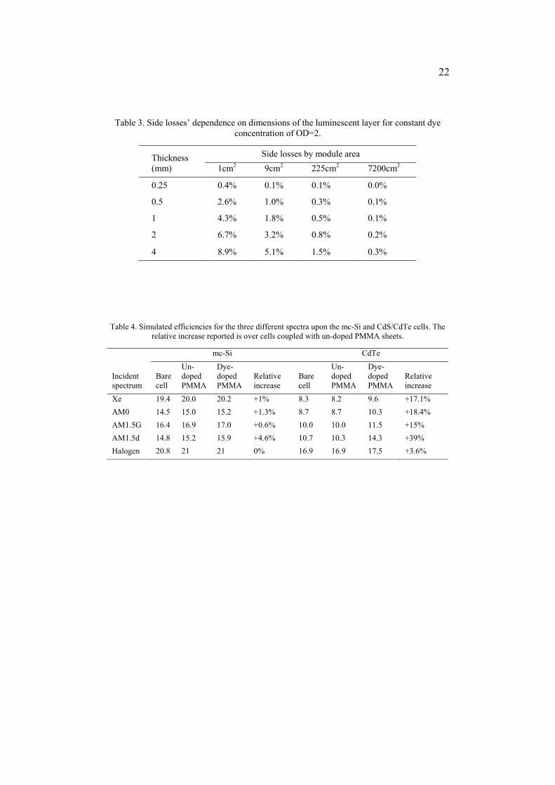
5
escape from the top plane has been quantified to the range of ≈12.5% for the case of air and a material with refractive index of 1.5 [4, 42]. The losses from the side planes are usually not included in calculations and estimations for overall losses in the literature, although they have been identified at least once as the main loss mechanism if small area devices are tested [51], again however, without quantification. These losses are strongly dependent on the dimensions of the LDS layer, as can be seen in Tables 2 and 3. Thin large area sheets will lose smaller fraction of photons through the sides than thicker ones with a smaller area, as the emitted photons are more likely to be absorbed by the cell or transmitted out of the sheet through the top plane, than to be incident on the sides at suitable angles for transmission out of the sheet. This issue is much more important when smaller area cells and sheets are used, as is the norm in laboratory scale experiments. Therefore, the losses occurring from the side planes were quantified, using our in-house ray-tracer package RAYLENE [16]. We did so for a host material of PMMA containing a 3 dye mixture (BASF Lumogen F Violet 570, Yellow 083 and Orange 240) of combined LQE=93% and in concentrations equivalent to an optical density (OD) of 2 for more than half of its absorption band. OD for a dye doped sheet is defined through Eq. 1, where T is the internal transmittance of the sheet. For OD=2, 1% of the incident light is transmitted through the sheet thus, 99% is absorbed by the dyes.
TOD 10log (1)
The results in Table 2 reveal that indeed the presence of the luminescent species increases significantly the side losses. Additionally, that a fraction of these losses, is inherent in the introduction of an additional layer on top of a cell.
The assumed isotropic emission profile of luminescence will also result to an altered distribution
of the photons’ angles of incidence to the interface between LDS layer and module as well as to the already existing interfaces within the module itself. The simplified Fresnel equations quantify adequately reflection losses occurring at the interfaces for small angles of incidence only and will underestimate them for larger ones. PV devices are usually characterized using small angles of incidence [52], although in real applications larger angles are present as well, especially where tracking of the sun is not applied or under diffuse solar conditions. The isotropic emission of photons by luminescence will result in a much wider distribution of incident angles. Since reflection is dependant on angle of incidence and is increasing with increasing angle [52], LDS will result in increased reflection losses.
If we consider altogether the losses due to non unity LQE of the luminescence species, absorption of the host material, optical losses and the re-absorption from the luminescent species, with the latter reported as the most difficult to quantify [4, 17], then the estimates in the literature for the losses due to light emitted by the luminescent species light vary from 15-50% [17, 4, 33]. Consequently, the gains from the increased response of the cell to the new spectrum will have to compensate for these additional losses and offer an additional gain to justify the application of the LDS method.
Having stated the above requirements for the choice of materials, any application that has the ambition of commercialisation needs to consider additionally the parameters of cost of the materials, the applicability of the method on a production scale and, as stated before, their photostability over the long periods of time that PV manufacturers are guaranteeing minimum performance for their modules. If all the above requirements are met, the LDS concept presents us with two very attractive points. The optimization of the LDS layer can be done independently of the cell and thus imposes no additional difficulties other than the manufacturing of the layer itself. Furthermore, the cell’s design can be re-optimised to receive less high energy photons under the new spectrum, which are the most challenging for successful harnessing of their energy in a cell’s design, as we can understand from the reduced EQE of all devices at short λ in figures 1a and 1b.
Since the late 1970s, the LDS method has been demonstrated repeatedly and extensively on a theoretical basis [4, 15, 35, 36, 53], supported by simulation results [16, 34, 35, 49, 54]. The experimental results [6, 7, 12, 18-20, 22-26, 28-30, 33-45, 53, 55-59] to a large degree verify these estimates. The most inhibitive factor in the early years of experimentation had been the inadequacy of the properties of the available materials. The most important of which were the inadequate photostability of organic luminescent molecules [4, 42], the low LQE of luminescent species [4], and the absorption of the encapsulation materials [35]. The following sections review the application of the

6
LDS method to the most common PV technologies, but firstly the effect of different solar spectra on such devices needs to be clarified.
While thin films currently make up only 10% of the total solar cell market [55], they are important in terms of the large and diverse number of PV technologies involved and the potential growth of their market share. Thin film PV devices vary hugely in their chemical composition and manufacturing process. As would be expected, the properties of these cells are also diverse. Recent research on thin film cells with LDS can be spilt into four main groups by cell type: CdTe-based cells, CIS-based cells, a-Si and emerging cells technologies.
3. The effect of different spectra
The spectral energy distribution of the incident to a cell spectrum is of paramount importance for the gains to be obtained by the LDS method. This is because more gains are to be made when more photons are available to be shifted in the first place. LDS will therefore result in higher gains under blue weighted spectra. The effect of the different spectra under which tests are made has been reported with ≈25% increase for direct (D) spectrum and ≈35% for diffuse (diff), using exactly the same cells and luminescent sheets [39]. It has also been modeled [34], where keeping all other parameters the same, the AM1.5diff spectrum results in 3 times higher relative improvement in comparison to AM1.5G and 4 times in comparison to AM1.5D. Recently, this effect was quantified experimentally for three different standard spectra, resulting in the AM0 spectrum exhibiting a 50% greater improvement in comparison to AM1.5G [43]. Additionally, the effect of different air mass standard spectra upon the results has been recognized and shown via modeling in [34] and calculations based on experimentally measured EQEs in [43]. It should be highlighted at this point that under extra terrestrial and/or diffuse conditions LDS is resulting to enhanced cell performance in terms of conversion efficiency and not necessarily of absolute output power, which primarily depends on the power density of the illuminating spectrum.
In laboratory experiments, the relevance of this issue lies in the choice of the spectrum under which measurements are taken. Although the PV community established a standard method to report results under one-sun intensity (1000W/m2) AM1.5G spectrum, this is not always the case and indeed in the literature there is a disparity in which spectra various researchers used in their experiments. This disparity makes direct comparisons of results complicated.
Therefore, simulations were performed using RAYLENE to demonstrate the effect of different spectra upon two standard production-line cells: multi crystalline silicon (mc-Si) and CdTe. The LDS layer was PMMA doped with the dye mix previously identified as the optimum for mc-Si [49] and CdTe [16]. The concentrations resulted in a minimum OD=2 in both cases. The spectra used were those of an unfiltered 1000W xenon (Xe) arc and a Halogen lamps, the extra-terrestrial AM0, the standard AM1.5G and the AM1.5diff, all normalised for incident power of 1000 W/m 2. The AM1.5diff is in its non normalised form a component of AM1.5G and is defined via two other standard spectra as: AM1.5diff(λ) = AM1.5G(λ) – AM1.5D(λ). It has a higher relative UV and blue content than all the other spectra, which explains the higher experimental results under this spectrum. The AM0 is second in relative energy density in this region of the spectrum. On the contrast, the Xe spectrum exhibits a much higher near-infrared (NIR) and lower visible relative content than the rest, due to the NIR spikes of the Xe arc. The AM1.5G and AM0 also exhibit a relatively high NIR content. The halogen lamp emits most of its light in the visible and NIR region of the spectrum. The EQE and spectral irradiance curves are shown in Figure 4 and the results of the simulations in Table 4.
The differences in these results highlight the effect that the different spectra have upon the results
obtained. The halogen lamp gives the best result for both devices, since most of its energy is in the visible and NIR region of the spectrum, where the devices exhibit their best performance, especially the CdTe that operates in the much more narrow region of 500-850nm. The Xe lamp with the intense spikes in the NIR region gives very good absolute result for the case of mc-Si, due to this cell’s good EQE in this region. On the other hand, the AM0 and AM1.5diff give the lowest results for the mc-Si device due to their high UV and blue content, where the mc-Si EQE is poorest. The CdTe cell gives the lowest absolute result under the Xe spectrum, due to its poor response in both UV and NIR regions of the spectrum, where the Xe spectrum is rich. The benefits from the LDS layer, in relative increase of efficiency, are more pronounced in both cases under the blue-weighted spectra AM1.5diff, which is in

7
agreement with the experimental results [34, 39], since in these cases there is a higher proportion of short-λ photons to be shifted and contribute to the cell’s output. The AM0 gives the second best improvements, as it is the second richest in short-λ light. Finally, it must be highlighted that this comparison is based on normalised to one-sun intensity spectra and the results presented refer to relative rather than absolute improvements. Naturally the AM1.5diff spectrum will give in absolute figures the smallest gains, since it has the smallest energy flux, but is the spectrum that offers the largest improvement in relative terms.
The consequence of this analysis is that results depend on the choice of incident spectrum. This should always be taken into consideration for the analysis of results and reports should refer clearly to the illuminating spectrum. Direct comparison of results obtained from different research groups should be made with caution when they have used different spectra.
4. Si wafer-based devices
The impact of any new concept upon wafer-based silicon (c-Si, mc-Si and Si ribbon) devices is particularly interesting for the PV world, since it comprised about 90% of the global PV module production in 2007 [55]. Representative EQEs for high efficiency c-Si and the more standard screen-printed mc-Si production-line solar cells are shown in Figure 1. These cells exhibit high EQEs, the mc-Si higher than 80% for most of the visible part of the spectrum, and the c-Si at 90%. The poorer EQE exhibited by the mc-Si cell at λ<500 nm is due to higher reflection and absorption by the anti-reflective coating (ARC), which are optimised for longer λ, and increased emitter recombination due to its heavy doping. Its EQE is dropping to almost zero for λ<400nm when absorption by the glass and the encapsulation material (EVA) are also increasing [49]. The c-Si exhibits a better performance for short λ till 400nm where again reflectance at the ARC and absorption by the glass and the encapsulant are increasing. These reasons make the mc-Si cell a good candidate for applying LDS, while the c-Si is not expected to benefit as much, although its sharp decrease for λ<400nm justifies investigation of the effect of LDS. There is still a maximum of 1.1 mA/cm2 to be harnessed in the region of λ<390nm in the AM1.5G spectrum [51].
Wafer-based Si devices have been investigated using the LDS method by many research groups. A number of theoretical calculations and simulation-based predictions as well as experimental attempts to exhibit the potential of the method have been reported in the literature and are presented in Tables 5 and 6.
There is a large disparity of results in Tables 5 and 6. This is due to the large variety of materials
that have been investigated by the various researchers as well as the different approaches in where and how to introduce the luminescent species.
Theoretical calculations are routinely presented, all agreeing on the potential of improvement for Si devices. To a large degree the initial analysis of Hovel et al. [4] is valid and the difference from their calculations originates from the improvement of the properties of the available materials and the development of new ones. Modeling tools are useful to explore the large number of combination of materials and configuration of module layers in a fast and simple manner. The first simplistic model in the literature is reported in [22]. In [33, 35] there is a second method developed, but it is one which assumes many parameters (LQE of luminescent species, profile of emission spectra, zero re-absorption losses, minimum transmission losses, ideal properties of host material, ideal synergistic operation of luminescent species and host material, molar extinction coefficient relationship to particle size). Due to the many assumptions, the authors of the paper reached to some qualitative results that they couldn’t explain and they had to lower their quantitative predictions from the most impressive values in Tables 5 and 6 of 30-40% to a more moderate but arbitrary 10%. The third modeling tool in the literature is the RAYLENE ray-tracer mentioned previously. Again this has implicit assumptions (ideal interfaces and isotropic profile of emission). It is using however, experimentally obtained values as inputs before calculating through ray tracing and standard optical laws. The results obtained with this tool are much more modest and relatively good agreement has been achieved between simulation [49] and experimental results [43].
In the experimental field, the variation among the chosen materials and the application methods is also large and consequently large differences are found again among the reported results. The absence of an agreed standard method of reporting the obtained results makes comparative evaluation of the

8
applications complicated, very often impossible, due to lack of knowledge of essential parameters of the experiment.
Two major sources of complication in the analysis and comparison of results are, firstly, the illuminating spectra, as discussed in section 3, and secondly, the utilization of cells using different or at times no ARC. Bare Si will reflect 30% or more of the incident light if left uncoated [52] thus, there is no PV device in a real application without an ARC. Several reports of large improvements via application of an LDS layer with cells not possessing an ARC can be found in the literature [15, 22, 25, 27-29, 41], but, in these cases is simply the addition of an extra layer of a material with refractive index less than that of Si that has resulted in a reduction in front surface reflection losses and thus an efficiency enhancement [17, 40, 51]. The actual improvement due to LDS will be significantly less, as reported in one case, where the initial reported value of 30% improvement in overall efficiency, attributed to reduced reflection for an uncoated cell, is revised to a 5% enhancement due to LDS alone [28]. Nevertheless, there is the potential to re-optimize the ARC to the new red-shifted spectrum that is incident upon the solar cell [25, 49, 56].
We believe that in relation to these two issues a more uniform presentation of results in the future would make the comparative analysis simpler. It is most informative for the evaluation of the LDS method when a result is presented in comparison to a coated device with a non-luminescent layer of the same material. It is this way only that the result is representative of the effect of LDS alone. The use of standard spectra would again simplify the analysis, but given that even a solar simulator with a “class A” match to the AM1.5G solar spectrum is allowed a tolerance of ±25% [57], this makes accurate reporting difficult.
To evaluate the true potential of the LDS method applied to Si solar cells, the reported results that include a comparison to non-luminescent coated devices from Tables 5 and 6 are examined [18, 19, 39, 40, 43, 56]. In all these cases 0.5-3% improvement in overall efficiency was reported. Further small gains through re-optimization of the ARC for the new spectrum have been predicted [40, 56], but this has not been realized yet in practice to our knowledge. Thus, wafer-based Si devices are expected to benefit slightly from application of the LDS method.
There are also some secondary benefits that can be gained through LDS. In cases where UV stabilizers are used in order to prevent UV-induced photodegradation either of the cells [58] or of the encapsulants used in module fabrication [31], the absorption of UV photons by a luminescent layer could reduce or even eliminate the need for the UV stabilizers. Additionally, the LDS process will result in reduced electron-hole pair thermalisation losses in the cells [59], which will occur in the LDS layer instead. This may decrease slightly the operational temperature of the cells and thus slightly increase their overall performance. Finally, the aesthetical presentation of PV modules could be improved through coloration, if visible emitting luminescent species is utilised, helping this way the expansion of niche PV markets that can make use of colored modules, such as building integrated photovoltaics (BIPV) and/or flexible mini modules.
The improvement in efficiency of Si wafer-based PV devices can be achieved at low cost, which is important for any method with a prospect of commercialisation. The improvements in [39, 40, 43] have been achieved by using polymeric host material and organic dyes, both of which represent the most cost effective options in their area. An additional challenge in the prospect of commercialisation, is to establish a methodology on an industrial scale that would not add much additional complication in the manufacturing process.
We highlight two distinctive approaches that propose the utilization of an already existing layer as the host material for the luminescent species. This idea would add minimal indeed additional complications. First is the utilization of glass, which is always present at the top of a Si PV device to protect the device from environmental factors. This has been realized in [21-23, 56] with varying results for the reasons discussed previously. Second is the utilization as host material of EVA, the commonly used encapsulant in Si devices [31]. This has been proposed in [30, 40, 43], but there are no reports of experiments having used the EVA copolymer as host material yet. To our knowledge, there are no apparent reasons why it should not perform well. This is a research activity the authors of this study are currently undertaking with encouraging preliminary results, which show Lumogen-F organic dyes have similar quantum yields in EVA to the ones measured in PMMA [60]. For example the Orange 240 dye was measured with the same technique and equipment as in [60] and gave 95% quantum yield in comparison to 100% in PMMA (both cases measured with ±5% error). The EVA relevant results will be reported analytically in the near future elsewhere.
9
5. Galium arsenide (GaAs) devices
Some early LDS experiments were performed using GaAs cells [4, 61], as GaAs cells also exhibit lower EQE at short λ. This is because GaAs is a direct band gap semiconductor and thus, electron-hole pairs are generated by high energy photons very close to the surface, where recombination is fast [61], as well as due to absorption by the window layer of aluminium gallium arsenide (AlGaAs) [4, 61]. These initial results were mixed, as can be seen in Table 7. Recent work however, has not focused on this technology. In the case of triple junction GaAs cells, there is very little room for any improvement, given the very good response of these cells at short λ [62].
It is worth noting that, for the case of GaAs devices used in space applications, it is a standard
technique since the 70’s to include a 5% of cerium oxide in the cover glass [63]. Cerium is a luminescent material [64]. The reason however, for its inclusion in the special cover glass in space applications is not improvement of performance via LDS, but one of the secondary potential benefits mentioned previously for the case of Si wafer-based devices i.e. protection of the glass [65] and of the encapsulation material [63] from the high energy UV irradiation.
6. CdTe-based devices
Based on its SR, CdTe-based cells would appear to be most promising candidates for LDS. This is due to the sharp cut-off in SR for λ < 515 nm, mainly due to parasitic absorption in the CdS buffer layer. While attempts have been made to reduce the thickness of this layer – or even eliminate it – to improve SR, these have resulted in lower cell efficiencies to date [66]. The application of LDS to CdTe over the past decade has demonstrated that efficiency increases of up to 33% are achievable [38], with a predicted maximum increase, assuming the use of a dye with LQE = 1, of 40% theoretically possible [38]. Comparison between reported results, shown in Table 8, is simplified since all improvements were reported under the AM1.5 spectrum – although in [37] and [38] this increase is calculated using results taken under day-light and white-light spectra. Also, the choice of luminescent material has been organic dyes in all cases except one, where Sm3+ ions where added to a KMgF3 crystal [67].
The results indicate that organic dyes seem promising, with the best two results coming from
Lumogen-F dyes hosted in PMMA [16, 38]. It is worth noting that the model used in [16] indicates that dye mixes can produce better results than a single dye, suggesting that the cell used in [37] could be improved beyond the reported 33%. The increase in efficiency was significantly lower in [16], as a present day CdTe production technology was used, which exhibited better response at short λ.
In [68] both PVB and PMMA were used as host materials. PVB was used due to its higher stability than EVA, which is commonly used in PV modules [68]. The maximum intensity of the Rhodamine 6G dye in PVB was measured to be six times higher than in PMMA, with PMMA hosted dye also exhibiting reduced EQE in 500-650nm range [68]. This indicates that PMMA is less suited for use with the Rhodamine dyes as well as the importance of selecting an appropriate host material for the dye. Unfortunately no LDS experiments published to date have used other organic dyes in PVB or any organic dyes in EVA.
While CdTe-based cells appear very promising for LDS, there are three notes of caution. Firstly, the CdS buffer layer in CdTe cells may be negatively affected by the absence of short-λ light [10, 11]. This is the result of the light modulated barrier height of the CdS buffer layer. The absence of high energy photons, which lowers the CdS conduction band height and reduces the barrier to electron transport [69], potentially results in significantly reduced FF and Jsc, for affected cells used with LDS layers. While this has not stopped significant improvements occurring in research to date, this may become important as the scale on which LDS is implemented increases. Secondly, the laboratory–scale cells with highest efficiency show a significantly better SR in the blue region of the spectrum [70]. This indicates that the improvements possible for currently in-production cells will be diminished in the future, as new production techniques will lead to mass produced cells with properties closer to that of today’s record cells, assuming the problems detailed above can be overcome. Thirdly, since the CdS and CdTe layers are grown on a transparent conducting oxide (TCO) coated glass superstrate, there is little scope for including a LDS layer underneath the glass, which would be the most elegant solution.

10
7. CIS-based devices
CIS-based solar cells share many of the same properties as CdTe-based cells. Most importantly, absorption in the buffer layer (CdS or other) accounts for reduced EQE at short λ and negative effects may occur when this layer is not illuminated at these wavelengths [69]. To date, only two experiments have been reported where a LDS layer has been added to a CIS-based cell, with similar increases of 4% [51] and 3% [32], even though very different materials were used in each case, as can be seen in Table 9.
While a variety of combinations of cells, host material and dyes were used in [51], it is difficult to
draw conclusions about the optimum combination based on the results reported. The importance of device dimensions was highlighted in [51], where the edge losses played a significant role in the different improvement achieved by PMMA and varnish hosted luminescent dyes. It was noted that a large part of the observed improvement was due to the anti-reflection properties of the host materials when applied to bare cells. This effect is also noted in [32], along with a reduction in sheet resistance of the TCO used as the front contact, probably caused by the annealing of the TCO during the deposition of the LDS layer. It is not possible to quantify the impact of these effects on the solar cell properties, as no results are given for a cell coated in a non-luminescent layer. Recent work by the authors’ group has indicated that little change in sheet resistivity of the TCO layer is expected, even when it is illuminated by a red-rich spectrum [71]. Further investigations are currently underway in order to determine any change in photoconductance on the CdS layer under similar conditions.
One important note regarding the use of LDS layers with CIS-based devices is that standard rigid substrate modules require an EVA or similar encapsulation layer, like mc-Si devices. As mentioned in section 4, it has been proposed in [30, 40, 43] that EVA could be used as the host material, adding this way minimal further complications to the manufacturing process.
8. a-Si devices
The majority of research into LDS for a-Si devices, presented in Table 10, has concentrated on Eu3+ and Tb3+ ions as luminescent materials, suspended in a variety of host materials. The a-Si technology was investigated by Hovel et al. [4], but no overall performance increase was reported as the increase in EQE at short λ was cancelled out by a lowering of EQE at longer λ [4]. A recent theoretical study [33, 35] also indicated there would be no efficiency gains (in a model that used QDs in an ideal plastic layer). While this would seem to imply that the lack of gains was a result of the properties of a-Si cells in general, as always, caution must be used when comparing work conducted on different cells. The normalised EQEs of the cells reported in these studies show very different potential for improvement in the region of λ<500nm, due to the differing properties of the cells. For example, the cell used in [33] is designed to be thin and thus, to respond better at shorter λ.
As can be seen in Fig 5, there are clearly different levels of improvement possible, depending on
the cells used. The EQEs of cells used in [33, 35], [24, 25, 44] and [20, 21, 45] correspond to efficiency increases with LDS layers of 0, 8 and 50% respectively, showing the importance of the initial SR of the cells used on the possible improvements achievable. It is, therefore, impossible to identify which areas are most promising for further research, as the EQEs of the cells differed so greatly and the materials used with each specific cell were not altered. A less apparent benefit of LDS is the role it could possibly play in reducing cell degradation due to exposure to high energy photons. The performance of a-Si cells is reduced initially – cell FF is reduced by ≈13% under one sun illumination [72] – mainly due to the Staebler-Wronski effect [73]. It is possible that this could be altered by the use of LDS layers. The additional benefit of LDS in blocking high energy photons is also relevant when discussing dye sensitized solar cells (DSSCs).
9. DSSCs and polymer-based devices
The work conducted on DSSCs [17, 58] is summarized in Table 11 . While initially it might seem unlikely that LDS layers would result in an improvement for these devices, given their good EQE at short λ, this is not necessarily the case. Liu et al. [58] noted that LDS layers of some form could be

11
used to replace the UV blocking layer that is currently needed for long term stable DSSCs. In [58] is shown that while a cell with LDS layer had an 8% lower efficiency than a bare cell, its lifetime was greatly improved and its efficiency was 23% higher than a cell with a UV blocking layer.
It was noted that improvement was also possible for a polymer cell [17]. As can be seen in Table
12, a variety of dyes were tested as the luminescent material in PMMA sheet, with Stilben 189 showing the most promising result, a relative efficiency increase of 2%. Investigation of dye mixes, as has been reported by others for different types of solar cells [16, 51], would also be of interest. Both polymer and DSSCs are emerging technologies, still under development and no commercially available product exists – although Konarka have recently conducted lifetime tests and aim to have a commercial product available soon [74]. If LDS proves to be as viable at production level as are other cell technologies, one possible twist could be the design of DSSCs and polymer-based devices with LDS layers factored in as the UV blocking layers in DSSCs, for example, or the encapsulating material needed in polymer-based devices.
10. Cost considerations
Quantification of the reductions in the cost of energy production through implementation of LDS is attempted in the present section. It is difficult to calculate accurately the impact of the addition of one or more steps to the manufacturing process, to its overall cost. Adding however, luminescent material in an already existing layer of a device is the approach that introduces minimal additional complications to the process and thus, the simpler to make a good estimation about. Si wafer-based devices are commonly encapsulated with sheets of cover glass and EVA at the front and Tedlar at the rear. The dissolvement of organic dyes in EVA is possible by similar or the same equipment that is producing the clear EVA sheets. It is reasonable to assume that in such a scenario the only additional cost is that of the dyes.
In [49] a mix of Lumogen F Violet 570 and Yellow 083 dyes has been identified as optimum for mc-Si cells. The quantity of dye that is needed for specific OD can be calculated from Eq. (1), with the transmittance of a sheet given from the Beer-Lambert equation:
Lc
I
IT 10
0 (2) In Eq. (2) ε is the mass absorptivity of the dye (cm3·g-1·cm-1) [75], L the thickness of the sheet
(cm) and c the concentration of the dye (g/cm3). For the manufacturing of a 1 m2 sheet of EVA, 0.5mm thick, 0.96 g/cm3 dense [76] and at OD=2 for both dyes at the peak of their absorption bands, are required 0.417 mg of the Violet 570 and 0.225 mg of the Yellow 083. Lumogen-F dyes are commercially available at US$11-14k/kg [77] thus, at an additional cost of less than US$1¢ a module of 1m2 active area can be encapsulated with such a doped sheet of EVA. This cost is insignificant in comparison to the overall manufacturing cost of a Si-based module, which is in the range of US$250-300/m2 (average of ≈US$1.5/Wp in 2005) [78]. A relative increase of efficiency of the module of ≈2% can be expected with the above mix [49], for the case of a mc-Si device with η=14.8% and under the AM1.5G spectrum with a total energy flux of 982W/m2 [79]. Such an improvement at the above calculated additional cost, results to a new price for power production of ≈US$1.47/Wp, which corresponds for the improved efficiency to an overall manufacturing cost of ≈US$218/m2.
This analysis is valid for the technologies that utilize a polymeric encapsulant - c-Si, mc-Si and CIS-based devices - but it is not as simple as that for superstrate grown cells. CdTe-based devices for example, which exhibit a very good potential for improvement via LDS, as noted in section 6, are commonly grown directly onto a glass superstrate thus, only require a rear encapsulation layer. A 17% relative increase in module efficiency is possible for a modern in-production device [16]. The average cost of a CdTe module is about US$130/m2 [80]. If we take an efficiency of 9.6% under the AM1.5G spectrum [16], this translates to power production cost of US$1.38/Wp. This price is reduced to US$1.18/Wp for a 17% relative increase of efficiency, from 9.6% absolute to 11.2%, which equals to a manufacturing cost reduction of ≈US$19/m2. The cost of the luminescent species itself has been considered negligible in comparison to the overall cost of a module (as seen in the case of Si based

12
devices above), but the position and means of introduction of the luminescent layer have not been included in these calculations. These issues are the most important challenges for commercial application of LDS to technologies that do not utilize polymeric encapsulants, and will obviously reduce the financial gains possible.
11. Conclusions
The potential of more efficient utilization of short-λ light via LDS of the solar irradiance has been extensively demonstrated and reviewed through both theoretical analysis and experimental applications. The concept is developed to the point that for certain technologies future commercialisation seems viable. Good results have been achieved in the experimental field having used the most cost effective materials from the available options: polymers as host material and organic dyes as luminescent species [15-17, 38-41, 43, 51, 68]. LDS layers also present us with some additional advantages not directly related to enhanced EQE, such as: i) potential elimination of requirement for UV stabilizers in polymeric encapsulants, ii) reduction of electron-hole pair thermalisation losses at the semiconducting material via the luminescent process at the LDS layer and a possible consequent benefit of the device running cooler and iii) improvement of aesthetical presentation of PV modules through coloration.
The most promising technologies for LDS are those using a CdS buffer layer, which exhibit a sharp decrease in EQE due to parasitic absorption in the buffer layer. For CdTe-based devices a 10-20% increase seems realistic, while for CIS there are not sufficient experiments to reveal the true potential. The best literature result of 4% increase seems a good start for further investigation of this technology and the fact that CIS-based devices use EVA encapsulation may offer such an improvement at minimal cost and alteration of fabrication sequences. The mc-Si cells that represent alone ≈45% of the global production [55] seem to have the potential of benefiting slightly, ≈0.5-3%, but this improvement again might come with no additional steps in the manufacturing process and at relatively low cost through utilization of the existing EVA encapsulant as the host material. At the same time it does not seem that c-Si, GaAs, a-Si or DSSCs can benefit largely, because of their higher SR at short λ.
A more systematic and consistent method of reporting results would simplify comparative analysis of the current research in the area of LDS, as it is difficult to compare results and thus methodologies of various research groups, due to the inconsistency in the illuminating spectrum and the presence of ARC in the devices that were tested. To quantify and compare LDS results, the authors strongly recommend that, firstly, all results for a given cell technology need to be compared to a control sample, which has the same host material but without the luminescent materials being present. This avoids false attribution of LDS gains to what are, in fact, simply a reduction in reflectance losses. Secondly, the choice of the illuminating spectrum has a significant effect upon the obtained results. When measured under blue-weighted spectra, the improvements realized by LDS are generally higher than under terrestrial solar spectra. Thus, it is recommended that the evaluation of LDS layers be conducted under the established AM1.5G spectrum to enable good comparisons, in addition to any other spectra of interest.
Fluorescent organic dyes continue to be the most promising luminescent species, due to their high LQEs and absorption coefficients, ease of processing in polymeric matrices and relatively low cost. While QDs are attractive due to their tunable absorption and emission bands, continued research and development is required to drastically improve their LQE and lower the cost. As host materials, polymers appear to be the most attractive choice due to the good optical properties that they exhibit, ease of processing and low cost. It was shown that large thin films minimize optical losses in the LDS layer.
There are several R&D challenges that need to be overcome in order to realize the potential of the LDS method on a PV production line. Firstly, further improved experimental results are needed, especially in the case of the CdS buffer layer containing devices. Secondly, although the LDS layer alone can improve cell response, additional improvements are possible through re-optimization of the solar cell to suit the red-shifted (UV-blue poor) incident spectrum. This could be as simple as re-optimizing the thickness of an ARC on a mc-Si solar cell, or perhaps investigating the alternate buffer layer materials for CdS containing devices. Thirdly, techniques for the industrial application of LDS technology need to be investigated in order to successfully apply LDS to the PV technologies that currently do not rely on using a front encapsulation layer. Finally, the reader is reminded that the

13
beneficial effect of LDS is based on the currently poor short-λ response of many in-production PV devices, for which, as their electronic performance improves over time, the gains achieved via LDS will decrease.
12. Acknowledgements
The authors would like to thank Dr. Brenda Rowan and Lindsay R. Wilson of Heriot-Watt University, U.K., for their useful conversations and information and Dr. Boehm of ColorFlex GmbH & Co. KG, Germany, for the information regarding the luminescent dyes.
13. References
[1] W. Shockley and H. J. Queisser, Detailed Balance Limit of Efficiency of p-n Junction Solar Cells, J. Appl. Phys. 32 (1961) 510-519. [2] M. A. Green, K. Emery, Y. Hishikawa and W. Warta, Solar Cell Efficiency Tables, Prog. Photovoltaics 16 (2008) 61-67. [3] M. A. Contreras, B. Egaas, K. Ramanathan, J. Hiltner, A. Swartzlander and F. H. R. Noufi, Progress toward 20% efficiency in Cu(In,Ga)Se2 polycrystalline thin-film solar cells, Prog. Phtovoltaics 7 (1999) 311-316. [4] H. J. Hovel, R. T. Hodgson and J. M. Woodall, The Effect of Fluorescent Wavelength Shifting on Solar Cell Spectral Response, Sol. Energ. Mater. 2 (1979) 19-29. [5] S. M. Bedair, M. F. Lamorte and J. R. Hauser, A two-junction cascade solar-cell structure, Appl. Phys. Lett. 34(1) (1979) 38-39. [6] M. Taguchi, K. Kawamoto, S. Tsuge, T. Baba, H. Sakata, M. Morizane, K. Uchihashi, N. Nakamura, S. Kiyama and O. Oota, HITTM cells - high-efficiency crystalline Si cells with novel structure, Prog. Photovoltaics 8(5) (2000) 503-513. [7] A. Luque and A. Marti, Increasing the efficiency of ideal solar cells by photon induced transitions at intermediate levels, Phys. Rev. Lett. 78 (1997) 5014-5017. [8] A. Goetzberger and W. Greubel, Solar energy conversion with fluorescent collectors, Appl. Phys. 14 (1977) 123-129. [9] W. H. Weber and J. Lambe, Limiting efficiencies of ideal single and multiple energy gap terrestrial solar cells, Appl. Opt. 15 (1976) 2299. [10] M. Gloeckler and J. R. Sites, Apparent quantum efficiency effects in CdTe solar cells, J. Appl. Phys. 95(8), (2004), 4438-4445. [11] M. Kontges, R. Reineke-Koch, P. Nollet, J. Beier, R. Schaffler and J. Parisi, Light induced changes in the electrical behavior of CdTe and Cu(In,Ga)Se2 solar cells, Thin Solid Films 403-404 (2002) 280-286. [12] SunPower Corporation, http://www.sunpowercorp.com/Products-and-Services/Residential-Solar-Panels.aspx (Last accessed on 18-10-2008). [13] Sharp Corporation, http://www.sharp.co.uk/content/ebiz/sharp/resources/pdf/solarspecsheet_nd.pdf (Last accesed on 18-10-2008). [14] Sanyo Corporation, http://www.unlimited-power.co.uk/edc-sanyo-hip-215.pdf (Last accessed on 18-10-2008). [15] T. Maruyama, A. Enomoto and K. Shirasawa, Solar cell module colored with fluorescent plate, Sol. Energ. Mat. Sol. C 64(3) (2000) 269-278. [16] B. S. Richards and K. R. McIntosh, Overcoming the poor short wavelength spectral response of CdS/CdTe photovoltaic modules via luminescence down-shifting: ray-tracing simulations, Prog. Photovoltaics 15(1) (2007) 27-34. [17] L. H. Slooff, R. Kinderman, A. R. Burgers, N. J. Bakker, J. A. M. van Roosmalen, A. Buchtemann, R. Danz and M. Schleusener, Efficiency enhancement of solar cells by application of a polymer coating containing a luminescent dye, J. Sol. Energ.-T Asme 129(3) (2007) 272-276. [18] S. Marchionna, F. Meinardi, M. Acciari, S. Binetti, A. Papagni, S. Pizzini, V. Malatesta and R. Tubino, Photovoltaic quantum efficiency enhancement by light harvesting of organo-lanthanide complexes, J. Lumin. 118 (2006) 325-329.

14
[19] A. LeDonne, M. Acciarri, S. Binetti, S. Marchionna, D. Narducci and D. Rotta, Enhancement of solar energy conversion efficiency by light harvesting of organolanthanide complexes, presented at the 23rd EU PVSEC, Valencia, Spain, September 2008. [20] K. Kawano, N. Hashimoto and R. Nakata, Effects on Solar Cell Efficiency of Fluorescence of Rare-Earth Ions, Mat. Sci. Forum. 239-241 (1997) 311-314. [21] K. Kawano, K. Arai, H. Yamada, N. Hashimoto and R. Nakata, Application of rare-earth complexes for photovoltaic precursors, Sol. Energ. Mat. Sol. C 48(1-4) (1997) 35-41. [22] V. Svrcek, A. Slaoui and J. C. Muller, Silicon nanocrystals as light converter for solar cells, Thin Solid Films 451-452 (2004) 384-388. [23] K. Yamada, Y. Wada and K. Kawano, Improvement of Efficiency of Solar Cells by Application of the Rare Earth Ions Doped Fluorescent Glass, Kidorui (Rare Earths) 36 (2000) 252-253. [24] S. Inoue, T. Jin, K. Machida and G. Adachi, Luminescence Property and Application of Rare Earth Complexes Incorporated in ORMOSIL Matrices, Kidorui (Rare Earths) 30 (1997) 190-191. [25] T. Jin, S. Inoue, K. Machida and G. Adachi, Photovoltaic Cell Charicteristics of Hybrid Silicon Devices with Lanthanide Complex Phosphor-Coating Film, J. Electrochem. Soc. 144(11) (1997) 4054-4058. [26] K. Machida, H. Li, D. Ueda, S. Inoue and G. Adachi, Preparation and application of lanthanide complex incorporated ormosil composite phosphor films, J. Lumin. 87-89 (2000) 1257-1259. [27] T. Maruyama and J. Bandai, Solar Cell Module Coated with Fluorescent Coloring Agent, J. Electrochem. Soc. 146(12) (1999) 4406-4409. [28] T. Maruyama and Y. Shinyashiki, Solar Cells Coated with Fluorescent Coloring Agent, J. Electrochem. Soc. 145(8) (1998) 2955-2957. [29] T. Maruyama, Y. Shinyashiki and S. Osako, Energy conversion efficiency of solar cells coated with fluorescent coloring agent, Sol. Energ. Mat. Sol. C 56 (1998) 1-6. [30] B. S. Richards and A. Shalav, The role of polymers in the luminescence conversion of sunlight for enhanced solar cell performance, Synthetic Met 154(1-3) (2005) 61-64. [31] A. W. Czanderna and F. J. Pern, Encapsulation of PV modules using ethylene vinyl acetate copolymer as a pottant: A critical review, Sol Energ Mat Sol C 43 (1996) 101-181. [32] H. J. Muffler, M. Bar, I. Lauermann, K. Rahne, M. Schroder, M. C. Lux-Steiner, C. H. Fischer, T. P. Niesen and F. Karg, Colloid attachment by ILGAR-layers: Creating fluorescing layers to increase quantum efficiency of solar cells, Sol. Energ. Mat. Sol. C 90 (2006) 3143-3150. [33] W. G. J. H. M. v. Sark, A. Meijerink, R. Schropp, J. v. Roosmalen and E. Lysen, Modeling improvement of spectral response of solar cells by deployment of spectral converters containing semiconductor nanocrystals, Semiconductors+ 38(8) (2004) 962-969. [34] W. G. J. H. M. v. Sark, Enhancement of solar cell performance by employing planar spectral converters, Appl. Phys. Lett. 87(15) (2005) 151117-151113. [35] W. G. J. H. M. v. Sark, A. Meijerink, R. E. I. Schropp, J. A. M. v. Roosmalen and E. H. Lysen, Enhancing solar cell efficiency by using spectral converters, Sol. Energ. Mat. Sol. C 87 (2005) 395-409. [36] F. Galluzzi and E.Scafé, Spectrum Shifting of Sunlight by Luminescent Sheets: Performance Evaluation of Photovoltaic Applications, Sol. Energy 33(6) (1984) 501-507. [37] T. Maruyama and R. Kitamura, Transformations of the wavelength of the light incident upon CdS/CdTe solar cells, Sol. Energ Mat. Sol. C 69(1) (2001) 61-68. [38] T. Maruyama and R. Kitamura, Transformations of the wavelength of the light incident upon solar cells, Sol. Energ. Mat. Sol. C 69(3) (2001) 207-216. [39] D. Sarti, F. Le Poull and P. Gravisse, Transformation du rayonnement solaire par fluorescence: Application a l'encapsulation des cellules, Sol. Cells 4 (1981) 25-35. [40] E. Klampaftis, B. S. Richards, L. R. Wilson, K. R. McIntosh, A. Cole and K. Heasman, Improving Spectral Response of mc-Si Cells via Luminescent Down-Shifting of the Incident Spectrum, presented at the 4th PVSAT Conference, Bath, U.K., 2008. [41] A. F. Mansour, On enhancing the efficiency of solar cells and extending their performance life, Polym. Test. 22 (2003) 491-495. [42] W. Viehmann, Thin-film scintillators for extended ultraviolet (UV) response silicon detectors, Measurements of Optical Radiations 196 (1979) 90-95.

15
[43] K. R. McIntosh, G. Lau, J. N. Cotsell, K. Hanton, D. L. Batzner, F. Bettiol and B. S. Richards, Increase in external quantum efficiency of encapsulated silicon solar cells from a luminescent down-shifting layer, Prog. Photovoltaics (In press). [44] T. Jin, S. Inoue, S. Tsutsumi, K. Machida and G. Adachi, High Conversion Efficiency Photovoltaic Cell Enhanced by Lanthanide Complex Phosphor Film Coating, Chem. Lett. 26 (1997) 171-172. [45] R. Nakata, N. Hashimoto and K. Kawano, High-Conversion-Efficiency Solar Cell Using Fluorescence of Rare-Earth Ions, Jpn. J. Appl. Phys. 35(1B) (1996) 90-93. [46] B. C. Rowan, L. R. Wilson and B. S. Richards, Advanced material concepts for luminescent solar concentrators, IEEE J. Sel. Top. Quant. (In press). [47] G. Seybold and G. Wagenblast, New perylene and violanthrone dyestuffs for fluorescent collectors, Dyes Pigments 11 (1989) 303-317. [48] R. E. Sah and G. Baur, Influence of the solvent matrix on the overlapping of the absorption and emission bands of solute fluorescent dyes, J. Appl. Phys. 23 (1980) 369-372. [49] K. R. McIntosh and B. S. Richards, Increased mc-Si module efficiency using fluorescent organic dyes: A ray-tracing study, in: Conference record of the IEEE 4th World Conference on Photovoltaic Energy Conversion, Hawaii, USA, May 2006, Vol. 2, pp. 2108-2111. [50] C. Strumpel, M. McCann, G. Beaucarne, V. Arkhipov, A. Slaoui, V. Svrcek, C. del Canizo and I. Tobias, Modifying the solar spectrum to enhance silicon solar cell efficiency-An overview of available materials, Sol. Energ. Mat. Sol. C 91 (2007) 238-249. [51] G. C. Glaeser and U. Rau, Improvement of photon collection in Cu(In,Ga)Se2 solar cells and modules by fluorescent frequency conversion, Thin Solid Films 515(15) (2007) 5964-5967. [52] A. Parretta, A. Sarno, P. Tortora, H. Yakubu, P. Maddalena, J. Zhao and A. Wang, Angle-dependent reflectance measurements on photovoltaic materials and solar cells, Opt. Commun. 172 (1999) 139-151. [53] D. Z. Garbuzov, S. R. Forrest, A. G. Tsekoun, P. E. Burrows, V. Bulovic and M. E. Thompson, Organic films deposited on Si p-n junctions: Accurate measurements of fluorescence internal efficiency, and application to luminescent antireflection coatings, J. Appl. Phys. 80(8) (1996) 4644-4648. [54] V. Badescu, A. D. Vos, A. M. Badescu and A. Szymanska, Improved model for solar cells with down-conversion and down-shifting of high-energy photons, J. Phys. D Appl. Phys. 40 (2007) 341-352. [55] W. P. Hirshman, G. Hering and M. Schmela, Market survey, Cell & module production 2007: The Q factor, Sharp and the market, PHOTON International, March 2008, pp. 140-174. [56] R. A. Zakhidov and A. I. Koifman, Solar cell with a protecting coating, Applied Solar Energy 30(4) (1994) 22-25. [57] ASTM Standard E927 - 05, http://www.astm.org/Standards/E927.htm (Last accessed 18-10-2008). [58] J. Liu, Q. Yao and Y. Li, Effects of downconversion luminescent film in dye-sensitized solar cells, Appl. Phys. Lett. 88(17) (2006) 173119-173113. [59] S. Riekeberg, P. P. Altermatt and R. Brendel, Decoupling thermalisation from solar cells, in: Proceedings of the 21st EU PVSEC, Dresden, Germany, 4-8 September 2006, pp. 294-297. [60] L. R. Wilson and B. S. Richards, Measurement method for absolute PLQY of fluorescent organic dyes in PMMA for luminescent solar concentrators, Applied Optics (submitted for publication). [61] D. Walsh and Y. Shing, ZnSe Solar Spectrum Converter for GaAs Solar Cells, in: Conference record of the IEEE 14th Photovoltaic Specialists Conference, New Jersey, USA, 1980, pp. 476-477. [62] M. Stan, D. Aiken, B. Cho, A. Cornfeld, J. Diaz, V. Ley, A. Korostyshevsky, P. Patel, P. Sharps and T. Varghese, Very high efficiency triple junction solar cells grown by MOVPE, J. Cryst. Growth (In Press). [63] A. Luque and S. Hegedus, Handbook of photovoltaic science and engineering, John Wiley and Sons, 2003, Chap. 10. [64] M. Laczka and L. Stoch, Rare earth elements as components of special glasses, J. Less-Common Met. 166(1) (1990) 163-171. [65] R. L. Crabb, Evaluation of Cerium Stablized Microsheet Coverslips for Higher Solar Cell Outputs, in: Conference record of the IEEE 9th Photovoltaic Specialist Conference, Silver Springs, USA, May 1972, pp. 329.

16
[66] H. R. Moutinho, F. S. Hasoon and L. L. Kazmerski, Studies of the micro- and nanostructure of polycrystalline CdTe and CuInSe2 using atomic force and scanning tunneling microscopy, Prog. Photovoltaics 3(1) (1995) 39-46. [67] B. C. Hong and K. Kawano, PL and PLE studies of KMgF3:Sm crystal and the effect of its wavelength conversion on CdS/CdTe solar cell, Sol Energ Mat Sol C 80(4) (2003) 417-432. [68] B. C. Hong and K. Kawano, Organic Dye-Doped Thin Films for Wavelength Conversion and Their Effects on the Photovoltaic Characteristics of CdS/CdTe Solar Cells, Jpn. J. Appl. Phys. 43(4a) (2004) 1421-1426. [69] A. O. Pudov, J. R. Sites, M. A. Contreras, T. Nakada and H. W. Schock, CIGS J-V distortion in the absence of blue photons, Thin Solid Films 480-481 (2005) 273-278. [70] X. Wu, J. C. Keane, R. G. Dhere, C. DeHart, A. Duda, T. A. Gessert, S. Asher, D. H. Levi and P. Sheldon, 16.5%-efficient CdS/CdTe polycrystalline thin-film solar cell, in: Proceedings of the 17th EU PVSEC, Munich, Germany, October 2001, pp. 995-1000. [71] D. Ross and B. S. Richards, Spectral dependence of sheet resistance measurements on TCO layers for thin film solar cells, presented at the 23rd EU PVSEC, Valencia, Spain, September 2008. [72] A. Kolodziej, Staebler-Wronski effect in amorphous silicon and its alloys, Opto-Electronics review 12(1) (2004) 21-32. [73] D. L. Staebler and C. R. Wronski, Reversible conductivity changes in discharge-produced amorphous Si, Appl. Phys. Lett. 31(4) (1977) 292-294. [74] C. J. Brabec, Technology, Manufacturing and Cost Roadmap for Printed Organic Photovoltaics, presented at the 23rd EU PVSEC, Valencia, Spain, September 2008. [75] BASF Lumogen F data sheets, http://www.performancechemicals.basf.com/ev-wcms-in/internet/en_GB/portal/show-content_cps/function:evproducts:/multilist/basic/4704/4732 (Last accessed 18-10-2008). [76] DuPont Elvax resins product data sheet, http://www2.dupont.com/Elvax/en_US/assets/downloads/elvax_pv1650.pdf (Last accessed 18-10-2008). [77] A. Boehm, ColorFlex GmbH & Co. KG, Kirchwaldstrasse 75, Mannheim, Germany, PLZ: 68305, personal communication (2008). [78] D. Mooney, R. Mitchell, E. Witt, R. King and D. Ruby, PV manufacturing R&D accomplishments and status, NREL/TP-520-35278 (2003). [79] ASTM Standard G-173-03, http://rredc.nrel.gov/solar/spectra/am1.5/ (Lasta ccessed 18-10-2008). [80] J. E. Trancik and K. Zweibel, Technology Choice and the Cost Reduction Potential of Photovoltaics, Conference Record of the 4th IEEE World Conference on Photovoltaic Energy Conversion, Hawaii, USA, May 2006, Vol. 2, pp. 2490-2493 [81] W. P. Mulligan, D. H. Rose, M. J. Cudzinovic, D. M. d. Ceuster, K. R. McIntosh, D. D. Smith and R. M. Swanson, Manufacture of solar cells with 21% Efficiency, in: Proceedings of the 19th EU PVSEC, Paris, France, June 2004, p. 387. [82] A. W. Bett, F. Dimroth, G. Stollwerck and O. V. Sulima, III-V compounds for solar cell applications, Appl Phys A-Mater 69 (1999) 119-129. [83] S. H. Demtsu and J. R. Sites, Quantification of losses in thin-film CdS/CdTe solar cells, in: Proceedings of the IEEE 31st Photovoltaic Specialists Conference, Florida, USA, 2005, pp. 347-350. [84] X. Deng and E. A. Schiff, Handbook of Photovoltaic Science and Engineering, John Wiley and Sons 2004, pp. 505-565. [85] J. Meier, J. Spitznagel, U. Kroll, C. Bucher, S. Fay, T. Moriarty and A. Shah, High-efficiency amorphous and micromorph silicon solar cells, in: Proceedings of the 3rd World Conference on Photovoltaic Energy Conversion, Osaka, Japan, May 2003, Vol 3, pp. 2801-2805. [86] G. Dennler, K. Forberich, M. C. Scharber, C. J. Brabec, I. Tomis, K. Hingerl and T. Fromherz, Angle dependence of external and internal quantum efficiencies in bulk-heterojunction organic solar cells, J. Appl. Phys. 102(5) (2007) 054516-054517. [87] Newport corporation technical information, http://www.newport.com/350---1000-W-Arc-Spectral-Irradiance-Data/409190/1033/catalog.aspx (Last accessed 18-10-2008). [88] ASTM Standard E-490-00, http://rredc.nrel.gov/solar/spectra/am0/ (Last accessed 18-10-2008). [89] D. Z. Garbuzov, V. Bulovic, P. E. Burrows and S. R. Forrest, Photoluminescence efficiency and absorption of aluminum-tris-quinolate (Alq3) thin films, Chem. Phys. Lett. 249 (1996) 433-437.

17
14. Figure Captions
Fig 1a. EQEs of wafer-based devices. c-Si [81], single junction GaAs [82] and mc-Si [49]
Fig 1b. EQEs of thin-film devices. DSSC [17], copper indium gallium diselenide (CIGS) [51], cadmium telluride (CdTe) [83], triple junction a-Si [84], single junction a-Si [85] and organic poly(3-hexylthiophene) phenyl-C61-butyric acid methyl ester (P3HT:PCBM) [86].
Fig. 2: A diagram of a PV module with an LDS layer on top. Light having λ within the absorption band of the luminescent species will be absorbed and re-emitted at longer λ. Assuming that the emission is isotropic, the majority of the light will be emitted to the cell, either directly , or following internal reflection at air : LDS interface , or via re absorption and re-emission by another luminescent species. A fraction of the luminescence will be emitted out of the module through the top escape cone or through the side of the LDS layer . Light that is not absorbed by the luminescent species will be transmitted to the cell . Reflection at the LDS : module interface has been neglected since the refractive indices of these layers are likely to be very similar.
Fig 3. Visual representation of the LDS method. Normalized emission and absorption bands of a fluorescent organic dye (BASF Lumogen F Yellow 083) [75], along with the AM1.5G solar spectrum [79]and the EQE of a production line CdTe PV module [83].
Fig 4. EQEs of the mc-Si and CdS/CdTe cells used in the simulations and the three spectra under investigation. Data: mc-Si EQE [49] CdTe EQE [83], Xe lamp spectrum [87], AM1.5G [79] and AM0 [88].
Fig 5. Comparison of different a-Si cells, data from: Jin [24, 25, 44], Nakata [20, 21, 45] and van Sark [33, 35].

18
15. Figures and Tables
300 400 500 600 7000.0
0.2
0.4
0.6
0.8
1.0
E
QE
Wavelength (nm)
c-Si GaAs 1j mc-Si
Figure 1a
300 400 500 600 7000.0
0.2
0.4
0.6
0.8
1.0
EQ
E
Wavelength (nm)
DSSC CIGS CdTe a-Si 3j a-Si 1j P3HT:PCBM
Figure 1b

19
Figure 2
300 400 500 600 7000.0
0.2
0.4
0.6
0.8
1.0
CdTe EQE
EQ
E
Wavelength (nm)
0.0
0.2
0.4
0.6
0.8
1.0 N
orm
aliz
ed
Spe
ctra
Dye absorption Dye emission AM1.5G
Figure 3
Module
LDS Layer
Air Escape Cone

20
300 400 500 600 700 800 900 1000 11000.0
0.2
0.4
0.6
0.8
1.0
EQ
E
Wavelength (nm)
CdTe mc-Si
0.0
0.5
1.0
1.5
2.0
2.5
3.0
Sp
ectr
al I
rra
dian
ce
(Wm
-2nm
-1)
Xe AM0 AM1.5g AM1.5diff
Figure 4
300 400 500 600 700 800 900
0.0
0.2
0.4
0.6
0.8
1.0 Jin et al. Nakata et al. van Sark
No
rma
lise
d E
QE
(a
rb.u
nits
)
Wavelength (nm)
Figure 5

21
Table 1. Major loss mechanisms at short λ for various in-production PV technologies Cell type Major loss mechanism at short λ
c-Si Emitter recombination, increased reflectance and absorption from ARC
mc-Si Recombination at the "dead” front surface layer due to heavily doped emitter, increased reflectance and absorption from ARC
a-Si Absorption in TCO layer & recombination due to heavily doped semiconducting layers
GaAs Absorption in AlGaAs or InGaAs window layer
CdTe Absorption in buffer (typically CdS) and TCO layers
CIS* Absorption in buffer (typically CdS) and TCO layers
All Absorption from glass & encapsulation material (except for superstrate grown thin-film technologies like a-Si and CdTe).
Abbreviations: anti reflective coating (ARC), transparent conducting oxide (TCO), indium gallium arsenide (InGaAs).
* The term CIS is used throughout this paper to refer to all CIS based devices, including CIGS and copper indium gallium selenide selenium (CIGSSe), except when referring to specific cases/data.
Table 2. Side losses’ dependence on module area for luminescent and non-luminescent sheets.
Module area (cm2)
Side losses
OD=0 OD=2
1 1.3% 4.3%
4 0.7% 2.6%
9 0.5% 1.8%
16 0.4% 1.5%
25 0.3% 1.2%
56 0.2% 0.8%
100 0.1% 0.6%
225 0.1% 0.5%
22
Table 3. Side losses’ dependence on dimensions of the luminescent layer for constant dye concentration of OD=2.
Thickness (mm)
Side losses by module area
1cm2 9cm2 225cm2 7200cm2
0.25 0.4% 0.1% 0.1% 0.0%
0.5 2.6% 1.0% 0.3% 0.1%
1 4.3% 1.8% 0.5% 0.1%
2 6.7% 3.2% 0.8% 0.2%
4 8.9% 5.1% 1.5% 0.3%
Table 4. Simulated efficiencies for the three different spectra upon the mc-Si and CdS/CdTe cells. The relative increase reported is over cells coupled with un-doped PMMA sheets.
Incident spectrum
mc-Si CdTe
Bare cell
Un-doped PMMA
Dye-doped PMMA
Relative increase
Bare cell
Un-doped PMMA
Dye-doped PMMA
Relative increase
Xe 19.4 20.0 20.2 +1% 8.3 8.2 9.6 +17.1%
AM0 14.5 15.0 15.2 +1.3% 8.7 8.7 10.3 +18.4%
AM1.5G 16.4 16.9 17.0 +0.6% 10.0 10.0 11.5 +15%
AM1.5d 14.8 15.2 15.9 +4.6% 10.7 10.3 14.3 +39%
Halogen 20.8 21 21 0% 16.9 16.9 17.5 +3.6%

23
Table 5. Review of recorded applications of the LDS method for c-Si
Luminescent Material Host Material Performance Difference
Illuminating Spectrum
Reference
Fluorescent dye (λpeak(abs) = 400 nm λpeak(em) = 500 nm)
Undefined < 1 mA/cm2 Undefined [36]
Cr3+ Al2O3 +1-2% AM0 [4]
Eu3+ ORMOSIL +18% †
(+7 mA/cm2)
AM1.5 [24, 25]
Rhodamine (6G), Lumogen F (241 and 339)
PMMA +48% † * Xe arc lamp [41]
Uvitex OB, Hostasol (8G)
PMMA +22-27%
+35%
AM1D
AM1d
[39]
Silicon nanocrystals
Spin-on glass +2.5 mA/cm2 †
+2 mA/cm2
Undefined [22]
Ag Phosphate glass
+1.6% * AM0 [56]
Large range of laser dyes (not photostable)
EMA, BMA, MMA
+5-20% Specific wavelengths
[42]
Alq3, TPD, Gaq2Cl Alq3, TPD, Gaq2Cl
≈+10% † (at λ=530nm)
Xe arc lamp [53, 89]
Eu3+ PVA +0.8-1% AMO [18]
Eu3+ PVA +0.5% AM1.5 [19]
Experimental result, Calculated result through experimental data, Modeling/simulation result, Estimation, † No prior ARC, * Best result among a series.

24
Table 6. Review of recorded applications of the LDS method for mc-Si
Luminescent Material Host Material Performance Difference
Illuminating Spectrum
Reference
MPI- (503C) Paint thinner +29% † Xe arc lamp [29]
MPI- (505C and 503C) Paint thinner +30% † * Xe arc lamp [28]
MPI- (505C and 507C) Paint thinner +6% † Xe arc lamp [27]
Acrylite (SG715, S996, S995 and S994) & Sumipex (652, 352, 451 and 452)
PMMA +3% † * AM1.5G [15]
Bis-MSB, Stilben 189, Uvitex OB, Lumogen F (570, 650, 083, 170 and 300), Coumarin 307, Fluorescence Yellow CRS 040
PMMA +1.8% * AM1.5G [17]
Eu3+ Bycor glass (Corning 7930)
-2-3% Undefined [21]
CdSe QDs Ideal plastic +30-40%
+10%
AM1.5G
[33, 35]
+28.6%
+6.3%
+9.6%
AM1.5d
AM1.5D
AM1.5G
[34]
Lumogen F (570, 083, 240 and 300)
PMMA +0.3% (+0.8 mA/cm2)
AM1.5G [49]
Lumogen F (570, 083 and 300)
PMMA +0.37 mA/cm2
+0.56 mA/cm2
+0.27 mA/cm2
AM1.5G
AMO
AM1.5D
[43]
Lumogen F (570, 083, 240 and 300)
PMMA +1.2% in Jsc * AM1.5G [40]
Eu3+ Glass (R7, G9)
+2-3% * 1 – 5 suns [23]
Experimental result, Calculated result through experimental data, Modeling/simulation result, Estimation, † No prior ARC, * Best result among a series.

25
Table 7. Review of recorded applications of the LDS method for GaAs.
Luminescent Material Host Material
Performance Difference
Illuminating Spectrum
Reference
Roehm-Haas (2154), Coumarin (540), Rhodamine (6G)
PMMA +17% * AM0 [4]
Cr3+ Al2O3 +3% AM0 [4]
ZnSe ZnSe 0% Undefined [61]
Experimental result, * Best result among a series.
Table 8. Review of recorded applications of the LDS method for CdTe based cells
Luminescent Material Host Material Performance Difference
Illuminating Spectrum
Reference
Rhodamine (6G) PMMA
Negative effect AM1.5 [68]
PVB +11%
Sm3+ KMgF3 crystal +5% AM1.5 [67]
MPI- (505M) paint thinner +11% AM1.5 [37]
Lumogen F (083) PMMA +33% AM1.5D [38]
Lumogen F (570 + 083 + 240)
PMMA +17% AM1.5G [16]
Experimental result, Calculated result through experimental data, Modeling/simulation result.
Table 9. Review of recorded applications of the LDS method for CIS based cells
Luminescent Material
Host Material Performance Difference
Illuminating Spectrum
Reference
Lumogen F (570, 083)
PMMA +2% Undefined [51] varnish
(Paraboloid B72) +4%
QDs (CdS nano-particles)
ILGAR-ZnO/Zn(OH)2
+3% † AM1.5 [32]
Experimental result, † No prior ARC.

26
Table 10. Review of recorded applications of the LDS method for a-Si
Luminescent Material
Host Material Performance Difference
Illuminating Spectrum
Reference
Roehm-Haas (2154)
PMMA 0% AM0 [4]
Eu2+ CaF2 +50% AM1.5 [20, 21, 45]
Eu3+, Tb3+ Glass (R7, G9) +2% * 1 – 5 suns [23]
Eu3+, Tb3+ ORMOSIL +8% * AM1.5 [24, 25, 44]
QDs
Ideal plastic No benefit AM1.5G [33, 35]
Experimental result, Modeling/simulation result, * Best result among a series.
Table 11. Review of recorded applications of the LDS method for DSSCs
Luminescent Material Host Material Performance Difference
Illuminating Spectrum
Reference
Dy+3 LaVO4 +23%
-8% † Undefined [58]
Bis-MSB, Stilben (189), Uvitex OB, Lumogen F (570, 650, 083, 170 and 300), Coumarin (307), CRS (040)
PMMA No benefits † AM1.5G [17]
Experimental result, † No prior ARC.
Table 12. Review of recorded applications of the LDS method for polymer cells
Luminescent Material Host Material Performance Difference
Illuminating Spectrum
Reference
Bis-MSB
PMMA
+0.9% †
AM1.5G [17]
Stilben (189) +1.9% †
Uvitex OB +1.2% †
Lumogen F (570) +1.2% †
Coumarin (307) +0.7% †
CRS (040) -4% †
Lumogen F (083) -5% †
Lumogen F (170) -28% †
Experimental result, † No prior ARC.