Enhanced dielectric properties of Pb0.92La0.08 Zr0.52Ti0.48O3 films with compressive stress
10
Enhanced dielectric properties of Pb0.92La0.08 Zr0.52Ti0.48O3 films with compressive stress Beihai Ma, Shanshan Liu, Sheng Tong, Manoj Narayanan, and U. (Balu) Balachandran Citation: J. Appl. Phys. 112, 114117 (2012); doi: 10.1063/1.4768926 View online: http://dx.doi.org/10.1063/1.4768926 View Table of Contents: http://jap.aip.org/resource/1/JAPIAU/v112/i11 Published by the American Institute of Physics. Related Articles Homogeneous pinhole free 1nm Al2O3 tunnel barriers on graphene Appl. Phys. Lett. 101, 203104 (2012) Single-crystalline BiFeO3 nanowires and their ferroelectric behavior Appl. Phys. Lett. 101, 192903 (2012) Influence of target composition and deposition temperature on the domain structure of BiFeO3 thin films AIP Advances 2, 042104 (2012) The structural and piezoresponse properties of c-axis-oriented Aurivillius phase Bi5Ti3FeO15 thin films deposited by atomic vapor deposition Appl. Phys. Lett. 101, 112903 (2012) Accessing intermediate ferroelectric switching regimes with time-resolved transmission electron microscopy J. Appl. Phys. 112, 052013 (2012) Additional information on J. Appl. Phys. Journal Homepage: http://jap.aip.org/ Journal Information: http://jap.aip.org/about/about_the_journal Top downloads: http://jap.aip.org/features/most_downloaded Information for Authors: http://jap.aip.org/authors Downloaded 10 Dec 2012 to 146.139.77.245. Redistribution subject to AIP license or copyright; see http://jap.aip.org/about/rights_and_permissions
-
Upload
independent -
Category
Documents
-
view
1 -
download
0
Transcript of Enhanced dielectric properties of Pb0.92La0.08 Zr0.52Ti0.48O3 films with compressive stress

Enhanced dielectric properties of Pb0.92La0.08 Zr0.52Ti0.48O3 films withcompressive stressBeihai Ma, Shanshan Liu, Sheng Tong, Manoj Narayanan, and U. (Balu) Balachandran Citation: J. Appl. Phys. 112, 114117 (2012); doi: 10.1063/1.4768926 View online: http://dx.doi.org/10.1063/1.4768926 View Table of Contents: http://jap.aip.org/resource/1/JAPIAU/v112/i11 Published by the American Institute of Physics. Related ArticlesHomogeneous pinhole free 1nm Al2O3 tunnel barriers on graphene Appl. Phys. Lett. 101, 203104 (2012) Single-crystalline BiFeO3 nanowires and their ferroelectric behavior Appl. Phys. Lett. 101, 192903 (2012) Influence of target composition and deposition temperature on the domain structure of BiFeO3 thin films AIP Advances 2, 042104 (2012) The structural and piezoresponse properties of c-axis-oriented Aurivillius phase Bi5Ti3FeO15 thin films depositedby atomic vapor deposition Appl. Phys. Lett. 101, 112903 (2012) Accessing intermediate ferroelectric switching regimes with time-resolved transmission electron microscopy J. Appl. Phys. 112, 052013 (2012) Additional information on J. Appl. Phys.Journal Homepage: http://jap.aip.org/ Journal Information: http://jap.aip.org/about/about_the_journal Top downloads: http://jap.aip.org/features/most_downloaded Information for Authors: http://jap.aip.org/authors
Downloaded 10 Dec 2012 to 146.139.77.245. Redistribution subject to AIP license or copyright; see http://jap.aip.org/about/rights_and_permissions

Enhanced dielectric properties of Pb0.92La0.08 Zr0.52Ti0.48O3 filmswith compressive stress
Beihai Ma,1,a) Shanshan Liu,1 Sheng Tong,1,2 Manoj Narayanan,1
and U. (Balu) Balachandran1
1Energy Systems Division, Argonne National Laboratory, Argonne, Illinois 60439, USA2School of Electronic and Computing Systems, College of Engineering and Applied Science, University ofCincinnati, Cincinnati, Ohio 45221, USA
(Received 21 September 2012; accepted 6 November 2012; published online 10 December 2012)
We deposited ferroelectric (Pb0.92La0.08)(Zr0.52Ti0.48)O3 (PLZT 8/52/48) films on nickel foils and
platinized silicon (PtSi) substrates by chemical solution deposition. Prior to the deposition of PLZT, a
conductive oxide buffer layer of LaNiO3 (LNO) was deposited on the nickel foil. Residual stresses of
the films were determined by x-ray diffraction. Compressive stress of ��370 MPa and tensile stress
of �250 MPa were measured in �2-lm-thick PLZT grown on LNO-buffered Ni foil and PtSi
substrate, respectively. We also measured the following electrical properties for the PLZT films
grown on LNO-buffered Ni and PtSi substrates, respectively: remanent polarization, �23.5 lC/cm2
and �10.1 lC/cm2; coercive electric field, �23.8 kV/cm and �27.9 kV/cm; dielectric constant at
room temperature, �1300 and �1350; and dielectric loss at room temperature, �0.06 and �0.05.
Weibull analysis determined the mean breakdown strength to be 2.6 MV/cm and 1.5 MV/cm for
PLZT films grown on LNO-buffered Ni and PtSi substrates, respectively. The difference in dielectric
properties and breakdown strength can be attributed to the residual stress in the PLZT films. Our
results suggest that compressive stress enhances the dielectric breakdown strength of the PLZT films.VC 2012 American Institute of Physics. [http://dx.doi.org/10.1063/1.4768926]
INTRODUCTION
In recent years, significant interest has been focused on
the development of ferroelectric (FE) thin film materials
because of their potential applications for decoupling capaci-
tors, micro-actuators, electro-optical components, and digital
memories.1–4 Applications are also possible in advanced
power electronics, which require capacitors that can operate
under high voltage and yet have minimal footprint. This
requirement can be fulfilled by stacking or embedding high-
permittivity ceramic film capacitors into a printed circuit
board (PCB).5,6 Such a technology would free up surface
space and reduce the number of solder joints on the PCB, and
this improvement would lead to increased device reliability
and minimization of electromagnetic interference and induct-
ance loss. Although this technology has primarily received
attention for decoupling capacitors in microelectronic appli-
cations, it can potentially be extended to high-power energy
storage, such as plug-in hybrid electric vehicles.
The maximum energy storage capability of a capacitor is
proportional to the dielectric constant times the square of the
breakdown strength. Therefore, ferroelectric materials with
high dielectric constant and breakdown strength provide sig-
nificant advantages in reducing the volume and weight of an
energy storage device. However, at present, integration of
high-permittivity ceramic dielectric films into PCBs is chal-
lenging because of the incompatibility in the processing con-
ditions for the different materials involved. Polymer layers in
a PCB cannot withstand the high temperatures (600–700 �C)
required for processing the ceramic film to the desired crys-
talline structures. Development of these crystalline structures
is extremely difficult at reduced processing temperatures.7
Success has been demonstrated through a film-on-foil
approach, where a ceramic is first coated on a thin base metal
foil by chemical solution deposition and then crystallized at
high temperature.8,9 These coated foils can subsequently be
embedded into a PCB. By far, the vast majority of FE films
are fabricated on single crystals or silicon wafers.10–13 Use of
metallic substrates, however, is more desirable for the fabri-
cation of large-area devices with low cost. Metal foils coated
with dielectric material, the so-called “film-on-foil” dielectric
sheets, could be laminated onto PCBs to create embedded
capacitors that have broad applications in power electronics.
Alternatively, these film-on-foils could be stacked to form a
capacitor cartridge with minimal footprint on a circuit board.
However, substantial technical challenges still exist in the
fabrication of FE film-on-foil capacitors that exhibit high
dielectric strength and are crack free. Problems include ther-
mal expansion mismatch between films and metal substrates,
formation of a low-dielectric-constant parasitic layer at the
film/substrate interface, and diffusion of cations from the sub-
strate into the dielectric film.
Recently, several research groups have reported that
stress or strain can significantly affect the physical and elec-
tric properties of ferroelectric materials.14–16 In epitaxial
BaTiO3 thin films, for example, biaxial compressive strain
resulted in a higher ferroelectric transition temperature
(approximately 500 �C) and enhancement of remanent polar-
ization (at least 250%) compared to bulk BaTiO3 ceramics.
The stress magnitude and sign can be controlled by modify-
ing the interface between the film and substrate which have
a)Author to whom correspondence should be addressed. Electronic mail:
[email protected]. Telephone: 630-252-9961. Fax: 630-252-3604.
0021-8979/2012/112(11)/114117/9/$30.00 VC 2012 American Institute of Physics112, 114117-1
JOURNAL OF APPLIED PHYSICS 112, 114117 (2012)
Downloaded 10 Dec 2012 to 146.139.77.245. Redistribution subject to AIP license or copyright; see http://jap.aip.org/about/rights_and_permissions

small lattice misfit strain. Regarding the electrical properties
with residual stress level, Lee et al.15 reported that the ferro-
electric properties of (111)-oriented Pb(Zr,Ti)O3 (PZT) thin
films were enhanced by inducing compressive stress, which
was introduced during annealing by bending the substrate.
Xu et al.17 have also shown that highly oriented PZT thin
films under compressive residual stress exhibited superior
ferroelectric properties compared to bulk polycrystalline fer-
roelectrics. However, prior studies are mostly based on the
epitaxial thin films or require a special fixture to control the
stress. Epitaxial films with thickness over 1 lm are difficult
to fabricate because of the critical stress-relaxing thickness.
We had earlier reported18–20 fabrication of high-quality
polycrystalline ferroelectric films grown on base metal
(nickel and copper) foils. These films exhibit superior ferro-
electric properties and dielectric breakdown strength under
high (>2� 106 V/cm) applied field. To produce film-on-foil
sheets with high quality, we found it necessary to apply a
conductive oxide LaNiO3 (LNO) buffer to the nickel foil
prior to the deposition of Pb0.92La0.08Zr0.52Ti0.48O3 (PLZT).
This architecture allows crystallization of dielectric ceramic
films grown on nickel foils in air without the formation of
deleterious interfacial secondary phases. An alternative
approach is to process the ceramic dielectric films in a con-
trolled atmosphere with reduced oxygen partial pressure.20
In this paper, we report our recent results of dielectric char-
acterization and residual stress analysis of PLZT films grown
on LNO-buffered nickel and platinized silicon (PtSi)
substrates.
EXPERIMENT
High-purity (99.98% pure) nickel substrates with dimen-
sions of 25 mm� 25 mm� 0.4 mm were obtained from MTI
Corp. (Richmond, CA). They were polished by a chemical-
mechanical planarization process. A root-mean-square sur-
face roughness of �2 nm was measured by atomic force
microscopy (AFM) in the tapping mode with 5 lm� 5 lm
scan size. Platinized silicon wafers with 500-nm-thick ther-
mally oxidized silicon dioxide coated with 20-nm-thick tita-
nium and 200-nm-thick platinum were acquired from Nova
Electronic Materials (Flower Mound, TX). Prior to being
coated, the substrates were ultrasonically cleaned in distilled
water, then wipe-cleaned with acetone and methanol in
sequence.
Nickel substrates were first coated with a conductive ox-
ide film of LNO by chemical solution deposition to serve as a
buffer layer. Precursor solutions of 0.2 M LNO were prepared
by dissolving an appropriate amount of lanthanum nitrate hex-
ahydrate and nickel acetate tetrahydrate in 2-methoxyethanol
(all from Sigma-Aldrich) and refluxing for 2 h inside a chemi-
cal glove box. In addition, precursor solutions of 0.5 M PLZT
were prepared by a modified 2-methoxyethanol synthesis
route5,21 using an appropriate amount of titanium isopropox-
ide, zirconium n-propoxide, lead acetate trihydrate, and lan-
thanum nitrate hexahydrate (all from Sigma-Aldrich). The
resulting stock solution contained 20% excess lead to com-
pensate for lead loss during the heat treatments described
below. Before being used for coating, the LNO and PLZT pre-
cursor solutions were filtered through Whatman (Whatman
Inc., Sanford, ME) syringe filters of 0.02-lm pore size. The
filtered LNO precursor solution was spin coated with a Laurell
WS400 spin processor (Laurell Technologies, North Wales,
PA) at 3000 rpm for 30 s on the Ni substrates, pyrolyzed at
450 �C for 5 min, and annealed at 625 �C for 2–5 min in air.
This process was repeated three to five times to build the
desired �0.4-lm-thick LNO buffer film. Subsequently, to pro-
duce a single coating layer, filtered PLZT precursor solution
was spin coated on the LNO-buffered Ni or PtSi substrates at
3000 rpm for 30 s, followed by pyrolysis at 450 �C for 5 min
and annealing at 650 �C for 5–10 min. After every three
layers, additional annealing was performed at 650 �C for
15 min. Solution coating and firing were repeated to produce
films of desired thickness. All pyrolysis and annealing were
performed in air in Lindburg tube furnaces. The final PLZT
coating thickness after pyrolysis and crystallization was
�0.115 lm per coating. Film thickness was determined from
cross-sectional images with scanning electron microscopy
(SEM). Residual stress in the film was studied by a Bruker
(Madison, WI) AXS D8 diffraction system equipped with
a General Area Detector Diffraction System (GADDS) detec-
tor. Film microstructures were characterized by a Hitachi
S-4700-II field-emission electron microscope. The surface
roughness was determined by a Veeco Instruments D3100
scanning probe microscope operated in the tapping mode.
Platinum (Pt) top electrodes with thickness of 100 nm
were deposited by electron-beam evaporation through a
shadow mask to define �250-lm-diameter capacitors. Sam-
ples with Pt top electrodes were annealed at 450 �C in air for
2 min for electrode conditioning. A Signatone QuieTempVR
probe system with heatable vacuum chuck (Lucas Signatone
Corp., Gilroy, CA) was used for electrical characterization.
An Agilent E4980A precision LCR Meter was used to deter-
mine the capacitance and dissipation factor under an applied
bias field. A Radiant Technologies Precision Premier II tester
measured the hysteresis loops. The capacitor samples were
immersed in Fluka silicone oil (Sigma-Aldrich) during meas-
urements of high-field hysteresis loops and dielectric break-
down. A Keithley 237 high-voltage source meter measured
the current-voltage characteristics for determination of the
steady-state leakage current density.
RESULTS AND DISCUSSION
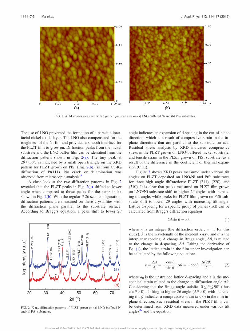
Figures 1(a) and 1(b) show the AFM height images
measured over a 1 lm� 1 lm scan area on �2-lm-thick
PLZT films deposited on LNO-buffered nickel and on PtSi
substrate, respectively. We measured the average grain size
to be �45 nm and �25 nm on PLZT films grown on LNO/Ni
and PtSi substrates, respectively. The root mean square
(RMS) surface roughness determined from AFM was
roughly the same value (�2 to 3 nm) for both samples grown
on LNO/Ni and PtSi substrates.
Figure 2 shows the 2h x-ray diffraction (XRD) patterns
measured on �2-lm-thick PLZT films deposited on LNO-
buffered Ni and PtSi substrates. The patterns indicate that
both samples are well crystallized without preferred orienta-
tion. All peaks can be indexed accordingly (JCPDS 56-0900).
114117-2 Ma et al. J. Appl. Phys. 112, 114117 (2012)
Downloaded 10 Dec 2012 to 146.139.77.245. Redistribution subject to AIP license or copyright; see http://jap.aip.org/about/rights_and_permissions
The use of LNO prevented the formation of a parasitic inter-
facial nickel oxide layer. The LNO also compensated for the
roughness of the Ni foil and provided a smooth interface for
the PLZT film to grow on. Diffraction peaks from the nickel
substrate and the LNO buffer film can be identified from the
diffraction pattern shown in Fig. 2(a). The tiny peak at
2h� 36�, as indicated by a small open triangle on the XRD
pattern for PLZT grown on PtSi (Fig. 2(b)), is from Cu-Kb
diffraction of Pt(111). No crack or delamination was
observed from microscopic analysis.5
A close look at the two diffraction patterns in Fig. 2
revealed that the PLZT peaks in Fig. 2(a) shifted to lower
angle when compared to those peaks for the same index
shown in Fig. 2(b). With the regular h-2h scan configuration,
diffraction patterns are measured on these crystallites with
the diffraction plane parallel to the substrate surface.
According to Bragg’s equation, a peak shift to lower 2h
angle indicates an expansion of d-spacing in the out-of-plane
direction, which is a result of compressive strain in the in-
plane directions that are parallel to the substrate surface.
Residual stress analysis by XRD indicated compressive
stress in the PLZT grown on LNO-buffered nickel substrate,
and tensile strain in the PLZT grown on PtSi substrate, as a
result of the difference in the coefficient of thermal expan-
sion (CTE).
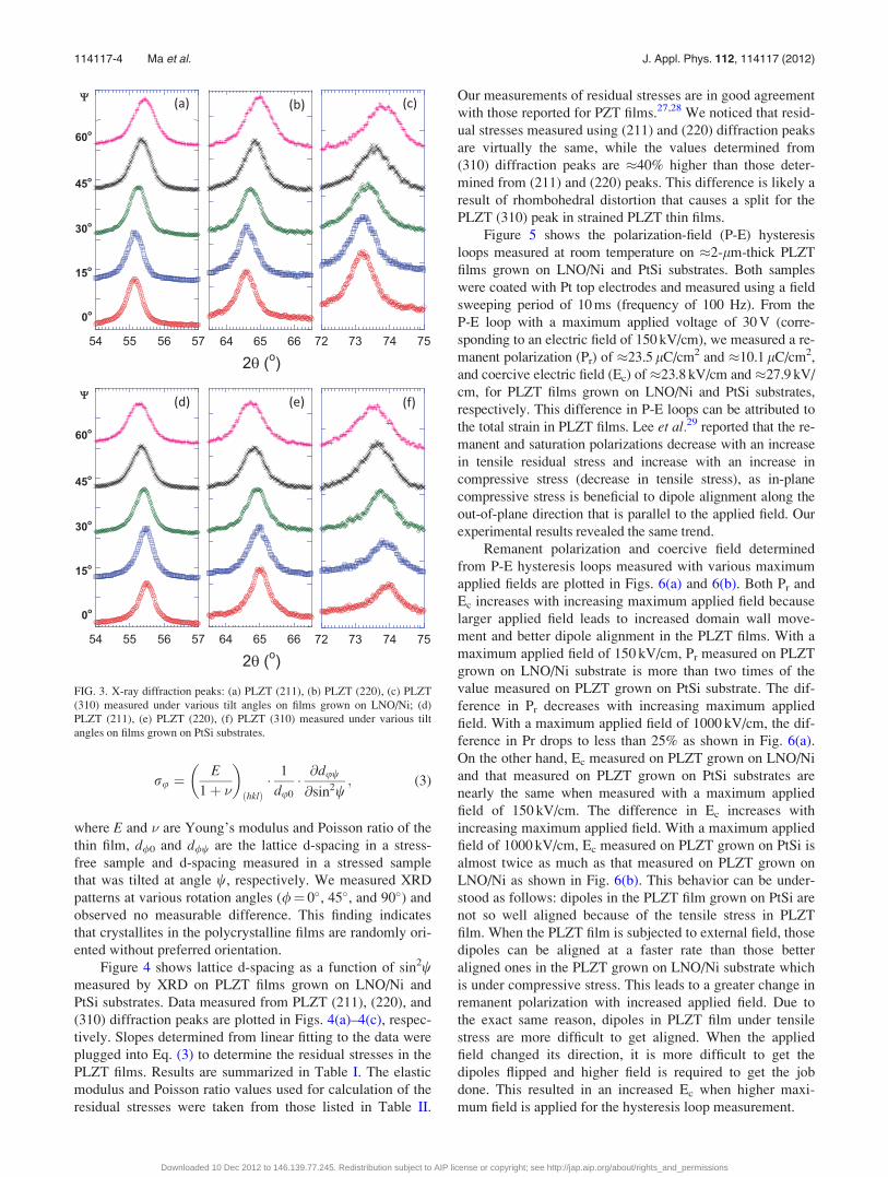
Figure 3 shows XRD peaks measured under various tilt
angles on PLZT deposited on LNO/Ni and PtSi substrates
for three high angle diffractions: PLZT (211), (220), and
(310). It is clear that peaks measured on PLZT film grown
on LNO/Ni substrate shift to higher 2h angles with increas-
ing tilt angle, while peaks for PLZT film grown on PtSi sub-
strate shift to lower 2h angles with increasing tilt angle.
Lattice d-spacing for a specific group of planes (hkl) can be
calculated from Bragg’s diffraction equation
2d sin h ¼ nk; (1)
where n is an integer (the diffraction order, n¼ 1 for this
study), k is the wavelength of the incident x-ray, and d is the
interplanar spacing. A change in Bragg angle, Dh, is related
to the change in d-spacing, Dd. Taking the derivative of
Eq. (1), the lattice strain in the film under investigation can
be calculated by the following equation:
e ¼ Dd
d0
¼ � cos hsin h
� Dh ¼ �cot h � Dð2hÞ2
; (2)
where d0 is the unstrained lattice d-spacing and e is the me-
chanical strain related to the change in diffraction angle Dh.
Considering that the Bragg angle satisfies 0� h� 90� (thus
cot h> 0), shifting to higher 2h angle (Dh> 0) with increas-
ing tilt w indicates a compressive strain (e< 0) in the film in-
plane direction. Such residual stress in the PLZT films can
be determined from XRD data measured under various tilt
angles22 and the equationFIG. 2. X-ray diffraction patterns of PLZT grown on (a) LNO-buffered Ni
and (b) PtSi substrates.
FIG. 1. AFM images measured with 1 lm� 1 lm scan area on (a) LNO-buffered Ni and (b) PtSi substrates.
114117-3 Ma et al. J. Appl. Phys. 112, 114117 (2012)
Downloaded 10 Dec 2012 to 146.139.77.245. Redistribution subject to AIP license or copyright; see http://jap.aip.org/about/rights_and_permissions
ru ¼E
1þ �
� �ðhklÞ� 1
du0
� @duw
@sin2w; (3)
where E and � are Young’s modulus and Poisson ratio of the
thin film, d/0 and d/w are the lattice d-spacing in a stress-
free sample and d-spacing measured in a stressed sample
that was tilted at angle w, respectively. We measured XRD
patterns at various rotation angles (/¼ 0�, 45�, and 90�) and
observed no measurable difference. This finding indicates
that crystallites in the polycrystalline films are randomly ori-
ented without preferred orientation.
Figure 4 shows lattice d-spacing as a function of sin2wmeasured by XRD on PLZT films grown on LNO/Ni and
PtSi substrates. Data measured from PLZT (211), (220), and
(310) diffraction peaks are plotted in Figs. 4(a)–4(c), respec-
tively. Slopes determined from linear fitting to the data were
plugged into Eq. (3) to determine the residual stresses in the
PLZT films. Results are summarized in Table I. The elastic
modulus and Poisson ratio values used for calculation of the
residual stresses were taken from those listed in Table II.
Our measurements of residual stresses are in good agreement
with those reported for PZT films.27,28 We noticed that resid-
ual stresses measured using (211) and (220) diffraction peaks
are virtually the same, while the values determined from
(310) diffraction peaks are �40% higher than those deter-
mined from (211) and (220) peaks. This difference is likely a
result of rhombohedral distortion that causes a split for the
PLZT (310) peak in strained PLZT thin films.
Figure 5 shows the polarization-field (P-E) hysteresis
loops measured at room temperature on �2-lm-thick PLZT
films grown on LNO/Ni and PtSi substrates. Both samples
were coated with Pt top electrodes and measured using a field
sweeping period of 10 ms (frequency of 100 Hz). From the
P-E loop with a maximum applied voltage of 30 V (corre-
sponding to an electric field of 150 kV/cm), we measured a re-
manent polarization (Pr) of �23.5 lC/cm2 and �10.1 lC/cm2,
and coercive electric field (Ec) of �23.8 kV/cm and �27.9 kV/
cm, for PLZT films grown on LNO/Ni and PtSi substrates,
respectively. This difference in P-E loops can be attributed to
the total strain in PLZT films. Lee et al.29 reported that the re-
manent and saturation polarizations decrease with an increase
in tensile residual stress and increase with an increase in
compressive stress (decrease in tensile stress), as in-plane
compressive stress is beneficial to dipole alignment along the
out-of-plane direction that is parallel to the applied field. Our
experimental results revealed the same trend.
Remanent polarization and coercive field determined
from P-E hysteresis loops measured with various maximum
applied fields are plotted in Figs. 6(a) and 6(b). Both Pr and
Ec increases with increasing maximum applied field because
larger applied field leads to increased domain wall move-
ment and better dipole alignment in the PLZT films. With a
maximum applied field of 150 kV/cm, Pr measured on PLZT
grown on LNO/Ni substrate is more than two times of the
value measured on PLZT grown on PtSi substrate. The dif-
ference in Pr decreases with increasing maximum applied
field. With a maximum applied field of 1000 kV/cm, the dif-
ference in Pr drops to less than 25% as shown in Fig. 6(a).
On the other hand, Ec measured on PLZT grown on LNO/Ni
and that measured on PLZT grown on PtSi substrates are
nearly the same when measured with a maximum applied
field of 150 kV/cm. The difference in Ec increases with
increasing maximum applied field. With a maximum applied
field of 1000 kV/cm, Ec measured on PLZT grown on PtSi is
almost twice as much as that measured on PLZT grown on
LNO/Ni as shown in Fig. 6(b). This behavior can be under-
stood as follows: dipoles in the PLZT film grown on PtSi are
not so well aligned because of the tensile stress in PLZT
film. When the PLZT film is subjected to external field, those
dipoles can be aligned at a faster rate than those better
aligned ones in the PLZT grown on LNO/Ni substrate which
is under compressive stress. This leads to a greater change in
remanent polarization with increased applied field. Due to
the exact same reason, dipoles in PLZT film under tensile
stress are more difficult to get aligned. When the applied
field changed its direction, it is more difficult to get the
dipoles flipped and higher field is required to get the job
done. This resulted in an increased Ec when higher maxi-
mum field is applied for the hysteresis loop measurement.
FIG. 3. X-ray diffraction peaks: (a) PLZT (211), (b) PLZT (220), (c) PLZT
(310) measured under various tilt angles on films grown on LNO/Ni; (d)
PLZT (211), (e) PLZT (220), (f) PLZT (310) measured under various tilt
angles on films grown on PtSi substrates.
114117-4 Ma et al. J. Appl. Phys. 112, 114117 (2012)
Downloaded 10 Dec 2012 to 146.139.77.245. Redistribution subject to AIP license or copyright; see http://jap.aip.org/about/rights_and_permissions
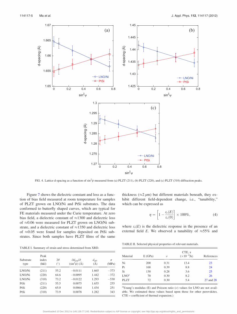
Figure 7 shows the dielectric constant and loss as a func-
tion of bias field measured at room temperature for samples
of PLZT grown on LNO/Ni and PtSi substrates. The data
conformed to butterfly shaped curves, which are typical for
FE materials measured under the Curie temperature. At zero
bias field, a dielectric constant of �1300 and dielectric loss
of �0.06 were measured for PLZT grown on LNO/Ni sub-
strate, and a dielectric constant of �1350 and dielectric loss
of �0.05 were found for samples deposited on PtSi sub-
strates. Since both samples have PLZT films of the same
thickness (�2 lm) but different materials beneath, they ex-
hibit different field-dependent change, i.e., “tunability,”
which can be expressed as
g ¼ 1� erðEÞerð0Þ
� �� 100%; (4)
where er(E) is the dielectric response in the presence of an
external field E. We observed a tunability of �55% and
FIG. 4. Lattice d-spacing as a function of sin2w measured from (a) PLZT (211), (b) PLZT (220), and (c) PLZT (310) diffraction peaks.
TABLE I. Summary of strain and stress determined from XRD.
Substrate
type
Peak
index
(hkl)
2h(�)
@d/w/@
(sin2w) (A)
d/0
(A)
r(MPa)
LNO/Ni (211) 55.2 �0.0111 1.665 �373
LNO/Ni (220) 64.6 �0.0095 1.442 �372
LNO/Ni (310) 73.2 �0.0122 1.293 �530
PtSi (211) 55.5 0.0075 1.655 255
PtSi (220) 65.0 0.0064 1.434 251
PtSi (310) 73.9 0.0078 1.282 343
TABLE II. Selected physical properties of relevant materials.
Material E (GPa) �
CTE, a(�10�6/k) References
Ni 200 0.31 13.4 23
Pt 168 0.39 8.8 24
Si 130 0.28 3.6 25
LNOa 70 0.30 8.2 26
PLZT 72 0.30 5.4 27 and 28
aYoung’s modulus (E) and Poisson ratio (�) values for LNO are not avail-
able. We estimated these values based upon those for other perovskites.
CTE¼ coefficient of thermal expansion.)
114117-5 Ma et al. J. Appl. Phys. 112, 114117 (2012)
Downloaded 10 Dec 2012 to 146.139.77.245. Redistribution subject to AIP license or copyright; see http://jap.aip.org/about/rights_and_permissions

�40% at room temperature under 100 kV/cm applied field
for PLZT deposited on LNO/Ni and PtSi substrates, respec-
tively. This difference in tunability can be attributed to dif-
ference in residual stress for PLZT films grown on different
substrates. Because the dipoles in PLZT film under compres-
sive stress have better tendency of getting aligned in the out-
of-plane direction, the dipole momentum is easier to get
changed under small applied field (or near zero-field); but
under high applied field, dipoles are more clamped and
dipole momentum is more difficult to get changed. This is
why we measured sharper peaks in the butterfly curve of
dielectric constant as a function of applied field for PLZT
grown LNO/Ni substrate and broader peaks for PLZT grown
on PtSi substrate.
Figure 8 shows the dielectric constant and loss measured
as a function of frequency for PLZT grown on LNO/Ni and
PtSi substrates. The dielectric constant decreases while
dielectric loss increases with increasing frequency for both
samples. No obvious effect observed due to different stress
levels in the PLZT films grown on LNO/Ni and PtSi
substrates.
Figure 9 shows the time relaxation for the current den-
sity measured at 25 �C on PLZT films grown on LNO/Ni and
PtSi substrates with a constant bias field of �100 kV/cm
applied across the top and bottom electrodes. The measure-
ments were conducted by keeping the top Pt electrode posi-
tive and the bottom Ni electrode grounded. Both curves
show strong initial time dependence with comparable magni-
tude in current density. The decay in dielectric relaxation
current obeys the Curie-von Schweidler law30
J ¼ Js þ J0 � t�n; (5)
where Js is the steady-state current density, J0 is a fitting
constant, t is the relaxation time in seconds, and n is the
slope of the log-log plot. Fitting the data to Eq. (5), we
FIG. 5. Polarization-field hysteresis loops measured at room temperature on
PLZT films grown on LNO/Ni and PtSi substrates.
FIG. 6. (a) Remanent polarization and (b) coercive electric field as a function of maximum applied field measured at room temperature on PLZT films grown
on LNO/Ni and PtSi substrates.
FIG. 7. Field-dependent dielectric properties measured at room temperature
on PLZT films grown on LNO/Ni and PtSi substrates.
114117-6 Ma et al. J. Appl. Phys. 112, 114117 (2012)
Downloaded 10 Dec 2012 to 146.139.77.245. Redistribution subject to AIP license or copyright; see http://jap.aip.org/about/rights_and_permissions

determined steady-state leakage current densities of �9.0
� 10�9 A/cm2 and �5.1� 10�8 A/cm2, and n values of 0.7
and 0.8 for �2-lm-thick PLZT grown on PtSi and LNO/Ni
substrates, respectively. Higher steady state leakage current
density measured for PLZT grown on LNO/Ni substrates is
likely due to larger grain size and therefore increased grain
boundary conduction when compared to PLZT film grown
on PtSi substrate.
The dielectric breakdown strength was measured on
250-lm-diameter capacitors with Pt top electrodes using the
“top-to-bottom” electrode configuration. The applied voltage
was increased by 5 V per second, and the breakdown
voltage was determined with a 1-lA criterion. Weibull statis-
tics31,32 was employed for failure behavior analysis. The em-
pirical two-parameter Weibull function for failure
probability distribution, also known as the “cumulative dis-
tribution function,” can be written as
FðtÞ ¼ 1� exp � t
g
� �b" #
; (6)
where b and g are fitting parameters, the Weibull modulus
and mean value of experimental observable t, respectively.
The Weibull modulus is a measure of sample distribution,
high values of b corresponding to smaller variation. For
breakdown field measurements, the parameter of interest is
applied field. Mean breakdown strength can be extracted
from points where the fitting lines intersect with the horizon-
tal line through lnðlnð1=ð1� pÞÞÞ¼ 0. We calculated the
sampling cumulative distribution parameter p, using Ber-
nard’s approximation, from the following formula33 for each
set of experimental data
p ¼ r � 0:3
N þ 0:4; (7)
where N is the total sample number and r is the sample se-
quential number.
Figure 10 shows the Weibull plot of breakdown field
strength obtained at room temperature from 30 capacitor
samples of PLZT grown on LNO/Ni and another 30 capac-
itor samples of PLZT grown on PtSi substrates. The solid
straight line is a least-square fitting to the two-parameter
distribution function given in Eq. (6). We measured mean
breakdown field strengths of 2.6� 106 V/cm and 1.5� 106
V/cm, and Weibull moduli b of 7.8 and 4.0, for the
�2-lm-thick PLZT films grown on LNO/Ni and PtSi sub-
strates, respectively. Note that PLZT samples grown on
LNO/Ni and PtSi are bearing compressive stress of
��370 MPa and tensile stress of �250 MPa, respectively,
as determined from XRD analysis. When an electrical
potential is applied between the top and the bottom elec-
trodes, the electrostrictive strain causes expansion in the
longitudinal direction (same direction as the applied elec-
tric field) and contraction in the radial direction (film
FIG. 8. Frequency-dependent dielectric properties measured at room tem-
perature on PLZT films grown on LNO/Ni and PtSi substrates.
FIG. 9. Time-relaxation current density measured on PLZT films grown on
PtSi and LNO/Ni substrates.
FIG. 10. Weibull plot for breakdown field strength of PLZT deposited on
LNO/Ni and PtSi substrates.
114117-7 Ma et al. J. Appl. Phys. 112, 114117 (2012)
Downloaded 10 Dec 2012 to 146.139.77.245. Redistribution subject to AIP license or copyright; see http://jap.aip.org/about/rights_and_permissions

in-plane direction). This condition leads to additional ten-
sile stress in the PLZT film that is subjected to the applied
field. A threshold value of external applied field (Eb) can
be defined to characterize the breakdown field strength in
a PLZT film that is free of residual stress. When there is
tensile residual stress in a PLZT film, such as the one
grown on a PtSi substrate, it needs less additional tensile
strain to reach the threshold strain value that will cause
dielectric breakdown. Therefore, this sample bearing resid-
ual tensile stress needs only an electric field of Eb � DE1
(with DE1> 0) to reach the breakdown threshold value.
For PLZT grown on LNO/Ni substrate, due to the existing
compressive stress, additional field strength DE2 is
required to compensate the residual compressive strain. In
other words, for the film to reach the threshold tensile
strain level value that will cause dielectric breakdown, a
total electric field of EbþDE2 (with DE2> 0) must be
applied. For this reason, we observed higher mean break-
down field strength in PLZT films grown on LNO/Ni when
compared to those grown on PtSi substrates. This differ-
ence in breakdown strength is a direct result of the differ-
ence in residual stresses inside these two types of samples,
PLZT films grown on LNO/Ni and PtSi substrates. Resid-
ual compressive strain in the PLZT film was found to be
beneficial to enhanced dielectric strength.
CONCLUSIONS
We have grown high-breakdown-strength ferroelectric
PLZT films on LNO-buffered Ni foils and PtSi substrates by
chemical solution deposition. Residual stress analysis by
XRD revealed compressive stress of ��370 MPa in the
PLZT grown on nickel foil but a tensile stress of �250 MPa
in the PLZT grown on PtSi substrates. We measured Pr of
�23.5 lC/cm2 and �10.1 lC/cm2, and Ec of �23.8 kV/cm
and �27.9 kV/cm, for PLZT films grown on LNO/Ni and
PtSi substrates, respectively. At room temperature, we meas-
ured a dielectric constant of �1300 and �1350 and dielectric
loss of �0.06 and �0.05 for PLZT films grown on LNO-
buffered Ni foils and PtSi substrates, respectively. Weibull
analysis determined the mean breakdown strength to be
2.6� 106 V/cm and 1.5� 106 V/cm for samples grown on
LNO-buffered Ni and PtSi, respectively. The difference in
dielectric breakdown strength can be attributed to the differ-
ence in residual stress for PLZT grown on LNO-buffered Ni
foil and PtSi substrates.
ACKNOWLEDGMENTS
This work was funded by the U.S. Department of
Energy, Vehicle Technologies Program, under Contract No.
DE-AC02-06CH11357.
1G. H. Haertling and C. E. Land, “Hot-pressed (Pb,La)(Zr,Ti)O3 ferroelec-
tric ceramics for electrooptic applications,” J. Am. Ceram. Sci. 54, 1–11
(1971).2J. F. Scott and C. A. Araujo, “Ferroelectric memories,” Science 246,
1400–1405 (1989).3K. Uchiyama, A. Kasamatsu, Y. Otani, and T. Shiosaki, “Electro-optic
properties of lanthanum-modified lead zirconate titanate thin films
epitaxially grown by the advanced sol–gel method,” Jpn. J. App. Phys. 46,
L244–L246 (2007).4B. Guttler, U. Bismayer, P. Groves, and E. Salje, “Fatigue mechanisms in
thin film PZT memory materials,” Semicond. Sci. Technol. 10, 245–248
(1995).5B. Ma, D. K. Kwon, M. Narayanan, and U. Balachandran, “Dielectric
properties of PLZT film-on-foil capacitors,” Mater. Lett. 62, 3573–3575
(2008).6M. D. Losego, L. H. Jimison, J. F. Ihlefeld, and J-P. Maria, “Ferroelectric
response from lead zirconate titanate thin films prepared directly on low-
resistivity copper substrates,” Appl. Phys. Lett. 86, 172906 (2005).7S. Kandasamy, M. K. Ghantasala, A. Holland, Y. X. Li, V. Bliznyuk, W.
Wlodarski, and A. Mitchell, “Heat treatment effects on the formation of
lanthanum-modified lead zirconate titanate THIN films,” Mater. Lett. 62,
370–373 (2008).8J. Ihlefeld, B. Laughlin, A. Hunt-Lowery, W. Borland, A. Kingon, and
J. P. Maria, “Copper Compatible Barium Titanate Thin Films for Embed-
ded Passives,” J. Electroceram. 14, 95–102 (2005).9A. I. Kingon and S. Srinivasan, “Lead zirconate titanate thin films directly
on copper electrodes for ferroelectric, dielectric and piezoelectric
applications,” Nat. Mater. 4, 233–237 (2005).10H.-J. Zhao, T.-L. Ren, N.-X. Zhang, R.-Z. Zuo, X.-H. Wang, L.-T. Liu,
Z.-J. Li, Z.-L. Gui, and L.-T. Li, “Preparation and properties of PLZT
thick films on silicon,” Mater. Sci. Eng. B 99, 195–198 (2003).11L. B. Kong and J. Ma, “Preparation and characterization of antiferroelec-
tric PLZT2/95/5 thin Films via a sol–gel process,” Mater. Lett. 56, 30–37
(2002).12R. Seveno, H. W. Gundel, and S. Seifert, “Preparation of antiferroelectric
PbZrxTi1�xO3 thin films on LaSrMnO3-coated steel substrates,” Appl.
Phys. Lett. 79, 4204–4206 (2001).13R. G. Polcawich, C.-N. Feng, S. Kurtz, S. Perini, P. J. Moses, and S.
Trolier-McKinstry, “AC and DC electrical stress reliability of piezoelec-
tric lead zirconate titanate (PZT) thin films,” Int. J. Microcircuits Electron.
Packag. 23, 85–91 (2000).14K. J. Choi, M. Biegalski, Y. L. Li, A. Sharan, J. Schubert, R. Uecker, P.
Reiche, Y. B. Chen, X. Q. Pan, V. Gopalan, L. Q. Chen, D. G. Schlom,
and C. B. Eom, “Enhancement of ferroelectricity in strained BaTiO3 thin
films,” Science 306, 1005 (2004).15J.-W. Lee, G.-T. Park, C.-S. Park, and H.-E. Kim, “Enhanced ferroelectric
properties of Pb(Zr,Ti)O3 films by inducing permanent compressive
stress,” Appl. Phys. Lett. 88, 072908 (2006).16J. H. Haeni, P. Irvin, W. Chang, R. Uecker, P. Reiche, Y. L. Li, S. Choud-
hury, W. Tian, M. E. Hawley, B. Craigo, A. K. Tagantsev, X. Q. Pan,
S. K. Streiffer, L. Q. Chen, S. W. Kirchoefer, J. Levy, and D. G. Schlom,
“Room-temperature ferroelectricity in strained SrTiO3,” Nature 430, 758–
761 (2004).17F. Xu, S. Trolier-McKinstry, W. Ren, B. Xu, Z.-L. Xie, and K. J. Hemker,
“Domain wall motion and its contribution to the dielectric and piezoelec-
tric properties of lead zirconate titanate films,” J. Appl. Phys. 89, 1336–
1348 (2001).18B. Ma, M. Narayanan, and U. Balachandran, “Dielectric strength and reli-
ability of ferroelectric PLZT films deposited on nickel substrates,” Mater.
Lett. 63, 1353–1356 (2009).19B. Ma, S. Tong, M. Narayanan, S. Liu, S. Chao, and U. Balachandran,
“Fabrication and dielectric property of ferroelectric PLZT films grown on
metal foils,” Mater. Res. Bull. 46, 1124–1129 (2011).20S. Liu, B. Ma, M. Narayanan, S. Chao, R. E. Koritala, and U. Balachan-
dran, “Improved properties of barium strontium titanate thin films grown
on copper foils by pulsed laser deposition using a self-buffered layer,”
J. Phys. D: Appl. Phys. 45, 175304 (2012).21Q. Zou, H. E. Ruda, and B. G. Yacobi, “Improved dielectric properties of
lead zirconate titanate thin films deposited on metal foils with LaNiO3
buffer layers,” Appl. Phys. Lett. 78, 1282–1284 (2001).22P. S. Prev�ey, “X-ray diffraction residual stress techniques,” Metals Hand-
book (American Society for Metals, 1986), pp. 380–392.23J. Zacharias, “The temperature dependence of Young’s modulus for nickel,”
Phys. Rev. 44, 116–122 (1933).24J. Merker and D. Lupton, “High temperature mechanical properties of the
platinum group metals,” Platinum Met. Rev. 45, 74–82 (2001).25M. A. Hopcroft, W. D. Nix, and T. W. Kenny, “What is the Young’s mod-
ulus of silicon,” J. Microelectromech. Syst. 19, 229–238 (2010).26L. Qiao and X. F. Bi, “Strain state, microstructure and electrical transport
properties of LaNiO3 films grown on Si substrate,” J. Phys. D: Appl. Phys.
41, 195407 (2008).
114117-8 Ma et al. J. Appl. Phys. 112, 114117 (2012)
Downloaded 10 Dec 2012 to 146.139.77.245. Redistribution subject to AIP license or copyright; see http://jap.aip.org/about/rights_and_permissions

27R. J. Ong, D. A. Payne, and N. R. Sottos, “Processing effect for Integrated
PZT: Residual stress, thickness, and dielectric properties,” J. Am. Ceram.
Soc. 88, 2839 (2005).28G. A. C. M. Spierings, G. J. M. Dormans, W. G. J. Moors, M. J. E.
Ulenaers, and P. K. Larsen, “Stresses in Pt/Pb(Zr,Ti)O3/Pt thin-film stacks
for integrated ferroelectric capacitors,” J. Appl. Phys. 78, 1926 (1995).29J.-W. Lee, C.-S. Park, M. Kim, and H.-E. Kim, “Effects of residual stress on
the electrical properties of PZT,” J. Am. Ceram. Soc. 90, 1077–1080 (2007).
30K. Jonscher, Dielectric Relaxation in Solids (Chelsea Dielectrics Press,
London 1983).31W. Weibull, “A statistical distribution function of wide applicability,”
J. Appl. Mech. 18, 293–297 (1951).32L. A. Dissado, “Theoretical basis for the statistics of dielectric break-
down,” J. Phys. D: Appl. Phys. 23, 1582–1591 (1990).33See, for example, D. J. Smith, Reliability, Maintainability and Risk: Prac-
tical Methods for Engineers (Newnes, 2001).
114117-9 Ma et al. J. Appl. Phys. 112, 114117 (2012)
Downloaded 10 Dec 2012 to 146.139.77.245. Redistribution subject to AIP license or copyright; see http://jap.aip.org/about/rights_and_permissions