Elektor-1975-11.pdf - World Radio History
66
-
Upload
khangminh22 -
Category
Documents
-
view
2 -
download
0
Transcript of Elektor-1975-11.pdf - World Radio History


Tit E TIM electronicsDept. 9 56. Fortis Green Road.
Muswell Hill, London, N10 3HN.
telephone: 01-883 3705
C - MOS
1-24 25-99 100vp
CD4000AE 23p 19p 15p
CD4001AE 23p 19p 15p
CD4002AE 23p 19p 15pCD4006AE £1.59 £1.33 £1.06CD4007AE 23p 19p 15p
CD4008AE £1.75 £1.46 £1.17CD4009AE Use CD4049CD4010AE Use CD4050CD4011AE 23p 19p 15p
CD4012AE 23p 19p 15pCD4013AE 69p 58p 46pCD4014AE £1.75 £1.46 £1.17CD4015AE 0.75 £1.46 £1.17CD4016AE 69p 58p 46pCD4017AE £1.75 £1.46 £1.17CD4018AE £2.51 £2.09 £1 .67CD4019AE 80p 66p 53pCD4020AE £1.97 £1.64 £1.31CD4021AE £1.75 £1.46 £1.17CD4022AE £1.83 El . 53 £1.22CD4O23AE 23p 19p 15pCD4024AE £1.26 £1.05 84pCD4025AE 23p 19p 15pCD4026AE £2.79 £2.33 £1.86CD4027AE 98p 82p 65pCD4028AE £1.53 £1.28 £1.02CD4029AE £1.12 £1.76 £1.41CD4030AE 71p 59p 47pCD4035AE £1.75 £1.46 £1.17CD4040AE £2.01 £1.68 £1.34CD4042AE £1.49 £1.24 99pCD4049AE 69p 58p 46pCD4050AE 69p 58p 46pCD4051AE £2.78 £2.32 £1.85CD4052AE £2.78 £2.32 £1.85CD4056AE £2.12 £1.76 £1.41CD4060AE £2.51 £2.09 £1.67CD4066AE £1.13 94p 75pCD4068AE 28p 24p 19pCD4069AE 28p 24p 19pCD4070AE 28p 24p 19pCD4071AE 28p 24p 19pCD4077AE 71p 59p 47pCD4081AE 28p 24p 19pCD4082AE 28p 24p 19pC04085AE £1.28 £1.06 85pC04086AE £1.28 £1.06 85pCD4093AE £1.56 £1.20 £1.04CD4099AE £2.95 £2.46 £ 1 .96
74 TTl
1-24 25-99 100
7400 14p 12p 10p7401 14p 12p 10p
7402 14p 12p 10p
7403 15p 12ip 10p
7404 16p I3p llp7408 16p I3p llp7409 16p 13p llp7410 16p 13p lip7413 29p 24p 20p7417 27p 221p 20P7420 16p 13p llp7427 27p 22)p 18p7430 16p I3p llp7432 27p 22)p 18P7437 27p 22;P 18p7441 75p 62p 50p7442 65p 55p 43p7445 85p 7Ip 57p7447 95p 83p 67p7447A 95p 83p 67p7448 85p 7Ip 57p7470 30p 25p 20p7472 25p 2Ip 17P7473 30p 25p 20p7474 32p 26p 2Ip7475 47p 39p 31p7476 32p 26p 21p7482 75p 62p 50P7485 £1.30 £1.09 87p7486 32p 26p 21p7489 £3.56 £2.80 £2.107490 49p 40p 32p7491 65p 55p 45p7492 57p 46p 36p
7493 49p 40p 32p7495 67p 55p 45p
74100 £1.08 89p 72p74107 35p 28p 22p
74121 34p 28p 23p74122 47p 39p 31974141 78p 63p 53p74145 68p 58p 48p74154 £1.75 £1.48 86p
74174 £1.00 83p 67p74180 £1.06 88p 71p74181 £3.20 £2.50 £1.9074192 £1.35 £1.14 90p74193 £1.35 £1.14 90p74196 £1.64 £1.34 99p
SIEMENS LCD's LINE -0 -LIGHTLIQUID CRYSTAL DISPLAY complete withsocket and removable reflective backing,Ref AN4132R 13rnm character height. Canbe directly driven by Notional SemiconductorsAlarm Clock chip MM5316. £13.99
PHOTO -DARLINGTON
2N5777Vceo; Vcbo 25v, Vebo 8v
/7 Vceo; Vcbo 25v, VEBO Bv
hle 2500, Ic 250 mA 35p.
I .C. SOCKETS
Dual -in -line 105Pins 8 14 16 24 28 36 40 8 10
Pricel3p 15p 15p 26p 30p 39p 44p 31p 35p
0.125"dia. lens(TIL209)1* 10. 100
Red 16p 15p 13p Green 27p 24p 22p Orange 27p 249 22p Yellow 34p 3lp 29p
Free snap -on plastic retainer
Low Cost Red GaissPMotorola MLED 500in a 1092 package. 15P
NEW LED Linear Cursorseach device contains 10 lightemitting diodes in o 20pin dual -in -line package. Ideal for solidstore analogue meters Or dials.Type 101 RED £2.26
LINEAR
+ 555 (8 pin dip) V 55p 811A0002 £3.01 MC1358 (CA3065) £1.16 SN76544N £1.81
555 (10-99) T Blp 556 (14 pin dip) £1.29 CA2111 £1.1.9
MC1375 £1.48 SN76550-2 (TAA550) 891,SN76552-2 81p
CA3045 £1.69 MC1455 (555T) 62p SN76660N (TBA120) 75P
703 (RF/IF Amp) 68p CA3046 88p MC1456CG £1.68 SN76666N (CA3065) £1 .12
709 (8 pin dip) 38p CA3053 59p MC1458CP1 84p
709 (T0-99) 45P CA3065 £1.60 MCI 468G £2.18 TAA263 £1.50709 (14 pin dip) 39p CA3075 £1.64 MCI 495L £4.24 TAA300 £2.16710 (8 pin dip) 39p CA3078 £1.26 MCI 496G 96p TAA310A £1.87710 (10-99) 45P CA3080 59p TAA320 £1.44710 (14 pin dip) 44p CA3081 £1.86 MC3302P £1.50 TAA350 £2.43711 (10-99) 51p CA3082 £1.86 MC340I P 74P TAA370 £3.45711 (14 pin dip) 44p CA3089E (T DA1200) £2.43 TAA550 75p
720 (A.M. Radio) £1.76 CA3097E £1.67 MFC4000B 87p TAA570 £2.74723 (T0-99) £1.09 CA3123E £1.76 MFC4060A 79p TAA700 £5.03723 (14 pin dip) 74p CA3401E (LM3900) 68p MFC6030A 79p 741 (8 pin dip) 36p CA3600E £1,44 MFC6040 96p TBA120S £1.25741 (T0-99) 43p MFC6070 £1.66 TBA231 £1.02741 (14 pin dip) 36p CT7001 £5.34 TBA281 (723) £2.59747 (14 pin dip) £1.04 MM5314 £4.80 TBA500Q £3.16748 ( 8 pin dip) 42p LOO5TI (T0.3) £1.46 MM5316 £9.99 TBA520Q £3.85748 (T0-99) 46p 1036T I (T0.3) £1.46 TBA5300 £3.27748 (14 pin dip) 49p 1.037T1 (10-3) £1.46 MVR5V (T0-3) £1.45 TBA5400 £3.72753 (F.M. 1st. I .F .1 L129 (SOT -32) 85p MVR12V (T0-3) £1.45 TBA5500 £5.29
£1.08 LI30 (SOT -32) 85p MVRISV (T0-3) £1.45 TBA560C0 £5.2975491 88p L131 (50T-32) 85p 75492 £1.10 NE540L £1.25 TBA625A £1.03
1.M301T (Tr.' -99) 65p NE546A £1.16 TBA625B £1.03Regulators 100 mA LM301 S (E. pin dip) 59p NE555V 73p TBA625C £1.0378105WC (10-92) 60p LIA)1A T(T0-99) 67p NE556 £1.2978L12WC (T0-92) 60p LM301A S (8 pin dip) 59p NE560B £5.06 TBA651 £1.8778L15WC (10-921 60p LM307 T (10-99) 59p NE56IB £5.06 T8A7200 £2.79
LM307 S (8pin dip) 57p NE562B £5.06 T8A7500 £2.79Regulators 10OrnA LM308 T (10-99) £1,96 NE563 £2.96 TBA800 £1.1178105AWC (TBA625A)90p 1M308 S (8 pin dip) 98p NE565N £2.63 TBA810S £1.2478112AWC (TBA625B) 90p LM308A T (T0 -99)E7.92 NE566V £1.87 TBA810AS £1.2478L15AWC (TBA625C)90p LM3O8A S (8 pin dip) NE567V £2.63 TBA820 86p
£6.90 TBA9200 £4.71Regulators 500mA LM309K £2.34 SL414A £2.09 TBA9900 £4.7178M05HC £1.35 LM339 £2.25 SL415A £2.7578 M12HC £1.35 LM370N £2.85 SL437D £7.50 TCA2700 £5.2478M15HC £1.35 LM371 £2.08 SL440 £2.84 TCA760 £2.1678M18HC £1.35 1M372N £1.99 TCA800Q £7.2478M24HC £1.35 LM373N £2.99 SL610C £2.03 TCA830S £1.04
LM377N £2.71 SL611C £2.03 TCA940 £2.25Regulators IA LM380 £1.25 51.612C £2.037805KC (T0-3) E2.09 1M381 £1.85 51613C £4.31 TDAI054 £1.507812KC (T0-31 £2.09 LM382 £1.66 51620C £3.06 TDA1200 £2.437815KC (T0-31 £2.09 LM703 68P SL621C £3.06 TDA1405 80p I
7818KC (T0-31 £2.09 SL622C £7.62 TDA1412 80P 17824KC (To -3) £2.09 I.1+81820 £1.03 St.623C £5.57 TDA1415 80p 4
LM2111 £1.12 SL624C £2.84 TDA2010 £3.00Regulators IA LM3900 69p SL630C £1.87 TDA2020 £3.757805UC (10-220) £1.72 SL640C £3.757812UC (10-220) £1.72 MC1303L £1.84 SL641C £3.75 ULN2111A £1.5278I5UC (10-220) £1.72 MC1306P BOp SL645C £3.757818UC (T0-2201 £1.72 MC1310P £2.39 SL650C £9.857824UC (10-2201 £1.72 MC1312 £2.42 ZN414 £1.26
ICL8038 £3.52 MC1314 £4.13MC1315 £4.62
SN75491NSN75492N
88p £1.10 MINITRON
Av-1-0212 £6.93MC1327 £1.12MC 1330P 84 SN76001N (TAA611) £1.82
AY -1-5051 £1.44AY -5-1224 £3.95 AY -5-3500 £6.59 AY -5-3507 £6.59 AY -5-4007 £7.94
MC1339P £1.52MC1350 64pMCI351 88pMC1352 88pMC1357 £1.52
SN76003N £3.30SN76013N £1.98SN76023N £1.98SN76227N (MC1327) £1.89SN76532N £1.88
Minitton Filament Displaybidirectional 0.36"3015F 0;9 L/H d.pt.30150 - 1 £1.08.
SPECIAL PURCHASE
enables
LIT707 90p; LIT747 £1.990.3'. 0.6".
ICI1 1 II. -
0.16- 0.2"dia. lens(MLED 650)
1+ 10* 100 1. 10* 100 *,
27p 24p 22p 18p 16p 14p 33p 30p 27p 30p 27p 259 33p 30p ?7p 30p 27p 25p 35p 32p 29p 35p 33p 30p
- - - -
dia. lens
NEW Opto-isolotorsILI (4N25 o. TIL 116)6 pin industry standard package2.5KV isolation £1.00
NEW
Litronix Double Digit Displays0.5", Common Anode 2 R./H
D .P .'sDL721 gives 1.9DL727 gives 0.0. to 9.9Suitable for Clocks; Instruments;T .V. Chonnel IndicatorOur Price £4.75 each..
NOTICEPostage & Pocking Charges
With the recent inc. ease inpostal charges and a continuingincrease in packagingwe have been forced to reviewour policy.Henceforward:1. Orders valued at £5 or
more will be post free.2. All U.K. 'small package'
orders will go first class moil.3. Minimum postage & pocking
charge will increase to 20p.
SEVEN SEGMENT DISPLAYS
litronix
Nankin'
Monsanto
COMMON COMMON COMMON COMMON OurANODE ANODE ANODE CATHODE PriceR/H L/H :
I R/tiDec. Pt. Dec. Pt. Dec. Pt.
RED DL707P DL707 DL701 DL704-£1.824
GREEN WN51 MAN52 MAN53 MANS4 £1.821
0.3" RED
YELLOWMAN7IMAN81
MAN72MANEI2
MAN73MAN83
MAN74MAN84
£1.824£1.824
ORANGE MAN3610 MAN3620 MAN3630 MAN3640 £1.82a
GREEN XAN51 XAN52 XAN54 £1.494RED XAN71 XAN72 XAN74 £1.49.YELLOW XAN81 XAN82 XAN84 £1.49
GREEN MAN4510 MAN4520 MAN4530 MAN4540 £2.32a
0.4" RED
YELLOWMAN4710MAN4810
MAN4720MAN4820
MAN4730MAN4830
MAN4740MAN4840
£2.324£2.32
ORANGE MAN4610 MAN4620 MAN4630 MA N4640 £2.320
C.A. VII C.A. C.C. L.,/i1 C.C.Dec Pr. - I Dec Pt. - I
0.6" RED DL747 01746 DL750 DL749 £2 410
NOTE: MAN4000 series pinouts ore 1.1 pin dil the same os MAN50;70 & 80 series.
VAT INCLUDEDItems 'worked with a include 8% VATItems unmarked include VAT at 25%
ADVERT. No.1. of Series B.CALLERS WELCOME

arusement elektor november 1975 - 1101
CAPACITORSlAID RESISTORS TRANSISTORS IC's CONNECTORS
Use DORAMcomponents foryourproject
SWITCHES CASES INDICATORS
The doorvi* to Amateur Electronics
144
UMW404ONLY
QC POST AND PACKING
* DORAM'S NEW CATALOGUE OFFERS THOUSANDS UPON THOUSANDS OFQUALITY ELECTRONIC COMPONENTS AND AUDIO ACCESSORIES FROM
TRUSTED BIG NAME MANUFACTURERS.ilk ALL COMPONENTS ARE INDIVIDUALLY CODED AND PRICED - MANY NEW
COMPONENTS ADDED FROM CUSTOMER REQUESTS.
* 16 EXTRA PAGE DATA SECTION.UNIQUE FREE UP -DATE PRODUCT INFORMATION SERVICE DURING LIFE
'T. SPAN OF CATALOGUE.III ALL COMPONENTS SENT BY RETURN OF POST.
POST AND PACKING FREE (only applies for Great Britain, N. Ireland and
B.F.P.O. Nos. - overseas orders F.O.B.)
111 NO QUIBBLE REPLACEMENT PART SERVICE
PIM., doorway to amateur electronics
DORAM ELECTRONICS LIMITEDI P. 0. Box TRBI Leeds LS12 2UF
I enclose 600. Please send me by return mynew Doram Catalogue. (Overseas ordersexcept for B.F.P.O., please add 30p foroost and packing surface only).
PLEASE PRINT BLOCK CAPITALS
NAME
ADDRESS
Post Code

1102 - elektor november 1975 publisher's notict
Many Elektor circuits are accompanied by designs for printed circuits. Forthose who do not feel inclined to etch their own printed circuit boards,a number of these designs are also available as ready -etched and predrilledboards. These boards can be ordered from our Canterbury office.Payment, including 0.15 p & p, must be in advance.Delivery time is approximately three weeks.Bank account number: A/C No. 11014587, sorting code 40-16-11Midland Bank Ltd, Canterbury.
circuitedwin amplifieraustereo 3 -watt amplifieraustereo power supplyaustereo control amplifieraustereo disc preampuniversal frequency referencedistortion metera/d convertertap sensorminidrum gyratorminidrum mixer/preampminidrum noiseminiature amplifierlight dimmerbeetleequa amplifierelectronic loudspeakermostapcar power supplydigital rev counter (control p.c.b. only!)car anti -theft alarmmos clock 5314 clock circuitmos clock 5314 display boardmos clock timebaseminidrum tapminidrum ruffle circuitautomatic bassdrummicrodrurnaerial amplifiercoilless receiver for MW and LWtap preamptwin minitron displaytwin led displaytwin decade counterrecip-riaadisc preamp 76131maxi displayversatile digital clockdil-led probebig ben 95compressortv soundcar clock (2 boards)car clock front panel (transparent redplastic)tup/tun testertup/tun tester front panelp.c.b. and wiring testerrhythm generator M 2527400 sirenCA3090AQ stereo decoderkitchen timercapacitance meter
NEW:circuittap preamp front panels:
powerinputvolumetonewidth
clamant clock, alarmclamant clock, time signalota plltv tennis, main pcbtv-tennis, modulator/oscillatorfrequency countertap powertv tennis 5 -volt supply
number issue price % VAT97-536 6 1.20 (25)HB11 5 1.10 (25)HB12 5 0.55 (25)HB13 5 1.50 (25)HB14 5 0.65 (25)HD4 5 1.10 ( 8)1437 1 1.65 ( 8)1443 3 0.90 ( 8)1457 1 0.60 ( 8)1465A 2 0.80 (25)1465B 2 0.55 (25)1465C 2 1.05 (25)1486 6 0.55 (25)1487 6 0.45 ( 8)1492 4 2.20 ( 8)1499 1 1.20 (25)1527 2 0.50 (25)1540 2 1.05 ( 8)1563 4 1.25 ( 8)1590 1 0.55 ( 8)1592 4 1.40 ( 8)1607A 1 1.15 ( 8)1607B 1 0.85 ( 8)1620 4 0.70 ( 8)1621A 2 0.70 (25)1621B 3 1.10 (25)1621C 3 0.55 (25)1661 2 0.95 (25)
(25)3166 5 0.80 (25)4003 4 1.80 (25)4029-1 2 1.40 ( 8)4029-2 2 1.40 ( 8)4029-3 2 1.40 ( 8)4039 2 0.50 ( 8)4040A 3 0.95 (25)4409 2 1.50 ( 8)4414B 6 1.10 ( 8)5027A-FB 2 1.85 ( 8)5028 2 1.25 (25)6019A 3 1.20 (25)6025 2 1.40 (25)7036 6 1.75 8)
7036-3 6 0.90 8)9076* 4 1.70 8)9076i2A 4 1.90 8)9106* 5 0.55 8)9110* 5 0.80 (25)9119* 5 0.75 (25)9126* 5 0.80 (25)9147* 5 0.75 ( 8)9183* 5 0.75 ( 8)
number issue price % VAT
1626A 7 1.55 (25)1626B 4 1.55 (25)1626C 4 1.55 (25)1626D 4 1.55 (25)1626E 4 1.55 (25)4015-13 7 1.30 ( 8)4015-16 7 0.85 ( 8)6029 7 1.10 (25)9029-1A* 7 3.80 ( 8)9029-2* 7 0.90 ( 8)9033* 7 1.30 ( 8)9072* 7 1.90 (25)9218A' 7 0.80 ( 8)
ELENTVolume 1 - number 7
Editor : W. van der HorstDeputy editor : P. HolmesTechnical editors : J. Barendrecht
G.H.K. DamE. KrempelsauerFr. ScheelK.S.M. Walraven
Art editor C. SinkeDrawing office : L. MartinSubscriptions : Mrs. A. van Meyel
UK. Staff:Editorial : T. EmmensAdvertising : P. Appleyard
Editorial offices, administration and advertising:6 Stour Street, Canterbury CT1 2XZ.Tel. Canterbury (0227) - 54430.Telex: 965504.
Elektor has been published every two months untilAugust 1975; it now appears monthly.Copies can be ordered from our Canterbury office.The subscription rate for 1975 is £ 3.60 (incl. p & p);the first issue (Nov/Dec 1974) will be included in thisat no additional cost.Single copies: £ 0.35 (incl. p & p: £ 0.45).
Subscription rates (airmail):
Australia/New ZealandEuropean countriesoutside UKUSAAll other countries
- 8 issues £ 7.20
- 8 issues £ 5.20- 8 issues £ 6.25- 8 issues £ 6.40
Subscribers are requested to notify a change ofaddress four weeks in advance and to return envelopebearing previous address.Members of the technical staff will be available toanswer technical queries (relating to articles publishedin Elektor) by telephone on Mondays from 14.00 to16.30.Letters should be addressed to the departmentconcerned: TQ = Technical Queries; ADV = Advertise-ments; SUB = Subscriptions; ADM = Administration;ED = Editorial (articles submitted for publication etc.);EPS = Elektor printed circuit board service.
The circuits published are for domestic use only. Thesubmission of designs or articles to Elektor impliespermission to the publishers to alter and translate thetext and design, and to use the contents in otherElektor publications and activities. The publisherscannot guarantee to return any material submitted tothem.All drawings, photographs, printed circuit boards andarticles published in Elektor are copyright and maynot be reproduced or imitated in whole or partwithout prior written permission of the publishers.
Distribution: Spotlight Magazine Distributors Ltd.,Spotlight House, 1, Bentwell road, Holloway,London N7 7AX.
* with solder mask
All prices include VAT at the rate shown in brackets. Copyright © 1975 Elektor publishers Ltd - Canterbury.
Printed in the Netherlands.
aeon elektor november 1975 - 1103
a/7
AP selektor 1109
,P
tv tennis 1111The popularity of television tennis games has prompted Elektor to produce a design than can easily be built by
ro,
the home constructor for a modest cost. Although several designs have previously appeared on the market, itwas felt that there was a need for a simple circuit using a minimum of components.
frequency counter
circuit described here is based on the popular 74 TTL logic family. The first part deals with the basic counter,Logic IC's are so cheap that it is possible to build a digital frequency counter for a very small outlay. The
1121
,P
humming kettle - J.P. Ku hler jr. 1129
and in a subsequent article additions to the instrument will be described.
P
p
active flash slave - R. Buggle 1129
tap -powerrS
1130This 'TAP -power' circuit has been specially designed for the TAP preamp system. It includes touch -controlledswitches for turning the whole equipment on or off and for selecting the main power amplifiers or the head-phone amplifiers, a power supply for the TAP pre -amp, simple headphone amplifiers and a disc preamplifier.N.6. See the 'Missing link' on page 1156.
0
clamant clock (1) 1134Any horologist who keeps a digital clock in the same room as conventional clocks cannot but feel sad to see itsitting there, mute and reproachful amongst its more vociferous brothers, its only sound the feeble humming ofthe mains transformer. In this article we look at various ways of providing the digital clock with a voice, so thatit can draw our attention to the fact that it is keeping time far more accurately than any mere mechanical
ii
clock.
,
lie detector - J. Jacobs 1143
'PSp
P
brake lights for model cars - R. Zimmer
universal ota pll 1144Elektor has taken a lead in drawing attention to the possibilities of the PLL (Phase Locked Loop).
1143
i
i
The Universal OTA (Operational Transconductance Amplifier) PLL described here is a printed -circuit modulewhich can form the nucleus of many different types of receiver.
r.
tv test pattern generator 1149A television pattern generator is one of the most useful TV service aids. It simplifies checking of the videostages, adjustment of picture geometry, and perhaps most important, setting up of convergence in colour
1with a pencil point - W. Schmidt 1153
circuit.receivers. Using logic IC's for the generation of the test pattern allows the construction of a simple and reliable
1,
market 1154
1
i'6
pi
r:

1104 - elektor november 1975 advertisemer
BOOK CORNERDIGITAL ELECTRONICCIRCUITS AND SYSTEMS
NOEL M. MORRISMACMILLAN BASIC BOOKS IN ELECTRONIC SERIESUsing the example of the electronic calculator to illustrate many of the systems, this text beginswith a description of basic logic functions, including a full coverage of boolean algebra andKarnaugh maps. It then goes on to describe high-speed switching elements, logic gates, calculatingfunctions, asynchronous and synchronous counters, shift registers and display decoding circuits.
£ 2.45
C,
mom a
ELECTRONICnommem=mi
EQUIPMENT RELIABILITYJ.C. Clule
The principles of assessing the reliability of electronic equipment, including the mathematicbackground, component failure data, and methods to improve reliability, are described and e:plained at a level suitable for degree and diploma students upwards.
Experiments with oper-ational amplifiersby G.B. ClaytonThis book covers a wide range of practi-cal operational amplifier applications. Itprovides circuits which include compo-nent values, and suggest measurementsthat can be made in order to study cir-cuit action.The experiments will be useful for a
large variety of measurement and instru-mentation systems. The way in whichperformance errors are related to thecharacteristics of the particular amplifierused in a circuit are treated in anappendix.
Paperback £ 3.30Hardcover £ 6.85
Please Supply the following (all prices include postage and packing)
£ 2.6
Linear integrated circuitapplicationsby G.B.Clayton
ORDER FORM
copy/copies of Experiments with Operational Amplifiers by G.B. Clayton at£ 6.85 per copy (hard cover)
copy/copies of Experiments with Operational Amplifiers by G.B.Clayton at£ 3.30 per copy (paperback)
copy/copies of Linear Integrated Circuit Applications by G.B.Clayton at £ 6.85per copy (hard cover)
This book is concerned with the newtcircuits now available, important fcsuch things as signal measurement anprocessing systems.After first looking at how to use opeational amplifiers as measurement amp)fiers and in active filter circuits, thbook then deals with the more recent)introduced liner integrated circuitmonolithic integrated circuit mocklators, four quadrant multipliers, timerwaveform generators and phase lockeloops.
Paperback £ 3.31Hardcover £ 6.8!
copy/copies of Linear Integrated Circuit Applications by G.B. Clayton at £ 3.per copy (paperback)
copy/copies of Digital Electronic Circuits and Systems by Noel M. Morris£ 2.45 per copy
copy/copies of Electronic Equipment reliability by J.C. Cluley at £ 2.65 per cop
To: Technical Book Services Ltd., I enclose £Dept. 7,25 Court Close
NameBrayMaidenheadBerks SL6 2DL Address

ferbsement elektor november 1975 - 1105
loin the Digital Revolutionreach yourself the
atest techniques of
ligital electronics:omputers and calculators are only the beginning of theigital revolution in electronics. Telephones, wristwatches,V, automobile instrumentation - these will be justome of the application areas in the next few years.
.re you prepared to cope with these developments?
his four volume course - each volume measuring14" x 81" and containing 48 pages - guides youtep-by-step with hundreds of diagrams and questionstrough number systems, Boolean algebra, truth tables,e Morgan's theorem, flipflops, registers, counters anddders. All from first principles. The only initial abilityssumed is simple arithmetic.
Nt the end of the course you will have broadened yourlorizons, career prospects and your fundamental under-tanding of the changing world around you.
Desi9n ofDigital Systems
EWE 1 ComputelArmtnietc 1
Also available - a moreadvanced course in 6volumes:
1. Computer Arithmetic
2. Boolean Logic
3. Arithmetic Circuits
4. Memories & Counters
5. Calculator Design
6. Computer ArchitectureOffer Order this togetherwith Digital Computer Logic &Electronics for the bargain
£5.95 plus 50 p p &p.
price of £ 9.25, plus 50 p p & p.
Design of Digital Systems contains over twice as muchinformation in each volume as the simpler course DigitalComputer Logic and Electronics. All the information in thesimpler course is covered as part of the first volumes ofDesign of Digital Systems which. as you can see from itscontents also covers many more advanced topics.
)esignerManagerEnthusiastscientistEngineerstudent
These courses were written so that you could teachyourself the theory and application of digital logic.Learning by self -instruction has the advantages ofbeing quicker and more thorough than classroomlearning. You work at your own speed and mustrespond by answering questions on each new pieceof information before proceeding to the next.
ivarantee - no risk to youf you are not entirely satisfied with Digital::omputer Logic and Electronics or Design of Digitalsystems, you may return them to us and yournoney will be refunded in full, no questions asked.
Digital ComputerLogic andElectronicsA Self -instructional Course
Book Basiccomputerlogic
Book 2 cLircLitalelements
Book 3
pokyDesigning circuitsto carry outlogical functions
Flipflopsandregisters
C PG.ine MA IC.intablA VI Unwo BA leardaD)
Digital ComputerLogic andElectronicsA Self otiAnctove Cane
Book 1 %;.-
8'S
£3 .9 5plus 50 p packing andsurface post anywherein the world
Quantity discountsavailable on request.
Payment may be madein foreign currencies.
VAT zero rated.
To: Cambridge Learning Enterprises,FREEPOST, St. Ives, Huntingdon, Cambs PE17 4BR
" Please send me set(s) of Digital Computer Logic& Electronics at £ 4.45 each, p & p included.
" or set(s) of Design of Digital Systems at £ 6.45each, p & p included.
" or combined set(s) at £ 9.75 each, p & p included.
Name
Address
E71
delete as applicableNo need to use a stamp - just print FREEPOST on the envelope.

1106 - elektor november 1975 dCIVETI15eITIU
Have you Fenthis years most importantcomponent catalogue yet?
HENRY'S 1975CATALOGUEIS NOW AVAILABLE
Don't buy another electronic component until you've consulted theHenry's 1975 issue! It's packed with more items than ever before-over 5000 in all, making the Henry's range of electronic componentsthe largest in the UK for the home constructor.There are literally dozens of new lines and new ranges to get excitedabout ! And many components are selling at reduced prices. Get yourcopy soon, and start reading these 200 pages of vital statistics aboutelectronic components. If you don't, you'll miss out on a lot of kits,projects and test gear, apart from all the other products.
ONLY 50p+20p p & p
Complete withFREE 50p
Discount Voucher!
FREE to Educational
Establishments when ordered
on official headed notepaper.
Get your copy NOW - send remittance of 70p (cheque or P.O.).
ELECTRONIC FOOTBALL &TENNIS WITH THE FABULOUS
VIDEO SPORTON YOUR OWN TVPlay three exciting elec-tronic ball games. FOOT-BALL. TENNIS. HOLE INTHE WALL on your ownTV. Just plug Video Sportinto the aerial socket ofyour TV and away you go.Completely safe for you,your children and your TV.Mains operated.
OUR INCREDIBLE PRICE£29.50 INCL. VAT
DEMONSTRATIONS NOW IN ALL HI FlCENTRES.
SINCLAIR MODULES & KITSSINCLAIR PROJECT 80
ST80 Stereo preamplifierAudio Filter UnitZ40 15 Watt AmplifierZOO 25 Walt Amplifier
TEXAN STEREO AMPLIFIERFeatures glass fibre pc board, gardnerslow fieldtransformer 6 -IC's10 -transistorsplus diodesetc. Designed by TexasInstruments engineers for Henry's and P W1972. Overall size 15'4" x 2i x 6'4" mainsoperated. Free teak sleeve with every kit
£29.95 (carriage 50p.)(also built and tested £39.501
TEXAN STEREO FM TUNERFeatures capacity diode tuning lead andtuning meter indicators, mains operatedHigh performance and sensitivity. Overallsize in teak sleeve 8" x 2%:." xComport:' kit with teak sleeve.
£26.25 (f. i P 50p I(also built .nil tested £31.20)
£14.05£8.17£6.40£8.17
PZ5 Power Supplies for 1 or 2 Z40 £5.72PZ6 Power Supplies (S Tab) for 1 or 2 Z40 £8.18TRANSFORMER FOR PZ8FM TUNERSTEREO DECODERIC20 power amp kitPZ20 power supply for 1 01 2 IC20
£4.86£14.05£9.34£9.34£5.88
PACKAGE DEALS .carr..nackg 391,12 x Z40 ST80 PZ5 £29.322 x Z60 ST80 PZ6 £32.602 x Z60 ST80 PZ8-trans £40.42805 Kit £42.25
SINCLAIR SPECIAL PURCHASES'Project 60 stereo prearnp
'Project 605 Kit
AM/FM MODULESLP1179 LP1171
Combined AM/FM tuner modules, togetherwith a small number of R.C.'s Ferrite Aerial,make up a sensitive FM/MW/LW tuner.6 Volts supply, supplied with data and circuitsheets. All Henry's prices inclusive of VAT
MIDLANDS:NEW ELECTRONICS STbRE OPEN.94/96 UPPER PARLIAMENT STREETNOTTINGHAM TEL 40403LONDON:231 TOTTENHAM COURT ROAD WI.(LOWER SALES FLOOR)
w 1
NR#NRAy54
FREE Brochureon New KITSWhether professional,
student, teacher or amateur,the field of electronics can open
up a new world for you.
CROFTON don't just sell kits, we offer you a technicalback up service to ensure your success
The following is a selection of some of the more popular kits* Mullard CCTV Camera* PE CCTV Camera* PE Rondo Quadraphonic Four Channel Sound(Designer Approved )* Electronic Ignition* Electronic Flash* PW Tele-Tennis Game* U.H F. Modulator* Bench Power Supply* Wobbulator
All ETI Top Projects* Many of the Elektor ProjectsNOTE: PC.Bs for most published projects available to order
CROFTON ELECTRONICS LTDDept.A 124 Colne Road,Twickenham,Middx. 01 898 1569
£7.94(post 2011 1
£23.44(post 25p .I
LP1171 combined IF strip £4.60LP1179 FM front end and AM gang £4.60£8.62 the pair.Suitable Ferrite aerial 87p.
Electronic Centres404.406 Electronic Components & Equipment 01 402 8381309 PA Disco- Lighting High Power Sound 01 723 6963303 Special offers and bargains storeAll mail to 303 Edgware Road London W2 18W
HifianclEh, ironicCentre, 0gam 6 pn
correct at time of preparation Subject to change wit hour notice E Er0
CRYSTALSFast delivery of prototypes andproduction runs
INCLUDING:Statek LF crystals in TO5 packageBuckman LF, clock and mobile radio crystalsAstro Filter crystalsJan General purpose crystalsCrystals for Elektor clock designs available.
Interface QuartzDevices Limited
29 Market Street,Crewkerne, Somerset.
Tel.: (046031) 2578Telex: 46283

elektor november lu/b - 1107
ELECTRONIC COMPONENT DISTRIBUTORSP.O. Box 25 Canterbury Kent
Telephone: Canterbury (0227) 52139
Elektorprinted circuit boards and binders.
Prices as in this issue
Component kits and individual componentsavailable by return of post from stocks at
Canterbury. All prices include VAT and P.+P.741-8/14DI L £0.22 E.1109 £6.087400 £0.15 7038A £3.687401 £0.15 TBA231 .... £1.027405 £0.19 CA1310AE.. £2.277447 £1.20 CA3080 .... £0.797473 £0.30 CD4011AE . .£0.237495 £0.69 CD4017AE . .£1.7674121 £0.32 CD4049AE .10.67MM5314N .. £4.77 TBA120 £1.24SFE 6 mA (6 MHz Filter) £0.90I/C EXTRACTOR £0.55 NE555V £0.65I/C INSERTER £1.40 2N3055 £0.54
Crystals for any requirementPH 100 5 -digit 30 MHz freq. counter £99.50
Above types are partial examples.Write or phone for details.
7 p.m. to 9 p.m. phone Dover (0304) 812332
Stock List free on request.
RCA CMOS PRICES ARE DOWNCMOS from the leachn9 manufacturers at their new 1 off prices
CD4000 0.17 C04019 0.46 C04041 0.69 CD4060 0.92 C04086 0.57C04001 0.17 C04020 0.92 C04042 0.69 CD4063 0.90 C04093 0.66C04002 0.17 C04027 0.79 C04043 0.83 CD4066 0.58 C04095 0.86C04006 0.97 C04023 0.17 CD4044 0.77 C04068 0.18 C04099 1.50
C04007 0.17 C04024 0.64 C04045 1.15 CD4069 0.18 MC14501 0.32CD4008 0.79 C04025 0.17 C04046 1.10 C04070 0.18 MC14502 0.65C04009 0.46 C04026 1.42 C134047 0.74 C04071 0.18 MC14508 4.20C04010 0.46 004027 0.46 CD4048 0.46 CD4072 0.18 MC14510 1.26
C04011 0.17 C04029 0.94 C04049 0.46 C04073 0.18 MC14511 1.95C04012 0.17 C04030 0.46 CD4050 0.46 CD4075 0.18 MC14518 1.03
C04013 0.46 C04031 1.81 CD4051 0.77 C04076 1.27 MC14520 1.03
C04014 0.83 004033 1.14 CD4052 0.77 C04077 0.18 MC14528 0.87004015 0.83 C04034 j.83 C04053 0.77 C04078 0.18 MC14553 4.07C04016 046 C04035 0.97 C 04054 0.95 C04081 0.18 MC14566 1.21
C04017 0.63 C04036 7,47 C04055 1.08 C04082 0.18 MC14585 1.45
CD4018 0.83 C04040 0.88 CD4J56 1 08 C04085 0.57 MM74C14 1.16
RCA 1975 CMOS Databook 400 pages of data sheets and 200 pages of circuits,applications and other useful information £2 30 (No VATI + 37p p&pNew 1975 MOTOROLA McMOS Databook £2 30 (No VAT) h 47p p&p
CLOCK COMPONENTS, KITS, etc.6 DIGIT ALARM CLOCK KITS - complete except for case - bleep alarm -intensity control - snooze With 0.3" LED displays £19.86
With 0.5" LED displays £23.76QUARTZ CRYSTAL TIMEBASE - suitable for any digital clock32.768 kHz Min. Xtal: Higft accuracy/stability for clock or watch . . . £ 3.6050 cps Crystal Timebase Kit - will provide stable 50 cps for any clock ICgiving time accurate to within a few seconds a month; contains small PCB,32.768 kHz Xtal, 3 CMOS IC's, trimmer, zener, C's, R's, IC skts £ 6 40DL704E 0.3" Red Common Cathode 7 segment LED display . . . only .85pFND500 0.5" Red Common Cathode 7 segment LED display £ 1.505LT01 0.5" 4 digit green Phosphor Diode clock display with am/pm £ 5.80MK50253 4 or 6 digit 12 or 24 hr format alarm clock IC with snooze . £ 5.60AY51202 4 digit clock IC specially designed for use with 5LT01 . . £ 5.60MM5314 4/6 digit clock IC . . £4.44 AY51224 4 digit clock IC £ 4.25MK5030M CMOS watch IC for LED display with date and seconds . . . £19.50Display PCB's are available for clocks & counters (up to 8 digits)SOLDERCON IC PIN SOCKETS (using these & nylon supports, 28 pin Skt: 30p)The sensible method for lowest cost sockets for IC's, displays, CMOS, TTLStrip of 100 for 50p 400 for £2.00 1000 for £4.00 3000 for £10.50
7.way Boss Switch: 7 ultramin. toggle switches in 14 pin DIL £ 2.60
ADD VAT at 8% (higher rate does not apply to any of the above)15p p&p on orders under £3. Despatch is First Class Post BY RETURN.Price List & Data sent free with any order, or on request (an sac helps)Official Orders welcomed, written, phoned or telexed, from Univs, Polys, Schools,Govt. Depts, Nat. Inds., Rated Cos. etc. Fastest delivery for R & D
SINTEL 531K1 Aston St.Oxford Tel. 0865 43203Tlx. 837650 A/B ELECTRONIC OXFD iz--1 11 1
Technology spoken here.AMBIT supplies coils, filters andsemiconductors, based on a themeof wireless and entertainment elec-tronics.Linear ICs:CA3089E FM IF System £1.94*CA3090AQ PLL MPX decoder £3.75MC1310P PLL MPX decoder £2.20TBA120AS FM IF and detector £1.00*SN76660N FM IF and detector £0.75*uA720/CA3123 AM radio system £1.40TBA651 AM radio system £1.81uA753 FM IF gain block £0.99MC1350 FM IF gain with AGC £0.70NE560/1/2 HF PLL systems, each £3.19NE565/7 LF PLL tone decoders £2.75NE566 Function generator £2.00
LM380 2w AF amp. £1.00LM381 stereo low noise preamp £1.85TBA810AS 7w AF amp. £1.30
ICL8038CC One chip waveform source,with sine square and triangle outputs. Inc.12 pages of data and applications £3.10
723CN DIL voltage regulator £0.807800 series voltage regulators - see theprice list for full details.
Coils and filters from TOKO.455kHz IFTs with capacitor.10mm square type 10E 27p each.7mm square type 7P 27p each.Set of three of either 7P or 10E 60p.
10.7 MHz IFTs with capacitor(s).10mm square type 10K interstage IF 30p .2 x 10mm square type 10E ratio detectortype system for 10.7 MHz 50pK586 10.7 MHz quadrature coil for suchICs as the CA3089E, TBA120 etc. 30pTK342 10.7 MHz dual quadrature coil forultra low distortion . ( 2 x 10K) 55p
10.7 MHz FM IF filtersCFS 10.7M ceramic filter, sim.to SFE andFM4 types for WBFM at 10.7MHz 40p3132 6 pole linear phase filter IF 2.253125 4 pole linear phase IF filter 1.30
AM IF filters for 455/470 kHz.MFH41T 4kHz BW mechanical IF filterfor transistor/IC use £1.45MFH71T 7kHz BW mechanical IF filterfor transistor/IC use £1.45CFT455/470C 6kHz ceramic IF filter for455 or 470 kHz £0.50CFU050D Hi Q 6kHz ceramic IF filter for470kHz use. £0.55
Full cataolgue system 40p, or shortformprice list free with an SAE. Telephone:(0277)216029 Telex 995194.
Radio modules and kits for AM/FMEF5600 FM tunerhead with 5 varicaptuned circuits, AFC & AGC. The best youcan buy for the money £10.00.EC3302 FM varicap head. 3 tuned circuitswith AFC. Good value at £5.00MT3302 AM/FM gang tuner with the samecircuit for FM as EC3302 £5.008319 Dual mosfet, AFC, AGC, 4 tunedcircuits, varicap control FM head. £9.001185 FM IF system with single ceramicIF filter and the functions of the CA3089IC IF system. £4.35991200 FM IF strip, with mute, AFC,AGC, meter drive, 8 pole IF filter and adual detector for 0.1% THD. £9.0099720 MW varicap tuner, with RF stageceramic IF filter and AGC. £9.959720- the 99720 in kit form £8.00
Also in our general catalogue: 15cmwirewound slider potentiometers, acomprehensive car radio kit, FM tun-er kits, Larsholt FM tunersets,. DAUtrimmers, 15:1 ratio hyper abruptvaricap tuning diode for MW/LW-with 300+ pF swing, (matched gps.)
AMBIT international: 37 High Street, Brentwood, Essex, U.K.All prices exclude VAT. UK customers please add 25% VAT and 20p perorder postage. Min. CWO £1.00. Overseas customers: please allow extrafor postage. Any excess postage or VAT will be credited. Payment may bemade with Access, Eurocard, Mastercharge. Simply quote card number.

1108 - elektor november 1975 advertisenu
elektorback issuesare stillavailable
over
and mostlyincluding postag
Prices for singleincluding P & P*)
EditionNo. 5 is a
summer circuitissue. It contains
one hundred cir-cuit designs all provedoriginal. Price 80p (U.K.
e).
copies (1, 2, 3, 4 and 6,
U.K. Europe U.S.A. Australia/New Zealand45p 65p 78p 90p
* may be subject to increase in postal rates
We shall be exhibiting a variety of working projectsselected from current and future issues of Elektor,
InternationalAudio Festival
and Fair.October 20 26
at Olympia,London.
Elr
in the rand MILotandnumber dill
3 S HALLGRAND
ENTRANCE FRCOLYMPIA WAY
Members of our Editorial Staff will be on hand toanswer your technical queries, and we look for-ward to seeing you there.
ELEKTOR PUBLISHERS LTD . 6, Stour Street, Canterbury, CT1 2XZ, Tel.: 0227-54430.

tennis elektor november 1975 - 1111
tw (ODORS
The popularity of television tennisgames has prompted Elektor toproduce a design that can easily bebuilt by the home constructor fora modest cost. Although severaldesigns have previously appearedon the market, it was felt thatthere was a need for a simplecircuit using a minimum of compo-nents.
ri1.11,315131 74e4 0 0 0 0 0 0,
In order to keep costs down the TVtennis circuit generates the most basic`picture' possible, i.e. two 'bats' and a`ball'. The ball is 'served' from one sideof the screen or the other and theplayers move their bats up and downthe screen to intercept the path of theball. If the ball strikes a bat it is re-turned, otherwise it leaves the side ofthe screen and a 'new ball' must beserved. Should the ball reach the upperor lower edge of the screen during itstraverse across the screen it will 're-bound'. The upper and lower bound-aries are, however, not displayed on thescreen.The output of the TV tennis game isused to modulate a VHF oscillator sothat the game may be plugged directinto the aerial socket of a television.
Principle of operationFor those not familiar with TV a briefresume of the principles involved mayprove helpful. A TV picture is, of course,generated by an electron beam scanningacross the phosphor -coated face of a
cathode-ray tube in a zig-zagfashion from top to bottom.At the end of each horizontalline the beam flies back tothe left hand edge of thescreen and starts the next lineslightly lower down thescreen. Each complete scan(frame) of the picture con-sists of either 405 or 625lines, depending on the trans-mission standard. To reducethe bandwidth required totransmit the video infor-mation a complete frame isnot transmitted in a singlescanning of the picture, but ismade up of two 'fields' con-taining half the number oflines in a frame. These twofields are interlaced with eachother to make up a completeframe. Fields are transmitted
at a 50 Hz rate, therefore frames aretransmitted at half that rate,i.e. 25 frames per second.
The video waveformIn order to build up a picture on thescreen the brightness of the trace mustbe modulated by varying the electron

1112 - elektor november 1975 tv tenn
beam current. This is controlled by theamplitude of the video waveform. Sothat the scanning of the electron beamin the TV set is in synchronism with thereceived signal in order to build up thepicture correctly, field sync. pulses aretransmitted (at the end of each field)and line sync. pulses are transmitted(at the end of each line).To distinguish sync. pulses from videoinformation, sync. pulses are negative -going and confined to a voltage belowthat required for zero beam current(black level). Video information oc-cupies a range of voltages above blacklevel up to the voltage required tosaturate the TV tube phosphor (peakwhite level). Circuitry in the TV dis-tinguishes between sync. pulses andvideo information. Field sync. pulses
also have a longer duration to dis-tinguish them from line sync. pulses.From the foregoing some of the require-ments for the circuit become apparent.Firstly, the circuit must contain oscil-lators capable of generating field andsync. pulses at the appropriate fre-quencies (50 Hz and 15625 Hz re-spectively). Secondly, circuitry forgenerating the bat and ball waveforms,and for controlling the movement ofthese, is required. Fortunately, since weare concerned only with white bats andball on a black background the onlymodulation required is peak white levelor black level, so analogue circuitry isnot needed to produce these waveforms,and digital logic circuits can be used togenerate the rectangular pulses necess-ary.
Block DiagramThe operation of the circuit is beunderstood with the aid of a blocdiagram (figure 1). Sync. pulses fro]the field and line oscillators are mixein the video mixer and then fed to timodulator. They are also used to coltrol the timing of the other waveform
All the video waveforms are generateusing monostable multivibrators and ;the generation of the 'bats' is simple:this will be considered first. The lefhand player's horizontal bat generatcIC5 is triggered continuously from thline sync oscillator. A presettable triggfdelay is incorporated so that the pulEappears a little time after the line synpulse. This ensures that the bat appealsome way in from the left hand edge c
1
videomixer OA
video output
fieldsync.oscil-lator
preset
linesync.oscil-lator
IC9
triggerdelay
horizontal
delay
IC1
ball
playercontrol(right)
preset
delay
delay
playercontrol(left)
IC2
vertical
horizontal
right bat
vertical
horizontal
ballsignal
batsignal
(r)
FF1
FF2
inte-grator
inte-grator
9029.1
vertical
Innis elektor november 1975 - 1113
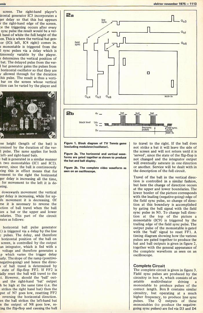
screen. The right-hand player'sizontal generator IC3 incorporates ager delay so that this bat appearsr the right-hand edge of the screen..7.e the triggering occurs after everysync pulse the result would be a ver-
1 band of white the full height of theThis is where the vertical bat gen-
or (IC6 left, IC4 right) comes in.s monostable is triggered from the1 sync pulses via a delay which istinuously variable by the player.s determines the vertical position ofbat. The delayed pulse from the ver-1 bat generator gates the pulses fromhorizontal oscillator so that they arey allowed through for the durationthis pulse. The result is thus a verti-bar on the screen whose vertical
ition can be varied by the player and
)se height (length of the bat) isrmined by the duration of the ver-
1 pulse. The same applies for bothleft- and right-hand bats.ball is generated in a similar manner
[I two monostables (IC1 and IC2).Never, since the ball is continuouslyving this in effect means that forvement to the right the horizontalger delay is increasing all the time,for movement to the left it is de -
'sing.
downwards movement the verticalger delay is increasing, while for up-ds movement it is decreasing. Ofrse it is necessary to reverse thection of ball travel when the ballces a bat or the upper and lowerndaries. This part of the circuitrates as follows:
horizontal ball pulse generator1) is triggered via a delay by the linec pulses. The delay, and thereforehorizontal position of the ball onscreen, is controlled by the outputan integrator, which is fed with avoltage and therefore generates a
p which varies the trigger delayarly. The slope of the ramp (positive -negative -going) and hence the direc-t of ball travel is determined bystate of flip-flop FF2. If FF2 is
ially reset the ball will travel to theit. However, should the 'ball' out -
and the right-hand tat' outputh be high at the same time (i.e. thestrikes the right hand bat) then the
put of N7 goes low, resetting FF2reversing the horizontal direction.
en the ball strikes the left-hand batn the output of N8 goes low, re-:ing the flip-flop and causing the ball
2a
fieldsync.
PQic4
linesync.
Q c2 Qic6
n
0
9029.2a
Qic3
Qicl
Qic5
2bblack level
4v
1.4v
bat ball bat
Ov
1111L_ITTIMITIT 1111111111111 IIIIIIIIIIIIUline syncpulses
11TITITTILJMITfield sync.pulse9029-2b
Figure 1. Block diagram of TV Tennis game(excluding modulator/oscillator).
Figure 2a. The horizontal and vertical wave-forms are gated together as shown to producethe bat and ball display.
Figure 2b. The complete video waveform asseen on an oscilloscope.
to travel to the right. If the ball doesnot strike a bat it will leave the side ofthe screen and will not return until it is`served', since the state of the flip-flop isnot changed and the integrator outputwill eventually saturate in one directionor another. Service will be dealt with inthe description of the full circuit.
Travel of the ball in the vertical direc-tion is controlled in a similar fashion,but here the change of direction occursat the upper and lower boundaries. Thelower border of the picture correspondswith the leading (negative -going) edge ofthe field sync pulse, so change of direc-tion at this boundary is accomplishedby gating the ball signal with the fieldsync pulse in N5. To change ball direc-tion at the top of the picture amonostable (IC9) is triggered by thetrailing edge of the field sync pulse. Theoutput pulse of the monostable is gatedwith the 'ball' signal to reset FF1. Atiming diagram showing how the variouspulses are gated together to produce thebat and ball outputs is given in figure 2,together with the general appearance ofthe complete waveform as seen on anoscilloscope.
Complete CircuitThe complete circuit is given in figure 3.Field sync pulses are produced by thecircuitry in box A, which consists of anastable multivibrator driving amonostable to produce pulses of thecorrect length. Box B contains similarcircuitry, but operating at a muchhigher frequency, to produce line syncpulses. The Q outputs of thesemonostables (to produce the negative -going sync pulses) are fed via D3 and D4

1114 - elektor november 1975 tv tent
35V
0
I 03V-FEI
NT(
04V
4,8
/4121.o
TUN
012
fl
Aoil
A017
A013
"I i,
TUNOUS
C
74121
IC1 ... IC9 = 9 x 74121IC10 = N1... N4 = 1 x 7400IC11 = N5... N8 = 1 x 7400IC12 = N9... N11 =%x 7402IC13 = FF1, FF2 = 1 x 7474
131 ... D14= DUS t1N41481Ti ... T12 = TUN c8C1088,T13 = AF 239
a 34
104
ball
~~^C
4/4, TUN
1C2
/4121
_1
o
ouc FF1 047
C31
-0T11
fr,404UN
.71 11
TUN
,±I"'0-1
,,,' 74121
mm
F
right
~&~"N
lot IDUS 40^
,C4
TUN
/121
0,
of -IIOUS T N
L^
011. 70-1
74121
t I
left
TUN
='.
L.-
13
9029 2 see text
11o
ou FF21_
049
L 4P5,09 ltnrn Cu 17, ernol
4k7
T1285,0
C32 RS1
rUN
4
3a

r tenniselektor november 1975 - 1115
igure 3. The complete circuit of the TVnnis game. The modulator/oscillatorrcuit is shown inset at the bottom right -and corner.
igure 3a. Suggested modification to deriveeld sync pulses from the mains for mainsmy versions of the game. This should give alore stable picture than the free -runningeld oscillator.
igure 4. Circuit of the mains power supply)r TV Tennis.
Parts list for figures 3, 5 and 7
Resistors:R1,R2,R39,R43,R55 = 4k7R3,R4,R47 = 33 kR5,R9 = 10 k NTCR6,R10 = 820 E2R7,R11 = 5k6R8,R12 = 18 kR13,R16,R17,R20,R21,R24,R25,
R28,R29,R32,R33,R36,R56,R59= 10 k
R14,R18,R22,R26,R30,R34,R40,R44,R57 = 100 k
R15,R19,R23,R27,R31,R35,R53 = 2k2R37,R41,R48,R52 = 2k7R38,R42 = 10 czR45 = 1k8R46,R49,R54 = 1 k
R50 = 12 kR51 = 470 E2
R58 = 27 kP1,P2 = 4k7 lin. presetP3,P6 = 47 k lin.P4,P5,P7,P8 = 100 k lin. preset
Capacitors:C1,C2 = 4/17, 10 VC3 = 22 nC4,C8,C11,C14,C17,C20,C23 = 100 nC5,C6 = 15 nC7 = 390 pC9,C15,C21 = 1n5C10,C16,C22 = 180 pC12,C18,C24,C26,C27,C28,C29 = 470 nC13 = 68 nC19,C25,C30 = 220 n
C31,C32 = 47 µ, 10 VC33 = 3n3C34 = 150 nC35 = 3p3C36 = 4 ... 20 p trimmerC37 = 47 p
Semiconductors:T1,T2,T3,T4,T5,T6,T7,T8,T9,T10,T11,
T12 = BC547BT13 = A F239D1 ... D14 = 1N4148IC1,1C2,1C3,1C4,1C5,1C6,1C7,1C8,1C9
= 74121IC10,1C11 = 7400IC12 = 7402IC13 = 7474
Sundries:L = 4 wdg, 1 mm q5 c u , (1) 8 mmHF Tr = 60 2 -> 240 2 impedance con-
verter (see text)
4
8V
oi
DUS
500mA
100n
C4
* see text
Al147o St]
L129
CI= C2470µ 100n
I16V
R202
-r
9218
*C3 C==
T1611
C)50Hz
Z 4V7
250mW
®5V
TO.126
1 3 2
L 12 9
O
to the junction of R58 and R59. Thisportion of the circuitry fuctions as thevideo mixer. Black level occurs whenthe Q outputs of IC7 and IC8 are bothhigh and the bat and ball inputs to D 11,D12 and D13 are all low. The voltage atthe junction of R58 and R59 is thensolely determined by the value of theseresistors and is about 1.35 V. When async pulse occurs then the junction ofthese two resistors is held down toabout 1 V via D3 or D4. When bat orball signals occur the inputs to D11,D12 or D13 go high, so the potentialat the junction of R58 and R59becomes about 4 V. If the unit is to beused for mains only operation theastable in box A can be dispensed withand field sync pulses may be derivedfrom the 50 Hz mains by the modifi-cation shown in figure 3a. P1, R5, R6,C 1 and C2 are omitted; the sync pulsesare fed in at the original connection tothe positive side of Cl on the board,and the track between this point andthe output of N2 (pin 6 of IC10) mustbe broken.The sync pulses are buffered by emitterfollowers T1 and T2 to avoid loadingthe monostables excessively. Thebuffered sync pulses are then fed via thetrigger delays to the appropriatemonostables which generate the hori-zontal and vertical components of thebat and ball waveforms. The triggerdelay circuits are all identical in prin-ciple and merely vary in componentvalues. The trigger delay for IC3 oper-ates as follows: normally T5 is turnedon by base current through R23. Itscollector voltage (and hence the A in-puts of IC3) is low. The cathode of D7is held at a few volts positive by thevoltage via R21 from P7 (max. 2.5 V),and since T2 is turned off the anode ofD7 is at 0 V. Cl 5 thus has a voltageacross it equal to the voltage on thecathode of D7 minus the base -emittervoltage of T5. On the leading edge ofthe line sync pulse T2 turns on, forwardbiassing D7. C15 thus charges until thevoltage across it is5 V - VbeT2 - VD7 - VbeT5 = 3 Vapproximately. On the trailing edge ofthe sync pulse T2 turns off. The voltageon the cathode of D7 therefore revertsto its initial value (the potential sup-
plied via R21 from P7). However, sincethe voltage across C15 is still 3 V thenthe base of T5 must be negative. T5therefore turns off. C15 now chargesvia R22 until the voltage on the base ofT5 reaches about 0.7 V when T5 turnson and the collector voltage goes low,triggering the monostable.It is evident that the trigger delay isdependent on the time taken to chargeC15 after T5 has been turned off, whichis in turn dependent upon the voltageapplied to the cathode of D7 from P7.The trigger delay may thus be varied bya d.c. voltage, in the case of the batsderived from the various poten-tiometers, and in the case of the ballfrom the emitters of Ti 1 and T12.In the case of the ball, as explainedearlier, the trigger delay in both hori-zontal and vertical directions is continu-ously varied to achieve motion of theball. Horizontal movement of the ball iscontrolled by FF2 and the integratorconstructed around T12. When FF2 ispreset the Q output is high and C32charges via P9 and R50. The potentialon the emitter of T12 therefore rises.This is applied to R13, thus continu-ously increasing the trigger delay andmaking the ball move to the right. WhenFF2 is cleared (reset) then C32 dis-charges via P9 and R50. The voltage onthe emitter of T12 falls, thus decreasingthe trigger delay and making the ballmove to the left. The rate of charge ordischarge of C32, hence the speed of theball, is determined by the setting of P9.Vertical ball movement is controlled ina similar manner by FF I and T11. Notethat in this circuit the AND -gates shownin the block diagram have been replacedby NOR -gates connected to the Q out-puts of the monostables. This is ofcourse exactly equivalent to AND -gatesconnected to the Q outputs (DeMorgan's theorem).The horizontal bat trigger delays arepreset,by P7 for the right-hand player,and by P4 for the left-hand player. Thisallows the position of the bats to beadjusted to a few cm away from thesides of the screen. The vertical positionof the bats is continuously adjustable,by P6 for the right-hand player and P3for the left-hand player. P5 and P8 arepresets used to adjust the bat position

1116 - elektor november 1975 tv tenr
Figure 5. Printed circuit board and com-ponent layout for the modulator/oscillatorcircuit.Figure 6. Printed circuit for the TV Tennisgame.
Figure 7. Component layout for the mainboard.
so that P6 and P3 are effective over thefull height of the screen.
Service of the ballIt is evident that if the state of FF2 isnot reversed by a coincidence betweenthe ball and one of the bat signals thenthe voltage at the emitter of T12 willcontinue to rise or fall as C32 eithercharges or discharges, until it reacheseither zero volts or supply minus thebase -emitter voltage of T12. The ball.will then disappear off one side of thescreen or the other and will not return.For this reason (as well as for the rulesof the game) it is necessary to 'serve' theball when this has occurred.Ideally the ball should emanate fromthe bat of the player who is serving.However, in practice this is difficult toachieve as it means that at the instantof service the vertical ball trigger delaymust be matched to the vertical battrigger delay. Since the delay circuits areindependent component tolerances willmake this unlikely. It is, however,
6
possible to make the ball service depen-dent upon the bat position at the timeof service, though not coincident withit.Service is accomplished as follows:for a service by the left-hand player the
4 -pole switch SI is closed. Thiproduces several results. Firstly pointsand Z are connected to ground via R38This clears FF1 and presets FF2 so thawhen the ball is served it will travel upwards and to the right.

tennis elektor november 1975 - 1117
7
'oint U (R51) is connected to positiveupply, thus charging C32 rapidly andiolding the ball off the left-hand side ofhe screen. Point T (cathode of D14) is:onnected to the emitter of T9, whose)ase is fed via R39 from P3 (left-hand
bat control). The voltage on C31 is thusconstrained to slightly above the emittervoltage of T9, thus determining the ver-tical position from which the ball willstart. When the switch is released theconstraints on C31 and C32 are released
so the ball travels in a directiondetermined by the states of FF1 andFF2 (i.e. up and to the right).Service by the right-hand player oper-ates, so to speak the same way butbackwards, i.e. pushing S2 groundspoint X so that the ball still travels up-wards. However, point Y is grounded sothat the ball travels to the left, andpoint U is grounded to discharge C32 sothat it starts from the right. The verti-cal starting position is determined bythe emitter potential of T10.
Modulator and oscillatorThe only part of the circuit whichremains to be described is the modu-lator/oscillator which converts the videooutput at point A into a VHF signal suit-able for feeding direct into a televisionaerial socket. This part of the circuit isshown inset in figure 3. An AF239forms the basis of the oscillator circuitwhich is tuned to the required fre-quency by the coil L and C36/C37. Theoutput may be fed direct into an unbal-anced 50 - 75 2 coaxial cable termin-ating in a normal TV coax plug, or if theTV has continental type 240 - 300twin feeder input then the output mustbe fed through an inverse balun trans-former before feeding into the 300 E2feeder.
Power SupplyA power supply which is absolutely freefrom mains ripple is absolutely essentialfor the TV Tennis game. The reasonfor this is fairly obvious. Any mainsripple will cause a variation in the inputvoltages to the trigger delay circuits, andhence in the trigger delays. This pro-duces distortion of the picture as thetrigger delay varies down the screenheight. For portable operation a 6 Vlantern battery or accumulator may beused, with a decoupling capacitor acrossthe supply pins on the board (say1000 µ), whilst for mains only oper-ation the 5 V power supply shown infigure 4 is strongly recommended. Itis based on an integrated circuit regu-lator the L129. This IC will provide astabilised voltage of 5 V from inputs upto 20 V and will supply a maximumcurrent of 600 mA. However, to mini-mise power dissipation within the IC itis recommended that a transformerwith a 6.3 V RMS secondary voltagebe used. This will give a D.C. input tothe IC of about 9 V. The bridge rectifieris made up of 4 1 -amp diodes such as1N4001. Note that C3 should be a
tantalum type to reduce output noiseand any tendency to R.F. instability.Components D1, D2, R1 and R2correspond with figure 3a.
Construction and adjustmentThe p.c. board and component layoutfor the VHF oscillator are given infigure 5, for the main board in figures 6and 7, and for the power supply infigure 8. A point-to-point wiring dia-gram is given in figure 9. Slider poten-

1118- elektor november 1975
9
Kii'Atix::.
tv tenn
-
:: :
.
11..." .
,//.--;:- :.:..:.t.1 1.,-.-.:-.---.4".4);J
....-....f..,,_:.
..:.:: ..,
s:::. .* 41;
V, ."'" '"s\N%:'
',,''''..'si 4,k . , \
. ''''t'ke.`' "k k$*. M.\, Ns.,N 't V,Z,:s. , .
'' ' *
4111.1110 ':..
11-mu.
*tkA*. ,
.,''
, ,,,.N't,
;*::::;: ,.iiin;:'
-....;:*%:::*:::;::::;::::*:.:;:.
-*AA 'AlaWAY !*****' ' : ::::::::::::::::;.:. 1.::if:*:>a1:MUWZ;;::;;:::4RMiE*E:i ff!:.....+.:::::::....:i::::!..:*:illi.gir.:-....f...:°.:
t......7.1r4";;Ig.f.>"1::1::!>.;.;..;.7..*....;
,t-,k .,,v. k>.
..*- ,. ....
,,. ,,,,,,,.

tennis
Figure 9. Point-to-point wiringshowing how the various boards arnected with each other and with thand potentiometers.
'NfRit*..t,c;.4-c1". ' ttlN.:;k4sW,,,t '::'47.,t.*k
'A\
*.4sAA"t
,%, ..;.;isPO"tk`.
diagrame intercon-e switches A4.
isa3
4,.kis,v.
..
elektor november 1975 - 1119

1120 - elektor november 1975 tv teni
tiometers are used for the bat controlsas these give easier control than rotarytypes and are sufficiently robust fordomestic use. The oscillator is mountedon a separate board as it must be housedin a completely screened box to avoidradiated interference and to minimisepickup of other transmissions. A smalldiecast or pressed aluminium box witha lid is suitable. The main board housingshould also be a metal box. Havingchecked that the circuit is correct andthat the power supply is giving thecorrect voltage before connecting it tothe unit, power can then be applied andthe output of the VHF oscillatorplugged into a TV set. Due to the har-monics generated extending into thehundreds of MHz the unit will functionon both VHF and UHF although theline oscillator frequency is of coursedifferent for 405 and 625 line reception.Initially all the potentiometers should
Parts list for figures 4 and 8
Resistors:R1,R2 = 470
Capacitors:C1 = 470 /1/16 VC2,C4 = 100 nC3 = 10 µ/6 V (tantalum)
Semiconductors:D1 = DUSD2 = 4.7 V zenerB = Bridge rectifier, or 4 x 1 N4001IC1 = L129
Sundries:Transformer, 6.3 ... 8 V (r.m.s.) second-
ary
Figure 8. Printed circuit board and com-ponent layout for the power supply.
be set at the middle of their travel. Ifoscilloscope is available the waveformpoint A can be checked, if not, thproceed as follows. For VHF operaticthe TV set should be tuned to channelor 9, though with pushbutton tunethere is often no indication of tchannel the set is tuned to, so it musttuned over the entire band until t
signal is picked up. By adjusting the 1tuning and C36 it should be possibletune in the signal. At first the pictuwill be rather chaotic as the field alline sync oscillators are not runningthe correct frequency. By adjusting lit should be possible to obtain verticlock, i.e. the picture will stop `rollimOf course with mains field sync thereno adjustment and if lock is niobtained it will be necessary to adjuthe frame hold control on the TV SE
It may be found that, due to the toleances of Cl and C2 it is not possibleobtain the correct field sync frequencThe oscillator may run at 25 Hz,which case the picture will lock b.will jitter considerably. In this case Cand C2 should be reduced to 2 µ 2.may be found that a black bar appeain the centre of the screen. Thisbecause the field sync oscillatorrunning at 100 Hz, and P1 should 1adjusted until normal lock is obtaineHaving obtained vertical lock tlpicture will probably consist ofrandom pattern of white dashes. I
can now be adjusted until the tvbats appear on the screen. If the lusync oscillator is tuned to a multipof the line frequency then four bamay appear. Having obtained tlcorrect number of bats the horizontpositions of the left- and right-harbats may be adjusted by P4 andrespectively.
The final adjustment is to the rangethe vertical bat controls. With tlslider controls set to the centretheir travel P5 and P8 are adjustedthat the bats are halfway down tlscreen. It should now be possibletraverse the bats over the entiscreen height, and some furthslight readjustment of P5 and Imay be necessary to achieve this.The unit is now ready for use andshould be possible to serve a ball froeither side of the screen by pressi:the appropriate service button. Duethe simple nature of the circuit it m:be found that pressing the serviibutton causes slight picture jitter, bithis should not prove inconvenientpractice.

xluencY counter elektor november 1975 - 1121
ife46.1ael9416at.1
\C's are ho\Nadaysso
the thatt \s possib1e
to bad a d4ta\
quencycountef,
iov a \levysola11
out\ay.-Che
et descobedbete
s
basedoh the popu\af
1411-k-\ogc
iaroW
the 01, pathdea1s
\NO tbe
bask cototefand
in a st_lbsecoeht
avtc\eaddvoohs
to e hsvorneht
\NO be descv\bed.
Specification
Input sensitivity (frequencymeasurement)Input sensitivity (periodmeasurement)with an input risetime of0.5 As/V.Maximum input frequency
1.7 V p -p.
2.6 V p -p.
18 MHz.
i its basic form the instrument is a six-igit frequency/period meter. The basicPunter/latch/display is shown in fig -re 1, which is the circuit of two stagesf the counter, showing how the 7490'sre cascaded, and how the intercon-ections between the latch and resetiputs are made. The segment series re-stors are shown dotted, as the circuitiay be used with either Minitron orED displays, and series resistors areof required with Minitrons.
p.c. board for one stage of theounter/latch/display decoding is givenI figure 2. Six of these boards are re-uired for the six -digit counter. Theisplays are all mounted on a singleoard to which the counter boards aretired, either with wire links, as in fig -re 3, or if LED displays are used, via.,gment resistors, as in figure 4.Igure 5 shows the pinout and voltage/urrent curve for a Minitron displayype 3015F. Note that for use with a447 decoder the points shown asround are in fact commoned to +5 V.
p.c. board for use with Minitron dis-lays is shown in figure 6, and the corn-onent layout in figure 7, showing theonnections to a counter board.
dp
\DP
1,
Test -1
RB1
4
I.
Cl falis la: fa, :di P.,..ng
;F2 1?11§1?.21:,9
151 141131 :Lk 9,
i
9 3 b c
7447 1C3
A
6
15
2
9 10
7
16
B
7475 1C2
Clock
3 7 6 2
r
\DP
fGig!
Test
RBO-iRB1
11 9 12
Rgit)",(2)
BDIN
7490 IC1 AIN
110111"0121
2_,
314
6
Latch
7 2 3
4
dp
a b c d
7447 1C3
6
15 9 10
7
16
7475 1C2
Clock
3
11
7
8
6
9
2
12
n910942)
C B ANj
74901C1 "iN
R0111110121
6 7 2 3
1R11.1
LTI
Parts list for figure 1
5V
oqReset
O9033 -I9312-13-14.15
rigure 1. Two stages of the counter/latch/lisplay circuit, showing how the counters areascaded.
IC's:IC1 = 7490IC2 = 7475IC3 = 7447
Resistors:R1 = 1 kRa Rg = 180 EZ (LED display only)

1122 - elektor november 1975 frequency coun
2ICJ
.1c-0
007
5lc 16A 15
8 14-13
TA
normal
Max3F
aC
03.
20eN
1 IC
3 F Is
4 G
5 --Qm 10
C 11 4.7 6 E07 D
6EH 9 8 Ic
7D
; 5 6 i ; 9 ;0 ;I ;2 ;1 1'.4 ;9
;-_-; 146
12
.11C
L. 10
9m
90339312.13 144 5-5
Figure 2. P.c. board for one decade of Icounter, latch and display driver.
Figure 3. Component layout for figure 2 useMinitron displays.
Figure 4. Component layout for figureshowing segment resistors for LED displa
Figure 5. Pinout and characteristics of Mitron.
Figure 6. P.c. board for Minitron displa
Figure 7. Component layout for Minitrdisplay.
Figure 8. Pinouts of three popular LED dplays.
Figure 9 shows the corresponding boa]for use with LED displays. Most cormon anode LED displays are pin corpatible with respect to the cathode (sement) connections, but some types haimultiple anode connections (usualpins 3 and 9). These are catered for cthe board, but if a display is used thdoes not have anode connections I
these pins it may or may not be necesary to cut them off, depending c
whether or not they are N.C. (no co]nection).The pin connections of three popul;LED displays are given in figure 8. Fcfurther data on common -anode LED diplays see Elektor No. 3 page 451.Photographs 1 and 2 show the generappearance of the display/counter boarassembly, and also how the segmerresistors are soldered to the back of thdisplay board when using LED display
Control logicTo make the decade counter just dl
scribed function as a frequency countsvarious control signals must be applieto it. Firstly, the pulses to be countemust be gated into the first stage of tlicounter. Secondly, after the courperiod has ended the count muststored in the latch. The counter mu:then be reset ready for the next counAll these functions are performed bthe control logic, the circuit of whichgiven in figure 10.The counter will operate in two basimodes, frequency and period. In try
frequency mode incoming pulses alcounted for a period of time dependerupon the counter gate period. Thusthe incoming frequency was 100 kHand the gate period 1 s then the courdisplayed would be 100000.In the period mode the internal fr(quency reference of the counter is itse]counted and is gated by one cycle of thincoming signal. Thus, if the internreference frequency was 100 Hz, anthe signal to be measured had a perioof 1 s, then the count displayed woulbe 000100. Of course the decimal poiron the display board can be shifted sthat this could be displayed as 1.00 (sebelow).The control logic operates as follows. I

equency counter elektor november 1975 - 1123
e
C1:104:1 CCINI141 CED10 01:310 wOCD CID41:11:1
CD COMme CICID ce,Cla CM CO Cif CID CDCM ON0 cap Oo an 0-0 as 4)4)m 0.4) am 41.4)
ez .e.; aet, ez 0, .61
ape we =se
7IVIIIVITRONI DISPLAY
C 0C DCC DCC DC 0
CCC
CCCC
0
tad
1
2
3
4
5
6
7
O 0
a
Opcoa SLA 1
Pin
1 Cathode a2 Cathode f3 NC4 NC5 NC6 Cathode DP7 Cathode e8 Cathode d9 NC
10 Cathode c11 Cathode g12 NC13 Cathode b14 Common Anode
Hewlett-Packard
Pin 5082-7730
1 Cathode a2 Cathode f3 Common Anode4 No pin5 No pin6 Cathode DP7 Cathode e8 Cathode d9 NC
10 Cathode c11 Cathode g12 No pin13 Cathode b14 Common Anode
Data Lit 707
Pin
1 Cathode a2 Cathode f3 Common Anode4 NC5 NC6 Cathode DP7 Cathode e8 Cathode d9 Common Anode
10 Cathode c11 Cathode g12 NC13 Cathode b14 Common Anode
14
13
12
11
10
9
8

1124 - elektor november 1975 frequency count,
9
III cr
4-JO.
01
0
-J
IncmnnnoCZ)00uouuu
tnnnonnn
OOuuouu
rm00n00
C.JUVUUUU
the basic version of the frequencycounter the reference frequency is de-rived from the 50 Hz mains. This isadequate for many applications, butprovision is made for the addition of acrystal -controlled reference for greateraccuracy and versatility.The 50 Hz reference is taken from thesecondary of the mains transformer thatsupplies power to the counter. The
A.C. waveform is rectified by the bridgethus providing a 100 Hz full -waverectified waveform. This is fed to theinput of Si ('/2 7413 NAND Schmitttrigger) via RI , and is clamped to 4.7 Vby DI . The 100 Hz pulses from the out-put of Si are divided down to 50 Hz,10 Hz, 5 Hz, 1 Hz and 0.5 Hz by FF1,IC4 and IC5. The 50 Hz, 5 Hz and0.5 Hz outputs are used to provide
10 ms, 100 ms or 1 s gate periods depending on the position of switch SIFor ease of operation, a fifth deck orSi can be used to switch the decimapoint (figure 10b). The switch position:can then be labelled 'MHz', 'kHz' anc`sec'.In the first three positions of SI th(gate pulse is fed from Slb into Schmittrigger S2, together with the signal to blmeasured.Thus when the gate signal from Slb is alogic '1' the signal to be measured i
allowed through S2 to the counter input. The latching and reset signals ariderived in the following manner, referring to the timing diagram figure 11During the gate period (waveform Ifrom SI b 'high') the gating signal Iholds pin 9 of NI and pin 11 of N2 highThe outputs C (to latch) and D (to reseinputs of counter) are thus low. Thelatch is thus in the 'store' mode and thereset inputs of the counter are low, scthe counter counts the pulses which arcgated through S2 to output E by thegating signal.At the end of the gate period wave.form B and waveform A (from Sla:both go low. A is connected directly tcpin 8 of NI and B is connected via R4and CI . The negative -going edge of Bdifferentiated (B'). Ni performs thelogic function C = A + B so a short posi.tive-going pulse appears at output Cmomentarily putting the latches intc

requency counter elektor november 1975 - 1125
10a
8V,
100n
100n
3A DIODE
1.101GofQI
- - -13 121101 9
SEMI
700n
D2
11
47k
10
C2
22011/10
05V
14
Al
4
IC674121
125
C4
g
I S1
03
ExtRel
141
,..106Hz
5 4 11
Clock ® ®
FF1
aClear
2
D5
H
C
100n
9
8
Sld
H
FF1 ... FF2 = IC1 =7473S1 ... S2 = IC2 = 7413N1 ... N4 = IC3 = 7402'
IC4 = 7490IC5 = 7490IC6 = 74121
D2 ... D3 = DUSE = CounterC = Latch
= Reset * see text
1213
it
r 5 41 1,1
S2
2216V16V6
6 7 10 2 3
5 flgii)89(21 0 n011180121
IC4*-0 8°1r4 7490.
D C 8AIN
S1 1= x100 Hz
5V 2= x10 Hz3 X1 Hz
cx
5
5 Hz 1
50 Hz
81 91
14
4 = period
6 7 10 2 3
311,R912) 0 9011180121IC5
soiN 7490.0.5 Hz
AINC 14
11 81 91
10 Hz 1 Hz
R4
C1
10
10k
I100b
N3
1
o23
A
01Clock
FF 2
0Clear
Sib o-B 04
1?
6
3
9033.10
R3
N4 1800J-
5V
D4
LED
Figure 9. P.c. board and component layoutFor LED display.
Figure 10. Circuit diagram of control logic.
10b
/ I I/ / / / / / / / IU / / I / / ./ I
kHzHI sec
Ste
the 'enable data entry' mode and thusstoring the count. This pulse also trig-gers the monostable IC6, which per-forms several functions. Firstly, itsQ output holds the input to SI high,thus blocking the 100 Hz pulses to FF1.It also holds pin 12 of N2 high, so theoutput remains low. The Q outputclears FF 1. When the monostable resetsthe timebase will restart. The next posi-tive transition of the A signal will beinverted by N3, and the input (pin 12)of N2 will be pulled low by R5. Sincethe other input is connected to theB signal, which is already low, the out-put of N2 goes high for the duration ofthe positive A pulse, thus resetting thecounter. When the B signal goes highagain the counter commences anothercount and the sequence repeats. D4lights when the gate is open.The pulse length of the monostable IC6can be varied by P1 . It is apparent thatthis pulse length determines the time forwhich the timebase is disabled, andhence the interval between counts. Thisfacility is useful, as with a short countinterval the continual variation in thelast digit can be annoying. A longercount interval will alleviate this. On theother hand, when a rapid succession ofmeasurements is to be taken then ashort count interval is useful.
Parts list for figure 10
Resistors:R1,R2 = 470 1-2R3 = 180 E2R4 = 10 kR5 = 330 E2P1 = 47 k, lin.
Capacitors:C1 = 100 pC2 = 220 pt, 10 VCx = 100 n
Semiconductors:D1 = zener 4.7 V, 250 mWD2,D3,D5,D6 = DUSD4 = LED
IC's:IC1 = 7473IC2 = 7413IC3 = 7428 (7402)IC4,1C5 = 7490IC6 = 74121
Sundries:51 = 4 -pole 4 -way switch (or 5 -pole
4 -way, see text)
9033.106
Period MeasurementTo measure the period of the incoming
1126 - elektor november 1975 frequency counte
11A
B
B'
C
9312-13-14-1511
9033
12H+A+F
B
B'
E
C
r.9312.13-14-159033
3waveform the 100 Hz reference i
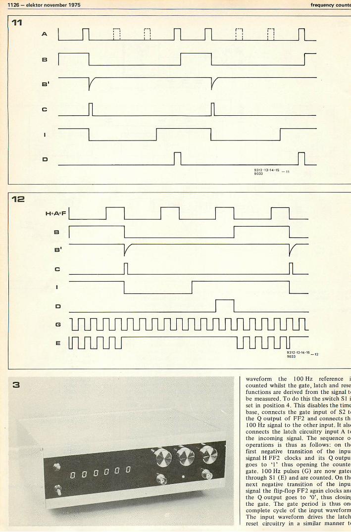
counted whilst the gate, latch and resefunctions are derived from the signal tcbe measured. To do this the switch S1 iset in position 4. This disables the timebase, connects the gate input of S2 tcthe Q output of FF2 and connects thi100 Hz signal to the other input. It alsoconnects the latch circuitry input A tcthe incoming signal. The sequence ooperations is thus as follows: on thefirst negative transition of the inpusignal H FF2 clocks and its Q outpugoes to '1' thus opening the countegate. 100 Hz pulses (G) are now gate(through Si (E) and are counted. On thenext negative transition of the inpusignal the flip-flop FF2 again clocks an(the Q output goes to '0', thus closingthe gate. The gate period is thus onecomplete cycle of the input waveformThe input waveform drives the latchreset circuitry in a similar manner tc

requency counter elektor november 1975 - 1127
13
14
H
TI. il
---
i
Counter
,
H ;lIr1-1
C4 Al
1-i
sic4
Ba A2 132
-1
A I
Sla
0- -)
Reset Latch
'igure 11. Timing diagram of counter in fre-luency measuring mode.
igure 12. Timing diagram of counter in)eriod measuring mode.
'igure 13. P.c. board for control logic.
:igure 14. Component layout for contrologic.
:hat for a frequency measurement, andhe timing diagram is shown in fig -
ire 12. Of course, the A signal is nowhe input signal, and the B signal is theoutput of FF2.
With a 100 Hz reference frequency and
1128 - elektor november 1975 frequency count
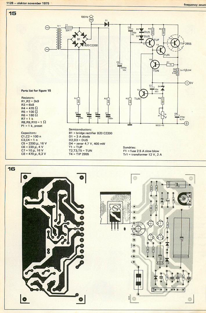
15100 Hz "n -
Parts list for figure 15
Resistors:R1 ,R2 = 3k9R3 = 6k8R4 = 470 E2
R5 = 100 E2
R6 = 180 E2
R7 = 1 k
R8,R9,R10 = 152P1 = 1 k, preset
Capacitors:C1,C2 = 100 nC3,C4 = 1 n
C5 = 22001i, 16 VC6 = 220 4 VC7 =10 pi, 16 VC8 = 470 6,3 V
Tr 1
C3 C4 Clammo .d.
/-100n In InT T TOn
C5-7
Cfc012200yi
1 tiV
Cl-1 D2
220p4V
D3
TUN
115
TUP
T3
5
//r4
TUN
R-7
TUN
1k
F818, "ET
810').
C, 7 04
lop1662
86
9033 -15
Semiconductors:B1 = bridge rectifier B20 C2200D1 = 3 A diodeD2,D3 = DUSD4 = zener 4.7 V, 400 mWT1 = TUP Sundries:T2,T3,T5 = TUN F1 = fuse 2.5 A slow blowT4 = TIP 2955 Tr1 = transformer 12 V, 2 A
TIP 2955
3 x1S2/0,5W
05v
C8C---3
470p6,3V
16
MO
0 0

requency counter humming kettle / active flash slave
igure 15. Power supply for frequency)unter.
elektor november 1975 - 1129
J.P. Kuhler jr.
igure 16. P.c. board and component layoutf power supply.
he gate periods of 10 ms, 100 ms ands the range of the instrument ismited. It is only possible to obtain aall -scale reading in the period modeThen the period is 9,999.99 seconds.'or a period of 1 s the display will benly 000100, a resolution of oneart in a hundred. Clearly, for shorteriod measurements a higher referencerequency is necessary to obtain a largerount and hence a better resolution.rovision is made for feeding in an ex-mmal reference frequency by breakinghe circuit at the point marked `EXT:EF'. In the frequency mode the maxi-ium and minimum frequencies whichan be measured are limited by the gateeriods. For instance with a 1 s gateeriod a frequency of 100 Hz will only,e measured with a resolution of oneart in a hundred, whilst with a 10 msate period an input frequency ofreater than 99.9999 MHz would causehe counter to overrange. However,ince the upper frequency limit of the'TL counters used in the circuit is only8 MHz anyway, this problem does notrise.printed circuit board and component
iyout for the control logic board areiven in figures 13 and 14, showing theonnections to the switch.
'ower supplysuitable power supply for the fre-
uency counter is shown in figure 15.'his is well decoupled against mains-,orne interference and has a 100 Hz)utput for the reference frequency. A)oard and component layout for the)ower supply are given in figure 16.
the complete frequency countercraws about 2 amps, the series regulatorransistor T4 should be mounted on andequate heatsink. If the unit is housedn an aluminium case then the back ofhe case should prove suitable.n a future issue we shall be describingdditions to the frequency counter,Lotably an input preamplifier to in-rease the input sensitivity.
humming kettleThose who have in the course of timelost the whistle of their domestic kettleand the unfortunate ones who do notpossess a whistling kettle at all, who mustboil water without the aid of an acousticsignal, are encouraged by the author notto resign themselves to this unsatisfac-tory situation. A very modest amountspent on components together with alittle work puts a 'humming kettle' withineveryone's grasp!The circuit is so simple that further ex-planation is hardly necessary. As thetemperature increases, the resistance ofthe NTC drops until at a certain moment(adjustable with P1) transistor T1 cutsoff, so that T2 conducts and the buzzeris activated.
Of course the circuit must be mountedin, on, or in the immediate vicinity ofthe kettle.
R. Buggle
active flash slaveFor those who have often been annoyedby badly illuminated flash photographsand also dislike the tangle of cablesinvolved in using two flashguns, theflash slave is the only solution.The author spent quite some time build-ing several slave units before arriving atthe design presented here, which has theadvantages that it requires no separatesupply voltage and that both electronicand ordinary flashguns can be operated.Four silicon photovoltaic cells (BPY 11)form a light sensor. Undoubtedly othertypes will do, too. The thyristor must beof a type with a very low firing voltage;the TIC 46 used here performs quite well.The circuit itself needs little comment:only that the polarity of the flash con-nection should be correct; the 'plus'
should be connected to the centre pinof the connecting cable. The circuit canbest be housed in a small, transparentplastic box.

1130 - elektor november 1975 tap -pow
of
Thi!'TAP -power'
circuit has been speciallydesigned for the TAP preamp
system.It includes touch -controlled switches for turning the
whole equipment on or off and for selecting the main poweramplifiers or the headphone amplifiers, a power supply for theTAP pre -amp, simple headphone amplifiers and a disc preamplifier.
NAND gates Ni, N2 and N3, N4 (IC4 =CD4001) make up two touch switches.Four LEDs are used to indicate the con-dition in which the system has been set;D2 = ON, D3 = OFF, D6 = headphonesand D5 = power amplifier.Because of the difference between thiscircuitry and the rest of the TAP system,construction is much simpler: insteadof a diode matrix only two flip-flops areused here.The power supply is split up into threesections: one for the touch switches,one for the rest of the TAP preamp andone for the disc preamplifier.The supply for the touch switches muststay in operation even in the 'OFF'condition, because it would not other-wise be possible to start the whole out-fit with the 'ON' touch switch. For thisreason, the switch supply is drawndirectly from the unstabilised supplyvia series resistor R15 and zener diodeDI.Integrated voltage stabiliser IC3 stabil-ises the 10-V supply needed for the TAPpre -amp. This can be accurately ad-justed with preset potentiometer P1.As the maximum output current of thisIC is only 150 mA, the external powertransistor T1 is added. When the supply
voltage is switched on with the 'ON'touch switch, the logic state prevailingat the output of gate NI is '1', while itis '0' at the output of N2. TransistorsT2 and T3 are therefore cut off, andthe supply voltage becomes availableat output C.When the 'OFF' panel is touched, logiclevels at the outputs of NI and N2 arereversed, with the result that T2 and T3turn on. The potential at pin 13 of IC3is therefore pulled down almost to zero,so that the internal output transistors inthe IC are cut off. The voltage at outputC drops to 0 and the TAP preamp isturned off.The flip-flop formed by N3 and N4 pro-vides a changeover between headphonesand the main power amplifier. When theoutput of N3 is at logic 'I', transistorsT5 and T6 turn on, switching on theheadphone amplifier built around T7and T8. This amplifier, including theassociated components within thedashed rectangle in figure 1, is dupli-cated on the board for the left-handheadphone channel. Both amplifiersderive their supply from the collectorof T6.The output of N4 is at logic`0'.Transistor T4 is cut off and relay Re isnot energised. The relay contacts,
Figure 1. Circuit of the main power supplythe TAP switches for on/off switching aniloudspeaker/headphone selection, and one othe headphone amplifiers.

ip-power elektor november 1975 - 1131
Ars'
B40C1500
C18
2200p35V
Di C19
5V6400mW
220p16V
T1 --'j.3D-9160,68$2
18)12 (7 11 (6) 10 001 2
IC3= 723 DIL(TO)
(5 7 (4116 (3) 5 (9) 13
3(1)
4(2)
C20
330n
R17
1k
F118
C21
F119
470n
D21110
ON see text
*AO0N,0
R21
OFF
ft] R22
R23
co,
N3R29
{ 27k I
R2727k
N1...N4 = CD4011E
C22
16V
15
C24
TUP 100p16V
'`R30
D6=/1
TUN
611
R32
m F133
IT
©
-R34
R35 -c7(136
II
D5.
0Re*
4
BC517
R28 >4000
DUS
9072-1O
Parts list for figure 1
Resistors:R15,R35 = 680 E2
R16 = 0.68 12R17 = 1 kR18 = 3k3R19,R28,R31,R36 = 470 E2
R20,R21,R22,R23 = 10 MR24,R26,R27,R29,R32 = 27 kR25 = 220 12
R30 = 10 kR33 = 6k8R34 = 1k5P1 = 1 k
Capacitors:C18 = 2200 p/35 VC19,C23 = 220 p/16 VC20 = 330 nC21 = 470 nC22 = 4p7/16 VC24 = 100 p/26 V
Sundries:Transformer = 240 V/16 V, 1 A (see
text)Bridge rectifier = B40C 1500Relay Re = 10 V, 300 E2 (see text)
Semiconductors:D1 = 5V6/400 mWD2,D3,D5,D6 = LEDD4 = DUST1 = BD 135 (cooled)T2,T6 = BC 177 (possib. TUP)T3,T5,T8 = BC 107 (possib. TUN)T4= BC 517T7 = BC 549 C, BC 109 CIC3 = pA 723IC4 = CD 4011
vhich switch the supply for the maincower amplifiers on and off at the)rimary of the mains transformer for:hese amplifiers, stay open.When the loudspeaker touch panels touched the relay contacts close andthe power amplifier is turned on: theheadphone amplifier no longer gets apower supply because the logic '0' atthe output of gate N3 cuts off transis-tors T5 and T6.The. disc preamplifier (figure 2) is thesame as was described in the April 1975issue of Elektor. Power supply for the
preamplifier is provided by the inte-grated stabiliser IC2. Points A and B areconnected to the corresponding pointsin figure 1.
ConstructionCurrent consumption of the touch -switching circuit is about 30 mA in the`OFF' position. In the switched -onstate, the maximum consumption withheadphone listening is about 100 mA(not counting the TAP preamplifier, ofcourse!). Including the TAP preampli-fier, the maximum current consumption
is 320 mA when the headphone ampli-fiers are on and the volume control is atmaximum.Figure 1 shows six points at which theD.C. voltage can be checked. With thetransformer secondary delivering 16volts RMS and the TAP preamp notconnected, the voltages at these pointsshould be 20 V, 10 V, 12 V, 6.8 V,1.8 V and 6 V respectively.The headphone amplifier delivers 2 VR.M.S. with the maximum input signalof 850 mV. Headphones with an im-pedance of 400 ohms or higher can be

1132 - elektor november 1975 tap -power
15V
C4
4n7
(11./
4n1
C? 4i1 7 i25V
27R4 4P-7
rs, 25V
112
IC is
R6
as
15V
0
reO
R8 CI
O
C.07
-CrL
R7
C9
047p'"'""
C
IMP=lop16v
0-Cr-R
-112
12
IC lb
4 n7
4 n 7
13
R13
C14
TO 5 TBA625C
IC1=SN 761314,A739 TBA 231
Bottom view
Parts list for figure 2
Resistors:R1,R14 = 100 kR2,R13 = 1 MR3,R11 = 10 SZR4,RI2 = I k2R5,R10 = 270 kR6,R9 = 150 kR7 = 56 kR8 = 470 k
Capacitors:C1,C15 = 680 pC2,C6,C10,C14 = 40/25 VC3,C13 = 2n7C4,C5,C11,C12 = 4n7C7,C9 = 470 nC8 = 10 µ/16 VC16 = 100 nC17 = 10 ... 22 µ/25 V
Semiconductors:ICI = SN 76131, µA 739, TBA 231IC2 = TBA 625 C
Figure 2. Circuit of the disc preamplifiers, andexternal connections to the TBA 625C stabil-iser IC from which they are supplied.
Figure 3. Printed circuit board and com-ponent layout.

ap-power elektor november 1975 - 1133
onnected to the output D. The value)f capacitor C23 is calculated for head -)hones with an impedance of 2 k.Transistor T1 must be adequately:ooled; the power dissipation - andience the dimensions of the heatsinkseeded - depends on the transformer,econdary voltage:
Transformersecondary
voltage(V RMS)
Heatsinkarea
(cm2)
16 5018 80
It is often a good solution to use thecase as a heat sink, with the transistormounted on the outside.The pull -in voltage for relay Re is about10 V. The contacts Must be rated tomake and break at least 250 V, and acurrent depending on the maximumdrawn by the power amplifiers. Fortwo 100 W amplifiers driving 4 -ohmloads a relay with 8 A contacts is suit-able.
To avoid relay chatter when a numberof touch panels are operated at thesame time, it is advisable to connect1 n capacitors Ca to Cd across eachpair of touch contacts.A 100 n/400 V capacitor can be con-
nected across the relay to preventcontact burning.
The TBA 625C stabiliser IC delivers anoutput of 15 V. As this is the minimumacceptable voltage for the disc preampli-fier, it is essential that a Type C stabil-iser be used. A heat sink is not absol-utely necessary. A tantalum electrolyticcapacitor should be used for C17 toforestall any possible tendency to oscil-lation.Figure 3 shows the printed circuit boardand the component layout for the TAP -power circuit. Except for the mainstransformer, bridge rectifier, smoothingcapacitor C18 and relay, all the com-ponelits are accomodated on one board.
3
B
cs
etC16
TIP
C21
*A F.
*R <3-L 41I'L
-L.410-4
:411.-114 .17
T T RJ--C2
C=1
e--{ m** }--
7413 919-4-1-1"--.i2
R9 1--
tai Re 1--
0.-{ At61-4
.- ft 354-99
0---{113419
.-{11 759
R33 b 1-0
R25 1-0
C20
0--{ R6 I-.
Or -
0--{ R 17 }-- R18
Ot
g c23911, g
11-c11.--0
I
I In
1.1)
13(
4051072
RE

1134 - elektor november 1975 clamant clock part 1
Any horologist who keeps a digitalclock in the same room as conven-tional clocks cannot but feel sadto see it sitting there, mute andreproachful amongst its morevociferous brothers, its only soundthe feeble humming of the mainstransformer. In this article welook at various ways of providingthe digital clock with a voice, sothat it can draw our attention tothe fact that it is keeping time farmore accurately than any meremechanical clock.
The main attribute lacking in a digitalclock is the comforting tick which as-sures us that the thing is actually going.How many man-hours have been wastedwaiting for the elusive change of thatlast digit? 'Well I'm sure its been stuckat that time for more than a minutenow.'A clock with a seconds display or flash-ing colon alleviates these problems, butthe hypnotic effect of such deviceshas been known to send people to sleep.No such problem exists with a tick,which informs us that the clock is work-ing without actually looking at it.
The circuitThe tick-tock sound of a conventional
clock is produced by the balance wheel(or pendulum) and escapement, the tickand tock sounds having different pitch.The pitch of the sounds and the rep-etition frequency obviously depend onthe physical construction of the clock.A grandfather clock will have a deeper,more leisurely tick than a travellingalarm.Electronic simulation of the sound isfortunately relatively simple. Thewaveform of the ticking is a damped res-
Figure 1. Gyrator circuit to simulate tick-tockof a clock.
Figure 2. P.C. board and component layoutfor gyrator circuit.

lament clock part 1 elektor november 1975 - 1135
This article is based in part on sugges-tions made by:H. F. Daems (alarm) andJ. P. Vos (Time signal).
onance similar to a percussion instru-ment. A suitable circuit is the.refore thegyrator used in the Elektor Minidrum(february 1975). This circuit (with thecomponent values modified for thisapplication) is given in figure 1. Suitable1 Hz trigger pulses may be obtainedfrom the clock circuit by taking an out-put from the counter preceding theseconds counter. The pulses must beTTL compatible (5 V amlitude) andhave a 1 : 1 mark -space ratio, otherwisethe ticking will sound unbalanced. Thepulses are fed into the base of T3through C3 to trigger the gyrator.whilst T5 switches C2 in and out ofcircuit to alter the relative frequency ofthe tick and tock.
Components list for figure 1
Resistors:' R1 R9,R11 = 6k8R10= 1k5
Capacitors:C1 = 4n7
C2 = 1 n8
C3 = 1 n
C4 = 6n8
C5 = 100,u/10 V
C6 = 100 n
Semiconductors:T1,T3,T5,T6 = TUNT2,T4 = TUP
D1,D2 = DUS
Is1
elrpaLL.Nimpi
g41.*411 : 1 I PrIeam Iladil),1,,--3 J.JL--1, .
0 ft I
GYRATOR
R5
IU

1136 - elektor november 1975 clamant clock part 13
4 minute -counter
R9111 R9121 80111 R0(2)
7490:6
A B C D
1 0-0-0-0
A BCD
7442
1 2 3 4
units of hours
fTl nRg(1) R9(2) R0(11R0(2)
AIN 7490:10
B C D
tens of hours
I---cloCk
clear
1/2 7473:2
clock
clear
1/2 7473:2
_J
- - - - - - - - 0-0 -0
0 06
Si
alarm system
C D
7442
1 2 3 4 5 6 7 8 9
S2
0 10o 20\ S3
alarm signalgenerator
_J4015 4
The frequency of the sounds may beadjusted to suit personal taste by exper-imenting with the values of C 1, C2 andC4. Since C3 and the input impedanceof the trigger input differentiate thetrigger pulse, changing the value of C3will affect the 'crispness' of the sound.
P.C. BoardA suitable printed circuit board alreadyexists for the Minidrum gyrator, and theboard and component layout (modifiedfor use with clock) are given in figure 2.
Alarm ClockOne clock noise in popular demand byreaders (though perhaps not first thingin the morning) is an alarm. It is asimple matter to add an alarm to a digi-tal clock (but unfortunately not sosimple if the display is multiplexed).The alarm control circuit given in figure4 is suitable for TTL clocks with paralleloutputs (i.e. where the BCD outputs ofthe hours and minutes counters areavailable continuously and are notstrobed). It was felt that an alarm set-ting accuracy of one minute was notnecessary, so the smallest step providedin this circuit is 10 minutes.The circuit operates as follows:the portion of the circuit inside thedotted box is the alarm. The rest is theexisting clock circuitry. The BCD out-puts of the hours and tens of minutescounters are decoded to decimal by the7442's. No decoding of the tens ofhours is required as the truth table forthis counter (table 1) shows. Outputs Aand B are never both '1' at the sametime. The desired alarm time is selectedby single -pole switches S1 - S3. Whenthe required time is reached three of theinputs of the four -input NAND gate gohigh. This allows the alarm signal con-nected to the fourth input to passthrough the gate.The possibilities for the actual alarm sig-nal generator are endless. The simplestsolution would be a fixed frequency os-cillator such as an astable multivibrator.There are however more interestingpossibilities. The voltage -controlledmultivibrator of figure 5 can be made toplay a tune by connecting differingvoltages sequentially to the control in-put. For a control voltage range of2-5 V the frequency range covered isabout 3 octaves. There are variousmethods of driving the oscillator. Asimple circuit is shown in figure 6. Thisconsists of a 7490 connected as a BCDdecade counter, with its outputs con-nected to the VCO via presets. As the
Table I
HOURS A A B B
0 0 1 0 1
10 1 0 0 1
20 0 1 1 0

clamant clock part 1 elektor november 1975 - 1137
Figure 3. Photograph of the completed board.
Figure 4. Circuit of an alarm control system.
Figure 5. A voltage -controlled oscillator VCOthat may be used to generate a tuneful alarmsignal.
Figure 6. Using the existing seconds counterin the clock to produce a varying voltage forthe VCO. Since the outputs interact it is diffi-cult to tune this circuit to play a particularmelody.
Figure 7. This circuit may be used to makethe VCO play a tune. Ten independentsequential outputs are produced, so each pre-set can be used to tune one note in the se-quence.
Figure 8. Extension of the circuit of figure 7to a 20 -note sequence.
Table I. Output of an arbitrary tens of hourscounter as in figure 4.
output states of the counter change sowill the output voltage to the VCO. Ofcourse the outputs change in a binarysequence so more than one output canbe high at one time.Since the outputs interact it is difficultto set this circuit to play a particulartune. In addition the 1 Hz clock pulsesare also fed in via R2 increasing the per-mutations still further.If one requires a circuit which can be setto play a particular tune then figure 7 ismore suitable. Here the outputs of the7490 are decoded with a 7442 to giveten independent outputs. These outputsgo low in sequence as the counter goesthrough its cycle. All other outputs arehigh, reverse -biassing their respectivediodes, so no current flows throughtheir respective presets. Only the presetconnected to the output which is lowforms a potential divider with R I. This
81Hz0
(1) R0(2)
7490BOIN
A
R9(1 R9(2)
r115/677404 0
7400L _ _ _
7442 B
2 3 5 6 7 8
11
........1.4
1 31 51 71 811 1 1 1
1 131 151 171 1
DUS....
47kin
11 1 /11447k
40.9 __J
7442 A
2j 41 61 8 10j 12; 14; 16 18 5V
DUS
47k 1111411 T ovc4015 8
means that each note in the sequencecan be tuned independently.This ten -note sequence can easily be ex-tended to twenty notes by the circuit offigure 8. In this circuit two decoders aredriven by the 7490 and are switched inand out by the 1 Hz clock pulses to thecounter. Thus, during the half -periodwhen the clock pulse is '0' the outputsof the 7490 are switched through thetransfer gates (7400) to decoder A. Theother transfer gates are disabled by the`0' on their commoned inputs, so theiroutputs are all '1'. This is an invalid in-put code for the 7442 so all its outputsare high. During the '1' half period ofthe clock pulse the reverse situationoccurs. Decoder B is enabled,whilst A isdisabled. Decoder A thus controls theeven notes 0, 2, 4, . . . in the sequence,whilst decoder B controls the odd notes1, 3, 5, . . . . Of course in this case, if an
equal time span is required for eachnote then the clock pulse waveformmust have a 1 : 1 mark -space ratio. The7490 in all these cases can be theexisting seconds counter in the clock.Another variation on the alarm themecan be obtained by a circuit whichchanges the rhythm of the tone se-quence, making it less monotonous.Such a circuit is given in figure 9. Thedividers I to III are again part of theexisting clock circuit. The operation ofthe circuit is as follows:counter II controls the pitch of the volt-age controlled multivibrator as in thecircuit of figure 6, except that no ad-justment is provided for. The time atwhich the alarm sounds is again deter-mined by the alarm control circuit, asin figure 4. The rhythm variation isprovided by gating the C output ofcounter I with the A output of counter

1138 - elektor november 1975 clamant clock part 1
9
10Hz0
ROW- AIN
BD NB2 C2 02
R0(2) R9(1) R9(2)
7490:10 I
A?
1Hz
TI TT80(1) N0(2) now N9(2)AIN
7490:10
BD N
5V0-1 18k
II
0.1Hz 9(1) N9(2) NOW ROG.)
BD NA3 83 C3 03 -1 A4
± 1 1T T T
7490:6
84 C4
m
74 00
N1
N2
minutes0
signalgenerator
alarm controlcircuitas figure 4
N4
N5
4015 9
III, and the B output of counter I withthe B output of counter III. This has thefollowing effects. Starting at a point inthe timing cycle where counter III hasjust reset A4 and B4 are both '0'. Theoutputs of N 1 and N2 are thus high so(assuming it is time for the alarm to gooff and the outputs of N3 and N4 arehigh) the tone sequence controlled bycounter III can pass through N5. After10 seconds output A4 goes high and thepulses from output C2 switch the out-put of N2 between '0' and '1'. The tonefrom the output of N5 is thus switchedon and off at a 2.5 Hz rate. After 20seconds output B4 goes to '1' whilstoutput A4 goes to '0'. The output ofN2 is thus high whilst via N1 outputB2 switches the tone on and off at a5 Hz rate. After 30 seconds outputA4 again goes to '1' while B4 remainsat '1'. Outputs B2 and C2 thereforeboth affect the tone output. Wheneither of these outputs is high the toneis off, and when both of them are lowthe tone is on.A timing diagram for these events isshown in figure 10. The top two wave-forms are the outputs B2 and C2 during
,a 1 second interval of the sequence (thisrepeats every second). The other 4waveforms are the tone outputs thatoccur for the four possible states .of A4and B4.The audible effect is thus as follows:an uninterrupted tone sequence for 10seconds, then a further 10 second in-terval of tone bursts and silence as infigure 10d, then 10 seconds as figure10e and finally 10 seconds as in figure10f, after which the sequence repeats.Of course, during each ten secondperiod the frequency of the tone isbeing varied by the outputs of counterII.It should be noted that for all thesealarm circuits a symmetrical 1 Hzsquarewave is required from the outputof counter II. This means that the 7490(which consists of a divide -by -2 and a
Figure 9. Circuit for generating an alarm sig-nal with variable pitch and rhythm.
Figure 10. Timing diagram for the circuit offigure 9, showing the tone sequences for thefour possible states of A4 and B4.
Figure 11. Circuit to gradually increase thevolume of the alarm signal if the sleeper doesnot awaken immediately.
Figure 12. A complete alarm circuit incorpor-ating the ideas of the previous circuits.
divide -by -five counter in the samepackage) must be connected with thedivide -by -2 after the divide -by -5, asshown in figure 9. If an existing clockcircuit is used this counter may beconnected as a BCD decade counter(i.e. with the divide -by -5 after thedivide -by -2). Some slight modificationmay therefore be necessary.
Volume ControlIn order not to awaken the sleeper tooharshly it is a simple matter to arrange avolume control so that the alarm tonestarts at a low level and gradually be-comes louder and louder until it isswitched off. This is achieved by thecircuit of figure 11. The counter shownis the minutes counter (i.e. the one thatdrives the minutes display). Since thealarm can only be set in units of tenminutes, the alarm will sound when the
tens of minutes have just changed to therequired number and the minutes coun-ter is reset. Outputs A to C of theminutes counter are thus at '0', so T2 toT4 are turned off. The alarm tone isapplied to the base of T 1 via RI andswitches this transistor on and offcausing a signal from the loudspeaker.Since there is a 390 S2 resistor (R2) inseries with it the tone is not very loud.After 1 minute the A output of thecounter goes to 'I', switching on T2 andthus connecting R3 in parallel with R2.The tone thus becomes louder. After2 minutes output B becomes '1' while Abecomes '0'. R4, which is smaller thanR3, is paralleled with R2, so the tonebecomes louder still. After 3 minutesoutputs A and B are 'I', and after4 minutes output C becomes '1', bywhich time the tone is quite loud.Output D is not connected to this sys-tem. If the sleeper has not awoken after8 minutes output D will become '1' andcan be connected to set off a smallexplosive charge underneath the bed. Aless drastic cure for the deep sleeper isto connect an additional transistor tooutput D with a 56 S2 resistor in serieswith its emitter.The complete circuit of an alarm systemis given in figure 12. Everything withinthe dotted box is the alarm circuit,whilst everything outside is the existingclock circuitry. This differs slightlyfrom the circuits discussed in that aHEX -inverter replaces the five -inputNAND -gate in the alarm control circuit.This has open -collector outputs, so theoutputs may be joined to perform awired -OR function. In this circuit theadditional transistor T9 is shown con-nected to output D5 for the extra loudalarm signal. A suitable printed circuitboard and component layout for thisalarm are given in figure 13.
Time Signal GeneratorProvision of a 'six pips' time signalevery hour is a relatively simple matter

00 703:170 DCIM/17:1770373 DJ....., 01 -n -fl -. -A (0 .03 ....i 0) 1...) -, CDh 1-B3 ...I 0) al :D. -,,, m II ii
.N 0 0 II II D3 -k -A -a -a'.,II LT: , -, -. -. o --.r.) co .4 (.00_, -, 0) NI 00 c° II ii 7) al '77 77
:I 0 0 ii _.01 **(4) N),.. CA) 414
C(0 x II 44
-. ;1/4-
77
cn cn cn cn - 0 -I cf)W NJ -. , 0 0 0 -.. CD
II II II ;i M .." (i' 3,-,. to cn cn 0 F.) II 0 i a''. 3 g. C3 .'l n.) -I oc co 10 10 ?? -tz.
II
up oC3 ai F. n'T
1 1 c) 0 II ccr ...1 C -I 00 0 '00 4,4, Cf) c 87- -
2 (I) ZIT 07 13 2 ;1'a. Ca -i0)(' 0,7,,, < a,
*<a,. cu
cl ......<
7 (9-0C)._ .c 3
1010 af;', 0NoQ. coaa
33
390
37
12052
-439001
5
3
100 HzO
r
L
7 x 7490
AIN
: 10/: 5'8
81 CI
1
5V
O
2x TUN
R6
18k
10 HzAIN
: 10
SIN
A2 B2 C2 D
1 sec.
B2
D3 04
SIN
: 10
DINA3 3
C2_ ()Ain 0A3 83 0C3
RI 82.-.83- R4-85
i TTT
10sec. 110111 80(31
:6ODIN
A4 84 C. 04
1 min.
1111- AIN
: 10
BD1NA5 85 C5 05
10 min.
AIROW 80121
:6BD1N
A6 86 C6 06
1 hour
: 10
8DINAl 81 C7
D3 A4 B4 X spare A5 B5 C5 _D5 A6 B6 C6 D6 A7 97 C7
05 136
2x TUN
D3 ... D6 = DUG
11 ... 16 = 7405 = 1C1
3 -1
:2clock
7473
clock
37 I AB A89 A9 I
L . _7777.J10 hours 20 hours
D70-------OiA8I
5V0
01,49) T9
15 14 13 12
A C D
1C2=7442
0 1 2 3 4
2 3 4 5 6
0<\D.....;020 450
O4/{/SI
S1,S20S30
15 14 13 12
A 8 C 0
1C3=7442
2 3 4 5 6 72 3 4 5 6 7 9 10 11
0 1 23 4 5 67 8 90 0000 0000 0
0 0 00)D0 2
LS
coLTUN
T5
TUN
16
TUN
813{ 1k
TUN
STOP
Ls852
1901 I
817
5612 1--.
RI611001-4
RI5taof2)-4
R14
390
TUN4015.12j

1140 - elektor november 1975 clamant clock part
X 0-
0
.27
S
C
CC
p
Ri6
0 17,'
0
0
ofo ,9-S
and a suitable circuit is given in fig-ures 14 (block diagram) and 15. Theportion of the circuit outside the dottedbox in figure 15 is the existing secondscounter in the clock. The circuit worksin the following manner:the inputs of gate 1 are connected tothe outputs of the tens of minutes,minutes, tens of seconds and secondscounters corresponding to the time
59 minutes 55 seconds. When this timeis reached the inputs of gate 1 will all behigh, so the output will be low. At anyother time at least one input must below, so the output will be high. Nor-mally therefore, the Q output of IC2 islow, so the output of IC4b is highblocking the oscillator IC4a (which willbe dealt with later), whilst the Q outputis high, holding the 6 counter IC3 in
Figure 13. P.C. board and component layoutfor the circuit of figure 12.
Figure 14. Block diagram of a time -signal gen-erator.
Figure 15. Complete circuit of the time -signalgenerator.
14Tens ofminutescounter
minutescounter
Tens ofminutescounter
secondscounter
gate 1 Flipflop
oscillator
6 counter
gate 2
Differen-tiator
amplifier LS
8S2
0
1 Hz pulses4015 14

:lamant clock part 1 elektor november 1975 - 1141
151
I
I
I
Ao
CoI
I
AoDo
I
I
1
0
A6
3
12
gate 1
IC1
A
7490
sC
-6-
clear IC2
clock Q
5
8
6
gate 2
7
R0111 R0(2)
IN 1C3 7492
CI
1 Hz pulses
Components list for figure 15
L
Resistors:R1 = 220 kR2,R5 = 2k2R3,R4,R6 = 1 kR7 = 100 1-2P1,P2 = 1 k
fi
'70n
PI
-1 71-1klin
8 IC4a1/2
7413
2_4
ft
9
10-012,13,
R6
C2f--111.1
6v
R52k2
T3
117
TUN
2P1klin
T4
R31k
R2
T1
N
R4 --1-
''
TUN T* see text
Capacitors:C1 = 470 n IC's:C2 = 1 /2, 6 V IC1 = 7430
IC2 = 7473Transistors: IC3 = 7492T1 ... T4 = TUN IC4 = 7413
ICI = 7430IC4a,IC4b = 74130 14 = +Vb0 7 = GND
IC2 = 1/2 74730 4 = +Vb0 11 =GND
IC3 = 74920 5 = +Vb0 10 = GND
N
0
J4015 15
the reset condition. On the negative -
going edge of the incoming secondspulse at 59 minutes 55 seconds the out-put of the seconds counter will assumethe condition '5', i.e. outputs A and Chigh. The output of gate 1 will go low,clearing IC2 so that the Q output goeslow and the Q output goes high.IC3 may now count the incoming sec-onds pulses. However, due to the propa-gation delays through the secondscounter, IC1 and IC2, it will not counton the abovementioned negative -goingedge, as this has already disappeared be-fore the counter is enabled. However,the negative -going pulse is differentiatedby C 1 and R3 (neglecting R1 and thebase resistance of T1), and turns off T1for about 100 ms. This takes pin 1 of1C4 high, and since pins 4 and 5 arealready held high by the Q output ofIC2 the oscillator will be gated throughit. providing a 1 kHz tone burst of100 ms duration.On each negative -going edge of the fivesubsequent second pulses IC3 will countand the oscillator will provide a 100 mstone burst. On the fifth pulse the D out-put of IC3 will go high, and on the sixthpulse the D output goes low, clockingIC2, so that its Q output goes high andits Q output goes low. This disables theoscillator and holds the counter (IC3) ina reset condition so that it can count nofurther seconds pulses. This conditionobtains for a further 59 minutes 55 sec-
onds until it is time for the next signal.The circuit thus produces six pips everyhour, starting with the first pip at59 minutes 55 seconds and terminatingwith a pip exactly on the hour. Ofcourse, this circuit produces pips ofequal length, whereas the last pip of aradio time signal is longer than the pre-ceding five. An alternative circuit, whichproduces this type of signal, was de-scribed in Elektor July/August 1975.
Oscillator and AmplifierThe oscillator is a simple single time
COUNT D
OUTPUTS
C B
0 0 0 0
1 0 0 1
2 0 1 0
3 1 0 0
4 1 0 1
5 1 1 0
0 0 0 0
Table II. Truth table for the 7492 connectedas a divide -by -6 counter.

1142 - elektor november 1975 clamant clock part '
constant multivibrator based on the7413 which is a dual 4 -input NANDSchmitt Trigger. Assuming the outputof IC4a is initially high then C2 willcharge through PI until the voltageacross it reaches the threshold of theSchmitt trigger. The output will then golow and C2 will discharge through P1until it falls below the threshold, whenthe output will go high again. Becauseof hysteresis the negative -goingthreshold is below the positive -goingthreshold, so the frequency of the oscil-lator is determined by the time taken tocharge and discharge C2 between thesepoints, which is of course dependent onthe time constant P1C2. The oscillatorfrequency can therefore be varied by Pl.With C2 = 1 p and P I set to 330 S2 thefrequency will be about 1 kHz. AlteringP1 also changes the mark -space ratio ofthe waveform, but this is unimportantin this application.The other gate in IC4 is used to gate theoscillator output into the amplifier,consisting of T2 to T3. This is a simpleswitching amplifier, as only square wavesare being dealt with. In the quiescentstate only T2 is turned on so the currentdrawn is only about 7 mA.
P.C. BoardThe track pattern and component lay -
Figure 16. Board and component layout forthe time -signal generator.
out of a board suitable for the time -signal circuit is given in figure 16. Notethat R4 (shown dotted in figure 15) is aprecaution against power supply rippleappearing at the loudspeaker output.Depending on the power supply it mayor may not be necessary.

lie detector / brake lights for model cars elektor november 1975 - 1143
J. Jacobs
This lie detector works in the usualmanner by measuring skin resistance andtherefore is no innovation, but in com-parison with the designs popular someyears ago it offers a number of useful im-provements. In the circuit the advantagesof opamps have been turned to full use.The detector operates fully symmetri-cally, and therefore two batteries arerequired. The voltage across the elec-trodes according to local regulations insome countries, may not be higher than2 V so a reference voltage of no morethan 1.2 V is applied to the input of themeasuring bridge. Since the resistanceof the human skin is generally 50 k orless, the voltage across the electrodes willbe at maximum 0.6 V. The set-up of themeasuring bridge has the additionaladvantage that the reference voltage isindependent of the battery voltage. Toobtain a sufficiently high sensitivity thetotal amplification in the detector shouldpreferably be greater than 100,000 times.Therefore a second opamp was added,which brings the overall amplificationto about 250,000 times. With the doublepotentiometer of 500 k the amplification
lie detectorcan be adjusted from 0 to theabove -mentioned maximum. The 100 kpotentiometer serves to adjust thesensitivity of the moving coil meter;therefore the input bridge is first broughtcompletely out of balance to the oneside and then to the other by means of
the 100 k potentiometer, whilst thepositive and negative deflection of themeter is adjusted to maximum. After-wards the adjustment potentiometer can,if required, be replaced by a fixed re-sistor.
500k
1k
----H
500k
TT
741
- 9V
100k
e/-*--100-0-100$4A
9V
4043-c
R. Zimmer
This circuit performs two functions:when the supply voltage to the motorof the model car cuts out, the car will notstop abruptly but will continue over somedistance and during that time two LED'swill light up and function as brake lights.Thus a very realistic effect is obtained.The circuit is extremely simple. As longas the car is under power, there is avoltage across the motor (M), the polarityof which is indicated in the diagram.Capacitor C1 and (via diode D) also C2are now charged.When the voltage cuts out, C1 discharges
brake lights formodel cars
across M and C2 discharges via the twoLED's, resistor R, and motor M. Ifbraking is the result of a short-circuit ofthe supply voltage, both capacitors dis-charge via the short-circuit connection;in that case the LED's burn somewhatbrighter. The value of resistor R can becalculated with the following simpleformula:
1LED
Usually a value of about 560 SI will besuitable.
12 - 2.VLED

1144 - elektor november 1975 universal ota pll
Performance Data
Narrow -band FM reception(VCO free -running frequency approxi-mately 10.7 MHz)
Capture and hold rangesCapture Hold
Input 160 pV 190 kHz 540 kHzInput 1.6 mV 250 kHz 4 MHzInput 10 mV 400 kHz 10 MHz
AM SuppressionInput 160µVInput 100µV
>60 dB>40 dB
SensitivityDeviation = ±3 kHzMinimum input = 3.2 pVWith input = 4 pV:output = 700 mV,signal/noise ratio = 40 dB
Wide -band Stereo FM reception(VCO free -running frequency approxi-mately 455 kHz)
Capture and hold rangesWith minimum input (12.6µV):Capture range ti hold range c----% 400 kHz
Sensitivity(Deviation = ±30 kHz)Minimum input = 12.6µVWith input = 500µV:output = 360 mV,signal/noise ratio '40 dB
Elektor has taken a lead in drawing attention to the possibilities of thePLL (Phase Locked Loop), and has devoted a number of articles todesigns incorporating this versatile circuit, as well as to explaining theprinciples of different applications. The Universal OTA (OperationalTransconductance Amplifier) PLL described here is a printed -circuitmodule which can form the nucleus of many different types ofreceiver.
Most of the integrated PLLs now avail-able for FM receivers are expensive andrequire a 24 -volt power supply, whichmakes them inconvenient for eitherportable or car -borne use. This universalPLL works quite happily on a 5 -voltsupply, but the working voltage may bedetermined in practice by the needs of aMOSFET RF amplifier, which can re-quire 9 volts. This, however, is easy toprovide in battery -powered portableequipment, and it also leaves a marginfor stabilisation when running from a12 V car supply.
Sensitivity on a 103 MHz FM inputwith 3 kHz deviation is 3.2 µV for a700 mV audio output.For a receiver for the 144 to 146 MHzband, the aerial signal is pre -amplifiedand converted to a band from 10 MHzto 12 MHz by a stable 134 MHz mixer -oscillator. Any signal in the 2 MHz -wideband can then be tuned in by adjusting(with a potmeter) the frequency of thevoltage -controlled oscillator incorpor-ated in the PLL.Figure 1 shows a block diagram of thearrangement. The 134 MHz local oscil-lator will normally be a crystal oscillatorof lower frequency in conjunction witha multiplier. Assuming the combinedgain of the pre -amplifier and the mixingstage to have the easily -achievable value

universal ota pll elektor november 1975 - 1145
of 20 dB, the overall receiver sensitivityfor the quoted audio output of 700 mVwill be some 0.3 pV, which is betterthan that of most commercial receiversfor this band.For reception of wide -band broadcastFM signals, the unusual arrangement ofa double superheterodyne, with asecond IF as low as 455 kHz, is used(see figure 2). The low modulationindex of a stereo FM signal makes de-modulation with a good signal-to-noiseratio difficult to achieve, and even inthe best (and most expensive) receiversthis is seldom above 50 dB on strong sig-nals. With this very low second IF, 60 dBis achieved.
Yet again; what is a PLL?For those who have not yet had anopportunity to familiarise themselveswith the basic concept of the phase -locked loop, the essential features ofthis circuit can be repeated. The keyelement is a voltage -controlled oscillator.When the loop is used in a receiver, thisoscillator is automatically synchronisedwith the carrier of the incoming signal.The other elements in the loop are sub-servient to the main purpose of keepingthe oscillator synchronised. In practice,this is done by maintaining a constantphase difference between the incoming
146MHz
MIX
OTA PLL
XTO134MHz
10... 2MHz
L _
OTA
ClI
vcoT4...T7
6029 1
_J
0 AF
Figure 1. Block diagram of a receiver fornarrow -band FM transmissions in the144 MHz -146 MHz amateur band, with a
fixed -frequency mixing oscillator and band -spread tuning by varying the intermediatefrequency.
signal and the oscillator output : hencethe term 'phase -locked loop'.By definition, the oscillator is voltage -controlled. So if the incoming signal isfrequency -modulated, the control volt-age applied to the oscillator to keep itsynchronised becomes, of itself, thedemodulation of the incoming signal. As

1146 - elektor november 1975 universal ota pll
TUNER7 7 10.;MIX7 450
MHz kHz
70...108MHz
a method of detection, this has import-ant advantages over other methods interms of better rejection of interferingsignals, lower distortion, and bettersignal-to-noise ratio.
Circuit descriptionThe input is fed in across resistor R1(figure 3). The value of this resistormust be selected to give correctmatching to the preceding mixer stage,and suitable values will be given in laterarticles describing particular appli-cations. Transistors T1 and T2 form adifferential amplifier with an asym-metrical input, while T3 and diodes DIand D2 stabilise the current flowingthrough T1 and T2. The two collectorsof the differential amplifier are con-nected through capacitors C4 and C5 tothe two differential inputs (2 and 3) ofthe CA3080 operational transconduc-tance amplifier IC1. The use of both in-puts in this fashion gives an extra 6 dB
gain without impairing stability and alsofacilitates the operation of the limitingdiodes D3 and D4.In addition to receiving the RF (or IF)signal at the differential inputs (pins 2and 3)., IC1 is fed via pin 5 with theoutput of the voltage -controlled oscil-lator formed by T4 and T5. Althoughthis oscillator is described as voltage -controlled, it should more properly becalled current -controlled, the currentbeing regulated by T6 and T7 in theemitter leads of T4 and T5 respectively.It can, however, be said without toomuch straining of the truth that thecommoned bases of T6 and T7 are volt-age -controlled from the output (pin 6)of ICI .
In the foregoing description the path ofthe loop has, in effect, been followed inthe reverse direction. Recapping andgoing the correct way round: the DCcomponent of the signal at pin 6 of thephase -comparator ICI is amplified by
T6 and T7 and controls the frequencyof oscillator T4 + T5.As in all FM detectors, AM rejection isimportant. The CA 3080 has good AMrejection at low input -signal levels, butis less good at higher levels. These higherlevels, however, are taken care of by theclipping diodes D3 and D4, which begincontributing to AM rejection when thepeak -to -peak signal between pins 2 and3 of ICI exceeds 1 volt.Capacitor C11 is one of the componentswhose value influences the VCO free -running frequency (455 kHz in thebroadcast FM receiver, or about 10 MHzin the narrow -band FM receiver) so itsvalue is quoted for particular appli-cations (see Table). When the receiver istuned by varying the VCO frequency, asin the narrow -band FM receiver, pot -
meters PI and P2 come into play. Whenthe working IF frequency is fixed, thesepotmeters can be used for preset adjust-ment.
3a
R2
CI
R5
Ti
100n
R3
C3
1470P16V
T2
R8
R4
T3
DI
02NI8
C2
C4
1122n
cs
-111nn
loon
R11
RI?
D3 D4X I
6
100n
IC1CA3080
1113
220k
C71I 147P
16V
R15
R16
R14
C8
470n
C9
O
" see text
6029 3a

universal ota pll elektor november 1975 - 1147
Figure 2. Block diagram of a double super-heterodyne for stereo FM reception, withintermediate frequencies of 10.7 MHz and455 kHz.
Figure 3. Circuit of the Universal OTA PLL.
Table: Values of R1, R14, R24, C9, C11 andC14 for specific applications.
Values of R1, R14, R24, C9, C11 and C14 for specific applications
Mode of operation(all FM)
Supplyvoltage
R1 R14 R24 C9 C11 C14
Type oftransmission
Intermediatefrequency
Minimuminput*
Wide bandmono 10.7 MHz 160 µV 9 330 E2 1 k 150 E2 - 100 p 10n
Narrow band 10.7 MHz 3.2 µV 9 330 n- 47 k 0 S2 - 220 p 10 n2k2
Wide bandmono 455 kHz 400 µV 9 - 47 k 2k2 560 p 2n2 10 n
Narrow band 455 kHz 20 pV 9 3k3 47 k 82 2 560 p 2n2 10 n
Wide bandstereo 455 kHz 500 µV 9 - 47 k 2k2 220 p 2n2 -
Wide bandstereo 455 kHz 200 µV 12 - 47 k 2k2 220 p 2n2 -
* At the PLL! (- = omitted)
O
0I144. 44
T6 T7
OD 1 C4
Omeg/
R18
P1
1k
4k7
C13
R20
C12
47/iP2 10V
CI4
" see text
21
I470n
R
T8
1122
1124'
C15
LI
470pH
T9
(r) F116
.4'R25 10/i0
10V
1126
100P6V
11 27
06029 3b
12V
The low-pass filter which removes theunwanted 'sum' frequency (oscillatorplus input signal) is formed by C8, C9,R14 and R16. As the values of theseresistors also effect the VCO free -running frequency, they have to be sel-ected carefully for each application. Inpractice, R16 is given a fixed value of68 IcS2 while R14 is specified for eachapplication. This also applies to thefeedback resistor R24 which controlsthe gain of the output audio ampli-fier T8 and T9. Resistor R28 and ca-pacitor C14 provide de -emphasis. It willbe seen that the whole of the DC com-ponent at the output (pin 6) of thephase comparator is passed to the VCO:this helps to ensure a large 'hold range'for the loop.Detailed descriptions of applications ofthe Universal PLL will be given in laterarticles, but the two which have alreadybeen mentioned can be briefly discussedhere.
Resistors: Parts listR1 ,R14,R24 = see tableR2 ,R4 ,R11 ,R12,R28 = 4k7R3,R8,R15,R17,R18,R19,R20 = 1 kR9,R10,R23 = 10 kR5,R6 = 560 2R7 = 100 E2
R27 = 100 kR13,R22 = 220 kR16 = 68 kR21 = 470 kR25,R26 = 2k2P1 = 1 kP2 = 100 2Capacitors:Cl ,C2,C6,C10 = 100 nC3 = 470 /2/16 VC4,C5 = 22 nC7 = 47 /2/16 VC8,C13 = 470 nC9,C11,C14 =see tableC12 = 47 /2/10 V Semiconductors:C15 = 100 µ16 V T1 ... T7 = BF 494C16 = 10/2/10 V T8 = BC 547
T9 = BC 557Inductor: IC1 = CA 3080L1 = 470µH D1 ... D6 = 1 N 4148

1148 - elektor november 1975 universal ota pl
Narrow -band FM receiverIn narrow -band FM systems, noisealways tends to be a problem becausethe modulation index (the ratio of themaximum deviation to the highestmodulation frequency) is by definitionlow, but the good noise performance ofa PLL demodulator goes a long waytowards overcoming this handicap. Thelimiting sensitivity of the Universal PLL,when used in a narrow -band FM re-ceiver, has already been stated to be3.2 µV, not counting the gain of the RFand mixer stages preceding it. With aninput of 4 µV - slightly above thelimiting value - the signal-to-noiseratio is 40 dB.The principle of using a crystal -con-trolled fixed -frequency local oscillator,and tuning the IF with the VCO, offersa very simple and effective form ofband -spreading.
Stereo FM receiverFM sound broadcasting has a maximumdeviation of 75 kHz, which gives amodulation index of 5 on mono trans-missions having a 15 -kHz audio band-width. With a stereo transmission, themaximum modulation frequency is53 kHz, but the effective bandwidth of
-..1R4 )--io---f 0.2 1--
T
ea-W.-11-0
2
tl
I
R18
R7o
e ---1R281-4)
0-1 "444-, 4)---4
Figure 4. Printed circuit board.
Figure 5. Component layout of the universalOTA PLL.
the composite stereo signal is greaterthan this, and in practice the modu-lation index works out as low as 0.6.This means that, 'other things beingequal', stereo reception has a signal-to-noise ratio 20 dB lower than the samestereo transmission reproduced in mono.These problems are discussed more fullyin 'Modulation Systems' (Elektor 2p. 246 and Elektor 3, p. 454).A PLL detector can help considerablyin this situation, because it can easily bemade to work on a very low second IF.The output of an FM demodulator isproportional to the quotient of the de-viation and the working frequency. If,therefore, the working (intermediate)frequency is as low as 455 kHz, the out-put will be considerably greater thanwith the normal intermediate fre-quency of 10.7 MHz, while the noisewill be approximately the same in bothcases. In theory, a 'normal' discrimi-nator could be made with this workingfrequency and the usual 75 -kHz devi-ation, but it would be difficult to makeit work satisfactorily. A PLL demodu-lator, on the other hand, lends itselfreadily to working with these para-meters and enables a 60 -dB signal-to-noise ratio to be obtained.

tv test pattern generator elektor november 1975 - 1149
teet6ttet eeael6t
A television pattern generator is one of the most useful TV service aids.It simplifies checking of the video stages, adjustment of picture ge-ometry, and perhaps most important, setting up of convergence incolour receivers. Using logic IC's for the generation of the test patternallows the construction of a simple and reliable circuit, and the designgiven here is based on the 74 series TTL logic family.
The test pattern generator produces thewell-known dot and crosshatch patterns.In the crosshatch mode a number ofhorizontal and vertical bars are displayedon the screen, whilst in the dot modeonly the crossing points of these barsare displayed, thus producing an arrayof dots.
Building up the video signalThe number of bars in the display hascertain constraints placed upon it bythe nature picture.This is composed of a raster of 625lines. Since the horizontal bars areproduced by dividing down the15625 Hz line frequency digitally, itfollows that the ratio (625 : numberof bars) must be a whole number, as itis not possible to obtain a non -integraldivision ratio digitally, and if it were thepattern would move anyway.Since 625 = 252 then 25 is a convenientnumber of bars. One of these is lostduring the field blanking interval, soonly 24 are in fact displayed. Since the`boxes' formed by the bars shouldideally be squares rather than rectanglesthis determines the number of verticalbars. The aspect ratio of a televisionpicture is 4 : 3, so the number of verti-
Parts list for figures 1 and 6
Resistors:R1 = 1 kR2,R3 = 470 g2P1 = 470 S2 lin.P2 = 1 k lin.
Capacitors:C1 = 1n5C2 = 220 pC3 = 220 n/250 V
IC's:IC1 = 7400IC2 = 7413IC3,1C4 = 7490IC5 = 7402
Figure 1. Circuit of the video generatorsection.
cal bars is 243x 4 or 32. The oscillator
which produces the vertical bars runs ata higher frequency than line frequency(since there are several picture elementsalong each line).The circuit can conveniently be dividedinto two sections. The video generator,which produces the actual pattern, anda synchronising unit which produces thefield and line sync pulses and also pro-vides the timing for the video generator.The circuit of the video generator isgiven in figure 1. The vertical bar gener-ator SI is a NAND Schmitt triggerconnected as an astable multivibrator.Since the TV line frequency is 15625 Hzand there are 32 vertical bars it followsthat the frequency of this astable mustbe 500 kHz. P I provides some adjust-ment so that the number of lines can bevaried slightly. This oscillator issynchronised by line sync pulses. Eachline sync pulse turns on T1, groundingpin 5 of S1 and momentarily blockingthe oscillator. When the line sync pulsefinishes TI turns off and the oscillatorrestarts. This ensures that the pulseswhich make up the vertical bars occurat the same point along every line of theTV picture, as otherwise a randompattern would result.
A R,lk
D1omm
D U S
line pick-up
TUN
5
1
1n5
220p
dill
11
j5D -5in
IC3
Roo)RO(7R9(1) R9(2)
21 31 61 7
S2
2
N113
11 D
BD +5in
I C4
R00)R0t2IRS(1)R9(2)
21 3j 61 7
10 ID -
IDIF1a 10
RV dot
S1
H+Vcrosshatch
N1,N2,N5 = 3/4 IC1 = 7400N3,N4,N6 = 3/4 IC5 = 7402S1,S2 = IC2 = 7413IC3,1C4 = 7490
S2 Pos./Neg.
P2 C3 C
1kFoil Video
11" 220n250V
1636 1

1150 - elektor november 1975 tv test pattern generato
.9611V14.1."
rttrlNt'ItI 11 I 11 101
+
III 114 ,f
4-1-14-44 I
2 43
BDin - IC3
:1171171-
D - IC3b
D - IC4C
Fi
1717TITTIFITTIFIETT
r717111FT
64ps1636.3
5
C
10n
1
27=GND
014=+Vb
32%L.-6_.1 _4_1
IC1 = 7413
f os = 250 kHz
0 5V
5
+Vb
A 0--62AINIC2=7490
()DIN 011
11,1010, GND
2 3 10 6
+Vb
IC3=7490BD1N
Romfloo GND0t
2 3 10 6 7
+Vb
AiNIC4=7490
anini°80,010,21 GND
2 3 10 6 17
A
(), 5 31250 Hz
14
FIDIN +Vb
AINIC5=7490
AFlomfic,) GND
12
3 10 6
50 Hz15625 Hz
7
05VC2
;-'7 76 He -11
82
7 6
RCext Cc t
IC6= 2
74123
A
( ND Cext RCe
5
4
a 4 15
33n
03DUS
DUS
02
®5V
270n
D4
videogenerator
DUS DUS
L_
Ca
113
5V
74404.5

tv test pattern generator elektor november 1975 - 1151
Figure 2. Oscillogram of the V signal at theoutput of N1.
Figure 3. Timing diagram for the generationof the H signal.
Figure 4. Oscillogram of the H signal.
Figure 5. Circuit of the sync generator,showing connections to the video generator.
Figure 6. P.c. board and component layoutfor the video generator.
Figure 7. Photograph of the completed videogenerator.
The output of the astable has substan-tially a 1:1 mark space ratio. Thiswould, if used as the video signal, pm -duce black and white vertical bands ofequal thickness. However, for thepurposes of the pattern generator verynarrow bands provide more informationabout the state of the video stages ofthe TV, since a narrow band requiresa shorter pulse length and hence agreater bandwidth.Accordingly the output of the astable isdifferentiated by C2 and R3, and thespiky pulses are fed into a secondSchmitt trigger to square them up again.This also inverts the signal, so it is in-verted a second time by NI to appearin the correct sense. Figure 2 shows thevertical signal V as it appears at the out-put of NI . The absence of pulses wherethe sync pulses occur can be clearlyseen. The pulse length of the V signal isabout 200 ns.Line sync pulses at the collector of T1are also counted by IC3 and IC4, whichare 7490's connected as divide -by -fivecounters. Output D of IC4 is thereforea pulse train at 1/25 of line frequency.The timing diagram for this division isshown in figure 3. Waveform 'a' is theline sync input. Waveform 'b' is theD output of IC3, and waveform 'c' isthe D output of IC4. However, thiswaveform cannot be used directly as thehorizontal video signal, as the pulselength is equal to 5 line periods, whichwould make the horizontal bars toothick. For this reason it is `NANDed'with waveform 'b' in N2 and theninverted by N3 to produce waveform`d' (H). This has a duration of 64 ps orone line period. However, due to inter-lace each horizontal bar will actuallyhave a thickness of two lines. Figure 4shows an oscillogram of the H signal.To produce the complete video signalthe Fl and V signals must be summed.To produce the crosshatch pattern thehorizontal and vertical signals must be`OR -d' together, as there must be a barwhen vertical or horizontal pulses arepresent. For the dot pattern, whichcorresponds to the crossing points of
7DOT CROSSHATCH
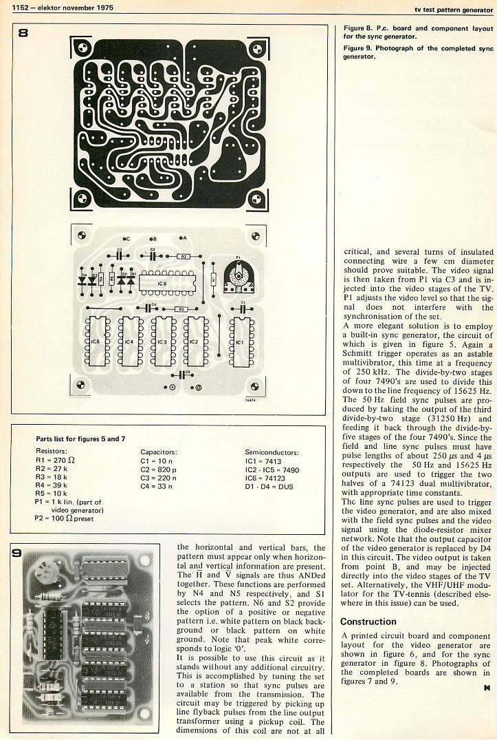
1152 - elektor november 1975 tv test pattern generator
C a *A
"
® .©7 4 40 4
Parts list for figures 5 and 7
Resistors:R1 = 270 E2R2 = 27 kR3 = 18 kR4 = 39 kR5= 10kP1 = 1 k lin. (part of
video generator)P2 = 100 E2 preset
Capacitors:Cl = 10 nC2 = 820 pC3 = 220 nC4 = 33 n
Semiconductors:IC1 = 7413IC2 - IC5 = 7490IC6 = 74123D1 - D4 = DUS
the horizontal and vertical bars, thepattern must appear only when horizon-tal and vertical information are present.The' H and V signals are thus ANDedtogether. These functions are performedby N4 and N5 respectively, and Siselects the pattern. N6 and S2 providethe option of a positive or negativepattern i.e. white pattern on black back-ground or black pattern on whiteground. Note that peak white corre-sponds to logic '0'.It is possible to use this circuit as itstands without any additional circuitry.This is accomplished by tuning the setto a station so that sync pulses areavailable from the transmission. Thecircuit may be triggered by picking upline flyback pulses from the line outputtransformer using a pickup coil. Thedimensions of this coil are not at all
Figure 8. P.c. board and component layoutfor the sync generator.
Figure 9. Photograph of the completed syncgenerator.
critical, and several turns of insulatedconnecting wire a few cm diametershould prove suitable. The video signalis then taken from P1 via C3 and is in-jected into the video stages of the TV.PI adjusts the video level so that the sig-nal does not interfere with thesynchronisation of the set.A more elegant solution is to employa built-in sync generator, the circuit ofwhich is given in figure 5. Again aSchmitt trigger operates as an astablemultivibrator, this time at a frequencyof 250 kHz. The divide -by -two stagesof four 7490's are used to divide thisdown to the line frequency of 15625 Hz.The 50 Hz field sync pulses are pro-duced by taking the output of the thirddivide -by -two stage (31250 Hz) andfeeding it back through the divide -by -five stages of the four 7490's. Since thefield and line sync pulses must havepulse lengths of about 250 gs and 4µsrespectively the 50 Hz and 15625 Hzoutputs are used to trigger the twohalves of a 74123 dual multivibrator,with appropriate time constants.The line sync pulses are used to triggerthe video generator, and are also mixedwith the field sync pulses and the videosignal using the diode -resistor mixernetwork. Note that the output capacitorof the video generator is replaced by D4in this circuit. The video output is takenfrom point B, and may be injecteddirectly into the video stages of the TVset. Alternatively, the VHF/UHF modu-lator for the TV -tennis (described else-where in this issue) can be used.
ConstructionA printed circuit board and componentlayout for the video generator areshown in figure 6, and for the syncgenerator in figure 8. Photographs ofthe completed boards are shown infigures 7 and 9.
14

iith a pencil point elektor november 1975 - 1153
V. Schmidt
Many electronics enthusiasts look onolder removing as a loathsome job. Thiss especially true of printed circuit)oards with narrowly -spaced conductors.Filings which often happen when one isrying to desolder are:The solder forms bridges between theconductors.Blobs of solder drop off the board.)e -soldering tools or wicks are availableommercially, but there is no need toay out that kind of money. Any work -hop toolbox should yield a really cheapevice which will do the trick - a pencil.'ropelling pencils with long leads of 2B
B hardness are particularly suitablee.g. clutch pencils). To remove solderrom a hole, the solder must be heatedvith a soldering iron until it meltsfigure 1). The next step is to stick the)encil point in the hole, and take awayhe iron (figure 2). Where the pencilcad touches molten solder, the solderjumps' away, because of its surfaceension, and the hole is cleared of solderfigure 3).
similar method can be used for get-ing rid of bridges of solder betweenracks. To do this, the pencil point isiid flat on the molten solder betweenhe tracks.
arneummeiriti, ==tit z=azva.Lam"."".
'Lino

1154 - elektor november 1975 marks
111111RICH'Ir
Hall effect ICSpecial features of a new MullardHall -effect integrated circuit, typeTCA450A, include: small physicalsize, wide operating voltage andtemperature ranges, high sensi-tivity, low offset flux, and selfbalancing. It can therefore beused to advantage in the measure-ment of magnetic field strengthsin small areas or gaps.The function of the TCA450A isto translate information about thepolarity and strength of a mag-netic field into a differential out-put current. The device is mono-lithic and consists of a siliconHall -effect element and two as-sociated integrated amplifiersencapsulated in a miniature lowprofile plastic package.Typical applications include theprovision of isolated currentsensing and control in high cur-rent applications, contactless andhighly -reliable electronicswitching, sensing and control inelectromagnetic systems wherethe field strength must be main-tained at a precisely determinedlevel, the conversion of magneticquantities into proportional cur-rents and the detection and pos-
itional movement of rotatingshafts.
Brief Min. Typ. Max.Data
Supplyvoltage 4Magneticsensitivityof Hallelement - 0.4 -Voltagegain ofamplifierMutualconduc-tance ofamplifier - ±240Offsetflux den-sity inbalancedcondition -
15 -
±25
8 16 V
V/T
mA/V
mT
Mullard House, Torrington Place,London, W.C. I.
C.R.T. probe attachmentA new probe attachment has beenintroduced by BrandenburgLimited for use with the
company's direct -reading high -voltage meters. The beryllium -copper attachment which screwsinto the existing h.v. probe unit,is designed to be slipped beneaththe anode connection on the c.r.t.
Brandenburg Limited, High Volt-age Engineering Division,939 London Road, ThorntonHeath, Surrey, CR4 6JE.
New transistor forswitched mode powersuppliesThe latest addition to the Mullardrange of transistors for high -
frequency switched mode powersupplies operating direct from`rectified mains' inputs is typeBUX82.It is intended for use in 400 \Vpush-pull or 100 W to 200 Wsingle -ended circuits. Togetherwith other types in the sameseries, the BUX82 will not onlyoperate satisfactorily at the`rectified mains' level, but willalso accommodate the ±10%voltage variations regularly ex-perienced on mains supplies.To meet these requirements,the device has an open basecollector -emitter rating of 400 Vand a collector breakdown ratingof 800 V (VBE = 0). The d.c. andpeak collector current ratings are5 A and 8 A respectively.Fast switching characteristics notonly minimise switching losses,but also facilitate high -frequency(25 kHz to 50 kHz) operation.
Mullard House, Torrington Place,London, W.C. I.

market elektor november 1975 - 1155
111111RHInRange of Coiled CablesAvailable from LemoLemo (UK) can now supply arange of coiled cables, terminatedor unterminated. Up to five con-ductors can be ordered, in avariety of uncoiled (maximum)lengths, and these can be eithertelecommunications light -currentflexibles or with mains -carryingflex in the cores. Outer insulationcan be either p.v.c. or rubber,with the conductor insulationfollowing suit.
Lemo (UK) Ltd, 6 South Street,Worthing, Sussex BNI 1 3AE.
M-Tron industriesestablishes internationaldivisionM-Tron Industries of Yankton,South Dakota, has formed anInternational Division to sell theircrystals to the overseas market.The new international divisionwill be located at 2200 ShamesDrive, Westbury, L.I., New York11590. Telex 961474.M-Tron Industries manufacture awide line of quartz crystals. Pro-ducing over 10 million crystals ayear, they are the number onemanufacturer of CB and monitorcrystals in the United States.
Combined C-MOS andbipolar relay driverpackage
The MM74C908/918 Dual HighVoltage C-MOS driver consists oftwo C-MOS "NAND" gatesdriving a bi-polar emitter -followerDarlington to achieve high currentdrive and high voltage capabilities,while having the very low input -current characteristics ofcomplementary -metal -oxide.The MM74C908/918 specifi-cations are at a min. 30 V break-down voltage and an outputcurrent range between 250 mAand 350 mA. However, this com-ponent is aimed at the telecom-
munications market and wasspecifically designed to replacehigh voltage telephone relaydrivers. Therefore, an improvedversion for this usage will bespecified at 56 V min., packagedin a 14 -lead, 2.5 Watt configur-ation.The main advantage of this newC-MOS High Voltage Driver is itsnil power consumption - justleakage current in the stand -by -mode, while -a conventionaltelephone relay driver in the samemode uses about 10 to 20 mA.The dual high -voltage C-MOSdrivers will be available in twodifferent versions, theMM74C908N 8 -pin mouldeddual -in -line package and theMM74C918N 16 -pin mouldeddual -in -line package.
National Semiconductor,The Precinct, Broxbourne,Herts. EN1 0 71IY.
'Switchmode' powertransistors
Motorola have just introduced theswitchmode series of power tran-sistors. Designed for high -voltagepower switching applications, thefirst devices in this series aredesignated 2N6542 to 2N6547and are n -p -n triple -diffused sili-con transistors. Before thesedevices were introduced, designers
of power equipment had to usetransistors that were often onlyspecified for resistive loads atroom temperature. Unfortunately,in real life things are seldom sosimple and, consequently, thedesigner was often faced withthe task of using power devices athigh temperatures and withreactive loads without sufficientinformation as to how the transis-tors were likely to perform underthese conditions.Featured in the data sheets forthese devices are all the significantspecifications for high tempera-ture use (TC = 100°C) and forsecondary breakdown under baseforward -biased and base -reverse -biased conditions.Dynamic voltage capabilities (sus-taining voltages) are given forVCEO (SUS) and VCEX (SUS).Furthermore, VCEX (SUS) mini-mum is specified at two values ofIC at a case temperature of100°C, with the.device driving aclamped inductive load. Ablocking voltage rating, VCEV, isspecified at the same case tem-perature and maximum values forVCE (sat), VBE (sat)' ICEV andIcER are also provi ed.Fall time and storage time, im-portant parameters for switchingperformance, are specified atrated IC, VCEX (SUS) andTj = 100°C, with an inductiveload.
CHARACTERISTICS OF NEW SWITCHMODETRANSISTORS
POWER
*TC = +25°C,unless other-wise noted
2N6542 2N6543 2N65442N6545 2N6546 2N6547
VCEX @TC =+100°C 350V 450V 350V 450V 350V 450V
VCEV 650 V 850 V 650 V 850 V 650 V 850 V
VCEO 300V 400V 300V 400V 300V 400V
VCE (SAT)@TC =100°C 2V 2V 2.5 V 2.5 V 2.5 V 2.5 V
VBE (SAT)@TC =
+100°C 1.4V 1.4V 1.6V 1.6V 1.6V 1.6VIc peak(Amps) 10 10 16 16 30 30
IC continuous(Amps) 5 5 8 8 15 15
Es/b (min)joules 180 pj 180 µ1 500 pj 500 pj 2mj 2mj
HFE (min) 7 7 7 7 6 6
td (max) µsec .05 .05 .05 .05 .05 .05tr (max) µsec 0.7 0.7 1.0 1.0 1.0 1.0
is (max) µsec 4/4* 4/4* 4/4* 4/4* 4/5* 4/5*tf (max) µsec 0.8/ 0.8/ 1.0/ 1.0/ 0.7/ 0.7/
0.8* 0.8* 0.9* 0.9* 1.5* 1.5*PD watts 100 100 125 125 175 175
*TC = +100°C Inductive load operating conditions.
New Mains Filters forElectrical Equipment
Tekdata announce the availabilityin U.K. of a new mains filterincorporating an I.E.C. socket.The units are UnderwritersLaboratories approved and are de-signed in accordance with theI.E.C., V.D.E., C.S.A. and theproposed American StandardsAssociation specifications.Each filter measures only40.6 mm square by 20.5 mmhigh, and is incorporated in thepanel -mounted recessed connec-tor on the equipment. Currentratings from 1 to 6 amps. areavailable, for voltages of 125/250at 0 to 60 Hz. Equipment con-nection to the mains input/filtercombination is by solder lugs.Maximum leakage to earth is0.25 mA at 125 V, and 0.5 mA at250 V; the filters will withstand adielectric test of 2,100 V d.c.
Tekdata Ltd, Westport Lake,Canal Lane, Tunstall, Stoke onTrent, Staffs. ST6 4PA.
Heat sinks
The range of heat sinks producedby Dieter Assmann ElectronicsLimited now includes extrudedmetal, die cast, staggered fingerand spring types.More than 35 different versionsof standard extruded metal heatsinks are stocked. The total rangeof standard products, which in-cludes more than 80 heat sinks ofa variety of shapes and dimen-sions, is one of the most compre-hensive available from a singlesource.
Dieter Assmann Electronics Ltd,Victoria Works, Water Lane,Watford, Herts. WD1 2NW.

1156 - elektor november 1975 advertisemen
In connection with the rapidgrowth of Elektor, we are nowlooking for an
assistant editorApplicants should have a soundknowledge of electronics and anability to write lucidly on that sub-ject. Previous journalistic experi-ence is not essential but would bean advantage, as would a knowledgeof the German language.
The successful applicant will havethe opportunity to assist in thetechnical development of ourmagazine. Conditions of employ-ment: attractive salary, 371/2 hourweek, 8.3% holiday bonus and 3.5%Christmas bonus, etc.
Applications with career detailsshould be addressed to theManaging Director, ElektorPublishers Ltd, 6 Stour Street,Canterbury CT1 2XZ.
HARDWAREA comprehensive range of screws, nuts, washers etc. in small quan-tities, and many useful constructors' items.
Sheet aluminium to individual requirements, punched, drilled, etc.Fascia panels, dials, nameplates in etched aluminium.
Printed circuit boards to personal designs, one-off's or small runs.
Machine engraving in metals and plastics, contour milling.
Send 10p stamps for catalogue.
RAMAR Constructor ServicesMasons roadStratford on AvonWarwicks. CV37 9NF.
Missing linkThe most recent experiments with the TAP -
power (this issue, page 1130) have shown thatthe most reliable circuit for the touch inputsis as follows:- capacitors Ca and Cd are included across
the touch contacts, Cb and Cc are omitted;- the connections from the touch panels to
the main pcb are made via 1 ME2 seriesresistors instead of wire links, e.g. a 1 M&2resistor connects the junction of the 'ON'touch panel and Ca to the junction of R20and pin 8 of N1.
PLASTIC BOXESTwo new ranges of ABS plastic boxes are offeredat competitive prices and with short deliveries. Thefirst range, for electronic circuits and controls,gives volumes from 348 to 1,369 cc in four sizes.
The second, for potting, gives 41 to 187 cc in threesizes. ABS material is said to be antistatic, easilypunched and drilled, and capable of withstanding100°C. Standard colours offered are grey, blue,orange and red.
Albol Ltd.3 Crown Buildings, Crown Street, London SE5.

market elektor november 1975 - 1157
IMBRUE'
Mercury -wetted relaysFrom Astralux Dynamics Limited,the 270/280 series of miniaturemercury -wetted reed relays areideal for low-level switchingapplications. The mercury wettingof the relay contacts eliminateselectrical contact 'bounce' andgives a stable contact resistance(initial contact rating 0.05 E2maximum).The avoidance of spuriousoperation means that the devicesare suitable for interfacing withlow-level logic equipment, whilethe relatively high power ratingsenable the relays to be used forswitching inductive loads. Thelife expectancy is also increased:up to 50 x 106 operations.The relays are available ini Form A, 2 Form A, 1 Form Cind 2 Form C configurations.latings for the Form A types are:)reakdown 1.2 kV d.c. minimum;:witching 200 V, 1 mA and 28 V,
A (1 kV d.c. and 2 A d.c. maxi-mum); d.c. contact rating 50 Wnaximum. The correspondingfigures for the Form C types are:neakdown 1 kV d.c. minimum;;witching 200 V, 1 mA and 28 V,I A (200 V d.c. and 1 A d.c.naximum); d.c. contact rating14 W maximum.
Astralux Dynamics Limited,9rightlingsea, Colchester, Essex,
OSW.
P.C.B. Transfer SystemThis system, from1.H. Equipment Ltd allows theproduction of high -quality one-off printed circuits without re-course to photography. The etch -resistant pads and tracks are laidout on the copper side of theboard and the resulting circuit canthen be etched. The manufac-turers claim that their method ofapplying the adhesive to the sym-bols gives better definition thansimilar systems, as there is no ad-
hesive overlap which can produceragged edges.The system is available in kits often sheets of symbols as illus-trated.
-4 ees
-It
00
000
co,
oo0
7,0 0
error
OD
CD CEO
MIDCID
44444
Metallised plastic filmcapacitorsDesignated Type MKM, thesecapacitors are the latest in a seriesdeveloped by Siemens and featureexceptional compactness, stab-ility, low loss and close tolerance.They have been introducedprincipally for use in completelyautomated production systemsbut, in a protected version, arealso well suited to applications inboth professional and semi-professional electronic equip-ment.Individual capacitors are cut froma large 'mother' capacitor ofknown value, on which many ofthe processes necessary to theproduction of discrete units havealready been carried out. In thisway a uniformity of the electricalcharacteristics of the capacitors isachieved, which is not possiblewhen produced individually.Currently, LST Electronic Com-ponents stock the B32551 versionof the MKM capacitor. This isavailable at voltage ratings of
100 V d.c. and preferred values of10 to 68 nF, and at 250 V d.c.and preferred values of 100, 150and 220 nF. The pin spacing ofthe B32551 is 10 mm.
LST Electronic Component Ltd,Victoria Road, Chelmsford, Essex.
InexpensiveProgrammable Op -AmpA single external resistor allowsthe characteristics of a newMotorola op -amp to beoptimised to suit power suppliesfrom ±6 to ±15 V. Parameterswhich are programmed by theexternal resistor include inputcurrent and voltage, power con-sumption and current noise.The new op -amp, designated type
MOTOROLA INC.Semiconductor Products Division
MC3476, does not require fre-quency compensation, has offsetnull capability and is fully pro-tected against damage from shortcircuits. A typical power con-sumption of only 4.8 mW makesthe MC3476 a good choice for usein battery powered equipment.The data sheet gives the typicaloffset voltage, offset current andbias current as 2 mV, 2 nA and15 nA respectively. Inputresistance and capacitance are5 Mil and 2 pF, while inputcommon -mode voltage range,common -mode rejection ratio andsupply voltage rejection ratios arequoted as ±10 V, 70 dB and25 µV/V respectively. The outputresistance is 1 1(2 and the outputcurrent into a short circuit istypically 12 mA.From the performance point ofview the MC3476 offers a mini-mum large signal voltage gain of50 kV/V (min) with a 10 k& loadand an output voltage swing of±10 V at 25°C. Slew rate with thesame load is 0.8 V/µsec and theunity gain transient response istypically 0.35 µsec.
Motorola Ltd, SemiconductorProducts Division, York HouseEmpire Way, Wembley, Middlesex.
76.chnical Piss* information
MC3476PROGRAMMABLE
OPERATIONAL AMPLIFIER
011.1,
1/NeNwki 1,9%.
G SUFFIXMETAL PACKAGE
CASE 60103
vi
vcc
Output
011o, N,
PI SUFFIXPLASM PACKAGE
CASE 626
011.. ANA.
N., ...on., ,^ov,vccOutput
Onset NvII
GAIN BANDY.' DT/1 PRODUCT MONDFoos SET CURRENT
a
to
INPUT 0 AS CURRENT Lulus SOT CURRENT
nos ;1121746"""roTorairgt1 111dEEntlw.1.:Ztt MarNums! inrummamma h =II. it metFriffira's;;;;;;$
milmil'a!nEL169IILEIEW"nn oriii!irAtfl!!!!!!!!!!-/F),-=mg i=;:iWilirt Mann!ma: laza
s 0
, Cv lot
so GROUND
T p.v4 N., A4os
fV CC VEIE , 10 .A60 V S60*. 360.9.9 V 620.51 560.
t 12V 10..0 750.0et5 v 16.431 tOMll
R., to NEGATIVE EIHILV
Ivo.. R.., V.A.**
vcc. ., 10.A.6 0 v190 V112 V119 V
lomnt mn
2 Mn2_,VS1
$702.4G
tett.2 0 WI
TRANSIENT RESPONSETEST CIRCUIT
VOLTAGE OFFSETNULL CIRCUIT
BIPOLAR CURRENT SOURCE
.11
-I
FUT CURRENT SOURCE
.11
v11
1158 - elektor november 1975 advertisemen
TRANSISTORS
BRAND NEW FULLY GUARANTEEDType Price Type Price Type Price Type Price Type PriceAC107 020 BSY40 0.29 AF125 0.31 P346A 0.20 BF173 0.22AC113 0.19 BSY41 0.29 AF126 0.29 P397 0.43 BF176 0.36AC115 020 BSY95 0.13 AF127 0.29 ST140 0.13 BF177 0.36AC117K 0.30 BSY95A 0.13 AF139 0.31 ST141 0.18 BF178 0.31AC122 0.12 BU105 £2.04 AF178 0.51 TIP29 0.44 BF 179 0.31AC125 0.18 C111E 0.51 AF179 0.51 TIP30 0.52 BF180 0.31AC126 0.18 C400 0.31 AF180 0.51 TIP31A 0.56 BF181 0.31AC127 0.19 C407 0.26 AF181 0.51 TIP32A 0.68 BF182 0.41AC128 0.19 C424 0.26 AF186 0.51 TIP41A 0.68 BF183 0.41AC132 0.15 C425 0.51 AF239 0.38 TIP42A 0.81 BF184 0.26AC134 0.15 C426 0.36 AL102 0.68 TIS43 0.31* 6F185 0.31AC137 0.15 C428 0.20 AL103 0.68 UT46 0.28 BF187 0.28AC141 0.19 C441 0.31 ASY26 0.26 ZN414 1.11 BF188 0.41AC141K 0.30 0442 0.31 ASY27 0.31 2G301 0.19 BF194 0.12AC142 0.19 C444 0.36 ASY28 0.26 2G302 0.19 BF195 0.12AC142K 026 C450 0.22 ASY29 026 2G303 0.19 BF196 0.15AC151 0.16 MAT100 0.19 ASY50 0.26 2G304 0.25 BF197 0.15AC154 0.20 MAT101 0.20 ASY51 0.26 2G306 0.41 BF200 0.46AC155 0.20 MAT120 0.19 ASY52 026 2G308 0.36 BF222 0.98AC156 0.20 MAT121 020 ASY54 026 2N2926 G 0.13 BF257 0.46AC157 025 MJE521 0.56 ASY55 0.26 2N2926 Y 0.11 BF258 0.61AC165 0.20 MJE2955 0.88 ASY56 0.26 2N2926 0 0.10 8F259 0.87AC166 020 MJE3055 0.57 ASY57 0.26 2N2926 R 0.10 8F262 0.56AC167 0.20 MJE3440 0.51 ASY58 0.26 2N2926 8 0.10 BF263 0.56AC168 0.25 MPF102 0.43 ASY73 0.26 2N3010 0.71 BF270 0.36AC169 0.15 MPF104 0.38 ASZ21 0.41 2N3011 0.15 8F271 0.31AC176 020 MPF105 0.38 BC107 0.08 2N3053 0.18 8F272 0.81AC177 025 0C19 0.36 BC108 0.08 2N3054 0.47 BF272 0.81AC178 029 0C20 0.65 BC109 0.08 2N3055 0.42 BF273 0.36AC179 0.29 0C22 0.47 BD136 0.41 2N3319 0.15 BF274 0.36AC180 020 0C23 0.49 BD137 0.46 2N3391 A 0.17 BFW20 0.61AC180K 0.30 0C24 0.57 BD138 0.51 2N3392 0.15 BFX29 0.28AC181 0.20 0C25 0.39 BD139 0.56 2N3393 0.15 BF X84 0.22AC181K 0.30 0C26 0.30 BD140 0.61 2N3394 0.15 8F X85 0.31AC187 0.22 0C28 0.51 BD155 0.81 2N3395 0.18 BF X86 0.22AC187K 023 0C29 0.51 BD175 0.61 2N3402 0.21 BF X87 0.25AC188 0.22 0C35 0.43 BD176 0.61 2N3403 0.21 BF X88 0.22AC188K 0.23 0C36 0.51 BD177 0.67 2N3404 0.29 BFY50 0.20ACY17 0.26 0C41 0.20 BD178 0.67 2N3405 0.43 BFY51 0.20ACY18 0.20 0C42 0.25 BD179 0.71 2N3414 0.16 BFY52 0.20ACY19 0.20 2N918 0.31 BD180 0.71 2N3415 0.16 2G309 0.37ACY20 0.20 2N929 0.g1 BD185 0.67 2N3416 0.29 2G339 0.20ACY21 0.20 2N930 0.21 60186 0.67 2N3417 0.29 2G339A 0.17ACY22 0.17 2N1131 0.20 BD187 0.71 2N3525 0.77 2G344 0.19ACY27 0.19 2N1132 0.22 BD188 0.71 2N3614 0.69 2G345 0.17ACY28 0.19 2N1302 0.15 BD189 0.77 2N3615 0.76 2G371 0.17ACY29 0.36 2N1303 0.15 80190 0.77 2N3616 0.76 2G3718 0.12ACY30 0.29 2N1304 0.18 BD195 0.87 2N3646 0.09 2G373 0.18ACY31 029 2N1305 0.18 80196 0.87 2N3702 0.12 2G374 0.18ACY34 0.21 2N1306 0.21 BD197 0.92 2N3703 0.12 2G377 0.31BC173 0.15 2N1307 0.21 BD198 0.92 2N3704 0.13 2G378 0.17BC174 0.15 2N1308 0.24 80199 0.98 2N3705 0.12 2G381 0.17BC175 022 2N1309 0.24 B0200 0.98 2N3706 0.12 2G382 0.17BC177 0.19 2N1613 0.20 BD205 0.81 2N3707 0.13 2G401 0.31BC178 0.19 2N1711 0.20 BD206 0.81 2N3708 0.08 2G414 0.318C179 0.19 2N1889 0.32 BD207 0.98 2N3709 0.09 2G417 0.26BC180 025 2N1890 0.46 BD208 0.98 2N3710 0.09 2N388 0.36BC181 025 2N1893 0.38 BDY20 £1.02 2N3711 0.09 2N388A 0.56BC182 0.15 2N2147 0.73 BF115 025 2N3819 0.29 2N404 0.20BC182L 0.15 2N2148 0.58 BF117 0.46 2N3820 0.51 2N404A 0.29BC183 0.15 2N2192 0.36 BF118 0.71 2N3821 0.36 2N524 0.43BC183L 0.15 2N2193 0.36 BF119 0.71 2N3823 0.29 2N527 0.50BC184 020 2N2194 0.36 BF121 0.46 2N3903 0.29 2N598 0.438C184L 020 2N2217 0.22 BF123 0.51 2N3904 0.31 2N599 0.46BC186 0.29 2N2218 0.20 BF125 0.46 2N3905 0.29 2N696 0.13BC187 0.29 2N2219 0.20 BF127 0.51 2N3906 0.28 2N697 0.14BC207 0.11 2N2220 0.22 BF152 0.56 2N4058 0.12 2N698 0.25BC208 0.11 2N2221 0.20 BF153 0.46 2N40591 0.10 2N699 0.36BC209 0.12 2N2222 020 BF154 0.46 2N4060 0.12 2N706 0,08BC212L 0.18 2N2368 0.18 BF155 0.71 BC113 0.10 2N706A 0,09BC213L 0.13 2N2369 0.15 BF156 0.49 BC114 0.16 2N708 0.12BC214L 0.17 2N2369A 0.15 BF157 0.56 BC115 0.16 2N711 0.31BC225 026 2N2411 0.25 BF158 0.56 BC116 0.16 2N717 0.36BC226 0.36 2N2412 0.25 BF159 0.61 BC117 0.19 2N718 0.25BC301 028 2N2646 0.48 BF160 0.41 BC118 0.10 2N718A 0.51BC302 025 2N2711 0.21 BF162 0.41 BC119 0.81 2N726 0.29BC303 0.31 2N2712 0.21 BF163 0.41 BC120 0.81 2N727 0.29BC304 0.37 2N2714 0.21 BF164 0.41 8C125 0.12 2N743 0.20BC440 0.31 2N2904 0.18 BF165 0.41 BC126 0.19 2N744 0.20BC460 0.37 2N2904A 0.21 0C44 0.16 BC132 0.12 2N914 0.15BCY30 025 2N2905 0.21 0C45 0.13 BC134 0.19 2N4061 0.12BCY31 0.27 2N2905A 0.21 OC70 0.10 BC135 0.12 2N4062 0.12BCY32 0.31 2N2906 0.16 0071 0.10 BC136 0.16 2N4284 0.18BCY33 0.22 2N2906A 0.19 0072 0,15 BC137 0.16 2N4285 0.18BCY34 0.26 2N2907 0.20 0074 0.15 8C139 0.41 2N4286 0.18BCY70 0.15 2N2907A 0.22 0075 0.16 BC140 0.31 2N4287 0.18BCY71 0.20 2N2923 0.15 0076 0.16 BC141 0.31 2N4288 0.18BCY72 0.15 2N2924 0.15 0077 0.26 BC142 0.31 2N4289 0.18BCZ10 020 2N2925 0.15 0081 0.16 BC143 0.31 2N4290 0.18BCZ11 026 ACY35 021 OC81D 0.16 BC145 0.46 2N4291 0.18BCZ12 0.26 ACY36 029 0082 0.16 BC147 0.10 2N4292 0.1880115 0.63 ACY40 0.18 OC82D 0.16 BC148 0.10 2N4293 0.1880116 0.81 ACY41 0.19 0083 0.20 BC149 0.12 2N5172 0.12BD121 0.61 ACY44 0.36 0C139 0.20 BC150 0.19 2N5194 0.56BD123 0.67 AD130 0.39 0C140 0.20 BC151 0.20 2N5294 0.56BD124 0.70 A0140 0.49 0C169 0.26 BC152 0.18, 2N5296 0.56BD131 0.51 AD142 0.49 0C170 0.26 BC153 0.29 2N5457 0.32BD132 0.61 AD143 0.39 0C171 0.26 BC154 0.31 2N5458 0.3280133 0.67 AD149 0.51 0C299 0.26 BC157 0.19 2N5459 0.41B0135 0.41 AD161 0.36 OC201 0.29 BC158 0.12 2N6122 0.69BFY53 0.18 AD162 0.36 0C202 0.29 BC159 0.12 2S301 0.51BSX19 0.16 AD161 & OC203 0.26 BC160 0.46 2S302A 0.43BSX20 0.16 AD162(MP) 0.69 0C204 0.26 BC161 0.51 2S302 0.43BSY25 0.16 ADT140 0.51 OC205 0.36 BC167 0.12 2S303 0.56BSY26 0.16 AF114 0.25 0C309 0.41 BC168 0.12 2S304 0.71BSY27 0.16 AF115 0.25 OCP71 0.44* BC169 0.12 2S305 0.80BSY28 0.16 AF116 0.25 ORP12 0.44* BC170 0.12 2S306 0.80BSY29 0.16 AF117 0.25 ORP60 0.41 BC171 0.15 2S307 0.80BSY38 0.19 AF118 0.36 ORP61 0.41* 8C172 0.15 2S321 0.75BSY39 0.19 AF124 0.31 P20 0.51* BF167 0.22
SEMICONDUCTORS
/Ifff74 SERIES T.T.L. I.C's
BI-PAK STILL LOWEST IN PRICE. FULL SPECIFICATION GUARANTEED. ALL FAMOUSMANUFACTURERS.
Type Quantities Type Quantities Type Quantities1 25 100+ 1 25 100+ 1 25 100+
7400 0.14 0.18 0.12 7448 £1.02 0.99 0.97 74122 0.65 0.63 0.607401 0.14 0.13 0.12 7450 0.14 0.13 0.12 74123 0.69 0.68 0.657402 0.14 0.13 0.12 7451 0.14 0.13 0.12 74141 0.79 0.76 0.737403 0.14 0.13 0.12 7453 0.14 0.13 0.12 74145 £120 £1.16 £1.117404 0.14 0.13 0.12 7454 0.14 0.13 0.12 74150 £1.39 £1.30 £1.207405 0.14 0.13 0.12 7460 0.14 0.13 0.12 74151 £1.02 0.97 0.937406 0.36 0.31 0.29 7470 0.30 0.27 0.25 74153 0.93 0.88 0.837407 0.36 0.31 0.29 7472 0.30 0.27 0.25 74154 £1.57 £1.48 £1.487408 028 022 021 7473 0.38 0.36 0.32 74155 £1.11 £1.06 £1.027409 023 022 0.21 7474 0.38 0.36 0.32 74156 £1.11 £1.06 £1.027410 0.14 0.13 0.12 7475 0.56 0.54 0.52 74157 0.93 0.88 0.837411 0.23 0.22 0.21 7476 0.41 0.40 0.39 74160 £1.30 £1.25 £1.207412 0.26 025 0.24 7480 0.56 0.54 0.51 74161 £1.30 £1.25 £1.257413 0.30 0.29 0.28 7481 £1.02 0.97 0.93 74162 £1.30 £1.25 £1.207416 0.28 027 0.26 7482 0.83 0.79 0.74 74163 £1.30 £1.25 £1.207417 0.28 0.27 0.26 7483 £1.11 £1.06 0.97 74164 £1.67 £1.62 £1.557420 0.14 0.13 0.12 7484 0.93 0.90 0.88 74165 £1.67 £1.62 £1.557422 0.28 027 0.26 7485 £1.48 £1.44 £1.39 74166 £1.48 £1.44 £1.397423 0.37 0.36 0.35 7486 0.32 0.31 0.30 74174 £1.48 £1.44 £1.397425 0.37 0.36 0.35 7489 £3.70 £3.47 £3.24 74715 £1.02 0.97 0.937426 0.37 0.35 0.33 7490 0.60 0.58 0.56 74176 £1.16 £1.11 £1.067427 0.37 0.35 0.33 7491 £1.02 0.97 0.93 74177 £1.16 £1.11 £1.067428 0.42 0.39 0.37 7492 0.69 0.66 0.59 74180 £1.16 £1.11 £1.067430 0.14 0.13 0.12 7493 0.69 0.66 0.59 74181 £3.66 £3.56 £3.477432 0.37 0.35 0.33 7494 0.79 0.76 0.69 74182 £1.16 £1.11 £1.067433 0.39 0.37 0.35 7495 0.79 0.76 0.69 74184 £1.67 £1.62 £1.557437 0.32 0.30 0.28 7496 0.89 0.86 0.80 74190 £1.81 £1.76 £1.717438 0.32 0.30 0.28 74100 £1.39 £1.34 £1.30 74191 £1.81 £1.76 £1.717440 0.14 0.13 0.12 74104 0.56 0.54 0.51 74192 £1.81 £1.76 £1.717441 0.69 0.66 0.59 74105 0.56 0.54 0.51 74193 £1.81 £1.76 £1.717442 0.69 0.66 0.59 74107 0.41 0.39 0.37 74194 £1.20 £1.16 £1.117443 £1.11 £1.06 £1.02 74110 0.56 0.51 0.46 74195 £1.02 0.97 0.937444 £1.11 £1.06 £1.02 74111 0.83 0.81 0.78 74196 £1.11 £1.06 £1.027445 £1.48 £1.44 £1.39 74118 0.93 0.88 0.83 74197 £1.11 £1.06 £1.027446 £1.11 £1.06 £1.02 74119 £1.39 £1.30 £1.20 74198 £2.55 £2.50 £2.457447 £1.02 0.99 0.97 74121 0.46 0.44 0.41 74199 £2.31 £2.21 £2.11
Devices may be mixed to qua ify for quantity prices. ITTL 74 series only) data is available forthe above series of I.C's in booklet form. PRICE 35p.
LINEAR I.C'sType Quantities Type Quantities Type Quantities
1 25 100+ 1 25 100+ 1 25 100+72702 0.46 0.44 0.42 SL701C 0.46 0.42 0.37 pA723C 0.45 0.43 0.4072709 0.23 0.21 0.19 SL702C 0.46 0.42 0.37 76003 £1.39 £1.34 £1.3072709P 0.19 0.18 0.17 TAA263 0.74 0.65 0.56 76023 £1.39 £1.34 £1.3072710 0.32 0.31 0.28 TAA293 0.93 0.88 0.83 76660 0.88 0.86 0.8372741 028 0.27 0.26 TAA350A £1.71 £1.67 £1.57 LM380 0.93 0.90 0.8872741C 026 0.25 0.24 pA703C 0.26 0.24 0.22 NE555 0.45 0.43 0.4072741P 028 0.27 0.26 pA709C 0.19 0.18 0.17 NE556 0.88 0.86 0.8372747 0.79 0.74 0.61 pA711C 0.32 0.31 0.28 TBA800 £1.39 £1.34 £1.3072748P 0.35 0.33 0.31 .LA712C 0.32 0.31 0.28 ZN414 £1.11 -SL201C 0.46 0.42 0.37
TRIACSCase
2 Amp T056 Amp 1066
10 Amp T048
100y0.310.510.77
200V0.510.610.92
400V0.710.77
£1.12
D.I.L. SOCKETS1 25 100+
TS014 14 pin type 0 31 0.28 0.25TS016 16 pin type 0 35 0.32 0.30TS024 24 pin type 0 69 0.64 0.62BPS 8 8 pin type (low cost) . . .0.14 0.12 0.10BPS14 14 pin type (low cost) . . .0.15 0.13 0.11BPS16 16 pin type (low cost) . . .0.16 0.14 0.12
ALL PRICESPLEASE ADD VAITEMS EXCEPT
GIRO NUMBER388-7006
Postage & Packin.Add extra for airma
D.T.L. 930 SERIES
Type Quantities Type Quantities Type Quantities1 25 100+ 1 25 100+ 1 25 100+
BP930 0.14 0.13 0.12 BP944 0.15 0.14 0.13 BP962 0.14 0.13 0.12BP932 0.15 0.14 0.13 BP945 0.28 0.26 0.23 BP9093 0.42 0.40 0.38BP933 0.15 0.14 0.13 BP946 0.14 0.13 0.12 BP9094 0.42 0.40 0.38BP935 0.15 0.14 0.13 BP948 0.28 0.26 0.23 BP9097 0.42 0.40 0.38BP936 0.15 0.14 0.13 BP951 0.65 0.60 0.56 BP9099 0.42 0.40 0.38
SILICON RECTIFIERS
PIV300mAMO 7)
750mA(SO 16)
1 AmpPlastic
1.5 AmpISO 16)
3 AmpISO 101
10 Amp(SO 10)
30 Amp(TO 48)
50 0.05 0.06 1N4001 0.05 0.07 0.14 0.19 0.56100 0.05 0.07 1N4002 0.06 0.09 0.16 0.21* 0.69200 0.06 0.09 1N4003 0.07 0.12 0.20 0.23 0.93*400 0.07 0.14 1N4004 0.08 0.14 0.28 0.35' £1.25*600 0.08 0.16 1N4005 0.09 0.16 0.33 0.42* £1.76*800 0.11 0.18 1N4006 0.10 0.18 0.35 0.51 £1.94
1000 0.13 0.28 1N4007 0.11 0.23 0.44 0.60' £2.311200 - 0.32 0.28 0.54 0.69' £2.88*

advertisement elektor november 1975 - 1159
PO BOX 6 WARE HERTSSUPER UNTESTED PAKS
Pak No.
U 1U 2U 3U 4U 5U 6U 7U 8U 9U10U11 20U13 30U14 150U15 20U16 10U17 30U18 8U19 20U20 12U21 30U23 25U24 20U25 25U26 30U29 10U32 25U33 15U34 30U35 25U36 20U37 30U38 20U39 30U40 10U43 25U44 20U45 7U46 20U47 10U48 9U49 12
Description£p
120 Glass Sub -min. General purpose Germ. diodes50 Mixed Germanium transistors AF/RF75 Germanium gold bonded sub -min. like 0A5, PA47 . .
30 Germanium Transistors like 0081, AC12860 200mA sub -min. silicon diodes30 Sil. Planar trans. NPN like BSY95A, 2N70616 Sil. rect. TOP -HAT 750mA, VLTG. RANGE up to 10050 Sil. planar diodes DO.7 glass 250mA like 0A200/20220 Mixed voltages, 1 Watt Zener Diodes20 BAY50 charge storage diodes DO.7 glass . . .
PNP Sil. planar trans. TO.5 like 2N1132, 2N2904. . .
PNP-NPN Sil. transistors 0C200 & 2S104Mixed silicon and germanium diodesNPN Sil. planar trans. TO -5 like 2N696, 2N6973 Amp sil. rectifiers stud type up to 1000 PIVGermanium PNP AF transistors TO -5 like ACY 17-226Amp sil. rectifiers BYZ13 type up to 600 PIVSilicon NPN transistors like BC 1081.5 Amp sil. rectifiers top hat up to 1000 PIVAF. Germ. alloy transistors 2G300 series & 0071. . .
MADT's like MHz series PNP transistors . . . ..... .
Germ. 1 Amp rectifiers GJM series up to 300 PI V . .
300 MHz NPN silicon transistors 2N708, BSY27 . . .
Fast switching silicon diodes like 1N914 Micro -Min..1 Amp SCR's TO.5 can. up to 600 PIV CRS1/25.600Zener diodes 400 mW DO.7 case 3.33 volts mixed .
Plastic case 1 Amp sil. rec:ifiers 1N4000 seriesSilicon PNP alloy trans. TO -5 BCY26 25302/4Silicon planar transistors PNP TO -18 2N2906Silicon planar NPN transistors TO.5 BFY50/51/52 .Silicon alloy transistors SO.2 PNP 0C200, S2322. .Fast switching silicon trans. NPN 400 MHz 2N3011RF. Ger. PNP transistors 2N1303/5 TO -5Dual transistors 6 lead TO.5 2N2060Silicon trans. plastic TO -18 A.F. BC113/114Silicon trans. plastic TO -5 BC1153A SCR. TO -66 up to 600 PIVUnijunction transistors similar to TIS43TO220 AB plastic triacs 50 V 6 ANPN Sil. power transistors like 2N3055. . . . .
NPN Sil. plastic power trans. 60 W like 2N5294/5296
Price
0.600.600.600.600.600.600.600.600.600.600.600.600.600.600.600.600.600.600.600.600.600.600.600.60
£1.20*0.600.600.600.600.600.600.600.600.600.600.60
£1.20'0.60'
£1.20*£1.20£1.20
Code No's mentioned above are given as a guide, to the type of device inthe pak. The devices themselves are normally unmarked.
EXCLUDE VATAT 25% TO ALL
*ADD 8ZNO VAT
add 20p overseasMinimum order 75p
VOLTAGEREGULATORS
TO.3 Plastic EncapsulationpA.7805/L129 5V
(Equiv. to MVRSV) E1.25ppA.7812/L130 12V
(Equiv. to MVR12V) E1.25ppA.7815/L131 15V
(Equiv. to MVR15V) E1.25ppA.7818 18V
(Equiv. to MVR18V) E1.25p
THYRISTORS
PIV 0.6A 0.8A 1A 3A 5A 5A 7A 10A 16A 30AT018 TO92 TO5 TO66 TO66 T064 TO48 TO48 TO48 TO48
10 0.13 0.15 - - -20 0.15 0.18 - - - - - -30 0.19 022 - - - - - -50 0.22 0.28 0.20 0.25 0.36 0.36 0.48 0.51 0.54 £1.18
100 0.25 0.30 0.25 0.25 0.48 0.48 0.51 0.57 0.58 £1.43150 0.31 0.38 - - - - -200 0.38 0.44 0.25 0.30 0.50 0.50 0.57 0.62 0.62 £1.63400 - - 0.30 0.39 0.55 0.57 0.62 0.71 0.77 £1.79600 - - 0.39 0.48 0.69 0.69 0.78 0.99 0.90 -800 -- - 0.58 0.65 0.81 0.81 0.92 £1.22 £1 .39 £4.07
DIODES
Type Price Type Price Type Price Type PriceAA119 0.08 BY101 0.12 BYZ16 0.41 0A85 0.09AA120 0.08 BY105 0.18 BYZ17 0.36 0A90 0.07AA129 0.08 BY114 0.12 BYZ18 0.36 0A91 0.07AAY30 0.09 8Y124 0.12 BYZ19 0.28 0A95 0.07AAZ13 0.10 BY126 0.15 CG62 OA 200 0.07BA100 0.10 BY127 0.16 (0A91 Eq) 0.06 0A202 0.07BA116 0.21 BY128 0.16 CG651 (0A70- SDIO 0.06BA126 0.22 BY130 0.17 0A79) 0.07 SD19 0.06BA148 0.15 BY 133 0.21 0A5 Short 1N34 0.07BA 154 0.12 BY 164 0.51 Leads 0.21 1N34A 0.07BA155 0.15 BYX38/30 0.43 °A1° '0.14 1N914 0.06BA156 0.14 BYZ10 0.36 0A47 0.07 1N916 0.06BA173 0.15 BYZ11 0.31 0A70 0.07 1N4148 0.06BB104 0.15 BYZ12 0.31 0A79 0.07 1S021 0.10BY100 0.16 BYZ13 0.26 0A81 0.07 1S951 0.70
QUALITY TESTED PAKSPak No. Quality Tested Paks PriceQ 1 20 Red spot transistors PNP . . . 0.60Q 2 16 White spot R.F. transistors PNP . . 0.60Q 3 4 OC 77 type transistors . . . . . 0,60Q 4 6 Matched transistors 0C4.4./45/81/
81 D 0.60Q 5 4 OC 75 transistors 0.60Q 6 5 OC 72 transistors 0.60Q 7 4 AC 128 transistors PNP high gain 0.60Q 8 4 AC 126 transistors PNP 0.60CI 9 7 OC 81 type transistors 0.60010 7 OC 71 type transistors 0.60011 2 AC 127/128 Complementary pairs
PNP/NPN 0.60Q12 3 AF 116 type transistors 0.60013 3 AF 117 type transistors 0.60Q14 3 OC 171 H.F. type transistors . . 0.60Q15 7 2N2926 Sil. Epoxy transistors
mixed colours 0.60Q17 5 NPN 2 x ST.141. & 3 x ST.140 . 0.60Q18 4 MADT'S 2 x MAT 100 &
2 x MAT 120 0.60Q19 3 MADT'S 2 x MAT 101 &
1 x MAT 121 0.60020 4 OC 44 Germanium transistors A.F 0.60Q21 4 AC 127 NPN Germanium
transistors 0.60Q22 20 NKT transistors A.F. R.F. coded . 0.60Q23 10 OA 202 Silicon diodes sub -min . . 0.60Q24 8 OA 81 diodes 0.60Q25 15 1N914 Silicon diodes 75 PIV
75 mA 0.60Q26 8 OA 95 Germanium diodes sub-
min1N69 0.60Q27 2 10A 600PIV Silicon rectifiers
1S425B 0.60'Q28 2 Silicon power rectifiers BYZ 13. 0.60Q29 4 Sil. transistors 2 x 2N696,
1 x 2N697, 1 x 2N698 0.60030 7 Silicon switch transistors
2N706 NPN 0.60Q31 6 Silicon switch transistors
2N708 NPN 0.60Q32 3 PNP Sil. trans. 2 x 2N1131,
1 x 2N1132 0.60Q33 3 Silicon. NPN transistors 2N1711 . 0.60Q34 7 Sil. NPN trans. 2N2369, 500 MHz
(code P397) 0.60035 3 Silicon. PNP TO.5 2 x 2N2904 &
1 x 2N2095 0.60Q36 7 2N3646 TO -18 plastic 300 MHz
NPN 0.60Q37 3 2N3053 NPN Silicon transistors. . 0.60Q38 5 PNP transistors 3 x 2N3703,
2 x 2N3702 0.60Q39 5 NPN transistors 3 x 2N3704,
2 x 2N3705 0.60Q40 5 NPN transistors 3 x 2N3707,
2 x 2N3708 0.60Q41 3 Plastic NPN TO18 2N3904 0.60Q43 5 BC 107 NPN transistors 0.60044 5 NPN transistors 3 x BC 108,
2 x BC 109 0.60045 3 BC 113 NPN TO -18 transistors 0.60Q46 3 BC 115 NPN TO -5 transistors . 0.60047 4 NPN high gain transistors
2x BC 157, 2 x BC 168 0.60Q48 3 BCY 70 PNP transistors TO -18 0.60049 3 NPN transistors 2 x BFY 51,
1 x BFY 52 0.60Q50 7 BSY 28 NPN switch
transistors TO -18 0.60Q51 7 BSY 95A NPN transistors
300 MHz 0.60052 8 BY 100 type silicon rectifiers . £1.20053 25 Sil. & Germ. trans. mixed all
marked new £1.50Q54 6 TIL 209 Red LED £1.20*
UNTESTED T.T.L. PAKSManufacturers "Fall Outs" which include Functionaland part Functional Units. These are classed as 'out -of -spec' from the makers' very rigid specifications, butare ideal for learning about I.C's and experimentalwork.
Pak No. Contents Price Pak No. Contents PriceUIC00 = 12 x 7400 0.60 Ul C72 = 8 x 7472 0.60UIC01 = 12 x 7401 0.60 UIC73 = 8 x 7473 0.60Ul CO2 = 12 x 7402 0.60 U I C74 = 8 x 7474 0.60UIC03 = 12 x 7403 0.60 U I C75 = 8 x 7475 0.60UIC04 = 12 x 7404 0.60 U1C76 = 8 x 7476 0.60UIC05 = 12 x 7405 0.60 UIC80 = 5 x 7480 0.60UIC06 = 8 x 7406 0.60 UIC81 = 5 x 7481 0.60U IC07 = 8 x 7407 0.60 Ul C82 = 5 x 7482 0.60UIC10 = 12 x 7410 0.60 UIC83 = 5 x 7483 0.60UIC13 = 8 x 7413 0.60 UIC86 = 5 x 7486 0.60UIC20 = 12 x 7420 0.60 UIC90 = 5 x 7490 0.60UIC30 = 12 x 7430 0.60 UIC91 = 5 x 7491 0.60UIC40 = 12 x 7440 0.60 UIC92 = 5 x 7492 0.60UIC41 = 5 x 7441 0.60 UIC93 - 5 x 7493 0.60UIC42 = 5 x 7442 0.60 UIC94 = 5 x 7494 0.60UIC43 = 5 x 7443 0.60 UIC95 = 5 x 7495 0.60UIC44 = 5 x 7444 0.60 UIC96 = 5 x 7496 0.60UIC45 5 x 7445 0.60 UIC100 = 5 x 74100 0.60UIC46 = 5 x 7446 0.60 UIC121 = 5 x 74121 0.60UIC47 = 5 x 7447 0.60 =141 5 x 741410.60UIC48 = 5 x 7448 0.60 UIC151 = 5 x 74151 0.60UIC50 12 x 7450 0.60 U1C154 5 x 74154 0.60UIC51 = 12 x 7451 0.60 UIC193 = 5 x 74193 0.60UIC53 = 12 x 7453 0.60 UIC199 = 5 x 74199 0.60UIC54 = 12 x 7454 0.60 UIC XI 25 Assor-U1C60 = 12 x 7460 0.60 ted 74's £1.50UIC70 = 8 x 7470 0.60
MAMMOTH I.C. PAKAPPROX. 200 PIECES
Assorted fall -out integrated circuits, including: Logic,74 series, Linear, Audio and D.T.L. Many codeddevices but some unmarked - you to identify.
OUR SPECIAL PRICE £1.20p
WORLD SCOOP
JUMBO SEMICONDUCTOR PAKTransistors -Germ. and Silicon. Rectifiers-Diodes-Triacs-Thyristors-I.C.'s and Zeners. ALL NEW ANDCODED
APPROX 100 PIECESOffering the amateur a fantastic bargain PAK and anenormous saving -identification and data sheet inevery pak.
ONLY £1.85p
UNTESTED LIN PAKS
Manufacturers "Fall Outs" which include Functionaland part Functional Units. These are classed as 'out -of -spec' from the makers' very rigid specifications, butare ideal for learning about I.C.'s and experimentalwork.Pak No. Contents PriceULIC709 = 10 x 709 0.60ULIC710 - 7 x 710 0.60ULIC741 = 7 x 741 0.60ULIC747 = 5 x 747 0.60ULIC748 = 7 x 748 0.60
C280 CAPACITOR PAK
Containing 75 of the C280 range of capacitors as-sorted in values ranging from .01 ttF to 2.2 µF.Complete with identification chart.
FANTASTIC VALUEONLY £1.20p.
.SIL. G.P. DIODES
300 mW 40 PIV (min) SUB -MIN FULLY TESTEDIdeal for Organ builders
30 for 50p, 100 for £1.50, 500 for £5, 1000 for £9.
G.P. SWITCHING TRANSTO18 SIM. TO 2N706/8 BSY27/28/95AAll usuable devices. No open and shorts. ALSOAVAILABLE IN PNP similar to 2N2906, BCY 7020 for 50p, 50 for £1, 100 for £1.80, 500 for £8,1000 for £14.When ordering please state NPN or PNP
G.P. 100
30 WATT GERMANIUM TO3 METAL CASEVcbo 80 V, Vceo 50 V, IC 10 A, Hfe 30-170 replacesthe majority of Germanium power Transistors in theOC. AD NKT range.1.2444p
25.99 100+41p 37p
G.P. 300115 WATT SILICON TO3 METAL CASEVcbo 100 V, Vceo 60 V, IC 15 A, Hfe, 20-100 suit-able replacement for 2N3055, BDY11 or BDY201.24 25-99 100+50p 48p 46p
INDICATORS3015F Minitron 7 Segment IndicatorMAN 3M L.E.D. 7 SEGMENT DISPLAY
0.127" High Characters
£1.11p
£1.76p
ZENER DIODESFULL RANGE IN STOCK
VOLTAGE RANGE 2-33 V
400 mW 1.5W 10W8p 17p 30p

1160 - elektor november 1975 advertisemen'
"Coeeer
`octet coto
yovt\oose
coc\esok
\e\(.1.ot\t\tO
ooe\-\aody
`1°Wcoe
P's`0\\3\e
s`lske(1\
e'oP\es
yokltO add
eac\lcopy
as \N.W(C
z`cNI-0'(e\c'`Je
\l`q\'3G09`1
Eater
Ni\t`oovt
d\st.vv\PNg et
ot`oet
"Vteb\odets
can \le ()teed
or\ eatCaotettik0
o\k\ce
oeo\\C.. \
..Z.
\oc\ . \I .P:.coes.
sod 9P9.
91olos\
Eye\ o
accoorc.
ov-tet..
advaoce.
No .111Aq?,1
PoetPq
code6,016:11
1\:\O\z,06?)3<``A
\-6.,
C,e,o.cet`ovty
H.M. ELECTRONICS275a, Fulwood Road, Broomhill,
SHEFFIELD S10 360 Tel: 0742-669676
BEC CABINETS(Book End Chassis)
Standard cabinetGB1 14"x6"x2"GB1 A9"x6"x2"GB2 14"x7"x3"GB3 14"x9"x4"GB4 14"x9"x6"
Send 15p for wallet of leaflets (Refundable on 1st purchase)A beautifully designed modern cabinet with simulated blackleatherette top (PVC bonded to metal) solid wooden end cheeks,with room at the back for Output Sockets etc. Felt pads are fittedon bottom of cheeks for non -scratch.
HAVE YOUGOT YOURS
CATALOGUE NO 4NEW CONVENIENTSIZE, AND FULLYILLUSTRATED
CONTAINS MANYHARD TO GETITEMS
66 PAGES3000 ITEMS
600 PICTURESYOUR
COMPLETEELECTRONIC
STORES,MAIL
ORDERAND
SHOP
INCLUDES DISCOUNTVOUCHERS WORTH
20p
* DISCOUNTS
* ALL NEW STOCK
* SATISFACTIONGUARANTEE
* DEPENDABLESERVICE
Guestpeaker
The Castle 8.RS.DD.
A highly sensitive,full range eight inch unitdesigned for use in the recommended cabinet, orone of similar dimension.
Suitable for use with good quality stereoinstallations, tape recorders, car radios, publicaddress and background music systems, it has afrequency range of 50 to 20,000 kHz - the lowerlimit variable with increases in cabinet volume.Recommended retail price is £9.00 excluding VAT.
Aluminium Voice CoilHigh Flux 14,000 Oersteds Ceramic MagnetRoll SurroundDouble Diaphragm8" Die-cast Chassis8 ohms Impedance15 Watt DIN Power Handling
CastleAcoustics LimitedPark Mill, Shortbank Road,Skipton, Yorks. Tel: Skipton 5333.
B H COMPONENT FACTORS LTD.
LEIGHTON ELECTRONICS CENTRE, 59 NORTH ST.,LEIGHTON BUZZARD, BEDS. LU7 7EG. Tel. (05253) 2316.

iclvertisement elektor november 1975 - 1161
LICENSEES FOR CBS SO, JVC CD4 and SANSUI QS QUADRAPHONIC SYSTEMS
Complete kits of parts and P.C.B. to licenser's specificationCBS SQ MATRIX DECODER TYPE M1 KIT £ 8.00CBS SQ FULL LOGIC TYPE L1A KIT £21.00CBS SQ FULL LOGIC TYPE L2A KIT £25.50CBS SQ FULL LOGIC TYPE L3A KIT £29.50CBS SQ STEREO TO QUAD SYNTHESISOR KIT £14.00CD4 DEMODULATOR KIT £20.00QS VARIOMATRIX DECODER KIT £18.00
As described in Elektor June 1975 "Quadro in Practice"Circuits 2, 4 an 6 on Pages 647, 649 and 650.
ALL KITS INCLUDE FINEST TOLERANCE COMPONENTS, FIBRE GLASS P.C.B.'s AND ALL IC'sLICENSE FEE PAID
BUILT E 9.00BUILT £23.00*BUILT £27.50BUILT £32.50BUILT £15.50BUILT £22.00*BUILT £20.00*
New range of ELEKTOR project kits complete with ELEKTOR P.C.B.'sEqua Amplifier KitMos Clock 5314 KitMos Clock Timebase KitDisc Pre -Amp 76131 KitTV -Sound KitTap Pre -Amp Kit
£ 9.00 CA 3090 AQ Stereo Decoder Kit £ 7.00£ 18.00 Electronic Loudspeaker Kit (2 -Way) £ 2.75£ 10.00 Loudspeaker Kit (3 -Way) £ 5.00£ 4.00£ 9.90 ALL PCB's & PARTS SOLD SEPARATELY£ 11.00 MINIMUM ORDER E 1.00 plus 25% VAT
SOLE MANUFACTURERS OF THE COMPLETE RANGE OF THE RONDO QUADRAPHONICSYSTEM AS DESCRIBED IN "PRACTICAL ELECTRONICS", SEPTEMBER 1973 TO
JULY 1974. SUPERVISED AND APPROVED BY THE AUTHOR, R.A. COLE.
MAIL ORDER
'LEASE SUPPLY: KIT
SUPERVISOR
BUILT
SHELAGH LONGMAN
KITNAMECBS SQ MATRIX DECODER
TYPE M1 EQUA AMPLIFIER KITADDRESS
CBS SQ FULL LOGIC TYPEL1A MOS CLOCK 5314 KIT
CBS SQ FULL LOGIC TYPEL2A MOS CLOCK TIMEBASE KIT
TOTAL ENCLOSED £
CBS SQ FULL LOGIC TYPEL3A DISC PRE -AMP 76131 KIT CASH CHEQUE
CBS SQ STEREO TO QUADSYNTHESISOR TV SOUND KIT P.O.
ALL PRICES INCLUDE POSTAGE &PACKING.
PLEASE ADD 25% VAT TO ALL PRICES,EXCEPT MOS CLOCK (8%).
CD4 DEMODULATOR TAP PRE -AMP KIT
QS VARIOMATRIX RONDO DETAILS
CA 3090 AQ STEREODECODER
ELECTRONICLOUDSPEAKER
3
10-14, BURWELL ROAD, LEYTON, LONDON, E.10. TELEPHONE 01-539 0347
1162 - elektor november 1975 advertisement
babanipressYou can now obtainthese best-sellingreference worksthrough Elektorat Canterbury:
Please send me (tick circle)
O
O
O
O
O
First book of transistorequivalents and substitutes
40 p
Second book of transistorequivalents and substitutes
95 p
Handbook of integrated circuits, equiv-alents and substitutes 75 p
Practical electronicscience projects . . 75 p
Practical stereo and quadro-phony handbook . . . 75 p
I enclose remittance of for the books and20 p post and packing.
Name
Address
The new RankWOW& FWTTER
MeterType 1742
Fully transistorisedfor high reliability
VersatileMeets in every respect all current specifications
for measurement of Wow, Flutter and Drifton Optical and Magnetic sound recording/reproduction
equipment using film, tape or disc
High accuracywith crystal controlled oscillator
Simple to useaccepts wide range of input signals with
no manual tuning or adjustment
Two models available:Type 1742 'A BS 4847: 1972 DIN 45507
CC1R 409-2 SpecificationsType 1742 'B' BS 1988: 1953 Rank Kalee
Specifications
For further information please address your enquiry toMrs B. Nodwell
Rank Film Equipment, PO Box 70Great West Road, Brentford
Middlesex TW8 9HRTel: 01-568 9222. Telex 24408. Cables Rankaudio Brentford
RANK FILM EQUIPMENTEK-11 FOR FURTHER DETAILS
Postcode
E5

advertisement elektor november 1975 1163
sorder
loschphonbeekbrLook through this issue of ELEKTOR and you will find thatELEKTOR is not just one more electronics magazine.ELEKTOR is different
different
- in its presentation
- in its style and content
- in its use of new techniques and components in practical circuits.
ELEKTOR is the magazine for your profession, study or hobby.ELEKTOR avoids long-winded theoretical discussions and thelike. Instead, it gives practical applications.
If you order a subscription, you will be sure to receiveELEKTOR regularly' .
Fill in the form overleaf and send it today toELEKTOR PUBLISHERS LTD.
' ELEKTOR is also on sale at leading component shops,newsagents and stationers throughout the UK.
/dor b rdersThe dark green binder collects your loose copies of ELEKTORinto one handy volume.Each copy is fastened simply and firmly with a metal pin, andany copy can easily be removed later without disturbing theothers.Matching self-adhesive labels are provided to show the year.ELEKTOR binders can be ordered from our Canterbury officeusing the form overleaf.Price: £ 1.85 (incl. VAT and p&p).

Subscription rates (up toand including no.9 -
January 1976):
Please note that no. 5(July/August) is adouble issue;our 'Summer Circuits'issue.All prices includePostage.
Postagewill bepaid byElektor
- Subscription to 8 issues(no. 1 included free)
- Trial subscription to 4issues (no. 2 - no. 5)
- From no. 2 (February 1975)- From no. 3 (April 1975)- From no. 4 (June 1975)- From no. 5 (July/August 1975)- From no. 6 (September 1975)- From no. 7 (November 1975)- From no. 8 (December 1975)- Single copies
Do not affix Postage Stamps if posted inGt. Britain, Channel Islands or N. Ireland
BUSINESS REPLY SERVICELicence No. CU 203
ELEKTOR PUBLISHERS LTD.,
6, Stour Street,
CANTERBURY CT1 2BR
£ 3.60
£ 2.00£ 3.60£ 3.15£ 2.70£ 2.25£ 1.80£ 1.35£ 0.90£ 0.45
2. FOLD HERE
m0000
z
O
6-)
rn
Ir
m
3. FOLD HERE AND TUCK IN -1
I would like to receive a
copy of ELEKTOR no.
subscription to ELEKTOR, starting with no.
trial subscription to ELEKTOR.
dark green ELEKTOR binder.
I am not enclosing money, but await your invoice
Name
Address
Post code
Cut out address and glueit on envelope; cut outorder slip and encloseit in envelope.
or:
Remove page then foldand tuck in as indi-cated.No stamp is needed.
ELEKTORPC
BOARDSFull range of Elektor
boards ex -stock.
NUMBER
1437144314571465A146561465C14991527154015901607A160781621A162161621C166116684029 1
4029 24029 340394040A44095027A & B50286019A60251492156315921620400390769076/2A
PRICE
£1.65£0.90£0.60£0.80£0.55£1.05£1.20£0.50£1.05£0.55£1.15£0.85£0.70£1.10£0.55£0.95£0.95£1.40£1.40£1.40£0.50£0.95£1.50£1.85£1.25£1.20£1.40£2.20£1.25£1.40£0.70£1.80£1.70£1.90
ELECTRONIC KITSUK 92UK 105/CUK 115UK 165UK 167
UK 195UK 220UK 230UK 275UK 285UK 302UK 305UK 330
UK 345/AUK 555UK 710/CUK 715UK 780UK 832
TELEPHONE AMPLIFIERF.M. MICROTRANSMITTERHI Fl AMPLIFIER 8 W. . .
R.I.A.A. EQUALIZED STEREO .PREAMPLIFIER £
STEREO PREAMPLIFIER RIAA & CCIRSTANDARDSMINIATURE AMPLIFIER 2WSIGNAL INJECTORAM/FM ANTENNA AMPLIFIERMIKE PREAMPLIFIERVHF/UHF ANTENNA AMPLIFIER .
RADIO CONTROL TRANSMITTERFM TRANSMITTER . . ...GCX2 CHANNEL SPLITTING UNIT1500 & 2500 HZSUPERHET RADIO CONTROL RECEIVERRADIO CONTROL STRENGTH METER .
FOUR CHANNEL A.F. MIXER
8 278 074.505.64
£ 6 98f 3 67f 3 53£ 4.16£ 6 98£ 8.87£17.50£ 3.38
£ 8 34£ 8.81£ 9.65£11 12
PHOTOELECTRIC CELL SWITCH . . . . £ 7.74ELECTRONIC UNIT FOR METAL DETECTOR £11.65PHOTO ELECTRONIC REVOLUTIONCOUNTER £17 71
UK 855 ELECTRONIC FUZZ BOX £ 7.23UK 875 CAPACITIVE DISCHARGE ELECTRONIC
IGNITION UNIT NEG. EARTH £17 33UK 930 R.F. POWER AMPLIFIER 3 to 30 MHz.UK 3009/00 METAL CABINETUK 3009/10 METAL CABINETUK 3009/20 METAL CABINET
£ 2.65£ 6 26£ 6 08£ 6 98
ElektorMOS Clock
KITE/19.45
ALL PRICESINCLUDE VATPLEASE ADD20p FOR P&P.
L.E.D. DISPLAYSTYPE EP27 7SEGMENT 4 FOR£5.00
I.C. INSERTION TOOL£1.45 each
I.C. EXTRACTION TOOL£0.45p EACH
BOOKSMULLARD FET'S £1.80MULLARD MOS I.C.'S.. £2.00MULLARD DATA BOOK1974/75 £0.40MULLARD TRANSISTORAUDIO & RADIOCIRCUITS £1.80ELEKTOR BACK ISSUESNOS. 1,2,3,4 .. £0.35NO. 5 ISSUE .. £0.70
LINEAR IC'sFAIRCHILD
14 Pin D.I.L.Var. Voltage Reg.
65p
FAIRCHILD8 Pin D.I.L.Op.Amp
33p
NATIONALsemiconductor
14 Pin D.I.L.2 WattAudioAmp.
£ 1.20
NATIONALsemiconductor
14 Pin D.I.L.StereoPre -Amp
£ 1.65
MOTOROLA14 Pin D.I.L.CoilessStereo Decoder
£ 2.30
FERRANTIradio chip
£ 1.25
SIGNETICS8 Pin D.I.L.Timer
70p
NATIONALsemiconductors
24 PinClockChip
£ 4.35
giVgELECTRONICS
283 Edgware Road, London W2.Tel. 01-262 8614Hours of business 9.30 - 6.00Monday to Saturday
callers welcome

Unlike filament indicator lamps, Motorola Light EmittingDiodes don't die.
They come in three colours-red,yellow and green-and in viewing angles to suit all applications.
We're so confident of your determination to beup-to-date, that we've invested heavily to give you
the LEDs you want, when you want them.Use indicator lamps that are worthy of your
equipment. Use Motorola LEDs as sentries towatch over it.
To find out more about the designpossibilities of these high -reliability
products,just send for the newMotorola Opto Electronics brochure,
which gives you information about ourlight detectors and couplers too.
You'll find it profitable reading.
MOTOROLA SemiconductorsMotorola Semiconductors Ltd., York House.Empire Way, Wembley, Middlesex. Telephone: 01-902 8836.European manufacturing facilities at Toulouse and East Kilbride.Distributors: Celdis Ltd.. Reading.East Kilbride:GDS (Sales) Ltd., Slough. Dublin: Jermyn,Sevenoaks:Lock Distribution,Oldham: Semicomps Ltd.. Wembley.