Elektor-1979-02.pdf - World Radio History
49
p* EUROTRONICS: international circuit and design idea competition - with A- over £10,000 worth of prizes to be won! Details inside!
-
Upload
khangminh22 -
Category
Documents
-
view
1 -
download
0
Transcript of Elektor-1979-02.pdf - World Radio History

p* EUROTRONICS:international circuit and design idea competition - with
A- over £10,000 worth of prizes to be won! Details inside!

UK 4 - elektor february 1979 decoder
elektor 46Volume 5 Number 2
Elektor Publishers Ltd., Elektor House,10 Longport, Canterbury CT1 1PE, Kent, U.K.Tel.: Canterbury (0227) 54430. Telex: 965504.Office hours: 6.30 - 12.45 and 13.30 - 16.45.Bank: 1. Midland Bank Ltd., Canterbury, A/C no. 11014587
Sorting code 40-16-11, Giro no. 3154524.2. U.S.A. only: Bank of America, c/o World Way
Postal Center, P.O. Box 80689, Los Angeles,CA 90080, A/C no. 12350-04207.
3. Canada only: The Royal Bank of Canada,c/o Lockbox 1969, Postal Station A, Toronto,Ontario, M5W 1W9. A/C no. 160-269-7.
Please make all cheques payable to Elektor Publishers Ltd. at theabove address.
Elektor is published monthly.Number 51/52 (July/August) is a double issue.SUBSCRIPTIONS: Mrs. S. BarberSubscription 1979, January to December incl.:U.K. U.S.A./Can. other countries
surface mail airmail surface mail airmail£ 8.50 $ 21.00 $ 31.00 £ 8.50 £ 14.00Subscriptions normally run to December incl. Subscriptions fromMarch issue:U.K. U.S.A./Can. other countries
surface mail airmail surface mail airmail£ 7.00 S 17.00 $ 26.00 £ 7.00 £ 11.50Back issues are available at original cover price.Change of address: Please allow at least six weeks for change of address.Include your old address, enclosing, if possible, an address label from arecent issue.
ADVERTISING MANAGER: N.M. WillisNational advertising rates for the English -language edition of Elektorand international rates for advertising in the Dutch, French and Germanissues are available on request.
EDITORW. van der Horst
J. BarendrechtG.H.K. DamP. HolmesE. KrempelsauerG. Nachbar
U.K. EDITORIAL STAFFI. Meiklejohn
TECHNICAL EDITORIAL STAFFA. NachtmannJ. OudelaarA.C. PauptitK.S.M. WalravenP. de Winter
Technical telephone query service, Mondays only, 13.30 - 16.45.For written queries, letters should be addressed to dept. TQ.Please enclose a stamped, addressed anvelope or a self-addressedenvelope plus an IRC.
ART EDITOR: F. v. Rooij
Letters should be addressed to the department concerned:TQ = Technical Queries ADV = AdvertisementsED = Editorial (articles sub- ADM = Administration
miffed for publications etc.) EPS = Elektor printed circuitSUB = Subscriptions board service
The circuits published are for domestic use only. The submission ofdesigns or articles to Etektor implies permission to the publishers toalter and translate the text and design, and to use the contents in otherElektor publications and activities. The publishers cannot guarantee toreturn any material submitted to them. All drawings, photographs,printed circuit boards and articles published in Elektor are copyrightand may not be reproduced or imitated in whole or part without priorwritten permission of the publishers.
Patent protection may exist in respect of circuits, devices, componentsetc. described in this magazine.The publishers do not accept responsibility for failing to identify suchpatent or other protection.
Dutch edition: Elektuur B.V., Postbus 75, 6190 AB Beek (L),the Netherlands.
German edition: Elektor Verlag GmbH, 5133 Gangelt, W -GermanyFrench edition: Elektor Sarl, Le Doulieu, 59940 Estaires, France.
Distribution in U.K.:Seymour Press Ltd., 334 Brixton Road, London SW9 7AG.Distribution in CANADA: Fordon and Gotch (Can.) Ltd.,55 York Street, Toronto, Ontario M5J 1S4.
Copyright © 1979 Elektor publishers Ltd. - Canterbury.Printed in the UK.
A C
decoderWhat is a TUN?What is 10 n?What is the EPS service?What is the TQ service?What is a missing link?
Semiconductor typesVery often, a large number ofequivalent semiconductors existwith different type numbers. Forthis reason, 'abbreviated' typenumbers are used in Elektorwherever possible: '741' stand for mA741,
LM741, MC641, MIC741,RM741, SN72741, etc.
'TUP' or 'TUN' (Transistor,Universal, PNP or NPN respect-ively) stand for any low fre-quency silicon transistor thatmeets the following specifi-cations:
UCEO, maxIC, maxhfe, minNot, maxfT, min
20V100 mA100100 mW100 MHz
Some 'TUN's are: BC107, BC108and BC109 families; 2N3856A,2N3859, 2N3860, 2N3904,2N3947, 2N4124. Some 'TUP'sare: BC177 and BC178 families;BC179 family with the possibleexeption of BC159 and BC179;2N2412, 2N3251, 2N3906,2N4126, 2N4291.
'DUS' or 'DUG' iDiode Univer-sal, Silicon or Germaniumrespectively) stands for anydiode that meets the followingspecifications:
DUS DUGU -R, max 25V 20VIF, max 100mA 35mAIR, max 1µA 100µAPtot, max 250mW 250mWCD, max 5pF 10pF
Some 'DUS's are: BA127, BA217,BA218, BA221, BA222, BA317,BA318, BAX13, BAY61, 1N914,1N4148.Some 'DUG's are: 0A85, 0A91,0A95, AA116.
'BC10713', 'BC237B', 'BC547B'all refer to the same 'family' ofalmost identical better -qualitysilicon transistors. In general,any other member of the samefamily can be used instead.
BC107 (-8, -9) families:BC107 (-8, -9), BC147 (-8, -9),BC207 (-8, -9), BC237 (-8, -9),BC317 1-8, -9), BC347 -91,BC547 (-8, -9), BC171 (-2, -3),BC182 (-3, -4), BC382 1-3, -4),BC437 -9), BC414
BC177 (-8, -9) families:BC177 (-8, -91, BC157 (-8, -9),8C204 1-5, -6), BC307 (-8, -9),BC320 (-1, -2), BC350 (-1, -2),BC557 (-8, -9), BC251 (-2, -3),BC212 (-3, -4), BC512 (-3, -4),BC261 (-2, -3), BC416.
Resistor and capacitor valuesWhen giving component values,decimal points and large numbers
Of zeros are avoided whereverpossible. The decimal point isusually replaced by one of thefollowing abbreviations:p = 10 "n (nano-) = 10-9
(micro-) = 10-6m (milli-) = 10k (kilo-) = 103M (mega-) = 106G (giga-) = 109A few examples:Resistance value 2k7: 2700 Q.Resistance value 470: 470 11.Capacitance value 4p7: 4.7 pF, or0.000 000 000 004 7 F . . .
Capacitance value 10n: this is theinternational way of writing10,000 pF or .01 gF, since 1 n is10-9 farads or 1000 pF.Resistors are V. Watt 5% carbontypes, unless otherwise specified.The DC working voltage ofcapacitors (other than electro-lytics) is normally assumed to beat least 60 V. As a rule of thumb,a safe value is usually approxi-mately twice the DC supplyvoltage.
Test voltagesThe DC test voltages shown aremeasured with a 20 kft/V instru-ment, unless otherwise specified.
U, not VThe international letter symbol'U' for voltage is often usedinstead of the ambiguous 'V'.'V' is normally reserved for 'volts'.For instance: Ub = 10 V,not Vb = 10 V.
Mains voltagesNo mains (power line) voltagesare listed in Elektor circuits. It isassumed that our readers knowwhat voltage is standard in theirpart of the world!Readers in countries that use60 Hz should note that Elektorcircuits are designed for 50 Hzoperation. This will not normallybe a problem; however, in caseswhere the mains frequency is usedfor synchronisation some modifi-cation may be required.
Technical services to readers EPS service. Many Elektorarticles include a lay -out for aprinted circuit board. Some - butnot all - of these boards are avail-able ready -etched and predrilled.The 'EPS print service list' in thecurrent issue always gives a com-plete list of available boards. Technical queries. Members ofthe technical staff are available toanswer technical queries (relatingto articles published in Elektor)by telephone on Mondays from14.00 to 16.30. Letters withtechnical queries should beaddressed to: Dept. TQ. Pleaseenclose a stamped, self addressedenvelope; readers outside U.K.please enclose an I RC instead ofstamps. Missing link. Any importantmodifications to, additions to.improvements on or correctionsin Elektor circuits are generallylisted under the heading 'MissingLink' at the earliest opportunity.
1.11.1t OF AuDiT11401HAV OF CLO:Vt.T.F/a

contents elektor february 1979 - UK 5
Eurotronics -a world-wide circuit and designidea competition, withover £ 10,000 worth ofelectronic equipment tobe won! Note that theclosing date for thecompetition is31st March, 1979.
p. 2-02
Every week, predictingthe results of the footballpools is a time ofagonizing indecision. Thepools predictor is in-tended to change all this.For each game, infor-mation on the leagueposition of the two teamsis fed in; the unit carefullyweighs the odds andcomes up with its finalverdict: 1, 2 or X.
p. 2-06
There are a number ofmeasurement jobs whichrequire an AC test signal,which, as nearly aspossible, is a perfectsinewave. Not only mustthe amplitude of thesignal be absolutelystable, but the hum,noise and harmonic dis-tortion components mustbe negligable. The spotsinewave generator willprovide a sinewave out-put with harmonicdistortion of less than0.0025%. p. 2-20
Eurotronics and you.
Read page 2-02 .. .
. ... NOW!
contentsselektor UK 14
eurotronics 2-02international circuit and design idea competition
optical memory disc 2-03Ten billion bits, five thousand printed pages, forty fivethousand tracks are certainly large numbers, but all of these,and more, are contained on a twelve inch disc in the newcomputer storage system recently developed by Philips.
pools predictor IL. Giise) 2-061, 2 or X based on statistics
D/A for µPs IT. Basien and P. Haberoetzer) 2-10Using a couple of inexpensive CMOS ICs it is not difficult tobuild a simple D/A converter which affords the possibility ofgenerating analogue signals from software.
delay lines 2-11One of the most important sound -processing techniquesemployed by amateur and professional musicians as well assound recording studios is the electronic delay line. Thearticle takes a close look at the 'ins and outs' of this device,and examines some of the less well-known uses to which it isput.
spot sinewave generator 2-20A sinewave with less than 0.0025% harmonic distortion!
clap -switch 2-27You clap your hands, and - hey presto - the light comes on!The article describes how to achieve this impressive effect bybuilding a simple 'clap -activated switch'.
ejektor 2-30squelch for FM radio receivers
missing link 2-31temperature controlled soldering iron, cackling egg timer,consonant.
using Elbug (H. HuschitoIt is almost a year since the article on Elbug, the monitorsoftware program for the Elektor SC/MP I.LP system waspublished. The original article concentrated on a descriptionof the various control functions which Elbug provided, anddid not examine how the program actually worked.Prompted partly by the many requests from readers, thearticle takes a more detailed look at Elbug, describing howsome of the more important subroutines function, and howthese routines can profitably be incorporated into one's ownprograms.
2-32
missing link in audio systems 2-39Correct level -matching between preamps and power amps.
Formant - an invitation to our readers 2-39
market 2-40
advertisers index UK 24

advertisementElektor February 1979 - UK 9
DE BOERWE STOCK THE COMPIETE seRSCS CoSHOS!cD40008 I 0,24CD40018 t 0,22cD40028 L 0,24CD40068 L 0,84cD4007B t 0,23CD4008B E 0,9/CD40098 t 0,55CD40108 E 0,55CD40118 E 0,22
C040128 E 0,24CD401311 E 0,42CD40148 E 0,97
CD40158 L 0,81CD4016B t 0,42CD401711 E 0,83CD40188 E 0,97C1)40198 L 0,58CD40208 E 0,99CD40218 L 0,97CU40226 E 0,92
C040238 C 0,24C040248 L 0,69
01)40258 t 0,24CD4026B t 1,64
CD402711 E 0,58C040288 t 0,86C040298 t 0,920040308 t 0,58CD40318 t 2,350040328 L 1,29
0040338 t 2,17C0403411 t 1,12
CD403513 E 1,12
CD40368 t 2,60c040178 L 2,60
CD4038B E 1,59CD40398 E 2,37CD40408 t 0,88CD40418 1,20CD404211 E 0,80CD4043B E 0,81C04044B E 1,13CD4045B E 1,40
CD4046B E 1,49
0040478 E 0,73CD4048B E 0,58CD4049B E 0,48CD4050B E 0,480040518 t 0,90CD40528 E 0,90C040538 t 0,900040548 E 1,900040558 t 1,25
c0405611 t 1,25
CD40578 E 30,1201)40598 E 7,650040608 L 1,35CD4061B E 14,90CD4062B E 5,47CD40638 f 0,930040668 t 0,52
CD40678 E 3,08CD40688 t 0,240040698 t 0,24CD4070B E 0,26C040718 t 0,26CD4072B E 0,2601)40738 t 0,26CD407511 t 0,25CD4076B E 1,59
CD4077B t 0,260040788 t 0,2609408111 t 0,23cD40828 t 9,26CD40858 E 0,73C040868 E 0,74CD40898 t 1,47
CD40938 t 0,6700409413 C 2,26C940958 t 1,310040968 t 1,500040978 t 3,190940988 t 0,81CD4099B t 1,98
C040104100401053CD410411
0054026Co45038C045078C045088C04510800451180945128CD4514800451580045168CD451711
CD4519BCD45208CD4522BCD45278CD4528B0045318CD45328CD45348
1,70
1,391,70
1,130,550,432,93
1,21
1,271,02
3,15
3,15
1,21
1,21
0,621,21
1,21
1,21
0,900,661,30
5,50
CD453815
CD4539BCD45538CD4556BCD45668CD45678CD45818CD458211
CD45848CD458513
CD4001411
CD4006113
CD40085BCD400978CD4010080040101800401028004010313
CD401048C0401058CD4010613
CD4010713
CD401088C04010913
CD40160BCD40161B00401628CD401638CD40164BCD401748CD4017513
CD40181B00401828CD401928CD40193BCD40194BCD401958CD40208BCD40257B
1,44
1,130,71
1,62
1,621,62
1,93
1,13
0,531,26
0,484,871,00
0,65
3,382,092,932,93
1,70
1,39
0,780,97
6,101,22
1,72
1,72
1,62
1,721,721,38
1,284,34
1,79
1,79
1,79
1,79
1,806,101,97
ELEKTOR KITSInterface (9721-1) E 18,50
Interface receiver (9721-2) E 3,85
Power supply (9721-3) E 37,00
Keyboard divider (9721-4) 1 2,25VCO modul (9723-1) E 52,35
VCF (9724-1) f 21,40
ADSR (9725-1) E 14,45
Dual VCA (9726-1) E 19,30
LF0 (9727-1) E 18,15
Noise (9728-1) E 11,15
COM (9727-1) 1 13,75
Front panels cpl (11 items) £ 13,85
3 okt. Keyboard with KA contacts £ 50,00
Cpl.set with keyboard, all nesserymodule (thus inkl. 3 x VCO and2 x ADSR) and front panels f 365,00
OuR SW) mes izeiz Akz. Pink°Electronic piano complete kitwith all PCB's keyboard andcontacts K.A., x-tal etc. E 259,00
OuR MiatoPRocESSOR kirRAM 1/0 (9846-1)SC/MP board (9846-2)CPU card (9851)BUS board (9857)Memory card (9863)HEX 1/0 (9893)4-k RAM (9885)Power supply (9906)Cass. interface (9905)3 Elburg programmed EPROM'sCpl. system (consists of kits with)
E 32,35£ 26,75£ 90,50E 3,00
E 57,50
£ 67,25
E 122,0523,35
1 16,::5
f 68,85£ 349,00
ALL auk kITS ruCLI4DE THE Fe810,4) Fla eaCrgatuG CoMpolJENTS;Sk,ir Hers. RAJJ) R DESCRIPTI.0141.
Gigahertz counter CPL (9887)A time base control (9887-1)B low frequentie input amp. (9887-3) EC counter and display (9887-2)D high frequentie input amp (9887-4) E
Automatic mono/stereo switch(9923) T.V. sound modulator (9925) 1
Mini counter (9927)
104,50
48,906,65
65,90
15,306,306,30
27,70
Mini short wave receiver (9920) E 9,05 Digital reverberation main board(9913-1)67,25 Digitale reverberation extension board
(9913-2) E 69,55 Percolator switch (9902) E 8,40
Colour modulator (9873) f 14,90Moving coil preamp (9911) E 19,50mElektornado (without heatsinks)
(9874) E 20,00
Colour TV games board (9892) 1 24,45*Infra red light gate transmitter
(9862-1) £ 3,30
Infra red light gate receiver(9862-2) E 9,85
Development timer (9840) E 18,50
*Elektor equaliser (9832) E 23,00
IJAA 180 LED meter (9817-1+2) E 12,10
Simple function generator (9453) £ 27,75
Signal injector (9765) Sensitive lightmeter (9886) M.N. reflex receiver (9880) Heating controller (9877)Analogue freq. meter (9869)*Elektret mike preamp (9866) £
UHF TV modulator (9864) 1
Magnetiser (9827)Sensor for electrometer (9826-2) Electrometer (9826-1)Video bio feedback generator (9825-1)1
*Video bio alpha amplifier (9825-2)*Ioniser (9823)Infra red transmitter (9822)l.og darkroom timer (9797)0F.M. mains intercom (9359)*31/2 Digit DVM (77109)*4 Watt car radio amp (77101)*TV games with AT -3-8500 (77084)Guitar preamp (77020)Precision time base (9448)Power supply for orec. time base
(9448-1)
Preconsonant Luminant ConsonantTouch dimmerPower flaherElectronic gong Bicycle speedometerGlowplug regulatorAak Mike for the new elektor kits!
ElekterminalVideoscope (9969-2) Videoscope (9969-3)livide0scepe (9969-1)
6,0012,557,55
28,5010,155,10
3,70
4,505,80
5,8012,35
E 12,35E. 11,40E 23,051 16,05E 37,80E 23,50E 5,25£ 13,75£ 6,05
1 15,85
5,60
£ 6,25£ 20,50E 42,50
7,45
£ 3,85E 3,65E 3,40E 7,50
E 69,00E 5.85E 5,40
E 37,00
ORDERNtS DETAILSYou can reach us by phone from monday tillfriday 13.00 pm to 18.00 pmsaturday 10.00 am to 13.00 pm atHillington (04856) 553- or by letter to:Mike Hutchinson, 2 Lynn road, Grimston,Kings Lynn, Norfolk PE321AD.Payment: cheque and postalorder onlyto the name of De Boer Electronics.All prices are vat -included,add 50p for post and package .
Overseas orders please to Holland(cef below) No house calls please.
TELEX 1.1. de boar59307. /elektrondia"
Klein* Borg 35-41 Eindhoven.Nederland, lel 040-44622.
aJ

UK 14 - elektor february 1979selektor
G.P.O. uses fibre optics intelephone systems
Standard Telephones and Cables' (STC)optical fibre link between Hitchin andStevenage is now carrying telephonetraffic in the public network afterhaving undergone extensive testing sinceits installation in 1977.Using laser beams guided through twohair -thin glass fibres to carry the signals,the system is able to handle theequivalent of nearly 2000 simultaneoustelephone conversations. The 140 Mbit/sdigital optical transmission system is theworld's first high -capacity fibre optictelephone link to be installed in thefield. The light -carrying fibres arecontained in a cable 7 millimeters(about a quarter inch) in diameter andrun through six miles of normaltelephone cable ducting between thetwo towns where Post Office exchangebuildings house the multiplexing andoptical terminal equipment. Tworepeaters are spaced at two mile inter-vals in standard repeater cases inmanholes along the route. Each repeaterpoint is equipped with two regenerators,one for each direction of transmission.A total of six gallium aluminiumarsenide lasers are used in the system.The optical cable comprises twoworking fibres, a spare fibre, four metalconductors (two of which carry thepower to the repeaters and two ofwhich are 'order wires' used by tech-nicians) and a filler fibre that roundsout the cable. These eight cores aregrouped round a central steel strengthmember and completely sheathed inpolyethylene. Not withstanding itsnovel method of transmission, the newsystem works with standard multi-channel digital multiplex equipment.During the past 18 months of continu-ous operation the system has providedvaluable data relating to the long termstability and performance which thisnew technology offers and has beendemonstrated to many visiting scientistsand potential customers from more thanthirty countries covering all five conti-nents. In addition, the BBC has used thelink for a successful series of colourtelevision test transmissions.Widespread use of the new optical fibrelinks can be forecast because of thesecables' outstanding advantages: greatlyreduced bulk and weight compared withcopper, far greater capacity, freedomfrom electrical interference, andenhanced security.STC supplied the special optical cable,electronics and the terminal PCMmultiplex equipment for the system.Two other associated Europeancompanies, Bell Telephone Manufac-turing Company (BTM) of Antwerp,and Fabbrica Apparecchiature perCommunicazioni Elettriche Standard
(FACE) of Milan supplied the higher-speed multiplexing equipment for eitherend of the system.
(421 S)
New developments in ICtechnologyConsiderable progress is being made atthe present time in the investigation ofnew microminiaturisation techniquesfor manufacturing integrated circuits.With the aid of current photolitho-graphic methods it is possible to makestructures of approximately 4 micronson a silicon wafer with an alignmentaccuracy of approximately 1 micron.By using the 'Silicon Repeater', anautomatic machine designed at thePhilips Research Laboratories inEindhoven, it has now become possibleto impart details of 1.5 to 2 grn to sucha wafer with an alignment accuracy thatis approximately 10 times greater. Aswith conventional photolithographicmethods the wavelength of light formsthe natural limit to miniaturisation here.Simultaneous investigations are alsobeing made at the Philips ResearchLaboratories in Redhill, England intothe possibility of using electron beamsin place of light. There are indicationsthat electron -beam lithography mayopen the door to even greater minia-turisation. It looks as if it will bepossible in the future to produce details
of 0.5 to 1 pm with an accuracy ofalignment of approximately 0.1 pmusing this method.
MiniaturisationIt is now possible to produce entirecircuits, which earlier had had to bemade by soldering one component toanother, on a single small silicon wafer(this is now known as an integratedcircuit). Large circuits which formerlyconsisted of valves, coils, resistors etc.can now be made on a silicon wafer of afew square millimeters.Transistors and integrated circuits areproduced by bringing about localchanges in monocrystalline silicon withthe aid of foreign atoms in such a waythat the electrical properties of theseregions become different from those ofthe area surrounding them. Connectingthese regions to one another and to the`outside world' creates an integratedcircuit. Because a slice of silicon has asurface area of two to four inches indiameter and a few square millimeters isall that is required for an IC, a siliconslice is good for the manufacture ofmore than a 1000 identical ICs. It hasbeen shown that circuits with a large`electronics content' can only beproduced with a reasonable yield and atan acceptable price if the total surfacearea of each separate IC is as small as ispractically possible. There is also thefact that the speed at which the circuitscan function increases as the dimensions

selektor elektor february 1979 - 2-01
of the circuits decrease. The importanceof fast speeds will be obvious when wethink, for example, of ICs for computerapplications. Research is still continuinginto new techniques of microminia-turisation.
Conventional photolithographyA brief description of a standardmanufacturing method will give someidea of the problems that can occur inthe manufacture of transistors andintegrated circuits.An entire wafer of silicon is coated witha layer of silicon oxide which, on theone hand, protects the wafer fromundesired influences and, on the otherhand, makes it possible for the wafer tobe uncovered again locally. The latter isdone by applying a light-sensitivelacquer to the oxide and by selectiveexposure of this lacquer layer using amask. The pattern on the mask is thustransferred to the lacquer layer. Theexposed places on this layer undergo achemical change which makes theminsoluble. If the exposed layer is treatedwith a suitable solvent then the lacqueris dissolved locally and a copy of themask pattern is obtained on the wafer:the oxide layer underneath is uncoveredat the exposed points. The wafer is thentreated in an etching bath. The etchingfluid dissolves the oxidelonger protected by the lacquer. Afterthe remaining lacquer layer has beenremoved using another solvent a siliconwafer has been obtained on which thereis an oxide layer in which pits have beenetched in accordance with the patternof the mask. The edges of the pits are ofsilicon oxide, and the `bottom' consistsof silicon. Foreign atoms can beintroduced into the 'silicon bottoms'.The process can be repeated, using adifferent mask each time, until thecomplete IC has been produced on thewafer.The masks used for the photolitho-graphic method are made as follows.The desired pattern is drawn bynumerically controlled machines and isthen transferred to a photographicplate. Transparent regions appear onthis plate which are approximately10 times as large as the pattern for theultimate circuit. The intermediateproduct is then photolithographicallycopied in reduced size on a metallisedglass plate, the parent mask. By movingit in steps the parent mask becomescovered with identical patterns of thetrue size. A number of copies are madefrom this parent mask and these are theworking masks used in the manufactureof the circuits.
ProblemsA number of problems occur with thephotolithographic method justdescribed. For the successive litho-
graphic operations the prints of thedifferent working masks have to bealigned very accurately with oneanother on the silicon wafer. This is anecessary prerequisite for obtaining aproperly working circuit. As the`electronics content' of the individualIC increases and the detailed structuresare subject to even greater minia-turisation, alignment, which inconventional methods is done by hand,can become something of a problem.The working mask itself may also causeproblems. In a mass production processof making ICs, that is automated to themaximum possible extent, the workingmask, after being aligned, is usuallybrought into direct contact with a waferof silicon that is covered with a light-sensitive lacquer layer. As a result ofthis contact both the mask and thelacquer layer could easily be damagedby, for example, irregularities on thewafer. Another drawback is the factthat it is not always possible in practiceto press masks completely flat againstthe wafer. This may cause lightdiffraction problems resulting in a lessthan sharp image of the mask pattern.
The Silicon RepeaterIn order to get over the abovedifficulties, scientists at the PhilipsResearch Laboratories in Eindhovenhave designed an instrument, the SiliconRepeater, which enables details of 1.5to 2µm to be transferred to the waferwithout contact and with an accuracyof alignment of 0.1 pm.A photographic mask, that has onepattern, magnified 5 times, and not alarge number of identical patterns as inthe usual contact method is projected inreduced size on to a wafer. Because themachine then moves the wafer, theentire surface of the wafer becomescovered with identical patterns. Theentire projection process, the aligning ofthe wafer and the step-by-stepmovement of it are all done automati-cally, using two laser interferometersystems under computer control. Toobtain accurate positioning of the
individual projections use is made oftantalum markers previously applied tothe silicon wafer. The X-ray radiationwhich these markers emit whenbombarded with electrons is used toachieve alignment. Unevennesses in thesurface of the wafer are traced by theequipment: refocusing is done auto-matically before each exposure. Thisand the fact that the mask has only asingle pattern mean that accuracy ofalignment and line definition (smallestdimension of a detail that has to heimaged) are better than in the conven-tional method. Damage to the mask isprevented because the mask no longercomes into contact with the wafer.
Electron beams in place of lightNew prospects for miniaturisation arebeing seen in the use of electron beamsinstead of light in the manufacture ofICs: there are scarcely any diffractionphenomena, the depth of focus isgreater and the beam diameter is smallerso that even smaller details can beinscribed on the wafer.Scientists at the Philips ResearchLaboratories in Redhill, England are atthis moment exploring three areaswhere electron beams might fruitfullybe used.The first area is in the fabrication ofmasks using electron beams. Becausethere are no intermediate stages thefabrication time for the masks is veryshort, a high yield of good masks isachieved and the line definition is high.The second area is the development ofequipment whereby patterns can becopied on the wafer by means ofelectrons (Electron image projector).This procedure starts with a mask madeusing the electron beam techniquealready mentioned, to which a layer isapplied which on being illuminatedemits electrons. The electrons releasedare projected via an electron opticalsystem on to the silicon wafer. Thesilicon wafer has been provided with alacquer layer which is sensitive toelectrons. As with the Silicon Repeater,there is no wear of the mask.A third area being studied by theEnglish laboratory is a method wherebya controlled electron beam inscribes apattern directly on to a silicon waferwithout the use of a mask.It is expected that line definitions of 0.5to 1 pm with an alignment accuracy of0.1 pm will be able to be obtained usingthe above electron beam techniquesalthough much research has still to bedone before this accuracy and linedefinition are obtainable in the massproduction of ICs.
(413 S)

2-02 - elektor february 1979 eurotronics
Eurotronics
internationaldamn and designidea competition
Elektor is promoting the first world-wide circuit and design idea competitionfor electronics enthusiasts, with over£ 10,000 worth of electronic equipmentto be won. It is the intention that thiscompetition should stimulate elec-tronics as a hobby on a world-widescale, by the resulting exchange of cir-cuit ideas. Entries are not limited tofully -developed and tested circuits:original design ideas, that could be im-plemented in circuits (given time andsufficient experience), can also beentered. Obviously, both circuits anddesign ideas must be original.
Complete circuitsEntries should be interesting, originalcircuits that can be built for less than£ 20.00 - not counting the case andprinted circuit board. Circuits used incommercially available equipment, de-scribed in manufacturer's applicationnotes, or already published are notconsidered 'original'.The complete circuit should be sent in,together with a parts list, a brief expla-nation of how it works and what it issupposed to do, a list of the most im-portant specifications and a roughestimate of component cost. The lattercan be based on retailer's advertisements.A jury, consisting of members of theeditorial staffs for the English, Germanand French issues of Elektor and theDutch edition, Elektuur, will judge theentries according to the criteria listed
above. The best designs will be publishedin the four Summer Circuits issues, witha combined circulation of over 250,000copies. All entries included in this finalround will be rewarded with an initiallee' of £ 60.00.
Design ideasReaders who cannot submit a completecircuit (for lack of time, know-how orhardware) may enter an interesting andoriginal design idea. However, the samebasic rule holds: the idea should be for afeasible circuit that can be built for anestimated component cost of less than£ 20.00. The idea should be described asfully as possible. Perferably, a blockdiagram and - if at all possible - abasic (untested) circuit should be in-cluded. The jury will select the bestideas for inclusion in the final round.These ideas will be rewarded with a 'fee'of £ 20.00.
The final roundThe readers of Elektor and its sisterpublications will select the winners!This is where the half -a -million -or -morereaders of the Summer Circuits issuescome in (yes, we know that each copy isread, on average, by 2.6 people . . . ).The readers are requested to select the10 best circuits from those published.Everybody who co-operates in this finalvote may also win a prize.
The prizesOver £ 10,000 worth!The ten entries selected by our readerswill receive a total of £ 10,000 worth ofprizes. Dream prizes for any enthusiasticelectronics hobbyist!
The closing date for the competition is31st March, 1979.Entries should be sent to:Elektor Publishers Ltd.,Elektor house,10 Longport,Canterbury, CT1 1PE,Kent, U.K.Both the envelope and the entry shouldbe clearly marked 'Eurotronics circuit'or 'Eurotronics design idea'.
General conditions
Members of the Elektor/Elektuurstaff cannot enter the competition.
Any number of circuits and/or designideas may be submitted by anyperson.
Entries that are not included in thefinal round will be returned, pro-vided a stamped, addressed envelopeis included.
The decision of the jury is final.

optical memory disc elektor february 1979 - 2-03
optical memory disc
diode laser writes and reads tenbillion bits on one 12" disc.
Ten billion bits, five thousandprinted pages, forty five thousandtracks are certainly large numbers,but all of these, and more, arecontained on a twelve inch disc inthe new computer storage systemrecently developed by Philips.Using video disc techniques with adiode laser providing the opticalmedium gives a ten times greaterstorage capacity than the mostadvanced magnetic disc systems.
The technology required for the memorydisc is similar to that originally devel-oped for the video long-playing disc.The most sensational aspect of the newmemory disc is its enormous storagecapacity: ten billion bits, or the equiva-lent of half -a -million printed pages! Thisis ten times the memory capacity of themost advanced magnetic disc packsystems.The information can be read out im-mediately after it has been written onthe disc. The system features fastrandom access: any address can belocated within, on average, 250 ms. Thismeans that virtually instant access ispossible to 5 billion bits (i.e. the ca-pacity of one side of the disc).
BreakthroughThe possibility of using lasers for opticaldata recording has been known forseveral years, but several problems pre-vented the development of a practicalread/write system. A miniature diodelaser and a compact optical system wererequired, as well as a sensitive recordingmedium that is sufficiently durable forlong-term storage. Furthermore, ahighly accurate servo system is neededthat will provide fast, random access tothe data stored on the disc.Philips was in a unique position to makethe necessary breakthroughs, because oftheir experience and parallel develop-ments in several allied fields.The diode laser used in the new re-cording system is approximately thesame size as a small -signal transistor.The chip itself is 0.1 mm square, andconsists of an aluminium -gallium -arsen-ide diode. Despite its small size, thepulsed light output power is equiv-alent to that of a big gas laser with itsassociated modulator. The diode laseris mounted in an extremely compactoptical system weighing only 40 grams;the latter also contains the positioningand focussing optical systems and elec-tronics.This type of diode -laser system can readoptical data in the same way as a VLP(Video Long Play) system. By increasingthe power of the laser it is also possibleto write data on the disc by 'burning'
into a suitable recording medium. In thePhilips system this is done by meltingmicron sized holes in the (tellurium -based) recording material. The datawritten in this way can be read immedi-ately; the system detects the differencebetween a high light level reflected fromthe 'virgin' surface of the disc and a lowlight level reflected from the holes- where most of the light is scattered.These high and low light levels are con-verted into electronic binary signals: thedata 'bits'.
Fast random access
The system must provide the possibilityto write data anywhere on the disc, ifthe desirable random access facility is tobe provided. This would appear todemand absolute positioning accuracyto a fraction of a micron - sufficient tolocate and read the micron -sized holes.Philips found a different solutionbased on a modification of existing VLPtechnology.In the VLP system, data is normallyread sequentially from pressed, plasticdiscs. This data is recorded on the discas a series of holes in the substrate,having a depth equivalent to one -quarterwavelength of the laser light. Duringplayback, this information is retrievedby detecting high and low levels of re-flected light.For the new diode -laser recording sys-tem, the disc is initially provided with aone -eighth wavelength deep groovein which the data addresses are pre-recorded. Figure 5 shows a micro -photo-graph of this groove, with data alsorecorded in it. Both during recordingand playback (in this application it isperhaps better to use the phrases 'write'and 'read' cycles) the optical system cantrack along this groove, finding andreading all the addresses. This meansthat data can be stored on and retrievedfrom virtually any spot on the usefulrecording area of the disc. In this way,random access is provided both forreading and writing data. Note, however,that this system is not a true RandomAccess Memory (RAM), since there isno provision for erasing or modifyingdata once stored. The Philips system is

2-04 - elektor february 1979
equivalent to a PROM (ProgrammableRead -Only Memory).
The disc
The initial groove and the address dataare recorded on the disc using VLPmastering and duplicating techniques.45,000 concentric tracks or grooves(spaced 1.6 microns apart), each dividedinto 128 'sectors' as shown in figure 3,are recorded on a plastic substrate. Theaddresses are also recorded at regularintervals along the groove. A layer ofrecording material (in which data can bestored) is then evaporated onto thesubstrate, protecting the groove andaddress data; finally, two of these discsare mounted 'front -to -front' in a sealed`sandwich' construction (figure 4).The laser light is focussed through the1 mm thick plastic substrate to reachthe actual recording medium. Thisprovides good protection against dust,finger -prints, scratches and the like,without any adverse effect on the re-cording sensitivity. The optical systemreads the addresses, tracks the 'groove',writes and reads data in the sensitivelayer as described above. The objectivelens is positioned at a relatively largedistance (2 mml from the surface of the
disc, thereby eliminating vertical pos-itioning problems between optical sys-tem and disc.The system can be used to store 1024bits of information in each of the45,000 x 128 sectors, each of which hasits own unique address. The disc is uncon-ventional in its playing speed: 150 RPMor 2.5 revolutions per second. This,combined with a fast 'groove -finding'servo mechanism, gives an average accesstime of 250 ms for the full storagecapacity of five billion data bits.The writing speed in normal operation is300 Kbits per second. However, thesystem is capable of much higher speeds:Philips have successfully experimentedwith a read/write speed of 6 Mbits/s!
The servo
Although the use of a pre-recordedgroove eliminates the need for absolutelyaccurate positioning of the opticalsystem, the recording system still re-quires fast and accurate positioning overthe groove. This is achieved by mount-ing the optical system on an arm that isdriven by a linear motor. An opticalgrating on the arm is used to rapidlybring the optics to within ten grooves(16 microns) of the desired position.
optical memory disc
Groove reading and sector reading thentake over. With this technique, themaximum time required to go from theouter to the inner track is only 100 ms;the maximum access time (at 2.5 rev-olutions per second for the disc) istherefore only 500 ms - for a storagecapacity equal to five magnetic discpacks!Once the required address has beenlocated, the optical system is main-tained in focus on the groove. Forfocussing, the position of the objectivelens relative to the sensitive layer ismaintained within one micron by meansof a most unlikely electro-mechanicalsystem: a loudspeaker voice coil! Thegroove is followed by means of a servosystem using the linear motor thatdrives the arm, and groove eccentricitiesof up to 100 microns are reduced to atracking error of less than 0.1 micron.Several error -correction systems areused for retrieval of data. A special datamodulation system is used; code wordsare interleaved throughout a sector; anda high (20%) redundancy is used - inother words, 20% more bits are actuallyrecorded than the corresponding data.These error -correction systems detectand correct 99.9% of all errors. Theremaining 0.1% are detected, but cannotbe corrected; all data in that sector must

optical memory disc elektor february 1979 - 2-05
4
ti IT 11111111h I
79055-4
Figure 1. The new optical memory disc intro-duced by Philips is the same size as a standardLP disc (12" diameter), but it can be used tostore the same amount of information as halfa million printed pages ...
Figure 2. The complete optical data recorderlooks very much like a normal record player.The playing arm, however, is mounted under-neath the record.
Figure 3. Over five million sectors on the discare each addressed individually; since 1024data bits can be stored in each sector, rapidrandom access is possible to a total datastorage capacity of over five billion bits.
Figure 4. The optical disc uses a sandwichconstruction: the sensitive layer (B), in whichthe data are stored, is protected by the plasticsubstrate (A).
Figure 5. This microphotograph of (a verysmall part of) the surface of the disc showsthe grooves, with data stored as holes 'burnt'in the sensitive layer.
Figure 6. The optical read/write cartridge, inwhich the diode -laser is mounted. The opticaloutput power is approximately 50 mW, suf-ficient to burn a hole in the sensitive layer in20 ns.
then be rewritten in a new sector. Inpractice, this means that the recordingsystem is error -free.
Future applicationsPhilips foresee two different appli-cations areas: the storage of alpha-numeric information and the storage ofimages. The latter application demandsstorage capability of an extremely largenumber of bits. Well, ten billion isindeed a very large number, and imagestoring is well within the capabilities ofthe system. Since both words andimages can be stored and retrieved withfast, random access, this optical mem-ory system may well become the elec-tronic equivalent of paper and micro-film.The high information density, in con-junction with long-term storage capa-bility, makes the optical storage systema viable replacement for magnetic tapeand disc in a wide range of applications;especially where large quantities of dataare stored and only infrequently up-dated - for example in Viewdatasystems. The information density isalready higher than that of magneticmaterial, and this is likely to becomeeven more apparent in the future. Thestorage cost per bit is also expected to
decrease significantly, as experience isgained and technology improves.The system is compatible with present-day and future data transmissionsystems, such as fibre optics. Forexample, in the office of the future thesystem may be expected to tie up withexotic electronic typewriters called`word processors', providing an elec-tronic 'filing cabinet'. Documents andimages received through facsimile ma-chines can also be stored. In hospitals,patient records can be stored - includ-ing complete case histories, X-rayphotos, graphs and other visual materialas well as written and even spoken texts.As with most important technologicalinnovations, it is to be expected thatthis system will not be commerciallyavailable for several years to come. Evenso, it can safely be assumed that it willbecome highly important in the nearfuture. If technology can progress to thepoint where the data -storage layerbecomes erasable, this system could leadto the creation of gigantic RAMs.Optical storage would then become themainstay of future computing systems.
Philips press officeP.O. Box 523EindhovenThe Netherlands

2-06 - elektor february 1979 pools predictor
pools predictor1, 2 or X based on statistics
Every week, predicting the resultsof the football pools is a time ofagonizing indecision. The poolspredictor described here isintended to change all this. Foreach game, information on theleague position of the two teams isfed in; the unit carefully weighsthe odds and comes up with itsfinal verdict: 1, 2 or X.
(L. Giise)
Hundreds of thousands of people aredisappointed every week when theyhear the football results. It is extremelydifficult to predict a sufficient numberof results correctly -- luck seems to beat least as important as skill. However,it is advisable to make some use ofstatistics. This is not always easy, andconsidering the relatively small chanceof success it seems rather a waste oftime to spend hours working out theodds. One can therefore either resortto blind guesswork, or else call in theaid of a statistically weighted predic-tor.
Statistics?Statistical analysis of league footbal:may prove profitable. One way to dothis is as follows. The results of a largenumber of games played in the past areanalysed: for each game the relativestrengths of the two teams involved arederived from their positions in theleague at that time. If there are, say,20 teams in that particular league, therelative strengths can vary between20 : 1 and 1 : 20 - where the firstfigure is the position of the 'home' teamand the second refers to the position ofthe 'away' team. If team A is in fourthposition and team B in seventh, the
relative strength is 4 : 7 if team A isplaying at home (otherwise it would be7 : 4). It is furthermore assumed thatthe relative strengths are determinedsolely by the relative positions of thetwo teams, not by their strength withrespect to other teams. This means that4 : 7 (a difference of three places) givesthe same relative strength as 1 : 4,2 : 5 and so on.The next step is to compare the resultsof the games with the relative strengthsof the two teams to determine thestatistical chance of a particular result(1, 2 or X) occurring for a particularrelative strength. For instance, for allgames played between two teams thatfollow each other on the position list(first against second, fifth againstsixth, etc. ) whereby the stronger of thetwo is playing at home, it may be foundthat in 45% of the games the home teamwon; in 20% the home team lost; theremaining 35% of the games ended in adraw. Similar calculations can be madefor all possible relative strengths, and theresults can be plotted as shown infigure 1.How can this knowledge be used? Onepossibility would he to make a sufficientnumber of 'predictor discs' as shown infigure 2. Each disc corresponds to a
Figure 1. Statistical analysis will show thatthe percentage chance of the result of a gamebeing 1, 2 or X depends on the relativestrengths of the two teams. If 'relativestrength' is defined as the difference betweenthe positions of the two teams in the total list,the results for all possible combinations ofteams in a 20 -team league will be approxi-mately as shown here.
Figure 2. One way to make use of this stat-istical knowledge would be to throw darts atspinning discs of the type shown here. Theareas of the three sectors correspond to thepercentage chances for one particular relativestrength, as derived from figure 1. The discshown here would be valid for a relativestrength of 1 : 12 - for instance, if the thirdteam is playing at home against the fifteenthteam.
Figure 3. Complete circuit of the poolspredictor.

pools predictor elektor february 1979 - 2-07
3
DI
HDUS
D2
DUS
D3
DUS
R1
N1
N8 N9*R2
D4
DUS
QfA
6
R4
R17
Ton
EEC! 0
N10 N11
1111.
R5
3
05
DUS
4
0 C2
RIB
Ton
,, 0
1211
4,5V
13
N12 N13DR7
R8
0 C6
2 13
R3
Eri
Re
Eri
R9
EOM
4,5V
RIO
14D6
TUN
D7
TUN
T3 D8
TUN
O
0R11
0 EOM
C5l R12
73n2 052
2 111-C4
3 30n
R13
C3
R15
N1 ... N3 =1C1 = CD 4023N4... N7=1C2. CD 4011N8 ... N13 =IC 3 = CD 4069
Home ...i--o-Away
4,5V
79053 - 3b
0,6/15mA
Ell
15n
4
TUN
79053 3a
4,5V
relative strength, and it is divided intosectors corresponding to the percentages.To `determine' the result of the gamebetween teams 5 (home team) and 14(away team) the disc 1 : 10 is spunrapidly and a dart is aimed off-centre.The point where it hits the disc (`a' infigure 2) is taken as the 'probable'result.This system is complicated, time-con-suming and difficult to implement inpractice. An electronic simulation ispreferrable.
Electronic statistics!Detailed analysis of the `cardboard discand darts' system gives the basis for anelectronic 'predictor'. There are threepossible results, therefore, an electroniccircuit is required with three possibleoutputs, only one of which can occur atany given time (mutually exclusive).Each of these three outputs is possibleduring a percentage (corresponding tofigure 1) of a total period time. Each`relative strength' is derived fromsettings of potentiometers and used todetermine the percentages.The output conditions can be displayedusing LEDs and operating a push-button `freezes' the display at oneparticular result. Since only one of thethree possible outputs can occur at anytime, a single LED will light - indi-cating the result: 1, 2 or X.This, basically, is the operating principleof the pools predictor.
The circuitThe complete 'pools predictor' is shownin figure 3. The three mutually exclusiveoutputs are derived from NI . . . N3 andthese outputs are inverted by N8, NIOand N12. For one particular output tohe at logic 0, the three inputs to thecorresponding gate must all be at logic 1.Since the output of each gate is connec-ted to the inputs of the two other gates(either direct or via two inverters incascade, which amounts to the samething), a gate can only be at logic zero ifboth other gates are at logic 1: at anygiven time, only one output can be atlogic zero.However, gates NI and N2 cannotremain at logic zero for long. Ni, forinstance, together with N8, R2, PI a,P2a, R17 and Cl forms an astablemultivibrator. If the output of Niinitially goes to zero, it will return tologic 1 after a time determined by thesetting of P1 and P2. This causes theoutput of N2 to go to logic zero; sinceN2 is part of a similar circuit, its outputwill also return to logic 1 after a certaintime has elapsed, causing N3 to go tologic 0.The output of N3 will now remain atlogic 0 until it receives a pulse, via C6,from the clock generator (N6/N7). Theclock frequency is preset, by means ofP3, so that the corresponding period isalways longer than the total period ofN1 and N2. The result, so far, is that the
2-08 - elektor February 1979 pools predictor
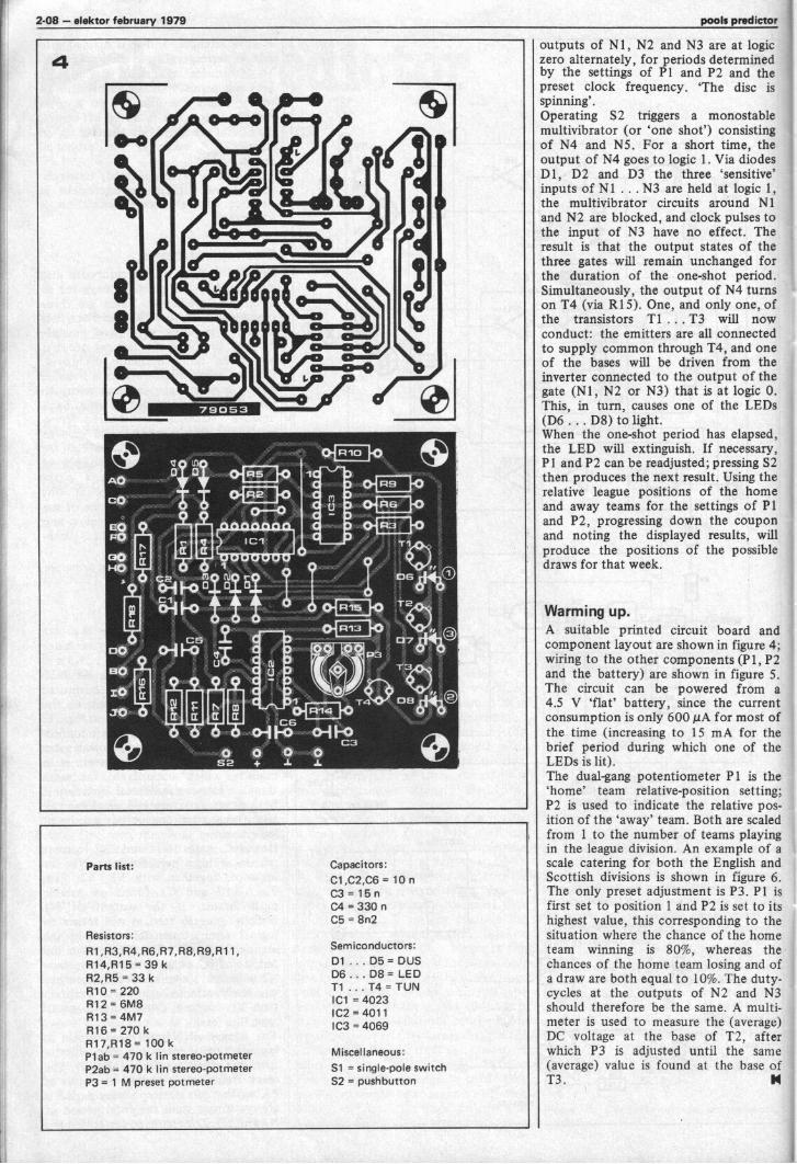
Parts list:
Resistors:
R1,R3,R4,R6,R7,R8,R9,R11,R14,R15 = 39 kR2,R5 = 33 kR10 = 220R12 = 6M8R13 = 4M7R16 = 270 kR17,R18 = 100 kPleb = 470 k lin stereo-potmeterP2ab = 470 k lin stereo-potmeterP3 = 1 M preset pot meter
Capacitors:C1,C2,C6 = 10 nC3 = 15 nC4 = 330 nC5 = 8n2
Semiconductors:D1 ... D5 = DUSD6 ... D8 = LEDT1 ... T4 = TUNIC1 = 4023IC2 = 4011IC3 = 4069
Miscellaneous:
S1 = single -pole switchS2 = pushbutton
outputs of N1, N2 and N3 are at logiczero alternately, for periods determinedby the settings of P1 and P2 and thepreset clock frequency. 'The disc isspinning'.Operating S2 triggers a monostablemultivibrator (or 'one shot') consistingof N4 and N5. For a short time, theoutput of N4 goes to logic 1. Via diodesDI, D2 and D3 the three 'sensitive'inputs of NI . N3 are held at logic 1,the multivibrator circuits around NIand N2 are blocked, and clock pulses tothe input of N3 have no effect. Theresult is that the output states of thethree gates will remain unchanged forthe duration of the one-shot period.Simultaneously, the output of N4 turnson T4 (viaR15). One, and only one, ofthe transistors T1 ... T3 will nowconduct: the emitters are all connectedto supply common through T4, and oneof the bases will be driven from theinverter connected to the output of thegate (N1, N2 or N3) that is at logic 0.This, in turn, causes one of the LEDs(D6 ... D8) to light.When the one-shot period has elapsed,the LED will extinguish. If necessary,P1 and P2 can be readjusted; pressing S2then produces the next result. Using therelative league positions of the homeand away teams for the settings of P1and P2, progressing down the couponand noting the displayed results, willproduce the positions of the possibledraws for that week.
Warming up.A suitable printed circuit board andcomponent layout are shown in figure 4;
wiring to the other components (P1, P2
and the battery) are shown in figure 5.
The circuit can be powered from a4.5 V 'flat' battery, since the currentconsumption is only 600 I.LA for most ofthe time (increasing to 15 mA for thebrief period during which one of theLEDs is lit).The dual -gang potentiometer P 1 is the`home' team relative -position setting;P2 is used to indicate the relative pos-ition of the 'away' team. Both are scaledfrom 1 to the number of teams playingin the league division. An example of ascale catering for both the English andScottish divisions is shown in figure 6.The only preset adjustment is P3. P1 isfirst set to position 1 and P2 is set to itshighest value, this corresponding to thesituation where the chance of the hometeam winning is 80%, whereas thechances of the home team losing and ofa draw are both equal to 10%. The duty -cycles at the outputs of N2 and N3should therefore be the same. A multi -meter is used to measure the (average)DC voltage at the base of T2, afterwhich P3 is adjusted until the same(average) value is found at the base ofT3. 14

pools predictor elektor february 1979 - 2-09 1
Figure 4. Printed circuit board and com-ponent layout (EPS 79053).
Figure 5. Particular care should be takenwhen wiring up the potentiometer to thep.c. board, as otherwise the predictions willnot be relative to the calculations for figure 1and this may not be apparent initially.
Figure 6. Suitable scales must be made for P1and P2, running from 1 up to the number ofteams playing in that particular league, withthe lowest team position being fully clockwise.
Figure 7. Layout design will follow manyvariations, depending on personal preferences,an example of which is shown here.
1 Liverpool 20 31
2 Everton 19 303 West Bromw. 18 274 Arsenal 19 255 Nottingham 18 256 Manch. Un. 19 247 Coventry 19 228 Tottenham 19 229 Leeds 20 21
10 Aston Villa 20 21
11 Bristol 20 21
12 Southampton 20 1913 Norwich 18 1714 Derby 20 1715 Manch. C. 18 1616 Ipswich 20 1617 Middlesbr. 19 1518 Queens Park 19 1419 Bolton 20 1420 Wolverhampt. 19 9
21 Birmingham 20 822 Chelsea 19 8

2-10 - elektor februery 1979 D/A for µPs
Dfor/AAPs
Using a couple of inexpensiveCMOS ICs it is not difficult tobuild a simple D/A converterwhich affords the possibility ofgenerating analogue signals fromsoftware.
From an idea by T. Basien andP. Haberoetzer
One of the 'problems' facing the micro-processor user is how to interface hissystem with the 'real world'. The fol-lowing simple circuit for a D/A con-verter should prove useful in extendingthe number of possible applications forwhich, among others, the ElektorSC/MP system can be used.The circuit diagram of the converter isshown in figure I . The actual conversionis performed with the aid of a voltagedivider network comprised of resistorsconnected to the outputs of a quad
Table 1
C4FF LDI FF TA8 OF00 OF
00O2 31 XPAL1 2E00O3 C4FF LDIFF 4D0005 35 XPAH1 6C0006 C40F LDIOF 880008 36 XPAH2 AA0009 $1 C400 LOIN C9OCOB 32 XPAL2 E8(DUX C410 LDI10 D7OCOE C80B ST COUNT B60C10 $2 C601 LD@ 1(1) 950C12 C900 ST 00(2) 740C14 6805 DLD COUNT 530C16 98F1 JZ $ 1 320C18 90F6 JMP $ 2 11
0C1A 00 COUNT 00
2
latch (IC1). The inputs of the latch areconnected to the data bus of the SC/MP.Thus to write data into the latch it issimply put on the data bus whilst theappropriate address is sent out on theaddress bus. The address decoder (IC3,IC4 and N 1 . N3) decodes all 16address bits, and since the data bus is8 bits wide two quad latches can beused simultaneously. The address of thelatches in the above circuit is FFFF.Depending upon the data byte presenton the latch inputs, a logic '1' or logic`0' will appear on the correspondingresistors at the outputs of the latches.In the case of CMOS ICs a logic ' 1 ' is+5 V, whilst logic '0' is 0 V. Thus at thejunction of RI ... R4 and R5 . R8will appear a voltage which may liebetween 0 and 4.6 V - depending uponthe number of logic '1's' on the latchoutputs. The resistor values are chosensuch that the output voltage range(0 - approx. 5 V) is divided into virtu-ally equal steps, the lowest voltage
corresponding to the number X'0 andthe highest to X'F. Al and A2 aresimply output buffers (voltage fol-lowers), whilst P1 and P2 allow thevoltage levels to be adjusted as desired.Since one gate of ICS is spare, it can beused to invert one of the address bits, sothat a different address can be chosenfor the converter.
ProgramTable 1 provides just one example ofthe many possible programs whichcould be used to generate an analogueoutput signal from software. Theprogram shifts data byte for byte out ofa 16 byte table (starting at OFØØ) intothe latches. When all 16 bytes have beentransferred the program jumps back tothe start ((WOO) and repeats the process,so that a simple periodic signal is pro-duced. The type of waveform generatedby the above program is illustrated infigure 2.
1
9
04
06
07
01
02
4304
05
CA07
CO
CC0 08
9 0910
13
14
15
16 6
7c
7.
3
4
IC14042
4
16 6 5
10c 13
14
IC24042
2
10
11
10
R1
ECMR2
R3
R4
EEO
5
R6
68k
R7
R8
18,1c
d)IC3 IC4 IC5y I y 4a,4c
3a,c
0 12 V
0
O
IC6741
C
5V
12 V 10k
0 5 V
R10
0
0
IC7+741
012 V
5V
P2
10k
26a
4c
24. 10
11
22.21c
21.
20c 9 IC420. 10
9c
9.
13
3
110-1 2,1°
13
12
IC3 = 4068IC4 = 4068N1 ... N3 = IC5 = 4001
40
5
31. 0NWDS
(RAW)
79060
Al
A2

delay lines elektor february 1979 - 2-11
delay lines
One of the most important sound -processing techniques employedby amateur and professionalmusicians as well as soundrecording studios is the electronicdelay line. Reverberation, echo,vibrato, phasing, flanging andchorus are just a few of the specialeffects which can be obtained bydelaying an audio signal. Howeverthe applications of delay units arenot restricted to audio effects;sound reinforcement systems,level control equipment, speechprocessors all employ delay linesin one form or another. Thefollowing article takes a close lookat the 'ins and outs' of this device,and examines some of the lesswell-known uses to which it is put.
As is well-known, sound travels throughfree air at a speed of some 1150 feet persecond, which means that, even overcomparatively short distances, it takes aperceptible length of time to reach alistener (roughly 25 . . . 30 ms per 10yards). When listening to music - re-gardless of whether it is being reproducedvia a domestic stereo system or by afull-scale orchestra in a concert hall - thesignal reaching one's ears will be amixture of direct and delayed sound.The former travels straight to thelistener from the sound source, whilstthe latter is first reflected off the walls,ceiling, furniture etc. and hence mustcover a greater distance. The fact is thatthe human ear is extremely sensitive to
in the time taken for a signalto arrive and to the level of reflectedsound which it contains. A signal whichis deprived of natural reverberation, e.g.the output of an oscillator listened tovia headphones, sounds distinctly`artificial' and is often experienced asbeing somewhat unpleasant, inducinglistener fatigue.Close-miking techniques during record-ing often have the effect of depriving apiece of music of natural reverberation,with the result that the sounds seems`dead', 'flat', devoid of any ambience.For this reason studios must introduceartificial reverberation to restore thenatural fullness and 'body' of the music.Many concert halls which have in-herently poor acoustics can be improvedby employing delay lines to controlthe reverberation characteristics elec-tronically. By varying the length andlevel of reverberation the acoustics ofthe hall can be tailored to suit the typeof music being performed - long rever-beration times for orchestral works,shorter times for chamber music.In addition to simulating the soundreflection characteristics of particularacoustic environments, delay lines canalso be used to process the music signalin a variety of ways and obtain a rangeof often spectacular effects. Certainpsychoacoustic responses of the braincan be exploited to convince the listenerhe is hearing not one but several voices- i.e. 'chorus'. Phasing/flanging and`space' -effects can be obtained - thelatter being an extremely 'un-natural'
and sciencefiction like sound which hasno exact correlation in real life. Furtherapplications for delay lines are in signalprocessing equipment where they areused to give the control circuits suf-ficient time to iron out signal overloads,glitches etc. before being fed on to thenext stage; and in P.A. systems, wherethey can considerably improve theintelligibility of speech signals.For a number of years there have beendelay lines of an electro-mechanicaltype - the most well-known being the`echo chamber'. This is simply a speciallydesigned enclosure whose acoustic re-sponse can be varied by the use ofcurtains, tiles etc. to alter the sound -absorbing properties of the reflectivesurfaces. The signal to be echoed isreproduced via loudspeakers and thenpicked up by carefully situated micro-phones. An expensive process, and onewhich is limited by the size of chamberbeing used. For reverberation and echoeffects electro-mechanical units basedon spring lines or metal foils are alsopopular. In this type of delay line anacoustic signal is fed into e.g. a helicalspring via a transducer. The signaltravels round the coils of the springuntil it is picked up at the other end viaa second transducer which reconverts itinto an electrical signal. Unfortunately,however, this type of unit has a numberof limitations. Firstly, they are fairlylimited in the range of possible appli-cations, being restricted to echo/reverbeffects. Secondly, they are extremelysusceptible to external vibration (micro -phonic) and furthermore they tend toexhibit resonance modes of their own,so that their frequency response is notperfectly flat. Similar problems ofinherent sensitivity to mechanical dis-turbance apply with tape echo/reverbmachines employing several replay headswhich are mutually offset to providevariable delay to the audio signal.Tremendous demands are placed uponthe mechanical engineering of suchunits, which of course means that theyare generally fairly expensive.Fortunately, however, recent advancesin hardware have made possible thedevelopment of all -electronic delaylines, which not only are more reliable,provide uncoloured, faithful sound

2-12 - etektor february 1979 delay lines
ClockGenerator
0 -SampleA/D-Converter
^AP'LP
S& HA/D
M D/A
InputAmplifier
Low PassFilter
& Hold DigitalMemory
D/A-Converter
Low PassFilter
D -0OutputAmplifier
79056 - 1
quality, and are often considerablycheaper, but also can be used to producea wide variety of time -related specialeffects.
Electronic delay linesUnlike electromechanical delay units,the audio signal is not transmittedcontinuously through the delay line butrather is sampled at a frequency whichmust be at least twice the highest signalfrequency. The samples are then clockedthrough some form of shift register andthe original signal is reconstituted at theoutput by lowpass filtering to removethe clock frequency components. Abasic distinction can be made betweentwo types of electronic delay line. Thereis the digital delay line, which employseither random access memory (RAM)with special control logic, or digital shiftregisters; in both cases the digitalmemory must be preceded and followedby A -D and D -A converters. On theother hand there is the analogue delayline, which employs analogue 'bucket -brigade' - or CCD (Charge CoupledDevice) memories.Figure 1 shows the block diagram of adigital delay line. A clock generatorcontrols the A -D and D -A converters aswell as the rate at which the sampledsignal is read into and out of the digitalshift register. Two basic methods of A -Dconversion are used: delta modulationand pulse code modulation. The deltamodulator has a single output in theform of a train of pulses which providea continuous indication of whether theanalogue input signal is increasing ordecreasing. If the former is the case, theoutput of the modulator will be high, ifhowever the analogue signal is falling,the modulator will output a logic '0'. Ifthe input signal were constant, themodulator would output 01010101..The digital reverberation unit describedin the May 1978 issue of Elektor(no. 37) employed just such a modu-lator.With pulse code modulation, on theother hand, the analogue signal isconverted into rows of pulses which, inbinary code, represent the instantaneous
value of the samples. The process can belikened to comparing the analoguesignal with a reference voltage whichtakes the shape of a rising staircasewaveform. As soon as the referencevoltage exceeds the analogue signal theoutput of the comparator changes state.The height of the staircase, i.e. thenumber of steps it contains, is an indexof the size of the analogue signal. Thenumber of bits in each binary word (i.e.the number of outputs of the A -Dconverter) determines the resolution oraccuracy of the conversion. The greaterthe number of bits, the greater thenumber of steps in the staircase, andhence the smaller is the error introducedby the fact that the minimum variationin signal level that the converter willdetect is equal to the height of one step.To obtain a satisfactory resolution it isusual to employ at least a 12 -bit code,which means that there are 212 = 4096steps in the staircase. If the height ofeach step is the same, the code is said tobe linear, i.e. there is a linear relation-ship between the analogue input and thebinary-coded output of the converter.If, on the other hand, the step height isnot constant, the code is said to be`companded', whilst it is also possiblefor the staircase to have several 'flights'of steps, whereby the height of the stepsvary from flight to flight. In this casethe conversion characteristic will have anumber of `kinks' in it. In additionthere is a sophisticated techniqueknown as 'floating decimal pointencoding' which can he employed toimprove the range of the converter.Thus it is possible, for example, to varythe gain (or attenuation) of the A -Dconverter in accordance with theamplitude of the input signal. Theinformation relating to the degree ofgain introduced by the converter is alsobinary coded and transmitted along withthe digitised version of the analogueinput, so that the inverse amount ofgain/attenuation can be applied in theprocess of D -A reconversion at theoutput, thereby restoring the originalsignal level.The binary data is either clockedthrough a digital shift register or, with

delay lines elektor february 1979 - 2-13
2
0 -InputAmplifier
LIT\
Clock 1
Clock Generator
0
41-F E Clocka
-110-
Low PassFilter
ClanT
Bucket Brigade Device
LP
Low PassFilter
OutputAmplifier
-0
79056-2
the aid of special control logic, througha random access memory (RAM). Therate at which the data is transferred, andhence the amount of delay introduced,is of course determined by the clockfrequency.According to Nyquist's sampling the-orem, the sampling frequency must beat least twice the maximum signalfrequency. For this reason the analogueinput signal is bandwidth limited by alowpass input filter which has anextremely sharp roll -off. A similararrangement is required at the output ofthe delay line in order to remove thehigh frequency clock components andany spurious products caused by thesignal and clock frequencies interacting.Digital delay lines have the advantagethat they can be extended to virtuallyany desired length without adverselyaffecting the signal quality. This is incontrast to analogue delay lines, inwhich the degree of attenuation intro-duced into the signal is proportional todelay time. Digital shift registers arethus ideally suited for applicationsrequiring longer delay times.Furthermore, the ability to use longdelay lines means that it is possible toincrease the clock frequency and hencethe maximum permissible bandwidth ofthe system whilst retaining reasonabledelay times. The disadvantage of digitalshift registers is the relatively high costof A -D and D -A converters. Althoughthe digital shift registers themselves areactually cheaper than their analoguecounterparts, the additional expense ofA -D -A conversion pushes the price upconsiderably. This is particularly true ifone requires a digital delay line with anumber of different outputs, each witha separate delay time. In this case a D -Aconverter is needed for each output,whereas with an analogue delay line thesignal can be fed straight out at virtuallyany point.Analogue delay lines can be divided intothose using so-called bucket -brigadememories, and those which employcharge -coupled devices. The basic prin-ciple involved is the same in both cases,the difference being in the chip structureof the two types of device. The term
Figure 1. Block diagram of a digital delay linefor audio signals. The analogue input signal isfirst bandwidth -limited by feeding it througha lowpass filter, converted into a digital signalby means of the D -A converter, then clockedthrough a digital shift register or randomaccess memory at a rate determined by aclock generator. At the output of the digitalmemory the delayed, sampled signal is recon-verted into an analogue waveform beforebeing passed through a second lowpass filterwhich rolls off the clock frequency com-ponents.
Figure 2. An analogue delay line for audiosignals employing a bucket -brigade shiftregister. Charge levels representing the instan-taneous value of the sampled analogue wave-
from capacitor to capacitorlike buckets of water being passed down achain of fire-fighters.
Photo 1. A professional electronic reverber-ation unit, the EMT250. This unit, whichemploys digital delay lines and microcomputer -controlled random access memory (128 K),provides 19 different delay elements, whichunder programme control, can simulate awide variety of effects such as phasing, chorus,echo and of course reverberation.
`bucket -brigade' comes from the factthat the operation of the shift registercan he likened to a chain of men passingbuckets of water down a line. In thecase of the chip, the buckets are in factcapacitors, and the 'water' is packets ofcharge which correspond to the instan-taneous value of the sampled analoguewaveform. The charge packets aretransferred from capacitor to capacitorvia FET switches which are controlledby a two-phase clock.Since the integrated capacitances on thechip are far from representing idealcapacitors, and have a significantleakage current, the samples are inevi-tably attenuated as they pass throughthe shift register. However, as eachsample is attenuated by the sameamount, the envelope of the originalwaveform is preserved. Unfortunately,when longer delay times are required,which means that the signal must beshifted through large numbers of stages,the cumulative effect of all these smalllosses adds up to a perceptible deterio-ration in the signal-to-noise ratio. This isa particular problem when feedbackloops are used and the signal passesthrough the same shift register severaltimes. Bucket -brigade memories aresuperior to charge -coupled devices inthis respect and are to be preferred foraudio work. However CC D's offerhigher chip densities (a typical CCDdelay line will contain upward of 64separate shift registers, each containing256 stages) and are better suited forhigh frequency applications such asdelaying video signals.The basic elements of a delay linefeaturing bucket -brigade memories areillustrated in figure 2. Once again steeplowpass filters at the input and outputare necessary to band -limit the inputsignal and eliminate clock frequencycomponents.
Applications of delay linesBy far the commonest, but also themost complex application of delay linesis in producing reverberation. Reverber-ation is an acoustic phenomenon whichis an integral feature of all normal

2-14 - elektor february 1979 delay lines
3
\
// /
//
. X/x N /
\\ / N
N\//\
// \
\ /11 /C\ I /
'
Listener
/
///
/
/
Direct Sound
- Direct Reflection
Multiple Reflection
79066 3
4dB
o.
-10-
-20 -
-30-
40
Direct Sound
1st Reflection
25 50 75 100 125 150 175
tlmsl200
Figure 3. Illustration of the various paths ofsound waves as they travel from the signalsource around a rectangular room to thelistener.
Figure 4. Amplitude v. time graph whichillustrates the density and decay characteristicsof echoes during the reverberation period of asingle sharp sound signal. The amplitude ofand interval between successive reflections isdetermined by the path lengths of the soundwaves and also by the sound -absorptionproperties of the reflective surfaces theyencountered. As can be seen, after only arelatively short time the reverberation signalpossesses an extremely high echo density.This rapid increase in the number of reflec-tion signals is a characteristic property of theacoustic phenomenon, 'reverberation'.
Figure 5a. Block diagram of a simple rever-beration module, comprising a delay line withdelay time r, and a feedback loop whichattenuates the delayed signal by a factor g.
Figure 5b. Circuit diagram for the simplereverberation module of figure 5a. The attenu-ation, g, of the feedback signal can be con-tinuously varied from 0 dB with the aid of thepotentiometer.
Figure 5c. Amplitude v. time graph of theoutput signal of the simple reverberationcircuit, where 7 = 20 ms and g = -3 dB (0.7).
Figure 5d. The frequency response of thesimple reverberation circuit resembles that ofa comb filter. The delay time, r, determinesthe interval between successive peaks in the
1,response (= -1, whilst the attenuation, g, of
the feedback loop determines the amplitudeof the peaks.
79056 4

delay lines elektor february 1979 - 2-15
5b100n
QUI
ILO
Al delay moduler
Al A2 = L F 356, 1/4 TL 084,1741)
A2
g10klin
79056 - 55
5cdB
0
I -es
-12
-18
-24
-30
-360 20 40 80 80 100 120 140 180 180 200 220 240
t(ms)
79056 - 5c
listening environments, be they domesticliving rooms or concert halls. Only inspecially constructed so-called anechoicchambers will reverberation - the re-flection of at least part of the soundwave off the walls, ceiling and floor, beabsent.In a large volume enclosure, such as e.g.a cathedral, which has hard reflectiveinterior surfaces, a sound may take aslong as four or five seconds to die away.This provides a wonderful acousticenvironment for a church organ, yettends to render human speech all butunintelligible unless spoken extremelyslowly (the acoustics of churches areprobably the prime reason for thesomewhat rather meandering, sing -songinflection often adopted by ministers orpriests!) In addition to the walls,ceiling etc. of a concert hall, the numberof people present also influences theacoustics. A hall which is completelyfilled will have a shorter reverberationperiod than the same hall when it is halfempty - unless, of course, as is the casewith the Albert Hall, the seats aredesigned to have similar reverberationcharacteristics to those of people.The dispersion pattern of a short, sharpsound signal in a conventionally -shapeddomestic room is illustrated by thediagram in figure 3. First of all thelistener will hear the original signaltravelling straight from the source of thesound. This is followed after a shortinterval, by the first direct reflection -from the nearest wall, and is succeededby further direct reflections from moredistant surfaces such as ceiling, floorand rear walls etc. These quickly mergeinto the increasing number of indirector multiple reflections off more thanone surface. Since the energy of thesound waves is absorbed as they strikeeach reflective surface, the amplitude ofthe 'echo' signals fall more or lessexponentially.An important and characteristic featureof natural reverberation is the highdensity of reflected signals. Whensimulating reverberation electronically itis necessary to provide around 1000echoes per second for the effect toavoid sounding artificial. Furthermore,it is also important that the spacing ofthe echoes be non -periodic. Thesepoints are illustrated in the amplitude v.time graph shown in figure 4.
The basic circuit configuration for areverberation unit is shown in figures 5aand 5b. As can be seen, this consistssimply of a delay line with a feedbackloop. The corresponding graph ofamplitude v. time is given in figure 5c.By attenuating the portion of thedelayed signal sent back round thefeedback loop the reverberation signalcan be made to decay exponentially asdesired.The reverberation time is defined as thetime taken for the amplitude of thesignal to drop to 1 millionth of itsoriginal level, i.e. 60 dB down. In thecase of the simple circuit in figure 5a

delay lines2-16 - elektor february 1979
Figure 6a. An extension of the basic reverbcircuit is the 'all -pass' reverberation module,which has a linear frequency response.
Figure 6b. A practical circuit of an all -passreverberation unit, with a damping factor of-3.5 dB (0.66).
Figure 7. By mixing the outputs of severaldelay lines in different proportions, it is
possible to simulate more accurately thenatural acoustics of different types of room.
Figure 8. Professional electronic reverberationunits typically employ a large number ofdelay lines in order to obtain truly authenticreverberation characteristics. The compara-tively simple circuit shown here nonethelesscontains four parallel -connected reverberationmodules of the type shown in figure 5,followed by two all -pass modules as in figure6. Potentiometer g7 determines the relativeproportions of direct and delayed signalmixed in the output stage.
the number of times the delayed signalreturns around the feedback path beforeit reaches this level can be calculated bydividing 60 dB by the attenuation, g. ofthe feedback loop. The reverberationtime, T, is then equal to the number oftimes the signal loops round the feedbackpath multiplied by the delay time T:
60 rg
A delay time of 50 ms and an attenu-ation of 3 dB will give a reverberationtime of 1 second. Here, however, wecome up against the first problemcaused by employing this simple ar-rangement. To achieve sufficient rever-beration times (1 . . . 2 seconds) onemust either use long delay times, whichmeans a low echo density, or else short
Bb
R4
470n R7
0 OAR2
150k
R3
ECM
A3
RI
ECM
Al
ruR1 _110050 KK =0,66 (-3,5 dB)
rid-V= 150 KR3 100 K - -0,66
_ R5 _ 100 K _ 0 55W6- 180 K '
R8
100k
R6
111:13
R5
EON
tc*
delay module
RIO
R9
-
ELS
A2
79056 -60
Al . A4 = TL 084, RC 4136, (LM 324)
delay times with a high echo density. Inthe former case the reverberationsounds unnatural, whilst a high echodensity involves reducing the attenu-ation of the feedback loop to the pointwhere the circuit will tend towardsinstability. Furthermore, because thedelay time of the shift register is con-stant, the diffusion rate or spacing ofthe reflection signals will be regular.A further limitation of the circuit lies inthe fact that it has a comb -filter -likeresponse, with periodic dips and peaks(see figure 5d). The distance betweenthe peaks is equal to 1, thus, with the
delay time shown in figure 5c of= 20 ms, the frequency response of
the delay line will exhibit a peak every100 Hz. The difference in amplitude
between the peaks and dips is inverselyproportional to the amount of attenu-ation, g. introduced in the feedbackloop. Thus, for g = 0.7 (-3 dB), the
+1 g 1
ratio is +077-5.7 or 15 dB!1 g 1
The above -described drawback can beavoided by employing the configurationshown in figure 6a, which is an ex-tended version of the simple circuit offigure 5a, and which has a flat fre-quency response.The input signal is attenuated by afactor equal to the attenuation of thefeedback loop, inverted and thensummed with the output of the delayline, which itself has been attenuated bya factor of 1 - g2 . In practice the processis simpler than it may at first appear.

delay lineselektor february 1979 - 2.17
7
100n
A1,A2 = 1/4 TL 084, LF 356, (741)
ddelay module
T 1
delay module
' 2
d delay module1 3
delay module7 4
reverb time
p
100klog
100klog
100klog
100klog
C1379056 7
8
SR1rl,g1
SR272,g2
SR3'3,93
SR4T444
ULM
CI3
CI3
A2
EC3
Al
C/3
CI3
AR175,95
AR276,96
9710klog
Al ... A3 = 1/4 TL 084, LF 356 (741)
79058 - 8
Generally speaking the attenuation ofthe feedback loop is -3 dB (a factor of0.7), so that 1 - g2 = 1 - 0.72 = 1 - 0.5= 0.5 (-6 dB). In practice this factor of0.5 is nothing more than a symmetricalvoltage divider.Figure 6b shows the equivalent circuitdiagram for the block diagram of 6a.Through a suitable choice of values forR2, R4 and R6 an attenuation, g. of0.66 (3.5 dB) is obtained. Although thedelay circuit shown in figure 6b willhave a flat frequency response, it doesnot solve the problem of insufficientecho density and the regular spacing ofthe echoes.The echo density can be increased to anacceptable level by connecting several`all -pass' reverberation circuits as shownin figure 6b in cascade and arranging for
the first delay element to have thelongest delay time, and each successivedelay time to be a third of the previous.To prevent the echoes occurring atregular intervals, the delay times arechosen such that they have no commondenominator. Thus the natural reverber-ation characteristics of a conventionalroom (amplitude, diffusion pattern anddensity of echoes) can be fairly accu-rately approximated by employing fivedelay modules of the type shown in fig.6b with delay times of 100, 68, 60, 19,7 and 5.85 ms respectively.Another possible approach for achievingnatural electronic reverberation is shownin figure 7. The different reflectionpaths of a signal reproduced in a roomare simulated by connecting a numberof delay modules in cascade. Reverber-
ation times of differing length can berealised by means of the level poten-tiometers at the output of each shiftregister. The individual delayed signals,each representing a different reflectionpath, are summed, and the overallreverberation time is determined by acommon feedback level control. Onceagain delay times should be chosenwhich do not have a common denomi-nator.When selecting the various delay times itis worthwhile bearing in mind thecorresponding path lengths which thesignal would cover in that period. Thus,for example, a 10 ms delay wouldcorrespond to a path length of 3.3 m(there and back!) so that one is simulat-ing the effect of a reflective surface1.65 m from the sound source. A delay

2-18 - elektor february 1979delay lines
of 100 ms on the other hand, wouldcorrespond to a path length of 33 m, i.e.would simulate the effect of a small hall.Generally speaking delay times of lessthan 10 ms are avoided, and long delaytimes (greater than 100 ms) are onlyused if a particularly 'spacious' or`echoey' effect is desired.The number of delay lines dependsupon the application, however ingeneral one can say that the greater thenumber of echoes, the more natural -
sounding is the system. At any rate, aminimum of four delay lines is a must.
ReverberationFigure 8 shows the basic design for areverberation unit, which, assuming thedelay modules are of suitably highquality, will satisfy even professionalrequirements.The circuit consists of a parallel connec-tion of four simple reverberationmodules, SRI . . . SR4, of the typeshown in figure 5b. These are followedby two all -pass delay modules of thetype shown in figure 6b. The values ofdelay times r 1 . r4 are chosen withinthe range from 30 to 45 ms such thatthey share no common denominator.The damping factors gl . . . g4 shouldall lie below 0.85, otherwise the combresponse of the delay lines will proveover -prominent. The shortest delay timeof the first four modules determines thedelay between the direct signal and thefirst reflection. The two all -pass reverber-atory, AR1 and AR2, provide suitableecho density; acceptable values for r5and r6 are roughly 5 ms and 1.7 msrespectively, whilst a suitable value for gis something in the region of 0.7. If it isdesired to make the reverberation timefrequency -dependent, this can beachieved quite simply by inserting anRC network with the appropriateturnover frequency in the feedbackloop.Professional electronic reverberationunits used in studio work etc. oftenincorporate an even greater number ofdelay lines. Thus, for example, theEMT250, a programmable digital reverbunit (see photo I) has four outputs,each of which can be set to providespecific delay characteristics. 19 separatedelay lines provide reverberation timesbetween 0.4 and 4.5 seconds in 16switched steps. Some of the delay linesincorporate feedback, and in each casethe degree of feedback can be indepen-dently varied by the operator.In addition to these professional reverbunits, a number of instruments haverecently appeared on the market whichare intended to improve or compensatefor the reverberation characteristics ofdomestic listening environments. Onesuch unit is the Audio Pulse Model Onefrom Digital Delay Systems whichemploys digital shift registers and deltamodulator A -D and D -A converters.This unit provides a stereo reverberationsignal which is reproduced via two

delay lines elektor february 1979 - 2-19
additional loudspeakers situated oneither side of the listener. As can beseen from the block diagram of figure9a, the delay lines are arranged in across -coupled configuration. This ap-proach provides a high echo density,whilst choosing delay times which haveno common denominator once againeliminates periodic echoes. The shortdelay times which are necessary for ahigh echo density would normally limitthe available reverb times to an unac-ceptably short value. However thisproblem is solved by employing fourdelay lines (see figure 9b) one of whichprovides a delay of roughly 100 ms.This long delay ensures an amplereverberation time, whilst the remainingthree delay lines, which are considerablyshorter, are responsible for the rapidtransition to high echo density.The 'Acoustic Dimension Compiler',ADC -2 from WEGA (see photo 2) isdesigned for a similar purpose, namelyto reproduce a reverberation signal viatwo ancillary loudspeakers situated inthe living room. The 'space' controlvaries the delay time, whilst the 'reflec-tion' control determines degree offeedback round the delay lines. The'characteristic' switch varies the highfrequency response of the unit.
EchoIn contrast to reverberation, echo ischaracterised by relatively long delaytimes, and more importantly, theregular repetition of individual reflectionsignals. In the simplest example of echo,say the reflection of a shouted soundfrom a cliff or mountain face, the signalis thrown hack to the listener just once,and reaches him after a time, t, which isdetermined by the distance betweenhimself and the reflective surface. Theelectronic equivalent would be a simpledelay line whose output signal wasattenuated and then mixed with theoriginal direct signal (see figure 10).If one extends the model slightly toinclude a second cliff face at a certaindistance from the first, the sound signalis slowly reflected to and fro betweenthe two surfaces, with the result thatone can clearly distinguish betweensuccessive echo signals. This effect isquite simple to simulate electronically:A simple reverberator circuit such asthat already shown in figure 5 can beemployed; one merely has to use longerdelay times and reduce the attenuationintroduced by the feedback loop.Depending upon the length of the delayand the degree of feedback, extremelyvaried echo effects can be obtained.With delay times under roughly 20 ms,the comb response of the module lendsa metallic -sounding tone to the resultantsignal, whilst delays of between 50 and70 ms still produce a 'harsh' or rougheffect. It is only with longer delays thatthe overall frequency response becomesless irregular and the separate echosignals become discernible. If the delay
time (interval between echoes) is set tocoincide with the rhythm of a piece ofmusic, extremely interesting effects canbe obtained.
Space effects - 'super echo''Space' effects are characterised byextremely long reverberation times(approx. 10 seconds), giving a sort of`super' -echo which has no equivalent inreal life. (because of the sound -absorption properties of air, reverber-ation of this duration cannot occurnaturally). For this reason the effect hasbeen christened 'space' and is extremelypopular in sci-fi applications. The effectis obtained simply by using very longdelay times and recirculating a largeproportion of the delayed signal roundthe feedback loop.
First reflection delayIn the case of electro-acoustic reverber-ation units such as spring lines andreverberation plates as well as echochambers, which often have extremelysmall dimensions, the initial delaybetween the original signal and the firstreflection or echo is frequently tooshort for the reverberation to soundnatural. This problem can be overcomeby employing an electronic delay line toprovide a sufficient interval between thedirect signal and the reverb signal fromthe electro-acoustic reverberator. Delaysof between 20 and 100 ms are normal inthis type of application, however inrecordings of pop records the initialdelay period is often extended togreater than 100 ms in order to obtainspecial effects. Many electronic reverbunits incorporate a special variable delaymodule in order to provide independentcontrol of the 'first reflection' delay.Of particular interest for the electronics
Figure 9a. Simple reverberation circuit em-ploying two cross -coupled delay modules toobtain stereo reverberation.
Figure 9b. An extended version of the stereoreverb unit which provides increased echodensity. Suitable reverberation times can beobtained by selecting a delay time of around100 ms for T1.
Figure 10. A circuit to produce single -echoeffect.
Photo 2. The Acoustic Dimension Compiler(ADC -2) from WEGA which employs a
bucket -brigade delay line is an example of areverberation unit designed for use withdomestic hi-fi installations.
enthusiast cum music fan, is the use ofdelay lines to achieve special effectssuch as phasing, flanging, vibrato,chorus, ensemble and string ensemble.These and allied effects are obtained byvarying the frequency at which thedelayed signal is clocked through theshift register, in contrast to reverb andecho, where the clock frequency of thedelay line is constant.Several psycho -acoustic phenomena con-nected with the delaying of audiosignals and how these effects can beexploited to 'improve' room acousticsand studio recordings together with thehighly specialised areas of speechmanipulation and pitch correction arebeyond the scope of this article butcould merit a further article in the nottoo distant future.
Photographs:Photo 1: EMT-FRANZ Gmbh.
7630 Lahr.Photo 2: WEGA
Bibliography:Schroeder, M.R. and Logan, B.F.'Colorless Artificial Reverberation',J. Audio Eng. Soc., vol. 9 nr. 3 pp.192-197, July 1961.Schroeder, M.R. 'Natural soundingArtificial Reverberation', J. Audio Eng.Soc., vol. 10, nr. 3 pp. 219-223,July 1962EMT 'Elektronisches NachhallgerlitEMT 250', EMT-Kurier Nr. 26, pp. 3-8,Februari 1976EMT 'Digitales Tonsignal-Verzogerungsgeriit EMT 444',1 st paragraph, 'Warum verzeigern?',EMT-Kurier, Nr. 30, pp 3-6, July 1978Reticon Corp. 'Acoustic Applications ofSerial Analog Delay -Devices - ReticonSAD 1024 Serial Analog Delay',Application Note no. 104Mitchell, P.W. and DeFreitas, R.E.'A New Digital Time -Delay andReverberation System Part II:Psycho -acoustics vs. PracticalElectronics'. presented at the 55th AESconvention October 1976, AES PreprintNo. 1191 (L-6).Elektor 'Digital Reverberation Unit',Elektor 37, pp 5-08 - 5-16. May 1978Elektor 'Analogue Reverberation Unit',Elektor 42, pp 10-44 - 10-50,October 1978.
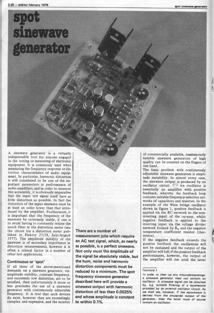
2-20 - elektor february 1979
inewaveenerator
A sinewave generator is a virtuallyindispensable tool for anyone engagedin the testing or measuring of electronicequipment. It is commonly used whenmeasuring the frequency response or dis-tortion characteristics of audio equip-ment. In particular, harmonic distortionis still considered to be one of the im-portant parameters in performance of
.
audio amplifiers, and in order to measure .
this accurately, it is obviously imperativethat the input test signal itself have aslittle distortion as possible. In fact thedistortion of the input sinewave must beat least an order lower than that intro-duced by the amplifier. Furthermore, itis important that the frequency of thesinewave be extremely stable, if one isto avoid having to constantly retune thenotch filter in the distortion meter (seethe circuit for a distortion meter pub-lished in Elektor 27/28, July/August1977). The amplitude stability of thesinewave is of secondary importance indistortion measurements, however it isoften a critical factor in a number ofother test applications.
Continuous or 'spot'If all three of the above -mentioneddemands on a sinewave generator, viz.amplitude stability, constant frequency,and extremely low distortion, are to besatisfied, then unfortunately it more orless precludes the use of a sinewavegenerator with continuously adjustablefrequency. It is true that such devicesdo exist, however they are exceedinglycomplex and expensive, and the number
There are a number ofmeasurement jobs which requirean AC test signal, which, as nearlyas possible, is a perfect sinewave.Not only must the amplitude ofthe signal be absolutely stable, butthe hum, noise and harmonicdistortion components must bereduced to a minimum. The spotfrequency sinewave generatordescribed here will provide asinewave output with harmonicdistortion of less than 0.0025%and whose amplitude is constantto within 0.1%.
spot sinewave generator
of commercially available, continuouslytunable sinewave generators of highquality can be counted on the fingers ofone hand.The basic problem with continuouslyadjustable sinewave generators is ampli-tude instability. In almost every case,the sinewave output is produced by anoscillator circuit. (1) An oscillator isessentially an amplifier with positivefeedback, whereby the feedback loopcontains suitable frequency -selective net-works of capacitors and resistors. In theexample of the Wien bridge oscillatorshown in figure 1, positive feedback isapplied via the RC network to the non -inverting input of the op -amp, whilstnegative feedback is applied to theinverting input via the voltage dividernetwork formed by Ro and the negativetemperature coefficient resistor (ther-mistor).If the negative feedback exceeds thepositive feedback the oscillations willnot be sustained and the output of theamplifier will fall; if the positive feedbackpredominates, however, the output ofthe amplifier will rise until the latter
footnote 1In order to clear up any misunderstandings:a sinewave generator need not contain anoscillator. A sinewave signal can be obtainedby, e.g. suitable filtering of a squarewaveprovided by an external oscillator circuit. Aswe shall see, however, if the squarewave isderived from the sinusoidal output of thegenerator, then the latter must of coursecontain an oscillator.

spot sinewave generator elektor february 1979 - 2-2
I
Specifications
Harmonic distortion: < 0.005%for: f= 40 Hz ... 10 kHz
Uout < 6 Vpp600 t2 (output47 f2 (output II)
typically: 0.0025% falling linearly withamplitude
Frequency stability:
Amplitude stability:
L'fosc
fosc
A
< 0.01%
< 0.1%
Figure 1. The basic principle of a Wien bridgeoscillator.
Figure 2. Basic block diagram of the oscillatoremployed in the spot sinewave generator.
Figure 3. The amplitude- (a) and phaseresponse (13) of the type of selective bandpassfilter used in the spot sinewave generator.Curves show the response obtained for alow Q, curves '2' for a high Q. The combinedresponse of two such filters connected incascade can be obtained by adding the indi-vidual amplitude/phase curves of each filter.
saturates. The circuit is prevented fromlapsing into either of these two con-ditions by the thermistor, which stabil-ises the output amplitude as follows:should the output voltage rise, thecurrent through the thermistor willincrease, causing its temperature to riseand hence its resistance to fall. Thiscauses an increase in the proportion ofnegative feedback, thereby automati-cally reducing the gain of the op -amp.The opposite occurs when the outputvoltage tends to fall; the resistance ofthe thermistor is reduced since it dissi-pates less heat, thus also reducing theamount of negative feedback.Assuming that the resistor and capacitorvalues in the two arms of the bridge areidentical, the proportion of outputvoltage which is fed back round thepositive feedback loop at the resonantfrequency, f0, of the oscillator is 1/3.The output voltage of the oscillatorsettles at the value which ensures thatthe resistance of the NTC resistor isequal to 2R0 . It is obvious that thefrequency of the oscillator could becontinuously adjusted by using a stereopotentiometer or twin -ganged trimmercapacitor to vary the RC time constantsin the arms of the bridge. However, inpractice it is impossible to obtain stereopots or trimmers in which both gangsare perfectly matched. Variations in theresistance or capacitance values betweenthe two arms of the bridge have theeffect of altering the positive feedbackfactor, k, the result of which is a changein the resistance value of the thermistor

2-22 - elektor february 1979 spot sinewave generator
(see figure 1). Thus varying the fre-quency of the oscillator has the effectof also varying the amplitude of theoutput signal. What is more, the ampli-tude of the output signal at the newfrequency (after the balance betweenpositive- and negative feedback has beenre-established) differs from that obtainedbefore the change in frequency.The op -amp is not the only source ofdistortion in the sinewave output (thiscan be counteracted by a high open -loop gain); a further contributory factoris the fact that the voltage -currenttransfer characteristic of the thermistoris not completely linear. Other ampli-tude -stabilising components such asfilament lamps, diode -resistor networksor voltage -controlled FETs can be used,but these are also by no means perfect.For a large number of applications theabove -mentioned failings are not par-ticularly critical; however, for measure-ment purposes where accuracy is
important, they represent an unaccept-able source of error. For this reason, themost common solution is to do withoutthe admittedly attractive facility ofcontinuously adjustable frequency andto settle instead for an oscillator with anumber of switched output frequencies.Basically this amounts to a series ofindividual oscillators each designed toproduce a single optimal frequency.This elegantly solves the problem ofamplitude stability which bedevils con-tinuously variable oscillators. If oneconsiders that a high -quality continu-ously variable sinewave generator will
cost in the region of £ 500 - £ 600,whilst a (simple) spot frequency sinewaveoscillator on the other hand can beconstructed for under £ 10, and further-more, that only four or five test fre-quencies are normally required inharmonic distortion measurements, thenit is clear that a spot frequency generatorrepresents a highly cost-effective ap-proach. The distortion meter publishedin the Summer Circuits 1977 is alsodesigned for spot frequency measure-ments.
Spot sinewave generatorThe basic principle of the spot sinewavegenerator described here should befamiliar to a number of readers, since itwas used in the design for a simple spotsinewave generator published in lastyear's Summer Circuits issue (circuit 25).The operation of the circuit is illus-trated by the block diagram shown infigure 2. A symmetrical squarewavesignal is fed to a number of cascadedselective filters (in figure 2 two suchfilters are used). These remove theharmonic content of the squarewave,leaving the more or less pure sinusoidalfundamental. The resulting sinewave isin turn used to trigger the squarewavefrom which it is derived. The amplitudeof the sinewave is clipped to ± u, beforebeing fed back to the input of thesquarewave oscillator, so that theoscillations are maintained. For this infact to happen, two conditions must befulfilled: the input- and output signals
Figure 4. Complete block diagram of the spotsinewave generator.
Figure 5. The effect of changes in frequencyand of the slope of the lowpass output filterupon the amplitude stability of the generator.
Figure 6. Complete circuit diagram of thespot sinewave generator.
must be in phase; this means that thephase shift of the selective filters mustbe either 0°, 360° or a multiple of 360°(the phase shift introduced by theclipping circuit can be neglected).Secondly, the loop gain of the system atthe oscillator frequency, fosc, must begreater than 1. The former is the productof the gain of the clipping circuit plusthat of the selective filters, and anydamping introduced by an attenuatorwhich may be included in the system. Infigure 2 the centre frequencies of thetwo selective filters are identical, hencefosc = fo The output signal of the clipping circuitis not a perfect squarewave, since it doesnot have an infinite gain. Strictlyspeaking the output is a clipped sinewave,which has more in common with asymmetrical trapezoidal waveform. Thisis all to the good, however, since thistype of waveform has fewer harmonicsto filter out than a perfect squarewave.Figure 3a shows the amplitude responsecurve of the type of selective filteremployed in the circuit, whilst in figure3b we see the phase response of thefilter. The overall response of a numberof filters connected in cascade can beobtained by adding each point of theseparate response curves for each filter.The resonant frequency of the system isthat at which the combined phaseresponse curve intersects the x-axis.With two selective filters whose centrefrequencies, f01 and fcr2, are offsetslightly, the resonant frequency f-oscwill equal Vfoi f02. The amplitude

spot sinewave generator elektor february 1979 - 2-23
values shown in figure 2 assumeoutput signal of the limiter is a perfectsquarewave and that the resonant gainof each filter is 2. The harmonic sup-pression of the filters is discussed inAppendix 2 at the end of the article.
Practical designThe block diagram of the full spotsinewave generator is shown in figure 4,
whilst figure 6 contains the completecircuit diagram. In contrast to figure 2,
the block diagram of figure 4 contains avariable attenuator (in the shape of apotentiometer), a lowpass filter and anoutput buffer stage.In addition to varying the amplitude ofthe output signal, the potentiometerfulfils a second function. Without somekind of signal level control at this stagethere is the danger that an excessivelylarge input signal would overload thefilters, causing their output to clip.The output buffer stage ensures that,even under heavy load conditions, thegenerator can provide a low distortionoutput signal. It is an obvious step tocombine the output buffer with an18 dB per octave lowpass filter - allthat is needed is three extra resistorsand capacitors. If the turnover fre-quency of the filter is calculated toroughly coincide with the oscillatorfrequency, the result is further sup-pression of harmonics without incurringtoo great a voltage loss or significantlyaffecting the amplitude stability of theoutput signal. This latter point may
require further explanation: see figure 5.If one assumes that the oscillatorfrequency can vary by a factor of± fosc (the frequency stability is then
fosc x 100%), then the amplitude offosc
the output signal of the lowpass filtercan vary by ± AA; the result is that inaddition to variations in amplitudecaused by the oscillator itself, theamplitude of the sinewave generatoroutput can be affected by variations inthe output of the lowpass filter causedby frequency drift. Fortunately, in viewof the extreme stability of the oscillatorand the relatively gradual roll -off in thelowpass filter's response at the 3 dBpoint, this effect is of little practicalimportance. The detailed circuit dia-gram of the spot sinewave generator isshown in figure 6.
The clipping circuit is built round ICI ,(which has a gain of 11) R3, and T1and T2, which are connected as sym-metrical zener diodes. The trapezoidalvoltage at the junction of R3 and R4 is
attenuated by R4 and PI , and fed to thefirst selective filter consisting of IC2,1C3, R5 . . . R9, C 1 and C2. The secondbandpass filter (IC4, IC5, R10 . R14,C3, C4) is identical to the first; a moredetailed discussion of these filters iscontained in Appendix 1 at the end ofthe article.The frequency -determining componentsof the lowpass filter are R15, R16, R17,C5, C6 and C7, whilst IC6 is the associ-ated emitter follower, which also
functions as output buffer. If desired, asymmetrical emitter follower (T3 ... T6
etc.) can be connected to the output of106, allowing the generator to be usedwith load impedances as low as 47 7. Ifload impedances as low as this are notforeseen, the emitter follower com-ponents can be omitted, points A and Bare linked together and outputs I and Hcan be used with impedances of 600 ,5-2
or greater.The frequency of the oscillator isdetermined by the choice of componentvalues for Cl . . . C7:
C I = C2 = C3 = C4 -8842 ;low
22 56C5 = C6 = ;
fosc fosc9
C7 =3
fosc
Capacitances are in nanofarads, theoscillator frequency is in kHz.
ConstructionFigures 7 and 8 show the copper trackpattern and component overlay respect-ively of the p.c.b. for the 47 S2 versionof the spot sinewave generator. Figure 9shows the component layout for theversion without the emitter followeroutput buffer (into 600 St or above).As far as the choice of componentvalues are concerned, the values givenfor R8, R9, R13 and R14 are nominally33 k; possible alterations to these valuesare discussed in the following sectiondescribing the calibration procedure.The values of R6, R7, R11 and R12

2-24 - elektor february 1979 spot sinewave generator
should be as closely matched as possible.The best procedure is to measure theirresistance, but in practice it is sufficientto take four successive resistors fromthe 'belt' in which they are packaged.Although desirable, 1 or 2% metal -oxidetypes are not absolutely necessary. Thevalues of C 1 . C7 are calculated fromthe equations listed above. Room hasbeen provided on the p.c.b. to make upthe correct values by connecting twocapacitors in parallel. Cl . . . C4 shouldalso be as closely matched as is possible.If there are discrepancies in the valuesof Cl . C4 or R6, R7, R 11 and R12,it may slightly affect the quality of theoutput signal. However this can berectified during the calibration pro-cedure, which is described next.
CalibrationAn oscilloscope is a prerequisite forcorrect calibration of the sinewavegenerator. After the usual checks thegenerator is connected to the oscillo-scope and the power switched on. Thewiper of P1 should he turned fullytowards R4, whereupon, hopefully, asinewave signal should appear on thescreen. If, however, nothing happens,then the circuit is failing to oscillate, astate of affairs which is almost certainlydue to the fact that the centre fre-quencies of the two selective filtersare too far apart, with the result thatthe loop gain at the resonant frequencyis less than 1. The first thing to do,therefore is tune in the frequencies ofthese filters. Figure 10a shows the
response curves of a number of selectivefilters of differing centre frequencywhilst figure 10b shows three differentresponse curves obtained: (1) when twofilters with the response of curve 1 infigure 10a are connected in cascade (i.e.both filters have the same centre fre-quency); (2) when the centre frequenciesof the two filters are slightly offset, as isthe case with curves 2 in figure 10a; (3)and when the centre frequencies ofthe two filters are fairly far apart(curves 3 in figure 10a). The Q and res-onant gain, A, of all the filters infigure 10a are identical. It is apparentthat the greater the difference in thecentre frequencies of the two filters, thesmaller the gain at the resonant fre-quency (it may even fall to the pointwhere the loop gain of the system is lessthan 1; see also Appendix 3), and alsothe less filtering of higher frequenciesthere is - i.e. less suppression of thehigher harmonics.One should thus attempt to ensure thatthe centre frequencies of the twobandpass filters are as close as possible,at least enough to ensure that theoscillator starts.If, during the calibration procedure, theoscillator should initially refuse to start,the loop gain of the system should betemporarily increased by bridging R Iwith a resister of a couple of hundredOhms. As soon as the oscillator starts,the output signals of both bandpassfilters should be displayed on the scope.The signals at pin 6 of IC2 and IC4 willalmost certainly exhibit a considerablephase shift (if there was only a smallshift the oscillator would have started
first time). The extent of the phase shiftis a measure of the difference betweenthe centre frequencies of the selectivefilters. Thus the centre frequency of oneor both filters should be adjusted untilthe two signals are as nearly as possiblein phase; at the same time the amplitudeof the sinewave at the output of IC4should rise. The adjustments are realisedby altering the value of one or more of re-sistors R8, R9, R13 and RI4 (see Appen-dix 1). Each resistor can be varied be-tween 22 k and 68 k. Of course it is alsopossible to vary the value of other fre-quency -determining components (againsee Appendix 1). Once the frequenciesof the selective filters have been alignedas accurately as is possible, the resist-ance bridge across RI can he removed.As described above, the more accuratetuning of the two filters will have theeffect of increasing the resonant gain ofthe system; if as a result of this theoutput of one or both filters shouldstart clipping, P1 should be adjusteduntil the loop gain is at a satisfactorylevel. The calibration procedure is thencomplete.
In conclusionThe spot sinewave generator requires asymmetrical stabilised supply of ± 15 V .The current consumption per oscillatoris a maximum of 50 mA for the 600 SZversion and 150 mA for the 47 1-2version. The quiescent current of theoutput stage of the latter should be setto 100 mA using P2. The lower theamplitude of the output signal, the lessharmonic distortion. Thus the size of

spot sinewave generator1
elektor february 1979 - 2-25
the output signal can be adjusted asdesired by means of P1. There are twoconditions attached to using P1 as anamplitude control however: it should beset neither too high as to allow clippingto occur, nor too low as to cause theoscillator to stop. It is also possible toomit P1 altogether. R4 and R5 are thenjoined and between this junction andearth a resistance of suitable value isinserted. In nine out of ten cases thevalue of a simple carbon resistor willprove stabler than that obtained using apotentiometer; the above step can there-fore only improve the overall amplitudestability of the generator.If several oscillator frequencies arerequired, then, in order to keep the com-ponent count down it would be logicalto use a 9 -pole switch (for C1 . . . C7and Pl) with however many ways as onerequires different frequencies. Althoughthis represents the most elegant solution,whether it is the cheapest is anotherquestion.Spot sinewave generators are of coursemost commonly used in AF applications,however the model described here canalso be used for high frequency work. Itwas with an eye to this type of appli-cation that the 50 SI output was pro-vided. Unless one possesses a tunabletwo-tone generator, measuring the inter -modulation distortion of r.f. amplifierscan be a difficult business. The two-tonegenerator produces a pair of signals ofidentical amplitude but differing fre-quency. If one feeds the output of thespot sinewave generator to a double -balanced mixer (DBM) (see figure 11)one obtains two output signals whose
frequencies differ by twice the fre-quency of the original input signal. Ofparticular interest are the unevenharmonic distortion components, sincetheir frequencies lie in the region of thedesired signals. The IM distortion of thetwo-tone generator itself must be lessthan -60 dB for reliable measurementpurposes - a specification which thespot sinewave generator easily improvesupon.
Bibliography:1. Spot frequency sinewave gener-
ator; Elektor 27128, JulylAugust1977.
2. Klein and Zaalberg van Zelst,A non-linear low output im-pedance AF oscillator with ex-tremely low distortion. PhilipsTechnical Journal, 25.20.1963.
Appendix1. It can be shown that the centrefrequency fo, the resonant gain, A,and the Q of the selective filterformed by IC2 and IC3 in figure 2can be determined as follows:
fo =1
R8 1
R6. R7. Cl' C2R9
Figures 7 and 8. Track pattern and componentlayout of the p.c.b. for the circuit of figure 6.(EPS 9948).
Figure 9. Component layout for the versionwithout the 47 11 output.
Parts list:Resistors:
R1 = 1 kR2,R15,R16,R17 = 10 kR3 = 2k2R4 = 22 kR5,R10 = 1 MR6,R7,R11,R12 = 18 kR8` ,R9' ,R13' ,R14' = 33 kR182 ,R222 = 8k2R192,R212 = 6k8R202 = 1k5R232 ,R252 = 3k9R242 ,R262 = 22 S2/Y2 WP1 = 10 k presetP22 = 1 k preset
Capacitors:
C1,C2,C3,C4,C5,C6,C7 = see text'
C8 = 22 pC92 ,C102 ,C13,C14,C15,C16,C17,
C18,C19,C20 = 100 nC112,C122 = 22 µ/16 V
Semiconductors:T1 ,T2,T42 = BC 1076, BC 5476
or equivalentT32 = BC 1776, BC 557B or
equivalentT52 = BD 139T62 = BD 140IC1 = LF 357 (National Semi-
conductors or second sourced)1C2,1C3,IC4,IC5,IC6 = LF 356
(National Semiconductors orsecond sourced)
IC7 = TDA 1034 (Philips),NE 5534 (Signetics).
Notes:1. nominal value, see text.2. these components are only used for
the 50 S2 version (output II, wire linkAB is omitted)
3. Capacitors C1 ... C7 are formed byconnecting two separate capacitors,a and b, in parallel to obtain thedesired values.
N.B. The component overlay shown infigure 9 is only valid for the standard(600 n) version of the circuit; the over-lay shown in figure 8 is correct for boththe standard and extended (50 t( ver-sions. If only the standard version is
required, several components can be
omitted (in particular, T3... T6 andP2).

2-26 - elektor february 1979 spot sinewave generator
10b
A2
Amplitude
f
fosc I
9968-lob
A -R8 + R9R9
Q.,. R5 R8 CI 1 I
R9 C2 R6. R7If Cl = C2 = C, R8 = R9 R5 = RQand R6 = R7 = R, then:
1
fo2/TRC
A = 2 Q=
These equations are also true forthe second filter (round IC4 andIC5). It is apparent from theexpression for 1'0 that (small)variations in centre frequencies ofthe two filters can be obtained byvarying the value of one or more ofresistors R8, R9, R13 and R14.
2. As far as the amplitude responseof the selective filters used in thiscircuit is concerned, it can beshown that:
n22 Q2
2 (n2 - 1)2n2Q
input voltage and u0 the outputvoltage of the filter, and n =
foIf the Q of the filter is sufficiently
2where ui is the
high, the above expression can besimplified to:
uo2 n
ui2 (n2 - 1) QA symmetrical squarewave containsexclusively odd harmonics (this isin addition to the fundamental.
4which is -x the amplitude of thesquarewave), i.e. n = 3, 5, 7 etc.The amplitude of the n-th harmonic
is1 x the fundamental. The ampli-
tude of the third harmonic of asymmetrical squarewave is therefore33 1/3% that of the fundamental,the fifth harmonic is 20% of thefundamental, the seventh harmonicis approx. 14%. . . and so on.The Q of the filters shown in figure2 is approx. 55. If the centrefrequencies f01 and f02 of the twofilters are identical (and equal tothe resonant frequency, f-osc= N/foi f02), then a single filterwill suppress the third harmonic bya factor of 146, the fifth harmonicby a factor of 264, and so on. Withtwo filters connected in cascade,these factors should be squared. Inactual fact the filters are fed notwith a perfect squarewave, but with
for n 1
Figures 10a and 10b. The effect of discrep-ancies between the centre frequencies of thetwo filters upon the combined amplituderesponse.
Figure 11. How the spot sinewave generatorcan be used to measure the intermodulationdistortion of r.f. amplifiers.
a trapezoidal waveform, whose har-monics are less pronounced thanthose of a squarewave.
3. It can be shown that, with twobandpass filters connected in cas-cade, which have resonant fre-quencies of foi and f02 , respect-ively, but which have the sameresonant gain and quality factor, Q,that, at the frequency .,/ f-oi foe ,
where f02 > f01 , the gain will fall
by a factor of 1 + (Q1 -x2),
where x = V fn,=""i
lf, as a resultfoof component toler-ances, f0, and f02 vary from oneanother by more than 10%(x 1.05, x2 = 1.1), and if Q = 55,then the gain of the two filters atthe oscillator frequency will bereduced by a factor of 28.4. Forthis reason it is important that, asfar as possible, one should attemptto match the components used inthe two filters.
x

clap -switch elektor february 1979 - 2-27
clap -switch
Imagine you are sitting in yourliving room, enjoying the compa-ny of a few friends, when younotice that evening is approachingand the daylight is beginning tofade. Suddenly you clap yourhands, and - hey presto- the lightcomes on! Not only have youspared yourself the trouble ofleaving the comfort of your chair,but you have 'dazzled' the as-sembled guests with the magicalpowers of your electronic wiz-ardry. The following articledescribes how to achieve thisimpressive effect by building asimple 'clap -activated switch',which should cost not much morethan £ 10.
There are numerous interesting appli-cations for a switch which can be con-trolled simply by clapping one's hands,however the problem with all such de-vices is that they are susceptible to spu-rious triggering. Most clap -switches aredesigned simply to detect a short, sharpsound signal. This signal is picked upby a microphone and fed to a triggercircuit which in turn provides a controlpulse. This design suffers from the ob-vious drawback that any other suddensharp noise will also activate the switch.The circuit described here, however,employs a different approach. In ad-dition to having a fairly large amplitude,the waveform produced by clappingone's hands is characterised by a veryshort rise time, that is to say that thesignal contains ultrasonic frequencycomponents. By employing a switchwhich is sensitive to ultrasonic signals,the circuit is capable of a much higherdegree of discrimination between auth-entic and spurious commands. With thecircuit described here, only soundswhich have a considerable proportionof ultrasonic frequencies, such as,e.g., those produced by jangling a bunchof keys, will also trigger the switch.
DesignThe basic design of the circuit is illus-trated by the block diagram of figure 1.The ultrasonic frequency componentsproduced by clapping one's hands arepicked up by a suitable transducer.After being amplified and filtered theyare fed to a monostable with a lowtrigger threshold. This provides a signalwith a sufficiently fast rise time to inturn trigger a flip-flop.Since two flip-flops are contained inone 4013, a second flip-flop in thecircuit affords the possibility of acti-vating the switch by two handclaps.This means that either one can `program'the switch (two claps means, e.g. turnthe light on) or else simply reduce evenfurther the chance of spurious triggering,since any extraneous sound signal with ahigh ultrasonic content would have tobe repeated for the switch to be activ-ated.
Circuit diagramThe complete circuit diagram of theultrasonic switch is shown in figure 2.Virtually any commonly available ultra-sonic transducer, including ultrasonic-ally -sensitive electret microphones, willprove suitable. The input amplifier isformed by a BC109C (T1), whilst C3,C4, R4 and R5 function as an activehighpass filter. The 709 op -amp func-tions both as an amplifier and as amonostable. In principle a 741 couldalso be used, however this would signifi-cantly reduce the sensitivity of thecircuit.The time constant of the monostable isapprox. 70 ms. This allows MKM- orMKH capacitors to be used (1 µF is thelargest value available in this series) and,more importantly, is sufficiently long toensure that the monostable cannot betriggered by reverberation signals. Thispoint illustrates another advantage ofthe ultrasonic approach, since the rever-beration times of ultrasonic signals aremuch shorter than those in the audiospectrum, and hence will always lieinside the period of the monostable.
Construction and setting -up
As far as construction is concerned, aglance at the printed circuit boardshown in figure 3 will show that thecircuit can easily be mounted into mosttypes of equipment that one might wishto switch on and off in this fashion. Thecurrent consumption is sufficiently low-approx. 20 mA - that the circuit can bepowered by battery. If however a mains -derived supply is desired, then thisneed not be stabilised, and the simplecircuit of figure 4 will do the trick. Thesupply should, however, be well -screenedfrom the circuit, in order to preventmains interference.Figure 5 illustrates how, with the aid ofa relay, the A- or B -output of thecircuit can be used to switch such elec-trical apparatus as room lighting, etc.Before the switch can be used, the inputsensitivity of the circuit must first be setto a suitable level. This is carried out asfollows:

2-28 - elektor February 1979 clapswitch
parts list
Resistors:
R1 = 150 kR2 = 1 MR3 = 100 kR4,R5 = 220 kR6,R7 = 18 kR8 = 3M3R9 = 1 k
Capacitors:C1,C6 = 10 nC2 = 2/12/16 VC3 = 1 n
C4 = 120 pC5 = 1 /1 IMKM)
Semiconductors:T1 = BC 109C, BC 549CIC1 = 709IC2 = 4013
Miscellaneous:P1 = 1 M preset potentiometerP2 = 2k5 preset potentiometerultrasonic transducer (see text)

clap -switch elektor february 1979 - 2-29
1. After the supply voltage is applied,the output of IC1 (pin 6) is set tologic '0' with the aid of P2.
2. The wiper of P 1 is turned fullytowards R5, thereby adjusting thecircuit for maximum sensitivity.
3. The sensitivity is gradually reduceduntil the point is reached where thecircuit still responds to a handclap,but not to quieter noises. To do thisthe trigger threshold is increased bysetting P2 to the position just be-yond that needed to take the outputof ICI high, and then adjusting P Iuntil the desired sensitivity is ob-tained.
'Clapper'For those readers who find their handsotherwise occupied too often for clap-ping, the circuit in figure 6 provides theanswer. Comprising a single 4011 and anultrasonic transducer, the circuit isbasically a miniature ultrasonic trans-mitter, which, when started produces a5 ms signal burst to which the 'clap -switch' will respond. The ultrasonic
Figure 1. Block diagram of the 'clap -activatedswitch'.
Figure 2. Complete circuit diagram of theultrasonic clap -switch. The cheap and readilyavailable 709 op -amp is used to form themonostable.
Figure 3. Track pattern and componentlayout of the p.c.b. for the clap -switch(EPS 79026).
Figure 4. A simple power supply circuit forthe clap -switch. In order to counteract mainsinterference, the supply should be well -screen-ed using e.g. lengths of copper laminate board.The screening material should of course besecurely connected to an earth point.
Figure 5. This circuit shows how with the aidof a relay the clap -switch can be used tocontrol e.g. a room light.
Figure 6. Circuit diagram of an ultrasonic'clapper' which can be used to control theclap -switch at distances of up to 15 metres.
`clapper' also has the advantage that itconsiderably increases the distance atwhich the switch can be actuated. Inresponse to a simple handclap the rangeof the switch is approx. 5 to 6 metres;with the circuit of figure 6 however,(and assuming the device is pointed atthe switch) this is extended to roughly15 metres.The circuit (N3/N4) is a gated astablemultivibrator which oscillates at a fre-quency of approx. 30 kHz when trig-gered by a monostable formed byN1/N2. As stated, each time the startbutton (S 1) is depressed, a signal burstroughly 5 ms long is transmitted.In view of the very modest currentconsumption (approx. 100 pA) whichmeans that it could be powered byseveral button cells connected in series,and the fact that it uses only a handfulof components, the above circuit isideally suited for miniaturisation.The frequency of the astable multi -vibrator can be adjusted by means of Pl,and is best set by testing to see at whichfrequency the ultrasonic switch is mostsensitive.

2-30 - elektor february 1979
aninvitation toinvestigate,improve on andimplementimperfect butinterestingideas
Squelch for FM stereo receiverThe majority of FM receivers are pro-vided with some form of squelch circuitwhich suppresses the noise arising frommis-tuning. Such a circuit prevents theextremely intrusive 'inter -station' noisefrom breaking through into the audiosignal.Most squelch circuits function on theprinciple of blocking the audio signalwhen a control signal derived from theIF amplifier falls below a certain level.However the strength of the receivedsignal is not in itself an index of thequality of reception. It is perfectlypossible that the reception can be quitepoor in spite of a large signal beingavailable, as is the case for example
I
2
3
4
MPX
stereodecoder
1444713kHz
AM
frontend
indicator
L +R
0,03
demodulator
stereodecoder
1 11 L -R L-R15 19 23 38 53
16.625 21.375 (kHz)
squelch
mono,slorree
79057 4
ILstereodecoder
thca
79057.2
79057 - 3
ejector
Isquelch
A
/905/

ejector missing link elektor february 1979 - 2-31
when multipath distortion occurs (thetransmitted signal not only travels directto the receiver, but also via multiplereflection paths). It is also possible that,e.g. two transmitters are broadcasting atthe same frequency and the receivedsignals are roughly equal in strength.Taken together these present a relativelylarge signal, however the actual qualityof reception would of course be quiteunsatisfactory. For this reason it isbetter if the control signal for thesquelch is taken not from the IF ampli-fier, but rather is derived from the FMmultiplex signal - which, in the finalinstance, is the signal which is reallyimportant.The spectrum of a typical FM multiplexsignal (i.e. the output of the demodu-lator before it has been fed to the stereodecoder) is shown in figure 2. The bandof frequencies between 30 Hz and15 kHz contains the mono audiosignal (i.e. L + R), whilst the stereo in-formation (L - R), which is modulatedonto a 38 kHz subcarrier, straddles thetwo sidebands stretching from 23 kHzto 53 kHz.Detecting the presence of a transmittersignal in these frequency bands is not asstraightforward as one might assume;there is no simple way of distinguishingbetween a coherent modulated trans-mission signal and plain noise. Anotherpossibility which presents itself is to usethe frequency band above 53 kHz todetermine whether the receiver is
correctly tuned, since that portion ofthe spectrum is in theory 'empty'. Inpractice however, it is less than suitable,since there are in fact all sorts of inter-ference signals present from transmittersoperating on adjacent wavelengths.A more promising idea is to use the areaaround the 19 kHz pilot tone. In mostsquelch circuits which detect andamplify a noise signal the attempt ismade to ensure that the noise amplifieris sufficiently selective that it does notdetect the 19 kHz pilot tone. Howeverthere is no reason why the noise ampli-fier should not be tuned to exactly19 kHz - especially since the hand offrequencies around this point is delib-erately protected from interference lestthe operation of the stereo decoder beadversely affected.The presence of the pilot tone itselfcould interfere with the detection of thenoise signal, however in contrast to thelatter it is constant, and its influencecan be counteracted by rectifying thenarrow band of frequencies around19 kHz and slightly smoothing the latterso that any pilot tone present would beconverted to a DC voltage. Assumingthat the smoothing of the rectifiedsignal is not particularly drastic, anynoise component in the signal will stillbe detectable: even if rectified, noise isstill noise.
Figure 3 shows a block diagram of asquelch circuit based on the approachoutlined above. The filtered 19 kHzsignal is rectified in a peak detector. The19 kHz pilot tone, should it be present,appears as a DC component at the de-tector output and has no further influ-ence on the operation of the circuit.The noise signal components below say,1 kHz, are rectified in detector 2 andfed to a comparator, so that when theyexceed a certain level, the squelchcircuit cuts in.
What to do with the squelch signal?The amount of noise in the multiplexsignal can not only be used to determinewhen the audio signal is suppressed, butalso when it is desirable to switch fromstereo to mono. It is often the case thatquite acceptable mono reception canstill be achieved when the stereo recep-tion is extremely poor.The difference in signal-to-noise ratiobetween mono and stereo is approx.22 dB, and so switching from stereo tomono will often be a more drastic stepthan is actually required. A smallnumber of receivers are provided with a`half -way house', i.e. the receiver isswitched to stereo reception, but aboveapprox. 3 kHz a certain amount ofcrosstalk is introduced between the twochannels. Thus a stereo image is ob-tained, without the worst of the stereonoise.By using a control voltage to regulatethe amount of crosstalk betweenchannels it is possible to ensure that thesignal-to-noise ratio never falls below acertain value as a result of this techni-que. One possible solution is shown infigure 4. The amount of L -channelsignal introduced via capacitor C intothe R -channel is determined by the dutycycle of the signal controlling theanalogue switch S.To prevent interference products theswitching signal should be synchronisedto either the 76 kHz subcarrier or aharmonic of the latter. In PLL decodersthere is generally a suitable waveformdirectly available. An indication of themode in which the receiver is function-ing (from pure mono to full stereo) canhe obtained by using a two-colour LEDwith anti -parallel diodes, as is shown inthe figure.To ensure that it does not produce anyunwanted 'plops' or 'clicks', a goodsquelch circuit should switch at thezero -crossing point of the input signal.One method of realising this is shownin the circuit of figure 5. The compara-tors change state at the zero -crossingpoints of each channel. Only when apositive -going signal crosses zero simul-taneously in both channels will theflip-flop be triggered and the squelchturned on.
ipissing
Modifications toAdditions toImprovements onCorrections inCircuits published in Elektor
Temperature controlled solderingiron.Elektor 41 September 1978,page 9-42. The value for P2 isincorrect in the parts list, itshould be a 100 Si linear poten-tiometer.
Cackling egg timer.Elektor 43, November 1978,page 11-02. The value of R1 andCl are incorrect in the parts list,the correct values are; R1 = 2M2,Cl = 100 nF.
Consonant
Elektor 39/40, July/August 1978,p. 7-38. A few readers have ex-perienced problems with exess-ively high hiss levels. In somecases, the S/N ratio can be un-proved by shorting out R27 andR27' (replacing these resistors bywire links). However, in mostcases it has been found that theConsonant meets its specifications,but that correct level -matchingwith the power amplifier is thereal problem. This is dealt withelsewhere in this issue.Excessive hum is normally due toearth loops, and this, too, merits aseparate article. One particularpoint should, however be noted:the controls on the Consonantboard are connected to supplycommon. If metal parts of thesecontrols make contact with themetal front panel, earth loopsmay occur.Some readers would prefer more'effective' bass control. This is,of course, a question of personaltaste ... If this is required, C12,C12', C13 and C13' can bereduced to 15 n; the higher turn-over frequency will then beshifted from 300 Hz to approxi-mately 750 Hz. Similarly, reduc-ing the values of C14 and C14' to18 n will then shift the lowerturn -over frequency up to ap-proximately 300 Hz.

2-32 - elektor february 1979 using elbug
using elbug
It is almost a year since the articleon Elbug, the monitor softwareprogram for the Elektor SC/MPp.P system was published. Theoriginal article concentrated on adescription of the various controlfunctions which Elbug provided,and did not examine how theprogram actually worked.Prompted partly by the manyrequests from readers, thefollowing article takes a moredetailed look at Elbug, describinghow some of the more importantsubroutines function, and howthese routines can profitably beincorporated into one's ownprograms.
(H. Huschitt)
Figure 1. This figure illustrates the functionsassigned to the various locations in Elbug'ssoftware stack.
Programming techniquesWriting programs for microcomputers isnot difficult, providing one adopts theapproach of breaking the program downinto a number of smaller units whichcan be tackled individually. Just as acomplex electronic circuit is built upfrom a number of separate components,so any large program is composed of anumber of smaller routines and subrou-tines. This is also true of Elbug, whichcontains e.g. a display routine, whichensures that the hexadecimal represen-tation of a data byte appears on thedisplays, a keyboard routine, whichensures that the correct code is generatedwhen a particular key is depressed, andso on. Subroutines are implemented byjumping from the main program to thestart address of the routine in question.At the end of the routine the micro-processor resumes main program ex-ecution by jumping back to the addressof the main program instruction whichfollows the subroutine call.In higher programming languages, suchas, e.g. BASIC, there are special instruc-tions, GOSUB (go to subroutine) andRETURN (return from subroutine), forthese tasks. Certain microprocessors arealso provided with similar instructions,however this is not the case with theSC/MP. The instruction which theSC/MP employs to initiate a subroutineis XPPC (Exchange Pointer withProgram Counter). By loading theaddress of the subroutine in whicheverpointer is specified, the above instruc-tion will effect a jump to that routine,since the address in question is loadedinto the program counter.The SC/MP has of course three 16 -bitpointer registers in addition to the
program counter. Each of these pointersmay be used as page pointers, stackpointers or subroutine pointers, how-ever PTR 3 is unique in that, when theSC/MP senses an interrupt request (theenable interrupt line - Sense bit A in theStatus Register - goes high) the SC/MPautomatically executes an XPPC-3 in-struction. Thus, after a valid interrupt,the next instruction executed will bethat contained in the address held inPTR 3 (incremented by one). At theend of the interrupt routine the jumpback to the main program is similarlyeffected by means of an XPPC-3 in-struction. As a result of this interruptfacility, PTR 3 is conventionally as-signed as the subroutine pointer. How-ever, it is of course perfectly feasible touse the other two pointer registers tocall subroutines from within the mainprogram.To implement a subroutine call, thesubroutine pointer is actually loadedwith the start address of the routineminus one. The reason for this is thatthe SC/MP increments the contents ofthe program counter before it fetchesthe next instruction. Thus:LDI L(SUBR)-1XPAL nLDI H(SUBR)XPAH nSince the address contained in thesubroutine pointer must be incrementedin order to obtain the true start addressof the subroutine, it is important thatthis operation does not require a carryfrom bit 11 to bit 12 of the addresssince the SC/MP will not perform such acarry. Thus, for example, if the startaddress of the subroutine is Fc)0(6,normally the address loaded into the
Table 1.
DELAY:LDI 08ST COUNT
LOOP:DLY X'FFDLD COUNTJNZ LOOPXPPC 3JMP DELAY
COUNT: BYTE
; load counter with 8
; execute delay instruction 8 times; jump back to main program; jump to start
; RAM byte as counter

using elbug elektor february 1979 - 2-3_
ADR STACK LDKB GETHEX PUTHEX
OFF F STAKPT, lowerOFFE STAKPT, higherOFFD ROUTAD, lowerOFFC ROUTAD, higherOFFB STFULLUFA STDEEPOF F 9 STKE FFOFFS ACOFF7 PTR, lowerOFF6 PTR, higherOFF5 SPEED
OFF4OFFSOFF2OFF1OFF0OFEF Counter
OFEEOFEDOFEC 7-Segm-
OFEB Code
OFEAOFE9 Key, binaryOFE8 Key -Code
OFE7OFE6
7 -Segm-C odehalf
OFE5OFE4
Keys Bytesbinary
OFE3
OFE2 Byte, higher ADR, higher
OFE1 Byte, lower ADR, lowerOFE0 STKBSE Counter DATAOFDF ACOFDE E
OFDD SR
OFDC PTR 1 LOFDB PTR 1 HOFDA PTR 2 L STATUS 1OFD9 PTR 2 HOFD8OFD7
PTR 3 LPTR 3 H
OFD6OFD5
ROUTAD LROUTAD H
OFD4 ACOFD3 E
OFD2 SR
OFD1 PTR 1 L
OFDO PTR 1 HOFCF PTR 2 L STATUS 2OFCE PTR 2 HOFCDOFCC
PTR 3 LPTR 3 H
OFCB ROUTAD LOFCAOFC9
ROUTAD HAC
STATUS 3 etc
pointer would be FOKI - I = EFFF.However in this instance the addressthereby obtained would be incorrect,since, as stated, there can be no carryfrom bit 11 to bit 12 and the fourhighest address bits would remainunaltered (i.e. `E'). The correct addressto enter into the pointer is thereforeFFFF.Whilst the subroutine is being executed,PTR 3 will contain the address of thelast instruction executed in the mainprogram, i.e. the return address -1,
assuming of course that the contents ofthe PTR are not altered by the subrou-tine. Thus an XPPC-3 instruction at theend of the subroutine will effect areturn to main program execution.However, the address now held byPTR 3 will be that of the last instruc-tion in the subroutine, which meansthat a subsequent XPPC-3 instructionwould effect a jump to the end of thesubroutine and not the start. For thisreason the final instruction of almostevery subroutine will be a jump back to
the start of the routine.A practical example of the above -described techniques is the delayroutine listed in table I. This routinecan be used in the course of mainprogram execution in order to avoidfilling a large portion of programmemory with delay instructions. If thedelay routine is used repetitively, thesubroutine call will be structured asfollows:
JS 3* (DELAY) ; load PTR 3 and makefirst jump to delayroutine
XPPC 3 ; second jump to delayroutine
XPPC 3 ; third jump to delayroutine
Unfortunately, the process is not quiteas simple as might first appear. Thecontents of the accumulator are alteredby the subroutine. Thus if the contentsof the AC prior to the jump to delayroutine are required later in the mainprogram, they must first be storedsomewhere. As long as it is simply thecontents of the AC which must bepreserved, this does not present anyspecial problems, since they can easilybe stored in the extension register.Unfortunately, however, the situationbecomes slightly more complicated ifthe contents of the pointers themselvesare altered in the course of a subroutine,since the return addresses to the mainprogram will then be lost.Thus it is necessary to store the returnaddresses at the beginning of the sub-routine, and then re-enter these into thepointers at the end of the routine, sothat an XPPC instruction will effect areturn to the main program.From a programming point of view it isextremely useful to be able to jumpfrom the middle of one subroutine to asecond subroutine, i.e. to 'nest' routinesinside one another like chinese boxes.However for each jump that is made areturn address must be stored, so that itmust be possible to 'stack up' the returnaddresses somewhere in memory inorder that they can be retrieved asrequired. Some microprocessors areprovided with an integral on -chip stack,capable of storing up to 12 or 16 returnaddresses. This is not the case with theSC/MP, however, so that it is necessaryto employ a 'software stack'.
Software lifo stackA software stack is basically a routinewhich simulates the function of a stack
'JS 3 is a symbol for a 'pseudo instruction',i.e. a statement which results in the gener-ation of several machine -language instructions- in this case the loading of PTR 3 andexchanging the contents of PC and PTR 3.

2-34 - elektor february 1979 using elbug
register, by employing a section of read/write memory as a scratch -pad store forthe data to be saved.The advantage of a software stack isthat there need be virtually no limit toits depth, i.e. the number of returnaddresses it is capable of storing. Inaddition there is the possibility ofstoring the contents of other importantregisters, such as the AC or extensionregister, in the stack. The software stackof Elbug utilises the section of RAMbetween OFC9 and OFFF. This sectionwas chosen since it can easily be ad-dressed via the program counter fromthe beginning of that page of memory(i.e. from 0000). In addition to returnaddresses the contents of all the CPUregisters, with the exception of the PC,are stored on Elbug stack.In order to store the status of all of theCPU registers 11 bytes of RAM arerequired. Figure 1 indicates whichlocations are reserved for this purpose.As can be seen, the stack containssufficient space to store the status ofeach CPU register twice. Since Elbugonly nests to a level of one subroutine(i.e. one subroutine called by another)this is sufficient. However a particularuser's program may require severalsubroutines to be nested, in which casethe stack can be extended downwardsfrom OFC9 as far as is desired.The stack is organised on a last -in -first -out' (lifo) basis, and employs a 'stackpointer' - usually PTR 2 - to point tothe last value pushed onto the stack. A`stack routine' is required to write thecontents of the CPU registers into thestack, and in order to ensure that thestack pointer can be used during asubroutine and the stack address still bepreserved, the status of the stackpointer (STAKPT) is itself stored inlocations OFFF and OFFE at the top ofthe stack (see figure 1). When Elbug isstarted, the address OFEO is written intothese locations; this location representsthe 'base' of the stack. The section ofstack from OFFF to OFE0 is fixed,however below this point the stack canhe expanded or contracted as required.In a user's program which contains alarge number of nested interrupts, thereexists the danger of the dynamic portionof the stack being extended downwardsto the point where it overlaps a user'sprogram stored from OCOO onwards. Inorder to prevent such an eventuality, astack counter (STKEFF) is maintained,which is incremented or decrementedeach time a byte is pushed onto orpulled off the stack. In addition, a byteof RAM is reserved which, via theMODIFY routine or the user's program,can be used to specify the number ofbytes of status information which maybe stored on the stack.This byte, which effectively determinesthe depth of the stack, is stored inlocation OFFA (STDEEP) - see figure 1.This byte is compared with the contentsof the stack counter each time a stackoperation is performed, and when theeffective stack depth (STEFF) equals
Table 2.
Elbug STACK routines
0700 DISPL = 0700OFFF STAKPT = OFFFOFFD ROUTAD= OFFD
; EA of display; 2 bytes for current contents of stack ptr; 2 -byte address of subroutine
OFFB STFULL = OFFB ; 'stack -full' flagOFFA STDEEP = OFFA ; 1 byte to set stack depthOFF9 STKEFF = OFF9 ; current stack depthOFF8 AC = OFF8
; scratch -pad for (ac)OFF7 PTR = OFF7
; scratch -pad for (ptr)OFF5 SPEED = OFF5 ; speed of cassette routineOFE0 STKBSE = OFE0 ; stack base0000 .= 0000
STACK:0000 08 NOP0001 C415 LDI X'15 set cassette speed0003 C8F1 ST SPEED to 600 bits/sec0005 C4E0 LDI L (STKBSE) set stack ptr to0007 C8F7 ST STAKPT stack base0009 C40F LDI H (STKBSE)000B C8F2 ST STAKPT-1300D C400 LDI 00000F C8E9 ST STKEF F set stack counter to 00011 C8E9 ST STFULL stack -full byte = 00013 903D JMP $1
PULL:jump to 'elbug'pull status off stack
0015 COE9 LD STAKPT load ptr 1 with current0017 31 XPAL 1 contents of stack ptr0018 COE5 LD STAKPT-1001A 35 XPAH 100113 C501 LD @1 (1) load routine -address from001D C8DE ST ROUTAD-1 stack into 'routad'001F C501 LD @1 (1)0021 C8DB ST ROUTAD0023 C501 LD @1 (1) ; load ptr 3 from stack0025 37 XPAH 30026 C501 LD @1 11)0028 33 XPAL 30029 C501 LD @1 (1) ; load ptr 2 from stack002B 36 XPAH 2002C C501 LD @1 (1)002E 32 XPAL 2002F C501 LD @1 (1) ; load (ptr 1) from stack0031 C8C4 ST PTR-1 ; into scratch -pad0033 C501 LD @1 (110035 C8C1 ST PTR0037 C501 LD @1 (1) ; load s -register from stack0039 07 CAS003A C501 LD @1 (1) ; load e -register from stack003C 01 XAE003D C501 LD @1 (1) ; load lac) from stack into scratch -pad003F C8B8 ST AC0041 C0134 LD PTR-1 ; store current contents of stack0043 35 XPAH 1 ; ptr in 'stakpt' and load ptr 1 from0044 C8B9 ST STAKPT-1 ; scratch -pad0046 COBO LD PTR0048 31 XPAL 10049 C8B5 ST STAKPT004B B8AD DLDSTKEFF ; update stack counter004D COAA LD AC ; load ac from scratch -pad004F 3F XPPC 3 ; return0050 9004 JMP PUSH
$1:0052 904D JMP START ; 'jump -assist'
$2:0054 90BF JMP PULL ; ditto
PUSH: ; push status onto stack0056 C8A1 ST AC ; store lac) in scratch -pad0058 C0A6 LD STAKPT005A 33 XPAL 3 ; store (ptr 3) in scratch -pad and0058 C898 ST PTR ; load ptr 3 as stack pointer005D COAO LD STAKPT-1005F 37 XPAH 30060 C895 ST PTR-10062 C4F F LDI L (STAKPT) ; push (ptr 1) onto stack and0064 31 XPAL 1 ; load ptr 1 as ram pointer0065 CFFC ST @-4 (3)

using elbugelektor february 1979 - 2-35
Table 2, continued.
00670069006A
C4OF35CFFF
LDI h (STAKPT)XPAH 1ST @-1 (3)
006C 01 XAE ; push (e) onto stack006D CB03 ST 3 (3)006F 06 CSA ; push (sr) onto stack0070 CM ST 2 (3)0072 C1F9 LD-7 (1) ; lac) from scratch -pad onto stack0074 CB04 ST 4 13/0076 32 XPAL 2 ; push (ptr 2) onto stack0077 CFFF ST @-1 (3)0079 36 XPAH 2007A CFFF ST @-1 (3)007C C1F8 LD-8 (1) ; (ptr 3) from scratch -pad onto007E CFFF ST @-1 (3) ; stack0080 C1F7 LD-9 (1)0082 CFFF ST @-1 (3)0084 C1FE LD-2 (1) ; routine -address from 'routad'0086 CFFF ST @-1 (3) ; onto stack0088 C1 FD LD-3 111
008A CFFF ST @-1 (3) ; load ptr 3 with routine address and008C 37 XPAH 3 ; store current contents of stack ptr008D C9FF ST -1 (1) ; (from ptr 3) in 'stakpt'008F C1FE LD-2 (1)0091 33 XPAL 30092 C900 ST 0 (1)0094 A9FA I LD-6 (1) ; update stack counter and0096 E1FB XOR-5 (1) ; compare with preset stack depth0098 9C04 JNZ $3009A C4FF LDI X'FF ; set 'stack -full' flag009C C9FC ST -4 (1)
$ 3:009E 3F XPPC 3 ; jump to subroutine009F 90133 JMP $2
Table 3. LDBYTE routine
.LOCAL
.PAGELDBYTE: ; routine: fetch one byte from cassette
01D1 C215 LD X'15 (2101D3 1C SR ; speed: 2 to ram01D4 CA14 ST X'14 (2)
$ 1:01D6 C4FF LDI X'FF01D8 01 XAE01D9 19 SIO ; give stop bit01DA 40 LDE01DB 9402 JP $ 2 ; wait for start bit01DD 90F7 JMP $ 1
$ 2:01DF C4FF LDI X'FF01E1 01 XAE01E2 C214 LD X'14 (2) ; copyspeed/201E4 CAOA ST 10 (2)
$ 3:01E6 BA0A DLD 10 (2) ; 1/2 bit delay01E8 9CFC JNZ $ 301EA C408 LDI 08 ; load bit -counter01EC CA08 ST 8 (2)
$ 4:01EE C215 LD X'15 (2) ; copy speed01F0 CA09 ST 9 12)01F2 C416 LDI 22 ; delay 1141.is Isc/mp 1)01 F4 8F00 DLY 00
$ 5:01F6 BA09 DLD 9 (2) ; decrement speed01 F8 9CFC JNZ $ 501FA 19 SIO ; accept bit01FB BAN DLD 8 (2)01FD 9CEF JNZ $ 4 ; 8 bits accepted01FF C215 LD X'15 (2)0201 CA09 ST 9 (2)
$ 6:0203 BA09 OLD 9 (2) ; decrement speed (1 x 66 ;us)0205 9CFC JNZ $ 6 ; Isc/mp 118207 40 LDE ; load byte in ac0208 3F XPPC 3 ; return0209 9006 JMP LDBYTE ; jump for next pass
the preset maximum stack depth(STDEEP), this condition is flagged byloading X'FF into OFFB (=STFULL).
The STFULL flag can be tested by theuser's program, and if desired set, sothat subsequent jumps to subroutine areprevented.The stack routines in Elbug which areresponsible for storing the contents ofthe CPU registers before a subroutine isexecuted and retrieving same after thesubroutine is finished are designated thePUSH and PULL routines respectively.A complete listing for both routines isprovided in table 2, whilst figure 2illustrates the timing sequence of theroutines.The end of the PUSH routine containsthe instructions required to effect thejump to subroutine, thus it is importantthat the start address of the subroutinein question is first stored on the stackfor reference. The I6 -bit start address(-1) is loaded into locations OFFD andOFFC (ROUTAD).With the aid of Elbug's stack and thePUSH and PULL routines a jump tosubroutine can be implemented asfollows:
the start address (-1) of the subrou-tine is loaded into the appropriatelocations (ROUTAD).(if the user's program has not yetcaused the contents of PTR 2 to bealtered, the ROUTAD bytes can beloaded via it. Upon pressing the RUNkey and leaving Elbug, PTR 2 isautomatically loaded with the addressof the stack base (OFEC). Thedisplacement values X'1C and X'IDwill reference the higher and lowerROUTAD locations respectively. IfPTR 2 has already been used, theneffective addresses can be obtainedvia PTR 3, since the latter willcontain the start address (-1) ofPUSH. The relative addresses (dis-placements) are then X'A8 and X'A7respectively.PTR 3 should be loaded with thestart address (-1) of the PUSHroutine (0055)
- If the above steps have been taken,the actual subroutine jump can beeffected by an XPPC-3 instruction.
The program will now jump to PUSH,causing the current contents of theSC/MP's registers to be stored on thestack, whereupon the subroutine will beexecuted. This subroutine may use anyregister, the user need have no fears fortheir original contents. However it is
worth noting that it is impossible totransfer data from the main program toa subroutine via one of the CPU registers(and vice versa).The above procedure will enable a
subroutine to be called and implementedunder any circumstances. However thereare situations where the process is evensimpler.- If the same subroutine is called by
the main programme more than oncewithout a second subroutine beingcalled in between, then one need notload the ROUTAD addresses anew

2-36 - elektor february 1979using elbug
Table 4.
BYTOUT
.LOCALBY TOUT: ; copy one byte to cassette
05D8 CA07 ST 7 (2) ; store byte in ram05DA C4OB LDI 1105DC CA08 ST 8 (2) ; load bit -counter05DE C400 LDI 0005E0 01 XAE05E1 19 SIO ; supply start bit05E2 01 XAE05E3 BA20 DLD X'20 (2)05E5 C207 LD 7 (2)05E7 01 XAE ; byte to e
$ 1:05E8 C40B LDI 1105EA 8F00 ; delay 70 gs (scimp 1)05EC C215 LD X'15 121 ; copy 'speed'05EE CA09 ST 9 (2)
$ 2:05F0 BA09 DLD 9 (21 ; decrement speed05F2 9CFC JNZ $ 205F4 19 SIO ; shift bit out05F5 40 LDE05F6 DC80 ORI X'80 ; add stop bit to byte05F8 01 XAE05F9 BA08 DLD 8 (2)05FB 9CEB JNZ $ 1 ; if bit -counter = 0, continue05FD 3F XPPC 3 ; return05FE 90D8 JMP BYTOUT ; jump for next pass
Table 5.
LDKB routine
PAGE LOCALLDKB:
'load keyboard' routine
0206 C414 LDI LIPULL)-1 ; prepare ptr 3020D 33 XPAL 3020E C400 LDI H(PULL)0210 37 XPAH 3
LDKB1: ; label for start address without stack0211 C401 LDI LIDISPL)+10213 31 XPAL 10214 C407 LDI HUDISPU ; prepare ptr 1 and ptr 20216 35 XPAH 10217 C4E0 LDI L(STKBSE)0219 32 XPAL 2021A C4OF LDI HiSTKBSE)021C 36 XPAH 2
$ 1:021D C108 LD 8 (11021F 94FC JP $ 1 ; wait for key closure0221 8F1E DLY 30 ; debounce time - approx. 30 ms0223 C108 LD 8 (1)0225 CA08 ST 8 12) ; store keyboard code in ram0227 D4OF ANI OF0229 CA09 ST 9 (2) ; store binary value of key in ram and022B 01 XAE ; in e
$ 2:022C C108 LD 8 (1)022E 9402 JP $ 3 ; wait for key release0230 90FA JMP $ 2
$ 3:0232 8F1E DLY 30 ; debounce time0234 C41F LDI L (TAB)0236 31 XPAL 10237 C401 LDI H (TAB)0239 35 XPAH 1023A C180 LD 12811) ; fetch 7 -segment code023C CA07 ST 7 (2) ; store in ram023E 3F XPPC 3 ; return
each time, since once loaded theyremain unaltered. If a second subrou-tine is called whose address is within1/4 K of the first, then only the lowerorder address byte need be loaded(ROUTAD low)
- If the contents of PTR 3 are notaltered by the main program betweenjumps to one or more subroutine,then the jump to the PUSH routinecan be realised via an XPPC 3 instruc-tion.
- If both of the above conditions apply- which is not infrequently thecase - a single XPPC instruction willsave the status of the CPU registersand effect a jump to the subroutine!
To return from a subroutine to mainprogram (or the previous subroutine),the address of the PULL routine (startaddress 0013) is loaded into PTR 3 atthe end of the routine in question. Ifthe subroutine does not alter thecontents of PTR 3 (again, this will oftenbe the case), the latter will contain thelast instruction of the PUSH routine.Since this is in fact a jump to the startaddress of the PULL routine (see table 2),a single XPPC 3 instruction at the endof the subroutine will cause a return tothe main program,A similar instruction is present at theend of the PULL routine, namely JMPPUSH. This means once PTR 3 has beenloaded with the start address (-1) ofPUSH, and assuming its contents are notaffected by the subroutine, then jumpsto and from the subroutine can alwaysbe implemented using just an XPPC 3instruction. The subroutine proceduredescribed above remains valid forexternal subroutine calls, i.e. interruptrequests. It goes without saying, how-ever, that the interrupt line is notenabled until the ROUTAD bytes andPTR 3 have been loaded. Only then willthe XPPC 3 instruction generated by theinterrupt cause a jump to subroutine tobe implemented.If several interrupt inputs are used, thesoftware required to recognise thepriority of simultaneous interrupt re-quests must be included in the sub-routine. This software was discussed inan earlier article in the SC/MP series (seeElektor 33, January 1977).
Series/parallel and parallel/series conversion routinesVia the extension register and the SIO(Serial Input/Output) instruction theSC/MP offers the user the possibility ofserial/parallel and parallel/serial conver-sion without the need for additionalhardware. The appropriate routines arealready contained in Elbug, since theyare required when transferring data toand from the cassette interface.The 'load byte' routine (LDBYTE, seetable 3) will load a serial data byte,including start and stop bits, via theserial input (SIN) into the extensionregister. As was explained in part 5 ofthe series on the SC/MP system (seeElektor 35, March 1978), the rate at

using elbug elektor february 1979 - 2-3,
which the data is transferred can bevaried. This is done by altering thecontents of the SPEED -address (OFF 5).Once LDBYTE has been executed theserial data word is available in parallelform in both the AC and extensionregister. During this routine a stop bit ispresent: continuously at the serialoutput (SOUT).The 'byte out' routine (BYTOUT, seetable 4) enables a byte to be transmittedin serial form - along with start andstop bits - from the serial output. Onceagain the transmission rate can be variedwith the aid of the SPEED byte. In thecase of both the LDBYTE and BYTOUTroutines the data is coded in ASCIIformat, i.e. one start bit, eight data bitsand one stop bit. Data presented at theserial input during execution of theBYTOUT routine is ignored, whichmeans that using these routines theSC/MP may only be operated in thehalf -duplex mode.The routines can be employed in avariety of applications such as, e.g. tointerface to a TTY or telex. The rou-tines are initiated not by the Elbugstack routines, but in the mannerillustrated in the case of the delayroutine described earlier. The user thushas the possibility of inputting andoutputting information via the CPUregisters. In the case of the BYTOUTroutine it is in fact necessary that thebyte to be transmitted be loaded intothe AC under main program control.In addition to PTR 3, which is used injumping to both routines, PTR 2 is alsorequired. Before the jump to eitherroutine this pointer is loaded with OFE0,since it is via this pointer that theSPEED byte is referenced. Both rou-tines leave PTR 1 unaltered.
The keyboard routineThis routine, the listing for which isgiven in table 5, is designed to scan thekeyboard. An interesting feature of theroutine is that it has two start addresses:LDKB = 020B the start address when
called by the stack routinesLDKB1 = 0211 the start address when
called by other than thestack routines.
In the latter case PTR 3 is loaded withthe address (-1) LDKB I , and theroutine started by an XPPC 3 instruc-tion. PTR 3 must be loaded with theappropriate address prior to each jump,since there is no JMP LDKB1 instruc-tion. In both cases the jump back to themain routine is only implemented afterthe key has been released.When called by other than via the stack,at the end of the keyboard routine thebinary equivalent of the hex data keywhich has been pressed is available inthe extension register, whilst the corre-sponding 7 -segment code is present inthe AC. The code generated by thekeyboard hardware is written intoaddress 0FE8.If the routine is called via the stack,then it is not possible to transfer infor-
Table 6. GETHEX routine
023F C4060241 31
0242 C4070244 350245 C4E70247 320248 C4OF024A 360246 C404024D CAF9
024F C4550251 330252 C4000254 370255 C40A0257 CBA80259 C4020256 CBA7025D 3F025E C4E00260 330261 C4OF0263 370264 C3070266 CDFF0268 C400026A C9FF026C C9FE026E C9FD0270 C9FC0272 C9FB0274 C3090276 CEFF0278 BBOO027A 9CD3027C C480027E C9FF0280 C9FE0282 C3060284 1E
0285 1E
0286 1E
0287 1E
0288 010289 C3050286 58028C CB02028E C3040290 1E
0291 1E
0292 1E
0293 1E
0294 01
0295 C3030297 580298 C801
029A C400029C 37
029D C414029F 33
02A0 3F
PAGE LOCALGETHEX:
LDI L (DISPL)+6XPAL 1 ; of display 6LDI H (DISPL)XPAH 1LDI L ISTKBSE)+7 ; load ptr 2 withXPAL 2 ; stack base + 7LDI H (STKBSE)XPAH 2LDI 04ST - 7 (2)
$ 1:LDI L (PUSH) -1XPAL 3LDI H (PUSH)XPAH 3LDI L (LDK61-1ST - 88 (3)LDI H (LDKB)ST - 89 (3)XPPC 3LDI L (STKBSE)XPAL 3LDI H (STKBSE)XPAH 3LD 7 (3)ST @-1 (1)LDI 00ST- 1 (1)ST- 2 (1)ST- 3(1)ST - 4 (1)ST- 5 (1)LD 9 (3)ST @-1 (2)DLD 0 (3)
; 4 keys?LDI X'80ST- 1 (1)ST - 2 (1)LD 6 (3)RRRRRRRRXAELD 5 (3)OREST 2 (3)LD 4 (3)RRRRRRRRXAELD 3 (3)OREST 1 (3)
JSPULL:JS 3 (PULL)
; load ptr 1 with address
load key -counter
call 'Idkb' (via stack)
ptr 3 becomes ram pointer
fetch 7 -segment codewrite to display 5 (4, 3, 2)
blank all other displays
binary value of key to ram table
' to displays 0,1
form higher byte
form lower byte
assist -label for return via 'pull'to main program
mation out of the keyboard routine, viathe SC/MP registers, into the mainprogram. The above information is onlyavailable at the RAM locations reservedfor this purpose, namely OFE7 to 0FE9(see figure 1). If desired, the table of7 -segment code can be used separately.For organisational reasons it is notincluded in LDKB, but is stored inmemory from location 011F.
The GETHEX routineThis routine itself calls the above -
described LDKB routine four times inorder to store the four hexadecimalnumbers successively generated by thekeyboard. These four hex digits arejoined together to form two bytes,which are stored at addresses OFE1(lower byte) and OFE2 (higher byte).The start address of the GETHEXroutine is 023F (see table 6) and theroutine is initiated via the stack routines.In order to jump to the routine fromthe main program the start address (-1)is loaded into location ROUTAD, and

2-38 - elektor february 1979 using elbug
Figure 2. This diagram shows the sequence inwhich the PUSH and PULL routines of Elbugstore and retrieve status information whensubroutines are called.
2Subroutine 3 -
Subroutine 2 -
Subroutine 1
Push
Push
-11110-_1
Main program
Pull Push
Pull
Pull
79021 2
Table 7.
PUTHEX routine
02A1 C4E002A3 3302A4 C4OF02A6 3702A7 C4E002A9 3202AA C4OF02AC 3602AD C4E302AF 31
02B0 C4OF02B2 350283 C4030285 CBOF
0267 C2000289 D4OF02BB CD0102BD C60102BF 1C
02C0 1C
02C1 1C02C2 1C
02C3 CD0102C5 BBOF
0207 9CEE02C9 C41F02CB 31
02CC C40102CE 3502CF C40602D1 CBOF
02D3 C60102D5 0102D6 C18002D8 CA0502DA BBOF02DC 9CF502DE C40002E0 31
02E1 C40702E3 3502E4 C40602E6 CBOF
02E8 C60102EA CD0102EC BBOF02EE 9CF802F0 90A8
PAGE LOCALPUTHEX:
LDI L (STKBSE)XPAL 3LDI H (STKBSE)XPAH 3LDI L (STKBSE)XPAL 2LDI H (STKBSE)XPAH 2LDI L ISTKBSE)+3XPAL 1LDI H (STKBSE)XPAH 1LDI 03ST OF (3)
$ 1:LD 0 (2)ANI OFST @-1 (1)LD @-1 (2)SRSRSRSRST @-1 (1)DLD OF (3)JNZ $ 1LDI L (TAB) -1XPAL 1LDI H (TAB)XPAH 1LDI 06ST OF (3)
$ 2:LD @-1 (2)XAELD - 128 (1)ST 5 (2)DLD OF (3)JNZ $ 2LDI L (DISPL)XPAL 1LDI H (DISPL)XPAH 1LDI 06ST OF (3)
$ 3:LD @-1 (2)ST @-1 (1)DLD OF (3)JNZ $ 3JMP JSPULL
; puthex routine
; load ptr 3 as ram pointer
prepare ptr 2 and ptr 1 forauto -indexed addressing
; load byte -counter
fetch first (next) bytebits 0 3 toramfetch same byte again,and bits 4-7
; to next ram address
; 3rd byte stored?
; prepare ptr 1 for indirect addressing
; load hex -character -counter
; fetch first (next) half -byte
; fetch 7 -segment code; load in ram
; 6 digits ready?
; load ptr 1 with address of displays
; load counter
; 7 -segment code to; display 5
; ready?; via assist -label to 'pull'
PTR 3 is loaded with the start address(-1) of the PUSH routine, whereuponan XPPC 3 can be executed.When the routine is finished, the twoabove -mentioned bytes can be read outof their locations in memory (OFEI andOFE2) to he used later in the program.Care should be taken to ensure that thedata is retrieved before the GETHEXroutine is called again, otherwise twonew bytes will be written into theselocations and the previous data will belost.
PUTHEX routineThe last routine to be examined is alsothe simplest. The PUTHEX routine doesnothing more than convert the contentsof memory locations OFE0 to OFE2into the equivalent 7 -segment code, andthen display the results as a six -digithexadecimal number. The code for thefour lowest -order bits of address (1)FE(21appears on display 2 (third from theright), the code for the next four hits ondisplay 3, and so on. The start addressof PUTHEX is 02A I (see table 7), andthe routine may only be called via thePUSH routine in the fashion describedabove.That concludes the discussion of Elbugroutines which can he called by a user'sprogram. As one might have imagined,the entire monitor program has notbeen analysed, since the remainingroutines cannot be used outside ofElbug. It is hoped that the above articlewill not only reveal how the routineswhich have been discussed can beprofitably incorporated into one's ownprograms, but also that studying theseroutines will lead the aspiring program-mer to an understanding of the varioustechniques involved, and enable him totackle longer and more sophisticatedprogramming tasks.

missing link/formant elektor february 1979 - 2-39
maudiming link Sinio system
correct level -matching betweenpreamps and power ampsA well-known hobby -horse among theor-eticans is optimum impedance matchingbetween the various units in a hi-fiinstallation. In practice, however, thisis rarely a problem. Optimum levelmatching is often more important, butapparently it is less interesting intheory .A case in point is the Consonant pre-amplifier, described in last year'sSummer Circuits issue. Several readershave commented on the relatively highnoise level. However, lab tests haveshown that even particularly 'noisy'Consonants almost invariably met theirspecifications: 'output noise level, ap-proximately 0.1 mV RMS' and 'dynamicrange > 90 dB'. So what's wrong?Several readers are using the Consonantin combination with the Elektornado,and the latter is fully driven with ap-proximately 900 mV RMS. The Conson-ant can deliver up to 3.5 V RMS - fourtimes the required level, or 12 dB'overdrive'. Effectively, since the outputnoise level of the Consonant is almost
constant (independent of output levelor setting of the volume control), theS/N ratio is then 12 dB worse than itcould be!This type of level mismatching isusually apparent from the 'normal'setting of the volume control. If, innormal use, the volume control is neverset above the half -way mark, some20 dB in S/N ratio are being wasted! Inthe Consonant circuit, this test iscomplicated slightly by the input levelpresets (P1 and P2). These should be setto the highest level consistent with goodlevel matching between the three inputs.In other words, the lowest input signal
level is taken as a reference (usually thedisc input) and the other two inputs areturned down, by means of the corre-sponding presets, to attain the samelevel. Turning the presets down anyfurther leads to poorer S/N perform-ance.In this type of situation, one obvioussolution is to include an attenuatorbetween the output of the preamp andthe power amplifier. A 10 dB attenuatoris shown in the accompanying circuit;reducing R2 to 820 St gives 20 dBattenuation. A similar solution is oftenuseful when matching sensitive head-phones to a headphone output,although in that case lower resistancevalues should be used (e.g. 680 S-2 and330 S2).An alternative solution is to reduce thegain of the power amplifier. For theElektornado, this can be achieved byincreasing the value of RI (and R I ') to18 k; in that case, however, C4, C4',C7 and C7' should also be increased to18 p.
formantan invitationto our readers
A demonstration model of the Formanthoused in a transparent modular frame(Zeissler system).
Almost a year ago in the April 78issue of Elektor, the tenth and finalinstalment in the series on the Formantmusic synthesiser was published. Sincethen there have been two additionalarticles - one for a 24 dB VCF, theother describing a resonance filtermodule (see Elektor no.s 41 and 42) -which rounded off the design of thebasic system. In the interim periodmany readers have gone ahead andcompleted construction of the Formant;thus it now seems a good time to takestock of the project and to examine thepossibilities of future contributions onthis theme.As far as the reaction of readers to theFormant series is concerned, there isno doubt that this has been extremelyfavourable, and that the basic designconcept of a modular system has provenamply justified. Despite their complexityand scale, a virtually 100% reproduc-ibility in the performance of the cir-cuits has been achieved in practice -which says a lot for the quality of theoriginal designs.The question is, where do we go fromhere? Judging from the large number of
letters we receive on the subject, thereis considerable interest in furtherextensions to the Formant and in syn-thesiser circuits in general. Indeed manyreaders have taken the initiative in thisrespect and developed their own circuitsfor use with the Formant. In view ofthis fact, we would like to take thisopportunity of inviting Formant-fans toshare their experience/expertise withother enthusiasts. Any reader who hasdesigned an interesting add-on circuitor module, who has made a usefulmodification to the system or thoughtof a novel application for the Formant,is invited to submit his idea(s) forpossible publication. If a sufficientnumber of suitable contributions werereceived, they could be collectedtogether and published as a special issueor in book -form. Such a collection ofnew circuits, tips etc. would not onlyprove of great interest to all Formantusers, but might also help to furtherthe progress of non-commercial syn-thesiser technology. It goes withoutsaying that a suitable fee will be paidfor all contributions which are pub-lished.

2-40 - elektor february 1979 market
IMARKEHigh intensity indicatortubesImpectron Limited have intro-duced a broad range of miniatureincandescent indicator tubes foruse in high ambient light con-ditions. The APOLLO rangeconsists of 41 mm (1.6 in) dia-meter glass tubes containing aseven segment filament assemblyon a matt black ceramic back-ground. The devices can indicatenumerals 1 to 10, plus and minussigns, some fractions as well asletters A, C, E, F, H, J, L, P and U.
The filament construction createsan extremely wide viewingangle of about 140° and excellentreadability. Brightness is fullyadjustable from zero to amaximum of 6,000 FL - easilyread in direct sunlight. Thedevices have many applications inelectronic instruments, displays,clocks, petrol pumps, etc -equipment normally used out ofdoors.Each tube has nine base -entryconnector pins and an un-usually rugged internal construc-tion. Tested life expectancy isover 100,000 hours, and becausethey have low voltage (3 to 51/2V)and current (23 mA/segment)requirements they can be drivendirectly from standard ICdecoder/driver chips. Either ACor DC operation is possible. TheApollo range consists of theDA -0135, DA -1300, DA -2000and DA -2300 Series, which are allpin compatible replacements forexisting RCA types.The Apollo range offers a widechoice of display, connection andmounting styles. The DA -2300for example, is suitable for plug-inconnection to a standard TO -5style 10 -pin commercial socket.Colour variations can also be met,since filament colour is white andany desired colour can beobtained by the use of filters.Impectron claim that theseindicators have higher brightness,longer life expectancy and lowercost than almost any otherdisplay component of this size.They can be used in low ambienttemperatures down to -50°C andso lend themselves to equipmentused in harsh meteorologicalconditions.
Impectron Limited,Impectron House,23-31 King Street,London W3 9LH. England
(1036 M)
Telephone uses GIMA new microcomputer controlledtelephone exhibited at a recentConsumer Show, offers a widerange of functions to the user.The instrument, which uses asingle chip microcomputerproduced by General InstrumentMicroelectronics, features a12 -digit display with alphanu-meric capability, and a clock withelapsed time indicator. It has animpressive multiple -functioncapability, including 16 -numberrepertory dialling, single buttonrecall, single button redial of lastnumber and pushbutton pulsedialling.The telephone uses the newlyannounced TZ 2000 micro-computer family from GeneralInstrument Microelectronics,which GIM is now marketing tothe international telephoneindustry. Each member of theTZ 2000 family is tailored to aparticular set of 'phoneapplications, because each isbased on an 8 -bit machineprogrammed for whichever set ofcapabilities the telephonemanufacturer has decided isimportant to his market;Consumer or Business.The range of functions which theTZ 2000 can handle is large andmany GIM customers have beenvery imaginative in developingnovel telephone -related concepts.The company is programming thedevices for some customers, whileothers prefer to do it themselves,using GIM's inexpensiveDevelopment System.
Jim Smilie, GIM's EuropeanProduct Manager Telecommuni-cations, comments:'An 'intelligent' telephone is ahighly marketable instrument inview of the increasing complexityof modern PABX exchanges. Theinteractive capability of suchphones can guide the user througha complex sequence of operationsquite easily. We see increasingmarket interest in view of theseprospects.'The TZ 2000 family is now readyfor volume production; GIM issampling products and is involvedin preliminary applicationprograms with several majortelephone manufacturers. As oneof the world's major LSI suppliersto telephone manufacturers, ithas shipped to date more than
two million pushbutton pulseconverters as well as diallers,Codecs, and coinbox circuits.General InstrumentMicroelectronics Ltd.,Regency House,1-4 Warwick Street,London WIR 5WB, England
(1027 Ml
High-speed s -o -s memoryThe MWS5101 Series 256 -wordx 4 bit static random-accessmemories are now available fromRCA Solid State with a choice offour different options on speedand leakage current. Using RCA'ssilicon -on -sapphire C-MOSintegrated -circuit technology,which combines high-speedoperation with the low -power,high -noise -immunity advantagesof C-MOS circuitry, the memoriesoffer access times of 250 - 450 nsand quiescent currents from only10 µA to 500 µA. All the devicesare fully characterised for aninput voltage of 5 V over thetemperature range 0°C to +70°C.
Designed for use in memory andmicroprocessor systems wherehigh speed, very low operatingcurrent (4 mA at 5 V) andsimplicity of use are desirable, theMWS5101 has separate datainputs and outputs and operatesfrom a single power supply of4.75 - 5.25 V. Two chip -selectinputs are provided to simplifysystem expansion, while anoutput -disable control provideswired -OR capability for commoninput/output systems.An important feature of theMWS5101 is the low -voltage data -retention capability of 2 V. Thememory is compatible with TTLcircuitry, and for TTL interfacingat 5 V operation excellent systemnoise margin is preserved by usingan external pull-up resistor ateach input.'For applications requiring widertemperature and operating -voltageranges, an equivalent 10 Vcomponent, the CDP1822, isavailable, which is characterisedover the range -40°C to +85°C.The MWS5101 types are suppliedin 22 -lead hermetic dual-inlineside -brazed ceramic packages or22 -lead dual-inline plasticpackages.
RCA Solid State -Europe,Sunbury -on -Thames,Middlesex, TW 16 7HW England
(1031 Ml
New security aidA pocket sized radio transmitterwith an effective operating rangeof up to a quarter of a mile is theheart of a new security aid systemthat has been launched byEmergency Warning Systems Ltd.It measures just 4" by 2W by 1"- the size of a cigarette packet -and weighs less than 4% oz. Whenactivated by the touch of abutton the unit transmits a codedVHF radio signal to a receiver andrelay mechanism, which thenoperates any equipment connec-ted to it on a fail safe basis.There are many possible appli-cations of this system, rangingfrom industrial and commercial todomestic uses. For instance in anyfactory where men are workingsingly in hazardous environmentswith a chance of being overcomeby fumes, the system can be usedto raise an alarm to call helpimmediately should the workerfeel in any sort of danger.Wider applications are constantlybecoming apparent. A particularneed for communication is seen inthe case of old people living alonewho are likely to be incapacitated.Linking the equipment with arelay that operates a telephoneauto -dialling unit means that helpcan be summoned without havingto move. In private homes at riskthere are a number of very effec-tive precautions that can be takenby using any combination ofdevices with the emergencyalerting system.
Use is not limited purely to thefield of security and safety. Usingthe pocket transmitter anynumber of operations can beautomatically carried out at adistance, ranging from the remotecontrol of production machineryto opening garage doors from acar.These systems are available fromEmergency Warning Systems Ltd.,on a rental basis and included intheir agreement is a comprehen-sive guarantee of free mainten-ance and service available from anetwork of centres throughoutthe country.Emergency Warning Systems Ltd.44-50 Osnaburgh Street,London, NW!, England
(1047 M)

market elektor february 1979 - 2-41
Wire -wrapping kitWire wrapping for the amateurhas been expensive, butOK Machine and Tool Ltd. are acompany who produce equipmentspecifically for this market andtheir latest kit HW-K1 bringspower wire -wrapping withineconomical reach of the homeelectronics enthusiast.The main item in the kit is anewly designed battery -operatedwire -wrapping gun, based on thedesign of the company's industrialunits. It is for use with 0.6 mm x0.6 mm mini -wrap terminals andhas a bit and sleeve to give modi-fied wrap. The tool is also selfindexing and has a back forcedevice to prevent overwrapping.It is powered by two NiCadbatteries, and a mains -operatedcharger is included.
Also in the kit is a hand toolwhich can strip, wrap and unwrapwire, together with a handy'pocket -sized' wire dispenser,containing 50 ft of 0.25 mm wire,which has a cut and strip attach-ment to give the correct length ofstripped wire for successful wirewrapping.All parts are available separatelybut buying the complete kit givesthe customer a price advantage.OK Machine & Tool (UK) Ltd.,48a The Avenue,Southampton,Hants SO1 2SY, England
(1044 M)
New microprocessorA to D interfaceNational Semiconductor haveintroduced two microprocessor -oriented analogue -to -digitalconvertor devices. Type desig-nations arc, for a 31/2 digit versionADC 3511, and a 33/4 digit versionADC 3711. The new devices arccomplementary MOS (CMOS)circuits that provide addressedbinary coded decimal outputallowing easy interface to micro-
processor systems.The 33/4 digit capacity of theADC 3711 makes it suitable forapplications requiring its extended3999 count full scale range, suchas weight scales, angle indicators,line voltage monitors, azimuthencoders and temperature sensors.The more traditional 31/2 digit,1999 count full-scale ADC 3511 isuseful for applications requiringresolution up to 1 part in 2000.The converted value of the inputsign is available one BCD digit ata time. The value of the digitselected by the 2 latchable digitselect inputs is presented ondemand at the device outputs.This 'addressed' BCD method ofdata transfer not only simplifiessystem interface, but allows theseconvertors to be housed in 24 -pinDIP packages.Both convertors use pulse modu-lation conversion, an integratingconversion technique requiring noexternal precision componentsthat allows a reference voltage ofthe same polarity as the inputvoltage to be employed.Operating from a single isolated5 -volt supply, they are designedto convert input voltages from-2.00 to +2.00 volts. The sign ofthe input voltage is automaticallydetermined and indicated on thesign output pin, and overflow isindicated by a hex EEEE outputreading as well as by an overflowoutput pin. Unipolar input volt-ages do not require the use ofisolated supplies.The ADC 3511 and 3711 havetheir conversion rates set by aninternal oscillator whosefrequency may be determined byan external RC network, or canbe driven from an externalfrequency source. The timing ofconversions may be controlledand monitored via the 'StartConversion' input and `ConversionComplete' output which havebeen included on both devices.National Semiconductor Ltd.,301 Harpur Centre, Horne Lane,Bedford MK40 I TR, England
(1046 MI
Calculator with'elephant' memoryA new powerful slimline scien-tific calculator with a constantmemory feature has been intro-duced by Texas Instruments.Designated the TI -50 it canretain data in its two fullarithmetic memories even when itis switched off. This constantmemory feature is intended forretention of continuously usedconstants, values or statistics forrepetitive calculations. The T1-50
also offers 60 algebraic functions,including logarithms and trigon-ometry, plus statistical operations.The calculator has a large 8 -digitliquid -crystal display, and incor-porates full scientific notation(with a 5 -digit mantissa and2 -digit exponent display format)and mantissa expansion capa-bility.The algebraic entering systemincludes 15 levels of parenthesesand up to four pending oper-ations, allowing the user to enterproblems from left to right asthey are usually written. Theautomatic power down featureshuts the calculator off afterabout 15 minutes of non-use. Thelow power consumption liquid -crystal display and internalcircuitry help to provide up totwo years of normal operation ona single set of batteries. A batterylow indicator is also provided.Texas Instruments Ltd.,Manton lane,Bedford, England
(1050 M)
'Floating' programmableopampA programmable power oper-ational amplifier with an elec-tronic shut down capability thatallows it to `float' in the 'off'mode, passing only microamperesof current, has been developed byNational Semiconductor.Designated the LM 13080, thedevice is internally compensatedand can be programmed to allowthe user to optimise the amplifierperformance for his individualapplication.The LM 13080 has been designedprimarily for those applicationsthat require load currents fromthe output of 50 to 250 mA,either sink or source. Intendedapplications include HiZ in audioamplifiers, power comparators,DC -DC convertors and servodrivers for motor speed control.The user establishes the bias forthe amplifier's input stage bymeans of an external resistor andas a result can control a numberof the device's performancecharacteristics, including: inputbias current, input offset voltage,and frequency response.
Unlike other devices on themarket, the LM 13080 has anelectronic shutdown capabilitywithout the need to carry loadcurrents in the control device.This facility results in a quiescentcurrent of a few microampsmaking the device very useful inbattery powered systems. TheLM 13080 is designed to operatefrom both dual and single powersupplies, and will operate from aslittle as 3 volts.National Semiconductor Ltd.,301 Harpur Centre, Horne Lane,Bedford MK40 1TR, England
(1045 MI
New range of instrumentcasesThe new Pactec 'C' series instru-ment cases from OK Machine andTool Ltd. are high quality unitsavailable in over 25 sizes. Thereare numerous variations toaccomodate many forms of con-struction projects.The range is versatile and has beendesigned to provide a purpose-built package for electronic instru-ments. The cases are built upfrom simple components - top,bottom, sides and ends - ratherthan being a one piece moulding.Moulded from tough, durableABS, 3 mm thick, they are avail-able in tan or black requiring noadditional external furnishing.Standard width is 212 mm anddepth is 232 mm with heightranging from 62 mm to 88 mm in6 mm increments. Additionally,a miniature series is offeredstarting at 37 mm high x 130 mmwide x 144 mm deep.
Internally, the cases have verticalcircuit hoard guides in 11 placesand horizontal bosses on the topand bottom covers. Optionsinclude rail and card slideadaptors, standard and specialfront and rear panels andRFI/EM1 shielding. Handles andtilt stands also are available.OK Machine & Tool (UK) Ltd.,48a The Avenue,Southampton,Hants SO1 2SY, England
(1048 MI

2-42 - elektor february 1979 market
Elastomeric circuitboardsCharcroft Electronics Ltd.,exclusive agent for Orcus Inter-national in Europe, announce theavailability of a new series ofSolderless Circuit Boards usingconductive elastomeric contacts.The new 'wonderboard' circuitboards allow the user to insertone component lead and up to6 interconnection wires into eachconductive contact. The boardsare essentially the same dimen-sions as a printed circuit board.These boards can be used forprototypes or for production andcan replace plated hole printedcircuit boards, multilayers,wirewrap as well as breadboards.Reliability is assured by the sealformed between component leadsand the conductive material whencomponents arc inserted.
Any desired board format can bemade up by using cyanoacrylateadhesive to join smaller boardstogether. Two standard modelsarc presently available. 'SmallWonder' has a capacity of 12 ICs(DIL-14) and 'Big Wonder' has acapacity of 48 ICs. Wonderboardsaccept all sizes of IC packages upto 60 pins as well as discretecomponents and are reusable.Charcroft Electronics LimitedCharcroft House, Sturmer,Haverhill, Suffolk, CB 9 7XR.England
(1051 M)
Adjustable 3 ampregulatorsNational Semiconductor hasannounced a series of adjustablemonolithic IC regulators, capableof providing over 3 amps outputcurrent anywhere from 1.2 voltsoutput to 32 volts. DesignatedLM 150, LM 250, and LM 350only two external resistors areneeded with these regulators toset the output voltage. Housed ina steel 3 lead TO -3 transistorpackage they are easy to use withstandard transistor heat sinks.It is claimed that the line regu-lation of this series is typically
0.005% (volts) while load regu-lation is 0.1% for a 3 amp outputchange.For the LM 150, thermalregulation is guaranteed to0.01% (Watt), and typically it isonly 0.002% (Watt). This com-pares favourably to some oldertype regulators which havethermal regulation of 0.1% (Watt).The combination of improvedprotection circuitry plus thermallimit test should make the seriesreliable.They will find wide applicationwhere the 1 amp output of olderregulators is insufficient or wherediscrete designs are now used.Since the output voltage is adjust-able, only one regulator need bestocked for many applications.The LM 150 is rated for use over a-55°C to 125°C temperaturerange, the LM 250 from -25°Cto 150°C and the LM 350 from0°C to 125°C.National Semiconductor Ltd.301 Harpur Centre, Home Lane,Bedford MK40 1TR, England
(1052 M)
Multipurpose processtimerNew from Swift Hardman is anall -British multipurpose processtimer, the EP Model 338,designed for universal mountingto international standards.Housed in a 72 x 72mm DINstandard configuration, the Model338 is equally suited to panelmounting, surface mounting orDIN -rail mounting with eitherscrew terminals or push -on tags.To facilitate the use of the timerin equipment destined for over-seas markets, the timer can beused on 240V or 110V, 50 or6011z, supplies without modifi-cation. Two multirange modelscover the entire timing of therange from 1 sec to 100h.The Model 338 timer uses thelatest solid-state electroniccircuitry, combining a variable -frequency oscillator (varied bythe time -setting dial control) with
an integrated -circuit program-mable pulse counter controlled bythe range -changing switch. Settingaccuracy is 2% of range, andrepeat accuracy is ± 20 ms on the1-10 sec range and t 0.2% ofrange on other ranges. Reset timeis 100 ms maximum. In thisstandard delay -time mode, theModel 338 has a double -polechangeover relay which is ener-gised all the time that the mainssupply is present. The relay ener-gises only at time-out and remainsin this state until the timer is resetby removing the mains supply.The timer may also be modifiedto operate in an 'interval' mode,in which the relay energises whenthe mains supply is switched onand de -energises at time-out.Two indicator lamps in the dialof the Model 338 indicate'mains -on' and on/off operationof the load circuit. The Model338 is of rugged construction,with environmental protectionagainst extremes of temperature,vibration, humidity and ingress ofdust. The only moving parts arethe output relay contacts,ensuring long life and reliability,and the timer meets the appro-priate VDE standards on electricalsafety.Swift Hardman,P 0 Box 23,Baillie Street,Rochdale, OL16 IJE.England
(1032 M)
Printed circuit boardconnectorsA new and novel method forconnecting power and externalcircuitry to matrix or printedcircuit boards said to be a low-cost alternative to conventional
edge connectors and two-partconnectors, is announced byKlippon Electricals Ltd.Called the BL range of connectors,the system comprises 2, 3, 4, 5, 6,7, 8, 10, 12 and 15 pole screwclamp terminal sockets whichplug onto pins mounted separ-ately on the PCB at 5 mm inter-vals. Spring loaded contactsensure good connections, and acoding pin module is available to
ensure that terminals are correctlyinserted.Manufactured from tough poly -amide, the terminals are rated at250 V, 10 A, and will acceptsingle flexible conductors of crosssectional area in the range0.5 - 1.5 mm, making them idealfor use where circuit boards needto be interchanged or removedfor servicing.Klippon Electricals Ltd.,Terminal Works,Power Station Road,Sheerness,Kent, ME12 3AB
(1049 M)
Miniature two wireelectronic timerFoxtam Controls Limited are nowoffering a new miniature SyrelecBAS Electronic Timer half thesize of conventional timers(overall dimensions 24 mm widex 48 mm high x 54 mm deep),which is simple to use needingonly to be connected in serieswith the load. This offersflexibility for designers andpractical scope within industry.
This reliable compact timerincorporates a series static switchwhich is capable of switching aninrush of 15 A, and thereforeensures a long trouble free lifeeven in arduous applications.These versatile units are'multi -voltage' having availableranges of 10 - 50 V, 40 - 260 V,190 - 440 V a.c. or d.c. andvariable time ranges from 0.05 to180 secs in three scales withindividual maximum times of5 secs. 30 sec, and 180 sec. Theunits can be panel or DIN - railmounted.Fox tam Control Limited,18 Herbert Street,Oldham,Lancs. OL4 2QU England
(1033 MI

market elektor february 1979 - UK 15
GaAs FET 0.5-2.0 GHzamplifierAvantek, Inc., Santa Clara, CA isnow offering a 0.5 to 2.0 GHzGaAs FET amplifier thatcombines a 4.0 dB guaranteedmaximum noise figure with 25 dBminimum gain, ± 1.0 dB gainflatness and a +12 dBm (16 mW)linear output power capability(1 dB gain compression point).Packaged in a lightweight (5 oz.),compact (2.85 x 1.95 x 0.84 in.)aluminium case, the AvantekAMG-2045 is an ideal replacementfor the low noise traveling wavetube amplifiers commonly used inELINT, ECM and other widebandreceiving and signal processingsystems. It is also suitable forapplication as a laboratory post -amplifier to increase the outputpower capability of swept signalsources. As a TWT replacement,the AMG-2045 offers asubstantial reduction in size,weight and power consumptioncombined with a lower noisefigure and higher MTBF. UnlikeTWTA, the noise figureperformance of this GaAs FETamplifier will not degrade afterlong use.Other performance characteristicsof this Avantek GaAs FET ampli-fier include +23 dBm interceptpoint for third -order intermodu-lation products, indicative of avery wide dynamic range; 2.0:1maximum input and outputVSWR and excellent group delaycharacteristics. The AMF-2045 ispowered from a single +15 VDCpower source and requires only110 mA for operation.All GaAs FET's in the AMG-2045are designed and fabricated byAvantek. Each amplification stageincorporates a unique feedbackarrangement which assuresexcellent gain flatness and lowVSWR over the 2 octaveoperating frequency range. Activebiasing, which maintains the GaAsFET amplification stages at theoptimum operating point over awide range of input signal levels,is used throughout.The AMG-2045 case is 0 -ringsealed and the interior of the caseis filled with a foam encapsulantto provide additional moisture,shock and vibration protection.
The amplifier can be qualified toMIL -E-16400 and MIL -E-4158environmental specifications, iscapable of meeting the EMIrequirements of MIL -STD -461
and produced under a qualityassurance/quality control programthat meets the requirements ofMIL -Q -9858A.Options for the AMG-2045include higher and lower gainlevels and a wide variety of firstarticle qualification tests to meetuser requirements.Delivery of the AMG-2045 issixty days ARO. A data sheetdetailing both the guaranteed andtypical performance character-istics of this product is availablefrom Avantek.Avantek, Inc.,3175 Bowers Avenue,Santa Clam, CA 95051 USA
(1030 M)
Solid-stateMercury -vapour tubereplacement
A pair of solid-state rectifiersreplace 249C, 4B32 and 872Amercury -vapour tubes in indus-trial, military and aerospace appli-
cations where cost effectivenessand long life are mandatory.Developed by Solid State Devices,Inc., the TA1OKV substitutes forthe 249C provides a working volt-age of 10KV at 0.75A, while theSTR4B32 replaces the 4B32 and872A, giving 10KV at 1.25A. TheSSDI rectifiers have an operatinglifetime of over 10,000 hours- ten to twenty times longer thanthe equivalent gas -filled units.The SSDI units are assembledusing controlled avalanche diodeswith sharp -knee breakdown volt-age. Each diode is metallurgicallybonded and is enclosed in a her-metically sealed glass package.The assemblies are further encap-sulated in a high-dilectric strengthepoxy which polymerizes to avoid -free, rigid condition throughchemical cross -linking.Both the TA1OKV and STR4B32have maximum rated reverse volt-ages of 14KV with a forwardvoltage of 10 V. Reverse leakagecurrent at rated PIV is 1µA. Theywithstand a peak transient reversepower test of three 20KV dis-charges within a 90 second period,and a reverse power surge of
2.4 Joules minimum. Neitherdevice exhibits any corona whentested at 10.4KV.The TA IOKV has a peakrepetitive forward current of 4Aand a peak surge current of 50 A.The STR4B32 has a peakrepetitive forward current of 25Awith a peak surge current of 150A.Electrically and physically com-patible with the gas -dischargeunits, the TA1OKV is 5.2 incheshigh and 1.38 inches in diameter;the STR4B32 is 7.25 inches highand 2.0 inches in diameter. Oper-ting temperature is -50° to+150° C.The TA1OKV is priced at $20each and the STR4B32 is pricedat $40 each in 100 piecequantities. Although this is abouttwice the price of equivalenttubes, the ten times longer life,reduced maintenance costs, morerugged assembly effectivelyreduce overall cost.Delivery is stock to 60 days.
Solid State Devices, Inc.,14830 Valley Vieuw Avenue,La Mirada, CA 90638; U.S.A.
(1028 MI
YIG-tuned oscillatorcovers 8 to 18 GHz
Avantek, Inc., Santa Clara, CAhas introduced the industry'sfirst YIG-tuned fundamentaltransistor oscillator with8 to 18 GHz frequency coverage.Designated the AV -78118, theoscillator features an all -GaAsFET design (with GaAs FET os-cillator followed by a GaAs FETbuffer amplifier), highly reliableand repeatable thin-filmconstruction, hermetically sealedpackage and full guaranteed per-formance over the -54° to + 71°Cmilitary temperature range.Packaged in a compact 1.05 x 1.50inch (height and diameter) casethat weighs only 17 oz., theAV -78118 can be qualified toMIL -E-5400 (airborne) andMIL -E-16400 operating environ-ments.The buffered design gives theAV -78118 a minimum +7 dBm(5 mW) output power, frequencypulling of 1.0 MHz maximum overall phases of a 12 dB return lossand assures a second harmoniccontent at least -12 dBc. Spuriousoutputs are -60dBc minimumand the pushing figure is0.1 MHz/V, typical.Tuning linearity of the AV -78118is typically within 0.2% and themain tuning port offers a20 MHz/mA sensitivity within
5 kHz bandwidth. As a standardfeature, the unit is equipped witha highrate FM tuning port with450 kHz/mA sensitivity and400 kHz bandwidth. Powerrequirements are minimal:+ 15 VDC at 125 mA maximumfor the RF circuitry and + 20 to+28 VDC at 5 W maximum(-54°C) to power the selfregulat-ing YIG sphere heater.Both the oscillator and amplifierGaAs FET devices are designedand fabricated specifically forthis application in the Avantekmicrowave transistor facility.These Avantek GaAs FET chipsuse an all gold metal system,including gold gate structures forexcellent performance, corrosionresistance and freedom frommetal migration under highcurrent density.As an added assurance oflong-term reliability, theAV -78118, like all AvantekYIG-tuned oscillators, uses thin-film hybrid construction.
All circuit conductors are goldand all resistors are thin-filmtantalum nitride, both depositeddirectly on a precision ceramicsubstrate. Hybrid construction,combining chip transistors andcapacitors with thin-film circuitryis noted for withstanding extremeshock, vibration and thermalcycling conditions in military andaerospace equipment.To protect the circuitry and un-packaged components from moist-ure and corrosive gases, theAV -78118 package is filled withdry nitrogen, hermeticallyclosed and leak tested beforeshipment.The AV -78118 delivery is 30 to60 days ARO. A data sheetdetailing this state-of-the-art GaAsFET YIG-tuned oscillator is avail-able from Avantek.Avantek, Inc.3175 Bowers Ave.Santa Clara, CA 95051, U.S.A.
(1029 M)

advertisment Elektor February 1979 - UK 1:
PHILTRONElectronic Components Specialists
325, DUTOIT STREET, P.O. BOX 2749, PRETORIA,0001 TRANSVAAL. REPUBLIC OF SOUTH AFRICA
Telegraph address "TR IN ITRON"
Crystals &SocketsPiezo ElectricCeramics
CapacitorsTantalumPolyesterElectrolyticCo -axial &P.C. Mount
LED'S
Panel Metersswitches ...
Connectors ...Potentiometers ...Trim pots ...
MAGAZINESBINDERSPRINTED CIRCUITBOARDS
Electronic books,Projects, data etc.
innersKit
m*1Stockists of
Heathkit - Siemens -Monsanto -
Texas,- Interface -Linear - MOS - Signetics
FairchildPRODUCTS
Transistors
Diodes
Op AmpsVol. Regs.,Lin. Amps,Digitals, Nor,Latching etc.etc.
InductorsSCRS .. . TriacsQuaracs Variacs .
Transformers
Sole South African distributors for ELEKTORTrade EnquiriesWelcome


![Elektor[nonlinear.ir] 1976-03.pdf](https://static.fdokumen.com/doc/165x107/63255337cedd78c2b50c8927/elektornonlinearir-1976-03pdf.jpg)