Electronics Practicals Real World Circuits Applications.pdf
336
Electronics practicals Real world circuits applications IBYIMANIKORA Ibrahim UWIRINGIYIMANA Innocent From Theories to Practicals 1
-
Upload
khangminh22 -
Category
Documents
-
view
1 -
download
0
Transcript of Electronics Practicals Real World Circuits Applications.pdf

Electronics practicalsReal world circuits applications
IBYIMANIKORA Ibrahim
UWIRINGIYIMANA Innocent
From Theories to Practicals
1


Notice
ISBN: 978-1523374861
All right reserved. No part of this publication may be reproduced or transmit-ted in any form or by any means including recording, mechanical, photocopying
or storing it in any medium by electronic means and whether or not transiently or incidentally to some other use of this publication without the written permission of the copyright owner.
Under The intellectual property law no 31/2009 of 26/10/2009
Mark number RW/C/2014/300
KIGALI-RWANDATel: (+250) 788 477 999 (+250) 788 896 139E-mail: [email protected]
Copyright © 2014
iii
Book with the same author
Step in electronics practicals;
“real world circuits applications” ISBN: 9781417491376

PrefaceThe study of electronics is one of the basic steps in gaining an understanding of all modern tech-
nology and science also; our everyday life depends a lot on the electronic. So, this book of elec-tronics practicals provides a comprehensive and clear coverage of electronic practical concepts, practical applications and troubleshooting. In this book many topics have been strengthened and some topics, innovative and features have been added related to the real world. These practical topics are coordinated with the text showing working principles and their practical design and will make any candidate to be more effective in practical applications. Additionally, real world circuits design make the book more visually interesting and easier to use. The circuit provided have been simulated using reliable and accurate method and tested using real components.
This Electronics Practicals book will help to strengthen TECHNICAL and ENGINEERING EDUCATION with practical skills.
Features
•Math level is limited to basic algebra•Full-color format•A chapter opener includes a list of chapter objectives and website or book reference•Numerous schematic circuits with their related circuits connection as they appear in real world
iv

Chapter oneSymbols, Units and Quantities
1. 1. Electrical and Electronic symbols . . . . . . . . . . . . . . . . . . . . . . . . . . 21. 2. Engineering Quantities and International Standard Units . . . . . . . . . . . . . 8
1. 2. 1. Base units . . . . . . . . . . . . . . . . . . . . . . . . . . . . . . . . . . . 81. 2. 2. Quantities and Units in Electrical and Electronics . . . . . . . . . . . . . . 81.2.3.Unitprefixes . . . . . . . . . . . . . . . . . . . . . . . . . . . . . . . . . . 12
1.3.Scientificandengineeringnotation . . . . . . . . . . . . . . . . . . . . . . . . . 12
Chapter twoElectronic Hand Tools
2. 1. Pliers . . . . . . . . . . . . . . . . . . . . . . . . . . . . . . . . . . . . . . . . . 152.1.1.PliersFeaturesandBenefits . . . . . . . . . . . . . . . . . . . . . . . . . . 152. 1. 2. Cutting Edge Quality . . . . . . . . . . . . . . . . . . . . . . . . . . . . . 152.1.3.Userfirstchoice . . . . . . . . . . . . . . . . . . . . . . . . . . . . . . . . 152. 1. 4. Transverse end cutting pliers . . . . . . . . . . . . . . . . . . . . . . . . . 162. 1. 5. Diagonal cutting pliers . . . . . . . . . . . . . . . . . . . . . . . . . . . . 162. 1. 6. Long nose pliers with side cutter . . . . . . . . . . . . . . . . . . . . . . . 172. 1. 7. Needle nose pliers . . . . . . . . . . . . . . . . . . . . . . . . . . . . . . . 172. 1. 8. Round nose pliers . . . . . . . . . . . . . . . . . . . . . . . . . . . . . . . 17
2. 2. Screwdriver . . . . . . . . . . . . . . . . . . . . . . . . . . . . . . . . . . . . . 182. 2. 1. User preferences . . . . . . . . . . . . . . . . . . . . . . . . . . . . . . . . 182. 2. 2. Types of screwdrivers . . . . . . . . . . . . . . . . . . . . . . . . . . . . . 19
2. 3. Wire stripper . . . . . . . . . . . . . . . . . . . . . . . . . . . . . . . . . . . . 232. 4. Tweezers . . . . . . . . . . . . . . . . . . . . . . . . . . . . . . . . . . . . . . . 24
2. 4. 1. Flat tip tweezers . . . . . . . . . . . . . . . . . . . . . . . . . . . . . . . . 242. 4. 2. Long needle-like tip and curved tweezers . . . . . . . . . . . . . . . . . . 242. 4. 3. Triangular tip tweezers . . . . . . . . . . . . . . . . . . . . . . . . . . . . 25
2. 5. Breadboard . . . . . . . . . . . . . . . . . . . . . . . . . . . . . . . . . . . . . 26
Chapter threeElectronic Signal Generators and AC Supply
3. 1. The sinusoidal waveform . . . . . . . . . . . . . . . . . . . . . . . . . . . . . . 283. 1. 1. Identify a sinusoidal waveform and measure its characteristics . . . . . . . 283. 1. 2. Polarity of a sine wave . . . . . . . . . . . . . . . . . . . . . . . . . . . . 293. 1. 3. Period of a sine wave . . . . . . . . . . . . . . . . . . . . . . . . . . . . . 303. 1. 4. Frequency of a sine wave . . . . . . . . . . . . . . . . . . . . . . . . . . . 303. 1. 5. Relationship of frequency and period . . . . . . . . . . . . . . . . . . . . . 313. 1. 6.Voltage and current of a sine wave . . . . . . . . . . . . . . . . . . . . . . 31
3. 2. Electronic Signal Generators . . . . . . . . . . . . . . . . . . . . . . . . . . . . 323. 3. Direct Current and Alternating Current Supply . . . . . . . . . . . . . . . . . . . 36
3. 3. 1. Direct Current . . . . . . . . . . . . . . . . . . . . . . . . . . . . . . . . 363. 3. 2. Alternating current . . . . . . . . . . . . . . . . . . . . . . . . . . . . . . 38
Contents
v

Chapter fourBasic Electronic Measuring Instruments
4. 1. Multimeter . . . . . . . . . . . . . . . . . . . . . . . . . . . . . . . . . . . . . . 414. 1. 1. Analog multimeter . . . . . . . . . . . . . . . . . . . . . . . . . . . . . . 414. 1. 2. Digital multimeters . . . . . . . . . . . . . . . . . . . . . . . . . . . . . . 434. 1. 3. Voltmeter . . . . . . . . . . . . . . . . . . . . . . . . . . . . . . . . . . . 454. 1. 4. Ammeter . . . . . . . . . . . . . . . . . . . . . . . . . . . . . . . . . . . 514. 1. 5. Ohmmeter . . . . . . . . . . . . . . . . . . . . . . . . . . . . . . . . . . . 54
4. 2. Oscilloscope . . . . . . . . . . . . . . . . . . . . . . . . . . . . . . . . . . . . . 574. 2. 1. Oscilloscope user’s manuel guide . . . . . . . . . . . . . . . . . . . . . . . 574. 2. 2. Interpreting the display . . . . . . . . . . . . . . . . . . . . . . . . . . . . 60
Chapter fiveElectronic Passive Components
5. 1. Resistor . . . . . . . . . . . . . . . . . . . . . . . . . . . . . . . . . . . . . . . 705. 1. 1. The unit of measuring of resistance . . . . . . . . . . . . . . . . . . . . . 705. 1. 2. Identifying resistor value . . . . . . . . . . . . . . . . . . . . . . . . . . . 705. 1. 3. Standard Resistor Values . . . . . . . . . . . . . . . . . . . . . . . . . . . 745. 1. 4. Resistor grouping . . . . . . . . . . . . . . . . . . . . . . . . . . . . . . . 775. 1. 5. Potentiometer . . . . . . . . . . . . . . . . . . . . . . . . . . . . . . . . . 885. 1. 6. Trimmer Resistor . . . . . . . . . . . . . . . . . . . . . . . . . . . . . . . 955. 1. 7. Resistor Power Ratings . . . . . . . . . . . . . . . . . . . . . . . . . . . . 96
5. 2. Capacitor . . . . . . . . . . . . . . . . . . . . . . . . . . . . . . . . . . . . . . 975. 2. 1. Capacitor Code Information . . . . . . . . . . . . . . . . . . . . . . . . . 1015. 2. 3. Determining Capacitor Values . . . . . . . . . . . . . . . . . . . . . . . . 1015. 2. 4. Capacitor color code . . . . . . . . . . . . . . . . . . . . . . . . . . . . . 1025. 2. 5. Standard capacitor values . . . . . . . . . . . . . . . . . . . . . . . . . . . 1035. 2. 6. Capacitors grouping . . . . . . . . . . . . . . . . . . . . . . . . . . . . . . 1035. 2. 7. Capacitor voltage rating . . . . . . . . . . . . . . . . . . . . . . . . . . . . 1045. 2. 8. Testing the Capacitor . . . . . . . . . . . . . . . . . . . . . . . . . . . . . 1055. 2. 9. Capacitor in AC circuits . . . . . . . . . . . . . . . . . . . . . . . . . . . . 1115. 2. 10. Variable capacitors . . . . . . . . . . . . . . . . . . . . . . . . . . . . . . 115
5. 3. Inductor . . . . . . . . . . . . . . . . . . . . . . . . . . . . . . . . . . . . . . . 1165. 3. 1. Inductor Color Codes . . . . . . . . . . . . . . . . . . . . . . . . . . . . . 1175. 3. 2. Inductor grouping . . . . . . . . . . . . . . . . . . . . . . . . . . . . . . . 1215. 3. 3. Inductor in AC Circuits . . . . . . . . . . . . . . . . . . . . . . . . . . . . 1225. 3. 4. Transformer . . . . . . . . . . . . . . . . . . . . . . . . . . . . . . . . . . 134
Chapter sixDiode Rectifier
6. 1. Diode biasing . . . . . . . . . . . . . . . . . . . . . . . . . . . . . . . . . . . . 1556.2.Diodetesting(AnodeandCathodeidentification) . . . . . . . . . . . . . . . . . . 1586.3.Rectifier . . . . . . . . . . . . . . . . . . . . . . . . . . . . . . . . . . . . . . . 164
6.3.1.HalfWaveRectifier . . . . . . . . . . . . . . . . . . . . . . . . . . . . . . 1646. 3. 2.FullWaveRectifier . . . . . . . . . . . . . . . . . . . . . . . . . . . . . . 173
6. 4. Smoothing capacitor choice preference . . . . . . . . . . . . . . . . . . . . . . . 1876.5.Rectifierdiodes . . . . . . . . . . . . . . . . . . . . . . . . . . . . . . . . . . . 1896.6.Rectifierdioderequirements . . . . . . . . . . . . . . . . . . . . . . . . . . . . . 190
vi

Chapter sevenRegulated DC Power Supply
7. 1. Voltage stabilization principle . . . . . . . . . . . . . . . . . . . . . . . . . . . . 1927. 2. Zener diode . . . . . . . . . . . . . . . . . . . . . . . . . . . . . . . . . . . . . 1957. 3. IC Regulators . . . . . . . . . . . . . . . . . . . . . . . . . . . . . . . . . . . . 210
7. 3. 1. 78xx Series voltage regulator . . . . . . . . . . . . . . . . . . . . . . . . . 2117. 3. 2. Increasing the output voltage of 78xx regulator . . . . . . . . . . . . . . . 2157. 3. 3. 79xx Series Voltage Regulator . . . . . . . . . . . . . . . . . . . . . . . . 2177. 3. 4. Dual polarity power supply . . . . . . . . . . . . . . . . . . . . . . . . . . 2187. 3. 5. Variable voltage power supply . . . . . . . . . . . . . . . . . . . . . . . . 222
Chapter eightVoltage Clipper
8. 1. Series clipper . . . . . . . . . . . . . . . . . . . . . . . . . . . . . . . . . . . . . 2288. 1. 1. Series positive clipper . . . . . . . . . . . . . . . . . . . . . . . . . . . . . 2288. 1. 2. Series positive clipper with bias . . . . . . . . . . . . . . . . . . . . . . . 2308. 1. 3. Series negative clipper . . . . . . . . . . . . . . . . . . . . . . . . . . . . 2358. 1. 4. Series negative clipper with bias . . . . . . . . . . . . . . . . . . . . . . . 238
8. 2. Shunt or parallel clipper . . . . . . . . . . . . . . . . . . . . . . . . . . . . . . . 2438.2.1.Shunt(parallel)positiveclipper . . . . . . . . . . . . . . . . . . . . . . . . 2438. 2. 2. Shunt or parallel positive clipper with bias . . . . . . . . . . . . . . . . . . 2468. 2. 3. Shunt or parallel negative clipper . . . . . . . . . . . . . . . . . . . . . . . 2508. 2. 4. Shunt or parallel negative clipper with bias . . . . . . . . . . . . . . . . . . 253
8.3.Dual(combination)diodeclipper . . . . . . . . . . . . . . . . . . . . . . . . . . 2598. 4. Voltage clipper using zener diode . . . . . . . . . . . . . . . . . . . . . . . . . . 2668. 5. Applications of voltage clipper . . . . . . . . . . . . . . . . . . . . . . . . . . . 273
Chapter nineVoltage Clamper
9. 1. Clamper circuits tips . . . . . . . . . . . . . . . . . . . . . . . . . . . . . . . . . 2759. 1. 1. Working principles . . . . . . . . . . . . . . . . . . . . . . . . . . . . . . 275
9. 1. 2. Clamper circuit practical considerations . . . . . . . . . . . . . . . . . . . 2759. 2. Positive clamper . . . . . . . . . . . . . . . . . . . . . . . . . . . . . . . . . . . 2769. 3. Negative clamper . . . . . . . . . . . . . . . . . . . . . . . . . . . . . . . . . . 2849. 4. Applications of clamping circuits . . . . . . . . . . . . . . . . . . . . . . . . . . 291
Chapter tenVoltage Multiplier
10. 1. Diode and capacitor voltage multiplier . . . . . . . . . . . . . . . . . . . . . . . 29310. 2. Voltage Doubler . . . . . . . . . . . . . . . . . . . . . . . . . . . . . . . . . . 29310. 3. Voltage tripler . . . . . . . . . . . . . . . . . . . . . . . . . . . . . . . . . . . . 29810. 4. Positive and negative voltage multiplier . . . . . . . . . . . . . . . . . . . . . . 30310. 5. Full wave voltage multipliers circuit principle . . . . . . . . . . . . . . . . . . . 30410. 6. Precautions . . . . . . . . . . . . . . . . . . . . . . . . . . . . . . . . . . . . . 30510. 7. Applications of voltage multipliers . . . . . . . . . . . . . . . . . . . . . . . . . 305
AppendixDevices Data Sheets . . . . . . . . . . . . . . . . . . . . . . . . . . . . . . . . . . . . 306
vii


Symbols, Units and Quantities
chap 1
Objectives
When you have studied this chapter, you should• Be familiar with the standard electrical and electronic circuit symbols• Be familiar with base units and a variety of delivered units and quantities used in elec-
tronic• Be able to analyse simple applications of the given SI units• Beabletoanalysescientificandengineeringnotation• Have an understanding of electronic quantities and their relevance
Circuit symbols are used for electronic circuit diagrams. The various symbols are used to rep-resent different electronic components and devices in circuit diagrams from wires to batteries and passive components to semiconductors, logic circuits and highly complicated integrated cir-cuits. By using a common set of circuit symbols in circuit diagrams, it is possible for electronic engineers around the globe to communicate circuit information concisely and without ambiguity. Although there are a number of different standards in use for the different circuit symbols around the globe, the differences are normally small, and because most systems are well known there is normally little room for ambiguity.Scientificandengineeringnotationwhichareusedtowritenumbersincompactformarerep-
resented in this chapter.Electrical and electronics quantities of measurement are described in this chapter. These quan-
tities are derivatives of the International System of Units. The SI base quantities make a set of mutually independent dimensions that are used in science and technology. However, in a given realizationintheseunitstheymaywellbeinterdependent,i.e.definedintermsofeachother.
Further readingStudy aids for this chapter are available at the companion website• http://www.physics-help.info/physicsguide/appendices/si_units.shtml• http://www.electronic-symbols.com/electronic-electrical-symbols/ba-
sic-electrical-electronic-symbols.htm
Symbols, Units and Quantities
Chapter one
1

Symbols, Units and Quantities
chap 1
1. 1. Electrical and Electronic symbols
Table 1-1 describes the most commonly used electrical and electronic circuit symbols for draw-ing schematic diagram.
Symbol Component name Significance
Wire Symbols
Electrical Wire Conductor of electrical current
Connected Wires Connected crossing
Not connected Wires No interconnection
Switch Symbols and Relay Symbols
Single Pole Single Throw Toggle Switch Disconnects current when open
Single Pole Double Throw Toggle Switch
Selects between two way connections
PushbuttonSwitch(N.O) Momentary switch - normally open
PushbuttonSwitch(N.C) Momentary switch - normally closed
Single Pole Single Throw RelayRelay open / close connection by apply-ing an electromagnet
Single Pole Double Throw Relay
JumperClose connection by jumper insertion on pins.
Solder Bridge Solder to close connection
Ground Symbols
Earth Ground Used for zero potential reference and electrical shock protection.
2

Symbols, Units and Quantities
chap 1
Chassis Ground Connected to the chassis of the circuit
Digital / Common Ground Zero logic for digital circuits
Resistor Symbols
Resistor(IEEE)Resistorrestrictstheflowofcurrent.
Resistor(IEC)
Potentiometer(IEEE)Adjustable resistor - has 3 terminals.
Potentiometer(IEC)
VariableResistor/Rheostat(IEEE)Adjustable resistor - has 2 terminals.
VariableResistor/Rheostat(IEC)
Capacitor Symbols
Capacitor Capacitor is used to store electric charge. It acts as short circuit with AC and open circuit with DC.Capacitor
Polarized Capacitor Electrolytic capacitor
Polarized Capacitor Electrolytic capacitor
Variable Capacitor Adjustable capacitance
Inductor / Coil Symbols
InductorCoil / solenoid that generates magnetic field
Iron Core Inductor Coil includes iron
3

Symbols, Units and Quantities
chap 1
Variable Inductor Adjustable inductor
Power Supply Symbols
Voltage Source Generates constant voltage
Current Source Generates constant current.
AC Voltage Source AC voltage source
GeneratorElectrical voltage is generated by me-chanical rotation of the generator
Battery Cell Generates constant voltage
Battery Generates constant voltage
Controlled Voltage SourceGenerates voltage as a function of volt-age or current of other circuit element.
Controlled Current SourceGenerates current as a function of voltage or current of other circuit element.
Meter Symbols
VoltmeterMeasures voltage. Has very high internal resistance. Connected in parallel.
AmmeterMeasures electric current. Has near zero resistance. Connected serially.
Ohmmeter Measures resistance
Wattmeter Measures electric power
Lamp / Light Bulb Symbols
Lamp / light bulb Generateslightwhencurrentflowsthrough
Lamp / light bulb
4

Symbols, Units and Quantities
chap 1
Lamp / light bulb Generateslightwhencurrentflowsthrough
Diode / LED Symbols
Diode Diodeallowscurrentflowinonedirec-tiononly(lefttoright).
Zener DiodeAllowscurrentflowinonedirection,butalsocanflowinthereversedirectionwhen above breakdown voltage
Schottky diodeSchottky diode is a diode with low volt-age drop
Varactor / Varicap Diode Variable capacitance diode
TunnelDiode(Esakidiode)Very fast diode that can operate well into the microwave radio frequency region.
LightEmittingDiode(LED)LEDemitslightwhencurrentflowsthrough
Photodiode Photodiodeallowscurrentflowwhenexposed to light
Transistor Symbols
NPN Bipolar Transistor Allowscurrentflowwhenhighpotentialatbase(middle)
PNP Bipolar TransistorAllowscurrentflowwhenlowpotentialis applied at base
Darlington Transistor Made from 2 bipolar transistors. Has total gain of the product of each gain.
JFET-N Transistor N-channelfieldeffecttransistor
JFET-P Transistor P-channelfieldeffecttransistor
NMOS Transistor N-channel MOSFET transistor
PMOS Transistor P-channel MOSFET transistor
5

Symbols, Units and Quantities
chap 1
Miscellaneous Symbols
Motor Electric motor
TransformerChange AC voltage from high to low or low to high.
Electric bell Rings when activated
Buzzer Produce buzzing sound
Fuse The fuse disconnects when current above threshold. Used to protect circuit from high currents.Fuse
Bus
Contains several wires. Usually for data / address.
Bus
Bus
Optocoupler / Opto-isolatorOptocoupler isolates connection to other board
Loudspeaker Converts electrical signal to sound waves
Microphone Converts sound waves to electrical signal
OperationalAmplifierAmplifiesinputsignalandprovidesanoutput with some mathematic operations
Schmitt Trigger Operates with hysteresis to reduce noise.
Analog-to-digitalconverter(ADC) Converts analog signal to digital numbers
Digital-to-Analogconverter(DAC) Converts digital numbers to analog signal
6

Symbols, Units and Quantities
chap 1
Crystal OscillatorUsed to generate precise frequency clock signal
Antenna Symbols
Antenna / aerial
Transmits & receives radio waves
Antenna / aerial
Dipole Antenna Two wires simple antenna
Logic Gates Symbols
NOTGate(Inverter) Outputs 1 when input is 0
AND Gate Outputs 1 when both inputs are 1.
NAND GateOutputs 0 when both inputs are 1. (NOT +AND)
OR Gate Outputs 1 when any input is 1.
NOR GateOutputs 0 when any input is 1. (NOT + OR)
XOR GateOutputs 1 when inputs are different. (Ex-clusiveOR)
D Flip-Flop Stores one bit of data
Multiplexer / Mux 2 to 1Connects the output to selected input line.
Multiplexer / Mux 4 to 1
Demultiplexer / Demux 1 to 4Connects selected output to the input line.
Table 1-1: Electric and Electronic symbols
7

Symbols, Units and Quantities
chap 1
1. 2. Engineering Quantities and International Standard Units
The International System of Units (abbreviated SI from French: Le Système international d'unités)isthemodernformofthemetricsystemandistheworld'smostwidelyusedsystemofmeasurement, used in both everyday commerce and science. It comprises a coherent system of units of measurement built around seven base units, 22 named and an indeterminate number of un-namedcoherentderivedunits,andasetofprefixesthatactasdecimal-basedmultipliers.Itispartof the International System of Quantities.
1. 2. 1. Base units
Base units are the building blocks of SI and all other units of measure can be derived from the base units. The seven base units are shown in table 1-2.
Unit name Unit symbol Quantity name Dimension symbol
Metre m length L
Kilogram kg mass M
Second s time T
Ampere A electric current I
Kelvin K thermo dynamic temperature Θ
Mole mol amount of substance N
Candela cd luminous intensity
1. 2. 2. Quantities and Units in Electrical and Electronics
• Volt (V or E)Volt is the electrical unit of voltage. Measuring unit of volt is represented by a letter V or E.
Onevoltistheenergyof1joulethatisconsumedwhenelectricchargeof1coulombflowsinthecircuit.
1V = 1J / 1C
• Ampere (A)
Ampere is the electrical unit of electric current. Measuring unit of ampere is represented by a letter I or i.Itmeasurestheamountofelectricchargethatflowsinanelectricalcircuitper1second.
Table 1-2: Base units
8
Symbols, Units and Quantities
chap 1
1A = 1C / 1s
• Ohm (Ω)
Ohm is the electrical unit of resistance. Measuring unit of Ohm is symbolized by a latter R or a GreekletterΩ.ForACtheresistanceissaidImpedanceandisrepresentedbyaletterZ.
1Ω=1V/1A
Z[Ω]=√(R2+X2)
• Watt (W)
Watt is the electrical unit of electric power. It measures the rate of consumed energy.
1W = 1J / 1s
1W=1V•1A
• Decibel-milliwatt (dBm)
Decibel-milliwatt or dBm is a unit of electric power, measured with logarithmic scale referenced to 1mW.
10dBm=10•log10 (10mW/1mW)
• Decibel-Watt (dBW)Decibel-watt or dBW is a unit of electric power, measured with logarithmic scale referenced to
1W.
10dBW=10•log10(10W/1W)
• Farad (F)
Farad is the unit of capacitance. Measuring unit is represented by a letter C. It represents the amount of electric charge in coulombs that is stored per 1 volt.
1F = 1C / 1V
• Henry (H)
Henry is the unit of inductance. Measuring unit symbol is represented by a letter H or L.
1H = 1Wb / 1A• Siemens (S)Siemens is the unit of conductance, which is the opposite of resistance. The measuring unit of
conductance is represented by a letter G
1S=1/1Ω=1Mho
9

Symbols, Units and Quantities
chap 1
• Coulomb (C)
Coulomb is the unit of electric charge.
1C = 6.238792×10¹⁸ electron charges
• Ampere-hour (Ah)
Ampere-hour isaunitofelectriccharge.Oneampere-hour is theelectriccharge thatflowinelectrical circuit, when a current of 1 ampere is applied for 1 hour.
1Ah=1A•1hour
One ampere-hour is equal to 3600 coulombs.
1Ah = 3600C
• Tesla (T)
Teslaistheunitofmagneticfield.
1T = 1Wb / 1m2
• Weber (Wb)
Weberistheunitofmagneticflux.
1Wb=1V•1s
• Joule (J)
Joule is the unit of energy.
1J=1kg•1(m/s)2
• Kilowatt-hour (kWh)
Kilowatt-hour is a unit of energy.1kWh=1kW•1h=1000W•1h
• Kilovolt-amps (kVA)
Kilovolt-amps is a unit of apparent power.
1kVA=1kV•1A=1000•1V•1A
10

Symbols, Units and Quantities
chap 1
• Hertz (Hz)
Hertz is the unit of frequency. It measures the number of cycles per second.
1 Hz = 1 cycles / s
• Volt-Ampere-Reactive (Var)
Var is the unit of Reactive power and its measuring unit symbol is represented by a letter Q. In inductororcapacitorhowmuchmagneticorelectricfieldmadeby1Ax1Viscalledtheunitofreactive power.
1Var=1V•1A
Q=V•I•sinθ;Thiscanbepositiveforinductanceandnegativeforcapacitance.
• Ohm-meter (Ω·m)Ohm-meter is the unit of electrical Resistivity. Resistivity is symbolized by Greek small letter
Rho “ρ”.
1Ω•m=1Ω•1m
• Siemens per meter (S/m)Siemens per meter is the unit of Conductivity. Measuring unit of conductivity is represented by
Greeksmalllettersigma“σ”
1S/m=1siemence/1meter
• Volts per meter (V/m)
Volts per meter is the unit of Electric Field. Measuring unit of Electric Field is symbolized by a letter E.
1V/m=1Volt/1meter
• Newton per coulomb (N/C)
Newton per coulomb is the unit ofElectric field.The unit ofmeasuring ofElectric Field issymbolized by a letter “E”.
1N/C=1Newton/1Coulomb
• Volt-meter (V·m)Volt-meter is the unit of Electric Flux. Measuring unit of Electric Flux is symbolized by “Φe”.
1Vm=1Volt•1meter
Therelationshipbetweenquantitiescanbewrittenusingwordsorsymbols(letters),butsymbolsare normally used because they are much shorter.
11

Symbols, Units and Quantities
chap 1
For example V is used for voltage, I for current and R for resistance: As a word equation: voltage = current × resistance The same equation using symbols: V = I × R
1.2.3. Unit prefixes
Units’prefixesarelettersaddedtounitnamestoproducemultipleandsub-multiplesoftheorigi-nal unit.
Standard prefixes for the SI units of measure
Multiples
Name deca- hecto- kilo- mega- giga- tera- peta- exa- zetta- yotta-
Prefix da h k M G T P E Z YFactor 100 101 102 103 106 109 1012 1015 1018 1021 1024
FractionsName deci- centi- milli- micro- nano- pico- femto- atto- zepto- yocto-Prefix d c m μ n p f a z yFactor 100 10−1 10−2 10−3 10−6 10−9 10−12 10−15 10−18 10−21 10−24
All multiples are integer powers of ten and above a hundred or below a hundredth all are integer powers of a thousand. For example, kilo- denotes a multiple of a thousand and milli- denotes a multiple of a thousandth; hence there are one thousand millivolts to the volts and one thousand voltstothekilovolts.Theprefixesarenevercombined,andmultiplesofthekilovoltsarenamedasif the volt were the base unit. Thus a millionth of a volt is a microvolt, not a millimillivolt, and a millionth of a volt is a millivolt, not a microkilovolt.
Some of the units have a convenient size for electronics, but most are either too large or too small tobeuseddirectlysotheyareusedwiththeprefixes.Theprefixesshownwithunitquantitymakethe unit larger or smaller by the value shown.
Examples:
75mA = 75 × 10-3 A = 75 × 0.001 A = 0.075 A Whichisequalto75thousandths(75/1000)ofanAmpere.
22nF = 22 × 10-9 F = 22 × 0.000 000 001 F = 0.000,000,022 F Whichisequalto22millionths(22/1,000,000)ofaFarad.56MΩ=56×106 Ω=56×1,000,000Ω=56,000,000Ω This is equal to 56 million Ohm.
1. 3. Scientific and engineering notation
These two notations are similar in that they express the number in the form of a decimal number multiplied by 10 to some power.
Table 1-3: Units prefixes
12

Symbols, Units and Quantities
chap 1
• Engineering notation
Engineering notation represents the numbers in which the powers of ten must be multiples of three.
In electronics there is a need to represent very large numbers and very small numbers with accuracy and with ease, usually within the same circuit or problem. This notation allows us to communicate in written form as well as verbally with circuit values and properties more accurately and will allow us to perform mathematical calculations with greater straightforwardness.
Example: 15778.25
In Engineering Notation this number is written as: 15.77825 x 10³
Thisnumberisoftheform,whereAisbetweenand(orbetweenand),andpisamultipleof3.Engineering notation is used in many physical and engineering applications because numbers
often come with units. if the above quantity represented the number of volts, then you could express 15778.25 volts as 1.577825 x 10⁴volts,ormoreconvenientlyas15.77825kilovolts(kV).Themetricprefixesareusedcommonlyforthosepowersthataremultiplesof3.Forexample,invariousscientificandengineeringdisciplinesyoucanseetheuseofGigavolts
(GV),Megavolts(MV),Kilovolts(KV),volts(V),millivolts(mV),microvolts(uV),nanovolts(nV)andevenpicovolts(pV).Butitisraretoseetheuseofdecivolts(dV)orhectovolts(hV).
• Scientific Notation
Scientific notation is just a fancy name for floating point arithmetic or notation also knowncommonlyasPowerofTenNotationandcanbeappliedtoanynumber.Inscientificnotationasingledigit(valuefrom1to9)mustbetotheleftofthedecimalpointandsomenumberofdigitsto the right of the decimal point for accuracy. The number of digits to the right of the decimal point will vary depending on the science you are studying or the precision required for needed calcula-tions. Usually the precision requirements will be between two and four digits; the last digit will need to be rounded. The last part of this notation will show times 10 raised to some power indicat-ing the correct placement of the decimal point.
Example: 15778.25
Inscientificnotationiswrittenas:1.577825x10⁴
Thisnumberisoftheform,whereAisbetweenand(orbetweenand-),andpisaninteger.
Things to remember
• The power to 10 exponent is equal to the number of places the decimal point was moved. If the decimal point is moved to the left, the number of places is added to the current power of 10 exponent value. If the decimal point is moved to the right, the number of places is subtracted from the current power of 10 exponent value.
• Engineeringnotation,likescientificnotationgenerally,canusetheEnotation,suchthatcan be written as or. The “E” or “e” should not be confused with the exponential “e” which holdsacompletelydifferentsignificance.Inthelettercase,itwouldbeshownthat:
3e-9 ≈0.00037023.
13

Electronic Hand Tools
chap 2
Objectives
When you have studied this chapter you should
• Be familiar with hand tools used in electronics• Be capable to indentify a variety hand tools most encountered in electronics• Becapabletomaintainandproperuseofspecificelectronichandtools• Beawareandabletopurchasespecificelectronichandtoolstothespecifictask
Electronics has its own special tools and supplies. Before thinking on electronics machines re-pair and maintenance you need to know at first hand tools you will use and the role of each. Hand tools are extensions of our hands. When we misuse our hands, we experience pain. When we mis-use hand tools, the possibility of injury to ourselves or people working around us increases con-siderably. Furthermore, using a tool incorrectly can damage the tool or even cause the tool to fail. Usingthecorrecttoolforthejobisthefirststepinsafehandtooluse.Toolsaredesignedforspe-
cificneeds.That’swhyyou’llfindscrewdriverswithvariouslengthsandtipstylesandplierswithdifferent head shapes. Using any tool inappropriately is a step in the wrong direction. To avoid personal injury and tool damage, select the proper tool to do the job well and safely.
Quality professional hand tools will last many years if they are taken care of and treated with re-spect.Manufacturersdesigntoolsforspecificapplications.Ifyouuseyourscrewdriverasachiselor a pry bar, you can’t expect it to be in good shape when you actually need to drive a screw. Use tools only for their intended purpose. Many jobs require the use of insulated tools. Hand tools are often used in combination with lockout tag systems to ensure that the circuits are not live. Many insulatedhandtollslikescrewdriversandpliersmustbeclearlymarkedwithofficial1.000Voltrating symbol. They also must meet IEC 60900 and ASTM F1505 standards. These tools are de-signed to reduce the chance of injury if the tool should make contact with an energized. In this chapter we are going to describe some of the electronics hand tools and their intended use.The hand tools described in this chapter are the most encountered from many electronics hand tools.
Further readingStudy aids for this chapter are available at the companion websitehttp://www.slideshare.net/rodericklamban/basic-hand-tools-electronics-technology
Chapter two Electronic Hand Tools
14

Electronic Hand Tools
chap 2
2. 1. Pliers
Pliersareahand toolsused toholdobjectsfirmly, forbending,orphysicalcompressionandshapingwire.Generally, pliers consist of a pair ofmetal first-class levers joined at a fulcrumpositioned closer to one end of the levers, creating short jaws on one side of the fulcrum, and lon-ger handles on the other side. This arrangement creates a mechanical advantage, allowing the force ofthehand’sgriptobeamplifiedandfocusedonanobjectwithprecision.Thejawscanalsobeusedtomanipulateobjectstoosmallorunwieldytobemanipulatedwiththefingers.
2. 1. 1. Pliers Features and Benefits
• Lightweight, miniature pliers line. Includes versatile selection of diagonal, angular, tip and end cutters plus wiring and assembly tools.
• Choiceofoval, tapered, relievedandangledheaddesigns forgeneralorconfinedareacutting.
• Full flush or semi-flush cutting edgesmachine ground and electronically hardened forextended life in cutting either hard or soft wires.
• Needlenose styles include long, short, curved,flatand round tohandlemost forming,looping, twisting, insertion and pickup jobs.
• Copaloy joint maintains perfect cutting edge and tip alignment to maximize operational consistency and tool life.
• Handle coil springs, standard on all Copaloy pliers, allow faster cutting action with re-duced user fatigue.
• Forged from high quality alloy steel for maximum strength and durability.• Precisiongroundtoclosetolerances,individuallyfinishedandtestedtoensureexactfitof
jaws.• Polished heads with gun metal handles.
2. 1. 2. Cutting Edge Quality
The quality of a pair of cutting pliers can be determined by visual inspection. The blades should smoothly and evenly meet at the tips. From a point just behind the tips to the joint, an increasing amountoflightshouldbevisible.Aprecisiontipinterfaceassurescleancuttingoffinewires,whilethe “no contact” area behind the tips extends cutter life by allowing the tips to continue to meet as they wear.
2. 1. 3. User first choice
User preference considerations can be a matter of personal preference. Handle shape, grip color, grip material, spring tension and leverage ratio are usually related to user comfort. Proper spring tension will allow pliers to open and close with minimum effort. Finally, pliers with high leverage ratio provide the greatest ease of use and the longest life. Therearemanykindsofpliersmadeforvariousgeneralandspecificpurposeandsomeuseful
ones in electronics are described in this chapter.
15

Electronic Hand Tools
chap 2
2. 1. 4. Transverse end cutting pliers
Transverseendflushcutterisidealforverticalcuttingintightspaces.
2. 1. 5. Diagonal cutting pliers
Diagonalpliers(orwirecuttersordiagonalcuttingpliersordiagonalcutters)arepliersintendedforthecuttingofwire(theyaregenerallynotusedtograborturnanything).Theplanedefinedby the cutting edges of the jaws intersects the joint rivet at an angle or “on a diagonal”, hence the name. Instead of using a shearing action as with scissors, they cut by indenting and wedging the
wire apart. The jaw edges are ground to a symmetri-cal “V” shape; thus the two jaws can be visualized to form the letter “X”, as seen end-on when fully oc-cluded. The pliers are made of tempered steel with inductive heating and quenching often used to selec-tively harden the jaws.
The handles of diagonal cutting pliers are common-lyinsulatedwithadip-typeorshrinkfitelectrically-insulating material for comfort and some protection against electrical shock. Diagonal pliers are useful for cutting copper, brass, iron, aluminum and steel wire. Lower quality versions are generally not suit-able for cutting tempered steel, such as piano wire, as the jaws are not hard enough. Attempting to cut such material will usually cause indentations to be made in the jaws, or a piece to break out of one or both jaws, thus ruining the tool. For electronics work, special di-agonalcuttersthataregroundflushtotheapexofthecutting edge on one side of the jaws are often used. Theseflush-cuttingpliersallowwirestobetrimmedflush or nearly flush to a solder joint, avoiding the
sharp tip left by symmetrical diagonal cutters. It is common for this type of diagonal cutter to be referredtobyanothername,suchas“flushcutter”todistinguishitfromsymmetricalcutters.
Figure 2-1: Transverse end cutting plier
Figure 2-2: Diagonal cutting plier
16

Electronic Hand Tools
chap 2
2. 1. 6. Long nose pliers with side cutter
Longnosepliersareusedtoholdthingsinsmall,awkwardareaswhereyourfingerswillnotfit.Long nose pliers are also used for bending, and stretching the lead of electronic component or connecting wires.
2. 1. 7. Needle nose pliers
Needle-nosepliers(alsoknownaspinch-nosepliers,orsnipe-nosepliers)arebothcuttingandgripping pliers used by electricians and other tradesmen to bend, re-position and cut wire. Their namesake long gripping nose provides excellent con-trolandreachforfineworkinsmallorcrowded electrical, while cutting edges nearer the pliers’ joint provide “one-tool”convenience. Given their long shape, they are useful for reaching into cavities where cables (or other materi-als)havebecomestuckorunreachabletofingersorothermeans.
2. 1. 8. Round nose pliers
Round nose pliers because the bent jaws provide better access to tight areas. Especially useful for “tucking in” wire ends in beads. Cross section and taper is the same as chain nose pliers, but the jaws bend to one side.
Figure 2-3: Long nose plier
Figure 2-4: Needle nose plier
17

Electronic Hand Tools
chap 2
2. 2. Screwdriver
Screwdriver is a hand-tool used to turn, drive screws and sometimes bolts or other machine ele-ments with a mating drive system.
A typical screwdriver comprises:
1. The handle: A part which a person holds when using screwdriver. An approximately cylindrical handle of a size and shape to be held by a human hand.
2. The shaft: often called the shank. Narrow metal, often of cylindrical shape, embedded in and protruding from the handle. The handle and shaft allow the screwdriver to be positioned and sup-ported.
3. The blade: The blade is lo-cated on the tip of the shank. The tip of the screwdriver with which a person turns a particular screw is generally referred to as the screwdriver blade. Screwdriver canbeclassifiedaccording to the shapeof blade and the most popular styles are theflatheadbladeandthePhillipsheadblade.
4. The tip: Found at the end of the shaft, opposite the handle. By rotating the handle, torque is applied to the tip via the screwdriver’s shaft.
2. 2. 1. User preferences
Qualityscrewdriversarejudgedbythekindofmetalintheblade,finishandamountofgrinding
Figure 2-5: Round nose plier
Figure 2-6: Screwdriver parts description
18

Electronic Hand Tools
chap 2
on the tip. Material used in the handle and bar attachment to the handle are other quality indicators.If blade metal is poor quality, it will chip and crumble under pressure. If the tip is improperly
groundandflarestoomuch,itwillriseoutofthescrewslot.Ifthebladeisnotattachedfirmlytothe handle, it will eventually loosen and slip in the handle.Usetherighttipsize.Thetipofthescrewdrivershouldcompletelyfilltheslotofthescrewyou
are driving or removing. If the tip is too narrow, there will be considerable loss of leverage while driving, which means you will have to use more muscle to drive the screw. Also, you risk strip-ping the screw and bending the tip of your screwdriver. If the tip is too wide, you risk damaging thesurfaceyouarescrewinginto.Ifthetipistoothick,thebladewillnotfitinthescrewslotandwill just slip out as you are driving.
Proper use of a screwdriver requires that the screwdriver’s tip engages with the head of a screw having the same size and type designation as the screwdriver itself. Screwdriver tips are available in a large variety of shapes and sizes. Most screwdrivers, being hand-tools, are operated manually, butitisnotuncommontofindscrewdriversthatareoperatedbyanelectricmotororothermotor.
2. 2. 2. Types of screwdrivers
Screwdrivers come in a large variety of sizes to match those of screws. Some screwdriver tips are magnetic, so that the screw remains attached to the screwdriver without requiring external force.This isparticularlyused in small screws,whichareotherwisedifficult tohandle.Manyscrewdriver designs have a handle with detachable tip (the part of the screwdriver which engages withthescrew),calledbitsaswithdrillbits,allowingasetofonehandleandseveralheadstobeused for a variety of screw sizes and types. Common types of screwdrivers most encountered in electronics and electrical are described below.
2. 2. 2. 1. Regular or Flat-head screwdriver
Flat-head screwdrivers are used with large, heavy screws and werethefirsttypeofscrewdriv-ers to be developed, and for centuries it was the simplest and cheapest to make. Tipisflaredsoit is wider than the driver bar. Quality drivers with regular tips should be accurately ground for uniformity. Blades should not taper too sharply from the tip, because an improperly tapered tip has a tendency to rise out of the screw slot. The slot screw drive has a single slot in the fastener head andisdrivenbyaflat-bladedscrewdriver.Theslottedscrewiscommoninsimplewoodworking
Figure 2-7: Screws shapes
19

Electronic Hand Tools
chap 2
applications, but is not often seen in applications where the power tool would be used because the-power driver tends to slip out of the head and potentially damage the surrounding material.
The tool used to drive a slot is called a standard, flat-blade, slot-head, flat-tip, or the controversialname, flat-head screwdriver. Thislast usage can sometimes be con-fusing,becausethetermflat-headisalso used to describe a screw with a flat top, designed to be installedinacountersunkhole.Suchaflat-headed screw may have a slotted, cross, square recessed, or combina-tion head, causing further confusion about the terminology.
2. 2. 2. 2. Cross-slot / Phillips
A cross-recess screw driver has two slots, oriented perpendicular to each other, in the fastener head; a slotted screwdriver is still used to drive just one of the slots. This type is usually found in cheaplymaderoofingboltsandthelike,whereathreadof5mm(0.20inch)orabovehasalargeflattenedpanhead.Thesoleadvantage is toprovidesomemeasureof redundancy:shouldone
slot be chewed up in service, the second may still be used.
Phillips screwdriver was created by Henry F. Phillips. The Phillips screw-driver was purposely designed to cam out when the stalled, to prevent the fas-tener damaging the work or the head, instead damaging the driver. This was causedbytherelativedifficultyinbuild-ing torque limiting into the early drivers.
The similar to the Phillips screw driv-er is the Frearson screwdriver which is shown on right. The Frearson screw-driver, also known as the Reed and Prince screwdriver, is similar to a Phil-lips but the Frearson has a more pointed 75° V shape. One advantage over the Phillips drive is that one driver or bit fitsallscrewsizes.Thetoolrecessisaperfect, sharp cross, allowing for higher applied torque, unlike the rounded, ta-
pered Phillips head, which was designed to cam out at high torque.
Figure 2-8: Flat-head screwdriver
Figure 2-9: Phillips screwdriver
20

Electronic Hand Tools
chap 2
2. 2. 3. 3. Pozidriv
The Pozidriv, sometimes misspelled Pozidrive, screwdriver is an improved version of the Phillips screwdriver. It is jointly patented by the Phillips Screw Company and American Screw Company. The name is thought to be an abbreviation of positive drive. Its advantage over Phillips drives is its decreased likelihood to cam out, which allows greater torque to be applied. Phillips drivers have an
intentionalangleontheflanksandrounded corners so they will cam out of the slot before a power tool will twist off the screw head. The Pozidriv screws and drivers have straightsidedflanks.
The Pozidriv screwdriver and screws are also visually distin-guishable from Phillips by the sec-ond set of radial indentations set 45 degrees from the cross recess. The manufacturing process for Pozidriv screwdrivers is slightly more complex. The Phillips driver has four simple slots cut out of it, whereas in the Pozidriv each slot is the result of two matching pro-cesses at right angles. The result of this is that the arms of the cross are parallel-sided with the Pozid-riv, and tapered with the Phillips.
This design is intended to decrease the likelihood that the Pozidriv screwdriver will slip out, pro-vide a greater driving surface, and decrease wear. The principal disadvantage of Pozidriv screws is that they are visually quite similar to Phillips, thus many people are unaware of the difference or do notownthecorrectdriversforthem,anduseincorrectscrewdrivers.Thisresultsindifficultywithremoving the screw and damage to the recess, rendering any subsequent use of a correct screw-driverunsatisfactory.PhillipsscrewdriverswillfitinandturnPozidrivscrews,butwillcamoutif enough torque is applied, potentially damaging the screw head. The drive wings on a Pozidriv screwdriverwillnotfitaPhillipsscrewcorrectly,andarelikelytosliportearoutthescrewhead.
2. 2. 2. 4. Hexagon screwdriver
A hexagon screwdriver uses six-sided fastener heads. The fastener is known as a hex head cap screw. It can be turned with an adjustable wrench, combination wrench, and 6- or 12-point sockets. The hex drive is better than square drive for locations where surrounding obstacles limit wrench-ing access, because smaller wrench-swing arcs can still successfully rotate the fastener.
Hex(hexagonal)tipsareusedinrepairworkintheelectronicsfield,particularlyinradioandtelevision repair. They are used to tighten socket-set screws and usually come in sets. Some sets are attached to and fold into a metal carrying case.
Figure 2-10: Pozidriv screwdriver
21

Electronic Hand Tools
chap 2
2. 2. 2. 5. Torx screwdriver
Torx drive system provides six lobular drive surfaces mated from lobes of the driving and driven elements. Drive surfaces have vertical sides that permit the maximum torque application to assure reliable clamping force. All driving torque is transmit-ted as a perpendicular force to the driven element so there is no cam-out.
2. 2. 2. 6. Multi-bit screwdrivers
Multi-bit screwdrivers allow the user to have a number of different types of tips in one tool. Some products keep the interchangeable bits in a self-contained unit. Offset screwdrivers are de-signed for removing and inserting screws in places where it is impossible to use a straight-shank screwdriver. They are available in many combinations of slotted and Phillips-head tips and with ratchet-type mechanisms. Many screwdrivers of this type have magnetized tips, convenient when guiding screws to holes or otherwise inaccessible areas. They also retrieve dropped screws and nuts.Othershavesplitpointsthatcanbeexpandedinwidthtofillthescrewslotandholdscrewswhenguidingintoinaccessibleareas.Aspringclampthatfitsoverthescrewhead,holdingthebit
Figure 2-11: Hexagonal screwdriver
Figure 2-12: Torx screwdriver
22

Electronic Hand Tools
chap 2
in the slot, serves a similar purpose. If a screwdriver that is not the right size and type for the screw is used, it is likely that the screw will be damaged in the process of tightening it. This is less important for Pozidriv andSupadriv,whicharedesignedspecificallytobemoretolerantofsizemismatch.Whentight-
ening a screw with force, it is important to press the head hard into the screw, again to avoid damaging the screw.
Many modern electrical appliances, if they contain screws at all, often use screws with heads other than the typi-cal slotted or Phillips styles. Torx is one such pattern that has become very widespread. The main cause of this trend is manufacturing efficiency:Torx and other types are de-signed so the driver will not slip out of the fastener as will a Phillips driver. (Slotted
screws are rarely used in mass-produced devices, since the driver is not inherently centered on the fastener.)Abenefitordisadvantageofnon-typicalfasteners(dependingonyourpointofview)isthatitcanbemoredifficultforusersofadevicetodisassembleitthanifmorecommonheadtypeswere used, but Torx and other drivers are widely available.
2. 3. Wire stripper
A simple manual wire stripper is a pair of opposing blades much like scissors or wire cutters. The addition of a center notch makes it easier to cut the insulation without cutting the wire. This
type of wire stripper is used by rotat-ing it around the insulation while ap-plying pressure in order to make a cut around the insulation. Since the insula-tion is not bonded to the wire, it then pulls easily off the end. This is the most versatile type of wire stripper. Another type of manual wire stripper is very similar to the simple design previously mentioned, except this type has several notches of varying size. This allows the user to match the notch size to the wire size, thereby eliminating the need for twisting. Once the device is clamped
on, the remainder of the wire can simply be pulled out, leaving the insulation behind.
Figure 2-13: Mult-bit screwdrivers
Figure 2-14: Wire stripper
23

Electronic Hand Tools
chap 2
2. 4. Tweezers
Tweezers are tools used for picking up objects too small to be easily handled with the human hands. They are probably derived from tongs, pincers, or scissors-like pliers used to grab or hold hotobjectssincethedawnofrecordedhistory.Inascientificormedicalcontexttheyarenormallyreferred to as forceps. Tweezers are also used to hold, remove, and/or maneuver objects that are too small to be gripped with the hand.
There are two common forms of construction for tweezers: Two fused, angled pieces of metal, or one piece of metal bent in half. The bent tweezers is
cheaper to manufacture, but gives weaker grip. The fused tweezers is more expensive, but allows for a stronger grip. The width between the tips of the tweezers when no force is applied also affects how powerfully they grip.
Tweezers shapes and typesTweezers come in a variety of tip shapes and sizes. Blunt tip tweezers have a rounded end which
can be used when a pointed object may get entangled, when manipulating cotton swabs, for ex-ample.
2. 4. 1. Flat tip tweezers
Flat-tip tweezers have larger, wider tips useful for gripping larger electronic objects from circuit.Flat tip tweezers, pictured below, have an angled tip which may be used for removing splinters.
2. 4. 2. long needle-like tip and curved tweezers
Some tweezers have a long nee-dle-like tip which may be useful for reaching into small crevices. Tweezers with curved tips also ex-ist, sometimes called bent forceps.
Figure 2-15: Flat tip tweezers
Figure 2-16: Tweezers; Long needle-like (a) and curved (b)
24

Electronic Hand Tools
chap 2
2. 4. 3.Triangular tip tweezers
Triangular tip tweezers have an extremely small, pointed tip used for manipulating tiny electronic components and the like. Microtweezers have an extremely small, pointed tip used for manipulating tiny electronic components and the like.
Tweezers can be used for other tasks such as plucking hair from the face or eyebrows, and whenever small objects have to be manipulated, including for example small, particularly surface-
mount, electronic parts, and small me-chanical parts for models and precision mechanisms. Stamp collectors use tweezers(stamptongs)tohandlepost-age stamps which, while large enough to pick up by hand, could be damaged by handling; the jaws of stamp tongs are smooth. One example of a special-izeduseispickingoutflakesofgoldingold panning. It also used in kitchens toremovebonesfromfilletsoffishina process known as pin boning. Other uses of the same principle are named tweezers; although such terms are not
necessarilywidelyusedtheirmeaningiscleartopeopleintherelevantfield. E.g., Raman tweezers, which combine Raman spectroscopy with optical tweezers.
2. 5. Breadboard
Breadboards are often used to test new circuit designs because it is faster and easier to experi-mentonabreadboardthanitistosolder(fuseintoplace)circuitcomponents.Inthenexttutorials,you will gain hands-on experience building and testing electronic circuits by creating a breadboard circuit with basic electronic components, and a battery or an AC supply. This will help prepare you for more advanced electronic projects.
• Breadboard description
A breadboard (protoboard) is a construction base for prototypingof electronics.The term iscommonlyusedtorefertosolderlessbreadboard(plugboard).The blue lines on the image on the right show how the sockets are connected. You can see that the vertical columns of holes labeled with a “+” are connected to each other, as are the columns of holes labeled with a “-”. The col-umns labeled with a “+” are called the power bus, and you will connect one of them to a positive input voltage, such as the positive terminal of a 12V battery. One of the columns labeled with a “-”(thegroundbus)willbeattachedtothenegativeterminalofthebattery.Notethatineachrow(numbered1through29)sockets“a”to“e”areconnectedtoeachother.And“f”to“j”arealsoconnected to each other. These groups of connected sockets form a node. Figure 2-18 shows some of the parts of a breadboard, including a map of the connections between breadboard sockets.
• Instructions for Working with Breadboards
1. Use 22-gauge (0.33mm2)solid wire.
Figure 2-17: Triangular tip tweezers
25

Electronic Hand Tools
chap 2
a. If the wire is bigger, it could permanently deform the spring contacts in the bread-board sockets and make those sockets unreliable in the future.
b. Testprobesfrommultimetersaredefinitelytoobigfortheholesinbreadboards.2. Some breadboards have bus lines that run all the way from one end of the board to the
other.Buslinesarethecolumnsofsocketsbeneaththe+and−signslocatedattheedgesof thebreadboard.Ifyouarenotsurehowyourspecificbreadboardiswiredinternally,use your multimeter to verify which groups of holes are connected. The breadboard may also come with a map of its connections. This map, if present, can usually be found in the breadboard’s instructions.
3. Breadboards are not meant for high-current connections.4. Breadboards are not meant for high-voltage circuitry.5. Be careful not to push insulation down into the spring contact in the breadboard sockets, as
this can lead to a bad connection. Only put the bare, un-insulated part of the wire into the breadboard socket.
6. Stripping too much insulation or leaving long component leads may create accidental connections in the air above the breadboard, if two wires accidentally touch.
7. Some parts, like diodes, have a direction. Adding a part in the wrong direction might damage it and make the circuit not work.
8. It is good practice to build up a circuit one stage at a time and to check the connections using continuity tester or ohmmeter (a multimeter set to measure resistance) beforeapplying power.
Figure 2-18: Breadboard description and connections map between breadboad sockets
+ - + -
+ - + -
+ -
+ -
+ -
+ -
26

Electronic Signal Generators and AC Supply
chap 3
Objectives
When you studied this chapter, you should
• Be able to manipulate and use signal generators• Be able to differentiate AC and DC source, draw and sketch the shape of the signal wave• Be able to measure and calculate peak and peak-to-peak values• Be able to measure and calculate period and frequency
• Be able to differentiate RMS value to Peak value
A sine signal generator provides variable frequency, low power, and variable voltage. The signal generator might have a cleaner sine wave. A signal generator is more likely to have an adjustable frequency and made adjustable more for facilitating other circuitry and less for matching some power requirement. The usual waveform of an AC power circuit is a sine wave. In alternating current(AC),theflowofelectricchargeperiodicallyreversesdirection,whereasindirectcurrent(DC,alsodc),theflowofelectricchargeisonlyinonedirection.TheabbreviationsACandDCare often used to mean simply alternating and direct, as when they modify current or voltage. In certain applications, different waveforms are used, such as triangular or square waves. Audio and radio signals carried on electrical wires are also examples of alternating current. MainsACpowersupplyisafixed-frequency50Hzor60Hz(dependingoncountry)sinewave
signalofhighpowerandfixedvoltage.TheACpoweroutletcanlikelydeliveralotmorevoltage(120V,220Vor240Vr.m.s.)andalotmorecurrentthananysignalgeneratoryoucanbuyand,hence, a lot more power.
Being signal from function generator or from the main AC supply are characterized by their rms (rootmeansquare)value,peakorpeak-to-peakvalue,periodandfrequency,power,andcurrentand voltage phase relationship. In this chapter we are going to describe how to measure and iden-tify the peak, the peak-to-peak, the rms voltage, the period and frequency from a given waveform.
Further readingStudy aids for this chapter are available atBakshi,U.A.;Bakshi,A.V.;Bakshi,K.A. (2008).Electronic Measurements and Instrumentation. Pune, India: Technical Publications. pp. 3–26,3–27.
Electronic Signal Generators and AC Supply
Chapter three
27

Electronic Signal Generators and AC Supply
chap 3
3. 1. The sinusoidal waveform
Thesinusoidalwaveformorsinewaveisthefundamentaltypeofalternatingcurrent(AC)andalternating voltage. It is also referred to as a sinusoidal wave, or, simply, sinusoidal. The electrical service provided by the power companies is in the form of the sinusoidal voltage and current. In addition, other types of repetitive waveform are composites of many individual sine waves called harmonics.
3. 1. 1. Identify a sinusoidal waveform and measure its characteristics
Sine waves, or sinusoids, are produced by two types of sources: rotating electrical machines (AC generators)orelectronicoscillatorcircuits,whichareusedininstrumentscommonlyknownaselectronicsignalgeneratorsorfunctiongenerators.Thefigure3-1showsthesymbolusedtopres-ent a source of sinusoidal voltage.
Thefigure3-2isagraphthatshowsthegeneralshapeofasinewave,whichcanbeeitheranalternatingcurrentoranalternatingvoltage.Voltage(orcurrent)isdisplayedontheverticalaxis,andtime(t)isdisplayedonthehorizontalaxis.Noticehowthevoltage(orcurrent)varieswithtime.Startingatzero,thevoltage(orcurrent)increasestoapositivemaximum(peak),returnstozero,andthenincreasestoanegativemaximum(peak)beforereturningagaintozero,thuscom-pleting on full cycle.
Figure 3-1: Symbol of Sinusoidal voltage source
Figure 3-2: General shape of a sine wave
28

Electronic Signal Generators and AC Supply
chap 3
3. 1. 2. Polarity of a sine wave
As mentioned, a sine wave change polarity at its zero value; that is, it alternates between posi-tiveandnegativevalues.Whensinusoidalvoltagesource(Vs)isappliedtoaresistivecircuit,analternating current results. When the voltage changes polarity, the current correspondingly changes directionasindicatedinfigure3-3andfigure3-4.
During positive alternation of the source voltage Vs, the current is in the direction shown in the figure3-3.
During negative alternation of the source voltage, the current is in the opposite direction, as showninthefigure3-4.Thecombinedpositiveandnegativealternationsmakeuponecycleofasine wave.
Figure 3-3: Direction of current during negative alternation
Figure 3-4: Direction of current during positive alternation
29

Electronic Signal Generators and AC Supply
chap 3
3. 1. 3. Period of a sine wave
Asinewavevarieswithtime(t)inadefinablemanner.Thetimerequiredforagivensinewavetocompleteonefullcycleiscalledtheperiod(T).Typically,asinewavecontinuestorepeatitselfinidenticalcycles,asillustratedinthefigure3-5.Sinceallcyclesofarepetitivesinewavearethesame,theperiodisalwaysafixedvalueforagivensinewave.
The period of a sine wave can be measured from a crossing to the next corresponding zero cross-ing. The period can also be measured from any peak in a given cycle to the corresponding peak in the next cycle.
3. 1. 4. Frequency of a sine wave
Frequency is the number of cycles that a sine wave completes in one second. The more cycles completed in one second, the higher the frequency. Frequency (f)ismeasuredinhertz(Hz).Onehertzisequivalenttoonecyclepersecond;forexample,50Hzis50cyclespersecond.Thefigure3-7showstwosinewavesofdifferentfrequencies.Thefirstone,figure3-7part(A),completestwo
Figure 3-5: Periode for any number of cycles
Figure 3-6: Period measuring technics
30

Electronic Signal Generators and AC Supply
chap 3
fullcyclesinonesecond.Thesecondone,figure3-7part(B),completesfourcyclesinonesecond.Therefore,thesinewaveofthesecondhastwicethefrequencyofthefirstone.
3. 1. 5. Relationship of frequency and period
The formulas for relationship between frequency and period are:
f= 1/T T=1/f
There is a reciprocal relationship between f and T. knowing one, you can calculate the other with the x-1or 1/x on the calculator. This inverse relationship indicates that a sine wave with a longer period goes through fewer cycles in one second than one with a shorter period.
3. 1. 6.Voltage and current of a sine wave
Five ways to express and measure the value of a sine wave in terms of its voltage or its current magnitude are instantuous, peak, peak-to-peak, rms, and average value.
• Peak value
The peak value of a sine wave is the valueofavoltage(current)atthepos-itive or negative maximum (peaks)with respect to zero. Since positive and negative peak values are equal in magnitude, a sine wave is character-ized by a single peak value, as illus-trated in the figure 3-8. For a givensine wave, the peak value is constant and is represented by Vp or Ip. In the figure3-8thepeakvalueis8V.
A B
Figure 3-7: Frequency of a sine wave; (A) Lower frequency: fewer cycles per second, (B) Higher frequency: more cycles per second
Figure 3-8: Measuring Peak value of a sine wave
31

Electronic Signal Generators and AC Supply
chap 3
• Peak-to-peak
Thepeak-to-peakofasinewaveisthevoltage(orcurrent)fromthepositivetothenegativepeak.It is always the twice the peak value as illustrated by the following equations. Peak-to-peak values are represented by Vpp or Ipp
Vpp=2Vp[Equation3-1]
Ipp=2Ip [Equation3-2]
Forthefigure3-9,thepeak-to-peakvalueis16V
• RMS value
The term rms stand for root mean square. Most of voltmter display the rms voltage. The 220V at the wall outlet is an rms value. The rms, also refered to as the effective value, of a sinusoidal voltage is actually a measure of the heating effect of the sine wave. For example, when a resistor isconnectedacrossanAC(sinusoidal)voltagesource,acertainamountofheatisgeneratedbythepower in the resistor.
3. 2. Electronic Signal Generators
The signal generator is an instrument that electronically produces sine waves for use in testing or controlling electronic circuits and systems. There are a variety of signal genarators, ranging from special-purpose instruments that produce only type of waveform in a limited frequency range to programmable instruments that produce a wide range of frequencies and a variety of waveforms. All signal generators consist basically of an oscillator, which is an electronic circuit that produces sinusoidal voltages or other types of waveforms whose amplitute and frequency can be adjusted.
Function generator and arbitrary waveform generators
The function generator provides pulse waveforms as well as sine waves and triangular waves. The arbitrary waveform generator can be used to genarate standard signals like sine waves, tri-angular waves, and pulse waves as well as signals with various shapes and characteristics. Wave-forms can be defined by mathematical or graphical input.
Figure 3-9: Measuring peak-to-peak on a sine wave
32
Electronic Signal Generators and AC Supply
chap 3
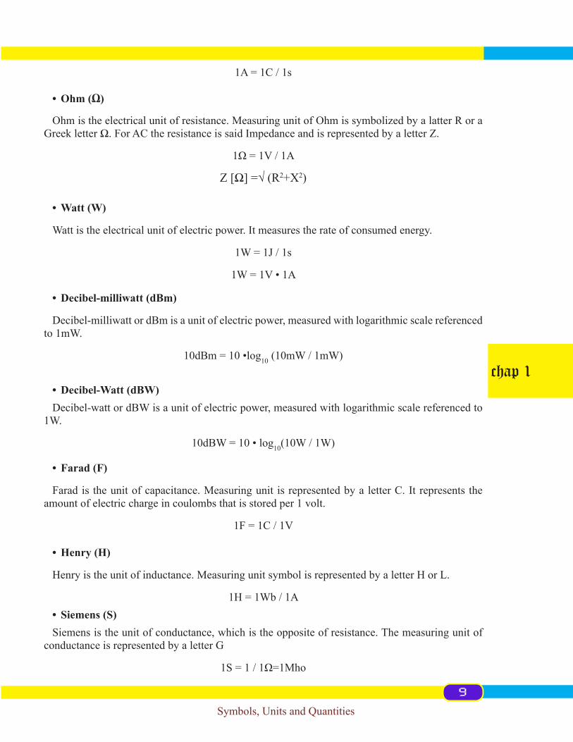
a) Agilent 33120A Function generator description and user’s guide
1. Function/modulation keys2. Menu operation keys3. Waveform modify keys4. Single/internaltriggerkey(Burstandsweeponly)5. Recall/store instrument state key6. Enter number key7. Shift/rocal key8. Enter number key
Figure 3-10: Agilent Function generator 33120A front view pannel
33

Electronic Signal Generators and AC Supply
chap 3
b) You can enter number from front-pannel by using one of the three methods.
1. Using the knob and the allow keys to modify the displayed number
2. Use the allow keys to modify the individual number
3. Use the “enter” number mode to enter a number with the appropriate units
c) Display annunciators
Adrs Function generator is addressed to listen or talk over a remote interfaceAM AM modulation is enabledArb Arbitrary wavefom function is enabled.Bust Burst modulation is enabledERROR Hardware or remote interface command errors are detected
Usethe“enter”for thoseoperations thatdonotrequireunits tobespecified(AMlevel,Offset,%duty,andStore/Recallstate)
34

Electronic Signal Generators and AC Supply
chap 3
Ext Functiongeneratorissetforanexternalmodulationdource(AM,FSK,Bust)FM FM modulation is enabledFSK FSK(Frequency-shiftkeying)modulationisenabledNum “enter number” mode is enabled. Press “shift-cancel to disable.Offset The waveform is being output with an offset voltageRmt Functiongeneratorisinremotemode(remoteinterface)Shift “shift” key has been pressed . press “shift again to turn off”Swp Sweep mode is enabledTrig Functiongeneratoriswaitingforasingletriggerorexternaltrigger(Burst,sweep) Sine waveform function is enabled
Square waveform function is enabledTriangle waveform function is enabledRamp waveform function is enabled
To review the display annunciators, hold down the “shift” key as you turn on the function generator.
d) The rear pannel at a glance
1. Chassis ground2. Power-line fuse-holder assembly3. Power-line voltage setting
Figure 3-11: The rear pannel at a glance of 33120A agillent function generator
35
Electronic Signal Generators and AC Supply
chap 3
4. AM modulation input terminal5. External Trigger / FSK /Burst modulation input terminal6. GPIB(IEEE-488)interfaceconnector7. RS-232 interface connector
3. 3. Direct Current and Alternating Current Supply
A power supply is a device that provides power to a load. A load is any electrical device or circuit that is connected to the output of the power supply and draws current from the supply. Electrical suppliescanbedirectcurrent(DC)oralternatingcurrent(AC).Belownotesdescribedifferencebetweendirectcurrent(DC)andalternatingcurrent(AC)electricalsupply.
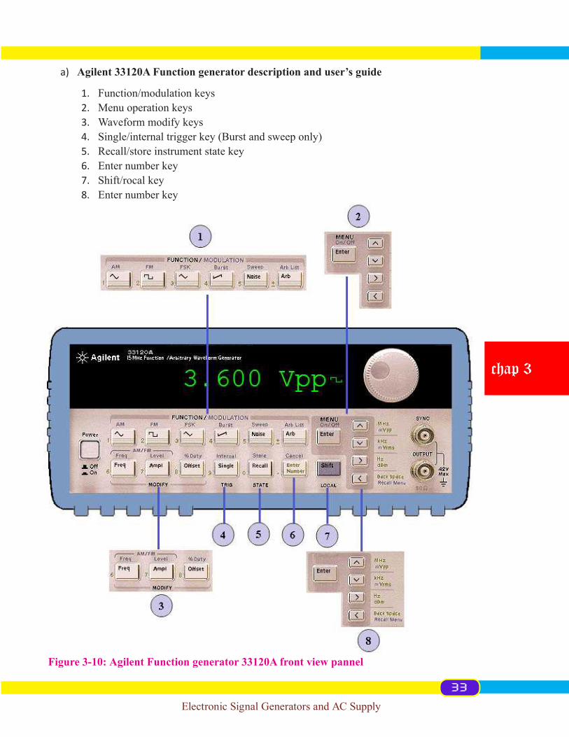
3. 3. 1. Direct Current
If thecurrentflowsinonlyonedirectionitiscalleddirectcurrent(DC).Batteriesandcellssup-plyDCelectricity,atypicaltwobatteriessupplyaround3V(1.5Veach).Batteriesconvertchemi-cal energy into electrical energy. Because of their limited source of chemical energy, batteries have a certain capacity that limits the amount of time over which they can produce a given power. This capacityismeasuredinampere-hours(Ah).
A battery is a type of DC source that converts chemical energy into electrical energy. A battery consists of one or more electromechanical cells that are electrically connected together internally.
Two basic methods of generating sinusoidal voltages are electromagnetic and electronic. Sine waves are pro-duced electromagnetically by ac generators and elec-tronically by oscillator circuits.
Hands on tip
Figure 3-12: Size of common batteries. AA Cell (A) and Batteries DC source (B)
A B
36
Electronic Signal Generators and AC Supply
chap 3
The materials used in battery cell determine the voltage that is produced. Although the voltage of a batterycellisfixedbyitschemistry,thecapacityisvariableanddependsonthequantityofmateri-als in the cell. Also the way the cells are connected and the type of cells determine the voltage and capacity of the battery. If the positive is connected to the negative of the next and so on, the battery voltage is the sum of the individual cell voltage. This is called series connection.
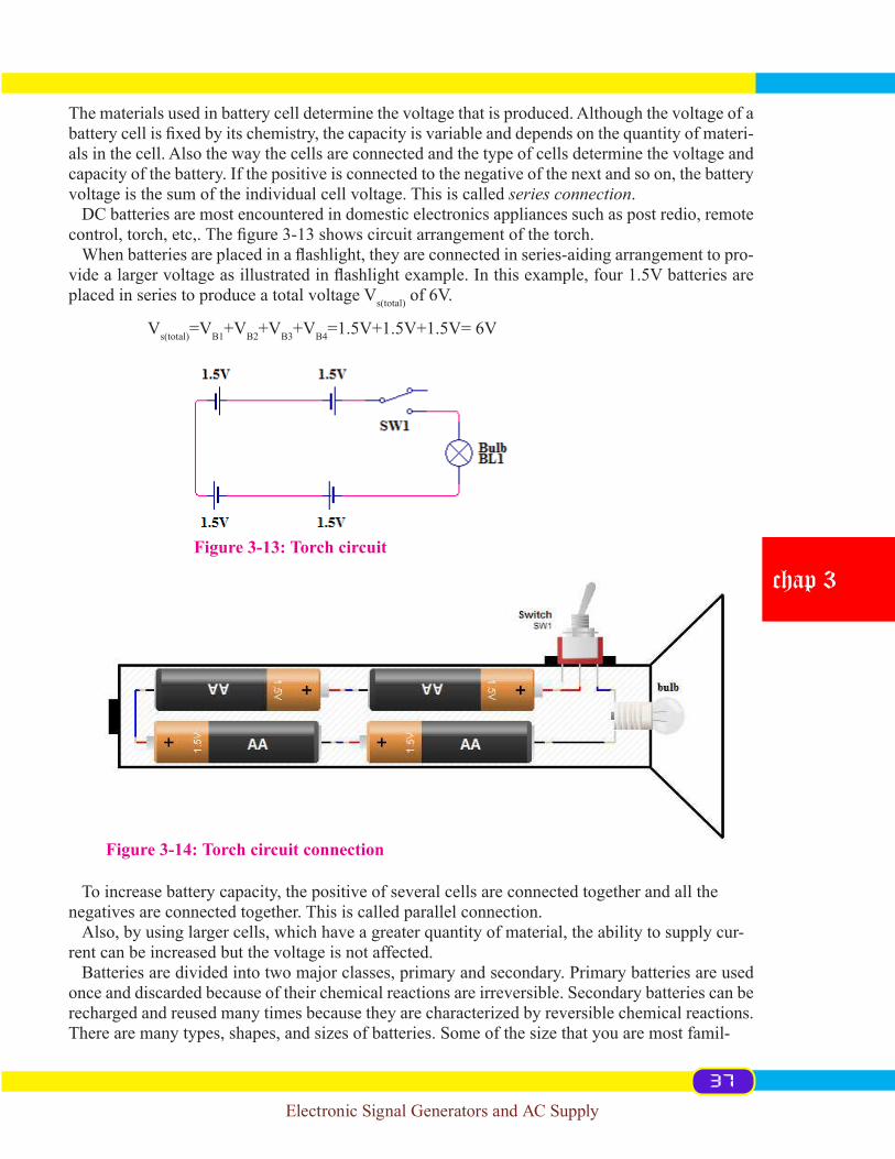
DC batteries are most encountered in domestic electronics appliances such as post redio, remote control,torch,etc,.Thefigure3-13showscircuitarrangementofthetorch.Whenbatteriesareplacedinaflashlight,theyareconnectedinseries-aidingarrangementtopro-
videalargervoltageasillustratedinflashlightexample.Inthisexample,four1.5Vbatteriesareplaced in series to produce a total voltage Vs(total) of 6V.
Vs(total)=VB1+VB2+VB3+VB4=1.5V+1.5V+1.5V= 6V
To increase battery capacity, the positive of several cells are connected together and all the negatives are connected together. This is called parallel connection.
Also, by using larger cells, which have a greater quantity of material, the ability to supply cur-rent can be increased but the voltage is not affected.
Batteries are divided into two major classes, primary and secondary. Primary batteries are used once and discarded because of their chemical reactions are irreversible. Secondary batteries can be recharged and reused many times because they are characterized by reversible chemical reactions.There are many types, shapes, and sizes of batteries. Some of the size that you are most famil-
Figure 3-13: Torch circuit
Figure 3-14: Torch circuit connection
37

Electronic Signal Generators and AC Supply
chap 3
iar with are AAA, AA, C, D and 9V. There is also a less common size called AAAA, which is smaller than the AAA.
Ampere-hour ratings of batteries
Because of their limited source of chemical energy, batteries have a certain capacity that limits the amount of time over which they can produce a given power level. This capacity is measured inampere-hours(Ah).Theampere-hourratingdeterminesthelengthof timethatabatterycandeliver a certain amount of average current to a load at the rated voltage.
A rating of one ampere-hour means that a battery can deliver an average of one ampere of cur-rent to a load for one hour at the rated voltage output. This same battery can deliver an average of two amperes for one-half hour. The more current the battery is required to deliver; the shorter thelifeofthebattery.Inpractice,abatteryusuallyisratedforaspecifiedcurrentlevelandoutputvoltage. For example, a 12V automobile battery may be rated for 70Ah at 3.5A. This means that it can deliver an average of 3.5A for 20h at the rated voltage.
Apart of the batteries, DC source include Solar cells, Generators, Thermocouples, Piezoelectric sensorsandtheElectronicPowerSupply(rectifiers).Thelaterisdiscussedinthenextchapters.
3. 3. 2. Alternating current
Ifthecurrentflowsinbothdirections(positiveandnegativedirectionalternatively)itiscalledAlternatingcurrent(AC).SynchronousgeneratorsandFunctiongeneratorsareexamplesofACsupply. Thesinusoidalwaveformorsinewaveisthefundamentaltypeofalternatingcurrent(AC)and
alternating voltage. It is also referred to as a sinusoidal wave, or, simply, sinusoidal. The electrical service provided by the power companies is in the form of the sinusoidal voltage and current. In addition, other types of repetitive waveform are composites of many individual sine waves called harmonics.
Sine waves, or sinusoids, are produced by two types of sources: rotating electrical machines (AC generators)orelectronicsoscillatorcircuits,whichareusedininstrumentscommonlyknownaselectronic signal generators or function generators.
Figure 3-15: Parallel connected batteries; (1) Schematic circuit, (2) Circuit connection
38

Electronic Signal Generators and AC Supply
chap 3
Thediagram,figure3-17,showsanoscilloscopescreendisplayingthesignalfromanACsup-ply.
Figure 3-16: DC voltage and AC voltage shapes; (a) Positive DC voltage, (b) Negative DC voltage, (c) AC voltage oscillates both in positive and negative direction in function of time
Figure 3-17: Oscilloscope displaying the signal from an AC source
An electronic power supply provides both output voltage and current. You should make sure the voltage range is sufficient for your applications. Also, you must have sufficient current capacity to assure proper circuit operation. The current capacity is the maximum current that a power supply can provide to a load at a given volt-age. The power supply efficiency is the ratio of the output power, (Pout), to the input power, (Pin), and is often expressed as a percentage.
Hands on tip
39

Basic Electronic Measuring Instruments
chap 4
Objectives
When you have studied this chapter, you should
• Be able for proper use of Voltmeter, Ammeter, Ohmmeter and oscilloscope• Be aware and fault diagnosis while measuring• Be able to calibrate multimeter and oscilloscope with respect to the quantity to be measured• Be able to measure Peak and Peak-to-Peak voltage using oscilloscope• Be able to measure Period and frequency using oscilloscope
In developing electronics circuits, assembly and in electronics experiment practical requires the use of many different kinds of electronic test equipment ranging from the very simple and inexpensive to extremely complex and sophisticated. Generally, more advanced test instrument is necessary when developing circuits and systems than is needed when doing production testing, testingexperimentalcircuitorwhentroubleshootingexistingproductionunitsinthefield.Meas-uring and testing instruments are required to analyze, diagnose and measure different quantities of electrical signal.
Measuring and testing instrument that we use to test and troubleshooting experimental circuit include, ammeter that measures current, voltmeter that measures voltage, ohmmeter that measures resistance, continuity tester to examine connectivity, function generator to deliver a reference sig-nal, and oscilloscope whose essential is to display voltages which vary rapidly with time.
Multimeters contain Ohmmeters, Voltmeters, Ammeters and a variety of capabilities to measure other quantities. AC and DC voltages are most often measurable. Multimeters also feature a con-tinuity detector, basically an Ohmmeter with a beeper if the multimeter sees less than dedicated ohmvalue,50Ωforexample,thenitbeepsotherwiseitissilent.Thisisveryusefulforfindingwhether components are connected when debugging or testing circuits. Multimeters are also of-ten able to measure capacitance and inductance. This may be achieved using a Wien bridge. A diode tester is also generally onboard; this allows one to determine the anode and cathode of an unknown diode. A LCD display is also provided for easily reading of results. In this chapter we are going to illustrate the use of electronics basic testing and measuring instruments.
Further readingStudy aids for this chapter are available at the companion websitehttp://webphysics.davidson.edu/Course_Material/Py230L/oscopes/scopes.htm
Chapter four Basic Electronic Measuring Instruments
40

Basic Electronic Measuring Instruments
chap 4
4. 1. Multimeter
A multimeter is an electronic measuring instrument that combines several measurement func-tionsinoneunitandisalsoknownasamultitesterorVOM(Volt-Ohmmeter).Atypicalmulti-meter would include basic features such as the ability to measure voltage, current, and resistance. Multimeter can be analog or digital.
4. 1. 1. Analog multimeter
Analog multimeters use a microammeter whose pointer moves over a scale calibrated for all the different measurements that can be made. Resolution of analog multimeters is limited by the width of the scale pointer, parallax, vibration of the pointer, the accuracy of printing of scales, zero calibration, number of ranges, and errors due to non-horizontal use of the mechanical display. The figure4-1representstheanalogmultimeterdisplay.Mirroredscalesandlargermetermovementsare used to improve resolution; two and a half to three digits equivalent resolution is usual (and is usuallyadequateforthelimitedprecisionneededformostmeasurements).
Resistance measurements, in particular, are of low precision due to the typical resistance mea-surement circuit which compresses the scale heavily at the higher resistance values. Inexpensive analog meters may have only a single resistance scale, seriously restricting the range of precise measurements. Typically an analog meter will have a panel adjustment to set the zero-ohms cali-bration of the meter, to compensate for the varying voltage of the meter battery.
Analogue multimeter description
• The dial: It has the arc-shaped scales visible through the window. The pointer indicates values read from the scale.
• The pointer or needle: This is the thin black line at the left-most position in the dial face window in the image. The needle moves to the value measured.
• Arc shaped lines or scales on the meter dial face: These may be different colors for each scale, but will have different values. These determine the ranges of magnitude.
Figure 4-1: Analog ammeter screen
41

Basic Electronic Measuring Instruments
chap 4
• A wider mirror-like surface shaped like the scales mentioned previously might also be present. The mirror is used to help reduce parallax viewing error by lining up the pointer withitsreflectionbeforereadingthevaluethepointerisindicating.Intheimage,itappearsas a wide gray strip between the red and black scales.
• A wider mirror-like surface shaped like the scales mentioned previously might also be present. The mirror is used to help reduce parallax viewing error by lining up the pointer withitsreflectionbeforereadingthevalueindicatedbythepointer.Intheimage,itappearsas a wide gray strip between the red and black scales.
• A selector switch or knob:Thisallowschanging thefunction(volts,ohms,amps)andscale(x1,x10,etc.)ofthemeter.Manyfunctionshavemultipleranges.Itisimportanttohave both set correctly, otherwise serious damage to the meter or harm to the operator may result. Most meters employ the knob type like the one shown in the image, but there are others. Regardless of the type, they work similarly. Some meters (like the one in the image above)havean“Off”positiononthisselectorswitchwhileothershaveaseparateswitchto turn off the meter. The meter should be set to “Off” when stored.
Figure 4-2: Analog ammeter (A) and its connecting leads (B)
A B
42

Basic Electronic Measuring Instruments
chap 4
• Jacks or openings in the case to insert test leads. Most multimeters have several jacks. Theonepicturedhasjusttwo.Oneisusuallylabeled“COM”or(-),forcommonandnega-tive. This is where the black test lead is connected. It will be used for nearly every measure-menttaken.Theotherjack(s)islabeled“V”(+)andtheOmegasymbol(anupsidedownhorseshoe)forVoltsandOhms,respectively,andpositive.The+and-symbolsrepresentthe polarity of probes when set for and testing DC volts. If the test leads were installed as suggested, the red lead would be positive as compared to the black test lead. This is nice to know when the circuit under test is not labeled + or -, as is usually the case. Many meters have additional jacks that are required for current or high-voltage tests. It is equally impor-tant to have the test leads connected to the proper jacks as it is to have the selector switch rangeandtesttype(volts,amps,ohms)set.Allmustbecorrect.Consultthemetermanualif you’re unsure which jacks should be used.
• Test leads: There should be two test leads or probes. Generally, one is black and the other red. Black probes is considered as negative whereas the red probe as positive.
• Battery and fuse compartment: Usually found on the reverse, but sometimes on the side. Thisholdsthefuse(andpossiblyaspare),andthebatterythatsuppliespowertothemeterfor resistance tests. The meter may have more than one battery and they may be of different sizes. A fuse is provided to help protect the meter movement. Sometimes there is more than one fuse. A good fuse is required for the meter to function. Fully charged batteries will be required for resistance/continuity tests.
• Zero Adjustment: This is a small knob usually located near the dial that is labeled “Ohms Adjust”, “0 Adj”, or similar. This is used only in the ohms or resistance range, while the probesareshortedtogether(touchingeachother).Rotatetheknobslowlytomovethenee-dle as close to the 0 position on the Ohms scale as possible. If new batteries are installed, this should be easy to do - a needle that will not go to zero indicates weak batteries that should be replaced.
4. 1. 2. Digital multimeters
Digital multimeters sometimesabbreviated(DMMorDVOM)display themeasuredvalue innumerals, and may also display a bar of a length proportional to the quantity being measured. Digital multimeters are now far more common than analog ones, but analog multimeters are still preferable in some cases, for example when monitoring a rapidly-varying value.Amultimetercanbeahand-helddeviceusefulforbasicfaultfindingandfieldservicework,ora
bench instrument which can measure to a very high degree of accuracy. They can be used to trou-bleshoot electrical problems in a wide array of industrial and household devices such as electronic equipment, motor controls, domestic appliances, power supplies, and wiring systems.
Quantities measured by multimeter
Modern multimeters can measure many quantities. The common ones are:• Voltage: alternating and direct, in volts.• Current: alternating and direct, in amperes.• Resistance, in ohms.
43

Basic Electronic Measuring Instruments
chap 4
ThefrequencyrangeforwhichACmeasurementsareaccuratemustbespecified.
Additionally, some multimeters measure:• Capacitance in farads.• Conductance in siemens.• Decibels.
Digital multimeters may also include circuits for:• Continuity tester; sounds when a circuit conducts• Diodes(measuringforwarddropofdiodejunctions),andtransistors(measuring
currentgainandotherparameters)• Battery checking for simple 1.5 volt and 9 volt batteries. This is a current loaded
voltage scale which simulates in-use voltage measurement.
Modern multimeters are often digital due to their accuracy, durability and extra features. In a digitalmultimeterthesignalundertestisconvertedtoavoltageandanamplifierwithelectroni-
• Duty cycle as a percentage.• Frequency in hertz.• Inductance in henrys.
A
B
Figure 4-3: Digital multimeter (A) and connecting leads (B)
44

Basic Electronic Measuring Instruments
chap 4
cally controlled gain preconditions the signal. A digital multimeter displays the quantity measured as a number, which eliminates parallax errors.
Modern digital multimeters may have an embedded computer, which provides a wealth of con-venience features. Measurement enhancements available include:
• Auto-ranging, which selects the correct range for the quantity under test so that the most significant digits are shown. For example, a four-digitmultimeterwould automaticallyselect an appropriate range to display 1.234 instead of 0.012, or overloading. Auto-ranging meters usually include a facility to hold the meter to a particular range, because a measure-ment that causes frequent range changes can be distracting to the user. Other factors being equal, an auto-ranging meter will have more circuitry than an equivalent non-auto-ranging meter, and so will be more costly, but will be more convenient to use.
• Auto-polarity for direct-current readings, shows if the applied voltage is positive (agrees withmeterleadlabels)ornegative(oppositepolaritytometerleads).
• Sample and hold, which will latch the most recent reading for examination after the instrument is removed from the circuit under test.
• Current-limited tests for voltage drop across semiconductor junctions. While not a replacement for a transistor tester, this facilitates testing diodes and a variety of transistor types.
• Simple data acquisition features, to record maximum and minimum readings over a givenperiod,ortotakeanumberofsamplesatfixedintervals.
A multimeter is also used to check for AC or DC voltage, resistance or continuity of electrical components and small amounts of current in circuits. This instrument will let the user to check if there is voltage present on a circuit, etc. Here is how to measure those values by using multimeter.
4. 1. 3. Voltmeter
Voltage is always measured in parallel within the circuit or direct to the terminals of the battery. This is due to the high internal resistance that a voltmeter has. Here below we describe general procedures for voltage measuring by using Volts Function of multimeter.
1. Set the meter for the highest range provided for AC Volts. Many times, the voltage to be mea-sured has a value that is unknown. For this reason, the highest range possible is selected so that the meter circuitry and movement will not be damaged by voltage greater than expected. If the meter were set to the 50 volt range and a common system electrical outlet were to be tested, the 220 volts present could irreparably damage the meter. Start high, and work down-ward to the lowest range that can be safely displayed.
2. Insert the black probe in the “COM” or “-” jack. 3. Inserttheredprobeinthe“ΩV”or“+”jack.4. Locate the voltage scales. There may be several Volt scales with different maximum values.
The range chosen by the selector knob determines which voltage scale to read. The maxi-mum value scale should coincide with selector knob ranges. The voltage scales, unlike the Ohm scales, are linear. The scale is accurate anywhere along its length.
45

Basic Electronic Measuring Instruments
chap 4
It will of course be much easier accurately reading 24 volts on a 50 volt scale than on a 250 volt scale, where it might look like it is anywhere between 20 and 30 volts.
5. Test a common electrical outlet. In many countries you might expect 220 volts or even 380 volts. In other places like in U.S., 120 or 240 volts might be expected.
• Press the black probe into one of the straight slots. It should be possible to let go of the black probe, as the contacts behind the face of the outlet should grip the probe, much like it does when a plug is inserted.
• Insert the red probe into the other straight slot. The meter should indicate a voltage verycloseto120or240volts(dependingontypeoutlettested).
• Remove the probes, and rotate the selector knob to the lowest range offered, that is greaterthanthevoltageindicated(120or240).
• Reinsert the probes again as described earlier. The meter may indicate between 110 and as much as 125 volts this time for 120 outlet system and 210 to 230 for 220 outlet system. The range of the meter is important to obtain accurate measurements.
• If the pointer did not move, it is likely that DC was chosen instead of AC. The AC and DC modes are not compatible. The correct mode must be set. If not set correctly, the user would mistakenly believe there was no voltage present. This could be deadly.
Figure 4-4: Test electrical wall outlet using voltmeter
46

Basic Electronic Measuring Instruments
chap 4
• Be sure to try both modes if the pointer does not move. Set meter to AC volts mode, and try again.
• Whenever possible, try to connect at least one probe in such a way that it will not be required to hold both while making test. Some meters have accessories that include alligator clips or other types of clamps that will assist doing this. Minimizing your contact with electrical circuits drastically reduces that chance of sustaining burns or injury.
a) Measuring the voltage of the battery Voltage is always measured in parallel within the circuit or direct to the terminal of the battery.
To start with something simple, let’s measure voltage on an AA cell battery.
Part list
No Item Specification Quantity
1 Voltmeter Digital Multimeter 1
2 DC battery Cell AA 1.5V battery 1
Steps:
1. PulloutyourmultimeterandplugtheblackprobeintoCOM(common)jackandtheredprobeintoVΩ.
Experiment 4-1: Measuring Voltage
Figure 4-5: Measuring Voltage of an AA cell battery
47

Basic Electronic Measuring Instruments
chap 4
2. Setthemultimeterto“2V”intheDCrange(DCisastraightline,ACisthewavyline).3. Squeeze the probes with a little pressure against the positive and negative terminals of the
AA battery. 4. The black probe is customarily connected to ground or “-”and red goes to power or “+”. If
you have got a fresh battery, you should see around 1.5V on the display.
b) Testing voltage in a circuit
The voltage across a component is a measure of the difference in electrical potential from one side of the component to the other and so the meter must be connected as shown in the following experiment.
Part list
No Items Specifications Quantity
1 Resistor 560Ω 1
2 Wire 22-gauge solid wire 10 cm
3 Breadboard Prototyping board 1
4 Battery 9V dc supply 1
5 Diode Light emitting diode 1
Let’sstartwithsimplifiedcircuitcontainingoneresistorandabatteryasshowninfigure4-6.
Steps:
1. Set themultimeter toread“directcurrent(DC)voltage”.DCvoltagedoesnotalternatefrom positive to negative and is represented by this symbol ” ” on multimeter. Check that the two probes are inserted into the correct holes to measure DC voltage i.e. plug the blackprobeintoCOM(common)jackandtheredprobeintoVΩ.
2. Set multimeter to “20” DC voltage scale.
Experiment 4-2: Measuring Voltage in a circuit
Figure 4-6: Measuring Voltage in a simplified circuit
48

Basic Electronic Measuring Instruments
chap 4
3. Touch the probes against the terminal ends of a fresh 9V battery. You should get a reading of approximately 9 V. The battery has a positive and a negative pole. Note that the multime-ter also has a positive and a negative probe. If you attach the positive probe to the negative side of the battery, it will still read out 9 V, but it will have a negative sign in front of it.
The above procedure is almost similar to the previous one on cell voltage measuring since the meter reading is the battery voltage but for this experiment, you are requested to measure the volt-agedropalthoughtheelementsmadeupthecircuitasdescribedinthefigure4-8.
Figure 4-7: Use of multimeter to measure voltage across a circuit component.
All opposite charges (positive and
negative) possess a certain potential energy because of separation between them. The difference in potential en-ergy of the charges is potential differ-ence or VOLTAGE. Voltage is driving force in electrical circuits and is what establishes current.
Hands on tip
Figure 4-8: Measuring Voltage in a circuit containing two components
49

Basic Electronic Measuring Instruments
chap 4
4. With the circuit closed and the LED “ON,” measure the voltage across the resistor by touching the probes to the metal wires on either side of the resistor (at positions “2” and “3”incircuitarrangementoffigure4-9).
5. Measure the voltage across the LED (positions “4” and “5” in circuit arrangement of figure4-9).
Currentflowsfromthepositiveterminal(1),throughtheresistor(2and3),theLED(4and5),thejumperwire(5-6)whichisdirectlyconnectedtothenegativeterminaloftheDCsupply.
6. Compare the voltage of the battery to the sum of the voltage drops across the resistor and
Figure 4-9: Measuring Voltage in a circuit with two components circuit connection
50

Basic Electronic Measuring Instruments
chap 4
the LED. It is possible that you can get the summation of voltage drop a little bit less than thebattery’svoltage(9Volt)suchas8.8Volt,withsuchvaluedrift,donotpanicthisisprac-tice. This is caused by imperfection of materials.
4. 1. 4. Ammeter
Ammeter is an electronic test meter used to measure the current. The ammeter has a very low internal resistance. For that reason, it requires to be connected in series within the circuit otherwise it can be destroyed. Care has to be taken when measuring high current circuits. There are the gen-eral procedures to be followed while using the Amps Function of multimeter to Measure Amperes.
General procedures: 1. Current is always measured in series with the circuit2. Determine if it is an AC or a DC voltage to measure.3. Set the meter to the highest AC or DC Amp range supported. If the circuit to be tested is
ACbutthemeterwillonlymeasuretheDCamps(orvice-versa),youhavetoleaveit.Themetermustbeabletomeasurethesamemode(ACorDC)ampsasthevoltageinthecir-cuit, otherwise it will indicate 0.
Be aware that most multimeters will only measure extremely small amount of current, in the uA and mA ranges. 1 uA is equivalent to 0.000001 amp and 1 mA is to 0.001 amp. These arevaluesofcurrentthatflowonlyinthemostdelicate electronic circuits, and are literally thousands(andevenmillions)oftimessmallerthan values seen in the home and automotive circuits that most homeowners would be inter-ested testing. Just for reference, a typical 100W / 220V light bulb will draw 0.4545 Amps. This amount of current would likely damage the me-ter beyond repair.
The movement of the free electrons from the negative end of a material to the
positive end is the electrical current, symbolized by I. Electrical current is the rate of flow of charge. Current in a conductive material is measured by the num-ber of electrons (amount of charge) that flow past a point in a unit of time.
I=Q/t
Hands on tip
Where: I= Current in amperes (A)
Q= The charge of the electrons in coulombs (C)
t= Time in second (s)
Figure 4-10: Analogue ammeter zeroed
51

Basic Electronic Measuring Instruments
chap 4
4. Use a “clamp-on” ammeter.a. A “clamp-on” type ammeter would be ideal for the typical homeowner require-
ments,anddoesnotrequireopeningthecircuittotakemeasurements(figure4-11).If this meter were to be used to measure current through a 4700 ohm resistor across 9 Volts DC,
it would be done as outlined below:b. Insert the black probe into the “COM” or “-”jack.c. Insert the red probe into the “A” jack.d. Shut off power to the circuit.e. Open the portion of the circuit that is to be tested (one lead or the other of the resis-
tor).Insertthemeterinserieswiththecircuitsuchthatitcompletesthecircuit.Anammeter is placed in series with the circuit to measure current. It cannot be placed “across” the circuit the way a voltmeter is used (otherwise the meter will probably bedamaged).Polaritymustbeobserved.Currentflowsfromthepositivesidetothenegative side. Set the range of current to the highest value.
f. Apply power and adjust range of meter downward to allow accurate reading of pointer on the dial. Do not exceed the range of the meter, otherwise it may be dam-aged. A reading of about 2 milliamps should be indicated since from Ohm’s law I=V/R=(9volts)/(4700Ω)=.00191amps=1.91mA.
Figure 4-11: Clamp-on multimeter
When reading the
scales on an analog meter, always view the scale and “needle” di-rectly from the front and not from an angle. This practice will avoid par-allax, which is an appar-ent change in position of the needle relative to the meter scale and results in inaccurate readings.
Hands on tip
52

Basic Electronic Measuring Instruments
chap 4
5. Ifyouaremeasuringthecurrentconsumedbythedeviceitself,beawareofanyfilterca-pacitorsoranyelementthatrequiresaninrush(surge)currentwhenswitchedon.Evenifthe operating current is low and within the range of the meter fuse, the surge can be many timeshigherthantheoperatingcurrent(astheemptyfiltercapacitorsarealmostlikeashortcircuit).Blowingthemeterfuseisalmostcertainifthedeviceundertest’sinrushcurrentismany times higher than the fuses rating. In any case, always use the higher range measure-mentprotectedbythehigherfuserating(ifyourmeterhastwofuses),andjustbecareful.
Current is always measured in series within the circuit as opposed to parallel voltage measuring.
Part list
No Items Specifications Quantity1 Ammeter Digital multimeter 12 Resistor 100Ωresistor 13 LED Lightemittingdiode(yellow) 14 Wire 22-gauge (0.33mm2)solidwire 40cm5 Breadboard Prototypingboard(miniboard) 16 Battery 3Vdcsupplyor(2x1.5Vcell) 1
Current measuring steps1. Setthemultimetertoread“directcurrent(DC).”Important:Checkyourmultimetertosee
where the probe should be plugged in so it reads “current.”2. In order to measure current, you have to open up the circuit and attach the leads from the
multimetersothatthecurrentflowsthroughthemultimeter.Todothis,usejumperwiresand wires with alligator clips to add the multimeter to the circuit, as shown in Figure 4-13.
3. The yellow wire is unplugged from the breadboard and attached to the red probe from the multimeter(6).
Experiment 4-3: Measuring electrical Current
Figure 4-12: Measuring current in a circuit
53

Basic Electronic Measuring Instruments
chap 4
4. Ajumperwireinblack(8-9)isconnectedtothenegativebus.5. Theotherendofthewireisattachedtothenegativeleadfromthemultimeter(7).6. Thecurrentnowflowsfromthepositiveterminalofthebattery(1)throughtheresistor
(2-3),theLED(4-5),themultimeter(6-7),andthentothenegativeterminalofthebat-tery. 7,8 and 9 are connected together.
7. Depending on your resistor and LED, the current will be measured at around 8.68 mA (milliamps).
8. RemoveLEDandconnecttheredprobeofmultimeterdirectlytotheresistor(3-4),atthistimethemeterreadingwillbealmost30mAdespitetheinfluenceoftheammeterinternalresistance.
4. 1. 5. Ohmmeter
Ohmmeter is an electronics instrument used to measure electrical resistance. The property that allowsmaterialtoopposetotheflowofcurrentiscalledresistancewhilethespecificdevicefor
Figure 4-13: Measuring current in a circuit, real world circuit connection
When measuring the current, open the circuit either be-
tween the load and the positive terminal or between the load and negative terminal of the source. Install the ammeter in the current path with respect to the polarity (negative to negative and positive to positive).
Hands on tip
54

Basic Electronic Measuring Instruments
chap 4
suchtaskiscalledresistor.Theohmmeterquantifieshowmucharesistorrestrictsthefollowofcurrent in a given circuit. Here below describes the use of ohm’s function to measure resistance.
General procedure:
1. Turn the multimeter on if it has a separate power switch and set to Ohm’s range marked with “ ” symbol. Understand that resistance and continuity are opposite. When multimeter measures resis-tance in ohms, it cannot measure continuity. When there is little resistance there is a great deal of continuity. Conversely, when there is a great deal of resistance, there is little con-tinuity. With this in mind, when we measure resistance we can make assumptions about continuity based on the resistance values measured.
• Observe the meter indication. If the test leads are not in contact with anything, the needle or pointer of an analog meter will be resting at the left-most position. This representsaninfiniteamountofresistance,oran“opencircuit”;itisalsosafetosaythere is the no continuity, or path between the black and red probes.
• Careful inspection of the dial should reveal the Ohm scale. It is usually the top-mostscaleandhasvaluesthatarehighestontheleftofthedial(“∞”orasideways“8”forinfinity)andgraduallyreduceto0ontheright.Thisisoppositeoftheotherscales; they have the lowest values on the left and increase going right.
2. Connect the black test lead to the jack marked “Common” or “-”.3. ConnecttheredtestleadtothejackmarkedwiththeOmega(Ohmsymbol)orletter“R”
near it.4. Settherange(ifprovided)toRx100.5. Hold the probes at the end of the test leads together. The meter pointer should move fully
to the right. Locate the “Zero Adjust” knob and rotate so that the meter indicates “0” (or as closeto“0”aspossible).Notethatthispositionisthe“shortcircuit”or“zeroohms”indica-tion for this R x 1 range of this meter.
• Always remember to set to zero the analog multimeter immediately after changing resistance ranges.
6. Replacebatteries(ifneeded).Ifyouareunabletoobtainazeroohmindication,thismaymean the batteries are weak and should be replaced. Retry the zeroing step above again with fresh batteries.
7. Measure resistance of something like a light bulb you know is good. Locate the two electri-cal contact points of the bulb. They will be the threaded base and the center of the bottom of the base. Have a helper hold the bulb by the glass only. Press the black probe against the threaded base and the red probe against the center tab on the bottom of the base. Watch the needle move from resting at the left and move quickly to 0 on the right. Digital multimeter displays numerically the resistance of the device under measuring.
8. Try different ranges. Change the range of the meter to R x 1. Zero the meter again for this range. Repeat the step above. Observe how the meter did not go as far to the right as before. The scale of resistance has been changed so that each number on the R scale can be read directly. In the previous step, each number represented a value that was 100 times greater. Thus, 150 really was 15,000 before. Now, 150 is just 150. Had the R x 10 scale been se-
55

Basic Electronic Measuring Instruments
chap 4
lected, 150 would have been 1,500 for example. The scale selected is very important for accurate measurements. With this understanding, study the R scale. It is not linear like the other scales. Values at the left side are harder to accurately read than those on the right. Trying to read 5 ohms on the meter while in the R x 100 range would look like 0. It would be much easier at the R x 1 scale instead. This is why when you are testing resistance, ad-just the range so that the readings may be taken from the middle rather than the extreme left or right sides.
9. Test resistance between hands. Set the meter to the highest R x value possible. Zero the meter.
• Loosely hold a probe in each hand and read the meter. Squeeze both probes tightly. Notice the resistance is reduced.
• Free the probes and wet your hands. Hold the probes again. Notice that the resis-tance is lower still.
• For these reasons, it is very important that the probes not touch anything other than the device under test. A device that has burned out will not show “open” on themeterwhentestingifyourfingersprovideanalternatepatharoundthedevice,like when they are touching the probes. Testing round cartridge type and older style glass automotive fuses will indicate low values of resistance if the fuse is lying on a metal surface when under test. The meter indicates the resistance of the metal sur-face that the fuse is resting upon (providing an alternate path between the red and blackprobearoundthefuse)insteadoftryingtodetermineresistancethroughthefuse. Every fuse, good or bad, will indicate “good”.
Figure 4-14: Measuring resistance of a bulb using Ohmmeter
56

Basic Electronic Measuring Instruments
chap 4
4. 2. Oscilloscope
Oscilloscope is an electronic test instrument for measuring and observing of constantly vary-ing signal voltages. The oscilloscope is basically a graph-displaying device that traces a graph of measured electrical signal on its screen. In most applications the graph shows how signal change over time. The vertical axis of the display screen represents voltage and the horizontal axis repre-sents time. You can measure amplitude, period, and frequency of a signal using oscilloscope. Also, you can determine the pulse width, duty cycle, rise time and fall time of a pulse waveform. Most oscilloscopes can display at least two signals on the screen at one time, enabling you to observe theirtimerelationship.Afrontpanelofatypicalcommercialoscilloscopeisshowninfigure4-15.
4. 2. 1. Oscilloscope user’s manuel guide
Each mark of oscilloscope comes with user’s manual to guide for manipulating. Most of oscil-loscopes have common control keys. Let describe the function of control keys of the most popular digital oscilloscope called Agilent 54622D 100 MHz.
Front panel controls keys
1. Channel On/Off key: Use this key to switch the channel on or off, or to access the channel’s menu in the softkeys. There is one channel on/off key for each channel.
2. Math key: ThemathkeyprovidesaccesstoFFT(FastFourierTransform),multi-ply, subtract, differentiate, and integrate functions.
3. Display: The display shows captured waveforms using a different color for each channel.
4. Vertical sensitivity control: Also called VOLTS/DIV control. Vertical attenuation for channel provides step adjustment of vertical sensitivity. Use this knob to change theverticalsensitivity(gain)ofthechannel.
5. Autoscale Key: When you press the autoscale key the oscilloscope will quickly determine which channels have activity, and it will turn these channels on and scale them to display the input signals.
6. Entry knob: The entry knob is used to select items from menus and to change val-ues. Its function changes based upon which menu is displayed. Note that the curved arrow symbol above the entry knob illuminates whenever the entry knob can be used to select a value. Use the entry knob to select among the choices that are shown on the softkeys.
7. Horizontal Sweep Speed control: Also called Time base, TIME/DIV control, pro-vides steps selection of sweep rate for the main time base. This control has 23 steps from 0.1uS time/div to 2S time/div in 1-2-5 sequences. Turn this control to adjust the sweep speed. This changes the time per horizontal division on the display. When adjusted after the waveform has been aquired and the oscilloscope is stopped, this has the effect of stretching out or squeezing the waveform horizontally.
8. Horizontal Main/Delayed key: Press this key to access the menu where you can split the oscilloscope display into Main and Delayed sections, and where you can select XY and roll modes. You can also select horizontal time/division vernier and
57

Basic Electronic Measuring Instruments
chap 4
select the trigger time reference point on this menu.9. Horizontal Delay Control: when the oscilloscope is running, this control lets you
set the acquisition window relative to the trigger point. When the oscilloscope is stopped, you can turn this knob to pan through the data horizontally. This lets you seethecapturedwaveformbeforehetrigger(turntheknobclockwise)orafterthetrigger(turntheknobcounterclockwise).
10. Measure key: Press the cursors key to switch on cursors that you can use for mak-ing measurements. Press the “ ”keytoaccessasetofpredefinedmeasure-ments.
11. Waveform key: The acquire key lets you set the oscilloscope to acquire in Normal, Peak Detect, Averaging, or High Resolution modes, and lets you turn Realtime sampling off or on. The display key lets you access the menu where you can select infinitypersistence,switchvectorsonoroff,andadjustthedisplaygrid(graticule)intensity
12. Run controls: Press the “ ” key to make the oscilloscope begin looking for a trigger. The Run/Stop key will illuminate in green. If the trigger mode is set to “Normal”, the display will not update until a trigger is found. If the trigger mode is set to “Auto”, the oscilloscope looks for a trigger, and if none is found, it will automatically trigger, and the display will immediately show the input signals. In thiscase,thebackgroundoftheAutoindicatoratthetopofthedisplaywillflash,indicating that the oscilloscope is forcing triggers.
Press “ ” again to stop acquisition of data. The key will illuminate in Red.
Now you can pan across and zoom-in on the acquires data.
Press “ ” key to make a single acquisition of data. The key will illuminate in yellow untill oscilloscope triggers.
13. Digital channel controls: These controls switch the digital channels on/off, and can be used to select a digital channel for repositioning on the display.
14. Trigger controls: These controls determine how the oscilloscope triggers to cap-ture data.
15. Trigger input: Use this input for external trigger input.16. Utility key: Pressthiskeytoaccesstheutilitymenu,whichletsyouconfigurethe
oscilloscope’sI/Osettings,printerconfiguration,fileexplorer,servicemenu,andother options.
17. File key: Pressfilekeythekeytoaccessthefilefunctionssuchassaveorrecallawaveform or setup. Or press the quick print key to print the waveform from display.
18. Vertical Position control: Use this knob to change the channel’s vertical position on the display. There is one vertical position control for each channel.
19. Channel Input BNC connector: Attach the oscilloscope probe or BNC cable to the BNC connector. This is the channel’s input connector.
20. Power switch: Press once to switch power ON; press again to power OFF.
58

Basic Electronic Measuring Instruments
chap 4
Figu
re 4
-15:
Osc
illos
cope
fron
t pan
nel c
ontr
ol k
eys
59

Basic Electronic Measuring Instruments
chap 4
21. Softkeys: The functions of these keys change based upon the menus shows on the display directly above the keys such as frequency and voltage measuring
“ ”.22. Intensity control: Rotate clockwise to increase analog waveform intensity; coun-
terclockwise to decrease analog waveform intensity. You can vary the intensity control to bring out signal detail, much like an analog oscilloscope. Digital chan-nel waveform intensity is not adjustable.
4. 2. 2. Interpreting the display
Figure 4-16: Agilent oscilloscope 54622D 100MHz display
1. Analog channels and ground levels2. Analogchannelone(CH1)3. Analogchannelone(CH1)verticalsensitivityorCH1voltage/Division4. Analogchanneltwo(CH2)
60

Basic Electronic Measuring Instruments
chap 4
An oscilloscope is an electronic measuring instrument and helps to visualize the shape of the signal. Before taking a measurement, verify the settings of some key controls on oscilloscope. The exact steps to follow to set up the oscilloscope vary depending on the exact type and model of oscilloscope, so better to read the instruction manual that came with the oscilloscope. But the general steps should be as follows:
1. Examine all the controls of the oscilloscope and set them to normal positions.For most oscilloscopes, all rotating dials should be centered, all pushbuttons should be out, and all slide switches and paddle switches should be up.
2. Turn on oscilloscope.If it is an old-fashioned CRT kind, give it a minute or two to warm up.
3. Set the VOLTS/DIV control to 1.This sets the scope to display one volt per vertical division. Depending on the signal you want to be displayed, you may need to increase or decrease this setting, but one volt is a good starting point.
4. Set the TIME/DIV control to 1.This control determines the time interval represented by each horizontal division on the display. Try turning this dial to its slowest setting. Then, turn the dial one notch at a time and watch the dot speed up until it becomes a solid line.
5. Set the Trigger switch to Auto.The Auto position enables the oscilloscope to stabilize the trace on a common trigger point in the waveform. If the trigger mode is not set to Auto, the waveform may drift across the screen,makingitdifficulttowatch.
6. Connect a probe to the input connector.If the oscilloscope has more than one input connector, connect the probe to the one labeled A or CH1.Oscilloscope probes include a probe point, which you connect to the input signal and a separate ground lead. The ground lead usually has an alligator clip. When testing a circuit, this clip can be connected to any common ground point within the circuit. In some probes, the ground lead is detachable, so you can remove it when it is not needed.
5. Analogchanneltwo(CH2)verticalsensitivityorCH2voltage/Division6. Trigger point time reference7. Delay time8. Sweep speed or horizontal sensitivity9. Run/Stop and automatic mode10. Trigger type11. Trigger level or Digital threshold12. AC/DC coupling mode
Experiment 4-4: Oscilloscope calibration
61

Basic Electronic Measuring Instruments
chap 4
7. Touch the end of the probe to the oscilloscope calibration terminal.This terminal provides a sample square wave that you can use to calibrate the oscillo-scope’s display. Some oscilloscopes have two calibration terminals, labeled and. If the oscilloscope has two terminals, touch the probe to the 2 V terminals.For calibrating, it is best to use an alligator clip test probe. If your test probe has a pointy tip instead of an alligator clip, you can usually push the tip through the little hole in the end of the calibration terminal to hold the probe in place.It is not necessary to connect the ground lead of your test probe for calibration.
8. Ifnecessary, adjust theTIME/DIVandVOLTS/DIVcontrolsuntil the squarewavefitsnicely within the display.
9. If necessary, adjust the Y-POS control to center the trace vertically.10. If necessary, adjust the X-POS control to center the trace horizontally.11. If necessary, adjust the Intensity and Focus settings to get a clear trace.
With all these procedures, you are now ready to begin viewing the waveforms of actual elec-tronic signals.
One important function of the oscilloscope is to make voltage measurements. The oscilloscope is
Figure 4-17: Oscilloscope displaying a square wave
Experiment 4-5: Measuring Direct Current with oscilloscope
62

Basic Electronic Measuring Instruments
chap 4
capable of measuring both AC and DC. Now measure the voltage of series cell batteries by using oscilloscope.
Part list
No Items Specifications Quantity 1 Oscilloscope Digital oscilloscope 12 3V DC supply 1.5V AA cell Battery 2
Procedure1. Switch on the oscilloscope
2. Adjust voltage/Division to 1V3. Hold oscilloscope’s probe against battery’s polarity; red probe on positive terminal and
black probe on negative terminal of the battery
Figure 4-18: Measuring DC voltage using oscilloscope
63

Basic Electronic Measuring Instruments
chap 4
4. Measure voltage using quick meas of the oscilloscope or calculate by using formula. Con-sider: - Vol/Division =1V;
- Number of division =3 Thus, V = Volt/Div* Number of division =1V/Div*3Div =3V
The oscilloscope is capable of measuring AC components such as frequency, period and maxi-mum voltage value. This experiment will demonstrate the way the oscilloscope is used to measure the above mentioned quantities.
Part list
No Items Specifications Quantity 1 Oscilloscope Digital oscilloscope 12 AC supply Agilent function generator 1
Procedure
1. Turn on both function generator and oscilloscope2. Set function generator to produce 2.121V rms value at 50Hz3. Adjust oscilloscope to 1V/division and time base at 5mSec/Division4. Connect the output of the function generator to CH1 of the oscilloscope by respecting the
polarities (red lead of the function generator to red probe of the oscilloscope and black lead of the function generator to black probe of the oscilloscope.
5. Use oscilloscope’s quick meas to measure period, frequency, maximum voltage and peak-to-peak voltage
6. If you are not using digital oscilloscope proceed with calculation demonstrated below.
Calculationoftheperiod,frequencyandvoltageofanAC(alternatingcurrent)supplyfromanoscilloscope trace.
Period
TheperiodofanACsupplyisthetimetakenforonecompleteoscillation.Youcanfindthisbylooking at the time between one peak and the next, between one through and the next, or between any two identical places on adjacent oscillations.Intheoscilloscopetraceonthispage,onehorizontaldivisionrepresents5ms(fivemilliseconds).
There are four divisions between two adjacent peaks, so the period is:
T= 4 × 5 = 20 msFrequency
ThefrequencyofanACsupplyisthenumberofoscillationspersecond.Youcanfinditfromthe period:
Experiment 4-6: Measuring Alternating current quantities using oscilloscope
64

Basic Electronic Measuring Instruments
chap 4
• Frequency = 1/T• Remember to convert to seconds if needed. In this example, 20 ms = 20*10-3 Sec = 20/1000 Sec = 0.020 Sec.• Frequency=1/(0.020Sec)=50Hz• In most of the countries, the main frequency is 50 Hz or 60 Hz but you may get other
frequencies(andperiods)tocalculateintheexamination.
VoltageVoltage is determined by using vertical sensitivity from oscilloscope display.
Figure 4-19: Measuring sinewave quantities using oscilloscope
65

Basic Electronic Measuring Instruments
chap 4
Each square on the oscilloscope display is called “Division”
Just as voltmeter has a range switch, so does an oscilloscope. This switch selects volts per divi-sion. For example, at 2volts/div position means that one vertical division represents two volts. By taking example given for the above experiment we have: 3divisions at 1V/divisionThus;
Peak Amplitude =(Volt/Div)*(numberofdivision)=(1Volt/Div)*(3Div)= 3V
Peak to Peak amplitude = Peak amplitude*2 = 3V*2 = 6V
Conversions of sine wave values summary
To change from To Multiply byPeak rms 0.707Peak Peak-to-peak 2Peak Average 0.637rms Peak 1.414Peak-to-peak Peak 0.5Average Peak 1.57
The digital scope is more widely used than analog scope. However, this type can be used in many applications; each has characteristics that make it more suitable for certain situations. Analog scope displays waveforms as they occur in “real time.” Digital scopes are useful for measuring transient pulses that may randomly or only once. Also, because information about measured waveform can be stored in a digital scope, it may be viewed at some later time, printed out, or thoroughly ana-lyzed by a computer or other means.
Basic operation of Analog Oscilloscope: To measure a voltage, a probe must be connected from the scope to point in a circuit at which the voltage is present. Generally, a x10 probe is used to re-duce(attenuate)thesignalamplitudebyten.Thesignalgoesthroughtheprobeintotheverticalcir-cuitswhereitiseitherfurtherattenuated(reduced)oramplifieddependingontheactualamplitudeand on where you set the vertical control of the scope. The vertical circuits then drive the vertical deflectionplatesoftheCRT(cathoderaytube).Also,thesignalgoestothetriggercircuitsthattrig-ger the horizontal circuits to initiate repetitive horizontal sweeps of the electron beam across the screen using a sawtooth waveform. There are many sweeps per second so that the beam appears to form a solid line across the screen in the shape of the waveform.
Basic operation of Digital Oscilloscope: Some parts of a digital scope are similar to the analog scope. However, the digital scope is more complex than analog scope and typically has an LCD (LiquidCrystalDisplay)screenratherthanCRT.Ratherthandisplayingawaveformasitoccurs,thedigital scopefirst acquires themeasuredanalogwaveformandconverts it toadigitalpro-cessed. The data then goes to the reconstruction and display circuits for displaying in its original analog form.
Table 4-1: Summary of sine wave values conversions
66

Basic Electronic Measuring Instruments
chap 4
Triggering the waveform
Triggering stabilizes a waveform on the screen and properly triggers on a pulse that occurs only on time or randomly. Also it allows to observe time delays between two waveforms. Figure 4-21 compares a trigger to an untriggered signal. The untriggered signal tends to drift across the screen producing what appears to be multiple waveforms.
Coupling a signal into the scope: Coupling is the method used to connect a signal voltage to be measured into the oscilloscope. The DC and AC coupling modes are selected from the vertical menu. DC coupling allows a waveform including its dc components to be displayed. AC coupling blocks the dc components of a signal so that you see the waveform centered to 0V. the ground mode allows to connect the channel input to ground to see where the 0V reference is on the screen. Figure 4-22 illustrates the result of DC and AC coupling using a sinusoidal waveform that has a dc component.
Figure 4-20: Typical analog oscilloscope
(1) (2)Figure 4-21: Comparision of untriggered waveform (1), and triggered waveform (2)
67

Basic Electronic Measuring Instruments
chap 4
Things to remember:
There are a variety of oscilloscope model and the controls of every oscilloscope model are unique. Even if many alike control keys have the same working principle, be sure to read the owner’s man-ual that came with your oscilloscope to see if there are any other setup or calibration procedures you need to follow before feeding real signals into your oscilloscope.Beforeconnectingtheprobestothecircuit,yousouldalignthetwohorizontallines(traces)so
that they appear as a single line across the center of the scope screen. To do so, ground the probe tips and adjust the vertical position knobs to move the traces toward the center line of the screen until they are superimposed. This procedure ensures that both wave-forms have the same zero acrossing so that an accurate phase measurement can be made.
Figure 4-22: AC coupled waveform (1), DC coupled waveform containing dc component(2)(1) (2)
Since all instruments tend to affect the circuit being measured due to loading, most oscilloscope probes proved an attenuation network to minimize loading effects. Probes that attenuate the measured signal by a factor of 10 are called x10 (times ten) probes. Probes with no attenuation are called x1 (times one) probes. The oscilloscope adjusts its calibration for the attenuation of the type of probe being used. For most measurements, the x10 probe should be used. However, if you are measuring very small signal, x1 may be the best choice. The probe has an adjustment that allows you to compensate for the input capacitance of the oscilloscope. Most oscilloscopes have a probe compensation output that provides a calibrated square wave for probes compensation. Before making measurement, you should make sure that the probe is properly compensated to eliminate any distortion introduced.
Hands on tip
68

Electronic Passive Components
chap 5
Objectives
When you have studied this chapter, you should
• Identify electronic passive component values using color code• Be familiar with capacitor and its ability to store electrical charges• Have an understanding of charging and discharging process which occur in circuits contain-
ing capacitors• Diagnosis fault and replacement to the equivalent component• Recognize series and parallel connected loads• Have an understanding that series-connected loads all pass the same current• Have an understanding that parallel-connected load all share the same applied voltage• Be familiar with Kirchhoff’s laws• Be capable of analyzing relatively simple circuits and networks containing series and par-
allel-connected loads
Componentsthatarespecificallydesignedtohaveacertainamountofresistancearecalledresis-tors. The principle applications of resistors are to limit the current, divider voltage, and, in circuit case, generate heat. Although different types of resistors come in many shapes and sizes, they can be placed in one of two main categories: fixed and variable.
A passive electrical component that stores electrical charge and has property of capacitance is called capacitor. A capacitor is made of two parallel conductive plates separated by an insulating material called the dielectric. Connecting leads are attached to the parallel plates.
A passive electrical component formed by a coil of wire and which exhibits the property of in-ductance is called inductor.
In this chapter we are going to describe these three electrical passive components
Further readingStudy aids for this chapter are available at•www.electronics-tutorials.ws• James H. Harter, Paul Y. Lin, Essentials of electric circuits, pp. 96–97
Electronic Passive ComponentsChapter five
69

Electronic Passive Components
chap 5
5. 1. Resistor
A resistorisapassivetwo-terminalelectronicscomponentthatrestrictstheflowofcurrentinelectrical or electronic circuit. Resistors are the most commonly used component in electronics andtheirfunctionistocreatespecifiedvaluesofcurrentandvoltageinacircuit.
5. 1. 1. The unit of resistance
TheunitformeasuringresistanceistheOHM.(TheGreekletterΩ-calledOmega).Higherre-sistancevaluesarerepresentedby“k”(kilo-ohms)andM(Megohms).Forexample,560000Ωisrepresentedas560k,while5600000Ωisrepresentedas5M6.Thedotisgenerallyomittedasitcan easily be lost in the printing process. In some circuit diagrams, a value such as 4 or 270 repre-sents a resistance in ohms. Another common practice is to use the letter E for resistance in ohms. TheletterRcanalsobeused.Forexample,270E(270R)standsfor270Ω,2E7standsfor2R7.
5. 1. 2. Identifying resistor value
ThevalueofaresistorcanbeidentifiedbyeitherusingOhmmeterorbyusingcolorcode.
Resistor marking
Most axial resistors use a pattern of colored stripes to indicate resistance. Surface-mount resis-tors are marked numerically, if they are big enough to permit marking; more-recent small sizes are impractical to mark. Cases are usually tan, brown, blue, or green, though other colors are occasion-ally found such as dark red or dark gray.
Identifying Resistor Value by using Color Dode
Most composition resistors have their ohmic value indicated by a series of colored bands around the body of the unit. The colors used are those designated by the Electronic Industries Association (E.I.A.),andhavebeenuniversallyadopted.Inpracticeitisbettertobefamiliarwiththesecodes.
Some types of fixed resistors with value tolerance of 5% or 10% are color coded with four bands to indicate the resistance value and the tolerance. Certain precision resistors with tolerances of 2%, 1%, or less are generally color coded with five bands as shown in table 5. The bands are always located closer to the end.
The 4-band color code is read as follow:
1. Start with the band closest to one end of the resistor. The first band is the first digit of the resistance value. If it is not clear which is the band end, start from the end that does not begin with a gold or silver band.
Figure 5-1: Resistor American symbol (1), Resistor European symbol (2)(1) (2)
70

Electronic Passive Components
chap 5
2. The second band is the second digit of the resistance value.3. The third band is the number of zeros following the second digit, or the multiplier.4. The fourth band indicates the percent tolerance and is usually gold or silver. If there is no
fourth band, the tolerance is ± 20%.For example, a 5% tolerance means that the actual resistance value is within ± 5% of the color-
codedvalue.Thus,a100Ωwithatoleranceof±5%canhaveanacceptablerangeofvaluesfromaminimumof95Ωtoamaximumof105Ω.Asindicatedinthetable,forresistorvalueslessthan10Ω,thethirdbandiseithergoldorsilver.Goldinthethirdbandrepresentsamultiplierof0.1,andsilverrepresents0.01.Forexample,acolorcodeofred,violet,gold,andsilverrepresents2.7Ωwitha tolerance of ± 10%. A table of standard resistor values is shown in table 5-2 through table 5-6.
The 5-band color code is read as follow:
Begin at the band closest to one end,
1. The first band is the first digit of the resistance value.2. The second band is the second digit of the resistance value.
Table 5-1: Resistor color codes
71

Electronic Passive Components
chap 5
3. The third band is the third digit of the resistance value.4. The fourth band is the multiplier or the number of zeroes after the third digit5. The fifth band indicates the tolerance
Example: Find the resistance in ohms and the percent tolerance for each of the color-coded resistors as shown below.
a) First band is red = 2, Second band is violet = 7, Third band is orange = 3 zeros, the fourth band is silver = ± 10% tolerance;
Thus,R=27,000Ω±10%or27KΩ±10%
b) First band is green = 5, Second band is blue = 6, Third band is red = 2, fourth band is black = no zeros or multiply by 1, the fifth band is brown = ± 1% tolerance;
Thus,R=562Ω±1%
Some examples of color code resistors with their equivalent values.
10Ω 12Ω 15Ω 18Ω
22Ω 27Ω 33Ω 39Ω
47Ω 56Ω 68Ω 82Ω
The use of multiple of tenth for higher value is achieved by simply changing the multiplier color code.
Identifying Resistor Value by using Ohmmeter
The resistor’s value is measured by using ohmmeter but care has to be taken on the gotten value since this can differ to that of color codes. The reason behind is that resistors’ value vary within margin given by their corresponding tolerance, ohmmeter calibration and to the state of atmo-sphere such as temperature. Sometimes the value given by the ohmmeter does not conform to the resistors’ standard values found on market. In the next tutorial we will give the resistor standard values corresponding to their tolerance.
Use digital multimeter set in Ohm’s range to measure a given resistor.
Experiment 5-1: Measuring Resistance
72

Electronic Passive Components
chap 5
Parts list
No Items Specifications Quantity1 Ohmmeter Digital multimeter 12 Resistor 5.6KΩ 1
Procedure
1. SetthemultimetertotheΩrange(Ohm’srange)2. Setathighmodevaluethanwhatyouexpecttomeasure(10Kor20K).3. Hold the probes against the resistor’s legs.
The meter will read one of three things, 0.00, “1”, or the actual resistor value. If the meter reads for example 5.59, then you have got a 5.59kΩ(Kilo-Ohm)resistor.At this timeyouare in the20kΩ,soyouneedtomovethedecimalthreeplacestotherightor5590Ohms.Theexpectedvalueby using color codes was 5.6KΩ. The reasonable range to measure 5.6KΩresistor is10KΩorsomewhat20KΩ.Theusehighercalibrationcanignorethedecimalvaluesandgiveawrongvalue.Forexample,theuseof2MΩrangereads6KΩwhichiserroneous.Practically5.59KΩresistordoes not exist in resistor standard values packet and does not found on market. It is better to refer to the standard values and choose the one closest to the value gotten.
Figure 5-2: Multimeter set in Ohm’s range to measure resistance
73

Electronic Passive Components
chap 5
5. 1. 3. Standard Resistor Values
On market, resistors are offered in a number of standard ranges, often called “preferred values”. Theseranges,orseries,aresetoutbytheElectronicIndustriesAssociation(EIA),andareE3,E6,E12, E24, E48, E96 and E192. The number after the ‘E’ denotes the number of values the series contains per decade. The series are logarithmic and are derived from the resistor tolerance; resis-tors with a tighter tolerance can have more values in the series that will not overlap one another.
The underlying principle to select values for components based on the tolerances with which they are able to be manufactured is based on this theory. Using 10% tolerance devices as an exam-ple,supposethatthefirstpreferredvalueis100ohms.Itmakeslittlesensetoproducea105ohmresistor since 105 ohms falls within the 10% tolerance range of the 100 ohm resistor. The next rea-sonable value is 120 ohms because the 100 ohm resistor with a 10% tolerance is expected to have a value somewhere between 90 and 110 ohms. The 120 ohm resistor has a value ranging between 110 and 130 ohms. Following this logic, the preferred values for 10% tolerance resistors between 100 and 1,000 ohms would be 100, 120, 150, 180, 220, 270, 330, 390, 470, 560, 680 and 820.
The EIA “E” series specify the preferred values for various tolerances as follows:
E350%tolerance(nolongerused) E620%tolerance(nowrarelyused) E12 10% tolerance E24 5% tolerance E48 2% tolerance E96 1% tolerance E192 0.5, 0.25, 0.1% and higher tolerances
E12 Series
Standard resistor values (±10%) E12 Series
1R0 10R 100R 1K0 10K 100K 1M0 10M1R2 12R 120R 1K2 12K 120K 1M2 1R5 15R 150R 1K5 15K 150K 1M5 1R8 18R 180R 1K8 18K 180K 1M8 2R2 22R 220R 2K2 22K 220K 2M2 2R7 27R 270R 2K7 27K 270K 2M7 3R3 33R 330R 3K3 33K 330K 3M3 3R9 39R 390R 3K9 39K 390K 3M9 4R7 47R 470R 4K7 47K 470K 4M7 5R6 56R 560R 5K6 56K 560K 5M6 6R8 68R 680R 6K8 68K 680K 6M8 8R2 82R 820R 8K2 82K 820K 8M2 8R2 82R 820R 8K2 82K 820K 8M2
Table 5-2: E12 series standard resistor values
74

Electronic Passive Components
chap 5
E24 Series
Standard resistor values (±5%) E24Series
1R0 10R 100R 1K0 10K 100K 1M0 10M1R1 11R 110R 1K1 11K 110K 1M1 1R2 12R 120R 1K2 12K 120K 1M2 1R3 13R 130R 1K3 13K 130K 1M3 1R5 15R 150R 1K5 15K 150K 1M5 1R6 16R 160R 1K6 16K 160K 1M6 1R8 18R 180R 1K8 18K 180K 1M8 2R0 20R 200R 2K0 20K 200K 2M0 2R2 22R 220R 2K2 22K 220K 2M2 2R4 24R 240R 2K4 24K 240K 2M4 2R7 27R 270R 2K7 27K 270K 2M7 3R0 30R 300R 3K0 30K 300K 3M0 3R3 33R 330R 3K3 33K 330K 3M3 3R6 36R 360R 3K6 36K 360K 3M6 3R9 39R 390R 3K9 39K 390K 3M9 4R3 43R 430R 4K3 43K 430K 4M3 4R7 47R 470R 4K7 47K 470K 4M7 5R1 51R 510R 5K1 51K 510K 5M1 5R6 56R 560R 5K6 56K 560K 5M6 6R2 62R 620R 6K2 62K 620K 6M2 6R8 68R 680R 6K8 68K 680K 6M8 7R5 75R 750R 7K5 75K 750K 7M5 8R2 82R 820R 8K2 82K 820K 8M2 9R1 91R 910R 9K1 91K 910K 9M1
E48 SeriesThe values of the decade 100-1000 for the E48 series are:
Standard resistor values (±2%) E48 Series
100 105 110 115 121 127 133 140147 154 162 169 178 187 196 205 215 226 237 249 261 274 287 301316 332 348 365 383 402 422 442464 487 511 536 562 590 619 649681 715 750 787 825 866 909 953
Table 5-3: E24 series standard resistor values
Table 5-4: E48 series resistor standard values
75

Electronic Passive Components
chap 5
Multiply or divide the values by 10 for other decades.
E96 SeriesThe values of the decade 100-1000 for the E96 series are:
Standard resistor values (±1%) E96 Series
100 102 105 107 110 113 115 118121 124 127 130 133 137 140 143147 150 154 158 162 165 169 174178 182 187 191 196 200 205 210215 221 226 232 237 243 249 255261 267 274 280 287 294 301 309316 324 332 340 348 357 365 374383 392 402 412 422 432 442 453464 475 487 499 511 523 536 549562 576 590 604 619 634 649 665681 698 715 732 750 768 787 806825 845 866 887 909 931 953 976
Multiply or divide the values by 10 for other decades.
E192 SeriesThe values of the decade 100-1000 for the E192 series are:
Standard resistor values (±0.5, ±0.25, ±0.1% and higher tolerances) E192 Series
100 101 102 104 105 106 107 109110 111 113 114 115 117 118 120121 123 124 126 127 129 130 132133 135 137 138 140 142 143 145147 149 150 152 154 156 158 160162 164 165 167 169 172 174 176178 180 182 184 187 189 191 193196 198 200 203 205 208 210 213215 218 221 223 226 229 232 234237 240 243 246 249 252 255 258261 264 267 271 274 277 280 284287 291 294 298 301 305 309 312316 320 324 328 332 336 340 344348 352 357 361 365 370 374 379
Table 5-5: E96 series resistor standard values
76

Electronic Passive Components
chap 5
383 388 392 397 402 407 412 417422 427 432 437 442 448 453 459464 470 475 481 487 493 499 505511 517 523 530 536 542 549 556562 569 576 583 590 597 604 612619 626 634 642 649 657 665 673681 690 698 706 715 723 732 741750 759 768 777 787 796 806 816825 835 845 856 866 876 887 898909 920 931 942 953 965 976 988
Multiply or divide the values by 10 for other decades.
When you are designing a circuit you need to round calculated resistor values to a preferred value. Normally this would be the value closest to the calculated one for the series you are using. However in some circumstances, it is better to round up to the next higher value, such as current limiting, resistors where using a value smaller than calculated could overload a component.
5. 1. 4. Resistor grouping
In circuit it is possible to have a resistor which is not found in standard resistor values and the change of it can have an effect on the whole circuit. The way out for this is recombine more than one resistor in such way they give the required value. The resistor can be grouped in series, paral-lel or mixt.
Series resistors
When resistors are connected in series, the resistor value add because each resistor offers opposi-tion to the current in direct proportion to the its resistance. A greater number of resistors connected in series creates more opposition to current. More opposition to current implies a higher value of resistance. Thus for every resistance that is added in series, the total resistance increases.
Inaseriesconfiguration,thecurrentthroughalloftheresistorsisthesame,butthevoltageacrosseachresistorwillbeinproportiontoitsresistance.Thepotentialdifference(voltage)seenacrossthe network is the sum of those voltages, thus the total resistance can be found as the sum of those resistances:
As a special case, the resistance of N resistors connected in series, each of the same resistance R, is given by N*R.
Connect two equal resistors in series and measure the resulting resistance using Ohmmeter.
Table 5-6: E196 series resistor standard values
Experiment 5-2: Measuring equal series resistors
77

Electronic Passive Components
chap 5
Part list
No Item Quantity 1 Ohmmeter 12 Fixed resistors 10K 33 Breadboard(miniboard) 14 Wire (0.33mm2) 5cm
Procedure
1. Connectresistorsasshownonbreadboardcircuitarrangementinfigure5-42. Thefirstresistor(1-2)isinserieswiththesecondresistor(3-4)throughajumperwire(2-3)3. Set multimeter in Ohm’s range in higher value than expected to measure, for this experi-
ment set in 200K or 50K if provided.
Figure 5-3: Circuit for measuring two equal series resistors
Figure 5-4: Measuring two equal series resistors
20KΩ
78

Electronic Passive Components
chap 5
4. Holdmultimeter’sleadagainsttheendterminalsoftheseriesconnectedresistors(1-4)5. The displayed value is about 20K despite the value deviation caused by tolerance and the
atmosphere condition.
Note: Remember to use fresh battery of the multimeter otherwise the obtained value can be errone-ous. The polarity does not matter when you are measuring resistance.
Connect three equal resistors in series and measure the resulting resistance using Ohmmeter.
Procedure
1. Connectresistorsasshownonbreadboardcircuitarrangementfigure5-62. Thefirstresistor(1-2)isinserieswiththesecondresistor(3-4)bothinserieswiththethirdresistor(5-6)allinterconnectedthroughthejumperwires(2-3)and(4-5)
Figure 5-5: Circuit for measuring three equal series resistors
Figure 5-6: Circuit connection for measuring three equal series resistors
30KΩ
79

Electronic Passive Components
chap 5
3. Set multimeter in Ohm’s range in higher value than expected to measure, for this experi-ment set in 50K scale.
4. Holdmultimeter’sleadagainsttheendterminalsoftheseriesconnectedresistors(1-6)5. The displayed value is about 30K despite the value deviation caused by tolerance and the
atmosphere condition.6. The use of drained battery can lead to the wrong value reading7. The atmosphere condition such as heat and cold can affect on resistors properties where the
value reading mistake.
As result, connecting any equal resistors in series their equivalent resistance equal to one resistor multiply the number of series connected equal resitors.
5. 1. 4. 2. Parallel resistors
When two or more resistors are individually connected between the same two points, they are in parallel with each other. A parallel circuit provides more than one path for current. Resistors in aparallelconfigurationareeachsubjectedtothesamepotentialdifference(voltage),howeverthecurrent through them add. The conductance of the resistors then add to determine the conductance ofthenetwork.Thustheequivalentresistance(Req)ofthenetworkcanbecomputed.
1/Req =1/R1 +1/R2 + …+1/Rn
The parallel equivalent resistance can be represented in equations by two vertical lines “||” (as in geometry)asasimplifiednotation.Occasionallytwoslashes“//”areusedinsteadof“||”,incasethe keyboard or font lacks the vertical line symbol. For the case of two resistors in parallel, this can be calculated using:
Req=R1 ‖R2= (R1*R2)/(R1+R2)
As a special case, the resistance of N resistors connected in parallel, each of the same resistance R, is given by R/N.
Part list
No Item Quantity 1 Ohmmeter 12 Resistor 2x10K, 3x15K 5
Experiment 5-3: Measuring equal parallel resistors
80

Electronic Passive Components
chap 5
3 Breadboard(miniboard) 1
Connect two equal resistors in parallel and measure the resulting resistance using Ohmmeter.
Procedure
1. Connectresistorsasshownonbreadboardcircuitarrangementfigure5-82. Allthethreeresistorsterminalsofthesamesideareconnectedtogether(1-2)
Figure 5-7: Circuit for measuring two equal resistors
Figure 5-8: Circuit connection for measuring two equal parallel resistors
When measuring a resistance, make sure you do not touch the meter leads or the resistor leads. If you hold both ends of a high-value resistor in your fingers along with the meter probes, the measurement will be inaccurate because your body resistance can affect the measured value. When body resistance is placed in parallel with a high-value resistor, the measured value will be less than the actual value of resistor.
Hands on tip5KΩ
81

Electronic Passive Components
chap 5
3. Set multimeter in Ohm’s range in higher value than expected to measure, for this experi-ment set in 10K or 20K scale
4. Holdmultimeter’sleadagainsttheendterminalsoftheparallelconnectedresistors(1-2)5. The displayed value is about 5K despite the value deviation caused by tolerance and the
atmosphere condition.
Note: Remember to use fresh battery of multimeter
Connect three equal resistors in parallel and measure the resulting resistance using Ohmmeter.
Procedure
1. Connectresistorsasshownonbreadboardcircuitarrangementfigure5-102. Allterminalsofthefirstresistorandthatofthesecondareconnectedtogether(1-2)3. Set multimeter in Ohm’s range in higher value than expected to measure, for this experi-
ment set in 10K or 20K scale4. Holdmultimeter’sleadagainsttheendterminalsoftheparallelconnectedresistors(1-2)5. The displayed value is about 5K despite the value deviation caused by tolerance and the
atmosphere condition.6. Remember to use multimeter’s fresh battery
Figure 5-9: Circuit for measuring three equal parallel resistors
5KΩ
82
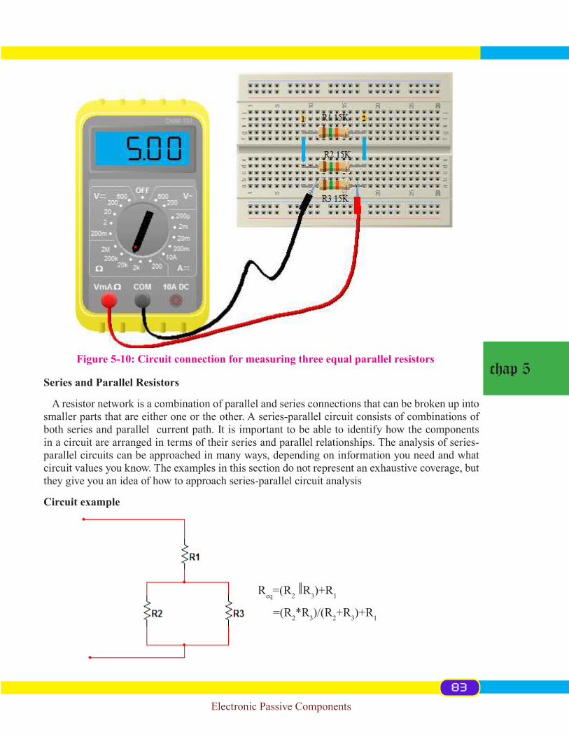
Electronic Passive Components
chap 5Series and Parallel Resistors
A resistor network is a combination of parallel and series connections that can be broken up into smaller parts that are either one or the other. A series-parallel circuit consists of combinations of both series and parallel current path. It is important to be able to identify how the components in a circuit are arranged in terms of their series and parallel relationships. The analysis of series-parallel circuits can be approached in many ways, depending on information you need and what circuit values you know. The examples in this section do not represent an exhaustive coverage, but they give you an idea of how to approach series-parallel circuit analysis
Circuit example
Req=(R2 ‖R3)+R1
=(R2*R3)/(R2+R3)+R1
Figure 5-10: Circuit connection for measuring three equal parallel resistors
83

Electronic Passive Components
chap 5
However, some complex networks of resistors cannot be resolved in this manner, requiring more sophisticated circuit analysis.
R34=R3+R4=6Ω+4Ω=10Ω
R34R2=(R34*R2)/(R34+R2)=(1Ω*10Ω)/(10Ω+10Ω)=5Ω
Req= R34R2+R1=5Ω+7Ω=12Ω
Do the next circuit as your exercise. This is a bit complicated than the above circuit problem. The application is still the same. Given that R1= 1 ohm, R2= 2 ohms, R3= 3 ohms, R4= 4 ohms, R5= 5 ohms, R6= 6 ohms, R7= 7 ohms, R8= 8 ohms and R9= 9 ohms. What will be the total resistance of the circuit below?
Note that resistors are constructed respecting standard values. This implies that you cannot get a
resistor of 17.3K, 23.5K or fractional resistance on market.
The objective of this experiment is to verify Ohm’s law applied to 1.Seriesresistors(experimentallyverifyingthattheyexperiencethesamecurrent),2.Parallelresistors(experimentallyverifyingthattheyexperiencethesamevoltage),and3. A module of parallel resistors collectively in series with another resistor.
Experiment 5-4: Series and Parallel Resistors (current and voltage measuring)
12Ω
84

Electronic Passive Components
chap 5
Part list
No Items Specifications Quantity1 Multimeter Digital multimeter 22 Resistor 1kΩ 13 Wire 22-gauge (0.33mm2)solidwire 40cm4 Breadboard Prototyping board 15 Battery 9V dc supply 1
With Ohms’s law: I=V/R
ThereforeI=V/R=9V/1000Ω=0.009A
Procedure 1. Connectthecircuitasillustratedinfigure5-122. Set ammeter in DC amps range at 20mA scale3. Theammeterisconnectedinserieswiththecircuit(2-3)4. Set the voltmeter in DC volts range at 20V scale5. VoltmeterisconnecterinparallelwithR1resistor(3-4)6. SupplythecircuitwithDCsource;positiveofthebatteryatpowerbus(1)andconnected
totheredleadoftheammeterthroughajumperwire(1-2),thenegativeofthebatteryatgroundbusofbreadboard(5-6)andconnectedtooneterminalofaresistorR1 and black leadofvoltmeterthroughajumperwire(4-5)
Figure 5-11: Circuit for measuring current and voltage
Ohm’s Law of Electricity
Ohm’s law of Electricity states that the current through a conductor between two points is directly proportional to the po-tention difference across the two points, and inversely proportional to the resis-tance between them. it can be represented by equation I=V/R where I is the current through the conductor in amperes, V is the potential difference measured across the conductor volts, and R is the resis-tance of the conductor in Ohms.
85

Electronic Passive Components
chap 5
Forseries-connectedresistors,Figure5-14),theequivalentresistance(Requ)iscalculatedusingthe following equation: Req=R1+R2 and current I=Vbattery/Requ.
Part list
No Items Specifications Quantity1 1 Ammeter, 2Voltmeter Digital multimeter 32 Resistor 1kΩand560Ω 23 Connecting wire 22-gauge (0.33mm2)solidwire 40cm
Figure 5-12: Circuit connection for measuring current and voltage
Experiment 5-5: Measuring current and voltage across Series Resistors
86

Electronic Passive Components
chap 5
4 Breadboard Prototypingboard(miniboard) 15 9V dc supply 9V Battery 1
By Ohm’s law, I=V/R and V=R*IReq=R1+R2
=1K+560R =1.56K =1560R
Total current I=VB1/Req =9V/1560 =0.005769A
Voltage on R1 (VR1)=I*R1
=1000R*0.005769A =5.769V
Voltage on R2 (VR2)=I*R2
=0.005769A*560R =3.23064V Procedure
1. Connectthecircuitasillustratedinfigure5-142. Set ammeter in DC amps range at 20mA scale3. The ammeter is connected in serieswith the circuit (1-2); the red lead is connected to
the positive of the battery and black lead on one terminal of resistor R1 through a jumper wire(2-3)
4. Set both voltmeters in DC volts range at 20V scale5. One voltmeter is connecter in parallel with R1resistor(3-4)andtheotherinparallelwith
R2resistor(5-6)
Figure 5-13: Circuit for measuring current and voltage across two resistors
87

Electronic Passive Components
chap 5
6. Supply the circuit with DC source; positive of the battery to the power bus of breadboard (1)andthenegativeofthebatteryatgroundbusofbreadboard(7-8)andconnectedtooneterminal of a resistor R1andblackleadofvoltmeterthroughajumperwire(6-7)
5. 1. 5. Potentiometer
A potentiometer or pot for short is a variable resistor with three terminals. Two of the terminals arepermanentlyfixedoneachendoftheresistor,butthemiddleterminalisconnectedtoawiperthat slides in contact with the entire surface of the resistor. Thus, the amount of resistance between this center terminal and either of the two side terminals varies as the wiper moves. Potentiometer inschematicdiagramsisanarrowpointingatthecentertapoftheresistor.Itismeanttoreflectthatthe value of the resistance at this terminal varies when the wiper moves.
Figure 5-14: Circuit connection for measuring current and voltage
88

Electronic Passive Components
chap 5
Potentiometer Markings.
The code to indicate the resistance and law of a potentiometer in case of replacement and even it would have been so bad if there was no overlap between the “old” and “new” “standards” the table 5-7 indicates standard notation.
Taper Old Code New Code Alternate
Linear A B LIN Log (Audio) C A LOG Antilog F N/A N/A
It is obviously important to check before you make assumptions, or you can easily get the wrong type especially if working on older equipment.
There is a much smaller range of potentiometer values, always in a 1, 2.5, 5 sequence. Common values for panel pots are 1k, 5k, 10k, 25k, 50k, 100k, 500k and 1M. Potentiometer with 2.5k and 250k went missing along the way, and these are not stocked by many distributors. 25k pots are becoming harder to get as well. Not all values are available in log and linear, and in some cases youmayevenfindthatforaparticulartype,youcangettheminanyvalueyouwant,aslongasitis100k(forexample).Theonlywaytoknowwhatyoucangetfromyourlocalsupplieristochecktheir catalogue. In reality, everything is available, but you may have to go a very long way to get it.
Potentiometer is a three terminal device used to vary the resistance in any circuit and the shaft is attached with it to vary the resistance. Many people use potentiometer in their day to day life, for example varying the volume of your music system by rotating the knob, controlling the brightness of television by pressing a button on the remote.
This tutorial will explain how to measure the resistance of the potentiometer by using digital multimeter for its accurate value.
Part list
No Item Specification Quantity 1 Ohmmeter Digital multimeter 12 Linear potentiometer B1M 1
Figure 5-15: American potentiometer symbol (1), European potentiometer symbol (2)(1) (2)
Table 5-7: Potentiometer markings
Experiment 5-6: Measuring the resistance of a Potentiometer
89

Electronic Passive Components
chap 5
Procedure:
Step 1: Knowing the potentiometer
Turn the potentiometer and you will see the maximum resistance value of the potentiometer en-graved over it. Here 1Mega ohm is the maximum value of resistance for this potentiometer.
Step 2: Making connections to the multimeter
Connect the multimeter probes according to their polarity. The red wire goes to the positive while the black one goes to the ground or neutral.
Step 3: Adjusting the multimeter for measuring resistance
For most multimeters, 2M ohm is the starting range for measuring resistance in Mega ohms. As ourpotisof1MegaOhm,2Mohmrangeismorethansufficienttomeasure1Megaohm.
Step 4: Measuring the total resistance of the potentiometer
We can see the maximum resistance of this potentiometer by connecting the probes at both the ends.
Front view Back view
B1M
90

Electronic Passive Components
chap 5
Here999.999KΩisthemaximumresistanceofthispotentiometer.Themeasuringrangeofthemultimeter is the same as what we have seen in the Step 2.
Step 5: Connecting probes to the lugs of potentiometer.
The positive probe is connected to the middle lug while the negative probe is connected to the firstlug.
Position of the lugs can be changed but it will affect the change of resistance i.e. changing the terminals will change the minimum and maximum point of the resistance.
Potentiometercanbeeitherangular(rotational)orlinear(slidertype)initsmovement.Thus,theamount of resistance between the wiper and either of the two side terminals varies as the wiper moves. The long handle on the potentiometer / variable resistor can be turned clockwise or anti-clockwise, altering the value of the resistance. The range of movement of its wiper or slider (and hencetheoutputobtained)islimitedtothephysicalsizeofthepotentiometerbeingused.
999.999KΩ
600KΩ
400KΩ
POT1MΩ
POT1MΩ
1MΩ 40%
91

Electronic Passive Components
chap 5
Step 6: Maximum resistance
The knob is turned to its maximum position and by connecting the probes to the terminals of the potentiometer; digital multimeter displays the value of resistance.
Step 7: Varying the resistance
The knob of the potentiometer is turned anticlockwise and the resistance of the potentiometer is decreased.
Step 8: Minimum resistance
As the knob is rotated to its minimum position resistance also comes to its minimum value.
250KΩ
999.998KΩ
25%
100%
POT1MΩ
1MΩ
1MΩ
92

Electronic Passive Components
chap 5
Note that if only two terminals of potentiometer are used, one end and the wiper, it acts as a vari-
able resistor or rheostat.
Dimmer switch
Dimmerswitchisusedtoshowhowthebrightnessofthebulbisrelatedtothecurrentflowingthroughthebulbsimplybyusingpotentiometerconnectedasrheostatasshowninthecircuitfigure5-16. Variable resistors are designed so that their resistance values can be changed easily with a manual or automatic adjustment. As resistance increases, the current decreases and also the bright-ness of the bulb decreases and vice versa.
The volume control of a radio receiver is a common application of a potentiometer used as voltage divider. Since the loudness of the sound is dependent on the amount of voltage associated with the radio signal, you can increase or decrease the volume by adjusting the potentiometer, that is, by tuning the knob of the volume control on the set.
Hands on tip
Figure 5-16: Dimmer circuit
0.1Ω1MΩ0%
93

Electronic Passive Components
chap 5
Figure 5-17: Dimmer circuit connection
A potentiometer is a variable resistor with three termi-nals. A potentiometer acts as voltage divider when only one end and adjustable terminal or wiper are used.
When you are using a multimeter, such as analog or digi-tal multimeter, when you manually select the voltage and current ranges, it is good practice to always set the multi-meter on the maximum range before you measure an un-known voltage or current. You can then reduce the range until you get an acceptable reading.
Hands on tip
Variable resistor
Bulb
94

Electronic Passive Components
chap 5
5. 1. 6. Trimmer Resistor
A trimmer resistor usually called a trim pot or preset potentiometer is a small variable resistor that is used in circuits to do preset. It is trimmed with a trimmer screwdriver it is made up with a roundfiberdiscwithalayerofcarbonwithawiperthatrunonthecarbonlayertochangetheresis-tance it always have 3 connecting pins where the center one is connected to the wiper and the other two to opposite ends of the carbon strip. Resistance trimmers are required when the value of resis-tanceorvoltagedivisioninacircuitmustbeadjustedtocompensateforenvironmentalinfluences,when the desired circuit performance cannot be procured and retained through manufacturing, or it is unknown what precision is required. This applies to precision applications, among others.
Trimmer codes labeling value identification
Trimmer resistance value is taken to mean from digits codes written to them. These codes can be in the form of two or three digits.
Two digits Trimmer resistor codes
Inprinciple,whentwodigitsareused,thefirstdigitrepresentssignificantdigitofohmunitwhiletheseconddigitrepresentsanumberofzerosfollowingthesignificantfigure.Thetable5-8showsthe common values.
Nominal resistance values (Ω) Code Nominal resistance values (Ω) Code
10 11 10K 1420 21 20K 2450 51 3K 34100 12 5K 54
Figure 5-19: American trimmer resistor symbol (1), European trimmer resistor symbol (2)
(1) (1)
Figure 5-18: Examples of typical commercial trimmer resistors
95

Electronic Passive Components
chap 5
200 22 100K 15300 32 200K 25500 52 500K 551K 13 1M 162K 23 2M 233K 33 - -5K 53 - -
Three digits Trimmer resistor codes
Inprinciple,when3digitsareused,thefirstandseconddigitsrepresentsignificantfiguresofohmunitwhilethelastdigitrepresentsanumberofzerosfollowingthesignificantfigures.Thetable 5-9 describes the common encountered values.
Nominal resistance values (Ω) Code Nominal resistance values (Ω) Code
10 100 10K 10320 200 20K 203- - 25K 253
50 500 50K 503100 101 100K 104200 201 200K 204
- - 250K 254500 501 500K 5041K 102 1M 1052K 202 2M 2055K 502 5M 505
5. 1. 7. Resistor Power Ratings
Practicalresistorsarespecifiedashavingamaximumpowerratingwhichmustexceedthean-ticipated power dissipation of that resistor in a particular circuit: this is mainly of concern in power electronics applications.
Resistors with higher power ratings are physically larger and may require heat sinks. In a high-voltage circuit, attention must sometimes be paid to the rated maximum working voltage of the
Table 5-8: Two digits Trimmer resistor codes
Table 5-9: Three digits Trimmer resistor codes
Figure 5-20: 1/2 watt resistor and 1 watt resistor
96

Electronic Passive Components
chap 5
resistor. Resistorsareavailablewithpowerratingsof1/8thW(orlessforsurfacemountdevices),upto
hundredsofwatts.Themostcommonare1/4W(0.25W),1/2W(0.5W),1W,5Wand10W.
5. 2. Capacitor
A capacitor is an electronic passive component consisting of a pair of conductors separated by a dielectric.Acapacitorcanstoreenergyintheelectricalfieldbetweenapairofconductorscalled“plates”.Whenavoltagepotentialdifferenceexistsbetweentheconductors,anelectricfieldispresent in thedielectric.Thisfieldstoresenergyandproducesamechanical forcebetween theplates. The process of storing energy in the capacitor is known as “charging”, and involves electric charges of equal magnitude, but opposite polarity, building up on each plate. The effect is greatest betweenwide,flat,parallel,narrowlyseparatedconductors.
Capacitors store electrical energy between two internal “plates,” or conductors. They are com-monly used to help differentiate between high and low frequencies in signal-carrying circuitry. They can be made of several different materials to produce varying levels of capacitance.
Charging a Capacitor
Acapacitorwillchargewhenitisconnectedtoadcvoltagesource.Thecapacitorinfigure5-22part(a)isuncharged;thatis,plateAandplateBhaveequalnumbersoffreeelectrons.Whentheswitchisclosed,infigure5-22part(b),thesourcemoveselectronsawayfromplateAthroughthecircuit to the plate B as the arrows indicate.
A B
Figure 5-21: Capacitor symbol (A) and capacitor structure (B)
(a) (b) (c) (d)Figure 5-22: Charging a capacitor process. (a) Uncharged, (b)Charging, (c) Fully charged, (d) retains charge
97
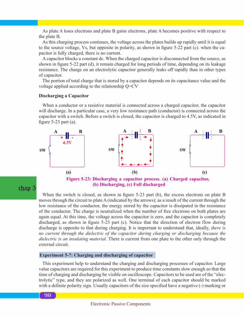
Electronic Passive Components
chap 5
As plate A loses electrons and plate B gains electrons, plate A becomes positive with respect to the plate B.
As this charging process continues, the voltage across the plates builds up rapidly until it is equal tothesourcevoltage,Vs,butoppositeinpolarity,asshowninfigure5-22part(c).whentheca-pacitor is fully charged, there is no current.
A capacitor blocks a constant dc. When the charged capacitor is disconnected from the source, as showninfigure5-22part(d),itremainchargedforlongperiodsoftime,dependingonitsleakageresistance. The charge on an electrolytic capacitor generally leaks off rapidly than in other types of capacitor.
The portion of total charge that is stored by a capacitor depends on its capacitance value and the voltage applied according to the relationship Q=CV
Discharging a Capacitor
When a conductor or a resistive material is connected across a charged capacitor, the capacitor willdischarge.Inaparticularcase,averylowresistancepath(conductor)isconnectedacrossthecapacitor with a switch. Before a switch is closed, the capacitor is charged to 4.5V, as indicated in figure5-23part(a).
When the switch is closed,as shown infigure5-23part (b), theexcesselectronsonplateBmovesthroughthecircuittoplateA(indicatedbythearrows);asaresultofthecurrentthroughthelow resistance of the conductor, the energy stored by the capacitor is dissipated in the resistance of the conductor. The charge is neutralized when the number of free electrons on both plates are again equal. At this time, the voltage across the capacitor is zero, and the capacitor is completely discharged, as shown infigure 5-23 part (c).Notice that the direction of electron flowduringdischarge is opposite to that during charging. It is important to understand that, ideally, there is no current through the dielectric of the capacitor during charging or discharging because the dielectric is an insulating material. There is current from one plate to the other only through the external circuit.
This experiment help to understand the charging and discharging processes of capacitor. Large value capacitors are required for this experiment to produce time constants slow enough so that the time of charging and discharging be visible on oscilloscope. Capacitors to be used are of the “elec-trolytic” type, and they are polarized as well. One terminal of each capacitor should be marked withadefinitepolaritysign.Usuallycapacitorsofthesizespecifiedhaveanegative(-)markingor
(a) (b) (c)Figure 5-23: Discharging a capacitor process. (a) Charged capacitor, (b) Discharging, (c) Full discharged
Experiment 5-7: Charging and discharging of capacitor
98

Electronic Passive Components
chap 5
series of negative markings pointing toward the negative terminal. Very large capacitors are often polarity-labeledbyapositive(+)markingnexttooneterminal.Failuretoheedproperpolaritywillalmost surely result in capacitor failure, even with a source voltage as low as 4.5 volts. When elec-trolytic capacitors fail, they typically explode, spewing caustic chemicals and emitting foul odors.
Build the circuit and observe voltage variation across the capacitor by changing the position of switch and notice how it increases and decreases slowly over time. You can “reset” the capacitor back to a voltage of zero by shorting across its terminals with a piece of wire.
Part list
No Item Quantity 1 Oscilloscope 12 Resistor 1K 13 Breadboard(RSR03MB102) 14 SPDT toggle switch 15 Electrolytic capacitor 470uF/50V 16 Wire 0.33mm2 10cm7 3x1.5V cell battery or use 4.5V DC supply 1
ThechargingtimetakesplacewhenswitchSW1isatposition1(P1)whiledischargingtimetakesplacewhentheswitchSW1isatposition2(P2).Thetimeconstantdeterminesthedurationofcharginganddischargingprocesses.The“timeconstant”(τ=RC)ofaresistorcapacitorcircuitiscalculatedbytakingthecircuitresistanceandmultiplyitbythecircuitcapacitance.Fora1kΩresistor and a 1000µF capacitor, the time constant should be 1 second. This is the amount of time ittakesforthecapacitorvoltagetoincreaseapproximately63.2%fromitspresentvaluetoitsfi-nalvaluewhichisthevoltageofthebattery.Fortheabovecircuitfigure5-24ittakes0.4second.Normally a one-second time constant doesn’t provide much time to take voltmeter readings but for oscilloscope it is possible to change time/division. We can increase this circuit’s time constant two different ways: changing the total circuit resistance, and/or changing the total circuit capacitance. Let’sobservecircuitconnectionfigure5-25.
Figure 5-24: Circuit for charging and discharging a capacitor
99

Electronic Passive Components
chap 5
Procedure
1. Connectcircuitasshowninthecircuitfigure5-25byusingspecifieditems2. Check electrolytic capacitor’s polarities 3. First discharge capacitor by shorting its terminals4. Supply the circuit with 4.5V DC supply5. Set oscilloscope to 2V/Div and at 100ms/Div, vertical and horizontal sensitivity respec-
tively6. Connect oscilloscope probes against capacitor’s leg (black probe is at negative terminal of
thebattery)
Figure 5-25: Circuit connection for charging and discharging of a capacitor
100
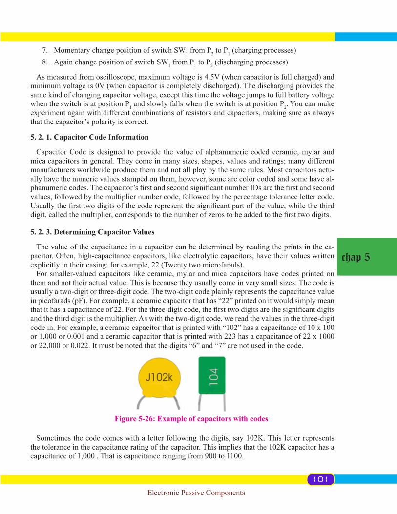
Electronic Passive Components
chap 5
7. Momentary change position of switch SW1 from P2 to P1(chargingprocesses)8. Again change position of switch SW1 from P1 to P2(dischargingprocesses)
Asmeasuredfromoscilloscope,maximumvoltageis4.5V(whencapacitorisfullcharged)andminimumvoltageis0V(whencapacitoriscompletelydischarged).Thedischargingprovidesthesame kind of changing capacitor voltage, except this time the voltage jumps to full battery voltage when the switch is at position P1 and slowly falls when the switch is at position P2. You can make experiment again with different combinations of resistors and capacitors, making sure as always that the capacitor’s polarity is correct.
5. 2. 1. Capacitor Code Information
Capacitor Code is designed to provide the value of alphanumeric coded ceramic, mylar and mica capacitors in general. They come in many sizes, shapes, values and ratings; many different manufacturers worldwide produce them and not all play by the same rules. Most capacitors actu-ally have the numeric values stamped on them, however, some are color coded and some have al-phanumericcodes.Thecapacitor’sfirstandsecondsignificantnumberIDsarethefirstandsecondvalues, followed by the multiplier number code, followed by the percentage tolerance letter code. Usuallythefirsttwodigitsofthecoderepresentthesignificantpartofthevalue,whilethethirddigit,calledthemultiplier,correspondstothenumberofzerostobeaddedtothefirsttwodigits.
5. 2. 3. Determining Capacitor Values
The value of the capacitance in a capacitor can be determined by reading the prints in the ca-pacitor. Often, high-capacitance capacitors, like electrolytic capacitors, have their values written explicitlyintheircasing;forexample,22(Twentytwomicrofarads).
For smaller-valued capacitors like ceramic, mylar and mica capacitors have codes printed on them and not their actual value. This is because they usually come in very small sizes. The code is usually a two-digit or three-digit code. The two-digit code plainly represents the capacitance value inpicofarads(pF).Forexample,aceramiccapacitorthathas“22”printedonitwouldsimplymeanthatithasacapacitanceof22.Forthethree-digitcode,thefirsttwodigitsarethesignificantdigitsand the third digit is the multiplier. As with the two-digit code, we read the values in the three-digit code in. For example, a ceramic capacitor that is printed with “102” has a capacitance of 10 x 100 or 1,000 or 0.001 and a ceramic capacitor that is printed with 223 has a capacitance of 22 x 1000 or 22,000 or 0.022. It must be noted that the digits “6” and “7” are not used in the code.
Sometimes the code comes with a letter following the digits, say 102K. This letter represents the tolerance in the capacitance rating of the capacitor. This implies that the 102K capacitor has a capacitance of 1,000 . That is capacitance ranging from 900 to 1100.
Figure 5-26: Example of capacitors with codes
101

Electronic Passive Components
chap 5
The table 5-10 gives applicable values and letters used to represent tolerance on a capacitor.
Third digit Multiplier or number of zeros Letter Tolerance
0 1 D +/-0.5%1 10 F +/- 1%2 100 G +/- 2%3 1000 H +/- 3%4 10000 J +/- 5%5 100000 K +/- 10%
M +/- 20%P +/- 100%
8 0.01 Z +/- 80%9 0.1
5. 2. 4. Capacitor color code
The way of identifying capacitor values and tolerances, an international color coding scheme was developed. This consists of colored bands in spectral order. The color codes currently in use aretheJointArmy-Navy(JAN)codeandtheRadioManufacturer’sAssociation(RMA)code.
Table 5-11: Capacitor color codes
Table 5-10: Applicable values and letters used to represent tolerance on capacitor
102

Electronic Passive Components
chap 5
Examples:
5. 2. 5. Standard capacitor values
Capacitors are manufactured with respect to the standard values. Values other than from capaci-tor standard values are obtained by gouping capacitors either in series or in parallel. The table 5-12 shows capacitor standard values with ±10% tolerance.
Capacitor standard values (±10%)10pF 100pF 1000pF 0.010µF 0.10µF 1µF 10µF12pF 120pF 1200pF 0.012µF 0.12µF 1.2µF 15pF 15pF 1500pF 0.015µF 0.15µF 1.5µF 18pF 18pF 1800pF 0.018µF 0.18µF 1.8µF 22pF 22pF 2200pF 0.022µF 0.22µF 2.2µF 22µF27pF 27pF 2700pF 0.027µF 0.27µF 2.7µF 33pF 33pF 3300pF 0.033µF 0.33µF 3.3µF 33µF39pF 39pF 3900pF 0.039µF 0.39µF 3.9µF 47pF 47pF 4700pF 0.047µF 0.47µF 4.7µF 47µF56pF 56pF 5600pF 0.056µF 0.56µF 5.6µF 68pF 68pF 6800pF 0.068µF 0.68µF 6.8µF 82pF 82pF 8200pF 0.082µF 0.82µF 8.2µF
5. 2. 6. Capacitor grouping
In a circuit two or more capacitors can be combined to obtain the desired capacitance value. When combining capacitors in a series connection, the capacitance is decreased, while in a parallel connection the capacitance is increased. This is the opposite of what happens when we combine resistors.
5. 2. 6. 1. Capacitors in series
In a series connection, the total capacitance is equal to the reciprocal of the sum of the reciprocal values of the capacitors. 1/Ct = 1/C1 + 1/C2 + 1/Cn
Table 5-12: Standard Capacitor values of ±10% tolerance
103

Electronic Passive Components
chap 5
Example: C1 = 10uF; C2 = 33uF and C3 = 47uF
The circuit diagram:
Resolution:1/Ct = 1/10uF + 1/33uF + 1/47uF1/Ct = 0.15157963uFCt = 6.597uF
5. 2. 6. 2. Capacitors in parallel
In a parallel connection, the total capacitance is obtained by adding the individual capacitance values of the connected capacitors.
Ct = C1 + C2 + Cn
Example: C1 = 10uF; C2 = 33uF and C3 = 47uF
The circuit diagram
Solution:Ct = Ct = C1 + C2 + Cn = 10uF + 33uF + 47uF
Ct = 90uF
5. 2. 7. Capacitor voltage rating
The voltage rating on a capacitor is the maximum amount of voltage that a capacitor can safely be exposed to and can store.Below is the table describing the common capacitor working voltages.
Series capacitors store the same amount of charge (QT=Q1=Q2=Q3=Qn)and thevoltageacrosseachonedependsonitscapacitancevalue(V=Q/C).The sum of the capacitor voltages (VC1, VC2,VC3,... VCn)equal the source voltage Vs. Vs= VC1+VC2+VC3+... +VCn
Each capacitor in a parallel circuit stores a portion of the total charge and depends on its capacitance value (Q=CV). The total chargestored is given by: QT=Q1+Q2+Q3+...+Qn; Since the voltage across both capacitor is the same, the larger capacitor stores more charge
Figure 5-27: Example of a circuit with three parallel capacitors
104
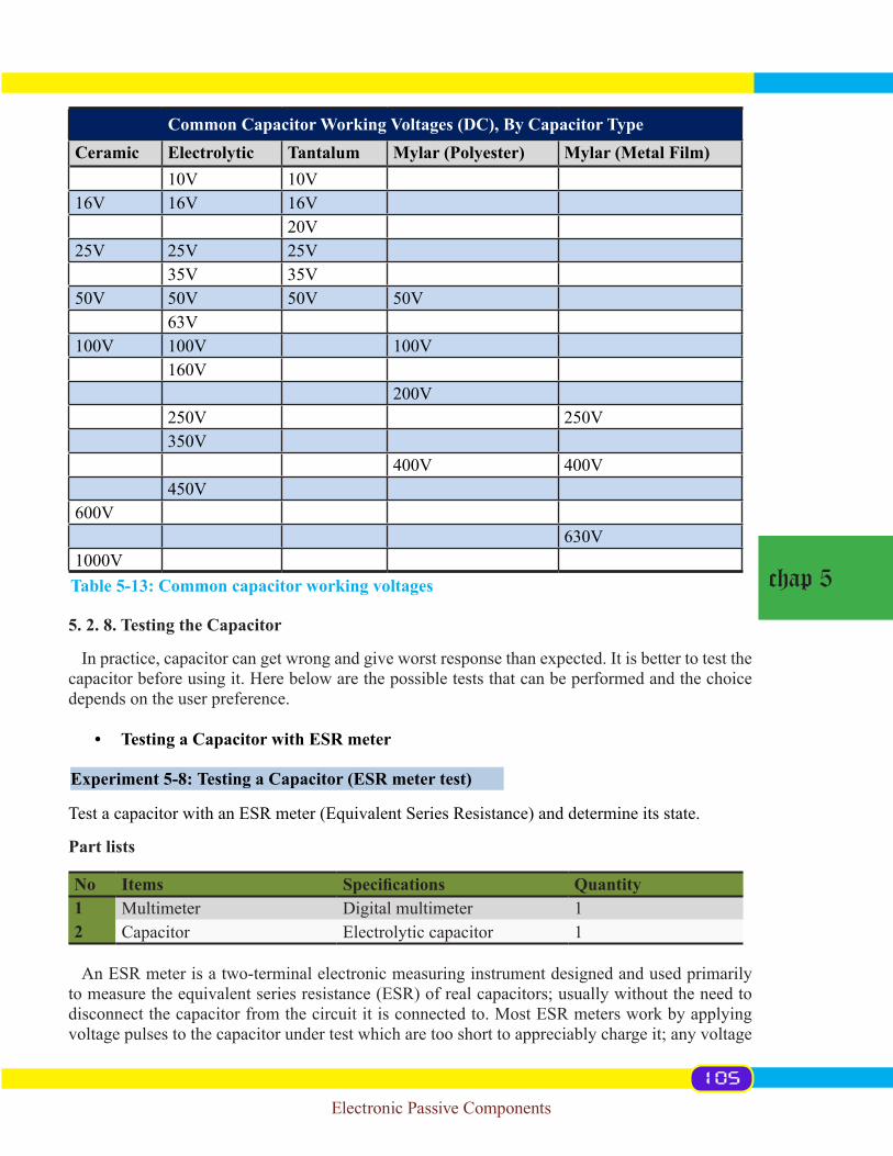
Electronic Passive Components
chap 5
Common Capacitor Working Voltages (DC), By Capacitor TypeCeramic Electrolytic Tantalum Mylar (Polyester) Mylar (Metal Film) 10V 10V 16V 16V 16V 20V 25V 25V 25V 35V 35V 50V 50V 50V 50V 63V 100V 100V 100V 160V 200V 250V 250V 350V 400V 400V 450V 600V 630V1000V
5. 2. 8. Testing the Capacitor
In practice, capacitor can get wrong and give worst response than expected. It is better to test the capacitor before using it. Here below are the possible tests that can be performed and the choice depends on the user preference.
• Testing a Capacitor with ESR meter
TestacapacitorwithanESRmeter(EquivalentSeriesResistance)anddetermineitsstate.
Part lists
No Items Specifications Quantity1 Multimeter Digital multimeter 12 Capacitor Electrolytic capacitor 1
An ESR meter is a two-terminal electronic measuring instrument designed and used primarily tomeasuretheequivalentseriesresistance(ESR)ofrealcapacitors;usuallywithouttheneedtodisconnect the capacitor from the circuit it is connected to. Most ESR meters work by applying voltage pulses to the capacitor under test which are too short to appreciably charge it; any voltage
Experiment 5-8: Testing a Capacitor (ESR meter test)
Table 5-13: Common capacitor working voltages
105

Electronic Passive Components
chap 5
appearing across the capacitor is due to ohmic drop across the ESR.Most ESR meters work by discharging a real electrolytic capacitor (essentially equivalent to a
perfectcapacitorinserieswithanunwantedresistance,theESR)andpassinganelectriccurrentthrough it for a short time, too short for it to charge appreciably. This will produce a voltage across the de-vice equal to the product of the current and the ESR plus a negligible contribution from a small charge in the capacitor; this voltage is measured and its value di-videdbythecurrent(i.e.,theESR)showninohmsormilliohms on a digital display or by the position of a pointer on a scale. The process is repeated tens or hun-dreds of thousands of times a second
To test a capacitor for resistance using an ESR meter, follow the steps below.
Step 1- Remove power from the circuit.
Be certain the circuit is not connected to a power source and is dead.
Step 2- Discharge the capacitor.
Discharge the capacitor using a resistor with a resis-tance 5 to 50 times the rated voltage of the capacitor. Hold the resistor with insulated needle nose pliers and touch the resistor leads to the capacitor leads. Hold for several seconds to drain the capacitor into the resistor.
Step 3- Test the capacitor with an ESR meter.
Connect the ESR meter probes to the capacitor using the correct polarity. The negative side of tubetypecapacitorsisclearlymarkedwitha“-“symbol(Seephotooffigure5-29).Connecttheblack probe to the negative lead and the red probe to the positive lead.
Step 5- Review the test results.
Look at the readout on the ESR meter, which could be analog, LED readout, or digital. The reading is the equivalent series resistance which should be close to zero for a good capacitor. The
higher the number, the more defective the capacitor. Remember, zero is ideal, but capacitors with age may climb higher than that.
Because of the process used for insu-lating pentoxide dielectric, the metallic (aluminiumortantalum)plate isalwayspositive with respect to the electrolytic plate, and thus all electrolytic capacitors are polarized.
Figure 5-28: ESR meter
Figure 5-29: Capacitor polarity identification
106

Electronic Passive Components
chap 5
• Alternate Capacitor Test Method
This method uses a common multimeter to test a capacitor. This test method is less accurate than the ESR test and requires at least one side of the capacitor to be removed from the circuit. Step 1- Connect the meter to the capacitor
Connect your meter to the discharged leads of the capacitor. Be certain to connect the red probe to the positive capacitor lead, and the black probe to the negative lead.
Step 2- Watch the capacitor charge
For capacitors in the microfarad uF range or larger, you should be able to see the capacitor charge when connected to the meter. This is because the meter will charge the capacitor. Step 3- Review the test results
When the meter is set in the high resistance range, the resistance should start out low and increase until it goes to open. If the capacitor is shorted, then it will never charge and resistance will not increase.Ifthecapacitorisopen,theresistancewillbeinfiniteimmediatelyandwillnotchange.
• Test a Capacitor with Ohmmeter
A very good test you can do is to check a capacitor with your multimeter set on the ohmmeter setting. This gives the value at which the settle on the state of capacitor is taken.
By taking the capacitor’s resistance, we can determine whether the capacitor is good or bad. To do this test, we take the ohmmeter and place the probes across the leads of the capacitor. The orientation doesn’t matter, because resistance is not polarized.
Part lists
No Items Specifications Quantity1 Multimeter Digital multimeter 12 Capacitor Electrolytic capacitor 1
Ifthereadinggivesaverylowresistance(near0Ω)acrossthecapacitor,weknowthecapacitoris defective. It is reading as if there is a short across it. If we read a very high resistance across the capacitor(severalMΩ),thisisasignthatthecapacitorlikelyisdefectiveaswell.Itisreadingasif there is an open across the capacitor.
A normal capacitor would have a resistance reading up somewhere in between these 2 extremes, say,anywhereinthetensofthousandsorhundredsofthousandsofohms.Butnot0ΩorseveralMΩ.
Thisisasimplebuteffectivemethodforfindingoutifacapacitorisdefectiveornot.
Experiment 5-9: Testing a Capacitor with digital Ohmmeter (digital multimeter)
107

Electronic Passive Components
chap 5
• Testing Capacitors with an analog Ohmmeter (Analog Multitester)
Unliketotheuseofdigitalohmmeterwhichgivesaspecificnumber,theuseofanalogohmmetertotestcapacitorgivesthedeflectionofthepointer and its orientation helps to determine the state of capacitor.
A capacitor may develop troubles like open, shorted and weak or leaky. Following are rules to be followed in testing capacitors:
Part list
No Items Specifications Quantity1 Multimeter Analog multimeter 12 Capacitor Electrolytic capacitor 1
Steps
1. Switch off the power supply.2. To be safe and to protect your ohmmeter from damage, discharge the capacitor before
testing. Do this by short-circuiting its two terminals with a conductor. Make sure that the conductor that you are using has an insulated handle to protect you from electric shock.
3. Disconnect one terminal lead of the capacitor from the circuit before testing.4. Adjust your ohmmeter to appropriate range. Use the guide below in selecting the range to
be used for a range of capacitance values.
No Capacitance Range1 0.01 uF to 1 uF X10KΩandabove2 1 uF to 47 uF X1KΩ
Figure 5-30: Test a capacitor with Ohmmeter
Experiment 5-10: Testing Capacitors with an analog Ohmmeter (Analog Multitester)
108

Electronic Passive Components
chap 5
3 47 uF to 1000 uF X10Ω4 1000 uF and above X1Ω
Connect the test probes to the terminal of the capacitor.
Table 5-14: Ohm’s range used to test a given capacitor
Figure 5-31: Test probes of analog ohmmeter connected to the terminals of the capacitor
Figure 5-32: Four methods to identify capacitor’s condition using analogue Ohmmeter
Good Open
Short Leaky
109

Electronic Passive Components
chap 5
• Test a Capacitor with a Multimeter in the Capacitance Setting
Some digital multimeters are equipped with capacitance check range. If you have a capacitance meter on your multimeter, you can check the capacitance of the capacitor with a multimeter the same way as to measure resistor.
All you have to do is to read the capacitance that is on the exterior of the capacitor and take the multimeter probes and place them on the leads of the capacitor. Polarity doesn’t matter. This is the sameashowthesetupisforthefirstillustration,onlynowthemultimeterissettothecapacitancesetting.
You should read a value near the capacitance rating of the capacitor. Due to tolerance and the factthat(specifically,electrolyticcapacitors)maydryup,youmayreadalittlelessinvaluethanthecapacitanceoftherating.Thisisfine.Ifitisalittlelower,itisstillagoodcapacitor.However,ifyoureadasignificantlylowercapacitanceornoneatall,thisisasuresignthatthecapacitorisdefective and needs to be replaced.
Checking the capacitance of a capacitor is a great test for determining whether a capacitor is good or not
• Test a Capacitor with a Voltmeter
Capacitors are electronic storage devices for DC current. They store a potential difference of charges across their plate, which are voltages. The anode has a positive voltage and the cathode has a negative voltage.
Part lists
No Items Specifications Quantity1 Voltmeter Digital multimeter 12 Capacitor Electrolytic capacitor 13 Battery 9V dc supply 1
A test that you can do is to see if a capacitor is working as normal is to charge it up with a voltage and then read the voltage across the terminals. If it reads the voltage that you charged it to, then the capacitor is doing its job and can retain voltage across its terminals. If it is not charging up and reading voltage, this is a sign the capacitor is defective.
Experiment 5-11: Test a Capacitor with a Multimeter in the Capacitance Setting
Experiment 5-12: Test a Capacitor with a Voltmeter
110

Electronic Passive Components
chap 5
5. 2. 9. Capacitor in AC circuits
Capacitor blocks constant dc. A capacitor passes ac with an amount of opposition, called capaci-tance reactance, which depends on the frequency of the ac.
Figure 5-33: Test a Capacitor with a Voltmeter
• Capacitors are capable of storing electrical charge for a long time after power has turned off in a circuit. Be caraful when touching or handling capacitors in or out of a circuit. If you touch the leads, you may be in for a shock as the capacitor discharges through your body! It is usually good practice to discharge a capacitor using a shorting tool with an insulated grip of some sort before handling the capacitor.
• Be extremely careful with electrolytic capacitors because it does make a difference which way an electrolytic capacitor is connected. If a polarized capacitor is connected backwards, it may explode and cause injury.
Safety point
111

Electronic Passive Components
chap 5
Capacitance reactance, Xc
Fromthecircuitsoffigure5-34,acapacitorisshownconnectedtoasinusoidalvoltagesource.When the source voltage is held at a constant amplitude value and its frequency is increased, the amplitude of the current increases. Also, when the frequency of the source is decreased, the current amplitude decreases.
Procedure
1. Connecta220nF(nopolarized)capacitorinserieswithammeterandsignalgeneratorasshowninthecircuitfigure3-35.
2. Set multimeter in amp’s range 1A or 2A scale if provided.3. Set the function generator to output a 6V rms sine wave with adjustable frequency.
Figure 5-34: The current in a capacitive circuit varies directly with the frequency of the source voltage; (a) Current increases when the frequency increases, (b) Current decreases when the frequency decreases
a b
Some multimeters have a relatively low frequency re-sponse of 1KHz or less, while others can measure voltages or currents with frequencies up to about 2MHz. Always check to make sure that your meter is capable of making accurate measurements at the particular frequency you are working with.
Hands on tip
Figure 5-35: Turn the knob in clockwise (a) to increase frequency, Turn the knob in anticlockwise (b) to decrease the frequency
a b
112
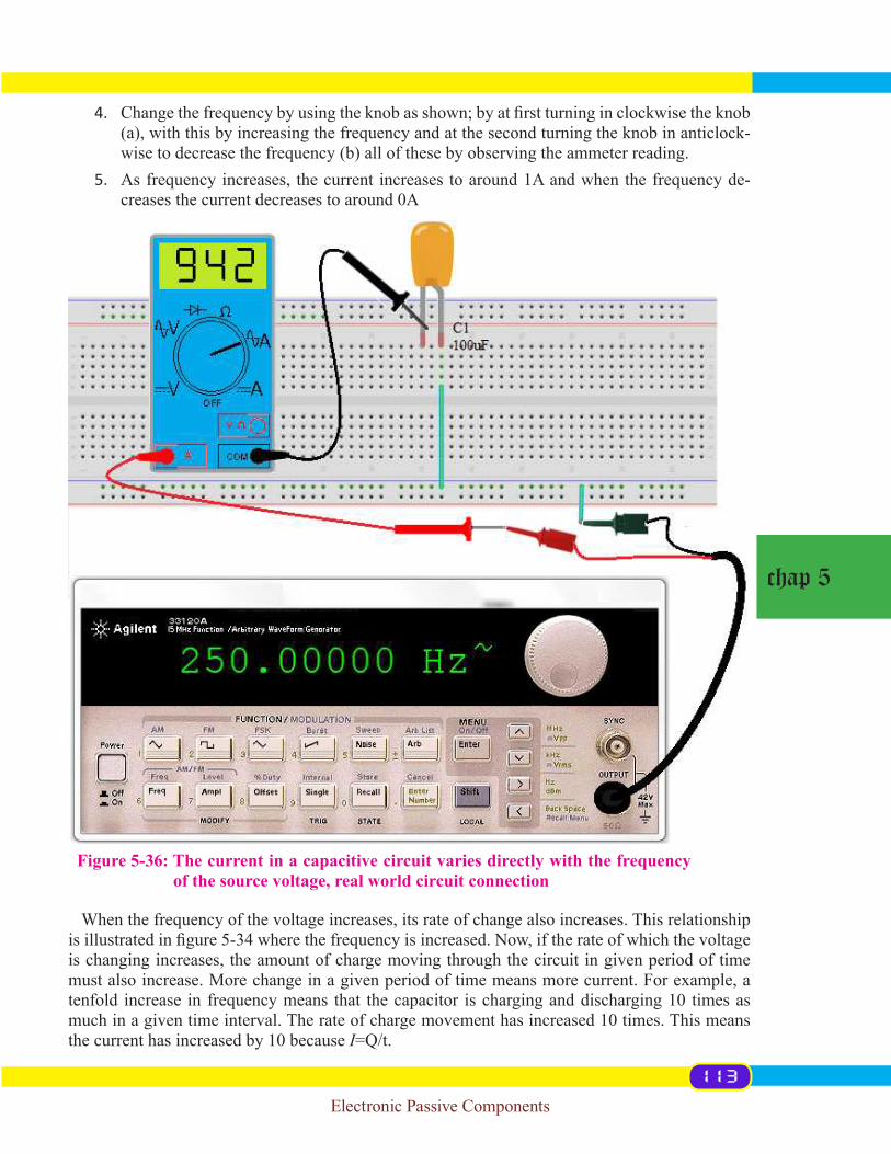
Electronic Passive Components
chap 5
4. Changethefrequencybyusingtheknobasshown;byatfirstturninginclockwisetheknob(a),withthisbyincreasingthefrequencyandatthesecondturningtheknobinanticlock-wisetodecreasethefrequency(b)allofthesebyobservingtheammeterreading.
5. As frequency increases, the current increases to around 1A and when the frequency de-creases the current decreases to around 0A
When the frequency of the voltage increases, its rate of change also increases. This relationship isillustratedinfigure5-34wherethefrequencyisincreased.Now,iftherateofwhichthevoltageis changing increases, the amount of charge moving through the circuit in given period of time must also increase. More change in a given period of time means more current. For example, a tenfold increase in frequency means that the capacitor is charging and discharging 10 times as much in a given time interval. The rate of charge movement has increased 10 times. This means the current has increased by 10 because I=Q/t.
Figure 5-36: The current in a capacitive circuit varies directly with the frequency of the source voltage, real world circuit connection
113
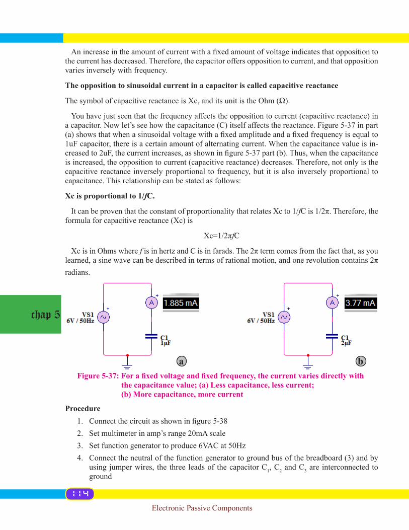
Electronic Passive Components
chap 5
Anincreaseintheamountofcurrentwithafixedamountofvoltageindicatesthatoppositiontothe current has decreased. Therefore, the capacitor offers opposition to current, and that opposition varies inversely with frequency.
The opposition to sinusoidal current in a capacitor is called capacitive reactance
ThesymbolofcapacitivereactanceisXc,anditsunitistheOhm(Ω).
Youhavejustseenthatthefrequencyaffectstheoppositiontocurrent(capacitivereactance)inacapacitor.Nowlet’sseehowthecapacitance(C)itselfaffectsthereactance.Figure5-37inpart(a)showsthatwhenasinusoidalvoltagewithafixedamplitudeandafixedfrequencyisequalto1uF capacitor, there is a certain amount of alternating current. When the capacitance value is in-creasedto2uF,thecurrentincreases,asshowninfigure5-37part(b).Thus,whenthecapacitanceisincreased,theoppositiontocurrent(capacitivereactance)decreases.Therefore,notonlyisthecapacitive reactance inversely proportional to frequency, but it is also inversely proportional to capacitance. This relationship can be stated as follows:
Xc is proportional to 1/fC.
It can be proven that the constant of proportionality that relates Xc to 1/fCis1/2π.Therefore,theformulaforcapacitivereactance(Xc)is
Xc=1/2πfC
Xc is in Ohms where fisinhertzandCisinfarads.The2πtermcomesfromthefactthat,asyoulearned,asinewavecanbedescribedintermsofrationalmotion,andonerevolutioncontains2πradians.
Procedure1. Connectthecircuitasshowninfigure5-382. Set multimeter in amp’s range 20mA scale3. Set function generator to produce 6VAC at 50Hz 4. Connecttheneutralofthefunctiongeneratortogroundbusofthebreadboard(3)andby
using jumper wires, the three leads of the capacitor C1, C2 and C3 are interconnected to ground
Figure 5-37: For a fixed voltage and fixed frequency, the current varies directly with the capacitance value; (a) Less capacitance, less current; (b) More capacitance, more current
a b
114

Electronic Passive Components
chap 5
5. Connect the multimeter’s red lead to the line output of function generator and the black lead of the multimeter to the lead of the capacitor C1(2)andthenobservetheammeterreading. The ammeter reading is about 1.88mA.
6. Move the black lead of multimeter to the leads of capacitor C2 parallel to C3(2)andagainobserve the ammeter reading. The ammeter reading is about the twice the previous reading.
:
5. 2. 10. Variable capacitors
Variable capacitors are used in a circuit when there is a need to adjust the capacitance value ei-ther manually or automatically. These capacitors are generally less than 300 pF but are available in larger values for specialized applications. The schematic symbol for a variable capacitor is shown in figure 5-39.
Figure 5-38: For a fixed voltage and fixed frequency, the current varies directly with the capacitance value real world circuit connection
115

Electronic Passive Components
chap 5
Adjustable capacitors that normally have sloted screw-type adjustments and are used for very fine adjustments in a circuit are called trimmers. Ceramic or mica is a common dielectric in these types of capacitors, and the capacitance usually is changed by adjusting the plate separation.
Application of Capacitors
• Electrolyte capacitors: Usedasfilterinapowersupply,timeconstantcircuits,bypass,coupling/decoupling, smoothing and power electronic applications.
• Non-polarised electrolytic capacitors: Used in applications such as AC motor starting, cross over networks and large pulse signals.
• Ceramic capacitors: Used as bypass capacitor and used in decoupling applications, fre-quency discriminators and biasing applications.
• Tubular capacitor: Used to isolate the antennas in receivers.• Polystyrene capacitors: Used in coupling, resonant and measuring circuits.• Polyester capacitors: Used for coupling /decoupling applications, and also in power elec-
tronics.• Polycarbonate capacitors: Used in dc applications.• Mica capacitors: Used as coupling capacitors at high frequency, in radio transmitters,
measuring circuits, bypass circuits and RF resonant circuits.• Variable capacitors: Used in tuning circuits of communication receivers, transmitters and
in oscillators.
5. 3. Inductor
An inductor or bobbin is a passive component of an electrical circuit, which stores energy in
The capacitance of a capacitor is analogous to the resistance of a re-sistor. In fact, both are expressed in Ohms. Since both R and Xc are forms of opposition to current, Ohm’s law applies to capacitive circuits as well as to resistive cir-cuits.
I = V/Xc
Chip capacitors are for surface mounting on a printed circuit board and have a conductive ter-minals plated on the ends. These capacitors will withstand the molten solder temperatures en-countered in reflow and wave soldering used in automated circuit board assembly. Chip capaci-tors are in great demande because of the move toward miniaturization.
Hands on tip
Figure 5-39: Symbol of variable capacitor
116

Electronic Passive Components
chap 5
magneticfieldwhenthestrengthofcurrentincrease,andreturnenergywhenthestrengthofcur-rent decrease.
An inductor can be a single turn of wire or many turns:
An inductor can be wound: Onaplasticformer(plasticspool)onametalcoreoronaircore
,
An inductor can almost be any size or shape and is the most complex component in electronics. Inductance is measured in Henries. One Henry is a large unit. An inductor of 1 Henry would be a few cm in diameter and a few cm long and have many turns of wire on a ferrite core.
5. 3. 1. Inductor Color Codes
Inductors are labeled with a number of different ways. The most common are text codes and color codes. The color codes for inductors are identical to that of a resistor so if you are familiar with resistors this should be very easy. The tricky part is remembering the results from this will be in micro Henrys, not just Henrys.
• Values are in micro Henries (μH)
(2) (3)
(4) (5) (6)Figure 5-40: Inductor symbol (1), Single turn inductor (2), Many turns inductor (3), Induc-
tor on plastic spool (4), Inductor on a meatal core (5), Inductor on air core (6)
(1)
117

Electronic Passive Components
chap 5
• First two digits are the value • Third digit is the multiplier • If there is an R, it acts as a decimal point, and there is no multiplier • Examples:
o 101 = 10*101μH=100μHo 4R7=4.7μH
• Suffix
o Sometimestheprecisionoftheinductorwillbemarked,usingafinalletterF,G,J,K, or M
F = +/-1% G = +/-2% J = +/-5% K = +/-10% M = +/-20%
Color Code Markings
Inductors can be marked by colored bands or colored dots. Each color represents a value. The color codes for inductors are identical to that of a resistor so if you are familiar with resistors
this should be very easy. The tricky part is remembering the results from this will be in microHen-rys, not just Henrys. From the inductor color code table, the last band is the tolerance, and the band right before tolerance band is the multiplier. The other bands are the numbers. Themilitarystandardforcylindricalinductorsspecifies5colouredbands.Thesamecoloursareused as in the 4 band code, but:
Figure 5-41: Different inductor shapes
118

Electronic Passive Components
chap 5
For band 1, a double width sliver band is used to signify Military Standard.
• Four Bands Standard EIA Colour Code for Inductors.
Note: If no Band 4 is used, tolerance is +/-20%
Example: Suppose we have the colors yellow, red, brown, black. They would mean the inductor has a value of: yellow - red - brown - black 4 2 x10 +/-20% So we have 42 * 10 +/-20%,Meaningthattheinductanceis420uH(micro-Henrys)witha20percenttolerance,orinother
words, our actual inductance can be anywhere between 336µH and 504µH micro Henrys.Notes: For values less than 10µH: Bands 2, 3 and 4 indicate the value of inductance in µH, a gold
band might be used in either band 2 or band 3. In either of these two bands, gold indicates a deci-mal point and band 4 is used as a digit instead of a multiplier band. When no gold band is present in bands 2 or 3, band 4 is a multiplier band.For example:• If bands 2, 3 and 4 are red, gold, red the value would be 2.2 µH• Ifbands2,3and4aregold,yellow,violetthevaluewouldbe0.47µH(470nH)
Table 5-15: Four band inductor color codes
119

Electronic Passive Components
chap 5
Band 5 indicates the tolerance between 1% and 20%For values of 10µH or more:Bands 2 and 3 represent basic value, and band 4 gives the number of zeros.
For example:If bands 2, 3 and 4 are red, violet, orange the value would be 27000 µH
• Five Band Military Standard Inductor Color Code
Faraday’s Law of Induction
Faraday’s Law of Induction states that any change in magnetic environment of a coil of wire will causeavoltage,electromotiveforce(emf),tobe“induced”inthecoil.
Make 50 turns on a cylindrical core using a 0.5 mm2 copper wire isolated. Turns are made by rotating from left to right. Let consider the starting terminal as positive and the ending as negative. Connectbothendsontheoscilloscopeprobes.Thestartingatthepositiveprobe(redprobe)andtheendingterminalatthenegativeprobe(blackprobe).RegulatetheoscilloscopeatlowVerti-
Table 5-16: Five Band Military Standard Inductor Color Codes
Experiment 5-13: Coil rewinding and faraday’s law
120

Electronic Passive Components
chap 5
cal sensitivity control of 10 mV/DIV. pass a permanent magnet closer to designed inductor and observe the voltage variation produced on oscilloscope.
5. 3. 2. Inductor grouping
Inductor can be grouped either in series or in parallel. When inductors are connected in series, the total inductance increases. When inductors are connected in parallel, the total inductance de-creases.
• Series inductors
When inductors are connected in series, the total inductance, LT, is the sum of the individual inductances. The formula for LT is expressed in the following equation for the general case of n inductors in series
LT=L1+L2+L3+⋯Ln
Notice that the calculation of total inductance in series is analogous to the calculation of total re-sistance in series and total capacitance in parallel.
Figure 5-42: Inductor rewinding and voltage generation
121

Electronic Passive Components
chap 5
• Parallel inductors
When inductors are connected in parallel, the total inductance is less than the smallest induc-tance. The general formula states that the reciprocal of the total inductance is equal to the sum of the reciprocals of the individual inductances.
1/LT =1/L1 +1/L2 +1/L3 +...+1/Ln
You can calculate total inductance, LT, by taking the reciprocals of both sides of the previous equation.
LT=1/(1/L1 +1/L2 +1/L3 +...+1/Ln)
Notice that this calculation of total inductance in parallel is analogous to the calculation of the total parallel resistance and total series capacitance.
5. 3. 3. Inductor in AC Circuits
Inductive reactance, XL
An inductor passes ac but with an amount of opposition that depends on the frequency of the ac supply.Incircuitsoffigure5-43aninductorisshownconnectedtoasinusoidalvoltagesource.When the source voltage is held at a constant amplitude value and its frequency is increased, the amplitude of the current decreases. Also, when the frequency of the source is decreased, the cur-rent amplitude increases.
Part list
No Item Quantity 1 Breadboard 12 1Hinductor(Step-downpowertransformer(110-220V/6V)) 13 6VACsourcewithdifferentfrequenciescapability(functiongenerator) 14 Wire (0.33mm2solidwire) 5cm5 Ammeter(Digitalmultimetersetinampsrange) 1
When the frequency of the source voltage increases, its rate of change also increases, as you al-ready know. Now, if the frequency of the source voltage is increased, the frequency of the current also increases. According to the Faraday’s and Lenz’s Laws, this increase in frequency induces more voltage across the inductor in a direction to oppose the current and causes it to decrease in amplitude. Similarly, a decrease in frequency will cause an increase in current.
122

Electronic Passive Components
chap 5
Adecreaseintheamountofcurrentwithanincreaseinfrequencyforafixedamountofvoltageindicates that opposition to the current has increased. Thus, the inductor offers opposition to cur-rent, and that opposition varies directly with frequency.
Figure 5-43: The current in an inductive circuit varies inversely with the frequency of ......................the source voltage. (a) Current decreases when the frequency increases, (b) Current increases when the frequency decreases
a b
Figure 5-44: The current in an inductive circuit varies inversely with the frequency of the source voltage, circuit connection
123

Electronic Passive Components
chap 5
Procedure
1. Preferably use power transformer as an inductor, with only one winding connected. The unused winding should be left open. A simple iron core, single-winding inductor may also beused,butsuchinductorsaremoredifficulttoobtainthanpowertransformersandhavea low internal resistance which can be neglected and cause damage to the ammeter. Power transformershaveprimary(110volt)windinginductancesofapproximately1H.
2. Connectthecircuitasshowninfigure5-44(makesuretheammeterisinserieswiththetransformer’sinductance)
3. Set multimeter in amp’s range 200 mA scale4. Setfunctiongeneratortoproduce6VACatfirst100Hzandadjustthefrequencyupto
500Hz with this by observing the current amplitude on ammeter
Inductive reactance is the opposition to sinusoidal current in an inductor
The symbol of inductive reactance is XL, anditsunitisOhm(Ω).
Youhavejustseenhowfrequencyaffectstheoppositiontocurrent(inductivereactance)inaninductor.Now,let’sseehowtheinductance,L,affectsthereactance.Thefigure5-45inpart(a)showsthatwhenasinusoidalvoltagewithafixedamplitudeandfixedfrequencyisappliedtoa1Hinductor, there is a certain amount of alternating current. When the inductance value increased to 2H,thecurrentdecreasesasshowninfigure5-45part(b).
Thus,whentheinductanceisincreased,theoppositiontocurrent(inductivereactance)increases.So not only is the inductance reactance directly proportional to the frequency, but it is also directly proportional to inductance. This relationship can be stated as follows:
XL is proportional to fL
Itcanbeproventhattheconstantoftheproportionalityis2π,sotheformulaforinductivereac-tance (XL)is
XL=2πfL
a bFigure 5-45: For a fixed voltage and fixed frequency, the current varies inversely with the inductance value. (a) Less inductance more current, (b) More .......................inductance less current
124

Electronic Passive Components
chap 5
XL is in Ohms when frequency f is in hertz and L is in henries. As with capacitive reactance, the2πtermcomesfromtherelationshipofthesinewavetorotationalmotion.
Procedure1. Preferably use power transformer as an inductor, with only one winding having center
tapped connected. The unused winding should be left open. Is possible to have the simple iron core, single-winding inductors may be used instead by making sure that they have a desired inductance and not negligible internal resistance as well. Once a power transformer is used, assume that the primary corresponding to 110 volt winding has inductances of ap-proximately 1H while the primary of 220 Volt winding has inductances of approximately 2H.
Figure 5-46: For a fixed voltage and fixed frequency, the current varies inversely with the inductance value, circuit connection
Between 2-3: 1H 1-3: 2H
125

Electronic Passive Components
chap 5
2. Connectthecircuitasshowninfigure5-46(makesuretheammeterisinserieswiththetransformer’sinductance)
3. Set multimeter in amp’s range 200mA scale4. Set function generator to produce 6VAC at 50Hz 5. Connecttheneutralofthefunctiongeneratortothethirdwire(3)ofthetransformer6. Connect the multimeter’s red lead to the line output of function generator and the black
leadofthemultimetertothesecondwire(2)ofthetransformerandthenobservetheam-meter reading. The ammeter reading is about 19.099mA.
7. Movetheblackleadofammetertothefirstwire(1)ofthetransformerandagainobservethe ammeter reading. The ammeter reading is about 9.549mA.
Inductor-capacitor tank circuit
The parallel resonant LC circuit is often called a tank circuit. The term tank circuit refers to the fact that the parallel resonant circuit stores energy in the magnetic field of the coil and in the elec-tric field of the capacitor. The stored energy is transferred back and forth between the capacitor and the coil on the alternate half-cycles as the current goes first one way and then the other when the inductor deenergizes and the capacitor charges, and vice versa.
Parts and materials
No Item Quantity 1 Oscilloscope 12 Non-polarizedcapacitor(10µF) 23 Breadboard 14 Step-downpowertransformer(110-220V/6V) 15 6V battery 16 Wire (0.33mm2solidwire) 20cm
The power transformer is used simply as an inductor, with only one winding connected. The un-used winding should be left open. A simple iron core, single-winding inductor (sometimes known asachoke)mayalsobeused,butsuchinductorsaremoredifficulttoobtainthanpowertransform-ers.
Procedure and working principle Ifaninductorandacapacitorareconnectedinparallelwitheachother,andthenbrieflyener-
gized by connection to a DC voltage source, oscillations will result as energy is exchanged from the capacitor to inductor and vice versa. These oscillations may be viewed with an oscilloscope connected in parallel with the inductor/capacitor circuit. Parallel inductor/capacitor circuits are commonly known as tank circuits. A high voltage can be generated by the inductor when the bat-tery isdisconnected (inductive“kickback”).Thishighvoltageof theshort timehas tobewellmanaged to avoid any damage especially when using a PC/sound card as an oscilloscope for this
Experiment 5-14: Tank circuit
126

Electronic Passive Components
chap 5
experiment will surely damage the sound card’s input and perhaps other portions of the computer as well.
A tank circuit’s natural frequency, called the resonant frequency, is determined by the size of the inductor and the size of the capacitor, according to the following equation:
Fresonance=1/(2π√LC)
Manysmallpowertransformershaveprimary(110volt)windinginductancesofapproximately1H.Usethisfigureasaroughestimateofinductanceforyourcircuittocalculateexpectedoscil-lation frequency.
Ideally, theoscillationsproducedbya tankcircuitcontinueindefinitely.Realistically,oscilla-tions will decay in amplitude over the course of several cycles due to the resistive and magnetic losses of the inductor. Inductors with a high “Q” rating will, of course, produce longer-lasting oscillations than low-Q inductors.
Try changing capacitor values and noting the effect on oscillation frequency. You might notice changes in the duration of oscillations as well, due to capacitor size. Since you know how to calcu-lateresonantfrequencyfrominductanceandcapacitance,youfigureoutawaytocalculateinduc-tor’sinductancefromknownvaluesofcircuitcapacitance(asmeasuredbyacapacitancemeter)andresonantfrequency(asmeasuredbyanoscilloscope).
While using computer simulation, resistance may be intentionally added to the circuit, either in series or parallel, for the express purpose of dampening oscillations. Eliminating this resistor from the circuit results in endless oscillation.
Figure 5-47: Tank circuit
127

Electronic Passive Components
chap 5
RLC circuits
Resistor, Inductor and capacitor can be combined to make a single circuit called RLC circuit. Thesecanbeconfiguredinseriesorinparalleldependingonthedesiredapplication.Oneofthecommon use of series RLC circuitsisinthefilterapplications.
Exampleofafilter:The band-pass filter
Aband-passfilterallowssignalattheresonantfrequencyandatthefrequencieswithinacertainband(orrang)extendingbelowandabovetheresonantvaluetopassfrominputtooutputwithoutasignificantreductioninamplitude.Signalatfrequencieslyingoutsidethisspecifiedband(called
Figure 5-48: Tank circuit connection
128

Electronic Passive Components
chap 5
thebandpass)arereducedinamplitudetobelowacertainlevelandareconsideredtoberejectedbythefilter.
Thefiltering action is the result of the impedance characteristic of thefilter.The impedanceis minimum at resonance and has increasingly higher value below and above the resonance fre-quency. At very low frequencies, the impedance is very high and tends to block the current. As the frequency increases, the impedance drops, allowing more current and thus more voltage across the output. At the resonance frequency, the impedance is very low and equal to the winding resistance of the coil. At this point there is a maximum current and the resulting output voltage is maximum. As the frequency goes above the resonance, the impedance again increases, causing the current and the resulting output voltage to drop.
Part list
No Item Quantity 1 Breadboard 12 Inductor 47mH 13 10VACsourcewithdifferentfrequenciescapability(functiongenerator) 14 Wire (0.33mm2solidwire) 20cm5 Resistor100Ω 16 Capacitor 220nF
Thecircuitsoffigure5-49illustratethegeneralfrequencyresponseofaseriesresonantband-passfilter.
Forabovegivenresistor,capacitorandinductorlet’sdetermineband-passfilterrelatedquantities.
Resonant frequency, fr==1/(2*3.14*√0.00022*0.047)=1565Hz
Inductivereactance,XL=2πLf=2*3.14*0.047H*1565Hz=461.63Ω
Quality factor Q of the circuit is the ratio of the reactance power in the inductor to the true power in the winding resistance of the coil and any other resistance in series with the coil.
Quality factor, Q = XL/R = 461.63/100 = 4.6163
Bandwidth(BW)ofthepass-bandfilter:Thisistherangeoffrequenciesforwhichthecurrent(oroutputvoltage)isequaltoorgreaterthan70.7%ofitsvalueattheresonantfrequency.Thefrequencyatwhichtheoutputofafilteris70.7%ofitsmaximumarecalled“cutofffrequencies”and are rebelled as f1 and f2alongside(lowerandupper)oftheresonantfrequencyfr. Other names are -3dB frequencies, critical frequencies and half-power frequencies.
Band width, BW = fr/Q
= 1565/4.6163 = 339HzAlso BW = f2-f1
129

Electronic Passive Components
chap 5
f1 = fr - BW/2 = 1565Hz -169.5Hz = 1395.5Hzf2 = fr + BW/2 = 1565Hz + 169.4Hz = 1734.5Hz
(a)Asthefrequencyincreasestof1, Vout increases to 7.07V
(b)Asthefrequencyincreasesfromf1 to fr, Vout increases from 7.07V to 10V
(c)Asthefrequencyincreasesfromfr to f2, Vout decreases from 10V to 7.07V
a
b
c
130

Electronic Passive Components
chap 5
(d)Asthefrequencyincreasesabovef2, Vout decreases below 7.07V
Procedure
1. Connecta100Ωresistor,47mHinductorand(nopolarized)220nFcapacitorinserieswithasignalgeneratorasshowninthecircuitoffigure5-50.
2. Make sure that the ground of oscilloscope and that of signal generator are connected to-gether.
3. Set the function generator to output a 10V rms sine wave.4. Setbothchannel1(CH1)andchannel2(CH2)to5Volt/Division5. Connectthechannel1(CH1)totheinputofthecircuitandthechannel2(CH2)attheout-
put(ontheterminaloftheresistor)6. Change the frequencies by using the knob shown below and take the resulting data to form
a table of Vs(inputvoltage)andVout(voltageon100ΩresistorR1)forarangeoffrequen-cies, f, from about fr/2 to 2fr or for more exercise from 100Hz to 6Khz with 100Hz interval
Notethatforabovecircuits,figure5-49,f1 and f2 are the frequencies where Vout/Vsfallsto1/√2of the peak value of the input.7. From obtained result, plot a graph of normalized values of Vout/Vs versus frequency. (here
normalized means divide all the Vout/Vs values by the maximum value which occurs at fr. Thismeanswhenthegraphisplotteditspeakvaluewillappeartobeunit).
Frequencies between f1 and f2arepassedthroughthefilterwithamplitudesnolessthan70.7%(≤7.07V≥) of maximum. The frequencies outside pass-band are reduced to less than 70.7%(<7.07V)ofthemaximumandareconsideredtoberejected.
Figure 5-49: (a), (b), (c) and (d) are Series RLC circuits used as band-pass filter
d
131

Electronic Passive Components
chap 5
Figure 5-50: Series RLC circuit used as band-pass filter real world circuit connection
132

Electronic Passive Components
chap 5
We ideally assume that a resonant circuit accepts frequencies within its bandwidth and complete-ly eliminates frequencies outside the bandwidth. Such is not the case, however, because signals with frequencies outside the bandwidth are not completely eliminated. Their magnitude, however, are greatly reduced. The further the frequencies are from the cutoff frequencies, the greater the reductionasillustratedingraphfigure5-51andfigure5-52.
Frequencies from f1 and f2 are assumed to be passed equally. All frequencies outside the passband are eliminated.
Comparethepracticalresulttothetheoryyoumaywellfindthatthesevaluesarenotthesame.Part of the reason for this difference is the fact that inductor also has a resistance, which you have not taken into account. The other thing, the resistor in this circuit is the resistance of the inductor plus any resistance contributed by the function generator. Normally the function generator has an outputimpedanceof50Ω.
Figure 5-51: Generalized response curve of a series resonant band-pass filter
Figure 5-52: Generalized selectivity curve of a band-pass filter
133

Electronic Passive Components
chap 5
Verify this by measuring the resistance of the function generator output with the generator turned on but the output voltage set to 0 V.Whenacoilismadeofacertainmaterial(forexample,insulatedcopperwire),thatwirehasacer-
tain resistance per unit of length. When many turns of wire are used to construct a coil, the total resistance may be significant. This in-herent resistance is called the dc resistance or winding resistance. Although, this resistance is distributed along the length of the wire, it is sometimes indicated in a schematic as resis-tance appearing in a series with the inductance of the coil. In many application, the winding resistance can be ignored and the coil can be considered as an ideal inductor. In other cases, the resistance must be considered.
5. 3. 4. Transformer
A basictransformerisanelectricaldeviceconstructedoftwocoilsofwire(windings)electro-magnetically coupled to each other so that there is a mutual inductance for the transfer of power fromonewindingtotheother.Theschematicofatransformerisshowninfigure5-53part(a).One coil is called the primary winding and the other coil is called the secondary winding. For standard operation, the source voltage is applied to the primary winding, and a load is connected tothesecondarywinding,asshowninfigure5-53part(b).Theprimarywindingistheinputofthetransformer, and the secondary winding is the output winding. It is common to refer to the side of the transformer that has the source voltage as the primary, and the side that has the induced voltage as the secondary.
The transformer does this by linking together two or more electrical circuits using a common
oscillating magnetic circuit which is produced by the transformer itself. A transformer operates on the principals of “electromagnetic induction”, in the form of Mutual Induction.
Mutual induction is the process by which a coil of wire magnetically induces a voltage into an-other coil located in close proximity to it. Then we can say that transformers work in the “magnetic domain”, and transformers get their name from the fact that they “transform” one voltage or cur-rent level into another.
Figure 5-53: Basic transformer, (a) Schematic symbol, (b) source/load connection
Be careful when working with inductors because high induced voltages can be de-veloped due to a rapidly changing magnetic field. This occurs when the current is in-terrupted or its value abrupt-ly changed.
Safety point
134

Electronic Passive Components
chap 5
Transformer Working Principle
A transformer basically consists of two coils wound around a common soft iron core. When an alternatingvoltageisappliedtotheprimarycoil,currentflowsthroughthecoilwhichinturnsetsupamagneticfieldarounditself,calledmutual inductance,bythiscurrentflowaccordingtoFara-day’s Lawofelectromagneticinduction.ThestrengthofthemagneticfieldbuildsupasthecurrentflowrisesfromzerotoitsmaximumvaluewhichisgivenasdΦ/dt.Asthemagneticlinesofforcesetup by this electromagnet expand outward from the coil the soft iron core forms a path for and concentratesthemagneticflux.ThismagneticfluxlinkstheturnsofbothwindingsasitincreasesanddecreasesinoppositedirectionsundertheinfluenceoftheACsupply.However, thestrengthof themagneticfield inducedinto thesoft ironcoredependsuponthe
amount of current and the number of turns in the winding. When current is reduced, the magnetic fieldstrengthreduces.Whenthemagneticlinesoffluxflowaroundthecore,theypassthroughthe turns of the secondary winding, causing a voltage to be induced into the secondary coil. The amount of voltage induced will be determined by:
E = N.dΦ/dt(Faraday’sLaw),
Where
N: Number of coil turns. E: Induced voltageΦ: Flux
Also this induced voltage has the same frequency as the primary winding voltage. Then the samevoltageisinducedineachcoilturnofbothwindingsbecausethesamemagneticfluxlinksthe turns of both the windings together. As a result, the total induced voltage in each winding is directly proportional to the number of turns in that winding. However, the peak amplitude of the output voltage available on the secondary winding will be reduced if the magnetic losses of the core are high.
Figure 5-54: Transformer structure
135

Electronic Passive Components
chap 5
• Voltage Transformer
Thetransformersareclassifiedbasedonvoltagelevels,Coremediumused,windingarrange-ments used and installation place etc. In this tutorial, we are going to describe the most transform-ers used for home appliances and in electronics circuits as well, that is voltage transformer.
The Voltage Transformer can be thought as an electrical component rather than an electronic component. Transformers are capable of either increasing or decreasing the voltage and current levels of their supply, without modifying its frequency, or the amount of Electrical Power being transferred from one winding to another via the magnetic circuit. I.e. if the voltage is high at sec-ondary side then the current drawn from the secondary will be low so that the power will be the same. Same as in the reverse case when the voltage is low the current drawn will be high. Thus, transformersareclassifiedasstep-upandstep-downtransformersasthevoltageratiosfrompri-mary to secondary. These are widely used transformer types for all the applications
One of the main reasons that we use alternating AC voltages and currents in our homes and workplace’s is that it can be easily generated at a convenient voltage, transformed into a much higher voltage and then distributed around the country using a national grid of pylons and cables over very long distances. The reason for transforming the voltage is that higher distribution volt-ages imply lower currents and therefore lower losses along the network.
These high AC transmission voltages and currents are then reduced to a much lower, safer and usable voltage level where it can be used to supply electrical equipment in our homes and work-places, and all this is possible thanks to the basic Voltage Transformer.
• Step-up Transformer
Asthenamespecifiesthesecondaryvoltageissteppedupwitharatiocomparedtoprimaryvolt-age.Thisisachievedbyincreasingthenumberofcoilturnsinthesecondaryasshowninfigure5-55.
Generally step-up transformers are used in power plant as connecting transformer of generator to grid. I.e. the Generated low voltage should be suitably stepped up to connect to high voltage grid.
• Step-down Transformer
The high voltage applied to the primary winding is stepped down to the secondary winding of the transformer so that the secondary voltage is less than the primary where the name step-down transformer. The winding turns will be high at primary side where as it will be less at secondary side.Exampleofstep-downtransformerdesignisshowninfigure5-56.
Figure 5-55: Step-up transformer structure example
136

Electronic Passive Components
chap 5
The step down transformer is widely used to convert the high grid voltage to the low voltage which can be used at house purposes such as radio receivers, television, etc.
In power plant the use of this transformer are very high where the grid power supply stepped down and given to corresponding plant auxiliaries during starting of the power plant. Once the plant has started then the voltage stepping down is necessary where the plant auxiliaries will oper-ate at low voltage compared to its generated voltage.
• Auto Transformer
Unlike the previous voltage transformer which has two electrically isolated windings called, i.e. primary and secondary, but in auto transformer, both the windings that is primary and secondary windings are connected to each other both physically and magnetically to form only one single voltage winding which is common to both sides. This single winding is “tapped” at various points along its length to provide a percentage of the primary voltage supply across its secondary load. Then the autotransformer has the usual magnetic core but only has one winding, which is common to both the primary and secondary circuits.
Where
VP: is the Primary Voltage
VS: is the Secondary Voltage
NP: is the Number of Primary Windings NS: is the Number of Secondary Windings
The Autotransformer can also be constructed with more than one single tapping point. Auto-transformers can be used to provide different voltage points along its winding or increase its sup-ply voltage with respect to its supply voltage.
Figure 5-57: Autotransformer basic schematic
Figure 5-56: Step-down transformer structure example
137

Electronic Passive Components
chap 5
Therefore in an autotransformer the primary and secondary windings are linked together both electrically and magnetically. The main advantage of this type of transformer design is that it can be made a lot cheaper for the same VA rating, but the biggest disadvantage of an autotransformer is that it does not have the primary/secondary winding isolation of a conventional double wound transformer.
The section of winding designated as the primary part of the winding is connected to the AC power source with the secondary being part of this primary winding. An autotransformer can also be used to step the supply voltage up or down by reversing the connections. If the primary is the total winding and is connected to a supply, and the secondary circuit is connected across only a portion of the winding, then the secondary voltage is “stepped-down”.
• Transformer Dot Orientation
The two coil windings can have a distinct orientation of one with respect to the other. Either coil could be wound around the core clockwise or anticlockwise so to keep track of their relative orientations “dots” are used to identify a given end of each winding.
This method of identifying the orientation or direction of a transformer’s windings is called the “dot convention”. Then a transformer’s windings are wound so that the correct phase relations existbetween thewindingvoltageswith the transformerspolaritybeingdefinedas the relativepolarity of the secondary voltage with respect to the primary voltage.Thefirsttransformer,figure5-59(1),showsitstwo“dots”sidebysideonthetwowindings.
The current leaving the secondary dot is “in-phase” with the current entering the primary side dot. Thus the polarities of the voltages at the dotted ends are also in-phase so when the voltage is positive at the dotted end of the primary coil, the voltage across the secondary coil is also positive atthedottedend.Thesecondtransformerfigure5-59(2)showsthetwodotsatoppositeendsofthe windings which means that the transformers primary and secondary coil windings are wound in opposite directions. The result of this is that the current leaving the secondary dot is 180o “out-of-phase” with the current entering the primary dot. So the polarities of the voltages at the dotted ends are also out-of-phase so when the voltage is positive at the dotted end of the primary coil, the voltage across the corresponding secondary coil will be negative.
Then the construction of a transformer can be such that the secondary voltage may be either “in-phase” or “out-of-phase” with respect to the primary voltage.
Figure 5-58: Autotransformer with Multiple Tapping Points
138
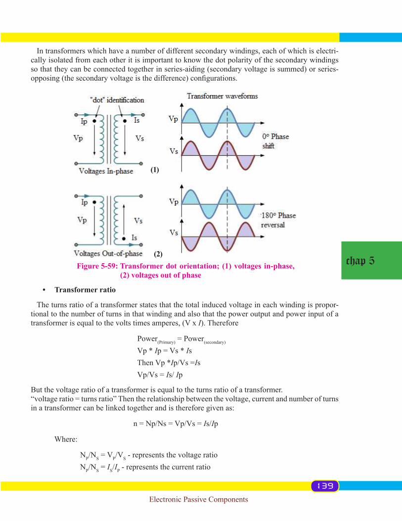
Electronic Passive Components
chap 5
In transformers which have a number of different secondary windings, each of which is electri-cally isolated from each other it is important to know the dot polarity of the secondary windings sothattheycanbeconnectedtogetherinseries-aiding(secondaryvoltageissummed)orseries-opposing(thesecondaryvoltageisthedifference)configurations.
• Transformer ratio
The turns ratio of a transformer states that the total induced voltage in each winding is propor-tional to the number of turns in that winding and also that the power output and power input of a transformer is equal to the volts times amperes, (V x I).Therefore
Power(Primary) = Power(secondary) Vp * Ip = Vs * Is Then Vp *Ip/Vs =Is Vp/Vs = Is/ Ip
But the voltage ratio of a transformer is equal to the turns ratio of a transformer. “voltage ratio = turns ratio” Then the relationship between the voltage, current and number of turns in a transformer can be linked together and is therefore given as:
n = Np/Ns = Vp/Vs = Is/Ip
Where:
NP/NS = VP/VS - represents the voltage ratio NP/NS = IS/IP - represents the current ratio
Figure 5-59: Transformer dot orientation; (1) voltages in-phase, (2) voltages out of phase
(1)
(2)
139

Electronic Passive Components
chap 5
Note that the current is inversely proportional to both the voltage and the number of turns. This means that with a transformer loading on the secondary winding, in order to maintain a balanced power level across the transformers windings, if the voltage is stepped up, the current must be stepped down and vice versa. In other words, “higher voltage — lower current” or “lower voltage — higher current”.
• Series and Parallel Connected Secondary Transformer
Voltage transformers can be connected to operate from power supplies of different voltage lev-els. For example, let’s say that the primary winding could have a voltage rating of 220/110V on the primary and 12/24V on the secondary. To achieve this, each of the two primary windings is, therefore, rated at 110V, and each secondary winding is rated at 12V. The transformer must be con-nectedsothateachprimarywindingreceivesthepropervoltage.Considerthecircuitfigure5-60.
Series Connected Secondary Transformer
In this example, the two 110V rated primary windings are connected together in series across a 220V supply as the two windings are identical, half the supply voltage, namely 110V, is dropped acrosseachwindingandthesameprimarycurrentflowsthroughboth.Thetwosecondarywind-ings rated at 12V, 2A each are connected in series with the secondary terminal voltage being the sum of the two individual winding voltages giving 24 Volts. As the two windings are connected in series,thesameamountofcurrentflowsthrougheachwinding,thenthesecondarycurrentisthesame at 2 Amps. So for a series connected secondary, the output in our example above is rated at 24Volts,2Amps.Considertheparallelconnectedtransformeroffigure5-61.
Parallel Connected Secondary Transformer
Here we have kept the two primary windings the same but the two secondary windings are now connected in a parallel combination.
As before, the two secondary windings are rated at 12V, 2A each, therefore the secondary termi-nal voltage will be the same at 12 Volts but the current adds. Then for a parallel connected second-ary, the output in our example above is rated at 12 Volts, 4 Amps.
Figure 5-60: Series connected secondary transformer
140

Electronic Passive Components
chap 5
• Transformer testing
Transformers are key electrical components in power supplies and electronic circuits. Though, they are reliable and have no moving parts, sometimes transformers fail, rendering the equipment it powers inoperable where they need to be tested. Different methods can be used to test home ap-pliances’ transformer functionality. Some simple and reliable methods are described below.
If you suspect a miss function of a transformer in a part of equipment, you can carry out a simple test with a function generator that checks the transformer’s basic functions. The function genera-tor’s ac signal tests the integrity of the primary and secondary windings; broken wires or shorts inside the transformer will produce no output. The method is safe as it avoids the high voltages usually present inside electronic equipment.
Part list
No Item Specification 1 5V/50Hz ac supply Function generator 2 Voltmeter Digital multimeter
Procedure
1. Disconnect the equipment containing the transformer from the wall outlet, if the trans-former is in a circuit.Turn the function generator on and set its frequency to 50 Hz.
2. Touch the digital multimeter’s probe tips to the function generator’s output. Set the multi-meter to read AC volts.
3. Set the function generator’s signal amplitude to 5 volts by monitoring the multimeter’s dis-play as you adjust the function generator’s amplitude control. Disconnect the multimeter from the function generator.
4. Connect the function generator’s output to the transformer’s two primary wires. 5. Touch the multimeter’s probe tips to the transformer’s two secondary wires. A good isola-
tion transformer reads about 5 volts AC on the meter. A good step-down transformer pro-duces from 100 millivolts to 1 volt AC, depending on its rated output voltage.
Figure 5-61: Parallel connected secondary transformer
Experiment 5-15: Test a transformer by using a function generator (ac source)
141

Electronic Passive Components
chap 5
If the output reads only a few millivolts or less on the multimeter, the transformer is faulty.
Checking a transformer for its proper operation can be conducted by using voltmeter to test the voltage presence. The transformer can be divided into two parts. The supply voltage or primary which is usually high voltage for step-down transformer, and the secondary or low voltage. What we need to determine is that we are getting correct supply voltage according to the transformer specificationsandthesupplyvoltagefromnetwork.
Figure 5-62: Testing transformer form a function generator
Experiment 5-16: Test transformer from wall outlet socket
142

Electronic Passive Components
chap 5
Part list
No Item Specification 1 Voltmeter Digital multimeter2 Transformer 220V/12V, 50Hz, 1A Transformer
Procedure
1. Set the multimeter to read AC volts at a scale equivalent to the highest voltage you are expecting to measure. The next scale higher than 220 volts AC on a lot of meters is 600. Most digital multimeters have a dial to turn for the different settings and scales them, use this dial to set to the desired range except if you are using auto range multimeter. Make surethatthereadleadofmultimeterisconnectedonVΩjackandblackleadtotheCOMjack of multimeter.
2. Test incoming voltage from wall outlet socket. If no voltage is present in either case you have a bad breaker or voltage has became interrupted somewhere along the way and needs to be repaired. If voltage is present you should read about 220 volts ac on your meter. Then you have proper supply voltage and now you can test your transformer.
3. Locate the transformer wires. You should be able to read transformer’s main plate infor-mation in order to know which wires are for primary and that of the secondary windings otherwise you can damage your transformer. Some transformer have color-code on their lead which can help to indentify the wires but let us refer on a transformer where the color code has faded to the point as to be unreadable. The supply voltage wires coming from the transformer can be of many colors; the most common for a 220 volt ac transformer supply voltage is black and white, the black being the hot wire and the white being the neutral common wire or, black and red with red as live wire. If the indication on main plate is +, 0,-,(220V/6-0-6forexample)thisisacentretappedtransformerwherethe3wireswhichhave continuity are for secondary windings and the remaining two wires having the con-tinuity are for primary winding. If the indication on the main plate of a transformer is not readablerefertothewindingsection.Thewindingwiththin(small)sectionisforprimarysupplying voltage 220V while the winding with big section is for secondary, 12VAC for this experiment. Transformer windings have a phase relationship, but it is typically not im-portant for power supplies. Unless one of the wires has continuity to the transformer core, the polarity doesn’t matter.
4. Connect the primary of a transformer on the wall outlet socket.
AC voltage settings
Dial(selector)
143

Electronic Passive Components
chap 5
5. Set the multimeter to read 12 volts AC and connect the leads of multimeter to the secondary winding of a transformer and observe the reading on multimeter. The reading should be at about 12V. If the reading is 11V or 13V there everything is good up to the transformer. If there is no power go further back on the line and measure the voltage. Keep going until youfindvoltage.Lookfortheproblembe-tween the point with the voltage and the last point checked that had no voltage. If there is no voltage there then the transformer itself is faulty and you need to replace the trans-former.
This test should only be done by an experienced person familiar with electricity.
Safety point
Figure 5-63: Testing transformer from wall outlet socket real
144

Electronic Passive Components
chap 5
Inspect Transformer Visually
Overheating, which causes the internal wiring of the transformer to run at elevated temperatures, is a common cause of transformer failure. Whenever a winding has shorted turns, applying full input voltage may spell disaster in the form of a smoking transformer. If the transformer exterior is swelling or shows what appear to be burn marks, don’t waste your time by testing the transformer. This is the sign that shows you that the transformer is burnt and can not work.
Transformers are key electrical components in power supplies. Transformers change the volt-age of the system to suit the electronics equipments. Step-down transformers are found in electric power company systems and in a multitude of appliances for household and industrial uses. Size ranges are found from a cell phone charger up to one the size of power house equipment to the end of a high voltage transmission line. For standard household transformer testing a digital multime-ter(DMM)makesagoodtest.
Part list
No Item Specification 1 Voltmeter Digital multimeter2 DC power supply motherboard 220V/12V, 50Hz, 1A Transformer
Procedure
1. Determine the wiring of the transformer. The transformer should be clearly labeled. How-ever, it is always best to obtain a schematic of the circuit containing the transformer to determine how the transformer is connected. The schematic for the circuit will be available in the product documentation or on the website of the circuit manufacturer.
2. Identifythetransformerinputsandoutputs.Thefirstelectricalcircuit,whichisgenerat-ingthemagneticfield,willbeconnectedtotheprimaryofthetransformer.Thevoltagebeing supplied to the primary should be on both the transformer label and the schematic. Thesecondcircuitthatisreceivingpowerfromthemagneticfieldwillbeconnectedtothesecondary of the transformer.
Experiment 5-17: Test transformer from a circuit
145

Electronic Passive Components
chap 5
The voltage being generated by the secondary winding should be on both the transformer label and the schematic.
3. Determinetheoutputfiltering.Itiscommontoattachcapacitorsanddiodestothetrans-formersecondarytoshapetheACpowerfromtheoutputintoDCpower.Thisfilteringandshapingwillnotbeavailablefromthetransformerlabel.Thefilteringandshapingwillbeshown on the schematic.
Figure 5-64: Schematic circuit diagram of an AC-DC power supply +12VDV and +9VDC
Figure 5-65: Input and output of an AC-DC +12VDC, +9VDC supply
146

Electronic Passive Components
chap 5
4. Prepare to measure circuit voltages. Remove covers and panels as necessary to gain access tothecircuitsthatcontainthetransformer.Acquireadigitalmultimeter(DMM)totakethevoltagereadings.Arrangethemultimeter’sleadwithredleadconnectedtoVΩjackandblack lead connected to COM jack of multimeter.
5. onfirmproperinputtothetransformer.Applypowertothecircuit.UsetheDMMinACmode to measure the transformer primary voltage. Set multimeter to read AC voltage at 600V scale. If the measurement is less than 80 percent of the expected voltage, the fault could lie in either the transformer or the circuitry providing the primary with power. In this case, the primary must be separated from the input circuit. If the input power (not thedisconnectedtransformerprimary)climbstotheexpectedvalue,thentheprimaryofthe transformer is faulty. If the input power does not go up to the expected value, then the problem lies not with the transformer, but with the input circuitry.
Figure 5-66: Locating different parts of an AC-DC power supply’s motherboard
147
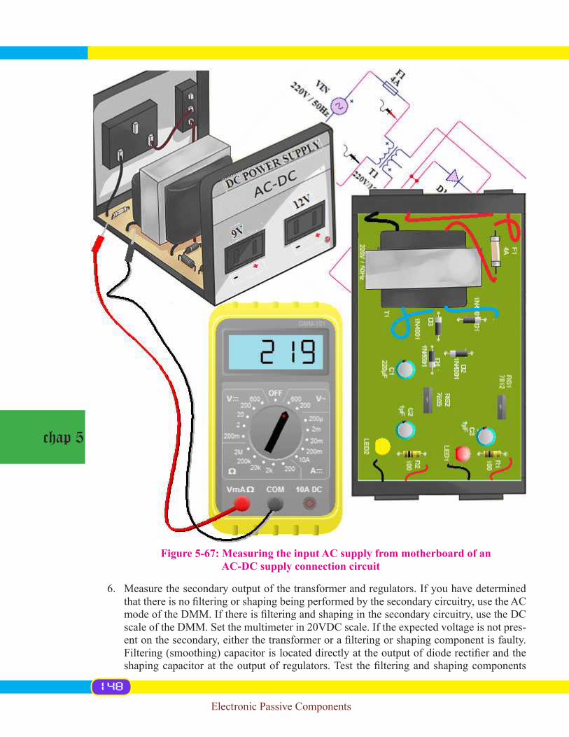
Electronic Passive Components
chap 5
6. Measure the secondary output of the transformer and regulators. If you have determined thatthereisnofilteringorshapingbeingperformedbythesecondarycircuitry,usetheACmodeoftheDMM.Ifthereisfilteringandshapinginthesecondarycircuitry,usetheDCscale of the DMM. Set the multimeter in 20VDC scale. If the expected voltage is not pres-entonthesecondary,eitherthetransformerorafilteringorshapingcomponentisfaulty.Filtering(smoothing)capacitorislocateddirectlyattheoutputofdioderectifierandtheshapingcapacitorat theoutputof regulators.Test thefilteringandshapingcomponents
Figure 5-67: Measuring the input AC supply from motherboard of an AC-DC supply connection circuit
148

Electronic Passive Components
chap 5
separately.Ifthetestingofthefilteringandshapingcomponentsshowsnoproblems,thenthe transformer is faulty and needs to be replaced.
• Identifying Transformer Windings
Most of technician who repair vintage electronic equipments, it is not unusual to have several power transformers that have either been removed from some old radio or other piece of equip-ment lying around. Due to the expense and availability of new power transformers, it would be nice to identify the windings and voltages of these spare units so that they could be re-used.
Most of power transformers come with color-coding on their leads. If the color-coding on the leads is still readable then you only have to refer to the chart to determine the windings. But often thecolorcodingontheleadsofthesetransformershasfadedtothepointitisdifficultorimpos-sible to read the color code and know which winding. By using the procedures outlined here, you should be able to identify the windings so the next time you discover the transformer in the set you are about to restore is defective, perhaps one of those spare transformers will qualify as a replace-ment unit. On a transformer where the color code has faded to the point as to be unreadable, there
Figure 5-68: Measuring the output from motherboard of an AC-DC supply, real world circuit connection
149

Electronic Passive Components
chap 5
is a technique to identify the various windings. The ohm-meter is the test instrument we use to accomplish this task.
Below is a diagram of a typical power transformer. This one has a primary winding with a center tapped and a secondary winding also with a center tapped. The diagram gives the color code of the leads for each winding.
As can be seen from the diagram, each winding will have continuity from one lead of the wind-ing to the other, but there should be no continuity between different windings, i.e. primary and secondary winding. It is possible to have a secondary with multiple windings which provide differ-ent voltages. Also, each set of windings will have a resistance value determined by the number of turns and size of the wire. So we can use the ohm-meter to determine which leads have continuity and use the resistance reading to determine which winding is primary and that of secondary (low andhighvoltagewindings),broken,etc.
Part list
No Item Specification 1 Ohmmeter Digital multimeter2 Transformer 220-110V/6-0-6V, 50Hz, 2A Transformer
Procedure
1. Settheohmmeterto200Ωscalethatgivesthelowestohmsreading,andcalibratetheme-ter so when the test leads are shorted the meter reads zero ohms. The lowest reading scale is use as the windings will have very low resistance with exception of the high voltage wind-ing. Now pick one of the transformer leads and clip one test lead of the meter to that lead. With the other meter lead, begin checking the other transformer winding leads. Make sure thatthetransformerisnotconnectedtothesupplysystem.Whenyoufindtheotherleadofthe winding under test, the ohm-meter will show continuity.
2. Makeanoteof the resistance reading.With thefirst lead still attached, checkallotherleadstoseeifanyothersalsohavecontinuitywiththefirstlead.Ifso,makeanoteofthatreading also. If three leads have continuity, then this winding has a center-tap. Tag these
Figure 5-69: Identifying transformer windings
150
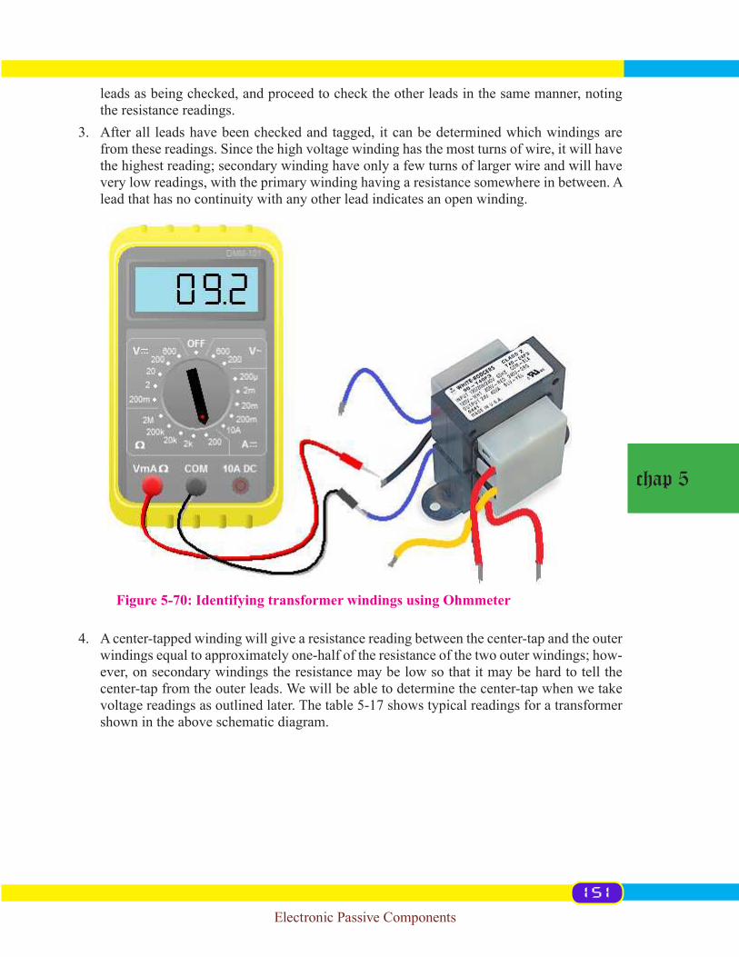
Electronic Passive Components
chap 5
leads as being checked, and proceed to check the other leads in the same manner, noting the resistance readings.
3. After all leads have been checked and tagged, it can be determined which windings are from these readings. Since the high voltage winding has the most turns of wire, it will have the highest reading; secondary winding have only a few turns of larger wire and will have very low readings, with the primary winding having a resistance somewhere in between. A lead that has no continuity with any other lead indicates an open winding.
4. A center-tapped winding will give a resistance reading between the center-tap and the outer windings equal to approximately one-half of the resistance of the two outer windings; how-ever, on secondary windings the resistance may be low so that it may be hard to tell the center-tap from the outer leads. We will be able to determine the center-tap when we take voltage readings as outlined later. The table 5-17 shows typical readings for a transformer shown in the above schematic diagram.
Figure 5-70: Identifying transformer windings using Ohmmeter
151

Electronic Passive Components
chap 5
Winding Resistance Corresponding Voltage
Primary 1st Ending terminal - center tapped 150Ω 110 VCenter-tapped – 2nd ending terminal 150Ω 110 V1st Ending terminal - 2nd ending terminal 300Ω 220 V
Secondary1st Ending terminal - center tapped 9Ω 6 VCenter-tapped – 2nd ending terminal 9Ω 6 V1st Ending terminal - 2nd ending terminal 18Ω 12 V
Note: These resistances are approximate. Readings may vary by several ohms from one trans-former to the next. The idea is not to be concerned with the exact resistance of the windings, but to identify the various windings by the difference in the resistance of the windings
Transformer Replacement
When replacing a transformer in household electronic equipments, consideration must be given to the power handling capabilities of the replacement unit. One rule of thumb is, if the replacement unit’s physical core size is as large or larger than the original, it will probably work. The true test howeverwillbeifthesecondaryvoltagesareuptospecificationsandtheunitdoesnotruntowarmwhen under operating conditions. A transformer should not be so warm that you cannot hold your hand on it after it has been operating for 20 to 30 minutes.
RMA (Radio Manufacturers Association)
Standard Power Transformer Lead Color CodeWinding Color code
Primary Both black if not taped, if tapped other winding may be red
Primarytap(optional) Black/YellowHigh-voltage secondary Red High-voltage Center-tap Red/YellowNo. 1 Secondary YellowNo. 1 Center-tap Yellow/BlackNo. 2 Secondary GreenNo. 2 Secondary Center-tap Green/YellowNo. 3 Secondary BrownNo. 3 Secondary Center-tap Brown/YellowNo. 4 Secondary Slate No. 4 Secondary Center-tap Slate/Yellow
Table 5-17: Examples of identifying the various windings by the difference in the resistance of the windings
Table 5-18: Standard Power Transformer Lead Color Code based on Radio Manufacturers Association.
152

Electronic Passive Components
chap 5
Note: The number of secondary windings can vary, and may or not be center-tapped. Windings that are center-tapped, the center-tap will carry the same color as the winding plus a yellow tracer. Theexceptionisthefive-voltrectifierwindingwherethecenter-tapwillcarrysomeothercolortracer such as black or blue.
Power Transformer Lead Color Codes
Old and NewWinding Old RCA Color Code New Color Code
Primary Red Black
Tapped primaryStart: Red Black Tap: Red and Black Black and YellowFinish: Black and Red tracer Black and Red
Rectifierfilament Green and Red tracer YellowFilament(secondary) Blue BrownHigh voltage Brown Red High voltage Center tap Brown and black Red and Yellow
Table 5-19: Old and new power transformer lead color codes
153

Diode Rectifier
chap 6
Objectives
When you have studied this chapter, you should
•Be able to test and to identify diode polarity•Have an understanding of the diode’s one direction conduction processes •Haveanunderstandingofdifferenttypesofrectifier,advantageanddisadvantageofeachtype•Haveanunderstandingofthewaytoimprovetherectifier’sefficiencywithsmoothingca-
pacitor •Haveanunderstandingofthediodespecificationsrequiredforanyrectifier•Beabletodesignrectifierforanyrequiredspecificationandvoltage
Arectifierisanelectronicdevicethatconvertsalternatingcurrent(AC)intodirectcurrent(DC).Theprocessisknownasrectification.Rectificationistheconversionofalternatingcurrent(AC),whichperiodicallyreversesdirection,todirectcurrent(DC),whichflowsinonlyonedirection.Thisinvolvesadevicethatonlyallowsone-wayflowofelectrons.Thisisexactlywhatasemicon-ductor diode does. TheinputofrectifyisanACcurrentthatalternatesinitsnature.Asresult,theprocessofrectifi-
cation alone produces a DC current that, though unidirectional, consists of pulses of current. Many applicationsofrectifiers,suchaspowersuppliesforradio,televisionandcomputerequipment,requireasteadyconstantDCcurrent(aswouldbeproducedbyabattery).Intheseapplicationstheoutputoftherectifierissmoothedbyanelectronicfilter(usuallyacapacitor)toproduceasteadycurrent.Therearedifferentformsofrectifiersincludingvacuumtubediodes,mercury-arcvalves,cop-
per and seleniumoxide rectifiers, semiconductor diodes, silicon-controlled rectifiers andothersilicon-basedsemiconductorswitches.Rectifiercircuitsmaybesingle-phaseormulti-phase(threebeingthemostcommonnumberofphases).Mostlowpowerrectifiersfordomesticequipmentaresingle-phase,butthree-phaserectificationisveryimportantforindustrialapplicationsandforthetransmissionofenergyasDC.Inthischapter,wewilldescribedifferentcircuits’configurationsofsemiconductordioderectifiersbasedaroundsinglephase.
Further readingStudy aids for this chapter are available at Lander,CyrilW.(1993).“2.RectifyingCircuits”.Powerelectronics(3rded.).London: McGraw-Hill.
Chapter six DiodeRectifier
154

Diode Rectifier
chap 6
Diodeisa two-terminalelectroniccomponentwhichallowselectricalcurrent toflowinonlyonedirectionandblockstheflowintheoppositedirection.Diodepresentsasymmetrictransfercharacteristic,withlow(ideallyzero)resistancetocurrentflowinonedirection,andhigh(ide-allyinfinite)resistanceintheother.Diodesmayberegardedasone-wayvalvesandtheyareusedinvariouscircuits,usuallyasaformofprotectionandrectification.Therearedifferenttypesofdiodebuttheirbasicfunctionsarethesame.Thefigure6-1showspackageandschematicsymbolof diode.
6. 1. Diode biasing
To bias a diode, we apply dc voltage across it. Mainly there are three methods of diode biasing: forward bias, reverse bias and zero bias. For zero bias no external dc voltage is applied to the diode thusinthefollowingsessionwearegoingtodiscussonthetwofirstbiasingmethods.
• Forward biasing
Forward bias is the condition that permits the current to pass through the diode. A dc voltage must be connected in direction to forward-bias the pn junction. The negative terminal of the bias-ing dc source must be connected to the n region (cathode) and the positive terminal connected to the p region (anode).
Connect the diode in the condition that allows the current to pass through the PN junction, a dc
voltage source connected by conductive material across a diode in the direction to produce forward bias. This external bias voltage is designated as V (Bias or B1).Theresistor(lamp),limitsthecur-rent to a value that will not damage the diode.
Part lists
No Items Specifications Quantity 1 Voltmeter Digital multimeter 12 Lamp Lamp 9V-10W 13 Wire 22-gauge (0.33mm2)solidwire 40cm4 Breadboard Prototypingboard(RSR03MB102) 15 Battery 9V dc supply 16 Diode 1N4001 1
Figure 6-1: Diode device package (1) , diode Schematic symbol (2)
Experiment 6-1: Diode forward and reverse biasing
155

Diode Rectifier
chap 6
Whentheanode(A)ispositiveandthecathode(K)isnegative(thoughtheload)currentwillflowthroughtheload,thediodeandbacktothepowersupplybattery(B1).Asdiodeismadefromsilicon, creates a voltage drop of approximately 0.6 to 0.75 Volts or more.
Thereadingonvoltmeteristhesupplyvoltageminusvoltagedropofthediode(9V-0.7V)andthecircuitlayoutisshowninfigure6-3.
Forward Voltage Drop
Electricity uses up a little energy pushing its way through the diode, rather like a person push-ing through a door with a spring. This means that there is a small voltage across a conducting diode, it is called the forward voltage drop and is about 0.7V for all normal diodes which are made
Figure 6-2: Diode forward biased current pass “Lamp ON”
Figure 6-3: Diode forward biased and lamp ON, circuit connection
156

Diode Rectifier
chap 6
from silicon. The forward voltage drop of a diode is almost constant whatever the current passing throughthediodesotheyhaveaverysteepcharacteristic(current-voltagegraph).
• Reverse bias
Whenthecathode(K)ofdiodeisconnectedatpositiveofpowersupplyandAnode(A)tonega-tiveofpowersupply,thediodeissaidtobereversebiased.Actuallynocurrentflowthroughtheloadandvoltageontheloadgoesacrosstozero(0Volt).
Whentheanode(A)isnegativeandthecathode(K)ispositivenocurrentwillflowthroughtheload(lampisOFF)thereforethereadingonvoltmeteriszero.
Normally, when a reverse voltage is applied to a perfect diode does not conduct, but all real di-odes leak a very small current of a few µA or less. This can be ignored in most circuits because it willbeverymuchsmallerthanthecurrentflowingintheforwarddirection.
Figure 6-4: I/V silicon diode characteristics
Figure 6-5: Diode Reverse biased no current pass “Lamp OFF”
157

Diode Rectifier
chap 6 However,alldiodeshaveamaximumreversevoltage(usually50Vormore)andifthisisex-ceeded the diode will fail and pass a large current in the reverse direction, this is called breakdown. Ordinary diodes can be split into two types: Signal diodes which pass small currents in order of 100mAorlessandRectifierdiodeswhichcanpasslargecurrents.
6. 2. Diode testing (Anode and Cathode identification)
Apart of eye inspection on the white color which determine the location of cathode, diodes can be tested using a multimeter. It is normally the resistance of the diode in both forward and reverse directions that is tested. There are however a number of points to remember when testing diodes.
Being digital and analogue multimeters are suitable for diode testing, and in many cases will have a special “diode check” range usually marked with a diode symbol. This range is most often used when testing diodes or any other semiconductor device. The importance for this is that the meter tests the diode by applying a voltage across the diode junction. The normal voltages used by the meter on other resistance ranges will not be high enough to overcome the diode’s forward junc-tion potential and so will not make the diode conduct, even in the forward direction. This would giveanindicationthatthediodewasopencircuit(veryhighresistance).Ifthedioderangeisused,the test voltage applied by the meter will be high enough to overcome the forward junction poten-tial and the diode will conduct. Therefore in the forward direction (meter positive lead to the anode andblackprobetocathodeofdiode)thediode’sresistancecanbemeasured.Theactualvaluewillvary from device to device and from meter to meter, so a precise value cannot be given. With a goodsilicondiodehowever,areadingintheforwarddirectionofabout1kΩcouldbeexpected,rather than germanium diodes.
Figure 6-6: Diode reverse biased and lamp OFF, circuit connection
158

Diode Rectifier
chap 6
Withthemeterleadsreversed,anoutofrange(infinity)oropencircuitreading(usuallyindicatedbyadisplaysomethinglike“1.”onadigitalmeter)shouldbeexpected.
Beingabletodeterminethepolarity(cathodeversusanode)andbasicfunctionalityofadiodeisa very important skills for the electronics technician. Normally a diode behaves like one-way valve for electricity; this implies that we should be able to verify its one-way working.
1st method: using ohmmeter
Part lists
No Items Specifications Quantity 1 Ohmmeter Digital multimeter 12 Diode 1N4001 1
When test a diode using Ohm’s range, there are a number of things to remember:• Makesureyouareusingtheohm(Ω)range.• Using a digital meter, connect the black lead to the cathode and red to the anode
(forwardbias-around1kΩ).
• Reversethemeterconnections(reversebias-infinityreading).
Note:- If you are using an analogue meter the above polarities, on second point, are reversed.- To determine which end of the diode is either the cathode or anode, you must know with
sureness which test lead of the multimeter is positive and which is negative. With most digital multimeters, the red lead is used as positive and the black lead as negative.
Low resistance indicates forward bias when black lead is connected to the cathode and red lead to anode of diode. Reversingleadsshowshighresistancetendingtotheinfinity“1.”indicatingreversebias.Atthis
time the red lead is connected to the cathode and the black lead to the anode of the diode. Ohm-meter connected this way across the diode, it should show a very high resistance (“OL” on some digitalmetermodels).
Beware that some digital multimeters equipped with a “diode check” function may output a very lowtestvoltage(lessthan0.3volts)whensettotheregular“resistance”(Ω)function:toolowtofully collapse the depletion region of a PN junction. The reason behind is that the “diode check” function is to be used for testing semiconductor devices, and the “resistance” function for anything else. By using a very low test voltage to measure resistance, it is easier for a technician to measure the resistance of non-semiconductor components connected to semiconductor components, since the semiconductor component junctions will not become forward-biased with such low voltages.
Experiment 6-2: Detemining diode polarity
159

Diode Rectifier
chap 6
Consider the example of a resistor and diode connected in parallel, soldered in place on a printed circuitboard(PCB),asshowninfigure6-8.Normally,onewouldhavetounsoldertheresistor
Figure 6-7: Determining the diode polarities using ohmmeter
Figure 6-8: Testing Diode in a circuit
160

Diode Rectifier
chap 6
fromthecircuit(disconnectitfromallothercomponents)beforemeasuringitsresistance,other-wise any parallel-connected components would affect the reading obtained. When using a multi-meter which outputs a very low test voltage to the probes in the “resistance” function mode, the diode’s PN junction will not have enough voltage impressed across it to become forward-biased, and will only pass negligible current. Consequently, the meter “sees” the diode as an open (no continuity),andonlyregisterstheresistor’sresistance.Ohmmeterequippedwithalowtestvoltage(lessthan0.7V)doesnotseethediodeallowingit
to measure parallel resistors.If such ohmmeter were used to test a diode, it would indicate a very high resistance (many kilo-
ohms)even ifconnected to thediode in the“correct”(forward-biased)direction. It isbetter tocheck the multimeter’s battery since the battery fail can lead to wrong value reading.
2nd method: using multimeter’s diode check
For the reason mentioned above, some digital multimeter manufacturers equip their meters with a special “diode check” function which displays the actual forward voltage drop of the diode in volts, rather thana “resistance”figure inohms.Thesemetersworkby forcinga small currentthrough the diode and measuring the voltage dropped between the two tests leads.
Part lists
No Items Specifications Quantity 1 Diode tester Digital multimeter with diode test function 12 Diode 1N4001 1
Meter with a “Diode check” function displays the forward voltage drop of 0.613 volts instead of a low resistance.
Figure 6-9: Determining diode polarities by us-
ing diode check function
161

Diode Rectifier
chap 6
The forward voltage reading obtained with such a meter will typically be less than the “normal” drop of 0.7 volts for silicon and 0.3 volts for germanium, because the current provided by the meter is of trivial proportions.
3rd method: using DC supply
This method is used when a multimeter with diode-check function is not available, or you would like to measure a diode’s forward voltage drop at some non-trivial current.
Part lists
No Items Specifications Quantity 1 Voltmeter Digital multimeter 12 Diode 1N4007 13 Resistor 68Ω 14 Battery AAcellBattery(2)or3VDCSupply 15 Breadboard Prototypingboard(RSR03MB102) 1
Connecting diode in the forward bias, anode to the positive and cathode to the negative termi-nal of the battery, the voltmeter reads the diode voltage drop of about 0.6V to 0.7V.
But on other hand, connecting the diode backwards to this testing circuit will simply result in the voltmeter indicating the full voltage of the battery.
Figure 6-10: Determining diode polarity by using forward DC voltage, volt-meter indicates diode voltage drop of about 0.7V
162

Diode Rectifier
chap 6
Figure 6-11: Circuit connection for determining diode polarity by using forward DC voltage, voltmeter reads diode voltage drop of about 0.7 V
Figure 6-12: Determining diode polarity by ......................using reverse DC voltage, voltmeter
indicates supply voltage
A special type of diode that makes use of the depletion region capacitance is the varactor. It is used as vari-able capacitor in which the capacitance is controlled by the reverse-bias voltage. By increasing or decreasing the reverse voltage, you can in-crease or decrease the capac-itance.
Hands on tip
163

Diode Rectifier
chap 66. 3. Rectifiers
Arectifierisanelectroniccircuitthatconvertsalternatingcurrent(AC),whichperiodicallyre-versesdirection,todirectcurrent(DC),whichflowsinonlyonedirection.Theprocessisknownasrectification.MostofelectronicdevicesuseDCordirectcurrent.Adiodeisasolid-statedevicewhichhastheactionofallowingthecurrenttoflowinonlyonedirectionfromanalternatingcur-rentandthisformarectifiercircuit.Thereareanumberofdifferentconfigurationsofdioderecti-fiercircuitthatcanbeused.Thesedifferentconfigurationseachhavetheirownadvantagesanddisadvantages, and are therefore applicable to different applications.
6. 3. 1. Half Wave Rectifier
AhalfwaverectifierisanelectroniccircuitwhichconvertstheincomingAlternatingCurrent(AC)inputpowerintoaDirectCurrent(DC)outputpowerbyjust blocking one half cycle of each complete sine wave and allows through the other. Thisisthesimplestformofrectifierwhichoftenuses only a single diode.Theprimaryofthetransformer(VP1)isconnectedtotheACsupply.Thisinducesanacvoltage
(VS)acrossthesecondaryofthetransformer.Duringthepositivehalfcycleoftheinputvoltagethe polarity of the voltage across the secondary forward biases the diode.
Figure 6-13: Circuit connection for Determining diode polarity by using reverse DC voltaget, voltmeter indicates supply voltage
164

Diode Rectifier
chap 6
Half Wave Rectifier Circuit Principle
The output voltage waveform is pulsed since at negative half cycle the diode is in reverse and does not allow the current to follow through the load. The input and output voltages waveforms areshowninfigure6-15.
Working Principle of the Half Wave Rectifier
During each “positive” half cycle of the AC sine wave, the diode is forward biased as the anode ispositivewithrespecttothecathoderesultingincurrentflowingthroughthediode,loadresistorand back to the supply.
During each “negative” half cycle of the AC sinusoidal input waveform, the diode is reverse biasedastheanodeisnegativewithrespecttothecathode.Therefore,nocurrentflowsthroughthediodeorcircuit.Theninthenegativehalfcycleofthesupply,nocurrentflowsintheloadresistoras no voltage appears across it, therefore Vout = 0.WhentheDCloadisresistive,thecurrentflowingintheloadresistorisproportionaltothevolt-
age, and the voltage across the load resistor will therefore be the same as the supply voltage. ThecurrentontheDCsideofthecircuitflowsinonedirectiononlymakingthecircuitunidirec-
tional. Thus, the load resistor receives from the diode a positive half of the waveform, zero volts, a positive half of the waveform, zero volts, etc.The equivalent DC voltage, VDC across the load resistor is calculated as follows:
The value of the voltage across the load resistor is equal in value to an equivalent DC voltage of 0.318 x Vmax of the input sinusoidal waveform or 0.45 x Vrms of the input sinusoidal waveform.
Figure 6-14: Half Wave Rectifier Circuit
Figure 6-15: Half Wave Rectifier waveform
165

Diode Rectifier
chap 6
Vdc = Vmax/π=0.318Vmax= 0.45Vs
Where: Vmax: The maximum or peak voltage value of the AC sinusoidal supply, VS:TheRMS(RootMeanSquared)valueofthesupply,Vdc:TheDCvoltageoftheoutputofrectifier.
Designahalfwaverectifierwith9Vasinputvoltageand220Ωasloadresistor.Calculatethepeak input voltage Vin(max) and the output voltage Vdc applied on load resistor. By using oscillo-scope measure the output voltage and compare it with what you have calculated.
Part lists
No Items Specifications Quantity1 Oscilloscope Agile oscilloscope 54622D 12 Diode 1N4001 13 Resistor 220Ω 14 9VAC supply Agilent Function generator 33120A 15 Breadboard Prototypingboard(RSR03MB102) 16 Wire 22-gauge (0.33mm2)solidwire 40cm
The sinusoidal input supply voltage V1 is connected to CH1 of the oscilloscope while the output voltage is connected to CH2 of the oscilloscope.
Vmax = (Vin*√2)-0.7V=(9V*1.414)-0.7V=12.0279V
Figure 6-16: Halfwave rectifier waveform pictured from oscilloscope
Experiment 6-3: Half wave Rectifier
166

Diode Rectifier
chap 6
VR1= Vdc=Vmax/π
= 12.0279V/3.14 = 3.83V
Procedure and Working PrincipleDuring the positive half cycle of the input voltage the diode is forward biased and the current is
diverted to the load. On the other hand, the negative half cycle of the input voltage the polarity of voltage gets reversed as a result, the diode is reverse biased. Practicallywhendiodeisreversedbiasednocurrentflowsthroughthecircuitandalmostnovolt-
age is developed across the resistor. All input voltage appears across the diode itself, thus the cur-rentwillflowonlyinthepositivehalf-cycle(0to180degrees)andthediodewillshut-offduringthe negative half-cycle from 180 degrees to 360 degrees. The period of a sine wave from 0 degrees to 360 degrees equals the inverse of the input frequency (1/Fin).
In the case of 50 Hertz it is: 1/50 = 20 mSec.This implies that when the input voltage is going through its positive half cycle, output voltage
is almost the same as the input voltage despite the diode voltage drop and during the negative half cycle no voltage is available across the load. This explains the unidirectional pulsating dc wave-form obtained as output. This is why we get very poor power transfer with the diode off during the negative half-cycle and the positive half-cycle changing constantly between zero volts and peak. Note that Vmax is equal to Vpeak .
Principally when rectifying an alternating voltage we wish to produce a “steady” and continuous DC voltage free from any voltage variations or ripple. One way of doing this is to connect a large value Capacitor across the output voltage terminals in parallel with the load resistor as shown be-low. This type of capacitor is known commonly as a “Reservoir” or Smoothing Capacitor.
Figure 6-17: Half wave rectifier circuit
167

Diode Rectifier
chap 6
Figure 6-18: Half wave rectifier circuit connection
168

Diode Rectifier
chap 6
Half wave Rectifier with Smoothing Capacitor
During the positive first quater-cycle of the input, the diode is forward-biased, allowing thecapacitor to charge to approximately the diode drop of the input peak. When the input begins to decrease below its peak, the capacitor retains its charge and the diode becomes reversed-biased.
During the remaining part of the cycle, the capacitor can discharge only through the load re-sistance at a rate determined by the RLC time constant. The larger the time constant, the less the capacitor will discharge.
A word of caution.
When constructing these circuits observe capacitor polarity and diode polarity. The voltage rat-ings of the capacitors should exceed the expected peak voltage by 50%.
Also note the current ratings of the transformers and diodes.
Designahalfwaverectifierwith9Vasinputvoltageand220Ωasloadresistorandinsertthecapacitor in parallel with load. Calculate the peak input voltage Vin(max) and the output voltage Vdc applied on load resistor without capacitor. Insert a capacitor and measure Vout using oscilloscope.
Part lists
No Items Specifications Quantity1 Oscilloscope Agile oscilloscope 54622A 12 Diode 1N4001 13 Resistor 220Ω 14 9VAC supply Agilent Function generator 33120A 15 Breadboard Prototypingboard(RSR03MB102) 16 Wire 22-gauge (0.33mm2)solidwire 40cm7 Capacitor 47µF/50V 18 Capacitor 470µF/50V 1
Experiment 6-4: Half wave rectifier with smoothing capacitor
Figure 6-19: Half wave Rectifier with Smoothing Capacitor
169

Diode Rectifier
chap 6
Infigure6-19,weinserteda47µF/50Vcapacitoracrosstheload.Thecapacitorchargesduringthe positive half-cycle, then discharges through the load during the negative half-cycle since no currentflowthroughthediode.Theamountofrippleisdependentontheresistanceoftheloadandthe value of the capacitance used.
A small capacitor produces a number of ripples or a low resistance load (drawing high current thuslesstimeforthecapacitortodischarge)willnotbereduceenoughthelevelofripplesbecausethe capacitor has less time to discharge.
A larger capacitor produces less ripples or a higher resistance load (drawing less current thus enoughlargetimeforthecapacitortodischarge)willreducethelevelofripplebecausetheca-pacitorhassufficienttimetodischarge.Withnoloadatall,justthecapacitorandtherectifier,thecapacitor will charge to peak and will hold the charges until it gets the load to discharge through. Theresultingwaveformisshowninfigure6-20.
Whenrectificationisusedtoprovideadirectvoltagepowersupplyfromanalternatingsource,the amount of ripple can be further reduced by using larger value capacitors but there are limits bothoncostandsize.Foragivencapacitorvalue,agreaterloadcurrent(smallerloadresistor)willdischarge the capacitor more quickly (RC TimeConstant)andsoincreasestherippleobtained.Replacecapacitorwithlowcapacitance(47µF)withacapacitoroflargecapacitance(470µF)asshowninthecircuitfigure6-22.
Figure 6-20: Waveform of Half wave Rectifier with smoothing capacitor and with high or removed load resistance
A diode is sometimes used to isolate two power sources such as in the case of a battery backup for a computer system. The power from the power supply is connected through a series diode to the power input point on the system. A battery backup system is connected to the same point through its own series diode. The battery backup is set for s slightly lower voltage so that it does not discharge the battery during normal operation. When a power failure occurs, the battery backup system takes over and the diodes prevent the two power sources from affecting each other.
Hands on tip
170

Diode Rectifier
chap 6
Figure 6-21: Half wave Rectifier with Smoothing Capacitor, circuit connection
171

Diode Rectifier
chap 6
Even if the amount of ripples is reduced notwithstanding that are not removed completely to get asteadydirectcurrent.Thisiscausedbyexcessofripplesofasinglephasehalfwaverectifier.Theresultingimprovementoftheoutputwaveformisshownontheoscilloscopefigure6-23.
Inpractice,thehalf-waverectifierismostusedinlow-powerapplicationsbecauseoftheirmajordisadvantages. The output amplitude is less than the input amplitude, there is no output during the negative half cycle so a half of the power is wasted and the output is pulsed DC resulting in exces-
Figure 6-22: Circuit for Half wave rectifier with a large capacitor
Figure 6-23: Half wave rectifier with a large capacitor waveform
172

Diode Rectifier
chap 6
sive ripple. To overcome these disadvantages a number of Power Diodes are connected together to produceaFullWaveRectifierasdiscussedinthenexttutorial.
Even though the capacitor is made high to reduce the ripples, the output voltage represents changes(ripples)whicharenotconvenienttotheelectronicequipmentslikecomputer,printer,TV,etc..Thisleadstotheuseofabridgerectifier(Full-waverectifier).
The advantage of this circuit is its simplicity; the drawback is the fact that there is long interval betweensuccessivepeaksoftherectifiedsignal.Thismakessmoothinglesseffectiveandmoredifficulttoachievehighlevelripplerejection.
Half wave Rectifier Advantage and Disadvantage
Although,thehalfwaverectifiercircuitmaynotprovidethelevelofperformanceneededformanyapplications,itisthemoststraightforwardrectifiercircuitthatcanbeusedinrectification. Someoftheadvantagesanddisadvantagesofhalfwaverectifieraredescribedintable6-1.
Advantage Disadvantage
• Simplicity in design since it uses only one diode
• Excess of voltage variation and the output is pulsed.
• The output voltage is less than the input volt-age; there is no output during the negative half cycle so the half of the power is wasted.
• Requires large capacitor for smoothing which is expensive and big size.
6. 3. 2. Full Wave Rectifier
Full-waverectificationisanelectroniccircuitwhichconvertsincomingACcurrentpowerintoaDCoutputpowerbymakinguseofbothpolarities(positiveandnegativehalfcycle)oftheinputwaveform. Mainlytherearetwoformsoffullwaverectifiercircuitthatcanbeused;thefullwavebridgerectifierandthetwodiodesfullwavewithacentretappedtransformer. Each type has its own features and is suited for different applications.
• The Full Wave Bridge Rectifier
ThefullwavebridgerectifiercircuitusesfourdiodesinconfigurationthatlookslikeabridgeandismostoftencalledGraëtzBridge.Thistypeofrectifierismorewidelyusednowadays.Itoffersamoreefficientuseofthetransformeraswellasnotrequiringacentretappedtransformer.
Table 6-1: Advantage and disadvantages of half wave rectifier
173

Diode Rectifier
chap 6
Full Wave Bridge Rectifier Circuit Configurations
Often four diode bridges can be bought as single items, making construction of the overall cir-cuit much simpler but their discrete construction is based on four diodes arrangement. The basic circuitsareoutlinedinfigure6-24:
Or
Working Principle of the Circuit
The four diodes labeled D1 to D4 are arranged in “series pairs” with only two diodes conducting current during each half cycle.
The Positive Half-cycle
During the positive half cycle of the supply, diodes D1 and D3 conduct in series while diodes D2 and D4arereversebiasedandthecurrentflowsthroughtheloadasshownbelow.Thearrowsshowconventionalcurrentflow.
Figure 6-24: (A) and (B), Full wave bridge rectifier schematic circuits
A
B
174

Diode Rectifier
chap 6
The Negative Half-cycle
During the negative half cycle of the supply, diodes D2 and D4 conduct in series, but diodes D1 and D3switch“OFF”astheyarenowreversebiased.Thecurrentflowingthroughtheloadisthesame direction as before.
Asthecurrentflowingthroughtheloadisunidirectional,sothevoltagedevelopedacrosstheloadisalsounidirectional.Theresultingwaveformisshowninfigure6-27.
Figure 6-25: Diodes of full wave bridge rectifier working during the positive half-cycle of AC supply
Figure 6-26: Diodes of full wave bridge rectifier working during the negative half-cycle of AC supply
When you view pulse waveforms on an oscil-loscope, set the scope to be DC coupled, not AC coupled. The reason is that AC coupling places a capacitor in series and can cause distortion in low-frequency pulse signals. Also, DC coupling allows you to observe the dc level of the pulse.
Hands on tip
175

Diode Rectifier
chap 6
The average DC voltage across the load is calculated as follow:
Vdc= Vav= (2Vmax)/π=0.637Vmax
Howeverinreality,duringeachhalfcyclethecurrentflowsthroughtwoseriesdiodesinsteadofjustonesotheamplitudeoftheoutputvoltageistwodiodevoltagedrops(2x0.7=1.4V)less than the input VIN(max) amplitude. It can be seen from the waveforms, that the fundamental frequencywithintherectifiedwaveformistwicethatofthesourcewaveform,therearetwiceasmanypeaksintherectifiedwaveform.The ripple frequency is now twice the supply frequency (e.g.100Hzfora50Hzsupply).
Bridge output voltage: As shown, the two diodes are always in series with the load resistor during both the positive and the negative half-cycles. Neglecting the barrier potential of the two diodes,theoutputvoltageisafull-waverectifiedvoltagewithapeakvalueequaltothepeaksec-ondary voltage of transformer once used.
Vpeak(out)=Vpeak(seccondary)
Althoughwecanusefourindividualpowerdiodestomakeafullwavebridgerectifier,pre-madebridgerectifiercomponentsareavailable“off-the-shelf”inarangeofdifferentvoltageandcurrentsizes that can be soldered directly into a PCB circuit board or be connected by spade connectors.
Fullwavebridgerectifierusesfourindividualrectifyingdiodesconnectedinaclosedloopcalled“bridge”configurationtogeneratethedesiredoutput.Thebridgerectifiercircuitdoesnotrequireaspecial centre tapped transformer, thereby reducing its size and cost. The single secondary winding is connected to one side of the diode bridge network and the load to the other side. Design a DC supplybasedonfullwaverectifiercapabletoproduce7VDConitsoutputterminal.Inexperiment,the secondary winding voltage of transformer is replaced by a function generator and the part list is given below.
Figure 6-27: Input waveform (a) and output of full wave bridge rectifier waveform (b)
Experiment 6-5: Full wave bridge rectifier
(b) (b)
176

Diode Rectifier
chap 6
Part lists
No Items Specifications Quantity1 Oscilloscope Agile oscilloscope 54622D 12 Diode 1N4001 43 Resistor 1.5KΩ,1/2watt 14 Function generator Agilent Function generator 33120A 15 Breadboard Prototypingboard(miniboard) 16 Connecting wire 22-gauge (0.33mm2)solidwire 40cm
Procedure and Working principle
Inthefigure6-28,D1 and D3 conduct during the positive half-cycle while D2 and D4 conduct dur-ingthenegativehalf-cycle.Powerdeliveredhereistwicethatofhalf-waverectificationbecausewe are using both half-cycles.
Using9voltsAC,wehave9X1.414or12.726voltspeak,(12.726volts).
The peak on load resistor is the two diode voltage drop less than the peak input voltage (12.726-1.4) that is11.326Volts.Now toget theaveragewemultiply thepeak (11.326volts)by0.637which equals 7.23 volts, double that of half-wave.
Figure 6-28: Full wave bridge rectifier circuit
When connecting protoboard circuits, always consistently use stan-dard colors for universal connections such as signals, power supply voltage, and ground. For example, you can use green wires for signals, red wires for power supply voltage, and black wires for ground con-nection. This helps you identify wiring during connecting and trouble-shooting.
Hands on tip
177

Diode Rectifier
chap 6
It should be noted that when this circuit is constructed the voltage on the meter will be about one volt lower. This is due to a 0.7 volt drop across the diodes, meter calibration due to the frequency change(from50Hzto100Hz),andcalculationerrors.
Figure 6-29: Full wave bridge rectifier, circuit connection
178

Diode Rectifier
chap 6
The Full Wave Bridge Rectifier with a Smoothing Capacitor
Thefull-wavebridgerectifiergivesusagreatermeanDCvalue(0.637Vmax)withlesssuper-imposed ripple while the output waveform is twice that of the frequency of the input supply fre-quency.Wecanuseasmallerfiltercapacitortocleanouttheripplethanweusedwithhalf-waverectification. We can therefore increase its average DC output level even higher by connecting a suitablesmoothingcapacitoracrosstheoutputofthebridgecircuitasshowninfigure6-30.
Tosmooththeoutputoftherectifierareservoircapacitorisusedandplacedacrosstheoutputoftherectifierandinparallelwiththeload.Thiscapacitorchargesupwhenthevoltagefromtherec-tifierrisesabovethatofthecapacitorandthenastherectifiervoltagefalls,thecapacitorprovidesthe required current from its stored charge. The capacitor used must be able to handle the output voltageofarectifier.ThisimpliesthatavoltageratingofacapacitorisgreaterthanVDC. The part list is given below.
Part lists
No Items Specifications Quantity1 Oscilloscope Agile oscilloscope 54622D 12 Diode 1N4001 43 Function generator Agilent Function generator 33120A 14 Breadboard Prototypingboard(miniboard) 15 Wire 22-gauge (0.33mm2)solidwire 50cm6 Resistor 1.5kΩ 17 Capacitor 47µF/50V 18 Capacitor 100µF/50V 1
When capacitor charges up as the supply voltage rises the only way discharge path for the ca-pacitor,apartfrominternalleakageisthroughtheloadtotherectifierorsmoothingsystem.Thediodespreventbackflowthroughthesupplysystemsuchastransformerorfunctiongenerator.
Figure 6-30: Full wave rectifier with a smoothing capacitor circuit principle
Experiment 6-6: Full wave bridge rectifier with filtering capacitor
179

Diode Rectifier
chap 6
By inserting 47µF/50V capacitor in parallel with the load resistor, the amount of voltage varia-tion is reduced but this voltage variation can still cause malfunction to the digital system which requiresasteadycurrent.Theresultingcircuitandwaveformareshowninfigure6-32.
Full Wave Rectifier with a Large Capacitance
Theresultingvoltagewaveformwith47µFcapacitordoesnotfulfillthedesireddirectcurrentform. On the discharge cycle of the smoothing capacitor, the capacitor needs to replace all the lost in ripple voltage up to the next charging with less as possible between the maximum and the fol-lowingchargingstart.Butitcanonlyachievethiswhenthevoltagefromtherectifierexceedsthatfrom the smoothing capacitor. This only occurs over a short period of the cycle. Consequently the current during this period is much higher. The large the capacitor, the better it reduces the ripple and the shorter the charge period.
Figure 6-31: Full wave bridge rectifier with a smoothing capacitor
Figure 6-32: Full wave bridge rectifier with a large capacitor
180

Diode Rectifier
chap 6
By increasing a largefiltering capacitor value, up to 100µF/50V, the signal becomes almoststeadyandtheaverageoutputvoltageisincreasedasshowninfigure6-34.
Figure 6-33: Full wave bridge rectifier with a smoothing capacitor circuit connection
181

Diode Rectifier
chap 6
Warning:
• Do not attempt to measure both the AC voltage on the secondary winding and the output voltage across the load resistor at the same time. You could create a ground loop that coulddestroyoneoftherectifierdiodes.
• Electrolytic capacitors are polarized. Pay attention to their polarity to avoid possible injury to you or to others and to avoid destruction of the device.
Full Wave Bridge Rectifier Advantages and Disadvantages
Eventhoughthefullwaverectifiercircuitrequiresmorediodesthanahalfwaverectifiercircuit,it has advantages in terms of utilizing both halves of the alternative input current waveform to provide the output.
Advantages Disadvantages
•Utilizes both positive and negative waves of the AC waveform of the input current
• Morecomplicatedthanhalfwaverectifier
•Requires small smoothing capacitor • The twice frequency hum on an audio circuit may be more audible
•The output voltage is almost equal to the input voltage despite the diode voltage drop
•Utilizes the whole secondary winding volt-age of a transformer
Figure 6-34: Full wave bridge rectifier with a large capacitor waveform
Table 6-2: Advantages and disadvantages of full wave bridge rectifier
182

Diode Rectifier
chap 6
Two-Diode Full Wave Rectifier
Thetwo-diodefullwaverectifierisanelectroniccircuitwhichconvertstheinputACcurrentintoaDCoutputcurrentbyusingcentertappedtransformer.Thetwo-diodefullwaverectifiercircuitwas widely used in the days of thermionic valves or vacuum tubes because it only required the use of two diodesasarectifiercircuitusingfourvalveswouldbelarge,thetwodiodeversionwasmuch more preferable. These could be encapsulated in one device, thereby reducing cost and size. Thebasicfullwaverectifiercircuitusingtwodiodesandacentretappedtransformerisshowninfigure6-35.
Thiscircuit,figure6-35,usestwodiodes,D1 and D2 , and it does need a center tapped trans-former.Thecurrentflowwithinthecircuitisrepresentedbyarrowsintheabovecircuitdiagram.Thisisusefulinseeinghowthecircuitoperatesandhowitisnotasefficientintermsofusageofthetransformer.Lookingatthecurrentflowdiagram,itcanbeseenthatcurrenteachhalfofthesecondarywindingisonlyusedofhalfthecycle.Thismakesforveryinefficientuseofthetrans-former in terms of cost and resources.
Working Plinciple of the Circuit
The primary of the transformer is connected to AC supply system. This induces the current in the secondary winding with voltage corresponding to the ratio of number of turns of the primary to the secondary winding.
Vs= Ns/Np*Vp
Where:Vs: Secondary winding voltageVp: Primary winding voltageNs: Number of turns of the secondary windingNp: Number of turns of the primary winding
Figure 6-35: Two-diode full wave rectifier circuit principle using centre tapped transformer
CurrentflowswhenD1 conducts
CurrentflowswhenD2 conducts
Vs=V(in1)+Vin(2)
183

Diode Rectifier
chap 6
The induced secondary voltage has the same frequency of the primary and is split into Vin(1) and Vin(2) with the common centre tapped connection. Each diode conducts in turn when its anode terminal is positive with respect to the transformer centre point C producing an output during both half-cycles.Thisfullwaverectifiercircuitconsistsoftwopowerdiodesconnectedtoasingleloadresistance
(RL)witheachdiodetakingitinturntosupplycurrenttotheload.At positive half cycle, anode of D1 is positive with respect to point C of a center tap, diode D1
conducts in the forward direction as indicated by the arrows. At negative half cycle, anode of D2 is positive with respect to point C, diode D2conductsintheforwarddirectionandthecurrentflowingthrough resistor R1 is in the same direction for both half-cycles. As the output voltage across the load resistor R1isthephasorsumofthetwowaveformscombined,thistypeoffullwaverectifiercircuit is also known as a “bi-phase” circuit. The average DC output voltage across the load resis-torisdoubleofthesinglehalf-waverectifiercircuitandisabout0.637Vmax of the peak voltage, assuming no losses.
Vdc = 2 Vmax/π = 0.637 Vmax = 0.9 Vrms
Where:
Vmax: The maximum peak value in one half of the secondary winding and Vrms: The root mean square value measured in one half of the secondary winding.
Thetwodiodesfullwaverectifierrequirestheuseofcentertappedtransformerandtwopowerdiodesaswell.Thistypeofrectifiergivesagreatmeanoutputvoltagewithrespecttothehalfwaverectifier.DesignaDCsupplycapabletoreplace3x1.5Vcellbatteriesofaradio.Listofitemstoconduct experiment on it is provided below.
Part lists
No Items Specifications Quantity1 Oscilloscope Agile oscilloscope 54622D 12 Diode 1N4007 23 Resistor 1KΩ 14 Transformer Center taped transformer 220/6-0-6; 50Hz 15 Breadboard Prototypingboard(RSR03MB102) 16 Connecting wire 22-gauge (0.33mm2)solidwire 40cm
A 220VAC/12VAC center tapped transformer is to be pluged to a 220VAC outlet. Normally a 12VAC of the secondary winding of a center tapped transformer splite into two equal voltages. Thissignifiesthattherootmeansquaretotherectifierinputsideis6V.
At the positive half cycle, D1 is forward biased while D2 is in reverse, therefore the current passes through the load resistor R1 back to the center tap.
Experiment 6-7: Two diodes full wave rectifier using centre tapped transformer
184

Diode Rectifier
chap 6
At negative half cycle, D2 is forward biased and D1 is in reverse, the current pass through the load resistor back to the center tap of a transformer as a result the unidirectional dc waveform obtained as output with twice the frequency of input. The circuit arrangement on breadboard is shwon in figure6-37.
The oscilloscope should be AC coupled to read the input waveform but should be DC coupled to read the output waveform.Thechanneloneofoscilloscopeisconnectedtotheinputofthedioderectifierwhilethechannel
oneisconnectedontheterminalofaloadresistor.Thepeakvalueoftheoutputrectifierdiodeis7.9V and the average voltage (Vdc)onloadresistoris4.87V.
Remember that diode voltage drop has to be taken in consideration in calculations. Normally diode voltage drop varies between 6.5 and 7.5. A 6Vrms without diode voltage drop gives:
Vmax=6*√2 =8.484V
With taking in account the diode voltage drop:
Vmax=(6*√2)-0.7 =7.784V
The average voltage is given by:
Vdc = 2 Vmax/π = 0.637*7.784 = 4.96 V(rms)
Note: The theory results differ a little bit to the practical results as it was shown in the above ex-periments. The reason behind is the use of imperfect devices.
Figure 6-36: Two diodes full wave rectifier circuit using centre tapped transformer
185

Diode Rectifier
chap 6
Figure 6-37: Two diodes full wave rectifier using centre tapped transformer, circuit connection
186
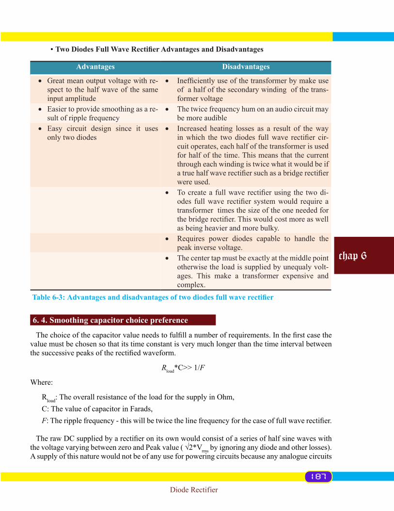
Diode Rectifier
chap 6
• Two Diodes Full Wave Rectifier Advantages and Disadvantages
Advantages Disadvantages
• Great mean output voltage with re-spect to the half wave of the same input amplitude
• Inefficientlyuseofthetransformerbymakeuseof a half of the secondary winding of the trans-former voltage
• Easier to provide smoothing as a re-sult of ripple frequency
• The twice frequency hum on an audio circuit may be more audible
• Easy circuit design since it uses only two diodes
• Increased heating losses as a result of the way inwhich the twodiodes fullwave rectifier cir-cuit operates, each half of the transformer is used for half of the time. This means that the current through each winding is twice what it would be if atruehalfwaverectifiersuchasabridgerectifierwere used.
• Tocreateafullwaverectifierusing the twodi-odes fullwave rectifier systemwould require atransformer times the size of the one needed for thebridgerectifier.Thiswouldcostmoreaswellas being heavier and more bulky.
• Requires power diodes capable to handle the peak inverse voltage.
• The center tap must be exactly at the middle point otherwise the load is supplied by unequaly volt-ages. This make a transformer expensive and complex.
6. 4. Smoothing capacitor choice preference
Thechoiceofthecapacitorvalueneedstofulfillanumberofrequirements.Inthefirstcasethevalue must be chosen so that its time constant is very much longer than the time interval between thesuccessivepeaksoftherectifiedwaveform.
Rload*C>> 1/F
Where:
Rload: The overall resistance of the load for the supply in Ohm, C: The value of capacitor in Farads,F:Theripplefrequency-thiswillbetwicethelinefrequencyforthecaseoffullwaverectifier.
TherawDCsuppliedbyarectifieronitsownwouldconsistofaseriesofhalfsinewaveswiththevoltagevaryingbetweenzeroandPeakvalue(√2*Vrmsbyignoringanydiodeandotherlosses).A supply of this nature would not be of any use for powering circuits because any analogue circuits
Table 6-3: Advantages and disadvantages of two diodes full wave rectifier
187

Diode Rectifier
chap 6
would have the huge level of ripple superimposed on the output, and any digital circuits would not function because the power would be removed every half cycle.
Ripple Voltage
Astherewillalwaysbesomerippleontheoutputofarectifierusingasmoothingcapacitorcir-cuit, it is necessary to be able to estimate the approximate value. Over-specifying a capacitor too much will add extra cost, size and weight under specifying it will lead to poor performance.
Half wave ripple voltage: Vripple = Iload/(fC)Full wave ripple voltage: Vripple = Iload/(2fC)
Theseequationsprovidemoresufficientaccuracy.Althoughthecapacitordischargeforapurelyresistive load is exponential, the inaccuracy introduced by the linear approximation is very small for low values of ripple. It is also worth remembering that once used, the input to a voltage regula-tor is not a purely resistive load but a constant current load. Finally, the tolerances of electrolytic capacitorsusedforrectifiersmoothingcircuitsarelargeupto±20%attheverybestandthiswillmask any inaccuracies introduced by the assumptions in the equations.
Ripple Current
Forapplicationswherelargelevelsofcurrentmayflow,asinthecaseofarectifiersmoothingcapacitor, a third parameter which is its maximum ripple current becomes an important factor. The ripple current is not just equal to the supply current. There are two circumstances:
• Capacitor Discharge Current
On the discharge cycle, the maximum current supplied by the capacitor occurs as the output fromtherectifiercircuitfallstozero.Atthispointallthecurrentfromthecircuitissuppliedbythecapacitor. This is equal to the full current of the circuit.
• Capacitor Charging Current
On the charge cycle of the smoothing capacitor, the capacitor needs to replace all the lost charge, butitcanonlyachievethiswhenthevoltagefromtherectifierexceedsthatfromthesmoothingcapacitor.
Maximum current
188
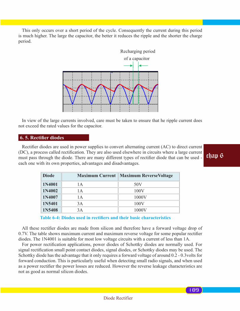
Diode Rectifier
chap 6
This only occurs over a short period of the cycle. Consequently the current during this period is much higher. The large the capacitor, the better it reduces the ripple and the shorter the charge period.
In view of the large currents involved, care must be taken to ensure that he ripple current does not exceed the rated values for the capacitor.
6. 5. Rectifier diodes
Rectifierdiodesareusedinpowersuppliestoconvertalternatingcurrent(AC)todirectcurrent(DC),aprocesscalledrectification.Theyarealsousedelsewhereincircuitswherealargecurrentmustpassthroughthediode.Therearemanydifferenttypesofrectifierdiodethatcanbeused-each one with its own properties, advantages and disadvantages.
Diode Maximum Current Maximum ReverseVoltage
1N4001 1A 50V1N4002 1A 100V1N4007 1A 1000V1N5401 3A 100V1N5408 3A 1000V
Alltheserectifierdiodesaremadefromsiliconandthereforehaveaforwardvoltagedropof0.7V.Thetableshowsmaximumcurrentandmaximumreversevoltageforsomepopularrectifierdiodes. The 1N4001 is suitable for most low voltage circuits with a current of less than 1A.Forpowerrectificationapplications,powerdiodesofSchottkydiodesarenormallyused.For
signalrectificationsmallpointcontactdiodes,signaldiodes,orSchottkydiodesmaybeused.TheSchottky diode has the advantage that it only requires a forward voltage of around 0.2 - 0.3volts for forward conduction. This is particularly useful when detecting small radio signals, and when used asapowerrectifierthepowerlossesarereduced.Howeverthereverseleakagecharacteristicsarenot as good as normal silicon diodes.
Table 6-4: Diodes used in rectifiers and their basic characteristics
Recharging period of a capacitor
189

Diode Rectifier
chap 6
6. 6. Rectifier diode requirements
Whendesigningarectifiercircuit,itiscompulsorytomakesurethatthediodeiscapableofpro-vidingtherequiredperformance.Whiletherearemanyparametersthatdefineindividualdiodes,and these may need to be taken into account for a given design, some of the major parameters are detailed below:
• Forward current:
It is obligatory that the diode is able to handle the levels of average current and maximum currentflowingthroughitinarectifiercircuit.Thecurrentwillhitthehighestpointasaresultofthecapacitorsmoothingcircuit.Asthecurrentonlyflowsasthecapacitorchargesup, the current is in short bursts which are much higher than the average current.
• Peak inverse voltage:
The diode must be able to reliably withstand the peak reverse or inverse voltages that appear across it. The peak voltages are not just the output voltage, but higher. The peak inversevoltageratingofthediodeshouldbeatleast2x√2timestheRMSvoltageoftheinput. This is because the output is normally smoothed by a capacitor, and this will take a valuethatisthepeakoftheinputwaveform.Thiswillbe√2timestheRMSvoltage.Withthis voltage on the output, the input waveform on the “blocked” half of the cycle will fall andreachapeakvalueatthebottomofthecrestof√2timestheRMSvalue.Themaxi-mumreversevalueseenacrosstherectifierdiodeisthesumofthesetwovoltages.
Thereshouldalsobeasignificantmargin,especiallywhenusedinamainsorlinepowersupply.This is because voltage spikes can appear on the line.
Application of Rectifiers
• Theprimaryapplicationof rectifiers is toderiveusableDCpower fromanACsupply.almostallelectronicdevicesrequireaDCsupplybutmainspowerisACsorectifiersfinduses inside the power supplies of virtually all electronic equipments.
•Converting DC voltage from one level to another is much more complicated. One method ofsuchDCtoDCconversionistofirstconverttoAC(usingadevicecalledaninverter),thenuseatransformertochangethevoltage,andfinallyrectifyitbacktoDC.
• Rectifiersalsofindauseindetectionofamplitudemodulatedradiosignals.Thesignalmayornotbeamplifiedbeforedetectionbutifunamplifiedaverylowvoltagedropdiodemustbe used. In this case the capacitor and load resistance must be carefully matched. Too low a capacitance will result in the high frequency carrier passing to the output and too high will result in the capacitor just charging and staying charged.
• Rectifiersarealsousedtosupplypolarizedvoltageforwelding.Insuchcircuitscontrolof the output current is required and this is sometimes achieved by replacing some of the diodesinbridgerectifierwiththyristors,whosevoltageoutputcanberegulatedbymeansofphasefiredcontrollers.
• Rectifiershavemanyuses,butareoftenfoundservingascomponentsofDCpowersup-pliesandhigh-voltagedirectcurrentpowertransmissionsystems.Rectificationmayservein roles other than to generate direct current for use as a source of power. In general, recti-
190

Diode Rectifier
chap 6
fiersreplacebatteriesandarefoundinradio,television,phonechargers,computerequip-ments and other electronics instruments that require DV voltage.
The diode forward V-I Characteristic curve can be plotted on the os-cilloscope using the circuit shown below. Channel 1 senses the voltage across the diode and channel 2 senses a signal that is proportional to the current. The scope must be in the X-Y mode. The signal generator provides a 5Vpp sawtooth or triangular waveform at 50Hz, and its ground must not be the same as the scope ground. Channel 2 must be inverted for the displayed curve to be propery oriented.
Hands on tip
Figure 6-38: Circuit used to plot the diode forward V-I Characteristic curve on the oscilloscope
Y inverted
191

Regulated DC Power Supply
chap 7
Objectives
When you have studied this chapter, you should
• Have an understanding of working principle of Zener diode• Be capable to design a supply with a constant DC voltage• Be able to describe different 3-terminal ICs voltage regulators• Be able to design dual polarity DC supply
7. 1. Voltage stabilization principle
Avoltagefromarectifiervarieswiththeload.Evenifthesmoothingcapacitorcanimprovethewaveformofarectifierbutastheresistanceofconnectedloadgetslow,theamountofripplesincreasessincethetimeofdischargingofacapacitor(RC)decreases.Thewaytoovercomethisbehavior is achieved by using a voltage stabilizer device such as Zener diode which provides a constant voltage over a wide range of power supply voltages. Presume we are requested to build a circuit which cannot tolerate variations in power supply voltage, but need to be powered by a chemical battery, whose voltage changes over its lifetime. We have to form a circuit as shown in figure7-1andconnectthecircuitrequiringsteadyvoltageacrossthediode,whereitwouldreceivean unchanging 0.7 volts.
Even though we connect a diode and resistor in series with a DC voltage source so that the diode is forward biased, the voltage drop across the diode will remain fairly constant over a wide range ofpowersupplyvoltagesasinfigure7-2.
Futher readingStudy aids for this chapter are available at the companion website• http://www.circuitstoday.com/regulated-power-supply• http://electrical4u.com/regulated-power-supply
Regulated DC Power SupplyChapter seven
192

Regulated DC Power Supply
chap 7
Thecircuitfigure7-2willwithoutdoubtwork,butmostpracticalcircuitsofthesamekindre-quireapowersupplyvoltageinexcessofdiodevoltagedrop(0.7V)toproperlyfunction.Onewaywe could increase our voltage regulation point would be to connect multiple diodes in series, so that their individual forward voltage drops of 0.7 volts each would add to create a larger total. For instance,ifwehadfivediodesinseries,theregulatedvoltagewouldbefivetimes0.7V(5*0.7V)thatis3.5V.Theequivalentcircuitisshowninfigure7-3.
Figure 7-1: One ordinary diode used as voltage stabilizer circuit
Figure 7-2: One ordinary diode used as voltage stabilizer circuit connection
193

Regulated DC Power Supply
chap 7
So long as the battery voltage never sagged below 3.5 volts, there will always be about 3.5 volts droppedacrossthefivediodeloadup.Wheneverlargerstabilizedvoltagesarerequired,wecaneither use more diodes in series, which takes a big size, or make another arrangement. From the circuitconfigurationabove,infigure7-3,itisshownthatdiodeforwardvoltageisfairlyconstantunder a wide range of conditions. But if we reverse the polarity of the diode in our single-diode sta-bilization circuit and increase the power supply voltage to the point where the diode “broke down” (couldnolongerwithstandthereversebiasvoltageimpressedacrossit),thediodewouldsimilarlystabilize the voltage at that breakdown point, not allowing it to increase further.
Figure 7-3: Five ordinary diodes used as voltage stabilizer
194

Regulated DC Power Supply
chap 7
Unfortunately, when normal rectifying diodes “break down,” they usually do so destructively. However, it is possible to build a special type of diode that can handle breakdown without failing completely. This type of diode is called a Zener diode.
7. 2. Zener diode
Zener diode is a general purpose diode, which behaves like a normal diode when forward biased, But when it is reverse biased above a certain voltage known as Zener breakdown voltage or zener voltage or avalanche point or zener knee voltage the voltage remains constant for a wide range of current.
DCpowersupplyconsistsonlyofatransformer,full-waverectifier,andfiltercapacitorareusedwith success in many practical applications. However, this basic circuit has several important disadvantages:
1. The capacitors required to reduce the ripple voltage to a small magnitude are physically large and expensive;
2. Even with minimal ripple, the output voltage can vary considerably due to AC line voltage fluctuations;and
3. Changes in load current can lead to changes in output voltage due to the voltage drops acrosstheinternalresistancesoftherectifierdiodesandtransformerwindings.
Thesedeficienciescanbeaddressedthroughtheuseofavoltageregulatorcircuit,whichmain-tains the output voltage of the power supply close to a predetermined level. Zener diodes, which exhibit very stable voltages across themselves when operated in their reverse breakdown regions, serve as simple yet effective voltage regulators in a wide range of applications.
Zener Diode I-V Characteristics
It is with this characteristic that makes the Zener diode useful as a voltage stabilizer. If a load is connected in parallel with the diode, and if the diode’s operating point is maintained in the reverse breakdown region, then the voltage across the diode, and therefore the voltage across the load, will remain very close to the Zener voltage.
Figure 7-4: Symbols of Zener diode
or
195

Regulated DC Power Supply
chap 7
Where:
VF: Forward bias voltage in Volts,VR: Reverse bias voltage in Volts,VZ: Zener breakdown voltage,IF: Current passing through a Zener diode when forward biased,IR: Current passing through a Zener diode when reverse biased without reaching breakdown,IZ: current through a Zener diode at its breakdown voltage.
For the proper designing of the Zener diode stabilizer you have to know:
• Unregulated Input Voltage Range• Required Output Voltage• Max Load Current Required
The Zener diode requires a series resistor Rs that limits the current that can damage the device. The value of Rs must be small enough to keep the Zener diode in reverse breakdown region. The minimum current required for a Zener Diode to keep it in reverse breakdown region will be given in its datasheet. For example, a 5.6 V, 0.5 W Zener diode has a recommended reverse current of 5 mA. If the reverse current is less than this value, the output voltage will be unregulated.
Figure 7-5: Zener Diode I-V Characteristics
196

Regulated DC Power Supply
chap 7
The value of Rs must be large enough so that the current through the zener diode should not de-stroy it. That is the maximum power dissipation (Pmax)shouldbelessthanIzVz.
ThusweshouldfindRs(min)and Rs(max).TofindthevalueofRs(min) we should consider the extreme condition that is Vin minimum and load current is maximum.
Is = Iz(min) + IL(max) Iz(min) = see Datasheet Vs = Vin(min) – Vz
Rs(min)= Vs/Is
TofindthevalueofRs(max) we should consider the extreme condition that is Vin maximum and loadcurrentisminimum(ie,noloadconnected).
Is = Iz(max) + IL(min) Iz(max) = Pmax/Vz
Vs = Vin(max) – Vz
Rs(max) = Vs/Is
Stabled Multiple Output Supply
Industrial applications generally require a number of outputs to supply Analog and digital low voltage circuitry. In a world where glamorous portable devices such as smart phones and tablet computers dominate the headlines, it is easy to forget that most consumer electronic products draw power from the mains supply. And yet, these products use the same sensitive silicon requir-ing stable, low-voltage power. Despite the fact that mains outlets around the world supply AC voltagesfrom90to264Vrunningatfrequenciesfrom47to63Hz,almostallofficeandhomeequipment cannot be plugged straight into a wall socket without some kind of power conversion. Motor Control applications often require several separately isolated outputs to supply half-bridge drivers and control circuitry. Typical consumer applications of these multiple output converters include Television and related products such as set- top decoders and Video cassette recorders (VCRs).Thisarticleexplainsthebasicsofpowerregulationinmains-powereddevices,fromtheline transformer that converts the high mains voltage to an isolated low voltage, through AC line rectificationmethodstoconverttheACvoltagetoDC,andthentotheDC/DCconverteroptionsthat supply the stable low-voltage outputs required by the electronics.
Some sub-circuits on motherboard require different voltage form a single DC supply. By con-necting Zener diodes in series, these share the same DC supply voltage and the individual Zener voltage sum up.
Build a power supply, based on Zener diodes and ordinary diodes, with four outputs where you can connect a load requiring 10V, 10.7V, 14V and 19.1V from 24V DC supply.
Experiment 7-1: Zener Diodes Series Connection (multi-output voltage)
197

Regulated DC Power Supply
chap 7
Part lit
No Items Specifications Quantity 1 Voltmeter Digital Multimeter 42 Zener diode Zener diode BZV55C10V0 13 Zener diode Zener diode BZV55-B3V3 14 Resistor 150Ω 15 Small signal diode 1N4148 16 Zener diode Zener diode BZV55-B5V1 17 Connecting Wire 22-gauge (0.33mm2)wire 30cm8 Breadboard Prototyping board 19 24VDC supply 24V DC power supply 1
Fromschematiccircuitfigure7-6,eachvoltmeterreadingiscapturedfromtheterminalwherearequestedvoltagetosupplyaspecificsub-circuitistakenfrom.Noworryfromvoltmeterreadingdeviation since Zener diodes are manufactured with zener voltages ranging anywhere from a few volts to hundreds of volts.
This zener voltage changes slightly with temperature, and like common carbon-composition resistor values, may be anywhere from 5 percent to 10 percent in error from the manufacturer’s specifications.However,thisstabilityandaccuracyisgenerallygoodenoughforthezenerdiodeto be used as a voltage regulator device in common power supply circuits.
Figure 7-6: Zener Diodes Series Connection (multi-output voltage) circuit
198

Regulated DC Power Supply
chap 7
Working Principle of the Circuit
The input B1isfromregulateddcvoltageandmustbehighenough(greaterthan22V)tomain-tain the required maximum voltage to be delivered. R1 serves as the input current limiter, and D1 to D4 as voltage regulators and each sets the desired output voltage on its terminal.
D4 outputs 10V on its terminals taken from ground and to its cathode.D3 outputs 10.7V (10V of the D4+0.7Vofthediodedropwhenforwardbiased)fromgroundto
its anode.D2 outputs 14V (10V of D4+0.7VofD3+3.3VofBZX55C,3V3zener)andthis14Vistaken
from ground to the cathode of D2.D1 outputs 19.1V (10V of D4 + 0.7V of D3 + 3.3V of D2+5.1VofBZX55C,5V1zener)andthis
19.1V is taken from ground to cathode of D1.
In practice these outputs voltage can deviate to a tolerable amount as indicated on voltmeters.The values of the individual Zener diodes can be chosen to suit the application while the silicon
diode will always drop about 0.6 to 0.7V in the forward bias condition. The supply voltage, Vin must of course be higher than the largest output reference voltage and in our example above this is 19.1V.
Series Resistor Requirements
The value of series resistor must satisfy two conditions:1. Theseries resistor (RS)mustbesmallenough that thecurrent through theZenerdiode
keeps it in reverse breakdown. The value of this current is given in the data sheet for chosen Zener type. For example, the common BZX79C5V6 device, a 5.6 V 0.5 W Zener diode, has a recommended reverse current of 5 mA. Whenever unsatisfactory current exists through Zener diode, then output voltage will be unregulated, and less than the nominal breakdown voltage. When calculating the series resistor value, allowance must be made for any current through the external load. This means that with a large series resistor most of power will be wasted through it and no current across the zener diode and so no regulation as shown infigure7-8.
An electronic power supply provides both output voltage and current. You should make sure the voltage range is suf-ficient for your applications. Also, you must have sufficient current capacity to assure proper circuit operation. The current capacity is the maxi-mum current that a power supply can provide to a load at a given voltage.
Hands on tip
To avoid electrical shock, never touch circuit while it is connected to a voltage source. If you need to han-dle a circuit, remove a component, or change a component, first make sure the voltage source is discon-nected.
Safety point
199

Regulated DC Power Supply
chap 7
2. ThelowseriesresistortoaspecificvalueallowsagreatcurrenttopassthroughaZenerdiode and this can destroy the device. If the current through the Zener diode is IZ, VZ its breakdown voltage and PMAX its maximum power dissipation, then IZ*VZ<PMAX.
Figure 7-7: Zener Diodes Series Connection (multi-output voltage), real world circuit connection
200

Regulated DC Power Supply
chap 7
To have a regulated output voltage requires to use a supply battery, here named B1, with hundreds volts which cannot happen.
A load may be placed across the diode in the circuit, and as long as the Zener stays in reverse breakdown, the diode will provide a stable voltage source to the load. Zener diodes in such con-figurationareoftenusedasstablereferencesformoreadvancedvoltageregulatorcircuits.
Shunt regulators require that the ballast resistor to be small enough to avoid excessive voltage dropduringworst-caseoperation(lowinputvoltageconcurrentwithhighloadcurrent)tendstoleavealotofcurrentflowinginthediodemuchofthetime,makingforafairlywastefulregulatorwith high quiescent power dissipation, only suitable for smaller loads.
Circuit Guidelines
The Zener diode is a very useful circuit component in DC voltage regulators. However, like any other electronic components, there are a few hints and tips which enable the best to be made of the Zener diode. A number are listed below.
• Choose correct voltage for best stability
In applications where stability with temperature changes is required, the Zener voltage reference diode should be chosen to have a voltage of around 5.5 volts. The nearest preferred value is 5.6 volts although 5.1 volts is another popular value in view of its proximity to 5 volts required for some logic families. Where different levels of voltage are required, the 5.6 volt Zener can be used and the surrounding electronic can be used to transfer this to the required output value.
• Buffer the Zener diode circuit with an emitter or source follower
TokeepthevoltagefromtheZenerdiodeasstableaspossible,thecurrentflowingthroughtheZener diode must be kept constant. Any variations in current drawn by the load must be minimized as these will change the current through the Zener diode and cause slight voltage variations. The changes caused by the load can be minimized by using an emitter follower stage to reduce the cur-rent taken from the Zener diode circuit and hence the variations it sees. This also has the advantage that smaller Zener diodes may be used.
Figure 7-8: Zener voltage stabilizer circuit with high series resistor
201
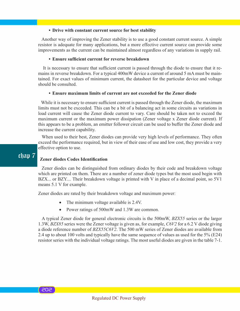
Regulated DC Power Supply
chap 7
• Drive with constant current source for best stability
Another way of improving the Zener stability is to use a good constant current source. A simple resistor is adequate for many applications, but a more effective current source can provide some improvements as the current can be maintained almost regardless of any variations in supply rail.
• Ensure sufficient current for reverse breakdown
Itisnecessarytoensurethatsufficientcurrentispassedthroughthediodetoensurethatitre-mains in reverse breakdown. For a typical 400mW device a current of around 5 mA must be main-tained. For exact values of minimum current, the datasheet for the particular device and voltage should be consulted.
• Ensure maximum limits of current are not exceeded for the Zener diode
WhileitisnecessarytoensuresufficientcurrentispassedthroughtheZenerdiode,themaximumlimits must not be exceeded. This can be a bit of a balancing act in some circuits as variations in load current will cause the Zener diode current to vary. Care should be taken not to exceed the maximumcurrentor themaximumpowerdissipation(ZenervoltagexZenerdiodecurrent).Ifthis appears to be a problem, an emitter follower circuit can be used to buffer the Zener diode and increase the current capability.
When used to their best, Zener diodes can provide very high levels of performance. They often exceed the performance required, but in view of their ease of use and low cost, they provide a very effective option to use.
Zener diodes Codes Identification
Zener diodes can be distinguished from ordinary diodes by their code and breakdown voltage which are printed on them. There are a number of zener diode types but the most used begin with BZX... or BZY.... Their breakdown voltage is printed with V in place of a decimal point, so 5V1 means 5.1 V for example.
Zener diodes are rated by their breakdown voltage and maximum power:
• The minimum voltage available is 2.4V. • Power ratings of 500mW and 1.3W are common.
A typical Zener diode for general electronic circuits is the 500mW, BZX55 series or the larger 1.3W, BZX85 series were the Zener voltage is given as, for example, C6V2 for a 6.2 V diode giving a diode reference number of BZX55C6V2. The 500 mW series of Zener diodes are available from 2.4uptoabout100voltsandtypicallyhavethesamesequenceofvaluesasusedforthe5%(E24)resistor series with the individual voltage ratings. The most useful diodes are given in the table 7-1.
202

Regulated DC Power Supply
chap 7
7. 2. 2. Zener Diode Standard Voltages
BZX55 Zener Diode Power Rating 500mW
2.4V 2.7V 3.0V 3.3V 3.6V 3.9V 4.3V 4.7V5.1V 5.6V 6.2V 6.8V 7.5V 8.2V 9.1V 10V11V 12V 13V 15V 16V 18V 20V 22V24V 27V 30V 33V 36V 39V 43V 47V
BZX85 Zener Diode Power Rating 1.3W
3.3V 3.6V 3.9V 4.3V 4.7V 5.1V 5.6 6.2V6.8V 7.5V 8.2V 9.1V 10V 11V 12V 13V15V 16V 18V 20V 22V 24V 27V 30V33V 36V 39V 43V 47V 51V 56V 62V
Zener diodes act much the same as standard rectifying diodes when forward-biased and they have a forward voltage drop which follows the “diode equation” and is about 0.7 volts. In reverse biasconfiguration,theydonotconductuntiltheappliedvoltagereachesorexceedstheso-calledZener voltage, at which point the diode is able to conduct substantial current, and will try to limit the voltage dropped across it to that Zener voltage point. So long as the power dissipated by this reverse current does not exceed the diode’s thermal limits, the diode will not be harmed. As the currentfromhalfwaverectifierencompassanexcessofvariations,onewaytomaintainaconstantoutput voltage is to bring into play the Zener diode as stabilizer. The list of materials is given be-low.
Part list
No Items Specifications Quantity 1 9VAC supply Function generator 12 Oscilloscope Agilent oscilloscope 54622D 13 Resistor 560Ω,1/2watt 14 Resistor 100Ω,1/2watt 15 Diode 1N4001 16 Diode Zener diode BZV55-B5V1 17 Connecting Wire 22-gauge (0.33mm2)wire 50cm8 Breadboard Prototypingboard(RSR03MB102) 1
Table 7-1: Zener Diode Standard Voltages
Experiment 7-2: Zener regulator from half wave rectifier voltage source
203

Regulated DC Power Supply
chap 7
The Zener diode orientation in the circuit is reverse-biased, and with intent so. If we had oriented the diode in the “normal” way, so as to be forward-biased, it would only drop 0.7 volts, just like a regular rectifying diode.
As we want to exploit this diode’s reverse breakdown properties, we have made it to work in its reverse-bias mode. So long as the power supply voltage remains above the Zener voltage (5.1 volts,inthisexperiment),thevoltagedroppedacrosstheZenerdiodewillremainatapproximately5.1 volts.Intheabovecircuitdiagram,figure7-9,aseriesresistorR1 limits the current through the Zener
diode D2 by creating a voltage drop (Vin – Vz)acrossit.Set function generator to output 9Vrms/50Hz(youcanalsouse9Vor12Vtransformer).Setboth
channelone(CH1)andchanneltwo(CH2)ofoscilloscopeto5Vvolt/divandto10mStime/div.Thechannelone(CH1)oftheoscilloscopedisplaysno-stabilizedvoltagedirecttotheoutputof
arectifierwhilethechanneltwo(CH2)displaysstabilizedvoltageontheterminalonaloadresis-tor. The load resistor must be connected in parallel to the Zener diode and thus will have the same voltage.
You can adjust vertical sensitivity and horizontal sensitivity to make the wave take up most of the screen without chopping any of its amplitude off and in the easy way reading and calculation. The output voltage is taken on R2, just on the terminals of the load resistor or directy to the terminal on zener diode D2. The oscilloscope should be AC coupled to read the input waveform but should be DC coupled to read the output waveform.
The oscilloscope display may have a natural coarseness, which can be reduced by selecting the Average function. Try to use as few samples as possible to avoid long delays while moving from one display to another.
Push the AUTOSCALE button to display both channels. Reposition so that the 0V is at the mid-line on the both channels and the waveforms appear to overlap.AtveryhighfrequenciesAUTOSCALEmaynotworkbecausethefilteredsignalistoosmall.
Use manual adjustments of the volts/division to reveal the signal. At least one full period of the waveform must be in view to for the oscilloscope measure functions to be accurate.
Figure 7-9: Zener regulator from half wave rectifier circuit
204

Regulated DC Power Supply
chap 7
Asseenfromoscilloscope,thevoltageontheterminalofloadresistorisconstantandfixedat 5.1V despite the change of the input voltage.
Figure 7-10: Zener regulator from half wave rectifier, circuit connection with oscilloscope for measuring
205

Regulated DC Power Supply
chap 7
Instead of using oscilloscope, the resulting output voltage can be measured from voltmeter as showninfigure7-11.
Figure 7-11: Zener regulator from half wave rectifier, circuit connection with voltmeter
206

Regulated DC Power Supply
chap 7
Evenifafullwaverectifiergiveseasywayforsmoothingbyusingasmallcapacitorbutastheload resistance decreases, the amount of voltage variation increases and this can have a negative effect on connected load. To overcome this voltage variation, a Zener diode stabilizer is inserted atoutputofarectifierandprovidesastableoutputvoltagedespitethechangeoninputvoltage.
Part list
No Items Specifications Quantity 1 9VAC supply Agilent function generator 33120A 12 Oscilloscope Agilent oscilloscope 54622D 13 Resistor 820Ω 14 Resistor 100Ω 15 Diode 1N4001 46 Zener diode Zener diode BZV55-B6V2 17 Connecting Wire 22-gauge wire 40cm8 Breadboard Prototypingboard(RSR03MB102) 1
Use the function generator or a transformer to supply the sircuit with 9V/50Hz or 12V/50Hz. You can use any other varying AC source with acceptable minimum and maximum voltage de-pending on the series resistor and zener voltage.
Set both CH1 and CH2 of oscilloscope to 5V volt/div and to 5mS time/div. Push the AUTO-SCALE button to display both channels. Reposition so that the 0V is at the midline on the both channelsandthewaveformsappeartooverlap.Thechannelone(CH1)displaysunregulatedvolt-agedirectlytotheoutputofrectifierwhilechanneltwoofoscilloscopeshowsaregulatedvoltagefrom a zener regulator. Press on MEASSURE and measure maximum and minimum input voltage on CH1. Measure also the output average voltage just on load resistor at CH2.
Experiment 7-3: Zener diode stabilizer from full wave rectifier using BZV55-B6V2
Figure 7-12: Zener diode stabilizer from full wave rectifier circuit
207
Regulated DC Power Supply
chap 7
Asseenfromoscilloscope,thevoltagefromoutputofrectifiervariesbetween7.64Vto12.01V,minimum and maximum voltage respectively.
Figure 7-13: Zener diode stabilizer from full wave rectifier circuit, real world circuit connection with oscilloscope for measuring
208

Regulated DC Power Supply
chap 7
Zener diodes work by limiting voltage to some maximum level; they cannot make up for a lack of voltage. Any zener diode regulating circuit will function so long as the load’s resistance is equal to or greater than some minimum value. If the load resistance is too low, it will draw too much current,droppingtoomuchvoltageacrosstheseriesdroppingresistor,leavinginsufficientvoltageacross the zener diode to make it conduct. When the zener diode stops conducting current, it can
Figure 7-14: Zener regulator from full wave rectifier circuit, real world circuit connection with voltmeter reading
209

Regulated DC Power Supply
chap 7
no longer regulate voltage, and the load voltage will fall below the regulation point as shown in figure7-15.
Thesewaveformsareresultsobtainedbyreplacing1KΩloadresistorwith68Ω.The design pro-cedure for Zener stabilizer circuit differs somewhat from that used for the basic full wave circuit. Typically, a regulated power supply is designed to provide a constant output voltage for a wide range of load currents up to some maximum value. Theexactspecificationsaredeterminedbythedevice or devices that are to be powered by the supply. The output voltage is equal to the Zener voltage,sotheoutputvoltagespecificationdictatesthevalueofVz.Theothercomponentvalueto be set is usually the peak voltage of the secondary winding of the transformer. One commonly usedruleofthumbistomakethisvalueapproximately30-50%(ormore)higherthanthedesiredoutputvoltage.Recallthatwhenafiltercapacitorisusedattheoutputofafull-waverectifier,the voltage across the capacitor approximately equals the peak voltage of the secondary minus two diodes voltage drops. The 30-50% rule of thumb helps to ensure that there is enough voltage “headroom,”or“buffer,”betweentheoutputvoltageoftherectifierandtheZenervoltage.TheheadroomisnecessarytoensurethatsufficientcurrentflowsthroughtheZenerdiodetomaintainit in its reverse breakdown region of operation, even at maximum load current.
7. 3. IC Regulators
Whilefilterscanreducetheripplefrompowersuppliestoalowvalue,themosteffectivefilteriscombinationofacapacitor-inputfilterusedwithan integrated circuit (IC)voltageregulator.Anintegratedcircuitregulatorisadevicethatisconnectedtotheoutputofafilteredrectifierandmaintains a constant output voltage despite changes in the input, the load or the temperature. The
Figure 7-15: Zener diode stabilizer from full wave rectifier circuit with overload
210

Regulated DC Power Supply
chap 7
capacitor-inputfilterreducestheinputrippletotheregulatortoanacceptablelevel.Thecombina-tion of a large capacitor and an IC regulator is inexpensive and helps produce an excellent small power supply.
The most popular IC regulator have three terminals; an input terminal, an output terminal, and a reference(oradjust)terminal.Theinputtotheregulatorisfirstfilteredwithacapacitortoreducethe ripple to less than 10%. The regulator further reduces the ripple to a negligible amount. In addi-tion, most regulators have an internal voltage reference, short-circuit protection, and thermal shut down circuitry. They are available in a variety of voltages, including positive and negative outputs, and can furnish a constant output of one or more amps of current with high ripple rejection. IC regulators are available that can supply load currents of over 5 A.
Three-terminalregulatorsdesignedforafixedoutputvoltagerequireonlyexternalcapacitorstocomplete the regulation portion of the power supply.
Filtering is accomplished by a large-value capacitor between the input and ground. Sometimes a secondsmall-valueinputcapacitorisconnectedinparallel,especiallyifthefiltercapacitorisnotclose to the IC, to prevent oscillation. This capacitor needs to be located close to the IC. Finally, anoutputcapacitor(typically0.1µFto1.0µF)isplacedinparallelwiththeoutputtoimprovethetransient response.
7. 3. 1. 78xx Series voltage regulator
The78xx(sometimesL78xx,LM78xx,MC78xx...)isafamilyofthree-terminalself-containedfixedlinearvoltageregulatorintegratedcircuits.The78xxfamilyiscommonlyusedinelectroniccircuits requiring a regulated power supply due to their ease-of-use and low cost. The xx is re-placed with two digits and stand for the output voltage; thus, the 7805 has a +5 volt output, while the7812produces+12volts).The78xxseriesarepositivevoltageregulators:theyproduceavolt-age that is positive relative to a common ground.
78xx ICs have three terminals and are commonly found in the TO220 form factor, although smaller surface-mount and larger TO3 packages are available. These devices support an input voltage anywhere from a few volts over the intended output voltage, up to a maximum of 35 to 40 volts depending on the maker, and typically provide 1 or 1.5 amperes of current (though, smaller orlargerpackagesmayhavealowerorhighercurrentrating).
211

Regulated DC Power Supply
chap 7
Therearecommonconfigurationsfor78xxICsthatareavailablewithvariousoutputvoltageandcansupplyupto1Aofloadcurrent(withadequateheatsinking).The7805iscommon,asitsregulated 5 volt supply provides a convenient power source for most TTL components. Each de-vice in this series has minimum input voltage to be maintained to get regulated output as indicated in the table 7-2.
Lesscommonarelower-powerversionssuchastheLM78Mxxseries(500mA)andLM78Lxxseries(100mA)fromNationalSemiconductor.Somedevicesprovideslightlydifferentvoltagesthanusual,suchastheLM78L62(6.2volts)andLM78L82(8.2volts)aswellasSTMicroelectron-icsL78L33ACZ(3.3volts).
Note: There are some ICs that have close similar numbering with 78xx that you don’t have to confound when you are selecting voltage regulators since their working principle is not the same. This includes
• The LM78S40 from National Semiconductor is not part of the 78xx family since it does not use the same design. It is a component in switching regulator designs, and is not a linear regulator like other 78xx devices.
• The 7803SR from Datel is a full switching power supply module (designed as a drop-in replacementfor78xxchips),andnotalinearregulatorlikethe78xxICs.
Figure 7-16: Typical 78xx voltage regulator with pin configuration
Table 7-2: 78xx series common voltage configuration with their minimum input voltage
1. Input2. Gound3. Output
212

Regulated DC Power Supply
chap 7
Part list
No Item Specifications Quantity 1 Diode 1N4001rectifierdiode 42 Capacitor 470µF/50V electrolytic capacitor 13 Capacitor 1µF/50V electrolytic capacitor 24 Voltage regulator LM7805 15 9VAC, 50Hz supply Functiongenerator(Agilent33120A) 16 Oscilloscope Digitaloscilloscope(Agilent54622D) 17 Voltmeter Digital Multimeter 1
Procedure
1. Choose four 1N4001 diodes, one 470µF/50V electrolytic capacitor, two 1µF/50V electro-lytic capacitors and one LM7805 positive voltage regulator.
2. Connectthecircuitasillustratedinthefigure7-18.3. Switch on the function generator and set the output frequency to 50 Hz and the output am-
plitude to 9 V rms sinusoidal. 4. Connecttheoutputofthefunctiongeneratortotheinputoftherectifierandconnectchan-
nel1oftheoscilloscopetotheoutputoftherectifiertoobserveunregulatedvoltagejustdirecttotheoutputoftherectifier.Connectchannel2oftheoscilloscopetotheoutputofregulator to visualize regulated voltage. Again set the multimeter in Volt settings 20V scale and connect it to the output of the regulator to measure the regulated output voltage.
Figure 7-17: Circuit for 7805 used as voltage regulator
213

Regulated DC Power Supply
chap 7
Figure 7-18: Circuit for 7805 used as voltage regulator, real world circuit connection
214

Regulated DC Power Supply
chap 7
5. Press measure button from oscilloscope and measure Vmax and Vmin at channel 1 (to keep an eyeonvoltagevariation)andVav at channel 2.
7. 3. 2. Increasing the output voltage of 78xx regulator
The +5V output of the 7805 is referenced to the “ground, Gnd” or “0v” terminal. If we increase this pin-2 terminal voltage from 0V to 3V for example, then the output would also rise by an ad-ditional3voltsprovidingtherewassufficientinputvoltage.
Then by placing a small 3 volt Zener diode between pin-2 of the regulator and ground, we can makea7805(5V)regulatorproducea+8voltsoutputvoltage.
Working Principle of the Circuit
The 3V Zener diode requires a reverse bias current of around 5mA to maintain an output with the regulator taking about 0.5mA. This total current of 5.5 mA is supplied via resistor “R1” from the output pin-3. So the value of the resistor required for a 7805 regulator will be: R = 5V/5.5mA = 910Ohm(1KΩusingstandardresistorvalue).Thefeedbackdiode,D5connectedacrosstheinputto output terminals is for protection and prevents the regulator from being reverse biased when the input supply voltage is switched OFF while the output supply remains ON or active for a short period of time due to a large inductive load such as a solenoid or motor.
Then, we can use 3-terminal voltage regulators and a suitable Zener diode to produce a variety offixedoutputvoltagesfromourpreviouscircuitpowersupplyrangingfrom+5Vupto+12V.Butwecanimproveonthisdesignbyreplacingthefixedvoltageregulatorwithavariablevoltageregulator such as the LM317T that we are going to discuss later.
Figure 7-19: Circuit example for increasing the output voltage of 78xx
215

Regulated DC Power Supply
chap 7
Related Fixed Positive Regulators ICs
The LM7800C has the same features as LM140/LM340A/LM340. These are monolithic 3-termi-nal positive voltage regulators employ internal current-limiting, thermal shut down and safe-area compensation, making them essentially indestructible. If adequate heat sinking is provided, they candeliverover1.0Aoutputcurrent.Theyareintendedasfixedvoltageregulatorsinawiderangeofapplicationsincludinglocal(on-card)regulationforeliminationofnoiseanddistributionprob-lemsassociatedwithsingle-pointregulation.Inadditiontouseasfixedvoltageregulators,these
Figure 7-20: Circuit example for increasing the output voltage of 78xx, real world circuit connection
216

Regulated DC Power Supply
chap 7
devices can be used with external components to obtain adjustable output voltages and currents.
Advantage and Disadvantage of 78xx Series Regulator
Advantages Disadvantages• 78xx series ICs do not require additional
components to provide a constant, regu-lated source of power, making them easy touse,aswellaseconomicalandefficientuses of space. Other voltage regulators may require additional components to set the output voltage level, or to assist in the regulation process. Some other designs (such as a switched-mode power supply)may need substantial engineering exper-tise to implement.
• The input voltage must always be higher than the output voltage by some minimum amount (typically 2.5 volts). This canmake these devices unsuitable for pow-ering some devices from certain types of power sources (for example, powering a circuit that requires 5 volts using 6-volt batterieswillnotworkusinga7805).
• 78xx series ICs have built-in protection against a circuit drawing too much power. They have protection against overheating and short-circuit, making them quite ro-bust in most applications. In some cases, the current-limiting features of the 78xx devices can provide protection not only for the 78xx itself, but also for other parts of the circuit.
• As they are based on a linear regulator de-sign, the input current required is always the same as the output current. As the in-put voltage must be always higher than the output voltage, this means that the total power(voltagemultipliedbycurrent)go-ing into the 78xx will be more than the out-put power provided. The extra input power is dissipated as heat. This means both that for some applications an adequate heat-sink must be provided, and also that a (of-tensubstantial)portionoftheinputpoweris wasted during the process, rendering them less efficient than someother typesof power supplies. When the input voltage is significantly higher than the regulatedoutput voltage (for example, powering a 7805 using a 24 volt power source), thisinefficiencycanbeasignificantissue.
7. 3. 3. 79xx Series Voltage Regulator
The 79xx devices which are complementary negative voltage regulators. The negative output versionsofthesameregulatoras78xxarenumberedasthe79xxandhasalsocommonconfigura-tions, including 7905 (–5volt),7906(–6volt),7908(–8volt),7909(–9volt),7910(–10volt),7912 (– 12volt),7915(–15volt),7918(–18volt),and7924(–24volt)versions.
Table 7-3: Advantages and disadvantages of 78xx series regulator
217

Regulated DC Power Supply
chap 7
78xx and 79xx ICs can be used in combination to provide positive and negative supply voltages in the same circuit. This gives a dual polarity power supply.
7. 3. 4. Dual polarity power supply
Dual polarity power supply consists of a circuit capable to produce both positive voltage and negative voltage. This can be achieved by using two sources of DC voltage connected in series and by taking ground terminal at junction point of positive and negative terminals of the two batteries thereafter, the remaining terminals serve as positive supply and negative supply as shown in the circuitofthefigure7-23.
The other method for getting dual polarity is using both positive and negative voltage regulator (78xxand79xxvoltageregulators)havingthesamesupply(rectifierforexample)fromapaircon-nected capacitors as.
In principle, when pair equal capacitors are connected in series and supplied by a dc source, their point of connection serves as ground and the positive voltage and negative voltage are taken directly to the terminal of the main supply respectively. Itiswiththispropertyusedtogetdualpolaritywhenthemaindcsourceisrectifierbuthasthe
main disadvantage that the voltage reaching on any polarity side is halved with respect to the input mainsupply.Thisprincipleisshowninthecircuitofthefigure7-22.
Figure 7-21: 79xx pictorial with pinout
Figure 7-22: Designing dual polarities power supply using equal pair capacitors; (a) Circuit principle, (b) Circuit example.
1. Gound2. Input3. Output
218

Regulated DC Power Supply
chap 7
Figure 7-23: Dual polarity power supply using two dc sources; (a) Circuit principle, (b) Circuit example, (c) Circuit example real world connection
219

Regulated DC Power Supply
chap 7
Dual Polarity Using Full-Wave Bridge Rectifier
Asmentionedearlier,dualpolarityvoltagecanbeconstructedfromarectifierasdcsourceandbyusingbothpositiveandnegativeregulators.Thecircuitoffigure7-24,showsanexampleofthedualpolaritysupplyfromafullwavebridgerectifier.
Working Principle of the Circuit.
Transformer T1 reduces the wall outlet voltage to a convenient level, 220V ac to 24V ac for thisexample,whichwillsupplyapeakvoltageof24V*√2=33.9Vtotherectifiers.Thepeakofthe secondary of transfomer should be slightly greater than the desired regulated voltage so as to compansate for diode drop and regulator dropout. The peak secondary is halved (minus diode drop)togetdualpolarityattheterminalsofthecapacitors(C1, C2).DiodesD1, D2, D3 and D4 form a rectifying circuitry, output of which is pulsing DC waveform. Capacitor C1 and C2 are used for filteringoutputDCwaveform,whereascapacitorC3 and C4 are used to improve transient response andfilteringhighfrequencylinenoise.BothRG1 and RG 2arefixedregulators.RG1 is a positive regulator capable to provide +5V dc, whereas RG2 is negative regulator supplying –9V dc. C5 and C6 stiffen the output voltage and reduce the output impadance. Note that this is an example, for any required voltages, you can change the value of regulators and use any other transformer accord-ingly.
Multiple Output Dual Polarity using Center-Tapped Transformer Full Wave Rectifier
Some of the units within the circuit require different voltages and currents. These different volt-ages form the groups depending on their level and polarity. These groups are the so-called “mul-tiple power supply rails”.
Figure 7-24: Example for dual polarity supply using bridge rectifier
220

Regulated DC Power Supply
chap 7
They are not fully independent; they are all connected to a single high-current source inside the power supply, but have separate output. This can be built easily for delivering up to 1 ampere with the appropriate choice of center tapped transformer and 3-terminal voltage regulator pairs at +/- 5V, +/- 9V, +/- 12V, and so on. The 3-terminal pair of regulators you choose: 7805 & 7905, 7809 & 7909, 7812 & 7912, 7815 & 7915, 7818 & 7918 or 7824 & 7924. The + and – regulators do not have to be matched; you can for example, use a +5v and –9V pair. Example circuit is shown in figure7-25.
Working Principle of the Circuit
Transformer T1 reduces the wall outlet voltage to a convenient level, 220V ac to 24V ac for this example,whichwillsupplyapeakvoltageof12V*√2=16.97Vtotherectfiers.Thetotalsec-
Figure 7-25: Example for dual polarity supply with multiple outputs using center-tapped full wave rectifier
221

Regulated DC Power Supply
chap 7
ondary voltage is 24V ac 50Hz, the center tap serves as ground thus having 12V at positive half cycle of the secondary voltage and 12V at the negative half cycle. The peak of the secondary of transfomer should be slightly greater than the desired regulated voltage so as to compansate for diode drop and regulator dropout. Diodes D1 through D4 form a rectifying circuitry, output which is pulsing DC waveform. D1 and D2 make positive pulsing and supply positive regulators RG1 and RG2. D3 and D4 compose negative pulsing and supply negative regulators RG3 and RG4. Capaci-tor C1 and C2areusedforfilteringoutputDCwaveform,whereascapacitorC3 and C4 stiffen the output voltage and prevent any high frequency present at the output. Regulators RG1 through RG 4arefixedregulators.RG1 and RG2 are positive regulators capable to provide +5V dc and +9V dc respecitively, whereas RG3 and RG4 are negative regulator supplying –5V dc and –9V dc respec-tively. For any required regulated voltage, you can change the value of regulators and use any other transformer accordingly.
Application of Dual Polarity Supply
Dual polarity is more often used for powering op-amp circuits, as well as other circuits that re-quire a dual supply voltage. The other applications of dual polarity power supply are brushless DC motor testing, aircraft ground support system, hybrid vehicle systems, water treatment.
7. 3. 5. Variable voltage power supply
Another type of three-terminal regulator is adjustable regulator. There are a variety of ICs for variable regulator but the most used include:
Positive Variable Voltage Regulator
The most encountered positive adjustable voltage regulator ICs include
• LM350: The LM350 is an adjustable 3-terminal positive voltage regulator capable of sup-plying an excess of 3.0A over an output voltage range of 1.2V to 33V
• LM117/LM317: The LM317 is an adjustable 3-terminal positive voltage regulator capable of supplying in excess of 1.5 A over an output voltage range of 1.2 V to 37 V. This voltage regulator is exceptionally easy to use and requires only two external resistors to set the out-put voltage. Further, it employs internal current limiting, thermal shut down and safe area compensation, making it essentially blow-out proof.The LM317 serves a wide variety of applications including local, on card regulation. This devicecanalsobeusedtomakeaprogrammableoutputregulator,orbyconnectingafixedresistor between the adjustment and output, the LM317 can be used as a precision current regulator.
Negative Variable Voltage Regulator
The LM137/LM337-N are adjustable 3-terminal negative voltage regulators capable of supply-inginexcessof−1.5Aoveranoutputvoltagerangeof−1.2Vto−37V.Theseregulatorsareexcep-tionally easy to apply, requiring only 2 external resistors to set the output voltage and 1 output ca-pacitor for frequency compensation. The circuit design has been optimized for excellent regulation and low thermal transients. Further, the LM137 series features internal current limiting, thermal shut down and safe-area compensation, making them virtually blowout-proof against overloads.
222

Regulated DC Power Supply
chap 7
The LM137/LM337-N serve a wide variety of applications including local on-card regulation, programmable-output voltage regulation or precision current regulation. The LM137/LM337-N are ideal complements to the LM117/LM317 adjustable positive regulators.
The LM317T is a fully adjustable 3-terminal positive voltage regulator capable of supplying 1.5 amps with an output voltage ranging from about 1.25 to 30 volts. By using the ratio of two resistances,oneofafixedvalueandtheothervariable,canbeusedtosettheoutputvoltagetothedesired level with a corresponding input voltage between 3 and 40 volts. The output voltage of the LM317T is determined by ratio of the two feedback resistors which form a potential divider networkacrosstheoutputterminalasshowninfigure7-26.
The voltage across the feedback resistor R1 is a constant 1.25 V reference voltage, Vref produced between the “output” and “adjustment” terminal. This produces a constant current in R1 of Vref/R1. Also, the LM317 has very good load regulation providing that the minimum load current is greater than 10 mA. So to maintain a constant reference voltage of 1.25 V, the minimum value of feedback resistor R1needstobe1.25V/10mA=120Ωandthisvaluecanrangeanywherefrom120ohmsto1,000 ohms with typical values of R1beingabout220Ωto240Ωforgoodstability.Therefore,ForR1=220Ω,thecurrentthroughR1is1.25V/220Ω=5.6mA.Sincethereferencevoltageacrossre-sistor R1 is constant and neglecting the very small current through adjustment terminal, a constant current IwillflowthroughtheotherresistorR2. The output voltage is taken across both R1 and R2 and is found from the equation:
Vout = 1.25V (R1 + R2/R1)
Note that the output voltage from the power supply is the regulator’s 1.25V multiplied by a ratio of resistances.
Obviously the input voltage, Vin must be at least 2.5 volts greater than the required output voltage to power the regulator.
If we know the value of the required output voltage, Vout and the feedback resistor R1 is say 220 ohms, then we can calculate the value of resistor R2 from the above equation. For example, our original output voltage of 9V would give a resistive value for R2 of:
Experiment 7-4: Design a variable positive voltage using LM317
Figure 7-26: Variable voltage regulator base circuit using LM317
1. Adjust2. Output3. Input Input
voltageOutput voltage
223

Regulated DC Power Supply
chap 7
R2 = R1*[(Vout/1.25)– 1]=220*[(9/1.25)– 1]=1,346Ωor1,500Ω(1K5ifwechoosethenearestpreferredvaluefromresistorpack)
Of course in practice, resistor R2 would normally be replaced by a potentiometer so as to produce avariablevoltagepowersupply,orbyseveralswitchedpresetresistancesifseveralfixedoutputvoltages are required.
Part list
No Item Specifications Quantity 1 Diode 1N4001rectifierdiode 42 Capacitor 1000µF/50V electrolytic capacitor 13 Capacitor 1µF/50V electrolytic capacitor 24 Variable Voltage regulator LM317 15 12VAC, 50Hz supply Transformer 220V/6-0-6V, 50Hz, 2A 16 R1 resistor 220Ωfixedresistor 17 Voltmeter Multimeter 18 R2 resistor 1.5KΩ(2.5K)Potentiometer 1
Working Principle of the Circuit
Transformer T1 reduces the wall outlet voltage to a convenient level, 220V ac to 12V ac for this example,whichwillsupplyapeakvoltageof12V*√2=16.97Vtotherectfiers.Thetotalsecond-ary voltage is 24V ac 50Hz, the center tap serves as ground thus having 12V at positive half cycle of the secondary voltage and 12V at the negative half cycle. The peak of the secondary of trans-
Figure 7-27: Circuit for variable voltage regulator using LM317
224

Regulated DC Power Supply
chap 7
fomer should be slightly greater than the desired regulated voltage so as to compansate for diode drop and regulator dropout.
Diodes D1 through D4 form a rectifying circuitry, output of which is pulsing DC waveform. C1iselectrolyticcapacitorusedforfilteringoutputDCwaveform,whereasC2 stiffen the output voltage and prevent any high frequency present at the output. Capacitor C3 improve the regulators’ ripplerejectionfrom65dBto80dB(typical)bypreventingripplevoltagefrombeingamplifiedatthe output of the regulator. Regulator RG1 is positive variable regulator capable to supply variable output voltage from 1.25V up to 37V dc, for the case of this circuit, when R2 is set to the minimum (zero)resistance,theoutputis1.25V,whenR2 is set to the maximum the output is nearly 10.5V. For any higher regulated voltage, you can use transformer with high secondary voltage.
Procedure
1. Choose220Ωfixed resistorand1.5KΩ(2.5KΩ)potentiometer,1000µF/50Velectrolyt-iccapacitor,100nF (104)ceramiccapacitorandLM317positivevariable regulatorand220V/12V 50Hz transformer. You can use 220/24V 50Hz transformer instead.
2. Connectthecircuitasillustratedinthefigure7-28.3. Check the proper connectivity of the circuit and measure the secondary voltage of the
transformer using multimeter set in ac voltage settings. 4. Connect the secondary of the transformer to the circuit and set multimeter in dc setting to
measure the secondary voltage. 5. Use the potentiometer knob to vary the output voltage available at pin 2 of the regulator
and ground.
225

Regulated DC Power Supply
chap 7
Figure 7-28: Circuit connection for variable voltage regulator using LM317
Resistors can become very hot in normal operation. To avoid a burn, do not touch a circuit component while the power is connected to the circuit. After has turned off, allow time for components to cool down.
Safety point
226

Voltage Clipper
chap 8
Objectives
When you studied this chapter, you should• Have an understanding of the working principle of the voltage clipper• Be capable to design a voltage limiting to any desired DC level• Have an understanding of the voltage clipper and their applications
Aclipper(alsocalledlimiter)isanelectroniccircuitwhichcutsoff,limits,removesorpreventssomeportionofthewaveform(positiveornegativeamplitude,orbothofinputsignalvoltage)aboveorbelowaspecifiedvoltagelevel.Adiodeisakeyelementinelectroniccircuitclipperandits position, presence or absence of DC bias determines the type of clipper used. Mainly the clip-per circuits are of the following types.
1. Series positive clipper2. Series negative clipper3. Shunt or parallel clipper 4. Dual(combination)Diodeclipper5. Zener clipper
Further readingStudy aids for this chapter are available at the companion websitehttp://www.allaboutcircuits.com/vol_3/chpt_3/6.html
Voltage ClipperChapter eight
227

Voltage Clipper
chap 8
8. 1. Series clipper
Series voltage clippers consist of a diode connected in series with a load.
8. 1. 1. Series positive clipper
A series positive clipper consists of a diode connected in series (anode connected to the input supplyandcathodetotheoutputload)withtheoutputandthisremovesorclipsthepositivehalfcompletely. The diode acts as a series switch between the source and load.
Build a circuit having 6V input AC supply and a diode connected in series to a load resistor. The required materials to build this circuit for experiment are listed below.
Part lists
No Items Specifications Quantity1 Oscilloscope Agile oscilloscope 54622D 12 Diode 1N4002 13 Resistors 1kΩ 14 6VAC supply Agilent Function generator 33120A 15 Breadboard Prototypingboard(RSR03MB102) 16 Wire 22-gauge (0.33mm2)solidwire 40cm
Working Principle of the CircuitDuring the positive half of the AC input voltage, the cathode of diode is positive with respect to
its anode. This reverse biases the diode and it acts as an open switch therefore all the applied volt-age drops across the diode and none across the resistor.
Experiment 8-1. Series positive clipper
Figure 8-1: Series positive clipper circuit
228

Voltage Clipper
chap 8
Figure 8-2: Series positive clipper, real world circuit connection
229
Voltage Clipper
chap 8
As a result of this, there is no output voltage during the positive half cycle of the input voltage, means that the positive half cycle of the output is limited to 0V thus,the circuit is called a positive Clipper. Here the diode is considered as a series switch between the source and load.
During the negative half cycle of the input AC voltage the anode of diode is positive with respect to the cathode. Therefore, it forward-biases the diode and it acts as a closed switch. Thus there is no voltage drop across the diode during the negative half cycle of the input voltage. All the input voltage is dropped across the resistor as shown in the output waveform.
ProcedureConnectACsupplytopowerbusandgroundbus(1-5)ofbreadboardasillustratedinfigure8-2.
Normally AC supply has no positive and negative polarities but in case a function generator takes a place of AC supply, consider red lead as positive and black lead as negative to avoide mistakes. Thereforeredprobehastobeconnectedtopositivebusofbreadboard(1)andblackprobetonega-tivebusofbreadboard(5).Cathodeofdiodeisconnectedtoapositivepowerbusthroughajumperwire(1-2).Aloadresistorisconnectedtotheanodeofdiode(3-4)andtothegroundornegativepowerbus(5).Beforesupplyingthecircuititisbettertochecktheconnection.
Set function generator to 6V rms. If you are not using digital function generator which shows the value in digital format you can measure its output voltage using voltmeter set to AC mode. Setchanneloneandchanneltwo(CH1andCH2)ofoscilloscopeto5Volt/divandto10mSec/divvertical sensitivity and horizontal sensitivity respectively. The oscilloscope should be AC coupled to read the input waveform but should be DC coupled to read the output waveform.
You can adjust vertical sensitivity and horizontal sensitivity to make the wave take up most of the screen without chopping any of its amplitude off and in the easy way reading and calculation.TheinputACvoltagewaveformisdisplayedfromchannelone(CH1)ofoscilloscopewhilethe
channeltwo(CH2)isshowingtheclippedwaveontheloadresistor.As result shown from oscilloscope, the maximum input voltage is 8.49V while the maximum
output voltage is 709.31uV or simply say zero volt and its minimum peak value is –7.9V. However a positive portion of the input wave is removed or clipped completely. Due to this reason the circuit is called series positive clipper.
8. 1. 2. Series positive clipper with bias
Sometimes it is desired to remove a small portion of positive half cycle of the signal voltage (inputsignal)inordertopreventitfromexceedingaspecificamplitudelevel.ForthispurposeaDC supply is inserted in a circuit. Depending on the orientation of battery, a circuit can either be a series positive clipper with a positive bias or a series positive clipper with a negative bias.
By using a 3VDC battery and 6VAC supply, build a circuit containing a diode connected in series with a combination of a battery and a resistor. Detailed items for such circuit are given in the list below.
Experiment 8-2. Series positive clipper with bias
230

Voltage Clipper
chap 8
Part lists
No Items Specifications Quantity1 Oscilloscope Agile oscilloscope 54622D 12 6VAC supply Agilent function generator 33120A 13 3VDC supply 1.5V AA cell x2 14 Resistors 1KΩ 15 Breadboard Prototypingboard(RSR03MB102) 16 Connecting wire 22-gauge solid wire 40cm7 Diode 1N4001 1
• Series Positive Clipper with Positive Bias
For series positive clipper with positive bias, the positive terminal of the battery is connected to theanodeofdiodethroughaloadresistorasshowninfigure8-3.
Procedure
Connectthecircuitasillustratedinfigure8-4.TheACsupplyisconnectedtopowerbusandgroundbus (1-6) of breadboard.The AC supply canbe taken from the secondaryof a trans-former with this the polarity does not matter but in case of a function generator, consider red lead as positive and black lead as negative to avoid errors. Therefore the red probe has to be connected toapositivebusofbreadboard(1)andblackprobe toanegativebusofbreadboard(6).Cathodeofdiodeisconnectedtoapositivepowerbusthroughajumperwire(1-2).Aloadresistorisconnectedtotheanodeofdiode(3-4)andtothepositiveterminaloftheDCbattery.ThenegativeofaDCbatteryisconnectedtothenegativebusof breadboard(6).Setfunctiongenerator to 6V rms and supply the circuit. For analog function generator, you can measure its output voltage using voltmeter set to AC mode or just by using oscilloscope with the peak voltageequal to 6*√2(8.484V).Setchanneloneandchannel two(CH1andCH2)ofoscillo-scope to 5Volt/div and to 10mSec/div vertical sensitivity and horizontal sensitivity respectively.
Figure 8-3: Series positive clipper with positive bias circuit
231

Voltage Clipper
chap 8
Figure 8-4: Series positive clipper with positive bias, real world circuit connection
232

Voltage Clipper
chap 8
You can adjust vertical sensitivity and horizontal sensitivity to make the wave take up most of the screen without chopping any of its amplitude off and in the easy way reading and calculation. The output voltage is taken between the terminal end of the load resistor and the battery. The oscil-loscope should be AC coupled to read the input waveform but should be DC coupled to read the output waveform.
The oscilloscope display may have a natural coarseness, which can be reduced by selecting the Average function. Try to use as few samples as possible to avoid long delays while moving from one display to another.
Push the AUTOSCALE button to display both channels. Reposition so that the 0V is at the mid-line on the both channels and the waveforms appear to overlap.AtveryhighfrequenciesAUTOSCALEmaynotworkbecausethefilteredsignalistoosmall.
Use manual adjustments of the volts/division to reveal the signal. At least one full period of the waveform must be in view to for the oscilloscope measure functions to be accurate.TheinputACvoltagewaveformisdisplayedfromchannelone(CH1)ofoscilloscopewhilethe
channeltwo(CH2)isshowingtheclippedwave.Asresultshownfromoscilloscope,themaximuminput voltage is 8.49V, the maximum output voltage is 3V and the minimum output voltage peak value is –7.88V.
Since a positive portion of the input wave exceeding +3V is removed or clipped out, the circuit is called series positive clipper with positive bias. The clipped level can be shifted up by varying the bias voltage.
• Series Positive Clipper with Negative Bias
A series positive clipper with negative bias, the negative terminal of the battery is connected to theanodeofdiodethroughaloadresistorasshownincircuitexamplefigure8-5.
Figure 8-5: Circuit for series positive clipper with negative bias
233

Voltage Clipper
chap 8
Figure 8-6: Series positive clipper with negative bias, real world circuit connection
234

Voltage Clipper
chap 8
Procedure
Connect thecircuitas shown infigure8-6.The inputACsupply fromfunctiongenerator ispluggedonpowerbusandgroundbus(1-6)ofbreadboard.Theredleadtopositivebusofbread-board and black lead to negative bus. Normally the red lead from a function generator is some-times called signal while the black is taken as ground but for a transformer the polarity does not matter.Thereforetheredprobehastobeconnectedtoapositivebusofbreadboard(1)andblackprobetoanegativebusofbreadboard(6).Cathodeofdiodeisconnectedtoapositivepowerbusthroughajumperwire(1-2).Aloadresistorisconnectedtotheanodeofdiode(3-4)andtoanega-tive terminal of the DC battery. The positive of a DC battery is connected to the negative bus of breadboard(6).
Set function generator to generate 6V rms sinusoidal and supply the circuit. For analog function generator, you can measure its output voltage using voltmeter set to AC mode or just by using os-cilloscopewiththepeakvoltageequalto6*√2(8.484V).Setchanneloneandchanneltwo(CH1andCH2)ofoscilloscopeto5Volt/divandto10mSec/divverticalsensitivityandhorizontalsensi-tivity respectively. The oscilloscope should be AC coupled to read the input waveform but should be DC coupled to read the output waveform.
You can adjust vertical sensitivity and horizontal sensitivity to make the wave take up most of the screen without chopping any of its amplitude off and in the easy way reading and calculation. The output voltage is taken between the terminal end of the load resistor and the battery.TheinputACvoltagewaveformisdisplayedfromchannelone(CH1)ofoscilloscopewhilethe
channeltwo(CH2)isshowingtheclippedwave.Asresultshownfromoscilloscope,themaximuminput voltage is 8.49V, the maximum output voltage is –3V and the minimum output voltage peak value is –7.93V. A portion of the input wave exceeding –3V is removed or clipped, the circuit is called series positive clipper with negative bias.
The clipping level can be shifted down the X-axis by varying the bias voltage but not exceed the input AC supply level.
As inspected, being either unbiased or biased positive clipper, a removed portion of the wave takes place during the positive cycle only and when the AC input voltage is greater than battery voltage.
8. 1. 3. Series negative clipper
In a series negative clipper a diode is connected in a direction appositive to that of a positive clip-per. A series negative clipper the diode is connected in series with the output load and this removes or clips wholly the negative half of the input. The role of diode in such clipper is to operate as a series switch between the source and load.
Build a series negative clipper containing diode, a resistor which stands for a load, and supply the
circuit with 6VAC. Display the resulting on oscilloscope. The part list is given below.
Experiment 8-3. Series negative clipper
235

Voltage Clipper
chap 8
Part lists
No Items Specifications Quantity1 Oscilloscope Agile oscilloscope 54622D 12 6VAC supply Agilent function generator 33120A 13 Resistors 5.6KΩ 14 Breadboard Prototypingboard(RSR03MB102) 15 Connecting wire 22-gauge (0.33mm2)solidwire 20cm6 Diode 1N4002 1
Working Principle of the Circuit
During the positive half cycle of the input AC voltage, the anode of diode is positive with respect to the cathode. Therefore, the diode is forward biased and it acts as a closed switch as a result, all the input voltage appears across the load.
During the negative half cycle of the input voltage, the anode is negative with respect to the cathode. Therefore the diode is reverse biased and it acts as an open switch, thus there is no volt-age drop across the resistor during the negative half cycle as shown in the output waveform on oscilloscope.
Procedure
Connectthecircuitasillustratedinfigure8-8.TheACsupplyfromafunctiongeneratoriscon-nectedtopowerbusandgroundbus(1-6)ofbreadboard.Theredleadfromafunctiongeneratorisconnectedtoapositivebusofbreadboard(1)andblackprobetoanegativebusofbreadboard(6).Anodeofdiodeisconnectedtoapositivepowerbusthroughajumperwire(1-2).Aloadresistorisconnectedtothecathodeofdiode(3-4)andtothegroundornegativepowerbusthroughajumperwire(5-6).Setfunctiongeneratorto6Vrmsor6*√2(8.48V)peakvalue.Measurethermsvaluefrom a function generator by using voltmeter set in VAC mode or use the oscilloscope to measure the peak value.
Figure 8-7: Series negative clipper circuit
236

Voltage Clipper
chap 8
Figure 8-8: Series negative clipper, real world circuit connection
237

Voltage Clipper
chap 8
Setchanneloneandchanneltwo(CH1andCH2)ofoscilloscopeto5Volt/divandto10mSec/div vertical sensitivity and horizontal sensitivity respectively. You can adjust vertical sensitivity and horizontal sensitivity to make the wave take up most of the screen without chopping any of its amplitude off and in the easy way reading and calculation.
Push the AUTOSCALE button to display both channels. Reposition so that the 0V is at the mid-line on the both channels and the waveforms appear to overlap. The oscilloscope display may have a natural coarseness, which can be reduced by selecting the Average function.
Try to use as few samples as possible to avoid long delays while moving from one display to another. You can push the AUTOSCALE button to display both channels.TheinputACvoltagewaveformisdisplayedfromchannelone(CH1)ofoscilloscopewhilethe
channeltwo(CH2)isshowingtheclippedwaveontheloadresistor.Asresultshownfromoscil-loscope, the maximum input voltage is 8.49V, the maximum output voltage is 7.9V and the output minimum peak value is –709.29uV or simply say zero volt. Actually a voltmeter measuring volt-age ranging in micro displays zero value. However a negative portion of the input wave is removed or clipped completely. Due to this reason the circuit is called series negative clipper.
It may be observed that if it is desired to remove or clip the negative half cycle of the input, the only thing to be done is to reverse the polarities of the diode in the circuit. Such a clipper is then called a series negative clipper
8. 1. 4. Series-negative clipper with bias
When it requires removing a small portion of negative half cycle of the input AC signal to pre-ventitfromexceedingaspecificamplitudelevelaDCsupplyisinsertedinacircuitandthisspeci-fieswhichlevelthewaveistobeclipped.Dependingontheorientationofthebattery,acircuitcaneither be a series negative clipper with a positive bias or a series negative clipper with a negative bias.
For series negative clipper with bias, the clipping take place during the negative half cycle only when the AC input voltage is greater than biasing voltage. The clipping level can be shifted up or down by changing the orientation of the battery or by varying the bias voltage. The effect of bias DC source is that even if there may be no input AC voltage, the output will remain the voltage of the DC source. This means that the output voltage will be limited to the biasing voltage on the side of clipping.
• Series Negative Clipper with Positive Bias
Build a circuit on breadboard having a diode connected in series with a combination of a battery and a resistor and supply it with 6VAC sinusoidal. The cathode of diode is connected to the posi-tive of the battery. Detailed items for such circuit are given in the list below.
Part lists
No Items Specifications Quantity1 Oscilloscope Agile oscilloscope 54622D 1
Experiment 8-4. Series negative clipper with bias
238

Voltage Clipper
chap 8
2 6VAC supply Agilent function generator 33120A 13 Resistors 5.6KΩ 14 Breadboard Prototypingboard(RSR03MB102) 15 Connecting wire 22-gauge (0.33mm2)solidwire 30cm6 Diode 1N4001 17 1.5VDC supply 1.5V cell battery 1
Procedure
Connectthecircuitasillustratedinfigure8-10.TheACsupplyfromfunctiongeneratorispluggedonpowerbusandgroundbus(1-6)ofbreadboard.Theredleadtothepositivebusofbreadboardandblackprobetoanegativebus.Theredprobeisconnectedtoapositivebusofbreadboard(1)andblackprobetoanegativebusofbreadboard(6).Theanodeofdiodeisconnectedtoapositivepowerbusthroughajumperwire(1-2).Aloadresistorisconnectedtothecathodeofdiode(3-4)andtoapositiveterminaloftheAAcellbattery(5).ThenegativeoftheAAcellbatteryiscon-nectedtonegativebusonbreadboard(6).
After connecting the circuit on breadboard, set function generator to 6V rms sinusoidal and sup-ply the circuit. For analog function generator, you can measure its output voltage using voltmeter set to AC mode or just by using oscilloscope with the maximum voltage equal to 8.484V. Setchanneloneandchanneltwo(CH1andCH2)ofoscilloscopeto5Volt/divandto10mSec/
div vertical sensitivity and horizontal sensitivity respectively. You can adjust vertical sensitivity and horizontal sensitivity to make the wave take up most of the screen without chopping any of its amplitude off and in the easy way reading and calculation.
The oscilloscope display may have a natural coarseness, which can be reduced by selecting the Average function. Try to use as few samples as possible to avoid long delays while moving from one display to another. Push the AUTOSCALE button to display both channels. Reposition so that the 0V is at the midline on the both channels and the waveforms appear to overlap. The output voltage is taken between the terminal end of the load resistor and the negative terminal of AA cell battery.
Figure 8-9: Circuit for series negative clipper with positive bias
239

Voltage Clipper
chap 8
Figure 8-10: Series negative clipper with positive bias, real world circuit connection
240

Voltage Clipper
chap 8
TheinputACvoltagewaveformisdisplayedfromchannelone(CH1)ofoscilloscopewhilethechanneltwo(CH2)isshowingtheclippedwave.Asresultshownfromoscilloscope,themaximuminput voltage is 8.49V, the maximum output voltage is 7.91V and the minimum output voltage peak value is 1.5V. A portion of the input wave less than 1.5V is removed or clipped, the circuit iscalledseriesnegativeclipperwithpositivebias.ThislevelcanbemodifiedbyusingvariableDC power supply in the way that the voltage of the battery does not exceed that of the AC supply.
• Series Negative Clipper with Negative Bias
In a series negative clipper with a negative bias the battery is connected in a direction apposite to that of a negative clipper with positive bias. The negative terminal of the battery is connected to thecathodeofdiodeasshowninfigure8-11.
Procedure
Connectthecircuitasshowninarrangementonbreadboardfigure8-12.ConnecttheACsupplyfromfunctiongeneratortoapowerbusandgroundbus(1-6)ofbreadboard.Theredleadfromafunctiongeneratorisconnectedtoapositivebusofbreadboard(1)andblackleadtoanegativebus(6).Theanodeofdiodeisconnectedtoapositivepowerbusthroughajumperwire(1-2).Aloadresistorisconnectedtothecathodeofdiode(3-4)andtoanegativeterminaloftheAAcellbattery(5).ThepositiveoftheAAcellbatteryisconnectedtonegativebusonbreadboard(6).
After connecting the circuit on breadboard, supply the circuit with 6V rms sinusoidal from a functiongenerator.Setchanneloneandchanneltwo(CH1andCH2)ofoscilloscopeto5Volt/divand to 10mSec/div vertical sensitivity and horizontal sensitivity respectively.
The oscilloscope should be AC coupled to read the input waveform but should be DC coupled to read the output waveform.
Adjust vertical sensitivity and horizontal sensitivity to make the wave take up most of the screen without chopping any of its amplitude off and in the easy way reading and calculation. The output voltage is taken between the terminal end of the load resistor and the positive terminal of AA cell battery.
Figure 8-11: Circuit for series negative clipper with negative bias
241
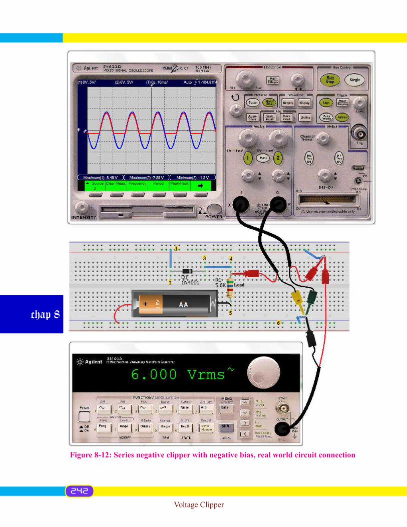
Voltage Clipper
chap 8
Figure 8-12: Series negative clipper with negative bias, real world circuit connection
242

Voltage Clipper
chap 8
TheinputACvoltagewaveformisdisplayedfromchannelone(CH1)ofoscilloscopewhilethechanneltwo(CH2)isshowingtheclippedwave.Asresultshownfromoscilloscope,themaximuminput voltage is 8.49V, the maximum output voltage is 7.91V and the minimum output voltage peak value is –1.5V. A portion of the input wave less than –1.5V is removed or clipped, the circuit iscalledseriesnegativeclipperwithnegativebias.ThislevelcanbemodifiedbyusingvariableDC power supply in the way that the voltage of the battery does not exceed that of the AC supply.
8. 2. Shunt or parallel clipper
A parallel clipper circuit uses a resistor connected in series with the input AC signal and the out-put signal is developed across the diode. The output is in parallel with the diode hence the circuit name parallel clipper. The parallel clipper can limit either the positive or negative alternation of theinputsignaltoaspecificlevel.Inaclippercircuit,thediodeactsasaswitch.Thediodeactsas a closed switch when is forwarded biased, and the input AC voltage is greater than zero diode voltagedrop(0.7V)andasanopenswitchwhenisreversebiased.Therearemanyformsofparal-lel clipper circuits depending on diode position, and biasing DC voltage. The output waveform has the same shape as that of a series clipper but for parallel clipper the diode voltage drop is taken in account as the output is in parallel with diode.
8. 2. 1. Shunt (parallel) positive clipper
In the parallel Positive clippers the alp will develop when the diode is cut off. For positive half wave of AC input voltage, the diode is forward biased and the output voltage is limited to diode voltage drop, 0.7V. At the negative half cycle of the input AC voltage, the diode is reverse biased and acts as an open switch, therefore, the output voltage looks like the input voltage.
Build a circuit having a series resistor and the diode in such way that the output is taken to the parallel terminal of the diode. The output is developed at negative half cycle of the input AC volt-age while during positive half cycle the output is clipped off to the diode volatge drop.
Part list
No Items Specifications Quantity1 Oscilloscope Agile oscilloscope 54622D 12 3VAC supply Agilent function generator 33120A 13 Resistors 68Ω,1/2watt 14 Resistors 1KΩ,1/4watt 15 Breadboard Prototypingboard(RSR03MB102) 16 Connecting wire 22-gauge (0.33mm2)solidwire 40cm7 Diode 1N4001 1
Experiment 8-5. Shunt (parallel) positive clipper
243

Voltage Clipper
chap 8
Parallel clippers are operated from AC supply with a series resistor, R1 used to limit the current
toasafevalueflowingthroughadiode.For a positive half wave of the input AC voltage Vin, the diode D1 is forward biased and the
voltage to the terminal of the load resistor R2 is equal to the diode voltage drop, that is 07V. For a negative half wave, the diode D1 is reverse biased and behaves like an open switch and the most of the input voltage develops across the load resistor R2 despite the voltage drop on series resistor R1. This can be calculated using Ohm’s law.
VLoad =Vin [ RLoad/(Rs+RLoad )]=3V[1KΩ/(68Ω+1KΩ)]=2.81V
The minimum value is given by : Vrms*√2=2.8V*1.414
=3.97V(withanegativesign–3.97V)
Procedure
Connectthecircuitasillustratedinfigure8-14.ConnecttheACsupplyfromfunctiongeneratortoapowerbusandgroundbus(1-7)ofbreadboard.Theredleadfromafunctiongeneratoriscon-nectedtoapositivebusofbreadboard(1)andblackleadtoanegativebus(7).TheseriesresistorRs1isconnectedtoapositivepowerbusthroughajumperwire(1-2)andtotheanodeofdiode(3).Thecathodeofdiodeisconnectedtoanegativepowerbusofbreadboadthroughajumperwire(4-7).Aloadresistorisconnectedtotheanodeofdiode(3-5)andtoanegativebusofbreadboadthroughajumperwire(6-7).Thecircuitissuppliedwith3Vrmssinusoidalfromafunctiongen-erator. The channel one of oscilloscope is at 2Volt/div vertical sensitivity while the channel two (CH2)isat5Volt/divverticalsensitivity.
The horizontal sensitivity is set to 10mSec/div. Whenever nedded, adjust vertical sensitivity and horizontal sensitivity to make the wave take up most of the screen without chopping any of its amplitude and in the easy way reading and calculation. The output voltage is taken on the terminal of the diode.
Figure 8-13: Shunt (parallel) positive clipper circuit
244

Voltage Clipper
chap 8
Figure 8-14: Shunt (parallel) positive clipper, real world circuit connection
245

Voltage Clipper
chap 8
TheinputACvoltagewaveformisdisplayedfromchannelone(CH1)ofoscilloscopeandthechanneltwo(CH2)displaystheresultingclippedwave.Asresultshownfromoscilloscope,themaximum input voltage is 4.42V, the maximum output voltage is 703.82mV and the minimum output voltage peak value is –3.97V.
8. 2. 2. Shunt or parallel positive clipper with bias
When the necessity to limit the positive half wave of the input AC signal to a desired level oither than 0.7V is a must, a DC voltage for biasing is inserted in series with a diode. The position of the biasing voltage polarity determines the type of biased shunt clipper.
• Shunt Positive Clipper with Positive Bias
Shunt positive clipper with positive bias, positive terminal of the battery is connected to the cath-ode of the diode. This causes the diode to be reversed biased at all times except when the input AC signal is more positive with respect to the bias voltage (i.e Vin greater than VBaterry).
Design a shunt positive clipper that limits the positive half cycle to 2.2 V. Use 82Ωasaseriesresistorand1.5KΩasloadresistor.MeasuretheresultingoutputvoltageVout using oscilloscope.
Part list
No Items Specifications Quantity1 Oscilloscope Agile oscilloscope 54622D 12 3VAC supply Agilent function generator 33120A 13 Resistors 82Ω,½watt 14 Resistors 1.5KΩ,¼watt 15 Breadboard Prototypingboard(RSR03MB102) 16 Connecting wire 22-gauge solid wire 40cm7 Diode 1N4005GP 18 1.5VDC supply 1.5V AA cell Battery 1
Experiment 8-6. Shunt positive clipper with positive bias
Figure 8-15: Shunt positive clipper with positive bias circuit
246

Voltage Clipper
chap 8
Figure 8-16: Shunt positive clipper with positive bias, real world circuit connection
247

Voltage Clipper
chap 8
Working Principle of the Circuit
For the positive half wave of the input AC voltage Vin greater than the battery bias voltage (1.5V),thediodeD1 is forward biased and the voltage to the terminal of the load resistor R2 is equal tothediodevoltagedropplusthebatterybiasvoltage(07V+1.5V),thatis2.2V.Foranegativehalf wave, the diode D1 is reverse biased and behaves like an open switch and the most of the input voltage develops across the load resistor R2 despite the voltage drop on series resistor RS1. This is given by the equation below.
VLoad = Vin [RLoad/(Rs+RLoad)]=4V[1.5KΩ/(82Ω+1.5KΩ)] = 3.79V
The minimum value is given by:Vrms*√2=3.79V*1.414=5.36V(withanegativesign–5.36V)
This implies that the output voltage will oscillate between two extremities. i.e 2.2 Volts for maxi-mum positive peak and –5.36 Volts for negative peak. These values can be changed to the desired amplitude values by changing the bias voltage and input supply voltage.
• Shunt Positive Clipper with Negative Bias
Shunt positive clipper with negative bias, negative terminal of the battery is connected to the cathode of the diode. This keeps the diode to be in forward bias all along the positive half cycle of the input AC signal. The input signal lying above the battery biasing voltage (VBaterry)isclipped.
Working Principle of the Circuit
For a positive half wave of the input AC voltage Vin, the diode D1 is forward biased. As the cathode of diode is connected to the negative terminal of the biasing battery, the diode remain forwarded bi-ased at voltage less than DC bias (i.e. –1.5V).Atthistimethevoltagetotheterminaloftheloadre-sistor R2 is equal to the diode voltage drop minus the battery bias voltage (07V–1.5V),thatis–0.8V.
Figure 8-17: Shunt positive clipper with negative bias
248

Voltage Clipper
chap 8
Figure 8-18: Shunt positive clipper with negative bias, real world circuit connection
249

Voltage Clipper
chap 8
For a negative half wave, the diode D1 is reverse biased and behaves like an open switch and the most of the input voltage develops across the load resistor R2 despite the voltage drop on series resistor RS1. This is given by the equation below.
VLoad = Vin [RLoad/(Rs+RLoad)]=4V[1.5KΩ/(82Ω+1.5KΩ)] = 3.79V
The minimum value is given by: Vrms*√2=3.79V*1.414=5.36V(withanegativesign:–5.36V)
This implies that the output voltage will oscillate between two extremities. i.e –0.8 Volts for maximum peak and –5.36 Volts for minimum peak.
These values can be changed to the desired amplitude values by changing the bias voltage and input supply voltage by making sure that the bias voltage is not greater than the ac supply voltage since this can create back effect and destroy the ac supply and also no desired clipping since the diode will stay reversed biased as long as the ac voltage is less than the bias voltage.
8. 2. 3. Shunt or parallel negative clipper
The negative clipper allows to pass the positive half cycle of the input voltage and clipped the negative half cycle. In the parallel negative clippers the alp will be developed when the diode is cut off. For positive half wave of AC input voltage, the diode is reverse biased and acts as an open switch, at the negative half cycle of the input AC voltage, the diode is forward biased and acts as a closed switch.
Build a circuit having a series resistor and the diode in such way that the output is taken to the parallel terminal of the diode. The output is developed at positive half cycle of the input AC volt-age while during negative half cycle the output is cut off.
Part list
No Items Specifications Quantity1 Oscilloscope Agile oscilloscope 54622D 12 3VAC supply Agilent function generator 33120A 13 Resistors 68Ω,1/2watt 14 Resistors 1KΩ,1/4watt 15 Breadboard Prototypingboard(RSR03MB102) 16 Connecting wire 22-gauge (0.33mm2)solidwire 40cm7 Diode 1N4001 1
Experiment 8-7. Shunt (parallel) negative clipper
250

Voltage Clipper
chap 8
Working Principle of the Circuit
Insuchcircuit,figure8-19,thediodeD1 acts as a closed switch for a negative half wave of the input voltage (i.e. VIN lessthanzero)andasanopenswitchforapositivehalfwaveoftheinputvoltage (i.e. Vingreaterthanzerovolt).The voltage to the terminal of the load resistor R2 when diodeisforwardbiasedisequaltothediodevoltagedrop(0.7V).Forpositivehalfwave,thediodeD1 is reverse biased and behaves like an open switch and the most of the input voltage develops across the load resistor R2 despite the voltage drop on series resistor RS1. This can be calculated using Ohm’s law.
VLoad = Vin [RLoad/(Rs+RLoad)]=3V[1KΩ/(68Ω+1KΩ)=2.81V
Themaximumvalueisgivenby:Vrms*√2=2.8V*1.414=3.97V
Procedure
Connectthecircuitasillustratedinfigure8-20.ConnecttheACsupplyfromfunctiongeneratortopowerbusandgroundbus(1-7)ofbreadboard.Theredleadfromafunctiongeneratoriscon-nectedtoapositivebusofbreadboard(1)andblackleadtoanegativebus(7).
The series resistor Rs1isconnectedtoapositivepowerbusthroughajumperwire(1-2)andtothecathodeofdiode(3).Theanodeofdiodeisconnectedtoanegativepowerbusofbreadboadthroughajumperwire(4-7).A load resistor is connected to the anodeofdiode (3-5) and to anegativebusof breadboad
throughajumperwire(6-7).Thecircuitissuppliedwith3Vrmssinusoidalfromafunctiongen-erator. The channel one of oscilloscope is at 2Volt/div vertical sensitivity while the channel two (CH2)isat5Volt/divverticalsensitivity.
The horizontal sensitivity is set to 10mSec/div. Whenever nedded, adjust vertical sensitivity and horizontal sensitivity to make the wave take up most of the screen without chopping any of its amplitude off and in the easy way reading and calculation.
Figure 8-19: Shunt (parallel) negative clipper circuit
251

Voltage Clipper
chap 8
Figure 8-20: Shunt (parallel) negative clipper, real world circuit connection
252

Voltage Clipper
chap 8
The oscilloscope display may have a natural coarseness, which can be reduced by selecting the Average function. Try to use as few samples as possible to avoid long delays while moving from one display to another.
The output voltage is taken on the terminal of the diode.Load resistor R2standforanyno-specificelectricaldeviceandmayjustbeakindofshorthand
representation of something else more practical than a resistor.Push the AUTOSCALE button to display both channels. Reposition so that the 0V is at the mid-
line on the both channels and the waveforms appear to overlap.At high frequencies, the amplitude of the signal may be too small to be detected by the Auto-
scale feature. You may need to set the Volts/division and time/division scale manually in order to see the signal.
Also, at very high frequencies AUTOSCALE may not work because the signal is too small. Use manual adjustments of the volts/division and time/division to reveal the signal.TheinputACvoltagewaveformisdisplayedfromchannelone(CH1)ofoscilloscopeandthe
channeltwo(CH2)displaystheresultingclippedwave.Press the MEASURE button to determine the voltage peak amplitudes for both channels, and
make a record.As result shown from oscilloscope, the maximum input voltage is 4.42V, the maximum output
voltage is 3.97V and the minimum output voltage peak value is –703.82mV. Compare with what you would expect for this circuit based on theoretical calculations.
8. 2. 4. Shunt or parallel negative clipper with bias
It happens that a signal can have negative amplitude larger than the positive half wave. The ex-ceedingpeakcanberemovedandfixedatadesiredlevelbyusingclippercircuitwithbias.Thisis achieved by inserting a DC voltage in series with a diode and the output is taken to the terminal combination of diode and the battery bias. The negative wave clipped level can be shifted by vary-ing and changing the polarity of the DC voltage.
• Shunt Negative Clipper with Positive Bias
In shunt negative clipper with positive bias circuit the clipping take place during the negative half cycle only when the input voltage (Vin is less than Vbias)andtheclippinglevelcanbeshiftedup or down by varying the biasing DC voltage. In such circuit, the positive terminal of the battery is connected to the anode of the diode. This keeps the diode to be in forward bias all along the negative half cycle of the input AC signal. The input signal lying below the battery biasing voltage (VBaterry)isclippedoff.
Design a circuit based on shunt negative clipper which allows passing the positive half cycle and clips off the negative to +2.3V close. Supply the circuit with 6VAC and display the resulting wave formsonoscilloscope.Use270Ωseriesresistorand5.6KΩasLoad.
Experiment 8-8. Shunt negative clipper with positive bias
253

Voltage Clipper
chap 8
Part list
No Items Specifications Quantity1 Oscilloscope Agile oscilloscope 54622D 12 9VAC supply Agilent function generator 33120A 13 Resistors 270Ω,1/2watt 14 Resistors 5.6KΩ,1/2watt 15 Breadboard Prototypingboard(RSR03MB102) 16 Connecting wire 22-gauge (0.33mm2)solidwire 50cm7 Diode 1N4001 18 3VDC supply 1.5VAAcellbattery(2) 1
Working Principle of the Circuit
Initially the positive terminal of the battery B1 forward biases the diode D1. The diode remains forwarded biased at voltage less than DC bias minus diode voltage drop (i.e. 3V–0.7V).Forin-coming positive half wave of the input AC voltage Vin greater than biasing voltage, the diode D1 gets reversed biased and diverts it to a load resistor R2. At this time, the most of the input voltage develops across the load resistor R2 notwithstanding the voltage drop on series resistor RS1. This is given by the equation below.
VLoad = Vin [RLoad/(Rs + RLoad)]=6V[5.6KΩ/(270Ω+5.6KΩ)]=5.72V
The maximum voltage is given by: Vrms*√2=5.72V*1.414=8.09V
For a negative half cycle, the diode D1 stays forwarded biased and the minimum voltage on load resistor R2 is equal to the battery bias voltage minus the diode voltage drop (3V–0.7V);thatis2.3V.
Figure 8-21: Circuit for shunt negative clipper with positive bias
254

Voltage Clipper
chap 8
Procedure
Connectthecircuitasillustratedinfigure8-22.ConnecttheACsupplyfromfunctiongeneratortopowerbusandgroundbus(1-7)ofbreadboard.Theredleadfromafunctiongeneratoriscon-nectedtoapositivebusofbreadboard(1)andblackleadtothenegativebus(7).TheseriesresistorRS1isconnectedtoapowerbusthroughajumperwire(1-2)andtothecathodeofdiodeD1(3).Thepositiveofthebatteryisconnectedtotheanodeofdiode(4)anditsnegativeterminalisconnectedtothenegativebusofthebreadboard.Theloadresistorisconnectedtothecathodeofdiode(3-4)andtothenegativepowerbusofbreadboard(7).Thecircuitissuppliedwith6Vrmssinusoidalfromafunctiongenerator.Channelone(CH1)isat10Volt/divandchanneltwoat5Volt/divverti-cal sensitivity and horizontal sensitivity is at 10mSec/div.
Adjust vertical sensitivity and horizontal sensitivity to make the wave take up most of the screen without chopping any of its amplitude off and in the easy way reading and calculation. The oscil-loscope display may have a natural coarseness, which can be reduced by selecting the Average function. Try to use as few samples as possible to avoid long delays while moving from one dis-play to another.
At least one full period of the waveform must be in view for the oscilloscope measure functions to be accurate.
Push the AUTOSCALE button to display both channels. Reposition so that the 0 V is at the midline on the both channels and the waveforms appear to overlap. The output voltage is taken between the cathode of diode and the negative terminal of the battery.Thechannelone(CH1)ofoscilloscopeisdisplayingtheinputACvoltagewaveformwhilethe
channel two (CH2) is displaying the resulting output voltage.The oscilloscope should beACcoupled to read the input waveform but should be DC coupled to read the output waveform.
Press the MEASURE button to determine the voltage RMS amplitudes for both channels, and make a record. As result shown from oscilloscope, the maximum input voltage is 8.49V, the maxi-mum output voltage is 8.09V and the minimum output voltage peak value is 2.31V.
A portion of the input wave less than 2.31V is removed or clipped off. This level can be modi-fiedbyusingvariableDCpowersupplyinthewaythatthevoltageofthebatterydoesnotexceedthat of the AC supply. Compare with what you would expect for this circuit based on theoretical calculations. The circuit is called shunt negative clipper with positive bias.
The frequency response of an oscil-loscope limits the accuracy with which waveforms can be accurately displayed. To view pulse waveforms, the frequency response must be high enough for all sig-nificant harmonics of the waveform. For example, a 100MHz oscilloscope distorts a 100MHz pulse waveform because the third, fifth, and higher harmonics are greatly attenuated.
Hands on tip
255

Voltage Clipper
chap 8
Figure 8-22: Shunt negative clipper with positive bias, real world circuit connection
256

Voltage Clipper
chap 8
• Shunt Negative clipper with negative bias
If the polarity of the bias voltage is reversed the entire signal below the voltage level is clipped off. At this time, the negative terminal of the battery is connected to the anode of the diode. This keeps the diode to be in reverse bias all along the negative half cycle of the input AC signal until Vin becomes greater than Vbias. The input signal lying below the battery biasing voltage (VBaterry)isclipped off.
In general shunt negative clipper with negative bias is achieved by reversing the polarity of the batteryfromshuntnegativeclipperwithpositivebiasasshowninthecircuitfigure8-23.
Working Principle of the Circuit
The negative terminal of the battery B1 reverse biases the diode D1. The diode remains reversed all along the positive half wave of the incoming input voltage Vin. At this time the diode D1 behaves as an open switch and the input positive diverts to the output. The voltage developed across the load resistor R2 is calculated by using the Ohm’s law. This is given by the equation below.
VLoad = Vin [RLoad/(Rs+RLoad)]=6V[5.6KΩ/(270Ω+5.6KΩ)] =5.72V
The maximum voltage is given by: Vrms*√2=5.72V*1.414 = 8.09V
For a negative half wave, the diode D1 stays reversed until the negative wave voltage exceeds the battery’s voltage. At Vin negative wave greater than the battery bias, the diode D1 gets forward biased and the minimum voltage on load resistor R2 is equal to the battery biasing voltage minus the diode voltage drop (–3V–0.7);thatis–3.7V.
Experiment 8-9. Shunt negative clipper with negative bias
Figure 8-23: Circuit for shunt negative clipper with negative bias
257

Voltage Clipper
chap 8
Figure 8-24: Shunt negative clipper with negative bias, real world circuit connection
258

Voltage Clipper
chap 8
Procedure
Connectthecircuitasillustratedinfigure8-24.TheACsupplyfromfunctiongeneratorispluggedonpowerbusandground(1-7)ofbreadboard.Theredleadfromafunctiongeneratorisconnectedtoapositivebusofbreadboard(1)andblackleadtoanegativebus(7).TheseriesresistorRS1isconnectedtoapowerbusthroughajumperwire(1-2)andtothecathodeofdiodeD1(3).Thenegativeofthebatteryisconnectedtotheanodeofdiode(4)anditspositiveterminalisconnectedtonegativebusofthebreadboard.Theloadresistorisconnectedtothecathodeofdiode(3-4)andtoanegativepowerbusofbreadboard(7).Thecircuitissuppliedwith6Vrmssinusoidalfromafunctiongenerator.Channelone(CH1)isat10Volt/divandchanneltwoat5Volt/divverticalsen-sitivity and horizontal sensitivity is at 10mSec/div.
Adjust vertical sensitivity and horizontal sensitivity to make the wave take up most of the screen without chopping any of its amplitude off and in the easy way reading and calculation. The output voltage is taken between the cathode of diode and the negative terminal of the battery. Any ac-curate adjustment made on vertical or horizontal sensitivity does not affect the result. The oscil-loscope should be AC coupled to read the input waveform but should be DC coupled to read the output waveform.Thechannelone(CH1)ofoscilloscopeisdisplayingtheinputACvoltagewaveformwhilethe
channeltwo(CH2)isdisplayingtheresultingoutputvoltage.Asresultshownfromoscilloscope,the maximum input voltage is 8.49V, the maximum output voltage is 8.09V and the minimum output voltage peak value is –3.63V. A portion of the input wave less than –3.63V is removed or clippedoff.ThislevelcanbemodifiedbyusingvariableDCpowersupplyinthewaythatthevolt-age of the battery does not exceed that of the AC supply to avoid any risk of damage of AC supply. the circuit is called shunt negative clipper with negative bias.
8. 3. Dual (combination) diode clipper
Dual diode clipper is electronic circuit used to limit both positive and negative of the input AC signal to a desired amplitude level. It can be dual biased clipper or dual unbiased clipper and these are based on shunt positive and negative clipper combined.
• Dual polarity unbiased diode clipper
Dual polarity unbiased diode clipper or simply dual polarity diode clipper combines parallel pos-itive clipper with negative clipper. It uses two diodes connected back to back. One diode becomes forwarded biased for one half cycle of the input voltage while the other is in reverse in return to the next half cycle.
Design a circuit which limits the incoming input voltage to 0.7V for positive half cycle and to –0.7V for negative half cycle. The circuit is based on combination of positive and negative shunt clippers.Thecircuithastobesuppliedwith3Vrmsfromasinusoidalsource,using470Ωseriesresistor and silicon diodes as shown in part list below.
Experiment 8-10. Dual polarity unbiased diode clipper
259
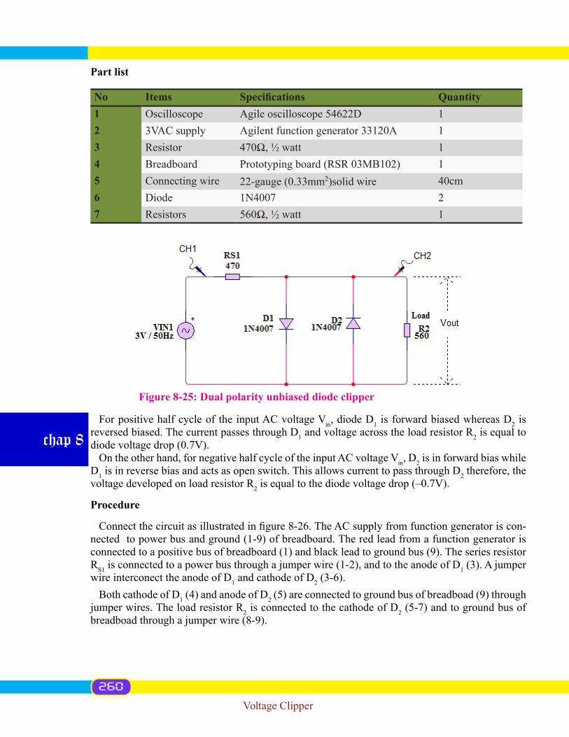
Voltage Clipper
chap 8
Part list
No Items Specifications Quantity1 Oscilloscope Agile oscilloscope 54622D 12 3VAC supply Agilent function generator 33120A 13 Resistor 470Ω,½watt 14 Breadboard Prototypingboard(RSR03MB102) 15 Connecting wire 22-gauge (0.33mm2)solidwire 40cm6 Diode 1N4007 27 Resistors 560Ω,½watt 1
For positive half cycle of the input AC voltage Vin, diode D1 is forward biased whereas D2 is reversed biased. The current passes through D1 and voltage across the load resistor R2 is equal to diodevoltagedrop(0.7V).
On the other hand, for negative half cycle of the input AC voltage Vin, D2 is in forward bias while D1 is in reverse bias and acts as open switch. This allows current to pass through D2 therefore, the voltage developed on load resistor R2isequaltothediodevoltagedrop(–0.7V).
Procedure
Connectthecircuitasillustratedinfigure8-26.TheACsupplyfromfunctiongeneratoriscon-nectedtopowerbusandground(1-9)ofbreadboard.Theredleadfromafunctiongeneratorisconnectedtoapositivebusofbreadboard(1)andblackleadtogroundbus(9).TheseriesresistorRS1isconnectedtoapowerbusthroughajumperwire(1-2),andtotheanodeofD1(3).Ajumperwire interconect the anode of D1 and cathode of D2(3-6).
Both cathode of D1(4)andanodeofD2(5)areconnectedtogroundbusofbreadboad(9)throughjumper wires. The load resistor R2 is connected to the cathode of D2(5-7)andtogroundbusofbreadboadthroughajumperwire(8-9).
Figure 8-25: Dual polarity unbiased diode clipper
260

Voltage Clipper
chap 8
Figure 8-26: Dual polarity unbiased diode clipper, real world circuit connecrion
261

Voltage Clipper
chap 8
The circuit is supplied with 3V rms sinusoidal from a function generator. Both channel one (CH1)andchanneltwo(CH2)areat2Volt/divverticalsensitivityand10mSec/divhorizontalsen-sitivity. Adjust vertical sensitivity and horizontal sensitivity to make the wave take up most of the screen without chopping any of its amplitude off and in the easy way reading and calculation. The output voltage is taken between the cathode of diode D2 and ground bus of breadboard. Any ac-curate adjustment made on vertical or horizontal sensitivity does not affect the result.Thechannelone(CH1orX)ofoscilloscopeisdisplayingtheinputACvoltagewaveformwhile
thechanneltwo(CH2orY)isdisplayingtheresultingoutputvoltage.Asresultshownfromoscil-loscope,themaximuminputvoltageis4.24V,themaximumoutputvoltageis0.691mV(0.691V)andtheminimumpeakoutputvoltagevalueis–691mV(–0.691V).Aportionoftheinputwaveexceeding 0.691 V is removed or clipped off. This level is determined by diode voltage drop and remain unchanged for a wide range of input voltage greater than 0.7V for silicon. The positive and negative are equal in magnitude and have the oposite sign where the name dual polarity diode clip-per.Theclippinglevelonbothpolaritiescanbemodifiedbyusingbiaseddualpolarityclippers.
• Dual polarity biased clipper
Dual polarity biased clipper circuit can clip at both signal half-cycles (positive and negative half-cycle)independentlevelsdependinguponthebiasvoltages.Thiscombinesparallelclipperwithnegative bias and parallel clipper with positive bias.
Design a circuit which limits positive half cycle of input AC signal to 2.2 V and negative half cycleto–3.7Vcloser.Thecircuitisbasedonparallelclipperswith390Ωseriesresistorand1.8KΩasload.Usetwodiodes1N4005andotherspecificationprovidedinpartlistbelow.
Part list
No Items Specifications Quantity1 Oscilloscope Agile oscilloscope 54622D 12 5VAC supply Agilent function generator 33120A 13 Resistors 390Ω,½watt 14 Resistors 1.8KΩ,¼watt 15 Breadboard Prototypingboard(RSR03MB102) 16 Connecting wire 22-gauge solid wire 40cm7 Diode 1N4005 28 1.5V DC supply 1.5V AA cell battery 19 3V DC supply 2x 1.5V AA cell battery 1
This type of clipper combines a parallel negative clipper with negative bias (D2 and B2)andaparallel positive clipper with positive bias (D1 and B1).Hencethecombinationofabiasedposi-tive clipper and a biased negative clipper is called combination or dual biased diode clipper. Such a clipper circuit can clip at both two in dependent levels depending upon the bias voltages. The circuitoffigure8-27showsthecircuitofadual(combination)diodeclipper.
Experiment 8-11. Dual polarity biased clipper
262

Voltage Clipper
chap 8
A sinusoidal AC input voltage Vin is applied at the input terminals of the circuit. During the positive half cycle, the diode D1 is forward biased, while diode D2 is reverse biased. Therefore the diode D1 will conduct and will acts as a short circuit. On the other hand, diode D2 will acts as an open circuit. However, the value of output voltage cannot exceed the voltage level of battery B1 plus diode voltage drop (VB1+0.7V).
If VB1= 1.5VTherefore; VB1+0.7V= 2.2V
This implies that during positive half cycle, the output voltage is equal to 2.2 VIn the same way during the negative input half cycle the diode D2 acts as a short circuit while the
diode D1 as an open circuit. However the value of output voltage cannot exceed the voltage level of battery B2plusdiodevoltagedrop(3V+0.7);valuewithnegativesign.
When VB2 = 3VThen–(3+0.7)=–3.7V
Thissignifiesthatduringnegativecycle,theoutputvoltageisequalto–3.7V.It may be noted that the clipping levels of the circuit can be varied by changing the values of
biasing voltages VB1 and VB2. If the values of VB1 and VB2 are equal, the circuit will clip both the positive and negative half cycles at the same voltage level. Such a circuit is known as a symmetri-cal clipper.
Figure 8-27: Dual (combination) biased diode clipper circuit
263

Voltage Clipper
chap 8
Procedure
Connectthecircuitasshowninfigure8-28.TheACsupplyfromfunctiongeneratorispluggedtopowerbusandgroundbus(1-9)ofbreadboard.Theredleadfromafunctiongeneratoriscon-nectedtoapositivebusofbreadboard(1)andblackleadtogroundbus(9).TheseriesresistorRS1 isconnectedtoapowerbusthroughajumperwire(1-2),andtotheanodeofD1(3).Ajumperwireinterconnects the anode of D1 and cathode of D2(3-6).CathodeofD1 is connected to positive of battery B1(4)andanodeofD2 is connected to negative terminal of the battery B2(5).
Both negative terminal of battery B1 and positive terminal of the battery B2 are connected to groundbusofbreadboad(9).TheloadresistorR2 is connected to the cathode of D2(5-7)andtogroundbusofbreadboadthroughajumperwire(8-9).
The circuit is supplied with 6V rms sinusoidal from a function generator. Both channel one (CH1)andchanneltwo(CH2)areat2Volt/divverticalsensitivityand5mSec/divhorizontalsen-sitivity.
Adjust vertical sensitivity and horizontal sensitivity to make the wave take up most of the screen without chopping any of its amplitude off and in the easy way reading and calculation. Any ac-curate adjustment made on vertical or horizontal sensitivity does not affect the result. The oscil-loscope should be AC coupled to read the input waveform but should be DC coupled to read the output waveform.
The oscilloscope display may have a natural coarseness, which can be reduced by selecting the Average function. Try to use as few samples as possible to avoid long delays while moving from one display to another.
Push the AUTOSCALE button to display both channels. Reposition so that the 0 V is at the mid-line on the both channels and the waveforms appear to overlap.
At high frequencies, the amplitude of the signal may be too small to be detected by the Auto-scale feature. You may need to set the Volts/division and time/division scale manually in order to seethesignal.AtveryhighfrequenciesAUTOSCALEmaynotworkbecausethefilteredsignalis too small. Use manual adjustments of the volts/division and time/division to reveal the signal.Thechannelone(CH1orX)ofoscilloscopeisdisplayingtheinputACvoltagewaveformwhile
thechanneltwo(CH2orY)isdisplayingtheresultingoutputvoltage.PresstheMEASUREbuttonto determine the voltage RMS and peak amplitudes for both channels, and make a record.
As result shown from oscilloscope, the maximum input voltage is 7.07 V, the maximum output voltageis2.24Vandtheminimumoutputvoltagepeakvalueis(–3.71V).Aportionoftheinputwave exceeding +2.24V and –3.71 V is removed or clipped off. These levels are determined by biasing voltage values and can be varied by changing the later. The positive and negative are equal in magnitude and have the oposite sign when the biasing volatge are equal where the name symet-ric dual polarity diode clipper.
Compare with what you would expect for this circuit based on theoretical calculations.
264

Voltage Clipper
chap 8
Figure 8-28: Dual (combination) biased diode clipper, real world circuit connection
265

Voltage Clipper
chap 8
8. 4. Voltage clipper using zener diode
A zener diode replaces both the diode and the DC voltage source. The use of a bias voltage helps to clip off a certain amount of voltage waveform and this can be accurately controlled. One of the main disadvantages of using voltage biased diode clipping circuits is that they need an additional emf(electromotiveforce)batterysourcewhichmayornotbeaproblem.Oneeasywayofcre-ating biased diode clipping circuits without the need for an additional dc supply is to use Zener diodes.
The zener diode is a special diode that has been specially manufactured to operate in its reverse biased breakdown region and as such can be used for voltage regulation or zener diode clipping applications.
When forward biased, the zener acts just like an ordinary silicon diode with a forward volt-agedropof0.7V(700mV).Ontheotherhand,ifthezenerdiodeisreversedbiased,thevoltageis blocked until the zener diode breakdown voltage is reached. At this point, the reverse current through the zener increases sharply but the zener voltage (VZ)acrossthedeviceremainsconstanteven if the zener current (IZ)varies.Thus,wecanexploitthischaracteristicofzenerdiodeandusethem for clipping a waveform.
Zener diodes are manufactured with a wide range of voltages and can be used to give different voltage references on each half cycle, the same as above. Zener diodes are available with zener breakdown voltages, VZ ranging from 2.4 to 33 volts, with a typical tolerance of 1 or 5%. Note thatonceconductinginthereversebreakdownregion,fullcurrentwillflowthroughthezenerdiode so a suitable current limiting resistor, Rs must be chosen.
Design positive and negative voltage clipping circuit using zener diode. Display and measure the resulting waveform on oscilloscope. Supply the circuit with a sinusoidal voltage of 5V/50Hz rms.
Part list
No Item Specification Quantity 1 Zener diode BZX55C,3V0 zener diode 12 Function generator Agilent 33120A 1
Figure 8-29: Base circuit for voltage clipper using Zener diode; (a) Negative clipper, (b) Positive clipper
Experiment 8-12. Positive and negative voltage clipping using zener diode
266

Voltage Clipper
chap 8
3 Oscilloscope Tektronix TDS2024 14 56Ωseriesresistorand8.2KΩasload 56Ω,½watt;8.2KΩ½watt 16 Breadboard Prototyping board 390-pin 17 Connecting wires 22-gauge (0.33mm2)solidwire 10cm
Negative Clipper
Working Principle of the Circuit
Refertothefigure8-30;thezenerdiodeisactinglikeabiaseddiodeclippingcircuitwiththebiasvoltage being equal to the zener breakdown voltage. In this circuit during the positive half of the input waveform the zener diode is reverse biased so the waveform is clipped at the zener voltage, VZ equal to 3.0V. During the negative half cycle the zener acts like a normal diode with its usual 0.7V junction value.
Positive Clipper
Working Principle of the CircuitForthefigure8-31;thezenerdiodeisactinglikeabiaseddiodeclippingcircuitwiththebias
voltage being equal to the zener breakdown voltage. During the positive half of the waveform the
Figure 8-30: Negative clipping circuit using zener diode
Figure 8-31: Negative clipping circuit using zener diode
267

Voltage Clipper
chap 8
zener diode is forward biased and behaves as normal diode with 0.7V as diode voltage drop. When the input voltage reveres direction to the negative half cycle, the zener diode is reverse biased so the waveform is clipped at the zener voltage, VZ equal to –3.0V.
Figure 8-32: Negative clipping circuit using zener diode, real world circuit connection
268

Voltage Clipper
chap 8
Procedure
1. Choose56Ωseriesresistor,8.2KΩasloadresistorandBZX55C3V0zenerdiodeandcon-nectthecircuitasillustratedinfigure8-32
2. Set the function generator to output 5V rms at 50Hz. The input voltage and frequency may change at desired value in the way that the working principle remains unchanged. For a diode to be forward biased, the input voltage needs to be greater than 0.7V
3. Setchanneloneandchanneltwo(CH1andCH2)ofoscilloscopeto2Volt/divandto5mSec/div vertical sensitivity and horizontal sensitivity respectively. The oscilloscope should be AC coupled to read the input waveform but should be DC coupled to read the output wave-form.
4. The oscilloscope display may have a natural coarseness, which can be reduced by select-ing the Average function. Try to use as few samples as possible to avoid long delays while moving from one display to another.
5. Push the AUTOSCALE button to display both channels. Reposition so that the 0V is at the midline on the both channels and the waveforms appear to overlap.
6. AtveryhighfrequenciesAUTOSCALEmaynotworkbecausethefilteredsignalistoosmall. Use manual adjustments of the volts/division and time/division to reveal the signal. At least one full period of the waveform must be in view to for the oscilloscope measure functions to be accurate.
7. As measured by the oscilloscope, the output voltage varies between 3.1V and -0.585V (585mV)maximumandminimumvoltsrespectively.Theresultingispositivevoltageclip-per.
Figure 8-33: Waveform for positive clipper using zener diode
269

Voltage Clipper
chap 8
8. Bychanging thepositionofzenerdiode(anodeatpointBandcathodeatpointA), theoutputvoltagevariesbetween0.585V(585mV)and–7.07V maximum and minimum volts respectively.Theresultingisnegativevoltageclipperasshowninresultingwaveformfig-ure 8-33.
Dual Polarity Zener Clipper
Whenever required to remove a portion of both positive and negative half-cycle of the input voltagewaveform,thezenerdiodescanbeconfiguredinseriesback-toback.Theclippingleveliscontrolledbyreversebreakdownvoltageofthezenerdiodeandcanbemodifiedbyreplacingthezenerofdifferentbreakdownvoltage.Thebasecircuitisshowninfigure8-34.
Working Principle of the Circuit
The output waveform from full wave zener diode clipping circuits resembles that of the previous voltage biased diode clipping circuit. The output waveform will be clipped at the zener voltage plus the 0.7V forward volt drop of the other diode. So for example, the positive half cycle will be clipped at the sum of zener diode, ZD1 plus 0.7V from ZD2 and vice versa for the negative half cycle.
Design a voltage clipping circuit using zener diode which can limit both positive and negative half cycle of the input ac supply at 5.4V and -3.4V respectively. Display and measure the resulting waveform on oscilloscope. Supply the circuit with a sinusoidal voltage of 5V/50Hz rms.
Part list
No Item Specification Quantity 1 Zener diode BZX55C,2V7; BZX55C,4V7 22 Function generator Agilent 33120A 13 Oscilloscope Tektronix TDS2024 14 27Ωseriesresistorand4.7KΩasload 27Ω,½watt;4.7KΩ½watt 1
Figure 8-34: Base circuit for dual polarity voltage clipper using zener diode
Experiment 8-13. Dual polarity voltage clipping using zener diode
270

Voltage Clipper
chap 8
6 Breadboard Prototyping board 390-pin 17 Connecting wires 22-gauge (0.33mm2)solidwire 10cm
Working Principle of the Circuit
Thefullwavezenerdiodeclipperofthefigure8-35usestwodiodesconnectedback-to-back.Theoutputvoltageistakenacrosstheterminalsofthetwodiodes.ThefirstzenerdiodeDZ1 has breakdown voltage of 2.7V whilst the second has breakdown voltage of 4.7V. For positive half cycle, diode DZ1 is forward biased with 0.7V as diode voltage drop while the second zener diode DZ2 is reversed biased. Therefore, the output voltage is equal to 0.7V+ VDZ2 (0.7V+4.7V), i.e.5.4V. During the negative half cycle, diode DZ2 is forward biased and makes voltage drop of 0.7V at the same time, diode DZ1 is reversed biased and maintain its breakdown voltage of 2.7V. Thus, theoutputvoltageisequalto–(0.7V+2.7V),thatis–3.4V.Thismeansthattheoutputvoltagewillswing between 5.4V and –3.4V maximum and minimum voltage respectively.
Procedure
1. Choose27Ωseriesresistor,4.7KΩasloadresistorandBZX55C2V7,BZX55C4V7zenerdiodesandconnectthecircuitasillustratedinfigure8-36
2. Set the function generator to output 5V rms at 50Hz. The input voltage and frequency may change at desired value in the way that the working principle remains unchanged. In this case, you need to supply the circuit with voltage greater than 0.7V so that the diode may be forward biased.
3. Setchanneloneandchanneltwo(CH1andCH2)ofoscilloscopeto2Volt/divandto5mSec/div vertical sensitivity and horizontal sensitivity respectively.
4. The oscilloscope should be AC coupled to read the input waveform but should be DC coupled to read the output waveform.
5. Try to use as few samples as possible to avoid long delays while moving from one display to another.
Figure 8-35: Circuit for dual polarity voltage clipper using zener diode
271

Voltage Clipper
chap 8
6. Push the AUTOSCALE button to display both channels. Reposition so that the 0V is at the midline on the both channels and the waveforms appear to overlap.
Figure 8-36: Dual polarity clipping circuit using zener diode, real world circuit connection
272

Voltage Clipper
chap 8
7. AtveryhighfrequenciesAUTOSCALEmaynotworkbecausethefilteredsignalistoosmall. Use manual adjustments of the volts/division and time/division to reveal the signal. At least one full period of the waveform must be in view for the oscilloscope measure func-tions to be accurate.
8. As measured by the oscilloscope, the output voltage varies between 5.31V and –3.41V maximumandminimumvoltsrespectively.Theresultinggivesafullwave(dualpolarity)voltage clipping. Note that the deviation of practical result to the expected theoretical result is base on the tolerance of diodes.
8. 5. Applications of voltage clipper
There arenumerous applications for diode clippers.Theyfindwide application in televisionreceiver for separating synchronizing signals from composite picture signals and also in television transmitters at the time of processing the picture signals.
They are also employed for different wave generation such as trapezoidal, square or rectangular waves.
Series clippers are employed as noise limiters in FM transmitters by clipping excessive noise peaksaboveaspecifiedlevel.
The diode clipper can be used for the protection of different types of circuits. For example, a digital circuit against transients which may cause considerable damage.Apracticalapplicationofaclipperistopreventanamplifiedspeechsignalfromoverdrivinga
radio transmitter. Over driving the transmitter generates false radio signals which cause interfer-ence with other stations. The clipper is a protective measure. A sine wave may be squared up by overdriving a clipper.
Figure 8-37: Clipper prevents over driving radio transmitter by voice peaks
273

Voltage Clamper
chap 9
Objectives
When you have studied this chapter, you should
• Have an understanding of the working principle of voltage clamping and their applications• Be capable to design a voltage clamping circuit to a desired DC level
Clamper is an electronic circuit that places either the positive or negative peak of a signal at a desired DC level. The clamper does not restrict the peak-to-peak outing of the signal, it moves the whole signal up or down so as to place the peaks at the reference level. Certain applications inelectronicsrequirethattheupperorlowerextremityofawavetobefixedataspecificvalue.In such applications a clamper or clamping circuits are used. Principally a clamping circuit intro-duces or restores a DC level to an AC signal. The dc component is simply added to or subtracted from the input signal. Hence a clamping circuit in practices is also given other names such as DC restorer,orDCreinsertedorabaselinestabilizer.Adiodeclamp(asimple,commontype)consistsof a diode, which conducts electric current in only one direction and prevents the signal exceed-ing the reference value; and a capacitor which provides a DC offset from the stored charge. The capacitor forms a time constant with the resistor load which determines the range of frequencies over which the clamper will be effective.
Further readingStudy aids for this chapter are available at S. P. Bali, Linear Integrated Circuits, p.279, Tata McGraw-Hill, 2008
Voltage ClamperChapter nine
274

Voltage Clamper
chap 9
9. 1. Clamper circuits tips
Clamper circuits are categorized according to their mode of operation. Principally there are two types of clamping circuits: negative or positive clamper; and these can be biased or unbiased. A clamper circuit adds the positive or negative dc component to the input signal so as to push it either on the positive side or on the negative side with respect to the ground level.
The following are two general types of clamper.
1. Positive clamper: This occurs when negative peaks raised or clamped to ground or on the zero level. In other words, it pushes the signal upwards so that negative peaks fall on the zero level. For positive biased clamper, the circuit outputs a purely positive waveform from an input signal; it offsets the input signal so that all of the waveform is greater than 0 V.
2. Negative clamper: negative clamping occurs when positive peaks dropped or clamped to ground or on the zero level. In other words, it pushes the signal downwards so that the posi-tive peaks fall on the zero level.
For negative biased clamper, the circuit outputs a purely negative waveform from an in-put signal; it offsets the input signal so that all of the waveform is less than 0 V.
Whatever positive or negative clamper the shape of the original signal has not changed; only there is vertical shift in the signal. For a clamping circuit at least three components such as diode, a capacitor and a resistor are required. Sometimes an independent dc supply is also required to cause an additional shift.
9. 1. 1. Working principles
The schematic of a clamper comprises a capacitor, followed by a diode in parallel with the load. The clamper circuits rely on a change in the capacitor’s time constant; this is the result of the diode changing current path with the changing input voltage. The magnitude of resistor (R)andcapacitor(C)arechosensothatthetimeconstant,τ=RC, is large enough to ensure that the voltage across thecapacitordoesnotdischargesignificantlyduringthediode’snon-conductingintervalsincethiscan affect the output signal. On the other hand the capacitor is chosen small enough to allow it to chargequicklyduringthediode’sconductinginterval.DuringthefirstnegativephaseoftheACinput voltage, the capacitor in the positive clamper charges rapidly. As Vin becomes positive, the capacitor serves as a battery; since it has stored the equivalent of Vin during the negative cycle, it provides nearly that voltage during the positive cycle; this essentially doubles the voltage seen by the load. As Vin becomes negative, the capacitor acts as a battery of the same voltage of Vin. The voltage source and the capacitor neutralize each other, resulting in a net voltage of zero as seen by the load.
9. 1. 2. Clamper circuit practical considerations
When designing clamper circuits, there are key points that have to be considered. These key points are described below.
1. The shape of the waveform will be the same, but its level is shifted either upward or downward.
275

Voltage Clamper
chap 9
2. There will be no change in the peak-to-peak or rms value of the waveform due to the clamping circuit. Thus, the input waveform and output waveform will have the same peak-to-peak value that is, 2Vmax.Thisisshowninthefigureabove.Inclampercircuitsthe same readings will be obtained in the ac voltmeter for the input voltage and the clamped output voltage.
3. There will be a change in the peak and average values of the waveform. For example, the input waveform having a peak value of 6V maximum value and 0V average value over a complete cycle, the clamped output varies from 0V and 12V as peak value (or 0 and-12Vfornegativeclamper)andaveragevalueof6V(or-6Vfornegativeclampedwave).Thusthepeakvalueoftheclampedoutputis2Vmax and average value is Vmax.
4. The circuit containing resistor R and capacitor C, the values of the resistor R and ca-pacitor C affect the waveform.
5. The values for the resistor R and capacitor C should be determined from the time con-stantequationofthecircuit,τ=RC.Thevaluesmustbelargeenoughtomakesurethatthe voltage across the capacitor Cdoesnotchangesignificantlyduringthetimeintervalthediodeisnotconducting.Inagoodclampercircuit,thecircuittimeconstantτ=RC should be at least ten times the time period of the input signal voltage.
6. The signal out of a clamper appears having one peak clamped to a DC voltage. Ex-ample: The negative peak is clamped to 0 VDC, the waveform appears to be shifted upward. The polarity of the diode determines which peak is clamped.
Itisadvantageoustofirstconsidertheconditionunderwhichthediodebecomesforwardbiased.AcapacitivelycoupledsignalalternatesaboutitsaverageDClevel(0V).
9. 2. Positive clamper
Positive clamper circuit raises the input AC signal so that oscillates above the zero level. In such circuit, the negative crest coincides the ground level or above zero. By using DC voltage source, the clamper can be biased to bind the output voltage to a different values. Positive clamper circuit consists mainly of a diode and a capacitor. The diode arrow points upward, again the same direc-tion as the DC shifts. It means that, when the diode points upward we have a positive DC clamper circuit.
Build a circuit which shifts the input sinusoidal signal to oscillate above the ground level so that the negative peak touches the ground level. With the same principle insert a biasing voltage so that the resulting output wave oscillates above 2V from ground level. Thecircuithastobesuppliedby6Vrmsfromasinusoidalsourceandfeedtoaloadof3.9KΩ
resistor.Thecircuithastobebuiltusing47uFandotheritemsspecifiedinlistbelowanddisplaythe resulting waveforms on oscilloscope.
Experiment 9-1: Positive clamper
276

Voltage Clamper
chap 9
Part list
No Items Specifications Quantity1 Oscilloscope Agile oscilloscope 54622D 12 6VAC supply Agilent function generator 33120A 13 Resistors 3.9KΩ,½watt 14 Breadboard Prototype breadboard 15 Connecting wire 22-gauge solid wire 40cm6 Diode 1N4007 17 Capacitor 47µF/50V Capacitor 18 3VDC supply 2x1.5AA cell battery 1
• Unbiased positive clamper
Refertothecircuitexampleoffigure9-1,thevaluesusedonthiscircuitcanbemodifiedforanydesired result. During the negative half cycle of the input voltage VIN1, the diode D1 is forwarded biased thus conducts heavily and behaves as a closed switch. As result of this, the capacitor C1 is charged to somewhat maximum input voltage beyond the negative peak voltage i.e.,–Vmax. Once the capacitor is fully charged to –Vmax it cannot discharge because the diode cannot conduct in the reverse direction.
When the input signal changes the direction to the positive half cycle, the diode is shunt off and the capacitor charged to -Vmax behaves as a battery. It means that this capacitor acts as a battery withanelectromotiveforce(emf)equaltothe–Vmax. The polarity of this voltage is such that it adds to the input signal Vin. Therefore the output voltage is equal to the sum of the AC input signal and the capacitor voltage VC i.e., Vin + Vmax.
For Vin=6V(rmsvalue);The capacitor C1 will be charged to: Vc = Vin*√2 = 6V*1.414 = 8.4853V
Figure 9-1: Positive clamper circuit
277

Voltage Clamper
chap 9
The output peak voltage value:
Vout(max) = Vin(max) + Vc = Vin(max)*2 = 8.4853*2 =16.9706V
The output minimum voltage: Vout(min)= 0VThe result gives positive clamped voltage where the positive clamping circuit.
Procedure
Connectthecircuitasillustratedinfigure9-2.PlugtheleadsofACsupplyfromfunctiongen-eratortopowerbusandgroundbus(1-8)ofbreadboard.Theredleadfromafunctiongeneratorisconnectedtoapositivebusofbreadboard(1)andblackleadtogroundbus(8).ThecapacitorC1 is connectedtoapowerbusthroughajumperwire(1-2),andtothecathodeofdiodeD1(3-4).Theanode of diode D1(5)isconnectedtogroundbusofbreadboardthroughajumperwire(5-8).Theload resistor R2 is connected to the cathode of D1(4)andtogroundbusofbreadboadthroughajumperwire(7-8).Thecircuitissuppliedwith6Vrmssinusoidalfromafunctiongenerator.
Bothchannelone(CH1)andchanneltwo(CH2)areat5Volt/divverticalsensitivityand5mSec/div horizontal sensitivity. Adjust vertical sensitivity and horizontal sensitivity to make the wave take up most of the screen without chopping any of its amplitude off and in the easy way reading and calculation.
The oscilloscope display may have a natural coarseness, which can be reduced by selecting the Average function. Try to use as few samples as possible to avoid long delays while moving from one display to another.
Push the AUTOSCALE button to display both channels. Reposition so that the 0V is at the mid-line on the both channels and the waveforms appear to overlap.Athighfrequencies,theamplitudeofthefilteredsignalmaybetoosmalltobedetectedbythe
Auto-scale feature. You may need to set the Volts/division and time/division scale manually in order to see the signal.
Any accurate adjustment made on vertical or horizontal sensitivity does not affect the result.AtveryhighfrequenciesAUTOSCALEmaynotworkbecausethefilteredsignalistoosmall.
Use manual adjustments of the volts/division and time/division to reveal the signal.Thechannelone(CH1orX)ofoscilloscopeisdisplayingtheinputACvoltagewaveformwhile
thechanneltwo(CH2orY)isdisplayingtheresultingoutputvoltage.Press the MEASURE button to determine the voltage peak amplitudes for both channels, and
make a record.
278
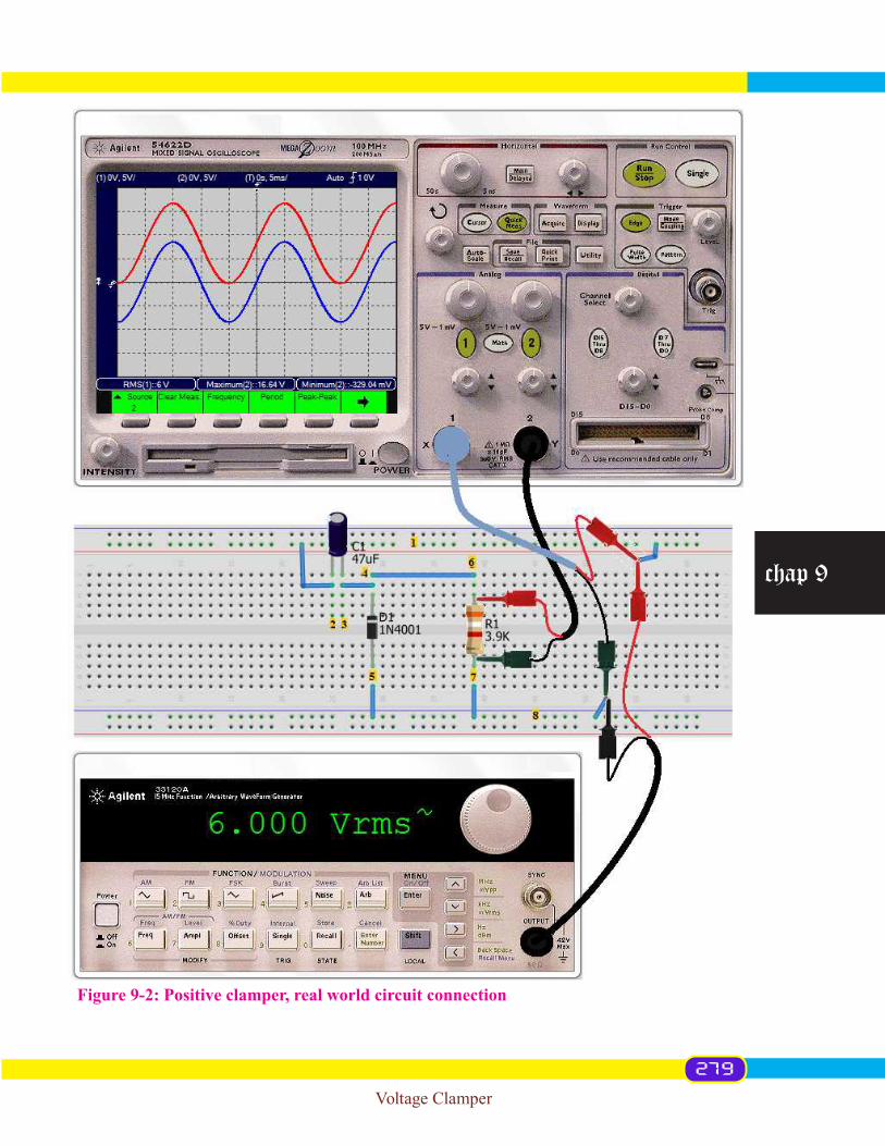
Voltage Clamper
chap 9
Figure 9-2: Positive clamper, real world circuit connection
279

Voltage Clamper
chap 9
As result shown from oscilloscope, the maximum output voltage is 16.64V and the minimum outputvoltagepeakvalueis(–329.04mV).Aportionlowerzerolevelisduetodiodevoltagedropand theoricaly this is said to be zero.
Compare with what you would expect for this circuit based on theoretical calculations.
• Positive clamper with bias
Biased clamper circuit operates in exactly the same manner as unbiased clampers. The different is only that a dc bias voltage is added in series with the diode and resistor. A biased clamper means that the clamping can be done at any voltage level other than zero. With a 3VDC battery in series withasilicondiodegives2.3V(3V–0.7)ifweconsiderdiodevoltagedrop.Thisimpliesthatthenegativepeakofresultingoutputwaveformhavetobeabove2.3V.Thecircuitoffigure9-3showspositive clamper with positive bias.
In the above circuit, a 3V battery (B1)isaddedinsuchawaythattheclampingtakeplaceposi-tively from 3V. The positive terminal of the battery keeps diode D1 forwarded biased and the bat-tery’s voltage helps as reference. Reversing battery’s polarity downwards a small portion of the input wave below ground level (–3.7V from this circuit. Mainly the offset level is 2.3V. This signi-fiesthattheoutputvoltageremainstobe2.3Vforabsenceofinputsignal.
Procedure
Connectthecircuitasillustratedinfigure9-4.ConnecttheACsupplyfromfunctiongeneratortopowerbusandgroundbus(1-8)ofbreadboard.Theredleadfromafunctiongeneratoriscon-nectedtoapositivebusofbreadboard(1)andblackleadtogroundbus(8).ThecapacitorC1 is connectedtoapowerbusofbreadboardthroughajumperwire(1-2),andtothecathodeofdiodeD1(3-4).TheanodeofdiodeD1 is connected to negative terminal of the battery B1(5)andthepositiveterminalisconnectedtogroundbusof(8).
Figure 9-3: Positive clamper with positive bias circuit
280

Voltage Clamper
chap 9
Figure 9-4: Positive clamper with positive bias, real world circuit connection
281

Voltage Clamper
chap 9
The load resistor R1 is connected to the anode of diode D1(4-6)andtogroundbusofbreadboadthroughajumperwire(7-8).Thecircuitissuppliedwith6Vrmssinusoidalfromafunctiongen-erator.Bothchannelone(CH1)andchanneltwo(CH2)areat5Volt/divverticalsensitivityandat5mSec/div horizontal sensitivity.
Modify caliblation of vertical sensitivity and horizontal sensitivity to make the wave take up most of the screen without cutting any of its amplitude off and in the easy way reading and calcula-tion where necessary. Push the AUTOSCALE button to display both channels. Reposition so that the 0V is at the midline on the both channels and the waveforms appear to overlap.
Any accurate adjustment made on vertical or horizontal sensitivity does not affect the result.Thechannelone(CH1orX)ofoscilloscopeisdisplayingtheinputACvoltagewaveformwhile
thechanneltwo(CH2orY)isdisplayingtheresultingoutputvoltage.TheoscilloscopeshouldbeAC coupled to read the input waveform but should be DC coupled to read the output waveform.
Press the MEASURE button to determine the voltage peak amplitudes for both channels, and make a record. Maximum input voltage is 8.49V and the maximum and minimum output voltages measured from oscilloscope are 19.2V and 2.27V respectively. Compare with what you would expect for this circuit based on theoretical calculations.
Similarly, it is possible to clamp the input waveform negatively at –3V (–3.7V since in practice thediodevoltagedrophastobetakeninaccount)byreversingthebatteryconnectionsasshowninthecircuitfigure9-5.
The battery’s voltage acts as reference level from which the input voltage has to be shifted up-wards or downwards. From the above circuit with respect to the orientation of polarities of the battery B1,thevoltagereferenceis–3V(–3.7Vinpractice).Thenegativepeakofinputsignalfallson – 3.7V for any input voltage greater than reference voltage 3V.
Figure 9-5: Positive clamper with negative bias circuit
282

Voltage Clamper
chap 9
Figure 9-6: Positive clamper with negative bias, real world circuit connection
283
Voltage Clamper
chap 9
The maximum and minimum output voltages measured from oscilloscope are 13.28V and –3.68V respectively from 6VAC supply source. The shifted signal is not purely in positive due to the re-versing of battery’s polarity. for that reason in designing such circuit attention must be taken in case clamping requires the input wave to be shifted entirely in positive or negative with respect to the ground level.
Theresultingwaveformandthecircuitconnectiononbreadboardareshowninthefigure9-6.
9. 3. Negative clamper
Negative clamper is electronics circuit that shifts the original signal in a vertical downward di-rection. In negative clamping circuit, the positive peak is slumped to level or below zero. By using DC voltage source, the clamper can be biased to bind the output voltage to a different negative values. Negative diode clamper circuit consists mainly of a diode and a capacitor. The diode arrow pointsdownward,alloveragainthesamedirectionastheDCshifts.Thissignifiesthat,whenthediode points downward we have a negative clamper circuit.
Designacircuitwhichfixestheinputsinusoidalsignaldownwardstooscillatebelowthegroundlevel.Atfirstthepositivepeaksontheinputsignalhavetocoincidetozerolevelandatthesec-ondto–2V.Theaverageoutputvoltageswingto–8.48Vandto–10.48fromthefirstcaseandthesecondcaserespectively.Thecircuithastobebuiltusing100uFcapacitor,2.7KΩasloadresistor.Display the resulting wave forms on oscilloscope.
Finding Vin voltage value:
Given: Vav (1stcase)=–8.48V
Vav (2ndcase)=–10.48V
Formular : Vav = (Vmax+Vmin)/2
Vin(Peakvalue) = V(peak-to-peak)/2= Vav– Vreferance
Vin(rmsvalue)=Vin(Peakvalue)/√2
Where:
- Vmax: The peak voltage of the positive half cycle- Vmin: The peak value of the negative half cycle
Forthefirstcase;Vreferance = 0V;
Therefore, Vin(peak) = – 8.48V – 0V = – 8.48V
Vin(rms) = Vin(peak)/(√2)
= (– 8.48)/1.4142
= – 6V
Experiment 9-2: Negative clamping circuit
284

Voltage Clamper
chap 9
For the second case; Vreference = -2VThus, Vin(peak)=–10.48V-(-2V)=–10.48V+2V=–8.48VTherefore Vin(rms) = Vin(peak)/(√2)=(–8.48)/1.4142=–6V
Forthefirstandthesecondcase,theinputvoltage(Vin)isthesameandisequalto6Vinabsolutevalue. From market we get 1.5V or 3V batteries therefore, 2V in practice has to be represented by 3V battery since this gives 2.3V in consideration of diode voltage drop where the part list below.
Part list
No Items Specifications Quantity1 Oscilloscope Agile oscilloscope 54622D 12 6VAC supply Agilent function generator 33120A 13 Resistors 2.7KΩ,½watt 14 Breadboard Prototypingboard(RSR03MB102) 15 Connecting wire 22-gauge solid wire 40cm6 Diode 1N4002 17 Capacitor 100µF/50V Capacitor 18 3VDC supply 2x1.5AA cell battery 1
• Unbiased negative clamper
When the input signal is applied during positive half cycle, the diode D1 will be forward biased and the capacitor C1 is charged. During the positive half cycle of input, the output voltage will be equal to the barrier potential of the diode, VD = 0.7V and the capacitor is charged to (Vin – VD).During the negative half cycle, the diode becomes reversed biased and acts as an open circuit. Thus, there will be no effect on the capacitor voltage. The load resistance R1, being of very high value, cannot discharge C1 a lot during the negative portion of the input waveform. Thus, during
Figure 9-7: Unbiased negative clamper circuit
285

Voltage Clamper
chap 9
negative input, the output voltage will be the sum of the input voltage and the capacitor voltage and is equal to:
– Vin – (Vin – VD)or–(2Vin – VD).
Vout=–6*√2-(6*√2–0.7) = –8.4853*2 + 0.7 = –16.9706 + 0.7 = –16.2706V
The value of the peak-to-peak output voltage will be the difference of the negative and positive peak voltage levels is equal to:
VD–[–(2Vin–VD)]or2Vin.
VOUT(peak-to-peak)=0.7V–[–(2*6*√2–0.7V)]=0.7–[–(16.9706V–07V)] = 0.7V+16.9706V–0.7V = 16.9706V
Average voltage: Vav = (Vmax+Vmin)/2=(0.7V–16.2706)/2=–7.7853
Procedure
Connectthecircuitasillustratedinfigure9-8.ConnecttheACsupplyfromfunctiongeneratortopowerbusandgroundbus(1-8)ofbreadboard.Theredleadfromafunctiongeneratoriscon-nectedtoapositivebusofbreadboard(1)andblackleadtogroundbus(8).ThecapacitorC1 is connectedtoapowerbusofbreadboardthroughajumperwire(1-2),andtotheanodeofdiodeD1(3-4).ThecathodeofdiodeD1(5)isconnectedtogroundbusofbreadboardthroughajumperwire(5-8).
The load resistor R1 is connected to the anode of D1 (4-6) and to groundbus of breadboadthroughajumperwire(7-8).Thecircuitissuppliedwith6Vrmssinusoidalfromafunctiongen-erator.Bothchannelone(CH1)andchanneltwo(CH2)areat5Volt/divverticalsensitivityandat5mSec/div horizontal sensitivity.
Push the AUTOSCALE button to display both channels. Reposition so that the 0V is at the mid-line on the both channels and the waveforms appear to overlap.
Change vertical sensitivity and horizontal sensitivity to make the wave take up most of the screen without cutting any of its amplitude off and in the easy way reading and calculation where neces-sary. Any accurate adjustment made on vertical or horizontal sensitivity does not affect the result.Thechannelone(CH1orX)ofoscilloscopeisdisplayingtheinputACvoltagewaveformwhile
thechanneltwo(CH2orY)isdisplayingtheresultingoutputvoltage.Asresultshownfromoscil-loscope, the maximum output voltage is 708.91mV and the minimum output voltage peak value is(–16.24V)with–7.75Vaverageoutputvoltage.Aportionof708.91mVabovegrounglevelisdue to diode voltage drop and theoricaly this is said to be zero.
286
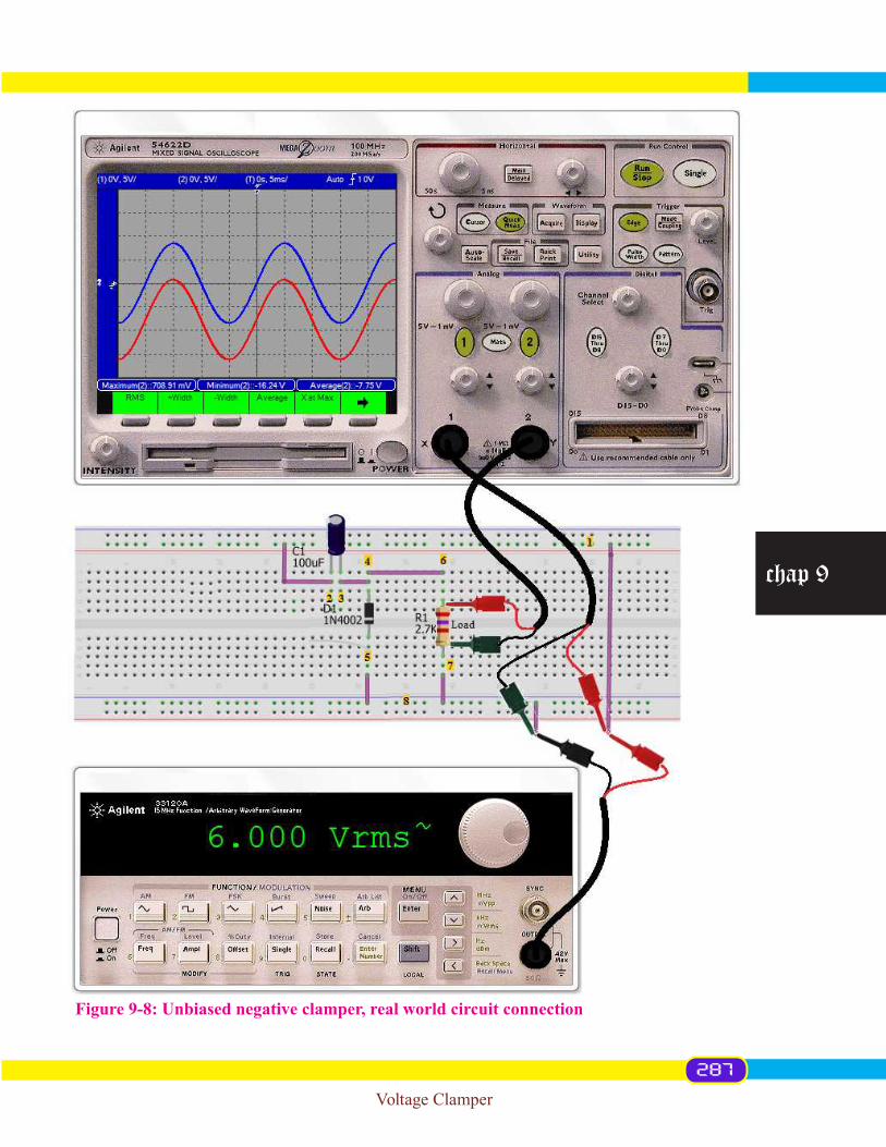
Voltage Clamper
chap 9
Figure 9-8: Unbiased negative clamper, real world circuit connection
287

Voltage Clamper
chap 9
• Biased negative clamper
Biased negative clamper is realized by inserting in negative clamper the DC source in series with diodeasshowninthecircuitfigure9-9.
When an input signal is applied during positive half cycle, the diode D1 will be forward biased when VIN1 is greater than the battery’s B1voltage(-3V)andthecapacitorC1 is charged. During the positive half cycle of input, the output voltage will be equal to the barrier potential of the di-odeplusthebattery’svoltage,0.7V+(-3V)andthecapacitorischargedto(Vin – VD).Duringthenegative half cycle, the diode becomes reversed biased and acts as an open circuit. Thus, there will be no effect on the capacitor voltage. The load resistance R1, being of very high value, cannot discharge C1 a lot during the negative portion of the input waveform. Thus during negative input, the output voltage will be the sum of the input voltage, the capacitor voltage and the batter’s volt-age and is equal to:
– Vin – (Vin – VD)-VB1 or – (2Vin+VB1 – VD).
Vout = –6*√2–(6*√2–0.7)–3V = –8.4853*2 + 0.7V – 3V = –16.9706–2.3V = –19.1706V
The value of the peak-to-peak output voltage will be the difference of the negative and positive peak voltage levels is equal to:
VD–VB1–[–(2Vin+VB1–VD)]orsimply2Vin.
Vout(peak-to-peak)=0.7V–3V–[(2*6*√2+3V–0.7V)]
=–2.3V–[–(16.9706V+2.3V)]
= –2.3 + 16.9706V + 2.3V
Figure 9-9: Biased negative clamper circuit
288

Voltage Clamper
chap 9
=16.9706V
Average voltage: Vav = (Vmax+Vmin)/2 = ((0.7–3)– (16.2706+3–0.7))/2 = – 20.8706/2
= –10.4353V
Procedure
Connectthecircuitasillustratedinfigure9-10.PlugtheACsupplyfromfunctiongeneratortopowerbusandgroundbus(1-8)ofbreadboard.Theredleadfromafunctiongenerator iscon-nectedtoapositivebusofbreadboard(1)andblackleadtogroundbus(8).
The capacitor C1isconnectedtoapowerbusofbreadboardthroughajumperwire(1-2),andtothe anode of diode D1(3-4).
The cathode of diode D1 is connected to negative terminal of the battery B1(5)andthepositiveterminalisconnectedtogroundbusof(8).
The load resistor R1 is connected to the anode of diode D1(4-6)andtogroundbusofbreadboadthroughajumperwire(7-8).
The circuit is supplied with 6V rms sinusoidal from a function generator. Both channel one (CH1)andchannel two(CH2)areat5Volt/divverticalsensitivityandat5mSec/divhorizontalsensitivity.
Push the AUTOSCALE button to display both channels. Reposition so that the 0V is at the mid-line on the both channels and the waveforms appear to overlap.
Modifying caliblation of vertical sensitivity and horizontal sensitivity to make the wave take up most of the screen without cutting any of its amplitude off and in the easy way reading and calcula-tion where necessary. Any accurate adjustment made on vertical or horizontal sensitivity does not affect the result.AtveryhighfrequenciesAUTOSCALEmaynotworkbecausethefilteredsignalistoosmall.
Use manual adjustments of the volts/division and time/division to reveal the signal.At high frequencies, the amplitude of the signal may be too small to be detected by the Auto-
scale feature. You may need to set the Volts/division scale manually in order to see the signal.Press the MEASURE button to determine the maximum and minimum voltages and peak-to-
peak amplitudes for both channels, and make a record.Thechannelone(CH1orX)ofoscilloscopeisdisplayingtheinputACvoltagewaveformwhile
thechanneltwo(CH2orY)isdisplayingtheresultingoutputvoltage.Theminimunandpeak-to-peak voltages measured from oscilloscope are – 19.14V and 16.89V respectively. The average value measured between the maximum and minimum of output voltage is – 0.67V.
Compare with what you would expect for this circuit based on theoretical calculations.
289

Voltage Clamper
chap 9
Figure 9-10: Biased negative clamper, real world circuit connection
290

Voltage Clamper
chap 9
9. 4. Applications of clamping circuits
Clamping circuits are used to shift any part of the input signal waveform and can be maintained ataspecifiedvoltagelevel.Suchcircuitsareusedinanalogtelevisionreceiverstorestoretheorigi-nald.creferencesignal(correspondingtothebrightnesslevelofthepicture)tothevideosignal.Analog television have a DC restorer circuit, which returns the voltage of the signal during the back porch of the line blanking period to 0 V. Low frequency interference, especially power line hum, induced onto the signal spoils the rendering of the image, and in extreme cases causes the set to lose synchronization. This interference can be effectively removed by using clamping circuits. In other words, the signal that is sent to the TV receiver may lose the dc components after being passedthroughcapacitivecoupledamplifiers.Thusthesignallosesitsblackandwhitereferencelevels and the blanking level. Before passing these signals to the picture tube, these reference levels have to be restored. This is done by using clamper circuits. Though the dc component that is lost in transmission is not the same as that introduced through a clamping circuit, the necessity to establish the extremity of the positive or negative signal excursion at some reference level is important.Clampercircuitsalsofindtheirapplicationinbothtelevisiontransmittersandreceiverswhere
areusedasa“DCrestorer”in“compositevideo”circuitry.AnNTSC(USvideostandard)videosignal“whitelevel”correspondstominimum(12.5%)transmittedpower.Thevideo“blacklevel”corresponds to a high level (75% of transmitter power. There is a “blacker than black level” cor-responding to 100% transmitted power assigned to synchronization signals. The NTSC signal contains both video and synchronization pulses. The problem with the composite video is that its average DC level varies with the scene, dark versus light. The video itself is supposed to vary. However, the sync must always peak at 100%. To prevent the sync signals from drifting with changing scenes, a “DC restorer” clamps the top of the sync pulses to a voltage corresponding to 100% transmitter modulation.
Clamper circuits are also used in storage counters, analog frequency meter, capacitance meter, divider and stair-case waveform generator.
291

Voltage Multiplier
chap 10
Objectives
When you have studied this chapter, you should
• Have an understanding of the working principle of the voltage multipliers• Be aware of the nuisance while working with high dc voltage• Be capable to design any type of voltage multiplier for any required voltage• Have an understanding of the applications of the diodes and capacitor voltage multipliers
Avoltagemultiplierisaspecialtypeofdioderectifiercircuitwhichproducesanoutputvolt-age greater than of the applied AC input voltage. The produced output voltage is theoretically an integer times the AC peak input, for example, 2, 3, 4, 5 etc. times the AC peak input. This type of voltage multiplier generates high voltages at relatively low currents and the circuit is generally at low cost. The circuit is constructed based on diodes and capacitor cascaded in concordance of the required output voltage. The diode and capacitor voltage multiplier is also referred to as CockcroftWaltonmultiplier,namedafterthetwomenwhousedthiscircuitdesigntobethefirsttosucceedinperformingthefirstnucleardisintegrationin1932.JamesDouglasCockcroftandErnest Thomas Sinton Walton, in fact have used this voltage multiplier cascade for the research which later made them winners of the 1951 Nobel Prize in physics for “Transmutation of atomic nucleusbyartificiallyacceleratedatomicparticles”.Lessknownisthefactthatthecircuitwasfirstdiscovered much earlier, in 1919, by Heinrich Greinacher, a Swiss physicist. For this reason, this doubler cascade is sometimes also referred to as the Greinacher multiplier.
Further readingStudy aids for this chapter are available at Zumbahlen,Hank(2008),Linear Circuit Design Handbook, Newnes
Chapter ten
Voltage Multiplier
292

Voltage Multiplier
chap 10
10. 1. Diode and capacitor voltage multiplier
Although it is usual in Electronic circuits to use a voltage transformer to increase a voltage, sometimes a suitable step-up transformer or a specially insulated transformer required for high voltage applications may not always be available. One alternative approach is to use a diode volt-age multiplier circuit which increases or “steps-up” the voltage without the use of a transformer. Unlike transformers this method eliminates the requirement for the heavy core and the bulk of insulation or potting required. By using only capacitors and diodes, these voltage multipliers can step up relatively low voltages to extremely high values, while at the same time being far lighter and cheaper than transformers. The major advantage of such circuit is that the voltage across each stage of this cascade is only equal to twice the peak input voltage, so it has the advantage of requir-ing relatively low cost components and being easy to insulate.Withinapowersupplyorotherrectifiercircuititispossibletoconfigurethediodesinsuchaway
that they double, triple or more, the level of the incoming voltage. Thus, it is possible to get 20 VDC from a 10 Vpeak AC source using a doubler, 40 VDC from a quadrupler. Any load in a practical circuitwilllowerthesevoltages.Thistypeofvoltagemultipliercircuitfindsusesinmanyapplica-tions where a low current, high voltage source is required.
10. 2. Voltage Doubler
As its name imply, a Voltage Doubler is a voltage multiplier circuit which has a voltage multi-plication factor of two. The circuit consists of only two diodes, two capacitors and an oscillating ACinputvoltage(aPulseWidthModulationwaveformcouldalsobeused).Thissimplediode-capacitor pump circuit gives a DC output voltage equal to the peak-to-peak value of the sinusoidal input. In other words, double the peak voltage value because the diodes and the capacitors work together to effectively double the voltage.
• Half wave voltage doubler
The half-wave voltage doubler is composed of two circuits: clamper and peak-detector (half-waverectifier).Thepeakdetector(halfwaverectifier)infigure10-2part(b)isshowninmodifiedformwhere
capacitor C1hasbeenadded.Referringtotheabovecircuit(a),capacitorC1 charges to the peak voltage of the supply, VC1=Vin*√2,(VC1=(Vin*√2)– 07consideringthediodedrop),onthenegative
Figure 10-1: Half wave voltage doubler circuit principle
293

Voltage Multiplier
chap 10
half cycle of AC input. The right end is grounded by the conducting of D1. The left end is charged at the negative peak of the AC input. This has the same operation of the clamper.
Duringthepositivehalfcycle,thehalfwaverectifiercomesintoplayatfigure10-2part(b).Di-ode D1 is out of the circuit since it is reverse biased. Capacitor C1 is now in series with the voltage source. At this time the polarities of the generator and capacitor C1 becomes in series aiding. Thus, rectifying diode D2 sees a total voltage at the peak of the sine wave, Vin*√2fromgeneratorandVC1 = Vin*√2 from capacitor C1. This total voltage charges the capacitor C2 with VC2 = 2* Vin*√2 (Vin*√2– (Vin*√2)– 0.7inconsiderationofdiodevoltagedrop).
In other words, V(positive peak) + V(negative peak) as on the negative half-cycle, D1 charges C1 to peak and on the positive half cycle D2 adds the AC peak voltage to Vpeak on C1 and transfers it all to C2. The voltage across capacitor C2 discharges through the load ready for the next half cycle.
Then the voltage across capacitor, C2 can be calculated as:
Vout = 2Vp,(minusofcoursethevoltagedropsacrossthediodesused)
Where Vp: The peak value of the input voltage.
Note that this double output voltage is not instantaneous but increases slowly on each input cycle, eventually settling to 2Vp. As capacitor C2 only charges up during one half cycle of the input waveform, the resulting output voltage discharged into the load has a ripple frequency equal to the supply frequency, hence the name half wave voltage doubler.
Thedisadvantageisthedifficultytosmoothoutthislargeripplefrequencyalmostthesamewayasforahalfwaverectifiercircuit.Also,capacitorC2 must have a DC voltage rating at least twice the value of the peak input voltage.
• Full wave voltage doubler
Full wave voltage doubler circuit is made up from two half-wave rectifier circuits. This isachievedbyaddingaseconddiodeandcapacitortotheoutputofastandardhalfwaverectifierandthis helps to increase its output voltage to the double of the input.
Figure 10-2: Voltage doubler; (a) Clamper and peak-detector, (b) Half-wave rectifier
294

Voltage Multiplier
chap 10
Working Principle of the Circuit
For the positive half cycle of the input voltage Vin, capacitor C1 charges up to (VC1) thepeakof the applied input voltage through diode D1. When the sinusoidal input voltage Vin is negative, capacitor C2 charges up to (VC2)thepeakinputthroughdiodeD2. These two capacitors work as storingdevices(batteries)withseriesadding.ThereforetheoutputvoltageVout is summation of voltage stored by two capacitors, Vout = VC1+VC2 = 2Vin(peak) and is taken across the two series con-nected capacitors. The advantage of such circuit is an easy smoothing.
Design a voltage multiplier based on voltage doubler capable to provide output DC voltage double of the input AC voltage from 9VACsupply.Usecomponentswithspecificationdescribedinthe part list below and measure the resulting voltage using voltmeter.
Part list
No Items Specifications Quantity1 9VAC supply Agilent function generator 33120A 12 Voltmeter Digital multimeter 13 Breadboard Prototypingboard(miniboard) 14 Connecting wire 22-gauge (0.33mm2)solidwire 20cm5 Diode(D1andD2) 1N4007 26 Capacitor(C1andC2) 33µF/50V electrolytic Capacitor 27 Load resistor 10KΩ,½watt 1
• Half wave voltage doubler
Letconsiderthehalfwavevoltagedoublerofthecircuitfigure10-4obtainedbyassigningthevaluestothepriordetailedcircuitwiththeaboveitemsspecifications.
Procedure and Working Principle
Thecircuit,figure10-4,showsahalfwavevoltagedoubler.Duringthenegativehalfcycleofthe
Figure 10-3: Full wave voltage doubler circuit principle
Experiment 10-1: Half wave voltage doubler and full wave voltage doubler
295

Voltage Multiplier
chap 10
sinusoidal input waveform Vin, diode D1 is forward biased and conducts charging up the capacitor C1 to the peak value (Vp)oftheinputvoltage.
Figure 10-4: Half wave voltage doubler circuit
Figure 10-5: Half wave voltage doubler, real world circuit connection
296

Voltage Multiplier
chap 10
VC1 = Vin*√2=9V*1.4142=12.7279V; (12.0279Vconsideringthediodedrop).Becausethereis no path for capacitor C1 to discharge into, it remains fully charged and acts as a battery in series with the voltage supply Vin.
During the positive half cycle, diode D1 is reverse biased blocking the discharging of C1 while diode D2 is forward biased charging up capacitor C2. Since there is a voltage across ca-pacitor C1 already equal to the peak input voltage 12.7279V (12.0279V considering diode drop),capacitorC2 charges to twice the peak voltage value of the input signal Vin or simply say V(positivepeak) + V(negativepeak).
VC2 = 2*Vin*√2 = 2*9*1.4142 = 25.4558V; (25.4558V-1.4V = 24.0558V considering diodes voltage drops.
Voltmeter reading is rms value and this is given by:
Vrms= Vpeak/√2 =24.0558/1.4142=17.01V
• Full wave voltage doubler
Thefull-wavevoltagedoubler iscomposedofapairofseriesstackedhalfwaverectifiersasshowninthecircuitfigure10-6.ThebottomrectifierchargesC2onthenegativehalfcycleofinput.ThetoprectifierchargesC1
on the positive half cycle. Each capacitor takes on a charge the peak voltage of the supply, that is 9*Vor12.727V(12.0.27Vconsideringdiodedrop).Theoutputvoltageistheseriestotalvoltagestored in capacitor C1 and C2.
Vout = VC1 + VC2 = 12.727 V+12.727 V = 25.456 V; Vout =12.027V*2=24.054V(byconsideringdiodedrops).Voltmeter reading is rms value and this is given by:Vrms = Vpeak/√2=24.054V/1.4142=17.008V
Figure 10-6: Full wave voltage doubler circuit
Be careful when touching or handling capacitors in or out of a circuit. Capacitors are capable of storing electrical charge for a long time after power has turned off in a cir-cuit. If you touch the leads, you may be in for a shock as the capacitor discharges through you! It is usually good practice to discharge a capacitor using a shorting tool with an insu-lated grip of some sort before handling the capacitor.
Safety point
297
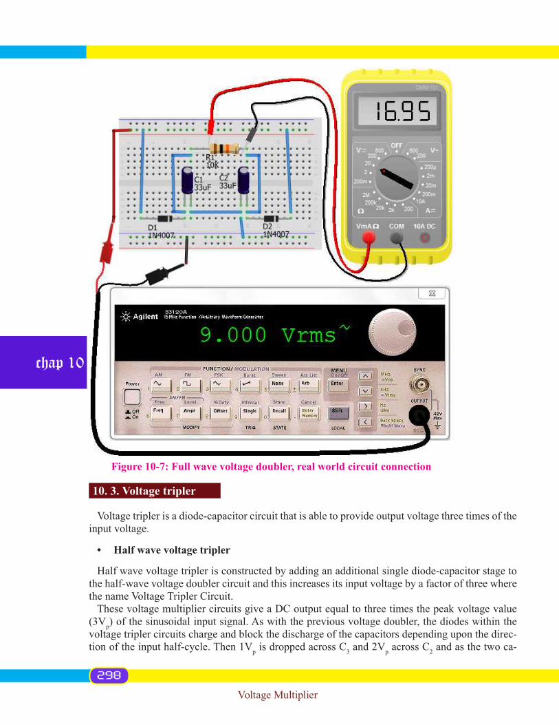
Voltage Multiplier
chap 10
10. 3. Voltage tripler
Voltage tripler is a diode-capacitor circuit that is able to provide output voltage three times of the input voltage.
• Half wave voltage tripler
Half wave voltage tripler is constructed by adding an additional single diode-capacitor stage to the half-wave voltage doubler circuit and this increases its input voltage by a factor of three where the name Voltage Tripler Circuit.
These voltage multiplier circuits give a DC output equal to three times the peak voltage value (3Vp)ofthesinusoidalinputsignal.Aswiththepreviousvoltagedoubler,thediodeswithinthevoltage tripler circuits charge and block the discharge of the capacitors depending upon the direc-tion of the input half-cycle. Then 1Vp is dropped across C3 and 2Vp across C2 and as the two ca-
Figure 10-7: Full wave voltage doubler, real world circuit connection
298

Voltage Multiplier
chap 10
pacitors are in series and act as batteries, this results in the output load seeing a voltage equivalent to 3Vp.
• Full wave voltage tripler
A full wave voltage tripler is built from a combination of a doubler and a half wave rec-tifier (C3, D3). The half-wave rectifier produces the peak voltage from input, Vp=Vin*√2V , (Vp=Vin*√2V– 0.7Vconsideringdiodedrop)atnodejunctionofC3 and C2.
The doubler provides another 2Vp=2*Vin*√2V (2*Vin*√2V– 1.4V considering diode voltage drop)attheterminalofC2. For a total output voltage of 3Vp=3Vin*√2V(3Vin*√2V– 2.1V consider-ingdiodevoltagedrop)attheoutputofD2 with respect to ground.
Design a voltage multiplier based on voltage tripler capable to provide output DC voltage three timestheinputACvoltagefrom9VACsupply.Usecomponentswithspecificationdescribedinthepart list below and measure the resulting voltage using voltmeter.
Figure 10-8: (a) and (b), Half wave voltage tripler base circuits
Figure 10-9: Full wave voltage tripler circuit principle
Experiment 10-2: Halfwave voltage tripler, fullwave voltage tripler
299

Voltage Multiplier
chap 10
Part list
No Items Specifications Quantity1 9VAC supply Agilent function generator 33120A 12 Voltmeter Digital multimeter 13 Breadboard Prototypingboard(RSR03MB102) 14 Connecting wire 22-gauge (0.33mm2)solidwire 20cm5 Diode(D1,D2andD3) 1N4002 36 Capacitor(C1,C2andC3) 47µF/100V electrolytic Capacitor 37 Load resistor 100KΩ,1watt 1
• Half wave voltage tripler
Procedure and Working Principle
1. Positive half cycle of the input voltage Vin, capacitor C3 is charged through D3 to the peak value Vp=9V*√2,thatis12.7278V(12.0278Vconsideringdiodevoltagedrop)betweenleft and right plate of the capacitor C3.
2. Negative half cycle of the supply voltage Vin, the potential of C3 (VC3)addswiththatofsupply Vin thus charging capacitor C1 through D1 to 2Vp=9*√2+9*√2,thatis25.4556V(24.0556Vconsideringdiodevoltagedrop).
3. Positive half cycle of the input supply Vin, the potential of C3 (VC3)hasdroppedto0Vthusallowing capacitor C2 to be charged to 3Vp through D2, the potential of C1 (VC1)addstothesource Vin.
VC2 = 3Vp=9V*√2+2*9V*√2=12.7278V+25.4556V=38.1834V(36.0834Vconsideringdiodesvoltagedrop)
Figure 10-10: Half wave voltage tripler circuit
300

Voltage Multiplier
chap 10
• Full wave Voltage Tripler
Procedure and Working Principle
1. Negative half cycle of the input voltage Vin, capacitor C1 is charged through D1 to the peak value Vp=9V*√2, that is12.7278V(12.0278Vconsideringdiodevoltagedrop)betweenleft and right plate of the capacitor C1. At the same time, capacitor C3 charges to the peak value VC3=12.7278V(12.0278Vconsideringdiodedrop)
2. Positive half cycle of the supply voltage Vin, the potential of C1 (VC1)addswith thatofsupply Vin thus charging capacitor C2 through D2 to 2Vp=9*√2+9*√2, that is25.4556V(24.0556Vconsideringdiodevoltagedrop).
Thus the potential of capacitor C2 (VC2)addstothatofcapacitorC3 (VC3)togiveoutputvoltagethat is equal to 3Vp.
Figure 10-11: Half wave voltage tripler, real world circuit connection
301

Voltage Multiplier
chap 10
Vout=VR(load)=3*9V*√2=38.1834V(36.0834Vconsideringdiodesdrop)
Figure 10-12: Full wave voltage tripler circuit
Figure 10-13: Full wave voltage tripler, real world circuit connection
302

Voltage Multiplier
chap 10
PVariations of the basic circuit and concept are available to provide a voltage multiplier function ofalmostanyfactor.Applyingthesameprincipleofsittingonerectifierontopofanotherandusing capacitive coupling enables a form of ladder network to build up.
To calculate the expected voltage at the output with a given input and number of stages, just replace number in the following formula:
Vout=(2xVin)xSx√2
Where
Vout: The output voltage, Vin: Input voltage from supply and S: The number of stages
In theory any desired amount of voltage multiplication can be obtained and a cascade of “N” doublers, would produce an output voltage of 2N.Vp volts. For example, a 10-stage voltage multi-plier circuit with a peak input voltage of 100 volts would give a DC output voltage of about 1,000 volts or 1kV, assuming no losses, without the use of a transformer. This is achieved by simply using circuits made from diodes and capacitors that can increase the input voltage by two, three, or four times, etc, depending on the ratio of the output voltage to the input voltage, by cascading together individual half or full stage multipliers in series to apply the desired DC voltage to a given load without the need for a step-up transformer.
However, the diodes and capacitors used in all multiplication circuits need to have a minimum reverse breakdown voltage rating of at least twice the peak voltage across them as multi-stage volt-age multiplication circuits can produce very high voltages, so take care. Also, voltage multipliers usually supply low currents to a high resistance loads as the output voltage quickly drops away as the load current increases.
10. 4. Positive and negative voltage multiplier
The Voltage Multiplication circuits shown above are all designed to give a positive DC output voltage. But they can also be designed to give negative voltage outputs by simply reversing the polarities of all the multiplier diodes and capacitors to produce negative voltage doublers.
Several cycles are required to reach full voltage. The polarity of the high voltage output is simply determinedbytheconfigurationofthediodes,asshowninthediagramsabove.
Figure 10-14: Positive multiplier circuit principle
303

Voltage Multiplier
chap 10
InanymultiplierrunningunderloadtheaverageDCcurrentflowingthrougheachdiode,Idiode, is the same.Inreality,morecyclesarerequiredtoreachthefullvoltageasshowninthefigure10-16.
10. 5. Full wave voltage multipliers circuit principle
Increasing the frequency can dramatically reduce the ripple, and the voltage drop under load, which accounts for the popularity of driving a multiplier stack with a switching power supply. A cleverwaytoreducerippleistoimplementafullwavevoltagedoublerasshowninfigure10-17.This effectively doubles the number of charging cycles per second, and thus cuts down the voltage drop and ripple factor. The input is usually fed from a centre tapped ac transformer or MOSFET H-bridge circuits.
The Cockcroft Walton or Greinacher design is based on the Half-Wave Series Multiplier, or volt-age doubler. In fact, all multiplier circuits can be derived from its operating principles.
Figure 10-15: Negative multiplier circuit principle
Figure 10-16: Cycles to reach to the full voltage
304

Voltage Multiplier
chap 10
10. 6. Precautions
Voltage multipliers produce lethal current at high voltage. The output of these devices can cause injury which can result in death if the common sense safety procedures are not followed.
Safety precautions and procedures
• Wear rubber safety groves and stand on a rubber safety mat when powering or using volt-age multipliers.
• Ground the output of voltage multiplier after powering it off. It can retain a lethal voltage for several minutes after powering down.
• Do not touch any of its device at any time during operation• Do not allow others who are not familiar with high voltage devices to touch or use without
proper supervision.
• Do not operate these devices alone. Have an emergency person available when performing your experiment who is familiar with proper rescue procedures.
10. 7. Applications of voltage multipliers
The voltage multiplier circuits are very useful. However they are normally suitable only for low current applications. As the voltage multiplication increases the losses increase. The source resis-tance tends to rise, and loading becomes an issue. For each diode in the chain there is the usual diodedrop(normally0.6voltsforasilicondiode),butthereactanceofthecapacitorscanbecomesignificant,especiallywhenmainsfrequenciesof50or60Hzareused.Highvoltagehighvaluecapacitors can be expensive and large. This may provide physical constraints for making them too large.Voltagemultipliershavemanypracticalapplicationsandfindtheirwayin lasersystems,CRT tubes, hv power supplies, LCD backlighting, power supplies, x-ray systems, traveling wave tubes, ion pumps, electrostatic systems, air ionisers, particle accelerators, copy machines, scien-tificinstrumentation,oscilloscopes,andmanyotherapplicationsthatutilizehighvoltageDC.
Figure 10-17: Full wave voltage multiplier circuit principle
305

General Purpose Plastic Rectifier
This data sheet provides information on subminiature size, axial lead mounted rectifiers for general−purpose low−power applications.
PRIMARY CHARACTERISTICSIF(AV) 1.0 AVRRM 50 V to 1000 VIFSM (8.3 ms sine-wave) 30 AIFSM (square wave tp = 1 ms) 45 AVF 1.1 VIR 5.0 μA
TJ max. 150 °C
FEATURES
• Low forward voltage drop
• Low leakage current
• High forward surge capability
• Solder dip 275 °C max. 10 s, per JESD 22-B106
• Compliant to RoHS Directive 2002/95/EC and in accordance to WEEE 2002/96/EC
Vishay General Semiconductor
1N4001, 1N4002, 1N4003, 1N4004, 1N4005, 1N4006, 1N4007
MARKING
A = Assembly Location
1N400x = Device Number
x = 1, 2, 3, 4, 5, 6 or 7
YY = Year
WW = Work Week
= Pb−Free Package
(Note: Microdot may be in either location)
CASE: DO-41
Devices DatasheetsAppendix
306

TYPICAL APPLICATIONS
For use in general purpose rectification of power supplies,
inverters, converters and freewheeling diodes application.
MECHANICAL DATA
Case: DO-204AL, molded epoxy body
Molding compound meets UL 94 V-0 flammability rating
Base P/N-E3 - RoHS compliant, commercial grade
Terminals: Matte tin plated leads, solderable per
J-STD-002 and JESD 22-B102
E3 suffix meets JESD 201 class 1A whisker test
Polarity: Color band denotes cathode end
MAXIMUM RATINGS (TA = 25 °C unless otherwise noted)PARAMETER SYMBOL 1N4001 1N4002 1N4003 1N4004 1N4005 1N4006 1N4007 UNIT
Maximum repetitive peak reverse voltage VRRM 50 100 200 400 600 800 1000 VMaximum RMS voltage VRMS 35 70 140 280 420 560 700 VMaximum DC blocking voltage VDC 50 100 200 400 600 800 1000 VMaximum average forward rectified current 0.375" (9.5 mm) lead length at TA = 75 °C IF(AV) 1.0
A
Peak forward surge current 8.3 ms single half sine-wave superimposed on rated load IFSM 30
A
Non-repetitive peak forward surge current square waveform TA = 25 °C
tp=1msIFSM
45Atp=2ms 35
tp=5ms 30Maximum full load reverse current, full cycle average 0.375" (9.5 mm) lead length TL = 75 °C IR(AV) 30
µA
Rating for fusing (t < 8.3 ms) I2t(1) 3.7 A2S
Operating junction and storage temperature range
TJ, TSTG -50 to +150
0C
Note(1) For device using on bridge rectifier application
Stresses exceeding Maximum Ratings may damage the device. Maximum Ratings are stress rat-ings only. Functional operation above the Recommended Operating Conditions is not implied. Extended exposure to stresses above the Recommended Operating Conditions may affect device reliability.
307

ELECTRICAL CHARACTERISTICS (TA = 25 °C unless otherwise noted)PARAMETER TEST CONDITIONS SYMBOL 1N4001 1N4002 1N4003 1N4004 1N4005 1N4006 1N4007 UNIT
Maximum instantaneous forward voltage 1.0 A VF 1.1 V
Maximum DC reverse current at rated DC blocking voltage
TA = 25 °CIR
5.5μA
TA = 125 °C 50Typical junction capacitance 4.0 V, 1 MHz CJ 15 pF
THERMAL CHARACTERISTICS (TA = 25 °C unless otherwise noted)PARAMETER SYMBOL 1N4001 1N4002 1N4003 1N4004 1N4005 1N4006 1N4007 UNIT
Typical thermal resistance
RθJA (1) 50 °C/WRθJL
(1) 25 Note
(1) Thermal resistance from junction to ambient at 0.375" (9.5 mm) lead length, PCB mounted
PACKAGE OUTLINE DIMENSION
Dimemsion DO-204AL (DO-41)Min Max
A 25.40 -B 4.06 5.21C 0.71 0.864D 2.00 2.72
All dimensions in mm
308

BZX85C...Vishay Semiconductors
Silicon Epitaxial Planar Z–Diodes
Features
• Sharp edge in reverse characteristics• Low reverse current• Low noise• Very high stability• Available with tighter tolerances
Applications
Voltage stabilization
Order Instruction
Type Ordering Code RemarksBZX85C2V7 BZX85C2V7–TAP Ammopack
BZX85C2V7–TR Tape and Reel
Absolute Maximum Ratings
Tj = 25° C
Parameter Test Conditions Type Symbol Value UnitPower dissipation l=4 mm, TL=25 °C PV 1.3 WJunction temperature Tj 175 °CStorage temperature range Tstg –65...+175 °C
309

Maximum Thermal Resistance
Tj = 25° C
Parameter Test Conditions Symbol Value UnitJunction ambient l=4 mm, TL=constant RthJA 110 K/W
Electrical Characteristics
Tj = 25° C
Parameter Test Conditions Type Symbol Min Typ Max UnitForward voltage IF=200mA VF 1 V
ELECTRICAL CHARACTERISTICS (TA=25OC unless otherwise noted)
Nominal zener voltage
Zener voltage range Dynamic resistance
Reverse leakage current
Temperature Coefficient of zener voltage
Type VZnom IZT for VZT and rzjT rzjk at IZK IR at VR TKVZ
BZX85C... V mA V(1) Ohm Ohm mA A V %/KBZX85C 2V7 2.7 80 2.5 to 2.9 < 20 < 400 1 < 150 1 –0.08 to –0.05BZX85C 3V0 3.0 80 2.8 to 3.2 < 20 < 400 1 < 100 1 –0.08 to –0.05BZX85C 3V3 3.3 80 3.1 to 3.5 < 20 < 400 1 < 40 1 –0.08 to –0.05BZX85C 3V6 3.6 60 3.4 to 3.8 < 20 < 500 1 < 20 1 –0.08 to –0.05BZX85C 3V9 3.9 60 3.7 to 4.1 < 15 < 500 1 < 10 1 –0.07 to –0.02BZX85C 4V3 4.3 50 4.0 to 4.6 < 13 < 500 1 < 3 1 –0.07 to –0.01BZX85C 4V7 4.7 45 4.4 to 5.0 < 13 < 500 1 < 3 1 –0.03 to +0.04BZX85C 5V1 5.1 45 4.8 to 5.4 < 10 < 500 1 < 1 1.5 –0.01 to +0.04BZX85C 5V6 5.6 45 5.2 to 6.0 < 7 < 400 1 < 1 2 0 to +0.045BZX85C 6V2 6.2 35 5.8 to 6.6 < 4 < 300 1 < 1 3 +0.01 to +0.055BZX85C 6V8 6.8 35 6.4 to 7.2 < 3.5 < 300 1 < 1 4 +0.015 to +0.06BZX85C 7V5 7.5 35 7.0 to 7.9 < 3 < 200 0.5 < 1 4.5 +0.02 to +0.065BZX85C 8V2 8.2 25 7.7 to 8.7 < 5 < 200 0.5 < 1 6.2 0.03 to 0.07BZX85C 9V1 9.1 25 8.5 to 9.6 < 5 < 200 0.5 < 1 6.8 0.035 to 0.075BZX85C 10 10 25 9.4 to 10.6 < 7 < 200 0.5 < 0.5 7.5 0.04 to 0.08BZX85C 11 11 20 10.4 to 11.6 < 8 < 300 0.5 < 0.5 8.2 0.045 to 0.08BZX85C 12 12 20 11.4 to 12.7 < 9 < 350 0.5 < 0.5 9.1 0.045 to 0.085BZX85C 13 13 20 12.4 to 14.1 < 10 < 400 0.5 < 0.5 10 0.05 to 0.085BZX85C 15 15 15 13.8 to 15.6 < 15 < 500 0.5 < 0.5 11 0.055 to 0.09BZX85C 16 16 15 15.3 to 17.1 < 15 < 500 0.5 < 0.5 12 0.055 to 0.09BZX85C 18 18 15 16.8 to 19.1 < 20 < 500 0.5 < 0.5 13 0.06 to 0.09BZX85C 20 20 10 18.8 to 21.2 < 24 < 600 0.5 < 0.5 15 0.06 to 0.09BZX85C 22 22 10 20.8 to 23.3 < 25 < 600 0.5 < 0.5 16 0.06 to 0.095
310

BZX85C 24 24 10 22.8 to 25.6 < 25 < 600 0.5 < 0.5 18 0.06 to 0.095BZX85C 27 27 8 25.1 to 28.9 < 30 < 750 0.25 < 0.5 20 0.06 to 0.095BZX85C 30 30 8 28 to 32 < 30 < 1000 0.25 < 0.5 22 0.06 to 0.095BZX85C 33 33 8 31 to 35 < 35 < 1000 0.25 < 0.5 24 0.06 to 0.095BZX85C 36 36 8 34 to 38 < 40 < 1000 0.25 < 0.5 27 0.06 to 0.095BZX85C 39 39 6 37 to 41 < 50 < 1000 0.25 < 0.5 30 0.06 to 0.095BZX85C 43 43 6 40 to 46 < 50 < 1000 0.25 < 0.5 33 0.06 to 0.095BZX85C 47 47 4 44 to 50 < 90 < 1500 0.25 < 0.5 36 0.06 to 0.095BZX85C 51 51 4 48 to 54 < 115 < 1500 0.25 < 0.5 39 0.06 to 0.095BZX85C 56 56 4 52 to 60 < 120 < 2000 0.25 < 0.5 43 0.06 to 0.095BZX85C 62 62 4 58 to 66 < 125 < 2000 0.25 < 0.5 47 0.06 to 0.095BZX85C 68 68 4 64 to 72 < 130 < 2000 0.25 < 0.5 51 0.06 to 0.095BZX85C 75 75 4 70 to 79 < 135 < 2000 0.25 < 0.5 56 0.06 to 0.095
(1) Tighter tolerances available on request: BZX85B... ± 2% of VZ nominal
Dimensions in mm
Technical drawings according to DIN specifications
Standard Glass Case 54
B 2 DIN 41880 JEDEC
DO 41 Weight max. 0.3 g
311

BZX55C...Vishay Telefunken
Silicon Epitaxial Planar Z–Diodes
Features
• Very sharp reverse characteristic
• Low reverse current level
• Very high stability
• Low noise
• Available with tighter tolerances
Applications
Voltage stabilization
Absolute Maximum Ratings
Tj = 25° C
Parameter Test Conditions Type Symbol Value UnitPower dissipation l=4mm, TL=25° C PV 500 mWZ–current IZ PV/VZ mAJunction temperature Tj 175 °CStorage temperature range Tstg –65...+175 °C
Maximum Thermal Resistance
Tj = 25° C
Parameter Test Conditions Symbol Value UnitJunction ambient l=4mm, TL=constant RthJA 300 K/W
312

Electrical Characteristics
Tj = 25° C
Parameter Test Conditions Type Symbol Min Typ Max UnitForward voltage IF=200mA VF 1.5 V
Type VZnom IZT for VZT and rzjT rzjk at IZK IR and IR at VR
TKVZ
BZX55C... V mA V (1) Ohm Ohm mA A A(2) V %/KBZX55C2V4 2.4 5 2.28 to 2.56 < 85 < 600 1 < 50 <
1001 –0.09 to –0.06
BZX55C2V7 2.7 5 2.5 to 2.9 < 85 < 600 1 < 10 < 50 1 –0.09 to –0.06BZX55C3V0 3.0 5 2.8 to 3.2 < 85 < 600 1 < 4 < 40 1 –0.08 to –0.05BZX55C3V3 3.3 5 3.1 to 3.5 < 85 < 600 1 < 2 < 40 1 –0.08 to –0.05BZX55C3V6 3.6 5 3.4 to 3.8 < 85 < 600 1 < 2 < 40 1 –0.08 to –0.05BZX55C3V9 3.9 5 3.7 to 4.1 < 85 < 600 1 < 2 < 40 1 –0.08 to –0.05BZX55C4V3 4.3 5 4.0 to 4.6 < 75 < 600 1 < 1 < 20 1 –0.06 to –0.03BZX55C4V7 4.7 5 4.4 to 5.0 < 60 < 600 1 < 0.5 < 10 1 –0.05 to +0.02BZX55C5V1 5.1 5 4.8 to 5.4 < 35 < 550 1 < 0.1 < 2 1 –0.02 to +0.02BZX55C5V6 5.6 5 5.2 to 6.0 <25 < 450 1 < 0.1 < 2 1 –0.05 to +0.05BZX55C6V2 6.2 5 5.8 to 6.6 < 10 < 200 1 < 0.1 < 2 2 0.03 to 0.06BZX55C6V8 6.8 5 6.4 to 7.2 < 8 < 150 1 < 0.1 < 2 3 0.03 to 0.07BZX55C7V5 7.5 5 7.0 to 7.9 < 7 < 50 1 < 0.1 < 2 5 0.03 to 0.07BZX55C8V2 8.2 5 7.7 to 8.7 < 7 < 50 1 < 0.1 < 2 6.2 0.03 to 0.08BZX55C9V1 9.1 5 8.5 to 9.6 < 10 < 50 1 < 0.1 < 2 6.8 0.03 to 0.09BZX55C10 10 5 9.4 to 10.6 < 15 < 70 1 < 0.1 < 2 7.5 0.03 to 0.1BZX55C11 11 5 10.4 to 11.6 < 20 < 70 1 < 0.1 < 2 8.2 0.03 to 0.11BZX55C12 12 5 11.4 to 12.7 < 20 < 90 1 < 0.1 < 2 9.1 0.03 to 0.11BZX55C13 13 5 12.4 to 14.1 < 26 < 110 1 < 0.1 < 2 10 0.03 to 0.11BZX55C15 15 5 13.8 to 15.6 < 30 < 110 1 < 0.1 < 2 11 0.03 to 0.11BZX55C16 16 5 15.3 to 17.1 < 40 < 170 1 < 0.1 < 2 12 0.03 to 0.11BZX55C18 18 5 16.8 to 19.1 < 50 < 170 1 < 0.1 < 2 13 0.03 to 0.11BZX55C20 20 5 18.8 to 21.2 < 55 < 220 1 < 0.1 < 2 15 0.03 to 0.11BZX55C22 22 5 20.8 to 23.3 < 55 < 220 1 < 0.1 < 2 16 0.04 to 0.12BZX55C24 24 5 22.8 to 25.6 < 80 < 220 1 < 0.1 < 2 18 0.04 to 0.12BZX55C27 27 5 25.1 to 28.9 < 80 < 220 1 < 0.1 < 2 20 0.04 to 0.12BZX55C30 30 5 28 to 32 < 80 < 220 1 < 0.1 < 2 22 0.04 to 0.12BZX55C33 33 5 31 to 35 < 80 < 220 1 < 0.1 < 2 24 0.04 to 0.12BZX55C36 36 5 34 to 38 < 80 < 220 1 < 0.1 < 2 27 0.04 to 0.12BZX55C39 39 2.5 37 to 41 < 90 < 500 0.5 < 0.1 < 5 30 0.04 to 0.12BZX55C43 43 2.5 40 to 46 < 90 < 600 0.5 < 0.1 < 5 33 0.04 to 0.12BZX55C47 47 2.5 44 to 50 < 110 < 700 0.5 < 0.1 < 5 36 0.04 to 0.12
313

BZX55C51 51 2.5 48 to 54 < 125 < 700 0.5 < 0.1 < 10 39 0.04 to 0.12BZX55C56 56 2.5 52 to 60 < 135 < 1000 0.5 < 0.1 < 10 43 0.04 to 0.12BZX55C62 62 2.5 58 to 66 < 150 < 1000 0.5 < 0.1 < 10 47 0.04 to 0.12BZX55C68 68 2.5 64 to 72 < 200 < 1000 0.5 < 0.1 < 10 51 0.04 to 0.12BZX55C75 75 2.5 70 to 79 < 250 < 1500 0.5 < 0.1 < 10 56 0.04 to 0.12
(1) Tighter tolerances available on request:
BZX55A... ± 1% of VZnominal
BZX55B... ± 2% of VZnominal
BZX55F... ± 3% of VZnominal
(2) at Tj= 150 C
All dimensions in mm
Technical drawings ac-cording to DIN specifications
Standard Glass
Case 54 A 2 DIN
41880 JEDEC DO 35
Weight max. 0.3 g
314

LM78XX/LM78XXA3-Terminal 1A Positive Voltage Regulator
Features• Output Current up to 1A• Output Voltages of 5, 6, 8, 9, 10, 12, 15, 18, 24• Thermal Overload Protection• Short Circuit Protection• Output Transistor Safe Operating Area Protection
General Description
The LM78XX series of three terminal positive regulators are available in the TO-220 package and with several fixed output voltages, making them useful in a wide range of applications. Each type employs internal current limiting, ther-mal shut down and safe operating area protection, making it essentially inde-structible. If adequate heat sinking is provided, they can deliver over 1A output current. Although designed primarily as fixed voltage regulators, these devices can be used with external components to obtain adjustable voltages and currents.
Pin assignment
Absolute Maximum Ratings
Absolute maximum ratings are those values beyond which damage to the device may occur. The datasheetspecificationsshouldbemet,withoutexception,toensurethatthesystemdesignisreli-able over its power supply, temperature, and output/input loading variables. It is not recommend operationoutsidedatasheetspecifications. Inaddition,extendedexposure tostressesabove therecommended operating conditions may affect device reliability. The absolute maximum ratings are stress rating only. Values are at TA = 25oC unless otherwise noted.
Symbol Parameter Value UnitVI Input Voltage VO = 5V to 18V 35 V
VO = 24V 40 VRθJC ThermalResistanceJunction-Cases(TO-220) 5 °C/WRθJA ThermalResistanceJunction-Air(TO-220) 65 °C/WTOPR Operating temperature
rangeLM78XX -40 to +125 °CLM78XXA 0 to +125
TSTG Storage Temperature Range -65 to + 150 °C
315

Electrical Characteristics (LM7805)
Refer to the test circuits. -40°C < TJ < 125°C, IO = 500mA, VI = 10V, CI = 0.1µF, unless otherwise speci-fied.Symbol Parameter Conditions Min. Typical Max. UnitVo Output voltage TJ = +25°C 4.8 5.0 5.2 V
5mA ≤ IO ≤ 1A, PO ≤ 15W, VI = 7V to 20V
4.75 5.0 5.25 V
Electrical Characteristics (LM7806)
Refer to the test circuits. -40°C < TJ < 125°C, IO = 500mA, VI = 11V, CI = 0.33µF, CO = 0.1µF, unless other-wise specified.Symbol Parameter Conditions Min. Typical Max. UnitVo Output voltage TJ = +25°C 5.75 6.0 6.25 V
5mA ≤ IO ≤ 1A, PO ≤ 15W, VI = 8.0V to 21V
5.7 6.0 6.3 V
Electrical Characteristics (LM7808)
Refer to the test circuits. -40°C < TJ < 125°C, IO = 500mA, VI = 14V, CI = 0.33µF, CO = 0.1µF, unless other-wise specified.Symbol Parameter Conditions Min. Typical Max. UnitVo Output voltage TJ = +25°C 7.7 8.0 8.3 V
5mA ≤ IO ≤ 1A, PO ≤ 15W, VI = 10.5V to 23V
7.6 8.0 8.4 V
Electrical Characteristics (LM7809)
Refer to the test circuits. -40°C < TJ < 125°C, IO = 500mA, VI = 15V, CI = 0.33µF, CO = 0.1µF, unless other-wise specified.Symbol Parameter Conditions Min. Typical Max. UnitVo Output voltage TJ = +25°C 8.65 9.0 9.35 V
5mA ≤ IO ≤ 1A, PO ≤ 15W, VI = 11.5V to 24V
8.6 9.0 9.4 V
Electrical Characteristics (LM7810)
Refer to the test circuits. -40°C < TJ < 125°C, IO = 500mA, VI = 16V, CI = 0.33µF, CO = 0.1µF, unless other-wise specified.Symbol Parameter Conditions Min. Typical Max. UnitVo Output voltage TJ = +25°C 9.6 10.0 10.4 V
5mA ≤ IO ≤ 1A, PO ≤ 15W, VI = 12.5V to 25V
9.5 10.0 10.5 V
316

Electrical Characteristics (LM7812) (Continued)
Refer to the test circuits. -40°C < TJ < 125°C, IO = 500mA, VI = 19V, CI = 0.33µF, CO = 0.1µF, unless other-wise specified.Symbol Parameter Conditions Min. Typical Max. UnitVo Output voltage TJ = +25°C 11.5 12.0 12.5 V
5mA ≤ IO ≤ 1A, PO ≤ 15W, VI = 14.5V to 27V
11.4 12.0 12.6 V
Electrical Characteristics (LM7815)
Refer to the test circuits. -40°C < TJ < 125°C, IO = 500mA, VI = 23V, CI = 0.33µF, CO = 0.1µF, unless other-wise specified.Symbol Parameter Conditions Min. Typical Max. UnitVo Output voltage TJ = +25°C 14.4 15.0 15.6 V
5mA ≤ IO ≤ 1A, PO ≤ 15W, VI = 17.5V to 30V
14.25 15.0 15.75 V
Electrical Characteristics (LM7818)
Refer to the test circuits. -40°C < TJ < 125°C, IO = 500mA, VI = 27V, CI = 0.33µF, CO = 0.1µF, unless other-wise specified. Symbol Parameter Conditions Min. Typical Max. UnitVo Output voltage TJ = +25°C 17.3 18.0 18.7 V
5mA ≤ IO ≤ 1A, PO ≤ 15W, VI = 21V to 33V
17.1 18.0 18.9 V
Electrical Characteristics (LM7824)
Refer to the test circuits. -40°C < TJ < 125°C, IO = 500mA, VI = 33V, CI = 0.33µF, CO = 0.1µF, unless other-wise specified.Symbol Parameter Conditions Min. Typical Max. UnitVo Output voltage TJ = +25°C 23.0 24.0 25.0 V
5mA ≤ IO ≤ 1A, PO ≤ 15W, VI = 27V to 38V
22.8 24.0 25.25 V
•These parameters, although guaranteed, are not 100% tested in production.
LM79XX3-Terminal 1A Negative Voltage Regulator
Features•Output Current in Excess of 1A•Output Voltages of -5, -6, -8 , -9, -10, -12, -15, -18 and -24V• Internal Thermal Overload Protection•Short Circuit Protection•Output Transistor Safe Operating Area Compensation
317

Description
The LM79XX series of three terminal negative regulators are available in TO-220 package and with several fixed output voltages, making them useful in a wide range of applications. Each type employs internal current limiting, thermal shut down and safe operating area protection, making it essentially indestructible.
Parameter Symbol Value UnitInput Voltage VI -35 VThermalResistanceJunction-Cases(note1) RθJC 5
°C/WThermalResistanceJunction-Air(note1,2) RθJA 65Operating Temperature Range TOPR
0 ~ +125 °C
Storage Temperature Range TSTG-65 ~ +150 °C
Note:
1. Thermal resistance test boardSize:76.2mm*114.3mm*1.6mm(1S0P) JEDEC standard: JESD51-3, JESD51-72.Assumenoambientairflow
Electrical Characteristics (LM7905)(VI = -10V, IO = 500mA, 0°C ≤TJ ≤ +125°C, CI =2.2μF, CO =1μF, unless otherwise specified.)
Symbol Parameter Conditions Min. Typical Max. Unit
Vo Output voltageTJ = +25°C -4.8 -5.0 -5.2 VIO = 5mA to 1A, PO ≤ 15W
VI = -7V to -20V
-4.75 -5.0 -5.25
Electrical Characteristics (LM7906) (VI = -11V, IO = 500mA, 0°C ≤TJ ≤ +125°C, CI =2.2μF, CO =1μF, unless otherwise specified.)
Symbol Parameter Conditions Min. Typical Max. Unit
Vo Output voltageTJ = +25°C -5.75 -6.0 -6.25 VIO = 5mA to 1A, PO ≤ 15W
VI = -9V to -21V
-5.7 -6.0 -6.3
Electrical Characteristics (LM7908) (VI = -14V, IO = 500mA, 0°C ≤TJ ≤ +125°C, CI =2.2μF, CO =1μF, unless otherwise specified.)
Symbol Parameter Conditions Min. Typical Max. Unit
Vo Output voltageTJ = +25°C -7.7 -8.0 -8.3 VIO = 5mA to 1A, PO ≤ 15W
VI = -10V to -23V
-7.6 -8.0 -8.4
318

Electrical Characteristics (LM7909) (VI = -15V, IO = 500mA, 0°C ≤TJ ≤ +125°C, CI =2.2μF, CO =1μF, unless otherwise specified.)
Symbol Parameter Conditions Min. Typical Max. Unit
Vo Output voltageTJ = +25°C -8.7 -9.0 -9.3 VIO = 5mA to 1A, PO ≤ 15W
VI = -1.5V to -23V
-8.6 -9.0 -9.4
Electrical Characteristics (LM7910) (VI = -17V, IO = 500mA, 0°C ≤TJ ≤ +125°C, CI =2.2μF, CO =1μF, unless otherwise specified.)
Symbol Parameter Conditions Min. Typical Max. Unit
Vo Output voltageTJ = +25°C -9.6 -10 -10.4 VIO = 5mA to 1A, Pd ≤ 15W
VI = -12V to -28
-9.5 -10 -10.5
Electrical Characteristics (LM7912) (VI = -19V, IO = 500mA, 0°C ≤TJ ≤ +125°C, CI =2.2μF, CO =1μF, unless otherwise specified.)
Symbol Parameter Conditions Min. Typical Max. Unit
Vo Output voltageTJ = +25°C -11.4 -12 -12.5 VIO = 5mA to 1A, PO ≤ 15W
VI = -15.5V to -27V
-11.4 -12 -12.6
Electrical Characteristics (LM7915) (VI = -23V, IO = 500mA, 0°C ≤TJ ≤ +125°C, CI =2.2μF, CO =1μF, unless otherwise specified.)
Symbol Parameter Conditions Min. Typical Max. Unit
Vo Output voltageTJ = +25°C -14.4 -15 -15.6 VIO = 5mA to 1A, PO ≤ 15W
VI = -18V to -30V
-14.25 -15 -15.75
Electrical Characteristics (LM7918) (VI = -27V, IO = 500mA, 0°C ≤TJ ≤ +125°C, CI =2.2μF, CO =1μF, unless otherwise specified.)
Symbol Parameter Conditions Min. Typical Max. UnitVo Output voltage TJ = +25°C -17.3 -18 -18.7 V
IO = 5mA to 1A, PO ≤ 15W
VI = -22.5V to -33V
-17.1 -18 -18.9
Electrical Characteristics (LM7924) (VI = -33V, IO = 500mA, 0°C ≤TJ ≤ +125°C, CI =2.2μF, CO =1μF, unless otherwise specified.)
Symbol Parameter Conditions Min. Typical Max. Unit
Vo Output voltage
TJ = +25°C -23 -24 -25V
IO = 5mA to 1A, PO ≤ 15W
VI = -27V to -38V
-22.8 -24 -25.2
319

THREE-TERMINAL ADJUSTABLE NEGATIVE VOLTAGE REGULATORS
Features• OUTPUT VOLTAGE ADJUSTABLE DOWN TO Vref • 1.5A GUARANTEED OUTPUT CURRENT • 0.3%/V TYPICAL LOAD REGULATION
• 0.01%/V TYPICAL LINE REGULATION CURRENT LIMIT CON-STANT WITH TEMPERATURE
• RIPPLE REJECTION: 77dB • STANDARD 3-LEAD TRANSISTOR PACKAGES • EXCELLENT THERMAL REGULATION:0.002% /V • 50ppm/oC TEMPERATURE COEFFICIENT
DESCRIPTION
The LM137 series are adjustable 3-terminal negative voltage regulators capable of supplying in excess - 1.5A over a - 1.2 to - 37V output voltage range. They are exceptionally easy to use and require only two external resistors to set the output voltage. Further, both line and load regulation are better than standard fixed regulators. Also, LM137 regulators are supplied in standard transistor packages which are easily mounted and handled. In addition to higher performance than fixed regulators, the LM137 series offer full overload protection available only in integrated circuits. Included on the chip are current limit, thermal overload pro-tection and safe area protection. All overload protection circuitry re-
mains fully functional even if the adjustment terminal is disconnected.
PIN Configulation
320

ABSOLUTE MAXIMUM RATING
Symbol Parameter Value UnitVI - VO Input Output Voltage Differential 40 VIo Output current TO-220/TO-3 1.5 Q
TO-39 0.5Tstg LM137 -55 to 150 oC
LM237 -25 to 150LM337 0 to 125
Tstg -65 to 150 oCPtot Internally limited W
THERMAL CHARACTERISTICS
Symbol Parameter Typ. Max. UnitRthj-case Junction-case Thermal Resistance T-3 4
oC/WTO-220 3TO-39 15
Rthj-amb Junction-ambient Thermal Resis-tance
TO-3 35oC/WTO-220 70
TO-39 160
ORDER CODES
PART NUMBER TEMPERATURE RANGE
PACKAGETO-3 TO-220 TO-39
LM137 -55 to 150 oC LM137K LM137HLM237 -25 to 150 oC LM237K LM237SP LM237HLM337 0 to 125 oC LM337K LM337SP LM337H
ELECTRICAL CHARACTERISICSLM137: -55 oC < Tj < 150 oCLM237: -25 oC < Tj < 150 oCLM337: 0 oC < Tj < 150 oCVI - VO = 5V, IO=0.5A(unlessotherwisespecified)
Typical application
Vout=-1.25V(1+R2/120)+(-IADJ*R2)
321

Notes : 1. Although power dissipation is internally limited, these specifications are applicable for power dissipation of :• 2W for TO-39• 15W for TO-220• 20W for TO-3 Package
IO(max)is:• 1.5A for TO-3 and TO-220• 0.5A for TO-39
2. Regulation is measured at constant junction temperature, using pulse testing with a low duty cycle. Changes in output voltage due to heating effects are covered under the specification for thermal regulation.
322

TEXAS INSTRUMENTS LM117, LM317A, LM317-N
LM117, LM317A, LM317-N Three-Termianl Adjustable Regulator
FEATURES•Specified 1% Output Voltage Tolerance
(LM317A)•Specified max. 0.01%/V Line Regulation
(LM317A)•Specified max. 0.3% Load Regulation (LM117)
•Specified 1.5A Output Current•Adjustable Output Down to 1.2V•Current Limit Constant with Temperature •P+ Product Enhancement tested•80 dB Ripple Rejection•Output is Short-Circuit Protected
DESCRIPTION
The LM117 series of adjustable 3-terminal positive voltage regulators is capable of supply-ing in excess of 1.5A over a 1.2V to 37V out-put range. They are exceptionally easy to use and require only two external resistors to set the output voltage. Further, both line and load regulation are better than standard fixed regu-lators. Also, the LM117 is packaged in stan-dard transistor packages which are easily mounted and handled.
In addition to higher performance than fixed regulators, the LM117 series offers full overload protection available only in IC’s. In-cluded on the chip are current limit, thermal overload protection and safe area protection. All overload protection circuitry remains fully functional even if the adjustment terminal
is disconnected.
Normally, no capacitors are needed unless the device is situated more than 6 inches from the input filter capacitors in which case an input bypass is needed. An optional output capaci-tor can be added to improve transient response. The adjustment terminal can be bypassed to achieve very high ripple rejection ratios which are difficult to achieve with standard 3-termi-nal regulators.
Besides replacing fixed regulators, the LM117 is useful in a wide variety of other applications. Since the regulator is “floating” and sees only the input-to-output differential voltage, supplies of several hundred volts can be regulated as long as the maximum input to output differential is not exceeded, i.e., avoid short-circuiting the output.
Also, it makes an especially simple adjustable switching regulator, a programmable output regulator, or by connecting a fixed resistor between the adjustment pin and output, the LM117 can be used as a precision current regu-lator. Supplies with electronic shutdown can be achieved by clamping the adjustment terminal to ground which programs the output to 1.2V where most loads draw little current.
For applications requiring greater output cur-rent,seeLM150series(3A)andLM138series(5A)datasheets.Forthenegativecomplement,see LM137 series data sheet.
323

Typical ApplicationFull output current not available at high input-output voltages
*Needed if device is more than 6 inches from filter capacitors.
†Optional—improves transient response. Outputcapacitorsintherangeof1μFto1000μFofaluminumortantalumelectrolyticarecommonly used to provide improved output impedance and rejection of transients.
††Vout=1.25V(1+R2/R1)+IADJ(R2)
LM117/LM317A/LM317-N Package Options
Part Number Package Drawing Package Type Output CurrentLM117K STEEL NDS TO-3
1.5A
LM317KLM317AT NDE
TO-220LM317TLM317T/LF01 NDGLM317S KTT TO-263LM317AEMP DCY SOT-223 1.0ALM317EMPLM117H NDT
TO 0.5ALM317AHLM317HLM317AMDT NDP TO-252LM317MDT
ABSOLUTE MAXIMUM RATINGS (1) (2)
Power Dissipation Internally LimitedInput-Output Voltage Differential +40V, −0.3VStorage Temperature −65°C to +150°C
Lead Temperature Metal Package (Soldering, 10 seconds) 300°C
Plastic Package (Soldering, 4 seconds) 260°C
ESD Tolerance (3) 3 kV
(1) Absolute Maximum Ratings indicate limits beyond which damage to the device may occur. Operating Ratings indicate conditions for which the device is intended to be functional, but do not ensure specific performance limits. For ensured specifications and test conditions, see the Electrical Characteristics. The ensured specifications apply only for the test conditions listed.
(2) If Military/Aerospace specified devices are required, please contact the Texas Instruments Sales Office/Distributors for availability and specifications.
(3) Human body model, 100 pF discharged through a 1.5 kΩ resistor.
324

OPERATING TEMPERATURE RANGE
LM117 −55°C ≤ TJ ≤ +150°CLM317A −40°C ≤ TJ ≤ +125°CLM317-N 0°C ≤ TJ ≤ +125°CPreconditioningThermal Limit Burn-In All Devices 100%
Connection diagrams
SOT-223 vs TO-252 Packages
325

LM117 ELECTRICAL CHARACTERISTICS (1)
Specifications with standard type face are for TJ = 25°C, and those with boldface type apply over full Operating
Temperature Range. Unless otherwise specified, VIN − VOUT = 5V, and IOUT = 10 mA.
Parameter Conditions
LM117 (2)
Min. Typ. Max. Units
Reference Voltage
3V ≤ (VIN − VOUT) ≤ 40V,
10 mA ≤ IOUT ≤ IMAX (1)
1.20 1.25 1.30 V
Line Regulation 3V ≤ (VIN − VOUT) ≤ 40V (3)
0.01
0.02
0.02
0.05 %/V
Load Regulation
10 mA ≤ IOUT ≤ IMAX (1) (3)
0.1
0.3
0.3
1 %
Thermal Regulation 20 ms Pulse 0.03 0.07 %/W
Adjustment Pin Current 50 100 μA
Adjustment Pin Current Change
10 mA ≤ IOUT ≤ IMAX (1)
3V ≤ (VIN − VOUT) ≤ 40V 0.2 5 μA
Temperature Stability TMIN ≤ TJ ≤ TMAX 1 %
Minimum Load Current (VIN − VOUT) = 40V 3.5 5 mA
Current Limit
(VIN − VOUT) ≤ 15V
NDS Package 1.5 2.2 3.4
ANDT Package 0.5 0.8 1.8
(VIN − VOUT) = 40V
NDS Package 0.3 0.4
ANDT Package 0.15 0.20
RMS Output Noise, % of VOUT 10 Hz ≤ f ≤ 10 kHz 0.003 %
Ripple Rejection Ratio
VOUT = 10V, f = 120 Hz, CADJ = 0 μF 65 dB
VOUT = 10V, f = 120 Hz, CADJ = 10 μF 66 80 dB
Long-Term Stability TJ = 125°C, 1000 hrs 0.3 1 %
Thermal Resistance, θJC
Junction-to-Case
NDS (TO-3) Package 2
°C/WNDT (TO) Package 21
Thermal Resistance, θJA
Junction-to-Ambient
(No Heat Sink)
NDS (TO-3) Package 39
°C/WNDT (TO) Package 186
(1) IMAX = 1.5A for the NDS (TO-3), NDE (TO-220), and KTT (TO-263) packages. IMAX = 1.0A for the DCY (SOT-223) package. IMAX = 0.5A for the NDT (TO) and NDP (TO-252) packages. Device power dissipation (PD) is limited by ambient temperature (TA), device maximum junction temperature (TJ), and package thermal resistance (θJA). The maximum allowable power dissipa-tion at any temperature is : PD(MAX) = ((TJ(MAX) - TA)/θJA). All Min. and Max. limits are ensured to TI's Average Outgoing Quality Level (AOQL).
(2) Specifications and availability for military and space grades of LM117/883 can be found in the LM117QML datasheet (SNVS356).
Specifications and availability for military and space grades of LM117/JAN can be found in the LM117JAN datasheet (SNVS365).
326

(3) Regulation is measured at a constant junction temperature, using pulse testing with a low duty cycle. Changes in output voltage due to heating effects are covered under the specifications for thermal regulation.
LM317A and LM317-N ELECTRICAL CHARACTERISTICS (1)
Specifications with standard type face are for TJ = 25°C, and those with boldface type apply over full Operating
Temperature Range. Unless otherwise specified, VIN − VOUT = 5V, and IOUT = 10 mA.
Parameter Conditions
LM317A LM317-N
Min Typ Max Min Typ Max Units
Reference Voltage
1.238 1.250 1.262 - 1.25 - V
3V ≤ (VIN − VOUT) ≤ 40V,
10 mA ≤ IOUT ≤ IMAX (1)
1.225 1.250 1.270 1.20 1.25 1.30 V
Line Regulation 3V ≤ (VIN − VOUT) ≤ 40V (2)
0.005
0.01
0.01
0.02
0.01
0.02
0.04
0.07 %/V
Load Regulation 10 mA ≤ IOUT ≤ IMAX (1) (2)
0.1
0.3
0.5
1
0.1
0.3
0.5
1.5 %
Thermal Regulation 20 ms Pulse 0.04 0.07 0.04 0.07 %/W
Adjustment Pin Current 50 100 50 100 μA
Adjustment Pin Current
Change
10 mA ≤ IOUT ≤ IMAX (1)
3V ≤ (VIN − VOUT) ≤ 40V 0.2 5 0.2 5 μA
Temperature Stability TMIN ≤ TJ ≤ TMAX 1 1 %
Minimum Load Current (VIN − VOUT) = 40V 3.5 10 3.5 10 mA
Current Limit
(VIN − VOUT) ≤ 15V
NDS, KTT Packages - - - 1.5 2.2 3.4
A
DCY, NDE Packages 1.5 2.2 3.4 1.5 2.2 3.4NDT Package 0.5 0.8 1.8 0.5 0.8 1.8
(VIN − VOUT) = 40V
NDS, KTT Packages - - 0.15 0.40
ADCY, NDE Packages 0.15 0.40 0.15 0.40
NDT Package 0.075 0.20 0.075 0.20
RMS Output Noise, % of
VOUT10 Hz ≤ f ≤ 10 kHz 0.003 0.003 %
Ripple Rejection Ratio
VOUT = 10V, f = 120 Hz, CADJ = 0 μF 65 65 dB
VOUT = 10V, f = 120 Hz, CADJ = 10 μF 66 80 66 80 dB
Long-Term Stability TJ = 125°C, 1000 hrs 0.3 1 0.3 1 %
327

Thermal Resistance, θJC
Junction-to-Case
NDS (TO-3) Package - 2
°C/W
NDE (TO-220) Package 4 4
KTT (TO-263) Package - 4
DCY (SOT-223) Package 23.5 23.5
NDT (TO) Package 21 21
NDP (TO-252) Package 12 12
Thermal Resistance, θJA
Junction-to-Ambient
(No Heat Sink)
NDS (TO-3) Package - 39
°C/W
NDE (TO-220) Package 50 50
KTT (TO-263) Package (3) - 50
DCY (SOT-223) Package (3) 140 140
NDT (TO) Package 186 186
NDP (TO-252) Package (3) 103 103
(1) IMAX = 1.5A for the NDS (TO-3), NDE (TO-220), and KTT (TO-263) packages. IMAX = 1.0A for the DCY (SOT-223) pack-age. IMAX = 0.5A for the NDT (TO) and NDP (TO-252) packages. Device power dissipation (PD) is limited by ambient tem-perature (TA), device maximum junction temperature (TJ), and package thermal resistance (θJA). The maximum allowable power dissipation at any temperature is : PD(MAX) = ((TJ(MAX) - TA)/θJA). All Min. and Max. limits are ensured to TI's Average Outgoing Quality Level (AOQL).
(2) Regulation is measured at a constant junction temperature, using pulse testing with a low duty cycle. Changes in output voltage due to heating effects are covered under the specifications for thermal regulation.
(3) When surface mount packages are used (TO-263, SOT-223, TO-252), the junction to ambient thermal resistance can be reduced by increasing the PC board copper area that is thermally connected to the package.
328