The Wear Properties of Tungsten Carbide-Cobalt Hardmetals ...
INSTITUTE OF PHYSICS PUBLISHING JOURNAL OF PHYSICS: CONDENSED MATTER
J. Phys.: Condens. Matter 16 (2004) S1555–S1578 PII: S0953-8984(04)67171-2
Electron diffraction methods for the analysis of siliconcarbide surfaces and the controlled growth of polytypeheterostructures
Aimo Winkelmann, Bernd Schroter1 and Wolfgang Richter
Institut fur Festkorperphysik, Friedrich-Schiller-Universitat, Max-Wien-Platz 1,D-07743 Jena, Germany
E-mail: [email protected]
Received 5 August 2003Published 16 April 2004Online at stacks.iop.org/JPhysCM/16/S1555DOI: 10.1088/0953-8984/16/17/008
AbstractThe growth of different silicon carbide (SiC) polytypes on each other ispossible by control of the surface structure and the appropriate thermodynamicparameters. Special ultrahigh vacuum conditions, like those used in solidsource molecular beam epitaxy, allow the determination of the species on thesurface and also the in situ characterization of the growing polytype by electrondiffraction methods. The surface reconstruction which favours the growth of acertain polytype can be controlled by reflection high energy electron diffraction.For a non-destructive determination of the polytype of a grown thin SiC film,methods like x-ray photoelectron diffraction (XPD) and electron channellingcan be used. The interaction length of electrons near 1 keV kinetic energy is inthe range of 1 nm and therefore sensitive to the stacking sequence of the mostcommon SiC polytypes 3C, 4H, 6H with c-axis dimensions between 0.75 and1.5 nm. To prepare polytype heterostructures like 4H/3C/4H or 6H/3C/6H,untwinned 3C SiC films without double-positioning boundaries have to begrown. On-axis α-SiC substrates with uniform surface stacking termination area prerequisite for this. Such surfaces can be prepared using high temperaturehydrogen etching, sublimation etching or step-flow growth. These equallyterminated crystals with threefold surface symmetry are particularly suitablefor detailed studies of the atomic-geometric structure and their changes duringgrowth or after certain treatments. Results of surface-sensitive characterizationmethods like scanning tunnelling microscopy, XPD and low energy electrondiffraction are presented.
(Some figures in this article are in colour only in the electronic version)
1 Author to whom any correspondence should be addressed.
0953-8984/04/171555+24$30.00 © 2004 IOP Publishing Ltd Printed in the UK S1555
S1556 A Winkelmann et al
1. Introduction
1.1. Polytype heterostructures
The concept of semiconductor heterostructures consisting of a single material in differentcrystal modifications is an exciting idea which may lead to novel applications in electronicdevices [1, 2]. Up to now, heterostructures are usually grown from different materials such asGaAs and AlAs. The problems that occur when trying to match the interfaces of both materialsmay be circumvented by the use of a single material. Silicon carbide (SiC) has been shown tobe one of the most promising materials in this field because it occurs in several modifications(polytypes) which can be stacked on each other with practically no lattice mismatch (figure 1).
Among the potential applications, there are two very interesting devices for SiCheteropolytype structures: the high electron mobility transistor (HEMT) [3] for high frequency,high power electronics and the quantum cascade laser (QCL) [4] for optical emitters in thenear-infrared.
Despite the very amazing results of GaN/AlGaN HEMTs, these devices suffer from thelattice mismatch of AlN and GaN. The Al content of the AlGaN gate is limited to about 30% toprevent an unfavourably high interface roughness between the gate and the GaN channel mate-rial. The interface roughness leads to electron scattering and, as a consequence, to a limitationon the electron drift velocity. A hypothetical SiC polytype HEMT consists of a hexagonal SiCgate electrode with a large bandgap on top of the cubic SiC channel material, both materialsgrown on the Si face of a hexagonal SiC(0001) polytype. Due to the very small in-plane latticemismatch of the different SiC polytypes the interface can be expected to be smooth and there-fore no extra electron scattering takes place. Together with the high thermal conductivity of SiCand the intrinsic pyroelectric field, high performance SiC polytype HEMTs can be expected.
The group IV semiconductors suffer from their indirect band structure concerning theirpotential application for active optoelectronic devices. As SiC polytype heterostructures showthe main band discontinuity in the conduction band, heterostructures of the type 6H/3C/6Hor 4H/3C/4H are expected to form a quantum well in the conduction band. At a quantumwell thickness of only a few nanometres, the well contains more than one electronic state and,consequently, intersubband transitions are possible. Therefore, the successful QCL conceptwith III–V semiconductors may be used to construct such an optical emitter using a stack ofSiC heteropolytype structures. This can pave the way for integration of high frequency HEMTdevices with unipolar light emitters in the near-infrared region on the material base of groupIV semiconductors.
For the successful production of polytype heterostructures, the crystal structure of thegrowing films has to be engineered on thickness scales of a few nanometres. Apart fromcontrolling surface structure and the thermodynamic conditions which lead to the formationof a specified polytype, a non-destructive thin-film polytype determination during or aftergrowth of only a few atomic layers is a great challenge. Conventional techniques like x-raydiffraction (XRD), Raman scattering and photoluminescence (PL) can provide non-destructivepolytype information for bulk samples and thick films but are less surface-sensitive. Due to theshort inelastic mean free paths of electrons with low and medium energies, electron diffractiontechniques are sensitive to only a few atomic layers. This is why we have concentrated onelectron diffraction techniques.
In this paper, we will review the progress that has been made in the field of thin filmSiC polytype growth by molecular beam epitaxy and we will show how electron diffractionmethods can be applied for non-destructive analysis of the grown films. In the main part wewill review the methods of x-ray photoelectron diffraction (XPD) and electron channelling(EC) and will discuss some applications and results on thin-film polytype determination.

Electron diffraction for SiC surfaces and polytype heterostructures S1557
A
4H 6H 3C
4H 6H 3C
Si face(0001)
C face(000-1)
Figure 1. SiC polytypes 4H, 6H, 3C and their (1120) plane.
Additionally, we will present recent results on the potentiality of reflected high energy electrondiffraction (RHEED) for in situ polytype identification as well as results obtained on unit-cellterminated α-SiC surfaces.
1.2. Growth and formation of silicon carbide polytypes
Over the last 40 years much experimental and theoretical knowledge on the growth andformation of SiC polytypes has been achieved.
The occurrence of different polytypes dependent on the temperature has been studied insublimation experiments under near-equilibrium conditions [5]. Factors affecting the crystalpolytype are the temperature and the pressure in the growth chamber, the polarity of theseed crystal, the presence of certain impurities and the Si/C ratio. Under more Si-rich (C-rich)conditions the formation of the cubic (hexagonal) polytype should be preferred [6]. Nucleationfar from equilibrium conditions has been generally assumed to give the cubic polytype [7–9]. This is supported by nucleation theory. 3C SiC has the lowest surface energy and asmall cubic nucleus consisting of mainly surface atoms will be stable at high supersaturation.All these effects can also influence the epitaxial layer growth. Additionally, the variety ofsurface superstructures changing the surface energy play a role in the epitaxial growth process,especially at temperatures below 1500 K [10–14].
High-quality SiC has usually been grown by chemical vapour deposition (CVD). A step-flow growth mode on vicinal (off-oriented) SiC(0001) reproduces the substrate polytype andresults in homoepitaxial layers which have reached a quality suitable for device application. Bynucleation on the terraces of well-oriented SiC(0001) substrates, the cubic 3C SiC polytype isalways grown by CVD. By sublimation epitaxy at high temperatures, different polytypes havebeen obtained by varying the temperature and Si/C ratio [15, 16]. High-quality SiC layers canbe grown by high temperature CVD at high growth rates and under Si-rich conditions [17].Gas-source MBE has been used to grow cubic and hexagonal SiC layers [18–20].
Few growth experiments have been done by solid-source molecular beamepitaxy (SSMBE) using electron guns for the evaporation of silicon and carbon [21–24].

S1558 A Winkelmann et al
Figure 2. Stacking terminations of 6H SiC.
Contrary to CVD or gas-source MBE, there are simpler conditions at the surface as only afew different species are involved. SSMBE allows an easy control of the growth process andthe surface stoichiometry, which is a prerequisite for the formation of different polytypes vianucleation. The surface stoichiometric conditions are related to surface superstructures whichcan be observed by RHEED during MBE. Models of the most common superstructures onhexagonal SiC surfaces have been proved by low-energy electron diffraction (LEED), scanningtunnelling microscopy (STM) and photoelectron spectroscopy [25–27].
Recently, Fissel et al [28–30] succeeded in the realization of SiC polytype heterostructureslike 4H/3C/4H by careful control of the surface superstructure and the thermodynamicconditions during MBE growth. The regions of homogeneous formation of the polytypeon 3C SiC were found to be in the range of some microns [29] and are likely to be limited bysurface and bulk-related defects.
A prerequisite for the growth of cubic SiC without twin boundaries is a uniform stackingtermination of the hexagonal on-axis SiC substrate surfaces (figure 2). Correspondingly, acareful surface preparation of the substrates characterized by a low defect density is important.
2. The controlled growth of SiC polytype heterostructures by MBE
2.1. Review of the previous experimental results
The growth of certain polytype heterostructures by controlling the surface superstructure andstoichiometry under well-defined thermodynamic conditions has been described by Fissel et al[29–32]. SSMBE under ultrahigh vacuum (UHV) conditions allows the in situ characterizationof the surface superstructure and growth by RHEED. We will briefly review the results of theseinvestigations.
Before growth, the on-axis substrate surfaces were prepared by wet chemical treatment andplasma etching [33]. No ordered step structure has been observed after this ex situ treatment.In situ the samples were prepared by sublimation etching at high temperatures of 1600 K ina Si flux, resulting in surface steps of 2–6 Si–C bilayers (BLs) in height in the case of 6HSiC(0001) and of 1–4 BL in the case of 4H SiC(0001). Subsequently, a SiC buffer layer hasbeen grown at the same temperature and Si flux but with additional carbon flux [31]. At theseconditions the growth rate was low enough to prevent nucleation even on the nominal on-axissubstrates, leading to a step morphology with unit-cell step heights predominating.
Growing 3C SiC on a hexagonal SiC polytype, the occurrence of domains with differentstacking orientations and their incoherent twin (double-position) boundaries in between has tobe prevented. Fissel et al [29–32] have shown that the growth of 3C SiC on on-axis substratescan be significantly improved by an alternating supply of Si and C, especially at a ratherhigh temperature >1500 K. Single-domain 3C SiC was obtained on α-SiC(0001) in lateral

Electron diffraction for SiC surfaces and polytype heterostructures S1559
dimensions of some millimetres. Small regions of cubic SiC in twin positions were foundto be only associated with surface imperfections like scratches or bulk defects. Although thelattice parameters of cubic and hexagonal SiC polytypes differ slightly, no difference has beenfound in the in-plane lattice constant between the 3C layer and the hexagonal SiC substrates,whereas the lattice constants in the growth direction are different. This means that the cubiclayers grow pseudomorphically on hexagonal α-SiC(0001) [34].
Further growing SiC at even higher temperature near 1600 K under C-rich conditions onthe 3C SiC layer at the same growth rate results in the formation of 4H on top of the cubiclayer grown on 4H SiC(0001) or of 6H when the 3C layer was grown on 6H, respectively. TheC-rich conditions can be checked by the occurrence of the (
√3 × √
3)R30 superstructurespots in the RHEED pattern. That superstructure is formed by a Si adlayer of 1/3 monolayeron top of the SiC surface [35].
The regions of homogeneous formation of the hexagonal polytypes on 3C SiC had lateraldimensions of some microns, likely to be limited by bulk and surface-related defects. Thepreferential formation of the α-SiC polytypes at low supersaturation and C-rich conditionsagrees very well with estimations performed within the framework of nucleation theory [32].However, the formation of either only a 4H/3C/4H or a 6H/3C/6H heterostructure indicates aninfluence of the strain within the layers on the growing polytype.
2.2. What has to be done?
Summarizing previous experimental results, the controlled growth of SiC heteropolytypicstructures consisting of hexagonal and cubic polytypes has been performed by SSMBE. Thequality of the polytype heterostructures is limited by defect-induced inhomogeneities andvery critical experimental conditions which require a careful in situ characterization of thesurface superstructure as well as of the polytype or stacking sequence of the upper SiC layer.Techniques to determine the polytype of a very thin SiC layer nondestructively have to beused in situ. We will describe several electron diffraction methods sensitive to the polytypestructure in the main part of this paper.
Obviously, bulk and surface-related defects limit the homogeneity of the heterostructures.Substrate surface preparation is crucial for high-quality polytype growth. The in situsublimation etching in a Si flux at 1600 K before MBE growth is rather expensive and,apparently, not sufficient to yield low-defect substrate surfaces.
High-temperature hydrogen or HCl/H2 etching has been known to result in a stepmorphology with atomically flat terraces and a characteristic stacking termination or stepbunching [36–39]. On the other hand, surface roughening after hydrogen etching has beenreported, indicating the strong dependence on etching conditions and crystal quality. Thereare a few studies on the effects of on-axis 6H SiC substrate etching on the quality of epitaxialSiC layers [40, 41]. Hydrogen etching was effective in removing 3C nucleation sites andreducing double-positioning boundaries. The preferential occurrence of half or full unit-cellhigh steps on etched surfaces has been reported [36–39, 42]. It was suggested that stepbunching is a surface equilibrium process with different surface energies of each additionalSiC BL [7, 8, 43–45]. The formation of steps half a unit cell high can be explained by thedifferent growth velocities of S1, S2 and S3 steps for the case of 6H SiC (figure 2). Due to thedifferent number of dangling bonds, the two half-unit cell stacking sequences ABC and ACBadvance at different speeds vABC and vACB and thus may form a unit cell size step [46].
We have used high temperature hydrogen etching to prepare unit-cell terminated 6H and4H SiC0001 substrate surfaces on both Si or C faces (figure 3). The unit-cell termination isa prerequisite for the growth of single-domain 3C SiC in polytype heterostructures. The 6H
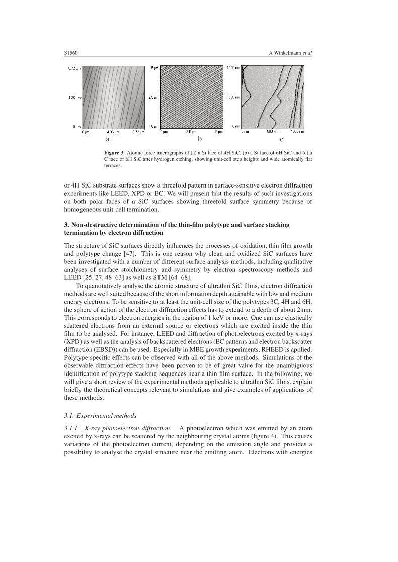
S1560 A Winkelmann et al
Figure 3. Atomic force micrographs of (a) a Si face of 4H SiC, (b) a Si face of 6H SiC and (c) aC face of 6H SiC after hydrogen etching, showing unit-cell step heights and wide atomically flatterraces.
or 4H SiC substrate surfaces show a threefold pattern in surface-sensitive electron diffractionexperiments like LEED, XPD or EC. We will present first the results of such investigationson both polar faces of α-SiC surfaces showing threefold surface symmetry because ofhomogeneous unit-cell termination.
3. Non-destructive determination of the thin-film polytype and surface stackingtermination by electron diffraction
The structure of SiC surfaces directly influences the processes of oxidation, thin film growthand polytype change [47]. This is one reason why clean and oxidized SiC surfaces havebeen investigated with a number of different surface analysis methods, including qualitativeanalyses of surface stoichiometry and symmetry by electron spectroscopy methods andLEED [25, 27, 48–63] as well as STM [64–68].
To quantitatively analyse the atomic structure of ultrathin SiC films, electron diffractionmethods are well suited because of the short information depth attainable with low and mediumenergy electrons. To be sensitive to at least the unit-cell size of the polytypes 3C, 4H and 6H,the sphere of action of the electron diffraction effects has to extend to a depth of about 2 nm.This corresponds to electron energies in the region of 1 keV or more. One can use elasticallyscattered electrons from an external source or electrons which are excited inside the thinfilm to be analysed. For instance, LEED and diffraction of photoelectrons excited by x-rays(XPD) as well as the analysis of backscattered electrons (EC patterns and electron backscatterdiffraction (EBSD)) can be used. Especially in MBE growth experiments, RHEED is applied.Polytype specific effects can be observed with all of the above methods. Simulations of theobservable diffraction effects have been proven to be of great value for the unambiguousidentification of polytype stacking sequences near a thin film surface. In the following, wewill give a short review of the experimental methods applicable to ultrathin SiC films, explainbriefly the theoretical concepts relevant to simulations and give examples of applications ofthese methods.
3.1. Experimental methods
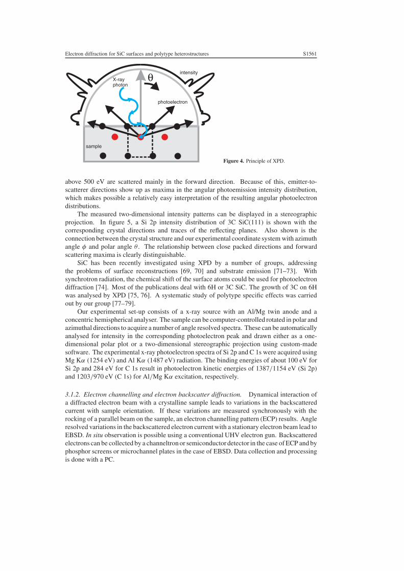
3.1.1. X-ray photoelectron diffraction. A photoelectron which was emitted by an atomexcited by x-rays can be scattered by the neighbouring crystal atoms (figure 4). This causesvariations of the photoelectron current, depending on the emission angle and provides apossibility to analyse the crystal structure near the emitting atom. Electrons with energies
Electron diffraction for SiC surfaces and polytype heterostructures S1561
θ intensity
photoelectron
sample
X-rayphoton
Figure 4. Principle of XPD.
above 500 eV are scattered mainly in the forward direction. Because of this, emitter-to-scatterer directions show up as maxima in the angular photoemission intensity distribution,which makes possible a relatively easy interpretation of the resulting angular photoelectrondistributions.
The measured two-dimensional intensity patterns can be displayed in a stereographicprojection. In figure 5, a Si 2p intensity distribution of 3C SiC(111) is shown with thecorresponding crystal directions and traces of the reflecting planes. Also shown is theconnection between the crystal structure and our experimental coordinate system with azimuthangle φ and polar angle θ . The relationship between close packed directions and forwardscattering maxima is clearly distinguishable.
SiC has been recently investigated using XPD by a number of groups, addressingthe problems of surface reconstructions [69, 70] and substrate emission [71–73]. Withsynchrotron radiation, the chemical shift of the surface atoms could be used for photoelectrondiffraction [74]. Most of the publications deal with 6H or 3C SiC. The growth of 3C on 6Hwas analysed by XPD [75, 76]. A systematic study of polytype specific effects was carriedout by our group [77–79].
Our experimental set-up consists of a x-ray source with an Al/Mg twin anode and aconcentric hemispherical analyser. The sample can be computer-controlled rotated in polar andazimuthal directions to acquire a number of angle resolved spectra. These can be automaticallyanalysed for intensity in the corresponding photoelectron peak and drawn either as a one-dimensional polar plot or a two-dimensional stereographic projection using custom-madesoftware. The experimental x-ray photoelectron spectra of Si 2p and C 1s were acquired usingMg Kα (1254 eV) and Al Kα (1487 eV) radiation. The binding energies of about 100 eV forSi 2p and 284 eV for C 1s result in photoelectron kinetic energies of 1387/1154 eV (Si 2p)and 1203/970 eV (C 1s) for Al/Mg Kα excitation, respectively.
3.1.2. Electron channelling and electron backscatter diffraction. Dynamical interaction ofa diffracted electron beam with a crystalline sample leads to variations in the backscatteredcurrent with sample orientation. If these variations are measured synchronously with therocking of a parallel beam on the sample, an electron channelling pattern (ECP) results. Angleresolved variations in the backscattered electron current with a stationary electron beam lead toEBSD. In situ observation is possible using a conventional UHV electron gun. Backscatteredelectrons can be collected by a channeltron or semiconductor detector in the case of ECP and byphosphor screens or microchannel plates in the case of EBSD. Data collection and processingis done with a PC.

S1562 A Winkelmann et al
φ =90
0
30
60
θ =0 4040 8080
(11-20)
(1-100)
(2-1-10)
(10-10)
(1-210)
(-1120)
(-1010)(-2110)
(-1100)
(-12-10)
(01-10) (0-110)(0001)
a
bhexagonal
a
b
ccubic
Figure 5. Stereographic projection of Si 2p photoelectron intensities of 3C SiC(111) and therelationship between crystal structure and experimental coordinate system.
ECP and EBSD provide various kinds of information [80, 81]. The patterns show thesymmetry elements of the crystal structure and can be used for the identification of symmetryaxes and mirror planes [82]. Orientation determination of crystals and crystallites is possiblebecause of the fixed relative positions of the channelling patterns and the sample. The quality ofthe crystal is reflected by the sharpness of the patterns. That is why ECP and EBSD have beenused for analysis of the quality of epitaxially grown films [83–87] and for the quantificationof ion implantation damage [88]. Crystal defects can be imaged by EC because they create acontrast [89].
The principle of our experimental set-up is shown in figure 6. The measurements werecarried out in an UHV chamber equipped with a STAIB EK-12-M electron gun capable ofdelivering an electron beam with energies of up to 12 keV. This gun is also used for Augerelectron spectroscopy and low resolution scanning electron microscopy. The beam energies canbe continuously varied. The backscattered electrons were collected either using a channeltronor a photomultiplier type of detector which gave equivalent results. The sample was positivelybiased with 50 V to suppress secondary electrons. Image acquisition and electron beamscanning was computer controlled. The beam is adjusted to be parallel while it is scannedover the surface. Thus its angle relative to the surface changes. This leads to variations ofthe backscattered electron current which are displayed on the computer. The variations in

Electron diffraction for SiC surfaces and polytype heterostructures S1563
Figure 6. Principle of ECPs and EBSD.
backscattered current amount to less than 5%, which makes necessary a careful adjustment ofsignal amplification and image processing by the computer software.
ECP and EBSD have been used for the analysis of SiC samples. For instance, a veryfast polytype identification is possible by taking ECPs near the (0001) direction [90, 91].Damage on a crystalline 4H SiC surface can also be evaluated by ECP [92]. Layer spacingmeasurements in EBSD have been shown to be of use for the analysis of SiC polytypes [82].
3.1.3. Low energy electron diffraction. Elastic scattering of low energy electrons (LEED) isa standard surface-analytical technique. In combination with dynamical simulations, LEEDmeasurements are a powerful tool for the determination of the structure of adsorbates andsurface reconstructions.
Quantitative LEED was successful in the determination of the structure of SiC surfacereconstructions and led to models of the atomic arrangement of a number of surface structures.It was demonstrated in a number of publications how the power of LEED can be usedon SiC surfaces. They found models for the (3 × 3) [26, 93, 94] and (
√3 × √
3)R30reconstructions [13] on SiC(0001). C faces were analysed in [95, 96], the step structure ofSiC surfaces with different stacking terminations was determined [97–99] and the problems ofsurface oxidation and passivation were investigated [100–103]. The central role of the surfacestructure for a controlled growth of SiC was pointed out [13, 14, 100, 104].
At energies above 0.5 keV, LEED will be sensitive to more than just the top layer ofthe surface. Thus, information on stacking sequences can be gained. However, reliablemeasurements of I–V data at these energies are very difficult because of the increasinginfluence of inelastic scattering. Electrons which experienced phonon losses are the sourceof the so-called Kikuchi patterns. The energy loss of the Kikuchi electrons is less than1 eV (quasielastic scattering) and they can be thought of as originating from point sourceslocated at the atomic nuclei. This leads to a close analogy between these Kikuchi patterns andphotoelectron diffraction.
3.1.4. Reflection high energy electron diffraction. Elastic reflection of high energy electronsat grazing incidence (RHEED) is a standard tool for the in situ characterization of thinfilm growth by MBE. The grazing incidence of the electron beam leads to a surface

S1564 A Winkelmann et al
0
surface normal
incoming X-rays
inelastic attenuation of thephotoelectrons
electron analyserdirection
solid anglek
Emitter scatterer
r0
Rp
R
(θ,φ)
photoemission
scatteringamplitude
direct wave
scattered waves
Ψ direct
Ψ (p)
cluster limit
ε
Ω
thermal movement
θp
Figure 7. SSC model of XPD.
sensitivity comparable to LEED. Together with the absence of energy filtering in RHEED, thismakes polytype differentiation by elastic RHEED patterns rather difficult, because inelasticelectrons may contribute a dominating part to the diffraction pattern. However, kinematicsimulations have shown that polarity and polytype determination could be possible under idealconditions [105].
As in LEED, inelastic scattering in RHEED can lead to the formation of Kikuchi patterns.Because of the specific geometry of the RHEED set-up, the Kikuchi lines can be caused fromone-, two- or three-dimensional periodicities [106, 107] at the surface. The Kikuchi lines ofthe polytype-specific three-dimensional lattice planes can be used for the determination of thepolytype [108, 109].
3.2. Theory and simulation
3.2.1. XPD. We have used a single scattering cluster (SSC) model to simulate the effects ofXPD on ultrathin SiC films (figure 7). The SSC model used in our calculations is describedby Fadley in [110]. In this model, the outgoing photoelectrons are scattered only once bya neighbouring atom. The intensity which is scattered by such an atom is described by ascattering factor calculated from the phase shifts of the angular momentum components of anincoming plane wave. In addition, the effects of inelastic scattering, thermal attenuation of thescattered amplitudes and the limited angular resolution of the analyser have to be taken intoaccount. The SSC model was incorporated into a computer program which allows simulationsof single scattering XPD patterns from arbitrary bulk and surface structures.
The phase shifts needed for the calculations have been derived from a muffin-tin potentialusing the Barbieri–Van Hove phase shift package [111]. Values of the inelastic attenuationlength have been obtained using the Tanuma–Powell–Penn (TPP) formula [112]. A fittingprocedure for the attenuation length showed that it had to be reduced by a factor of 1.5compared to the TPP formula [113]. The Debye temperature of SiC was taken to be around1300 K [114]. For comparison with experimental data, the angular resolution of the analyser

Electron diffraction for SiC surfaces and polytype heterostructures S1565
(2) was simulated by summing up the intensities from a number of different directions thatfall into the analyser solid angle.
Calculations using the plane wave SSC model tend to overestimate the intensity alongatomic chains. This can be corrected in part by the use of spherical wave scattering [115, 116].Our calculations for the emission of the Si 2p and C 1s core levels in SiC excited by Al/Mg Kα
radiation have shown that the experimental curves are equally well described by an empiricalreduction of the plane wave scattering amplitudes [113].
The size of the hemispherical cluster of atoms considered has been increased until nofurther changes in the diffraction pattern took place. This leads to a cluster radius around25 Å, which is equivalent to more than 3000 atoms. This large cluster size is necessarybecause of the long inelastic mean free path (>20 Å) of the Si 2p and C 1s electrons emitted.Large numbers of atoms have been shown to be necessary to simulate all the fine structure ofsubstrate core level emission [113] but user-friendly programs for full scale multiple scatteringcalculations are currently limited to several hundred atoms [117]. This is why we used thesingle scattering approach.
In order to minimize the influence of the instrumental response function, we used polar χ
curves for the comparison between experiment and theory, χ = (I − I0)/I0, with I0 being asmooth background fitted to the experimental polar scan intensities I by means of a polynomialspline fitting method [117, 118]. In the case of full hemispherical patterns, I0 should notdepend on the azimuth and can be estimated by taking the average value of all intensities atthe particular polar angle and smoothing the background obtained in the polar direction. Inthis way, all diffraction effects in the background are eliminated [119]. For comparison of thecalculated and measured curves, we used R-factor routines supplied in a program of the MSCDpackage [117]. In most of our calculations, we considered the surface as bulk-terminated anddisregarded any effects due to surface reconstructions. It has been shown that this can safelybe done due to the relatively high kinetic energy of the photoelectrons [120, 121].
3.2.2. Dynamical theory of electron channelling patterns. The variations of the backscatteredelectron current which form the ECP are due to dynamical diffraction effects of the incomingelectron beam with wavevector k0. We have used a Bloch wave approach to describe thediffraction of the incoming electrons. The use of this method is described in several reviews(e.g. [122, 123]). In the following, we give a short summary of the basic theory we applied.
The wavefunction inside the crystal is described as a superposition of Bloch waves withwavevectors k( j):
(r) =∑
j
c j exp(2π ik( j) · r)∑
g
C ( j)g exp(2π ig · r) (1)
with three-dimensional reciprocal lattice vectors g. Substituting these Bloch waves into theSchrodinger equation leads to the standard dispersion relation
[K2 − (k( j) + g)2]C ( j)g +
∑
h
U cg−hC ( j)
h = 0. (2)
The crystal potential is described by complex electron structure factors U cg = 2m|e|Vg/h2,
with Vg being a Fourier coefficient of the total crystal potential in volts and the relativisticelectron mass m. K is the electron wavevector inside the crystal, k2
0 = 1/λ2 = K 2 − U c0 .
One then writes k( j) as k( j) = K + γ ( j)n, where n is a unit vector normal to the surface andneglects elastic backscattering to transform (2) into an eigenvalue problem which gives theeigenvalues γ ( j) and eigenvectors with elements C ( j)
g . The boundary conditions at the surfacedetermine the coefficients c j in (1). After this, the wavefunction (1) is known and can be usedto calculate the electron current density inside the crystal.
S1566 A Winkelmann et al
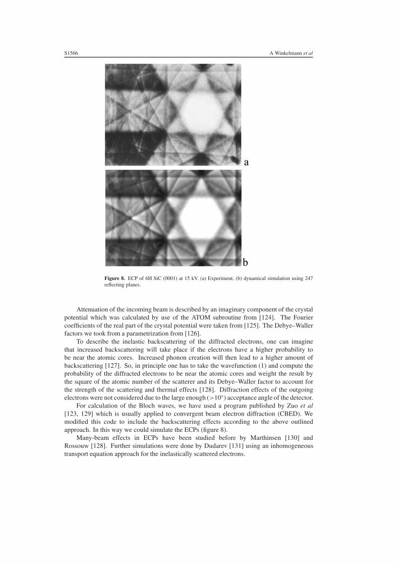
Figure 8. ECP of 6H SiC (0001) at 15 kV. (a) Experiment, (b) dynamical simulation using 247reflecting planes.
Attenuation of the incoming beam is described by an imaginary component of the crystalpotential which was calculated by use of the ATOM subroutine from [124]. The Fouriercoefficients of the real part of the crystal potential were taken from [125]. The Debye–Wallerfactors we took from a parametrization from [126].
To describe the inelastic backscattering of the diffracted electrons, one can imaginethat increased backscattering will take place if the electrons have a higher probability tobe near the atomic cores. Increased phonon creation will then lead to a higher amount ofbackscattering [127]. So, in principle one has to take the wavefunction (1) and compute theprobability of the diffracted electrons to be near the atomic cores and weight the result bythe square of the atomic number of the scatterer and its Debye–Waller factor to account forthe strength of the scattering and thermal effects [128]. Diffraction effects of the outgoingelectrons were not considered due to the large enough (>10) acceptance angle of the detector.
For calculation of the Bloch waves, we have used a program published by Zuo et al[123, 129] which is usually applied to convergent beam electron diffraction (CBED). Wemodified this code to include the backscattering effects according to the above outlinedapproach. In this way we could simulate the ECPs (figure 8).
Many-beam effects in ECPs have been studied before by Marthinsen [130] andRossouw [128]. Further simulations were done by Dudarev [131] using an inhomogeneoustransport equation approach for the inelastically scattered electrons.
Electron diffraction for SiC surfaces and polytype heterostructures S1567
3.2.3. LEED and RHEED. Because of the importance of multiple scattering effects atenergies used in LEED, a dynamical theory has to be used to explain the dependence of thespot intensity on the electron energy (I–V curve). We applied the SATLEED package [111]for the simulations which were compared to the experimental I–V curves.
At higher energies near 1 keV, LEED patterns are dominated by inelastic effects. Theformation of Kikuchi patterns caused by phonon scattered electrons is observed. Theseelectrons can be thought to originate from point sources at the atomic cores, which leadsto a close analogy with photoelectron diffraction. This is why LEED Kikuchi patterns can alsobe successfully modelled with a cluster approach.
In our SSC model, the inelastically scattered electrons were thought to originateisotropically from Si and C atoms scaled with the square of the atomic number to take intoaccount the different phonon creation cross sections of Si and C. The remaining elasticallyscattered electrons cause a spot diffraction pattern and were also modelled using the clusterapproach. The incoming plane wave was scattered at each atom at R j according to the complexscattering amplitude f j (k) and the scattered waves were summed up coherently to give theelastically scattered intensity in an angular direction specified by the change in wavevectork. To account for inelastic attenuation with the distance L j travelled in the material, anexponential damping term exp(−L j/2λ) was applied with the inelastic mean free path λ. TheDebye–Waller factor exp(−M j ) accounts for the thermal damping of the scattering amplitude.This SSC model can be summed up in a modified kinematical formula for the scatteredamplitude:
Ak =∑
j
f j (k) exp(−M j ) exp(ikR j ) exp(−L j/2λ). (3)
The elastic and inelastic intensities were calculated for the complete angular range visiblein the LEED pattern and showed the characteristic spot pattern superimposed with the Kikuchibands. It cannot be assumed that the simulated spot pattern reflects all the observed relativeintensities and possible absences of spots because dynamical effects are completely neglected.The spot pattern is merely used qualitatively to compare the positions of the inelastic featuresrelative to it.
The observed Kikichu lines in the RHEED set-up were also compared to kinematicalsimulations. These were carried out using the program ‘Electron Diffraction’ [132].
3.3. Applications
3.3.1. Polytype and polarity determination by XPD. The arrangement of atoms surroundingan emitter of photoelectrons leads to intensity variations of the angular photoelectron intensity.There are specific changes of the local structure around silicon and carbon emitters in differentSiC polytypes. These variations can be used for polytype determination by XPD.
In figure 9 we show specific scattering directions which enable the differentiation between6H SiC and 4H SiC. Because the specified scattering atoms are at relatively long distancesaway from the emitters, the observed effects are small in comparison to the dominating forwardscattering directions to the nearest silicon atoms. This emphasizes a careful alignment of thesamples and sufficient long measuring times to optimize the signal-to-noise ratio. Experimentalphotoelectron intensity plots and the corresponding simulations for the case illustrated infigure 9 can be found in [79].
Two-dimensional photoelectron diffraction patterns of Al Kα excited Si 2p photoelectronsof 6H, 4H and 3C SiC are shown in figure 10. The corresponding SSC simulations reproducethe characteristic differences of these patterns, depending on polytype and polarity. Multiplescattering effects can have a notable influence along densely packed directions [79].

S1568 A Winkelmann et al
43°41°
6H
43°41°
4H
Figure 9. Characteristic scattering directions around a C 1semitter in the (1120) plane of 6H SiC (full arrows). Thesescattering directions are missing in 4H SiC (broken arrows).
Based on film growth experiments and emitter resolved simulations, one can estimatethe information depth of XPD in SiC. We have found that, at photoelectron energies of about1–2 keV, this depth amounts to a maximum of about 8–10 double layers or approximately20 Å [79].
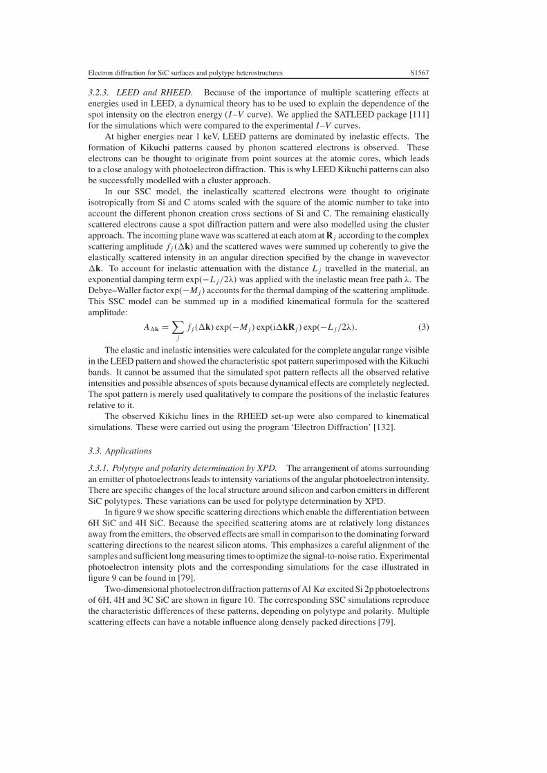
3.3.2. Polytype determination by electron channelling patterns. The possibility to use ECPsfor polytype determination of thin surface layers of SiC was described in [90]. There it wasshown that, in order to identify the polytypes, it is sufficient to change the angle of incidenceof the electron beam by ±40 mrad relative to the surface normal coinciding with the [0001]symmetry axis of a crystal. ECPs at 9.25 keV for the basic SiC polytypes 3C, 4H, 6H, 8H,15R, 21R, 27R and 33R were presented.
For the analysis of ultrathin SiC films, we have used energies in the range from 2 to 8 keV.Characteristic patterns can be observed at a number of energies which enables the use of thismethod in a fingerprint mode [91]. The observed patterns could be explained by the use ofmany-beam dynamical simulations using a Bloch wave model (figure 11) [133, 134].
3.3.3. Kikuchi lines in RHEED for polytype determination. For the controlled MBE growthof SiC polytype films it would be desirable to distinguish the grown polytype directly on theRHEED screen. The symmetry of the RHEED diffraction pattern is based on the symmetryof the two-dimensional surface layers. Because the different polytypes are built up fromthe same two-dimensional layers, polytype information cannot be gained from the symmetryof the RHEED diffraction pattern. However, differences in the stacking sequence shouldmanifest themselves in intensity variations along the rods of the reciprocal space which areseen as streaks on the RHEED screen. These variations are caused by the influence of theperiodicity normal to the surface layer and thus could supply polytype information. As inLEED, the intensity variations are also strongly influenced by dynamical effects due to theatomic structure of the surface layer [106]. The effects due to polytype, surface reconstructions,partial surface disorder and inelastically scattered electrons are superimposed in the finaldiffraction pattern. Together with the experimental set-up of RHEED, which usually does notinclude energy filtering as in LEED, this poses a difficulty for the experimental confirmationof polytypic differences in the elastic diffraction pattern which have been found in kinematicalsimulations [105].
Because of the strong influence of inelastically scattered electrons in RHEED, diffractioneffects of these electrons can also be used for polytype determination. The resulting Kikuchilines have the advantage that one can rely on line positions and positions of line crossings andnot on the measurement of elastic intensities over an unknown inelastic background.
Kikuchi line measurements for polytype determination in RHEED have been first proposedby Zhukova et al [108, 109], who also gave explicit formulae for their experimentally

Electron diffraction for SiC surfaces and polytype heterostructures S1569
Figure 10. Measured Si 2p photoelectron diffraction patterns and comparison with SSCsimulations.
determined Kikuchi line positions. To be consistent with the notation in [108, 109],a hexagonalcoordinate system with three indexes (hkl) is used in this section.
Only reflections (h, k, l) with h − k = 3n are sensitive to a change of the stackingsequence [108]. For polytype determination in RHEED, the lines which belong tothe first group or reflexes with h2 + hk + k2 = 1 are especially useful: (h, k) =(0, 1), (1, 0), (1,−1), (0,−1), (−1, 0), (−1, 1).
S1570 A Winkelmann et al
Figure 11. ECP of 3C SiC(111) at 4000 eV. (a) Kinematical pattern, (b) experiment, (c) dynamicalsimulation [133].
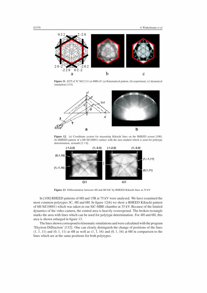
Figure 12. (a) Coordinate system for measuring Kikuchi lines on the RHEED screen [108].(b) RHEED pattern of a 6H SiC(0001) surface with the area marked which is used for polytypedetermination, azimuth [2 1 0].
(1,-1,16)
4H6H
(0,1,16)
(0,1,11)
(1,–1,11)
(-1,2,0) (1,-2,0)(-1,2,0) (1,-2,0)
Figure 13. Differentiation between 4H and 6H SiC by RHEED Kikuchi lines at 35 kV.
In [108] RHEED patterns of 6H and 15R at 75 kV were analysed. We have examined themost common polytypes 3C, 4H and 6H. In figure 12(b) we show a RHEED Kikuchi patternof 6H SiC(0001) which was taken in our SiC-MBE chamber at 35 kV. Because of the limiteddynamics of the video camera, the central area is heavily overexposed. The broken rectanglemarks the area with lines which can be used for polytype determination. For 4H and 6H, thisarea is shown enlarged in figure 13.
The lines shown correspond to kinematic simulations and were calculated with the program‘Electron Diffraction’ [132]. One can clearly distinguish the change of positions of the lines(1, 1, 11) and (0, 1, 11) at 4H as well as (1, 1, 16) and (0, 1, 16) at 6H in comparison to thelines which are at the same positions for both polytypes.

Electron diffraction for SiC surfaces and polytype heterostructures S1571
6H3C
(0,1,16)
(-1,3,16) (-1,3,15)
(0,1,15)
(-1,2,0) (1,-2,0)
(2,-3,8) (-1,3,8)
(1,-1,8)
(0,1,8)
(-1,2,0) (1,-2,0)
Figure 14. Differentiation between 6H and 3C by RHEED Kikuchi lines at 35 kV (hexagonalcoordinate system with c = 7.55 Å for 3C and c = 15.17 Å for 6H).
The reflexes mentioned in [108] are also useful for the differentiation between 3C and6H. One only has to keep in mind that a doubling of the layer constant in real space leads toa reciprocal space layer constant which is half as large. There are twice as many reflectionsfor 6H as for 3C which show up as additional lines. In figure 14 we show RHEED Kikuchipictures of a 3C thin film and a 6H SiC substrate. Clearly one can see additional lines at 6H.The 3C pattern is indexed in a hexagonal coordinate system with a c axis of 7.55 Å to see thesystematic changes in the Miller indices. At 6H, the l index of a (hkl) line shared with 3C istwice as large as at 3C because of the longer c axis. However, 6H lines with an odd l, have nocounterpart at 3C and are the characteristic sign of 6H.
In summary, we have shown how polytype determination of 4H, 6H and 3C is possiblewith RHEED Kikuchi patterns.
3.3.4. Surface stacking termination. The surface stacking termination of SiC samples wasinvestigated by Starke et al using LEED. It was shown that it is possible to determine thearea ratios of domains with different stacking termination by quantitative LEED analyses [99]with error margins of the mixing ratios of about ±20% [95]. Polytypes with statisticallymixed terminations are difficult to distinguish while samples with preferential terminationsshow larger differences [97]. The LEED simulations showed that detection of stacking faultsbetween the third and fourth layers (S3 and S4 termination) poses the limit of this methodbecause of the short inelastic mean free paths of low energy electrons [97].
3.3.5. Unit-cell terminated SiC surfaces. An effective method of surface preparation of SiCis etching in hot hydrogen gas at temperatures of about 1700–1800 K. Ideally, this leads tosurfaces which are terminated by flat terraces with step heights of half or full unit-cell sizes.Surfaces prepared this way are well suited for MBE growth of polytype heterostructures. Theterraces have widths of up to 1 µm, depending on the off-axis angle of the sample. In thissection we show the results of investigations on C-face 6H SiC(0001).
STM. The 6H SiC(0001) sample was investigated by STM. A surface morphology was foundwhich consisted of steps with an equal step size of one unit cell (figure 15). This is consistentwith a surface which is almost uniformly terminated by the same stacking termination. Becausethe STM does not give information about deeper layers, XPD and LEED have been used todetermine the stacking sequence near the surface. This can be used to give a model of thestepped surface.

S1572 A Winkelmann et al
Figure 15. STM picture of the hydrogen-etched 6H SiC(0001) sample.
Figure 16. XPD patterns of 6H SiC(0001) Al Kα excitation of Si 2p and C 1s, experiment andSSC simulation.
XPD. A uniformly terminated surface should show a threefold symmetry using surface-sensitive electron diffraction methods like XPD and LEED. In the case of XPD, thephotoelectron angular distributions of Al Kα-excited Si 2p and C 1s electrons were analysed.The corresponding intensity maps are shown in figure 16. The pattern shows a threefoldsymmetry which supports the assumption of a uniformly terminated surface. A statisticaltermination would lead to a sixfold pattern.

Electron diffraction for SiC surfaces and polytype heterostructures S1573
Figure 17. Threefold LEED pattern of a 6H SiC(0001)
surface, 124 eV.
Table 1. R-factor comparison for different terminations of the hydrogen-etched 6H SiC(0001)
sample.
Termination RPendry
S1 0.64S1* 0.44S2 0.37S2* 0.72S3 0.17S3* 0.52S4 0.27S4* 0.55
On the right side of figure 16, the SSC simulations for a S3-terminated surface are shown.These reproduce the experimental patterns very well. The S3 termination was supported in anR-factor analysis of the XPD polar plots.
LEED. In figure 17 a LEED pattern is shown, which was observed on the 6H SiC sample.There is a clear threefold symmetry which has to come from the uniform termination of thesample. Effects due to surface reconstructions or adsorbates can be ruled out from XPSmeasurements. Such effects should show the same symmetry as the underlying substrate aslong as there is no adsorbate which arranges itself independently of the substrate. So, inany case a uniform stacking termination of the substrate would be the basis for a threefoldsymmetry of the diffraction pattern.
LEED I–V measurements were carried out and compared with dynamical simulations. Inthe simulations a clean surface with no adsorbates was considered with atoms at the positionsof the bulk crystal. Eight terminations were considered which are listed in table 1 together withthe corresponding Pendry R factors. The best factor of 0.17 was found for the S3 termination.The much worse R factor of the S3* termination shows the strong threefold symmetry of thepattern. This means that there is only a small part of the domains present which are rotated by60. If both domains were present in equal amounts, this would lead to a sixfold symmetryof the pattern. In figure 18 we show measured I–V data and simulated curves of the S3termination.

S1574 A Winkelmann et al
Energy [eV]
Inte
nsity
[a.u
.]
Figure 18. LEED I–V measurements (full curves) of the 6H SiC(0001) sample and dynamicalsimulations (broken curves) for S3 termination, RPendry = 0.17.
In the next step, we tried to consider a mixture of different terminations. The largestchange in the R factor was found for a mixture of 90% S3 and 10% S3* with a Pendry Rfactor of 0.13. An error margin was determined from the variance of the Pendry R factor atthe minimum with var(Rmin) = √
8V0i/E , with E being the measured energy range [135].From the error interval, the amount of S3 termination can be estimated as 80–100%.
For the uppermost layers, a slight compression was found which was less than 0.05 Å,which is within the experimental error. A strong compression of 40% (0.63–0.38 Å) in thefirst layer of the C face was predicted theoretically [136]. The absence of compression couldbe caused by saturation of the dangling bonds. Because LEED is not very sensitive to smallamounts of hydrogen or oxygen at the surface, the presence of these atoms cannot be ruled out.This was also found in a different investigation of 6H SiC(0001) [95], where surface modelswith adatoms could not be differentiated from the clean bulk surface.
The LEED I–V data of the 6H SiC(0001) sample was taken in the energy range from 200to 400 eV. At higher energies, inelastic effects begin to dominate the diffraction pattern andKikuchi bands are observed. The Kikuchi pattern at 1000 eV, which is given in figure 19, alsoshows the threefold symmetry. We applied the SSC model to calculate the elastic spot patternand the Kikuchi bands. For a cluster of 15 Å radius and S3 termination, the superimposedinelastic and elastic patterns in figure 19 reproduce the experimentally observed structuresquite well. The relative positions of the elastic and Kikuchi patterns match up and the threefoldsymmetry of both patterns is also reproduced.

Electron diffraction for SiC surfaces and polytype heterostructures S1575
EXPERIMENT SSC SIMULATION
Figure 19. Kikuchi patterns of the uniformly S3-terminated 6H SiC sample at 1000 eV andcomparison to SSC simulation.
We have shown how the combination of various analysis methods can lead to a pictureof the step structure on hydrogen-etched SiC samples. The investigations by STM, XPD andLEED convincingly support the assumption of uniform S3 termination of the 6H SiC(0001)
sample analysed. Similar results have been found on the Si face of 6H SiC after hydrogenetching.
4. Summary
The current progress in the growth of polytype heterostructures by SSMBE has been reviewed.The growth of different SiC polytypes on each other is possible by control of the appropriatethermodynamic parameters and analysis of the growing crystal structure. UHV conditionsallow the determination of the species on the surface and also the in situ characterization ofthe growing polytype by electron diffraction methods.
For a non-destructive determination of the polytype of a very thin SiC film, methods likeXPD and ECP can be used. The interaction length of electrons near 1 keV kinetic energy isin the range of 1 nm and is therefore sensitive to the stacking sequence of the most commonSiC polytypes 3C, 4H and 6H with c-axis dimensions between 0.75 and 1.5 nm. Additionally,Kikuchi lines observed in RHEED patterns can be used for polytype identification.
To prepare polytype heterostructures like 4H/3C/4H or 6H/3C/6H, untwinned 3C SiCfilms without double-positioning boundaries have to be grown. α-SiC substrates with uniformsurface stacking termination are a prerequisite for this. Such surfaces can be prepared usinghigh temperature hydrogen etching, sublimation etching or step-flow growth.
We have used high temperature hydrogen etching to prepare unit-cell terminated 6Hand 4H SiC0001 substrate surfaces on both Si or C faces. These crystals show threefoldsurface symmetry and are particularly suitable for detailed studies of the atomic-geometricstructure and their changes during the growth or certain treatments. Results of surface-sensitivecharacterization methods like STM, XPD and LEED were presented.
The power of electron diffraction methods with low to medium energy electrons lies inits ability to sample a number of surface layers which makes these methods very suitable fornon-destructive in situ UHV measurements of ultrathin crystalline films.

S1576 A Winkelmann et al
Acknowledgment
We thank A Fissel for providing samples of MBE-grown SiC layers.
References
[1] Bechstedt F and Kackel P 1995 Phys. Rev. Lett. 75 2180[2] Murayama M and Nakayama T 1994 Phys. Rev. B 49 4710[3] Weisbuch C and Vinter B 1991 Quantum Semiconductor Structures (San Diego, CA: Academic)[4] Capasso F 1999 Semiconductor Quantum Electronics ed A Miller, M Ebrahimzadeh and D M Finlayson (Bristol:
Institute of Physics Publishing) p 391[5] Knippenberg W F 1963 Philips Res. Rep. 18 161[6] Omuri M, Takei H and Fukuda T 1989 Japan. J. Appl. Phys. 28 1217[7] Heine V, Cheng C and Needs R J 1991 J. Am. Ceram. Soc. 74 2630[8] Limpijumnong S and Lambrecht W R L 1998 Phys. Rev. B 57 12017[9] Tairov Y M and Tsevtkov V F 1981 J. Cryst. Growth 52 146
[10] Fissel A, Kaiser U, Ducke E, Schroter B and Richter W 1995 J. Cryst. Growth 154 72[11] Fissel A, Kaiser U, Pfennighaus K, Schroter B and Richter W 1996 Appl. Phys. Lett. 68 1204[12] Furthmuller J, Kackell P, Bechstedt F, Fissel A, Pfennighaus K, Schroter B and Richter W 1998 J. Electron.
Mater. 27 848[13] Starke U, Schardt J, Bernhardt J, Franke M and Heinz K 1999 Phys. Rev. Lett. 82 2107[14] Grossner U, Fissel A, Furthmuller J, Richter W and Bechstedt F 2001 Mater. Sci. Forum 353–356 211[15] Vodakov Y A, Mokhov E N, Ramm M G and Roenkov A D 1979 Krist. Technik 14 729[16] Mokhov E N, Shulpina I L, Tregunova A S and Vodakov Y A 1981 Cryst. Res. Technol. 16 879[17] Kordina O et al 1996 Appl. Phys. Lett. 69 1456[18] Fuyuki T, Yoshinobu T and Matsunami H 1993 Thin Solid Films 225 225[19] Yoshinobu T, Mitsui H, Izumikawa I, Fuyuki T and Matsunami H 1992 Appl. Phys. Lett. 60 824[20] Kern R S, Jahrendahl K, Tanaka S and Davis R F 1997 Phys. Status Solidi b 202 379[21] Kaneda S, Sakamoto Y, Nishi C, Kanaya M and Hannai S I 1981 J. Cryst. Growth 81 536[22] Zenkentes K, Callec R, Tsagaraki K, Sagnes B, Arnaud G, Pascual J and Camassel J 1995 Mater. Sci. Eng. B
29 138[23] Petzoldt J, Stauden T, Cimalla V, Ecke G, Romanus H and Eichhorn G 1998 Mater. Sci. Forum 264–268 251[24] Kitabatake M 1998 Mater. Sci. Forum 264–268 327[25] Starke U 1997 Phys. Status Solidi b 202 475[26] Starke U et al 1998 Phys. Rev. Lett. 80 758[27] Johansson L I, Owman F and Martensson P 1996 Phys. Rev. B 53 13793[28] Fissel A, Schroter B, Kaiser U and Richter W 2000 Appl. Phys. Lett. 77 2418[29] Fissel A 2001 J. Cryst. Growth 227/228 805[30] Fissel A, Kaiser U, Schroter B, Richter W and Bechstedt F 2001 Appl. Surf. Sci. 184 37[31] Fissel A, Kaiser U, Schroter B, Kraußlich J and Richter W 2000 Thin Solid Films 380 89[32] Fissel A 2000 Thin Solid Films 212 438[33] Ducke E, Kriegel R, Fissel A, Kaier U, Schroter B, Muller P and Richter W 1996 Inst. Phys. Conf. Ser. 142
609[34] Bauer A, Krausslich J, Kocher B, Goetz K, Fissel A and Richter W 1999 Mater. Sci. Eng. B 61/62 179[35] Northrup J E and Neugebauer J 1995 Phys. Rev. B 52 R17001[36] Powell J, Larkin D and Abel P 1995 J. Electron. Mater. 24 295[37] Hallin C, Owman F, Martensson P, Ellison A, Konstantinov A, Kordina O and Janzen E 1997 J. Cryst. Growth
181 241[38] Ramachandran V, Brady M, Smith A, Feenstra R and Greve D 1998 J. Electron. Mater. 27 308[39] Nakamura S, Kimoto T, Matsunami H, Tanaka S, Teraguchi N and Suzuki A 2000 Appl. Phys. Lett. 76 3412[40] Xie Z Y, Edgar J H, Burkland B K, George J T and Chaudhuri J 2001 J. Cryst. Growth 224 235[41] Powell J A et al 1991 Appl. Phys. Lett. 59 333[42] Ohtani N, Katsuno M, Aigo T, Fujimoto T, Tsuge H, Yashiro H and Kanaya M 2000 J. Cryst. Growth 210 613[43] Cheng C, Needs R J and Heine V 1988 J. Phys. C: Solid State Phys. 21 1049[44] Kackell P, Furthmuller J and Bechstedt F 1998 Phys. Rev. B 58 1326[45] Righi M C, Pignedoli C A, Borghi G, Felice R D, Bertoni C M and Catellani A 2002 Phys. Rev. B 66 045320[46] Kimoto T, Itoh A and Matsunami H 1997 J. Appl. Phys. 81 3494

Electron diffraction for SiC surfaces and polytype heterostructures S1577
[47] Heinz K, Starke U, Bernhardt J and Schardt J 2000 Appl. Surf. Sci. 162/163 9[48] Dillon J A, Schlier R E and Farnsworth H E 1959 J. Appl. Phys. 30 675[49] van Bommel A J, Crombeen J E and van Tooren A 1975 Surf. Sci. 48 463[50] Bozso F, Muelhoff L, Trenary M, Choyke W J and Yates J T Jr 1984 J. Vac. Sci. Technol. 2 1271[51] Adachi S, Mohri M and Yamashina T 1985 Surf. Sci. 161 479[52] Muehlhoff L, Choyke W J, Bozack M J and Yates J T Jr 1986 J. Appl. Phys. 60 2842[53] Kaplan R and Parrill T M 1986 Surf. Sci. 165 L45[54] Kaplan R 1989 Surf. Sci. 215 111[55] Nakanishi S, Tokutaka H, Nishimori K, Kishida S and Ishihara N 1989 Appl. Surf. Sci. 41/42 44[56] Bermudez V M 1995 Appl. Surf. Sci. 84 45[57] Nienhaus H, Kampen T U and Monch W 1995 Surf. Sci. 324 L328[58] Johansson L I, Owman F and Martensson P 1996 Surf. Sci. 360 L483[59] Johansson L I, Owman F, Martensson P, Persson C and Lindefelt U 1996 Phys. Rev. B 53 13803[60] Johansson L I, Owman F and Martensson P 1996 Surf. Sci. 360 478[61] Tautz F S, Sloboshanin S, Starke U and Schaefer J A 2000 Surf. Sci. 470 L25[62] Amy F, Enriquez H, Soukiassian P, Storino P F, Chabal Y J, Mayne A J, Dujardin G, Hwu Y K and
Brylinski C 2001 Phys. Rev. Lett. 86 4342[63] Amy F, Soukiassian P, Hwu Y K and Brylinski C 2002 Phys. Rev. 65 165323[64] Chang C S, Tsong I S T, Wang Y C and Davis R F 1991 Surf. Sci. 256 354[65] Tsai M H, Chang C S, Dow J D and Tsong I S T 1992 Phys. Rev. B 45 1327[66] Kulakov M A, Heuell P, Tsvetkov V F and Bullemer B 1994 Surf. Sci. 315 248[67] Marumoto Y, Tsukamoto T, Hirai M, Kusaka M, Iwami M, Ozawa T, Nagamura T and Nakata T 1995 Japan.
J. Appl. Phys. 34 3351[68] Li L, Tindall C, Takaoka O, Hasegawa Y and Sakurai T 1997 Surf. Sci. 385 60[69] Simon L, Bischoff J L and Kubler L 1999 Phys. Rev. B 60 11653[70] King S W, Ronning C, Davis R F and Nemanich R J 1998 J. Appl. Phys. 84 6042[71] Juillaguet S, Kubler L, Diani M, Bischoff J L, Gewinner G, Wetzel P and Becourt N 1995 Surf. Sci. 339 363[72] Diani M, Bischoff J L, Kubler L and Bolmont D 1993 Appl. Surf. Sci. 68 575[73] Bischoff J L, Dentel D and Kubler L 1998 Surf. Sci. 415 392[74] Shimomura M, Yeom H, Mun B S, Fadley C, Hara S, Yoshida S and Kono S 1999 Surf. Sci. 438 237[75] Matko I, Chenevier B, Audier M, Madar R, Diani M, Simon L, Kubler L and Aubel D 2002 Mater. Sci. Forum
389–393 315[76] Diani M, Simon L, Kubler L, Aubel D, Matko I, Chenevier B, Madar R and Audier M 2002 J. Cryst. Growth
235 95[77] Schroter B, Winkelmann A and Richter W 2001 J. Electron. Spectrosc. Relat. Phenom. 114 443[78] Schroter B, Winkelmann A, Fissel A, Lebedev V and Richter W 2001 Mater. Sci. Forum 353–356 227[79] Winkelmann A, Schroter B and Richter W 2002 Surf. Sci. 515 126[80] Reimer L 1998 Scanning Electron Microscopy—Physics of Image Formation and Microanalysis (Berlin:
Springer)[81] Baba-Kishi K Z 2002 J. Mater. Sci. 37 1715[82] Michael J R and Eades J A 2000 Ultramicroscopy 81 67[83] Young K H, James T W, Robinson M, Cardona A H, Suzuki H, Kurosawa H, Yamashita T and Hirai T 1991
Thin Solid Films 206 369[84] Geier S, Schreck M, Hessmer R, Rauschenbach B, Stritzker B, Kunze K and Adams B L 1994 Appl. Phys.
Lett. 65 1781[85] Mo S, Peiner E, Schlachetzki A, Klockenbrink R and Weber E R 1998 Mater. Sci. Eng. B 56 37[86] Sweeney F, Trager-Cowan C, Cowan D A, O’Donnell K P, Zubia D, Hersee S D, Foxon C T, Harrison I and
Novikov S V 2001 Phys. Status Solidi b 228 533[87] Trager-Cowan C et al 2002 J. Micr. 205 226[88] Page T F, Mc Hargue C J and White C W 1991 J. Micr. 163 245[89] Wilkinson A J and Hirsch P B 1997 Micron 28 279[90] Levchuk B I, Makarov V V, Petrov N N, Trairov Y M and Tsvetkov V F 1987 Phys. Chem. Mech. Surf. 4 2744[91] Schroter B, Kreuzberg M, Fissel A, Pfennighaus K and Richter W 1998 Mater. Sci. Forum 264–268 355[92] Wagner G, Doerschel J and Gerlitzke A 2001 Appl. Surf. Sci. 184 55[93] Reuter K, Schardt J, Bernhardt J, Wedler H, Starke U and Heinz K 1998 Phys. Rev. B 58 10806[94] Schardt J, Bernhardt J, Starke U and Heinz K 2000 Phys. Rev. B 62 10335[95] Hollering M et al 1998 Phys. Rev. B 58 4992[96] Seubert A, Bernhardt J, Nerding M, Starke U and Heinz K 2000 Surf. Sci. 454–456 45

S1578 A Winkelmann et al
[97] Schardt J, Bram C, Muller S, Starke U, Heinz K and Muller K 1995 Surf. Sci. 337 232[98] Starke U, Schardt J and Franke M 1997 Appl. Phys. A 65 587[99] Schardt J, Bernhardt J, Franke M, Starke U and Heinz K 1998 Mater. Sci. Forum 264–268 343
[100] Starke U, Bernhardt J, Schardt J and Heinz K 1999 Surf. Rev. Lett. 6 1129[101] Bernhardt J, Schardt J, Starke U and Heinz K 1999 Appl. Phys. Lett. 74 1084[102] Sieber N, Mantel B F, Seyller T, Ristein J, Ley L, Heller T, Batchelor D R and Schmeißer D 2001 Appl. Phys.
Lett. 78 1216[103] Sieber N, Stark T, Seyller T, Ley L, Zorman C A and Mehregany M 2002 Appl. Phys. Lett. 80 4726[104] Starke U 2001 Mater. Sci. Forum 353–356 205[105] Scharmann F and Pezoldt J 2002 Mater. Sci. Forum 389–393 463[106] Braun W 1999 Applied RHEED: Reflection High-Energy Electron Diffraction During Crystal Growth (Berlin:
Springer)[107] Gajdardziska-Josifovska M and Cowley J M 1991 Acta Crystallogr. A 47 74[108] Zhukova L A, Evstigneev A M, Prokof’eva N K, Shashkov Y M and Gran Y M 1975 Kristallografiya 21 807[109] Zhukova L A and Zvyagin B B 1976 Kristallografiya 21 1193[110] Fadley C S 1992 Synchrotron Radiation Research: Advances in Surface Science vol 2, ed R Z Bachrach (New
York: Plenum) pp 421–518[111] Barbieri A and Van Hove M A 1999 private communication (http://electron.lbl.gov/leedpack/)[112] Tanuma S, Powell C J and Penn D R 1987 Surf. Sci. 192 L849[113] Kono S, Goldberg S M, Hall N F T and Fadley C S 1980 Phys. Rev. B 22 6085[114] Harris G (ed) 1995 Properties of Silicon Carbide (Washington, DC: INSPEC)[115] Fritzsche V 1989 Surf. Sci. 213 648[116] Rehr J J, Albers R C, Natoli C R and Stern E A 1986 Phys. Rev. B 34 4350[117] Chen Y, de Abajo F J G, Chasse A, Ynzunza R X, Kaduwela A P, Van Hove M and Fadley C S 1998 Phys.
Rev. B 58 13121[118] Sambi M and Granozzi G 1999 Surf. Sci. 426 235[119] Seelmann-Eggebert M and Richter H 1991 Phys. Rev. B 43 9578[120] Seelmann-Eggebert M 1993 Phys. Rev. B 48 11838[121] Schieffer P, Jezequel G, Lepine B, Sebilleau D, Feuillet G and Daudin B 2001 Surf. Sci. 482–485 593[122] Humphreys C J 1979 Rep. Prog. Phys. 42 1825[123] Spence J C H and Zuo J M 1992 Electron Microdiffraction (New York: Plenum)[124] Bird D M and King Q A 1990 Acta Crystallogr. A 46 202[125] Doyle P A and Turner P S 1968 Acta Crystallogr. A 24 390[126] Gao H X and Peng L M 1999 Acta Crystallogr. A 55 926[127] Hall C and Hirsch P 1965 Proc. R. Soc. A 286 158[128] Rossouw C J, Miller P R, Josefsson T W and Allen L J 1994 Phil. Mag. A 70 985[129] Zuo J M, Gjonnes K and Spence J C H 1989 J. Electron. Microsc. Technol. 12 29[130] Marthinsen K and Høier R 1986 Acta Crystallogr. A 42 484[131] Dudarev S L, Rez P and Whelan M J 1995 Phys. Rev. B 51 3397[132] Morniroli J P 2000 Electron Diffraction (Lille: Universite des Sciences et Technologies)[133] Winkelmann A, Schroter B and Richter W 2003 Surf. Sci. 532–535 869[134] Winkelmann A, Schroter B and Richter W 2003 Ultramicroscopy 98 1[135] Pendry J B 1980 J. Phys. C: Solid State Phys. 13 937[136] Sabisch M, Kruger P and Pollmann J 1997 Phys. Rev. B 55 10561
Copyright © 2022 FDOKUMEN