Unit of electrical resistance is: (A) Ohm (B) Mho - Kerala PSC
Upload
khangminh22Category
view
0download
0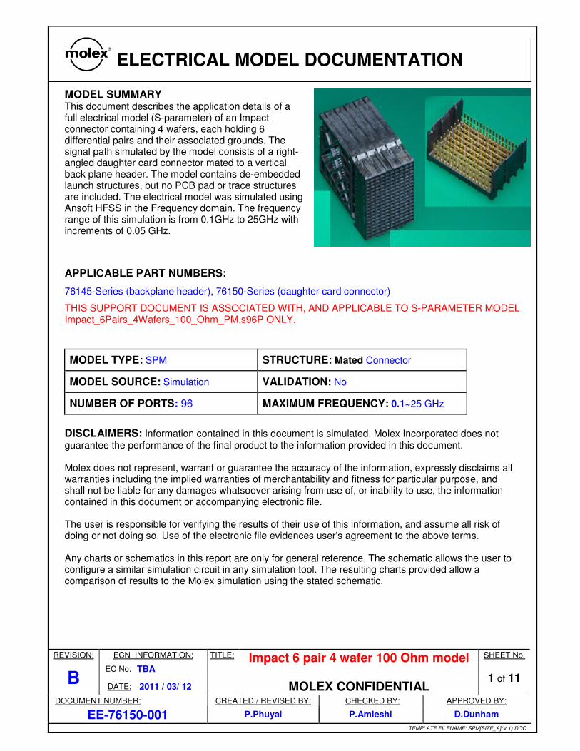
ELECTRICAL MODEL DOCUMENTATION
REVISION: ECN INFORMATION: TITLE: Impact 6 pair 4 wafer 100 Ohm model
MOLEX CONFIDENTIAL
SHEET No.
B EC No: TBA
1 of 11 DATE: 2011 / 03/ 12
DOCUMENT NUMBER: CREATED / REVISED BY: CHECKED BY: APPROVED BY:
EE-76150-001 P.Phuyal P.Amleshi D.Dunham
TEMPLATE FILENAME: SPM[SIZE_A](V.1).DOC
MODEL SUMMARY This document describes the application details of a full electrical model (S-parameter) of an Impact connector containing 4 wafers, each holding 6 differential pairs and their associated grounds. The signal path simulated by the model consists of a right-angled daughter card connector mated to a vertical back plane header. The model contains de-embedded launch structures, but no PCB pad or trace structures are included. The electrical model was simulated using Ansoft HFSS in the Frequency domain. The frequency range of this simulation is from 0.1GHz to 25GHz with increments of 0.05 GHz.
APPLICABLE PART NUMBERS:
76145-Series (backplane header), 76150-Series (daughter card connector)
THIS SUPPORT DOCUMENT IS ASSOCIATED WITH, AND APPLICABLE TO S-PARAMETER MODEL Impact_6Pairs_4Wafers_100_Ohm_PM.s96P ONLY.
MODEL TYPE: SPM STRUCTURE: Mated Connector
MODEL SOURCE: Simulation VALIDATION: No
NUMBER OF PORTS: 96 MAXIMUM FREQUENCY: 0.1~25 GHz
DISCLAIMERS: Information contained in this document is simulated. Molex Incorporated does not guarantee the performance of the final product to the information provided in this document. Molex does not represent, warrant or guarantee the accuracy of the information, expressly disclaims all warranties including the implied warranties of merchantability and fitness for particular purpose, and shall not be liable for any damages whatsoever arising from use of, or inability to use, the information contained in this document or accompanying electronic file. The user is responsible for verifying the results of their use of this information, and assume all risk of doing or not doing so. Use of the electronic file evidences user's agreement to the above terms. Any charts or schematics in this report are only for general reference. The schematic allows the user to configure a similar simulation circuit in any simulation tool. The resulting charts provided allow a comparison of results to the Molex simulation using the stated schematic.

ELECTRICAL MODEL DOCUMENTATION
REVISION: ECN INFORMATION: TITLE: Impact 6 pair 4 wafer 100 Ohm model
MOLEX CONFIDENTIAL
SHEET No.
B EC No: TBA
2 of 11 DATE: 2011 / 03/ 12
DOCUMENT NUMBER: CREATED / REVISED BY: CHECKED BY: APPROVED BY:
EE-76150-001 P.Phuyal P.Amleshi D.Dunham
TEMPLATE FILENAME: SPM[SIZE_A](V.1).DOC
CONDUCTOR TO PORT MAPPING TABLE SIGNAL PATHS
Conductor pin out Ports Daughter card/backplane
T1 B1 1,49
T2 C1 2,50
T3 E1 3,51
T4 F1 4,52
T5 H1 5,53
T6 J1 6,54
T7 L1 7,55
T8 M1 8,56
T9 O1 9,57
T10 P1 10,58
T11 S1 11,59
T12 T1 12,60
T13 A2 13,61
T14 B2 14,62
T15 D2 15,63
T16 E2 16,64
T17 G2 17,65
T18 H2 18,66
T19 K2 19,67
T20 L2 20,68
T21 N2 21,69
T22 O2 22,70
T23 R2 23,71
T24 S2 24,72
Conductor pin out Ports Daughter card/backplane
T25 B3 25,73
T26 C3 26,74
T27 E3 27,75
T28 F3 28,76
T29 H3 29,77
T30 J3 30,78
T31 L3 31,79
T32 M3 32,80
T33 O3 33,81
T34 P3 34,82
T35 S3 35,83
T36 T3 36,84
T37 A4 37,85
T38 B4 38,86
T39 D4 39,87
T40 E4 40,88
T41 G4 41,89
T42 H4 42,90
T43 K4 43,91
T44 L4 44,92
T45 N4 45,93
T46 O4 46,94
T47 R4 47,95
T48 S4 48,96

ELECTRICAL MODEL DOCUMENTATION
REVISION: ECN INFORMATION: TITLE: Impact 6 pair 4 wafer 100 Ohm model
MOLEX CONFIDENTIAL
SHEET No.
B EC No: TBA
3 of 11 DATE: 2011 / 03/ 12
DOCUMENT NUMBER: CREATED / REVISED BY: CHECKED BY: APPROVED BY:
EE-76150-001 P.Phuyal P.Amleshi D.Dunham
TEMPLATE FILENAME: SPM[SIZE_A](V.1).DOC
PRE-DEFINED RETURN PATHS
PIN Label
A3 G
D3 G
G3 G
K3 G
N3 G
R3 G
C4 G
F4 G
J4 G
M4 G
P4 G
T4 G
PIN Label
A1 G
D1 G
G1 G
K1 G
N1 G
R1 G
C2 G
F2 G
J2 G
M2 G
P2 G
T2 G

ELECTRICAL MODEL DOCUMENTATION
REVISION: ECN INFORMATION: TITLE: Impact 6 pair 4 wafer 100 Ohm model
MOLEX CONFIDENTIAL
SHEET No.
B EC No: TBA
4 of 11 DATE: 2011 / 03/ 12
DOCUMENT NUMBER: CREATED / REVISED BY: CHECKED BY: APPROVED BY:
EE-76150-001 P.Phuyal P.Amleshi D.Dunham
TEMPLATE FILENAME: SPM[SIZE_A](V.1).DOC
PART ILLUSTRATIONS Back plane (76145)
Daughter card (76150)
PORT 1 PORT 2
PORT 47 PORT 48
PORT 49 PORT 50
PORT 95
PORT 96
ELECTRICAL MODEL DOCUMENTATION
REVISION: ECN INFORMATION: TITLE: Impact 6 pair 4 wafer 100 Ohm model
MOLEX CONFIDENTIAL
SHEET No.
B EC No: TBA
5 of 11 DATE: 2011 / 03/ 12
DOCUMENT NUMBER: CREATED / REVISED BY: CHECKED BY: APPROVED BY:
EE-76150-001 P.Phuyal P.Amleshi D.Dunham
TEMPLATE FILENAME: SPM[SIZE_A](V.1).DOC
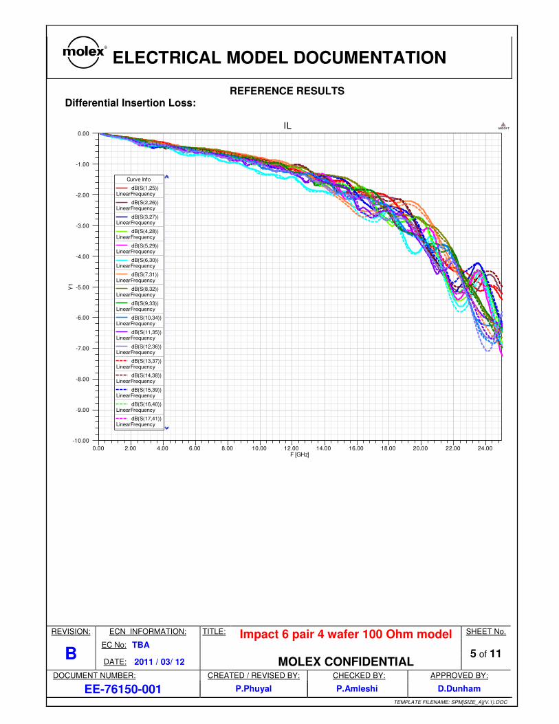
REFERENCE RESULTS Differential Insertion Loss:
0.00 2.00 4.00 6.00 8.00 10.00 12.00 14.00 16.00 18.00 20.00 22.00 24.00F [GHz]
-10.00
-9.00
-8.00
-7.00
-6.00
-5.00
-4.00
-3.00
-2.00
-1.00
0.00
Y1
IL ANSOFT
Curve Info
dB(S(1,25))LinearFrequency
dB(S(2,26))LinearFrequency
dB(S(3,27))LinearFrequency
dB(S(4,28))LinearFrequency
dB(S(5,29))LinearFrequency
dB(S(6,30))LinearFrequency
dB(S(7,31))LinearFrequency
dB(S(8,32))LinearFrequency
dB(S(9,33))LinearFrequency
dB(S(10,34))LinearFrequency
dB(S(11,35))LinearFrequency
dB(S(12,36))LinearFrequency
dB(S(13,37))LinearFrequency
dB(S(14,38))LinearFrequency
dB(S(15,39))LinearFrequency
dB(S(16,40))LinearFrequency
dB(S(17,41))LinearFrequency
ELECTRICAL MODEL DOCUMENTATION
REVISION: ECN INFORMATION: TITLE: Impact 6 pair 4 wafer 100 Ohm model
MOLEX CONFIDENTIAL
SHEET No.
B EC No: TBA
6 of 11 DATE: 2011 / 03/ 12
DOCUMENT NUMBER: CREATED / REVISED BY: CHECKED BY: APPROVED BY:
EE-76150-001 P.Phuyal P.Amleshi D.Dunham
TEMPLATE FILENAME: SPM[SIZE_A](V.1).DOC
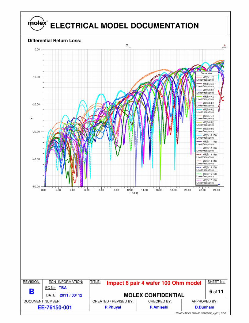
Differential Return Loss:
0.00 2.00 4.00 6.00 8.00 10.00 12.00 14.00 16.00 18.00 20.00 22.00 24.00F [GHz]
-50.00
-40.00
-30.00
-20.00
-10.00
0.00
Y1
RL ANSOFT
Curve Info
dB(S(1,1))LinearFrequency
dB(S(2,2))LinearFrequency
dB(S(3,3))LinearFrequency
dB(S(4,4))LinearFrequency
dB(S(5,5))LinearFrequency
dB(S(6,6))LinearFrequency
dB(S(7,7))LinearFrequency
dB(S(8,8))LinearFrequency
dB(S(9,9))LinearFrequency
dB(S(10,10))LinearFrequency
dB(S(11,11))LinearFrequency
dB(S(12,12))LinearFrequency
dB(S(13,13))LinearFrequency
dB(S(14,14))LinearFrequency
dB(S(15,15))LinearFrequency
dB(S(16,16))LinearFrequency
dB(S(17,17))LinearFrequency
ELECTRICAL MODEL DOCUMENTATION
REVISION: ECN INFORMATION: TITLE: Impact 6 pair 4 wafer 100 Ohm model
MOLEX CONFIDENTIAL
SHEET No.
B EC No: TBA
7 of 11 DATE: 2011 / 03/ 12
DOCUMENT NUMBER: CREATED / REVISED BY: CHECKED BY: APPROVED BY:
EE-76150-001 P.Phuyal P.Amleshi D.Dunham
TEMPLATE FILENAME: SPM[SIZE_A](V.1).DOC
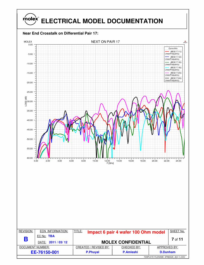
Near End Crosstalk on Differential Pair 17:
0.00 2.00 4.00 6.00 8.00 10.00 12.00 14.00 16.00 18.00 20.00 22.00 24.00F [GHz]
-60.00
-55.00
-50.00
-45.00
-40.00
-35.00
-30.00
-25.00
-20.00
-15.00
-10.00
-5.00
0.00
LO
SS
(d
B)
MOLEX NEXT ON PAIR 17 ANSOFT
Curve Info
dB(S(17,11))LinearFrequency
dB(S(17,12))LinearFrequency
dB(S(17,16))LinearFrequency
dB(S(17,18))LinearFrequency
dB(S(17,23))LinearFrequency
dB(S(17,24))LinearFrequency
ELECTRICAL MODEL DOCUMENTATION
REVISION: ECN INFORMATION: TITLE: Impact 6 pair 4 wafer 100 Ohm model
MOLEX CONFIDENTIAL
SHEET No.
B EC No: TBA
8 of 11 DATE: 2011 / 03/ 12
DOCUMENT NUMBER: CREATED / REVISED BY: CHECKED BY: APPROVED BY:
EE-76150-001 P.Phuyal P.Amleshi D.Dunham
TEMPLATE FILENAME: SPM[SIZE_A](V.1).DOC
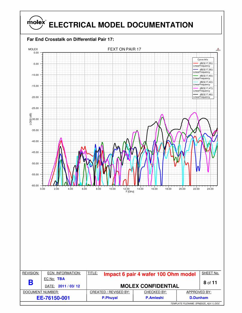
Far End Crosstalk on Differential Pair 17:
0.00 2.00 4.00 6.00 8.00 10.00 12.00 14.00 16.00 18.00 20.00 22.00 24.00F [GHz]
-60.00
-55.00
-50.00
-45.00
-40.00
-35.00
-30.00
-25.00
-20.00
-15.00
-10.00
-5.00
0.00
LO
SS
(d
B)
MOLEX FEXT ON PAIR 17 ANSOFT
Curve Info
dB(S(17,35))LinearFrequency
dB(S(17,36))LinearFrequency
dB(S(17,40))LinearFrequency
dB(S(17,42))LinearFrequency
dB(S(17,47))LinearFrequency
dB(S(17,48))LinearFrequency
ELECTRICAL MODEL DOCUMENTATION
REVISION: ECN INFORMATION: TITLE: Impact 6 pair 4 wafer 100 Ohm model
MOLEX CONFIDENTIAL
SHEET No.
B EC No: TBA
9 of 11 DATE: 2011 / 03/ 12
DOCUMENT NUMBER: CREATED / REVISED BY: CHECKED BY: APPROVED BY:
EE-76150-001 P.Phuyal P.Amleshi D.Dunham
TEMPLATE FILENAME: SPM[SIZE_A](V.1).DOC
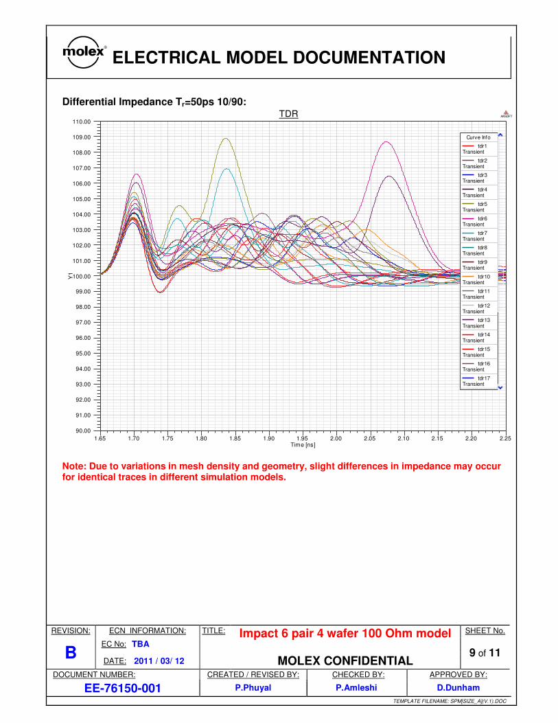
Differential Impedance Tr=50ps 10/90:
1.65 1.70 1.75 1.80 1.85 1.90 1.95 2.00 2.05 2.10 2.15 2.20 2.25Time [ns]
90.00
91.00
92.00
93.00
94.00
95.00
96.00
97.00
98.00
99.00
100.00
101.00
102.00
103.00
104.00
105.00
106.00
107.00
108.00
109.00
110.00
Y1
TDR ANSOFT
Curve Info
tdr1Transient
tdr2Transient
tdr3Transient
tdr4Transient
tdr5Transient
tdr6Transient
tdr7Transient
tdr8Transient
tdr9Transient
tdr10Transient
tdr11Transient
tdr12Transient
tdr13Transient
tdr14Transient
tdr15Transient
tdr16Transient
tdr17Transient
Note: Due to variations in mesh density and geometry, slight differences in impedance may occur for identical traces in different simulation models.
ELECTRICAL MODEL DOCUMENTATION
REVISION: ECN INFORMATION: TITLE: Impact 6 pair 4 wafer 100 Ohm model
MOLEX CONFIDENTIAL
SHEET No.
B EC No: TBA
10 of 11 DATE: 2011 / 03/ 12
DOCUMENT NUMBER: CREATED / REVISED BY: CHECKED BY: APPROVED BY:
EE-76150-001 P.Phuyal P.Amleshi D.Dunham
TEMPLATE FILENAME: SPM[SIZE_A](V.1).DOC
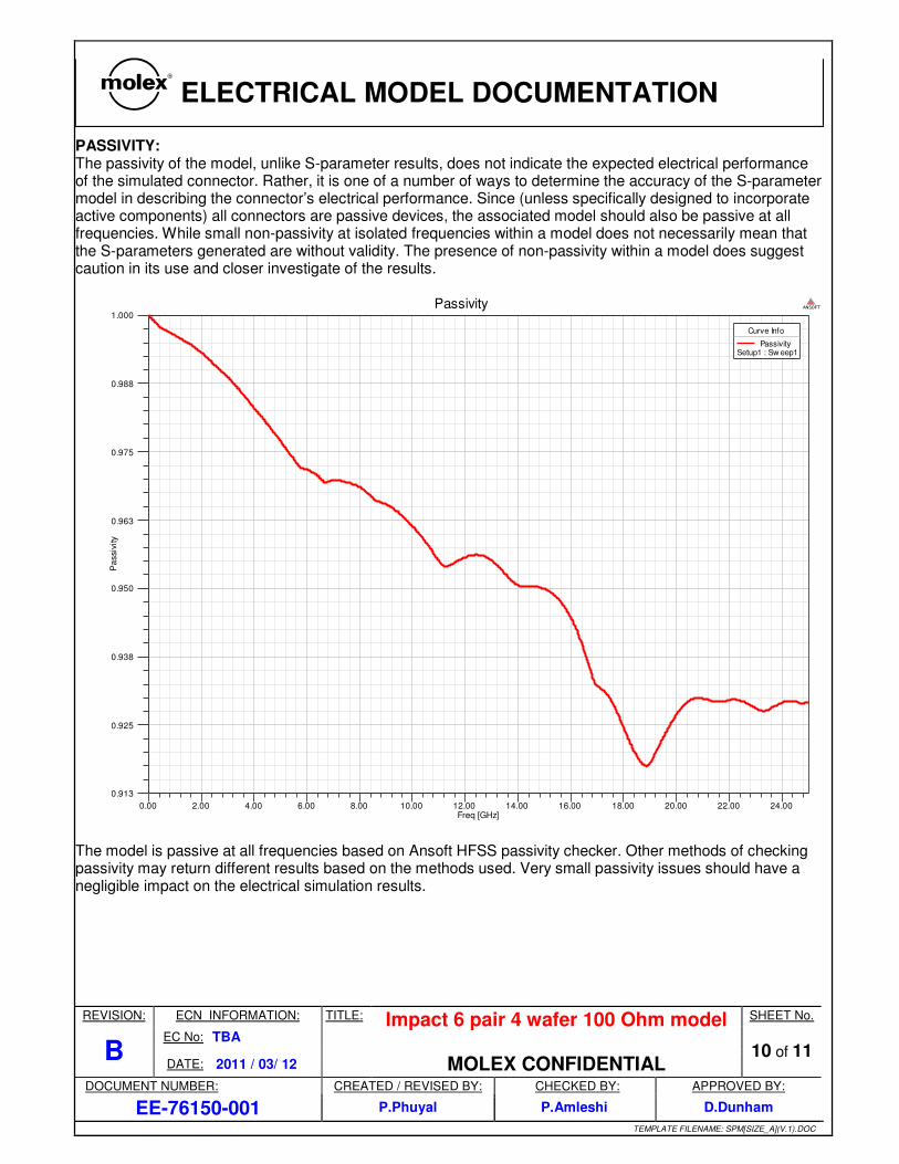
PASSIVITY: The passivity of the model, unlike S-parameter results, does not indicate the expected electrical performance of the simulated connector. Rather, it is one of a number of ways to determine the accuracy of the S-parameter model in describing the connector’s electrical performance. Since (unless specifically designed to incorporate active components) all connectors are passive devices, the associated model should also be passive at all frequencies. While small non-passivity at isolated frequencies within a model does not necessarily mean that the S-parameters generated are without validity. The presence of non-passivity within a model does suggest caution in its use and closer investigate of the results.
0.00 2.00 4.00 6.00 8.00 10.00 12.00 14.00 16.00 18.00 20.00 22.00 24.00Freq [GHz]
0.913
0.925
0.938
0.950
0.963
0.975
0.988
1.000
Pa
ssiv
ity
Passivity ANSOFT
Curve Info
PassivitySetup1 : Sw eep1
The model is passive at all frequencies based on Ansoft HFSS passivity checker. Other methods of checking passivity may return different results based on the methods used. Very small passivity issues should have a negligible impact on the electrical simulation results.
ELECTRICAL MODEL DOCUMENTATION
REVISION: ECN INFORMATION: TITLE: Impact 6 pair 4 wafer 100 Ohm model
MOLEX CONFIDENTIAL
SHEET No.
B EC No: TBA
11 of 11 DATE: 2011 / 03/ 12
DOCUMENT NUMBER: CREATED / REVISED BY: CHECKED BY: APPROVED BY:
EE-76150-001 P.Phuyal P.Amleshi D.Dunham
TEMPLATE FILENAME: SPM[SIZE_A](V.1).DOC
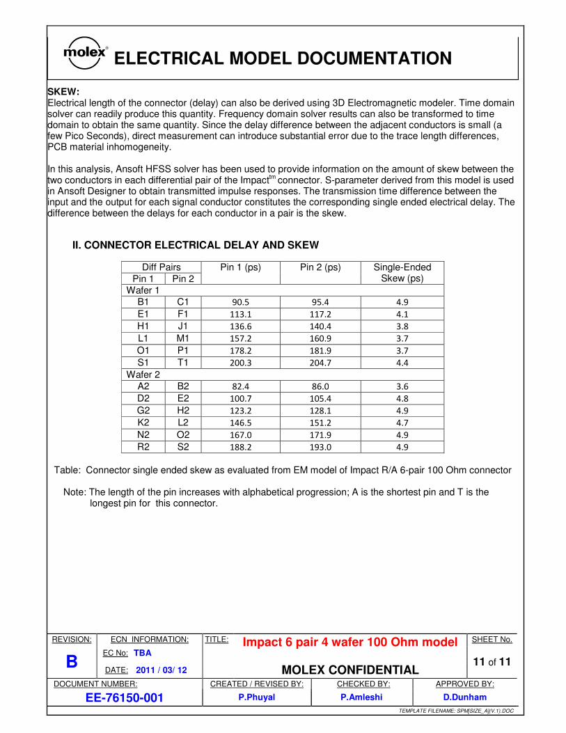
SKEW: Electrical length of the connector (delay) can also be derived using 3D Electromagnetic modeler. Time domain solver can readily produce this quantity. Frequency domain solver results can also be transformed to time domain to obtain the same quantity. Since the delay difference between the adjacent conductors is small (a few Pico Seconds), direct measurement can introduce substantial error due to the trace length differences, PCB material inhomogeneity. In this analysis, Ansoft HFSS solver has been used to provide information on the amount of skew between the two conductors in each differential pair of the Impacttm connector. S-parameter derived from this model is used in Ansoft Designer to obtain transmitted impulse responses. The transmission time difference between the input and the output for each signal conductor constitutes the corresponding single ended electrical delay. The difference between the delays for each conductor in a pair is the skew.
II. CONNECTOR ELECTRICAL DELAY AND SKEW
Diff Pairs Pin 1 (ps) Pin 2 (ps) Single-Ended Skew (ps) Pin 1 Pin 2
Wafer 1
B1 C1 90.5 95.4 4.9
E1 F1 113.1 117.2 4.1
H1 J1 136.6 140.4 3.8
L1 M1 157.2 160.9 3.7
O1 P1 178.2 181.9 3.7
S1 T1 200.3 204.7 4.4
Wafer 2
A2 B2 82.4 86.0 3.6
D2 E2 100.7 105.4 4.8
G2 H2 123.2 128.1 4.9
K2 L2 146.5 151.2 4.7
N2 O2 167.0 171.9 4.9
R2 S2 188.2 193.0 4.9
Table: Connector single ended skew as evaluated from EM model of Impact R/A 6-pair 100 Ohm connector
Note: The length of the pin increases with alphabetical progression; A is the shortest pin and T is the longest pin for this connector.
Copyright © 2022 FDOKUMEN