Dicyclopentadiene and Sodium Silicate Microencapsulation for Self-Healing of Concrete
Upload
khangminh22Category
view
0download
0
Lehigh UniversityLehigh Preserve
Theses and Dissertations
2017
Electric field-induced softening of alkali silicateglassesCharles Thomas McLarenLehigh University
Follow this and additional works at: https://preserve.lehigh.edu/etd
Part of the Other Materials Science and Engineering Commons
This Dissertation is brought to you for free and open access by Lehigh Preserve. It has been accepted for inclusion in Theses and Dissertations by anauthorized administrator of Lehigh Preserve. For more information, please contact [email protected].
Recommended CitationMcLaren, Charles Thomas, "Electric field-induced softening of alkali silicate glasses" (2017). Theses and Dissertations. 2956.https://preserve.lehigh.edu/etd/2956

Electric field-induced softening of alkali silicate glasses
By
Charles McLaren
Presented to the Graduate and Research Committee
of Lehigh University
in Candidacy for the Degree of
Doctor of Philosophy
in
Materials Science and Engineering
Lehigh University
August 2017

ii
© Copyright 2017 by Charles Thomas McLaren
All Rights Reserved

iii
Certificate of Approval
Approved and recommended for acceptance as a dissertation in partial fulfillment of the
requirements for the degree of Doctor of Philosophy for Charles T. McLaren.
______________________
Date
_______________________
Dissertation Director
______________________
Accepted Date
Committee Members:
________________________
Dr. Himanshu Jain
________________________
Dr. William R. Heffner
________________________
Dr. Richard P. Vinci
________________________
Dr. Nicholas C. Strandwitz
________________________
Dr. Nicholas J. Smith
iv
Acknowledgements
I gratefully thank Professor Himanshu Jain for giving me the opportunity to continue
my education and to be a part of this research project. I greatly appreciate his guidance
and the knowledge I have gained from him in my graduate career. His willingness to help
either professionally or personally is extremely appreciated.
I give special thanks to Bill Heffner who graciously donated his time and knowledge
of electronics to set me up for success with this project. Without him, electrical
characterization of my samples would not have been performed smoothly. I have learned
to apply the Heffner rule of ‘You’ll fail three times before success, so get to failing
quick’ to more than just my research.
I would like to extend my sincere gratitude to my dissertation committee, Profs.
Richard P. Vinci, Nicholas C. Strandwitz along with Dr. Nicholas J. Smith for their
advice, guidance and dedication of time to the project and me personally.
I would like to thank Professor Rishi Raj at the University of Colorado at Boulder for
allowing me to visit his laboratories on a research exchange. I also thank Dr. Bernhard
Roling and his graduate student Marco Balabajew for allowing me to visit their
laboratories on an international exchange at the University of Marburg. The technical
discussion were instrumental to the background and setup of this research project.
Thank you to my fellow glass group members Chatree Saiyasombat, Adam Stone,
Ukrit Thamma, Sean McAnany, Dmytro Savytskyy and Roman Holovchak. Your
training sessions, insights, and critical discussions have helped me to advance my

v
laboratory and problem solving skills. I also give a special thank you to Christie
Hasbrouck for her help with the experiments during her REU. To the rest of the graduate
students in the Materials Department thank you for your support and friendships.
I would also like to thank the many members of the Materials Science and
Engineering Department. The guidance and assistance of Sarah Wing, Janie Carlin, Lisa
Arechiga, Sue Stetler, Katrina Kraft, Mike Rex and John Gregoris have played a critical
role in assuring the success of this research project.
I am enormously thankful to my family and Rachel Bedics for all their love and
support throughout my education. The encouragement I have received from my parents,
grandparents, and siblings has allowed me to achieve all that I have set my mind to.
Finally, I gratefully acknowledge the financial support of the National Science
Foundation through the International Materials Institute for New Functionality in Glass
(DMR 0844014) at Lehigh University.

vi
Table of Contents Certificate of Approval ...................................................................................................... iii
Acknowledgements ............................................................................................................ iv
List of Tables ...................................................................................................................... x
List of Figures .................................................................................................................... xi
Abstract ............................................................................................................................... 1
Chapter 1: Introduction and Background Review .............................................................. 5
1.1 Glass introduction ................................................................................................ 5
1.2 U.S. glass industry ................................................................................................ 6
1.3 Flash sintering ...................................................................................................... 7
1.4 Electro-thermal poling.......................................................................................... 9
1.5 Thermally stimulated poling currents ................................................................ 12
1.6 Dielectric properties ........................................................................................... 13
1.7 Dielectric breakdown ......................................................................................... 15
1.8 Photoemission .................................................................................................... 16
Chapter 2: Statement of purpose ....................................................................................... 24
2.1 Challenges .......................................................................................................... 24
2.2 Project motivation .............................................................................................. 25
2.3 Objectives ........................................................................................................... 25
2.4 Dissertation outline ............................................................................................ 25
Chapter 3: Experimental methods ..................................................................................... 29
3.1 Glass compositions ............................................................................................. 29
3.2 Melt-quench technique ....................................................................................... 29
3.3 Differential scanning calorimetry....................................................................... 30
3.4 Impedance spectroscopy .................................................................................... 30
3.5 Design of EFIS equipment ................................................................................. 31
3.5.1 DC setup – circuit schematic ...................................................................... 32
3.5.2 AC setup – circuit schematic ...................................................................... 34
3.6 Measurement of EFIS......................................................................................... 35
3.6.1 Defining softening point furnace temperatures ........................................... 36

vii
3.7 Compositional analysis ...................................................................................... 37
3.7.1 Energy-dispersive x-ray spectroscopy (EDS) ............................................. 37
3.7.2 Time-of-flight secondary ion mass spectroscopy (ToF-SIMS) .................. 38
3.7.3 X-ray photoelectron spectroscopy .............................................................. 39
3.8 Infrared imaging of temperature profile ............................................................. 39
Chapter 4: Basic electrical and dielectric characteristics .................................................. 53
4.1 AC electrical characteristics of bulk glass ......................................................... 53
4.2 DC electrical conductivity .................................................................................. 54
4.2.1 Ionic conductivity activation energy ........................................................... 55
4.3 Frequency dependence of dielectric constant..................................................... 56
4.4 Chapter summary ............................................................................................... 57
Chapter 5: Effect of electric field on the softening of alkali silicate glasses .................... 63
5.1 DC dependence of EFIS ..................................................................................... 63
5.1.1 Compositional dependence of DC EFIS ..................................................... 64
5.1.2 Field/voltage dependence of EFIS .............................................................. 66
5.1.3 Field/voltage dependence discussion .......................................................... 67
5.2 AC dependence of EFIS ..................................................................................... 70
5.2.1 Frequency dependence ................................................................................ 71
5.2.2 Compositional dependence of AC EFIS ..................................................... 71
5.3 Pressure dependence of EFIS ............................................................................. 72
5.4 Photoemissions during EFIS .............................................................................. 73
5.4.1 DC photoemissions ..................................................................................... 73
5.4.2 AC photoemissions ..................................................................................... 74
5.5 Chapter summary ............................................................................................... 74
Chapter 6: Electro-thermal poling of alkali silicate glasses .............................................. 86
6.1 Electro-thermal poling experimental setup ........................................................ 86
6.2 Electro-thermal poling results ............................................................................ 88
6.3 Discussion of electro-thermal poling observations ............................................ 94
6.3.1 Bulk dielectric constant and electrical conductivity ................................... 94
6.3.2 Depletion layer formation ........................................................................... 96

viii
6.3.3 Electrical and dielectric behavior of alkali ion depletion layer ................ 100
6.3.4 Depletion layer behavior during thermally stimulated depoling .............. 104
6.4 Implications for EFIS ....................................................................................... 105
6.5 Chapter summary ............................................................................................. 109
Chapter 7: Characteristics of depletion layer formation prior to EFIS ........................... 124
7.1 Thermally stimulated currents under DC voltages ........................................... 124
7.1.1 DC TSPC results ....................................................................................... 124
7.1.2 Discussion of DC TSPC results ................................................................ 128
7.2 Thermally stimulated currents under AC voltage ............................................ 132
7.2.1 AC TSPC results ....................................................................................... 132
7.2.2 Discussion of AC TSPC results ................................................................ 134
7.3 Compositional analysis of modified and parent glass ...................................... 139
7.3.1 EDS results................................................................................................ 140
7.3.2 EDS discussion ......................................................................................... 143
7.3.3 XPS results ................................................................................................ 146
7.3.4 Discussion of XPS results ......................................................................... 148
7.4 Athermal alkali ion depletion layer formation ................................................. 150
7.4.1 Experimental methods of athermal depletion layer formation ................. 151
7.4.2 Thermal imaging of depletion layer formation ......................................... 151
7.4.3 Discussion of athermal depletion layer formation .................................... 153
7.5 Chapter summary ............................................................................................. 156
Chapter 8: Mechanism of electric field-induced softening of glass ............................... 188
8.1 Finite element analysis of alkali migration ...................................................... 188
8.1.1 FEA model setup....................................................................................... 189
8.1.2 FEA results................................................................................................ 191
8.1.3 FEA discussions ........................................................................................ 192
8.2 Anion migration ............................................................................................... 196
8.3 Dielectric breakdown ....................................................................................... 199
8.3.1 Photoemissions spectra ............................................................................. 202
8.4 Joule heating ..................................................................................................... 207

ix
8.5 Infrared imaging ............................................................................................... 209
8.5.1 AC vs DC power dissipation..................................................................... 210
8.6 Finite element analysis of thermal runaway ..................................................... 211
8.6.1 Model setup ............................................................................................... 212
8.6.2 FEA results of thermal runaway ............................................................... 215
8.6.3 FEA discussions ........................................................................................ 216
8.7 Mechanism of EFIS .......................................................................................... 219
8.8 Chapter summary ............................................................................................. 221
Chapter 9: Conclusions and future work ........................................................................ 241
9.1 Conclusions ...................................................................................................... 241
9.2 Future work ...................................................................................................... 244
9.2.1 Low-frequency depletion layer formation ................................................ 244
9.2.2 EFIS with in situ impedance spectroscopy ............................................... 245
9.2.3 Alkali ion concentration study .................................................................. 246
9.2.4 Photoemission origin ................................................................................ 247
9.2.5 Finite element model refinement .............................................................. 248
References ....................................................................................................................... 251
Appendix A: Dielectric measurement procedure ............................................................ 260
Appendix B: EFIS measurement procedure ................................................................... 262
Appendix C: FEA model equations ................................................................................ 269
Appendix D: Dissertation research publications............................................................. 272
Vita .................................................................................................................................. 273

x
List of Tables
Table 1-1: Energy consumption in mmBtu per ton of glass produced broken down by
process stage. Glass forming consumes about 30% of total energy.[12].......................... 18
Table 3-1: Glass compositions and their respective glass transition temperatures (Tg)
measured by DSC at 10°C/min. ........................................................................................ 41
Table 4-1: Activation energies (Ea) for each glass composition measured by impedance
spectroscopy (IS) ranging from ambient to Tg. ................................................................. 58
Table 5-1: Glass compositions and their respective Tg and Ts0 values ............................. 76
Table 5-2: Fitting parameters for A and B in Eq. 5-1 for estimating the reduction in
furnace temperature for an applied voltage relative to conventional softening for each
glass composition. Note: Large error in 5L5NS is due to small EFIS effect.................... 76
Table 6-1: Glass compositions with their respective glass transition temperature (Tg),
poling temperature (Tp), DC electrical conductivity activation energy (Ea), thermally
stimulated depoling current activation energy (TSDC Ea) and thermally stimulated poling
current activation energy (TSPC Ea). .............................................................................. 111
Table 6-2: Relaxation time constants of poling current, τfast and τslow, for each glass
composition with a poling voltage of Vp=25 or 100 V at Tp for 2 h. The experimental
error in τfast and τslow is estimated to be ± 20 s and 20%, respectively. ........................... 111
Table 6-3: Bulk and depletion layer electrical conductivity values after poling for time,
τslow, at Tp. The relative dielectric constant (𝜺𝒉𝒇′) at room temperature (RT), poling
temperature (Tp) and depletion layer permittivity (𝜺𝑫𝑳′) at Tp. Note: Only bulk value for
NS Vp= 25 V is shown due to lack of ToF-SIMS data. .................................................. 112
Table 7-1: Glass compositions and their respective glass transition temperatures (Tg) and
activation energy for alkali ion migration during constant heating. Activation energies
from impedance spectroscopy and thermally stimulated current measurements are
compared with values from Table 6-1. ........................................................................... 158
Table 7-2: Comparison of thermally stimulated current peaks of each glass type with
150V applied externally. ................................................................................................. 158
Table 7-3: Numerical parameters of various 1s core level XPS spectra. Binding energy
(B. E.) and FWHM in eV and area percent for each sample. ......................................... 159
Table 7-4: Surface compositions of NS after poling with 100 V and unpoled NS glass
including carbon contamination. ..................................................................................... 160
Table 7-5: Surface compositions following poling with 100 V excluding carbon
contamination. Theoretical sodium disilicate composition is added for comparison. .... 160
Table 8-1: Peak centers of the 2L8NS photoemission as seen in Figure 7-16. The peak
centers were matched to alkali ion electron energy level transitions.[126] .................... 223
Table 8-2: EDS measurements of powder buildup on compression hook after 2L8NS
tested at 200 V/cm, as shown in Figure 7-9. Note: Li could not be detected due to
window absorption from the detector. ............................................................................ 223

xi
List of Figures
Figure 1-1: DC electrical fields enhance the rate of sintering in 3YSZ. Moreover, an
abrupt shrinkage occurs when the field is greater than a threshold value, estimated to be
about 40 V/cm where full density is reached in just a few seconds.[17] .......................... 19
Figure 1-2: Flash sintering manifests in a power surge at a critical sintering temperature is
reached for 3YSZ. The onset of power instability coincides with the onset of flash
sintering above a threshold electric field.[17]................................................................... 19
Figure 1-3: Impedance spectroscopy diagrams of ZrO2: 8 mol% Y2O3 (a) flash sintered
and (b) conventionally sintered to full density.[25] .......................................................... 20
Figure 1-4: Scanning probe microscopy images of (a) the carbon-coated mold (groove
depth=150 nm) and (b) glass surface imprint at 450°C, 200 V and 3 MPa for 180 s.[7] . 20
Figure 1-5: Sketch of different steps of the layer formation at the anode/glass interface.
The approximate values for a poling voltage of Vp = 50 V. The electric field, E, and the
electric potential, φ, are plotted versus the distance from the anode x after completion of
the respective step.[32] ..................................................................................................... 21
Figure 1-6: Schematic representation of (a) TSDC and (b) TSPC measurement (from top
to bottom) of polarization, sample temperature and current. Note: E is electrometer and R
is recorder.[57] .................................................................................................................. 22
Figure 1-7: Space charge, field strength and voltage distribution in colored alkali halide
crystal after charging (theoretical).[69] ............................................................................ 22
Figure 1-8: The effect of specimen thickness on the breakdown strength of pyrex BSI
glass for a voltage rise time of 30 seconds at different temperatures.[63] ....................... 23
Figure 1-9: Breakdown strength and maximum internal poling field as a function of
temperature. Also plotted are predictions of limiting Eb(T) behavior, per the theory of
Vermeer (dash-dot lines), while the remaining lines are guides for the eye.[73] ............. 23
Figure 3-1: DSC measurement of NS from ambient to 800°C at a heating rate of
10°C/min. Tg measured as 469°C. .................................................................................... 42
Figure 3-2: DSC measurement of 2L8NS from ambient to 800°C at a heating rate of
10°C/min. Tg measured as 424°C. .................................................................................... 42
Figure 3-3: DSC measurement of 5L5NS from ambient to 800°C at a heating rate of
10°C/min. Tg measured as 420°C. .................................................................................... 43
Figure 3-4: Three electrode configuration for electrical measurements. a) specimen with
electrodes and b) circuit connections. Note: Guard ring thickness (g), central electrode
radius (r1) and sample thickness (d). ................................................................................. 44
Figure 3-5: Image of a NS sample with gold sputtered electrodes used for impedance
spectroscopy with the three-probe configuration. Top center electrode was connected to
high tension terminal, bottom electrode was low tension terminal and top outer electrode
was ground of the general radio impedance spectrometer. Gold electrodes were connected
to platinum wires using silver paint. ................................................................................. 45
xii
Figure 3-6: Modifications to ATS pneumatic creep tester for measurements of EFIS. A
cathode and anode were made to apply an electric field across the sample. A spectrometer
probe and video camera used the window slits into the furnace. A thermocouple was
added near the sample. ...................................................................................................... 46
Figure 3-7: Design and dimensions of compressional hooks (pull to push) for application
of load to glass samples in the ATS pneumatic creep tester. ............................................ 47
Figure 3-8: Images into ATS pneumatic creep tester where a) compression hooks are
placed on the ends of the pull rods and b) shows sample placement between hooks. ...... 48
Figure 3-9: Experimental setup inside the modified ATS model 2605 pneumatic creep
tester where the anode was located at the top of the sample and the cathode at the bottom.
The electrode portion of the system was electrically insulated from the rest of the furnace
through the Macor standoffs. ............................................................................................ 49
Figure 3-10: Schematic of measurement circuit used to record EFIS experimental data.
Voltage and current were reduced and converted to 0 to 10 V DC and recorded with a
DATAQ Instruments model DI-149HS. ........................................................................... 50
Figure 3-11: Schematic of AC power supply used for EFIS. A transformer was driven in
reverse where the output side was applied to the measurement circuit in Figure 3-10. ... 51
Figure 3-12: Representative calculations of intersecting tangents (highlighted blue) of
softening temperatures of a) NS conventional Ts0 and b) NS TsV with 150 V applied at
10°C/min. Note: This technique was applied to all EFIS tested samples. ........................ 52
Figure 4-1: Electrical conductance with respect to frequency for NS glass from room
temperature to 525°C. The relative trends are the same for all glass compositions but shift
downward with increased mixed alkali content. ............................................................... 59
Figure 4-2: Representative variation of conductance vs. frequency for 2L8NS at 78.5,
103.3 and 154.3°C. Note: All glass compositions followed similar behavior. ................. 59
Figure 4-3: Capacitance as a function of frequency for NS glass from room temperature
to 525°C. The relative trends are the same for all glass compositions but shift downward
with increased mixed alkali content. ................................................................................. 60
Figure 4-4: Representative behavior of capacitance vs. frequency for 2L8NS at 78.5,
103.3 and 154.3°C. Note: All glass compositions followed similar behavior. ................. 60
Figure 4-5: Nyquist impedance plots for 2L8NS at 78.5, 103.3 and 154.3°C. Real and
imaginary components of impedance were calculated using data collected in Figure 3-6
and Figure 3-7. Note: All glass compositions behaved similarly. .................................... 61
Figure 4-6: Arrhenius plot for evaluating the activation energy for each glass composition
using conductivities from impedance spectroscopy, ranging from ambient to about 400°C
........................................................................................................................................... 61
Figure 4-7: Real dielectric permittivity for NS as a function frequency from room
temperature to 525°C. The relative trends are the same for all glass compositions. ........ 62

xiii
Figure 4-8: Imaginary dielectric permittivity for NS as a function frequency from room
temperature to 525°C. The relative trends are the same for all glass compositions. ........ 62
Figure 5-1: Displacement vs. furnace temperature of NS at various applied electric fields
with a constant heating rate of 10°C/min. The Tg for NS is indicated by arrow. Reference
alumina rod displacement of the support structure is shown by light green dashes.
Transition between Stage I and Stage II is shown by a vertical line while the onset of the
large abrupt displacement is indicated by the red arrow. .................................................. 77
Figure 5-2: EFIS displacement of 2L8NS at various applied electric fields with a constant
heating rate of 10°C/min. 2L8NS Tg indicated by arrow. ................................................ 78
Figure 5-3: EFIS displacement of 5L5NS at various applied electric fields with a constant
heating rate of 10°C/min. 5L5NS Tg indicated by arrow. ................................................ 78
Figure 5-4: EFIS displacement of NAS at various applied electric fields with a constant
heating rate of 10°C/min. .................................................................................................. 79
Figure 5-5: Normalized FIS effect for NS (black, squares), 2L8NS (blue, triangles),
5L5NS (pink, inverted triangle) and NAS (red, circles). The Difference ΔT(V) in regular
softening temperature (Ts0) to softening temperature with an applied electric field (TsV)
plotted versus applied electric field. Arrows indicate approximate threshold applied
electric field for each glass composition. .......................................................................... 79
Figure 5-6: Plot of change in sample thickness vs. temperature for NAS glass under 10
MPa pressure, demonstrating that EFIS is dependent on external voltage rather than
external electric field......................................................................................................... 80
Figure 5-7: Plot of change in sample thickness vs. temperature for NAS glass with
different surface roughness. Applied pressure was 10 MPa. ............................................ 80
Figure 5-8: Replotted data from Figure 5-5: ΔT(V) as a function of applied voltage where
each glass composition is normalized to its respective Ts0. Dashed lines are empirical fits
of Equation 5-1 to the voltage dependence of EFIS. ........................................................ 81
Figure 5-9: Electric field-induced softening of a) NS glass and b) 5L5NS glass with 150
V at a constant heating rate of 10°C/min. Various frequencies were used for AC testing.
Note: The 0 V conventional softening of each glass was added for reference. ................ 82
Figure 5-10: Comparison of EFIS with respect to frequency for NS and 5L5NS of a)
EFIS softening temperature, TsV and b) change in softening temperature relative to
conventional softening, ΔT(V). ........................................................................................ 83
Figure 5-11: Effect of pressure on EFIS of NAS glass. .................................................... 84
Figure 5-12: Effect of pressure on EFIS of NAS glass with 199 1V (Black, Squares)
and 142 2V (Red, Circles) applied. ............................................................................... 84
Figure 5-13: Images of NS during 150 V/cm test condition when the furnace temperature
was a) T<TF and b) TF<T<TS of EFIS. ............................................................................. 85

xiv
Figure 5-14: Images of NS during EFIS with AC voltages of a) 120 V 60 Hz and b) 150
V 125 Hz. These images are representative of photoemissions observed at both
electrodes. ......................................................................................................................... 85
Figure 6-1: Representative experimental conditions for LS with Tp=120°C (black, solid)
and Vp=100 V (red, dashed) for a poling time of 2 h. .................................................... 112
Figure 6-2: Arrhenius behavior of DC electrical conductivity used to calculate activation
energy for ionic conduction. ........................................................................................... 113
Figure 6-3: Electrical behavior of NS during poling with Vp=25 V at Tp=100°C for 2 h a)
showing representative conductance vs. frequency behavior and b) representative
impedance growth of an alkali ion depletion layer (arrow indicating increasing direction).
The inset indicates the intersection between bulk and depletion layer impedance
components. .................................................................................................................... 114
Figure 6-4: Nyquist plots of real impedance vs. imaginary impedance during poling with
100V for 2 hours with a) LS (Tp=120°C), b) 5L5NS (Tp=230°C), c) 2L8NS (Tp=190°C)
and d) NS (Tp=100°C) glass compositions at 120 s interval. ......................................... 115
Figure 6-5: Impedance spectra for depoling of NS with Vp= 0 V at Tp=100°C for 20 h.
Impedance was observed to increase upon removal of the poling voltage and gradually
decrease over the course of depoling at Tp. .................................................................... 116
Figure 6-6: Real capacitance of NS before (black, squares) and during poling with Vp=25
V at Tp=100°C. High frequency plateau attributed to bulk capacitance and low frequency
plateau corresponds to depletion layer formation. Note: Large noise in start (red, circles)
and 120 second (blue, triangles) spectra due to glass changing on a faster time scale than
impedance frequency sweep. .......................................................................................... 117
Figure 6-7: Capacitance values of unpoled and poled samples for each composition with
respect to frequency. Note: All spectra were collected at each glass composition’s
corresponding Tp. ........................................................................................................... 118
Figure 6-8: Time dependence of current density (left axis, symbols) and charge flow
(right axis, lines) for each glass composition with Vp=100 V at Tp for a) initial 50 s, b)
complete 7,200 s duration (on log-log scale) and c) exponential and stretched exponential
decay fits of current density during poling of LS. .......................................................... 119
Figure 6-9: TSDC of current density (left axis, pink inverted triangles), charge flow (right
axis, black line) and sample temperature (far right axis, blue dashes) for 5L5NS from
ambient to 300°C at a heating rate of 10°C/min. ............................................................ 120
Figure 6-10: TSPC of current density (left axis, bold lines), charge flow (right axis, lines)
for each glass composition from ambient to 300°C at a heating rate of 10°C/min. ....... 120
Figure 6-11: ToF-SIMS measurement of depletion layer thickness for 2L8NS of about
100 nm following poling with Vp=100 V at Tp=190°C for 2 h. Annotations for platinum
electrode layer (Anode), alkali ion depletion layer (DL), and bulk glass (Bulk) are labeled
approximately with sputter depth.................................................................................... 121

xv
Figure 6-12: Schematic of fitted equivalent DC circuit for electrode polarization (E),
alkali ion depletion layer (DL) and bulk glass (B). ........................................................ 122
Figure 6-13: Depletion layer resistivity as a function of poling time for NS (black,
squares), 2L8NS (blue, triangles), 5L5NS (pink, inverted triangles) and LS (red, circles)
with Vp=100 V at Tp for 2 h. ........................................................................................... 122
Figure 6-14: Comparison of ToF-SIMS alkali ion depletion layer thickness (black,
squares) measurements between glass compositions after poling with Vp=100 V for 2 h at
Tp. The corresponding depletion layer permittivity (red, circles) calculated from Equation
6-1 are also compared. .................................................................................................... 123
Figure 6-15: Pairs of images captured during electric field-induced softening at a heating
rate of 10°C/min. The first two images show NS with an external voltage of 150 V at a
furnace temperature of a) 428°C and b) 429°C taken 6 seconds apart. The second pair of
images taken 20 seconds apart show NAS with an external voltage of 200 V
corresponding to current measurements c) 0.3 mA (1.2 mA/cm2) and d) 10 mA (40.5
mA/cm2) prior to glass softening. Note: the anode is located at top of the sample and
photoemissions are indicated by yellow arrows. ............................................................ 123
Figure 7-1: Time dependence of current density (black line) through NS glass sample
with 150V applied during heating at 10°C/min. The current density peaks are indicated
by red arrows. Accumulated charge flow (red line) was observed to surge around 0.1 C.
Note: There is an axis break for integrated charge where it appears to be constant but it
still increasing with time. ................................................................................................ 161
Figure 7-2: Thermally stimulated current density in NS glass as a function of
temperature, under different voltage ranging from 100 V to 200 V. Applied pressure = 1
MPa. Note: Large surge in current density due to dielectric breakdown of samples. .... 162
Figure 7-3: Time variation of a) accumulated charge density through NS glass along with
the transition from region II to III indicated by the dashed line and b) area-specific
capacitance to electrical breakdown of the samples under different voltage as indicated.
......................................................................................................................................... 163
Figure 7-4: Current density through different glasses as a function of temperature. All
samples were subjected to 150V and 1 MPa pressure. ................................................... 164
Figure 7-5: Arrhenius plot of thermally stimulated poling current through 5L5NS glass
with 150V applied during constant heating at 10°C/min. The linear fit portion yields
activation energy for alkali ion migration. ...................................................................... 164
Figure 7-6: Comparison of accumulated charge density flow to breakdown in four
different glass compositions with 150V applied. Note: Charge density flow corresponds
to current measurements in Figure 7-4. .......................................................................... 165
Figure 7-7: Heating rate dependence of thermally stimulated current densities of LS with
150V applied at 10℃/min or 5℃/min. ........................................................................... 165

xvi
Figure 7-8: Frequency dependence of current density for a) NS and b) 5L5NS glass
compositions during heating at 10°C/min for EFIS with 150 V. .................................... 166
Figure 7-9: Frequency dependence of charge density for a) NS and b) 5L5NS glass
compositions during heating at 10°C/min for EFIS with 150 V. Charge density was
calculated from the integral of current density. .............................................................. 167
Figure 7-10: Frequency dependence of power density dissipation for a) NS and b) 5L5NS
glass compositions during heating at 10°C/min for EFIS with 150 V. ........................... 168
Figure 7-11: Frequency dependence of electrical conductivity for a) NS and b) 5L5NS
glass compositions during heating at 10°C/min for EFIS with 150 V. A model Jonscher
sum of AC and DC contributions to overall electrical conductivity are added for
comparison as dashed lines. ............................................................................................ 169
Figure 7-12: Activation energy calculated by the initial Arrhenius rise of electrical
conductivity with respect to AC frequency for both NS (black, squares) and 5L5NS (red,
circles) glass compositions. ............................................................................................ 170
Figure 7-13: NS125V EDS line scan of the glass near the anode. An alkali ion depletion
layer was measured to be roughly 60 µm thick. Note: Oxygen (green), silicon (purple),
sodium (blue) and carbon (red). ...................................................................................... 171
Figure 7-14: EDS map of NS 125V near the anode (located to the left of the sample). The
pink rectangle on the secondary electron image was the mapped area. .......................... 172
Figure 7-15: NS 150V EDS line scan of the glass near the anode (electrode located left of
dashed line). An alkali depletion layer of 160 µm was measured. The region closest to the
anode is beveled indicated preferential polishing post-mortem. .................................... 173
Figure 7-16: EDS map of NS 175V near the anode. Pink region was mapped. Pores were
only observed within the alkali ion depletion layer. ....................................................... 174
Figure 7-17: Secondary electron images of NAS after EFIS with 200 V and 1 MPa
applied where a) is a representative image of the anode (right) /glass (left) region and b)
is an overlay of Na intensity (green) taken from an EDS map. Note: The yellow arrow
indicates a semicircular cavity of interest. ...................................................................... 175
Figure 7-18: NS 175V EDS line scan of the glass near the cathode. An accumulation of
alkali was not measured by EDS. Note: Linescan intensity x1000. ............................... 176
Figure 7-19: EDS line scan across optically brown region corresponding to a sodium-rich
composition. .................................................................................................................... 176
Figure 7-20: EDS line scan across the a) anode electrode and b) cathode electrode. Note:
Oxygen (yellow), Sodium (Green), Silicon (Purple). ..................................................... 177
Figure 7-21: EDS line scan for NS 150V stopped in Region II corresponding to alkali ion
migration. EDS did not detect a discreet depletion layer. Porosity was not observed in the
glass near the anode. ....................................................................................................... 177

xvii
Figure 7-22: Survey spectra of binding energy from NS glass prior to and post poling.
Spectra compare virgin glass composition (green) to the modified anode (black) and
cathode (red) compositions. ............................................................................................ 178
Figure 7-23: High resolution binding energy peak analysis for a) O 1s, b) Na 1s, c) Si 2p
and d) C 1s orbitals in the virgin glass, anode and cathode compositions. ..................... 179
Figure 7-24: High resolution peak analysis of O 1s for a) virgin, b) anode and c) cathode
glass surfaces which has been deconvoluted into various identified components with their
cumulative fit. ................................................................................................................. 180
Figure 7-25: High resolution peak analysis of Na 1s for a) virgin, b) anode and c) cathode
glass surfaces which has been deconvoluted into various identified components with their
cumulative fit. ................................................................................................................. 181
Figure 7-26: High resolution peak analysis of C 1s for a) virgin, b) anode and c) cathode
glass surfaces which has been deconvoluted into various identified components with their
cumulative fit. ................................................................................................................. 182
Figure 7-27: Current density (black) decay of a) LS, b) LS repeat and c) 5L5NS during
application of 150V held at a furnace temperature of 250°C. The amount of calculated
charge flow (red) is also shown for each run. Note: Gain of current amplifier was
saturated at the start of a) LS. ......................................................................................... 183
Figure 7-28: Infrared image of LS prior to being poled. The rectangular glass sample is
located in the middle of the image while the anode is at the top and cathode is at the
bottom of the image. ....................................................................................................... 184
Figure 7-29: Temporal plots of a) LS, b) LS Repeat and c) 5L5NS during application of
150V held at a furnace temperature of 250°C. Temperature measurements were taken
from multiple areas of the sample for comparison. ........................................................ 185
Figure 7-30: SIMS depth profile for a) LS, b) 5L5NS and c) 7Li+ for each of the three
samples tested with two areas per sample (dashed lines for unpoled values). The alkali
ion depletion layer was measured to be approximately 1 micrometer thick and indicated
by the dashed lines in a) and b). ...................................................................................... 186
Figure 7-31: SIMS depth profiles of a) 18O- and b) 1H- ions normalized to the Si- signal
to a depth of 2.5 µm from the anode/glass interface. Surface roughness of the glass may
result in variation of values at the interface. ................................................................... 187
Figure 8-1: Representative FEA charge carrier behavior for NS with 200 V applied for a)
sodium concentration profile and b) corresponding electrical conductivity attributed to
composition variation within 100 nm from the anode for 20 seconds. ........................... 224
Figure 8-2: FEA depletion layer thickness after 20 seconds for a) various temperatures
from 100°C to 350°C with 10, 50 and 90% concentration of bulk values and b) depletion
layer thickness at the 50%, 10% to 90% transition width and depletion layer midpoint
thickness minus half the transition width as a function of temperature. ......................... 225

xviii
Figure 8-3: FEA current density decay as a function of time for depletion layer formation
in a temperature range from 100°C to 350°C. ................................................................ 226
Figure 8-4: Current density through 2L8NS glass with 150V applied. Run 1 sample was
ramped at a constant heating rate of 10℃/min until EFIS. Run 2 also was heated at
10℃/min, but then held at 420℃. .................................................................................. 227
Figure 8-5: Accumulated charge density threshold measured prior to breakdown versus
external voltage applied across samples of each glass composition. Dashed line is least
squares fit to the data for NS........................................................................................... 227
Figure 8-6: Photoemission spectra at the 200 V/cm test condition ranging from 350-900
nm for NS (black, bottom) and 2L8NS (blue, top). Peaks labels correspond with those
listed in Table 8-1. 5L5NS has same peaks as 2L8NS. Note: Intensity of 2L8NS was
offset by an arbitrary amount for comparison................................................................. 228
Figure 8-7: Photoemissions from LS sample during the high current region of electric
field-induced softening. Applied voltage was 200V. The inset scale shows the three major
characteristic peak positions. .......................................................................................... 229
Figure 8-8: After testing 2L8NS with 200 V/cm a) buildup of white powder was observed
on the compression hook near the anode. The powder was investigated using EDS where
b) spot 1 is indicated by the red crosshairs with its c) collected spectrum and d) spot 2
again indicated by the red crosshairs with its e) collected spectrum. The semi quantitative
compositions are given in Table 7-1. .............................................................................. 230
Figure 8-9: Energy dissipation and corresponding increase in sample temperature beyond
furnace temperature for NS 150 V DC from Fig. 7-8a. Energy dissipation calculated from
Eq. 7-1 and temperature increase from Eq. 7-2. ............................................................. 231
Figure 8-10: Series of infrared images of NS with 200 V applied from video at a) start of
thermal runaway (time=41 s), b) localized heating during EFIS (time=43 s), c) anode
discharge following intense heating (time=45 s) and d) localized glass softening (time=54
s). Note: Anode is located at top of sample .................................................................... 232
Figure 8-11: IR image of a) temporal cursor locations and b) cursors temperature average
of 3x3 pixels for anode, bulk and cathode glass regions along with furnace and anode
temperatures for the first 30 s of EFIS thermal runaway. ............................................... 233
Figure 8-12: IR images of 2L8NS with 150 V applied. The formation of an alkali-rich
phase can be seen growing from cathode to anode at a) sample temperature of 575°C and
b) continued growth at 600°C. The alkali-rich phase circled. ........................................ 234
Figure 8-13: IR images of NS with 150 V applied in DC at a) run time=2069.4 s and
furnace temperature=353.5°C and b) run time=2108.5 s and furnace
temperature=363.6°C. Note: Color scale was not updated but hottest pixel is identified
with accurate temperature reading. ................................................................................. 235
Figure 8-14: IR images of NS with 150 V 1000 Hz applied in AC at a) run time=2130 s
and furnace temperature=385.3°C and b) run time=2403 s and furnace

xix
temperature=428.6°C. Note: Color scale was not updated but hottest pixel is identified
with accurate temperature reading. ................................................................................. 236
Figure 8-15: Simulated a) electric potential and b) temperature profiles of NS resulting
from self-heating at 1 s intervals over 30 s total with 200 V DC applied at an initial
temperature of 277°C. The anode/glass interface is located at 0 mm while glass/cathode
interface at 10 mm in the model. .................................................................................... 237
Figure 8-16: Model calculations of thermal runaway of NS at various initial temperatures
with a depletion layer thickness of 100 nm for a) current during 30 s of self-heating and
b) thermal profile at 30 s. Note: Current limit reach is a result of heat generation versus
heat loss. .......................................................................................................................... 238
Figure 8-17: Thermal profiling at 30 s of self-heating as a function of depletion layer
thickness. Below 100 nm, heat loss from the depletion layer occurs rapidly. Above 100
nm the depletion layer resistivity limits the current as a negative feedback. ................. 239
Figure 8-18: Calculated blackbody radiation spectra during thermal runaway. ............. 239
Figure 8-19: Sketch of the various steps of EFIS at the anode/glass interface with an
applied voltage during constant heating. The dielectric breakdown strength (red, dashed
dot line), local internal electric field (green, dashed line) and electric potential (blue, solid
line). Processes for a) dipolar polarization of region I, b) start of alkali ion migration in
region II, c) formation of depletion layer in region II, d) growth of depletion layer in
region II, e) anion migration in region III and f) onset of dielectric breakdown in region
IV. Note: Sketches b, c and d are adapted from Zakel et. al. for convenience.[32] ....... 240
Figure 9-1: Frequency dependence of current density of NS during heating at 10°C/min
for EFIS with 150 V. The red arrow indicates decrease in current density for 60 Hz and
125 Hz samples. .............................................................................................................. 250
Figure C-0-1: Calculated NS electrical conductivity dependence on Na2O concentration
along with the temperature dependence based on activation energies for 48 sodium
silicate glass compositions.[2,124] ................................................................................. 270

1
Abstract
The advancement of materials engineering relies on our ability to develop innovative
processing techniques or incrementally improve efficiency of existing ones. Glass
manufacturing is an energy intensive process. Many efforts have been focused on
increasing the energy efficiency of glass melting, however, very few have focused on
additional energy savings through innovative glass forming techniques. Therefore,
reduction in glass processing time and temperature could be readily accepted into already
existing or new forming techniques. A similar scenario has recently occurred in the
ceramics community. A novel ceramic sintering technique, named flash sintering, has
greatly improved sintering of ceramics by application of an electric field at elevated
temperatures. The technique has been demonstrated to successfully reduce sintering time
and temperature on a wide variety of ceramic materials. The underlying mechanism of
flash sintering is controversial. It remains unclear if Joule heating solely accounts for
flash sintering or if an electric field enhances defect concentration and mobility. In this
dissertation, an innovative glass forming technique named electric field-induced
softening (EFIS) has been demonstrated to reduce furnace temperature and processing
times for bulk glass softening using an applied voltage, similar to flash sintering. A
family of binary and mixed alkali disilicate glasses were used to delineate the role of
alkali ion migration. This study also identifies the underlying mechanism of EFIS and
provides insight on how to tailor the technique for application.
The reduction of furnace temperature and processing time for glass softening was
quantitatively measured as compressive displacement upon viscous flow of the glass

2
samples. The difference in temperature between conventional glass softening and EFIS
was used to compare the effect of electric fields or more appropriately, applied voltage. It
also allowed for quantitative comparison between glass compositions of varying glass
transition temperatures. EFIS showed dependence on glass resistivity, applied voltage,
frequency, current limit and heating rate.
The formation of an alkali ion depletion layer was investigated due to EFIS being
dependent on applied voltage rather than nominal external electric field. Electro-thermal
poling and impedance spectroscopy was used to measure the kinetics of depletion layer
formation along with its associated electrical and dielectric characteristics. The results
from time-of-flight secondary ion mass spectroscopy (ToF-SIMS) showed a depletion
layer thickness ranging from 50 nm to 200 nm depending on glass composition. The
formation of the depletion layer also revealed two relaxation time constants (~20 s and
~1,000 s) which have been attributed to alkali ion migration followed by electrolysis of
non-bridging oxygens. The electric and dielectric properties of the depletion layer are
similar to those of fused silica.
Polarization mechanisms during EFIS were identified by investigating thermally
stimulated poling current (TSPC). Four distinct regions of the TSPC were observed using
DC voltages while only three were observed using AC. In the case of DC, the four
regions corresponded to dipolar polarization, alkali ion migration, anion migration/proton
injection and dielectric breakdown, in order of increasing temperature. Photoemissions
were observed as part of the dielectric breakdown process using UV-Vis spectrometer.
The peak temperatures of thermally stimulated current and their associated activation

3
energies of each peak were used to identify the dominate charge carrier process within
each region. Activation energy for alkali ion diffusion was measured by both impedance
spectroscopy and initial rise method. Secondary electron microscopy (SEM) and energy-
dispersive spectroscopy (EDS) were used to measure depletion layer depth profiles up to
50 µm thick following EFIS. In the case of AC, the three regions of the thermally
stimulated current are attributed to short-range oscillations of cations around the non-
bridging oxygens, long-range migration oscillations of cations followed by thermal
runaway, in order of increasing temperature.
Finally, finite element analysis (FEA) simulated two major parts of EFIS. First, the
formation of an alkali ion depletion layer was modeled. The electrical properties of the
depletion layer were then calculated as a function of composition from parent to modified
glass. The current density decay of depletion layer formation agrees with experimental
results from electro-thermal poling. Second, thermal runaway was calculated using a
fixed depletion layer thickness at various starting temperatures. FEA also calculated
thermal runaway with depletion layer thicknesses ranging from 5 nm to 50 µm starting
from the same temperature. A maximum calculated temperature was about 1,650°C
within the model on the anode side of the glass. Experimental measurements of thermal
runaway were recorded using infrared imaging cameras up to a maximum temperature of
2,000°C. Temperatures within the alkali disilicate glasses during EFIS readily exceeded
1,300°C nearest the anode. A maximum temperature was measured to be 1,868°C during
softening. Results from simulated FEA and experimental measurements are in good
qualitative agreement with the proposed mechanism of EFIS.

4
Based on the above results, the overall mechanism that determines EFIS of alkali
silicate glasses occurs as follows: i) dipolar polarization of alkali ions in the direction of
the applied voltage, ii) long-range alkali ion migration toward the oppositely charge
electrode, iii) formation of a highly resistive alkali ion depletion layer near the positively
charge electrode creating a large internal electric field, iv) migration of anions toward the
positive electrode along with proton injection into the depletion layer, v) mixed ionic-
electronic conduction sustains large internal electric field strength, iv) at elevated
temperatures the dielectric strength of the depletion layer decreases to the point where it
is exceeded by the local internal electric field within the alkali ion depletion layer. Here,
dielectric breakdown occurs leading to thermal runaway and subsequent heat transfer into
the bulk ultimately leading to bulk glass softening.

5
Chapter 1: Introduction and Background Review
1.1 Glass introduction
Glass is a useful engineering material due to several material properties such as its
transparency, durability, and chemical stability. Glasses can also possess low thermal
expansion and be excellent electrical insulators. Most commercially produced glasses are
oxide silicates. These glasses have found a wide range of applications from basic
functions such as windows, containers and decorative art to much more advanced
functions such as dielectrics, photovoltaics, pharmaceuticals, surface patterned glasses,
display glasses and optical devices.[1,2]
Many advanced applications listed above require glass to interact with electric fields
or electrical components. It is well known that mobile cations predominantly determine
the electrical characteristics of oxide glasses below the glass transition temperature.[3]
These cations can either be intentionally added for desired material properties or found as
impurities. From this simple understanding, one can control the electrical characteristics
of a glass through both batching and processing resulting in electrical conductivity
ranging from 10-15 S/cm up to 10-2 S/cm.[4]
Recently, there have been several innovations in glass processing that manipulated
the electrical characteristics of glass to tailor specific properties of the material. Such
innovations include electro-thermal poling[5,6], electrical imprinting[7] and anodic
bonding[8], which apply external electric fields to glass. These techniques allow for
careful control of modified glass composition as the mobile cations carry the charge from

6
one electrode to the other in the direction of the electric field. They also allow for precise
control of modifying the glass on the micrometer scale.[7,9,10]
1.2 U.S. glass industry
Glass manufacturing is energy intensive and often encompasses long processing
times. It consists of multiple stages that are vital to producing quality articles. The energy
consumption per ton of glass produced is broken down by processing stage in Table 1-1
for flat, container, fiber and pressed/blown glass sectors. Glass melting is the most energy
intensive component for all sectors, accounting for approximately 50-80% of total energy
consumption.[11] Whereas, there are many actions taken to reduce energy consumption
of the melting stage, energy consumption in the post-melting process (20-50%) is
significant and needs to be reduced.[12] As seen in Table 1-1, the forming process alone
can consume about 30% of the total energy needed per ton of glass produced. Reduction
of energy consumption for soda-lime container glass melting, when optimized conditions
are in-place, appears to be nearing the theoretical limit indicating that further research
will only provide relatively small energy savings.[11] As for post-melting processes, the
state-of-art techniques are far from optimized relative to their theoretical limits.[11]
Therefore, energy savings may be more readily obtained through innovative post-melting
operations and techniques rather than optimization of melting.
Several near surface glass processing techniques are currently under development for
surface structuring of glass post-melting, such as abrasive (water/air) jet machining,
micro-electrochemical discharge machining, laser machining and laser-assisted hot
embossing.[13–16] However, these technologies are limited in the types of features that

7
can be produced to feature size of ~100 µm.[14] Smaller feature sizes less than 100 µm
have been demonstrated, but the processing speed becomes unacceptably slow.[13,14]
The slow speeds for small features and machine layouts required for these techniques are
mostly suited for small scale applications such as optical and advanced electronic
components. Another challenge for these techniques is that they are not easily scalable
for large-scale applications involving flat glass.[15] Therefore, technologies that can
improve manufacturing capabilities and efficiency of patterned glass are much needed.
1.3 Flash sintering
Electric fields, applied with a pair of electrodes can reduce the furnace temperature
and sintering time of a wide range of ceramics.[17–21] This electric field enhanced
sintering is generally divided into two regimes: field assisted sintering (FAST) and flash
sintering – see Figure 1-1. In FAST, which occurs at low field, sintering is somewhat
enhanced and progresses gradually with time.[17] By comparison, at higher fields flash
sintering occurs abruptly in just a few seconds, when a critical temperature is reached at a
given applied field.[17] Figure 1-2 characterizes flash sintering as a power surge
produced by an abrupt increase in conductivity. It has also been reported that an applied
DC electric field of similar magnitude to flash sintering had a significant influence on the
flow stress of fine-grained Al2O3 and MgO.[22]
The mechanism of flash sintering is controversial. The sudden increase in
conductivity produces Joule heating, which has been the first explanation of the flash
effect. A recent study using dynamic modeling with non-uniform temperature supports

8
pure Joule heating runaway to be responsible for enhancing the sintering rates.[23] The
power dissipation in the sample from electrical heating is given simply by:
𝑃 =𝑉2𝐴
𝜌𝐿 (Equation 1-1)
where P is thermal power dissipation (watts), V is potential drop (V), A is cross-sectional
area (cm2), ρ is resistivity (Ω.cm) and L is the thickness of the sample (cm). However,
detailed studies suggest that Joule heating alone may not be sufficient to explain the
extreme sintering rates of flash sintering.[20,24] In these studies Joule heating was
viewed as being a consequence of Frenkel pair defect nucleation at furnace temperature
that subsequently ionizes into charge neutral defects and electron-hole pairs.[24] Other
mechanisms have been hypothesized to result in the formation of vacancies along with
electrochemical reductions within the ceramic.[21] It is speculated that an increase in the
number of vacancies enhances charge carrier mobility along with localized Joule heating
further inducing the runaway process.[21] Impedance spectroscopy measured in situ
during flash sintering of an ionic conductor (ZrO2: 8 mol% Y2O3), a proton conductor
(BaCe0.8Zr0.1Y0.1O3-δ) and a semiconductor (SnO2: 0.5 mol% MnO2) show distinct
differences in the electrical behavior. For example, differences between impedance
spectra for samples of ZrO2: 8 mol% Y2O3 are shown in Figure 1-3a for flash sintering
and Figure 1-3b for conventional sintering.[25] During conventional sintering, impedance
spectroscopy revealed that charge carrier migration occurs through the bulk of grains and
are blocked at the grain boundaries.[25] For flash sintering, only a single impedance
semicircle was observed in Figure 1-3b with a 45° spike at low frequency. This is

9
attributed to the bulk grain while the low frequency spike suggests diffusion of the charge
carriers occurs through intergranular layers with negligible blocking.[25]
Beyond the DC results already mentioned, flash sintering has also been observed
under AC fields of similar magnitude at frequencies of both 50 and 1000 Hz.[26,27] The
application of AC fields also revealed two distinct regimes of sintering - FAST and flash.
The main difference observed between DC and AC fields was the development of
microstructure. It was reported that AC fields developed equiaxed grains while DC fields
preferentially lead to grain growth in one direction.[27]
1.4 Electro-thermal poling
Electro-thermal poling was primarily developed to induce second-order nonlinear
(SONL) optical susceptibility in glasses by application of DC electric fields.[28–31] In
recent years, interest in this technique has expanded beyond SONL to enhance a variety
of biological, physical and chemical properties of glass.[32–45] For example, electro-
thermal poling has been reported to modify a glass’ affinity to atmospheric water at the
anode region.[45] The experimental setup of electro-thermal poling of glasses has many
similarities to that of flash sintering. It generally comprises of four main processing steps.
First, a glass is heated to a predetermined poling temperature (Tp) below the glass
transition temperature (Tg), which allows for increased ionic conductivity while retaining
the preformed dimensions. Electrodes on opposite sides of the glass sample are then used
to apply a DC voltage (Vp) at Tp. After sufficient charge flow has occurred, the glass is
then cooled to ambient while still applying the DC voltage to ‘freeze’ ionic
displacements. Finally, the applied voltage is removed at ambient temperature where

10
ionic conductivity is significantly lower to prevent ionic migration back towards original
positions. Modification of properties is largely effected by the formation of an alkali ion
depletion layer at the anode due to charge transport of ions during these steps.
Electro-thermal poling has been reported to cause structural rearrangements in glass
such as the creation of an alkali ion depletion layer.[41,43,44] A consistent structural
change following electro-thermal poling is an increase in polymerization of the glassy
network in the subsurface region at the anode.[41,43] Thermally and electric field
activated charge compensation of non-spontaneous structural rearrangements have been
under debate. In any case, it appears that the charge compensation mechanism heavily
depends on the electrode/glass interface and testing atmosphere.[41,43,44] For example,
a commercially available borosilicate glass with ~5 mol% alkali content was poled at a
temperature of 300°C for 30 mins with 2 kV in a nitrogen atmosphere.[44] An unpolished
silicon wafer was used as the anode allowing the furnace atmosphere to fill gas gaps due
to surface roughness. A gaseous discharge emission at the silicon anode/glass interface
was attributed to the N2 electronic transitions from furnace atmosphere.[44] Within the
alkali depletion layer, molecular oxygen, NO+ and NO2 were found as evidence of redox
reactions.[44] Electro-thermal poling has also been used as a technique to imprint the
surface of glass. Surface patterns can be imprinted using a patterned anode surface as
shown in Figure 1-4a at and below the Tg to create sub-micron surface features such as
seen in Figure 1-4b.[7,9,10]
Despite numerous electro-thermal poling studies, the mechanisms responsible for
depletion layer formation and charge compensation remain only partially understood.

11
There is consistent agreement that the cations migrate toward the cathode during poling
creating a thin layer depleted of mobile positive ions within the glass nearest the
anode.[28,37] However, bulk electrical conductivity and charge compensation via anion
migration or cation injection from the anode remain additional possibilities.[30,42–44]
The extent of electro-thermal poling has been shown to be dependent on both ionic and
electronic conductivities.[31] The dielectric response of the depletion layer and bulk glass
during poling also remains unclear, as we may anticipate it to also change since the
dielectric constant of alkali silicate glasses decreases with decreasing alkali content.[46]
The charge transport mechanisms of depletion layer formation of 46S4 bioactive
glass (46.4SiO2 - 25.2Na2O - 25.2CaO - 3.2P2O5 in mol%) have been studied by Zakel et
al.[32] Both the poling current and impedance spectroscopy were investigated in situ
during electro-thermal poling. Post-poling analysis yielded a depletion layer thickness of
about 110 nm.[32] The study also reported two charge transport processes with
significantly different time dependences of poling current at a constant temperature: a
first process with a fast time constant, τfast ~40 s and another process with a slower time
constant, τslow ~1000 s. Zakel et al. presented a model for charge transport mechanisms of
46S4 glass, which is described in Figure 1-5.[32] The τfast corresponded to Na+ ion
migration creating a depletion layer where the electric field may approach the dielectric
breakdown field strength allowing electrons to become mobile as shown in Figure 1-5.
On the other hand, τslow was attributed to the migration of Ca2+ ions away from the
depletion layer as seen in Figure 1-5. A numerical model using Monte Carlo simulation
of 46S4 glass showed an excellent agreement with the time dependent Na+ and Ca2+ ionic

12
concentration profiles, as well as between experimentally measured relaxation time
constants and theoretical calculations.[47]
1.5 Thermally stimulated poling currents
A method for characterizing polarization mechanisms in solids is by use of thermally
stimulated poling currents (TSPC) [48–53]. During heating of an ionic conductor under
an applied DC voltage, the temperature dependence of current is investigated. The testing
procedure for thermally stimulated depoling current (TSDC) and TSPC are schematically
shown in Figure 1-6a and Figure 1-6b, respectively. Increase in furnace temperature
provides thermal energy to introduce/deplete various polarizations. The resulting
variation of thermally stimulated current with temperature exhibits peaks superimposed
on uniformly increasing current [54]. The characteristics of peak position relative to
heating rate yields activation energy that can help identify polarization mechanisms [55].
If thermally stimulated peaks are well resolved with respect to temperature, the initial rise
of current within a peak can give an accurate calculation for the activation energy
associated with its polarization mechanism as well.[56]
The resulting thermally stimulated current from ionic conductors such as glass arise
from (a) the thermal release of trapped electrons, holes or ions, (b) some type of
orientational (dipole) polarization, or (c) space charge polarization.[57] If a material
contains several of these processes at different energy levels, a corresponding number of
peaks should appear during heating to appropriate temperatures.

13
1.6 Dielectric properties
Glass is often used in dielectric applications either as a capacitive element or as an
insulator in electronic devices [58–60]. The dielectric properties of glass are primarily
determined by four polarization mechanism: electronic polarization, atomic/ionic
polarization, dipole polarization and interfacial polarization [58,61,62]. Under extreme
conditions, such as the application of large voltages and high temperatures, glass has
been observed to experience dielectric breakdown [63–67]. This is a process where the
dielectric insulator suddenly becomes conductive due to several possible mechanisms
depending on the situation. The most general mechanisms being intrinsic breakdown via
charge particle impact ionization or thermal breakdown by Joule heating [64].
The four main polarization mechanisms are briefly discussed as a reminder.
Electronic polarization occurs when the electron cloud within each atom is shifted by an
external electric field. The whole material then becomes polarized due to the collective
shift of the negative electron clouds relative to the positive nuclei. In atomic or ionic
polarization, ions within the dielectric material are slightly displaced due to the
application of an external electric field (cations toward cathode, anions toward anode).
This displacement results in a net average dipole moment per ion, creating polarization
that carries charge. Orientational polarization results from molecules that contain a
permanent dipole aligning with the external electric field due to torque. Finally,
interfacial polarization occurs from charge accumulation at a boundary between two
materials or regions. Charge accumulation at a boundary could result from the charge
reaching the boundary but not being able to permeate it. The individual polarization due

14
to each of these mechanisms can then be summed to calculate a total polarization of the
dielectric material.[68] Charge transfer across a dielectric material can occur from each
of these mechanisms as they collectively align with the external electric field.
Space charge theory has been developed to understand interfacial polarization and
electret formation in solids originally for dry rectifiers and transistors. It is based on the
release of electrons from the electrode and their conductance through the dielectric.[69]
This has been applied to understand interfacial polarization of dielectric materials. During
the application of a DC electric field to an ionic conductor, mobile cations predominately
carry the charge. The migration of cations leave behind positive countercharges which
produce local charge buildup. The uncompensated space charge layer is schematically
plotted in Figure 1-7 for an alkali halide crystal along with the internal electric field and
voltage distribution. From the developed space charge theory, the thickness of the space
charge layer is determined by the following equation:[69]
𝑑∞ = √2𝜀′𝑉𝑁𝑣𝑒⁄ (Equation 1-2)
where d∞ is the steady-state thickness of the space charge layer [m], ε’ is the dielectric
constant of the material [F/m], V is the applied voltage [V], Nv is the initial concentration
of mobile charge carriers [m-3] and e is elementary charge [C]. Since most of the voltage
drops across this layer, the local internal electric fields can be on the order of dielectric
breakdown strength.[69]
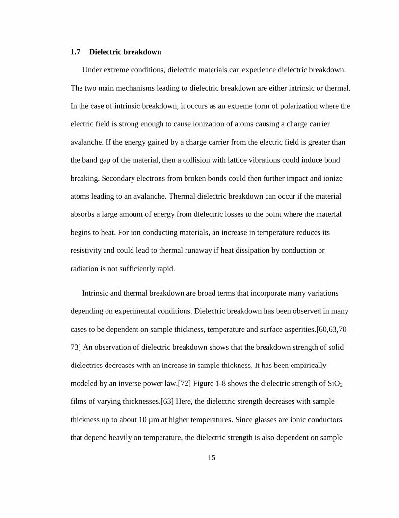
15
1.7 Dielectric breakdown
Under extreme conditions, dielectric materials can experience dielectric breakdown.
The two main mechanisms leading to dielectric breakdown are either intrinsic or thermal.
In the case of intrinsic breakdown, it occurs as an extreme form of polarization where the
electric field is strong enough to cause ionization of atoms causing a charge carrier
avalanche. If the energy gained by a charge carrier from the electric field is greater than
the band gap of the material, then a collision with lattice vibrations could induce bond
breaking. Secondary electrons from broken bonds could then further impact and ionize
atoms leading to an avalanche. Thermal dielectric breakdown can occur if the material
absorbs a large amount of energy from dielectric losses to the point where the material
begins to heat. For ion conducting materials, an increase in temperature reduces its
resistivity and could lead to thermal runaway if heat dissipation by conduction or
radiation is not sufficiently rapid.
Intrinsic and thermal breakdown are broad terms that incorporate many variations
depending on experimental conditions. Dielectric breakdown has been observed in many
cases to be dependent on sample thickness, temperature and surface asperities.[60,63,70–
73] An observation of dielectric breakdown shows that the breakdown strength of solid
dielectrics decreases with an increase in sample thickness. It has been empirically
modeled by an inverse power law.[72] Figure 1-8 shows the dielectric strength of SiO2
films of varying thicknesses.[63] Here, the dielectric strength decreases with sample
thickness up to about 10 µm at higher temperatures. Since glasses are ionic conductors
that depend heavily on temperature, the dielectric strength is also dependent on sample

16
temperature. The relation between dielectric strength and sample temperature is
summarized in Figure 1-9 for several glass types that contain alkali or are alkali
‘free’.[73] Here, two regimes are observed: At low temperatures, breakdown is
independent of sample temperature indicating intrinsic breakdown, whereas at higher
temperatures breakdown is heavily temperature dependent, especially for the alkali
containing glasses. The dashed dot lines reveal the behavior of Vermeer’s thermal
breakdown strength based on the heat-balance of initial sample temperature and applied
voltage rise.[66] The open symbols of Figure 1-9 show the maximum values of internal
electric fields developed within glass samples during electro-thermal poling. These
values exceed those predicted by thermal breakdown but remain lower than intrinsic
breakdown.[73]
1.8 Photoemission
Light emission or photoemissions are characteristic features of breakdown of
semiconducting and ion conducting materials.[70] The photoemission spectra during
breakdown conduction are characteristic of single atomic species in the gaseous state and
not of bound atoms of a solid.[70] The creation of photoemissions consist of three
steps.[74] First, an electron initially collides with a gas molecule which becomes excited
and emits a photon with a given energy during its relaxation back to the ground state. The
energy of the emitted photon is determined by the energy difference in electron energy
levels from the electron’s excited to relaxed states. Second, the emitted photon then
propagates through the gas to the surface of the dielectric. Lastly, at the surface the
dielectric emits an electron which serves as a seed for a new avalanche or participates in

17
an ongoing avalanche. The gas within the dielectric is formed due to large energy
dissipation through the sample during breakdown causing solid-to-gas sublimation.[70]

18
Table 1-1: Energy consumption in mmBtu per ton of glass produced broken down by
process stage. Glass forming consumes about 30% of total energy during production.[12]
Energy Consumption by Process Stage
Process
Stage
Flat Container Fiber Pressed/blown
mmBtu
/ton %
mmBtu
/ton %
mmBtu
/ton %
mmBtu
/ton %
Batch
preparation 0.68 5.2 0.68 5.6 0.68 3.4 0.68 4.2
Melting
/refining 8.6 66.3 5.5 45.7 8.4 41.6 7.3 44.8
Subtotal 9.28 71.5 6.18 51.3 9.08 45 7.98 49
Forming 1.5 11.6 4 33.2 7.2 35.7 5.3 32.6
Post-
forming 2.2 16.9 1.86 15.5 3.9 19.3 3 18.4
Subtotal 3.7 28.5 5.86 48.7 11.1 55 8.3 51
Total 12.98 100 12.04 100 20.18 100 16.28 100

19
Figure 1-1: DC electrical fields enhance the rate of sintering in 3YSZ. Moreover, an
abrupt shrinkage occurs when the field is greater than a threshold value, estimated to be
about 40 V/cm where full density is reached in just a few seconds.[17]
Figure 1-2: Flash sintering manifests in a power surge at a critical sintering temperature is
reached for 3YSZ. The onset of power instability coincides with the onset of flash
sintering above a threshold electric field.[17]

20
Figure 1-3: Impedance spectroscopy diagrams of ZrO2: 8 mol% Y2O3 (a) flash sintered
and (b) conventionally sintered to full density.[25]
Figure 1-4: Scanning probe microscopy images of (a) the carbon-coated mold (groove
depth=150 nm) and (b) glass surface imprint at 450°C, 200 V and 3 MPa for 180 s.[7]

21
Figure 1-5: Sketch of different steps of the layer formation at the anode/glass interface.
The approximate values for a poling voltage of Vp = 50 V. The electric field, E, and the
electric potential, φ, are plotted versus the distance from the anode x after completion of
the respective step.[32]

22
Figure 1-6: Schematic representation of (a) TSDC and (b) TSPC measurement (from top
to bottom) of polarization, sample temperature and current. Note: E is electrometer and R
is recorder.[57]
Figure 1-7: Space charge, field strength and voltage distribution in colored alkali halide
crystal after charging (theoretical).[69]

23
Figure 1-8: The effect of specimen thickness on the breakdown strength of pyrex BSI
glass for a voltage rise time of 30 seconds at different temperatures.[63]
Figure 1-9: Breakdown strength and maximum internal poling field as a function of
temperature. Also plotted are predictions of limiting Eb(T) behavior, per the theory of
Vermeer (dash-dot lines), while the remaining lines are guides for the eye.[73]

24
Chapter 2: Statement of purpose
2.1 Challenges
A major challenge in the glass industry is the continual pursuit of reducing
manufacturing costs while still producing quality products. Glass manufacturing and
processing requires high energy, environmental and economic costs. The combination of
these costs is currently at the point where further cost reduction can only be realized
through innovative optimization and processing techniques. In the case of glass forming,
following melting, the glass is usually formed while still cooling from melt
temperatures.[2,11] This requires the forming line to immediately follow the glass
melting tank during manufacturing. However, this may not always be practical. For
example, if glass needs to be shipped to a consumer for further processing, the glass
needs to be reheated to decrease its viscosity. Reheating glass to softening temperatures
may require long processing times and significant energy costs as to avoid thermal shock.
The interaction of glass with electric fields has been studied for many years on a
variety of applications. Electro-thermal poling of silicate glasses has already been
employed within the optically fiber community with success but with room for
improvement.[31,75] There is practical knowledge of how to implement electro-thermal
poling but a comprehensive understanding of underlying mechanisms is incomplete.
Preliminary results on glass softening motivated by the successful implementation of
flash sintering to ceramic processing has provided an avenue for addressing challenges
within the glass industry.
25
2.2 Project motivation
The challenging demands of glass manufacturing and successful results of flash
sintering motivated this project. It focuses on the adaptation of electro-thermal poling and
flash sintering to develop electric field-induced softening of glass.
2.3 Objectives
The development of an innovative glass processing technique encompasses the
objectives of this dissertation on macroscopic results and identification of mechanisms
for electric field-induced softening (EFIS) of alkali silicate glasses as follows:
1. Can electric fields enhance the softening of bulk glass beyond the surface region
i.e. is there a viable electric field-induced softening phenomenon?
2. Anticipating the answer to (1) is yes, what are the quantitative dependences of
furnace temperature reduction for glass softening on electric field magnitude,
glass type and associated glass resistivities?
3. Which mechanisms are responsible for EFIS and how do process parameters
affect them?
4. How can EFIS be appropriately modeled and optimized for glass industry use?
2.4 Dissertation outline
After a brief introduction of glass and its current technology state are presented, a
review of general background knowledge and literature is presented in more depth in
Chapter 1. Background topics include flash sintering, electro-thermal poling, thermally
stimulated DC ionic conduction and dielectric breakdown. The literature review provides
26
a good understanding of the current knowledge about each topic and build towards
critical questions addressed by this dissertation.
Chapter 2 addresses the current challenge of energy reduction in glass industry and
provides the motivation of this dissertation. It also includes this section listing the main
objectives of this dissertation as a series of critical questions.
The experimental methods of electric field-induced softening are described in detail
in Chapter 3. They include the glass composition selection and preparation method,
electrical characterization of glass samples using audio/RF frequencies, design of EFIS
equipment along with alkali ion depletion layer depth and compositional analysis by
energy-dispersive spectroscopy (EDS), secondary ion mass spectroscopy (SIMS) and x-
ray photoelectron spectroscopy (XPS). The parent and modified glass compositions were
measured both qualitatively and quantitatively. The experimental details for infrared
imaging (IR) of depletion layer formation and EFIS are also included.
Basic electrical and dielectric characteristics of the prepared glass compositions is
investigated in Chapter 4 by impedance spectroscopy. These data include the
conductivity and capacitance of the glasses as a function of frequency and temperature.
Impedance spectra were calculated to determine the DC conductivity, yielding the
activation energy for ionic conduction.
Novel glass softening results are presented in Chapter 5 for EFIS of alkali silicate
glasses. A dramatic reduction in furnace temperature required for glass softening is
presented for both DC and AC voltages. The dependence of EFIS on glass composition,
27
frequency and applied pressure are also presented in Chapter 5. Spectra of photoemission
from the glass was observed during EFIS and are presented here.
Chapter 6 addresses the electro-thermal poling characteristics of the same glass
compositions used for EFIS. Impedance spectroscopy and current density decay
measured the electrical and dielectric characteristics of the glasses. It identifies
similarities between EFIS and electro-thermal poling and their main mechanism.
The characteristics of depletion layer formation measured via thermally stimulated
currents during EFIS are presented in Chapter 7. Here, the various peaks observed in DC
are due to different polarization mechanism resulting in electrical conduction within the
glass. Four regions within the thermally stimulated current measurements have been
identified, which help build an understanding of the fundamental steps leading to EFIS of
alkali silicate glasses. Thermally stimulated currents from AC reveal a non-ohmic
behavior with temperature dependence. Chapter 7 also presents the characteristics of
alkali ion depletion layer formation by compositional and thermal studies using EDS,
XPS and thermal imaging.
The mechanism of EFIS is considered in Chapter 8 as a series of distinct stages,
ultimately leading to resistive self-heating. Finite element modeling of the alkali ion
depletion layer is discussed here with respect to temperature. This chapter emphasizes the
process of dielectric breakdown of glass during EFIS with the effects of Joule heating.
Thermal runaway was experimentally measured with in situ infrared imaging and
modeled with finite element analysis. It is often coincident with photoemissions which

28
are characterized as well. This correlation builds an understanding of dielectric
breakdown just prior to the observed process of EFIS in glass.
The conclusions of this dissertation are presented in Chapter 9 along with suggestions
for future work to continue the development and understanding of EFIS in glass. Finally,
operating procedures for impedance spectroscopy and EFIS are provided in Appendices
A and B, respectively. Appendix C presents the theoretical equations used in finite
element analysis whereas Appendix D lists the publications so far resulting from this
dissertation.

29
Chapter 3: Experimental methods
3.1 Glass compositions
Five glass compositions were used in this study to delineate the role of alkali
diffusion. Two of these glasses were binary alkali disilicate glasses (NS and LS), whereas
two other glasses were mixed alkali lithium-sodium disilicates of varying alkali ion ratios
(2L8NS and 5L5NS). The disilicate glasses were selected due to their similar network
structure but varying electrical properties where the 50/50 mixed alkali ratio (5L5NS) has
the highest resistivity.[76] For contrast, the final glass composition was a sodium
aluminosilicate (NAS). Each glass type’s corresponding composition is listed in Table
3-1. This dissertation used several batches of each glass composition. The characteristic
properties of each glass melt are summarized in the corresponding table for each
appropriate chapter.
3.2 Melt-quench technique
Standard melt-quench method was used to prepare all glasses by mixing varying
amounts of sodium carbonate (NaCO3), lithium carbonate (LiCO3), alumina (Al2O3) and
silica (SiO2) powders. The batched powders were then heated in a Pt-Rh crucible to
800℃ at 10℃/min to decompose the carbonates and melted at 1550℃ for 2 hours using
a heating rate of 2℃/min. The glass was poured into rectangular stainless-steel molds and
annealed 20℃ below the glass transition temperature (Tg) for 3 hours. Samples were
sectioned with a low speed diamond blade into rectangular blocks. The blocks were
ground and polished to a final cross-section of 5 mm x 5 mm and a height of about 10
mm for most of the measurements. The grit sizes used, in order, were 240, 320, 400 and

30
600. A solution of mineral spirits and paraffin wax was used instead of water to avoid
alkali ions from being leeched out during sample preparation. Conductive carbon paste
was applied to the top and bottom of the sample to ensure good electrical contacts with
graphite electrodes.
3.3 Differential scanning calorimetry
The glass transition onset temperature (Tg) was determined by differential scanning
calorimetry (DSC) in a NETZSCH 404/3F microcalorimeter. The DSC measurements
were done from ambient temperature to 800°C at 10°C/min. The values for Tg are
reported in Table 3-1 with their respective glass compositions. The glass transition
temperature was measured for each batch of glass made for each composition. This was
done to ensure that each glass batch was similar, preventing unexpected variation of
results between glass batches. The Tg for NS was measured to be 470°C as shown in
Figure 3-1. The mixed alkali glasses 2L8NS and 5L5NS had Tg values at 424°C and
420°C, respectively. A representative run for 2L8NS is shown in Figure 3-2 while 5L5NS
is displayed in Figure 3-3 with Tg indicated. The Tg for LS was measured as 468°C and
NAS was 511°C.
3.4 Impedance spectroscopy
Electrical impedance was measured on thin samples (~1 mm) that were ground and
polished to obtain parallel surfaces. Gold electrodes were sputtered on the top and bottom
of the sample in a three-probe configuration using a Polaron SEM Coating Unit E5100
and a ring mask. A schematic of electrode configuration is shown in Figure 3-4 along
with circuit connections.[77] Figure 3-5 shows the sample configuration where the top

31
center electrode was connected to high potential, bottom electrode was low potential and
top outer ring electrode was ground. Gold electrodes were connected to platinum wires
using high purity silver paint. The AC conductance (G) and capacitance (C) of the
samples were measured in a frequency range from 10 Hz to 100 kHz using a capacitance
bridge (Andeen Model CGA-83), as a function of temperature from ambient up to Tg.
Measurements were performed when the temperature was stabilized within ±0.2 K. The
operating procedure for impedance spectroscopy using the Andeen capacitance bridge is
described in Appendix A.
3.5 Design of EFIS equipment
A pneumatic creep tester (Applied Test Systems (ATS) model 2605) was chosen to
conduct electric field-induced softening experiments due to its ability to apply a load at
high temperature while monitoring the sample through two window slits into the furnace.
Modifications were needed to mechanically test the glass samples under DC electrical
fields as seen in Figure 3-6. Modifications to the furnace included the addition of a
cathode and an anode to apply electric field across the sample. A spectrometer probe and
video camera used the window slits to monitor the sample in situ. A thermocouple was
placed further into the furnace near the sample. The ATS pneumatic creep tester was
originally designed for tension testing only. So, a set of hooks was designed to convert
tension into compression (i.e. pull to push), as shown in Figure 3-7. The compressional
hooks where placed on the ends of the pull rods as seen in Figure 3-8a. A range of 0.85
MPa to 25 MPa compressive stress could be applied to the samples. The sample
placement between the hooks is displayed in Figure 3-8b with the sample thermocouple

32
near the sample on the backside of the hooks. An overall schematic of the experimental
setup is given in Figure 3-9. Optical emission was recorded through the back window slit
of the furnace. The spectrum was recorded with an Ocean Optics USB4000 UV-VIS-ES
spectrometer with a wavelength (λ) resolution of ~1.5nm.
3.5.1 DC setup – circuit schematic
The external voltage ranging from 0 to 200 V was applied with a DC power supply
(Harrison Laboratories model 890A). The electrical behavior of the samples was
measured by a specially designed circuit as shown schematically in Figure 3-10. Voltage
was measured across the sample. Current was monitored as the voltage drop across a
sensing resistor of either 1 Ω or 1 kΩ,. The voltage across the sample and voltage
corresponding to current were first converted to voltages appropriate for recording using
a DATAQ Instruments model DI-149HS. A power resistor of 250 ohms was inserted in
series with the sample in order to limit the current in the circuit to 0.5 A.
The large voltage across the sample was first reduced through a divide by 100
amplifier using a precision operational amplifier (OP07), as shown on the left side of
Figure 3-10. For AC measurements, the voltage was subsequently rectified by a second
stage. Finally, the rectified voltage was filtered by a third filtering stage. With this signal
processing, the original voltage was reduced and filtered to a 0 to 10 V DC signal that
was recorded in WinDaq software provided by DATAQ Instruments.
The voltage across the current sensing resistor was similarly processed by three stages
shown on the right side of Figure 3-10. The primary difference being in the first stage

33
where amplification was necessary. This first stage is a high gain amplifier discussed
further below. At low electrical conductivities corresponding to low furnace
temperatures, the 1 kΩ sensing resistor was used to multiply the current measurement
through the sample. The resistance across the 1 kΩ sensing resistor is negligible
compared to the resistance of the glass sample at low temperatures. At high temperatures
where electrical conductivity is higher, the 1 Ω sensing resistor was used when lower
amplifying gain was needed. This change also ensured the resistance across the sensing
resistor remained negligible compared to the sample, even at high temperature.
The amount of gain across the first stage was controlled by a rotatory switch with
which changed the feedback resistance and consequently multiplied the input voltage
across the sensing resistor. The gain was determined by the ratio of the input resistor (10
kΩ) with the selected feedback resistor. The feedback resistors used were 10 MΩ, 1 MΩ,
100 kΩ and 10 kΩ, which are displayed in Figure 3-10 and correspond to a gain of
x1000, x100, x10 and x1, respectively. The rotary used for controlling the gain was a 2-
pole 6-position switch. This allowed for the opportunity to record the switch position of
the gain by following an incremental voltage drop across series resistors on the second
pole. A switch option was installed so that if AC experimental conditions were used, the
amplified voltage across the sensing resistor could be subsequently be rectified into a DC
signal, similar to how the voltage across the sample was processed. If the experimental
conditions were for DC, then the switch could be toggled to skip this step. Finally, the
measured voltage was filtered to eliminate noise captured by the circuit that could be

34
amplified by the precision operational amplifier. The processed signal was recorded
within 0 to 10 V DC utilizing the WinDaq software.
3.5.2 AC setup – circuit schematic
The same pneumatic creep tester and measurement systems were used during testing
with AC fields. An specialized AC power source was built to provide AC voltages at
variable frequencies and at rms voltage range similar to the DC testing, i.e. from 0 to 200
V and is schematically shown in Figure 3-11. The frequency range of the AC power
supply was 60 to 1000 Hz with a maximum current of 0.5 A. The AC power generator
used with a push-pull PNP and NPN transistors arrangement to drive a 6V filament
transformer in reverse. This provided an AC signal that was within the desired voltage
and current range. As previously mentioned, the circuit for measuring the voltage across
the current sensing resistor was built with a switch to toggle between DC and AC
experimental conditions as seen in Figure 3-10. For AC testing the switch was toggled for
the voltage measurement across the sensing resistor to bypass the rectifying stage used
for DC.
To ensure that the power dissipation in AC was the same as that in DC, an 11% factor
was multiplied to the measured values of the former. This factor compensated for the
ratio between RMS (0.707) and average (0.636) of an AC sinewave compared to a DC
signal. For example, if 150V were applied across the glass in DC, the average read by the
measurement circuit would be 150V. In the case of AC, 150V were applied across the
glass the measurement circuit would read 135V as an average. However, the RMS value
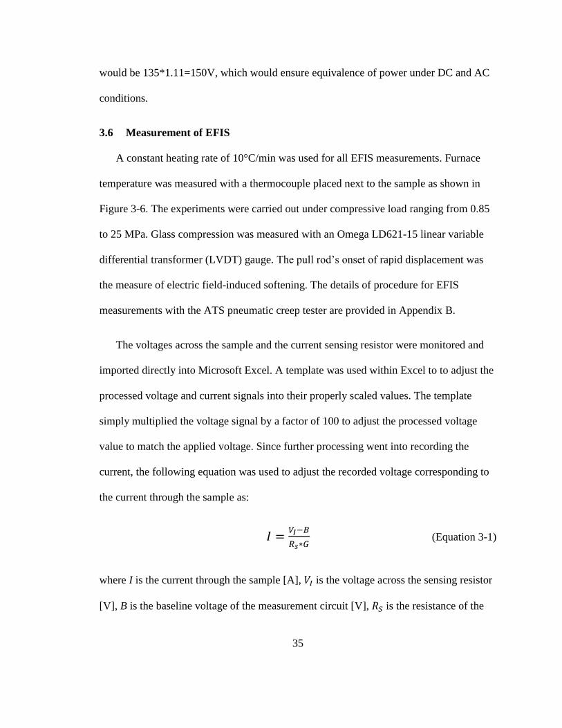
35
would be 135*1.11=150V, which would ensure equivalence of power under DC and AC
conditions.
3.6 Measurement of EFIS
A constant heating rate of 10°C/min was used for all EFIS measurements. Furnace
temperature was measured with a thermocouple placed next to the sample as shown in
Figure 3-6. The experiments were carried out under compressive load ranging from 0.85
to 25 MPa. Glass compression was measured with an Omega LD621-15 linear variable
differential transformer (LVDT) gauge. The pull rod’s onset of rapid displacement was
the measure of electric field-induced softening. The details of procedure for EFIS
measurements with the ATS pneumatic creep tester are provided in Appendix B.
The voltages across the sample and the current sensing resistor were monitored and
imported directly into Microsoft Excel. A template was used within Excel to to adjust the
processed voltage and current signals into their properly scaled values. The template
simply multiplied the voltage signal by a factor of 100 to adjust the processed voltage
value to match the applied voltage. Since further processing went into recording the
current, the following equation was used to adjust the recorded voltage corresponding to
the current through the sample as:
𝐼 =𝑉𝐼−𝐵
𝑅𝑠∗𝐺 (Equation 3-1)
where I is the current through the sample [A], 𝑉𝐼 is the voltage across the sensing resistor
[V], B is the baseline voltage of the measurement circuit [V], 𝑅𝑆 is the resistance of the

36
sensing resistor [Ω] and G is the gain of the operational amplifier [unitless]. This
template was also used to simultaneously record run time, push rod displacement (LVDT
conversion 1V/mm), gain switch position, applied load (voltage = 0.01*load + 0.3 [V])
and furnace temperature (AD595AQ chip conversion 10 mV/°C).
Videos of EFIS were also recorded through the front window slit of the furnace. They
were captured at a rate of 29 frames per second. The time stamp of the videos were
synchronized to the run time of the measurements recorded by the DI-149HS using
Logger Pro 3.8 provided by Vernier Software.[78] The video recording was started upon
the observation of small photoemissions near the anode and was stopped after the glass
was fully displaced and the applied external electric field was removed.
3.6.1 Defining softening point furnace temperatures
The softening temperature of glass sample is determined from displacement vs
furnace temperature plots (see Figure 3-12) as the intersection of two tangents for the
gradual vs rapid slopes. The conventional softening temperature (TS0) is the furnace
temperature at which the glass softens with 0 V applied at a constant heating rate. A
representative calculation of conventional glass softening is shown in Figure 3-12a for
the NS glass composition with 0 V at 10°C/min. The slight displacement (compression)
at lower furnace temperatures is due to thermal expansion of the ATS pull arms and
compressional hooks. At higher furnace temperatures, the larger displacements indicate
viscous flow of glass. For experimental conditions with an applied voltage V, the EFIS
temperature (TsV) is calculated in the same manner using the intersection of two tangents.

37
A representative calculation of TsV is shown in Figure 3-12b for NS with 150 V applied
at 10°C/min as the intersection of the two blue slopes.
3.7 Compositional analysis
It was been well reported that exposing glass to electric fields results in ionic
displacements.[6,43,61,79] These displacements result in a change in composition in the
regions nearest the electrodes. The use of DC voltages has been observed to cause the
largest compositional changes near the anode.[33,40,42] Several techniques were used to
investigate the modified glass composition compared to the parent glass composition
following exposure to electric fields: energy-dispersive x-ray spectroscopy (EDS),
secondary ion mass spectroscopy (SIMS) and x-ray photoelectron spectroscopy (XPS).
Representative samples used for EFIS were prepared for compositional analysis. After
cooling the samples to room temperature, the samples were sectioned along the profile
from anode to cathode. The sectioned surface was then ground down to 30 µm using SiC
paper and 200 proof ethanol. Water was not used to avoid alkali leaching. The sectioned
surface was then polished to a 0.25 µm finish using diamond paste and mixture of
isopropanol and denatured alcohol. Immediately following final polishing, the samples
were sputter coated with iridium. The coating had an estimated thickness of 1.3 nm.
3.7.1 Energy-dispersive x-ray spectroscopy (EDS)
Energy dispersive spectroscopy (EDS) was performed on samples using a Zeiss 1550
Secondary electron microscopy (SEM). An accelerating voltage of 5 kV with an aperture
of 120 µm and a working distance of 8 mm was used. Samples were coated with iridium
to reduce charging effects. It should be noted that sodium migration away from the

38
electron beam was observed when a window length raster scan of 1 µm was used. EDS
provided information about qualitative compositional changes along the profile of the
glass from anode region to the center of the bulk and then from the bulk to cathode
region. The region of the glass near the anode was placed facing away from the detector
to avoid edge effects. Linescans are indicated on the appropriate SEM images by a
yellow line. The regions that were selected for EDS mapping is outlined with a pink box.
3.7.2 Time-of-flight secondary ion mass spectroscopy (ToF-SIMS)
Time-of-Flight Secondary Ion Mass Spectroscopy (ToF-SIMS) analysis was
conducted with an IONTOF ToF-SIMS IV-200P instrument. Measurements were made
in a similar manner as reported by Zakel et al.[32,36] Upon completion of depth
profiling, the crater depth was measured using a profilometer. Crater depth and sputtering
rate were analyzed to obtain depth profiles.
Depth profiling using SIMS was also performed on samples that were held at a
constant furnace temperature during infrared imaging with applied voltages ranging from
100 V to 200 V for depletion layer formation analysis. These samples were measured for
both positive and negative ion concentrations in the glass region in contact with the
anode. Two regions were measured for positive and negative ions on each sample for a
total of four areas per sample that were characterized. Sputtering craters of 200 µm x 200
µm were created for depth profiling. Only the center 100 µm x 100 µm raster was used
for reconstructing the ionic depth profiles. A primary ion beam of Cs+ was used for
sputtering. The incident energy was 2 kV at a current of ~40 nA in a spot of ~20 µm
diameter.

39
3.7.3 X-ray photoelectron spectroscopy
Quantitative compositional changes were determined using x-ray photoelectron
spectroscopy (XPS) on a Scienta ESCA300 instrument. A poled NS sample was
compared to an unpoled NS sample to highlight observed compositional changes along
with chemical bonding environments. The poled NS was exposed to an applied voltage of
100 V and cooled to room temperature just prior to EFIS with the applied voltage. This
sample was then sectioned horizontally in the bulk to separate the anode side of the glass
from the cathode side. The carbon paste coating was removed with acetone and cleaned
with isopropanol. A reference sample of unpoled NS glass was then treated similarly
where the surface was coated in carbon paste and then removed. This ensured that the
surfaces measured by XPS were processed in the same manner. Each sample was pressed
onto conductive carbon tape which was previously affixed to the sample holder. All
measurements were made with an excitation energy of 1486.6 eV, Al Kα, where the
analysis of electrons escaping was normal to the sample surface. A charge neutralization
was employed during analysis to avoid charging of the glass surface. The measured
spectra were referenced to Si 2p line at the literature value of 103.4 eV for SiO2.[80]
3.8 Infrared imaging of temperature profile
For infrared imaging of the temperature profile during EFIS the samples were
prepared in a manner described earlier in section 3.2 for EFIS experiments with the
exception that the final grinding was only to 130 µm. The final polish was eliminated in
this case to avoid a smooth surface that could produce reflections altering the infrared
(IR) measurements. Two types of IR cameras were used for thermal imaging during

40
EFIS. First, a FLIR SC8303HD-HS F/4 BHP 3-5um 1344X78 was used in collaboration
with Corning Incorporated which was calibrated one month prior to the measurements. A
100 mm lens with a 65 mm extension tube was used with the camera to give a resolution
on target sample of 0.03 mm. This allowed for focusing on the target sample 24.4 cm into
a furnace from a window. However, a 3x3 pixel matrix was averaged giving an achieved
resolution of 0.1 mm. The maximum temperature reading of the FLIR camera was
1,300°C 2%. Videos were collected at 30 frames per second and processed with two
color scales. The first color scale showed relative differences in temperature change
while the second scale was linear and showed specific temperature ranges.
A second IR camera was used at Lehigh in combination with the same setup as
described in section 3.5. This camera was a Fluke TiX660 IR camera with a resolution on
target of 0.2 mm with a temperature range from -40°C to 2000°C 1.5%. These videos
were also collected at 30 frames per second.

41
Table 3-1: Glass compositions and their respective glass transition temperatures (Tg)
measured by DSC at 10°C/min.
Glass Type Composition Tg [℃]
NS 0.33 Na2O • 0.67 SiO2 469.7 0.9
2L8NS 0.33 [0.2 Li2O • 0.8 Na2O] • 0.67 SiO2 424.3 0.7
5L5NS 0.33 [0.5 Li2O • 0.5 Na2O] • 0.67 SiO2 420.4 0.3
LS 0.33 Li2O • 0.67 SiO2 468.5 0.5
NAS 0.25 Na2O • 0.05 Al2O3 • 0.70 SiO2 511.3 0.2

42
Figure 3-2: DSC measurement of 2L8NS from ambient to 800°C at a heating rate of
10°C/min. Tg measured as 424°C.
Figure 3-1: DSC measurement of NS from ambient to 800°C at a heating rate of
10°C/min. Tg measured as 469°C.

43
Figure 3-3: DSC measurement of 5L5NS from ambient to 800°C at a heating rate of
10°C/min. Tg measured as 420°C.

44
Figure 3-4: Three electrode configuration for electrical measurements. a)
specimen with electrodes and b) circuit connections. Note: Guard ring thickness
(g), central electrode radius (r1) and sample thickness (d).

45
Figure 3-5: Image of a NS sample with gold sputtered electrodes used for impedance
spectroscopy with the three-probe configuration. Top center electrode was connected to
high tension terminal, bottom electrode was low tension terminal and top outer electrode
was ground of the general radio impedance spectrometer. Gold electrodes were connected
to platinum wires using silver paint.
46
Anode
Cathod
e
Sample
TC
Spectrometer
Probe
Window
Slit
Figure 3-6: Modifications to ATS pneumatic creep tester for measurements of
EFIS. A cathode and anode were made to apply an electric field across the
sample. A spectrometer probe and video camera used the window slits into the
furnace. A thermocouple was added near the sample.

47
Figure 3-7: Design and dimensions of compressional hooks (pull to push) for application
of load to glass samples in the ATS pneumatic creep tester.

48
a) b)
Figure 3-8: Images into ATS pneumatic creep tester where a) compression
hooks are placed on the ends of the pull rods and b) shows sample placement
between hooks.

49
Figure 3-9: Experimental setup inside the modified ATS model 2605 pneumatic creep
tester where the anode was located at the top of the sample and the cathode at the bottom.
The electrode portion of the system was electrically insulated from the rest of the furnace
through the Macor standoffs.

50
Figure 3-10: Schematic of measurement circuit used to record EFIS experimental data.
Voltage and current were reduced and converted to 0 to 10 V DC and recorded with a
DATAQ Instruments model DI-149HS.

51
Figure 3-11: Schematic of AC power supply used for EFIS. A transformer was driven in
reverse where the output side was applied to the measurement circuit in Figure 3-10.

52
Figure 3-12: Representative calculations of intersecting tangents (highlighted blue) of
softening temperatures of a) NS conventional Ts0 and b) NS TsV with 150 V applied at
10°C/min. Note: This technique was applied to all EFIS tested samples.
a)
b)

53
Chapter 4: Basic electrical and dielectric characteristics
Experimental data characterizing the basic electrical and dielectric properties of bulk
glass compositions used for EFIS are presented here. Impedance spectroscopy is
commonly used to analyze charge transport processes, which are modeled as an
equivalent circuit of ideal resistors and capacitors.[81] AC conductance and capacitance
were measured to yield impedance spectra along with activation energies for DC
electrical conduction. The dielectric constant and dielectric loss were also calculated as a
function of frequency.
4.1 AC electrical characteristics of bulk glass
Impedance spectroscopy was used to characterize the electrical behavior of each glass
composition. The AC conductance (G, [Ω-1]) and capacitance (C, [F]) were measured
using a capacitance bridge. Complex impedance analysis is composed of calculating the
real (Z’, in phase resistance) and imaginary (Z”, out of phase resistance) parts of
electrical impedance (Z* = Z’ + iZ”). The real and imaginary impedance are determined
by the following relations of Equation 4-1 and Equation 4-2, respectively[77]:
𝑍′ = 𝐺
𝐺2+𝜔2𝐶2 (Equation 4-1)
𝑍′′ = 𝜔𝐶
𝐺2+𝜔2𝐶2 (Equation 4-2)
where ω is angular frequency [Hz]. Conductance for NS as a function of frequency is
shown in Figure 4-1 for temperatures ranging from 25°C to 525°C. From Figure 4-1,
conductivity is frequency dependent at low temperature where its DC magnitude is
minimal. At higher temperatures, the conductivity becomes temperature independent due

54
to the dominant DC component of ionic conduction. The observed general trend of
conduction occurred for NS, NAS, 2L8NS and 5L5NS but shifted downward in
magnitude as the mixed alkali ratio increased as expected from literature.[76]
Conductance for 2L8NS from 78°C to 154°C is shown in Figure 4-2 as an example,
which is used for calculating impedance spectra. Representative capacitance is shown for
NS in Figure 4-3 for the same temperature range from 25°C to 525°C. Here, the
capacitance shows frequency dependence for all temperatures measured, indicating that
as frequency increases the sample capacitance decreases. However, at high frequency, the
capacitance is observed to converge toward a frequency independence plateau. The same
general trends of capacitance were observed for each glass composition. The capacitance
values of 2L8NS corresponding to the conductance plots in Figure 4-2 are displayed in
Figure 4-4. It should be noted that at higher temperatures near Tg, noise (crossover from
high DC component) interfered with some measurements. For this reason, the amount of
data points is reduced for higher temperatures as seen in Figure 4-1 and Figure 4-3.
4.2 DC electrical conductivity
Impedance spectra were, calculated using Equations 4-1 and 4-2 for each composition
at all temperatures measured. Representative spectra are shown in Figure 4-5 for 2L8NS.
The corresponding conductance and capacitance values used to generate these spectra
were from Figure 4-2 and Figure 4-4, respectively. As temperature increased, the
impedance semicircle decreased. The inset of Figure 4-5 reveals the decrease in
semicircle size at 154°C compared to 78°C and 103°C. For example, the diameter of the
78°C impedance circle along the real impedance was measured as 950 MΩ while 154°C
55
was measured as 4 MΩ. This is expected since ionic conductivity increases in an
Arrhenius behavior. The intersection of the Z” vs. Z’ semicircle with the Z’ axis at low
frequencies gives the inverse DC conductance 1/GDC. The DC conductivity is then
calculated from the GDC by multiplying by the geometric factor of the sample as:
σDC = GDCd/π𝑟12 (Equation 4-3)
where, r1 is central electrode radius [cm] and d is the sample thickness [cm] which are
shown schematically in Figure 3-4. As the impedance semicircle reduces in size with
temperature, the corresponding conductivity increases. DC conductivity determined from
AC complex impedance analysis gives a value of 3.88x10⁻⁸ S/cm for NS, 1.19x10⁻¹¹ S/cm
for the 2L8NS and 9.49x10⁻¹¹ S/cm for 5L5NS at room temperature.
4.2.1 Ionic conductivity activation energy
DC conductivity was calculated from the impedance measurements at various
isothermal holds from room temperature up to Tg. The activation energy of electrical
conductivity is then calculated from its temperature dependence which follows an
Arrhenius behavior. The activation energies for NS, NAS, 2L8NS and 5L5NS were
calculated from the data presented in Figure 4-6. The slope of the linear relationship of
ln(σDC) vs. inverse temperature from the Arrhenius equation (Equation 4-4 below) gives
the activation energy.
56
𝜎𝐷𝐶 =𝐴
𝑇𝑒−𝐸𝑎 𝑘𝐵𝑇⁄ (Equation 4-4)
where A is a pre-exponential factor, T is temperature in Kelvin, Ea is activation energy in
eV and kB is Boltzmann’s constant [eV/K].[77,82] The calculated activation energies for
NS, 2L8NS and 5L5NS are listed in Table 4-1 as 0.70, 0.99, 1.14 and 0.76 eV,
respectively. In the case of alkali disilicate glasses, as the ratio of mixed alkali content
increases from 0 to 1, the activation energy of electrical conductivity passes through a
maximum.[82] LS was measured during electro-thermal poling of Chapter 6.
4.3 Frequency dependence of dielectric constant
The capacitance is expected to become frequency independent at high frequencies
where it is unaffected by the electrode phenomenon.[83] For this case, the real and
imaginary parts of dielectric constant may be simply calculated from capacitance and
conductance with the following relations:
𝜀′ =𝐶𝑑
0𝐴 , 𝜀′′ =
𝐺𝑑
𝜔 0𝐴 (Equation 4-5)
where ε’ is dielectric constant, ε” is dielectric loss, A is effective electrode area [m2], d is
sample thickness [m], ω is angular frequency [Hz], ε0 is permittivity of free space [F/m].
The dielectric constant for NS is shown in Figure 4-7 as a function of temperature. The
dielectric constant for the mixed alkali glasses follows the trend identified by
Tomozawa.[84] At low frequencies the mixed alkali glasses have a larger dielectric
constant compared to single alkali glasses. At higher frequencies the dielectric constant
of single alkali glasses becomes only slightly larger compared to mixed alkali glasses.

57
The corresponding dielectric loss for NS is calculated in Figure 4-8 as a function of
frequency. Each composition experienced the same downward trend in dielectric loss
with increased frequency. The frequency range measured did not capture the peak in
dielectric loss exhibited by glass of similar composition.[83]
4.4 Chapter summary
The electrical conductivity of each glass composition was measured to be frequency
dependent at low temperatures below 150°C. At higher temperatures, the electrical
conductivity was frequency independent due to ionic conduction predominately carrying
charge. The electrical conductivity decreased toward a minimum as the ratio of Na+ to Li+
ranged from 0 to 1. The capacitance was observed to be frequency dependent at all
temperatures but appeared to be converging toward a common point at high frequency.
This trend was measured for each glass composition.
The conductance and capacitance were used to calculate imaginary versus real
impedance to create Nyquist impedance plots. The DC conductivity was determined from
impedance spectra. The temperature dependence of DC conductivity was used to
calculate the activation energy associated with DC ionic conductivity. As the ratio of
mixed alkali content increase from 0 to 1, the activation energy increase toward a
maximum, as expected.
The dielectric constant was measured to be both frequency and temperature
dependent. Dielectric losses were measured to increase with temperature but decrease
with frequency.

58
Table 4-1: Activation energies (Ea) for each glass composition measured by impedance
spectroscopy (IS) ranging from ambient to Tg.
Glass Type Composition IS Ea [eV]
NS 0.33 Na2O • 0.67 SiO2 0.69
2L8NS 0.33 [0.2 Li2O • 0.8 Na2O] • 0.67 SiO2 0.92
5L5NS 0.33 [0.5 Li2O • 0.5 Na2O] • 0.67 SiO2 0.97
NAS 0.25 Na2O • 0.05 Al2O3 • 0.70 SiO2 0.70

59
Figure 4-1: Electrical conductance with respect to frequency for NS glass from room
temperature to 525°C. The relative trends are the same for all glass compositions but shift
downward with increased mixed alkali content.
Figure 4-2: Representative variation of conductance vs. frequency for 2L8NS at 78.5,
103.3 and 154.3°C. Note: All glass compositions followed similar behavior.

60
Figure 4-3: Capacitance as a function of frequency for NS glass from room temperature
to 525°C. The relative trends are the same for all glass compositions but shift downward
with increased mixed alkali content.
Figure 4-4: Representative behavior of capacitance vs. frequency for 2L8NS at 78.5,
103.3 and 154.3°C. Note: All glass compositions followed similar behavior.

61
Figure 4-5: Nyquist impedance plots for 2L8NS at 78.5, 103.3 and 154.3°C. Real and
imaginary components of impedance were calculated using data collected in Figure 3-6
and Figure 3-7. Note: All glass compositions behaved similarly.
Figure 4-6: Arrhenius plot for evaluating the activation energy for each glass composition
using conductivities from impedance spectroscopy, ranging from ambient to about 400°C

62
Figure 4-7: Real dielectric permittivity for NS as a function frequency from room
temperature to 525°C. The relative trends are the same for all glass compositions.
Figure 4-8: Imaginary dielectric permittivity for NS as a function frequency from room
temperature to 525°C. The relative trends are the same for all glass compositions.

63
Chapter 5: Effect of electric field on the softening of alkali silicate glasses
In general, glass is usually softened or formed by heating the sample to a high
enough temperature to achieve viscous flow. Electric field-induced softening (EFIS) of
glass applies an external electric field across the sample while applying pressure inside a
furnace during constant heating rate. The application of the field has been observed to
dramatically reduce the furnace temperature and time required for glass to soften as
compared to conventional softening during a constant heating rate. These observations
have been made while applying moderate external electric fields ranging from 0 V/cm to
250 V/cm. Direct current (DC) and alternating current (AC) have both been investigated
within the scope of EFIS. Quantitative measurements of the reduction of furnace
temperature for glass softening, defined as the temperature where rapid displacement of
glass occurs, are reported in this chapter.
5.1 DC dependence of EFIS
Representative behavior of glass softening is shown in Figure 5-1, in terms of the
strain gauge displacement (shown as negative values since the experiments were done in
compression) as a function of temperature (that increases at a constant heating rate).
These data are for the simple sodium disilicate glass composition with a field varying
from 0 to 200 V/cm.
There is slight slope to the displacement in the push rod as the temperatures rises,
which is attributed to thermal expansion in the loading structure as demonstrated by using
an alumina reference sample in Figure 5-1. The sudden and much greater displacement at
higher temperatures arises from viscous flow. We define the softening temperature, Ts, by

64
the abrupt onset of large deformation indicated by the red arrow in Figure 5-1. Note that
the temperature for the onset of viscous flow decreases as the applied electrical field is
increased.
The curves for 0, 50 and 100 V/cm field show compressive displacement that occurs
gradually. But at fields greater than 125 V/cm viscous flow occurs abruptly. (A visual
demonstration is included in supplemental information as ‘Video A NAS 150V EFIS’).
Thus, we observe two regimes of behavior. At low electric fields (100 V/cm in Figure
5-1, stage I) the viscosity decreases gradually, in a manner that is similar to the reference
sample at 0 V. However, at high fields ( 125 V/cm, stage II), NS samples flow quickly,
within a few seconds, at furnace temperatures that are well below Tg (see Figure 5-1
below for details). This behavior is similar to the observations in flash sintering of
ceramics described in section 1.3.[17]
5.1.1 Compositional dependence of DC EFIS
It is well-known that alkali ions are the dominant charge carriers in silicate glasses.[3]
The role of alkali ions has been investigated by gradually substituting sodium ions by
lithium ions in the sodium disilicate glass. The bulk resistivity of these mixed alkali
glasses goes through a maximum at Na/Li ratio of ~0.5; so 5L5NS has the highest
resistivity as shown in Figure 4-6.[76] Therefore, we may expect that the glass with the
highest resistivity to be the least influenced if EFIS arises from Joule heating.
Representative softening behavior of 2L8NS and 5L5NS is shown in Figure 5-2 and
Figure 5-3, respectively. Another glass composition was tested that contained 5 mol%

65
alumina which replaced an equivalent amount of soda (NAS). The softening behavior of
NAS is shown in Figure 5-4. It is clearly demonstrated that as the resistivity of the
associated glass composition is increased, the phenomenon still occurs but it does not
have as pronounced of an effect on reducing the softening temperature as revealed by
Figure 5-2 for 2L8NS and Figure 5-3 for 5L5NS.
The effect of glass composition is analyzed by normalizing the data with respect to
conventional softening of each glass composition in the absence of an applied field.
These results are included in Table 5-1. The normalized EFIS effect is quantified with
parameter ΔT(V) = (Ts0-TsV), where Ts0 is the softening temperature at 0 V (conventional
softening), and TsV the softening temperature under an applied field (EFIS). These
results, shown in Figure 5-5, delineate two regimes of behavior (stage I and II) similar to
FAST and flash sintering in ceramics. At low electric fields, in stage I, ΔT(V) is small
and increases slightly with field. At higher fields, typically above a threshold value,
ΔT(V) begins to increase rapidly, marking a transition from stage I to stage II. For NS,
2L8NS and 5L5NS the threshold fields are approximately 95, 100 and 175 V/cm,
respectively. Above the threshold, the value of ΔT(V) is significantly higher for the
binary NS glass than for the mixed alkali glasses. From Figure 5-5, ΔT(V) for NS had a
maximum value of about 150°C at 200 V/cm while 2L8NS and 5L5NS ΔT(V) values
were only about 50 and 25°C at 250 V/cm, respectively. This difference in EFIS of single
and mixed alkali glass samples is attributed to the higher resistivity of the mixed alkali
glasses. A higher resistivity reduces Joule heating, as shown by Equation 1-1, which may
be responsible for the lower values of ΔT(V). It is interesting to note that ΔT(V) for the

66
NS glass increased continually with applied field, whereas it reaches a plateau at ~175
V/cm for the mixed alkali glasses. This is discussed in the next section.
5.1.2 Field/voltage dependence of EFIS
Flash sintering was shown to be field dependent in section 1.3 where its sintering
behavior changed above a threshold external field. Here, the voltage dependence of EFIS
is demonstrated by comparing glass displacement (negative due to compression) versus
furnace temperature of four NAS samples, for example. The first sample is a control
measurement of conventional glass softening during heating with 10 MPa compressive
stress and zero voltage applied. Here, Ts0 is the furnace temperature at which the glass
softens without applying an external voltage; it is indicated by the arrow in Figure 5-6.
The onset of large compressive displacement was used to determine the temperature of
glass softening. The next two samples were of varying heights with the same externally
applied voltage of about 200 V. The external field of the two samples were 200 V/cm and
267.4 V/cm as labeled in Figure 5-6; both tests exhibited a similar reduction in furnace
temperature. The fourth sample in Figure 5-6 used a smaller applied voltage of 143 V on
a shorter sample making the external field 200 V/cm. The reduction in furnace
temperature for this case was not as dramatic as those observed with 200 V applied
suggesting that ΔT for EFIS is a function of applied voltage than external field strength.
The voltage dependence of EFIS for NAS glass was further studied at several more
voltages. The reduction in softening temperature with applied voltage follows the same
trend as in section 5.1, i.e. as the applied voltage increased, the furnace temperature at

67
which glass softened also decreased. The furnace temperature of glass softening for NAS
was reduced by 130°C with 200 V applied as compared to when no voltage was applied.
Since glass is a well-known insulator, a test was carried out to ensure current flow
was through the bulk of the glass rather than along the surface. This was determined by
varying the surface roughness of the samples, which alters the path length for surface
conduction without altering the volume path. The effect of surface roughness on EFIS is
indicated by the samples designated as ‘199.5 V 30 µm’, ‘199.4 V 130 µm’ and ‘199.8 V
130 µm’ in Figure 5-7. The indicated surface roughness was the last grinding paper grain
size used during sample preparation. Since a change in surface roughness did not
influence the TsV of the glass, we conclude that the observed current flows through the
volume of glass, unaffected by the surface. The data also show high reproducibility of the
measurements.
5.1.3 Field/voltage dependence discussion
It was originally thought that EFIS (or more specifically, the reduction in furnace
temperature ΔT for glass softening) was dependent on the applied external electric field.
However, Figure 5-6 shows that EFIS is dependent on applied voltage rather than the
nominal external electric field across the glass i.e. voltage/thickness of the sample. This
correlation has been observed similarly for electro-thermal poling and is expected for
glasses containing alkali ions [85]. It differs from that observed for flash sintering where
the reduction of furnace temperature required to fully sinter ceramics depends on the
applied external field [17,86]. The observed voltage dependence of EFIS can be
explained by considering the alkali ions migrating away from the positively charged
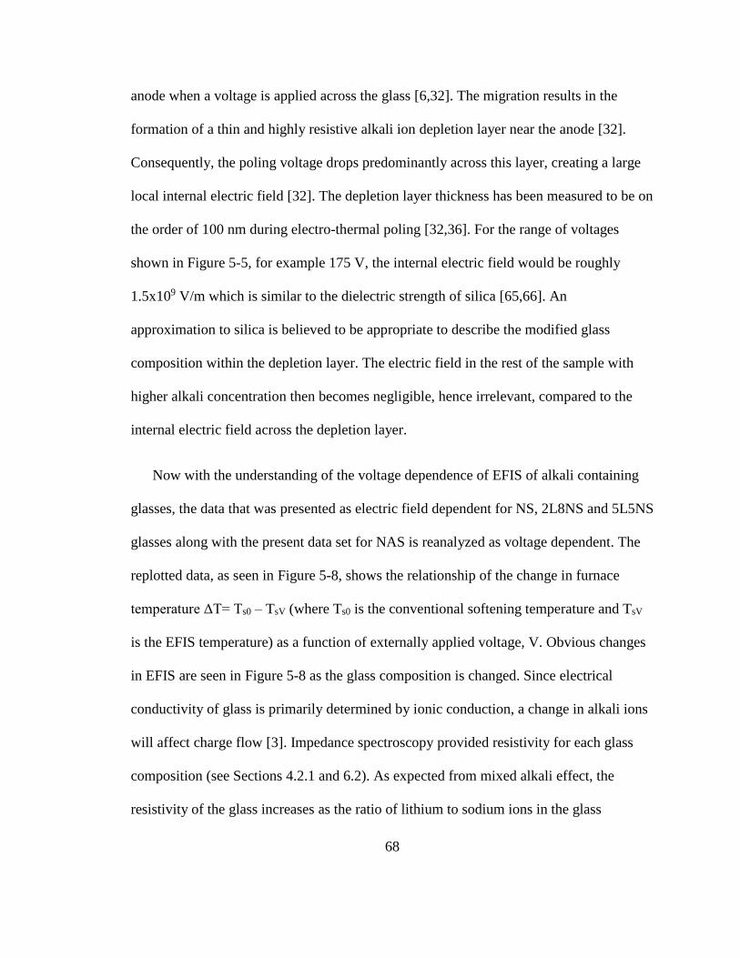
68
anode when a voltage is applied across the glass [6,32]. The migration results in the
formation of a thin and highly resistive alkali ion depletion layer near the anode [32].
Consequently, the poling voltage drops predominantly across this layer, creating a large
local internal electric field [32]. The depletion layer thickness has been measured to be on
the order of 100 nm during electro-thermal poling [32,36]. For the range of voltages
shown in Figure 5-5, for example 175 V, the internal electric field would be roughly
1.5x10⁹ V/m which is similar to the dielectric strength of silica [65,66]. An
approximation to silica is believed to be appropriate to describe the modified glass
composition within the depletion layer. The electric field in the rest of the sample with
higher alkali concentration then becomes negligible, hence irrelevant, compared to the
internal electric field across the depletion layer.
Now with the understanding of the voltage dependence of EFIS of alkali containing
glasses, the data that was presented as electric field dependent for NS, 2L8NS and 5L5NS
glasses along with the present data set for NAS is reanalyzed as voltage dependent. The
replotted data, as seen in Figure 5-8, shows the relationship of the change in furnace
temperature ΔT= Ts0 – TsV (where Ts0 is the conventional softening temperature and TsV
is the EFIS temperature) as a function of externally applied voltage, V. Obvious changes
in EFIS are seen in Figure 5-8 as the glass composition is changed. Since electrical
conductivity of glass is primarily determined by ionic conduction, a change in alkali ions
will affect charge flow [3]. Impedance spectroscopy provided resistivity for each glass
composition (see Sections 4.2.1 and 6.2). As expected from mixed alkali effect, the
resistivity of the glass increases as the ratio of lithium to sodium ions in the glass

69
composition increases to 50/50. The reduction in furnace temperature, ΔT indicating
EFIS, is plotted in Figure 5-8 as a function of applied voltage. In general, as the
resistivity of the glass increases, ΔT decreases. For example, the maximum values of ΔT,
which were observed with 200V, were 181, 127, 62 and 36°C for NS, NAS, 2L8NS and
5L5NS, respectively. The reduction of EFIS is due to the mixed alkali effect where
5L5NS has the highest resistivity and hence, lowest ΔT [76]. The kinetics determining
the formation of the alkali ion depletion layer is controlled by the glass resistivity. At
higher resistivities it is necessary to provide additional thermal energy for alkali ion
diffusion to create the alkali ion depletion layer which ultimately reduces ΔT of EFIS.
Large scatter in the data of Figure 5-8 is indicative of the variability of the depletion
layer characteristics.[6] Nevertheless, the behavior in Figure 5-8 demonstrates an
exponential dependence of ΔT on V. It can be described empirically as:
ΔT = A*[exp(B*V)-1] (Equation 5-1)
where V is the applied voltage [V], A is a pre-exponential factor [K] and B is a fitting
parameter [V-1]. Fits for each glass composition are shown in Figure 5-8 as dashed lines
from 0 V to 200 V. The values of the pre-exponential factor, A, and fitting parameter, B,
are listed in Table 5-2. The values of B for NS, 2L8NS, 5L5NS and NAS are 12 1.7
mV-1, 9.2 2.7 mV-1, 5.1 5.3 mV-1 and 17.5 3.7 mV-1, respectively. Large uncertainty
in the fit occurs in the case of 5L5NS since its EFIS voltage dependence is much weaker
than that of the other glass compositions, but still the data follows the same trend.

70
The dependence of EFIS on applied voltage rather than external electric field easily
explains the plateau behavior of ΔT(V) in Figure 5-5 for the mixed alkali glasses. The
maximum of the DC power supply was 200 V, therefore, in order to increase the external
electric field any further the height of the sample was reduced but the same voltage was
applied across the glass. This resulted in the observed plateau of Figure 5-5.
5.2 AC dependence of EFIS
The effect of an AC voltage on EFIS is shown in Figure 5-9 for two glass
compositions. The compositions chosen are the least resistive glass, NS, and the most
resistive glass, 5L5NS. Here, a constant voltage of 150 V was chosen to compare the
RMS of AC voltages with DC voltages that can be thought of as very low or zero
frequency AC oscillations. A pressure of 1 MPa was applied to all samples tested in AC.
The same constant heating rate of 10°C/min was used for all samples as well for
comparison with DC EFIS results. Overall, the use of AC voltages further reduced the
furnace temperature required for glass softening as compared to both the DC case and
conventional softening. In the case of a DC voltage for both NS and 5L5NS, the
compressive displacement occurs abruptly compared to AC. Since heating is done at a
constant rate, the temperature axis correlates with run time. A vertical or near vertical
displacement was measured for 150 V 0 Hz (DC scenario) for both NS in Figure 5-9a and
5L5NS in Figure 5-9b. With AC voltages of 150 V, the displacement of the glass samples
was gradual, indicating that the rate of displacement decreased compared to DC with the
same applied pressure.

71
5.2.1 Frequency dependence
The applied AC voltage of 150 V ranged in frequency from 0 Hz (DC) to 1000 Hz.
Using the intersecting tangent method as described in section 3.6.1, the furnace
temperature at which softening occurs was defined as TsV. These values are summarized
in Figure 5-10a for both NS and 5L5NS with respect to frequency. For comparison, the
Ts0 values are added to Figure 5-10a as well and circled with a dashed outline. The
introduction of an oscillating voltage lowered furnace temperatures for EFIS beyond the
DC case. However, within the range of frequencies tested (60 Hz to 1000 Hz) the furnace
temperature for glass softening remained relatively constant. This is likely due to the
elimination of the depletion layer. It is believed that at much higher frequencies in the RF
range a frequency dependence could be realized due to additional dielectric losses. As of
now, little work has been done within the flash sintering community of ceramics
investigating a frequency dependence on the reduction of furnace temperatures.[21]
5.2.2 Compositional dependence of AC EFIS
The effect of glass composition on AC EFIS can be determined by plotting the
difference in softening temperature to conventional softening temperature of NS and
5L5NS as ΔT(V) in Figure 5-10b. The same trend using AC voltages is observed as in the
DC case. The less resistive glass had a much more pronounced EFIS temperature
reduction comparatively. From Figure 5-10b, NS with 150 V applied had a DC ΔT of
181°C and an average AC ΔT of 224°C. The DC ΔT for 5L5NS was 12°C and an average
AC ΔT of 63°C was measured. In both cases, additional furnace reduction was achieved
with the application of an oscillating voltage. However, the glass composition and

72
associated resistivity determined the magnitude of the EFIS effect. Therefore, the role of
alkali ion diffusion plays a role in the kinetics of EFIS in both AC and DC scenarios.
5.3 Pressure dependence of EFIS
The effect of applied pressure as a processing parameter for EFIS was also studied. A
range of pressures from 0.85 MPa to 25 MPa was applied together with an external
voltage to the samples. Figure 5-11 shows a set of data for NAS samples with varying
pressure of 0.85 MPa to 10 MPa under an applied voltage of 140-145 V. The results show
that the applied pressure does not significantly influence the furnace temperature required
for glass softening. However, it does influence the rate of displacement upon viscous
flow of the NAS glass as seen in Figure 5-11. The change in furnace temperature, ΔT(P),
is then plotted in Figure 5-12 as a function of applied pressure for two different applied
voltages: 142 2 V and 199 1 V. Both sets of samples showed little to no influence of
pressure on EFIS as compared to the dramatic dependence of externally applied voltage.
The results in Figure 5-11 indicate no clear correlation between applied pressure and
the EFIS temperature with an applied voltage of 142 2 V. A higher applied voltage of
199 1 V was used with NAS samples to further examine the effect of pressure as seen
in Figure 5-12. Once again, there is no correlation beyond voltage dependence. It is
believed that the downward trend of ΔT in Figure 5-12 is due to experimental changes in
external voltage. The phenomenon of Equation 5-1 accounts for the difference in
softening temperature. For example, NAS with 200 V at 0.85 MPa has a ΔT of 120°C
while 198 V at 25 MPa has a ΔT of 99°C; a difference of 21°C. This difference in ΔT for
NAS is within the error of fitting of data to Equation 5-1 for the voltages of 198 V and

73
200 V. So the pressure does not influence the softening temperature of glass, unlike that
observed during sinterforging of ceramics since glass is fully dense [87].
In comparison to T, the applied pressure significantly affects the rate of glass
softening as noted above. With 0.85 MPa applied, the glass softened at a much slower
rate as compared to 10 MPa in Figure 5-11. For example, with 0.85 MPa applied the
glass displaced ~2 mm in 4 minutes while with 10 MPa the glass displaced ~3.25 mm in
30 seconds. From Figure 5-11 and Figure 5-12 it is believed that pressure only affects
viscous flow rate following abrupt thermal runaway of region IV, but not the EFIS
initiation temperature itself. In any case, the influence of applied pressure as a processing
parameter could be used to tailor the amount and rate of deformation during glass
forming during EFIS.
5.4 Photoemissions during EFIS
5.4.1 DC photoemissions
Just prior to and during EFIS each glass composition produced photoemissions at
external fields greater than 50 V/cm. Figure 5-13a shows NS sample under 150 V/cm at a
furnace temperature of ~435°C before photoemission. When the temperature increased
above the flashing temperature (TF), the first photoemission was observed as seen in
Figure 5-13b for a furnace temperature TF < T < TsV (see supplemental information
‘Video A NAS 150V EFIS’). Figure 5-13b visually captured the photoemission near the
anode which is located at the top of the sample in the image. It has been observed that NS
flashed for a longer time frame (~2-5 min) before EFIS, while 2L8NS flashed for about a
minute or less before EFIS. A spectrometer was used to collect the spectra of the

74
photoemissions from the various glass types, which will be discussed later in section
8.3.1.
5.4.2 AC photoemissions
Photoemissions under AC field were observed similarly to the DC experimental
conditions. There were two major differences, however, between AC and DC conditions.
First, the photoemissions while using AC fields were less intense even with the same
current limit through the samples. Secondly, the photoemissions were observed to occur
at both electrodes. Although the video frame rate was slower than the AC frequencies
used, the videos appear to show the photoemissions flickering suggesting they oscillate
with the AC field. Representative photoemissions of AC testing are displayed in Figure
5-14 for NS. Figure 5-14a shows NS with 120 V 60 Hz and Figure 5-14b is NS with 150
V 125 Hz. The diagnostics of the photoemissions are discussed later in section 8.3.1.
5.5 Chapter summary
A new phenomenon of electric field induced softening (EFIS) of glass has been
identified. The application of external voltage (both DC and AC) produces glass
deformation at lower furnace temperatures than conventional glass softening. Higher
voltages continue to reduce the furnace temperature for the onset of softening. The EFIS
effect is stronger for the single than for the mixed alkali disilicate glasses, suggesting a
role for ionic mobility in this phenomenon. The phenomenon is dependent on applied
voltage rather than external electric field.

75
A change in pressure did not show a dependence on initiation of EFIS. Rather,
pressure was observed to only aid in the rate of displacement upon viscous flow of the
glass. This demonstrates that EFIS could potentially be tailored for surface imprinting.
Photoemissions were observed only during high current passage through the glass
samples. In DC, photoemissions were only observed near the anode while in AC they
were seen at both electrodes.

76
Table 5-1: Glass compositions and their respective Tg and Ts0 values
Glass type Glass Composition Tg [°C] Ts0 [°C]
NS 0.3Na2O • 0.7SiO2 475 550
2L8NS 0.33[0.2 Li2O•0.8Na2O] • 0.67SiO2 427 491
5L5NS 0.33[0.5 Li2O•0.5 Na2O] • 0.67 SiO2 423 493
NAS 0.25 Na2O • 0.05 Al2O3 • 0.70 SiO2 507 573
Table 5-2: Empirical fitting parameters for A and B in Eq. 5-1 for estimating the
reduction in furnace temperature for an applied voltage relative to conventional softening
temperatures for each glass composition. Note: Large error in 5L5NS is due to small
EFIS effect.
Glass Type A [K] B [mV]
NS 19.0 6.5 12.0 1.7
NAS 3.8 2.7 17.5 3.7
2L8NS 11.0 6.5 9.2 2.7
5L5NS 14.4 22.3 5.1 5.3

77
Figure 5-1: Displacement vs. furnace temperature of NS at various applied electric fields
with a constant heating rate of 10°C/min. The Tg for NS is indicated by arrow. Reference
alumina rod displacement of the support structure is shown by light green dashes.
Transition between Stage I and Stage II is shown by a vertical line while the onset of the
large abrupt displacement is indicated by the red arrow.
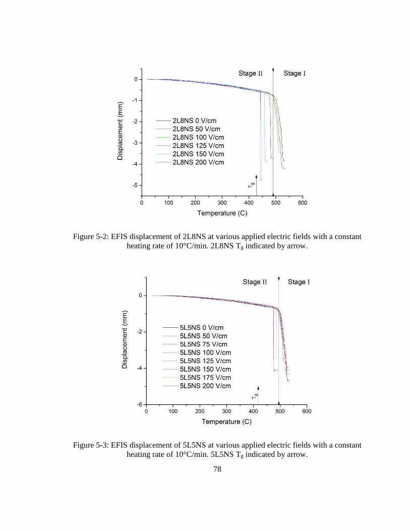
78
Figure 5-2: EFIS displacement of 2L8NS at various applied electric fields with a constant
heating rate of 10°C/min. 2L8NS Tg indicated by arrow.
Figure 5-3: EFIS displacement of 5L5NS at various applied electric fields with a constant
heating rate of 10°C/min. 5L5NS Tg indicated by arrow.

79
Figure 5-4: EFIS displacement of NAS at various applied electric fields with a constant
heating rate of 10°C/min.
Figure 5-5: Normalized FIS effect for NS (black, squares), 2L8NS (blue, triangles),
5L5NS (pink, inverted triangle) and NAS (red, circles). The Difference ΔT(V) in regular
softening temperature (Ts0) to softening temperature with an applied electric field (TsV)
plotted versus applied electric field. Arrows indicate approximate threshold applied
electric field for each glass composition.
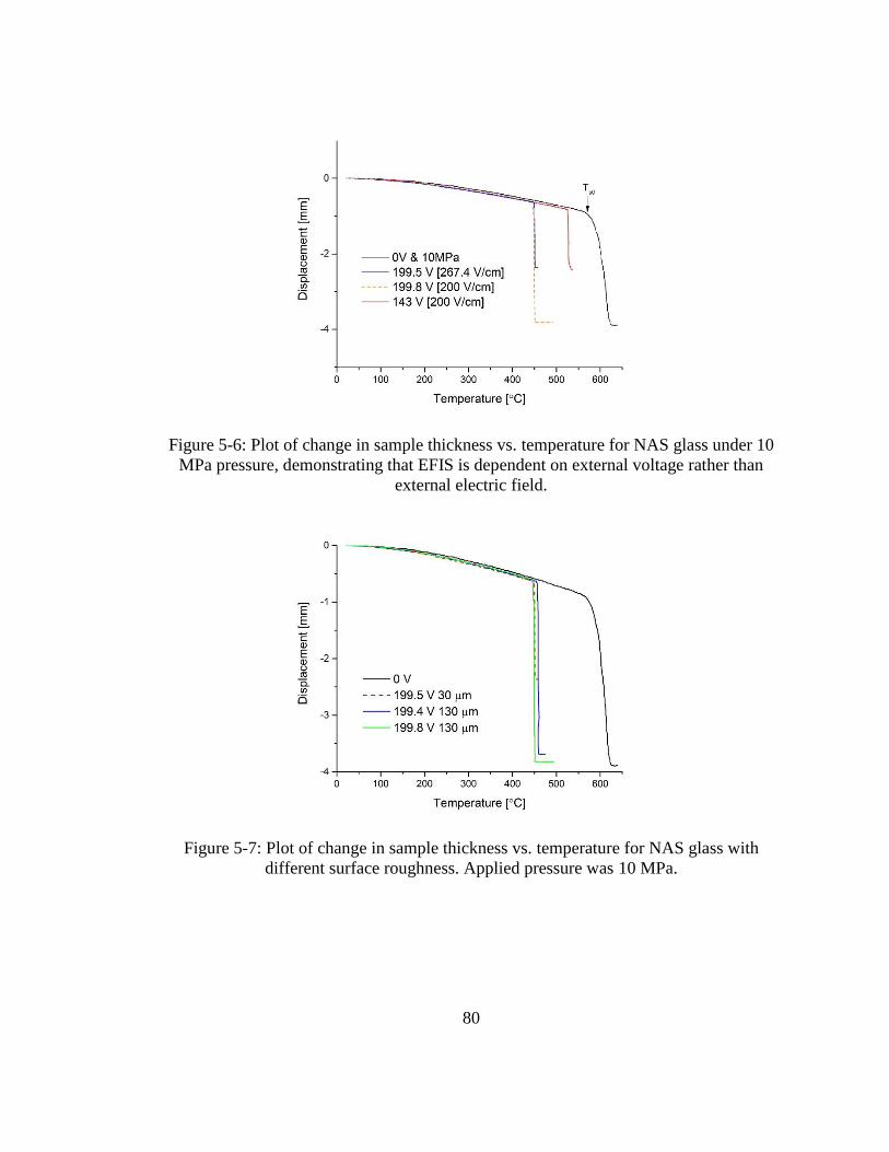
80
Figure 5-6: Plot of change in sample thickness vs. temperature for NAS glass under 10
MPa pressure, demonstrating that EFIS is dependent on external voltage rather than
external electric field.
Figure 5-7: Plot of change in sample thickness vs. temperature for NAS glass with
different surface roughness. Applied pressure was 10 MPa.
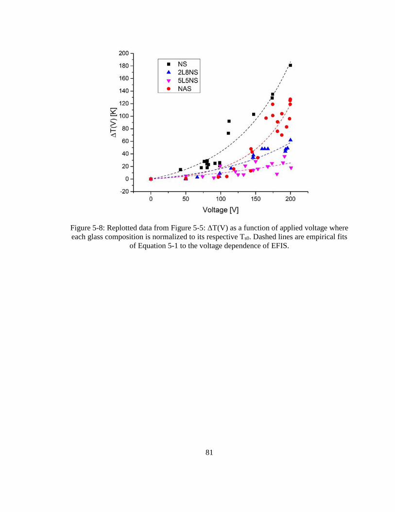
81
Figure 5-8: Replotted data from Figure 5-5: ΔT(V) as a function of applied voltage where
each glass composition is normalized to its respective Ts0. Dashed lines are empirical fits
of Equation 5-1 to the voltage dependence of EFIS.

82
Figure 5-9: Electric field-induced softening of a) NS glass and b) 5L5NS
glass with 150 V at a constant heating rate of 10°C/min. Various frequencies
were used for AC testing. Note: The 0 V conventional softening of each glass
was added for reference.
a)
b)

83
a)
b)
Figure 5-10: Comparison of EFIS with respect to frequency for NS and 5L5NS of
a) EFIS softening temperature, TsV and b) change in softening temperature
relative to conventional softening, ΔT(V).

84
Figure 5-11: Effect of pressure on EFIS of NAS glass.
Figure 5-12: Effect of pressure on EFIS of NAS glass with 199 1V (Black, Squares)
and 142 2V (Red, Circles) applied.

85
a) b)
Figure 5-13: Images of NS during 150 V/cm test condition when
the furnace temperature was a) T<TF and b) TF<T<TS of EFIS.
a) b)
Figure 5-14: Images of NS during EFIS with AC voltages of a) 120 V 60 Hz
and b) 150 V 125 Hz. These images are representative of photoemissions
observed at both electrodes.
86
Chapter 6: Electro-thermal poling of alkali silicate glasses
An electro-thermal poling study was conducted for three reasons. First, the
underlying mechanisms on the formation of an alkali ion depletion layer under DC
voltages remains unconfirmed in literature. It is believed that these mechanisms also
determine EFIS. Second, the electrical and dielectric behavior of the depletion layer
needs to be compared to the parent glass composition. This will characterize the relation
between modified and parent glass compositions in response to externally applied DC
voltage. The third reason is to measure current versus temperature at a constant heating
rate relating it to the EFIS process to identify similar mechanisms.
6.1 Electro-thermal poling experimental setup
Samples of NS, 2L8NS, 5L5NS and LS were melt-quenched with compositions listed
in Table 6-1 LS was added to cover the full range of mixed alkali disilicate glass
compositions to understand poling mechanisms. Samples were cut to a 10 mm x 10 mm
rectangular cross section. They were ground and polished with 0.25 μm diamond paste to
a final thickness ranging from 0.6 to 0.8 mm. Platinum film was sputtered on the top and
bottom faces of the samples to make good electrical contact with the platinum coated
stainless steel electrodes.
Impedance spectra for all glass compositions were collected in 10°C intervals from
30°C to 300°C with a 0.1 Vrms probing voltage using a Novocontrol Alpha-AK
impedance analyzer (accuracy within 0.2%) combined with a Novocontrol Quatro
Cryosystem for temperature control. The impedance spectroscopy frequency range
covered 10-2 to 106 Hz. The impedance frequency sweep took about 2 min to complete.

87
Electro-thermal poling tests included in situ impedance and current measurements.
Samples were heated to a poling temperature (Tp) where the electrical conductivity (σDC)
was approximately 10-6 S/cm unless otherwise stated. Corresponding poling temperatures
for the desired conductivity for each glass composition are listed in Table 6-1. Two
poling voltages (Vp) of either 25 V or 100 V were used. A typical example of
experimental conditions is outlined in Figure 6-1 for LS with Tp=120°C and Vp=100 V.
Selected samples of each composition were short-circuited after poling, i.e. a voltage of 0
V was applied, while maintaining the temperature at Tp for 18 to 20 h to observe possible
depoling. A high-voltage amplifier providing a maximum voltage of 500 V connected to
a Novocontrol Alpha-AK was used for impedance measurements during electro-thermal
poling testing using a probing voltage of 1 Vrms. The AC frequency range during
characterization of electro-thermal poling was from 10-2 to 104 Hz. A Keithley 6517A
electrometer was used to measure in situ poling currents when impedance spectroscopy
was not used.
Thermally stimulated depoling (TSDC) and poling (TSPC) currents were measured
similar to electro-thermal poling. Samples during both TSDC and TSPC were heated
from 25°C to 300°C at a constant rate of 10°C/min and then held at 300°C for two hours.
Prior to TSDC measurements, samples were poled with Vp=25 V at Tp for two hours and
cooled to ambient under the electric field. The applied voltage was then removed and the
sample was heated at a constant rate while measuring current. Unpolarized glass samples
were used for TSPC measurements where a voltage of 25, 50 or 100 V was applied at

88
ambient. Next, in situ current was measured as the sample was heated at a constant rate of
10°C/min as well.
Following poling, ToF-SIMS analysis was conducted on glass samples with a ToF-
SIMS IV-200P instrument from IONTOF GmbH. Measurements were made in a similar
manner as reported by Zakel et al on the anode side of the samples.[32,36] Upon
completion of depth profiling, the crater depth was measured using a profilometer. Crater
depth and sputtering rate were analyzed to obtain depth profiles from anode/glass
interface into the bulk region of the glass.
6.2 Electro-thermal poling results
Impedance spectroscopy was used to obtain the DC electrical conductivity (σDC) as a
function of temperature and corresponding activation energy (Ea) for all compositions
prior to electro-thermal poling as listed in Table 6-1. The NS and LS binary compositions
yielded σDC= 1.7x10⁻⁸ and 2.8x10⁻⁹ S/cm at room temperature, and Ea values of 0.70 and
0.76 ±0.01 eV, respectively. The 2L8NS and 5L5NS mixed alkali compositions had σDC=
8.9x10⁻¹² and 1.4x10⁻¹³ S/cm at room temperature, and Ea values of 0.99 and 1.14 ±0.01
eV, respectively. The Arrhenius behavior of electrical conductivity is plotted in Figure
6-2 where the slope was used to calculate activation energy for each composition. The
calculated activation energies match well with those measured in Section 4.2.1 and listed
in Table 4-1, however, 5L5NS is slightly larger. The poling temperature (Tp), where DC
electrical conductivity σDC=1x10⁻⁶ S/cm, was determined from impedance spectroscopy.

89
Tp for NS, 2L8NS, 5L5NS and LS were 100, 190, 230, and 120°C, respectively (see
Table 6-1).
AC impedance was then measured during and following electro-thermal poling to
observe changes in electrical behavior of the glass samples at Tp. Representative
conductance versus frequency measurements are shown for various poling times, as
examples in Figure 6-3a for NS at Tp=100°C with Vp=25 V. The conductance of NS at Tp
but before poling is displayed as the black squares in Figure 6-3a. A spectrum was
collected immediately following the application of the poling voltage which is shown as
the red circles. Upon application of the poling voltage, the frequency-independent
conductance slightly increases initially. After the initial increase, the high frequency
conductance remains relatively steady for the duration of poling, as supported by Figure
6-3a. The first two spectrums experienced large variation due to the sample changing on
a faster time scale than the frequency sweep measurement. Following 300 seconds of
poling the conductance of the sample decreased and formed a low frequency plateau.
After 2 h of poling, the low frequency conductance was reduced by about two orders of
magnitude compared to the unpoled value. Upon removal of the external electric field,
the low frequency conductance reduced further as seen in Figure 6-3a. Depoling of NS
sample after removing the poling voltage of 25 V occurred slowly where the low
frequency conductance increased slightly. However, samples poled using Vp=100 V
revealed that the conductance remained steady throughout the depoling process and did
not increase (not shown). The related Nyquist impedance spectra observed during poling
are shown in Figure 6-3b from measurements on NS at Tp=100°C with Vp=25 V. An

90
impedance spectrum prior to poling reveals the end of a semicircle along with a second
component at lower frequencies, as shown in the inset of Figure 6-3b.After the sample
was poled for 2 h, a second component formed a large semicircle in Figure 6-3b,
indicating that the impedance increased steadily while a poling voltage was applied. The
end of the original semicircle (as seen more clearly in the inset) did not change during the
poling process. The Nyquist plots for NS, 2L8NS, 5L5NS and LS with 100 V applied are
shown in Figure 6-4 with a poling time of 2 h at 120 s intervals between spectra. These
Nyquist plots show the same trend as observed for NS in Figure 6-3b.
To observe depoling, the applied voltage was removed from selected samples, which
remained at Tp for 18 to 20 h. Following the poling process with Vp=25 V, Figure 6-5
reveals the evolution of depoling for NS at Tp. An impedance spectrum was measured
upon the removal of the applied voltage. Within the first 2 mins of the voltage being
removed the resistance corresponding to the larger semicircle increased dramatically as
seen in Figure 6-5. Subsequently, the semicircle started to decrease over the course of 20
h of depoling but did not reach initial values. At the start of depoling, the low frequency
plateau of the conductance spectra was observed to decrease, as seen in Figure 6-3a, for
all glasses. However, quickly the low frequency conductance started to increase gradually
in a complex manner.
The effect of poling on the capacitance of the sample is shown in Figure 6-6 with
respect to frequency for the same NS sample as in Figure 6-3 (i.e. for Tp=100°C and
Vp=25 V). Prior to poling the capacitance decreased with increasing frequency due to
electrode polarization and formed a high frequency plateau.[77] Within the first 5
91
minutes of applying the poling voltage, as seen in Figure 6-6, a low frequency plateau is
formed as well. This feature remains constant for the duration of poling after the first 5
min. The capacitance during depoling after Vp=25 V, is also shown in Figure 6-6, where
the low frequency plateau is still clearly visible but slightly shifts towards the initial
capacitance of unpolarized NS glass after 20 h. For samples poled with Vp=100 V, the
capacitance change toward initial values was significantly slower compared to Vp=25 V.
A summary of capacitance as a function of frequency is shown in Figure 6-7 for each
glass composition. Capacitance spectra in Figure 6-7 were collect just prior to (unpoled)
and at the end of the poling process (poled). These capacitances show the same behavior
as that for NS sample seen in Figure 6-6.
The time dependence of the DC current was measured separately from impedance
spectroscopy with an applied DC voltage of either 25 or 100 V. The current density
decay, (J(t)), measured during poling for each composition is displayed in Figure 6-8 at
Tp with Vp=100 V. Ideally current density for each glass composition should have similar
values at the start of poling at poling temperature. However, designated temperature hold
where the bulk electrical conductivity of 10-6 S/cm was only approximate (described later
in Table 6-3). The current density decay appears to be comprised of at least two distinct
relaxation time constants which can be seen in Figure 6-8. The faster process with a
smaller time constant is shown in Figure 6-8 within 50 seconds, while the slower process
is captured in Figure 6-8 over the duration of poling. The current density decay cannot be
modeled well with one exponential function (i.e. J(t) = J0 exp (-t/)), a sum of two
exponential functions (i.e. J(t) = J01 exp (-t/1) + J0
2 exp (-t/2)), or a single stretched

92
exponential function J(t) = J0 exp (-t/)β where t is time [s], is relaxation time constant
[s] while J01, J
02 and β are fitting parameters.
The exponential fits are compared for LS at Tp with Vp=100 V in Figure 6-8c. The
inset of Figure 6-8c reveals the residuals of the fit to the experimental data. The residuals
of both the sum exponential decay fit and the stretched exponential decay fit are large on
short time scales. The current density residuals may be in excess due to a self-
decelerating process where alkali mobility could be continuously reduced. Although the
exponential decay functions did not model the data well, it is clear from visual inspection
of Figure 6-8b that at least two exponential processes exist. The relaxation time constants
were calculated in a similar empirical approach as Zakel et al.[32] The fast time constant
was defined as the time it takes the current density (Jfast) to decay from its initial value by
Euler’s number (Jfast /e). From this fast time constant, a charge flow was obtained
pertaining to the fast process within the glass during poling. A second time constant for
the remaining charge flow decay by 1/e can then be calculated associated with the slower
process. These time constants are recorded in Table 6-2 along with their respective
experimental conditions. Relaxation time constants presented here are of similar
magnitudes as those calculated by Zakel et al (τfast = 40 s and τslow =1000 s) for the
bioactive 46S4 glass.[32] However, the 46S4 bioactive glass contains Na+ and Ca2+ ions,
while the present glass compositions contain only monovalent cations, Na+ and Li+.
Thermally stimulated depoling current (TSDC) was measured on samples of 2L8NS,
5L5NS and LS glasses, as described above. An example of the depoling current as a
function of time is displayed in Figure 6-9 for 5L5NS which was previously poled at

93
230°C. Each composition displayed a single depoling current density peak. The charge
flow was calculated as the integral of current density. Only 2L8NS and 5L5NS met the
criteria[54] for a first-order peak allowing for an activation energy estimate of about 1.08
and 1.14 eV, respectively (Table 6-1). The binary silicate, LS, did not meet the criteria
due to an elongated current density peak tail at higher temperatures compared to the
mixed alkali glasses.
Thermally stimulated poling currents (TSPC) were measured as well for all
compositions. A comparison of TSPC for each glass composition is shown in Figure 6-10
as a function of temperature whereas the samples in Figure 6-8 were held at a constant
temperature. Note that the current density appears to decrease around the maximum
temperature of 300°C. This is likely due to the heating rate decreasing upon nearing the
maximum set point of the instrument. Charge flow was calculated from the integral of
thermally stimulated current density and shown in Figure 6-10 as well. The major peak
temperatures for NS, 2L8NS, 2L8NS (Repeat), 5L5NS and LS with Vp=100V were 60,
140, 155, 185 and 80°C, respectively. The activation energy for the major peak of each
glass during TSPC was estimated using the initial current rise method outlined by Garlick
& Gibson[88] and is listed in Table 6-1. A repeat run of unpolarized 2L8NS revealed that
the shape of TSPC curve was reproducible. The charge flow through each glass
composition with Vp=100 V during TSPC in Figure 6-10 is comparable to those observed
in Figure 6-8b held at Tp for 2 h with Vp=100 V.
Following poling, the alkali ion depletion layer composition was characterized using
ToF-SIMS. A depletion layer was always observed on the anode side of the glass after
94
poling for all compositions. As an example, the depletion layer depth profile for 2L8NS
that was poled at Tp with Vp=100 V for 2 h is shown in Figure 6-11. The surface of the
glass sample was identified by the maximum intensity of the Pt+ signal as annotated in
Figure 6-11.[32] The average depletion layer thickness for NS, 2L8NS, 5L5NS and LS
with Vp=100 V was about 200 ± 20, 100 ± 8, 50 ± 20 and 120 ± 24 nm, respectively.
6.3 Discussion of electro-thermal poling observations
The discussion is organized to identify the mechanism of electro-thermal poling of
alkali disilicate glasses starting from bulk glass properties. Next, the kinetics of the
formation of an alkali ion depletion layer is discussed followed by its associated electrical
characteristics. The relaxation of stored charge is then discussed as a depoling process.
Finally, the implications of electro-thermal poling on EFIS are referred to as thermally
stimulated current.
6.3.1 Bulk dielectric constant and electrical conductivity
The bulk impedance and capacitance were measured prior to poling. The resistance of
the bulk was calculated by fitting the impedance spectrum with an equivalent RC circuit
with bulk resistance (RB), capacitance (CB) and electrode polarization capacitance (CE) as
seen in Figure 6-12. During poling, additional components were added in Figure 6-12 for
an alkali ion depletion layer resistance (RDL) and capacitance (CDL). The high frequency
relative dielectric constant was calculated from the fitted RC component capacitance and
sample dimensions.[81,89]

95
The high frequency relative dielectric constant (𝜀ℎ𝑓′ ) for each composition at room
temperature and poling temperature is listed in Table 6-3. It has been reported at room
temperature that mixed alkali disilicate glasses have lower relative dielectric constants at
high frequencies1 than single alkali disilicate glasses.[84] The dielectric constants at room
temperature in Table 6-3 are higher than those reported by Tomozawa for the same glass
compositions as NS, 5L5NS and LS, which were 8.9, 7.6 and 8.5, respectively.[84] This
may be a result of a slight difference in composition, most likely due to water content.
However, the same trend of dielectric constants between glass compositions is observed
in Table 6-3 as reported by Tomozawa.[84] At poling temperature, the relative dielectric
constant increases significantly, nearly tripling for 5L5NS and doubling for other
compositions as compared to their respective room temperature values. This has already
been observed for multiple binary sodium silicate glass compositions.[82] It is useful to
note that the relative dielectric constant of silica glass is about 4.5 at room
temperature.[46]
The bulk electrical conductivity of the glass samples was calculated from the
resistance attributed to the bulk by impedance spectroscopy and geometrical factors. The
calculated bulk conductivities for samples poled during in situ impedance measurements
are listed in Table 6-3. At the designated poling temperatures for each glass composition,
1 ‘High frequency’ in the present context refers to the frequency where electrode (and dipolar effects, if
any) are absent. It is in the range of radio frequencies (10-100 kHz), rather than microwave or higher
frequencies.

96
the bulk conductivity was approximately 10-6 S/cm. However, the actual isothermal hold
for 5L5NS was at a slightly lower temperature than the set point.
6.3.2 Depletion layer formation
Impedance spectroscopy revealed major changes in the electrical behavior of all glass
compositions during electro-thermal poling. The growth of a large semicircle during
poling is shown in Figure 6-3b in the direction of the annotated arrow. The emergence
and growth of this large semicircle was also observed to occur during poling of 46S4
bioactive glass by Zakel et. al.[32]. It represented the formation of an alkali ion depletion
layer at the anode, which heavily influenced the electrical behavior of the bioactive
glass.[33,37] The impedance of the depletion layer continued to increase throughout
poling for the 46S4 as well as present glasses. Within the first 5 minutes of poling, a low
frequency capacitance plateau was observed to form in Figure 6-6 similar to 46S4
bioactive glass studied by Zakel et al.[32] This plateau was identified as the capacitance
of the depletion layer suggesting that the thickness of the depletion layer is established
quickly by the initial migration of alkali ions.[33,36] Since the low frequency capacitance
plateau is formed within the first 5 mins and is steadily maintained throughout the
duration of poling, subsequent alkali removal must then originate from within the
depletion layer. The removal of alkali ions from within the depletion layer is supported
by Figure 6-13 displaying an increase of depletion layer resistivity, extracted from the
modeling, with respect to poling time for each glass composition with Vp=100 V. The
resistivity of the depletion layer was calculated by the resistance measured from

97
impedance spectroscopy along with the geometrical factors measured from ToF-SIMS
depth profiling.
The continued removal of alkali ions is shown in Figure 6-8 as a current density
decay process. Two relaxation time constants were observed in the current density decay.
Since a sum of two exponentials or stretched exponential decay function did not model
current density decay well as seen in Figure 6-8c, the relaxation time constants were
calculated as described by Zakel et al.[32] The time constants for each sample are listed
in Table 6-2 for the fast and slow processes. Time constants were also determined at a
lower Tp for 2L8NS and LS where conductivity was ~10-7 S/cm and listed in Table 6-2 as
well. Large experimental uncertainty in Table 6-2 is believed to be a result of the alkali
ion depletion layer continuously forming as a self-decelerating process.
Poling voltage was observed to influence the relaxation time constant. Generally, the
higher poling voltage Vp= 100 V reduced the measured relaxation time constants by
nearly 1/3 to 1/2 compared to a poling voltage Vp= 25 V. The differences between glass
types have been normalized to some extent by selecting the poling temperature where the
electrical conductivity was 10-6 S/cm. Within experimental error the time constants for
the two relaxation processes are roughly the same among the various glass compositions
(see Table 6-2). This similarity of time constants suggests that the two relaxation
processes are primarily determined by the magnitude of electrical conductivity rather
than glass composition or structure. At any given temperature, the electrical conductivity
of various glasses would vary greatly with composition. So, if poling is performed at the
same temperature for all glasses, we expect that for the mixed alkali glasses (2L8NS and

98
5L5NS) the time constants for both processes would be much larger than for the single
alkali glasses (NS and LS) with higher conductivity. When LS and 2L8NS were tested at
a lower electrical conductivity of 10-7 S/cm, the relaxation times increased, which clearly
demonstrates the effect of electrical conductivity on the relaxation time constants. The
binary LS glass at the lower electrical conductivity showed an increase in τfast by a factor
of about 7, while τslow remained unchanged within experimental error. By comparison,
τfast and τslow increased by nearly a factor of 120 and 2, respectively, at the reduced
electrical conductivity for the 2L8NS sample. This difference in the behaviors of the two
relaxation processes (i.e. time constants) for LS and 2L8NS glasses suggests that the slow
and fast relaxation processes are of different origins. Further experiments on additional
compositions are needed at varying poling voltages to identify the dependencies of the
two relaxation processes.
The tabulated time constants are of the same order of magnitude as reported by Zakel
et al.[32] for their bioactive glass of a more complex composition. The two time scales
for the 46S4 bioactive glass were attributed to sodium and calcium ion migration as τfast
and τslow, respectively.[32] However, the binary alkali silicate glasses containing only one
kind of mobile alkali ions have similar relaxation time constants so the present results
require an alternative explanation. The fast relaxation time constant is still likely to be a
result of fast alkali ion migration from the depletion layer. However, the slower process
cannot be explained by doubly charged cations for the present glass compositions.
From the performed impedance spectroscopy, it is evident that the poling
phenomenon that determines the alkali ion depletion layer thickness is dependent on

99
poling voltage and sample temperature. The electrical conductivity controls the kinetics
of the poling process. Therefore, with the same applied poling voltage and sample
conductivity each glass type should have similar depletion layer thicknesses that are
ultimately determined by the dielectric breakdown field strength of the remaining glassy
silicate network.
Depth profiling of the poled glass samples of all compositions via ToF-SIMS
characterized ionic concentrations as a function of depth into the sample from the
anode/glass interface. An analysis of the ToF-SIMS depth profiles yields the alkali ion
depletion layer thickness for the binary and mixed alkali glass compositions; Figure 6-11
shows a representative profile for 2L8NS. The average alkali ion depletion layer
thickness for each glass composition is summarized in Figure 6-14 as a function of mixed
alkali ratio. The observed alkali ion concentration in the depletion layer can be compared
to that in the bulk of the sample for Na2+, 6Li+ and Pt+. The alkali signals for 2L8NS
decreased in the depletion layer compared to the bulk while H+, SiO+ and O+ increased.
The H+ signal continued to decrease further into the bulk whereas Na2+, 6Li+, SiO+ and O+
remained constant. This suggests protons were injected from air or water and
subsequently diffused into the glass during electro-thermal poling.[43] An increase in the
SiO+ and O+ signals is due to the SIMS matrix effect.[90,91] Due to the heavy influence
of the matrix effect within the depletion layer a charge compensation mechanism for
alkali ion displacement can only be speculated.
Upon removal of all samples from the furnace it must be noted that the anode became
bonded to the glass. This behavior was also observed with a barium boroaluminosilicate

100
glass following electro-thermal poling.[43] It was reported that the barium depletion layer
bonded with the PtSi electrode film (on Si) to form a SiO2 interface instead of a Pt-oxide
layer.[43] The formation of SiO2 from a PtSi film suggests anion migration could be
associated with electrolysis and possible gaseous O2 evolution originating from the
depletion layer. Electrolysis involving anion migration is likely to occur on a longer time
scale than that for the migration of alkali ions as seen in long duration XPS exposure.[92]
As the alkali ions migrate away from the anode, non-bridging oxygens (NBOs) will be
left behind. For charge compensation, these NBOs likely bond with the electrode material
or each other, creating bridging oxygens (BOs) that possibly liberate gaseous O2 at the
anode.[3] Alternatively, the extra electron of NBO may hop toward the anode without
requiring the diffusion of NBO itself. It should be noted that the number of counts for H+
is similar to Na2+ which is below the saturation limit of the ToF-SIMS whereas Li+ and
Na+ were above the limit in the bulk. The injection of H+ occurs but does not fully
account for charge compensation within the alkali ion depletion layer. This was also
observed following poling of barium boroaluminosilicate glass.[43] Therefore, we
propose that for the binary and mixed alkali silicate glass compositions, τfast corresponds
to alkali cation migration away from the anode while τslow is attributed to electrolysis
quite likely accompanying gaseous O2 evolution from the alkali ion depletion layer.
6.3.3 Electrical and dielectric behavior of alkali ion depletion layer
The ratio of the low and high frequency capacitance plateaus along with ToF-SIMS
depth profiles can be used to estimate the relative permittivity of the alkali ion depletion
layer using the following relation[36]:

101
𝐶𝐷𝐿
𝐶𝐵= 𝐷𝐿
′
𝐵′ ∗
𝑑𝐵
𝑑𝐷𝐿 (Equation 6-1)
where CDL is the capacitance of the depletion layer, CB is the capacitance of the bulk,
𝜀𝐷𝐿′ is the relative permittivity of the depletion layer, and 𝜀𝐵
′ is the high frequency
dielectric constant of the bulk. The thickness of the depletion layer and bulk are dDL and
dB, respectively. The high frequency dielectric constant of the bulk was calculated using
the fitted capacitance value determined from impedance spectroscopy during poling. The
depletion layer relative permittivity was calculated for each glass composition during
poling at poling temperature and is listed in Table 6-3, labeled as 𝜀𝐷𝐿′ (Tp). For example,
the relative permittivity in the depletion layer for NS was calculated using the ratio of
capacitance plateau values taken from Figure 6-6. The capacitance of the bulk NS sample
was 38.9 pF whereas for the depletion layer it was 45.7 nF. A depletion layer thickness of
about 200 nm was measured by ToF-SIMS similar to Figure 6-11 while the bulk
thickness was around 0.8 mm. Taking the high frequency dielectric constant measured at
poling temperature along with the capacitance and thickness ratios for Equation 6-1, a
relative permittivity of about 8.4 was calculated to for the depletion layer in NS. The
depletion layer relative permittivity for the binary disilicate LS glass was about 6.1. The
calculated relative permittivities of the depletion layer for the mixed alkali glasses were
lower: for 2L8NS and 5L5NS they were 5.3 and 2.4, respectively. The same trend of
mixed alkali glass displaying lower dielectric constants compared to their binary alkali
silicate counterparts was still observed following poling at Tp.

102
A comparison of the depletion layer permittivity and thickness is shown in Figure
6-14 as a function of glass composition. It is seen in Figure 6-14 that the permittivity of
the depletion layer correlates with the measured depletion layer thickness from ToF-
SIMS. The high frequency dielectric constant of silica glass, as mentioned previously,
has a value of about 4.5 at room temperature.[46] This value for silica glass is quite
similar to the calculated relative permittivity of the depletion layer during poling at
poling temperature as listed in Table 6-3. The reduction of the relative permittivity during
poling reveals that the depletion layer behaves similar to that of silica glass with low
alkali ion concentrations.[46] This suggests there is an increase in glass network
connectivity in the depletion layer during electro-thermal poling due to the removal of
non-bridging oxygens or their conversion to bridging oxygens following alkali ion
migration.[3] Evidently, the migration of both cations (sodium & lithium) and
elimination of anions (NBOs) from the depletion layer reduces the relative permittivity of
the depletion layer.
The electrical conductivity of the alkali ion depletion layer was calculated using
Equation 6-2 (see below) similar to Zakel et al.[32] This separates out the electrical
conductivity of the depletion layer from the total conductivity of the sample. The fitted
impedance parameters of resistance and capacitance associated with this layer along with
its relative permittivity after time τslow are related as follows:

103
𝜎𝐷𝐿 = 0 𝐷𝐿′
𝑅𝐷𝐿𝐶𝐷𝐿 (Equation 6-2)
where σDL is the depletion layer conductivity [S/m], 𝜀0is vacuum permittivity, 𝜀𝐷𝐿′ is the
permittivity of the depletion layer, RDL is the resistance [Ω] and CDL is the capacitance
[F] of the depletion layer. The electrical conductivity values are listed in Table 6-3 for
each composition at the poling temperature as σDL (Tp). The depletion layer electrical
conductivity was about 5 to 6 orders of magnitude less than that of the bulk at the poling
temperature. For comparison, a binary sodium silicate glass with 7.8 mol% Na2O at
100°C had an electrical conductivity of 1.29x10⁻¹⁰ S/cm.[82] This electrical conductivity
for a low alkali silicate glass is still two orders of magnitude larger than that of the
depletion layer of NS suggesting the alkali content is even lower. Since measurements for
each glass composition were done at Tp, the change in electrical conductivity was not
dependent on mixed alkali ratio. This is seen in Table 6-3 as well.
The electrical behavior of the depletion layer was also investigated at Tp following
poling by removing the poling voltage. Immediately following the removal of the poling
voltage an impedance spectrum was measured as shown in Figure 6-5 for NS after poling
with Vp=25 V. This observation revealed that the resistance (at low frequencies) of the
depletion layer component at least had doubled, if not more. The frequency range used
was not adequate to accurately fit an equivalent RC circuit to provide a depletion layer
resistance estimate. Upon removal of poling voltage charge carriers, both electronic and
ionic would essentially ‘freeze’ due a lack of driving force from a large internal electric
field, leading to a sharp increase in its impedance.[32] During depoling, without the

104
presence of a strong electric field, the electrical conductivity of the depletion layer was
essentially dependent on ionic conductivity. A slow depoling process was observed to
occur over the course of 18 to 20 h for all compositions. The strongest depoling process
was observed for NS as seen in Figure 6-5 after poling with Vp=25 V. Depoling arises
from the diffusion of alkali ions back into the depletion layer. The real capacitance with
respect to frequency in Figure 6-6 shows that the low frequency plateau also reverts back
towards the unpoled condition, but only slightly. The depoling process observed for 46S4
bioactive glass was much more prevalent. At poling temperature, the bioactive glass
depoled almost entirely within 10 h.[32] This indicates that the depoling process for the
present glass compositions was hindered or suppressed likely due to a stronger
electrolysis of the depletion layer.
6.3.4 Depletion layer behavior during thermally stimulated depoling
Thermally stimulated depoling current (TSDC) provides insight on the amount of
reversible charge retained in the sample after electro-thermal poling has occurred.[54,93]
TSDC for 5L5NS is displayed in Figure 6-9 where the sample was previously poled with
Vp=25 V. An investigation of TSDC for 46S4 bioglass was reported by Mariappan and
Roling.[33] Their data show three current density peaks with increasing sample
temperature. The largest peak corresponded to Na+ transport while the remaining peaks
were attributed to the annihilation of anode and cathode layers formed during poling
between the glass and electrodes.[37] TSDC measurements on 2L8NS, 5L5NS and LS
revealed a single major peak for each glass. Activation energies associated with these
peaks could only be calculated for the mixed alkali glasses, viz. 2L8NS and 5L5NS. The

105
calculated TSDC activation energies for 2L8NS (1.08 eV) and 5L5NS (1.14 eV) are in
good agreement with their corresponding DC electrical conductivity activation energies
in Table 6-1. Following the major TSDC peak, the samples were left at 300°C for two
hours where the current density decreased. A charge flow was still observed to occur
beyond the major TSDC peak indicating further depoling for each glass composition.
However, the charge flow during TSDC was observed to be much less compared to that
during the poling process. For example, 5L5NS was poled at Tp with Vp= 25V for two
hours where a charge flow of about 66 C/m2 was measured. The sample was then cooled
to ambient temperature where the voltage was removed. The same sample was then
heated for TSDC measurements as shown in Figure 6-9. A charge flow of approximately
13 C/m2 was observed after depoling at 300°C for two hours. This reduction in charge
flow was observed for each glass composition. Electrolysis may explain the dramatic
reduction of charge flow during depoling.
6.4 Implications for EFIS
Thermally stimulated poling currents (TSPC) were measured to observe the effects of
an external electric field on the time and temperature dependence of current density.
These measurements were conducted to compare electro-thermal poling and electric
field-induced softening (EFIS) phenomena. Measurements for TSPC however, had a
maximum temperature of 300°C. The current density and corresponding charge flow
related to TSPC are displayed in Figure 6-10 for all compositions. The charge flow of
TSPC was observed to be greater in Figure 6-10 compared to conventional electro-
thermal poling at Tp for 2 h as seen in Figure 6-8 with the same applied voltage. This

106
observation is expected since temperatures greater than Tp were employed in the former,
resulting in larger electrical conductivities allowing additional charge flow. The
estimated activation energies for the major peak of NS, 2L8NS, 5L5NS and LS during
TSPC are listed in Table 6-1 as 0.66 ± 0.02, 0.91 ± 0.02, 1.01 ± 0.02 and 0.73 ± 0.02 eV,
respectively. These values are similar to that of DC electrical conductivity. It is well-
known that in alkali silicate glasses the ionic conductivity accounts for almost the entirety
of electrical conductivity.[3] Therefore, since these activation energies are similar, alkali
ion migration is responsible for the major TSPC peak for each glass composition, as
expected.[37]
The investigation of TSPC yields the following proposed mechanism of EFIS. Since
there is larger charge flow in TSPC, we assume the alkali ion depletion layer thickness
and/or resistance is greater than that formed under standard poling. As seen from standard
poling, the resistance of the depletion layer increased by six orders of magnitude. The
increased resistance of the depletion layer is much larger than the resistance of the bulk
leading to almost the entirety of the poling voltage to be dropped across the depletion
layer. From the present standard poling study, a typical depletion layer thickness was
observed to be about 200 nm for NS glass at 100 V poling voltage. The internal electric
field induced near the anode is estimated to be close to 5x10⁸ V/m, which is similar to the
breakdown field for silicate glasses at ~109 V/m.[65,66] This estimate is in excellent
agreement with Zakel et al.[36] for 46S4 bioactive glass where an average internal
electric field was calculated from the inverted slope of linear regression for depletion
layer thickness versus poling voltage.

107
It is well known that an increase in sample temperature reduces the dielectric
breakdown strength of silica.[63] From electro-thermal poling measurements, a depletion
layer is formed well below Tg for each glass composition which induces a large internal
electric field across the layer. When the sample is exposed to higher temperatures the
breakdown field will decrease to the point that it is exceeded by the local internal electric
field. At the same time, the local internal electric field is increasing due to the depletion
layer resistivity increasing relative to the bulk as seen in Figure 6-13. It is known that
current flow prior to dielectric breakdown is almost entirely due to ionic conductivity for
alkali silicate glasses.[66] Further increase in current beyond ionic conductivity is
suspected to be due to injection of holes from the anode into the glass leading to
dielectric breakdown.[94,95]
Hole injection from the anode is supported by images taken during EFIS. For
example, images in Figure 6-15a and Figure 6-15b were taken 6 seconds apart and show
the progression of photoemission from NS sample with an external voltage of 150 V
being applied at heating rate of 10°C/min. Photoemissions are observed to originate near
the anode side of the glass. Another sample of a sodium aluminosilicate glass (70 SiO2 -
25 Na2O - 5 Al2O3 in mol%, NAS) shows the progression of photoemission during EFIS
even more clearly – compare Figure 6-15c and Figure 6-15d. An interesting feature is
seen in these images where photoemission (indicated by yellow arrows) is seen near the
anode (top of sample). It appears that the photoemission in Figure 6-15c is contained near
the anode and only extends about halfway across the sample. The photoemission
observed in Figure 6-15d was the most intense near the anode, but gradually appears to

108
extend the entire length of the sample from anode to cathode. The corresponding current
measurements of Figure 6-15c and Figure 6-15d were about 0.3 mA (1.2 mA/cm2) and 10
mA (40.5 mA/cm2), respectively. It is important to note that both images were captured
within 20 seconds of each other and therefore the dramatic increase in measured current
is not simply due to radiative furnace heating increasing the bulk glass ionic conductivity.
Hole injection from the anode and across the highly resistive depletion layer produces
Joule heating as holes collide and interact with the glassy network. As the sample
temperature increases the electrical conductivity increases further. The power density
created within the depletion layer due to Joule heating is simply σE2 where σ is electrical
conductivity and E is the internal electric field.[68] This process leads to thermal
dielectric breakdown of the depletion layer. It is proposed that the conducting motion of
injected holes into the depletion layer produces bremsstrahlung radiation observed in
EFIS experiments due to collision events. The hole collision events also occur with alkali
ions which produce characteristic photoemission peaks. The depletion layer is proposed
to be the initial source of photoemissions. During dielectric breakdown, the high current
paths through the glass from anode to cathode become a second source for
photoemissions. Following dielectric breakdown of the depletion layer, the bulk glass is
heated continuously via Joule heating and thermal conduction. Subsequently, the whole
glass block softens (especially near the anode) at lower furnace temperatures as compared
to conventional radiative heating, producing EFIS.

109
6.5 Chapter summary
The electrical behavior of depletion layer formation during electro-thermal poling has
been characterized using in situ impedance spectroscopy and current measurements.
Impedance spectra during poling revealed an increase in sample impedance due to the
formation of an alkali ion depletion layer near the anode within a few minutes. The
electrical conductivity of the depletion layer was calculated to be nearly six orders of
magnitude less than the bulk glass for all compositions. ToF-SIMS measured the
thickness of the alkali ion depletion layer as ~100 nm. An analysis of frequency
dependent capacitance indicated that the relative permittivity of the depletion layer was
comparable to that of low alkali silica glass.
An alkali ion depletion layer forms as a result of two processes with two relaxation
time constants: a fast process comprising of alkali ion migration toward the cathode, and
a relatively slower process possibly corresponding to electrolysis and/or gaseous O2
evolution from the depletion layer. Depletion layer thickness appears to be dependent on
poling voltage and sample temperature while electrical conductivity controls the
formation kinetics. Charge flow during depoling of samples was much less compared to
that during poling, presumably due to electrolysis in the latter.
There is a greater charge flow in EFIS than in standard poling. An alkali ion depletion
layer of similar dielectric behavior must be formed in the glass near the anode prior to
EFIS. Exposing the alkali ion depletion layer to higher sample temperatures allows for
further ionic conductivity compared to standard electro-thermal poling, as expected. In
response, the resistance of the depletion layer increases by about six orders of magnitude.

110
Eventually at high enough temperature in the alkali ion depletion layer, due to combined
radiative furnace heating and electrical Joule heating, conditions conducive for dielectric
breakdown are reached. Electro-thermal poling supports hole injection as the source of
current spikes and photoemissions observed prior to and during EFIS. Dielectric
breakdown fully occurs when the sample becomes electronically conductive and sustains
high current leading to the observed EFIS of alkali silicate glasses.

111
Table 6-1: Glass compositions with their respective glass transition temperature (Tg),
poling temperature (Tp), DC electrical conductivity activation energy (Ea), thermally
stimulated depoling current activation energy (TSDC Ea) and thermally stimulated poling
current activation energy (TSPC Ea).
Glass
Type Composition Tg [°C] Tp [°C] Ea [eV]
TSDC
Ea [eV]
TSPC
Ea [eV]
NS 0.33 Na2O • 0.67 SiO2 473 ±
0.9 100
0.70 ±
0.01 -
0.66 ±
0.02
2L8NS 0.33 [0.2 Li2O • 0.8
Na2O] • 0.67 SiO2
431 ±
0.7 190
0.99 ±
0.01 1.08
0.91 ±
0.02
5L5NS 0.33 [0.5 Li2O • 0.5
Na2O] • 0.67 SiO2
421 ±
0.3 230
1.14 ±
0.01 1.14
1.01 ±
0.02
LS 0.33 Li2O • 0.67 SiO2 472 ±
0.5 120
0.76 ±
0.01 -
0.73 ±
0.02
Table 6-2: Relaxation time constants of poling current, τfast and τslow, for each glass
composition with a poling voltage of Vp=25 or 100 V at Tp for 2 h. The experimental
error in τfast and τslow is estimated to be ± 20 s and 20%, respectively.
Glass Tp [°C] Vp [V] τfast [s] τslow [s] σDC (Tp) [S/cm]
NS 100 25 110 3060 10-6
NS 100 100 25 1510 10-6
2L8NS 190 25 30 2850 10-6
2L8NS 190 100 10 3120 10-6
2L8NS 145 100 1200 6750 10-7
5L5NS 230 25 30 1690 10-6
5L5NS 230 100 20 1140 10-6
LS 120 25 35 2950 10-6
LS 80 25 250 3270 10-7
LS 120 100 15 1940 10-6
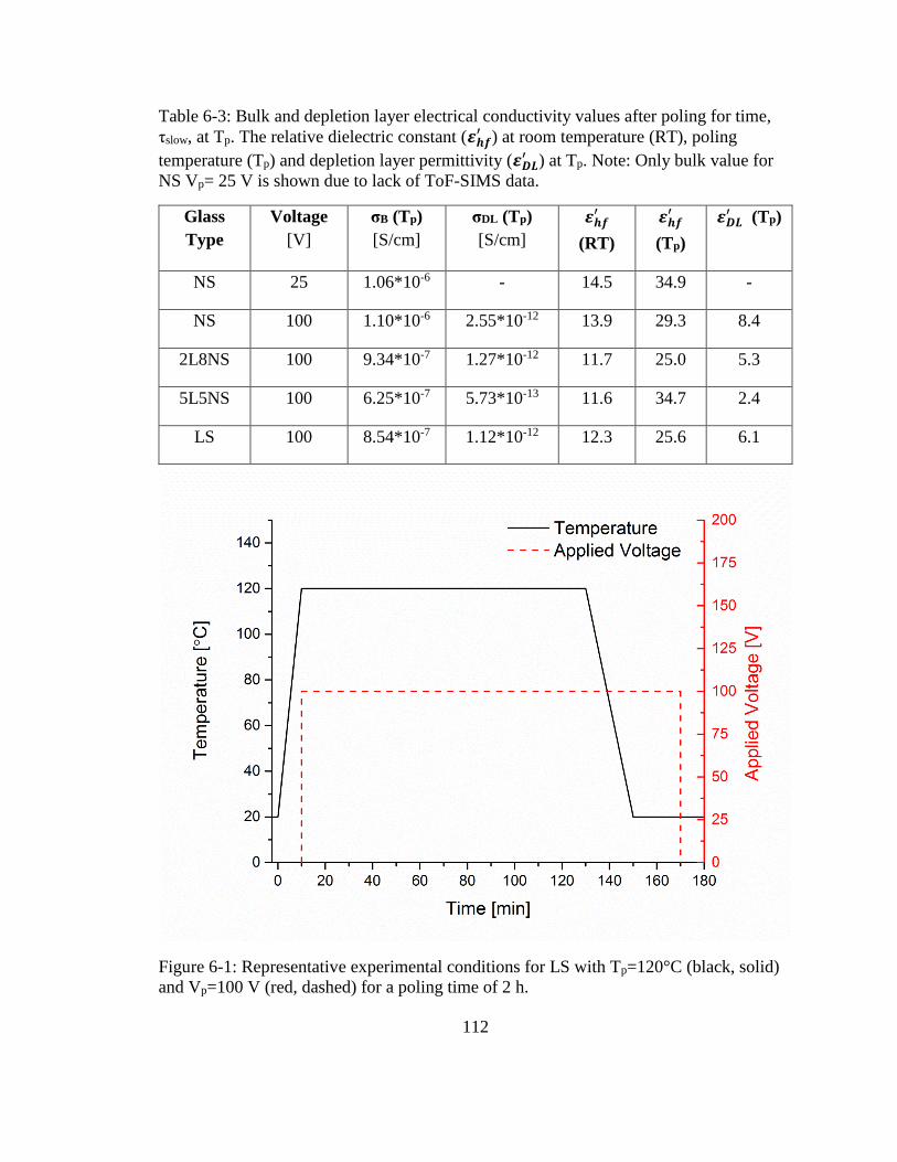
112
Table 6-3: Bulk and depletion layer electrical conductivity values after poling for time,
τslow, at Tp. The relative dielectric constant (𝜺𝒉𝒇′ ) at room temperature (RT), poling
temperature (Tp) and depletion layer permittivity (𝜺𝑫𝑳′ ) at Tp. Note: Only bulk value for
NS Vp= 25 V is shown due to lack of ToF-SIMS data.
Glass
Type
Voltage
[V]
σB (Tp)
[S/cm]
σDL (Tp)
[S/cm]
𝜺𝒉𝒇′
(RT)
𝜺𝒉𝒇′
(Tp)
𝜺𝑫𝑳′ (Tp)
NS 25 1.06*10-6 - 14.5 34.9 -
NS 100 1.10*10-6 2.55*10-12 13.9 29.3 8.4
2L8NS 100 9.34*10-7 1.27*10-12 11.7 25.0 5.3
5L5NS 100 6.25*10-7 5.73*10-13 11.6 34.7 2.4
LS 100 8.54*10-7 1.12*10-12 12.3 25.6 6.1
Figure 6-1: Representative experimental conditions for LS with Tp=120°C (black, solid)
and Vp=100 V (red, dashed) for a poling time of 2 h.

113
Figure 6-2: Arrhenius behavior of DC electrical conductivity used to calculate activation
energy for ionic conduction.

114
b)
a)
Figure 6-3: Electrical behavior of NS during poling with Vp=25 V at Tp=100°C for 2 h
a) showing representative conductance vs. frequency behavior and b) representative
impedance growth of an alkali ion depletion layer (arrow indicating increasing
direction). The inset indicates the intersection between bulk and depletion layer
impedance components.

115
Fig
ure
6-4
: N
yquis
t plo
ts o
f re
al i
mped
ance
vs.
im
agin
ary i
mped
ance
duri
ng
poli
ng w
ith 1
00V
for
2 h
ours
wit
h a
) L
S (
Tp=
120°C
), b
) 5
L5
NS
(T
p=
230°C
),
c) 2
L8N
S (
Tp=
190°C
) an
d d
) N
S (
Tp=
100°C
) gla
ss c
om
posi
tions
at 1
20 s
inte
rval
.
a)
b)
c)
d)

116
Figure 6-5: Impedance spectra for depoling of NS with Vp= 0 V at Tp=100°C
for 20 h. Impedance was observed to increase upon removal of the poling
voltage and gradually decrease over the course of depoling at Tp.

117
Figure 6-6: Real capacitance of NS before (black, squares) and during poling with Vp=25
V at Tp=100°C. High frequency plateau attributed to bulk capacitance and low frequency
plateau corresponds to depletion layer formation. Note: Large noise in start (red, circles)
and 120 second (blue, triangles) spectra due to glass changing on a faster time scale than
impedance frequency sweep.
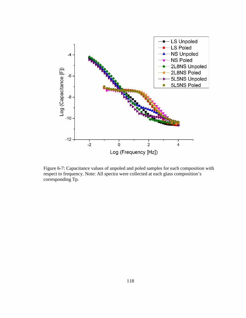
118
Figure 6-7: Capacitance values of unpoled and poled samples for each composition with
respect to frequency. Note: All spectra were collected at each glass composition’s
corresponding Tp.

119
a)
b)
c)
Figure 6-8: Time dependence of current density (left axis, symbols) and charge flow (right
axis, lines) for each glass composition with Vp=100 V at Tp for a) initial 50 s, b) complete
7,200 s duration (on log-log scale) and c) exponential and stretched exponential decay fits
of current density during poling of LS.

120
Figure 6-9: TSDC of current density (left axis, pink inverted triangles), charge flow (right
axis, black line) and sample temperature (far right axis, blue dashes) for 5L5NS from
ambient to 300°C at a heating rate of 10°C/min.
Figure 6-10: TSPC of current density (left axis, bold lines), charge flow (right axis, lines)
for each glass composition from ambient to 300°C at a heating rate of 10°C/min.

121
Figure 6-11: ToF-SIMS measurement of depletion layer thickness for 2L8NS of about
100 nm following poling with Vp=100 V at Tp=190°C for 2 h. Annotations for platinum
electrode layer (Anode), alkali ion depletion layer (DL), and bulk glass (Bulk) are labeled
approximately with sputter depth.

122
Figure 6-13: Depletion layer resistivity as a function of poling time for NS (black,
squares), 2L8NS (blue, triangles), 5L5NS (pink, inverted triangles) and LS (red, circles)
with Vp=100 V at Tp for 2 h.
Figure 6-12: Schematic of fitted equivalent DC circuit for electrode
polarization (E), alkali ion depletion layer (DL) and bulk glass (B).

123
Figure 6-15: Pairs of images captured during electric field-induced softening at a heating
rate of 10°C/min. The first two images show NS with an external voltage of 150 V at a
furnace temperature of a) 428°C and b) 429°C taken 6 seconds apart. The second pair of
images taken 20 seconds apart show NAS with an external voltage of 200 V
corresponding to current measurements c) 0.3 mA (1.2 mA/cm2) and d) 10 mA (40.5
mA/cm2) prior to glass softening. Note: the anode is located at top of the sample and
photoemissions are indicated by yellow arrows.
Figure 6-14: Comparison of ToF-SIMS alkali ion depletion layer thickness (black,
squares) measurements between glass compositions after poling with Vp=100 V for 2 h
at Tp. The corresponding depletion layer permittivity (red, circles) calculated from
Equation 6-1 are also compared.

124
Chapter 7: Characteristics of depletion layer formation prior to EFIS
This chapter reports on the investigation of the various thermally stimulated
polarization mechanisms that occur upon heating during EFIS. We also examine
compositional changes associated with depletion layer formation using various analytic
techniques. We report modifications of glass composition by EDS linescans and maps of
the anode region. The chemical bonding environment was determined by XPS. The
formation of an alkali ion depletion layer was investigated in situ by thermal imaging
followed by depth profiling using SIMS.
7.1 Thermally stimulated currents under DC voltages
7.1.1 DC TSPC results
Polarization mechanisms were investigated using thermally stimulated poling current
(TSPC) density measurements. In this case, TSPC is in situ with EFIS experiments. NS,
2L8NS, 5L5NS and LS glass compositions are listed in Table 7-1. The thermally
stimulated current density of NS with 150 V applied is shown in Figure 7-1 at a heating
rate of 10°C/min. Four characteristic regions are identified here as I-IV. Three of these
regions contain current density peaks as indicated by red arrows and the corresponding
peak temperatures are listed in Table 7-2. The fourth region occurs abruptly where high
current passes through the sample and is maintained until the voltage is removed. This
high current region becomes a plateau, indicating the current is limited by the power
resistor in series with the sample. The current measurements are then integrated to
calculate the amount of charge density passing through the sample. The right y-axis (red)

125
of Figure 7-1 shows the accumulated charge density as a function of time with an axis
break. Origin of the regions will be discussed in section 7.1.2.
The voltage dependence of thermally stimulated current density is shown in Figure
7-2 for NS of the same sample height with five applied voltages: 100 V, 125 V, 150 V,
175 V and 200 V. The height of the current density peak in region I of Figure 7-2
increases with applied voltage. The current density peak in region II also increases in
height, but shifts to higher temperatures by 19°C as applied voltage increases from 100 V
to 200 V. The shift in this peak’s temperature (Tpeak) follows a linear trend of
Tpeak=0.192*V+169 [°C] where V is the magnitude of applied voltage. The current
density peak in region III of Figure 7-2 remains constant as applied voltage increases
from 100 V to 150 V. With increasing voltage, the transition from region III to region IV
continuously shifts to lower furnace temperatures. It should be noted that for the NS
composition, spikes in current density were observed in some cases. The shift of the high
current density region IV at high voltage obscures the current density peak of region III
as compared to lower applied voltage.
As mentioned above, the current measurements can be integrated to calculate the
accumulated charge flowing per unit area through the sample. Inspection of accumulated
charge density can reveal the amount of charge required to form an alkali ion depletion
layer within the glass. The voltage dependence of accumulated charge density is revealed
in Figure 7-3a where the latter is plotted as a function of time. These plots highlight the
accumulated charge density to dielectric breakdown (seen as surge in Figure 7-3a). This
charge density for breakdown is observed to both increase and shift to shorter times as
126
applied voltage is increased. The accumulated charge density was then normalized by
applied voltage and plotted in Figure 7-3b. The result has the units of capacitance per unit
area (C/V.cm2), and therefore termed area-specific capacitance. However, it does not
have the conventional meaning of dielectric capacitance i.e. the charge stored density.
Figure 7-3b reveals that just prior to electrical breakdown a common area-specific
capacitance of approximately 2 to 3 mF/cm2 is reached within the glass irrespective of
voltage.
The role of alkali ion diffusion in thermally stimulated currents was delineated by
varying the ratio of Li+ to total alkali content (Li+ + Na+) in a disilicate glass system. The
thermally stimulated current density for NS, 2L8NS, 5L5NS and LS is shown in Figure
7-4 with respect to furnace temperature at an applied voltage of 150 V and pressure of 1
MPa. As Na+ content decreased, the current density peak in region I of Figure 7-4
decreased to the point where for the LS composition it is not observed. A similar shift in
peak temperature in region I was reported during thermally stimulated poling current
measurements of thin mixed alkali silicate glass films [96]. As Na/Li ratio increased to
~1 within the mixed alkali series, the height of current density peak in region II of Figure
7-4 remained constant. However, its peak position shifted to higher furnace temperatures
non-monotonically, indicative of the mixed-alkali effect. The current density peak in
region III of the thermally stimulated current density remained constant in peak
temperature as revealed by Figure 7-4 with only a slight increase in height as Li+ was
substituted into the glass composition. Region IV corresponds to large and sustained

127
current density following the same shift in furnace temperature as the current density
peak in region II.
The activation energy of thermally stimulated current density corresponding to alkali
ion diffusion can be calculated using the initial rise method, as shown by the Arrhenius
plot in Figure 7-5 for 5L5NS with 150 V applied [56]. The activation energy
corresponding to the slope of the linear fit is calculated to be 1.14 eV. Following this
procedure, the activation energy for TSPC alkali ion diffusion for NS, 2L8NS, 5L5NS
and LS is determined and given in Table 7-1 as 0.62 0.06 eV, 1.00 0.07 eV, 1.14
0.02 eV and 0.66 0.03 eV, respectively. These values remained constant for varying
applied voltage. The peak temperatures of thermally stimulated current densities can also
give an estimate for activation energy of each process that contributes to the current
[50,54,97]. From this estimate, the activation energy is approximately equal to 25KbTMax
[eV] where TMax is the temperature of the peak maximum in Kelvin [54]. These estimates
are listed in Table 7-2 for each peak temperature and corresponding composition.
However, this calculation is only approximate since the peaks need to be well resolved
for accurate analysis.
The accumulated charge density corresponding to the current density measurements
of Figure 7-4 was calculated and is shown in Figure 7-6 as a function of time, where the
abscissa emphasizes the buildup of charge density in region III to electrical breakdown in
region IV of current runaway. The transition between the two regions is seen in Figure
7-6 as a sudden increase in charge density. The accumulated charge density just prior to
dielectric breakdown of the two single alkali glasses at 150 V was similar (~0.5 C/cm2),

128
while it decreased by nearly a third for the mixed alkali glass 5L5NS to 0.3 C/cm2.
Accumulated charge density at breakdown decreased with mixed alkali content but
breakdown shifted to longer times corresponding to higher furnace temperatures.
The effect of heating rate on thermally stimulated current density in LS with 150 V
applied is shown in Figure 7-7 for 10°C/min (black) and 5°C/min (red). The results
demonstrate that the peak temperature corresponding to DC conduction of alkali ions in
region II is reduced from 228°C for 10°C/min to 212°C at the slower heating rate of
5°C/min. The same trend occurs for the current density peak in region III prior to
electrical breakdown, where the peak at 367°C for 10°C/min shifts to 348°C for 5°C/min.
The activation energy calculated using the initial rise method for the current density peak
in region II representing DC conduction of cations in LS is 0.63 eV for the slower heating
rate, which is within experimental error of 0.66 0.03 eV calculated for 10°C/min.
7.1.2 Discussion of DC TSPC results
The role of alkali ions in EFIS was investigated by measuring thermally stimulated
current densities for each composition. For the simple case of a single alkali containing
glass, thermally stimulated current density for NS with 150 V applied across 0.9 cm thick
sample is shown in Figure 7-1. As mentioned above, there are four distinct regions (I-IV)
that contain three current density peaks and a sustained high current density plateau. The
current density peak temperatures and associated activation energies are listed in Table
7-2. The current density peak in region I corresponds to short-range dipolar polarization
of alkali ions aligning in the direction of the applied voltage around non-bridging
oxygens (NBOs) [48,61]. Region II of Figure 7-1 corresponds to long-range DC ionic

129
conduction of alkali ions from anode to cathode as a function of temperature [48,54,98].
The activation energy of DC ionic conduction for the current density peak in Region II
was calculated for all samples as shown in Figure 7-5 using the initial rise method [56].
The transition between regions II and III was chosen to split the current density plateau
between the second and third peaks in current density. The exact transition of current
density into region III is only speculated to be when the current density from the third
peak begins to overcome the current density provided by the second peak. The activation
energy of the peak in region III is roughly 1.4 eV (depending on heating rate as discussed
later) as listed in Table 7-2. From the electro-thermal poling study of Chapter 5,
experimental evidence of anion migration and proton injection were provided. The
activation energy of either oxygen anion (such as an NBO) migrating toward the anode
(literature lists values of 1.2 to 1.35 eV [6,41,99–101]) or since experiments were
conducted in air proton injection from the anode into the glass (literature cites values of
1.5 eV in ambient [41,102]) could be attributed to the peak of region III. It is possible that
region III could be a combination of the two processes. The abrupt increase in
accumulated charge density and sustained high current density in region IV and current
spikes prior reveal rapid electrically discharge. The current spikes could be the initiation
of electrical discharge followed by rapid healing as a kind of ‘shorting’ of current flow.
The current spikes and sustained high current suggest and have been attributed to
dielectric breakdown of the glass samples at elevated temperatures [103].
The voltage dependence of thermally stimulated current densities is displayed in
Figure 7-2. Region I of Figure 7-2 reveals that the dipole polarization current density

130
peak increases to a maximum at a voltage of 150 V and above, indicating that the region
near the anode becomes fully polarized at room temperature. The DC ionic conduction
peak of region II grows in height by a factor of three for 200 V as compared to 100 V. It
also shifts to higher temperatures as voltage is increased, indicating that additional
sodium ion migration occurs and is expected to increase the depletion layer thickness
[36]. However, the peak in region III remains constant for 100 V, 125 V and 150 V, and
does not appear for the higher applied voltages. Thus, EFIS does not depend on the
polarization process of region III. EFIS is primarily associated with region IV where
dielectric breakdown shifts to lower furnace temperatures with an increase in applied
voltages. For example, an increase of applied voltage from 100 V to 200 V, the furnace
temperature for dielectric breakdown of NS decreased by approximately 130°C (see
Figure 7-2).
The dependence of thermally stimulated current density on glass composition is
demonstrated in Figure 7-4 for NS, 2L8NS, 5L5NS and LS with 150 V applied. The peak
of region I shifts as lithium is substituted for sodium toward lower temperatures. This
shift of dipolar polarization has been observed at room temperatures and below for mixed
alkali trisilicate thin film glasses [96]. It is assumed that with the lithium disilicate glass
composition the depolarization peak occurs rapidly upon application of a voltage and
recording time was not sufficient to capture the current measurement.
The shift in peak temperatures in region II for each composition is listed in Table 7-2
along with their calculated activation energies. The increase in activation energy
attributed to DC ionic conduction is expected as mixed alkali ratio approaches unity
131
[76,96]. This is supported by measurements from impedance spectroscopy from Figure
4-6. For 5L5NS to have the same electrical conductivity as NS, it needs to reach higher
temperatures. For example, DC conductivity of NS at 205°C was 3.27x10⁻⁵ S/cm,
whereas that of 5L5NS at 203°C was 1.93x10⁻⁷ S/cm. This supports that the shift to
higher temperatures in the thermally stimulated current densities is due to DC conduction
of alkali ion migration and influenced by their corresponding activation energies.
The accumulated charge density and area-specific capacitance in Figure 7-3
demonstrate how the formation of the alkali ion depletion layer influences the electrical
characteristics of the glass. The inflection of the charge density is associated with the
formation of the depletion layer near the anode due to the exhaustion of mobile cations
during region II. The inflection point in Figure 7-3a is observed near 1,250 s mark for all
voltages. As applied voltage is increased, the accumulated charge density at which the
inflection takes place increases. However, by normalizing the accumulated charge density
with the applied voltage the area-specific capacitance can be calculated as seen in Figure
7-3b. An interesting characteristic is observed following the formation of the alkali ion
depletion layer: the area-specific capacitance has about the same value around 2.5
mF/cm2, irrespective of applied voltage. This indicates that the mechanism of dielectric
breakdown is insensitive to various external voltages, supporting that the local internal
electric field across the alkali ion depletion layer dictates its breakdown.
The change in heating rate produces multiple effects on EFIS. Its main effect is the
measured shift in thermally stimulated current density as shown in Figure 7-7. A heating
rate of 10°C/min (black) and 5°C/min (red) was used to heat two samples of LS. A shift

132
toward lower furnace temperatures at a slower heating rate was expected as observed in
polymers since the sample temperature does not lag behind [104]. The shift in current
density to lower furnace temperature for the slower heating rate did not influence the
activation energy for alkali conduction outside of experimental error. Reducing the
heating rate by half increased the furnace temperature at which the glass began to soften
by 8°C (see Figure 7-7); glass softening began at a furnace temperature of 419°C with a
heating rate of 10°C/min and increased to 427°C with 5°C/min. The shift in thermally
stimulated current density significantly influenced the amount of accumulated charge
density that the glass experienced just prior to electrical breakdown. The accumulated
charge density to electrical breakdown were 0.73 C/cm2 and 0.45 C/cm2 for the 5°C/min
and 10°C/min heating rates, respectively. The slower heating rate allowed an increase in
accumulated charge density at breakdown by a factor of 1.6. This reveals that heating rate
heavily influences accumulated charge density at breakdown. So, the depletion layer
thickness prior to electrical breakdown could potentially be controlled by tailoring the
heating rate during EFIS.
7.2 Thermally stimulated currents under AC voltage
7.2.1 AC TSPC results
Thermally activated processes were also investigated for AC frequencies in the same
manner as DC in the previous section. These current measurements were made during
EFIS testing of the same samples discussed in Figure 5-9 for both NS and 5L5NS glass
compositions as listed in Table 7-1. A constant voltage of 150 Vrms was chosen to
compare with the 150 V DC (0 Hz) condition. The frequency dependence of current

133
density is shown in Figure 7-8a for NS and Figure 7-8b for 5L5NS in the frequency range
of 0 Hz to 1000 Hz. The presence of an oscillating voltage immediately reveals a change
in thermally activated current as compared to DC. In the case of DC, the thermally
stimulated current was broken down into four distinct regions. Here, for AC there are
only has three distinct regions. From both NS and 5L5NS in Figure 7-8 it can be seen at
low furnace temperature that a steady-state current is produced with the application of
150 V for all but the 0 Hz. The second region in Figure 7-8 occurs when the current
density begins to rise at a constant semi-log slope with increase in furnace temperature.
The current density converges to a common increase with temperature, irrespective of
frequency except for 0 Hz. The semi-log slope constant for NS was 0.018 ± 0.0001 while
5L5NS was 0.019 ± 0.0001. The third region of current density in AC begins when the
current density begins to rise beyond the mentioned semi-log slope constant with furnace
temperature. The power resistor in series with the sample, as described in section 3.5,
then limits the rise in current density. The sudden drop in current density in Figure 7-8 is
from the voltage being removed from the sample.
The accumulated charge density was calculated as for the case of DC i.e. as the time
integral of current density. The frequency dependence of charge density is show in Figure
7-9a for NS and in Figure 7-9b for 5L5NS. From Figure 7-9a, an accumulated charge
density of approximately 10 C/cm2 was required for NS to transition region II of Figure
7-8a to region III. This transition appears to be independent of frequency likely due to
self-heating. A similar accumulated charge density of 10 C/cm2 was required for 5L5NS
for the same transition in Figure 7-9b, however, at 1000 Hz, the transition occurred

134
around 1 C/cm2 for 5L5NS. The accumulated charge density at breakdown in the DC
case for 150 V was smaller around 0.5 C/cm2 and 0.3 C/cm2 for NS and 5L5NS,
respectively.
The power density corresponding to the current densities of Figure 7-8 were
calculated by multiplying the applied voltage with the current density. The frequency
dependence of power density is shown in Figure 7-10a for NS and Figure 7-10b for
5L5NS showing the same response as current density since voltage is constant. From
Figure 7-10, it is obvious that the amount of power dissipated within the samples were
much greater compared to the DC case. However, following dielectric breakdown in DC,
power dissipation increases dramatically to a current limit imposed by the series resistor.
The electrical conductivity was calculated from the current density, applied voltage
and sample height. The temperature and frequency dependence of electrical conductivity
for NS is calculated in Figure 7-11a while 5L5NS in Figure 7-11b. The electrical
conductivity empirically follows the same behavior as current density exhibiting the three
regions. The plateau of electrical conductivity at low temperatures is due to an AC
component while at higher furnace temperature the conductivity is dominated by a DC
component.[105]
7.2.2 Discussion of AC TSPC results
The steady-state current density measured in Figure 7-8 for both NS and 5L5NS
reveals that electrode polarization is likely occurring. At low furnace temperatures, the
alkali ions are unable to migrate away from their associated NBO’s. Hence, no long-

135
range alkali ion migration occurs and current is produced by interfacial polarization. In
this frequency range the electrical conductivity is frequency independent as shown in
Figure 4-1 and capacitance is heavily frequency dependent as seen in Figure 4-3. The
initial current density with respect to frequency and the convergence of current density to
a semi-log linear rise follows the empirical Jonscher power law.[105] This power law
behavior has been reported for oxide and chalcogenide glass compositions.[106–108] The
power law of total electrical conductivity is the sum of the DC and AC components as:
𝜎𝑇𝑜𝑡𝑎𝑙 = 𝜎𝐷𝐶 + 𝜎𝐴𝐶 (Equation 7-1)
This relation can be further broken down as temperature dependent and frequency
dependent terms. The temperature dependent is determined from the Arrhenius behavior
of DC electrical conductivity of Equation 4-4 as previously mentioned. This term
determines the conductivity due to thermal agitation and diffusion of mobile ions.[106]
Since energy is provided to mobile ions thermally, the term is frequency independent.
The frequency dependent term has been empirically defined as the following relation:
𝜎𝐴𝐶 = 𝐴𝜔𝑆 (Equation 7-2)
where A is a constant [S/cm.rad], ω is angular frequency [radian] and the exponent S lies
within the range 0 < S < 1 but appears to reach a limit at temperatures above ambient in
glasses of S=0.6.[109] This term dominates the total conductivity when sample
temperatures are low. Therefore, mobile ions do not have enough thermal energy to hop
resulting in diffusions or migration. At these lower temperatures an increase in frequency
will increase the probability of an ion successfully completing jumps resulting in an
136
increase in conductivity.[106] Equation 4-4 and Equation 7-2 can be substituted back into
Equation 7-1 to give the following relation of total electrical conductivity as:
𝜎𝑇𝑜𝑡𝑎𝑙 = 𝜎0𝑒𝑥𝑝(−𝐸𝑎 𝑘𝐵𝑇⁄ ) + 𝐴𝜔𝑆 (Equation 7-3)
This model however, is only empirical and generally fits experimental data well.
Multiple models have been developed to take on physical means such as ‘universal
dynamic response’ (S=0.6) and ‘nearly constant loss’ or second-universality (S>0.6)
model occurring at low temperatures.[110–113] Equation 7-3 was applied to Figure 7-11a
for NS and Figure 7-11b for 5L5NS as dashed lines for 60, 125 and 1000 Hz.
The semi-log linear increase in current density in the second region at intermediate
furnace temperatures occurs due to a change in conduction processes within the glass.
The semi-log linear increase in current density as a function of temperature for AC
frequencies matches well to the second region of Figure 7-8 as observed in the DC case.
At these furnace temperatures, long-range ionic diffusion can occur. Migration of alkali
ion begins to overcome and dominate the current density produced due to short-range
oscillations. The activation energy associated with the second region was calculated from
the initial rise of the electrical conductivity for each glass composition similar to Figure
7-5. The calculated activation energies for NS and 5L5NS are summarized in Figure 7-12
with their corresponding frequency. NS was calculated to have an activation energy of
0.73 0.03 eV while 5L5NS was 1.29 0.03 eV during the initial rise with an AC
voltage. The initial rise while using a DC voltage was closer to impedance spectroscopy
values of 0.64 eV and 1.24 eV for NS and 5L5NS, respectively. The values are about 0.1

137
eV larger than the activation energy calculated for DC conduction from impedance
spectroscopy in Table 4-1 and Table 6-1.
The major difference between AC and DC is that a decrease in current density is
measured for DC around 200°C for NS in Figure 7-8a and 340°C for 5L5NS in Figure
7-8b. This decrease in current density is attributed to the exhaustion of charge carriers
away from the anode. In the case where an oscillating voltage was used, the current
density continues to increase linearly. This is a result of two half-cycle processes
comprised within the AC signal frequency.[114] First, the alkali ions migration away
from the positive electrode during the first half-cycle in the direction of the electric field.
The second half-cycle consists of the recovery of alkali ions back toward the electrode in
the reverse direction of the initial electric field. This process prevents the development of
an alkali ion depletion layer near the electrodes. The two half-cycles can be thought of as
a competition of the two driving forces as demonstrated in the following equation:
𝐽𝑖 = −𝐷𝑖∇C + µC𝐄 (Equation 7-4)
where Ji is the flux of alkali ions [mol/cm2.s], Di is the diffusion constant of alkali ions
within a silicate glass matrix [cm2/s], ∇C is the concentration gradient of alkali ions
[mol/cm], µ is the charge carrier mobility [cm2/V.s] and E is the electric field [V/cm].
The first term on the right-hand side of Equation 7-4 is the flux of alkali ions due to
diffusion while the second term is the flux resulting from migration in an electric field.
The mobility of charge carriers is further related to the electrical conductivity of an ionic
conductor as follows:

138
µ = 𝜎𝑛𝑖𝑒⁄ (Equation 7-5)
where σ is the electrical conductivity [S/cm], ni is the concentration of mobile ions [cm-3]
and e is the elementary charge for a monovalent ion [C].
At the start of the first half-cycle the flux of alkali ions is controlled by the migration
term of Equation 7-4 since the concentration gradient is zero. However, as ions migrate
away from the electrode within the first half-cycle the concentration gradient grows
leading to a self-decelerating process of backward diffusion. During the second half-cycle
where the electric field is reversed, both the concentration gradient and migration terms
of Equation 7-4 add resulting in recovery of alkali ions to their original positions. While
the sample remains at furnace temperature the flux of alkali ions toward the electrode
should readily exceed the flux away as a self-healing process. Therefore, a depletion
layer is not expected to accumulate within the frequency range tested. However,
dielectric breakdown can still occur if charge injection is faster than the half-cycle of the
AC frequency i.e. damage from charge injection can occur faster than healing from the
reverse AC cycle. Another possibility could occur if the sample begins to heat beyond the
furnace temperature, dielectric breakdown can still occur across the depletion layer
formed from the first half-cycle resulting in localized hot spots. Here, the temperature
increase could dramatically enhance the mobility and displacement during the first half-
cycle. Upon the second half-cycle the sample could dissipate heat quickly and effectively
‘freeze’ in the alkali ion displacements and inhibit a full recovery back towards the
electrode. If this condition is met, the sample is susceptible to breakdown. In fact,

139
evidence of a depletion layer during AC is shown in the next section, where EDS is
discussed (see section 8.3.1).
Power dissipation results in self-heating as a positive feedback system. This process
gives insight into the reduction of furnace temperature required for EFIS. As summarized
earlier in Figure 5-10, the application of an AC voltage further reduced furnace softening
temperatures as compared to DC. With an oscillating voltage, the amount of power
dissipated is more than measured in DC due to the formation and annihilation of an alkali
ion depletion layer. The power dissipation in AC is split between the two electrodes
creating a more uniform self-heating profile and a faster approach to EFIS. For the DC
case, the power dissipation is contained within a thin alkali ion depletion layer which
upon breakdown, experiences abrupt and intense power dissipation. The contained power
dissipation in DC leads to a non-uniform self-heating thermal runaway process. The
comparison of DC to AC self-heating is described in section 8.5 with infrared imaging as
seen in Figure 8-13 for DC 150 V and Figure 8-14 for AC 150 V 1000 Hz for NS glass
samples. Though similar power densities were experienced in both AC and DC scenarios,
the manner power was dissipated within the samples lead to uniform heating in the
former and localized heating in the latter.
7.3 Compositional analysis of modified and parent glass
Here, the goal was to quantitatively measure the thickness of the alkali ion depletion
layer while also investigating the microstructure of the glass near the anode by energy
dispersive spectroscopy (EDS). Quantification of compositional analysis and chemical
140
environment of the depletion layer and bulk glass were investigated using x-ray
photoelectron spectroscopy (XPS).
7.3.1 EDS results
Thermally stimulated current measurements were made during the EFIS process on
the NS and NAS glass compositions of Table 7-1 were used as lithium could not be
detected in the current EDS detector. A voltage ranging from 100 to 200 V was applied
across the top and bottom faces of the samples at room temperature. One sample of NS
was tested with an AC voltage of 120 V at 60 Hz. A representative current measured for
NS is shown in Figure 7-1 with 150V applied across the glass. These thermally
stimulated currents have previously been discussed for other alkali disilicate glasses with
their polarization mechanisms identified in section 7.1.2. The samples used for EDS were
stopped quickly after the current density of the glass reached that of Region IV
corresponding to dielectric breakdown. The samples were cooled the room temperature
quickly under an applied voltage to retain ionic displacements for characterization.
Compositional changes in the glass were observed using EDS as displayed in Figure
7-13 for NS with 125 V applied. Here, a linescan was taken in the glass region near the
anode as indicated by the yellow line in the secondary electron image. The depth profile
is represented by graphing the intensity of each constituent element with respect to scan
length in Figure 7-13. The scan length is equivalent to depth into the glass and represents
a clear alkali ion depletion layer, measured to be roughly 50 µm. An EDS map is shown
in Figure 7-14 of the same sample of NS with 125 V applied. The map reveals that the
alkali ion depletion layer thickness is non-uniform and can vary greatly.

141
Another observation revealed by SEM in Figure 7-15 was that the edge of the glass in
contact with the anode appeared beveled. This could indicate preferential polishing of the
alkali depletion region as compared with the bulk of the glass, or alternatively, a
densification of the glass within the depletion region.[115] The NS sample in Figure 7-15
was poled with 150 V. The increase in applied voltage resulted in a large depletion layer
thickness of about 150 µm. A similar trend in depletion layer thickness increase with
increasing voltage was reported during poling of bioactive glasses.[36]
An important feature associated with the alkali ion depletion region is the presence of
cavities post-mortem. The cavities shown in Figure 7-14 and Figure 7-16, were only
observed in locations of the glass where alkali ions were depleted. An example that
highlights this feature is displayed in Figure 7-17 for NAS following EFIS with 200 V
and 1 MPa applied. Here, Figure 7-17a is a secondary electron image of the anode/glass
region where the anode would be located on the left of the image and the glass sample is
the right side. An EDS map was collected over this region and into the bulk sample. An
overlay of the sodium intensity map is shown in Figure 7-17b which reveals a clear alkali
ion depletion layer of about 40 µm thick. From Figure 7-17b it is interesting the note that
the cavities are located only in the depletion layer. In fact, in the middle of the image
indicated by a yellow arrow, a semicircular cavity appears to be forming, reinforcing that
cavities only form within the alkali ion depletion layer. Upon removal of all NS samples
from the furnace at room temperature it was found that the anode side of the glass had
adhered to the anode.

142
An EDS linescan in Figure 7-18 of NS in the region near the cathode after 175 V was
applied showed no appreciable buildup of alkali ions at the cathode. However, for other
NS samples with 175 V and 200 V along with NS 120 V at 60 Hz, an optically brown
region was observed within the glass near the cathode. This was not observed on all
samples. The optically brown region was revealed as sodium-rich by Figure 7-19 for the
NS 120 V 60 Hz sample. It should be noted that during EFIS vapor was visually observed
coming from the sample. Due to this observation, the graphite electrodes were also
inspected by SEM and EDS. The anode area in contact with the glass did not contain any
alkali ions as seen in Figure 7-20a. However, on the anode surrounding the area where
contact was made, strong sodium and oxygen EDS signals were measured indicated
vapor condensed on the anode as Na2O. The cathode was investigated as well as seen in
Figure 7-20b and found that the graphite cathode accepted alkali ions into the electrode
material.
Two samples with 150 V applied were stopped prior to experiencing dielectric
breakdown in region IV of Figure 7-1. The first sample (NS 150 V Max) was stopped at
the current density peak of region II and cooled to room temperature with the applied
voltage. The second sample (NS 150 V Level off) was taken to the plateau regime in
region III and consequently stopped and cooled to room temperature with an applied
voltage as well. Both samples were characterized with SEM and EDS. However, a
detectable depletion layer was not measured as seen in Figure 7-21 for NS 150 V Max. A
minor alkali ion depletion was observed for these samples, however, the probe size used
for SEM and EDS was approximately 1 µm as to avoid sodium migration away from the

143
probe. Despite the lack of a detectable depletion layer, it is important evidence that there
is no presence of cavities in the glass near the anode as observed for all glass that were
stopped before region IV of Figure 7-1.
7.3.2 EDS discussion
During the poling processing of the sodium disilicate glasses with DC voltages,
thermally stimulated currents were measured as previously discussed in section 7.1.2 and
as shown in Figure 7-1. Each of the NS samples that were brought to region IV (unless
otherwise noted) and subsequently cooled to room temperature all contained an alkali
depletion layer that had a thickness ranging from 40 µm to 150 µm depending on the
applied voltage. This alkali ion depletion layer thickness is much greater than those
measured from electro-thermal poling on the same glass compositions in Chapter 5. This
difference is due to the much higher ionic conductivity when glass is exposed to higher
furnace temperatures in the former along with internal Joule heating caused by the
increased conductivity.
The lack of alkali ions within the depletion layer can be seen as a change in contrast
in Figure 7-13 at the anode/glass interface region. The alkali ion depletion region appears
brighter in contrast due to the relative increase of heavier atomic mass elements
compared to the bulk. The difference in contrast is supported by the EDS maps of Figure
7-14 and Figure 7-16 as the thickness of the alkali ion depletion region. The EDS maps
reveal that the depletion layer thickness is not uniform indicating that there are
preferential locations of the glass surface that make better electrical contact with the
electrode compared to other anode/glass interface locations. It is expected that the

144
depletion layer thickness would be uniform if the glass surface was entirely smooth and
all asperities were removed.
Although it appears certain locations make good electrical contact, the anode was
observed to adhere well to all the glass samples, especially for NS with 200 V applied.
This has been observed in various glass poling situations and has been studied as anodic
bonding to the electrode as an oxidation process.[8,43] It is believed that the cavities
observed within the depletion region are a result of electrolysis.[3,42,116] The
electrolysis process occurs in order to charge balance the uncompensated NBO after its
associated cation has migrated toward the cathode. As the furnace temperature and
subsequent Joule heating of the sample occurs, the mobility of the O-1 anion increases.
During this process, the anion can either combine with another NBO to form molecular
oxygen or migrate across the depletion layer toward the anode to be neutralized. It is
presumed that the path length for an anion to find another is shorter than migrating to the
anode. Therefore, the cavities form within the depletion layer when molecular oxygen
accumulates as gas and deforms the glass structure. If this process occurs near the edge of
the sample, the gas could escape. If the gaseous species form relatively ‘deep’ inside the
depletion layer (such as seen in Figure 7-17b), they could coalesce to form packets of gas
that are trapped upon cooling the sample.
As Joule heating within the sample increases as a positive feedback from increase in
electrical conductivity, the glass begins to heat rapidly. Figure 7-20a shows an alkali EDS
signal on the anode electrode material. Sodium would not normally migrate to the anode
due to repulsion. So, it must have vaporized and condensed on the electrode. Previously,

145
a white powder accumulation was observed on the push rods of the system and identified
through EDS as having a composition same as that of the glass (see Figure 8-8). This
further supports glass vaporization occurs during EFIS in region IV. Cations within the
glass were not observed to accumulate at the cathode/glass interface, as expected. The
cations were either accepted by the cathode material as seen in Figure 7-20b or
accumulate about 50 µm inside the glass as shown by Figure 7-18 away from the
cathode/glass interface. The accumulation within the glass was visually brown and was
sodium-rich compared to the bulk composition.
An accumulation of sodium ions within the glass while using an AC voltage of 120 V
at 60 Hz was not expected. However, a depletion layer thickness ranged from 0 to 20 µm
within the same sample of 120 V at 60 Hz. Heating of the sample beyond the furnace
temperature in localized spots could dramatically increase ionic mobility as seen in
Equation 7-5 since electrical conductivity is temperature dependent. As discussed later in
infrared imaging section to follow, localized hot spots were still observed indicating
dielectric breakdown as a mechanism for EFIS in AC as well as DC conditions.
For the two samples, ‘NS 150 V max’ and ‘NS 150V Level off’, that did not
experience dielectric breakdown, it was anticipated that the depletion layer thickness
would be on the same order of magnitude as those measured from electro-thermal poling
ranging from 50 nm to 200nm. Although EFIS and electro-thermal poling occur on
different temperature scales the applied voltage is similar and therefore, the depletion
layer thicknesses similar in magnitude according to the equation for space charge theory
in Equation 1-2. However, a large probe size was required when characterizing NS due to

146
the migration and volatilization of sodium under the electron beam. A large beam size
reduced these effects but consequently reduced resolution. The probe size used was too
large to consistently confirm the existence of a depletion layer thickness less than 1 µm.
It is believed however, that a depletion layer still exists on the order observed during
poling as in Figure 6-14.
Despite the lack of a depletion layer thickness measurement, the anode/electrode
interface integrity was observed for the two samples that were stopped prior to reaching
dielectric breakdown. The main feature from both samples and shown in Figure 7-21 is
the lack of cavities in the glass near the anode. This supports the mobility of the NBO
anion migration along with the electrolysis of glass. Other characteristics seen in Figure
7-21 of the anode/glass interface is that the edge is a smooth cut with no contrast
difference of the glass closest to the anode and the bulk further away. The edge of the
glass also did not preferentially polish. This indicates that EFIS largely changes the
characteristics of glass near the anode as opposed to conventional electro-thermal poling.
7.3.3 XPS results
Survey spectra across a wide range of binding energies from 0 to 1100 eV are shown
in Figure 7-22 for NS surface in contact with the anode, NS surface in contact with the
cathode and an unpoled virgin reference sample of the parent glass. The survey spectra
show the core-shell orbital binding energies of the surface and near surface atoms along
with Auger lines. The main overall trend revealed from the survey spectra of Figure 7-22
was the increase in sodium peak intensity from anode surface to virgin glass to cathode
surface. The higher resolution peak scans of Figure 7-23 were collected for the a) oxygen
147
1s, b) sodium 1s, c) silicon 2p and d) carbon 1s orbitals. The higher resolution peaks were
then deconvoluted into multiple components for each element depending on bonding
environment after subtracting a Shirley background and shown by the dashed line. This
was done for each high-resolution spectrum at the virgin, anode and cathode surfaces.
Three peaks can be identified in the oxygen 1s peak in Figure 7-23a, which are
deconvoluted in Figure 7-24 for each sample surface. Overall, the oxygen 1s peaks are
located at 533.0 eV, 531.7 eV and 531.0 eV binding energies as listed in Table 7-3. The
small broad peak at higher energies above the oxygen 533 eV peak is due to sodium
Auger signal.[117] The sodium 1s peak of Figure 7-23b remained constant at 1072.6 eV
for the virgin (Figure 7-25a) and cathode (Figure 7-25c) glasses, but shifted slightly to
lower binding energies for the anode (Figure 7-25b) composition to 1071.7 eV as listed in
Table 7-3. The silicon 2p peak position in Figure 7-23c is obviously unchanged due to the
XPS spectra being calibrated to this peak. For the cathode surface, the Si 2p peak was just
above background. Finally, the carbon 1s spectrum is shown in Figure 7-23d, which
consists of four distinct peaks at binding energies of 284.0, 285.0, 286.5 and 289.0 eV.
The deconvolution of the carbon components is shown in Figure 7-26 and corresponding
parameters along with their suggested origins are listed in Table 7-3.
The peak areas of Figure 7-23 and Table 7-3, were used to quantify the glass
compositions within the three surfaces of NS glass as given in Table 7-4 and Table 7-5.
Since carbon paste was placed on the surfaces in contact with the electrodes, large carbon
contamination was measured even after cleaning. The calculated compositions included
carbon contamination in Table 7-4, but excluded it and impurities in the results of Table

148
7-5 to obtain the composition that is representative of underlying glass. The theoretical
batch composition of NS is also listed in Table 7-5 for comparison.
7.3.4 Discussion of XPS results
The survey spectra of Figure 7-22 confirm the results of EDS that sodium ions
migrate away from the anode toward the cathode. The higher resolution core level spectra
of Figure 7-23 reveal additional information about the chemical bonding within the virgin
and modified glass compositions. The three deconvoluted oxygen 1s peaks of Figure 7-24
correspond to bridging oxygen represented by the 533 eV peak, while lower binding
energies are attributed to two types of non-bridging oxygen (NBO) species [118–120]:
These NBO peaks are attributed to O-Na bonding at 531.0 eV whereas O-Ca bonding
yields the 531.7 eV peak. Each spectrum in Figure 7-23 was analyzed in this way and the
numerical parameters of deconvolution are given in Table 7-3.
Two peaks were observed for the anode oxygen 1s spectrum at 532.8 eV and 531.1
eV corresponding to BO and O-Na NBO bonding, respectively. Two peaks were also
observed in the cathode oxygen 1s spectrum. Here, the peaks were at 533.0 eV and 532.0
eV, which have been attributed to BO and presence of oxygen in sodium carbonate,
respectively.[80] The virgin glass with the carbon paste removed had about 81% BO and
19% NBO. The BO to NBO ratio is higher than expected for NS, which has a theoretical
ratio of 3:2, likely from leaching of sodium during surface cleaning.[2,119] The anode
had a 96% BO signal while the cathode had 58% BO and 42% NBO. These ratios of BO
to NBO in Table 7-3 reveal that electrolysis occurs at the anode/glass interface surface

149
following poling. It also reveals that oxidation of cations occur at the cathode/glass
interface as well.
The sodium peak position in Figure 7-23b corresponds to Na-O bonding for each
sample surface.[80] The slight shift in binding energy of the sodium 1s spectra is likely
due to error in referencing to a rather small silicon 1s peak for the cathode surface
spectrum. The silicon peak was measured as a single component peak in Figure 7-23c,
meaning that silicon only had one bonding condition viz. to oxygen. The anode side of
the glass indicated a relative increase in silicon due to the lack of alkali ions while silicon
signal at the cathode was minimal. However, oxygen was still present at the cathode as
BO and NBO. Since the alkali signal at the cathode was large, the silicon was effectively
‘buried’ just below the surface. It is assumed that the remaining BO signal from the
cathode corresponded to Si-O bonding, allowing for further compositional calculations.
Four distinct carbon peaks were identified for the virgin, anode and cathode surfaces
in Figure 7-26, which are broken down in Table 7-3 by identified components. The
lowest binding energy peak at about 284 eV corresponds to sp2 C-C bonding. At
approximately 1 eV higher at 285 eV, the peak is attributed to sp3 C-C bonding.[121] The
third carbon peak corresponds to C-O bonding at around 286.5 eV, and the fourth peak
around 289 eV is determined to be C=O.[80] Note that graphite paste was applied to the
top and bottom faces of the glass disks to make good electrical contact with the graphite
electrodes. This paste was removed with acetone and then rinsed with 200 proof ethanol.
The amount of C-O bonding varied depending on the location of the sample. The anode
had the most C-O bonding while the cathode exhibited the least fraction. This is likely

150
due to the oxygen at the anode bonding with carbon. The opposite situation then occurs at
the cathode where there is an excess of cations that form sodium carbonates.
The formation of sodium carbonate is independently supported by two calculations
for estimating its amount. From Table 7-3 there is about 21% C-O bonding in the cathode
C 1s spectrum. Using this fraction multiplied by the total amount of carbon measured in
the sample from Table 7-4 of the cathode/glass surface gives an estimate of sodium
carbonate formation as about 16% of the total composition there. If a similar calculation
is performed using the fraction of O 1s peak connected with sodium carbonate at the
cathode (see Table 7-3 listing 42% of the oxygen), its concentration amounts to 21% of
the composition. The two estimates are very similar, considering the experimental error
associated with the deconvolution of spectra.
The composition of various surfaces with the omission of carbon (which is from
external contamination) is presented in Table 7-5. The calcium signal in the XPS spectra
is believed to be contamination from the carbon paste and was omitted as well. From
Table 7-5 the composition analysis of the virgin glass gave an approximate empirical
formula of 22 Na2O ● 78 SiO2. The expected composition was 33 Na2O ● 67 SiO2. The
reduction in sodium to silicon ratio is likely due to the leaching of sodium from the glass
into 200 proof ethanol during the cleaning of samples. However, a fracture surface
compositional analysis may provide a more accurate measurement closer to nominal
batch composition.[118] The composition analysis of the anode in Table 7-5 corresponds
to empirical formula of 1Na2O ● 99 SiO2. Here the dramatic reduction of sodium at the
anode is a consequence of the DC electric field or electrolysis of the sample. Positive

151
sodium ions migrate away from the anode toward the cathode producing current through
the sample. By comparison, the composition of the cathode is 40 Na2O ● 60 SiO2 (see
Table 7-5, assuming BO signal gives a good estimate of silicon). The expected
composition was Na2O as to account for the accumulation of sodium from the anode to
the cathode. The measured increase in sodium was not as dramatic as expected most
likely due to the formation of sodium carbonate during poling at the cathode which
consequently was washed away during cleaning. Another possibility could be due to
sodium being accepted by the graphite cathode and not being blocked at the
glass/electrode interface preventing a buildup of sodium at the interface. In fact, sodium
was detected by EDS on the cathode itself in Figure 7-20b supporting this.
7.4 Athermal alkali ion depletion layer formation
It is well known that thermal energy predominantly determines the structure of glassy
networks.[46] Here, the goal was to study alkali ion depletion layer formation well below
Tg of the parent glass. The measurement of current density decay describes alkali ion
depletion held isothermally. Thermal imaging of in situ alkali ion depletion formation
was performed along with SIMS depth profiling to confirm compositional changes in the
region of the glass near the anode.
7.4.1 Experimental methods of athermal depletion layer formation
LS and 5L5NS glass compositions were selected for this study. Graphite paste was
used on the top and bottom faces of three samples (two LS and one 5L5NS) to make
good electrical contact with the graphite electrodes. All samples were heated to a furnace
temperature of 250°C and held for 10 minutes to equilibrate. A voltage across the top and
152
bottom of 150 V was applied at furnace temperature to observe current density decay
with respect to time along with in situ thermal imaging. Following a sufficient current
density decay, the furnace was cooled to ambient while a voltage was still applied. This
would effectively ‘freeze’ in ionic displacements that occurred during poling.
The samples were sectioned in half between the anode and cathode sides of the glass.
The top and bottom faces were then cleaned to remove the thick carbon paste. Depth
profiling using SIMS was performed on the samples as described in section 3.7.2. These
samples were measured for both positive and negative ion concentrations in the glass
region in contact with the anode. Two regions were measured for positive and negative
ions on each sample for a total of four areas per sample that were characterized.
7.4.2 Thermal imaging of depletion layer formation
At the start of poling LS in Figure 7-27a, the current amplifier became saturated upon
application of the external voltage due to too low of a gain being used. However, a repeat
sample of LS using a higher gain setting in Figure 7-27b gave an initial conductivity for
LS as 1.5x10⁻⁴ S/cm while 5L5NS in Figure 7-27c had an initial conductivity of 2.7x10⁻⁶
S/cm at 250°C. These values correspond to an initial heat dissipation of 1.1 Watts for LS
and 0.02 Watts for 5L5NS.
Current density decay and charge flow are shown for each of the three samples in
Figure 7-27. The current density decay was similar to electro-thermal poling in Figure
6-8a. The decay profile of Figure 7-27 could not be fitted to a single exponential decay
function as expected from electro-thermal poling of Figure 6-8c. The isothermal hold
153
times for the three samples were too short to empirically estimate relaxation time
constants of the current density decay as in Section 6.2.
An infrared image of LS prior to poling is shown in Figure 7-28 at 250°C furnace
temperature. The anode, cathode and sample are labeled in yellow for clarity. Several
cursors were placed throughout the live image to collect temperature values as a function
of frame number. Two 3x3 pixel cursors were placed at the anode, cathode and bulk
regions of the sample along with a cursor off the sample for furnace temperature. The
temporal plots corresponding to the cursors are displayed in Figure 7-29 for (a) LS, (b)
LS Repeat and (c) 5L5NS. The black arrows of Figure 7-29 indicate the frame number
when the poling voltage was applied. Figure 7-29a and Figure 7-29b both show an
immediate change in sample temperature near the anode at a maximum of 8°C. The
temperature is then observed to decay with current density back to furnace temperature.
Figure 7-29c for 5L5NS did not show appreciable sample heating upon application of
poling voltage.
Depth profiling via SIMS of positive ions within the glass from anode into the bulk
are shown for LS in Figure 7-30a and for 5L5NS in Figure 7-30b. All ion signals were
normalized to the intensity of silicon. These depth profiles are representative for each
spot measured. A compilation of the lithium ion signal is shown in Figure 7-30c for all
spots. The average depletion layer thickness was approximately 1 µm in depth. A rough
estimate can only be obtained due to the rough surface finish of the glass during
preparation before poling. From Figure 7-30 it appears as though calcium and potassium
ions were injected into the sample as far as the depletion layer thickness for potassium

154
and half that for calcium. A depth profile for the negative oxygen anion is shown in
Figure 7-31a where possibly a slight depletion of oxygen was measured within 0.25 µm
of the glass closest to the anode. The hydrogen depth profile in shown in Figure 7-31b
where hydrogen appears to be enriched within 0.5 µm from the anode.
7.4.3 Discussion of athermal depletion layer formation
Current density decay as shown in Figure 7-27 follows the same decay relaxation
processes as observed in electro-thermal poling.[32] The two processes as described in
detail in section 6.3.2 are attributed to the fast relaxation process of alkali ion migration
away from the anode and a slow process of electrolysis of the glassy network leading to
anion migration toward the anode. It is believed that these processes occur here also, but
are potentially accelerated due to the higher poling temperature of LS at 250°C compared
to electro-thermal poling at 120°C. However, reliable measurements of relaxation time
constants for these samples could not be estimated due to their short poling times.
Upon application of the poling voltage 1.1 W of electrical power in LS and 0.02 W in
5L5NS were initially dissipated into the glass. From thermal imaging, it can be seen in
Figure 7-29a and Figure 7-29b that most of the Joule heating was contained near the
anode region of the glass with slight heating in the bulk. Heat generated near the anode
dissipated quickly back to furnace temperature as current decayed. For 5L5NS in Figure
7-29c, only 0.02 W was dissipated and no measurable temperature increase was
observed. The difference in electrical conductivity easily accounts for the two orders of
magnitude difference in heat dissipation due to current density decay. Although a
temperature increase of 8°C for LS was measured, the sample temperature remained well

155
below the Tg where glass is conventionally considered to be in a rigid state.[3] The glass
transition temperatures for LS and 5L5NS are 468°C and 420°C, respectively.
To accommodate for the migration of alkali ions away from the anode, the remaining
glass structure must rearrange for charge compensation in the absence of an internal
electric field.[43] The structural rearrangement below Tg must then be an athermal
process in the presence of an applied poling voltage. From the XPS discussion of section
7.3.4, structural changes were observed as an increase bridging to non-bridging oxygens
following poling at anode/glass interface. These observations are supported by structural
analysis following poling of soda lime glasses. Irreversible polymerization of the glass
located near the anode was measured using specular reflectance infrared spectroscopy
where NBO’s were observed to convert to BO’s or Si-OH groups.[122] Another study
using Raman Spectroscopy also observed structural rearrangements that were triggered
by NBO migration during poling that resulted in the formation of four-member (D1) and
three-member (D2) silicate defect rings.[41]
The detection of an alkali ion depletion layer was observed using SIMS depth
profiling. Here, in Figure 7-30, glass composition was modified within a region of a 1µm
thickness until reaching bulk values of the parent glass. The depletion layer thickness for
both LS and 5L5NS in Figure 7-30a and Figure 7-30b were thicker than compared to
those summarized in Figure 6-14 for electro-thermal poling on the same glass
compositions. This result was expected due to both the increase in applied voltage from
100 V to 150 V and increase in furnace temperature for LS and 5L5NS compared to
electro-thermal poling conditions. The SIMS signal for Ca+ and K+ appear to be

156
impurities introduced from graphite paste that were pushed on the glass. This is
consistent with results from XPS. The K+ accumulates at the interface between the alkali
ion depletion layer and the bulk. The Ca+ signal is present only about halfway into the
depletion layer. This is expected due to their difference in diffusivities, which depend on
their size and valence, as similarly observed in electro-thermal poling of bioactive
glass.[32] The ionic oxygen signal of Figure 7-31a indicates that little to no long-range
anion migration occurred toward the anode. However, a slight decrease in oxygen signal
was measured closest to the anode potentially due to oxygen evolution and escape from
the sample as gas. It should be noted again that the surface roughness of the sample was
too large for accurate measurements within the glass closest to the surface. As for charge
compensation by structural rearrangements below Tg, hydrogen injection provides part of
the charge compensation in the absence of mobile cations from the parent glass
composition. Hydrogen injection was measured from Figure 7-31b to only occur within
half of the depletion layer thickness at 0.5 µm. Therefore, the near surface injection of
hydrogen cannot fully account for charge compensation of NBOs following alkali
migration and subsequent depletion.
7.5 Chapter summary
Thermally stimulated current density measurements have revealed four distinct
regions of polarization. Region I results from dipolar polarization of alkali ions rotating
around their non-bridging oxygen in the direction of the applied field. Region II is
attributed to long-range alkali ion migration from anode to cathode. The activation
energy from the initial rise of Region II matches well with the activation energy for DC

157
electrical conduction measured by impedance spectroscopy. Region III is proposed as
from anion migration due to electrolysis and proton injection from the anode in
atmosphere. Region IV corresponds to dielectric breakdown of the sample leading to
large current flow and the creation of photoemissions.
The dependence of thermally stimulated current density on AC frequency showed a
power law dependence on temperature and frequency. It is believed that the AC
dependence results from two half-cycle processes. First, the positive electrode induces
alkali ion migration toward the opposing electrode. Second, with a reversed field during
AC oscillation, the alkali ions recover back to their original positions due to both
migration and diffusion.
Post-mortem characterization of depletion layer formation by EDS reveals a non-
uniform depletion layer much larger than those measured during electro-thermal poling.
The depletion layer for EFIS following dielectric breakdown was measured to be ~50 µm
thick. Visually brown regions in the sample were characterized as an alkali-rich phase
acting as areas for cation accumulation. A change in chemical bonding environment was
measured in XPS revealing an increase in depletion layer polymerization of the glassy
network near the anode.
Thermal imaging and current measurements of the depletion layer formation revealed
that the migration of alkali ions prior to dielectric breakdown does not significantly
increase the sample temperature near the anode. This indicates that structural
rearrangements occur in glass well below Tg. SIMS depth profiling confirmed the
formation of a depletion layer at 250°C to be about 1 µm in thickness.

158
Table 7-1: Glass compositions and their respective glass transition temperatures (Tg) and
activation energy for alkali ion migration during constant heating. Activation energies
from impedance spectroscopy and thermally stimulated current measurements are
compared with values from Table 6-1.
Glass
Type Composition
Tg
[°C]
Ea [eV]
(Table 6-1)
TSPC [eV]
(Table 6-1)
TSPC
Ea [eV]
NS 0.33 Na2O • 0.67 SiO2 469.7
0.9 0.70 0.01 0.66 0.02
0.62
0.06
2L8NS 0.33 [0.2 Li2O • 0.8 Na2O]
• 0.67 SiO2
424.3
0.7 0.99 0.01 0.91 0.02
1.00
0.07
5L5NS 0.33 [0.5 Li2O • 0.5 Na2O]
• 0.67 SiO2
420.4
0.3 1.14 0.01 1.01 0.02
1.14
0.02
LS 0.33 Li2O • 0.67 SiO2 468.5
0.5 0.76 0.01 0.73 0.02
0.66
0.03
NAS 0.25 Na2O • 0.05 Al2O3 •
0.70 SiO2
511.3
0.2 - -
0.82
0.04
Table 7-2: Comparison of thermally stimulated current peaks of each glass type with
150V applied externally.
Glass
Type
Peak I
Temp
[°C]
Peak I
Ea [eV]
Peak II
Temp
[°C]
Peak II
Ea [eV]
Peak III
Temp
[°C]
Peak III
Ea [eV]
NS 30 0.65 203 1.02 369 1.38
2L8NS 33 0.66 298 1.23 366 1.38
5L5NS - - 335 1.31 364 1.37
LS - - 228 1.08 367 1.38

159
Table 7-3: Numerical parameters of various 1s core level XPS spectra. Binding energy
(B. E.) and full-width at half-maximum (FWHM) in eV and area percent for each sample.
Sample Component B.E. [eV] FWHM [eV] Area %
Virgin O 1s O-Si 533.0 1.8 81%
Virgin O 1s O-Ca 531.8 0.9 5%
Virgin O 1s O-Na 531.1 1.2 14%
Anode O 1s O-Si 532.7 1.5 96%
Anode O 1s Na2CO3 531.0 1.3 4%
Cathode O 1s O-Si 532.9 2.9 58%
Cathode O 1s Na2CO3 532.0 1.4 42%
Virgin C 1s C-C sp2 284.4 0.7 13%
Virgin C 1s C-C sp3 285.6 1.2 47%
Virgin C 1s C-O 286.9 2 31%
Virgin C 1s C=O 289.7 1.8 9%
Anode C 1s C-C sp2 283.6 0.6 7%
Anode C 1s C-C sp3 284.6 1.5 60%
Anode C 1s C-O 286.4 1.2 22%
Anode C 1s C=O 287.8 1.8 10%
Cathode C 1s C-C sp2 284.3 0.6 44%
Cathode C 1s C-C sp3 284.8 1.3 26%
Cathode C 1s C-O 286 2.9 21%
Cathode C 1s C=O 290 2.1 9%
Virgin Na 1s Na-O 1072.3 1.5 100%
Anode Na 1s Na-O 1071.7 1.6 100%
Cathode Na 1s Na-O 1072.1 1.6 100%

160
Table 7-4: Surface compositions of NS after poling with 100 V and unpoled NS glass
including carbon contamination.
at% Glass/Anode
Surface
Glass/Cathode
Surface
Virgin Coating
Removed
Si 18.98 0.38 14.58
O 44.37 17.28 40.34
Na 0.44 6.45 9.47
Ca 0.65 0.12 1.65
F 1.45 0 0
C 34.12 75.77 33.95
Sum 100.01 100 99.99
Table 7-5: Surface compositions following poling with 100 V excluding carbon and
calcium contamination from surface paste. Theoretical sodium disilicate composition is
added for comparison.
at% Glass/Anode
Surface
Glass/Cathode
Surface
Virgin Coating
Removed Theoretical NS
Si 22.67 30.13 1.59 22.3
O 62.6 69.18 71.67 55.7
Na 14.73 0.7 26.74 22
Sum 100 100.01 100 100
Na/Si 0.02 16.84 0.65 0.99
O/Si 2.34 45.13 2.77 2.5

161
Figure 7-1: Time dependence of current density (black line) through NS glass sample
with 150V applied during heating at 10°C/min. The current density peaks are indicated
by red arrows. Accumulated charge flow (red line) was observed to surge around 0.1 C.
Note: There is an axis break for integrated charge where it appears to be constant but it
still increasing with time.

162
Figure 7-2: Thermally stimulated current density in NS glass as a function of
temperature, under different voltage ranging from 100 V to 200 V. Applied pressure = 1
MPa. Note: Large surge in current density due to dielectric breakdown of samples.
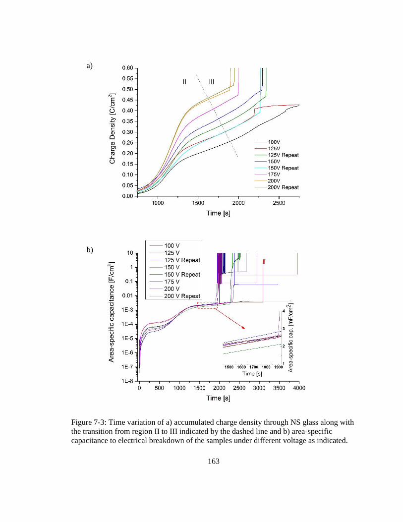
163
Figure 7-3: Time variation of a) accumulated charge density through NS glass along with
the transition from region II to III indicated by the dashed line and b) area-specific
capacitance to electrical breakdown of the samples under different voltage as indicated.
a)
b)

164
Figure 7-4: Current density through different glasses as a function of temperature. All
samples were subjected to 150V and 1 MPa pressure.
Figure 7-5: Arrhenius plot of thermally stimulated poling current through 5L5NS glass
with 150V applied during constant heating at 10°C/min. The linear fit portion yields
activation energy for alkali ion migration.

165
Figure 7-6: Comparison of accumulated charge density flow to breakdown in four
different glass compositions with 150V applied. Note: Charge density flow corresponds
to current measurements in Figure 7-4.
Figure 7-7: Heating rate dependence of thermally stimulated current densities of LS with
150V applied at 10℃/min or 5℃/min.

166
Figure 7-8: Frequency dependence of current density for a) NS and b) 5L5NS
glass compositions during heating at 10°C/min for EFIS with 150 V.
a)
b)
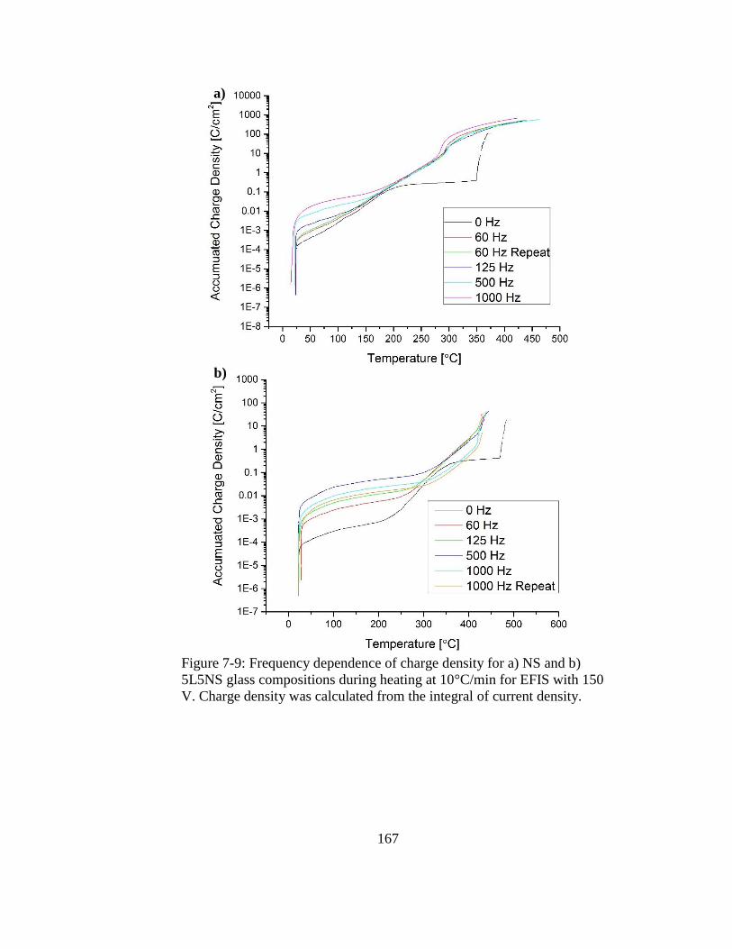
167
a)
b)
Figure 7-9: Frequency dependence of charge density for a) NS and b)
5L5NS glass compositions during heating at 10°C/min for EFIS with 150
V. Charge density was calculated from the integral of current density.

168
Figure 7-10: Frequency dependence of power density dissipation for a) NS and
b) 5L5NS glass compositions during heating at 10°C/min for EFIS with 150 V.
a)
b)

169
Figure 7-11: Frequency dependence of electrical conductivity for a) NS and b)
5L5NS glass compositions during heating at 10°C/min for EFIS with 150 V. A
model Jonscher sum of AC and DC contributions to overall electrical conductivity
are added for comparison as dashed lines.
a)
b)
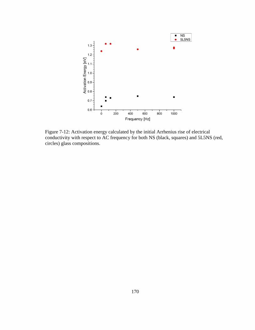
170
Figure 7-12: Activation energy calculated by the initial Arrhenius rise of electrical
conductivity with respect to AC frequency for both NS (black, squares) and 5L5NS (red,
circles) glass compositions.

171
Figure 7-13: NS125V EDS line scan of the glass near the anode. An alkali ion depletion
layer was measured to be roughly 60 µm thick. Note: Oxygen (green), silicon (purple),
sodium (blue) and carbon (red).

172
Fig
ure
7-1
4:
ED
S m
ap o
f N
S 1
25V
nea
r th
e an
ode
(loca
ted t
o t
he
left
of
the
sam
ple
). T
he
pin
k r
ecta
ngle
on t
he
seco
ndar
y e
lect
ron i
mag
e w
as t
he
map
ped
are
a.
A n o d e
A n o d e A n o d e
A n o d e

173
Figure 7-15: NS 150V EDS line scan of the glass near the anode (electrode located left of
dashed line). An alkali depletion layer of 160 µm was measured. The region closest to the
anode is beveled indicated preferential polishing post-mortem.
A
n
o
d
e
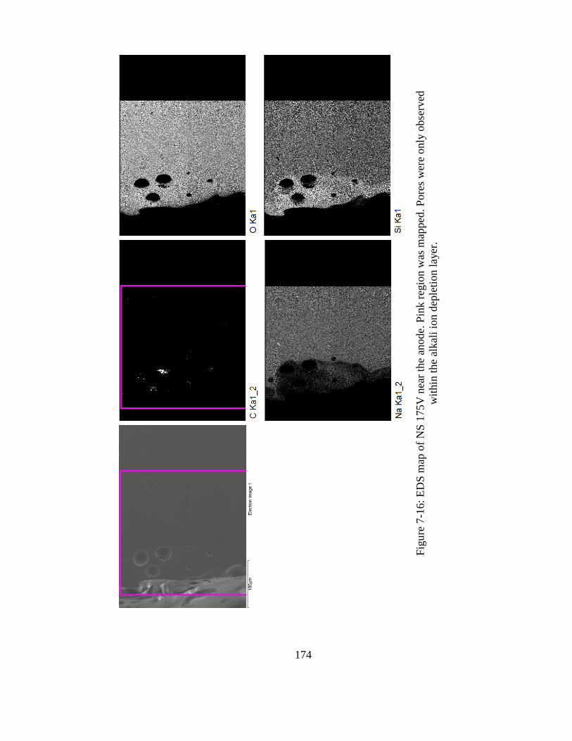
174
Fig
ure
7-1
6:
ED
S m
ap o
f N
S 1
75V
nea
r th
e an
ode.
Pin
k r
egio
n w
as m
apped
. P
ore
s w
ere
only
obse
rved
wit
hin
the
alkal
i io
n d
eple
tion l
ayer
.

175
Figure 7-17: Secondary electron images of NAS after EFIS with 200 V and 1 MPa
applied where a) is a representative image of the anode (right) /glass (left) region and b)
is an overlay of Na intensity (green) taken from an EDS map. Note: The yellow arrow
indicates a semicircular cavity of interest.

176
Figure 7-19: EDS line scan across optically brown region corresponding to a sodium-rich
composition.
Figure 7-18: NS 175V EDS line scan of the glass near the cathode. An accumulation
of alkali was not measured by EDS. Note: Linescan intensity x1000.

177
Figure 7-20: EDS line scan across the a) anode electrode and b) cathode electrode. Note:
Oxygen (yellow), Sodium (Green), Silicon (Purple).
a) b)
Figure 7-21: EDS line scan for NS 150V stopped in Region II corresponding to alkali
ion migration. EDS did not detect a discreet depletion layer. Porosity was not observed
in the glass near the anode.

178
Figure 7-22: Survey spectra of binding energy from NS glass prior to and post poling.
Spectra compare virgin glass composition (green) to the modified anode (black) and
cathode (red) compositions.

179
Fig
ure
7-2
3:
Hig
h r
esolu
tion b
indin
g e
ner
gy p
eak a
nal
ysi
s fo
r a)
O 1
s, b
) N
a 1s,
c)
Si
2p
and d
) C
1s
orb
ital
s in
the
vir
gin
gla
ss,
anode
and c
athode
com
posi
tions.
a)
b)
c)
d)

180
Figure 7-24: High resolution peak analysis of O 1s for a) virgin, b) anode and c) cathode
glass surfaces which has been deconvoluted into various identified components with their
cumulative fit.

181
Figure 7-25: High resolution peak analysis of Na 1s for a) virgin, b) anode and c) cathode
glass surfaces which has been deconvoluted into various identified components with their
cumulative fit.
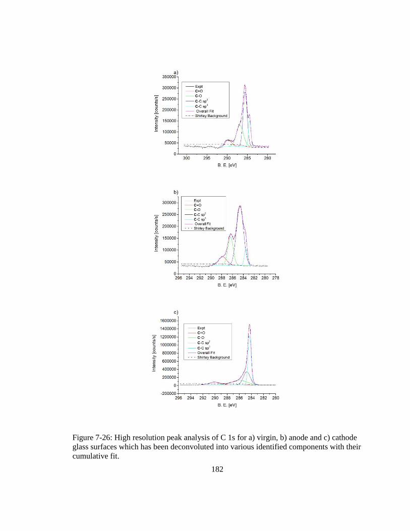
182
Figure 7-26: High resolution peak analysis of C 1s for a) virgin, b) anode and c) cathode
glass surfaces which has been deconvoluted into various identified components with their
cumulative fit.

183
Figure 7-27: Current density (black) decay of a) LS, b) LS repeat and c) 5L5NS
during application of 150V held at a furnace temperature of 250°C. The amount
of calculated charge flow (red) is also shown for each run. Note: Gain of
current amplifier was saturated at the start of a) LS.
a)
b)
c)

184
Figure 7-28: Infrared image of LS prior to being poled. The rectangular glass sample is
located in the middle of the image while the anode is at the top and cathode is at the
bottom of the image.
Anode
Cathode
Sample

185
a)
b)
c)
Figure 7-29: Temporal plots of a) LS, b) LS Repeat and c) 5L5NS during
application of 150V held at a furnace temperature of 250°C. Temperature
measurements were taken from multiple areas of the sample for comparison.

186
Figure 7-30: SIMS depth profile for a) LS, b) 5L5NS and c) 7Li+ for each of
the three samples tested with two areas per sample (dashed lines for unpoled
values). The alkali ion depletion layer was measured to be approximately 1
micrometer thick and indicated by the dashed lines in a) and b).
a)
b)
c)

187
Figure 7-31: SIMS depth profiles of a) 18O- and b) 1H- ions normalized to the Si- signal
to a depth of 2.5 µm from the anode/glass interface. Surface roughness of the glass may
result in variation of values at the interface.
a)
b)

188
Chapter 8: Mechanism of electric field-induced softening of glass
This chapter focuses on identifying the underlying mechanisms of EFIS through the
additional resource of modeling. It is known from electro-thermal poling studies of
Chapter 6 and from the thermally stimulated current density observations described in
Chapter 7 that the alkali ion depletion layer has a major impact both electrically and
compositionally on EFIS. As discussed earlier, the depletion layer is highly resistive
resulting in almost the entirety of the applied voltage dropping across this thin layer. The
formation of the depletion layer was modeled using finite element analysis to calculate
electrical properties and kinetics. Infrared imaging was used to experimentally measure
the self-heating of glass samples from the resistive heating of this layer. Finite element
analysis calculated the dependence of thermal runaway of EFIS on initiation temperature
as well as depletion layer thickness. Next, the observed photoemissions mentioned in
Chapter 5 are studied in detail and related to dielectric breakdown of the depletion layer
by thermal runaway and charge injection.
8.1 Finite element analysis of alkali migration
The current profile during EFIS associated with alkali ion migration in region II of
Figure 7-1 has already been discussed in the previous chapter in relation to the formation
of alkali ion depletion layer. Here, we model this layer using finite element analysis
(FEA). The goal is to calculate the depletion layer thickness as a function of sample
temperature and time. The calculated values are then compared to experimentally
measured values for validity. It is expected that the alkali ion depletion layer grows to a
thickness of around 100 to 200 nm during EFIS prior to dielectric breakdown similar to

189
electro-thermal poling in Figure 6-14. Following breakdown, resistive heating enhances
alkali mobility allowing for the creation of a larger depletion layer thickness of up to 50
µm as observed in EDS such as Figure 7-13.
8.1.1 FEA model setup
FEA calculations used Comsol version 5.2.0.220 software. For simplicity, the charge
carrier modeled the glass sample as a weak electrolyte system.[123] The electric currents
AC/DC module was used with the Nernst-Planck weak electrolyte module. One domain
was created representing the bulk properties of the parent NS glass composition.
This FEA contains two limitations for depletion layer formation calculations. First,
charge neutrality must be maintained throughout the entire length of the system at each
element. Therefore, no space charges can form within the domain. This results in other
constituent ions becoming much more mobile than in real glass systems to account for the
motion of sodium in the weak electrolyte model. The second limitation arises from the
weak electrolyte assumption itself which treats the ions as fully dissociated rather than
accounting for the glassy network structure ultimately affecting ionic mobility.
The electrical conductivity of the glass was defined as both temperature and
compositionally dependent. This was done to ensure that as the alkali ion depletion layer
formed, the electrical conductivity would reflect the corresponding modification of the
glass.[2] Note that the activation energy of each glass composition increases with
decreasing alkali. To reflect this, an exponential fit was applied to 48 binary sodium
silicate glass compositions of varying alkali content.[124] The electrical conductivity

190
dependencies are shown in Appendix C: Part 1 for a Na2O mol% ranging from 0 to 50
and a temperature range of 100°C to 350°C. The initial starting concentrations of ions
were 25870, 65450 and 26350 mol/m3 for Na+, O2- and Si4+, respectively.
The domain consisted of two boundaries. The left boundary was designated as the
anode with a constant voltage of 200 V applied using an electric potential boundary
condition. The right boundary was set as the cathode where ground potential was
established. Current conservation was used at every element to maintain the same current
throughout the entire domain. A global element constraint was added to each element
where the concentration of sodium was not allowed to be negative. Both boundaries were
set to not allow a flux of ions into or out of the system acting as blocking electrodes. A
cross sectional area of 25 mm2 was used to match those used in EFIS experiments. The
initial furnace temperature ranged from 100°C to 350°C in 50°C intervals.
Two element meshes were used for charge carrier simulations. First, the region of
interest is located within 1 µm of the left boundary where the voltage is applied. Here, a
mesh density was used as 1 element/nm. Beyond 1 µm from the anode, the rest of the
domain was meshed using Comsol’s default ‘extra fine mesh’ giving a mesh density of
about 2 elements/mm. All charge carrier simulations were tested from 0 to 20 s with 1 s
intervals. This time range was chosen to match the τfast relaxation time constants
measured by electro-thermal poling in Chapter 6, and attributed to alkali ion migration.
The main equation used to calculate the time dependence of ionic mass transport by
diffusion and migration is described by the Nernst-Planck relation:
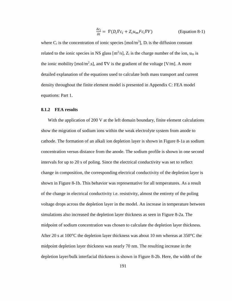
191
𝛿𝑐𝑖
𝛿𝑡= 𝛻(𝐷𝑖𝛻𝑐𝑖 + 𝑍𝑖𝑢𝑚𝐹𝑐𝑖𝛻𝑉) (Equation 8-1)
where Ci is the concentration of ionic species [mol/m3], Di is the diffusion constant
related to the ionic species in NS glass [m2/s], Zi is the charge number of the ion, um is
the ionic mobility [mol/m2.s], and ∇V is the gradient of the voltage [V/m]. A more
detailed explanation of the equations used to calculate both mass transport and current
density throughout the finite element model is presented in Appendix C: FEA model
equations: Part 1.
8.1.2 FEA results
With the application of 200 V at the left domain boundary, finite element calculations
show the migration of sodium ions within the weak electrolyte system from anode to
cathode. The formation of an alkali ion depletion layer is shown in Figure 8-1a as sodium
concentration versus distance from the anode. The sodium profile is shown in one second
intervals for up to 20 s of poling. Since the electrical conductivity was set to reflect
change in composition, the corresponding electrical conductivity of the depletion layer is
shown in Figure 8-1b. This behavior was representative for all temperatures. As a result
of the change in electrical conductivity i.e. resistivity, almost the entirety of the poling
voltage drops across the depletion layer in the model. An increase in temperature between
simulations also increased the depletion layer thickness as seen in Figure 8-2a. The
midpoint of sodium concentration was chosen to calculate the depletion layer thickness.
After 20 s at 100°C the depletion layer thickness was about 10 nm whereas at 350°C the
midpoint depletion layer thickness was nearly 70 nm. The resulting increase in the
depletion layer/bulk interfacial thickness is shown in Figure 8-2b. Here, the width of the

192
interface was defined from a sodium concentration of 90% to 10% of the bulk values
(concentrations indicated by horizontal dashed lines) and increased with temperature. The
midpoint halfwidth is defined as the midpoint minus half of the interface width.
The current density within the model is calculated from the cumulative mass transport
of migration and diffusion of ions. The time dependence of current density is shown in
Figure 8-3 as current density decay. The temperature dependence of the current density
decay is also shown in Figure 8-3. At higher temperatures, the current density decay
becomes greater corresponding to the formation of thicker depletion layers. An
interesting feature of Figure 8-3 is that the current density at the start of both 100°C and
150°C did not decay immediately, but only after a finite latent period.
8.1.3 FEA discussions
The simulated depletion layer profiles such as the one of NS at 200°C in Figure 8-1a
contain several important features regarding their formation process. First, the shape of
the depletion layer profile reveals the competition between alkali migration versus back-
diffusion. The midpoint of the interface (50% of bulk Na+ concentration) between the
depletion layer and the bulk indicates the amount of alkali migration. This is a
displacement of concertation due to the presence of an electric field. However, due to the
depletion of alkali ions, the concentration gradient across the interface becomes large
driving back-diffusion to occur. This gives the characteristic interfacial shape similar to
the letter ‘S’ or more formerly known as a sigmoidal curve. Due to the sigmoidal shape
of the interface and sharp dependence of electrical conductivity on composition, a
shoulder is developed in the electrical conductivity profile as seen in Figure 8-1b.

193
Secondly, since these simulations assumed isothermal conditions, the depletion layer
thickness after 20 s strongly depends on temperature as shown in Figure 8-2a, where the
50% of the bulk sodium concentration continually increases with temperature. These
values of depletion layer thickness are smaller than those measured by ToF-SIMS for
electro-thermal poling in Figure 6-14. However, this difference is expected since the
calculated depths were only for 20 s whereas for poling the depth was measured after 2
hours. Also, at higher temperatures, the sigmoidal shape of the depletion layer/bulk
interface stretches to larger depths indicative of the amount of enhanced back-diffusion as
illustrated in Figure 8-2a. It is highlighted further in Figure 8-2b by the increasing
interface width interface. Using this profile width, presumably dominated by diffusion,
we can attempt to extract the more drift dominated portion of the depletion layer by
defining a Diffusive Depletion Layer width and the midpoint (50%) DL width minus half
of the 90-10% width, essentially approximating the region of low concentration. This
width is referred to as midpoint-halfwidth. These characteristic widths are displayed in
Figure 8-2b and all increase with temperature, although the drift component represented
by the midpoint-halfwidth estimate of the DL does indeed suggest a slowing or self-
limiting to that measure.
The next feature reveals the kinetics of depletion layer formation as a function of
time. The lines in Figure 8-1a show the depth profile in 1 second interval. The spacing
between successive interval decreases with time indicating a self-decelerating process.
This observation is supported by both the decay in current density of Figure 8-3 and
explained by the increase in resistance of the depletion layer in Figure 8-1b as the

194
geometrical factors increase. At the start of the depletion layer formation process the
electrical conductivity is uniform through the entire sample. As the composition of the
depletion layer changes due to migration and diffusion processes the corresponding
electrical conductivity decreases dramatically (see Appendix C: Part 1). The resistivity of
the depletion layer increases nearly eight orders of magnitude which begins to limit the
current through the model. The current limiting process is revealed by the current density
evolution in Figure 8-3. In return, the limited current reduces the amount of ionic mass
transport ultimately reducing the rate of depletion layer growth.
The current density decay calculations of Figure 8-3 appear to behave similarly to the
current density measurements of electro-thermal poling of Figure 6-8a within 20 s.
Comparison of the calculated current density with measured values were done for the
150°C and 250°C temperatures for NS and LS. At 150°C the starting current density of
Figure 8-3 was calculated to be 1100 µA/cm2 while after 20 s of poling it dropped to 47
µA/cm2. For comparison at 150°C during electro-thermal poling measurements of Figure
6-8a the starting current density was 1860 µA/cm2 which decayed down to 880 µA/cm2.
The calculated and measured starting current density values agree well. However, the
finite element model predicts a more severe decay process. The discrepancy between
calculated and experimental current density decay is due to a large drop off in
conductivity as alkali content decreases to zero (see Figure C-1). In the ToF-SIMS
measurements of electro-thermal poling it is shown that although alkali content within the
depletion layer is reduced compared to the bulk, it is still present on the impurity level
which has a higher conductivity than zero alkali content. A second factor could

195
potentially be due to the weak electrolyte model assuming all alkali ions are dissociated
and mobile without accounting for the network structure. A second example between NS
and LS was used for comparison at 250°C. It is believed that this comparison is valid
since both NS and LS have similar electrical conductivity and activation energies values
along with similar network structure. At 250°C the starting current density of Figure 8-3
was calculated to be 26,000 µA/cm2 while after 20 s of poling it dropped to 150 µA/cm2.
For comparison at 250°C during poling of Figure 7-25b the starting current density was
27,000 µA/cm2 which decayed down to 2,000 µA/cm2. Again, the starting current density
values are in good agreement, however, the finite element model predicts a stronger
decay than measured experimentally.
An interesting feature of current density for 100°C and 150°C in Figure 8-3 is the
calculated plateau at the start of the simulation. For 100°C, the plateau continued for 18 s
while at 150°C the plateau lasted only for 3 s. The depth profile of Na+ concentration
explains this feature. The corresponding depletion layer thickness for these simulation
times is about 5 nm to the midpoint. Therefore, a thickness of about 5 nm, the resistance
of the depletion layer begins to impede current flow and begins the self-decelerating
process. Although the resistivity is large within the depletion layer, the thickness is small
making the overall resistance of the depletion layer negligible compared to the bulk.
Upon growth at and beyond 5 nm the geometrical factor makes the resistance of the
depletion layer be comparable or much larger than that of the bulk. The increase in
resistance follows Ohm’s law and in return reduces the current at constant voltage.
196
8.2 Anion migration
It is necessary to identify the charge carriers prior to electrical breakdown to fully
understand the mechanisms of EFIS. From Figure 7-4, it is interesting to note that the
current measurements following the current density peak in region II level off to a plateau
between regions II and III, which is constant irrespective of glass composition. To
determine the origin of this plateau as ionic or electronic, two samples of 2L8NS were
tested with 150 V applied at the start of each run. The first sample was heated at
10°C/min until breakdown occurred (Run 1). A second sample was heated to 420°C at
10°C/min and held isothermally (Run 2). A comparison of the thermally stimulated
currents from both runs are shown in Figure 8-4 as a function of time with the
corresponding furnace temperature indicated by the dashed lines. An isothermal hold at
420°C was chosen since that furnace temperature was higher than the current density
peak in region III but was still within the plateau region of the current density prior to
breakdown. During the isothermal hold of Run 2, the current was observed to decay as
for Run 1 in the same temperature range of Figure 8-4. Nonetheless, the sample still
experienced electric breakdown after a accumulated charge density of 0.38 C/cm2 had
passed. By comparison, this value was 0.43 C/cm2 for Run 1 indicating a comparable
accumulated charge density necessary for electrical breakdown.
Figure 7-3 shows that both the accumulated charge density and area-specific
capacitance increase with temperature following the exhaustion of cations. These should
remain constant rather than increase if all charge carriers have migrated. The current
density in region III appears to plateau (rather than decrease) for all compositions and

197
voltages as observed in Figure 7-2 and Figure 7-4 prior to dielectric breakdown. These
observations raise questions about the alkali ions as being the only charge carriers. So,
the nature of the charge carriers was investigated using an isothermal hold as shown in
Figure 8-4 for 2L8NS. It was speculated that if the charge carriers were electronic, the
current density would remain constant and if ionic, the current density would decay to a
negligible value. From Figure 8-4, we find that the current density decreased during the
isothermal hold (Run 2) as compared to the constant heating condition (Run 1). It was
originally hypothesized that a decrease in current density during an isothermal hold was
the result of an ionic depletion of charge carriers which would not be the case during
electronic charge injection within a large internal field. This indicates that the charge
carriers prior to dielectric breakdown are not sustained by the large internal electric field
within the depletion layer. The current density decay during the isothermal hold reveals
that the current limiting process is likely due to depletion of charge carriers from ionic
migrations rather than electronic conduction. This analysis supports the idea that the
current density peak within region III arises from either O-1 migration toward the anode
as a result of electrolysis within the depletion layer or H+ injection from the anode in
atmosphere [101,102,125]. Again, since the activation energy of the current density peak
in region III lies between the activation energies of these processes it could be a
combination of the two.
Just prior to breakdown, the accumulated charge density was measured to vary
between 0.3 to 0.6 C/cm2 within the voltage range tested for all compositions (see Figure
8-5). The inflection observed in charge density of Figure 7-3a near the 1,250 s x-axis

198
mark corresponds to the decay of current density associated with alkali ion conduction.
The accumulated charge density associated with the formation of the alkali ion depletion
layer in electro-thermal poling with the same glass compositions range from 0.015 C/cm2
to 0.04 C/cm2 [125]. The accumulated charge density just prior to breakdown in EFIS is
an order of magnitude larger than the charge density for the formation of an alkali ion
depletion layer in electro-thermal poling. It is believed that the charge carriers in region II
are cations migrating toward the cathode due to the well matching activation energies
between DC conduction and the initial current rise of this region, as discussed earlier.
Following the inflection point, the charge transport mechanism changes due to cations
being exhausted from the anode region. Anion migration within the depletion layer
toward the anode is thought to occur due to the presence of cavities found during SEM
analysis. The migration of anions would require a higher activation energy compared to
cation migration to maintain the charge compensation until electric breakdown of the
layer begins [100]. It is likely that proton injection also accompanies this process. For
example, the accumulated charge density prior to breakdown for NS with 150 V applied
was 0.39 C/cm2. A depletion layer thickness of 200 nm was assumed to be similar as that
measured during electro-thermal poling with a sodium ion concentration of
approximately 2.5x10²² ions/cm3 [125]. This gives a total charge displacement of 0.08
C/cm2 which is about 20% of the accumulated charge density at breakdown for NS.
Therefore, additional processes account for the charge transfer process such as mobile
electronic charge carriers and oxygen anions from within the alkali ion depletion layer

199
[32,101]. The decrease of current density during the isothermal hold of Figure 8-4
supports that anion migration occurs within region III due to anion depletion.
From Figure 7-2 and Figure 7-4 the current density peak of region III remains
constant when measurable irrespective of applied voltage or composition. The lack of
alkali ratio dependence of the peak in region III also suggests anion migration and/or
proton injection since the number of NBOs and network structure are similar among the
disilicate compositions [2]. The lack of voltage dependence suggests it depends on the
internal electric field within the depletion layer. Anion migration has been reported to
occur once the alkali ion depletion layer is devoid of mobile cations and a large internal
electric field across the layer has been established [6,28,53,101]. A correlation between
charge density and anion migration was identified using Raman spectroscopy. This
technique showed that as charge density during poling increased, the amount of dissolved
O2 within the depletion layer increased as well [101]. This correlation has been attributed
to a two-step process of anion migration of the O-1 ions. The first step is the
recombination of NBOs to form both a BO and an interstitial O-1 ion while the second
step is the recombination of two interstitial oxygen ions to form molecular oxygen while
migrating toward the anode [101].
8.3 Dielectric breakdown
Region IV of Figure 7-1 is associated with dielectric breakdown leading to thermal
runaway within the depletion layer, ultimately leading to EFIS of glass. This situation
arises when resistive (Joule) heating within the glass is greater than heat dissipation into
the electrodes or radiation into the atmosphere. Joule heating is determined by the power

200
dissipation density (P) within the glass according to P=(i2*R)/(a*d)=σ*E2 where i is
current [A], R [Ω] is the resistance, a is cross sectional area [cm2], d is sample thickness
[cm], σ is electrical conductivity [S/cm] and E is the electric field [V/cm]. The electrical
conductivity of an ionic conductor is exponentially (Arrhenius) dependent on sample
temperature. As discussed above, almost the entirety of the poling voltage drops across
the thin depletion layer after its formation [32,125]. Therefore, the relevant electric field
is the very high localized field across the depletion layer rather than the nominal external
electric field across the bulk of the glass. The power dissipation from Joule heating forms
a positive feedback loop, which results in a thermal runaway behavior. For example, as
the furnace heats the glass the electrical conductivity within the already alkali depleted
layer increases with sample temperature allowing for an increase in current. The
incremental increase in current leads to enhanced Joule heating which further increases
the electrical conductivity and so on.
Dielectric breakdown leading to high currents as observed in region IV dictates the
sample temperature at which glass softens with an applied voltage. The voltage
dependence of accumulated charge density is shown in Figure 7-3a. The abrupt surge in
charge density is a result of dielectric breakdown of the glass [64,65]. As applied voltage
is increased from 100 V to 200 V, there is an increase in accumulated charge density
prior to breakdown by nearly 30% as shown by Figure 7-3a. While accumulated charge
density at the onset of EFIS or breakdown increases with applied voltage, the time to
dielectric breakdown is observed to decrease. Since the furnace is heated at a constant
rate, a decrease in time to breakdown correlates with a decrease in furnace temperature to

201
breakdown as well. The influence of alkali ion ratio (sodium to lithium) is demonstrated
in Figure 7-6 with an applied voltage of 150 V. This trend matches well with the
resistivity of each glass composition with NS being the least resistive and 5L5NS being
the most resistive. Therefore, as the resistivity of glass increases, the amount of charge
density decreases, postponing the dielectric breakdown to longer times. As mentioned
above, the inflection of charge density is associated with a change in charge carriers from
alkali cations to oxygen anions and/or protons. These processes maintain the large
internal electric field at higher furnace temperatures between regions II and III.
The accumulated charge density at electrical breakdown is defined as the threshold
value just prior to the surge in Figure 7-3 and Figure 7-6. These values are summarized
and compiled in Figure 8-5 with respect to applied voltage. There is large scatter in data
for the limited number of samples due to the statistical nature of breakdown [63].
Notwithstanding, the accumulated charge density at breakdown appears to increase with
applied voltage, as indicated by the slope of the line least square fitted to the data for NS
glass in Figure 8-5. For example, the accumulated charge density to breakdown for NS
with 100 V applied was about 0.40 C/cm2 whereas for NS with 200 V was up to 0.55
C/cm2. This is an increase in accumulated charge density at breakdown by 37%. A
positive trend is observed for 2L8NS and 5L5NS as well.
It should be noted that dielectric breakdown is a stochastic process which depends on
sample flaws and surface asperities rather than a material property strictly. Therefore,
these data contain large experimental error and only rough conclusions can be drawn.
Within this disclaimer, the trend appears to be that as the applied voltage is increased,
202
additional charge transfer occurs before breakdown of the sample. An increase in
accumulated charge density at breakdown by 37% was observed between an applied
voltage of 100 V to 200 V. This can be explained by additional charge transfer due to an
increase in depletion layer thickness. This layer thickness is modeled by von Hippel et.
al. to be proportional to the square-root of the voltage holding the other parameters
constant as discussed in Equation 1-2 [40,69]. An increase of voltage from 100 V to 200
V would be proportional to an increase of the depletion layer by √2. This increases the
amount of charge provided from alkali ion migration by the same factor. An observation
that supports this is seen in Figure 7-3a. Here, the inflection of current density increases
with voltage and is associated with the formation of the alkali ion depletion layer.
Beyond the inflection point, the slope of the charge density until breakdown remains
similar for various voltages. This indicates that the additional charge density as voltage is
increased results from the region II process instead of region III.
8.3.1 Photoemissions spectra
In EFIS experiments photoemissions are often observed in the glass near the anode as
revealed in Figure 5-13. The photoemission spectra give a detailed insight into the
mechanism involved into dielectric breakdown of region IV. As previously mentioned in
the DC case, photoemissions were observed to originate within the glass closest to the
anode. For AC, photoemissions were seen within the edges of the glass closest to both
electrodes. It is believed that the photoemissions in AC oscillate with frequency.
The photoemission spectra for NS and 2L8NS are shown in Figure 8-6. The
photoemission spectra for the two compositions are similar, with a broad background in

203
the visible and near-infrared region and several sharp characteristic peaks. All samples
show an intense emission peak at ~589 nm (labeled C). In the presence of lithium, in
2L8NS, two additional peaks at 611 (E) and 671 (G) nm are observed. The peak energies
match very well with the electron energy level transitions for the alkali ions, as in
Grotrian diagrams provided by NIST.[126] The sharp peaks suggest photoemission from
gaseous species as opposed to electroluminescence reported for stage III flash sintering of
yttria stabilized zirconia as exciton recombination.[127] A comparison of the
photoemission peaks is presented in Table 8-1 for NS and 2L8NS with 200 V applied. An
impurity peak located at 767 nm is identified using EDS as due to potassium that is
present as an impurity similar to that has been seen in the spectra of high pressure sodium
vapor lamps.[128–130] The observed photoemission peaks follow a behavior similar to
breakdown conduction in Al-SiO-Al, Al-SiO-Ni and Al-MgF2-Al capacitors.[70]
A series of photoemission spectra from LS with 200 V applied are shown in Figure
8-7 collected by a spectrometer at four time intervals each being 200 ms apart. The
spectrometer started collecting photoemission spectra at ‘t=0’ which was within region
III of current density of Figure 7-1. Electric breakdown began within the first 200 ms
interval between ‘t=0’ and ‘t=200 ms’, where large current densities typical of region IV
began to pass through the entirety of the sample. The current density increased as the
spectra marked ‘t=400 ms’ and ‘t=600 ms’ were captured. These spectra have the same
features as seen in Figure 8-6. In particular, they again exhibit characteristic emission
peaks at 460.2, 588.8, 609.9 and 671±0.2 nm, superimposed on a large broad
background. Joule heating is known to occur during dielectric breakdown and therefore

204
blackbody radiation is expected. However, the characteristic peaks correspond very well
to alkali ion energy level transitions similar to Table 8-1, and what appears to be
bremsstrahlung radiation as a broad background [103]. The characteristic peaks in Figure
8-7 located at 460.2, 588.8, 609.9 and 671.0 0.2 nm are attributed to the electron energy
level transitions of Li+ 4d to 2p, Na+ 3p to 3s, Li+ 3d to 2p and Li+ 2p to 2s orbitals,
respectively [126]. The sodium peak is from impurities found in the glass batch powders.
The spectral distribution of the broad background observed in the photoemissions
satisfies two main criteria for bremsstrahlung radiation: first, there is a short-wavelength
limit (SWL) and second, the wavelength of the maximum intensity is approximately 1.5
times larger than the SWL [131]. Contrary to expectation, the observed photoemissions
were not polarized in the perpendicular direction of the electric field toward the
spectrometer. However, polarized bremsstrahlung radiation is expected only from
extremely thin target samples [131]. The data from the spectra in Figure 8-7 gives the
SWL of the bremsstrahlung radiation as ~350 nm, giving a maximum energy for a single
collision event to be approximately 3.5 eV. The sudden rise in current in the glass
appears as dielectric breakdown where charge carriers are injected from the anode into
the glass. This energy is only about 60% of the energy band gap for the sodium disilicate
glass composition at 5.8 eV.[132] Since dielectric breakdown occurs in the depletion
layer, the energy required for intrinsic breakdown would need to be much higher around
8 eV (for pure silica).[133] Therefore, the mechanism for dielectric breakdown is not an
intrinsic electron avalanche which requires the same or greater energies as the band gap
for initiation.[68,71]

205
The charge carriers injected from the anode into the glass would likely be holes.
Bremsstrahlung radiation is indicative of charge carriers undergoing deceleration in the
Coulombic field of the atoms.[134] The current spikes of Figure 7-2 are believed to be
related to an electron avalanche breakdown process.[70] The voltage dependence of the
SWL is given by the Duane-Hunt law as follows [131,135]:
𝜆𝑆𝑊𝐿 =ℎ𝑐
𝑒𝑉 (Equation 8-2)
where λSWL is the short-wavelength limit [m], h is Planck’s constant [J.s], c is the speed of
light [m/s], e is the charge of an electron [C] and V is the voltage [V]. For example, if the
entirety of the applied voltage (say, 100 V) determined the maximum energy of a charged
particle then the SWL should be 12.4 nm. This should be reducing to 6.2 nm for 200 V
applied. However, as seen in Figure 8-7, the SWL is 350 nm and this limit occurs
irrespective of applied voltage. The measured SWL of 350 nm is an order of magnitude
larger than expected using the Duane-Hunt law with the range of voltages (100 V to 200
V) used for EFIS. A SWL of 350 nm corresponds to a voltage of 3.54 V. It is believed
that the applied voltage drops across three parts of the sample. First, approximately 3.54
V drops across the electrode/glass interface resulting in charge injection from the anode.
The majority of the applied voltage then drops across the highly resistive alkali ion
depletion layer while the remainder is across the bulk of the glass. These calculations
assume that the kinetic energy of an electron is completely converted into one photon per
electron [131]. The observed photoemissions support electronic conduction for dielectric
breakdown [70]. Since charge injection occurs at the anode, hole injection is the likely

206
mechanism. Bremsstrahlung radiation occurs from charge particle interactions with ions
from electronic injection and conduction within or near the depletion layer.
The dielectric strength of various glasses are known to decrease with increase in
sample temperature due to thermal dielectric breakdown as demonstrated in Figure 1-9
[63,67]. Therefore, the dielectric strength of the depletion layer should also decrease with
temperature. This is important since it reveals that eventually the constant internal
electric field strength will exceed the temperature dependent dielectric strength resulting
in breakdown.
Additionally, the photoemissions were always observed in the glass near the anode.
Dielectric breakdown for thin SiO2 has been proposed using the anode hole injection
model consisting of two steps [95]. The first step comprises slow degradation due to
electrical stresses, while the second step produces thermal run-away leading to
conductive pathways through the material [94,95]. For SiO2 thicker than 10 nm the
injected-hole fluence should be approximately 0.1 C/cm2 to produce breakdown [95]. We
propose a similar breakdown process during EFIS. The thin alkali ion depletion layer is
thought to behave similarly to SiO2. Hole injection could eventually start an avalanche
when the internal electric field exceeds the temperature dependent dielectric strength of
the modified depletion layer composition. The accumulated charge density to breakdown
was larger but of the same order of magnitude (Figure 8-5) as 0.1 C/cm2 as injected-hole
fluence to breakdown in SiO2. The breakdown of the depletion layer leads to a surge in
charge density of region IV where high current density is maintained through the glass
producing photoemissions and Joule heating. The heat generated within the depletion

207
layer is then believed to transfer into the bulk of the glass leading to the observed EFIS of
the entire glass sample.
8.4 Joule heating
In industry, Joule heating is used for melting and fining of glass.[136,137] This
technique depends on glass resistivity and its temperature dependence. So, we ask if EFIS
is simply due to Joule heating.
Multiple videos of experiments showed evidence of fuming, which was accompanied
by buildup of white powder on the push rods. The powder was observed on the
compression hook near the anode as seen in Figure 8-8a. It was collected after an
experimental run of 2L8NS with 200 V/cm and investigated using EDS where spot 1,
Figure 8-8b, is indicated by the red crosshairs with its collected spectrum, Figure 8-8c. A
second spot was analyzed in Figure 8-8d, again indicated by the red crosshairs with its
collected spectrum in Figure 8-8e. The semi-quantitative compositions are given in Table
8-2. They indicate that the powder from 2L8NS at 200V/cm was glass that had
condensed on the surfaces after evaporation. No additional EDS peaks were observed
outside of the glass composition. Evidently, high enough temperatures within the
depletion layer next to the anode caused vaporization.[32,33]
As a rough approximation, Joule heating can be estimated as the power dissipated
within the sample during EFIS. The power dissipation can be estimated using the voltage
across the sample with the current passed as follows:

208
𝑄 = ∫ 𝑣 ∗ 𝐼 𝑑𝑡𝑡𝑓
𝑡𝑠 (Equation 8-3)
where Q is the thermal energy due to power dissipation [J], v is the voltage across the
sample [V], I is the current [A], ts and tf are the start and finish times of EFIS [sec]. This
assumes complete conversion of electrical energy into thermal energy. The thermal
energy estimated from Equation 8-3 can then be used to calculate a corresponding
temperature rise within the sample as simple heat transfer with the following relation:
𝑄 = 𝑚 ∗ 𝐶𝑝 ∗ 𝛥𝑇 (Equation 8-4)
where m is the mass of the sample [g], Cp is the specific heat capacity of the glass
[J/g.K], and ΔT is the change in temperature from initial to final [K].
For example, consider NS with 150 V DC applied. The power density for this test is
shown in Figure 7-10a. The energy dissipated within the glass is estimated using
Equation 8-3 and plotted in Figure 8-9 along with its corresponding increase in sample
temperature beyond furnace temperature. The change in sample temperature was
approximated from Equation 8-4 with a specific heat capacity of 1.15 J/g.K and a mass of
0.5921 g.[138] There are two important features observed in Figure 8-9. First, the energy
dissipation at the onset of EFIS increases in an exponential manner which is labeled as
‘Thermal Runaway’. The second feature is a linear increase in energy dissipation which
results from current limiting process imposed by the power resistor in series with the
sample. The energy dissipation eventually levels off due to the applied voltage being
removed. This rough approximation gives a limiting estimate of the sample temperature
increasing by 2,500°C after two minutes of the limited thermal runaway heating. This

209
intense heating could account for softening and vaporization of the glass as seen in Figure
8-8. However, this approximation assumes there is no heat loss and that the heat is
generated uniformly throughout the sample.
8.5 Infrared imaging
In collaboration with Corning Incorporated the temperature of several samples from
each glass composition were tested in situ under EFIS conditions with applied DC
voltages ranging from 100 V to 200 V. A series of representative IR images are shown in
Figure 8-10 of NS with 200 V during the thermal runaway process. (A video of the
thermal runaway process can be found as supplemental material as ‘Video B 5L5NS
200V’). These images show four distinct stages that the glass samples experience. All of
the images were captured within 13 seconds during the video and reported along with
recording time in Figure 8-10. At first, the glass begins to resistively heat near the anode
in Figure 8-10a and is also displayed by temporal plots of the same sample in Figure
8-11. The role of the depletion layer near the anode is clearly revealed by these plots.
Here, within the first 30 s of large current passage in EFIS only localized regions of the
glass near the anode are resistively heated. It is believed that the localized heating is
stochastic and depends on surface asperities. This would lead to the non-uniform heating
observed in both Figure 8-10 and Figure 8-11. Next, in Figure 8-10b, the positive
feedback of thermal runaway builds up quickly causing intense heating of the glass
located near the anode to above 1,300°C. Discharges within the anode are then observed
in Figure 8-10c. It is seen in optical images such as Figure 6-15 that areas of intense
photoemissions move around the anode region of the glass as seen in supplemental video

210
A. The same movement mimicked by the intense local heating of the glass are believed to
be related. Lastly, the glass begins to soften locally as thermal conduction of the
generated heat transfers into the bulk sample as seen in Figure 8-10d.
An interesting feature was observed during an EFIS run on 2L8NS with 150 V
applied. The IR video shows the growth of a dendrite-like phase from cathode toward the
anode during the dielectric breakdown phase of the glass. This is highlighted in Figure
8-12 by yellow circles. Upon removing the sample from the furnace, it was noted that the
region in the video was optically brown. This is consistent with EDS measurements of a
sodium-rich phase near the cathode as seen in Figure 8-12. It indicates that the migration
of alkali ions was forming a short circuit through the bulk of the glass during dielectric
breakdown.
8.5.1 AC vs DC power dissipation
The differences in softening temperature observed in Figure 5-9a and Figure 5-9b
between DC and AC applied voltages are believed to be due to the power dissipation
during EFIS for the two cases that leads to self-heating and thermal runaway. A
comparison of NS with 150 V in Figure 8-13 with DC voltage, and in Figure 8-14 with
AC voltage are made. The current density measurements for these two samples are shown
in Figure 7-8a as 150 V 0 Hz and 150V 1 kHz. Note that the sample in the IR images is
located in the center with the anode at the top and cathode at the bottom. Figure 8-13
compares the same NS sample with 150 V DC at two furnace temperatures; 353.5°C and
363.6°C. Since the furnace heating rate was 10°C/min and the two images were captured
within 40 s of each other, the massive difference in sample temperature is due to thermal
211
runaway. In the DC case in Figure 8-13 the hottest temperature measurement was on the
anode side of the glass similar to Figure 8-10. Within 40 seconds the sample temperature
jumped by about 1,400°C and is non-uniform. In the case of AC in Figure 8-14 the two
images were taken about 270 s apart at furnace temperatures of 385.3°C and 428.6°C.
The temperature change of the furnace was observed to be greater than in sample.
The self-heating of the NS in AC is uniform and the hottest measurement was in the
center of the sample between the electrodes. This indicates that thermal runaway is
limited which is likely a result of the oscillating voltage where thermal runaway is started
and stopped every half-cycle of the frequency. The use of DC voltages leads to extreme
localized heating and glass softening while AC contributed to uniform heating and
softening. However, it was observed in infrared videos taken during AC that localized hot
spots still develop similar to those seen in DC. These hot spots in AC were much smaller
compared to those in DC, presumably due to dielectric breakdown occurring during half
of the voltage cycle while self-healing during the second half-cycle from thermal
runaway. This process would prevent a continuous dielectric breakdown forming intense
localized heating measured in the case for DC voltages.
8.6 Finite element analysis of thermal runaway
Finite element analysis (FEA) was used to calculate the thermal runaway behavior on
the dependence of initial sample temperature along with its dependence on the alkali ion
depletion layer thickness. These calculated results are then compared to experimental
values for validity and insight.

212
8.6.1 Model setup
FEA calculations used Comsol version 5.2.0.220 software. For thermal modeling via
Joule heating the electric currents AC/DC module was combined with the heat transfer in
solids module using a Multiphysics coupling of electromagnetic heat source and
temperature. Two domains were created in series representing the alkali ion depletion
layer and bulk.
This FEA contains two limitations in thermal runaway calculations. First, the two
domains modeling the alkali ion depletion layer and bulk of the sample are 1-
dimensional. Therefore, a radial temperature gradient from center-to-surface of the
modeled glass was not considered. The only temperature gradient allowed was the
thermal profile from anode to cathode.
A set of material properties were assigned to each domain. The domain representing
the alkali ion depletion layer was modeled as silica glass. The temperature dependent
electrical conductivity was taken from literature values following the relation
σSilica=350*exp(-1.3 eV/ kb*T) [S/m].[82] The second domain represented the bulk NS
glass material properties. The temperature dependent electrical conductivity of the bulk
NS was taken from impedance spectroscopy measurements of Figure 4-6. Comsol
multiphysics’ nearest function interpolation method was used to extrapolate
conductivities at higher sample temperatures as the following relation σNS=12500*exp(-
0.61 eV/ kb*T) [S/m]. The thermal conductivity of both domains were set equal to 1.38
W/m.K with a heat transfer coefficient for convective heat flow as 800 W/m2.K.[139]

213
The heat transfer coefficient used to calculate heat convection is assumed to be constant
in the model.
The two domains consisted of three boundaries; the outer boundary of the depletion
layer, interface between depletion layer and bulk and the outer boundary of the bulk. The
outer left boundary (depletion layer domain) was designated as the anode with an initial
voltage of 200 V applied using a terminal boundary. The right outer boundary (bulk
domain) was set as the cathode where ground was established. The terminal boundary
was used instead of an electric potential boundary to simulate the effect of a power
resistor in series with the glass sample acting as a current limiting resistor to 0.3 A. A
logic statement (see Appendix C: Part 2) was used to limit the amount of voltage applied
at the terminal to limit the current to 0.3 A, if needed. Convective heat flux was allowed
at the outer boundaries while a diffuse surface boundary was used for heat loss through
radiation. A cross sectional area of 25 mm2 was used to match the one used in EFIS
experiments. The initial furnace temperature ranged from 500 K (227°C) to 700 K
(427°C) in 50 K intervals. Lastly, the depletion layer thickness dependence was measured
at 700 K with its value ranging from 5 nm to 50 µm.
The mesh for the depletion layer domain contained 200 elements. Typically, the
depletion layer thickness of 100 nm would have a mesh density of 2 elements/nm. In to
the bulk domain, only 500 elements were used to reduce computing time. The bulk mesh
density was close to 50 elements/mm. All thermal runaway simulations were tested from
0 to 30 s with 1 s intervals. Most experiments during EFIS experienced viscous flow of
the sample within 30 s of entering region IV of Figure 7-1 with large current.

214
The main equations used to calculate heat generation within the finite element model
are summarized next. The current density calculated from within the two domains was
calculated between each element node.
𝐽𝑇𝑜𝑡𝑎𝑙 = 𝜎𝐸 + 𝐽𝑒 (Equation 8-5)
where JTotal is the total current density [A/cm2], σ is the electrical conductivity [S/cm], E
is the local electric field strength [V/cm] and Je is external current density which was set
as zero for this analysis. The amount of energy dissipation from electrically resistive
losses was then calculated using current density from Equation 8-5 multiplied by the
local electric field strength at each element node along the 1-dimensional model to give
energy density as:
𝑄𝑒 = 𝐽𝑇𝑜𝑡𝑎𝑙 ∗ 𝐸 (Equation 8-6)
where Qe is the energy density due to electrically resistive losses [W/cm3]. Assuming
complete conversion of energy dissipation into thermal energy, the increase in sample
temperature or the temperature gradient between element nodes can be calculated by
taking the energy density from Equation 8-6 and relating it to the thermal conductivity
designated in material properties as follows:
𝑄𝑒 = 𝜌𝐶𝑃𝛿𝑇
𝛿𝑡− 𝛻(𝐾 ∗ 𝛻𝑇) (Equation 8-7)
where ρ is density [g/cm3], CP is the specific heat capacity at constant pressure [J/g.K], K
is thermal conductivity [W/cm.K] and ∇T is the temperature gradient [K/cm] along the
profile of the model. A more detailed explanation of the equations used to calculate both
heat generation and heat loss throughout the finite element model is presented in
Appendix C: Part 2.

215
8.6.2 FEA results of thermal runaway
The dependence of initial furnace temperature on resistive heating was calculated
using starting temperatures ranging from 227°C (500 K) to 427°C (700 K) in 50°C
intervals with a depletion layer thickness of 100 nm. For example, the temperature profile
of the entire model is shown in Figure 8-15 for each 1 s interval for 30 s. This profile is
representative of the various initial temperatures. The amount of current through the
depletion layer is the main source of resistive heating due to the large electric potential
drop within a localized area. The current for each initial temperature simulated is shown
in Figure 8-16a as a function of time to 30 s. At 227°C, the current gradually increased
before an appreciable increase in current representative of a positive feedback was
observed. Within 30 s, the temperature in the depletion layer is about 650°C which is
about 425°C above the initial temperature of 227°C. The remaining initial temperatures
of 277°C to 427°C displayed an exponential rise much faster as seen in Figure 8-16a, but
the current reaches an asymptote prior to the artificial current limit boundary condition
imposed on the system. As the initial starting temperature was increased, the highest
temperature reached after 30 seconds also increased as shown in Figure 8-16b. For
example, at 277°C, 327°C, 377°C and 427°C the highest temperature calculated in the
depletion layer was 1525°C, 1600°C, 1625°C and 1650°C, respectively.
The dependency of the temperature profile on depletion layer thickness was also
investigated with FEA. The depletion layer thickness was varied from 5 nm to 50 µm
with an initial temperature of 427°C. The dependence of the thermal profile after 30 s of
self-heating is shown in Figure 8-17 as a function of distance from the anode. At 5 nm,
216
the thickness of depletion layer resistance prevented it from having much influence over
the resistance of the bulk, therefore, the bulk heated quicker than the depletion layer. This
resulted in a thermal profile that was symmetric with the center of the bulk being the
hottest at about 750°C. An increase in the depletion layer thickness to 50 nm dramatically
increased the resistance of the depletion layer allowing for localized heating up to
1450°C. The maximum temperature of the depletion layer was reached with 100 nm at
1650°C. Depletion layer thicknesses greater than 100 nm did not experience as severe
thermal runaway near the anode. It was calculated that as the depletion layer increased,
the maximum current decreased resulting in thermal runaway becoming suppressed as
observed in Figure 8-17.
8.6.3 FEA discussions
The exponential rise of current in Figure 8-16a reveals the positive feedback of Joule
heating. However, the rise in current reaches an asymptote showing a competition
between heat generation via Joule heating versus heat loss through convection into the
electrodes and radiation into the surrounding furnace temperature. In the model setup, a
current limit using a logic statement was imposed at 0.3 A which was larger than the
asymptote reached during FEA. A similar current limit of about 0.23 A was also
measured experimentally. During EFIS, the series power resistor would limit the current
during region IV to 0.5 A but was never reached as well. This shows that the self-
imposed limit results from heat loss. The calculated temperatures along the thermal
profile match well with experimental measurements. Thermal imaging showed that
temperatures above 1300°C (see Figure 8-10) was often reached using DC voltages. A

217
maximum temperature of 1868°C was measured near the depletion layer region during
DC for NS with 150 V after 30 s of dielectric breakdown in Region IV as seen in Figure
8-13.
Simulations that varied the depletion layer thickness revealed an insightful trend in
Figure 8-17 for the optimization of heat generation. At 5 nm, the resistivity of the
depletion layer did not create localized heating near the anode. Instead, uniform Joule
heating was experienced in the bulk of the glass as seen in Figure 8-17. In addition, the
heat that was generated within the 5 nm depletion layer could dissipate quickly out into
the electrode by convection. The maximum temperature experienced by the depletion
layer was when its thickness was 100 nm. A depletion layer thickness beyond 100 nm
began to limit the amount of current that could pass through the sample due to the larger
resistivity of the depletion layer. In turn, the limited current reduced the Joule heating
effects as seen in Figure 8-17. This suppressed thermal runaway and essentially
eliminates its effect. This insight gained by thermal modeling can be applied to what has
been observed through experimental thermal imaging. Thermal imaging videos show that
the localized heating during EFIS near the anode is highly non-uniform (see supplemental
video B). The localized hot spot also tends to shift side to side across the anode/glass
interface region. The FEA supports this observation where intense localized heating
creates a large depletion layer thickness due to thermally enhance migration of cations.
The depletion layer thickness can then grow to be on the order of 50 µm which has been
measured by EDS linescans such as shown in Figure 7-13. Upon reaching a relatively
‘thick’ depletion layer of 50 µm, the thermal runaway is suppressed by limited current

218
through the localize hot spot. This process is a negative feedback loop of the dielectric
material’s ability to sustain current in a localized area. However, in a region near the
localized heating, conditions may be conducive for dielectric breakdown to continue by
shifting over to a region that was heated by the nearby thermal runaway event but
retained an ‘optimally’ thin depletion layer thickness of around 100 nm. The thermal
runaway process continues to the new region until it becomes suppressed and shifts and
so on. As neighboring ‘hot spot’ regions join each other, the collective resistance of the
extended depletion layer will decrease and sufficient heat will be generated to introduce
EFIS. Thus, heat transfer from the depletion layer into the bulk will eventually result in
the bulk sample temperature reaching softening temperatures allowing for viscous flow to
occur.
From the simulated temperature profiles within the depletion layer, it is expected that
a spectrometer could observe blackbody radiation. The blackbody radiation spectra of
temperatures readily modeled in Figure 8-17 of 800°C, 1200°C, 1450°C and 1600°C are
plotted in Figure 8-18.[140] The measured photoemissions, such as Figure 8-6 and Figure
8-7, do not match that of the corresponding blackbody radiation of 1600°C. The
theoretical maximum intensity wavelength of the simulated blackbody radiation at
1600°C occurs at a wavelength of 1.55 µm. This wavelength increases with decreasing
temperature where at 800°C the wavelength would be 2.7 µm. In the measured spectra
during EFIS, the maximum intensity of the background occurs at a wavelength of 530
nm. If this background was the result of blackbody radiation it would correspond to a
blackbody temperature of 5195°C. Also, in Figure 8-6 and Figure 8-7, the spectra do not

219
appear to extend into infrared wavelengths as expected from blackbody radiation.
Therefore, supported from the calculated thermal modeling and dielectric breakdown
analysis, the resulting photoemissions of EFIS is a result of charge injection from the
anode into the glass and causing as Bremsstrahlung radiation.
8.7 Mechanism of EFIS
Based on various observations discussed above, the following mechanism of EFIS is
proposed, as represented schematically in Figure 8-19. showing dielectric strength
presumed to be composition independent (red, dash dot line), electric potential (blue,
solid line) and local electric field (green, dashed line) across different sections of the
sample, each of which is assumed for simplicity to be uniform within itself. The tan
region represents the alkali ion depletion layer while shaded blue section represents the
depletion layer/bulk interface. The EFIS mechanism comprises of several steps
corresponding to the four Regions (I-IV) identified in Figure 7-1 as follows:
a) Region I: Alkali ions shift to align in the direction of the applied voltage
where no long-range migration occurs. The electric potential drops linearly
across the entire sample creating an internal electric field well below the
dielectric strength. (Figure 8-19a)
b) Region II: Alkali ions migrate away from the anode creating an electric
double layer. It starts the transition between Region I and Region II, and
initiates a large local internal electric field, approaching the dielectric
breakdown strength [32]. (Figure 8-19b)

220
c) Region II: The formation of an alkali ion depletion layer starts near the anode
where resistivity increases dramatically. Increase in temperature provides
thermal energy to continue current density rise of Region II. A small voltage
drop across this thin layer produces a large local internal field near the
dielectric breakdown strength. Here, electronic charges (likely from ionization
of non-bridging oxygens) become mobile resulting in a mixed ionic-electronic
transport [32]. (Figure 8-19c)
d) Region II: Further growth of the depletion layer continues, both in resistivity
and thickness, until almost the entirety of the poling voltage drops across it.
At this point the current density reaches a maximum. The layer thickness is on
the order of 100 nm [32]. (Figure 8-19d)
e) Region III: At higher furnace temperatures anion migration and hydrogen
injection contribute to charge flow. Anion migration toward the anode results
in the formation of molecular oxygen. (Figure 8-19e)
f) Region IV: Further increase in sample temperature decreases the dielectric
breakdown strength of the depletion layer to the point where the local internal
electric field exceeds it resulting in dielectric breakdown and causing hole
injection from the anode, which produces photoemissions. Intense local
heating continues the growth of the depletion layer to several micrometers in
thickness. Local heat transfers into the bulk, thus increasing the temperature
of the entire sample for softening (Figure 8-19f). This is accompanied by the
coalescence of molecular oxygen which escapes as gas or forms bubbles.

221
Heat transfer into the bulk was estimated using Fourier’s law prior to and during
dielectric breakdown. The estimated heat flux was taken as the product of voltage and
current divided by the cross-sectional area. The thermal conductivity was calculated from
values measured on glasses with the same parent glass composition [141,142]. Prior to
breakdown the heat flux was measured as 460 W/m2 while during breakdown it increased
to 9.3x10⁵ W/m2. As an approximation, a distance from the depletion layer into the bulk
of 1 mm was chosen for the temperature gradient. Prior to breakdown the temperature
difference was calculated to be 0.5 K. During breakdown, this temperature difference
increases dramatically to 920.7 K due to large current flow. This gives an estimate of
1275°C for the temperature within the depletion layer during breakdown and agrees well
with FEA calculations. The collective heating from localized hot spots in DC followed by
heat transfer toward the bulk glass increases the sample temperature inducing viscous
flow for softening.
8.8 Chapter summary
Finite element modeling predicts the alkali ion depletion layer thickness that was
measured via ToF-SIMS from electro-thermal poling. The 50% sodium concentrating
measures the amount of alkali migration while the width of the concentration rise
indicates the amount of back diffusion. A characteristic depletion layer thickness of 5 nm
was found to start the current decay process during depletion layer formation.
Dielectric breakdown was studied in terms of accumulated charge density just prior to
its surge. It was calculated that only about 30% of the charge prior to breakdown was
associated with cation conduction while the rest was from a combination of anion and

222
electronic conduction/injection. The observed photoemission spectra support dielectric
breakdown as due to hole injection and thermal runaway.
Resistive self-heating beyond the furnace temperatures of glass samples was
estimated empirically through power dissipation measurements as well as modeled via
finite element analysis as a competition between heat generation and dissipation to the
surroundings. The depletion layer thickness was varied to understand how heat
generation balanced dissipation via thermal conduction and radiation. Thermal runaway
estimates agree with infrared imaging of EFIS. Finite element modeling predicts an
overall depletion layer temperature of about 1600°C while infrared imaging measured
about 1800°C. The discrepancy in values could result from FEA modeling the sample as
one-dimensional whereas under experimental conditions heat buildup in the center of the
glass could occur as well as using a temperature independent thermal conductivity. Both
photoemissions and localized heating were observed to occur simultaneously in the same
area of the glass. These were observed to move back and forth near the anode/glass
interface. The motion of localized heating was attributed to the growth of depletion layer
thickness due to enhanced cation mobility but was suppressed by the depletion layers
associated resistance.
The overall mechanism of EFIS is proposed, which results from dipolar polarization,
alkali ion migration, anion migration, proton and hole injection followed by dielectric
breakdown ultimately resulting in thermal runaway. Heat transfer from the depletion
layer into the bulk then increases the overall sample temperature to allow for glass
softening.

223
Table 8-1: Peak centers of the 2L8NS photoemission during 200 V applied test condition
as seen in Figure 7-16. The peak centers were matched to alkali ion electron energy level
transitions.[126]
200 V applied electron energy level transition table
Peak
Label
Peak
Center
(nm)
Peak
Energy
(eV)
Transition[126]
Energy of the
levels [126]
(eV)
Transition
Energy
Difference (eV)
A 499 2.48 Na I 5d to 3p 4.59-2.10 2.49
B 569 2.18 Na I 4d to 3p 4.28-2.10 2.18
C 589 2.10 Na I 3p to 3s 2.10-0 2.10
D 592 2.09 Na I 3p to 3s 2.10-0 2.10
E 611 2.03 Li I 3d to 2p 3.87-1.84 2.03
F 615 2.02 Na I 5s to 3p 4.12-2.10 2.02
G 671 1.85 Li I 2p to 2s 1.85-0 1.85
H 767 1.62 K I 4p to 4s 1.62-0 1.62
I 820 1.51 Na I 3d to 3p 3.62-2.10 1.52
Table 8-2: EDS measurements of powder buildup on compression hook after 2L8NS
tested at 200 V/cm, as shown in Figure 7-9. Note: Li could not be detected due to
window absorption from the detector.
Scan Area C at% O at% Na at% Si at%
Spot 1 3.77 40.67 16.28 39.28
Spot 2 3.12 48.67 16.52 31.69
Overall 3.83 49.04 17.36 29.77

224
Figure 8-1: Representative FEA charge carrier behavior for NS with 200 V applied for a)
sodium concentration profile and b) corresponding electrical conductivity attributed to
composition variation within 100 nm from the anode for 20 seconds.
a)
b)

225
Figure 8-2: FEA depletion layer thickness after 20 seconds for a) various temperatures
from 100°C to 350°C with 10, 50 and 90% concentration of bulk values and b) depletion
layer thickness at the 50%, 10% to 90% transition width and depletion layer midpoint
thickness minus half the transition width as a function of temperature.
a)
b)

226
Figure 8-3: FEA current density decay as a function of time for depletion layer formation
in a temperature range from 100°C to 350°C.

227
Figure 8-4: Current density through 2L8NS glass with 150V applied. Run 1 sample was
ramped at a constant heating rate of 10℃/min until EFIS. Run 2 also was heated at
10℃/min, but then held at 420℃.
Figure 8-5: Accumulated charge density threshold measured prior to breakdown versus
external voltage applied across samples of each glass composition. Dashed line is least
squares fit to the data for NS.

228
Figure 8-6: Photoemission spectra at the 200 V/cm test condition ranging from 350-900
nm for NS (black, bottom) and 2L8NS (blue, top). Peaks labels correspond with those
listed in Table 8-1. 5L5NS has same peaks as 2L8NS. Note: Intensity of 2L8NS was
offset by an arbitrary amount for comparison.

229
Figure 8-7: Photoemissions from LS sample during the high current region of electric
field-induced softening. Applied voltage was 200V. The inset scale shows the three major
characteristic peak positions.

230
b) c)
d) e)
a)
Figure 8-8: After testing 2L8NS with 200 V/cm a) buildup of white powder was
observed on the compression hook near the anode. The powder was investigated
using EDS where b) spot 1 is indicated by the red crosshairs with its c) collected
spectrum and d) spot 2 again indicated by the red crosshairs with its e) collected
spectrum. The semi quantitative compositions are given in Table 8-2.

231
Figure 8-9: Energy dissipation and corresponding increase in sample temperature beyond
furnace temperature for NS 150 V DC from Fig. 7-8a. Energy dissipation calculated from
Eq. 7-1 and temperature increase from Eq. 7-2.

232
a) b)
c) d)
Figure 8-10: Series of infrared images of NS with 200 V applied from video
at a) start of thermal runaway (time=41 s), b) localized heating during EFIS
(time=43 s), c) anode discharge following intense heating (time=45 s) and d)
localized glass softening (time=54 s). Note: Anode is located at top of sample
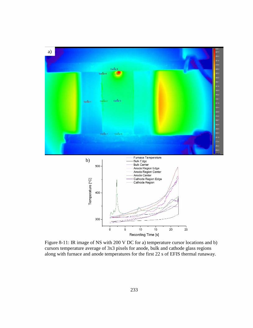
233
Figure 8-11: IR image of NS with 200 V DC for a) temperature cursor locations and b)
cursors temperature average of 3x3 pixels for anode, bulk and cathode glass regions
along with furnace and anode temperatures for the first 22 s of EFIS thermal runaway.
a)
b)

234
a)
b)
Fig
ure
8-1
2:
IR i
mag
es o
f 2
L8
NS
wit
h 1
50 V
appli
ed. T
he
form
atio
n o
f an
alkal
i-ri
ch p
has
e ca
n b
e se
en g
row
ing f
rom
cat
hod
e to
anode
at a
) sa
mple
tem
per
ature
of
575
°C a
nd b
) co
nti
nued
gro
wth
at
600
°C. T
he
alkal
i-ri
ch p
has
e
circ
led.

235
a)
b)
Figure 8-13: IR images of NS with 150 V applied in DC at a) run
time=2069.4 s and furnace temperature=353.5°C and b) run time=2108.5 s
and furnace temperature=363.6°C. Note: Color scale was not updated but
hottest pixel is identified with accurate temperature reading.

236
Figure 8-14: IR images of NS with 150 V 1000 Hz applied in AC at a) run
time=2130 s and furnace temperature=385.3°C and b) run time=2403 s
and furnace temperature=428.6°C. Note: Color scale was not updated but
hottest pixel is identified with accurate temperature reading.
a)
b)

237
Figure 8-15: Simulated a) electric potential and b) temperature profiles of NS resulting
from self-heating at 1 s intervals over 30 s total with 200 V DC applied at an initial
temperature of 277°C. The anode/glass interface is located at 0 mm while glass/cathode
interface at 10 mm in the model.
a)
b)

238
Figure 8-16: Model calculations of thermal runaway of NS at various initial temperatures
with a depletion layer thickness of 100 nm for a) current during 30 s of self-heating and
b) thermal profile at 30 s. Note: Current limit reach is a result of heat generation versus
heat loss.
a)
b)

239
Figure 8-17: Thermal profiling at 30 s of self-heating as a function of depletion layer
thickness. Below 100 nm, heat loss from the depletion layer occurs rapidly. Above 100
nm the depletion layer resistivity limits the current as a negative feedback.
Figure 8-18: Calculated blackbody radiation spectra during thermal runaway.
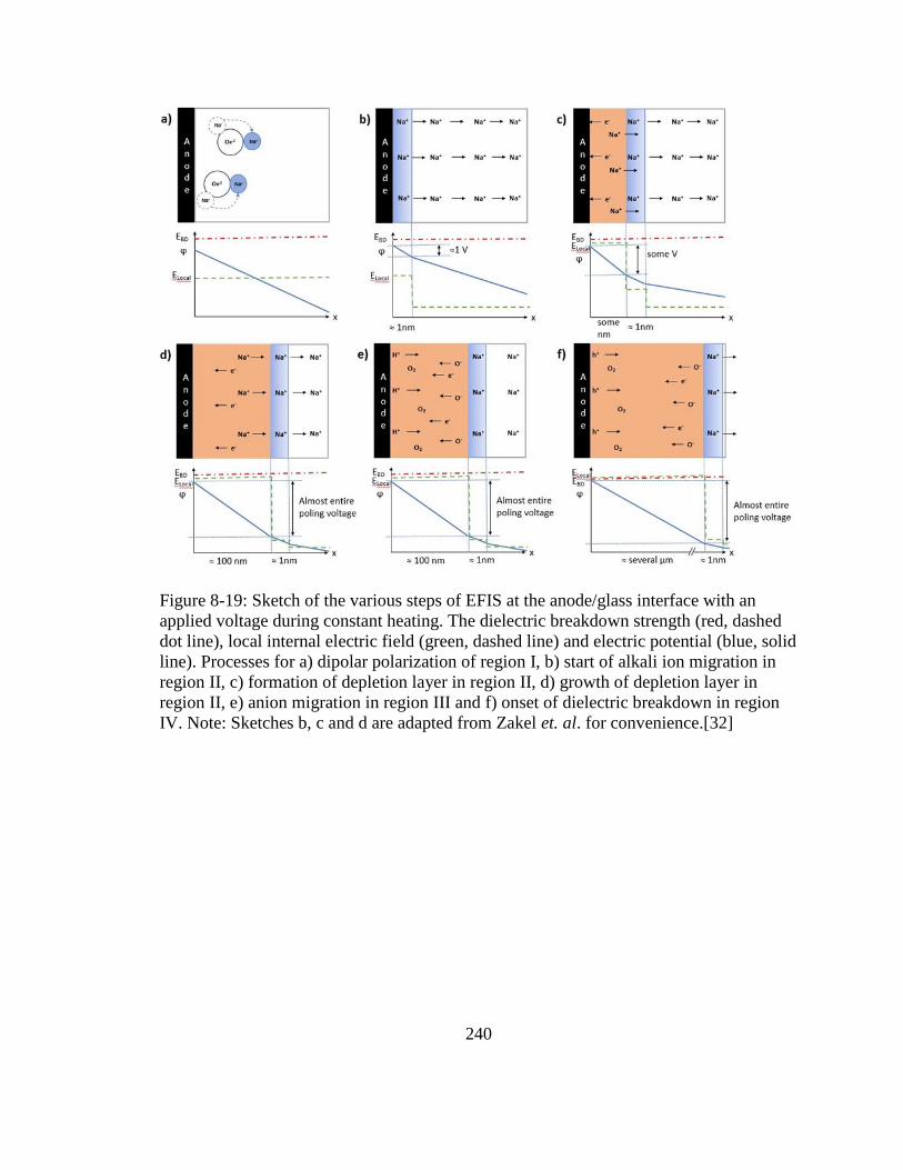
240
Figure 8-19: Sketch of the various steps of EFIS at the anode/glass interface with an
applied voltage during constant heating. The dielectric breakdown strength (red, dashed
dot line), local internal electric field (green, dashed line) and electric potential (blue, solid
line). Processes for a) dipolar polarization of region I, b) start of alkali ion migration in
region II, c) formation of depletion layer in region II, d) growth of depletion layer in
region II, e) anion migration in region III and f) onset of dielectric breakdown in region
IV. Note: Sketches b, c and d are adapted from Zakel et. al. for convenience.[32]
241
Chapter 9: Conclusions and future work
9.1 Conclusions
This dissertation has studied electric field-induced softening as an innovative
processing technique that could readily obtain savings by both energy reduction and
processing time of glass forming. Not only does this technique allow for cost savings but
it also opens avenues for glass surface patterning, shaping and controlled compositional
modifications. Understanding the underlying mechanism and dependencies of EFIS were
crucial to tailoring the effect to create a processing technique with its desired outcome.
The objectives of this dissertation were outlined in Chapter 2. These were to seek
answers to the following questions: (1) Is there a viable electric field-induced softening
phenomenon? (2) What are the quantitative dependences of EFIS such as glass
composition and applied voltage? (3) What mechanisms are responsible for EFIS? (4)
How can EFIS be appropriately modeled and optimized for glass industry use? This final
chapter summarizes how the results of the previous chapters have addressed these
questions.
In this dissertation, electric field-induced softening has been reported as a viable glass
softening phenomenon that occurs in bulk glass in both DC and AC. The quantitative
reduction in furnace temperature for EFIS depends on multiple parameters: glass
resistivity, applied voltage, frequency, current limit and heating rate. The observed
reduction in furnace temperature for glass softening ranged from essentially nothing up to
almost 200°C. The applied pressure determines only the rate of viscous flow during EFIS
of the glass samples.

242
There are many underlying processes that occur which form the mechanism of EFIS
of alkali silicate glasses. Upon heating the sample at constant rate under electric field
first, dipolar polarization of alkali ions occurs where the cations align with the external
electric field around their associated non-bridging oxygen in short-range movement.
Next, the alkali ions migrate away from their non-bridging oxygen charge compensating
centers via long-range movements. This migration forms an alkali ion depletion layer
near the positively charge electrode. Growth of the depletion layer continues until almost
the entirety of the applied voltage drops across it. The depletion layer thickness prior to
field induced melting is shown to be on the order of 100 nm thick by ToF-SIMS. Since
almost all the voltage drops across this thin layer, a large internal electric field is created,
which induces mixed ionic-electronic conduction. At higher furnace temperatures anion
migration and proton injection can also occur within the depletion layer. Eventually, at
high enough furnace temperatures the local electric field strength exceeds the dielectric
breakdown strength of the depletion layer. Conditions conducive for dielectric
breakdown occur and large current passes through the sample. The amount of power
dissipation determines the resistive heating and positive feedback of thermal runaway.
Temperatures above 1300°C were regularly reached within the glass closest to the
positive electrode as demonstrated by thermal imaging. The competition between heat
generation and heat loss determines the temperature profile of the glass sample. Heat
transfer of thermal runaway within the modified glass region nearest the positive
electrode into the bulk increases the overall sample temperature leading to the observed

243
EFIS. Post-mortem samples had depletion layer thicknesses of about 50 µm as measured
by EDS.
Modeling of EFIS has been accomplished successfully using two finite element
analyses. The first model focused on charge carrier migrations to predict alkali ion
depletion layer formation and its properties. The second model gave insight into the
process of thermal runaway that could occur during EFIS. An important insight gained
from modeling was the temperature profile’s dependence on depletion layer thickness.
The model showed that as the thickness grew toward 50 µm, the current was suppressed
thereby the localized heating was limited. This observation from FEA explains how the
breakdown process continued to move across the anode/glass interface as observed
experimentally in videos.
The combination of the two finite element models could be used to tailor shaping
techniques used within the glass industry. For example, if it is known that a certain
temperature is needed within the glass to create an imprint or bulk softening, the
temperature profile can be predicted with FEA. It has been shown that the temperature
profile heavily depends on the thickness of the depletion layer in DC. Therefore, the
thermal profile can be tailored by controlling the depletion layer thickness. From the
charge carrier model and experimental data, we show that voltage, temperature and time
determine the depletion layer thickness. We also show that pressure can be tailored to
achieve specific displacement rates upon viscous flow of glass. The technique could also
be tailored by changing the geometry of the anode to allow for surface or near surface

244
feature imprinting. These combinations of process parameters can become a powerful
tool in the future of glass forming in industry.
9.2 Future work
9.2.1 Low-frequency depletion layer formation
Upon investigation of thermally stimulated current densities with AC voltages using
NS, a decrease in electrical conductivity was observed prior to thermal runaway on a few
samples. The electrical conductivity of glass should always be increasing with
temperature below Tg. A ‘dip’ in current density with increasing temperature is shown in
Figure 9-1 by the red arrow. This decrease in current density at higher temperatures was
observed only with three samples and they were treated the same as the samples shown in
Figure 7-8a which did not show the dip in current. However, this decrease in current
density could not be reproduced after these initial three runs for 60 Hz, 125 Hz and 125
Hz repeat. Therefore, further work should be conducted at lower frequencies to
investigate plausible causes.
It is initially thought that this decrease in current density with temperature is a result
of the formation of an alkali ion depletion layer similar to the DC case. From the current
density decay results of electro-thermal poling NS in Figure 6-8, a majority of the charge
flow occurs quickly upon application of the DC voltage. For example, let us assume a
depletion layer of about 30 nm is large enough to impede further current density and
cause a dip similar to the decrease seen in region II depletion. A 30 nm depletion layer
would correspond to a charge density of approximately 4.8x10⁻³ C/cm2. The decrease in
current density occurred at about 5x10⁻² A/cm2 corresponding to a time to form a 30 nm
245
depletion layer being around 100 ms which is 10 Hz. However, the depletion layer should
only be formed every half-cycle suggesting a frequency of 5 Hz is needed for a sufficient
amount of charge to pass instead. Thicker depletion layer formations would require
longer times further reducing the associated frequency. Although this approximation
suggests that the decrease in current density is not likely due to the formation of a
depletion layer at 60 or 125 Hz, such an impeding layer could be a possibility at slightly
lower frequencies.
EFIS at lower frequencies could yield interesting depletion layer dependencies in the
range of 0.1 Hz up to 10 Hz. There is a lack of literature on the effects of alkali ion
depletion layer on electrical characteristics of glass at low frequencies and could be an
interesting topic to explore. The current AC power supply relies on driving a transformer
to achieve the high voltage and unsuitable at frequencies below 60 Hz. The AC driving
system would need to be redesigned to accommodate this change.
9.2.2 EFIS with in situ impedance spectroscopy
The dielectric characteristics of the depletion layer can further be investigated by
superimposing a comparatively small AC voltage (1 to 2 Vrms) for in situ impedance
spectroscopy together with a larger DC voltage (100 to 200 V). A similar study was
conducted where following each thermally stimulated current peak the sample was held
isothermally while a frequency sweep was measured.[53] The application of in situ
impedance spectroscopy has also demonstrated that the dielectric constant with respect to
frequency for each equivalent circuit can be calculated.[53] If this is done for EFIS, the
temperature dependence of each thermally stimulated regions could be determined.

246
It is expected that the impedance of the alkali ion depletion layer increases with
temperature during EFIS. However, once the depletion layer has grown to a maximum
thickness the impedance is expected to level off. The capacitance can be used to estimate
the in situ depletion layer thickness.[36] The main purpose of this technique would be to
confirm the thermally stimulated peak in region III of Figure 7-1 as anion migration and
to track the dielectric constant until dielectric breakdown. The main challenge will be that
EFIS is done at a constant heating rate and dielectric breakdown occurs within
milliseconds. The frequency sweep (10-2 to 104 Hz) for impedance spectroscopy can take
approximately two minutes meaning that the sample is changing on a time scale faster
than a single spectrum can measure. To address this, a slower heating rate can be
implemented expecting a shift in current density with temperature as seen in Figure 7-7.
A reduction in heating rate shifts EFIS to higher temperatures allowing for longer times
to complete a frequency sweep prior to dielectric breakdown.
9.2.3 Alkali ion concentration study
The dependence of EFIS on alkali concentration can be investigated using several
potassium germanate glass compositions. A large variation in alkali content can be
achieved using germanium as the glassy network formers due to the absence of phase
separation that is observed in sodium silicate glass system.[143,144] A series of a xK2O ●
(1-x) GeO2 where x ranges from 0.02 to 0.2 will vary the alkali content by an order of
magnitude. It is hypothesized that the EFIS effect will be dramatically reduced with a
decrease in alkali content since EFIS has already been shown to be highly dependent on
glass resistivity. However, it will be interesting to compare the alkali ion depletion layer

247
thickness dependence on parent glass composition. From space charge theory developed
by Von Hippel, the alkali ion depletion layer thickness should be inversely proportional
to the square root of mobile ion concentration.[69] However, it has been reported that this
model appears to be too simple for highly alkali-rich systems, and we need to account for
a second charge carrier beyond alkali ion migration.[33,145,146] A coherent model for
depletion layer thickness that works with a wider range of alkali ion concentration is
lacking and further investigation such as the one proposed here are needed. It is possible
that a change in alkali content rearranges network structure, which may affect subsequent
alkali ion depletion layer formation.[144]
9.2.4 Photoemission origin
Though it is believed that the photoemission from alkali disilicate glass occurs due to
hole injection during dielectric breakdown, further experiments should be done for
confirmation. It has been suggested that the characteristic peaks originate from the
oxidation of alkali ions.[21] Two experiments can be done to verify these interpretations
as electron or plasma excitations. First, a study can be done in collaboration with the
Princeton Plasma Physics Laboratory for determining if the photoemissions are due to
plasma that is generated from extreme localized temperatures. This can be done using a
special high speed camera along with high speed current measurements. The
photoemissions of a plasma can be categorized in three ways; hot plasma, strongly
ionized plasma or weakly ionized plasma.[147] It is likely that the photoemissions
observed during EFIS fit into the strongly ionized plasma category. In such plasma the

248
photoemission spectra is determined by both the long-range Coulomb forces and the
internal structure of particles (atoms or ions) with their collision kinetics.[147]
A second study would be to construct the electronic band structure of the modified
alkali ion depletion layer. This can be done by using a specialized XPS technique that
measures the near zero binding energy region of the spectrum, which contains
information about the valence band.[148] From here, the donor and acceptor levels within
the bandgap could be found and possibly account for the short-wavelength limit of 3.5 eV
of EFIS photoemissions. It was expected that the limit would have a larger energy
associated with dielectric breakdown. This was assumed if the alkali ion depletion layer
composition is similar to silica where the bandgap is larger compared to the parent glass
composition. However, small amounts of alkali could reduce the bandgap energy to the
observed value.
9.2.5 Finite element model refinement
The charge carrier and thermal heat transfer models can be combined to investigate
the entire EFIS from room temperature to softening temperatures. This comprehensive
model of EFIS will allow the process to be tailored for specific heat profiles within the
glass samples. To achieve this, the diffusion and migration terms will need to become
temperature dependent while the entire model is heated externally. Also, the mesh scale
difference between mass transport and heat transfer will need to be compensated. It was
found during FEA that mass transport occurs on a finer mesh scale than heat transfer.
Running the whole simulation with a finer mesh size will require larger computing power
than by splitting the two simulations performed here.
249
The model could also be expanded to include all compositions presented in this
dissertation. In addition, if the material properties are well known for other glasses the
model could be used to predict the behavior of glass not yet tested for EFIS. A step
further could relate the viscous behavior of each glass composition to the thermal profile
during EFIS. The effect of Joule heating could be used to calculate deformation when a
pressure is applied to the boundary conditions.
Lastly, all finite element modeling only considered the effect of DC voltages on NS
glass. The model could be expanded to include a parametric sweep of AC frequencies. At
low frequencies (<60 Hz) the formation and annihilation of alkali ion depletion layer is
expected, whereas at higher frequencies (above RF range) the ion response is not
expected to be affected by the oscillating voltage. The application of AC field can also be
used to calculate the temperature profile that is expected to be symmetric as seen in
thermal imaging such as seen in Figure 8-14. The applied voltage and frequency could be
tailored in the simulation to control EFIS behavior.

250
Figure 9-1: Frequency dependence of current density of NS during heating at 10°C/min
for EFIS with 150 V. The red arrow indicates decrease in current density for 60 Hz and
125 Hz samples.

251
References
[1] R.H. Doremus, Glass science, Wiley, 1994.
[2] J.E. Shelby, Introduction to Glass Science and Technology, Royal Society of
Chemistry, 2005.
[3] A.K. Varshneya, Fundamentals of Inorganic Glasses, Elsevier, 2013.
[4] M.D. Ingram, Ionic conductivity in glass, Phys. Chem. Glas. 28 (1987) 215–234.
[5] D.E. Carlson, K.W. Hang, G.F. Stockdale, Electrode “Polarization” in Alkali-
Containing Glasses, J Am Ceram Soc. 55 (1972) 337.
[6] D.E. Carlson, Ion Depletion of Glass at a Blocking Anode: I, Theory and
Experimental Results for Alkali Silicate Glasses, J. Am. Ceram. Soc. 57 (1974)
291–294. doi:10.1111/j.1151-2916.1974.tb10903.x.
[7] N. Ikutame, K. Kawaguchi, H. Ikeda, D. Sakai, K. Harada, S. Funatsu, J. Nishii,
Low-temperature fabrication of fine structures on glass using electrical nanoimprint
and chemical etching, J Appl Phys. 114 (2013) 83514.
[8] K.M. Knowles, A.T.J. van Helvoort, Anodic bonding, Int. Mater. Rev. 51 (2006)
273–311. doi:10.1179/174328006X102501.
[9] A. Lipovskii, M. Kuittinen, P. Karvinen, K. Leinonen, V. Melehin, V. Zhurikhina,
Y. Svirko, Electric field imprinting of sub-micron patterns in glass-metal
nanocomposites, Nanotechnology. 19 (2008) 415304.
[10] S. Youn, H. Takagi, S. Park, M. Takahashi, R. Maeda, Surface Patterning of Glass
via Electrostatic Imprinting Using a Platinum Mold, J Nanosci Nanotechnol. 12
(2012) 3181.
[11] K. Bange, H. Jain, C. Pantano, Making Glass Better, International Commission on
Glass, Madrid, 2015.
[12] C.P. Ross, G.L. Tincher, Glass Melting Technology: A Technical and Economic
Assessment, Glass Manufacturing Industry Council, Westerville, 2004.
[13] D.-S. Park, M.-W. Cho, H. Lee, W.-S. Cho, Micro-grooving of glass using micro-
abrasive jet machining, J. Mater. Process. Technol. 146 (2004) 234–240.
doi:10.1016/j.jmatprotec.2003.11.013.
[14] X.D. Cao, B.H. Kim, C.N. Chu, Micro-structuring of glass with features less than
100 μm by electrochemical discharge machining, Precis. Eng. 33 (2009) 459–465.
doi:10.1016/j.precisioneng.2009.01.001.
[15] M.D. Perry, B.C. Stuart, P.S. Banks, M.D. Feit, V. Yanovsky, A.M. Rubenchik,
Ultrashort-pulse laser machining of dielectric materials, J. Appl. Phys. 85 (1999)
6803–6810. doi:10.1063/1.370197.
[16] J. Holtkamp, A. Gillner, Laser-assisted hot embossing of microstructures, in: 3rd
Pac. Int. Conf. Appl. Lasers Opt. PICALO 2008 Conf. Proc. CD-ROM, 2008: pp.
801–806.
[17] M. Cologna, B. Rashkova, R. Raj, Flash Sintering of Nanograin Zirconia in <5 s at
850°C, J. Am. Ceram. Soc. 93 (2010) 3556–3559. doi:10.1111/j.1551-
2916.2010.04089.x.
[18] K.S. Naik, V.M. Sglavo, R. Raj, Field assisted sintering of ceramic constituted by
alumina and yttria stabilized zirconia, J. Eur. Ceram. Soc. 34 (2014) 2435–2442.
doi:10.1016/j.jeurceramsoc.2014.02.042.

252
[19] M. Cologna, J.S.C. Francis, R. Raj, Field assisted and flash sintering of alumina and
its relationship to conductivity and MgO-doping, J Eur Ceram Soc. 31 (2011) 2827.
[20] R. Raj, Joule heating during flash-sintering, J Eur Ceram Soc. 32 (2012) 2293.
[21] M. Yu, S. Grasso, R. Mckinnon, T. Saunders, M.J. Reece, Review of flash sintering:
materials, mechanisms and modelling, Adv. Appl. Ceram. 116 (2017) 24–60.
doi:10.1080/17436753.2016.1251051.
[22] H. Conrad, Space Charge and the Dependence of the Flow Stress of Ceramics on an
Applied Electric Field, Scr. Mater. 44 (2001) 311.
[23] R.I. Todd, E. Zapata-Solvas, R.S. Bonilla, T. Sneddon, P.R. Wilshaw, Electrical
characteristics of flash sintering: thermal runaway of Joule heating, J Eur Ceram
Soc. 35 (2015) 1865.
[24] K.S. Naik, V.M. Sglavo, R. Raj, Flash sintering as a nucleation phenomenon and a
model thereof, J. Eur. Ceram. Soc. 34 (2014) 4063–4067.
doi:10.1016/j.jeurceramsoc.2014.04.043.
[25] R. Muccillo, E.N.S. Muccillo, Electric field assisted sintering of electroceramics and
in situ analysis by impedance spectroscopy, J. Electroceramics. 38 (2017) 24–42.
doi:10.1007/s10832-016-0054-x.
[26] M.C. Steil, D. Marinha, Y. Aman, J.R.C. Gomes, M. Kleitz, From conventional ac
flash-sintering of YSZ to hyper-flash and double flash, J Eur Ceram Soc. 33 (2013)
2093.
[27] C. Schmerbauch, J. Gonzalez-Julian, R. Röder, C. Ronning, O. Guillon, Flash
Sintering of Nanocrystalline Zinc Oxide and its Influence on Microstructure and
Defect Formation, J Am Ceram Soc. 97 (2014) 1728.
[28] M. Dussauze, T. Cremoux, F. Adamietz, V. Rodriguez, E. Fargin, G. Yang, T.
Cardinal, Thermal Poling of Optical Glasses: Mechanisms and Second-Order
Optical Properties, Int J Appl Glass Sci. 3 (2012) 309.
[29] A. Kudlinkski, G. Martinelli, Y. Quiquempois, Time evolution of second-order
nonlinear profiles induced within thermally poled silica samples, Opt. Lett. 30
(2005) 1039.
[30] A. Kudlinkski, Y. Quiquempois, G. Martinelli, Modeling of the X(2) susceptibility
time-evolution in thermally poled fused silica, Opt. Express. 13 (2005) 8015.
[31] C. Corbari, L.C. Ajitdoss, I.C.S. Carvalho, O. Deparis, F.P. Mezzapesa, P.G.
Kazansky, K. Sakaguchi, The problem of achieving high second-order nonlinearities
in glasses: The role of electronic conductivity in poling of high index glasses, J
Non-Cryst Solids. 356 (2010) 2742.
[32] J. Zakel, M. Balabajew, B. Roling, On the mechanism of field-induced mixed ionic–
electronic transport during electro-thermal poling of a bioactive sodium–calcium
phosphosilicate glass, Solid State Ion. 265 (2014) 1–6.
doi:10.1016/j.ssi.2014.07.003.
[33] C.R. Mariappan, B. Roling, Mechanism and kinetics of Na+ ion depletion under the
anode during electro-thermal poling of a bioactive glass, J Non-Cryst Solids. 356
(2010) 720.

253
[34] A.L. Moura, M.T. de Araújo, E.A. Gouveia, M.V.D. Vermelho, Deep and shallow
trap contributions to the ionic current in the thermal-electric field poling in soda-
lime glasses, Opt. Express. 15 (2007) 143.
[35] C.M. Lepienski, J.A. Giacometti, G.F.L. Ferreira, F.L. Freire Jr., C.A. Achete,
Electric field distribution and near-surface modifications in soda-lime glass
submitted to a dc potential, J Non-Cryst Solids. 159 (1993) 204.
[36] J. Zakel, V. Heddinga, S.O. Steinmüller, B. Roling, Investigation of sodium ion
depletion layers in electrothermally poled bioglasses by combining impedance
spectroscopy with ToF-SIMS depth profiling, Solid State Ion. 237 (2013) 46–49.
doi:10.1016/j.ssi.2013.02.011.
[37] C.R. Mariappan, B. Roling, Investigation of bioglass–electrode interfaces after
thermal poling, Solid State Ion. 179 (2008) 671–677. doi:10.1016/j.ssi.2008.04.032.
[38] J. Kruempelmann, C.R. Mariappan, B. Roling, Electrochemical double layers at the
interface between glassy electrolytes and platinum: Differentiating between the
anode and the cathode capacitance, Phys Rev B. 82 (2010) 224203.
[39] U.K. Krieger, W.A. Lanford, Field assisted transport of Na+ ions, Ca2+ ions and
electrons in commercial soda-lime glass I: Experimental, J Non-Cryst Solids. 102
(1988) 50.
[40] A.L.R. Brennand, Thermal Poling of Multioxide Silicate Glasses and Ion-
Exchanged Waveguides, University of Southampton, 2002.
[41] M. Dussauze, V. Rodriguez, A. Lipovskii, M. Petrov, C. Smith, K. Richardson, T.
Cardinal, E. Fargin, E.I. Kamitsos, How Does Thermal Poling Affect the Structure
of Soda-Lime Glass?, J Phys Chem C. 114 (2010) 12754.
[42] E.C. Ziemath, V.D. Araújo, C.A. Escanhoela, Compositional and structural changes
at the anodic surface of thermally poled soda-lime float glass, J. Appl. Phys. 104
(2008) 54912. doi:10.1063/1.2975996.
[43] N.J. Smith, C.G. Pantano, Structural and compositional modification of a barium
boroaluminosilicate glass surface by thermal poling, Appl. Phys. A. 116 (2014)
529–543. doi:10.1007/s00339-014-8467-3.
[44] T. Cremoux, M. Dussauze, E. Fargin, T. Cardinal, D. Talaga, F. Adamietz, V.
Rodriguez, Trapped Molecular and Ionic Species in Poled Borosilicate Glasses:
Toward a Rational Description of Thermal Poling in Glasses, J Phys Chem C. 118
(2014) 3716.
[45] A. Lepicard, T. Cardinal, E. Fargin, F. Adamietz, V. Rodriguez, K. Richardson, M.
Dussauze, Surface Reactivity Control of a Borosilicate Glass Using Thermal Poling,
J. Phys. Chem. C. 119 (2015) 22999–23007. doi:10.1021/acs.jpcc.5b07139.
[46] G.N. Greaves, K.L. Ngai, Reconciling ionic-transport properties with atomic
structure in oxide glasses, Phys Rev B. 52 (1995) 6358.
[47] M. Schäfer, K.-M. Weitzel, Numerical model for electro-poling, Solid State Ion.
282 (2015) 70.
[48] M.B. Dutt, D.E. Day, Origin of thermally stimulated currents in oxide glasses, J.
Non-Cryst. Solids. 71 (1985) 125–132. doi:10.1016/0022-3093(85)90281-9.

254
[49] M.B. Dutt, D.E. Day, Effects of Modes of Formation on the Structure of Glass
Origin of thermally stimulated currents in oxide glasses, J. Non-Cryst. Solids. 71
(1985) 125–132. doi:10.1016/0022-3093(85)90281-9.
[50] A. Pradel, D.E. Day, Origin of thermally stimulated currents in sodium silicate
glasses, J. Non-Cryst. Solids. 99 (1988) 59–64. doi:10.1016/0022-3093(88)90457-7.
[51] A. Doi, Thermally stimulated currents in lithium-sodium disilicate glasses, J. Mater.
Sci. 17 (1982) 2087–2094. doi:10.1007/BF00540427.
[52] A. Doi, T. Ishikawa, Pulse generation in thermally stimulated current of soda-lime
silicate glass, Solid State Ion. 37 (1990) 183–188. doi:10.1016/0167-
2738(90)90241-I.
[53] A. Doi, Y. Menjou, T. Ishikawa, Y. Abe, Generation and annihilation of positive
and negative ion‐depleted region in soda‐lime silicate glass, J. Appl. Phys. 67
(1990) 691–697. doi:10.1063/1.345773.
[54] C.-M. Hong, D.E. Day, Thermally Stimulated Currents in Sodium Silicate Glasses,
J. Am. Ceram. Soc. 64 (1981) 61–68. doi:10.1111/j.1151-2916.1981.tb09577.x.
[55] J. Plans, M. Zieliński, M. Kryszewski, Theory of the thermally-stimulated-current
transport peak. Application to a dispersive transport case, Phys. Rev. B. 23 (1981)
6557–6569. doi:10.1103/PhysRevB.23.6557.
[56] R. Chen, Methods for kinetic analysis of thermally stimulated processes, J. Mater.
Sci. 11 (n.d.) 1521–1541. doi:10.1007/BF00540887.
[57] C.-M. Hong, D.E. Day, Thermally stimulated polarization and depolarization
current (TSPC/TSDC) techniques for studying ion motion in glass, J. Mater. Sci. 14
(1979) 2493. doi:10.1007/BF00737040.
[58] L.L. Hench, H.F. Schaake, Electrical Properties of Glass, in: L.D. Pye, H.J. Stevens,
W.C. LaCourse (Eds.), Introd. Glass Sci., Springer US, 1972: pp. 583–659.
http://link.springer.com/chapter/10.1007/978-1-4757-0328-3_19 (accessed
December 9, 2016).
[59] D.J. Dumin, Oxide Reliability: A Summary of Silicon Oxide Wearout, Breakdown,
and Reliability, World Scientific, 2002.
[60] R. Bartnikas, R.M. Eichhorn, Engineering Dielectrics, Volume IIA, Electrical
Properties of Solid Insulating Materials: Molecular Structure and Electrical
Behavior - STP 783, American Society for Testing & Materials, 1983.
[61] R.J. Charles, Polarization and Diffusion in a Silicate Glass, J. Appl. Phys. 32 (1961)
1115–1126. doi:10.1063/1.1736169.
[62] L.L. Hench, J.K. West, Principles of electronic ceramics, Wiley, 1990.
[63] J.J. O’Dwyer, The theory of electrical conduction and breakdown in solid
dielectrics, Clarendon Press, 1973.
[64] A.R.V. Hippel, Dielectrics and Waves, Artech House, 1995.
[65] K.J. Keller, Breakdown and electric conductivity of glass, Physica. 17 (1951) 511–
530. doi:10.1016/0031-8914(51)90016-X.
[66] J. Vermeer, On the relation between ionic conductivity and breakdown strength of
glass, Physica. 22 (1956) 1269–1278. doi:10.1016/S0031-8914(56)90219-1.
[67] J. Vermeer, The electric strengths of glasses with different sodium contents,
Physica. 22 (1956) 1247–1253. doi:10.1016/S0031-8914(56)90216-6.

255
[68] S.O. Kasap, Principles of Electronic Materials and Devices, McGraw-Hill, New
York, 2006.
[69] A. von Hippel, E.P. Gross, J.G. Jelatis, M. Geller, Photocurrent, Space-Charge
Buildup, and Field Emission in Alkali Halide Crystals, Phys. Rev. 91 (1953) 568–
579. doi:10.1103/PhysRev.91.568.
[70] P.P. Budenstein, On the Mechanism of Dielectric Breakdown of Solids, IEEE Trans.
Electr. Insul. EI-15 (1980) 225.
[71] B.K. Ridley, Mechanism of electrical breakdown in SiO2 films, J Appl Phys. 46
(1975) 998.
[72] G. Chen, J. Zhao, S. Li, L. Zhong, Origin of thickness dependent dc electrical
breakdown in dielectrics, Appl Phys Lett. 100 (2012) 222904.
[73] N.J. Smith, M.T. Lanagan, C.G. Pantano, Thermal poling of alkaline earth
boroaluminosilicate glasses with intrinsically high dielectric breakdown strength, J.
Appl. Phys. 111 (2012) 83519. doi:10.1063/1.3703679.
[74] R.E. Jorgenson, L.K. Warne, A.A. Neuber, J. Krile, J. Dickens, H. Krompholz,
Effect of Dielectric Photoemission on Surface Breakdown: An Ldrd Report, Sandia
National Labs., Albuquerque, NM (US); Sandia National Labs., Livermore, CA
(US), 2003. https://www.osti.gov/scitech/biblio/811483 (accessed April 3, 2017).
[75] P.G. Kazansky, P.S.J. Russell, H. Takebe, Glass fiber poling and applications, J.
Light. Technol. 15 (1997) 1484–1493. doi:10.1109/50.618381.
[76] D.E. Day, Mixed alkali glasses — Their properties and uses, J. Non-Cryst. Solids.
21 (1976) 343–372. doi:10.1016/0022-3093(76)90026-0.
[77] H. Jain, Measurement of Electrical Conductivity of Glasses, in: C.J. Simmons, O.H.
El-Bayoumi (Eds.), Exp. Tech. Glass Sci., American Ceramic Society, 1993: pp.
433–461.
[78] Vernier Software, LoggerPro 3, Version 3 (2009)
http://www.vernier.com/products/software/lp/.
[79] D.E. Carlson, K.W. Hang, G.F. Stockdale, Ion Depletion of Glass at a Blocking
Anode: II, Properties of Ion-Depleted Glasses, J. Am. Ceram. Soc. 57 (1974) 295–
300. doi:10.1111/j.1151-2916.1974.tb10904.x.
[80] A.V. Naumkin, A. Kraut-Vass, S.W. Gaarenstroom, C.J. Powell, NIST X-ray
Photoelectron Spectroscopy (XPS) Database, Version 3.5, (n.d.).
https://srdata.nist.gov/xps/ (accessed February 20, 2017).
[81] E. Barsoukov, J.R. MacDonald, Impedance Spectroscopy Theory, Experiment, and
Applications, John Wiley & Sons, Inc., Hoboken, 2005.
[82] N.P. Bansal, R.H. Doremus, Handbook of Glass Properties, Academic Press, Inc.,
Orlando, 1986.
[83] M. Tomozawa, R.H. Doremus, Glass I: Interaction with Electromagnetic Radiation:
Treatise on Materials Science and Technology, Elsevier, 2013.
[84] M. Tomozawa, Structure of mixed alkali glasses, J Non-Cryst Solids. 196 (1996)
280.
[85] A.L.C. Triques, C.M.B. Cordeiro, V. Balestrieri, B. Lesche, W. Margulis, I.C.S.
Carvalho, Depletion region in thermally poled fused silica, Appl. Phys. Lett. 76
(2000) 2496–2498. doi:10.1063/1.126387.

256
[86] R. Raj, Analysis of the Power Density at the Onset of Flash Sintering, J. Am.
Ceram. Soc. 99 (2016) 3226–3232. doi:10.1111/jace.14178.
[87] J.S.C. Francis, R. Raj, Flash-Sinterforging of Nanograin Zirconia: Field Assisted
Sintering and Superplasticity, J. Am. Ceram. Soc. 95 (2012) 138–146.
doi:10.1111/j.1551-2916.2011.04855.x.
[88] C.F.J. Garlick, A.F. Gibson, The Electron Trap Mechanism of Luminescence in
Sulphide and Silicate Phosphors, Proc Phys Soc. A60 (1948) 574.
[89] A.K. Jonscher, Dielectric Relaxation in Solids, Chelsea Dielectric Press, London,
1983.
[90] L.A. McDonnell, R.M.A. Heeren, Imaging Mass Spectrometry, Mass Spectrom.
Rev. 26 (2007) 606.
[91] Sputtering by Particle Bombardment III - Characteristics of | Rainer Behrisch |
Springer, n.d. http://www.springer.com/us/book/9783662311042 (accessed
February 3, 2017).
[92] A. Sharma, H. Jain, A.C. Miller, Surface modification of a silicate glass during XPS
experiments, Surf. Interface Anal. 31 (2001) 369–374. doi:10.1002/sia.983.
[93] R. Chen, Review: Methods for kinetic analysis of thermally stimulated processes, J
Mater Sci. 11 (1976) 1521.
[94] D.J. DiMaria, J.H. Stathis, Anode hole injection, defect generation, and breakdown
in ultrathin silicon dioxide films, J. Appl. Phys. 89 (2001) 5015–5024.
doi:10.1063/1.1363680.
[95] K.F. Schuegraf, C. Hu, Hole injection SiO2 breakdown model for very low voltage
lifetime extrapolation, IEEE Trans. Electron Devices. 41 (1994) 761–767.
doi:10.1109/16.285029.
[96] A.K. Agarwal, D.E. Day, Polarization and Conduction Mechanism in Mixed-Alkali
Glasses, J. Am. Ceram. Soc. 65 (1982) 231–237. doi:10.1111/j.1151-
2916.1982.tb10424.x.
[97] H.D. Jannek, D.E. Day, Sodium Motion in Phase-Separated Sodium Silicate
Glasses, J. Am. Ceram. Soc. 64 (1981) 227–233. doi:10.1111/j.1151-
2916.1981.tb10274.x.
[98] A. Doi, K. Watanabe, Conduction in the positive-ion depleted region of alkali borate
glasses, Solid State Ion. 104 (1997) 215–225. doi:10.1016/S0167-2738(97)00431-1.
[99] M.A. Lamkin, F.L. Riley, R.J. Fordham, Oxygen mobility in silicon dioxide and
silicate glasses: a review, J. Eur. Ceram. Soc. 10 (1992) 347–367.
doi:10.1016/0955-2219(92)90010-B.
[100] R.H. Doremus, Transport of oxygen in silicate glasses, J. Non-Cryst. Solids. 349
(2004) 242–247. doi:10.1016/j.jnoncrysol.2004.08.149.
[101] A.V. Redkov, V.G. Melehin, A.A. Lipovskii, How Does Thermal Poling Produce
Interstitial Molecular Oxygen in Silicate Glasses?, J. Phys. Chem. C. 119 (2015)
17298–17307. doi:10.1021/acs.jpcc.5b04513.
[102] D.E. Carlson, Anodic Proton Injection in Glasses, J. Am. Ceram. Soc. 57 (1974)
461–466. doi:10.1111/j.1151-2916.1974.tb11390.x.
257
[103] C. McLaren, W. Heffner, R. Tessarollo, R. Raj, H. Jain, Electric field-induced
softening of alkali silicate glasses, Appl. Phys. Lett. 107 (2015) 184101.
doi:10.1063/1.4934945.
[104] S.K. Shrivastava, J.D. Ranade, A.P. Srivastava, Thermally stimulated discharge
currents in polystyrene films, Thin Solid Films. 67 (1980) 201–206.
doi:10.1016/0040-6090(80)90451-4.
[105] A.K. Jonscher, The “universal” dielectric response, Nature. 267 (1977) 673–679.
doi:10.1038/267673a0.
[106] K. El-Egili, AC conductivity of some alkali borosilicate glasses, J. Phys.
Condens. Matter. 8 (1996) 3419. doi:10.1088/0953-8984/8/19/017.
[107] M. Kitao, Ac Conductivity of Amorphous As2Se3, Jpn. J. Appl. Phys. 11 (1972)
1472. doi:10.1143/JJAP.11.1472.
[108] N.A. Hegab, H.M. El-Mallah, AC Conductivity and Dielectric Properties οf
Amorphous Te 42 As 36 Ge 10 Si 12 Glass, Acta Phys. Pol. A. 116 (2009) 1048–1052.
doi:10.12693/APhysPolA.116.1048.
[109] W.K. Lee, J.F. Liu, A.S. Nowick, Limiting behavior of ac conductivity in
ionically conducting crystals and glasses: A new universality, Phys. Rev. Lett. 67
(1991) 1559–1561. doi:10.1103/PhysRevLett.67.1559.
[110] A.S. Nowick, B.S. Lim, A.V. Vaysleyb, Nature of the ac conductivity of ionically
conducting crystals and glasses, J. Non-Cryst. Solids. 172 (1994) 1243–1251.
doi:10.1016/0022-3093(94)90649-1.
[111] S.R. Elliott, Frequency-dependent conductivity in ionically and electronically
conducting amorphous solids, Solid State Ion. 70 (1994) 27–40. doi:10.1016/0167-
2738(94)90284-4.
[112] A.S. Nowick, A.V. Vaysleyb, W. Liu, Identification of distinctive regimes of
behaviour in the ac electrical response of glasses, Solid State Ion. 105 (1998) 121–
128. doi:10.1016/S0167-2738(97)00457-8.
[113] K. Funke, R.D. Banhatti, L.G. Badr, D.M. Laughman, H. Jain, Toward
understanding the second universality—A journey inspired by Arthur Stanley
Nowick, J. Electroceramics. 34 (2015) 4–14. doi:10.1007/s10832-014-9898-0.
[114] R.J. Charles, Structural State and Diffusion in a Silicate Glass, J. Am. Ceram.
Soc. 45 (1962) 105–113. doi:10.1111/j.1151-2916.1962.tb11094.x.
[115] H. He, J. Luo, L. Qian, C.G. Pantano, S.H. Kim, Thermal Poling of Soda-Lime
Silica Glass with Nonblocking Electrodes—Part 2: Effects on Mechanical and
Mechanochemical Properties, J. Am. Ceram. Soc. 99 (2016) 1231–1238.
doi:10.1111/jace.14080.
[116] M. Dussauze, E.I. Kamitsos, E. Fargin, V. Rodriguez, Structural Rearrangements
and Second-Order Optical Response in the Space Charge Layer of Thermally Poled
Sodium−Niobium Borophosphate Glasses, J. Phys. Chem. C. 111 (2007) 14560–
14566. doi:10.1021/jp074335f.
[117] B.. Veal, D.. Lam, A.. Paulikas, W.. Ching, XPS study of CaO in sodium silicate
glass, Proc. Sixth Univ. Conf. Glass Sci. 49 (1982) 309–320. doi:10.1016/0022-
3093(82)90127-2.

258
[118] C.G. Pantano, X-ray photoelectron spectroscopy of glass, in: C.J. Simmons, O.H.
El-Bayoumi (Eds.), Exp. Tech. Glass Sci., American Ceramic Society, 1993: pp.
123–160.
[119] J.S. Jen, M.R. Kalinowski, An ESCA study of the bridging to non-bridging
oxygen ratio in sodium silicate glass and the correlations to glass density and
refractive index, J. Non-Cryst. Solids. 38 (1980) 21–26. doi:10.1016/0022-
3093(80)90388-9.
[120] G.W. Tasker, D.R. Uhlmann, P.I.K. Onorato, M.N. Alexander, C.W. Struck,
Structure of sodium aluminosilicate glasses: X-ray photoelectron spectroscopy, J.
Phys. Colloq. 46 (1985) C8-273-C8-280. doi:10.1051/jphyscol:1985840.
[121] A.V. Shchukarev, D.V. Korolkov, XPS Study of group IA carbonates, Cent. Eur.
J. Chem. 2 (2004) 347–362. doi:10.2478/BF02475578.
[122] J. Luo, H. He, N.J. Podraza, L. Qian, C.G. Pantano, S.H. Kim, Thermal Poling of
Soda-Lime Silica Glass with Nonblocking Electrodes—Part 1: Effects of Sodium
Ion Migration and Water Ingress on Glass Surface Structure, J. Am. Ceram. Soc. 99
(2016) 1221–1230. doi:10.1111/jace.14081.
[123] D. Ravaine, J. Souquet, Thermodynamic approach to ionic conductivity in oxide
glasses; I, Correlation of the ionic conductivity with the chemical potential of alkali
oxide in oxide glasses, Phys. Chem. Glas. 18 (1977) 27–31.
[124] M.L.F. Nascimento, Test of the Anderson–Stuart model and correlation between
free volume and the “universal” conductivity in sodium silicate glasses, J. Mater.
Sci. 42 (2007) 3841–3850. doi:10.1007/s10853-006-0490-0.
[125] C. McLaren, M. Balabajew, M. Gellert, B. Roling, H. Jain, Depletion Layer
Formation in Alkali Silicate Glasses by Electro-Thermal Poling, J. Electrochem.
Soc. 163 (2016) H809–H817. doi:10.1149/2.0881609jes.
[126] C.E. Moore, P.W. Merrill, Partial Grotrian Diagrams of Astrophysical Interest,
NSRDS Natl. Bur. Stand. 23 (1968).
[127] K. Terauds, J.-M. Lebrun, H.H. Lee, T.Y. Jeon, S.H. Lee, H.J. Je, R. Raj,
Electroluminescence and the measurement of temperature during Stage III of flash
sintering experiments, J Eur Ceram Soc. 35 (2015) 3195.
[128] J.J. de Groot, J.A.J.M. van Vliet, The High-Pressure Sodium Lamp, MacMillan
Education LTD, London, 1986.
[129] M. Rakić, G. Pichler, Comparison of visible and infrared spectrum of light
sources, Opt. Commun. 284 (2011) 2881–2885. doi:10.1016/j.optcom.2011.02.050.
[130] C.D. Elvidge, D.M. Keith, B.T. Tuttle, K.E. Baugh, Spectral Identification of
Lighting Type and Character, Sensors. 10 (2010) 3961–3988.
doi:10.3390/s100403961.
[131] R.V. Grieken, A. Markowicz, Handbook of X-Ray Spectrometry, Second Edition,
CRC Press, 2001.
[132] G.H.J. Sigel, Optical Absorption of Glasses, in: M. Tomozawa, R.H. Doremus
(Eds.), Glass Interact. Electromagn. Radiat. Treatise Mater. Sci. Technol., Elsevier,
2013: pp. 5–82.
[133] R. Williams, Photoemission of Electrons from Silicon into Silicon Dioxide, Phys.
Rev. 140 (1965) A569–A575. doi:10.1103/PhysRev.140.A569.

259
[134] J. Goldstein, D. Newbury, D. Joy, C. Lyman, P. Echlin, E. Lifshin, L. Sawyer, J.
Michael, Scanning Electron Microscopy and X-Ray Microanalysis, Springer, New
York, 2007.
[135] W. Duane, F.L. Hunt, On X-Ray Wave-Lengths, Phys. Rev. 6 (1915) 166–172.
doi:10.1103/PhysRev.6.166.
[136] De Voe Charles F, Electric glass melting furnace and process, US2490339 A,
1949. http://www.google.com/patents/US2490339 (accessed February 3, 2017).
[137] J. Stanek, J. Matej, Electric Melting of Glass, J Non-Cryst Solids. 84 (1986) 353.
[138] N. Zotov, Heat capacity of sodium silicate glasses: comparison of experiments
with computer simulations, J. Phys. Condens. Matter. 14 (2002) 11655.
doi:10.1088/0953-8984/14/45/309.
[139] R. Guidat, O. Lobet, P. Woehl, Systems and methods for scale-up of continuous
flow reactors, WO2012173848 A1, 2012.
http://www.google.com/patents/WO2012173848A1 (accessed April 10, 2017).
[140] R.J.D. Tilley, Colour and the Optical Properties of Materials: An Exploration of
the Relationship Between Light, the Optical Properties of Materials and Colour,
John Wiley & Sons, 2010.
[141] Y. Hiroshima, Y. Hamamoto, S. Yoshida, J. Matsuoka, Thermal conductivity of
mixed alkali silicate glasses at low temperature, J. Non-Cryst. Solids. 354 (2008)
341–344. doi:10.1016/j.jnoncrysol.2007.08.082.
[142] K. Hirao, N. Soga, M. Kunugp, Low-Temperature Heat Capacity and Structure of
Alkali Silicate Glasses, J. Am. Ceram. Soc. 62 (1979) 570–573. doi:10.1111/j.1151-
2916.1979.tb12733.x.
[143] W.C. Huang, H. Jain, G. Meitzner, The structure of potassium germanate glasses
by EXAFS, J. Non-Cryst. Solids. 196 (1996) 155–161. doi:10.1016/0022-
3093(95)00578-1.
[144] H. Verweij, J.H.J.M. Buster, The structure of lithium, sodium and potassium
germanate glasses, studied by Raman scattering, J. Non-Cryst. Solids. 34 (1979) 81–
99. doi:10.1016/0022-3093(79)90008-5.
[145] T.G. Alley, S.R.J. Brueck, R.A. Myers, Space charge dynamics in thermally poled
fused silica, J. Non-Cryst. Solids. 242 (1998) 165–176. doi:10.1016/S0022-
3093(98)00788-1.
[146] V. Pruneri, F. Samoggia, G. Bonfrate, P.G. Kazansky, G.M. Yang, Thermal
poling of silica in air and under vacuum: The influence of charge transport on
second harmonic generation, Appl. Phys. Lett. 74 (1999) 2423–2425.
doi:10.1063/1.123868.
[147] V.N. Ochkin, Spectroscopy of Low Temperature Plasma, John Wiley & Sons,
2009.
[148] D. Foix, H. Martinez, A. Pradel, M. Ribes, D. Gonbeau, XPS valence band
spectra and theoretical calculations for investigations on thiogermanate and
thiosilicate glasses, Chem. Phys. 323 (2006) 606–616.
doi:10.1016/j.chemphys.2005.10.037.

260
Appendix A: Dielectric measurement procedure
1. Make sample disk by grinding and polishing to a 400 grit surface finish where the
sample thickness is ~2mm or less
a. The thinner and wider a sample will give less noise in the data
2. Cover edges of sample with carbon tape then sputter gold on the entire bottom
surface
3. Flip sample over, place washer on top surface of sample and sputter gold again.
a. The washer is used to create a guard ring for grounding the sample
b. Three electrode configuration
i. High Tension – Top middle
ii. Low Tension – Bottom
iii. Ground – Outside Top
4. Clean wires with acetone before attaching to setup
5. After attaching the sample to the setup, place setup inside alumina tube of furnace
a. Make sure mark on tube lines up with the edge of the furnace
b. Hook up thermocouple to fluke meter
c. Connect ground to the ground wiring on the back of the setup
6. Turn on temperature control and adjust temperature control manually with excel
calibration file
7. Turn on Andeen capacitance bridge
8. On the computer, open Microsoft Advanced Basic for conductivity testing
a. F3 to load a program

261
i. LOAD”c:\basic\bridge_c”
ii. Enter
b. F2 to run program
i. Ask which communication port
1. 2 -> Enter
9. Set bridge by hitting reset -> 6 -> 1
a. Press enter to send test command to see if bridge is reading correctly
10. Press enter to send command and continue
11. Enter # of samples
12. Enter output file name *Make sure to add file type of .out to file name*
a. Example.out
i. Saves to c:\basdata
13. Program asks if you want to redefine output file name
a. Enter to continue if satisfied with name
14. Press 2 to run a measurement and hit enter
15. Enter command F04G6 in uppercase for frequency sweep
16. Enter starting temperature [C] to start test
17. Enter end temperature [C]
a. Usually do 3 measurements per temperature step for statistics
18. When done with all measurements press 4 then hit enter to exit Basic
19. Then type SYSTEM and hit enter to close window
Turn off Andeen capacitance bridge when done

262
Appendix B: EFIS measurement procedure
1. Record dimensions and mass of test specimen in WH 339b
2. Turn on ATS Creep Tester in WH 179 and furnace controls with front two main
power switches
3. Apply carbon paste to top and bottom of the test specimen
a. Wipe excess paste off with Kimwipe and let dry
4. Load DATAQ Instruments Hardware Manager
a. In edit menu change sampling rate to 1 point/sec or faster
b. Also add channels 5, 6 and 7
5. Open Excel template for data collection
a. While waiting for both programs to open record starting TARE cylinder
value
6. In Excel fill in the cells that are highlighted yellow and save file as #Glass Type
and votlage
a. From height dimension calculate the external electric field from the
desired applied voltage [V/cm]
7. If needed, replace graphite electrodes or Macor® by removing the pins from the
compression C-hooks from the pull rods.
a. If a new electrode is needed, cut graphite using low speed saw to 1.75mm
thick X 8mm wide X 14mm long. Then two grooves need to be filed near
to end of one long dimension in order to hold the copper wire loop in
place.

263
b. If new Macor® is needed, cut Macor® to the dimensions that will cover
most of the space between the opening of the two C-hooks for top and
bottom. This can easily be done using a hacksaw and vice with a piece of
wood.
c. Place the C-hooks back on the pull rods
8. Set ATS creep Tester to LOAD to engage pull arm
9. Open the air valve slightly in order to let enough air pressure to raise the bottom
pull rod. Builds up to 30 lbs then wait until the applied pressure returns to zero or
near zero on readout screen.
10. Once bottom pull rod has reached the top (Think of this as building from bottom
to top for the sample setup), place a piece of Macor® on the bottom C-hook.
a. Then place the graphite cathode on top of the Macor®.
b. The sample is then placed standing up with the graphite paste in contact
with the graphite electrode.
c. The reverse is done for the top where the anode is in contact with the top
of the sample.
d. The top Macor® piece then is placed to separate the electrode from the C-
hook.
11. When finished, hold the setup steady with your left hand and then apply 4lbs of
pressure using the thumbwheel. This will cause the bottom pull rod to move
downwards and hold the setup itself.
12. Then open the air valve a little more in order to apply <30 PSI

264
13. When the air pressure is steady, apply 7 lbs in order to force good contact
between electrodes and sample.
14. Now time to check the voltage; turn on the DC power supply and turn the knob on
the front so the voltage is 15V. Check using blue multimeter and charge if
necessary.
a. Turn the circuit switch to ON and then check the voltage between the
electrodes. Also check the voltage between each electrode and each C-
hook to make sure it is zero or very small. (We don’t want to have stray
potentials)
b. If there are any stray voltages on the C-hooks adjust the electrodes and
wire leads from touching the C-hooks
15. Once the voltages are fine, increase the DC power supply to the desired applied
voltage
16. Then increase the pressure (cross section x 10 = N) to 59lbs (250N) and close the
furnace door. Make sure to close the four latches around the furnace starting with
the bottom two.
a. Then adjust the fiberfrax insulator around the bottom pull rod and the
bottom of the furnace opening.
17. Now connect the two batteries to the data collection circuit and check their values
in DATAQ
a. I recommend doing a test run in Excel before actually starting the test just
to make sure everything is collecting properly.

265
b. Start a test run by going to the Add-Ins menu and clicking on the left
button called start Windaq-XL
c. In Device settings tab select DI-149. In Import Options tab select Time
Stamp, Starting cell B7 and Rows to Fill 6000 and Select save Settings.
d. Once these are filled out hit Start Import.
e. If test numbers are good then stop data collection with the square stop
button
18. Set the furnace controls to proper heating rate and setpoint (Usually 10°C/min to
620°C). Set the overtemperature controller to slightly higher ~850°C.
19. Before starting the furnace make sure that:
a. Voltage is on
b. Correct pressure is applied (Typically 59lbs, 250N, 10MPa for 5mm X
5mm sample cross section)
c. Furnace is set
20. On the furnace control press start and change to auto mode.
21. Once the temperature of the furnace begins to rise, start the data collection and
record the starting temp.
22. After the data collection has started, click and drag the time reference cell (J31) to
cell (I31) and double click bottom right corner of cell to extend to bottom of
column.
a. This is only needed if you want to see the graphs plotted in real time (I
recommend this)

266
23. If video is to be collected, setup the camera on the tripod with the legs placed on
the masking tape on the floor.
a. Will not be able to see into furnace until blackbody radiation is great
enough around 400°C
b. Start recording video before significant deformation or flash occurs and
record which cell the video recording started (This will help sync the data
to video)
24. If the photoemission is to be collected, open OceanView software in quick view
a. Setup the save configuration to save in a folder for the test run after every
5 scans.
b. Add save directory with new folder then label the basename with the 5
padding digits
c. Press the save spectrum button before expect photoemission occurs
End of Test Procedure
1. After the test has completed, the first thing should be to switch the voltage OFF
using the circuit switch
2. Let the data collection continue for a few more seconds and then press the square
stop button
a. SAVE DATA with new file name than the template excel sheet.
b. Stop photoemission collection
c. Stop video recording (If cell wasn’t marked when video started, sync to
when voltage was turned off if flashing occurred)

267
3. Then the furnace should be turned off manually by pressing the manual mode
button on the furnace control. Then slowly decrease the output% down to zero
and press the start/stop button. (It is a good idea to do this manually because it
will lead to a longer lifetime of the heating elements inside the furnace)
4. Next, dial down the voltage of the power supply slowly. Once the voltage is zero
turn off the power supply.
5. Then decrease the applied pressure using the thumbwheel by setting it to zero.
a. The creep tester will take a few moments to release the pressure
b. Also make sure to record the ending TARE cylinder pressure
c. Unhook batteries
d. Turn off blue multimeter
6. When the furnace has cooled to about 350°C the air valve can be closed
a. Unlatch the furnace door and open slightly to remove the Macor® pieces
using the tweezers and place on bottom of furnace and close the furnace
door
b. To dump tare cylinder set the ATS Creep Tester to SETUP and turn the
leftmost handle to dump tare pressure
c. The Video can then be copied over from the camera to the desktop and
SAVED
7. Let the furnace continue to cool down naturally ( This will take a little bit more
than an hour)

268
a. Once the furnace has cooled to ~70°C the furnace door can be opened
again and the sample can be taken out
b. A good portion of the time the sample sticks to the top electrode and needs
to be carefully detached in order to not break the glass sample
c. Once sample is removed place top of sample towards the front of the
sample bag and close the furnace door for consistency
8. Turn off power for ATS Creep Tester and furnace controls with front two main
switches

269
Appendix C: FEA model equations
Part 1: Alkali ion depletion layer finite element equations
Electric Current Equations
• Electric field from potential gradient:
• Current density due to electrical conductivity, diffusion and external current density
as: or with corresponding dielectric properties
• The charge associated with the gradient of the current density is calculated as:
Nernst-Planck Equations
• Mass transport by convection, diffusion and migration:
• Conservation of electric charge: where Ri is the reaction term if
needed
• Electroneutrality condition:
• Mass flux vector: where u=0
• Current density calculated from mass transport by diffusion and migration:
Note: Convection contributes a net zero to current
density.
• Mobility of each ionic species calculated from their diffusion constants: 𝑢𝑚,𝑖 =𝑒∗𝐷𝑖
𝑘𝑏∗𝑇∗𝐹
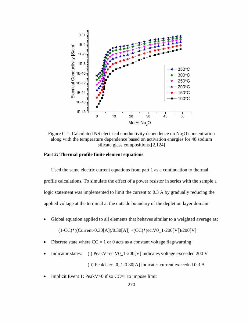
270
Figure C-1: Calculated NS electrical conductivity dependence on Na2O concentration
along with the temperature dependence based on activation energies for 48 sodium
silicate glass compositions.[2,124]
Part 2: Thermal profile finite element equations
Used the same electric current equations from part 1 as a continuation to thermal
profile calculations. To simulate the effect of a power resistor in series with the sample a
logic statement was implemented to limit the current to 0.3 A by gradually reducing the
applied voltage at the terminal at the outside boundary of the depletion layer domain.
• Global equation applied to all elements that behaves similar to a weighted average as:
(1-CC)*((Current-0.30[A])/0.30[A]) +(CC)*(ec.V0_1-200[V])/200[V]
• Discrete state where CC = 1 or 0 acts as a constant voltage flag/warning
• Indicator states: (i) PeakV=ec.V0_1-200[V] indicates voltage exceeded 200 V
(ii) PeakI=ec.I0_1-0.30[A] indicates current exceeded 0.3 A
• Implicit Event 1: PeakV>0 if so CC=1 to impose limit

271
• Implicit Event 2: PeakI>0 if so CC=0 to impose limit
Heat Transfer Equations
• Heat transfer equation in solids where u (velocity field of translational motion) and
Qted (Thermoelastic damping) are assumed to not contribute and set to zero.
• Heat conduction in solids by the heat flux vector is described as the relationship
between thermal conductivity and the temperature gradient as:
• Heat loss via diffuse surfaces alters the heat flux vector at the boundaries as:
• Convective heat flow out of the sample into the electrodes also alter the heat flux
vector as: where and h is the heat transfer coefficient
(Assumed 800 W/m2.K from literature)
Electromagnetic Heat Source Equations
• Multiphysics coupling represents the source term Qe (power density) calculated from
the electric current equations and implements it into the heat transfer equations by the
following relation as: where again, the velocity field
u, is zero for this analysis.
• The resistive heating due to electric current is calculated from current density and
electric field strength as:

272
Appendix D: Dissertation research publications
[1] C. McLaren, W. Heffner, R. Tessarollo, R. Raj, H. Jain, “Electric field-induced
softening of alkali silicate glasses”, Appl. Phys. Lett. 107 (2015) 184101.
doi:10.1063/1.4934945.
[2] C. McLaren, M. Balabajew, M. Gellert, B. Roling, H. Jain, “Depletion Layer
Formation in Alkali Silicate Glasses by Electro-Thermal Poling”, J. Electrochem.
Soc. 163 (2016) H809–H817. doi:10.1149/2.0881609jes.
[3] C. McLaren, B. Roling, R. Raj and H. Jain, “Mechanism of electric field-induced
softening of alkali silicate glasses”, Submitted to J. Non-Cryst. Solids, in press.
http://dx.doi.org/10.1016/j.jnoncrysol.2017.06.025
[4] C. McLaren, W. Heffner, H. Jain, “AC electric field-induced softening of alkali
silicate glasses”, in preparation.
[5] C. McLaren, N. J. Smith, R. Raj, H. Jain, “Thermal Imaging and Modeling of electric
field-induced softening of alkali silicate glasses”, in preparation.
[6] C. McLaren, H. Jain, “Restructuring of glass under DC field”, in preparation.
[7] C. McLaren, N. J. Smith, H. Jain, “Athermal depletion layer formation under DC
field”, in preparation.

273
Vita
Charles Thomas McLaren was born and raised in Corning, New York by his parents
George and Susan McLaren. He attended Erwin Elementary School, Northside Blodgett
Middle School, and Corning – Painted Post West High School, from which he graduated
in 2008. In August 2008, Charles enrolled in Rutgers University in New Brunswick, New
Jersey where he majored in Materials Science and Engineering with a focus on ceramics
and glass. He graduated with highest honors and received a Bachelor of Science degree in
May 2012. Charles then chose to continue his education by enrolling in the graduate degree
program at Lehigh University in the Department of Materials Science and Engineering,
where he joined the International Materials Institute for New Functionalities in Glass (IMI-
NFG) under the advisement of Dr. Himanshu Jain. He graduated with his Master of Science
degree in May 2016 and continued on toward his Ph.D degree in August 2017.
Copyright © 2022 FDOKUMEN