Electric Drive TEchnologies 2015 Annual Report - Department ...
347
-
Upload
khangminh22 -
Category
Documents
-
view
0 -
download
0
Transcript of Electric Drive TEchnologies 2015 Annual Report - Department ...


FY 2015 Annual Progress Report iii Electric Drive Technologies
CONTENTS
ACRONYMS AND ABBREVIATIONS ........................................................................................................ xviii
I. INTRODUCTION ........................................................................................................................................ 11.1. Accomplishments ............................................................................................................................... 3
1.1.A. Ribbon Electrical Interconnects Demonstrate Reliability to Enable Increased Current Density in Power Electronics ............................................................................................................. 31.1.B. Thermal Stackup Enables Full Potential of WBG Devices ..................................................... 41.1.C. Integrated WBG Onboard Charger and dc-dc Converter: Double Power Density at Half the Cost ...................................................................................................................................... 51.1.D. Next Generation Inverter Approaches DOE 2020 Goals ........................................................ 6
1.2. Small Business Innovative Research Grants ...................................................................................... 7
II. RESEARCH AREAS ................................................................................................................................. 12
2.0 Electric Motor Research and Development ................................................................................................ 122.1. Non-Rare Earth Motor Development ............................................................................................... 12
2.2. Multi-Speed-Range Electric Motors ................................................................................................ 252.3. Alternative High-Performance Motors with Non-Rare Earth Materials .......................................... 372.4. Unique Lanthanide-Free Motor Construction .................................................................................. 482.5. Brushless and Permanent Magnet Free Wound Field Synchronous Motors for EV Traction.......... 592.6. Electric Motor Thermal Management R&D .................................................................................... 752.7. Development of Radically Enhanced alnico Magnets (DREaM) for Traction Drive Motors .......... 88
3.0 Power Electronics Research and Development ........................................................................................ 1003.1. Inverter R&D ................................................................................................................................. 1003.2. Innovative Technologies for Converters and Chargers .................................................................. 1123.3. Traction Drive Systems with Integrated Wireless Charging .......................................................... 124
3.4. Gate Driver Optimization for WBG Applications ......................................................................... 1353.5. Power Electronics Thermal Management R&D ............................................................................. 1443.6. High Temperature DC Bus Capacitor Cost Reduction & Performance Improvements ................. 1573.7. Advanced Low-Cost SiC and GaN Wide Bandgap Inverters for Under-the-Hood Electric
Vehicle Traction Drives ................................................................................................................. 1633.8. 88 Kilowatt Automotive Inverter with New 900 Volt Silicon Carbide Mosfet Technology ......... 1773.9. High-Efficiency High-Density GaN-Based 6.6kW Bidirectional On-board Charger for PEVs .... 1903.10. Cost-Effective Fabrication of High-Temperature Ceramic Capacitors for Power Inverters .......... 206
3.11. High Performance DC Bus Film Capacitor ................................................................................... 2213.12. A Disruptive Approach to Electric Vehicle Power Electronics ..................................................... 2333.13. Next Generation Inverter ............................................................................................................... 247
4.0 Benchmarking, Testing, and Analysis ...................................................................................................... 2544.1. Benchmarking EVs and HEVs ....................................................................................................... 2544.2. Thermal Performance Benchmarking ............................................................................................ 2674.3. 2015: Continued Analysis of the xEV Traction Drive Electric Motor & PE Supply Chain in
North America ............................................................................................................................... 280
5.0 Advanced Packaging Research and Development ................................................................................... 287
5.1. Power Electronics Packaging ......................................................................................................... 2875.2. Performance and Reliability of Bonded Interfaces for High-Temperature Packaging .................. 298

FY 2015 Annual Progress Report iv Electric Drive Technologies
6.0 Materials Research and Development ...................................................................................................... 313 6.1. Power Electronics and Electric Motor Materials Support (Joint with VTO Propulsion
Materials) ....................................................................................................................................... 313

FY 2015 Annual Progress Report v Electric Drive Technologies
Figures Figure 1: IGBT with wire interconnects (left) and ribbon interconnects (right). .................................................. 3
Figure 2: Scanning acoustic microscopy images of delaminated sintered-Ag interconnects. Dark patches represented undelaminated bonding. ORNL and NREL are using such analysis to improve understanding of sintered-Ag reliability. .............................................................................. 5
Figure 3: A 6.8 kW SiC charger converter with a built-in 2 kW 14V buck converter tested in an integrated SiC bidirectional OBC with a 100 kW segmented traction inverter .................................. 5
Figure 4: The Next Generation Inverter Prototype ............................................................................................... 6Figure 5: The Next Generation Inverter Prototype Under Active Load Test in GM’s Dynamometer
Laboratory ........................................................................................................................................... 6Figure 6: Next Generation Inverter Efficiency Map during Regeneration (Left) and Motoring (Right) .............. 6Figure 2-1: Various exterior views of the 2014 Honda Accord hybrid power converter unit. ........................... 13Figure 2-2: Comparison of electrical steel core losses: 6.5% Si vs. 3% Si. ........................................................ 15Figure 2-3: Simulated Si positions before and after a compressive strain of 0.153. ........................................... 16Figure 2-4: Monte Carlo simulation of the hysteresis loop for a randomly oriented single crystal
showing the evolution of the initial domain structure. ...................................................................... 17Figure 2-5: Certain concentrated winding configurations contain two adjacent phases with opposite
polarities. While possessing certain favorable characteristics in terms of torque ripple and back-electromotive-force, they can pose a significant risk of demagnetization with a pure quadrature axis current. ..................................................................................................................... 19
Figure 2-6: Efficiency map for Design A. .......................................................................................................... 19
Figure 2-7: Efficiency map for Design-B. .......................................................................................................... 20Figure 2-8: Torque waveform from a design with winding designed for torque ripple minimization. .............. 21Figure 2-9: Electromagnetic efficiency contour plot for Design D. ................................................................... 22Figure 2-10: Torque versus speed for ORNL’s Design B and Design D compared with that of the 2010
Prius. ................................................................................................................................................. 22Figure 2-11: Power versus speed for ORNL’s Design B and Design D compared with that of the 2010
Prius. ................................................................................................................................................. 23Figure 2-12: Overlay of drive cycle operation points on efficiency map. .......................................................... 26Figure 2-13: Example of 3-speed-range operation in UDDS drive cycle. .......................................................... 27Figure 2-14: A commercial 3-speed transmission for PEV applications. ........................................................... 27Figure 2-15: 2011 Hyundai Sonata hybrid 6-speed transmission and its key parts. ........................................... 28Figure 2-16: Schematics illustrating two industry patents: (left) patent A-US8415910 B2 (published in
2013 by Fulton) and (right) patent B-US20120086380 (published in 2012 by Krieger and Shum). ............................................................................................................................................... 29
Figure 2-17: Original Prius drive system efficiency map (top left), system efficiency with 2:1 reduction (top right), system efficiency with 3:1 reduction (bottom left), and optimized system efficiency map (bottom right). .............................................................................................. 29
Figure 2-18: Proposed MSR design. ................................................................................................................... 31Figure 2-19: Loss simulation of the proposed MSR, fixed winding drive, and patent A system. ...................... 32
Figure 2-20: Loss simulation of the proposed MSR, fixed winding drive, and patent A system. ...................... 33Figure 2-21: Solid-state ac switch board (top view at top left; bottom view at bottom left) and motor
winding used in benchtop test (right). ............................................................................................... 34Figure 2-22: Test circuit diagram with an inverter and three solid-state ac switches. ........................................ 34Figure 2-23: Key test waveform of a series to parallel transient, output current 50 A/div, time is
5 ms/div. ............................................................................................................................................ 35Figure 2-24: Motor required efficiency map ....................................................................................................... 38Figure 2-25: Thermal Management: Oil flow path indicated by arrows. ............................................................ 40Figure 2-26: Prototype photographs: (a) Stator; (b): Rotor; (c): Prototype on test bench. ................................. 40Figure 2-27: (Left) Measured vs. calculated open circuit phase voltage for 10ADC field current and
1000rpm. (Right) Measured vs. calculated RMS phase back EMF at 1000rpm (back EMF constant), for various DC field current.............................................................................................. 41
Figure 2-28: Measured and calculated torque vs. current for two levels of DC field current. ............................ 41Figure 2-29: Drag loss measurements. ................................................................................................................ 41Figure 2-30: (Left) Peak Power characteristics. (Right) Temperatures during peak power operation. .............. 42Figure 2-31: Rated Load Characteristics. ........................................................................................................... 42

FY 2015 Annual Progress Report vi Electric Drive Technologies
Figure 2-32: Temperatures during rated load 2800rpm heat run. ....................................................................... 43
Figure 2-33: Temperatures during rated load 5000rpm (left) and 7000rpm (right) heat runs. ........................... 43Figure 2-34: Second stator with 280˚C insulation system. ................................................................................. 44Figure 2-35: (left) Schematic of section of synchronous reluctance machine laminate. Gray regions are
magnetic and green regions are non-magnetic. (right) Fully processed laminate on permanent magnetic sheet. The green indicator film reveals the magnetic stripe domains magnetized into the sheet. The magnetic regions of the laminate are observed to be shielding the strip domains, whereas the stripe domain patterns show through the non-magnetic regions. .............................................................................................................................. 45
Figure 2-36: Image of 18 rotor laminates on test stand. Test rotor was spun to failure in vacuum. ................... 45Figure 2-37: Plot of calculated versus measured deflection of the outer diameter (O.D.) of the 18
laminate test rotor stack. ................................................................................................................... 46Figure 2-38: View of POC Motor Prior to Final Assembly ................................................................................ 50Figure 2-39: Dynamometer Testing Apparatus .................................................................................................. 51Figure 2-40: Back EMF POC1 Before High Torque Test .................................................................................. 51Figure 2-41: EMF after 100% Torque POC1 ...................................................................................................... 52Figure 2-42: Torque vs Speed results for Maximum Torque Test ...................................................................... 52Figure 2-43: Torque vs Speed results for Power Profile test .............................................................................. 53Figure 2-44: Power vs Speed results for Power Profile Test .............................................................................. 53Figure 2-45: Full CFD model (top) and FEA section model (bottom). .............................................................. 55Figure 2-46: Summary of material sensitivity study. .......................................................................................... 56
Figure 2-47: Schematic of ASTM setup (top) and test hardware (bottom) ........................................................ 57Figure 2-48: Motor stator thermal test bench. ..................................................................................................... 57Figure 2-49: (a) rendering of wound field synchronous motor with field winding excited by capacitive
power transfer and (b) estimated 2004 Prius power factor................................................................ 60Figure 2-50: Circuit representation of field coupling for: (a) rotary transformer, (b) rotary capacitor
coupler ............................................................................................................................................... 61Figure 2-51: Multi-objective optimization: (a) structure with ActiveX software interfaces, (b)
simulation results illustrating the magnetic flux density distribution of the Prototype 1 machine. ............................................................................................................................................ 62
Figure 2-52: Example comparison of electromagnetic simulation package (FEMM and MagNet) results for (a) static electromagnetic torque versus current angle for a fixed rotor position, and (b) electromagnetic torque versus rotation angle at the maximum torque per amp (MTPA) current angle. ...................................................................................................................... 62
Figure 2-53: Example rotor nondimensional parameters and geometry morphing illustrating point merging and collapsing. .................................................................................................................... 63
Figure 2-54: Example WFSM rotor structural analysis simulation results: (a) Von-Mises stress, (b) strain .................................................................................................................................................. 64
Figure 2-55: Torque density versus “goodness” (Average Torque/ Plosses) for 48 slot 8 pole single layer WFSM designs from the final optimization run: (a) full population results color coded for constraints, (b) designs which meet all hard constraints. .................................................. 65
Figure 2-56: Torque density versus losses for 48 slot 8 pole single layer WFSM designs from the final multi-objective optimization run: (a) full population results color coded for constraints, (b) designs which meet all hard constraints. ........................................................................................... 66
Figure 2-57: Torque and voltage per turn maps for WFSM Prototype 1 at a current angle of 20° as a function of stator, Js, and rotor, Jr, current densities: (a) torque map, (b) voltage per turn map. ................................................................................................................................................... 66
Figure 2-58: Class E amplifier utilizing interleaved switching .......................................................................... 67
Figure 2-59: Wound and varnished WFSM prototype 1 rotor and stator. .......................................................... 68Figure 2-60: Coupling capacitor stator (a), rotor (b), and rectifier board (c), which comprise the
capacitive power coupler assembly. .................................................................................................. 69Figure 2-61: Coupler mounted on WFSM rotor (a), dynamometer test stand (b), and inverter for
capacitive power coupling to rotor (c). ............................................................................................. 69Figure 2-62: (left) stator plate, (right) rotor plate. .............................................................................................. 70Figure 2-63: Photo of the hydroflex plate stack on a small dyne bed ................................................................. 70Figure 2-64: Capacitance vs. Speed plot, displaying per section capacitance of coupler assembly. .................. 71

FY 2015 Annual Progress Report vii Electric Drive Technologies
Figure 2-65: Measured 600 W test waveforms (a) MOSFET drain to source and gate voltages, (b) coupling capacitor voltage, (c) DC output ........................................................................................ 71
Figure 2-66: WFSM with CPT Genset system architecture ................................................................................ 73Figure 2-67: Measured waveforms of a getset output and field winding utilizing CPTexcitation ..................... 73Figure 2-68: Thermal management impact on motor performance to support increased power ........................ 76Figure 2-69: Heat must pass through several layers within the motor to be extracted through active
cooling such as through a cooling jacket or spray cooling with oil such as ATF. ............................ 77Figure 2-70: Approach to motor thermal management divided between passive thermal design and
active convective cooling .................................................................................................................. 77Figure 2-71: Experimental velocity profile of jet impingement showing variation in velocity at the
target or wall boundary. Data measured using particle image velocimetry equipment at NREL. ............................................................................................................................................... 78
Figure 2-72: Heat transfer due to ATF jet impingement will vary over the end-winding surface. ..................... 79Figure 2-73: Passive stack thermal properties and terminology. ........................................................................ 79Figure 2-74: Cross-sectional view of TLC test article (left). Test article with nozzle assembly (right). ............ 80Figure 2-75: Assembled test article showing impingement surface (left), Assembled test article
showing embedded LEDs to illuminate the TLC surface (right). ..................................................... 80Figure 2-76: Test article and nozzle assembly (left), assembled test article showing camera view of
illuminated TLC surface (right) ........................................................................................................ 81Figure 2-77: Illustration of sensor package installed in end winding (left), three-dimensional drawing
of stator end winding with sensor package installed for convective heat transfer measurements (right) ......................................................................................................................... 81
Figure 2-78: Design of sensor package showing assembled components and ability to change target surfaces (left), thermal finite element model of sensor package design (right). ............................... 82
Figure 2-79: Assembled sensor packages for outer diameter surface measurement and end surface measurement (left), stator winding removed for sensor package (right) ........................................... 82
Figure 2-80: Images of sample slot-winding and end-winding motor components ............................................ 83Figure 2-81: Images of sample slot-winding materials (left), sample slot winding under test for
measuring cross-slot thermal conductivity (right)............................................................................. 83Figure 2-82: Winding sample blocks prepared by ORNL for thermal property measurements (left), cut
samples prepared by ORNL and sent to NREL for directional thermal property measurements (right) ......................................................................................................................... 85
Figure 2-83: Experimental setup for measuring stator-to-case thermal contact resistance and lamination in-plane thermal conductivity under high pressure ......................................................... 85
Figure 2-84: Iso-concentration surfaces: threshold settings at 10 at.% Cu to show the Cu (brown), 10 at.% Ni to show the outline of the AlNi phase/Fe-Co phases (red) and 30% Ni to show the high Ni regions (blue). Cu-enriched rods are at the corners of the Fe-Co phas ................................ 91
Figure 2-85: (a) Color composite energy-dispersive-X-ray map of alnico 9 taken along [001] crystal direction; (b,c) aberration corrected HAADF STEM images of alnico 9 taken under [100] zone axis along transverse direction. (d) HAADF STEM image of alnico 9 along long .................. 92
Figure 2-86: Composition profile of alnico 8 along the z-direction and the atomic structure obtained from MC simulation at 973 and 823 K. The silver, light green, blue, gold and red balls in the crystal structure indicate the Al, Ni, Co, Fe and Ti atoms, respectivel ....................................... 93
Figure 2-87: Summary of magnetic properties that result from Ti substitutions for Fe in alnico 8H magnet alloy, where MA was optimized and extended draw cycles were used. ............................... 94
Figure 2-88: TEM micrographs of transverse sections of cast alnico sample after optimized FHT to illustrate representative microstructure effects at 3 elevated Ti contents where the 8.2 at.% Ti represents the peak coercivity level. ............................................................................................. 94
Figure 2-89: Summary of XRD peak ratios for (110) peak of L21 phase vs./(110) peak of BCC phase. .......... 95Figure 2-90: Summary of VSM results indicating the decreasing Curie temperature of the L21 phase
for increased Ti content. .................................................................................................................... 95Figure 3-1: Overall strategy to address limitations of the state of the art. ........................................................ 101
Figure 3-2: Specific approach to address limitations of the state of the art. ..................................................... 102Figure 3-3: The i-v curves of a 1200 V, 30 A SiC MOSFET. .......................................................................... 103Figure 3-4: On-state resistances. ....................................................................................................................... 103Figure 3-5: Double pulse test setup. ................................................................................................................. 103
FY 2015 Annual Progress Report viii Electric Drive Technologies
Figure 3-6: Energy losses of planar gate SiC MOSFETs. ................................................................................ 104
Figure 3-7: Energy losses of trench gate SiC MOSFETs. ................................................................................ 105Figure 3-8: Air-cooled inverter module. ........................................................................................................... 106Figure 3-9: Air-cooled module switching performance. ................................................................................... 107Figure 3-10: Air-cooled module switching loss with 400 V dc bus voltage. .................................................... 107Figure 3-11: Air-cooled inverter assembly. ...................................................................................................... 108Figure 3-12: Air-cooled inverter testing results. ............................................................................................... 108Figure 3-13: Efficiency of the air-cooled inverter. ........................................................................................... 109Figure 3-14: The 10 kW SiC inverter layout. ................................................................................................... 109Figure 3-15: Liquid-cooled inverter assembly. ................................................................................................. 110Figure 3-16: Experimental waveforms of 30 kW SiC inverter with 400 V dc-link operation. ......................... 110Figure 3-17: Inverter efficiency vs. output power. ........................................................................................... 111Figure 3-18: An integrated dc-dc converter and charger architecture. ............................................................. 114Figure 3-19: Dual active H-bridge–based isolated charger converter topology. .............................................. 115Figure 3-20: An example of the proposed integrated OBC based on the segmented traction drive
topology. ......................................................................................................................................... 115Figure 3-21: Equivalent circuit for operating in the charging mode. ................................................................ 116
Figure 3-22: Control block diagram. ................................................................................................................ 117Figure 3-23: Design of an SiC traction drive inverter that can be operated as dual 3-phase inverters,
each rated at 50 kW, or a segmented 3-phase inverter, rated at 100 kW, by swapping the output bus bar and current sensor assembly. (a) Inverter base assembly, (b) output bus bar and current sensor assembly for segmented inverter, (c) output bus bar and current sensor assembly for dual 3-phase inverters. ............................................................................................... 118
Figure 3-24: Photo of a 100 kW SiC traction drive inverter prototype used in the integrated charger tests. ................................................................................................................................................ 118
Figure 3-25: Photos of a 6.8 kW charger converter and SiC MOSFET phase-leg modules (36×46 mm). ....... 119Figure 3-26: Typical operating waveforms of the SiC charger converter at fsw=200 kHz (left) and 250
kHz (right). From top: input dc voltage (Vin, 500 V/div), output dc voltage (Vout, 500 V/div), transformer primary terminal voltage (vTr1, 500 V/div), transformer secondary terminal voltage (vTr2, 500 V/div), input current (Iin, 40 A/div) and output current (Iout, 40 A/div). ........................................................................................................................................ 119
Figure 3-27: Measured charger converter efficiencies. ..................................................................................... 119Figure 3-28: Photo of the test setup using the SiC segmented inverter, the charger converter, and a
motor for an integrated 6.8 kW OBC. ............................................................................................. 120Figure 3-29: Waveforms of the OBC with 120 V input and 1.0 kW (left), 1.7 kW (right) charging
power. From top: grid voltage (vs, 500 V/div, CH1), converter input voltages (va1a2, CH2, vb1b2, CH3, 500 V/div), dc bus voltage (Vdc, 500 V/div, CH4), charging current (Ibat, 20 A/div, CH5), grid current (is, 50 A/div, CH6) and motor phase a1 and a2 currents (ia1, CH7, ia2, CH8, 50 A/div). .............................................................................................................. 120
Figure 3-30: Waveforms of the OBC at 240 V input and 2.7 kW (left), 6.8 kW (right) charging power. From the top: grid voltage (vs, 500 V/div, CH1), grid current (is, 100 A/div, CH6), converter input voltage (va1b1, 500 V/div, CH2), dc bus voltage (Vdc, 500 V/div, CH4), charging current (Ibat, 50 A/div, CH5) and motor phase a1 and a2 currents (ia1, CH7, ia2, CH8, 100 A/div). ............................................................................................................................. 121
Figure 3-31: Measured OBC system efficiencies at grid voltages of 120 and 240 V. ...................................... 121Figure 3-32: Photo of the 3D-printed nanocomposite magnetic E and I cores (58×38×17 mm). ..................... 122Figure 3-33: Design for a 6.8 kW charger converter using a GaN transistor (left) and power plane and
planar transformer assembly (right). ............................................................................................... 122Figure 3-34: A conceptual block diagram for wireless chargers based on loosely coupled coils. .................... 125Figure 3-35: Conceptual block diagram for a traction drive system with integral wireless charging
functionality, in which the traction drive inverters and motors are used as part of the onboard ac-dc converter to eliminate or minimize the number of components for the wireless charger. Primary converters and transmitting coils are installed at charging stations, and receiving coils are installed underneath the electric vehicles. .................................... 126
FY 2015 Annual Progress Report ix Electric Drive Technologies
Figure 3-36: ORNL’s previous work on traction drive, onboard charger: 6.8 kW SiC isolation converter (left), ORNL SiC module 1200 V/100 A (middle), SiC traction drive inverter with an integrated 6.8 kW OBC (right). .......................................................................................... 127
Figure 3-37: ORNL’s add-on wireless chargers operating at 22–26 kHz. ........................................................ 127Figure 3-38: ORNL’s previous work on add-on wireless chargers: coils (left), stationary wireless
charging of a Prius PHEV (middle), in-motion wireless charging of a GEM EV (right). .............. 127Figure 3-39: Simplified converter block diagram for studying resonant circuits. ............................................ 128Figure 3-40: Comparison of operating waveforms between a traditional resonant circuit with low load
power factor (left) and the optimized resonant circuit with high load power factor (right). ........... 129Figure 3-41: Comparison of losses and primary currents between the optimized resonant circuit with
high power factor and the traditional circuit with low power factor at various charging rates. ................................................................................................................................................ 129
Figure 3-42: Simulated topology 1: tapping into the accessory power supply 14 V converter. ....................... 130Figure 3-43: Simulation results for topology 1 for charging at 1.5 kW from a 120 V ac source,
showing a high input power factor of 99.7% and a low THD of 1.2%. .......................................... 130Figure 3-44: Simulated topology 2: using the traction motor and inverter. ...................................................... 131Figure 3-45: Simulation results for topology 2 for charging at 5 kW from a 240 V source, showing a
high input power factor of 99.5% and a low current THD of 0.8%. ............................................... 131Figure 3-46: Simulated topology 3: using a multiport dc-dc converter that combines a boost converter
of reduced power for stepping up the dc bus voltage of the traction drive inverter, a 14 V buck converter for powering the 14 V vehicle accessory loads, and a wireless battery charging converter. .......................................................................................................................... 132
Figure 3-47: Simulated operating waveforms for topology 3 for charging at 6.6 kW from a 240 V source, showing high input power factor and low current distortion. ............................................. 132
Figure 3-48: Simulated operating waveforms for topology 3 operating in propulsion mode. .......................... 133Figure 3-49: Simulated power factor and THD against charging power for topology 3. ................................. 133
Figure 3-50: General active gate drive topology selected incorporating WBG source inductive current sensing for di/dt feedback control. Optional dv/dt sensing method is also shown for completeness. .................................................................................................................................. 141
Figure 3-51: Candidate gate drive waveforms for di/dt and dv/dt control: (a) single slope, (b) RC-based, (c) dual slope, and (d) threshold method. ............................................................................. 141
Figure 3-52: Simulated di/dt (left column) and dv/dt (right column) produced using the threshold gate drive waveform during SiC powerMOS device turn-on (top row) and turn-off (bottom row). ................................................................................................................................................ 141
Figure 3-53: Closed-loop PSPICE simulation showing dynamic changing of the di/dt loop control set point and subsequent loop settling. The switch frequency chosen is 8 kHz. .................................. 142
Figure 3-54: Closed-loop PSPICE simulation showing dynamic changing of the di/dt loop control set point and subsequent loop settling. The switch frequency chosen is 8 kHz and the dynamic range of the di/dt for this simulation is ~3×. ................................................................................... 142
Figure 3-55: Pictures of the 2012 Nissan Leaf inverter. The middle image shows the cold plate cooling channels. Image on the right shows one power module mounted on the cold plate. The dielectric pad and TIM layers are shown (right). ............................................................................ 146
Figure 3-56: CAD model of the Nissan Leaf power module. The top image shows the entire module. The various power module layers are shown in the lower, cross-sectional view. The interface bonding layers are labeled on the lower image. ............................................................... 146
Figure 3-57: Cross-sectional view of the LEAF module configuration that incorporates a DBC substrate. ......................................................................................................................................... 147
Figure 3-58: FEA-generated temperature contours for the LEAF module. The left side has the silicone encapsulant hidden to reveal the devices. ....................................................................................... 147
Figure 3-59: Specific (junction-to-liquid) thermal resistance plotted versus the convective thermal resistance for three different power module configurations. The Semikron SKM data were taken from Bennion and Moreno [1]. .............................................................................................. 148
Figure 3-60: Junction-to-liquid thermal impedance plotted versus time for two different power module configurations. ................................................................................................................................. 149
Figure 3-61: The maximum temperatures for the device solder, copper-moly solder, and TIM layers at five different junction temperatures. Temperatures are provided for three different

FY 2015 Annual Progress Report x Electric Drive Technologies
convective cooling thermal resistance values– 100 mm^2-K/W (left), 50 mm^2-K/W (middle), and 10 mm^2-K/W (right). .............................................................................................. 150
Figure 3-62: CAD renderings showing the geometry of the direct-cooled DBC (left) and direct-cooled baseplate (right) configurations. FEA was conducted to evaluate the effect of varying the a and b dimensions on the total thermal resistance. ........................................................................... 150
Figure 3-63: Specific thermal resistance plotted versus the convective thermal resistance for different DBC-to-die edge offset values. ....................................................................................................... 151
Figure 3-64: Specific thermal resistance plotted versus the convective thermal resistance for different baseplate-to-DBC edge offset values. The plot on the left uses a 3.5 mm die-to-DBC distance, and the plot on the right uses a 7.5 mm die-to-DBC distance. ......................................... 152
Figure 3-65: Specific thermal resistance plotted versus the convective thermal resistance for DBC- and baseplate-cooled configurations. ..................................................................................................... 152
Figure 3-66: PIV system schematics showing the piping layout (left) and the laser and camera setup (right). ............................................................................................................................................. 153
Figure 3-67: PIV-generated velocity contour plots for a submerged jet impinging on a roughened surface. The velocity magnitude (left), fluctuating component of the radial velocity (middle), and the fluctuating component of the axial velocity (right) are shown. .......................... 154
Figure 3-68: Thermal image of a sample capacitor .......................................................................................... 160Figure 3-69: Comparison of state of the art 350μF/400V/600 Vmax DC-link metallized PP capacitor
(left), and a GEN1 350μF/450V/720Vmax PML capacitor (unpackaged). .................................... 161Figure 3-70: Capacitance and dissipation factor variation of PML capacitors with 0.5µm dielectric
designed for a pulse application such as that encountered in implantable defibrillator devices ............................................................................................................................................. 161
Figure 3-71: GaN System’s 650 V, 55 mΩ (30 A) GaN-on-Si embedded chip power transistor. .................... 167Figure 3-72: (Left) APEI’s GaN-based enhancement mode, low inductance power module using the
HT-3000 series housing and (right) a rendered CAD image with a transparent lid showing the GaN power transistors mounted to the power substrate. ........................................................... 167
Figure 3-73: Clamped inductive load circuit diagram. ..................................................................................... 168Figure 3-74: Parasitic turn-on of low-side switch position. Switching conditions: VGS = +7/0 V, RG =
100 Ω, VDS = 150 V, ID = 12 A. Ch. 1 (yellow) source current measured via 2.475 mΩ sense resistor; Ch. 2 (Cyan) control signal; Ch. 3 (Magenta) drain source voltage; Ch. 4 (Green) inductor current. ................................................................................................................. 168
Figure 3-75: Parasitic turn-on of high-side switch position. Switching conditions: VGS = +7/0 V, RG = 30 Ω, VDS = 100 V, ID = 20 A. Ch. 1 (yellow) source current measured via 2.475 mΩ sense resistor; Ch. 2 (Cyan) control signal; Ch. 3 (Magenta) drain source voltage; Math1 (Orange) Ch. 1 scaled to current. .................................................................................................... 169
Figure 3-76: An enlarged view of the new GaN package nesting. ................................................................... 170Figure 3-77: GaN-based HT-3000 power module. ........................................................................................... 170Figure 3-78: 450 V, 300 A, 75°C switching of the Design Cycle 2 GaN-based HT-3000 power
module. ............................................................................................................................................ 171Figure 3-79: GS66516T-based HT-3000 thermal simulation using COMSOL™. ........................................... 171Figure 3-80: Silicon-carbide inverter in the environmental chamber ready for testing. ................................... 172Figure 3-81: Initial results: SiC-based inverter efficiency at 200 VDC. Ambient and coolant
temperature is 25°C. ........................................................................................................................ 173
Figure 3-82: Initial results: SiC-based inverter efficiency at 325 VDC. Ambient and coolant temperature is 25°C. ........................................................................................................................ 173
Figure 3-83: Initial results: SiC-based inverter efficiency at 450 VDC. Ambient and coolant temperature is 25°C. ........................................................................................................................ 174
Figure 3-84: Initial results: SiC-based inverter efficiency at 650 VDC. Ambient and coolant temperature is 25°C. ........................................................................................................................ 174
Figure 3-85: The WBG Inverter Project test bed at NCREPT. ......................................................................... 175Figure 3-86: APEI designed and built housing containing a heater, pump, and air compressor to
achieve a 105°C coolant loop temperature. ..................................................................................... 175Figure 3-87: This work brought together a team which is leading the market in SiC power device
production (Cree), SiC power module technology (Cree Fayetteville, formerly APEI), and HEV/EV platforms in the US market (Ford). Cree is the leading supplier of SiC and GaN
FY 2015 Annual Progress Report xi Electric Drive Technologies
components, including SiC power MOSFETs and diodes, and is also an automotive supplier of SiC diodes to HEV / EV platforms. Cree-Fayetteville is a leading producer of high-temperature and low-inductance modules, which take full advantage of SiC power devices. Cree-Fayetteville has also constructed automotive drive train prototype inverters in concert with other automotive OEMs on other efforts. Ford is the number one US producer of HEV / EV platforms, with a 13% market share in the US at the end of 2013. ............ 178
Figure 3-88: Comparison of RDSON over temperature of two power MOSFETs in TO-247 style package. The blue line represents the lowest RDSON commercial 650V Silicon MOSFET, while the red line represents a 900V SiC MOSFET produced on this program. ............................ 180
Figure 3-89: Comparison of forward characteristics of the 900V, 10 mΩSiC MOSFET in a TO-247 package and a 650V 100 A IGBT [4] at 175˚C. .............................................................................. 180
Figure 3-90: Circuit used for measurement comparison of switching characteristics of the 900V, 10 mΩ SiC MOSFET in a TO-247-3L package and a TO-247-4L (source Kelvin contact) package............................................................................................................................................ 181
Figure 3-91: Comparison of switching waveforms for turn-on and turn-off conditions of the 900V, 10 mΩ SiC MOSFET in a TO-247-3L package and TO-247-4L (source Kelvin contact) package at 25˚C. .............................................................................................................................. 181
Figure 3-92: Switching Energy losses at 25 ˚C for the 900V for 900V, 10 -247-4 package (RG=5Ohm, VGS=-4V/+15V, VDD=600V) .......................................................... 182
Figure 3-93: Switching Energy losses at 25C for the 900V for 900V, 10 mΩ SiC MOSFET in TO-247-3 package (RG=5Ohm, VGS=-4V/+15V, VDD=600V) .......................................................... 182
Figure 3-94: Third quadrant characteristics of the 900V, 10 mΩ MOSFET at 175˚C ..................................... 183Figure 3-95: HT-3291-R switch position; four of eight die positions populated. Upper image illustrates
thermal simulation of all eight MOSFETs inside the HT-3291-R module, with peak temperature of 150C on each die. Lower image illustrates a close-up of four MOSFETs in a single switch position inside the module. ........................................................................................ 184
Figure 3-96: HT-3291-R on-state characteristics, Vgs = 15 V; (top) 25˚C; (bottom) 175˚C. .......................... 185Figure 3-97: HT-3291-R on-state resistance; (top) 25˚C; (bottom) 175˚C. ...................................................... 186Figure 3-98: HT-3291-R 3rd quadrant operation, Vgs = 15 V; (top) 25˚C; (bottom) 175˚C. ............................ 187
Figure 3-99: HT-3291-R switching losses versus rms current as a function of RG, EXT. ............................... 188Figure 3-100: Si-based switch vs. GaN-based switch for bi-directional OBC ................................................. 191Figure 3-101: Summary of GaN power device benefit ..................................................................................... 192Figure 3-102: GaN device and Si device reverse recovery test waveform (Left – Si MOSFET
IPW65R041CFD, right - GaN HEMT TPH3205WSA) .................................................................. 193Figure 3-103: GaN device and Si device turn-on test waveform (Left – Si MOSFET IPW65R041CFD,
right - GaN HEMT TPH3205WSA) ............................................................................................... 193Figure 3-104: Simulation waveform of turn off transition period .................................................................... 194Figure 3-105: Voltage distribution of cascode device during turn off period ................................................... 194Figure 3-106: Equivalent circuit of a cascode GaN HEMT device with Cx ..................................................... 195
Figure 3-107: Package diagram (left) and picture (right) of a single cascode GaN HEMT device with additional Cx ................................................................................................................................... 195
Figure 3-108: Package diagram (left) and picture (right) of a half-bridge cascode GaN HEMT module with additional Cx ........................................................................................................................... 195
Figure 3-109: Matrix transformer using PCB winding with leakage integration.............................................. 196Figure 3-110: 12 layer transformer design and 2X6 layer transformer design ................................................. 196Figure 3-111: Power loss comparison of 12 layer transformer design and 2X6 layer transformer design ....... 197Figure 3-112: Topology selected for 3.3kW charger Concept Prototype Build ............................................... 197Figure 3-113: Topology selected for further research....................................................................................... 198Figure 3-114: 3.3kW concept prototype 3-D model ......................................................................................... 198Figure 3-115: Pictures of 3.3kW bi-directional OBCM prototypes .................................................................. 198Figure 3-116: Charge mode full power efficiency vs output voltage ............................................................... 200Figure 3-117: Charge mode full power efficiency vs output voltage ............................................................... 201Figure 3-118: Component temperature data ..................................................................................................... 201Figure 3-119: 120Vac input power factor vs power level ................................................................................. 202
Figure 3-120: 240Vac input power factor vs power level ................................................................................. 203Figure 3-121: Inverter dynamic load test .......................................................................................................... 203

FY 2015 Annual Progress Report xii Electric Drive Technologies
Figure 3-122: Schematic illustration of the aerosol deposition system developed at Argonne for the fabrication of dense PLZT films at room temperature. ................................................................... 210
Figure 3-123: Photograph of the aerosol deposition system built at Argonne National Laboratory. ............... 210Figure 3-124: X-ray diffraction pattern of the PLZT powder used for deposition of PLZT film by AD
process. ............................................................................................................................................ 211Figure 3-125: (a) SEM image and (b) particle size distribution of PLZT powder used for deposition of
PLZT film by AD process. .............................................................................................................. 212Figure 3-126: Photographs of PLZT films deposited on (a) glass and (b) aluminum metallized
polyimide film by AD process. ....................................................................................................... 212Figure 3-127: (a) plan-view and (b) cross-sectional view SEM microimages of PLZT deposited on
platinized silicon substrate by AD process. .................................................................................... 213Figure 3-128: X-ray diffraction pattern of PLZT film deposited on PtSi substrate by AD process. ................ 213Figure 3-129: Frequency dependent dielectric properties of ≈8 μm thick PLZT film deposited on
aPluminum metallized polyimide film by AD process. .................................................................. 214Figure 3-130: Dielectric properties as a function of applied bias voltage for a ≈8 μm thick PLZT film
deposited on aluminum metallized polyimide film by AD process. ............................................... 214Figure 3-131: PE hysteresis loops measured at different temperatures for a ≈8 μm thick PLZT film
deposited on aluminum metallized polyimide film. ........................................................................ 215Figure 3-132: (a) Time relaxation current density and (b) Field-dependent leakage current density for
a ≈8 μm thick PLZT film deposited on aluminum metallized polyimide film by AD process. ............................................................................................................................................ 216
Figure 3-133: Dielectric properties and the corresponding PE hysteresis loops of AD PLZT films deposited on platinized silicon substrates. From left to right, the samples are as-deposited, 450°C annealed in air for 30 minutes, and 650°C annealed in air for 30 minutes, respectively. .................................................................................................................................... 216
Figure 3-134: Weibull plot of breakdown strength of PLZT deposited on aluminum metallized polyimide films by AD process. ...................................................................................................... 217
Figure 3-135: PE hysteresis loops and associated recoverable energy density as a function of applied field (shown in inset) of PLZT films deposited on aluminum metallized polyimide substrates by AD process. ............................................................................................................... 217
Figure 3-136: Temperature dependent dielectric properties of PLZT deposited on aluminum metallized polyimide substrates by AD process. The inset plot illustrates that the PLZT film capacitors meet X8R specification. ......................................................................................... 218
Figure 3-137: DC bus capacitor in an inverter for a electric vehicle ................................................................ 222Figure 3-138: Schematic extrusion and winding process for polymer films .................................................... 222Figure 3-139: Schematic and image of an e-beam coating tool ........................................................................ 223Figure 3-140: Film capacitor manufacturing process flow ............................................................................... 223Figure 3-141: PEI film extrusion methods and films production capability ..................................................... 224Figure 3-142: Physical dimension change of 5um PEI film as a function of temperature ................................ 224Figure 3-143: Polarized light images of a 5 µm PEI film surface showing subtle features (<10 µm) and
defects (~100 µm). .......................................................................................................................... 225Figure 3-144: Images of PEI film rolls before (top) and after de-wrinkling process (bottom). ........................ 225Figure 3-145: Roll of 4 µm film which will be evaluated and processed into capacitors. ................................ 226Figure 3-146: Weibull distribution of DC breakdown strength of a 3 µm PEI film. ........................................ 226Figure 3-147: A roll of 5 µm film with an oxide coating (left) and TEM image of the cross section of
the coating (right). ........................................................................................................................... 227Figure 3-148: Statistical analysis of breakdown strength for SiOx coated 5 µm PEI film (based on 2-
sample test in normal distribution). P~0.023. ................................................................................. 227
Figure 3-149: SEM images of PEI films metallized to surface resistance of 40 Ohm/sq (left) and 24 Ohm/sq (right). ................................................................................................................................ 228
Figure 3-150: SEM images of a 5 µm PEI film metallized with 16 Ω/sq. ........................................................ 229Figure 3-151: Image of an Epoxy potted capacitor made of 5 µm film from supplier A (left), and
capacitor made of 5 µm film from supplier B (right). ..................................................................... 229Figure 3-152: Images of metallized 4 µm PEI film (left) and wound capacitors of 1.5 µF (right). .................. 230Figure 3-153: Composite converter powertrain approach with integrated charger ........................................... 235Figure 3-154: Conventional boost converter power stage ................................................................................ 235
FY 2015 Annual Progress Report xiii Electric Drive Technologies
Figure 3-155: Composite boost converter: (left) power stage, (right) operating modes and measured efficiencies of 10 kW pilot .............................................................................................................. 236
Figure 3-156: Comparison of efficiency curves of conventional boost converter and proposed composite boost converter ............................................................................................................... 236
Figure 3-157: Typical histogram of system operating points (Power, DC bus voltage) for the US06 drive cycle. ...................................................................................................................................... 237
Figure 3-158: Modeled loss mechanisms over the US06 drive cycle for the Si composite boost converter. Top: US06 speed profile. Bottom: total semiconductor conduction loss, switching loss, and DC+AC magnetics losses. ............................................................................... 237
Figure 3-159: Improvement of efficiency curves for the boost function, at Vbatt = 250 V and Vbus = 650 V. Left: measured DCX primary waveforms, showing achievement of zero-voltage switching at light load. Right: efficiency curves of conventional boost with Si IGBTs, composite boost with Si MOSFETs, and composite boost with improved zero-voltage switching. ........................................................................................................................................ 239
Figure 3-160: Photograph of assembled silicon prototype. .............................................................................. 239Figure 3-161: Prototype measured waveforms, operating at 250 V battery voltage, 650 V DC bus
voltage, and 50% of rated power (15 kW). Left oscilloscope figure waveforms, from top to bottom: DCX primary switch node voltage, DCX secondary switch node voltage, buck module switch node voltage, boost module switch node voltage. Right oscilloscope figure waveforms, from top to bottom: DCX primary transformer current, boost inductor current, buck inductor current. ..................................................................................................................... 240
Figure 3-162: Efficiency of DC-DC boost system at 250 V battery and 650 V DC bus. Data points: experimental measurements for Si composite boost converter prototype. Red curve: efficiency of Si composite boost converter as predicted by calibrated loss model. Green curve: efficiency of Si conventional boost converter, as predicted by calibrated loss model. ........ 240
Figure 3-163: Predicted instantaneous loss of Si composite boost system over US06 drive cycle, based on measured efficiency data. ........................................................................................................... 241
Figure 3-164: Test board for 900 V 10mΩ SiC modules. Left: H-bridge package. Right: test PCB. ............... 241Figure 3-165: Measured half-bridge switching waveforms for 900 V 10 mΩ SiC MOSFET test PCB.
Left: with zero-voltage switching. Right: with hard switching. ...................................................... 242Figure 3-166: Predicted loss mechanisms of the SiC DCX module at the important operating point Vin
= 250 V, Pdcx = 8 kW. .................................................................................................................... 242Figure 3-167: Predicted efficiency contours of the SiC composite DC-DC converter system at Vbatt =
250 V and with 100˚C junction temperature. The red dots represent superimposed operating points during the US06 drive cycle. ................................................................................ 243
Figure 3-168: Simulink model of controller algorithms for composite boost system with 250 V battery input. The commanded bus voltage is stepped from 300 V to 800 V and back. The system automatically switches modes as necessary, and the transient response is well behaved. .............. 244
Figure 3-169: Bridgeless boost module prototype for integrated charger. ....................................................... 245
Figure 3-170: Measured waveforms of bridgeless boost prototype: ac line voltage (blue), inductor current (purple), and DC output voltage (green). ............................................................................ 245
Figure 3-171: NGI Prototype Manufacturing Process ...................................................................................... 249Figure 3-172: Vce Traces During Device Turn-Off (Blue: NGI; Orange: Conventional Power Stage) ........... 250Figure 3-173: NGI Power Stages Being Prepared for Intermittent Operating Life Test .................................. 251Figure 3-174: NGI Under Inductive Load Test ................................................................................................ 251Figure 3-175: NGI Under Active Load Test ..................................................................................................... 251Figure 3-176: NGI Efficiency Map during Regeneration (Top) and Motoring (Bottom) ................................. 252Figure 4-1: Diagram of the 2014 Honda Accord hybrid electrical system. ...................................................... 255Figure 4-2: Various exterior views of the 2014 Honda Accord hybrid PCU. ................................................... 256Figure 4-3: Upper compartment (left) and lower compartment (right) of 2014 Honda Accord PCU. ............. 256Figure 4-4: Accord power module periphery (left) and heat exchanger (right). ............................................... 257Figure 4-5: Accord power module with (left) and without (right) driver board. .............................................. 257Figure 4-6: Accord IGBT and diode (left) and power module stack-up (right). ............................................... 258Figure 4-7: 2014 Honda Accord electronic continuously variable transmission. ............................................. 258
Figure 4-8: 2014 Honda Accord motor cooling system (left) and gear arrangement (right). ........................... 259Figure 4-9: 2010 Prius rotor (left) and 2014 Honda Accord rotor lamination (right). ...................................... 260
FY 2015 Annual Progress Report xiv Electric Drive Technologies
Figure 4-10: Flux density plot for 2014 Honda Accord (left) and differential plot of flux density—cut versus no cut (right). ....................................................................................................................... 260
Figure 4-11: Simulated locked rotor torque (left) and running torque ripple (right). ....................................... 261Figure 4-12: 2014 Accord running waveforms collected from vehicle in collaboration with ANL. ................ 261Figure 4-13: 2014 Honda Accord PCU and electronic continuously variable transmission components
in ORNL dynamometer test cell...................................................................................................... 262Figure 4-14: 2014 Accord motor back-EMF voltage (left) and locked rotor torque (right). ............................ 262Figure 4-15: 2014 Honda Accord motor efficiency map at 300 Vdc................................................................ 263Figure 4-16: 2014 Honda Accord inverter efficiency map at 300 Vdc. ............................................................ 263Figure 4-17: 2014 Honda Accord combined (motor and inverter) efficiency map at 300 Vdc. ....................... 263Figure 4-18: 2014 Honda Accord combined (motor and inverter) efficiency contours at 500 Vdc. ................ 264Figure 4-19: 2014 Honda Accord combined motor efficiency contours with 700 Vdc. ................................... 264Figure 4-20: 2014 Honda Accord inverter efficiency contours with 700 Vdc. ................................................. 265Figure 4-21: 2014 Honda Accord combined (motor and inverter) efficiency contours with 700 Vdc. ............ 265Figure 4-22: Continuous tests of 2014 Honda Accord at 7000 rpm and 25 and 50 kW. .................................. 266Figure 4-23: Pictures of the 2012 Nissan LEAF motor. Image on the right shows the cooling jacket
sectioned-off to reveal the internal coolant channels. ..................................................................... 269Figure 4-24: Pictures show the thermocouple placements on the end-windings (left) and stator surfaces
(right). ............................................................................................................................................. 270
Figure 4-25: Experimentally measured and model-predicted thermal resistance values for different parts of the 2012 Nissan LEAF motor stator. Note: Side 1 refers to the end-winding side of the motor that has the electrical connections. ................................................................................. 271
Figure 4-26: CFD-generated plots showing the coolant velocities (left) and coolant channel temperatures (right). ........................................................................................................................ 271
Figure 4-27: FEA-generated temperature contours of a one-eighth model of the motor stator. ....................... 271Figure 4-28: Temperature profile through the motor stator depicting the thermal path from the inner
surface of the slot liner to the coolant. The arrow in the upper image indicates the thermal path. ................................................................................................................................................. 273
Figure 4-29: Pictures of the 2012 Nissan LEAF inverter. The middle image shows the cold plate cooling channels. Image on the right shows one power module mounted on the cold plate. The dielectric pad and TIM layers are shown (right). ..................................................................... 274
Figure 4-30: CAD model of a Nissan LEAF power module. The various power module layers are shown in the lower, cross-sectional view. ....................................................................................... 274
Figure 4-31: Experimentally measured and model-predicted IGBT thermal resistance values for the 2012 Nissan LEAF inverter ............................................................................................................ 275
Figure 4-32: CFD-generated plot showing the coolant velocity vectors at a flow rate of 10 Lpm ................... 276Figure 4-33: Temperature profile through the inverter depicting the thermal path from the IGBT to the
coolant. The TIM-dielectric pad-TIM layers constitute a significant thermal resistance to the power modules. ......................................................................................................................... 277
Figure 4-34: Experimentally measured parasitic power losses for the Nissan LEAF motor and inverter heat exchangers ............................................................................................................................... 277
Figure 4-35: Approximate Number of xEVs Supplied, by City or Prefecture of Motor Supplier HQ, from 2011-2015 Source: Synthesis Partners, LLC (2015). ............................................................. 282
Figure 5-1: Electrical diagram of an all-SiC phase-leg power module (U=upper unit, L=lower unit). ............ 289Figure 5-2: Schematic packaging structure of forced-air-cooled SiC phase-leg power module. ...................... 289Figure 5-3: Schematic of conventional packaging of power electronics modules. ........................................... 290Figure 5-4: Schematic of an integrated cooling structure of multiple planar SiC modules for a
multiphase converter/inverter. ......................................................................................................... 290Figure 5-5: Cross-sectional view of a planar-bond-all SiC phase-leg power module. ...................................... 291Figure 5-6: Design for assembly of an integrated double-sided, direct liquid-cooled SiC power
electronics block. ............................................................................................................................ 291Figure 5-7: Cross-sectional view of an SiC die bonded onto a DBC substrate................................................. 292
Figure 5-8: Three groups of packaged SiC power device units for air-cooled inverter. ................................... 292Figure 5-9: Packaged one-phase leg SiC power module assembled on a heat sink for an air-cooled
inverter. ........................................................................................................................................... 293

FY 2015 Annual Progress Report xv Electric Drive Technologies
Figure 5-10: Photos of a 100 A, 1,200 V PBA SiC MOSFET/JBS diode phase-leg power module: (a) 3-dimensional planar interconnections, (b) double-sided cooling with two pin-fin substrates directly bonded on both sides, and (c) the final encapsulated module. ........................................... 294
Figure 5-11: Double-sided integrated direct liquid cooling of PBA module: two phase-leg power modules in a coolant manifold. ....................................................................................................... 294
Figure 5-12: Extraction of electrical parasitic parameters in PBA SiC power module: (a) simulated current distribution and (b) lump element model. ........................................................................... 295
Figure 5-13: Photo of an experimental setup for evaluation of PBA SiC module electrical performance. ................................................................................................................................... 295
Figure 5-14: Current/voltage waveforms of PBA SiC module: (a) switching on and (b) switching off........... 296Figure 5-15: Photos of Ag-sintered die attachment SiC module packaging: (a) SiC diode dies bonded
on DBC substrates, (b) zoomed-in die attachment and wire bonds, and (c) encapsulated power modules. ............................................................................................................................... 297
Figure 5-16: Operating range of common interface materials .......................................................................... 300Figure 5-17: V-K curve ..................................................................................................................................... 301Figure 5-18: Representative metalized substrate/base plate assembly for sintered-silver (left) and
delamination distance of sintered Ag BIM as a function of number of thermal cycles, or da/dN curves (right) ........................................................................................................................ 302
Figure 5-19: Crack inserted into the sintered Ag layer ..................................................................................... 303Figure 5-20: Sample sintering assembly ........................................................................................................... 303Figure 5-21: Sintered Ag interface images for 10-mm diameter bond area samples with coupon
configurations of Cu-Cu (A), Invar-Invar (B), and Cu-Invar, shown from both the Invar (C) and Cu (D) sides .............................................................................................................................. 304
Figure 5-22: Sintered Ag interface images for 18-mm diameter bond area samples with coupon configurations of Cu-Cu (A), Invar-Invar (B), and Cu-Invar, shown from both Invar (C) and Cu (D) sides .............................................................................................................................. 304
Figure 5-23: Sintered Ag interface images for 22-mm diameter bond area samples with coupon configurations of Cu-Cu (A), Invar-Invar (B), and Cu-Invar, shown from both Invar (C) and Cu (D) sides .............................................................................................................................. 305
Figure 5-24: Test sample and shear test fixture (left) and Instron mechanical testing system (right) .............. 307
Figure 5-25: Solder stress-strain curves ............................................................................................................ 307Figure 5-26: Sintered Ag stress-strain curves ................................................................................................... 308Figure 5-27: Quarter symmetry tetrahedral mesh of the 50 x 50-mm sample .................................................. 309Figure 5-28: Crack inserted into the sintered Ag layer ..................................................................................... 309Figure 5-29: Simulations modeling crack growth – A, B, and C ...................................................................... 310Figure 5-30: J-Integral contour plot .................................................................................................................. 310Figure 6-1: The strength and reliability of a sintered-Ag interconnect is a function of many
parameters. ...................................................................................................................................... 315Figure 6-2: Example of copper windings in slot liners [Sato et al., SAE Intl, 2011]. ....................................... 315Figure 6-3: Scanning acoustic microscopy image of the "5-dice-pattern" interconnect used with DBC
sandwiches to quantify shear strength. Squares (12.7×12.7 mm) are the DBC substrates. The dark circles are the sintered-Ag interconnecting pads. Total bonds are nominally 20 mm2. ................................................................................................................................................ 316
Figure 6-4: Polished cross-sections of the silver (left) and gold (right) platings used on the DBC substrates. ........................................................................................................................................ 317
Figure 6-5: Test setup for measuring the shear strength of the DBC sandwiches. ........................................... 317Figure 6-6: Failure shear stress values fitted against 2-parameter Weibull distributions. Specimens are
now undergoing failure analysis and data censoring. ...................................................................... 318Figure 6-7: Description of “Oreo-cookie” test coupons used to study the effect of CTE-induced
residual stress on delamination onset and propagation. Sintered-Ag print diameters are 10, 18, and 22 mm on these 25 mm diameter disks of either copper or Invar. ..................................... 318
Figure 6-8: Matrix of “cookie” samples for the three sintered-Ag bond diameters and three different combinations of copper and invar. At least three samples were made of each. .............................. 319
Figure 6-9: Preliminary scanning acoustic microscopy shows a residual bond area/size, which is being analyzed as a way to identify the maximum allowable sintered-Ag interconnect size. .................. 319
Figure 6-10: The power module from a Honda Accord was sectioned and metallographically prepared. ....... 320

FY 2015 Annual Progress Report xvi Electric Drive Technologies
Figure 6-11: Annotated cross-section of power module shown in Figure 6-10. ............................................... 320
Figure 6-12: Examples of preliminary sintered-Ag bonding of SiC to either Ag-plated or gold-plated DBC substrates. ............................................................................................................................... 321
Figure 6-13: Disk specimens were sintered-Ag bonded by ORNL for NREL for internal thermoreflectance measurements. ................................................................................................... 321
Figure 6-14: Double-lap specimens were sintered-Ag bonded by ORNL for NREL to conduct shear tests. ................................................................................................................................................ 321
Figure 6-15: Examples of mineral-filled molding compounds fabricated at ORNL. ....................................... 322Figure 6-16: Custom copper-wound specimens were fabricated to facilitate the measurement of
directional thermal diffusivity and thermal conductivity. Two copper wire diameters also were examined. ............................................................................................................................... 322
Figure 6-17: Polished cross sections of the two copper wire diameters used in the specimens shown in Figure 6-16. ..................................................................................................................................... 323
Figure 6-18: Core-drilled specimens were harvested from thin slabs of packed copper wire and used for thermal diffusivity measurements. ............................................................................................ 323
FY 2015 Annual Progress Report xvii Electric Drive Technologies
Tables Table 1: Al ribbon and Al wire at equivalent current densities. ........................................................................... 3
Table 2: Approximations of thermal conductivity, forming temperature, and cost for contemporary interconnection options. ...................................................................................................................... 4
Table 3: Some factors examined at ORNL that are observed to affect the quality of sintered-Ag interconnection. ................................................................................................................................... 4
Table 4: Performance comparison against the state-of-the-art (SOA) .................................................................. 5Table 2-1: Estimated material volumes and masses for Design B ...................................................................... 21Table 2-2: Comparison of status with DOE targets ............................................................................................ 23Table 2-3: Average drive cycle efficiency .......................................................................................................... 30Table 2-4: Drive cycle total energy loss ............................................................................................................. 30Table 2-5: Loss comparison ................................................................................................................................ 32Table 2-6: Motor Specification ........................................................................................................................... 37Table 2-7: Summary of FEA Results Incorporating Potting Encapsulate for End Windings ............................. 56Table 2-8: WFSM Optimization Hard Constraints and Objectives .................................................................... 64Table 2-9: Initial WFSM Motor Targets and Prototype 1 Design ...................................................................... 67Table 2-10: Summary of the measurement results on the slot winding materials .............................................. 84Table 2-11: Magnetic Property Comparison for Sintered alnico 8H Pre-alloyed Powder .................................. 96Table 3-1: Summary of conventional current measurement methods (sources: Allegro STP98-1-AN,
Rev.2, Pearson 2878 data sheet) ..................................................................................................... 139
Table 3-2: Summary of published active gate drive methods ........................................................................... 139Table 3-3: Comparison of three candidate protection methods ........................................................................ 140Table 3-4: Materials used for the module show in Figure 3-62 ........................................................................ 151Table 3-5: Area of Interest 12 inverter targets. ................................................................................................. 164Table 3-6: Budget Year One Milestones........................................................................................................... 179Table 3-7: Needs Title??? ................................................................................................................................. 190Table 3-8: GaN device and Si device key parameter comparison .................................................................... 192Table 3-9: Requirement and Test Result Summary .......................................................................................... 199Table 3-10: Experimental Conditions Used for Aerosol Deposition at Argonne ............................................. 211Table 3-11: Comparison of Supplier's capability in producing PEI films. ....................................................... 224Table 3-12: Test results of capacitors made of 5 µm PEI film with 24 Ω/sq. ................................................... 230Table 3-13: Comparison of Projected 30 kW US06 Performance .................................................................... 238Table 3-14: Comparison of Projected 30 kW UDDS Performance .................................................................. 238Table 3-15: Predicted Efficiencies of SiC System Over US06 Drive Cycle..................................................... 243
Table 3-16: Projected Performances of Boost Technologies ............................................................................ 243Table 3-17: Comparing KVA Density of GM Inverters ................................................................................... 253Table 4-1: Thermal conductivity values used in the Nissan LEAF motor stator thermal models. ................... 272Table 4-2: Thermal resistance values used for the Nissan LEAF motor stator thermal models ....................... 272Table 4-3: CFD-predicted average heat transfer coefficient values for the Nissan LEAF motor cooling
jacket ............................................................................................................................................... 272Table 4-4: Thermal conductivity and thickness values used in the LEAF inverter thermal models ................. 276Table 4-5: CFD-predicted average heat transfer coefficient values for the Nissan LEAF inverter cold
plate ................................................................................................................................................. 276Table 4-6: Secondary Source Research Statistics for FY15 ............................................................................. 281Table 4-7: Companies Active In or Of Direct Relevance to the NA Motors Supply Chain ............................. 283Table 5-1: Emerging Die- and Substrate-Attach Processes. ............................................................................. 300Table 5-2: Material Properties .......................................................................................................................... 304Table 5-3: Failure Rate of Test Samples ........................................................................................................... 305Table 5-4: Shear Stress and Shear Modulus Comparison ................................................................................. 308Table 5-5: J-integral from Three Simulations ................................................................................................... 310

FY 2015 Annual Progress Report xviii Electric Drive Technologies
ACRONYMS AND ABBREVIATIONS 3D three dimensional ac alternating current A AD Adc
Ampere aerosol deposition Amps direct current
Ag silver AGD Al
active gate drive aluminum
AM APT ASIC ATF
additive manufacturing atom-probe tomography application-specific integrated circuit automatic transmission fluid
Au BCC
Gold body-centered cubic
BEV BOPP
battery electric vehicle biaxially-oriented polypropylene
C CAD CAN CE CFD
capacitor computer-aided design controller area network cluster expansion computation fluid dynamics
CI CIL CMP CPSR CPT
constant current chemical-mechanical planarization clamped inductive load constant power speed range capacitive power transfer
CTE coefficient of thermal expansion CV constant voltage CVD chemical vapor deposition
DAQ DBC
data acquisition direct bond copper
dc direct current di/dt instantaneous current change rate DF DFC
dissipation factor density functional theory
DOE dv/dt
US Department of Energy instantaneous voltage change rate
DWV dielectric withstanding voltage EDT EDV
Electric Drive Technologies electric drive vehicle

FY 2015 Annual Progress Report xix Electric Drive Technologies
EM electric motor EMI ESL ESR
electromagnetic interference equivalent series inductance equivalent series resistance
EV FCA FCC
electric vehicle Fiat Chrysler Automobiles face-centered cubic
Fe iron FEA FHT FIB FOA FWD
finite element analysis full heat treatment focused ion beam funding opportunity announcement free-wheeling diode
GaN GGA
gallium nitride generalized gradient approximation
Gpm HAADF HALT HEMT
gallon per minute high angle annular dark field highly accelerated life test high electron mobility transistor
HEV HREM HTRB HTSOI
hybrid electric vehicle high resolution transmission electron microscopy high temperature reverse bias high temperature silicon-on-insulator
HV high voltage HV-WBG high-voltage wide bandgap HWFET ICD
Highway Fuel Economy Test Interface control document
IGBT IM IPMSM
insulated gate bipolar transistor induction motor interior permanent magnet synchronous machine
JBS junction barrier Schottky K degrees Kelvin L LNO MA MC
Inductor LaNiO3 magnetic annealing Monte Carlo
MOSFET metal oxide semiconductor field-effect transistor MPH miles per hour MSR NA NGI
multiple speed range North America next generation inverter
NREL National Renewable Energy Laboratory (DOE)

FY 2015 Annual Progress Report xx Electric Drive Technologies
OBC onboard charger OEM original equipment manufacturer ORNL PAW
Oak Ridge National Laboratory projector-augmented wave
PBA planar bond-all PCB PCBA
printed circuit board printed circuit board assembly
PE PEI
power electronics polyetherimide
PEV plug-in electric vehicle PFC PHEV
power factor correction plug-in hybrid electric vehicle
PI PIV PLZT
proportional integral particle image velocimetry lanthanum zirconate titanate
PM PML POC POD PP
permanent magnet polymer multi-layer proof of concept proof of design polypropylene
PPS PSTTR PWD
polyphenylene sulfide phase-sensitive transient thermoreflectance pulse width modulation
PWM pulse width modulated/modulation R&D RE
research and development rare earth
Rms RTD
root mean square resistance temperature detection
SBD SD
Schottky barrier diode spinodal decomposition
SEM Si SiC SMT
scanning electron microscope silicon silicon carbide surface mount technology
SOI SRM STEM TEM TIM
silicon-on-insulator switched reluctance machine scanning transmission electron microscopy transmission electron microscopy thermal interface material
TDS traction drive system THD total harmonic distortion UDDS Urban Dynamometer Driving Schedule

FY 2015 Annual Progress Report xxi Electric Drive Technologies
US06 US06 Supplemental Federal Test Procedure U.S. DRIVE
UVLO
Driving Research and Innovation for Vehicle efficiency and Energy sustainability (cooperative research effort between DOE and industry partners) under-voltage lockout
V volt Vac VASP
volts of alternating current Vienna Ab-initio simulation package
Vdc VSM
volts of direct current (operating voltage) vibrating sample magnetometer
VTO Vehicle Technologies Office (DOE) WBG WEG WFSM
wide bandgap water ethylene glycol wound field synchronous motor
ZS zero sequence ZSIN ZVS
zero sequence impedance network zero voltage switching

FY 2015 Annual Progress Report 1 Electric Drive Technologies
I. INTRODUCTION The US Department of Energy (DOE) announced in May 2011 a new cooperative research effort comprising DOE, the US Council for Automotive Research (composed of automakers Ford Motor Company, General Motors Company, and Chrysler Group), Tesla Motors, and representatives of the electric utility and petroleum industries. Known as U.S. DRIVE (Driving Research and Innovation for Vehicle efficiency and Energy sustainability), it represents DOE’s commitment to developing public–private partnerships to fund high-risk–high-reward research into advanced automotive technologies. The new partnership replaces and builds upon the partnership known as FreedomCAR (derived from “Freedom” and “Cooperative Automotive Research”) that ran from 2002 through 2010 and the Partnership for a New Generation of Vehicles initiative that ran from 1993 through 2001.
The Electric Drive Technologies (EDT) subprogram within the DOE Vehicle Technologies Office (VTO) provides support and guidance for many cutting-edge automotive technologies now under development. Research is focused on developing revolutionary new power electronics (PE), electric motor (EM), and traction drive system (TDS) technologies that will leapfrog current on-the-road technologies, leading to lower cost and better efficiency in transforming battery energy to useful work. The research and development (R&D) is also aimed at achieving a greater understanding of and improvements in the way the various new components of tomorrow’s automobiles will function as a unified system to improve fuel efficiency through research in more efficient TDSs.
In supporting the development of advanced vehicle propulsion systems, the EDT subprogram fosters the development of technologies that will significantly improve efficiency, costs, and fuel economy.
The EDT subprogram supports the efforts of the U.S. DRIVE partnership through a three-phase approach intended to
identify overall propulsion- and vehicle-related needs by analyzing programmatic goals and reviewing industry recommendations and requirements, and then develop and deliver the appropriate technical targets for systems, subsystems, and component R&D activities
develop, test, and validate individual subsystems and components, including EMs and PE
estimate how well the components and subsystems work together in a vehicle environment or as a complete propulsion system and whether the efficiency and performance targets at the vehicle level have been achieved
The research performed under this subprogram addresses the technical and cost barriers that currently inhibit the introduction of advanced propulsion technologies into hybrid electric vehicles (HEVs), plug-in HEVs, battery electric vehicles (BEVs), and fuel-cell-powered automobiles that meet the goals set by U.S. DRIVE.
A key element in making these advanced vehicles practical is providing an affordable electric TDS. This will require attaining weight, volume, efficiency, and cost targets for the PE and EM subsystems of the TDS. Areas of development include
novel traction motor designs that result in increased power density and lower cost
inverter technologies that incorporate advanced wide bandgap (WBG) semiconductor devices to achieve higher efficiency while accommodating higher-temperature environments and delivering higher reliability
converter concepts that leverage higher-switching-frequency semiconductors, nanocomposite magnetics, higher-temperature capacitors, and novel packaging techniques that integrate more functionality into applications offering reduced size, weight, and cost
new onboard battery charging electronics that build from advances in converter architectures for decreased cost and size

FY 2015 Annual Progress Report 2 Electric Drive Technologies
more compact and higher-performing thermal controls achieved through novel thermal materials and innovative packaging technologies
integrated motor-inverter TDS architectures that optimize the technical strengths of the underlying PE and electric machine subsystems.
EDT research program conducts fundamental research, evaluates hardware, and assists in the technical direction of the VTO EDT program and in setting national policy for future BEVs that addresses the overarching goal of petroleum and greenhouse gas reduction
DOE’s continuing R&D into advanced vehicle technologies supports the administration’s goal to produce a five-passenger affordable BEV with a payback of less than 5 years and sufficient range and fast charging capability to enable average Americans everywhere to meet their daily transportation needs more conveniently and at lower cost by the year 2022.
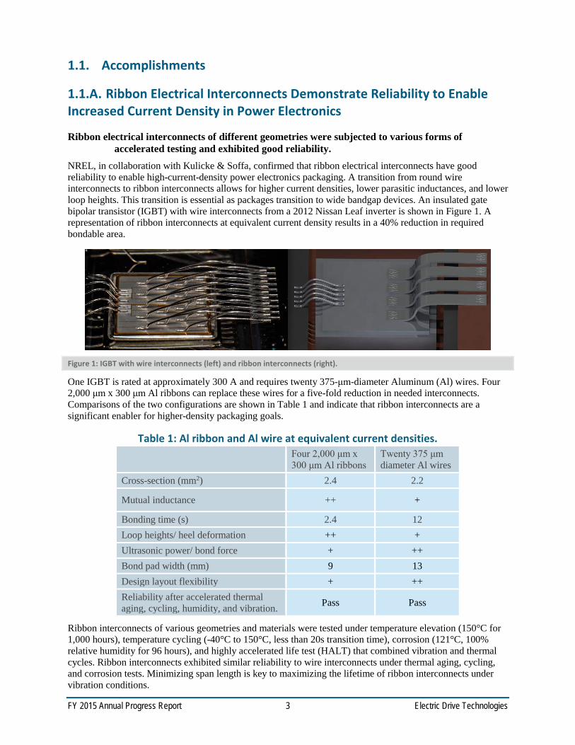
FY 2015 Annual Progress Report 3 Electric Drive Technologies
1.1. Accomplishments
1.1.A. Ribbon Electrical Interconnects Demonstrate Reliability to Enable Increased Current Density in Power Electronics
Ribbon electrical interconnects of different geometries were subjected to various forms of accelerated testing and exhibited good reliability.
NREL, in collaboration with Kulicke & Soffa, confirmed that ribbon electrical interconnects have good reliability to enable high-current-density power electronics packaging. A transition from round wire interconnects to ribbon interconnects allows for higher current densities, lower parasitic inductances, and lower loop heights. This transition is essential as packages transition to wide bandgap devices. An insulated gate bipolar transistor (IGBT) with wire interconnects from a 2012 Nissan Leaf inverter is shown in Figure 1. A representation of ribbon interconnects at equivalent current density results in a 40% reduction in required bondable area.
Figure 1: IGBT with wire interconnects (left) and ribbon interconnects (right).
One IGBT is rated at approximately 300 A and requires twenty 375-μm-diameter Aluminum (Al) wires. Four 2,000 μm x 300 μm Al ribbons can replace these wires for a five-fold reduction in needed interconnects. Comparisons of the two configurations are shown in Table 1 and indicate that ribbon interconnects are a significant enabler for higher-density packaging goals.
Table 1: Al ribbon and Al wire at equivalent current densities.
Four 2,000 μm x 300 μm Al ribbons
Twenty 375 μm diameter Al wires
Cross-section (mm2) 2.4 2.2
Mutual inductance ++ +
Bonding time (s) 2.4 12 Loop heights/ heel deformation ++ + Ultrasonic power/ bond force + ++ Bond pad width (mm) 9 13 Design layout flexibility + ++ Reliability after accelerated thermal aging, cycling, humidity, and vibration. Pass Pass
Ribbon interconnects of various geometries and materials were tested under temperature elevation (150°C for 1,000 hours), temperature cycling (-40°C to 150°C, less than 20s transition time), corrosion (121°C, 100% relative humidity for 96 hours), and highly accelerated life test (HALT) that combined vibration and thermal cycles. Ribbon interconnects exhibited similar reliability to wire interconnects under thermal aging, cycling, and corrosion tests. Minimizing span length is key to maximizing the lifetime of ribbon interconnects under vibration conditions.
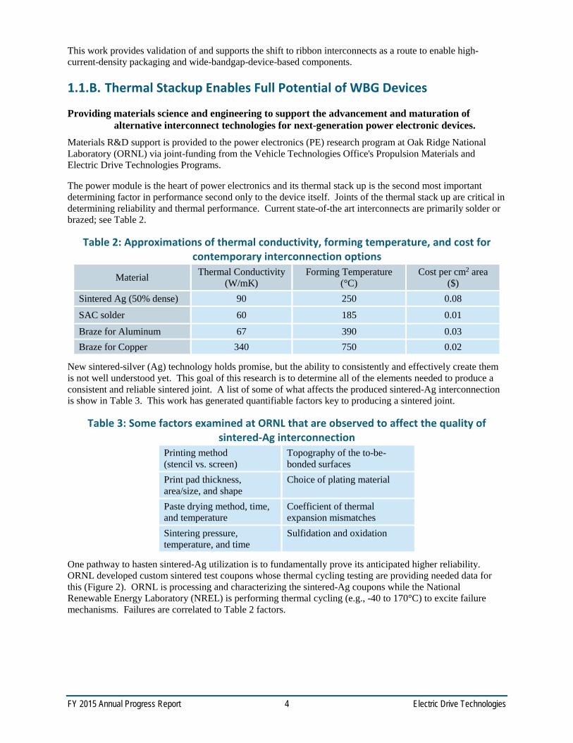
FY 2015 Annual Progress Report 4 Electric Drive Technologies
This work provides validation of and supports the shift to ribbon interconnects as a route to enable high-current-density packaging and wide-bandgap-device-based components.
1.1.B. Thermal Stackup Enables Full Potential of WBG Devices
Providing materials science and engineering to support the advancement and maturation of alternative interconnect technologies for next-generation power electronic devices.
Materials R&D support is provided to the power electronics (PE) research program at Oak Ridge National Laboratory (ORNL) via joint-funding from the Vehicle Technologies Office's Propulsion Materials and Electric Drive Technologies Programs.
The power module is the heart of power electronics and its thermal stack up is the second most important determining factor in performance second only to the device itself. Joints of the thermal stack up are critical in determining reliability and thermal performance. Current state-of-the art interconnects are primarily solder or brazed; see Table 2.
Table 2: Approximations of thermal conductivity, forming temperature, and cost for contemporary interconnection options
Material Thermal Conductivity (W/mK)
Forming Temperature (°C)
Cost per cm2 area ($)
Sintered Ag (50% dense) 90 250 0.08
SAC solder 60 185 0.01
Braze for Aluminum 67 390 0.03 Braze for Copper 340 750 0.02
New sintered-silver (Ag) technology holds promise, but the ability to consistently and effectively create them is not well understood yet. This goal of this research is to determine all of the elements needed to produce a consistent and reliable sintered joint. A list of some of what affects the produced sintered-Ag interconnection is show in Table 3. This work has generated quantifiable factors key to producing a sintered joint.
Table 3: Some factors examined at ORNL that are observed to affect the quality of sintered-Ag interconnection
Printing method (stencil vs. screen)
Topography of the to-be-bonded surfaces
Print pad thickness, area/size, and shape
Choice of plating material
Paste drying method, time, and temperature
Coefficient of thermal expansion mismatches
Sintering pressure, temperature, and time
Sulfidation and oxidation
One pathway to hasten sintered-Ag utilization is to fundamentally prove its anticipated higher reliability. ORNL developed custom sintered test coupons whose thermal cycling testing are providing needed data for this (Figure 2). ORNL is processing and characterizing the sintered-Ag coupons while the National Renewable Energy Laboratory (NREL) is performing thermal cycling (e.g., -40 to 170°C) to excite failure mechanisms. Failures are correlated to Table 2 factors.
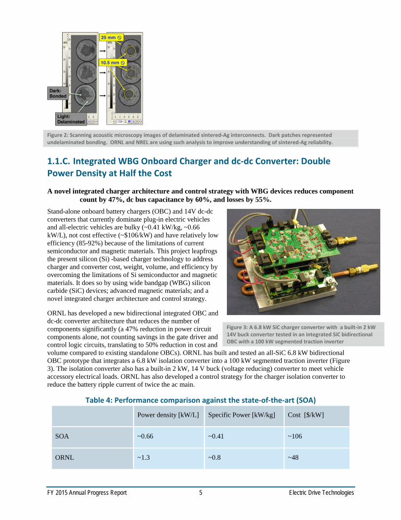
FY 2015 Annual Progress Report 5 Electric Drive Technologies
Figure 3: A 6.8 kW SiC charger converter with a built-in 2 kW 14V buck converter tested in an integrated SiC bidirectional OBC with a 100 kW segmented traction inverter
Figure 2: Scanning acoustic microscopy images of delaminated sintered-Ag interconnects. Dark patches represented undelaminated bonding. ORNL and NREL are using such analysis to improve understanding of sintered-Ag reliability.
1.1.C. Integrated WBG Onboard Charger and dc-dc Converter: Double Power Density at Half the Cost
A novel integrated charger architecture and control strategy with WBG devices reduces component count by 47%, dc bus capacitance by 60%, and losses by 55%.
Stand-alone onboard battery chargers (OBC) and 14V dc-dc converters that currently dominate plug-in electric vehicles and all-electric vehicles are bulky (~0.41 kW/kg, ~0.66 kW/L), not cost effective (~$106/kW) and have relatively low efficiency (85-92%) because of the limitations of current semiconductor and magnetic materials. This project leapfrogs the present silicon (Si) -based charger technology to address charger and converter cost, weight, volume, and efficiency by overcoming the limitations of Si semiconductor and magnetic materials. It does so by using wide bandgap (WBG) silicon carbide (SiC) devices; advanced magnetic materials; and a novel integrated charger architecture and control strategy.
ORNL has developed a new bidirectional integrated OBC and dc-dc converter architecture that reduces the number of components significantly (a 47% reduction in power circuit components alone, not counting savings in the gate driver and control logic circuits, translating to 50% reduction in cost and volume compared to existing standalone OBCs). ORNL has built and tested an all-SiC 6.8 kW bidirectional OBC prototype that integrates a 6.8 kW isolation converter into a 100 kW segmented traction inverter (Figure 3). The isolation converter also has a built-in 2 kW, 14 V buck (voltage reducing) converter to meet vehicle accessory electrical loads. ORNL has also developed a control strategy for the charger isolation converter to reduce the battery ripple current of twice the ac main.
Table 4: Performance comparison against the state-of-the-art (SOA)
Power density [kW/L] Specific Power [kW/kg] Cost [$/kW]
SOA ~0.66 ~0.41 ~106
ORNL ~1.3 ~0.8 ~48

FY 2015 Annual Progress Report 6 Electric Drive Technologies
1.1.D. Next Generation Inverter Approaches DOE 2020 Goals
Developed, tested, and demonstrated a scalable and highly efficient inverter that meets the DOE 2020 power density targets and is projected to meet DOE 2020 cost target at scaled up power level.
GM’s Next Generation Inverter achieved DOE’s 2020 traction inverter power density target of 13.4kW/L and specific power target of 14.1kW/kg. Furthermore, if GM's internal cost targets for the components and other manufacturing targets could be achieved, the Next Generation Inverter, scaled up to its highest power configuration, was projected to meet the DOE's 2020 cost target of $3.30/kW if scaled up to its maximum power level (significantly higher than the 55kW the DOE targets were based on) with 100,000 units annual volume.
In this project, GM collaborated with Oak Ridge National Laboratory (ORNL), National Renewable Energy Laboratory (NREL), and other technology and equipment suppliers. The performance of the inverter prototype (Figure 4) was verified under active load in GM’s dynamometer lab (Figure 5). Figure 6 shows the inverter efficiency maps in motoring and regeneration.
The overall design approach taken was to integrate "active" components and reduce/eliminate "supporting" components. The resulting Next Generation Inverter prototype integrates the following key features: closed aluminum coolant manifold, power semiconductors and substrates directly attached to the coolant manifold, film capacitor elements built into the coolant manifold frame, press-fit pins for signal and power circuit interconnections, one piece power semiconductor and bus plane assembly, and gate drive and control circuits on a single printed circuit board.
Key manufacturing processes were studied in this project to make sure the design can be built in high volume production. Working with GM’s internal plant and equipment supplier, a vertically integrated manufacturing plan was developed, which was key in meeting the design and aggressive cost targets.
Figure 4: The Next Generation Inverter Prototype
Figure 5: The Next Generation Inverter Prototype Under Active Load Test in GM’s Dynamometer Laboratory
Figure 6: Next Generation Inverter Efficiency Map during Regeneration (Left) and Motoring (Right)
FY 2015 Annual Progress Report 7 Electric Drive Technologies
1.2. Small Business Innovative Research Grants Gilbert Moreno, Principal Investigator National Renewable Energy Laboratory (NREL) Transportation and Hydrogen Systems Center 15013 Denver West Parkway Golden, CO 80401 Phone: (303) 275-4450 E-mail: [email protected] Steven Boyd, DOE Technology Development Manager U.S. Department of Energy 1000 Independence Avenue SW, EE-3V Washington, DC 20585 Phone: (202) 586-8997 E-mail: [email protected] Sreekant Narumanchi, NREL Task Leader Phone: (303) 275-4062 Email: [email protected]
Objectives Use the resources available through the Small Business Innovation Research (SBIR) and Small Business Technology Transfer (STTR) programs to conduct research and development of technologies that can benefit the Electric Drive Technologies (EDT) subprogram within the Vehicle Technologies Office.
Achieve the four SBIR objectives: (1) to stimulate technological innovation; (2) to increase private sector commercialization of innovations; (3) to use small business to meet federal research and development needs; and (4) to foster and encourage participation by minority and disadvantaged persons in technological innovation.
Accomplishments Initiated three Phase I awards and one Phase II award
Introduction
The Small Business Innovation Research (SBIR) program was created in 1982 through the Small Business Innovation Development Act. Eleven federal departments participate in the SBIR program and five departments participate in the STTR program, awarding a total of $2billion to small high-tech businesses. Small Business Innovation Research (SBIR) and Small Business Technology Transfer (STTR) are U.S. Government programs in which federal agencies with large research and development (R&D) budgets set aside a small fraction of their funding for competitions among small businesses only. Small businesses that win awards in these programs keep the rights to any technology developed and are encouraged to commercialize the technology.
A 1982 study found that small businesses had 2.5 times as many innovations per employee as large businesses, while large businesses were nearly three times as likely to receive government assistance. As a result, the SBIR Program was established to provide funding to stimulate technological innovation in small businesses to meet federal agency research and development needs. After more than a decade, the STTR program was launched. The major difference is that STTR projects must involve substantial (at least 30%) cooperative research collaboration between the small business and a non-profit research institution.

FY 2015 Annual Progress Report 8 Electric Drive Technologies
Approach
Each year, DOE issues a solicitation inviting small businesses to apply for SBIR/STTR Phase I grants. It contains technical topics in such research areas as energy production (Fossil, Nuclear, Renewable, and Fusion Energy), Energy Use (in buildings, vehicles, and industry), fundamental energy sciences (materials, life, environmental, and computational sciences, and nuclear and high energy physics), Environmental Management, and Nuclear Nonproliferation. Grant applications submitted by small businesses MUST respond to a specific topic and subtopic during an open solicitation.
SBIR and STTR have three distinct phases. Phase I explores the feasibility of innovative concepts with typical awards up to $225,000 for 9 months. Only Phase I award winners may compete for Phase II, the principal R&D effort, with awards up to $1,500,000 over a two-year period. There is also a Phase III, in which non-Federal capital is used by the small business to pursue commercial applications of the R&D. Also under Phase III, Federal agencies may award non-SBIR/STTR-funded, follow-on grants or contracts for products or processes that meet the mission needs of those agencies, or for further R&D.
Results and Discussion
Phase I Topics for 2015
Below is the text for the Electric Drive Technology topic from the 2015 SBIR Phase I Release 2 topics. The full topic release can be found at: http://science.energy.gov/~/media/sbir/pdf/TechnicalTopics/FY2015_Phase_1_Release_2_Topics.pdf
Power electronic inverters are essential for electric drive vehicle operation. DOE R&D targets and research pathways for inverters are described in both the U.S. DRIVE Partnership Electrical and Electronics Technical Team Roadmap [1] (http://www1.eere.energy.gov/vehiclesandfuels/pdfs/program/eett_roadmap_june2013.pdf) and EV Everywhere Blueprint [2] (http://energy.gov/sites/prod/files/2014/02/f8/eveverywhere_blueprint.pdf). These documents discuss both performance benefits of and the barriers (including high cost) — to high volume automotive adoption of wide bandgap (WBG) semiconductors. With large area (>150 mm, or 6”) SiC epiwafer is available from a large number of qualified suppliers. The SiC device industry is approaching the same cost-competitiveness as the silicon power device industry, where the cost of fabrication is the primary driver of device costs, and high device yield enables low overall device costs.
The devices that are best positioned to be an early adopter of these SiC epiwafers are SiC Schottky diodes, which offer 100X smaller on-state resistance as compared to Si and GaAs diodes and enable very high power density inverters for use in electric drive vehicles. The high switching speed of SiC diodes also provides significantly increased efficiencies for power inverter applications. While lower current (<50A) SiC Schottky diodes offered by a few SiC device suppliers have already penetrated solar and computer power supply manufacturers, higher, >100 A current remains a key threshold for automotive applications.
VTO seeks applicants to overcome this SiC device current threshold barrier by demonstrating production of >100A, >600V rated diodes suitable for use in electric-drive vehicle traction motor inverters. Specifically, devices produced should show automotive application readiness by passing qualification specifications or standards while achieving high yields. Where possible, applicants should show a relationship to, and demonstrate an understanding of automotive application requirements and environments. Example approaches for applicants include surface and/or substrate treatments and processing and compatibility with existing wire bond power module processing. Applications should also describe the cost of manufacturing SiC diodes compared to competing silicon diodes, including details such as costs and availability of commercial SiC substrates, epilayers, and additional equipment needed. Applications should link these costs to a commercially viable business model for scale up and increased production that could be executed in Phase II.

FY 2015 Annual Progress Report 9 Electric Drive Technologies
Phase I Awards Made in 2015
900-1200 V/200 A SiC Schottky Diode fabrication on 150 mm substrates in a high volume Si foundry for automotive traction inverters
Dr. Siddarth Sundaresan, GeneSiC Semiconductor
Reducing the size, weight, and increasing the efficiency of electric vehicle traction power inverters requires the development of novel high-voltage, high current silicon carbide high-speed rectifiers, since the existing silicon technology is severely limited in terms of operating temperature, frequency and energy efficiency. However, the non-optimized device and manufacturing technology currently used for silicon carbide power diode fabrication results in higher energy losses and a non-competitive price point with respect to silicon, which is the major roadblock that must be overcome to gain entry into the cost-sensitive automotive market.
Novel device and process technology in combination with the use of a high-volume manufacturing strategy on large diameter silicon carbide wafers is proposed in this proposed program for achieving near-theoretical device performance on high-current power Schottky rectifiers. The proposed device and manufacturing strategies will drastically reduce the manufacturing costs for silicon carbide Schottky diodes, making them cost-competitive with the existing silicon technology.
Phase I will be focused on developing and optimizing the device and layout designs necessary to scale up the rated current of the silicon carbide Schottky rectifiers to levels necessary for automotive traction drive Inverters. A major task would involve transferring the process technology to a large-scale, high-volume foundry identified in the proposal. A systematic method to individually qualify specific process steps at the remote foundry will be devised. A pilot wafer lot will be implemented at the large-volume foundry and the device performance will be benchmarked against the current state-of-the-art in silicon carbide power device technology.
Electric vehicle power electronics manufacturers such as Delphi Automotive and Cummins Power Systems are expected to be direct customers of the proposed silicon carbide devices to be developed in this program. Reducing the weight of the power module, which represents 23% of the total Inverter weight will extend its electric range and/or reduce the size and cost of the battery. Significantly reduced silicon carbide chip-sizes for the same current rating along with low-cost, high-volume manufacturing strategies proposed in this program will help meet the aggressive power electronics targets set for the electric vehicle industry by the DOE for the year 2022. This in turn will enhance the country’s energy security by reducing dependence on foreign oil, save money by cutting fuel costs for American families and businesses, and result in a cleaner environment by reducing harmful CO2 emissions from gas-powered vehicles.
Development of 600V, 100A SiC Schottky Diodes in a 150mm Si Foundry for Electric Vehicle Traction Inverter Applications
Dr. Kiran Chatty, Monolith Semiconductor
The final objective of the phase 1 and 2 research is to develop cost-effective, automotive qualified, 600V, 100A SiC Schottky diodes for use in traction inverter applications. The phase 1 research will focus on laying the foundation towards understanding the key factors for achieving high yield, high reliability and low cost—critical for adoption in the automotive applications.
In phase 1 program, 600V, 100A SiC Schottky diodes will be designed and fabricated in a large volume, automotive qualified 150mm Si foundry. The key yield limiters for the large area SiC diodes will be studied and the design/process trade-offs to maximize the yield and lower the cost will be presented. A preliminary reliability assessment will be performed in phase 1 to lay the groundwork for AEC-Q101 qualification in phase 2. A financial analysis that demonstrates the viability of low cost, 600V, 100A diodes via a fabless manufacturing model using 150mm Si foundry will be presented.

FY 2015 Annual Progress Report 10 Electric Drive Technologies
High Current SiC Schottky Diodes for Electric Drive Vehicle Power Electronics
Dr. John L. Hostetler, United Silicon Carbide, Inc.
The U.S. represents the world’s leading market for electric vehicles and is producing some of the most advanced plug-in electric vehicles (PEV’s) available today. PEV’s are gaining widespread adoption every year, where 58% of all PEV sales occurred in 2013 and it is expected that by 2023, there will be ~3.2 million PEV’s on the road in the U.S. alone. To increase adoption and maintain this leadership, the EV Everywhere initiative has set the goal to make electric vehicles as affordable as gasoline vehicles by 2022.
To meet the goals of the EV Everywhere initiative, the primary efforts lie in reducing costs for the batteries, PM motor and electric drive train while simultaneously reducing weight. Increasing the drive train conversion efficiency has a significant impact as it extends battery life, vehicle range and allows for a reduction of heavy cooling components through the reduction of heat generating losses. Therefore much attention is placed on increasing the efficiency of the traction power inverter that drives the electric motor. It is well documented that inverter efficiency and power density can be increased while simultaneously reducing weight through the use of Silicon Carbide (SiC) wide bandgap semiconductors. For example, demonstrations of inverters utilizing SiC-JFETs and SiC-MOSFETs are emerging, where the efficiencies are reaching >99% with 10X increased power densities.
However, today’s electric vehicle motor drive applications require high current (200-400A) power modules. SiC devices have been limited to lower current (<50A) due to the material defects, lower yields and higher costs associated with large area devices. For the electric vehicle traction inverters, it is of great interest to push up the SiC device current to 100-200A per device to make full use of the SiC system. Material defect densities have dropped dramatically in recent years as the commercial acceptance of the SiC Schottky diode have driven higher volume and more state-of-the-art semiconductor fabrication.
USCi proposes in Phase I to fabricate 200A 650V SiC Schottky Diodes on 6” diameter wafers. The high current diodes will begin reliability qualifications in Phase I. The cost of manufacturing SiC diodes will be addressed in Phase I as well. In Phase II, the diodes will be co-packaged with Si switches to form hybrid modules. When integrated, the SiC diodes will increase the efficiency of electric motor power conversion from the battery to the drive train. In Phase II, the goal will be to qualify the high current diodes on the system level for automotive applications.
Phase II Awards Made in 2015
Under the SBIR/STTR process, companies with Phase I awards from FY 2014 are eligible to apply for a Phase II award in FY 2015. One Phase II award was made in FY 2015 that resulted in the following project:
High-efficiency, Low-cost, High-temperature Nanocomposite Soft Magnetic Materials for Vehicle Power Electronics
Dr. Timothy Lin, Aegis Technology, Inc.
Opportunities exists to use high pressure gas atomization (HPGA) to replace currently used, expensive meltspinning for making soft magnetic nanocomposite alloy powders containing high moment -CoFe phase. The key to this development is to design advanced soft nanocomposite materials for small, lightweight vehicle power electronics, by using an innovative low cost HPGA approach to obtain high induction, high temperature soft magnetic nanocomposite materials that have low magnetostrictive coefficients and eddy current, and high operating temperature over conventional ones.
This project will (1) develop high permeability, large induction, low-loss (hysteretic/eddy current) soft magnetic nanocomposite materials containing high moment CoFe, which are capable of operating at high temperatures and high frequencies; and (b) improve mechanical properties and corrosion resistance of these materials with weight reduction and magnetic performance enhancement at higher operating temperatures as a result of reduction in powder size, which can be achieved by lowing annealing temperature for crystallization process, because mixtures of amorphous and nanocrystalline powders can be directly obtained by HPGA as compared to the conventional melt-spinning process that forms amorphous ribbons.

FY 2015 Annual Progress Report 11 Electric Drive Technologies
In the Phase I study, Aegis Technology has demonstrated a novel class of CoFe-based nanocomposite soft magnetic materials, and developed an innovative cost-effective approach to produce this class of high permeability, large saturation, and induction, low-loss (hysteretic/eddy current) soft magnetic nanocomposite materials with high operating temperatures. The Phase I research covered material design, processing development, characterization and prototyping, with an aim to identify the underlying technical issues that govern the fabrication and performance of this novel class of soft magnetic nanocomposites.
In Phase II more detailed research toward product development will be carried out. The composition design and processing parameters will be further optimized to meet targeted magnetic performance at both room and elevated temperatures. A cost-effective fabrication process for the production of nanocomposite cores established in Phase I will be scaled up. Some typical prototypes of inductors will be designed, built and tested, which will pave the way for potential commercialization of proposed soft materials.
The successful development of the high permeability, high induction soft magnetic nanocomposite materials with low-loss (hysteretic/eddy current) and high operating temperatures/frequencies will enable the production of high efficiency small/lightweight passive inductor. This proposed soft magnetic nanocomposite will lay the foundation for next-generation small/lightweight passive inductors that would have much improved magnetic performance in both induction and application temperatures. Applications for these new magnets are expected to include electric power generation and distribution for use in electric drive vehicles, aircraft, space vehicles, and weapons power systems. Soft magnetic materials with the capabilities of high temperature and high frequency operation would enable simpler, more efficient designs for many military and commercial applications.
Conclusions and Future Directions
The Electric Drive Technologies (EDT) subprogram hopes to continue with new Phase I and Phase II SBIR projects in FY2016.
FY 2015 Annual Progress Report 12 Electric Drive Technologies
II. RESEARCH AREAS 2.0 Electric Motor Research and Development
2.1. Non-Rare Earth Motor Development Tim Burress, Principal Investigator Oak Ridge National Laboratory (ORNL) National Transportation Research Center 2360 Cherahala Boulevard Knoxville, TN 37932 Phone: (865) 946-1216 E-mail: [email protected] Susan A. Rogers, DOE EDT Program Manager Phone: (202) 586-8997 E-mail: [email protected] Burak Ozpineci, ORNL EDT Program Manager Phone: (865) 946-1329 E-mail: [email protected] Contractor: UT-Battelle, LLC, managing and operating contractor for the Oak Ridge National Laboratory Contract No.: DE-AC05-00OR22725
Abstract/Executive Summary Almost all hybrid electric vehicles (HEVs) and electric vehicles (EVs) use permanent magnets (PMs) with rare earth materials such as neodymium and dysprosium because they facilitate the achievement of high power densities, specific powers, and efficiencies. However, there has been significant market volatility associated with these rare earth materials in recent years, including a price increase for dysprosium by a factor of 40 within one year. Therefore, alternatives to rare earth PM motors are of very high interest to original equipment manufacturers and suppliers, particularly as vehicles become more electrified and uses for rare earth materials in other applications expand. Achieving competitive performance and efficiency with alternative motors having comparable mass, volume, voltage, and other key metrics requires a highly advanced multidisciplinary research approach including high-accuracy modeling; the research, use, and development of soft and hard magnetic materials; and novel multi-objective nonlinear optimization computational design methods.
Accomplishments Machine design and development
o Developed several non-rare earth motor designs including the use of ferrite magnets. o Conducted simulations that indicate several of ORNL’s motor designs can achieve DOE 2020
targets for power density, specific power, and cost per unit of power.
Soft magnetic materials research and development (R&D) o Continued research on electrical sheet steel with high silicon (Si) content (>6%). o Confirmed capability for ingot-based processing vs. expensive chemical vapor deposition (CVD). o Developed and confirmed a novel processing technique to reduce brittleness; otherwise, the
workability of high-Si steel is not suitable for mass production of motor laminations.
Advanced modeling o Began incorporating findings from research on soft magnetic materials properties using the new
characterization system into electromagnetics modeling.
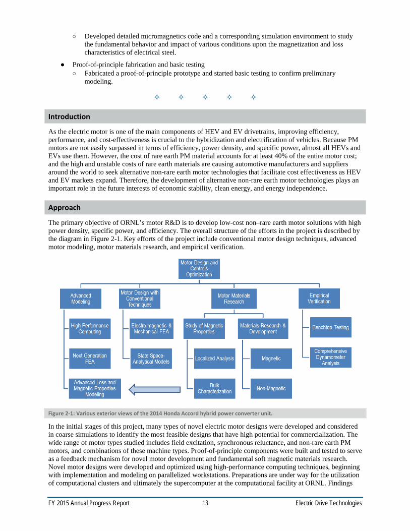
FY 2015 Annual Progress Report 13 Electric Drive Technologies
o Developed detailed micromagnetics code and a corresponding simulation environment to study the fundamental behavior and impact of various conditions upon the magnetization and loss characteristics of electrical steel.
Proof-of-principle fabrication and basic testing o Fabricated a proof-of-principle prototype and started basic testing to confirm preliminary
modeling.
Introduction
As the electric motor is one of the main components of HEV and EV drivetrains, improving efficiency, performance, and cost-effectiveness is crucial to the hybridization and electrification of vehicles. Because PM motors are not easily surpassed in terms of efficiency, power density, and specific power, almost all HEVs and EVs use them. However, the cost of rare earth PM material accounts for at least 40% of the entire motor cost; and the high and unstable costs of rare earth materials are causing automotive manufacturers and suppliers around the world to seek alternative non-rare earth motor technologies that facilitate cost effectiveness as HEV and EV markets expand. Therefore, the development of alternative non-rare earth motor technologies plays an important role in the future interests of economic stability, clean energy, and energy independence.
Approach
The primary objective of ORNL’s motor R&D is to develop low-cost non–rare earth motor solutions with high power density, specific power, and efficiency. The overall structure of the efforts in the project is described by the diagram in Figure 2-1. Key efforts of the project include conventional motor design techniques, advanced motor modeling, motor materials research, and empirical verification.
Figure 2-1: Various exterior views of the 2014 Honda Accord hybrid power converter unit.
In the initial stages of this project, many types of novel electric motor designs were developed and considered in coarse simulations to identify the most feasible designs that have high potential for commercialization. The wide range of motor types studied includes field excitation, synchronous reluctance, and non-rare earth PM motors, and combinations of these machine types. Proof-of-principle components were built and tested to serve as a feedback mechanism for novel motor development and fundamental soft magnetic materials research. Novel motor designs were developed and optimized using high-performance computing techniques, beginning with implementation and modeling on parallelized workstations. Preparations are under way for the utilization of computational clusters and ultimately the supercomputer at the computational facility at ORNL. Findings

FY 2015 Annual Progress Report 14 Electric Drive Technologies
from fundamental magnetic materials research are being incorporated into new modeling tools to improve accuracy, and this is greatly facilitated with parallelized computing.
In addition to novel motor and controls development, the development and use of new materials and materials processing techniques is under way to improve the magnetization and/or efficiency characteristics of soft magnetic materials (e.g., electrical steel). This effort is being conducted in coordination with the VTO Propulsion Materials Program. Additionally, new materials or manufacturing techniques are being studied and used to achieve improvements in manufacturability (cost reduction), cooling (in collaboration with National Renewable Energy Laboratory), and improved mechanical integrity.
To improve motor modeling accuracy and complement new materials and processing developments, fundamental research is being conducted to study the phenomena behind magnetization and loss characteristics of soft magnetic materials in electric motors, details that are still not fully quantified or understood in the scientific community. For example, residual stresses or induced stresses incurred during manufacturing or motor operation have a considerable impact upon losses and permeability. Additionally, the impact of temperature, pulsed-width modulation excitation, and other factors impact the magnetic properties in a way that is not considered or modeled with conventional finite element analysis (FEA) tools. These studies support the development of high-fidelity models and modeling tools, which are particularly important as high-performance computing is used in the optimization of detailed geometric features to achieve high power density, specific power, efficiency, and cost effectiveness.
Results and Discussion
Motor design optimization in FY 2015 was conducted with commercial FEA packages in combination with other software packages for parametric optimization algorithms as well as state space simulations. The progress and results in the area of motor design are discussed after the following sections describing the parallel efforts in materials R&D. These parallel efforts are ultimately in support of improving motor designs by developing or facilitating the use of more efficient materials and by conducting fundamental research to improve the modeling accuracy of electrical steel characteristics. Findings from this research will continue to be incorporated into new modeling tools in FY 2016.
Motor Materials Research—6.5% Silicon Steel
ORNL is developing ways to facilitate the use of electrical steel with high Si content. Near the end of FY 2014, this effort began to be a joint project with the VTO Propulsion Materials Program. Conventional electrical steel has about 2–3% Si content, and there are some expensive products on the market with 6.5% Si content. A higher amount of Si increases resistivity and therefore reduces eddy current and hysteresis losses. The comparison in Figure 2-2 indicates that an increase from 3 to 6.5% Si yields an average core loss reduction of about 35%. This reduction of core loss is nearly indirectly proportional to the resistance increase; thus the specific resistance of the 3% Si steel (labeled “Non-oriented SiFe”) is about 44% lower than the specific resistance of 6.5% Si (labeled “JNEX-Core”). The loss reduction is consistent for the various frequencies and flux density levels indicated.

FY 2015 Annual Progress Report 15 Electric Drive Technologies
Figure 2-2: Comparison of electrical steel core losses: 6.5% Si vs. 3% Si.
Currently, 6.5% Si is commercially available, but it is expensive because it is made using an intensive CVD process. Silicon steel is rolled into sheets about 0.1 to 1 mm thick, depending on the application requirements. The CVD process is used because conventional 6.5% Si steel is so brittle that it cannot be easily rolled and mechanically worked with conventional methods. Therefore, 6.5% Si sheet processing begins with 3% Si sheets, and the CVD process is used to increase the Si content to 6.5%. It remains a challenge to produce motor laminations from conventional 6.5% Si sheet steel, since a stamping process is used for mass-produced motors. The brittle 6.5% Si sheet steel is difficult to stamp consistently without undesirable fracturing, and stamping tool lifetime is reduced because the material is harder.
Research on this project aims to facilitate the production of 6.5% Si sheet steel from ingot form using thermo-mechanical processing techniques that are similar to conventional methods. Trace elements can be added to enhance strain softening behavior. In previous years, this phenomenon was confirmed with experimental measurements as samples were prepared with trace amounts of various materials, including boron. Results confirmed that ductility can be recovered during warm rolling, in which certain crystalline phase ordering is destroyed.
In addition to developing methods to produce 6.5% Si from ingots, ORNL is developing processing techniques to facilitate the rolling process, as well as lamination production. This is a critical part of the development, because lamination quality control and tool lifetime are key considerations for motor production. Hardness measurements confirm that ORNL’s new processing method softens 6.5% Si to a level similar to the softness of 3% Si without significant modification of conventional processing methods. The hardness and brittleness is associated with the formation of B2 ordered domains in the steel microstructure when Si content exceeds a critical amount, and this precludes cold rolling of the steel. Recently, it has been shown that warm rolling the steel to a critical strain results in the destruction of the B2 order because of the dislocation flow that renders the steel ductile enough for subsequent cold rolling to the finish thickness. Such an approach is clearly less expensive than the current process based on diffusion annealing.
In FY 2015, we performed thermo-mechanical processing of Fe-Si-B steels with different Si and boron contents. The steels possessed sufficient ductility during warm rolling that significant thickness reductions could be achieved without incidence of cracking. The microstructure after warm rolling indicated reduced B2 ordering. However, the dislocation density after warm rolling was high enough to adversely impact the room-temperature ductility. We are currently performing controlled warm deformation studies to optimize the warm rolling conditions that would maximize the subsequent room-temperature ductility for cold rolling of the sheet to the finish thickness.
Significant progress has also been made in investigating mechanisms that would result in significant softening of the steel during secondary forming operations, thus potentially reducing die wear. As part of the effort to understand the fundamental mechanisms that result in the destruction of the B2 order, we performed molecular dynamics simulations of warm deformation using a modified embedded atom potential (MEAM) for Fe-Si, shown in Figure 2-3. The initial microstructure consisted of multiple B2 domains in the form of circular discs lying in the [100] planes. These simulations were able to capture the reduction in the B2 order due to

FY 2015 Annual Progress Report 16 Electric Drive Technologies
deformation consistent with experimental observation. The B2 domains were broken up to smaller and smaller sizes with increasing deformation. The experimental effort is continuing with the additional melting and casting of additional Fe-Si-B alloy compositions for subsequent thermo-mechanical processing trials in FY 2016.
Figure 2-3: Simulated Si positions before and after a compressive strain of 0.153.
Motor Materials Research—Electrical Steel Modeling
The objective of this effort is to simulate the domain structure in iron (Fe) and Fe-Si alloys and the evolution of the domain structure during magnetization. The simulations will also capture the effect of nonmagnetic inclusions and elastic strain fields on the domain wall velocity and its effect on the magnetization curves. The output of the simulations will be used to improve finite element simulations of the electric motor to provide physically based constitutive laws for the soft magnetic materials used. The simulations use a Monte Carlo technique to evolve the distribution of the magnetic moments in the material, taking into account energy contributions from external magnetizing field, exchange energy, magneto-crystalline anisotropy, and magnetic dipole-dipole interaction. A message passing interface (MPI) –based parallel code has been developed that calculates exchange energy using up to 3rd-nearest neighbors, and calculates the dipole-dipole interactions through a fast multi-pole technique. A scaling law has been developed for the exchange energy term when the simulations are scaled from an atomistic to a mesoscopic length scale where each atom is replaced by a collection of unit cells.
The simulations have been used to simulate the stable presence of a domain wall when the simulation size exceeds the single-domain particle size for iron. The single-crystal simulations have been used to quantify the drag force exerted on a strain domain wall owing to the presence of a non-magnetic inclusion. The magnetization curves for a single crystal with a cube orientation and a crystal with a random orientation were generated using the simulation approach that captures the hysteresis loop associated with demagnetization and re-magnetization. The simulations have been extended to polycrystals, where the orientation of each grain in the polycrystal is identified by the three Euler angles. A realistic, three-dimensional polycrystalline microstructure was simulated using Potts model. The simulations were able to capture the effects of grain orientations and of the evolution of magnetic moments in each grain on the overall hysteresis of the microstructure. In all of the above domain wall simulations, a theoretical material with uniaxial magneto-crystalline anisotropy was used. The magnitude of the magneto-crystalline anisotropy energy relative to the exchange energy was artificially increased to obtain a stable magnetic domain wall within a relatively small computational volume. A director’s discretionary project has been requested in order to perform the simulations using Titan, ORNL’s leadership-class supercomputer, so that the above constraint on the simulation size can be relaxed and the simulations can be performed for realistic materials, including Fe and Fe-Si based magnetic materials.
Figure 2-4 shows the simulation results for the magnetization of a randomly oriented single crystal. The initial stable structure contains a few domains. Initial magnetization involves the growth of the domain, which is closest to the applied direction at the expense of the other unfavorably oriented domains. Subsequent magnetization involves the rotation of the magnetic moments in the single domain to the magnetization direction. During the demagnetizing stage as well as the re-magnetizing stage, the single domain remains intact and the magnetic moments rotate to reduce the net magnetization in the direction of the applied field. One of the aspects that the simulation is missing is the rotation of a collection of spins to the easy magnetization

FY 2015 Annual Progress Report 17 Electric Drive Technologies
directions to nucleate the domains during the demagnetization stage. The Monte Carlo code is being improved to include cluster Monte Carlo moves and implement it in a parallel code to overcome this challenge.
.
Figure 2-4: Monte Carlo simulation of the hysteresis loop for a randomly oriented single crystal showing the evolution of the initial domain structure.
Motor Design and Modeling
The development of unconventional motor technologies was accomplished by improvising upon promising technologies from previous work and initiating work on novel motor concepts. Previous research includes the design of various motor types, including the induction motor, switched reluctance motor, hybrid excitation motor, and flux coupling/field coil machines, with the latter two displaying the most potential. Novel motor designs were conceived and simulated, with consideration of various machine types such as switched reluctance, hybrid PM excitation, synchronous reluctance, and field coil excitation. Recent designs include the utilization of ferrite magnets for improved power density.
ORNL used advanced optimization algorithms to optimize motor design and controls. Electromagnetic FEA tools were used to implement basic models to determine the performance and operational characteristics of new motor designs. Analytical models were used to determine additional performance metrics and associated control methods.
Considerations in Using Non-Rare Earth Permanent Magnets
Non-rare earth PM motors must accommodate a much larger volume of magnet material in the rotor to achieve similar performance to that of a motor employing rare-earth materials. There are two main reasons for this. First, non-rare earth magnets, such as ferrites, have a much lower remanent flux density than those based on rare earths like NdFeB. For high-performance ferrites, a typical remanent flux density is about 0.4 T (4 kG) whereas 1.2 T (12 kG) is typical for NdFeB magnets. This indicates that the total surface area of ferrite magnets in an electric motor rotor must be three times greater than in an NdFeB motor producing an equivalent flux-linkage in the stator.
Second, ferrites have a much lower intrinsic coercivity than NdFeB magnets. For example, the Hitachi Metals 12 series ferrites have coercivities in the range of 300–450 kA/m (3.8–5.7 kOe). In comparison, the coercivity

FY 2015 Annual Progress Report 18 Electric Drive Technologies
of NdFeB magnets will be closer to 950 kA/m (12 kOe). Again, the ratio is about 3:1. Therefore, to resist demagnetization against a field produced by a given number of amp-turns in the stator, the magnets in a ferrite design would need to be about three times as thick as an equivalent design with rare earth materials. It should be emphasized that this approximation assumes similar stator designs for both ferrite and NdFeB designs. This issue will be addressed in more depth later.
Depending on the effective magnetic path length through the motor, each PM material has an associated magnet aspect ratio that operates the magnet at maximum flux per volume. Achieving high flux levels leads to increasingly poor magnet utilization and lower torque/power per dollar. Rare earth motors can be designed more economically by using reluctance torque to achieve the targeted torque and power levels. For example, about half of the 2010 Toyota Prius’s peak torque is due to reluctance torque. On the other hand, motors that do not operate with high reluctance torque have a potential benefit of an improved power factor.
Stators with concentrated windings have several advantages, as the teeth can be wound individually and a higher slot fill factor can be achieved. The short end turn length reduces the volume of non-active material in the motor (from a mechanical power production standpoint). Both of these factors lead to an overall decrease in copper losses.
A disadvantage of concentrated windings is that they can cause time-varying fields in the rotor, increasing rotor core losses. This is an especially serious issue for rotors with rare earth PMs, which have high conductivities. Any time-varying fields in the rotor will induce eddy currents in the PMs which will cause the PM to heat up, decreasing performance and increasing the risk of permanent demagnetization. This is less an issue for ferrite magnets because of their low conductivity and good temperature stability.
Design Constraints and Concentrated Windings
The concentrated winding design allows for the balancing of core losses and time-varying rotor fields with a corresponding decrease in copper losses. From a heat transfer perspective, losses occurring in the core of the stator often sustain a higher effective rate of heat transfer to the outside of the motor. In contrast, heat generated in the windings must be transferred through insulating materials to the stator core and is more difficult to manage.
To assess the feasibility of a concentrated winding motor design within a practical application framework, we have imposed constraints on our design based on the existing hybrid powertrain topology of the 2010 Toyota Prius. In particular, the voltage limit, current limit, stator outer diameter, and maximum speed were taken directly from this system.
For motors with no appreciable reluctance torque, the torque 𝜏𝜏 is given by 𝜏𝜏 = 1.5𝑁𝑁𝑝𝑝𝑁𝑁𝑡𝑡𝜆𝑝𝑝𝑝𝑝𝑖𝑖𝑞𝑞where 𝑁𝑁𝑝𝑝 is the number of motor poles, 𝑁𝑁𝑡𝑡 is the number of turns, 𝑖𝑖𝑞𝑞 is the quadrature current, and 𝜆𝑝𝑝𝑝𝑝 is the normalized (single-turn) PM flux-linkage. Increasing the torque by achieving a large number of turns is limited by (1) the risk of demagnetizing the PM materials and (2) saturation of the magnetic core. From a bulk parameter perspective, the demagnetization risk is associated purely with a direct axis current (𝑖𝑖𝑑𝑑), which is not the torque-producing component. At the continuum level, this is largely true for PM motors with integer slot winding configurations because, for each pole, the field generated by 𝑖𝑖𝑞𝑞 is truly in quadrature with the PM fields.
The situation is different for concentrated windings that produce a spatial distribution of the flux with rather large subharmonics. The bulk parameter model is the result of the phasor sum of the individual stator teeth interacting with the rotor poles, and the effects of the subharmonics are unobservable in this model. In the worst-case scenario, the peak demagnetizing field is produced by two adjacent teeth roughly aligned with different rotor poles. This is to say a PM motor with concentrated windings must be protected against demagnetization from both direct and quadrature currents. This depends on the tooth/winding configuration, with some choices increasing the risk of q-axis demagnetization more than others, as demonstrated in Figure 2-5.
The other limiting factor is saturation of the core. An ideally sized motor would meet the demagnetization and saturation constraints simultaneously. A saturation limitation would reduce the ability to perform field weakening in order to achieve constant power over a wide speed range. Alternatively, it implies an overuse of
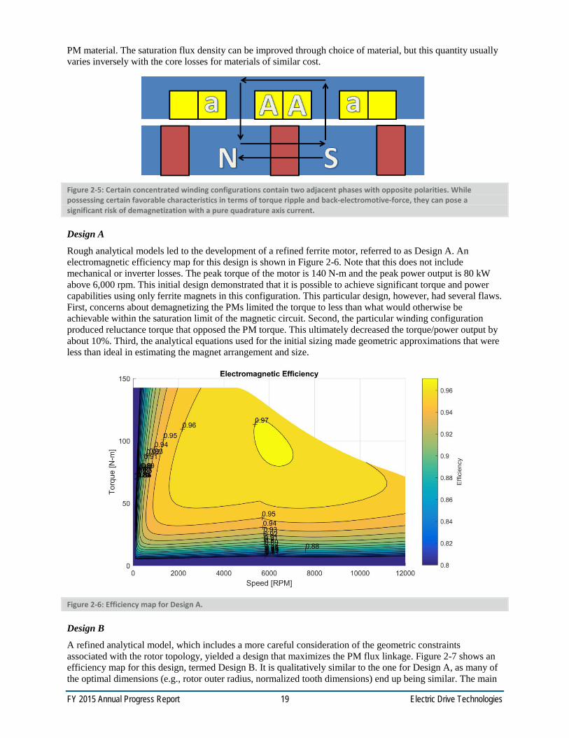
FY 2015 Annual Progress Report 19 Electric Drive Technologies
PM material. The saturation flux density can be improved through choice of material, but this quantity usually varies inversely with the core losses for materials of similar cost.
Figure 2-5: Certain concentrated winding configurations contain two adjacent phases with opposite polarities. While possessing certain favorable characteristics in terms of torque ripple and back-electromotive-force, they can pose a significant risk of demagnetization with a pure quadrature axis current.
Design A
Rough analytical models led to the development of a refined ferrite motor, referred to as Design A. An electromagnetic efficiency map for this design is shown in Figure 2-6. Note that this does not include mechanical or inverter losses. The peak torque of the motor is 140 N-m and the peak power output is 80 kW above 6,000 rpm. This initial design demonstrated that it is possible to achieve significant torque and power capabilities using only ferrite magnets in this configuration. This particular design, however, had several flaws. First, concerns about demagnetizing the PMs limited the torque to less than what would otherwise be achievable within the saturation limit of the magnetic circuit. Second, the particular winding configuration produced reluctance torque that opposed the PM torque. This ultimately decreased the torque/power output by about 10%. Third, the analytical equations used for the initial sizing made geometric approximations that were less than ideal in estimating the magnet arrangement and size.
Figure 2-6: Efficiency map for Design A.
Design B
A refined analytical model, which includes a more careful consideration of the geometric constraints associated with the rotor topology, yielded a design that maximizes the PM flux linkage. Figure 2-7 shows an efficiency map for this design, termed Design B. It is qualitatively similar to the one for Design A, as many of the optimal dimensions (e.g., rotor outer radius, normalized tooth dimensions) end up being similar. The main
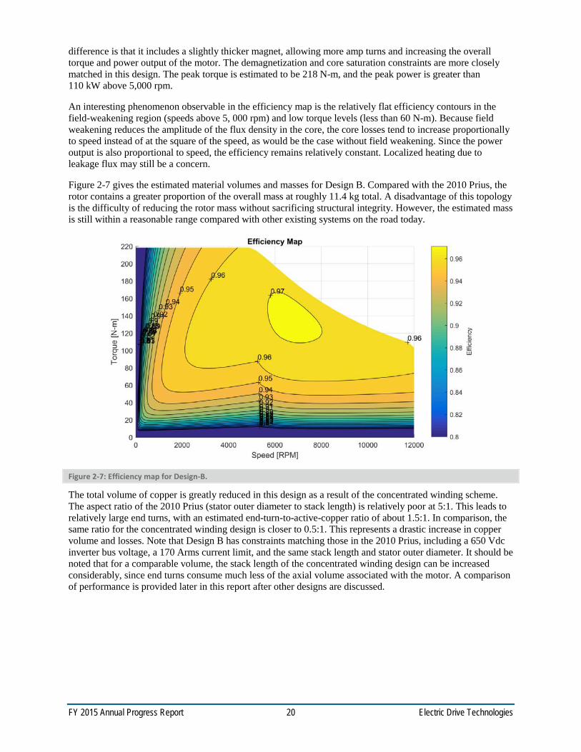
FY 2015 Annual Progress Report 20 Electric Drive Technologies
difference is that it includes a slightly thicker magnet, allowing more amp turns and increasing the overall torque and power output of the motor. The demagnetization and core saturation constraints are more closely matched in this design. The peak torque is estimated to be 218 N-m, and the peak power is greater than 110 kW above 5,000 rpm.
An interesting phenomenon observable in the efficiency map is the relatively flat efficiency contours in the field-weakening region (speeds above 5, 000 rpm) and low torque levels (less than 60 N-m). Because field weakening reduces the amplitude of the flux density in the core, the core losses tend to increase proportionally to speed instead of at the square of the speed, as would be the case without field weakening. Since the power output is also proportional to speed, the efficiency remains relatively constant. Localized heating due to leakage flux may still be a concern.
Figure 2-7 gives the estimated material volumes and masses for Design B. Compared with the 2010 Prius, the rotor contains a greater proportion of the overall mass at roughly 11.4 kg total. A disadvantage of this topology is the difficulty of reducing the rotor mass without sacrificing structural integrity. However, the estimated mass is still within a reasonable range compared with other existing systems on the road today.
Figure 2-7: Efficiency map for Design-B.
The total volume of copper is greatly reduced in this design as a result of the concentrated winding scheme. The aspect ratio of the 2010 Prius (stator outer diameter to stack length) is relatively poor at 5:1. This leads to relatively large end turns, with an estimated end-turn-to-active-copper ratio of about 1.5:1. In comparison, the same ratio for the concentrated winding design is closer to 0.5:1. This represents a drastic increase in copper volume and losses. Note that Design B has constraints matching those in the 2010 Prius, including a 650 Vdc inverter bus voltage, a 170 Arms current limit, and the same stack length and stator outer diameter. It should be noted that for a comparable volume, the stack length of the concentrated winding design can be increased considerably, since end turns consume much less of the axial volume associated with the motor. A comparison of performance is provided later in this report after other designs are discussed.

FY 2015 Annual Progress Report 21 Electric Drive Technologies
Table 2-1: Estimated material volumes and masses for Design B Material Volume (L) Mass (kg) Note
Rotor laminations 0.81 6.3 JFE 35H440
Ferrite magnets 0.67 3.5 Hitachi NMF-12G+
Rotor shaft 0.21 1.6 Estimate based on 2010 Prius
Stator laminations 0.91 7.1 JFE 35H440
Copper 0.20 1.8 Assuming a 50% fill factor
Design C
Refinements were made to the winding layout of Design B to achieve a very low (~1.7%) torque ripple with this topology without skewing of the stator or rotor. An example torque waveform is shown in Figure 2-8. Some winding approaches to reduce torque ripple tend to excite lower-frequency vibrational modes due to a slower spatial variation of the radial forces between the stator and the rotor. This can be undesirable from a noise perspective, depending on where the vibration frequency falls within the spectrum of human perception. The problem is confounded by the fact that mechanical systems tend to be more efficient at damping high-frequency vibrations.
Additional mechanical simulations are required to evaluate the feasibility of achieving reduced torque ripple in this manner. If possible, it is certainly cheaper from a manufacturing perspective than the method of skewing the stator and/or rotor. The optimal solution involves a compromise that will still reduce the torque ripple, although to a lesser extent, but will suffer fewer negative effects from radial forces.
Figure 2-8: Torque waveform from a design with winding designed for torque ripple minimization.
System Level Considerations— Design D
The base speed of Design B is about twice that of the 2010 Prius. The fact that the peak torque can be delivered at much higher speeds is directly responsible for the higher output power of the design. This may in fact be unnecessary, and the extra headroom could be used to improve the overall system elsewhere. For example, the current rating of the inverter could be lowered (say, by 50%) and the number of turns increased in the motor to give similar peak torque and power capabilities to those of the 2010 Prius with a greatly downsized inverter. Or the operating voltage can be lowered so that the electric drive system operates at lower voltages, near those of typical nominal battery voltages in the range of 300–400Vdc. Otherwise, a boost converter may be required.
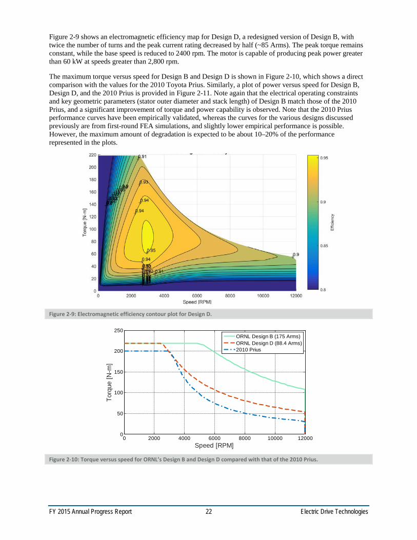
FY 2015 Annual Progress Report 22 Electric Drive Technologies
Figure 2-9 shows an electromagnetic efficiency map for Design D, a redesigned version of Design B, with twice the number of turns and the peak current rating decreased by half (~85 Arms). The peak torque remains constant, while the base speed is reduced to 2400 rpm. The motor is capable of producing peak power greater than 60 kW at speeds greater than 2,800 rpm.
The maximum torque versus speed for Design B and Design D is shown in Figure 2-10, which shows a direct comparison with the values for the 2010 Toyota Prius. Similarly, a plot of power versus speed for Design B, Design D, and the 2010 Prius is provided in Figure 2-11. Note again that the electrical operating constraints and key geometric parameters (stator outer diameter and stack length) of Design B match those of the 2010 Prius, and a significant improvement of torque and power capability is observed. Note that the 2010 Prius performance curves have been empirically validated, whereas the curves for the various designs discussed previously are from first-round FEA simulations, and slightly lower empirical performance is possible. However, the maximum amount of degradation is expected to be about 10–20% of the performance represented in the plots.
Figure 2-9: Electromagnetic efficiency contour plot for Design D.
Figure 2-10: Torque versus speed for ORNL’s Design B and Design D compared with that of the 2010 Prius.
0 2000 4000 6000 8000 10000 120000
50
100
150
200
250
Speed [RPM]
Torq
ue [N
-m]
ORNL Design B (175 Arms)ORNL Design D (88.4 Arms)2010 Prius

FY 2015 Annual Progress Report 23 Electric Drive Technologies
Figure 2-11: Power versus speed for ORNL’s Design B and Design D compared with that of the 2010 Prius.
Conclusions and Future Direction
ORNL continues to make advances in the development of low-cost processing methods for the production of high-efficiency Si steel for motor laminations. In this FY 2015 effort, jointly funded by the Propulsion Materials Program, thermo-mechanical processing of Fe-Si-B steels with different Si and boron contents, sufficient ductility during warm rolling, and significant thickness reductions was achieved without incidence of cracking. Controlled warm deformation studies are under way to optimize the warm rolling conditions that would maximize the subsequent room-temperature ductility for cold rolling of the sheet to the finish thickness.
Simulations are being implemented on ORNL’s Titan supercomputer using a Monte Carlo technique to study the fundamental impacts of residual stress, temperature, and other influences upon the magnetic properties of electrical steel that is used in electric motors. Ultimately, this information will be used to help in the development of high-fidelity FEA models.
Motor performance and efficiency metrics from FY 2015 motor design efforts involving the use of ferrite PMs are highly competitive with those for state-of-the-art rare earth PM motors. Table 2-2 shows a summary of the various targets compared with ORNL’s designs and the 2010 Prius design. While the designs still need to be verified with empirical testing, the results are highly encouraging. Secondary prototypes will be fabricated and tested in FY 2016.
Table 2-2: Comparison of status with DOE targets Parameter DOE 2020 targets ORNL Design B ORNL Design D 2010 Prius
kW/L 5.7 8.8 5.1 4.8
kW/kg 1.6 3.2 1.8 1.6
Estimated $/kW 4.7 3.1 2.2 13.5
0 2000 4000 6000 8000 10000 120000
50
100
150
Speed [RPM]
Pow
er [k
W]
ORNL Design B (175 Arms)ORNL Design D (88.4 Arms)2010 Prius

FY 2015 Annual Progress Report 24 Electric Drive Technologies
FY 2015 Presentations/Publications/Patents
1. T. Burress, et al., “Non-rare earth motor development,” presented at the DOE Vehicle Technologies Program Electric Drive Technologies FY 2015 Kickoff Meeting, Oak Ridge, Tennessee, November 18, 2014.
2. T. Burress, et al., “Non-rare earth motor development,” presented at the DOE Vehicle Technologies Program Electric Drive Technologies Electrical and Electronics Technical Team Meeting, February 24, 2015.
3. T. Burress, et al., “Non-rare earth motor development,” presented at the VTO 2015 Annual Merit Review, Washington DC, June 2015.

FY 2015 Annual Progress Report 25 Electric Drive Technologies
2.2. Multi-Speed-Range Electric Motors Lixin Tang, Principal Investigator Oak Ridge National Laboratory (ORNL) National Transportation Research Center 2360 Cherahala Boulevard Knoxville, TN 37932 Phone: (865) 946-1526 E-mail: [email protected] Susan A. Rogers, DOE EDT Program Manager Phone: (202) 586-8997 E-mail: [email protected] Burak Ozpineci, ORNL EDT Program Manager Phone: (865) 946-1329 E-mail: [email protected] Contractor: UT-Battelle, LLC, managing and operating contractor for the Oak Ridge National Laboratory Contract No.: DE-AC05-00OR22725
Abstract/Executive Summary In this project, multi-speed-range (MSR) solutions for electric motors are being developed to improve
drive cycle efficiency, increase power density/specific power, and reduce system cost. In FY 2015, we used drive cycle simulation to confirm the effectiveness of MSR operation, developed a new design to achieve MSR operation, and finished initial benchtop tests.
Accomplishments Confirmed by drive cycle simulation that MSR operation achieves higher drive cycle efficiency.
o Used a 3-speed-range motor to reduce the total loss by 24% in a combined drive cycle.
Developed a novel MSR system design. o It features fewer added solid-state ac switches and lower losses in low-speed and high-speed
mode. o It does not have a dc short-circuit failure mode.
Conducted a bench top component test. o Designed/fabricated a low-cost fast switching ac switch printed circuit board (PCB) assembly for
changing switching arrangements. o Confirmed the capability to decrease current, change winding configurations, and increase current
in a short amount of time.
Introduction
The latest benchmarking test results for different hybrid electric vehicle (HEV) and plug-in electric vehicle (PEV) drive systems show that single-speed-range drive systems normally are most efficient in a high-power region—i.e., medium torque in a medium- to high-speed area—and less efficient in low torque and speed regions. To achieve high efficiency, it is desirable to operate the drive system as close as possible to the high-efficiency area. Figure 2-12 is an efficiency map of an EV drive system at different torques and speeds. Its efficiency ranges from 70% at around 500 rev/min to a peak efficiency of 96% at around 6,400~8,600 rev/min with 80 ~ 100 Nm load torque.
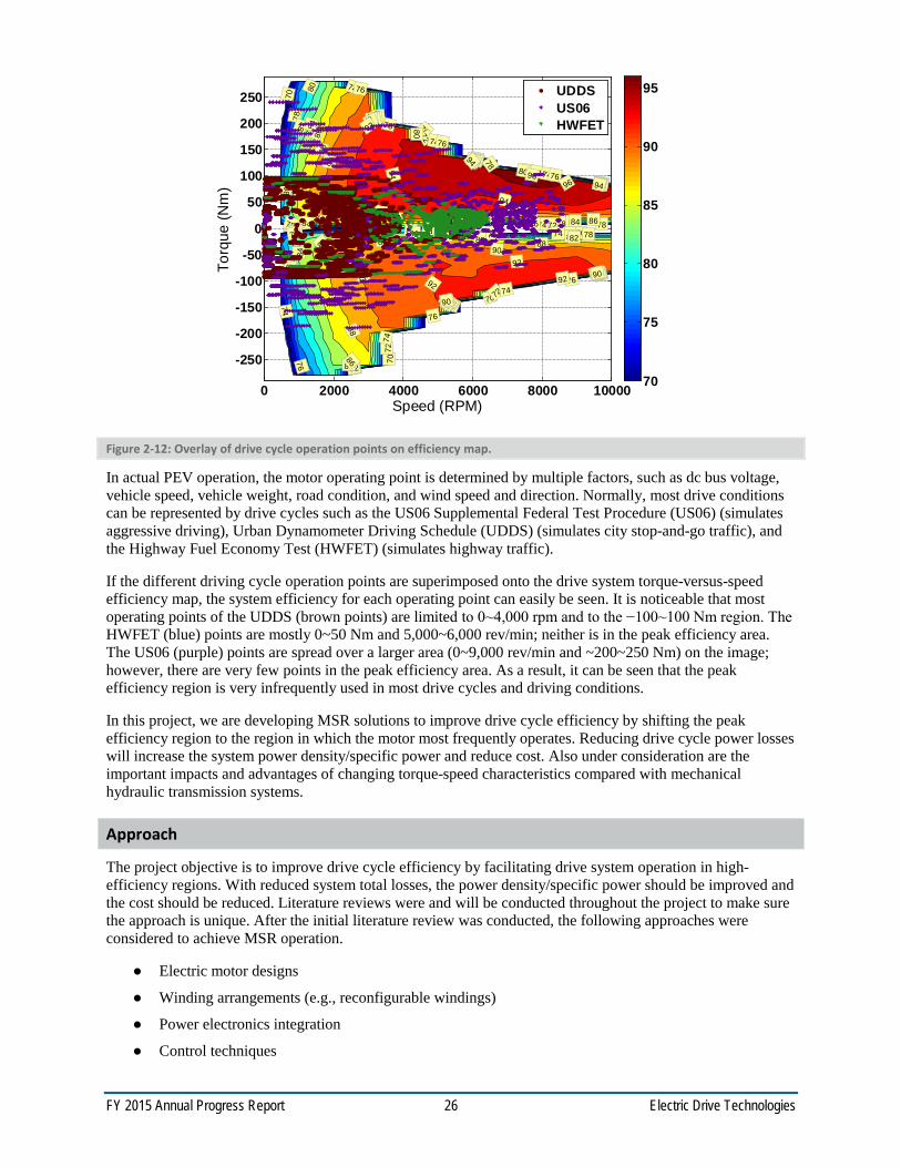
FY 2015 Annual Progress Report 26 Electric Drive Technologies
Figure 2-12: Overlay of drive cycle operation points on efficiency map.
In actual PEV operation, the motor operating point is determined by multiple factors, such as dc bus voltage, vehicle speed, vehicle weight, road condition, and wind speed and direction. Normally, most drive conditions can be represented by drive cycles such as the US06 Supplemental Federal Test Procedure (US06) (simulates aggressive driving), Urban Dynamometer Driving Schedule (UDDS) (simulates city stop-and-go traffic), and the Highway Fuel Economy Test (HWFET) (simulates highway traffic).
If the different driving cycle operation points are superimposed onto the drive system torque-versus-speed efficiency map, the system efficiency for each operating point can easily be seen. It is noticeable that most operating points of the UDDS (brown points) are limited to 0~4,000 rpm and to the −100~100 Nm region. The HWFET (blue) points are mostly 0~50 Nm and 5,000~6,000 rev/min; neither is in the peak efficiency area. The US06 (purple) points are spread over a larger area (0~9,000 rev/min and ~200~250 Nm) on the image; however, there are very few points in the peak efficiency area. As a result, it can be seen that the peak efficiency region is very infrequently used in most drive cycles and driving conditions.
In this project, we are developing MSR solutions to improve drive cycle efficiency by shifting the peak efficiency region to the region in which the motor most frequently operates. Reducing drive cycle power losses will increase the system power density/specific power and reduce cost. Also under consideration are the important impacts and advantages of changing torque-speed characteristics compared with mechanical hydraulic transmission systems.
Approach
The project objective is to improve drive cycle efficiency by facilitating drive system operation in high-efficiency regions. With reduced system total losses, the power density/specific power should be improved and the cost should be reduced. Literature reviews were and will be conducted throughout the project to make sure the approach is unique. After the initial literature review was conducted, the following approaches were considered to achieve MSR operation.
Electric motor designs
Winding arrangements (e.g., reconfigurable windings)
Power electronics integration
Control techniques
0 2000 4000 6000 8000 10000
-250
-200
-150
-100
-50
0
50
100
150
200
250
Speed (RPM)
Torq
ue (N
m)
70
70
70
7070
72
72
7272
74
74
74
7474
76
76
76
7676
78
78
78
787878
80
80
80
80
8080 828282
82
82
82
82
848484
84
84
84
84
868686
86
86
86
86
8888
88
88
88
88
9090
90
90
90
90
9292
92
92
92
94
94
94
949696
70
70
7070
72
72
7272
74
74
74
7474
76
76
76
7676 7878
78
78
78
78
8080
80
80
80
80
8282
82
82
82
82
84
84
84
84
84
8686
86
86
86
8888
88
88
88
90
90
90
9092
92 92
70
75
80
85
90
95UDDSUS06HWFET

FY 2015 Annual Progress Report 27 Electric Drive Technologies
Figure 2-13 shows an example of MSR operation in the UDDS drive cycle, which indicates stop-and-go driving characteristics typically experienced in cities. The speed range transition levels are set at 15 and 27 mph with three different operating modes that are determined by the vehicle speed. A transition occurs if the vehicle speed crosses one of the two speed transition levels, and it is desirable that each transition be smooth, short, and stable.
Figure 2-13: Example of 3-speed-range operation in UDDS drive cycle.
This approach can be viewed as mimicking the functionality of a mechanical transmission. A 3-speed transmission designed for PEV applications is shown in Figure 2-14 to show the complexity, weight, and volume of a mechanical transmission. It weighs about 45 kg, and its overall length can be as much as 16.3 in. The oil pumps are heavy and occupy a large volume. A wet clutch requires maintenance and is the component most likely to fail in a conventional transmission. Figure 2-15 shows a 6-speed transmission for a 2011 Hyundai Sonata hybrid vehicle. A large oil pump and valve body are visible on the left, and some of the clutches and gears of the transmission are shown on the right. Normally, hydraulic clutches are mechanically complicated. They need oil pumps to maintain the pressure—requiring extra power and control—and extra sensors, valves, and a control unit. Our approach will replace a significant number of these parts in a mechanical transmission. Note that an electric drive system may not need a 6-speed transmission because it can generate peak torque at zero speed.
Figure 2-14: A commercial 3-speed transmission for PEV applications.
0 200 400 600 800 1000 1200 14000
10
20
30
40
50
60UDDS driving cycle
Time (sec.)
Spee
d (M
PH)
Speed Range 2
Speed Range 3
Speed Range 1
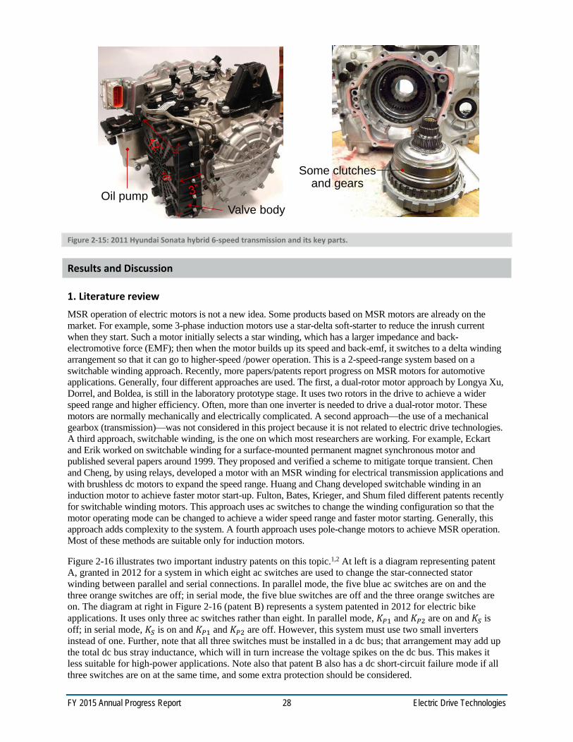
FY 2015 Annual Progress Report 28 Electric Drive Technologies
Figure 2-15: 2011 Hyundai Sonata hybrid 6-speed transmission and its key parts.
Results and Discussion
1. Literature review MSR operation of electric motors is not a new idea. Some products based on MSR motors are already on the market. For example, some 3-phase induction motors use a star-delta soft-starter to reduce the inrush current when they start. Such a motor initially selects a star winding, which has a larger impedance and back-electromotive force (EMF); then when the motor builds up its speed and back-emf, it switches to a delta winding arrangement so that it can go to higher-speed /power operation. This is a 2-speed-range system based on a switchable winding approach. Recently, more papers/patents report progress on MSR motors for automotive applications. Generally, four different approaches are used. The first, a dual-rotor motor approach by Longya Xu, Dorrel, and Boldea, is still in the laboratory prototype stage. It uses two rotors in the drive to achieve a wider speed range and higher efficiency. Often, more than one inverter is needed to drive a dual-rotor motor. These motors are normally mechanically and electrically complicated. A second approach—the use of a mechanical gearbox (transmission)—was not considered in this project because it is not related to electric drive technologies. A third approach, switchable winding, is the one on which most researchers are working. For example, Eckart and Erik worked on switchable winding for a surface-mounted permanent magnet synchronous motor and published several papers around 1999. They proposed and verified a scheme to mitigate torque transient. Chen and Cheng, by using relays, developed a motor with an MSR winding for electrical transmission applications and with brushless dc motors to expand the speed range. Huang and Chang developed switchable winding in an induction motor to achieve faster motor start-up. Fulton, Bates, Krieger, and Shum filed different patents recently for switchable winding motors. This approach uses ac switches to change the winding configuration so that the motor operating mode can be changed to achieve a wider speed range and faster motor starting. Generally, this approach adds complexity to the system. A fourth approach uses pole-change motors to achieve MSR operation. Most of these methods are suitable only for induction motors.
Figure 2-16 illustrates two important industry patents on this topic.1,2 At left is a diagram representing patent A, granted in 2012 for a system in which eight ac switches are used to change the star-connected stator winding between parallel and serial connections. In parallel mode, the five blue ac switches are on and the three orange switches are off; in serial mode, the five blue switches are off and the three orange switches are on. The diagram at right in Figure 2-16 (patent B) represents a system patented in 2012 for electric bike applications. It uses only three ac switches rather than eight. In parallel mode, 𝐾𝐾𝑃𝑃1 and 𝐾𝐾𝑃𝑃2 are on and 𝐾𝐾𝑆𝑆 is off; in serial mode, 𝐾𝐾𝑆𝑆 is on and 𝐾𝐾𝑃𝑃1 and 𝐾𝐾𝑃𝑃2 are off. However, this system must use two small inverters instead of one. Further, note that all three switches must be installed in a dc bus; that arrangement may add up the total dc bus stray inductance, which will in turn increase the voltage spikes on the dc bus. This makes it less suitable for high-power applications. Note also that patent B also has a dc short-circuit failure mode if all three switches are on at the same time, and some extra protection should be considered.
Some clutches and gears
Valve bodyOil pump
9”
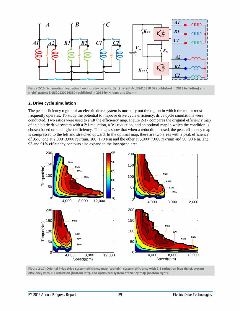
FY 2015 Annual Progress Report 29 Electric Drive Technologies
Figure 2-16: Schematics illustrating two industry patents: (left) patent A-US8415910 B2 (published in 2013 by Fulton) and (right) patent B-US20120086380 (published in 2012 by Krieger and Shum).
2. Drive cycle simulation The peak efficiency region of an electric drive system is normally not the region in which the motor most frequently operates. To study the potential to improve drive cycle efficiency, drive cycle simulations were conducted. Two ratios were used to shift the efficiency map. Figure 2-17 compares the original efficiency map of an electric drive system with a 2:1 reduction, a 3:1 reduction, and an optimal map in which the condition is chosen based on the highest efficiency. The maps show that when a reduction is used, the peak efficiency map is compressed to the left and stretched upward. In the optimal map, there are two areas with a peak efficiency of 95%: one at 2,000~3,000 rev/min, 100~170 Nm and the other at 5,000~7,000 rev/min and 50~90 Nm. The 93 and 91% efficiency contours also expand to the low-speed area.
Figure 2-17: Original Prius drive system efficiency map (top left), system efficiency with 2:1 reduction (top right), system efficiency with 3:1 reduction (bottom left), and optimized system efficiency map (bottom right).
Torq
ue(N
m)
4,000 8,000 12,0000
50
100
150
200
70
75
80
85
90
95
4,000 8,000 12,0000
50
100
150
200
95%
Speed(rpm)
Torq
ue(N
m)
4,000 8,000 12,0000
50
100
150
200
Speed(rpm)
4,000 8,000 12,0000
50
100
150
200
95%
93%
91%
89%
95%
93%
91% 89%
95%
93%
91%
89%
95%
93%
91%
89%

FY 2015 Annual Progress Report 30 Electric Drive Technologies
To study drive cycle efficiency, three scenarios were considered. The first scenario was the original Prius drive system with a fixed-speed-range motor; the second and third scenarios used the Prius system with 2-speed and 3-speed ratios. Four drive cycles (US06, UDDS, HWFET, and a combined cycle including all three) were selected to compare the drive cycle efficiency.
Table 2-3 shows the average drive cycle efficiency. The option-1 system is a 2-speed-range drive, and the option-2 system is a 3-speed-range drive. It can be seen that in the MSR system, the drive cycle efficiency is improved most significantly in the UDDS cycle, followed by the US06 cycle and the HWFET cycle. The improvement in the HWFET cycle is low because the operating points were already in a relatively high-efficiency area. The option-2 system is more efficient than the option-1 system with only two speed ranges.
Table 2-3: Average drive cycle efficiency
US06 (aggressive )
UDDS (city/stop-and-go)
HWFET (highway) Combined
2013 Prius motor only 86.9 80.7 89.9 84.7
2013 Prius inverter only 91.8 81.0 95.95 87.6
2013 Prius system 81.7 69.1 86.6 76.7
Option-1 system 83.6 75.5 87.5 81.5
Option-2 system 86.3 78.7 87.8 83.0
Table 2-4 shows the total energy loss of the original and option-2 system. The results show that with the 3-speed-range system, the total energy loss can be reduced by 29.7, 28, 4.6, and 23.6% in the US06, UDDS, HWFET, and combined cycles, respectively. All the results show that an MSR system can improve drive cycle efficiency and reduce drive cycle loss significantly.
Table 2-4: Drive cycle total energy loss
US06
(× 1,000,000 Joules)
UDDS (× 1,000,000
Joules)
HWFET (× 1,000,000
Joules)
Combined (× 1,000,000
Joules)
2013 Prius system 1.374 1.621 0.803 3.798
Option-2 system 0.966 1.167 0.766 2.899
Loss reduction (%) 29.7 28.0 4.61 23.6
3. New MSR designs MSR designs based on a switchable winding approach were proposed to achieve MSR operation; the block diagram can be seen in Figure 2-18. Compared with the patent A approach shown in Figure 2-16, the proposed design uses fewer ac power switches; and because it does not insert ac power switches in the dc bus, it does not have the dc short-circuit failure mode that patent B has. To evaluate the advantages, the inverter losses of the design proposed in patent A were compared with those of the MSR design. The inverter loss includes switching loss and conduction loss. The basic equations used to calculate switching loss and conduction loss in a 3-phase voltage source inverter can be seen in Eqs. (1–3). Equation (1) shows the inverter switching loss, where 𝑓𝑓𝑆𝑆𝑆𝑆 is the switching frequency, 𝑉𝑉𝑑𝑑𝑑𝑑 is the dc bus voltage, 𝐼𝐼𝑃𝑃𝑃𝑃𝐴𝐴𝐴𝐴 is the peak phase current, 𝑉𝑉𝑟𝑟𝑟𝑟𝑟𝑟 and 𝐼𝐼𝑟𝑟𝑟𝑟𝑟𝑟 are the voltage and current at which the switching losses are given, 𝐸𝐸𝑂𝑂𝑂𝑂_𝐼𝐼𝐼𝐼𝐼𝐼𝐼𝐼, 𝐸𝐸𝑂𝑂𝑂𝑂𝑂𝑂_𝐼𝐼𝐼𝐼𝐼𝐼𝐼𝐼 are the turn-on, turn-off loss of the insulated gate bipolar transistor (IGBT), and 𝐸𝐸𝑂𝑂𝑂𝑂𝑂𝑂_𝐷𝐷𝐼𝐼𝑂𝑂𝐷𝐷𝑃𝑃 is the turn-off loss of the diode.
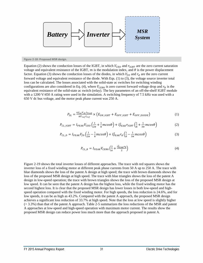
FY 2015 Annual Progress Report 31 Electric Drive Technologies
Figure 2-18: Proposed MSR design.
Equation (2) shows the conduction losses of the IGBT, in which 𝑉𝑉𝐶𝐶𝑃𝑃𝑂𝑂 and 𝑟𝑟𝐼𝐼𝐼𝐼𝐼𝐼𝐼𝐼 are the zero current saturation voltage and equivalent resistance of the IGBT, 𝑚𝑚 is the modulation index, and 𝜃𝜃 is the power displacement factor. Equation (3) shows the conduction losses of the diodes, in which 𝑉𝑉𝑟𝑟𝑂𝑂 and 𝑟𝑟𝑑𝑑 are the zero current forward voltage and equivalent resistance of the diode. With Eqs. (1) to (3), the voltage source inverter total loss can be calculated. The losses associated with the solid-state ac switches for switching winding configurations are also considered in Eq. (4), where 𝑉𝑉𝐶𝐶𝑃𝑃𝐶𝐶0 is zero current forward voltage drop and 𝑟𝑟𝐶𝐶 is the equivalent resistance of the solid-state ac switch (relay). The key parameters of an off-the-shelf IGBT module with a 1200 V/450 A rating were used in the simulation. A switching frequency of 7.5 kHz was used with a 650 V dc bus voltage, and the motor peak phase current was 250 A.
𝑃𝑃𝑆𝑆𝑆𝑆 = 6𝑟𝑟𝑠𝑠𝑠𝑠𝑉𝑉𝑑𝑑𝑑𝑑𝐼𝐼𝑃𝑃𝑃𝑃𝑃𝑃𝑃𝑃𝜋𝜋𝑉𝑉𝑟𝑟𝑃𝑃𝑟𝑟𝐼𝐼𝑟𝑟𝑃𝑃𝑟𝑟
× 𝐸𝐸𝑂𝑂𝑂𝑂_𝐼𝐼𝐼𝐼𝐼𝐼𝐼𝐼 + 𝐸𝐸𝑂𝑂𝑂𝑂𝑂𝑂_𝐼𝐼𝐼𝐼𝐼𝐼𝐼𝐼 + 𝐸𝐸𝑂𝑂𝑂𝑂𝑂𝑂_𝐷𝐷𝐼𝐼𝑂𝑂𝐷𝐷𝑃𝑃 (1)
𝑃𝑃𝐶𝐶𝑆𝑆_𝐼𝐼𝐼𝐼𝐼𝐼𝐼𝐼 = 𝐼𝐼𝑃𝑃𝑃𝑃𝐴𝐴𝐴𝐴𝑉𝑉𝐶𝐶𝑃𝑃𝑂𝑂 12𝜋𝜋
+ 18𝑚𝑚𝑚𝑚𝑚𝑚𝑚𝑚𝜃𝜃+ 𝐼𝐼𝑃𝑃𝑃𝑃𝐴𝐴𝐴𝐴2 𝑟𝑟𝐼𝐼𝐼𝐼𝐼𝐼𝐼𝐼
18
+ 13𝜋𝜋𝑚𝑚𝑚𝑚𝑚𝑚𝑚𝑚𝜃𝜃 (2)
𝑃𝑃𝐶𝐶𝑆𝑆_𝐷𝐷 = 𝐼𝐼𝑃𝑃𝑃𝑃𝐴𝐴𝐴𝐴𝑉𝑉𝑟𝑟0 12𝜋𝜋− 1
8𝑚𝑚𝑚𝑚𝑚𝑚𝑚𝑚𝜃𝜃+ 𝐼𝐼𝑃𝑃𝑃𝑃𝐴𝐴𝐴𝐴2 𝑟𝑟𝑑𝑑
18− 1
3𝜋𝜋𝑚𝑚𝑚𝑚𝑚𝑚𝑚𝑚𝜃𝜃 (3)
𝑃𝑃𝐶𝐶𝑆𝑆_𝐶𝐶 = 𝐼𝐼𝑃𝑃𝑃𝑃𝐴𝐴𝐴𝐴𝑉𝑉𝐶𝐶𝑃𝑃𝐶𝐶0
2𝜋𝜋
+ 𝐼𝐼𝑃𝑃𝑃𝑃𝑃𝑃𝑃𝑃2 𝑟𝑟𝑅𝑅2
(4)
Figure 2-19 shows the total inverter losses of different approaches. The trace with red squares shows the inverter loss of a fixed winding motor at different peak phase currents from 50 A up to 250 A. The trace with blue diamonds shows the loss of the patent A design at high speed; the trace with brown diamonds shows the loss of the proposed MSR design at high speed. The trace with blue triangles shows the loss of the patent A design in low-speed operation; the trace with brown triangles shows the loss of the proposed MSR design at low speed. It can be seen that the patent A design has the highest loss, while the fixed winding motor has the second highest loss. It is clear that the proposed MSR design has lower losses in both low-speed and high-speed operation compared with the fixed winding motor. For high speeds, the loss reduction is 24.6%, and for low speeds, it can be as high as 43.2%. Compared with the patent A approach, the proposed MSR design achieves a significant loss reduction of 33.7% at high speed. Note that the loss at low speed is slightly higher (+ 3.3%) than that of the patent A approach. Table 2-5 summarizes the loss reductions of the MSR and patent A approaches at low-speed and high-speed operation with maximum motor current. The results show the proposed MSR design can reduce power loss much more than the approach proposed in patent A.
Battery MSRSystemInverter
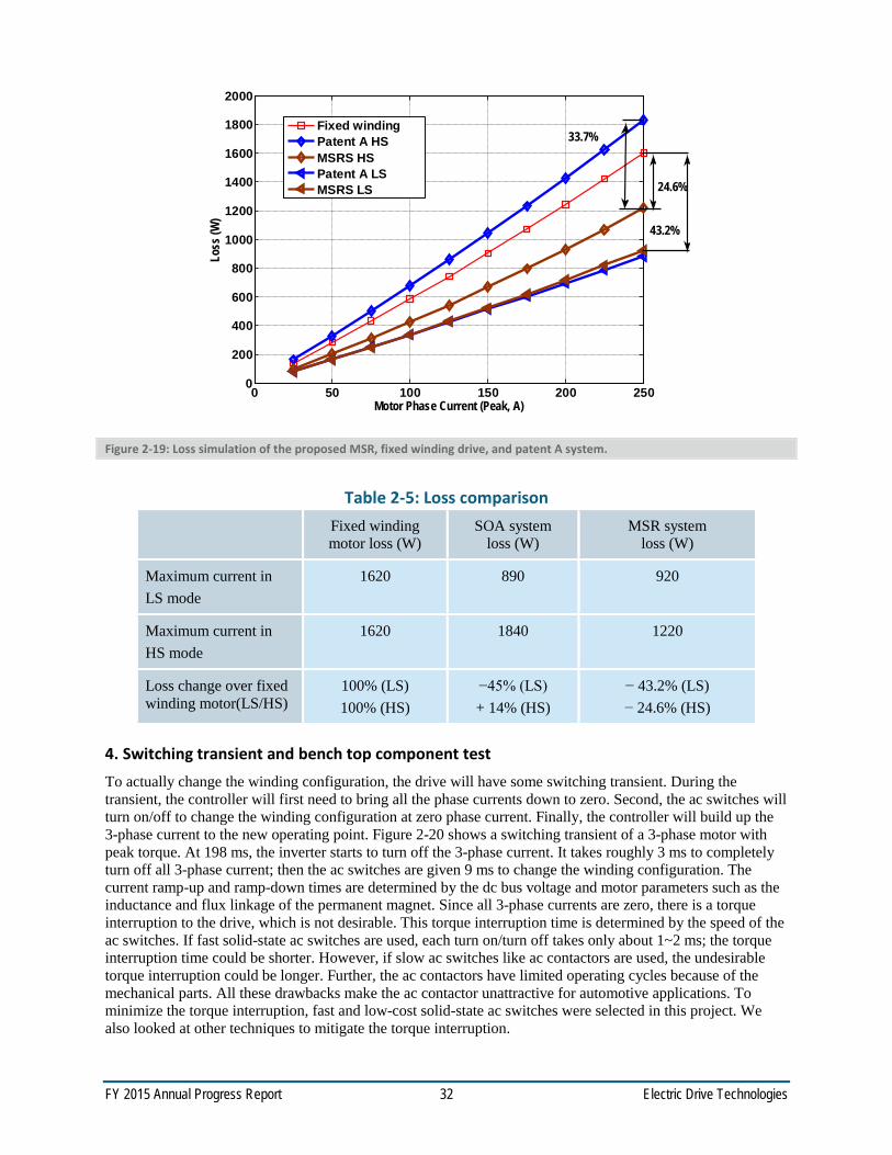
FY 2015 Annual Progress Report 32 Electric Drive Technologies
Figure 2-19: Loss simulation of the proposed MSR, fixed winding drive, and patent A system.
Table 2-5: Loss comparison
Fixed winding motor loss (W)
SOA system loss (W)
MSR system loss (W)
Maximum current in LS mode
1620 890 920
Maximum current in HS mode
1620 1840 1220
Loss change over fixed winding motor(LS/HS)
100% (LS) 100% (HS)
−45% (LS) + 14% (HS)
− 43.2% (LS) − 24.6% (HS)
4. Switching transient and bench top component test To actually change the winding configuration, the drive will have some switching transient. During the transient, the controller will first need to bring all the phase currents down to zero. Second, the ac switches will turn on/off to change the winding configuration at zero phase current. Finally, the controller will build up the 3-phase current to the new operating point. Figure 2-20 shows a switching transient of a 3-phase motor with peak torque. At 198 ms, the inverter starts to turn off the 3-phase current. It takes roughly 3 ms to completely turn off all 3-phase current; then the ac switches are given 9 ms to change the winding configuration. The current ramp-up and ramp-down times are determined by the dc bus voltage and motor parameters such as the inductance and flux linkage of the permanent magnet. Since all 3-phase currents are zero, there is a torque interruption to the drive, which is not desirable. This torque interruption time is determined by the speed of the ac switches. If fast solid-state ac switches are used, each turn on/turn off takes only about 1~2 ms; the torque interruption time could be shorter. However, if slow ac switches like ac contactors are used, the undesirable torque interruption could be longer. Further, the ac contactors have limited operating cycles because of the mechanical parts. All these drawbacks make the ac contactor unattractive for automotive applications. To minimize the torque interruption, fast and low-cost solid-state ac switches were selected in this project. We also looked at other techniques to mitigate the torque interruption.
0 50 100 150 200 2500
200
400
600
800
1000
1200
1400
1600
1800
2000
Motor Phase Current (Peak, A)
Loss
(W)
Fixed windingPatent A HSMSRS HSPatent A LSMSRS LS
43.2%
33.7%
24.6%
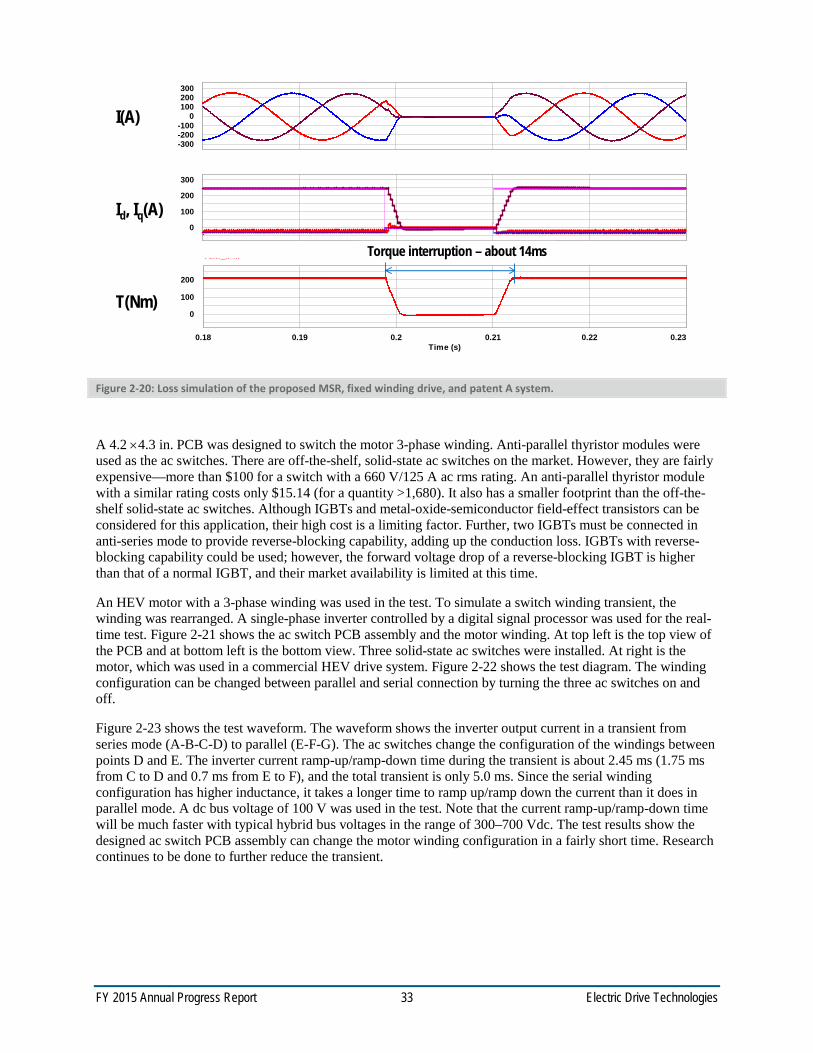
FY 2015 Annual Progress Report 33 Electric Drive Technologies
Figure 2-20: Loss simulation of the proposed MSR, fixed winding drive, and patent A system.
A 4.2 ×4.3 in. PCB was designed to switch the motor 3-phase winding. Anti-parallel thyristor modules were used as the ac switches. There are off-the-shelf, solid-state ac switches on the market. However, they are fairly expensive—more than $100 for a switch with a 660 V/125 A ac rms rating. An anti-parallel thyristor module with a similar rating costs only $15.14 (for a quantity >1,680). It also has a smaller footprint than the off-the-shelf solid-state ac switches. Although IGBTs and metal-oxide-semiconductor field-effect transistors can be considered for this application, their high cost is a limiting factor. Further, two IGBTs must be connected in anti-series mode to provide reverse-blocking capability, adding up the conduction loss. IGBTs with reverse-blocking capability could be used; however, the forward voltage drop of a reverse-blocking IGBT is higher than that of a normal IGBT, and their market availability is limited at this time.
An HEV motor with a 3-phase winding was used in the test. To simulate a switch winding transient, the winding was rearranged. A single-phase inverter controlled by a digital signal processor was used for the real-time test. Figure 2-21 shows the ac switch PCB assembly and the motor winding. At top left is the top view of the PCB and at bottom left is the bottom view. Three solid-state ac switches were installed. At right is the motor, which was used in a commercial HEV drive system. Figure 2-22 shows the test diagram. The winding configuration can be changed between parallel and serial connection by turning the three ac switches on and off.
Figure 2-23 shows the test waveform. The waveform shows the inverter output current in a transient from series mode (A-B-C-D) to parallel (E-F-G). The ac switches change the configuration of the windings between points D and E. The inverter current ramp-up/ramp-down time during the transient is about 2.45 ms (1.75 ms from C to D and 0.7 ms from E to F), and the total transient is only 5.0 ms. Since the serial winding configuration has higher inductance, it takes a longer time to ramp up/ramp down the current than it does in parallel mode. A dc bus voltage of 100 V was used in the test. Note that the current ramp-up/ramp-down time will be much faster with typical hybrid bus voltages in the range of 300–700 Vdc. The test results show the designed ac switch PCB assembly can change the motor winding configuration in a fairly short time. Research continues to be done to further reduce the transient.
0-100-200-300
100200300
I3 I4 I5
0
100
200
300
id idr iq iq*
0.18 0.19 0.2 0.21 0.22 0.23Time (s)
0
100
200
Tem_IPM
I(A)
Id, Iq(A)
T(Nm)
Torque interruption – about 14ms
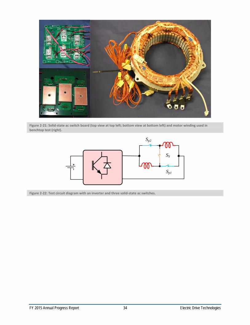
FY 2015 Annual Progress Report 34 Electric Drive Technologies
Figure 2-21: Solid-state ac switch board (top view at top left; bottom view at bottom left) and motor winding used in benchtop test (right).
Figure 2-22: Test circuit diagram with an inverter and three solid-state ac switches.
Sp2
Sp1
SS

FY 2015 Annual Progress Report 35 Electric Drive Technologies
Figure 2-23: Key test waveform of a series to parallel transient, output current 50 A/div, time is 5 ms/div.
Conclusions and Future Direction
A literature review indicates that most MSR research is ongoing and not on the market. There are different paths to achieving MSR operation, such as switchable winding
Drive cycle simulations show that an MSR solution with three speed ranges reduces drive cycle losses by about 24% in a combined drive cycle. The loss reductions for different drive cycles are different. The greatest benefit is achieved in the US06 drive cycle (30% loss reduction). In the UDDS cycle, the MSR design reduces losses by 28%; and in the HWFET drive cycle, it cuts losses by 4.6%. We developed a MSR solution with fewer solid state switches that does not have a battery short-circuit failure mode. It achieves significant loss reduction compared with a fixed winding motor drive and a state-of-the-art approach. A 4.2 ×4.3 in. ac switch PCB based on a low-cost solid-state switch was designed, fabricated, and tested. Initial test results show it can change the motor winding configuration in a fairly short time.
In FY 2016, we will build and test a bench top prototype to verify the benefits of the novel MSR solution. We will build a final prototype in FY 2017.
For commercialization, in-depth discussions will be held with automotive original equipment manufacturers to maintain their awareness of the advancements made in this motor project
FY 2015 Presentations/Publications/Patents
1. L. Tang and T. Burress, “Multi-speed-range electric motors,” presented at the DOE Vehicle Technologies Program Electric Drive Technologies FY 2015 Kickoff Meeting, Oak Ridge, Tennessee, November 19, 2014.
2. L. Tang and T. Burress, “Multi-speed range electric motor R&D,” presented at the DOE Vehicle Technologies Program Electric Drive Technologies Electrical and Electronics Technical Team Meeting, February 26, 2015.
3. L. Tang and T. Burress, “Multi-speed-range electric motor R&D,” presented at the DOE Vehicle Technologies Office 2015 Annual Merit Review, Washington, DC, June 2015.

FY 2015 Annual Progress Report 36 Electric Drive Technologies
References
1. D. A. Fulton, “Switch Module for an Electric Machine Having Switchable Stator Windings,” US patent application publication, US 2012/0068656 A1, March 22, 2012.
2. M. Krieger and H. Shum, “Electric Motor Having Windings Operable in Parallel and/or Series, and Related Methods,” US patent application publication, US 2012/0086380 A1, April 12, 2012.

FY 2015 Annual Progress Report 37 Electric Drive Technologies
2.3. Alternative High-Performance Motors with Non-Rare Earth Materials
Ayman EL-Refaie :Principal Investigator General Electric Global Research Center 1 Research Circle. Niskayuna, NY 12309 Phone: (518) 387-6660; Fax: (518) 387-6675; E-mail: [email protected] Francis Johnson :Materials Tasks Leader General Electric Global Research Center 1 Research Circle. Niskayuna, NY 12309 Phone: (518) 387- 5087; Fax: (518) 387-6232; E-mail: [email protected]
Abstract/Executive Summary The goal of the project is to develop traction motors that reduce or eliminate the use of rare-earth materials and meet the DOE specifications summarized in Table 2-6 and Figure 2-24. This is accomplished by evaluating/developing multiple motor topologies in conjunction with advanced materials
Table 2-6: Motor Specification
Items Specification
Maximum Speed 14,000 RPM Peak Power 55kW @ 20% speed for 18 seconds Maximum Current 400Arms Continuous Power 30kW @20-100% speed @ 325 volts
direct current (VDC) Efficiency Refer to target efficiency map Operating Voltage 200-450V (325V nominal) Back EMF < 600Vpk line-to-line @ 100% speed Torque Pulsation < 5% of Peak Torque @ any speed Characteristic Current < Maximum Current Weight ≤ 35kg Volume ≤ 9.7L Cost @ 100k ≤ $275 Ambient (outside housing) Operating Temperature
-40-140˚C
Coolant inlet 105˚C, <10LPM, 2psi drop, <20psi inlet Minimum isolation impedance-phase terminal to GND
1Mohm
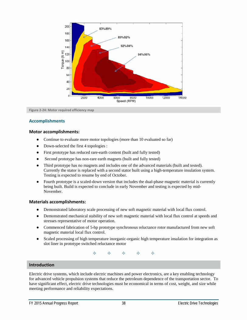
FY 2015 Annual Progress Report 38 Electric Drive Technologies
Figure 2-24: Motor required efficiency map
Accomplishments
Motor accomplishments: Continue to evaluate more motor topologies (more than 10 evaluated so far) Down-selected the first 4 topologies : First prototype has reduced rare-earth content (built and fully tested) Second prototype has non-rare earth magnets (built and fully tested) Third prototype has no magnets and includes one of the advanced materials (built and tested).
Currently the stator is replaced with a second stator built using a high-temperature insulation system. Testing is expected to resume by end of October.
Fourth prototype is a scaled-down version that includes the dual-phase magnetic material is currently being built. Build is expected to conclude in early November and testing is expected by mid-November.
Materials accomplishments: Demonstrated laboratory scale processing of new soft magnetic material with local flux control. Demonstrated mechanical stability of new soft magnetic material with local flux control at speeds and
stresses representative of motor operation. Commenced fabrication of 5-hp prototype synchronous reluctance rotor manufactured from new soft
magnetic material local flux control. Scaled processing of high temperature inorganic-organic high temperature insulation for integration as
slot liner in prototype switched reluctance motor
Introduction
Electric drive systems, which include electric machines and power electronics, are a key enabling technology for advanced vehicle propulsion systems that reduce the petroleum dependence of the transportation sector. To have significant effect, electric drive technologies must be economical in terms of cost, weight, and size while meeting performance and reliability expectations.

FY 2015 Annual Progress Report 39 Electric Drive Technologies
The objective of the GE Global Research “Alternative High-Performance Motors with Non-Rare Earth Materials” program is to develop a higher power density traction motors at a lower cost while simultaneously eliminating or reducing the need for rare-earth materials. Successful completion of this program will accelerate the introduction of hybrid electric vehicles into the U.S. road vehicle fleet and bring the added benefits of reduced fuel consumption and environmental impacts.
(A) Motor Development
Develop advanced motor concepts including electromagnetic, mechanical, and thermal concepts. Build proof-of-principle machines to verify the design process as well retire the key risks. Design and build 55kW/30kW machines that meet the DOE specifications Develop cost model to estimate the advanced motors cost based on 100,000 units/year Investigate the scalability of the developed concepts by evaluating 120kW/65kW machines
(B) Materials Development
The objective of the materials development tasks is to develop non-rare-earth containing component materials that enable non rare-earth containing motor designs that meet project performance goals. In the first phase of research, the capability for improvement of four classes of materials is being studied:
Improving the coercivity of an existing non-rare-containing permanent magnet composition to enable operation at temperatures above 150 °C.
Improving the tensile strength of electrical steel to enable high speed motor operation with low iron loss
Improving the ability of motor laminates to control magnetic flux distribution Improving the ability of dielectrics to withstand operating temperatures in excess of 280 °C.
Approach
Motor Development:
Perform tradeoff study of various motor topologies
Identify promising scalable materials and produce coupons showing the expected properties
Down-select promising topologies/materials
Design/build/test 2-3 proof-of-principle motors
Down-select, build and test final motor topology
Materials Development:
The materials development approach for the project is to develop the structure/ processing/properties relationships of four categories of motor components being made with novel materials. The materials tasks will produce and characterize samples of the new materials and will culminate in the selection of materials for scaled-up production sufficient to produce a prototype motor.
The microstructure of the non-rare-earth containing permanent magnet alloy is being refined through the application of modern casting and annealing technology. A series of designed experiments is being conducted to probe the capability of these technologies to increase coercivity while maintaining energy product. Magnet post-processing and characterization is being performed at Arnold Magnetic Technologies. Atom-scale structural characterization is being performed in collaboration with Ames laboratory to produce in-depth structure/processing/properties relationships.
A novel processing route is being applied to conventional silicon steel alloys to improve the tensile strength by while retaining comparable power loss. The approach relies on understanding and controlling the trade-off between coercivity (and hence power loss) and tensile strength. The processing technology is being developed to form the new material into sheets suitable for motor laminates

FY 2015 Annual Progress Report 40 Electric Drive Technologies
Novel processing technology is being developed to enable improved control of magnetic flux contained within motor laminates. This approach requires the development of new alloys that are operable with this processing method and the demonstration of scalable processing at dimensions specified by the motors teams. High temperature dielectrics are being developed that maintain high dielectric strength with resistance to degradation by oxidation. This requires the selection of suitable materials components, production of sample films, and verification of electrical and mechanical properties as a function of time at temperature.
Results and Discussion
(A) Motor Development:
Figure 2-25: Thermal Management: Oil flow path indicated by arrows.
A 12 slot 10 pole doubly-excited switched reluctance machine (SRM) prototype was built and tested. Figure 2-25 represents the assembly of the prototype and highlights the thermal management system used. The stator lamination is cooled by a water jacket. The end bells have spray nozzle manifolds spraying the end windings. The rotor is cooled by oil spray on its bore. The oil sprayed from the rotor will also reach the inner faces of the armature end windings as it is moved by centrifugal force, providing additional cooling of the end windings. The oil sprayed from the end bells and the rotor is collected at the bottom of the housing to close the oil flow circuit. Figure 2-26(a) shows the stator while (b) shows the rotor. Figure 2-26(b) shows the non-magnetic composite wedges used to fill the interpolar rotor spaces and smooth the rotor surface to reduce friction and windage losses at 14,000 rpm. Figure 2-26(c) shows the prototype mounted on the test bench.
(a) (b) (c)
Figure 2-26: Prototype photographs: (a) Stator; (b): Rotor; (c): Prototype on test bench.
Figure 2-27 shows the predicted and measured open circuit phase voltage waveforms for 10 amps direct current (ADC) field current at 1000 rpm and the predicted and measured back EMF constant as a function of the DC field current. Figure 2-28 shows the predicted and measured torque as function of the armature phase current for two levels of field excitation corresponding to peak torque (21ADC) and rated torque (13ADC) operations. The measured peak torque is 8.6% lower than prediction. This is mainly due to three-dimensional effects since 7% torque discrepancy was calculated between 2D and 3D FE analyses. It should be noted that

FY 2015 Annual Progress Report 41 Electric Drive Technologies
the machine is able to provide the required 187.6Nm peak torque. Overall, there is a good agreement between FE predictions and measurements.
Figure 2-27: (Left) Measured vs. calculated open circuit phase voltage for 10ADC field current and 1000rpm. (Right) Measured vs. calculated RMS phase back EMF at 1000rpm (back EMF constant), for various DC field current.
Machine performance was then characterized in terms of mechanical loss, peak torque capability, full load power capability, efficiency, and thermal behavior. As a precaution, the machine was tested with a lower coolant inlet temperature. The measured temperature rises in the machine can be used to easily predict the temperature with 105˚C coolant inlet temperature. Since the field excitation can be turned off, it was possible to isolate the mechanical drag losses. The influence of the end winding and the rotor spray cooling were verified and the drag torque measurements are presented in Figure 2-29. It can be seen that the end winding spray from the end bells does not generate any additional drag loss. However, the rotor spray does cause some degree of drag loss increase.
Figure 2-28: Measured and calculated torque vs. current for two levels of DC field current.
Figure 2-29: Drag loss measurements.

FY 2015 Annual Progress Report 42 Electric Drive Technologies
The left chart in Figure 2-30 shows an 18s peak power test at the base speed of 2800rpm. It can be seen that the prototype was able to provide 65kW within the current and voltage limitations, and with 90% efficiency. The right graph in Figure 2-30 shows the evolution of the temperatures in the windings during the 18s peak power test. The hot spot was in the armature winding inside the lamination stack with a safe temperature rise of 28.6˚C.
Figure 2-30: (Left) Peak Power characteristics. (Right) Temperatures during peak power operation.
Figure 2-31 shows the rated power characteristics up to 7000rpm. The machine was able to provide the specified continuous 30kW power while staying within the current and voltage limitations. The efficiency at 2800rpm was 88.3%, a reflection of the copper losses in the field winding.
Figure 2-31: Rated Load Characteristics.
Figure 2-32 shows the heat run for continuous operation at rated power and rated speed of 2800 rpm. The hot spot was in the armature winding inside the lamination stack. The corresponding temperature rise was 96.5˚C which is outside of the specification and implies the insulation system must be designed for 200˚C operation. This operating point requires the highest field and armature currents, hence the highest copper losses. The machine requires large slot area to accommodate both field and armature windings and this poses a thermal challenge since the thermal resistance of the heat path from the winding hot spot to the lamination is increased. More aggressive cooling within the winding slot is necessary to reduce the temperature rise.

FY 2015 Annual Progress Report 43 Electric Drive Technologies
Figure 2-32: Temperatures during rated load 2800rpm heat run.
Although the temperature rise was challenging and slightly above the specification, this operating point was still safe since the machine is capable of high temperature operation due to the absence of permanent magnets and the use of high temperature insulation materials.
Figure 2-33 shows the heat runs for rated power operations at 5000rpm and 7000rpm. Again, the hot spots were on the armature winding inside the lamination stack. At 5000rpm, the temperature rise was 69.9˚C which is within the specification. At 7000 rpm, the temperature rise was 82˚C which is at the limit of the specification.
Figure 2-33: Temperatures during rated load 5000rpm (left) and 7000rpm (right) heat runs.
In the above heat runs, the hot spot was generally in the armature winding inside the lamination stack. In fact, the field winding is located at the bottom of the slot and has a wider heat exchange surface area with the stator lamination than the armature winding. Therefore, the field winding is better cooled by the water jacket than the armature winding. Furthermore, the armature winding has a significantly lower fill factor due to the use of Litz wire (27.5% for the armature winding vs. 55% for the field winding). As a result, the heat load is higher in the armature winding. Since the end windings of the armature windings are cooled by oil spray the hot spot is located in the middle of the stack.
The second stator with the 280˚C insulation system is shown in Figure 2-34. The machine build will be finalized and testing started in the first half of November.

FY 2015 Annual Progress Report 44 Electric Drive Technologies
Figure 2-34: Second stator with 280˚C insulation system.
(B) Materials Development:
a. Non-rare earth containing permanent magnets: The advanced manufacturing method explored during this project has been found to be most effective in controlling the remanence of the non-rare-earth magnet material. Compositional variations were found that maintained the energy product while increasing coercivity by 25%. In 2014, further variations in composition and processing conditions were explored in an attempt to increase beyond that achieved in 2013. None of the compositions exceeded the best properties achieved in 2013. No work was done on the non-rare earth containing permanent magnets in 2015.
b. High strength soft magnetic laminates: The power loss and magnetic properties of the higher strength soft magnetic laminates produced in 2013 were fully characterized. The best performing material had a tensile strength 15% greater than 3% Silicon Steel. However, the power loss was approximately 2X greater than that of Silicon steel in the frequency range used in electric machines. Additional efforts to reduce power loss were evaluated and judged to have a low likelihood of success. Further work on the high strength laminates was suspended.
c. Improved magnetic flux control: In 2015 we conducted a series of processing scale-up experiments centered around producing the laminates needed for a small-scale motor prototype. The goal of the experiments was to evaluate the readiness level of the manufacturing methods, identify unforeseen process limitations, and validate the calculated performance of a motor design made with the new material. In December of 2014 a single laminate of the new material was produced and fully processed to enable local control of magnetic flux. In this laminate the bridges and posts of a synchronous reluctance motor design were processed to become non-magnetic but still retained their mechanical integrity. Figure 2-35 shows the laminate that was processed. This laminate has a diameter of 5.5" and a thickness of 0.015." The left side of the figure is a schematic showing the desired arrangement of non-magnetic regions in the ferromagnetic laminate. The right side of image shows how magnetic flux lines are allowed to penetrate through the non-magnetic regions of the laminate. At the same time, the high permeability magnetic regions of the laminate absorb the flux through a shielding effect.
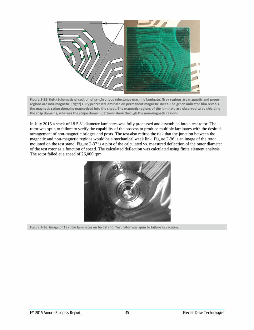
FY 2015 Annual Progress Report 45 Electric Drive Technologies
Figure 2-35: (left) Schematic of section of synchronous reluctance machine laminate. Gray regions are magnetic and green regions are non-magnetic. (right) Fully processed laminate on permanent magnetic sheet. The green indicator film reveals the magnetic stripe domains magnetized into the sheet. The magnetic regions of the laminate are observed to be shielding the strip domains, whereas the stripe domain patterns show through the non-magnetic regions.
In July 2015 a stack of 18 5.5" diameter laminates was fully processed and assembled into a test rotor. The rotor was spun to failure to verify the capability of the process to produce multiple laminates with the desired arrangement of non-magnetic bridges and posts. The test also retired the risk that the junction between the magnetic and non-magnetic regions would be a mechanical weak link. Figure 2-36 is an image of the rotor mounted on the test stand. Figure 2-37 is a plot of the calculated vs. measured deflection of the outer diameter of the test rotor as a function of speed. The calculated deflection was calculated using finite element analysis. The rotor failed at a speed of 26,000 rpm.
Figure 2-36: Image of 18 rotor laminates on test stand. Test rotor was spun to failure in vacuum.
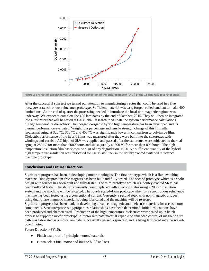
FY 2015 Annual Progress Report 46 Electric Drive Technologies
Figure 2-37: Plot of calculated versus measured deflection of the outer diameter (O.D.) of the 18 laminate test rotor stack.
After the successful spin test we turned our attention to manufacturing a rotor that could be used in a five horsepower synchronous reluctance prototype. Sufficient material was cast, forged, rolled, and cut to make 400 laminations. At the end of quarter the processing needed to introduce the local non-magnetic regions was underway. We expect to complete the 400 laminates by the end of October, 2015. They will then be integrated into a test rotor that will be tested at GE Global Research to validate the system performance calculations. d. High temperature dielectrics: The inorganic-organic hybrid high temperature has been developed and its thermal performance evaluated. Weight loss percentage and tensile strength change of this film after isothermal aging at 320 °C, 350 °C and 400 °C was significantly lower in comparison to polyimide film. Dielectric performance of the hybrid films was measured after they were built into the statorettes with windings and varnish, AC hipot of 3kV was applied and passed after the statorettes were subjected to thermal aging at 280 °C for more than 2000 hours and subsequently at 300 °C for more than 800 hours. The high temperature insulation film has shown no sign of any degradation. In 2015 a sufficient quantity of the hybrid high temperature insulation was fabricated for use as slot liner in the doubly excited switched reluctance machine prototype.
Conclusions and Future Directions
Significant progress has been in developing motor topologies. The first prototype which is a flux-switching machine using dysprosium-free magnets has been built and fully-tested. The second prototype which is a spoke design with ferrites has been built and fully-tested. The third prototype which is a doubly-excited SRM has been built and tested. The stator is currently being replaced with a second stator using a 280oC insulation system and the machine will be re-tested. The fourth scaled-down prototype which is a synchronous reluctance machine has been tested using a conventional current. Currently a second rotor with non-magnetic bridges using dual-phase magnetic material is being fabricated and the machine will be re-tested. Significant progress has been made in developing advanced magnetic and dielectric materials for use as motor components. Structure/processing/properties relationships have been determined. Initial test coupons have been produced and characterized. Production of the high temperature dielectrics were scaled up in batch process to support a motor prototype. A motor laminate material capable of enhanced control of magnetic flux path was fabricated as a motor laminate, successfully passed a spin test, and is being fabricated into the scaled-down motor. Future Direction (FY16):
Finish test proof-of-principle motors/materials
Down-select final motor and initiate build and test
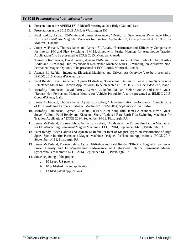
FY 2015 Annual Progress Report 47 Electric Drive Technologies
FY 2015 Presentations/Publications/Patents
1. Presentation at the APEEM FY15 kickoff meeting at Oak Ridge National Lab 2. Presentation at the 2015 DoE AMR at Washington DC 3. Patel Reddy, Ayman El-Refaie and James Alexander, “Design of Synchronous Reluctance Motor
Utilizing Dual-Phase Magnetic Materials for Traction Applications”, to be presented at ECCE 2015, Montreal, Canada
4. James McFarland, Thomas Jahns and Ayman EL-Refaie, “Performance and Efficiency Comparisons for Interior PM and Flux-Switching PM Machines with Ferrite Magnets for Automotive Traction Applications”, to be presented at ECCE 2015, Montreal, Canada
5. Tsarafidy Raminosoa, David Torrey, Ayman El-Refaie, Kevin Grace, Di Pan, Stefan Grubic, Karthik Bodla and Kum-Kang Huh, “Sinusoidal Reluctance Machine with DC Winding: an Attractive Non-Permanent Magnet Option”, to be presented at ECCE 2015, Montreal, Canada
6. Ayman EL-Refaie, “Integrated Electrical Machines and Drives: An Overview”, to be presented at IEMDC 2015, Coeur d’Alene, Idaho
7. Patel Reddy, Kevin Grace, and Ayman EL-Refaie, “Conceptual Design of Sleeve Rotor Synchronous Reluctance Motor for Traction Applications”, to be presented at IEMDC 2015, Coeur d’Alene, Idaho
8. Tsarafidy Raminosoa, David Torrey, Ayman EL-Refaie, Di Pan, Stefan Grubic, and Kevin Grace, “Robust Non-Permanent Magnet Motors for Vehicle Propulsion”, to be presented at IEMDC 2015, Coeur d’Alene, Idaho
9. James McFarland, Thomas Jahns, Ayman EL-Refaie, “Demagnetization Performance Characteristics of Flux Switching Permanent Magnet Machines”, ICEM 2014, September 2014, Berlin
10. Tsarafidy Raminosoa, Ayman El-Refaie, Di Pan, Kum Kang Huh, James Alexander, Kevin Grace, Steven Galioto, Patel Reddy and Xiaochun Shen, “Reduced Rare-Earth Flux Switching Machines for Traction Applications” ECCE 2014, September 14-18, Pittsburgh, PA
11. James McFarland, Thomas Jahns, Ayman EL-Refaie, “Analysis of the Torque Production Mechanism for Flux-Switching Permanent Magnet Machines” ECCE 2014, September 14-18, Pittsburgh, PA
12. Patel Reddy, Steve Galioto and Ayman El-Refaie, “Effect of Magnet Types on Performance of High Speed Spoke Interior Permanent Magnet Machines designed for Traction Applications” ECCE 2014, September 14-18, Pittsburgh, PA
13. James McFarland, Thomas Jahns, Ayman El-Refaie and Patel Reddy, ”Effect of Magnet Properties on Power Density and Flux-Weakening Performance of High-Speed Interior Permanent Magnet Synchronous Machines” ECCE 2014, September 14-18, Pittsburgh, PA
14. Since beginning of the project: a. 10 issued US patents b. 10 published patent application c. 13 filed patent applications
FY 2015 Annual Progress Report 48 Electric Drive Technologies
2.4. Unique Lanthanide-Free Motor Construction
Josh Ley, VP Engineering, Principle Investigator UQM Technologies, Inc. 4120 Specialty Place Longmont, CO 80504 Phone: (303) 682-4900; Fax: (303) 682-4901 E-mail: [email protected] Contractor: UQM Technologies, Inc. Contract No.: DE-EE0005389
Abstract/Executive Summary Objectives
o This project pursues new motor construction that eliminates, or significantly reduces the use of rare earth elements while maintaining the attractive size, weight and efficiency features of rare earth permanent magnet motors
o The primary drivers for this work include: – Lack of transparency in the rare earth magnet supply market and its pricing structures – Significant rare earth price escalation in calendar year 2011 – Need for small, lightweight, high efficiency, low cost motors for electric traction drives – New architectures and/or materials that eliminate rare earth materials while maintaining
performance that is attractive for electrified vehicles
Technical Barriers o The low coercivity of the AlNiCo magnets requires an unconventional rotor design for power
density. This unconventional rotor design requires an innovative magnet retention system for high speed operation. The proof-of-concept (POC) rotor involves the use of retention bars, adhesive and fiber wrap to accomplish the retention.
o A second item of concern is also related to the AlNiCo magnets and their characteristic of of de-magnetizing if not magnetically coupled with a conductive outer sleeve. This sleeve must be over the rotor any time it is not fully inserted in the stator. UQM has worked with the company magnetized the rotor to insure a sleeve can be designed to maintain the magnetization.
Technical Targets o The DOE motor specifications that are targeted for this work include: o 55 kW baseline design o Scalable to 120 kW or higher
Accomplishments Phase 1 - The items originally identified as milestones for the Phase 1 (BP1) have been completed and
show that it is possible to produce a motor using non-rare earth, Lanthanide free magnets. In addition, this motor can be competitive with a motor using the more costly rare earth magnet technology. Specific milestones completed in Phase 1 include: o The development of an Interface Control Document (ICD) that captures the design
targets/specifications of the motor including those defined by the DOE. o Review of the current state of the target magnet technology and what improvements may be
possible within the time frame of the project. o An development of an electromagnetic model using the ANSYS finite element analysis tool, to be
used in the initial design and any subsequent refinement/redesign work o Analysis of the motor commutation, using Matlab/Simulink to determine interaction between the
motor electromagnetics and the inverter (drive)

FY 2015 Annual Progress Report 49 Electric Drive Technologies
o Preliminary motor package design including magnet/rotor configuration, housing/cooling jacket and overall package size and weight
Phase 2 - Proof of Concept (POC) build and test, the specific milestones that were achieved in the second phase include: o Finalized the electromagnetic design, including; o Final design rotor/magnet configuration o Stator winding and requirements for magnetizing the magnets o Complete design package to be used for POC build o The assembly of two (2) POC motors to be used for dynamometer testing o Dynamometer testing at UQM’s facility to demonstrate technology feasibility, a “Go/No-Go”
milestone. Based on results from this testing UQM believes the technology is feasible and the next phase of work should be pursued.
o During this period Ames has made good progress on the development of an enhanced version of the AlNiCo magnet material (referred to as AlNiCo 8X). As such UQM will be incorporating the AlNiCo 8X into the second iteration proof-of-design (POD) motors for the BP3 effort.
o Delivery of a POC motor to ORNL for independent performance evaluation
Introduction
This project pursues the development of a non-rare-earth permanent magnet motor architecture. It incorporates a novel rotor geometry that allows the use of lower energy Al-Ni-Co, Fe-Co-W, or other high flux, low coercivity magnet material. These materials are not currently adopted due to demagnetization within existing magnetic circuit designs, a problem that is overcome with this proposed design.
Three unique design features of this motor architecture are proposed to enable the use of low coercivity magnet technology: magnet shape along with magnetization direction, a nonmagnetic support structure, and design features that reduce demagnetization fields. The project relies upon incremental improvement in the non-rare-earth magnet properties (collaboration with Ames Laboratory) and this is where the project starts. From there, UQM develops a motor design and integrates thermal technology in collaboration with the National Renewable Energy Laboratory. Finally, motors are built in years two and three (initial proof-of-concept motor followed by refined hardware). These will be tested at UQM and delivered to Oak Ridge National Laboratory for independent confirmatory testing. The project concludes with designs scaled to higher power and detailed cost estimating activities. Cost is key to the adoption of electrified vehicles, so substantial focus is placed on the tasks related to the detailed costing of the technology.
The outcome of the technology development and the resultant scalable hardware will be motor designs that apply to a full range of vehicle electrification, from mild hybrid to heavy hybrid to fully electric vehicles. This unique permanent magnet motor technology has an efficiency advantage over wound-field or induction machines (no energy consumed to create the magnetic field), and therefore, will decrease petroleum consumption relative to other non-rare-earth motor technologies. Economically, the magnet material used for this program is one-third the cost of NdFeB magnets on a per-pound basis, and therefore, supports lower cost if the material content can be maintained to be less than three times the amount of NdFeB for a given power level. UQM is confident that the total magnet cost of the proposed technology will be lower than the equivalent rare-earth motor. This will provide economic benefit to the end-use consumers (lower vehicle cost) and improve electrified transportation industry with products that compete more favorably with traditional petroleum engine driven vehicles.
Approach
Pursue design that enables the use of low coercivity magnets, using a unique magnet and supporting rotor geometry as well as stator and rotor design features that reduce demagnetization fields.
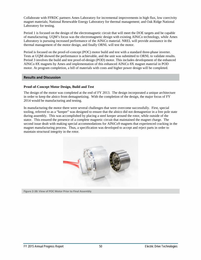
FY 2015 Annual Progress Report 50 Electric Drive Technologies
Collaborate with FFRDC partners Ames Laboratory for incremental improvements in high flux, low coercivity magnet materials; National Renewable Energy Laboratory for thermal management; and Oak Ridge National Laboratory for testing.
Period 1 is focused on the design of the electromagnetic circuit that will meet the DOE targets and be capable of manufacturing. UQM’s focus was the electromagnetic design with existing AlNiCo technology, while Ames Laboratory is pursuing increased performance of the AlNiCo material. NREL will provide assistance in the thermal management of the motor design, and finally ORNL will test the motor.
Period is focused on the proof-of-concept (POC) motor build and test with a standard three-phase inverter. Tests at UQM showed the performance is achievable, and the unit was submitted to ORNL to validate results. Period 3 involves the build and test proof-of-design (POD) motor. This includes development of the enhanced AlNiCo 8X magnets by Ames and implementation of this enhanced AlNiCo 8X magnet material in POD motor. At program completion, a bill of materials with costs and higher power design will be completed.
Results and Discussion
Proof-of-Concept Motor Design, Build and Test
The design of the motor was completed at the end of FY 2013. The design incorporated a unique architecture in order to keep the alnico from demagnetizing. With the completion of the design, the major focus of FY 2014 would be manufacturing and testing.
In manufacturing the motor there were several challenges that were overcome successfully. First, special tooling, referred to as a “keeper” was designed to ensure that the alnico did not demagnetize in a free pole state during assembly. This was accomplished by placing a steel keeper around the rotor, while outside of the stator. This ensured the presence of a complete magnetic circuit that maintained the magnet charge. The second issue dealt with making special accommodations for AlNiCo9 magnets that experienced cracking in the magnet manufacturing process. Thus, a specification was developed to accept and reject parts in order to maintain structural integrity in the rotor.
Figure 2-38: View of POC Motor Prior to Final Assembly

FY 2015 Annual Progress Report 51 Electric Drive Technologies
Figure 2-39: Dynamometer Testing Apparatus
Once key manufacturing problems had been addressed, the motor final assembly was completed and testing commenced. The motors were fixed on the dynamometer testing apparatus to verify motor characteristics such as Back-EMF, Torque, and power. The initial tests on the dynamometer measured back EMF. The back EMF screen captures from the oscilloscope are shown below in Figure 2-40.
Figure 2-40: Back EMF POC1 Before High Torque Test
The above Figure 2-40 is a scope capture, illustrating the EMF wave shape. The back EMF amplitude measured 84.25 V/krpm Line-to-Line on POC1 motor before the high torque test. This was close to the 89.8 V/krpm value predicted and within the range of expected magnet property tolerance. The next step in the design verification process was to run an incremental torque test to determining maximum torque before demagnetization. The demagnetization analysis results from FY 13 were used to establish the methodology behind this test. The analysis predicted that the motor could partially demagnetize at near full torque. Therefore an incremental torque test was conducted by increasing current and torque in 10% increments and the EMF was measured after every point such that the point of demagnetization could be determined. The test results for EMF is shown in Figure 4 for EMF taken after the 100% torque test.

FY 2015 Annual Progress Report 52 Electric Drive Technologies
Figure 2-41: EMF after 100% Torque POC1
As, shown in Figure 2-41 results indicate the back EMF dropped to 76.6 V/krpm, indicating about 8% demagnetization. This was expected, since the demagnetization analysis indicated partial demagnetization given the loaded operating point fell on the knee of the B-H curve at 100% of full torque, see Figure 2-42. It was note that at 90% of full torque (235 Nm) no measureable demagnetization occurred. Therefore, the demagnetization point is somewhere between 90 and 100% of full torque. The torque data from the incremental torque test are shown in Figure 2-42.
Figure 2-42: Torque vs Speed results for Maximum Torque Test
Once design validation tests had been performed to determine the maximum torque before demagnetization, power profile tests were performed on POC2, to measure the torque vs. speed and power vs. speed characteristics. The test involved validation of the motor’s torque vs. speed curve up to 5000 [rpm]. The speed was limited to 5000 rpm due to durability concerns, given the cracked magnets. The torque was also limited to 85% of full torque, or 225 Nm, to ensure no demagnetization occurs. The results of this test are shown, below in Figure 2-43 and Figure 2-44.
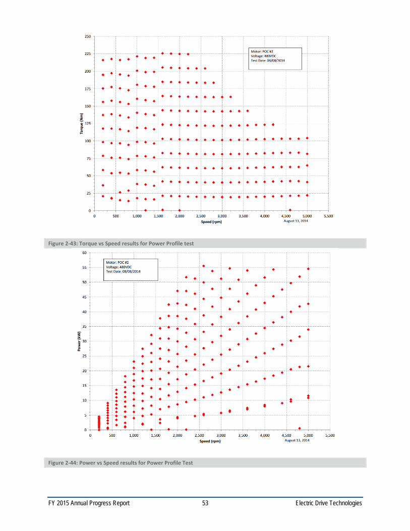
FY 2015 Annual Progress Report 53 Electric Drive Technologies
Figure 2-43: Torque vs Speed results for Power Profile test
Figure 2-44: Power vs Speed results for Power Profile Test

FY 2015 Annual Progress Report 54 Electric Drive Technologies
As can be seen from the results of this test, the motor was able produce the DOE Goal of 55 kW from 2000 rpm to 5000 rpm. Although the speed was intentionally limited as a precaution, POC1 did achieve 10 krpm in a separate test.
In conclusion, the test results verified the design EMF and reached the power goal of 55 kW. The design also proved capable of producing 90% of the torque goal 235 Nm relative to the goal of 262 Nm.
Magnet Improvements:
During the period Ames Laboratory (Ames) focused on refining the AlNiCo material, AlNiCo 8 and 9 showed the most promise for improvement, due to their higher starting coercivity. This higher starting coercivity is believed to be the result of the elongated Fe-Co phase shape anisotropy. Using the in house gas atomizer, Ames produced a pre-alloy powder that had very spherical shape and a low content of satellite particles. Additionally, this powder had excellent flowability and powder packing. Sintering and compression molding, with a binder, were investigated as potential methods to form the powder into bulk magnet shapes. Compression molding was determined to be the preferred method for producing inexpensive bulk magnet shapes.
Additionally, Ames had very good success in determining the one of key parameters, reduced spinodal spacing, which leads to increased coercivity. This reduction in spinodal spacing is a direct function of the time spent at a specific magnetic annealing temperature.
From these successes Ames has determined that an improved magnet composition (increased coercivity) can be produced for use in the POD motors for the next phase. This improved material will be a variation of AlNiCo 8.
In the next phase Ames will focus their efforts on producing an adequate quantity of the powder, molding into bulk shapes and the processing (annealing and final sizing).
Thermal Management
In support of UQM’s motor project “Unique Lanthanide-Free Motor Construction”, NREL is providing thermal management analysis and design support. This report contains a summary of work performed at NREL during phase two of UQM’s motor project.
Cooling Jacket Flow and Thermal Analysis
The phase two modeling work focused on verifying that the methodology developed during phase one to simplify the motor thermal analysis modeling was valid. The simplified thermal finite element analysis (FEA) model (Figure 2-38) developed during phase one focused on breaking the model down into a fundamental component in order to achieve a fast solving, efficient model. During phase two of the project NREL worked to verify the accuracy of the section FEA model and the process from which it was derived by running a full conjugate heat transfer model using computational fluid dynamics (CFD) (Figure 2-45) for the stator and cooling jacket to integrate the thermal performance and fluid flow.
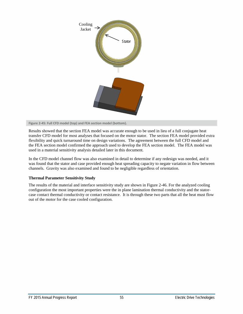
FY 2015 Annual Progress Report 55 Electric Drive Technologies
Figure 2-45: Full CFD model (top) and FEA section model (bottom).
Results showed that the section FEA model was accurate enough to be used in lieu of a full conjugate heat transfer CFD model for most analyses that focused on the motor stator. The section FEA model provided extra flexibility and quick turnaround time on design variations. The agreement between the full CFD model and the FEA section model confirmed the approach used to develop the FEA section model. The FEA model was used in a material sensitivity analysis detailed later in this document.
In the CFD model channel flow was also examined in detail to determine if any redesign was needed, and it was found that the stator and case provided enough heat spreading capacity to negate variation in flow between channels. Gravity was also examined and found to be negligible regardless of orientation.
Thermal Parameter Sensitivity Study
The results of the material and interface sensitivity study are shown in Figure 2-46. For the analyzed cooling configuration the most important properties were the in plane lamination thermal conductivity and the stator-case contact thermal conductivity or contact resistance. It is through these two parts that all the heat must flow out of the motor for the case cooled configuration.
Cooling Jacket
Stator
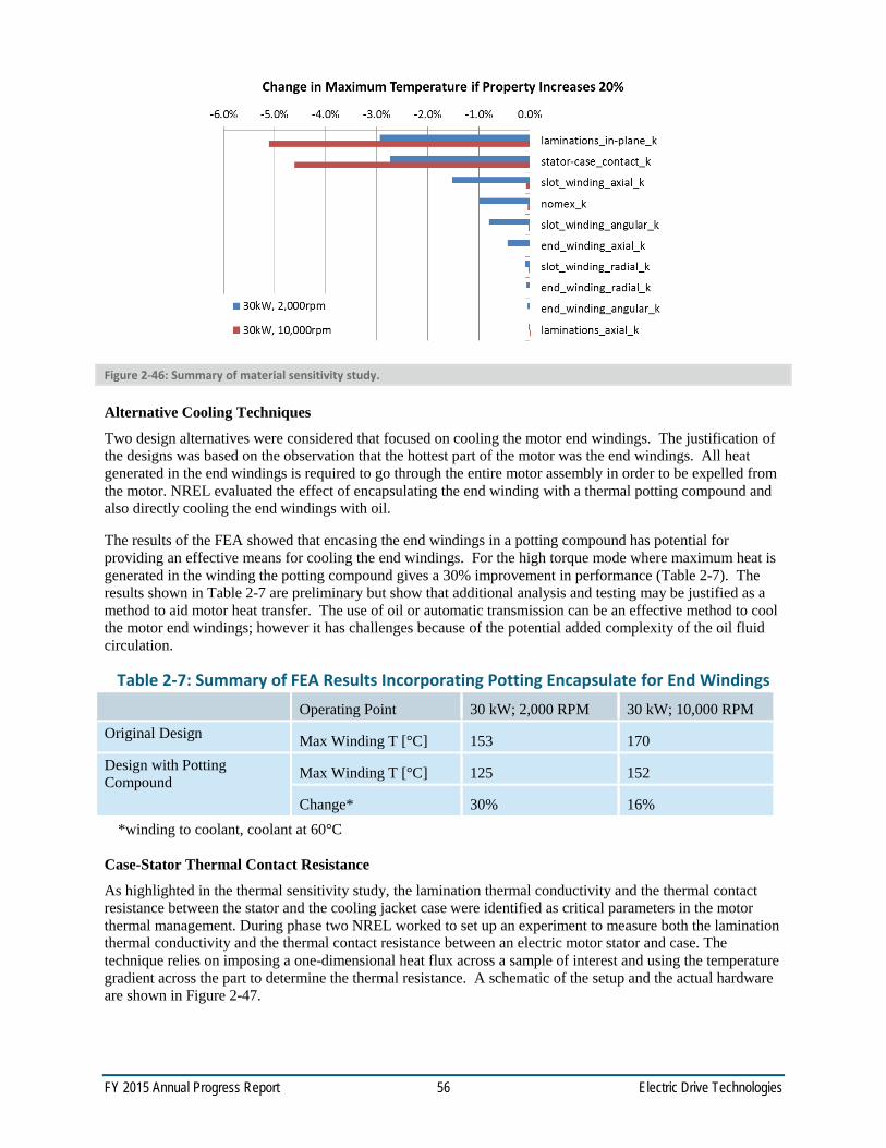
FY 2015 Annual Progress Report 56 Electric Drive Technologies
Figure 2-46: Summary of material sensitivity study.
Alternative Cooling Techniques
Two design alternatives were considered that focused on cooling the motor end windings. The justification of the designs was based on the observation that the hottest part of the motor was the end windings. All heat generated in the end windings is required to go through the entire motor assembly in order to be expelled from the motor. NREL evaluated the effect of encapsulating the end winding with a thermal potting compound and also directly cooling the end windings with oil.
The results of the FEA showed that encasing the end windings in a potting compound has potential for providing an effective means for cooling the end windings. For the high torque mode where maximum heat is generated in the winding the potting compound gives a 30% improvement in performance (Table 2-7). The results shown in Table 2-7 are preliminary but show that additional analysis and testing may be justified as a method to aid motor heat transfer. The use of oil or automatic transmission can be an effective method to cool the motor end windings; however it has challenges because of the potential added complexity of the oil fluid circulation.
Table 2-7: Summary of FEA Results Incorporating Potting Encapsulate for End Windings Operating Point 30 kW; 2,000 RPM 30 kW; 10,000 RPM Original Design Max Winding T [°C] 153 170 Design with Potting Compound Max Winding T [°C] 125 152
Change* 30% 16% *winding to coolant, coolant at 60°C
Case-Stator Thermal Contact Resistance
As highlighted in the thermal sensitivity study, the lamination thermal conductivity and the thermal contact resistance between the stator and the cooling jacket case were identified as critical parameters in the motor thermal management. During phase two NREL worked to set up an experiment to measure both the lamination thermal conductivity and the thermal contact resistance between an electric motor stator and case. The technique relies on imposing a one-dimensional heat flux across a sample of interest and using the temperature gradient across the part to determine the thermal resistance. A schematic of the setup and the actual hardware are shown in Figure 2-47.
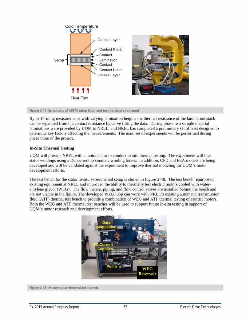
FY 2015 Annual Progress Report 57 Electric Drive Technologies
Heat Flux
Cold Temperature
Metering Block
Metering Block
Samp
Contact
Contact
Lamination
Contact Plate
Contact Plate Grease Layer
Grease Layer
Figure 2-47: Schematic of ASTM setup (top) and test hardware (bottom)
By performing measurements with varying lamination heights the thermal resistance of the lamination stack can be separated from the contact resistance by curve fitting the data. During phase two sample material laminations were provided by UQM to NREL, and NREL has completed a preliminary set of tests designed to determine key factors affecting the measurements. The main set of experiments will be performed during phase three of the project.
In-Situ Thermal Testing
UQM will provide NREL with a motor stator to conduct in-situ thermal testing. The experiment will heat stator windings using a DC current to simulate winding losses. In addition, CFD and FEA models are being developed and will be validated against the experiment to improve thermal modeling for UQM’s motor development efforts.
The test bench for the stator in-situ experimental setup is shown in Figure 2-48. The test bench repurposed existing equipment at NREL and improved the ability to thermally test electric motors cooled with water-ethylene glycol (WEG). The flow meters, piping, and flow control valves are installed behind the bench and are not visible in the figure. The developed WEG loop can work with NREL’s existing automatic transmission fluid (ATF) thermal test bench to provide a combination of WEG and ATF thermal testing of electric motors. Both the WEG and ATF thermal test benches will be used to support future in-situ testing in support of UQM’s motor research and development efforts.
Figure 2-48: Motor stator thermal test bench.
WEG Reservoir
Pump
DC Current Supplies
Data Acquisition
FY 2015 Annual Progress Report 58 Electric Drive Technologies
Conclusions and Future Directions
Based on the analysis and testing completed in the reporting period it was determined that the POC motor meets many of the DOE targets and will demonstrate compliance with the DOE targets in the next phase the program upon completion of the POD (proof of design motor) which will utilize improved magnet materials developed by AMES laboratories. A summary of the status for analysis and testing to DOE requirements follows:
The POC motors were constructed in FY14/FY15 and tested to confirm compliance with the above list specifications. Upon completion of in-housing testing a motor will be delivered to ORNL for independent testing and validation of performance.
Based on the successful demonstration and identified improvements from POC analysis, design, and testing a POD motor will be developed, built, and tested in FY16.
FY 2015 Presentations/Publications/Patents
1. Presentation - DOE Vehicle Technologies Office FY15 Kickoff Meeting (October 2015) 2. Patent - Innovative Permanent Magnet Electric Motor Design that Allows the Use of Non-Rare Earth
Magnets (January 2015)

FY 2015 Annual Progress Report 59 Electric Drive Technologies
2.5. Brushless and Permanent Magnet Free Wound Field Synchronous Motors for EV Traction
Daniel C. Ludois, Principle Investigator University of Wisconsin -Madison 1415 Engineering Dr. Madison, WI 53706 Phone: (608) 262-8211 E-mail: [email protected] Steven Boyd, DOE Technology Development Manager Vehicle Technologies Office of the EERE Forrestal Building, 1000 Independence Avenue, SW Washington, DC 20585 Phone: 1-(202) 586-8967 E-mail: [email protected] Adrienne L. Riggi, NETL Program Officer Power & Vehicles Technologies Division, NETL 3610 Collins Ferry Road Morgantown, WV 26507-0880 Phone: 1-(304) 285-5223 Email: [email protected]
Objectives Develop noncontact capacitive power transfer (CPT) to transfer power at the kilowatt level between
rotating assemblies with high efficiency to displace the need for brushed slip rings.
Design, develop, and demonstrate a prototype wound field synchronous motor (WFSM) with brushless rotor excitation via CPT capable of replicating the performance of commercially available interior permanent magnet (PM) motors for electric vehicle (EV) traction.
Technical Barriers Interior permanent magnet synchronous machines (IPMSMs) are one of the dominant electric machine
types used for EV traction. While IPMSMs can offer high power density and high efficiency over wide operating conditions they have a number of detractions because of the use of rare earth PMs in the rotor. Rare earth PMs are a significant fraction of the EV traction motor cost and have been subject to significant market volatility and are largely single source from a foreign power. Additionally, the PMs provide a fixed flux level which is always, "on", leading to safety concerns during inverter faults and requiring additional current to be injected into the machine during field weakening operation to buck the magnet flux. This additional current lowers the power factor of the machine, requires that the traction inverter be oversized to supply the reactive current, and leads to increased ohmic losses in the stator and inverter.
Wound field synchronous machines stand to overcome the limitations of PM based machines via rotor electromagnets. EV traction applications require extremely high reliability inhibiting the use of brushes, a typical necessity of rotor field windings. CPT technology offers an attractive means of providing brushless power transfer to the rotor field windings. Designing a CPT system of sufficient power to enable rotor electromagnets is a critical aspect of this work.
A high power density, high efficiency and low cost WFSM without PMs is challenging, regardless of brushed or brushless operation. PMs have very high energy density, and are difficult to outperform in this scale of electric machine.
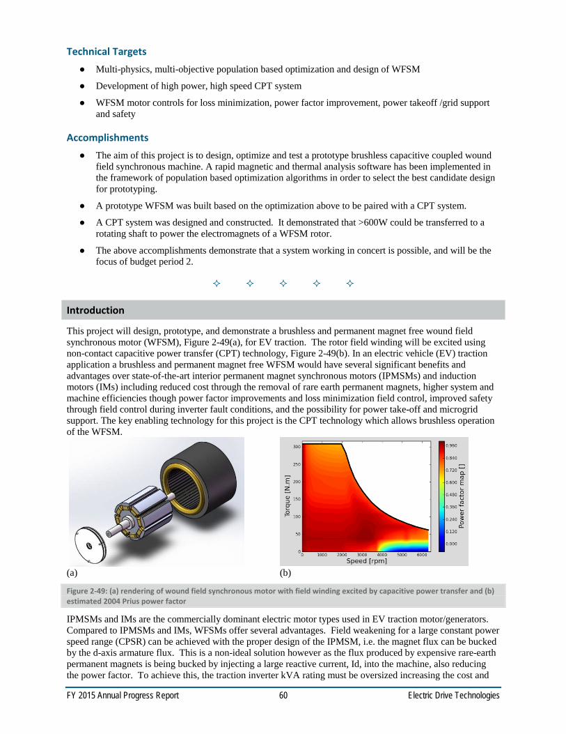
FY 2015 Annual Progress Report 60 Electric Drive Technologies
Technical Targets Multi-physics, multi-objective population based optimization and design of WFSM
Development of high power, high speed CPT system
WFSM motor controls for loss minimization, power factor improvement, power takeoff /grid support and safety
Accomplishments The aim of this project is to design, optimize and test a prototype brushless capacitive coupled wound
field synchronous machine. A rapid magnetic and thermal analysis software has been implemented in the framework of population based optimization algorithms in order to select the best candidate design for prototyping.
A prototype WFSM was built based on the optimization above to be paired with a CPT system.
A CPT system was designed and constructed. It demonstrated that >600W could be transferred to a rotating shaft to power the electromagnets of a WFSM rotor.
The above accomplishments demonstrate that a system working in concert is possible, and will be the focus of budget period 2.
Introduction
This project will design, prototype, and demonstrate a brushless and permanent magnet free wound field synchronous motor (WFSM), Figure 2-49(a), for EV traction. The rotor field winding will be excited using non-contact capacitive power transfer (CPT) technology, Figure 2-49(b). In an electric vehicle (EV) traction application a brushless and permanent magnet free WFSM would have several significant benefits and advantages over state-of-the-art interior permanent magnet synchronous motors (IPMSMs) and induction motors (IMs) including reduced cost through the removal of rare earth permanent magnets, higher system and machine efficiencies though power factor improvements and loss minimization field control, improved safety through field control during inverter fault conditions, and the possibility for power take-off and microgrid support. The key enabling technology for this project is the CPT technology which allows brushless operation of the WFSM.
(a) (b)
Figure 2-49: (a) rendering of wound field synchronous motor with field winding excited by capacitive power transfer and (b) estimated 2004 Prius power factor
IPMSMs and IMs are the commercially dominant electric motor types used in EV traction motor/generators. Compared to IPMSMs and IMs, WFSMs offer several advantages. Field weakening for a large constant power speed range (CPSR) can be achieved with the proper design of the IPMSM, i.e. the magnet flux can be bucked by the d-axis armature flux. This is a non-ideal solution however as the flux produced by expensive rare-earth permanent magnets is being bucked by injecting a large reactive current, Id, into the machine, also reducing the power factor. To achieve this, the traction inverter kVA rating must be oversized increasing the cost and
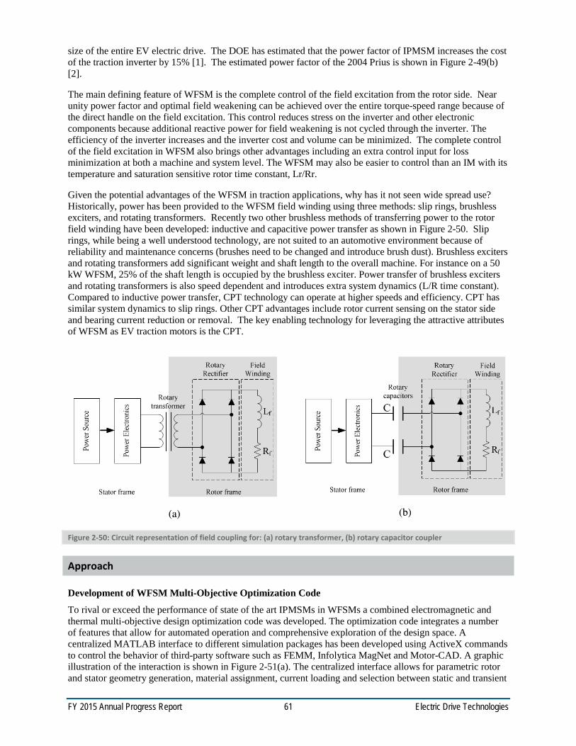
FY 2015 Annual Progress Report 61 Electric Drive Technologies
size of the entire EV electric drive. The DOE has estimated that the power factor of IPMSM increases the cost of the traction inverter by 15% [1]. The estimated power factor of the 2004 Prius is shown in Figure 2-49(b) [2].
The main defining feature of WFSM is the complete control of the field excitation from the rotor side. Near unity power factor and optimal field weakening can be achieved over the entire torque-speed range because of the direct handle on the field excitation. This control reduces stress on the inverter and other electronic components because additional reactive power for field weakening is not cycled through the inverter. The efficiency of the inverter increases and the inverter cost and volume can be minimized. The complete control of the field excitation in WFSM also brings other advantages including an extra control input for loss minimization at both a machine and system level. The WFSM may also be easier to control than an IM with its temperature and saturation sensitive rotor time constant, Lr/Rr.
Given the potential advantages of the WFSM in traction applications, why has it not seen wide spread use? Historically, power has been provided to the WFSM field winding using three methods: slip rings, brushless exciters, and rotating transformers. Recently two other brushless methods of transferring power to the rotor field winding have been developed: inductive and capacitive power transfer as shown in Figure 2-50. Slip rings, while being a well understood technology, are not suited to an automotive environment because of reliability and maintenance concerns (brushes need to be changed and introduce brush dust). Brushless exciters and rotating transformers add significant weight and shaft length to the overall machine. For instance on a 50 kW WFSM, 25% of the shaft length is occupied by the brushless exciter. Power transfer of brushless exciters and rotating transformers is also speed dependent and introduces extra system dynamics (L/R time constant). Compared to inductive power transfer, CPT technology can operate at higher speeds and efficiency. CPT has similar system dynamics to slip rings. Other CPT advantages include rotor current sensing on the stator side and bearing current reduction or removal. The key enabling technology for leveraging the attractive attributes of WFSM as EV traction motors is the CPT.
Figure 2-50: Circuit representation of field coupling for: (a) rotary transformer, (b) rotary capacitor coupler
Approach
Development of WFSM Multi-Objective Optimization Code
To rival or exceed the performance of state of the art IPMSMs in WFSMs a combined electromagnetic and thermal multi-objective design optimization code was developed. The optimization code integrates a number of features that allow for automated operation and comprehensive exploration of the design space. A centralized MATLAB interface to different simulation packages has been developed using ActiveX commands to control the behavior of third-party software such as FEMM, Infolytica MagNet and Motor-CAD. A graphic illustration of the interaction is shown in Figure 2-51(a). The centralized interface allows for parametric rotor and stator geometry generation, material assignment, current loading and selection between static and transient
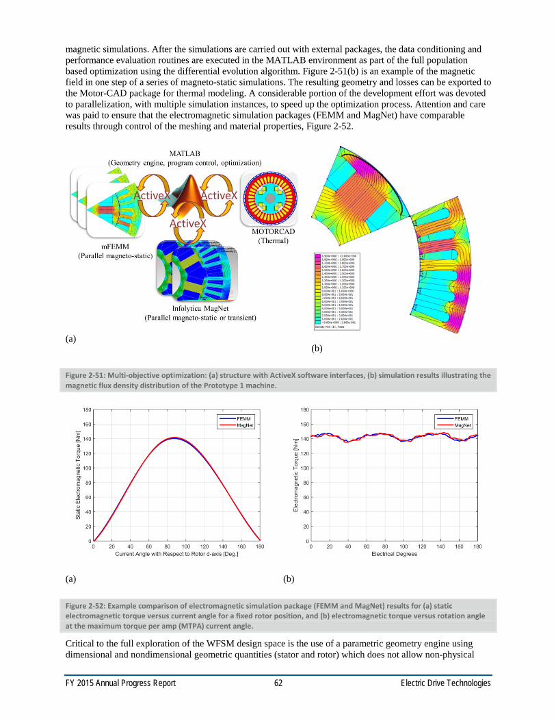
FY 2015 Annual Progress Report 62 Electric Drive Technologies
magnetic simulations. After the simulations are carried out with external packages, the data conditioning and performance evaluation routines are executed in the MATLAB environment as part of the full population based optimization using the differential evolution algorithm. Figure 2-51(b) is an example of the magnetic field in one step of a series of magneto-static simulations. The resulting geometry and losses can be exported to the Motor-CAD package for thermal modeling. A considerable portion of the development effort was devoted to parallelization, with multiple simulation instances, to speed up the optimization process. Attention and care was paid to ensure that the electromagnetic simulation packages (FEMM and MagNet) have comparable results through control of the meshing and material properties, Figure 2-52.
(a) (b)
Figure 2-51: Multi-objective optimization: (a) structure with ActiveX software interfaces, (b) simulation results illustrating the magnetic flux density distribution of the Prototype 1 machine.
(a) (b)
Figure 2-52: Example comparison of electromagnetic simulation package (FEMM and MagNet) results for (a) static electromagnetic torque versus current angle for a fixed rotor position, and (b) electromagnetic torque versus rotation angle at the maximum torque per amp (MTPA) current angle.
Critical to the full exploration of the WFSM design space is the use of a parametric geometry engine using dimensional and nondimensional geometric quantities (stator and rotor) which does not allow non-physical

FY 2015 Annual Progress Report 63 Electric Drive Technologies
geometries to occur when using a population based design optimization algorithm. The developed geometry engine allows for points to merge and collapse. An example of some of the rotor nondimensional parameters and point merging and collapsing is shown in Figure 2-53.
Figure 2-53: Example rotor nondimensional parameters and geometry morphing illustrating point merging and collapsing.

FY 2015 Annual Progress Report 64 Electric Drive Technologies
WFSM Specifications and Determination of Feasible Design Variable Ranges
WFSM specifications for peak output power, continuous output power, specific power density, and volumetric power density were developed in consultation with DOE USDRIVE targets, Table 2-9. A base speed of 4000 RPM was selected along with a target constant power speed range of three (corresponding to 12,000 RPM).
The stator outer diameter was constrained based on typical packaging constraints in an automotive application and to fit the dynamometer available for experimental characterization. An additional minimum stator inner diameter constraint was imposed to allow the CPT to nest inside the stator end turns if desired. To determine the ranges of feasible rotor geometric parameters a structural analysis was carried out using a design of experiments approach in SolidWorks based on the selected maximum constant power speed and a safety factor. Representative Von-Mises stress and strain analysis results are shown in Figure 2-54(a) and Figure 2-54(b).
(a) (b)
Figure 2-54: Example WFSM rotor structural analysis simulation results: (a) Von-Mises stress, (b) strain
The CPT also imposed several constraints on the rotor field winding including a maximum rotor field winding power transfer of 2 kW, field winding terminal current of 10 A, and minimum field winding terminal voltage of 200 V, Table 2-9.
WFSM Multi-Objective Optimization Results and Prototype Down Selection
After extensive test runs of the optimizer to identify the most feasible initial topology at 48 slot 8 pole single layer winding design was selected. Using the differential evolution optimization method with extensive test runs showed that hard constraints act as additional objectives as long as a suitable population is found, and in general, it has been observed that adding hard constraints speed up convergence more than increasing the number of optimization objectives.
The final optimization run from which the WFSM Prototype 1 geometry has been selected takes into account 3 dimensional geometric parameters, 9 nondimensional geometric parameters that morph the machine geometry, 2 current density ranges and the 5 hard constraints (Table 2-8) on allowed losses and torque metrics. Finally, two optimization objectives were used for maximization (Actually implemented as minimizations): volumetric torque density and electromagnetic torque scaled for machine losses ("goodness"), Table 2-8. The optimizations were run with 75 members per generation evolving over 75 generations. A graphical projection of the results on a torque density versus "goodness" (average torque scaled by the square root of the losses) plane are shown in Figure 2-55. Figure 2-55(a) shows the full population and (b) the subset of the members of the population that meet all the constraints are detailed. In (b) the designs which do not meet all the hard constraints are colored white. Another graphical projection of the results is on the torque density versus losses plane are shown in Figure 2-56. Again, (a) shows the full population and (b) the subset of members of the population that meet all the constraints are detailed.
Table 2-8: WFSM Optimization Hard Constraints and Objectives
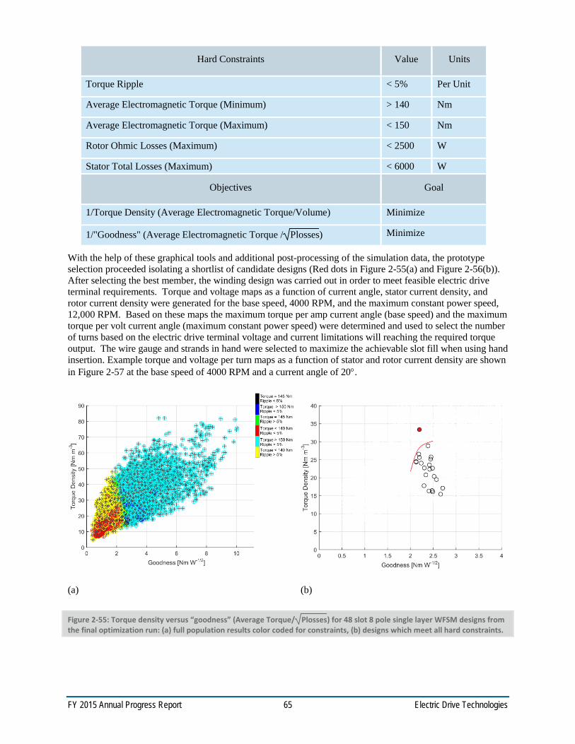
FY 2015 Annual Progress Report 65 Electric Drive Technologies
Hard Constraints Value Units
Torque Ripple < 5% Per Unit
Average Electromagnetic Torque (Minimum) > 140 Nm
Average Electromagnetic Torque (Maximum) < 150 Nm
Rotor Ohmic Losses (Maximum) < 2500 W
Stator Total Losses (Maximum) < 6000 W
Objectives Goal
1/Torque Density (Average Electromagnetic Torque/Volume) Minimize
1/"Goodness" (Average Electromagnetic Torque / Plosses) Minimize
With the help of these graphical tools and additional post-processing of the simulation data, the prototype selection proceeded isolating a shortlist of candidate designs (Red dots in Figure 2-55(a) and Figure 2-56(b)). After selecting the best member, the winding design was carried out in order to meet feasible electric drive terminal requirements. Torque and voltage maps as a function of current angle, stator current density, and rotor current density were generated for the base speed, 4000 RPM, and the maximum constant power speed, 12,000 RPM. Based on these maps the maximum torque per amp current angle (base speed) and the maximum torque per volt current angle (maximum constant power speed) were determined and used to select the number of turns based on the electric drive terminal voltage and current limitations will reaching the required torque output. The wire gauge and strands in hand were selected to maximize the achievable slot fill when using hand insertion. Example torque and voltage per turn maps as a function of stator and rotor current density are shown in Figure 2-57 at the base speed of 4000 RPM and a current angle of 20°.
(a) (b)
Figure 2-55: Torque density versus “goodness” (Average Torque/ Plosses) for 48 slot 8 pole single layer WFSM designs from the final optimization run: (a) full population results color coded for constraints, (b) designs which meet all hard constraints.
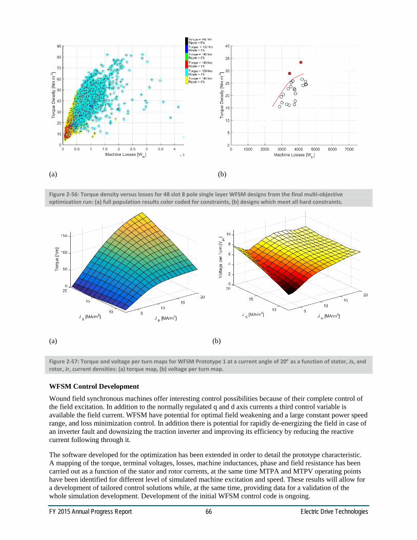
FY 2015 Annual Progress Report 66 Electric Drive Technologies
(a) (b)
Figure 2-56: Torque density versus losses for 48 slot 8 pole single layer WFSM designs from the final multi-objective optimization run: (a) full population results color coded for constraints, (b) designs which meet all hard constraints.
(a) (b)
Figure 2-57: Torque and voltage per turn maps for WFSM Prototype 1 at a current angle of 20° as a function of stator, Js, and rotor, Jr, current densities: (a) torque map, (b) voltage per turn map.
WFSM Control Development
Wound field synchronous machines offer interesting control possibilities because of their complete control of the field excitation. In addition to the normally regulated q and d axis currents a third control variable is available the field current. WFSM have potential for optimal field weakening and a large constant power speed range, and loss minimization control. In addition there is potential for rapidly de-energizing the field in case of an inverter fault and downsizing the traction inverter and improving its efficiency by reducing the reactive current following through it.
The software developed for the optimization has been extended in order to detail the prototype characteristic. A mapping of the torque, terminal voltages, losses, machine inductances, phase and field resistance has been carried out as a function of the stator and rotor currents, at the same time MTPA and MTPV operating points have been identified for different level of simulated machine excitation and speed. These results will allow for a development of tailored control solutions while, at the same time, providing data for a validation of the whole simulation development. Development of the initial WFSM control code is ongoing.

FY 2015 Annual Progress Report 67 Electric Drive Technologies
Design of Capacitive Coupler
Figure 2-58 depicts a class E amplifier, specifically a two switch interleaved configuration. Functionally, the same operating principles of a single switch class E apply except the interleaved version is capable of twice the power due to extra semiconductors and higher effective switching frequency. To ensure the CPT performance metric for the Go/No-Go Point of budget period 1 is satisfied, the interleaved class-E power electronic circuit topology was selected for this project. The circuit diagram is illustrated in Figure 2-58 highlighting the primary side, the circuitry embedded in the coupling, and the field winding.
Figure 2-58: Class E amplifier utilizing interleaved switching
Results and Discussion
WFSM Prototype 1 Predicted Performance
The predicted perfomance of WFSM Prototype 1 versus target specifications is listed in Table 2-9. Because the peak power density is higher than the specification target the base and maximum constant power speeds maybe lowered.
Table 2-9: Initial WFSM Motor Targets and Prototype 1 Design
Parameter Target Specifications Prototype 1 Units
Peak Power 55 59.13 kW
Continuous Power 30 30 kW
Specific Power Density 1.3 2.08 kW/kg
Volumetric Power Density 4.5 13.97 kW/l
Maximum Stator Outer Diameter 300 254 mm Minimum Rotor Inner Diameter 100 118 mm Minimum Stator Winding Inner Diameter 150 178 mm
Base Speed 4000 4000 RPM
Maximum Constant Power Speed 12000 12000 RPM Maximum Field Winding Load 2 1.9 kW Maximum Field Winding Current 10 6.69 A
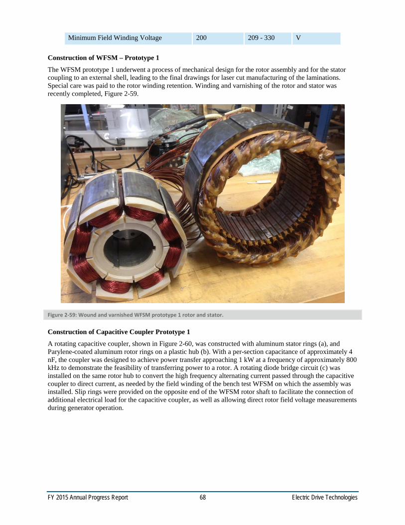
FY 2015 Annual Progress Report 68 Electric Drive Technologies
Minimum Field Winding Voltage 200 209 - 330 V
Construction of WFSM – Prototype 1
The WFSM prototype 1 underwent a process of mechanical design for the rotor assembly and for the stator coupling to an external shell, leading to the final drawings for laser cut manufacturing of the laminations. Special care was paid to the rotor winding retention. Winding and varnishing of the rotor and stator was recently completed, Figure 2-59.
Figure 2-59: Wound and varnished WFSM prototype 1 rotor and stator.
Construction of Capacitive Coupler Prototype 1
A rotating capacitive coupler, shown in Figure 2-60, was constructed with aluminum stator rings (a), and Parylene-coated aluminum rotor rings on a plastic hub (b). With a per-section capacitance of approximately 4 nF, the coupler was designed to achieve power transfer approaching 1 kW at a frequency of approximately 800 kHz to demonstrate the feasibility of transferring power to a rotor. A rotating diode bridge circuit (c) was installed on the same rotor hub to convert the high frequency alternating current passed through the capacitive coupler to direct current, as needed by the field winding of the bench test WFSM on which the assembly was installed. Slip rings were provided on the opposite end of the WFSM rotor shaft to facilitate the connection of additional electrical load for the capacitive coupler, as well as allowing direct rotor field voltage measurements during generator operation.

FY 2015 Annual Progress Report 69 Electric Drive Technologies
(a) (b) (c)
Figure 2-60: Coupling capacitor stator (a), rotor (b), and rectifier board (c), which comprise the capacitive power coupler assembly.
The assembled capacitive coupler was installed on the WFSM rotor shaft, Figure 2-61(a), which was then coupled to the dynamometer prime mover and mounted on an open frame dynamometer (b). A high frequency inverter (c) was connected to the stator rings as input to the capacitive coupler.
(a) (b) (c)
Figure 2-61: Coupler mounted on WFSM rotor (a), dynamometer test stand (b), and inverter for capacitive power coupling to rotor (c).
Additionally, a hydroflex coupling capacitor was also constructed per the original proposal. Here, the stator and rotor plates were water jet cut from 0.016” thick 6061 aluminum stock. These plates are pictured in Figure 2-62. The rotor plates are coated with parylene, a transparent dielectric, to ensure galvanic isolation at zero speed. These plates were then alternately stacked, 4 stators and 3 rotors, 0.001” apart, onto a dynamometer test stand to evaluate the resulting capacitance verses speed curve. The entirety of the hydroflex plate test dynamometer stand is pictured in Figure 2-63.
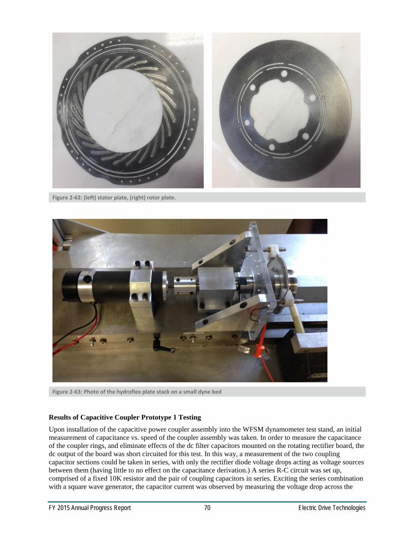
FY 2015 Annual Progress Report 70 Electric Drive Technologies
Figure 2-62: (left) stator plate, (right) rotor plate.
Figure 2-63: Photo of the hydroflex plate stack on a small dyne bed
Results of Capacitive Coupler Prototype 1 Testing
Upon installation of the capacitive power coupler assembly into the WFSM dynamometer test stand, an initial measurement of capacitance vs. speed of the coupler assembly was taken. In order to measure the capacitance of the coupler rings, and eliminate effects of the dc filter capacitors mounted on the rotating rectifier board, the dc output of the board was short circuited for this test. In this way, a measurement of the two coupling capacitor sections could be taken in series, with only the rectifier diode voltage drops acting as voltage sources between them (having little to no effect on the capacitance derivation.) A series R-C circuit was set up, comprised of a fixed 10K resistor and the pair of coupling capacitors in series. Exciting the series combination with a square wave generator, the capacitor current was observed by measuring the voltage drop across the
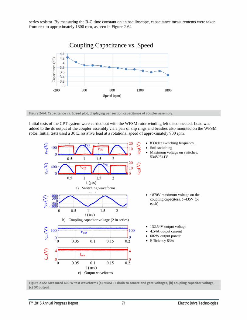
FY 2015 Annual Progress Report 71 Electric Drive Technologies
series resistor. By measuring the R-C time constant on an oscilloscope, capacitance measurements were taken from rest to approximately 1800 rpm, as seen in Figure 2-64.
Figure 2-64: Capacitance vs. Speed plot, displaying per section capacitance of coupler assembly.
Initial tests of the CPT system were carried out with the WFSM rotor winding left disconnected. Load was added to the dc output of the coupler assembly via a pair of slip rings and brushes also mounted on the WFSM rotor. Initial tests used a 30 Ω resistive load at a rotational speed of approximately 900 rpm.
Figure 2-65: Measured 600 W test waveforms (a) MOSFET drain to source and gate voltages, (b) coupling capacitor voltage, (c) DC output
33.23.43.63.8
44.24.4
Cap
acita
nce
(nF)
-200 300 800 1300 1800Speed (rpm)
Coupling Capacitance vs. Speed
• 833kHz switching frequency. • Soft switching • Maximum voltage on switches:
534V/541V
a) Switching waveforms
• ~870V maximum voltage on the coupling capacitors. (~435V for each)
b) Coupling capacitor voltage (2 in series)
• 132.54V output voltage • 4.54A output current • 602W output power • Efficiency 83%
c) Output waveforms

FY 2015 Annual Progress Report 72 Electric Drive Technologies
The circuit is able to deliver 600W with 83% efficiency with selected waveforms plotted in Figure 2-65. The winding on the test synchronous machine has 31.4 ohm resistance, and it is rated for 200W power dissipation. So the converter can be used on the field winding for the test bench machine. The system will honed further to be able to provide kW power levels for the intended final WFSM traction application.
After the power throughput capability of the capacitive power coupler was thoroughly verified, the 31.4 Ω 200 W rotor field winding of the test WFSM was connected across the dc output terminals of the capacitive power coupler. Slip rings were left connected in parallel with the winding to allow continuous monitoring of the generator field voltage during rotation. The 3-phase stator terminals of the WFSM were star-connected, and the output leads were connected to a 3-phase resistive load in a delta configuration. Generator power output into the resistive load of approximately 5 kW was achieved using the journal bearing capacitive power coupler as the sole means of exciting the rotor winding to full field, approximately 200 W. Figure 2-66 shows the system setup. Figure 2-67 shows an initial test to check generated 3-phase voltage balance as well as rotor field and load voltages.
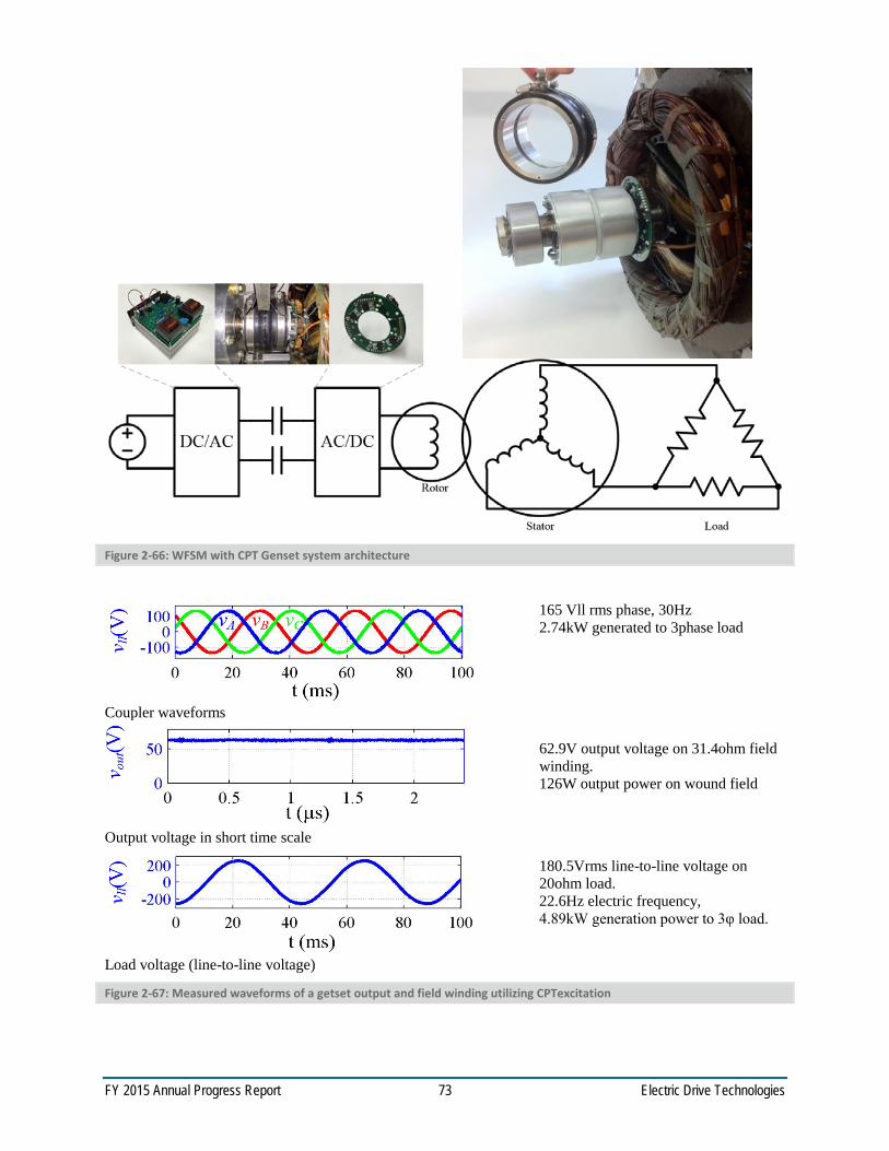
FY 2015 Annual Progress Report 73 Electric Drive Technologies
Figure 2-66: WFSM with CPT Genset system architecture
165 Vll rms phase, 30Hz 2.74kW generated to 3phase load
Coupler waveforms
62.9V output voltage on 31.4ohm field winding. 126W output power on wound field
Output voltage in short time scale
180.5Vrms line-to-line voltage on 20ohm load. 22.6Hz electric frequency, 4.89kW generation power to 3φ load.
Load voltage (line-to-line voltage)
Figure 2-67: Measured waveforms of a getset output and field winding utilizing CPTexcitation
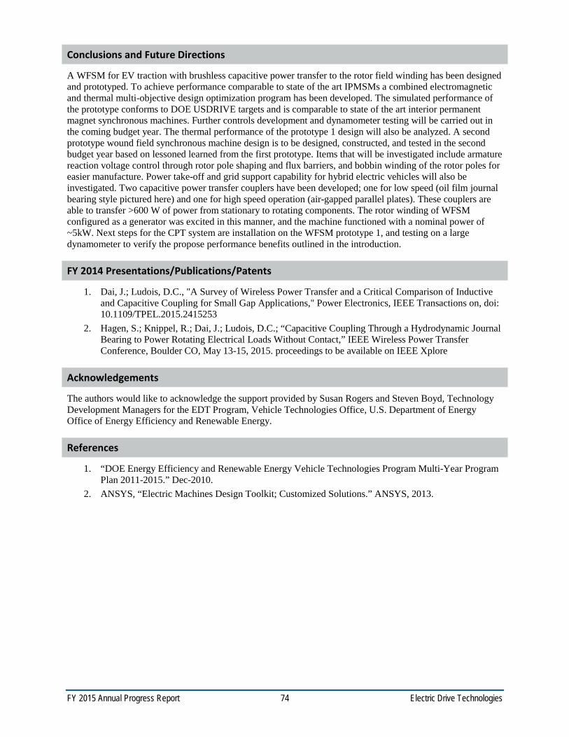
FY 2015 Annual Progress Report 74 Electric Drive Technologies
Conclusions and Future Directions
A WFSM for EV traction with brushless capacitive power transfer to the rotor field winding has been designed and prototyped. To achieve performance comparable to state of the art IPMSMs a combined electromagnetic and thermal multi-objective design optimization program has been developed. The simulated performance of the prototype conforms to DOE USDRIVE targets and is comparable to state of the art interior permanent magnet synchronous machines. Further controls development and dynamometer testing will be carried out in the coming budget year. The thermal performance of the prototype 1 design will also be analyzed. A second prototype wound field synchronous machine design is to be designed, constructed, and tested in the second budget year based on lessoned learned from the first prototype. Items that will be investigated include armature reaction voltage control through rotor pole shaping and flux barriers, and bobbin winding of the rotor poles for easier manufacture. Power take-off and grid support capability for hybrid electric vehicles will also be investigated. Two capacitive power transfer couplers have been developed; one for low speed (oil film journal bearing style pictured here) and one for high speed operation (air-gapped parallel plates). These couplers are able to transfer >600 W of power from stationary to rotating components. The rotor winding of WFSM configured as a generator was excited in this manner, and the machine functioned with a nominal power of ~5kW. Next steps for the CPT system are installation on the WFSM prototype 1, and testing on a large dynamometer to verify the propose performance benefits outlined in the introduction.
FY 2014 Presentations/Publications/Patents
1. Dai, J.; Ludois, D.C., "A Survey of Wireless Power Transfer and a Critical Comparison of Inductive and Capacitive Coupling for Small Gap Applications," Power Electronics, IEEE Transactions on, doi: 10.1109/TPEL.2015.2415253
2. Hagen, S.; Knippel, R.; Dai, J.; Ludois, D.C.; “Capacitive Coupling Through a Hydrodynamic Journal Bearing to Power Rotating Electrical Loads Without Contact,” IEEE Wireless Power Transfer Conference, Boulder CO, May 13-15, 2015. proceedings to be available on IEEE Xplore
Acknowledgements
The authors would like to acknowledge the support provided by Susan Rogers and Steven Boyd, Technology Development Managers for the EDT Program, Vehicle Technologies Office, U.S. Department of Energy Office of Energy Efficiency and Renewable Energy.
References
1. “DOE Energy Efficiency and Renewable Energy Vehicle Technologies Program Multi-Year Program Plan 2011-2015.” Dec-2010.
2. ANSYS, “Electric Machines Design Toolkit; Customized Solutions.” ANSYS, 2013.
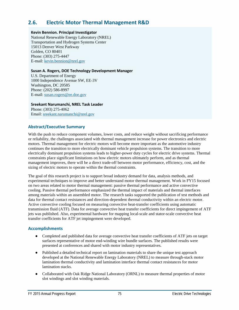
FY 2015 Annual Progress Report 75 Electric Drive Technologies
2.6. Electric Motor Thermal Management R&D
Kevin Bennion. Principal Investigator National Renewable Energy Laboratory (NREL) Transportation and Hydrogen Systems Center 15013 Denver West Parkway Golden, CO 80401 Phone: (303) 275-4447 E-mail: [email protected] Susan A. Rogers, DOE Technology Development Manager U.S. Department of Energy 1000 Independence Avenue SW, EE-3V Washington, DC 20585 Phone: (202) 586-8997 E-mail: [email protected] Sreekant Narumanchi, NREL Task Leader Phone: (303) 275-4062 Email: [email protected]
Abstract/Executive Summary With the push to reduce component volumes, lower costs, and reduce weight without sacrificing performance or reliability, the challenges associated with thermal management increase for power electronics and electric motors. Thermal management for electric motors will become more important as the automotive industry continues the transition to more electrically dominant vehicle propulsion systems. The transition to more electrically dominant propulsion systems leads to higher-power duty cycles for electric drive systems. Thermal constraints place significant limitations on how electric motors ultimately perform, and as thermal management improves, there will be a direct trade-off between motor performance, efficiency, cost, and the sizing of electric motors to operate within the thermal constraints.
The goal of this research project is to support broad industry demand for data, analysis methods, and experimental techniques to improve and better understand motor thermal management. Work in FY15 focused on two areas related to motor thermal management: passive thermal performance and active convective cooling. Passive thermal performance emphasized the thermal impact of materials and thermal interfaces among materials within an assembled motor. The research tasks supported the publication of test methods and data for thermal contact resistances and direction-dependent thermal conductivity within an electric motor. Active convective cooling focused on measuring convective heat-transfer coefficients using automatic transmission fluid (ATF). Data for average convective heat transfer coefficients for direct impingement of ATF jets was published. Also, experimental hardware for mapping local-scale and stator-scale convective heat transfer coefficients for ATF jet impingement were developed.
Accomplishments Completed and published data for average convective heat transfer coefficients of ATF jets on target
surfaces representative of motor end-winding wire bundle surfaces. The published results were presented at conferences and shared with motor industry representatives.
Published a detailed technical report on lamination materials to share the unique test approach developed at the National Renewable Energy Laboratory (NREL) to measure through-stack motor lamination thermal conductivity and lamination interface thermal contact resistances for motor lamination stacks.
Collaborated with Oak Ridge National Laboratory (ORNL) to measure thermal properties of motor slot windings and slot winding materials.
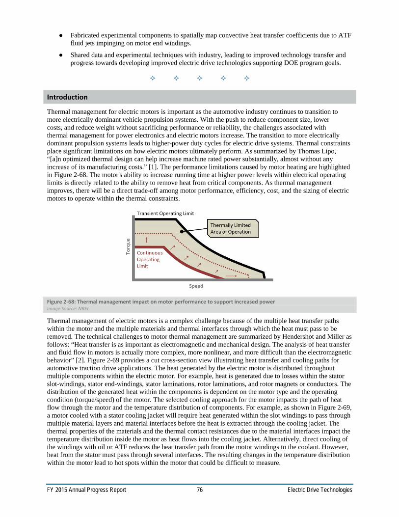
FY 2015 Annual Progress Report 76 Electric Drive Technologies
Fabricated experimental components to spatially map convective heat transfer coefficients due to ATF fluid jets impinging on motor end windings.
Shared data and experimental techniques with industry, leading to improved technology transfer and progress towards developing improved electric drive technologies supporting DOE program goals.
Introduction
Thermal management for electric motors is important as the automotive industry continues to transition to more electrically dominant vehicle propulsion systems. With the push to reduce component size, lower costs, and reduce weight without sacrificing performance or reliability, the challenges associated with thermal management for power electronics and electric motors increase. The transition to more electrically dominant propulsion systems leads to higher-power duty cycles for electric drive systems. Thermal constraints place significant limitations on how electric motors ultimately perform. As summarized by Thomas Lipo, “[a]n optimized thermal design can help increase machine rated power substantially, almost without any increase of its manufacturing costs.” [1]. The performance limitations caused by motor heating are highlighted in Figure 2-68. The motor's ability to increase running time at higher power levels within electrical operating limits is directly related to the ability to remove heat from critical components. As thermal management improves, there will be a direct trade-off among motor performance, efficiency, cost, and the sizing of electric motors to operate within the thermal constraints.
Figure 2-68: Thermal management impact on motor performance to support increased power Image Source: NREL
Thermal management of electric motors is a complex challenge because of the multiple heat transfer paths within the motor and the multiple materials and thermal interfaces through which the heat must pass to be removed. The technical challenges to motor thermal management are summarized by Hendershot and Miller as follows: “Heat transfer is as important as electromagnetic and mechanical design. The analysis of heat transfer and fluid flow in motors is actually more complex, more nonlinear, and more difficult than the electromagnetic behavior” [2]. Figure 2-69 provides a cut cross-section view illustrating heat transfer and cooling paths for automotive traction drive applications. The heat generated by the electric motor is distributed throughout multiple components within the electric motor. For example, heat is generated due to losses within the stator slot-windings, stator end-windings, stator laminations, rotor laminations, and rotor magnets or conductors. The distribution of the generated heat within the components is dependent on the motor type and the operating condition (torque/speed) of the motor. The selected cooling approach for the motor impacts the path of heat flow through the motor and the temperature distribution of components. For example, as shown in Figure 2-69, a motor cooled with a stator cooling jacket will require heat generated within the slot windings to pass through multiple material layers and material interfaces before the heat is extracted through the cooling jacket. The thermal properties of the materials and the thermal contact resistances due to the material interfaces impact the temperature distribution inside the motor as heat flows into the cooling jacket. Alternatively, direct cooling of the windings with oil or ATF reduces the heat transfer path from the motor windings to the coolant. However, heat from the stator must pass through several interfaces. The resulting changes in the temperature distribution within the motor lead to hot spots within the motor that could be difficult to measure.
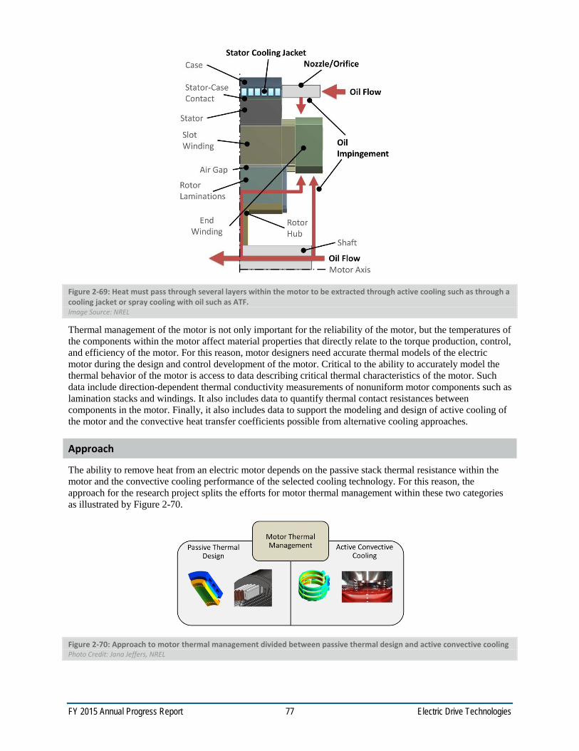
FY 2015 Annual Progress Report 77 Electric Drive Technologies
Figure 2-69: Heat must pass through several layers within the motor to be extracted through active cooling such as through a cooling jacket or spray cooling with oil such as ATF. Image Source: NREL
Thermal management of the motor is not only important for the reliability of the motor, but the temperatures of the components within the motor affect material properties that directly relate to the torque production, control, and efficiency of the motor. For this reason, motor designers need accurate thermal models of the electric motor during the design and control development of the motor. Critical to the ability to accurately model the thermal behavior of the motor is access to data describing critical thermal characteristics of the motor. Such data include direction-dependent thermal conductivity measurements of nonuniform motor components such as lamination stacks and windings. It also includes data to quantify thermal contact resistances between components in the motor. Finally, it also includes data to support the modeling and design of active cooling of the motor and the convective heat transfer coefficients possible from alternative cooling approaches.
Approach
The ability to remove heat from an electric motor depends on the passive stack thermal resistance within the motor and the convective cooling performance of the selected cooling technology. For this reason, the approach for the research project splits the efforts for motor thermal management within these two categories as illustrated by Figure 2-70.
Figure 2-70: Approach to motor thermal management divided between passive thermal design and active convective cooling Photo Credit: Jana Jeffers, NREL
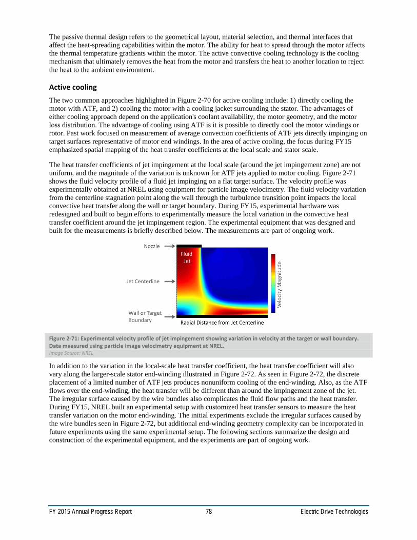
FY 2015 Annual Progress Report 78 Electric Drive Technologies
The passive thermal design refers to the geometrical layout, material selection, and thermal interfaces that affect the heat-spreading capabilities within the motor. The ability for heat to spread through the motor affects the thermal temperature gradients within the motor. The active convective cooling technology is the cooling mechanism that ultimately removes the heat from the motor and transfers the heat to another location to reject the heat to the ambient environment.
Active cooling The two common approaches highlighted in Figure 2-70 for active cooling include: 1) directly cooling the motor with ATF, and 2) cooling the motor with a cooling jacket surrounding the stator. The advantages of either cooling approach depend on the application's coolant availability, the motor geometry, and the motor loss distribution. The advantage of cooling using ATF is it is possible to directly cool the motor windings or rotor. Past work focused on measurement of average convection coefficients of ATF jets directly impinging on target surfaces representative of motor end windings. In the area of active cooling, the focus during FY15 emphasized spatial mapping of the heat transfer coefficients at the local scale and stator scale.
The heat transfer coefficients of jet impingement at the local scale (around the jet impingement zone) are not uniform, and the magnitude of the variation is unknown for ATF jets applied to motor cooling. Figure 2-71 shows the fluid velocity profile of a fluid jet impinging on a flat target surface. The velocity profile was experimentally obtained at NREL using equipment for particle image velocimetry. The fluid velocity variation from the centerline stagnation point along the wall through the turbulence transition point impacts the local convective heat transfer along the wall or target boundary. During FY15, experimental hardware was redesigned and built to begin efforts to experimentally measure the local variation in the convective heat transfer coefficient around the jet impingement region. The experimental equipment that was designed and built for the measurements is briefly described below. The measurements are part of ongoing work.
Figure 2-71: Experimental velocity profile of jet impingement showing variation in velocity at the target or wall boundary. Data measured using particle image velocimetry equipment at NREL. Image Source: NREL
In addition to the variation in the local-scale heat transfer coefficient, the heat transfer coefficient will also vary along the larger-scale stator end-winding illustrated in Figure 2-72. As seen in Figure 2-72, the discrete placement of a limited number of ATF jets produces nonuniform cooling of the end-winding. Also, as the ATF flows over the end-winding, the heat transfer will be different than around the impingement zone of the jet. The irregular surface caused by the wire bundles also complicates the fluid flow paths and the heat transfer. During FY15, NREL built an experimental setup with customized heat transfer sensors to measure the heat transfer variation on the motor end-winding. The initial experiments exclude the irregular surfaces caused by the wire bundles seen in Figure 2-72, but additional end-winding geometry complexity can be incorporated in future experiments using the same experimental setup. The following sections summarize the design and construction of the experimental equipment, and the experiments are part of ongoing work.

FY 2015 Annual Progress Report 79 Electric Drive Technologies
Figure 2-72: Heat transfer due to ATF jet impingement will vary over the end-winding surface. Photo Credit: Kevin Bennion, NREL
Passive Thermal Design The passive thermal stack elements illustrated in Figure 2-69 and Figure 2-73 are critical to designing effective thermal management systems for electric motors. The work supports improved thermal models for motor design, but it also enables analysis to compare the potential impacts of new materials, fabrication methods, or material processing on motor heat transfer. Figure 2-73 illustrates a few of the critical elements that influence the passive cooling of the motor or the ability of heat to flow through the motor. A few of the items highlighted in Figure 2-73 include the stator-to-case thermal contact resistance, lamination through-stack and in-plane thermal conductivity, winding cross-slot thermal properties and thermal interface resistance between ground insulation materials and the respective motor elements in contact with the slot liner or ground insulation. Efforts continued in FY15 to measure passive stack elements within the motor as highlighted above in collaboration with industry, universities, and ORNL.
Figure 2-73: Passive stack thermal properties and terminology. Image Source: NREL
Results and Discussion
The discussion included below is separated into the two main focus areas described above. The first section summarizes the progress for active cooling with emphasis on using ATF for cooling electric motors. The second section focuses on the passive cooling of the electric motor. The sections also highlight published reports prepared during FY15 that can be referenced for additional details beyond what can be included in this report.
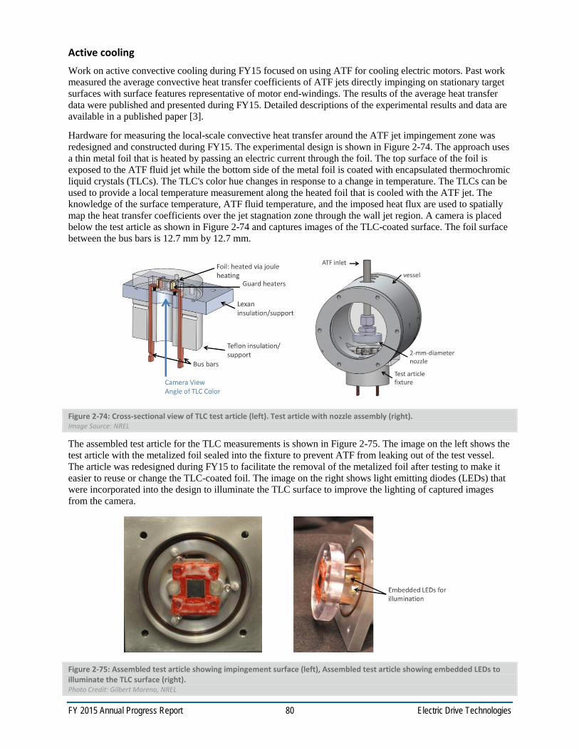
FY 2015 Annual Progress Report 80 Electric Drive Technologies
Active cooling Work on active convective cooling during FY15 focused on using ATF for cooling electric motors. Past work measured the average convective heat transfer coefficients of ATF jets directly impinging on stationary target surfaces with surface features representative of motor end-windings. The results of the average heat transfer data were published and presented during FY15. Detailed descriptions of the experimental results and data are available in a published paper [3].
Hardware for measuring the local-scale convective heat transfer around the ATF jet impingement zone was redesigned and constructed during FY15. The experimental design is shown in Figure 2-74. The approach uses a thin metal foil that is heated by passing an electric current through the foil. The top surface of the foil is exposed to the ATF fluid jet while the bottom side of the metal foil is coated with encapsulated thermochromic liquid crystals (TLCs). The TLC's color hue changes in response to a change in temperature. The TLCs can be used to provide a local temperature measurement along the heated foil that is cooled with the ATF jet. The knowledge of the surface temperature, ATF fluid temperature, and the imposed heat flux are used to spatially map the heat transfer coefficients over the jet stagnation zone through the wall jet region. A camera is placed below the test article as shown in Figure 2-74 and captures images of the TLC-coated surface. The foil surface between the bus bars is 12.7 mm by 12.7 mm.
Figure 2-74: Cross-sectional view of TLC test article (left). Test article with nozzle assembly (right). Image Source: NREL
The assembled test article for the TLC measurements is shown in Figure 2-75. The image on the left shows the test article with the metalized foil sealed into the fixture to prevent ATF from leaking out of the test vessel. The article was redesigned during FY15 to facilitate the removal of the metalized foil after testing to make it easier to reuse or change the TLC-coated foil. The image on the right shows light emitting diodes (LEDs) that were incorporated into the design to illuminate the TLC surface to improve the lighting of captured images from the camera.
Figure 2-75: Assembled test article showing impingement surface (left), Assembled test article showing embedded LEDs to illuminate the TLC surface (right). Photo Credit: Gilbert Moreno, NREL

FY 2015 Annual Progress Report 81 Electric Drive Technologies
The test apparatus installed within the test vessel is shown in Figure 2-76.The image on the left shows the test article with the TLC-coated foil installed. The orifice nozzle for the fluid jet is installed within the test vessel and is located above the metal foil. The image also shows the lighting provided by the LEDs to illuminate the TLC surface. The image on the right shows the view from the camera view angle looking up at the TLC-coated surface illuminated by the LEDs. Work is currently in progress to calibrate the TLCs response to temperature after they are coated onto the metalized foil and placed within the test apparatus.
Figure 2-76: Test article and nozzle assembly (left), assembled test article showing camera view of illuminated TLC surface (right) Photo Credit: Gilbert Moreno, NREL
The objective of the stator-scale ATF thermal measurements on motor end-windings is to map the spatial distribution of the heat transfer coefficients over the motor end-winding surface. The image on the left of Figure 2-77 illustrates the goals of the experimental setup. The experiment was designed to enable the measurement of heat transfer on multiple surfaces of the motor end winding while allowing for the relative position between the heat transfer sensor and fluid jet impingement zone to change. Unlike prior measurements, the fluid jet is not constrained to be in a fixed location relative to the heat transfer sensor location. The experimental setup allows for the study of nozzle location, nozzle type, jet interactions, flow rates, gravity, and alternative cooling designs along the inner diameter, outside diameter, and outside edge of the motor end winding. The drawing on the right of Figure 2-771 illustrates the heat transfer sensor package installed in two locations to measure the heat transfer on the outside diameter and outside edge of the motor end winding.
Figure 2-77: Illustration of sensor package installed in end winding (left), three-dimensional drawing of stator end winding with sensor package installed for convective heat transfer measurements (right) Image Source: NREL
The details of the heat transfer sensor package are shown in Figure 2-78. The drawings on the left show the construction of the sensor package. The outside surface of the sensor package simplifies the structure of the end winding with a flat surface in comparison to the irregular shape of the wire bundles. However, the outside
1
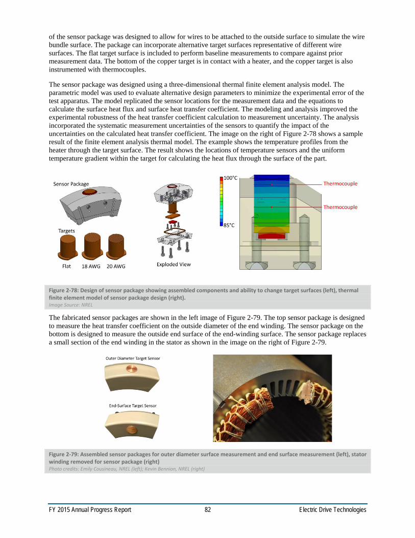
FY 2015 Annual Progress Report 82 Electric Drive Technologies
of the sensor package was designed to allow for wires to be attached to the outside surface to simulate the wire bundle surface. The package can incorporate alternative target surfaces representative of different wire surfaces. The flat target surface is included to perform baseline measurements to compare against prior measurement data. The bottom of the copper target is in contact with a heater, and the copper target is also instrumented with thermocouples.
The sensor package was designed using a three-dimensional thermal finite element analysis model. The parametric model was used to evaluate alternative design parameters to minimize the experimental error of the test apparatus. The model replicated the sensor locations for the measurement data and the equations to calculate the surface heat flux and surface heat transfer coefficient. The modeling and analysis improved the experimental robustness of the heat transfer coefficient calculation to measurement uncertainty. The analysis incorporated the systematic measurement uncertainties of the sensors to quantify the impact of the uncertainties on the calculated heat transfer coefficient. The image on the right of Figure 2-78 shows a sample result of the finite element analysis thermal model. The example shows the temperature profiles from the heater through the target surface. The result shows the locations of temperature sensors and the uniform temperature gradient within the target for calculating the heat flux through the surface of the part.
Figure 2-78: Design of sensor package showing assembled components and ability to change target surfaces (left), thermal finite element model of sensor package design (right). Image Source: NREL
The fabricated sensor packages are shown in the left image of Figure 2-79. The top sensor package is designed to measure the heat transfer coefficient on the outside diameter of the end winding. The sensor package on the bottom is designed to measure the outside end surface of the end-winding surface. The sensor package replaces a small section of the end winding in the stator as shown in the image on the right of Figure 2-79.
Figure 2-79: Assembled sensor packages for outer diameter surface measurement and end surface measurement (left), stator winding removed for sensor package (right) Photo credits: Emily Cousineau, NREL (left); Kevin Bennion, NREL (right)

FY 2015 Annual Progress Report 83 Electric Drive Technologies
Passive Thermal Design The work focusing on characterizing and improving the passive thermal stack in an electric motor is summarized below. During FY15, experimental data for lamination materials and interface thermal contact resistances were published as part of an NREL technical report [4] and presented [5], [6] at conferences. The NREL technical report provides details of the experimental approach and data related to lamination materials [4]. The report also provides equations that can be used to interpret or apply the data. The published report and testing capability developed at NREL have led to increased interactions with industry interested in applying the data to their motor designs or taking advantage of NREL's developed testing capability.
During FY15, NREL worked in collaboration with ORNL to focus more closely on the winding materials within the electric motor. Figure 2-80 shows examples of the motor winding materials. The irregular shape of the motor end winding makes the process of extracting measurement samples for testing a challenge. However, future work will continue to investigate methods to quantify the direction-dependent thermal properties of the motor end winding. The focus during FY15 in collaboration with ORNL was on the slot winding of the motor.
Figure 2-80: Images of sample slot-winding and end-winding motor components Photo credit: Kevin Bennion, NREL
Examples of the tested slot materials are shown in Figure 2-81. The images on the left show examples of tested materials that include the slot winding with and without the slot liner or ground insulation bonded to the wire bundle of the slot. The image on the right of Figure 2-81 shows sample slot winding materials being tested. In the provided example, tests were performed to measure the cross-slot thermal conductivity of the slot winding wire bundle. Measurements were also taken for the slot liner and for the thermal resistance between the slot liner and the slot winding.
Figure 2-81: Images of sample slot-winding materials (left), sample slot winding under test for measuring cross-slot thermal conductivity (right) Photo credits: Emily Cousineau, NREL

FY 2015 Annual Progress Report 84 Electric Drive Technologies
The measurement data are summarized in Table 2-10. The cross-slot thermal conductivity measurements are summarized within the first row of the table. The copper fill factor of the wire bundle was measured to be approximately 75%, which excludes the area occupied by the slot liner and only includes the wire bundle portion of the slot. The tested cross-slot thermal conductivity was 0.88 W/m-K with 95% confidence uncertainty limits (U95) of ± 11 W/m-K. In comparison, the estimated thermal conductivity from modeling the slot bundle was 0.99 W/m-K. More testing is needed, but the model and experimental results appear to agree.
The measurements of the slot liner insulation are summarized in row two of Table 2-10. The measured thermal conductivity was 0.175 W/m-K, which corresponds to a thermal resistance of 1,676 mm2-K/W for the measured material thickness. The results compare favorably to available literature data of 0.144 W/m-K [7] and 0.139 W/m-K for 10-mil Nomex [8].
Table 2-10: Summary of the measurement results on the slot winding materialsa
Thermal conductivity [W/m-K]
Thickness [mm]
Thermal Resistance [mm2-K/W]
Slot winding cross-slot 0.88 ± 0.11 NA NA Slot liner 0.175 0.294 1,676 Slot-liner to slot-winding interface NA NA 1,800a a Preliminary measurements; more experiments are necessary.
A key measurement to highlight is the slot-liner to slot-winding interface thermal resistance. The preliminary measurements of this interface thermal resistance were approximately 1,800 mm2-K/W. The measured thermal resistance was higher than initially expected and is as significant as the slot-liner insulation thermal resistance alone. The measured thermal interface is equivalent to a 0.1-mm to 0.3-mm solid varnish layer between the slot-winding and the slot-liner insulation. While not measured, it is thought that the thermal interface between the slot-liner insulation and the stator lamination could be a comparable thermal resistance. Future work is proposed to measure this interface resistance.
The measurements provide valuable data when trying to develop a motor thermal model from the component level up to the full motor system. The measured material properties were applied to the thermal benchmarking efforts to model motor thermal resistance, and the modeling results matched the experimental results. The results provided by the thermal benchmarking performed at NREL provided confirmation of the experimental techniques and data for material and interface thermal measurements that have been measured to date.
These results were shared with industry and ORNL. Efforts are continuing to further characterize the thermal resistances within the slot winding. As part of the motor research collaboration between NREL and ORNL, ORNL prepared wire bundle samples for testing. ORNL prepared blocks of the wire bundle samples as shown in the left image of Figure 2-82. The blocks were then cut by ORNL into 50-mm by 50-mm (2-in. by 2-in.) blocks of various thicknesses to allow testing at NREL of the directional thermal conductivity of the wire bundle blocks. The samples allow for testing the cross-wire thermal conductivity and the along-wire thermal conductivity as shown in the images on the right of Figure 2-82. The measurements results performed in collaboration with ORNL will look at alternative measurement techniques and compare the impact of wire gauge and copper fill factor for samples of various thicknesses.
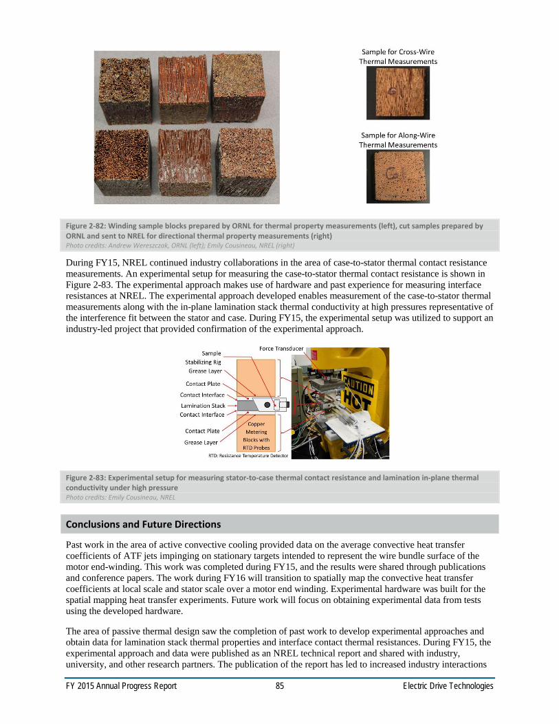
FY 2015 Annual Progress Report 85 Electric Drive Technologies
Figure 2-82: Winding sample blocks prepared by ORNL for thermal property measurements (left), cut samples prepared by ORNL and sent to NREL for directional thermal property measurements (right) Photo credits: Andrew Wereszczak, ORNL (left); Emily Cousineau, NREL (right)
During FY15, NREL continued industry collaborations in the area of case-to-stator thermal contact resistance measurements. An experimental setup for measuring the case-to-stator thermal contact resistance is shown in Figure 2-83. The experimental approach makes use of hardware and past experience for measuring interface resistances at NREL. The experimental approach developed enables measurement of the case-to-stator thermal measurements along with the in-plane lamination stack thermal conductivity at high pressures representative of the interference fit between the stator and case. During FY15, the experimental setup was utilized to support an industry-led project that provided confirmation of the experimental approach.
Figure 2-83: Experimental setup for measuring stator-to-case thermal contact resistance and lamination in-plane thermal conductivity under high pressure Photo credits: Emily Cousineau, NREL
Conclusions and Future Directions
Past work in the area of active convective cooling provided data on the average convective heat transfer coefficients of ATF jets impinging on stationary targets intended to represent the wire bundle surface of the motor end-winding. This work was completed during FY15, and the results were shared through publications and conference papers. The work during FY16 will transition to spatially map the convective heat transfer coefficients at local scale and stator scale over a motor end winding. Experimental hardware was built for the spatial mapping heat transfer experiments. Future work will focus on obtaining experimental data from tests using the developed hardware.
The area of passive thermal design saw the completion of past work to develop experimental approaches and obtain data for lamination stack thermal properties and interface contact thermal resistances. During FY15, the experimental approach and data were published as an NREL technical report and shared with industry, university, and other research partners. The publication of the report has led to increased industry interactions
FY 2015 Annual Progress Report 86 Electric Drive Technologies
at NREL in the area of motor thermal management. During FY15, in collaboration with ORNL, NREL focused on the measurement of wire-bundles and materials for motor slot windings. The work in collaboration with ORNL will support test methods to characterize the thermal properties of the materials and interface thermal resistances. The data will enable motor thermal models based on component level and thermal interface data. Future efforts will continue with ORNL to complete thermal property measurements of sample materials provided by ORNL.
FY 2015 Presentations/Publications/Patents
1. K. Bennion, J. E. Cousineau, X. Feng, C. King, and G. Moreno. “Electric Motor Thermal Management R&D.” presented at the IEEE Power & Energy Society General Meeting, Denver, CO, July 26-30, 2015.
2. J. E. Cousineau, K. Bennion, D. DeVoto, and S. Narumanchi. “Characterization of Contact and Bulk Thermal Resistance of Laminations for Electric Machines.” Presented at the ASME 2015 International Technical Conference and Exhibition on Packaging and Integration of Electronic and Photonic Microsystems and ASME 2015 12th International Conference on Nanochannels, Microchannels, and Minichannels, San Francisco, CA, United States, July 6-9, 2015.
3. K. Bennion and G. Moreno. “Convective Heat Transfer Coefficients of Automatic Transmission Fluid Jets with Implications for Electric Machine Thermal Management.” in ASME 2015 International Technical Conference and Exhibition on Packaging and Integration of Electronic and Photonic Microsystems and ASME 2015 12th International Conference on Nanochannels, Microchannels, and Minichannels, San Francisco, CA, United States, July 2015.
4. E. Cousineau, K. Bennion, D. DeVoto, M. Mihalic, and S. Narumanchi. “Characterization of Contact and Bulk Thermal Resistance of Laminations for Electric Machines.” NREL Technical Report NREL/TP-5400-63887, June 2015.
5. K. Bennion. “Electric Motor Thermal Management R&D.” 2015 DOE Vehicle Technologies Office (VTO) Annual Merit Review, June 2015.
6. K. Bennion, E. Cousineau, C. King, G. Moreno, and C. Stack. “Electric Motor Thermal Management R&D.” Electric Drive Technologies FY15 Kickoff Meeting, DOE Vehicle Technologies Office, Oak Ridge, TN, November 2014.
Acknowledgements
The author would like to acknowledge the support provided by Susan Rogers and Steven Boyd, Technology Development Managers for the Electric Drive Technologies Program, Vehicle Technologies Office, U.S. Department of Energy Office of Energy Efficiency and Renewable Energy.
The significant contributions from Emily Cousineau, Xuhui Feng, Charlie King, Gilbert Moreno, Caitlin Stack, and Adam Stokes (NREL) to the project are acknowledged. The support, collaboration, and sample motor materials provided by Andrew Wereszczak and Tim Burress (ORNL) are also acknowledged.
References
1. T. A. Lipo, Introduction to AC Machine Design, 3rd ed. Wisconsin Power Electronics Research Center, University of Wisconsin, 2007.
2. J. R. Hendershot and T. J. E. Miller, Design of Brushless Permanent-Magnet Motors. Oxford, UK: Magna Physics Publishing, 1994.
3. K. Bennion and G. Moreno, “Convective Heat Transfer Coefficients of Automatic Transmission Fluid Jets with Implications for Electric Machine Thermal Management,” in ASME 2015 International Technical Conference and Exhibition on Packaging and Integration of Electronic and Photonic Microsystems and ASME 2015 12th International Conference on Nanochannels, Microchannels, and Minichannels, San Francisco, CA, United States, 2015.
4. E. Cousineau, K. Bennion, D. DeVoto, M. Mihalic, and S. Narumanchi, “Characterization of Contact and Bulk Thermal Resistance of Laminations for Electric Machines.” NREL Technical Report NREL/TP-5400-63887, Jun-2015.

FY 2015 Annual Progress Report 87 Electric Drive Technologies
5. J. E. Cousineau, K. Bennion, D. DeVoto, and S. Narumanchi, “Characterization of Contact and Bulk Thermal Resistance of Laminations for Electric Machines,” presented at the ASME 2015 International Technical Conference and Exhibition on Packaging and Integration of Electronic and Photonic Microsystems and ASME 2015 12th International Conference on Nanochannels, Microchannels, and Minichannels, San Francisco, CA, United States, July 9, 2015.
6. K. Bennion, J. E. Cousineau, X. Feng, C. King, and G. Moreno, “Electric Motor Thermal Management R&D,” presented at the IEEE Power & Energy Society General Meeting, Denver, CO, July 26, 2015.
7. E. Jih, K. Chen, T. Abraham, and V. Siddapureddy, “Thermal Management for the HEV Liquid-Cooled Electric Machine,” in Vehicle Thermal Management Systems Conference & Exposition, Nashville, TN, 2001, vol. 2001–01–1713.
8. “DuPontTM Nomex® 410 Paper, 10 mil Nominal Thickness.” [Online]. Available: http://www.matweb.com/search/datasheet.aspx?matguid=389ac8bf734e4aa1980022397e6b5016&ckck=1. [Accessed: 15-Sep-2015].

FY 2015 Annual Progress Report 88 Electric Drive Technologies
2.7. Development of Radically Enhanced alnico Magnets (DREaM) for Traction Drive Motors
Iver E. Anderson, Principal Investigator Ames Laboratory (USDOE) 222 Metals Development, Iowa State University, Ames, Iowa 50011 Phone: (515) 294-9791, Fax: (515) 294-8727 E-mail: [email protected] Susan A. Rogers, Program Manager Electric Drive Technologies (EDT), Vehicle Technologies Office (VTO) Forrestal Building Washington, DC Phone: (202) 586-8997 E-mail: [email protected] Subcontractors: Univ. Nebraska-Lincoln, ORNL, Univ. Maryland, Arnold Magnetic Technologies, Inc. Contract No.: U.S. Department of Energy Contract No. DE-AC02-07CH11358, Ames Laboratory
Abstract/Executive Summary New alnico magnets are being developed that do not contain rare-earth (RE) elements; instead the
main alloy components are Al, Ni, Co, and Fe, with minor additions (e.g., Ti, Cu), which are all abundant and readily available around the world from multiple sources (including recycling) and can be obtained in a sustainable manner.
Alnico magnets retain a temperature dependence of their magnetic flux that is far superior to RE-based magnet alloys, i.e., essentially without any significant change through the planned vehicle drive motor operating range of -55˚C to 180-200˚C.
Of key importance for permanent magnet (PM) drive motors, the new magnets are being developed to have superior coercivity (up to 2X) compared to current alnico magnets and must retain high levels of magnetization to enable high performance operation of advanced PM motors. The magnets also must be developed with a highly aligned structure for enhanced remanence and magnetic anisotropy to satisfy motor load line designs that make full use of the enhanced coercivity that is being pursued.
The improved alnico magnet alloys and innovative processing methods also are intended to enable production of bulk magnets with reduced cost, where the powder processing method that is being developed will permit mass production of final-shaped magnets in quantities of millions with far less machining and scrap material.
Accomplishments Transmission electron microscopy (TEM) microstructural analysis results show that a well-faceted
regular mosaic structure only forms in alnico 8 and 9 alloys on magnetic annealing in a narrow temp. range close to the onset of the spinodal (~840°C), specific for each alnico magnet alloy, which results in optimum magnetic properties.
An additional Ni-rich phase was discovered, beyond the α1, α2, and Cu-rich phases that were previously reported for alnico 8 and 9 that seems to correlate with enhanced magnetic properties. The new Ni-rich phase, roughly formulated as (Ni,Co,Fe)3Al, appeared to form only as an alternative Fe-Co phase faceting developed, again at the facet “points” like the position of the Cu-rich phase rods. Monte Carlo (MC) metropolis modeling for the quinternary Al-Ni-Co-Fe-Ti alloy also predicted this Ni-rich phase formation as a product of the spinodal decomposition reaction, showing excellent agreement between theory and experiment.

FY 2015 Annual Progress Report 89 Electric Drive Technologies
Although not shown in this report, additional TEM observations showed that the external magnetic field during the MA step is needed for best magnetic properties and results in the formation of a well-faceted mosaic structure, but only at the optimal temperature and time.
TEM analysis of samples before and after draw annealing indicated that these cycles have no significant effect on the alloy’s nano-metric spacing, but do increase coercivity, if the MA time is long enough. Thus, more subtle (short range diffusion) changes in the nano-structure must be occurring.
As an example of the magnet alloy design studies that are being pursued, characterization results revealed that with increasing Ti content, the volume fraction of L21 phase increases, while the Curie temperature of L21 phase rapidly reduces. With increasing L21 volume fraction, Hci increases and reaches a peak value when the volume fraction is ~45%. Further increase of Ti content results in reduction of Hci due to the formation of excessive γ phase on grain boundaries, among other possible effects.
Introduction
Broad expansion of electric drive vehicles and the global economic competitiveness of the domestic automotive industry are tied to establishing key technology advances that provide them with superior permanent magnets that do not contain rare earth (RE) elements. This project utilizes a DOE National Lab-lead effort and a demonstrated science-based process to design and synthesize a high energy product permanent magnet of the alnico type in bulk final shapes without RE elements that will be competitive with existing commercial RE-based magnets on a cost per MGOe per kg basis and will have a more sustainable long term supply and cost outlook. This work utilizes a combination of researcher capabilities centered in a national laboratory, Ames Lab, and partnerships with 2 universities, Univ. of Nebraska-Lincoln and Univ. of Maryland-College Park, with another national lab, ORNL, and with a commercial magnet manufacturer, Arnold Magnetic Technologies, to leverage critical capabilities for permanent magnet development. The project harnesses the power of fundamental science, modern instrumentation for detailed characterization, and the most advanced processing methods that respond to concerns expressed by industry partners for scale up to full-scale manufacturing capability. New alnico magnets being developed do not contain RE elements; instead the main alloy components are Al, Ni, Co, and Fe, which are all abundant and readily available around the world from multiple sources (including recycling) and can be obtained in a sustainable manner. The alnico magnets should retain a temperature dependence of their magnetic flux that is far superior to RE-based magnet alloys, i.e., essentially without any significant change through the planned operating range of -55˚C to 180-200˚C. Of key importance for PM drive motors, the new magnets should have superior coercivity (up to 2X) compared to current alnico magnets and retain high levels of magnetization and remanence to enable high performance operation of advanced PM motors. The magnets also must meet expectations for magnetic anisotropy to satisfy motor load line designs that make full use of their enhanced coercivity. Improved alnico magnet alloys and innovative processing methods should enable production of bulk magnets with reduced cost, compared to current RE-based magnets. More specifically, the powder processing method that is being developed will permit mass production of final-shaped magnets in quantities of millions with far less machining and scrap material and in a cost efficient manner.
Understanding Gained from Microstructural Characterization of alnico 9 Alloy
Probably the most attractive non-RE PM is alnico, a family of magnetic alloys composed primarily of Al, Ni, Co and Fe, with excellent magnetic stability at high temperature, where alnico 8 and 9 have closely related compositions, microstructures, and magnetic properties, which are judged to be most ripe for improvements. The magnetic properties of alnico alloys are strongly related to the control of the spinodal decomposition (SD) into an Fe-Co (α1 phase) hard magnetic phase and a non-magnetic NiAl-rich phase (α2 phase). Improving alnico, especially coercivity, will require subtle changes in chemistry and processing to reduce the diameter of the magnetic phase while maintaining its volume fraction, by one theoretical prediction. Alnico 9 is the current available commercial alnico alloy with the highest energy product (BH)max and a moderate coercivity, which is grain aligned during solidification and, subsequently, spinodally decomposed within an applied magnetic field.[1] Needed improvements can be achieved in one major way through a better understanding of nano-
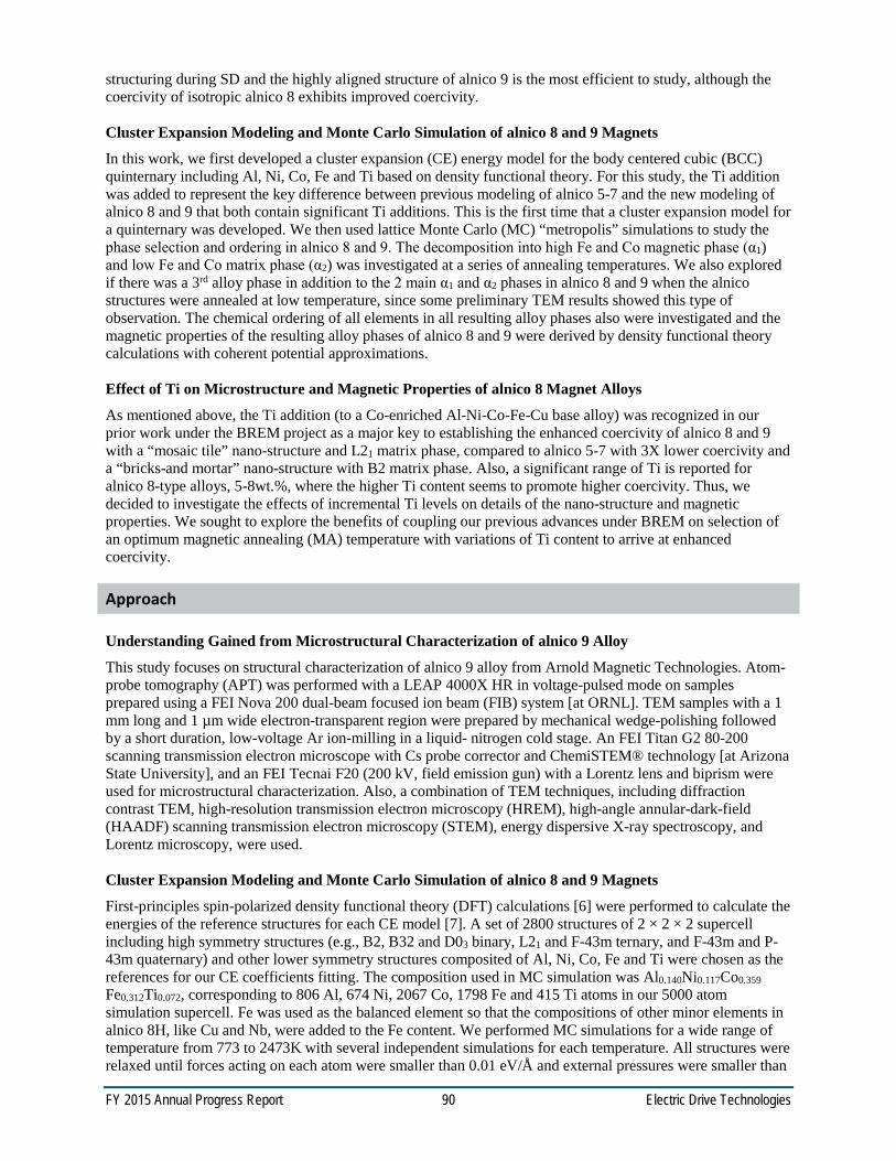
FY 2015 Annual Progress Report 90 Electric Drive Technologies
structuring during SD and the highly aligned structure of alnico 9 is the most efficient to study, although the coercivity of isotropic alnico 8 exhibits improved coercivity.
Cluster Expansion Modeling and Monte Carlo Simulation of alnico 8 and 9 Magnets
In this work, we first developed a cluster expansion (CE) energy model for the body centered cubic (BCC) quinternary including Al, Ni, Co, Fe and Ti based on density functional theory. For this study, the Ti addition was added to represent the key difference between previous modeling of alnico 5-7 and the new modeling of alnico 8 and 9 that both contain significant Ti additions. This is the first time that a cluster expansion model for a quinternary was developed. We then used lattice Monte Carlo (MC) “metropolis” simulations to study the phase selection and ordering in alnico 8 and 9. The decomposition into high Fe and Co magnetic phase (α1) and low Fe and Co matrix phase (α2) was investigated at a series of annealing temperatures. We also explored if there was a 3rd alloy phase in addition to the 2 main α1 and α2 phases in alnico 8 and 9 when the alnico structures were annealed at low temperature, since some preliminary TEM results showed this type of observation. The chemical ordering of all elements in all resulting alloy phases also were investigated and the magnetic properties of the resulting alloy phases of alnico 8 and 9 were derived by density functional theory calculations with coherent potential approximations.
Effect of Ti on Microstructure and Magnetic Properties of alnico 8 Magnet Alloys
As mentioned above, the Ti addition (to a Co-enriched Al-Ni-Co-Fe-Cu base alloy) was recognized in our prior work under the BREM project as a major key to establishing the enhanced coercivity of alnico 8 and 9 with a “mosaic tile” nano-structure and L21 matrix phase, compared to alnico 5-7 with 3X lower coercivity and a “bricks-and mortar” nano-structure with B2 matrix phase. Also, a significant range of Ti is reported for alnico 8-type alloys, 5-8wt.%, where the higher Ti content seems to promote higher coercivity. Thus, we decided to investigate the effects of incremental Ti levels on details of the nano-structure and magnetic properties. We sought to explore the benefits of coupling our previous advances under BREM on selection of an optimum magnetic annealing (MA) temperature with variations of Ti content to arrive at enhanced coercivity.
Approach
Understanding Gained from Microstructural Characterization of alnico 9 Alloy
This study focuses on structural characterization of alnico 9 alloy from Arnold Magnetic Technologies. Atom-probe tomography (APT) was performed with a LEAP 4000X HR in voltage-pulsed mode on samples prepared using a FEI Nova 200 dual-beam focused ion beam (FIB) system [at ORNL]. TEM samples with a 1 mm long and 1 µm wide electron-transparent region were prepared by mechanical wedge-polishing followed by a short duration, low-voltage Ar ion-milling in a liquid- nitrogen cold stage. An FEI Titan G2 80-200 scanning transmission electron microscope with Cs probe corrector and ChemiSTEM® technology [at Arizona State University], and an FEI Tecnai F20 (200 kV, field emission gun) with a Lorentz lens and biprism were used for microstructural characterization. Also, a combination of TEM techniques, including diffraction contrast TEM, high-resolution transmission electron microscopy (HREM), high-angle annular-dark-field (HAADF) scanning transmission electron microscopy (STEM), energy dispersive X-ray spectroscopy, and Lorentz microscopy, were used.
Cluster Expansion Modeling and Monte Carlo Simulation of alnico 8 and 9 Magnets
First-principles spin-polarized density functional theory (DFT) calculations [6] were performed to calculate the energies of the reference structures for each CE model [7]. A set of 2800 structures of 2 × 2 × 2 supercell including high symmetry structures (e.g., B2, B32 and D03 binary, L21 and F-43m ternary, and F-43m and P-43m quaternary) and other lower symmetry structures composited of Al, Ni, Co, Fe and Ti were chosen as the references for our CE coefficients fitting. The composition used in MC simulation was Al0.140Ni0.117Co0.359 Fe0.312Ti0.072, corresponding to 806 Al, 674 Ni, 2067 Co, 1798 Fe and 415 Ti atoms in our 5000 atom simulation supercell. Fe was used as the balanced element so that the compositions of other minor elements in alnico 8H, like Cu and Nb, were added to the Fe content. We performed MC simulations for a wide range of temperature from 773 to 2473K with several independent simulations for each temperature. All structures were relaxed until forces acting on each atom were smaller than 0.01 eV/Å and external pressures were smaller than

FY 2015 Annual Progress Report 91 Electric Drive Technologies
0.5 GPa while the unit cells were kept cubic. Because it is known that some structures such as L21 can be relaxed from BCC to a face-centered cubic (FCC) structure, full relaxation was allowed without constraints on the unit cell [8]. The spin-polarized DFT calculations were performed with a Vienna Ab-initio Simulation Package (VASP) [9] with projector-augmented wave (PAW) pseudo-potential method [10,11] within a generalized-gradient approximation (GGA) parameterized by Perdew, Burke, and Ernzerhof [12]. The energy cutoff used was 350 eV and the Monkhost-Pack scheme [13] was used for Brillouin zone sampling with a high quality k-point grid equivalent to 16 × 16 × 16 k-mesh for BCC Fe structure.
Effect of Ti on Microstructure and Magnetic Properties of alnico 8 Magnet Alloys
While much of our recent processing research work was performed with pre-alloyed powder of an alnico 8H magnet alloy powder, this work on a series of modified alloy compositions was done (most efficiently) with small arc-melted and chill-cast “button” samples. The button ingots were produced with composition of Co34Al14.25Ni12.5Cu2.5Fe36.75-xTix (x=0~10 in at. %) in an inert (Ar) atmosphere. Cylindrical 3 mm (dia.) X 7.5 mm samples were cut from the buttons for heat treatment, followed by microstructural analysis and magnetic measurement. A typical full heat treatment (FHT) process included solutionizing at 1250C for 0.5h followed by oil quench, MA (@ 1.2T) at 800-860C for 10 min. followed by air cool, and “draw” (annealing) cycles at 650C for 5h followed by furnace cool and 580C for 15h followed by furnace cool. The drawing cycles were performed in two or more steps. Microstructural characterization was performed with XRD, SEM, and TEM with the FEI Tecnai F20 (200 kV, field emission gun), as listed above. Magnetic properties were measured with a vibrating sample magnetometer (VSM) and a hysteresigraph a Laboratorio Elettrofisico Engineering Walker LDJ Scientific AMH-5 Hysteresigraph with a 5 mm coil and a maximum applied field of 5.0 kOe at room temperature in a closed-loop setup.
Results and Discussion
Understanding Gained from Microstructural Characterization of alnico 9 Alloy
The interpenetrating nature of the α1 and α2 phase of alnico 9 is shown in Figure 2-84. The α2 phase is continuous, but whether the α1 phase consists of fully isolated particles or has some degree of interconnectivity cannot be established definitively, because the volume sampled by the APT is too small relative to the size of the α1 phase. Fine Cu-enriched rod-shaped particles with either a cylindrical or elliptical cross section were also observed at the corners of adjacent cuboidal α1 phase, and they occupy ~4% volume fraction of the alloy. Moreover, a Ni-enriched rod-shape phase parallel to the primary α1 /α2 interface in the AlNi phase was detected.
Figure 2-84: Iso-concentration surfaces: threshold settings at 10 at.% Cu to show the Cu (brown), 10 at.% Ni to show the outline of the AlNi phase/Fe-Co phases (red) and 30% Ni to show the high Ni regions (blue). Cu-enriched rods are at the corners of the Fe-Co phas
A nanometer scale mosaic structure formed by SD in alnico 9 (viewed along the transverse direction) was shown in the TEM elemental map of Figure 2-85(a). The red partially faceted “tiles” with a size of ~35nm are α1 precipitates, while the dark blue phase with similar size is α2 matrix. The α1 /α2 interface facets along 110 planes as well as 100 planes. Cu rods (light blue, ~5nm) sit in the α2 phase at the corner of two 110 α1

FY 2015 Annual Progress Report 92 Electric Drive Technologies
facets. A Ni-rich (green) shell was observed in the α2 phase at the α1 /α2 boundary. Ti partitioned to the α2 phase. Selected area diffraction pattern taken along [110] zone axis confirms the α2-phase has a L21 ordered structure. Aberration-corrected STEM images of the Cu-rich phase indicates that when the Cu-rich phase has a small diameter (“squared-off” cylindrical shape, Figure 2-85(b)), it is forms a coherent interface with the α2-phase. For Cu-enriched phase with larger diameter, either intrinsic or extrinsic stacking faults were introduced. The Cu-rich phase forms an elliptical rod shape with distorted FCC structure (Figure 2-85(c)). Further, Ni-enriched rods/particles were observed in the α2 phase (as a pair, just left of center in Figure 2-85a) when the α1 phase is faceted on 100 planes. Observation of alnico 9 along the longitudinal direction (Figure 2-85(d)) showed that the α1 precipitates were very long (>400nm) and generally had tapered ends with an aspect ratio >10. Branching was commonly observed in the α1 rods. An in situ Lorentz microscopy study was also performed to analyze the movement of magnetic domains with an external magnetic field.
Figure 2-85: (a) Color composite energy-dispersive-X-ray map of alnico 9 taken along [001] crystal direction; (b,c) aberration corrected HAADF STEM images of alnico 9 taken under [100] zone axis along transverse direction. (d) HAADF STEM image of alnico 9 along long
Cluster Expansion Modeling and Monte Carlo Simulation of alnico 8 and 9 Magnets
CE energy modeling permitted interatomic potentials to be calculated for the BCC quinternary including Al, Ni, Co, Fe and Ti based on density functional theory. These potentials were used in lattice Monte Carlo (MC) “metropolis” simulations to study the phase selection and ordering in alnico 8 and 9, where decomposition into high Fe and Co magnetic phase (α1) and low Fe and Co matrix phase (α2) was investigated at a series of annealing temperatures. Figure 2-86 shows the results for annealing at 823˚K, in this case simulating completion of the SD reaction, that predicts formation of a 3rd alloy phase in the SD nano-structure, in addition to the 2 main α1 and α2 phases. Figure 2-86 reveals that the apparent stoichiometry of this extra phase (located at z = 0.35) is about Ni3Al. It should be noted that the Cu-rich phase that appears in alnico 9 (and 8) after MA and draw cycling (see Figure 2-84 and Figure 2-85a) will not show up in this simulation, since Cu is not included in the calculation.
FY 2015 Annual Progress Report 93 Electric Drive Technologies
Figure 2-86: Composition profile of alnico 8 along the z-direction and the atomic structure obtained from MC simulation at 973 and 823 K. The silver, light green, blue, gold and red balls in the crystal structure indicate the Al, Ni, Co, Fe and Ti atoms, respectivel
Interestingly, the prediction of the 3rd Ni-rich phase fully supports the previous novel experimental observation by TEM mapping that was reported (see above). Other results (not shown) also indicate that the decomposition of constituent elements is a multi-step process, i.e., not occurring at a single SD reaction temperature. This prediction is now being studied in a current series of experiments that will be reported later. The orderings of chemical elements in all 3 alloy phases also were investigated, where α1 phase is in B2 ordering, the α2 phase is in L21 ordering and the newly identified α3 phase is in D03 ordering, consistent with the TEM analysis and XRD measurements. We also calculated the magnetic properties of the 3 alloy phases of alnico 8 and 9 by density functional theory calculations with a coherent potential approximation, but do not report these, herein.
Effect of Ti on Microstructure and Magnetic Properties of alnico 8 Magnet Alloys
As shown in Figure 2-87, with increasing Ti content of 0 to 10 at.%, the Hcj of the samples first increases from 150 Oe at 0%, reaches a peak value of 2074 Oe at 8.2 at.% and then decreases to 1972 Oe at 10 at.%, while the saturation magnetization (Ms) and remanence (Br) monotonically decrease from Ms = 16.1 kG and Br = 10.8 kG at 0% to 10.4 and 6.9 at 10 at.%, respectively. It should be noted that this peak value for coercivity was achieved by a procedure that utilized calorimetric observations of the SD transition, by both DSC and by magnetic TGA, to specifically select a MA temperature and by use of a modified draw annealing cycle that emphasized extension of the low temperature cycle. By comparing the microstructures of samples with different Ti content it was found that with increasing Ti content, a well-defined mosaic structure is formed, and the volume fraction of L21 (AlNi) phase is increased. Eventually, the mosaic structure was partially destroyed at a higher Ti content.

FY 2015 Annual Progress Report 94 Electric Drive Technologies
Figure 2-87: Summary of magnetic properties that result from Ti substitutions for Fe in alnico 8H magnet alloy, where MA was optimized and extended draw cycles were used.
Figure 2-88: TEM micrographs of transverse sections of cast alnico sample after optimized FHT to illustrate representative microstructure effects at 3 elevated Ti contents where the 8.2 at.% Ti represents the peak coercivity level.
X-ray data analysis showed that the intensity of the (110) peak of the L21 phase increases steadily with increasing Ti content, relative to the (110) peak of the BCC (Fe-Co) phase. Thus, it follows that the intensity ratio of L21 phase to BCC phase also grows, as shown in Fig. 6. The increase of intensity ratio of L21 phase indicates that the volume fraction of L21 phase increases with increasing Ti content. The highest Hci at about 8.2 at.%Ti corresponds to the L21 volume fraction of ~45 %.
0 2 4 6 8 106
8
10
12
14
16
18
H cj (O
e)
Ms &
Br (
kGs)
x (at. %)
Ms
Br
0
500
1000
1500
2000
Hc

FY 2015 Annual Progress Report 95 Electric Drive Technologies
Figure 2-89: Summary of XRD peak ratios for (110) peak of L21 phase vs./(110) peak of BCC phase.
Thermal magnetic measurements (Figure 2-90) show that with increasing Ti content, the Curie temperature of L21 phase is rapidly reduced, indicating that the L21 phase becomes weak or non-magnetic with increased Ti content. These VSM results can be correlated with the hysteresigraph results that indicate a maximum coercivity at about 8.2 at.%Ti, i.e., the matrix phase that separates the Fe-Co phase becomes a much better magnetic isolation phase between adjacent Fe-Co pillars, increasing the barrier to domain coupling.
Figure 2-90: Summary of VSM results indicating the decreasing Curie temperature of the L21 phase for increased Ti content.
0 2 4 6 8 100
10
20
30
40
50
60
Inte
nsity
ratio
of L
2 1 (%
)Ti (at.%)
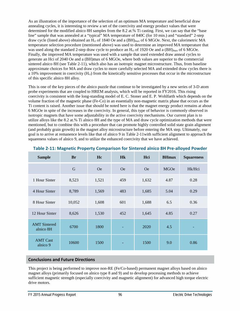
FY 2015 Annual Progress Report 96 Electric Drive Technologies
As an illustration of the importance of the selection of an optimum MA temperature and beneficial draw annealing cycles, it is interesting to review a set of the coercivity and energy product values that were determined for the modified alnico 8H samples from the 8.2 at.% Ti casting. First, we can say that the “base line” sample that was annealed at a “typical” MA temperature of 840C (for 10 min.) and “standard” 2-step draw cycle (listed above) obtained an Hci of 1840 Oe and a (BH)max of 6 MGOe. Next, the calorimetric MA temperature selection procedure (mentioned above) was used to determine an improved MA temperature that was used along the standard 2-step draw cycle to produce an Hci of 1920 Oe and a (BH)max of 6 MGOe. Finally, the improved MA temperature was used with a sample that used extended draw anneal cycles to generate an Hci of 2040 Oe and a (BH)max of 6 MGOe, where both values are superior to the commercial sintered alnico 8H (see Table 2-11), which also has an isotropic magnet microstructure. Thus, from baseline approximate choices for MA and draw cycles to more carefully selected MA and extended draw cycles there is a 10% improvement in coercivity (Hci) from the kinetically sensitive processes that occur in the microstructure of this specific alnico 8H alloy.
This is one of the key pieces of the alnico puzzle that continue to be investigated by a new series of 3-D atom probe experiments that are coupled to HREM analysis, which will be reported in FY2016. This rising coercivity is consistent with the long-standing model of E. C. Stoner and E. P. Wohlfarth which depends on the volume fraction of the magnetic phase (Fe-Co) in an essentially non-magnetic matrix phase that occurs as the Ti content is raised. Another issue that should be noted here is that the magnet energy product remains at about 6 MGOe in spite of the increases in the coercivity. In general, this type of behavior is commonly observed in isotropic magnets that have some adjustability in the active coercivity mechanisms. Our current plan is to utilize alloys like the 8.2 at.% Ti alnico 8H and the type of MA and draw cycle optimization methods that were mentioned, but to combine this with a procedure that can promote highly controlled solid state grain alignment (and probably grain growth) in the magnet alloy microstructure before entering the MA step. Ultimately, our goal is to arrive at remanence levels like that of alnico 9 in Table 2-11with sufficient alignment to approach the squareness values of alnico 9, and to utilize the enhanced coercivity that we have achieved.
Table 2-11: Magnetic Property Comparison for Sintered alnico 8H Pre-alloyed Powder
Sample Br Hc Hk Hci BHmax Squareness
G Oe Oe Oe MGOe Hk/Hci
1 Hour Sinter 8,523 1,521 459 1,632 4.87 0.28
4 Hour Sinter 8,789 1,569 483 1,685 5.04 0.29
8 Hour Sinter 10,052 1,608 601 1,688 6.5 0.36
12 Hour Sinter 8,626 1,530 452 1,645 4.85 0.27
AMT Sintered alnico 8H 6700 1800 - 2020 4.5 -
AMT Cast alnico 9 10600 1500 - 1500 9.0 0.86
Conclusions and Future Directions
This project is being performed to improve non-RE (Fe/Co-based) permanent magnet alloys based on alnico magnet alloys (primarily focused on alnico type 8 and 9) and to develop processing methods to achieve sufficient magnetic strength (especially coercivity and magnetic alignment) for advanced high torque electric drive motors.

FY 2015 Annual Progress Report 97 Electric Drive Technologies
TEM microstructural analysis results show that a well-faceted regular mosaic structure only forms in alnico 8 and 9 alloys on magnetic annealing in a narrow temp. range, close to the onset of the spinodal (~840°C) that is specific for each alnico magnet alloy and results in optimum magnetic properties.
Within new high resolution TEM and 3-D atom probe results, an additional Ni-rich phase was discovered, beyond the α1, α2, and Cu-rich phases that were previously reported for alnico 8 and 9 in our prior publications. The new Ni-rich phase, roughly formulated as (Ni,Co,Fe)3Al, appeared to form only as alternative faceting of the Fe-Co phase developed at the facet “points,” like the position of the Cu-rich phase rods. New MC metropolis modeling for the quinternary Al-Ni-Co-Fe-Ti alloy also predicted that this Ni-rich phase should form as a product of the spinodal decomposition reaction. This excellent agreement between theory and experiment gives us enhanced confidence in the predictive capability of the MC modeling as we go forward with additional alloy design investigations, with the specific goal of Co replacement and further increased coercivity.
Although not shown in this report, additional TEM observations showed that the external magnetic field during the MA step aids in the formation of a well-faceted mosaic structure and enhanced magnetic properties, but only at the optimal temperature and time.
TEM analysis of samples before and after draw annealing indicated that these cycles have no significant effect on the alloy’s nano-metric spacing, but do increase its coercivity, if the MA time is long enough. Thus, more subtle (short range diffusion) changes in the nano-structure must be occurring. This understanding is being pursued by very recent 3-D atom probe work that will be reported in FY2016.
As an example of the magnet alloy design studies that are being pursued, characterization results revealed that with increasing Ti content, the volume fraction of L21 phase increases, while the Curie temperature of L21 phase rapidly reduces. With increasing L21 volume fraction, Hci increases and reaches a peak value when the volume fraction is ~45%. Further increase of Ti content results in reduction of Hci due to the formation of excessive γ phase on grain boundaries, among other possible effects. These results give us confidence that a non-magnetic matrix phase in these alnico alloys is critical to achieving maximum coercivity, which should be applicable to other alternative alloying efforts.
Future Directions:
Although recent increases in coercivity are impressive, magnetic remanence and, especially, hysteresis loop “squareness” (in second quadrant) can benefit greatly from grain alignment. If the impressive coercivity gains are maintained with large gains in alignment, the maximum energy product values that were achieved should be possible to raise to levels sufficient for alnico magnet use in an advanced PM traction drive motor. Results (see Table 1) on powder processing reported last year under the BREM project showed that some 8h sintered (at 1250C) samples exhibited a few large (>1mm) grains that were aligned in a direction close to the optimum, but occupying more than 50 vol.% of the sample. This degree of alignment resulted in a high Br (equivalent to fully aligned alnico 9) and a BH(max) that was 44% greater than sintered alnico 8H, but still 38% less than alnico 9, which is directionally solidified. The solid-state grain growth was promoted apparently by high grain boundary mobility from the high sintering temperature, but the preferred alignment was a “happy accident.” Thus, investigations on aligned grain growth of powder processed and chill cast samples have been underway this year along several pathways to promote highly aligned grain growth in sintered bulk magnets, but were not ready to report for FY2015.
Further gains in coercivity will be aided by growth in understanding of the most significant parameters or characteristics of alnico microstructure and nano-structure for best magnetic properties from the solid linkage of theoretical analysis and experimental studies. This will be enabled by continuation of detailed microstructural characterization of alnico samples that are systematically produced by chill casting and by rapid solidification methods, primarily by gas atomization, but also by melt spinning to generate ribbon samples that are analogous to atomized powders. For samples where both microstructure and magnetic properties can be tracked, both cast and powder-based sintered samples can be used. The ability to correlate theory and experiment will be improved in critical cases by matching the simplified alloy chemistry of theoretical samples with experimental samples of exactly the same composition. This practice will be especially important in the search for very low Co-content alnico alloy designs that is in-progress. As theory methods are verified, more complex compositions, e.g., 6-component (Al-Ni-Co-Fe-Ti-Cu) alloys will be

FY 2015 Annual Progress Report 98 Electric Drive Technologies
modeled, with attempts to test meso-scale magnetic and product phase predictions, eventually up to phase field microstructure modeling that can be used as a tool to guide processing choices.
To develop further up-scaled capabilities to fabricate alnico magnets in prototype sizes and shapes, the powder-based approach for binder-assisted compression molding also will need up-scaling to maintain full-density final-shape sintered microstructures, along with meeting the challenge of grain growth and correct alignment to generate improved magnetic properties. To enable extensive experiments on compression molding and other bulk magnet fabrication methods, additional gas atomized pre-alloyed powder batches will be produced with high purity and desired composition, using methods and parameters that should be transferrable to an industrial partner. The first alloy design to be tested in a full-scale final shape (as part of a parallel project on advanced motors with UQM) will be alnico 8H with high Ti and minor Nb addition, as reported herein with elevated coercivity. The second magnet alloy design will be a Co-lean version of alnico 8 that is under investigation and should be developed enough for initial testing in about a year, but will need to be adapted for the grain alignment process that may take an additional year. The third development stage for “super-alnico” (with tetragonal distortion of the Fe-Co phase) is anticipated to be sufficiently complete in another 2 years to assess the viability of the concept, as well. If even the first alloy design stage can provide high energy non-RE permanent magnets that demonstrate improved performance in an experimental motor, this could catalyze rapid growth of the US-based high energy PM industry and lead to expansion of existing US manufacturing capacity for advanced PM traction motors.
FY 2015 Publications
1. L. Zhou, M. K. Miller, P. Lu, L. Q. Ke, R. Skomski, H. Dillon, Q. Xing, A. Palasyuk, M. R. McCartney, D. J. Smith, S. Constantinides, R. W. McCallum, I. E. Anderson, V.Antropov, and M. J. Kramer, "Architecture and magnetism of alnico," Acta Mater 74, 224-233 (2014)
2. A. Nelson, Y. Huh, P. Kharel, V. R. Shah, R. Skomski, and D. J. Sellmyer, "Structural, Magnetic and Electron Transport Properties of Mn3-xPtxSn (x = 0, 0.5, 1) Nanomaterials,” J. Appl. Phys. 115, 17A923 (2014).
3. X.Z. Li, W.Y. Zhang, D.J. Sellmyer, X. Zhao, M.C. Nguyen, C.Z. Wang, K.M. Ho, “Orthorhombic Zr2Co11 Phase Revisited,” J. Alloys and Compounds 611, 167-170 (2014).
4. B. Balamurugan, B. Das, P. Mukherjee, D.J. Sellmyer, “Development of Nanoparticle-Based Permanent-Magnet Materials: Challenges and Advances,” Proc. REPM’14, Annapolis 2014, p. 429-432.
5. C.Z. Wang, X. Zhao, M.C. Nguyen, L.Q. Ke, W.Y. Zhang, M.J. Kramer, D.J. Sellmyer, X.Z. Li, V.P. Antropov, F. Zhang, K.M. Ho, “Predicting the Crystal Structures of Magnet Materials Using Adaptive Genetic Algorithm,” Proc. REPM’14, Annapolis 2014, p. 446-449.
6. A. G. Kusne, T. Gao, A. Mehta, L. Ke, M. C. Nguyen, K. M. Ho, V. Antropov, C. Z. Wang, M. J. Kramer, C. Long, and I. Takeuchi, "On-the-fly machine-learning for high-throughput experiments: search for rare-earth free permanent magnets" Sci. Rep. 4, 6367 (2014).
7. Manh Cuong Nguyen, Xin Zhao, Cai-Zhuang Wang and Kai-Ming Ho, "Cluster Expansion Modeling and Monte Carlo Simulation of Alnico 5-7 Permanent Magnets", J. Appl. Phys. 117, 093905 (2015).
8. I.E. Anderson, A. G. Kassen, E. M. H. White, L. Zhou, W. Tang, A. Palasyuk, K. W. Dennis, R. W. McCallum, and M. J. Kramer, “Novel pre-alloyed powder processing of modified alnico 8: Correlation of microstructure and magnetic properties,” Journal of Applied Physics 117, pp. 17D138-(1-4) (2015); doi: 10.1063/1.4916996.
9. B. Balasubramanian, P. Mukherjee, R. Skomski, P. Manchanda, B. Das, and D.J. Sellmyer, “Magnetic Nanostructuring and Overcoming Brown’s Paradox to Realize Extraordinary High-Temperature Energy Products,” Scientific Reports 4, 6265 (2014); DOI: 10.1038/srep06265.
10. X.Z. Li, W.Y. Zhang, and D.J. Sellmyer, “SAED and HREM Studies of Zr2Co11 Intermetallic Compound,” Microscopy & Microanalysis 20 (Suppl. 3), pp. 242-243; doi:10.1017/S1431927614002931 (2014).
11. A. Jesche, L. Ke, J. L. Jacobs, B. Harmon, R. S. Houk, and P. C. Canfield, “Alternating magnetic anisotropy of li2(li1-xTx)N(t=Mn,Fe,Co,andNi),” Phys. Rev. B, 91:180403, (2015). Rapid communication.

FY 2015 Annual Progress Report 99 Electric Drive Technologies
12. .Liqin Ke and Mark van Schilfgaarde, “Band-filling effect on magnetic anisotropy using a green's function method,” Phys. Rev. B, 92:014423, (2015).
13. Lanping Yue, Yunlong Jin, Wenyong Zhang, and David J. Sellmyer, “Magnetic Force Microscopy Study of Zr2Co11-Based Nanocrystalline Materials: Effect of Mo Addition,” Journal of Nanomaterials, vol. 2015, Article ID 151740, 5 pages, 2015. doi: 10.1155/2015/151740.
14. Weiwei Yang, Wenjuan Lei, Yongsheng Yu, Wenlei Zhu, T.A. George, X.-Z. Li, D.J. Sellmyer and Shouheng Sun, “From FePt-Fe3O4 to L10-FePt-Fe Nanocomposite Magnets with a Gradient Interface,” J. Mater. Chem. C, 2015, 3, 7075.
15. W.Y. Zhang, R. Skomski, A. Kashyap, S. Valloppilly, X.Z. Li, J.E. Shield, and D.J. Sellmyer, “Coercivity and Nanostructure of Melt-Spun Ti-Fe-Co-B-Based Alloys,” AIP Advances (in press).

FY 2015 Annual Progress Report 100 Electric Drive Technologies
3.0 Power Electronics Research and Development
3.1. Inverter R&D Madhu Chinthavali, Principal Investigator Oak Ridge National Laboratory (ORNL) National Transportation Research Center 2360 Cherahala Boulevard Knoxville, TN 37932 Phone: (865) 946-1411 E-mail: [email protected] Susan A. Rogers, DOE EDT Program Manager Phone: (202) 586-8997 E-mail: [email protected] Burak Ozpineci, ORNL EDT Program Manager Phone: (865) 946-1329 E-mail: [email protected] Contractor: UT-Battelle, LLC, managing and operating contractor for the Oak Ridge National Laboratory Contract No.: DE-AC05-00OR22725
Abstract/Executive Summary The overall objective of this project is to design and develop a high-voltage wide-bandgap (HV-WBG) 30 kW continuous 55 kW peak power inverter. WBG devices offer some distinct advantages over silicon (Si) components. Primarily, they can operate at higher junction temperatures. This benefit allows for hotter coolant and smaller heat sinks and can potentially help facilitate air cooling without a sacrifice in performance. Many of the typical components in a commercial inverter cannot withstand the desired operating temperature of WBG devices, i.e., the capacitor and gate driver. Thus the whole inverter must be considered in developing new high-temperature packages. The new concepts developed under this project will increase the power density and decrease the volume and weight for electric-base vehicle traction-drive inverters and will achieve the DOE 2022 weight, volume, and efficiency targets.
Accomplishments Completed evaluation of a 1,200 V, 30 A, trench silicon carbide (SiC) metal-oxide-semiconductor
field-effect transistor (MOSFET)
Completed the design, build, and testing of a 10 kW WBG-based air-cooled inverter prototype using ORNL’s WBG modules
Completed the design, build, and testing of a 10 kW WBG-based liquid-cooled inverter prototype using an advanced package built at ORNL
Completed the design and build of a 30 kW WBG-based liquid-cooled inverter
Introduction
There is an increasing need for higher-temperature operation of power electronics in automotive applications. The capability of components to operate reliably at elevated temperatures can enable cost and weight savings by making it feasible to reduce the sizes of heat sinks and eliminate secondary cooling loops. Additionally, devices capable of increased-frequency operation can reduce requirements for passive components, leading to further reductions in cost, weight, and volume. WBG devices, specifically SiC and gallium nitride

FY 2015 Annual Progress Report 101 Electric Drive Technologies
semiconductors, are emerging technologies that enable operation at higher temperatures and frequencies, as well as efficiency and reliability improvements. The development of WBG devices promises to help achieve these goals, as well as VTO targets. WBG technology assessment performed under this project will help to determine when a viable market introduction of these devices for automotive use will occur. The independent assessment of devices for the automotive industry is carried out to monitor progress and provide data readily when the need arises.
It should be no surprise that none of the electric drive vehicle traction drive systems on the market can meet cost and efficiency goals. Efficiency is achieved by using lower-loss devices and materials, which tend to be expensive even as their quantity levels increase. A case in point is motor lamination steel, lower-loss grades of which are manufactured using novel processes that add more cost.
Problems associated with power electronics for advanced vehicle applications include the following:
Low efficiency at light load conditions for inverters and converters
Low current density and device scaling issues for high-power converters
Lack of reliable higher-junction-temperature devices
High costs of devices and power modules, especially for WBG and advanced Si devices
High numbers of components for low-voltage electronics (e.g., gate drivers, controllers, sensors)
Lack of standardized high-power-density, low-cost power modules for scalable and modular power converters
Substrates that use expensive ceramics for thermal stability and reliability
Low-cost, low-loss magnetics and high-temperature films for capacitors
The goal of this research is to reduce the size and weight of power converters to meet the 2015 and 2020 inverter targets. The overall strategy for addressing the limitations of the state of the art is shown in Figure 3-1.
Figure 3-1: Overall strategy to address limitations of the state of the art.
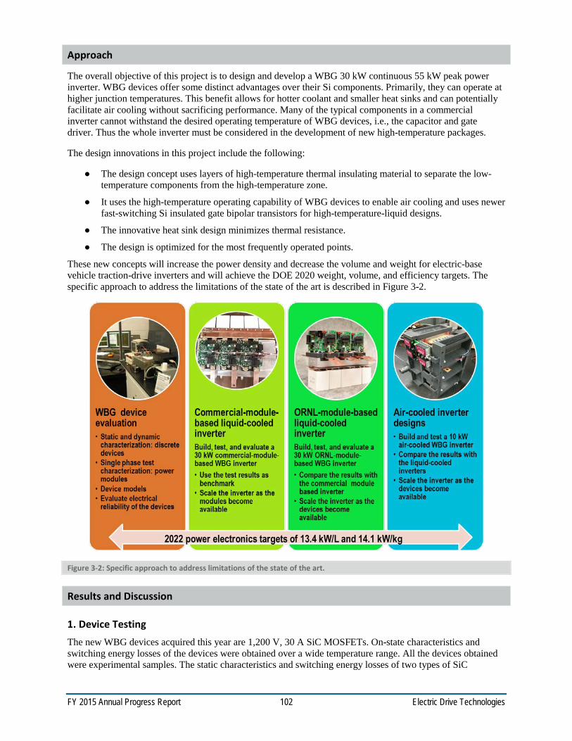
FY 2015 Annual Progress Report 102 Electric Drive Technologies
Approach
The overall objective of this project is to design and develop a WBG 30 kW continuous 55 kW peak power inverter. WBG devices offer some distinct advantages over their Si components. Primarily, they can operate at higher junction temperatures. This benefit allows for hotter coolant and smaller heat sinks and can potentially facilitate air cooling without sacrificing performance. Many of the typical components in a commercial inverter cannot withstand the desired operating temperature of WBG devices, i.e., the capacitor and gate driver. Thus the whole inverter must be considered in the development of new high-temperature packages.
The design innovations in this project include the following:
The design concept uses layers of high-temperature thermal insulating material to separate the low-temperature components from the high-temperature zone.
It uses the high-temperature operating capability of WBG devices to enable air cooling and uses newer fast-switching Si insulated gate bipolar transistors for high-temperature-liquid designs.
The innovative heat sink design minimizes thermal resistance.
The design is optimized for the most frequently operated points.
These new concepts will increase the power density and decrease the volume and weight for electric-base vehicle traction-drive inverters and will achieve the DOE 2020 weight, volume, and efficiency targets. The specific approach to address the limitations of the state of the art is described in Figure 3-2.
Figure 3-2: Specific approach to address limitations of the state of the art.
Results and Discussion
1. Device Testing The new WBG devices acquired this year are 1,200 V, 30 A SiC MOSFETs. On-state characteristics and switching energy losses of the devices were obtained over a wide temperature range. All the devices obtained were experimental samples. The static characteristics and switching energy losses of two types of SiC
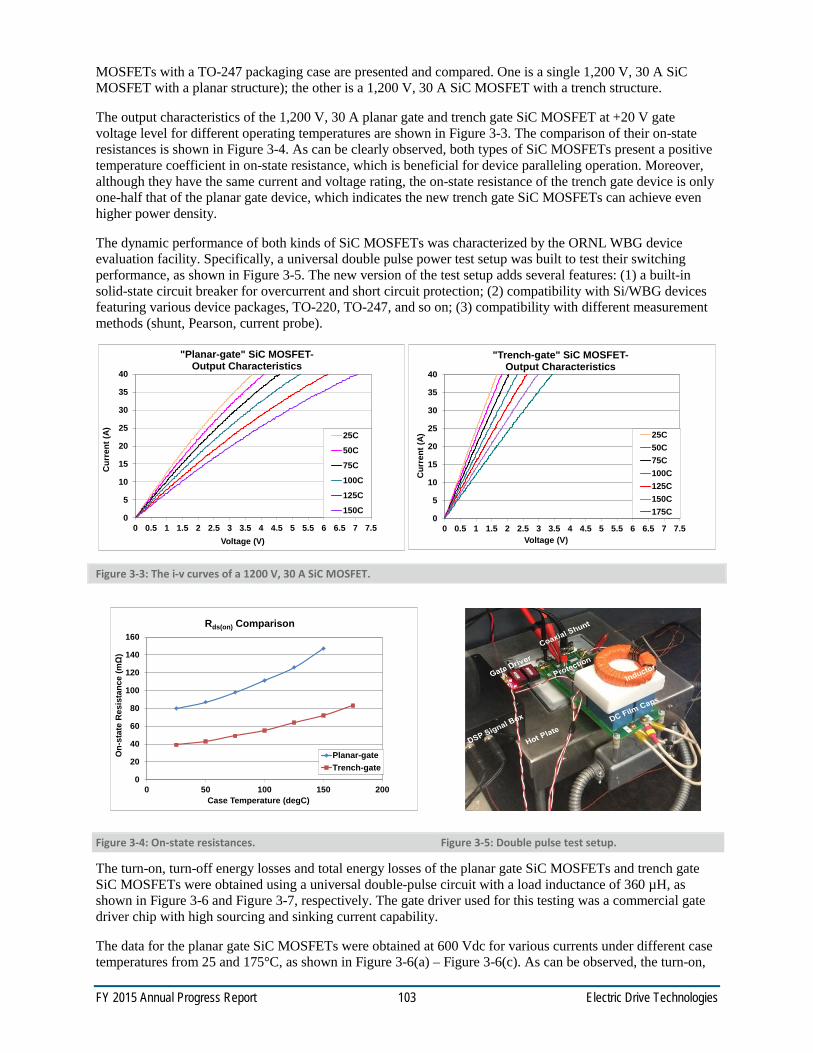
FY 2015 Annual Progress Report 103 Electric Drive Technologies
MOSFETs with a TO-247 packaging case are presented and compared. One is a single 1,200 V, 30 A SiC MOSFET with a planar structure); the other is a 1,200 V, 30 A SiC MOSFET with a trench structure.
The output characteristics of the 1,200 V, 30 A planar gate and trench gate SiC MOSFET at +20 V gate voltage level for different operating temperatures are shown in Figure 3-3. The comparison of their on-state resistances is shown in Figure 3-4. As can be clearly observed, both types of SiC MOSFETs present a positive temperature coefficient in on-state resistance, which is beneficial for device paralleling operation. Moreover, although they have the same current and voltage rating, the on-state resistance of the trench gate device is only one-half that of the planar gate device, which indicates the new trench gate SiC MOSFETs can achieve even higher power density.
The dynamic performance of both kinds of SiC MOSFETs was characterized by the ORNL WBG device evaluation facility. Specifically, a universal double pulse power test setup was built to test their switching performance, as shown in Figure 3-5. The new version of the test setup adds several features: (1) a built-in solid-state circuit breaker for overcurrent and short circuit protection; (2) compatibility with Si/WBG devices featuring various device packages, TO-220, TO-247, and so on; (3) compatibility with different measurement methods (shunt, Pearson, current probe).
Figure 3-3: The i-v curves of a 1200 V, 30 A SiC MOSFET.
Figure 3-4: On-state resistances. Figure 3-5: Double pulse test setup.
The turn-on, turn-off energy losses and total energy losses of the planar gate SiC MOSFETs and trench gate SiC MOSFETs were obtained using a universal double-pulse circuit with a load inductance of 360 µH, as shown in Figure 3-6 and Figure 3-7, respectively. The gate driver used for this testing was a commercial gate driver chip with high sourcing and sinking current capability.
The data for the planar gate SiC MOSFETs were obtained at 600 Vdc for various currents under different case temperatures from 25 and 175°C, as shown in Figure 3-6(a) – Figure 3-6(c). As can be observed, the turn-on,
0
5
10
15
20
25
30
35
40
0 0.5 1 1.5 2 2.5 3 3.5 4 4.5 5 5.5 6 6.5 7 7.5
Cur
rent
(A)
Voltage (V)
"Planar-gate" SiC MOSFET-Output Characteristics
25C
50C
75C
100C
125C
150C0
5
10
15
20
25
30
35
40
0 0.5 1 1.5 2 2.5 3 3.5 4 4.5 5 5.5 6 6.5 7 7.5
Cur
rent
(A)
Voltage (V)
"Trench-gate" SiC MOSFET-Output Characteristics
25C50C75C100C125C150C175C
0
20
40
60
80
100
120
140
160
0 50 100 150 200
On-
stat
e R
esis
tanc
e (m
Ω)
Case Temperature (degC)
Rds(on) Comparison
Planar-gateTrench-gate

FY 2015 Annual Progress Report 104 Electric Drive Technologies
turn-off, and total energy losses increased with an increase in current. With a rise in temperature, the turn-on energy loss decreased as the result of a faster switching speed, whereas the turn-off energy loss increased as the result of a slower switching speed. The net result was that the total switching energy loss became somewhat lower at higher temperatures.
(a) Turn-on loss (b) Turn-off loss
(c) Total loss
Figure 3-6: Energy losses of planar gate SiC MOSFETs.
(a) Turn-on loss (b) Turn-off loss
00.20.40.60.8
11.21.41.61.8
2
0 10 20 30 40 50
Eon (mJ)
I (A)
25C_Eon50C_Eon75C_Eon100C_Eon125C_Eon150C_Eon175C_Eon
0
0.2
0.4
0.6
0.8
1
1.2
0 10 20 30 40 50
Eoff (mJ)
I (A)
25C_Eoff50C_Eoff75C_Eoff100C_Eoff125C_Eoff150C_Eoff175C_Eoff
0
0.5
1
1.5
2
2.5
0 10 20 30 40 50
Etot (mJ)
I (A)
25C_Etot50C_Etot75C_Etot100C_Etot125C_Etot150C_Etot175C_Etot
00.20.40.60.8
11.21.41.61.8
2
0 10 20 30 40 50
Eon (mJ)
I (A)
25C_Eon50C_Eon75C_Eon100C_Eon125C_Eon150C_Eon175C_Eon
0
0.2
0.4
0.6
0.8
1
1.2
0 10 20 30 40 50
Eoff (mJ)
I (A)
25C_Eoff50C_Eoff75C_Eoff100C_Eoff125C_Eoff150C_Eoff175C_Eoff

FY 2015 Annual Progress Report 105 Electric Drive Technologies
(c) Total loss
Figure 3-7: Energy losses of trench gate SiC MOSFETs.
Figure 3-7(a) – Figure 3-7(c) illustrate the turn-on, turn-off, and total energy losses of the SiC MOSFET with trench gate structure under the same testing conditions (600 V, 25 to 175°C). Compared with the planar gate SiC MOSFET, the turn-on energy loss was lower because of smaller equivalent junction capacitance and thus faster switching speed; and the turn-off energy loss was nearly the same. Therefore, the total energy loss of the tested trench device was a little lower.
2. WBG Inverter Design and Development Device packages able to withstand high temperatures are essential to take advantage of the high-temperature operating capability of WBG devices. Various organizations are working on high-temperature packaging for high-temperature devices. Several high-temperature packages, which include discrete device packages for power modules, have been reported in the past several years. Novel packaging concepts focus primarily on improving the existing packages, designing new packages using new materials, and/or developing processing techniques for better reliability and performance. Even though the novel packages enable the devices to work at higher temperatures, theoretical advantages such as the current density of WBG devices are not realized because of the interconnects needed for the power module to access the device terminals. In addition, the novel designed packages need further development to be used in full systems.
Other factors that limit system designers from reaping the benefits of WBG technology are low-voltage electronics and passive components. This is because although the packages and the power devices can handle high temperatures, the low-power electronics that drive the power devices, silicon-on-insulator (SOI) –based technologies, are limited to a maximum temperature of 200°C. Silicon-based electronics are limited to 125°C operating temperatures. Although SOI-based electronics can work at up to 200°C, they are expensive. High-temperature (over 200°C) electronics have been reported to be feasible; however, they have not been built to demonstrate their performance capabilities. It could be many years before a logic-level high-temperature transistor can be built. This time lag creates a void in the power module industry, especially for intelligent power module products, which include the electronics inside the module.
Similarly, the passive components in an inverter have low operating temperatures and cannot be operated in close proximity to high-temperature WBG devices. This situation leads to an increase in the volume and a reduction in the power density of the system. High-temperature passive components are currently being developed to address the requirement for high-temperature-operation. However, as with the electronic components, they will be much more expensive than the low-temperature components.
To address these problems, a system-level approach for packaging design needs to be developed. Complex 3-dimensional packaging structures with integrated interconnects can reduce the required assembly steps and increase the power densities of power electronic systems. Recent advancements in additive manufacturing (AM) promise an exciting future trend that will allow WBG technology to make inroads into the power electronics industry. AM techniques enable the development of complex 3-dimensional geometries that will result in size and volume reductions at the system level by integrating low-temperature components with high-temperature active devices and reducing the amount of material needed to build the heat exchangers in
0
0.5
1
1.5
2
2.5
0 10 20 30 40 50
Etot (mJ)
I (A)
25C_Etot50C_Etot75C_Etot100C_Etot125C_Etot150C_Etot175C_Etot
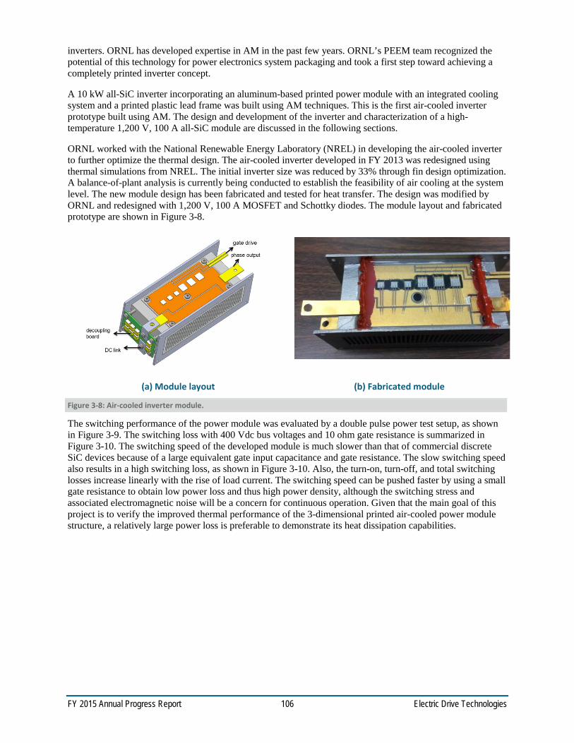
FY 2015 Annual Progress Report 106 Electric Drive Technologies
inverters. ORNL has developed expertise in AM in the past few years. ORNL’s PEEM team recognized the potential of this technology for power electronics system packaging and took a first step toward achieving a completely printed inverter concept.
A 10 kW all-SiC inverter incorporating an aluminum-based printed power module with an integrated cooling system and a printed plastic lead frame was built using AM techniques. This is the first air-cooled inverter prototype built using AM. The design and development of the inverter and characterization of a high-temperature 1,200 V, 100 A all-SiC module are discussed in the following sections.
ORNL worked with the National Renewable Energy Laboratory (NREL) in developing the air-cooled inverter to further optimize the thermal design. The air-cooled inverter developed in FY 2013 was redesigned using thermal simulations from NREL. The initial inverter size was reduced by 33% through fin design optimization. A balance-of-plant analysis is currently being conducted to establish the feasibility of air cooling at the system level. The new module design has been fabricated and tested for heat transfer. The design was modified by ORNL and redesigned with 1,200 V, 100 A MOSFET and Schottky diodes. The module layout and fabricated prototype are shown in Figure 3-8.
(a) Module layout (b) Fabricated module
Figure 3-8: Air-cooled inverter module.
The switching performance of the power module was evaluated by a double pulse power test setup, as shown in Figure 3-9. The switching loss with 400 Vdc bus voltages and 10 ohm gate resistance is summarized in Figure 3-10. The switching speed of the developed module is much slower than that of commercial discrete SiC devices because of a large equivalent gate input capacitance and gate resistance. The slow switching speed also results in a high switching loss, as shown in Figure 3-10. Also, the turn-on, turn-off, and total switching losses increase linearly with the rise of load current. The switching speed can be pushed faster by using a small gate resistance to obtain low power loss and thus high power density, although the switching stress and associated electromagnetic noise will be a concern for continuous operation. Given that the main goal of this project is to verify the improved thermal performance of the 3-dimensional printed air-cooled power module structure, a relatively large power loss is preferable to demonstrate its heat dissipation capabilities.
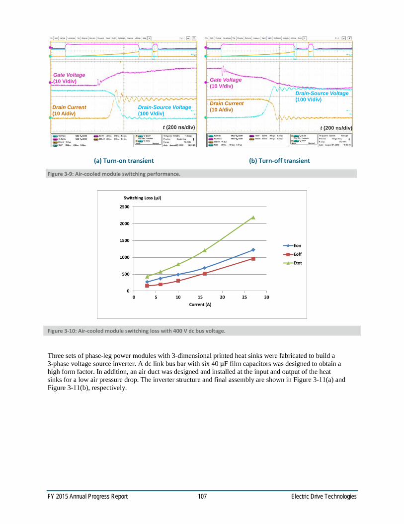
FY 2015 Annual Progress Report 107 Electric Drive Technologies
(a) Turn-on transient (b) Turn-off transient
Figure 3-9: Air-cooled module switching performance.
Figure 3-10: Air-cooled module switching loss with 400 V dc bus voltage.
Three sets of phase-leg power modules with 3-dimensional printed heat sinks were fabricated to build a 3-phase voltage source inverter. A dc link bus bar with six 40 µF film capacitors was designed to obtain a high form factor. In addition, an air duct was designed and installed at the input and output of the heat sinks for a low air pressure drop. The inverter structure and final assembly are shown in Figure 3-11(a) and Figure 3-11(b), respectively.
Drain-Source Voltage (100 V/div)
Gate Voltage (10 V/div)
t (200 ns/div)
Drain Current (10 A/div)
Drain-Source Voltage (100 V/div)
Gate Voltage (10 V/div)
t (200 ns/div)
Drain Current (10 A/div)
0
500
1000
1500
2000
2500
0 5 10 15 20 25 30
Switching Loss (µJ)
Current (A)
Eon
Eoff
Etot
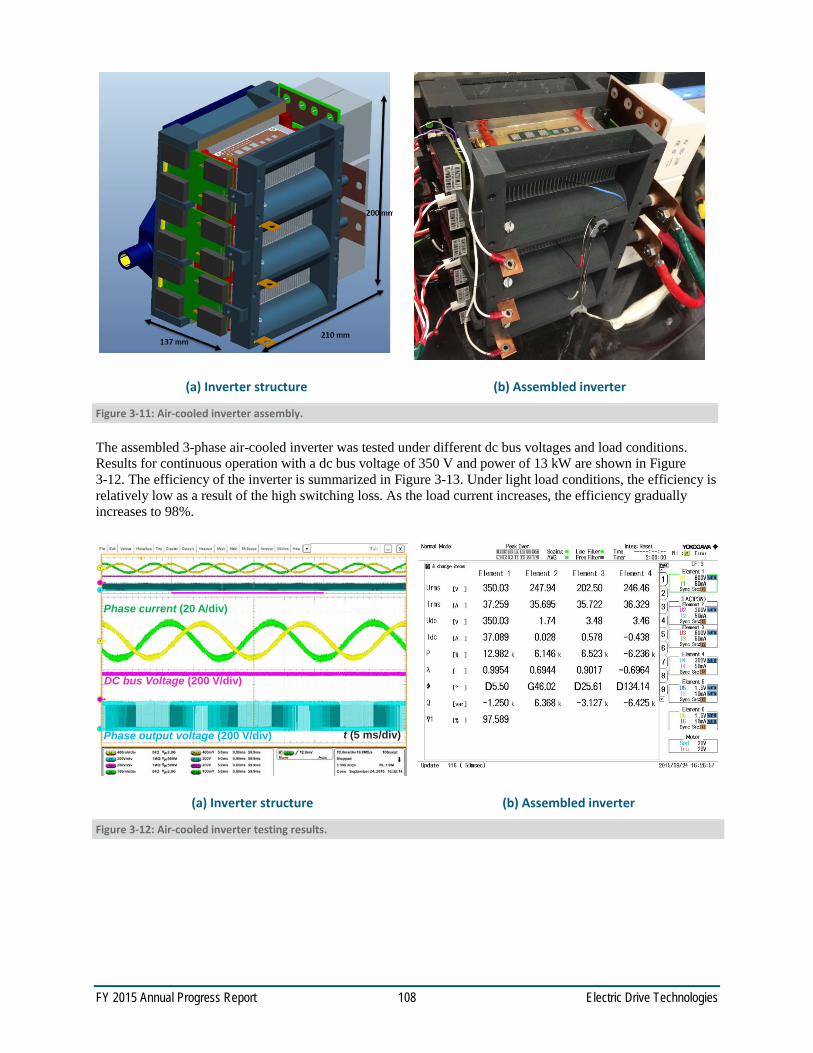
FY 2015 Annual Progress Report 108 Electric Drive Technologies
(a) Inverter structure (b) Assembled inverter
Figure 3-11: Air-cooled inverter assembly.
The assembled 3-phase air-cooled inverter was tested under different dc bus voltages and load conditions. Results for continuous operation with a dc bus voltage of 350 V and power of 13 kW are shown in Figure 3-12. The efficiency of the inverter is summarized in Figure 3-13. Under light load conditions, the efficiency is relatively low as a result of the high switching loss. As the load current increases, the efficiency gradually increases to 98%.
(a) Inverter structure (b) Assembled inverter
Figure 3-12: Air-cooled inverter testing results.
Phase output voltage (200 V/div)
DC bus Voltage (200 V/div)
t (5 ms/div)
Phase current (20 A/div)

FY 2015 Annual Progress Report 109 Electric Drive Technologies
Figure 3-13: Efficiency of the air-cooled inverter.
The 30 kW all-SiC inverter was designed using a commercially available 1,200 V, 100 A SiC MOSFET-based module. The layout of the inverter is shown in Figure 3-14. The total inverter volume is 3.6 L (226 × 224 × 73 mm). Commercially available gate drivers from Rohm were used. The gate driver has galvanic isolation up to 3,000 Vrms and integrated overcurrent protection, undervoltage lockout, and temperature feedback. The performance of the module was evaluated before the inverter was built. The cooling system for this prototype is a single-sided cooling commercially available cold plate. The modules were mounted on the cold plate with thermal grease as the heat transfer medium from the lower sides of the power modules. This prototype model will be packaged as shown in Figure 3-14, with the controls and capacitors packaged close to the heat sink. The capacitors used in this design are not a brick type but are small individual capacitors in series to ensure better cooling and reduce costs.
Figure 3-14: The 10 kW SiC inverter layout.
The final inverter assembly inverter is shown in Figure 3-15. For this test, the dc-link voltage was fixed at nominal operating voltage (325 V) to the maximum bus voltage (450 V). The load resistance was set to the minimum value, and the current was controlled by changing the modulation index. The coolant was set at 20°C at a flow rate of 1.5 gpm. The open-loop frequency of operation and the pulsed width modulation frequency were fixed, and the current command was varied for a particular dc-link voltage. The command current was
91
92
93
94
95
96
97
98
99
0 2 4 6 8 10 12 14
Effic
ienc
y(%
)
Input_Power(kW)
3 Phases Printed Air Cool SiC Inverter Efficiency
250V
300V
350V

FY 2015 Annual Progress Report 110 Electric Drive Technologies
increased in steps without exceeding the power rating of the inverter or of the load. The coolant temperature was changed to 60°C, and data were recorded for a wide range of current and switching frequencies.
(a) Inverter structure (b) Assembled inverter
Figure 3-15: Liquid-cooled inverter assembly.
The experimental waveforms and results for 400 Vdc bus voltage and 27 kW active power operation are shown in Figure 3-16.
(a) Power analyzer data (b) Experimental waveforms
Figure 3-16: Experimental waveforms of 30 kW SiC inverter with 400 V dc-link operation.
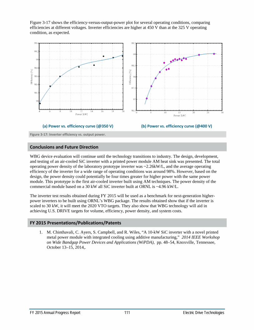
FY 2015 Annual Progress Report 111 Electric Drive Technologies
Figure 3-17 shows the efficiency-versus-output-power plot for several operating conditions, comparing efficiencies at different voltages. Inverter efficiencies are higher at 450 V than at the 325 V operating condition, as expected.
(a) Power vs. efficiency curve (@350 V) (b) Power vs. efficiency curve (@400 V)
Figure 3-17: Inverter efficiency vs. output power.
Conclusions and Future Direction
WBG device evaluation will continue until the technology transitions to industry. The design, development, and testing of an air-cooled SiC inverter with a printed power module AM heat sink was presented. The total operating power density of the laboratory prototype inverter was ~2.26kW/L, and the average operating efficiency of the inverter for a wide range of operating conditions was around 98%. However, based on the design, the power density could potentially be four times greater for higher power with the same power module. This prototype is the first air-cooled inverter built using AM techniques. The power density of the commercial module based on a 30 kW all SiC inverter built at ORNL is ~4.96 kW/L.
The inverter test results obtained during FY 2015 will be used as a benchmark for next-generation higher-power inverters to be built using ORNL’s WBG package. The results obtained show that if the inverter is scaled to 30 kW, it will meet the 2020 VTO targets. They also show that WBG technology will aid in achieving U.S. DRIVE targets for volume, efficiency, power density, and system costs.
FY 2015 Presentations/Publications/Patents
1. M. Chinthavali, C. Ayers, S. Campbell, and R. Wiles, “A 10-kW SiC inverter with a novel printed metal power module with integrated cooling using additive manufacturing,” 2014 IEEE Workshop on Wide Bandgap Power Devices and Applications (WiPDA), pp. 48–54, Knoxville, Tennessee, October 13–15, 2014,.

FY 2015 Annual Progress Report 112 Electric Drive Technologies
3.2. Innovative Technologies for Converters and Chargers Gui-Jia Su, Principal Investigator Oak Ridge National Laboratory (ORNL) National Transportation Research Center 2360 Cherahala Boulevard Knoxville, TN 37932 Phone: (865) 946-1330 E-mail: [email protected] Susan A. Rogers, DOE EDT Program Manager Phone: (202) 586-8997 E-mail: [email protected] Burak Ozpineci, ORNL EDT Program Manager Phone: (865) 946-1329 E-mail: [email protected] Contractor: UT-Battelle, LLC, managing and operating contractor for the Oak Ridge National Laboratory Contract No.: DE-AC05-00OR22725
Abstract/Executive Summary The overall objective of this multiyear project is to develop low-cost, high-efficiency, high-power-
density all–wide bandgap (WBG) dc-dc converters and onboard chargers (OBCs). The aim is to reduce charger converter cost by 50% and weight and volume by a factor of 2 compared with the state of the art and provide charger efficiency of more than 96%.
A major task for FY 2015 was to design, build, and test an all-SiC integrated OBC at the level 2 charging power of 6.6 kW. To this end, a 100 kW segmented traction inverter using commercial SiC metal-oxide-semiconductor field-effect transistors (MOSFETs) and 3-dimensional (3D) printed components was designed, built, and tested. The isolated SiC charger dc-dc converter developed in FY 2014 was then integrated with the traction inverter to provide an integral onboard charging functionality. Testing and evaluation of the integral onboard charging functionality was successfully completed at power levels up to 6.8 kW.
Another task for FY 2015 was to develop a gallium nitride (GaN) -based charger dc-dc converter. A 6.8 kW charger converter was designed using the GaN Systems GaN transistor GS66516T, high-voltage heavy copper printed circuit board (PCB) power planes, low-voltage (14 V) high-current PCB power planes, and a planar transformer. A prototype will be built and tested in FY 2016.
Accomplishments Completed the design, fabrication, and testing of a reconfigurable SiC traction inverter for use in the
development of all-WBG integrated OBCs of different topologies. The traction inverter can be configured as either a 100 kW segmented inverter or a dual 3-phase inverter, each rated at 50 kW.
Completed the integration and testing of a 6.8 kW all-SiC integrated OBC using the 100 kW SiC segmented traction inverter and the isolated SiC charger dc-dc converter. It showed a peak efficiency of 96.5% when charged from a 240 V source and 92.6% when charged from a 120 V source, and a 2% point improvement over the silicon-based counterpart developed in FY 2013.
Completed a design for a 6.8 kW charger converter using GaN Systems GaN transistors, high-voltage heavy copper PCB power planes, low-voltage (14 V) high-current PCB power planes, and a planar transformer. The design has a high power density of 7.1 kW/L.

FY 2015 Annual Progress Report 113 Electric Drive Technologies
In collaboration with Aegis Technology, completed fabrication of an advanced magnetic material core set of an E-shaped core and a plate using ORNL’s additive manufacturing capability and Aegis Technology’s nanocomposite magnetic powders.
Introduction
Most current plug-in electric vehicles (EVs) employ a stand-alone OBC to charge the propulsion battery. However, a stand-alone OBC is not cost-effective because of its large number of components. Moreover, its performance in terms of weight, volume, and efficiency is limited by the capabilities of existing semiconductor and magnetic materials. Bulky and expensive passive components (inductors, capacitors, and transformers) are needed in OBCs because (1) silicon switches constrain switching frequencies to less than 100 kHz at power levels of several kilowatts, and (2) inductors and transformers based on soft ferrite magnetic materials further limit power density and efficiency because of low saturation flux densities (~0.3 T) and high core losses at high frequencies. As a result, OBCs (1) add significant cost (~$106/kW); (2) have low power-density and specific-power numbers (~0.6 kW/kg, ~0.8 kW/L); (3) are relatively inefficient (85–93%); and (4) are unidirectional (can charge the battery but are incapable of vehicle-to-grid support, a highly desirable function in future smart grids).
The problems of existing silicon-based OBC technology are addressed in this multiyear project through overcoming the limitations of existing semiconductor and magnetic materials by using WBG devices, advanced magnetic materials, and novel integrated charger topologies and control strategies to significantly increase power density, specific power, and efficiency at lower cost. Emerging WBG devices—including those made with SiC and GaN—and advanced soft magnetic materials enable significant improvements in ac-dc and dc-dc converters, major components of OBCs. Their ability to operate with enhanced efficiency over higher frequencies and temperatures minimizes requirements for the passive components and reduces cooling demands. In addition, a novel control strategy developed under this project and reported in the FY 2014 annual report was shown to reduce the dc link capacitance in the ac-dc stage by 60%. Because currently passive components contribute more than 30% to the charger cost, weight, and volume in state-of-the-art silicon-based technology, the approach proposed in this project provides enabling technologies to produce low-cost, light, compact, and highly efficient OBCs and converters.
Approach
Our strategy to address the problems of state-of-the-art OBCs and dc-dc converters is multifold:
Push the envelope on functional integration of the traction drive, 14 V dc-dc converter, and OBC.
Take up the challenge of introducing WBG materials, specifically GaN, into automotive applications to determine what performance, packaging, cost, and efficiency benefits can be gained.
Perform analysis, modeling, and simulation that lead to a functional prototype meeting VTO OBC specific power, power density, and efficiency requirements while significantly reducing the current cost levels.
Design, build, test, and demonstrate prototypes.
Work with U.S. DRIVE to develop insights and lessons learned from the automotive community pertinent to dc-dc converters and OBCs.
Collaborate with industry stakeholders, universities, and other national laboratories to maximize the impact of this work.
Three technical approaches based on converter topology, advanced semiconductor and magnetic materials, and control strategy are being pursued. First, in power conversion topology, integrated bidirectional WBG OBCs are being developed that (a) provide galvanic isolation; (b) provide an integrated function for dc-dc conversion of high voltages to 14 V; and (c) use soft switching at the dc-dc stage to reduce electromagnetic interference (EMI) and improve efficiency. Figure 3-18 shows an integrated dc-dc converter and charger architecture

FY 2015 Annual Progress Report 114 Electric Drive Technologies
consisting mainly of an ac filter, a WBG front active converter, a dc bus capacitor, and a WBG isolation converter. The isolation converter integrates the functions for charging both the high-voltage traction battery and the 14 V battery for vehicle accessory loads. It includes a high-frequency transformer and dc filters as well as WBG switches.
Figure 3-18: An integrated dc-dc converter and charger architecture.
Second, increasing power density and specific power without compromising efficiency is aggressively pursued by exploiting high switching frequency with WBG devices (especially GaN switches) and using advanced soft magnetic materials (nanocomposites) to drastically reduce the cost, weight, and volume of the ac and dc filters and isolation transformer. Because the availability of WBG power modules is limited, SiC and GaN devices are purchased or obtained directly from device vendors; they are tested, characterized, and packaged for use in converter design and prototype development. Prototypes will be built and tested first using SiC devices—for which wafer processing and device fabrication technologies have advanced to a stage such that SiC MOSFETs and other switches are available commercially—and then GaN switches as that technology matures and devices with high current ratings become available.
Third, further integration with traction drive systems is employed to reduce the component count for OBCs. For instance, WBG traction drive inverters and motors will be used to operate as the active front converter and to replace the ac filter inductor, significantly reducing OBC cost, weight, and volume.
Finally, a control strategy for the isolation converter has been developed to shrink the bulky dc link capacitor. Without adequate control, this bulky capacitor is necessary to filter out the large voltage ripple— with twice the grid supply frequency—inherent in single-phase ac-dc converters. The proposed control strategy enables a 60% reduction in the ripple current and thereby a significant size reduction in the bulky dc link capacitor in the front ac-dc converter.
Figure 3-19 shows the integrated isolation converter topology selected through simulation. The converter is based on a phase-shifted dual active H- bridge converter that consists of two H-bridges (HB1 and HB2) and a buck converter coupled through a high-frequency transformer (Tr), which provides galvanic isolation for charging the batteries. One H-bridge is connected to the high-voltage traction battery and the other to the active front ac-dc converter. The H-bridge connected to the high-voltage battery, transformer, and buck converter forms a typical 14 V accessory converter, rated at around 2 kW in plug-in electric vehicles, for charging the 14 V battery and powering the vehicle’s low-voltage accessory loads. Sharing the transformer and other switch components between the OBC and the 14 V converter leads to substantial cost, weight, and volume savings for the OBC compared with a stand-alone counterpart. Other features of the integrated charger include these: (1) It provides bidirectional power flow and thus can offer additional desired functions, such as vehicle-to-grid and vehicle-to-home applications. (2) It can charge the 14 V battery from the grid in addition to normal operation from the high-voltage traction battery. (3) It uses the parasitic capacitance of the switches and the transformer leakage inductance to achieve zero-voltage switching for EMI noise reduction and efficiency improvement. (4) The dual H-bridge converter enables the OBC to charge the battery over a wide range of voltages by providing a voltage buck-and-boost function through phase shifting and duty ratio control.
HVbatt.
14V batt.
C1
S2
S1
S4
S3120V
or 240V
WBG front converter
ac filter
dc filterIsolation transformer
dc link capacitor
WBG Isolation converter
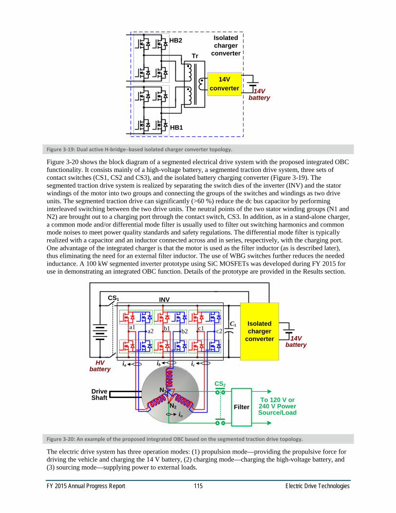
FY 2015 Annual Progress Report 115 Electric Drive Technologies
Figure 3-19: Dual active H-bridge–based isolated charger converter topology.
Figure 3-20 shows the block diagram of a segmented electrical drive system with the proposed integrated OBC functionality. It consists mainly of a high-voltage battery, a segmented traction drive system, three sets of contact switches (CS1, CS2 and CS3), and the isolated battery charging converter (Figure 3-19). The segmented traction drive system is realized by separating the switch dies of the inverter (INV) and the stator windings of the motor into two groups and connecting the groups of the switches and windings as two drive units. The segmented traction drive can significantly (>60 %) reduce the dc bus capacitor by performing interleaved switching between the two drive units. The neutral points of the two stator winding groups (N1 and N2) are brought out to a charging port through the contact switch, CS3. In addition, as in a stand-alone charger, a common mode and/or differential mode filter is usually used to filter out switching harmonics and common mode noises to meet power quality standards and safety regulations. The differential mode filter is typically realized with a capacitor and an inductor connected across and in series, respectively, with the charging port. One advantage of the integrated charger is that the motor is used as the filter inductor (as is described later), thus eliminating the need for an external filter inductor. The use of WBG switches further reduces the needed inductance. A 100 kW segmented inverter prototype using SiC MOSFETs was developed during FY 2015 for use in demonstrating an integrated OBC function. Details of the prototype are provided in the Results section.
Figure 3-20: An example of the proposed integrated OBC based on the segmented traction drive topology.
The electric drive system has three operation modes: (1) propulsion mode—providing the propulsive force for driving the vehicle and charging the 14 V battery, (2) charging mode—charging the high-voltage battery, and (3) sourcing mode—supplying power to external loads.
14V battery
Tr
HB2
HB1
14V converter
Isolatedcharger
converter
C1
To 120 V or 240 V Power Source/Load
14V battery
CS1
HV battery
CS2Drive Shaft
Isolated charger
convertera2 b2 c2a1 b1 c1
N1
N2 Filter
ia ib
in
ic
INV
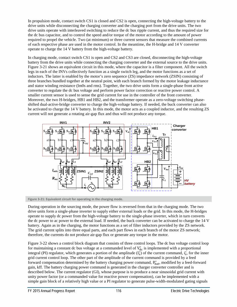
FY 2015 Annual Progress Report 116 Electric Drive Technologies
In propulsion mode, contact switch CS1 is closed and CS2 is open, connecting the high-voltage battery to the drive units while disconnecting the charging converter and the charging port from the drive units. The two drive units operate with interleaved switching to reduce the dc bus ripple current, and thus the required size for the dc bus capacitor, and to control the speed and/or torque of the motor according to the amount of power required to propel the vehicle. Two (at minimum) or three current sensors that measure the combined currents of each respective phase are used in the motor control. In the meantime, the H-bridge and 14 V converter operate to charge the 14 V battery from the high-voltage battery.
In charging mode, contact switch CS1 is open and CS2 and CS3 are closed, disconnecting the high-voltage battery from the drive units while connecting the charging converter and the external source to the drive units. Figure 3-21 shows an equivalent circuit in this mode, where the capacitor is a filter component. All the switch legs in each of the INVs collectively function as a single switch leg, and the motor functions as a set of inductors. The latter is enabled by the motor’s zero sequence (ZS) impedance network (ZSIN) consisting of three branches bundled together at the neutral point, with each branch formed by the motor leakage inductance and stator winding resistance (lm0s and rms). Together, the two drive units form a single-phase front active converter to regulate the dc bus voltage and perform power factor correction or reactive power control. A smaller current sensor is used to sense the grid current for use in the controller of the front converter. Moreover, the two H-bridges, HB1 and HB2, and the transformer operate as a zero-voltage switching phase-shifted dual-active-bridge converter to charge the high-voltage battery. If needed, the buck converter can also be activated to charge the 14 V battery. In this mode, the motor acts as a coupled inductor, and the resulting ZS current will not generate a rotating air-gap flux and thus will not produce any torque.
Figure 3-21: Equivalent circuit for operating in the charging mode.
During operation in the sourcing mode, the power flow is reversed from that in the charging mode. The two drive units form a single-phase inverter to supply either external loads or the grid. In this mode, the H-bridges operate to supply dc power from the high-voltage battery to the single-phase inverter, which in turn converts the dc power to ac power to the external load. If needed, the buck converter can be activated to charge the 14 V battery. Again as in the charging, the motor functions as a set of filter inductors provided by the ZS network. The grid current splits into three equal parts, and each part flows in each branch of the motor ZS network; therefore, the currents do not produce air-gap flux or generate any torque in the motor.
Figure 3-22 shows a control block diagram that consists of three control loops. The dc bus voltage control loop for maintaining a constant dc bus voltage at a commanded level of Vdc∗ is implemented with a proportional integral (PI) regulator, which generates a portion of the amplitude (Is∗) of the current command, is∗, for the inner grid current control loop. The other part of the amplitude of the current command is provided by a feed forward compensation determined by the battery charging power command, Pbat∗ , modified by a feed-forward gain, kff. The battery charging power command is generated in the charger converter controller and is described below. The current regulator (GI), whose purpose is to produce a near sinusoidal grid current with unity power factor (or a commanded value for reactive power compensation), can be implemented with a simple gain block of a relatively high value or a PI regulator to generate pulse-width-modulated gating signals
Rms
lm0s
a1 b1 c1Cdcf
Sa1
Sb1
Sc1
S1d
S1e
S1f
INV1
S2a
S2b
S2c
S2d
S2e
S2f
INV2
a2 b2 c2
Vbat
vs
Ibat
is
ZSIN2ZSIN1 Cacf
Tr
HB2
Charger converter
HV battery
C2
HB1Vdc
vTr1
vTr2
iTr1
N2
ia2 ib2 ic2
N1
ia1 ib1 ic1

FY 2015 Annual Progress Report 117 Electric Drive Technologies
for the two INVs. As shown in the figure, low pass filters (LPFs) are used in the feedback paths to remove the high-frequency components in the sensed voltages and currents.
Figure 3-22: Control block diagram.
The third control loop is for the charger converters, HB1 and HB2. The purpose of this control is to maintain a constant battery terminal voltage at a commanded level of Vbat∗ in the constant voltage (CV) charging mode or a constant current (CI) at a commanded level of Ibat∗ in the CI charging mode. A software switch, SVI, is used to select the charging mode, according to the state of charge of the battery. Again, a PI controller is used to regulate the battery voltage or current. Because of the significantly smaller dc bus capacitor in the segmented inverter, the dc bus voltage, Vdc, will fluctuate to a greater degree during operation in single-phase charger mode. To prevent it from causing a large ripple component in the battery charging current, the PI output is divided by the high-frequency component of Vdc, obtained with a band-pass filter and then fed to the pulse-width-modulation block, which controls the duty cycles. It also regulates the phase shift between the two H-bridges, if needed.
In addition, the battery charging power command, Pbat∗ , is computed by
𝑃𝑃𝑏𝑏𝑏𝑏𝑡𝑡∗ = 𝑉𝑉𝑏𝑏𝑏𝑏𝑡𝑡∗ 𝐼𝐼𝑏𝑏𝑏𝑏𝑡𝑡, in CV charging mode𝐼𝐼𝑏𝑏𝑏𝑏𝑡𝑡∗ 𝑉𝑉𝑏𝑏𝑏𝑏𝑡𝑡, in CI charging mode (1)
where Vbat and Ibat are the measured battery terminal voltage and current. As mentioned, 𝑃𝑃𝑏𝑏𝑏𝑏𝑡𝑡∗ is used in the feed-forward compensation in the grid current control loop to improve the dynamic response of the dc bus voltage loop.
Results and Discussion
A prototype consisting of an electrical drive system and a charger converter was built to test the integrated charging functionality. A traction drive inverter was designed and built using six commercial SiC MOSFET phase-leg modules rated at 1,200 V/120 A, four film dc bus capacitors with a total 880 µF of capacitance, a water-cooled cold plate (36 × 12.7 cm), a 3D-printed mounting frame, and other fixture components. The SiC MOSFET modules contain antiparallel SiC Schottky barrier diodes, so the MOSFET body diodes with inferior characteristics are bypassed. The inverter design is flexible so that it can be configured as dual 3-phase inverters, each rated at 50 kW, or a segmented 3-phase inverter, rated at 100 kW, by swapping the output bus bar and current sensor assembly, as shown in Figure 3-23. Figure 3-24 shows a photo of the inverter prototype configured as a 100 kW segmented inverter used in the OBC tests.
ia1
ib1ic1
ZSIN2
INV1
ia2ib2ic2
INV2
ZSIN1
vsis
Vdc
PIVdc
Vdc* is*
LPFGI
PWM
LPF
Rmslm0s
LPF
kffPbat
*Is*
BPF
IbatlTrs
Vbat
PI
Vbat
LPF
HB2
Vbat*
Ibat*PI
Ibat
LPF
vTr1
SVI
CV
CI
CV
CI
Pbat*
Iin
÷
PWM
Rmslm0s
HB1
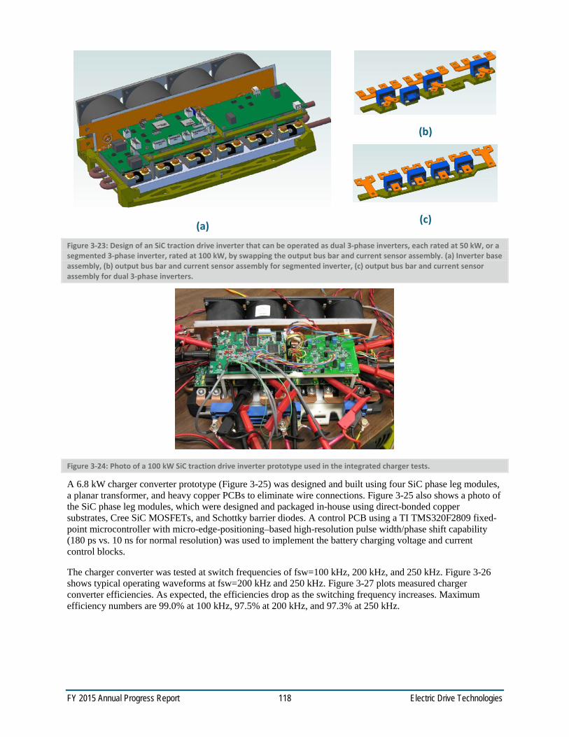
FY 2015 Annual Progress Report 118 Electric Drive Technologies
(a) (c)
(b)
Figure 3-23: Design of an SiC traction drive inverter that can be operated as dual 3-phase inverters, each rated at 50 kW, or a segmented 3-phase inverter, rated at 100 kW, by swapping the output bus bar and current sensor assembly. (a) Inverter base assembly, (b) output bus bar and current sensor assembly for segmented inverter, (c) output bus bar and current sensor assembly for dual 3-phase inverters.
Figure 3-24: Photo of a 100 kW SiC traction drive inverter prototype used in the integrated charger tests.
A 6.8 kW charger converter prototype (Figure 3-25) was designed and built using four SiC phase leg modules, a planar transformer, and heavy copper PCBs to eliminate wire connections. Figure 3-25 also shows a photo of the SiC phase leg modules, which were designed and packaged in-house using direct-bonded copper substrates, Cree SiC MOSFETs, and Schottky barrier diodes. A control PCB using a TI TMS320F2809 fixed-point microcontroller with micro-edge-positioning–based high-resolution pulse width/phase shift capability (180 ps vs. 10 ns for normal resolution) was used to implement the battery charging voltage and current control blocks.
The charger converter was tested at switch frequencies of fsw=100 kHz, 200 kHz, and 250 kHz. Figure 3-26 shows typical operating waveforms at fsw=200 kHz and 250 kHz. Figure 3-27 plots measured charger converter efficiencies. As expected, the efficiencies drop as the switching frequency increases. Maximum efficiency numbers are 99.0% at 100 kHz, 97.5% at 200 kHz, and 97.3% at 250 kHz.

FY 2015 Annual Progress Report 119 Electric Drive Technologies
Figure 3-25: Photos of a 6.8 kW charger converter and SiC MOSFET phase-leg modules (36×46 mm).
Figure 3-26: Typical operating waveforms of the SiC charger converter at fsw=200 kHz (left) and 250 kHz (right). From top: input dc voltage (Vin, 500 V/div), output dc voltage (Vout, 500 V/div), transformer primary terminal voltage (vTr1, 500 V/div), transformer secondary terminal voltage (vTr2, 500 V/div), input current (Iin, 40 A/div) and output current (Iout, 40 A/div).
Figure 3-27: Measured charger converter efficiencies.
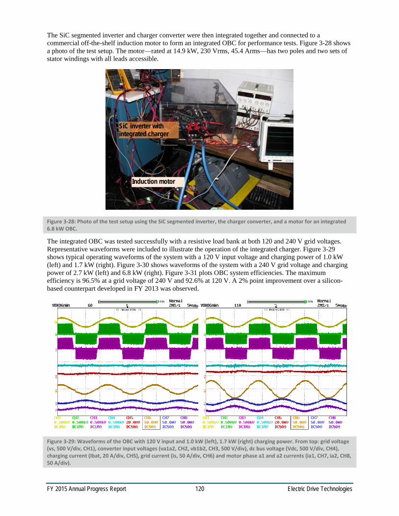
FY 2015 Annual Progress Report 120 Electric Drive Technologies
The SiC segmented inverter and charger converter were then integrated together and connected to a commercial off-the-shelf induction motor to form an integrated OBC for performance tests. Figure 3-28 shows a photo of the test setup. The motor—rated at 14.9 kW, 230 Vrms, 45.4 Arms—has two poles and two sets of stator windings with all leads accessible.
Figure 3-28: Photo of the test setup using the SiC segmented inverter, the charger converter, and a motor for an integrated 6.8 kW OBC.
The integrated OBC was tested successfully with a resistive load bank at both 120 and 240 V grid voltages. Representative waveforms were included to illustrate the operation of the integrated charger. Figure 3-29 shows typical operating waveforms of the system with a 120 V input voltage and charging power of 1.0 kW (left) and 1.7 kW (right). Figure 3-30 shows waveforms of the system with a 240 V grid voltage and charging power of 2.7 kW (left) and 6.8 kW (right). Figure 3-31 plots OBC system efficiencies. The maximum efficiency is 96.5% at a grid voltage of 240 V and 92.6% at 120 V. A 2% point improvement over a silicon-based counterpart developed in FY 2013 was observed.
Figure 3-29: Waveforms of the OBC with 120 V input and 1.0 kW (left), 1.7 kW (right) charging power. From top: grid voltage (vs, 500 V/div, CH1), converter input voltages (va1a2, CH2, vb1b2, CH3, 500 V/div), dc bus voltage (Vdc, 500 V/div, CH4), charging current (Ibat, 20 A/div, CH5), grid current (is, 50 A/div, CH6) and motor phase a1 and a2 currents (ia1, CH7, ia2, CH8, 50 A/div).
Induction motor
SiC inverter with integrated charger

FY 2015 Annual Progress Report 121 Electric Drive Technologies
Figure 3-30: Waveforms of the OBC at 240 V input and 2.7 kW (left), 6.8 kW (right) charging power. From the top: grid voltage (vs, 500 V/div, CH1), grid current (is, 100 A/div, CH6), converter input voltage (va1b1, 500 V/div, CH2), dc bus voltage (Vdc, 500 V/div, CH4), charging current (Ibat, 50 A/div, CH5) and motor phase a1 and a2 currents (ia1, CH7, ia2, CH8, 100 A/div).
Figure 3-31: Measured OBC system efficiencies at grid voltages of 120 and 240 V.
In collaboration with Aegis Technology, an advanced magnetic material–based core set of an E-shaped core and a plate (Figure 3-32) was made at ORNL’s Manufacturing Demonstration Facility using a nanocomposite magnetic powder supplied by Aegis Technology. The powder is a mixture of magnetic nanoalloy (FeNbSiCuB) particles (60 vol % or 90 wt %) and polyphenylene sulfide (PPS) polymer powders (40 vol % or 10 wt %). The cores were printed with an inkjet 3D printer using the powder, and then baked in an oven at 320° C for a little over an hour to set the PPS polymer in the mixture. The cores produced were a PPS-bound magnetic nanocomposite with an operating temperature of up to 200° C. The core set was designed to emulate a commercial-off-the-shelf ferrite core and is being comparatively evaluated against the commercial product for high-frequency inductor and transformer applications.
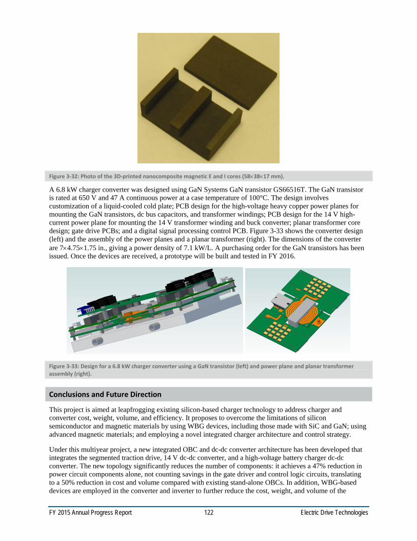
FY 2015 Annual Progress Report 122 Electric Drive Technologies
Figure 3-32: Photo of the 3D-printed nanocomposite magnetic E and I cores (58×38×17 mm).
A 6.8 kW charger converter was designed using GaN Systems GaN transistor GS66516T. The GaN transistor is rated at 650 V and 47 A continuous power at a case temperature of 100°C. The design involves customization of a liquid-cooled cold plate; PCB design for the high-voltage heavy copper power planes for mounting the GaN transistors, dc bus capacitors, and transformer windings; PCB design for the 14 V high-current power plane for mounting the 14 V transformer winding and buck converter; planar transformer core design; gate drive PCBs; and a digital signal processing control PCB. Figure 3-33 shows the converter design (left) and the assembly of the power planes and a planar transformer (right). The dimensions of the converter are 7×4.75×1.75 in., giving a power density of 7.1 kW/L. A purchasing order for the GaN transistors has been issued. Once the devices are received, a prototype will be built and tested in FY 2016.
Figure 3-33: Design for a 6.8 kW charger converter using a GaN transistor (left) and power plane and planar transformer assembly (right).
Conclusions and Future Direction
This project is aimed at leapfrogging existing silicon-based charger technology to address charger and converter cost, weight, volume, and efficiency. It proposes to overcome the limitations of silicon semiconductor and magnetic materials by using WBG devices, including those made with SiC and GaN; using advanced magnetic materials; and employing a novel integrated charger architecture and control strategy.
Under this multiyear project, a new integrated OBC and dc-dc converter architecture has been developed that integrates the segmented traction drive, 14 V dc-dc converter, and a high-voltage battery charger dc-dc converter. The new topology significantly reduces the number of components: it achieves a 47% reduction in power circuit components alone, not counting savings in the gate driver and control logic circuits, translating to a 50% reduction in cost and volume compared with existing stand-alone OBCs. In addition, WBG-based devices are employed in the converter and inverter to further reduce the cost, weight, and volume of the

FY 2015 Annual Progress Report 123 Electric Drive Technologies
passive components, as well as improve system efficiency. A control strategy for the charger isolation converter was also developed to reduce the battery ripple current inherent in single-phase ac-dc converters. The control strategy was shown to reduce the ripple current by 60%, enabling a corresponding reduction in the bulky dc link capacitor in the active front end converter.
A 6.8 kW SiC-based OBC prototype based on the new topology was designed, built, and tested by integrating a 3-port isolated SiC dc-dc converter with a 100 kW SiC traction inverter. Test results showed it to have a peak efficiency of 96.5% when charged from a 240 V source and of 92.6% when charged from a 120 V source. The test results also show a 2% point improvement over the silicon-based counterpart.
Progress was made on employing GaN switches and advanced nanocomposite magnetic materials for OBCs. A design for a 6.8 kW charger converter was completed using GaN Systems GaN transistors, high-voltage heavy copper PCB power planes, low-voltage (14 V) high-current PCB power planes, and a planar transformer. The design has a high power density of 7.1 kW/L. In addition, in collaboration with Aegis Technology, an advanced magnetic material core set of an E-shaped core and a plate was fabricated using ORNL’s additive manufacturing capability and Aegis Technology’s nanocomposite magnetic powders.
Future work will be directed at designing, building, and testing prototypes for a 6.6 kW GaN isolation converter and OBC and a 2 kW GaN 14 V converter.
FY 2015 Presentations/Publications/Patents
1. G. J. Su and L. Tang, “An integrated onboard charger and accessory power converter using WBG devices,” in Proceedings of the 7th IEEE Energy Conversion Congress and Exposition (ECCE 2015), pp. 6306–6313, Montreal, Canada, September 20–24, 2015.
2. G. J. Su, “Innovative technologies for converters and chargers,” presented at the DOE Vehicle Technologies Office Electric Drive Technologies Advanced Power Electronics and Electric Motors R&D FY 2015 Kickoff Meeting, Oak Ridge, Tennessee, November 18–20, 2014.
3. G. J. Su, “Innovative technologies for converters and chargers,” presented at the 2015 DOE Hydrogen and Fuel Cells Program and Vehicle Technologies Office Annual Merit Review and Peer Evaluation Meeting, Arlington, Virginia, June 8–12, 2015.
FY 2015 Annual Progress Report 124 Electric Drive Technologies
3.3. Traction Drive Systems with Integrated Wireless Charging Gui-Jia Su, Principal Investigator Oak Ridge National Laboratory (ORNL) National Transportation Research Center 2360 Cherahala Boulevard Knoxville, TN 37932 Phone: (865) 946-1330 E-mail: [email protected] Susan A. Rogers, DOE EDT Program Manager Phone: (202) 586-8997 E-mail: [email protected] Burak Ozpineci, ORNL EDT Program Manager Phone: (865) 946-1329 E-mail: [email protected] Contractor: UT-Battelle, LLC, managing and operating contractor for the Oak Ridge National Laboratory Contract No.: DE-AC05-00OR22725
Abstract/Executive Summary The project aims to redesign the electric drive system for plug-in electric vehicles to include wireless
charging functionality and reduce cost while increasing efficiency and power density using wide bandgap (WBG) devices.
The FY 2015 objective is to develop converter topologies suitable for traction drive systems with integral wireless charging functionality and control strategies for minimizing component size and circuit losses through detailed circuit simulation. o An optimal resonant circuit was designed that can significantly reduce the resonant circuit current
and the losses. o Three electric drive topologies were developed and proved to be functional by circuit simulation.
Accomplishments Simulated various resonant circuits and designed one that is optimized for minimizing circulating
current and the associated losses. It shows, with the optimized resonant circuit, a range of 61–75% reduction in the primary current and 10–44% reduction in the total losses in a dc-ac wireless charger.
Simulated and proved concepts for three electric drive topology candidates with integrated wireless charging functionality: o Topology 1: Tapping into the 14 V accessory power supply converter to eliminate the secondary
ac-dc converter for the wireless charger. o Topology 2: Using the traction motor and inverter to eliminate the secondary ac-dc converter for
the wireless charger o Topology 3: Using a multiport dc-dc converter that combines a reduced-power boost converter for
stepping up the dc bus voltage of the traction drive inverter, a 14 V buck converter for powering the 14 V vehicle accessory loads, and a wireless battery charging converter.
o Simulation results show all the wireless chargers have high input power factors of greater than 99% and low total harmonic distortion (THD) factors of less than 3.5% in the ac source current.
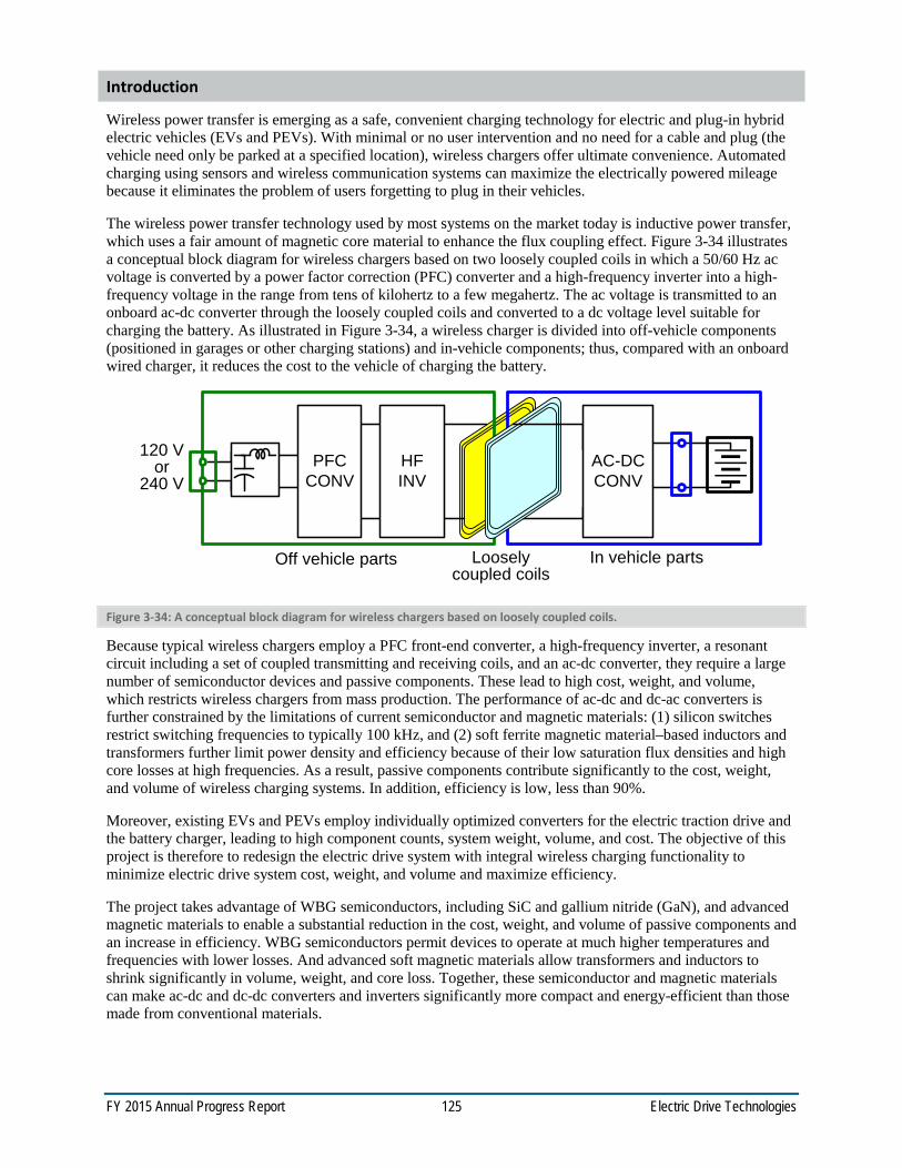
FY 2015 Annual Progress Report 125 Electric Drive Technologies
Introduction
Wireless power transfer is emerging as a safe, convenient charging technology for electric and plug-in hybrid electric vehicles (EVs and PEVs). With minimal or no user intervention and no need for a cable and plug (the vehicle need only be parked at a specified location), wireless chargers offer ultimate convenience. Automated charging using sensors and wireless communication systems can maximize the electrically powered mileage because it eliminates the problem of users forgetting to plug in their vehicles.
The wireless power transfer technology used by most systems on the market today is inductive power transfer, which uses a fair amount of magnetic core material to enhance the flux coupling effect. Figure 3-34 illustrates a conceptual block diagram for wireless chargers based on two loosely coupled coils in which a 50/60 Hz ac voltage is converted by a power factor correction (PFC) converter and a high-frequency inverter into a high-frequency voltage in the range from tens of kilohertz to a few megahertz. The ac voltage is transmitted to an onboard ac-dc converter through the loosely coupled coils and converted to a dc voltage level suitable for charging the battery. As illustrated in Figure 3-34, a wireless charger is divided into off-vehicle components (positioned in garages or other charging stations) and in-vehicle components; thus, compared with an onboard wired charger, it reduces the cost to the vehicle of charging the battery.
Figure 3-34: A conceptual block diagram for wireless chargers based on loosely coupled coils.
Because typical wireless chargers employ a PFC front-end converter, a high-frequency inverter, a resonant circuit including a set of coupled transmitting and receiving coils, and an ac-dc converter, they require a large number of semiconductor devices and passive components. These lead to high cost, weight, and volume, which restricts wireless chargers from mass production. The performance of ac-dc and dc-ac converters is further constrained by the limitations of current semiconductor and magnetic materials: (1) silicon switches restrict switching frequencies to typically 100 kHz, and (2) soft ferrite magnetic material–based inductors and transformers further limit power density and efficiency because of their low saturation flux densities and high core losses at high frequencies. As a result, passive components contribute significantly to the cost, weight, and volume of wireless charging systems. In addition, efficiency is low, less than 90%.
Moreover, existing EVs and PEVs employ individually optimized converters for the electric traction drive and the battery charger, leading to high component counts, system weight, volume, and cost. The objective of this project is therefore to redesign the electric drive system with integral wireless charging functionality to minimize electric drive system cost, weight, and volume and maximize efficiency.
The project takes advantage of WBG semiconductors, including SiC and gallium nitride (GaN), and advanced magnetic materials to enable a substantial reduction in the cost, weight, and volume of passive components and an increase in efficiency. WBG semiconductors permit devices to operate at much higher temperatures and frequencies with lower losses. And advanced soft magnetic materials allow transformers and inductors to shrink significantly in volume, weight, and core loss. Together, these semiconductor and magnetic materials can make ac-dc and dc-dc converters and inverters significantly more compact and energy-efficient than those made from conventional materials.
120 V or
240 VAir
coresHFINV
Loosely coupled coils
AC-DCCONV
PFCCONV
In vehicle partsOff vehicle parts
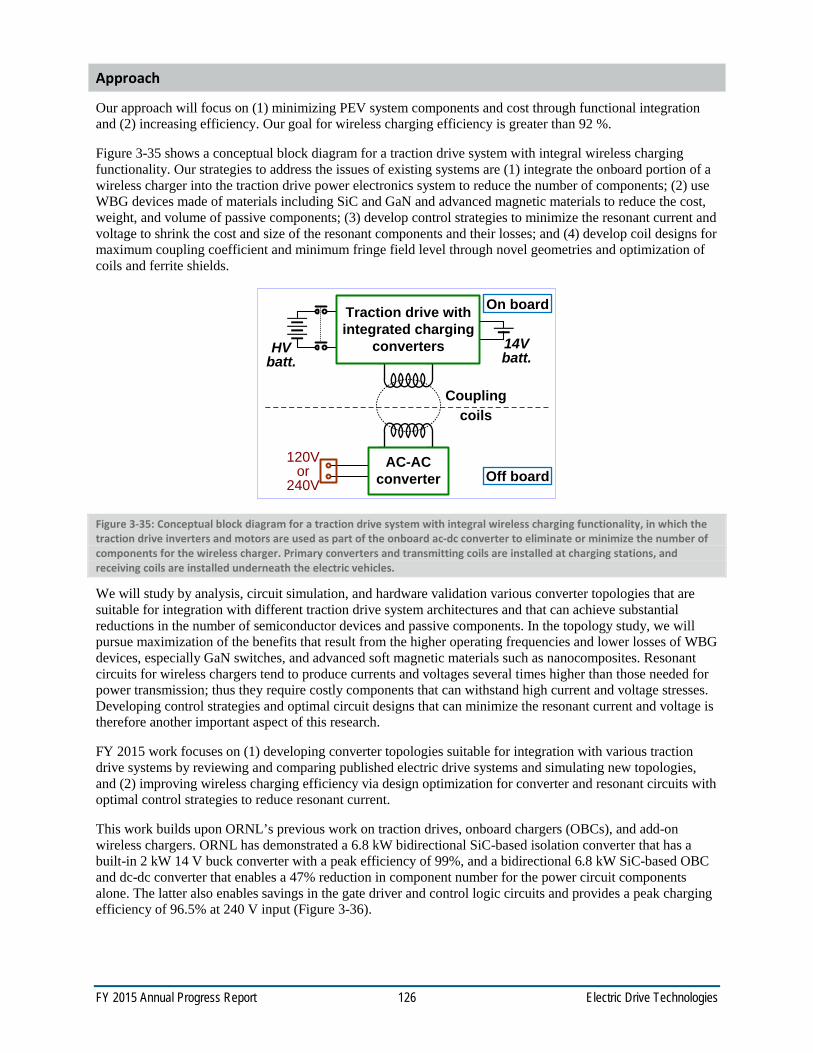
FY 2015 Annual Progress Report 126 Electric Drive Technologies
Approach
Our approach will focus on (1) minimizing PEV system components and cost through functional integration and (2) increasing efficiency. Our goal for wireless charging efficiency is greater than 92 %.
Figure 3-35 shows a conceptual block diagram for a traction drive system with integral wireless charging functionality. Our strategies to address the issues of existing systems are (1) integrate the onboard portion of a wireless charger into the traction drive power electronics system to reduce the number of components; (2) use WBG devices made of materials including SiC and GaN and advanced magnetic materials to reduce the cost, weight, and volume of passive components; (3) develop control strategies to minimize the resonant current and voltage to shrink the cost and size of the resonant components and their losses; and (4) develop coil designs for maximum coupling coefficient and minimum fringe field level through novel geometries and optimization of coils and ferrite shields.
Figure 3-35: Conceptual block diagram for a traction drive system with integral wireless charging functionality, in which the traction drive inverters and motors are used as part of the onboard ac-dc converter to eliminate or minimize the number of components for the wireless charger. Primary converters and transmitting coils are installed at charging stations, and receiving coils are installed underneath the electric vehicles.
We will study by analysis, circuit simulation, and hardware validation various converter topologies that are suitable for integration with different traction drive system architectures and that can achieve substantial reductions in the number of semiconductor devices and passive components. In the topology study, we will pursue maximization of the benefits that result from the higher operating frequencies and lower losses of WBG devices, especially GaN switches, and advanced soft magnetic materials such as nanocomposites. Resonant circuits for wireless chargers tend to produce currents and voltages several times higher than those needed for power transmission; thus they require costly components that can withstand high current and voltage stresses. Developing control strategies and optimal circuit designs that can minimize the resonant current and voltage is therefore another important aspect of this research.
FY 2015 work focuses on (1) developing converter topologies suitable for integration with various traction drive systems by reviewing and comparing published electric drive systems and simulating new topologies, and (2) improving wireless charging efficiency via design optimization for converter and resonant circuits with optimal control strategies to reduce resonant current.
This work builds upon ORNL’s previous work on traction drives, onboard chargers (OBCs), and add-on wireless chargers. ORNL has demonstrated a 6.8 kW bidirectional SiC-based isolation converter that has a built-in 2 kW 14 V buck converter with a peak efficiency of 99%, and a bidirectional 6.8 kW SiC-based OBC and dc-dc converter that enables a 47% reduction in component number for the power circuit components alone. The latter also enables savings in the gate driver and control logic circuits and provides a peak charging efficiency of 96.5% at 240 V input (Figure 3-36).
HV batt.
Coupling coils
14V batt.
120V or
240V
Traction drive with integrated charging
converters
AC-AC converter Off board
On board

FY 2015 Annual Progress Report 127 Electric Drive Technologies
Figure 3-36: ORNL’s previous work on traction drive, onboard charger: 6.8 kW SiC isolation converter (left), ORNL SiC module 1200 V/100 A (middle), SiC traction drive inverter with an integrated 6.8 kW OBC (right).
ORNL has demonstrated several add-on wireless chargers for both stationary and in-motion applications (Figure 3-37 and Figure 3-38). The ORNL approach employs a series resonant circuit that operates at 22–26 kHz and has high voltage gain. A high-frequency transformer is inserted in the primary side to adjust the gain for matching the output voltage to the vehicle battery. The ORNL work has been focused on antenna design and power transfer capability against misalignment of the antennas. It has demonstrated power transfer up to 10 kW continuous in full-scale laboratory test setups, with a peak efficiency of around 90%.
Figure 3-37: ORNL’s add-on wireless chargers operating at 22–26 kHz.
Figure 3-38: ORNL’s previous work on add-on wireless chargers: coils (left), stationary wireless charging of a Prius PHEV (middle), in-motion wireless charging of a GEM EV (right).
Unique aspects of the approach are (1) leveraging ORNL’s extensive past and current work on wired and wireless chargers and traction drives to redesign the electric drive system with wireless charging functionality; and (2) using ORNL’s expertise and facility in converter design, packaging, and testing to fully take advantage of WBG devices in PEV applications.

FY 2015 Annual Progress Report 128 Electric Drive Technologies
The impacts of the ORNL work are (1) successful demonstration of an electric drive system that incorporates wireless charging and WBG devices, providing a technological path to commercialization; and (2) a low-cost, high-efficiency electric drive system with wireless charging.
Results and Discussion
Inductor (L) and capacitor (C) resonant circuits are employed in wireless power transfer systems to increase the power transfer capability and efficiency between primary and secondary coils and minimize the supply voltage and current ratings by achieving soft-switching operation in the converters. There are four basic combinations of resonant topologies between the primary and secondary windings for wireless power transfer systems: series-series, series-parallel, parallel-series, parallel-parallel. In general, series resonance on the secondary side leads to a constant voltage source, while parallel resonance on the secondary side produces a constant current source.
Various LC resonant circuit designs that use modified circuits based on the four basic combinations were studied by simulation using the simplified dc charger converter in Figure 3-39, and one design was selected that can minimize the H-bridge inverter reactive power requirement by increasing load power factor and reducing circulating current.
Figure 3-39: Simplified converter block diagram for studying resonant circuits.
Figure 3-40 shows a comparison of operating waveforms between a traditional resonant circuit with low load power factor (left) and the optimized resonant circuit with high load power factor (right). The traditional resonant circuit has a high primary current of io = 64.3 Vrms, compared with 19.3 Arms for the optimized resonant circuit.
The lower primary current levels and high power factors with the optimized resonant circuit lead to lower losses in the dc charger. For a comparison of losses and primary currents between the two resonant circuits, Figure 3-41 plots the ratios of the losses and primary current of the optimized resonant circuit against those of the traditional low-power-factor resonant circuit at various charging rates. The chart shows a range of 61–75% reduction in current and 10–44% reduction in losses.
Three electric drive topology candidates that have integrated wireless charging functionality and employ the optimized LC resonant circuit were studied using a detailed circuit simulation software package, which proved these concepts:
Topology 1: Tapping into the 14 V accessory power supply converter to eliminate the secondary ac-dc converter for the wireless charger
Topology 2: Using the traction motor and inverter to eliminate the secondary ac-dc converter for the wireless charger
Topology 3: Using a multiport dc-dc converter that combines a boost converter of reduced power for stepping up the dc bus voltage of the traction drive inverter, a 14 V buck converter for powering the 14 V vehicle accessory loads, and a wireless battery charging converter
Resonant circuit
Air cores
H-Bridge RectifiervAB
io VBat
IBat

FY 2015 Annual Progress Report 129 Electric Drive Technologies
Figure 3-40: Comparison of operating waveforms between a traditional resonant circuit with low load power factor (left) and the optimized resonant circuit with high load power factor (right).
Figure 3-41: Comparison of losses and primary currents between the optimized resonant circuit with high power factor and the traditional circuit with low power factor at various charging rates.
Figure 3-42 shows a high-level block diagram of the first topology that taps into the 14 V accessory power supply converter to eliminate the need for a secondary ac-dc converter for the wireless charger. Figure 3-43 shows simulation results for charging at 1.5 kW from a 120 V ac source. It gives a high input power factor of 99.6% and a low THD of 1.1% in the ac source current.
Vbat (V)
Ibat (A)
vAB (V) 3*io (A) vAB (V) 3*io (A)
Vbat (V)
Ibat (A)
0
0.1
0.2
0.3
0.4
0.5
0.6
0.7
0.8
0.9
1
0.00
0.10
0.20
0.30
0.40
0.50
0.60
0 1 2 3 4 5 6 7
Loss
ratio
Curr
ent r
atio
Charging Power [kW]
Primary current ratioLoss ratio
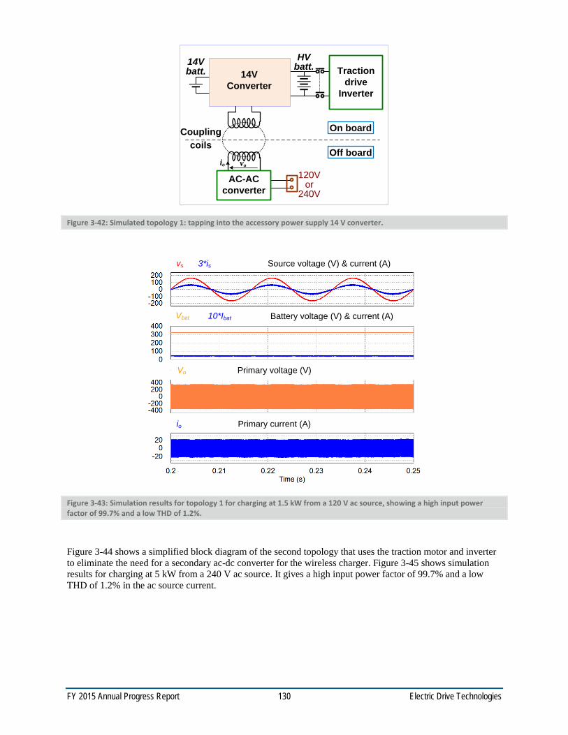
FY 2015 Annual Progress Report 130 Electric Drive Technologies
Figure 3-42: Simulated topology 1: tapping into the accessory power supply 14 V converter.
Figure 3-43: Simulation results for topology 1 for charging at 1.5 kW from a 120 V ac source, showing a high input power factor of 99.7% and a low THD of 1.2%.
Figure 3-44 shows a simplified block diagram of the second topology that uses the traction motor and inverter to eliminate the need for a secondary ac-dc converter for the wireless charger. Figure 3-45 shows simulation results for charging at 5 kW from a 240 V ac source. It gives a high input power factor of 99.7% and a low THD of 1.2% in the ac source current.
HV batt.
Coupling coils
14V batt.
120V or
240V
Traction drive
Inverter
AC-AC converter
Off board
On board
H
Bridge
14V Converter
voio
Battery voltage (V) & current (A)
Source voltage (V) & current (A)
Primary current (A)
Primary voltage (V)
vs
Vbat
Vo
3*is
10*Ibat
io
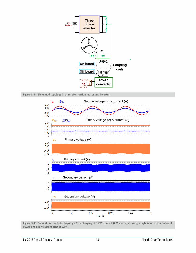
FY 2015 Annual Progress Report 131 Electric Drive Technologies
Figure 3-44: Simulated topology 2: using the traction motor and inverter.
Figure 3-45: Simulation results for topology 2 for charging at 5 kW from a 240 V source, showing a high input power factor of 99.5% and a low current THD of 0.8%.
a1 b1 c1HV
battery
Coupling coils
120V or
240V
AC-AC converter
Off board
On board
Three phase
inverter
voio
v2
i2
Battery voltage (V) & current (A)
Source voltage (V) & current (A)
Primary current (A)
Primary voltage (V)
vs
Vbat
Vo
5*is
10*Ibat
io
Secondary current (A)
Secondary voltage (V)v2
i2
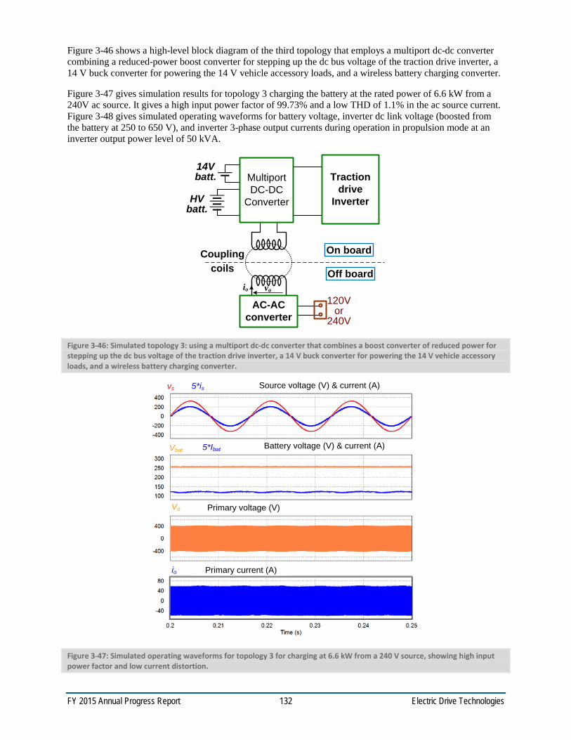
FY 2015 Annual Progress Report 132 Electric Drive Technologies
Figure 3-46 shows a high-level block diagram of the third topology that employs a multiport dc-dc converter combining a reduced-power boost converter for stepping up the dc bus voltage of the traction drive inverter, a 14 V buck converter for powering the 14 V vehicle accessory loads, and a wireless battery charging converter.
Figure 3-47 gives simulation results for topology 3 charging the battery at the rated power of 6.6 kW from a 240V ac source. It gives a high input power factor of 99.73% and a low THD of 1.1% in the ac source current. Figure 3-48 gives simulated operating waveforms for battery voltage, inverter dc link voltage (boosted from the battery at 250 to 650 V), and inverter 3-phase output currents during operation in propulsion mode at an inverter output power level of 50 kVA.
Figure 3-46: Simulated topology 3: using a multiport dc-dc converter that combines a boost converter of reduced power for stepping up the dc bus voltage of the traction drive inverter, a 14 V buck converter for powering the 14 V vehicle accessory loads, and a wireless battery charging converter.
Figure 3-47: Simulated operating waveforms for topology 3 for charging at 6.6 kW from a 240 V source, showing high input power factor and low current distortion.
HV batt.
Coupling coils
120V or
240V
Traction drive
Inverter
AC-AC converter
Off board
On board
voio
14V batt. Multiport
DC-DC Converter
Battery voltage (V) & current (A)
Source voltage (V) & current (A)
Primary current (A)
Primary voltage (V)
vs
Vbat
Vo
5*is
5*Ibat
io

FY 2015 Annual Progress Report 133 Electric Drive Technologies
Figure 3-48: Simulated operating waveforms for topology 3 operating in propulsion mode.
Figure 3-49 plots simulated power factor and THD against charging power for topology 3. It shows high input power factors of greater than 99% and low THD factors of less than 3.5% in the ac source current.
Figure 3-49: Simulated power factor and THD against charging power for topology 3.
Battery voltage (V)
Inverter dc link voltage (V)
Inverter output currents (A)
0.0%
0.5%
1.0%
1.5%
2.0%
2.5%
3.0%
3.5%
4.0%
99.0%
99.1%
99.2%
99.3%
99.4%
99.5%
99.6%
99.7%
99.8%
0 1 2 3 4 5 6 7
THD
Pow
er fa
ctor
Charging Power [kW]
pf thd

FY 2015 Annual Progress Report 134 Electric Drive Technologies
Conclusions and Future Direction
This project aims at redesigning the electric drive system for PEVs to provide wireless charging as an integral function at low cost and high efficiency. It does so by minimizing the PEV system component numbers and cost through functional integration of onboard power electronics for vehicle propulsion and wireless battery charging. In addition, increased efficiency and further reduced weight and volume are achieved by optimizing the converter topology and coil design and using WBG devices.
FY 2015 work generated a high-power-factor resonant circuit that was found effective in reducing the circulating current and the associated losses. Simulation results showed reductions in the range of 61–75% for the current and 10–44% for the losses.
FY 2015 work also produced and proved concepts for three electric drive topologies with integrated wireless charging functionality. Simulation results showed all the wireless chargers have high input power factors of greater than 99% and low THD factors of less than 3.5% in the ac source current.
Future work includes (1) design, build, and testing of WGB-based prototypes and (2) once proof-of-concept hardware development is complete, collaboration with and/or technology transfer to industry.
FY 2015 Presentations/Publications/Patents
4. G. J. Su, “Traction drive systems with integrated wireless charging,” presented at the DOE Vehicle Technologies Office Electric Drive Technologies Advanced Power Electronics and Electric Motors R&D FY 2015 Kickoff Meeting, Oak Ridge, Tennessee, November 18–20, 2014.
5. G. J. Su, “Traction drive systems with integrated wireless charging,” presented at the 2015 DOE Hydrogen and Fuel Cells Program and Vehicle Technologies Office Annual Merit Review and Peer Evaluation Meeting, June 8–12, 2015.
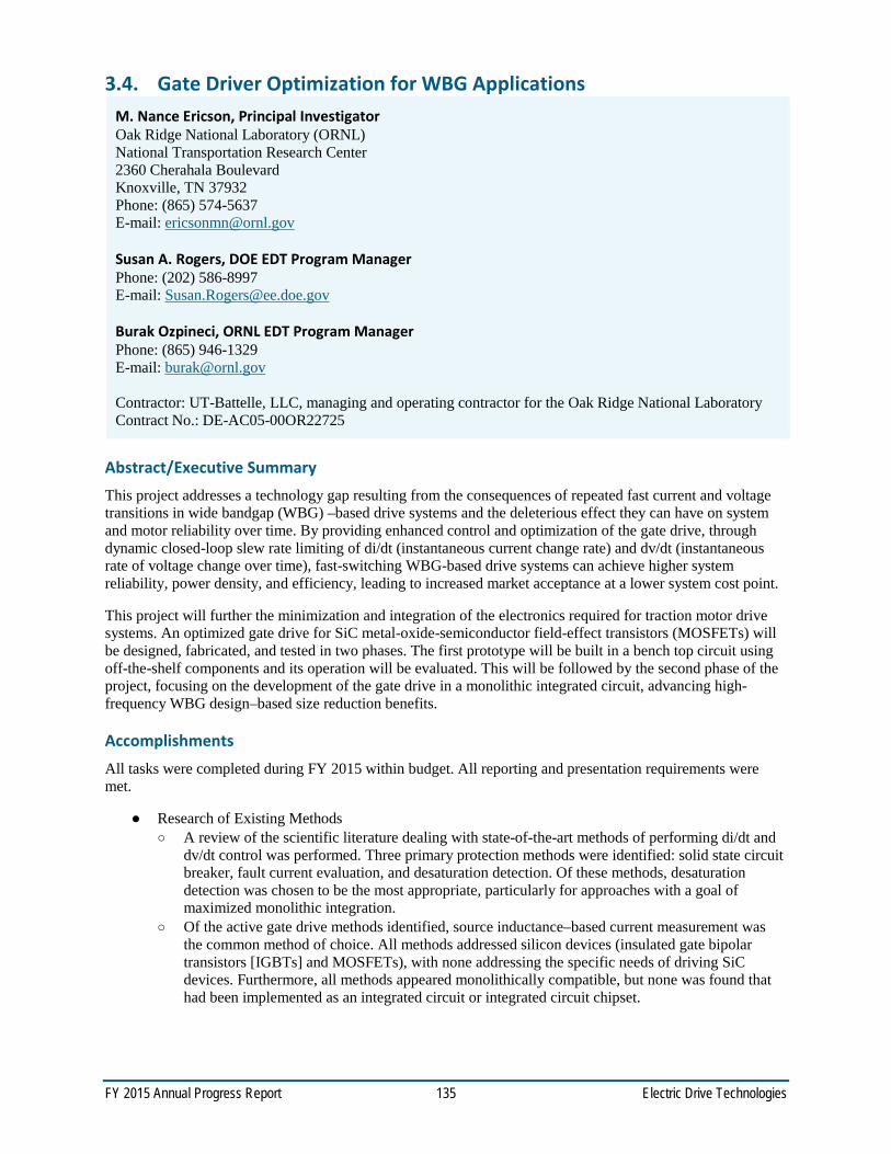
FY 2015 Annual Progress Report 135 Electric Drive Technologies
3.4. Gate Driver Optimization for WBG Applications M. Nance Ericson, Principal Investigator Oak Ridge National Laboratory (ORNL) National Transportation Research Center 2360 Cherahala Boulevard Knoxville, TN 37932 Phone: (865) 574-5637 E-mail: [email protected] Susan A. Rogers, DOE EDT Program Manager Phone: (202) 586-8997 E-mail: [email protected] Burak Ozpineci, ORNL EDT Program Manager Phone: (865) 946-1329 E-mail: [email protected] Contractor: UT-Battelle, LLC, managing and operating contractor for the Oak Ridge National Laboratory Contract No.: DE-AC05-00OR22725
Abstract/Executive Summary This project addresses a technology gap resulting from the consequences of repeated fast current and voltage transitions in wide bandgap (WBG) –based drive systems and the deleterious effect they can have on system and motor reliability over time. By providing enhanced control and optimization of the gate drive, through dynamic closed-loop slew rate limiting of di/dt (instantaneous current change rate) and dv/dt (instantaneous rate of voltage change over time), fast-switching WBG-based drive systems can achieve higher system reliability, power density, and efficiency, leading to increased market acceptance at a lower system cost point.
This project will further the minimization and integration of the electronics required for traction motor drive systems. An optimized gate drive for SiC metal-oxide-semiconductor field-effect transistors (MOSFETs) will be designed, fabricated, and tested in two phases. The first prototype will be built in a bench top circuit using off-the-shelf components and its operation will be evaluated. This will be followed by the second phase of the project, focusing on the development of the gate drive in a monolithic integrated circuit, advancing high-frequency WBG design–based size reduction benefits.
Accomplishments All tasks were completed during FY 2015 within budget. All reporting and presentation requirements were met.
Research of Existing Methods o A review of the scientific literature dealing with state-of-the-art methods of performing di/dt and
dv/dt control was performed. Three primary protection methods were identified: solid state circuit breaker, fault current evaluation, and desaturation detection. Of these methods, desaturation detection was chosen to be the most appropriate, particularly for approaches with a goal of maximized monolithic integration.
o Of the active gate drive methods identified, source inductance–based current measurement was the common method of choice. All methods addressed silicon devices (insulated gate bipolar transistors [IGBTs] and MOSFETs), with none addressing the specific needs of driving SiC devices. Furthermore, all methods appeared monolithically compatible, but none was found that had been implemented as an integrated circuit or integrated circuit chipset.

FY 2015 Annual Progress Report 136 Electric Drive Technologies
o di/dt was established as the most appropriate measured parameter from this literature search, and a review of conventional means for current measurement was performed, specifically for measuring the drain current of a power MOSFET (see Table 3-1).
o Current measurement using a sense inductor was determined to be the overall best choice for motor drive applications.
o Results of the reviewed methods and architectures for active gate drives are summarized in Table 3-2, with an emphasis on the topology and measured parameter (di/dt, dv/dt).
Gate Driver Design and Architecture Selection o Multiple gate drive waveforms were investigated and simulations performed using SPICE to
predict efficacy in controlling the di/dt and dv/dt of a MOSFET switching a motor leg. o A double pulse test setup was constructed and used to evaluate the transient switching
characteristics of commercially available SiC MOSFET devices from Cree. Using data from these tests, some SPICE model adjustments were made and simulations re-run.
o It was determined that improved SPICE models were needed for more accurate dynamic simulation of the WBG devices.
o To address the SiC MOSFET modeling need, a private company was identified that has expertise in SiC circuit modeling and simulation. A commercial simulation tool (CoolSPICE) was acquired, along with a few SiC powerMOS device models for evaluation.
Gate Driver Design Simulations o A new gate drive waveform was developed (variable threshold) and was shown via simulation to
provide the desired control of the transient switching characteristics. This method also automatically compensates for variation in the powerMOS threshold voltage from device to device and over temperature.
o Simulations of the closed-loop gate driver were performed in PSPICE using vendor-supplied SiC powerMOS device models (C2M0080120D, Cree Inc.). The loop control set point was stepped to demonstrate the range of operation. Some simplifications were used to improve the simulation convergence, including the use of a single-slope gate drive waveform. Results showed the loop operated in a stable fashion.
o Enhanced modeling activities with CoolSPICE software were begun and will be carried forward in year 2 of the project.
The results demonstrated the efficacy of the ORNL-developed sensing and control approach and will serve as the beginning point for the physical prototyping of an advanced gate drive circuit in year 2 of the project.
Introduction
WBG devices, primarily SiC and GaN, have characteristics that can lead to dramatic benefits in a variety of power electronics applications. These include higher-temperature and higher-frequency operation, smaller device and overall system sizing, and greater operational efficiency. Their ability to switch at higher frequencies than their silicon counterparts can also lead to significant volume reduction in associated passive components, yielding second-order benefits in reduced material costs and weights. For every 10% reduction in the weight of a vehicle, a 6–7% increase in fuel economy can be realized. For this reason, significant attention has been given to the miniaturization and lightweighting of all components and systems in a vehicle by automotive original equipment manufacturers. The rapidly escalating move from the use of power silicon to WBG devices to capture some of these advantages entails revisiting and optimizing their interplay with ancillary circuits and systems to truly exploit their unique characteristics.
Available commercial gate drives are not optimized for use with WBG devices. They have historically been developed for silicon devices and cannot exploit the distinctions that WBG semiconductors can offer traction drive systems. The faster di/dt and dv/dt switching capabilities of WBG devices can impose implications that need to be addressed at a system level. Fast switching can reduce the reliability of motor insulation by creating pinholes in the insulation that eventually can cause arcing and failure of the motor. To combat this possibility,

FY 2015 Annual Progress Report 137 Electric Drive Technologies
additional costs must be incurred for higher-rated winding insulation, imposing increased motor and cabling costs and resulting in larger and heavier motors. Additionally, fast switching transients can cause pitted bearings, resulting in unwanted circulating currents. Fast voltage and current transitions can also necessitate added electromagnetic interference (EMI) filtering requirements to protect sensitive electronic systems from electronic interference, adding further costs and increased system volume.
This project addresses the cost and volume barriers to achieving the DOE traction system goals of $8/kW and >4 kW/L power density. To achieve these goals, a cost-effective, efficient topology for monitoring and controlling the dynamic slew rate of a WBG gate drive will be developed to drive a SiC MOSFET motor leg. The design will be implemented in an integrated circuit to minimize the volume and reduce packaging issues.
This work can serve as an enabling technology, which, if implemented in a high-temperature process, can be utilized for future integrated motor/inverter systems.
The design will result in
Higher inverter reliability and efficiency by monitoring and utilizing dynamic slew control
50% reduction in gate drive electronics volume by drive integration
Higher temperature capability (>200°C), by use of silicon-on-insulator (SOI) technology
Higher motor reliability
Reduced insulation breakdown
Reduced bearing currents
Lower-cost gate drive systems through parts reduction
Gate driver integration
Decreased EMI filtering
This project will advance the technology of gate drives and hasten the deployment of WBG devices in vehicular traction drives by significantly increasing power density and lowering cost, circuit volume, and weight while increasing reliability and allowing the opportunity to move toward an integrated, high-temperature-capable traction system.
Approach
An active gate driver topology was developed to address the technology gaps associated with WBG-specific gate drives. This architecture was simulated using a custom-designed circuit topology with a vendor-supplied WBG device model in PSPICE. The three tasks identified for carrying out the project goals are the following:
Task 1. Research Existing Methods o Evaluate existing methods for slew rate limiting/control for feasibility and for implementation in
an integrated circuit. o Investigate both commercially available methods and those in the open literature.
Task 2. Gate Driver Design and Architecture Selection o Perform an iterative gate drive architecture design considering potential cost and system-level
performance implications.
Task 3. Gate Driver Design Simulations o Optimize and finalize the gate driver architecture via iterative circuit simulation.
Previous work had been performed on a VTO-funded project with the University of Tennessee on an SOI integrated gate driver design. However, it did not incorporate active switching. Circuits constructed and tested under that project included the following:

FY 2015 Annual Progress Report 138 Electric Drive Technologies
Input level translator
Shoot-through protection
Protection circuits o Thermal shutdown o Under-voltage lockout o Short circuit detection o Desaturation o Gate current
Integrated voltage regulator
The project strategy was to incorporate lessons learned from that project, as well as synergies with other previous projects focused on SiC gate drivers; incorporate slew rate control; and ultimately develop a high-temperature-capable gate driver integrated circuit suitable for integration with a traction motor to realize size, volume, and DOE cost targets.
The implementation of an active gate drive was divided into two broad categories, and the pros and cons of each topology were examined.
1. Gate voltage control—gate voltage is fed through a resistor from an amplifier or buffer
Implementation advantages o Simple o Voltage amplifier can be used o Can be used to control both di and dv loops
Implementation disadvantages o Amplifier/resistor combination needs to be able to handle both on and off switching, which likely
requires different set points o Gate voltage is dropped across a resistor
2. Gate current control—current through a resistor is monitored
Implementation advantages o Actual gate voltage is sensed o More opportunity for control with greater complexity o Can be used to control both di and dv loops
Implementation disadvantages o More complex o Potentially harder to compensate
Following a careful analysis of options suitable for incorporation into an integrated circuit gate driver design, tasks were combined with modeling and simulation activities. These activities resulted in the selection of a closed-loop circuit architecture. This topology was designed with several requirements in mind: ability to handle the high bandwidth of SiC MOSFET switches, practical and effective sensing of di/dt and dv/dt, potential to use only a single feedback parameter, and suitability for monolithic integration.
Results and Discussion
A literature review was performed to investigate common current measurement methods. Each of the methods was evaluated with an emphasis on parameters important to incorporation of the technique into a gate drive feedback system. These parameters included insertion loss, the need for external power, degree of electrical isolation, signal bandwidth, physical size, measurement accuracy, and relative cost compared with other conventional current measurement techniques (see Table 3-1). Of the methods investigated, the use of a sense inductor collectively met all of the requirements for the intended application, except accuracy. The accuracy limitation is primarily due to the relatively low inductance value generally used (5–10 nH). However, the method is receiving significant industry attention, and a number of SiC powerMOS devices are now packaged to provide separate current sense and source power pins (a Kelvin connection). Furthermore, this method is the

FY 2015 Annual Progress Report 139 Electric Drive Technologies
most commonly reported for current measurement in active gate drive circuits (see Table 3-2), was very cost-effective, and was selected for use in this program.
Table 3-1: Summary of conventional current measurement methods (sources: Allegro STP98-1-AN, Rev.2, Pearson 2878 data sheet)
Sensor type Insertion loss
External power
Circuit isolation Bandwidth Size Accuracy Relative
cost
Sense resistor High Low Low DC to 50MHz Medium Medium Low
Sense inductor Low Low Low DC to 50MHz Small Low Low
Open-loop Hall effect
Low Low High DC to >100 kHz Small Medium Medium
Closed-loop Hall effect
Low Medium High DC to 1MHz Medium/ large
Medium Medium
Current transformers
Medium None High 30Hz to 70MHz Medium/ large
Low-High
High
Table 3-2: Summary of published active gate drive methods
Reference di/dt dv/dt Complexity i measurement method
Chip compatible Notes
Lobsinger 2012 1 Y Y Moderate Le Y IGBT
Lobsinger 20152 Y Y Moderate Le Y IGBT
Wang 20133 Y N Low Le Y IGBT
Park 20034
Y Y Low Le Y IGBT/MOSFET
Gerster 19965 Y Y Low Le Y IGBT
Riazmontazer 20156
Y Y Moderate – Y IGBT/MOSFET, SiC MOSFET
Chen 20097 Y Y Low Le Y IGBT
Previous VTO-funded collaborative research between ORNL and the University of Tennessee was reviewed to identify opportunities to leverage it. This previous research included chip-level design of an input level translator, shoot-through protection, various protection circuits, and an integrated voltage regulator. The primary candidate protection methods are compared in Table 3-3. A desaturation detection method was chosen for future implementation based on its functionality and suitability for monolithic integration. These methods will be further reviewed and finalized during the chip integration activities of year 3.

FY 2015 Annual Progress Report 140 Electric Drive Technologies
Table 3-3: Comparison of three candidate protection methods Protection method
features SSCB Desaturation Fault current evaluation
Fault response Fast Fast Fast
Power dissipation High Low Very low
Reliability Very Good Good Good
Implementation complexity Medium High High
Integration complexity High Low Medium
Cost High Low Low
A literature review was performed to investigate closed-loop active gate drive (AGD) architectures, with an emphasis on the type of feedback (di/dt and/or dv/dt), implementation complexity, current measurement method, chip compatibility, and application space (e.g., Si IGBT, Si MOSFET, WBG MOSFET). These methods were entirely directed toward silicon IGBT and MOSFET switching devices, except in Riazmontazer et al. (2015), who used a predictive, somewhat complex method solely based on drain-to-source dv/dt for driving SiC MOSFETs.
A clamped inductor test system was constructed to facilitate double pulse testing of commercial SiC power MOSFETs. Second- and third-generation devices from CREE (C2M0080120 and C3M0065090, respectively) were tested using this setup, and the measurement results were compared with PSPICE simulations using vendor-supplied device simulation models.
The initial proposed AGD topology for this work is based on di/dt feedback using a sensing inductor, as shown in Figure 3-50. Since the bandwidth requirements for pulse-by-pulse gate control are impractically high, a topology was chosen that averages a number of cycles to produce the needed gate drive for di/dt control. Means of sampling the peak di/dt on both the rising and falling transitions are shown, and each is low-pass filtered and fed to the slew generator block for adjusting the subsequent gate drive slew characteristics. Sampling and control are synchronous operations that are controlled by the timing generator block. The output gate buffer provides large source and sink currents required for the gate drive, and protection circuits (undervoltage-lockout and desaturation) are included for monitoring and drive disabling.
Multiple gate drive waveforms were investigated via PSPICE simulation and the results were compared for the purpose of maximizing di/dt and dv/dt control, including single-slope (variable slew), RC (variable RC time constant), dual slope (fixed threshold, variable slew to opposite rail), and threshold control (fast transition to a plateau voltage—hold for a period of time, then transition rapidly to the opposite rail). For the latter, note that on the turn-on transition, the plateau voltage is above the device threshold voltage; and for the turn-off transition, the plateau voltage is below the device threshold voltage. Of these waveforms (shown in Figure 3-51), threshold control was found to provide the optimum drive, in terms of maximized di/dt and dv/dt dynamic range and minimized delay variation. One added advantage of this technique is that it compensates for variations in the switching device threshold voltage and associated temperature dependence. Hybrids of these control methods are possible—including varying the hold time, varying the slew rate during the hold period, and control of the fast control edge slew rates—which may be investigated, time permitting. A summary of the PSPICE simulation results for the threshold gate drive waveform method is shown in Figure 3-52. The simulated di/dt and dv/dt, shown as a function of the voltage level (plateau voltage) for both turn-on and turn-off transitions, predict reasonable control of these important transient parameters using this waveform method.

FY 2015 Annual Progress Report 141 Electric Drive Technologies
Figure 3-50: General active gate drive topology selected incorporating WBG source inductive current sensing for di/dt feedback control. Optional dv/dt sensing method is also shown for completeness.
Figure 3-51: Candidate gate drive waveforms for di/dt and dv/dt control: (a) single slope, (b) RC-based, (c) dual slope, and (d) threshold method.
Figure 3-52: Simulated di/dt (left column) and dv/dt (right column) produced using the threshold gate drive waveform during SiC powerMOS device turn-on (top row) and turn-off (bottom row).
After further simulation, the AGD topology was refined for closed-loop simulation using PSPICE (see Figure 3-53). For simplicity, the single slope drive method (Figure 3-51a) was used, as it provided a straightforward slew generator implementation with good convergence characteristics. The positive peak of the source sensing
WBG Switch
PWMInput
Protection Circuits(UVLO, Desat, ...)
TimingGenerator
VCC
VEE
Slew Generator(Dual Slope)
Rg
Le
v = L di/dt
D
S
G
+ Peak Stretcher LPF
- Peak StretcherLPF
+ Peak Stretcher LPF
- Peak StretcherLPF
dv/dt
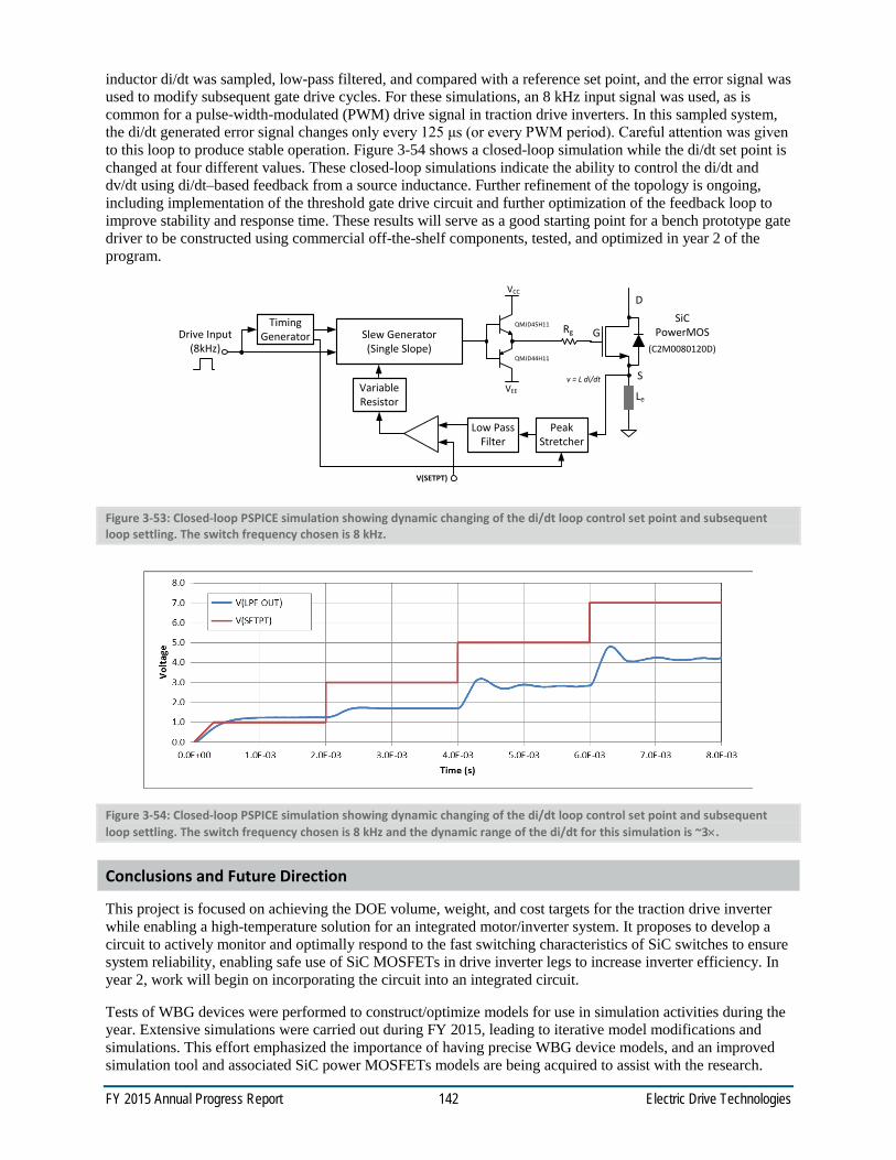
FY 2015 Annual Progress Report 142 Electric Drive Technologies
inductor di/dt was sampled, low-pass filtered, and compared with a reference set point, and the error signal was used to modify subsequent gate drive cycles. For these simulations, an 8 kHz input signal was used, as is common for a pulse-width-modulated (PWM) drive signal in traction drive inverters. In this sampled system, the di/dt generated error signal changes only every 125 μs (or every PWM period). Careful attention was given to this loop to produce stable operation. Figure 3-54 shows a closed-loop simulation while the di/dt set point is changed at four different values. These closed-loop simulations indicate the ability to control the di/dt and dv/dt using di/dt–based feedback from a source inductance. Further refinement of the topology is ongoing, including implementation of the threshold gate drive circuit and further optimization of the feedback loop to improve stability and response time. These results will serve as a good starting point for a bench prototype gate driver to be constructed using commercial off-the-shelf components, tested, and optimized in year 2 of the program.
Figure 3-53: Closed-loop PSPICE simulation showing dynamic changing of the di/dt loop control set point and subsequent loop settling. The switch frequency chosen is 8 kHz.
Figure 3-54: Closed-loop PSPICE simulation showing dynamic changing of the di/dt loop control set point and subsequent loop settling. The switch frequency chosen is 8 kHz and the dynamic range of the di/dt for this simulation is ~3×.
Conclusions and Future Direction
This project is focused on achieving the DOE volume, weight, and cost targets for the traction drive inverter while enabling a high-temperature solution for an integrated motor/inverter system. It proposes to develop a circuit to actively monitor and optimally respond to the fast switching characteristics of SiC switches to ensure system reliability, enabling safe use of SiC MOSFETs in drive inverter legs to increase inverter efficiency. In year 2, work will begin on incorporating the circuit into an integrated circuit.
Tests of WBG devices were performed to construct/optimize models for use in simulation activities during the year. Extensive simulations were carried out during FY 2015, leading to iterative model modifications and simulations. This effort emphasized the importance of having precise WBG device models, and an improved simulation tool and associated SiC power MOSFETs models are being acquired to assist with the research.
SiCPowerMOS Drive Input
(8kHz)
TimingGenerator
VCC
VEE
Slew Generator(Single Slope)
Rg
Le
v = L di/dt
D
S
G
Peak Stretcher
Low Pass Filter
V(SETPT)
QMJD45H11
QMJD44H11(C2M0080120D)
Variable Resistor

FY 2015 Annual Progress Report 143 Electric Drive Technologies
The past year's work has culminated in the development of an improved architecture for actively controlling the gate drive of an inverter SiC power switch. Multiple waveform types were evaluated by simulation, and an improved waveform was developed that is actively modulated using a di/dt sensing inductor. To handle the extremely fast switching behavior of WBG devices, a slower control loop is used, rather than high bandwidth. Single pulse modulation is commonly used in silicon-based gate drive applications. This topology and associated implementation were developed with the intention of incorporating it into an integrated circuit for minimizing size, weight, cost and volume.
Further simulation activities will be performed during FY 2016 to more accurately optimize the gate drive architecture, including the drive waveform specifics and compensation of the control loop. Simulation efforts will transition to the newly acquired CoolSPICE for closed-loop, system-level simulations with optimized SiC powerMOS device models (provided by CoolCAD Inc.). A board-level prototype of the active gate driver will be constructed and bench tested with an inductive load. This prototype will enable further testing and optimization of the circuit, including the drive waveform, feedback parameters, and associated sensing, before the device is transitioned to an integrated circuit.
With the maturation of WBG devices and their penetration into the automotive sector, it is expected that a more system-level approach to their implementation will be needed in the years to come. Optimization of the gate drive and its packaging will be paramount in these efforts. This research will position the ORNL team to initiate SOI integrated circuit implementation of the AGD an enabling technology for realizing reliable and highly compact WBG-based traction drive systems.
FY 2015 Presentations/Publications/Patents
1. N. Ericson, C. Britton, L. Marlino, S. Frank, D. Ezell, L. Tolbert, and J. Wang, “Gate Driver Optimization for WBG Applications,” DOE VTO Electric Drive Technologies FY 2015 Kickoff Meeting, Knoxville, Tennessee, November 18, 2014.
2. N. Ericson, C. Britton, L. Marlino, S. Frank, D. Ezell, L. Tolbert, J. Wang, and B. Blalock, “Gate Driver Optimization for WBG Applications,” USCAR EE Tech Team Project Update Meeting, Southfield, Michigan, March 26, 2015.
3. N. Ericson, C. Britton, L. Marlino, S. Frank, D. Ezell, L. Tolbert, and J. Wang, “Gate Driver Optimization for WBG Applications,” DOE Annual Merit Review, Washington, DC, June 10, 2015.
References
1. Y. Lobsiger and J. W. Kolar, “Closed-loop IGBT gate drive featuring highly dynamic di/dt and dv/dt control,” in IEEE Energy Conversion Congress and Exposition, 4754–4761, September 2012.
2. Y. Lobsiger and J. W. Kolar, “Closed-loop di/dt and dv/dt IGBT gate driver,” IEEE Transactions on Power Electronics 30(6), 3402–3417, June 2015.
3. Z. Wang, X. Shi, L. M. Tolbert, B. J. Blalock, “Switching performance improvement of IGBT modules using an active gate driver,” in IEEE Applied Power Electronics Convergence, 266–1273, March 2013.
4. S. Park and T. M. Jahns, “Flexible dv/dt and di/dt control method for insulated gate power switches,” IEEE Transactions on Industry Applications 39(3), 657–664, May/June 2003.
5. C. Gerster and P. Hofer, “Gate-controlled dv/dt and di/dt limitation in high power IGBT converters,” EPE Journal 5(3/4), 11–16, January 1996.
6. H. Riazmontazer, A. Rahnamaee, A. Mojab, S. Mehrnami, S. K. Mazumber, M. Zefran, “Closed-loop control of switching transition of SiC MOSFETs,” in IEEE Applied Power Electronics Conference, 782–788, March 2015.
7. L. Chen, F. Z. Peng, “Closed-loop gate drive for high power IGBTs,” in IEEE Applied Power Electronics Conference, 1331–1337, February 2009.
FY 2015 Annual Progress Report 144 Electric Drive Technologies
3.5. Power Electronics Thermal Management R&D Gilbert Moreno, Principal Investigator National Renewable Energy Laboratory (NREL) Transportation and Hydrogen Systems Center 15013 Denver West Parkway Golden, CO 80401 Phone: (303) 275-4450 E-mail: [email protected] Susan A. Rogers, DOE Technology Development Manager U.S. Department of Energy 1000 Independence Avenue SW, EE-3V Washington, DC 20585 Phone: (202) 586-8997 E-mail: [email protected] Sreekant Narumanchi, NREL Task Leader Phone: (303) 275-4062 Email: [email protected]
Abstract The objective for this project is to develop thermal management strategies to enable efficient and high-temperature wide-bandgap (WBG)-based power electronic systems (e.g., emerging inverter and DC-DC converter). Device- and system-level thermal analyses are conducted to determine the thermal limitations of current automotive power modules under elevated device temperature conditions. Additionally, novel cooling concepts and material selection will be evaluated to enable high-temperature silicon and WBG devices in power electronics components. WBG devices (silicon carbide [SiC], gallium nitride [GaN]) promise to increase efficiency, but will be driven as hard as possible. This creates challenges for thermal management and reliability.
Accomplishments We conducted steady-state and transient analyses to compare the thermal performance of the 2012
Nissan LEAF power module to the performance of a more conventional power module design (power module that incorporates a metalized-ceramic substrate).
We evaluated the effect of increasing the junction temperatures (up to 250°C) on an automotive power module (2012 Nissan LEAF) to simulate WBG conditions. Results indicated the need for high-temperature attach materials (e.g., sintered silver) for WBG-based power modules.
We determined that a direct-cooled direct-bond copper (DBC) configuration is superior to a direct-cooled baseplate configuration when the convective thermal resistance values are lower than 20 mm^2-K/W.
We used a particle image velocimetry (PIV) system to measure flow fields of an impinging liquid jet in an attempt to understand heat transfer enhancement mechanisms and improve power electronics thermal management. The high-heat transfer rates of jet impingement cooling provide a way to achieve convective resistance values lower than 20 mm^2-K/W.
Introduction
This project will analyze and develop thermal management strategies for WBG-based power electronics systems. Research will be conducted to evaluate thermal management strategies at the device and system
FY 2015 Annual Progress Report 145 Electric Drive Technologies
levels. Device-level research will focus on die and substrate-integrated cooling strategies and heat transfer enhancement technologies. System-level research will focus on thermal management strategies for the entire power electronics system to enable smart packaging solutions. One challenge with WBG device power electronics is that although losses in the form of heat are lower, the area of the devices is also reduced to increase power density and reduce costs associated with the use of WBG materials. This creates higher heat fluxes that must be removed from a smaller footprint, and combined with higher operational temperatures requires advanced thermal management strategies. Several strategies may be implemented to improve thermal management:
Concepts related to die/substrate-integrated thermal management
Flow enhancements and enhanced surfaces
Advanced manufacturing techniques
Multiple mode cooling concepts
Power electronics system-level thermal analysis for effective packaging.
Most of the current and past research efforts have been focused on power module-level cooling strategies. In this project, a system-level approach will be used to evaluate the thermal interactions between the various system components (i.e., power modules, capacitor, control boards) and their ambient under-hood environment. The trend towards high-temperature WBG devices emphasizes the need for system-level thermal management analysis. Although WBG devices can operate at higher temperatures (>200°C), other components (e.g., capacitors, attach layers, interconnects) may not tolerate the higher temperatures, and thus system-level analysis and innovative cooling strategies are required to allow for reliable system operation.
Approach
Work conducted in this project can be grouped into two categories—application thermal research, and thermal and fluid measurement systems. Research conducted in the application thermal research category aims to understand the effects of high-temperature WBG-based devices on the power electronics components and develop thermal management strategies to enable WBG-based inverters. There are currently no automotive power electronics systems that use WBG devices. Therefore, an automotive silicon-based power electronics system will be modeled and used as the framework for the WBG analyses. The analyses will begin at the power module level and then expanded to include all of the inverter components.
Research conducted in the thermal and fluid measurements systems works to develop thermal measurement techniques to understand heat transfer mechanisms and to develop novel packaging materials. The following provides more details on the project approach.
Application thermal research Create and validate thermal computational fluid dynamics (CFD) and finite element analysis (FEA)
models of an automotive power electronics system.
Use the models to evaluate the effects of incorporating high-temperature WBG devices on other system components (e.g., power module attach layers, capacitors, electrical boards, interconnects). Identify thermal bottlenecks within the system and map out system temperatures.
Generate thermal management concepts to enable the use of WBG-based inverters.
Thermal and fluid measurement systems Measure fluid flow fields using PIV to understand heat transfer and improve heat exchanger designs.
Quantify the performance of novel high thermal performance materials using the phase-sensitive transient thermoreflectance (PSTTR) system.
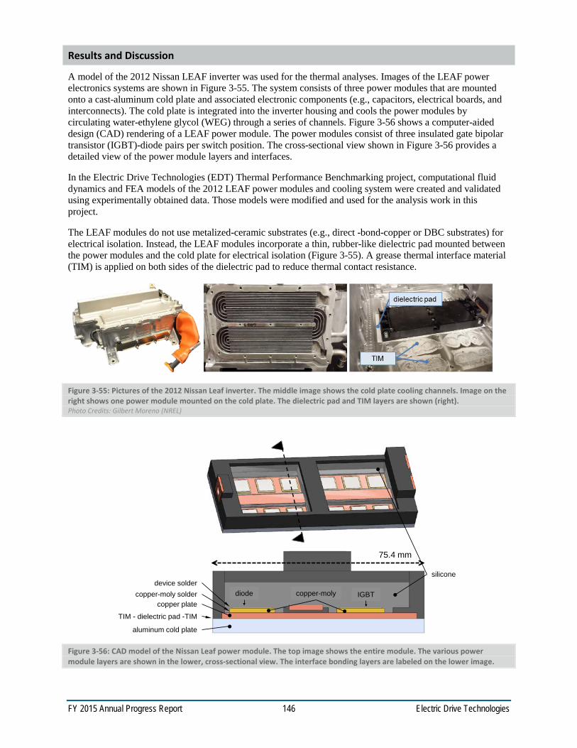
FY 2015 Annual Progress Report 146 Electric Drive Technologies
Results and Discussion
A model of the 2012 Nissan LEAF inverter was used for the thermal analyses. Images of the LEAF power electronics systems are shown in Figure 3-55. The system consists of three power modules that are mounted onto a cast-aluminum cold plate and associated electronic components (e.g., capacitors, electrical boards, and interconnects). The cold plate is integrated into the inverter housing and cools the power modules by circulating water-ethylene glycol (WEG) through a series of channels. Figure 3-56 shows a computer-aided design (CAD) rendering of a LEAF power module. The power modules consist of three insulated gate bipolar transistor (IGBT)-diode pairs per switch position. The cross-sectional view shown in Figure 3-56 provides a detailed view of the power module layers and interfaces.
In the Electric Drive Technologies (EDT) Thermal Performance Benchmarking project, computational fluid dynamics and FEA models of the 2012 LEAF power modules and cooling system were created and validated using experimentally obtained data. Those models were modified and used for the analysis work in this project.
The LEAF modules do not use metalized-ceramic substrates (e.g., direct -bond-copper or DBC substrates) for electrical isolation. Instead, the LEAF modules incorporate a thin, rubber-like dielectric pad mounted between the power modules and the cold plate for electrical isolation (Figure 3-55). A grease thermal interface material (TIM) is applied on both sides of the dielectric pad to reduce thermal contact resistance.
Figure 3-55: Pictures of the 2012 Nissan Leaf inverter. The middle image shows the cold plate cooling channels. Image on the right shows one power module mounted on the cold plate. The dielectric pad and TIM layers are shown (right). Photo Credits: Gilbert Moreno (NREL)
Figure 3-56: CAD model of the Nissan Leaf power module. The top image shows the entire module. The various power module layers are shown in the lower, cross-sectional view. The interface bonding layers are labeled on the lower image.
IGBTdiode copper-molycopper plate
TIM - dielectric pad -TIM
aluminum cold plate
device soldercopper-moly solder
75.4 mm
silicone
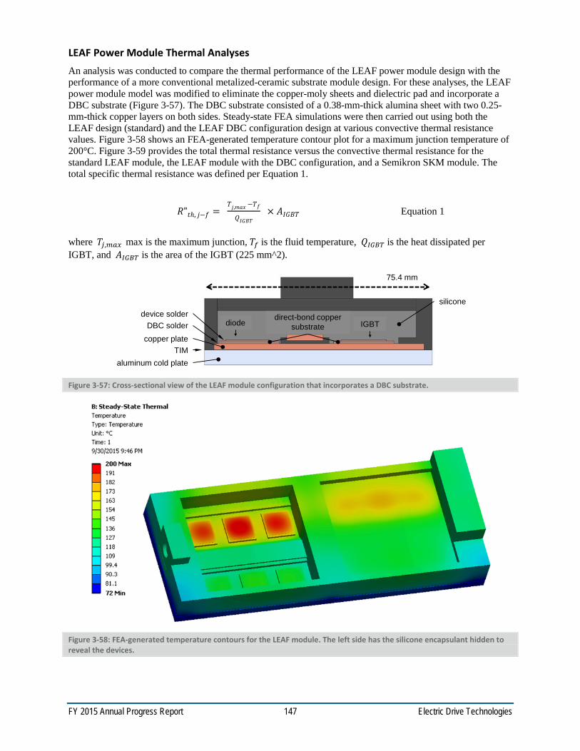
FY 2015 Annual Progress Report 147 Electric Drive Technologies
LEAF Power Module Thermal Analyses An analysis was conducted to compare the thermal performance of the LEAF power module design with the performance of a more conventional metalized-ceramic substrate module design. For these analyses, the LEAF power module model was modified to eliminate the copper-moly sheets and dielectric pad and incorporate a DBC substrate (Figure 3-57). The DBC substrate consisted of a 0.38-mm-thick alumina sheet with two 0.25-mm-thick copper layers on both sides. Steady-state FEA simulations were then carried out using both the LEAF design (standard) and the LEAF DBC configuration design at various convective thermal resistance values. Figure 3-58 shows an FEA-generated temperature contour plot for a maximum junction temperature of 200°C. Figure 3-59 provides the total thermal resistance versus the convective thermal resistance for the standard LEAF module, the LEAF module with the DBC configuration, and a Semikron SKM module. The total specific thermal resistance was defined per Equation 1.
where 𝑇𝑇𝑗𝑗,𝑝𝑝𝑏𝑏𝑚𝑚 max is the maximum junction, 𝑇𝑇𝑟𝑟 is the fluid temperature, 𝑄𝑄𝐼𝐼𝐼𝐼𝐼𝐼𝐼𝐼 is the heat dissipated per IGBT, and 𝐴𝐴𝐼𝐼𝐼𝐼𝐼𝐼𝐼𝐼 is the area of the IGBT (225 mm^2).
Figure 3-57: Cross-sectional view of the LEAF module configuration that incorporates a DBC substrate.
Figure 3-58: FEA-generated temperature contours for the LEAF module. The left side has the silicone encapsulant hidden to reveal the devices.
IGBTdiodedirect-bond copper
substratecopper plate
TIMaluminum cold plate
device solderDBC solder
75.4 mm
silicone
𝑅𝑅"𝑡𝑡ℎ, 𝑗𝑗−𝑓𝑓 = 𝑇𝑇𝑗𝑗,𝑚𝑚𝑚𝑚𝑚𝑚 −𝑇𝑇𝑓𝑓
𝑄𝑄𝐼𝐼𝐼𝐼𝐼𝐼𝑇𝑇 × 𝐴𝐴𝐼𝐼𝐼𝐼𝐼𝐼𝑇𝑇 Equation 1
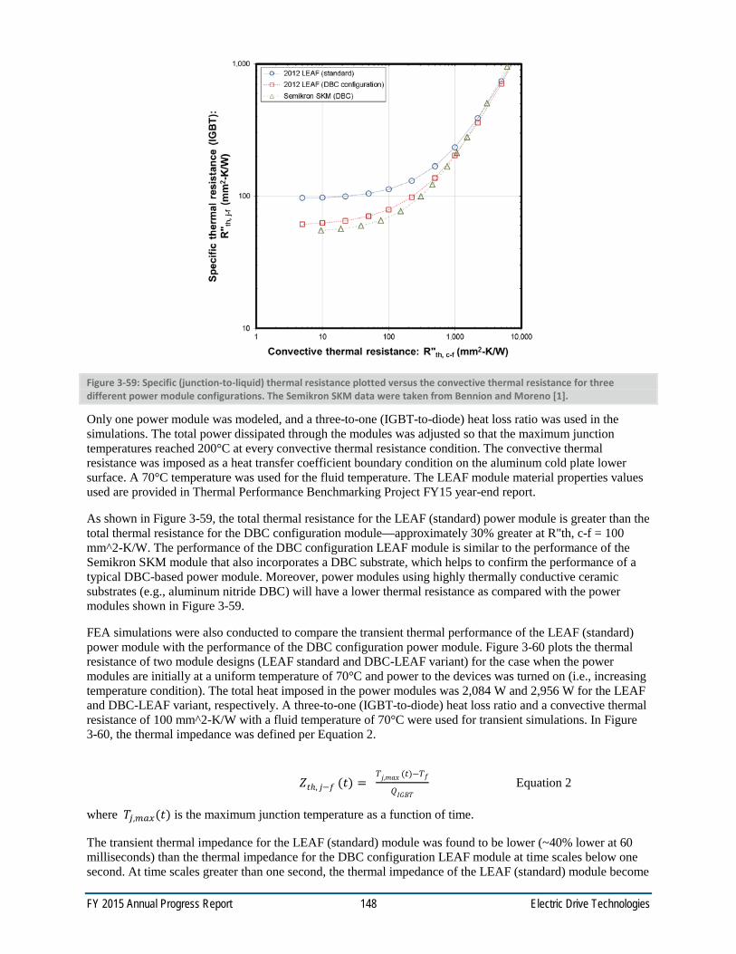
FY 2015 Annual Progress Report 148 Electric Drive Technologies
Figure 3-59: Specific (junction-to-liquid) thermal resistance plotted versus the convective thermal resistance for three different power module configurations. The Semikron SKM data were taken from Bennion and Moreno [1].
Only one power module was modeled, and a three-to-one (IGBT-to-diode) heat loss ratio was used in the simulations. The total power dissipated through the modules was adjusted so that the maximum junction temperatures reached 200°C at every convective thermal resistance condition. The convective thermal resistance was imposed as a heat transfer coefficient boundary condition on the aluminum cold plate lower surface. A 70°C temperature was used for the fluid temperature. The LEAF module material properties values used are provided in Thermal Performance Benchmarking Project FY15 year-end report.
As shown in Figure 3-59, the total thermal resistance for the LEAF (standard) power module is greater than the total thermal resistance for the DBC configuration module—approximately 30% greater at R"th, c-f = 100 mm^2-K/W. The performance of the DBC configuration LEAF module is similar to the performance of the Semikron SKM module that also incorporates a DBC substrate, which helps to confirm the performance of a typical DBC-based power module. Moreover, power modules using highly thermally conductive ceramic substrates (e.g., aluminum nitride DBC) will have a lower thermal resistance as compared with the power modules shown in Figure 3-59.
FEA simulations were also conducted to compare the transient thermal performance of the LEAF (standard) power module with the performance of the DBC configuration power module. Figure 3-60 plots the thermal resistance of two module designs (LEAF standard and DBC-LEAF variant) for the case when the power modules are initially at a uniform temperature of 70°C and power to the devices was turned on (i.e., increasing temperature condition). The total heat imposed in the power modules was 2,084 W and 2,956 W for the LEAF and DBC-LEAF variant, respectively. A three-to-one (IGBT-to-diode) heat loss ratio and a convective thermal resistance of 100 mm^2-K/W with a fluid temperature of 70°C were used for transient simulations. In Figure 3-60, the thermal impedance was defined per Equation 2.
where 𝑇𝑇𝑗𝑗,𝑝𝑝𝑏𝑏𝑚𝑚(𝑡𝑡) is the maximum junction temperature as a function of time.
The transient thermal impedance for the LEAF (standard) module was found to be lower (~40% lower at 60 milliseconds) than the thermal impedance for the DBC configuration LEAF module at time scales below one second. At time scales greater than one second, the thermal impedance of the LEAF (standard) module become
𝑍𝑍𝑡𝑡ℎ, 𝑗𝑗−𝑓𝑓 (𝑡𝑡) = 𝑇𝑇𝑗𝑗,𝑚𝑚𝑚𝑚𝑚𝑚 (𝑡𝑡)−𝑇𝑇𝑓𝑓
𝑄𝑄𝐼𝐼𝐼𝐼𝐼𝐼𝑇𝑇 Equation 2
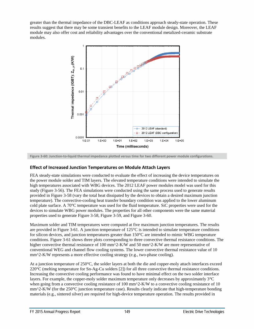
FY 2015 Annual Progress Report 149 Electric Drive Technologies
greater than the thermal impedance of the DBC-LEAF as conditions approach steady-state operation. These results suggest that there may be some transient benefits to the LEAF module design. Moreover, the LEAF module may also offer cost and reliability advantages over the conventional metalized-ceramic substrate modules.
Figure 3-60: Junction-to-liquid thermal impedance plotted versus time for two different power module configurations.
Effect of Increased Junction Temperatures on Module Attach Layers FEA steady-state simulations were conducted to evaluate the effect of increasing the device temperatures on the power module solder and TIM layers. The elevated temperature conditions were intended to simulate the high temperatures associated with WBG devices. The 2012 LEAF power modules model was used for this study (Figure 3-56). The FEA simulations were conducted using the same process used to generate results provided in Figure 3-58 (vary the total heat dissipated by the devices to obtain a desired maximum junction temperature). The convective-cooling heat transfer boundary condition was applied to the lower aluminum cold plate surface. A 70°C temperature was used for the fluid temperature. SiC properties were used for the devices to simulate WBG power modules. The properties for all other components were the same material properties used to generate Figure 3-58, Figure 3-59, and Figure 3-60.
Maximum solder and TIM temperatures were computed at five maximum junction temperatures. The results are provided in Figure 3-61. A junction temperature of 125°C is intended to simulate temperature conditions for silicon devices, and junction temperatures greater than 150°C are intended to mimic WBG temperature conditions. Figure 3-61 shows three plots corresponding to three convective thermal resistance conditions. The higher convective thermal resistance of 100 mm^2-K/W and 50 mm^2-K/W are more representative of conventional WEG and channel flow cooling systems. The lower convective thermal resistance value of 10 mm^2-K/W represents a more effective cooling strategy (e.g., two-phase cooling).
At a junction temperature of 250°C, the solder layers at both the die and copper-moly attach interfaces exceed 220°C (melting temperature for Sn-Ag-Cu solders [2]) for all three convective thermal resistance conditions. Increasing the convective cooling performance was found to have minimal effect on the two solder interface layers. For example, the copper-moly solder maximum temperature only decreases by approximately 3°C when going from a convective cooling resistance of 100 mm^2-K/W to a convective cooling resistance of 10 mm^2-K/W (for the 250°C junction temperature case). Results clearly indicate that high-temperature bonding materials (e.g., sintered silver) are required for high-device temperature operation. The results provided in

FY 2015 Annual Progress Report 150 Electric Drive Technologies
Figure 3-61 may be a useful resource for power module manufacturers that are designing WBG-based power electronic systems.
Figure 3-61: The maximum temperatures for the device solder, copper-moly solder, and TIM layers at five different junction temperatures. Temperatures are provided for three different convective cooling thermal resistance values– 100 mm^2-K/W (left), 50 mm^2-K/W (middle), and 10 mm^2-K/W (right).
Work in FY15 was limited to power module thermal analyses. In FY16, we will expand our analyses to incorporate the entire LEAF inverter.
Evaluation of Direct-Cooled DBC and Direct-Cooled Baseplate Configurations An objective of this project is to evaluate and develop new thermal management strategies that are applicable to traditional and WBG-based power electronic systems. Therefore, a parametric study was conducted to evaluate direct-cooled DBC and direct-cooled baseplate configurations (Figure 3-62). The direct-cooled DBC configuration provides cooling directly on the back side of the DBC substrate. The direct-cooled baseplate configuration provides cooling on the back side of the baseplate. The concept is to minimize the thermal resistance of the passive stack layers to reduce the total thermal resistance. However, the strategy of removing packaging layers limits the module's heat spreading ability; therefore, this strategy is best utilized when combined with low convective thermal resistance configurations. In this section, we evaluate various module designs to determine under what convective cooling conditions it makes sense to employ a direct-cooled DBC configuration.
Figure 3-62: CAD renderings showing the geometry of the direct-cooled DBC (left) and direct-cooled baseplate (right) configurations. FEA was conducted to evaluate the effect of varying the a and b dimensions on the total thermal resistance.
Steady-state FEA simulations were conducted to evaluate the effect of varying the DBC and baseplate dimensions on the total thermal resistance. Figure 3-62 shows the two CAD models used for the FEA. The
249.1
199.4
174.5
149.6
124.8
231.7
186.8
164.3
141.9
119.4
195.4
160.6
143.2
125.8
108.4
100
120
140
160
180
200
220
240
260
250 200 175 150 125
Tem
pera
ture
(°C
)
Maximum junction temperature (°C)
Device solder
Copper-Moly solder
TIM
249.0
199.3
174.4
149.6
124.7
230.2
185.7
163.4
141.2
119.0
190.6
157.1
140.4
123.6
106.9
100
120
140
160
180
200
220
240
260
250 200 175 150 125
Tem
pera
ture
(°C
)Maximum junction temperature (°C)
Device solder
Copper-Moly solder
TIM
248.7
199.3
174.4
149.5
124.7
228.5
184.7
162.5
140.5
118.5
185.5
153.6
137.5
121.4
105.3
100
120
140
160
180
200
220
240
260
250 200 175 150 125
Tem
pera
ture
(°C
)
Maximum junction temperature (°C)
Device solderCopper-Moly solderTIM
a: Die-to-DBC edge offsetb: DBC-to-baseplate edge offset
a
b
Die area: 5 mm × 5 mm
DBC
Baseplate
a
Direct-cooled DBC Direct-cooled baseplate
Heat transfer coefficient applied to back side
Heat transfer coefficient applied to back side
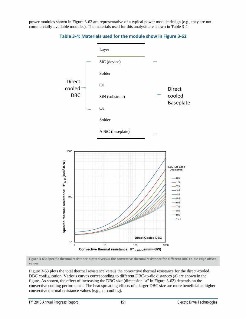
FY 2015 Annual Progress Report 151 Electric Drive Technologies
power modules shown in Figure 3-62 are representative of a typical power module design (e.g., they are not commercially-available modules). The materials used for this analysis are shown in Table 3-4.
Table 3-4: Materials used for the module show in Figure 3-62
Layer
SiC (device)
Solder
Cu
SiN (substrate)
Cu
Solder
AlSiC (baseplate)
Figure 3-63: Specific thermal resistance plotted versus the convective thermal resistance for different DBC-to-die edge offset values.
Figure 3-63 plots the total thermal resistance versus the convective thermal resistance for the direct-cooled DBC configuration. Various curves corresponding to different DBC-to-die distances (a) are shown in the figure. As shown, the effect of increasing the DBC size (dimension "a" in Figure 3-62) depends on the convective cooling performance. The heat spreading effects of a larger DBC size are more beneficial at higher convective thermal resistance values (e.g., air cooling).
Direct cooled
DBC Direct cooled Baseplate
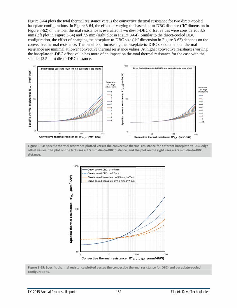
FY 2015 Annual Progress Report 152 Electric Drive Technologies
Figure 3-64 plots the total thermal resistance versus the convective thermal resistance for two direct-cooled baseplate configurations. In Figure 3-64, the effect of varying the baseplate-to-DBC distance ("b" dimension in Figure 3-62) on the total thermal resistance is evaluated. Two die-to-DBC offset values were considered: 3.5 mm (left plot in Figure 3-64) and 7.5 mm (right plot in Figure 3-64). Similar to the direct-cooled DBC configuration, the effect of changing the baseplate-to-DBC size ("b" dimension in Figure 3-62) depends on the convective thermal resistance. The benefits of increasing the baseplate-to-DBC size on the total thermal resistance are minimal at lower convective thermal resistance values. At higher convective resistances varying the baseplate-to-DBC offset value has more of an impact on the total thermal resistance for the case with the smaller (3.5 mm) die-to-DBC distance.
Figure 3-64: Specific thermal resistance plotted versus the convective thermal resistance for different baseplate-to-DBC edge offset values. The plot on the left uses a 3.5 mm die-to-DBC distance, and the plot on the right uses a 7.5 mm die-to-DBC distance.
Figure 3-65: Specific thermal resistance plotted versus the convective thermal resistance for DBC- and baseplate-cooled configurations.

FY 2015 Annual Progress Report 153 Electric Drive Technologies
Figure 3-65 plots the direct-cooled DBC and direct-cooled baseplate curves on the same graph. The figure indicates that direct cooling the DBC is superior to direct cooling the baseplate at convective thermal resistance values less than 20 mm^2-K/W. Achieving a convective thermal resistance value less than 20 mm^2-K/W (equivalent to an overall heat transfer coefficient value greater than 50,000 W/m^2-K) would likely require the use of micro-channels and/or impinging jets in a single-phase liquid cooling configuration or the use of two-phase heat transfer. In this analysis the layer dimensions were not constrained based on package space limitations. Applications constrained by space or requiring the dies to be packaged closely would benefit more from low convective thermal resistance cooling techniques as compared to applications where devices are spaced farther apart.
Measurement of Jet Impingement Flow Fields using PIV Prior work at NREL has demonstrated that enhanced surfaces (e.g., roughened, microporous, micro-finned) can significantly increase jet impingement heat transfer [3]. In that study, the heat transfer increases were measured, but the mechanisms responsible for the enhancements were not fully understood. In this project, we used a PIV system to measure fluid flow fields and thus understand the underlying mechanisms responsible for the jet impingement heat transfer improvements associated with enhanced surfaces.
Figure 3-66 shows a picture and schematics of the PIV system. The PIV system was used to measure the flow fields of an impinging liquid (water) jet. Initial tests were conducted using a submerged-jet configuration. Future tests will be conducted using a free-jet configuration. The PIV system consists of a laser, camera, computer, and associated electronics. To visualize the fluid flow, the fluid must first be seeded with micrometer-sized particles that follow the motion of the fluid. A laser is used to illuminate the particles, allowing the camera to track the particles' motion. A 100-cm-long pipe with a 6-mm-inner diameter metal tube was used as the nozzle for these tests. The length of the tube combined with average water flow rate (~2 m/s) created a fully developed turbulent jet at the tube/nozzle exit. The nozzle-to-target surface distance was maintained at 6 mm for all tests.
Figure 3-67 shows PIV-generated velocity contour plots for a submerged-jet impinging on a roughened surface. The velocity magnitude, fluctuating component of the radial velocity, and the fluctuating component of the axial velocity were computed by averaging 1,000 data sets. The fluctuating velocity components (i.e., RMS velocity) are used to quantify the amount of turbulence within a flow. PIV data have been collected for smooth and roughened surfaces. Work is currently underway to evaluate the data to determine the effect of the surface roughness on the flow within the wall-jet region. It has been hypothesized that the surface roughness features advance the laminar-to-turbulent flow transition within the wall-jet region and that this is the reason for the heat transfer enhancements. This study aims to experimentally evaluate this theory using PIV.
Figure 3-66: PIV system schematics showing the piping layout (left) and the laser and camera setup (right).
bypass
T
Flow meter
Pump
Adjustable height stand
6-mm-diameter-inner pipe nozzle
Impingement surface
Test vessel
Resevior
Laser
Camera
Test vessel
Laser sheet

FY 2015 Annual Progress Report 154 Electric Drive Technologies
Figure 3-67: PIV-generated velocity contour plots for a submerged jet impinging on a roughened surface. The velocity magnitude (left), fluctuating component of the radial velocity (middle), and the fluctuating component of the axial velocity (right) are shown.

FY 2015 Annual Progress Report 155 Electric Drive Technologies
Conclusions and Future Directions
Conclusions FEA simulations were conducted to compare the thermal performance of the 2012 Nissan LEAF
power module to the performance of a more conventional power module design (power module that incorporates a metalized-ceramic substrate). Results indicate that the LEAF power module has a higher steady-state total thermal resistance (approximately 30% greater at R"th, c-f = 100 mm^2-K/W) as compared with a conventional power module design. However, the transient analysis indicates that the LEAF power module may offer advantages under certain transient conditions.
The effect of elevating the device temperatures on the power module attach layers was evaluated. FEA simulations were conducted using maximum junction temperatures of 125°C, 150°C, 175°C, 200°C, and 250°C. The higher junction temperatures were intended to simulate WBG devices. Temperatures for the component attach (e.g., solder and TIM) layers were computed. Results clearly indicate that high-temperature bonding materials (e.g., sintered silver) are required for high-temperature device operation.
Direct-cooled DBC configurations were evaluated and compared with direct-cooled baseplate configurations. Analyses showed that direct-cooled DBC configurations are superior to direct-cooled baseplate configurations when the convective thermal resistance values are less than 20 mm^2-K/W. To achieve convective thermal resistance values less than 20 mm^2-K/W would likely require micro-channel, jet impingement, or two-phase heat transfer cooling strategies.
PIV was used to measure flow fields for impinging liquid jets. Results from this work will help to understand how enhanced surfaces increase jet impingement heat transfer. This information can then be used to develop more effective power electronic heat exchangers.
Future Work System-level thermal analysis will be conducted to evaluate the effect of increased device
temperatures on the inverter components (e.g., capacitors, interconnects, electrical boards). System hot spots and thermal bottlenecks will be identified. Thermal management solutions to enable WBG-based inverters will be proposed.
PIV research efforts to understand heat transfer enhancement mechanisms in submerged- and free-jets will continue into FY16.
NREL's PSTTR system will be used to quantify the performance of novel, high thermal performance materials.
Nomenclature
A area DBC direct-bond copper k thermal conductivity Q heat Rth thermal resistance R"th specific thermal resistance T temperature Z impedance
Subscripts
b baseplate c cold plate f fluid
FY 2015 Annual Progress Report 156 Electric Drive Technologies
j junction
FY 2015 Presentations /Publications/Patents
1. Waye, S. “Power Electronics Thermal Management R&D.” Advanced Power Electronics and Electric Motors FY15 Kickoff Meeting, DOE Vehicle Technologies Office (VTO), Oak Ridge, TN, November 2014.
2. Bennion, K. “Power Electronics Thermal Management R&D.” 2015 DOE VTO Annual Merit Review, Crystal City, VA, June 2015.
3. Bennion, K. “Power Electronics Thermal Management R&D.” 2015 presentation to the DOE VTO Electrical and Electronics Technical Team, Southfield, MI, May 2015.
Acknowledgments
The author would like to acknowledge the support provided by Susan Rogers and Steven Boyd, Technology Development Managers for the EDT Program, Vehicle Technologies Office, U.S. Department of Energy Office of Energy Efficiency and Renewable Energy. The significant contributions of Kevin Bennion, Emily Cousineau, Charles King, and Xuhui Feng are acknowledged.
References
1. Bennion, K.; Moreno, G. 2010. “Thermal Management of Power Semiconductor Packages — Matching Cooling Technologies with Packaging Technologies.” Presented at 2nd Advanced Technology Workshop on Automotive Microelectronics and Packaging, Dearborn, MI. 26 pp. NREL/PR-540-48147.
2. Kester, 2010 "Alloy Temperature Chart" downloaded from www.kester.com/kester-content/.../Alloy-Temperature-Chart-15Feb11.pdf
3. Moreno, G.; Narumanchi, S.; Venson, T.; Bennion, K. 2013. "Microstructured Surfaces for Single-Phase Jet Impingement Heat Transfer Enhancements." ASME Journal of Thermal Sciences and Engineering Applications, 5(3), 031004, 9 pp. Paper No. TSEA-12-1033; doi: 10.1115/1.4023308.
FY 2015 Annual Progress Report 157 Electric Drive Technologies
3.6. High Temperature DC Bus Capacitor Cost Reduction & Performance Improvements
Angelo Yializis, Principle Investigator Sigma Technologies International Group 10960 N Stallard Place Tucson, AZ 85737 Phone: (520) 575 8013; Fax: (520) 575 8013 E-mail: [email protected] DOE Project Officer: Rondle Harp Phone: (304) 285 5436 E-mail: [email protected] Sigma Technologies Program Manager: Christopher Hohmann Phone: (520) 575 8013 Email: [email protected] Subcontractor: Delphi Automotive Systems, LLC Subcontractor: Oak Ridge National Laboratory Contract No.: DE-EE0006438
Objectives Reduce the cost, size and weight of the direct current (DC)-link capacitor by >50% and increase durability in high temperature environments.
Technical Barriers The performance and lifetime of capacitors available today degrade rapidly with increasing temperature (ripple current capability decreases with temperature increase from 85˚C to 105˚C). Therefore, today’s capacitors are typically twice the size (up to 40% of the inverter’s volume) and too costly (up to 30% of the inverter’s cost).
Technical Targets For Phase 1 the GEN 1 targets will be
o A polymer multi-layer (PML) capacitor that will have a rating of 800 μF / 400 Vdc / 650V transient
o Designed for a 30 kW continuous, 55 kW peak (30 seconds) inverter o Operating temperature: -40°C to +140°C o Projected volume: < 0.2L o Dissipation factor: < 0.01 up to 160°C o Ripple current: 130Arms continuous o Energy density: > 3X today’s polypropylene (PP) capacitors, or > 1 J/cc o Cost: < $30 (with direct cost < $15) o Benign failure mechanism
Accomplishments Sigma and their partners Delphi Automotive and Oak Ridge National Laboratory have completed all Phase 1 work including, dielectric selection, prototype line equipment, preliminary packaging work and preliminary cost and commercialization plan. Capacitors have been produced which meet or exceed the Technical Targets outlined above.

FY 2015 Annual Progress Report 158 Electric Drive Technologies
Introduction
The proposed project focuses on process development and scale-up to produce application-specific direct current (DC)-link capacitors for automotive inverter applications. In Phase I of the program (2013 – 2015), the development work addresses optimization of the polymer dielectric formulation and thickness, to produce GEN 1 capacitors with a rating of 800 μF / 400 Vdc / 650 Vtransient. GEN 1 will demonstrate operation at -40°C to 140°C, a benign failure mode, direct cost < $15 and 3X reduction in the volume and weight, compared to today’s baseline polypropylene (PP) capacitors. A significant part of the Phase I effort was to scale-up process steps to allow manufacture and assembly of an adequate number of parts for the various test protocols and to meet the Phase I deliverables. In the Phase II effort (2015 – 2016), GEN 2 capacitors will be produced that will further decrease capacitor volume by optimizing the polymer dielectric thickness and increasing the dielectric constant. GEN 2 capacitors will be packaged, integrated into a Delphi inverter, and long-term reliability tests will be performed to confirm the target specifications have been met.
Approach
Sigma has developed a solid-state Polymer-Multi-Layer (PML) capacitor comprising 1000s of radiation cured polymer dielectrics and aluminum (Al) electrodes to form a large area nanolaminate (Mother Capacitor) that is segmented into individual capacitors.
Having a prismatic shape with low equivalent series inductance (ESL) and equivalent series resistance (ESR)
Operating temperature range of -40°C to 140°C
Dissipation Factor (DF) < 0.01
Amorphous high breakdown strength dielectrics
Dielectric constants in the range of 3.0 < k < 6.2
Benign failure mode
Low-cost materials and process
This PML technology is a transformational and potentially disruptive technology in the following ways:
Liquid monomer and Al wire are converted in a single step into Mother Capacitor material
Eliminates film manufacturing and metallizing by outside suppliers
Capacitor manufacturer has opportunity to innovate and create application-specific products with different polymer dielectric properties
Results and Discussion
2015 activities for Phase 1 of the project consisted of completing the following 4 tasks:
Task 1 – Program Management
Task 3 – DC-Link Capacitor Prototype Line
Task 5 – Package PML DC-Link Capacitor
Task 6 – Preliminary Cost and Commercialization Plan
A brief summary of the work performed for each of these tasks follows.

FY 2015 Annual Progress Report 159 Electric Drive Technologies
Task 1 – Program Management Sigma Technologies and Delphi have worked closely together over the first phase of the project. There have been monthly review meetings involving Sigma and Delphi, as well as correspondence via email and phone calls. All quarterly Research Performance Progress Reports and other reporting requirements have been submitted on time to the DOE.
This task was completed at the end of Phase 1 of the project but the Program Management will continue in Phase 2 as Task 7.
Task 3 - DC-Link Capacitor Prototype Line The most significant task for Phase 1 of this project was the completion of the upgrades to the pilot system in place at Sigma Technologies in Arizona. The work as originally proposed has been completed at the end of Phase 1 although work on several new equipment/process upgrades which were deemed necessary for the execution of this project will continue into Phase 2. Key elements of the pilot line upgrade include:
PML Capacitor Mask and Evaporator Nozzle: A new monomer evaporator and deposition nozzle were designed, fabricated and installed.
Monomer Feed Controls: A precision monomer metering system was put into place to control monomer feed and dielectric thickness.
Rough Saw: Upgrade of the sawing system that segments the mother capacitor system into smaller area plates.
Dicing saw: An automated precision dicing saw was put into operation that segments the capacitor plates into smaller capacitor units.
Heat Setting Press: This system allows for the heat to be applied to the capacitor material to remove stress.
Capacitor Termination Equipment: Several pieces of equipment were put into place to connect the 1000s of electrodes in a single PML in parallel and provide a means for attaching an external lead.
Task 5 – Package PML DC-Link Capacitor Delphi Automotive Systems, LLC (Delphi), working with Sigma Technologies International Group, Inc. (Sigma), has provided to Sigma a generic DC-link capacitor specification that includes end-of-life capacitor performance, test conditions and suggested test procedures for documenting the performance of the DC-link capacitor. The specification also provides a subset of the long-term automotive test requirements for verification of the DC-link capacitor performance.
Delphi, working with Sigma and Oak Ridge National Laboratory (ORNL), has provided dielectric material properties and construction details of various possible PML DC-link capacitor configurations. Using the information provided by Delphi, ORNL has constructed thermo-mechanical models of the various capacitor configurations, which will be compared to actual measured data from the DC-link capacitors to verify the models.
Delphi has put in place thermal and thermal cycle chambers, a humidity chamber, impedance analyzers, an IR imaging system, various power supplies and an autoclave for testing of the capacitor samples. Using sample capacitors provided by Sigma, Delphi ran various tests to access the performance of the sample capacitors. Some of the tests included thermal, thermal cycle, high temp bias, humidity, ripple current injection with IR imagery, and capacitor characterizations. The results of the tests were documented and compared to the capacitor specification, and shared with Sigma and ORNL.

FY 2015 Annual Progress Report 160 Electric Drive Technologies
Figure 3-68: Thermal image of a sample capacitor
Several packaging approaches, experiments, have been performed by Delphi to determine the best way to protect the capacitor under various environmental conditions experienced in the automotive environment. To date, each experiment has added insight into the requirements of the packaging material required to survive in the automotive environment.
Task 6 – Preliminary Cost and Commercialization Plan Sigma has completed a 5-year financial model which includes, among other things, an analysis of direct manufacturing costs, fixed manufacturing requirements, capital expenditures, as well as a detailed account of sales, general, and administrative requirements throughout the period. Additionally, the model takes into consideration revenue projections based on input from suppliers of power electronics to the automotive market. Included are quarterly pro-forma financial statements (income statement, balance sheets, and statements of cash flow). Multiple versions of the model have been created to simulate various scenarios based on input received from potential customers and the investment community.
The aforementioned financial model was used to form the basis of a draft business plan, which is in the final stages of completion. The plan, as well as certain sections and summaries of the financial model, have been shared with potential customers and strategic partners. Additionally, Sigma has begun approaching, very selectively, potential capital sources for commercialization.
Finally, Sigma has recruited an executive with more than 28-years’ experience in the power electronics industry with market experience ranging from automotive to renewable power generation and solid-state lighting. This individual is working with Sigma to refine its business plan and to introduce it to potential customers.
Update on Capacitor Development Along with the work on the specific tasks listed above, Sigma has continued to produce and test a large range of capacitors with different capacitance sizes and voltage ratings. A Sigma PML capacitor consists of multiple individual capacitor strips connected in parallel to build to the required capacitance value specified. A comparison of a GEN1 PML capacitor with a conventional metallized PP capacitor is shown in Figure 3-69.

FY 2015 Annual Progress Report 161 Electric Drive Technologies
Figure 3-69: Comparison of state of the art 350μF/400V/600 Vmax DC-link metallized PP capacitor (left), and a GEN1 350μF/450V/720Vmax PML capacitor (unpackaged).
The energy density of the PML capacitors designed for DC-link applications (as shown above) is >3X that of the metallized PP capacitors and is expected to remain >3X after packaging. PML capacitors designed for applications such as pulse power and implantable defibrillators, which are additional target markets, can have much higher energy density by altering the polymer dielectric and metalized electrodes. Defibrillator capacitors are typically aluminum and tantalum electrolytics and have energy densities of about 5.0-6.0 J/cc. Tantalum capacitors have higher energy density than aluminums but also high gravimetric density (much heavier). PML capacitors with 1000 layers, with dielectric thickness of 0.5µm designed for a defibrillator application, were tested for capacitance and dissipation factor stability as a function of applied voltage (see Figure 3-70).
Figure 3-70: Capacitance and dissipation factor variation of PML capacitors with 0.5µm dielectric designed for a pulse application such as that encountered in implantable defibrillator devices
Capacitance loss after 500V is due to the cumulative electrode loss from 100s of self-healing events, demonstrating the ecxellent self-heaing ability of the PML dielectrics. At 500 VDC the 0.5µm dielectric capacitors are stressed at 1000 V/µm, which is higher not only than all all other polymer dielectric capacitors, but even higher than the intrinsic breakdown strength of polymer film dielectrics (which is in the range of 400 V/µm to 700 V/µm). The energy density of these capacitors, including 40% of additional volume to the active capacitor volume to accommodate for termination and packaging, is 9.4 J/cc. This represents a major breakthrough in capacitor technology. Energy density of 9.4J/cc is by far the highest energy density ever recorded for full size polymer capacitors.

FY 2015 Annual Progress Report 162 Electric Drive Technologies
Testing A Phase I effort was completed in automating the Sigma test facility to the extent that 100s of capacitors can be placed at different temperature, voltage and humidity life tests and their performance can be automatically monitored over time.
Conclusions and Future Directions
In conclusion, Sigma and their partners, Delphi Automotive and Oak Ridge National Laboratory, have completed all Phase 1 work including, dielectric selection, prototype line equipment, preliminary packaging work and preliminary cost and commercialization plan. Capacitors have been produced which meet or exceed the DOE requirements of a GEN 1 part.
The work presented here completes Phase I of the program, Phase II will continue with the following identified tasks:
1. Program Management 2. Develop PML GEN 2 Capacitors 3. Package GEN 2 Capacitors 4. Fabricate Packaged PML GEN 2 DC-Link Capacitors 5. Develop a Business Plan for Production
FY 2015 Presentations/Publications/Patents
1. 2015 DOE Annual Merit Review meeting presentation 2. One patent application was filed that claims key design and process elements involved in producing
higher voltage and temperature PML capacitors.

FY 2015 Annual Progress Report 163 Electric Drive Technologies
3.7. Advanced Low-Cost SiC and GaN Wide Bandgap Inverters for Under-the-Hood Electric Vehicle Traction Drives
Kraig J. Olejniczak, Ph.D., P.E., Principal Investigator APEI 535 W. Research Center Boulevard Fayetteville, AR 72701 Phone: (479) 443-5759, ext. 8393 Email: [email protected] Ty R. McNutt, Ph.D., Program Manager APEI 535 W. Research Center Boulevard Fayetteville, AR 72701 Phone: (479) 443-5759, ext. 8170 Email: [email protected] Contractor: APEI Contract No.: DE-EE0006429
Objectives The objectives of this R&D project are to:
Develop two independent 55 kW traction drive designs (one silicon-carbide [SiC] based and one gallium nitride [GaN] based) to showcase the performance capabilities of wide bandgap (WBG) power devices – namely high efficiency, increased gravimetric and volumetric density through high operating junction temperature capability;
Demonstrate a substantial cost reduction from the die level to the system level; Optimize proven productized high temperature WBG power modules for increased manufacturability
and reduced cost; Integrate existing APEI high temperature silicon-on-insulator (HTSOI) application-specific integrated
circuit (ASIC) designs as a means to procure low-cost, high-reliability, high-temperature control circuitry;
Apply advanced system-level packaging techniques to completely eliminate a vehicle’s secondary cooling loop system, utilize 85°C rated capacitors, reduce the number of interconnects, and enable increased system reliability;
Demonstrate design robustness and reliability through extended testing of subsystems and systems under realistic application-specific operating conditions; and,
Complete a cost and manufacturing analysis to aid in the commercialization effort.
The research goals are to reduce traction inverter size (≥ 13.4 kW/L), weight (≥ 14.1 kW/kg), and cost (≤ $182 / 100,000) while maintaining 15-year reliability metrics.
Technical Barriers The following technical barriers have been identified and are listed in decreasing risk order:
Unit cost: ≤ $182 unit cost / 100,000; Ambient operating temperature: [-40 to +140°C]; and, A reduction in the upper limit of the ambient operating temperature range would significantly increase
the candidate parts count within the designer’s library. Weight: ≤ 3.9 kg (≤ 8.6 lbs.), largely due to cold plate.

FY 2015 Annual Progress Report 164 Electric Drive Technologies
Technical Targets The Area of Interest 12, Advanced, Integrated, Modular, and Scalable WBG Inverter R&D for Electric Traction Drive Vehicles, inverter targets are summarized in Table 3-5 below.
Table 3-5: Area of Interest 12 inverter targets.
Requirement Target
Continuous power output (kW) 30
Peak power output for 18 seconds (kW) 55
Weight (kg) ≤ 3.9
Volume (L) ≤ 4.1
Efficiency (%) > 93
Unit Cost for quantities of 100,000 ($) ≤ 182
Operating voltage (V dc) 200 - 450; nominal: 325
Power factor of load > 0.8
Maximum current per phase (A rms) 400
Precharge time – 0 to 200 V dc (sec) 2
Output current ripple – peak to peak (% of fundamental peak) ≤ 3
Maximum switching frequency (kHz) 20
Current loop bandwidth (kHz) 2
Maximum fundamental electrical frequency (Hz) 1000
Minimum isolation impedance-input and phase terminals to ground (MΩ) 1
Minimum motor input inductance (mH) 0.5
Ambient operating temperature (°C) -40 to +140
Coolant inlet temperature (°C) 105
Maximum coolant flow rate (liters/min.) 10
Maximum coolant pressure drop (psi) 2
Maximum coolant inlet pressure (psi) 20
Accomplishments Development of the world’s most compact 55 kW all-SiC vehicle traction inverter
Development of the world’s first 650 V, 420 A, enhancement-mode GaN High Electron Mobility Transistor (HEMT)-based power module
Development of the world’s most compact 55 kW all-GaN vehicle traction inverter

FY 2015 Annual Progress Report 165 Electric Drive Technologies
Introduction
Widespread industry and consumer adoption of automotive electric traction drive vehicles promises to substantially decrease transportation costs, reduce environmental pollution and greenhouse gas emission, reduce reliance on non-renewable fuels, and increase energy independence from unstable foreign sources. In contrast to internal combustion powered vehicles, electric traction drive vehicles (either hybrid-electric or fully-electric) are more energy efficient through the use of advanced energy storage systems, power electronics, and electric motors. However, several challenging technological and economic barriers exist presently which limit mass adoption of these electric drivetrain vehicles – many in the area of vehicular onboard power electronics. Specifically, dramatic reductions in subsystem cost, volume, and weight coupled with simultaneous improvements in power throughput, energy efficiency, operating temperature capability, and lifetime are needed to spur true competition in the automotive propulsion world.
The traction inverter is the power electronic heart of all electric traction systems and is responsible for converting stored DC electrical energy (typically in a battery) into precisely controlled three-phase AC power, allowing the electric motor to accelerate or decelerate the vehicle. Present-day traction inverters are simply too expensive, too heavy, and too bulky to penetrate the mass consumer automotive market – ultimately limiting the vehicle customer base to a moderately high-end subset of the population and necessitating additional economic incentives.
This Department of Energy program seeks to advance the development and demonstration of next-generation WBG automotive traction inverter systems which directly address the barriers listed above. APEI, TRINA, GaN Systems, National Renewable Energy Laboratory, and the University of Arkansas’ National Center for Reliable Electric Power Transmission project team will develop two completely independent traction inverter systems in this program: one designed around the latest commercially-available SiC power MOSFETs, and the other designed around emerging GaN power HEMTs, to meet and exceed the program specifications listed above. The team will develop both SiC and GaN inverter systems in parallel paths in order to make direct technological and system-level performance comparisons. This program will also explore advanced packaging and active cooling techniques to enable the use of widely-available 85°C-rated Direct Current (DC) link capacitors in this 140°C ambient application.
Approach
This program will develop two 55 kW WBG traction inverters. In both cases, APEI will design “inside out”—from the power devices inside the power module to the outside world—to optimize the local and global system performance. This will be done specifically by:
Using the highest current-carrying SiC Metal Oxide Semiconductor Field Effect Transistor (MOSFET) (1200 V, 25 mΩ) commercially available in the industry;
Using the highest power (i.e., 650 V and 60 A) enhancement- mode GaN HEMT (27 mΩ) available in the industry; and,
Packaging them inside the highest current-carrying, smallest form factor, lightest weight, and highest performing commercially available WBG power module in the industry.
Results and Discussion
Since the last Electric Drive Technologies (EDT) Annual Report, much has been completed from a component, subsystem, and system points of view. Some of these activities, which are secondary and tertiary in importance and will not be discussed in further detail below, include:
Redesigning, generating a new layout, outsourcing the Printed Circuit Board (PCB) build, and populating a Design Cycle 2 Controller PCB for use in the SiC- and GaN-based inverters;
Redesigning and outsourcing a Design Cycle 2 aluminum enclosure for the inverter;
Adding chassis grounding for both electrical equipment safety and cable shielding termination;
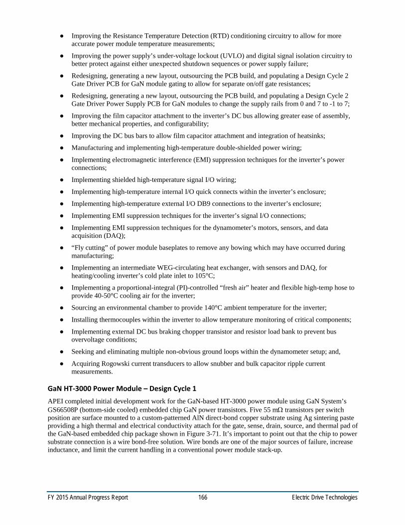
FY 2015 Annual Progress Report 166 Electric Drive Technologies
Improving the Resistance Temperature Detection (RTD) conditioning circuitry to allow for more accurate power module temperature measurements;
Improving the power supply’s under-voltage lockout (UVLO) and digital signal isolation circuitry to better protect against either unexpected shutdown sequences or power supply failure;
Redesigning, generating a new layout, outsourcing the PCB build, and populating a Design Cycle 2 Gate Driver PCB for GaN module gating to allow for separate on/off gate resistances;
Redesigning, generating a new layout, outsourcing the PCB build, and populating a Design Cycle 2 Gate Driver Power Supply PCB for GaN modules to change the supply rails from 0 and 7 to -1 to 7;
Improving the film capacitor attachment to the inverter’s DC bus allowing greater ease of assembly, better mechanical properties, and configurability;
Improving the DC bus bars to allow film capacitor attachment and integration of heatsinks;
Manufacturing and implementing high-temperature double-shielded power wiring;
Implementing electromagnetic interference (EMI) suppression techniques for the inverter’s power connections;
Implementing shielded high-temperature signal I/O wiring;
Implementing high-temperature internal I/O quick connects within the inverter’s enclosure;
Implementing high-temperature external I/O DB9 connections to the inverter’s enclosure;
Implementing EMI suppression techniques for the inverter’s signal I/O connections;
Implementing EMI suppression techniques for the dynamometer’s motors, sensors, and data acquisition (DAQ);
“Fly cutting” of power module baseplates to remove any bowing which may have occurred during manufacturing;
Implementing an intermediate WEG-circulating heat exchanger, with sensors and DAQ, for heating/cooling inverter’s cold plate inlet to 105°C;
Implementing a proportional-integral (PI)-controlled “fresh air” heater and flexible high-temp hose to provide 40-50°C cooling air for the inverter;
Sourcing an environmental chamber to provide 140°C ambient temperature for the inverter;
Installing thermocouples within the inverter to allow temperature monitoring of critical components;
Implementing external DC bus braking chopper transistor and resistor load bank to prevent bus overvoltage conditions;
Seeking and eliminating multiple non-obvious ground loops within the dynamometer setup; and,
Acquiring Rogowski current transducers to allow snubber and bulk capacitor ripple current measurements.
GaN HT-3000 Power Module – Design Cycle 1 APEI completed initial development work for the GaN-based HT-3000 power module using GaN System’s GS66508P (bottom-side cooled) embedded chip GaN power transistors. Five 55 mΩ transistors per switch position are surface mounted to a custom-patterned AlN direct-bond copper substrate using Ag sintering paste providing a high thermal and electrical conductivity attach for the gate, sense, drain, source, and thermal pad of the GaN-based embedded chip package shown in Figure 3-71. It’s important to point out that the chip to power substrate connection is a wire bond-free solution. Wire bonds are one of the major sources of failure, increase inductance, and limit the current handling in a conventional power module stack-up.
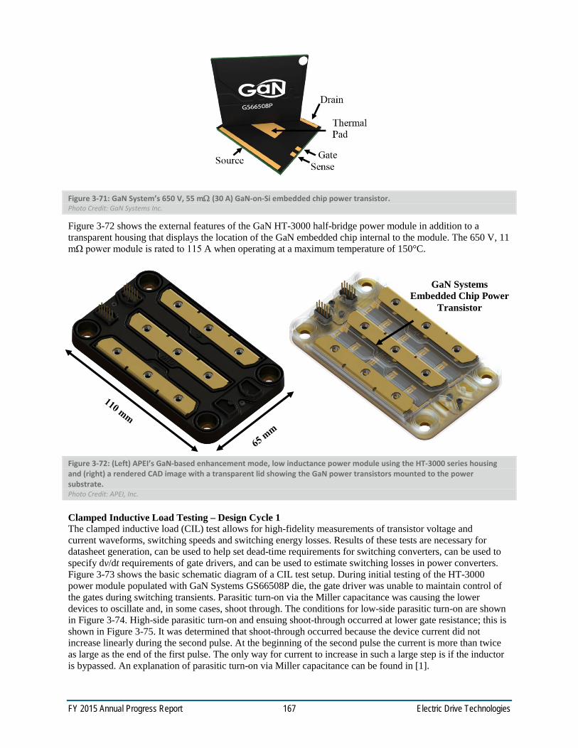
FY 2015 Annual Progress Report 167 Electric Drive Technologies
Figure 3-71: GaN System’s 650 V, 55 mΩ (30 A) GaN-on-Si embedded chip power transistor. Photo Credit: GaN Systems Inc.
Figure 3-72 shows the external features of the GaN HT-3000 half-bridge power module in addition to a transparent housing that displays the location of the GaN embedded chip internal to the module. The 650 V, 11 mΩ power module is rated to 115 A when operating at a maximum temperature of 150°C.
Figure 3-72: (Left) APEI’s GaN-based enhancement mode, low inductance power module using the HT-3000 series housing and (right) a rendered CAD image with a transparent lid showing the GaN power transistors mounted to the power substrate. Photo Credit: APEI, Inc.
Clamped Inductive Load Testing – Design Cycle 1 The clamped inductive load (CIL) test allows for high-fidelity measurements of transistor voltage and current waveforms, switching speeds and switching energy losses. Results of these tests are necessary for datasheet generation, can be used to help set dead-time requirements for switching converters, can be used to specify dv/dt requirements of gate drivers, and can be used to estimate switching losses in power converters. Figure 3-73 shows the basic schematic diagram of a CIL test setup. During initial testing of the HT-3000 power module populated with GaN Systems GS66508P die, the gate driver was unable to maintain control of the gates during switching transients. Parasitic turn-on via the Miller capacitance was causing the lower devices to oscillate and, in some cases, shoot through. The conditions for low-side parasitic turn-on are shown in Figure 3-74. High-side parasitic turn-on and ensuing shoot-through occurred at lower gate resistance; this is shown in Figure 3-75. It was determined that shoot-through occurred because the device current did not increase linearly during the second pulse. At the beginning of the second pulse the current is more than twice as large as the end of the first pulse. The only way for current to increase in such a large step is if the inductor is bypassed. An explanation of parasitic turn-on via Miller capacitance can be found in [1].
GaN Systems Embedded Chip Power
Transistor
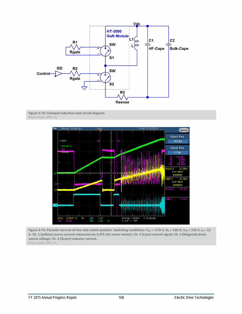
FY 2015 Annual Progress Report 168 Electric Drive Technologies
Figure 3-73: Clamped inductive load circuit diagram. Photo Credit: APEI, Inc.
Figure 3-74: Parasitic turn-on of low-side switch position. Switching conditions: VGS = +7/0 V, RG = 100 Ω, VDS = 150 V, ID = 12 A. Ch. 1 (yellow) source current measured via 2.475 mΩ sense resistor; Ch. 2 (Cyan) control signal; Ch. 3 (Magenta) drain source voltage; Ch. 4 (Green) inductor current. Photo credit: APEI, Inc.
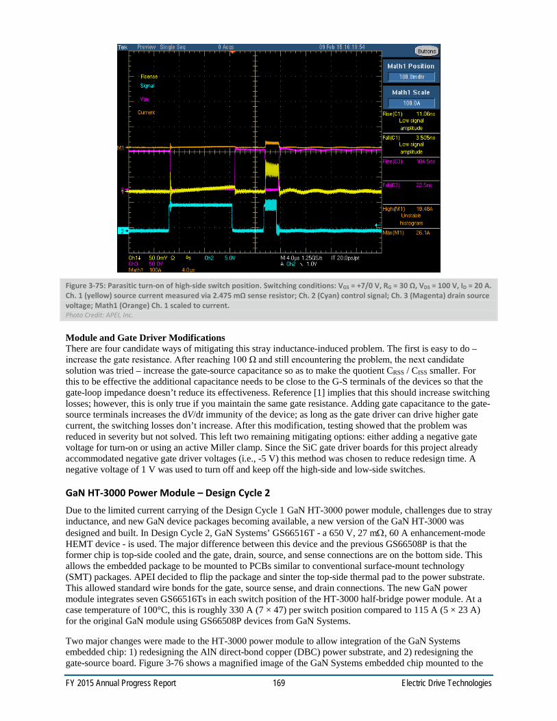
FY 2015 Annual Progress Report 169 Electric Drive Technologies
Figure 3-75: Parasitic turn-on of high-side switch position. Switching conditions: VGS = +7/0 V, RG = 30 Ω, VDS = 100 V, ID = 20 A. Ch. 1 (yellow) source current measured via 2.475 mΩ sense resistor; Ch. 2 (Cyan) control signal; Ch. 3 (Magenta) drain source voltage; Math1 (Orange) Ch. 1 scaled to current. Photo Credit: APEI, Inc.
Module and Gate Driver Modifications There are four candidate ways of mitigating this stray inductance-induced problem. The first is easy to do – increase the gate resistance. After reaching 100 Ω and still encountering the problem, the next candidate solution was tried – increase the gate-source capacitance so as to make the quotient CRSS / CISS smaller. For this to be effective the additional capacitance needs to be close to the G-S terminals of the devices so that the gate-loop impedance doesn’t reduce its effectiveness. Reference [1] implies that this should increase switching losses; however, this is only true if you maintain the same gate resistance. Adding gate capacitance to the gate-source terminals increases the dV/dt immunity of the device; as long as the gate driver can drive higher gate current, the switching losses don’t increase. After this modification, testing showed that the problem was reduced in severity but not solved. This left two remaining mitigating options: either adding a negative gate voltage for turn-on or using an active Miller clamp. Since the SiC gate driver boards for this project already accommodated negative gate driver voltages (i.e., -5 V) this method was chosen to reduce redesign time. A negative voltage of 1 V was used to turn off and keep off the high-side and low-side switches.
GaN HT-3000 Power Module – Design Cycle 2 Due to the limited current carrying of the Design Cycle 1 GaN HT-3000 power module, challenges due to stray inductance, and new GaN device packages becoming available, a new version of the GaN HT-3000 was designed and built. In Design Cycle 2, GaN Systems’ GS66516T - a 650 V, 27 mΩ, 60 A enhancement-mode HEMT device - is used. The major difference between this device and the previous GS66508P is that the former chip is top-side cooled and the gate, drain, source, and sense connections are on the bottom side. This allows the embedded package to be mounted to PCBs similar to conventional surface-mount technology (SMT) packages. APEI decided to flip the package and sinter the top-side thermal pad to the power substrate. This allowed standard wire bonds for the gate, source sense, and drain connections. The new GaN power module integrates seven GS66516Ts in each switch position of the HT-3000 half-bridge power module. At a case temperature of 100°C, this is roughly 330 A (7 × 47) per switch position compared to 115 A (5 × 23 A) for the original GaN module using GS66508P devices from GaN Systems.
Two major changes were made to the HT-3000 power module to allow integration of the GaN Systems embedded chip: 1) redesigning the AlN direct-bond copper (DBC) power substrate, and 2) redesigning the gate-source board. Figure 3-76 shows a magnified image of the GaN Systems embedded chip mounted to the

FY 2015 Annual Progress Report 170 Electric Drive Technologies
power substrate with the power and signal interconnections. Twelve- and five-mil Aluminum wire bonds are used for the power and signal bonds, respectively. Two five-mil Aluminum wire bonds are used to connect to the device’s gate pads on both sides to allow for equal current spreading during operation. The gate-source board was updated such that both gate resistors and capacitors could be mounted to allow for a favorable Miller capacitance ratio.
Figure 3-76: An enlarged view of the new GaN package nesting. Photo Credit: APEI, Inc.
Figure 3-77 shows a top view of the GaN-based HT-3000 power module with a transparent lid. Similar to the SiC version, this module utilizes a paralleled die design enabling equal current sharing among devices. The external power and signal connections are exactly the same as the SiC-based HT-3000 power module so that the module is a direct swap in the system—excluding the custom gate driver designed for switching GaN devices.
Figure 3-77: GaN-based HT-3000 power module. Photo Credit: APEI, Inc.
Clamped Inductive Load Testing – Design Cycle 2
After the modules’ static characterization versus temperature tests were completed, the GaN power modules were double pulse tested to quantify voltage rise and fall times, current fall and rise times, voltage and current overshoots, and energy loss at turn-off and turn-on. Figure 3-78 shows 450 V, 300 A, 75°C switching with Vgs = +7/-1 V, Rg-on = 1 Ω, Rg-off = 0 Ω with a diode, and ∆t = 100 ps. At turn off, the voltage rise was 15 ns, current fall was 14 ns, voltage overshoot was 180 V, and the turn-off energy loss was 2.8 mJ. At turn on, the voltage fall was 71 ns, current rise was 23 ns, current overshoot was 73 A, and the turn-on energy loss was 4.3 mJ.
Gate
Kelvin
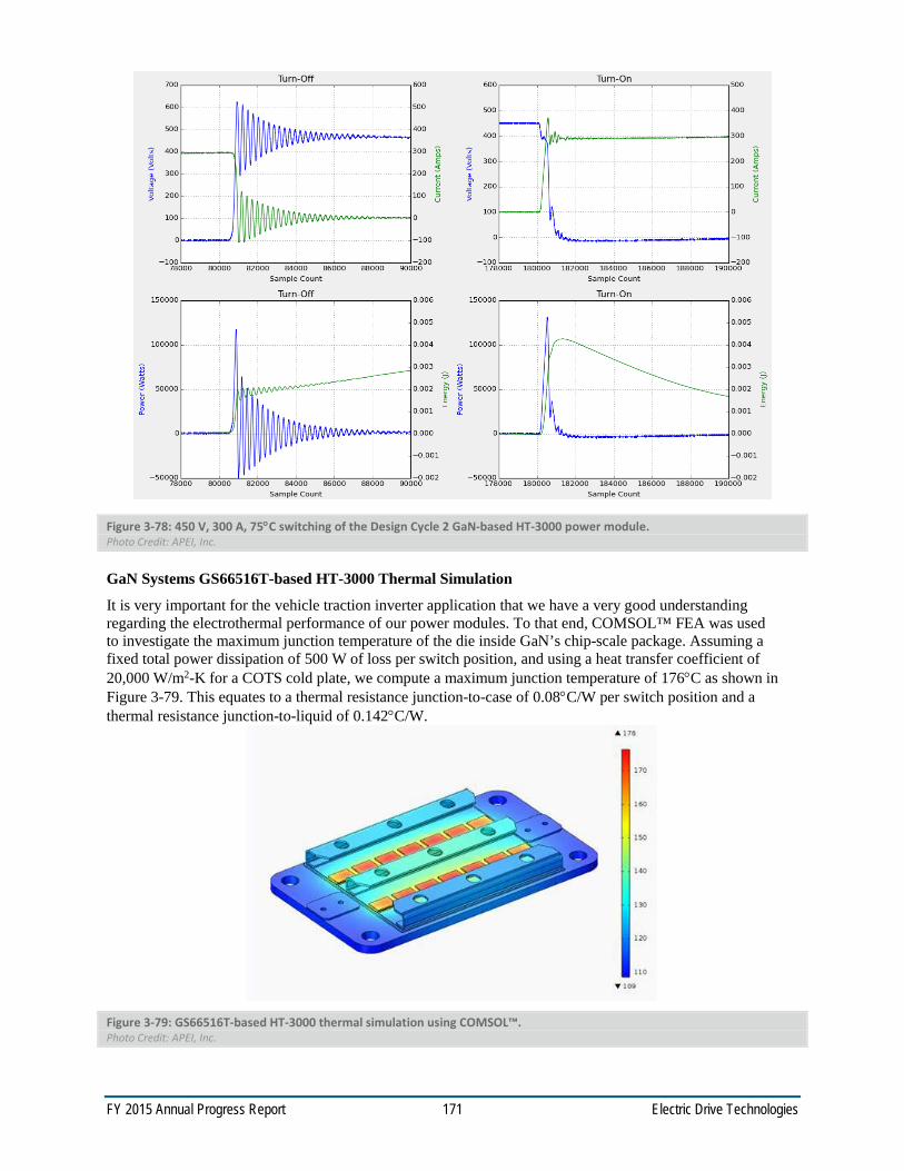
FY 2015 Annual Progress Report 171 Electric Drive Technologies
Figure 3-78: 450 V, 300 A, 75°C switching of the Design Cycle 2 GaN-based HT-3000 power module. Photo Credit: APEI, Inc.
GaN Systems GS66516T-based HT-3000 Thermal Simulation
It is very important for the vehicle traction inverter application that we have a very good understanding regarding the electrothermal performance of our power modules. To that end, COMSOL™ FEA was used to investigate the maximum junction temperature of the die inside GaN’s chip-scale package. Assuming a fixed total power dissipation of 500 W of loss per switch position, and using a heat transfer coefficient of 20,000 W/m2-K for a COTS cold plate, we compute a maximum junction temperature of 176°C as shown in Figure 3-79. This equates to a thermal resistance junction-to-case of 0.08°C/W per switch position and a thermal resistance junction-to-liquid of 0.142°C/W.
Figure 3-79: GS66516T-based HT-3000 thermal simulation using COMSOL™. Photo Credit: APEI, Inc.

FY 2015 Annual Progress Report 172 Electric Drive Technologies
Alternatively, if we choose to fix the maximum junction temperature to 150°C, then the thermal model estimates a maximum power dissipation per switch position to be limited to approximately 320 W.
Resolver Interface Fully Qualified Much time and effort has been invested in this year iteratively refining the resolver interface, signal conditioning, firmware, and software. This interface provides a sinusoidal excitation to the resolver primary in the form A sin(ωexc t). The two resolver secondaries are then scaled in amplitude by the sine or cosine of the resolver angle to yield signals in the form sin(θ) A sin(ωexc t), and cos(θ) A sin(ωexc t), where A is the amplitude of the excitation signal, ωexc is the radian frequency of the excitation, and θ is the angle of the resolver shaft and thus the motor shaft.
The sampling of all analog signals is synchronized with the pulse-width modulation (PWM) switching so that signals are acquired at a time when none of the power switches are changing state. This avoids contaminating the analog signals with switching noise. If the resolver excitation is not synchronized with the sampling, then there will be times at which the sampling occurs when the excitation voltage is at or near 0 V. At such time there is no information contained in the secondaries since those voltages will be nearly zero regardless of the amplitude A or the angle θ. A robust solution is to synchronize the excitation of the resolver with the PWM switching frequency. Since the switching frequency is 20 kHz, and double update symmetric space vector modulation is used, the controller sampling occurs at 40 kHz. The synchronized excitation is at 10 kHz so that four samples are obtained during each excitation cycle. The phasing is set so that the samples occur at 45, 135, 225, and 315 degrees. This ensures that the amplitude of the excitation signal is always (1/2 × √2 × A) and will appear with alternating signs in a ++-- pattern. Two benefits are achieved. First is that sampling occurs when no power devices are switching thus avoiding noise from switching transients. Second is that sampling always occurs when there is a large and constant amplitude of excitation, thus avoiding the problem of sampling when the excitation is near zero and no information is contained in the secondary signals.
Baseline Characterization of SiC Inverter Efficiency Using the high-power dynamometer at the NCREPT facility, the inverter - shown in Figure 3-80 - was investigated over predetermined portions of the machine’s torque-speed plane at various bus voltages. These preliminary tests were used to verify the automated testing capability of the dynamometer test bed and to find the extreme operating points bounding the feasible operating points for different bus voltages. This provides a baseline for safe operation of the system prior to the extreme environment testing. Figure 3-81, Figure 3-82, Figure 3-83, and Figure 3-84 show initial commissioning test results at 200, 325, 450, and 650 VDC.
Figure 3-80: Silicon-carbide inverter in the environmental chamber ready for testing. Photo credit: APEI, Inc.

FY 2015 Annual Progress Report 173 Electric Drive Technologies
Figure 3-81: Initial results: SiC-based inverter efficiency at 200 VDC. Ambient and coolant temperature is 25°C. Photo Credit: APEI, Inc.
Figure 3-82: Initial results: SiC-based inverter efficiency at 325 VDC. Ambient and coolant temperature is 25°C. Photo Credit: APEI, Inc.

FY 2015 Annual Progress Report 174 Electric Drive Technologies
Figure 3-83: Initial results: SiC-based inverter efficiency at 450 VDC. Ambient and coolant temperature is 25°C. Photo Credit: APEI, Inc.
Figure 3-84: Initial results: SiC-based inverter efficiency at 650 VDC. Ambient and coolant temperature is 25°C. Photo Credit: APEI, Inc.
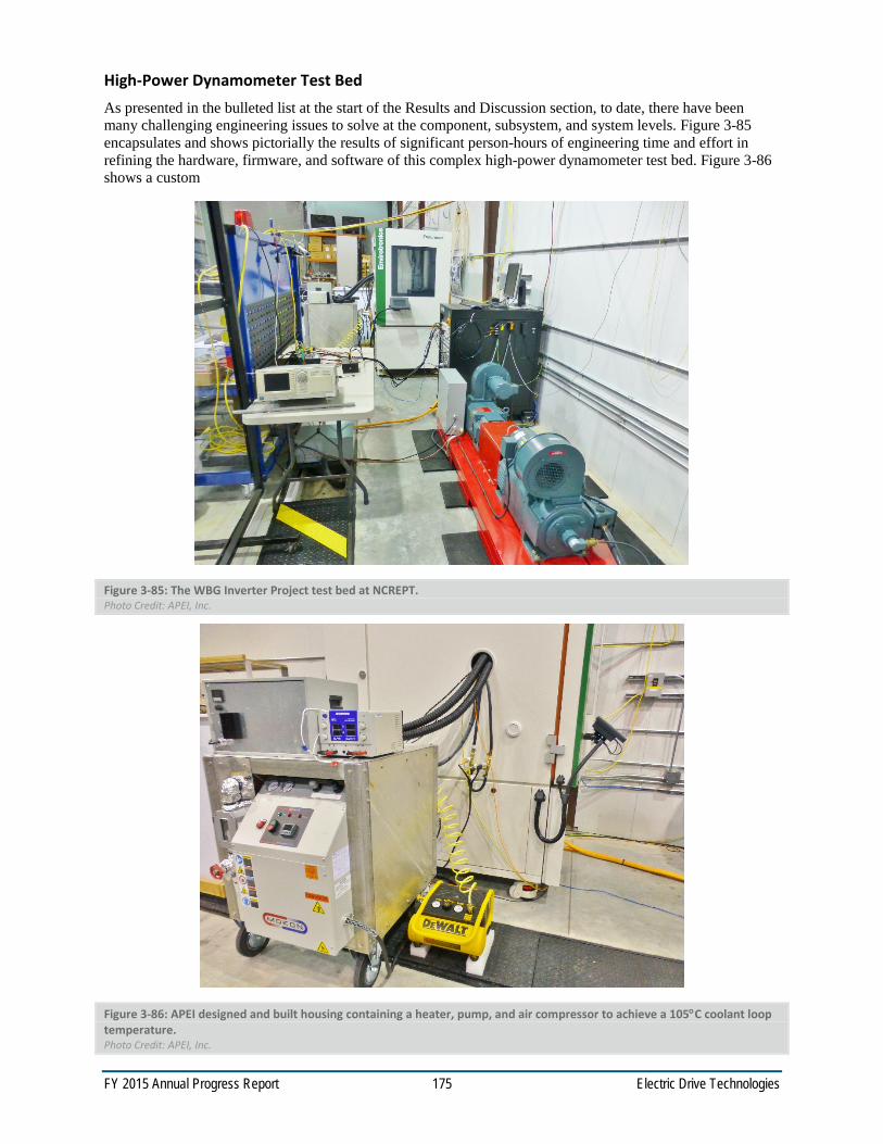
FY 2015 Annual Progress Report 175 Electric Drive Technologies
High-Power Dynamometer Test Bed As presented in the bulleted list at the start of the Results and Discussion section, to date, there have been many challenging engineering issues to solve at the component, subsystem, and system levels. Figure 3-85 encapsulates and shows pictorially the results of significant person-hours of engineering time and effort in refining the hardware, firmware, and software of this complex high-power dynamometer test bed. Figure 3-86 shows a custom
Figure 3-85: The WBG Inverter Project test bed at NCREPT. Photo Credit: APEI, Inc.
Figure 3-86: APEI designed and built housing containing a heater, pump, and air compressor to achieve a 105°C coolant loop temperature. Photo Credit: APEI, Inc.
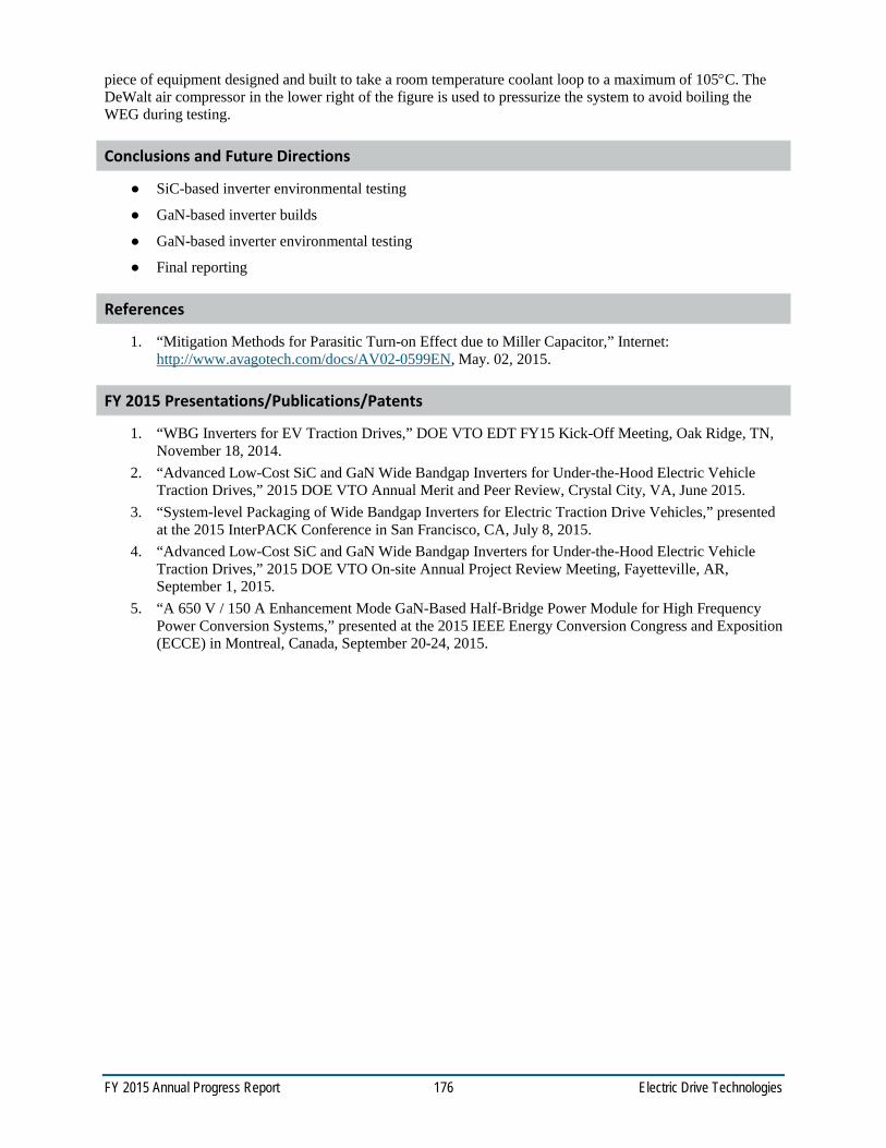
FY 2015 Annual Progress Report 176 Electric Drive Technologies
piece of equipment designed and built to take a room temperature coolant loop to a maximum of 105°C. The DeWalt air compressor in the lower right of the figure is used to pressurize the system to avoid boiling the WEG during testing.
Conclusions and Future Directions
SiC-based inverter environmental testing
GaN-based inverter builds
GaN-based inverter environmental testing
Final reporting
References
1. “Mitigation Methods for Parasitic Turn-on Effect due to Miller Capacitor,” Internet: http://www.avagotech.com/docs/AV02-0599EN, May. 02, 2015.
FY 2015 Presentations/Publications/Patents
1. “WBG Inverters for EV Traction Drives,” DOE VTO EDT FY15 Kick-Off Meeting, Oak Ridge, TN, November 18, 2014.
2. “Advanced Low-Cost SiC and GaN Wide Bandgap Inverters for Under-the-Hood Electric Vehicle Traction Drives,” 2015 DOE VTO Annual Merit and Peer Review, Crystal City, VA, June 2015.
3. “System-level Packaging of Wide Bandgap Inverters for Electric Traction Drive Vehicles,” presented at the 2015 InterPACK Conference in San Francisco, CA, July 8, 2015.
4. “Advanced Low-Cost SiC and GaN Wide Bandgap Inverters for Under-the-Hood Electric Vehicle Traction Drives,” 2015 DOE VTO On-site Annual Project Review Meeting, Fayetteville, AR, September 1, 2015.
5. “A 650 V / 150 A Enhancement Mode GaN-Based Half-Bridge Power Module for High Frequency Power Conversion Systems,” presented at the 2015 IEEE Energy Conversion Congress and Exposition (ECCE) in Montreal, Canada, September 20-24, 2015.
FY 2015 Annual Progress Report 177 Electric Drive Technologies
3.8. 88 Kilowatt Automotive Inverter with New 900 Volt Silicon Carbide Mosfet Technology
Dr. Jeffrey B. Casady, Business Development & Program Manager Cree, Inc. 3028 East Cornwallis Road Research Triangle Park, NC 27709 Phone: (919) 308-2280 E-mail: [email protected] Dr. Vipindas Pala, Principal Investigator Phone: (919) 407-7076 E-mail: [email protected] Sharon M. Degnan, Contracts Manager Phone: (919) 407-5554 E-mail: [email protected] Contractor: Cree, Inc. Contract No.: DE-EE0006920
Abstract/Executive Summary for Budget Year One Benchmark lowest SiC MOSFET RDSON possible, with 900V blocking capability
o 900V, 10mΩ SiC MOSFET with specific RDSON less than 2.5mΩ·cm2 – Sample 100 pieces to Ford Motor Company and Cree-Fayetteville in discrete packages – Ford Motor Company and Cree-Fayetteville to characterize – Sample to other automotive Tier One suppliers and OEM providers
o Build and characterize six low-inductance modules at Cree-Fayetteville – Use 900V, 10mΩ SiC MOSFETs – Perform 1,000 hour High-Temperature Reverse Bias (HTRB) stress test
Accomplishments Fabricated three lots of 900V, 10mΩ SiC MOSFETs with specific RDSON less than 2.5mΩ•cm2
Built six half-bridge power modules using four 900V, 10mΩ SiC MOSFETs per switch position o 900V, 400A, 2.5mΩ module measured at 25˚C o RDSON measured less than 4.5mΩ for all six modules at 175˚C
– Significantly lower conduction and switching losses than Si IGBT technology – Loss reduction compatible with estimated 2% savings in EV battery costs
Introduction
Present-day traction inverters are too expensive, too heavy, and too bulky to penetrate the mass consumer automotive market and hybrid vehicle sales are only about 3% of all vehicle sales. This effort seeks to revolutionize the electric vehicle traction drive industry through the optimization of the SiC device, power package, and traction drive systems to address the barriers listed. The main innovation thrust from the industry team will be on reducing system costs and extending reliability through inserting the newest break-through technology 900 V SiC MOSFET into advanced SiC-based power packaging and demonstrated traction drive technology. This new breakthrough SiC MOSFET based module is anticipated to reduce SiC die costs and switching losses in an 88 kW traction drive inverter modeled after the Ford Focus by 40% while increasing vehicle fuel economy, performance, and productivity (battery range, emissions reduction).

FY 2015 Annual Progress Report 178 Electric Drive Technologies
This effort brings together industrial teams which are leaders in products critical to hybrid electric/fully electric vehicle (HEV/EV) drivetrains. Cree is the leading supplier of SiC and GaN components, including SiC power MOSFETs and diodes. Cree is an automotive supplier of SiC diodes to HEV/EV platforms. APEI is a leading producer of high-temperature and low-inductance modules, which take full advantage of SiC power devices. APEI has also constructed automotive drive train prototype inverters in concert with other automotive OEMs on other efforts. Ford is the number one US producer of HEV/EV platforms, with a 13% market share in the US at the end of 2013.
It is critical in this program is to use the best available SiC MOSFETs with 900V blocking (to handle up to 700V DC bus), low specific RDSON (cost), low RDSON over temperature, and low conduction losses. Working with a vehicle OEM (Ford), the team can determine if the improvement in drive-train efficiency would reduce battery costs enough to offset the extra cost of SiC. This team is uniquely positioned to develop the best available 900V SiC MOSFET, measure its performance in both discrete and module form, and bench mark it against other technologies in terms of cost and performance.
Approach
The approach here in the first year was to scale up the lowest RDSON, lowest RDSON per unit area, 900V SiC MOSFET possible, and optimize it for low conduction losses over temperature. This would produce the lowest RDSON MOFET of any technology known, with a blocking voltage capability >650V.
The system level advantage, still to be quantified, would be to produce a low RDSON power module which would enable dramatically lower conduction losses in the electric drive train. If the drive train inverter is responsible for approximately 4% of overall losses in an electric vehicle, cutting these losses in half would reduce vehicle losses by 2%, which is fairly dramatic impact to the cost of an electric vehicle.
Figure 3-87: This work brought together a team which is leading the market in SiC power device production (Cree), SiC power module technology (Cree Fayetteville, formerly APEI), and HEV/EV platforms in the US market (Ford). Cree is the leading supplier of SiC and GaN components, including SiC power MOSFETs and diodes, and is also an automotive supplier of SiC diodes to HEV / EV platforms. Cree-Fayetteville is a leading producer of high-temperature and low-inductance modules, which take full advantage of SiC power devices. Cree-Fayetteville has also constructed automotive drive train prototype inverters in concert with other automotive OEMs on other efforts. Ford is the number one US producer of HEV / EV platforms, with a 13% market share in the US at the end of 2013.
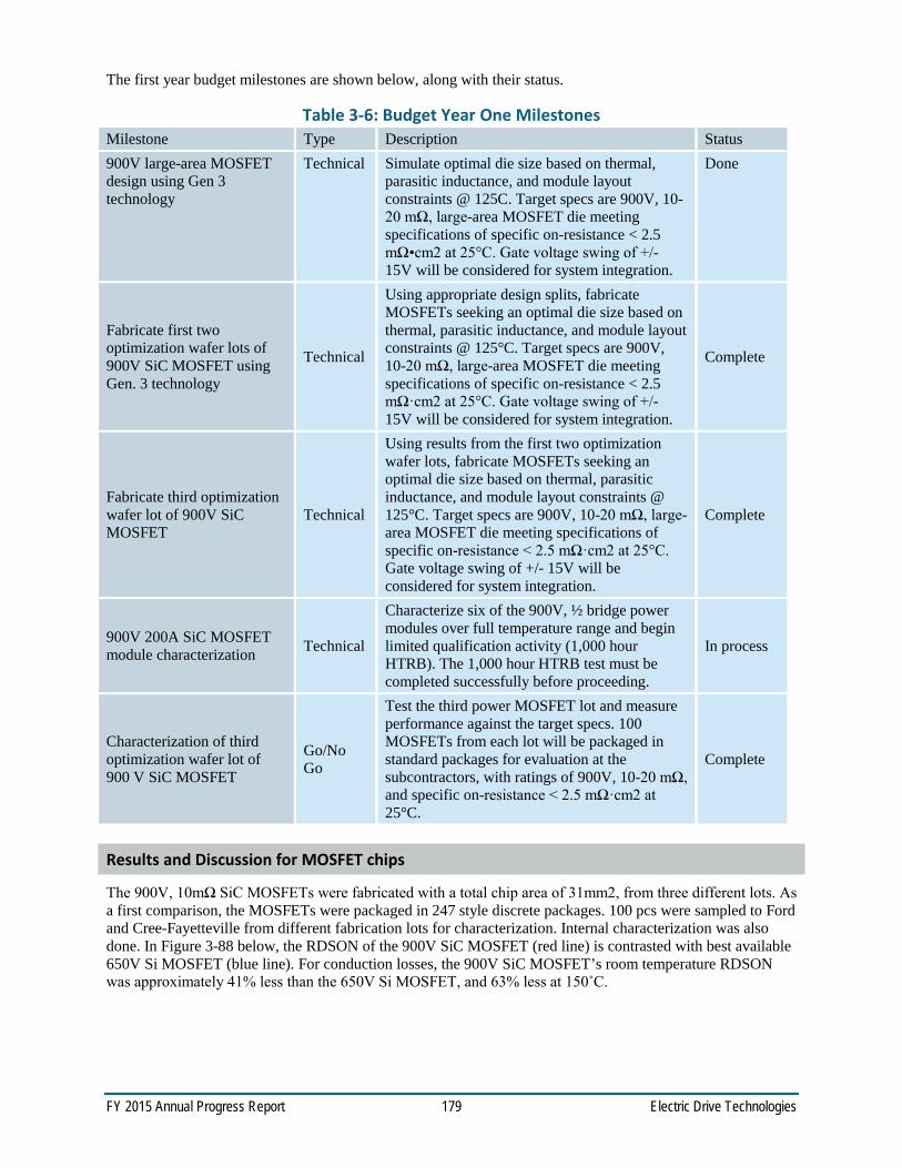
FY 2015 Annual Progress Report 179 Electric Drive Technologies
The first year budget milestones are shown below, along with their status.
Table 3-6: Budget Year One Milestones Milestone Type Description Status 900V large-area MOSFET design using Gen 3 technology
Technical Simulate optimal die size based on thermal, parasitic inductance, and module layout constraints @ 125C. Target specs are 900V, 10-20 mΩ, large-area MOSFET die meeting specifications of specific on-resistance < 2.5 mΩ•cm2 at 25°C. Gate voltage swing of +/- 15V will be considered for system integration.
Done
Fabricate first two optimization wafer lots of 900V SiC MOSFET using Gen. 3 technology
Technical
Using appropriate design splits, fabricate MOSFETs seeking an optimal die size based on thermal, parasitic inductance, and module layout constraints @ 125°C. Target specs are 900V, 10-20 mΩ, large-area MOSFET die meeting specifications of specific on-resistance < 2.5 mΩ·cm2 at 25°C. Gate voltage swing of +/- 15V will be considered for system integration.
Complete
Fabricate third optimization wafer lot of 900V SiC MOSFET
Technical
Using results from the first two optimization wafer lots, fabricate MOSFETs seeking an optimal die size based on thermal, parasitic inductance, and module layout constraints @ 125°C. Target specs are 900V, 10-20 mΩ, large-area MOSFET die meeting specifications of specific on-resistance < 2.5 mΩ·cm2 at 25°C. Gate voltage swing of +/- 15V will be considered for system integration.
Complete
900V 200A SiC MOSFET module characterization Technical
Characterize six of the 900V, ½ bridge power modules over full temperature range and begin limited qualification activity (1,000 hour HTRB). The 1,000 hour HTRB test must be completed successfully before proceeding.
In process
Characterization of third optimization wafer lot of 900 V SiC MOSFET
Go/No Go
Test the third power MOSFET lot and measure performance against the target specs. 100 MOSFETs from each lot will be packaged in standard packages for evaluation at the subcontractors, with ratings of 900V, 10-20 mΩ, and specific on-resistance < 2.5 mΩ·cm2 at 25°C.
Complete
Results and Discussion for MOSFET chips
The 900V, 10mΩ SiC MOSFETs were fabricated with a total chip area of 31mm2, from three different lots. As a first comparison, the MOSFETs were packaged in 247 style discrete packages. 100 pcs were sampled to Ford and Cree-Fayetteville from different fabrication lots for characterization. Internal characterization was also done. In Figure 3-88 below, the RDSON of the 900V SiC MOSFET (red line) is contrasted with best available 650V Si MOSFET (blue line). For conduction losses, the 900V SiC MOSFET’s room temperature RDSON was approximately 41% less than the 650V Si MOSFET, and 63% less at 150˚C.
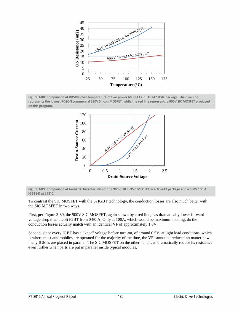
FY 2015 Annual Progress Report 180 Electric Drive Technologies
Figure 3-88: Comparison of RDSON over temperature of two power MOSFETs in TO-247 style package. The blue line represents the lowest RDSON commercial 650V Silicon MOSFET, while the red line represents a 900V SiC MOSFET produced on this program.
Figure 3-89: Comparison of forward characteristics of the 900V, 10 mΩSiC MOSFET in a TO-247 package and a 650V 100 A IGBT [4] at 175˚C.
To contrast the SiC MOSFET with the Si IGBT technology, the conduction losses are also much better with the SiC MOSFET in two ways.
First, per Figure 3-89, the 900V SiC MOSFET, again shown by a red line, has dramatically lower forward voltage drop than the Si IGBT from 0-80 A. Only at 100A, which would be maximum loading, do the conduction losses actually match with an identical VF of approximately 1.8V.
Second, since every IGBT has a “knee” voltage before turn-on, of around 0.5V, at light load conditions, which is where most automobiles are operated for the majority of the time, the VF cannot be reduced no matter how many IGBTs are placed in parallel. The SiC MOSFET on the other hand, can dramatically reduce its resistance even further when parts are put in parallel inside typical modules.
05
1015202530354045
25 50 75 100 125 150 175O
N R
esis
tanc
e (m
Ω)
Temperature (°C)
0
20
40
60
80
100
120
0 0.5 1 1.5 2 2.5
Dra
in-S
ourc
e Cur
rent
Drain-Source Voltage
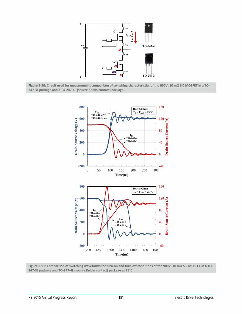
FY 2015 Annual Progress Report 181 Electric Drive Technologies
Figure 3-90: Circuit used for measurement comparison of switching characteristics of the 900V, 10 mΩ SiC MOSFET in a TO-247-3L package and a TO-247-4L (source Kelvin contact) package.
Figure 3-91: Comparison of switching waveforms for turn-on and turn-off conditions of the 900V, 10 mΩ SiC MOSFET in a TO-247-3L package and TO-247-4L (source Kelvin contact) package at 25˚C.
TO-247-4
TO-247-3
-40
0
40
80
120
160
-200
0
200
400
600
800
0 50 100 150 200 250 300D
rain
-Sou
rce C
urre
nt (A
)
Dra
in-S
ourc
e Vol
tage
(V)
Time(ns)
RG = 5 OhmsTJ = TAmb = 25 °CVDS
TO-247-4TO-247-3
IDSTO-247-4TO-247-3
-40
0
40
80
120
160
-200
0
200
400
600
800
1200 1250 1300 1350 1400 1450 1500
Dra
in-S
ourc
e Cur
rent
(A)
Dra
in-S
ourc
e Vol
tage
(V)
Time(ns)
RG = 5 OhmsTJ = TAmb = 25 °C
IDSTO-247-4TO-247-3
VDSTO-247-4TO-247-3
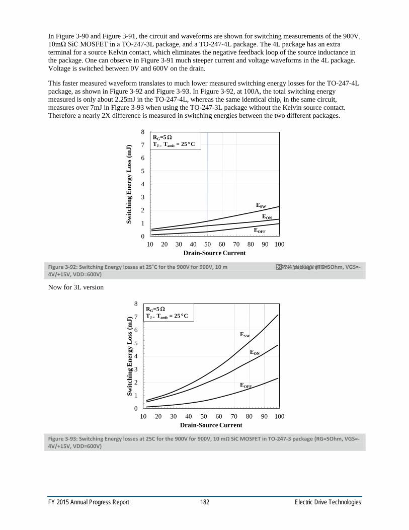
FY 2015 Annual Progress Report 182 Electric Drive Technologies
In Figure 3-90 and Figure 3-91, the circuit and waveforms are shown for switching measurements of the 900V, 10mΩ SiC MOSFET in a TO-247-3L package, and a TO-247-4L package. The 4L package has an extra terminal for a source Kelvin contact, which eliminates the negative feedback loop of the source inductance in the package. One can observe in Figure 3-91 much steeper current and voltage waveforms in the 4L package. Voltage is switched between 0V and 600V on the drain.
This faster measured waveform translates to much lower measured switching energy losses for the TO-247-4L package, as shown in Figure 3-92 and Figure 3-93. In Figure 3-92, at 100A, the total switching energy measured is only about 2.25mJ in the TO-247-4L, whereas the same identical chip, in the same circuit, measures over 7mJ in Figure 3-93 when using the TO-247-3L package without the Kelvin source contact. Therefore a nearly 2X difference is measured in switching energies between the two different packages.
Figure 3-92: Switching Energy losses at 25˚C for the 900V for 900V, 10 m SiC MOSFET in TO-247-4 package (RG=5Ohm, VGS=-4V/+15V, VDD=600V)
Now for 3L version
Figure 3-93: Switching Energy losses at 25C for the 900V for 900V, 10 mΩ SiC MOSFET in TO-247-3 package (RG=5Ohm, VGS=-4V/+15V, VDD=600V)
0
1
2
3
4
5
6
7
8
10 20 30 40 50 60 70 80 90 100
Switc
hing
Ene
rgy
Los
s (m
J)
Drain-Source Current
ESW
EON
EOFF
RG=5 ΩTJ = Tamb = 25 °C
0
1
2
3
4
5
6
7
8
10 20 30 40 50 60 70 80 90 100
Switc
hing
Ene
rgy
Los
s (m
J)
Drain-Source Current
ESW
EON
EOFF
RG=5 ΩTJ = Tamb = 25 °C

FY 2015 Annual Progress Report 183 Electric Drive Technologies
Figure 3-94: Third quadrant characteristics of the 900V, 10 mΩ MOSFET at 175˚C
Module assembly and characterization
Next the SiC MOSFETs were placed in APEI (now Cree Fayetteville) 62 mm power modules in a half-bridge configuration. Four MOSFETs per switch position, or eight MOSFETs per module, were assembled in the low-inductance modules, which are labeled as HT-3291-R. Figure 3-95 below illustrates the placement of the MOSFETs in the module.
-120
-100
-80
-60
-40
-20
0-6 -5 -4 -3 -2 -1 0
Dra
in-S
ourc
e Cur
rent
Drain-Source Voltage
VGS=-4 V
VGS=0V VGS=15V
TJ=175 °C
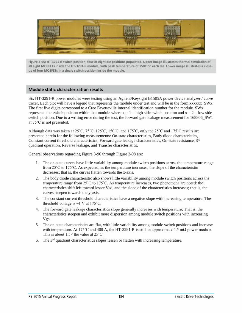
FY 2015 Annual Progress Report 184 Electric Drive Technologies
Figure 3-95: HT-3291-R switch position; four of eight die positions populated. Upper image illustrates thermal simulation of all eight MOSFETs inside the HT-3291-R module, with peak temperature of 150C on each die. Lower image illustrates a close-up of four MOSFETs in a single switch position inside the module.
Module static characterization results
Six HT-3291-R power modules were testing using an Agilent/Keysight B1505A power device analyzer / curve tracer. Each plot will have a legend that represents the module under test and will be in the form xxxxxx_SWx. The first five digits correspond to a Cree Fayetteville internal identification number for the module. SWx represents the switch position within that module where x = 1 = high side switch position and x = 2 = low side switch position. Due to a writing error during the test, the forward gate leakage measurement for 168806_SW1 at 75˚C is not presented.
Although data was taken at 25˚C, 75˚C, 125˚C, 150˚C, and 175˚C, only the 25˚C and 175˚C results are presented herein for the following measurements: On-state characteristics, Body diode characteristics, Constant current threshold characteristics, Forward gate leakage characteristics, On-state resistance, 3rd quadrant operation, Reverse leakage, and Transfer characteristics.
General observations regarding Figure 3-96 through Figure 3-98 are:
1. The on-state curves have little variability among module switch positions across the temperature range from 25˚C to 175˚C. As expected, as the temperature increases, the slope of the characteristic decreases; that is, the curves flatten towards the x-axis.
2. The body diode characteristic also shows little variability among module switch positions across the temperature range from 25˚C to 175˚C. As temperature increases, two phenomena are noted: the characteristics shift left toward lesser Vsd, and the slope of the characteristics increases; that is, the curves steepen towards the y-axis.
3. The constant current threshold characteristics have a negative slope with increasing temperature. The threshold voltage is ~1 V at 175˚C.
4. The forward gate leakage characteristics slope generally increases with temperature; That is, the characteristics steepen and exhibit more dispersion among module switch positions with increasing Vgs.
5. The on-state characteristics are flat, with little variability among module switch positions and increase with temperature. At 175˚C and 400 A, the HT-3291-R is still an approximate 4.5 mΩ power module. This is about 1.5× the value at 25˚C.
6. The 3rd quadrant characteristics slopes lessen or flatten with increasing temperature.

FY 2015 Annual Progress Report 185 Electric Drive Technologies
Figure 3-96: HT-3291-R on-state characteristics, Vgs = 15 V; (top) 25˚C; (bottom) 175˚C.
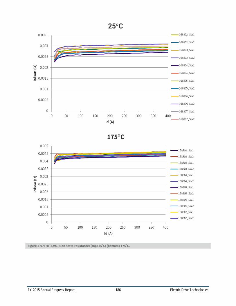
FY 2015 Annual Progress Report 186 Electric Drive Technologies
Figure 3-97: HT-3291-R on-state resistance; (top) 25˚C; (bottom) 175˚C.
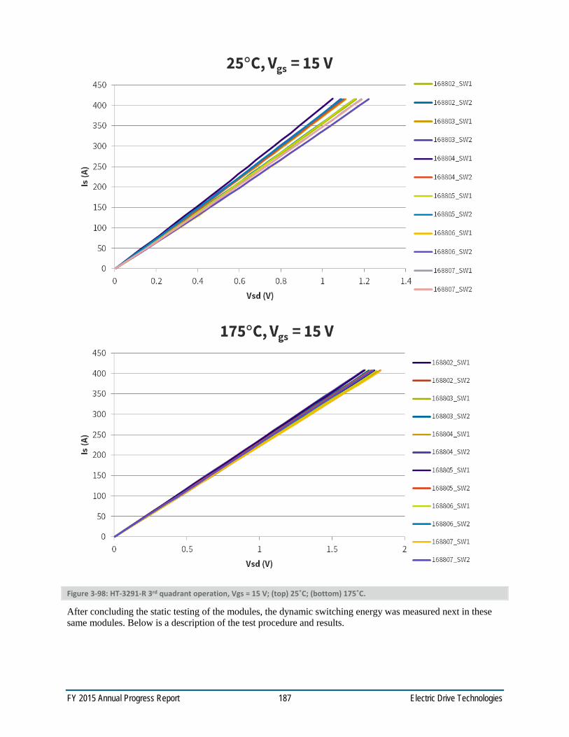
FY 2015 Annual Progress Report 187 Electric Drive Technologies
Figure 3-98: HT-3291-R 3rd quadrant operation, Vgs = 15 V; (top) 25˚C; (bottom) 175˚C.
After concluding the static testing of the modules, the dynamic switching energy was measured next in these same modules. Below is a description of the test procedure and results.
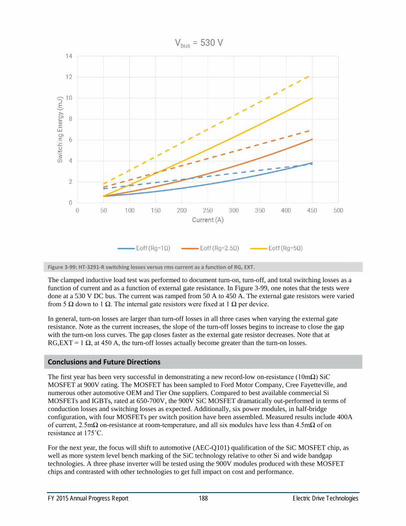
FY 2015 Annual Progress Report 188 Electric Drive Technologies
Figure 3-99: HT-3291-R switching losses versus rms current as a function of RG, EXT.
The clamped inductive load test was performed to document turn-on, turn-off, and total switching losses as a function of current and as a function of external gate resistance. In Figure 3-99, one notes that the tests were done at a 530 V DC bus. The current was ramped from 50 A to 450 A. The external gate resistors were varied from 5 Ω down to 1 Ω. The internal gate resistors were fixed at 1 Ω per device.
In general, turn-on losses are larger than turn-off losses in all three cases when varying the external gate resistance. Note as the current increases, the slope of the turn-off losses begins to increase to close the gap with the turn-on loss curves. The gap closes faster as the external gate resistor decreases. Note that at RG,EXT = 1 Ω, at 450 A, the turn-off losses actually become greater than the turn-on losses.
Conclusions and Future Directions
The first year has been very successful in demonstrating a new record-low on-resistance (10mΩ) SiC MOSFET at 900V rating. The MOSFET has been sampled to Ford Motor Company, Cree Fayetteville, and numerous other automotive OEM and Tier One suppliers. Compared to best available commercial Si MOSFETs and IGBTs, rated at 650-700V, the 900V SiC MOSFET dramatically out-performed in terms of conduction losses and switching losses as expected. Additionally, six power modules, in half-bridge configuration, with four MOSFETs per switch position have been assembled. Measured results include 400A of current, 2.5mΩ on-resistance at room-temperature, and all six modules have less than 4.5mΩ of on resistance at 175˚C.
For the next year, the focus will shift to automotive (AEC-Q101) qualification of the SiC MOSFET chip, as well as more system level bench marking of the SiC technology relative to other Si and wide bandgap technologies. A three phase inverter will be tested using the 900V modules produced with these MOSFET chips and contrasted with other technologies to get full impact on cost and performance.

FY 2015 Annual Progress Report 189 Electric Drive Technologies
FY 2015 Presentations/Publications/Patents
1. V. Pala, et al, “Record-low 10mΩ SiC MOSFETs in TO-247, Rated at 900V,” submitted for publication at 2016 IEEE Applied Power Electronics Conference, March 2016, Long Beach, CA.
2. J. Casady, et al, “Ultra-low (1.25mΩ) On-Resistance 900V SiC 62mm Half-Bridge Power Modules Using New 10mΩ SiC MOSFETs,” submitted for publication at PCIM, May 2016, Nuremburg, Germany.
References
1. Infineon 650V, 19mΩ MOSFET, part number IPZ65R019C7, http://www.infineon.com/dgdl/Infineon-IPZ65R019C7-DS-v02_00-en.pdf.
2. Infineon 650V 100 A IGBT, Part No. IGZ100N65H5, http://www.infineon.com/dgdl/Infineon-IGZ100N65H5-DS-v02_01-EN.pdf.
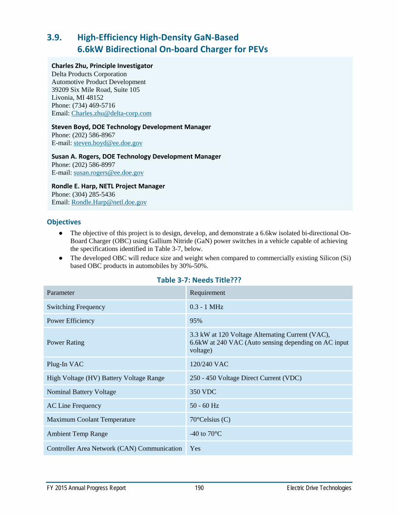
FY 2015 Annual Progress Report 190 Electric Drive Technologies
3.9. High-Efficiency High-Density GaN-Based 6.6kW Bidirectional On-board Charger for PEVs
Charles Zhu, Principle Investigator Delta Products Corporation Automotive Product Development 39209 Six Mile Road, Suite 105 Livonia, MI 48152 Phone: (734) 469-5716 Email: [email protected]
Steven Boyd, DOE Technology Development Manager Phone: (202) 586-8967 E-mail: [email protected]
Susan A. Rogers, DOE Technology Development Manager Phone: (202) 586-8997 E-mail: [email protected]
Rondle E. Harp, NETL Project Manager Phone: (304) 285-5436 Email: [email protected]
Objectives The objective of this project is to design, develop, and demonstrate a 6.6kw isolated bi-directional On-
Board Charger (OBC) using Gallium Nitride (GaN) power switches in a vehicle capable of achieving the specifications identified in Table 3-7, below.
The developed OBC will reduce size and weight when compared to commercially existing Silicon (Si) based OBC products in automobiles by 30%-50%.
Table 3-7: Needs Title??? Parameter Requirement
Switching Frequency 0.3 - 1 MHz
Power Efficiency 95%
Power Rating 3.3 kW at 120 Voltage Alternating Current (VAC), 6.6kW at 240 VAC (Auto sensing depending on AC input voltage)
Plug-In VAC 120/240 VAC
High Voltage (HV) Battery Voltage Range 250 - 450 Voltage Direct Current (VDC)
Nominal Battery Voltage 350 VDC
AC Line Frequency 50 - 60 Hz
Maximum Coolant Temperature 70°Celsius (C)
Ambient Temp Range -40 to 70°C
Controller Area Network (CAN) Communication Yes
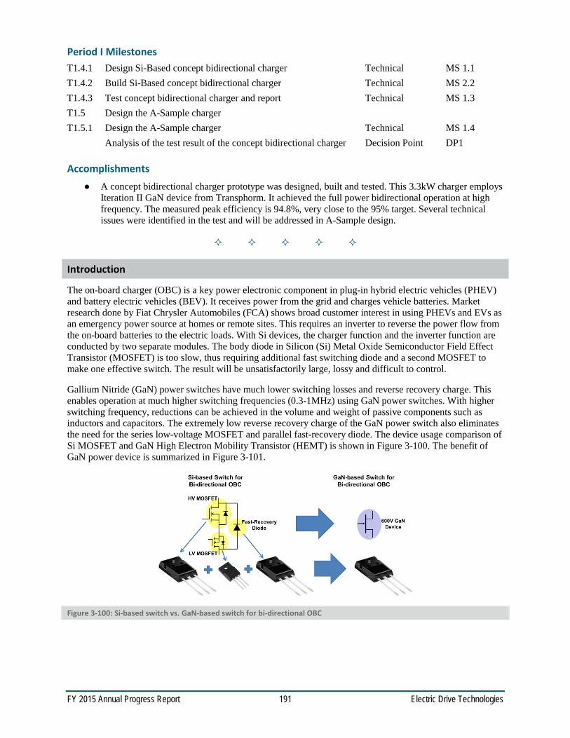
FY 2015 Annual Progress Report 191 Electric Drive Technologies
Period I Milestones T1.4.1 Design Si-Based concept bidirectional charger Technical MS 1.1 T1.4.2 Build Si-Based concept bidirectional charger Technical MS 2.2 T1.4.3 Test concept bidirectional charger and report Technical MS 1.3 T1.5 Design the A-Sample charger
T1.5.1 Design the A-Sample charger Technical MS 1.4
Analysis of the test result of the concept bidirectional charger Decision Point DP1
Accomplishments A concept bidirectional charger prototype was designed, built and tested. This 3.3kW charger employs
Iteration II GaN device from Transphorm. It achieved the full power bidirectional operation at high frequency. The measured peak efficiency is 94.8%, very close to the 95% target. Several technical issues were identified in the test and will be addressed in A-Sample design.
Introduction
The on-board charger (OBC) is a key power electronic component in plug-in hybrid electric vehicles (PHEV) and battery electric vehicles (BEV). It receives power from the grid and charges vehicle batteries. Market research done by Fiat Chrysler Automobiles (FCA) shows broad customer interest in using PHEVs and EVs as an emergency power source at homes or remote sites. This requires an inverter to reverse the power flow from the on-board batteries to the electric loads. With Si devices, the charger function and the inverter function are conducted by two separate modules. The body diode in Silicon (Si) Metal Oxide Semiconductor Field Effect Transistor (MOSFET) is too slow, thus requiring additional fast switching diode and a second MOSFET to make one effective switch. The result will be unsatisfactorily large, lossy and difficult to control.
Gallium Nitride (GaN) power switches have much lower switching losses and reverse recovery charge. This enables operation at much higher switching frequencies (0.3-1MHz) using GaN power switches. With higher switching frequency, reductions can be achieved in the volume and weight of passive components such as inductors and capacitors. The extremely low reverse recovery charge of the GaN power switch also eliminates the need for the series low-voltage MOSFET and parallel fast-recovery diode. The device usage comparison of Si MOSFET and GaN High Electron Mobility Transistor (HEMT) is shown in Figure 3-100. The benefit of GaN power device is summarized in Figure 3-101.
Figure 3-100: Si-based switch vs. GaN-based switch for bi-directional OBC
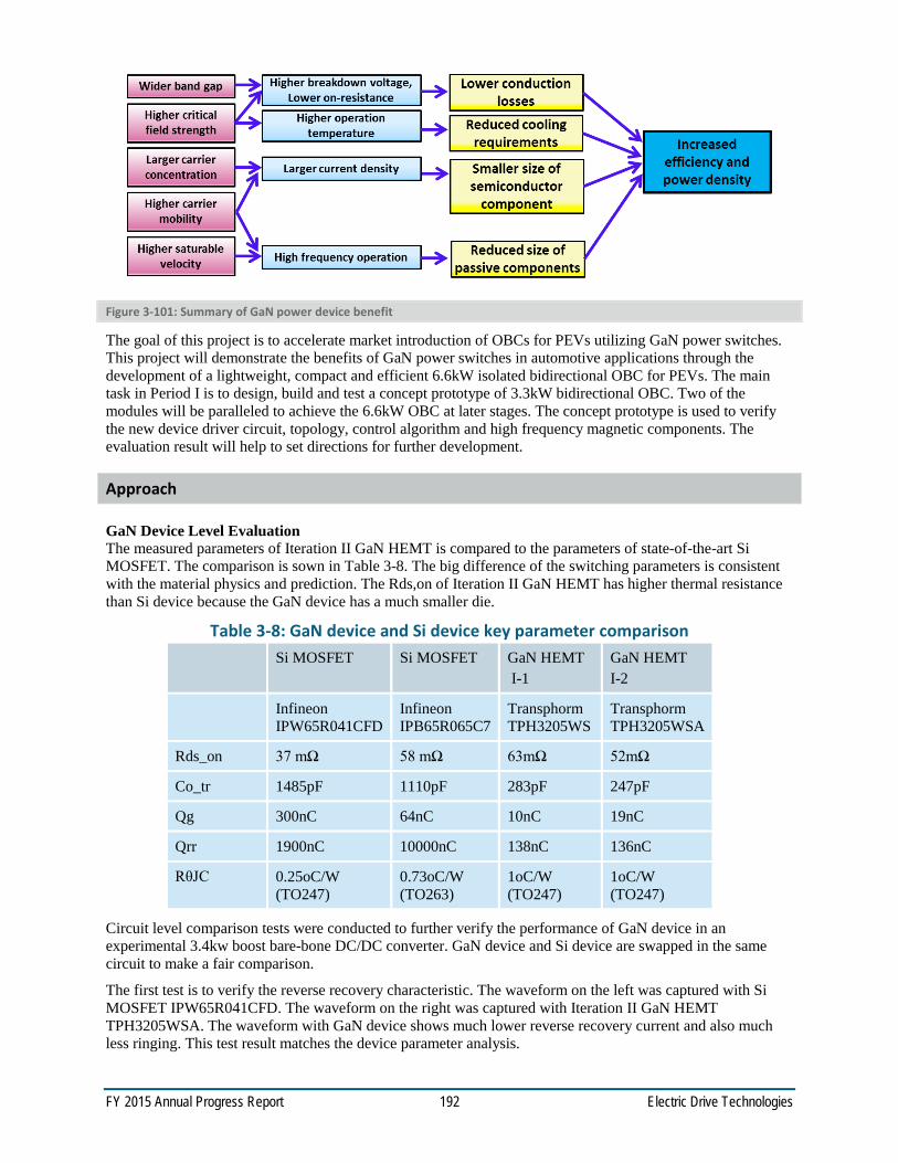
FY 2015 Annual Progress Report 192 Electric Drive Technologies
Figure 3-101: Summary of GaN power device benefit
The goal of this project is to accelerate market introduction of OBCs for PEVs utilizing GaN power switches. This project will demonstrate the benefits of GaN power switches in automotive applications through the development of a lightweight, compact and efficient 6.6kW isolated bidirectional OBC for PEVs. The main task in Period I is to design, build and test a concept prototype of 3.3kW bidirectional OBC. Two of the modules will be paralleled to achieve the 6.6kW OBC at later stages. The concept prototype is used to verify the new device driver circuit, topology, control algorithm and high frequency magnetic components. The evaluation result will help to set directions for further development.
Approach
GaN Device Level Evaluation The measured parameters of Iteration II GaN HEMT is compared to the parameters of state-of-the-art Si MOSFET. The comparison is sown in Table 3-8. The big difference of the switching parameters is consistent with the material physics and prediction. The Rds,on of Iteration II GaN HEMT has higher thermal resistance than Si device because the GaN device has a much smaller die.
Table 3-8: GaN device and Si device key parameter comparison Si MOSFET Si MOSFET GaN HEMT
I-1 GaN HEMT I-2
Infineon IPW65R041CFD
Infineon IPB65R065C7
Transphorm TPH3205WS
Transphorm TPH3205WSA
Rds_on 37 mΩ 58 mΩ 63mΩ 52mΩ
Co_tr 1485pF 1110pF 283pF 247pF
Qg 300nC 64nC 10nC 19nC
Qrr 1900nC 10000nC 138nC 136nC
RθJC 0.25oC/W (TO247)
0.73oC/W (TO263)
1oC/W (TO247)
1oC/W (TO247)
Circuit level comparison tests were conducted to further verify the performance of GaN device in an experimental 3.4kw boost bare-bone DC/DC converter. GaN device and Si device are swapped in the same circuit to make a fair comparison.
The first test is to verify the reverse recovery characteristic. The waveform on the left was captured with Si MOSFET IPW65R041CFD. The waveform on the right was captured with Iteration II GaN HEMT TPH3205WSA. The waveform with GaN device shows much lower reverse recovery current and also much less ringing. This test result matches the device parameter analysis.
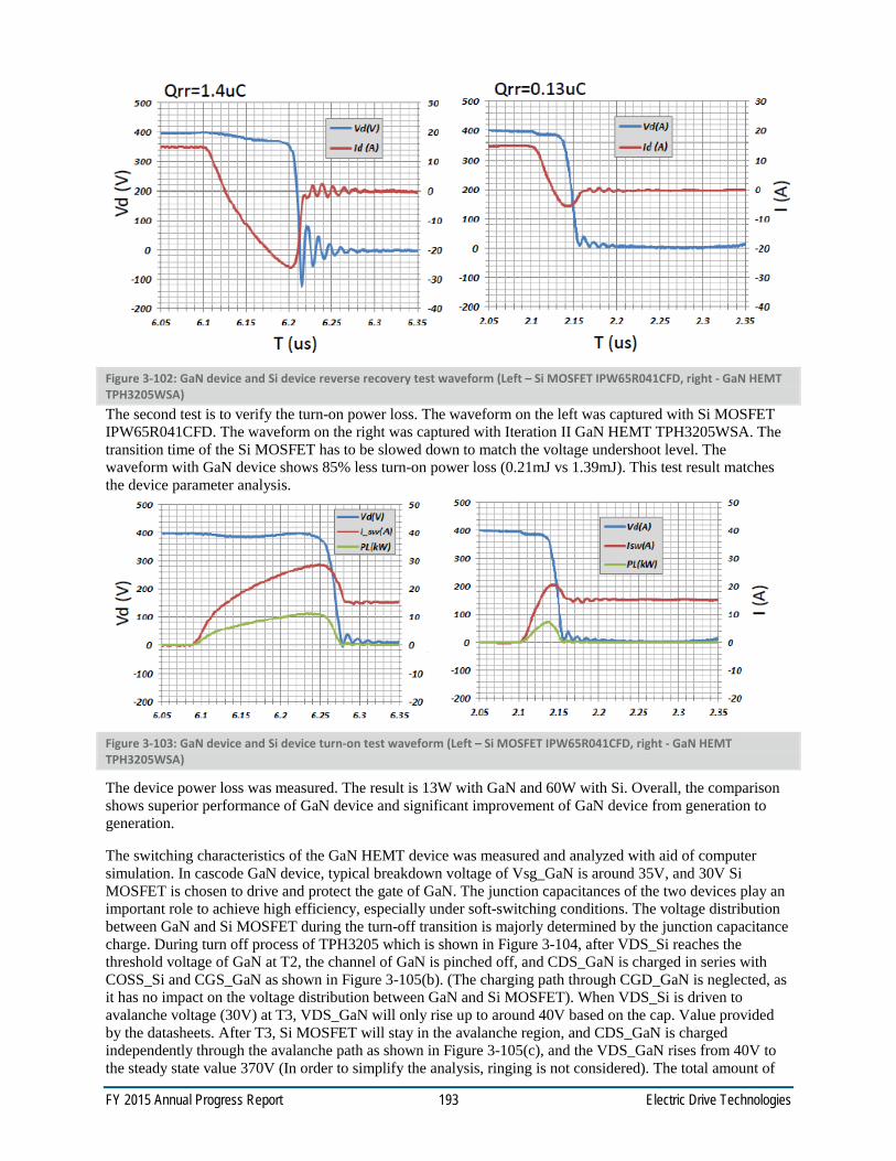
FY 2015 Annual Progress Report 193 Electric Drive Technologies
Figure 3-102: GaN device and Si device reverse recovery test waveform (Left – Si MOSFET IPW65R041CFD, right - GaN HEMT TPH3205WSA) The second test is to verify the turn-on power loss. The waveform on the left was captured with Si MOSFET IPW65R041CFD. The waveform on the right was captured with Iteration II GaN HEMT TPH3205WSA. The transition time of the Si MOSFET has to be slowed down to match the voltage undershoot level. The waveform with GaN device shows 85% less turn-on power loss (0.21mJ vs 1.39mJ). This test result matches the device parameter analysis.
Figure 3-103: GaN device and Si device turn-on test waveform (Left – Si MOSFET IPW65R041CFD, right - GaN HEMT TPH3205WSA)
The device power loss was measured. The result is 13W with GaN and 60W with Si. Overall, the comparison shows superior performance of GaN device and significant improvement of GaN device from generation to generation.
The switching characteristics of the GaN HEMT device was measured and analyzed with aid of computer simulation. In cascode GaN device, typical breakdown voltage of Vsg_GaN is around 35V, and 30V Si MOSFET is chosen to drive and protect the gate of GaN. The junction capacitances of the two devices play an important role to achieve high efficiency, especially under soft-switching conditions. The voltage distribution between GaN and Si MOSFET during the turn-off transition is majorly determined by the junction capacitance charge. During turn off process of TPH3205 which is shown in Figure 3-104, after VDS_Si reaches the threshold voltage of GaN at T2, the channel of GaN is pinched off, and CDS_GaN is charged in series with COSS_Si and CGS_GaN as shown in Figure 3-105(b). (The charging path through CGD_GaN is neglected, as it has no impact on the voltage distribution between GaN and Si MOSFET). When VDS_Si is driven to avalanche voltage (30V) at T3, VDS_GaN will only rise up to around 40V based on the cap. Value provided by the datasheets. After T3, Si MOSFET will stay in the avalanche region, and CDS_GaN is charged independently through the avalanche path as shown in Figure 3-105(c), and the VDS_GaN rises from 40V to the steady state value 370V (In order to simplify the analysis, ringing is not considered). The total amount of
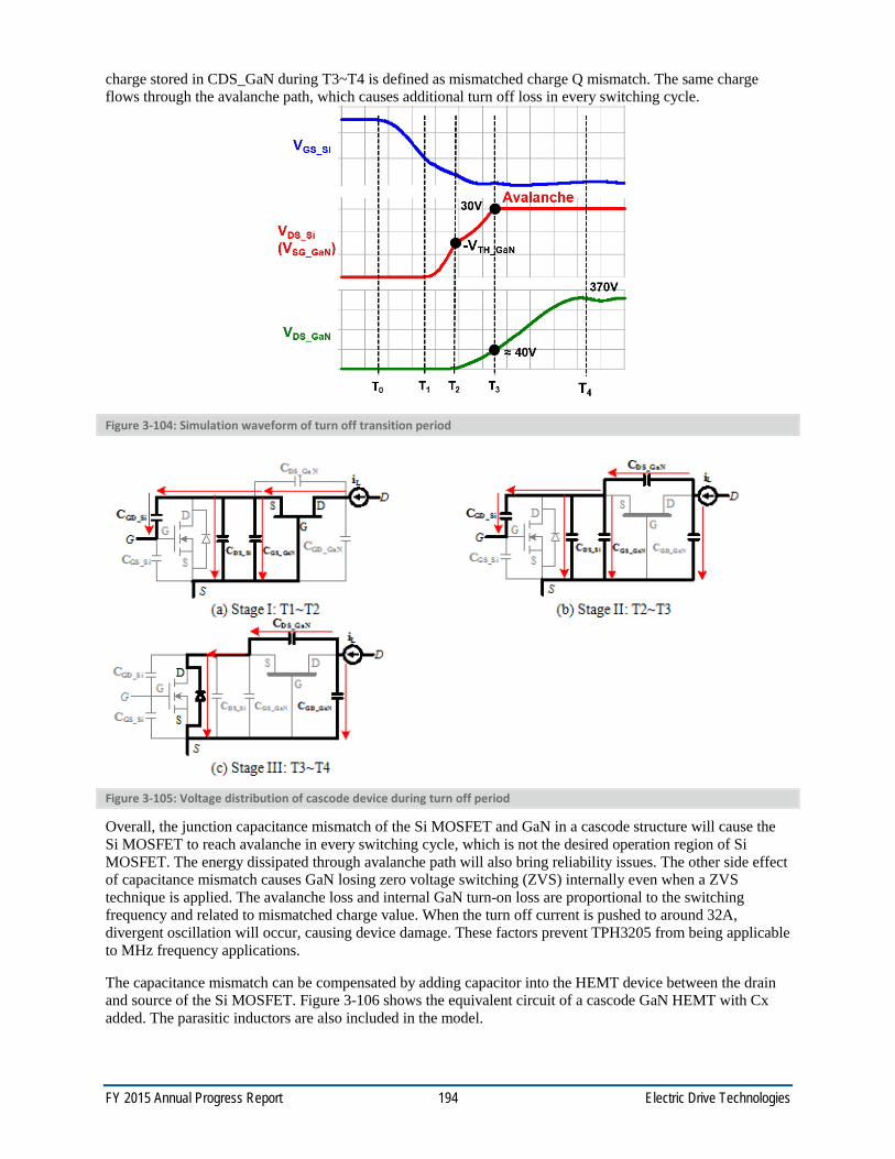
FY 2015 Annual Progress Report 194 Electric Drive Technologies
charge stored in CDS_GaN during T3~T4 is defined as mismatched charge Q mismatch. The same charge flows through the avalanche path, which causes additional turn off loss in every switching cycle.
Figure 3-104: Simulation waveform of turn off transition period
Figure 3-105: Voltage distribution of cascode device during turn off period
Overall, the junction capacitance mismatch of the Si MOSFET and GaN in a cascode structure will cause the Si MOSFET to reach avalanche in every switching cycle, which is not the desired operation region of Si MOSFET. The energy dissipated through avalanche path will also bring reliability issues. The other side effect of capacitance mismatch causes GaN losing zero voltage switching (ZVS) internally even when a ZVS technique is applied. The avalanche loss and internal GaN turn-on loss are proportional to the switching frequency and related to mismatched charge value. When the turn off current is pushed to around 32A, divergent oscillation will occur, causing device damage. These factors prevent TPH3205 from being applicable to MHz frequency applications.
The capacitance mismatch can be compensated by adding capacitor into the HEMT device between the drain and source of the Si MOSFET. Figure 3-106 shows the equivalent circuit of a cascode GaN HEMT with Cx added. The parasitic inductors are also included in the model.
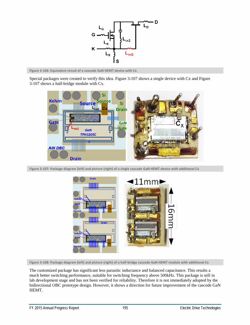
FY 2015 Annual Progress Report 195 Electric Drive Technologies
Figure 3-106: Equivalent circuit of a cascode GaN HEMT device with Cx
Special packages were created to verify this idea. Figure 3-107 shows a single device with Cx and Figure 3-107 shows a half-bridge module with Cx.
Figure 3-107: Package diagram (left) and picture (right) of a single cascode GaN HEMT device with additional Cx
Figure 3-108: Package diagram (left) and picture (right) of a half-bridge cascode GaN HEMT module with additional Cx
The customized package has significant less parasitic inductance and balanced capacitance. This results a much better switching performance, suitable for switching frequency above 500kHz. This package is still in lab development stage and has not been verified for reliability. Therefore it is not immediately adopted by the bidirectional OBC prototype design. However, it shows a direction for future improvement of the cascode GaN HEMT.

FY 2015 Annual Progress Report 196 Electric Drive Technologies
Advanced Magnetic Components Development
High frequency operation brings a challenge for magnetic components design. At high frequency, both core loss and winding loss increases dramatically and parasitic parameters become significant. It might still be possible to use conventional wire wound technology at 300kHz, but it is approaching the limitation. Printed circuit board (PCB) winding provides an alternative solution.
Adopting matrix transformer concept, a UI core based transformer is used [15, 16], as shown in Figure 3-109. However, the leakage inductance is very small due to perfect interleave. Since regulation is still needed for DCDC stage, a larger leakage inductance must be used to serve as resonant inductor.
Figure 3-109: Matrix transformer using PCB winding with leakage integration One way to get a larger leakage inductance is to change the UI core into an EI core. In this structure, the center post serves as leakage pass. The reluctance model is built to calculate the magnetic inductance (Lm) and leakage inductance (Lk). Multiple winding structures were evaluated in terms of power loss, size and manufacturability. The design is narrowed down to two candidates, shown in Figure 3-110. The power loss comparison is shown in Figure 3-111.
Figure 3-110: 12 layer transformer design and 2X6 layer transformer design

FY 2015 Annual Progress Report 197 Electric Drive Technologies
Figure 3-111: Power loss comparison of 12 layer transformer design and 2X6 layer transformer design
The 6 layer design has higher loss for two reasons. First, the core loss is higher because it has higher core volume. Second, the winding loss is higher because the winding width is reduced to maintain the footprint.
The study on high frequency transformer will continue to reduce the power loss and harmonize with the electric and mechanical design.
Module Level Development Early in the 1st calendar quarter 2015, the initial power system topology was finalized. The power circuit is comprised of two stages, an AC/DC stage and a DC/DC stage. Prior development and study in program proposal shows this is the overall best strategy for the design. A hard-switching full bridge AC/DC and a DBA derived CLLC resonant DC/DC was proposed in the program application material. In the 4th quarter of 2014 and the 1st quarter of 2015, more topologies were brought forth for study. After circuit analysis, simulation and experimentation, the original topology was re-confirmed at a joint team review and will be used in the concept prototype. The topology for concept prototype is illustrated in Figure 3-112.
Figure 3-112: Topology selected for 3.3kW charger Concept Prototype Build
A totem-pole AC/DC topology was also identified for further research for its potential to realize bi-directional soft switching at 500kHz. This initial architecture was finalized in a partner joint review. The topology for further research are illustrated in Figure 3-113. This is the Plan B for the OBC development.
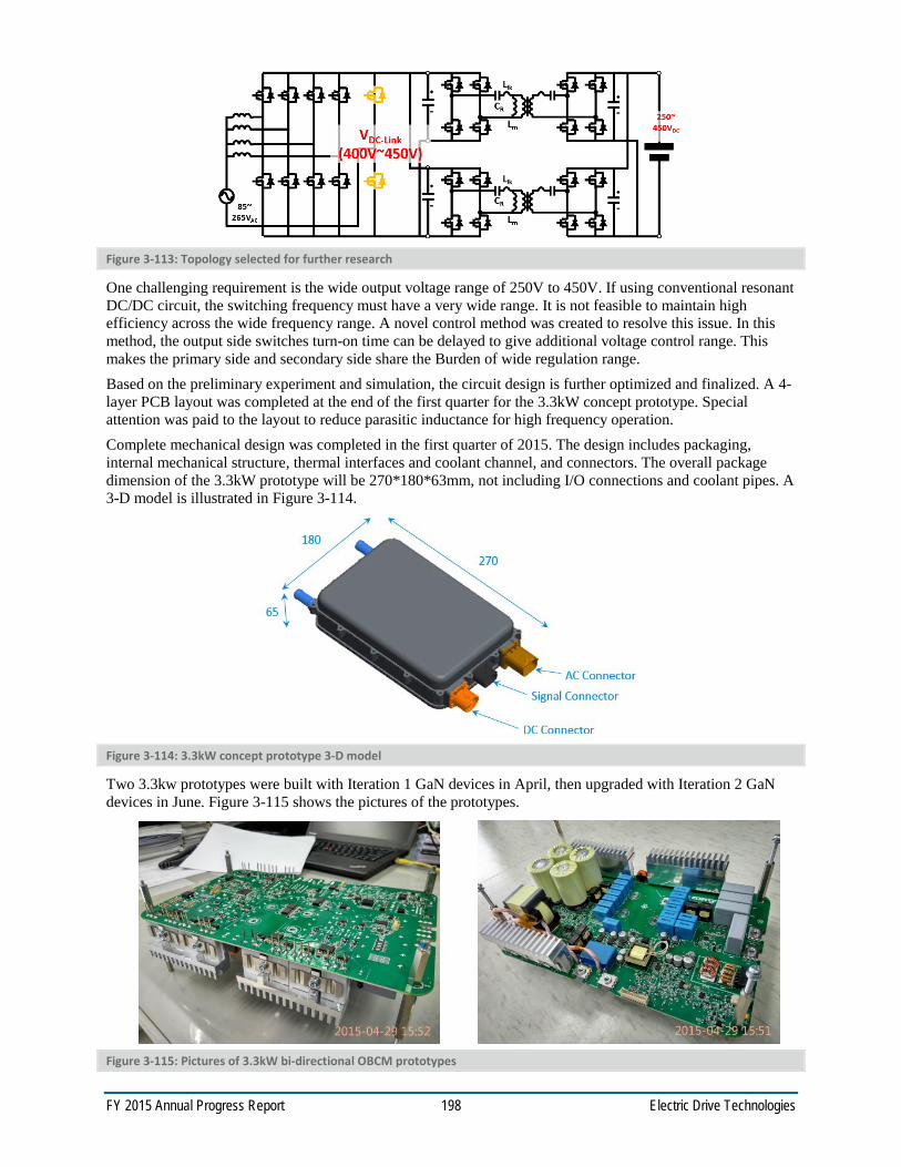
FY 2015 Annual Progress Report 198 Electric Drive Technologies
Figure 3-113: Topology selected for further research
One challenging requirement is the wide output voltage range of 250V to 450V. If using conventional resonant DC/DC circuit, the switching frequency must have a very wide range. It is not feasible to maintain high efficiency across the wide frequency range. A novel control method was created to resolve this issue. In this method, the output side switches turn-on time can be delayed to give additional voltage control range. This makes the primary side and secondary side share the Burden of wide regulation range. Based on the preliminary experiment and simulation, the circuit design is further optimized and finalized. A 4-layer PCB layout was completed at the end of the first quarter for the 3.3kW concept prototype. Special attention was paid to the layout to reduce parasitic inductance for high frequency operation. Complete mechanical design was completed in the first quarter of 2015. The design includes packaging, internal mechanical structure, thermal interfaces and coolant channel, and connectors. The overall package dimension of the 3.3kW prototype will be 270*180*63mm, not including I/O connections and coolant pipes. A 3-D model is illustrated in Figure 3-114.
Figure 3-114: 3.3kW concept prototype 3-D model
Two 3.3kw prototypes were built with Iteration 1 GaN devices in April, then upgraded with Iteration 2 GaN devices in June. Figure 3-115 shows the pictures of the prototypes.
Figure 3-115: Pictures of 3.3kW bi-directional OBCM prototypes
FY 2015 Annual Progress Report 199 Electric Drive Technologies
Results and Discussion
This concept prototype OBCM are built with Iteration II GaN device, PN TPH3205WSA. It is capable of 3.3kW operation in both directions. The AC/DC stage’s operates frequency is 150kHz at device level and 300kHz as a full bridge. The DC/DC stage operates at various frequencies above 300kHz. Table 3-9 is the summary of the test result side-by-side with the project technical requirement. Text Text Text Text
Parameter Requirement Test Result of Concept Prototype Notes
Switching Frequency 0.3 - 1 Mega-Hertz (MHz)
0.3MHz at PFC Stage and >0.3MHz at DC/DC Stage
Meet requirement
Power Efficiency 95% 94.8% Need improvement
Power Rating
3.3 kilo-Watt (kW) at 120 Volts Alternating Current (VAC), 6.6kW at 240 VAC (Auto sensing depending on AC input voltage)
3.3kW output at 240Vac per module Meet requirement
Plug-In VAC 120/240 VAC 120V/240Vac Meet requirement High Voltage (HV) Battery Voltage Range
250 - 450 Voltage Direct Current (VDC) Meet requirement
Nominal Battery Voltage 350 VDC Meet requirement
AC Line Frequency 50 - 60 Hz Tested at 60Hz Low risk to operate at 50Hz
Maximum Coolant Temperature 70°Celcius (C) Some components
are hot Need improvement
Ambient Temp Range -40 to 70°C Not tested To be tested with A-
Sample or B-Sample Controller Area Network (CAN) Communication
Yes Not implemented Will be implemented in A-sample or B-Sample
Table 3-9: Requirement and Test Result Summary
Parameter Requirement Test Result of Concept Prototype Notes
Switching Frequency 0.3 - 1 Mega-Hertz (MHz) 0.3MHz at PFC Stage and >0.3MHz at DC/DC Stage
Meet requirement
Power Efficiency 95% 94.8% Need improvement
Power Rating 3.3 kW at 120 VAC, 6.6kW at 240 VAC (Auto sensing depending on AC input voltage)
3.3kW output at 240Vac per module Meet requirement
Plug-In VAC 120/240 VAC 120V/240Vac Meet requirement High Voltage (HV) Battery Voltage Range
250 - 450 VDC Meet requirement
Nominal Battery 350 VDC Meet requirement
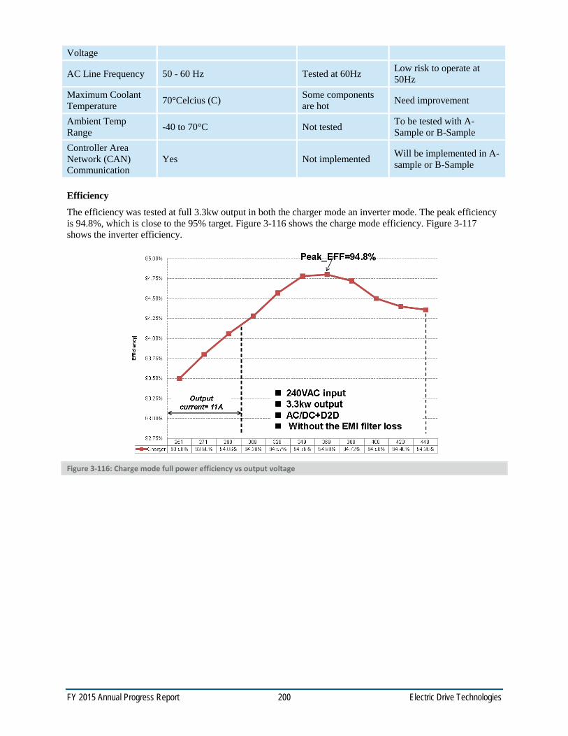
FY 2015 Annual Progress Report 200 Electric Drive Technologies
Voltage
AC Line Frequency 50 - 60 Hz Tested at 60Hz Low risk to operate at 50Hz
Maximum Coolant Temperature 70°Celcius (C) Some components
are hot Need improvement
Ambient Temp Range -40 to 70°C Not tested To be tested with A-
Sample or B-Sample Controller Area Network (CAN) Communication
Yes Not implemented Will be implemented in A-sample or B-Sample
Efficiency
The efficiency was tested at full 3.3kw output in both the charger mode an inverter mode. The peak efficiency is 94.8%, which is close to the 95% target. Figure 3-116 shows the charge mode efficiency. Figure 3-117 shows the inverter efficiency.
Figure 3-116: Charge mode full power efficiency vs output voltage
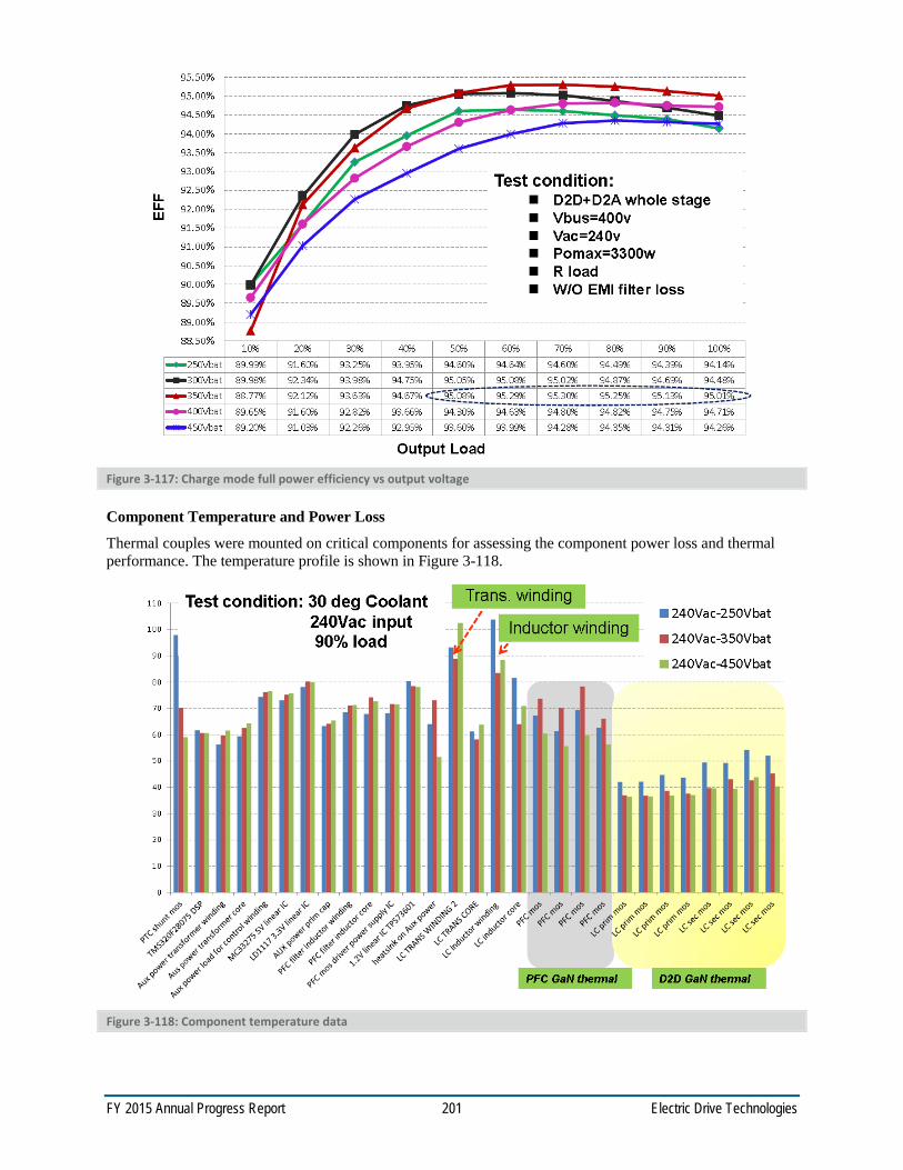
FY 2015 Annual Progress Report 201 Electric Drive Technologies
Figure 3-117: Charge mode full power efficiency vs output voltage
Component Temperature and Power Loss
Thermal couples were mounted on critical components for assessing the component power loss and thermal performance. The temperature profile is shown in Figure 3-118.
Figure 3-118: Component temperature data

FY 2015 Annual Progress Report 202 Electric Drive Technologies
From this test we identified two issues.
1. Excessive power loss on power factor correction (PFC) Stage GaN devices
The PFC stage GaN devices operate in hard switching. Even the GaN device has much better switching performance than Si device, hard switching at 150kHz is still a stretch. The power loss is approximately 30W per device. This is a challenge for thermal design. Several mitigation approaches are to be experimented:
a. Improving the Rds,on and switching performance of the GaN device. By increase the die size, the Rds,on can be reduced. However, bigger die also means bigger parasitic capacitance, which will cause higher switching loss. Additional technology progress is needed to keep the parasitic capacitance down.
Add snubber circuit. Although snubber circuit usually increases power loss. However, sometimes it can reduce switching loss by reducing switching resonance.
b. Reduce switching frequency. If the device is still too hot at the end, we can still reduce the switching frequency. This proportionally reduces switching loss. After all, there is a limitation of how far we can push a certain device; and the module reliability is more important than switching frequency for commercialization, particularly in automotive application. But we still have more than a year to make the improvement.
2. Excessive power loss on DC/DC transformer and resonance inductor
The current transformer design has a purposely induced space between the primary winding and secondary winding, in order to increase the leakage inductance of the transformer. This leakage inductor serves as part of the resonance inductor, allowing a smaller resonance inductor. However, the leakage inductor created a high frequency magnetic field in surrounding air. When the transformer is enclosed by thermally conductive metal walls, the magnetic field caused significant eddy loss in the metal walls. This eddy power loss is approximately 10W. The next transformer design will return to highly coupled windings to minimize the leakage field.
Charger AC Input Power Factor
Power factor was measured at multiple power levels under both 120VAC input condition and 240VAC input condition. The result is satisfactory. The power factor data is shown in Figure 3-119 and Figure 3-120.
Figure 3-119: 120Vac input power factor vs power level
0.12 0.24 0.34 0.48 0.58 0.73 0.81 0.92120Vac PF 0.9110.9890.9980.9990.9980.9970.9960.994
0.90.910.920.930.940.950.960.970.980.99
1
Pow
er fa
ctor
120Vac PF vs. output power percent

FY 2015 Annual Progress Report 203 Electric Drive Technologies
Figure 3-120: 240Vac input power factor vs power level
120VAC PF > 0.97 above 50% load and PF > 0.99 at full load. 240VAC PF > 0.95 above 50% load and PF > 0.99 at full load. Input current THD meet or exceed the EN61000-3-2 CLASS A specifications.
Dynamic Response
The preliminary dynamic load test shows the converter maintains good output regulation when the load changes. Figure 3-121 shows the test result. The AC output voltage (blue trace) remains in good shape when the load current (red trace) changes from 20% to 70% load.
Figure 3-121: Inverter dynamic load test
Parallel Operation When two inverter modules are paralleled, there is naturally some difference in their phase and amplitude. This causes circulating current between the two modules. Therefore, one module has higher current than the other. Without feedback control or artificial impedance, this difference will increase cycle by cycle until one module’s current reaches it maximum limit. Several mitigation approaches are to be experimented:
0.24 0.36 0.49 0.61 0.73 0.85 0.96240Vac PF 0.884 0.96 0.984 0.994 0.998 0.999 0.999
0.880.89
0.90.910.920.930.940.950.960.970.980.99
1
Pow
er fa
ctor
240Vac PF vs. output power percent

FY 2015 Annual Progress Report 204 Electric Drive Technologies
a. Add additional control loop to force the amplitude balance and phase synchronization of the two modules b. Change topology and make device paralleling instead of module paralleling
Conclusions and Future Directions
The result of the test proves the GaN device, the innovative topology and control strategy. The maximum efficiency of the prototype is 94.8%, close to the 95% target. With further improvement of GaN device and circuit optimization, we are optimistic about meeting the 95% efficiency with A-Sample or B-Sample. Several issues were exposed through these evaluation and experiments as discussed above. A-Sample design has started and is to be completed in the 4th quarter of 2015. The A-Sample design will address the issues found in concept module test and will have two 3.3kw modules paralleled.
FY 2014 Présentations/Publications/Patents
1. Yungtaek Jang, Milan M. Jovanović, Juan M. Ruiz, and Gang Liu, “Series-Resonant Converter with Reduced-Frequency-Range Control”, in IEEE Applied Power Electronics Conf. Rec. 2015
2. Yungtaek Jang, Milan M. Jovanović, Juan M. Ruiz, Misha Kumar, and Gang Liu, “A Novel Active-Current-Sharing Method for Interleaved Resonant Converters”, in IEEE Applied Power Electronics Conf. Rec. 2015
3. Y.-F. Wu and K. Smith, “Progress of GaN Transistors for Automotive Applications”, in PICM May 2015.
Acknowledgements
The author would like to acknowledge the support provided by Susan Rogers and Steven Boyd, Technology Development Managers for the EDT Program, Vehicle Technologies Office, U.S. Department of Energy Office of Energy Efficiency and Renewable Energy. The significant contributions of Xiaopeng Wang and Yungtaek Jung are acknowledged. The author would also like to acknowledge Qiang Li (CPES) for their excellent work on GaN HEMT switching characteristics analysis and high frequency circuit study; Yifeng Wu (Transphorm) for support on GaN HEMT samples and application support; as well as David Williams (FCA) for vehicle application specification.
References
1. Transphorm, "TPH3205WSA v2c preliminary data sheet," www.transphorm.com, Jue16, 2015. 2. Zijian Wang, Shuo Wang, Pengju Kong, Fred C. Lee, “DM EMI Noise Prediction for Constant On-
Time, Critical Mode Power Factor Correction Converters”, IEEE Transactions on Power Electronics, vol. 27, issue 7, pp. 3150-3157, July 2012.
3. M. S. Elmore, “Input current ripple cancellation in synchronized, parallel connected critically continuous boost converters,” in Proc. IEEE Appl. Power Electron. Conf. (APEC), Mar. 1996, pp. 152–158.
4. M. S. Elmore and K. A. Wallace, “Zero voltage switching supplies connected in parallel.” U.S. Patent 5 793 191, Aug. 11, 1998.
5. X. Xu and A. Huang, “A novel closed loop interleaving strategy of multiphase critical mode boost PFC converters,” in Proc. IEEE Appl. Power Electron. Conf. (APEC), Feb. 2008, pp. 1033–1038.
6. Huber, L.; Irving, B.T.; Jovanovic, M.M., "Review and Stability Analysis of PLL-Based Interleaving Control of DCM/CCM Boundary Boost PFC Converters," Power Electronics, IEEE Transactions on, vol.24, no.8, pp.1992,1999, Aug. 2009
7. Xiliang Chen, “Research on Totem-Pole Bridgeless PFC Converter”, MS Thesis, Zhejiang University, 03.24.2014
8. Kolar, J.W.; Kamath, G.R.; Mohan, N.; Zach, Franz C., "Self-adjusting input current ripple cancellation of coupled parallel connected hysteresis-controlled boost power factor correctors," Power

FY 2015 Annual Progress Report 205 Electric Drive Technologies
Electronics Specialists Conference, 1995. PESC '95 Record., 26th Annual IEEE, vol.1, no., pp.164,173 vol.1, 18-22 Jun 1995
9. T. Ishii and Y. Mizutani, “Power factor correction using interleaving technique for critical mode switching converters,” in Proc. IEEE Power Electronics Specialists Conf. (PESC), May 1998, pp. 905–910.
10. T. Ishii and Y. Mizutani, “Variable Frequency Switching of Synchronized Interleaved Switching Converters,” U.S. Patent 5 905 369, May 18, 1999.
11. B. T. Irving, Y. Jang, and M. M. Jovanovic´, “A comparative study of soft-switched CCM boost rectifiers and interleaved variable-frequency DCM boost rectifier,” in Proc. IEEE Applied Power Electronics Conf. (APEC), Feb. 2000, pp. 171–177.
12. J. Zhang, J. Shao, F. C. Lee, and M. M. Jovanovic´, “Evaluation of input current in the critical mode boost PFC converter for distributed power systems,” in Proc. IEEE Applied Power Electronics Conf. (APEC), Feb. 2001, pp. 130–136.
13. L. Huber, B. T. Irving, and M. M. Jovanovic, “Open-Loop Control Methods for Interleaved DCM/CCM Boundary Boost PFC Converters,” IEEE Trans. On Power Electron., vol. 23, no. 4, pp. 1649-1655, Jul. 2008.
14. M. Mingkai, L. Qiang, D. Gilham et al., "New core loss measurement method for high frequency magnetic materials," in Energy Conversion Congress and Exposition (ECCE), 2010 IEEE. pp. 4384-4389.
15. D. Reusch, and F. C. Lee, "High frequency bus converter with integrated matrix transformers for CPU and telecommunications applications," in Energy Conversion Congress and Exposition (ECCE), 2010 IEEE. pp. 2446-2450.
16. D. Reusch, and F. C. Lee, "High frequency bus converter with low loss integrated matrix transformer," in Applied Power Electronics Conference and Exposition (APEC), 2012 Twenty-Seventh Annual IEEE. pp. 1392-1397.
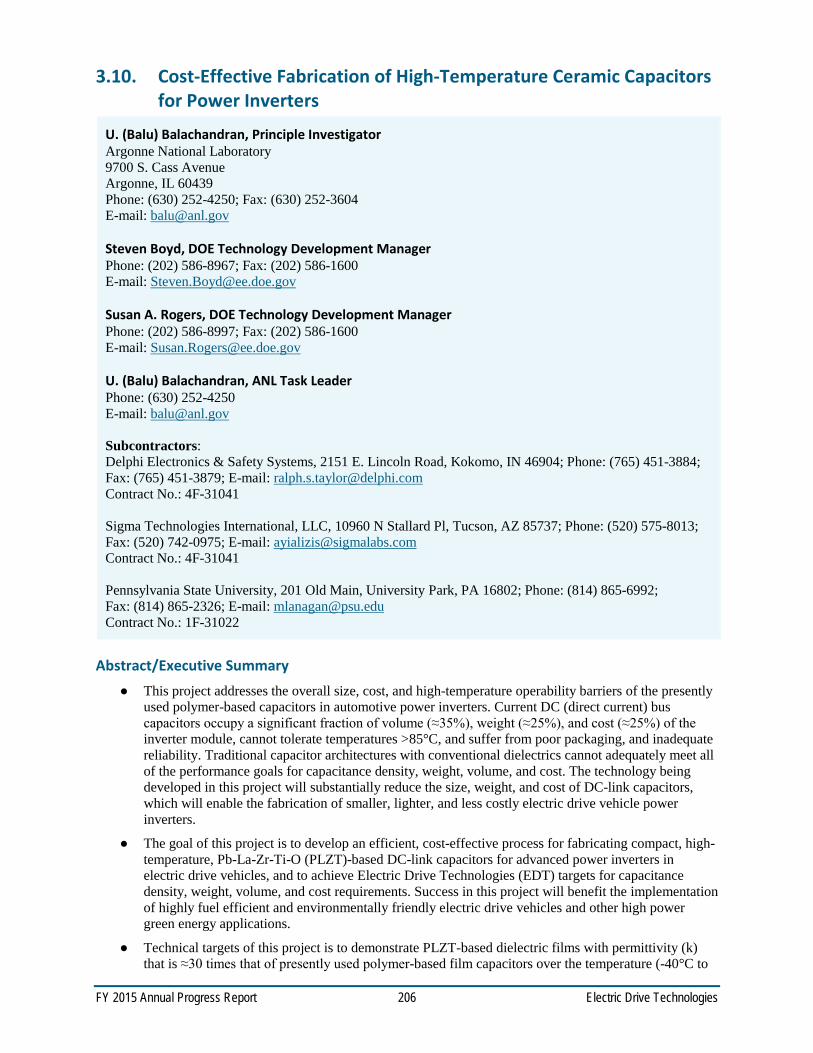
FY 2015 Annual Progress Report 206 Electric Drive Technologies
3.10. Cost-Effective Fabrication of High-Temperature Ceramic Capacitors for Power Inverters
U. (Balu) Balachandran, Principle Investigator Argonne National Laboratory 9700 S. Cass Avenue Argonne, IL 60439 Phone: (630) 252-4250; Fax: (630) 252-3604 E-mail: [email protected] Steven Boyd, DOE Technology Development Manager Phone: (202) 586-8967; Fax: (202) 586-1600 E-mail: [email protected] Susan A. Rogers, DOE Technology Development Manager Phone: (202) 586-8997; Fax: (202) 586-1600 E-mail: [email protected] U. (Balu) Balachandran, ANL Task Leader Phone: (630) 252-4250 E-mail: [email protected] Subcontractors: Delphi Electronics & Safety Systems, 2151 E. Lincoln Road, Kokomo, IN 46904; Phone: (765) 451-3884; Fax: (765) 451-3879; E-mail: [email protected] Contract No.: 4F-31041 Sigma Technologies International, LLC, 10960 N Stallard Pl, Tucson, AZ 85737; Phone: (520) 575-8013; Fax: (520) 742-0975; E-mail: [email protected] Contract No.: 4F-31041 Pennsylvania State University, 201 Old Main, University Park, PA 16802; Phone: (814) 865-6992; Fax: (814) 865-2326; E-mail: [email protected] Contract No.: 1F-31022
Abstract/Executive Summary This project addresses the overall size, cost, and high-temperature operability barriers of the presently
used polymer-based capacitors in automotive power inverters. Current DC (direct current) bus capacitors occupy a significant fraction of volume (≈35%), weight (≈25%), and cost (≈25%) of the inverter module, cannot tolerate temperatures >85°C, and suffer from poor packaging, and inadequate reliability. Traditional capacitor architectures with conventional dielectrics cannot adequately meet all of the performance goals for capacitance density, weight, volume, and cost. The technology being developed in this project will substantially reduce the size, weight, and cost of DC-link capacitors, which will enable the fabrication of smaller, lighter, and less costly electric drive vehicle power inverters.
The goal of this project is to develop an efficient, cost-effective process for fabricating compact, high-temperature, Pb-La-Zr-Ti-O (PLZT)-based DC-link capacitors for advanced power inverters in electric drive vehicles, and to achieve Electric Drive Technologies (EDT) targets for capacitance density, weight, volume, and cost requirements. Success in this project will benefit the implementation of highly fuel efficient and environmentally friendly electric drive vehicles and other high power green energy applications.
Technical targets of this project is to demonstrate PLZT-based dielectric films with permittivity (k) that is ≈30 times that of presently used polymer-based film capacitors over the temperature (-40°C to
FY 2015 Annual Progress Report 207 Electric Drive Technologies
+140°C), voltage (450 V nominal) and frequency (≈10 kHz) ranges required for automotive power electronics and develop a high-rate, room-temperature aerosol deposition (AD) process to economically manufacture PLZT-based capacitors.
Accomplishments Demonstrated that the PLZT-based ceramic capacitor's properties meet EDT project objectives. The
results have been verified by our industry and university collaborators.
Developed aerosol deposition, a high-rate, room-temperature film deposition process to economically fabricate the PLZT capacitors. Argonne developed AD process is being integrated onto a rotating-wheel deposition system at Sigma Technologies, LLC.
Developed solution chemistry to synthesize submicron PLZT powders suitable for AD process and identified a commercial supplier of powders for large-scale manufacturing of PLZT capacitors.
Fabricated ≈8-µm-thick PLZT film on metallized polyimide films in ≈20 min by AD process (vs. a week by spin-coating process used to demonstrate PLZT's properties).
Demonstrated graceful failure mode in single layer PLZT films.
Measured mean breakdown voltage of 990 V, high energy density of 10 J/cc and low leakage current density of <0.1 μA/square-cm at ≈500 V bias in a ≈8-µm-thick PLZT capacitor fabricated on metallized polyimide films by AD process.
PLZT film made by high-rate AD process has high dielectric constant and low loss over the advanced power inverter's operational temperature, voltage, and frequency range.
Defined capacitor specification for the inverter and established materials cost targets to meet the Funding Opportunity Announcement requirement.
Introduction
Capacitors are essential components of power electronics for carrying out a host of functions in pulse power and power electronics applications such as pulse discharge, filtering, voltage smoothing, coupling, de-coupling, DC blocking, power conditioning, snubbing, electromagnetic interference suppression, and commutation in power electronics. They are a critical to the performance of power inverter modules within electric drive vehicles (EDVs) which directly affects fuel efficiency and battery life. Capacitors occupy ≈35% of the inverter volume and account for ≈25% of the weight in current designs. Thus, even if all other components in an inverter are reduced significantly, the capacitor requirement is a serious impediment to achieving the required volume and weight reduction. In addition, the use of high-temperature coolants further exacerbates the situation because existing film capacitors lose their capability to absorb ripple currents at elevated temperatures, necessitating the addition of extra capacitors. Increasing the volumetric performance (capacitance per unit volume) of DC bus capacitors is required, and their maximum operating temperature also must be increased to assure reliability requirements. Ceramic capacitors have the greatest potential for volume reduction; they could be as small as 30% of the volume of a polymer-based capacitor currently used in EDVs. Ceramics offer high dielectric constants and breakdown fields and, therefore, high energy densities. They also can tolerate high temperatures with a low equivalent series resistance (ESR), enabling them to carry high ripple currents even at elevated temperatures.
Driven by the increasing demand for passive power electronics with improved performance, high reliability, and reduced size and weight, much attention has been paid to the so-called “film-on-foil” technology, in which ceramic films deposited on metal foils are embedded into a printed circuit board (PCB). Our research [1-4] had shown that the lead lanthanum zirconate titanate (Pb0.92La0.08Zr0.52Ti0.48O3, PLZT) films deposited on base metal foils possess excellent dielectric properties, which are promising for high power applications such as plug-in hybrid electric vehicles. Use of base-metal foils reduces the cost of the capacitor. The stacked and embedded capacitors approaches significantly reduces component footprint, improves device performance, provides greater design flexibility, and offers an economic advantage for commercialization. This technology
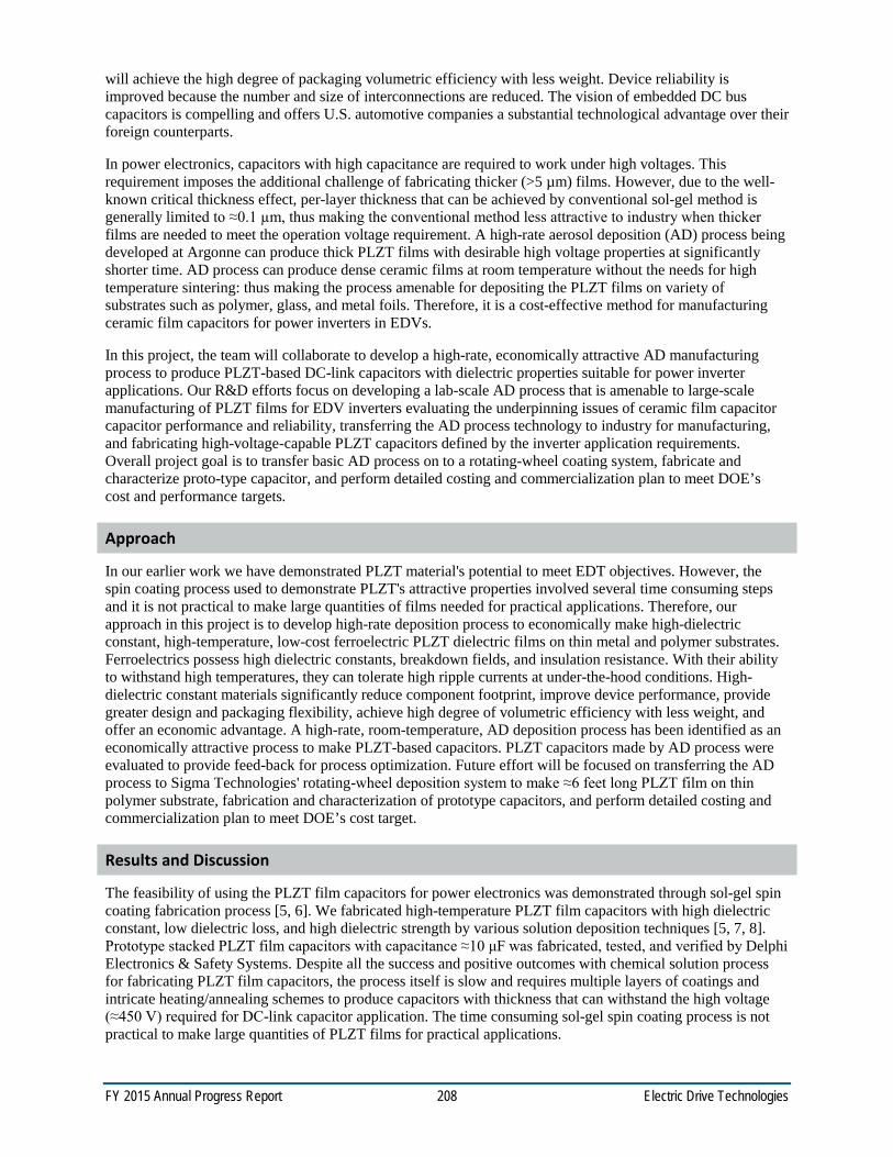
FY 2015 Annual Progress Report 208 Electric Drive Technologies
will achieve the high degree of packaging volumetric efficiency with less weight. Device reliability is improved because the number and size of interconnections are reduced. The vision of embedded DC bus capacitors is compelling and offers U.S. automotive companies a substantial technological advantage over their foreign counterparts.
In power electronics, capacitors with high capacitance are required to work under high voltages. This requirement imposes the additional challenge of fabricating thicker (>5 µm) films. However, due to the well-known critical thickness effect, per-layer thickness that can be achieved by conventional sol-gel method is generally limited to ≈0.1 µm, thus making the conventional method less attractive to industry when thicker films are needed to meet the operation voltage requirement. A high-rate aerosol deposition (AD) process being developed at Argonne can produce thick PLZT films with desirable high voltage properties at significantly shorter time. AD process can produce dense ceramic films at room temperature without the needs for high temperature sintering: thus making the process amenable for depositing the PLZT films on variety of substrates such as polymer, glass, and metal foils. Therefore, it is a cost-effective method for manufacturing ceramic film capacitors for power inverters in EDVs.
In this project, the team will collaborate to develop a high-rate, economically attractive AD manufacturing process to produce PLZT-based DC-link capacitors with dielectric properties suitable for power inverter applications. Our R&D efforts focus on developing a lab-scale AD process that is amenable to large-scale manufacturing of PLZT films for EDV inverters evaluating the underpinning issues of ceramic film capacitor capacitor performance and reliability, transferring the AD process technology to industry for manufacturing, and fabricating high-voltage-capable PLZT capacitors defined by the inverter application requirements. Overall project goal is to transfer basic AD process on to a rotating-wheel coating system, fabricate and characterize proto-type capacitor, and perform detailed costing and commercialization plan to meet DOE’s cost and performance targets.
Approach
In our earlier work we have demonstrated PLZT material's potential to meet EDT objectives. However, the spin coating process used to demonstrate PLZT's attractive properties involved several time consuming steps and it is not practical to make large quantities of films needed for practical applications. Therefore, our approach in this project is to develop high-rate deposition process to economically make high-dielectric constant, high-temperature, low-cost ferroelectric PLZT dielectric films on thin metal and polymer substrates. Ferroelectrics possess high dielectric constants, breakdown fields, and insulation resistance. With their ability to withstand high temperatures, they can tolerate high ripple currents at under-the-hood conditions. High-dielectric constant materials significantly reduce component footprint, improve device performance, provide greater design and packaging flexibility, achieve high degree of volumetric efficiency with less weight, and offer an economic advantage. A high-rate, room-temperature, AD deposition process has been identified as an economically attractive process to make PLZT-based capacitors. PLZT capacitors made by AD process were evaluated to provide feed-back for process optimization. Future effort will be focused on transferring the AD process to Sigma Technologies' rotating-wheel deposition system to make ≈6 feet long PLZT film on thin polymer substrate, fabrication and characterization of prototype capacitors, and perform detailed costing and commercialization plan to meet DOE’s cost target.
Results and Discussion
The feasibility of using the PLZT film capacitors for power electronics was demonstrated through sol-gel spin coating fabrication process [5, 6]. We fabricated high-temperature PLZT film capacitors with high dielectric constant, low dielectric loss, and high dielectric strength by various solution deposition techniques [5, 7, 8]. Prototype stacked PLZT film capacitors with capacitance ≈10 μF was fabricated, tested, and verified by Delphi Electronics & Safety Systems. Despite all the success and positive outcomes with chemical solution process for fabricating PLZT film capacitors, the process itself is slow and requires multiple layers of coatings and intricate heating/annealing schemes to produce capacitors with thickness that can withstand the high voltage (≈450 V) required for DC-link capacitor application. The time consuming sol-gel spin coating process is not practical to make large quantities of PLZT films for practical applications.
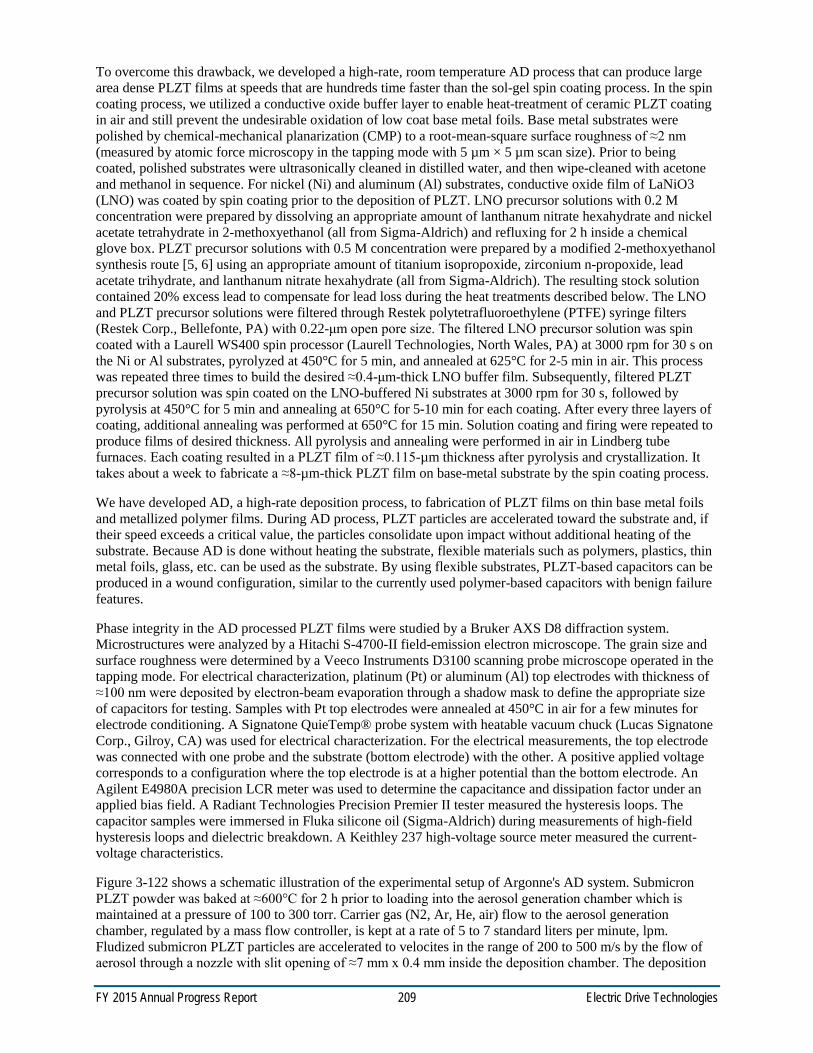
FY 2015 Annual Progress Report 209 Electric Drive Technologies
To overcome this drawback, we developed a high-rate, room temperature AD process that can produce large area dense PLZT films at speeds that are hundreds time faster than the sol-gel spin coating process. In the spin coating process, we utilized a conductive oxide buffer layer to enable heat-treatment of ceramic PLZT coating in air and still prevent the undesirable oxidation of low coat base metal foils. Base metal substrates were polished by chemical-mechanical planarization (CMP) to a root-mean-square surface roughness of ≈2 nm (measured by atomic force microscopy in the tapping mode with 5 µm × 5 µm scan size). Prior to being coated, polished substrates were ultrasonically cleaned in distilled water, and then wipe-cleaned with acetone and methanol in sequence. For nickel (Ni) and aluminum (Al) substrates, conductive oxide film of LaNiO3 (LNO) was coated by spin coating prior to the deposition of PLZT. LNO precursor solutions with 0.2 M concentration were prepared by dissolving an appropriate amount of lanthanum nitrate hexahydrate and nickel acetate tetrahydrate in 2-methoxyethanol (all from Sigma-Aldrich) and refluxing for 2 h inside a chemical glove box. PLZT precursor solutions with 0.5 M concentration were prepared by a modified 2-methoxyethanol synthesis route [5, 6] using an appropriate amount of titanium isopropoxide, zirconium n-propoxide, lead acetate trihydrate, and lanthanum nitrate hexahydrate (all from Sigma-Aldrich). The resulting stock solution contained 20% excess lead to compensate for lead loss during the heat treatments described below. The LNO and PLZT precursor solutions were filtered through Restek polytetrafluoroethylene (PTFE) syringe filters (Restek Corp., Bellefonte, PA) with 0.22-μm open pore size. The filtered LNO precursor solution was spin coated with a Laurell WS400 spin processor (Laurell Technologies, North Wales, PA) at 3000 rpm for 30 s on the Ni or Al substrates, pyrolyzed at 450°C for 5 min, and annealed at 625°C for 2-5 min in air. This process was repeated three times to build the desired ≈0.4-μm-thick LNO buffer film. Subsequently, filtered PLZT precursor solution was spin coated on the LNO-buffered Ni substrates at 3000 rpm for 30 s, followed by pyrolysis at 450°C for 5 min and annealing at 650°C for 5-10 min for each coating. After every three layers of coating, additional annealing was performed at 650°C for 15 min. Solution coating and firing were repeated to produce films of desired thickness. All pyrolysis and annealing were performed in air in Lindberg tube furnaces. Each coating resulted in a PLZT film of ≈0.115-µm thickness after pyrolysis and crystallization. It takes about a week to fabricate a ≈8-µm-thick PLZT film on base-metal substrate by the spin coating process.
We have developed AD, a high-rate deposition process, to fabrication of PLZT films on thin base metal foils and metallized polymer films. During AD process, PLZT particles are accelerated toward the substrate and, if their speed exceeds a critical value, the particles consolidate upon impact without additional heating of the substrate. Because AD is done without heating the substrate, flexible materials such as polymers, plastics, thin metal foils, glass, etc. can be used as the substrate. By using flexible substrates, PLZT-based capacitors can be produced in a wound configuration, similar to the currently used polymer-based capacitors with benign failure features.
Phase integrity in the AD processed PLZT films were studied by a Bruker AXS D8 diffraction system. Microstructures were analyzed by a Hitachi S-4700-II field-emission electron microscope. The grain size and surface roughness were determined by a Veeco Instruments D3100 scanning probe microscope operated in the tapping mode. For electrical characterization, platinum (Pt) or aluminum (Al) top electrodes with thickness of ≈100 nm were deposited by electron-beam evaporation through a shadow mask to define the appropriate size of capacitors for testing. Samples with Pt top electrodes were annealed at 450°C in air for a few minutes for electrode conditioning. A Signatone QuieTemp® probe system with heatable vacuum chuck (Lucas Signatone Corp., Gilroy, CA) was used for electrical characterization. For the electrical measurements, the top electrode was connected with one probe and the substrate (bottom electrode) with the other. A positive applied voltage corresponds to a configuration where the top electrode is at a higher potential than the bottom electrode. An Agilent E4980A precision LCR meter was used to determine the capacitance and dissipation factor under an applied bias field. A Radiant Technologies Precision Premier II tester measured the hysteresis loops. The capacitor samples were immersed in Fluka silicone oil (Sigma-Aldrich) during measurements of high-field hysteresis loops and dielectric breakdown. A Keithley 237 high-voltage source meter measured the current-voltage characteristics.
Figure 3-122 shows a schematic illustration of the experimental setup of Argonne's AD system. Submicron PLZT powder was baked at ≈600°C for 2 h prior to loading into the aerosol generation chamber which is maintained at a pressure of 100 to 300 torr. Carrier gas (N2, Ar, He, air) flow to the aerosol generation chamber, regulated by a mass flow controller, is kept at a rate of 5 to 7 standard liters per minute, lpm. Fludized submicron PLZT particles are accelerated to velocites in the range of 200 to 500 m/s by the flow of aerosol through a nozzle with slit opening of ≈7 mm x 0.4 mm inside the deposition chamber. The deposition
FY 2015 Annual Progress Report 210 Electric Drive Technologies
chamber pressure is maintained at ≈ 5 torr by high capacity rotary pumps. The distance between the nozzle and substrate is ≈3-mm. The velocity of the particle jet is monitored by a laser Doppler velocimeter (TSI Incorporated, Shoreview, MN). The sample stage is controlled by a computer for XY motion to accomplish desired deposition pattern.
Figure 3-122: Schematic illustration of the aerosol deposition system developed at Argonne for the fabrication of dense PLZT films at room temperature.
Figure 3-123: Photograph of the aerosol deposition system built at Argonne National Laboratory.
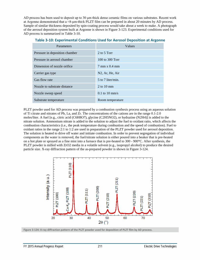
FY 2015 Annual Progress Report 211 Electric Drive Technologies
AD process has been used to deposit up to 30 μm thick dense ceramic films on various substrates. Recent work at Argonne demonstrated that a ≈8-μm-thick PLZT film can be prepared in about 20 minutes by AD process. Sample of similar thickness deposited by spin-coating process would take about a week to make. A photograph of the aerosol deposition system built at Argonne is shown in Figure 3-123. Experimental conditions used for AD process is summarized in Table 3-10.
Table 3-10: Experimental Conditions Used for Aerosol Deposition at Argonne Parameters Values
Pressure in deposition chamber 2 to 5 Torr
Pressure in aerosol chamber 100 to 300 Torr
Dimension of nozzle orifice 7 mm x 0.4 mm
Carrier gas type N2, Ar, He, Air
Gas flow rate 5 to 7 liter/min.
Nozzle to substrate distance 2 to 10 mm
Nozzle sweep speed 0.1 to 10 mm/s
Substrate temperature Room temperature
PLZT powder used for AD process was prepared by a combustion synthesis process using an aqueous solution of Ti citrate and nitrates of Pb, La, and Zr. The concentrations of the cations are in the range 0.1-2.0 moles/liter. A fuel [e.g., citric acid (C6H8O7), glycine (C2H5NO2), or hydrazine (N2H4)] is added to the nitrate solution. Ammonium nitrate is added to the solution to adjust the fuel to oxidant ratio, which affects the combustion characteristics (i.e., the peak temperature during combustion and the speed of combustion). Fuel to oxidant ratios in the range 2:1 to 1:2 are used in preparation of the PLZT powder used for aerosol deposition. The solution is heated to drive off water and initiate combustion. In order to prevent segregation of individual components as the water is removed, the fuel/nitrate solution is either poured into a beaker that is pre-heated on a hot plate or sprayed as a fine mist into a furnace that is pre-heated to 300 - 900°C. After synthesis, the PLZT powder is milled with ZrO2 media in a volatile solvent (e.g., isopropyl alcohol) to produce the desired particle size. X-ray diffraction pattern of the as-prepared powder is shown in Figure 3-124.
Figure 3-124: X-ray diffraction pattern of the PLZT powder used for deposition of PLZT film by AD process.

FY 2015 Annual Progress Report 212 Electric Drive Technologies
Figure 3-125: (a) SEM image and (b) particle size distribution of PLZT powder used for deposition of PLZT film by AD process.
Figure 3-126: Photographs of PLZT films deposited on (a) glass and (b) aluminum metallized polyimide film by AD process.
Particle size and distribution have strong effect on the quality of PLZT films deposited by AD process. Figure 3-125a shows a scanning electron microscope image of PLZT powder and Figure 3-125b shows the particle size distribution of the PLZT powder used in the AD process for deposition of PLZT films on metallized polymer films. The average particle size of ≈790 nm is used in the AD process. Low degree of agglomeration is evident in Figure 3-125b. More than 90% of the particle population is within the size range of 0.2 to 2 μm, which is the most desirable particle size for producing high quality dense oxide films by AD process [9].
Figure 3-126a shows a photograph of ≈8 μm thick and 10 mm x 15 mm PLZT film deposited on a glass slide by AD process. The PLZT on glass is transparent which illustrates its dense and pore-free nature. Shown in Figure 3-126b is an AD PLZT capacitor fabricated on aluminum (Al) metallized polyimide on an electrical testing station. The bottom electrode (in contact with left probe) and the top electrode (in contact with right probe) are slightly off-set to minimize the effect of any mechanical stresses that may be introduced by the probe tip placed on the top electrode.
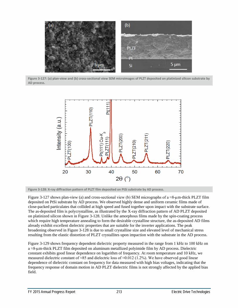
FY 2015 Annual Progress Report 213 Electric Drive Technologies
Figure 3-127: (a) plan-view and (b) cross-sectional view SEM microimages of PLZT deposited on platinized silicon substrate by AD process.
Figure 3-128: X-ray diffraction pattern of PLZT film deposited on PtSi substrate by AD process.
Figure 3-127 shows plan-view (a) and cross-sectional view (b) SEM micrographs of a ≈8-µm-thick PLZT film deposited on PtSi substrate by AD process. We observed highly dense and uniform ceramic films made of close-packed particulates that collided at high speed and fused together upon impact with the substrate surface. The as-deposited film is polycrystalline, as illustrated by the X-ray diffraction pattern of AD PLZT deposited on platinized silicon shown in Figure 3-128. Unlike the amorphous films made by the spin-coating process which require high temperature annealing to form the desirable crystalline structure, the as-deposited AD films already exhibit excellent dielectric properties that are suitable for the inverter applications. The peak broadening observed in Figure 3-128 is due to small crystalline size and elevated level of mechanical stress resulting from the elastic distortion of PLZT crystallites upon impaction with the substrate in the AD process.
Figure 3-129 shows frequency dependent dielectric property measured in the range from 1 kHz to 100 kHz on a ≈8-µm-thick PLZT film deposited on aluminum metallized polyimide film by AD process. Dielectric constant exhibits good linear dependence on logarithm of frequency. At room temperature and 10 kHz, we measured dielectric constant of ≈85 and dielectric loss of ≈0.012 (1.2%). We have observed good linear dependence of dielectric constant on frequency for data measured with high bias voltages, indicating that the frequency response of domain motion in AD PLZT dielectric films is not strongly affected by the applied bias field.

FY 2015 Annual Progress Report 214 Electric Drive Technologies
Figure 3-129: Frequency dependent dielectric properties of ≈8 μm thick PLZT film deposited on aPluminum metallized polyimide film by AD process.
Figure 3-130: Dielectric properties as a function of applied bias voltage for a ≈8 μm thick PLZT film deposited on aluminum metallized polyimide film by AD process.
Dielectric constant decreases with increasing applied bias voltage while dielectric loss is nearly independent of applied bias. To understand the dielectric response of AD PLZT films on bias field, we measured dielectric properties as a function of applied bias voltage up to 300 V (corresponding to an electric field of ≈400 KV/cm). Data is plotted in Figure 3-130. Again, we observed low dielectric loss ≈1% which is nearly independent of applied bias voltage. The little hump at ≈50 V on the dielectric constant curve, as shown in Figure 3-130, is related to the initial polarization. Further increase in the applied electric field leads to gradual decrease in dielectric constant. Dielectric constant displayed good linear dependence on applied bias voltage when the bias voltage is >100 V.
It worth noting that the PLZT films fabricated by room temperature AD process exhibit much lower tunability as defined by,
%100)0()(1)( ×
−=εεη EE (1)
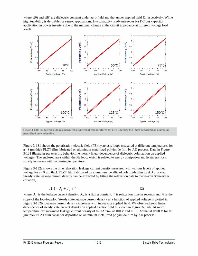
FY 2015 Annual Progress Report 215 Electric Drive Technologies
where ε(0) and ε(E) are dielectric constant under zero-field and that under applied field E, respectively. While high tunability is desirable for sensor applications, low tunability is advantageous for DC bus capacitor application in power inverters due to the minimal change in the circuit impedance at different voltage load levels.
Figure 3-131: PE hysteresis loops measured at different temperatures for a ≈8 μm thick PLZT film deposited on aluminum metallized polyimide film.
Figure 3-131 shows the polarisation-electric field (PE) hysteresis loops measured at different temperatures for a ≈8 μm thick PLZT film fabricated on aluminum metallized polyimide film by AD process. Data in Figure 3-131 illustrates paraelectric behavior, i.e. nearly linear dependence of dielectric polarization on applied voltages. The enclosed area within the PE loop, which is related to energy dissipation and hysteresis loss, slowly increases with increasing temperature.
Figure 3-132a shows the time relaxation leakage current density measured with various levels of applied voltage for a ≈8 μm thick PLZT film fabricated on aluminum metallized polyimide film by AD process. Steady state leakage current density can be extracted by fitting the relaxation data to Curie–von Schweidler equation,
nS tJJtJ −⋅+= 0)( (2)
where SJ is the leakage current density, 0J is a fitting constant, t is relaxation time in seconds and n is the slope of the log–log plot. Steady state leakage current density as a function of applied voltage is plotted in Figure 3-132b. Leakage current density increases with increasing applied field. We observed good linear dependence of steady state current density on applied electric field as shown in Figure 3-132b. At room temperature, we measured leakage current density of ≈2 nA/cm2 at 100 V and <0.1 μA/cm2 at ≈500 V for ≈8 μm thick PLZT film capacitor deposited on aluminum metallized polyimide film by AD process.

FY 2015 Annual Progress Report 216 Electric Drive Technologies
Figure 3-132: (a) Time relaxation current density and (b) Field-dependent leakage current density for a ≈8 μm thick PLZT film deposited on aluminum metallized polyimide film by AD process.
Figure 3-133: Dielectric properties and the corresponding PE hysteresis loops of AD PLZT films deposited on platinized silicon substrates. From left to right, the samples are as-deposited, 450°C annealed in air for 30 minutes, and 650°C annealed in air for 30 minutes, respectively.
Figure 3-133 shows the dielectric properties and corresponding PE hysteresis loops of AD PLZT films deposited on PtSi substrates by AD process. Dielectric constant of all three samples (as-deposited and high temperature annealed) exhibits linear dependence on the logarithm of frequency. Polarization of the as deposited sample displayed a good linear dependency on electric field (shown in the left), which is characteristic for paraelectric materials; whereas the high temperature annealed samples (450°C for 30 min. annealed shown in the middle and 650°C for 30 min. annealed shown on the right) displayed nonlinear dependency on the field. This paraelectric to ferroelectric phase transition in the AD PLZT films is possibly associated with the release of compressive strain, crystalline grain growth, and domain structure enhancement during the annealing process. Quantitative analysis can help to better understand their correlations to dielectric properties and capacitor performance.
Dielectric breakdown property of AD PLZT films deposited on Al metallized polyimide were investigated by means of Weibull analysis [10-12]. Figure 3-134 shows a two parameter Weibull plot of dielectric breakdown
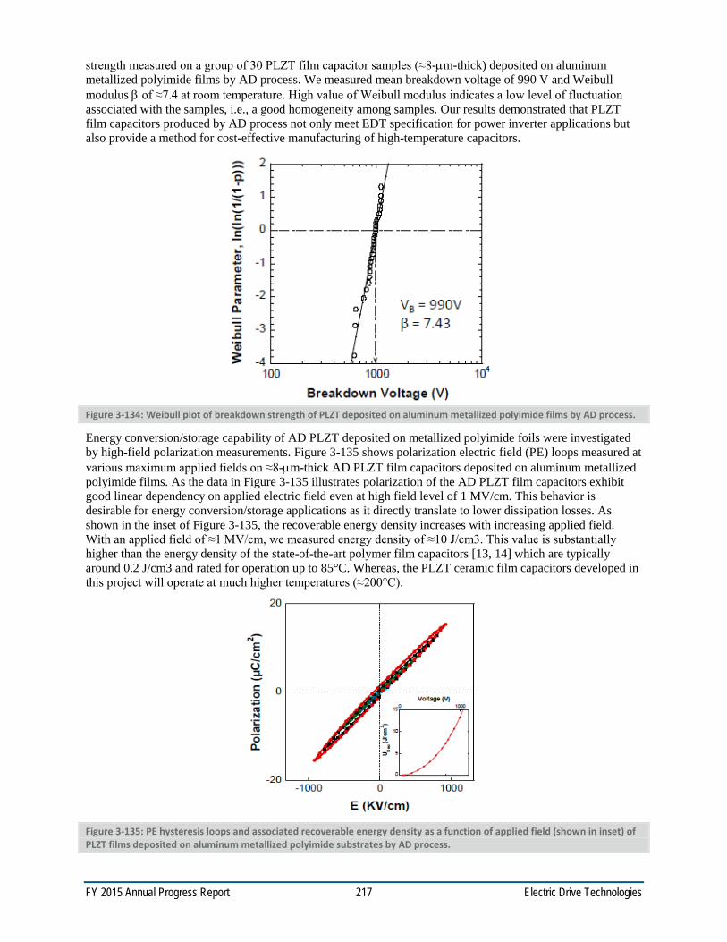
FY 2015 Annual Progress Report 217 Electric Drive Technologies
strength measured on a group of 30 PLZT film capacitor samples (≈8-µm-thick) deposited on aluminum metallized polyimide films by AD process. We measured mean breakdown voltage of 990 V and Weibull modulus β of ≈7.4 at room temperature. High value of Weibull modulus indicates a low level of fluctuation associated with the samples, i.e., a good homogeneity among samples. Our results demonstrated that PLZT film capacitors produced by AD process not only meet EDT specification for power inverter applications but also provide a method for cost-effective manufacturing of high-temperature capacitors.
Figure 3-134: Weibull plot of breakdown strength of PLZT deposited on aluminum metallized polyimide films by AD process.
Energy conversion/storage capability of AD PLZT deposited on metallized polyimide foils were investigated by high-field polarization measurements. Figure 3-135 shows polarization electric field (PE) loops measured at various maximum applied fields on ≈8-µm-thick AD PLZT film capacitors deposited on aluminum metallized polyimide films. As the data in Figure 3-135 illustrates polarization of the AD PLZT film capacitors exhibit good linear dependency on applied electric field even at high field level of 1 MV/cm. This behavior is desirable for energy conversion/storage applications as it directly translate to lower dissipation losses. As shown in the inset of Figure 3-135, the recoverable energy density increases with increasing applied field. With an applied field of ≈1 MV/cm, we measured energy density of ≈10 J/cm3. This value is substantially higher than the energy density of the state-of-the-art polymer film capacitors [13, 14] which are typically around 0.2 J/cm3 and rated for operation up to 85°C. Whereas, the PLZT ceramic film capacitors developed in this project will operate at much higher temperatures (≈200°C).
Figure 3-135: PE hysteresis loops and associated recoverable energy density as a function of applied field (shown in inset) of PLZT films deposited on aluminum metallized polyimide substrates by AD process.
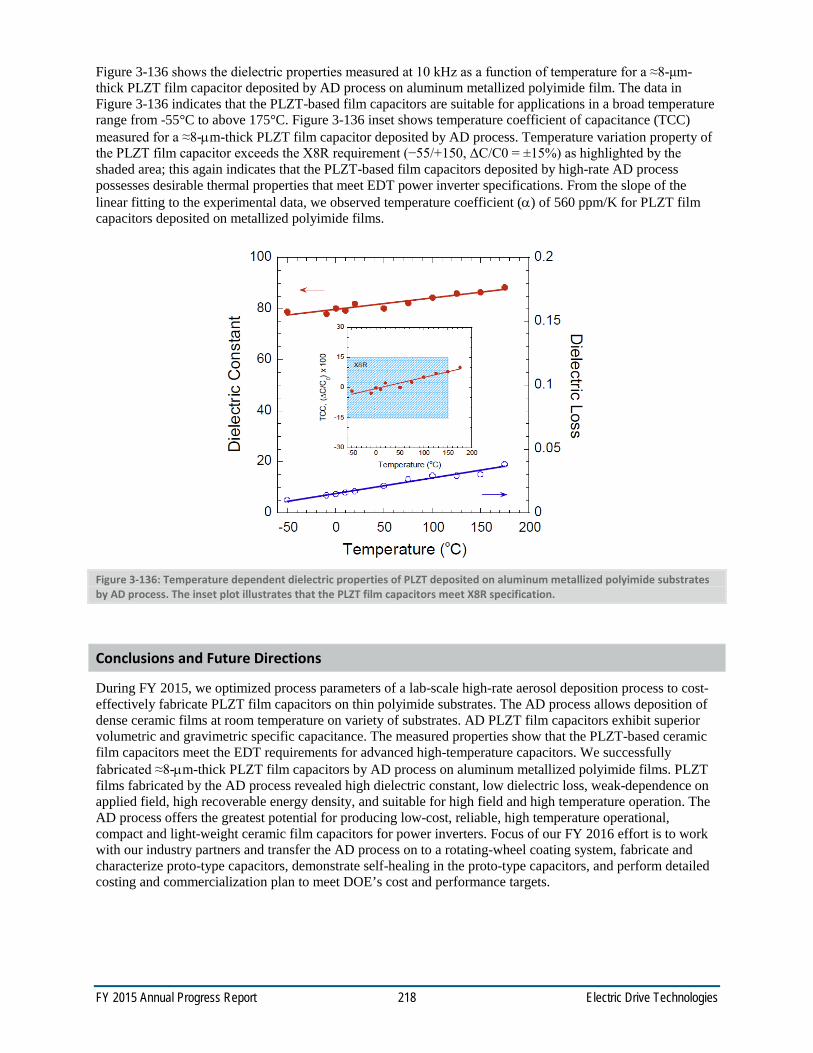
FY 2015 Annual Progress Report 218 Electric Drive Technologies
Figure 3-136 shows the dielectric properties measured at 10 kHz as a function of temperature for a ≈8-μm-thick PLZT film capacitor deposited by AD process on aluminum metallized polyimide film. The data in Figure 3-136 indicates that the PLZT-based film capacitors are suitable for applications in a broad temperature range from -55°C to above 175°C. Figure 3-136 inset shows temperature coefficient of capacitance (TCC) measured for a ≈8-µm-thick PLZT film capacitor deposited by AD process. Temperature variation property of the PLZT film capacitor exceeds the X8R requirement (−55/+150, ΔC/C0 = ±15%) as highlighted by the shaded area; this again indicates that the PLZT-based film capacitors deposited by high-rate AD process possesses desirable thermal properties that meet EDT power inverter specifications. From the slope of the linear fitting to the experimental data, we observed temperature coefficient (α) of 560 ppm/K for PLZT film capacitors deposited on metallized polyimide films.
Figure 3-136: Temperature dependent dielectric properties of PLZT deposited on aluminum metallized polyimide substrates by AD process. The inset plot illustrates that the PLZT film capacitors meet X8R specification.
Conclusions and Future Directions
During FY 2015, we optimized process parameters of a lab-scale high-rate aerosol deposition process to cost-effectively fabricate PLZT film capacitors on thin polyimide substrates. The AD process allows deposition of dense ceramic films at room temperature on variety of substrates. AD PLZT film capacitors exhibit superior volumetric and gravimetric specific capacitance. The measured properties show that the PLZT-based ceramic film capacitors meet the EDT requirements for advanced high-temperature capacitors. We successfully fabricated ≈8-µm-thick PLZT film capacitors by AD process on aluminum metallized polyimide films. PLZT films fabricated by the AD process revealed high dielectric constant, low dielectric loss, weak-dependence on applied field, high recoverable energy density, and suitable for high field and high temperature operation. The AD process offers the greatest potential for producing low-cost, reliable, high temperature operational, compact and light-weight ceramic film capacitors for power inverters. Focus of our FY 2016 effort is to work with our industry partners and transfer the AD process on to a rotating-wheel coating system, fabricate and characterize proto-type capacitors, demonstrate self-healing in the proto-type capacitors, and perform detailed costing and commercialization plan to meet DOE’s cost and performance targets.
FY 2015 Annual Progress Report 219 Electric Drive Technologies
FY 2015 Presentations/Publications/Patents
1. U. Balachandran, B. Ma, S. Tong, T.H. Lee, S.E. Dorris, "Effect of Residual Stress on the Dielectric Properties of Lead Lanthanum Zirconate Titanate Films," Presented at 11th International Conference of Pacific Rim Ceramic Societies (PacRim-11), Jeju, Korea, Aug. 30 to Sept. 4, 2015.
2. U. Balachandran, B. Ma, T.H. Lee, S.E. Dorris, "Aerosol Deposition of PLZT Ceramic Dielectric Films for Advanced Power Inverters in Electric Drive Vehicles," Presented at 11th International Conference of Pacific Rim Ceramic Societies (PacRim-11), Jeju, Korea, Aug. 30 to Sept. 4, 2015.
3. U. Balachandran, B. Ma, T.H. Lee, S.E. Dorris, "Ceramic Film Capacitors for Applications in Electric Drive Vehicles," Presented at the 8th International Conference on Materials for Advanced Technologies of the Materials Research Society of Singapore and 16th International Union of Materials Research Societies, International Conference in Asia, Suntec, SG, June 28 to July 3, 2015.
4. U. Balachandran, B. Ma, M. Lanagan, M. Pyrz, S. Garner, P. Cimo, "Development of Flexible Glass Capacitors for Power Inverters in Electric Drive Vehicles," Presented at the 2015 American Ceramic Society Glass & Optical Materials Division and Deutsche Glastechnische Gesellschaft Joint Annual Meeting, Miami, FL, May 17 - 21, 2015.
5. U. Balachandran, B. Ma, T.H. Lee, S.E. Dorris, "Fabrication of Ceramic Dielectric Films for Advanced Power Inverters in Electric Drive Vehicles by Spin-Coating and Aerosol Deposition," Presented at the 6th Tsukuba International Coating Symposium, Tsukuba, Japan, Dec.4 - 5, 2014.
6. D.-H. Choi, C. Randall, M. Lanagan, B. Ma, U. Balachandran, "Dielectric Energy and Power Densities," Presented at the 2015 IEEE International Workshop on Integrated Power Packaging, Chicago, IL, May 3-6, 2015.
7. B. Ma, T.H. Lee, S.E. Dorris, U. Balachandran, "Development of PLZT Film Capacitors for High-Temperature Power Electronics," Presented at the Materials Science and Technology 2014 (MS&T2014), Pittsburgh, PA, October 12-16, 2014.
8. B. Ma, S. Liu, Z. Hu, M. Narayanan, U. Balachandran, "Effect of manganese oxide insertion layer on the dielectric and ferroelectric properties of Pb0.92La0.08Zr0.52Ti0.48O3 films grown by a sol-gel process," Materials Research Bulletin 67,134-139, 2015.
9. Z. Hu, B. Ma, R.E. Koritala, U. Balachandran, “Temperature-dependent energy storage properties of antiferroelectric Pb0.96La0.04Zr0.98Ti0.02O3 thin films,” Appl. Phys. Lett. 104, 263902, 2014.
10. B. Ma, M. Narayanan, S.E. Dorris, U. Balachandran, "Method for Fabrication of Ceramic Dielectric Films on Copper Foils," US Patent No. 8,974,856 B2, issued 03/10/2015
11. B. Ma, U. Balachandran, S. Chao, S. Liu, M. Narayanan, “Method for Fabrication of Crack-Free Ceramic Dielectric Films,” US Patent No. 8,647,737 B2, issued 02/11/2014.
12. B. Ma, M. Narayanan, S.E. Dorris, U. Balachandran, "Method for Fabrication of Ceramic Dielectric Films on Copper Foils," US Patent Application 2015/0170845 A1, published 06/18/2015.
13. M.R. Fairchild, R.S. Taylor, C.W. Berlin, C.W. Wong, B. Ma, U. Balachandran, "Lead Lanthanum Zirconium Titanate (PLZT) capacitor on inorganic flexible glass substrate," European Patent Application EP 2869321 A2, published 05/06/2015.
14. M.R. Fairchild, R.S. Taylor, C.W. Berlin, C.W. Wong, B. Ma, U. Balachandran, "PLZT Capacitor on Glass Substrate," US Patent Application 2015/0116894 A1, published 4/30/2015.
References
1. B. Ma, M. Narayanan, S.E. Dorris, U. Balachandran, "Method for Fabrication of Ceramic Dielectric Films on Copper Foils," US Patent 8.974,856 B2, issued March 10, 2015.
2. U. Balachandran, D. K. Kwon, M. Narayanan, B. Ma, "Development of PLZT Dielectrics on Base Metal Foils for Embedded Capacitors," J. European Cer. Soc., 30, 365, 2010.
3. B. Ma, M. Narayanan, U. Balachandran, "Dielectric Strength and Reliability of Ferroelectric PLZT Films Deposited on Nickel Substrates," Materials Letters, 63, 1353, 2009.
FY 2015 Annual Progress Report 220 Electric Drive Technologies
4. U. Balachandran, M. Narayanan, S. Liu, B. Ma, "Development of Film-on-Foil Ceramic Dielectrics for Embedded Capacitors for Power Inverters in Electric Drive Vehicles,"
Jpn. J. Appl. Phys. 52, 05DA10, 2013.
5. B. Ma, D.-K. Kwon, M. Narayanan, U. Balachandran, "Chemical Solution Deposition of Ferroelectric Lead Lanthanum Zirconate Titanate Films on Base-Metal Foils," J. Electroceram. 22, 383-389, 2009.
6. K.D. Budd, S.K. Dey, D.A. Payne, "Sol-Gel Processing of PbTiO3, PbZrO3, PZT, and PLZT Thin Films," Proc. Br. Ceram. Soc. 36, 107, 1985.
7. B. Ma, S. Tong, M. Narayanan, S. Liu, S. Chao, U. Balachandran "Fabrication and Dielectric Property of Ferroelectric PLZT Films Grown on Metal Foils," Materials Research Bulletin 46, 1124-1129, 2011.
8. S. Chao, B. Ma, S. Liu, M. Narayanan, U. Balachandran, "Effects of Pyrolysis Conditions on Dielectric Properties of PLZT Films Derived from a Polyvinylpyrrolidone-Modified Sol–Gel Process," Materials Research Bulletin 47, 907-911, 2012.
9. J. Akedo, "Aerosol Deposition of Ceramic Thick Films at Room Temperature: Densification Mechanism of Ceramic Layers," J. Am. Ceram. Soc. 89, 1834-1839, 2006.
10. W. Weibull, "A Statistical Distribution Function of Wide Applicability," J. Appl. Mech. 18, 293-297, 1951.
11. L. A. Dissado, "Theoretical Basis for the Statistics of Dielectric Breakdown," J. Phys. D: Appl. Phys. 23, 1582-1591, 1990.
12. B. Ma, D.-K. Kwon, M. Narayanan, U. Balachandran, "Dielectric Properties of PLZT Film-on-Foil Capacitors," Materials Letters 62, 3573-3575, 2008.
13. L. Qi, L. Petersson, T. Liu, "Review of Recent Activities on Dielectric Films for Capacitor Applications," J. International Council on Electrical Engineering 4, 1-6, 2014.
14. S. Zhang, B. Zellers, J. Henrish, S. Rockey, D. Anderson, C. Zou, Q. Zhang, "High Energy Density Film Capacitors," Proc. IEEE Int. Pulsed Power Conf. Washington, pp. 779-783, 2009.
FY 2015 Annual Progress Report 221 Electric Drive Technologies
3.11. High Performance DC Bus Film Capacitor
Daniel Qi Tan, Principle Investigator GE Global Research Center 1 Research Circle Niskayuna, NY 12309 Phone: (515) 387-7142 E-mail: [email protected] Susan A. Rogers, DOE Technology Development Manager Phone: (202) 586-8997 E-mail: [email protected] Contractor: GE Global Research (1 Research Circle, Niskayuna, NY12309, P518-387-6996, F866-420-4878, [email protected]) Contract No.: DE-EE0006433 Subcontractor: Delphi Automotive Systems, LLC Phone: (765) 451-3884 E-mail: [email protected] Start Date: October 2013 Projected End Date: September 2016
Objectives Develop high-temperature, thin polymer films, and a scalable film process
Develop direct current (DC) bus capacitor to meet the performance, size and cost targets for electric vehicle inverters
Technical Barriers There is no commercially available capacitor film that meets DOE targets for electric vehicle inverter
capacitors, in terms of improved temperature rating (>140 °C), small volume (<0.6L), and low cost ($30). A low cost scalable extrusion method is a key challenge in producing very thin films with high dielectric strength and performance at high temperature.
Technical Targets
Scale up production of polyetherimide (PEI) films of 3-5 µm in thickness, with minimal film wrinkling and thickness variability.
Develop nanocoating process on thin PEI films for enhanced dielectric strength.
Qualify film properties in terms of thermal, dielectric and mechanical characteristics.
Prototype PEI film capacitors
Introduction
In a power inverter module, a capacitor is an essential component, decoupling the effects of the inductance from the direct current (DC) voltage source to the power bridge as shown in Figure 3-137. The bus link capacitor provides a low impedance path for the ripple currents associated with a hard switched inverter. However, current commercial capacitor technology imposes significant costs and design constraints on such
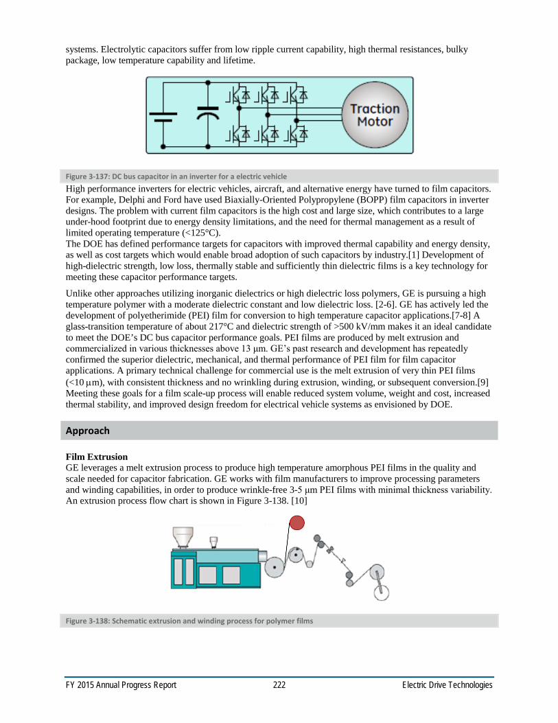
FY 2015 Annual Progress Report 222 Electric Drive Technologies
systems. Electrolytic capacitors suffer from low ripple current capability, high thermal resistances, bulky package, low temperature capability and lifetime.
Figure 3-137: DC bus capacitor in an inverter for a electric vehicle High performance inverters for electric vehicles, aircraft, and alternative energy have turned to film capacitors. For example, Delphi and Ford have used Biaxially-Oriented Polypropylene (BOPP) film capacitors in inverter designs. The problem with current film capacitors is the high cost and large size, which contributes to a large under-hood footprint due to energy density limitations, and the need for thermal management as a result of limited operating temperature (<125°C). The DOE has defined performance targets for capacitors with improved thermal capability and energy density, as well as cost targets which would enable broad adoption of such capacitors by industry.[1] Development of high-dielectric strength, low loss, thermally stable and sufficiently thin dielectric films is a key technology for meeting these capacitor performance targets.
Unlike other approaches utilizing inorganic dielectrics or high dielectric loss polymers, GE is pursuing a high temperature polymer with a moderate dielectric constant and low dielectric loss. [2-6]. GE has actively led the development of polyetherimide (PEI) film for conversion to high temperature capacitor applications.[7-8] A glass-transition temperature of about 217°C and dielectric strength of >500 kV/mm makes it an ideal candidate to meet the DOE’s DC bus capacitor performance goals. PEI films are produced by melt extrusion and commercialized in various thicknesses above 13 μm. GE’s past research and development has repeatedly confirmed the superior dielectric, mechanical, and thermal performance of PEI film for film capacitor applications. A primary technical challenge for commercial use is the melt extrusion of very thin PEI films (<10 µm), with consistent thickness and no wrinkling during extrusion, winding, or subsequent conversion.[9] Meeting these goals for a film scale-up process will enable reduced system volume, weight and cost, increased thermal stability, and improved design freedom for electrical vehicle systems as envisioned by DOE.
Approach
Film Extrusion GE leverages a melt extrusion process to produce high temperature amorphous PEI films in the quality and scale needed for capacitor fabrication. GE works with film manufacturers to improve processing parameters and winding capabilities, in order to produce wrinkle-free 3-5 μm PEI films with minimal thickness variability. An extrusion process flow chart is shown in Figure 3-138. [10]
Figure 3-138: Schematic extrusion and winding process for polymer films

FY 2015 Annual Progress Report 223 Electric Drive Technologies
Inorganic coating
GE leverages vacuum deposition methods to deposit nanoscale dielectric coating and aluminum electrode on free-standing polymer films. By working with commercial vendors, GE develops roll-to-roll processes of deposition of nanosized oxide and metallization layers to achieve higher operating voltages and graceful failure mechanism. Figure 3-139 shows a roll-to-roll deposition tool for film coating.
Figure 3-139: Schematic and image of an e-beam coating tool Photo credit: Amcor
Capacitor manufacturing
A selected capacitor manufacturing facility is used to make and test the capacitors required under this contract. In the first phase, GE also evaluates film properties by making small capacitor units. Success in the film scale-up and qualification based on prototype capacitors will lead to continued development and delivery of high performance packaged capacitors in the second phase.
Figure 3-140: Film capacitor manufacturing process flow
Results and Discussion
Extruded PEI Films
The GE team is working with three film suppliers who extruded PEI films of 3 to 7 µm in thicknesses in the second year of the program. Supplier A and B successfully extruded free-standing films with minimal wrinkles. Supplier C produced PEI films by depositing the PEI film on a carrier. Figure 3-141 shows the difference in film processes and film status at each supplier. For example, the chill roll surface was made embossed (imprinted) at Supplier A in order to minimize the affinity of the film with the chill roll. Table 3-11

FY 2015 Annual Progress Report 224 Electric Drive Technologies
shows a comparison of the film producing status at supplier A and B. These films (480-530 mm in width and 1000 meters in length) are essentially the production size rolls that these suppliers are currently able to provide. They are able to meet the needs for subsequent film processing and capacitor winding in this program.
Figure 3-141: PEI film extrusion methods and films production capability
Table 3-11: Comparison of Supplier's capability in producing PEI films.
Dielectric properties, mechanical and thermal properties of PEI films were all verified similar to those obtained in the first annual report[11]. For example, typical 5 µm PEI films were shown to be thermally stable when tested using a dilatational technique. Only minor change in the physical dimension was observed when the film was heated to 180˚C (Figure 3-142).
Figure 3-142: Physical dimension change of 5um PEI film as a function of temperature

FY 2015 Annual Progress Report 225 Electric Drive Technologies
The microscopic inspection of 2 inch x 2 inch film sections was made using a polarized light microscopy. This method highlights interference fringes from the residual stresses in the film, which aids with the identification of defects. Typically the larger defects were in the range of 30-125 µm in length (Figure 3-143). The subtle features around 5-10 µm in size were observed throughout the film as well. How these features affect the capacitor performance needs to be determined after making capacitors.
Figure 3-143: Polarized light images of a 5 µm PEI film surface showing subtle features (<10 µm) and defects (~100 µm).
Film wrinkling has been one of the main concerns for capacitor winding and performance. Wrinkles in the films directly add difficulty in winding consistent and high performing capacitors. GE directly leveraged a heat-treatment method to iron out the built-in wrinkles without losing the dielectric and mechanical properties of the films. This is fulfilled by a heat treatment of the extruded films through an oven pre-set at elevated temperatures. The thermal energy brought into the film is high enough to relax the tension built in the wrinkled films. Figure 3-144 shows the image of a 5 µm PEI film roll before and after de-wrinkling process. This additional process did not cause the loss of DC breakdown strength.
Figure 3-144: Images of PEI film rolls before (top) and after de-wrinkling process (bottom).

FY 2015 Annual Progress Report 226 Electric Drive Technologies
Production of 3-4 µm PEI films GE established a working relationship with the supplier B targeting the scale-up production of 4 µm film for the program. Several attempts were made at Supplier B to produce 4 µm film rolls of 200-2000 meter in length and 480 mm in width. Figure 3-145 shows the 4 µm film roll appearing similar to thicker films with light wrinkles. These rolls are being evaluated and processed into capacitors targeting Phase 1 deliverables.
Figure 3-145: Roll of 4 µm film which will be evaluated and processed into capacitors.
Facing the difficulty in producing 3 µm thick PEI film, GE developed a post-extrusion process. The process needs further optimization to maximize the useful width more than 300mm wide web with a thickness variation below +/-10%. The breakdown strength from Weibull distribution was measured to be 497.7 kV/mm (Figure 3-146). Using this process, large quantity of 3 µm films could be produced to meet the capacitor requirements in Phase 2.
Figure 3-146: Weibull distribution of DC breakdown strength of a 3 µm PEI film.
Nanocoating processes Sputtering and e-beam deposition techniques were utilized to achieve oxide coatings on PEI films. In the sputtering process, the thicknesses of oxide range from 20nm to 150nm. A coating morphology after a roll-to-roll sputtering process is shown in cross-section in the right image of Figure 3-147, where the left section is PEI film, dark grey layer is SiOx, and thin black layer on the right is platinum applied by the microscopist for electron charge reduction. Dielectric tests showed that there is no statistical difference in measured breakdown strength (Weibull values: 583 vs 566 kV/mm). The lack of enhancement in the dielectric strength was found to be related to the deposition conditions, particularly high film winding tension being used in the roll-to-roll sputtering process. When tension-free films of the same thickness and the same batch were coated, significant enhancement in breakdown strength was observed.
GE worked with two companies to deposit AlOx and SiOx on PEI films. The method for AlOx is hollow cathode evaporation from Al target and the method for SiOx is e-beam deposition from SiO2 target. They were
600550500450400350300
99
9080706050403020
10
532
1
Shape 13.12Scale 497.7N 20AD 0.952P-Value 0.014
Breakdown Strength (kV/mm)
Perc
ent
3um PEI filmWeibull - 95% CI
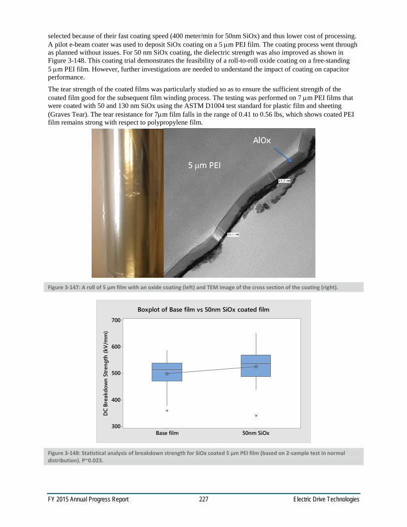
FY 2015 Annual Progress Report 227 Electric Drive Technologies
selected because of their fast coating speed (400 meter/min for 50nm SiOx) and thus lower cost of processing. A pilot e-beam coater was used to deposit SiOx coating on a 5 µm PEI film. The coating process went through as planned without issues. For 50 nm SiOx coating, the dielectric strength was also improved as shown in Figure 3-148. This coating trial demonstrates the feasibility of a roll-to-roll oxide coating on a free-standing 5 µm PEI film. However, further investigations are needed to understand the impact of coating on capacitor performance.
The tear strength of the coated films was particularly studied so as to ensure the sufficient strength of the coated film good for the subsequent film winding process. The testing was performed on 7 µm PEI films that were coated with 50 and 130 nm SiOx using the ASTM D1004 test standard for plastic film and sheeting (Graves Tear). The tear resistance for 7µm film falls in the range of 0.41 to 0.56 lbs, which shows coated PEI film remains strong with respect to polypropylene film.
Figure 3-147: A roll of 5 µm film with an oxide coating (left) and TEM image of the cross section of the coating (right).
Figure 3-148: Statistical analysis of breakdown strength for SiOx coated 5 µm PEI film (based on 2-sample test in normal distribution). P~0.023.
50nm SiOxBase film
700
600
500
400
300
DC
Brea
kdow
n St
reng
th (k
V/m
m)
Boxplot of Base film vs 50nm SiOx coated film
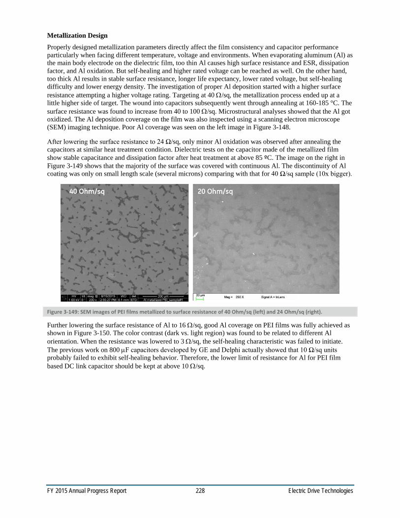
FY 2015 Annual Progress Report 228 Electric Drive Technologies
Metallization Design
Properly designed metallization parameters directly affect the film consistency and capacitor performance particularly when facing different temperature, voltage and environments. When evaporating aluminum (Al) as the main body electrode on the dielectric film, too thin Al causes high surface resistance and ESR, dissipation factor, and Al oxidation. But self-healing and higher rated voltage can be reached as well. On the other hand, too thick Al results in stable surface resistance, longer life expectancy, lower rated voltage, but self-healing difficulty and lower energy density. The investigation of proper Al deposition started with a higher surface resistance attempting a higher voltage rating. Targeting at 40 Ω/sq, the metallization process ended up at a little higher side of target. The wound into capacitors subsequently went through annealing at 160-185 °C. The surface resistance was found to increase from 40 to 100 Ω/sq. Microstructural analyses showed that the Al got oxidized. The Al deposition coverage on the film was also inspected using a scanning electron microscope (SEM) imaging technique. Poor Al coverage was seen on the left image in Figure 3-148.
After lowering the surface resistance to 24 Ω/sq, only minor Al oxidation was observed after annealing the capacitors at similar heat treatment condition. Dielectric tests on the capacitor made of the metallized film show stable capacitance and dissipation factor after heat treatment at above 85 ºC. The image on the right in Figure 3-149 shows that the majority of the surface was covered with continuous Al. The discontinuity of Al coating was only on small length scale (several microns) comparing with that for 40 Ω/sq sample (10x bigger).
Figure 3-149: SEM images of PEI films metallized to surface resistance of 40 Ohm/sq (left) and 24 Ohm/sq (right).
Further lowering the surface resistance of Al to 16 Ω/sq, good Al coverage on PEI films was fully achieved as shown in Figure 3-150. The color contrast (dark vs. light region) was found to be related to different Al orientation. When the resistance was lowered to 3 Ω/sq, the self-healing characteristic was failed to initiate. The previous work on 800 µF capacitors developed by GE and Delphi actually showed that 10 Ω/sq units probably failed to exhibit self-healing behavior. Therefore, the lower limit of resistance for Al for PEI film based DC link capacitor should be kept at above 10 Ω/sq.
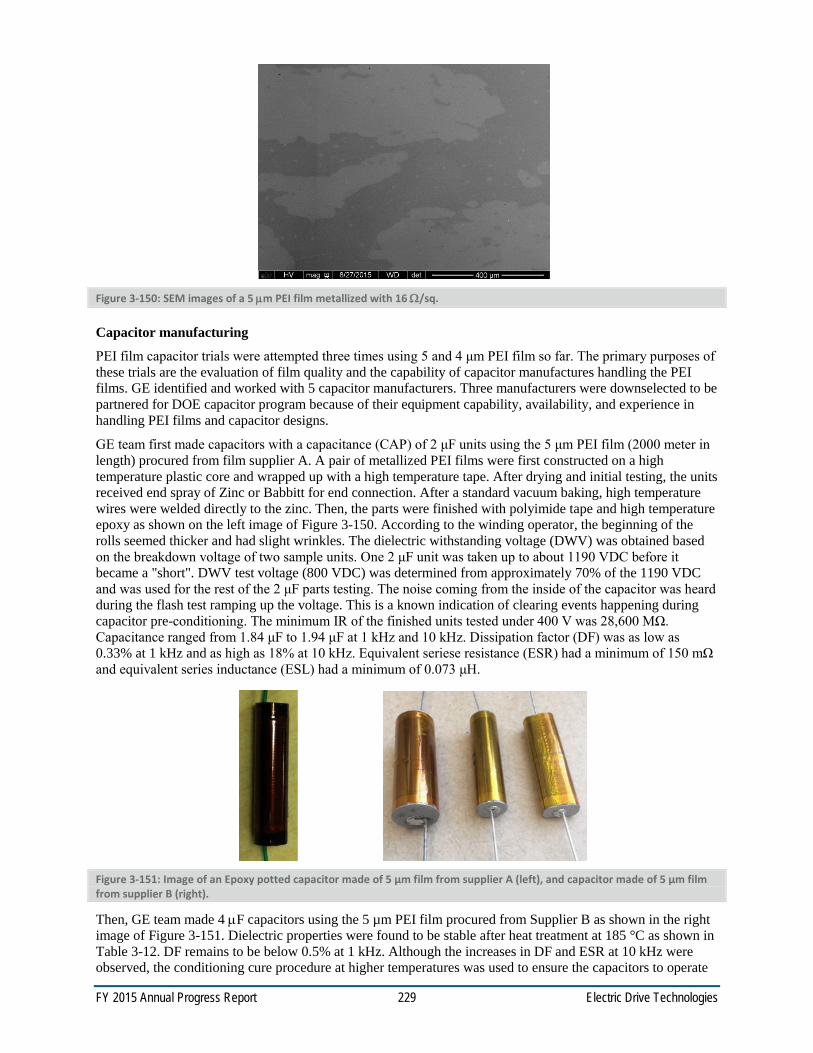
FY 2015 Annual Progress Report 229 Electric Drive Technologies
Figure 3-150: SEM images of a 5 µm PEI film metallized with 16 Ω/sq.
Capacitor manufacturing
PEI film capacitor trials were attempted three times using 5 and 4 μm PEI film so far. The primary purposes of these trials are the evaluation of film quality and the capability of capacitor manufactures handling the PEI films. GE identified and worked with 5 capacitor manufacturers. Three manufacturers were downselected to be partnered for DOE capacitor program because of their equipment capability, availability, and experience in handling PEI films and capacitor designs.
GE team first made capacitors with a capacitance (CAP) of 2 μF units using the 5 μm PEI film (2000 meter in length) procured from film supplier A. A pair of metallized PEI films were first constructed on a high temperature plastic core and wrapped up with a high temperature tape. After drying and initial testing, the units received end spray of Zinc or Babbitt for end connection. After a standard vacuum baking, high temperature wires were welded directly to the zinc. Then, the parts were finished with polyimide tape and high temperature epoxy as shown on the left image of Figure 3-150. According to the winding operator, the beginning of the rolls seemed thicker and had slight wrinkles. The dielectric withstanding voltage (DWV) was obtained based on the breakdown voltage of two sample units. One 2 μF unit was taken up to about 1190 VDC before it became a "short". DWV test voltage (800 VDC) was determined from approximately 70% of the 1190 VDC and was used for the rest of the 2 μF parts testing. The noise coming from the inside of the capacitor was heard during the flash test ramping up the voltage. This is a known indication of clearing events happening during capacitor pre-conditioning. The minimum IR of the finished units tested under 400 V was 28,600 MΩ. Capacitance ranged from 1.84 μF to 1.94 μF at 1 kHz and 10 kHz. Dissipation factor (DF) was as low as 0.33% at 1 kHz and as high as 18% at 10 kHz. Equivalent seriese resistance (ESR) had a minimum of 150 mΩ and equivalent series inductance (ESL) had a minimum of 0.073 μH.
Figure 3-151: Image of an Epoxy potted capacitor made of 5 µm film from supplier A (left), and capacitor made of 5 µm film from supplier B (right).
Then, GE team made 4 µF capacitors using the 5 µm PEI film procured from Supplier B as shown in the right image of Figure 3-151. Dielectric properties were found to be stable after heat treatment at 185 °C as shown in Table 3-12. DF remains to be below 0.5% at 1 kHz. Although the increases in DF and ESR at 10 kHz were observed, the conditioning cure procedure at higher temperatures was used to ensure the capacitors to operate
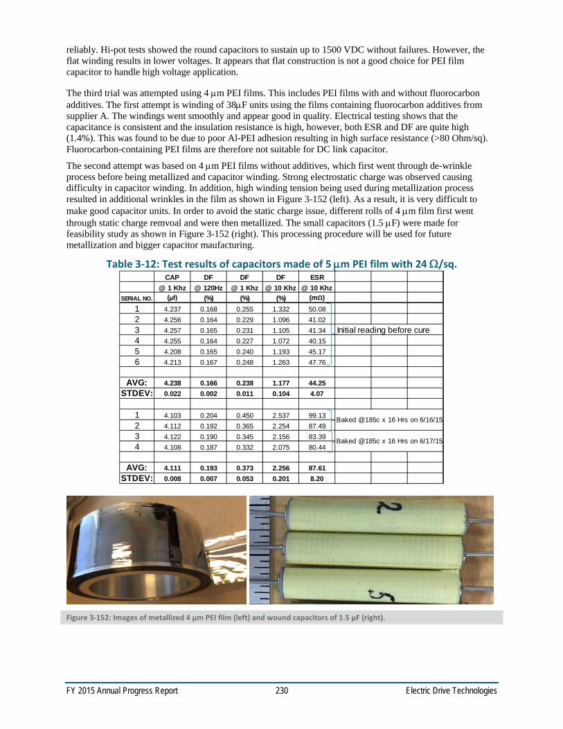
FY 2015 Annual Progress Report 230 Electric Drive Technologies
reliably. Hi-pot tests showed the round capacitors to sustain up to 1500 VDC without failures. However, the flat winding results in lower voltages. It appears that flat construction is not a good choice for PEI film capacitor to handle high voltage application.
The third trial was attempted using 4 µm PEI films. This includes PEI films with and without fluorocarbon additives. The first attempt is winding of 38µF units using the films containing fluorocarbon additives from supplier A. The windings went smoothly and appear good in quality. Electrical testing shows that the capacitance is consistent and the insulation resistance is high, however, both ESR and DF are quite high (1.4%). This was found to be due to poor Al-PEI adhesion resulting in high surface resistance (>80 Ohm/sq). Fluorocarbon-containing PEI films are therefore not suitable for DC link capacitor.
The second attempt was based on 4 µm PEI films without additives, which first went through de-wrinkle process before being metallized and capacitor winding. Strong electrostatic charge was observed causing difficulty in capacitor winding. In addition, high winding tension being used during metallization process resulted in additional wrinkles in the film as shown in Figure 3-152 (left). As a result, it is very difficult to make good capacitor units. In order to avoid the static charge issue, different rolls of 4 µm film first went through static charge remvoal and were then metallized. The small capacitors (1.5 µF) were made for feasibility study as shown in Figure 3-152 (right). This processing procedure will be used for future metallization and bigger capacitor maufacturing.
Table 3-12: Test results of capacitors made of 5 µm PEI film with 24 Ω/sq.
Figure 3-152: Images of metallized 4 µm PEI film (left) and wound capacitors of 1.5 µF (right).
CAP DF DF DF ESR@ 1 Khz @ 120Hz @ 1 Khz @ 10 Khz @ 10 Khz
SERIAL NO. (µf) (%) (%) (%) (mΩ)1 4.237 0.168 0.255 1.332 50.082 4.256 0.164 0.229 1.096 41.023 4.257 0.165 0.231 1.105 41.34 Initial reading before cure4 4.255 0.164 0.227 1.072 40.155 4.208 0.165 0.240 1.193 45.176 4.213 0.167 0.248 1.263 47.76
AVG: 4.238 0.166 0.238 1.177 44.25STDEV: 0.022 0.002 0.011 0.104 4.07
1 4.103 0.204 0.450 2.537 99.132 4.112 0.192 0.365 2.254 87.493 4.122 0.190 0.345 2.156 83.394 4.108 0.187 0.332 2.075 80.44
AVG: 4.111 0.193 0.373 2.256 87.61STDEV: 0.008 0.007 0.053 0.201 8.20
Baked @185c x 16 Hrs on 6/16/15
Baked @185c x 16 Hrs on 6/17/15

FY 2015 Annual Progress Report 231 Electric Drive Technologies
Conclusions and Future Directions
GE developed 3-5 µm thick free-standing PEI film rolls teaming with the film extrusion suppliers. Longer rolls of 4 µm x 480 mm x 1000 m have been produced. Film wrinkles generated from the extrusion were removable using a process involving a high heat exposure that is believed to remove the film tension. The additional de-wrinkling process, however, add more cost to the films. 3 µm thick PEI films was produced by converting procured thicker PEI films leaving minor loss of film area and dielectric strength. This proprietary process will need to be further optimized to produce higher film yield and minimal thickness variation. A roll-to-roll e-beam coating process was developed, demonstrating the feasibility to coat nanolayer oxide on 5 µm free-standing films. However, the scalable coating process needs further adjustment to maximize breakdown strength enhancement. It is to be found out if this coating layer is required for capacitor manufacturing in the next phase. Aluminum coating on the PEI film turns out to be unstable when the too thin Al is deposited giving rise to resistance >20 Ω/sq. A surface resistance of below 10 Ω/sq was also confirmed difficult to exhibit self-healing. The metallization window for DC link capacitor has been determined for future capacitor manufacturing. GE team has designed the capacitor specs and bus bar dimensions. The capacitor prototype of 100 and 300 µF are being manufactured as required in Phase 1 target. The projected cost model for the target film capacitor design was verified based on current and anticipated prices for 3 µm PEI film extrusion, oxide coating, metallization and capacitor manufacturing. The PEI film cost will be $23 for a DOE targeted capacitor, which requires a film price of $70/kg.
FY 2014 Presentations/Publications/Patents
1. Daniel Tan, “DOE Capacitor Deep Dive for Electrical & Electronics Technical Team”., 2015PRE0014, February 2015.
2. Daniel Tan, DOE's Vehicle Technologies Office Electric Drive Technologies R&D FY15 kickoff meeting at Oak Ridge National Lab on November 18-20, 2014.
3. Daniel Tan, “DOE DC Bus Capacitor Annual Report”. 2014GRC974, October 2014. 4. Daniel Tan, DOE APEEM Annual Merit Review; High Performance DC Bus Film Capacitor; June 17,
2014. 5. Daniel Tan, Lili Zhang, Qin Chen, and Patricia Irwin, “High Temperature Capacitor Films”,
2014GRC425, April 2014. 6. Daniel Tan, Lili Zhang, Qin Chen, and Patricia Irwin, “High Temperature Capacitor Polymer Films"
Journal of Electronic Materials, DOI: 10.1007/s11664-014-3440-7, 2014. 7. Daniel Tan, Joe Smolenski, Lili Zhang and Jeff Sullivan, High temperature capacitor core design,
Patent disclosure, 2015 8. Lili Zhang, Daniel Tan, Jeff Sullivan, Capacitor bank thermal management, Patent disclosure, 2015
Acknowledgements
The author would like to acknowledge the support provided by Susan Rogers and Steven Boyd, Technology Development Managers for the EDT Program, Vehicle Technologies Office, U.S. Department of Energy Office of Energy Efficiency and Renewable Energy. The significant contributions of Ralph Taylor of Delphi are acknowledged. The author would also like to acknowledge GE Aviation BPM for providing cost share.
References
1. Advanced Power Electronics and Electric Motors Program. DOE EERE Vehicle Technologies Office, 2008.
2. U. Balachandran, M. Narayanan, S. Liu, B. Ma, Development of film-on-foil ceramic dielectrics for embedded capacitors for power inverters in electric drive vehicles, Jpn. J. Appl. Phys. 52, 05DA10, 2013.
FY 2015 Annual Progress Report 232 Electric Drive Technologies
3. M. Manoharan, C. Zou, E. Furman, N. Zhang, D. Kushner, S.Zhang, T. Murata, and M.Lanagan. "Flexible Glass for High Temperature Energy Storage Capacitors." Energy Technology 1: 5‐6, 313-318, 2013.
4. S. Fries-Carr, S. Adams and J. Weimer, R.L.C. Wu, H. Kosai, K. Bray, T. Furmaniak, E. Barshaw, S. Scozzie and R. Jow, SAE Technical Paper 2004-02-3216, Power Systems Conference, Nevada, 2004.
5. Shihai Zhang, Chen Zou, Xin Zhou, Douglas Kushner, “High Temperature Polymer Capacitor Film with High Dielectric Constant” 2011 CARTS USA, March 28-31, 2011, Jacksonville, FL. http://strategicpolymers.squarespace.com/capacitors 2011. Strategic Polymer Sciences Inc.
6. K.W. Browall, M.W. DeVre, S.M. Gasworth, C.W. Reed, S.J. Rzad, ”High Energy Storage Capacitors for Pulse Power, ARL-CR-150, Contract DAAL01-91-C-0149, 1994.
7. Q. Tan, P.C. Irwin, Y. Cao, Advanced Dielectrics for Capacitors, IEEJ Transactions on Fundamentals and Materials, 11, 11532-1159 Vol 126 (2006).
8. D. Tan, Q. Chen, Y. Cao, P. Irwin, S. Heidger, “Polymer Based Nanodielectrics for Capacitors”, EMA 2010, Orlando, FL, (2010).
9. Bruce Mixer, High Temperature Inverter—Delphi Automotive S, Advanced Power Electronics and Electric Motors Program. DOE EERE Vehicle Technologies Office (2013).
10. Giles, H. F., Wagner, J. R. and Mount, E. M., “Extrusion: The Definitive Processing Guide and Handbook”; William Andrew Publishing (2005).
11. Daniel Tan, “DOE DC Bus Capacitor Annual Report”. 2014GRC974, October 2014.

FY 2015 Annual Progress Report 233 Electric Drive Technologies
3.12. A Disruptive Approach to Electric Vehicle Power Electronics
Robert Erickson, Principal Investigator University of Colorado Boulder Department of Electrical, Computer, and Energy Engineering Boulder, CO 80309-0425 Phone: (303) 492-7003 E-mail: [email protected] Dragan Maksimovic and Khurram Afridi, Co-Principal Investigators University of Colorado Boulder Department of Electrical, Computer, and Energy Engineering Boulder, CO 80309-0425 E-mail: [email protected], [email protected] Additional Investigators: David Jones, Hua Chen, Hyeokjin Kim, and Usama Anwar Kraig Olejniczak, Subcontractor PI Arkansas Power Electronics International 535 W. Research Center Drive, Suite 209 Fayetteville, AR 72701 APEI co-PI: Brandon Passmore Technology Manager Contract No.: EE0006921
Objectives This project includes development of two power electronics drivetrain demonstrations: a silicon (Si) 30 kW system, and a silicon carbide (SiC) 30 kW system. Both will meet aggressive efficiency and capacitor size targets, while the SiC demonstration will additionally meet power density targets and will provide an objective comparison of how SiC technology affects system optimization to improve cost and power density performance. Hence the objectives are:
Develop, design, and demonstrate a new electric vehicle (EV) power electronics architecture that reduces average loss over the US06 drive cycle by a factor of 2-4 and film capacitor size by a factor of two, using Si devices.
Develop, design, and demonstrate a SiC version meeting the above goals, that further improves efficiency and cost, and that meets DOE power density goals.
Technical Barriers In electric vehicle drivetrains containing boost direct current (DC)-DC converters, such as those
employed by Ford [1], Toyota [2-4], Honda [5], and others, the efficiency of the boost DC-DC converter dominates the power electronics system efficiency, and exhibits poor efficiency at partial power. This leads to a substantial additional average power loss over standard drive cycles, with typical power converter system average efficiencies of 92.5% for US06 and 90.4% for UDDS. Reduction of the average loss could lead to reduction of the cooling system size and cost.
Additionally, the film capacitors of these systems are bulky and expensive, with a specific energy of 9 J/kW in recent commercial designs. Capacitor size is generally constrained by RMS current and applied voltage [5]; hence, increase of switching frequency does not reduce capacitor size and other approaches must be found for reduction of capacitor size and cost.
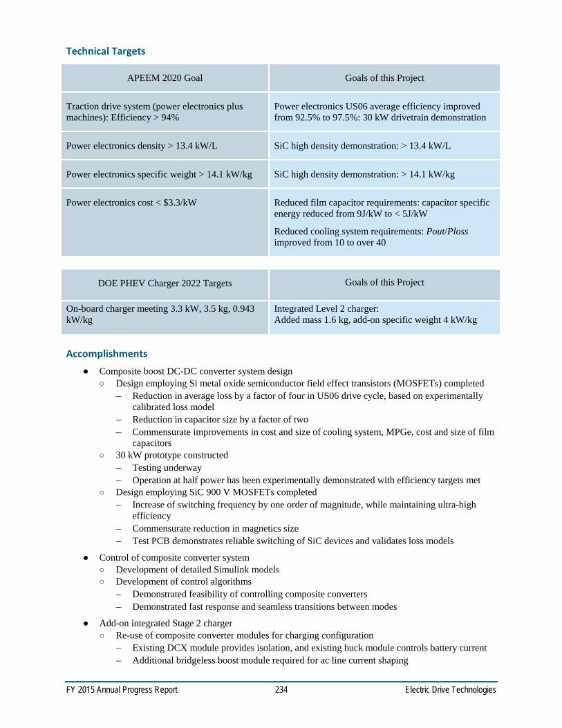
FY 2015 Annual Progress Report 234 Electric Drive Technologies
Technical Targets
APEEM 2020 Goal Goals of this Project
Traction drive system (power electronics plus machines): Efficiency > 94%
Power electronics US06 average efficiency improved from 92.5% to 97.5%: 30 kW drivetrain demonstration
Power electronics density > 13.4 kW/L SiC high density demonstration: > 13.4 kW/L
Power electronics specific weight > 14.1 kW/kg SiC high density demonstration: > 14.1 kW/kg
Power electronics cost < $3.3/kW Reduced film capacitor requirements: capacitor specific energy reduced from 9J/kW to < 5J/kW
Reduced cooling system requirements: Pout/Ploss improved from 10 to over 40
DOE PHEV Charger 2022 Targets Goals of this Project
On-board charger meeting 3.3 kW, 3.5 kg, 0.943 kW/kg
Integrated Level 2 charger: Added mass 1.6 kg, add-on specific weight 4 kW/kg
Accomplishments Composite boost DC-DC converter system design
o Design employing Si metal oxide semiconductor field effect transistors (MOSFETs) completed – Reduction in average loss by a factor of four in US06 drive cycle, based on experimentally
calibrated loss model – Reduction in capacitor size by a factor of two – Commensurate improvements in cost and size of cooling system, MPGe, cost and size of film
capacitors o 30 kW prototype constructed
– Testing underway – Operation at half power has been experimentally demonstrated with efficiency targets met
o Design employing SiC 900 V MOSFETs completed – Increase of switching frequency by one order of magnitude, while maintaining ultra-high
efficiency – Commensurate reduction in magnetics size – Test PCB demonstrates reliable switching of SiC devices and validates loss models
Control of composite converter system o Development of detailed Simulink models o Development of control algorithms
– Demonstrated feasibility of controlling composite converters – Demonstrated fast response and seamless transitions between modes
Add-on integrated Stage 2 charger o Re-use of composite converter modules for charging configuration
– Existing DCX module provides isolation, and existing buck module controls battery current – Additional bridgeless boost module required for ac line current shaping

FY 2015 Annual Progress Report 235 Electric Drive Technologies
– Projected added weight for charger modules: 1.6 kg for 6.6 kW on-board charger, exceeds plug-in hybrid electric vehicle (PHEV) 2022 target power density by factor of four
o Bridgeless boost module prototyping – Prototype 6.6 kW power stage and microcontroller printed circuit boards (PCBs) have been
fabricated – Testing underway
Introduction
Figure 3-153: Composite converter powertrain approach with integrated charger
A high-level block diagram of the power electronics system is illustrated in Figure 3-153. The system includes a voltage boost function, as is found in some hybrid vehicles such as the Toyota Prius or Ford Focus. The boost function is performed by the new Composite DC-DC converter approach, in which several partial-power converter modules are combined to perform the boost function with higher performance. An intermediate DC bus with voltage Vbus supplies a boosted voltage of up to 800 V peak to an inverter. The inverter is a conventional three-phase bridge that drives a high-speed permanent-magnet AC machine. An integrated charger reuses some of the composite converter modules to achieve Level 2 charging in an on-board charger having substantially lower weight than that of a discrete charger.
The conventional approach to realizing the DC-DC boost function is illustrated in Figure 3-154. Multiple 1200 V silicon insulated gate bipolar transistor (IGBT) die are connected in parallel in a multichip power semiconductor module. A typical switching frequency is 10 kHz, which then determines the inductor size and loss. The efficiency of the DC-DC boost converter dominates the system efficiency; the dominant loss mechanisms are inductor alternating current (AC) and DC losses, and IGBT switching losses. When boosting by a high voltage ratio, the boost converter must operate with a high duty cycle where the efficiency is relatively low. The partial-power efficiency is also poor, because of ac losses (switching loss and ac magnetics loss) that depend on voltage but are nearly independent of current. At high duty cycles, the rms current applied to the bus capacitor is also quite high; this impacts the size and cost of this capacitor.
Figure 3-154: Conventional boost converter power stage
Approach
We have proposed the new composite boost converter architecture illustrated in Fig. 3. With this approach, we employ the same silicon area as the conventional boost converter. However, instead of the brute-force parallel
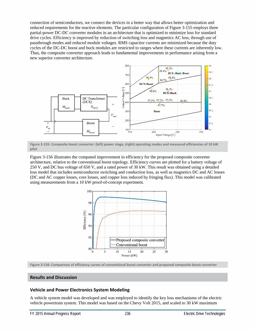
FY 2015 Annual Progress Report 236 Electric Drive Technologies
connection of semiconductors, we connect the devices in a better way that allows better optimization and reduced requirements for the reactive elements. The particular configuration of Figure 3-155 employs three partial-power DC-DC converter modules in an architecture that is optimized to minimize loss for standard drive cycles. Efficiency is improved by reduction of switching loss and magnetics AC loss, through use of passthrough modes and reduced module voltages. RMS capacitor currents are minimized because the duty cycles of the DC-DC boost and buck modules are restricted to ranges where these currents are inherently low. Thus, the composite converter approach leads to fundamental improvements in performance arising from a new superior converter architecture.
Figure 3-155: Composite boost converter: (left) power stage, (right) operating modes and measured efficiencies of 10 kW pilot
Figure 3-156 illustrates the computed improvement in efficiency for the proposed composite converter architecture, relative to the conventional boost topology. Efficiency curves are plotted for a battery voltage of 250 V, and DC bus voltage of 650 V, and a rated power of 30 kW. This result was obtained using a detailed loss model that includes semiconductor switching and conduction loss, as well as magnetics DC and AC losses (DC and AC copper losses, core losses, and copper loss induced by fringing flux). This model was calibrated using measurements from a 10 kW proof-of-concept experiment.
Figure 3-156: Comparison of efficiency curves of conventional boost converter and proposed composite boost converter
Results and Discussion
Vehicle and Power Electronics System Modeling A vehicle system model was developed and was employed to identify the key loss mechanisms of the electric vehicle powertrain system. This model was based on the Chevy Volt 2015, and scaled to 30 kW maximum

FY 2015 Annual Progress Report 237 Electric Drive Technologies
power. The motor is modeled based on the Toyota Prius 2010, and scaled to the 30 kW power level as well. A detailed converter loss model has also been developed, based on data from pilot-scale prototypes in our laboratory for systems containing a boost DC-DC function. The vehicle model has been simulated using standard driving profiles US06 and UDDS, and the required power and bus voltage profiles were calculated. Based on this data, the US06 average driving efficiency can be calculated. Figure 3-158 contains plots of the converter loss components and operating points for the US06 driving test. Figure 3-157 contains a typical bus voltage and power histogram for the US06 driving profile, based on these vehicle simulation results. It can be observed that performance at high bus voltages (in the vicinity of 650 V) and at partial power (10% to 20%) is most critical to the overall performance under driving conditions.
Figure 3-157: Typical histogram of system operating points (Power, DC bus voltage) for the US06 drive cycle.
Figure 3-158: Modeled loss mechanisms over the US06 drive cycle for the Si composite boost converter. Top: US06 speed profile. Bottom: total semiconductor conduction loss, switching loss, and DC+AC magnetics losses.
Based on the detailed loss models, multiple composite system architectures were modeled, and a candidate approach was found to be suitable for our project goals. A composite boost converter architecture (Figure 3-155) was selected, consisting of 650 V Si MOSFET DC-DC converter modules and a 1200 V SiC MOSFET inverter. Additionally, a similar system employing 900 V SiC MOSFETs in the DC-DC converter modules has been selected. The projected average US06 efficiencies for these approaches, as well as for a conventional commercial architecture, is summarized in Table 3-13. The proposed composite architecture can meet the goal of > 97.5% US06 average efficiency. Relative to the existing conventional approach employed in commercial products, the composite architecture achieves a reduction in US06 average loss of a factor of approximately
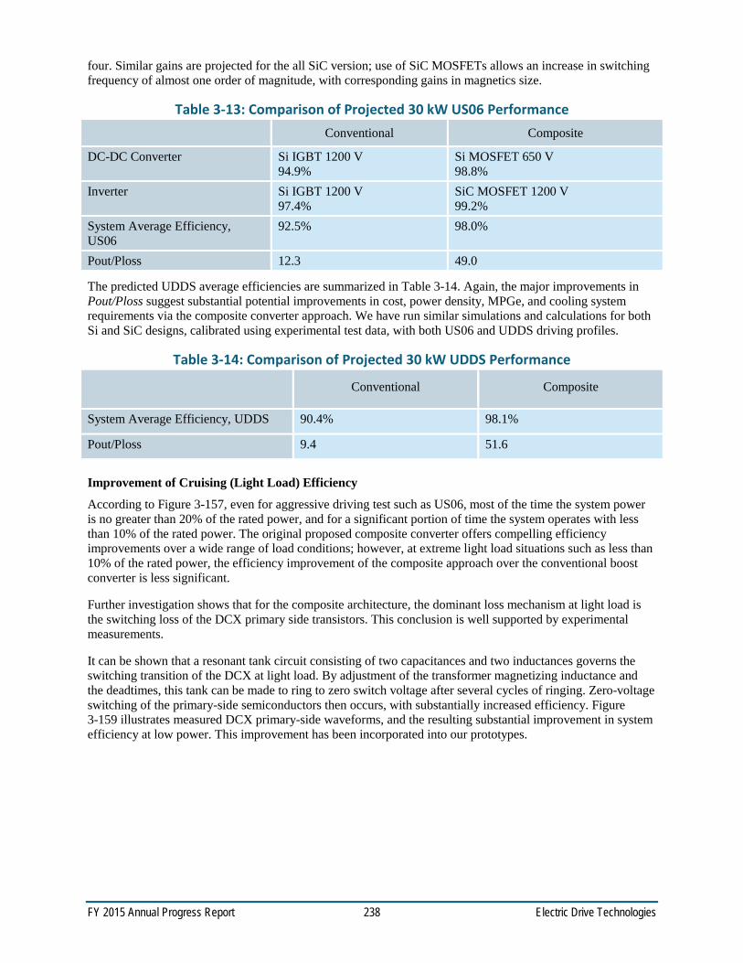
FY 2015 Annual Progress Report 238 Electric Drive Technologies
four. Similar gains are projected for the all SiC version; use of SiC MOSFETs allows an increase in switching frequency of almost one order of magnitude, with corresponding gains in magnetics size.
Table 3-13: Comparison of Projected 30 kW US06 Performance Conventional Composite
DC-DC Converter Si IGBT 1200 V 94.9%
Si MOSFET 650 V 98.8%
Inverter Si IGBT 1200 V 97.4%
SiC MOSFET 1200 V 99.2%
System Average Efficiency, US06
92.5% 98.0%
Pout/Ploss 12.3 49.0
The predicted UDDS average efficiencies are summarized in Table 3-14. Again, the major improvements in Pout/Ploss suggest substantial potential improvements in cost, power density, MPGe, and cooling system requirements via the composite converter approach. We have run similar simulations and calculations for both Si and SiC designs, calibrated using experimental test data, with both US06 and UDDS driving profiles.
Table 3-14: Comparison of Projected 30 kW UDDS Performance
Conventional Composite
System Average Efficiency, UDDS 90.4% 98.1%
Pout/Ploss 9.4 51.6
Improvement of Cruising (Light Load) Efficiency
According to Figure 3-157, even for aggressive driving test such as US06, most of the time the system power is no greater than 20% of the rated power, and for a significant portion of time the system operates with less than 10% of the rated power. The original proposed composite converter offers compelling efficiency improvements over a wide range of load conditions; however, at extreme light load situations such as less than 10% of the rated power, the efficiency improvement of the composite approach over the conventional boost converter is less significant.
Further investigation shows that for the composite architecture, the dominant loss mechanism at light load is the switching loss of the DCX primary side transistors. This conclusion is well supported by experimental measurements.
It can be shown that a resonant tank circuit consisting of two capacitances and two inductances governs the switching transition of the DCX at light load. By adjustment of the transformer magnetizing inductance and the deadtimes, this tank can be made to ring to zero switch voltage after several cycles of ringing. Zero-voltage switching of the primary-side semiconductors then occurs, with substantially increased efficiency. Figure 3-159 illustrates measured DCX primary-side waveforms, and the resulting substantial improvement in system efficiency at low power. This improvement has been incorporated into our prototypes.

FY 2015 Annual Progress Report 239 Electric Drive Technologies
Figure 3-159: Improvement of efficiency curves for the boost function, at Vbatt = 250 V and Vbus = 650 V. Left: measured DCX primary waveforms, showing achievement of zero-voltage switching at light load. Right: efficiency curves of conventional boost with Si IGBTs, composite boost with Si MOSFETs, and composite boost with improved zero-voltage switching.
Silicon Prototype Construction A silicon-based prototype composite boost converter system has been designed, assembled, and is currently under test. The module designs, DCX turns ratio, and magnetics designs each were optimized at the operating points where impact on the US06 average efficiency is greatest. This 30 kW system employs 650 V Si superjunction MOSFETs. A photograph of the laboratory prototype is illustrated in Figure 3-160. This top view shows the gate driver PCB (blue solder mask) attached to the top side of the power interconnect PCB (having a green solder mask). The power MOSFETs are attached underneath the PCB, and the heat exchanger with water cooling is also underneath the PCB. The gate driver PCB is a four layer board with 2 oz copper that can accommodate SOIC pin spacings. The power interconnect PCB is a two-layer board with 9 oz copper that can conduct the required currents. A laser-cut spacer having cutouts for the needed interconnects is placed between the driver and power PCBs, to provide isolation between PCBs. This approach leads to low-inductance interconnects between the power semiconductors, film capacitors, and gate drivers, with minimal ringing and overshoot of switch node and bus voltage waveforms. This silicon system is intended as an electrical testbed and is not packaged for high power density.
Figure 3-160: Photograph of assembled silicon prototype.

FY 2015 Annual Progress Report 240 Electric Drive Technologies
The ferrite planar magnetics of the 33 kHz DCX module can be seen in the upper right corner of the prototype. The filter inductors for the 20 kHz buck and boost modules employ metglass cores, and are visible on the lower side of the photograph. The film capacitors for the various modules are the blue rectangular elements.
Figure 3-161: Prototype measured waveforms, operating at 250 V battery voltage, 650 V DC bus voltage, and 50% of rated power (15 kW). Left oscilloscope figure waveforms, from top to bottom: DCX primary switch node voltage, DCX secondary switch node voltage, buck module switch node voltage, boost module switch node voltage. Right oscilloscope figure waveforms, from top to bottom: DCX primary transformer current, boost inductor current, buck inductor current.
Testing of the 30 kW Si composite boost converter is now underway. The system has been shown to operate reliably at up to 650 V and up to 15 kW; testing at higher powers and voltages will take place in the upcoming months. Figure 3-161 shows operating waveforms for all modules at an output of 650 V and 15 kW. It can be observed that the switch node voltages contain minimal ringing and overshoot; this is a consequence of the low-inductance interconnects possible with the two-PCB approach, along with the proper design of the gate driver circuitry. The measured efficiency of this system at a battery voltage of 250 V and bus voltage of 650 V is given in Figure 3-162. The predictions of our analytical loss model are superimposed (red curve) on the data points. Also shown (green curve) is the efficiency of a conventional 10 kHz Si IGBT boost converter, for comparison.
Figure 3-162: Efficiency of DC-DC boost system at 250 V battery and 650 V DC bus. Data points: experimental measurements for Si composite boost converter prototype. Red curve: efficiency of Si composite boost converter as predicted by calibrated loss model. Green curve: efficiency of Si conventional boost converter, as predicted by calibrated loss model.
Figure 3-163 contains the predicted US06 operating and loss model results, based on the measured efficiency data of Figure 3-162. This data suggests that the experimental prototype will exhibit an average US06 efficiency exceeding 97.5% as summarized in Table 3-16.

FY 2015 Annual Progress Report 241 Electric Drive Technologies
Figure 3-163: Predicted instantaneous loss of Si composite boost system over US06 drive cycle, based on measured efficiency data.
SiC Test Module Construction H-bridge modules containing 900 V 10 mΩ SiC MOSFETs with antiparallel 1200 V SiC schottky diodes were developed and delivered by subcontractor APEI. Testing of these devices in a single converter module is now underway. Figure 3-164 illustrates the H-bridge package, and the DC-DC converter test circuit. The test converter is again constructed using power PCB with high-weight copper, and a controller PCB having 2 oz copper, with an insulating spacer between PCBs. The SiC package is mounted on a heatsink on the bottom side of the power PCB. This test converter board can be configured as a buck module, boost module, or DCX primary-side circuit.
Figure 3-164: Test board for 900 V 10mΩ SiC modules. Left: H-bridge package. Right: test PCB.
The SiC power stage and gate driver has now been tested in a boost converter configuration with an input voltage range of 0 – 300 V, and output voltage range of 0 – 450 V, and an output power range of 0 – 10 kW. Reliable operation with both zero voltage switching (ZVS) and hard switching has been achieved. Our analytical switching loss models were found to be pessimistic, and have been revised based on laboratory measurements. Figure 3-165 documents measured switching waveforms for a half-bridge circuit in a boost converter configuration, with both soft switching and hard switching. The gate driver and MOSFETs operate correctly, and overshoot and ringing is minimal even with hard switching.

FY 2015 Annual Progress Report 242 Electric Drive Technologies
Figure 3-165: Measured half-bridge switching waveforms for 900 V 10 mΩ SiC MOSFET test PCB. Left: with zero-voltage switching. Right: with hard switching.
SiC System Design
Design of the power electronics for a high-density power train employing SiC MOSFETs has been completed. This design is based on 900 V 10 mΩ 100 A MOSFETs recently announced by Cree, with the same composite architecture being developed with 650 V Si MOSFETs. With these SiC devices, we estimate that the prototype will be rated at 30 kW. The SiC prototype has been designed for a 650 V (nominal), 800 V (maximum) DC bus, identical to the Si prototype so that easy comparisons can be made. Converter modules and magnetics are again optimized such that the system average US06 efficiency is maximized.
Figure 3-166: Predicted loss mechanisms of the SiC DCX module at the important operating point Vin = 250 V, Pdcx = 8 kW.
Figure 3-166 illustrates the predicted losses of the SiC DCX module at the important operating point where the battery voltage is 250 V, the DC bus voltage is 650 V, and the power is approximately half of rated power. The DCX module was optimized at this point. It can be seen that approximately half of the loss is in the planar magnetics, and the remainder is in the semiconductors.
Figure 3-167 illustrates the predicted loss curves for the SiC composite boost converter design, with a nominal battery voltage of 250 V and with junction temperatures of 100˚C. The superimposed red dots are sampled operating points over the US06 drive cycle. The highest density of operating points occurs in the vicinity of 650 V and 5 kW; high efficiency of approximately 98.5% occurs for most of these points.
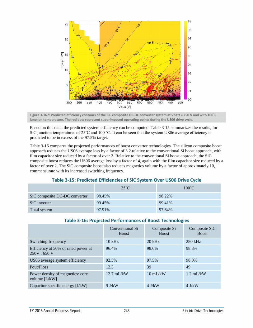
FY 2015 Annual Progress Report 243 Electric Drive Technologies
Figure 3-167: Predicted efficiency contours of the SiC composite DC-DC converter system at Vbatt = 250 V and with 100˚C junction temperature. The red dots represent superimposed operating points during the US06 drive cycle.
Based on this data, the predicted system efficiency can be computed. Table 3-15 summarizes the results, for SiC junction temperatures of 25˚C and 100 ˚C. It can be seen that the system US06 average efficiency is predicted to be in excess of the 97.5% target.
Table 3-16 compares the projected performances of boost converter technologies. The silicon composite boost approach reduces the US06 average loss by a factor of 3.2 relative to the conventional Si boost approach, with film capacitor size reduced by a factor of over 2. Relative to the conventional Si boost approach, the SiC composite boost reduces the US06 average loss by a factor of 4, again with the film capacitor size reduced by a factor of over 2. The SiC composite boost also reduces magnetics volume by a factor of approximately 10, commensurate with its increased switching frequency.
Table 3-15: Predicted Efficiencies of SiC System Over US06 Drive Cycle 25˚C 100˚C
SiC composite DC-DC converter 98.45% 98.22% SiC inverter 99.45% 99.41% Total system 97.91% 97.64%
Table 3-16: Projected Performances of Boost Technologies
Conventional Si Boost
Composite Si Boost
Composite SiC Boost
Switching frequency 10 kHz 20 kHz 280 kHz Efficiency at 50% of rated power at 250V : 650 V
96.4% 98.6% 98.8%
US06 average system efficiency 92.5% 97.5% 98.0% Pout/Ploss 12.3 39 49 Power density of magnetics: core volume [L/kW]
12.7 mL/kW 10 mL/kW 1.2 mL/kW
Capacitor specific energy [J/kW] 9 J/kW 4 J/kW 4 J/kW
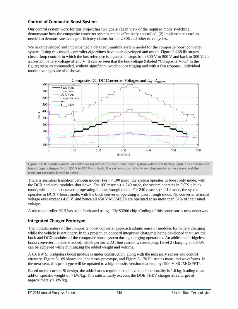
FY 2015 Annual Progress Report 244 Electric Drive Technologies
Control of Composite Boost System Our control system work for this project has two goals: (1) in view of the required mode switching, demonstrate how the composite converter system can be effectively controlled; (2) implement control as needed to demonstrate average efficiency claims for the US06 and other drive cycles.
We have developed and implemented a detailed Simulink system model for the composite boost converter system. Using this model, controller algorithms have been developed and tested. Figure 3-168 illustrates closed-loop control, in which the bus reference is adjusted in steps from 300 V to 800 V and back to 300 V, for a constant battery voltage of 250 V. It can be seen that the bus voltage (labeled “Composite Vout” in the figure) steps as commanded, without significant overshoot or ringing and with a fast response. Individual module voltages are also shown.
Figure 3-168: Simulink model of controller algorithms for composite boost system with 250 V battery input. The commanded bus voltage is stepped from 300 V to 800 V and back. The system automatically switches modes as necessary, and the transient response is well behaved.
There is seamless transition between modes. For t < 100 msec, the system operates in boost only mode, with the DCX and buck modules shut down. For 100 msec < t < 240 msec, the system operates in DCX + buck mode, with the boost converter operating in passthrough mode. For 240 msec < t < 410 msec, the system operates in DCX + boost mode, with the buck converter operating in passthrough mode. No converter terminal voltage ever exceeds 415 V, and hence all 650 V MOSFETs are operated at no more than 67% of their rated voltage.
A microcontroller PCB has been fabricated using a TMS3200 chip. Coding of this processor is now underway.
Integrated Charger Prototype The modular nature of the composite boost converter approach admits reuse of modules for battery charging while the vehicle is stationary. In this project, an onboard integrated charger is being developed that uses the buck and DCX modules of the composite boost system during charging operations. An additional bridgeless boost converter module is added, which performs AC line current waveshaping. Level 2 charging at 6.6 kW can be achieved while minimizing the added weight and volume.
A 6.6 kW Si bridgeless boost module is under construction, along with the necessary sensor and control circuitry. Figure 3-169 shows the laboratory prototype, and Figure 3-170 illustrates measured waveforms. In the next year, this prototype will be updated to a high density version that employs 900 V SiC MOSFETs.
Based on the current Si design, the added mass required to achieve this functionality is 1.6 kg, leading to an add-on specific weight of 4 kW/kg. This substantially exceeds the DOE PHEV charger 2022 target of approximately 1 kW/kg.
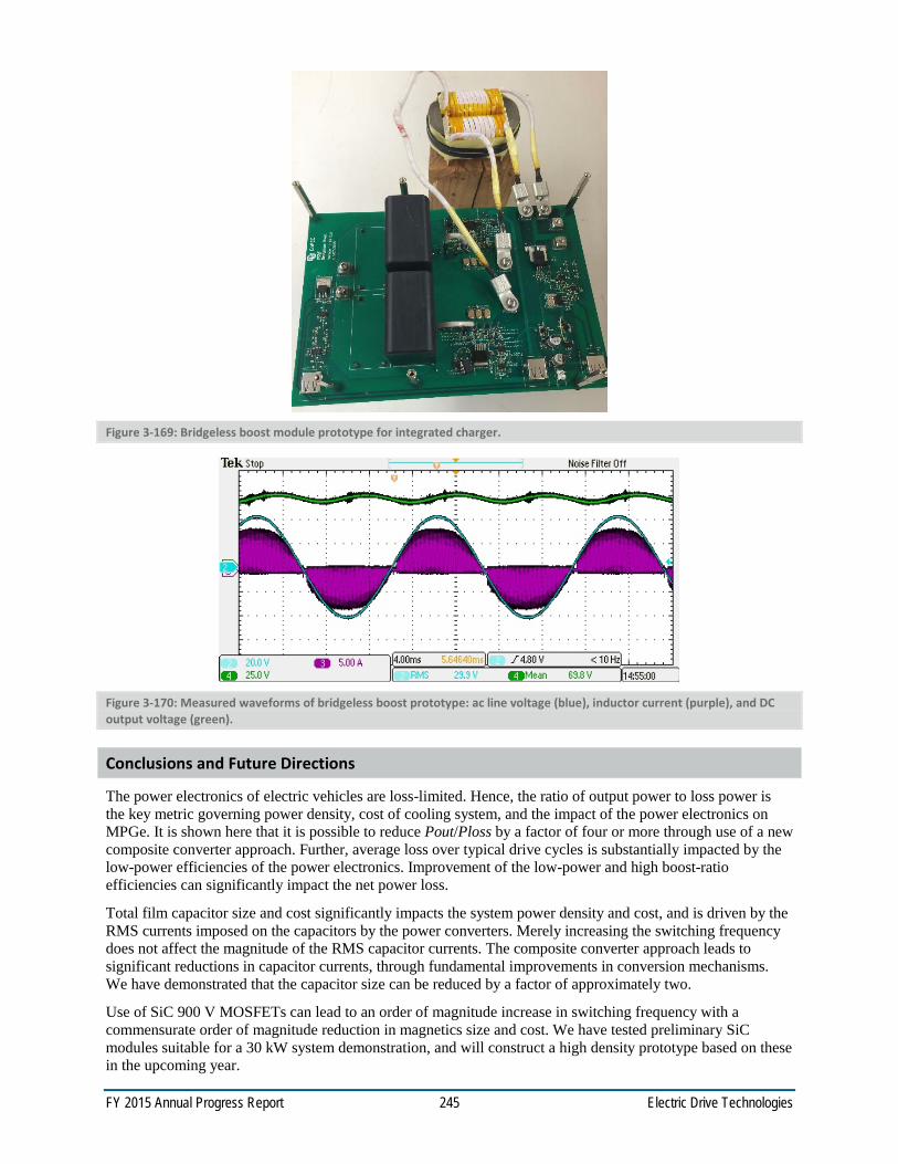
FY 2015 Annual Progress Report 245 Electric Drive Technologies
Figure 3-169: Bridgeless boost module prototype for integrated charger.
Figure 3-170: Measured waveforms of bridgeless boost prototype: ac line voltage (blue), inductor current (purple), and DC output voltage (green).
Conclusions and Future Directions
The power electronics of electric vehicles are loss-limited. Hence, the ratio of output power to loss power is the key metric governing power density, cost of cooling system, and the impact of the power electronics on MPGe. It is shown here that it is possible to reduce Pout/Ploss by a factor of four or more through use of a new composite converter approach. Further, average loss over typical drive cycles is substantially impacted by the low-power efficiencies of the power electronics. Improvement of the low-power and high boost-ratio efficiencies can significantly impact the net power loss.
Total film capacitor size and cost significantly impacts the system power density and cost, and is driven by the RMS currents imposed on the capacitors by the power converters. Merely increasing the switching frequency does not affect the magnitude of the RMS capacitor currents. The composite converter approach leads to significant reductions in capacitor currents, through fundamental improvements in conversion mechanisms. We have demonstrated that the capacitor size can be reduced by a factor of approximately two.
Use of SiC 900 V MOSFETs can lead to an order of magnitude increase in switching frequency with a commensurate order of magnitude reduction in magnetics size and cost. We have tested preliminary SiC modules suitable for a 30 kW system demonstration, and will construct a high density prototype based on these in the upcoming year.

FY 2015 Annual Progress Report 246 Electric Drive Technologies
The composite converter approach employs approximately the same amount of semiconductor area, but with somewhat more complex interconnections. There is significant ongoing research in power electronics packaging and interconnects; it is expected that this research could enable the practical deployment of more complex converter structures. Indeed, the substantial performance gains demonstrated by this work can justify further packaging and interconnect research.
A 30 kW power electronics power train will be demonstrated in the next year, and its performance under US06 and other drive cycles will be measured.
FY 2015 Presentations/Publications/Patents
1. R. Erickson, D. Maksimovic, and K. Afridi, “A Disruptive Approach to Electric Vehicle Power Electronics,” 2015 DOE VTO Annual Merit Review, Crystal City, VA, June 2015.
2. R. Erickson, D. Maksimovic, and K. Afridi, “A Disruptive Approach to Electric Vehicle Power Electronics,” Advanced Power Electronics and Electric Motors FY15 Kickoff Meeting, DOE VTO, Oak Ridge, TN, November 2015.
3. H. Kim, H. Chen, R. Erickson, and D. Maksimovic, “Design of a High Efficiency 30 kW Boost Composite Converter,” IEEE Energy Conversion Congress and Exposition (ECCE), Sept. 2015.
4. H. Chen, K. Sabi, H. Kim, T. Harada, R. Erickson and D. Maksimovic, “A 98.7% Composite Converter Architecture with Application-Tailored Efficiency Characteristic,” IEEE Transactions on Power Electronics, accepted, to appear January 2016.
References
1. L. Chen and A. Sankaran, “Vehicle electricification and traction inverter design,” IEEE Vehicle Power and Propulsion Conference, special presentation, 2012.
2. K. Muta, M. Yamazaki, and J. Tokieda, “Development of a new generation hybrid system THS II—Drastic improvement of power performance and fuel economy,” SAE paper 2004-10, 2004.
3. S. Nozawa, T. Maekawa, Eisuke Yagi, Yasuhiro Terao, and H. Kohno, “Development of new power control unit for compact-class vehicle,” 22nd International Symposium on Power Semiconductor Devices and ICs, pp. 34-45, 2010.
4. T. Burress, S. Campbell, C. Coomer, C. Ayers, A. Wereszczak, J. Cunningham, L. Marlino, L. Sieber, and H. Lin, “Evaluation of the 2010 Toyota Prius hybrid synergy drive system,” ORNL power electronics and electric machinery research facility technical report, 2011.
5. N. Higuchi and H. Shimada, “Efficiency enhancement of a new two-motor hybrid system,” IEEE 2013 World Electric Vehicle Symposium and Exhibition, pp. 1-11, 2013.

FY 2015 Annual Progress Report 247 Electric Drive Technologies
3.13. Next Generation Inverter
Principal Investigator: Zilai Zhao General Motors LLC 777 Joslyn Avenue, Mail Code: 483-720-450 Pontiac, MI 48340 Phone: (248) 326-5304 E-mail: [email protected] Contractor: General Motors LLC (Attn: Lillian Dodge, 895 Joslyn Avenue, MC 483710210, Pontiac, MI 48340 Contract No.: DE-EE0005572
Abstract/Executive Summary The overall objectives of the Next Generation Inverter (NGI) are:
To develop the technologies and the engineering product design for a low cost highly efficient next generation power inverter capable of 55kW peak/30kW continuous power.
To meet 2020 DOE goals by improving the cost of the power electronics to $3.30/kW produced in quantities of 100,000 units, the power density to 13.4kW/l, and the specific power to 14.1kW/kg.
Traction inverter cost is the key barrier to economic viability of electric traction drives. Achieving the cost goals must be done simultaneously with increasing efficiency, decreasing mass and volume, and maintaining reliability. Current materials used in today’s inverters for automotive applications are expensive and require multiple processes to be performed to construct a complete inverter. Additionally because of instability in the electric vehicle and hybrid electric vehicle (EV and HEV) market, commitment from the supplier base is difficult because the cost of introducing and validating new technologies is high.
The project has demonstrated an inverter design that can potentially achieve the technical and cost targets under certain conditions.
Accomplishments Completed the inverter design, including
o Power stage o Gate drive and control board o Housing and connectors
Developed inverter software based on GM Powertrain production inverter software.
Finished first phase of process development.
Produced test and demonstration units.
Demonstrated the operation of the NGI prototype to DOE.
Presented cost analysis to DOE.
Introduction
The goal of this Cooperative Agreement is the development of a Next Generation Inverter (NGI). The key goal is to reduce the production cost of a traction drive inverter while making improvements in mass, volume, and reliability/durability. Traction inverter cost is a key barrier to economic viability of electric traction drives. This program is divided into four budget periods: technology assessment, technology development, technology build, and non-destructive confirmatory testing. The technology assessment phase includes the investigation

FY 2015 Annual Progress Report 248 Electric Drive Technologies
through experimentation and evaluation of all key elements of the inverter. Technology development includes the concept and breadboard, and a final detailed design of the inverter. Technology build includes the procurement, fabrication of components, and the assembly of the inverter. Non-Destructive confirmatory testing includes environmental test setup, electrical verification, temp/vibe characterization and margining, and test support at a national lab. We are currently in Phase 4. The NGI project under this Cooperative Agreement will end on 1/15/2015.
In the past reporting year (October 1, 2014 to September 30, 2015), we finalized the design of the inverter, completed development of key processes, built prototypes for various non-destructive testing, completed cost study and final demonstration to DOE. Please see "Results and Discussion" section for detailed information.
Approach
In this project GM engaged with Tier 1, 2, and 3 suppliers along with National Labs to co-develop technology that reduces cost and increases efficiency, without increasing volume or mass. The resulting inverter design demonstrates modularity and scalability, which is necessary to support different vehicle applications from battery electric vehicles to strong electric hybrid vehicles. Additionally, this inverter has consistent electrical parameters and mechanical structure, provides adequate cooling for the capacitor, has low direct current (DC) loop stray inductance, and adheres to global manufacturing processes.
The overall design approach we took is to integrate "active" components and reduce/eliminate "supporting" components. Simply put, "active" components are the ones that appear on electrical schematic and "supporting" components are the ones that mechanically and environmentally support and protect the "active" components. Examples of "active" components are insulated gate bipolar transistor (IGBT) and free-wheeling diode (FWD) chips, film capacitor elements, bus bars, current sensors, gate drive and control printed circuit boards, etc. Examples of "supporting" components are various housing and encapsulation of sub-components, mechanical supports and fasteners, etc.
As reported in FY14 annual report, the following features of final design of the inverter reflects our design approach:
Closed aluminum coolant manifold
Power semiconductors and substrates directly attached to coolant manifold
Film capacitor built into coolant manifold frame, removing capacitor housing and providing better cooling
Press-fit pins for signal and power circuit interconnection
One piece lead frame for power semiconductor packaging
One piece bus bar to route DC and AC current
Gate drive and control circuit on one printed circuit board assembly (PCBA)
Another approach we took was to advance the design and manufacturing processes simultaneously. Starting from Phase 3, our design engineering team worked closely with our manufacturing engineering team to optimize the design for manufacturability and assembly. In the meantime, manufacturing was challenged to improve its processes to enable the new design. The final prototype not only shows the functionality of the NGI but also represents a near production design enabled by innovative manufacturing processes.
Results and Discussion

FY 2015 Annual Progress Report 249 Electric Drive Technologies
Prototype Manufacturing Process
Figure 3-171: NGI Prototype Manufacturing Process General Motors
Figure 3-171 shows the manufacturing process flow for the prototype inverters. As dictated by the design of the inverter, this process vertically integrates power semiconductor packaging and interconnects, PCBA manufacturing, film capacitor assembly and overall power electronics assembly. In addition to enabling the high power density design, such vertically integrated process provides a path to lower the overall supply chain costs.
In the past year, we conducted extensive development on two key process steps, discussed below.
The first key process step was the die and substrate attach (solder reflow). We evaluated more than 20 reflow process configurations. Variables included, reflow technologies, reflow passes, solder materials, flux materials, cleaning materials and process and temperature profiles. Test coupons from each configuration were evaluated based on the following criteria: wire bond yield, electrical test yield, voiding, intermetallic growth, accelerated reliability test and 3-D X-Ray. After the final configuration was chosen, test coupons from this configuration were sent to National Renewable Energy Lab for further reliability tests with different temperature cycling profiles.
The second key process step was integration of the film capacitor into the cooling frame. For the NGI, the DC link capacitor is integrated into the cast cooling frame. The capacitor elements, or bobbins, are first connected to the DC bus bars. The bus bars are then installed in the inverter. Potting material is applied to encapsulate the bobbins. In the past year, we evaluated 5 potting materials. We conducted high temperature high humidity tests to evaluate these materials and selected the potting material that performed the best in this test.
Inverter Performance and Reliability Evaluation Six power stages and four complete inverters were produced with the finalized prototype process in the past year for the purpose of inverter performance and reliability evaluation.
The six power stages are currently undergoing power cycle tests and intermittent operating life tests. The complete inverters went through tests consistent with GM's production inverter verification process, including tests under both inductive and active (electric motor on dynamometer) load.

FY 2015 Annual Progress Report 250 Electric Drive Technologies
Although the NGI uses aluminum cooling manifold, measurements indicate that the NGI's IGBT junction to coolant thermal resistance is on par with state-of-the-art single-side-cooled power modules with copper base-plate.
The bus bar structure of the NGI was designed to provide very low DC loop inductance, which was confirmed by test data. Figure 3-172 shows Vce traces during IGBT turn-off. Compared to a conventional power stage with the same silicon area, the NGI has significantly lower Vce voltage overshoot during turn-off. This feature will allow the NGI to either switch faster, thereby having lower switching loss and higher efficiency, or operate at higher battery voltage, leading to higher power output.
Figure 3-173, Figure 3-174, and Figure 3-175 show the different test setups and Figure 3-176 shows the result of the active load test. During the active load test, the inverter achieved 320 Arms phase current in both regeneration and motoring. Maximum regeneration power is 87 kW and maximum motoring power is 98 kW. The NGI in the current configuration has achieved 141 kVA. The power stage of the NGI is designed to accommodate Si dies 40% larger than what is used in the current configuration. Therefore, we project that the maximum KVA capability of the NGI is 195 kVA, making it potentially the most power dense inverter in GM (see Table 3-17).
Figure 3-172: Vce Traces During Device Turn-Off (Blue: NGI; Orange: Conventional Power Stage) General Motors
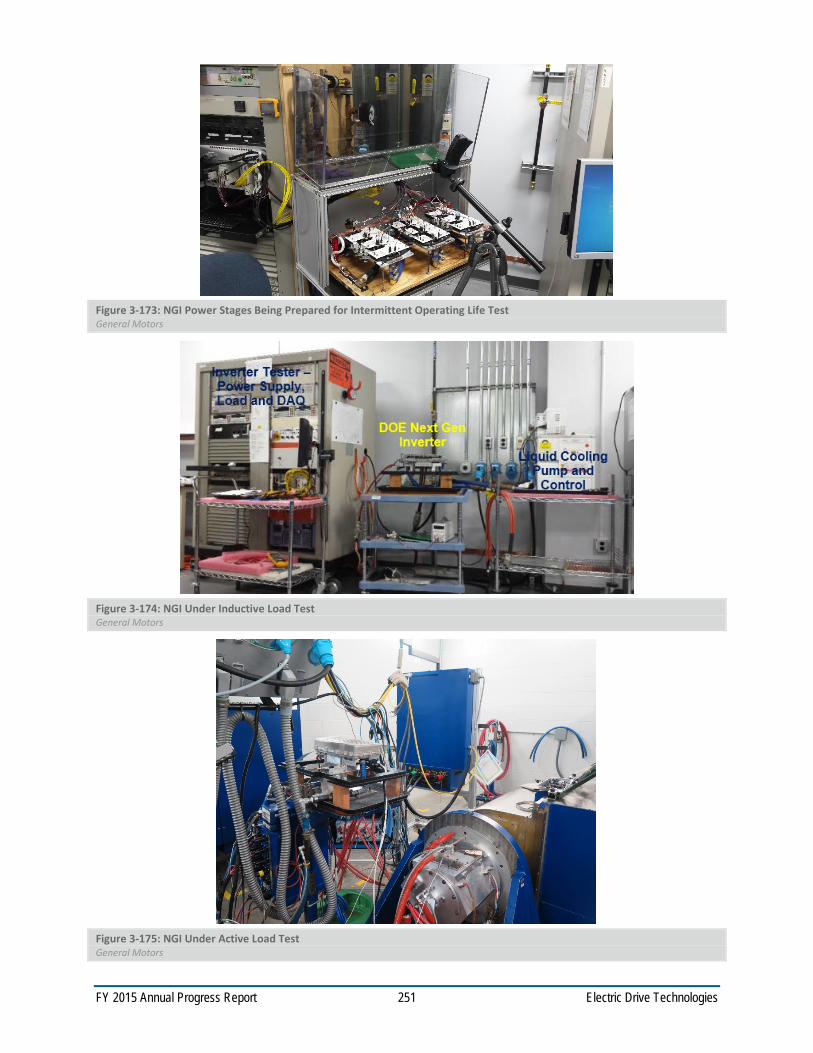
FY 2015 Annual Progress Report 251 Electric Drive Technologies
Figure 3-173: NGI Power Stages Being Prepared for Intermittent Operating Life Test General Motors
Figure 3-174: NGI Under Inductive Load Test General Motors
Figure 3-175: NGI Under Active Load Test General Motors

FY 2015 Annual Progress Report 252 Electric Drive Technologies
Figure 3-176: NGI Efficiency Map during Regeneration (Top) and Motoring (Bottom) General Motors
RPM
Torq
ue (
Nm
)
DoE Nextgen Regen Inverter Efficiency (300V)
0.5
0.7
0.6
0.8 0.90.92
0.94
0.960.97
0.98
1000 2000 3000 4000 5000 6000 7000 80000
50
100
150
200
250
300
0.5
0.55
0.6
0.65
0.7
0.75
0.8
0.85
0.9
0.95
RPM
Torq
ue (N
m)
DoE Nextgen Motor Inverter Efficiency (300V)
0.70.80.90.92
0.940.96
0.97
0.98
1000 2000 3000 4000 5000 6000 7000 80000
50
100
150
200
250
300
0.6
0.65
0.7
0.75
0.8
0.85
0.9
0.95

FY 2015 Annual Progress Report 253 Electric Drive Technologies
Table 3-17: Comparing KVA Density of GM Inverters
Note: NGI Lo is the NGI in the current configuration. NGI Hi is the NGI scaled up to its maximum capability. The data for NGI Hi is obtained by simulation while other data is from dynamometer tests.
On August 18, 2015, we successfully demonstrated the operation of the NGI to DOE in GM's dynamometer lab at Pontiac, Michigan.
Cost Analysis In the aforementioned 8/18 meeting with DOE, we also presented the final cost analysis. Included in the cost analysis are manufacturing line concept and commercialization assumptions based on 100,000 units per annum production volume. If GM's internal cost targets for the components can be achieved, we projected that the NGI, scaled up to its highest power configuration, can meet the DOE's 2020 cost target of $3.30/kW. However, our Bill of Materials (BOM) cost based on budgetary quotations from our supply base is still significantly higher than our cost target. The main reasons are:
1. Some components have small and specialized supply base, leading to inefficient market and high price.
2. Some components can be further optimized to reduced cost. 3. Commercial negotiation hasn't be carried out.
Conclusions and Future Directions
The NGI project is scheduled to conclude in January 2016. Before the end of the project, we will complete production of the prototype inverters and confirmatory tests.
Technologies developed in the project have been applied to GM's inverter design for future plug-in electric hybrid vehicles. Beyond this project, we intend to use the NGI design as the foundation for development of wide band-gap inverters.
FY 2015 Presentations/Publications/Patents
1. Zhao, Z. "2015 DOE Vehicle Technologies Annual Merit Review - NGI", Presentation in DOE Vehicle Technologies Annual Merit Review, Washington, DC, June 2015.

FY 2015 Annual Progress Report 254 Electric Drive Technologies
4.0 Benchmarking, Testing, and Analysis
4.1. Benchmarking EVs and HEVs Tim Burress, Principal Investigator Oak Ridge National Laboratory (ORNL) National Transportation Research Center 2360 Cherahala Boulevard Knoxville, TN 37932 Phone: (865) 946-1216 E-mail: [email protected] Susan A. Rogers, DOE EDT Program Manager Phone: (202) 586-8997 E-mail: [email protected] Burak Ozpineci, ORNL EDT Program Manager Phone: (865) 946-1329 E-mail: [email protected] Contractor: UT-Battelle, LLC, managing and operating contractor for the Oak Ridge National Laboratory Contract No.: DE-AC05-00OR22725
Abstract/Executive Summary Information from the Benchmarking project provides crucial information about the status of and trends in electric vehicle/hybrid electric vehicle (EV/HEV) technologies to DOE VTO for strategic planning with respect to state-of-the-art progressions. ORNL’s detailed benchmarking reports have received overwhelmingly positive feedback from researchers in academia and industry, as well as other individuals with an interest in EV/HEV technologies. This information serves as a valuable educational resource for EV/HEV architectures and yields a track of lessons learned, prevents reinventing/duplication of advancements, and promotes “leap-frog”/competitive development.
Accomplishments Designed, fabricated, and assembled the hardware necessary to adapt the 2014 Honda Accord HEV
transmission to the dynamometer test cell.
Successfully implemented the integration of ORNL controls with the 2014 Accord power converter unit (PCU).
Conducted comprehensive dynamometer testing of a 2014 Accord inverter and motor at 300, 500, and 700Vdc to obtain an efficiency map and many other performance metrics.
Confirmed published peak torque and power specifications for a 2014 Accord inverter and motor.
Introduction
The 2014 Honda Accord is a full hybrid vehicle that includes a motor with a published power rating of 124 kW, which is much more powerful than previous-generation ratings of about 12 and 14 kW. The hybrid system has many similarities to Toyota’s Hybrid Synergy Drive, and the vehicle reportedly has the highest city fuel efficiency rating (49 MPG) of all hybrids in its class. This report reviews results from the initial disassembly of the transaxle, motor, and PCU and discusses detailed findings from teardown analyses. Comprehensive dynamometer testing was conducted and the performance, efficiency, and other operational results are summarized.

FY 2015 Annual Progress Report 255 Electric Drive Technologies
Approach
Automotive manufacturers usually do not publish details about the design, functionality, and operation of EV/HEV technologies, and even published details and specifications need to be verified and clarified. For example, single-value power ratings for motors and inverters are often published; but they do not include information about the power capability throughout the operation range (e.g., versus speed), the duration for which this power can be maintained, the efficiency throughout the operation region, and many other important characteristics. Therefore, ORNL performs teardown assessments to obtain comprehensive information on design, functionality, and sub-component characteristics. Furthermore, components are completely instrumented and tested in a dynamometer test cell to determine operational characteristics such as performance and efficiency. These activities provide the information needed for DOE to warrant a robust program and provide DOE partners and other researchers with valuable information on state-of-the-art EV/HEV technologies.
Results and Discussion
The new Accord hybrid system contains two 3-phase electric motor-generators. The power train can operate in full electric mode, series electric mode, and engine mode. In series electric mode, power from the engine is absorbed and supplied to the battery and drive motor. When cruising at highway speeds, the engine can be directly coupled through a fixed gear ratio to the drive wheels, facilitating higher-efficiency operation. A diagram of the new hybrid system is shown in Figure 4-1. Overall, the electrical system layout and configuration is nearly identical to that of the previous Toyota hybrid systems that have been benchmarked. The HEV and plug-in HEV models include batteries with nominal voltages of 259 and 320 V, respectively. The HEV system includes a bidirectional boost (dc-dc) converter with a 411μF, 370 V capacitor on the input of the boost converter and a large 1,125 µF, 700 Vdc capacitor on the output of the boost converter. The battery voltage is boosted to a maximum level of 700 Vdc, and both motor and generator inverters are attached to the high-voltage bus.
Figure 4-1: Diagram of the 2014 Honda Accord hybrid electrical system.
Exterior views of the 2014 Honda Accord HEV PCU are shown in Figure 4-2. It is manufactured by Fuji Electric, and the overall mass and volume are 17.5 kg and 12.4 L, respectively. An oval connector on the PCU attaches to power cables from the battery, and two circular connectors attach to the 3-phase motor and generator. A 31-pin connector provides power to the PCU and, among many other functions, communication with other components on the vehicle. Cooling ports for the flow of standard ethylene glycol/water cooling are located at one end of the PCU, and another port is located on the opposite end to which the cooling system reservoir attaches.
The PCU has three main sections: the top compartment, bottom compartment, and heat sink located between them. As shown at right in Figure 4-3, the bottom compartment houses the capacitors, the inductor for the boost converter, a bleed resistor, and a current transducer for the boosted dc current. A white, zinc oxide–based thermal paste was observed on the bottom of the inductor, which is mounted to the bottom of the heat sink, but no other components in the bottom compartment are actively cooled.

FY 2015 Annual Progress Report 256 Electric Drive Technologies
Figure 4-2: Various exterior views of the 2014 Honda Accord hybrid PCU.
Figure 4-3: Upper compartment (left) and lower compartment (right) of 2014 Honda Accord PCU.

FY 2015 Annual Progress Report 257 Electric Drive Technologies
Shown at left in Figure 4-3 is the upper compartment, which includes the control board, power module, current transducers, and dc and ac bus bars from the power module to the exterior connectors. The control board is supported by a substantial plate that was cast as a part of the aluminum housing. After the driver board is removed from the power module, a planar electromagnetic interference (EMI) shield can be seen above the dc and ac bus bar infrastructure. In most Toyota power modules, the bus bars are more readily integrated within the module. The power module is integrated with the heat sink, which is shown at right in Figure 4-4. Upon removal of the driver board (shown at left in Figure 4-5), EMI shield, and bus bar structure, the power electronics devices are visible.
Figure 4-4: Accord power module periphery (left) and heat exchanger (right).
As shown at right in Figure 4-5, power devices for the generator inverter, motor inverter, and boost converter are located within the same module, a consolidation also observed in recent Toyota power modules. The generator inverter uses one insulated-gate bipolar transistor (IGBT) and one diode per switch, for a total of six IGBTs and six diodes. The motor inverter uses 2 IGBTs and 2 diodes per switch, giving a total of 12 IGBTs and 12 diodes. The boost converter uses three IGBTs with two diodes for the lower switch, and two IGBTS and two diodes for the upper switch. All previously benchmarked boost converters contained the same number of IGBTs for upper and lower switches.
Figure 4-5: Accord power module with (left) and without (right) driver board.
Dimensions of the IGBTs and diodes are labeled at left in Figure 4-6. All IGBTs and diodes in the PCU have the same dimensions: approximately 12.18×15.21 mm and 12.15×11.06 mm, respectively. Material compositional analysis was conducted to determine the materials used within the power module. The center image in Figure 4-6 indicates the overall stack-up of the power module; it shows that IGBT and diode power devices are soldered to a direct-bond copper (DBC) cladding about 1.12 mm thick. The solder layer thickness is ~ 0.13–0.14 mm. The upper copper cladding is attached to an ~0.32 mm thick silicon nitride ceramic dielectric that serves as an electrical insulator for the IGBT and diode. A more commonly used lower-cost ceramic dielectric is aluminum nitride; but a few other hybrid systems, including the Lexus LS 600h, also have used silicon nitride. The ceramic dielectric is attached to another copper-clad layer that is about 0.40 mm thick. The lower copper-clad layer is soldered to the nickel-plated aluminum baseplate/heat sink. The nickel plating is about 10 um thick and the lower solder layer is about 0.40 mm thick. Nickel plating appears to cover the entire baseplate/heat sink shown in Figure 4-4.

FY 2015 Annual Progress Report 258 Electric Drive Technologies
Figure 4-6: Accord IGBT and diode (left) and power module stack-up (right).
The 2014 Accord transmission, shown in Figure 4-7, has a total mass of about 113.5 kg (249.5 lb), which is quite close to the 2007 Camry hybrid transmission mass of 108 kg. This is a good comparison because both passenger vehicles are sedans of similar size and power requirements. As is the case for many hybrid transmissions, there is no torque converter between the internal combustion engine and the transmission. Other than the absence of a torque converter, the transmission mounts to the engine in a conventional manner with a flywheel attached to the spline. Various sections of the transmission are indicated at right in Figure 4-7, where the engine input spline shafted is labeled. The gear section is adjacent to the engine mounting location and includes the differential gear that drives the left and right drive shafts and ultimately the front wheels. The section that houses the drive motor is located next to the gear section, and the generator section is located next to the motor section on the opposite end of the transmission.
Figure 4-7: 2014 Honda Accord electronic continuously variable transmission.
After the end plate of the generator section is removed, the generator is clearly visible, as shown at left in Figure 4-8. The generator end plate includes a position resolver that has 14 stator teeth, and the generator shaft has a soft-magnetic resolver rotor with 4 smooth lobes consisting of 8 laminations for position sensing. Also indicated at left in Figure 4-8 are four tubes used for oil spray cooling of the generator and motor end windings. Four groups of two holes are positioned in the tubes so that they spray the end turns on both sides of the generator and motor. Since the generator is smaller than the motor, the two groupings for the generator are closer together than the grouping of the motor spray holes. After the generator is removed, a clutch located between the generator and the motor is visible. The clutch does not have hydraulic activation and is used only as a torque limiter, most likely to mitigate transients and peak conditions when the generator is used to start the engine.
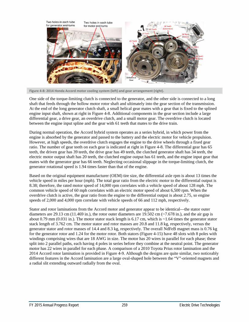
FY 2015 Annual Progress Report 259 Electric Drive Technologies
Figure 4-8: 2014 Honda Accord motor cooling system (left) and gear arrangement (right).
One side of the torque-limiting clutch is connected to the generator, and the other side is connected to a long shaft that feeds through the hollow motor rotor shaft and ultimately into the gear section of the transmission. At the end of the long generator clutch shaft, a small helical gear mates with a gear that is fixed to the splined engine input shaft, shown at right in Figure 4-8. Additional components in the gear section include a large differential gear, a drive gear, an overdrive clutch, and a small motor gear. The overdrive clutch is located between the engine input spline and the gear with 61 teeth that mates to the drive train.
During normal operation, the Accord hybrid system operates as a series hybrid, in which power from the engine is absorbed by the generator and passed to the battery and the electric motor for vehicle propulsion. However, at high speeds, the overdrive clutch engages the engine to the drive wheels through a fixed gear ratio. The number of gear teeth on each gear is indicated at right in Figure 4-8. The differential gear has 65 teeth, the driven gear has 39 teeth, the drive gear has 49 teeth, the clutched generator shaft has 34 teeth, the electric motor output shaft has 20 teeth, the clutched engine output has 61 teeth, and the engine input gear that mates with the generator gear has 66 teeth. Neglecting occasional slippage in the torque-limiting clutch, the generator rotational speed is 1.94 times faster than that of the engine.
Based on the original equipment manufacturer (OEM) tire size, the differential axle rpm is about 13 times the vehicle speed in miles per hour (mph). The total gear ratio from the electric motor to the differential output is 8.38; therefore, the rated motor speed of 14,000 rpm correlates with a vehicle speed of about 128 mph. The common vehicle speed of 60 mph correlates with an electric motor speed of about 6,500 rpm. When the overdrive clutch is active, the gear ratio from the engine to the differential output is about 2.75, so engine speeds of 2,000 and 4,000 rpm correlate with vehicle speeds of 66 and 112 mph, respectively.
Stator and rotor laminations from the Accord motor and generator appear to be identical—the stator outer diameters are 29.13 cm (11.469 in.), the rotor outer diameters are 19.502 cm (~7.678 in.), and the air gap is about 0.79 mm (0.031 in.). The motor stator stack length is 6.17 cm, which is ~1.64 times the generator stator stack length of 3.762 cm. The motor stator and rotor masses are 20.8 and 11.8 kg, respectively, versus the generator stator and rotor masses of 14.4 and 8.3 kg, respectively. The overall NdFeB magnet mass is 0.76 kg for the generator rotor and 1.24 for the motor rotor. Both stators (Figure 4-15) have 48 slots with 8 poles with windings comprising wires that are 18 AWG in size. The motor has 20 wires in parallel for each phase; these split into 2 parallel paths, each having 4 poles in series before they combine at the neutral point. The generator motor has 22 wires in parallel for each phase. A comparison of a 2010 Toyota Prius rotor lamination and the 2014 Accord rotor lamination is provided in Figure 4-9. Although the designs are quite similar, two noticeably different features in the Accord lamination are a large oval-shaped hole between the “V”-oriented magnets and a radial slit extending outward radially from the oval.
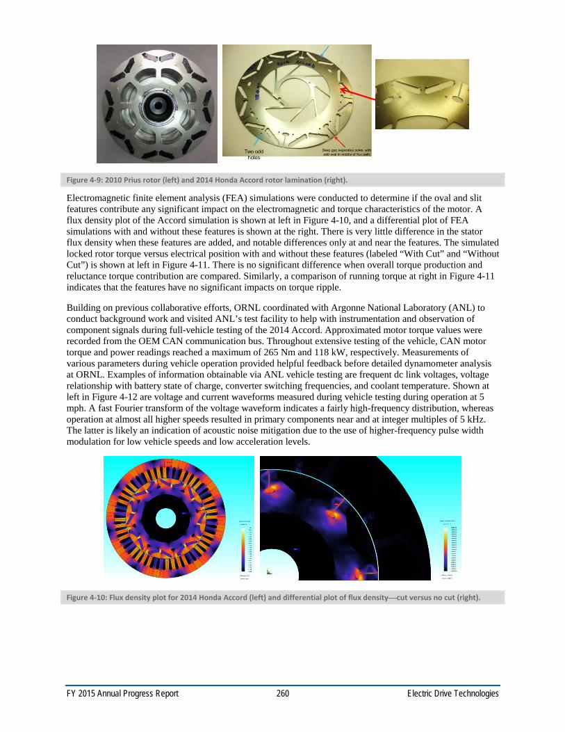
FY 2015 Annual Progress Report 260 Electric Drive Technologies
Figure 4-9: 2010 Prius rotor (left) and 2014 Honda Accord rotor lamination (right).
Electromagnetic finite element analysis (FEA) simulations were conducted to determine if the oval and slit features contribute any significant impact on the electromagnetic and torque characteristics of the motor. A flux density plot of the Accord simulation is shown at left in Figure 4-10, and a differential plot of FEA simulations with and without these features is shown at the right. There is very little difference in the stator flux density when these features are added, and notable differences only at and near the features. The simulated locked rotor torque versus electrical position with and without these features (labeled “With Cut” and “Without Cut”) is shown at left in Figure 4-11. There is no significant difference when overall torque production and reluctance torque contribution are compared. Similarly, a comparison of running torque at right in Figure 4-11 indicates that the features have no significant impacts on torque ripple.
Building on previous collaborative efforts, ORNL coordinated with Argonne National Laboratory (ANL) to conduct background work and visited ANL’s test facility to help with instrumentation and observation of component signals during full-vehicle testing of the 2014 Accord. Approximated motor torque values were recorded from the OEM CAN communication bus. Throughout extensive testing of the vehicle, CAN motor torque and power readings reached a maximum of 265 Nm and 118 kW, respectively. Measurements of various parameters during vehicle operation provided helpful feedback before detailed dynamometer analysis at ORNL. Examples of information obtainable via ANL vehicle testing are frequent dc link voltages, voltage relationship with battery state of charge, converter switching frequencies, and coolant temperature. Shown at left in Figure 4-12 are voltage and current waveforms measured during vehicle testing during operation at 5 mph. A fast Fourier transform of the voltage waveform indicates a fairly high-frequency distribution, whereas operation at almost all higher speeds resulted in primary components near and at integer multiples of 5 kHz. The latter is likely an indication of acoustic noise mitigation due to the use of higher-frequency pulse width modulation for low vehicle speeds and low acceleration levels.
Figure 4-10: Flux density plot for 2014 Honda Accord (left) and differential plot of flux density—cut versus no cut (right).

FY 2015 Annual Progress Report 261 Electric Drive Technologies
Figure 4-11: Simulated locked rotor torque (left) and running torque ripple (right).
Figure 4-12: 2014 Accord running waveforms collected from vehicle in collaboration with ANL.
For detailed component testing at ORNL, designs were developed to provide access to the electric motor shaft in the transmission while maintaining the cooling and lubrication functionality used in the original form. This integration requires special attention to detail because high speed and power levels are involved. The electric motor shaft is not normally externally accessible, and unique methods were required to obtain access for dynamometer testing. A custom plate was designed with high tolerance alignment features and considerations for lubrication. A unique adapter shaft also was designed to adapt the motor shaft to ORNL’s dynamometer, as shown in Figure 4-13. The graph at left in Figure 4-13 shows a comparison of back-electromotive force (EMF) results with those for other HEV motors. Locked rotor torque measurements for various positions and applied current are indicated at left in Figure 4-14. Test results indicate that a peak current of ~ 425 A dc is required to produce the published peak torque of 307 Nm. It was also observed that a significant amount of reluctance torque is produced in the motor. Additionally, the current angle at which the maximum torque occurs is slightly larger than that in most interior permanent magnet motor designs tested previously. For torques above
0 20 40 60 80 100 120 140 160 1800
50
100
150
200
250
300
350
Electrical Position [Degrees]
Torq
ue [N
-m]
Without CutWith Cut
0 0.1 0.2 0.3 0.4 0.5 0.6 0.7 0.8 0.9 1285
290
295
300
305
310
315
320
325
330
335
Time [s]
Torq
ue [N
-m]
Without CutWith Cut
-0.04 -0.02 0 0.02 0.04 0.06 0.08-500
-400
-300
-200
-100
0
100
200
300
400
500
Time (s)
Cur
rent
(A) a
nd V
olta
ge (V
)
Voltage (L-L)Phase Current
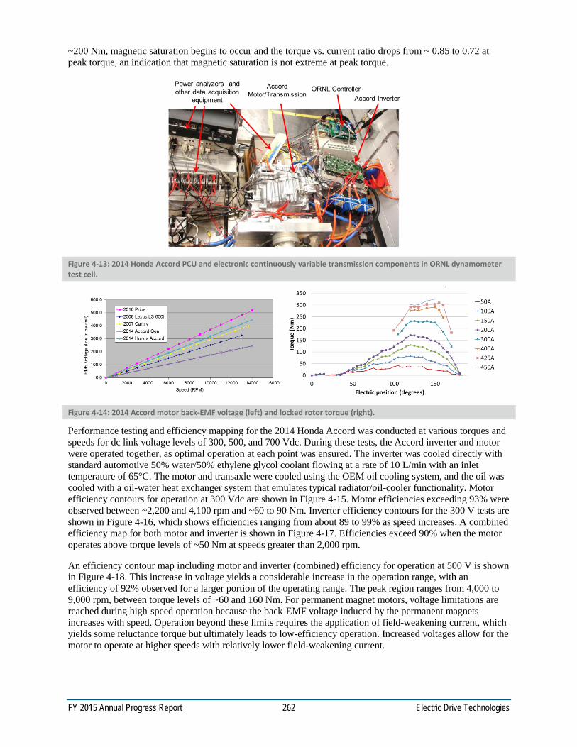
FY 2015 Annual Progress Report 262 Electric Drive Technologies
~200 Nm, magnetic saturation begins to occur and the torque vs. current ratio drops from ~ 0.85 to 0.72 at peak torque, an indication that magnetic saturation is not extreme at peak torque.
Figure 4-13: 2014 Honda Accord PCU and electronic continuously variable transmission components in ORNL dynamometer test cell.
Figure 4-14: 2014 Accord motor back-EMF voltage (left) and locked rotor torque (right).
Performance testing and efficiency mapping for the 2014 Honda Accord was conducted at various torques and speeds for dc link voltage levels of 300, 500, and 700 Vdc. During these tests, the Accord inverter and motor were operated together, as optimal operation at each point was ensured. The inverter was cooled directly with standard automotive 50% water/50% ethylene glycol coolant flowing at a rate of 10 L/min with an inlet temperature of 65°C. The motor and transaxle were cooled using the OEM oil cooling system, and the oil was cooled with a oil-water heat exchanger system that emulates typical radiator/oil-cooler functionality. Motor efficiency contours for operation at 300 Vdc are shown in Figure 4-15. Motor efficiencies exceeding 93% were observed between ~2,200 and 4,100 rpm and ~60 to 90 Nm. Inverter efficiency contours for the 300 V tests are shown in Figure 4-16, which shows efficiencies ranging from about 89 to 99% as speed increases. A combined efficiency map for both motor and inverter is shown in Figure 4-17. Efficiencies exceed 90% when the motor operates above torque levels of ~50 Nm at speeds greater than 2,000 rpm.
An efficiency contour map including motor and inverter (combined) efficiency for operation at 500 V is shown in Figure 4-18. This increase in voltage yields a considerable increase in the operation range, with an efficiency of 92% observed for a larger portion of the operating range. The peak region ranges from 4,000 to 9,000 rpm, between torque levels of ~60 and 160 Nm. For permanent magnet motors, voltage limitations are reached during high-speed operation because the back-EMF voltage induced by the permanent magnets increases with speed. Operation beyond these limits requires the application of field-weakening current, which yields some reluctance torque but ultimately leads to low-efficiency operation. Increased voltages allow for the motor to operate at higher speeds with relatively lower field-weakening current.
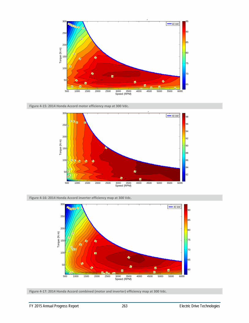
FY 2015 Annual Progress Report 263 Electric Drive Technologies
Figure 4-15: 2014 Honda Accord motor efficiency map at 300 Vdc.
Figure 4-16: 2014 Honda Accord inverter efficiency map at 300 Vdc.
Figure 4-17: 2014 Honda Accord combined (motor and inverter) efficiency map at 300 Vdc.
Speed (RPM)
Torq
ue (N
m)
y
66 6870 72 74 76 78 80
82
82
84
84
86
86
8686
88
88
88
8888 90
90
90
90
9191
91
91
92
92
92
90
93
91 92 93 94
500 1000 1500 2000 2500 3000 3500 4000 4500 5000 5500 6000
50
100
150
200
250
30040 kW
65
70
75
80
85
90
95
Speed (RPM)
Torq
ue (N
m)
y
8990
9192
92
9393
9494
95
95
9696
9797
98
98
98
99
99
99
500 1000 1500 2000 2500 3000 3500 4000 4500 5000 5500 6000
50
100
150
200
250
30040 kW
82
84
86
88
90
92
94
96
98
Speed (RPM)
Torq
ue (N
m)
62 64 66 68 70 72 74
76
76
78
78
80
80
81
81
81
82
82
82
83
83
83
84
84
84
85
85
85
85
86
86
86
87
87
87
87
88
88
88
88
89
89
89
90
90
90
91
91
8788
89 90
92
91 92
500 1000 1500 2000 2500 3000 3500 4000 4500 5000 5500 6000
50
100
150
200
250
30040 kW
60
65
70
75
80
85
90
FY 2015 Annual Progress Report 264 Electric Drive Technologies
Figure 4-18: 2014 Honda Accord combined (motor and inverter) efficiency contours at 500 Vdc.
A motor efficiency contour map for operation at 700 Vdc is shown in Figure 4-19. Motor efficiencies reached above 94% for speeds between ~6,000 and 10,000 rpm and between torque levels of ~40 and 150 Nm. Inverter efficiencies for 700 Vdc operation are shown in Figure 4-20, in which a peak inverter efficiency above 99% was observed for a considerable portion of the high-speed operation region. A combined (inverter and motor) efficiency contour map is shown in Figure 4-21, where the peak motor-inverter efficiency is 94% and efficiencies above 90% are noticeable for speeds ranging from about 3,500 to 12,000 rpm. During these tests, the published rated torque of 307 Nm was confirmed up to a speed of 3,500 rpm. Tests also confirmed that the motor is capable of producing the published peak power of 124 kW at speeds between ~4,000 and ~9,000 rpm.
Figure 4-19: 2014 Honda Accord combined motor efficiency contours with 700 Vdc.
Speed (RPM)
Torq
ue (N
m)
6870
72
72 74
76
76
78
78
78
80
80
81
81
81
8282
82
82
82
8383
83
83
83
8484
84
84
84
8585
85
85
85
8686
86
86
86
8787
87 87
87
8888
88 88
88
8989
89
89
89
909090
90
90
91
91
91
91
92
92
92
93
93
87
1000 2000 3000 4000 5000 6000 7000 8000 9000 10000 11000 12000
50
100
150
200
250
30090 kW
60
65
70
75
80
85
90
Speed (RPM)
Torq
ue (N
m)
y
70 7274
76
78
78
80
80
82
82
84
84
84
86
86
86
88
88
88
88 9090
90
90
90
90
90
91
91
91
91
91
91
91
92
92
92
92
92
92
92
93
93
93
93
93 93
9394
94
94
94
93
93
92
95
9293
93
95
1000 2000 3000 4000 5000 6000 7000 8000 9000 10000 11000 12000
50
100
150
200
250
300124 kW
65
70
75
80
85
90
95
FY 2015 Annual Progress Report 265 Electric Drive Technologies
Figure 4-20: 2014 Honda Accord inverter efficiency contours with 700 Vdc.
Figure 4-21: 2014 Honda Accord combined (motor and inverter) efficiency contours with 700 Vdc.
Continuous tests were conducted at 5,000, 7,000, and 9,000 rpm at power levels of 25 and 50 kW. The plot in Figure 4-22 indicates the power level and motor winding temperature versus time for continuous tests at 7,000 rpm and 25 and 50 kW, with a dc bus voltage level of 700 V. After operation at 25 kW for an hour, the motor temperature exceeded 100°C. Then the power was increased to 50 kW for an hour, and the motor temperature was relatively stable at ~135°C. Note that this speed is associated with the highest efficiency at which 124 kW can be reached, and 124 kW operation at other speeds resulted in higher motor temperatures.
Speed (RPM)
Torq
ue (N
m)
y
8081
82 83
8485
86
87
87
88
8889
89
90
9090
91
9191
92
9292
93
9393
94
9494
95
9595
9696
96
96
97
97
97
97
98
9898
98
98
9999
99
99
99
1000 2000 3000 4000 5000 6000 7000 8000 9000 10000 11000 12000
50
100
150
200
250
300124 kW
80
82
84
86
88
90
92
94
96
98
Speed (RPM)
Torq
ue (N
m)
y
66
68 70
70
72
72
74
74
74
76
76
76
78
78
78
80
80 80
81
81
81
81
82
82
82
82
83
83
83
83
84
84
84
84
84
85
85
85
85
85
86
86
86
86
86
87
87
87
87
87
88
88
88
88
88
89
89
89
89
89
90
90
90
90
90
90
91
91
91 91
91
92
92
92
92
92
93
93
93
94
94
91
94
1000 2000 3000 4000 5000 6000 7000 8000 9000 10000 11000 12000
50
100
150
200
250
300124 kW
55
60
65
70
75
80
85
90
FY 2015 Annual Progress Report 266 Electric Drive Technologies
Figure 4-22: Continuous tests of 2014 Honda Accord at 7000 rpm and 25 and 50 kW.
Conclusions and Future Direction
Detailed disassembly and analysis of a PCU/inverter revealed key design features. They include a heat sink integrated with the power module, whereas most previously benchmarked components have used a thermal paste, which greatly inhibits heat transfer. In regard to cost, manufacturability, and power density, the inverter heat sink, bus bars, and other peripherals seemed slightly more complex than similar components observed from Toyota. Silicon nitride insulators were used, as opposed to the less expensive and more commonly used aluminum nitride. The inverter performed well thermally during peak and continuous power testing and the operation requirements.
Transaxle/electric motor teardown analyses yielded many interesting design features, including a comprehensive oil-spray cooling system that targets the end-windings of the motor and generator. Rotor laminations looked relatively similar to those of many Toyota products, except for a large gap located between the magnetic poles. Electromagnetic FEA simulations indicated that this feature has no significant impact on motor operation, but a benefit is gained with respect to mechanical stress relief. This facilitates a reduction in the thickness of the magnet supports near the airgap, thereby reducing leakage and increasing efficiency.
Operation at published peak torque and peak power was confirmed, and tests were conducted at 300, 500, and 700 Vdc. Peak motor efficiencies reached 95% and inverter-motor efficiencies reached 94% at 700 Vdc operation. Continuous tests indicated that the system is capable of operating continuously at 50 kW, and the motor temperature remained below 140°C.
Components for the BMW i3 were procured and will be the focus of comprehensive benchmarking studies in FY 2016. Additionally, there is high interest in benchmarking a state-of-the-art onboard charger, and efforts to procure a suitable candidate will continue.
FY 2015 Presentations/Publications/Patents
1. T. Burress, et al, “Benchmarking of EVs and HEVs,” presented at the DOE Vehicle Technologies Program Electric Drive Technologies FY15 Kickoff Meeting, Oak Ridge, Tennessee, November 18, 2014.
2. T. Burress, et al, “Benchmarking EV and HEV Technologies: 2014 Honda Accord PCU,” presented at the DOE Vehicle Technologies Program Electric Drive Technologies Electrical and Electronics Technical Team meeting, location, February 24, 2015.
3. T. Burress, et al, “Benchmarking EV and HEV Technologies,” presented at the U.S. DOE VTO 2015 Annual Merit Review, Washington DC, June 2015.
FY 2015 Annual Progress Report 267 Electric Drive Technologies
4.2. Thermal Performance Benchmarking Gilbert Moreno, Principal Investigator National Renewable Energy Laboratory (NREL) Transportation and Hydrogen Systems Center 15013 Denver West Parkway Golden, CO 80401 Phone: (303) 275-4450 E-mail: [email protected] Susan A. Rogers, DOE Technology Development Manager U.S. Department of Energy 1000 Independence Avenue SW, EE-3V Washington, DC 20585 Phone: (202) 586-8997 E-mail: [email protected] Sreekant Narumanchi, NREL Task Leader Phone: (303) 275-4062 Email: [email protected]
Abstract The goal for this project is to thoroughly characterize the performance of state-of-the-art (SOA) in-production automotive power electronics and electric motor thermal management systems. Information obtained from these studies will be used to:
Evaluate advantages and disadvantages of different thermal management strategies Establish baseline metrics for the thermal management systems Identify methods of improvement to advance the SOA Increase the publicly available information related to automotive traction-drive thermal management
systems Help guide future electric drive technologies (EDT) research and development (R&D) efforts.
The performance results combined with component efficiency and heat generation information obtained by Oak Ridge National Laboratory (ORNL) may then be used to determine the operating temperatures for the EDT components under drive-cycle conditions. In FY15, the 2012 Nissan LEAF power electronics and electric motor thermal management systems were benchmarked. Testing of the 2014 Honda Accord Hybrid power electronics thermal management system started in FY15 and the results will be reported in FY16.
The focus of this project is to benchmark the thermal aspects of the systems. ORNL's benchmarking reports of electric and hybrid electric vehicle technology provide detailed descriptions of the electrical and packaging aspects of these automotive systems [1, 2].
Accomplishments We experimentally characterized the thermal performance of the 2012 Nissan LEAF motor and power
electronics thermal management systems. We developed and validated steady-state and transient thermal models of the 2012 Nissan LEAF
motor and power electronics systems. The models were used to identify the thermal bottlenecks within each system. Solutions to improve the thermal performance were proposed.
We are working to understand heat loss distributions within each system. Heat loss information will be used as inputs into the transient models and used to compute component temperatures under drive-cycle operations.
We initiated tests to measure the thermal performance of the 2014 Honda Accord power electronics thermal management system.

FY 2015 Annual Progress Report 268 Electric Drive Technologies
Introduction
This project will seek out the SOA power electronics and electric motor technologies to benchmark their thermal performance. The benchmarking will focus on the thermal aspects of the system. System metrics including the junction-to-coolant thermal resistance, winding-to-coolant thermal resistance, and the parasitic power consumption of the heat exchangers will be measured. The type of heat exchanger (i.e., channel flow, brazed, folded-fin) and any enhancement features will be identified and evaluated to understand their effect on performance. Additionally, the thermal resistance/conductivity of select power module and motor components will also be measured. The research conducted will allow insight into the various cooling strategies to understand which heat exchangers are most effective in terms of thermal performance and efficiency. Modeling analysis and fluid-flow visualization may also be carried out to better understand the heat transfer and fluid dynamics of the systems. The research conducted will allow insight into the various cooling strategies to understand the current SOA in thermal management for automotive power electronics and electric motors.
Approach
Hardware testing and modeling analyses were conducted to benchmark the performance of the power electronics and electric motor thermal management systems. The project approach is outlined below.
Collaborate with industry and ORNL to identify the vehicle system to benchmark o The 2012 Nissan LEAF power electronics and electric motor thermal management systems were
benchmarked in 2015. Tests were initiated to measure the thermal performance of the 2014 Honda Accord Hybrid power electronics thermal management system.
Experimentally measure the performance of the thermal management systems o Measure the power electronics junction-to-liquid and the motor winding-to-liquid thermal
resistances o Measure the thermal properties of the system components (e.g., thermal pads, stator laminations,
motor windings) o Measure heat exchanger thermal resistance, pressure drop, volume, and weight
Create thermal models of the thermal management systems o Validate the models using experimental results o Compute thermal resistances that cannot be experimentally measured o Create transient thermal models and use them to estimate component temperatures under various
drive-cycles
Analyze and report data o Identify thermal bottlenecks in the systems and provide solutions to improve the SOA o Establish baseline metrics for the thermal management systems o Share results with industry and research institutions o Support other EDT projects (power electronics thermal management R&D, electric motor thermal
management R&D, benchmarking electric vehicle and hybrid electric vehicle technologies [ORNL]).
Results and Discussion
In FY15, the 2012 Nissan LEAF power electronics and electric motor thermal management systems were benchmarked. Experimental testing of the hardware was first completed to measure thermal resistance values of the systems. The laboratory tests were intended to provide an accurate means of measuring thermal performance of the systems and were not intended to simulate actual automotive operating conditions. Steady-state and transient models were then created that were validated against the experimental data. The validated thermal models were used to further understand the heat transfer mechanisms within the systems. The goal is

FY 2015 Annual Progress Report 269 Electric Drive Technologies
to use the models to compute component temperatures under drive-cycle conditions. Efforts to benchmark the 2014 Honda Accord Hybrid power electronics thermal management system started in FY15.
2012 Nissan LEAF Motor Thermal Management System Figure 4-23 shows a picture of the 2012 Nissan LEAF motor. The motor is an interior permanent magnet synchronous machine that outputs a maximum of 80 kW [3]. The motor uses a distributed winding stator configuration. Figure 4-23 also shows the thermal management system that consists of a water-ethylene glycol (WEG) cooling jacket that is pressed around the motor stator. The cooling jacket is fabricated out of aluminum and has three relatively large coolant channels. The coolant channels have approximate dimensions of 35 mm in width and 12.5 mm in height. The cooling jacket has an inner diameter of approximately 200 mm, an outer diameter of approximately 250 mm, and a total axial length of approximately 210 mm. The approximate weight of the coolant jacket (not including the stator and rotor) is 10.1 kg.
Figure 4-23: Pictures of the 2012 Nissan LEAF motor. Image on the right shows the cooling jacket sectioned-off to reveal the internal coolant channels. Photo Credit: Kevin Bennion (NREL)
Experiments were conducted to measure the thermal performance of the motor thermal management system. For this, the motor was first connected to the WEG flow test bench. The test bench circulated WEG (50%/50% mixture by volume of water and ethylene glycol) at an inlet temperature of 65°C through the cooling jacket. The system thermal resistances were measured at various WEG flow rates. Three direct-current, high-current and low-voltage power supplies were used to provide heating to the motor's windings. Approximately 160 amps were conducted through all three phases of the motor to provide approximately 530 W of total heat. Voltage drop measurements taken at the positive and negative (neutral) sides of each phase were used along with the current supplied to compute the power dissipated. The motor was insulated on all sides with thick layers of insulation to minimize thermal losses to the surrounding environment.
Calibrated K-type thermocouples were installed on various parts of the motor to measure the temperatures at different locations (Figure 4-24). Twenty thermocouples were installed on the end-windings (both sides) to measure the inner, outer, and axial end-winding surface temperatures. Ten thermocouples were installed on the stator to measure the surface temperatures of the inner stator, slot liner, and interface between the slot liner and stator laminations. The stator surface temperatures were taken on both sides and at the midpoint of the stator. Ten thermocouples were instrumented on the various locations on the cooling jacket.

FY 2015 Annual Progress Report 270 Electric Drive Technologies
𝑅𝑅𝑡𝑡ℎ, 𝑤𝑤−𝑙𝑙 = (𝐼𝐼𝑠𝑠−𝐼𝐼𝑙𝑙)𝑄𝑄𝑇𝑇𝑇𝑇𝑇𝑇𝑃𝑃𝑙𝑙
Equation 1
Rth, s−l = (Ts−Tl)QTotal
Equation 2
Figure 4-24: Pictures show the thermocouple placements on the end-windings (left) and stator surfaces (right). Photo Credit: Gilbert Moreno (NREL)
Heat balances were calculated for the system to compare total heat generated to the heat absorbed by the WEG at different flow rates. Calculations revealed that heat losses to the surrounding conditions are approximately 9.9% at 1.8 Lpm and decrease to approximately 4.4% at 12 Lpm.
The thermal resistances of the motor were used to quantify the thermal performance of the system. The end-winding-to-liquid thermal resistance was defined using Eq. (1).
where 𝑤𝑤 𝑇𝑇 is the average end-winding temperature, 𝑇𝑇𝑙𝑙 is the average WEG temperature, and 𝑄𝑄𝐼𝐼𝑇𝑇𝑡𝑡𝑏𝑏𝑙𝑙 is the total heat absorbed by the WEG. The stator-to-liquid thermal resistance was defined using Eq. (2).
where 𝑇𝑇𝑠𝑠 is the average stator inner-surface temperature.
The measured thermal resistances versus the WEG flow rate for both the end winding and stator are provided in Figure 4-25. The resistance values are average values based on test repetitions. Figure 4-25 provides both the thermal resistance (Rth) and the specific thermal resistance (R"th) values. The stator-to-cooling jacket contact area was used to scale the thermal resistance values into a specific thermal resistance (R"th) metric. The specific thermal resistance is a metric that takes into account the size of the motor and its cooling system and can be used when comparing the performance of different motors.
As shown in Figure 4-25, at WEG flow rates ≥ 4 Lpm, the winding and stator thermal resistances decrease minimally as flow rates increase. This behavior indicates that the passive stack is the dominant thermal resistance at the higher flow rates (≥ 4 Lpm)—significantly greater than the convective resistance. Additionally, higher thermal resistances are measured on the electrical connection side of the motor (side 1). Higher thermal resistances on the electrical connection side of the motor (side 1) are associated with the geometry of the motor (e.g., motor is not perfectly symmetric) and also due to the added heat from the electrical connections.
Computational fluid dynamics (CFD) analysis and finite element analysis (FEA) were also conducted to model the thermal performance of the system. CFD simulations were carried out to model the WEG flow within the cooling channels. Figure 4-26 shows CFD-generated WEG velocities and coolant channel temperatures. Average heat transfer coefficients were obtained from the CFD analyses at various flow rates and used as boundary conditions in an FEA model (Figure 4-27). The FEA conditions were identical to the experiments conditions (dissipate approximately 530W through windings via volumetric heat generation). Motor component properties listed in Table 4-1 and contact thermal resistances listed in Table 4-2 were used in the model. The work conducted to measure component properties (excluding aluminum) and interface contact resistance was carried out under the EDT Electric Motor Thermal Management R&D Project. The thermal contact resistances provided in Table 4-2 are preliminary estimates. Work is currently underway to further validate these thermal contact resistance values.

FY 2015 Annual Progress Report 271 Electric Drive Technologies
Figure 4-25: Experimentally measured and model-predicted thermal resistance values for different parts of the 2012 Nissan LEAF motor stator. Note: Side 1 refers to the end-winding side of the motor that has the electrical connections.
Figure 4-26: CFD-generated plots showing the coolant velocities (left) and coolant channel temperatures (right).
Figure 4-27: FEA-generated temperature contours of a one-eighth model of the motor stator.
0
10
20
30
40
50
60
0.00
0.01
0.02
0.03
0.04
0.05
0.06
0.07
0 2 4 6 8 10 12 14 16
Spec
ific
ther
mal
resi
stan
ce (
cm2
-K/W
)
Ther
mal
resi
stan
ce (K
/W)
Flow rate (liters per minute)
End-winding surface - side 1End-winding surface - side 2Stator - side 1Stator - side 2Stator - middle
Experimental ModelEnd-winding surface – side 1
End-winding surface – side 2
Stator - middle
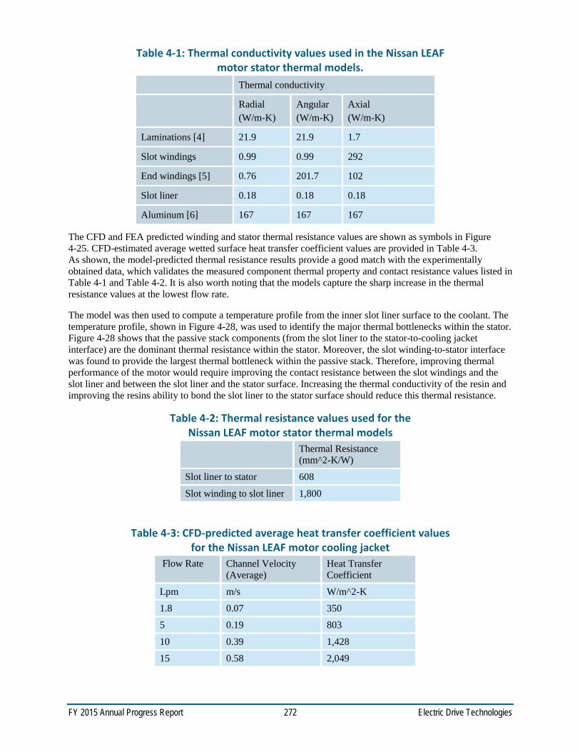
FY 2015 Annual Progress Report 272 Electric Drive Technologies
Table 4-1: Thermal conductivity values used in the Nissan LEAF motor stator thermal models.
Thermal conductivity
Radial (W/m-K)
Angular (W/m-K)
Axial (W/m-K)
Laminations [4] 21.9 21.9 1.7
Slot windings 0.99 0.99 292
End windings [5] 0.76 201.7 102
Slot liner 0.18 0.18 0.18
Aluminum [6] 167 167 167
The CFD and FEA predicted winding and stator thermal resistance values are shown as symbols in Figure 4-25. CFD-estimated average wetted surface heat transfer coefficient values are provided in Table 4-3. As shown, the model-predicted thermal resistance results provide a good match with the experimentally obtained data, which validates the measured component thermal property and contact resistance values listed in Table 4-1 and Table 4-2. It is also worth noting that the models capture the sharp increase in the thermal resistance values at the lowest flow rate.
The model was then used to compute a temperature profile from the inner slot liner surface to the coolant. The temperature profile, shown in Figure 4-28, was used to identify the major thermal bottlenecks within the stator. Figure 4-28 shows that the passive stack components (from the slot liner to the stator-to-cooling jacket interface) are the dominant thermal resistance within the stator. Moreover, the slot winding-to-stator interface was found to provide the largest thermal bottleneck within the passive stack. Therefore, improving thermal performance of the motor would require improving the contact resistance between the slot windings and the slot liner and between the slot liner and the stator surface. Increasing the thermal conductivity of the resin and improving the resins ability to bond the slot liner to the stator surface should reduce this thermal resistance.
Table 4-2: Thermal resistance values used for the Nissan LEAF motor stator thermal models
Thermal Resistance (mm^2-K/W)
Slot liner to stator 608
Slot winding to slot liner 1,800
Table 4-3: CFD-predicted average heat transfer coefficient values for the Nissan LEAF motor cooling jacket
Flow Rate Channel Velocity (Average)
Heat Transfer Coefficient
Lpm m/s W/m^2-K
1.8 0.07 350
5 0.19 803
10 0.39 1,428
15 0.58 2,049

FY 2015 Annual Progress Report 273 Electric Drive Technologies
Figure 4-28: Temperature profile through the motor stator depicting the thermal path from the inner surface of the slot liner to the coolant. The arrow in the upper image indicates the thermal path.
2012 Nissan LEAF Power Electronics (Inverter) Thermal Management System Figure 4-29 shows pictures of the Nissan LEAF power electronics and cooling system. The system consists of three power modules that are mounted onto a cast-aluminum cold plate and associated electronic components (e.g., capacitors, electrical boards, and interconnects). The cold plate is integrated into the inverter housing and weighs approximately 5 kg (not including the top or bottom inverter cover plates). The cold plate cools the power electronics modules by circulating WEG through a series of serpentine fin channels. Figure 4-30 shows a computer-aided design (CAD) rendering of a LEAF power module. The power modules consist of three insulated gate bipolar transistor (IGBT)-diode pairs per switch position. The cross-sectional view shown in Figure 4-30 provides a detailed view of the power module layers and interfaces. Unlike most power modules, the LEAF module does not use metalized-ceramic substrates (e.g., direct-bond copper substrates) for electrical isolation. Instead, the LEAF modules incorporate a dielectric pad mounted between the power modules and the cold plate for electrical isolation (Figure 4-29). Thermal interface material (TIM) is applied on both sides of the dielectric pad to reduce thermal contact resistance.
Tests were conducted to measure the junction-to-coolant resistance for the power modules. For the tests, the inverter was connected to the WEG flow test bench. The test bench circulated WEG (50%/50% of water and ethylene glycol by volume) at a 65°C inlet temperature through the inverter cold plate at various flow rates. The tests were repeated to ensure repeatable results. A transient thermal tester (T3ster) system was used to power/heat and measure the temperature of one IGBT. A total of 50 amps were provided to power one IGBT (approximately 55 W of heat). Measuring temperatures required calibrating the voltage drop through the IGBT to its temperature. Temperature calibration was carried out within a temperature-controlled chamber. Two calibrated K-type thermocouples were mounted onto the power modules (placed near the IGBT that was to be
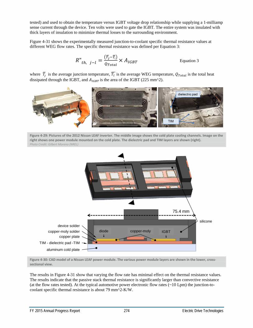
FY 2015 Annual Progress Report 274 Electric Drive Technologies
tested) and used to obtain the temperature versus IGBT voltage drop relationship while supplying a 1-milliamp sense current through the device. Ten volts were used to gate the IGBT. The entire system was insulated with thick layers of insulation to minimize thermal losses to the surrounding environment.
Figure 4-31 shows the experimentally measured junction-to-coolant specific thermal resistance values at different WEG flow rates. The specific thermal resistance was defined per Equation 3:
where 𝑇𝑇𝚥𝚥 is the average junction temperature, 𝑙𝑙 𝑇𝑇 is the average WEG temperature, 𝑄𝑄𝐼𝐼𝑇𝑇𝑡𝑡𝑏𝑏𝑙𝑙 is the total heat dissipated through the IGBT, and 𝐴𝐴𝐼𝐼𝐼𝐼𝐼𝐼𝐼𝐼 is the area of the IGBT (225 mm^2).
Figure 4-29: Pictures of the 2012 Nissan LEAF inverter. The middle image shows the cold plate cooling channels. Image on the right shows one power module mounted on the cold plate. The dielectric pad and TIM layers are shown (right). Photo Credit: Gilbert Moreno (NREL)
Figure 4-30: CAD model of a Nissan LEAF power module. The various power module layers are shown in the lower, cross-sectional view.
The results in Figure 4-31 show that varying the flow rate has minimal effect on the thermal resistance values. The results indicate that the passive stack thermal resistance is significantly larger than convective resistance (at the flow rates tested). At the typical automotive power electronic flow rates (~10 Lpm) the junction-to-coolant specific thermal resistance is about 79 mm^2-K/W.
IGBTdiode copper-molycopper plate
TIM - dielectric pad -TIM
aluminum cold plate
device soldercopper-moly solder
75.4 mm
silicone
𝑅𝑅"𝑡𝑡ℎ, 𝑗𝑗−𝑙𝑙 = 𝐼𝐼𝚥𝚥−𝐼𝐼𝑙𝑙𝑄𝑄𝑇𝑇𝑇𝑇𝑇𝑇𝑃𝑃𝑙𝑙
× 𝐴𝐴𝐼𝐼𝐼𝐼𝐼𝐼𝐼𝐼 Equation 3
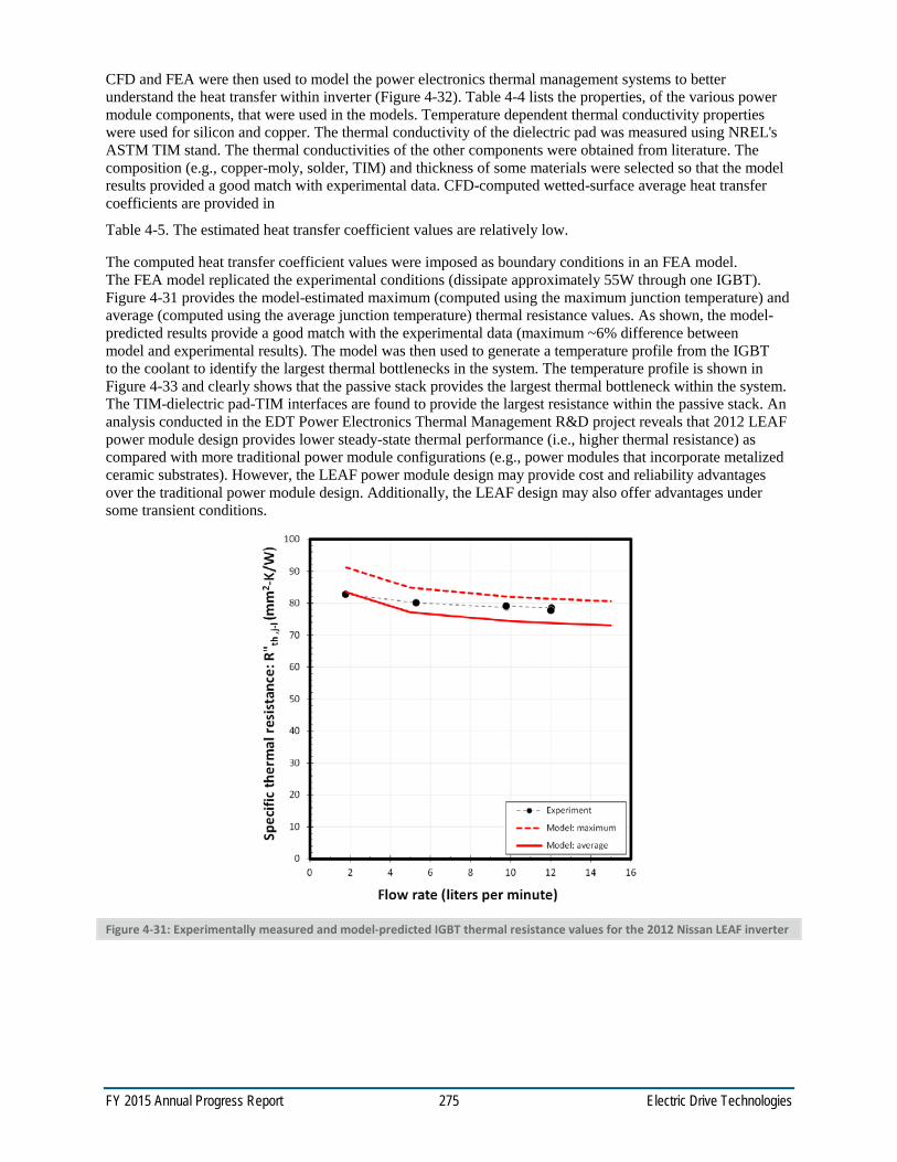
FY 2015 Annual Progress Report 275 Electric Drive Technologies
CFD and FEA were then used to model the power electronics thermal management systems to better understand the heat transfer within inverter (Figure 4-32). Table 4-4 lists the properties, of the various power module components, that were used in the models. Temperature dependent thermal conductivity properties were used for silicon and copper. The thermal conductivity of the dielectric pad was measured using NREL's ASTM TIM stand. The thermal conductivities of the other components were obtained from literature. The composition (e.g., copper-moly, solder, TIM) and thickness of some materials were selected so that the model results provided a good match with experimental data. CFD-computed wetted-surface average heat transfer coefficients are provided in
Table 4-5. The estimated heat transfer coefficient values are relatively low.
The computed heat transfer coefficient values were imposed as boundary conditions in an FEA model. The FEA model replicated the experimental conditions (dissipate approximately 55W through one IGBT). Figure 4-31 provides the model-estimated maximum (computed using the maximum junction temperature) and average (computed using the average junction temperature) thermal resistance values. As shown, the model-predicted results provide a good match with the experimental data (maximum ~6% difference between model and experimental results). The model was then used to generate a temperature profile from the IGBT to the coolant to identify the largest thermal bottlenecks in the system. The temperature profile is shown in Figure 4-33 and clearly shows that the passive stack provides the largest thermal bottleneck within the system. The TIM-dielectric pad-TIM interfaces are found to provide the largest resistance within the passive stack. An analysis conducted in the EDT Power Electronics Thermal Management R&D project reveals that 2012 LEAF power module design provides lower steady-state thermal performance (i.e., higher thermal resistance) as compared with more traditional power module configurations (e.g., power modules that incorporate metalized ceramic substrates). However, the LEAF power module design may provide cost and reliability advantages over the traditional power module design. Additionally, the LEAF design may also offer advantages under some transient conditions.
Figure 4-31: Experimentally measured and model-predicted IGBT thermal resistance values for the 2012 Nissan LEAF inverter
FY 2015 Annual Progress Report 276 Electric Drive Technologies
Figure 4-32: CFD-generated plot showing the coolant velocity vectors at a flow rate of 10 Lpm
Table 4-4: Thermal conductivity and thickness values used in the LEAF inverter thermal models
Silicon Solder Copper-Moly (20-80)
Copper Plastic Silicone Dielectric pad
Aluminum TIM
Thermal conductivity (W/m-K)
k versus T
35 160 k versus T
0.34 0.68 2.59 167 1
Thickness (mm) 0.25
0.08 (die-attach), 0.04 (copper-moly attach)
1.6 2 N/A N/A 0.3 3.25 0.08
Table 4-5: CFD-predicted average heat transfer coefficient values for the Nissan LEAF inverter cold plate
Flow rate (Lpm)
Heat Transfer Coefficient (W/m^2-K)
1.8 376
5 899
10 1,664
12 1,934
15 2,394

FY 2015 Annual Progress Report 277 Electric Drive Technologies
Figure 4-33: Temperature profile through the inverter depicting the thermal path from the IGBT to the coolant. The TIM-dielectric pad-TIM layers constitute a significant thermal resistance to the power modules.
Heat Exchanger Parasitic Power versus Flow Rate Figure 4-34 plots the experimentally-measured parasitic power versus the flow rate curves for the LEAF motor and power electronics heat exchangers. The motor heat exchanger provided lower pressure drop due to its relatively large coolant channels. This information combined with thermal performance results will be used to compute performance metrics that incorporate the system efficiency.
Figure 4-34: Experimentally measured parasitic power losses for the Nissan LEAF motor and inverter heat exchangers
0.0
0.5
1.0
1.5
2.0
2.5
3.0
0 4 8 12 16
Para
sitic
pow
er (W
)
Flow rate (liters per minute)
LEAF motor
LEAF inverter
FY 2015 Annual Progress Report 278 Electric Drive Technologies
Transient Models Transient FEA models were also created for both the 2012 LEAF motor and power electronics thermal management systems. The transient model results were found to provide a good match to experimentally measured transient results; however, work is currently underway to refine the models to improve their accuracy. The LEAF power module transient modeling results have also been used to generate resistance-capacitance thermal network models that can be used to quickly compute the thermal response of these components under different operating conditions. The goal is to use the various models to predict motor and power electronics component temperatures under drive-cycle operations. We are currently working with ORNL to understand heat-loss distributions within each system. The heat-loss distribution information can be imposed into the models to estimate component temperatures under drive-cycle conditions.
Conclusions and Future Directions
Experiments were conducted to measure the thermal performance of the 2012 Nissan LEAF motor and power electronics thermal management systems. CFD and FEA thermal models were developed for both systems. The models were found to provide a good match with experimentally obtained data. Experimental and modeling results demonstrate that the passive-stack is the dominant thermal resistance for both the motor and power electronics systems.
Modeling results indicate that the slot winding-to-stator lamination interface is the greatest thermal resistance within the motor stator. Increasing the thermal conductivity of the resin and improving the resin's ability to bond the slot liner to the stator surface should reduce this thermal resistance.
The 2012 LEAF power modules incorporate a dielectric pad to provide electrical isolation. The dielectric pad and associated TIM interfaces (on both sides of the dielectric pad) are found to provide the greatest thermal resistance in the LEAF power modules. Analysis indicates that the use of a more conventional power module design (e.g., power modules that incorporate metalized ceramics) can improve thermal performance. However, the LEAF design may offer cost and reliability benefits.
FEA transient models of both the LEAF motor and power electronic thermal management systems were developed. Work is currently underway to understand heat loss distributions within each system. Heat loss information will be used as inputs into the transient models and used to compute component temperatures under drive-cycle operations.
Tests have been initiated to measure the thermal performance of the 2014 Honda Accord power electronics thermal management system.
Nomenclature
A area k thermal conductivity Q heat Rth thermal resistance R"th specific thermal resistance T temperature
Subscripts
j junction l liquid s stator w windings (e.g., motor windings)

FY 2015 Annual Progress Report 279 Electric Drive Technologies
FY 2015 Presentations /Publications/Patents
1. Moreno, G.; Bennion, K.; Cousineau, E.; King, C. “Thermal Performance Benchmarking.” Advanced Power Electronics and Electric Motors FY15 Kickoff Meeting, DOE VTO, Oak Ridge, TN, November 2014.
2. Moreno, G.; Bennion, K.; Cousineau, E.; King, C. “Thermal Performance Benchmarking.” 2015 DOE VTO Annual Merit Review, Crystal City, VA, June 2015.
3. Moreno, G.; Bennion, K.; Cousineau, E.; King, C. “Thermal Performance Benchmarking.” 2015 Presentation to the DOE Vehicle Technologies Office (VTO) Electrical and Electronics Technical Team, Southfield, MI, September 2015.
Acknowledgements
The author would like to acknowledge the support provided by Susan Rogers and Steven Boyd, Technology Development Managers for the EDT Program, Vehicle Technologies Office, U.S. Department of Energy Office of Energy Efficiency and Renewable Energy. The significant contributions of Kevin Bennion, Emily Cousineau, and Charles King are acknowledged.
References
1. Burress, T. “Benchmarking of Competitive Technologies.” 2012. DOE VTO Annual Merit Review, Washington DC, May 2012.
2. Burress, T. “Benchmarking EV and HEV Technologies.” 2015. DOE VTO Annual Merit Review, Crystal City, VA, June 2015.
3. Sato, Y.; Ishikawa, S.; Okubo, T.; Abe, M.; Tamai, T., 2011. “Development of High Response Motor and Inverter System for the Nissan LEAF Electric Vehicle.” SAE Technical Paper.
4. Emily, C.; Bennion, K.; DeVoto, D., Mihalic, M., Narumanchi, S., 2015. “Characterization of Contact and Bulk Thermal Resistance of Laminations for Electric Machines” NREL Technical Report NREL/TP-5400-63887.
5. Bennion, K.; and Cousineau, J., 2012. “Sensitivity Analysis of Traction Drive Motor Cooling.” Paper presented at the IEEE Transportation Electrification Conference and expo, Dearborn, Michigan.
6. Matweb. “Aluminum 6061-T6; 6061-T651" Accessed August 7, 2015. http://www.matweb.com/search/DataSheet.aspx?MatGUID=1b8c06d0ca7c456694c7777d9e10be5b&ckck=1
FY 2015 Annual Progress Report 280 Electric Drive Technologies
4.3. 2015: Continued Analysis of the xEV Traction Drive Electric Motor & PE Supply Chain in North America
Christopher L. Whaling, Principal Investigator Synthesis Partners, LLC 11250 Roger Bacon Drive, Suite 2 Reston, VA 20190 Phone: (703) 318-6511; Fax: (703) 318-9553 E-mail: [email protected] Contractor: Synthesis Partners, LLC Contract No.: DE-DT0006388.
Abstract/Executive Summary During FY15 Synthesis Partners, LLC (“Synthesis”) carried out several research activities focused on the North American (NA) motors and power electronics (PE) supply chains. The main focus of the FY15 work has been on motors. The formal tasking for the main FY15 report upcoming is in Task 1, in the work-plan entitled, “Synthesis’ FY15 Work Plan” (dated 31 March 2015). That work-plan has been executed in support of DOE’s Vehicle Technologies Office (VTO)-Electric Drive Technologies (EDT).
Synthesis’ FY2015 work is part of on going tasking by DOE VTO to perform targeted research and analysis of the NA traction drive PE and motors supply chain. This tasking has generated more than ten public reports over the last five years, on topics ranging from an inverter cost analysis, rare earths supply, IGBT market trends, wide bandgap (WBG) technology for automotive applications, motors supply, PE supply chain gap analyses and PE technology roadmap analyses.
Synthesis was tasked in FY15 by the VTO to undertake research to address the following issues regarding the NA supply chain of technologies for traction drive PE and traction drive electric motors (motors) for plug-in, hybrid and electric passenger vehicles (PHEV, HEV and EVs; referred collectively in this document as xEVs):
1. Continued PE and more in-depth motors NA supply chain research, analysis and reporting, to include identifying gaps in the motors supply chain.
2. Limited scope research and analysis in support of ORNL's traction drive inverter cost model development. This resulted in a non-public Task 2 Deliverable, issued in July 2015, entitled “A Fast-Reaction Review of Public Information on Power Electronics Manufacturing Skill-Sets.”
3. Documentation in terms of reports and presentations, individually and in collaboration with VTO, based on PE and motors NA supply chain analyses.
Introduction
Synthesis employs a targeted primary- and secondary-source research strategy, including a narrowly scoped review of English, Japanese and Chinese secondary sources, executed over a limited time period. In FY15, the time available for research was approximately six (6) months and dictated a targeted set of methods applied against a targeted set of sources.
The primary research supporting the FY15 reports is built on Synthesis’ prior efforts sponsored by DOE-VTO. Specifically, hundreds of primary source contacts were made in 2015, and these contacts were built on 100s of primary source contacts and relationships developed in previous years. Synthesis continues to expand and refine a growing archive of 100s of confidential, open-ended, in-depth primary source interviews, dating from 2012 to present. With sources anonymized, Synthesis produces analyses for use by VTO.
In addition to the primary source data, Synthesis maintains background market data-sets covering newly collected information on companies, products and contacts, as well as quantified information on the number and size of suppliers of inverters, converters, motors and batteries, for all xEVs made globally. These data sets are continuously refined, maintained and used to inform the public and private analysis produced for VTO.

FY 2015 Annual Progress Report 281 Electric Drive Technologies
In FY15, Synthesis analyzed and quantified information provided by primary sources on key gaps or constraints in the NA motors supply chain. The primary source information on this topic extends back to 2012. In order to guarantee accuracy and trace-back for maximum validity, Synthesis maintains the ability to trace-back every quote and result in the upcoming report to the original data-source. In public documents Synthesis preserves the anonymity of primary sources. As an additional quality control measure, Synthesis endeavors to reach out to sources to ensure that all credible feedback is captured and maintained after each report is issued. The results of the FY15 research and analysis will be issued to the public in the form of a final report in the near future. Synthesis also attends and presents findings from VTO-sponsored research at industry conferences (e.g., Advanced Power Electronics Conferences (APEC)), as well as at other venues.
Approach
In terms of numbers and types of secondary sources, Synthesis employed the following sources in FY15 research work:
Table 4-6: Secondary Source Research Statistics for FY15 Secondary Source Research Statistics for FY15 (All sources are English language unless otherwise specified.)
Web Sites reviewed: 1,500+
English language websites 1,000+
Web Pages reviewed in depth:
English language 3,000+
Companies initially identified and reviewed for relevance: 1,000+
Companies identified for further assessment (based on possible involvement in NA traction drive PE or motors manufacturing or R&D for xEV passenger vehicle applications):
750
OEMs 29
Tier 1 79
Tier 2 171
Tier 3 241
Tier 4 58
Other (Academic, Association, Consulting, Engineering, USG Office, USG Lab, etc.)
80
Japanese and Chinese language Web sites reviewed: 250+ (In depth) 100+ Key documents reviewed.
The following Figure shows key findings regarding the approximate number of xEVs supplied, by city or prefecture of motor supplier HQ around the world, covering the 2011-2015 time period. This information will be discussed in more depth in the upcoming report.

FY 2015 Annual Progress Report 282 Electric Drive Technologies
Figure 4-35: Approximate Number of xEVs Supplied, by City or Prefecture of Motor Supplier HQ, from 2011-2015 Source: Synthesis Partners, LLC (2015).
0 1000 2000 3000 4000 5000 6000
Lichfield (UK)Longmont (USA)Sichuan (China)
Zhuzhou (China)Ikeda (Japan)
Taipei (Taiwan)Chongqing (China)
Taizhou (China)Mumbai (India)
Yongkang (China)Yongkang (China)
Detroit (USA)Zhejiang (China)Dearborn (USA)
Aurora (USA)Munich (Germany)
San Dimas (USA)Pendleton (USA)Shanghai (China)
Palo Alto (USA)Shenzhen (China)
Hildesheim (Germany)Friedrichshafen…
Gerlingen (Germany)Paris (France)
Hanover (Germany)Amsterdam (Neth.)
Seoul (S. Korea)Tokyo (Japan)
Aichi (Japan)
Thousands
Approximate Number of xEVs Supplied, By City or Prefecture of Motor Supplier HQ,
From 2011-2015
ApproximateNumber of xEVsSupplied, 2011-2015
FY 2015 Annual Progress Report 283 Electric Drive Technologies
In terms of primary sources, Synthesis engaged with the following numbers and types of sources in FY 2015. Primary Source Research Statistics for FY15 (All sources are English language.)
Total companies vetted for in-depth contact: 90
OEMs 12
Tier 1 24
Tier 2 15
Tier 3 27
Tier 4 5
Other (Association, Engineering, etc.) 7 (Association = 2; Engineering = 5)
Total contacts made (multiple contacts within many organizations): 371
E-mails 224
Phone Calls 107
In-Person Conference Contacts 40
In-depth interviews (incl. OEMs, Tier 1-4s and Others) Total >20
Results and Discussion
The following Table provides selected findings about the NA motors supply chain, integrated from primary and secondary sources. The Table provides information on companies that are active in the NA motors supply chain or are otherwise engaged in attempts to become active in the NA traction drive motors supply chain. This information is under continuous research and is expected to be refined as Synthesis uncovers new facts. Research for this list assessed companies in the role of OEMs (i.e., final integrators of the motor into a vehicle), Tier 1s (i.e., motor suppliers), Tier 2s (i.e., motor component suppliers), Tier 3s (i.e., motor materials and components supplied to Tier 2s), and Tier 4s (i.e., basic materials and material processing suppliers).
Table 4-7: Companies Active In or Of Direct Relevance to the NA Motors Supply Chain Manufacturer (HQ Location)
Electric Motor Type
Components or Materials Supplied
xEV Applications North American Mfg. Site
AK Steel, West Chester Township, OH
Not available (N/A)
E-steel/ lamination for stator and rotors
Role re: NA-produced vehicles remains under research.
Pittsburg, PA (Note: Activities in support of the automotive sector are under research.)
China Steel Corporation, Kaohsiung, Taiwan
3-phase, 4-pole induction w/ copper rotor
E-steel/ lamination for stator and rotors
Tesla Model S (Note: Expected to start a new production line by the end of 2014 for 0.15 mm-thick non-oriented silicon-steel sheets to be used as core material for motors of
Possibly mfg. E-steel in Mexico (under research).

FY 2015 Annual Progress Report 284 Electric Drive Technologies
Manufacturer (HQ Location)
Electric Motor Type
Components or Materials Supplied
xEV Applications North American Mfg. Site
electric vehicles such as Tesla Motors).
Eurotranciatura Mexico, Santa Rosa, Mexico
N/A E-steel/ lamination for stator and rotors
Role re: NA-produced vehicles remains under research.
Santa Rosa, Mexico
Ford Motor Co., Detroit, MI
8P - DC 400V PM
Motor C-Max Hermosillo, Mexico
JFE, Tokyo, Japan
N/A E-steel/ lamination for stator and rotors.
Magnets and magnetic wires.
Role re: NA-produced vehicles remains under research.
No current NA mfg. (Note: The JFE joint venture, called “R. bourgeois JFE Shoji Magnetic Lamination, Inc.” based in Tijuana, Mexico may begin offering stamping services to the EV/HEV market in 2016.
GM, Detroit, MI
3-phase AC PM synchronous
Motor, Rotor & Stator
GM Spark EV Whitemarsh, MD
GM, Detroit, MI
AC induction Motor, Rotor & Stator
GM Volt Whitemarsh, MD
Hitachi Automotive Systems America, Inc., Berea, KY
AC induction Motor, Rotor & Stator
GM Volt Berea, KY
Hitachi Metals North Carolina, Ltd., China Grove, NC
8P - DC 400V PM
Neomax Nd-sintered permanent magnets; Magnetic wires for rotor
Ford HEV (possibly, C-Max)
China Grove, NC
Kienle & Spiess, Chicago, IL
N/A Copper rotors N/A Not determined to date. (Note: Kienle & Spiess rep. publicly stated in April 2015 that the firm plans on initiating production of copper rotors for traction drive electric motors in NA in the next few years).
Magna International of America, Ltd., Troy, MI
AC PM synchronous
Motor; (possibly rotor and stator)
Ford Focus Mt. Holly, MI (Note: Motor components under research.)
Mitsui High Tec - Canada, Ottawa
N/A Motor cores for traction drive EVs (mfg. initially
N/A Ottawa, Canada (Note: Mitsui rep publicly stated in 07-15 that the initiation of operations has
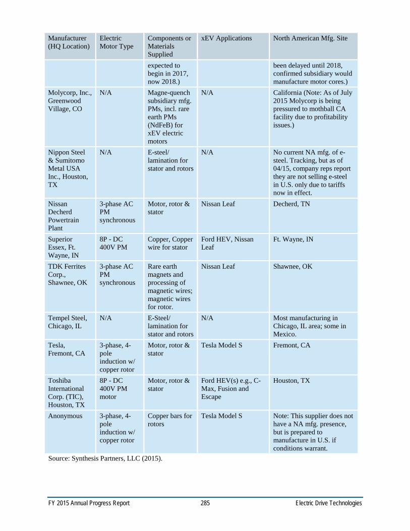
FY 2015 Annual Progress Report 285 Electric Drive Technologies
Manufacturer (HQ Location)
Electric Motor Type
Components or Materials Supplied
xEV Applications North American Mfg. Site
expected to begin in 2017, now 2018.)
been delayed until 2018, confirmed subsidiary would manufacture motor cores.)
Molycorp, Inc., Greenwood Village, CO
N/A Magne-quench subsidiary mfg. PMs, incl. rare earth PMs (NdFeB) for xEV electric motors
N/A California (Note: As of July 2015 Molycorp is being pressured to mothball CA facility due to profitability issues.)
Nippon Steel & Sumitomo Metal USA Inc., Houston, TX
N/A E-steel/ lamination for stator and rotors
N/A No current NA mfg. of e-steel. Tracking, but as of 04/15, company reps report they are not selling e-steel in U.S. only due to tariffs now in effect.
Nissan Decherd Powertrain Plant
3-phase AC PM synchronous
Motor, rotor & stator
Nissan Leaf Decherd, TN
Superior Essex, Ft. Wayne, IN
8P - DC 400V PM
Copper, Copper wire for stator
Ford HEV, Nissan Leaf
Ft. Wayne, IN
TDK Ferrites Corp., Shawnee, OK
3-phase AC PM synchronous
Rare earth magnets and processing of magnetic wires; magnetic wires for rotor.
Nissan Leaf Shawnee, OK
Tempel Steel, Chicago, IL
N/A E-Steel/ lamination for stator and rotors
N/A Most manufacturing in Chicago, IL area; some in Mexico.
Tesla, Fremont, CA
3-phase, 4-pole induction w/ copper rotor
Motor, rotor & stator
Tesla Model S Fremont, CA
Toshiba International Corp. (TIC), Houston, TX
8P - DC 400V PM motor
Motor, rotor & stator
Ford HEV(s) e.g., C-Max, Fusion and Escape
Houston, TX
Anonymous 3-phase, 4-pole induction w/ copper rotor
Copper bars for rotors
Tesla Model S Note: This supplier does not have a NA mfg. presence, but is prepared to manufacture in U.S. if conditions warrant.
Source: Synthesis Partners, LLC (2015).
FY 2015 Annual Progress Report 286 Electric Drive Technologies
Conclusion
Further details will be provided in an up-coming Synthesis’ final report on FY14 research, tentatively entitled, “NA Motors Supply Chain Gap Analysis.” Please contact Christopher Whaling @ [email protected] for further information. Thank you.
FY 2015 Presentations & Publications
• North American PE and Motors Supply Chain Assessment (Jan. 2015): The final report on Synthesis’ PE (mainly) and motors research and analysis work completed in FY14;
• Review of Public Data on Costs of WBG Substrate Manufacturing (Feb. 2015): The final report on Synthesis’ WBG costs research and analysis work completed in FY14;
• Clarifications to Jan2015 NA PE and Motors Report (May 2015): An update providing new information and feedback received by Synthesis following the Jan. 2015 final NA PE and motors supply chain report;
• Clarifications to Feb2015 WBG Report (May 2015): An update providing new information and feedback received by Synthesis following the Feb. 2015 final WBG costs report;
• “FY15 Task 2 – Specialized Manufacturing Skills and Summary Findings,” issued in July 2015. This is a special non-public report issued to VTO and ORNL. This report addresses the specific manufacturing skill-sets that may be needed to produce components, processes, materials and related technical aspects of PE and motors manufacturing. It covers topics of relevance to the global competitiveness of manufacturing skills training for automotive traction drive PE components and motors.
• Presentation: "Assessing the North American Traction Drive Power Electronics and Motors Supply Chain", a Co-Presentation by Steven Boyd, DOE Vehicle Technologies Office, Washington, DC & Christopher Whaling, Synthesis Partners, LLC, Reston, VA;
• Presentation: “North American Traction Drive Supply Chain Analysis,” by Christopher Whaling, Synthesis Partners, June 9, 2015, 2015 AMR 2015.
Please contact Christopher Whaling at Synthesis Partners, LLC at [email protected] for further information, or for a copy of any of the public reports that Synthesis has produced on behalf of DOE-VTO since 2009.

FY 2015 Annual Progress Report 287 Electric Drive Technologies
5.0 Advanced Packaging Research and Development
5.1. Power Electronics Packaging Zhenxian Liang, Principal Investigator Oak Ridge National Laboratory (ORNL) National Transportation Research Center 2360 Cherahala Boulevard Knoxville, TN 37932 Phone: (865) 946-1467 E-mail: [email protected] Susan A. Rogers, DOE EDT Program Manager Phone: (202) 586-8997 E-mail: [email protected] Burak Ozpineci, ORNL EDT Program Manager Phone: (865) 946-1329 E-mail: [email protected] Contractor: UT-Battelle, LLC, managing and operating contractor for the Oak Ridge National Laboratory Contract No.: DE-AC05-00OR22725
Abstract/Executive Summary The project focused on the implementation of advanced packaging technologies in wide bandgap
(WBG) semiconductor power modules to accelerate the application of WBG power semiconductor devices in the automotive industry. Most development work on packaging technologies conducted in FY 2015 is for silicon carbide (SiC) modules.
Packaging technologies were designed and developed for the in-house manufacture of the SiC power modules for air-cooled inverters, using the latest industrial SiC devices and integrating electrical, thermal, and mechanical functions in a high-density package.
An innovative integrated cooling package was developed based on planar SiC power modules. The in-house-fabricated prototypes successfully demonstrated the integration of the electrical and cooling functions in power electronics building blocks. In addition, numerous simulations and experimental analyses were performed and validated the design features of this packaging technology, such as lower thermal resistance, small electric parasitic parameters, and efficient manufacturability.
Working jointly with the material research projects (6.1, PE and EM Materials Support), silver (Ag) sintering bond technology was successfully used in the packaging for highly reliable SiC power modules. The packaging structure and associated packaging process technology were developed, and prototypes with different metal finishings on the substrate and different die layouts were manufactured for further evaluation.
Accomplishments Manufactured and delivered high-power SiC power modules for air-cooling system evaluation, which
allow a reduction of 30% in overall volume and weight.
Demonstrated that the integrated cooled planar SiC power electronics modules not only increase the power density by 60% but also enable a threefold increase in current density over their conventional silicon (Si) counterparts, resulting from a 35% reduction in the die size; 40 and 80% reductions in conduction and switching power losses, respectively; and a 35% reduction in package thermal resistance.
FY 2015 Annual Progress Report 288 Electric Drive Technologies
Fabricated and delivered Ag-sintered die-attached SiC power modules. Initiated research on that technology to develop high-reliability, high-temperature WBG power electronics.
Introduction
State-of-the-art power inverters and converters in electric vehicles (EVs), as in the 2010 Toyota Prius and the 2011 Nissan LEAF, use Si power semiconductors and industrial drive–type packaging technologies; however, the electrical, thermal, and thermo-mechanical performance of these inverters is limited, as well as their manufacturability. These limitations cause large power losses, low semiconductor operational temperatures (limited to 150°C), poor cooling (0.6 cm2·°C/W), and poor power thermal/temperature cycling capabilities, resulting in a derating of the power devices. They also result in the need for costly semiconductors, as well as complicated manufacturing processes and overly bulky inverter/converter assemblies including an extra cooling loop.
WBG semiconductors such as SiC and gallium nitride (GaN) permit devices to operate at much higher temperatures, currents/voltages, and frequencies—making power electronic modules using these materials significantly more powerful and energy efficient than those made from conventional semiconductor materials, such as Si. They also offer greater efficiency in converting electrical power and in operating the electric traction drive during vehicle use.
This research will lead to all-inclusive improvements in the performance and manufacturing of power modules for use in inverters/converters as a result of transitioning from Si to WBG power semiconductors and of innovations in packaging materials, structure, and processing. These comprehensive advances can directly affect the cost, efficiency, reliability, and density of power electronics systems in the electric drives of EVs. The goal of a 40% cost reduction and 60% power density increase in the power module supports DOE EDT 2022 power electronics targets of $3.3/kW and 14.1kW/kg, respectively.
Approach
The project focuses on the design and development of advanced packaging technologies for all-SiC power modules, enabling the exploitation of SiC’s superior performance. Three technologies—packaging of an air-cooled inverter module, integrated cooling packaging of planar power modules, and Ag-sintering die bonding for high-reliability power modules—were investigated, as well as packaging structure and associated process technology. Performance improvements were determined through experimental measurements; and efficiency, cost, and reliability benefits to power electronics systems were evaluated.
A. SiC Power Module Packaging for Air-Cooled Inverters A forced-air–cooled SiC inverter was developed as part of another EDT project (3.1, Inverter R&D). The all-SiC power module has a one-phase-leg configuration composed of SiC metal-oxide-semiconductor field-effect transistors (MOSFETs) and SiC Schottky barrier diodes (Figure 5-1), which is the basic building block for various automotive power converters and inverters. Power SiC MOSFETs and diodes are commercially available in the form of bare dies. The current rating of the power module can be multiplied by paralleling more dies. For the designed air-cooled power inverter, the switch units consist of three parallel bare dies of MOSFETs (each rated at 80 A, 1200 V) and three bare dies of diodes (each is rated at 50 A, 1200 V).
Figure 5-2 presents a schematic of this module’s packaging structure in which the upper unit of a phase-leg inverter, including all U-MOSFETs and U-diode dies, is attached to a direct bond copper (DBC) substrate and interconnected through bond wires. In the same way, in the lower unit, L-MOSFETs plus L-diode dies are attached to another DBC substrate. These two power units are mounted mechanically onto the two sides of a custom-manufactured heat sink, with a thermal interface material applied between the substrates and heat sink. All power devices and interconnections are also encapsulated for mechanical protection and electrical insulation.
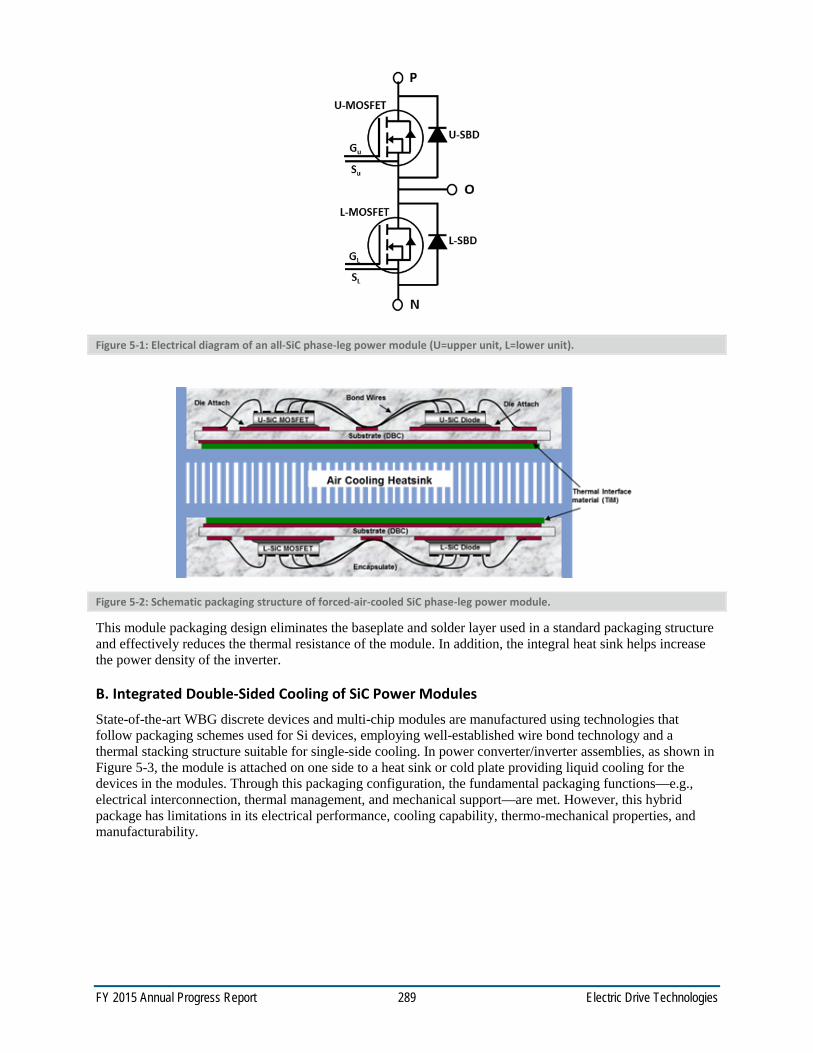
FY 2015 Annual Progress Report 289 Electric Drive Technologies
Figure 5-1: Electrical diagram of an all-SiC phase-leg power module (U=upper unit, L=lower unit).
Figure 5-2: Schematic packaging structure of forced-air-cooled SiC phase-leg power module.
This module packaging design eliminates the baseplate and solder layer used in a standard packaging structure and effectively reduces the thermal resistance of the module. In addition, the integral heat sink helps increase the power density of the inverter.
B. Integrated Double-Sided Cooling of SiC Power Modules State-of-the-art WBG discrete devices and multi-chip modules are manufactured using technologies that follow packaging schemes used for Si devices, employing well-established wire bond technology and a thermal stacking structure suitable for single-side cooling. In power converter/inverter assemblies, as shown in Figure 5-3, the module is attached on one side to a heat sink or cold plate providing liquid cooling for the devices in the modules. Through this packaging configuration, the fundamental packaging functions—e.g., electrical interconnection, thermal management, and mechanical support—are met. However, this hybrid package has limitations in its electrical performance, cooling capability, thermo-mechanical properties, and manufacturability.
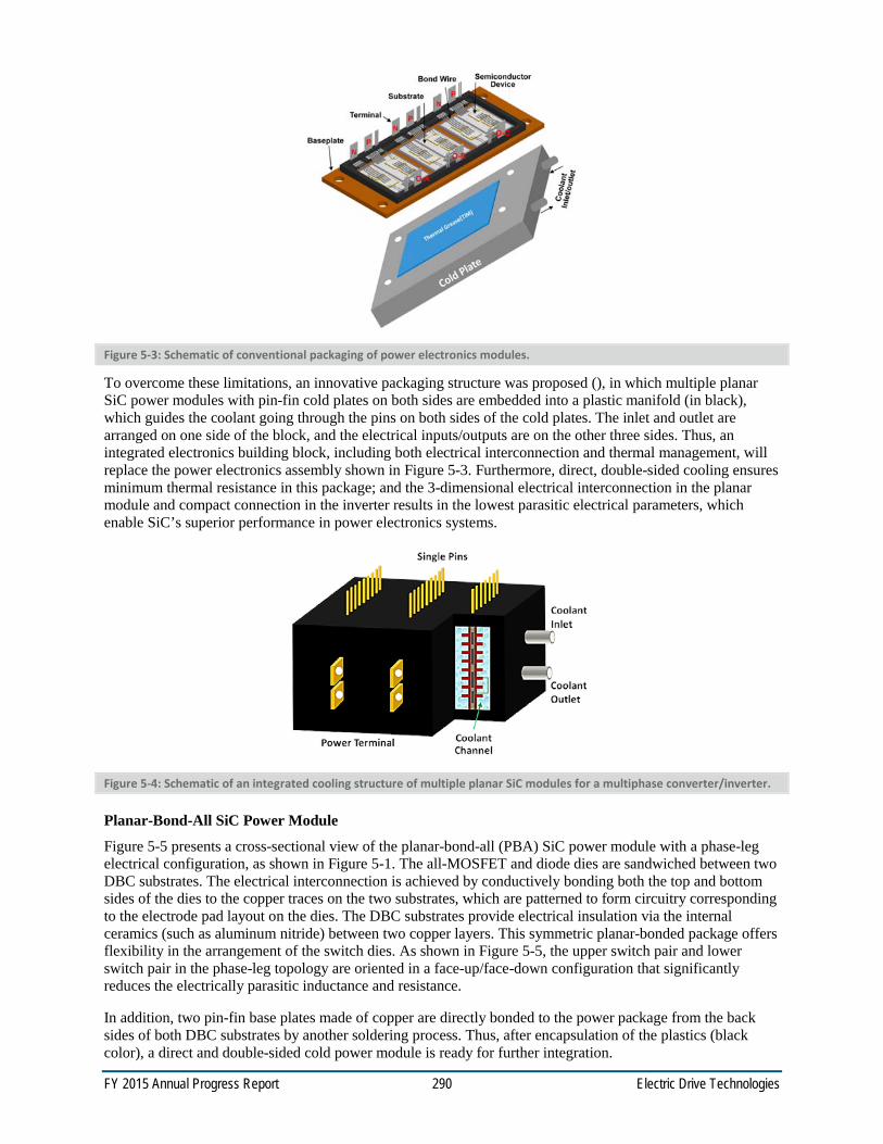
FY 2015 Annual Progress Report 290 Electric Drive Technologies
Figure 5-3: Schematic of conventional packaging of power electronics modules.
To overcome these limitations, an innovative packaging structure was proposed (), in which multiple planar SiC power modules with pin-fin cold plates on both sides are embedded into a plastic manifold (in black), which guides the coolant going through the pins on both sides of the cold plates. The inlet and outlet are arranged on one side of the block, and the electrical inputs/outputs are on the other three sides. Thus, an integrated electronics building block, including both electrical interconnection and thermal management, will replace the power electronics assembly shown in Figure 5-3. Furthermore, direct, double-sided cooling ensures minimum thermal resistance in this package; and the 3-dimensional electrical interconnection in the planar module and compact connection in the inverter results in the lowest parasitic electrical parameters, which enable SiC’s superior performance in power electronics systems.
Figure 5-4: Schematic of an integrated cooling structure of multiple planar SiC modules for a multiphase converter/inverter.
Planar-Bond-All SiC Power Module
Figure 5-5 presents a cross-sectional view of the planar-bond-all (PBA) SiC power module with a phase-leg electrical configuration, as shown in Figure 5-1. The all-MOSFET and diode dies are sandwiched between two DBC substrates. The electrical interconnection is achieved by conductively bonding both the top and bottom sides of the dies to the copper traces on the two substrates, which are patterned to form circuitry corresponding to the electrode pad layout on the dies. The DBC substrates provide electrical insulation via the internal ceramics (such as aluminum nitride) between two copper layers. This symmetric planar-bonded package offers flexibility in the arrangement of the switch dies. As shown in Figure 5-5, the upper switch pair and lower switch pair in the phase-leg topology are oriented in a face-up/face-down configuration that significantly reduces the electrically parasitic inductance and resistance.
In addition, two pin-fin base plates made of copper are directly bonded to the power package from the back sides of both DBC substrates by another soldering process. Thus, after encapsulation of the plastics (black color), a direct and double-sided cold power module is ready for further integration.

FY 2015 Annual Progress Report 291 Electric Drive Technologies
Figure 5-5: Cross-sectional view of a planar-bond-all SiC phase-leg power module.
To realize the concept shown in Figure 5-4, a special coolant manifold was assembled, as shown in Figure 5-6. The parts are made of plastic and manufactured using additive manufacturing (3D printing) technology. The manifold is designed to provide liquid passageways for coolant passing mainly through the pin-fin areas. The open tubes provide coolant inlets and outlets, and the inner channels serve to guide the coolant flow uniformly.
Figure 5-6: Design for assembly of an integrated double-sided, direct liquid-cooled SiC power electronics block.
C. Ag-Sintered Die Attachment The Ag layer formed during the sintering process, from a paste mixed with nanoscale Ag particles and other chemicals, is known to be a superior die attachment material compared with the solder layer formed during the soldering process. It offers much better electrical, thermal, and especially thermo-mechanical properties for power module packaging. These properties are especially critical to SiC power devices, allowing them to operate at temperatures higher than those of Si devices. However, Ag sintering also includes an additional process of mechanically pressing the stack of dies and substrates during heating. The quality of the bond formed between die and substrate can be affected by many factors, such as finishing metals on the die and substrate, geometry of the die, and patterns on the substrate, as well as process parameters—pressure, heating temperature, and heating time. Based on fundamental studies using various coupons, research on Ag sintering of SiC device dies on DBC substrate began this year. Figure 5-7Figure 5-6 shows schematically the packaging design of this SiC power module sample and where the Ag-sintering process is employed to realize the die attachment, instead of soldering, as in conventional power modules. Wire bonds and gel encapsulation are also included in the fabrication of a complete power module for electrical thermal and thermo-mechanical tests.
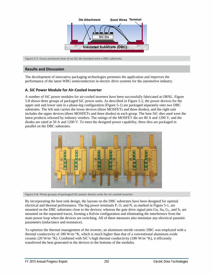
FY 2015 Annual Progress Report 292 Electric Drive Technologies
Figure 5-7: Cross-sectional view of an SiC die bonded onto a DBC substrate.
Results and Discussion
The development of innovative packaging technologies promotes the application and improves the performance of the latest WBG semiconductors in electric drive systems for the automotive industry.
A. SiC Power Module for Air-Cooled Inverter A number of SiC power modules for air-cooled inverters have been successfully fabricated at ORNL. Figure 5-8 shows three groups of packaged SiC power units. As described in Figure 5-2, the power devices for the upper unit and lower unit in a phase-leg configuration (Figure 5-1) are packaged separately onto two DBC substrates. The left unit carries the lower devices (three MOSFETs and three diodes), and the right unit includes the upper devices (three MOSFETs and three diodes) in each group. The bare SiC dies used were the latest products released by industry vendors. The ratings of the MOSFET die are 80 A and 1200 V, and the diodes are rated at 50 A and 1200 V. To meet the designed power capability, three dies are packaged in parallel on the DBC substrates.
Figure 5-8: Three groups of packaged SiC power device units for air-cooled inverter.
By incorporating the heat sink design, the layouts on the DBC substrates have been designed for optimal electrical and thermal performance. The big power terminals P, O, and N, as marked in Figure 5-1, are mounted on the DBC substrates close to the devices; whereas the gate drive signal pins Gu, Su, GL, and SL are mounted on the separated traces, forming a Kelvin configuration and eliminating the interference from the main power loop when the devices are switching. All of these measures also minimize any electrical parasitic parameters (inductance and resistance).
To optimize the thermal management of the inverter, an aluminum nitride ceramic DBC was employed with a thermal conductivity of 180 W/m·°K, which is much higher than that of a conventional aluminum oxide ceramic (20 W/m·°K). Combined with SiC’s high thermal conductivity (180 W/m·°K), it efficiently transferred the heat generated in the devices to the bottoms of the modules.

FY 2015 Annual Progress Report 293 Electric Drive Technologies
To fabricate these units, the first step was to attach all six dies, two power terminals, and two pins using a soldering process. A special jig was designed that made for the precise alignment of all the components. Solder preforms were used and placed beneath each component before one heating (solder reflow) profile. Then, multiple aluminum wires (10 mil in diameter) were bonded on the chips and substrate for electrical connection.
As shown in Figure 5-2, two packaged units were directly mounted onto a heat sink from both the top and bottom surfaces by mechanical pressing. To do so, five through holes were made in each DBC substrate. Figure 5-9 is a photo of the phase-leg SiC power module assembly with the lower unit visible. The heat sink was specially designed and manufactured. To improve thermal transfer, a thin thermal grease layer was applied beneath the DBC substrate to keep the substrate and heat sink in close contact. This simplified thermal stack ensured that the assembly had low thermal resistance.
Figure 5-9: Packaged one-phase leg SiC power module assembled on a heat sink for an air-cooled inverter.
Potting encapsulation was used to provide electrical and environmental protection to the DBC substrate, the devices, and the bond wires.
The module assemblies were delivered to another EDT project (3.1, Inverter R&D) to build and test a 3-phase air-cooled SiC inverter.
B. Integrated Double-Sided Cooling of SiC Power Modules Fabrication of the PBA SiC power module has been described in previous reports. The key difference is that the top interconnections of the dies use a planar, larger-area bond to their top electrodes, instead of multiple tiny wire bonds. This change makes it possible to integrate many superior packaging concepts into power modules. Figure 5-10 shows photos of such a module fabricated in the ORNL packaging laboratory.
Figure 5-10(a) is the package of a 100 A, 1,200 V SiC phase leg power with the topology illustrated in Figure 5-1. The power device upper or lower unit consists of two MOSFET dies and diode dies for power ratings at 100 A, 1200 V (the rating of each die is 50 A, 1200 V). All eight SiC dies were bonded between two DBC substrates by solder from both the top and bottom surfaces (see Figure 5-5). At the same time, the power terminals P, N (on the left side), and O (on the right side) and signal pins Gu, Su, GL, and SL (on the upper side) were also mounted onto the DBCs. A soldering process was employed to form the planar bonds. It offers high electrical conductivity and easy processing. As shown at the top left, bond wires were used to connect the device electrodes and pads on the DBC. Again, the Kelvin configuration was used here to avoid interference between the gate drive loop and power loop. This module measures 40×40×2 mm, excluding the terminals and pins.
Figure 5-10(b) shows the attachment of the dual cold plates from both sides, in which two pin-fin heat sinks made of copper were directly bonded onto the back sides of the DBC substrates by two solder layers (one is shown in photo (a), grey color) with a lower melting point. Another soldering process was employed using a special jig for these two-layer solder reflows. The area of each effective pin fin array is 38 mm × 38 mm; the fin height is 7 mm.
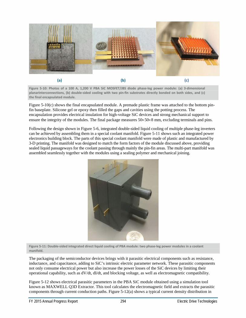
FY 2015 Annual Progress Report 294 Electric Drive Technologies
(a) (b) (c)
Figure 5-10: Photos of a 100 A, 1,200 V PBA SiC MOSFET/JBS diode phase-leg power module: (a) 3-dimensional planarinterconnections, (b) double-sided cooling with two pin-fin substrates directly bonded on both sides, and (c) the final encapsulated module.
Figure 5-10(c) shows the final encapsulated module. A premade plastic frame was attached to the bottom pin-fin baseplate. Silicone gel or epoxy then filled the gaps and cavities using the potting process. The encapsulation provides electrical insulation for high-voltage SiC devices and strong mechanical support to ensure the integrity of the modules. The final package measures 50×50×8 mm, excluding terminals and pins.
Following the design shown in Figure 5-6, integrated double-sided liquid cooling of multiple phase-leg inverters can be achieved by assembling them in a special coolant manifold. Figure 5-11 shows such an integrated power electronics building block. The parts of this special coolant manifold were made of plastic and manufactured by 3-D printing. The manifold was designed to match the form factors of the module discussed above, providing sealed liquid passageways for the coolant passing through mainly the pin-fin areas. The multi-part manifold was assembled seamlessly together with the modules using a sealing polymer and mechanical joining.
Figure 5-11: Double-sided integrated direct liquid cooling of PBA module: two phase-leg power modules in a coolant manifold.
The packaging of the semiconductor devices brings with it parasitic electrical components such as resistance, inductance, and capacitance, adding to SiC’s intrinsic electric parameter network. These parasitic components not only consume electrical power but also increase the power losses of the SiC devices by limiting their operational capability, such as dV/dt, dI/dt, and blocking voltage, as well as electromagnetic compatibility.
Figure 5-12 shows electrical parasitic parameters in the PBA SiC module obtained using a simulation tool known as MAXWELL Q3D Extractor. This tool calculates the electromagnetic field and extracts the parasitic components through current conduction paths. Figure 5-12(a) shows a typical current density distribution in
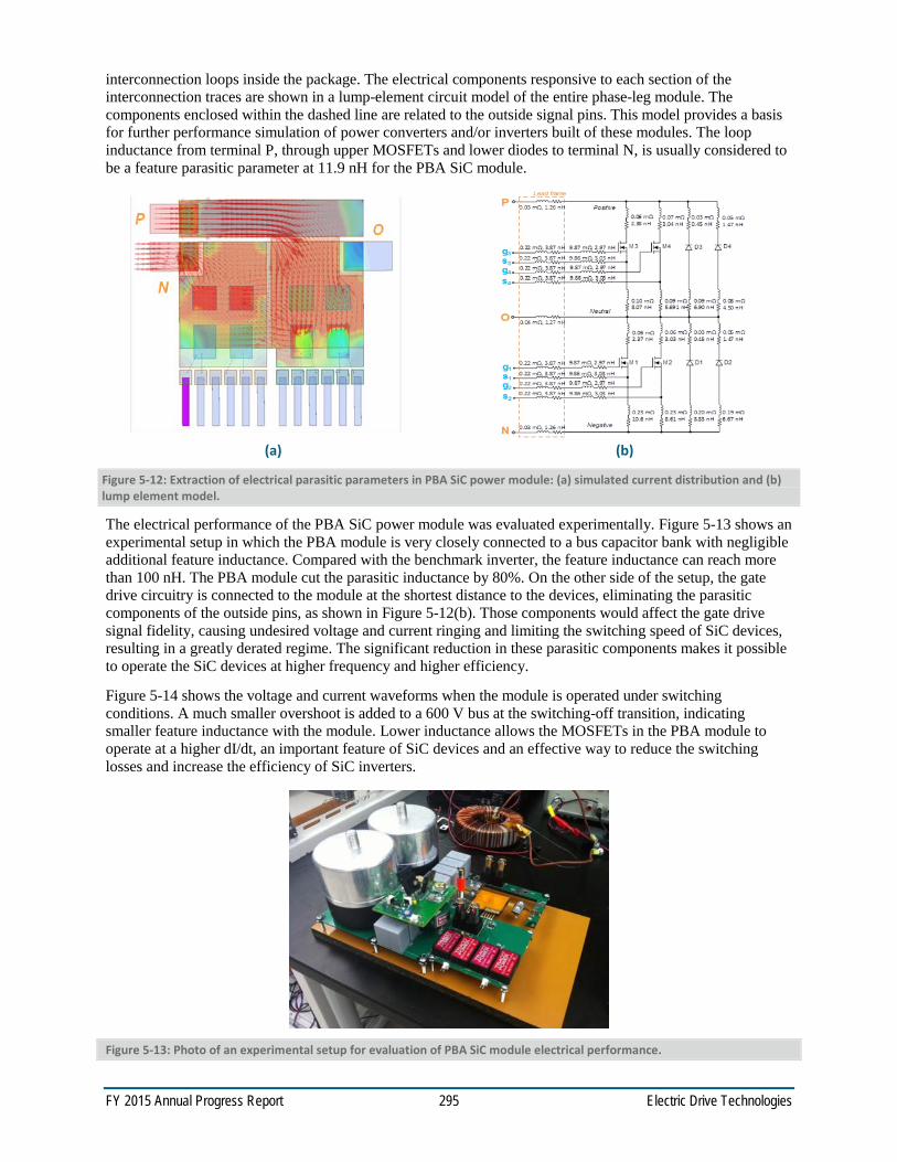
FY 2015 Annual Progress Report 295 Electric Drive Technologies
interconnection loops inside the package. The electrical components responsive to each section of the interconnection traces are shown in a lump-element circuit model of the entire phase-leg module. The components enclosed within the dashed line are related to the outside signal pins. This model provides a basis for further performance simulation of power converters and/or inverters built of these modules. The loop inductance from terminal P, through upper MOSFETs and lower diodes to terminal N, is usually considered to be a feature parasitic parameter at 11.9 nH for the PBA SiC module.
(a) (b) Figure 5-12: Extraction of electrical parasitic parameters in PBA SiC power module: (a) simulated current distribution and (b) lump element model.
The electrical performance of the PBA SiC power module was evaluated experimentally. Figure 5-13 shows an experimental setup in which the PBA module is very closely connected to a bus capacitor bank with negligible additional feature inductance. Compared with the benchmark inverter, the feature inductance can reach more than 100 nH. The PBA module cut the parasitic inductance by 80%. On the other side of the setup, the gate drive circuitry is connected to the module at the shortest distance to the devices, eliminating the parasitic components of the outside pins, as shown in Figure 5-12(b). Those components would affect the gate drive signal fidelity, causing undesired voltage and current ringing and limiting the switching speed of SiC devices, resulting in a greatly derated regime. The significant reduction in these parasitic components makes it possible to operate the SiC devices at higher frequency and higher efficiency.
Figure 5-14 shows the voltage and current waveforms when the module is operated under switching conditions. A much smaller overshoot is added to a 600 V bus at the switching-off transition, indicating smaller feature inductance with the module. Lower inductance allows the MOSFETs in the PBA module to operate at a higher dI/dt, an important feature of SiC devices and an effective way to reduce the switching losses and increase the efficiency of SiC inverters.
Figure 5-13: Photo of an experimental setup for evaluation of PBA SiC module electrical performance.

FY 2015 Annual Progress Report 296 Electric Drive Technologies
(a) (b) Figure 5-14: Current/voltage waveforms of PBA SiC module: (a) switching on and (b) switching off.
The thermal performance of the SiC power module was characterized by specific thermal resistance, θja, sp, which is a normalized parameter by die area (i.e., θja,sp = die area × thermal resistance). It is the sum of those from all thermal stacking elements, including the coolant, pin-fin substrate, DBC substrates, and SiC dies. The specific thermal resistance of the double-sided cooling of the PBA module assembly is 0.33cm2·°C/W, compared with the specific thermal resistance of a conventional module assembly of 0.54cm2·°C/W—a 39% reduction in thermal resistance.
The reduction in both parasitic power losses and thermal resistance helps increase the operational current (power) density in the SiC die. It has been demonstrated that the integrated double-sided-cooled SiC module packaging increases the current density of the SiC power device by 53%.
The current density increase helps reduce the SiC die size and, in turn, the cost of the power electronics system.
C. Ag-Sintered Die Attachment SiC Module Packaging Ag-sintered SiC die attachment was investigated by prototyping a SiC diode totem-pole module. Figure 5-15 shows photos of some typical samples. Figure 5-15(a) shows 10 SiC diode dies bonded onto five DBC substrates at different locations. The two DBC substrates on the left have Ag finishing, while the three on the right have gold (Au) finishing. The different designs allow evaluation of the effect of the metallization and die layout on the quality of this special die attachment.
The modules were packaged using processes identical to those used in the solder die attachment module packaging. Figure 5-15(b) shows the six aluminum wires (diameters of 10 mil) bonded onto the top of each diode die. A zoomed-in image also shows the sintered Ag on the substrate. Finally, the terminals were mounted on the substrate, and the entire module was encapsulated by Si gel, as shown in Figure 5-15(c).
Comprehensive evaluations including microstructural analysis, thermo-mechanical evaluation, and electrical reliability are under way in collaboration with other projects within the VTO program [6.1, PE and EM Materials Support], the results of which will be provided in future reports.

FY 2015 Annual Progress Report 297 Electric Drive Technologies
(a) (b)
(c)
Figure 5-15: Photos of Ag-sintered die attachment SiC module packaging: (a) SiC diode dies bonded on DBC substrates, (b) zoomed-in die attachment and wire bonds, and (c) encapsulated power modules.
Conclusions and Future Direction
The advanced packaging technologies successfully developed in FY 2015 include packaging of SiC air-cooled inverter modules, integrated cooling packaging of planar power modules, and Ag-sintered bond power modules. The resulting improvements made in reducing electrical parasitics and thermal impedance enable the efficient exploitation of WBG power devices. The benefits gained from these innovations were demonstrated by comprehensive upgrades in SiC packaging performance, leading to high-efficiency, high-density system operation beyond the limits of state-of-the-art technologies. These advances resulted in higher power conversion efficiency (low losses) and improved cost-effectiveness through reductions in power semiconductor size and higher productivity in manufacturing.
Further advancement in WBG automotive power electronics will depend greatly on improvements in power packaging technology through advances in structure, materials, and processing techniques. The focus will be on developing highly integrated functionality for WBG power inverter/converter modules with intelligence and improved operating performance (efficiency, density, and cost). The effort will include (1) incorporating advanced gate drive circuitry into the package, (2) implementing highly integrated cooling technologies for integrated multiphase conversion systems, (3) optimizing interconnection layouts and embedding passives for electromagnetic interference containment and sensors, and (4) developing processes for temperature-tolerant integrated SiC power module packages.
These advancements will enable considerable strides to be made toward achieving DOE power density and cost targets for power electronics systems in electric drive vehicles.
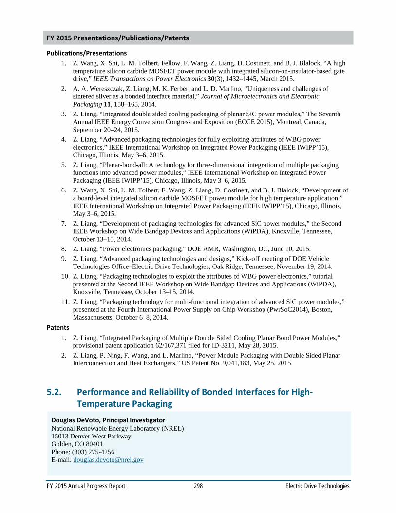
FY 2015 Annual Progress Report 298 Electric Drive Technologies
FY 2015 Presentations/Publications/Patents
Publications/Presentations 1. Z. Wang, X. Shi, L. M. Tolbert, Fellow, F. Wang, Z. Liang, D. Costinett, and B. J. Blalock, “A high
temperature silicon carbide MOSFET power module with integrated silicon-on-insulator-based gate drive,” IEEE Transactions on Power Electronics 30(3), 1432–1445, March 2015.
2. A. A. Wereszczak, Z. Liang, M. K. Ferber, and L. D. Marlino, “Uniqueness and challenges of sintered silver as a bonded interface material,” Journal of Microelectronics and Electronic Packaging 11, 158–165, 2014.
3. Z. Liang, “Integrated double sided cooling packaging of planar SiC power modules,” The Seventh Annual IEEE Energy Conversion Congress and Exposition (ECCE 2015), Montreal, Canada, September 20–24, 2015.
4. Z. Liang, “Advanced packaging technologies for fully exploiting attributes of WBG power electronics,” IEEE International Workshop on Integrated Power Packaging (IEEE IWIPP’15), Chicago, Illinois, May 3–6, 2015.
5. Z. Liang, “Planar-bond-all: A technology for three-dimensional integration of multiple packaging functions into advanced power modules,” IEEE International Workshop on Integrated Power Packaging (IEEE IWIPP’15), Chicago, Illinois, May 3–6, 2015.
6. Z. Wang, X. Shi, L. M. Tolbert, F. Wang, Z. Liang, D. Costinett, and B. J. Blalock, “Development of a board-level integrated silicon carbide MOSFET power module for high temperature application,” IEEE International Workshop on Integrated Power Packaging (IEEE IWIPP’15), Chicago, Illinois, May 3–6, 2015.
7. Z. Liang, “Development of packaging technologies for advanced SiC power modules,” the Second IEEE Workshop on Wide Bandgap Devices and Applications (WiPDA), Knoxville, Tennessee, October 13–15, 2014.
8. Z. Liang, “Power electronics packaging,” DOE AMR, Washington, DC, June 10, 2015. 9. Z. Liang, “Advanced packaging technologies and designs,” Kick-off meeting of DOE Vehicle
Technologies Office–Electric Drive Technologies, Oak Ridge, Tennessee, November 19, 2014. 10. Z. Liang, “Packaging technologies to exploit the attributes of WBG power electronics,” tutorial
presented at the Second IEEE Workshop on Wide Bandgap Devices and Applications (WiPDA), Knoxville, Tennessee, October 13–15, 2014.
11. Z. Liang, “Packaging technology for multi-functional integration of advanced SiC power modules,” presented at the Fourth International Power Supply on Chip Workshop (PwrSoC2014), Boston, Massachusetts, October 6–8, 2014.
Patents 1. Z. Liang, “Integrated Packaging of Multiple Double Sided Cooling Planar Bond Power Modules,”
provisional patent application 62/167,371 filed for ID-3211, May 28, 2015. 2. Z. Liang, P. Ning, F. Wang, and L. Marlino, “Power Module Packaging with Double Sided Planar
Interconnection and Heat Exchangers,” US Patent No. 9,041,183, May 25, 2015.
5.2. Performance and Reliability of Bonded Interfaces for High-Temperature Packaging
Douglas DeVoto, Principal Investigator National Renewable Energy Laboratory (NREL) 15013 Denver West Parkway Golden, CO 80401 Phone: (303) 275-4256 E-mail: [email protected]
FY 2015 Annual Progress Report 299 Electric Drive Technologies
Susan A. Rogers, DOE Technology Development Manager U.S. Department of Energy 1000 Independence Avenue SW, EE-3V Washington, DC 20585 Phone: (202) 586-8997 E-mail: [email protected] Sreekant Narumanchi, NREL Task Leader Phone: (303) 275-4062 Email: [email protected]
Abstract/Executive Summary Current generation automotive power electronics packages utilize silicon devices and lead-free solder alloys. To meet stringent technical targets for 2020 and beyond (for cost, power density, specific power, efficiency and reliability), wide-bandgap devices are being considered since they offer advantages such as operation at higher frequencies, voltages, and temperatures. Traditional power electronics packages must be redesigned to utilize the full potential of wide-bandgap devices, and the die- and substrate-attach layers are key areas where new material development and validation is required. Present solder alloys do not meet the performance requirements for these new package designs while also meeting cost and hazardous substance restrictions.
Sintered silver (Ag) promises to meet the needs for die- and substrate-attach interfaces but synthesis optimization and reliability evaluation must be completed. Sintered Ag material was proposed as an alternative solution in power electronics packages almost 20 years back. However, synthesis pressure requirements up 40 MPa caused a higher complexity in the production process and more stringent flatness specifications for the substrates. Recently, several manufacturers have developed sintered Ag materials that require lower (3 – 5 MPa) or even no bonding pressures.
Degradation mechanisms for these sintered Ag materials are not well known and need to be addressed. We are addressing these aspects to some extent in this project. We are developing generalized (i.e., independent of geometry) stress intensity factor versus cycles-to-failure relations for sintered Ag. Because sintered Ag is a relatively new material for automotive power electronics, the industry currently does not have a good understanding of recommended synthesis parameters or expected reliability under prescribed conditions. It is an important deliverable of this project to transfer findings to industry to eliminate barriers to using sintered Ag as a viable and commercialized die- and substrate-attach material. Only a few manufacturers produce sintered Ag pastes and may consider some processing conditions as proprietary. It is the goal of this project to openly explore and define best practices in order to impact the maximum number of power electronics module manufacturers and suppliers.
Accomplishments Established and initiated a procedure for the material and degradation characterization of sintered Ag
through long-term accelerated temperature testing.
Processed coefficient of thermal expansion (CTE)-mismatched disk samples with various diameter bond pads to validate stress field relationship with delamination initiation. Monitored delamination rates through acoustic microscopy while samples were subjected to accelerated temperature testing.
Synthesized and shear tested initial samples for mechanical characterization of sintered Ag. Material properties gathered are replacing bulk silver material properties to more accurately model the interface structure.
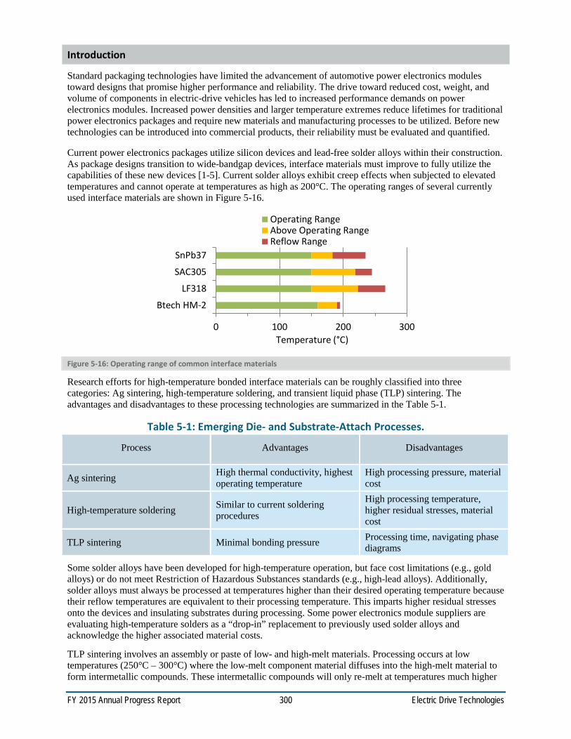
FY 2015 Annual Progress Report 300 Electric Drive Technologies
Introduction
Standard packaging technologies have limited the advancement of automotive power electronics modules toward designs that promise higher performance and reliability. The drive toward reduced cost, weight, and volume of components in electric-drive vehicles has led to increased performance demands on power electronics modules. Increased power densities and larger temperature extremes reduce lifetimes for traditional power electronics packages and require new materials and manufacturing processes to be utilized. Before new technologies can be introduced into commercial products, their reliability must be evaluated and quantified.
Current power electronics packages utilize silicon devices and lead-free solder alloys within their construction. As package designs transition to wide-bandgap devices, interface materials must improve to fully utilize the capabilities of these new devices [1-5]. Current solder alloys exhibit creep effects when subjected to elevated temperatures and cannot operate at temperatures as high as 200°C. The operating ranges of several currently used interface materials are shown in Figure 5-16.
Figure 5-16: Operating range of common interface materials
Research efforts for high-temperature bonded interface materials can be roughly classified into three categories: Ag sintering, high-temperature soldering, and transient liquid phase (TLP) sintering. The advantages and disadvantages to these processing technologies are summarized in the Table 5-1.
Table 5-1: Emerging Die- and Substrate-Attach Processes.
Process Advantages Disadvantages
Ag sintering High thermal conductivity, highest operating temperature
High processing pressure, material cost
High-temperature soldering Similar to current soldering procedures
High processing temperature, higher residual stresses, material cost
TLP sintering Minimal bonding pressure Processing time, navigating phase diagrams
Some solder alloys have been developed for high-temperature operation, but face cost limitations (e.g., gold alloys) or do not meet Restriction of Hazardous Substances standards (e.g., high-lead alloys). Additionally, solder alloys must always be processed at temperatures higher than their desired operating temperature because their reflow temperatures are equivalent to their processing temperature. This imparts higher residual stresses onto the devices and insulating substrates during processing. Some power electronics module suppliers are evaluating high-temperature solders as a “drop-in” replacement to previously used solder alloys and acknowledge the higher associated material costs.
TLP sintering involves an assembly or paste of low- and high-melt materials. Processing occurs at low temperatures (250°C – 300°C) where the low-melt component material diffuses into the high-melt material to form intermetallic compounds. These intermetallic compounds will only re-melt at temperatures much higher
0 100 200 300
Btech HM-2
LF318
SAC305
SnPb37
Temperature (°C)
Operating RangeAbove Operating RangeReflow Range

FY 2015 Annual Progress Report 301 Electric Drive Technologies
than the processing conditions (400°C – 600°C). Toyota Research Institute of North America has several publications on the development of nickel-tin (Ni-Sn) TLP bonding for automotive power electronics. The University of Maryland’s Center for Advanced Life Cycle Engineering is working to develop Ni-Sn and copper-tin (Cu-Sn) TLP bonding systems while Ames Laboratory has developed a Cu-Ni TLP process.
Sintered Ag material has been proposed as an alternative solution in power electronics packages as far back as 20 years. To reduce synthesis temperatures to below 300°C, the concurrent application of pressure up to 40 MPa onto the package or sintered Ag bonded interface material (BIM) was originally advocated. However, this caused a higher complexity in the production process and more stringent flatness specifications for the substrates. Recently, several manufacturers have developed sintered Ag materials that require lower (3 – 5 MPa) or even no bonding pressures. Virginia Tech, Heraeus, Henkel, and Kyocera have developed these materials. Semikron currently has production power electronics utilizing sintered Ag as the die-attach layer. Large-area substrate attachment requires additional research and development for power electronics module suppliers to transition to sintered Ag. Prior work at NREL and Oak Ridge National Laboratory (ORNL) has demonstrated the promise of the processing technology, but a comprehensive evaluation of all processing variables is needed to demonstrate best practices to industry.
Approach
Conventional high-temperature bonded interfaces within the power electronics module face CTE mismatches between materials/layers and resultant thermo-mechanical stresses. This can cause formations of voids and cracks in these bonded interfaces as well as delaminations, which pose a problem from a reliability standpoint. These defects manifest themselves in increased thermal resistance in the package, acting as a bottleneck to heat removal from the package. Research at NREL and ORNL has focused on evaluating the reliability of low- and no-pressure sintered Ag interface pastes. Prior samples have established a failure behavior that is consistent with stress-corrosion (fatigue) cracking. The experimental observation of cohesive failure of the sintered Ag interconnection allows us to combine the tracked ingress front of the delamination (captured with acoustic imaging) with their modeled thermo-mechanical strains and stress concentrations (also linked to the size and shape of the interconnection at any given time instant) to construct and interpret a crack velocity (V)-stress field (K) parameter response, or V-K curve, of a particular sintered Ag material, as shown in Figure 5-17.
Figure 5-17: V-K curve
While the authors recognize this study's interpretation may be specific to the employed sintered Ag paste, the authors feel the analysis method may provide a logical way to interpret such damage in interconnections of any no-pressure sintered Ag paste.
A description of the experiment, finite element modeling of the thermo-mechanical strains and stress concentrations, the construction of a V-K curve using the data and its interpretation will be presented. Crack growth rates within the sintered Ag BIM were determined as a function of number of thermal cycles from past work [6]. The assembly consisted of a 5-mm-thick Cu base plate attached to a 0.72-mm-thick active metal bonded substrate (0.32-mm-thick silicon nitride [Si3N4] with 0.2-mm-thick Cu foil on either side of Si3N4, 50.8 mm × 50.8 mm cross-sectional area footprint) via the bonding material. The Cu metallization layers were inset 1 mm from the perimeter of the Si3N4, for a 48.8 mm × 48.8 mm footprint, and the corners were given a radius
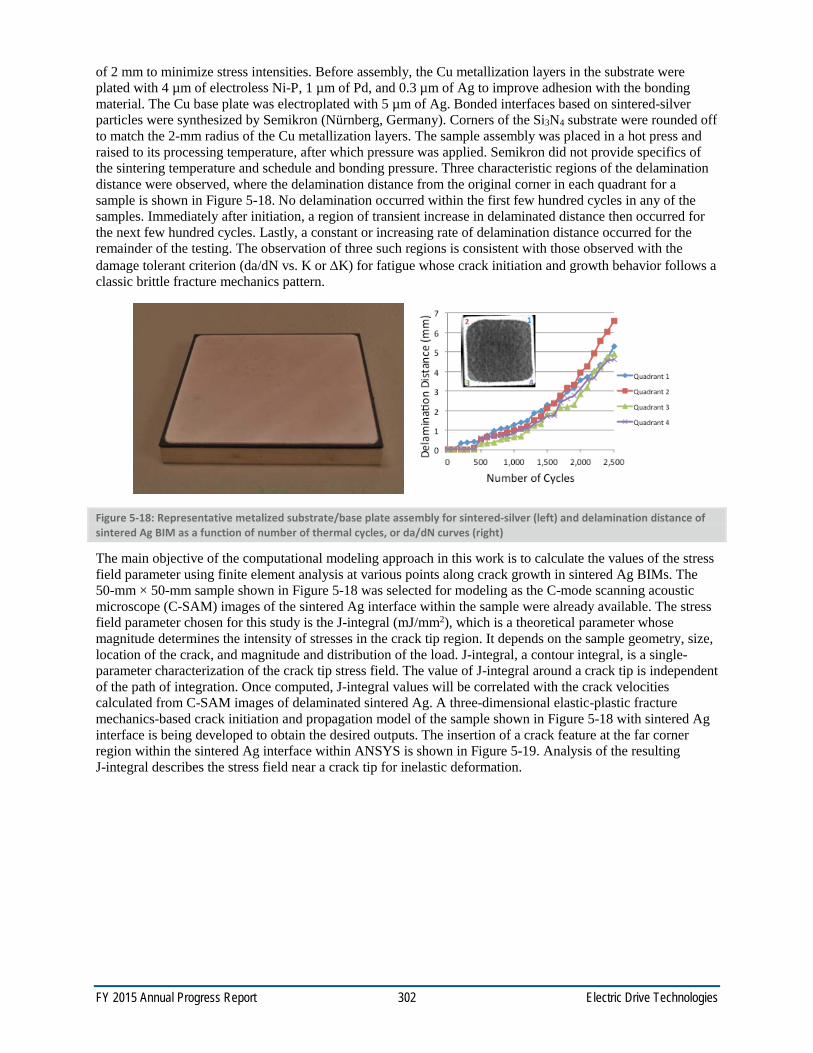
FY 2015 Annual Progress Report 302 Electric Drive Technologies
of 2 mm to minimize stress intensities. Before assembly, the Cu metallization layers in the substrate were plated with 4 µm of electroless Ni-P, 1 µm of Pd, and 0.3 µm of Ag to improve adhesion with the bonding material. The Cu base plate was electroplated with 5 µm of Ag. Bonded interfaces based on sintered-silver particles were synthesized by Semikron (Nürnberg, Germany). Corners of the Si3N4 substrate were rounded off to match the 2-mm radius of the Cu metallization layers. The sample assembly was placed in a hot press and raised to its processing temperature, after which pressure was applied. Semikron did not provide specifics of the sintering temperature and schedule and bonding pressure. Three characteristic regions of the delamination distance were observed, where the delamination distance from the original corner in each quadrant for a sample is shown in Figure 5-18. No delamination occurred within the first few hundred cycles in any of the samples. Immediately after initiation, a region of transient increase in delaminated distance then occurred for the next few hundred cycles. Lastly, a constant or increasing rate of delamination distance occurred for the remainder of the testing. The observation of three such regions is consistent with those observed with the damage tolerant criterion (da/dN vs. K or ∆K) for fatigue whose crack initiation and growth behavior follows a classic brittle fracture mechanics pattern.
Figure 5-18: Representative metalized substrate/base plate assembly for sintered-silver (left) and delamination distance of sintered Ag BIM as a function of number of thermal cycles, or da/dN curves (right)
The main objective of the computational modeling approach in this work is to calculate the values of the stress field parameter using finite element analysis at various points along crack growth in sintered Ag BIMs. The 50-mm × 50-mm sample shown in Figure 5-18 was selected for modeling as the C-mode scanning acoustic microscope (C-SAM) images of the sintered Ag interface within the sample were already available. The stress field parameter chosen for this study is the J-integral (mJ/mm2), which is a theoretical parameter whose magnitude determines the intensity of stresses in the crack tip region. It depends on the sample geometry, size, location of the crack, and magnitude and distribution of the load. J-integral, a contour integral, is a single-parameter characterization of the crack tip stress field. The value of J-integral around a crack tip is independent of the path of integration. Once computed, J-integral values will be correlated with the crack velocities calculated from C-SAM images of delaminated sintered Ag. A three-dimensional elastic-plastic fracture mechanics-based crack initiation and propagation model of the sample shown in Figure 5-18 with sintered Ag interface is being developed to obtain the desired outputs. The insertion of a crack feature at the far corner region within the sintered Ag interface within ANSYS is shown in Figure 5-19. Analysis of the resulting J-integral describes the stress field near a crack tip for inelastic deformation.
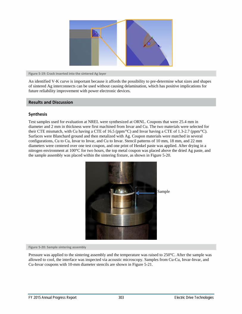
FY 2015 Annual Progress Report 303 Electric Drive Technologies
Figure 5-19: Crack inserted into the sintered Ag layer
An identified V-K curve is important because it affords the possibility to pre-determine what sizes and shapes of sintered Ag interconnects can be used without causing delamination, which has positive implications for future reliability improvement with power electronic devices.
Results and Discussion
Synthesis Test samples used for evaluation at NREL were synthesized at ORNL. Coupons that were 25.4 mm in diameter and 2 mm in thickness were first machined from Invar and Cu. The two materials were selected for their CTE mismatch, with Cu having a CTE of 16.5 (ppm/°C) and Invar having a CTE of 1.3-2.7 (ppm/°C). Surfaces were Blanchard ground and then metalized with Ag. Coupon materials were matched in several configurations, Cu to Cu, Invar to Invar, and Cu to Invar. Stencil patterns of 10 mm, 18 mm, and 22 mm diameters were centered over one test coupon, and one print of Henkel paste was applied. After drying in a nitrogen environment at 100°C for two hours, the top metal coupon was placed above the dried Ag paste, and the sample assembly was placed within the sintering fixture, as shown in Figure 5-20.
Figure 5-20: Sample sintering assembly
Pressure was applied to the sintering assembly and the temperature was raised to 250°C. After the sample was allowed to cool, the interface was inspected via acoustic microscopy. Samples from Cu-Cu, Invar-Invar, and Cu-Invar coupons with 10-mm diameter stencils are shown in Figure 5-21.
Sample
FY 2015 Annual Progress Report 304 Electric Drive Technologies
Figure 5-21: Sintered Ag interface images for 10-mm diameter bond area samples with coupon configurations of Cu-Cu (A), Invar-Invar (B), and Cu-Invar, shown from both the Invar (C) and Cu (D) sides
Cu-Cu coupons exhibited some defects after sintering that prevented a complete 10-mm diameter bond area. The partial delamination observed in some samples likely occurred during the cool-down phase to room temperature after sintering. Artifacts from scanning through 2 mm of Cu are present and should be disregarded. Invar-Invar coupons exhibited good initial adhesion with a clear bond edge. For Cu-Invar samples, the Cu coupon was used for drying the Ag paste while the Invar coupon was placed on top prior to sintering. The Invar coupons exhibited poor adhesion to the sintered Ag layer in this sample configuration, as shown by lighter areas within the 10-mm bond pad region. An additional set of Invar-Invar samples were sintered for a longer duration of two hours instead of one and were included in this reliably study.
The quality of the sintered Ag bond pad was also analyzed for 18-mm diameter bond pad samples, shown in Figure 5-22.
Figure 5-22: Sintered Ag interface images for 18-mm diameter bond area samples with coupon configurations of Cu-Cu (A), Invar-Invar (B), and Cu-Invar, shown from both Invar (C) and Cu (D) sides
Cu-Cu and Invar-Invar samples both exhibited quality adhesion between the interface material and the coupons. Cu-Invar coupons did not achieve a quality bond as the Invar coupon had poor adhesion within the central area of the bond pad and the Cu coupon showed delamination around the perimeter of the bond pad. The lower quality of the Cu-Invar coupons can be attributed to the CTE mismatch within the samples. While sintered Ag and Cu share close CTE values, the mismatch with Invar intentionally creates stress within the sample package. Values of the materials are shown in Table 5-2.
Table 5-2: Material Properties
Material CTE (ppm/°C)
E (GPa)
Cu 17 115
Sintered Ag 20 15 – 60
Invar 1.3 – 2.7 145
A B
C D
A B C D
FY 2015 Annual Progress Report 305 Electric Drive Technologies
Acoustic images were also evaluated for 22-mm-diameter bond pad samples, shown in Figure 5-23.
Figure 5-23: Sintered Ag interface images for 22-mm diameter bond area samples with coupon configurations of Cu-Cu (A), Invar-Invar (B), and Cu-Invar, shown from both Invar (C) and Cu (D) sides
Cu-Cu samples exhibited uniform adhesion between the coupons and the sintered Ag interface. Invar-Invar samples had difficulty maintaining a bond pad to the perimeter of the 22-mm diameter stencil. Cu-Invar samples again showed delamination after the sintering process due to the CTE mismatch. The Cu coupon maintained adhesion within its middle while the Invar coupon only had adhesion around the perimeter.
Accelerated Testing The bonded samples were subjected to temperature cycling conditions from -40°C to 170°C at ramp rates of 5°C/min and dwell periods of 15 minutes. Samples were removed from the environmental test chamber every 100 cycles, and the sintered Ag interface was reexamined from both coupon sides. No visual changes were observed in the acoustic images to indicate degradation of the sintered Ag layer; however, coupons were found to have fully separated after several hundred thermal cycles. Table 5-3 summarizes the bond condition of all samples; green indicates a bonded sample, and red indicates that separation occurred after the previous scan and before the current scan interval. As an example, Sample 5 passed the initial acoustic scan with no apparent defects but was found to have delaminated after it was inspected at 100 cycles. Please note that samples 10–12 were a second set of Invar-Invar samples that were sintered for a longer duration than other samples.
Table 5-3: Failure Rate of Test Samples
Sample Number Coupons
Stencil Diameter
(mm)
Cycles
0 100 200 300 400 500
1 Cu-Cu 10
2 Cu-Cu 10
3 Cu-Cu 10
4 Invar-Invar 10
5 Invar-Invar 10
6 Invar-Invar 10
7 Cu-Invar 10
8 Cu-Invar 10
9 Cu-Invar 10
10 Invar-Invar 10
11 Invar-Invar 10
12 Invar-Invar 10
13 Cu-Cu 18
A B
C D
FY 2015 Annual Progress Report 306 Electric Drive Technologies
Sample Number Coupons
Stencil Diameter
(mm)
Cycles
0 100 200 300 400 500
14 Cu-Cu 18
15 Cu-Cu 18
16 Invar-Invar 18
17 Invar-Invar 18
18 Invar-Invar 18
19 Cu-Invar 18
20 Cu-Invar 18
21 Cu-Invar 18
22 Cu-Cu 22
23 Cu-Cu 22
24 Cu-Cu 22
25 Invar-Invar 22
26 Invar-Invar 22
27 Invar-Invar 22
28 Cu-Invar 22
29 Cu-Invar 22
30 Cu-Invar 22
As the initial acoustic images indicated, the poor bonding of the Cu-Invar samples due to the intended CTE mismatch quickly led to separation of the test coupons. This was consistently shown for 10-, 18-, and 22-mm bond pad diameter samples, with no samples reaching 500 cycles. Several Invar-Invar samples also failed, with two of the three failures occurring in the samples that were sintered for a longer duration. Samples will continue to be cycled until all samples reach failure, presently defined as complete separation of the coupons from each other.
Mechanical Testing While the mechanical properties of bulk Ag are well known, variations in paste manufacturer, drying procedure, and sintering method can all lead to significant differences in properties for sintered Ag. To obtain the needed material properties for accurate modeling of the interface, shear testing of the material was completed. Three Cu coupons comprise the shear test sample, all 12.7 mm × 12.7 square. The middle coupon is 5 mm thick while the outer coupons are 1.8 mm thick. The desired bonded interface material is used to adhere the three coupons together into a test sample. This sample is placed in a shear test fixture that supports the outer coupons while applying a load to the middle coupon. The symmetry of the test samples allows for the interface layers to be loaded in a pure shear fashion. A test sample and the shear fixture are shown in Figure 5-24. The shear fixture is placed within an Instron 5966 dual column testing system that can be configured with 100 N and 10 kN load cells. The environmental chamber has a temperature range from -100°C to 350°C for capturing temperature-dependent material properties. A noncontact video extensometer is used for strain measurements. The Instron mechanical testing system is shown in Figure 5-24.

FY 2015 Annual Progress Report 307 Electric Drive Technologies
Figure 5-24: Test sample and shear test fixture (left) and Instron mechanical testing system (right)
To validate the shear testing procedure, Sn63Pb37 solder was used to synthesize several samples. Solder preforms were placed between the test coupons along with a few glass beads to ensure planarity of the bond line. After a solder reflow process was completed, the bond layers were inspected by acoustic microscopy. Only samples with minimal voiding were selected for shear testing. After screening, samples were placed within the shear test fixture and sheared at a strain rate of 0.02. The video extensometer measured displacement change of the fixture and the testing system recorded the compressive loading. Shear stress was calculated by dividing the compressive loading force by the bonded area of the test coupons. The acoustic images revised the bonded area by subtracting voided areas. A compilation of stress-strain curves of Sn63Pb37 solder samples is shown in Figure 5-25.
Figure 5-25: Solder stress-strain curves
The maximum shear stress and shear modulus of the test samples were compared to values found in literature. A shear stress of 50.5 MPa and a shear modulus of 12.2 GPa compare favorably to values reported by Darveaux [7].

FY 2015 Annual Progress Report 308 Electric Drive Technologies
Table 5-4: Shear Stress and Shear Modulus Comparison
Source Shear Stress (MPa)
Shear Modulus (GPa)
NREL 50.5 12.2
Darveaux [7] 50.5 13.1
The shear testing procedure was repeated with sintered Ag samples. Stress-strain curves are shown in Figure 5-26.
Figure 5-26: Sintered Ag stress-strain curves
When compared to previous Sn63Pb37 solder samples, it was found that sintered Ag samples reached their ultimate strength with very little displacement, confirming that creep effects are minimal within the material. Variation in ultimate strength varied more from sample to sample and may be contributed to synthesis variations between samples. The maximum shear stress values are also significantly lower than measurements of Sn63Pb37 solder samples indicating that additional synthesis optimization is required.
Crack Modeling Previously, the objective of the computational modeling approach in this work was to obtain stress intensity factor (K) values using finite element analysis at various points along crack growth in sintered Ag BIMs. Stress intensity factor was chosen as the fracture mechanics parameter as it was assumed that sintered Ag BIM was elastic under the given thermal loading condition. However, further literature review revealed the occurrence of ductile fracture [8] in which plastic deformation is the dominant failure mechanism. In such a case, an elastic-plastic fracture mechanics analysis is in order, and parameters such as J-integral, which characterizes the stress and strain fields around a crack tip in a plastic material, need to be computed. J-integral is defined as a path-independent contour integral around a crack tip and is equal to the nonlinear energy release rate.
The 50-mm × 50-mm sample shown in Figure 5-27 was selected for modeling as the C-SAM images of the sintered Ag interface within the sample were already available. J-integral values, once computed, will be correlated with the crack velocities or crack length calculated from C-SAM images of the delaminated sintered Ag. The crack-modeling feature in ANSYS is only available in version 15 or later. Crack size and location need to be known before an analysis can be completed. The sample geometry was created in ANSYS Design

FY 2015 Annual Progress Report 309 Electric Drive Technologies
Modeler, and a tetrahedral mesh was implemented. While a hexahedral mesh would provide more accurate results, the current capabilities within ANSYS are limited to performing crack modeling on a tetrahedral mesh.
Figure 5-27: Quarter symmetry tetrahedral mesh of the 50 x 50-mm sample
A crack was then inserted at the far corner region within sintered Ag using the "Fracture" feature available in ANSYS Model, shown in Figure 5-28. The crack takes a semi-elliptical shape, and the major and minor radii are defined to create a crack of the desired size. Currently, only a semi-elliptical shaped crack is available in ANSYS. After solving, J-integral values can be obtained along the crack contour in the post-processing phase. If the maximum value of the J-integral exceeds a critical value, which is unique for each material, it can be understood that crack would begin to propagate. However, crack propagation modeling is not currently available within ANSYS.
Figure 5-28: Crack inserted into the sintered Ag layer To simulate crack propagation or crack growth, multiple simulations with reduced bonded areas were conducted, as shown in Figure 5-29. Currently, the reduction in bonded areas was chosen arbitrarily to analyze the variation in J-integral values along crack growth path. Preliminary J-integral results have been obtained from these simulations. Additional work such as mesh independence study is being conducted to confirm the validity of the obtained results.
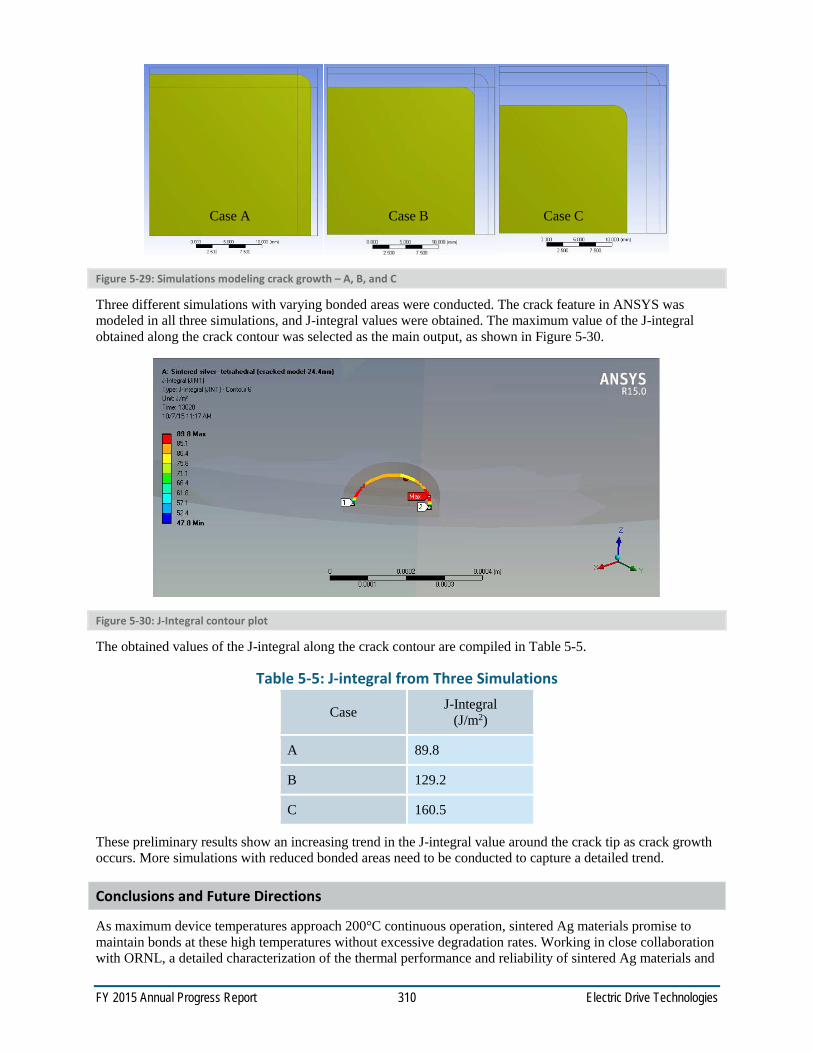
FY 2015 Annual Progress Report 310 Electric Drive Technologies
Figure 5-29: Simulations modeling crack growth – A, B, and C
Three different simulations with varying bonded areas were conducted. The crack feature in ANSYS was modeled in all three simulations, and J-integral values were obtained. The maximum value of the J-integral obtained along the crack contour was selected as the main output, as shown in Figure 5-30.
Figure 5-30: J-Integral contour plot
The obtained values of the J-integral along the crack contour are compiled in Table 5-5.
Table 5-5: J-integral from Three Simulations
Case J-Integral (J/m2)
A 89.8
B 129.2
C 160.5
These preliminary results show an increasing trend in the J-integral value around the crack tip as crack growth occurs. More simulations with reduced bonded areas need to be conducted to capture a detailed trend.
Conclusions and Future Directions
As maximum device temperatures approach 200°C continuous operation, sintered Ag materials promise to maintain bonds at these high temperatures without excessive degradation rates. Working in close collaboration with ORNL, a detailed characterization of the thermal performance and reliability of sintered Ag materials and
Case A Case B Case C

FY 2015 Annual Progress Report 311 Electric Drive Technologies
processes has been initiated. The CTE mismatch within Cu-Invar samples quickly led to separation of the test coupons. This was consistently shown for 10-, 18-, and 22-mm bond pad diameter samples, with no samples reaching 500 cycles. When compared to Sn63Pb37 solder samples, it was found that sintered Ag samples reached their ultimate strength with very little displacement. ORNL and NREL will continue to optimize the synthesis process for sintered Ag and will continue to provide the automotive industry a baseline for the reliability of these interfaces.
Future steps in crack modeling include efforts to simulate crack propagation directly using the extended finite element method (X-FEM). X-FEM is a numerical technique that uses partition of unity method for modeling discontinuities such as cracks in a system. The biggest advantage of XFEM is that crack propagation can be modeled without re-meshing. Also, we will investigate the application of cohesive zone models, which employ traction-separation laws, in an X-FEM framework to simulate cohesive crack growth.
Development of lifetime estimation tools will allow the reliability of sintered Ag to be predicted (similar to the reliability prediction of solder materials), and enable a time and cost-effective design process. Performance and reliability of novel/emerging techniques such as atomic-level bonding (in collaboration with industry) will also be investigated as a longer-term development goal.
FY 2015 Presentations/ Publications/ Patents
1. D.J. DeVoto, A.A. Wereszczak, and P.P. Paret. 2015. “Thermomechanical Reliability of Sintered-Silver Interface Materials.” International Technical Conference and Exhibition on Packaging and Integration of Electronic and Photonic Microsystems (InterPACK), San Francisco, CA.
2. A.A. Wereszczak, S.B. Waters, D.J. DeVoto, and P.P. Paret. 2015. “Method to Determine Maximum Allowable Sinterable Silver Interconnect Size.” In preparation, Journal of Electronic Materials.
3. D.J. DeVoto. 2015. “Performance and Reliability of Bonded Interfaces for High-Temperature Packaging.” Electric Drive Technologies (EDT) Program FY15 Annual Merit Review, DOE Vehicle Technologies Office, Arlington, VA, June 2015.
4. D.J. DeVoto. 2015. “Performance and Reliability of Bonded Interfaces for High-Temperature Packaging.” Presentation to the DOE Vehicle Technologies Office (VTO) Electrical and Electronics Technical Team, Southfield, MI, May 2015.
5. D.J. DeVoto. 2014. “Performance and Reliability of Bonded Interfaces for High-Temperature Packaging.” Electric Drive Technologies Program FY15 Kickoff Meeting, DOE Vehicle Technologies Office, Oak Ridge, TN, November 2014.
6. D.J. DeVoto, A.A. Wereszczak, and P.P. Paret. 2014. “Stress Intensity of Delamination in a Sintered-Silver Interconnection.” IMAPS High Temperature Electronics (HiTEC), Albuquerque, NM.
Acknowledgments
The author would like to acknowledge the support provided by Susan Rogers and Steven Boyd, Technology Development Managers for the EDT Program, Vehicle Technologies Office, U.S. Department of Energy Office of Energy Efficiency and Renewable Energy. The significant contributions of Andrew Wereszczak, Paul Paret, and Jake Callaghan are acknowledged.
References
1. A.A. Wereszczak, Z. Liang, M.K. Ferber, L.D. Marlino, 2014. “Uniqueness and Challenges of Sintered Silver as a Bonded Interface Material,” International Conference on High Temperature Electronics (HiTEC), Albuquerque, NM, 2014.
2. R.W. Chuang, C.C. Lee, 2002. “Silver-Indium Joints Produced at Low Temperature for High Temperature Devices,” IEEE Transactions on Components and Packaging Technologies, Vol. 25, No. 3, pp. 453–458.
3. K. Sow, 2014. “Are Sintered Silver Joints Ready for Use as Interconnect Material in Microelectronic Packaging?” Journal of Electronic Materials, Vol. 43, No. 4; pp. 947–961.

FY 2015 Annual Progress Report 312 Electric Drive Technologies
4. S.W. Yoon, K. Shiozaki, S. Yasuda, and M.D. Glover, 2012. “Highly reliable nickel-tin transient liquid phase bonding technology for high temperature operational power electronics in electrified vehicles” Twenty-Seventh Annual IEEE Applied Power Electronics Conference and Exposition (APEC), 478–482.
5. H. Greve and F.P. McCluskey, 2014. “LT-TLPS Die Attach for High Temperature Electronic Packaging,” Journal of Microelectronics and Electronic Packaging, Vol. 11, No. 1, pp. 7–15.
6. D.J. DeVoto, A.A. Wereszczak, and P.P. Paret. 2014. “Stress Intensity of Delamination in a Sintered-Silver Interconnection.” IMAPS High Temperature Electronics (HiTEC), Albuquerque, NM.
7. R. Darveaux and K. Banerji. 1992. “Constitutive Relations for Tin-Based Solder Joints,” IEEE Transactions on Components, Hybrids, and Manufacturing Technology, Vol. 15, No. 6; pp. 1013–1024.
8. G. Bai. 2005. "Low-Temperature Sintering of Nanoscale Silver Paste for Semiconductor Device Interconnection," PhD Thesis.
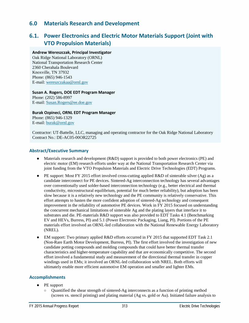
FY 2015 Annual Progress Report 313 Electric Drive Technologies
6.0 Materials Research and Development
6.1. Power Electronics and Electric Motor Materials Support (Joint with VTO Propulsion Materials)
Andrew Wereszczak, Principal Investigator Oak Ridge National Laboratory (ORNL) National Transportation Research Center 2360 Cherahala Boulevard Knoxville, TN 37932 Phone: (865) 946-1543 E-mail: [email protected] Susan A. Rogers, DOE EDT Program Manager Phone: (202) 586-8997 E-mail: [email protected] Burak Ozpineci, ORNL EDT Program Manager Phone: (865) 946-1329 E-mail: [email protected] Contractor: UT-Battelle, LLC, managing and operating contractor for the Oak Ridge National Laboratory Contract No.: DE-AC05-00OR22725
Abstract/Executive Summary Materials research and development (R&D) support is provided to both power electronics (PE) and
electric motor (EM) research efforts under way at the National Transportation Research Center via joint funding from the VTO Propulsion Materials and Electric Drive Technologies (EDT) Programs.
PE support: Most FY 2015 effort involved cross-cutting applied R&D of sinterable silver (Ag) as a candidate interconnect for PE devices. Sintered-Ag interconnection technology has several advantages over conventionally used solder-based interconnection technology (e.g., better electrical and thermal conductivity, microstructural equilibrium, potential for much better reliability), but adoption has been slow because it is a relatively new technology and the PE community is relatively conservative. This effort attempts to hasten the more confident adoption of sintered-Ag technology and consequent improvement in the reliability of automotive PE devices. Work in FY 2015 focused on understanding the concurrent mechanical limitations of sinterable Ag and the plating layers that interface it to substrates and die. PE-materials R&D support was also provided to EDT Tasks 4.1 (Benchmarking EV and HEVs, Burress, PI) and 5.1 (Power Electronic Packaging, Liang, PI). Portions of the PE materials effort involved an ORNL-led collaboration with the National Renewable Energy Laboratory (NREL).
EM support: Two primary applied R&D efforts occurred in FY 2015 that supported EDT Task 2.1 (Non-Rare Earth Motor Development, Burress, PI). The first effort involved the investigation of new candidate potting compounds and molding compounds that could have better thermal transfer characteristics and higher-temperature capability and that are economically competitive. The second effort involved a fundamental study and measurement of the directional thermal transfer in copper windings used in EMs; it involved an ORNL-led collaboration with NREL. Both efforts will ultimately enable more efficient automotive EM operation and smaller and lighter EMs.
Accomplishments PE support
o Quantified the shear strength of sintered-Ag interconnects as a function of printing method (screen vs. stencil printing) and plating material (Ag vs. gold or Au). Initiated failure analysis to

FY 2015 Annual Progress Report 314 Electric Drive Technologies
censor the measured strengths in the context of cohesive and adhesive failure locations. These results will illustrate the achievable strength characteristics of such interconnect systems, guide future sintered-Ag design for PE, and improve the community’s receptiveness to adopting sintered-Ag technology.
o Conceived of, coordinated, fabricated all specimens for, and assumed leadership of an ORNL-led collaboration with NREL to study delamination initiation and propagation response in sintered-Ag interconnects.
o Sectioned and analyzed the micro-architecture of the power module used in the Honda Accord inverter in support of EDT Task 4.1.
o Used sintered Ag as an interconnect to bond an SiC die to direct-bonded copper (DBC) substrates in support of EDT Task 5.1.
o Fabricated sintered-Ag samples for thermal and mechanical testing at NREL (DeVoto).
EM support ( EDT Task 2.1) o Measured thermal properties of developmental, mineral-filled potting and molding compounds
and established an collaboration with an industrial manufacturer of such materials. o Conceived of, coordinated, fabricated all specimens for, and assumed leadership of an ORNL-led
collaboration with NREL to better understand the directional thermal response of copper-wound structures.
o Developed versatile copper-wound billets from which samples were harvested to enable the thermal property measurement of their anisotropic structure using three different standardized techniques.
o Showed that the thermal conductivity in the direction of the copper wires is over two orders of magnitude higher than the thermal conductivity perpendicular to them.
Introduction
For future PE devices, the potential use of sintered-Ag interconnection technology has several advantages over conventionally used solder-based interconnection technology (e.g., better electrical and thermal conductivity, microstructural equilibrium, potential for much better reliability). However, its adoption has been slow because it is a relatively new technology and the PE community is relatively conservative. This VTO Propulsion Materials–EDT jointly funded effort will hasten the more confident adoption of sintered Ag by identifying the achievable strength characteristics of such interconnect systems (which are relative complex, as illustrated in Figure 6-1). This effort will guide future sintered-Ag design for PE and improve the PE community’s receptiveness to adopting sintered-Ag technology.
For EMs, minimizing the service temperature in copper windings in slot liners will promote greater efficiency and enable EM size and weight reductions. Figure 6-2 illustrates these wires in slot liners. Two ways to achieve minimization are by using more thermally conductive materials in EMs and by improving the understanding of the anisotropic thermal transfer within those copper windings. New potting and molding compounds that have better thermal transfer characteristics and higher-temperature capability are attractive candidates for this purpose, provided they are cost-competitive with currently used materials and do not introduce performance compromises. Greater understanding of the thermal transfer characteristics starts with the fundamental study and measurement of the directional thermal transfer in copper windings used in EMs; however, specimens must be developed and thermally measured that represent how these copper windings thermally respond in service.
FY 2015 Annual Progress Report 315 Electric Drive Technologies
Figure 6-1: The strength and reliability of a sintered-Ag interconnect is a function of many parameters.
Figure 6-2: Example of copper windings in slot liners [Sato et al., SAE Intl, 2011].
Approach
Power Electronics Support Fabricate custom-designed sintered-Ag test coupons that enable the measurement of shear strength as a function of the plating material (Ag vs. Au) and printing method (screen vs. stencil). Perform failure analysis to identify location in the context of either cohesive or adhesive failure of any of the constituents making up the sintered-Ag interconnect system.
Coordinate and lead an ORNL-led sintered-Ag thermo-mechanical reliability study with NREL. Examine the effect of coefficient-of-thermal-expansion (CTE) –induced residual stress on sintered-Ag printed pad size and the onset of delamination of the interconnect. Fabricate all specimens and provide materials characterization.
Section, metallographically polish, and analyze the micro-architecture of the power module used in the Honda Accord inverter in support of EDT Task 4.1. The analyses included optical microscopy, scanning electron microscopy, and chemistry mapping via energy-dispersive spectroscopy.
Bond an SiC die to DBC substrates using sintered Ag in support of EDT Task 5.1. Bond the die at different locations to ready it for different wire bonding placements and eventual device testing.
Fabricate sintered-Ag samples for NREL’s internal thermal and mechanical evaluations (DeVoto).

FY 2015 Annual Progress Report 316 Electric Drive Technologies
Electric Motor Support Support EDT Task 2.1 and measure thermal properties of developmental, mineral-filled potting and molding compounds.
Coordinate and lead an ORNL-led collaboration with NREL (Bennion) to better understand the directional thermal response of copper-wound structures. Conceive of and fabricate test specimens that facilitate the valid measurement of thermal diffusivity and thermal conductivity as a function of wire orientation. Use different methods of thermal property measurement to enable comparisons and validate the legitimacy of the results.
Results and Discussion
Power Electronics Support Custom-designed sintered-Ag test coupons were fabricated that enabled the measurement of shear strength as a function of plating material (Ag vs. Au) and printing method (screen vs. stencil). A scanning acoustic microscopy image of some of these samples is shown in Figure 6-3. Polished cross-sections of the platings are shown in Figure 6-4. Silver was plated directly onto the copper cladding on the DBC substrate, but an Ni-P interphase was applied onto the copper. Then the Au plating was deposited onto the Ni-P. The squares were then shear-tested to failure using a Nordson-Date tester (see Figure 6-5), and their uncensored results were regressed against a 2-parameter Weibull distribution (graphically shown in Figure 6-6).
Failure analysis is occurring in early FY 2016 to link each specimen’s strength with failure locations (i.e., censor the data). This data censoring will provide context to either cohesive or adhesive failure of any of the constituents making up the sintered-Ag interconnect system.
Figure 6-3: Scanning acoustic microscopy image of the "5-dice-pattern" interconnect used with DBC sandwiches to quantify shear strength. Squares (12.7×12.7 mm) are the DBC substrates. The dark circles are the sintered-Ag interconnecting pads. Total bonds are nominally 20 mm2.

FY 2015 Annual Progress Report 317 Electric Drive Technologies
Figure 6-4: Polished cross-sections of the silver (left) and gold (right) platings used on the DBC substrates.
Figure 6-5: Test setup for measuring the shear strength of the DBC sandwiches.
ORNL conceived of and is leading a collaboration with NREL (DeVoto) involving the study of the thermo-mechanical response of sintered Ag as a function of CTE-mismatch-induced residual stress. Residual stress was purposely introduced and varied using the conditions described in Figure 6-7. An “Oreo-cookie” sample was chosen because of its axisymmetric simplicity and to avoid complications introduced by the presence of corners. Invar (metal) was chosen for this study because its CTE is similar to that of silicon, and because the weakness and brittleness of silicon can prohibit measurement of the shear strength of the interconnect material. Three different sintered-Ag pad diameters and three different combinations of Cu-Cu, Invar-Invar, and Cu-Invar were used, producing the processed matrix shown in Figure 6-8. These disks are now being thermally cycled at NREL to monitor the onset and rate of advance of delamination of the sintered-Ag interconnect.

FY 2015 Annual Progress Report 318 Electric Drive Technologies
Figure 6-6: Failure shear stress values fitted against 2-parameter Weibull distributions. Specimens are now undergoing failure analysis and data censoring.
Figure 6-7: Description of “Oreo-cookie” test coupons used to study the effect of CTE-induced residual stress on delamination onset and propagation. Sintered-Ag print diameters are 10, 18, and 22 mm on these 25 mm diameter disks of either copper or Invar.
A delamination effect was immediately observed after the processing of these disks. Its analysis is ongoing with the intent of advocating a simple method to identify the potential maximum bond size of a sintered-Ag interconnect for a given suite of independent parameters (like those illustrated in Figure 6-1). Scanning acoustic microscopy showed that some of the interconnects had started to delaminate as a consequence of the high-temperature “cookie” sintering (Figure 6-9). The analysis will be described in a manuscript to be submitted to the open literature with NREL as a collaborator.
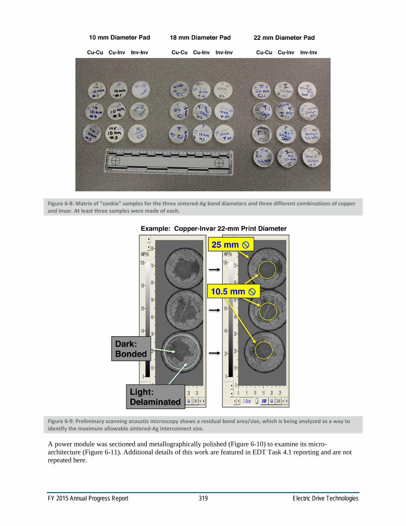
FY 2015 Annual Progress Report 319 Electric Drive Technologies
Figure 6-8: Matrix of “cookie” samples for the three sintered-Ag bond diameters and three different combinations of copper and invar. At least three samples were made of each.
Figure 6-9: Preliminary scanning acoustic microscopy shows a residual bond area/size, which is being analyzed as a way to identify the maximum allowable sintered-Ag interconnect size.
A power module was sectioned and metallographically polished (Figure 6-10) to examine its micro-architecture (Figure 6-11). Additional details of this work are featured in EDT Task 4.1 reporting and are not repeated here.

FY 2015 Annual Progress Report 320 Electric Drive Technologies
Figure 6-10: The power module from a Honda Accord was sectioned and metallographically prepared.
Figure 6-11: Annotated cross-section of power module shown in Figure 6-10.
In support of EDT Task 5.1, SiC dies were bonded to Ag- and Au-plated DBC substrates to ready them for wire bonding placement and eventual device testing (Figure 6-12).

FY 2015 Annual Progress Report 321 Electric Drive Technologies
Figure 6-12: Examples of preliminary sintered-Ag bonding of SiC to either Ag-plated or gold-plated DBC substrates.
Two additional sintered-Ag processing efforts were undertaken for the benefit of NREL (DeVoto). They included the sintered-Ag bonding of silicon disks to metal disks (Figure 6-13) for NREL’s internal thermoreflectance measurements and sintered-Ag bonding of squares to make double-lap shear specimens for mechanical testing (Figure 6-14). ORNL designed and fabricated the necessary fixtures to promote concentric alignment of the bonded pieces and then executed the sintered-Ag bonding.
Figure 6-13: Disk specimens were sintered-Ag bonded by ORNL for NREL for internal thermoreflectance measurements.
Figure 6-14: Double-lap specimens were sintered-Ag bonded by ORNL for NREL to conduct shear tests.
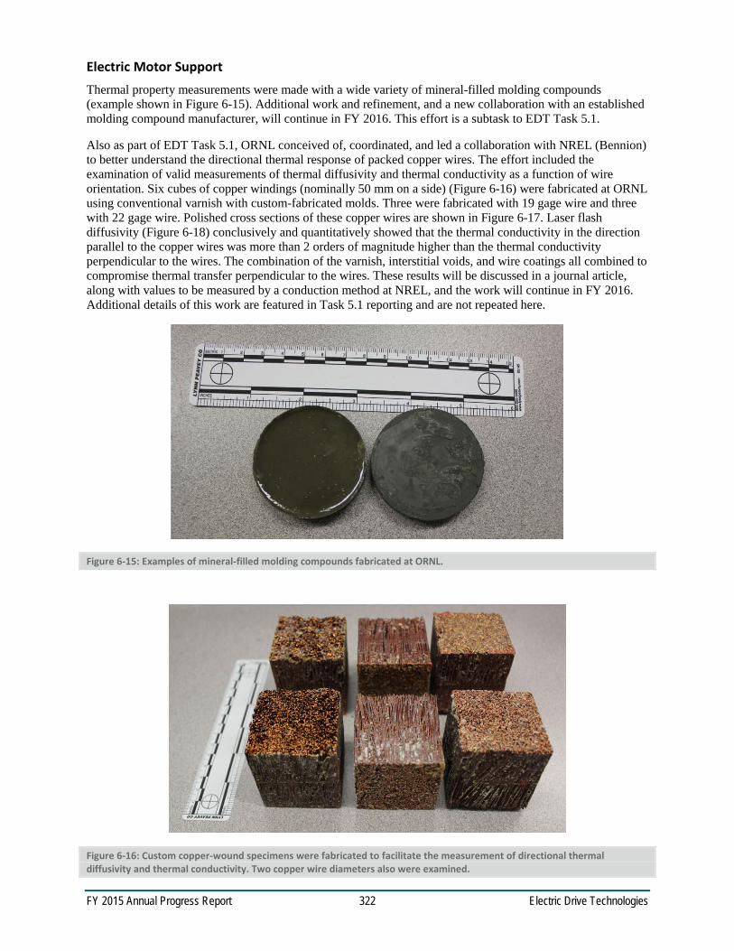
FY 2015 Annual Progress Report 322 Electric Drive Technologies
Electric Motor Support Thermal property measurements were made with a wide variety of mineral-filled molding compounds (example shown in Figure 6-15). Additional work and refinement, and a new collaboration with an established molding compound manufacturer, will continue in FY 2016. This effort is a subtask to EDT Task 5.1.
Also as part of EDT Task 5.1, ORNL conceived of, coordinated, and led a collaboration with NREL (Bennion) to better understand the directional thermal response of packed copper wires. The effort included the examination of valid measurements of thermal diffusivity and thermal conductivity as a function of wire orientation. Six cubes of copper windings (nominally 50 mm on a side) (Figure 6-16) were fabricated at ORNL using conventional varnish with custom-fabricated molds. Three were fabricated with 19 gage wire and three with 22 gage wire. Polished cross sections of these copper wires are shown in Figure 6-17. Laser flash diffusivity (Figure 6-18) conclusively and quantitatively showed that the thermal conductivity in the direction parallel to the copper wires was more than 2 orders of magnitude higher than the thermal conductivity perpendicular to the wires. The combination of the varnish, interstitial voids, and wire coatings all combined to compromise thermal transfer perpendicular to the wires. These results will be discussed in a journal article, along with values to be measured by a conduction method at NREL, and the work will continue in FY 2016. Additional details of this work are featured in Task 5.1 reporting and are not repeated here.
Figure 6-15: Examples of mineral-filled molding compounds fabricated at ORNL.
Figure 6-16: Custom copper-wound specimens were fabricated to facilitate the measurement of directional thermal diffusivity and thermal conductivity. Two copper wire diameters also were examined.
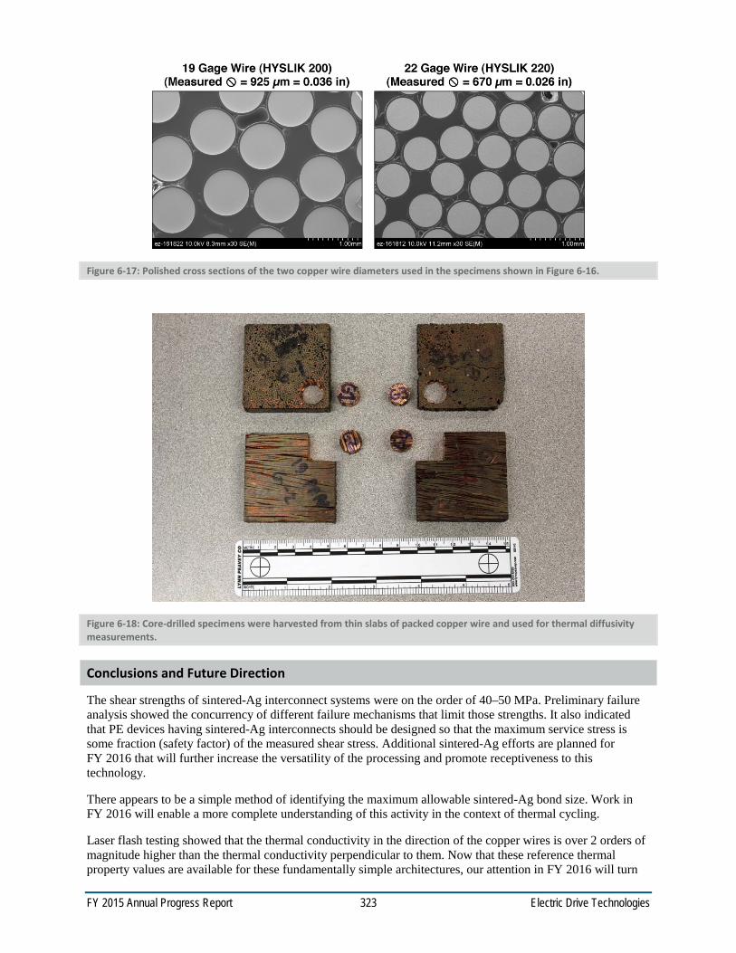
FY 2015 Annual Progress Report 323 Electric Drive Technologies
Figure 6-17: Polished cross sections of the two copper wire diameters used in the specimens shown in Figure 6-16.
Figure 6-18: Core-drilled specimens were harvested from thin slabs of packed copper wire and used for thermal diffusivity measurements.
Conclusions and Future Direction
The shear strengths of sintered-Ag interconnect systems were on the order of 40–50 MPa. Preliminary failure analysis showed the concurrency of different failure mechanisms that limit those strengths. It also indicated that PE devices having sintered-Ag interconnects should be designed so that the maximum service stress is some fraction (safety factor) of the measured shear stress. Additional sintered-Ag efforts are planned for FY 2016 that will further increase the versatility of the processing and promote receptiveness to this technology.
There appears to be a simple method of identifying the maximum allowable sintered-Ag bond size. Work in FY 2016 will enable a more complete understanding of this activity in the context of thermal cycling.
Laser flash testing showed that the thermal conductivity in the direction of the copper wires is over 2 orders of magnitude higher than the thermal conductivity perpendicular to them. Now that these reference thermal property values are available for these fundamentally simple architectures, our attention in FY 2016 will turn

FY 2015 Annual Progress Report 324 Electric Drive Technologies
toward (1) how to improve the thermal transfer perpendicular to the wires and (2) understanding thermal property variability in the context of wire diameter.
FY 2015 Presentations/Publications/Patents
1. A. A. Wereszczak, Z. Liang, M. K. Ferber, and L. D. Marlino, “Uniqueness and challenges of sintered silver as a bonded interface material,” Journal of Microelectronics and Electronic Packaging 11,158–165 (2014).
2. A. A. Wereszczak, S. B. Waters, and W. Carty, “Transfer Method for Printed Sinterable Paste Having Nonaqueous Solvent,” Invention Disclosure Number 201503508, DOE S-138,140, April 4, 2015.
3. A. A. Wereszczak, and W. Carty, “Drying Method for Sinterable Paste Used for Bonded Joints,” Invention Disclosure Number 201503507, DOE S-138,139, April 3, 2015.
4. A. A. Wereszczak, Z. Liang, and T. A. Burress, “Enabling materials for high-temperature power electronics,” presented at the 2015 VTO AMR, Arlington, Virginia, June 10, 2015.
5. A. A. Wereszczak, S. B. Waters, M. Modugno, D. J. DeVoto, and P. P. Paret, “Method to determine maximum allowable sinterable silver interconnect size,” in preparation, 2015.

FY 2015 Annual Progress Report 325 Electric Drive Technologies