Efficient architectures for 3D HWT using dynamic partial reconfiguration
11
An efficient FPGA-based dynamic partial reconfiguration design flow and environment for image and signal processing IP cores B. Krill a,b, , A. Ahmad b,c , A. Amira a , H. Rabah d a Nanotechnology and Integrated Bio-Engineering Centre (NIBEC), Faculty of Computing and Engineering, University of Ulster, Jordanstown Campus, Newtownabbey Co. Antrim, BT37 0QB Belfast, Northern Ireland b Department of Electronic and Computer Engineering, School of Engineering and Design, Brunel University, West London, UB83PH Uxbridge, UK c Department of Computer Engineering, Faculty of Electrical and Electronic Engineering, Universiti Tun Hussein Onn Malaysia (UTHM), 86400 Batu Pahat, Johor, Malaysia d Laboratoire d’Instrumentation, Electronique de Nancy, University Henri Poincare, 540003 Nancy, France article info Article history: Received 30 October 2009 Accepted 26 April 2010 Keywords: Dynamic partial reconfiguration (DPR) Design flow Field programmable gate array (FPGA) IP cores Image and signal processing abstract This paper describes a dynamic partial reconfiguration (DPR) design flow and environment for image and signal processing algorithms used in adaptive applications. Based on the evaluation of the existing DPR design flow, important features such as overall flexibility, application and standardised interfaces, host applications and DPR area/size placement have been taken into consideration in the proposed design flow and environment. Three intellectual property (IP) cores used in pre-processing and transform blocks of compression systems including colour space conversion (CSC), two-dimensional biorthogonal discrete wavelet transform (2-D DBWT) and three-dimensional Haar wavelet transform (3-D HWT) have been selected to validate the proposed DPR design flow and environment. Results obtained reveal that the proposed environment has a better solution providing: a scriptable program to establish the communication between the field programmable gate array (FPGA) with IP cores and their host application, power consumption estimation for partial reconfiguration area and automatic generation of the partial and initial bitstreams. The design exploration offered by the proposed DPR environment allows the generation of efficient IP cores with optimised area/speed ratios. Analysis of the bitstream size and dynamic power consumption for both static and reconfigurable areas is also presented in this paper. & 2010 Elsevier B.V. All rights reserved. 1. Introduction Image and signal processing is one of the emerging areas and their state-of-the-art have changed the way its computationally complex algorithms and systems are implemented. Increasing demand for real-time processing as well as maintaining the system performance is of crucial importance and motivates a strong justification to further research in these areas. Reconfigurable hardware, especially field programmable gate arrays (FPGAs) are widely used in image and signal processing applications from simple low-resolution and low-bandwidth applications to very high-resolution and high-bandwidth [1]. Owing to its massive parallelism capabilities, multimillion gate counts and special low power packages, FPGA has attracted a great deal of research and development. Since the employment of image and signal processing for adaptive applications uses several building blocks for its computationally intensive algorithms, complexity in Contents lists available at ScienceDirect journal homepage: www.elsevier.com/locate/image Signal Processing: Image Communication ARTICLE IN PRESS 0923-5965/$ - see front matter & 2010 Elsevier B.V. All rights reserved. doi:10.1016/j.image.2010.04.005 Corresponding author at: Nanotechnology and Integrated Bio- Engineering Centre (NIBEC), Faculty of Computing and Engineering, University of Ulster, Jordanstown Campus, Newtownabbey Co. Antrim, BT37 0QB Belfast, Northern Ireland. E-mail address: [email protected] (B. Krill). Signal Processing: Image Communication 25 (2010) 377–387
-
Upload
independent -
Category
Documents
-
view
3 -
download
0
Transcript of Efficient architectures for 3D HWT using dynamic partial reconfiguration
ARTICLE IN PRESS
Contents lists available at ScienceDirect
Signal Processing: Image Communication
Signal Processing: Image Communication 25 (2010) 377–387
0923-59
doi:10.1
� Cor
Enginee
Univers
BT37 0Q
E-m
journal homepage: www.elsevier.com/locate/image
An efficient FPGA-based dynamic partial reconfiguration design flowand environment for image and signal processing IP cores
B. Krill a,b,�, A. Ahmad b,c, A. Amira a, H. Rabah d
a Nanotechnology and Integrated Bio-Engineering Centre (NIBEC), Faculty of Computing and Engineering, University of Ulster, Jordanstown Campus,
Newtownabbey Co. Antrim, BT37 0QB Belfast, Northern Irelandb Department of Electronic and Computer Engineering, School of Engineering and Design, Brunel University, West London, UB83PH Uxbridge, UKc Department of Computer Engineering, Faculty of Electrical and Electronic Engineering, Universiti Tun Hussein Onn Malaysia (UTHM),
86400 Batu Pahat, Johor, Malaysiad Laboratoire d’Instrumentation, Electronique de Nancy, University Henri Poincare, 540003 Nancy, France
a r t i c l e i n f o
Article history:
Received 30 October 2009
Accepted 26 April 2010
Keywords:
Dynamic partial reconfiguration (DPR)
Design flow
Field programmable gate array (FPGA)
IP cores
Image and signal processing
65/$ - see front matter & 2010 Elsevier B.V. A
016/j.image.2010.04.005
responding author at: Nanotechnology an
ring Centre (NIBEC), Faculty of Computing
ity of Ulster, Jordanstown Campus, Newtow
B Belfast, Northern Ireland.
ail address: [email protected] (B. Krill).
a b s t r a c t
This paper describes a dynamic partial reconfiguration (DPR) design flow and
environment for image and signal processing algorithms used in adaptive applications.
Based on the evaluation of the existing DPR design flow, important features such as
overall flexibility, application and standardised interfaces, host applications and DPR
area/size placement have been taken into consideration in the proposed design flow and
environment. Three intellectual property (IP) cores used in pre-processing and
transform blocks of compression systems including colour space conversion (CSC),
two-dimensional biorthogonal discrete wavelet transform (2-D DBWT) and
three-dimensional Haar wavelet transform (3-D HWT) have been selected to validate
the proposed DPR design flow and environment. Results obtained reveal that the
proposed environment has a better solution providing: a scriptable program to establish
the communication between the field programmable gate array (FPGA) with IP cores
and their host application, power consumption estimation for partial reconfiguration
area and automatic generation of the partial and initial bitstreams. The design
exploration offered by the proposed DPR environment allows the generation of efficient
IP cores with optimised area/speed ratios. Analysis of the bitstream size and dynamic
power consumption for both static and reconfigurable areas is also presented in
this paper.
& 2010 Elsevier B.V. All rights reserved.
1. Introduction
Image and signal processing is one of the emergingareas and their state-of-the-art have changed the way itscomputationally complex algorithms and systems areimplemented. Increasing demand for real-time processingas well as maintaining the system performance is of
ll rights reserved.
d Integrated Bio-
and Engineering,
nabbey Co. Antrim,
crucial importance and motivates a strong justification tofurther research in these areas.
Reconfigurable hardware, especially field programmablegate arrays (FPGAs) are widely used in image and signalprocessing applications from simple low-resolution andlow-bandwidth applications to very high-resolution andhigh-bandwidth [1]. Owing to its massive parallelismcapabilities, multimillion gate counts and special low powerpackages, FPGA has attracted a great deal of research anddevelopment.
Since the employment of image and signal processingfor adaptive applications uses several building blocks forits computationally intensive algorithms, complexity in

ARTICLE IN PRESS
B. Krill et al. / Signal Processing: Image Communication 25 (2010) 377–387378
addressing and accessing real-time and massive amountof data to be processed have resulted in vast challengesfrom a hardware implementation point of view. In orderto address these issues, FPGAs with an efficientreconfigurability mechanism should be deployed to meetthe requirements in terms of speed, area (size), powerconsumption and throughput.
Dynamic partial reconfiguration (DPR) is a promisingsolution for reducing the hardware required inimplementing an efficient design for image and signalprocessing algorithms used in adaptive applications [2,3].With this solution, the design can be divided intosub-designs that fit into the available devices which canbe then ported onto the reconfigurable hardware whenneeded.
DPR has been widely studied in various fields [4–18].However, current DPR design flows and implementationsare not capable to provide a set of programs to establishcommunication between the FPGA and host computer.Moreover, estimation of power consumption for thereconfigurable area and auto-generated bitstream forpartial and initial cannot be performed [2,3].
To address these issues, this paper proposes aDPR design flow and environment to accelerate thedevelopment of partial reconfiguration platform andvalidation through a range of intellectual property (IP)cores used in image and signal processing foradaptive applications. Colour space conversion (CSC),two-dimensional biorthogonal discrete wavelet transform(2-D DBWT) and three-dimensional Haar wavelet trans-form (3-D HWT) IP cores have been selected to validatethe feasibility and advantages features of the proposedDPR design flow and environment.
The structure of the paper is organised as follows. Anoverview of the related work of DPR design flow,environment and application is given in Section 2. Section3 presents the proposed design flow and environment.Section 4 exposes the case study of the IP cores used inimage and signal processing adaptive applications. Ex-perimental results and analysis are described in Section 5.Finally, concluding remarks are given in Section 6.
Table 1Importance features for DPR techniques.
Features Xilinx DPR [16–18]
Overall flexibility Total flexibility
Application interfaces No fixed interfaces
Standardised interfaces No standard specification
Host applications Need to be programmed
DPR area place/size Manual placement by users
2. Related work
2.1. DPR design flow and environment
Shoa and Shirani [2] thoroughly explain differentissues in run-time reconfigurable (RTR) systems and listthe implemented system which supported RTR reconfi-guration as well as discussing different applications andthe improvements achieved by applying RTR. An evalua-tion of DPR for signal and image processing has beenpresented in [3] and the authors present the advantagesand limitation of DPR in professional electronics applica-tions as well as provide guidelines to improve itsapplicability. Furthermore, the missing elements of thedesign flow to be used in DPR have been identified andexplained.
Mitra et al. [19] describe a software tool for auto-matically generating the communication interface be-
tween the IP core based co-processing on the Virtex-4 FXFPGA and the host application running on the centralprocessing unit (CPU). The proposed implementationgenerates hardware wrappers for the core and resemblesa C-function invocation in the source codes. Moreover, thesame static wrapper is used for multiple cores and allowsusers to select the core to be invoked in the program.
An explanation of the DPR design flow that has beenutilised in sensor and software-defined radio applicationsis discussed in [14,15], respectively. In these papers, anoverview of the design flow together with theiradvantages and disadvantages are discussed.
As one of the main key players in the FPGA industry,Xilinx initially proposed methodologies termed asdifference-based and module-based [16,17] and the earlyaccess partial reconfiguration (EAPR) [18]. It is worth notingthat, although the difference-based approach is suitable forsmall changes in bitstream, it is, however, not suitable forlarge dynamically reconfigurable module. This fact has led tothe introduction of modular approach. Besides that, EAPRdesign flow suffers with the limitation of the partialbitstreams for a module to be executed on a reconfigurableregion, and it must be predetermined. Therefore, it can beclassified as semi-partial dynamic in nature.
In order to allow for better and efficient systemimplementation, simplification of the design flow isimportant. On the whole, the studies carried out revealthat there are opportunities to be explored and Table 1summarises all the significant features to be considered inthe DPR design flow and environment proposal and alsothe comparison with Xilinx DPR design flow. All thesefeatures have been taken into consideration in theproposed DPR design flow and environment and will befurther discussed in Section 3. Details of each feature canbe explained as follows:
1.
Overall flexibility: Flexibility is significant for the user/developer. With Xilinx DPR, the developer has the totalexploitation of flexibility. In this paper, the proposedframework can be considered as fixed, since themodification can only be made for the DPR area.2.
Application interfaces: Application interface is concernedwith the interfaces implementation. In Xilinx DPR,user/developer needs to establish the interfaces whilein the proposed DPR framework, it has a definedinterface to the host personal computer (PC).3.
Standardised interfaces: The framework provides astandardised interface which the user has to satisfy.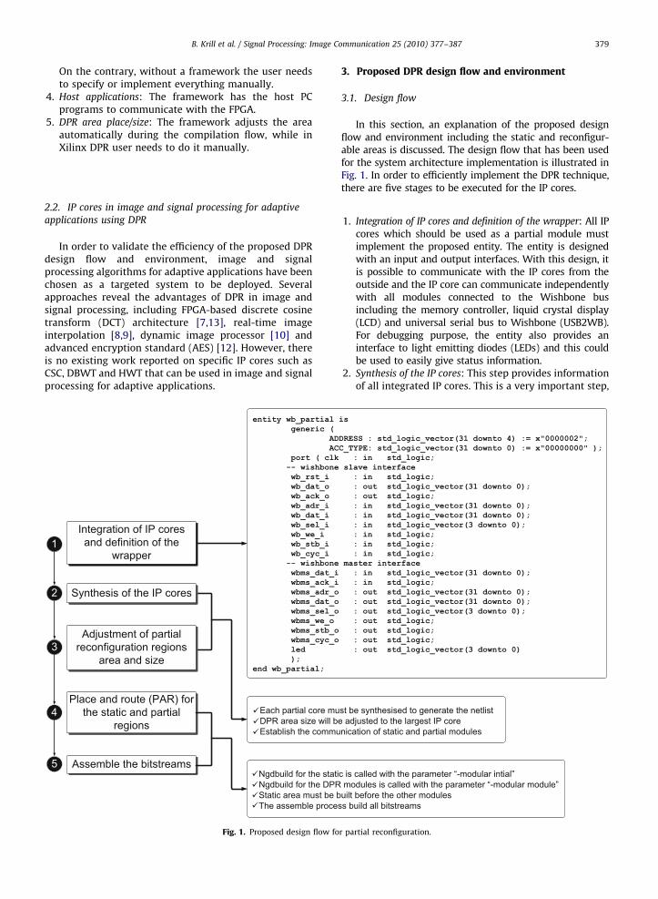
ARTICLE IN PRESS
B. Krill et al. / Signal Processing: Image Communication 25 (2010) 377–387 379
On the contrary, without a framework the user needsto specify or implement everything manually.
4.
Host applications: The framework has the host PCprograms to communicate with the FPGA.5.
DPR area place/size: The framework adjusts the areaautomatically during the compilation flow, while inXilinx DPR user needs to do it manually.2.2. IP cores in image and signal processing for adaptive
applications using DPR
In order to validate the efficiency of the proposed DPRdesign flow and environment, image and signalprocessing algorithms for adaptive applications have beenchosen as a targeted system to be deployed. Severalapproaches reveal the advantages of DPR in image andsignal processing, including FPGA-based discrete cosinetransform (DCT) architecture [7,13], real-time imageinterpolation [8,9], dynamic image processor [10] andadvanced encryption standard (AES) [12]. However, thereis no existing work reported on specific IP cores such asCSC, DBWT and HWT that can be used in image and signalprocessing for adaptive applications.
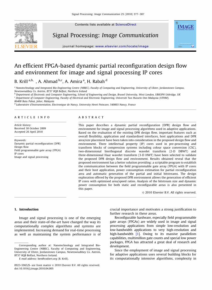
Fig. 1. Proposed design flow fo
3. Proposed DPR design flow and environment
3.1. Design flow
In this section, an explanation of the proposed designflow and environment including the static and reconfigur-able areas is discussed. The design flow that has been usedfor the system architecture implementation is illustrated inFig. 1. In order to efficiently implement the DPR technique,there are five stages to be executed for the IP cores.
1.
r pa
Integration of IP cores and definition of the wrapper: All IPcores which should be used as a partial module mustimplement the proposed entity. The entity is designedwith an input and output interfaces. With this design, itis possible to communicate with the IP cores from theoutside and the IP core can communicate independentlywith all modules connected to the Wishbone busincluding the memory controller, liquid crystal display(LCD) and universal serial bus to Wishbone (USB2WB).For debugging purpose, the entity also provides aninterface to light emitting diodes (LEDs) and this couldbe used to easily give status information.
2.
Synthesis of the IP cores: This step provides informationof all integrated IP cores. This is a very important step,rtial reconfiguration.
ARTICLE IN PRESS
B. Krill et al. / Signal Processing: Image Communication 25 (2010) 377–387380
since it provides the required area size of each module.Moreover, the generation of the netlists are performed.
3.
Adjustment of partial reconfiguration regions area and size:From step 2, all sizes of each IP core are given. This stepcollects all sizes and adjusts the partial reconfigurationarea to the biggest needed size. Moreover, it alsoconsiders all the resources needed such as slices, blockrandom access memory (BRAM) and digital signalprocessor (DSP) blocks. After all information is col-lected and processed, the required constraints areexported for the actual building/bitstream generation.4.
Place and route (PAR) for the static and partial regions: Inthis step, PAR is performed for the static and partialarea. The static area build has to be first executed andthe information of some routed signals are transferredto the partial module build. As described in theprevious step, the generated constraint informationof the partial area is applied.5.
Assemble the bitstreams: This step collects all buildnative circuit description (.ncd) files, the programs ‘‘PRverify design’’/‘‘PR assemble’’ are called, to verify thebuild and to extract the partial modules to generatethe partial bitstreams. Finally, the initial bitstream andall specified partial bitstreams are available.Fig. 3. Example of the program flow procedures.
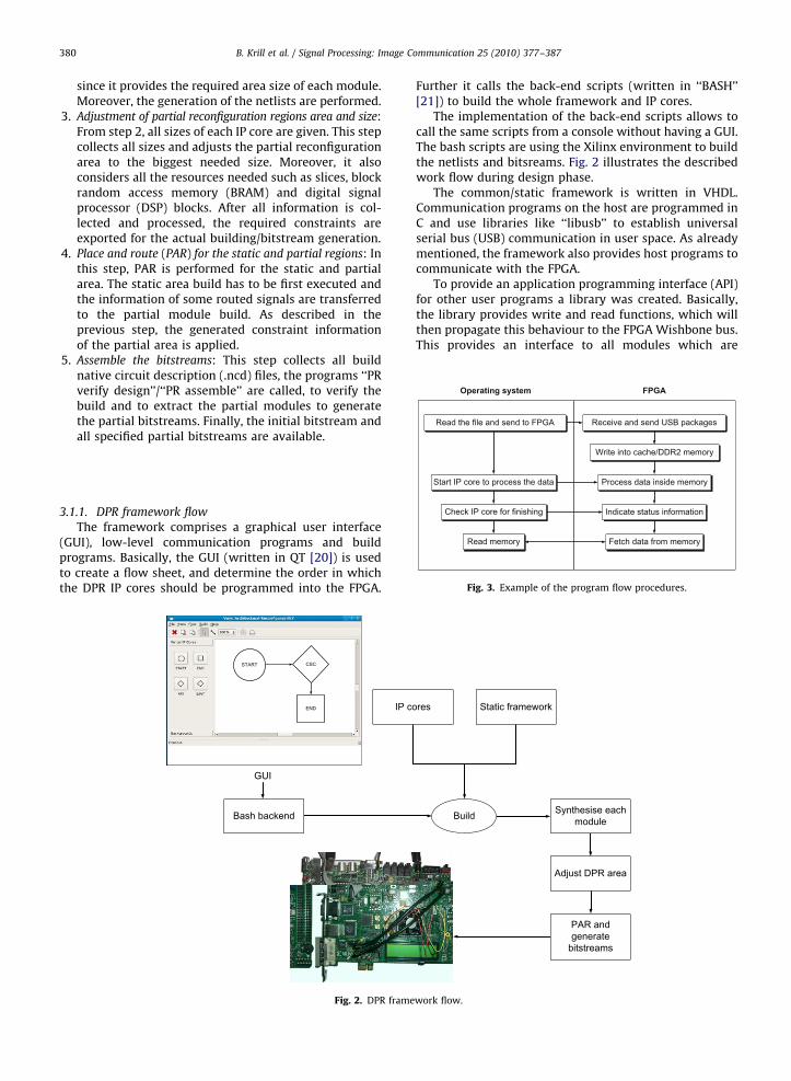
3.1.1. DPR framework flow
The framework comprises a graphical user interface(GUI), low-level communication programs and buildprograms. Basically, the GUI (written in QT [20]) is usedto create a flow sheet, and determine the order in whichthe DPR IP cores should be programmed into the FPGA.
Fig. 2. DPR frame
Further it calls the back-end scripts (written in ‘‘BASH’’[21]) to build the whole framework and IP cores.
The implementation of the back-end scripts allows tocall the same scripts from a console without having a GUI.The bash scripts are using the Xilinx environment to buildthe netlists and bitsreams. Fig. 2 illustrates the describedwork flow during design phase.
The common/static framework is written in VHDL.Communication programs on the host are programmed inC and use libraries like ‘‘libusb’’ to establish universalserial bus (USB) communication in user space. As alreadymentioned, the framework also provides host programs tocommunicate with the FPGA.
To provide an application programming interface (API)for other user programs a library was created. Basically,the library provides write and read functions, which willthen propagate this behaviour to the FPGA Wishbone bus.This provides an interface to all modules which are
work flow.

ARTICLE IN PRESS
B. Krill et al. / Signal Processing: Image Communication 25 (2010) 377–387 381
connected to the bus and the user can for example modifyconfigurations inside the IP core.
Fig. 3 shows an example of the program flow approach.At the beginning the user program reads a file and writesdata into FPGA double data rate (DDR2) memory. Afterfinishing writing data, it sends a signal to the FPGA toactivate the IP core in order to process the data insidememory. After data processing is completed, data can beread back from the memory.
4. Case study: IP cores for image and signal processingadaptive applications
4.1. Overview of an adaptive image and signal processing
applications
Fig. 4 illustrates an application where adaptivity isimportant, including the transform, quantisation andentropy coding blocks for a compression system. In eachblock, buffers have been used for storing intermediateresults to be processed.
Our goal is to propose an adaptive compression systemfor medical images, with all its blocks are reconfigurable.This paper focus only on the pre-processing and transformblocks. Hence, this was the main reason for selecting CSCand other transforms (2-D DBWT and 3-D HWT) tovalidate the proposed DPR design flow and environment.
The DPR is used because it allows to exchange the typeof algorithm (HWT, DBWT, etc.), thus making thearchitecture flexible. It also helps to examine the besttradeoffs between area, power consumption and hard-ware performance.
4.2. Proposed system architecture
The proposed system architecture as illustrated inFig. 5(a)–(e) is briefly explained, including the IP cores thathave been used, the top-level architecture of the proposedsystem environment and framework, architectures for theCSC and block diagrams for 2-D DBWT and 3-D HWT,respectively.
There are three areas in the system environment andarchitecture: application and operation system, static andreconfigurable areas. Fig. 5(b) illustrates the details of theworking system and the communication channel forhost-FPGA and different components.
The host part consists of command line tools andlow-level drivers that can be changed within the GUI.Current implementation system uses a USB connection to
Fig. 4. Proposed syste
the FPGA which could be exchanged by a peripheralcomponent interconnect express (PCI-E) connection.
The static area on the FPGA has been defined for allmodules, and it must be remained active during the FPGAduty cycle, while the reconfigurable area is used for the IPcores (CSC, 2-D DBWT and 3-D HWT). All used compo-nents are Wishbone bus compliant and connected via ashared bus interconnection.
4.2.1. Static area
The static area has been established for componentscommunication zone with memory controller interface,USB2WB interface, LCD visualisation, internal configura-tion access port (ICAP) and clock domain translation.
The memory controller interface provides a Wishboneconnection and translation to the Xilinx memory interfacegenerator (MIG) controller. Moreover, it provides a 256bytes cache to improve the read performance for accesseswithin a memory region. The core runs with a DDR2frequency of 133 MHz and an interface frequency of200 MHz which provides a non-cached read performanceof 256 MB/s and a write performance of 386 MB/s. TheUSB2WB interface is a component which is connected to aCypress EZ-host programmable embedded chip that hasbeen configured as a USB host/peripheral controller [22].
4.2.2. Reconfigurable area
The partial reconfiguration area has been declaredmainly for the IP cores that can be changed for the systemapplication. In order to accommodate with enough space/slices for the IP cores, the area size is calculated and it isalways defined based on the largest IP core. There are twoconnections that act as a slave and master to theWishbone bus. With these connectivities, the core canbe configured and performs read and write data operationfrom/to the memory controller.
4.2.3. Selected IP cores
1.
m a
CSC: Colour space is a technique to specify, create andvisualise colour. There are many existing colour spacesand the most popular models are RGB (used incomputer graphics), YIQ, YUV and YCrCb (used invideo systems) and CMYK (used in colour printing).RGB colour space is simple and uses three numericalcomponents to represent a colour and this colour spacecan be represented using a 3-D coordinate systemwhose axes correspond to the three components, R orRed, G or Green, and B or Blue.
pplications.

ARTICLE IN PRESS
Fig. 6. Block diagram for R0G0B0 2 Y 0CrCb.
On the other hand, Y0
CrCb is a scaled and offset version ofthe YUV colour space based on luminance and chromi-nance, which correspond to brightness and colour. In thiscolour space R
0
G0
B0
is separated into a luminance part (Y0
)and two chrominance parts (Cb and Cr). A general blockdiagram for R
0
G0
B0
2 Y0
CrCb is shown in Fig. 6.The CSC IP core that has been used in this DPRenvironment is based on distributed arithmetic (DA)principles [23] and its architecture is shown in Fig. 5(c).
DA provides an efficient method of computing vectormultiplication by means of bit-level rearrangement of themultiply accumulate process, and it is called as ROM-based DA method. It decomposes the variable input of theinner product to bit-level in order to generate pre-computed data.The basic operations required for performing DA-basedinner product are a sequence of ROM look up table,addition, subtraction and shift operations of the input datasequence.
2.
DBWT: Discrete wavelet transform (DWT) plays asignificant role in image and signal processing applica-tions as an alternative to classical time frequencyrepresentation techniques such as the discrete Fouriertransform (DFT) and DCT [24].With its multi-resolution characteristics and capabilityto represent real life non-stationary signals such asimage and speech, DWT has attracted a great deal ofresearch and development.The 2-D DWT is a multi-level decomposition techniquewhich provides an efficient analysis method of signalsat different frequency bands and the block diagramsfor both separable and non-separable 2-D DWT aredepicted in Fig. 5(d). Each decomposition level j can beseen as the further decomposition of a 2-D data setIj � 1 (having Nj�1 � Nj�1 samples) into four sub-bandsLLj; LHi; HLj and HHj (each having Nj � 1/2 samples,where N is input data/samples) [25].
ARTICLE IN PRESS
B. Krill et al. / Signal Processing: Image Communication 25 (2010) 377–387 383
3.
3-D HWT: As the simplest wavelet transform, the Haarwavelet chaar , is discontinuous, symmetric wavelet inthe Daubechies family, and the only one which has anexplicit expression. The scale function fhaar is a simpleaverage function. The wavelet and the scale functionscan be expressed as follows:chaarðtÞ ¼
1 if 0rto1
2
�1 if1
2rto1
0 otherwise
8>>>><>>>>:
ð1Þ
fhaarðtÞ ¼1 8 0rto1
0 otherwise
�ð2Þ
In addition, the HWT wavelet is simple and computa-tionally cheap because it can be implemented by a fewinteger additions, subtractions, and shift operations [26].The mathematical features of the basis are as follows: themost simplistic wavelet basis can be implemented usingpairwise averaging and differencing, both unitary andorthogonal, and also it has compact support. Therefore,this wavelet basis is by no means the most suitable toachieve close to optimal compression performance inimage compression systems application.Fig. 5(e) shows a block diagram of the 3-D HWT IP corewith transpose based computation that has been used asa one of the IP cores in this DPR design flow andenvironment.
5. Experimental results and analysis
Fig. 7 illustrates the partial reconfiguration design flowof the framework. Action points 1–3 have to be done once,since the framework specifies the top-level design.Currently, the user does not have the capability tochange the top-level design. Points 4 and 5 areperformed automatically by the framework during thebuild process. The size will be adjusted to the biggest IPcore used. Depending on the size of the DPR area the busmacros are placed at the edges of the area. The proposedframework specifies an interface which provides a readand write connection to the Wishbone bus. This givesopportunities to read from the core or the core can writeto the Wishbone bus.
The current design flow for partial reconfiguration byXilinx uses a module-based DPR which requires busmacros to integrate the static and partial areas [27].Configuration frames are reconfigured and bus macros areused to connect the DPR areas with the static area [18].
Another solution is presented in [28] withdirect bitstream manipulation. In order to locate thecomponents such as configurable logic blocks (CLBs) andblock random access memory (BRAMs) inside thebitstream, equations are required. However, this solutionis currently only applicable for Virtex-II FPGA devices.
A hierarchical analysis tool offered by Xilinx PlanAhead[29] has been discussed in [30] and the design flowrequires manual placement of the partial area and busmacros, hence lead to a complex design flow and systemimplementation.
On the contrary, the proposed DPR environmentpresented in this paper provides the followingadvantages:
1.
It has a scriptable program to establish a communica-tion of the FPGA with the IP cores and their application.It also capable to avoid user-errors in bus macroplacement and partial area selection.2.
It can calculates and estimates the power consumptionfor partial reconfiguration area based on the presentedequation in Section 5.2.3.
It provides an automation in generating the partial andinitial bitstream files.5.1. Bitstream utilisation
An evaluation of the proposed DPR environment withthree IP cores gives an information of the generatedbitstream file and configuration sizes. Fig. 8 illustrates therelationship of the bitstreams generated with thecomponents used including the CLBs, RAMB36, DSP48Eand input/output (I/O). These information are used duringthe internal calculation of the bitstream size andreconfiguration time of each IP core. In order to reducethe generated bitstream size, the proposed design flowalso provides an information of available components aswell as the suitable area to be located.
The interface that has been used for the partial arearequires a minimum of 12 CLBs. This is due to the fact thatin one CLB, there are two bus macros with four inputs/outputs. Bus macro is needed to establish the connectionof static and partial areas. The number of CLBs iscalculated by 32 bits data in/out buses, 32 bits addressbuses and eight control signals. In order to use DDR2memory, a minimum of 25 CLBs is also required. It isworth mentioning that the partial reconfiguration isperformed in frames and the minimum frame in Virtex-5 devices is defined by 20 CLBs and a bitstream for bothbuses has a minimum size of 153 kBytes.
5.2. Dynamic area utilisation
The framework adjusts the dynamic area automatically.During the build process, the log files of all used partialmodules are analysed and the required logic size isextracted. The area will be adjusted to the biggest logic sizeneeded. The constraint file that specifies the DPR area willthen be rewritten with new values.
The total usage power of an FPGA device can bedefined as the total of static (StP) and dynamic (DP) power[31]. StP is inherently dependent on the architecturallayout of the FPGA itself and it is technology dependent.For the case of Xilinx SRAM FPGAs, DP is classified intoclock, signal, logic, input and output power and can bedefined as follows:
DP ¼X
i
Ci � V2i � f ð3Þ
where C is the capacitance of the node, V is the corevoltage and f is defined as switching frequency. In this

ARTICLE IN PRESS
Fig. 7. Partial reconfiguration design flow. (a) Steps for partial design flow. (b) Define static and reconfigurable modules.
0
200000
400000
600000
800000
1e+06
1.2e+06
0 5 10 15 20 25 30 35 40
Bitf
ile s
ize
(Byt
es)
Component Count
SLICERAMB36DSP48E
IO
Fig. 8. Bitstream utilisation.
B. Krill et al. / Signal Processing: Image Communication 25 (2010) 377–387384
work, power components including logic, hardcore (likeBRAM), signal and clock are considered relevant. Theframework does not support the use of I/O componentsinside the partial reconfiguration area, so these compo-nents are ignored in the calculation.
Eq. (4) gives an average calculation of DP for a givenarea, where the sum of dynamic clock power (DPc) reflectsthe power used by CLBs and hardcores, while ci impliesthe components count. The arithmetic mean of all CLBs,inputs and outputs (DPio) provides an estimation of the

ARTICLE IN PRESS
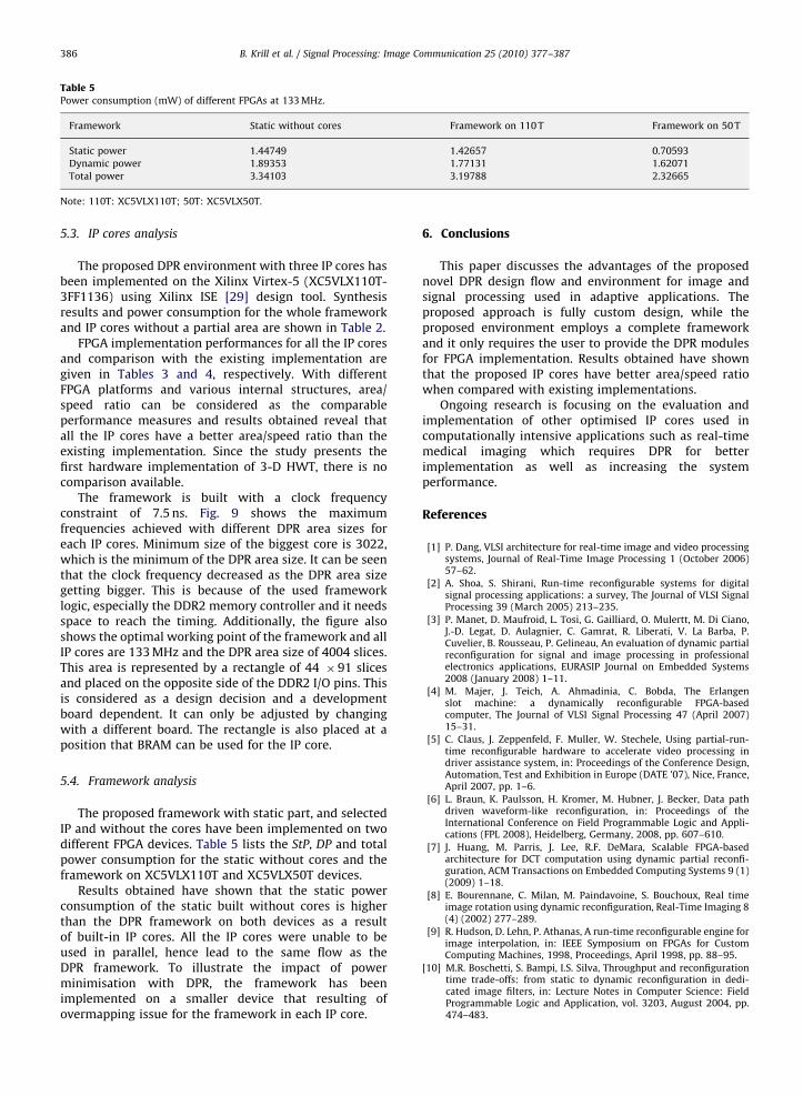
Table 5Power consumption (mW) of different FPGAs at 133 MHz.
Framework Static without cores Framework on 110 T Framework on 50 T
Static power 1.44749 1.42657 0.70593
Dynamic power 1.89353 1.77131 1.62071
Total power 3.34103 3.19788 2.32665
Note: 110T: XC5VLX110T; 50T: XC5VLX50T.
B. Krill et al. / Signal Processing: Image Communication 25 (2010) 377–387386
5.3. IP cores analysis
The proposed DPR environment with three IP cores hasbeen implemented on the Xilinx Virtex-5 (XC5VLX110T-3FF1136) using Xilinx ISE [29] design tool. Synthesisresults and power consumption for the whole frameworkand IP cores without a partial area are shown in Table 2.
FPGA implementation performances for all the IP coresand comparison with the existing implementation aregiven in Tables 3 and 4, respectively. With differentFPGA platforms and various internal structures, area/speed ratio can be considered as the comparableperformance measures and results obtained reveal thatall the IP cores have a better area/speed ratio than theexisting implementation. Since the study presents thefirst hardware implementation of 3-D HWT, there is nocomparison available.
The framework is built with a clock frequencyconstraint of 7.5 ns. Fig. 9 shows the maximumfrequencies achieved with different DPR area sizes foreach IP cores. Minimum size of the biggest core is 3022,which is the minimum of the DPR area size. It can be seenthat the clock frequency decreased as the DPR area sizegetting bigger. This is because of the used frameworklogic, especially the DDR2 memory controller and it needsspace to reach the timing. Additionally, the figure alsoshows the optimal working point of the framework and allIP cores are 133 MHz and the DPR area size of 4004 slices.This area is represented by a rectangle of 44 �91 slicesand placed on the opposite side of the DDR2 I/O pins. Thisis considered as a design decision and a developmentboard dependent. It can only be adjusted by changingwith a different board. The rectangle is also placed at aposition that BRAM can be used for the IP core.
5.4. Framework analysis
The proposed framework with static part, and selectedIP and without the cores have been implemented on twodifferent FPGA devices. Table 5 lists the StP, DP and totalpower consumption for the static without cores and theframework on XC5VLX110T and XC5VLX50T devices.
Results obtained have shown that the static powerconsumption of the static built without cores is higherthan the DPR framework on both devices as a resultof built-in IP cores. All the IP cores were unable to beused in parallel, hence lead to the same flow as theDPR framework. To illustrate the impact of powerminimisation with DPR, the framework has beenimplemented on a smaller device that resulting ofovermapping issue for the framework in each IP core.
6. Conclusions
This paper discusses the advantages of the proposednovel DPR design flow and environment for image andsignal processing used in adaptive applications. Theproposed approach is fully custom design, while theproposed environment employs a complete frameworkand it only requires the user to provide the DPR modulesfor FPGA implementation. Results obtained have shownthat the proposed IP cores have better area/speed ratiowhen compared with existing implementations.
Ongoing research is focusing on the evaluation andimplementation of other optimised IP cores used incomputationally intensive applications such as real-timemedical imaging which requires DPR for betterimplementation as well as increasing the systemperformance.
References
[1] P. Dang, VLSI architecture for real-time image and video processingsystems, Journal of Real-Time Image Processing 1 (October 2006)57–62.
[2] A. Shoa, S. Shirani, Run-time reconfigurable systems for digitalsignal processing applications: a survey, The Journal of VLSI SignalProcessing 39 (March 2005) 213–235.
[3] P. Manet, D. Maufroid, L. Tosi, G. Gailliard, O. Mulertt, M. Di Ciano,J.-D. Legat, D. Aulagnier, C. Gamrat, R. Liberati, V. La Barba, P.Cuvelier, B. Rousseau, P. Gelineau, An evaluation of dynamic partialreconfiguration for signal and image processing in professionalelectronics applications, EURASIP Journal on Embedded Systems2008 (January 2008) 1–11.
[4] M. Majer, J. Teich, A. Ahmadinia, C. Bobda, The Erlangenslot machine: a dynamically reconfigurable FPGA-basedcomputer, The Journal of VLSI Signal Processing 47 (April 2007)15–31.
[5] C. Claus, J. Zeppenfeld, F. Muller, W. Stechele, Using partial-run-time reconfigurable hardware to accelerate video processing indriver assistance system, in: Proceedings of the Conference Design,Automation, Test and Exhibition in Europe (DATE ’07), Nice, France,April 2007, pp. 1–6.
[6] L. Braun, K. Paulsson, H. Kromer, M. Hubner, J. Becker, Data pathdriven waveform-like reconfiguration, in: Proceedings of theInternational Conference on Field Programmable Logic and Appli-cations (FPL 2008), Heidelberg, Germany, 2008, pp. 607–610.
[7] J. Huang, M. Parris, J. Lee, R.F. DeMara, Scalable FPGA-basedarchitecture for DCT computation using dynamic partial reconfi-guration, ACM Transactions on Embedded Computing Systems 9 (1)(2009) 1–18.
[8] E. Bourennane, C. Milan, M. Paindavoine, S. Bouchoux, Real timeimage rotation using dynamic reconfiguration, Real-Time Imaging 8(4) (2002) 277–289.
[9] R. Hudson, D. Lehn, P. Athanas, A run-time reconfigurable engine forimage interpolation, in: IEEE Symposium on FPGAs for CustomComputing Machines, 1998, Proceedings, April 1998, pp. 88–95.
[10] M.R. Boschetti, S. Bampi, I.S. Silva, Throughput and reconfigurationtime trade-offs: from static to dynamic reconfiguration in dedi-cated image filters, in: Lecture Notes in Computer Science: FieldProgrammable Logic and Application, vol. 3203, August 2004, pp.474–483.

ARTICLE IN PRESS
B. Krill et al. / Signal Processing: Image Communication 25 (2010) 377–387 387
[11] Y.-J. Oh, H. Lee, C.-H. Lee, Dynamic partial reconfigurable FIR filterdesign, in: Lecture Notes in Computer Science: ReconfigurableComputing: Architectures and Applications, vol. 3985, August 2006,pp. 30–35.
[12] Z.E.A.A. Ismaili, A. Moussa, Self-partial and dynamic reconfigurationimplementation for AES using FPGA, IJCSI International Journal ofComputer Science Issues 2 (August 2009) 33–40.
[13] J. Gause, P.Y.K. Cheung, W. Luk, Static and dynamic reconfigurabledesigns for a 2D shape-adaptive DCT, in: FPL ’00: Proceedings of theThe Roadmap to Reconfigurable Computing, 10th InternationalWorkshop on Field-Programmable Logic and Applications, Spring-er-Verlag, London, UK, 2000, pp. 96–105.
[14] C. Ibala, K. Arshak, Using dynamic partial reconfiguration approachto read sensor with different bus protocol, in: Sensors ApplicationsSymposium, 2009, SAS 2009, IEEE, February 2009, pp. 175–179.
[15] E. McDonald, Runtime FPGA partial reconfiguration, in: AerospaceConference, 2008 IEEE, New Orleans, LA, March 2008, pp. 1–7.
[16] Two flows for partial reconfiguration: module based ordifference based, Xilinx Inc. XAPP290 Version 1.1, Technical Report,2003.
[17] Two flows for partial reconfiguration: module based or differencebased, Xilinx Inc. XAPP290 Version 1.2, Technical Report, 2004.
[18] P. Lysaght, B. Blodget, J. Mason, J. Young, B. Bridgford, Invited paper:enhanced architectures, design methodologies and CAD tools fordynamic reconfiguration of Xilinx FPGAs, in: International Con-ference on Field Programmable Logic and Applications, 2006, FPL’06, August 2006, pp. 1–6.
[19] A. Mitra, Z. Guo, A. Banerjee, W. Najjar, Dynamic co-processorarchitecture for software acceleration on CSoCs, in: InternationalConference on Computer Design, 2006, ICCD 2006, October 2006,pp. 127–133.
[20] [Online]. Available: /http://qt.nokia.comS.[21] [Online]. Available: /http://en.wikipedia.org/wiki/BashS.[22] EZ-host programmable embedded USB host/peripheral controller,
Cypress Semiconductor Corporation, Technical Report, 2003.
[23] F. Bensaali, A. Amira, Accelerating colour space conversion onreconfigurable hardware, Journal of Image and Vision Computing23 (11) (2005) 935–942.
[24] S.G. Mallat, A theory for multiresolution signal decomposition: thewavelet representation, IEEE Transactions on Pattern Analysis andMachine Intelligence 11 (1989) 674–693.
[25] I.S. Uzun, A. Amira, Real-time 2-D wavelet transform implementa-tion for HDTV compression, Journal of Real-Time Imaging—SpectralImaging II 11 (2) (2005) 151–165.
[26] C. Bajaj, I. Ihm, S. Park, 3D RGB image compression for interactiveapplications, ACM Transactions on Graphics 20 (1) (January 2001)10–38.
[27] Partial reconfiguration design with PlanAhead, Xilinx Inc., TechnicalReport, 2008.
[28] Y.E. Krasteva, E. de la Torre, T. Riesgo, D. Joly, Virtex II FPGAbitstream manipulation: application to reconfiguration controlsystems, in: International Conference on Field Programmable Logicand Applications, 2006, FPL ’06, August 2006, pp. 1–4.
[29] [Online]. Available: /http://www.xilinx.comS.[30] K. Arshak, E. Jafer, C. Ibala, Improving the performance of an FPGA
based model design for sensor monitoring using PlanAhead tool, in:Proceedings of the 2006 IEEE International Behavioral Modelingand Simulation Workshop, September 2006, pp. 91–96.
[31] R. Fischer, K. Buchenrieder, U. Nageldinger, Reducing the powerconsumption of FPGAs through retiming, in: 12th IEEE Interna-tional Conference and Workshops on the Engineering of Computer-Based Systems, 2005, ECBS ’05, April 2005, pp. 89–94.
[32] I. Uzun, A. Amira, Rapid prototyping—framework for FPGA-baseddiscrete biorthogonal wavelet transforms implementation, IEEProceedings Vision Image and Signal Processing 153 (6) (December2006) 721–734.
[33] F. Bensaali, A. Amira, Design and efficient FPGA implementation ofan RGB to YCrCb color space converter using distributed arithmetic,in: Lecture Notes in Computer Science: Field Programmable Logicand Application, vol. 3203, August 2004, pp. 991–995.