Dynamical observations on the crack tip zone and stress ...
7
ARTICLE Received 19 Jul 2016 | Accepted 29 Nov 2016 | Published 18 Jan 2017 Dynamical observations on the crack tip zone and stress corrosion of two-dimensional MoS 2 Thuc Hue Ly 1 , Jiong Zhao 1 , Magdalena Ola Cichocka 1,2,w , Lain-Jong Li 3 & Young Hee Lee 1,2 Whether and how fracture mechanics needs to be modified for small length scales and in systems of reduced dimensionality remains an open debate. Here, employing in situ transmission electron microscopy, atomic structures and dislocation dynamics in the crack tip zone of a propagating crack in two-dimensional (2D) monolayer MoS 2 membrane are observed, and atom-to-atom displacement mapping is obtained. The electron beam is used to initiate the crack; during in situ observation of crack propagation the electron beam effect is minimized. The observed high-frequency emission of dislocations is beyond previous understanding of the fracture of brittle MoS 2 . Strain analysis reveals dislocation emission to be closely associated with the crack propagation path in nanoscale. The critical crack tip plastic zone size of nearly perfect 2D MoS 2 is between 2 and 5 nm, although it can grow to 10 nm under corrosive conditions such as ultraviolet light exposure, showing enhanced dislocation activity via defect generation. DOI: 10.1038/ncomms14116 OPEN 1 IBS Center for Integrated Nanostructure Physics (CINAP), Institute for Basic Science, Sungkyunkwan University, Suwon 440-746, Korea. 2 Department of Energy Science, Sungkyunkwan University, Suwon 440-746, Korea. 3 Physical Sciences and Engineering, King Abdullah University of Science and Technology, Thuwal 23955-6900, Saudi Arabia. w Present address: Berzelii Center EXSELENTon Porous Materials and Inorganic and Structural Chemistry, Department of Materials and Environmental Chemistry, Stockholm University, Stockholm, SE-10691, Sweden. Correspondence and requests for materials should be addressed to J.Z. (email: [email protected]) or to Y.H.L. (email: [email protected]). NATURE COMMUNICATIONS | 8:14116 | DOI: 10.1038/ncomms14116 | www.nature.com/naturecommunications 1
-
Upload
khangminh22 -
Category
Documents
-
view
0 -
download
0
Transcript of Dynamical observations on the crack tip zone and stress ...

ARTICLE
Received 19 Jul 2016 | Accepted 29 Nov 2016 | Published 18 Jan 2017
Dynamical observations on the crack tip zoneand stress corrosion of two-dimensional MoS2Thuc Hue Ly1, Jiong Zhao1, Magdalena Ola Cichocka1,2,w, Lain-Jong Li3 & Young Hee Lee1,2
Whether and how fracture mechanics needs to be modified for small length scales and
in systems of reduced dimensionality remains an open debate. Here, employing in situ
transmission electron microscopy, atomic structures and dislocation dynamics in the crack tip
zone of a propagating crack in two-dimensional (2D) monolayer MoS2 membrane are
observed, and atom-to-atom displacement mapping is obtained. The electron beam is used to
initiate the crack; during in situ observation of crack propagation the electron beam effect is
minimized. The observed high-frequency emission of dislocations is beyond previous
understanding of the fracture of brittle MoS2. Strain analysis reveals dislocation emission to
be closely associated with the crack propagation path in nanoscale. The critical crack tip
plastic zone size of nearly perfect 2D MoS2 is between 2 and 5 nm, although it can grow to
10 nm under corrosive conditions such as ultraviolet light exposure, showing enhanced
dislocation activity via defect generation.
DOI: 10.1038/ncomms14116 OPEN
1 IBS Center for Integrated Nanostructure Physics (CINAP), Institute for Basic Science, Sungkyunkwan University, Suwon 440-746, Korea. 2 Department ofEnergy Science, Sungkyunkwan University, Suwon 440-746, Korea. 3 Physical Sciences and Engineering, King Abdullah University of Science and Technology,Thuwal 23955-6900, Saudi Arabia. w Present address: Berzelii Center EXSELENTon Porous Materials and Inorganic and Structural Chemistry, Department ofMaterials and Environmental Chemistry, Stockholm University, Stockholm, SE-10691, Sweden. Correspondence and requests for materials should beaddressed to J.Z. (email: [email protected]) or to Y.H.L. (email: [email protected]).
NATURE COMMUNICATIONS | 8:14116 | DOI: 10.1038/ncomms14116 | www.nature.com/naturecommunications 1

Fracture is a process relevant to many kinds of applications ofmaterials. Competition between two modes, namely, thecrystal plane cleavage and dislocation nucleation at the crack
tip, is the main factor governing the ductile or brittle behaviour ofcrystals1,2. Since the establishment of the well-known Griffithmodel3, it has been questioned whether linear elastic fracturemechanics hold true in the crack tip down to all length scalesand, specifically, whether it holds true for recently developedtwo-dimensional (2D) materials4,5 is debatable.
Direct electron microscopy observations of crack tips inceramic materials such as Si, SiC and Al2O3 show perfect fringelattices at the vicinity of the crack tips, and confirmed the absenceof dislocations6. The revealed atomic sharpness at the crack tipwithout any blunting process is a signature of pure brittleness.Recently, 2D materials such as graphene and transition metaldichalcogenide (TMD) come into view for the realization infabrication and for their exceptional physical properties7. Inparticular, in the monolayer form, they only consist of one atom(such as graphene) to three atoms (such as TMD) in thickness.The basal plane (intralayer) fracture of the bulk type covalent-bonding graphite or 2h-molybdenite (hexagonal MoS2, todifferentiate from the tetragonal phase) is purely brittle at roomtemperature8, and their fracture toughness GIC equals to 2g,where g is the surface energy per unit area8. Indentation testsusing atomic force microscopy on monolayer graphene4,9 andmonolayer hexagonal(h)-MoS2 (ref. 5) have demonstrated ultra-high strength that is close to the theoretical limit, followed bycatastrophic failure, and transmission electron microscopy (TEM)could distinguish the transgranular fracture from intragranularfracture; however, no atomistic information was given9.The fracture toughness of monolayer graphene was quanti-tatively measured by in situ TEM with supportive moleculardynamics simulations, suggesting pure brittleness10. The cracks inmonolayer graphene are along the preferable zigzag edge11.Meanwhile, several types of basal plane dislocations, or‘zero-dimensional’ dislocations, can emerge and are mobile ingraphene or TMD12–14, especially at high temperature or underelectron beam irradiation, indicative of the easier dislocationdynamics in 2D form than in bulk.
It is expected that the defect-free nature and high strength in2D4,5 may provide a higher chance to achieve the onset ofplasticity, but on the other hand, most molecular dynamicssimulations show that the fracture of graphene as well as MoS2 isbrittle15,16. To understand the atomistic features when fractureoccurs in 2D materials, a direct observation of the crackingprocess at the crack tip is necessary from the viewpoint of basicphysics and practical use. Previous work by in situ TEM demon-strated the capability of dynamical atomic-scale observations onthe sublimation and cracking process of few layer graphene17 ormonolayer graphene17. Moreover, environment-assisted crackingin MoS2 also needs to be investigated and compared withpure cracking that is of particular importance in real-worldapplications. The environmental susceptibility of MoS2 has drawnmuch attention18 that would have significant influence on theirphysical properties19.
Here, by using in situ transmission electron microscopy toresolve the atomic structures, we directly observed the limitedplastic behaviour at the forefront of a singular crack tip ofmonolayer h-MoS2. The cracks can be initialized at holes, andelectron beam damage and especially creation of sulfur vacancieswas carefully suppressed to ensure the crack propagation is closeto pure mechanical loading. The emission, glide and climb of thedislocations that can influence the propagation of the cracks werecaptured. High-quality MoS2 monolayer samples with 1% sulfurdeficiencies have around 2–5 nm size plastic zone (dislocationdistributed area) near the crack tip in vacuum and extends
to 5–10 nm under corrosive environments. Our results alsosuggest that the specific 2D geometry improves ductility, incombination with the reported ultrahigh strength of 2Dgraphene4 or MoS2 (ref. 5), creating potential applications forthese materials.
ResultsSample preparation and introduction of cracks. The monolayerMoS2 samples were grown on sapphire using chemical vapourdeposition20, and then transferred to TEM grids using thepolymethyl methacrylate (PMMA) method as a free-standingsheet21. Excellent quality of the as-grown MoS2 crystal wasconfirmed by TEM (Supplementary Fig. 1), revealing the sulfurdeficiencies lower than 1% (Supplementary Table 1).Owing to the high specific surface area, it was inevitable thatsome organic adsorbents remained on the sample surfaceafter transfer (Supplementary Fig. 2). Absorbents on the MoS2surface can be activated and evaporated gradually by electronbeam irradiation. From a mechanical point of view, theseloosely contacting adsorbents can stabilize the 2D samples inthe cracking process that we will discuss later. The vacuumin the JEOL ARM-200F TEM is 42� 10� 5 Pa and all TEMmeasurements were conducted at room temperature under 80 kV.During the in situ observation of cracking, the electron beam waskept sufficiently low or entirely turned off and only turned on(beam intensity 0.01 pAnm� 2) for taking images with a shortexposure time (0.32 s; see Supplementary Fig. 1 and Supple-mentary Table 1 for more defect analysis in MoS2 in allexperimental conditions). The occurrence of the beam damageon MoS2 requires much higher beam intensity (SupplementaryFig. 1)22.
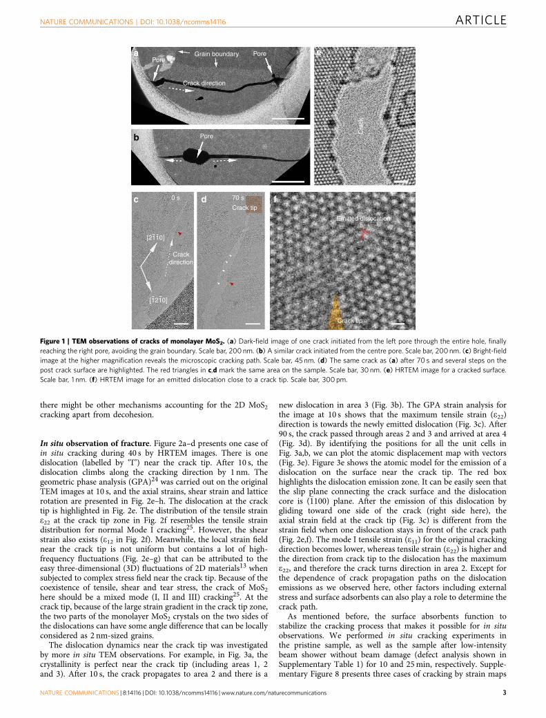
According to the criterion of continuum fracture mechanics, acrack starts to grow when the maximum stress intensity (K) onthe sample exceeds the critical stress intensity factor (Kc, fracturetoughness). We confirmed that crack propagation is preferablyinitiated at some pores (either in pristine samples or newlycreated by condensed electron beam; see dark-field (DF) TEMimages in Fig. 1a,b) that is congruent with the fact that the stressintensity factor is proportional to the square root of thedimension of defects3. The cracks can quickly run through theentire sampling area (suspended on 1 mm holes of the TEM grid,Fig.1a,b), or can stop in the centre because of relaxation ofstresses and stabilization by adsorbents (Supplementary Fig. 3).We also note that the crack does not usually follow the grainboundaries (Fig. 1a), similar to previous findings8. In thefollowing part, our discussion will be restricted to intragranularcracking.
Figure 1c,d presents two snapshots of cracking during 70 s.Generally, straight cracking surfaces can be seen, whereas thecleavage plane of monolayer MoS2 is determined by diffractionas the close-packed 01�10f g planes or a zigzag edge. The high-resolution transmission electron microscopy (HRTEM) image ofthe post cracking surfaces shows the two opposite S-terminatededge and Mo-terminated edge by direct decohesion (Supple-mentary Figure 4). Owing to the tensile stress direction notbeing exactly perpendicular to any cleavage plane, the nominalcracking direction is between [2�1�10] and [1�210] (Fig. 1c–e,and Supplementary Fig. 5). In addition to these proofs ofbrittleness, we also found some irregular steps or defective sites(highlighted by white triangles in Fig. 1d) on the crack surfaces.More importantly, dislocations that are absent in the pristinesample can be seen by HRTEM close to the crack tip (Fig. 1f).This dislocation structure consists of 4–6 cores with Burgersvector 1
3 1�210½ � (Supplementary Fig. 6), and dislocation cores inMoS2 may have more types23. These phenomena suggest that
ARTICLE NATURE COMMUNICATIONS | DOI: 10.1038/ncomms14116
2 NATURE COMMUNICATIONS | 8:14116 | DOI: 10.1038/ncomms14116 | www.nature.com/naturecommunications
there might be other mechanisms accounting for the 2D MoS2cracking apart from decohesion.
In situ observation of fracture. Figure 2a–d presents one case ofin situ cracking during 40 s by HRTEM images. There is onedislocation (labelled by ‘T’) near the crack tip. After 10 s, thedislocation climbs along the cracking direction by 1 nm. Thegeometric phase analysis (GPA)24 was carried out on the originalTEM images at 10 s, and the axial strains, shear strain and latticerotation are presented in Fig. 2e–h. The dislocation at the cracktip is highlighted in Fig. 2e. The distribution of the tensile straine22 at the crack tip zone in Fig. 2f resembles the tensile straindistribution for normal Mode I cracking25. However, the shearstrain also exists (e12 in Fig. 2f). Meanwhile, the local strain fieldnear the crack tip is not uniform but contains a lot of high-frequency fluctuations (Fig. 2e–g) that can be attributed to theeasy three-dimensional (3D) fluctuations of 2D materials13 whensubjected to complex stress field near the crack tip. Because of thecoexistence of tensile, shear and tear stress, the crack of MoS2here should be a mixed mode (I, II and III) cracking25. At thecrack tip, because of the large strain gradient in the crack tip zone,the two parts of the monolayer MoS2 crystals on the two sides ofthe dislocations can have some angle difference that can be locallyconsidered as 2 nm-sized grains.
The dislocation dynamics near the crack tip was investigatedby more in situ TEM observations. For example, in Fig. 3a, thecrystallinity is perfect near the crack tip (including areas 1, 2and 3). After 10 s, the crack propagates to area 2 and there is a
new dislocation in area 3 (Fig. 3b). The GPA strain analysis forthe image at 10 s shows that the maximum tensile strain (e22)direction is towards the newly emitted dislocation (Fig. 3c). After90 s, the crack passed through areas 2 and 3 and arrived at area 4(Fig. 3d). By identifying the positions for all the unit cells inFig. 3a,b, we can plot the atomic displacement map with vectors(Fig. 3e). Figure 3e shows the atomic model for the emission of adislocation on the surface near the crack tip. The red boxhighlights the dislocation emission zone. It can be easily seen thatthe slip plane connecting the crack surface and the dislocationcore is (�1100) plane. After the emission of this dislocation bygliding toward one side of the crack (right side here), theaxial strain field at the crack tip (Fig. 3c) is different from thestrain field when one dislocation stays in front of the crack path(Fig. 2e,f). The mode I tensile strain (e11) for the original crackingdirection becomes lower, whereas tensile strain (e22) is higher andthe direction from crack tip to the dislocation has the maximume22, and therefore the crack turns direction in area 2. Except forthe dependence of crack propagation paths on the dislocationemissions as we observed here, other factors including externalstress and surface adsorbents can also play a role to determine thecrack path.
As mentioned before, the surface absorbents function tostabilize the cracking process that makes it possible for in situobservations. We performed in situ cracking experiments inthe pristine sample, as well as the sample after low-intensitybeam shower without beam damage (defect analysis shown inSupplementary Table 1) for 10 and 25min, respectively. Supple-mentary Figure 8 presents three cases of cracking by strain maps
Emitted dislocation
Crack tip
0 s
Crackdirection
Crack tip
Cra
ck
70 s
Pore
PoreGrain boundary
Crack direction
Pore
[2110]
[1210]
a
b
e
fc d
Figure 1 | TEM observations of cracks of monolayer MoS2. (a) Dark-field image of one crack initiated from the left pore through the entire hole, finally
reaching the right pore, avoiding the grain boundary. Scale bar, 200nm. (b) A similar crack initiated from the centre pore. Scale bar, 200nm. (c) Bright-field
image at the higher magnification reveals the microscopic cracking path. Scale bar, 45 nm. (d) The same crack as (a) after 70 s and several steps on the
post crack surface are highlighted. The red triangles in c,d mark the same area on the sample. Scale bar, 30 nm. (e) HRTEM image for a cracked surface.
Scale bar, 1 nm. (f) HRTEM image for an emitted dislocation close to a crack tip. Scale bar, 300 pm.
NATURE COMMUNICATIONS | DOI: 10.1038/ncomms14116 ARTICLE
NATURE COMMUNICATIONS | 8:14116 | DOI: 10.1038/ncomms14116 | www.nature.com/naturecommunications 3

corresponding to the three conditions. The amount of absorbentson the MoS2 surface is reduced by increasing time of beamshower, confirmed by the direct TEM observations (Supple-mentary Figure 7). Mode I tensile strain (e22) decreases with lessamount of absorbents (Supplementary Fig. 8), in agreement to the
greater stabilization effect by more amount of absorbents. Thestatistics on the cracking speed and emitted dislocation densityper unit length of crack is presented in Supplementary Table 2.Smaller absorbents on the sample generate larger number ofdislocations. The reason for this is that larger strain at the crack
Atomic model
Climb
10 s0 s
Image simulationEmitted dislocation
Crack tip
10 s 10 s
10 s10 s
40 s25 s
Rotation
10%
–10%
ε11
ε12
ε22a
c d
e f
g h
b
Figure 2 | In situ TEM series revealing crack propagation and dislocation climb. (a–d) The in situ TEM image series showing a crack propagation at 0, 10,
25 and 40 s. All the images are aligned to show the same area (drift compensation) by aligning far-field less strain zones. Cracks are highlighted within the
white-dashed lines in the lower right corners. The atomic models for perfect MoS2 and multislice TEM image simulations of the atomic model
corresponding to experimental TEM conditions are shown in the inset of a. The electron beam was turned off during the cracking process but only turned
on to take images (exposure time 0.32 s), to exclude additional electron beam effect on the cracking. There is one edge dislocation at 0 s, highlighted by ‘T’.
It starts to climb because of the stress of the crack tip at 10 s, and disappears at 40 s when the crack extends further. Scale bar (a), 1 nm. (e,f) The GPA
strain analysis of the 10 s image. The box in e highlights the corresponding area shown in the HRTEM images in a–d. Axial strains with directions marked in
the upper right corners in e,f, shear strain shown in g and rotation shown in h. Scale bar (e), 5 nm.
Perfect
3
1
10 s
[2110]
90 s
2
2
1
3
4
Crack turningpoing
3Glide
Cra
ckC
rack
gro
wth
Cra
ck tu
rns
1
2
0 s 10 s
10%
–10%
ε22
ε11
Max σdirection
From 0 s to 10 satomic displacement map
a
b
c
d
e
Figure 3 | The in situ TEM observation of dislocation emission and crack turning. (a,b) The in situ TEM observation of cracking at 0 and 10 s. Electron
beam is off during cracking and only turned on for imaging. The series images are spatially aligned (drift compensation). There is no dislocation in view at
0 s, whereas one fresh dislocation emerges in the box at 10 s, highlighted by ‘T’. Scale bars, 1 nm. (c) The GPA strain analysis for the axial strains at 10 s.
Scale bar, 2 nm. (d) TEM image showing the crack turn after 90 s. All the related positions on the samples are labelled as 1, 2, 3 and 4 in a,b,d. The
maximum tensile stress direction in c is in agreement to the following crack path in d, showing that the emission of one dislocation can change the strain
field near the crack and thus turn the crack direction. Scale bar, 2 nm. (e) The atom displacement mapping between 0 and 10 s. All the unit cell locations in
monolayer MoS2 are determined by Gaussian fitting of the TEM images in a,b and then the displacement vector of each unit cell between 0 and 10 s can be
calculated by subtraction. The displacement vectors are presented directly in e, and the colour stands for the displacement magnitude. Relative slip
between two planes and creation of one dislocation can be seen clearly inside the red box. There are several surface atoms lost during cracking.
ARTICLE NATURE COMMUNICATIONS | DOI: 10.1038/ncomms14116
4 NATURE COMMUNICATIONS | 8:14116 | DOI: 10.1038/ncomms14116 | www.nature.com/naturecommunications
tip and slower cracking speed for the sample with moreabsorbents allows the dislocations at the crack tip to climb withthe propagating crack (supplementary Figure 8). Meanwhile,with smaller absorbents, the newly emitted dislocations have lesstime to move and dislocations will be caught up by thepropagating crack and escape from the surface, and thenanother new dislocation is emitted in the following crackingprocess (Supplementary Fig. 8). The local strain change caused bythe removal of adsorbents may influence the cracking path.However, the ability of emitting dislocations is intrinsic for MoS2,and the emitted dislocations can significantly change the stressfield at the crack tip and affect the cracking path prominently(Fig. 3).
According to our observations, the blunting of the crack tipwith a radius of up to 2 nm in MoS2 can be identified duringcracking (Supplementary Fig. 9) in line with the emission of alarge density of dislocations. The maximum dislocation densityoccurs right at the forefront of the crack tip, whereas the post-cracking part has fewer dislocations, partially because of thereleased dislocations after cracking, leaving steps and corruga-tions. The material constant, the size of the plastic zone (rc) at thecrack tip, can be estimated by models or simulations26; rc¼ 1
p ðKIcsYÞ2
for the plane stress condition, where sY is the yield stress.For monolayer MoS2, the observed rc is equal to 2–5 nm.Linear fracture mechanics can be applied if the cracking is brittleand rcooa, where a is the characteristic dimension of intrinsicdefects in the object. However, near the cracks our monolayerMoS2 sample has only sulfur vacancy defects, implying that aapproaches 0 nm. This implies a higher probability of generatingplasticity.
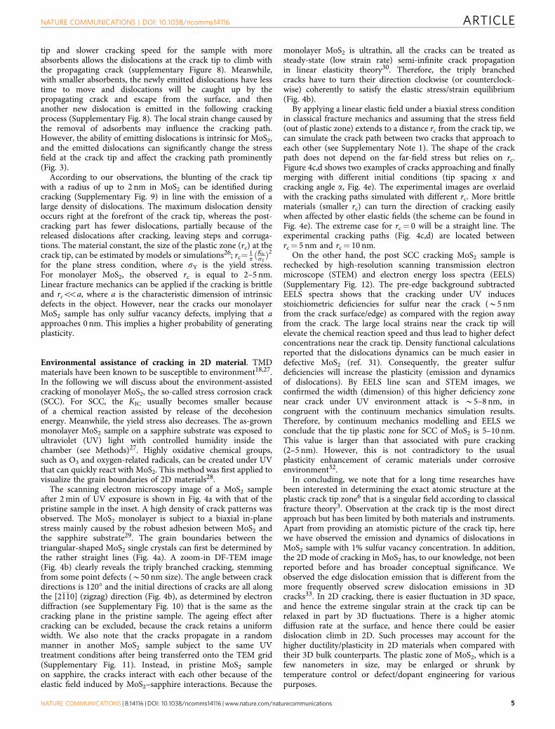
Environmental assistance of cracking in 2D material. TMDmaterials have been known to be susceptible to environment18,27.In the following we will discuss about the environment-assistedcracking of monolayer MoS2, the so-called stress corrosion crack(SCC). For SCC, the KIC usually becomes smaller becauseof a chemical reaction assisted by release of the decohesionenergy. Meanwhile, the yield stress also decreases. The as-grownmonolayer MoS2 sample on a sapphire substrate was exposed toultraviolet (UV) light with controlled humidity inside thechamber (see Methods)27. Highly oxidative chemical groups,such as O3 and oxygen-related radicals, can be created under UVthat can quickly react with MoS2. This method was first applied tovisualize the grain boundaries of 2D materials28.
The scanning electron microscopy image of a MoS2 sampleafter 2min of UV exposure is shown in Fig. 4a with that of thepristine sample in the inset. A high density of crack patterns wasobserved. The MoS2 monolayer is subject to a biaxial in-planestress mainly caused by the robust adhesion between MoS2 andthe sapphire substrate29. The grain boundaries between thetriangular-shaped MoS2 single crystals can first be determined bythe rather straight lines (Fig. 4a). A zoom-in DF-TEM image(Fig. 4b) clearly reveals the triply branched cracking, stemmingfrom some point defects (B50 nm size). The angle between crackdirections is 120� and the initial directions of cracks are all alongthe [2�1�10] (zigzag) direction (Fig. 4b), as determined by electrondiffraction (see Supplementary Fig. 10) that is the same as thecracking plane in the pristine sample. The ageing effect aftercracking can be excluded, because the crack retains a uniformwidth. We also note that the cracks propagate in a randommanner in another MoS2 sample subject to the same UVtreatment conditions after being transferred onto the TEM grid(Supplementary Fig. 11). Instead, in pristine MoS2 sampleon sapphire, the cracks interact with each other because of theelastic field induced by MoS2–sapphire interactions. Because the
monolayer MoS2 is ultrathin, all the cracks can be treated assteady-state (low strain rate) semi-infinite crack propagationin linear elasticity theory30. Therefore, the triply branchedcracks have to turn their direction clockwise (or counterclock-wise) coherently to satisfy the elastic stress/strain equilibrium(Fig. 4b).
By applying a linear elastic field under a biaxial stress conditionin classical fracture mechanics and assuming that the stress field(out of plastic zone) extends to a distance rc from the crack tip, wecan simulate the crack path between two cracks that approach toeach other (see Supplementary Note 1). The shape of the crackpath does not depend on the far-field stress but relies on rc.Figure 4c,d shows two examples of cracks approaching and finallymerging with different initial conditions (tip spacing x andcracking angle a, Fig. 4e). The experimental images are overlaidwith the cracking paths simulated with different rc. More brittlematerials (smaller rc) can turn the direction of cracking easilywhen affected by other elastic fields (the scheme can be found inFig. 4e). The extreme case for rc¼ 0 will be a straight line. Theexperimental cracking paths (Fig. 4c,d) are located betweenrc¼ 5 nm and rc¼ 10 nm.
On the other hand, the post SCC cracking MoS2 sample isrechecked by high-resolution scanning transmission electronmicroscope (STEM) and electron energy loss spectra (EELS)(Supplementary Fig. 12). The pre-edge background subtractedEELS spectra shows that the cracking under UV inducesstoichiometric deficiencies for sulfur near the crack (B5 nmfrom the crack surface/edge) as compared with the region awayfrom the crack. The large local strains near the crack tip willelevate the chemical reaction speed and thus lead to higher defectconcentrations near the crack tip. Density functional calculationsreported that the dislocations dynamics can be much easier indefective MoS2 (ref. 31). Consequently, the greater sulfurdeficiencies will increase the plasticity (emission and dynamicsof dislocations). By EELS line scan and STEM images, weconfirmed the width (dimension) of this higher deficiency zonenear crack under UV environment attack is B5–8 nm, incongruent with the continuum mechanics simulation results.Therefore, by continuum mechanics modelling and EELS weconclude that the tip plastic zone for SCC of MoS2 is 5–10 nm.This value is larger than that associated with pure cracking(2–5 nm). However, this is not contradictory to the usualplasticity enhancement of ceramic materials under corrosiveenvironment32.
In concluding, we note that for a long time researches havebeen interested in determining the exact atomic structure at theplastic crack tip zone6 that is a singular field according to classicalfracture theory3. Observation at the crack tip is the most directapproach but has been limited by both materials and instruments.Apart from providing an atomistic picture of the crack tip, herewe have observed the emission and dynamics of dislocations inMoS2 sample with 1% sulfur vacancy concentration. In addition,the 2D mode of cracking in MoS2 has, to our knowledge, not beenreported before and has broader conceptual significance. Weobserved the edge dislocation emission that is different from themore frequently observed screw dislocation emissions in 3Dcracks33. In 2D cracking, there is easier fluctuation in 3D space,and hence the extreme singular strain at the crack tip can berelaxed in part by 3D fluctuations. There is a higher atomicdiffusion rate at the surface, and hence there could be easierdislocation climb in 2D. Such processes may account for thehigher ductility/plasticity in 2D materials when compared withtheir 3D bulk counterparts. The plastic zone of MoS2, which is afew nanometers in size, may be enlarged or shrunk bytemperature control or defect/dopant engineering for variouspurposes.
NATURE COMMUNICATIONS | DOI: 10.1038/ncomms14116 ARTICLE
NATURE COMMUNICATIONS | 8:14116 | DOI: 10.1038/ncomms14116 | www.nature.com/naturecommunications 5

MethodsMoS2 grown on sapphire by chemical vapour deposition. MoS2 film wassynthesized following a previous report20. At first, 0.3 g MoO3 powder wasplaced in a ceramic boat located in the centre heating zone of the furnace andS powder was placed in a separate ceramic boat at the upper stream sidemaintained at 150 �C during the reaction. An Ar carrier gas (70 sccm, chamberpressure¼ 40 Torr) brought the S and MoO3 vapours to the target sapphiresubstrate that was located at the downstream side. The centre heating zone washeated to 635 �C at a ramping rate of 15 �C per min. After reaching 635 �C, theheating zone was maintained there for 30min and the furnace was then naturallycooled down to room temperature.
Transfer of MoS2 on sapphire to TEM grid. PMMA (A4, Chem) was spin-coatedonto the as-grown MoS2 (2,000 r.p.m., 1min) as a supporter and a protective layerwith no post-annealing step. The MoS2 and PMMA support were then detachedfrom the sapphire substrate by floating the PMMA/MoS2/sapphire, with thePMMA side up, in a hot 2M NaOH solution for 10min. The PMMA/MoS2 wasthen transferred into deionized water (4 times) for removing any remaining NaOHin the sample. Finally, the PMMA/MoS2 was scooped out in pieces and placed on aQuantifoil TEM grid with a gold-supported thin film (PELCO, 200 mesh, gold,1.2 mm holes). The grids were kept in an ambient oven at 80 �C for 1min toincrease adhesion between the PMMA/MoS2 and the grid. PMMA was ultimatelyremoved by acetone vapour. Before each TEM measurement, the grids wereannealed at 180 �C in a vacuum chamber (B7.5� 10� 5 Torr) for at least 12 h.
In situ TEM. TEM observations were conducted using a JEM ARM 200F operatedat 80 kV that is lower than the knock-on damage threshold for monolayer MoS2(90 kV)34. Acquisition time for bright-field and DF images was 1 s. DF image wasobtained using the smallest objective lens aperture. The HRTEM imagingacquisition time was 0.32–1 s. The Fourier filtering method was applied to reducethe noise level and enhance contrast of the images22. The beam intensity waso0.01 pA nm� 2 in order to obtain the HRTEM images. The beam intensity at thesample in TEM mode is measured by the screen current multiplied by the squareof magnifications. Because of contamination problems, it was difficult to obtainhigh-resolution STEM images during or after cracking. Annular dark-field STEMimaging was conducted using a probe aberration-corrected JEM ARM200Foperated at 80 kV. Annular dark-field images were acquired at a 20mradconvergence angle, with beam current 120–150 pA, beam size B1Å, acquisitiontimes of 40ms per pixel and collection angle from 50 to 180mrad. Because the
energy of the low-voltage electron beam was below the damage threshold energy,the pristine MoS2 remains stable after regular scanning.
UV light exposure. MoS2 grown on sapphire was placed in a chamber equippedwith a low-pressure Hg lamp (LH-arc, Lichtzen, with an output of 20mWcm� 2),with the majority of emitted light at a wavelength of 254 nm and B10% of emittedlight at a wavelength of 185 nm. Humidity was introduced into the chamber byconnecting it to a humidifier. The humidity level in the chamber was monitoredusing a hydro-thermometer (accuracy of ±3%). The humidifier was disconnectedfrom the chamber after reaching 65% humidity level. The MoS2 on sapphire wasthen irradiated under UV light for 2min. Radicals are generated under UV andhumidity conditions as follows: O2-O3; O3þH2O-O2þH2O2; 2O3þH2O2-2OH*þ 3O2; H2O-H*þOH*.
Scanning electron microscopy. The surface morphology of the TMDs on theSiO2/Si substrate was examined by field-emission SEM (JSM7000F, JEOL, Japan).An accelerating voltage of 15 kV was utilized to obtain a high contrast at differentmagnifications.
Data availability. The data that support the findings of this study are availablefrom the corresponding author on reasonable request.
References1. Bernstein, N. & Hess, D. W. Lattice trapping barriers to brittle fracture. Phys.
Rev. Lett. 91, 025501 (2003).2. Zhu, T., Li, J. & Yip, S. Atomistic study of dislocation loop emission from a
crack tip. Phys. Rev. Lett. 93, 025503 (2004).3. Griffith., A. A. The phenomena of rupture and flow in solids. Philos. Trans. R.
Soc. A 221, 163–198 (1921).4. Lee, C., Wei, X., Kysar, J. W. & Hone, J. Measurement of the elastic properties
and intrinsic strength of monolayer graphene. Science 321, 385–388 (2008).5. Bertolazzi, S, Brivio, J. & Kis, A. Stretching and breaking of ultrathin MoS2.
ACS Nano 5, 9703–9709 (2011).6. Clarke, D. R. & Faber, K. T. Fracture of ceramics and glasses. J. Phys. Chem.
Solids 48, 1115–1147 (1987).7. Butler, S. Z. et al. Progress, challenges, and opportunities in two-dimensional.
ACS Nano 7, 2898–2926 (2013).8. Tromans, D. & Meech, J. A. Fracture toughness and surface energies of covalent
minerals: theoretical estimates. Miner. Eng. 17, 1–15 (2004).
Grain boundary
(d)(c)
Stress corrosion crack
Defect
Crack A Crack B
rc rcx
�
�
�=35° x=1 μm
�=31° x=0.75 μm
�
�
�
σij(A)+
σij(B)120°
UV treatment for 2 min
rc=10 nm5 nm1 nm
1 nm5 nm
10 nmAs-grownmonolayerMoS2 on sapphire
a c
d
be
Figure 4 | Stress corrosion cracking of monolayer MoS2. (a) Scanning electron microscope image of crack pattern generated after 2min of UV light
exposure under humid conditions on MoS2. Scale bar, 2 mm. Inset shows an image of the as-grown sample. Scale bar, 5 mm. (b) TEM dark-field image of
triple crack paths initialized from one defect similar to (a). Scale bar, 100 nm. Inset highlights the crack. Scale bar, 20 nm. (c,d) Magnified images of two
areas in a, two cracks meet in the centre and are curved by each other because of the strain field. The three theoretically simulated paths using linear
elasticity theory with different rc are fitted with the experimental paths. Scale bar (c), 150 nm. Scale bar (d), 200nm. (e) Schematic showing the stress
state of two meeting cracks.
ARTICLE NATURE COMMUNICATIONS | DOI: 10.1038/ncomms14116
6 NATURE COMMUNICATIONS | 8:14116 | DOI: 10.1038/ncomms14116 | www.nature.com/naturecommunications

9. Lee, G. H., Cooper, R. C., An, S. J. & Lee, S. High-strength chemical-vapor-deposited graphene and grain boundaries. Science 340, 1073–1076(2013).
10. Zhang, P. et al. Fracture toughness of graphene. Nat. Commun. 5, 3782 (2014).11. Fujihara, M. et al. Selective formation of zigzag edges in graphene cracks. ACS
Nano 9, 9027–9033 (2015).12. Warner, J. H. et al. Dislocation-driven deformations in graphene. Science 337,
209–212 (2012).13. Lehtinen, O., Kurasch, S., Krasheninnikov, A. V. & Kaiser, U. Atomic scale
study of the life cycle of a dislocation in graphene from birth to annihilation.Nat. Commun. 4, 2098 (2013).
14. Azizi, A. et al. Dislocation motion and grain boundary migration in two-dimensional tungsten disulphide. Nat. Commun. 5, 4867 (2014).
15. Zhang, Z., Kutana, A. & Yakobson, B. I. Edge reconstruction-mediatedgraphene fracture. Nanoscale 7, 2716–2722 (2015).
16. Wang, X., Tabarraei, A. & Spearot, D. E. Fracture mechanics of monolayermolybdenum disulfide. Nanotechnology 26, 175703 (2015).
17. Huang, J. Y. et al. In situ observation of graphene sublimation andmultilayer edge reconstructions. Proc. Natl Acad. Sci. USA 106, 10103–10108(2009).
18. Gao, J. et al. Aging of transition metal dichalcogenide monolayers. ACS Nano10, 2628–2635 (2016).
19. Chow, P. K. et al. Defect-induced photoluminescence in monolayersemiconducting transition metal dichalcogenides. ACS Nano 9, 1520–1527(2015).
20. Lee, Y. H. et al. Synthesis of large-area MoS2 atomic layers with chemical vapordeposition. Adv. Mater. 24, 2320–2325 (2012).
21. Ly, T. H. et al. Misorientation-angle-dependent electrical transportacross molybdenum disulfide grain boundaries. Nat. Commun. 7, 10426ð2015Þ:
22. Liu, X. et al. Top–down fabrication of sub-nanometre semiconductingnanoribbons derived from molybdenum disulfide sheets. Nat. Commun. 4,1776 (2013).
23. Zhao, J. et al. Two-dimensional membrane as elastic shell with proof on thefolds revealed by three-dimensional atomic mapping. Nat. Commun. 6, 8935(2015).
24. Hytch, M. J. Quantitative measurement of displacement and strain fields fromHRTEM micrographs. Ultramicroscopy 74, 131–146 (1998).
25. Yates, J. R., Zanganeh, M., Tomlinson, R. A., Brown, M. W. & Diaz Garrido, F. A.Crack paths under mixed mode loading. Eng. Fract. Mech. 75, 319–330ð2008Þ:
26. Irwin, G. Analysis of stresses and strains near the end of a crack traversing aplate. J. Appl. Mech. 24, 361–364 (1957).
27. Ly, T. H. et al. Observing grain boundaries in CVD-grown monolayertransition metal dichalcogenides. ACS Nano 8, 11401–11408 (2014).
28. Duong, D. L. et al. Probing graphene grain boundaries with optical microscopy.Nature 490, 235–239 (2012).
29. Ji, Q. et al. Clean transfer of graphene on Pt foils mediated by a carbonmonoxide intercalation process. Nano Lett. 15, 198–205 (2014).
30. Xia, Z. C. & Hutchinson, J. W. Crack patterns in thin films. J. Mech. Phys. Solids48, 1107–1131 (2000).
31. Zou, X., Liu, M., Shi, Z. & Yakobson, B. I. Environment-controlled dislocationmigration and superplasticity in monolayer MoS2. Nano Lett. 15, 3495–3500(2015).
32. Wiederhorn, Jr S. M., Fuller, E. R. & Thomson, R. Micromechanisms of crackgrowth in ceramics and glasses in corrosive environments. Metal Sci. 14,450–458 (1980).
33. Ohr., S. R. An electron microscope study of crack tip deformation and itsimpact on the dislocation theory of fracture. Mater. Sci. Eng. 72, 1–35 (1985).
34. Komsa, H. P. et al. Two-dimensional transition metal dichalcogenides underelectron irradiation: defect production and doping. Phys. Rev. Lett. 109, 035503(2012).
AcknowledgementsThis work was supported by the Institute for Basic Science (IBS-R011-D1). We alsothank Dr Yu Zhiyang for useful discussions.
Author contributionsT.H.L. contributed to this work in the experimental planning, experimental measure-ments, data analysis and manuscript preparation. J.Z. conceived the idea and contributedto this work in the experimental planning, experimental measurements, data analysis andmanuscript preparation. M.O.C. did the TEM measurements. L.-J.L. provided the MoS2grown on sapphire. Y.H.L. contributed to the experimental planning, data analysis andmanuscript preparation.
Additional informationSupplementary Information accompanies this paper at http://www.nature.com/naturecommunications
Competing financial interests: The authors declare no competing financial interests.
Reprints and permission information is available online at http://npg.nature.com/reprintsandpermissions/
How to cite this article: Ly, T. H. et al. Dynamical observations on the cracktip zone and stress corrosion of two-dimensional MoS2. Nat. Commun. 8, 14116doi: 10.1038/ncomms14116 (2017).
Publisher’s note: Springer Nature remains neutral with regard to jurisdictional claims inpublished maps and institutional affiliations.
This work is licensed under a Creative Commons Attribution 4.0International License. The images or other third party material in this
article are included in the article’s Creative Commons license, unless indicated otherwisein the credit line; if the material is not included under the Creative Commons license,users will need to obtain permission from the license holder to reproduce the material.To view a copy of this license, visit http://creativecommons.org/licenses/by/4.0/
r The Author(s) 2017
NATURE COMMUNICATIONS | DOI: 10.1038/ncomms14116 ARTICLE
NATURE COMMUNICATIONS | 8:14116 | DOI: 10.1038/ncomms14116 | www.nature.com/naturecommunications 7