
3D Camera Pose Estimation Using Line Correspondences and 1D Homographies
Upload
khangminh22Category
view
2download
0
Departamento de Tecnología Electrónica Ingeniería de Sistemas yAutomática
Tesis Doctoral
Corrección de Factor de Potencia basada en laestimación digital de la corriente de líneaAplicación en el Convertidor Boost en modo de conducción
continua
Víctor Manuel López Martín
2013
Escuela Técnica Superior de Ingenieros Industriales y de Telecomunicación
Universidad de Cantabria


Digital power factor correction based online-current estimationCCM Boost converter appplication
PhD Thesis
For obtaining the PhD degree
Víctor Manuel López Martín
2013
Escuela Técnica Superior de Ingenieros Industriales y de Telecomunicación
Universidad de Cantabria


Universidad de CantabriaDepartment Of
Tecnología Electrónica, Ingeniería de Sistemas y Automática
The undersigned hereby certify that they have read and recommend to the Escuela Téc-nica Superior de Ingenieros Industriales y de Telecomunicación for acceptance a thesis enti-tled “Digital power factor correction based on line-current estimation” by VíctorManuel López Martín in partial fulfillment of the requirements for the degree of PhDThesis.
Dated: 2013
Advisor:Professor Francisco J. Azcondo
Dissertation Committee:
ChairProfessor Paolo Matavelli
Reader:Professor Javier Sebastian
Reader:Professor Alberto Pigazo


A mis padres, Marisa y Pedro
A Inés


Agradecimientos/Acknowledgements
En este documento se muestra una parte importante del trabajo realizado desde Octubre delaño 2008, en el que comencé mi proyecto fin de carrera, y que desembocaría posteriormenteen esta Tesis. Durante este tiempo han sido muchas personas las que me han ayudado y quemerecen un agradecimiento especial:
Paco Azcondo, tutor de esta Tesis, que me ha mostrado su apoyo, confianza y paciencia; yque me ha sabido ilustrar y enseñar la luz siempre que me han surgido dudas.
A Charo, Christian y Javi por ayudarme siempre que lo he necesitado.
Alejandro, mi grandísimo amigo y compañero. Hemos compartido una cantidad ingente dehoras juntos en el Laboratorio, con las que he disfrutado y aprendido cómo nunca habríaimaginado. Una parte de esta Tesis es gracias a tí, ya lo sabes.
Regan Zane, many thanks for your support during my time with you in Boulder and Logan.All your comments have helped me to improve my knowledge about Power Electronics.
Mi familia, con mis padres a la cabeza, por ayudarme a llegar aquí sin ninguna preocupaciónmás allá que mi propio trabajo.
Inés, tu apoyo y comprensión infinita desde el primer día han sido una bocanada de oxígenoen la consecución de esta Tesis. Todo lo que pueda decir es poco.
Y a mis amigos, que han entendido mis ausencias por las horas invertidas en esta Tesis.
Santander, Cantabria, Spain Víctor Manuel López Martín2013
vii


Abstract
Continuous conduction mode (CCM) power factor correction (PFC) without input currentmeasurement is a step forward with respect to previously proposed PFC digital controllers.Inductor volt-second (vsL) measurement in each switching period enables the digital estima-tion of the input current, used in the inner current loop. However, an accurate compensationof the small inaccuracies in the measured vsL is required in the estimation, to match theactual current. Otherwise, these errors are accumulated every switching period over the halfline cycle, leading to an appreciable current distortion.
A vsL estimation method is proposed in this Thesis, measuring the input (vg) and the outputvoltage (vo). Discontinuous conduction mode (DCM) occurs near input line zero crossings,and is also detected by measuring the drain-to-source MOSFET voltage, vds. Parasitic ele-ments also cause a small difference between the estimated voltage across the inductor, basedon input and output voltage measurements, and the actual one, which must be taken intoaccount to estimate the input current in the proposed sensorless PFC digital controller.
This Thesis analyzes deeply the current estimation inaccuracies caused by errors in the ON-time estimation, voltage measurements, and the parasitic elements. A new digital feedbackcontrol with high resolution is also proposed to cancel the difference between DCM operationtime of the real input current T gDCM , and the estimated DCM time T rebDCM . Therefore, thecurrent estimation is calibrated using digital signals during operation in DCM.
A fast feedforward coarse time error compensation is carried out with the measured delayof the drive signal, and then a fine compensation is achieved with the feedback loop thatmatches the estimated and real DCM times. With this contribution, an universal controlleris proposed. The digital controller can be used in universal applications due to the abilityof the DCM time feedback loop to autotune based on the operation conditions (power level,input voltage, output voltage. . . ), which improves the operation range in comparison withprevious solutions.
Furthermore, an additional improvement is presented in this controller in which the current
ix

x Abstract
demanded by the Sensorless PFC rectifier is pure sinusoidal despite the non-sinusoidal inputvoltage of the grid. This contribution is really interesting in applications where the harmonicslimits are stricter (like in aircraft systems) and must be fulfilled independently on the voltagewaveshape. This modification is totally done into the digital controller without any need ofextra analog components.
Experimental results are shown for a 1 kW boost PFC converter over a wide power and voltagerange. The digital controller is implemented in a field programmable gate array (FPGA) witha very simple analog circuitry to adapt the signals needed by the controller. The behavior ofthe controller, applied in lighting systems is also shown.
Universidad de Cantabria

Contents
Agradecimientos/Acknowledgements vii
Abstract viii
List of Figures xxii
List of Tables xxiii
Nomenclature xxv
0 Introducción 1
1 Introduction 9
2 Background 172.1 Power factor correction . . . . . . . . . . . . . . . . . . . . . . . . . . . . . . . 172.2 Standards about line current harmonics and power factor value . . . . . . . . 192.3 Digital control of Switched Mode Power Supplies . . . . . . . . . . . . . . . . 212.4 PFC converters . . . . . . . . . . . . . . . . . . . . . . . . . . . . . . . . . . . 26
2.4.1 Boost converter. Fundamentals . . . . . . . . . . . . . . . . . . . . . . 282.4.2 Analog Control in PFC converters . . . . . . . . . . . . . . . . . . . . 312.4.3 Digital control in PFC converters . . . . . . . . . . . . . . . . . . . . . 34
2.5 Current Sensing in Switched Mode Power Supplies . . . . . . . . . . . . . . . 352.5.1 Current sensor . . . . . . . . . . . . . . . . . . . . . . . . . . . . . . . 362.5.2 Ron sensing . . . . . . . . . . . . . . . . . . . . . . . . . . . . . . . . . 372.5.3 Filter-sense the Inductor . . . . . . . . . . . . . . . . . . . . . . . . . . 392.5.4 Current transformer sensor . . . . . . . . . . . . . . . . . . . . . . . . 402.5.5 Current-average technique . . . . . . . . . . . . . . . . . . . . . . . . . 412.5.6 Hall-effect sensor . . . . . . . . . . . . . . . . . . . . . . . . . . . . . . 422.5.7 Case study: Losses in a PFC stage with resistor current sensor . . . . 42
2.6 Digital power factor correction controllers with current sensor . . . . . . . . . 442.7 Digital power factor correction controllers without current sensor . . . . . . . 472.8 Thesis Approach . . . . . . . . . . . . . . . . . . . . . . . . . . . . . . . . . . 48
xi

xii Contents
3 Current estimation. Current control algorithm and errors 513.1 Current rebuilding. Theoretical concept. . . . . . . . . . . . . . . . . . . . . 513.2 Power factor correction algorithm. Non-linear carrier (NLC) control . . . . . 543.3 Current estimation errors. Boost Converter . . . . . . . . . . . . . . . . . . . 59
3.3.1 Time error effect. Delays between the drive signal, output of the digitaldevice, and the voltage across the inductor . . . . . . . . . . . . . . . 61
3.3.2 Effect of errors in data capture of voltage across the inductor . . . . . 673.3.3 Errors due to difference between real inductance L and the estimated
inductance Lest . . . . . . . . . . . . . . . . . . . . . . . . . . . . . . . 733.4 Chapter conclusion . . . . . . . . . . . . . . . . . . . . . . . . . . . . . . . . . 74
4 Influence of the converter parasitics in the current estimation 774.1 Modeling the parasitic elements effect with the Equivalent Parasitic Element
in series with the input voltage (EPEg) . . . . . . . . . . . . . . . . . . . . . 814.2 Modeling the parasitic elements effect with the Equivalent Parasitic Element
in series with the output voltage (EPEo) . . . . . . . . . . . . . . . . . . . . 844.3 Chapter conclusion . . . . . . . . . . . . . . . . . . . . . . . . . . . . . . . . . 87
5 Digital controller implementation 895.1 Current rebuilding. Digital implementation and quantization effects . . . . . 895.2 Drive signal delays compensation. Feedforward compensation in terms of time
(clock cycles) . . . . . . . . . . . . . . . . . . . . . . . . . . . . . . . . . . . . 945.3 Discontinuous Conduction Auxiliary Detection Circuit . . . . . . . . . . . . . 965.4 Feedback compensation of the DCM time discrepancy . . . . . . . . . . . . . 985.5 Chapter conclusion . . . . . . . . . . . . . . . . . . . . . . . . . . . . . . . . . 103
6 Model of the high-resolution error compensator. Steady-state gain and lowbandwidth model 1056.1 Steady state model. DC analysis . . . . . . . . . . . . . . . . . . . . . . . . . 1056.2 Small-signal AC model. Low bandwidth loop. . . . . . . . . . . . . . . . . . . 1116.3 Chapter conclusion . . . . . . . . . . . . . . . . . . . . . . . . . . . . . . . . . 113
7 Low THDi controller for Single Phase Rectifiers 1157.1 Introduction to distorted grids . . . . . . . . . . . . . . . . . . . . . . . . . . 1157.2 Definitions of Electric Power Quantities . . . . . . . . . . . . . . . . . . . . . 1177.3 Low THDi controller under distorted voltages . . . . . . . . . . . . . . . . . . 1197.4 Chapter conclusion . . . . . . . . . . . . . . . . . . . . . . . . . . . . . . . . . 123
8 Experimental validation 1258.1 Boost converter prototype . . . . . . . . . . . . . . . . . . . . . . . . . . . . . 1258.2 Operation in Steady state . . . . . . . . . . . . . . . . . . . . . . . . . . . . . 1298.3 Time evolution under different conditions . . . . . . . . . . . . . . . . . . . . 1388.4 Operation under distorted voltage. Resistance or pure sinusoidal current be-
havior . . . . . . . . . . . . . . . . . . . . . . . . . . . . . . . . . . . . . . . . 1508.5 Chapter conclusion . . . . . . . . . . . . . . . . . . . . . . . . . . . . . . . . . 152
Universidad de Cantabria

Contents xiii
9 Example of application: Digital PFC controllers for HID lamps electronicballast applications 1539.1 Introduction . . . . . . . . . . . . . . . . . . . . . . . . . . . . . . . . . . . . . 1539.2 Outer voltage loop in the digital PFC controller . . . . . . . . . . . . . . . . . 1559.3 Input voltage fluctuations detection algorithm . . . . . . . . . . . . . . . . . . 1579.4 Experimental results . . . . . . . . . . . . . . . . . . . . . . . . . . . . . . . . 1599.5 Chapter conclusion . . . . . . . . . . . . . . . . . . . . . . . . . . . . . . . . . 162
10 Conclusions 16710.1 Summary of contributions . . . . . . . . . . . . . . . . . . . . . . . . . . . . . 16810.2 Future works . . . . . . . . . . . . . . . . . . . . . . . . . . . . . . . . . . . . 169
11 Published papers 17111.1 Journals . . . . . . . . . . . . . . . . . . . . . . . . . . . . . . . . . . . . . . . 171
11.1.1 In review . . . . . . . . . . . . . . . . . . . . . . . . . . . . . . . . . . 17111.2 International Conferences . . . . . . . . . . . . . . . . . . . . . . . . . . . . . 17111.3 Spanish Conferences . . . . . . . . . . . . . . . . . . . . . . . . . . . . . . . . 173
References 175
A Definition of the rebuilt input current RMS value Ireb 191A.1 Linearization of the expression . . . . . . . . . . . . . . . . . . . . . . . . . . 191
Víctor M. López Martín

xiv Contents
Universidad de Cantabria

List of Figures
1 Circuito Valley-fill. . . . . . . . . . . . . . . . . . . . . . . . . . . . . . . . . . 22 (a) Formas de onda del circuito Valley-fill. Arriba: Corriente de entrada. Abajo:
Tensión de entrada. (b) Contenido armónico de la corriente de línea. . . . . . 33 Convertidor Buck-boost trabajandor como resistencia en modo natural. . . . 34 Esquemas de sistemas de alimentación: (a) Esquema tradicional con etapa PFC
con control analógico y dispositivo digital controlando el convertidor posterior.(b) Integración digital completa del control de las dos etapas . . . . . . . . . 5
5 Esquema típico de rectificador PFC con control digital y circuito de sensadode corriente. . . . . . . . . . . . . . . . . . . . . . . . . . . . . . . . . . . . . 6
6 Izq: Imagen de un convertidor Boost PFC con control analógico, usando elcontrolador comercial UC3854 de Unitrode. Der: Foto térmica del convertidortrabajando a plena carga. . . . . . . . . . . . . . . . . . . . . . . . . . . . . . 6
1.1 Valley-fill circuit. . . . . . . . . . . . . . . . . . . . . . . . . . . . . . . . . . . 101.2 (a) Valley-fill waveforms. Upper trace: Input current. Lower trace: Input
voltage. (b) Harmonics of the line current. . . . . . . . . . . . . . . . . . . . . 111.3 Buck-boost converter working as a PFC rectifier. . . . . . . . . . . . . . . . . 111.4 Switched mode power supply scheme. (a) Traditional approach with a PFC
stage with analog control and a digital device for the second stage. (b) Com-plete digital implementation of the two stages control. . . . . . . . . . . . . . 13
1.5 Typical scheme of a digitally controlled PFC converter with the current sensorcircuit. . . . . . . . . . . . . . . . . . . . . . . . . . . . . . . . . . . . . . . . 14
1.6 Left: Picture of a PFC Boost analog converter controlled by the UC3854 ofUnitrode. Right: Thermal picture of the converter at nominal power. . . . . 14
2.1 Line current (blue) in the Power Electronics Lab of the University of Cantabriaat Santander (Spain) in June 2012. In red is plotted the sinusoidal waveformwhose RMS values is equal to the line current. . . . . . . . . . . . . . . . . . 20
2.2 Fairchild PFC technology portfolio. . . . . . . . . . . . . . . . . . . . . . . . . 272.3 Typical power supply block diagram. . . . . . . . . . . . . . . . . . . . . . . . 282.4 DC-DC boost converter. . . . . . . . . . . . . . . . . . . . . . . . . . . . . . . 292.5 Boost converter waveforms in CCM (a) and DCM (b). MOSFET gate signal
(vgs), inductor current (iL), MOSFET drain-to-source voltage (vds) and outputvoltage (vo). . . . . . . . . . . . . . . . . . . . . . . . . . . . . . . . . . . . . . 30
xv

xvi List of Figures
2.6 Block diagram of the average current mode control in a Boost converter. . . . 312.7 Waveforms of critical conduction mode control in the boost converter. . . . . 322.8 Left: Block diagram of nonlinear carrier control (boost example). Right:
Waveforms of nonlinear carrier control (boost example) [15]. . . . . . . . . . 332.9 Current sensing options in a power converter. . . . . . . . . . . . . . . . . . . 352.10 Resistor inductance combined with high di/dt can cause voltage spikes in the
current measurement. . . . . . . . . . . . . . . . . . . . . . . . . . . . . . . . 372.11 (a) MOSFET Ron Current Sensing scheme and (b) Normalized drain-to-source
ON-resistance Ron, vs Junction Temperature for the IRF840 Power MOSFETof Fairchild. . . . . . . . . . . . . . . . . . . . . . . . . . . . . . . . . . . . . 38
2.12 Sensing the inductor current by measuring the inductor voltage with a RCfilter in a boost converter. . . . . . . . . . . . . . . . . . . . . . . . . . . . . 40
2.13 Current transformer equivalent circuit . . . . . . . . . . . . . . . . . . . . . . 412.14 Averaging the inductor voltage to sense the current. . . . . . . . . . . . . . . 412.15 Boost PFC converter scheme considering losses. . . . . . . . . . . . . . . . . . 432.16 Average current sensor scheme. . . . . . . . . . . . . . . . . . . . . . . . . . . 452.17 Operating waveforms of the average current sensor. . . . . . . . . . . . . . . 462.18 Voltage sensor approach used to obtain the digital data of the input and output
voltages. Scheme for the input voltage. . . . . . . . . . . . . . . . . . . . . . . 472.19 Input voltage and power range of the recent works in sensorless PFC con-
trollers. The green area represents the goal of this Thesis. . . . . . . . . . . 49
3.1 (a) Boost converter basic scheme and (b) basic simulation model of the sen-sorless Boost PFC converter current estimator. . . . . . . . . . . . . . . . . . 52
3.2 Schematic of the sensorless current controller. . . . . . . . . . . . . . . . . . . 543.3 Simulations Blocks in Simulink® with PLECS® toolbox. Top: PLECS® sub-
circuit in Simulink® with the switching delays (explained in Section 3.3.1).Bottom: Current estimator Simulink blocks. . . . . . . . . . . . . . . . . . . 55
3.4 NLC control waveforms. . . . . . . . . . . . . . . . . . . . . . . . . . . . . . . 563.5 Schematic of the sensorless current controller with a NLC control. . . . . . . 573.6 Left: Digital waveforms of the NLC control with estimation of the average
rebuilt current. Right: Hardware implementation blocks of the average rebuiltcurrent estimation. . . . . . . . . . . . . . . . . . . . . . . . . . . . . . . . . 58
3.7 Half cycle of the input rebuilt current with distortion due to DCM operationaround line zero crossings. . . . . . . . . . . . . . . . . . . . . . . . . . . . . 59
3.8 Digital signal ireb[j, k], compared with the analog real input current ig, underideal conditions. The on − off signal is the output of the digital device andvL the analog inductor voltage. . . . . . . . . . . . . . . . . . . . . . . . . . . 60
3.9 Simulated waveforms under ideal conditions obtained with the Simulink modelof the system with Vg = 230Vrms, Vo = 400Vdc, Pg ' Po = 640W (R = 250Ω),fsw = 100 kHz and reactive components L = 1 mH, and C = 220 µF , underideal conditions. . . . . . . . . . . . . . . . . . . . . . . . . . . . . . . . . . . 62
3.10 Boost converter circuit and gate drive signal vs MOSFET vds and inductorvoltage to show the switching delays. . . . . . . . . . . . . . . . . . . . . . . . 62
3.11 Experimental time switch transitions (vL) compared with the output drivesignal of the digital device (on− off). . . . . . . . . . . . . . . . . . . . . . 63
3.12 Digital estimated current ireb[j, k] compared with the analog real input currentig, when the drive signal’s delays ∆ton−off 6= ∆toff−on. The on − off signalis the output of the digital device, and vL the inductance voltage. . . . . . . . 64
Universidad de Cantabria

List of Figures xvii
3.13 Transient state simulated waveforms obtained with the Simulink/PLECs sys-tem model with Vg = 230 Vrms, Vo = 400 Vdc, Pg ' Po = 640W (R = 250 Ω),fsw = 100 kHz and reactive components L = 1 mH, and C = 220 µF , when∆ton= 10 ns. . . . . . . . . . . . . . . . . . . . . . . . . . . . . . . . . . . . . 65
3.14 Steady state simulated waveforms with the Simulink/PLECs system model ofthe system with Vg = 230 Vrms, Vo = 400 Vdc, Pg ' Po = 640W (R = 250 Ω),fsw = 100 kHz and reactive components L = 1 mH, and C = 220 µF , when∆ton= 10 ns. . . . . . . . . . . . . . . . . . . . . . . . . . . . . . . . . . . . . 66
3.15 Steady state simulated waveforms with the Simulink/PLECs system model ofthe system with Vg = 230 Vrms, Vo = 400 Vdc, Pg ' Po = 640W (R = 250 Ω),fsw = 100 kHz and reactive components L = 1 mH, and C = 220 µF , when∆ton= -10 ns. . . . . . . . . . . . . . . . . . . . . . . . . . . . . . . . . . . . . 66
3.16 Digital estimated current ireb[j, k] compared with the analog real input currentig with the drive signal’s delays supposing ∆ton−off = ∆toff−on. The on−offsignal is the output of the digital device, and vL the inductance voltage. . . . 68
3.17 Digital estimated current ireb compared with the analog real input current igwith the drive signal’s delays supposing ∆ton−off = ∆toff−on. The on− offsignal is the output of the digital device, and vL the inductance voltage. . . . 68
3.18 Voltage data acquisition scheme. . . . . . . . . . . . . . . . . . . . . . . . . . 693.19 Digital estimated current ireb[j, k], compared with the analog real input current
ig, under errors in data capture voltage across the inductance when qg 6= qo 6= q.The on − off signal is the output of the digital device and vL the analoginductance voltage. . . . . . . . . . . . . . . . . . . . . . . . . . . . . . . . . . 70
3.20 Steady state simulated waveforms with the Simulink/PLECs system model ofthe system with Vg = 230 Vrms, Vo = 400 Vdc, Pg ' Po = 640W (R = 250 Ω),fsw = 100 kHz and reactive components L = 1 mH, and C = 220 µF , whenq = 0.4617 V/bit, qg = 0.4611 V/bit, and qo = 0.4615 V/bit. . . . . . . . . . . . 72
3.21 Digital estimated current ireb[k] compared with the analog real input currentig when the estimated inductance value (Lest) is higher than the real (L). Theon−off signal is the output of the digital device, and vL the inductance voltage. 74
3.22 Steady state simulated waveforms with the Simulink/PLECs system model ofthe system with Vg = 230 Vrms, Vo = 400 Vdc, Pg ' Po = 640W (R = 250 Ω),fsw = 100 kHz and reactive components L = 1 mH, and C = 220 µF andLest = 1.8mH. . . . . . . . . . . . . . . . . . . . . . . . . . . . . . . . . . . . 75
3.23 Simulated current waveforms when the real inductance value L is a functionof the current L (iL) = 1.5 − 0.174iL [mH] and Lest = 1.5mH. Top: Inputcurrent ig, and rebuilt current ireb. Bottom: Current estimation error ierror. 75
4.1 Boost converter diagram with parasitic elements. . . . . . . . . . . . . . . . 774.2 Input current waveform ig, instantaneous vpar and average voltage drop over
the switching cycle in the parasitic elements, 〈vpar〉. Left: waveforms over thehalf line cycle. Right: Switching waveforms. . . . . . . . . . . . . . . . . . . 79
4.3 Simulated current waveforms without consideration of the parasitic elementsinfluence. Top: Real and rebuilt input current. Bottom: Simulated currentestimation error. . . . . . . . . . . . . . . . . . . . . . . . . . . . . . . . . . . 80
4.4 Equivalent boost converter circuit with the EPE connected in series with theinductor. . . . . . . . . . . . . . . . . . . . . . . . . . . . . . . . . . . . . . . . 81
4.5 Equivalence between the Equivalent Parasitic Element (EPEg) and a depen-dent voltage source function of the input voltage. . . . . . . . . . . . . . . . . 82
4.6 (a) Equivalent boost converter with the EPE represented by a dependent vol-tage source. (b) Modification of the current estimation block with the com-pensation in the input voltage data. . . . . . . . . . . . . . . . . . . . . . . . 83
Víctor M. López Martín

xviii List of Figures
4.7 Equivalent boost converter circuit with the EPEo connected in series with theoutput. . . . . . . . . . . . . . . . . . . . . . . . . . . . . . . . . . . . . . . . 84
4.8 Equivalence between the Equivalent Parasitic Element and a constant voltagesource. . . . . . . . . . . . . . . . . . . . . . . . . . . . . . . . . . . . . . . . . 85
4.9 Left: Model of the Boost converter with the influence of the parasitic elementsplaced in series with the output voltage. Right: Behavioral model of thecurrent estimator block with the digital compensation in the output voltage. 86
4.10 Simulated waveform for the Boost converter sensorless PFC controller whenqvdig = Vβ. . . . . . . . . . . . . . . . . . . . . . . . . . . . . . . . . . . . . . 87
5.1 Representation of the analog-to-digital conversion of the input voltage. . . . 905.2 (a) Simulink model of the input voltage ADC, (b) ierror waveform over half
utility period for different bits of resolution in the ADCs with a constantADC sample frequency of fADC =1 MHz, and (c) for different ADC samplingfrequencies and a constant Nbits = 10. . . . . . . . . . . . . . . . . . . . . . 92
5.3 Current rebuilding concept. (a) Hardware architecture and (b) digital waveforms. 935.4 Auxiliary circuit to adapt the drain-to-source voltage as a digital signal. Com-
parison with the on − off signal and the drive signal’s delays 4ton−off and4toff−on. . . . . . . . . . . . . . . . . . . . . . . . . . . . . . . . . . . . . . . 94
5.5 Compensated NLC control algorithm. . . . . . . . . . . . . . . . . . . . . . . 955.6 DCM condition detection auxiliary circuit for the real input current ig. (a)
Hardware architecture. (b) Circuit waveforms . . . . . . . . . . . . . . . . . . 975.7 DCM condition digital detection for the rebuilt input current ireb. Left: digital
signals and, right: hardware architecture in the digital device. . . . . . . . . 985.8 Left: Current estimation error generated by + 5 ns (with Tclk= 10 ns) of time
error compensation (in blue) and due to a qvdig value that cause the sameestimation error at the end of the half line period (in red). In magenta isplotted the difference between the two current estimation errors. Right: ireband ig current in this case . . . . . . . . . . . . . . . . . . . . . . . . . . . . . 99
5.9 Minimum current estimation error due to the resolution of ±0.5 LSB in thedigital control signal vdig. . . . . . . . . . . . . . . . . . . . . . . . . . . . . . 100
5.10 Current estimator hardware implementation with higher resolution. . . . . . . 1005.11 Real waveforms. Input voltage vg, real input current ig, waveforms and digital
signals DCMig and DCMireb for: Left: eDCM < 0, and then ireb > ig. Right:eDCM > 0 and ireb < ig. . . . . . . . . . . . . . . . . . . . . . . . . . . . . . 102
5.12 Experimental results. Top: DCM time of the input current T gDCM , and DCMtime error eDCM vs qgvdig − Vβ. Bottom: PF vs qgvdig − Vβ. . . . . . . . . . . 102
5.13 Block diagram of the DCM times compensation controller. . . . . . . . . . . 103
6.1 Current waveforms with current error estimation (top) and emulated resis-tances (real and digital) under this condition (bottom), over the half line cycle. 106
6.2 Low frequency equivalent circuit of the sensorless PFC controller. . . . . . . . 1086.3 Waveforms around the AC line zero-crossings. . . . . . . . . . . . . . . . . . 1096.4 Current error waveform ierror, and its linear approximation. . . . . . . . . . 1106.5 Operation time in DCM of the real input current T gDCM , in terms of switching
periods, of the real converter and the mathematical model. . . . . . . . . . . 1116.6 Block diagram system representation. . . . . . . . . . . . . . . . . . . . . . . 1126.7 Actual vs theoretical response time of the plant under a 2-bit vdig step-up.
Vg = 230Vrms, Vo = 400V , fsw = 96kHz Pg =460.9 W with q = 435/(214 − 1
)V/bit. . . . . . . . . . . . . . . . . . . . . . . . . . . . . . . . . . . . . . . . . 113
Universidad de Cantabria

List of Figures xix
7.1 Grid voltage in the Power Electronics Laboratory, on March 13th of 2013. . . 1167.2 Value of the power factor as function of the voltage harmonic distortion for
Case A and Case B. . . . . . . . . . . . . . . . . . . . . . . . . . . . . . . . . 1197.3 Top: First term of the carrier signal (red) and the harmonic voltage (blue)
waveforms. Bottom: Voltage harmonics in an example of input voltage withTHDv = 6 % . . . . . . . . . . . . . . . . . . . . . . . . . . . . . . . . . . . . 121
7.4 Block diagram of the low THDi controller with the boost converter. . . . . . 122
8.1 (a) Block diagram and (b) picture of the of the Laboratory Test bench . . . 1268.2 (a) Circuit scheme of the proposed digital controller. (b) Picture of the boost
converter prototype and the FPGA. . . . . . . . . . . . . . . . . . . . . . . . 1278.3 Top: Measured value of qg over the half line cycle, for two different input
voltages ADCs, under 230 Vrms (50 Hz). In red it is plotted the measuredvalue using the TLV1572 commercial ADC. In blue is plotted the qg valueusing the Σ4 ADC used in the output voltage measurement, that leads to theig current waveform at 648 W. Bottom: Experimental waveforms when theΣ4 ADC is used in the output, and also in the input voltage measurement. . 128
8.4 Experimental results: input voltage (vg) and current (ig) along with the DCMsignal of the rebuilt input current (DCMireb) and the real input current(DCMig). Waveforms under Vg =250 Vrms - 50 Hz, at 72 kHz switchingfrequency for different power levels. . . . . . . . . . . . . . . . . . . . . . . . . 131
8.5 Experimental results: input voltage (vg) and current (ig) along with the DCMsignal of the rebuilt input current (DCMireb) and the real input current(DCMig). Waveforms under Vg =230 Vrms - 50 Hz, at 72 kHz switchingfrequency for different power levels. . . . . . . . . . . . . . . . . . . . . . . . . 132
8.6 Experimental results: input voltage (vg) and current (ig) along with the DCMsignal of the rebuilt input current (DCMireb) and the real input current(DCMig). Waveforms under Vg =180 Vrms - 50 Hz, at 72 kHz switchingfrequency for different power levels. . . . . . . . . . . . . . . . . . . . . . . . . 133
8.7 Experimental results: input voltage (vg) and current (ig) along with the DCMsignal of the rebuilt input current (DCMireb) and the real input current(DCMig). Waveforms under Vg =120 Vrms - 60 Hz, at 72 kHz switchingfrequency for different power levels. . . . . . . . . . . . . . . . . . . . . . . . . 133
8.8 Experimental results: input voltage (vg) and current (ig) along with the DCMsignal of the rebuilt input current (DCMireb) and the real input current(DCMig). Waveforms under Vg =85 Vrms, at 72 kHz switching frequencyfor different power levels. . . . . . . . . . . . . . . . . . . . . . . . . . . . . . 134
8.9 Experimental results: Value of the duty cycle modification (4ton) due to thedrive signal delays over the half line cycle. . . . . . . . . . . . . . . . . . . . . 134
8.10 Power factor value for different delays used in the feedforward compensationwhen they are considered constant over the half line cycle. . . . . . . . . . . . 135
8.11 Input current and voltage waveforms if the feedforward is done consideringconstant drive signal delays. (a) 4tmeason =100 ns and (b) 4tmeason =220 ns . . 135
8.12 Experimental results for the DCM condition detection circuit for the real inputcurrent. . . . . . . . . . . . . . . . . . . . . . . . . . . . . . . . . . . . . . . . 136
8.13 Inductors used in the experimental results. Left: L = 1mH (RM12-3C90 corewith RL = 0.25 Ω). Right: L2 = 1.5 mH (soft saturation Kool mµ core withRL2 = 0.35 Ω). . . . . . . . . . . . . . . . . . . . . . . . . . . . . . . . . . . . 137
8.14 Experimental results: input voltage (vg) and current (ig) along with the DCMsignal of the rebuilt input current (DCMireb) and the real input current(DCMig). Vo = 400 Vdc and L2 = 1.5mH (RL2 = 0.35 W ). (a): Vg =230 Vrms(50Hz), Pg = 970W . (b): Vg = 85 Vrms(60Hz), Pg = 320W . . . . . 137
Víctor M. López Martín

xx List of Figures
8.15 Experimental results: input voltage (vg) and current (ig) along with the DCMsignal of the rebuilt input current (DCMireb) and the real input current(DCMig). Waveforms under Vg =250 Vrms - 50 Hz, at 96 kHz switchingfrequency for different power levels. . . . . . . . . . . . . . . . . . . . . . . . . 139
8.16 Experimental results: input voltage (vg) and current (ig) along with the DCMsignal of the rebuilt input current (DCMireb) and the real input current(DCMig). Waveforms under Vg =230 Vrms - 50 Hz, at 96 kHz switchingfrequency for different power levels. . . . . . . . . . . . . . . . . . . . . . . . . 139
8.17 Experimental results: input voltage (vg) and current (ig) along with the DCMsignal of the rebuilt input current (DCMireb) and the real input current(DCMig). Waveforms under Vg =180 Vrms - 50 Hz, at 96 kHz switchingfrequency for different power levels. . . . . . . . . . . . . . . . . . . . . . . . . 140
8.18 Experimental results: input voltage (vg) and current (ig) along with the DCMsignal of the rebuilt input current (DCMireb) and the real input current(DCMig). Waveforms under Vg =120 Vrms - 60 Hz, at 96 kHz switchingfrequency for different power levels. . . . . . . . . . . . . . . . . . . . . . . . . 140
8.19 Experimental results: input voltage (vg) and current (ig) along with the DCMsignal of the rebuilt input current (DCMireb) and the real input current(DCMig). Waveforms under Vg =85 Vrms, at 96 kHz switching frequencyfor different power levels. . . . . . . . . . . . . . . . . . . . . . . . . . . . . . 141
8.20 Experimental results: input voltage (vg) and current (ig) along with the DCMsignal of the rebuilt input current (DCMireb) and the real input current(DCMig). Waveforms under Vg =250 Vrms - 50 Hz, at 144 kHz switchingfrequency for different power levels. . . . . . . . . . . . . . . . . . . . . . . . . 141
8.21 Experimental results: input voltage (vg) and current (ig) along with the DCMsignal of the rebuilt input current (DCMireb) and the real input current(DCMig). Waveforms under Vg =230 Vrms - 50 Hz, at 144 kHz switchingfrequency for different power levels. . . . . . . . . . . . . . . . . . . . . . . . . 143
8.22 Experimental results: input voltage (vg) and current (ig) along with the DCMsignal of the rebuilt input current (DCMireb) and the real input current(DCMig). Waveforms under Vg =180 Vrms - 50 Hz, at 144 kHz switchingfrequency for different power levels. . . . . . . . . . . . . . . . . . . . . . . . . 143
8.23 Experimental results: input voltage (vg) and current (ig) along with the DCMsignal of the rebuilt input current (DCMireb) and the real input current(DCMig). Waveforms under Vg =120 Vrms - 60 Hz, at 144 kHz switchingfrequency for different power levels. . . . . . . . . . . . . . . . . . . . . . . . . 144
8.24 Experimental results: input voltage (vg) and current (ig) along with the DCMsignal of the rebuilt input current (DCMireb) and the real input current(DCMig). Waveforms under Vg =85 Vrms, at 144 kHz switching frequencyfor different power levels. . . . . . . . . . . . . . . . . . . . . . . . . . . . . . 144
8.25 Power factor and Total harmonic distortion value time evolution under differentload steps. Vo = 400Vdc Vg = 230Vrms(50Hz), fsw = 144kHz. (a) Load steps-down. (a) Load steps-up. . . . . . . . . . . . . . . . . . . . . . . . . . . . . . 147
8.26 Time evolution of the different electrical variables with Vo = 400 Vdc, fsw =72kHz under different load, grid voltage and grid frequency arbitrary conditions.148
8.27 Experimental results under high-frequency grids of two instants of the resultspresented in Fig. 8.26. Input voltage (vg) and current (ig) along with theDCM signal of the rebuilt input current (DCMireb) and the real input current(DCMig). . . . . . . . . . . . . . . . . . . . . . . . . . . . . . . . . . . . . . . 149
8.28 Experimental results under high-frequency grids of two instants of the resultspresented in Fig. 8.26. . . . . . . . . . . . . . . . . . . . . . . . . . . . . . . . 149
Universidad de Cantabria

List of Figures xxi
8.29 Pure sinusoidal behavior under different power levels and input voltage dis-tortions. Input voltage (vg) and current (ig) along with the DCM signal ofthe rebuilt input current (DCMireb) and the real input current (DCMig).Vg = 230 V , fsw = 96 kHz. With THDv =5 % at (a) Pg =964.9 W and (b)Pg =799.5 W. With THDv =12 % at (c) Pg =963.1 W and (d) Pg =800.4 W. 151
8.30 Resistance behavior under different power levels and input voltage distortions.Input voltage (vg) and current (ig) along with the DCM signal of the rebuiltinput current (DCMireb) and the real input current (DCMig).Vg = 230 V ,fsw = 96 kHz. With THDv =5 % at (a) Pg =966.7 W and (b) Pg =800.6 W.With THDv =12 % at (c) Pg =965.1 W and (d) Pg =800.9 W. . . . . . . . . 151
9.1 Two power stages ballast circuit with a analog PFC and inverter controllers. . 1549.2 Two power stages ballast circuit with digital controllers integrated in a single
device. . . . . . . . . . . . . . . . . . . . . . . . . . . . . . . . . . . . . . . . . 1549.3 Waveforms under voltage fluctuations situation: Utility voltage, vg, PFC stage
output voltage, vo, and lamp current, ilamp. . . . . . . . . . . . . . . . . . . . 1569.4 PFC stage and digital controller implementation. (a) Traditional digital vol-
tage control loop. (b) Digital control loop proposed. . . . . . . . . . . . . . . 1569.5 Sketches of the utility voltage, utility current, dc voltage and lamp current
changing the voltage loop: Low bandwidth loop during steady state and ex-tended bandwidth loop under utility voltage fluctuation. . . . . . . . . . . . . 157
9.6 Low frequency voltage fluctuation. . . . . . . . . . . . . . . . . . . . . . . . . 1589.7 Voltage range defined to detect the utility voltage fluctuations. . . . . . . . . 1589.8 Input voltage fluctuation detection algorithm flowchart. . . . . . . . . . . . . 1599.9 Block diagram of the laboratory test setup. . . . . . . . . . . . . . . . . . . . 1609.10 PFC stage input waveforms and power. Low bandwidth outer loop. (a) Input
voltage vin, and input current iin. Vin = 230 Vrms, 50 Hz. Ch2 input voltage,200 V/div, Ch4 input current, 10 mV/A and 10 mV/div. (b) Input currentFast Fourier Transform (FFT iin) and IEC 61000-3-2 class C limits with I1 =0.680 A and PF = 0.991. Math1. Vertical scale 111 mA/div, horizontal scale62.5 Hz/div. . . . . . . . . . . . . . . . . . . . . . . . . . . . . . . . . . . . . . 160
9.11 PFC stage input waveforms and power. Wide bandwidth outer loop. (a)Input voltage vin, and input current iin. Vin = 230 Vrms, 50 Hz. Ch2 inputvoltage, 200 V/div, Ch4 input current, 10 A/div. (b) Input current FastFourier Transform (FFT iin) and IEC 61000-3-2 class C limits with I1 = 0.680A and PF = 0.91. Math1. Vertical scale 111 mA/div, horizontal scale 62.5Hz/div. . . . . . . . . . . . . . . . . . . . . . . . . . . . . . . . . . . . . . . . 161
9.12 Bode plots for the different voltage loops. Green: Bode plot for steady-stateconditions with reduced bandwidth. Blue: Bode plot for transient state duringinput voltage fluctuation with wide bandwidth. . . . . . . . . . . . . . . . . . 162
9.13 The PFC stage output voltage (vo), the lamp light lux level measured by thephoto sensor (lxLAMP ) and input voltage (vin) under 10% VinRMS and 10 Hzfluctuation. Vin = 230–207 Vrms, 50Hz, Vo = 420 Vdc, Pg = 150 W and C=68mF output capacitor. (a) With a reduced voltage loop bandwidth and (b) Witha wide voltage loop bandwidth. Ch2 input voltage, 50 V/div, Ch1 lamp lightflux. Ch3 output voltage 50 V/div. Time scale: 40 ms/div. . . . . . . . . . . 163
9.14 Behavior of the input voltage fluctuation algorithm under different utility vol-tage conditions. Utility peak voltage envelope (blue) and “Fluctuation” signalthat indicates if a fluctuation is detected (red). . . . . . . . . . . . . . . . . . 164
9.15 Time necessary by the algorithm to determinate the steady state condition atthe end of the utility voltage fluctuation. . . . . . . . . . . . . . . . . . . . . . 164
Víctor M. López Martín

xxii List of Figures
9.16 Lucalox 150 W HPS lamp used to verify the proposal. . . . . . . . . . . . . . 164
A.1 System waveforms for a given Ireb and qvdig − Vβ values. Left: qvdig > Vβ andright: qvdig < Vβ. . . . . . . . . . . . . . . . . . . . . . . . . . . . . . . . . . . 192
A.2 Surface of Ig values obtained for different combinations of given Ireb and qvdig−Vβ values. . . . . . . . . . . . . . . . . . . . . . . . . . . . . . . . . . . . . . . 193
A.3 Comparison of Ig values obtained by (A.7) (represented in red), and by thelinear approximation defined by (A.9), labeled as Ig,lin and plotted in blue. . 194
Universidad de Cantabria

List of Tables
2.1 IEC 61000-3-2 harmonic current limits . . . . . . . . . . . . . . . . . . . . . 212.2 IEEE Std 519 Maximum odd harmonic current limits for general distribution
systems, 120 V to 69 kV. . . . . . . . . . . . . . . . . . . . . . . . . . . . . . . 212.3 CCM-DCM mode boundaries for the Boost converter. . . . . . . . . . . . . . 312.4 Theoretical power losses for different switching frequencies. Efficiencies with
(η) and without (ηssles) current sensor. And ratio between the current sensorlosses (PS), the conduction losses (Pcond) and total losses (Ploss). . . . . . . 44
3.1 (a) List of correspondence between of the analog variables and the digital. (b)Expressions that define the variation of the real and rebuilt input current in aswitching period . . . . . . . . . . . . . . . . . . . . . . . . . . . . . . . . . . 60
7.1 DO-160 Harmonic Current Limits . . . . . . . . . . . . . . . . . . . . . . . . . 1157.2 Voltage harmonics in the line voltage shown in Fig. 7.1. . . . . . . . . . . . . 117
8.1 Parameters of the components used in the Boost prototype. . . . . . . . . . . 1268.2 Experimental results in steady state with a switching frequency fsw =72 kHz 1308.3 Power Factor and THDi values under different conditions. . . . . . . . . . . 1388.4 Experimental results with a switching frequency of 96 kHz. . . . . . . . . . . 1428.5 Experimental results at 144 kHz of switching frequency. . . . . . . . . . . . . 1458.6 Experimental results at 230 Vrms - 400 Hz under high frequency line voltages. 1468.7 Experimental results at 230 Vrms - 400 Hz under distorted line voltages. . . . 150
xxiii

xxiv List of Tables
Universidad de Cantabria

Nomenclature
Abbreviations
AC Alternating Current
ADC Analog-to-digital conversion/converter
ASIC Application-specific integrated circuit
CCM Continuous Conduction Mode
CPLD Complex Programmable Logic Device
CRM Critical Conduction Mode
DC Direct Current
DCM Discontinuous Conduction Mode
DSP Digital Signal Processor
EMI Electromagnetic Interference
EPEg Equivalent Parasitic Element in series with the input voltage
EPEo Equivalent Parasitic Element in series with the output voltage
FFT Fast Fourier Transforms
FPGA Field Programable Gate Array
HIL Hardware in the loop
IC Integrated Circuit
LSB Least Significant Bit
OCC One-cycle control
PCC Point of common coupling
PF Power Factor
xxv

xxvi Nomenclature
PFC Power factor correction/corrector
PMBus Power Managment Bus
PWM Pulse Width Modulation
RMS Root mean square
SMPS Switched Mode Power Supplies
THDi Total Harmonic Distornic of the input current [%]
THDv Total Harmonic Distortion of the voltage [%]
VRM Voltage regulation module
ZCD Zero-crossing detector
ZOH Zero-order-hold
Greek Symbols
∆ig Real input current ripple [A]
∆ireb Estimated input current ripple [A]
4t Integration time [s]
∆toff−on OFF-to-ON delay [s]
4tmeason Duty cycle modification measurement [s]
∆ton−off ON-to-OFF delay [s]
∆ton ON-time modification [s]
4vo Output voltage ripple [V]
Γ Constant used in the denominator of the low bandwith model [V/s]
Latin Symbols
C Capacitor value [F]
d Duty Cycle command
Dmax Duty cycle saturation
DCMig Detection signal of the DCM in igDCMireb Detection signal of the DCM in irebe Error generated due to the A/D conversion [bit]
eDCM DCM time error [s]
fADC ADC sample frequency [Hz]
fc Crossover frequency of the PFC voltage loop [Hz]
fclk Clock frequency [Hz]
Universidad de Cantabria

Nomenclature xxvii
fsw Switching frequency [Hz]
fu Utility voltage frequency [Hz]
iavg Average value of the estimated input current each switching period [A]
ID RMS value of the diode current [A]
ierror Current estimation error [A]
ierror,sim Simulated current estimation error [A]
Ig RMS value of the real input current [A]
ig Real input current [A]
ig1 Fundamental component of the input current [A]
i+g Peak input current [A]
〈ig〉 Average input current [A]
Igh RMS value of the current hth component [A]
Ireb RMS value of the estimated/rebuilt input current [A]
ireb Rebuilt input current [A], [bit]
ireb [j, k] Estimated current in the clock period k in the switching cycle j [A]
i−reb Valley value of the rebuilt current [A]
iref Current reference [A]
iL Inductor current [A]
j jth switching period
k kth clock period
L Inductance [H]
Lest Estimated inductance [H]
Lr Parasitic series inductance in the current sensor [H]
M Voltage conversion ratio
nclk Clock-cycles per switching-period
nu Switching cycles per half-line period
Nbits Number of bits in the ADCs
on− off Control signal
Pcond Total conduction losses [W]
PD Conduction losses in the power diode [W]
Pg Input power [W]
PL Conduction losses in the inductor [W]
Ploss Total converter losses [W]
PQ Conduction losses in the MOSFET [W]
PS Conduction losses in the current sensor [W]
Víctor M. López Martín

xxviii Nomenclature
Psw Total switching losses [W]
q LSB resolution defined by the designer [V/bit]
qg LSB resolution of the input voltage [V/bit]
qi LSB resolution of the current [A/bit]
qo LSB resolution of the output voltage [V/bit]
Qrr Reverse recovery charge [C]
R Load resistance [Ω]
RD Diode ON-state resistor [Ω]
Re Emulated Resistance [Ω]
RL Parasitic resistance of the inductor [Ω]
Ron Power MOSFET ON-resistor [Ω]
Rs Sense resistor [Ω]
R∗e Digital emulated resistance [Ω]
Tclk Clock period [s]
ton Main switch ON-time [s]
t∗on Estimated ON-time in the digital controller [s]
Ts Sampling period of the PFC voltage loop [s]
Tsw Switching period [s]
Tu Utility voltage period [s]
T gDCM DCM time of the real input current [s]
T rebDCM DCM time of the estimated input current [s]
Vβ Voltage across the EPEo [V]
Vbus DC bus voltage [V]
VD Diode forward voltage at zero-current [V]
vdig Variable control to compensate current estimation error [bit]
vds MOSFET drain-to-source voltage [V]
v∗ds Digital drain-to-source voltage [bit]
Vg RMS value of the input voltage [V]
vg Input voltage [V]
vg1 Fundamental component of the input voltage [V]
v∗g Digital input voltage value [bit]
vsg Sampled input voltage [V]
vgs MOSFET drive signal [V]
vL Inductor voltage [V]
v∗L Digitally estimated inductor voltage [bit]
Universidad de Cantabria

Nomenclature xxix
vL,reb Rebuilt inductor voltage [V]
Vm Carrier signal amplitude [V]
vm Carrier signal [V]
vmax High-level voltage of the digital device [V]
Vo Average output voltage [V]
vo Output voltage [V]
v∗o Digital output voltage value [bit]
vso Sampled ouput voltage [V]
vpar Voltage drop accross the parasitic elements [V]
Vref Reference voltage level [V]
vxg Instantaneous EPE voltage when this is in series with L [V]
vxo Instantaneous EPE voltage when this is in series with vo [V]
vsL Volt-seconds in the inductance [V·s]
Víctor M. López Martín

xxx Nomenclature
Universidad de Cantabria

Capítulo 0
Introducción
La red eléctrica transmite y distribuye la potencia a una frecuencia constante (50 Hz - 60 Hz) ya una tensión alterna (AC). Sin embargo, la mayoría de los aparatos eléctricos y electrónicosnecesitan fuentes de alimentación de corriente continua (DC). Por tanto, se necesita unaconversión de potencia de AC a DC como primera etapa para la conexión a la red eléctrica.Un rectificador es un convertidor electrónico diseñado y construido para la conversión de ACa DC, entregando potencia en DC a una o varias cargas, pero todas ellas conectadas a lamisma línea de DC.
Rectificadores sin ningun tipo de control, como el rectificador de media onda o el de ondacompleta, seguidos por un gran condensador (que almacene la energía), han sido durantemuchos años las soluciones empleadas para conseguir tensión en DC y alimentar la carga,sucesivas etapas DC-DC o un regulador lineal. Pero el valor del factor de potencia (PF )en este tipo de rectificadores es muy bajo, y con un contenido armónico en la corriente muyelevado. Este factor de potencia aumenta si se introducen fuentes de alimentación controladas(convertidores DC-DC conmutados que controlan la corriente demandada por la red) entreel rectificador y el condensador de salida, haciendo que el sistema sea un rectificador activocon corrección de factor de potencia.
Una corriente de línea con un alto contenido armónico tiene efectos perjudiciales para la redelectrica, como:
• Valores eficaces mayores para el valor de potencia demandada, limitando los valores depotencia activa a entregar a la carga para una determinada sección de cable.
• Aumento de las corrientes por el neutro en sistemas trifásicos, provocando inestabilida-des y distorsión en la tensión.
Mientras la mayoría de la energia eléctrica consumida viene por el uso de motores eléctricos,
1

2 Introducción
C5 68uInitial DC voltage 100
BULK
+
Vin
D1
1N54
06
D2
1N54
06
D3
1N54
06
D4
1N54
06V
G1
I(Vin):1
C6 68uInitial DC voltage 100
D22
1N
5406
D24
1N
5406
D23
1N
5406
L1N
C3 1uInitial DC voltage 100
C4 1uInitial DC voltage 100
R1
50
AM
1
R2
200
Figura 1: Circuito Valley-fill.
hornos, iluminación ..., la cantidad de energía que representan estos equipos electronicos haaumentado de manera considerable, afectando a la red eléctrica por su característica no lineal.
Para mantener una calidad en la energia eléctrica y mitigar estos efectos negativos, dife-rentes normativas internacionales como la EN 61000-3-2 [1] definen lo límites admisibles dearmónicos de corriente inyectados a la red eléctrica para diferentes tipos de cargas.
El valor del factor de potencia es un dato que describe la “calidad” de una carga desde el puntode vista de la red eléctrica. Un factor de potencia alto indica un comportamiento resistivodesde el punto de vista de la red, con una corriente en fase y proporcional a la tensión delínea. Cargas con un factor de potenica bajo, poseen un contenido armónico en su corrientemuy alto y/o un desfase entre la tensión de línea y la corriente.
Soluciones pasivas utilizando filtros o circuitos Valley-fill [2, 3] consiguen buenos factores depotencia a cargas constantes y en condiciones de diseño. En la Fig. 1 se muestra el circuitoValley-fill, mientras que las formas de onda de tensión y de corriente se presentan en la Fig.2a. En lo que se refiere a la corriente de entrada, su contenido armónico se muestra en la Fig.2b.
Dentro de los rectificadores activos de corrección de factor de potencia (PFC rectifiers), elconvertidor Boost y el Flyback son, probablemente, las soluciones más utilizadas. Para bajaspotencias, el convertidor Flyback trabajando en modo de conducción discontinua (DCM -Discontinuous conduction mode) tiene un comportamiento resistivo de modo natural, sinnecesidad de un control de corriente, si su frecuencia de conmutación (fsw) y tiempo deON (ton) son constantes, tal y como se muestra en la Fig. 3, donde i+g , ig, 〈ig〉 son losvalores de pico, instanténeo y medio en cada periodo de conmutación de la corriente deentrada, respectivamente. En comparación con el Buck-Boost (su alternativa sin aislamiento)el convertidor Flyback proporciona aislamiento a su salida y evita los problemas debido a lapolaridad inversa de la tensión de salida del Buck-Boost.
El convertidor Boost también presenta esta propiedad de “emulador” natural de resistenciaoperando en el límite entre modo de conducción continua y discontinua (CRM - Critical
Universidad de Cantabria

3
T
Time (ms)0.5
I(Vin)
-3.00
3.00
Vin
-400.00
400.00
0.51 0.52 0.53 0.54 0.55
(a)
T
Base frequency 50[Hz]0 2 4 6 8 10 12 14
Am
plitu
de [A
]
0.0
0.1
0.2
0.3
0.4
0.5
0.6
0.7
(b)
Figura 2: (a) Formas de onda del circuito Valley-fill. Arriba: Corriente de entrada. Abajo: Tensiónde entrada. (b) Contenido armónico de la corriente de línea.
vg
ioig D
L
gigi
t
CR
gi
Figura 3: Convertidor Buck-boost trabajandor como resistencia en modo natural.
Víctor M. López Martín

4 Introducción
Conduction Mode) con tiempo de ON constante y a una frecuencia de conmutación variable,aunque este aspecto hace que el filtro EMI necesario en la entrada sea más complejo y costoso.Circuitos integrados como el L6560 [4] permiten una realización analógica de este control deuna manera sencilla.
En aplicaciones de alta potencia (por encima de 250 W) se prefiere la operación en modo deconducción continua (CCM) o la operación de etapas en paralelo en DCM y en “interleaving”.En CCM se emplean dos lazos de control: un lazo interno de ancho de banda amplio (alrededorde 1-5 kHz) que da forma a la corriente demandada de la red eléctrica; y un segundo lazolento, de unidades de Hz de ancho de banda, que regula la tensión de salida empleando comovariable de control la amplitud de la intensidad de entrada. En este caso, el convertidorBoost es el convertidor más empleado, debido a su alta eficiencia (la corriente que circula porsus dispositivos semiconductores es la menor comparada con otros convertidores), y su bajaemisión de ruido comparado con los diferentes tipos de convertidores.
Para resolver este doble lazo de control se pueden encontrar en el mercado circuitos integradoscon tecnología analógica, como el UC3854 [5], que es uno de los más usado para corrección defactor de porencia. Existen técnicas de control no lineales, como “Nonlineal-carrier (NLC)” oel control “One-Cycle”. Un dispositivo analógico que realiza este tipo de control es el IR1150[6]. Estos circuitos que se caracterizan por su simplicidad y mejora de la respuesta dinámicadel lazo de corriente, comparada con la solución tradicional de doble lazo. Pero a pesarde esta disponibilidad de controladores de corrección de factor de potencia comerciales, lasnormativas y los programas de certificación de fuentes de alimentación cada vez más estrictos,y la busqueda de precios más competitivos ha hecho que diversos grupos de investigaciónempleen sus esfuerzos es este tema.
Una parte importante de estos esfuerzos están orientados hacia el desarrollo de técnicas decontrol digital. Aunque se han presentado gran cantidad de soluciones, sólo unas pocas hanpodido entrar en el mercado con éxito. En lo que se refiere a la corrección de factor de potencia,los requisitos de dinámica en los controladores no son especialmente elevados, haciendo quela corrección de factor de potencia sea un ambito en el que se han presentado numerosastécnicas digitales de control.
El control de convertidores de potencia mediante dispositivos digitales permite incluir fun-ciones complejas para adaptarse a las diferentes situaciones de la tensión alimentación y dela carga. Algunas de las ventajas son generales para cualquier aplicación; como la progra-mabilidad, reducción del número de componentes, menor sensibilidad al ruido o toleranciasde componentes, y más recientemente en aplicaciones de potencia, la compatibilidad conestándares como el PMBus [7–9] para la gestión de potencia.
En aplicaciones de corrección del factor de potencia (PFC) en las que no existe interacción conotras etapas, el control analógico prevalece, ya que obtiene, en principio, mejor compromisoentre prestaciones y coste. Pero incluso en este caso, es habitual encontrar que las etapasposteriores, alimentadas por el PFC, dispongan de un control realizado en un dispositivodigital donde sería susceptible de ser integrado un control digital del PFC, simplificando el
Universidad de Cantabria

5
+
igiinConverter
+ +v
Load
vin
‐
PFCvg
‐
vo
‐
PFC controller 2nd stagecontroller
(a)
+
iinConverter
+v
Load
ig
+vin
‐
PFC vo
‐
vg
‐
Digital controller
(b)
Figura 4: Esquemas de sistemas de alimentación: (a) Esquema tradicional con etapa PFC concontrol analógico y dispositivo digital controlando el convertidor posterior. (b) Inte-gración digital completa del control de las dos etapas
diseño final (ver Fig. 4).
El uso de controles de digitales permite, por ejemplo, reducir la variación en el rendimientodebido al envejecimiento, temperatura u otro tipo de factores mediambientales, la posibilidadde diseñar controles adaptativos, o reducir el el tamaño en comparación con una materiali-zación analógica.
Además, el uso de plataformas de desarrollo como microprocesadores, FPGAs, CPLDs, PICs...,permite añadir funciones adicionales de control sin un coste extra excesivo, ya que los cam-bios se realizan interiormente en el dispositivo digital sin necesidad de introducir elementosanalógicos extra.
La regulación de la corriente de entrada al PFC operando en CCM para hacerla sinusoidal,proporcional a la tensión de entrada, se realiza generalmente a partir de un sensor de corriente.Las capacidades del PFC son sensibles a las prestaciones de este sensor que origina ruidoy disipación de potencia. La traducción directa de los controladores lineales empleados encontroladores analógicos, como el UC3854 [5], en controladores digitales requiere una solucióncomo la que se muestra en la Fig. 5, donde Rs representa el valor de la resistencia de sensado.Se necesitan tres medidas, la tensiónes de entrada (vg) y de salida (vo), y la corriente deentrada (ig).
Víctor M. López Martín

6 Introducción
ADC ADC
ADC
Digital device
Driver
ADC*gv
vg
L
QC
*ov
+vo
-
D
vgs
on-off
ig
- +
Rs
ig
Figura 5: Esquema típico de rectificador PFC con control digital y circuito de sensado de co-rriente.
Analog Boost CCM PFC
Current Sensor Thermal photo
Figura 6: Izq: Imagen de un convertidor Boost PFC con control analógico, usando el controladorcomercial UC3854 de Unitrode. Der: Foto térmica del convertidor trabajando a plenacarga.
De estas tres variables, la medida de la corriente es la que presenta una mayor complejidad,necesitando un circuito de adaptación de señal como el que se presenta en la Fig. 5. Porello, varios autores y grupos de investigación han prestado atención en este tema [10–14]. Laresistencia de sensado (Rs) es la solución más empleada para la medida de la corriente, y lapotencia disiparda por ella (que será mayor a medida que aumenta la corriente demandada)da lugar a un punto caliente en la placa de circuito impreso. La Fig. 6 muestra una placade un Boost PFC analógico controlado con el UC3854, que trabajando a plena carga (1 kW)genera una zona de alta temperatura como el que se muestra en la foto térmica de dichafigura.
Las tensiónes de entrada y de salida (vg y vo), tienen una dinámica lenta (50-60 Hz y 100-120 Hz) y su conversión analógico-digital no requiere de unas prestaciones muy elevadas. Esnecesario un circuito de adaptación de señal tras el sensor de corriente para que la señal seaadecuada como entrada al convertidor analógico-digital (ADC), y además, dicho convertidortiene que poseer un ancho de banda mucho mayor que los ADCs empleados en las tensiones.
Universidad de Cantabria

7
En el presente trabajo, se busca una solución digital de bajo coste, pero capaz de alcanzarlas especificaciones de la norma EN-61000-3-2 clase C para unas condiciones de tensionesy frecuencias universales, y un amplio intervalo de carga. Para ello, se propone sustituir lamedida de corriente de entrada en el PFC (ig), por su estimación digital (ireb), partiendo delos datos digitales de tensión de entrada y salida. La naturaleza de dinámica lenta de estastensiones hace que se pueden obtener a través de convertidores analógico-digitales de presta-ciones más bajas a las que se necesitan en la medida de corriente. Las señales de mando delconvertidor se generan de forma que la corriente estimada resulte proporcional a la tensión deentrada (sinusoidal), utilizando una técnica de control no-lineal [15–18] aplicado a la corrientereconstruida. En resumen, en todos aquellos lazos de control en los que tradicionalmente seemplea la variable ig, en este trabajo se sustituya la variable ireb.
Para realizar estas funciones se emplea un dispositivo digital configurable concurrente, fieldprogramable gate array (FPGA), donde se ha implementado el control. Los resultados expe-rimentales se presentan para un Boost PFC del 1kW.
En el capítulo 2 de este trabajo se realiza una breve revision de corrección de factor depotencia y normativas vigentes referentes que definen los límites de armónicos de corrienteinyectados a la red eléctrica, seguido por una muestra del estado del arte del control digital enfuentes conmutadas de alimentación, y en especial de etapas correctoras de factor de potencia.Se hace un especial énfasis en la técnicas de sensado de corriente en fuentes conmutadas, yuna breve revisión de los últimos trabajos de sensado de corriente en rectificadores activoscon corrección de factor de potencia.
El concepto de estimación digital de la corriente empleado en este trabajo se analiza en elCapítulo 3, junto con el algoritmo de corrección de factor de potencia empleado, y los erroresde estimación de corriente que afectan a este tipo propuesta sin medida de la corriente. Cadafuente de error es analizada por separado, obteniendo las expresiones que modelan ese error.El Capítulo 4 presenta el error de estimación de corriente debido a los elementos parásitosinternos del convertidor de potencia. Este tipo de errores se presentan por separado porqueno dependen de la resolución de la conversión analógico-digital de las variables, si no que esinherente al convertidor, y depende del punto de trabajo.
La implementación digital del control se muestra en el Capítulo 5, junto con la compensacióndigital de cada uno de las fuentes de error enunciadas. Se muestra la influencia de la resolución,y como se puede obtener una compensación de alta resolución sin necesidad de elementosanalógicos extra. Dicha compensación de alta resolución se realiza proponiendo un nuevolazo de realimentación. En el Capítulo 6 se realiza un modelado AC en pequeña señal delsistema a regular, para analizar la estabilidad del sistema. Por su parte, en el Apéndice A semuestra la relación que existe entre los valores eficaces de la corriente de entrada y la realen caso de que la estimación de corriente no sea correcta. Este aspecto es necesario para laobtención del modelo de la planta que corrige el error de estimación de corriente con altaresolución.
En el Capítulo 7 se propone un nuevo control digital de la corriente demandada de la red
Víctor M. López Martín

8 Introducción
eléctrica, para que ésta sea sinusoidal pura independientemente de la forma de onda de latensión de la red eléctrica. Aplicaciones críticas como aviónica, presentan unos requerimientosde armónicos de corriente que, ante una tensión de red distorsionada, los controladores de PFCtradicionales no son capaces de cumplir. Este nuevo control busca eliminar este problema.
La validación experimental de la aportación presentada en esta Tesis se muestra en el Capítulo8 para unas condiciones de trabajo universales de tensión y frecuencia de entrada (85 - 250Vrms y 50 - 800 Hz), para las cuales el controlador digital no ha sido reprogramado. Por suparte, en el Capítulo 9 se muestra un ejemplo de aplicacion industrial del trabajo presentadoen esta Tesis, donde se utiliza como etapa PFC para balastos de lámparas de alta intensidad dedescarga. Además, se introduce una modificación en el lazo de control para evitar parpadeosen la lámpara debido a fluctuaciones de baja frecuencia en la red eléctrica.
Las conclusiones obtenidas tras la realización de esta Tesis, y las futuras líneas de trabajose recogen en el Capítulo 10. Todas las publicaciones realizadas a partir de este trabajo semuestran en el Capítulo 11.
Universidad de Cantabria

Chapter 1
Introduction
Utility systems transmit and distribute power at constant frequency (50-60 Hz) and ACvoltage. Nonetheless, most of the electrical and electronics applications require DC powersupplies. Therefore, an AC to DC power conversion is needed as front-end stage. A rectifieris a power electronics interface built for converting AC power to DC power, and may supplyDC power to different electrical loads, all of them connected to the same DC bus.
Uncontrolled rectifiers, either half-wave or full-wave, followed by a large energy storage ca-pacitor were traditionally used to perform the necessary AC rectification, and supply a DCoutput to a load, downstream DC-DC converter or linear regulator. The power factor (PF )of such rectifiers is low with a high harmonic content in the AC line current. Placing acontrollable switched-mode converter between the rectifying elements and the large energystorage capacitor of the uncontrolled rectifier results in the configuration of a power factorcorrector (PFC) rectifier.
High harmonic input current content has undesirable effects:
• Increased RMS line currents, limiting the power available to an AC load for a given ACservice wire gauge
• Increased neutral currents in 3-phase systems. Possible AC system instability and linevoltage distortion.
The global growth of the electronics has led to the great increment in the use of electronicsdevices or gadgets. Although the most of the energy is consumed by electrical motors, fur-naces or lighting; the amount of energy consumed by these electronic equipment has increasedconsiderably, affecting the power grid due to its non-linear characteristic.
To maintain the quality of the AC line and mitigate these negative effects, internationalstandards such as EN 61000-3-2 [1] set the current harmonics magnitudes of many ubiquitous
9

10 Introduction
C5 68uInitial DC voltage 100
BULK
+
Vin
D1
1N54
06
D2
1N54
06
D3
1N54
06
D4
1N54
06V
G1
I(Vin):1
C6 68uInitial DC voltage 100
D22
1N
5406
D24
1N
5406
D23
1N
5406
L1N
C3 1uInitial DC voltage 100
C4 1uInitial DC voltage 100
R1
50
AM
1
R2
200
Figure 1.1: Valley-fill circuit.
electronic devices. Power factor describes the qualities of a load in a AC power system. Loadswith a high power factor appear largely resistive to the AC utility mains as the demandedcurrent is in-phase and proportional to the line voltage. Systems with a low power factorhave phase-displaced line voltage and current, non-proportionality between line voltage andline current resulting from high harmonic current content of the line current, or both phasedisplacement and high harmonic current content combined.
Passive approaches using filters or Valley-fill [2,3] topologies have a good behavior at constantload and around nominal conditions. Figure 1.1 shows the Valley-fill circuit scheme. Thevoltage and current waveforms are presented in Fig. 1.2a, in which the input current has ancurrent harmonic content shown in Fig. 1.2b.
Among the active switch mode PFC rectifiers, Boost or Flyback topologies are more populardue to their good current shaping ability for the entire line period.
In general, boost PFC rectifiers have higher conversion efficiency than Buck-Boost PFCrectifiers, which makes boost topology the most popular structure for PFC rectifiers. For lowpower applications, Flyback converter working in the discontinuous conduction mode (DCM)presents averaged resistive emulator behavior at a constant switching frequency (fsw) andON-time (ton) as is presented in Fig. 1.3, where i+g , ig, 〈ig〉 represent the peak, instantaneousand average value in each switching cycle of the input current, respectively. No current loopis needed. In comparison with the Buck-Boost converter, Flyback converter offers isolationand avoids problems due to the inverse polarity in the Buck-Boost output.
Boost converter shows resistive emulator behavior at the boundary between CCM and DCM(Critical Conduction Mode - CRM) with a constant ON-time and a variable switching fre-quency. This aspect makes necessary a EMI filter in the input, increasing the cost andcomplexity of the power supply. Integrated circuits (ICs) as the L6560 [4] enable an analogimplementation of this control in an easy way.
For higher power applications (more than 250 W), the continuous conduction mode (CCM) ispreferred, or several DCM stages in parallel and interleaved operation. In CCM two control
Universidad de Cantabria

11
T
Time (ms)0.5
I(Vin)
-3.00
3.00
Vin
-400.00
400.00
0.51 0.52 0.53 0.54 0.55
(a)
T
Base frequency 50[Hz]0 2 4 6 8 10 12 14
Am
plitu
de [A
]
0.0
0.1
0.2
0.3
0.4
0.5
0.6
0.7
(b)
Figure 1.2: (a) Valley-fill waveforms. Upper trace: Input current. Lower trace: Input voltage.(b) Harmonics of the line current.
vg
ioig D
L
gigi
t
CR
gi
Figure 1.3: Buck-boost converter working as a PFC rectifier.
Víctor M. López Martín

12 Introduction
loops are typically needed: a high frequency inner loop (around 1-5 kHz) whose goal isto obtain a sinusoidal current shape using a sinusoidal reference (obtained with the inputvoltage waveform), and a second low bandwidth voltage loop (around 10 Hz) that regulatesthe output voltage using the input current amplitude as control variable. In this case, Boostconverter is the most popular due to its efficiency (the current through the semiconductordevices is lower in comparison with other topologies), and low noise.
Several commercial analog integrated circuits (ICs) are available to solve this two loops, as theUC3854 [5], widely used in power factor correction. Nonlinear controllers as the “Nonlinear-carrier” (NLC)” control or the “One-Cycle” control are famous due to its simplicity andimprove the bandwidth of the current loop in comparison with the traditional approach. Ananalog device for this type of control approaches is the IR1150 [6]. But while these (and more)commercial ICs are available, the stricter standards and certification program requirementsas well as the pressure on achieving higher competitive cost, have motivate the research inthis topic.
The digital control in power converters enables the implementation and design of complexcontrol algorithms to adapt the behavior of the power supply according to the demandedpower and input voltage. There is no doubt about the interest in using digital control forswitched mode power supplies (SMPS). Due to that, an important part of the efforts arefocused in digital control techniques. However, only few designs have enjoyed widespreadmarket use and success. Talking about power factor correction, the relatively low dynamicrequirements of the controller, along with the increasing use of PFCs as front-end stages,provides a promising outlook for the appropriate application of digital control techniques inPFC rectifiers.
Some of the advantages are valid for any application, for example programmability, withdecreased number of components, less sensitivity to changes or noise, reduced design timeand, more recently, additional power management capabilities, such as Power ManagementBus, PMBus, compatibility or electromagnetic interference (EMI) reduction [7–9]. In PFCapplications without interaction with other stage, the use of analog controllers is the mostcommon solution due to its agreement between performance and cost. But it is usual to findsecond stages, supplied by the PFC stage, with a digital controller in with the PFC digitalcontrol can be implemented, simplifying the final design (see Fig. 1.4).
The benefits of a digital implementation of the controller prevent performance variation dueto age, temperature and other type of environmental factors, the ability to easily implementadaptive control structures and possibly a reduction in the controller cost and die/package sizewhen compared to an analog controller. A digital controller designed and implemented using aflexible digital device like a Complex Programmable Logic Device (CPLD), a Microprocessoror a Field Programmable Gate Array (FPGA), enables the inclusion of additional or auxiliarycontrol features without an extra cost, because the extra features are programmed into thedevice without need of extra discrete analog components.
The control of the input current in a PFC converter has the goal of obtaining a sinusoidal
Universidad de Cantabria

13
+
igiinConverter
+ +v
Load
vin
‐
PFCvg
‐
vo
‐
PFC controller 2nd stagecontroller
(a)
+
iinConverter
+v
Load
ig
+vin
‐
PFC vo
‐
vg
‐
Digital controller
(b)
Figure 1.4: Switched mode power supply scheme. (a) Traditional approach with a PFC stagewith analog control and a digital device for the second stage. (b) Complete digitalimplementation of the two stages control.
current (proportional to the input voltage), and is commonly done with a current sensor whenworking in the CCM. The PFC converter performances are sensitive to the sensor behavior,originating noise and power losses. A discretization of these traditional linear controllers usedin analog ICs, and its implementation in a digital device requires a solution as the depictedin Fig. 1.5, where Rs represents the value of the resistor used as current sensor. Threemeasurements are needed, the input (vg) and output (vo) voltages, and the input current(ig).1
Sensing the input current is more complex in comparison with the voltage sensing, becausea circuitry to adapt the signal, as the presented in Fig. 1.5, in needed. Due to that, severalauthors and research groups have paid attention to this aspect [10–14], focused on obtainingcost effective solutions without losing performance to measure and digitize the current. Aresistive sensor (Rs) is the most common practice, but it generates power losses (the higheris the current, the higher are the power losses) and a hot spot in the printed circuit board.Figure 1.6 shows a picture of a Boost PFC stage controlled by the UC3854 IC, that has athermal picture as the presented in the right side of the figure.
The low dynamic behavior of the input and output voltage (vg and vo) whose frequenciesare the same as the line frequencies (50 - 60 Hz and 100-120 Hz) and its analog-to-digitalconversion do not need high performance requirements. However, the input current frequency
1Although vg and ig represent the rectified signals of vin and iin, both symbols are used to indifferentlyrepresent the input voltage and current, respectively.
Víctor M. López Martín

14 Introduction
ADC ADC
ADC
Digital device
Driver
ADC*gv
vg
L
QC
*ov
+vo
-
D
vgs
on-off
ig
- +
Rs
ig
Figure 1.5: Typical scheme of a digitally controlled PFC converter with the current sensor circuit.
Analog Boost CCM PFC
Current Sensor Thermal photo
Figure 1.6: Left: Picture of a PFC Boost analog converter controlled by the UC3854 of Unitrode.Right: Thermal picture of the converter at nominal power.
Universidad de Cantabria

15
is equal to the switching frequency, so high sampling frequency is needed in the currentanalog-to-digital conversion, increasing the cost in comparison with the voltage analog-to-digital conversion.
This dissertation introduces a digital PFC cost-effective controller able to fulfill the require-ments defined by the EN-61000-3-2 standard for Class C equipment (the most restrictive) overa universal input voltage and frequencies values, for a wide power range. The current mea-surement is substituted by its digital estimation, from the input and output voltage data andthe model of the converter, implemented in the digital device. The drive signal is generatedto obtain a sinusoidal estimated current using a nonlinear technique [15–18] applied to theestimated input current. A Field Programmable Gate Array (FPGA) is used for the powerstage emulation and the control algorithms implementation, and the experimental results areobtained in a 1 kW Boost PFC prototype.
Chapter 2 provides a review of harmonic current power factor standards related to single-phase PFC rectifiers, followed by a brief background of the digital control in Switched ModePower Supplies (SMPS), specially for power factor correction stages. The different techniquesfor current sensing in SMPS are addressed, and a brief introduction of the last works aboutcurrent sensing techniques in PFCs.
The digital rebuilding concept used in this work is shown in Chapter 3, together with the usedPFC control technique and the current estimation error that affect this sensorless approach.Each cause of error is analyzed in detail and modeled. Chapter 4 presents the current esti-mation error due to the influence of the parasitic elements. This error is analyzed separatelybecause it does not depend on the resolution of the analog-to-digital conversion, it is inheritedto the converter and depends on the operating point.
The digital implementation of the control approach is shown in Chapter 5. The digitalcompensation of the different causes of error is presented in this Chapter, with the influenceof the resolutions and how is possible to have a high resolution compensation without analogextra components. In Chapter 6 a small-signal AC model of the system is derived, so as toanalyze its stability. Appendix A shows the relation between the RMS values of the real andestimated current when a current estimation error exists. This aspect is important to obtainthe model of the plant that enables the estimation error compensation with high resolution.
Chapter 7 proposes a new current control for front-end stages, with the aim of demanding apure sinusoidal current independently on the line voltage waveform. Critical applications likeairborne systems have a very strict requirements in terms of current harmonics that, underdistorted voltages can not be fulfilled by traditional PFC controllers. This new approachtries to solve this problem.
An experimental validation of the contributions presented in this Thesis is shown in Chapter8 under universal input voltage range (85 - 250 Vrms and 50 - 800 Hz), in which the digitalcontrollers does not need to be reprogrammed. In Chapter 9 it is shown an industry appli-cation of this controller in which the PFC rectifiers is used as front-end stage in electronic
Víctor M. López Martín

16 Introduction
ballast for HID lamps. Furthermore, an additional capability is introduced to avoid flickeringin the lamp light, rejecting low frequency fluctuations in the grid voltage.
A summary of the contributions and conclusions of this work are presented in Chapter 10,the publications that include the contributions of this Thesis are enumerated in Chapter 11,which concludes this document.
Universidad de Cantabria

Chapter 2
Background
This chapter provides a brief introduction to the existing controllers for boost power factorcorrection (PFC) rectifiers and describes the motivation for the research presented in thisThesis. First, basic principles of power factor correction and current harmonics are described;followed by an review of the benefits that digital control offers in switched mode powersupplies (SMPS). After that, the basics of the Boost converter are presented, with the mostpopular analog, and recent digital, boost PFC controllers. Then, current sensing techniquesin SMPS and the problems of current sensing are commented, with the different alternativesor solutions presented by many authors in order to avoid the current measurement. Themotivations of this research on circuit simplicity and universal behavior are addressed at theend of this Chapter.
2.1 Power factor correction
Traditionally, Power Factor (PF ) is defined as the ratio between the real power transmittedto the load and the apparent power taken from the source/utility, being a measurement ofthe energy conversion efficiency. The loads can be reactive and/or nonlinear. Reactive loads(or components of the load impedance) cause a phase shift between the input voltage andthe input current. Universal AC-DC power supplies of electronic systems should be designedto accept any level of utility voltage used in the world. Due to that, it is common to findapplication notes of PFC controllers whose input voltage range is 85 to 265 Vrms [19], atdifferent frequencies, such as 60 Hz ( typical in USA), 50 Hz (typical in Europe), or even360-800 Hz (airborne systems). The expression that defines the PF values is:
PF = Real power [W ]Apparent power [V A] (2.1)
17

18 Background
where the real power is the average power over a line cycle of the instantaneous product ofcurrent and voltage, and the apparent power is the product of the RMS value of the currentand the RMS value of the voltage. The voltage vg, and the current ig, have a line periodTu = 2π/ω = 1/fu and can be expressed in terms of its Fourier series components:
vg = V0 +∞∑h=1
Vhcos (hωt− αh) (2.2)
ig = I0 +∞∑h=1
Ihcos (hωt− βh) (2.3)
Voltage and current RMS values in terms of their Fourier components are given by:
Vg =
√√√√V 20 +
∞∑h=1
V 2h
2 (2.4)
Ig =
√√√√I20 +
∞∑h=1
I2h
2 (2.5)
Then, the real power can be written as:
Pg = 1Tu
Tuˆ
0
vgigdt = V0I0 +∞∑h=1
VhIh2 cos (βh − αh) (2.6)
where the phase difference between the voltage and current waveforms at the hth harmonicis represented by βh − αh. The total harmonic distortion of the current (THDi) is a termcommonly used to quantify the distortion caused by current harmonics, and is defined as theratio between the RMS value of the current without the fundamental (Ig1), and the RMSfundamental magnitude (it is assumed that Ig0 = 0), as is presented in Eq. (2.7).
THDi =
√∑∞h=2 I
2gh
Ig1(2.7)
The current harmonics limits, acceptable power factor and THDi values are defined in allthe Standards considering a pure sinusoidal voltage waveform (Vh = 0 ∀ h 6= 1). Therefore,Eq. (2.1) can be rewritten considering Eqs. (2.4), (2.5) and (2.6) as:
PF =
I1√2√
I20 +
∑∞h=1
I2h2
cos (β1 − α1) = (distortion factor) (displacement factor) (2.8)
It can be seen how for sinusoidal input voltages, the power factor value can be rewritten as aproduct of two terms, one term due to distortion from current harmonics and other term dueto the phase difference between the fundamental components of the current and the voltagewaveforms. The power factor PF , is a number between zero and one that represents the
Universidad de Cantabria

2.2 Standards about line current harmonics and power factor value 19
efficiency of the power transferred between the source and the load. The maximum (PF = 1)is achieved if the load has a resistor behavior. In this situation, the current waveform is areplica of the input voltage waveform with the same harmonics and in phase with the sourcevoltage.
According to (2.7), distortion factor can be rewritten in terms of THDi:
PF = cos (β1 − α1)√1− THDi2
(2.9)
Usually, line rectifiers have a diode bridge connected to the input voltage, therefore the inputcurrent and voltage are in phase, and the degradation of the power factor value is caused bycurrent harmonics; so the power factor becomes:
PF = 1√1− THDi2
(2.10)
Off-line AC–DC converters deliver important amounts of power, and power factor correctionhas of great interest for manufacturers and users. The line current, is in phase with theutility mains voltage, but is often non-sinusoidal with high peak values, placing high stresson circuit breakers, fuses, wall sockets, installation wires, and transformers [20]. For example,it is shown in Fig. 2.1 the line current (blue) in the Power Electronics Lab of the Universityof Cantabria in June 2012. In red, it is shown a sinusoidal signal with the same RMS value ofthe current. It can be seen the difference between the two waveforms (around 2.5 A peaks).With current distortion PF < 1, a larger RMS current value is required for a desired realpower Pg, increasing power losses in the transmission line. Since power companies want tominimize the power loss in the transmission lines, they want customers to have a power factoras close to 1 as possible. For this reason, they will provide penalties or price incentives toencourage users to reduce the cost of energy transmission.
2.2 Standards about line current harmonics and power factorvalue
Nonlinear loads cause current harmonics, which interact with the utility power system causingharmonic input voltage distortion. As the number of units of electronic equipment poweredfrom the AC line increases every year, the problem of line current harmonics grows up at thesame time. Significance of this problem has led to development of standards that place limitson current harmonics assuming a sinusoidal utility voltage. Other standards specify a powerfactor that must be obtained under certain line and/or load conditions, effectively limitingthe maximum amount of harmonic current permissible assuming that the input voltage andcurrent are in phase [21].
The IEC 61000-3-2 Standard [1] is published by the International Electrotechnical Com-mission (IEC) and it limits the line harmonic content caused by a electrical or electronic
Víctor M. López Martín

20 Background
time (seconds)
Lin
e cu
rren
t (A
)
0 0.005 0.01 0.015 0.02 0.025 0.03 0.035 0.04‐15
‐10
‐5
0
5
10
15
Figure 2.1: Line current (blue) in the Power Electronics Lab of the University of Cantabria atSantander (Spain) in June 2012. In red is plotted the sinusoidal waveform whoseRMS values is equal to the line current.
load/equipment with a demanded current per phase up to 16 A. Four classes of load/equipmentare addressed to define the allowed amount of current harmonic, as they are shown in Table2.1. Class B equipment includes portable and arc welding equipment. Class C includes alllighting equipment and Class D equipment like personal computers, monitors and TVs withan input power of less than 600 W. Class A equipment is all the equipment not consideredto be any other class.
Current limits are defined at a nominal (pure sinusoidal) utility voltage of 230 Vrms, with thePFC stage operating a full load. For Class A and B, the limits are referred to an absolutevalue of amperes (A), whereas Class C and D limits are defined as a percentage of the currentfundamental harmonics and units of mA/W, respectively (see Table 2.1). Class C currentlimit are the most restrictive.
IEC 61000-3-2 Std is theoretically only applicable in Europe but it has been adopted buy themost of the major electronics manufacturer companies to market universal power supplies.It is common to find products that can operate over a universal voltage range (85-265 Vrms)with frequencies of 50 and 60 Hz.
The IEEE Standard 519 [22], published by the Institute of Electrical and Electronics En-gineers (IEEE), specifies the limits on particular harmonics as well as on the THD of thecurrent waveform, THDi (Table 2.2). Harmonic limits are given in percentage of the funda-mental component of the line current (IL) depending on the short-circuit current (Isc) at thepoint of common coupling (PCC).
Universidad de Cantabria

2.3 Digital control of Switched Mode Power Supplies 21
hthharmonic Class A Class B Class C Class D(A RMS) (A RMS (% 1st harm.) (mA/W)
3 2.3 3.45 30×PF 3.45 1.14 1.71 10 1.97 0.77 1.155 7 1.09 0.40 0.60 5 0.511 0.33 0.495 3 0.35≥13 0.21 0.315 3 3.85/h2 1.08 1.62 2 -4 0.43 0.645 - -6 0.30 0.45 - -
8 ≤h ≤ 40 1.84/h 2.76/h - -
Table 2.1: IEC 61000-3-2 harmonic current limits
Isc/IL hth < 11 11 < hth < 17 17 < hth < 23 23 < hth < 35 35 < hth THDi
<20 4.0 % 2.0 % 1.5 % 0.6 % 0.3 % 5.0 %20-50 7.0 % 3.5 % 2.5 % 1.0 % 0.5 % 8.0 %50-100 10.0 % 4.5 % 4.0 % 1.5 % 0.7 % 12.0 %
100-1000 12.0 % 5.5 % 5.0 % 2.0 % 1.0 % 15.0 %>1000 15.0 % 7.0 % 6.0 % 2.5 % 1.4 % 20.0 %
Table 2.2: IEEE Std 519 Maximum odd harmonic current limits for general distribution systems,120 V to 69 kV.
In Japan, the Japanese Industrial Standards (JIS) Committee defines current limits equivalentto the IEC 61000-3-2 limits scaling them with the ratio of the fundamental utility voltagesin Europa and in Japan (230/100 = 2.3).
Other agencies may find it necessary to impose additional harmonic restrictions for criticalapplications. The U.S. military was one of the first organizations to adopt a current harmonicregulation with a 3% limit [23,24]. Boeing and Airbus, the aircraft companies, adopted theirown proprietary power quality standards for airborne equipment. These standards specifypower quality requirements for a range of AC line frequencies, from 360 Hz to 800 Hz.
2.3 Digital control of Switched Mode Power Supplies
If a power converter designer would have to define the main challenges or goals of a SwitchedMode Power Supply (SMPS), the answer could be [25]:
• To convert the energy between the input and the output, in some applications with abidirectional flow, so as to guarantee the highest efficiency.
• To satisfy the expected operations to offer a high grade of precision, flexibility, commu-nication capability and reliability to the end user.
• To decrease the overall costs.
Víctor M. López Martín

22 Background
This expected behavior must be achieved despite of the disturbances, tolerances, non-linearities,and a control is needed to drive the converter according to the value of the measured inputsand the expected outputs.
Traditionally, control systems was based on analog systems. But analog controllers permitonly a limited set of standard functions. Analog controllers are usually constrained to linearfunctions, with a large number of passive components. This reduce the reliability, the effi-ciency and increase the complexity and space of the system, with a reduced computationalcapability. But from the designer point of view, the digital controller design can be lessintuitive than the traditional analog design.
In the last 20 years, the capabilities of the digital devices (DSPs, CPLDs, FPGAs, Micro-controllers...) have increased in an exponential way, and the cost of these digital devices hasdecreased a lot. Due to that, digital control systems have become more attractive as theyallow the implementation of complex control strategies and functions that are not realizablein the analog domain (communication and system level integration, controller autotuning,efficiency monitoring and optimization, and complex nonlinear control for improved dynamicperformance) [25–27].
Microcontrollers and Digital Signal Processors (DSPs) embed input/output capability (ana-log and digital), making the connection with the power converter simpler; including 16 or32-bit core, RAM and FLASH memory, analog-to-digital converters, PWM modules, pulsecounters... Communication channels like SPI, CAN bus (very popular in automotive appli-cations), USB, Ethernet, Zig-Bee, WiFi appears in some commercial boards that enable theconnection to computers and other devices.
FPGAs can contain digital circuits with sophisticated system features, more logic flexibilityand much higher complexity. The speed, size, and number of input and output pins farexceeds that of a microcontroller or DSP [25,28].
But not only the digital devices have improved their capabilities. The simulation and designof digital controllers have decreased with the evolution of the software employed by thedesigner. Nowadays, there are several tools like MATLAB/Simulink or LabView of NationalInstruments offers an automatic code generations in high level languages. The design andsimulation is developed with block diagrams that are translated into the “C” or “VHDL”languages and implemented in the digital device or embedded platform. Hardware-in-the-loop (HIL) simulation is another approach used to simulate (in real time) the behavior of thecontroller with the power converter, decreasing the simulation time [29].
Digital control, juxtaposed to analog control of switched mode power supplies, present severaladvantages and challenges [26,30]:
• Integration and reduction of discrete components: The ongoing advances inpower semiconductor technologies industry makes an integration of high-performancedigital controllers with power semiconductors very attractive.
Universidad de Cantabria

2.3 Digital control of Switched Mode Power Supplies 23
• Reduced sensitivity to parameter tolerances: The properties of the discrete com-ponents change with temperature and with the increasing age of these components.When used in analog controllers, specifically for control loop compensation, the result-ing compensator can change significantly over time or with a considerable temperaturechange. As a digital controller’s, control law is not implemented with discrete com-ponents, so these effects due to temperature and aging, or environment variations, arecompletely avoided.
• Efficiency optimization: with digital control it is possible to make on-the-fly adjust-ments to the operating parameters of a switching converter in order to optimize theefficiency, or in applications with several converters working in parallel and controlledby the same digital device.
• Adaptive control: Adaptive control refers to changing the implemented control lawdepending on present or past controller inputs. While it is not impossible to implementadaptive control with an analog controller, it is considerably simpler to accomplish withdigital controllers. Also, the incremental cost of including adaptive control is relativelylow once a digital controller is implemented. Adaptive control is attractive due toit’s use particularly in realizing higher bandwidth regulation and converter efficiencyimprovements due to adaptive control actions. Control approaches, among others, likepredictive current mode control, improve the dynamic response of the inductor currentof the power converters, and are impractical with analog controllers.
• Digital autotuning: “Autotuning” represents the idea of a plug-and-play controlleror system that automatically identify the system (power converter). This approach hasa great interest in the industry.
• Power System Management: It is based in the idea of “Flexibility”. A digital powermanagement system is used to address communications and/or control outside one ormore power supplies, including functions as power system configuration, control andmonitoring and fault detection. It has a basic architecture consisting of power suppliescommunicated with a centralized power system host via digital communications bus.The Power Management Bus (PMBus) is a protocol adopted by several manufacturers[9], derived of the Inter-IC (I2C) bus, but focused to provide a greater functionality forpower control applications [31].
• Controller cost: With the ever increasing density of digital logic prevalent in thecomputer processor industry, it is conceivable that a digital controller might eventuallybecome more inexpensive than available analog controllers. This is particularly truefor full-featured digital controllers as adding features in digital design does not greatlyincrease the cost of a controller whereas additional features in analog controllers oftengreatly increases their cost.
A good industry application example of comparison between analog a digital controllers ispresented in [32]. The product used in the case study is the Ericsson PMH8918 Point of Load
Víctor M. López Martín

24 Background
(POL) regulator (an 18 A non-isolated synchronous buck regulator with a programmableoutput voltage and a nominal 12 V input voltage). It is shown how replacing some of theanalog components with digital circuitry provides performance benefits without penalties ofcost or design complexity, and how is possible to add an additional functionality of digitalpower management with a simple cost effective communication interface. The next are,literally the conclusions presented in the technical paper; and represents a real exampleof how a digital control can offer a good alternative to the standard analog control in acommercial power converter:
- “The general electrical performance of the digitally controlled regulators is equal to or betterthan the analog version”.
- “At the same current level, the efficiency of the digital designs is higher than that of theanalog version. Efficiency improvements excess of 1% are possible”.
- “The digital designs have a definite advantage in terms of packaging density. This can beused to make POLs smaller or to increase the power available within the standardizedpackage size”.
- “The digital designs exhibit drastically improved current and power densities when comparedto the analog POL regulator, ranging from 289 % to 330 %”.
- “The digital designs substantially reduce the parts count, a 58 % reduction for the 20 APOL design and 29 % for the 40 A version”.
- “Due to low parts count and increased integration, digital designs are expected to offeroutstanding value to the user when compared to analog POLs”.
But digital controllers have some limitations that should be considered. The resolutionand range are limited by the number of bits used in the digital control, and the PWMresolution and the upper limit of the switching frequency are defined by the device clockfrequency. Digital controllers suffer from latency issues that are not present in traditionalanalog controllers. The first latency issue is caused due to the sample rate of the analogADCs used to sense controller inputs. These ADCs typically convert at a fixed rate thatdirectly affects the response of the controller to a disturbance. If a disturbance occurs rightafter the previous sample point, the digital controller will not respond to the disturbanceuntil the next sample instance. Additionally, the time it takes to process the digital inputsand generate a proper control output requires a finite amount of time depending on thetype of hardware used to implement the controller and the controller clock rate/frequency.For ASIC and FPGA implementations processing of the appropriate control output can becomputed in parallel requiring a minimum of one clock cycle after the controller inputs arevalid. Microprocessor implementations often take far longer or require a high performancemicroprocessor to compute the control law as common microprocessors compute serially,thus requiring a number of clock cycles to produce an output. Limit cycling [33, 34] is
Universidad de Cantabria

2.3 Digital control of Switched Mode Power Supplies 25
another common problem associated with digitally controlled switching converters due to thequantization effects of the ADCs and the PWM
It is well-known how Digital control in Switched Mode in Power Supplies is a topic whichrepresents a great percentage of the articles presented nowadays in conferences and magazinesof reference of the IEEE Power Electronics, Industrial Electronics or Industry ApplicationsSocieties. Among others, recent developments of digital control for DC/DC switching con-verters (digital power factor correction controllers are addressed in more detail in next section2.4.3) are:
- Autotuning controllers in predictive current-mode control [35], based on the online fre-quency [36, 37] or impulse response [38], with the goal of keeping the loop stabilitybehavior in the DC/DC converter tuning the LSB of the digital controller [39], or usinga multiple-input-multiple-output (MIMO) controller to adjust continuously the PIDcompensator considering DCM-to-CCM mode transitions [40,41].
- Predictive control: [42–44].
- Feedforward control: [45]
- Improvement of the dynamic behavior with digital Time-Optimal Controllers [46–48] underload transients, or lineal/nonlinear controllers [49] implemented in low-cost FPGAswhich does not need the value of the buck converter output inductor, or with newadaptive slope control techniques (nonlinear) [50].
- Online system identification [51–54].
- Efficiency optimization and operation over a wide range of input voltages with pulse-widthmodulation/pulse-frequency modulation (PWM/PFM) controllers and input voltagefeedforward [55], reducing the turn-on switching losses on DCM mode [56], with recon-figurable structure DC-DC converters [57], or with scalable solutions [58].
- Increasing the resolution of the digital controller [59,60].
- Smart power management systems, that can be configured depending on the operatingconditions of the different DC-DC converters operating in parallel [61], or improvingthe current sharing in multiphase converters with nonidealities [62].
These trends and references are only a small representative of the actual research in digitalcontrol in switched-mode power supplies around the world. Digital control is revolutionizingthe industrial world, introducing complex control techniques which are impossible to beimplemented with analog systems. Nowadays, a high percentage of power converters, exceptthose with low power, include one or more microcontrollers, DSP or ASICs (CPLD or FPGA),or a combination of them. And furthermore, digital control is gaining new applications andin a future it will be used wherever power or energy must be controlled.
Víctor M. López Martín

26 Background
2.4 PFC converters
Several topologies used as PFC stage are Switched Mode Power Supplies connected to theutility. Basically, any converter topology like SEPIC, Ćuk or Buck-Boost converters arecapable of producing input-to-output conversion ratios from 1 to infinity can be employedin the PFC applications. The Boost converter operating in continuous conduction mode isthe most popular PFC topology, offering several advantages over the buck, flyback or SEPICconfigurations. If isolation is not required and it is acceptable that the DC output voltage behigher than the peak AC input voltage, the boost converter is the mainstream type topologyfor rectification purposes. The characteristics of the different solutions are [63]:
• BOOST CONVERTER:
– Lowest transistor RMS current, highest efficiency (95 % is typical in a 1 kWapplication).
– Isolated topologies are possible, with higher transistor stress.
– No limiting of inrush current. When the output voltage is lower than the instan-taneous input voltage, is not possible to control the inductor current. When theoutput capacitor is initially discharged, a high inrush current occurs, althoughauxiliary circuitry can be employed to manage this problem.
– Output voltage must be greater than the peak input voltage.
• BUCK-BOOST, SEPIC, and ĆUK CONVERTERS:
– Higher transistor RMS current, lower efficiency (the switches process all the powerof the converter).
– Isolated topologies are possible, without increased transistor stress.
– Inrush current limiting is possible.
– Output voltage can be greater than or less than peak input voltage.
A variety of integrated circuits (ICs) are commercially available to simplify the goal of powerfactor correction. They integrate the various blocks that would have been separate ICspreviously onto a single control chip, and require the design and implementation of an arrayof external passive components for the correct operation. Operating in the CCM, a well-known commercial IC is the UC3854 [5] of Texas Instruments.
The disadvantage of operating in the CCM is the increased stress on the boost power diode.During OFF-time, the load current flows through the diode, and the the converter turns ON,the diode must to recover quickly. Due to the reverse recovery time, trr, during in which thedevice experiences reverse current through, and reverse voltage across it, generating powerlosses on the diode. Furthermore, the reverse diode current increase the turn-ON losses onthe MOSFET. Faster, SiC or Schottky diodes are used to manage this problem.
Universidad de Cantabria

2.4 PFC converters 27
Figure 2.2: Fairchild PFC technology portfolio.
Figure 2.2 shows the PFC technology portfolio offered by Fairchild semiconductor, with thecommercial ICs available and the power range recommended for each technology. Boundaryconduction mode BCM (or Critical Conduction Mode - CrCM) is used in low power solution(300 W or lower), adding QR (Quasi-resonant) PWM modules when the power is around 200W. Dual BCM PFC technology controls two parallel-connected boost power trains 180º outof phase. With this interleaving, it is possible to extend the maximum practical power level ofthe control BCM technique from about 300 W to greater than 800 W, offering inherited zero-current switching of the boost diodes. On the other hand, the number of discrete componentsis higher. As it has been addressed before, CCM PFC for high power applications above 300W is the most commonly used since the inductor current has a small ripple and higher powerfactor can be achieved; but a high-speed diode with a small reverse recovery current is crucialto achieve high efficiency and low EMI.
In [19] a detailed comparative analysis of the different PFC approaches evaluated for a 300 Wapplication with the ON Semiconductor PFC commercial ICs, with the following observationsfor the CrCM (BCM) and CCM control modes:
- CrCM (Critical conduction mode):
• Pros: Good Efficiency for power levels below 300 W.
• Cons: Switching frequency variation, bigger PFC choke, a differential mode choke isneeded to reduce the input current ripple and EMI. This differential mode choke intro-duces more losses, affecting the overall efficiency.
- CCM (Continuous conduction mode):
• Pros: Fixed frequency, lower EMI filter, and a smaller ripple on the input and outputstage which create little stress for the input filter and output capacitor. Therefore thiscontrol mode is more suitable for high power applications.
Víctor M. López Martín

28 Background
+
iin
1st 2nd+ +vin
‐
1stage stage
LoadVbus
‐
vo
‐
Figure 2.3: Typical power supply block diagram.
• Cons: This mode exhibits higher switching losses due to the Qrr of the boost diode. Inthis control mode, the boost diode therefore becomes a critical component of the PFCstage.
2.4.1 Boost converter. Fundamentals
PFC rectifiers are typically only part of a electronics power supply. A typical complete powersupply, shown in Fig. 2.3 uses a first stage whose goal is to supply a second stage and fulfillall the requirements in the point of view of the utility mains, like harmonics current limitsdefined by the standards (see Section 2.2), so a PFC stage is commonly placed in this 1ststage. This PFC converter processes the utility mains AC power into a regulated DC outputvoltage Vbus, that is often in the 380 - 400 V range. A second stage, commonly a DC-DCswitched mode power supply is used to process the voltage a current available at the output ofthe boost PFC stage. The characteristics of the Boost converter have been addressed before,and in practice, in the 90 % of the applications, a Boost PFC converter with a 2nd DC-DCstage (with isolation is needed) is the classic adopted approach. This converter processes upor down the voltage to the application or load supplied.
As in all of the switched mode power converters, the current and the voltage are modulatedadjusting the duty cycle d of a constant frequency (fsw = 1/Tsw) drive signal (on − off)applied to a MOSFET, as is shown in Fig. 2.4. During the interval dTsw, the MOSFET (Q)is ON and the diode (D) is OFF. The rest of the time of the switching period (1−d)Tsw, theMOSFET is OFF, the diode is ON, supplying energy to the output RC filter if operating inthe CCM. Then, the given inductor voltage and capacitor current for the interval dTsw are:
vL = vg (2.11)
ic = −voR
(2.12)
During the rest of the switching period (1− d)Tsw,
vL = vg − vo (2.13)
Universidad de Cantabria

2.4 PFC converters 29
vg
+vo
-
ioig
C
DL
QdTsw
Tsw
vgs
Driver
on-off
+vds
-
ic+ vL -
Figure 2.4: DC-DC boost converter.
ic = iL −voR
(2.14)
These equations define the inductor and capacitor dynamics, knowing that vL = LdiLdt , andic = C dvo
dt , respectively. The average behavior of the inductor variables (2.11) and (2.13) canbe combined as:
〈vL〉 = Ld 〈iL〉dt
= vgd+ (vg − vo) (1− d) = vg + vo (1− d) (2.15)
and (2.12) and (2.14) as follows:
〈ic〉 = Cdvodt
= −voRd+
(〈iL〉 −
voR
)(1− d) = 〈iL〉 (1− d)− vo
R(2.16)
where 〈x〉 represents the average value of variable x over the switching period Tsw. The lowfrequency nature of the vg and vo voltages, leads to approximate 〈vg〉 ≈ vg and 〈vo〉 ≈ vo.These expression define the state equations of the Boost converter operating in the CCM,which means that the inductor current (iL) stays positive over the switching period. TheBoost converter waveforms in the CCM operation are presented in Fig. 2.5a.
In steady state operation, in the output capacitor and the inductance, it is derived that (2.15)and (2.16) are equal to zero, giving the DC voltage conversion ratio (defined as M),
M = vovg
= 11− d (2.17)
and the average inductor current,
〈iL〉 = vg
(1− d)2R(2.18)
On the other hand, if iL ramps down to zero before the end of the switching period, it issaid that the converter operates in the Discontinuous Conduction Mode (DCM), and thewaveforms are represented in 2.5b. In [20, 63] a deep analysis of the Boost converter ispresented. The time interval (in DCM) of the switching period when the diode is conductingis defined as d2Tsw, and as K a parameter that measures the tendency of a converter to
Víctor M. López Martín

30 Background
gigi
t
vds
iL
vo
vgs
vo
(a) CCM operation waveforms.
Li
t
vds
iL
vo
vgs
vo
vg
(b) DCM operation waveforms.
Figure 2.5: Boost converter waveforms in CCM (a) and DCM (b). MOSFET gate signal (vgs),inductor current (iL), MOSFET drain-to-source voltage (vds) and output voltage(vo).
Universidad de Cantabria

2.4 PFC converters 31
CCM: M (d) DCM: M (d,K) DCM: d2 (d,K) Kcrit (d)1
1−d1+√
1+4d2/K2
KdM (d,K) d (1− d)2
Table 2.3: CCM-DCM mode boundaries for the Boost converter.
x Voltage controller
Current controller
PWM
+-
+-
vgvo
ig
C
DL
Q
d
vgs
ierror
vg
u verror
iref
vref
Re
Figure 2.6: Block diagram of the average current mode control in a Boost converter.
operate in the DCM, equal to K = 2LRTsw
. Kcrit is the critical value of K that defines theboundary between DCM and CCM.
Table 2.3 shows the values of M , d2 and Kcrit for the Boost converter as functions of d andK. The CCM is assured if Kcrit > K.
2.4.2 Analog Control in PFC converters
Different analog PFC control approaches have been developed, but among them, maybe themost prevalent on boost PFC stages is the average current mode (ACM) controller. Thisapproach is represented in Fig. 2.6. It has, a current loop and voltage loop [63]. Operationof the ACM PFC rectifier is straightforward. In order to obtain low harmonic distortion ofthe input current (ig), the emulated input resistance (Re) has to be constant over the linecycle.
An inner current loop (with high bandwidth around 1-10 kHz) is used to regulate the averagevalue of the current as a reference (iref ) which is proportional to the rectified input voltage(vg). A power command signal (u) is adjusted by a outer voltage loop (with low bandwidtharound 10 Hz) given by an output voltage controller to regulate the output voltage of thepower supply (vo). The outer voltage loop requires a low bandwidth in order to avoid adistortion in the input current waveform. A considerable voltage ripple on the output at thedouble of the line frequency exists. This ripple is due to the inherent instantaneous powerimbalance between the AC input and DC output. As the output is supplying a constant (or
Víctor M. López Martín

32 Background
vg +vo
-
ig
C
D
L
Q
R
gi
gigi
t
gi
ont
swT
gi
gi
Figure 2.7: Waveforms of critical conduction mode control in the boost converter.
near constant load) in normal operation the output voltage drops when the power processingof the PFC stage is lower than the output power draw. Likewise, the output capacitor ischarged and the output voltage increases when the instantaneous input power is greater thanthe output power draw. Due to the low bandwidth of the voltage loop, u is constant over theline cycle, and iref value is proportional to the input voltage.
This control tracks the average input current ig, in each switching period, so a filteringaction of the instantaneous input current measurement is implemented. Average currentmode approach in PFC controller allows the converter to operate in CCM or in DCM.
Three variables have to be sensed in this controller to achieve power factor correction: therectified input voltage (vg) is used to shape of the current waveform, the rectified inputcurrent (ig) is sensed to be regulated by the inner current loop, and the output voltage (vo)is sensed to assure the desired output voltage.
Another control approach, widely used in Boost PFC stages for low power applications (<200 W), is the critical conduction mode (CrCM) controllers, also called transition mode (TM)controller, operates the boost PFC rectifier at the boundary between the CCM and the DCM.The current waveform are shown in Fig. 2.7 [63]. The controller keeps a fixed transistor turn-on interval (ton = Ton) over half of the line period and ends the transistor OFF-time whenthe inductor current reaches zero. Therefore, the switching period (Tsw) varies over the linecycle. Critical conduction mode controller makes the average inductor current 〈ig〉 followthe input voltage and exhibits loss-free-resistor (Re) as Eq. (2.19) without reference currentmultiplication. Critical conduction mode boost PFC controllers are classified as the voltagefollower type.
Re = vg〈ig〉
= 2LTon
(2.19)
Universidad de Cantabria

2.4 PFC converters 33
Voltage controller
Driver
+‐
vgvo
ig
C
DL
Q
vgs
vm
resetverror
vq
vref
Re
Integrator
Carrier generator
R QS Q
Clk
vc
gi
ont
swT
gi
gi
vgs
vq
vc
t
t
Figure 2.8: Left: Block diagram of nonlinear carrier control (boost example). Right: Waveformsof nonlinear carrier control (boost example) [15].
Nonlinear carrier control (NLC) is the third approach of the mainly analog controllers ap-proaches used for PFC Boost controllers. NLC controller applies the ideal quasi-steady stateconversion characteristic in CCM and shapes the input current without need of input voltagesensing. This approach is presented in [15] and [64] for Boost and Up-Down converters, re-spectively. NLC controllers forms a simple current loop by using a periodic reset integratorand a Set-Reset flip-flop with a nonlinear carrier waveform generator, as illustrated in Fig.2.8. When the amount of charge flowed through the inductor (vq) reaches the nonlinear car-rier waveform (vc), the gate signal resets, as Eq. (2.20) (corresponding waveforms are shownin Fig. 2.8). In comparison with the average current mode (ACM) control, this approachrequires no amplifier in the current-shaping loop, no sensing of the input voltage, and nomultiplier/divider in the voltage feedback loop.
vq (ton) =ˆ ton
0iL (τ) dτ = VoTsw
Re
(tonTsw
)2 (1− ton
Tsw
)(2.20)
Besides the analog PFC controllers mentioned above, including multiplication approaches,follower approaches, and charge approaches, recently, with the development of the digitalcircuits, digital PFC controllers are getting more and more attention. Although some worksabout analog controllers have been presented recently, for example in [65–67] for PFC rectifierswith high output voltage ripple to decrease the output capacitor value. A new nonlinearcontroller called “The Voltage-Controller Compensation Ramp” (VCCR) is presented in [68].
A digital version of this NLC control is the PFC control approach used in this thesis, withmodifications in comparison with the original one presented in [15]. It is presented with moredetails in Section 3.2.
Víctor M. López Martín

34 Background
2.4.3 Digital control in PFC converters
In Section 2.3, it has been addressed the interest of the digital controllers in comparison withthe standard analog controllers. With analog control it is required to implement as manycomponents as needed for desired controller performances; while with a digital controlleronly is necessary to modify control law/equations. Advanced control techniques has beenpresented in the recent years, developed with a digital control:
- Autotuning controllers to set the desired controller crossover frequency and phase marginin the controller adjusting the compensator gain [69] or the PID parameters [36], toimprove the transient response [70].
- Predictive control of the current: [35, 44,71–73].
- Feedforward control to increase the crossover frequency of the current loop [74–76].
- Dynamic improvements with a Lyapunov-based digital control [77], with the utilizationof the circle criterion [78], modifying the output voltage ripple [79], simply varyingthe gain of the voltage feedback loop considering the load variations [80], replacingthe energy storage capacitor (in 2-stage single-phase rectifiers) by a non-symmetriccapacitive divider with independent voltage controls [81], or using “dead-zone” digitalcontrollers [82]
- Operation improvements over wide load ranges [83–87], or universal input voltage range [88].
- Control of interleaved or dual PFC converters: [89–93].
- Control of Bridgeless PFC Boost converters: [86, 94]
In [95] a digital implementation of a “nonlinear carrier” (NLC) control is presented in com-parison with two different linear PFC controllers. Simulation and Experimental Results showa better behavior of the nonlinear controller in steady state (lower THDi and 3th currentharmonic). On the other hand, linear controllers have a better dynamic response under vol-tage and load steps down, with a similar behavior of the three controllers under load stepsup.
An interesting tendency is to avoid some measurement in the PFC stage. For example,in [44, 96–98] the input voltage is not measured, or in [99], where the output voltage is theavoided measurement. This aspect is presented in more detail in Section 2.6.
The concept of Harmonic Resistance in a Boost PFC converter with digital control is pre-sented in [100]. Important aspects to take into account in digital controllers are the resourcesof the digital device or its clock frequency, that can limit the switching frequency. Due tothat, some works present algorithms with low requirements for the digital device [101,102].
Universidad de Cantabria

2.5 Current Sensing in Switched Mode Power Supplies 35
Qdriver
on-off
I
II
III
Figure 2.9: Current sensing options in a power converter.
2.5 Current Sensing in Switched Mode Power Supplies
An important aspect in the control of switched mode power supplies of considerable poweris the measurement of the variables needed to control the system. Typical values of thevoltage of digital devices are 3.3 V, 5 V, o 12 V, while the variables under control can reachvalues of cents of volts (converter input or output voltages), or tens of amps. In these casesthat, the sample circuits must be designed carefully, because the measurement informationis transmitted in a environment with considerable EMI.
Although it is common to associate the SMPS design with only a voltage regulation, thereare applications in which a current mode behavior is needed, so it is necessary to sense thecurrent. Several authors have highlighted the difficulty of current sensing in comparison withvoltage sensing in SMPS [103–105]. A a review of the different current sensing techniques inswitched mode power supplies is presented in [103,105–108].
In current sensing, a trade-off between bandwidth, cost, losses, size and accuracy is made.The chosen current sensing technique depends on the converter application. One reason forthe industry not to change on mass to digital controllers is because there are many practicalproblems perfectly solved with analog designs, and the high and interesting capabilities of thedigital control have a higher cost. But this is not the only reason; another obstacle for the useor implementation of digital control in commercial power converters is the more complicatedcurrent sensing required.
Figure 2.9 shows the three different options to insert a current sensor in a switching converterto measure the input current. In option I, the inductor current is directly measured. A vol-tage changing in common mode appears, so some isolation is needed at this point. SolutionII is the most popular in PFC converters, because is related to ground, allowing the use ofa simple current resistor. But at point II, short circuit currents do not pass through thecurrent resistor, and so on, they are not detected [107]. The use of the current measurement,
Víctor M. López Martín

36 Background
with the option II, needs amplification large enough in a digital control to be an input ofthe analog-to-digital conversion stage and a filter to attenuate the influence of the switchingnoise and the parasitic inductance effect (Subsection 2.5.1). In position III, a current trans-former is typically placed. With a current transformer, the output signal is isolated and canbe used directly by a analog-to-digital converter. According to Fig. 2.9, the current at thispoint is equal to the input current during ON-time of the MOSFET, being this value usedin the control. The drawback of using the current transformer is the limitation on the mini-mum/maximum duty cycle of the switch for the transformer to be magnetized/demagnetized,respectively, without reaching saturation.
To be placed in the different positions presented in Fig. 2.9, different current sensing tech-niques can be addressed [107] :
2.5.1 Current sensor
It is the most common approach in applications such as power factor correction and over-current protection, due to its simplicity and cost. A dedicated sense resistor Rs, in serieswithe the inductor, functions as a current-to-voltage converter. The voltage across the sensoris proportional to the current flow. In can be used to sense both AC and DC currents.
The drawback of this sensing technique are the power losses incurred by resistor Rs, whichcan be calculated via Ohm’s law (i2R) and increases with the square of the current. Due tothat, this aspect restricts the use of resistive sensor in high current applications.
For digital control applications, the voltage drop across the sense resistor also need a costlyamplification so as to obtain a signal large enough for the ADC. It does not provide measure-ment isolation from transient voltage potentials on the load, and a noise filter is required toreduce the noise in the signal output, which affect the overall system bandwidth.
The current sensing resistor must be selected considering [103]:
- Low values to minimize the power losses (Rs < 1Ω).
- Low parasitic series inductance (Lr) due to the high di/dt that occurs in SMPS.
- Tight tolerance on initial value and low temperature coefficient for accuracy.
- High peak power rating to manage short high current pulses.
- High temperature rating for reliability.
Several manufacturers offer different types is current sense resistor, depending on the appli-cation, frequency of the current, magnitude of the measurement ...
The first criteria in determining the sense resistor’s value is, often, the voltage threshold ofthe following components (circuitry) which operates with the current sample. For example,this voltage threshold can be defined by the voltage range in nominal conditions, or by the
Universidad de Cantabria

2.5 Current Sensing in Switched Mode Power Supplies 37
i
i
i
Rs Lr t
+ ‐v
v
tFigure 2.10: Resistor inductance combined with high di/dt can cause voltage spikes in the
current measurement.
overcurrent protection. In more specific applications, the value is defined together with theamplification stage to minimize the voltage drop across the resistor. For example, in thecommercial UC3854 integrated circuit [5], the peak voltage of 1 V across the resistor isrecommended to have good noise margin but which is small enough to have a low powerdissipation.
Another important aspect to take into account is the nature of the current waveform. Thesensor circuit must be able to measure the steady state current, but capable of manage (oreven measure) also current peaks due to the transients.
In [103] several points are addressed to consider in the election of a resistive sensor and designof the sensing circuitry, but include the parasitic series inductance (Lr) with the resistor Rs.
As it is shown in Fig. 2.10, when the resistor is exposed to a high current slew rate, a peakor step appears in the voltage drop. This may cause an error or a prematurely overcurrentdetection. Due to that, several manufacturers have developed techniques to obtain “non-inductive” current resistors, but it should be remembered that this is a subjective term and,the higher the current, the less inductance it takes to create problems.
2.5.2 Ron sensing
MOSFETs have a resistive behavior when the are in ON-state and biased in the ohmnic region.The value of the ON-state resistance Ron, is given by Eq. (2.21), where µ is the mobility,Cox is the oxide capacitance per unit area, vgs is the gate to source voltage and vth is thethreshold voltage, and w and l the MOSFET length and width, respectively. Therefore, theswitch current is determined by measuring the drain-to-source voltage, vds during ON-state(Fig. 2.11a).
Ron = l
wµCoxl (vgs − vth)(2.21)
The main drawback of this technique is its low accuracy. The value of Ron is inherently non-
Víctor M. López Martín

38 Background
++
ivds
‐
ids
(a)
0
0,1
0,2
0,3
0,4
0,5
0,6
-50 0 50 100 150
Ron(Ω)
Junction temperature (ºC)
(b)
Figure 2.11: (a) MOSFET Ron Current Sensing scheme and (b) Normalized drain-to-sourceON-resistance Ron, vs Junction Temperature for the IRF840 Power MOSFET ofFairchild.
Universidad de Cantabria

2.5 Current Sensing in Switched Mode Power Supplies 39
linear due to the variation of µ, Coxand vT with the temperature [106], causing a exponentialdependency of the Ron value with the temperature (around 35 % of variation from 27 ºC to100 ºC) as is shown in Fig. 2.11b. MOSFETs ON-state resistor is not optimized to be usedas current sensor, so parasitic elements of the power MOSFET have an undesired influenceworking at higher frequencies. Despite this low linear behavior and accuracy, this methodenjoys commercial use for over current protection, for example in portable electronics deviceslike cell phones or laptops. Furthermore, the use of this technique needs a calibration, as ispresented in [109], representing an extra cost.
In the case of a Boost PFC converter, this technique can not be applied because the drain-to-source is a pulsated voltage at the switching frequency with a low value during ON-statewith a value of I×Ron, and a high value of hundred of voltages (around 400 Vdc in the boostconverter used in this thesis).
If more accuracy is needed in the current-mode converter, matched Sense-FET devices builtin parallel with the power MOSFET can be used. These devices are not strongly dependenton parameters such as frequency, temperature, switching frequency or external components,based con current mirror techniques [110].
2.5.3 Filter-sense the Inductor
This approach is used in [111,112], and is based in filtering the inductor voltage in switchedmode power supplies using the inherent parasitic resistor RL. The voltage across the inductoris given by Eq. (2.22), and the second term LdiLdt , can be eliminated if the inductance valueis known and a filter crossover frequency is suited accordingly.
vL = RLiL + LdiLdt
(2.22)
The required filtering is defined using a simple RC filter (first order), as in presented in Fig.2.12. In the Laplace domain, the sensor output voltage vsensor, is represented by
vsensor(s) = (RL + sL) IL(s)× 11 + sRFCF
=1 + s
RLL
1 + s1
RFCF
RLIL(s), (2.23)
being RF and CF the resistor and capacitor value of the RC filter, respectively. The inductorvoltage has AC and DC components. In the steady-state operation, the average value ofthe AC component is zero, and the DC component corresponds with the voltage drop in theinternal resistor RL.
Forcing RLL = 1
RFCFthe zero and pole of (2.23) are canceled one each other, so sensor output
voltage corresponds with the desired RLiL. Therefore, to use this technique, the value of Land RL must be known. In this case, RL varies with the temperature and L with the currentvalue, being this method viable only for a custom designs these values are well-known. Atrade off is needed between accuracy and bandwidth [113]; so if the bandwidth is too low,
Víctor M. López Martín

40 Background
kRF CF
RLL
Vsensor
iL
Figure 2.12: Sensing the inductor current by measuring the inductor voltage with a RC filter ina boost converter.
the accuracy is too low and the current data will not be useful for the current loop. Thistechnique can be applied in applications where only the average value of the current is needed,like in the average current-mode control.
2.5.4 Current transformer sensor
Current transformer sensors provide two benefits in comparison with the previous techniquesbased on Ohm’s law. The first one is the isolation between the control circuit and thepower stage, and the second advantage is the lower power losses, but the cost is higher.The transformer allows a much higher signal level in the measurement data improving thesignal-to-noise ratio in the control circuit.
Four different types of current transformers [108] are used: AC current transformers (ACCTs),unidirectional current transformers (UCTs), DC current transformers (DCCTs) and flyback-type current transformers (FBCTs). AC and Unidirectional CTs are the most commonlyused, being used the DCCTs for high-current applications and FBCTs for high frequencypulsated currents.
Current transformers used in switched mode power supplies have typically a single turn inthe primary side. A scheme of the current transformer equivalent circuit is shown in Fig.2.13, with a turns ratio N , being ip the current that must be measured, is the secondary sidecurrent and Lm the magnetizing inductance. The current is, through the load resistor Rsgenerates a magnetic flux, and is can be written as [107]:
is = ipN− 1Lm
ˆvsdt (2.24)
The transformer must be excited by the action of the magnetizing current. This current isgiven by the primary side and is subtracted by the secondary. A high magnetizing inductance
Universidad de Cantabria

2.5 Current Sensing in Switched Mode Power Supplies 41
1:N
ip
is
LM Rs
Figure 2.13: Current transformer equivalent circuit
RF CF
RLL
Vi-avg
iL
k+-
va vb
Figure 2.14: Averaging the inductor voltage to sense the current.
is needed (to obtain a low magnetizing current) [103]. Another additional requirements areflux density, low core loss with the typical goals of small size and cost.
Working at high frequencies, the integral term of Eq. (2.24) is small, being the secondarycurrent proportional to is. This variable can be converted, with a resistor, in a voltage thatdoes not need any amplification circuit and can be directly sampled by an analog-to-digitalconverter.
2.5.5 Current-average technique
The basic scheme of this technique is shown in Fig. 2.14. This technique is similar tothe presented in Section 2.5.3, and filter the pulsated voltage in the junction of the powerswitches in the converter (va in the example of Fig. 2.14). The output voltage of the sensoris defined by expression (2.25), approximated and Vi−avg ≈ kRLiL at frequencies lower thanthe switching frequency (RFCF switching frequency). The advantages and the drawbacksof this technique are the same as the filter-sense inductor technique:
Vi−avg = k
(va
11 + CFRF s
− vb)
= k
(vb + (RL + Ls) iL
1 + CFRF s− vb
)≈ kRLiL (2.25)
Víctor M. López Martín

42 Background
2.5.6 Hall-effect sensor
Hall-effect sensor is one of the most popular magnetic sensors. They are small, isolation andlow power consumption, but with a high cost [107]. A current through a conductor, createsa magnetic field, and is a second conductor is placed into this magnetic field, at one edge ofthe conductor the density of conductive carrier is higher. With that, it results in a voltagepotential proportional to the current that must be measured. Additional circuitry is neededin the Hall-effect sensor, and different configurations as open-loop Hall-effect sensing, closed-loop Hall-effect sensing, and combinations of open- and closed-loop Hall-effect sensing with aCT technique can be founded [106,108]. This aspect increases the cost of this type of sensor,being no popular in PFC rectifiers.
2.5.7 Case study: Losses in a PFC stage with resistor current sensor
It has been addressed before, in a PFC Boost converter, a current resistor Rs is the mostcommon solution adopted to measure the input current. Fig. 2.15 shows the boost converterscheme considering all the losses in the converter, highlighted in red the components thatcause these losses, which can be divided in two types:
- Conduction losses originated by the current flowing through each element:
• Losses in the inductor: PL = I2gRL, Ig being the RMS value of the input current and
RL the inductor equivalent series resistance.
• Losses in the current sensor: PS = I2gRs.
• Losses in the MOSFET: PQ = I2QRon, IQ being the RMS value of the transistor current
defined by (2.26), and Ron the MOSFET ON-state resistor [63].
IQ = Ig
√1− 8
3π
√2VgVo
(2.26)
• Losses in the diode: PD = I2DRD +VDID, ID being the RMS value of the diode current
defined by (2.27), RD the diode ON-state resistor and VD the forward voltage at zerocurrent [63].
ID = VoR
√163π
√2VgVo
(2.27)
Hence, the total conduction losses are defined by :
Pcond = PL + PS + PQ + PD (2.28)
- Switching losses generated in the ON-OFF transitions [63]: the energy dissipated due tothe switching losses each switching period is given by the sum of the dissipated energy
Universidad de Cantabria

2.5 Current Sensing in Switched Mode Power Supplies 43
CQ
ig
+ vL -+vg
-
+vo
-
R
D RD VD
Ron
L RL
Rs
iD
iQ
Switching losses
Figure 2.15: Boost PFC converter scheme considering losses.
each turn-OFF transition (eoff ), and the energy dissipated each turn-ON transitionduring the rise time (eon,rise) and due to the reverse recovery (eon,rr). The expressionthat define these values are given by (2.29), (2.30), and (2.31).
eoff = 12 (ig + ∆ig)Vo (td,off + tf ) (2.29)
eon,rise = 12 (ig −∆ig)Votrise (2.30)
eon.rr = ((ig −∆ig) trr +Qrr)Vo (2.31)
where td,off , tf , and trise are the turn-OFF delay time, the fall time and the rise timeof the MOSFET, respectively. trr is the reverse recovery time of the diode, and Qrr itsreverse recovery charge. According to that, and neglecting the losses due to the parasiticcapacitors, the total power dissipated each switching period psw, and the average powerPsw, are given by (2.32).
psw = (eoff + eon,rise + eon.rr) fsw; Psw = 1Tu
ˆ Tu
0pswdt (2.32)
Then, the total power dissipated in the Boost converter, is the addition of the conduc-tion and the switching losses Ploss = Psw + Pcond, and the theoretical efficiency of theconverter:
η = PoPg
= Pg − PlossPg
= 1− PlossPg
(2.33)
Paying attention in Fig. (2.15), it can be seen how the current sensor is the only elementof the converter that can be avoided in order to improve the efficiency. The switchingfrequency affects the value of the switching losses, but rest of the losses are inherentto the Boost operation. To evaluate the influence of the current sensor real values aregoing to be plug in the expressions presented before. Considering:
- Vg = 230 Vrms, Vo = 400 Vdc, L = 1 mH, fsw = 75-140 kHz, R = 160 W,
Víctor M. López Martín

44 Background
PS Pcond Psw η PS/Pcond PS/Ploss ηssless
75 kHz 3.98 W 13.56 W 13.65 W 97.3 % 29.34 % 14.62 % 97.7 %100 kHz 4.02 W 13.66 W 18.54 W 96.9 % 29.45 % 12.49 % 97.3 %140 kHz 4.08 W 13.82 W 26.44 W 96.1 % 29.57 % 10.15 % 96.5 %
Table 2.4: Theoretical power losses for different switching frequencies. Efficiencies with (η) andwithout (ηssles) current sensor. And ratio between the current sensor losses (PS),the conduction losses (Pcond) and total losses (Ploss).
- MOSFET IRFP27N60K: td,off = 43 ns, tf = 38 ns, trise = 60 ns, Ron = 180 mW,
- Diode RHRP860 : Qrr = 56 nC, trr = 35 ns, VD = 0.6 V, RD = 200 mW,
- Inductance : RL= 250 mW,
- Current sensor : Rs= 200 mW.
The theoretical results are shown in Table 2.4 for different switching frequencies. The powerlosses in the current sensor (PS) and the total conduction losses (Pcond) are almost constant,being the switching losses (Psw) higher as the switching frequency increases. They are pre-sented the percentage that represent PS in the total conduction losses PS/Pcond, and the totallosses PS/Ploss. The efficiency using current sensor (η) and the theoretical efficiency withoutit (ηssless) are shown too.
It can be seen that without current sensor, the total efficiency increases around 0.5 %, repre-senting the current sensor the 29 % of the conduction losses, and the 10-14 % of the totallosses.
2.6 Digital power factor correction controllers with currentsensor
Analog Average Current Mode (ACM), presented in Fig. 2.6, is one of the most prevalentanalog solutions for CCM PFC rectifiers, being [114, 115] some examples of a digital imple-mentation of the ACM relying on multiple current samples every switching period. Severalcurrent controllers implemented in a digital device can be found in the literature, but notonly related with the quality of the input current, adding features or performances.
The capabilities of the digital devices are well suited for the implementation of nonlinearcontrollers. Digital signal processing enables the reduction of sensed variables and the designof more specific algorithms to improve the dynamic response and noise immunity. Illustrativeexamples can be found in [70,82] where samples are avoided in the switch transition to preventthe effect of the switching noise in the control circuit or in [44] where the controller requires thesampling of two variables: the output voltage and the average input current; being estimatedthe input voltage. Therefore, two ADC ICs are used in that approach. Leveraging the digitalcontrol capabilities, the average value of the sensed current is obtained in the MOSFET
Universidad de Cantabria

2.6 Digital power factor correction controllers with current sensor 45
L
RsiL
+‐
+‐ Pulse width
measurement
Reference generator
C(z)
Tsw
v+=RsiL
v+
v- tp v+ v-
DCM detection pulse
Input pulse
0.5
dref
dp[n] de[n]
isensed[n]
R
C
FPGA
DCM/CCM
Cmain
Cdcm
Figure 2.16: Average current sensor scheme.
terminal without low-pass filters in the loop, and synchronizing sampling and modulation,so that the current is always sampled in the middle of the ON-time. The current control isdone in this case with a dead-beat controller. A modification is introduced in [96], whereboth measurements, the input current and the output voltage, are measured in the MOSFETterminals. The output voltage is measured with a small time delay after the turn-OFF timeand synchronized at the line voltage peak, rejecting the low-frequency output voltage ripple.
In [98] the current controller is a digital nonlinear carrier (DNLC) PFC controller, based ona simple control law that allows CCM operation without input voltage sensing or estimation,becoming an US Patent in 2012 [116]. The current is sampled to in the middle of the ON-time or OFF-time too, and uses a single comparator for the output voltage sensing [117].Improvements in the voltage dynamics are presented too in [118] where the output voltagesensor is substituted by a voltage estimation algorithm, with inherent cancellation of feedbackvoltage ripple. The diode current is used in [119] to compute the duty cycle without inputvoltage sensing.
The use of a feedforward control to improve the response in the current loop is introduced in[74], and digitally autotuning controllers perturbing the PFC current and voltage loops [120].
A sampling algorithm for digitally controlled Boost PFC Converters is presented in [121].This algorithm, called “alternating-edge-sampling” (AES) present switching noise immunity,straightforwardness, accurate measurement of the average input current, and the need foronly few processor cycles.
One of the most recent works about low cost current sensors for PFC converters is [10], whereno ADC IC is used. The analog-to-digital conversions are done by the concepts presentedin [122–124]. The architecture of the current proposed current sensor is shown in Fig. 2.16.
The instantaneous voltage of the current is represented by v+ = RsiL, and it is comparedwith two signals. One of these, is the signal v− which is compared by the comparator Cmainwhose output is called Input pulse. The signal v− represents the analog value of the digitalcurrent data isensed[n] (output data of the sensor) that in steady state represents the averagevalue of v− ≈ Rs 〈iL〉. In the comparator Cdcm, the signal v+ is compared with 0 V. The
Víctor M. López Martín

46 Background
tp
v+ v-
Ls iRv
drefTsw
Tsw
V+,pp
t
Figure 2.17: Operating waveforms of the average current sensor.
signal Input pulse has a pulse duration tp, and then a duty cycle dp = tp/Tsw, which ismeasured in the digital device dp[n]. With the feedback operation and the controller C(z), itis forced dp[n] to equal dref . The signal dref is a reference chosen depending on the converteroperation mode (for instance, if the converter operates in CCM then dref = 0.5).
The waveforms of the average current sensor presented in [10] are shown in Fig. 2.17. Thegoal of the controllers is to match the signal v− with the real average value of the currentsample 〈v+〉 = Rs 〈iL〉. With that, it is obtained:
dp = tpTsw
= dref + 〈v+〉 − v−V+,pp
(2.34)
being V+,pp the current sample ripple amplitude. The block represented by “Pulse-WidthMeasurement” in Fig. 2.16 turns the output pulse duty cycle dp into the digital signal dp[n].The error signal de[n], generated by the subtraction of dref from dp[n], is the input of the loopcompensator C(z). The output of the compensator isensed[n] is turned back by a digital-to-analog converter formed by a Σ∆ modulator and a RC low pass filter. The signal generatedby the Σ∆ modulator is a bitstream whose average values is equal to the isensed[n] inputsignal.
The same approach is used to obtain the input and output voltage data. The scheme ofthe voltage sensor is presented in Fig. 2.18. The voltage sample, represented by signal vs iscompared with the signal vc by the comparator Cg. The signal vc is, in this case, the resultof a digital-to-analog conversion of v∗[n], which represents the digital data of vc. The outputsignal of Cg, called Up/Down is a logic “1” if vc < vs, and a logic “0” if vc > vs and isthe input of the FPGA. The Up/Down counter block counts up 1 LSB if Up/Down = ”1”and counts down 1 LSB if Up/Down = ”0”. In steady state the output value of this blockrepresents the digital data of the input voltage, being the output of the voltage sensor. Thesignal v∗[n] is turned back to the analog domain by the digital-to-analog converter formed bythe Σ∆ modulator and the RC low pass filter. As in the current sensor, the signal generatedby the Σ∆ modulator is a bitstream whose average value is equal to the v∗[n].
Universidad de Cantabria

2.7 Digital power factor correction controllers without current sensor 47
vs +‐ Up/Down
counter
vcvs vc
Up/Down
v*[n]
R
C
FPGA
Cg
Rg2
Rg1vg
vs
vc
Figure 2.18: Voltage sensor approach used to obtain the digital data of the input and outputvoltages. Scheme for the input voltage.
So, with this proposal, in [10] the analog-to-digital conversion of the three variables (inputvoltage, input current and output voltage) is carried out without any discrete ADC chip,being an inexpensive solution. The main drawback of this approach is that the currentsensor has a bandwidth limited by the compensator C(z), that in turns limits the bandwidthof the current loop.
Another one recent solution of a PFC CCM rectifier controller without any type of ADCchip is presented in [11], based in [123, 125]. The line voltage zero crossings are detectedby a isolated transformer and a zero crossing detector. The inductor current in sensed witha Hall sensor and the output voltage by a voltage divider, followed both by the samplingcircuits presented in [11] to obtain the digital data of each variable. The sampling circuitsare based on comparisons between the signals to be sample and sawtoothed waves, and digitalcounters which count the duty cycle of these comparisons. The sinusoidal current commandis generated by the zero crossing detector and a sinusoid look-up table.
2.7 Digital power factor correction controllers without currentsensor
In parallel with the idea of avoiding the input voltage measurement, or the instantaneouscurrent values, or substitute the commercial ADC chips by low cost solutions based on com-parisons and digital counters, several works have been done with the aim of presenting PFCcontrollers in with the input current (or inductor current) is not measured. It decreases thecost of the overall circuit cost, where the ADC IC is one of the most expensive elements, butfurthermore (and maybe more interesting) simplifies the complexity of the control circuit andthe design of the system.
In [126] the inductor current sensor is avoided, and it is replaced by a slower load currentmeasurement. One of the first works about PFC rectifiers without any current sensor is [127].In this work, the duty cycle command is a function of the input voltage value vg and a functiond|sinθ|/dθ, where θ represents the phase angle in radians of vg. In continuous conduction mode
Víctor M. López Martín

48 Background
(CCM) Boost PFC Controllers, the most recent works proposing current sensorless solutionsare [12,128–132].
In [128], only the AC line voltage is detected and used to generate the switching signal for theMOSFET. So, not only the DC output voltage sensor but also the AC current sensor can beremoved in the control system, respectively. A Kalman filter approach to estimate the inputcurrent is presented in [129]. Several works presented by Hung-Chi Chen avoid the currentloop using the Single-Loop Current Sensorless Control (SLCSC) for single-phase boost-typePFC rectifier. This controller is firstly presented in [130] as the Duty Phase Control (DPC)and presented as SLCSC in [12], where the duty cycle command is computed taking intoconsideration the parasitic elements. Its model and small-signal Analysis is presented in [131].This controller type is programmed in the digital device measuring the values of the parasiticelements and considering them constant in the controller, and shows a good behavior undersinusoidal input voltages. A modification of the controller is presented in [132], where theinput voltage is measured and the SLCSC is extended to work under distorted input voltages.
The idea of achieving power factor correction with a pre-calculated duty cycle for a lineperiod in nominal conditions, and start applying these preprogrammed values at the half-linezero crossings is applied in [133–137]. In [133] no input voltage changes are considered andshows the control under voltage changes due to the load. A predictive duty-cycle is presentedin [134], with an implementation in a DSP, where the duty cycle command of the next ACline period is computed measuring the input and output voltages, presenting limitations ifthe load changes. This controller is improved in [135] and implemented in an FPGA, reducingthe cited limitations. However, to do that, the input current is measured.
With this strategy, the current measurement and the current loop are avoided too in [136].In [137], the control method is based on the experimental acquisitions of the duty-cyclecommand for different load conditions using a current sensor. These experimental acquisitionsare programmed in the digital device and used to control the converter without the need ofcurrent sensor.
2.8 Thesis Approach
In this Thesis, the input current measurement is substituted by an digital estimation in adigital device (in this case an FPGA) using as information the input and output voltage data,and the drain-to-source voltage. The variable volt-seconds (vsL) across the inductor is esti-mated in each switching period, and the small error (current estimation error) accumulatedper switching period over the half line cycle causes current distortion.
All the sensorless controllers mentioned in Section 2.7, high power factor value and low THDof the input current are achieved in the voltage and power ranges presented for each referencein Fig. 2.19 (according to the experimental results presented in each work). Furthermore,the influence of the parasitic elements and the effects of the nonidealities are not analyzed in
Universidad de Cantabria

2.8 Thesis Approach 49
250
230
210
190
170
150
130
110
90
70
50
30
1000900800700600500400300200100
Power [W]
RM
S I
nput
Vol
tage
[V
]
Commercial analog ICs for CCM PFC controllers& this Thesis
[132][12]
[130]
[134], [135]
Figure 2.19: Input voltage and power range of the recent works in sensorless PFC controllers.The green area represents the goal of this Thesis.
detail. The green area represents the goal of this Thesis, that corresponds with the typicalrange of the commercial ICs [138] for CCM PFC controllers (universal input voltage rangeand wide output power range).
The objectives of this work are to:
- Study and model the influence of the different sources of current estimation error: drivesignal delays, parasitic elements, and errors in the voltage acquisition data.
- Present a fast and coarse feedforward control to compensate automatically the effect of theswitching delays, measuring them every switching period.
- Propose a fine low frequency feedback control, with high resolution, to compensate auto-matically the current estimation error.
- Present a modification in the nonlinear-carrier (NLC) control to obtain a pure sinusoidalcurrent under a distorted input voltage.
With these goals achieved, an universal digital controller for Boost CCM power factor cor-rection stages based on rebuilding concept is done. The term “universal” is used becausewith the fine resolution low frequency feedback loop, the digital controller compensates theestimation error which are sensitive to the input voltage specifications and power conversionrate. Therefore, the digital controller extends the operation range in comparison with theprevious solutions presented in sensorless Boost CCM PFC controllers. The behavior underdifferent input voltage frequencies is presented too, showing how a low THDi is achieveddespite the distortion in the input voltage.
Víctor M. López Martín

50 Background
Universidad de Cantabria

Chapter 3
Current estimation. Current controlalgorithm and errors
In this Chapter, it is presented the concept of current rebuilding/estimation of the inductorcurrent and the current estimation error caused by the different sinks of error like delays, to-lerances of the analog components and non-linearities. Firstly, the current rebuilding conceptis presented as theoretical concept, an Simulink® blocks are used to define, mathematically,the different current estimation errors. All the errors are modeled, obtaining the expressionsthat define the current estimation error value in each case.
3.1 Current rebuilding. Theoretical concept.
Current rebuilding approach is first time presented in [139], as an observer which providesthe operating benefits in the current mode control without current sensing, denominatedas Sensorless Current Mode (SCM). This control uses state information from the converterand reconstruct and inductor current from voltage information. In this work, the rebuildingtechnique is applied in low voltage DC-DC power converters used in computer power supplies.The measurements of the voltage forward drop across the active switch when it is ON, and theinput voltage are needed; and for the DC output, a fixed reference value is used, replacing themeasurement of the real output voltage. The inductance voltage is function if these variables,and with its integration a proportional value of the inductor current is obtained.
The approach of this work is based on this idea, but applied to boost PFC controllers. ThisPFC topology is connected to the utility mains (120 - 230 Vrms) and the output voltage ishigher (around 400 Vdc), so the measurement of the active switch voltage is complicatedbecause is a pulsated voltage with low value around 1 V (ON-state), but during OFF-stateit is equal to the output voltage.
51

52 Current estimation. Current control algorithm and errors
CQ
igL
driver
on-off
+ vL -
io
+vg
-
+vo
-
R
(a)
1/qg
1/qoov - +
on-off
OFF
ON
q*Lv
sLest
1 ireb
gv*gv
*ov
Current estimator
vL,reb
(b)
Figure 3.1: (a) Boost converter basic scheme and (b) basic simulation model of the sensorlessBoost PFC converter current estimator.
Figure 3.1 shows a boost converter (Fig. 3.1a) and the first approach of the current estimatorsimulation model (Fig. 3.1b), which represents the behavioral model of the boost convertershown above. In the power converter, input and output voltages (vg and vo) are appliedacross the inductor terminals, and define the value of the real input current ig, so they haveto be measured and quantized to estimate the current in the digital circuit. Digital inputand output voltage data, v∗g and v∗o respectively, have a LSB (low significant bit) resolution(expressed in Volts per bit) represented by qg and qo, respectively, and given by (3.1):
qg = vgv∗g
(V
bit
); qo = vo
v∗o
(V
bit
)(3.1)
The inductor voltage (vL) is defined by the power converter state (ON- or OFF-state), beingemulated in the current estimator by the signal on − off which drives the power switch(Q) giving a digital estimated inductor voltage v∗L, expressed in bits, and a rebuilt inductorvoltage vL,reb, expressed in volts. Ideally, The ON- and OFF-times are known within thecontroller because the driving signal is generated there. The value of q represents the LSBresolution defined by the designer. Ideally, q = qg = qo, but a real analog-to-digital conversioncauses a small difference between them:
qg = q(1− εg), qo = q(1− εo) (3.2)
Universidad de Cantabria

3.1 Current rebuilding. Theoretical concept. 53
From (3.2), εg and εo are the percentage error of the input and output analog-to-digitalconversions, respectively.
In the Laplace domain, the inductance represents an integrator with a gain equal to theinverse of the inductance value. Theoretically, the inductance L, is known; but temperature,switching frequency, inductor current and the core material cause a difference between theestimated inductance (Lest) and the real one. The estimated value is used in the currentestimation algorithm. The integrator output corresponds to the digitally estimated currentireb, expressed in the same units than ig (i.e. amps).
Expressions (3.3) and (3.4) define the instant values for the real and estimated current,respectively. Assuming an ideal converter without parasitic elements, vL = vg during ON-state and vL = vg − vo during OFF-state. Parasitic elements have an important influencein the sensorless controller, as it is shown in Chapter 4, but expressions are now presentedwithout them to simplify the comprehension. Under ideal conditions, with qg = qo = q, andon− off signal defining the same converter stage than vL over the time (i.e. no drive signaldelays), ireb = ig and no current error is caused.
ig =
vgsL if ON − state
vg−vosL if OFF − state
(3.3)
ireb =
vgsL
qqg× L
Lestif on− off = 1(
vgsL
qqg− vo
sLqqo
)× L
Lestif on− off = 0
(3.4)
Once the input current is rebuilt ireb, any current loop can be used: average current, peak-current, hysteretic control, etc. The input current control loop shapes the rebuilt currentireb, while the output voltage control loop generates the current reference iref , for the utilityperiod as is depicted in the block diagram presented in Fig. 3.2.
In this proposal, nonlinear-carrier (NLC) controller is used [15, 17], presented in detail inSection 3.2, which has the advantage of using constant switching frequency that can be easilyimplemented in digital hardware, because it is based on additions and comparisons.
The simulation block presented in Fig. 3.1 has been done in MATLAB®/Simulink® andPLECS® (Piecewise Linear Electrical Simulation), making possible to model and simulateelectrical systems along with their controls. In this work, only the switching converter hasbeen modeled with PLECS®, the simulation control algorithm has been develop completely inSimulink®. Recent works of Hardware in the Loop (HIL) or different simulation tools has beenpresented [29,140]. In the most of the commercial simulation programs, switches are modeledas nonlinear elements that need small time integration steps for simulation; and is not easy tosimulate at the same time the digital control and the power converter. In this case, switchesare considered ideal (ON- or OFF-state) [141]. In addition, in MATLAB®/Simulink® andPLECS®, it is possible to determinate loop gains directly with a perturbation injection in
Víctor M. López Martín

54 Current estimation. Current control algorithm and errors
ADC
Output voltage loop
x
Current estimator
Inner current loop
Driver
ADC
gv
ov rebi
refi
eR1
gsv
Digital device
on-off
Figure 3.2: Schematic of the sensorless current controller.
any point of the switching converter using the different analysis tools [142].
This converter simulation model, connected in Simulink® to the sensorless current controller(as is presented in Fig. 3.3) is used in the next sections of this Chapter 3 to show the currentestimation error that appears due to the real implementation of the proposed converterand controller, like component tolerances, inherited non-linearities, component delays.., andcompares it with the obtained mathematical expressions of the current estimation error, thatmodel the sensorless controller behavior. Errors caused due to quantization effects and thedigital implementation of the controller approach are presented in Chapter 5.
3.2 Power factor correction algorithm. Non-linear carrier (NLC)control
This control approach was presented in [15] in high power boost power factor correctionstages and it is American patent since 1999 [143]. Later, the same controller is modifiedto be applied in up-down switching converters [64] and modeled in [144]. These non-linearcarrier controllers achieve power factor correction in continuous conduction mode (CCM).Many authors have presented several approaches of non-linear controls applied to switchedmode power supplies, and all of them are based in a comparison of a carrier signal withthe variable under control. The not use of the analog multiplier and a control based oncomparison make this type of control easy to be implemented in a digital device.
In [18], One-cycle control (OCC) technique is presented for a buck converter, but it can bedirectly applicable to pulse-width-modulated, resonant based, soft-switched switching con-verters, inverters and rectifiers, for either voltage or current control in continuous or discon-tinuous conduction mode. It proposes a control of the duty cycle command of the switchsuch that in each switching cycle the average value of a switched variable of the converter isexactly equal to (or proportional to) the control reference in steady state or in a transient.This control is an American patent since 1994 [145].
Universidad de Cantabria

3.2 Power factor correction algorithm. Non-linear carrier (NLC) control 55
FET1
C1R
A
Am1 D1D2 D3
D4 D5
VVm1
L
AAm2
rL
rESR
V1Vin
2on_off
1Ig
2Vo
3Iin
Delays
On_off Vgs
Vgs
Vgs
on_off
VVm2 Vg
2
v_L
1
i_reb
Switch
1s
Integrator
q1/L_est
1/q_o
1/q_g
3
on‐off
2
Vo
1
Vg
Figure 3.3: Simulations Blocks in Simulink® with PLECS® toolbox. Top: PLECS® subcircuit inSimulink® with the switching delays (explained in Section 3.3.1). Bottom: Currentestimator Simulink blocks.
Another technique similar to NLC control is presented in [146], as the name of Linear peakcurrent mode control (LPCMC). In [147], non-linear control approach is used to achieve ageneral PWM control for several converters, and in [17] is applied specifically for power factorcorrection stages. This technique applied for a boost converter as power factor correctionstage, with the name of OCC, is presented in [16]. Voltage-controlled compensation ramp(VCCR) is presented in [148], being a similar approach than OCC with differences about theupdate of the carrier signal amplitude.
Non-linear carrier control approach is applied in this Thesis. In a boost rectifies, the firstgoal of the controller is to keep the low-frequency portion of the input current proportionalto the input full-wave rectified utility voltage,
〈ig〉 = vgRe, (3.5)
where Re represents and the emulated resistance of the PFC stage viewed by the grid. Thesecond goal of the rectifier is to keep the output voltage vo, constant at a specified referencelevel, Vo = Vref .
When the converter operates in CCM, the ideal quasi-steady-state conversion characteristicis given by Eq. (3.6), neglecting the output voltage ripple 4vo, so vo ' 〈vo〉Tu = Vo.
vg = (1− d)Vo (3.6)
With Eq. (3.6), vg can be eliminated from (3.5), and the duty cycle command d = ton/Tsw,
Víctor M. López Martín

56 Current estimation. Current control algorithm and errors
mv
gi
mV
ontswT
on-off
Figure 3.4: NLC control waveforms.
so (3.5) can be expressed as:
〈ig〉 = VoRe
(1− d) = VoRe
(1− ton
Tsw
)(3.7)
Non-linear carrier (NLC) control is based on expression (3.7), trying to define the duty cyclethat satisfies it. To do that, the average value of the input current each switching period 〈ig〉,is compared with a triangular carrier waveform vm, periodical with a frequency equal to theswitching frequency fsw, whose value is given by (3.8). The comparison of the two variables,according to the Fig. 3.4, generates the MOSFET drive signal vgs .
vm = Vm
(1− t
Tsw
), with 0 ≤ t ≤ Tsw (3.8)
In the Sensorless control approach, the measurement of the real input current ig, is replacedby the rebuilt current ireb and is compared with the carrier signal vm, as it is shown in Fig.3.5. The carrier waveform vm, has an amplitude Vm proportional to the demanded power Pg,and, therefore function of the emulated resistance Re .
Vm = RsVoRe
= RsVoV 2g
Pg, (3.9)
being Vg the RMS value of the input voltage, and Rs the value of the current sensor (fictitiousin the sensorless approach, Rs = 1Ω). To achieve the goal of a current proportional to theinput voltage, as is presented in Eq. (3.5), the emulated resistance Re has to be constant, atleast over the line cycle (50 - 60 Hz). So a slowly-varying Vm is used in the voltage loop inorder to assure the output voltage value under load and input voltage variations.
In the analog approach, is it difficult to calculate the average value of the input current ina switching period 〈ig〉, before the end of the switching cycle, so second order carrier signals
Universidad de Cantabria

3.2 Power factor correction algorithm. Non-linear carrier (NLC) control 57
ADC
Output voltage loop
Current estimator
Driver
ADC
gv
ovrebi
mv
mV
gsv
Carrier signal generator
+‐
Digital device
on-off
Figure 3.5: Schematic of the sensorless current controller with a NLC control.
are used to compensate this aspect, as is shown in [15] for boost converters and in [64] forother up-down topologies. With a digital value of the current it is possible to approximatethe average rebuilt current 〈ireb〉, with a small error.
In this work, the instantaneous values of the estimated input current is labeled in two “di-mensions” as ireb [j, k], where j represents the switching period and k the clock period in thisjth switching period. Therefore, k takes values from zero to fclk
fsw− 1, at the beginning of the
switching period as ireb [j, 0], and ireb[j, fclkfsw
− 1]at the end of the same switching period,
respectively. To simplify the notation in the equations, ireb[j, fclkfsw
− 1]is labeled as i−reb [j].
With this, the valley value of the digitally rebuilt current in the switching cycle j is known atthe beginning of each switching period, ireb [j, 0] (that corresponds with ireb
[j − 1, fclkfsw
− 1]);
and the current rebuilding algorithm estimates the current value each clock period k, labeledas ireb [j, k]. Every switching cycle, the controller computes the average value of these twosignals, according to Eq. (3.10), labeled as iavg [j, k], compared every clock cycle with thedigital carrier signal vm [k].
Figure 3.6 represents the digital waveforms of the sensorless NLC control, and the blockdiagram of the iavg [j, k] computation. When the ON-to-OFF condition occurs, iavg [j, k]variable is not updated, keeping iavg constant with a value higher than the carrier signal,until the end of the switching cycle . This constant value is also labeled as iavg [j], becauserepresents the approximation of the average current in the jth switching period, given by(3.11) where d[j] represents the duty cycle of the drive signal in the actual switching periodj, and nclk = fclk/fsw represents the number of clock cycles in a switching period.
iavg [j, k] = ireb [j, 0] + ireb [j, k]2 (3.10)
iavg [j] = ireb [j, 0] + ireb [j, d[j]nclk]2 ≈ 〈ireb〉 (3.11)
Víctor M. López Martín

58 Current estimation. Current control algorithm and errors
],[ kjireb
]0,[ jireb
Clk
on-offt
],[ kjvm
],[ kjiavg
][ jiavg
++ 2
1
],[ kjiavg
]0,[ jireb
],[ kjireb
Figure 3.6: Left: Digital waveforms of the NLC control with estimation of the average rebuiltcurrent. Right: Hardware implementation blocks of the average rebuilt currentestimation.
NLC controller approach is based on CCM condition assumption, defined by Eq. (3.6), butit is not fulfilled in DCM condition so the resulting input current does not follow a shapeproportional to the input voltage and a current distortion is caused by the operation in theDCM. In the discontinuous conduction mode, the current drops to zero at the end of theswitching cycle, so ireb[j, 0] = 0, and iavg[j] is given by:
iavg[j] = vg[j]2L ton[j] (3.12)
and the duty-cycle command is given by Eq. (3.13) and d[j] can be solved according to
iavg[j] = vg[j]2L d[j]Tsw = Vo
Re(1− d[j]) (3.13)
d[j] = 11 + Re
R1Kvg [j]Vo
(3.14)
being R the load resistor and K = 2Lfsw/R is the load parameter commonly used in DCManalysis [63]. Boost PFC converter operates in DCM if
d[j] < 1− vg[j]Vo
(3.15)
Working with expressions (3.13) and (3.14), it is possible to define the expression for therebuilt input current ireb when the converter operates in the DCM, given by (3.16) accordingto [15]. It can be seen how the average current in DCM is based from the ideal currentiavg[j] = vg[j]/Re, with a distortion factor :
iDCMavg [j] = vg[j]Re× Re
R
1K
11− vg [j]
Vo
1(1 + Re
R1Kvg [j]Vo
)2 (3.16)
In Fig. 3.7 the current waveforms of the NLC controller are plotted, when a portion of the
Universidad de Cantabria

3.3 Current estimation errors. Boost Converter 59
0 0.001 0.002 0.003 0.004 0.005 0.006 0.007 0.008 0.009 0.010
0.2
0.4
0.6
0.8
1
1.2
]0,[ jireb
][ jiavg
][ jireb
time (seconds)
Cur
rent
(A
)
DCM distortion
Figure 3.7: Half cycle of the input rebuilt current with distortion due to DCM operation aroundline zero crossings.
line period the converter is operating in the DCM. During this time, iavg = iDCMavg , and therest of the time, iavg = vg/Re. The distortion due to this DCM conditions is analyzed deeplyin [15, 146]. In the figure, ireb [j, d[j]nclk] represents the peak value of the rebuilt current ineach switching period j, represents also as i+reb[j]. These waveforms are typical when theconverter operates at light load.
3.3 Current estimation errors. Boost Converter
Table 3.1a shows the correspondence between the analog variables (real variables in theconverter) and their corresponding digitally estimation expressed in the same units. And allof these variables define the value of the real and the estimated input current according tothe expressions presented in Table 3.1b, where ∆ig and ∆ireb represents the current ripple ofthe real and rebuilt input current, respectively. The instantaneous value of ig is given by vgand vo voltages, the inductor value (L) and the ON-time (ton) in the power converter. Onthe other hand, ireb is estimated with the digital voltage values (v∗g and v∗o), the estimatedvalue of the inductance (Lest) and the ON-time defined by the NLC controller in the digitaldevice (t∗on).
If analog and digital variables (Table 3.1a) are equivalent vg = v∗gq, vo = v∗oq, qg = qo = q,L = Lest, and ton = t∗on, both currents are matched ireb = ig, and the waveforms look like theones presented in Fig. 3.8. In this situation, there is not current estimation error, defined asthe difference between ig and ireb, expressed in amps by ierror = ig − ireb = 0, and thereforeireb corresponds with an accurate quantization of ig. At the beginning of the half line cycle,it is fulfilled that ig = ireb = 0. Since the input current is not measured, these line zerocrossings are the only points where real current is known.
Víctor M. López Martín

60 Current estimation. Current control algorithm and errors
Real Estimated Units
Inductor voltage ON vL = vg vL,reb = vgqqg
[V]OFF vL = vg − vo vL,reb =
(vgqg− vo
qo
)q [V]
Inductance value L Lest [mH]ON-time ton t∗on [seconds]
Input current ig ireb [A](a)
ON-state OFF-stateReal input current (ig [A]) ∆ig = vg
L ton ∆ig = vg−voL (Tsw − ton)
Rebuilt input current (ireb [A]) ∆ireb = v∗gq
Lestt∗on ∆ireb = (v∗g−v∗g)q
Lest(Tsw − t∗on)
(b)
Table 3.1: (a) List of correspondence between of the analog variables and the digital. (b)Expressions that define the variation of the real and rebuilt input current in a switchingperiod
ireb[j,k]
ig
on-offt*
on[j]
Tsw
t
vL
igireb
ton[j]
t*on[j+1]
i-reb[j]i-
g(jTsw) i -g((j+1)Tsw)
i -reb[j+1]
Tclk
Figure 3.8: Digital signal ireb[j, k], compared with the analog real input current ig, under idealconditions. The on−off signal is the output of the digital device and vL the analoginductor voltage.
Universidad de Cantabria

3.3 Current estimation errors. Boost Converter 61
Small errors in the digital variables compared with the analog (Table 3.1a) causes a currentestimation error in each switching period j. Therefore, the input current ig, does not growas is required and calculated by ireb, and the current estimation error is accumulated overthe half-line cycle. Main current estimation errors (i.e. inductance volt-seconds vsL,) causesan input current distortion due to:
- the drive signals’ delays (ton 6= t∗on),
- the difference between the estimated inductance (Lest) value and the real one (L), (L 6= Lest),and
- voltage data errors due to the tolerances of the voltage dividers, quantization process ornonidealities on the ADC (vg 6= v∗gq and/or vo 6= v∗oq and/or qq 6= qo 6= q).
All of these errors are described separately in this section, showing the current estimationerror caused by these three different situations. To better illustrate the influence of thesefactors in the real input current waveform and in the complete behavior of the system, realvalues for the controller and power converter components are given, with nominal inputvoltage Vg = 230 Vrms, a desired output voltage Vo = 400 Vdc, to supply power an outputpower of Po = 640 W (R = 250 Ω). The switching frequency of the system has been settledin fsw = 100 kHz, with reactive components L = 1 mH, and C = 220 µF . Under idealcondition, with vg = v∗gq, vo = v∗oq, L = Lest, and ton = t∗on, no current estimation erroris caused and the carrier signal peak value Vm, is given by (3.9), corresponding with Vm =4.84 V. Simulated waveforms under these conditions are shown in Fig. 3.9, where ig and irebare matched and the Vm signal given by voltage outer loop is around the theoretical value.To compare the different simulations presented in this Chapter, some important values areshown: the ratio between the RMS values of the rebuilt input current and the real one Ireb/Ig,the steady state value of Vm signal, the expected total harmonic distortion of ig (THDi) andpower factor value. Under ideal conditions, unit power factor value (PF = 1) is achievedwith THDi = 0%, and no current error estimation (Ireb/Ig= 1) .
3.3.1 Time error effect. Delays between the drive signal, output of thedigital device, and the voltage across the inductor
Switching delays, caused by the MOSFET driver and the MOSFET device, cause a differencebetween the output drive signal of the digital device on − off , and the inductance voltagevL, in each switching cycle. It is shown in Fig. 3.10 when ∆ton−off and ∆toff−on representthe ON-to-OFF delay and the OFF-to-ON delay, respectively. Figure 3.11 shows these delayswhen the PFC converter is operating with a IRFP27N60K Power MOSFET of Fairchild whichis driven by a optocoupled driver of Avago HCPL3120.
In this case, ∆ton−off 6= ∆toff−on, represents the most critical error due to the differencebetween the ON-to-OFF delay (∆ton−off ) and the OFF-to-ON delay (∆toff−on). It can
Víctor M. López Martín

62 Current estimation. Current control algorithm and errors
q = qg = qo
L = Lest
ton = t*on
Ireb/Ig = 1Vm = 4.84 V
PF = 1
0 0.002 0.004 0.006 0.008 0.01 0.012 0.014 0.016 0.018 0.020
1
2
3
4
5
Cur
rent
[A
]
Sensorless Boost PFC
Time [s]
Vm
<ireb>
<ig>
Figure 3.9: Simulated waveforms under ideal conditions obtained with the Simulink model ofthe system with Vg = 230 Vrms, Vo = 400 Vdc, Pg ' Po = 640 W (R = 250 Ω),fsw = 100 kHz and reactive components L = 1mH, and C = 220µF , under idealconditions.
+vg
-
+vds
-vgs
Driver
on-off
L
vds
on-off
ton-offtoff-on
t
vL
+ vL -
Figure 3.10: Boost converter circuit and gate drive signal vs MOSFET vds and inductor voltageto show the switching delays.
be described as the addition of two different causes: a duty-cycle modification (ON-timemodification in each switching period) and a switching period displacement. The duty-cyclemodification is explained previously, defining Dton [j] as the ON-time modification due theswitching delays and given by:
Dton [j] = Dton−off [j] −Dtoff−on [j] = ton [j] −t∗on [j] (3.17)
A positive value of Dton represents an effective duty-cycle applied to the real converter inputcurrent ton, higher than the used to estimate the input current t∗on, and vice-versa. In [149]the influence of these delays in multiphase voltage regulation modules (VRM) is described.
The real input current ig, is computed according to the vL signal, and the rebuilt inputcurrent ireb, according to the on− off signal. This situation is presented in Fig. 3.12 for theswitching periods j and j+ 1. In this case, the situation in the overall system with vg = v∗gq,vo = v∗oq, qg = qo = q, L = Lest and ton 6= t∗on is considered. This small error in the dutycycle causes a small estimation error every switching period. The nature of this controller,
Universidad de Cantabria

3.3 Current estimation errors. Boost Converter 63
570 ns420 ns
on-off
vL
Figure 3.11: Experimental time switch transitions (vL) compared with the output drive signalof the digital device (on− off).
without measurement of the real current, makes this error unknown by the controller, so itis not corrected in the next switching periods, being accumulated over the half line cycle.Line zero crossing are the only points where the controller knows that ig = 0, and the erroris reset ierror = 0.
The current estimation error ierror is defined as the difference between the real and theestimated input current ierror = ig − ireb. The evaluation of the current estimation error iscarried out at the end of every switching period j, not using the index k that defines theclock period, simplifying the comprehension. Therefore the current error is given by (3.18),and each term of this expression is given by (3.19) and (3.20), respectively; being i−g (jTsw)the valley value of the real input current at the end of the switching period j. To simplify thenotation, ireb [j, nclk − 1] is represented by i−reb [j]. The switching frequency is much higherthan the utility frequency fsw fu, so vg and vo are considered constant over the switchingperiod j as vg[j] and vo[j]:
ierror [j] = i−g (jTsw)− i−reb [j] (3.18)
i−g (jTsw) = i−g ((j − 1)Tsw) + vg[j]L
(t∗on [j] +Dton [j]) +
+ vg[j]− vo[j]L
(Tsw − t∗on [j]−Dton [j]) (3.19)
i−reb [j] = i−reb [j − 1] + vg[j]L
t∗on [j] + vg[j]− vo[j]L
(Tsw − t∗on [j]) (3.20)
Therefore, the error ierror [j] accumulated over n switching periods (ierror [n]) and is givenby:
ierror [n] = ierror [j − 1] + vo [j]L
Dton [j] =j=n∑j=1
vo [j]L
Dton [j] (3.21)
Víctor M. López Martín

64 Current estimation. Current control algorithm and errors
ig
on-off
ton[j]
Tsw
t
vL
ton[j] i-g(jTsw) i-g((j+1)Tsw)
i-reb[j+1]
t*on[j] t*on[j+1]
Tclk
ireb[j,k]i-reb[j]
ton[j+1]
Figure 3.12: Digital estimated current ireb[j, k] compared with the analog real input current ig,when the drive signal’s delays ∆ton−off 6= ∆toff−on. The on− off signal is theoutput of the digital device, and vL the inductance voltage.
These expressions are only valid considering the converter operating in the CCM. Assumingthis condition of operation, Eq. (3.21) can be approximated in the time domain as:
ierror(t) = 1TswL
ˆ t
ovo(t)4ton(t)dt (3.22)
that neglecting the output voltage ripple vo ≈ Vo, and considering a constant ON-timeerror/modification Dton, over the half line cycle can be rewritten as:
ierror(t) = VoL
DtonTsw
t (3.23)
It can be appreciated how this current error does not depend on the demanded power. This er-ror, accumulated at the end of the half-line cycle (Tu/2) is defined then by (3.24), being nu theparameter that represents the total number of switching periods over Tu/2 (nu = Tu/2Tsw).From (3.24), it can be seen how for the fsw/fu ratio influences the accumulated current errorat the end of the half-line cycle.
ierror [nu] = Vo2L
DtonTsw
Tu = VoDtonL
nu (3.24)
Expression (3.21), that models current estimation error due to drive signal delays (ierror)is compared now with the simulated current estimation error in MATLAB®/Simulink® &PLECS®, denoted as ierror,sim. The values of the power converter are the described before(Vg = 230 Vrms, Vo = 400 Vdc, Pg ' Po = 640 W (R = 250 Ω), fsw = 100 kHz, L = 1 mH,and C = 220 µF ), but with a constant duty cycle modification of ∆ton = 10 ns over the halfline cycle. Therefore, under this conditions vg = v∗gq, vo = v∗oq, qg = qo = q, L = Lest, andton 6= t∗on; the time evolution of the the signals ig, ireb, Vm, ierror and ierror,sim is shown in
Universidad de Cantabria

3.3 Current estimation errors. Boost Converter 65
0 0.02 0.04 0.06 0.08 0.1 0.120
1
2
3
4
5
6
Cur
rent
[A
]
Sensorless Boost PFC
ireb
ig
V m
0 0.02 0.04 0.06 0.08 0.1 0.120
5
Time [s]
Cur
rent
[A
]
Current Estimation Error
ierror
i error,sim
< >
< >
Figure 3.13: Transient state simulated waveforms obtained with the Simulink/PLECs systemmodel with Vg = 230 Vrms, Vo = 400 Vdc, Pg ' Po = 640 W (R = 250 Ω),fsw = 100 kHz and reactive components L = 1 mH, and C = 220 µF , when∆ton= 10 ns.
Fig. 3.13.
A positive value of ∆ton, leads to a positive current estimation error. Hence, ig is alwayshigher than the estimated current ireb. In this simulation, the initial value of Vm is the idealone (Vm = 4.84 V) obtaining a Vo is higher than the desired reference (400 V). Then, theoutput voltage loop acts with the propose of decrease Vo, decreasing the value of the controlvariable Vm, as it is shown in the Fig. 3.13. Finally, when the power delivered correspondswith the desired one, steady state is achieved. Waveforms in steady-state are presented inFig. 3.14. A power factor value of PF = 0.907 is computed, with Vm = 1.85 V, Ireb/Ig =0.29 and THDi= 32 %.
It can be observed the correspondence between the error resulted from the simulation (ierror,sim),computed as the difference between the simulated ig and ireb, and the waveform defined bythe mathematical expression of ierror defined in (3.21).
On the other hand, the simulated current waveforms are presented are shown in Fig. 3.15when a negative duty cycle modification (∆ton= -10 ns) affects the sensorless PFC controller.Contrary to the previous case, in this situation, the duty cycle applied to the converter islower than the computed by the controller, so ig grows slower than ireb. Therefore, ig isalways lower than ireb (Ireb/Ig =1.53), and the voltage loop increases the value of Vm todeliver the expected power (Vm =7.65 V). A power factor value of PF = 0.957 is computed,with THDi = 17 %.
It can be seen that ierror,sim does not corresponds with ierror at the end of each half linecycle. When the real input current ig, achieves DCM condition, the current value is zeroat the end of the switching period, meanwhile ireb continues decreasing proportional to theinput voltage. During this time, ierror decreases as it is shown in Fig. 3.15 as well as ierror,simgoes to zero. The mismatch is caused because DCM condition, and it is not considered inierror expression.
Víctor M. López Martín

66 Current estimation. Current control algorithm and errors
0.18 0.182 0.184 0.186 0.188 0.19 0.192 0.194 0.196 0.198 0.20
1
2
3
4
5C
urre
nt [
A]
Sensorless Boost PFC
0.18 0.182 0.184 0.186 0.188 0.19 0.192 0.194 0.196 0.198 0.20
2
4
Time [s]
Cur
rent
[A
]
Current Estimation Error
Vm
q = qg = qo
L = Lest
ton = 10 nsIreb/Ig = 0.29Vm = 1.85 VPF = 0.907
THDi = 32 %
ierror,sim
ierror
<ireb>
<ig>
Figure 3.14: Steady state simulated waveforms with the Simulink/PLECs system model of thesystem with Vg = 230 Vrms, Vo = 400 Vdc, Pg ' Po = 640 W (R = 250 Ω),fsw = 100 kHz and reactive components L = 1 mH, and C = 220 µF , when∆ton= 10 ns.
0.06 0.062 0.064 0.066 0.068 0.07 0.072 0.074 0.076 0.078 0.080
1
2
3
4
5
6
7
8
Cur
rent
[A
]
Sensorless Boost PFC
0.06 0.062 0.064 0.066 0.068 0.07 0.072 0.074 0.076 0.078 0.08-4
-2
0
2
Time [s]
Cur
rent
[A
]
Current Estimation Error
q = qg = qo
L = Lest
ton = -10 nsIreb/Ig = 1.53Vm = 7.65 VPF = 0.957
THDi = 17 %
<ireb>
<ig>
ierror ierror,sim
Vm
Figure 3.15: Steady state simulated waveforms with the Simulink/PLECs system model of thesystem with Vg = 230 Vrms, Vo = 400 Vdc, Pg ' Po = 640 W (R = 250 Ω),fsw = 100 kHz and reactive components L = 1 mH, and C = 220 µF , when∆ton= -10 ns.
Universidad de Cantabria

3.3 Current estimation errors. Boost Converter 67
When ∆ton−off = ∆toff−on, the current estimation error is caused only due to a constantdelay between ig and ireb, using this model. According to this, the expressions (3.25) and(3.26) define current values at the end of the switching period j as:
i−g (jTsw) = i−g ((j − 1)Tsw) + vg(jTsw −4Tsw)L
t∗on [j] +
+ vg(jTsw −4Tsw)− VoL
(Tsw − t∗on [j]) (3.25)
i−reb [j] = i−reb [j − 1] + vg(jTsw)L
t∗on [j] + vg(jTsw)− VoL
(Tsw − t∗on [j]) (3.26)
where 4Tsw represents the switching period displacement, and is defined as:
4Tsw = (∆ton−off + ∆toff−on) /2
Working with (3.25) and (3.26), ierror[n] is defined as:
ierror[n] = TswL
j=n∑j=0
vg(jTsw −4Tsw)− vg(jTsw) (3.27)
that is expressed in the time domain as:
ierror(t) = Vg√
2L
ˆ t
0sin [ω(t−4Tsw)]− sin(ωt) dt =
= Vg√
2ωL
cos (ωt)− cos [ω (t−4Tsw)] (3.28)
Figure 3.16 shows the theoretical current waveforms under this condition. The current errorcaused by this switching period delay is much lower, in comparison with the current errorwhen ∆ton−off 6= ∆toff−on defined by (3.22). The theoretical current waveforms are shownin Fig. 3.16, and a simulated waveforms with ∆ton−off = ∆toff−on = 500 ns, at the end ofthe utility period are presented in Fig. 3.17.
3.3.2 Effect of errors in data capture of voltage across the inductor
Input and output voltages of the converter are applied across the inductor, define the valueof the real input current ig and must be measure to estimate the current value in the digitalcontroller. As is defined in Section 3.1, input and output voltage data, v∗g and v∗o , have aLSB (low significant bit) resolution (expressed in Volts per bit) represented by qg and qo,respectively, and given by Eq. (3.1).
A scheme of the used voltage data acquisition scheme is presented in Fig. 3.18. A resistivevoltage divider adapts the input and output voltages (vg and vo) of the power converter, tobe an analog input signal to each analog-to-digital converter vsg and vso, respectively. In thisapplication, without negative values in vg and vo, the analog full range scale in the ADC
Víctor M. López Martín

68 Current estimation. Current control algorithm and errors
ireb[j,k]
ig
on-offt*
on[j]
Tsw
t
vL
igireb
ton[j]
t*on[j+1]
i-reb[j]
i-g(jTsw) i -g((j+1)Tsw)
i -reb[j+1]
Tclk
Figure 3.16: Digital estimated current ireb[j, k] compared with the analog real input current igwith the drive signal’s delays supposing ∆ton−off = ∆toff−on. The on − offsignal is the output of the digital device, and vL the inductance voltage.
ireb
ig
Figure 3.17: Digital estimated current ireb compared with the analog real input current ig withthe drive signal’s delays supposing ∆ton−off = ∆toff−on. The on− off signal isthe output of the digital device, and vL the inductance voltage.
Universidad de Cantabria

3.3 Current estimation errors. Boost Converter 69
Digital
deviceADC ADC
Rg1
Rg2
Ro1
Ro2
*
gv*
ovs
ovs
gv
+
vg
-
+
vo
-
Nbits Nbits
Figure 3.18: Voltage data acquisition scheme.
corresponds with the high-level input voltage of the digital device (vmax), both typicallybetween 2.5 and 5.0 V defines the maximum value permitted for signals vsg and vso.
The relationship between the power converter voltages vg and vo, and the voltage samplesvsg and vso, is defined by (3.29). The signals vsg and vso are digitized in the ADCs, andassuming and an ideal analog-to-digital conversion, it can be represented by a gain kadcg andkadco , represented by (3.30), per each voltage measurement. So the digital input and outputvoltage data v∗g and v∗o , are expressed according with (3.31).
vsgvg
= Rg2Rg1 +Rg2
(V
V
); vso
vo= Ro2Ro1 +Ro2
(V
V
)(3.29)
kadcg = kadco = 2Nbits − 1vmax
(bit
V
)(3.30)
v∗g = kadcg vsg = kadcg
Rg2Rg1 +Rg2
vg; v∗o = kadco vso = kadco
Ro2Ro1 +Ro2
vo (3.31)
Therefore, working together with expressions (3.1) and (3.31), it yields an expression for theLSB resolution of the input and output voltage data
qg = Rg1 +Rg2Rg2
1kadcg
and qo = Ro1 +Ro2Ro2
1kadco
. (3.32)
A difference between qg and qo is caused due to noise, non-linearities, offsets and errorsin the ADCs (affecting to kadcg and kadco not always in the same way), and/or tolerances inthe resistor divider used to sample the input and output voltage, so the real value of thesevariables is unknown by the designer. In this case, it is considered the situation in a morecomplete model with vg 6= v∗gq, vo 6= v∗oq, qg 6= qo 6= q, L = Lest and ton = t∗on. The valuesof the real input current ig and the estimated input current ireb, in CCM at the end of aswitching period j, i−g (jTsw) and i−reb [j] respectively, are defined by expressions (3.33) and
Víctor M. López Martín

70 Current estimation. Current control algorithm and errors
ireb[j,k]
ig
on-off
ton[j]
Tsw
t
vL
i -reb[j]
i-g(jTsw)
t*on[j] t*
on[j+1]
Lvg
L
qqv
g
g
i -g((j+1)Tsw)
L
qqv
qqv
o
o
g
g
L
vv og
i -reb[j+1]
Tclk
Figure 3.19: Digital estimated current ireb[j, k], compared with the analog real input current ig,under errors in data capture voltage across the inductance when qg 6= qo 6= q. Theon − off signal is the output of the digital device and vL the analog inductancevoltage.
(3.34) according to the Fig. 3.1:
i−g (jTsw) = i−g ((j − 1)Tsw) + vg[j]L
ton [j] + vg[j]− vo[j]L
(Tsw − ton [j]) =
= i−g ((j − 1)Tsw) + TswL
vg[j]−vo[j]d′ [j]
(3.33)
i−reb [j] = i−reb [j − 1] +vg [j]qqg
Lton [j] +
vg [j]qqg− vo[j]q
qo
L(Tsw − ton [j]) =
= i−reb [j − 1] + TswL
vg[j]qqg− vo[j]q
qod′ [j]
(3.34)
where (1− d [j]) in notated as d′ [j], and it is assumed a constant voltage value over theswitching period j as vg[j] and vo[j]:. Therefore, the current estimation error at the end of aswitching period j is given by the difference between expressions (3.33) and (3.34):
ierror [j] = ierror [j − 1] + TswL
vg[j]
(1− q
qg
)− vo[j]
(1− q
qo
)d′ [j]
(3.35)
According to Eq. (3.35), the current estimation error ierror [j], accumulated in n switchingperiods (ierror [n]) when the converter is operating in CCM is given by:
ierror [n] = i−g (nTsw)− i−reb [n] = TswL
j=n∑j=0
vg[j]
(1− q
qg
)− vo[j]
(1− q
qo
)d′ [j]
(3.36)
Working now only with the last term of the expression, and with the goal of obtaining ageneric expression of the current estimation error, the term vo[j]
(1− q
qg
)d′ [j] is added and
Universidad de Cantabria

3.3 Current estimation errors. Boost Converter 71
subtracted (in blue) in expression (3.36), as is done in (3.37):
TswL
vg[j]
(1− q
qg
)− vo[j]
(1− q
qo
)d′ [j]
=
= TswL
vg[j]
(1− q
qg
)−vo[j]
(1− q
qg
)d′ [j]− vo[j]
(1− q
qo
)d′ [j] +vo[j]
(1− q
qg
)d′ [j]
=
= TswL
(vg[j]−vo[j]d′ [j]
)(1− q
qg
)+ vo[j]d′ [j]
q
qg
(qgqo− 1
)(3.37)
Comparing the first term into the curly brackets of (3.37) with (3.33), expression (3.36) canbe rewritten as:
ierror [n] = i−g (nTsw)×(
1− q
qg
)+ Tsw
L
j=n∑j=0
vo[j]d′ [j]
q
qg
(qgqo− 1
)(3.38)
It is possible to define the value of the real input current in the switching cycle n, ig (nTsw)as:
ig (nTsw) = ireb[n]× qgq
+ TswL
j=n∑j=0
vo[j]d′ [j]
(qgqo− 1
)(3.39)
and the current estimation error ierror [n] is defined by:
ierror[n] = ireb[n]×(qgq− 1
)+ Tsw
L
j=n∑j=0
vo[j]d′ [j]
(qgqo− 1
). (3.40)
At this point, it is important to explain expressions (3.39) and (3.40). Both expressionshave two different terms, the first term defines a current proportional to the estimated inputcurrent ireb, which is the variable controlled by the PFC controller, and has a sinusoidal shapeif the converter operates in CCM. So the first term does not create distortion (harmonics) inthe real input current. The second term is not sinusoidal, describing a current distortion inig and then, decreasing the value of the power factor. It can be observed how this term isnon-zero when qg 6= qo.
If the boost converter operates in the CCM, the relation between vg and vo is given, approx-imately, by vg = Vo (1− d). Using this approach, the digital circuit computes the duty cyclecommand as:
d[j] = 1−v∗g [j]v∗o [j]
= 1− vg[j]qoqgvo[j]
(3.41)
which can be used in (3.40) to write ierror in terms of vg as:
ierror[n] = ireb[n]×(qgq− 1
)+ Tsw
L
j=n∑j=0
vg[j]
(1− qo
qg
). (3.42)
As an example, the same parameters as the used in the real converter are plugged in thecomponents of the Fig. 3.18, to illustrate the behavior of the controller. For both voltage
Víctor M. López Martín

72 Current estimation. Current control algorithm and errors
0 0.002 0.004 0.006 0.008 0.01 0.012 0.014 0.016 0.018 0.020
1
2
3
4
5
6
7
Cur
rent
[A
]
Sensorless Boost PFC
0 0.002 0.004 0.006 0.008 0.01 0.012 0.014 0.016 0.018 0.02
-2
-1
0
Time [s]
Cur
rent
[A
]
Current Estimation Error
Vm
ierrorierror,sim
q = 0.4617 V/bit qg = 0.4611 V/bitqo=0.4615 V/bit
Ireb/Ig = 1.26PF = 0.978
THDi = 12.7 %
<ireb>
<ig>
Figure 3.20: Steady state simulated waveforms with the Simulink/PLECs system model of thesystem with Vg = 230 Vrms, Vo = 400 Vdc, Pg ' Po = 640 W (R = 250 Ω),fsw = 100 kHz and reactive components L = 1 mH, and C = 220 µF , whenq = 0.4617 V/bit, qg = 0.4611 V/bit, and qo = 0.4615 V/bit.
measurements, two ADCs with Nbits = 10 and vmax = 5V have been implemented. Trying toassure the same LSB resolution in both measurements, the two resistor dividers use the sameresistors, defined by the catalog as Rg1 = Ro1 = 1MW±0.1% and Rg1 = Rg2 = 10.7kW±0.1%.According to this, the nominal LSB resolution q is given by:
q = 1MW+ 10.7 kW10.7 kW
5 V2Nbits − 1 = 0.4617 V
bit(3.43)
The real values of the resistances are function on the real tolerances, being Tg1, Tg2, To1, To2the real values of the resistance tolerances of Rg1 = 1MW+Tg1 and Rg2 = 10.7kW+Tg2 for theinput voltage measurement, and Ro1 = 1MW+ To1 and Rg2 = 10.7 kW+ To2, for the outputvoltage divider. Considering for simulation, Tg1 = −0.05%, Tg2 = 0.08%, To1 = 0.02%,To2 = 0.05%, the value of the real qg and qo are given by:
qg = (1MW+ Tg1) + (10.7 kW+ Tg2)10.7 kW+ Tg2
5 V2Nbits − 1 = 0.4611 V
bit(3.44)
qo = (1MW+ To1) + (10.7 kW+ To2)10.7 kW+ To2
5 V2Nbits − 1 = 0.4615 V
bit(3.45)
Plugging these values in the simulation model, waveforms like the presented in Fig. 3.20 areobtained for the components described previously. The current ig and ireb are plotted at thetop of the figure, and the simulated current error ierror,sim is compared with the modeled errordefined by (3.40), ierror, at the bottom of the figure. This simulated waveforms can occur
Universidad de Cantabria

3.3 Current estimation errors. Boost Converter 73
in the real system, because the tolerances simulated are between the limits defined by theresistor datasheet, so are inherent of the analog sampler circuit. Other sources of error thatcan modify the value of q, qg and qo, even over the half line cycle. Nonidealities of the ADCcan causes this, that is analyzed in detail in Chapter 5, where the digital implementation ofthe sensorless controller is described.
3.3.3 Errors due to difference between real inductance L and the estimatedinductance Lest
The last cause of current estimation error analyzed in this Chapter, is due to differencesbetween the real inductance value (L) and the estimated (Lest). The behavior of the sensorlessboost PFC controller is shown in Fig. 3.21 in this condition, when ton = t∗on, L 6= Lest,vg = v∗gq and/or vo = v∗oq with qo = qg = q . According to this, in a switching period j, thecurrent is a function of the different inductance as is described in Eq. (3.46) and (3.47).
ig (jTsw) = ig ((j − 1)Tsw) + vg[j]L
d [j]Tsw + vg[j]− vo[j]L
d′ [j]Tsw =
= ig ((j − 1)Tsw) + TswL
vg[j]−vo[j]d′ [j]
(3.46)
ireb [j] = ireb [j − 1] + vg[j]Lest
d [j]Tsw + vg[j]− vo[j]Lest
d′ [j]Tsw =
= ireb [j − 1] + TswLest
vg[j]−vo[j]d′ [j]
(3.47)
Comparing this two expressions, the relation between the real input current and the estimatedin this case, yields to expressions (3.48) and (3.49) for ig and ierror, over n switching periodsof the half line cycle (Tu/2), respectively. As it has been mentioned before, ireb is thevariable controlled by the NLC control algorithm, so it has a sinusoidal shape (proportionalto the input voltage). Considering the real inductance constant over Tu, the real current igis sinusoidal too and despite the current error estimation the power factor value does notdecrease.
ig (nTsw) = ireb[n]× LestL
(3.48)
ierror[n] = ireb[n]×(LestL− 1
)(3.49)
The PFC output voltage loop guarantees the desired output voltage (vo) and corrects theestimation error caused by the difference between L and Lest adjusting the amplitude of ireband then, ig . A simulation of a line period is presented in Fig. 3.22 for the componentvalues said before and with an estimated inductance Lest = 1.8 mH. It can be seen how bothcurrents, ireb and ig, are totally sinusoidal and proportional between them, so the PF do not
Víctor M. López Martín

74 Current estimation. Current control algorithm and errors
ton[j]
vL
ireb[k]
i -reb[j]
i-g((j+1)Tsw)
L
vv og
est
og
L
vv L
v g
on-off
Tsw
t*on[j] t*
on[j+1]
i -reb[j+1]est
g
L
v
Tclk
t
Figure 3.21: Digital estimated current ireb[k] compared with the analog real input current igwhen the estimated inductance value (Lest) is higher than the real (L). Theon− off signal is the output of the digital device, and vL the inductance voltage.
decrease.
But at this point, is important to clarify that it is possible that the inductance varies overthe half line cycle. Magnetic cores based on Soft Saturation material, like MPP or Koolmµ, in which the inductance is a function of the current. Ferrites cores result is almostconstant inductance, but it decreases abruptly when the core is saturated. However, withsoft saturation materials, it is possible to reduce the volume of the magnetic componentsbecause the flux density can reach up to 1 Tesla, i. e. around 3 times the traditional ferriteswhose hard saturation is found around 350 mT [150, 151]. One of the inductors used in theexperimental validation, shown in Chapter 8, has been built in a Kool mµ core 77071 whoseinductance is a function of the current, given as:
L (iL) = 1.5− 0.174iL [mH], (3.50)
so in this case, ierror and ig waveforms are not sinusoidal due to this non-linearity. Figure 3.23shows the simulated current waveforms when this inductance is used. It has been consideredVg = 230 Vrms, Vo = 400 Vdc, Pg ' Po = 640W (R = 250 Ω), fsw = 100 kHz, Lest = 1.5mH,and C = 220 µF . The simulated power factor is high, but the harmonics in the currentincrease in comparison with the linear inductor presented in Fig. 3.22.
3.4 Chapter conclusion
In this Chapter, several causes of current estimation error that produce a distortion in theinput current ig are analyzed and modeled in detail, in a Boost PFC rectifier controlled by thesensorless approach. Among the three sources of error analyzed in Section 3.3 the ON-timemodification (4ton) due to the drive signal’s delays, the difference between LSB resolution
Universidad de Cantabria

3.4 Chapter conclusion 75
0 0.002 0.004 0.006 0.008 0.01 0.012 0.014 0.016 0.018 0.020
1
2
3
4
5
Cur
rent
[A
]
Sensorless Boost PFC
Time [s]
q = qg = qo
L = 1 mH Lest= 1.8 mH
Ireb/Iin = 0.555PF = 1
<ireb>
<ig>
Figure 3.22: Steady state simulated waveforms with the Simulink/PLECs system model of thesystem with Vg = 230 Vrms, Vo = 400 Vdc, Pg ' Po = 640 W (R = 250 Ω),fsw = 100 kHz and reactive components L = 1 mH, and C = 220 µF andLest = 1.8mH.
q = qg = qo
L = 1.5 – 0.147·ig mH
Lest= 1 mHPF = 0.994
TDHi = 8.4 %
0 0.001 0.002 0.003 0.004 0.005 0.006 0.007 0.008 0.009 0.010
1
2
3
4
5
6
Cur
rent
[A
]
0 0.001 0.002 0.003 0.004 0.005 0.006 0.007 0.008 0.009 0.010
0.5
1
1.5
2
2.5
Time [s]
Cur
rent
[A
]
ierror
<ireb>
<ig>
Figure 3.23: Simulated current waveforms when the real inductance value L is a function of thecurrent L (iL) = 1.5− 0.174iL [mH] and Lest = 1.5mH. Top: Input current ig,and rebuilt current ireb. Bottom: Current estimation error ierror.
Víctor M. López Martín

76 Current estimation. Current control algorithm and errors
of the input (qg) and the output (qo) voltages and nonlinearity of L causes current distortionand then decreases the PF value. The first one means a difference between the effectiveON-time applied to the converter, and the estimated ON-time in the digital controller, andis given by:
ierror(t) = VoL
DtonTsw
t with 0 ≤ t ≤ Tu/2 (3.51)
where each half line cycle starts at t = 0.
The fact that qg 6= qo means a difference between the V/bit resolution in the ON-state and inthe OFF-state, and consequently, a difference in the A/bit also. So, to analyze the behaviorof the PFC controller with the current estimator (Fig. 3.1b), it can be considered q = qg
and L = Lest. With this consideration, the current error accumulated in the nth switchingperiod, defined previously by Eq. (3.40), can be rewritten now as:
ierror[n] = TswL
j=n∑j=0
vo[j]d′[j]
(qgqo− 1
)= Tsw
L
j=n∑j=0
vg[j]
(1− qo
qg
)(3.52)
which can be expressed in the time domain to obtain the expression ierror(t), considering qgand qo constant over the line cycle:
ierror(t) = Vg√
2L
(1− qo
qg
) ˆ t
0sin (ωt) dt = Vg
√2
ωL
(1− qo
qg
)(1− cos (ωt))
with 0 ≤ t ≤ Tu/2 (3.53)
Universidad de Cantabria

Chapter 4
Influence of the converter parasitics inthe current estimation
Up to this point, the analysis of the current estimation errors has been developed neglectingthe parasitics of the different components. Figure 4.1 shows the diagram of the boost con-verter with the parasitic elements, which have influence in the input current estimation, ireb.As first approximation, to describe the approach of current estimator, it has been consideredthe inductor voltage vL = vg during ON-state and vL = vg − vo during OFF-state, and thisinstant voltage is plugged in the inductance fundamental equation vL = LdiL/dt = Ldig/dt,implemented as finite difference equation in the digital device. But in the real converter thevoltage applied to the inductor is given by (4.1):
vL =
vg − (RL +Ron) ig if ON − state
vg − (RL +RD) ig − VD − vo if OFF − state(4.1)
CQ
ig
+ vL -+vg
-
+vo
-
R
D RD VD
Ron
L RL
Figure 4.1: Boost converter diagram with parasitic elements.
77

78 Influence of the converter parasitics in the current estimation
being RL the effective series resistor placed in series with an ideal inductance L, to emulatethe behavior of the real inductor. The power MOSFET Q, is modeled with an ON-stateresistance Ron, in series with an ideal switch; and in the power diode D, a voltage source VD,represents the forward voltage at zero current, in series with a resistor RD, which emulatesthe variation of the forward voltage with the diode current. According to this, the averagevoltage in the inductor is given by:
vL = vg − vo (1− d)−RLig −Ronigd−RDig (1− d)− VD (1− d) (4.2)
The controller varies the duty cycle d, so that the average input current 〈ig〉, over the switchingperiod follows the input voltage, 〈ig〉 = vg
Re, where the emulated resistance Re, is chosen by
the controller to obtain the desired DC output voltage. By solving the volt-second balancein L, where 〈vL〉 = 0:
vg − vo (1− d) = RL 〈ig〉+Ron 〈ig〉 d+RD 〈ig〉 (1− d) + VD (1− d) (4.3)
Substituting 〈ig〉 = vgRe
, in (4.3) to eliminate ig, it is obtained:
vg − vo (1− d) = RLvgRe
+RonvgRed+RD
vgRe
(1− d) + VD (1− d) (4.4)
and it is possible to solve the command d calculated by the PFC controller to obtain asinusoidal current [63]:
d =vg[1− (RL +RD) 1
Re
]− vo − VD
(Ron −RD) vgRe− vo − VD
(4.5)
This expression neglects the converter dynamics, assuming that these dynamics are suffi-ciently faster than the utility voltage variation, fsw fu. It also neglects DCM operationnear the input voltage zero crossings. It can be seen how the expression (4.5) correspondswith the ideal duty cycle command d ≈ 1 − vg
vo, neglecting the parasitic elements influence
(RL = RD = Ron = VD = 0).
To analyze the effect of the parasitic elements it is necessary to assess the average voltagedrop across them, in each switching period Tsw, defined as 〈vpar〉. By solving the volt-secondbalance in L, as in Eq. (4.3):
vg − vo (1− d) + 〈vpar〉 = 0 (4.6)
being
〈vpar〉 = −RL 〈ig〉 −Ron 〈ig〉 d−RD 〈ig〉 (1− d)− VD (1− d) = −vg + vo (1− d) (4.7)
Universidad de Cantabria

79
0 0.001 0.002 0.003 0.004 0.005 0.006 0.007 0.008 0.009 0.010
0.5
1
1.5
2
2.5
3
3.5
4
4.5
Cur
rent
[A
]
0 0.001 0.002 0.003 0.004 0.005 0.006 0.007 0.008 0.009 0.01-4
-2
0
Time [s]
Vol
tage
[V
]
Voltage acrros the parasitics elements
6.91 6.92 6.93 6.94 6.95 6.96 6.97
x 10-3
2.2
2.4
2.6
2.8
3
3.2
3.4
3.6
Cur
rent
[A
]
6.91 6.92 6.93 6.94 6.95 6.96 6.97
x 10-3
-4
-3
-2
-1
Time [s]
Vol
tage
[V
]
Voltage acrros the parasitics elements
<vpar>
vpar
ig
vpar
ig
<vpar>
Figure 4.2: Input current waveform ig, instantaneous vpar and average voltage drop over theswitching cycle in the parasitic elements, 〈vpar〉. Left: waveforms over the half linecycle. Right: Switching waveforms.
that can be rewritten substituting (4.5):
〈vpar〉 = vo (1− d)− vg = vg
(vo (Ron +RL −Re)
vg (Ron −RD)− (VD + vo)Re− 1
)(4.8)
Figure 4.2 shows the instant vpar and average 〈vpar〉 voltage across the parasitic elementsover the half line cycle, and in several switching waveforms. vpar is obtained with the MAT-LAB/PLECs simulation, and the waveform 〈vpar〉, is defined by expression (4.8).
An approximation to the structure of the digital current estimation, neglecting the influenceof the parasitics, has been presented in Chapter 3 (Fig. 3.1). Considering no errors in thedata acquisition process and no switching delays in the drive signal (vg = v∗gq, vo = v∗gq,qg = qo = q and t∗on = ton), the inductor voltage estimated in the digital device, expressed involts, is defined by:
vL,reb =
vg if ON − state
vg − vo if OFF − state(4.9)
and then, the averaged inductor estimated voltage en each switching period 〈vL,reb〉, is:
〈vL,reb〉 = vg − vo (1− d) (4.10)
considering the low dynamic nature of the signals, vg ≈ 〈vg〉 and vo ≈ 〈vo〉. Comparingexpressions (4.9) and (4.3), it can be observed that the average voltage across the inductor〈vL〉, is lower than the value estimated in the digital device 〈vL,reb〉. This small error is dueto the voltage drop in the parasitic elements:
〈vL〉 = 〈vL,reb〉 − 〈vpar〉 (4.11)
The small error is accumulated every switching period over the half-line cycle (ig =´vLdt
Víctor M. López Martín

80 Influence of the converter parasitics in the current estimation
0 0.002 0.004 0.006 0.008 0.01 0.012 0.014 0.016 0.018 0.020
5
10
15
20
25
Cur
rent
[A
]
Sensorless Boost PFC
0 0.002 0.004 0.006 0.008 0.01 0.012 0.014 0.016 0.018 0.02-20
-10
0
Time [s]
Cur
rent
[A
]
Current Estimation Error
q = qg = qo
L = Lest
ton = 0 nsIreb/Ig = 3.61RL = 0.3
Ron = 0.18 VD = 0.6 VRD = 0.2 PF = 0.728
THDi = 49 %
ierror,sim
Vm
<ireb>
<ig>
Figure 4.3: Simulated current waveforms without consideration of the parasitic elements influ-ence. Top: Real and rebuilt input current. Bottom: Simulated current estimationerror.
and ireb =´vL,rebdt) resulting in a low power factor. Since ig is less than the estimated ireb,
the voltage loop increases ireb, and then ig to obtain a RMS value of the input current Ig,which assures the expected output power (Ig = V 2
oRVg
).
Figure 4.3 shows the case where the estimated volt-seconds across the inductor are lower thanthe actual ones due to non-compensated parasitics effect with Vg = 230 Vrms, Vo = 400 Vdc,Pg ' Po = 640 W (R = 250 Ω), fsw = 100 kHz and reactive components L = 1 mH,and C = 220 µF . The parasitic elements are RL = 0.3 Ω for the inductor, RD = 0.2 Ωand VD = 0.6 V for the power diode, and Ron = 0.18 Ω for the power MOSFET. Thesevalues are the ones given by the datasheets of the RHRP860 Fairchild Power Diode and theIRFP27N60K International Rectifier Power MOSFET. It can be observed that, ig < ireb andthen ig operates in DCM longer than ireb with a PF value of 0.729, THDi = 49 %.
Current estimation error occurs because 〈vL〉 6= 〈vL,reb〉, caused due to the voltage dropin the parasitic elements 〈vpar〉, defined by (4.11). To model the effect of the parasiticelements, it is going to be considered that the boost converter only has one equivalent parasiticelement (EPE), and the average voltage drop through it in each switching period, is equal to〈vpar〉. The current estimation algorithm presented in this Thesis is based on the fundamentalequation of an inductor, iL = 1
L
´vLdt; and the measurements used to estimate this inductor
voltage are vg and vo. Two approaches are presented to analyze the effect:
1. The Equivalent Parasitic Element is placed in series with the input voltage (EPEg).
Universidad de Cantabria

4.1 Modeling the parasitic elements effect with the Equivalent ParasiticElement in series with the input voltage (EPEg) 81
CQ
ig
driver
on-off
+ vL,eq - io
+vg
-
+vo
-
R
+ vxg -
EPEg
Figure 4.4: Equivalent boost converter circuit with the EPE connected in series with the induc-tor.
2. The Equivalent Parasitic Element is placed in series with the output voltage (EPEo).
These two approaches are not only used to model the current estimation error caused dueto the parasitic elements, they are important to understand the digital compensation of theerrors, presented in Chapter 5. These models correspond with the average models of theboost converter, considering parasitic elements, shown in [63] particularized for the case ofa power factor correction stage, where the current waveform and duty cycle command areknown.
4.1 Modeling the parasitic elements effect with the EquivalentParasitic Element in series with the input voltage (EPEg)
The equivalent circuit of the boost converter with the Equivalent Parasitic Element in serieswith the input voltage (EPEg), as is presented in Fig. 4.4. The instantaneous EPEg voltageand the inductor voltage in the equivalent boost converter circuit are represented by vxg andvL,eq, respectively. The real voltage in the inductor vL, is given by exp. (4.12):
vL =
vg − (RL +Ron) ig if ON − state
vg − (RL +RD) ig − VD − vo if OFF − state(4.12)
whose average value in each switching period 〈vL〉 is:
〈vL〉 = vg − vo (1− d) + 〈vpar〉 (4.13)
where 〈vpar〉 is defined by Eq. (4.8). And vL,eq by (4.14)
vL,eq =
vg − vxg if ON − state
(vg − vxg)− vo if OFF − state(4.14)
Víctor M. López Martín

82 Influence of the converter parasitics in the current estimation
+ vL,eq -
+ vxg -
+ vL,eq -
vxg= γvg + -=EPEg
Figure 4.5: Equivalence between the Equivalent Parasitic Element (EPEg) and a dependentvoltage source function of the input voltage.
whose average value in each switching period 〈vL,eq〉 is:
〈vL,eq〉 = vg − vo (1− d)− vxg (4.15)
being 〈vxg〉 the average voltage in each switching period of the signal vxg, and correspondswith 〈vxg〉=vxgd + vxg (1− d) = vxg. The goal of this analysis is to match 〈vL,eq〉 = 〈vL〉,obtaining the expression that defines vxg:
vxg = −〈vpar〉 = vg
(1− vo (Ron +RL −Re)
vg (Ron −RD)− (VD + vo)Re
)(4.16)
It can be considered that expression (4.16) defines vxg as a product of vg (rectified sinusoidalinput voltage) and a term into the brackets quasi-constant over the half-line cycle, consideringa low output voltage ripple vo ≈ Vo and Ron ≈ RD, the term vg (Ron −RD) − (VD + vo)Reis approximated as Vg (Ron −RD) − (VD + Vo)Re. Then, the EPE can be considered as adependent voltage source, as is shown in Fig. 4.5, with:
γ =(
1− Vref (Ron +RL −Re)Vg (Ron −RD)− (VD + Vo)Re
)(4.17)
According to this, it is possible to create a circuit that models the behavior of the real boostPFC converter with the influence of the parasitic elements in series with the input voltage.This model has been developed considering a 〈ig〉 waveform proportional to the input voltage,so it is only valid around the steady state operating point (ig = ireb, Vo = Vref and 〈ig〉 = vg
Re).
But it shows how it is possible to correct the current estimation error adding to the currentestimator block a digital signal vdig in the input voltage data, as it is presented in Fig. 4.6,and the expression of the rebuilt/estimated inductor voltage vL,reb, as is given in (4.18).
To avoid current estimation error due to parasitic elements, the value of vdigqg must be equalto −vxg. It can be seen how vxg value is a function of the power (Re = Pg
V 2g), in comparison
with the other causes of current estimation error presented in Chapter 3, whose influence isnot a function of the power or load.
vL,reb =
(vg − vdigqg) qqg
if ON − state
(vg − vdigqg) qqg− vo qqo if OFF − state
(4.18)
Universidad de Cantabria

4.1 Modeling the parasitic elements effect with the Equivalent ParasiticElement in series with the input voltage (EPEg) 83
CQ
ig
+ vL -+vg-
+vo-
R
D RD VD
Ron
L RL
CQ
ig,eq
driver
on-off
+ vL,eq(t) - io
+vg-
+vo-
R
+ -
=
vxg= γvg
(a)
+-
vdig
1/qg
1/qoov - +
on-off
OFF
ON
q*Lv
sLest
1 ireb
*gv
*ov
Current estimator
vL,reb gv
(b)
Figure 4.6: (a) Equivalent boost converter with the EPE represented by a dependent voltagesource. (b) Modification of the current estimation block with the compensation inthe input voltage data.
Víctor M. López Martín

84 Influence of the converter parasitics in the current estimation
CQ
ig
driver
on-off
+ vL,eq - io
+vg
-
+vo
-
R
+ vxo -
EPEo
Figure 4.7: Equivalent boost converter circuit with the EPEo connected in series with theoutput.
withvdigq = vgγ ≈ vxg (4.19)
so vdig does not have high frequency components, being labeled as vdig1. Comparing expres-sions (4.14) and (4.18), it is possible to define the value of the current estimation error overn switching periods, ierror [n]:
ierror[n] = TswL
j=n∑j=0
vo[j]d′ [j]
(qgqo− 1
)+ Tsw
L
j=n∑j=1
(qvdig[j]− vxg[j]) (4.20)
It can be seen that (4.20) is the sum of two terms: the first term corresponds to the quan-tization mismatch of the ADCs employed to sample the input and output voltages and thesecond term as presented in section 3.3.2 and the second term corresponds with the currenterror caused due to the influence of the parasitic elements. Considering no errors in the vol-tage data capture (vg = v∗gq, vo = v∗gq, qg = qo = q) the accumulated current error generatedby parasitic elements influence over n switching periods, with a compensation in the currentestimator by vdig, is given by:
ierror[n] = TswL
j=n∑j=1
(qvdig[j]− vxg[j]) (4.21)
4.2 Modeling the parasitic elements effect with the EquivalentParasitic Element in series with the output voltage (EPEo)
Figure 4.7 represents the influence of the parasitic elements in series with the output voltage(vo). The instantaneous EPEo voltage and the inductor voltage, in the equivalent boostconverter circuit, are represented by vxo and vL,reb, respectively. In this case, vL and vL,rebare defined according to (4.22):
1It must be remembered that, in this case, is used indifferently q and qg, because it is considered q = qg
Universidad de Cantabria

4.2 Modeling the parasitic elements effect with the Equivalent ParasiticElement in series with the output voltage (EPEo) 85
+vo
-
R
+ vxo - = +vo
-
R
vxo=V
EPEo
Figure 4.8: Equivalence between the Equivalent Parasitic Element and a constant voltage source.
vL =
vg − (RL +Ron) igvg − (RL +RD) ig − VD − vo
vL,reb =
vg if ON − state
vg − (vo + vxo) if OFF − state(4.22)
Hence, matching the average value in each switching period 〈vL〉 and 〈vL,reb〉:
〈vL〉 = vg − vo (1− d) + 〈vpar〉 = vg − vo (1− d)− vxo (1− d) (4.23)
Expression (4.23) defines the instantaneous value vxo, which fulfill 〈vpar〉 = −vxo (1− d):
vxo = −〈vpar〉1− d = vo (Ron +RL) + VDRe − vg (Ron −RD)Re − (Ron +RL) (4.24)
Hence, with the same approximations considered previously, the EPEo can be considered asa constant voltage source (presented in Fig. 4.8) with:
Vβ = Vo (Ron +RL) + VDRe − Vg (Ron −RD)Re − (Ron +RL) (4.25)
Therefore, the behavior of the boost converter with parasitic elements can be modeled as isshown in Fig. 4.9. As it has been addressed before, the model has been obtained considering asinusoidal 〈ig〉 waveform, so it is only valid around the steady state operating point (ig = ireb,Vo = Vref and 〈ig〉 = vg
Re). But the aim of this model is showing how the influence of the
parasitic elements in the sensorless PFC controller can be corrected adding the digital signalvdig, in the output voltage data in the current estimator block, as is presented in Fig. 4.9.
Now, the expression that defines the value of the instant inductor voltage expressed in voltsvL,reb, is the next:
vL,reb =
vgqqg
if ON − state
vgqqg− (vo − vdigqo) q
qoif OFF − state
(4.26)
Figure 4.10 shows the current waveforms when qvdig = Vβ for the same parameters used inthe simulation shown in Fig. 4.3, where parasitic elements are not compensated. It can beobserved that in this case ireb ≈ ig, and the PF value increases to 0.997 with a lower currentestimation error accumulated over the half line cycle around 30 mA.
Víctor M. López Martín

86 Influence of the converter parasitics in the current estimation
CQ
ig
+ vL -+vg
-
+vo
-
R
D RD VD
Ron
L RL
=
CQdriver
on-off
+ vL - io
+vg
-
+vo
-
R
ig ++
vdig
1/qg
1/qoov - +
on-off
OFF
ON
q*Lv
sLest
1 ireb
*gv
Current estimator
vL,reb gv
vxo=V
Figure 4.9: Left: Model of the Boost converter with the influence of the parasitic elementsplaced in series with the output voltage. Right: Behavioral model of the currentestimator block with the digital compensation in the output voltage.
The current error estimation accumulated over n switching periods ierror [n], can be obtainedcomparing (4.22) with (4.26), that yields:
ierror[n] = TswL
j=n∑j=0
vo[j]d′ [j]
(qgqo− 1
)+ Tsw
L
j=n∑j=1
(qvdig[j]− vxo[j]) d′[j]
(4.27)
It can be seen that as it has been obtained in Section 4.1, ierror expression is an additionof the current error caused due to the errors in the data capture of the voltage across theinductor (first term), and the current error caused by the parasitic elements influence and itscompensation. With a total compensation of the parasitic, qvdig = vxo, this second term iszero. Considering no errors in the voltage data capture (vg = v∗gq, vo = v∗gq, qg = qo = q) thecurrent error generated by parasitic elements influence, and accumulated over n switchingcycles, is given by:
ierror[n] = TswL
j=n∑j=1
(qvdig[j]− vxo[j]) d′[j]
(4.28)
One important aspect to consider at this point is the shape of the of the two terms of theexp. (4.27). Into the brackets of each term, they are the expressions presented in (4.29). Thevariables qg and qo are constants, and also qvdig equal to Vβ to compensate the voltage dropacross the parasitic elements according to (4.25). The signals vo and vxo are constant with asmall ripple, and the influence of d′ = 1 − d is the same in both terms, so the shape is thesame for both terms.
(1st term) = vo[j]d′ [j](qgqo− 1
)(2nd term) = (qvdig[j]− vxo[j]) d′ [j] (4.29)
This concludes that with the addition of the signal vdig, constant during an utility periodin the current estimator block, it is possible to correct the errors caused by the parasiticelements, and also the mismatch between the LSB of the input voltage and the output
Universidad de Cantabria

4.3 Chapter conclusion 87
0 0.002 0.004 0.006 0.008 0.01 0.012 0.014 0.016 0.018 0.020
1
2
3
4
Cur
rent
[A
]
Sensorless Boost PFC
0 0.002 0.004 0.006 0.008 0.01 0.012 0.014 0.016 0.018 0.020
0.02
0.04
Time [s]
Cur
rent
[A
]
Current Estimation Error
Ireb/Ig = 0.995RL = 0.3
Ron = 0.18 VD = 0.6 VRD = 0.2 PF = 0.997
THDi = 1.78 %
ierror,sim
<ireb><ig>
Figure 4.10: Simulated waveform for the Boost converter sensorless PFC controller whenqvdig = Vβ .
voltage in the analog-to-digital conversion. Both sinks of error have the same effect, and thencan be corrected or compensated in one way.
4.3 Chapter conclusion
Errors in the current estimation process due to the no compensation of the parasitic elementseffect are studied an modeled in this Chapter, modeling their influence by the EquivalentParasitic Element (EPE). The influence of the parasitics is a function of the operating condi-tions (input voltage, demanded power...). This is the main difference between this source oferror and the one presented in Chapter 3 due to the mismatch between the LSB of the inputvoltage and the output voltage in the analog-to-digital conversion. This study is importantto understand the modification of the digital current estimator with the digital signal vdig,which enables the compensation of all the estimation errors in steady state.
Víctor M. López Martín

88 Influence of the converter parasitics in the current estimation
Universidad de Cantabria

Chapter 5
Digital controller implementation
In this Chapter the digital implementation of the controller is presented. Firstly, the inputand output voltages quantization effects are taken into account to model each analog-to-digital converter in Simulink and plotting the current estimation error over a half-line cyclefor different number of bits and sampling frequencies in the A/D converters. The currentestimator block, previously presented, is simplified to be implemented in the digital device.The resolution of rebuilt current ireb, expressed in bits, is obtained as a function of the digitalclock period and the inductor value.
Furthermore, two compensation strategies for the compensation of all the current estimationerrors are presented. The first one represents a time compensation with a reduced resolutioncalled “feedforward” compensation, and the second one represents a voltage compensation, inwhich the resolution can be increased as necessary in the digital device. This compensationis called “feedback” because a new feedback loop is introduced to compensate all the currentestimation errors.
5.1 Current rebuilding. Digital implementation and quanti-zation effects
In Section 3.3.2, the current estimation error is modeled when a difference between the LSBresolution of the input and output voltages exists, defined as qg and qo respectively; repre-senting the analog-to-digital conversion processes as a constant. This is not totally correctdue to the sample and hold, and quantization processes in the vg and vo data acquisitionprocess. To illustrate that aspect, Fig. 5.1 represents the analog-to-digital conversion of theinput voltage (for vo the analysis is totally the same).
The input voltage is adapted to the ADC specifications with a voltage resistive divider,obtaining vsg, that must be always lower than the analog range of the ADC, represented
89

90 Digital controller implementation
Tclk
][* kvg
sgv
e[k]
Sample & Hold
t
vmax 2Nbits-1
TADC
Figure 5.1: Representation of the analog-to-digital conversion of the input voltage.
by vmax. Therefore, if the ADC input voltage reaches vmax, the digital data will be v∗g =2Nbits − 1. The sample and hold process is represented in Fig. 5.1 with the dotted line as azero-order-hold (ZOH) sampler and the digital data of the voltage in red circles. This digitaldata v∗g [k], is used in the current estimator block where the current is computed every clockperiod k. Using the geometry of the Fig. 5.1, it can be written as:
v∗g [k] + e[k] = 2Nbits − 1vmax
vsg = kgadcRg2
Rg1 +Rg2vg = vg
qg(5.1)
where e[k] represents the quantization error in bits caused due to the analog-to-digital con-version in the clock period k. A new variable is defined to represent the relation between vgand the instantaneous input voltage data v∗g [k], in the clock period k, q′g[k]:
q′g[k] = vg
v∗g [k] = vgvgqg− e[k]
= vgqgvg − qge[k] (5.2)
The same expression is obtained for the output voltage analog-to-digital conversion, obtain-ing:
q′o[k] = vo
v∗o [k] = vovoqo− e[k] = voqo
vo − qoe[k] (5.3)
remembering that qg and qo represents the input and output analog-to-digital conversionas an ideal constant, respectively. Substituting these constants by q
′g[k] and q
′o[k] in the
expressions that define ierror in the Chapter 3, ierror(t) is rewritten as:
ierror(t) = Vg√
2L
ˆ t
0
(1− q
′o(t)q′g(t)
)sin (ωt)
dt (5.4)
To simulate the current error generated, due to the A/D conversion error e, both analog-to-digital converters are modeled in Simulink as is shown in Fig. 5.2a, by a Transport delayblock, a Zero-Order Hold block that samples the voltage signal, and a Quantizer block whose
Universidad de Cantabria

5.1 Current rebuilding. Digital implementation and quantization effects 91
quantization interval equals the LSB value in volts qg, of the ADC [152]. In Fig. 5.2b differentierror waveforms are plotted for different bits of resolution of the input and output ADCs.Both voltage dividers have been defined to measure voltages up to 473 V (a maximum of 5V in the control circuit, that represents the high level in the digital device), with a delay inthe Transport Delay block of 500 ns and a sample frequency in the ZOH block of 1 MHz .The ierror waveform is quasi-sinusoidal for Nbits ≥ 10 and is distorted for a lower number ofbits. For a higher number of bits, the delay and the sample frequency of the ADC are thepredominant factors that set ierror. In Fig. 5.2c the dependency of ierror for different ADCsampling frequencies fADC , with Nbits = 10, is shown. All of these graphs have been plottedfor an input voltage of Vg = 230 Vrms (50 Hz) and an output voltage of 400 Vdc. To have aquasi-sinusoidal ierror waveform is valid for the sensorless controller, not introducing currentdistortion in the system.
Expression (5.5) defines the instantaneous inductor current, being 4t the integration timeand vL the inductor voltage.
iL (t+4t) = iL (t) +t+4tˆ
t
vLLdt (5.5)
The voltage across the inductor vL, is defined by the converter topology and the state of theconverter (ON- or OFF-state) as is presented in Section 2.4.1. Equation (5.5) is translatedinto finite difference equation, to be implemented in the digital device according to (5.6).The integration time is given by the clock period of the digital device Tclk , setting therebuilding update frequency fclk = 1/Tclk, and the resolution of the pulse-width modulation(PWM). Therefore, the rebuilding technique is more appropriate for custom hardware (FPGAor ASIC) implementation than for DSP or microcontroller [14,114,135].
ireb [k + 1] = ireb [k] + vL [k]L
Tclk = ireb [k] + v∗L [k] qgL
Tclk, (5.6)
The ON- and OFF-times are known within the controller because the driving signal is ge-nerated there, and qg and L are constant values, so a simple accumulator can represent therebuilt input current ireb according to (5.7) as is presented in Fig. 5.3a.
ireb[k + 1] = ireb[k] +
v∗g [k] ON − state
v∗g [k]− v∗o [k] OFF − state(5.7)
with the waveforms shown in Fig. 5.3b . Hence, now the value of ireb is represented in bits,with a different scale of ig. The value in amps of the LSB of the current is given by:
qi = ig[A]ireb[bit]
=∑ vL[k]
L Tclk∑v∗L [k] = qg
TclkL
A
bit(5.8)
With this constant qi, it is possible to implement the current estimator block only as an ac-
Víctor M. López Martín

92 Digital controller implementation
vg
Zero‐OrderHold
TransportDelay
Scope1
Scope
Quantizer
[q’g]
Divide1
*gv
vg
e
(a)
0 0.001 0.002 0.003 0.004 0.005 0.006 0.007 0.008 0.009 0.010
0.1
0.2
0.3
0.4
0.5
0.6
0.7
Time [s]
i err
or [
A]
Sensorless Boost PFC
Nbits = 8Nbits = 9Nbits =10Nbits = 1112
473
Nbitsgq
(b)
0 0.001 0.002 0.003 0.004 0.005 0.006 0.007 0.008 0.009 0.010
0.05
0.1
0.15
0.2
0.25
0.3
0.35
0.4
Time [s]
Sensorless Boost PFC
fADC = 1 MHzfADC = 2 MHzfADC = 5 MHz
fADC = 10 MHz
i err
or [
A]
(c)
Figure 5.2: (a) Simulink model of the input voltage ADC, (b) ierror waveform over half utilityperiod for different bits of resolution in the ADCs with a constant ADC samplefrequency of fADC =1 MHz, and (c) for different ADC sampling frequencies and aconstant Nbits = 10.
Universidad de Cantabria

5.1 Current rebuilding. Digital implementation and quantization effects 93
1/qg
1/qoov - +
on-off
OFF
ON
qg
*Lv
Ls
1 ireb
gv*gv
*ov
Current estimator
vL,reb ][* kvg
][kirebClk
on-off
OFF
ON
][* kvo
][* kvL Accum++
+-
Hardware implementation
(a)
][kireb
]1[ kireb
Clk
on-offt
][* kvg
][][ ** kvkv og
(b)
Figure 5.3: Current rebuilding concept. (a) Hardware architecture and (b) digital waveforms.
Víctor M. López Martín

94 Digital controller implementation
v*ds
on-off
FPGA
+
vds
-
v*ds
t
Rds1
Rds2
ton-offtoff-on
Figure 5.4: Auxiliary circuit to adapt the drain-to-source voltage as a digital signal. Comparisonwith the on− off signal and the drive signal’s delays 4ton−off and 4toff−on.
cumulator without multiplications or divisions, optimizing the resources of the digital device.It can be seen in (5.8) how the clock period of the digital device and the inductance definethe resolution of the current estimator. High fclk and L values benefit the behavior of theestimator, but increases its cost and volume, and vice-verse.
5.2 Drive signal delays compensation. Feedforward compen-sation in terms of time (clock cycles)
Two compensation strategies, working at the same time, are presented in this Chapter. Thefirst one is the time compensation. The ON-time error 4ton[j], is measured (indirectly) everyswitching period j, and is compensated by accounting for it when the digital circuit calculatesthe required ON-time every switching period.
An auxiliary circuit, which includes a resistor divider and a signal diode, is used to detectthe drain-to-source voltage drop across the power MOSFET and obtain the digital signal v∗ds,which indicates the real ON-OFF transitions in the boost converter, as is presented in Fig.5.4.
The digital controller compares the signal on− off with the signal v∗ds to measure the ON-time modification every switching period j, in terms of clock periods of the digital circuit,defined as 4tmeason [j]:
4tmeason [j] ≈ 4ton[j] = 4ton−off [j]−4toff−on[j] (5.9)
The resolution of the4tmeason [j] measurement depends on the clock period of the digital device,and 4ton[j] represents the real ON-time modification in the same switching period j. Thisstrategy constitutes a coarse and fast feedforward compensation of the volt-second/currenterrors caused due to time errors. The original control algorithm is modified to use themeasured ON-time modification, and self-compensates the duty cycle in each switching periodTsw.
The NLC control algorithm compensation is achieved advancing the ON-to-OFF transition
Universidad de Cantabria

5.2 Drive signal delays compensation. Feedforward compensation in terms oftime (clock cycles) 95
],[ kjvm
],[ kjiavg
mV
*ont
swT
Theoretical on-off
onon tt *
on-off
vL
ont
Figure 5.5: Compensated NLC control algorithm.
of the on− off signal with respect the theoretical one. Figure 5.5 shows this compensationtechnique. When the converter is operating in the switching period j, the controller has theON-time modification measurement of the previous period 4tmeason [j − 1]. The theoreticalON-time t∗on[j], is decreased the quantity 4tmeason [j − 1], being t∗on[j] − 4tmeason [j − 1] theON-time of the on− off signal that drives the MOSFET. Once the on− off signal travelsthrough the driver and switch, the real ON-time on the converter ( given by vL) is given by:
ton = t∗on[j]−4tmeason [j − 1] +4ton[j] (5.10)
Considering 4tmeason [j−1] ≈ 4ton[j], which is the desired behavior, the ON-time estimated inthe digital device and the ON-time of the real converter are equal, compensating the currenterror estimation caused due to time errors.
As it has been addressed before, the resolution of the 4tmeason measurement depends onthe digital device clock frequency fclk = 1/Tclk. Therefore, a small difference exists between4tmeason and4ton, around ±Tclk/2. With this compensation technique, the current estimationerror, accumulated over n switching periods, is rewritten as:
ierror [n] =j=n∑j=1
vo [j]L
(Dton [j]−4tmeason [j − 1]) (5.11)
Víctor M. López Martín

96 Digital controller implementation
Considering 4tmeason [j − 1] − 4ton[j] = ±Tclk/2 constant (and with the same sign) everyswitching period, for a switching frequency of 100 kHz, a DC output voltage of 400 Vdc, anda inductance 1 mH working under an European Grid (50 Hz), the current estimation erroraccumulated over the half line cycle Tu/2, is given by:
ierror [nu] = ±VoTclk2LTu/2Tsw
= ±VoTclkTu4LTsw= ±2A (5.12)
being nu the number of switching periods in a half-line period. The clock frequency of thedigital circuit limits the resolution of the feedforward error compensation in absolute termsbecause it fixes the minimum value of the term Dton [j] − 4tmeason [j − 1]. Considering theduty-cycle as the parameter to be adjusted to compensate for the estimation errors, the ratiobetween the clock frequency and the converter switching frequency is the actual limitation forthe resolution of the feedforward compensation. The higher is fsw, the higher the influencein the current estimation error.
Due to this limitation of the compensation resolution and the feedforward nature of thealgorithm, zero current estimation error is not assured. A feedback control with fine com-pensation and higher resolution is applied to fully correct the current estimation error andpresented in the last section of this Chapter.
5.3 Discontinuous Conduction Auxiliary Detection Circuit
Accumulated current estimation error over the half-line cycle causes input current distortion,decreasing the power factor value. As it has been shown in previous Chapters, where thecurrent estimations errors are defined, the time in which the discontinuous conduction mode(DCM) occurs is a parameter that enables an indirect detection of discrepancy between ireband ig.
An auxiliary circuit, capable of detecting the converter mode of operation (CCM or DCM)without using the current variable measurement, is used to evaluate this discrepancy. Figure5.6 shows the hardware architecture (Fig. 5.6a) and the circuit behavior (Fig. 5.6b). A digitalsignal DCMig, indicates the converter operation mode by its logic level (e.g. DCMig = ”0”for the CCM operation and DCMig = ”1” for the DCM operation). This circuit, similar tothe one described in [41] and [87], compares the output voltage vo, with the MOSFET drain-to-source voltage vds (that is used at the same time to measure the drive signal’s delays),adapted with two equal resistors (Rds1 = Ra, Rds2 = Rb), with an analog comparator.In CCM operation vds > vo (due to the influence of the parasitic elements of the diode)during the whole OFF-time, but this is not true in the DCM operation. Drain-to-sourcevoltage vds, adopts a value close to the input voltage as soon as input current ig reacheszero. But inherited parasitic elements of the power switches cause oscillations in the drain-to-source voltage around vg [153]. The analog comparator output signal x1, is registered atthe beginning of the switching period using the on− off signal rising edge, that is internally
Universidad de Cantabria

5.3 Discontinuous Conduction Auxiliary Detection Circuit 97
D RD VD
+
vds
-
Rds1
Rds2
Ra
Rb
x1
on-off
D Q DCMig
Digital Device
io
+vo
-
CR
Q
driver
on-off
(a)
on-off
vds ig
x1
DCMig
CCM operation DCM operationt
vo
(b)
Figure 5.6: DCM condition detection auxiliary circuit for the real input current ig. (a) Hardwarearchitecture. (b) Circuit waveforms
available in the digital device. If x1 is high at this sample instant, the boost converteris operating in DCM (DCMig = ”1”). Conversely, if sample x1 is low, the converter isoperating in CCM (DCMig = ”0”).
In the case of the digitally rebuilt input current ireb, the DCM detection is carried out inter-nally in the digital circuit. The digital signals involved in the DCM detection are presentedin Fig. 5.7. The signal DCMireb indicates if ireb = 0 at the beginning of the switching period(DCM operation is estimated and DCMireb = ”1”) or not (DCM operation is estimated andDCMireb = ”0”). A digital comparison, with the threshold tuned at zero level, is performedevery rising edge of the signal on− off .
Víctor M. López Martín

98 Digital controller implementation
on-off
ireb
DCMireb
CCM operation DCM operationt
ireb
on-off
If ireb> 0 DCMireb
Digital Device
Tclk
Figure 5.7: DCM condition digital detection for the rebuilt input current ireb. Left: digitalsignals and, right: hardware architecture in the digital device.
5.4 Feedback compensation of the DCM time discrepancy
In the PFC circuits presented recently like [14, 102, 130, 134, 135, 154, 155] the input currentmeasurement is avoided and a PFC digital control which includes the measurement of theparasitic elements RL, Ron, VD and RD is proposed, taking into account those elements in thedigital controller to compute a duty cycle command d; or simply neglecting their influence.But parasitics change with the temperature, frequency and the components used in the PFCconverter.
It can be observed that in these previous solutions for the sensorless PFC controllers, theuse of high inductance and low switching frequencies are required, in comparison with thestate-of-art of CCM PFCs converters that include a current sensor, decreasing the influenceof the considered RL, Ron, VD and RD values, and the real ones.
All the situations that produce a current estimation error, are analyzed in Chapters 3 and 4and have a similar ierror waveform, due to the accumulation of small error every switchingperiod. The feedforward compensation, previously presented, has as bottleneck the digitaldevice clock period, and it does not assure zero current estimation error. The resolution ofthe compensation is around ±5 ns, resulting a current estimation error accumulated over nswitching periods:
ierror [n] =j=n∑j=1
vo [j]L
(4ton [j]−4tmeason [j − 1]) =j=n∑j=1
vo [j]L×(±Tclk2
)(5.13)
In Chapter 4 it is explained how a signal vdig added in the current estimator block is added tocompensate the current estimation error caused due to the influence of the parasitic elementsas
ierror[n] = TswL
j=n∑j=1
(qgvdig[j]− vxo[j]) d′[j]
(5.14)
where vxo is defined by (4.24). Figure 5.8 shows the current estimation error due to aconstant + 5 ns (with Tclk= 10 ns) time error in the feedforward compensation, labeled as
Universidad de Cantabria

5.4 Feedback compensation of the DCM time discrepancy 99
0 0.002 0.004 0.006 0.008 0.01-0.5
0
0.5
1
1.5
2
2.5
Time [s]
Cur
rent
[A
]
0 0.002 0.004 0.006 0.008 0.010
0.5
1
1.5
2
2.5
3
3.5
4
Time [s]
Cur
rent
[A
]
digerror qvi
nsierror 5
difference
ireb
ig
Figure 5.8: Left: Current estimation error generated by + 5 ns (with Tclk= 10 ns) of time errorcompensation (in blue) and due to a qvdig value that cause the same estimationerror at the end of the half line period (in red). In magenta is plotted the differencebetween the two current estimation errors. Right: ireb and ig current in this case
ierror(+5 ns). In red, the current error due to qvdig is plotted. It causes a current estimationerror ierror(qvdig), which compensates ierror(+5 ns) at the end of the half utility period. Inmagenta, the difference between these two currents is plotted. This difference is added to theireb signal to obtain the real input current represented in red in the right side of the figure, ig(ireb is the variable controlled by the PFC controller, i.e. is sinusoidal). It can be seen thatalthough ierror(qvdig) and ierror(+5 ns) are not totally equal, the difference between them issmall and ig has low distortion.
The aim of this compensation technique is to increase the resolution of the signal vdig, so withvdig not only the parasitic elements influence is compensated, but the errors due to the smallresolution of ±Tclk/2 in the feedforward compensation are compensated too. The currentestimation error for a constant given value of vdig is given by (5.14), and is approached tozero if vdig = Vβ/qg as is presented in Fig. 4.10 of Chapter 4. But vdig has a finite resolution,so the digital controller sets a value vdig = Vβ/qg ± 0.5 LSB. This 1 LSB uncertainty invdig represents a current estimation error ierror, over the half line cycle. This error is plottedin Fig. 5.9, with the boost converter parameters previously presented. It can be seen thatthis compensation in terms of volts can be implemented with the required resolution in thecurrent estimation error, for example, of one order of magnitude higher than the feedforwardcompensation (that results in ierror at the end of the half line cycle of ± 2 A), as it has beenpresented previously.
This higher resolution is achieved without the necessity of a high resolution ADC. As ispresented in Fig. 5.10, in this case a 10-bit ADC is used for the input and output voltages(v∗g [k] and v∗o [k]), and 4 LSBs are concatenated to obtain a 14 bits length. The signal vdigis 14-bits length to have the resolution needed in ierror, and is added to v∗o [k]. With thisapproach, the resolution can be increased by adding more LSBs in vdig, without any extracost. Only the utilized resources of the digital devices minimally increases. The value of vdigis function of the demanded power, and then, some extra information is needed to set its
Víctor M. López Martín

100 Digital controller implementation
0 0.001 0.002 0.003 0.004 0.005 0.006 0.007 0.008 0.009 0.010
0.2
0.4
0.6
0.8
1
1.2
Time [s]
Cur
rent
[A
]
Nbits = 10
Nbits = 11
Nbits = 12
Nbits = 13
Nbits = 14
Figure 5.9: Minimum current estimation error due to the resolution of ±0.5LSB in the digitalcontrol signal vdig.
&
][* kvg
][kirebClk
on-off
OFF
ON
][* kvo
][* kvL Accum++
+-
10
4
14
"0000]&"[* kvo
&10
4
14
"0000]&"[* kvg
"0000"
+
14vdig"0000"
Figure 5.10: Current estimator hardware implementation with higher resolution.
Universidad de Cantabria

5.4 Feedback compensation of the DCM time discrepancy 101
value automatically. This needed information is the current estimation error, that createsa difference between the DCM time of ireb, and the DCM of ig over the half line cycle.Therefore, these DCM times are used in a new proposed feedback loop to set vdig in steadystate.
The estimated input current ireb, has DCM time defined as T rebDCM , and ig has a differentDCM time T gDCM . A distortion in ig leads to T rebDCM 6= T gDCM reducing the power factorvalue. This controller captures DCMig and DCMireb as it has been presented in Section 5.3and, measures and compares T rebDCM and T gDCM , which correspond with the period of the halfline cycle in which DCMireb and DCMig are active, respectively. DCM time error eDCM , isdefined by the expression (5.15).
eDCM = T rebDCM − TgDCM (5.15)
Thus, an indirect measurement of the current estimation error is obtained by eDCM .
As a real example, Figs. 5.11 and 5.12 show some real situations of the converter duringoperation. Figure 5.11 shows two compensation situations for different values of vdig whencurrent estimation error exists. It can be seen that these waveforms are is correspondencewith the simulated waveforms shown in Chapter 3 (Fig. 3.14 and 3.15). If eDCM < 0 isbecause ireb > ig and qgvdig < Vβ, so it is necessary to increase vdig, and then decrease ireb tomatch the DCM times of the input and rebuilt input current. On the other hand, if eDCM > 0is because ireb < ig and qgvdig > Vβ, in which it is necessary to decrease vdig, to increase ireb.
The value of T gDCM , eDCM and PF for different values of vdig is plotted in Fig. 5.12. Thevalue of T gDCM and eDCM is represented in terms of switching cycles (with fsw = 72 kHz).It can be seen how the maximum PF is achieved for the minimum T gDCM , and with a eDCMclose to zero, but slightly negative. This is because the auxiliary circuit used to measure theDCM in ig with the drain-to-source voltage data is not so accurate as the DCM detectionin ireb (completely digital), because the vds presents a small difference with respect the idealcounterpart. Therefore, an offset measured experimentally is introduced to compensate thenegative eDCM value, and is the same for all the conditions presented in the experimentalvalidation (Chapter 8)
To obtain an universal PFC controller that compensates all the current estimation errors,the proposed new feedback loop adjust vdig to match T rebDCM = T gDCM . A block diagram ofthe proposed control loop is presented in Fig. 5.13. The DCM time error eDCM is the inputof a PID compensator, which adjust internally the value of the signal vdig until DCM timesmatch, i.e. eDCM = 0.
This feedback loop, modeled in Chapter 6, allows a universality of the digital controller forsensorless Boost CCM power factor correction stages based on current rebuilding concept.The term “Universal” is used because the DCM time feedback loop compensates for theestimation errors which are sensitive to the input voltage specifications and power conversionrate. Therefore, the digital controller extends the operation range in comparison with the
Víctor M. López Martín

102 Digital controller implementation
ig
vg
ig
vg
DCMigDCMireb
DCMigDCMireb
eDCMg
DCMrebDCM TT reb
DCMg
DCM TT eDCM
Figure 5.11: Real waveforms. Input voltage vg, real input current ig, waveforms and digitalsignals DCMig and DCMireb for: Left: eDCM < 0, and then ireb > ig. Right:eDCM > 0 and ireb < ig.
-150
-100
-50
0
50
100
150
200
-0.6 -0.5 -0.4 -0.3 -0.2 -0.1 0 0.1 0.2 0.3 0.4
Sw
itch
ing
cycl
es
qgvdig-VV
0.920.930.940.950.960.970.980.99
1
-0.6 -0.5 -0.4 -0.3 -0.2 -0.1 0 0.1 0.2 0.3 0.4
Pow
er F
acto
r (P
F)
eDCM
gDCMT
PF
Figure 5.12: Experimental results. Top: DCM time of the input current T gDCM , and DCM timeerror eDCM vs qgvdig − Vβ . Bottom: PF vs qgvdig − Vβ .
Universidad de Cantabria

5.5 Chapter conclusion 103
COMPENSATOR
CURRENT REBUILDINGPFC STAGE
rebDCMT
gDCMT
vdigeDCM
ireb
*gv
vdig
*ov
Figure 5.13: Block diagram of the DCM times compensation controller.
previous solutions/approaches presented in sensorless Boost CCM PFC controllers [14, 102,130,134,135,154,155] .
In a PFC controller working in the CCM, the DCM condition appears around the AC line zerocrossings, where the duty cycle is ideally d = 1, but in the real implementation is saturated(for example Dmax = 0.95). Therefore, under this conditions, T rebDCM is constant at differentpower levels, and is used as reference. The compensator modifies the value of vdig used inthe digital current estimator (Fig. 5.10). With the ireb value, the duty cycle command isobtained and applied to the power stage. The real input current waveform has a DCM timeequal to T gDCM , which is compared with the reference T rebDCM generating the DCM time erroreDCM , which is the input of the compensator block.
5.5 Chapter conclusion
The quantization aspects of the estimator are analyzed in this Chapter. The error betweenthe estimated and actual DCM periods close to the zero crossing of the input voltage is akey variable to accurately correct the error in the estimation of the input current and theconsequent distortion.
An auxiliary circuit detects indirectly DCM condition in the input current comparing drain-to-source voltage with the output voltage during the MOSFET OFF-time. The single digitalsignal acquired from the MOSFET drain-to-source voltage drop is used by both, the feedfor-ward and feedback compensator.
A feedforward and a feedback error compensation strategies, combining resolution and speedare presented, in which the current estimation error is canceled using a twofold strategy:the feedforward one represents a coarse compensation of current estimation errors due totime delays. And the new DCM time feedback loop generates a constant digital signal tocompensate current estimation errors, modifying the output voltage measurement used toestimate the input current, and minimizes this DCM time error. This feedback loop sets thevalue of the digital signal even if the converter operates in a wide load or voltage range witha high resolution.
Víctor M. López Martín

104 Digital controller implementation
Universidad de Cantabria

Chapter 6
Model of the high-resolution errorcompensator. Steady-state gain and
low bandwidth model
The traditional approach for a PFC controller uses two control loops. One fast “inner” loopcontrols the current waveform, with the goal of obtaining a sinusoidal shape (in this work thecontrolled current by this loop is ireb). And the second one is an “outer” voltage loop with alow bandwidth whose function is the control of the output voltage according to a referencevalue, demanding the desired power from the AC line.
In this system, a new feedback loop is introduced, whose target is to match the DCM timesof the rebuilt input current and the real one, modifying the value of a digital signal vdig usedin the current rebuilding algorithm to cancel the current estimation error. This Chapterpresents a complete model of the system under control (plant) in the time and frequencydomain as a function of the control signal vdig, identifying the DC steady-state values of theinvolved variables, and the small signal AC system model.
As presented before, the new feedback loop varies the digital signal vdig according to thedifference between the DCM times of the real input current ig, and the rebuilt input currentireb. This time difference constitutes an error signal which is an indirect measurement of thecurrent estimation error.
6.1 Steady state model. DC analysis
In a single phase AC-DC rectifier, resistive emulator behavior loading the utility voltage isdesired. With this, the AC line current and voltage are proportional achieving unity power
105

106Model of the high-resolution error compensator. Steady-state gain and low
bandwidth model
0.091 0.092 0.093 0.094 0.095 0.096 0.097 0.098 0.0990
1
2
3
4
5C
urre
nt [
A]
Sensorless Boost PFC
0.091 0.092 0.093 0.094 0.095 0.096 0.097 0.098 0.09920
40
60
80
100
120
Re [
Ohm
s]
Time [seconds]
R*e
Re(t)
<ireb>
<ig>
Figure 6.1: Current waveforms with current error estimation (top) and emulated resistances(real and digital) under this condition (bottom), over the half line cycle.
factor. In this work, there are two different signals in the system meaning line current:the real input current ig, and the rebuilt or estimated input current ireb. Typical currentwaveforms for a given power command, with not null current estimation error are presentedin Fig. 6.1.
The variable controlled by the NLC control is the estimated input current (ireb) which willbe always proportional to vg according to the PFC control law. On the other hand, ig is notsinusoidal due to the estimation error ierror. So in this system, two different emulated resis-tances are defined Re and R∗e which are the real and digital emulated resistances, respectively;both defined by (6.1), where Vg and Ireb are the RMS values of vg and ireb, respectively. Theinstantaneous values of Re and R∗e are shown in Fig. 6.1 over the half line cycle. It can beseen that R∗e is constant, while Re depends on the estimation error Re = Re(ωt).
Re(ωt) = vg〈ig〉
; R∗e = vg〈ireb〉
= VgIreb
(6.1)
It has been stated before that:ig = ireb + ierror (6.2)
To develop the model of the plant, different assumptions are considered: 1) At the operationpoint, the output voltage is constant, due to the action of the voltage loop, and the voltageripple is neglected, so vo = Vo = Vref and ∆vo ≈ 0. 2) The rebuilt input current ireb,
Universidad de Cantabria

6.1 Steady state model. DC analysis 107
operates in the CCM over the whole half-line cycle, so the duty cycle command is given bythe quasisteady-state characteristic of the boost converter: d = 1 − vg
Vo. 3) The feedforward
compensation has no error (i.e. 4tmeason = 4ton).
The new feedback control loop has a low bandwidth, so the signal vdig is considered constantover the half line cycle. The influence of the parasitic elements is modeled with the equivalentparasitic element in series with the output voltage, EPEo, (Section 4.2), by a constant voltagedrop over the half line cycle Vβ ≈ vxo, given by (4.25) and rewritten in this Chapter:
Vβ = Vo (Ron +RL) + VDRe − Vg (Ron −RD)Re − (Ron +RL) (6.3)
considering the system is around the steady operating point. With R∗e ≈ Re(ωt). The currentestimation error ierror, accumulated over n switching periods for a given value of vdig, is givenby (4.27) and remembered here in (6.4):
ierror[n] = TswL
j=n∑j=1
(qvdig[j]− vxo[j]) d′[j]
≈ Tsw
L
j=n∑j=1
(qvdig − Vβ) d′[j]
(6.4)
that can be rewritten in the time domain
ierror = 1L
ˆ t
0(qvdig − Vβ) d′dt = (qvdig − Vβ)Vg
√2
VoL
ˆ t
0sin (ωt) dt =
= (qvdig − Vβ)MgfswπKRfu
(1− cos (ωt)) = ξ (qvdig − Vβ) [1− cos (ωt)] (6.5)
where Mg = Vg,peak/Vo and K = 2Lfsw/R, and then ξ represents a constant value under adefined operation conditions, being
ξ = MgfswπKRfu
(6.6)
The derivation of the small-signal model is based on the loss-free resistor (LFR) concept [63],that is represented in Fig. 6.2 for the sensorless PFC controller with rebuilt input current,and is obtained by switching-period averaging, with the switching harmonics removed, soonly line frequency (50, 60 or 400 Hz) and DC components are considered. It represents thebehavior of the sensorless PFC controller with the feedback loop to compensate the currentestimation error, in a straightforward manner.
Assuming that the converter 100 % conversion efficiency, and working in steady-state, theinstantaneous power “dissipated” by Re must appear at the converter output port. In thisanalysis, it must be addressed that although ireb is the variable used to control ig, the powerdelivered to the output port is given by the value of the real input current ig. Therefore,from the large signal model, the RMS value of the real current Ig, is given by:
Ig = V 2o
RVg(6.7)
Víctor M. López Martín

108Model of the high-resolution error compensator. Steady-state gain and low
bandwidth model
C
ig i
vg
+vo
-RRe(vo)
p
Ideal rectifier (LFR)
gDCMT
R*e(vo,vdig)
ireb
rebDCMT
Sensorless rectifier
Figure 6.2: Low frequency equivalent circuit of the sensorless PFC controller.
The instantaneous rebuilt input current ireb, has a sinusoidal waveshape (it is controlled bythe PFC controller), so can be defined as:
ireb = Ireb√
2sin (ωt) (6.8)
Hence, (6.5) can be rewritten as:
ig = Ireb√
2sin (ωt) + ξ (qvdig − Vβ) [1− cos (ωt)] (6.9)
Among all the variables of (6.9), ξ and Vβ are constant for a defined operation point, and vdigis the control variable of the DCM time feedback loop. The RMS value of the input currentIg is defined by the outer voltage loop. To approximate the value of Ireb as a linear functionof ξ (qvdig − Vβ) and Ig, like is presented in (6.10), the Curve Fitting toolbox of MATLAB isused in this case:
Ireb = γIg − αξ (qvdig − Vβ) (6.10)
for a given Ig, being α and γ the linear coefficients. This analysis is detailed in Appendix(A), obtaining as result γ = 1 and α = 0.9, obtaining:
Ireb = Ig − 0.9ξ (qvdig − Vβ) (6.11)
According to that, the digital emulated resistance R∗eis defined as:
R∗e = VgIreb
= VgIg − 0.9ξ (qvdig − Vβ) = 1
2M2gR− 0.9
Vgξ (qvdig − Vβ)
(6.12)
Universidad de Cantabria

6.1 Steady state model. DC analysis 109
vg
Tu/2
iggi
gi
ttDCM gDCMT
ireb
rebi
rebi
rebDCMT
Figure 6.3: Waveforms around the AC line zero-crossings.
The rebuilt current operates in the DCM if
vgVo
< 1− KR
R∗e(6.13)
as in presented in [15] for the NLC controller. For any load between these boundary values,the boost converter goes from operating in the DCM to the CCM and back to the DCMduring half line cycle.
Figure 6.3 shows the typical waveforms for the PFC Boost sensorless controller when ierror 6=0, in this case ierror < 0. The rectified input voltage vg, is represented in red, achieves zeroat the half line cycle t = Tu
2 . The average, peak and valley values are represented by ig, i+gand i−g , respectively. In green, the same values for the rebuilt input current ireb, are plotted.The DCM time in ireb occurs due to the duty cycle saturation (for example, it is selectedDmax = 0.95).
The ripple in the rebuilt current ∆ireb, is defined by (6.14). The DCM appears, at nominalpower, around to the half-line zero crossings, where d is saturated, d = Dmax, so ∆ireb can beapproximated according to (6.15). Current estimation error causes a DCM time modificationin ig around this point.
∆ireb = vgd
2fswL(6.14)
∆ireb ≈ ∆ireb|d=Dmax = vgDmax
2fswL(6.15)
Víctor M. López Martín

110Model of the high-resolution error compensator. Steady-state gain and low
bandwidth model
0 0.001 0.002 0.003 0.004 0.005 0.006 0.007 0.008 0.009 0.01
Time [s]
Cur
rent
[A
]qvdigV
ierror
Figure 6.4: Current error waveform ierror, and its linear approximation.
From (6.11), the instantaneous value of the rebuilt current ireb, is given by:
ireb =[V 2o
RVg− 0.9ξ (qvdig − Vβ)
]√
2sin (ωt) (6.16)
According to this, the valley value of the rebuilt current is given by i−reb = ireb −∆ireb, andwith (6.16) and (6.15) it can be rewritten as:
i−reb =[V 2o
RVg− 0.9ξ (qvdig − Vβ)− VgDmax
2fswL
]√
2sin (ωt) (6.17)
Rewriting (6.2) for the case of the valley values of the real input current i−g = i−reb + ierror:
i−g =[V 2o
RVg− 0.9ξ (qvdig − Vβ)− VgDmax
2fswL
]√
2sin (ωt) + ξ (qvdig − Vβ) [1− cos (ωt)] (6.18)
The DCM condition starts at t = tDCM , when i−g = 0. Hence, according to this:
[V 2o
RVg− 0.9ξ (qvdig − Vβ)− VgDmax
2fswL
]√
2sin (ωtDCM ) + ξ (qvdig − Vβ) [1− cos (ωtDCM )] = 0
(6.19)To obtain tDCM , it is necessary to linearize (6.19). Around the operating point, the DCMoccurs near to the half line zero crossings, so the time in which the real current is operatingin the DCM T gDCM , is small. Therefore, the function sin
(ω(Tu2 − t
))can be approximated
to ωT gDCM . According to that, i−reb can be rewritten as:
i−reb ≈[V 2o
RVg− 0.9ξ (qvdig − Vβ)− VgDmax
2fswL
]√
2ωT gDCM (6.20)
On the other hand, the linear approximation of ierror at the end of the half line cycle (Tu/2)is given by:
Universidad de Cantabria

6.2 Small-signal AC model. Low bandwidth loop. 111
-100
-50
0
50
100
150
200
-0,7 -0,6 -0,5 -0,4 -0,3 -0,2 -0,1 0 0,1 0,2
qvdig-V [V]
[Sw
itch
ing
cycl
es]
g DC
MT
Real converter
Mathematical model
Figure 6.5: Operation time in DCM of the real input current T gDCM , in terms of switchingperiods, of the real converter and the mathematical model.
ierror ≈ ierror(Tu2
)+ dierror
dt
∣∣∣∣t=Tu
2
×(t− Tu
2
)= 2ξ (qvdig − Vβ) (6.21)
And shown in Fig. 6.4, so at the time t = tDCM , the condition i−g = i−reb + ierror = 0, is usedto define the dependency between vdig and tDCM :[
V 2o
RVg− 0.9ξ (qvdig − Vβ)− VgDmax
2fswL
]√
2ωT gDCM + 2ξ (qvdig − Vβ) = 0 (6.22)
Working with (6.22), it is possible to obtain the value of T gDCM as a function of vdig, givenby (6.23):
T gDCM = qvdig − Vβ0.9√
2πfu (qvdig − Vβ)− Γ(6.23)
where Γ is a constant factor defined by:
Γ = Voπ2f2uL
R
(2M2g
− Dmax
K
)(6.24)
The DCM operation time of the real input current T gDCM , is plotted in black in Fig. 6.5 interms of switching periods (with a switching frequency of fsw = 72 kHz) for different values ofvdig. It is compared with the experimental results obtained in the converter, which are plottedin red. To obtain the mathematical model, the DCM time that occurs due to the duty cyclesaturation around the line zero crossings has not been considered, so T gDCM (vdig = Vβ/q) = 0.
6.2 Small-signal AC model. Low bandwidth loop.
The small-signal AC model, is obtained assuming that the power rectifier is working at theoperating point with the current estimation error totally compensated, and the output voltage
Víctor M. López Martín

112Model of the high-resolution error compensator. Steady-state gain and low
bandwidth model
rebDCMT
gDCMT
PID G(s)vdigeDCM
Figure 6.6: Block diagram system representation.
constant Vo = Vref (due to the action of the output voltage loop).
The output voltage loop in a PFC controller has a typical bandwidth around fc = 5− 10Hzto set the output voltage vo according to the reference. To not interfere with this, the DCMtime compensation loop has a lower bandwidth, using a sample period equal to Ts = 1/fc.
The input perturbation, which causes a variation in T gDCM around the operating point, isimposed by vdig.
The block diagram of the system with the feedback loop is presented in Fig. 6.6, being G(s)the small signal transfer function that represents the plant and given by:
G(s) = T gDCM (s)vdig(s)
(6.25)
obtained by the linearization (6.23) around the operating point:
T gDCM (s) = ∂T gDCM∂vdig
∣∣∣∣∣vdig=Vβ/q
vdig(s) (6.26)
where
∂T gDCM∂vdig
= −qΓ[0.9√
2πfu (qvdig − Vβ)− Γ]2 (6.27)
Substituting (6.27) in (6.26), the compensation signal vdig is given by:
T gDCM (s)vdig(s)
= − qΓ (6.28)
In consistency with the assumptions previously enumerated, no dynamics appear in thistransfer function, but a digital controller, introduces a sample period delay, so the transferfunction in the z-domain, with a sample period Ts = 1/fc is:
T gDCM (z)vdig(z)
= − qΓz−1 (6.29)
From (6.29), the transfer function is translated into the Laplace domain considering theForward Euler relationship z = Tss+ 1. Hence, (6.28) is rewritten as:
T gDCM (s)vdig(s)
= −q/ΓTss+ 1 (6.30)
Universidad de Cantabria

6.3 Chapter conclusion 113
time (seconds)
[Sw
itchin
g c
ycl
es]
Real converter
Model
0.5 1 1.5 2 2.5 3 3.5 4 4.5 5 5.5 620
21
22
23
24
25
26
27
28
29
30
Figure 6.7: Actual vs theoretical response time of the plant under a 2-bit vdig step-up. Vg =230Vrms, Vo = 400V , fsw = 96kHz Pg =460.9 W with q = 435/
(214 − 1
)V/bit.
Using a PI compensator defined as:
PI(z) = KPI
z − 1 (6.31)
the Jury stability criterion defines the range of values of KPI for a stable system as:
0 > KPI >−Γq
(6.32)
A comparison of the actual and the theoretical step responses, under a 2-bits vdig step-upinput is shown in Fig. 6.7 with a LSB resolution in vdig of q = 435/
(214 − 1
). The response
of the model defined by (6.30), with fc = 1/Ts = 3 Hz, is plotted in red. The actual responseof the plant, G(s), is represented in blue.
6.3 Chapter conclusion
A model of the plant that enables the correction of the input current distortion due toestimation errors has been presented. The steady state model of the plant defines the valueof the DCM time of the real input current T gDCM , as a function of vdig, that is representedin this case by a constant due to the low frequency nature of the current estimation errorcontroller and the low bandwidth of the control loop designed to cancel the current estimationerrors. The dynamic behavior of the plant, is dominated by the inherent delay of the digitalsampler, and the value of the PI compensator gain is limited using the Jury stability criterion.The loop model is compared with the values measured in the real system, showing a goodagreement around the operating point.
Víctor M. López Martín

114Model of the high-resolution error compensator. Steady-state gain and low
bandwidth model
Universidad de Cantabria

Chapter 7
Low THDi controller for Single PhaseRectifiers
7.1 Introduction to distorted grids
The International Standards, like EN-61000-3-2 [1], defines the limits of the current harmon-ics that must be complied by every load connected to the grid. These limits are differentdepending on the load type (Class A, B, C or D for the EN-61000-3-2 Std) and imposeabsolute or relative limits on particular harmonics. The IEEE Std 519 [22] sets limits onparticular harmonics as well as on the THD of the current (specified in Section 2.2), but themost of the limits are given as a percentage of the fundamental component.
Other agencies have defined additional and very tight harmonic restrictions for critical appli-cations. For example, for military and commercial aircraft electronics, it is typically requiredto have all the harmonics magnitudes lower than 3 % of the fundamental and a total THDi≤ 5 % [23,156]. Table 7.1 summarizes the harmonic current limits specified in DO-160D Stdfor airborne applications [24].
Harmonic Orders Single PhaseOdd Triplen (h=3, 9,..., 39) Ih = 0.15I1/h
h=5, 7, 11, 13
Ih = 0.3I1/hh= 17, 19h= 23, 25
Other Odd Non-Triplen (h=29, 31,..., 37)h=2, 4 Ih = 0.01I1/h
Other Even (h=6,..., 40) Ih = 0.025I1/h
Table 7.1: DO-160 Harmonic Current Limits
115
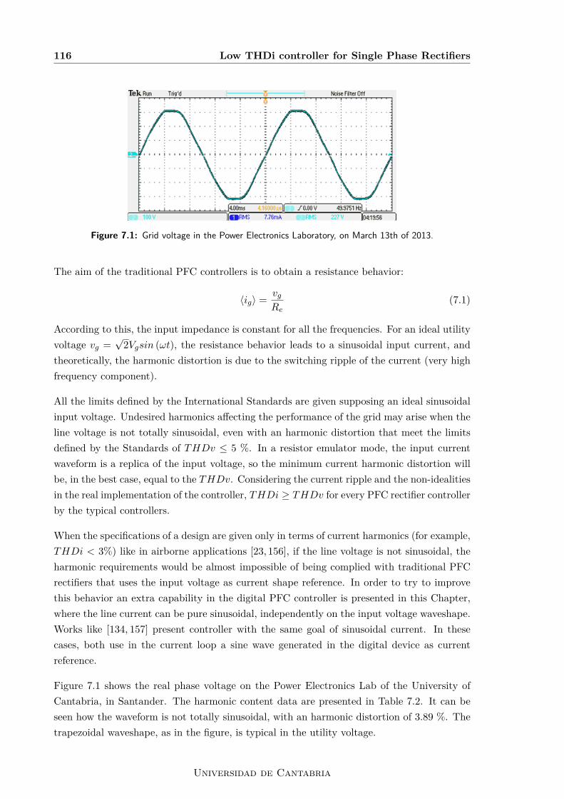
116 Low THDi controller for Single Phase Rectifiers
Figure 7.1: Grid voltage in the Power Electronics Laboratory, on March 13th of 2013.
The aim of the traditional PFC controllers is to obtain a resistance behavior:
〈ig〉 = vgRe
(7.1)
According to this, the input impedance is constant for all the frequencies. For an ideal utilityvoltage vg =
√2Vgsin (ωt), the resistance behavior leads to a sinusoidal input current, and
theoretically, the harmonic distortion is due to the switching ripple of the current (very highfrequency component).
All the limits defined by the International Standards are given supposing an ideal sinusoidalinput voltage. Undesired harmonics affecting the performance of the grid may arise when theline voltage is not totally sinusoidal, even with an harmonic distortion that meet the limitsdefined by the Standards of THDv ≤ 5 %. In a resistor emulator mode, the input currentwaveform is a replica of the input voltage, so the minimum current harmonic distortion willbe, in the best case, equal to the THDv. Considering the current ripple and the non-idealitiesin the real implementation of the controller, THDi ≥ THDv for every PFC rectifier controllerby the typical controllers.
When the specifications of a design are given only in terms of current harmonics (for example,THDi < 3%) like in airborne applications [23, 156], if the line voltage is not sinusoidal, theharmonic requirements would be almost impossible of being complied with traditional PFCrectifiers that uses the input voltage as current shape reference. In order to try to improvethis behavior an extra capability in the digital PFC controller is presented in this Chapter,where the line current can be pure sinusoidal, independently on the input voltage waveshape.Works like [134, 157] present controller with the same goal of sinusoidal current. In thesecases, both use in the current loop a sine wave generated in the digital device as currentreference.
Figure 7.1 shows the real phase voltage on the Power Electronics Lab of the University ofCantabria, in Santander. The harmonic content data are presented in Table 7.2. It can beseen how the waveform is not totally sinusoidal, with an harmonic distortion of 3.89 %. Thetrapezoidal waveshape, as in the figure, is typical in the utility voltage.
Universidad de Cantabria

7.2 Definitions of Electric Power Quantities 117
Vrms THDv V1,rms V3,rms V5,rms V7,rms V9,rms V11,rms
227.60 3.89 % 227.15 3.86 7.58 2.44 0.94 0.23
Table 7.2: Voltage harmonics in the line voltage shown in Fig. 7.1.
7.2 Definitions of Electric Power Quantities
The IEEE Std 1459 [158] defines the electric power to quantify the flow of electrical energyin single-phase and three-phase circuits under sinusoidal, non-sinusoidal, balanced and un-balanced conditions. Considering an non-sinusoidal (distorted) voltage vg, or current ig, in asingle-phase system, they can be written as:
vg = vg1 + vgH (7.2)
ig = ig1 + igH (7.3)
where vg1 and ig1 are the fundamental components defined by (7.4) and (7.5), respectively.And the harmonic content of the voltage vgH , and the current igH , defined by (7.6) and (7.7).h represents the harmonic component number, αh the phase of the hth harmonic voltagecomponent and βh the phase of the hth harmonic current.
vg1 =√
2Vg1sin (ωt) (7.4)
ig1 =√
2Ig1sin (ωt− β1) (7.5)
vgH = Vg0 +√
2∑h6=1
Vghsin (hωt− αh) (7.6)
igH = Ig0 +√
2∑h6=1
Ighsin (hωt− βh) (7.7)
The RMS values squared of the input current and voltage are as follows:
V 2g = V 2
g1 + V 2gH (7.8)
I2g = I2
g1 + I2gH (7.9)
being Vg1 and Ig1 the RMS values of the both fundamental components, and VgH and IgHthe square of the RMS values of vgH and igH , which are defined as:
IgH =√I2g − I2
g1 (7.10)
Víctor M. López Martín

118 Low THDi controller for Single Phase Rectifiers
andVgH =
√V 2g − V 2
g1, (7.11)
respectively. With these terms, the total harmonic distortion (THD) of the current andvoltage are expressed as:
THDv = VgHVg1
=
√√√√( VgVg1
)2
− 1 (7.12)
THDi = IgHIg1
=
√√√√( IgIg1
)2
− 1 (7.13)
The total active power (Pg) generated by all the components involved can be divided in twoterms Pg = Pg1 + PgH , where Pg1 represents the fundamental active power, and PgH theharmonic active power (or non-fundamental active power). Both terms are written as:
Pg1 = Vg1Ig1cos (β1) (7.14)
PgH = Vg0Ig0 +∑h6=1
VghIghcos (βh − αh) = Pg − Pg1 (7.15)
The total apparent power (Sg = VgIg) represents the amount of total power that can besupplied to a load under ideal conditions (sinusoidal voltage and current). In the samemanner, the fundamental apparent power is “generated” only by the fundamental componentsSg1 = Vg1Ig1. The IEEE Std 1459 defines the fundamental power factor (PF1) and the powerfactor (PF ) as function of the variables presented before as:
PF1 = Pg1Sg1
= cosβ1 (7.16)
PF = PgSg
= PF11 + PgH/Pg1√
1 + THDi2 + THDv2 + (THDi·THDv)2(7.17)
The approach presented in this Chapter is a digital controller for front-end Boost convertersworking in the CCM, in which the input current can be pure sinusoidal (Case A), or can beproportional to the input voltage and work as a traditional PFC stage (Case B). The userdecide among the two possibilities.
A study of the value of PF as function of the THDv for the two cases is done as follows:
- Case A: The current is sinusoidal: THDi = 0%, consequently no harmonic active powerflows through the system: PgH = 0 W . Fundamental components of the current andthe voltage are in phase, cosβ1 = 1. According to that, the PF value is rewritten as:
PF = 1√1 + THDv2
(7.18)
Universidad de Cantabria

7.3 Low THDi controller under distorted voltages 119
0 5 10 15 200.98
0.985
0.99
0.995
1
THDv [%]
Pow
er F
acto
r [P
F]
Case B
Case A
Figure 7.2: Value of the power factor as function of the voltage harmonic distortion for Case Aand Case B.
- Case B: The current is proportional to the input voltage (traditional behavior as a resistorwith a value Re): THDi = THDv, and due to that, the harmonic active power flowsthrough the system: PgH = V 2
gH/Re . The fundamental components of the current andthe voltage are in phase, cosβ1 = 1. According to that, the PF value can be rewrittenas:
PF = 1 + THDv2√
1 + 2·THDv2 + THDv4= 1 (7.19)
Figure 7.2 shows the value of PF as a function of the THDv. In both cases, the value of thefundamental power factor PF1 = 1, but it can be seen how the PF value decreases with theharmonic distortion if the current taken from the grid is sinusoidal . From the user point ofview, the case preferred is the resistance behavior (Case B, as a traditional PFC controller),because the power factor is the higher. The behavior with a totally sinusoidal current (CaseA) is preferred only if the specifications are given in terms of current harmonics, becauseideally, it is possible to obtain a pure sinusoidal waveform without dependence on the voltagesource. From the point of view of the utility grid, Case A is preferred because the loadperforms some active filter action avoiding the propagation of the harmonics presented in theutility voltage.
7.3 Low THDi controller under distorted voltages
The goal of the new approach presented in this Chapter, is to implement an extra capabilityin the controller in which the low-frequency portion of the input current is pure sinusoidal,according to:
〈ig〉 = PgVg
√2sin (ωt) (7.20)
Víctor M. López Martín

120 Low THDi controller for Single Phase Rectifiers
This controller based on the NLC controller presented in [15] to obtain an input currentproportional to the AC voltage. Defining the distorted AC line voltage as vg = vg1 + vgH ,with the fundamental component vg1 =
√2Vg1sin (ωt), exp. (7.20) can be rewritten as a
function of vg1:〈ig〉 = vg1
Rfict(7.21)
where Rfict is a fictitious resistor that represents the proportionality between the inputcurrent ig and the fundamental component of the voltage vg1. Substituting (7.2) in (7.21), itis obtained:
〈ig〉 = vg − vgHRfict
(7.22)
Considering the converter operating in the CCM, the ideal quasisteady-state conversion cha-racteristic is given by:
vg = Vo (1− d) (7.23)
and vg can be eliminated from exp. (7.22), obtaining
〈ig〉 = Vo (1− d)Rfict
− vgHRfict
(7.24)
The output voltage is considered a DC constant value at the specified reference level Vo =Vref . The first term Vo(1−d)
Rfict, is similar to the NLC control law shown in [15] or as LPCM
control in [146], that is a modification of the NLC controller presented before and corres-ponds with the expression that describes a PWM block. According to (7.24), the duty cyclecommand can be obtained by comparing a sample the average value of the current ig, witha triangular carrier signal vm, defined as:
vm = Vm
(1− t
Tsw
)− rs
vgHRfict
, 0 ≤ t ≤ Tsw (7.25)
where Vm = rsVo/Rsfict, being rs the value of the current sensor used to sample the inputcurrent. Figure 7.3 shows the control waveforms over a half line cycle, for an input voltagewith a THDv = 6 % with vg3 = 0.05Vg1
√2sin (3ωt), vg5 = 0.03Vg1
√2sin (5ωt+ π) and
vg7 = 0.01Vg1√
2sin (7ωt). For clarification purposes, Tsw has been depicted much longerthan the actual implemented switching period. The carrier signal has a frequency equal tothe switching frequency fsw = 1/Tsw, and the second term, vgH
Rfict, offsets the carrier signal in
each switching period. Considering the utility period, the second term means a low frequencyharmonic content in the carrier signal.
The value of Rfict changes with the load and is given by the outer voltage loop in terms ofVm [15]. A block diagram of the boost rectifier with the low THDi controller is shown in Fig.7.4. In grey, the part of the controller that is completely digital is highlighted. In this case,the current used in the controller is the rebuilt current ireb, but this approach can be usedtoo for the sensed input current ig, without any modification in the control law (rs is notused in the current estimation case, where ireb and vm signal are both digital). The input
Universidad de Cantabria

7.3 Low THDi controller under distorted voltages 121
0 0.001 0.002 0.003 0.004 0.005 0.006 0.007 0.008 0.009 0.01-30
-20
-10
0
10
20
Vol
tage
[V
]
0 0.001 0.002 0.003 0.004 0.005 0.006 0.007 0.008 0.009 0.01-20
-15
-10
-5
0
5
10
15
20
Time [seconds]
Vol
tage
[V
]Vm(1-t/Tsw)
vgH
vg3 vg5
vg7
Figure 7.3: Top: First term of the carrier signal (red) and the harmonic voltage (blue) wave-forms. Bottom: Voltage harmonics in an example of input voltage with THDv =6 % .
voltage vg, is digitized by the input voltage ADC, and with a digital zero crossing detector(ZCD) and sinusoidal pattern ins synchronized with the utility line voltage. A peak detectorfor the input voltage is used to approximate the value of vg1 as: vg1 ≈ Vg,peaksin (ωt). Hence,(7.21) can be rewritten as:
〈ig〉 = Vg,peakRfict
sin (ωt) (7.26)
In the case that vg1 6= Vg,peaksin (ωt), in the initial transient state ig is totally sinusoidalaccording to (7.26), but with a RMS value different to reference the demanded by the load.The outer voltage loop modifies then Vm and Rfict to adjust the input RMS current Ig.
With this, it is possible to obtain an indirect measurement of the harmonic voltage vgH =vg − Vg,peaksin (ωt). Using as digital device a microcontroller or an FPGA, the Fast FourierTransforms (FFT) is a good choice to obtain the harmonic content of a variable, with dedi-cated blocks to compute this, like [159,160], but it needs an important quantity of resources.In this case, the particular value of each voltage harmonic is not needed, so only the totalharmonic voltage vgH , is enough. Therefore, FFT blocks can be avoided, simplifying thedesign of the digital controller.
Note that with the proposed controller, the load viewed by the grid Re, is now a function ofthe input voltage phase, Re = Re (ωt). In steady state, and for a defined input power Pg, the
Víctor M. López Martín

122 Low THDi controller for Single Phase Rectifiers
Driver
+‐
vg
voC
DL
Q
vgs
verror
Vref
Re
Carrier generator
ADC ZCD
Peak
sint
X
Voltage controller
Vm
ireb
+‐
vg1
ADC
÷
Rfict=Vo/Vm
+‐
vgH
vm
R
Figure 7.4: Block diagram of the low THDi controller with the boost converter.
input current can be rewritten as:
〈ig〉 = PgVg
√2sin (ωt) (7.27)
that compared with (7.26) yields an expression for Rfict:
Rfict = Vg,peakVg
Pg√
2(7.28)
From (7.1) and (7.21), it is possible to obtain the expression for the input impedance Re:
Re (ωt) = Rfictvg1vg
= RfictVg,peaksin (ωt)vg
(7.29)
Equation (7.23) in only valid if the converter operates in the CCM. So around the AC linezero crossings, where the converter operates in the DCM, a little distortion in the inputcurrent occurs. It is presented in detail in [15] and in Section (3.2) of this document for thetraditional NLC controller, and affects in the same way in this low THDi controller. NLCcontrol is presented in [64] for rectifiers based on buck-boost, Ćuk or SEPIC topologies, and inthe same way as presented here, the low THDi controller can be extrapolated to them. If thebandwidth of the linear input current loop keeps constant but the line frequency increases, thetypical distortion around the line zero-crossing could make impossible to meet the harmoniclimits. This issue is addressed in [161,162]. Nonlinear controllers can deal with this problem,offering responses cycle-by-cycle [18,148,163].
Universidad de Cantabria

7.4 Chapter conclusion 123
7.4 Chapter conclusion
In this Chapter, a modification in the NLC controller has been presented, in order to demanda sinusoidal input current despite input voltage distortion. Therefore, no currents harmonicsare injected to the grid, no contributing in the propagation of the voltage distortion. Theinput voltage measurement is compared with a digital sinusoidal pattern to compute theharmonics in the input voltage, and modify the amplitude of the carrier signal used in theNLC control law.
No additional analog components are needed in comparison with the traditional control, be-cause the modification is completely digital. The user selects the desired behavior (resistancebehavior or pure sinusoidal current).
Víctor M. López Martín

124 Low THDi controller for Single Phase Rectifiers
Universidad de Cantabria

Chapter 8
Experimental validation
The previous Chapters have presented the theoretical approach and simulations of the digitalSensorless controller for Boost PFC rectifiers based on the current estimation concept. In thisChapter, an experimental validation is presented. A scheme and a picture of the laboratoryset-up are presented in Fig. 8.1a and 8.1b, respectively. An AC power source suppliesthe Boost PFC rectifier to emulate the electrical grid under different conditions, a poweranalyzer samples the input voltage and current RMS values with a 1-second sample period,and an oscilloscope is used to capture different signals of the system. The boost converter iscontrolled with a Spartan 3 FPGA used as digital device. A resistor array is used as load.
The aim of all the results presented in this Chapter is to show the behavior of the digitalcontroller under several conditions, illustrating its “universality”.
8.1 Boost converter prototype
A 1 kW Boost PFC rectifier is built to verify the Sensorless PFC controller presented in thisThesis, based on the input current rebuilding concept. The circuit scheme corresponding tothe experimental prototype is shown in Fig. 8.2a, in which the control circuitry is representedin blue and green. The values of all the parameters and components of the laboratoryprototype are listed in Table 8.1.
The part of the control circuit drawn in green does not represent any novelty in comparisonwith other types of digital controllers presented in PFC rectifiers; and corresponds with theinput and output voltage sampling circuit, with the ADCs, and the circuit that adapts theon− off signal generated in the digital device to drive the MOSFET. Two voltage dividers(Rg1 and Rg2 for the input voltage, and Ro1 and Ro2 for the output voltage) set the voltagesamples into the full scale range (vmax = 5 V) of the control circuit.
125

126 Experimental validation
AC power source Boost PFC rectifier
FPGAPower Analyzer
Oscilloscope
Computer
(a)
(b)
Figure 8.1: (a) Block diagram and (b) picture of the of the Laboratory Test bench
Element Value/ComponentInductor (L) L =1 mH, RL =0.25 W
Power Diode (D) IDH12S60, VD =0.8 V, RD =0.07 WOutput Capacitor (C) C =220 mF, 450 VPower MOSFET (Q) IRFP27N60K, Ron =180 mW
Driver HCPL 3120Signal resistor Rg1 = Ro1 1 MW ±0.1 %Signal resistor Rg2 = Ro2 10.7 kW ±0.1 %Signal resistor Ra = Rds1 1.2 MW ±1 %Signal resistor Rb = Rds2 9.31 kW ±1 %
Signal diodeDds 1N4148Signal comparator Co and Cds MAX942CPA
Signal resistor Rrc 2.2 kW ±5 %Signal capacitor Crc 3.3 nF ± 20 %
ADC TLV1572, Nbits = 10, vmax =5 V
Table 8.1: Parameters of the components used in the Boost prototype.
Universidad de Cantabria

8.1 Boost converter prototype 127
Digital device
Driver
ADC+-
+-
Rrc
Crc
Rds2
Rds1
Ro2
Ro1
DL
Rg2
Rg1vg +vo
-
on-off
Rb
Ra
Dds
Q
Co Cds
x1
*dsv
(a)
(b)
Figure 8.2: (a) Circuit scheme of the proposed digital controller. (b) Picture of the boostconverter prototype and the FPGA.
Víctor M. López Martín

128 Experimental validation
0 0.001 0.002 0.003 0.004 0.005 0.006 0.007 0.008 0.009 0.010.53
0.535
0.54
0.545
0.55
0.555
0.56
Time [seconds]
q g [
V/b
it] qg, qg,TLV
DCMigDCMireb
vg
ig
Figure 8.3: Top: Measured value of qg over the half line cycle, for two different input voltagesADCs, under 230 Vrms (50 Hz). In red it is plotted the measured value using theTLV1572 commercial ADC. In blue is plotted the qg value using the Σ4 ADC usedin the output voltage measurement, that leads to the ig current waveform at 648W. Bottom: Experimental waveforms when the Σ4 ADC is used in the output, andalso in the input voltage measurement.
With these values of the divider resistances, the maximum voltage in the converter thatcan be quantized, without saturation of the ADCs, is 473 V. As input voltage ADC, acommercial TLV1572 10-bits is used, with 1.25 MSPS. And an ad− hoc sigma-delta, as theADCs presented in Section 2.6 (Fig. 2.18) is used to measure the output voltage with theconcepts presented in [10,14,122–124].
A commercial ADC is used to discretize the input voltage to avoid non-linearities (vg is arectified sinusoidal waveform with a zero minimum value and a peak value up to 325 V),trying to keep qg constant over the half line cycle. Figure 8.3 shows the measured qg over thehalf line cycle under the European line voltage (230 Vrms - 50 Hz) for the commercial ADC,labeled as qg,TLV ; and using a low-cost Σ4 ADC similar to the ADC used in the outputvoltage, qg,Σ∆. The higher variation of qg,Σ∆ in comparison with qg,TLV makes this type ofADCs not valid for this sensorless controller to quantize vg. In Fig. 8.3, the input currentwaveform at 648 W is also presented, with a power factor of PF =0.948 and TDHi =29.35% using the Σ4 ADC in the input voltage.
On the other hand, the output voltage is quasi-constant over the half line cycle (with a small
Universidad de Cantabria

8.2 Operation in Steady state 129
ripple), so the Σ4 ADC approach can be used, because its behavior is linear around thereference voltage.
The part of the control circuit highlighted in blue is a contribution of this work, and corres-ponds with the analog part that substitutes the current sensing circuit. Rds1, Rds2 and Dds
adapts the MOSFET drain-to-source voltage to be an input of the digital device (v∗ds). Atthe same time v∗ds is compared by Cds with the output voltage, adapted by Ra and Rb toobtain the digital signal x1 used to detect the DCM in ig.
The whole digital controller is described in VHDL and implemented on a XC3S200E FPGA ofXilinx. The input current and power are measured with a Power Analyzer Voltech PM1000+,and the captures presented in this Chapter are taken with MSO2014 mixed Signal Oscilloscopeof Tektronix. The output voltage reference is 400 Vdc, with an input voltage ranging from85 Vrms-60 Hz to 250 Vrms-50 Hz (universal input voltage range). Three different switchingfrequencies has been used to test the proposal (72 kHz, 96 kHz and 144 kHz), and theprototype is also tested under high frequency grids, typical of airborne applications (360 -800 Hz).
8.2 Operation in Steady state
The experimental results obtained in steady state under different input voltages and powerlevels are presented in this section, with three different subsections depending on the switchingfrequency value. In all the captures, the input voltage (vg) and current (ig) are plotted alongwith the DCM signal of the rebuilt input current (DCMireb) and the real input current(DCMig). Five different input voltage levels have been tested, three of them at 50 Hz (250,230 and 180 Vrms), and two at 60 Hz (120 and 85 Vrms).
The steady state experimental results, with the digital controller settled with a constantswitching frequency of 72 kHz, presented in figures 8.4, 8.5, 8.6, 8.7, 8.8, show the waveformscaptured under 250, 230, 180, 120 and 85 Vrms input voltage, respectively; at different powerlevels. The power level, power factor and total harmonic distortion values are introduced ineach capture caption. Furthermore, Table 8.2 presents all the captured values together for thewaveforms previously presented. In each case, the current harmonics (up to 11th harmonic)are addressed too, compared with the current limits defined by the IEC 61000-3-2 Std forClass C equipment.
It can be seen that in all the cases, power factor correction is achieved and DCM signalsDCMireb and DCMig are matched despite not measuring the input (inductor) current. Thebest PF and THDi are obtained at higher power levels, and in all the tested conditions, thecurrent limits given by the standard are higher than the experimental results. It must beremarked that the digital controller has not been re-tuned or modified to operate under thedifferent conditions, showing the universality of the approach presented in this work.
The ON-time (t∗on), and the ON-time modification measurement (∆tmeason ≈ ∆ton) due to thedrive signal delays over the half line cycle are shown in Fig. 8.9 for different loads (320 W,
Víctor M. López Martín

130 Experimental validation
Current Harmonics (A)Vg Pg P F T HDi I1 I2 I3 I5 I7 I9 I11
250 V
482.2 W 0.974 12.36 %1.726 0.006 0.195 0.06 0.032 0.024 0.016Limits 0.035 0.505 0.173 0.121 0.086 0.052
637.0W 0.991 6.87 %2.562 0.005 0.172 0.031 0.008 0.016 0.005Limits 0.051 0.762 0.256 0.179 0.128 0.077
803.9 W 0.995 4.97 %3.222 0.003 0.154 0.040 0.016 0.011 0.007Limits 0.064 0.962 0.322 0.226 0.161 0.097
973.8 W 0.997 3.13 %3.901 0.004 0.110 0.049 0.024 0.015 0.003Limits 0.078 1.167 0.390 0.273 0.195 0.117
230 V
319.7 W 0.974 9.48 %1.38 0.003 0.112 0.068 0.013 0.020 0.005
Limits 0.028 0.403 0.138 0.097 0.069 0.041
480.2 W 0.985 8.76 %2.09 0.004 0.177 0.032 0.019 0.016 0.007
Limits 0.042 0.619 0.209 0.147 0.105 0.063
637.5 W 0.990 6.85 %2.782 0.004 0.186 0.034 0.025 0.009 0.004Limits 0.056 0.827 0.278 0.195 0.139 0.083
804.8 W 0.995 4.20 %3.509 0.004 0.135 0.051 0.029 0.013 0.005Limits 0.070 1.047 0.351 0.246 0.175 0.105
975.2 W 0.997 2.55 %4.253 0.004 0.089 0.048 0.039 0.018 0.003Limits 0.085 1.272 0.425 0.298 0.213 0.128
180 V
320.7 W 0.979 8.00 %1.789 0.003 0.134 0.049 0.011 0.003 0.005Limits 0.036 0.525 0.179 0.125 0.089 0.054
484.1W 0.990 4,88 %2.69 0.004 0.113 0.064 0.024 0.007 0.004
Limits 0.054 0.801 0.270 0.018 0.135 0.081
646.5 W 0.995 2.96 %3.600 0.003 0.061 0.082 0.027 0.006 0.006Limits 0.072 1.074 0.360 0.252 0.180 0.180
817.9 W 0.996 3.17 %4.555 0.005 0.099 0.101 0.028 0.011 0.005Limits 0.091 1.361 0.405 0.318 0.228 0.137
120 V
157.3 W 0.968 10.99 %1.357 0.007 0.146 0.023 0.013 0.013 0.012Limits 0.027 0.394 0.136 0.095 0.068 0.041
327.6 W 0.991 5.81 %2.741 0.005 0.155 0.036 0.013 0.008 0.005Limits 0.055 0.815 0.274 0.192 0.137 0.082
496.8 W 0.997 2.22 %4.153 0.004 0.076 0.045 0.026 0.019 0.016Limits 0.083 1.242 0.415 0.291 0.208 0.125
85 V164.2 W 0.989 5.06 %
1.939 0.004 0.079 0.059 0.005 0.006 0.008Limits 0.039 0.575 0.194 0.136 0.097 0.058
340.2 W 0.996 3.33 %4.022 0.005 0.084 0.087 0.052 0.047 0.008Limits 0.080 1.202 0.402 0.282 0.201 0.121
Table 8.2: Experimental results in steady state with a switching frequency fsw =72 kHz
Universidad de Cantabria

8.2 Operation in Steady state 131
vg
ig
DCMirebDCMig
(a) Pg = 482.2 W, PF = 0.974, THDi = 12.36 %
vg
ig
DCMirebDCMig
(b) Pg =637.0 W, PF =0.991, THDi =6.87 %
vg
ig
DCMirebDCMig
(c) Pg =803.9 W, PF =0.995, THDi =4.97 %
vg
ig
DCMirebDCMig
(d) Pg =973.8 W, PF =0.997, THDi =3.13 %
Figure 8.4: Experimental results: input voltage (vg) and current (ig) along with the DCMsignal of the rebuilt input current (DCMireb) and the real input current (DCMig).Waveforms under Vg =250 Vrms - 50 Hz, at 72 kHz switching frequency for differentpower levels.
480 W and 970 W) in steady state, when the DCM times are matched (ig with sinusoidalshape). These delays are function of the MOSFET gate resistor value and the, drain currentand the MOSFET parasitic elements. These values are measured, every switching period,with the circuit shown in Fig. 5.4. These measured values are used in the digital controllerto compensate the PFC algorithm as it has been presented in Section 5.2 . The drive signaldelays are measured in the switching period j − 1, to be applied in the compensation in theswitching period j.
Figure 8.10 shows the experimental PF values measured at 640 W for different values ofthe delays used in the compensation algorithm 4tmeason , constant over the half line cycle4tmeason [j] = 4tmeason ∀ j. The experimental results, compared with the results presented inTable 8.2, shows in what extend this assumption causes an important current distortion withPF values always lower than 0.98 . Input voltage and current waveforms of two situationsare shown in Fig. 8.11, that corresponds to 4tmeason =100 ns (Fig. 8.11a) and 220 ns (Fig.8.11b) cases. These results demonstrate that feedforward compensation with the continuousmeasurement of the switching delays is needed, and constant switching delays considerationdoes not assure sinusoidal input current [154].
Figure 8.12 shows the main waveforms of the DCM condition detection circuit for the realinput current, with Rds1 = Ra = 1.2 MW and Rds2 = Rb = 9.31 kW. The digital signal,DCMig changes to ‘1’ when the first DCM oscillation in the drain-to-source voltage occurs.It can be seen how experimental and theoretical waveforms (Fig. 5.6) are in good agreement.
Víctor M. López Martín

132 Experimental validation
vg
ig
DCMirebDCMig
(a) Pg =319.7 W, PF =0.974, THDi =9.48 %
vg
ig
DCMirebDCMig
(b) Pg =480.2 W, PF =0.985, THDi =8.76 %
vg
ig
DCMirebDCMig
(c) Pg =637.5 W, PF =0.990, THDi =6.85 %
vg
ig
DCMirebDCMig
(d) Pg =804.8 W, PF =0.995, THDi =4.20 %
vg
ig
DCMirebDCMig
(e) Pg =975.2 W, PF =0.997, THDi =2.55 %
Figure 8.5: Experimental results: input voltage (vg) and current (ig) along with the DCMsignal of the rebuilt input current (DCMireb) and the real input current (DCMig).Waveforms under Vg =230 Vrms - 50 Hz, at 72 kHz switching frequency for differentpower levels.
Universidad de Cantabria

8.2 Operation in Steady state 133
vg
ig
DCMirebDCMig
(a) Pg =320.7 W, PF =0.979, THDi =8.00 %
vg
ig
DCMirebDCMig
(b) Pg =484.1 W, PF =0.990, THDi =4.88 %
vg
ig
DCMirebDCMig
(c) Pg =646.5 W, PF =0.995, THDi =2.96 %
vg
ig
DCMirebDCMig
(d) Pg =817.9 W, PF =0.996, THDi =3.17 %
Figure 8.6: Experimental results: input voltage (vg) and current (ig) along with the DCMsignal of the rebuilt input current (DCMireb) and the real input current (DCMig).Waveforms under Vg =180 Vrms - 50 Hz, at 72 kHz switching frequency for differentpower levels.
vg
ig
DCMirebDCMig
(a) Pg =157.3 W, PF =0.968, THDi =10.99 %
vg
ig
DCMirebDCMig
(b) Pg =327.6 W, PF =0.991, THDi =5.81 %
vg
ig
DCMirebDCMig
(c) Pg =496.8 W, PF =0.997, THDi =2.22 %
Figure 8.7: Experimental results: input voltage (vg) and current (ig) along with the DCMsignal of the rebuilt input current (DCMireb) and the real input current (DCMig).Waveforms under Vg =120 Vrms - 60 Hz, at 72 kHz switching frequency for differentpower levels.
Víctor M. López Martín

134 Experimental validation
vg
ig
DCMirebDCMig
(a) Pg =164.2 W, PF =0.989, THDi =5.06 %
vg
ig
DCMirebDCMig
(b) Pg =340.2 W, PF =0.996, THDi =3.33 %
Figure 8.8: Experimental results: input voltage (vg) and current (ig) along with the DCMsignal of the rebuilt input current (DCMireb) and the real input current (DCMig).Waveforms under Vg =85 Vrms, at 72 kHz switching frequency for different powerlevels.
0 100 200 300 400 500 600 7000
50
100
150
200
Switching period [j]
ton
[ns
]
0 100 200 300 400 500 600 7000
5
10
15
ON
-Tim
e [
s]
970 W
480 W
320 W
Figure 8.9: Experimental results: Value of the duty cycle modification (4ton) due to the drivesignal delays over the half line cycle.
Universidad de Cantabria

8.2 Operation in Steady state 135
60 80 100 120 140 160 180 200 220 2400.91
0.92
0.93
0.94
0.95
0.96
0.97
0.98
measont
Constant delays compensation
[ns]
PF
Figure 8.10: Power factor value for different delays used in the feedforward compensation whenthey are considered constant over the half line cycle.
vg
ig
DCMigDCMireb
(a)
vg
ig
DCMigDCMireb
(b)
Figure 8.11: Input current and voltage waveforms if the feedforward is done considering constantdrive signal delays. (a) 4tmeason =100 ns and (b) 4tmeason =220 ns
Víctor M. López Martín

136 Experimental validation
DCM oscillation
on-off
vds
x1
DCMig
Figure 8.12: Experimental results for the DCM condition detection circuit for the real inputcurrent.
To demonstrate the universality of the controller with feedback control, a second inductor (L2)has been built, and the experimental results are achieved without modifying any parameterof the digital controller (the DCM time feedback loop sets the new value of the signal vdig).The two inductors used in these experimental validation are shown in Fig. 8.13. The firstinductor has been built with a RM12-3C90 core, resulting in the inductance L = 1mH anda measured parasitic resistor in series RL = 0.25 Ω. The second inductor (L2) has been builtwith a soft saturation Kool mµ core 77071. In this case, the inductance L2 = 1.5 mH withRL2 = 0.35 Ω at zero current level. The experimental results in steady-state operation areshown in Fig. 8.14 for two different input voltages (85 Vrms– 60 Hz and 230 Vrms – 50 Hz),output power and the inductance L2. It can be observed that a sinusoidal input current isachieved and DCM times are matched. Power factor and Total harmonic distortion of theinput current (THDi) values are listed in Table 8.3 for wide input voltage (from 85 Vrms –60 Hz to 230 Vrms – 50 Hz) and output power ranges.
Measured THDi are a little higher with L2 than with L at high power load, despite L2 > L.This is caused by the current dependent inductance of the inductor built with a soft saturationcore [150, 151]. The aim of using this inductance in the proposed controller is to showthe behavior of the controller under two different conditions. The use of L2 on one handintroduces a non-linear behavior (addressed in Section 3.3.3) that produces higher currentdistortion as the current increases, and on the other hand, keeps the CCM operation for ahigher load range. Despite this aspect, the experimental results present high power factorvalues for all the tested conditions. It must be remarked that the digital controller has notbeen modified to operate under these different conditions, showing the universality of theapproach presented in this work, with a switching frequency and inductance value similar tothe traditional and commercial analog PFC designs.
The same steady state results are presented with the switching frequency settled at 96 kHzand 144 kHz, with the same devices addressed before. All the results have been obtained
Universidad de Cantabria

8.2 Operation in Steady state 137
35 mm45 mm
Figure 8.13: Inductors used in the experimental results. Left: L = 1 mH (RM12-3C90 corewith RL = 0.25 Ω). Right: L2 = 1.5 mH (soft saturation Kool mµ core withRL2 = 0.35 Ω).
vg
ig
DCMigDCMireb
(a)
vg
ig
DCMigDCMireb
(b)
Figure 8.14: Experimental results: input voltage (vg) and current (ig) along with the DCMsignal of the rebuilt input current (DCMireb) and the real input current (DCMig).Vo = 400 Vdc and L2 = 1.5mH (RL2 = 0.35 W). (a): Vg = 230 Vrms(50Hz),Pg = 970W . (b): Vg = 85 Vrms(60Hz), Pg = 320W .
Víctor M. López Martín

138 Experimental validation
Experimental results with L2 = 1.5mHVg Pg PF THDi
250
460 W 0.975 9.0 %645 W 0.991 8.5 %800 W 0.993 9.5 %970 W 0.993 10.5 %
230
460 W 0.984 8.1 %640 W 0.988 9.1 %800 W 0.992 9.8 %970 W 0.993 10.5 %
180
323 W 0.980 5.4 %485 W 0.989 7.1 %650 W 0.992 8.6 %820 W 0.991 10.5 %
120497 W 0.996 9.8 %323 W 0.988 9.8 %497 W 0.996 9.8 %
85 161 W 0.989 5.0 %336 W 0.993 9.0 %
Table 8.3: Power Factor and THDi values under different conditions.
with the initial mentioned inductance L =1 mH (RL = 0.25 Ω). It must be remarked thatonly the switching frequency has been modified, not controller coefficients, that are the samefor all the conditions. Figures 8.15, 8.16, 8.17, 8.18 and 8.19 show the waveforms capturedat 250, 230, 180, 120 and 85 Vrms input voltage, respectively; at different power levels withthe digital controller tuned at 96 kHz, that corresponds with the measured data presented inTable 8.4.
And the steady state results obtained which a switching frequency of 144 kHz are enumeratedin Table 8.5 for the same conditions presented before. The waveforms captured in thoseconditions are shown in Fig. 8.20, 8.21, 8.22, 8.23 and 8.24.
8.3 Time evolution under different conditions
In Chapters 4 and 5, a digital compensation of all the current estimation error that canoccur in the sensorless controller for Boost PFC rectifiers has been presented. Among allthe causes of current estimation error, the influence of the parasitic elements is the only onethat depends on the current/power level. The DCM times feedback loop is needed to assurethe correct behavior under different conditions. To illustrate the behavior of the proposeddigital compensation, the time evolution of the PF and THDi values are plotted in the timedomain. A Voltech PM1000+ Power Analyzer is used to capture these data, with a sampleperiod of 1 second.
Figure 8.25 shows the time evolution of these variables under different load steps, with anEuropean Grid input voltage and a constant switching frequency of 144 kHz. The evolution
Universidad de Cantabria

8.3 Time evolution under different conditions 139
vg
ig
DCMirebDCMig
(a) Pg =481.9 W, PF =0.992, THDi =5.86 %
vg
ig
DCMirebDCMig
(b) Pg =639.6 W, PF =0.995, THDi =5.45 %
vg
ig
DCMirebDCMig
(c) Pg =806.9 W, PF =0.997, THDi =2.99 %
vg
ig
DCMirebDCMig
(d) Pg =976.3 W, PF =0.998, THDi =2.68 %
Figure 8.15: Experimental results: input voltage (vg) and current (ig) along with the DCMsignal of the rebuilt input current (DCMireb) and the real input current (DCMig).Waveforms under Vg =250 Vrms - 50 Hz, at 96 kHz switching frequency fordifferent power levels.
vg
ig
(a) Pg =480.6 W, PF =0.991, THDi =6.17 %
vg
ig
(b) Pg =637.8 W, PF =0.993, THDi =6.90 %
vg
ig
(c) Pg =803.9 W, PF =0.996, THDi =4.57 %
vg
ig
(d) Pg =977.1 W, PF =0.998, THDi =2.55 %
Figure 8.16: Experimental results: input voltage (vg) and current (ig) along with the DCMsignal of the rebuilt input current (DCMireb) and the real input current (DCMig).Waveforms under Vg =230 Vrms - 50 Hz, at 96 kHz switching frequency fordifferent power levels.
Víctor M. López Martín

140 Experimental validation
vg
ig
DCMirebDCMig
(a) Pg =324.6 W, PF =0.989, THDi =4.85 %
vg
ig
DCMirebDCMig
(b) Pg =488.3 W, PF =0.995, THDi =3.02 %
vg
ig
DCMirebDCMig
(c) Pg =651.4 W, PF =0.997, THDi =2.27 %
vg
ig
DCMirebDCMig
(d) Pg =822.9 W, PF =0.998, THDi =2.92 %
Figure 8.17: Experimental results: input voltage (vg) and current (ig) along with the DCMsignal of the rebuilt input current (DCMireb) and the real input current (DCMig).Waveforms under Vg =180 Vrms - 50 Hz, at 96 kHz switching frequency fordifferent power levels.
vg
ig
DCMirebDCMig
(a) Pg =162.2 W, PF =0.979, THDi =9.29 %
vg
ig
DCMirebDCMig
(b) Pg =329.4 W, PF =0.994,THDi =4.26 %
vg
ig
DCMirebDCMig
(c) Pg =500.0 W, PF =0.996, THDi =2.43 %
Figure 8.18: Experimental results: input voltage (vg) and current (ig) along with the DCMsignal of the rebuilt input current (DCMireb) and the real input current (DCMig).Waveforms under Vg =120 Vrms - 60 Hz, at 96 kHz switching frequency fordifferent power levels.
Universidad de Cantabria

8.3 Time evolution under different conditions 141
vg
ig
DCMirebDCMig
(a) Pg =165.1 W, PF =0.991, THDi =5.62 %
vg
ig
DCMirebDCMig
(b) Pg =340.7 W, PF =0.994, THDi =4.80 %
Figure 8.19: Experimental results: input voltage (vg) and current (ig) along with the DCMsignal of the rebuilt input current (DCMireb) and the real input current (DCMig).Waveforms under Vg =85 Vrms, at 96 kHz switching frequency for different powerlevels.
vg
ig
DCMirebDCMig
(a) Pg =480.5 W, PF =0.992, THDi =7.57 %
vg
ig
DCMirebDCMig
(b) Pg =638.8 W, PF =0.994, THDi =6.99 %
vg
ig
DCMirebDCMig
(c) Pg =806.7 W, PF =0.997, THDi =5.55 %
vg
ig
DCMirebDCMig
(d) Pg =978.4 W, PF =0.999, THDi =3.07 %
Figure 8.20: Experimental results: input voltage (vg) and current (ig) along with the DCMsignal of the rebuilt input current (DCMireb) and the real input current (DCMig).Waveforms under Vg =250 Vrms - 50 Hz, at 144 kHz switching frequency fordifferent power levels.
Víctor M. López Martín

142 Experimental validation
Current Harmonics (A)Vg Pg P F T HDi I1 I2 I3 I5 I7 I9 I11
250 V
481.9 W 0.992 5.86 %1.919 0.006 0.114 0.037 0.007 0.019 0.021Limits 0.038 0.517 0.192 0.134 0.096 0.058
639.6 W 0.995 5.45 %2.560 0.006 0.133 0.031 0.020 0.005 0.013Limits 0.051 0.764 0.256 0.179 0.128 0.077
806.9 W 0.997 2.99 %3.231 0.007 0.091 0.044 0.023 0.017 0.009Limits 0.065 0.966 0.323 0.226 0.162 0.097
976.3 W 0.998 2.68 %3.908 0.007 0.094 0.052 0.031 0.022 0.021Limits 0.078 1.170 0.391 0.274 0.195 0.117
230 V
480.6 W 0.991 6.17 %2.586 0.007 0.156 0.038 0.013 0.005 0.014Limits 0.052 0.769 0.259 0.181 0.129 0.078
637.8 W 0.993 6.90 %2.784 0.006 0.189 0.023 0.023 0.011 0.012Limits 0.056 0.829 0.278 0.195 0.139 0.084
803.9 W 0.996 4.57 %3.513 0.007 0.129 0.059 0.020 0.010 0.011Limits 0.070 1.049 0.351 0.246 0.176 0.105
977.1 W 0.998 2.55 %4.251 0.010 0.078 0.063 0.032 0.007 0.011Limits 0.085 1.273 0.425 0.298 0.213 0.128
180 V
324.6 W 0.989 4,85 %1.813 0.009 0.050 0.068 0.005 0.013 0.006Limits 0.036 0.538 0.181 0.127 0.091 0.054
488.3 W 0.995 3.02 %2.717 0.010 0.047 0.062 0.014 0.06 0.003Limits 0.054 0.811 0.272 0.190 0.136 0.081
651.4 W 0.997 2.27 %3.629 0.007 0.038 0.064 0.024 0.008 0.006Limits 0.073 1.085 0.363 0.254 0.181 0.109
822.9 W 0.998 2.92 %4.584 0.014 0.105 0.079 0.033 0.017 0.016Limits 0.092 1.373 0.458 0.321 0.229 0.138
120 V
162.2 W 0.979 9.29 %1.366 0.009 0.124 0.008 0.013 0.014 0.008Limits 0.027 0.401 0.137 0.096 0.068 0.041
329.4 W 0.994 4.26 %2.764 0.009 0.111 0.034 0.017 0.013 0.016Limits 0.055 0.824 0.276 0.193 0.138 0.083
500.0 W 0.996 2.43 %4.178 0.011 0.067 0.065 0.046 0.040 0.037Limits 0.084 1.248 0.418 0.292 0.209 0.125
85 V165.1 W 0.991 5.62 %
1.953 0.006 0.097 0.044 0.016 0.023 0.028Limits 0.039 0.580 0.195 0.137 0.098 0.059
340.7 W 0.994 4.80 %4.046 0.005 0.104 0.137 0.090 0.085 0.073Limits 0.081 1.207 0.405 0.283 0.202 0.121
Table 8.4: Experimental results with a switching frequency of 96 kHz.
Universidad de Cantabria
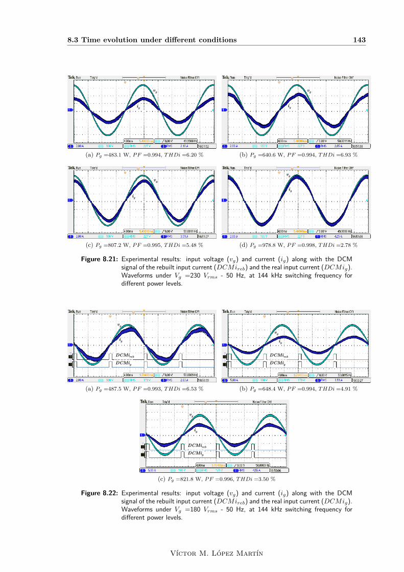
8.3 Time evolution under different conditions 143
vg
ig
(a) Pg =483.1 W, PF =0.994, THDi =6.20 %
vg
ig
(b) Pg =640.6 W, PF =0.994, THDi =6.93 %
vg
ig
(c) Pg =807.2 W, PF =0.995, THDi =5.48 %
vg
ig
(d) Pg =978.8 W, PF =0.998, THDi =2.78 %
Figure 8.21: Experimental results: input voltage (vg) and current (ig) along with the DCMsignal of the rebuilt input current (DCMireb) and the real input current (DCMig).Waveforms under Vg =230 Vrms - 50 Hz, at 144 kHz switching frequency fordifferent power levels.
vg
ig
DCMirebDCMig
(a) Pg =487.5 W, PF =0.993, THDi =6.53 %
vg
ig
DCMirebDCMig
(b) Pg =648.4 W, PF =0.994, THDi =4.91 %
vg
ig
DCMirebDCMig
(c) Pg =821.8 W, PF =0.996, THDi =3.50 %
Figure 8.22: Experimental results: input voltage (vg) and current (ig) along with the DCMsignal of the rebuilt input current (DCMireb) and the real input current (DCMig).Waveforms under Vg =180 Vrms - 50 Hz, at 144 kHz switching frequency fordifferent power levels.
Víctor M. López Martín

144 Experimental validation
vg
ig
DCMirebDCMig
(a) Pg =331.5 W, PF =0.992, THDi =6.61 %
vg
ig
DCMirebDCMig
(b) Pg =503.9 W, PF =0.995, THDi =5.18 %
Figure 8.23: Experimental results: input voltage (vg) and current (ig) along with the DCMsignal of the rebuilt input current (DCMireb) and the real input current (DCMig).Waveforms under Vg =120 Vrms - 60 Hz, at 144 kHz switching frequency fordifferent power levels.
vg
ig
DCMirebDCMig
(a) Pg =167.4 W, PF =0.991, THDi =7.83 %
vg
ig
DCMirebDCMig
(b) Pg =346.6 W, PF =0.988, THDi =11.13 %
Figure 8.24: Experimental results: input voltage (vg) and current (ig) along with the DCMsignal of the rebuilt input current (DCMireb) and the real input current (DCMig).Waveforms under Vg =85 Vrms, at 144 kHz switching frequency for different powerlevels.
Universidad de Cantabria
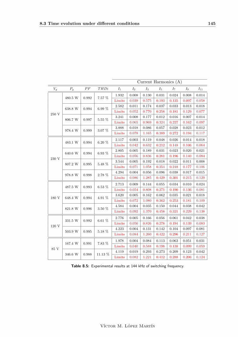
8.3 Time evolution under different conditions 145
Current Harmonics (A)Vg Pg P F T HDi I1 I2 I3 I5 I7 I9 I11
250 V
480.5 W 0.992 7.57 %1.932 0.008 0.130 0.031 0.024 0.008 0.014Limits 0.039 0.575 0.193 0.135 0.097 0.058
638.8 W 0.994 6.99 %2.582 0.011 0.174 0.037 0.033 0.013 0.018Limits 0.052 0.770 0.258 0.181 0.129 0.077
806.7 W 0.997 5.55 %3.241 0.008 0.177 0.012 0.016 0.007 0.014Limits 0.065 0.969 0.324 0.227 0.162 0.097
978.4 W 0.999 3.07 %3.888 0.018 0.086 0.057 0.028 0.023 0.012Limits 0.078 1.165 0.389 0.272 0.194 0.117
230 V
483.1 W 0.994 6.20 %2.117 0.003 0.119 0.048 0.026 0.014 0.018Limits 0.042 0.632 0.212 0.148 0.106 0.064
640.6 W 0.994 6.93 %2.805 0.005 0.189 0.031 0.023 0.020 0.021Limits 0.056 0.836 0.281 0.196 0.140 0.084
807.2 W 0.995 5.48 %3.544 0.005 0.192 0.018 0.022 0.011 0.008Limits 0.071 1.058 0.354 0.248 0.177 0.106
978.8 W 0.998 2.78 %4.294 0.004 0.056 0.096 0.038 0.017 0.015Limits 0.086 1.285 0.429 0.301 0.215 0.129
180 V
487.5 W 0.993 6.53 %2.713 0.009 0.144 0.055 0.034 0.010 0.024Limits 0.054 0.808 0.271 0.190 0.136 0.081
648.4 W 0.994 4.91 %3.620 0.005 0.162 0.062 0.035 0.021 0.018Limits 0.072 1.080 0.362 0.253 0.181 0.109
821.8 W 0.996 3.50 %4.584 0.004 0.035 0.150 0.044 0.038 0.042Limits 0.092 1.370 0.458 0.321 0.229 0.138
120 V331.5 W 0.992 6.61 %
2.776 0.005 0.166 0.056 0.061 0.042 0.038Limits 0.056 0.826 0.278 0.194 0.139 0.083
503.9 W 0.995 5.18 %4.223 0.004 0.131 0.142 0.104 0.097 0.081Limits 0.084 1.260 0.422 0.296 0.211 0.127
85 V167.4 W 0.991 7.83 %
1.978 0.004 0.084 0.113 0.063 0.051 0.031Limits 0.040 0.588 0.198 0.138 0.099 0.059
346.6 W 0.988 11.13 %4.119 0.019 0.293 0.273 0.209 0.123 0.042Limits 0.082 1.221 0.412 0.288 0.206 0.124
Table 8.5: Experimental results at 144 kHz of switching frequency.
Víctor M. López Martín

146 Experimental validation
Results at 230 Vrms - 400 Hz sinusoidal grid
Vg (V) Pg (W) P F T HDi (%) I1 (A) I3 (A) I5 (A) I7 (A) I9 (A) I11 (A)
224.8 969.4 0.996 1.49 4.32 0.05 0.02 0.03 0.02 0.02225.7 804.2 0.995 1.66 3.57 0.05 0.02 0.02 0.02 0.02226.7 631.5 0.992 2.24 2.72 0.06 0.03 0.02 0.01 0.01225.7 482.1 0.990 3.52 2.13 0.06 0.03 0.02 0.01 0.01225.7 321.3 0.982 4.35 1.41 0.05 0.03 0.02 0.02 0.01
Table 8.6: Experimental results at 230 Vrms - 400 Hz under high frequency line voltages.
under different load steps-down is plotted in Fig. 8.25a, and in Fig. 8.25b for the step-upevolution. The PF value is high, above 0.990 in all the cases, in steady state as long as theDCM time feedback loop has set vdig = Vβ/q. Just at the load step, PF value decreases (nolower than 0.950 in any case), and starts to increase when the DCM time feedback acts. Thetime evolution of the THDi value is similar to the PF , having a maximum value of the 20% in the load steps, but always lower then the 10 % in steady state.
The DCM time feedback loop sets vdig trying to compensate the current estimation error inall the different situations. To evaluate this approach, the converter controlled by the FPGAhas been tested under different voltage, grid frequency, and load steps randomly applied.
The results of this experiment are presented in Fig. 8.26. The variables Vg and fu are modifiedmanually in the 6813B AC power source of Agilent, used to supply the boost converter, andthe power demanded from the grid Pg is changed with load steps. PF and THDi are the“output” variables used to evaluate the behavior of the controller. It can be seen how everystep in Vg, fu or Pg decreases the PF value. The more aggressive the step is, the higherinstantaneous change in the PF value occurs. At the same time, in parallel with the PFmodification, the THDi value increases. This current distortion is detected by the DCMtime feedback loop that starts to compensate the DCM time mismatch, increasing the PFalways with a higher value than 0.990. There are three points where the THDi looks like animpulse but the PF keep high, that corresponds with grid frequency steps-up in which themeasurement given by the power analyzer is no correct.
Among the different situations under high frequency grids plotted in Fig. 8.26, the currentand voltage waveforms of two of them are presented in Fig. 8.27. Figure 8.27a correspondingto the second 116, and the values of the measurements are Vg =200.7 V, fu =600 Hz,THDi =1.88 %, PF =0.997, Pg =643.6 W. Figure 8.27b corresponds to the second 165of the test, and the results are Vg =229.7 V, fu =360 Hz, THDi =2.15 %, PF =0.998,Pg =968.3 W. It can be seen how the higher is fu, the lower THDi value is obtained.
More detailed results under a 230 Vrms - 400 Hz input voltage at high power level are presentedin Table 8.6, with a switching frequency of 96 kHz. The THDi is lower than 2% at highpower levels, and is better than the results obtained at 50-60 Hz. The current and voltagewaveforms that correspond to the conditions represented in Table 8.6 are presented in Fig.8.28.
Universidad de Cantabria

8.3 Time evolution under different conditions 147
0 10 20 30 40 50 60400
500
600
700
800
900
1000
Pg
[W]
10 20 30 40 50 60
0.96
0.97
0.98
0.99
1
PF
0 10 20 30 40 50 600
5
10
15
20
Time [seconds]
TH
Di [
%]
Vg = 230 Vrms – fsw = 144 kHz
(a)
0 5 10 15 20 25 30 35400
500
600
700
800
900
1000
0 5 10 15 20 25 300.96
0.97
0.98
0.99
1
Time [seconds]
Pg
[W]
PF
TH
Di [
%]
Vg = 230 Vrms – fsw = 144 kHz
0 5 10 15 20 25 30 350
5
10
15
20
(b)
Figure 8.25: Power factor and Total harmonic distortion value time evolution under differentload steps. Vo = 400 Vdc Vg = 230 Vrms(50Hz), fsw = 144 kHz. (a) Loadsteps-down. (a) Load steps-up.
Víctor M. López Martín

148 Experimental validation
0 50 100 150 200 250200
400
600
800
1000
0 50 100 150 200 2500.95
0.96
0.97
0.98
0.99
1
0 50 100 150 200 2500
5
10
15
20
25
30
35
40
0 50 100 150 200 250100
150
200
250
0 50 100 150 200 2500
200
400
600
800
1000
Time [seconds]
f u [
Hz]
Vg
[V]
TH
Di [
%]
PF
P
g [W
]
50 Hz 60 Hz
400 Hz
600 Hz
800 Hz
360 Hz
500 Hz
230 V
150 V
180 V
230 V 200 V 230 V
150 V
120 V
Figure 8.26: Time evolution of the different electrical variables with Vo = 400Vdc, fsw = 72kHzunder different load, grid voltage and grid frequency arbitrary conditions.
Universidad de Cantabria

8.3 Time evolution under different conditions 149
vg
ig
DCMigDCMireb
(a) Vg =200.7 V, fu =600 Hz, T HDi =1.88 %,P F =0.997, Pg =643.6 W
vg
ig
DCMigDCMireb
(b) Vg =229.7 V, fu =360 Hz, T HDi =2.15 %,P F =0.998, Pg =968.3 W
Figure 8.27: Experimental results under high-frequency grids of two instants of the results pre-sented in Fig. 8.26. Input voltage (vg) and current (ig) along with the DCM signalof the rebuilt input current (DCMireb) and the real input current (DCMig).
vg
ig
(a) Vg = 224.8 V, fu = 400 Hz, T HDi = 1.49 %,P F = 0.996, Pg = 969.4 W
vg
ig
(b) Vg = 225.7 V, fu = 400 Hz, T HDi =1.66%, P F = 0.995, Pg = 804.2 W
vg
ig
(c) Vg = 226.7 V, fu = 400Hz, T HDi = 2.24%, P F = 0.992, Pg = 631.5 W
vg
ig
(d) Vg = 225.7 V, fu = 400 Hz, T HDi = 3.52%, P F = 0.990, Pg = 482.1 W
vg
ig
(e) Vg = 225.7 V, fu = 400 Hz T HDi = 4.35%, P F = 0.982, Pg = 321.3 W
Figure 8.28: Experimental results under high-frequency grids of two instants of the results pre-sented in Fig. 8.26.
Víctor M. López Martín

150 Experimental validation
Pure Sinusoidal behavior under distorted voltage
Vg (V) Pg (W) P F T HDv (%) T HDi (%) I1 (A) I3 (A) I5 (A) I7 (A) I9 (A) I11 (A)
224.8 964.9 0.993 5.05 1.52 4.31 0.03 0.03 0.03 0.02 0.01225.6 799.5 0.994 5.03 1.81 3.56 0.04 0.04 0.02 0.01 0.01224.7 963.1 0.990 12.16 3.60 4.32 0.13 0.07 0.02 0.03 0.01225.5 800.4 0.988 12.17 2.93 3.58 0.06 0.07 0.03 0.03 0.02
Resistance behavior (traditional PFC controller approach)
Vg (V) Pg (W) P F T HDv (%) T HDi (%) I1 (A) I3 (A) I5 (A) I7 (A) I9 (A) I11 (A)
224.7 966.7 0.996 4.93 4.38 4.30 0.12 0.14 0.03 0.03 0.04225.6 800.6 0.995 4.92 4.64 3.55 0.11 0.12 0.03 0.02 0.03224.7 965.1 0.995 11.95 11.25 4.28 0.41 0.16 0.08 0.02 0.01225.5 800.9 0.995 11.95 11.25 3.53 0.37 0.14 0.07 0.02 0.01
Table 8.7: Experimental results at 230 Vrms - 400 Hz under distorted line voltages.
8.4 Operation under distorted voltage. Resistance or puresinusoidal current behavior
The modification of the NLC controller to demand a totally sinusoidal input current despitean input voltage harmonic distortion has been addressed in Chapter 7. With this, the usercan decide what type of behavior is preferred depending on the application, standard orspecifications that must be fulfilled by the front-end stage.
To experimentally validate this proposed approach, the boost converter has been tested undera 230 Vrms - 400 Hz input voltage, with a 5 % and 12 % of harmonic distortion, for two differentpower levels (around 965 W and 800 W), and a switching frequency of 96 kHz. These foursituations have been tested with the proposed controller approach (pure sinusoidal controller),and with the traditional PFC controller approach (resistance behavior), and the results areresumed in Table 8.7. To supply the front-end stage with a distorted voltage, a 345-AMXAC power source of Pacific is used in which different templates for distorted voltages arepredefined.
Comparing the results presented in Table 8.7, it can be seen how the higher power factor valuesare obtained with the resistance behavior, with a THDi value similar to the THDv of theinput voltage; obtaining a power factor value similar to the values obtained under sinusoidalgrids. On the other hand, with the new proposal, the current harmonics decrease (above all3th and 5th harmonic), and therefore the THDi value, despite the voltage distortion.
The current and voltage waveforms of the different situations, enumerated in Table 8.7, areshown in Fig. 8.29 and 8.30 for the pure sinusoidal behavior and the traditional PFC approachof resistance emulator, respectively. The vg waveform given by the AC power source is similarto the real grid waveform, with a trapezoidal shape, caused by the 5th harmonic with a phaselag of 180 degrees, and the 3th and 7th harmonic in phase with the fundamental harmoniccomponent.
Universidad de Cantabria

8.4 Operation under distorted voltage. Resistance or pure sinusoidal currentbehavior 151
vg
ig
(a)
vg
ig
(b)
vg
ig
(c)
vg
ig
(d)
Figure 8.29: Pure sinusoidal behavior under different power levels and input voltage distortions.Input voltage (vg) and current (ig) along with the DCM signal of the rebuiltinput current (DCMireb) and the real input current (DCMig). Vg = 230 V ,fsw = 96 kHz. With THDv =5 % at (a) Pg =964.9 W and (b) Pg =799.5 W.With THDv =12 % at (c) Pg =963.1 W and (d) Pg =800.4 W.
vg
ig
(a)
vg
ig
(b)
vg
ig
(c)
vg
ig
(d)
Figure 8.30: Resistance behavior under different power levels and input voltage distortions.Input voltage (vg) and current (ig) along with the DCM signal of the rebuiltinput current (DCMireb) and the real input current (DCMig).Vg = 230 V ,fsw = 96 kHz. With THDv =5 % at (a) Pg =966.7 W and (b) Pg =800.6W. With THDv =12 % at (c) Pg =965.1 W and (d) Pg =800.9 W.
Víctor M. López Martín

152 Experimental validation
8.5 Chapter conclusion
Experimental results under different situations are presented in this Chapter. Universal inputvoltage range at different power levels, for 72, 98 and 144 kHz has been presented. Powerfactor correction is achieved in all the cases despite not measuring the input current
One important aspect that must be emphasized is that despite the fact that the digitalcontroller has not been modified in this experimental validation, the power factor correctionis achieved in very different conditions (e.g. 230 Vrms - 50 Hz and 120 Vrms - 500 Hz),illustrating the “universality” of the proposed controller. This aspect is the most relevantcontribution of this work, representing a step-forward in comparison with other works in thesame topic, achieving the initial goal presented in Section 2.8.
It is important to remark the behavior of the proposed controller under high-frequency grids,used in airborne applications. Grid frequencies around 400 Hz are almost one order of magni-tude higher than the typical 50-60 Hz grids, so the error accumulated every switching periodover the half line cycle (for the same conditions and components) is divided by 10, leadingto a lower current distortion (i.e. 3 mA of error per switching period, represents a currentestimation error at the end of the switching period of 3 A in a 50 Hz grid, and 0.375 A in a400 Hz grid).
Results under distorted grids, with the proposed pure sinusoidal current behavior are pre-sented, and compared with the traditional resistance behavior. Current harmonics decreasewith the proposal despite the fact that the power factor value also decreases. In this case,the user selects the desired behavior.
Universidad de Cantabria

Chapter 9
Example of application: Digital PFCcontrollers for HID lamps electronic
ballast applications
In this Chapter, the digital controller presented in this Thesis is used in an applicationcontrolling a Boost PFC rectifier connected to electronic ballasts for high intensity discharge(HID) lamps. Furthermore, in parallel with the control without current sensor, an additionalperformance derived from the potential capabilities of the digital controllers is included.
Low frequency utility voltage fluctuations cause a perceptible variation in the light emitted bylamps, unpleasant for the human eye and known as flicker effect. An novel control techniquefor PFC stages analyzes the input voltage, detects the fluctuations only in the range ofhuman flicker sensitivity and modifies the parameters of the PFC output voltage controllerto avoid the propagation of the utility fluctuations to the dc bus, and then to the ballast,eliminating the lamp light variation. The controller is implemented in a Field ProgrammableGate Array (FPGA). A constant lamp luminance is achieved with this digital controller, withno dependence on the next ballast stage is needed.
9.1 Introduction
High Intensity Discharge (HID) lamps are of interest from a research and commercial pointof view. Key properties include higher energy efficiency, compact size, good color rendering,whiter light (higher color temperature), and longer lifetime [164–169]. Typical applicationsrange from car headlamps, greenhouse lighting, interior lighting, industrial sector and urbanlighting applications. Since the urban lighting consumption represents a non-negligible part
153

154Example of application: Digital PFC controllers for HID lamps electronic
ballast applications
+vin
-
iin
PFC
Converter
Analogcontroller
+vo
-
Analogcontroller
ig
+vg
-
Figure 9.1: Two power stages ballast circuit with a analog PFC and inverter controllers.
+vin
-
igiin
PFC
Converter
Digital controller
+vg
-
+vo
-
Figure 9.2: Two power stages ballast circuit with digital controllers integrated in a single device.
of the total energy amount consumed on Earth, improvements of the supply and efficiencyare investigated.
To cope with all these challenges, designers can rely on more and more mature digital electron-ics technologies, which now come along with friendly software development tools. Nowadays,it is becoming more usually to find digital control in electronic ballast that provides higherperformance [164–166]. In Fig. 9.1 a typical system of two power stages applies in electronicballast is shown: power factor correction (PFC) [1] and inverter. On the other hand, in Fig.9.2 the same system is depicted with a digital controller.
Light emitted by HID lamps is very sensitive to voltage supply fluctuations, producing aneffect on the human visual perception, known as flicker [170–172]. Flicker is a very uncom-fortable effect, which would cause a lot of human physiological effects; so it is addressed asa safety and health at work issue. These fluctuations can be caused by the connection anddisconnection of important loads (high-power motors, PFC bank capacitors, etc. . . ), com-pressors, resistive welding machines or arc furnaces. Flicker frequency can be perceived bythe eye-brain set, when it is below a range of the frequencies that extends from 0.5 to 25Hz [171]; and the maximum flicker perception is established at around 10 Hz.
In two-stage electronic ballast, where the inverter operates in open loop, the PFC outer loopand its output bulk capacitor, C, are the elements that attenuate the propagation of theutility voltage fluctuation to the dc bus and then contribute to reduce the light variation inHID lamps [171, 173, 174]. Increasing the PFC output capacitance is a simple solution to
Universidad de Cantabria

9.2 Outer voltage loop in the digital PFC controller 155
reduce human flicker sensitivity. The output capacitor filters out the utility voltage fluctua-tions at the expense of increasing its size and weight. But the power supply manufacturersand research groups are looking for reducing this capacitance and even avoiding the use ofelectrolytic capacitors [66, 175, 176]. Lamp light variation is avoided in [169] with a widebandwidth controller in the inverter stage. In [177], two control algorithms are presentedfor Distribution STATic synchronous COMpensator (DSTATCOM) for voltage fluctuationmitigation with electric arc furnace loads. Previous works like in [178] present a technique tomonitor voltage fluctuations in the power system with a least-squares-Kalman optimizationtechnique for fundamental frequency voltage phasor estimation. In [173], an input instanta-neous voltage detection algorithm, under ideal utility mains, is presented. A previous versionof the controller presented in this paper, appears in [174].
The proposed digital compensation of the voltage fluctuation does not modify the originalPFC controller if input voltage low frequency fluctuations are not detected. When thesefluctuations appear, the proposed controller changes the voltage loop dynamic response tominimize the dc voltage ripple at the fluctuation frequency assuring a constant light luminancein the lamp and avoiding the optical flicker perception. No extra cost and no extra analogcomponents are introduced whenever the FPGA is large enough to include the additionaldigital block. To clearly show the performance achieved, a practical application with a 150W HPS (High Pressure Sodium) lamp supplied by an open loop resonant inverter as secondstage (Fig. 9.1 and Fig. 9.2) is presented.
The objectives of this Chapter are: 1) to use a digital sensorless controller technique forthe PFC stage, presented in this Thesis, in a real ballast. 2) To develop a universal voltagefluctuation detection method that fits the standard definition human perception range. 3) Touse the lowest PFC output capacitance C by extending the capabilities of the digital outputvoltage loop, and 4) to minimize the flicker perception for the human eye caused by the utilitydisturbances.
9.2 Outer voltage loop in the digital PFC controller
In steady-state operation, the PFC output voltage loop has a low bandwidth (around 10 Hz)so not to interfere with the inner loop that keeps the current shape proportional to the inputvoltage to comply with the IEC 61000-3-2 for class C equipment [1]. The action of the lowbandwidth cannot reject the low-frequency fluctuations and they are propagated through thePFC and inverter stages, perturbing the lamp current and voltage, as is depicted in Fig. 9.3.The current fluctuation causes the lamp light variation, and then the flicker effect.
In order to attenuate this flicker effect, traditionally the capacitance of the output bulkcapacitor (C) in the PFC stage is increased over the required to limit the amplitude of thevoltage ripple at twice the line frequency. On the other hand, the electrolytic capacitor is atypical bottleneck to extend the useful life of the ballast system.
Víctor M. López Martín

156Example of application: Digital PFC controllers for HID lamps electronic
ballast applications
vg
t
vo
t
ilamp
t
Figure 9.3: Waveforms under voltage fluctuations situation: Utility voltage, vg, PFC stage out-put voltage, vo, and lamp current, ilamp.
Css(z)
Cfluc(z)
MuxCurrentloop
Vg fluctuationsdetector
ig
+vg
-
+vo
-R
C
L
0
1
Fluctuation
Vref
vo
+
-Z-1
voerror
(a)
Css(z)Current
loop
ig
+vg
-
+vo
-
RC
L
Vref
vo
+
-
Z-1
voerror
(b)
Figure 9.4: PFC stage and digital controller implementation. (a) Traditional digital voltagecontrol loop. (b) Digital control loop proposed.
Universidad de Cantabria

9.3 Input voltage fluctuations detection algorithm 157
vin
t
Vo
t
ilamp
t
Steady state Fluctuations
t
iin
Constant light flux. No light flickering
Low bandwith voltage loop Extended bandwith voltage loop
Figure 9.5: Sketches of the utility voltage, utility current, dc voltage and lamp current changingthe voltage loop: Low bandwidth loop during steady state and extended bandwidthloop under utility voltage fluctuation.
A traditional digital voltage loop is shown in Fig. 9.4a, where a low bandwidth compensator,Css(z) is implemented to assure that the output voltage that supplies the second stage fol-lows the reference (Vref ). The block diagram of the proposed digital controller is presentedin Fig. 9.4b. Under steady-state situation, without utility fluctuations, a low bandwidthcompensator, Css(z) is applied. When utility disturbances appear, an utility voltage fluctu-ations detector, that is presented in Section 9.3, activates the compensator Cfluc(z) in orderto extend the bandwidth of the PFC outer loop, avoiding their propagation to the lamp atthe expense of increasing the utility current distortion. With this capability, a low C valuecan be utilized [173,174].
Figure 9.5 shows the target behavior of the proposed control. During steady state, the outputvoltage loop has a low bandwidth and a current shape proportional to the input voltage andalso has an extended bandwidth loop in the utility voltage fluctuations situation with currentdistortion. Standard IEC 61000-3-2 class C [1] is not applied in presence of these utilitytransients. A constant PFC stage output voltage (vo) is achieved despite input voltage lowfrequency fluctuations. With this, constant lamp current (ilamp), and then constant lamplight luminance are also achieved.
9.3 Input voltage fluctuations detection algorithm
A utility mains voltage distorted with a low-frequency fluctuation is shown in Fig. 9.6. Dvdefines the depth and Tf the fluctuation period.
The value of utility peak voltage (vg,peak) is obtained, cycle by cycle, with a digital peakdetector of the digital input voltage value (v∗g). With this value, the steady-state utility peakvoltage is calculated and three different voltage ranges are defined as is shown in Fig. 9.7. Thealgorithm defines the non-fluctuation band (called “In” in Fig. 9.7), with the steady-stateutility peak voltage, vg,peak ±2%. When the utility peak voltage is outside this band, i.e.
Víctor M. López Martín

158Example of application: Digital PFC controllers for HID lamps electronic
ballast applications
Figure 9.6: Low frequency voltage fluctuation.
In Under In Under In
Ti Ti TiSteady state
vg
In
Under
Above Tfvg,peak 2%
Figure 9.7: Voltage range defined to detect the utility voltage fluctuations.
“Above” or “Below” in Fig. 9.7, the algorithm determines whether there is a fluctuation inthe most sensitive frequency range of the human eye, between 0.5 to 25 Hz. If the fluctuationhas a period Tf , it can be approximated that Tf/2 is the time in each voltage band. When thefirst change in the peak value is detected, the algorithm measures the time (Ti) that the peakvoltage is maintained in each band. If Ti is between 0.02 s and 1 s (half period of a 25 and0.5 Hz fluctuation, respectively), it is considered that there is a utility voltage fluctuation.The precise fluctuation frequency is only measured if it is in the 0.5 to 25 Hz range whereit produces an unpleasant optical flicker perception. The input voltage fluctuation detectionalgorithm flowchart is shown in Fig. 9.8. The signal “Fluctuation” is set to “1” under flickersituation, and therefore the time during the wide bandwidth voltage loop has to be applied(Twide−loop) is determined.
Universidad de Cantabria

9.4 Experimental results 159
ADC
Is outside “In band”?
No fluctuation band (“In”)
Yes
In band
Yes
No
No flicker situation
v*g
*gv
Fluctuation = 0 Fluctuation = 0 Low Bandwidth
Is 0.02 ≤Ti≤ 1 s ?
No
Fluctuation = 1 Extended Bandwidth
Flicker situation
Initialization
Figure 9.8: Input voltage fluctuation detection algorithm flowchart.
9.4 Experimental results
Laboratory experiments that illustrate the performance of the digital controller have beencarried out with an electronic ballast for a 150 W HPS lamp (LUCALOX). Fig. 9.9 shows ablock diagram of the laboratory test setup. A boost converter has been used as PFC stage.Values of the components are: L= 3.2 mH, Vin = 230 V (50 Hz), fsw = 73 kHz, Vo = 420 Vand Po= 150 W. The value of the output bulk capacitor is 68 mF. A LCC half-bridge resonantinverter (RI) is used as second stage. It provides the required ballast action at reduced costand behaves as an input voltage-dependent power source.
The LCC resonant circuit is designed to have zero resonant current phase lag at the end ofthe lamp lifetime, and it works in a frequency window free of acoustic resonance, which isa valid solution for 150 W HPS lamps [179]. This inverter operates in open loop, so it isa system without capability for compensation of input voltage disturbances, being a goodexample to illustrate the performance of the proposed digital controller. ZVS is guaranteedin the resonant inverter along with a minimum reactive component in the resonant tankconsidering the whole life span of the lamp. Using the design sequence described in [179],the RI design is defined by Zp = Rlamp/Qp= 170 W, Lr = 115 µH, Cp = 5.7 nF and Cs =330 nF. In order to measure the behavior of the system with the proposed digital control, anAPDS-9007 ambient light photo sensor is used. This photo sensor has a spectral responseclose to the standard photopic observer. The photo sensor is placed in front of the lamp to
Víctor M. López Martín

160Example of application: Digital PFC controllers for HID lamps electronic
ballast applications
3.3 Vdc
Rsen
Csen
PhotoSensor
APDS-9007
BoostPFC
LCC RI+vo
-
AC Power source
+ vin -
+
lxLAMP
-FPGA
iin
Figure 9.9: Block diagram of the laboratory test setup.
Figure 9.10: PFC stage input waveforms and power. Low bandwidth outer loop. (a) Inputvoltage vin, and input current iin. Vin = 230 Vrms, 50 Hz. Ch2 input voltage,200 V/div, Ch4 input current, 10 mV/A and 10 mV/div. (b) Input current FastFourier Transform (FFT iin) and IEC 61000-3-2 class C limits with I1 = 0.680 Aand PF = 0.991. Math1. Vertical scale 111 mA/div, horizontal scale 62.5 Hz/div.
get an output voltage proportional to the brightness of the lamp light, according to whathuman eye perceives). This output voltage is called lxLAMP (Fig. 9.9). An Agilent 6813BAC programmable power source is used to supply the HID lamp power supply.
Figure 9.10 shows the PFC stage input current (iin) and the input voltage (vin) waveformsin steady state situation. Despite not measuring the input current, power factor correctionis successfully achieved. The value of the power factor measurement is 0.991 with an inputpower (Pg) of 168 W. Then, in Fig. 9.10 the Fast Fourier Transform (FFT) on the inputcurrent in comparison with the IEC 61000-3-2 class C limits is shown. In this case, all currentharmonics are below the limits recommended by the standard. Figure 9.11 shows the PFCstage input current (iin) and the input voltage (vin) waveforms during utility fluctuation withthe wide bandwidth outer loop. In this case, the value of the power factor is 0.91. The inputcurrent is distorted because of the faster dynamic response. In Fig. 9.11 it is shown how theharmonic content of the input current do not comply with the IEC 61000-3-2 class C limits.The phase margin and the crossover frequency are 73º and 0.61 Hz for the reduced bandwidth
Universidad de Cantabria

9.4 Experimental results 161
Figure 9.11: PFC stage input waveforms and power. Wide bandwidth outer loop. (a) Inputvoltage vin, and input current iin. Vin = 230 Vrms, 50 Hz. Ch2 input voltage,200 V/div, Ch4 input current, 10 A/div. (b) Input current Fast Fourier Transform(FFT iin) and IEC 61000-3-2 class C limits with I1 = 0.680 A and PF = 0.91.Math1. Vertical scale 111 mA/div, horizontal scale 62.5 Hz/div.
voltage loop (9.10), and 78.8º and 149 Hz for the wide bandwidth loop (Fig. 9.11). Outputvoltage reference is the same for both controllers; in this case 420 Vdc. Fig. 9.12 shows theBode diagrams of the extended bandwidth (blue) and the reduced bandwidth (green) outerloops.
The PFC stage dc output voltage (vo), the lamp light lux level measured by the photo sensor(lxLAMP ) and the input voltage (vin) to the PFC stage under a 10% fluctuation (DV ) in theinput voltage (programmed in the AC power source) are shown in Fig. 9.13a when the PFCuses the slow PFC outer loop and in Fig. 9.13b when the PFC uses the fast PFC outer loopto compensate the fluctuation. Fluctuation frequency has been set close to the maximumlevel of human eye flicker perception, i.e. 10 Hz. Figures 9.13a and 9.13b shows the sameinput voltage and the differences on lxLAMP and vo waveforms between applying or not theextended bandwidth outer loop. In Fig. 9.13a, the lxLAMP signal has a fluctuation of 10 Hz(added to the output voltage 100 Hz fluctuation, imperceptible by the human eye). On theother hand, in Fig. 9.13b this fluctuation is highly attenuated, because the wide bandwidthvoltage loop is applied. In this case, lamp light variation and flicker perception disappear.Figures 9.14 and 9.15 show the behavior of the input voltage fluctuation detection algorithm.Figure 9.14 shows the signal “Fluctuation” under different utility voltage conditions. Atfirst, a 230 Vrms (325 V peak) utility voltage is applied. After 27 seconds, a step downof 30 Vrms is applied; and then, after 30 seconds, 210 Vrms (297 V peak) input voltage isapplied. In this situation, a 10 % and 10 Hz fluctuation is imposed (210 – 189 Vrms). Thealgorithm determinates the steady-state peak voltage and defines the ±2% “In” band. Whenthe fluctuation is detected, the signal “Fluctuation” turns to “1”. The extended bandwidthvoltage loop is applied during the time Twide−loop.
Víctor M. López Martín

162Example of application: Digital PFC controllers for HID lamps electronic
ballast applications
‐80
‐60
‐40
‐20
0
20
40
60
Magnitude
(dB)
10 ‐1 100 101 102 103
‐180
‐135
‐90
‐45
0
Phase (deg)
Frequency (Hz)fco1=0.61 Hz
PM1=73º
fco2=149 Hz
PM2=78.8º
Steady state
With Vin fluctuations
Figure 9.12: Bode plots for the different voltage loops. Green: Bode plot for steady-stateconditions with reduced bandwidth. Blue: Bode plot for transient state duringinput voltage fluctuation with wide bandwidth.
Figure 9.15 shows the result of the algorithm behavior at the end of the fluctuation. It can beseen that a period of 1 second is necessary to determinate that the fluctuation has finished.The experimental prototype of the PFC boost converter and the control circuit used to verifythe proposal. One of the HPS lamp used in the experimental results is shown in Fig. 9.16.
9.5 Chapter conclusion
A digital controller for power factor correction applied to HID lamp electronic ballast hasbeen proposed. This controller, implemented in a FPGA, achieves a power factor correctionaccording to the IEC 61000-3-2 class C limits and rejects input voltage disturbances to avoidthe flicker effect. Any current sensor is needed to determine the input ballast current andachieve a sinusoidal current shape. This current is estimated from input and output PFC stagevoltages measurements. Avoiding the current measurement can be a significant advantagewith respect to analog controllers. A voltage fluctuations detection algorithm is used to avoidthe fluctuations propagation to the lamp. The algorithm measures the steady-state utilitypeak voltage and detects low frequency voltage fluctuations in the most sensitive frequencyrange of the human eye. The digital controller changes the PFC stage voltage loop speeddepending of the disturbances detected, reducing the optical flicker perception. The proposeddigital controller is a valid solution although higher bandwidth (149 Hz) voltage loop distortsthe input current. This is acceptable under transient conditions. A two stage ballast system(Boost PFC + Resonant Inverter) that supplies a 150 W HPS lamp has been subjected tolow frequency utility fluctuations. These fluctuations have been programmed with an AC
Universidad de Cantabria

9.5 Chapter conclusion 163
(a)
(b)
Figure 9.13: The PFC stage output voltage (vo), the lamp light lux level measured by thephoto sensor (lxLAMP ) and input voltage (vin) under 10% VinRMS and 10 Hzfluctuation. Vin = 230–207 Vrms, 50Hz, Vo = 420 Vdc, Pg = 150 W and C=68mF output capacitor. (a) With a reduced voltage loop bandwidth and (b) With awide voltage loop bandwidth. Ch2 input voltage, 50 V/div, Ch1 lamp light flux.Ch3 output voltage 50 V/div. Time scale: 40 ms/div.
Víctor M. López Martín

164Example of application: Digital PFC controllers for HID lamps electronic
ballast applications
0 10 20 30 40 50 60 70 80 90
280
300
320
340U
tility
peak
volta
geen
velo
pe(V
)Vg=230 V
Vin-rms=200 V
Vg=210 V
Vg=210-189 V (10 Hz)
FluctuationTwide-loop
t (s)
Figure 9.14: Behavior of the input voltage fluctuation algorithm under different utility voltageconditions. Utility peak voltage envelope (blue) and “Fluctuation” signal thatindicates if a fluctuation is detected (red).
76 76.5 77 77.5 78 78.5
280 V
290 V
1 s
Fluctuation
Vg = 210-189 V (10 Hz)
t (s)
Figure 9.15: Time necessary by the algorithm to determinate the steady state condition at theend of the utility voltage fluctuation.
Figure 9.16: Lucalox 150 W HPS lamp used to verify the proposal.
Universidad de Cantabria

9.5 Chapter conclusion 165
power electronic source in order to produce a light variation close to the maximum level ofhuman eye flicker perception, emulating an industrial environment under grid disturbances. Aconstant light luminance in the lamp is achieved despite frequency utility mains fluctuationsand without extra analog components. Moreover, the size of the PFC output capacitor isreduced, decreasing the volume and cost, and increasing the lifetime of the converter.
Víctor M. López Martín

166Example of application: Digital PFC controllers for HID lamps electronic
ballast applications
Universidad de Cantabria

Chapter 10
Conclusions
A universal current sensorless controller for Boost PFC stages operating in CCM has beenpresented in this Thesis. The input current is digitally rebuilt in a digital device, and isused in the PFC current loop, substituting the traditional current measurement in the PFCrectifiers. Making the most of the digital control capabilities, this traditional current sensinganalog circuit is substituted by a simpler circuit (two resistor dividers and a comparator)which detects DCM condition in the input current by translating the pulsated drain-to-source voltage into a digital signal. With this circuit, an indirect measurement of the currentdistortion is obtained by comparing the actual DCM time in the converter, and the DCMtime in the digitally rebuilt input current.
The effect of the different causes of error in the input current estimation for sensorless PFCBoost digital controllers operating in CCM has been analyzed. In this case, the current esti-mation is carried out by measuring the input, output and MOSFET drain-to-source voltages.The error between the estimated and actual DCM periods close to the zero crossing of theinput voltage is a key variable to accurately correct the error in the estimation of the inputcurrent and the consequent distortion.
An auxiliary circuit detects indirectly DCM condition in the input current comparing drain-to-source voltage with the output voltage during the MOSFET OFF-time. The single digitalsignal acquired from the MOSFET drain-to-source voltage drop is used by both, the feedfor-ward and feedback compensator.
The feedforward one represents a coarse compensation of current estimation errors due totime delays. And the new DCM time feedback loop generates a constant digital signal tocompensate current estimation errors, modifying the output voltage measurement used toestimate the input current, and minimizes this DCM time error. This feedback loop sets thevalue of the digital signal when the converter operates in a wide load or voltage range witha high resolution.
167

168 Conclusions
With this approach, an universal Boost PFC digital controller is achieved without currentmeasurement, so in the point of view of the designer the complexity of the PFC controllerdecreases. With this feedback loop, parasitic element values do not need to be measured,and are compensated for automatically, representing a step-forward in comparison with theprevious works about sensorless PFC controllers. Experimental results show a boost PFCconverter under different load and input voltage conditions achieving high power factor withreliable performance.
10.1 Summary of contributions
(1) Use of a digital estimation of the input current in a Boost PFC Stagein CCM in the inner current loop:
In a common approach, digital Boost PFC controllers sense the input/inductor current tocontrol it, and assure a current shape proportional to the input voltage. Recent developmentsof Sensorless PFC controllers for Boost converters uses a stored duty cycle command to controlthe input current, or present new control approaches. Although the estimation of the inductorcurrent is a well-known technique for DC-DC converters, in this work it is used in the PFCinner loop to control the input current.
(2) Study of the current estimation errors due to different causes:
Small errors in the measurement of the variables used in the current estimation cause acurrent estimation error every switching period, accumulated over the half line cycle. All thesinks of error are studied deeply, and modeled by different mathematical expressions in thisThesis. This aspect is important to evaluate the waveshape of the current error, that causethe input current distortion and low power factor value.
(3) Feedforward compensation of the switching signal delays:
One cause of the estimation error is the mismatch between the on − off signal duty cyclegenerated by the NLC control applied to the rebuilt current which drives the MOSFET,and the effective duty cycle in the boost inductor due to the switching delays. These delaysare measured with the digital circuit every switching period and used to compensate thePFC controller. The resolution of this compensation is limited by clock period of the digitaldevice, resulting in a coarse fast compensation that not assuring the total compensation ofthe current estimation error originated by the switching delay.
Universidad de Cantabria

10.2 Future works 169
(4) Auxiliary circuit to detect the DCM in the Boost converter measuringthe drain-to-source voltage:
The difference between the DCM time of the actual current in the boost converter an theDCM time in the digitally estimated current is caused due to the input current distortion. Soit represents a indirect measurement of the current estimation error. To detect the DCM inthe boost converter without current sensor a new circuit that compares the drain-to-sourcevoltage with the output voltage during the OFF-state has been presented.
(5) DCM time feedback high resolution compensation of the current dis-tortion:
In parallel with the feedforward compensation, the mismatch between the DCM time of theactual and the estimated current is compensated by a slow feedback loop that assures nearzero current estimation accumulated error at the end of the half line cycle with high resolution.This resolution is obtained in the digital device, i. e. no extra analog components are needed.A DC and AC small signal analysis is this feedback loop has been presented, defining thelimits of stability. This DCM time feedback loop is slower that the output voltage loop.
(6) Low THDi demanded power under grid distortion:
Added to the sensorless approach, an additional functionality is presented in this work. Amodification in the nonlinear-carrier controller, used in this work, is presented in Chapter 7 todemand a sinusoidal input current despite the input voltage distortion. With this controllerused to control front-end stages, the system does not contribute in the voltage distortion. Inapplication in which the requirements of current harmonics are critical, this approach fulfillthem under distorted grids. This is not possible with the traditional PFC controllers with aresistance emulator behavior.
10.2 Future works
The most attractive work line is the possibility of develop a commercial integrated circuitwith the ideas and approaches presented in this Thesis. In the point of view of the research,the future works lines that would be interesting to follow, after the work done during thisThesis, are:
• To extend the Sensorless PFC controller with current rebuilding to another convertertopologies. One of the most interesting is the SEPIC converter, in which high powercan be managed with an output voltage lower than the input voltage.
• To extend the digital controller to bridgeless or bidirectional Boost PFC rectifiers, inwhich the input diode rectifier is substituted by different individual switches.
Víctor M. López Martín

170 Conclusions
• To modify the sensorless approach to three-phase systems.
• To extend the low THDi controller to Up-Down topologies, with or without currentsensing.
• To extend the approach to 3 phase bidirectional rectifiers and converters.
In all of these ideas and future application, one of the mainstream aspects that must beconsider is the modification of the DCM time feedback loop. The DCM condition is differentdepending on the converter topology.
Universidad de Cantabria

Chapter 11
Published papers
11.1 Journals
- Miguel Rodríguez, Víctor M. López, Francisco J. Azcondo, Javier Sebastián, DraganMaksimovic, “Average Inductor Current Sensor for Digitally Controlled Switched-ModePower Supplies,” in IEEE Transactions on Power Electronics, vol. 27, no. 8, pp.3795-3896, Aug. 2012.
- Francisco J. Azcondo, Ángel De Castro, Víctor M. López, Óscar Garcia, “Power FactorCorrection Without Current Sensor Based on Digital Current Rebuilding,” in IEEETransactions on Power Electronics, vol. 25, no. 6, pp. 1527-1536, Jun. 2010.
- Alberto Sánchez, Ángel de Castro, Víctor M. López, Francisco J. Azcondo, Javier Gar-rido, “Single ADC Digital PFC Controller using Pre-calculated Duty Cycles,” in IEEETransactions on Power Electronics, vol. 29, no. 2, pp. 996-1005, Feb. 2014.
- Víctor M. López, Francisco J. Azcondo, Ángel De Castro, Regan Zane, “Universal digitalcontroller for Boost CCM power factor correction stages based on current rebuildingconcept,” in IEEE Transactions on Power Electronics, IEEE Early Access Articles.
11.1.1 In review
- F. Javier Diaz, Víctor M. López, Francisco J. Azcondo, “Digital PFC controllers for HIDlamps electronic ballast applications,” in IET Power Electronics. Minor revision.
11.2 International Conferences
- Víctor M. López, Francisco J. Azcondo, Ángel De Castro, “Current error compensationfor current-sensorless power factor corrector stage in continuous conduction mode,” in
171

172 Published papers
IEEE 13th Workshop on Control and Modeling for Power Electronics (COMPEL), pp.1-8, Kyoto, Japan, June 2012.
- F. Javier Díaz, Víctor M. López, Francisco J. Azcondo, Rosario Casanueva, ChristianBrañas, “Anti-flicker digital PFC controller for HID lamp electronic ballast,” in 37thAnnual Conference on IEEE Industrial Electronics Society (IECON), pp. 2901-2906,Melbourne, VIC, Australia, Nov. 2011.
- F. Javier Díaz, Víctor M. López, Francisco J. Azcondo, Rosario Casanueva, ChristianBrañas, “New specification for the PFC controller in HID lamps electronic ballast,” in36th Annual Conference on IEEE Industrial Electronics Society (IECON), pp. 2595-2600, Glendale, AZ, USA, Nov. 2010.
- Víctor M. López, Francisco J. Azcondo, Ángel De Castro, “High-resolution error compen-sation in continuous conduction mode power factor correction stage without current sen-sor,” in 15th International Power Electronics and Motion Control Conference (EPE/PEMC),pp. LS3c.2-1 - LS3c.2-8, Novi Sad, Serbia, Sept. 2012.
- Víctor M. López, Francisco J. Azcondo, Ángel De Castro, “Autotuning digital controllerfor current sensorless power factor corrector stage in continuous conduction mode,” inIEEE 12th Workshop on Control and Modeling for Power Electronics (COMPEL), pp.1-8, Bouder, CO, USA, June 2010.
- Víctor M. López, Francisco J. Azcondo, “Low THDi front-end stage under non-sinusoidalvoltage,” in IEEE 14th Workshop on Control and Modeling for Power Electronics(COMPEL), pp. 1-6, Salt Lake City, UT, USA, June 2013.
- Víctor M. López, Francisco J. Azcondo, “Modeling of a High resolution DCM timesfeedback loop for Sensorless Boost PFC stages,” in IEEE 14th Workshop on Controland Modeling for Power Electronics (COMPEL), pp. 1-8, Salt Lake City, UT, USA,June 2013.
- Víctor M. López, F. Javier Díaz, Francisco J. Azcondo, Ángel De Castro, “Current Sen-sorless SEPIC PFC Stage for HID Lamps Ballast with Lamp Control Performances,”in International Exhibition & Conference for Power Electronics, Intelligent Motion andPower Quality (PCIM), pp. 1115-1131, Nuremberg, Germany, May 2011.
- Víctor M. López, F. Javier Díaz, Francisco J. Azcondo, Ángel De Castro, “Currentsensorless power factor corrector applied to electronic ballast for HID lamps,” in Inter-national Exhibition & Conference for Power Electronics, Intelligent Motion and PowerQuality (PCIM), pp. 1184-1190, Nuremberg, Germany, May 2010.
Universidad de Cantabria

11.3 Spanish Conferences 173
11.3 Spanish Conferences
- Víctor M. López, Francisco J. Azcondo, Ángel De Castro, “Corrección de Factor de Po-tencia basado en Estimación Digital de la Intensidad de Entrada,” in Seminario Anualde Automática y Electrónica Industrial e Instrumentación (SAAEI), Bilbao, Spain, July2010.
- Víctor M. López, Francisco J. Azcondo, F. Javier Díaz, “Nuevas especificaciones parael controlador CFP utilizado en balastos electrónicos para lámparas de alta intensidadde descarga,” in Seminario Anual de Automática y Electrónica Industrial e Instru-mentación (SAAEI), Badajoz, Spain, July 2011.
- Víctor M. López, Francisco J. Azcondo, A. de Castro, Regan Zane, “Controlador deCFP Universal para Boost en MCC sin sensado de corriente,” in Seminario Anual deAutomática y Electrónica Industrial e Instrumentación (SAAEI), Madrid, Spain, July2013.
Víctor M. López Martín

174 Published papers
Universidad de Cantabria

References
[1] EN 61000-3-2. Electromagnetic compatibility (EMC). Limits. Limits for harmoniccurrent emissions (equipment input current lower than 16 A per phase), CENELECStd.
[2] K. K. Sum, “Valley-fill power factor correction circuit,” United States of America Patent6,141,230, Oct. 31, 2000, 2000.
[3] C. Branas, F. Azcondo, and S. Bracho, “Evaluation of an electronic ballast circuit forHID lamps with passive power factor correction,” in IEEE 2002 28th Annual Conferenceof theIndustrial Electronics Society, IECON 02, vol. 1, 2002, pp. 371–376 vol.1.
[4] G. Comandatore and U. Moriconi, “Designing a high power factor switching preregu-lator with the L6560/A transition mode I.C.” Semiconductor Tecnologies, Tech. Rep.,2003.
[5] “Integrated circuit UC3854, product & application handbook,” Unitrode, Tech. Rep.,1995-1996.
[6] R. Brown and M. Soldano, “Application Note AN-1077. PFC Converter Design withIR1150 One Cycle Control IC,” International Rectifier, Tech. Rep., 2005.
[7] D. Freeman and B. McDonald, “Parameterization for power solutions,” in 2010 IEEE12th Workshop on Control and Modeling for Power Electronics (COMPEL), june 2010,pp. 1 –6.
[8] K. Leung and D. Alfano, “Design and implementation of a practical digital PWMcontroller,” in Twenty-First Annual IEEE Applied Power Electronics Conference andExposition (APEC), 2006., march 2006, p. 6 pp.
[9] R. White and D. Durant, “Understanding and using PMBus trade; data formats,”in Twenty-First Annual IEEE Applied Power Electronics Conference and Exposition,2006. (APEC ’06), march 2006, p. 7 pp.
175

176 References
[10] M. Rodriguez, V. Lopez, F. Azcondo, J. Sebastian, and D. Maksimovic, “Average in-ductor current sensor for digitally controlled switched-mode power supplies,” IEEETransactions on Power Electronics, vol. 27, no. 8, pp. 3795 –3806, aug. 2012.
[11] K. Hwu, H. Chen, and Y. Yau, “Fully digitalized implementation of PFC rectifier inCCM without ADC,” IEEE Transactions on Power Electronics, vol. 27, no. 9, pp. 4021–4029, sept. 2012.
[12] H.-C. Chen, “Single-Loop Current Sensorless Control for Single-Phase Boost-TypeSMR,” IEEE Transactions on Power Electronics, vol. 24, no. 1, pp. 163 –171, jan.2009.
[13] A. Sanchez, A. de Castro, V. Lopez, F. Azcondo, and J. Garrido, “Single ADC di-gital PFC controller using pre-calculated duty cycles,” IEEE Transactions on PowerElectronics, vol. PP, no. 99, pp. 1–1, 2013.
[14] F. Javier Azcondo, A. de Castro, V. Lopez, and O. Garcia, “Power factor correctionwithout current sensor based on digital current rebuilding,” IEEE Transactions onPower Electronics, vol. 25, no. 6, pp. 1527 –1536, june 2010.
[15] D. Maksimovic, J. Yungtaek, and R. Erickson, “Nonlinear-carrier control for high-power-factor boost rectifiers,” IEEE Transactions on Power Electronics, vol. 11, no. 4,pp. 578–584, Jul. 1996.
[16] R. Brown and M. Soldano, “One cycle control IC simplifies PFC designs,” in Twenti-eth Annual IEEE Applied Power Electronics Conference and Exposition, APEC 2005,vol. 2, Mar. 2005, pp. 825–829 Vol. 2.
[17] Z. Lai and K. Smedley, “A family of continuous-conduction-mode power-factor-correction controllers based on the general pulse-width modulator,” IEEE Transactionson Power Electronics, vol. 13, no. 3, pp. 501–510, May 1998.
[18] K. Smedley and S. Cuk, “One-cycle control of switching converters,” IEEE Transactionson Power Electronics, vol. 10, no. 6, pp. 625–633, Nov. 1995.
[19] ON Semiconductor, Power Factor Correction (PFC) Handbook. Chossing the RigthPower Factor Controller Solution, ON Semiconductor, Ed. ON Semiconductor, 2011.
[20] M. K. Kazimierczuk, Pulse-width Modulated DC-DC Power Converters. Wiley, 2008.
[21] R. C. Dugan, M. F. McGranaghan, S. Santoso, and H. W. Beaty, Electrical PowerSystems Quality, 3rd ed. McGraw-Hill Professional, January 2012.
[22] “IEEE recommended practices and requirements for harmonic control in electricalpower systems,” IEEE Std 519-1992.
Universidad de Cantabria

References 177
[23] R. Bachik, A. Brockschmidt, C. Epperson, and K. Yuen, “Practical aspects of line-lineand line-ground single phase PFC,” in Fourteenth Annual Applied Power ElectronicsConference and Exposition, 1999. APEC ’99., vol. 1, Mar 1999, pp. 342–348.
[24] Environmental conditions and test procedures for airborne equipment. DO-160D, Sec-tion 16 - Power Input, Radio Technical Commission for Aeronautics Inc. Std., December2010.
[25] C. Buccella, C. Cecati, and H. Latafat, “Digital control of power converters-A survey,”IEEE Transactions on Industrial Informatics, vol. 8, no. 3, pp. 437 –447, aug. 2012.
[26] D. Maksimovic, R. Zane, and R. Erickson, “Impact of digital control in power electron-ics,” in The 16th International Symposium on Power Semiconductor Devices and ICs,2004. Proceedings. ISPSD ’04., May 2004, pp. 13–22.
[27] Y.-F. Liu, E. Meyer, and X. Liu, “Recent developments in digital control strategies forDC/DC switching power converters,” IEEE Transactions on Power Electronics, vol. 24,no. 11, pp. 2567 –2577, nov. 2009.
[28] E. Monmasson and M. Cirstea, “FPGA Design Methodology for Industrial ControlSystems -A Review,” IEEE Transactions on Industrial Electronics, vol. 54, no. 4, pp.1824 –1842, Aug. 2007.
[29] O. Lucía, I. Urriza, L. Barragán, D. Navarro, O. Jiménez, and J. Burdío, “Real-time fpga-based hardware-in-the-loop simulation test bench applied to multiple-outputpower converters,” IEEE Transactions on Industry Applications, vol. 47, no. 2, pp. 853–860, march-april 2011.
[30] A. Emadi, A. Khaligh, Z. Nie, and Y. J. Lee, Integrated power electronic convertersand digtial control, L. Taylor & Francis Group, Ed. CRC Press, 2009.
[31] E. W. Paper, “Power supplies go digital,” Ericsson, Tech. Rep., September 2010.
[32] “Digital control techniques enabling power density improvements and power manag-ment capabilities,” Ericsson, Tech. Rep., 2012.
[33] B. Mather and D. Maksimovic, “Quantization effects and limit cycling in digitally con-trolled single-phase pfc rectifiers,” in IEEE Power Electronics Specialists Conference,PESC 2008, June 2008, pp. 1297 –1303.
[34] A. Peterchev and S. Sanders, “Quantization resolution and limit cycling in digitallycontrolled PWM converters,” IEEE Transactions on Power Electronics, vol. 18, no. 1,pp. 301 – 308, jan. 2003.
[35] Y.-T. Chang and Y.-S. Lai, “Parameter tuning method for digital power converter withpredictive current-mode control,” IEEE Transactions on Power Electronics, vol. 24,no. 12, pp. 2910 –2919, Dec. 2009.
Víctor M. López Martín

178 References
[36] M. Shirazi, R. Zane, and D. Maksimovic, “An autotuning digital controller for DC-DCpower converters based on online frequency-response measurement,” IEEE Transactionson Power Electronics, vol. 24, no. 11, pp. 2578 –2588, Nov. 2009.
[37] Z. Shen, N. Yan, and H. Min, “A multimode digitally controlled boost converter withPID autotuning and constant frequency/constant off-time hybrid PWM control,” IEEETransactions on Power Electronics, vol. 26, no. 9, pp. 2588 –2598, sept. 2011.
[38] A. Costabeber, P. Mattavelli, S. Saggini, and A. Bianco, “Digital autotuning of DC-DCconverters based on a model reference impulse response,” IEEE Transactions on PowerElectronics, vol. 26, no. 10, pp. 2915 –2924, oct. 2011.
[39] Y.-C. Lin, D. Chen, Y.-T. Wang, and W.-H. Chang, “A novel loop gain-adjustingapplication using LSB tuning for digitally controlled DC-DC power converters,” IEEETransactions on Industrial Electronics, vol. 59, no. 2, pp. 904 –911, feb. 2012.
[40] J. Morroni, R. Zane, and D. Maksimovic, “Design and implementation of an adaptivetuning system based on desired phase margin for digitally controlled DC-DC convert-ers,” IEEE Transactions on Power Electronics, vol. 24, no. 2, pp. 559 –564, feb. 2009.
[41] J. Morroni, L. Corradini, R. Zane, and D. Maksimovic, “Adaptive tuning of switched-mode power supplies operating in discontinuous and continuous conduction modes,”IEEE Transactions on Power Electronics, vol. 24, no. 11, pp. 2603 –2611, nov. 2009.
[42] A. Beccuti, S. Mariethoz, S. Cliquennois, S. Wang, and M. Morari, “Explicit modelpredictive control of DC-DC switched-mode power supplies with extended kalman fil-tering,” IEEE Transactions on Industrial Electronics, vol. 56, no. 6, pp. 1864 –1874,june 2009.
[43] J. Chen, A. Prodic, R. Erickson, and D. Maksimovic, “Predictive digital current pro-grammed control,” IEEE Transactions on Power Electronics, vol. 18, no. 1, pp. 411 –419, jan 2003.
[44] P. Mattavelli, G. Spiazzi, and P. Tenti, “Predictive digital control of power factor prereg-ulators with input voltage estimation using disturbance observers,” IEEE Transactionson Power Electronics, vol. 20, no. 1, pp. 140–147, Jan. 2005.
[45] S. Chae, B. Hyun, P. Agarwal, W. Kim, and B. Cho, “Digital predictive feed-forwardcontroller for a DC-DC converter in plasma display panel,” IEEE Transactions onPower Electronics, vol. 23, no. 2, pp. 627–634, Mar. 2008.
[46] L. Corradini, A. Costabeber, P. Mattavelli, and S. Saggini, “Parameter-independenttime-optimal digital control for point-of-load converters,” IEEE Transactions on PowerElectronics, vol. 24, no. 10, pp. 2235 –2248, Oct. 2009.
Universidad de Cantabria

References 179
[47] S. Kapat and P. Krein, “Improved time optimal control of a buck converter based oncapacitor current,” IEEE Transactions on Power Electronics, vol. 27, no. 3, pp. 1444–1454, march 2012.
[48] L. Corradini, A. Babazadeh, A. Bjeletic and, and D. Maksimovic and, “Current-limitedtime-optimal response in digitally controlled DC-DC converters,” IEEE Transactionson Power Electronics, vol. 25, no. 11, pp. 2869 –2880, nov. 2010.
[49] E. Meyer, Z. Zhang, and Y.-F. Liu, “Digital charge balance controller to improve theloading/unloading transient response of buck converters,” IEEE Transactions on PowerElectronics, vol. 27, no. 3, pp. 1314 –1326, march 2012.
[50] Y. Wen and O. Trescases, “DC-DC converter with digital adaptive slope control in aux-iliary phase for optimal transient response and improved efficiency,” IEEE Transactionson Power Electronics, vol. 27, no. 7, pp. 3396 –3409, july 2012.
[51] A. Barkley and E. Santi, “Improved online identification of a DC-DC converter andits control loop gain using cross-correlation methods,” IEEE Transactions on PowerElectronics, vol. 24, no. 8, pp. 2021 –2031, aug. 2009.
[52] M. Algreer, M. Armstrong, and D. Giaouris, “Active online system identification ofswitch mode DC-DC power converter based on efficient recursive DCD-IIR adaptivefilter,” IEEE Transactions on Power Electronics, vol. 27, no. 11, pp. 4425 –4435, nov.2012.
[53] J. Morroni, R. Zane, and D. Maksimovic, “An online stability margin monitor for dig-itally controlled switched-mode power supplies,” IEEE Transactions on Power Elec-tronics, vol. 24, no. 11, pp. 2639 –2648, nov. 2009.
[54] J. Castello and J. Espi, “DSP implementation for measuring the loop gain frequencyresponse of digitally controlled power converters,” IEEE Transactions on Power Elec-tronics, vol. 27, no. 9, pp. 4113 –4121, sept. 2012.
[55] X. Zhang and D. Maksimovic, “Multimode digital controller for synchronous buck con-verters operating over wide ranges of input voltages and load currents,” IEEE Trans-actions on Power Electronics, vol. 25, no. 8, pp. 1958 –1965, aug. 2010.
[56] S. H. Kang, D. Maksimovic, and I. Cohen, “Efficiency optimization in digitally con-trolled flyback dc-dc converters over wide ranges of operating conditions,” IEEE Trans-actions on Power Electronics, vol. 27, no. 8, pp. 3734 –3748, aug. 2012.
[57] P. Sun, L. Zhou, and K. Smedley, “A reconfigurable structure DC-DC converter withwide output range and constant peak power,” IEEE Transactions on Power Electronics,vol. 26, no. 10, pp. 2925 –2935, oct. 2011.
Víctor M. López Martín

180 References
[58] S. Effler, M. Halton, and K. Rinne, “Efficiency-based current distribution scheme forscalable digital power converters,” IEEE Transactions on Power Electronics, vol. 26,no. 4, pp. 1261 –1269, april 2011.
[59] L. Corradini, A. Bjeletic and, R. Zane, and D. Maksimovic, “Fully digital hystereticmodulator for dc-dc switching converters,” IEEE Transactions on Power Electronics,vol. 26, no. 10, pp. 2969 –2979, oct. 2011.
[60] C.-A. Yeh and Y.-S. Lai, “Digital pulsewidth modulation technique for a synchronousbuck DC/DC converter to reduce switching frequency,” IEEE Transactions on Indus-trial Electronics, vol. 59, no. 1, pp. 550 –561, jan. 2012.
[61] M. Rodriguez, G. Stahl, L. Corradini, and D. Maksimovic, “Smart DC power manage-ment system based on software-configurable power modules,” IEEE Transactions onPower Electronics, vol. PP, no. 99, p. 1, 2012.
[62] O. Garcia, A. de Castro, P. Zumelis, and J. Cobos, “Digital-control-based solution tothe effect of nonidealities of the inductors in multiphase converters,” IEEE Transactionson Power Electronics, vol. 22, no. 6, pp. 2155 –2163, nov. 2007.
[63] R. Erickson and D. Maksimovic, Fundamentals of Power Electronics. Springer, 2000.
[64] R. Zane and D. Maksimovic, “Nonlinear-carrier control for high-power-factor rectifiersbased on up-down switching converters,” IEEE Transactions on Power Electronics,vol. 13, no. 2, pp. 213–221, Mar. 1998.
[65] J. Sebastian, D. Lamar, M. Hernando, A. Rodriguez-Alonso, and A. Fernandez,“Steady-state analysis and modeling of power factor correctors with appreciable vol-tage ripple in the output-voltage feedback loop to achieve fast transient response,”IEEE Transactions on Power Electronics, vol. 24, no. 11, pp. 2555 –2566, nov. 2009.
[66] D. Lamar, J. Sebastian, M. Arias, and A. Fernandez, “On the limit of the outputcapacitor reduction in power-factor correctors by distorting the line input current,”IEEE Transactions on Power Electronics, vol. 27, no. 3, pp. 1168 –1176, march 2012.
[67] K. Yao, X. Ruan, X. Mao, and Z. Ye, “Reducing storage capacitor of a DCM boostPFC converter,” IEEE Transactions on Power Electronics, vol. 27, no. 1, pp. 151 –160,jan. 2012.
[68] J. Sebastian, D. Lamar, M. Hernando, A. Rodriguez-Alonso, and A. Fernandez,“Steady-state analysis and modeling of power factor correctors with appreciable vol-tage ripple in the output-voltage feedback loop to achieve fast transient response,”IEEE Transactions on Power Electronics, vol. 24, no. 11, pp. 2555 –2566, Nov. 2009.
[69] S. Moon, L. Corradini, and M. D., “Autotuning of digitally controlled boost powerfactor correction rectifiers,” IEEE Transactions on Power Electronics, vol. 26, no. 10,pp. 3006 –3018, oct. 2011.
Universidad de Cantabria

References 181
[70] A. Prodic, J. Chen, D. Maksimovic, and R. Erickson, “Self-tuning digitally controlledlow-harmonic rectifier having fast dynamic response,” IEEE Transactions on PowerElectronics, vol. 18, no. 1, pp. 420 – 428, Jan. 2003.
[71] Y. Lai, C. Yeh, and K. Ho, “A family of predictive digital-controlled PFC under boun-dary current mode control,” IEEE Transactions on Industrial Informatics, vol. PP,no. 99, p. 1, 2012.
[72] M. Perez, J. Rodriguez, and A. Coccia, “Predictive current control in a single phasePFC boost rectifier,” in IEEE International Conference on Industrial Technology, 2009.ICIT 2009., feb. 2009, pp. 1 –6.
[73] M. Abedi, B.-M. Song, and B. Ernzen, “Optimum tracking of nonlinear-model predic-tive control for boost based PFC rectifier,” in IEEE 43rd Southeastern Symposium onSystem Theory (SSST), 2011, march 2011, pp. 87 –91.
[74] M. Chen and J. Sun, “Feedforward current control of boost single-phase PFC con-verters,” IEEE Transactions on Power Electronics, vol. 21, no. 2, pp. 338 – 345, mar.2006.
[75] R. Ghosh and G. Narayanan, “Generalized feedforward control of single-phase PWMrectifiers using disturbance observers,” IEEE Transactions on Industrial Electronics,vol. 54, no. 2, pp. 984 –993, april 2007.
[76] Y.-T. Lin and Y.-Y. Tzou, “Digital control of boost PFC AC/DC converters with lowTHD and fast dynamic response,” in IEEE 6th International Power Electronics andMotion Control Conference, 2009. IPEMC ’09., may. 2009, pp. 1672 –1677.
[77] M. Pahlevaninezhad, P. Das, A. Servansing, P. Jain, A. Bakhshai, and G. Moschopou-los, “An optimal lyapunov-based control strategy for power factor correction AC/DCconverters applicable to electric vehicles,” in Twenty-Seventh Annual IEEE AppliedPower Electronics Conference and Exposition (APEC), 2012, feb. 2012, pp. 324 –328.
[78] A. Prodic, “Compensator design and stability assessment for fast voltage loops of powerfactor correction rectifiers,” IEEE Transactions on Power Electronics, vol. 22, no. 5,pp. 1719 –1730, sept. 2007.
[79] R. Ghosh and G. Narayanan, “A simple method to improve the dynamic response ofsingle-phase PWM rectifiers,” IEEE Transactions on Industrial Electronics, vol. 55,no. 10, pp. 3627 –3634, Oct. 2008.
[80] M. Daryabak, J. Milimonfared, G. B. Gharehpetian, and I. Salabeigi, “PFC preregula-tor controller with fast dynamic response and low input current THD,” in IEEE Region8 International Conference on Computational Technologies in Electrical and ElectronicsEngineering (SIBIRCON), 2010, jul. 2010, pp. 704 –707.
Víctor M. López Martín

182 References
[81] S. Ahsanuzzaman, T. McRae, B. Mahdavikhah, and A. Prodic, “Programmable-outputPFC rectifier with dynamic efficiency and transient response optimization,” in Twenty-Seventh Annual IEEE Applied Power Electronics Conference and Exposition (APEC),feb. 2012, pp. 285 –290.
[82] A. Prodic, D. Maksimovic, and R. Erickson, “Dead-zone digital controllers for improveddynamic response of low harmonic rectifiers,” IEEE Transactions on Power Electronics,vol. 21, no. 1, pp. 173 – 181, jan. 2006.
[83] S. F. Lim and A. Khambadkone, “A multimode digital control scheme for boost PFCwith higher efficiency and power factor at light load,” in Applied Power ElectronicsConference and Exposition (APEC), 2012 Twenty-Seventh Annual IEEE, feb. 2012,pp. 291 –298.
[84] W.-H. Wang and Y.-Y. Tzou, “Using repetitive control for THD reduction over wideload range for boost digital PFC converters,” in IEEE International Symposium onIndustrial Electronics (ISIE), 2012, may 2012, pp. 576 –581.
[85] S. F. Lim and A. Khambadkone, “A Simple Digital DCM Control Scheme for BoostPFC Operating in Both CCM and DCM,” IEEE Transactions on Industry Applications,vol. 47, no. 4, pp. 1802 –1812, july-aug. 2011.
[86] W. Wang, D.-C. Lu, and G. Chu, “Digital control of bridgeless buck PFC converterin discontinuous-input-voltage-mode,” in IECON 2011 - 37th Annual Conference onIEEE Industrial Electronics Society, nov. 2011, pp. 1312 –1317.
[87] F.-Z. Chen and D. Maksimovic, “Digital Control for Improved Efficiency and ReducedHarmonic Distortion Over Wide Load Range in Boost PFC Rectifiers,” IEEE Trans-actions on Power Electronics, vol. PP, no. 99, pp. 1 –1, 2010.
[88] K.-Y. Lee, H.-Y. Hsu, and Y. shin Lai, “Simple Digital-Controlled AC/DC Converterwith Power Factor Correction for Universal Input Applications,” in 33rd Annual Con-ference of the IEEE Industrial Electronics Society, 2007. IECON 2007., nov. 2007, pp.1472 –1477.
[89] F.-Z. Chen and D. Maksimovic, “Digital control for efficiency improvements in inter-leaved boost pfc rectifiers,” in Applied Power Electronics Conference and Exposition(APEC), 2010 Twenty-Fifth Annual IEEE, feb. 2010, pp. 188 –195.
[90] T. Nussbaumer, K. Raggl, and J. Kolar, “Design Guidelines for Interleaved Single-PhaseBoost PFC Circuits,” IEEE Transactions on Industrial Electronics, vol. 56, no. 7, pp.2559 –2573, july 2009.
[91] S. Choudhury and J. Noon, “A DSP based digitally controlled interleaved PFC con-verter,” in Twentieth Annual IEEE Applied Power Electronics Conference and Exposi-tion, APEC 2005, vol. 1, Mar. 2005, pp. 648 – 654.
Universidad de Cantabria

References 183
[92] Y. Liu and K. Smedley, “Control of a dual boost power factor corrector for high powerapplications,” in The 29th Annual Conference of the IEEE Industrial Electronics Soci-ety, IECON ’03, vol. 3, nov. 2003, pp. 2929 – 2932 Vol.3.
[93] Y. Zhang, X. Zhang, R. Zane, and D. Maksimovic, “Wide-bandwidth digital multi-phase controller,” in Power Electronics Specialists Conference, 2006. PESC ’06. 37thIEEE, june 2006, pp. 1 – 7.
[94] Y. Cho and J. Lai, “Digital Plug-in Repetitive Controller for Single-Phase BridgelessPFC Converters,” IEEE Transactions on Power Electronics, vol. PP, no. 99, p. 1, 2012.
[95] V. Rao, A. Jain, K. Reddy, and A. Behal, “Experimental comparison of digital im-plementations of single-phase PFC controllers,” IEEE Transactions on Industrial Elec-tronics, vol. 55, no. 1, pp. 67 –78, Jan. 2008.
[96] W. Stefanutti, P. Mattavelli, G. Spiazzi, and P. Tenti, “Digital control of single-phasepower factor preregulators based on current and voltage sensing at switch terminals,”IEEE Transactions on Power Electronics, vol. 21, no. 5, pp. 1356–1363, Sept. 2006.
[97] D. Borgonovo and S. Mussa, “Single-phase boost PFC voltage-doubler self-controlledusing FPGA,” in IEEE Power Electronics Specialists Conference, PESC 2008, June2008, pp. 4457 –4463.
[98] B. A. Mather and D. Maksimovic, “A simple digital power factor correction rectifiercontroller,” IEEE Transactions on Power Electronics, vol. PP, no. 99, pp. 1 –1, 2010.
[99] A. Prodic, J. Chen, R. Erickson, and D. Maksimovic, “Digitally controlled low-harmonicrectifier having fast dynamic responses,” in Seventeenth Annual IEEE Applied PowerElectronics Conference and Exposition, 2002. APEC 2002., vol. 1, mar. 2002, pp. 476–482 vol.1.
[100] K. De Gusseme, W. Ryckaert, D. Van de Sype, J. Gijselen, and J. Melkebeek, “A boostPFC converter with programmable harmonic resistance,” in Twentieth Annual IEEEApplied Power Electronics Conference and Exposition, 2005. APEC 2005., vol. 3, Mar.2005, pp. 1621 –1627.
[101] A. Prodic, “Digital controller for high-frequency rectifiers with power factor correctionsuitable for on-chip implementation,” in Power Conversion Conference - Nagoya, 2007.PCC ’07, apr. 2007, pp. 1527 –1531.
[102] W. Zhang, G. Feng, Y.-F. Liu, and B. Wu, “New digital control method for powerfactor correction,” IEEE Transactions on Industrial Electronics, vol. 53, no. 3, pp. 987– 990, jun. 2006.
[103] B. Mammano, “Current sensing solutions for power supply designers,” Power DesignSeminar SEM 1200, Unitrode Corp., 1997.
Víctor M. López Martín

184 References
[104] D. Qiu, S. Yip, H.-H. Chung, and S. Hui, “On the use of current sensors for the controlof power converters,” IEEE Transactions on Power Electronics, vol. 18, no. 4, pp. 1047– 1055, july 2003.
[105] K.-W. Ma and Y.-S. Lee, “Technique for sensing inductor and DC output currents ofPWM DC-DC converter,” IEEE Transactions on Power Electronics, vol. 9, no. 3, pp.346 –354, may 1994.
[106] H. Forghani-zadeh and G. Rincon-Mora, “Current-sensing techniques for DC-DCconverters,” in The 2002 45th Midwest Symposium on Circuits and Systems, 2002.MWSCAS-2002., vol. 2, aug. 2002, pp. II–577 – II–580.
[107] S. Ziegler, R. Woodward, H.-C. Iu, and L. Borle, “Current sensing techniques: Areview,” Sensors Journal, IEEE, vol. 9, no. 4, pp. 354 –376, april 2009.
[108] A. Patel and M. Ferdowsi, “Current Sensing for Automotive Electronics - A Survey,”IEEE Transactions on Vehicular Technology, vol. 58, no. 8, pp. 4108 –4119, oct. 2009.
[109] Y. Zhang, R. Zane, A. Prodic, R. Erickson, and D. Maksimovic, “Online calibrationof MOSFET on-state resistance for precise current sensing,” IEEE Power ElectronicsLetters, vol. 2, no. 3, pp. 100 – 103, sept. 2004.
[110] J.-J. Chen, H.-C. Lin, C.-M. Kung, Y.-S. Hwang, and J.-H. Su, “Integrated class-damplifier with active current sensing suitable for alternating current switches,” IEEETransactions on Industrial Electronics, vol. 55, no. 8, pp. 3141 –3149, aug. 2008.
[111] E. Dallago, M. Passoni, and G. Sassone, “Lossless current sensing in low-voltagehigh-current DC/DC modular supplies,” IEEE Transactions on Industrial Electronics,vol. 47, no. 6, pp. 1249 – 1252, dec 2000.
[112] Z. Luo, C. Wang, M. Xu, P. Kong, and F. Lee, “DCR current sensing technique forPFC circuits,” in Twenty-Third Annual IEEE Applied Power Electronics Conferenceand Exposition, 2008. APEC 2008., feb. 2008, pp. 1384 –1388.
[113] R. Lenk, “Application Bulletin AB-20: Optimum Current Sensing Techniques in CPUConverters,” Fairchild Semiconductor, Tech. Rep., 1999.
[114] A. de Castro, P. Zumel, O. Garcia, T. Riesgo, and J. Uceda, “Concurrent and simpledigital controller of an AC/DC converter with power factor correction based on anFPGA,” IEEE Transactions on Power Electronics, vol. 18, no. 1, pp. 334 – 343, Jan.2003.
[115] P. Zumel, A. De Castro, O. Garcia, T. Riesgo, and J. Uceda, “A simple digital hardwareto control a PFC converter,” in The 27th Annual Conference of the IEEE IndustrialElectronics Society, 2001. IECON ’01, vol. 2, pp. 943–948.
[116] D. Maksimovic, “Digital power factor correction,” U.S. Patent US 8,130,522 B2, Mar.6, 2012.
Universidad de Cantabria

References 185
[117] B. Mather, D. Maksimovic, and I. Cohen, “Input power measurement techniques forsingle-phase digitally controlled pfc rectifiers,” in Applied Power Electronics Conferenceand Exposition, 2009. APEC 2009. Twenty-Fourth Annual IEEE, feb. 2009, pp. 767–773.
[118] A. Pandey, B. Singh, and D. Kothari, “A novel DC bus voltage sensorless PFC rec-tifier with improved voltage dynamics,” in IEEE 2002 28th Annual Conference of theIndustrial Electronics Society, IECON 02, vol. 1, nov. 2002, pp. 226 – 228.
[119] Z. Yang and C. Paresh, “A novel technique to achieve unity power factor and facttransient response in AC-to-DC converters,” IEEE Transactions on Power Electronics,vol. 16, no. 6, pp. 764 –775, nov 2001.
[120] S. Moon, L. Corradini, and D. Maksimovic, “Autotuning of digitally controlled boostpower factor correction rectifiers,” IEEE Transactions on Power Electronics, vol. 26,no. 10, pp. 3006 –3018, oct. 2011.
[121] D. Van de Sype, K. De Gusseme, A. Van den Bossche, and J. Melkebeek, “A samplingalgorithm for digitally controlled boost PFC converters,” IEEE Transactions on PowerElectronics, vol. 19, no. 3, pp. 649 – 657, may. 2004.
[122] W. Stefanutti, E. Delia Monica, E. Tedeschi, P. Mattavelli, and S. Saggini, “Reductionof quantization effects in digitally controlled DC-DC converters using inductor currentestimation,” in Proc. 37th IEEE Power Electronics Specialists Conf. PESC ’06, 2006,pp. 1–7.
[123] K. I. Hwu and Y. Yau, “Applying a Counter-based PFM Control Strategy to an FPGA-based SR Forward Converter,” in TENCON 2006. 2006 IEEE Region 10 Conference,Nov. 2006, pp. 1–4.
[124] B. A. Mather and D. Maksimovic, “Single comparator based A/D converter for outputvoltage sensing in power factor correction rectifiers,” in Proc. IEEE Energy ConversionCongress and Exposition ECCE 2009, 2009, pp. 1331–1338.
[125] K. I. Hwu and Y. Yau, “Improvement of One-comparator Counter-based PWM Controlby Applying a Sawtoothed Wave Injection Method,” in Twenty Second Annual IEEEApplied Power Electronics Conference, APEC 2007, March 2007, pp. 478–481.
[126] S. Sivakumar, K. Natarajan, and R. Gudelewicz, “Control of power factor correctingboost converter without instantaneous measurement of input current,” IEEE Transac-tions on Power Electronics, vol. 10, no. 4, pp. 435 –445, jul 1995.
[127] Y.-K. Lo, H.-J. Chiu, and S.-Y. Ou, “Constant-switching-frequency control of switch-mode rectifiers without current sensors,” IEEE Transactions on Industrial Electronics,vol. 47, no. 5, pp. 1172 –1174, oct 2000.
Víctor M. López Martín

186 References
[128] T. Ohnishi and M. Hojo, “DC voltage sensorless single-phase PFC converter,” IEEETransactions on Power Electronics, vol. 19, no. 2, pp. 404–410, march 2004.
[129] J. Kimball and P. Krein, “A current-sensorless digital controller for active power factorcorrection control based on kalman filters,” in Twenty-Third Annual IEEE AppliedPower Electronics Conference and Exposition, APEC 2008, feb. 2008, pp. 1328 –1333.
[130] H.-C. Chen, “Duty Phase Control for Single-Phase Boost-Type SMR,” IEEE Transac-tions on Power Electronics, vol. 23, no. 4, pp. 1927 –1934, july 2008.
[131] H.-C. Chen, Z.-H. Wu, and J.-Y. Liao, “Modeling and small-signal analysis of a switch-mode rectifier with single-loop current sensorless control,” IEEE Transactions on PowerElectronics, vol. 25, no. 1, pp. 75–84, Jan. 2010.
[132] H.-C. Chen, C.-C. Lin, and J.-Y. Liao, “Modified Single-Loop Current Sensorless Con-trol for Single-Phase Boost-Type SMR With Distorted Input Voltage,” IEEE Transac-tions on Power Electronics, vol. 26, no. 5, pp. 1322 –1328, may 2011.
[133] I. Merfert, “Stored-duty-ratio control for power factor correction,” in Fourteenth AnnualApplied Power Electronics Conference and Exposition, APEC ’99, vol. 2, Mar. 1999,pp. 1123–1129.
[134] W. Zhang, G. Feng, Y.-F. Liu, and B. Wu, “A digital power factor correction (PFC)control strategy optimized for DSP,” IEEE Transactions on Power Electronics, vol. 19,no. 6, pp. 1474–1485, Nov. 2004.
[135] W. Zhang, Y.-F. Liu, and B. Wu, “A New Duty Cycle Control Strategy for Power Fac-tor Correction and FPGA Implementation,” IEEE Transactions on Power Electronics,vol. 21, no. 6, pp. 1745 –1753, Nov. 2006.
[136] A. Garcia, A. de Castro, O. Garcia, and F. Azcondo, “Pre-calculated duty cycle controlimplemented in FPGA for power factor correction,” in 35th Annual Conference of IEEEIndustrial Electronics, IECON ’09, nov. 2009, pp. 2955 –2960.
[137] A. Finazzi, L. de Freitas, J. Vieira, E. Coelho, V. Farias, and L. Freitas, “Current-sensorless PFC Boost converter with preprogrammed control strategy,” in IEEE Inter-national Symposium on Industrial Electronics (ISIE), 2011, june 2011, pp. 182 –187.
[138] F. Semiconductor, “Power factor correction,” Internet, Dec. 2012. [Online]. Available:http://www.fairchildsemi.com/products/pfc/
[139] P. Midya, P. Krein, and M. Greuel, “Sensorless current mode control-an observer-basedtechnique for DC-DC converters,” IEEE Transactions on Power Electronics, vol. 16,no. 4, pp. 522 –526, jul 2001.
[140] A. Sanchez, A. de Castro, and J. Garrido, “A comparison of simulation and hardware-in-the- loop alternatives for digital control of power converters,” IEEE Transactions onIndustrial Informatics, vol. 8, no. 3, pp. 491 –500, aug. 2012.
Universidad de Cantabria

References 187
[141] M. Ciobotaru, T. Kerekes, R. Teodorescu, and A. Bouscayrol, “PV inverter simulationusing MATLAB/Simulink graphical environment and PLECS blockset,” in IECON2006 - 32nd Annual Conference on IEEE Industrial Electronics, nov. 2006, pp. 5313–5318.
[142] Piece-wise Linear Electrical Circuit Simulation. PLECS ... circuit simulation at thesystem level. User Manual. Version 3.3, Plexim Gmbh, 2012. [Online]. Available:http://www.plexim.com
[143] Y. J. Dragan Maksimovic, Robert W. Erickson, “Non-linear carrier controllers for highpower factor rectification,” United States of America Patent 5,867,379, Feb. 2, 1999,1999.
[144] R. Zane and D. Maksimovic, “Modeling of high-power-factor rectifiers based on switch-ing converters with nonlinear-carrier control,” in 27th Annual IEEE Power ElectronicsSpecialists Conference, 1996. PESC ’96., vol. 2, Jun 1996, pp. 1105 –1111 vol.2.
[145] K. M. Smedley, “One-Cycle controller Switching Circuit,” United States of AmericaPatent 5,278,490, Jan. 11, 1994, 1994.
[146] J. Gegner and C. Lee, “Linear peak current mode control: a simple active power factorcorrection control technique for continuous conduction mode,” in 27th Annual IEEEPower Electronics Specialists Conference, 1996. PESC ’96, vol. 1, Jun. 1996, pp. 196–202 vol.1.
[147] Z. Lai and K. M. Smedley, “A general constant-frequency pulsewidth modulator andits applications,” IEEE Transactions on Circuits and Systems I: Fundamental Theoryand Applications, vol. 45, no. 4, pp. 386–396, Apr. 1998.
[148] J. Sebastian, D. Lamar, M. de Azpeitia, M. Rodriguez, and A. Fernandez, “The voltage-controlled compensation ramp: A waveshaping technique for power factor correctors,”IEEE Transactions on Industry Applications, vol. 45, no. 3, pp. 1016 –1027, may-june2009.
[149] A. V. Peterchev, J. Xiao, and S. R. Sanders, “Architecture and IC implementation ofa digital VRM controller,” IEEE Transactions on Power Electronics, vol. 18, no. 1, pp.356–364, 2003.
[150] M. Inc., “2011 magnetics powder core catalog,” Internet, 2011. [Online]. Available:http://www.mag-inc.com/design/technical-documents/technical-documents.
[151] V. Lopez, A. Navarro-Crespin, R. Schnell, C. Branas, F. Azcondo, and R. Zane,“Current phase surveillance in resonant converters for electric discharge applications toassure operation in zero-voltage-switching mode,” IEEE Transactions on Power Elec-tronics, vol. 27, no. 6, pp. 2925–2935, June 2012.
Víctor M. López Martín

188 References
[152] C. P. E. Center, “ECEN5807 supplementary notes - Introduction to MATLAB/Simulinkfor switched-mode power converters,” Online. [Online]. Available: http://ecee.colorado.edu/~ecen5797/course_material/matlab/lab1/5807_Simulink_tutorial.pdf
[153] K. D. Gusseme, D. Van de Sype, A. Van den Bossche, and J. Melkebeek, “Input-CurrentDistortion of CCM Boost PFC Converters Operated in DCM,” IEEE Transactions onIndustrial Electronics, vol. 54, no. 2, pp. 858 –865, april 2007.
[154] V. M. Lopez, F. J. Azcondo, F. J. Diaz, and A. de Castro, “Autotuning digital controllerfor current sensorless power factor corrector stage in continuous conduction mode,”in IEEE 12th Workshop on Control and Modeling for Power Electronics (COMPEL),2010, jun. 2010, pp. 1 –8.
[155] H.-C. Chen, “Single-Loop Current Sensorless Control for Single-Phase Boost-TypeSMR,” IEEE Transactions on Power Electronics, vol. 24, no. 1, pp. 163–171, Jan.2009.
[156] P. Athalye, D. Maksimovic, and R. Erickson, “High-performance front-end converterfor avionics applications [aircraft power systems],” Aerospace and Electronic Systems,IEEE Transactions on, vol. 39, no. 2, pp. 462–470, April 2003.
[157] T. F. Wu, C.-L. Shen, J. R. Tsai, and H. S. Nien, “A PFC Control Circuit for Accom-modating Line-Voltage Distortion to Achieve High Power Factor and Low HarmonicCurrent,” in IEEE 36th Power Electronics Specialists Conference, PESC ’05, 2005, pp.2327–2332.
[158] “IEEE Standard Definitions for the Measurement of Electric Power Quantities UnderSinusoidal, Nonsinusoidal, Balanced, or Unbalanced Conditions - Redline,” IEEE Std1459-2010 (Revision of IEEE Std 1459-2000) - Redline, pp. 1–52, 2010.
[159] R. Matusiak, “Implementing Fast Fourier Transform Algorithms of Real-Valued Se-quences With the TMS320 DSP Platform,” Texas Instruments, Application ReportSPRA291, August 2001.
[160] “LogiCORE IP, Fast Fourier Transform v7.1,” Xilinx, Product Specification, March2011.
[161] J. Sun, “Analysis and design of single-phase PFC converters for airborne systems,” inThe 29th Annual Conference of the IEEE Industrial Electronics Society, 2003. IECON’03, vol. 2, Nov. 2003, pp. 1101–1109 Vol.2.
[162] J. Sun, M. Chen, and K. Karimi, “Aircraft power system harmonics involving single-phase PFC converters,” IEEE Transactions on Aerospace and Electronic Systems,vol. 44, no. 1, pp. 217–226, January 2008.
Universidad de Cantabria

References 189
[163] A. Soto, P. Alou, and J. Cobos, “Nonlinear digital control breaks bandwidth limita-tions,” in Twenty-First Annual IEEE Applied Power Electronics Conference and Expo-sition, APEC ’06, march 2006, p. 7 pp.
[164] F. Azcondo, F. Diaz, C. Branas, and R. Casanueva, “Microcontroller power modestabilized power factor correction stage for high intensity discharge lamp electronicballast,” IEEE Transactions on Power Electronics, vol. 22, no. 3, pp. 845 –853, may.2007.
[165] F. Diaz, F. Azcondo, R. Casanueva, C. Branas, and R. Zane, “Digital control of a low-frequency square-wave electronic ballast with resonant ignition,” IEEE Transactionson Industrial Electronics, vol. 55, no. 9, pp. 3180–3191, 2008.
[166] B. P. Divakar, K. W. E. Cheng, D. Wang, D. Ping, and K. F. Kwok, “Implementation ofa voltage multiplier integrated hid ballast circuit with dimming control for automotiveapplication,” IEEE Transactions on Industrial Electronics, vol. 56, no. 7, pp. 2479–2492, 2009.
[167] R. Orletti, M. Co, D. Lyrio Simonetti, and J. de Freitas Vieira, “HID Lamp Elec-tronic Ballast With Reduced Component Number,” IEEE Transactions on IndustrialElectronics, vol. 56, no. 3, pp. 718–725, 2009.
[168] R. Sanchez, N. Vazquez, C. Hernandez, E. Rodriguez, S. Pinto, and M. Juarez, “ElectricDynamic Modeling of HID Lamps for Electronic Ballast Design,” IEEE Transactionson Industrial Electronics, vol. 57, no. 5, pp. 1655–1662, 2010.
[169] C. Brañas, F. Azcondo, and R. Zane, “Power-mode control of multiphase resonantelectronic ballast,” IEEE Transactions on Industrial Electronics, vol. 59, no. 4, pp.1770–1778, 2012.
[170] R. Cai, J. F. G. Cobben, J. M. A. Myrzik, J. H. Blom, and W. Kling, “Flicker responsesof different lamp types,” IET Generation, Transmission Distribution, vol. 3, no. 9, pp.816–824, 2009.
[171] F. Azcondo, M. Manana, A. Ortiz, F. Diaz, C. Brañas, C. Renedo, S. Perez, F. Del-gado, and R. Casanueva, “Voltage fluctuations in lamps and ballasts,” IEEE IndustryApplications Magazine, vol. 17, no. 5, pp. 45–52, 2011.
[172] A. Emanuel and L. Peretto, “A simple lamp-eye-brain model for flicker observations,”Power Delivery, IEEE Transactions on, vol. 19, no. 3, pp. 1308–1313, 2004.
[173] F. Diaz, M. Lopez Victor, and A. Francisco, “New specification for the pfc controllerin hid lamps electronic ballast,” in IECON 2010 - 36th Annual Conference on IEEEIndustrial Electronics Society, 2010, pp. 2595–2600.
Víctor M. López Martín

190 References
[174] F. Diaz, V. Lopez, F. Azcondo, R. Casanueva, and C. Branas, “Anti-flicker digital PFCcontroller for HID lamp electronic ballast,” in IECON 2011 - 37th Annual Conferenceon IEEE Industrial Electronics Society, nov. 2011, pp. 2901 –2906.
[175] J. Ho, T. Jow, and S. Boggs, “Historical introduction to capacitor technology,” IEEEElectrical Insulation Magazine, vol. 26, no. 1, pp. 20–25, 2010.
[176] F. Tomm, A. Raniere Seidel, A. Campos, M. Dalla Costa, and R. do Prado, “HID LampElectronic Ballast Based on Chopper Converters,” IEEE Transactions on IndustrialElectronics, vol. 59, no. 4, pp. 1799–1807, 2012.
[177] K. Anuradha, B. Muni, and A. Kumar, “Modeling of electric arc furnace: controlalgorithms for voltage flicker mitigation using DSTATCOM,” in IEEE 6th InternationalPower Electronics and Motion Control Conference, IPEMC ’09, 2009, pp. 1123–1129.
[178] I. Sadinezhad and V. Agelidis, “Frequency adaptive least-squares-kalman technique forreal-time voltage envelope and flicker estimation,” IEEE Transactions on IndustrialElectronics, vol. 59, no. 8, pp. 3330–3341, 2012.
[179] F. Azcondo, R. Zane, and C. Branas, “Design of resonant inverters for optimal efficiencyover lamp life in electronic ballast with phase control,” IEEE Transactions on PowerElectronics, vol. 22, no. 3, pp. 815 –823, may. 2007.
[180] MATLAB, “Curve Fitting Toolbox. User Guide. R2012a,” The MathWorks, Inc., Tech.Rep., 2012.
Universidad de Cantabria
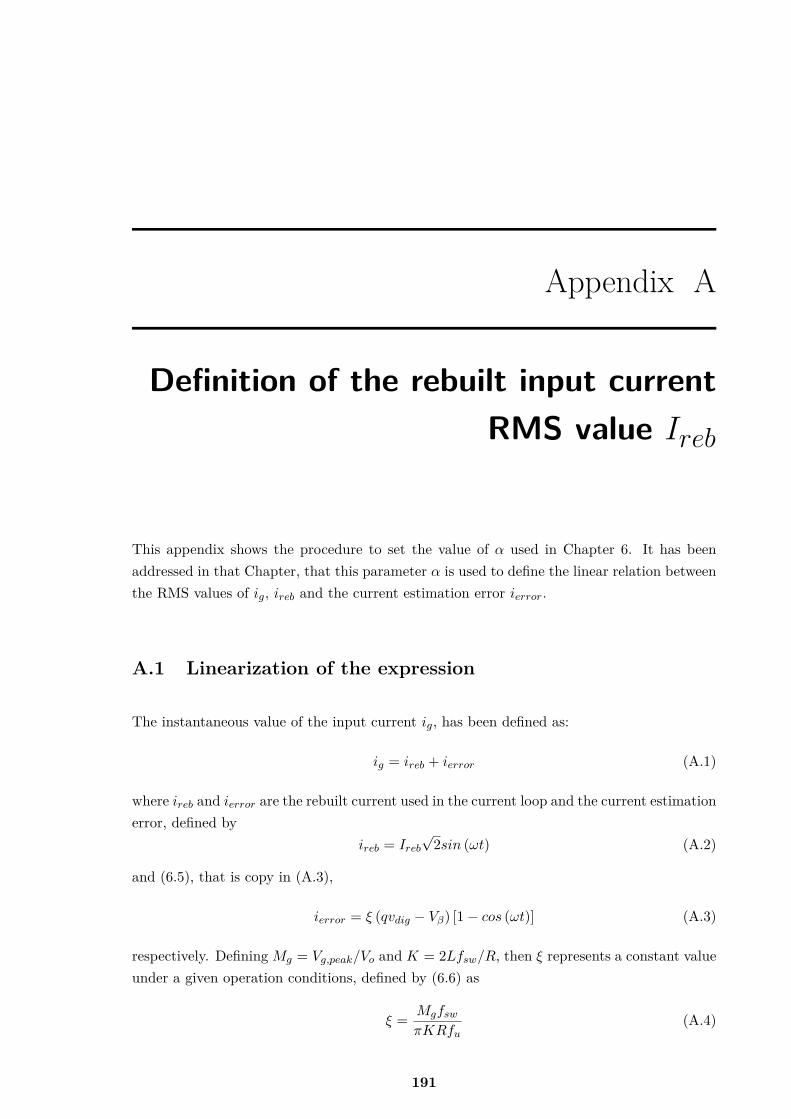
Appendix A
Definition of the rebuilt input currentRMS value Ireb
This appendix shows the procedure to set the value of α used in Chapter 6. It has beenaddressed in that Chapter, that this parameter α is used to define the linear relation betweenthe RMS values of ig, ireb and the current estimation error ierror.
A.1 Linearization of the expression
The instantaneous value of the input current ig, has been defined as:
ig = ireb + ierror (A.1)
where ireb and ierror are the rebuilt current used in the current loop and the current estimationerror, defined by
ireb = Ireb√
2sin (ωt) (A.2)
and (6.5), that is copy in (A.3),
ierror = ξ (qvdig − Vβ) [1− cos (ωt)] (A.3)
respectively. DefiningMg = Vg,peak/Vo and K = 2Lfsw/R, then ξ represents a constant valueunder a given operation conditions, defined by (6.6) as
ξ = MgfswπKRfu
(A.4)
191

192 Definition of the rebuilt input current RMS value Ireb
ig
ig
ireb
ireb
ierror
ierror
t t
Figure A.1: System waveforms for a given Ireb and qvdig − Vβ values. Left: qvdig > Vβ andright: qvdig < Vβ .
and Vβ is defined by (4.25)
Vβ = Vref (Ron +RL) + VDRe − Vg (Ron −RD)Re − (Ron +RL) (A.5)
To model the system, it is needed to define the portion of the half line cycle in with ig isoperating in the DCM. As it has been mentioned in Chapter 6. From the power balance ofthe large signal model, the RMS value of the real current Ig, is given by:
Ig = V 2o
RVg(A.6)
So the RMS value of the real current is known, being unknown the instantaneous value of ig,and the RMS value of rebuilt input current Ireb. The variable needed to develop the modelpresented in Chapter 6 is Ireb. Computing the RMS values of ig, according to (A.1):
Ig = V 2o
RVg=
√1Tu
ˆ Tu
0(ireb + ierror)2 dt (A.7)
Substituting (A.2) and (A.3), in (A.7):
V 2o
RVg=
√1Tu
ˆ Tu
0
[Ireb√
2sin (ωt) + ξ (qvdig − Vβ) [1− cos (ωt)]]2dt (A.8)
Computing and linearizing this expression to obtain the value of Ireb is not practical anduseful. To obtain a linear approximation of Ireb as a function of the known values Ig andξ (qvdig − Vβ), the Curve Fitting Toolbox [180] has been used. To do that, a sinusoidalireb waveform is created for several values of Ireb, according to (A.2). And different ierrorwaveforms are added to ireb, for different values of qvdig obtaining the corresponding ig
waveform. Two different examples are plotted in Fig. (A.1). With a positive ierror (obtainedwith qvdig > Vβ), the real input current is higher than ireb, and vice-verse. It must beconsidered, that ig can not be negative, so in the case ierror > ireb, ig keeps zero value (i.e.DCM condition).

A.1 Linearization of the expression 193
-0.4
-0.2
0
0.2
0.4
2
3
4
51
2
3
4
5
6
Ireb
Ig
qvdig - V
Figure A.2: Surface of Ig values obtained for different combinations of given Ireb and qvdig−Vβvalues.
Figure A.2 plots the surface of the different Ig values obtained under several Ireb and qvdig−Vβcombination values. In this case Irebε [2, 5] and qvdig −Vβε [−0.3, 0.3], and it can be seen howthe surface is similar to a plane, approximated as:
Ig = γIreb + αξ (qvdig − Vβ) (A.9)
being γ and α the coefficient of the expression that defined mentioned plane. With this Ireband qvdig −Vβ values vectors are inputs in the Curve fitting toolbox, which sets the values ofthe coefficients as: γ = 1 and α = 0.9. Figure (A.3) compare the Ig values obtained by thereal converter and defined by (A.7), and its linear approximation defined by (A.9), labeled byIg,lin in the figure, for the values of Irebε [2, 5] and qvdig−Vβε [−0.3, 0.3] presented previously.It can been seen the good agreement between the two curves around the operation point(qvdig −Vβ = 0). According to that, for a demanded power level Po = V 2
o /R, a RMS value ofthe input voltage Vg, and the vdig value given by the DCM time feedback controller it yieldswith the Ireb value:
Ireb = Ig − 0.9ξ (qvdig − Vβ) = V 2o
RVg− ξ (qvdig − Vβ) (A.10)
that corresponds with the expression (6.11), used in Chapter (6), to model the system.

194 Definition of the rebuilt input current RMS value Ireb
-0.2 -0.1 0 0.1 0.2 0.31
1.5
2
2.5
3
3.5
4
4.5
5
5.5
6
Ireb=5
Ireb=4
Ireb=3
Ireb=2
Ireb=4.5
Ireb=3.5
Ireb=2.5
qvdig - V
I g [
A]
I g,li
n [A
]
Figure A.3: Comparison of Ig values obtained by (A.7) (represented in red), and by the linearapproximation defined by (A.9), labeled as Ig,lin and plotted in blue.
Copyright © 2022 FDOKUMEN