
Device and Circuit-level Models for Carbon Nanotube and ...
193
Device and Circuit-level Models for Carbon Nanotube and Graphene Nanoribbon Transistors Michael Loong Peng Tan Queens’ College University of Cambridge A dissertation submitted for the degree of Doctor of Philosophy January 2011
-
Upload
khangminh22 -
Category
Documents
-
view
7 -
download
0
Transcript of Device and Circuit-level Models for Carbon Nanotube and ...

Device and Circuit-level Models for Carbon Nanotube and Graphene
Nanoribbon Transistors
Michael Loong Peng Tan
Queens’ College
University of Cambridge
A dissertation submitted for the degree of
Doctor of Philosophy
January 2011

ii
Declaration
This dissertation is the result of my own work and includes nothing which is the
outcome of work done in collaboration except where specifically indicated in the
text. This thesis has not been submitted in whole or in part as consideration for any
other degree or qualification at the University of Cambridge or any other University
or similar institution. In compliance with regulations, this thesis does not exceed
65,000 words, and contains 109 figures.
Michael Loong Peng Tan
January 2011

iii
To my wonderful parents and sister, for their guidance, support, love and
enthusiasm. I would not have made it this far without your motivation and
dedication to my success. Thank you, Mama and Daddy, I love you both.

iv
Acknowledgement
First of all, I am thankful to my supervisor, Prof. Gehan Amaratunga for his
valuable insight, guidance, advice and time. I would like to take this opportunity to
record my sincere gratitude for his supports and dedication throughout the years.
My thankfulness also goes to Prof. Vijay K. Arora, my mentor from Wilkes
University. His immense support and encouragement gave me the strength to go
forward. I wish to express my heartfelt thanks to Prof. Razali Ismail for the advice
and supports.
I could not complete my study without the help and discussions with Chin Shin
Liang, Desmond Chek, David Chuah and Caston Urayai. Their contributions in
quantum physics and circuit simulation in the aspect of this dissertation are greatly
appreciated. I would also like to acknowledge John Norcott for his computing
assistance.
Also, thank you to my friends namely Tee Boon Tuan, Chong Cheng Tung and
Javier Wong and Lim Kian Min. I cherish the ideas they have given me, their
supports and warmhearted friendships.
I would also like to thank Malaysia Ministry of Higher Education and Universiti
Teknologi Malaysia for the award of advanced study fellowship.
On a personal note, I would like to thank my family who has always supported me
and the encouragement they have given me.

v
List of Publications
Michael L. P. Tan and Gehan A. J. Amaratunga, “Performance Prediction of Gra-
phene-Nanoribbon and Carbon Nanotube Transistor”, Eleventh International Con-
ference on the Science and Application of Nanotubes, (NT10), 27 June – 2 July
2010, Montreal, Quebec, Canada.
Michael L. P. Tan and Gehan A. J. Amaratunga, “Performance Prediction of Gra-
phene-Nanoribbon and Carbon Nanotube Transistor”, Proceedings of the IEEE on
International Conference on Enabling Science and Nanotechnology, (Nanotech
Malaysia 2010), 1-3 December 2010, KLCC, Malaysia.

vi
Abstract
Device and Circuit-level Models for Carbon Nanotube and Graphene Nanoribbon Transistors
Michael Loong Peng Tan
Metal-oxide semiconductor field-effect transistor (MOSFET) scaling throughout the
years has enabled us to pack million of MOS transistors on a single chip to keep in
pace with Moore’s Law. After forty years of advances in integrated circuit (IC)
technology, the scaling of silicon (Si) MOSFET has entered the nanometer dimen-
sion with the introduction of 90 nm high volume manufacturing in 2004. The latest
technological advancement has led to a low power, high-density and high-speed gen-
eration of processor. Nevertheless, the scaling of the Si MOSFET below 22 nm may
soon meet its’ fundamental physical limitations. This threshold makes the possible
use of novel devices and structures such as carbon nanotube field-effect transistors
(CNTFETs) and graphene nanoribbon field-effect transistors (GNRFETs) for future
nanoelectronics. The investigation explores the potential of these amazing carbon
structures that exceed MOSFET capabilities in term of speed, scalability and power
consumption. The research findings demonstrate the potential integration of carbon
based technology into existing ICs. In particular, a simulation program with inte-
grated circuit emphasis (SPICE) model for CNTFET and GNRFET in digital logic
applications is presented. The device performance of these circuit models and their
design layout are then compared to 45 nm and 90 nm MOSFET for benchmarking.
It is revealed through the investigation that CNT and GNR channels can overcome
the limitations imposed by Si channel length scaling and associated short channel
effects while consuming smaller channel area at higher current density.

vii
Contents
1 Introduction
1.1 Background …………………………………………………………………. 1
1.2 Problem Statements …………………………..………………………….. 3
1.3 Objectives …………………………..………….…………………………. 4
1.4 Contributions …………………………..………….……..................... 4
1.5 Thesis Organization …………………………..…………................ 5
1.6 References …………………………..…………................................... 7
2 Overview of Carbon and Silicon-Based Technology
2.1 Carbon Nanotubes ………………………..………………………….. 8
2.1.1 Energy-Momentum Relation ……………………………… 12
2.1.2 Bandstructure of a Zigzag Nanotube …………….......... 13
2.1.3 Schottky Barrier CNTFET …………………………………. 14
2.1.4 Synthesis …………………………………………………………… 17
2.2 Graphene ……………………………………………………………………. 18
2.2.1 Synthesis …………………………………………………………… 22
2.3 Carbon-based Nanoelectronics ……………………….................... 23
2.4 Current Transport Models ………............................................. 24
2.5 Device Modeling ……………..……………………..……………..……. 28
2.6 Conclusion ……………..……………..…………….……………………... 33
2.7 References ……………..……………..…………….……………………... 35

Contents
viii
4 Performance Prediction of the CNTFET and the GNRFET
4.1 Introduction ………..……..………..………………………………………. 87
4.2 Performance Metric ………..……..………..…………………………….. 88
4.3 Performance Benchmarking ………..……..………..…………………. 94
4.4 Conclusion ………..……..………..………..……….…………………. 108
4.5 References ………..…..………..………..……….………..................... 110
5 Layout and Circuit Analysis
5.1 Introduction ……..………..……..………..………..………................ 111
5.2 Generic 45 nm PDK ………..……..………..………..………………. 112
5.2.1 MOSFET Layout for CNTFET Benchmarking ………. 113
5.2.2 MOSFET Layout for GNRFET Benchmarking ………. 115
3 Device Model
3.1 Introduction …………..……………..……………...…………………….. 44
3.2 Modeling Approaches ………..……………...………………………….. 45
3.3 Low Dimensional Structure Modeling ………………………………. 46
3.4 Electrostatic Capacitance ………………………………………………. 54
3.5 Quantum Capacitance …………………………………………………… 55
3.6 Channel, Quantum and Contact Resistance …………………… 57
3.7 Source and Drain Resistance ………………………………………. 59
3.8 Energy Dispersion in GNR and CNT ………………………….. 60
3.9 Model Verification ………………………………………………………… 63
3.10 MATLAB Implementation ……………………………………………. 66
3.11 Analog Behavior Modeling in PSPICE ………………...……….. 69
3.12 Comparison with MOSFET model ………..………..………........... 73
3.13 RC and Propagation Delay ………..………..………...................... 75
3.14 Conclusion ..………..………..……..……………….…..……..………….. 82
3.15 References ..………..………..……..……….…..……..………………….. 83

Contents
ix
5.3 Generic 90 nm PDK ……………………………………………………. 117
5.3.1 MOSFET Layout for CNTFET Benchmarking ………. 118
5.3.2 MOSFET Layout for GNRFET Benchmarking ………. 120
5.4 Digital Logic Circuit for CNTFET and GNRFET …………….. 122
5.5 Conclusion ………..……..………..………..……….………................ 138
5.6 References ………..…..………..…………………………………………. 139
6 Conclusions and Future Work
6.1 Summary ……..…..………..………..…………..……………………….. 140
6.2 Future Work ……..…..………..………..…………..……….…………… 142
6.3 References ……..…..………..………..…………..…………….……… 145
Appendix A Research Methodology
A.1 Introduction ……………..……………..…………………………….…… 147
A.2 Electrical Modeling ……………..……………..…………………………. 148
A.2.1 MATLAB ……………..……………..………………………….. 150
A.2.2 HSPICE ……………..……………..………………………….. 151
A.2.3 PSPICE ……………..……………..………………………….. 153
A.2.4 CADENCE ……………..……………..………………………….. 154
A.3 Conclusion ……………..……………..…………………………….…… 157
A.4 References ……………..……………..…………………………….…… 158
Appendix B Low Dimensional Modeling
B.1 Quasi-Two Dimensional Model ………….…………………………… 161
B.1.1 Density of States for Q2D Structure ………….………….. 161
B.1.2 Electron Concentration for Q2D Structure …………….. 161
B.1.3 Instrinsic Velocity for Q2D Structure ………….……….. 162

Contents
x
B.2 Quasi-One Dimensional Model ………….……………………………. 163
B.2.1 Density of States for Q1D Structure ………….………….. 163
B.2.2 Electron Concentration for Q1D Structure ………….…. 164
B.2.3 Instrinsic Velocity for Q1D Structure ………….………… 165
B.3 Summary of Relative Formulas ………….…………………………… 166
B.4 Gamma Function ………….……………….…………………………….. 167

xi
List of Abbreviations
ABM - Analog Behaviour Model
ALD - Atomic Layer Deposition
AMS - Analog Mixed Signal
BSIM - Berkeley Short-Channel IGFET Model
CAD - Computer Aided Design
CDF - Component Description Format
CMC - Compact Modeling Council
CMOS - Complementary Metal-Oxide-Semiconductor
CNTFET - Carbon Nanotube Field-Effect Transistor
DC - Direct Current
DG - Double Gate
DIBL - Drain-Induced Barrier Lowering
DOS - Density of States
DRC - Design Rules Check
ECAD - Electronic Computer-Aided Design
EDA - Electronic Design Automation
EDP - Energy Delay Product
FDSOI - Fully-Depleted Silicon on Insulator
FET - Field Effect Transistor
GaAr - Galium Arsenide
GCA - Gradual Channel Approximation
GDSII - Graphic Database System II
GHz - Giga Hertz

xii
GNR - Graphene Nanoribbon Field-Effect Transistor
GUI - Graphical User Interface
IBM - International Business Machines
IC - Integrated Circuit
IGFET - Insulated Gate Field-Effect Transistor
InP - Indium Phosphide
LVS - Layout versus Schematic
MFP - Mean Free Path
MMSIM - Multi-mode Simulation
MOS - Metal Oxide Semiconductor
MOSFET - Metal Oxide Semiconductor Field Effect Transistor
NEGF - Non-equilibrium Green’s Function
NMOS - n-channel MOSFET
OA - Open Access
PDP - Power-delay product
PDK - Process Design Kit
PMOS - p-channel MOSFET
Q1D - Quasi-one dimensional
Q2D - Quasi-two dimensional
RC - Resistive-Capacitive
RCX - Parasitic Extraction
RF - Radio Frequency
S/D - Source and Drain
Si - Silicon
Si2 - Silicon Integration Initiative
SiGe - Silicon Germanium
SOE - Second Order Effects
SP - Surface Potential based Models
SPE - Surface Potential Equation
SPICE - Simulation Program with Integrated Circuit Emphasis
SS - Subthreshold Swing

xiii
TCAD - Technology Computer-Aided Design
TSMC - Taiwan Semiconductor Manufacturing Company
UTB - Ultra-thin Body
VLSI - Very Large Scale Device
VSR - Velocity Saturation Region
VHDL - Very High Density Logic
2DEG - 2D Electron Gas

xiv
List of Figures
2.1 Buckyball C60 .…………………………………………………………….. 9
2.2 Multi-walled carbon nanotube .……………………………........ 9
2.3 Single-walled carbon nanotube .……………………………....... 9
2.4 Map of chiral vectors (n, m) of carbon nanotube .…………….. 10
2.5 The creation of (a) (3,3) armchair nanotube
(b) (4, 0) zigzag nanotube (c) (4,2) chiral nanotube
.………… 11
2.6 Classification of nanotubes .……………….…………………………. 11
2.7 Formation of nanotubes. T is the translational vector ……… 12
2.8 A zigzag nanotube with quantized ky .………………………… 13
2.9 Energy dispersion of (20,0) zigzag nanotube
with n=20, subband index v from 13 to 23
and quantized ky
.………………….. 13
2.10 Schottky barrier CNTFETs .…………………….………………....... 15
2.11 Schottky barrier CNTFET with ambipolar transport ………. 15
2.12 Sketch of a full band ohmically contacted SWNT-
FETs for (a) electron and (b) hole transport
.……….. 16
2.13 MOSFET-like CNTFET with chemically doped
contacts for (a) bottom and (b) top gate design
………...... 16
2.14 sp2 hybridization ………......………......………......………......….. 18
2.15 2pz orbitals ………......………......………......………......……………. 19

List of Figures
xv
2.16 (a) Energy bands near the Fermi level in
graphene. (b) Brillouin zone of the honeycomb
lattice. A closer look at the (c) metallic and
(d) semiconducting conic structure
………...... 20
2.17 Honeycomb lattice of an armchair and a
zigzag graphene nanoribbon
…………........... 21
2.18 Basic structure of a n-channel MOSFET ………….................. 25
2.19 Circuit representation of electrostatic and
quantum capacitance in series
……….................... 27
2.20 Circuit model of CNT complementary circuits .................... 30
3.1 General matrix model for nanoscale device
connected to two contacts
…………............... 46
3.2 Transistor circuit model with parasitic capacitance ………...... 46
3.3 Population of k-states at equilibrium at the top of
the barrier
………...... 47
3.4 A generic electrostatic capacitance model for
ballistic transistor
…………………… 49
3.5 Population of k-states at non-equilibrium at the top
of the barrier
………. 50
3.6 Self consistent solution for USC and carrier density N ………. 53
3.7 Structure of a (a) carbon nanotube and (b)
graphene nanoribbon field effect transistor
…........... 54
3.8 Metal–Insulator–Semiconductor capacitors (electrostatic,
quantum, gate capacitance) with channel and gate voltage
… 55
3.9 Energy versus wavevector for a Q1D device …………………….. 56
3.10 Source/drain terminal geometry (a) top view and
(b) side view
…........... 59
3.11 Energy bandgap versus chirality n for CNT and
GNR. GNR width versus chirality n
…........... 62

List of Figures
xvi
3.12 Comparison of simulated CNT drain characteristic
versus 80nm experimental data
…........... 63
3.13 Comparison of our CNTFET simulated results
against 10 nm Arizona CNTFET model for VG=
0.6 and 0.8V
…........... 64
3.14 Comparison of our CNTFET simulated results
against 50 nm single-tube Stanford CNTFET
model from VG=1V (top) with 0.1V spacing
…........... 64
3.15 Characteristics of the almost perfectly symmetric
CNT-based CMOS inverter fabricated on the same
SWCNT with d= 2 nm with gate length of
L=4.0 μm
…........... 65
3.16 Drain characteristics from VG=1V to 0V (top to
bottom) with 0.1 V spacing for n-type device and
VG=0V to 1V (top to bottom) with 0.1 V spacing
for p-type device
………….. 66
3.17 Matrix row vector versus matrix column vector
plotting
……… 66
3.18 Gate characteristic for CNTFET and GNRFET ………. 67
3.19 Matrix row vector versus matrix row vector plotting ………. 67
3.20 (a) CMOS-like circuit for (b) CNTFET and (c)
GNRFET.
………. 68
3.21 PSPICE ABM CNTFET macro-model …………………………… 70
3.22 PSPICE ABM GNRFET macro-model …………………………… 71
3.23 PSPICE I-V characteristic of the n-type CNTFET …………... 72
3.24 PSPICE I-V characteristic of the n-type GNRFET …..………. 72
3.25 I-V characteristics of 80-nm MOSFET for VG =0.7,
0.8, 0.9, 1.0, 1.1, and 1.2 V
………. 73

List of Figures
xvii
3.26 (a) Simulated 45 nm MOSFET drain characteristic
versus 45nm TSMC experimental data at VG =0.6V,
0.8V and 1.0V (b) comparison of simulated data
against 45nm IBM NMOS and PMOS experimental
data VG = 0.4V, 0.6V, 0.8V and 1.0V
………. 74
3.27 Measurement tPHL and tPLH between input and output
voltage, and tRC, trise and tfall in time domain
……. 75
3.28 Equivalent RC circuit from the p-type and n-type
device charging and discharging processes. Z is
impedance, R is resistance and X is reactance
………. 75
3.29 Fitting curve between CNTFET and GNRFET I-V
model with empirical equation
………. 76
3.30 Approximation for real equation and polynomial equation …. 78
3.31 The current i(t) response to an RC circuit ………………………. 79
3.32 The resistor voltage in the RC circuit as a
response to time
………………………. 79
3.33 The capacitor voltage in the RC circuit as
a response to time
………………………. 80
3.34 RC waveforms with large time scale. 570RC constant
for the CNT and 211RC constant for the GNR
……….. 80
3.35 RC waveforms with medium time scale. 27RC
constant for the CNT and 17RC constant for the
GNR
……….. 81
3.36 RC waveforms with small time scale. 1RC constant
for both the CNT and GNR
……… 81
4.1 (a) Electronic density of states calculated for a [19,0]
armchair graphene nanoribbon and [20,0] and zigzag
carbon nanotube (b) The carrier concentration in the
first and second subband for nanotube.
…....... 89

List of Figures
xviii
4.2 Drain characteristic of a 50 nm long zigzag single-
walled carbon nanotube model demonstrated in
comparison to L≈50 nm semiconducting CNT
experimental data and L≈85 nm metallic CNT
experimental data. Inset shows a 45 nm MOSFET
characteristics. Initial VG at the top for CNT and
MOSFET is 1 V with 0.1 V steps.
…....... 90
4.3 Drain characteristic of graphene nanoribbon and
zigzag carbon nanotube with perfect contact at linear
ON-conductance of 2e2/h and 4e2/h respectively.
The maximum VG is 1V with 0.1V gate spacing
(Rnc≈ 0 Ω)
…....... 91
4.4 Drain characteristic of graphene nanoribbon and
zigzag single-walled carbon nanotube with linear ON-
conductance of 0.2 × 4e2/h and 0.5 × 4e2/h
respectively. CNT have good agreement with the
experimental data of Pd ohmically contacted 50nm
channel nanotube. The maximum VG is 1V with 0.1V
gate spacing (Rnc≠ 0 Ω)
…....... 92
4.5 PDP of CNTFET and MOSFET logic gates
for 45 nm process
…................... 98
4.6 PDP of CNTFET and MOSFET logic gates
for 90 nm process
…................... 98
4.7 PDP of GNRFET and MOSFET logic gates
for 45 nm Process
…................... 99
4.8 PDP of GNRFET and MOSFET logic gates
for 90 nm Process
…................... 99
4.9 EDP of CNTFET and MOSFET logic gates
for 45 nm Process
…................... 100

List of Figures
xix
4.10 EDP of GNRFET and MOSFET logic gates
for 90 nm Process
…................... 100
4.11 EDP of GNRFET and MOSFET logic gates
for 45 nm Process
…................... 101
4.12 EDP of GNRFET and MOSFET logic gates
for 90 nm Process
…................... 101
4.13 3D plot of PDP and EDP of CNTFET logic gates
with copper interconnect length up to 5 μm for (a)
tnode = 45 nm and tsub = 500 nm (b) tnode = 90 nm and
tsub = 500 nm
…....... 102
4.14 3D plot of PDP and EDP of GNRFET logic gates
with copper interconnect length up to 5 μm for (a)
tnode = 45 nm and tsub = 500 nm (b) tnode = 90 nm and
tsub = 500 nm
…....... 103
4.15 Nanotube circuit on a 4 inch Si/SiO2 wafer …........................ 104
4.16 Layout of carbon-based NOR2 and NAND2 gate with
input A, B and output Z. Wafer scale assembly of
carbon nanotubes digital logic circuits based are
shown on the right
…....... 106
4.17 Layout of carbon-based NOR3 with input A, B, C
and output Z
…....... 107
4.18 Layout of a carbon-based NAND3 with input A, B, C
and output Z
…....... 107
4.19 Single layer SW-CNT interconnect ………………………… 109

List of Figures
xx
5.1 I-V characteristic of high and low current 45 nm
CMOS model for (a) CNTFET and (b) GNRFER
benchmarking
………. 112
5.2 (a) NOT (b) NAND2 (c) NAND3 (d) NOR2
(e) NOR3 logic circuit for 45 nm process technology
with L = 45 nm
………. 113
5.3 15 stage ring-oscillator circuit for 45 nm process
technology with L = 45nm
………. 113
5.4 MOSFET 45 nm process propagation delay for logic
gates NOT, NAND2, NAND3, NOR2 and NOR3.
These gates will be compared with CNTFET logic
circuits circuits.
………. 114
5.5 (a) NOT (b) NAND2 (c) NAND3 (d) NOR2
(e) NOR3 logic circuit for 45 nm process technology
with L = 200 nm
………. 115
5.6 15 ring-oscillator circuit for 45 nm process technology
with L = 200 nm
………. 115
5.7 MOSFET 45 nm process propagation delay for logic
gates NOT, NAND2, NAND3, NOR2 and NOR3.
These gates will be compared with GNRFET logic
circuits.
………. 116
5.8 I-V characteristic of high and low current 90 nm
MOSFET model for (a) CNTFET and (b) GNRFER
benchmarking. Top VG = 1V with 0.2V steps
………. 117
5.9 (a) NOT (b) NAND2 (c) NAND3 (d) NOR2
(e) NOR3 logic circuit for 90 nm process technology
with L = 200 nm
………. 118
5.10 15 ring-oscillator circuit for 90 nm process technology
with L = 200 nm
………. 118

List of Figures
xxi
5.11 MOSFET 90 nm process propagation delay for logic
gates NOT, NAND2, NAND3, NOR2 and NOR3.
These gates will be compared with CNTFET logic
circuits.
………. 119
5.12 (a) NOT (b) NAND2 (c) NAND3 (d) NOR2
(e) NOR3 logic circuit for 90 nm process technology
with L = 500 nm
………. 120
5.13 15 stage ring-oscillator circuit for 90 nm process
technology with L = 500 nm
………. 120
5.14 MOSFET 90 nm process propagation delay for logic
gates NOT, NAND2, NAND3, NOR2 and NOR3.
These gates will be compared with GNRFET logic
circuits.
………. 121
5.15 Contact design rules for (a) 45 nm and (b) 90 nm
process node
………. 122
5.16 Top view of CNTFET or GNRFET ………. 123
5.17 HSPICE macro-model for CNTFET and GNRFET ………. 123
5.18 Two cascaded inverter gate with parasitic capacitance ………. 126
5.19 Extrapolated interconnect capacitance for copper and
MWCNT for 90 nm, 65 nm, 45 nm process based on
32 nm, 22 nm and 14 nm technology process
………. 128
5.20 Cutoff frequency for 50 nm length CNTFET with
interconnect length from 0.01 μm to 100 μm with
source drain contact area for 45 nm and 90 nm
process nodes. Contact width is 100 nm for the 45 nm
process and 120 nm for the 90 nm process nodes.
CNTFET length remains the same.
………. 129

List of Figures
xxii
5.21 Cutoff frequency for a 20 nm length GNRFET with
interconnect length from 0.01 μm to 100 μm with
source drain contact area for 45 nm and 90 nm
process nodes. Contact width is 100 nm for the 45 nm
process and 120 nm for the 90 nm process nodes.
GNRFET length remains the same.
………. 129
5.22 (a) Schematic of NOT gate with parasitic
capacitance. Input and output waveform for
(b) CNTFET and (c) GNRFET
………. 130
5.23 (a) Schematic of 2-input NAND gate with parasitic
capacitance. Input and output waveform for
(b) CNTFET and (c) GNRFET
………. 131
5.24 (a) Schematic of 3-input NAND gate with parasitic
capacitance. Input and output waveform for
(b) CNTFET and (c) GNRFET
………. 132
5.25 (a) Schematic of 2-input NOR gate with parasitic
capacitance. Input and output waveform for
(b) CNTFET and (c) GNRFET
………. 133
5.26 (a) Schematic of 3-input NOR gate with parasitic
capacitance. Input and output waveform for
(b) CNTFET and (c) GNRFET
………. 134
5.27 Schematic of ring-oscillator of 15 cascaded inverters
with parasitic capacitance
………. 136
5.28 Input and output waveform for (a) CNTFET and
(b) GNRFET ring-oscillator with contact and
interconnect geometries extracted from 45 nm and 90
nm process nodes
………. 137

List of Figures
xxiii
6.1 Structure of a multi-channel CNT ………................................ 143
A.1 ECAD and TCAD flow chart …………................................... 149
A.2 MATLAB Simulation Process ………….................................... 150
A.3 HSPICE Simulation Process …………..................................... 152
A.4 ABM modeling in PSPICE …………........................................ 153
A.5 Cadence IC Design Flow …………............................................. 156

xxiv
List of Tables
1.1 Progress on transistor scaling and process technology
capabilities
…….... 1
2.1 Electrical and mechanical properties of carbon
nanotubes and graphene or GNR
.……………….. 21
2.2 Compact modeling approaches .……………………………............. 28
2.3 BSIM SPICE Level .……………………………………………………… 29
2.4 CNTFET compact model .………………………………………… 31
2.5 Comparison of CNTFET and GNRFET devices .…………… 32
3.1 Source and drain terminal resistance ………………………………. 59
3.2 CNT and GNR bandgap calculation ………………………………. 60
4.1 Performance metric for CNTFET, GNRFET and
MOSFET
………...... 88
4.2 Contact, channel and quantum resistance …………………...... 91
4.3 Dimension for MOSFET, GNRFET and CNTFET
channel (width, length and area) of 45 nm and 90
nm process technology
………...... 93
4.4 Copper interconnect capacitance of 45 nm and 90
nm process technology for 1 μm and 5 μm
interconnect length
………...... 94
4.5 Substrate insulator capacitance of CNTFET and
GNRFET for 100 μm and 500 μm thickness
………...... 94

List of Tables
xxv
4.6 PDP and EDP of CNTFET logic gates benchmarking
with 45nm and 90 nm CMOS technology. Copper
interconnect length of (a) 1μm and (b) 5 μm wire are
chosen to demonstrate the wire capacitance. The
influence of substrate insulator thickness variation
(100 nm and 500 nm) on PDP and EDP are also
presented.
…….. 95
4.7 PDP and EDP of GNRFET logic gates benchmarking
with 45nm and 90 nm CMOS technology. Copper
interconnect length of (a) 1μm and (b) 5 μm wire are
chosen to demonstrate the wire capacitance. Substrate
insulator thickness of 100 nm and 500 nm on EDP and
PDP are also assessed.
…….. 96
4.8 PDP and EDP of CNTFET and GNRFET logic gates
benchmarking with 45 nm and 90 nm MOSFET
technology.
……… 97
5.1 45 nm process delay computation for the comparison
with CNTFET
………… 114
5.2 45 nm process delay computation for the comparison
with GNRFET
………… 116
5.3 90 nm process delay computation for the comparison
with CNTFET
………… 119
5.4 90 nm process delay computation for the comparison
with GNRFET
………… 121
5.5 Source and drain capacitance for multiple substrate
insulator thickness
………… 125
5.6 Intrinsic and extrinsic capacitance and unity cutoff
frequency for CNTFET and GNRFET based one 45
nm and 90 nm MOSFET processes
………… 125

List of Tables
xxvi
5.7 Intrinsic and unity cutoff frequency unity cutoff
frequency for Si MOSFET 45 nm and 90 nm process
technology. They are benchmarked against for
CNTFET (high current) and GNRFET (low current)
…… 126
5.8 ITRS 2005 based simulation parameters ………………………….. 127
5.9 Extrapolated interconnect capacitance ………………………… 128
5.10 Load and output capacitance for logic gates NOT,
NAND2, NOR2, NAND3, NOR3 and ring oscillator
………… 135
5.11 CNTFET logic circuit delay computation for single
logic gate
………… 135
5.12 GNRFET logic circuit delay computation for single
logic gate
………… 136
5.13 Delay and frequency computation for CNTFET and
GNRFET against Si MOSFET 45 nm and 90 nm
ring-oscillator circuit
………… 137
A.1 Input netlist file sections …………………………………................. 151
A.2 Cadence custom IC design tools …………………………………….. 154

1
Chapter 1
Introduction
1.1 Background Complementary metal-oxide-semiconductor (CMOS) device scaling has enabled
MOS transistors to be shrunk from a micrometer into the sub-100 nm regime with
the number of transistor doubled by a factor of two every 18 months in accordance
to Moore’s Law. As channel length enters the sub-100 nm region, silicon (Si) device
performance is hampered by short channel effects. The end of planar CMOS scaling
is forecast to be at the 22 nm node as shown in Table 1.1.
Table 1.1: Progress on transistor scaling and process technology capabilities.
(Source: Intel)
High Volume Manufacturing 2004 2006 2008 2010 2012 2014 2016 2018
Feature Size (nm) 90 65 45 32 22 16 11 8
Integration Capacity (Billions of transistors)
2 4 8 16 32 64 128 256

Background
2
As we approach the limits of the Si roadmap, carbon nanotube (CNT) and
graphene nanoribbon (GNR) field-effect transistors (FETs) are being explored as
breakthrough structures for use in future electronic systems [1-5]. These one-dimen-
sional (1D) structures have remarkable electron transport properties including high
mobility and symmetric band structure [6]. They have the potential to be
integrated onto Si substrates as a new hybrid CNTFET-CMOS and GNRFET-
CMOS [7] to overcome economical and technological challenges [8]. Nanotubes and
nanoribbons are synthesized ex-situ and purified before they are deposited on a
conventional Si substrates at specific locations [9, 10].
The research reported in this dissertation focuses on the modeling and simulation
of CNTFETs and GNRFETs as alternatives to Si CMOS transistor circuits. While
significant progress has been achieved in the structural and mechanical nanotube
and nanoribbon characterization, much works is still required in electronics design,
particularly in digital logic systems before it can be implemented in practical
circuits. As such, device modeling plays a vital route in evaluating and
understanding the capabilities of a carbon channel material in an integrated circuit
design.
The approach taken is to design digital gates implemented in a simulation
environment for integrated circuits. The SPICE circuit simulator is used. Robust,
accurate and computationally efficient CNTFET and GNRFET models are
developed for the simulation. The research explores the potential of these carbon
nanoscale materials as a substitute for a silicon channel in scaled MOSFETs for logic
applications. The device performance of the circuit models is compared to design
layout specifications extracted from a predictive 45 nm technology model and 90 nm
foundry technology platforms for all other design parameters e.g. contact size, metal
widths, etc.

Problem Statements
3
SPICE is a widely accepted simulation environment for circuit design analysis
and verification. Many models have been developed over the years by various
computer aiding engineering (CAE) software vendors for SPICE to support the
semiconductor industry. Circuit simulation time has been substantially reduced
through algorithm improvement and hardware enhancement through high
performance computing (HPC) platforms. Given its ‘industry standard’ status for
computer aided design and analysis in integrated circuits, the models developed for
CNTFETs and GNRFETs are implemented within SPICE.
1.2 Problem Statements Device simulation of current transport models of CNTFETs and GNRFET are
essential for assessing their performance as post-Si channels in integrated circuits.
Carrier transport in carbon-based transistors can be quasi-ballistic or scattering-
limited depending on the contact interface and channel properties. Therefore, it is
essential to take non-idealities into account together with their particular
fundamental physics properties when describing the carrier transport in CNTFETs
and GNRFETs. Questions which were addressed in this research are
(i) How carbon nanotube and graphene nanoribbon perform as alter-
native to silicon MOSFET channel.
(ii) How do we transfer compact models from developed mathematical
environments to more general ECAD tools?
(iii) What is the performance of carbon channel devices in a digital
circuit?
(iv) How does one layout of carbon logic circuits compared to those in Si?

Contributions
4
1.3 Objectives This focus of this research is on the development of CNTFET and GNRFET device
and circuit level models which can be transferred into standard ECAD tools to
enable digital logic circuit design. The simulation is based on semiconducting (20,0)
zigzag CNT and (19,0) armchair GNR. The following are the objectives of this
research
(i) To formulate analytical and semi-empirical equations for CNTFETs
and GNRFETs
(ii) To implement circuit compatible compact device models for SPICE
(iii) To customize the physical layout of carbon channel MOSFET circuits
compatible with 45 nm and 90 nm Si technology nodes
(iv) To explore the device and circuit performance based on physical and
electrical parametric variations
(v) To investigate the circuit performance of CNTFETs and GNRFETs
in prototype digital logic gates
(vi) To verify the accuracy the compact models with published
experimental results and other accomplished models
1.4 Contributions MOSFET-based integrated circuits have become the dominant driving force in
realizing high performance computation with digital logic. When current Si
transistor features cannot be scaled to smaller sizes to keep improving performance,
alternative material based transistors come into focus. Carbon nanotubes are
essentially a rolled-up sheet of graphene about a nanometer in diameter and several
hundreds of nanometers in length. These structures are mechanically strong and
exhibit an array of remarkable electronic properties such as very high carrier
mobilities, quantized conductance and unique one-dimensional (1D) transport
phenomena.

Thesis Organization
5
Therefore, carbon-based devices hold great promise for post-Si nanoelectronics
and could outperform the state of the art Si MOSFET that we have today. In this
research, the potential of CNTFETs and GNRFETs in circuits is evaluated by
formulating quantitative models which match experimentally measured devices.
From these base models, logic circuit blocks such as NAND, NOR gates and ring
oscillators are constructed and evaluated in terms of performance. This enables the
assessment of CNT and GNR performance in practical digital circuit applications.
The impact of interconnects on the overall circuit performance metric is also
quantified. These contributions mark a major step towards understanding the
integration of carbon nanodevices into existing circuit architectures.
1.5 Thesis Organization This thesis consists of 7 chapters. Chapter 1 introduces the background and
motivation of this research. Chapter 2 provides an overview of the literature relevant
to the research. A detailed description of carbon and silicon-based transistor
technologies are also presented. This includes the overview of the physical
properties, synthesis and current transport model development for the CNTFET and
GNRFET. A comparable device modeling for silicon MOSFETs is also summarized.
Chapter 3 discusses the model formulation and device architecture of carbon
devices. The model is verified against experimental data and other compact models.
In addition, the analytical model for the propagation delay in a circuit environment
is also presented.
In Chapter 4, performance evaluation is carried out on the simulated drain and
gate characteristic between CNTFETs and GNRFETs, and compared with Si
MOSFETs. The effect of parametric variations in contact size, substrate insulator
thickness and interconnect length for CNTFET and GNRFET logic gates are also
considered. They are benchmarked against the Si MOSFET based circuits in term of
power-delay-product (PDP) and energy-delay-product (EDP).

Thesis Organization
6
Chapter 5 describes a CMOS type layout using CNTFETs and GNRFETs within
45 nm and 90 nm process nodes. This allows direct comparison with the equivalent
Si technologies. The calculation of load capacitance for each transistor in the logic
circuit and ring-oscillator is described. The influence of interconnect capacitance on
unity current gain cutoff frequency is also considered.
In Chapter 6, conclusions are drawn from the research and suggestions for future
work are given. Appendix A describes the design methodology carried out using
MATLAB, SPICE and Cadence to develop the transistor models. Appendix B
summarizes the derivation of quasi-low dimensional modeling presented in Chapter
3.

References
7
1.6 References [1] P. Avouris, "Molecular Electronics with Carbon Nanotubes," Accounts of
Chemical Research, vol. 35, pp. 1026-1034, 2002. [2] H. S. P. Wong, "Field effect transistors-from silicon MOSFETs to carbon
nanotube FETs," in Microelectronics, 2002. MIEL 2002. 23rd International Conference on, 2002, pp. 103-107 vol.1.
[3] M. Lundstrom, "A top-down look at bottom-up electronics," in VLSI Circuits, 2003. Digest of Technical Papers. 2003 Symposium on, 2003, pp. 5-8.
[4] J. Kong and A. Javey, "Carbon Nanotube Field-Effect Transistors," in Carbon Nanotube Electronics, A. Chandrakasan, Ed.: Springer US, 2009, pp. 1-24.
[5] F. Schwierz, "Graphene transistors," Nature Nanotechnology, vol. 5, pp. 487-496, 2010.
[6] Z. Zhang, S. Wang, Z. Wang, L. Ding, T. Pei, Z. Hu, X. Liang, Q. Chen, Y. Li, and L.-M. Peng, "Almost Perfectly Symmetric SWCNT-Based CMOS Devices and Scaling," ACS Nano, vol. 3, pp. 3781-3787, 2009.
[7] A. Javey and J. Kong, Carbon Nanotube Electronics (Integrated Circuits and Systems) vol. 1. New York: Springer 2009.
[8] N. Z. Haron and S. Hamdioui, "Why is CMOS scaling coming to an END?," in Design and Test Workshop, 2008. IDT 2008. 3rd International, 2008, pp. 98-103.
[9] X. M. H. Huang, R. Caldwell, L. Huang, S. C. Jun, M. Huang, M. Y. Sfeir, S. P. O'Brien, and J. Hone, "Controlled Placement of Individual Carbon Nanotubes," Nano Letters, vol. 5, pp. 1515-1518, 2005.
[10] I. Meric, V. Caruso, R. Caldwell, J. Hone, K. L. Shepard, and S. J. Wind, "Hybrid carbon nanotube-silicon complementary metal oxide semiconductor circuits," Journal of Vacuum Science & Technology B, vol. 25, pp. 2577-2580, Nov 2007.

8
Chapter 2
Overview of Carbon and Silicon-Based Technology
2.1 Carbon Nanotubes A carbon nanotube is a cylindrical nanostructures with sp2 bonded carbon atoms
arranged in honeycomb lattice. It is a part of the graphene family that not only has
tube-like but also ellipsoidal and spherical structures. A carbon nanotube also known
as a buckytube compared to spherical fullerene which is called buckyball [1, 2]. The
nanotube can be considered in this context as an elongated buckyball with a hemi-
spheric end capped structure.
Fullerenes were first discovered by Kroto, Curl and Smalley in 1985 who received
the 1996 Nobel Prize in Chemistry. Ijiima [3] identified multi-walled carbon nano-
tubes (MWCNTs) at the NEC Corporation in 1991 while conducting a fullerene syn-
thesis experiment. These structures consist of several concentric nanotubes nested
inside one another. Two year later, Bethune's group at IBM, [4] and Iijima and
Ichihashi at NEC, [5] independently synthesized single-walled carbon nanotubes
(SWCNTs) by using metal catalysts. Typically, the diameter of the MWCNT is tens
of nanometer while SWCNTs can be one or five nanometers wide.

Carbon Nanotubes
9
Although much more work is needed to control complex tube growth with specific
chirality, shapes and sizes, CNT fabrication technology can build on existing silicon-
based device processing steps [6]. The buckyball (C60), MWCNT and SWCNT are
depicted in Figure 2.1, Figure 2.2 and Figure 2.3 respectively. By using density gra-
dient ultracentrifugation (DGU), semiconducting and metallic tubes can be separat-
ed with 99% high purity. In addition, small diameter SWCNT (HiPco) with mean
diameter ≈1.0 nm and length from ≈ 100-1000 nm can be obtained. NanoIntegris is
an establish supplier of SWCNTs of uniform diameter and mono-chirality (semicon-
ducting or metallic) which uses DGU techniques [7]. In this process, CNT are
dispersed using a mixture of surfactants. During the interaction, the surfactants
selectively bind themselves with the CNTs. Following that, the CNTs are placed in-
to a density gradient for separation. At this stage, it can be seen that the CNTs are
distributed based on density along the centrifuge tube. After the centrifugation pro-
cess, the CNTs gradient are fractionated to obtain metallic, semiconducting and ul-
tra high purity SWCNTs.
Figure 2.1: Buckyball C60
Figure 2.2: Multi-walled carbon nanotube
Figure 2.3: Single-walled carbon nanotube

Carbon Nanotubes
10
A nanotube can be metallic or semiconducting according to the direction they
are wrapped [8] as depicted in Figure 2.4 and Figure 2.5. This direction is best de-
scribed by the chirality indexes (n, m) of the nanotube where n and m are integers
of the chiral vector, Ch = n a1 + m a2 = (n, m). Basis vectors a1 and a2 are described
by
⎛ ⎞⎟⎜ ⎟= +⎜ ⎟⎜ ⎟⎟⎜⎝ ⎠1
3 132 2cca a x y ,
⎛ ⎞⎟⎜ ⎟= −⎜ ⎟⎜ ⎟⎟⎜⎝ ⎠2
3 132 2cca a x y
(2.1)
where 0.14 nm≈cca is the nearest C-C bonding distance. The corresponding recip-
rocal lattice vector [9] is given by
⎛ ⎞⎟⎜= + ⎟⎜ ⎟⎜ ⎟⎝ ⎠12 1
3πb x ya
, ⎛ ⎞⎟⎜= − ⎟⎜ ⎟⎜ ⎟⎝ ⎠2
2 13
πb x ya
(2.2)
On this basis the nanotube can be classified as a zigzag, armchair or chiral nanotube
which has semiconducting and metallic characteristic as illustrated in Figure 2.6.
Nanotubes can be made into nanoscale transistors and on-chip interconnects [6, 7]
that have higher current carrying capacity and thermal conductivity than copper.
Figure 2.4: Map of chiral vectors (n, m) of carbon nanotube
Zigzag (n, m)
Armchair
(0,0) (1,0) (2,0) (3,0) (4,0) (5,0) (6,0) (7,0) (8,0) (9,0) (10,0) (11,0) (12,0) (13,0)
(1,1) (2,1) (3,1) (4,1) (5,1) (6,1) (7,1) (8,1) (9,1) (10,1) (11,1) (12,1) (13,1)
(2,2) (3,2) (4,2) (5,2) (6,2) (7,2) (8,2) (9,2) (10,2) (11,2) (12,2)
(3,3) (4,3) (5,3) (6,3) (7,3) (8,3) (9,3) (10,3) (11,3) (12,3)
(4,4) (5,4) (6,4) (7,4) (8,4) (9,4) (10,4) (11,4)
(5,5) (6,5) (7,5) (8,5) (9,5) (10,5) (11,5)
(6,6) (7,6) (8,6) (9,6) (10,6
(7,7) (8,7) (9,7) (10,7 )
Semiconductor
Metal
a1
a2 x
y

Carbon Nanotubes
11
(a) (b) (c) Figure 2.5: The creation of (a) (3,3) armchair nanotube, (b) (4,0) zigzag nanotube,
(c) (4,2) chiral nanotube
Figure 2.6: Classification of nanotubes

Energy-Momentum Relation
12
2.1.1 Energy-Momentum Relation The energy dispersion (E-k) for a quasi-one dimensional (Q1D) structure such as
nanotube and nanoribbon can be derived from the electronic properties of graphene
[7, 8] that is expressed by
( ) ( ) ( )( )= ± + ⋅ + ⋅ + ⋅ −1 2 2 13 2 2 2E(k ) t cos k a cos k a cos k a a
(2.3)
The tight binding model can be rewritten to become [10]
⎛ ⎞ ⎛ ⎞⎛ ⎞ ⎟ ⎟⎜ ⎜⎟⎜ ⎟ ⎟⎜ ⎜= ± + +⎟⎜ ⎟ ⎟⎜ ⎜⎟⎜ ⎟ ⎟⎟ ⎟⎝ ⎠ ⎜ ⎜⎝ ⎠ ⎝ ⎠23 3 31 4 4
2 2 2cc cc cc
x y x y ya a aE(k ,k ) t cos k cos k cos k (2.4)
The positive sign refers to the conduction band whereas the negative sign refers to
the valence band. To satisfy the periodic boundary condition, the wavevector k
around the circumferential direction is quantized while the wave vector along the
axis of the nanotube can take any value. It is given that
⋅ = 2k C πv
(2.5)
where C is the chiral circumference vector, k is the quantized wavevector (kx or ky)
and v is a subband index integer. An armchair nanotube has C along the x-axis and
a zigzag nanotube has C along the y-axis while a chiral nanotube has C lying in be-
tween. Figure 2.7 depicts the formation of zigzag, armchair and chiral nanotubes.
Figure 2.7: Formation of nanotubes. T is the translational vector.
Zigzag
Zigz
ag D
irect
ion
Armchair Direction
Armchair Chiral
T C C
T T
C

Bandstructure of a Zigzag Nanotube
13
2.1.2 Bandstructure of a Zigzag Nanotube
Figure 2.8: A zigzag nanotube with quantized ky
The energy dispersion for (n,0) zigzag nanotube can be obtained by indentifying the
chiral C shown in Eq. (2.5). Since the zigzag nanotube is rolled in the y-direction as
shown in Figure 2.8, wavevector ky is quantized. The E-k relation is given by
( ) ( )= − = − =1 2 3 ccC n, n n a a n a y
(2.6)
⋅ = =22 thus3y
cc
πvk C πv kn a
(2.7)
⎛ ⎞ ⎛ ⎞ ⎛ ⎞⎟ ⎟ ⎟⎜ ⎜ ⎜= ± + +⎟ ⎟ ⎟⎜ ⎜ ⎜⎟ ⎟ ⎟⎜ ⎜⎜ ⎝ ⎠ ⎝ ⎠⎝ ⎠231 4 4
2 2cc
xa vπ vπE(k) t cos k cos cos
n (2.8)
Eq. (2.8) is used in the device modeling in Chapter 3 to calculate the density of
states. The lowest subband index, v for (n,0) semiconducting zigzag carbon nanotube
is given by
⎛ ⎞⎟⎜= ⎟⎜ ⎟⎜⎝ ⎠2integer3nv (2.9)
x
y

Schottky Barrier CNTFET
14
Figure 2.9 shows the E-k relation for (20,0) zigzag nanotube with subband index v
from 13 to 23.
-1 -0.5 0 0.5 1-6
-4
-2
0
2
4
6
E (e
V)
kx/kxmax Figure 2.9: Energy dispersion of (20,0) zigzag nanotube with n=20, subband
index v from 13 to 23 and quantized ky
2.1.3 Schottky Barrier CNTFET The Schottky barrier CNTFET shown in Figure 2.10 works on the principle of direct
tunneling through the Schottky barrier and thermionic emission over the barrier at
the source-channel junction as illustrated in Figure 2.11. Electron tunneling is the
passage of electrons through a potential barrier which they would not be able to
cross according to classical mechanics but can be explained in quantum mechanics.
The barrier width is modulated by the application of gate voltage. Thus, the trans-
conductance of the device is dependent on the gate voltage. The carrier transport of
a SB-CNTFET is via thermionic emission and quantum tunneling at the conduction
and valence band resulting in a lower ON state current and limited conductance.
Figure 2.10: Schottky barrier CNTFETs (adapted from [6, 7])
Gate
Gate
S D
Intrinsic CNT
Oxide
Source Drain
Gate Oxide Intrinsic CNT
Metal
v=13
v=23
v=23

Schottky Barrier CNTFET
15
SB-CNTFETs are terminated by metal source and drain contacts [11] and exhibit
ambipolar conduction. It has an undesirable leakage current which can be sup-
pressed by adopting an asymmetric device structure. For example, a SB-CNTFET
can be fabricated to have different bottom oxide thickness at the source and drain
contacts or the gate can be moved closer to the source [12].
Figure 2.11: Schottky barrier CNTFET with ambipolar transport (adapted from
[13])
MOSFET-like CNTFETs operates on the principle of charge modulation by applica-
tion of the gate potential as shown in Figure 2.12. It has many advantages over the
SB-CNTFET such as low leakage current for the same tube dimension and minimal
parasitic capacitance. Furthermore, it is suitable for digital logic and can deliver
more drain current for faster switching operation [14].
MOSFET-like CNTFETs can be realized by using appropriate metals with work
function comparable to the intrinsic nanotube that does not require any doping
effect. In Ohmic contacted CNTFETs, the Schottky barrier is reduced significantly
to enhance unipolar current-voltage characteristics. For electron transport, metals
like Scandium (Sc), Aluminium (Al) or Calcium (Ca) can be chosen for the contacts
to obtain n-type CNTFET operation. Similarly, hole current can be encouraged by
using metals such as Paladium (Pd) that has very small Schottky barrier, φBp ≈0 at
the valence band. The barrier height on the conduction band φBn ≈ EG shall restrain
electrons from tunneling in the conduction band.
Drain Source
EC
EV
qVD
•
•
thermionictunneling

Schottky Barrier CNTFET
16
(a) (b)
Figure 2.12: Sketch of a full band ohmically contacted SWNT-FETs for (a) elec-
tron and (b) hole transport
Another aspect of MOSFET-like CNTFET design is based on the doping of the
source and drain regions of intrinsic nanotubes similar to conventional MOSFET
shown in Figure 2.13. The highly p or n-doped source and drain suppress the inser-
tion of minority carriers such as holes in n-type CNTFETs and electrons in p-type
CNTFETs when ohmic contacts are made at the two ends [11, 14] . An n-type
CNTFET with potassium (K) doped source and drain region was reported by Javey
et. al. It uses a top gated design with a Hafnium oxide (HfO2) high-κ gate dielectric
deposited by atomic layer deposition (ALD) [15]. It has a high on/off ratios of 106
and subthreshold swing of 70 mV/decade. These results clearly show the potential
of SWNTs that can rival 90 nm node Si n-MOSFET and beyond.
(a) (b)
Figure 2.13: MOSFET-like CNTFET with chemically doped contacts for (a) bot-
tom and (b) top gate design (adapted from [11, 15])
Oxide VS
Heavily doped
Intrinsic CNT
Source
Gate Oxide
Metal
Source
Metal
Drain
Gate
Oxide
p+ silicon
Pottasium
Drain
Source
EG φBp> φBn
φBn ≠0 EC
EV
EF
Drain
EG φBn > φBp
Source
φBp ≠ 0 EF
EC
EV
Drain

Synthesis
17
2.1.4 Synthesis Carbon nanotubes can be synthesized by this following common methods; arc dis-
charge, laser ablation and chemical vapor deposition (CVD). The arc discharge
technique produced the first large scale production of CNTs. It uses two graphite
electrode rods that are sustained at a fixed distance with an applied direct (DC) or
alternating current (AC) potential. They are placed in a chamber filled with inert
gas (Argon, Helium) at a controlled pressure. The two rods that are loaded with me-
tallic catalyst (Ni, Fe, Mo) and graphite powder, are brought closer together to gen-
erate plasma arcing [16, 17] where the positive electrode is consumed during the pro-
cess. The depositions of CNTs are found on the negative electrode.
Laser ablation [18] uses a continuous or pulse laser to vaporize graphene rods
which contain a mixture of catalyst in a chamber filled with a pressurized inert gas.
The hot plasma is cooled down swiftly to encourage the formation of nanotube
structures, which are collected at the cold target. The overall process yield can be
improved by varying the amount of catalyst in the target composition, growth tem-
perature and laser power [19].
Another growth mechanism that has been previously used to produce a wide
range of carbon materials, such as carbon fibers, is CVD. It is suitable for large-scale
production of high purity nanotubes and offers good controlled growth on patterned
substrates. The chemical reactions in the reactor form a solid material (nanotubes)
on the substrate surface from gaseous hydrocarbon (C2H2, CH4) molecules. The CVD
growth process for SWNTs from methane required temperature of up to 900 °C [20].
Therefore, plasma-enhanced chemical vapor deposition (PECVD) [21] is introduced
for device fabrication processes that cannot endure high temperature operation.
PECVD operates at a much lower wafer temperature operation than thermal CVD
so that any photoresist coated for masking and selective growth can be kept intact.

Graphene
18
2.2 Graphene
Graphene is a zero gap material which has a linear dispersion with electron-hole
symmetry. The single layer of carbon atoms are arranged in a honeycomb structure
where each atom having 4 valence electrons forming three sp2 orbital and one pz or-
bital. At ground state, carbon electron configuration is given as 1s22s22px12py
1. In
excited state, this electronic configuration becomes 1s2 2s1 2px1 2py
1 2pz1. In graphene
hybridization, one 2s orbital together with 2px1 and 2py
1 orbitals form three sp2
hybridized orbitals with neighbouring three carbon atoms. The three sp2 orbitals lie
in the same a plane with each carbon atom at 120° angles. All sp2 orbitals form
σ-bonds while the remaining electron in the 2pz1 orbital forms a π-bonds with
neigboring 2pz1 orbitals [22]. Figure 2.14 shows sp2 hybridization in graphene and
Figure 2.15 shows the 2pz orbitals.
Figure 2.14: sp2 hybridization (taken from [22])

Graphene
19
Figure 2.15: 2pz orbitals (taken from [22])
The conduction and valence bands of graphene converge into a single Dirac point
as illustrated in Figure 2.16. The Dirac points K and K’ are located at (2π/3a,
2π/3√3a) and (2π/3a, -2π/3√3a) respectively. The electronic structure of graphene
can be described using a nearest neighbour tight-binding model [23]. Unless a
bandgap is induced, graphene in its present state is not suitable for logic devices
since it has a very low Ion/Ioff ratio. Nevertheless, logic devices and circuits on
graphene can still be realized by using bandgap engineered narrow graphene
nanoribbons.
In GNR, we assume the wave vector ky is parallel to the GNR length direction
while the transverse wave vector kx is quantized [24, 25] with separation of π/W
where W is the width of the GNR. The material becomes metallic when the trans-
verse wave vector passes through any dirac point as shown in Figure 2.16 (c). Oth-
erwise, it is semiconducting. Through tight binding calculation [26], armchair GNRs
can have either metallic or semiconducting characteristic while zigzag GNRs are al-
ways metallic.

Graphene
20
(a) (b) (c) (d) Figure 2.16: (a) Energy bands near the Fermi level in graphene. (b) Brillouin
zone of the honeycomb lattice. A closer look at the (c) metallic and (d) semicon-
ducting conic structure (taken from [27])
ky
K
K’
M kx Γ
b1
b2
•
•
•
K’ K
kxky

Graphene
21
Integer N shown in Figure 2.17 gives the width of the nanoribbon that determines
the electronic properties (semiconducting or metalic) of the device. For a perfectly
terminated edge, integers j=0 and j=N+1 are introduced as a periodic boundary
condition. The edge atoms are passivated with Hydrogen. Table 2.1 shows the elec-
trical and mechanical properties of graphene-based nanostructures
Figure 2.17: Honeycomb lattice of an armchair (left) and a zigzag graphene nano-
ribbon [28]
Table 2.1: Electrical and mechanical properties of carbon nanotubes and gra-
phene or GNR [29, 30]
Parameter Carbon nanotubes Graphene or GNR Electrical Conductivity Metallic or semiconducting Electrical Transport Ballistic and scattering limited Mobility 100000 cm2/ V·s 200000 cm2/ V·s Energy gap (semiconductor) ≈ 1/d (nm) ≈ 1/W (nm) Maximum current density ≈ 1010 A/cm2 ≈ 109 – 1010 A/cm2 Tensile Strength 150 GPa (MWCNT) 130 GPa Thermal conductivity ≈ 3500 W m-1K-1 ≈5000 W m-1K-1 E-modulus 1000 GPa
Hydrogen atoms
Wid
th
j=N j=N+1
Length
Wid
th
x j=0j=1 j=2 j=3 j=4
j=N j=N+1
……
…..
y Length
j=0 j=1 j=4 j=5
Hydrogen atoms
Hydrogen atoms

Synthesis
22
2.2.1 Synthesis There are many approaches to synthesize graphene. In 2004, Novoselov’s group at
the University of Manchester successfully isolated a single layer of graphene using
mechanical exfoliation [31]. The top layer of the graphite flake is peeled using
scotch tape and the process is repeated several times until it gets thinner. Eventual-
ly, the sample is pressed against oxided silicon wafer and taken for optical inspec-
tions [32]. It is a painstaking process that requires patience and a trained eye to
find the fairly low quantity of mono layer graphene. Alternatively, graphene can be
grown epitaxially on a silicon carbide (SiC) substrate [33]. The wafer is annealed for
a few minutes in ultra high vacuum (UHV) chamber for the graphene growth to
take place on the silicon while the flow of argon (Ar) reduces the wafer temperature.
To pattern the graphene into nanoribbons, Poly(methyl methacrylate) (PMMA) can
be used as the mask for etching by ebeam irradiation [34]. Graphene can also be cut
using scanning tunnelling microscope (STM) lithography by applying a constant
bias potential on the STM tip when navigating along the sample [30].
Recently, graphene growth using CVD has been made possible where nickel (Ni)
catalyst is annealed in a carbonaceous gas [29, 35, 36]. The CVD approach produces
samples with exceptional electronic and optical properties as there are no severe
mechanical or chemical treatments involved [37]. Tour’s group in Rice University
has demonstrated that the carbon nanotube itself can be transformed into graphene
nanoribbon. They started by cracking the middle of the tube using a concentrated
sulphuric acid and an oxidizing agent. Then, the wall structure is untangled along a
longitudinal line to reveal a flat graphene ribbon [36]. At Stanford University, Dai’s
group has developed an Ar plasma etching method on multiwalled nanotubes. The
tubes are submerged in PMMA and placed on a Si substrate. After baking, the
polymer-nanotube film is taken off and exposed to Argon plasma to remove the top
wall. Depending on the etching time, a variety of single-, bi- and multilayer GNRs
[29, 35] are obtained.

Carbon-based Nanoelectronics
23
2.3 Carbon-based Nanoelectronics The control of orientation, density, consistent diameter, width, type, chirality of
nanotubes and nanoribbons are of utmost importance to realize industrial mass-
production of carbon-based nanoelectronic devices. In early 1998, researchers at
Stanford introduced the synthesis of SWCNTs on patterned silicon wafers by placing
a catalyst island on the spot where selective growth is desired [38, 39]. On the other
hand, researchers at Cambridge demonstrated the growth of high quality SWCNT
without amorphous carbon by using rapid growth at high temperature [40]. The
most recently developed technique has effectively improve the orientation control of
CNTs growth where they can be orthogonally [41] and horizontally [42] aligned on
crystal sapphire (R-Al2O3) wafers [43, 44] and single-crystal quartz (SiO2) wafers for
the implementation of logic circuits [45].
Various separation methods of semiconducting and metallic tubes have been
proposed such as eliminating metallic tubes at high current in air [46] or chromato-
graphically separating DNA-SWCNT hybrids [47-50]. Nevertheless, many research-
ers are still tackling the challenges that lie ahead particularly for chirality controlled
nanotube growth [51].
The potential high-frequency performance of CNTFETs is appealing. The pro-
jection of the CNTFET compact model [52] indicates that it can have switching
speed 50× faster than a 32 nm MOSFET. However, in the design back-annotation
process, the speed is limited to 2-10× due to interconnect and parasitic capacitance.
In 2007, SW-CNTFETs of dense CNT networks were reported to deliver an intrinsic
current gain cutoff frequency of 30 GHz [53, 54]. It increased sharply to 80 GHz in
2009 as 99% pure semiconducting CNTs [55] were obtained using the density-
gradient ultracentrifugation (DGU) technique [56].
CNTs were initially fabricated using bottom-gated geometry [57]. These
CNTFETs have high threshold voltage and low drain current [58]. The limitations
prompted researchers to look into more conventional top-gated structural design.
Among the advantages of top-gated CNTFETs are lower local gate biasing, reduced

Current Transport Model
24
gate hysteresis and improved switching speed due to parasitic capacitance reduction
[59]. Similar advantages are also observed in top gated GNRFETs [60].
There has also been promising progress in controlled etching of graphene, [61]
where graphene nanoribbons up to 10 nm wide can be realized [62]. In 2008, gra-
phene transistors produced using exfoliation technique have shown to have cutoff
frequency of 26 GHz [63]. Two years later, epitaxially grown graphene FET synthe-
sized on a two-inch SiC wafer gave an impressive 4 fold improvement on the former,
operating at 100 GHz [64].
A 5nm wide GNRFET is reported to have an Ion/Ioff ratio of 104 at room tem-
perature where thin Al lines are used as the etch mask instead of electron beam re-
sist. The narrow nanoribbon is a result of a gas phase etching process that took
place after 20 nm wide GNRs were derived through electron-beam lithography [65].
These advances certainly give an encouraging outlook for nanotube synthesis and
circuit integration [45] where bottom-up technology complements the top-down ap-
proach. The next materials of choice in the imminent future appear to be III-V
material, silicon germanium (SiGe) while the unconventional geometries for Si
MOSFET devices includes an ultra-thin body (UTB) fully-depleted silicon-on-
insulator (FD-SOI) MOSFET and double-gate (DG) MOSFET [66].
2.4 Current Transport Models The operation of a MOSFET is based on the modulation of current flow in the in-
version layer of the MOS structure. The entry and exit terminals for the current are
the source and drain, respectively. An inversion layer is formed when a sufficiently
large positive bias is applied at the gate terminal for an n-channel MOSFET. For a
p-channel MOSFET, negative bias is applied at the gate terminals to form the in-
version layer. A planar bulk NMOS is shown in Figure 2.18 and can be described by
a number of basic parameters such as channel length L, channel width W and gate
insulator thickness tox .

Current Transport Model
25
Figure 2.18: Basic structure of a n-channel MOSFET
A long channel I-V (current voltage) device is based on the classical Shockley
square-law MOSFET model [67]. The drain current can be modeled based on the
gradual channel approximation (GCA) where the Pao and Sah method [68] can be
adopted to calculate inversion charge numerically. Under the GCA assumption, the
change of the electric field in the y-direction along the channel is smaller than the
perpendicular variation in the x-direction as in Eq. (2.10)
y xE Ey x
∂ ∂<<
∂ ∂ (2.10)
As a result, the two dimensional problem can be separated into two independent one
dimensional problems to be solved individually. The first piece would be the vertical
electrostatics problem relating the gate voltage to the channel while the second piece
is the longitudinal problem involving the voltage drop along the channel. The drain
current can be calculated by solving the latter equation for the inversion charge per
unit area numerically. A charged sheet approximation approach [69] was shortly
introduced to make the algorithm simpler. This method considers the inversion layer
to be a sheet of conducting plane and offers a consistent result from the
subthreshold to the saturation region.
z y
x
SiO2 tox Source Drain
Gate
VV
V
L
W
n+n+
p-type Si substrate
Vb

Current Transport Model
26
The second order effects (SOE), particularly velocity saturation become crucial
in submicron transistor designs. The impact of saturation velocity has been widely
investigated [70, 71] and the short channel model is reported to be more accurate for
nanoscale MOSFETs than the long channel approach. Newer models incorporate a
quasi-two-dimensional (Q2D) analysis by solving the Poisson's equation in the pres-
ence of a high electric field. The conventional mobility model is tailored to have
not only transverse and longitudinal fields but channel doping of diverse degeneracy
[72]. Constant mobility is no longer accurate as the drain current saturates earlier
than predicted due to mobility degradation. It is found that velocity saturation de-
teriorates the current drive strength in the new CMOS generation when devices are
gradually scaled down to gain higher speed and integration density [73].
In low-dimensional nanostructures, cross over from conventional scattering lim-
ited transport in long channel devices to collision-free ballistic transport is possible
when the length of the devices is shorter than the electron mean free path. Many
advances has been accomplished to comprehend the quasi-ballistic nature in na-
noscale MOSFETs [74, 75] that facilitate the development in Q1D modeling namely
nanowire, nanotube and nanoribbon transistors. One of these approaches has been
led by Lundstrom [76] who developed a semi-classical approach to explore carrier
transport in ballistic DG-MOSFETs. In semi-classical approach, a simplified path
integral formalism is used to explore quantum physics. By using the Landauer-
Buttiker formalism, the current can be obtained from the integration of a net Fermi
Dirac distribution between the source and drain terminal coupled with a transmis-
sion coefficient (see Chapter 3.3 for comprehensive device modeling using Landauer-
Buttiker formalism). A simplified version of the formalism is based on the product of
quantum conductance and transmission coefficient, T propagating within the chan-
nel. It is given as
( )1
2 M
n F Dn
qI T E Vh =
= ∑ (2.11)
where M is the number of the subbands. The formalism is applicable to both nano-
ribbon and nanotube transistors that have a top-gated design.

Current Transport Model
27
Another crucial component in current transport modeling is the inclusion of
quantum capacitance. In 1987, Luryi [77] was the first to use quantum capacitance,
CQ to describe the extra energy required to move charges in a low dimensional elec-
tronic system, such as in a 2D electron gas (2DEG) system. This quantum capaci-
tance, CQ, can be modeled as a capacitance in series with the electrostatic capaci-
tance, CE, as shown in Figure 2.19.
Figure 2.19: Circuit representation of electrostatic and quantum capacitance
in series
Quantum capacitance appears due to poor screening properties in quasi-one and two
dimensional system [78]. In CNTs and GNRs, quantum capacitance is utilized to
account for excess gate field penetration through the honeycomb surface [79] . The
quantum capacitance is directly proportional to the density of states. In Q1D
devices, the density of states is usually small which results in low CQ . A large drop
of voltage across CE is desired to control the channel. CE is inversely proportional to
the dimension of the device (CE=tins/d). As the dimension of the device becomes
smaller, the value of CE becomes comparable to CQ . Therefore, there will be a large
voltage appearing across CQ . In this case, CQ can no longer be neglected. The gate
substantially loses control of the channel as a result of insufficient free charges in the
semiconductor to screen the applied potential. The remaining charges are attracted
to CQ. Therefore, the drain current model will not be accurate without considering
quantum capacitance [77]. The analytical model (see Chapter 3.5) captures the ef-
fect of quantum capacitance on a nanoscale transistor, a noteworthy expansion of
Natori’s ballistic MOSFET model [80].
.
. VG
CE CQ

Device Modeling
28
2.5 Device Modeling Semiconductor device modeling creates models to characterize the behavior of elec-
trical devices based on fundamental physics. A meticulous method to describe the
operation of the transistor is to write semiconductor equations in three dimensions
and solve it numerically by using software programs. This approach is not recom-
mended for general circuit simulation. Therefore, the most efficient way is to employ
compact or Computer Aided Design (CAD) models.
There are various types of well-known compact models [81]. Amongst these are
physical models based purely on device physics and empirical models that rely on
curve fitting using coefficients that may or may not have any physical significance.
The first model is based on device physics formulation and each parameter in the
model has a physical significance such as flat band voltage, doping concentration
and Fermi potential. The combination of both models mentioned beforehand is
called a semi empirical model. This model is based on device physics formulation
and partly on empirical measurements as a curve fitting expression. It includes an
additional non-physical coefficient that is used to best fit the experimental data.
Lastly, a compact model which places the input and output data in a two column
table is a table model. This saves a great deal of processing time as no calculation is
involved.
There are a couple of approaches to selecting the types of compact modeling
(CM) according to the derivation technique defined in Table 2.2. Charged based
(CB) and surface potential based models (SP) are available commercially in model-
ing tools known as Electronic and Electrical Computer Aided Design (ECAD).
Table 2.2: Compact modeling approaches
Charge-Based Models Surface-Potential Based Models BSIM - Berkeley Short-channel
IGFET Model PSP - An Advanced Surface-Potential
Based Compact MOSFET Model

Device Modeling
29
BSIM has been the standard model for deep submicron CMOS circuit design. It is
widely adopted by IC companies such as Intel, IBM, AMD, National Semiconductor,
Texas Instrument, TSMC, Samsung, Infineon and NEC for modeling devices with
good accuracy [82]. The BSIM model was developed by the BSIM Research Group
at the University of California, Berkeley. Table 2.3 shows the SPICE level of each
BSIM since it was first released in 1984.
Table 2.3: BSIM SPICE Level
MOSFET Model Description SPICE Level
BSIM1 13
BSIM2 29
BSIM3 39
BSIM3v2 47
BSIM3v3 49
BSIM4 54
Surface-Potential (SP) based compact models have been gaining ground since the
early 2000’s. In 2006, Pennsylvania State University and Philips developed the PSP
model (an enhancement of the SP model) that succeeded the BSIM3 and BSIM4
model. It became the latest industry standard for the 65nm technology node and
beyond [83, 84]. PSP has been selected to be the standard for a new generation of
integrated circuits over inversion-charge-based model given the fact that it enables
faster circuit simulation with fewer parameters [85]. It provides an accurate simula-
tion of transistor performance that includes both RF and analogue circuit.
SPICE is a general purpose analog circuit simulator [86]. It is used to check cir-
cuit design and to simulate the circuit behavior from board level to IC design.
SPICE can predict the performance of analog and mixed analog/digital systems by
solving equations in frequency and time domains. The modeling of a CNTFET for
circuit simulation can be also based on the surface-potential-based model [87]. The
surface-potential-based circuit model can be incorporated in SPICE for various tran-

Device Modeling
30
sistor simulations by understanding the physics behind the ballistic and quantum
transport models [88].
Although the full potential of this research is still unrealized, recent research on
semi-empirical SPICE models for a CNT has provided a solid ground for modeling of
nanoscale dimension three terminal devices. A semi-empirical SPICE model for a
carbon nanotube has been successfully implemented by Dwyer et. al [89]. The
CMOS design utilized genuine p-type CNTFET experimental data [90] and a con-
structed n-type CNTFET illustrated in Figure 2.20 to execute logic gates operation,
combinational logic circuits and an SR latch.
Figure 2.20: Circuit model of CNT complementary circuits
It has been reported that the CNTFET has a positive technology outlook in digi-
tal electronics and could offer far more advantages than silicon technology [91, 92].
CNTFETs are suitable for logic applications owing to the fact that they have high
ON current density and moderately high on-off ratio, the highest ratio reported to
date is six orders of magnitude [93, 94]. Electromechanically driven switches such as
carbon nanotube-based nonvolatile random access memory [95] have also been
demonstrated whereby an electric field induces a nanotube to bend and make con-
tact with a static nanotube to allow current flow and single bit storage [96].
CNT N Type
CNT P TypeG
G
S
S
D Out
Vdd
InG
S
D
Cds
CdsCg
Lg
Lds
CNT p type

Device Modeling
31
Table 2.4 : CNTFET compact model
Group Ref. Year Model Descriptions Coefficients
Purdue U. [87] 2003 Top of the barrier modeling approach EF,VG, Vd, Vs Florida U. [97] 2005 Treatment of phonon scattering in CNT-
FETs using non-equilibrium Green’s func-tion
Hamiltonian matrix and self-energies
Σ1, Σ2 and ΣS Stanford U. [98] 2006 Schottky barrier CNTFET modeling EF,VG, Vd, Vs Stanford U. [99, 100] 2007 HSPICE model of CNT for logic circuit
simulation EF,VG, Vd, Vs
Stanford U. [101] 2007 CNT density of states, effective mass, carrier density, and quantum capacitance analytical model
EF,VG, Vd, Vs,CQ
Arizona State U. [102] 2007 Surface potential approach to calculate ballistic current and tunneling probability EF,VG, Vd, Vs Arizona State U. [103] 2008
Southampton U. [104] 2009 Non-linear approximation of mobile charge density versus channel potential EF,VG, Vd, Vs
Southampton U. [105] 2009 Modeling non-ballistic effects in CNT modeling EF,VG, Vd, Vs
Southampton U. [106] 2009 VHDL-AMS model of CNT for logic cir-cuit simulation EF,VG, Vd, Vs
Table 2.4 lists the development of CNTFET compact models for process-design
exploration. There are two approaches for modeling CNT by using a simpler surface
potential method [87, 102, 103] or a non-equilibrium Green’s function (NEGF)
method [97]. Most of the surface potential models use terminal voltage coefficients
such as VG, Vd and Vs and Fermi energy, EF. The NEGF uses the Hamiltonian ma-
trix and self-energies Σ1, Σ2 and ΣS to describe how the channel couples to the source
contact, drain contact and scattering process. Non-ideality effects such as Schottky
barriers and phonon scattering can be added to improve the accuracy of the circuit
[101, 105]. By integrating these models into HSPICE [99, 100] and VHDL-AMS
[106], it is possible to perform large scale simulations at circuit and system level.
The compact model should not be too complicated as otherwise it will consume more
CPU time and increase the computing cost [104].

Device Modeling
32
Table 2.5 depicts the numerous methodologies adopted to control the type of nano-
tubes either p or n-type, their stability in air, compatibility with silicon processes
and voltage gain.
Table 2.5 : Comparison of CNTFET and GNRFET devices
CNTFET
Group
Ref.
Year
p/n control method
p-type
n-type
Stability in air
Si process compatibility
Voltage gain
Peking U. [107] 2007 S/D work function Pd contact Sc contact N/A Bad 11
Tsinghua U. [108] 2009 S/D work function Pd contact Sc contact N/A Bad 160
Stanford U. [109] 2002 Insulator and annealing
ZrO2 insula-tor
H2 anneal-ing Bad Good 60
IBM [110] 2001 Doping and annealing O2 doping Annealing
in vac. Bad Good 0.6
IBM [111] 2001 Doping Pristine K doping Bad Bad 2
IBM [112] 2006 Gate work function
Pd gate metal
Al gate metal Good Good 5
Nagoya U. [113, 114] 2010 Interface charge
Al2O3 gate insulator
HfO2 gate insulator Good Good 26
GNRFET
Tsinghua U. [115] 2007 Doping Pristine N doping N/A Bad N/A
Stanford U. Florida U.
[116] 2009 Annealing Pristine Ammonia annealing N/A Good N/A

Conclusion
33
2.6 Conclusion In this chapter, the current transport model developments for CNTs are described.
In addition, the device physic and synthesis of this 1D carbon material are reviewed.
Carbon nanotubes and graphene nanoribbon transistors have similar properties in
many ways. They are both quasi-one-dimensional (Q1D) structures that can be
either metallic or semiconducting with a direct bandgap depending on their chirality,
diameter or width. The bandstructure of these carbon materials are derived from the
electronic properties of graphene. Their unique electrical properties, high mobility,
current density and physical strength give them potential advantages over Si
MOSFETs in terms of performance. As such, both CNTFETs and GNRFETs have
the potential to overcome the 100 GHz cutoff frequency barrier.
The industry standard model for compact MOSFET modeling prior to 2007 was
the charge-based BSIM formulation. The Compact Modeling Council (CMC) re-
placed BSIM with the PSP model to overcome the challenges of RF design efficiency
and provide a more accurate model in the sub-threshold region. Potential along the
channel surface changes with gate bias whereby a Surface Potential Equation (SPE)
relationship can be formulated. SPE can also be adopted to model the CNTFET
and GNRFET and provide straightforward calculations compared to NEGF.
GNRFET modeling can be based upon the CNTFET modeling approach shown in
Table 2.4. For example, the Landauer-Buttiker formalism can be used to calculate
the drain current with minor adjustment on the quantum conductance and density
of states.
There has been progressive development of CNTFET and GNRFET device fab-
rication techniques to enable controlled assembly and etching with precision. There
are numerous techniques to control the carrier type (p or n-type). It can be done by
manipulating the source or drain workfunction, annealing at high temperature or
channel doping. For instance, to obtain an n-type CNTFET, a HfO2 gate insulator
can be deposited on the contact metal and nanotube interface and introduces posi-
tive fixed charges. The positive fixed charges induce opposing negative charges at
the metal interface that ultimately reduces the Schottky barrier thickness. It is not

Conclusion
34
yet clearly understood where the fixed charges originate from [113]. However, it is
assumed that the charges are introduced when oxygen is desorped from the HfO2
layer during the ALD process at high temperatures. With the steady improvement
of voltage gain, stability in air and silicon process compatibility of CNTFETs, the
development of GNR fabrication processes will also be greatly accelerated.

References
35
2.7 References [1] H. W. Kroto, J. R. Heath, S. C. O'Brien, R. F. Curl, and R. E. Smalley,
"C60: Buckminsterfullerene," Nature, vol. 318, pp. 162-163, 1985. [2] H. Kroto, "New insights in to the mechanisms of fullerene and nanotube
formation," in Vacuum Nanoelectronics Conference, 2005. IVNC 2005. Technical Digest of the 18th International, 2005, p. 37.
[3] S. Iijima, "Helical Microtubules of Graphitic Carbon," Nature, vol. 354, pp. 56-58, Nov 1991.
[4] D. S. Bethune, C. H. Kiang, M. S. Devries, G. Gorman, R. Savoy, J. Vazquez, and R. Beyers, "Cobalt-catalysed growth of carbon nanotubes with single-atomic-layer walls," Nature, vol. 363, pp. 605-607, Jun 1993.
[5] S. Iijima and T. Ichihashi, "Single-shell carbon nanotubes of 1-nm diameter," Nature, vol. 363, pp. 603-605, Jun 1993.
[6] P. G. Collins and P. Avouris, "Nanotubes for electronics," Scientific American, vol. 283, pp. 62-+, Dec 2000.
[7] "Semiconducting and Metallic Single-walled Carbon Nanotubes," 2011, http://www.nanointegris.com/.
[8] F. Kreupl, A. P. Graham, G. S. Duesberg, W. Steinhogl, M. Liebau, E. Unger, and W. Honlein, "Carbon nanotubes in interconnect applications," Microelectronic Engineering, vol. 64, pp. 399-408, Oct 2002.
[9] J. M. Marulanda and A. Srivastava, Carrier density and effective mass calculations for carbon nanotubes. New York: Ieee, 2007.
[10] R. Saito, G. Dresselhaus, and M. S. Dresselhaus, "Trigonal warping effect of carbon nanotubes," Physical Review B, vol. 61, p. 2981, 2000.
[11] J. Guo, A. Javey, H. Dai, S. Datta, and M. Lundstrom, "Predicted Performance Advantages of Carbon Nanotube Transistors with Doped Nanotubes Source/Drain," http://www.citebase.org/abstract?id=oai:arXiv.org:cond-mat/0309039, 2003.
[12] S. Heinze, J. Tersoff, and P. Avouris, "Electrostatic engineering of nanotube transistors for improved performance," Applied Physics Letters, vol. 83, pp. 5038-5040, Dec 2003.
[13] M. Lundstrom and J. Guo, Nanoscale Transistors: Device Physics, Modeling and Simulation. New York: Springer, 2006
[14] J. Appenzeller, Y. M. Lin, J. Knoch, Z. H. Chen, and P. Avouris, "Comparing carbon nanotube transistors - The ideal choice: A novel tunneling device design," IEEE Transactions on Electron Devices, vol. 52, pp. 2568-2576, Dec 2005.
[15] A. Javey, R. Tu, D. B. Farmer, J. Guo, R. G. Gordon, and H. Dai, "High Performance n-Type Carbon Nanotube Field-Effect Transistors with Chemically Doped Contacts," Nano Letters, vol. 5, pp. 345-348, 2005.
[16] T. W. Ebbesen and P. M. Ajayan, "Large-scale synthesis of carbon nanotubes," Nature, vol. 358, pp. 220-222, 1992.
[17] C. Journet, W. K. Maser, P. Bernier, A. Loiseau, M. L. de la Chapelle, S. Lefrant, P. Deniard, R. Lee, and J. E. Fischer, "Large-scale production of

References
36
single-walled carbon nanotubes by the electric-arc technique," Nature, vol. 388, pp. 756-758, 1997.
[18] T. Guo, P. Nikolaev, A. Thess, D. T. Colbert, and R. E. Smalley, "Catalytic growth of single-walled manotubes by laser vaporization," Chemical Physics Letters, vol. 243, pp. 49-54, 1995.
[19] C. D. Scott, S. Arepalli, P. Nikolaev, and R. E. Smalley, "Growth mechanisms for single-wall carbon nanotubes in a laser-ablation process," Applied Physics a-Materials Science & Processing, vol. 72, pp. 573-580, May 2001.
[20] N. R. Franklin and H. Dai, "An Enhanced CVD Approach to Extensive Nanotube Networks with Directionality," Advanced Materials, vol. 12, pp. 890-894, 2000.
[21] M. Meyyappan, L. Delzeit, A. Cassell, and D. Hash, "Carbon nanotube growth by PECVD: a review," Plasma Sources Science & Technology, vol. 12, pp. 205-216, May 2003.
[22] F. Rana, "Energy Bands in Graphene: Tight Binding and the Nearly Free Electron Approach," Cornell University, 2009 http://courses.cit.cornell.edu/ece407/Lectures/handout11.pdf.
[23] P. R. Wallace, "The Band Theory of Graphite," Physical Review, vol. 71, p. 622, 1947.
[24] T. Fang, A. Konar, H. Xing, and D. Jena, "Mobility in semiconducting graphene nanoribbons: Phonon, impurity, and edge roughness scattering," Physical Review B, vol. 78, p. 205403, 2008.
[25] C. X. Lian, K. Tahy, T. Fang, G. W. Li, H. G. Xing, and D. Jena, "Quantum transport in graphene nanoribbons patterned by metal masks," Applied Physics Letters, vol. 96, p. 3, Mar 2010.
[26] S. M. M. Dubois, Z. Zanolli, X. Declerck, and J. C. Charlier, "Electronic properties and quantum transport in Graphene-based nanostructures," European Physical Journal B, vol. 72, pp. 1-24, Nov 2009.
[27] M. S. Fuhrer, "An Introduction to Graphene Electronic Structure," University of Maryland, www.physics.umd.edu/mfuhrer/Presentations /GrapheneIntro.pps accessed on 01 August 2010.
[28] Z. Z. Yu, L. Z. Sun, C. X. Zhang, and J. X. Zhong, "Transport properties of corrugated graphene nanoribbons," Applied Physics Letters, vol. 96, p. 3, Apr 2010.
[29] L. Y. Jiao, L. Zhang, L. Ding, J. E. Liu, and H. J. Dai, "Aligned graphene nanoribbons and crossbars from unzipped carbon nanotubes," Nano Research, vol. 3, pp. 387-394, Jun 2009.
[30] L. Tapaszto, G. Dobrik, P. Lambin, and L. P. Biro, "Tailoring the atomic structure of graphene nanoribbons by scanning tunnelling microscope lithography," Nat Nano, vol. 3, pp. 397-401, 2008.
[31] K. S. Novoselov, A. K. Geim, S. V. Morozov, D. Jiang, Y. Zhang, S. V. Dubonos, I. V. Grigorieva, and A. A. Firsov, "Electric Field Effect in Atomically Thin Carbon Films," Science, vol. 306, pp. 666-669, October 22, 2004 2004.

References
37
[32] M. J. Allen, V. C. Tung, and R. B. Kaner, "Honeycomb Carbon: A Review of Graphene," Chemical Reviews, vol. 110, pp. 132-145, 2009.
[33] W. A. de Heer, C. Berger, X. S. Wu, P. N. First, E. H. Conrad, X. B. Li, T. B. Li, M. Sprinkle, J. Hass, M. L. Sadowski, M. Potemski, and G. Martinez, "Epitaxial graphene," Solid State Communications, vol. 143, pp. 92-100, Jul 2007.
[34] H. Duan, E. Xie, L. Han, and Z. Xu, "Turning PMMA Nanofibers into Graphene Nanoribbons by In Situ Electron Beam Irradiation," Advanced Materials, vol. 20, pp. 3284-3288, 2008.
[35] L. Y. Jiao, L. Zhang, X. R. Wang, G. Diankov, and H. J. Dai, "Narrow graphene nanoribbons from carbon nanotubes," Nature, vol. 458, pp. 877-880, Apr 2009.
[36] D. V. Kosynkin, A. L. Higginbotham, A. Sinitskii, J. R. Lomeda, A. Dimiev, B. K. Price, and J. M. Tour, "Longitudinal unzipping of carbon nanotubes to form graphene nanoribbons," Nature, vol. 458, pp. 872-876, 2009.
[37] A. N. Obraztsov, "Chemical vapour deposition: Making graphene on a large scale," Nat Nano, vol. 4, pp. 212-213, 2009.
[38] J. Kong, H. T. Soh, A. M. Cassell, C. F. Quate, and H. Dai, "Synthesis of individual single-walled carbon nanotubes on patterned silicon wafers," Nature, vol. 395, pp. 878-881, 1998.
[39] J. Kong, C. Zhou, A. Morpurgo, H. T. Soh, C. F. Quate, C. Marcus, and H. Dai, "Synthesis, integration, and electrical properties of individual single-walled carbon nanotubes," Applied Physics a-Materials Science & Processing, vol. 69, pp. 305-308, Sep 1999.
[40] R. G. Lacerda, A. S. Teh, M. H. Yang, K. B. K. Teo, N. L. Rupesinghe, S. H. Dalal, K. K. K. Koziol, D. Roy, G. A. J. Amaratunga, W. I. Milne, M. Chhowalla, D. G. Hasko, F. Wyczisk, and P. Legagneux, "Growth of high-quality single-wall carbon nanotubes without amorphous carbon formation," Applied Physics Letters, vol. 84, pp. 269-271, Jan 2004.
[41] W. Zhou, L. Ding, S. Yang, and J. Liu, "Orthogonal Orientation Control of Carbon Nanotube Growth," Journal of the American Chemical Society, vol. 132, pp. 336-341, 2009.
[42] C. M. Orofeo, H. Ago, T. Ikuta, K. Takahasi, and M. Tsuji, "Growth of horizontally aligned single-walled carbon nanotubes on anisotropically etched silicon substrate," Nanoscale, pp. -.
[43] H. Ago, K. Nakamura, K. Ikeda, N. Uehara, N. Ishigami, and M. Tsuji, "Aligned growth of isolated single-walled carbon nanotubes programmed by atomic arrangement of substrate surface," Chemical Physics Letters, vol. 408, pp. 433-438, Jun 2005.
[44] H. Ago, N. Uehara, K. Ikeda, R. Ohdo, K. Nakamura, and M. Tsuji, "Synthesis of horizontally-aligned single-walled carbon nanotubes with controllable density on sapphire surface and polarized Raman spectroscopy," Chemical Physics Letters, vol. 421, pp. 399-403, Apr 2006.
[45] K. Ryu, A. Badmaev, C. Wang, A. Lin, N. Patil, L. Gomez, A. Kumar, S. Mitra, H. S. P. Wong, and C. W. Zhou, "CMOS-Analogous Wafer-Scale Nanotube-on-Insulator Approach for Submicrometer Devices and Integrated

References
38
Circuits Using Aligned Nanotubes," Nano Letters, vol. 9, pp. 189-197, Jan 2009.
[46] P. G. Collins, M. S. Arnold, and P. Avouris, "Engineering Carbon Nanotubes and Nanotube Circuits Using Electrical Breakdown," Science, vol. 292, pp. 706-709, April 27, 2001 2001.
[47] M. Zheng, A. Jagota, E. D. Semke, B. A. Diner, R. S. McLean, S. R. Lustig, R. E. Richardson, and N. G. Tassi, "DNA-assisted dispersion and separation of carbon nanotubes," Nat Mater, vol. 2, pp. 338-342, 2003.
[48] M. Zheng, A. Jagota, M. S. Strano, A. P. Santos, P. Barone, S. G. Chou, B. A. Diner, M. S. Dresselhaus, R. S. Mclean, G. B. Onoa, G. G. Samsonidze, E. D. Semke, M. Usrey, and D. J. Walls, "Structure-Based Carbon Nanotube Sorting by Sequence-Dependent DNA Assembly," Science, vol. 302, pp. 1545-1548, November 28, 2003 2003.
[49] M. C. Hersam, "Materials science: Nanotubes sorted using DNA," Nature, vol. 460, pp. 186-187, 2009.
[50] X. Tu, S. Manohar, A. Jagota, and M. Zheng, "DNA sequence motifs for structure-specific recognition and separation of carbon nanotubes," Nature, vol. 460, pp. 250-253, 2009.
[51] J. Robertson, "Growth of nanotubes for electronics," Materials Today, vol. 10, pp. 36-43, Jan-Feb 2006.
[52] J. Deng, A. Lin, G. C. Wan, and H.-S. P. Wong, "Carbon nanotube transistor compact model for circuit design and performance optimization," J. Emerg. Technol. Comput. Syst., vol. 4, pp. 1-20, 2008.
[53] "Emerging Research Devices," in International Technology Roadmap for Semiconductors (ITRS), 2009 http://www.itrs.net/Links/2009ITRS/2009Chapters_2009Tables/2009_ERD.pdf.
[54] A. Le Louarn, F. Kapche, J. M. Bethoux, H. Happy, G. Dambrine, V. Derycke, P. Chenevier, N. Izard, M. F. Goffman, and J. P. Bourgoin, "Intrinsic current gain cutoff frequency of 30 GHz with carbon nanotube transistors," Applied Physics Letters, vol. 90, p. 3, Jun 2007.
[55] L. Nougaret, H. Happy, G. Dambrine, V. Derycke, J. P. Bourgoin, A. A. Green, and M. C. Hersam, "80 GHz field-effect transistors produced using high purity semiconducting single-walled carbon nanotubes," Applied Physics Letters, vol. 94, p. 3, Jun 2009.
[56] M. S. Arnold, A. A. Green, J. F. Hulvat, S. I. Stupp, and M. C. Hersam, "Sorting carbon nanotubes by electronic structure using density differentiation," Nat Nano, vol. 1, pp. 60-65, 2006.
[57] S. J. Tans, A. R. M. Verschueren, and C. Dekker, "Room-temperature transistor based on a single carbon nanotube," Nature, vol. 393, pp. 49-52, 1998.
[58] R. Sahoo and R. R. Mishra, "Simulations of Carbon Nanotube Field Effect Transistors," International Journal of Electronic Engineering Research, vol. 1, pp. 117–125, 2009.
[59] M. H. Yang, K. B. K. Teo, L. Gangloff, W. I. Milne, D. G. Hasko, Y. Robert, and P. Legagneux, "Advantages of top-gate, high-k dielectric carbon

References
39
nanotube field-effect transistors," Applied Physics Letters, vol. 88, p. 3, Mar 2006.
[60] L. Liao, J. Bai, R. Cheng, Y.-C. Lin, S. Jiang, Y. Huang, and X. Duan, "Top-Gated Graphene Nanoribbon Transistors with Ultrathin High-k Dielectrics," Nano Letters, vol. 10, pp. 1917-1921, 2010.
[61] D. Wei and Y. Liu, "Controllable Synthesis of Graphene and Its Applications," Advanced Materials, vol. 9999, p. NA.
[62] B. Huang, Q.-m. Yan, Z.-y. Li, and W.-h. Duan, "Towards graphene nanoribbon-based electronics," Frontiers of Physics in China, vol. 4, pp. 269-279, 2009.
[63] Y. M. Lin, K. A. Jenkins, A. Valdes-Garcia, J. P. Small, D. B. Farmer, and P. Avouris, "Operation of Graphene Transistors at Gigahertz Frequencies," Nano Letters, vol. 9, pp. 422-426, Jan 2009.
[64] Y. M. Lin, C. Dimitrakopoulos, K. A. Jenkins, D. B. Farmer, H. Y. Chiu, A. Grill, and P. Avouris, "100-GHz Transistors from Wafer-Scale Epitaxial Graphene," Science, vol. 327, pp. 662-662, 2010.
[65] X. Wang and H. Dai, "Etching and narrowing of graphene from the edges," Nat Chem, vol. 2, pp. 661-665, 2010.
[66] "Process Integration, Devices, & Structures Process Integration," in International Technology Roadmap for Semiconductors (ITRS), 2007 http://www.itrs.net/Links/2007ITRS/2007_Chapters/2007_PIDS.pdf.
[67] W. Shockley, "A unipolar field effect transistor," Proc. IRE, vol. 40, pp. 1365-1376, 1952.
[68] H. C. Pao and C. T. Sah, "Effects of diffusion current on characteristics of metal-oxide (insulator)-semiconductor transistors " Solid State Electronics, vol. 9, pp. 927-937, 1966.
[69] J. R. Brews, "A charge-sheet model of the MOSFET," Solid-State Electronics, vol. 21, pp. 345-355, 1978.
[70] V. K. Arora, "High-Field Effects in Sub-Micron Devices," presented at the IEEE Proceedings Conference on Optoelectronic and Microelectronic Materials and Devices (COMMAD), 2000.
[71] M. L. P. Tan, R. Ismail, R. Muniandy, and V. K. Wong, "Velocity Saturation Dependence on Temperature, Substrate Doping Concentration and Longitudinal Electric Field in Nanoscale MOSFET," presented at the IEEE Proceeding of the National Symposium on Microelectronics, 2005.
[72] M. L. P. Tan and R. Ismail, "Modeling of Nanoscale MOSFET Performance in the Velocity Saturation Region," ELEKTRIKA, vol. 9, pp. 37-41, 2007.
[73] Y. Taur, D. A. Buchanan, W. Chen, D. J. Frank, K. E. Ismail, S. H. Lo, G. A. SaiHalasz, R. G. Viswanathan, H. J. C. Wann, S. J. Wind, and H. S. Wong, "CMOS scaling into the nanometer regime," Proceedings of the IEEE, vol. 85, pp. 486-504, Apr 1997.
[74] S. Eminente, D. Esseni, P. Palestri, C. Fiegna, L. Selmi, and E. Sangiorgi, "Understanding quasi-ballistic transport in nano-MOSFETs: Part II - Technology scaling along the ITRS," IEEE Transactions on Electron Devices, vol. 52, pp. 2736-2743, Dec 2005.

References
40
[75] P. Palestri, D. Esseni, S. Eminente, C. Fiegna, E. Sangiorgi, and L. Selmi, "Understanding quasi-ballistic transport in nano-MOSFETs: Part I - Scattering in the channel, and in the drain," IEEE Transactions on Electron Devices, vol. 52, pp. 2727-2735, Dec 2005.
[76] M. Lundstrom and Z. B. Ren, "Essential physics of carrier transport in nanoscale MOSFETs," Ieee Transactions on Electron Devices, vol. 49, pp. 133-141, Jan 2002.
[77] S. Luryi, "Quantum capacitance devices," Applied Physics Letters, vol. 52, pp. 501-503, Feb 1988.
[78] L. Latessa, A. Pecchia, A. Di Carlo, and P. Lugli, "Quantum capacitance effects in carbon nanotube field-effect devices," in 2004 10th International Workshop on Computational Electronics, West Lafayette, IN,, 2004, pp. 73-74.
[79] L. Latessa, A. Pecchia, A. D. Carlo, and P. Lugli, "Quantum Capacitance Effects in Carbon Nanotube Field-Effect Devices," Journal of Computational Electronics, vol. 4, pp. 51-55, 2005.
[80] K. Natori, "Ballistic Metal-Oxide-Semiconductor Field-Effect Transistor," Journal of Applied Physics, vol. 76, pp. 4879-4890, Oct 1994.
[81] Y. Tsividis, Operation and Modeling of The MOS Transistor, 2nd Edition ed. Madison Avenue, New York: Oxford University Press, 1999.
[82] X. Xuemei and D. Mohan, "BSIM3 homepage," UC Berkeley http://www-device.eecs.berkeley.edu/~bsim3/latenews.html accessed on 15 November 2007.
[83] G. Gildenblat, T. L. Chen, X. Gu, H. Wang, and X. Cai, SP: An advanced surface-potential-based compact MOSFET model (invited). New York: IEEE, 2003.
[84] X. Gu, G. Gildenblat, G. Workman, S. Veeraraghavan, S. Shapira, and K. Stiles, A surface-potential-based extrinsic compact MOSFET model. Cambridge: Computational Publications, 2003.
[85] G. Gildenblat, X. Li, W. M. Wu, H. L. Wang, A. Jha, R. van Langevelde, G. D. J. Smit, A. J. Scholten, and D. B. M. Klaassen, "PSP: An advanced surface-potential-based MOSFET model for circuit simulation," IEEE Transactions on Electron Devices, vol. 53, pp. 1979-1993, Sep 2006.
[86] B. J. Sheu, D. L. Scharfetter, P. K. Ko, and M. C. Teng, "BSIM: Berkeley short-channel IGFET model for MOS transistors," IEEE Journal of Solid State Circuits, vol. 22, pp. 558-566, 1987.
[87] A. Rahman, J. Guo, S. Datta, and M. S. Lundstrom, "Theory of ballistic nanotransistors," IEEE Transactions on Electron Devices, vol. 50, pp. 1853-1864, Sep 2003.
[88] A. Raychowdhury, S. Mukhopadhyay, and K. Roy, "A circuit-compatible model of ballistic carbon nanotube field-effect transistors," IEEE Transactions on Computer-Aided Design of Integrated Circuits and Systems, vol. 23, pp. 1411-1420, Oct 2004.
[89] C. Dwyer, M. Cheung, and D. J. Sorin, "Semi-empirical SPICE models for carbon nanotube FET logic," in 4th IEEE Conference on Nanotechnology, Munich, Germany, 2004, pp. 386- 388.

References
41
[90] S. Rosenblatt, Y. Yaish, J. Park, J. Gore, V. Sazonova, and P. L. McEuen, "High performance electrolyte gated carbon nanotube transistors," Nano Letters, vol. 2, pp. 869-872, Aug 2002.
[91] J. Appenzeller, "Carbon nanotubes for high-performance electronics - Progress and prospect," Proceedings of the Ieee, vol. 96, pp. 201-211, Feb 2008.
[92] J. Kong, "Computation with carbon nanotube devices," Communications of the Acm, vol. 50, pp. 40-42, Sep 2007.
[93] A. Javey, J. Guo, Q. Wang, M. Lundstrom, and H. J. Dai, "Ballistic carbon nanotube field-effect transistors," Nature, vol. 424, pp. 654-657, Aug 2003.
[94] J. Q. Li, Q. Zhang, D. J. Yang, and J. Z. Tian, "Fabrication of carbon nanotube field effect transistors by AC dielectrophoresis method," Carbon, vol. 42, pp. 2263-2267, 2004.
[95] T. Rueckes, K. Kim, E. Joselevich, G. Y. Tseng, C. L. Cheung, and C. M. Lieber, "Carbon nanotube-based nonvolatile random access memory for molecular computing," Science, vol. 289, pp. 94-97, Jul 2000.
[96] J. E. Jang, S. N. Cha, Y. J. Choi, D. J. Kang, T. P. Butler, D. G. Hasko, J. E. Jung, J. M. Kim, and G. A. J. Amaratunga, "Nanoscale memory cell based on a nanoelectromechanical switched capacitor," Nature Nanotechnology, vol. 3, pp. 26-30, Jan 2008.
[97] J. Guo, "A quantum-mechanical treatment of phonon scattering in carbon nanotube transistors," Journal of Applied Physics, vol. 98, p. 6, Sep 2005.
[98] A. Hazeghi, T. Krishnamohan, and H. S. P. Wong, "Schottky-barrier carbon nanotube field-effect transistor modeling," Ieee Transactions on Electron Devices, vol. 54, pp. 439-445, Mar 2007.
[99] J. Deng and H. S. P. Wong, "A compact SPICE model for carbon-nanotube field-effect transistors including nonidealities and its application - Part I: Model of the intrinsic channel region," IEEE Transactions on Electron Devices, vol. 54, pp. 3186-3194, Dec 2007.
[100] J. Deng and H. S. P. Wong, "A compact SPICE model for carbon-nanotube field-effect transistors including nonidealities and its application - Part II: Full device model and circuit performance benchmarking," IEEE Transactions on Electron Devices, vol. 54, pp. 3195-3205, Dec 2007.
[101] D. Akinwande, Y. Nishi, and H. S. P. Wong, "Analytical model of carbon nanotube electrostatics: Density of states, effective mass, carrier density, and quantum capacitance," in 2007 IEEE International Electron Devices Meeting, Vols 1 and 2, ed New York: IEEE, 2007, pp. 753-756.
[102] A. Balijepalli, S. Sinha, and Y. Cao, "Compact modeling of carbon nanotube transistor for early stage process-design exploration," presented at the Proceedings of the 2007 international symposium on Low power electronics and design, Portland, OR, USA, 2007.
[103] S. Sinha, A. Balijepalli, and C. Yu, "A Simplified Model of Carbon Nanotube Transistor with Applications to Analog and Digital Design," in Quality Electronic Design, 2008. ISQED 2008. 9th International Symposium on, 2008, pp. 502-507.

References
42
[104] T. J. Kazmierski, D. F. Zhou, and B. M. Al-Hashimi, "Efficient circuit-level modelling of ballistic CNT using piecewise non-linear approximation of mobile charge density," in 2008 Design, Automation and Test in Europe, Vols 1-3, ed New York: IEEE, 2008, pp. 144-149.
[105] T. J. Kazmierski, Z. Dafeng, B. M. Al-Hashimi, and P. Ashburn, "Numerically Efficient Modeling of CNT Transistors With Ballistic and Nonballistic Effects for Circuit Simulation," Nanotechnology, IEEE Transactions on, vol. 9, pp. 99-107, 2009.
[106] Z. Dafeng, T. J. Kazmierski, and B. M. Al-Hashimi, "VHDL-AMS implementation of a numerical ballistic CNT model for logic circuit simulation," in 2008 Forum on Specification, Verification & Design Languages (FDL), Stuttgart, Germany, 2008, pp. 94-98.
[107] Z. Y. Zhang, X. L. Liang, S. Wang, K. Yao, Y. F. Hu, Y. Z. Zhu, Q. Chen, W. W. Zhou, Y. Li, Y. G. Yao, J. Zhang, and L. M. Peng, "Doping-free fabrication of carbon nanotube based ballistic CMOS devices and circuits," Nano Letters, vol. 7, pp. 3603-3607, Dec 2007.
[108] Y. He, M. Zhang, J. Y. Zhang, Y. Wang, and Z. P. Yu, "Schottky Barrier Formation at a Carbon Nanotube-Scandium Junction," Chinese Physics Letters, vol. 26, p. 3, Feb 2009.
[109] A. Javey, H. Kim, M. Brink, Q. Wang, A. Ural, J. Guo, P. McIntyre, P. McEuen, M. Lundstrom, and H. J. Dai, "High-kappa dielectrics for advanced carbon-nanotube transistors and logic gates," Nature Materials, vol. 1, pp. 241-246, Dec 2002.
[110] V. Derycke, R. Martel, J. Appenzeller, and P. Avouris, "Controlling doping and carrier injection in carbon nanotube transistors," Applied Physics Letters, vol. 80, pp. 2773-2775, Apr 2002.
[111] V. Derycke, R. Martel, J. Appenzeller, and P. Avouris, "Carbon Nanotube Inter- and Intramolecular Logic Gates," Nano Letters, vol. 1, pp. 453-456, 2001.
[112] Z. H. Chen, J. Appenzeller, Y. M. Lin, J. Sippel-Oakley, A. G. Rinzler, J. Y. Tang, S. J. Wind, P. M. Solomon, and P. Avouris, "An integrated logic circuit assembled on a single carbon nanotube," Science, vol. 311, pp. 1735-1735, Mar 2006.
[113] N. Moriyama, Y. Ohno, T. Kitamura, S. Kishimoto, and T. Mizutani, "Change in carrier type in high-k gate carbon nanotube field-effect transistors by interface fixed charges," Nanotechnology, vol. 21, p. 165201, 2010 Apr 23 2010.
[114] N. Moriyama, Y. Ohno, K. Suzuki, S. Kishimoto, and T. Mizutani, "High-performance top-gate carbon nanotube field-effect transistors and complementary metal–oxide–semiconductor inverters realized by controlling interface charges," Applied Physics Express, vol. 3, p. 105102, 2010.
[115] Q. Yan, B. Huang, J. Yu, F. Zheng, J. Zang, J. Wu, B.-L. Gu, F. Liu, and W. Duan, "Intrinsic Current−Voltage Characteristics of Graphene Nanoribbon Transistors and Effect of Edge Doping," Nano Letters, vol. 7, pp. 1469-1473, 2007.

References
43
[116] X. R. Wang, X. L. Li, L. Zhang, Y. Yoon, P. K. Weber, H. L. Wang, J. Guo, and H. J. Dai, "N-Doping of Graphene Through Electrothermal Reactions with Ammonia," Science, vol. 324, pp. 768-771, May 2009.

44
Chapter 3
Device Model
3.1 Introduction
In this chapter, the device models of the CNT and GNR FETs are described. A brief
overview of MOSFET modeling is also given. The work requires device performance
comparison of CNT and GNR against silicon in scaled MOSFETs. For a fair assess-
ment, both carbon and silicon-based devices are assessed at similar current drive
strength. The models have been customized to take account of the transistors from
single to multiband transport. Besides that, substrate and quantum capacitance
(Csub and CQ) together with channel, quantum and contact resistance (Rchannel,
RQ and Rcontact) are included in the model. The subsequent enhancement of this
model is carried out in the circuit design simulation framework where the intrinsic
parasitic capacitances such as gate to source capacitance, Cgs and interconnect ca-
pacitance, Cint are included. Our device model results agree well with published da-
ta. Initially, the model codes are written in MATLAB to solve complicated non-
linear equations. Subsequently, the device model is implemented in PSPICE and
HPISCE by replacing a Newton-Raphson iteration with non-linear approximation.
In addition, the RC time constants and propagation delays of CNTFET and
GNRFET are explored to investigate the speed of digital signal transmission in a
RC circuit.

Modeling Approaches
45
3.2 Modeling Approaches
The preliminary device modeling is based on transport theories developed by
Lundstrom [1] and Datta [2]. On the whole, SW-CNTFET and GNRFET can be
modeled either by using non-equilibrium Green’s function (NEGF) or a ballistic
transport model established by Natori, [3] further developed by Guo [4]. NEGF is a
quantum transport device modeling solution to the Schrödinger wave equation with
open boundary conditions [5, 6]. It uses a bottom up simulation approach and is
suitable for mesosopic device modeling. The Green’s function consists of a Hamilto-
nian matrix (N × N) based on a discrete lattice with N grid points [7]. In addition,
the influence of scattering into the source and drain contact as well as scattering
within the channel is represented by self-energy matrices Σ1, Σ2 and ΣS respectively
[1, 2, 6] as illustrated in Figure 3.1. The Green’s function can be incorporated in
Landauer current formula via transmission coefficients [8, 9]. For a system with
massive grid points, the computing cost can be enormous. Though NEGF modeling
is quite accurate, it is difficult to obtain a closed form of analytical model which is
the key factor in the development of compact models in circuit simulation [8]. In this
case, a simpler ballistic model that is able to capture and solve the device physics
effectively and efficiently is preferred to explore the early stage process design for
analog or digital application [8]. The top-of-the-barrier model originating from the
analytical MATLAB script codenamed Fettoy proposed by Rahman [9-11] was ini-
tially used to simulate a ballistic I-V of a Double-Gate (DG) Ultra-Thin-Body
(UTB) MOSFET and then a CNTFET. Wang [9] extended the work for ballistic
high electron mobility (HEM) and nanowire (NW) transistors.

Low Dimensional Structure Modeling
46
Figure 3.1: General matrix model for nanoscale device connected to two con-
tacts. (Adapted from [10])
3.3 Low Dimensional Structure Modeling
The field-effect-transistor is a four terminal solid state electronic device that can be
used as a switch or amplifier. In the transistor circuit model representation shown in
Figure 3.2, the semiconductor channel is driven by the gate voltage VG, drain
voltage Vd and source voltage Vs with substrate voltage Vsub. There are also four
prominent parasitic capacitances in a non-ideal transistor associated with the
terminal; gate capacitance CG, drain capacitance Cd, source capacitance Cs and
substrate capacitance, Csub. The gate capacitance is a series combination of electro-
static capacitance, CE and quantum capacitance, CQ.
Cs
Vd
VG
Cd
CG
Vs
Vsub
Csub
Cs
Channel Vd
VG
Cd
CG= CECQ/(CE+CQ)
Vs
Vsub
Csub
Figure 3.2: Transistor circuit model with parasitic capacitances
EF1 EF2
Σ1
- V +
Σ2 ΣS
Gate

Low Dimensional Structure Modeling
47
In equilibrium, the number of carriers populating the positive and negative velocity
(or momentum) vectors filled from the source and drain respectively are equal thus
giving a zero drift velocity as illustrated in Figure 3.3. Non-equilibrium mobile
charge is generated when an electric field is applied across the channel from the
drain and source terminal. The mobile charge [11, 12] can be expressed by
( )Δ = + + 0s dQ q N N N (3.1)
where Ns is the density of positive velocity states, Nd is the density of negative veloc-
ity states and N0 is the electron density at equilibrium.
Figure 3.3: Population of k-states at equilibrium at the top of the barrier
E
kx
EF
Positive velocity k-states
Negative velocity k-states
Source Drain
Top of the barrier
EC(x)

Low Dimensional Structure Modeling
48
A self-consistent voltage Vsc formalism was introduced by Datta in order to calculate
the voltage potential at the top of the barrier along the channel [2]. Vsc is also
known as the channel surface potential [11]. When gate and drain voltage is ap-
plied, the barrier voltage in the device is pushed down and is described by VL. How-
ever, the charge brought by the additional electron shifts the potential up by VP
[12]. The self-consistent voltage is given by
∑
− + Δ= + = t
sc L PQ QV V V
C (3.2)
where Qt and ∑C are the total charge and capacitance at all four terminals given as
= + + +t s s G G d d sub subQ C V C V C V C V (3.3)
∑ = + + +s G d subC C C C C (3.4)
The carriers obey the Fermi-Dirac probability distribution and the densities in Eq.
(3.1) and Eq. (3.2)
( ) ( )+∞
−∞
= −∫12s SFN D E f E U dE (3.5)
( ) ( )+∞
−∞
= −∫12d DFN D E f E U dE (3.6)
( ) ( )0 FN D E f E E dE+∞
−∞
= −∫ (3.7)
where USF and UDF are defined as
= −SF F scU E qV (3.8)
= − −DF F sc dsU E qV qV (3.9)
The 1D density of state function is given by
2 2
2( )3 ( 2 )
v s
cc i G
g g ED Eπa t E E
=−
∑ (3.10)
where = 1.42Å, t = 3 eVcca is the C-C bonding energy, EG is the bandgap energy,
gs is the spin degeneracy and gv is the valley degeneracy. In armchair GNRs, two
Dirac points (K and K’ ) are merged into one valley (gv=1), whereas those of CNTs
have two discrete valleys (gv=2).

Low Dimensional Structure Modeling
49
A generic circuit model with self consistent voltage at the top of the barrier with
grounded source and substrate is illustrated in Figure 3.4
Figure 3.4: A generic electrostatic capacitance model for ballistic transistor
(adapted from [12])
The model description in Figure 3.4 are relatively similar to Deng and Wong’s com-
prehensive CNTFET model from Stanford University [13]. In their work, Cs, Cd and
Vsc are represented by these corresponding expression
( )= −1s cC β C (3.11)
=d cC βC (3.12)
= Δsc BV Φ q (3.13)
where BΦ is channel surface potential. Both coupling capacitor Cc and β are fitting
parameters [13].

Low Dimensional Structure Modeling
50
When a low drain bias is applied, carriers occupying the negative velocity k-states
are reduced by qVd as illustrated in Figure 3.5. In high drain bias, all the carriers
populate the positive velocity k-states.
Figure 3.5: Population of k-states at non-equilibrium at the top of the barrier
Under thermal equilibrium, carriers move in random directions through a channel
with an average thermal velocity, vth and kinetic energy proportional to kT at room
temperature. The general thermal velocity is given as
∗=2 B
thkvm
T (3.14)
Electrons begin to drift when an electric field is applied. Here, we defined the drift
velocity as the average intrinsic velocity given as
( ) ( )C
top
idE
v D E f E dE≈∞
= ∫ (3.15)
E
kx
EF
Source Drain
Top of the barrier
EC(x)
EF2=EF-qVd
Contact 1 Contact 2

Low Dimensional Structure Modeling
51
Guo [4] also uses this velocity vector in his drain current formulation but the term
injection velocity is used instead. The maximum intrinsic velocity at the highest
Fermi energy level will give the saturation velocity and can be utilized to generate
an equivalent drain current characteristic. The analytical solution for Eq. (3.15)
with density of states and Fermi distribution is shown to be
( )
( )
⎛ ⎞− ⎟⎜ ⎟⎜ ⎟⎟⎜⎝ ⎠
⎛ ⎞− ⎟⎜ ⎟⎜ ⎟⎟⎜⎝ ⎠
⎛ ⎞+ ℑ⎟⎜ ⎟⎜ ⎟⎜⎝ ⎠=
⎛ ⎞ ℑ⎟⎜ ⎟⎜ ⎟⎜⎝ ⎠
12
22
12
2
dd
id thdd
d ηΓv v
d ηΓ (3.16)
where Γ(x) is a Gamma function [14]. Dimension d=1 is used for quasi-1D structure
such as a nanotube and nanoribbon while d=2 for quasi-2D MOSFET. The deriva-
tions are given in Appendix B. Based on Eq. (3.5) and Eq. (3.6), the carrier densities
and velocities of the quasi-one-dimensional (Q1D) charges [1, 12, 14] injected from
the source and drain can be rewritten as
( )−
= ℑ1 12
s D cN N η (3.17)
( )−
= ℑ −1 12
d D c dN N η U (3.18)
( )( )
+
−
ℑ= ⋅
ℑ0
1 2
c th
c
η νvη π
(3.19)
( )( )
−
−
ℑ −= ⋅
ℑ −0
1 2
c d th
c d
η U νvη U π
(3.20)
where
( )= −c F sc Bη E U / k T (3.21)
=d d BU qV / k T (3.22)
=1 22 *
BD
m k TNπ
(3.23)

Low Dimensional Structure Modeling
52
with the Fermi-Dirac integral function shown to be ∞
−ℑ =+ +∫
0
11 1
i
i ( x η)x(η) dx
Γ(i ) e (3.24)
Eq. (3.17) to Eq. (3.20) can be easily modified to include Q2D carriers in a
nanoscale MOSFET to give ( )= ℑ2 0s D cN N η (3.25)
( )= ℑ −2 0d D c dN N η U (3.26)
( )( )
+ ℑ= ⋅
ℑ1 2
02c
thc
ηπv νη
(3.27)
( )( )
− ℑ −= ⋅
ℑ −1 2
02c d
thc d
η Uπv νη U
(3.28)
The current can be evaluated from the rate of electric charge travelling into the
source and drain
( ) ( ) ( )+∞
+
−∞
= −∫12 SFI qv E D E f E U dE (3.29)
( ) ( ) ( )+∞
−
−∞
= −∫12 DFI qv E D E f E U dE (3.30)
For a Q1D structure, Eq. (3.29) and Eq. (3.30) can be rewritten as
( )0ONB
ck TI G ηq
+ = ℑ (3.31)
( )0ONB
c dk TI G η Uq
− = ℑ − (3.32)
while current in a Q2D structure is expressed as
( )1 2ONB
ck TI G ηq
+ = ℑ (3.33)
( )1 2ONB
c dk TI G η Uq
− = ℑ − (3.34)
where ONG is the ON-conductance. The quantum conductance limit of a ballistic
SWCNT and GNR is 24ONG q h= and 22ONG q h= respectively.

Low Dimensional Structure Modeling
53
The net current is given as the difference between the positive and negative currents
based on the Landauer-Buttiker formalism [15]
⎡ ⎤⎛ ⎞ ⎛ ⎞⎟ ⎟⎜ ⎜⎢ ⎥⎟ ⎟= ℑ −ℑ⎜ ⎜⎟ ⎟⎢ ⎥⎜ ⎜⎟ ⎟⎜ ⎜⎝ ⎠ ⎝ ⎠⎢ ⎥⎣ ⎦0 0ON
SFB DFds
B B
Uk T UI Gq k T k T
(Q1D structure) (3.35)
⎡ ⎤⎛ ⎞ ⎛ ⎞⎟ ⎟⎜ ⎜⎢ ⎥⎟ ⎟= ℑ −ℑ⎜ ⎜⎟ ⎟⎢ ⎥⎜ ⎜⎟ ⎟⎜ ⎜⎝ ⎠ ⎝ ⎠⎢ ⎥⎣ ⎦1 2 1 2ON
SFB DFds
B B
Uk T UI Gq k T k T
(Q2D structure) (3.36)
The drain current, Ids computation requires self consistent solution of Eq. (3.1), Eq.
(3.2) and Eq. (3.5) to Eq. (3.7) [16] as shown in Figure 3.6. Initially, a random
value of N is assigned to yield an arbitrary potential called Usc. Iteration is per-
formed until a converged N and Usc is found. Once that is achieved, we can calcu-
late the injected current from the source and drain (I+ and I-) for a fixed gate and
drain voltage bias.
Figure 3.6: Self consistent solution for USC and carrier density N
In the simulation of CNTFET and GNRFET, Eq. (3.35) can be rewritten in Vd, Vs
and VG coefficients.
( ) ( )( )( )( )
( )( )( )( )
⎡ ⎤= + −⎢ ⎥⎣ ⎦
⎡ ⎤− + − − −⎢ ⎥⎣ ⎦
1
1
ON
ON
Bds G d s F sc G d s B
BF sc G d s d s B
k TI V ,V ,V G log exp q E V V ,V ,V k Tq
k TG log exp q E V V ,V ,V V V k Tq
(3.37)
For a
Fixed
VG & Vds
Current
Ids
N USC
USC N

Electrostatic Capacitance
54
3.4 Electrostatic Capacitance The intrinsic gate capacitance, CG of a nanoscale field-effect transistor consists of
electrostatic capacitance, CE and quantum capacitance, CQ [17]. The CE of a CNT-
FET [18-20] is
⎛ ⎞+ ⎟⎜= ⎟⎜ ⎟⎜⎝ ⎠2Nanotube 2 ins
E inst dC πε ln
d (3.38)
and GNR-FET [21] is shown to be
⎛ ⎞⎟⎜ ⎟= +⎜ ⎟⎜ ⎟⎜⎝ ⎠Nanoribbon 1E ins
ins
WC εt
(3.39)
where tins is the thickness of the insulator, d is the diameter of the nanotube, εins is
the permittivity of the gate insulator and W is the width of the nanoribbon as de-
picted in Figure 3.7.
(a) (b)
Figure 3.7: Structure of a (a) carbon nanotube and (b) graphene nanoribbon
field effect transistor
Apart from this, the substrate capacitance Csub for CNT can be given by Eq. (3.38)
where tins is the insulator thickness on the substrate layer. Similarly, the Csub for
GNR can be obtained from Eq. (3.39).
CNT Gate Oxide GNR
Substrate

Quantum Capacitance
55
3.5 Quantum Capacitance
CNT and GNR transistor with high dielectric constant (high-κ) gate materials ex-
hibit high drain current performance in addition to suppressed leakage current [22].
However, given that CE is considerably larger than the CQ, it severely affects the
gate/intrinsic CG. This is because when two capacitors are placed in series, the total
capacitance will be less than value of the smaller capacitor. Figure 3.8 shows the to-
tal CG as a combination of CE and CQ.
Figure 3.8: Metal–Insulator–Semiconductor capacitors (electrostatic, quantum,
gate capacitance) with channel and gate voltage
The origin of quantum capacitance is described below. When a voltage is applied
and a charge Q is added to a Q1D device, the electrochemical potential energy is
shifted by [23]
( )2
2 E
δQδE
C= (3.40)
This conventional calculation method is valid for large DOS devices where the
process of adding an extra electron does not require a substantial amount of energy.
When the DOS is low, particularly for CNTs and GNRs, more energy is needed to
occupy higher states due to large separation of the discrete energies. In this case,
Eq. (3.40) becomes
( ) ( ) ( )2 2 2
2 2 2E Q G
δQ δQ δQδE
C C C= + = (3.41)

Quantum Capacitance
56
CQ is directly proportional to the DOS of the semiconductor but inversely propor-
tional to the electrochemical potential energy. When CQ becomes smaller than CE, a
large quantity of the electrochemical potential energy is needed to occupy the states
above the Fermi energy. These impact the overall gate capacitance and limit the
channel charges in a quantum device. Figure 3.9 shows a shift of electrochemical po-
tential energy, δE above the Fermi level in a mesoscopic device when the voltage is
applied.
Figure 3.9: Energy versus wavevector for a Q1D device. Available states are
denoted by dashed lines. The shaded area represents filled states. Current flows
when there is a shift in electrochemical potential energy and excess carriers at the
positive k-states (taken from [23]).
Thus, the contribution of quantum capacitance in low dimensional structure model-
ing has to be taken into account. It is expressed by [24-27]
( )= −−
∑2
2 2
2 2( 2)
v sQ Gi
F i Gi
g g q EC Θ E Ehv E E
(3.42)
where gs is the spin degeneracy, gv is the valley degeneracy, EGi is the bandgap
energy and vF is the Fermi velocity. A step function, ( )xΘ is equal to one when
x>0 and zero when x<0. In addition to that, the channel voltage in Figure 3.8 is
given by
Echannel G
E Q
CV VC C
=+
(3.43)
δE
E
k

Channel, Quantum and Contact Resistance
57
3.6 Channel, Quantum and Contact Resistance
The channel resistance for the GNR and CNT is given by
= 22channelv
h LRg q
(3.44)
where gv is the number of the valley. For instance, two Dirac points (K and K’) are
merged into one valley (gv=1) in an armchair GNR while there are two discrete val-
leys (gv=2) in a CNT [28]. L is the channel length while electron mean free path
(MFP), for the CNT and GNR are
( ) ( )−⎛ ⎞+ − ⎟⎜ ⎟⎜= + ⎟⎜ ⎟⎜ ⎟⎝ ⎠
1
AP OP,abs OP,ems
1 11 +λ λ λ
o OP o OPCNT
- f E ω - f E ω (3.45)
−⎛ ⎞⎟⎜ ⎟= +⎜ ⎟⎜ ⎟⎜⎝ ⎠
1
AP OP
1 1 1+λ λ λGNR
EDGE (3.46)
The MFP of the optical phonon and the acoustic phonon in CNT are λOP,300 ≈15d
[29] and λAP,300 ≈ 280d at T=300K where d is the tube diameter. Whereas for GNR,
λAP, λOP and λEDGE vary from 10nm to 15nm [30, 31]. The expressions for λAP and
λOP [32] are expressed by
( )( )
( ) ( )( )+
=+ ± ∓
0OP OP,300
300 1λ λ
1 2 1 2OP s
OP OP F
N v EDE,TN T DOS E ω v
(3.47)
( )( )
( )= 0
AP AP,300300λ λ s
F
v EDE,TT DOS E v
(3.48)
where
=02 v s
F
g gDhv
(3.49)
( )
=−
11OP
OP BN
exp ω k T (3.50)
=1
sdEvdk
(3.51)

Channel, Quantum and Contact Resistance
58
The upper (lower) signs in Eq. (3.47) correspond to optical phonon emission (ab-
sorption). In addition to that, NOP is the phonon occupation number, vs is the
band-structure-limited velocity [33] and OPω is the optical-phonon energy. The
total on resistance can be extracted from the linear region of I-V characteristic. It
can also be calculated from
= +ON channel contactR R R (3.52) where Rcontact is a summation of RQ and non-transparent resistance, Rnc. Rcontact re-
duces to RQ [34] when transparent contacts [35] to the channel are formed indicating
quasi-ballistic transport. Rcontact and RQ are described by
= +contact Q ncR R R (3.53)
= 22Qv
hRg q
(3.54)
where gv is valley degeneracy and RQ is the minimum resistance of a nanostructure
(nanotube or nanoribbon) when the length of the devices is shorter than the electron
mean free path giving scattering-free transport. The ON-conductance for such devic-
es is given by the reciprocal of Eq. (3.52)
=1
ONON
GR
(3.55)
The maximum conductance of a CNT and GNR in the ballistic limit are
=24
CNTqG Mh
(3.56)
=22
GNRqG Mh
(3.57)
with M is the number of subbands between the source and drain.

Source and Drain Resistance
59
3.7 Source and Drain Resistance Electrical resistance decreases with increasing area, while resistance increases with a
thicker source and drain terminal. It is shown that
T TRA WL
= =ρ ρ (3.58)
The layout of the source or drain terminal is depicted in Figure 3.10.
(a) (b)
Figure 3.10: Source/drain terminal geometry (a) top view and (b) side view
Table 3.1 lists the resistance of Aluminium, Scandium, Calcium and Paladium for 45
nm, 65 nm, 90 nm and 180 nm technology processes with thickness T=10 nm. The
contact via size is as follow; 45 nm process, 60 nm × 60 nm; 65 nm process, 90 nm
× 90 nm; 90 nm process, 120 nm × 120 nm; 180 nm process, 220 nm × 220 nm.
Table 3.1: Source and drain terminal resistance
Elements
Resistivity, ρ (nΩm)
Intrinsic Resistance, R (Ω) with T=10 nm 45 nm 65 nm 90 nm 180 nm C=60 nm C=90 nm C=120 nm C=220 nmS=20nm S=40nm S=50nm S=100nmW=L=100 nm W=L=170 nm W=L=220 nm W=L=420 nm
Aluminium 26.5 0.027 0.009 0.005 0.002Scandium 550 0.550 0.190 0.114 0.031Calcium 33.5 0.034 0.012 0.007 0.002Palladium 105 0.105 0.036 0.022 0.006
Contact Via L
C
C S
S T
Contact Via
W
W
L

Energy Dispersion in GNR and CNT
60
3.8 Energy Dispersion in GNR and CNT To obtain the energy gap versus chirality, the bandgaps for GNR [36, 37] is given
as
⎛ ⎞⎟⎜= − ⎟⎜ ⎟⎜⎝ ⎠+
22 31 3
iGi _GNR
pE πtn
(3.59)
and CNT [1] are evaluated as
⎛ ⎞− − − ⎟⎜ ⎟⎜= ⎟⎜ ⎟⎟⎜⎝ ⎠
6 3 14
icc
Gi _CNTa πt i ( )Enb
(3.60)
where b= ( )cca 3 2π is a constant, =acc 1.42Å, t=3 eV is the C-C bonding ener-gy, i is the subband index and n is the chirality index. Table 3.2 indicates the cal-culation of subband indices, pi based on chirality (18,0), (19,0) and (20,0) for both for GNR and CNT [1, 36, 37]. In the device and circuit simulation, (20,0) CNT and (19,0) GNR are used.
Table 3.2: CNT and GNR bandgap calculation
Parameter GNR (n,0) Zigzag CNT (n,0) Type S S M M S S N 3a 3a+1 3a+2 3a 3a+1 3a+2 Subband 1, p1 2a+1 2a+1 2a+2 2(n/3) 2(n/3) 2(n/3) Subband 2, p2 2a 2a+2 2a+3 2(n/3)+1 2(n/3)+1 2(n/3)+1 Subband 3, p3 2a+2 2a 2a+1 2(n/3)+2 2(n/3)+2 2(n/3)+2(N,0) for a=6 (18,0) (19,0) (20,0) (18,0) (19,0) (20,0) Subband 1, p1 (integer) 13 13 14 12 13 13 Subband 2, p2 (integer) 12 14 15 13 14 4 Subband 3, p3 (integer) 14 12 13 14 15 15 Width / Diameter (nm) 2.12 2.25 2.37 1.40 1.47 1.55

Energy Dispersion in GNR and CNT
61
The energy dispersion relation is the basis for the computation of the density of
states and velocity. It is given by
= +2 232 CC tE(k) ta β k (3.61)
where β is the quantized wavevector and can be written as = 3Gi ccβ E a t . The av-
erage intrinsic velocity can be computed by
=∫∫
si
v D(E) f(E) dEv
D(E) f(E) dE (3.62)
It is reduced to
( )= ℑ0C
i FC
Nv ηn
v (3.63)
The Fermi velocity can be extracted from Eq. (3.63) for the CNT and the GNR.
They can be written as
( )= 3 4F Gi _CNTv dE (3.64)
( )= 5 9F Gi _GNR Wv E (3.65) Based on Table 3.2, the relation between the GNR width and N can be approximat-
ed by the expression
= −0 125 0 127W . N . (3.66)
The diameter of the CNT is given by
d=2 π .nb (3.67)

Energy Dispersion in GNR and CNT
62
Figure 3.11 shows that when bandgap energy increases, chiral vector decreases (eg.
smaller tube and narrower ribbon). The GNR width versus chirality is shown on
the right axis extracted from Ref. [36]. The bandgap vanishes when devices become
metallic. The bandgap for CNT and GNR can be simplified into
=0 85
Gi _CNT.Ed
(3.68)
=1 15
Gi _GNR.EW
(3.69)
5 10 15 20 25 30 35 40
0.0
0.5
1.0
1.5
2.0
2.5
3.0
Chiral N
Ban
dgap
(eV)
0.0
1.0
2.0
3.0
4.0
5.0
6.0
7.0
8.0
GN
R W
idth
(nm
)
Figure 3.11: Energy bandgap (left axis) versus chirality n for CNT (solid
lines) and GNR (dashed lines). GNR width versus chirality n (right axis)
Chiral n

Model Verification
63
3.9 Model Verification The device model is verified against 80 nm n-type and p-type SW-CNTFET exper-
imental results. The p-type CNTFET is undoped whereas the n-type CNTFET is
heavily doped with potassium (K) at both source and drain regions. The devices are
biased from VG =±0.2 to ±1.0V in ±0.1V steps as shown below [38]. The simulation
based on Eq. (3.37) was able to fit fairly well with the linear region of the I-V char-
acteristic in the p-type CNTFET. The simulation slightly underestimates the satura-
tion current at lower gate voltage. This mismatch can be clearly seen at the n-type
CNTFET. The diameters of the synthesized CNTs are identified between 1.4-1.6
nm. For simplicity, it is assumed that the model uses (20,0) semiconducting zigzag
nanotube with 1.54 nm in diameter in the model verification.
-0.4 -0.3 -0.2 -0.1 0 0.1 0.2 0.3 0.40
2
4
6
8
10
12
14
VDS (Volt)
I DS ( μ
A)
Figure 3.12: Comparison of simulated CNT drain characteristic (solid lines)
versus 80 nm experimental data (filled diamonds) [38].

Model Verification
64
The simulated n-type CNTFET is also in good agreement with the compact model
from Arizona [8, 39] for a MOS-CNT as depicted in Figure 3.13.
0 0.1 0.2 0.3 0.4 0.5 0.6 0.7 0.80
10
20
30
40
50
60
VDS (Volt)
I DS ( μ
A)
Figure 3.13: Comparison of our CNTFET simulated results (solid and dotted
lines) against 10 nm Arizona CNTFET model [8, 39] for VG= 0.6 and 0.8V. Arizona
simulated results are denoted by filled circles for MOS-CNT. (d = 1nm, tins = 2nm)
In addition to that, the models are able to capture the electrical properties predicted
by the Stanford CNTFET model with minor adjustment. It is found that the steps
in the I-V characteristics vary quadratically with VG. This quadratic dependence is
incorporated as (VG-VT)2 into our model for the fitting as shown in Figure 3.14.
0 0.1 0.2 0.3 0.4 0.5 0.6 0.7 0.8 0.9 10
5
10
15
20
25
30
VDS (Volt)
I DS ( μ
A)
Figure 3.14: Comparison of our CNTFET simulated results (solid lines)
against 50 nm single-tube Stanford CNTFET model (bullets) from VG=1V (top)
with 0.1V spacing.
Qua
drat
ic D
epen
denc
e

Model Verification
65
Recently, it has been observed experimentally that CNT-based CMOS devices are
able to produce an almost perfectly symmetric inverter [40] as shown in Figure 3.15.
This is done by using a doping-free nanotube [41] and metal contact, that forms a
very small Schottky barrier. Metal contact such as Scandium has a work function
comparable to nanotubes. As a result, it forms a near perfect contact with the nano-
tube conduction band. It has also been demonstrated that Scandium can be used to
give high performance n-type nanotube [42, 43]. Therefore, this investigation uses a
perfectly matching model for both n- and p-type CNTFET and GNRFET. The n-
type model is created by inverting both the Ids and Vds data from the p-type transis-
tor [44, 45].
Figure 3.15: Characteristics of the almost perfectly symmetric CNT-based CMOS
inverter fabricated on the same SWCNT with d= 2 nm with gate length of L=4.0
μm (taken from [40])

MATLAB Implementation
66
3.10 MATLAB Implementation
The I-V drain characteristic shown in Figure 3.16 is obtained by plotting vector V
from across the matrix row against vector I down column vector. This is shown in
Figure 3.17.
0 0.2 0.4 0.6 0.8 1
0
10
20
30
40
50
VDS (Volt)
I DS ( μ
A)
Carbon Nanotube
0 0.2 0.4 0.6 0.8 1
0
5
10
15
20
VDS (Volt)
I DS ( μ
A)
Graphene Nanoribbon
Figure 3.16: Drain characteristics from VG=1V to 0V (top to bottom) with
0.1 V spacing for n-type device (solid lines) and VG=0V to 1V (top to bottom) with
0.1 V spacing for p-type device (dashed lines). The filled circle represents the circuit
current in CMOS during switching.
Figure 3.17: Matrix row vector versus matrix column vector plotting
•
• •
• •
••
• • • • • •
• •• •
•
•
•
• •
• •
• •• • • •
• •

MATLAB Implementation
67
Both matrices (I and V) must have the same dimension to obtain the gate charac-
teristic (Ids-VG) depicted in Figure 3.18. In this particular circumstance, vector V is
now plotted against vector I along the matrix row vector as shown in Figure 3.19.
0 0.2 0.4 0.6 0.8 110
-10
10-8
10-6
10-4
VG (Volt)
I DS (A
)
Carbon Nanotube
0 0.2 0.4 0.6 0.8 1
10-10
10-8
10-6
10-4
VG (Volt)
I DS (A
)
Graphene Nanoribbon
Fig 3.18: Gate characteristic for CNTFET and GNRFET at Vds=0.1V (top curves) and 1V (bottom curves).
Figure 3.19: Matrix row vector versus matrix row vector plotting

MATLAB Implementation
68
Figure 3.20 (a) depicts a CMOS-like inverter circuit with CNTFETs and
GNRFETs. The current and voltage transfer curves are given in Figure 3.20 (b)
and Figure 3.20 (c). DC gain of 20 is observed for both CNTFET and GNRFET.
Peak current of 18.4 µA for CNTFET and 6.3 µA for GNRFET are drawn at the
gate when switching from "low" to "high" and vice versa. For both carbon materi-
als, the maximum input voltage that is recognized as a low input logic level is 0.41
V while the minimum input voltage for the high input logic level is 0.57V. The
noise margins for low and high input level is NML=0.38 and NMH=0.42V respective-
ly.
0 0.2 0.4 0.6 0.8 1
0.0
0.1
0.2
0.3
0.4
0.5
0.6
0.7
0.8
0.9
1.0
Vout
(V)
0 0.2 0.4 0.6 0.8 10.0
2.0
4.0
6.0
8.0
10.0
12.0
14.0
16.0
18.0
20.0
Iout
( μA
)
Vin (V)
Carbon Nanotube
0 0.2 0.4 0.6 0.8 1
0.0
0.1
0.2
0.3
0.4
0.5
0.6
0.7
0.8
0.9
1.0
Vout
(V)
0 0.2 0.4 0.6 0.8 10.0
1.0
2.0
3.0
4.0
5.0
6.0
7.0
8.0
9.0
10.0
Iout
( μA
)
Vin (V)
Graphene Nanoribbon
(a) (b) (c)
Figure 3.20: (a) CMOS-like circuit for (b) CNTFET and (c) GNRFET. The
solid lines represent the voltage transfer curve (left axis) while the dashed lines de-
pict the current transfer curve (right axis)

Analog Behavioral Modeling in PSPICE
69
3.11 Analog Behavior Modeling in PSPICE The carbon-based models are implemented in PSPICE using an Analog Behavior
Model (ABM) based black box model. Unlike MATLAB, the mathematical expres-
sion here is simplified to remove the need of Newton-Raphson iterations for solving
the Fermi integral and nonlinear self-consistent voltage, Vsc [46] equation that is
given the form of
( )( )+ = −1
nn n
n
f xx x
f ' x (3.70)
where
( ) = 0nf x , ( )( ) ( )( )
∑
− + + += − 0t s n d n
n nQ q N x N x N
f x xC
(3.71)
=n scx V (3.72)
In PSPICE, Newton-Raphson iteration for Eq. (3.2) is replaced by introduction of a
non-linear approximation for Vsc dependence on Vd and VG in the form of fourth or-
der polynomial. The expression is given as
( ) = + + + + +4 3 2sc G d d G G G GV V ,V AV BV CV DV EV F (3.73)
where A, B, C, D, E and F are coefficients obtained by curve fitting Eq. (3.71).This
non-iterative model allows cross-platform simulation, faster execution time and re-
duced computational cost [39]. The coefficients for Vsc for CNT is given as
− +−= +−+ 4 3 20 035 0 664 0 877 0 349 0 921 3 821 -4sc d G G G GV V V V. * . . . V . EV . (3.74)
For GNR, it is expressed as
− +−= +−+ 4 3 20 035 0 419 0 517 0 185 0 898 1 853 -5sc d G G G GV V V V. * . . . V . EV . (3.75)

Analog Behavioral Modeling in PSPICE
70
Figure 3.21 and Figure 3.22 illustrate the ABM model of an n-type CNTFET and n-
type GNRFET respectively. These models employed six main algebraic operators to
solve for drain current. The operators are plus, minus, multiply, divide, exponent
and logarithm. Figure 3.21 uses Eq. (3.37) and Eq. (3.74) for the I-V simulation on
Figure 3.23.
Figure 3.21: PSPICE ABM CNTFET macro-model

Analog Behavioral Modeling in PSPICE
71
Figure 3.21 uses Eq. (3.37) and Eq. (3.75) to give the I-V characteristic on Figure
3.24.
Figure 3.22: PSPICE ABM GNRFET macro-model

Analog Behavioral Modeling in PSPICE
72
Figure 3.23 and Figure 3.24 illustrate the I-V characteristic of the CNTFET and
GNRFET ABM models respectively. They are similar to the characteristics of the
simulation obtained from MATLAB. In addition to that, the simulation process time
has also been reduced tremendously in PSPICE as the Newton-Raphson iteration
method has been replaced by a non-linear polynomial.
Figure 3.23: PSPICE I-V characteristic of the n-type CNTFET from Figure 3.21
Figure 3.24: PSPICE I-V characteristic of the n-type GNRFET from Figure 3.22

Comparison with MOSFET model
73
3.12 Comparison with MOSFET model Unlike CNTFET and GNRFET modeling approaches, nanoscale MOSFETs utilize
charge-based current models to derive the expression for drain current in the linear
and saturation regions. The I-V characteristic for a short channel MOSFET is given
as
⎛ ⎞⎟⎜ − ⎟⎜ ⎟⎜⎝ ⎠=
+
12
1
GT D DG f
DD
c
V V VC μ WI VL
V
≤ ≤0 D DsatV V (3.76)
where VDsat is the drain saturation current and fμ is the low-field mobility. The
critical voltage is expressed by =fc satV v L / μ . The drain current saturation is
expressed as
( )= −Dsat G GT Dsat satI αC V V Wv (3.77)
where = D satα v / v is the ratio of drain velocity to saturation velocity that varies
with drain voltage. Figure 3.25 gives the I-V characteristics of an 80 nm NMOS
transistor at room temperature.
0 0.2 0.4 0.6 0.8 10
0.2
0.4
0.6
0.8
1
1.2
1.4
1.6
1.8
2
I DS (m
A)
VDS (V) Figure 3.25: I-V characteristics of 80-nm MOSFET for VGS =0.7, 0.8, 0.9, 1.0, 1.1,
and 1.2. Solid lines are from Eq. (3.76) in the range ≤ ≤0 D DsatV V . The dotted
lines are from Eq. (3.77) and are extension for ≥D DsatV V . The filled squares are
experimental data taken from [47] (adapted from [48] )
α < 1 α = 1

Comparison with MOSFET model
74
The rise in the slope of the I-V characteristic in the saturation region or channel
length modulation can be represented by parameter α . When = 1α , I-V reaches a
constant saturation current. It is found that ≈ 1α in the macrochannel and < 1α
in the nanoscale channel [48, 49]. The rising envelope curves show the drain current
saturation points for the = 1α and < 1α model. Solid and dotted lines are simu-
lated results while the filled squares are the experimental data. In addition, the
MOSFET shows good accuracy and consistency with measured experimental data
taken from IBM and TSMC as depicted in Figure 3.26 [48-50].
0 0.1 0.2 0.3 0.4 0.5 0.6 0.7 0.8 0.9 10
0.2
0.4
0.6
0.8
VDS (Volt)
I DS (m
A/ μ
m)
VG = 0.6
VG = 0.8
VG = 1.0
-1 -0.8 -0.6 -0.4 -0.2 0 0.2 0.4 0.6 0.8 10.0
0.2
0.4
0.6
0.8
1.0
1.2
VDS (Volt)
I DS (m
A/ μ
m)
Figure 3.26: (a) Simulated 45 nm MOSFET (solid lines) drain characteristic ver-
sus 45nm TSMC experimental data (diamond) [51] at VG =0.6V, 0.8V and 1.0V (b)
comparison of simulated data (solid lines) against 45nm IBM NMOS and PMOS ex-
perimental data (diamond) [52] VG = 0.4V, 0.6V, 0.8V and 1.0V

RC and Propagation Delay
75
3.13 RC and Propagation Delay
Transit delay is caused by resistive-capacitive elements in a circuit. The delay con-
sist of RC delay tRC, high to low propagation delay tPHL, low to high propagation de-
lay tPLH, rise time trise and fall time tfall. In this section, the CNT and GNR are each
modeled as an effective resistor connected in series with the copper interconnect.
Figure 3.27 shows the method of measuring tRC, tPHL, tPLH, trise and tfall while Figure
3.28 illustrates the RC circuit during the charging and discharging process-
es.
Figure 3.27: Measurement tPHL and tPLH between input and output voltage, and
tRC, trise and tfall in time domain
Figure 3.28: Equivalent RC circuit from the p-type and n-type device charging
(left) and discharging (right) processes. Z is impedance, R is resistance and X is re-
actance
tPHL tPLH tRC tRC tfall trise
0.5VD
0.632VD0.9VDD
0.1VDD
Tclock
Z=R+iX
Z=R+iX

RC and Propagation Delay
76
First, I-V characteristics of the device are obtained. As both p-type and n-type
I-V models are symmetrical, either curve can be selected. Subsequently, the I-V
curve of the p-type/n-type device at VGS = -1V/1V is fitted with an empirical, tan-
gent hyperbolic equation for the charging /discharging process [53-55]. The curve
fitting is shown in Figure 3.29 and given as
=a/b
satc
Vi I tanh ( )V
(3.78)
where a and b are fitting parameters and V is the supply voltage.
0 0.1 0.2 0.3 0.4 0.5 0.6 0.7 0.8 0.9 10
10
20
30
40
50
VDS (Volt)
I DS ( μ
A)
Carbon Nanotube
0 0.1 0.2 0.3 0.4 0.5 0.6 0.7 0.8 0.9 1
0
5
10
15
20
25
VD (Volt)
I D ( μA
)
Graphene Nanoribbon
Figure 3.29: Fitting curve between CNTFET and GNRFET I-V model (solid
lines) with empirical equation (dashed lines).
The total voltage for the RC circuit is the sum of resistance voltage and capacitor
voltage [56]
−⎡ ⎤⎛ ⎞⎟⎜⎢ ⎥⎟= + = +⎜ ⎟⎢ ⎥⎜ ⎟⎜⎝ ⎠⎢ ⎥⎣ ⎦
1b/a
R CAP csat
i qV v v V tanhI C
(3.79)
Next, Eq. (3.79) is differentiated with respect to time t to find
−
−⎡ ⎤⎛ ⎞⎟⎜⎢ ⎥⎟ = −⎜ ⎟⎢ ⎥⎜ ⎟⎜⎝ ⎠⎢ ⎥⎣ ⎦ −
11
2 2
1 1
1
ba
csat o
sat
b i diV tanh dtia I i R C( )I
(3.80)
where =o C satR V / I and =o oR C τ is the RC time constant.

RC and Propagation Delay
77
Then, integration of Eq. (3.80) is carried out with the separation of variables to give
−
−⎡ ⎤⎛ ⎞⎟⎜⎢ ⎥⎟ = − +⎜ ⎟⎢ ⎥⎜ ⎛ ⎞⎛ ⎞⎟⎜⎝ ⎠⎢ ⎥ ⎟ ⎟⎜ ⎜⎣ ⎦ ⎟ ⎟− +⎜ ⎜⎟ ⎟⎜ ⎜⎟ ⎟⎜ ⎜⎝ ⎠⎝ ⎠
∫1
1 1
1 1
ba
csat o
sat sat
b i di tV tanh ln ka I i τi i
I I
(3.81)
Parameter k is introduced as a constant of integration. By replacing the left hand
side (LHS) numerator in Eq. (3.81) by a cubic polynomial equation, we find
+ + +⎛ ⎞⎛ ⎞⎟ ⎟⎜ ⎜⎟ ⎟− +⎜ ⎜⎟ ⎟⎜ ⎜⎟ ⎟⎜ ⎜⎝ ⎠⎝ ⎠
∫ 3 2 1
1 1sat sat
Wi Xi Yi Z dii i i
I I
(3.82)
The next step is to rearrange the right hand side (RHS) of Eq. (3.82) using partial
fractions. Eq. (3.82) becomes
+ + += + + +
⎛ ⎞⎛ ⎞⎟ ⎟⎜ ⎜ − +⎟ ⎟− +⎜ ⎜⎟ ⎟⎜ ⎜⎟ ⎟⎜ ⎜⎝ ⎠⎝ ⎠
∫ ∫3 2
1 11 1sat satsat sat
Wi Xi Yi Z A B Cdi D dii i ii i i I II I
(3.83)
Coefficients W, X, Y, Z are obtained from a curve fitting a cubic expression to this
expression
= + + +3 2y Wi Xi Yi Z (3.84)
−−
⎡ ⎤⎛ ⎞⎟⎜⎢ ⎥⎟= ⎜ ⎟⎢ ⎥⎜ ⎟⎜⎝ ⎠⎢ ⎥⎣ ⎦
11
ba
csat
b iy V tanha I
(3.85)

RC and Propagation Delay
78
The results of the basic fitting is depicted in Figure 3.30 for both a CNTFET and
GNRFET.
0 1 2 3 4 5
x 10-5
0.8
1
1.2
1.4
1.6
i(A)
y
Carbon Nanotube
Eq. 4.75Eq. 4.74
0 0.5 1 1.5 2 2.5
x 10-5
0.8
0.9
1
1.1
1.2
1.3
i(A)y
Graphene Nanoribbon
Eq. 4.75Eq. 4.74
Figure 3.30: Approximation for real equation (dashed lines) and polynomial equa-
tion (filled circles).
Coefficients A, B, C and D can be obtained from Eq. (3.80) once W, X, Y, Z are
found. Using the RHS of Eq. (3.83), the expression now can be written as
+ + + = − +− +
∫1 1 o
sat sat
A B C tD di ln ki i i τI I
(3.86)
and ultimately becomes
( )( )
−+=
−
2 718sat
o
sat
tI B C Disat τ
I Asat
I i i .ke
I i (3.87)
When t = 0, i in Eq. (3.87) is substituted by =0 a/b
sat ci( ) I tanh(V V ) . Constant k
is solved to yield ⎛ ⎞⎟⎜ ⎟⎜ ⎟⎜ ⎟⎜⎝ ⎠
⎡ ⎤⎛ ⎞⎛ ⎞ ⎡ ⎤⎢ ⎥⎟⎜ ⎟⎜ ⎢ ⎥⎟⎟⎜ ⎜ +⎢ ⎥⎟⎟⎜ ⎜ ⎢ ⎥⎟⎟⎟⎢ ⎥⎜ ⎜ ⎟⎜ ⎝ ⎠ ⎢ ⎥⎝ ⎠ ⎣ ⎦⎢ ⎥⎣ ⎦=⎛ ⎞⎛ ⎞⎟⎜ ⎟⎜ ⎟⎟⎜ ⎜ − ⎟⎟⎜ ⎜ ⎟⎟⎟⎜ ⎜ ⎟⎜ ⎝ ⎠⎝ ⎠
1
1
a /bsat
satc
sat
VI B C D I tanh( )a/b a/bV
sat satc c
I Aa/b
satc
V VI tanh( ) I tanh( ) eV V
kVI tanh( )V
(3.88)

RC and Propagation Delay
79
Eq. (3.88) is rearranged to find the current i(t) as a function of time t using the
Newton-Raphson method. The iteration process will solve for i that satisfies Eq.
(3.89).
( )( )
−+− =
−
2 7180
sat
o
sat
tI B C Disat τ
I Asat
I i i .ke
I i (3.89)
Figure 3.31 shows the current versus time in a RC circuit derived from Eq. (3.89).
0 0.05 0.1 0.15 0.20
10
20
30
40
50
Time (ns)
i (μA
)
Carbon Nanotube
0 0.1 0.2 0.3 0.4
0
5
10
15
20
25
Time (ns)
i (μA
)
Graphene Nanoribbon
Figure 3.31: The current i(t) response to an RC circuit where C is total capaci-
tance from the gate, source, drain, substrate and wire capacitances. A 15 μm
copper interconnect is used in the simulation
By applying Eq. (3.78) and (3.79), the following resistor and capacitor voltage re-
sponse are easily obtained as illustrated in Figure 3.32 and Figure 3.33 respectively.
0 0.05 0.1 0.15 0.20.0
0.2
0.4
0.6
0.8
1.0
Time (ns)
VR
(V)
Carbon Nanotube
0 0.1 0.2 0.3 0.4
0.0
0.2
0.4
0.6
0.8
1.0
Time (ns)
VR
(V)
Graphene Nanoribbon
Figure 3.32: The resistor voltage in the RC circuit as a response to time

RC and Propagation Delay
80
0 0.05 0.1 0.15 0.20.0
0.2
0.4
0.6
0.8
1.0
Time (ns)
VC
AP (V
)
Carbon Nanotube
0 0.1 0.2 0.3 0.4
0.0
0.2
0.4
0.6
0.8
1.0
Time (ns)
VC
AP (V
)
Graphene Nanoribbon
Figure 3.33: The capacitor voltage in the RC circuit as a response to time
As shown in Figure 3.33, the rise time of our PMOS model is approximately 0.2 ns
for the CNFET and 0.4 ns for the GNRFET each with a 2 fF load capacitor. By
changing the simulation time step, we are able to track the capacitor voltage re-
sponse in Figure 3.34, Figure 3.35 and Figure 3.36.
0 10 20 30-0.2
0.0
0.2
0.4
0.6
0.8
1.0
1.2
Time (ns)
VC
AP (V
)
Carbon Nanotube
0 10 20 30-0.2
0.0
0.2
0.4
0.6
0.8
1.0
1.2
Time (ns)
VC
AP (V
)
Graphene Nanoribbon
Figure 3.34: RC waveforms with large time scale. 570RC constant for the CNT
(left) and 211RC constant for the GNR (right)

RC and Propagation Delay
81
0 1 2 3-0.2
0.0
0.2
0.4
0.6
0.8
1.0
1.2
Time (ns)
VC
AP (V
)
Carbon Nanotube
0 1 2 3-0.2
0.0
0.2
0.4
0.6
0.8
1.0
1.2
Time (ns)
VC
AP (V
)
Graphene Nanoribbon
Figure 3.35: RC waveforms with medium time scale. 27RC constant for the CNT
(left) and 17RC constant for the GNR (right)
0 0.1 0.2 0.3-0.2
0.0
0.2
0.4
0.6
0.8
1.0
1.2
Time (ns)
VC
AP (V
)
Carbon Nanotube
0 0.1 0.2 0.3-0.2
0.0
0.2
0.4
0.6
0.8
1.0
1.2
Time (ns)
VC
AP (V
)
Graphene Nanoribbon
Figure 3.36: RC waveforms with small time scale. 1RC constant for both the
CNT (left) and GNR (right).

Conclusion
82
3.14 Conclusion
This chapter has provided details regarding the models of the CNTFET and the
GNRFET using the top-of-the-barrier model. The model is a simpler ballistic
approach compared to NEGF modeling. Many of the CNTFET modeling approaches
can also be utilized for GNRFET modeling. This can be done by modifying the en-
ergy dispersion and density of states according to the GNR chirality. By having the-
se changes, the drain current versus drain voltage or gate voltage characteristic can
be simulated to study the performance limits of the GNRFETs.
Transient effects in RC circuits for digital signal processing of CNTFETs and
GNRFETs are evaluated. Simulations show the rise and fall delays of the GNRFET
is twice that of the CNTFET. This because of the additional current available from
a CNT and due to the valley degeneracy of 2 compared to 1 for the GNR (see Eq.
(3.10) and Eq. (3.42)). Nevertheless, these delays can be improved when GNRs are
able to provide higher drain current with improved contact interface. An example of
a charge-based modeling approach for a short channel nanoscale MOSFET is also
presented in comparison with the surface potential model for CNTFET and
GNRFET. Our MOSFET model has good agreement with 45 nm channel length
experimental data from TSMC and IBM. Similarly, the CNTFET analytical model
provides a good fit to an 80 nm experimental data using the Stanford and Arizona
model data.
In order to capture the physics behind the current transport accurately, non-
idealities such as a Schottky barrier at the channel contact and phonon scattering
need to be taken into consideration. By using a non-linear approximation equation
as a substitute for Newton-Raphson iterations, the compact model can be made
more efficient, fast and portable. The portability of these codes can now be easily
implemented in most circuit-level EDA programs such as PSPICE, HSPICE and
VHDL-AMS.

References
83
3.15 References [1] M. Lundstrom and J. Guo, Nanoscale Transistors: Device Physics, Modeling
and Simulation. New York: Springer, 2006 [2] S. Datta, Quantum Transport: Atom to Transistor. Cambridge: Cambridge
University Press, 2006. [3] K. Natori, Y. Kimura, and T. Shimizu, "Characteristics of a carbon
nanotube field-effect transistor analyzed as a ballistic nanowire field-effect transistor," Journal of Applied Physics, vol. 97, p. 7, Feb 2005.
[4] J. Guo, M. Lundstrom, and S. Datta, "Performance projections for ballistic carbon nanotube field-effect transistors," Applied Physics Letters, vol. 80, pp. 3192-3194, Apr 2002.
[5] S. Datta, "Nanoscale device modeling: the Green's function method," Superlattices and Microstructures, vol. 28, pp. 253-278, 2000.
[6] S. Datta, Electronic Transport in Mesoscopic Systems. UK: Cambridge University Press, 1994.
[7] S. Datta, "The non-equilibrium Green's function (NEGF) formalism: An elementary introduction," in Electron Devices Meeting, 2002. IEDM '02. Digest. International, 2002, pp. 703-706.
[8] S. Sinha, A. Balijepalli, and C. Yu, "A Simplified Model of Carbon Nanotube Transistor with Applications to Analog and Digital Design," in Quality Electronic Design, 2008. ISQED 2008. 9th International Symposium on, 2008, pp. 502-507.
[9] J. Wang, "Device Physics and Simulation of Silicon Nanowire Transistors," ed, 2006.
[10] E. Polizzi, A. Sameh, and H. Sun, Computational challenges in nanoscale device modeling. Cambridge: Nano Science & Technology Inst, 2004.
[11] A. Aouaj, A. Bouziane, and A. Nouacry, "Nanotube carbon transistor (CNTFET): I-V and C-V, a qualitative comparison between fettoy simulator and compact model," in Multimedia Computing and Systems, 2009. ICMCS '09. International Conference on, 2009, pp. 236-239.
[12] A. Rahman, J. Guo, S. Datta, and M. S. Lundstrom, "Theory of ballistic nanotransistors," IEEE Transactions on Electron Devices, vol. 50, pp. 1853-1864, Sep 2003.
[13] J. Deng and H. S. P. Wong, "A compact SPICE model for carbon-nanotube field-effect transistors including nonidealities and its application - Part I: Model of the intrinsic channel region," IEEE Transactions on Electron Devices, vol. 54, pp. 3186-3194, Dec 2007.
[14] I. Saad, M. L. P. Tan, I. H. Hii, R. Ismail, and V. K. Arora, "Ballistic mobility and saturation velocity in low-dimensional nanostructures," Microelectronics Journal, vol. 40, pp. 540-542, Mar 2009.
[15] Y. Imry and R. Landauer, "Conductance viewed as transmission," Reviews of Modern Physics, vol. 71, pp. S306-S312, 1999.
[16] J. Guo, "Carbon Nanotube Electronics: Modeling, Physics, and Applications," Ph.D, Purdue University, West Lafayette, Indiana, USA, 2004.

References
84
[17] C. Kshirsagar, M. N. El-Zeftawi, and K. Banerjee, "Analysis and implications of parasitic and screening effects on the high-frequency/RF performance of tunneling-carbon nanotube FETs," presented at the Proceedings of the 45th annual Design Automation Conference, Anaheim, California, 2008.
[18] T. J. Kazmierski, Z. Dafeng, and B. M. Al-Hashimi, "HSPICE implementation of a numerically efficient model of CNT transistor," in Specification & Design Languages, 2009. FDL 2009. Forum on, 2009, pp. 1-5.
[19] S. Rosenblatt, Y. Yaish, J. Park, J. Gore, V. Sazonova, and P. L. McEuen, "High performance electrolyte gated carbon nanotube transistors," Nano Letters, vol. 2, pp. 869-872, Aug 2002.
[20] H. Shimotani, T. Kanbara, Y. Iwasa, K. Tsukagoshi, Y. Aoyagi, and H. Kataura, "Gate capacitance in electrochemical transistor of single-walled carbon nanotube," Applied Physics Letters, vol. 88, pp. 073104-073104-3, 2006.
[21] J. Guo, Y. Yoon, and Y. Ouyang, "Gate Electrostatics and Quantum Capacitance of Graphene Nanoribbons," Nano Letters, vol. 7, pp. 1935-1940, 2007.
[22] A. Javey, H. Kim, M. Brink, Q. Wang, A. Ural, J. Guo, P. McIntyre, P. McEuen, M. Lundstrom, and H. J. Dai, "High-kappa dielectrics for advanced carbon-nanotube transistors and logic gates," Nature Materials, vol. 1, pp. 241-246, Dec 2002.
[23] K. Banerjee, L. Hong, and X. Chuan, "Prospects of carbon nanomaterials in VLSI for interconnections and energy storage," in 2009 31st Electrical Overstress/Electrostatic Discharge Symposium. EOS/ESD 2009, Anaheim, CA, 2009, p. 10.
[24] S. Ilani, L. A. K. Donev, M. Kindermann, and P. L. McEuen, "Measurement of the quantum capacitance of interacting electrons in carbon nanotubes," Nature Physics, vol. 2, pp. 687-691, Oct 2006.
[25] T. Fang, A. Konar, H. L. Xing, and D. Jena, "Carrier statistics and quantum capacitance of graphene sheets and ribbons," Applied Physics Letters, vol. 91, p. 3, Aug 2007.
[26] J. Xia, F. Chen, J. Li, and N. Tao, "Measurement of the quantum capacitance of graphene," Nat Nano, vol. 4, pp. 505-509, 2009.
[27] C. Zhihong and J. Appenzeller, "Mobility extraction and quantum capacitance impact in high performance graphene field-effect transistor devices," in Electron Devices Meeting, 2008. IEDM 2008. IEEE International, 2008, pp. 1-4.
[28] Y. Ouyang, Y. Yoon, J. K. Fodor, and J. Guo, "Comparison of performance limits for carbon nanoribbon and carbon nanotube transistors," Applied Physics Letters, vol. 89, p. 203107, 2006.
[29] A. Liao, Y. Zhao, and E. Pop, "Avalanche-Induced Current Enhancement in Semiconducting Carbon Nanotubes," Physical Review Letters, vol. 101, p. 256804, 2008.

References
85
[30] X. R. Wang, Y. J. Ouyang, X. L. Li, H. L. Wang, J. Guo, and H. J. Dai, "Room-temperature all-semiconducting sub-10-nm graphene nanoribbon field-effect transistors," Physical Review Letters, vol. 100, p. 4, May 2008.
[31] P. Zhao, M. Choudhury, K. Mohanram, and J. Guo, "Computational Model of Edge Effects in Graphene Nanoribbon Transistors," Nano Research, vol. 1, pp. 395-402, Nov 2008.
[32] Z. Yang, A. Liao, and E. Pop, "Multiband mobility in semiconducting carbon nanotubes," Ieee Electron Device Letters, vol. 30, pp. 1078-1080, October 2009.
[33] P. Zhao, M. Choudhury, K. Mohanram, J. Guo, and S. O. C. Ieee Computer, "Analytical Theory of Graphene Nanoribbon Transistors," in IEEE International Workshop on Design and Test of Nano Devices, Circuits and Systems, Cambridge, MA, 2008, pp. 3-6.
[34] M. S. Purewal, B. H. Hong, A. Ravi, B. Chandra, J. Hone, and P. Kim, "Scaling of resistance and electron mean free path of single-walled carbon nanotubes," Physical Review Letters, vol. 98, p. 4, May 2007.
[35] A. Javey, J. Guo, Q. Wang, M. Lundstrom, and H. J. Dai, "Ballistic carbon nanotube field-effect transistors," Nature, vol. 424, pp. 654-657, Aug 2003.
[36] H. Raza and E. C. Kan, "Armchair graphene nanoribbons: Electronic structure and electric-field modulation," Physical Review B, vol. 77, p. 5, Jun 2008.
[37] H. X. Zheng, Z. F. Wang, T. Luo, Q. W. Shi, and J. Chen, "Analytical study of electronic structure in armchair graphene nanoribbons," Physical Review B, vol. 75, p. 6, Apr 2007.
[38] A. Javey, R. Tu, D. B. Farmer, J. Guo, R. G. Gordon, and H. Dai, "High Performance n-Type Carbon Nanotube Field-Effect Transistors with Chemically Doped Contacts," Nano Letters, vol. 5, pp. 345-348, 2005.
[39] A. Balijepalli, S. Sinha, and Y. Cao, "Compact modeling of carbon nanotube transistor for early stage process-design exploration," presented at the Proceedings of the 2007 international symposium on Low power electronics and design, Portland, OR, USA, 2007.
[40] Z. Zhang, S. Wang, Z. Wang, L. Ding, T. Pei, Z. Hu, X. Liang, Q. Chen, Y. Li, and L.-M. Peng, "Almost Perfectly Symmetric SWCNT-Based CMOS Devices and Scaling," ACS Nano, vol. 3, pp. 3781-3787, 2009.
[41] Z. Y. Zhang, X. L. Liang, S. Wang, K. Yao, Y. F. Hu, Y. Z. Zhu, Q. Chen, W. W. Zhou, Y. Li, Y. G. Yao, J. Zhang, and L. M. Peng, "Doping-free fabrication of carbon nanotube based ballistic CMOS devices and circuits," Nano Letters, vol. 7, pp. 3603-3607, Dec 2007.
[42] Z. Y. Zhang, S. Wang, L. Ding, X. L. Liang, T. Pei, J. Shen, H. L. Xu, O. Chen, R. L. Cui, Y. Li, and L. M. Peng, "Self-Aligned Ballistic n-Type Single-Walled Carbon Nanotube Field-Effect Transistors with Adjustable Threshold Voltage," Nano Letters, vol. 8, pp. 3696-3701, Nov 2008.
[43] Z. Y. Zhang, S. Wang, L. Ding, X. L. Liang, H. L. Xu, J. Shen, Q. Chen, R. L. Cui, Y. Li, and L. M. Peng, "High-performance n-type carbon nanotube field-effect transistors with estimated sub-10-ps gate delay," Applied Physics Letters, vol. 92, p. 3, Mar 2008.

References
86
[44] C. Dwyer, M. Cheung, and D. J. Sorin, "Semi-empirical SPICE models for carbon nanotube FET logic," in 4th IEEE Conference on Nanotechnology, Munich, Germany, 2004, pp. 386- 388.
[45] D. C. Y. Chek, M. L. P. Tan, M. T. Ahmadi, R. Ismail, and V. K. Arora, "Analytical modeling of high performance single-walled carbon nanotube field-effect-transistor," Microelectronics Journal, vol. 41, pp. 579-584, 2010.
[46] T. J. Kazmierski, D. F. Zhou, B. M. Al-Hashimi, and Ieee, "Efficient circuit-level modelling of ballistic CNT using piecewise non-linear approximation of mobile charge density," in 2008 Design, Automation and Test in Europe, Vols 1-3, ed New York: Ieee, 2008, pp. 144-149.
[47] M. L. P. Tan, R. Ismail, R. Muniandy, and V. K. Wong, "Velocity Saturation Dependence on Temperature, Substrate Doping Concentration and Longitudinal Electric Field in Nanoscale MOSFET," presented at the IEEE Proceeding of the National Symposium on Microelectronics, 2005.
[48] M. L. P. Tan, V. K. Arora, I. Saad, M. T. Ahmadi, and R. Ismail, "The drain velocity overshoot in an 80 nm metal-oxide-semiconductor field-effect transistor," Journal of Applied Physics, vol. 105, p. 7, Apr 2009.
[49] V. K. Arora, M. L. P. Tan, I. Saad, and R. Ismail, "Ballistic quantum transport in a nanoscale metal-oxide-semiconductor field effect transistor," Applied Physics Letters, vol. 91, p. 3, Sep 2007.
[50] M. L. P. Tan, "Modeling the effect of velocity saturation in nanoscale MOSFET," M. Eng, Faculty of Electrical Engineering, Universiti Teknologi Malaysia, Skudai, 2006.
[51] Z. Dawei, Z. Hao, Y. Zhiping, and T. Lilin, "A unified charge model comprising both 2D quantum mechanical effects in channels and in poly-silicon gates of MOSFETs," Solid-State Electronics, vol. 49, pp. 1581-1588, 2005.
[52] V. Chan, R. Rengarajan, N. Rovedo, J. Wei, T. Hook, P. Nguyen, C. Jia, E. Nowak, C. Xiang-Dong, D. Lea, A. Chakravarti, V. Ku, S. Yang, A. Steegen, C. Baiocco, P. Shafer, N. Hung, H. Shih-Fen, and C. Wann, "High speed 45nm gate length CMOSFETs integrated into a 90nm bulk technology incorporating strain engineering," in Electron Devices Meeting, 2003. IEDM '03 Technical Digest. IEEE International, 2003, pp. 3.8.1-3.8.4.
[53] V. K. Arora, "Quantum engineering of nanoelectronic devices: the role of quantum emission in limiting drift velocity and diffusion coefficient," Microelectronics Journal, vol. 31, pp. 853-859, 2000.
[54] M. T. Ahmadi, R. Ismail, M. L. P. Tan, and V. K. Arora, "The Ultimate Ballistic Drift Velocity in Carbon Nanotubes," Journal of Nanomaterials, p. 8, 2008.
[55] M. L. P. Tan, T. Saxena, and V. K. Arora, "Resistance blow-up effect in micro-circuit engineering," Solid-State Electronics, vol. 54, pp. 1617-1624, 2010.
[56] V. K. Arora, "High-electric-field initiated information processing in nanoelectronic devices," in Nanotechnology for Telecommunications Handbook, S. Anwar, Ed., ed Oxford: CRC/Taylor and Francis Group, 2010, pp. 309-334.

87
Chapter 4
Performance Prediction of the CNT-FET and the GNRFET
4.1 Introduction
The CNTFET and the GNRFET have been assessed qualitatively and compared
against the silicon MOSFET 45 nm and 90 nm process technology. The performance
metrics such as cutoff frequency, drain-induced-barrier-lowering (DIBL), subthresh-
old swing (SS) and on-off ratio (Ion/Ioff) are presented. Energy delay product (EDP)
and power delay product (PDP) of carbon and silicon-based logic gates are also ob-
served. These metrics are given as
T DSDIBL V V= ∂ ∂ (4.1)
( )10GS DSSS V log I= ∂ ∂ (4.2)
xav pPDP P t= (4.3)
x pEDP PDP t= (4.4)
where VT is the threshold voltage, VDS is the drain voltage, VGS is the gate voltage,
IDS is the drain current, Pav is the average power and tp is the propagation delay.
These device performance metrics provide significant insight into the potential of
carbon-based materials in electronic applications such as switches and logic arrays.

Performance Metric
88
4.2 Performance Metric The potential of the CNT and the GNR as a substitute for a silicon channel in a
scaled MOSFET for logic applications are explored in this chapter. We compare the
channel dimensions of CNTFETs and GNRFETs against Si MOSFET [4] and ex-
tracted key parameter such as SS and DIBL from the drain and gate characteristics
of these devices. Output drain current is critical in determining the switching speed
of a transistor in logic gates. In the same current output vicinity, there is a signifi-
cant reduction of SS and DIBL in the CNT and GNR when compared to short and
long channel nanoscale Si MOSFETs. However, the modeling results show that the
Ion/Ioff ratio of the MOSFET channel is slightly superior to its carbon counterpart.
Table 4.1 lists the performance metric for 50 nm CNTFET, 20 nm GNRFET and
45nm and 200 nm gate lengths MOSFET in a 45 nm process node.
Table 4.1 Performance metric for CNTFET, GNRFET and MOSFET
Parameter
CNTFET Benchmarking GNRFET Benchmarking CNTFET MOSFET GNRFET MOSFET
Channel Length, L 50 nm 45 nm 20 nm 200 nm Channel Width, Wchannel - 125 nm - 120 nm Contact Width, Wcontact 100 nm - 100 nm - Effective Channel Area 5 x 10-15 m2 5.625 x 10⁻¹⁵ m2 2 x 10-15 m2 2.4 x 10⁻¹⁴ m2 CNT diam. / GNR Width 1.5437 nm - 2.2 nm - Chiral Vector [n,m] [20,0] - [19,0] - Maximum Current , Idmax 46.56 µA 50.20 µA 19.92 µA 25.40 µA Transconductance, gm 68.1 µS 148 µS 27.98 µS 63.8 µS Carrier Density, Idmax / [d or W] 30.16 µA/ nm 0.40 µA/ nm 9.05 µA/ nm 0.21 µA/ nm Load Capacitance, CL at 1GHz 46.54 fF 50.13 fF 19.9 fF 25.1 fF Gate Capacitance, CG 14.85 aF 65.8 aF 5.55 aF 269.6 aF Drain Capacitance, Cd 0.59 aF 19.0 aF 0.54 aF 18.60 aF Source Capacitance, Cs 1.43 aF 78.7 aF 0.22 aF 267.00 aF Substrate Capacitance, Csub 1.60 aF 6.52 aF 0.71 aF 28.50 aF Total Terminal Capacitance, Cter 18.47 aF 209.02 aF 7.01 aF 619.70 aF Wire Capacitance (5 μm), CW 783.7 aF 783.7 aF 783.7 aF 783.7 aF Intrinsic Capacitance, Cint 21.29 aF 37.40 aF 12.29 aF 36.10 aF Extrinsic Capacitance, Cext 44.07 aF 384.0 aF 16.48 aF 1190 aF Total Capacitance, ΣC 867.5 aF 1414.12 aF 819.48 aF 2629.5 aF Cutoff Frequency, ft 12.49 GHz 16.65 GHz 5.43 GHz 3.86 GHz DIBL 40.85 mV/V 83.89 mV/V 40.91 mV/V 115.2 mV/V SS 72.3 mV/dec 113.67 mV/dec 70.20 mV/dec 111.7 mV/decOn-off ratio 2.99 × 10⁴ 9.54 × 10⁶ 3.08 × 10⁴ 4.08 × 10⁶

Performance Metric
89
The CNT has lower cutoff frequency than the 45 nm gate length MOSFET by 25 %
due to MOSFET high transconductance whereas the cutoff frequency for the GNR is
considerably higher than the Si MOSFET by 40 %. The cutoff frequency, fT is given
as
12
mT
G s d sub int ext w
gfπ C C C C C C C
=+ + + + + +
(4.5)
Figure 4.1 shows the density of states for a quasi-one-dimensional (Q1D) [20,0]
zigzag CNT and armchair GNR with three van Hove singularities. As the energy
span widens, more electrons are capable of occupying the singularities pinned be-
tween source and drain Fermi levels. In multimode transport [1], the contribution of
the other subbands (second subband in particular) is taken into consideration when
evaluating the drain current. The contribution of higher subbands in multimode
transport becomes substantial in nanotubes with larger diameters and smaller sub-
band separation. Figure 4.1 (b) shows the carrier concentration for a semiconduct-
ing zigzag CNT up to the second subband. The bandgap for both GNR and CNT is
EG = 0.5480 eV. According to the simulation, the inclusion of the second subband
contributes ≈ 9% of the total current.
-2 -1 0 1 20
1
2
3
4
5 x 10¹⁰
Den
sity
of S
tate
s (e
V.cm
)-1
Energy (eV) 0 0.5 1
0.0
1.0
2.0
3.0
4.0
5.0
6.0
7.0
Energy (eV)
Car
rier C
once
ntra
tion
(107 c
m-1
)
0.0
0.2
0.4
0.6
0.8
1.0
1.2
1.4
1.6
1.8
2.0
Car
rier C
once
ntra
tion
(103 c
m-1
)
Figure 4.1: (a) Electronic density of states calculated for a [19,0] armchair gra-
phene nanoribbon (solid lines) and [20,0] and zigzag carbon nanotube (dashed
lines). (b) The carrier concentration in the first and second subband for nanotube.
(a) (b)
Firs
t Sub
band
Seco
nd S
ubba
nd

Performance Metric
90
Our simulation results in Figure 4.2 indicate that the CNTFET is able to pro-
vide drain current performance comparable to a 45 nm gate length MOSFET. The
model is successful in predicting the expected output current levels in a sub-100 nm
channel CNT transistor experimental data (50 nm semiconducting and 85 nm metal-
lic CNT). The DIBL effects and SS are better suppressed in the CNT and GNR de-
vice, while the silicon transistor demonstrates a moderate SS due to short channel
effects. Although the CNT and GNR have similar ON-current, it sustains an Ion/Ioff
ratio two orders of magnitude lower than a Si MOSFET. The quantum conductance
limit of a ballistic SWCNT and GNR with a perfect contact is G = 4e2/h and G0 =
2e2/h (twice the fundamental quantum unit of conductance) respectively.
0 0.1 0.2 0.3 0.4 0.5 0.6 0.7 0.8 0.9 10
10
20
30
40
50
VDS (Volt)
I DS ( μ
A)
Figure 4.2: Drain characteristic of a 50 nm long zigzag single-walled carbon nano-
tube model (solid lines) demonstrated in comparison to L ≈ 50 nm semiconducting
CNT experimental data (filled circle) and L ≈ 85 nm metallic CNT experimental
data (filled diamond) [2]. Inset shows a 45 nm MOSFET characteristics. Initial VG
at the top for CNT and MOSFET is 1 V with 0.1 V steps.
We projected the device performance of the CNTFET and GNRFET for two
conditions; an ideal nanotube contact without non-transparent resistance, Rnc and a
non-ideal electrical contact with Rnc. In non-ballistic transport, the conductivity falls
below the 2G0 for the CNT and the G0 ballistic limits for GNT. It has been demon-
strated that conductivity reduces when there is a defect within the nanotube and
imperfect electrical contact between the electrodes and the nanotube or nanoribbon
0 0.2 0.4 0.6 0.8 10
1020304050
I DS ( μ
A)
VDS (V)
MOSFET
Metalic
Semiconducting

Performance Metric
91
[17]. CNTs outperform GNRs (≈ 2×) as illustrated due to valley degeneracy where
the quantum resistance, RQ of GNRs is double that of the CNTs. Figure 4.3 shows
the I-V characteristic of a ballistic CNTFET and GNRFET (Rnc≈ 0 Ω).
0 0.2 0.4 0.6 0.8 10
20
40
60
80
100
VDS (Volt)
I DS ( μ
A)
Figure 4.3: Drain characteristic of graphene nanoribbon (solid lines) and zigzag
carbon nanotube (dashed lines) with perfect contact at linear ON-conductance of
2e2/h and 4e2/h respectively. The maximum VG is 1V with 0.1V gate spacing.
(Rnc≈ 0 Ω).
By reducing the maximum conductance, 4e2/h by half, we found that the CNT
model fits quantitatively well with the 50 nm non ideal SWCNT at room tempera-
ture as reported by Javey [19]. The resistances in Table 4.2 can be calculated using
Eq. (3.44) and Eq. (3.52) to Eq. (3.54) where Rnc is a fitting parameter.
Table 4.2 Contact, channel and quantum resistance
Parameter GNR CNT Chiral Vector (19,0) (20,0) Length 20 nm 50 nm RQ 12.906 kΩ 6.453 kΩ Rnc 1.365 kΩ 3.231 kΩ Rcontact 14.271 kΩ 9.681 kΩ Rchannel 17.208 kΩ 3.225 kΩ RON 31.479 kΩ 12.906 kΩ GON 0.41 G0 G0 Mean Free Path 15 nm 100 nm
GNR
CNT
G=4e2/h G=2e2/h

Performance Metric
92
The result is depicted in Figure 4.4. The ON conductance, GON is calculated to be
0.41 G0 for the GNR and G0 for CNT. The existence of thermionic emission and
tunneling at the ohmic metal-tube interface [18] increases the contact resistance and
causes a reduction of drain current. Drain current up to 46 μA can be drawn from a
single CNT and 20 μA from GNRFET.
0 0.2 0.4 0.6 0.8 10
10
20
30
40
50
VDS (Volt)
I DS ( μ
A)
Figure 4.4: Drain characteristic of graphene nanoribbon (solid lines) and zigzag
single-walled carbon nanotube (dashed lines) with linear ON-conductance of
0.2 × 4e2/h and 0.5 × 4e2/h respectively. CNT have good agreement with the ex-
perimental data (filled circle) of Pd ohmically contacted 50nm channel nanotube.
The maximum VG is 1V with 0.1V gate spacing. (Rnc≠ 0 Ω).
Experimental Data
GNR
CNT

Performance Metric
93
Based on the technology process, channel length, width and area for the MOSFET,
GNRFET and CNTFET are described in Table 4.3. It is shown that by using a
nanotube, a reduction area of 11 % is viable for an n-type CNTFET and 36 % for a
p-type CNTFET of tnode=45nm compared to MOSFET. The nanoribbon provides the
most efficient area consumption by reducing the area by nearly 90 % for both the
n-type and p-type GNRFET. The maximum Ids for the quasi-ballistic GNRFET is
around 20 μA. It is found that for the MOSFET to provide a similar current as the
GNRFET (in the region of 20-25 μA), the MOSFET channel length has to be in-
creased from the minimum gate feature size.
Table 4.3: Dimension for MOSFET, GNRFET and CNTFET channel (width,
length and area) of a 45 nm and 90 nm process technology
tnode= 45nm TYPE MOSFET CNTFET Percentage Change
W L A W L A ΔW ΔL ΔA N-FET 125 nm 45 nm 5.63 fm2 100 nm 50 nm 5 fm2 -0.20 +0.11 -0.11 P-FET 175 nm 45 nm 7.88 fm2 100 nm 50 nm 5 fm2 -0.42 +0.11 -0.36 MOSFET GNRFET Percentage Change
W L A W L A ΔW ΔL ΔA N-FET 120 nm 200 nm 24 fm2 100 nm 20 nm 2 fm2 -0.17 -0.90 -0.92 P-FET 140 nm 200 nm 28 fm2 100 nm 20 nm 2 fm2 -0.29 -0.90 -0.93
tnode= 90 nm TYPE MOSFET CNTFET Percentage Change
W L A W L A ΔW ΔL ΔA N-FET 120 nm 200n 24 fm2 220 nm 50 nm 11 fm2 +0.83 -0.75 -0.54 P-FET 270 nm 200n 54 fm2 220 nm 50 nm 11 fm2 -0.19 -0.75 -0.80 MOSFET GNRFET Percentage Change
W L A W L A ΔW ΔL ΔA N-FET 120 nm 500n 60 fm2 220 nm 20 nm 44 fm2 +0.83 -0.96 -0.93 P-FET 250 nm 500n 125 fm2 220 nm 20 nm 44 fm2 -0.12 -0.96 -0.96

Performance Benchmarking
94
4.3 Performance Benchmarking The power-delay-product (PDP) and energy-delay-product (EDP) of CNTFET and
GNRFET logic gates are simulated and benchmarked against 45 nm
(tnode=45 nm) and 90 nm (tnode = 90 nm) silicon CMOS logic technology. The geome-
tries of the source, drain and contact for the CNTFET and GNRFET are scaled ac-
cording to the CMOS design rules provided by the TSMC foundry and the Cadence
generic PDK. Table 4.4 lists the interconnect capacitance for 1 μm and 5 μm cop-
per wire of 45 nm and 90 nm process technology. Table 4.5 lists the substrate insula-
tor capacitance for CNTFET and GNRFET of different thickness.
Table 4.4: Copper interconnect capacitance of 45 nm and 90 nm process technol-
ogy for 1 μm and 5 μm interconnect length
Technology Process
Interconnect Capacitance, Ccu
1 μm 5 μm
45 nm 156.7 aF 783.7 aF 90 nm 184.7 aF 923.6 aF
Table 4.5: Substrate insulator capacitance of CNTFET and GNRFET for 100
μm and 500 μm thickness
Devices
Substrate Capacitance, Csub
100 nm 500 nm
CNTFET (L = 50 nm) 1.9510 aF 1.5130 aF GNRFET (L = 20 nm) 0.7058 aF 0.6934 aF

Performance Benchmarking
95
The PDP and EDP of CNTFET, GNRFET and MOSFET are given below with var-
iation of substrate insulator thicknesses, interconnect length for 45 nm technology
node is listed in Table 4.6 and 90 nm technology node in Table 4.7.
Table 4.6: PDP and EDP of CNTFET logic gates benchmarking with 45nm
and 90 nm CMOS technology. Copper interconnect lengths of (a) 1μm and (b) 5
μm are chosen to demonstrate the wire capacitance. The influence of substrate insu-
lator thickness variation (100 nm and 500 nm) on PDP and EDP are also presented.
Table 4.6 (a)
Logic Gates
PDP with 1 μm interconnects EDP with 1 μm interconnects CNTFET (tsub=100nm) MOSFET CNTFET (tsub=100nm) MOSFET tnode=45nm tnode =90nm tnode=45nm tnode =90nm tnode=45nm tnode =90nm tnode= 45nm tnode 90nm
CMOS 0.17 × 10⁻¹⁸ 0.29 × 10⁻¹⁸ 7.034 × 10⁻¹⁸ 50.90 × 10⁻¹⁸ 3.19 × 10⁻³¹ 0.69 × 10⁻³⁰ 0.35 × 10⁻²⁸ 0.70 × 10⁻²⁷ NAND2 0.32 × 10⁻¹⁸ 0.73 × 10⁻¹⁸ 15.53 × 10⁻¹⁸ 132.8 × 10⁻¹⁸ 9.45 × 10⁻³¹ 3.05 x 10⁻³⁰ 1.35 × 10⁻²⁸ 3.44 × 10⁻²⁷ NAND3 0.50 × 10⁻¹⁸ 1.27 × 10⁻¹⁸ 25.25 × 10⁻¹⁸ 341.1 × 10⁻¹⁸ 20.5 × 10⁻³¹ 7.07 x 10⁻³⁰ 2.87 × 10⁻²⁸ 15.3 × 10⁻²⁷ NOR2 0.31 × 10⁻¹⁸ 0.70 × 10⁻¹⁸ 16.90 × 10⁻¹⁸ 224.5 × 10⁻¹⁸ 9.98 × 10⁻³¹ 3.25 x 10⁻³⁰ 1.49 × 10⁻²⁸ 7.25 × 10⁻²⁷ NOR3 0.46 × 10⁻¹⁸ 1.24 × 10⁻¹⁸ 28.65 × 10⁻¹⁸ 681.7 × 10⁻¹⁸ 17.7 × 10⁻³¹ 6.68 x 10⁻³⁰ 3.34 × 10⁻²⁸ 39.4 × 10⁻²⁷ Logic Gates
CNTFET (tsub=500nm) MOSFET CNTFET (tsub=500nm) MOSFET tnode=45nm tnode =90nm tnode=45nm tnode =90nm tnode=45nm tnode =90nm tnode= 45nm tnode 90nm
CMOS 0.16 × 10⁻¹⁸ 0.23 × 10⁻¹⁸ 7.034 × 10⁻¹⁸ 50.90 × 10⁻¹⁸ 2.90 × 10⁻³¹ 0.51 × 10⁻³⁰ 0.35 × 10⁻²⁸ 0.70 × 10⁻²⁷ NAND2 0.28 × 10⁻¹⁸ 0.41 × 10⁻¹⁸ 15.53 × 10⁻¹⁸ 132.8 × 10⁻¹⁸ 8.05 × 10⁻³¹ 1.42 × 10⁻³⁰ 1.35 × 10⁻²⁸ 3.44 × 10⁻²⁷ NAND3 0.43 × 10⁻¹⁸ 0.63 × 10⁻¹⁸ 25.25 × 10⁻¹⁸ 341.1 × 10⁻¹⁸ 17.0 × 10⁻³¹ 2.99 × 10⁻³⁰ 2.87 × 10⁻²⁸ 15.3 × 10⁻²⁷ NOR2 0.28 × 10⁻¹⁸ 0.41 × 10⁻¹⁸ 16.90 × 10⁻¹⁸ 224.5 × 10⁻¹⁸ 8.33 × 10⁻³¹ 1.46 × 10⁻³⁰ 1.49 × 10⁻²⁸ 7.25 × 10⁻²⁷ NOR3 0.39 × 10⁻¹⁸ 0.59 × 10⁻¹⁸ 28.65 × 10⁻¹⁸ 681.7 × 10⁻¹⁸ 14.3 × 10⁻³¹ 2.63 × 10⁻³⁰ 3.34 × 10⁻²⁸ 39.4 × 10⁻²⁷
Table 4.6 (b)
Logic Gates
PDP with 5 μm interconnects EDP with 5 μm interconnects CNTFET (tsub=100nm) MOSFET CNTFET (tsub=100nm) MOSFET
tnode=45nm tnode =90nm tnode=45nm tnode =90nm tnode= 45nm tnode 90nm tnode= 45nm tnode 90nm CMOS 3.77 × 10⁻¹⁸ 5.55 × 10⁻¹⁸ 7.034 × 10⁻¹⁸ 50.90 × 10⁻¹⁸ 3.53 × 10⁻²⁹ 6.33 × 10⁻²⁹ 0.35 × 10⁻²⁸ 0.70 × 10⁻²⁷ NAND2 5.44 × 10⁻¹⁸ 8.54 × 10⁻¹⁸ 15.53 × 10⁻¹⁸ 132.8 × 10⁻¹⁸ 7.06 × 10⁻²⁹ 13.4 × 10⁻²⁹ 1.35 × 10⁻²⁸ 3.44 × 10⁻²⁷ NAND3 7.43 × 10⁻¹⁸ 12.61 × 10⁻¹⁸ 25.25 × 10⁻¹⁸ 341.1 × 10⁻¹⁸ 12.7 × 10⁻²⁹ 26.7 × 10⁻²⁹ 2.87 × 10⁻²⁸ 15.3 × 10⁻²⁷ NOR2 5.41 × 10⁻¹⁸ 8.45 × 10⁻¹⁸ 16.90 × 10⁻¹⁸ 224.5 × 10⁻¹⁸ 7.11 × 10⁻²⁹ 13.7 × 10⁻²⁹ 1.49 × 10⁻²⁸ 7.25 × 10⁻²⁷ NOR3 7.27 × 10⁻¹⁸ 12.41 × 10⁻¹⁸ 28.65 × 10⁻¹⁸ 681.7 × 10⁻¹⁸ 12.2 × 10⁻²⁹ 25.8 × 10⁻²⁹ 3.34 × 10⁻²⁸ 39.4 × 10⁻²⁷ Logic Gates
CNTFET (tsub=500nm) MOSFET CNTFET (tsub=500nm) MOSFET tnode=45nm tnode =90nm tnode=45nm tnode =90nm tnode= 45nm tnode 90nm tnode= 45nm tnode 90nm
CMOS 3.72 × 10⁻¹⁸ 5.25 × 10⁻¹⁸ 7.034 × 10⁻¹⁸ 50.90 × 10⁻¹⁸ 3.45 × 10⁻²⁹ 5.8 × 10⁻²⁹ 0.35 × 10⁻²⁸ 0.70 × 10⁻²⁷ NAND2 5.36 × 10⁻¹⁸ 7.42 × 10⁻¹⁸ 15.53 × 10⁻¹⁸ 132.8 × 10⁻¹⁸ 6.95 × 10⁻²⁹ 11.3 × 10⁻²⁹ 1.35 × 10⁻²⁸ 3.44 × 10⁻²⁷ NAND3 7.15 × 10⁻¹⁸ 9.99 × 10⁻¹⁸ 25.25 × 10⁻¹⁸ 341.1 × 10⁻¹⁸ 12.1 × 10⁻²⁹ 19.8 × 10⁻²⁹ 2.87 × 10⁻²⁸ 15.3 × 10⁻²⁷ NOR2 5.28 × 10⁻¹⁸ 7.31 × 10⁻¹⁸ 16.90 × 10⁻¹⁸ 224.5 × 10⁻¹⁸ 6.85 × 10⁻²⁹ 11.1 × 10⁻²⁹ 1.49 × 10⁻²⁸ 7.25 × 10⁻²⁷ NOR3 6.95 × 10⁻¹⁸ 9.82 × 10⁻¹⁸ 28.65 × 10⁻¹⁸ 681.7 × 10⁻¹⁸ 11.5 × 10⁻²⁹ 19.2 × 10⁻²⁹ 3.34 × 10⁻²⁸ 39.4 × 10⁻²⁷

Performance Benchmarking
96
Table 4.7: PDP and EDP of GNRFET logic gates benchmarking with 45 nm
and 90 nm CMOS technology. Copper interconnect length of (a) 1 μm and (b)
5 μm are chosen to demonstrate the wire capacitance. Substrate insulator thickness
of 100 nm and 500 nm on EDP and PDP are also assessed.
Table 4.7 (a)
Logic Gates
PDP with 1 μm interconnects EDP with 1 μm interconnects GNRFET (tsub=100nm) MOSFET GNRFET (tsub=100nm) MOSFET
tnode=45nm tnode =90nm tnode=45nm tnode =90nm tnode= 45nm tnode 90nm tnode= 45nm tnode 90nm CMOS 0.38 × 10⁻¹⁸ 0.69 × 10⁻¹⁸ 20.03 × 10⁻¹⁸ 298.8 × 10⁻¹⁸ 1.73 × 10⁻³⁰ 0.43 × 10⁻²⁹ 0.23 × 10⁻²⁷ 1.25 × 10⁻²⁶ NAND2 0.63 × 10⁻¹⁸ 1.32 × 10⁻¹⁸ 59.61 × 10⁻¹⁸ 843.1 × 10⁻¹⁸ 4.16 × 10⁻³⁰ 1.24 × 10⁻²⁹ 1.27 × 10⁻²⁷ 7.81 × 10⁻²⁶ NAND3 0.92 × 10⁻¹⁸ 2.17 × 10⁻¹⁸ 98.55 × 10⁻¹⁸ 1779 × 10-18 8.22 × 10⁻³⁰ 2.82 × 10⁻²⁹ 2.87 × 10⁻²⁷ 27.1 × 10⁻²⁶ NOR2 0.62 × 10⁻¹⁸ 1.32 × 10⁻¹⁸ 62.06 × 10⁻¹⁸ 1188 × 10-18 4.31 × 10⁻³⁰ 1.34 × 10⁻²⁹ 1.30 × 10⁻²⁷ 12.5 × 10⁻²⁶ NOR3 0.89 × 10⁻¹⁸ 2.14 × 10⁻¹⁸ 89.07 × 10⁻¹⁸ 1803 × 10-18 7.85 × 10⁻³⁰ 2.75 × 10⁻²⁹ 2.37 × 10⁻²⁷ 32.7 × 10⁻²⁶ Logic Gates
GNRFET (tsub=500nm) MOSFET GNRFET (tsub=500nm) MOSFET tnode=45nm tnode =90nm tnode=45nm tnode =90nm tnode= 45nm tnode 90nm tnode= 45nm tnode 90nm
CMOS 0.36 × 10⁻¹⁸ 0.54 × 10⁻¹⁸ 20.03 × 10⁻¹⁸ 298.8 × 10⁻¹⁸ 1.56 × 10⁻³⁰ 2.95 × 10⁻³⁰ 0.23 × 10⁻²⁷ 1.25 × 10⁻²⁶ NAND2 0.55 × 10⁻¹⁸ 0.84 × 10⁻¹⁸ 59.61 × 10⁻¹⁸ 843.1 × 10⁻¹⁸ 3.60 × 10⁻³⁰ 6.52 × 10⁻³⁰ 1.27 × 10⁻²⁷ 7.81 × 10⁻²⁶ NAND3 0.78 × 10⁻¹⁸ 1.21 × 10⁻¹⁸ 98.55 × 10⁻¹⁸ 1779 × 10-18 6.53 × 10⁻³⁰ 12.5 × 10⁻³⁰ 2.87 × 10⁻²⁷ 27.1 × 10⁻²⁶ NOR2 0.55 × 10⁻¹⁸ 0.83 × 10⁻¹⁸ 62.06 × 10⁻¹⁸ 1188 × 10-18 3.44 × 10⁻³⁰ 6.66 × 10⁻³⁰ 1.30 × 10⁻²⁷ 12.5 × 10⁻²⁶ NOR3 0.75 × 10⁻¹⁸ 1.18 × 10⁻¹⁸ 89.07 × 10⁻¹⁸ 1803 × 10-18 6.19 × 10⁻³⁰ 12.1 × 10⁻³⁰ 2.37 × 10⁻²⁷ 32.7 × 10⁻²⁶
Table 4.7 (b)
Logic Gates
PDP with 5 μm interconnects EDP with 5 μm interconnects GNRFET (tsub=100nm) MOSFET GNRFET (tsub=100nm) MOSFET tnode=45nm tnode =90nm tnode=45nm tnode =90nm tnode= 45nm tnode 90nm tnode= 45nm tnode 90nm
CMOS 8.92 × 10⁻¹⁸ 12.88 × 10⁻¹⁸ 20.03 × 10⁻¹⁸ 298.8 × 10⁻¹⁸ 2.00 × 10⁻²⁸ 0.34 × 10⁻²⁸ 0.23 × 10⁻²⁷ 1.25 × 10⁻²⁶ NAND2 12.60 × 10⁻¹⁸ 19.17 × 10⁻¹⁸ 59.61 × 10⁻¹⁸ 843.1 × 10⁻¹⁸ 3.93 × 10⁻²⁸ 7.22 × 10⁻²⁸ 1.27 × 10⁻²⁷ 7.81 × 10⁻²⁶ NAND3 15.85 × 10⁻¹⁸ 23.91 × 10⁻¹⁸ 98.55 × 10⁻¹⁸ 1779 × 10-18 6.28 × 10⁻²⁸ 11.5 × 10⁻²⁸ 2.87 × 10⁻²⁷ 27.1 × 10⁻²⁶ NOR2 12.37 × 10⁻¹⁸ 18.92 × 10⁻¹⁸ 62.06 × 10⁻¹⁸ 1188 × 10-18 3.76 × 10⁻²⁸ 7.16 × 10⁻²⁸ 1.30 × 10⁻²⁷ 12.5 × 10⁻²⁶ NOR3 15.68 × 10⁻¹⁸ 23.68 × 10⁻¹⁸ 89.07 × 10⁻¹⁸ 1803 × 10-18 6.15 × 10⁻²⁸ 11.3 × 10⁻²⁸ 2.37 × 10⁻²⁷ 32.7 × 10⁻²⁶ Logic Gates
GNRFET (tsub=500nm) MOSFET GNRFET (tsub=500nm) MOSFET tnode=45nm tnode =90nm tnode=45nm tnode =90nm tnode= 45nm tnode 90nm tnode= 45nm tnode 90nm
CMOS 8.80 × 10⁻¹⁸ 12.18 × 10⁻¹⁸ 20.03 × 10⁻¹⁸ 298.8 × 10⁻¹⁸ 1.96 × 10⁻²⁸ 3.16 × 10⁻²⁸ 0.23 × 10⁻²⁷ 1.25 × 10⁻²⁶ NAND2 12.13 × 10⁻¹⁸ 17.17 × 10⁻¹⁸ 59.61 × 10⁻¹⁸ 843.1 × 10⁻¹⁸ 3.70 × 10⁻²⁸ 6.18 × 10⁻²⁸ 1.27 × 10⁻²⁷ 7.81 × 10⁻²⁶ NAND3 15.39 × 10⁻¹⁸ 20.77 × 10⁻¹⁸ 98.55 × 10⁻¹⁸ 1779 × 10-18 6.07 × 10⁻²⁸ 9.48 × 10⁻²⁸ 2.87 × 10⁻²⁷ 27.1 × 10⁻²⁶ NOR2 12.09 × 10⁻¹⁸ 17.10 × 10⁻¹⁸ 62.06 × 10⁻¹⁸ 1188 × 10-18 3.65 × 10⁻²⁸ 6.18 × 10⁻²⁸ 1.30 × 10⁻²⁷ 12.5 × 10⁻²⁶ NOR3 15.09 × 10⁻¹⁸ 20.51 × 10⁻¹⁸ 89.07 × 10⁻¹⁸ 1803 × 10-18 5.84 × 10⁻²⁸ 9.26 × 10⁻²⁸ 2.37 × 10⁻²⁷ 32.7 × 10⁻²⁶

Performance Benchmarking
97
Table 4.8 shows the benchmark of CNTFET, GNRFET logic gates with 45 nm and
90 nm MOSFET in term of PDP and EDP. The variation of PDP and EDP due to
substrate insulator thickness (100 nm and 500 nm) is also examined. This investiga-
tion does not take into account the effects of intermediate wire capacitance.
Table 4.8: PDP and EDP of CNTFET and GNRFET logic gates benchmarking
with 45 nm and 90 nm MOSFET technology.
Table 4.8 (a)
Logic Gates
PDP without interconnects EDP without interconnects CNTFET (tsub=100nm) MOSFET CNTFET (tsub=100nm) MOSFET tnode=45nm tnode =90nm tnode=45nm tnode =90nm tnode=45nm tnode =90nm tnode= 45nm tnode 90nm
CMOS 0.237 × 10⁻²⁰ 1.141 × 10⁻²⁰ 7.034 × 10⁻¹⁸ 50.90 × 10⁻¹⁸ 0.463 × 10⁻³³ 0.510 × 10⁻³² 0.35 × 10⁻²⁸ 0.70 × 10⁻²⁷ NAND2 1.447 × 10⁻²⁰ 9.582 × 10⁻²⁰ 15.53 × 10⁻¹⁸ 132.8 × 10⁻¹⁸ 7.566 × 10⁻³³ 11.26 × 10⁻³² 1.35 × 10⁻²⁸ 3.44 × 10⁻²⁷ NAND3 3.454 × 10⁻²⁰ 22.13 × 10⁻²⁰ 25.25 × 10⁻¹⁸ 341.1 × 10⁻¹⁸ 27.98 × 10⁻³³ 36.15 × 10⁻³² 2.87 × 10⁻²⁸ 15.3 × 10⁻²⁷ NOR2 1.208 × 10⁻²⁰ 10.18 × 10⁻²⁰ 16.90 × 10⁻¹⁸ 224.5 × 10⁻¹⁸ 7.177 × 10⁻³³ 17.67 × 10⁻³² 1.49 × 10⁻²⁸ 7.25 × 10⁻²⁷ NOR3 2.822 × 10⁻²⁰ 20.30 × 10⁻²⁰ 28.65 × 10⁻¹⁸ 681.7 × 10⁻¹⁸ 19.20 × 10⁻³³ 30.29 × 10⁻³² 3.34 × 10⁻²⁸ 39.4 × 10⁻²⁷ Logic Gates
CNTFET (tsub=500nm) MOSFET CNTFET (tsub=500nm) MOSFET tnode=45nm tnode =90nm tnode=45nm tnode =90nm tnode=45nm tnode =90nm tnode= 45nm tnode 90nm
CMOS 1.326 × 10⁻²¹ 2.341 × 10⁻²¹ 7.034 × 10⁻¹⁸ 50.90 × 10⁻¹⁸ 0.186 × 10⁻³³ 0.455 × 10⁻³³ 0.35 × 10⁻²⁸ 0.70 × 10⁻²⁷ NAND2 8.252 × 10⁻²¹ 14.31 × 10⁻²¹ 15.53 × 10⁻¹⁸ 132.8 × 10⁻¹⁸ 3.236 × 10⁻³³ 7.442 × 10⁻³³ 1.35 × 10⁻²⁸ 3.44 × 10⁻²⁷ NAND3 19.70 × 10⁻²¹ 34.17 × 10⁻²¹ 25.25 × 10⁻¹⁸ 341.1 × 10⁻¹⁸ 12.04 × 10⁻³³ 27.54 × 10⁻³³ 2.87 × 10⁻²⁸ 15.3 × 10⁻²⁷ NOR2 7.814 × 10⁻²¹ 13.49 × 10⁻²¹ 16.90 × 10⁻¹⁸ 224.5 × 10⁻¹⁸ 3.673 × 10⁻³³ 8.463 × 10⁻³³ 1.49 × 10⁻²⁸ 7.25 × 10⁻²⁷ NOR3 15.61 × 10⁻²¹ 27.91 × 10⁻²¹ 28.65 × 10⁻¹⁸ 681.7 × 10⁻¹⁸ 7.852 × 10⁻³³ 18.89 × 10⁻³³ 3.34 × 10⁻²⁸ 39.4 × 10⁻²⁷ Logic Gates
GNRFET (tsub=100nm) MOSFET GNRFET (tsub=100nm) MOSFET tnode=45nm tnode =90nm tnode=45nm tnode =90nm tnode=45nm tnode =90nm tnode=45nm tnode =90nm
CMOS 0.155 × 10⁻²⁰ 0.169 × 10⁻¹⁹ 20.03 × 10⁻¹⁸ 298.8 × 10⁻¹⁸ 0.415 × 10⁻³³ 0.144 × 10⁻³¹ 0.23 × 10⁻²⁷ 20.03 × 10⁻¹⁸ NAND2 1.130 × 10⁻²⁰ 1.089 × 10⁻¹⁹ 59.61 × 10⁻¹⁸ 843.1 × 10⁻¹⁸ 8.143 × 10⁻³³ 2.489 × 10⁻³¹ 1.27 × 10⁻²⁷ 59.61 × 10⁻¹⁸ NAND3 2.738 × 10⁻²⁰ 2.635 × 10⁻¹⁹ 98.55 × 10⁻¹⁸ 1779 × 10-18 30.86 × 10⁻³³ 9.340 × 10⁻³¹ 2.87 × 10⁻²⁷ 98.55 × 10⁻¹⁸ NOR2 1.079 × 10⁻²⁰ 1.080 × 10⁻¹⁹ 62.06 × 10⁻¹⁸ 1188 × 10-18 9.507 × 10⁻³³ 3.051 × 10⁻³¹ 1.30 × 10⁻²⁷ 62.06 × 10⁻¹⁸ NOR3 2.305 × 10⁻²⁰ 2.506 × 10⁻¹⁹ 89.07 × 10⁻¹⁸ 1803 × 10-18 22.26 × 10⁻³³ 8.415 × 10⁻³¹ 2.37 × 10⁻²⁷ 89.07 × 10⁻¹⁸ Logic Gates
GNRFET (tsub=500nm) MOSFET GNRFET (tsub=500nm) MOSFET tnode=45nm tnode =90nm tnode=45nm tnode =90nm tnode=45nm tnode =90nm tnode=45nm tnode =90nm
CMOS 0.575 × 10⁻²¹ 0.174 × 10⁻²⁰ 20.03 × 10⁻¹⁸ 298.8 × 10⁻¹⁸ 0.083 × 10⁻³³ 0.458 × 10⁻³³ 0.23 × 10⁻²⁷ 20.03 × 10⁻¹⁸ NAND2 3.586 × 10⁻²¹ 1.093 × 10⁻²⁰ 59.61 × 10⁻¹⁸ 843.1 × 10⁻¹⁸ 1.436 × 10⁻³³ 7.739 × 10⁻³³ 1.27 × 10⁻²⁷ 59.61 × 10⁻¹⁸ NAND3 8.596 × 10⁻²¹ 2.643 × 10⁻²⁰ 98.55 × 10⁻¹⁸ 1779 × 10-18 5.387 × 10⁻³³ 29.25 × 10⁻³³ 2.87 × 10⁻²⁷ 98.55 × 10⁻¹⁸ NOR2 3.413 × 10⁻²¹ 1.041 × 10⁻²⁰ 62.06 × 10⁻¹⁸ 1188 × 10-18 1.648 × 10⁻³³ 8.998 × 10⁻³³ 1.30 × 10⁻²⁷ 62.06 × 10⁻¹⁸ NOR3 6.828 × 10⁻²¹ 2.222 × 10⁻²⁰ 89.07 × 10⁻¹⁸ 1803 × 10-18 3.522 × 10⁻³³ 21.05 × 10⁻³³ 2.37 × 10⁻²⁷ 89.07 × 10⁻¹⁸

Performance Benchmarking
98
Figure 4.5 and Figure 4.6 shows the PDP of CNTFET and MOSFET logic gates for
the 45 nm and 90 nm processes. The simulation results show that the PDP of
CNTFET-based gates are lower than MOSFET-based gates by orders of magnitude
[3]. For the 45 nm process, the PDP of CNTFET-based gates is 2× smaller than that
of the MOSFET-based gates with Lwire = 5 μm. The PDP increases to 1000× when
there are no interconnect (Lwire = 0 μm).
INV NAND2 NAND3 NOR2 NOR3 10
-22
10-21
10-20
10-19
10-18
10-17
10-16
10-15 PDP of CNTFET and MOSFET (45nm Process)
Logic Gates
Pow
er D
elay
Pro
duct
MOSFET (tnode= 45 nm)
CNTFET (Lw ire= 5 μm , tsub = 100 nm)
CNTFET (Lw ire= 5 μm , tsub = 500 nm)
CNTFET (Lw ire= 1 μm , tsub = 100 nm)
CNTFET (Lw ire= 1 μm , tsub = 500 nm)
CNTFET (Lw ire= 0 μm , tsub = 100 nm)
CNTFET (Lw ire= 0 μm , tsub = 500 nm)
Figure 4.5: PDP of CNTFET and MOSFET logic gates for 45 nm process
INV NAND2 NAND3 NOR2 NOR3 10
-22
10-21
10-20
10-19
10-18
10-17
10-16
10-15 PDP of CNTFET and MOSFET (90nm Process)
Logic Gates
Pow
er D
elay
Pro
duct
MOSFET (tnode= 90 nm)
CNTFET (Lwire= 5 μm , tsub = 100 nm)
CNTFET (Lwire= 5 μm , tsub = 500 nm)
CNTFET (Lwire= 1 μm , tsub = 100 nm)
CNTFET (Lwire= 1 μm , tsub = 500 nm)
CNTFET (Lwire= 0 μm , tsub = 100 nm)
CNTFET (Lwire= 0 μm , tsub = 500 nm)
Figure 4.6: PDP of CNTFET and MOSFET logic gates for 90 nm process

Performance Benchmarking
99
Figure 4.7 and Figure 4.8 show the PDP of GNRFET and MOSFET logic gates for
a 45 nm and 90 nm processes. Inverter or NOT gates have the lowest PDP. As the
fan-in increases so does PDP. It is also shown that NAND2 has almost equal PDP to
NOR2 and vice versa for NAND3 and NOR3.
INV NAND2 NAND3 NOR2 NOR3 10
-22
10-21
10-20
10-19
10-18
10-17
10-16
10-15 PDP of GNRFET and MOSFET (45nm Process)
Logic Gates
Pow
er D
elay
Pro
duct
MOSFET (tnode= 45 nm)
GNRFET (Lwire= 5 μm , tsub = 100 nm)
GNRFET (Lwire= 5 μm , tsub = 500 nm)
GNRFET (Lwire= 1 μm , tsub = 100 nm)
GNRFET (Lwire= 1 μm , tsub = 500 nm)
GNRFET (Lwire= 0 μm , tsub = 100 nm)
GNRFET (Lwire= 0 μm , tsub = 500 nm)
Figure 4.7: PDP of GNRFET and MOSFET logic gates for 45 nm process
INV NAND2 NAND3 NOR2 NOR3 10
-22
10-21
10-20
10-19
10-18
10-17
10-16
10-15 PDP of GNRFET and MOSFET (90nm Process)
Logic Gates
Pow
er D
elay
Pro
duct
MOSFET (tnode= 90 nm)
GNRFET (Lwire= 5 μm , tsub = 100 nm)
GNRFET (Lwire= 5 μm , tsub = 500 nm)
GNRFET (Lwire= 1 μm , tsub = 100 nm)
GNRFET (Lwire= 1 μm , tsub = 500 nm)
GNRFET (Lwire= 0 μm , tsub = 100 nm)
GNRFET (Lwire= 0 μm , tsub = 500 nm)
Figure 4.8: PDP of GNRFET and MOSFET logic gates for 90 nm process

Performance Benchmarking
100
Figure 4.9 and Figure 4.10 shows the EDP of CNTFET and MOSFET logic gates
for the 45 nm and 90 nm processes. The EDP for the MOSFET increases tremen-
dously as the process technology progresses. The EDP gap between CNTFET-based
logic gates of tsub =100 nm and tsub = 500 nm decreases as interconnect length in-
creases.
INV NAND2 NAND3 NOR2 NOR3 10
-36
10-34
10-32
10-30
10-28
10-26
10-24 EDP of CNTFET and MOSFET (45nm Process)
Logic Gates
Ener
gy D
elay
Pro
duct
MOSFET (tnode= 45 nm)
CNTFET (Lwire= 5 μm , tsub = 100 nm)
CNTFET (Lwire= 5 μm , tsub = 500 nm)
CNTFET (Lwire= 1 μm , tsub = 100 nm)
CNTFET (Lwire= 1 μm , tsub = 500 nm)
CNTFET (Lwire= 0 μm , tsub = 100 nm)
CNTFET (Lwire= 0 μm , tsub = 500 nm)
Figure 4.9: EDP of CNTFET and MOSFET logic gates for 45 nm process
INV NAND2 NAND3 NOR2 NOR3 10
-36
10-34
10-32
10-30
10-28
10-26
10-24 EDP of CNTFET and MOSFET (90nm Process)
Logic Gates
Ener
gy D
elay
Pro
duct
MOSFET (tnode= 90 nm)
CNTFET (Lwire= 5 μm , tsub = 100 nm)
CNTFET (Lwire= 5 μm , tsub = 500 nm)
CNTFET (Lwire= 1 μm , tsub = 100 nm)
CNTFET (Lwire= 1 μm , tsub = 500 nm)
CNTFET (Lwire= 0 μm , tsub = 100 nm)
CNTFET (Lwire= 0 μm , tsub = 500 nm)
Figure 4.10: EDP of GNRFET and MOSFET logic gates for 90 nm process

Performance Benchmarking
101
Figure 4.11 and Figure 4.12 shows the EDP of GNRFET and MOSFET logic gates
for the 45 nm and 90 nm processes. It is noted that substrate insulator thickness
crucial becomes important when shorter interconnect are being used. For Lwire = 5
μm, tsub does not have any effect on EDP. This indicates that the energy and delay
efficiency of a GNRFET can be easily overwhelmed by wire capacitance if the length
is too long.
INV NAND2 NAND3 NOR2 NOR3 10
-36
10-34
10-32
10-30
10-28
10-26
10-24 EDP of GNRFET and MOSFET (45nm Process)
Logic Gates
Ener
gy D
elay
Pro
duct
MOSFET (tnode= 45 nm)
GNRFET (Lwire= 5 μm , tsub = 100 nm)
GNRFET (Lwire= 5 μm , tsub = 500 nm)
GNRFET (Lwire= 1 μm , tsub = 100 nm)
GNRFET (Lwire= 1 μm , tsub = 500 nm)
GNRFET (Lwire= 0 μm , tsub = 100 nm)
GNRFET (Lwire= 0 μm , tsub = 500 nm)
Figure 4.11: EDP of GNRFET and MOSFET logic gates for 45 nm process
INV NAND2 NAND3 NOR2 NOR3 10
-36
10-34
10-32
10-30
10-28
10-26
10-24 EDP of GNRFET and MOSFET (90nm Process)
Logic Gates
Ener
gy D
elay
Pro
duct
MOSFET (tnode= 90 nm)
GNRFET (Lwire= 5 μm , tsub = 100 nm)
GNRFET (Lwire= 5 μm , tsub = 500 nm)
GNRFET (Lwire= 1 μm , tsub = 100 nm)
GNRFET (Lwire= 1 μm , tsub = 500 nm)
GNRFET (Lwire= 0 μm , tsub = 100 nm)
GNRFET (Lwire= 0 μm , tsub = 500 nm)
Figure 4.12: EDP of GNRFET and MOSFET logic gates for 90 nm process

Performance Benchmarking
102
Figure 4.13 shows a 3D plot of PDP and EDP for a CNTFET with copper intercon-
nect up to 5 μm in length. Figure 4.13 (a) shows the PDP and EDP for a 45 nm
process with 500 nm substrate insulator thickness. Whereas Figure 4.13 (b) depicts
the PDP and EDP for the 90 nm process with 500 nm substrate insulator thickness.
We observe a 28% improvement in the PDP while 39% in the EDP for a NAND3
using a 45 nm process compared to a 90 nm process.
CMOS
NAND2NAND3
NOR2 NOR3
01
23
450
2
4
6
8
x 10-18
Logic Gates
PDP of CNTFET (tnode = 45 nm, tsub = 500 nm)
Interconnect Length (μm)
Pow
er D
elay
Pro
duct
(J)
CMOS
NAND2NAND3
NOR2 NOR3
01
23
450
0.5
1
1.5
2
x 10-28
Logic Gates
EDP of CNTFET (tnode = 45 nm, tsub = 500 nm)
Interconnect Length (μm)
Ene
rgy
Del
ay P
rodu
ct (J
.s)
(a)
CMOS NAND2
NAND3NOR2
NOR3
01
23
450
0.2
0.4
0.6
0.8
1
x 10-17
Logic Gates
PDP of CNTFET (tnode = 90 nm, tsub = 500 nm)
Interconnect Length (μm)
Pow
er D
elay
Pro
duct
(J)
CMOS NAND2
NAND3NOR2
NOR3
01
23
450
0.5
1
1.5
2
x 10-28
Logic Gates
EDP of CNTFET (tnode = 90 nm, tsub = 500 nm)
Interconnect Length (μm)
Ene
rgy
Del
ay P
rodu
ct (J
.s)
(b)
Figure 4.13: 3D plot of PDP and EDP of CNTFET logic gates with copper inter-
connect length up to 5 μm for (a) tnode = 45 nm and tsub = 500 nm (b) tnode = 90 nm
and tsub = 500 nm

Performance Benchmarking
103
Figure 4.14 illustrates a 3D plot of PDP and EDP for a GNRFET with copper in-
terconnect up to 5 μm long. Figure 4.14 (a) shows the PDP and EDP for a 45 nm
process with 500 nm substrate insulator thickness while Figure 4.14 (b) portrays the
PDP and EDP for a 90 nm process with 500 nm substrate insulator thickness. Note
that PDP for GNRFET increases by ≈2× compared to CNTFET. As for EDP, it is
≈4.5× larger than that of the CNTFET.
CMOS NAND2
NAND3NOR2
NOR3
01
23
450
0.5
1
1.5
2
x 10-17
Logic Gates
PDP of GNRFET (tnode = 45 nm, tsub = 500 nm)
Interconnect Length (μm)
Pow
er D
elay
Pro
duct
(J)
CMOS NAND2
NAND3NOR2
NOR3
01
23
450
2
4
6
x 10-28
Logic Gates
EDP of GNRFET (tnode = 45 nm, tsub = 500 nm)
Interconnect Length (μm)
Ene
rgy
Del
ay P
rodu
ct (J
.s)
(a)
CMOS NAND2
NAND3NOR2
NOR3
01
23
450
0.5
1
1.5
2
2.5
x 10-17
Logic Gates
PDP of GNRFET (tnode = 90 nm, tsub = 500 nm)
Interconnect Length (μm)
Pow
er D
elay
Pro
duct
(J)
CMOS
NAND2NAND3
NOR2 NOR3
01
23
450
0.2
0.4
0.6
0.8
1
x 10-27
Logic Gates
EDP of GNRFET (tnode = 90 nm, tsub = 500 nm)
Interconnect Length (μm)
Ene
rgy
Del
ay P
rodu
ct (J
.s)
(b)
Figure 4.14: 3D plot of PDP and EDP of the GNRFET logic gates with copper
interconnect length up to 5 μm for (a) tnode = 45 nm and tsub = 500 nm (b) tnode = 90
nm and tsub = 500 nm

Performance Benchmarking
104
The results are also compared to the work done by Cho et. al [3] where the PDP of
a 32 nm PTM (predictive technology model) Si MOSFET and 32 nm CNTFET logic
gates are studied using HSPICE. Cho et. al [3] used the same gate length for both
devices and multi-channel CNTFETs whereas both our MOSFET and CNTFET
model is scaled to have same current strength. Nevertheless, both simulation results
are quite similar where it is shown that PDP for CNTFET is much lower than that
of the MOSFET by at least 100×.
The digital logic circuits with CNTFETs shown in Figure 4.15 have been suc-
cessfully demonstrated on a full wafer-scale. The wafer also contained back-gated
transistors, top-gated transistors and inverters.
Figure 4.15 Nanotube circuit on a 4 inch Si/SiO2 wafer (taken from [4])

Performance Benchmarking
105
The synthesis of array multi-channel aligned nanotubes in carried out on a 4
inch quartz and sapphire substrates. Then, gold film is deposited onto the nanotubes
for the transfer process. A thermal tape is then applied to the gold film. Subsequent-
ly, the tape is peeled together with the gold film and nanotubes onto a Si/SiO2 sub-
strate target. The gold strip is etched off using gold etchant. Standard Si CMOS
technology particularly projection photolithography plays a major role in device fab-
rication of the integrated nanotubes. In the final stages of the wafer scale processing,
device patterning and electrodes metal and gate dielectric deposition are carried out
to construct the nanotube circuits.
Each logic circuit in the wafer uses multi-channel aligned nanotubes with current
density per unit length of 20 μA/μm and minimum gate length of 0.5 μm. The ana-
lytical CNT model is shown to be able to deliver current density as much as 931.2
μA/μm by only using sub-100 nm single channel nanotube. This can be realized
provided Schottky barriers at the ohmic contact of the nanotube–metal junctions
can be suppressed efficiently thus increasing the channel conductivity. In other
words, the interface between the channel and contact can be improved in light of
this advancement in nanotube assembly and integration.
The layout design and wafer scale assembly of carbon-based NOR2 and NAND2
are shown in Figure 4.16. In these carbon based layout design, the minimum contact
area can be used. Unlike the MOSFET layout illustrated in Chapter 6, the channel
width for CNTs is smaller than the contact width in 45 nm and 90 nm process tech-
nology nodes (see Table 4.1). CNTs and GNRs can have the same contact width for
both p-type and n-type conduction to produce an almost perfectly symmetrical
inverter whereas a MOSFET has a larger channel width for the p-type conduction
due to a lower hole mobility (see Table 4.3). As a result, wafer scale CNTFET and
GNRFET provide higher integration potential than Si MOSFET.

Performance Benchmarking
106
Figure 4.16 depicts the layout for carbon-based NOR2 and NAND2 gates and their
corresponding nanotube circuits built on a 4 inch Si/SiO2 wafer [4].
Figure 4.16 Layout of carbon-based NOR2 and NAND2 gate (adapted from [5])
with input A, B and output Z. Wafer scale assembly of carbon nanotubes digital
logic circuits based are shown on the right (taken from [4])
Electrode contact
Metal 1 p-type device
n-type device
Gate contact
A B
z
Metal 1
n-type device
Gate contact
z Electrode contact
A B
p-type device

Performance Benchmarking
107
Figure 4.17 and Figure 4.18 shows the layout of NOR3 and NAND3 gates for CNT-
FETs and GNRFETs.
Figure 4.17 Layout of carbon-based NOR3 with input A, B, C and
output Z
Figure 4.18 Layout of carbon-based NAND3 with input A, B, C and output Z
Electrode contact
Gate contact
z
n-type device
A CMetal 1
p-type device
A
B
C
B
Electrode contact
Metal 1 p-type CNFET
Gate contact
z
n-type CNFET
A C
A
B
C
Metal 2
B

Conclusion
108
4.4 Conclusion The performance prediction of CNTFET and GNRFET is compared with each oth-
er, and with Si MOSFET transistors for the 45 nm and 90 nm processes. In particu-
lar, the quasi one dimensional (Q1D) transport properties of the GNRFET is com-
pared to the CNTFET. In both cases the possibility of ballistic transport allows the
mitigation of short channel effects seen in Si transistors. In addition to that, we also
observed a 9% increase of the total current from the second subband in multimode
transport. By using the tight–binding energy dispersion approximation discussed in
Chapter 2, the performance of semiconducting CNT and GNR are assessed in terms
of device specification, drain current drive strength, band gap, density of states, sub-
threshold swing, drain-induced-barrier-lowering and on-off ratio. Subsequently,
CNTFET and GNRFET device models are implemented in HSPICE as digital logic
gates such as NAND, NOR, NAND2 and NOR3. A 15 ring-oscillator is also demon-
strated using interconnects for the 45nm and 90 nm processes. The carbon-based
devices are also compared to MOSFET design layout specifications extracted from a
predictive 45 nm technology model and 90 nm foundry technology platform in terms
of power-delay-product and energy-delay-product. The PDP for a GNRFET dou-
bled compared to CNTFET where as its EDP quadrupled compared to that of the
CNTFET. Both devices have extremely low PDP and EDP compared to the Si
MOSFET by at least four orders of magnitude. Even when the interconnect is taken
into consideration, the PDP for a distribution of logic gates with 5 µm wire length
are 46 % better than that of the MOSFET. These estimated results can be further
enhanced by using new material for the production of fine interconnects made from
metallic GNR and CNT as shown in Figure 4.19. They have resistances and capaci-
tances much lower than copper interconnects thus improving the performance metric
of CNTFETs and GNRFETs. We also found that thicker substrate insulator can
help to reduce the EDP and PDP considerably when the interconnect is kept shorter
than 5 μm.

Conclusion
109
Figure 4.19 Single layer SW-CNT interconnect (adapted from [6])
When the CNT maximum conductance 4e2/h is reduced by half, it is seen that
the model has a particularly good fit with the 50 nm channel SWCNT experimental
data. Given the same bandgap, CNTFETs outperform GNRFETs due to valley de-
generacy. Conductivity reduces when there is an imperfect electrical contact between
the electrodes and the channel. The existence of thermionic emission and tunneling
at the ohmic metal-tube interface also increases the contact resistance. The quality
of device contacts will determine ultimate transistor performance, especially in terms
of channel conductivity and hence output ON-current

References
110
4.5 References [1] J. Appenzeller, J. Knoch, M. Radosavljevicacute, and P. Avouris, "Multimode
Transport in Schottky-Barrier Carbon-Nanotube Field-Effect Transistors," Physical Review Letters, vol. 92, p. 226802, 2004.
[2] A. Javey, R. Tu, D. B. Farmer, J. Guo, R. G. Gordon, and H. Dai, "High Per-formance n-Type Carbon Nanotube Field-Effect Transistors with Chemically Doped Contacts," Nano Letters, vol. 5, pp. 345-348, 2005.
[3] G. Cho, Y.-B. Kim, and F. Lombardi, "Assessment of CNTFET based circuit performance and robustness to PVT variations," in Circuits and Systems, 2009. MWSCAS '09. 52nd IEEE International Midwest Symposium on, 2009, pp. 1106-1109.
[4] K. Ryu, A. Badmaev, C. Wang, A. Lin, N. Patil, L. Gomez, A. Kumar, S. Mi-tra, H. S. P. Wong, and C. W. Zhou, "CMOS-Analogous Wafer-Scale Nano-tube-on-Insulator Approach for Submicrometer Devices and Integrated Cir-cuits Using Aligned Nanotubes," Nano Letters, vol. 9, pp. 189-197, Jan 2009.
[5] W. Zhang, N. K. Jha, and I. C. Soc, "ALLCN: An automatic logic-to-layout tool for carbon nanotube based nanotechnology," in 2005 IEEE International Conference on Computer Design: VLSI in Computers & Processors, Proceed-ings Los Alamitos: Ieee Computer Soc, 2005, pp. 281-288.
[6] A. Naeemi and J. D. Meindl, "Design and Performance Modeling for Single-Walled Carbon Nanotubes as Local, Semiglobal, and Global Interconnects in Gigascale Integrated Systems," Electron Devices, IEEE Transactions on, vol. 54, pp. 26-37, 2007.

111
Chapter 5
Layout and Circuit Analysis
5.1 Introduction In this chapter, the potential of CNTs and GNRs in layout and circuit design in
comparison with Si MOSFETs are analyzed. First, MOSFET logic circuits are built
based on a 45 nm generic process design kit (GPDK) and the 90 nm TSMC foundry
PDK. The MOSFET designs are then compared with carbon-based circuit models
that consist of prototype digital gates implemented in an HSPICE circuit simulator.
These CNTFET and GNRFET circuit models are generated according to the 45nm
and 90nm technology process design rules particularly the contact, source and drain
area as in their Si counterpart.
For a fair assessment, we tailored the MOSFET digital design for two cases, for
45 nm and 90 nm technology process nodes. First, a high current (≈ 50 μA)
MOSFET circuit design is presented for comparison with the CNTFET compact
model followed by low current (≈ 25 μA) design for the GNRFET. The schematic
diagram of the MOSFET logic gate is created using the transistor models from the
45 nm technology library in Cadence IC 6.14. Next, the layout of the logic gate de-
sign is drawn. Subsequently, a design rule check (DRC) is carried out to check any
layout design rule violation using Cadence's Assura DRC. This is followed by an
Assura layout versus schematic (LVS) check to make sure that the layout matches

Generic 45 nm PDK
112
the schematic. Once the layout design is verified, the Layout parasitic can be ex-
tracted using the Assura Parasitic Extraction (RCX). These extracted parasitic re-
sults are then inserted into the circuit simulation environment for a full device simu-
lation. At this stage, logic operation can be simulated to investigate the propagation
delay of the logic gate.
CNT and GNR circuit logic operation is simulated in HSPICE based on the
compact models described in Chapter 3. Each CNT and GNR device has a high and
low current model for comparison with the 45 nm and 90 nm MOSFET process. The
layout of the carbon-based devices is described in detail in Section 5.3. The propa-
gation delay of these devices is computed with and without parasitic interconnect.
5.2 Generic 45 nm PDK The predictive 45 nm Si MOSFET model was developed by Accelicon Technologies.
It can be downloaded from the Cadence Foundry Solutions Portal at
http://pdk.cadence.com. In this section, two MOSFET layout designs are presented,
namely high current and low current MOSFET, to be compared with the CNT and
GNR designs respectively. Figure 5.1 shows the I-V characteristics of the high and
low current CMOS.
-1 -0.5 0 0.5 10
10
20
30
40
50
60
IV of CMOS 45 nm Process forCNTFET Benchmarking
Cur
rent
( μA
)
Voltage (V)-1 -0.5 0 0.5 10
5
10
15
20
25
30
IV of CMOS 45 nm Process forGNRFET Benchmarking
Cur
rent
( μA
)
Voltage (V) (a) (b) Figure 5.1: I-V characteristic of high and low current 45 nm CMOS model for (a)
CNTFET and (b) GNRFER benchmarking. Top VG = 1V with 0.2 V steps.

MOSFET Layout for CNTFET Benchmarking
113
5.2.1 MOSFET Layout for CNTFET Bench-marking Five CMOS digital logic gates are implemented in Cadence using the 45 nm GPDK.
The logic gates are inverter (NOT), 2-input (NAND2), 3-input NAND (NAND3), 2-
input NOR (NOR2) and 3-input NOR (NOR3) as shown in Figure 5.2. The contact
via area size is for the 45 nm process is 60 nm × 60 nm denoted by the black
squares.
(a) (b) (c) (d) (e)
Figure 5.2: (a) NOT (b) NAND2 (c) NAND3 (d) NOR2 (e) NOR3
logic circuit for 45 nm process technology with L = 45 nm
Figure 5.3: 15 stage ring-oscillator circuit for 45 nm process technology
with L = 45nm

MOSFET Layout for CNTFET Benchmarking
114
A 15 ring-oscillator is also implemented with propagation delay of 9.89 ps per gate.
The delay increases by 62 % to 16.06 ps with backanotated parasitic resistance and
capacitance components. The oscillator logic circuit is shown in Figure 5.3. Table 5.1
lists the width dimensions, low-to-high propagation delay (tpLH) and high-to-low
propagation delay (tpHL) with and without the back-anotation process. Figure 5.4
show the results of average propagation delay, tp = ½ (tpHL+tpLH) for logic gate NOT,
NAND2, NAND3, NOR2 and NOR3 during pre-layout and post-layout simulation.
Table 5.1: 45 nm process delay computation for the comparison with CNTFET
MOSFET circuits
Specifications (L= 45 nm) Delay (before backanotation) Delay (after backanotation) PMOS Width
(nm) NMOS Width
(nm) Rising, tpLH
(ps) Falling, tpHL
(ps) Rising, tpLH
(ps) Falling, tpHL
(ps)
NOT 175 125 3.663 3.71 5.000 5.009 NAND2 175 260 5.734 5.722 8.667 8.770 NAND3 175 350 8.559 8.613 10.915 11.77 NOR2 375 125 6.672 6.689 8.770 8.824 NOR3 475 125 8.710 8.680 12.040 11.270
INV NAND2 NAND3 NOR2 NOR3 0
2
4
6
8
10
12
14
16
MOSFET 45 nm Process Propagation delay forCNTFET Benchmarking
Logic Gates
Tim
e (p
s)
With Parasitic BackanotationWithout Parasitic Backanotation
Figure 5.4: MOSFET 45 nm process propagation delay for logic gates NOT,
NAND2, NAND3, NOR2 and NOR3. These gates will be compared with CNTFET
logic circuits.

MOSFET Layout for GNRFET Benchmarking
115
5.2.2 MOSFET Layout for GNRFET Bench-marking Logic gates NOT, NAND2, NAND3, NOR2 and NOR3 based on a 45 nm MOSFET
technology are shown in Figure 5.5.
(a) (b) (c) (d) (e)
Figure 5.5: (a) NOT (b) NAND2 (c) NAND3 (d) NOR2 (e) NOR3
logic circuit for 45 nm process technology with L = 200 nm
Figure 5.6: 15 ring-oscillator circuit for 45 nm process technology with L = 200
nm

MOSFET Layout for GNRFET Benchmarking
116
A 15 stage ring-oscillator shown in Figure 5.6 was designed and simulated. The
propagation delay for the ring-oscillator is 20.37 ps per gate. When the backanotated
parasitic components are taken into consideration the delay increases to 36.06 ps per
gate. This is a 77 % increase. Table 5.2 lists the width dimension, tpLH and tpHL with
and without the backanotation process. Figure 5.7 depicts the average tp for logic
gate NOT, NAND2, NAND3, NOR2 and NOR3 during pre-layout and post-layout
simulation.
Table 5.2: 45 nm process delay computation for the comparison with GNRFET
MOSFET circuits
Specifications (L= 200 nm) Delay (before backanotation) Delay (after backanotation) PMOS Width
(nm) NMOS Width
(nm) Rising, tpLH
(ps) Falling, tpHL
(ps) Rising, tpLH
(ps) Falling, tpHL
(ps)
NOT 140 120 9.235 9.181 11.57 11.47 NAND2 140 215 14.41 15.04 20.33 21.99 NAND3 140 270 20 20.06 27.74 30.49 NOR2 250 120 15.44 15.47 21.29 20.74 NOR3 290 120 19.05 18.91 28.06 25.25
INV NAND2 NAND3 NOR2 NOR3 0
5
10
15
20
25
30
35
40
MOSFET 45 nm Process Propagation delay forGNRFET Benchmarking
Logic Gates
Tim
e (p
s)
With Parasitic BackanotationWithout Parasitic Backanotation
Figure 5.7: MOSFET 45 nm process propagation delay for logic gates NOT,
NAND2, NAND3, NOR2 and NOR3. These gates will be compared with GNRFET
logic circuits.

TSMC 90 nm PDK
117
5.3 TSMC 90 nm PDK The process design kit is developed by TSMC and available at www.europractice-
online.be. Using the 90 nm foundry kit, a low and high current MOSFET logic cir-
cuits are implemented to be compared with GNR and CNT transistors respectively.
Figure 5.8 shows the I-V characteristic of the high and low current CMOS. Alt-
hough the I-V of the NMOS and PMOS is asymmetrical because the PMOS has
lower current than the NMOS, both devices have a comparable fall and rise propa-
gation delay.
-1 -0.5 0 0.5 10
10
20
30
40
50
60
IV of CMOS 90 nm Process forCNTFET Benchmarking
Cur
rent
( μA
)
Voltage (V)-1 -0.5 0 0.5 10
5
10
15
20
25
30
IV of CMOS 90 nm Process forGNRFET Benchmarking
Cur
rent
( μA
)
Voltage (V)
(a) (b)
Figure 5.8: I-V characteristic of high and low current 90 nm MOSFET model for
(a) CNTFET and (b) GNRFER benchmarking. Top VG = 1V with 0.2 V steps.

MOSFET Layout for CNTFET Benchmarking
118
5.3.1 MOSFET Layout for CNTFET Benchmark-ing The MOSFET logic gates NOT, NAND2, NAND3, NOR2 and NOR3 are imple-
mented using a 90 nm process technology and are shown in Figure 5.9. The contact
via area size for the 90 nm process is 120 nm ×120 nm as denoted by the black
squares.
(a) (b) (c) (d) (e)
Figure 5.9 (a) NOT (b) NAND2 (c) NAND3 (d) NOR2 (e) NOR3
logic circuit for 90 nm process technology with L = 200 nm
Figure 5.10: 15 ring-oscillator circuit for 90 nm process technology with L = 200
nm

MOSFET Layout for CNTFET Benchmarking
119
The propagation delay time of the 15 ring-oscillator, shown in Figure 5.6, is 33.61 ps
per gate. The delay increases by 37 % to 46.07 ps per gate when backanotated para-
sitic components are considered. Table 5.3 lists the width dimension, tpLH and tpHL
with and without backanotation process. Figure 5.11 illustrates the average tp for
logic gate NOT, NAND2, NAND3, NOR2 and NOR3 during pre-layout and post-
layout simulation. The post-layout delay increases as the logic circuit becomes larger
as shown by NAND3 and NOR3.
Table 5.3: 90 nm process delay computation for the comparison with CNTFET
MOSFET circuits
Specifications (L= 200 nm) Delay (before backanotation) Delay (after backanotation) PMOS Width
(nm) NMOS Width
(nm) Rising, tpLH
(ps) Falling, tpHL
(ps) Rising, tpLH
(ps) Falling, tpHL
(ps)
NOT 270 120 10.42 10.49 14.23 13.4NAND2 270 165 23.69 24.64 26.58 25.28 NAND3 270 240 40.45 39.36 48.71 41.13 NOR2 460 120 29.07 30.14 33.41 31.21NOR3 610 120 51.57 50.85 63.27 52.24
INV NAND2 NAND3 NOR2 NOR3 0
10
20
30
40
50
60
70
MOSFET 90 nm Process Propagation delay forCNTFET Benchmarking
Logic Gates
Tim
e (p
s)
With Parasitic BackanotationWithout Parasitic Backanotation
Figure 5.11: MOSFET 90 nm process propagation delay for logic gates NOT,
NAND2, NAND3, NOR2 and NOR3. These gates will be compared with CNTFET
logic circuits.

MOSFET Layout for GNRFET Benchmarking
120
5.3.2 MOSFET Layout for GNRFET Benchmark-ing The 90 nm process MOSFET logic gates featuring NOT, NAND2, NAND3, NOR2
and NOR3 are depicted in Figure 5.12.
(a) (b) (c) (d) (e)
Figure 5.12: (a) NOT (b) NAND2 (c) NAND3 (d) NOR2 (e) NOR3 logic
circuit for 90 nm process technology with L = 500 nm
Figure 5.13: 15 stage ring-oscillator circuit for 90 nm process technology with
L = 500 nm

MOSFET Layout for GNRFET Benchmarking
121
The propagation delay time for the 15 ring-oscillator shown in Figure 5.6, is 72.66 ps
per gate. The delay increases by 69 % to 123 ps per gate when backanotated para-
sitic components are considered. The large increase can be attributed to the long
wire delay connecting the last gate to the first gate. Table 5.4 lists the width di-
mension, tpLH and tpHL with and without the backanotation process. Figure 5.14 illus-
trates the average tp during pre-layout and post-layout simulation for logic gate
NOT, NAND2, NAND3, NOR2 and NOR3.
Table 5.4: 90 nm process delay computation for the comparison with GNRFET
MOSFET circuits
Specifications (L= 500 nm) Delay (before backanotation) Delay (after backanotation) PMOS Width
(nm) NMOS Width
(nm) Rising, tpLH
(ps) Falling, tpHL
(ps) Rising, tpLH
(ps) Falling, tpHL
(ps)
NOT 250 120 34.81 34.46 43.5 40.48 NAND2 250 150 85.91 87.33 95.83 89.5 NAND3 250 230 138.9 138.8 162.3 142.2 NOR2 380 120 96.93 97.6 113.5 97.52 NOR3 520 120 157.9 159.9 202.6 160.2
INV NAND2 NAND3 NOR2 NOR3 0
50
100
150
200
MOSFET 90 nm Process Propagation delay forGNRFET Benchmarking
Logic Gates
Tim
e (p
s)
With Parasitic BackanotationWithout Parasitic Backanotation
Figure 5.14: MOSFET 90 nm process propagation delay for logic gates NOT,
NAND2, NAND3, NOR2 and NOR3. These gates will be compared with GNRFET
logic circuits.

Digital Logic Circuit for CNTFET and GNRFET
122
5.4 Digital Logic Circuit for CNTFET and GNRFET
CNTFET and GNRFET logic circuits have been assessed for two distinct technolo-
gies, namely the 45 nm and 90 nm process nodes. First, the carbon-based circuit de-
sign is simulated using 45 nm contact design rules. This is followed for the 90 nm
design rules.
The contact design rules for the 45nm process were extracted from the Cadence
GPDK. The maximum and minimum contact width × length: 60 nm × 60 nm. The
minimum oxide to contact enclosure is assumed to be at least 20 nm. The contact
design rules for the 90 nm PDK is taken from the TSMC foundry kit. The maximum
and minimum contact width versus length is 120 nm × 120 nm. The minimum poly
to contact enclosure is 50 nm.
The size of the contact is important because it determines the parasitic capaci-
tance between the bulk and source/drain terminal and resistance of the ohmic con-
tact. Figure 5.15 shows the contact size adopted in the HSPICE simulation.
(a) (b)
Figure 5.15: Contact design rules for (a) 45 nm and (b) 90 nm process nodes
Contact Via
C = 60 nm
C S
S = 20nm
L = 100 nm
W=
100
nm
Contact Via
C = 120 nm
C S
S = 50nm
L = 120 nm
W=
120
nm

Digital Logic Circuit for CNTFET and GNRFET
123
The top view of a CNTFET and GNRFET with the source and drain contact is
shown in Figure 5.16. The filled black rectangular represents the contact enclosure
described in Figure 5.15. Nine capacitances are introduced into carbon-based mac-
romodel illustrated in Figure 5.16. They are the gate oxide capacitance Cox, quantum
capacitance CQ, source capacitance Cs, drain capacitance Cd, substrate capacitance
Csub, source-to-bulk capacitance Csb, drain-to-bulk capacitance Cdb, gate-to-source ca-
pacitance Cgs and drain-to-bulk capacitance Cgd.
Figure 5.16: Top view of CNTFET or GNRFET
VS
VSUB
Csb
Cs
Cgs
CQ
Cox
Cgd
CdVd
Cdb
Substrate
Insulator
Carbon nanotube / Graphene nanoribbon
Insulator
Gate
Source Drain
Csub
VGContact Contact
Figure 5.17: HSPICE macro-model for CNTFET and GNRFET
Top Gate
Carbon nanotube or Graphene nanoribbon
Length
Width
Source Drain
Contact Contact

Digital Logic Circuit for CNTFET and GNRFET
124
The size of the contact is crucial as it ultimately influences Csb and Cdb. They are
given in Table 5.5 and can be written as
⎛ ⎞⎟⎜ ⎟= ⎜ ⎟⎜ ⎟⎜⎝ ⎠sb db ins
ins
WLC or C εt
(5.1)
where tins is the thickness of the insulator, W is the width of the contact, L is the
length of the contact and εins is the permittivity of the insulator. The Cgs and Cgd
are given as
⎡ ⎤+⎢ ⎥= ⎢ ⎥+⎢ ⎥⎣ ⎦2g ox Q s
gstot Q
L C C CC
C C (5.2)
⎡ ⎤+⎢ ⎥= ⎢ ⎥+⎢ ⎥⎣ ⎦2
g Q dgd ox
tot Q
L C CC C
C C (5.3)
where Cs and Cd are source and drain capacitance fitting parameters [1, 2] and Lg is
the length of the gate. Ctot is expressed by
= + + +tot ox sub s dC C C C C (5.4)
The substrate insulator capacitance Csub for CNTFET and GNRFET is given by
( )=sub_CNTFET
2C4 dsub
πεln H
(5.5)
( )= +sub_GNRFETC 1subε W H (5.6)
where Hsub is the substrate oxide thickness, d is the diameter of CNT and W is the
width of GNR. From Table 5.5, Csb and Cdb reduce when Hsub is increased. There is
also major reduction of the capacitance from the 180 nm to the 45 nm process tech-
nology where the area size of the contacts is scaled 94% smaller than its predecessor.
The maximum drain current for both carbon-based devices at VG = 1V show mini-
mal change when the substrate insulator thickness is varied from 10 nm to 500 nm.
Across the Hsub range, a current change of 1.41 % is observed for the CNTFET and
0.82 % for the GNRFET.

Digital Logic Circuit for CNTFET and GNRFET
125
Table 5.5: Source and drain capacitance for multiple substrate
insulator thickness
The performance of the CNTFET and GNRFET NOT gate are analyzed for two
substrate insulator thicknesses, 100 nm and 500 nm, across both the 45 nm and 90
nm process technologies. The cutoff frequency (the frequency at which the current
gain is 1) is used to describe the high-frequency performance of a transistor. The
current unity gain cutoff frequency of the intrinsic transistor [1, 2] without intercon-
nect capacitance is given by
=+ + + +
12
mT
G s d sub
gfπ C C C C Cint
(5.7)
and is listed in Table 5.6. Devices with thicker substrate insulator (for instances,
500nm) and smaller contact area have higher unity cutoff frequency.
Table 5.6: Intrinsic capacitance and unity cutoff frequency for CNTFET and
GNRFET based on Si MOSFET the 45 nm and 90 nm processes
Parameter CNTFET GNRFET
Silicon Technology Node 45 nm 90 nm 45 nm 90 nm Substrate Insulator Thickness (nm) 100nm 500nm 100nm 500nm 100nm 500nm 100nm 500nm S/D to Bulk Capacitance (aF) 3.45 16.71 0.69 3.34 3.45 16.71 0.69 3.34Total Terminal Capacitance (aF) 18.82 18.39 18.82 18.39 7.01 7.00 7.01 7.00Intrinsic Capacitance, Cint (aF) 21.29 15.87 47.81 21.17 12.29 6.77 38.81 12.07Intrinsic Cutoff Unity Freq. (GHz) 270 316 162 274 233 323 97 233
Thickness (nm)
Source/ Drain to Bulk Capacitance (aF)
Maximum Drain Current (μA) at VG = 1V 45 nm 65 nm 90 nm 180 nm
W=L=100 nm W=L=170 nm W=L=220nm W=L=420 nm Carbon nanotube
Graphene nanoribbon A= 10fm2 A=28.9 fm2 A=48.4 fm2 A=176.4 fm2
10 34.530 99.790 167.100 609.100 47.395 20.139 20 17.270 49.900 83.560 304.600 47.382 20.135 50 6.906 19.960 33.430 121.800 47.340 20.125 100 3.453 9.979 16.710 60.910 47.272 20.108 200 1.727 4.990 8.356 30.460 47.135 20.075 300 1.151 3.326 5.571 20.300 46.998 20.041 400 0.863 2.495 4.178 15.230 46.860 20.007 500 0.691 1.996 3.343 12.180 46.723 19.973

Digital Logic Circuit for CNTFET and GNRFET
126
Table 5.7: Intrinsic and unity cutoff frequency unity cutoff frequency for Si
MOSFET 45 nm and 90 nm process technology. They are benchmarked against for
CNTFET (high current) and GNRFET (low current).
MOSFET High Current (50 µA) Low Current (25 µA)
Silicon Technology Node 45 nm 90 nm 45 nm 90 nm S/D to Bulk Capacitance (aF) 201.70 628.10 590.60 1571.00 Total Terminal Capacitance (aF) 37.4 83.3 36.09 83.23 Intrinsic Capacitance, Cint (aF) 9.31 27.74 30.05 86.41 Intrinsic Cutoff Unity Freq. (GHz) 95.9 19.2 15.49 4.64
From Table 5.7, the intrinstic capacitance, Cint is the sum of Cgd and Cdb while ex-
trinsic capacitance, Cext is the sum of wire capacitance Cw, and Cgs and CG of the
following gate. The capacitance load of a circuit, CL is the total of intrinstic and ex-
trinsic capacitance [3]. Component Cgs and CG can be omitted when Cw is very
large.
( ) ( )= + = + + + +L ext gd db w gs GC C C C C C C Cint (5.8)
M1
M2
VCC
VIN
M3
M4
VCC
VOUT2VOUT
CW
Cdb2
Cdb1
Cgd12
CG4
CG3
VOUT
CL
VIN VOUT2
Cgs3
Cgs4
Figure 5.18: Two cascaded inverter gate with parasitic capacitance (adapted
from [4] )

Digital Logic Circuit for CNTFET and GNRFET
127
Local, intermediate and global copper and MWCNT interconnect capacitances for 32
nm, 22 nm and 14 technology process are shown in Table 5.8 [5]. These capacitances
are calculated using the finite element method (FEM) extracted from Ref. [6].
Table 5.8: ITRS 2005 based simulation parameters (adapted from [5])
Technology Process (nm) 32 22 14 Width W (nm) 32 22 14
Local & Intermediate ILD Thickness tox (nm) 54.4 39.6 25.2 Ccu (pF/m) 144.93 131.01 111.83 Cmwcnt (pF/m) 130.15 117.70 100.51 Width W (nm) 48 32 21
Global ILD Tickness tox (nm) 110.4 76.8 52.5 Ccu (pF/m) 179.78 163.3 139.03 Cmwcnt (pF/m) 163.81 148.9 126.78
The interconnects between cascading logic gates are assumed to be in the intermedi-
ate layer [7] and vary from 1μm to 100μm in length [8]. For 0.18um technology, av-
erage interconnect lengths are found to be 7 μm per fanout [9]. The interconnect
capacitance for 90 nm, 65 nm and 45 nm process technology can be extrapolated
from Table 5.9. The approximation values are extracted using a cubic spline curve
function and are shown in Figure 6.19. These values are listed in Table 5.8

Digital Logic Circuit for CNTFET and GNRFET
128
90 65 45 32 22 14 60
80
100
120
140
160
180
200Interconnect Capacitance
Process Technology (nm)
Cap
acita
nce
(pF/
m)
Figure 5.19: Extrapolated interconnect capacitance for copper and MWCNT for
90 nm, 65 nm, 45 nm process based on 32 nm, 22 nm and 14 nm technology process
Table 5.9: Extrapolated interconnect capacitance
Capacitance
Technology Process (nm)90 65 45
Ccu (pF/m) 184.72 172.52 156.73Cmwcnt (pF/m) 154.80 140.68 130.15
The unity current gain cutoff frequency for the CNTFET and GNRFET circuit
model is depicted in Figure 5.20 and Figure 5.21. The models use a copper intercon-
nect of the 45 nm and 90 nm node technology with two distinct substrate insulator
thicknesses and contact area. The interconnect length varies from 0.01 μm to 100
μm.
Copper
MWCNT

Digital Logic Circuit for CNTFET and GNRFET
129
It is found that cutoff frequency is inversely proportional to interconnect length.
When the interconnects is longer than 10 μm, the frequency remains the same re-
gardless of the technology node. Therefore, it is essential to utilize interconnects as
short as possible to tap the high frequency capability of the CNTFETs and
GNRFETs. State of the art CNTFETs and GNRFETs have been shown to reach
operating frequencies up to 80 GHz and 100 GHz experimentally [10, 11].
10-2
10-1
100
101
102
0
50
100
150
200
250
300
350CNTFET
Length of Interconnect (μm)
Cut
off F
requ
ency
(GH
z)
45 nm node, A=10.0 fm2, Hsub= 500 nm
90 nm node, A=48.4 fm2, Hsub= 500 nm
45 nm node, A=10.0 fm2, Hsub= 100 nm
90 nm node, A=48.4 fm2, Hsub= 100 nm
Figure 5.20: Cutoff frequency for 50 nm length CNTFET with interconnect
length from 0.01 μm to 100 μm with source drain contact area for 45 nm and 90 nm
process nodes. Contact width is 100 nm for the 45 nm process and 120 nm for the 90
nm process nodes. CNTFET length remains the same.
10-2
10-1
100
101
102
0
50
100
150
200
250
300GNRFET
Length of Interconnect (μm)
Cut
off F
requ
ency
(GH
z)
45 nm node, A=10.0 fm2, Hsub= 500 nm
90 nm node, A=48.4 fm2, Hsub= 500 nm
45 nm node, A=10.0 fm2, Hsub= 100 nm
90 nm node, A=48.4 fm2, Hsub= 100 nm
Figure 5.21: Cutoff frequency for a 20 nm length GNRFET with interconnect
length from 0.01 μm to 100 μm with source drain contact area for 45 nm and 90 nm
process nodes. Contact width is 100 nm for the 45 nm process and 120 nm for the 90
nm process nodes. GNRFET length remains the same.

Digital Logic Circuit for CNTFET and GNRFET
130
Figure 5.22 to Figure 5.26 shows the schematic of NOT, NAND2, NAND3, NOR2
and NOR3 gates and their corresponding input and output waveform.
(a)
(b)
(c)
Figure 5.22: (a) Schematic of NOT gate with parasitic capacitance. Input and
output waveform for (b) CNTFET and (c) GNRFET

Digital Logic Circuit for CNTFET and GNRFET
131
(a)
(b)
(c)
Figure 5.23: (a) Schematic of 2-input NAND gate with parasitic capacitance. In-
put and output waveform for (b) CNTFET and (c) GNRFET

Digital Logic Circuit for CNTFET and GNRFET
132
(a)
(b)
(c)
Figure 5.24: (a) Schematic of 3-input NAND gate with parasitic capacitance. In-
put and output waveform for (b) CNTFET and (c) GNRFET
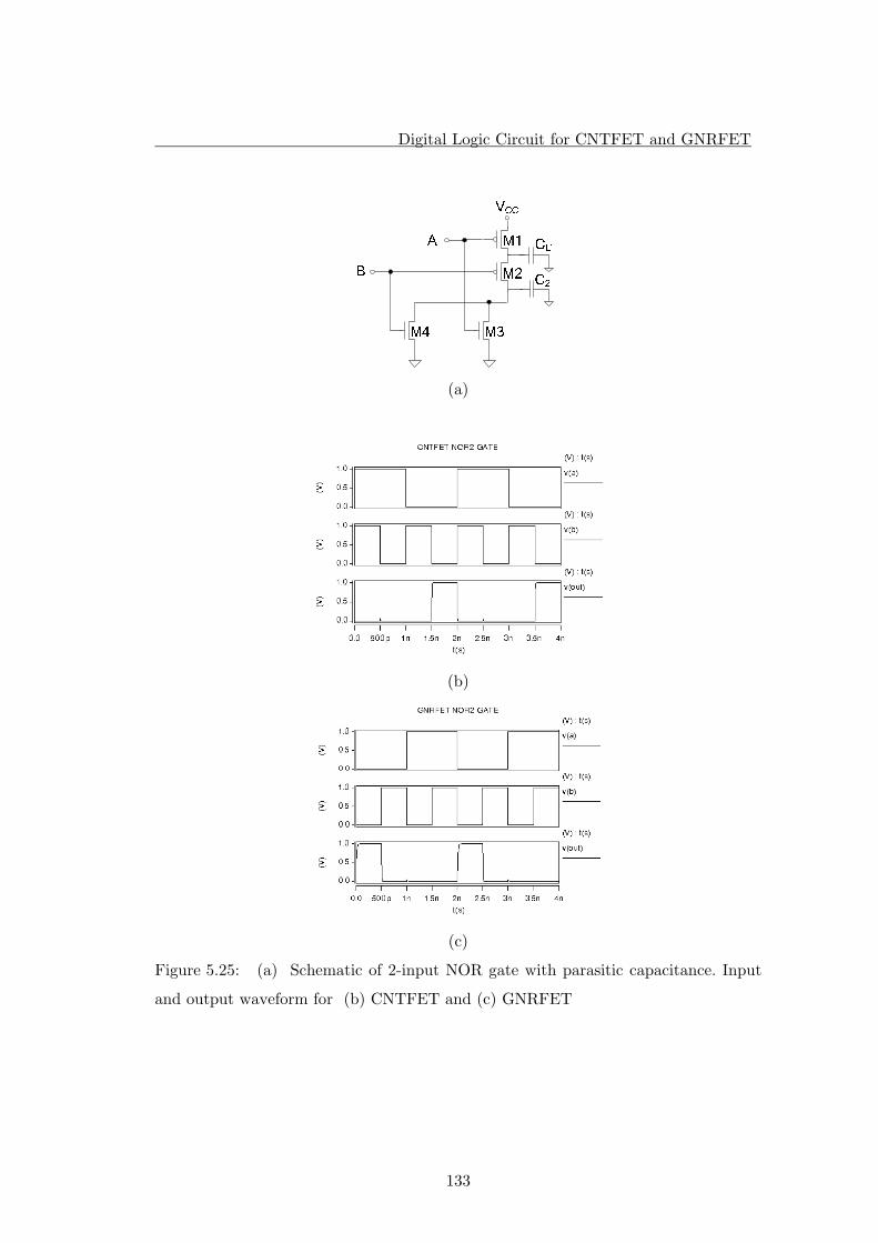
Digital Logic Circuit for CNTFET and GNRFET
133
(a)
(b)
(c)
Figure 5.25: (a) Schematic of 2-input NOR gate with parasitic capacitance. Input
and output waveform for (b) CNTFET and (c) GNRFET

Digital Logic Circuit for CNTFET and GNRFET
134
(a)
(b)
(c)
Figure 5.26: (a) Schematic of 3-input NOR gate with parasitic capacitance. Input
and output waveform for (b) CNTFET and (c) GNRFET

Digital Logic Circuit for CNTFET and GNRFET
135
Table 5.10 lists the expression for the load and output capacitance for the logic gates
and ring-oscillator in Figures 6.22 to 6.26. As each of the logic gates shown are
standalone single gate, the single gate load capacitance, CL’ does not have the Cgs
and CG components. The cascaded inverter in a ring configuration however has both
Cgs and CG components from subsequent gates. It is assumed that all ring-oscillators
have the same load capacitance.
Table 5.10: Load and output capacitance for logic gates NOT, NAND2,
NOR2, NAND3, NOR3 and ring oscillator
Gate Logic Capacitance NOT CL’ = Cgd1+ Cgd2 + Cdb1 + Cdb2 + Cw NAND2 C1 = Cdb1 + Csb2 + Cgd1 + Cgs2
CL’ = Cdb2 + Cdb3 + Cdb4 + Cgd2 + Cgd3 +Cgd4 + CW NOR2
NAND3 C1 = Cdb1 + Csb2 + Cgd1 + Cgs2 C2 = Cdb2 + Csb3 + Cgd2 + Cgs3 CL’ = Cdb3 + Cdb4 + Cdb5 + Cdb6 + Cgd3 + Cgd4 +Cgd5 +Cgd6 + CW NOR3
RING OSCILLATOR
CL1= Cint + Cext = Cgd1 + Cgd2 + Cdb1 + Cdb2 + CG3 + Cgs4 + CG4 + Cgs4 + Cw CL1= CL2 = CL3 = CL4 = CL5 = CL6 = CL7 = CL8 CL8 = CL9 = CL10 = CL11 = CL13 = CL14 = CL15
The propagation delay for the logic gates are shown in Table 5.11 for CNTFET and
Table 5.12 for GNRFET.
Table 5.11: CNTFET logic circuit delay computation for single logic gate
CNTFET circuits
With 45 nm Process Design Guidelines With 90 nm Process Design Guidelines Delay without inter-
connects Delay with 5 μm
interconnect Delay without inter-
connects Delay with 5 μm
interconnect
Propagation delay, tp (ps)
Propagation delay, tp (ps)
Propagation delay, tp (ps)
Propagation delay, tp (ps)
INVERTER 0.14 9.277 0.19 11.07 NAND2 0.39 12.97 0.52 15.17 NAND3 0.61 16.87 0.81 19.84 NOR2 0.47 12.98 0.63 15.18 NOR3 0.50 16.48 0.68 19.57

Digital Logic Circuit for CNTFET and GNRFET
136
Table 5.12: GNRFET logic circuit delay computation for a single logic gate
GNRFET circuits
With 45 nm Process Design Guidelines With 90 nm Process Design Guidelines Delay without inter-
connects Delay with 5 μm
interconnect Delay without inter-
connects Delay with 5 μm
interconnect
Propagation delay, tp (ps)
Propagation delay, tp (ps)
Propagation delay, tp (ps)
Propagation delay, tp (ps)
INVERTER 0.14 22.23 0.26 25.99 NAND2 0.40 30.19 0.71 35.99 NAND3 0.63 39.41 1.11 45.65 NOR2 0.48 30.48 0.86 36.13 NOR3 0.52 38.72 0.95 45.15
Figure 5.27 shows the schematic of a 15 stage ring-oscillator while Table 5.12 lists
the loop delay and propagation delay per gate for CNTFET, GNRFET and Si
MOSFET in a 45 nm and 90 nm process. The frequency of oscillation depends on
the delay of each inverter also known as the gate delay and the wire or interconnect
delay between each gate. Propagation delay increases with output load capacitance
and the interconnect capacitance.
= =1 1
2oscosc p
fT Nt
(5.9)
Figure 5.27: Schematic of ring-oscillator of 15 cascaded inverters with parasitic ca-
pacitance.

Digital Logic Circuit for CNTFET and GNRFET
137
From the ring-oscillator circuit, the propagation delay per gate for the CNTFET
circuit based on the 45 nm process guidelines is 12.04 ps. This is an increase of 29 %
on the delay of a single inverter, largely due to the contribution of Cgs and CG. The
input and output waveforms of the carbon-based ring-oscillator are shown in Figure
5.28.
Table 5.13: Delay and frequency computation for CNTFET and GNRFET
against Si MOSFET 45 nm and 90 nm ring-oscillator circuit
Ring-oscillator of NOT gates
With 45 nm Process Design Guidelines With 90 nm Process Design Guidelines
Loop delay (ps)
Oscillation frequency, fosc
(GHz)
Propagation delay
per gate (ps)
Loop delay (ps)
Oscillation frequency, fosc
(GHz)
Propagation delay
per gate (ps)
CNTFET circuits
180.58 2.76 12.04 212.12 2.36 14.14
MOSFET Circuits
240.9 2.08 16.06 69.09 7.23 46.06
GNRFET circuit
411.18 1.21 27.41 490.25 1.02 32.63
MOSFET circuits 691.05 0.72 46.07 1845 0.27 123
(a) (b)
Figure 5.28: Input and output waveform for (a) CNTFET and (b) GNRFET ring-
oscillator with contact and interconnect geometries extracted from 45 nm and 90 nm
process nodes
Conclusion
138
5.5 Conclusion The CNTFET and the GNRFET have been benchmarked against Si MOSFETs for
the 45 nm and 90 nm process nodes. For a fair assessment, the CNTFET is evaluat-
ed against a high current MOSFET (≈ 50 µA) and GNRFET with a low current
MOSFET (≈ 25 µA). The schematic and layout MOSFET logic circuit is generated
using the Cadence IC design suite while the CNTFET and the GNRFET circuit
simulation is carried out in HSPICE. The cutoff frequency for the carbon-based de-
vices are analyzed for two substrate insulator thicknesses, 100 nm and 500 nm with
copper interconnect length varying from 0.01 µm to 100 µm. Devices with thicker
substrate insulator and smaller source drain contact area give the highest frequency.
In addition to that, logic gates NOT, NAND2, NAND3, NOR2 and NOR3 gates and
their corresponding input and output waveform are given. It is found that NAND3
or NOR3 have the largest propagation delay since each has multiple fan-in and fan-
out. The interconnect length of cascading logic gates has a profound effect on the
signal propagation delay. In the digital logic simulation, we use an average length of
5 μm per fanout. The results indicate that inverters placed in a ring-oscillator con-
figuration have a major increase of delay compared to single gate mainly due to to-
tal gate parasitic capacitance from each cascading gate, other than the interconnect
capacitance. The key limiting factor for high-speed carbon nanotube and graphene
based chips is the interconnect itself. The performance enhancement gained through
carbon-based material is negligible if the interconnect capacitance is not reduced
significantly with transistor features size. Bundled metallic MWCNTs are seen as a
potential candidate to replace copper interconnects as future IC interconnects once
the challenges of integrating CNT interconnects onto existing manufacturing pro-
cesses are met.

References
139
5.6 References [1] G. Jing, S. Hasan, A. Javey, G. Bosman, and M. Lundstrom, "Assessment of
high-frequency performance potential of carbon nanotube transistors," IEEE Transactions on Nanotechnology, vol. 4, pp. 715-721, November 2005.
[2] Y. Yoon, Y. Ouyang, and J. Guo, "Effect of phonon scattering on intrinsic de-lay and cutoff frequency of carbon nanotube FETs," IEEE Transactions on Electron Devices, vol. 53, pp. 2467-2470, Oct 2006.
[3] S. Sreelal, C. K. Lau, and G. S. Samudra, "Parasitic capacitance characteris-tics of deep submicrometre grooved gate MOSFETs," Semiconductor Science and Technology, vol. 17, pp. 179-188, March 2002.
[4] J. Rabaey, A. Chandrakasan, and B. Nikolic, Digital integrated circuits : a design perspective: Pearson Education, 2003.
[5] L. Hong, Y. Wen-Yan, K. Banerjee, and M. Jun-Fa, "Circuit Modeling and Performance Analysis of Multi-Walled Carbon Nanotube Interconnects," IEEE Transactions on Electron Devices, vol. 55, pp. 1328-1337, 2008.
[6] J. F. Xu, H. Li, W. Y. Yin, J. F. Mao, and L. W. Li, "Capacitance extraction of three-dimensional interconnects using element-by-element finite element method (EBE-FEM) and preconditioned conjugate gradient (PCG) tech-nique," IEICE Transactions on Electronics, vol. E90C, pp. 179-188, Jan 2007.
[7] "Process Integration, Devices, & Structures Process Integration," in Interna-tional Technology Roadmap for Semiconductors (ITRS), 2005 http://www.itrs.net/links/2005itrs/Interconnect2005.pdf.
[8] T. Kanamoto, Y. Ogasahara, K. Natsume, K. Yamaguchi, H. Amishiro, T. Watanabe, and M. Hashimoto, "Impact of Well Edge Proximity Effect on Timing," IEICE Transactions on Fundamentals of Electronics Communica-tions and Computer Sciences, vol. E91A, pp. 3461-3464, Dec 2008.
[9] M. Vujkovic, D. Wadkins, and C. Sechen, "Efficient post-layout power-delay curve generation," in Integrated Circuit and System Design - Power and Tim-ing Modeling, Optimization and Simulation. vol. 3728, V. Paliouras, J. Vounckx, and D. Verkest, Eds. Berlin: Springer-Verlag Berlin, 2005, pp. 393-403.
[10] L. Nougaret, H. Happy, G. Dambrine, V. Derycke, J. P. Bourgoin, A. A. Green, and M. C. Hersam, "80 GHz field-effect transistors produced using high purity semiconducting single-walled carbon nanotubes," Applied Physics Let-ters, vol. 94, p. 3, Jun 2009.
[11] Y. M. Lin, C. Dimitrakopoulos, K. A. Jenkins, D. B. Farmer, H. Y. Chiu, A. Grill, and P. Avouris, "100-GHz Transistors from Wafer-Scale Epitaxial Gra-phene," Science, vol. 327, pp. 662-662, 2010.

140
Chapter 6
Conclusions and Future Work
6.1 Summary We have established that CNTs and GNRs are capable of providing similar drain
currents as Si MOSFET with better control of short channel effects (SCE). To
ensure a fair comparison, both CNT and GNR were assumed to have the same
bandgap and use the minimum contact size that is permitted by the 45 nm and 90
nm CMOS design layout rules. It is found that these carbon-transistors have
reduced drain-induced-barrier-lowering (DIBL), better subthreshold swing (SS) and
higher conductivity than a Si MOSFET. The carrier density is at least 75× times
that of the Si MOSFET for the CNTFET and 43× for the GNRFET. Unlike the
MOSFET, both nanostructures are able to provide almost perfectly symmetric I-V
characteristic for n and p-type devices [1]. The top gated structure with a high-κ
gate dielectric has a good gate control over the channel that can effectively suppress
DIBL and hysteresis while maintaining high transconductance [2]. High quality
graphene and carbon nanotube can have mobilities approaching 100,000 cm2 V−1 s−1
and 200,000 cm2 V−1 s−1 respectively in the absence of charged impurities at room
temperature. Under practical operating conditions, mobility from 10,000 cm2 V−1 s−1
are routinely observed for exfoliated graphene on silicon wafers [3] and for SWCNT
both of which are an order of magnitude higher than for a Si MOSFET [4, 5].

Future Work
141
High drain current can be obtained when the Fermi level of the channel is
shifted upward. When a high gate bias is applied, carriers populate not one but two
subbands thus increasing the current drive strength by a considerable amount [4].
Based on simulation results, multi-band transport provides a 9% increase of the
total current. The comprehensive carbon-based models have been verified with
experimental data and other existing compact models. The CNTFET models
developed in this research accurately predict the drain current of measured sub-100
nm channel CNT transistors. It is assumed that armchair GNRs can be either
metallic or semiconducting depending on their width. However, there has also been a
computational study that found all armchair GNRs are semiconducting [5] .
The maximum drain current for a monolayer GNRFET was found to be at
19 μA which is consistent with the work of Ouyang et al. [6] who projected Ion ≈ 24
μA with phonon scattering included. The CNTFET model also gives good agreement
with the Stanford [7] and Arizona model [8, 9]. It is demonstrated that a single
CNT can provide current up to 40 μA by improving the contact between the
channel and metal. A contact that has low Schottky barrier and high Ohmic
properties provides low resistance to the carriers. This so called transparent contact
can be attributed to the graphitic carbonization on the metal-channel interface when
the nanotube is annealed at high temperatures [10] .
A major improvement to the model is the substitution of the Newton-Raphson
iteration with a non-linear polynomial approximation. By having the shorter and
simpler expression, the simulation time is made much faster and efficient without
needing any numerical iteration. Hence, computing cost is effectively reduced. Apart
from that, the compact model itself is now portable and can be transferred between
multiple EDA software tools such as PSPICE and HSPICE without much
modification.
The low dimensional carbon devices outperform silicon MOSFET in term of
power-delay-product (PDP) and energy-delay-product (EDP) by several orders of
magnitude. For the same amount of drain current, the channel area consumed by
CNTFET and GNRFET is relatively smaller than for Si MOSFET. A 20 nm
GNRFET uses only 64 % of the Si MOSFET channel size in a 45 nm process.

Future Work
142
Moreover, 11% of the channel size can be reduced by adopting 50 nm SW-CNTFET
for a 45 nm MOSFET. This allows the fabrication of high density ICs made of
nanotubes and nanoribbons on chip. It is forecast that the cutoff frequency limit of
CNTFETs and GNRFETs can exceed 200 GHz twice the frequency recorded so far
[11, 12]. Here, it is shown that with practical interconnect limitations, cut off
frequencies are limited to ≈12.49 GHz for the CNTFET and ≈5.43 GHz for
GNRFET. A key advantage of carbon-based logic gates over the Si MOSFET
counterparts is their low energy consumption per logic transition [13]. It is shown
through simulation that the CNTFET and GNRFET logic gates can have wiring
lengths up to 5 μm before their performance becomes no better than a Si MOSFET.
6.2 Future Work Having developed the compact model for a single channel CNTFET and a
monolayer GNRFET, the next goal is to use multi-channel CNT [14] and bi-layer
GNR [6] in nanoelectronic circuits. This can provide tremendous improvement on
the transconductance and ON-current. The ideal drain current for a metallic single
channel CNT with ballistic transport is 100 μA per tube and a monolayer metallic
GNR can offer 50 μA. Practically, the measured current found in most
semiconducting single channel CNT is 25-35 μA [15-17]. This value drops to 5-8 μA
for monolayer GNR [18, 19]. However, it is shown in this investigation that with
good contact interface and high quality short channels, drain current can be
increased to 40-50 μA for CNT and 20-24 μA for GNR [6]. Using parallel multi-
channel CNT and bi-layer GNR, it should be able to drive digital circuits that
operate at high switching rate due to the increased output current. In addition,
research future on these lines will open a new paradigm for applications that require
large current such as RF power transistors and light-emitting diodes [20].

Future Work
143
Figure 6.1: Structure of a multi-channel CNT (adapted from [21])
Other interesting future work would be to study the screening capacitance
between nanotubes in multi-channel CNTs. They are known to downgrade the ON
current if the inter-CNT pitch is spaced less than 20 nm apart. They also affect the
gate to channel capacitance that determine the instrinsic cutoff frequency. For array
nanotubes which have roughly 2.5 nm inter-CNT-pitch, current is decreased by at
least 50% [16]. It has been demonstrated that in a multi-channel local bottom gate
(LBG) design, each nanotube carries the same amount of current. The study reveals
that ON-current has a linear dependence on the number of semiconducting CNTs
[22]. With nanotubes in an array, the width of CNTFETs can now be scaled similar
to Si MOSFETs to have equal high-to-low propagation delay tPHL and low-to-high
propagation delay tPLH in logic gates.
Source
Drain
Contact Width
Pitch
Gate Channel Length
CNTs

Future Work
144
In the present work, it is assumed that both the n-type and p-type CNTFETs
and GNRFETs have symmetrical I-V characteristic. Therefore, another possible
direction for future work is to adopt non-symmetrical I-V models. This result shall
provide valuable insight on the voltage gain and propagation delay that affect the
EDP and PDP.

References
145
6.3 References
[1] Z. Zhang, S. Wang, Z. Wang, L. Ding, T. Pei, Z. Hu, X. Liang, Q. Chen, Y. Li, and L.-M. Peng, "Almost Perfectly Symmetric SWCNT-Based CMOS Devices and Scaling," ACS Nano, vol. 3, pp. 3781-3787, 2009.
[2] M. H. Yang, K. B. K. Teo, L. Gangloff, W. I. Milne, D. G. Hasko, Y. Robert, and P. Legagneux, "Advantages of top-gate, high-k dielectric carbon nanotube field-effect transistors," Applied Physics Letters, vol. 88, p. 3, Mar 2006.
[3] F. Schwierz, "Graphene transistors," Nature Nanotechnology, vol. 5, pp. 487-496, 2010.
[4] Z. Yang, A. Liao, and E. Pop, "Multiband mobility in semiconducting carbon nanotubes," Ieee Electron Device Letters, vol. 30, pp. 1078-1080, October 2009.
[5] V. n. Barone, O. Hod, and G. E. Scuseria, "Electronic Structure and Stability of Semiconducting Graphene Nanoribbons," Nano Letters, vol. 6, pp. 2748-2754, 2006.
[6] Y. Ouyang, H. Dai, and J. Guo, "Projected performance advantage of multilayer graphene nanoribbons as a transistor channel material," Nano Research, vol. 3, pp. 8-15, 2010.
[7] J. Deng and H. S. P. Wong, "A compact SPICE model for carbon-nanotube field-effect transistors including nonidealities and its application - Part II: Full device model and circuit performance benchmarking," IEEE Transactions on Electron Devices, vol. 54, pp. 3195-3205, Dec 2007.
[8] A. Balijepalli, S. Sinha, and Y. Cao, "Compact modeling of carbon nanotube transistor for early stage process-design exploration," in Proceedings of the 2007 international symposium on Low power electronics and design Portland, OR, USA: ACM, 2007.
[9] S. Sinha, A. Balijepalli, and C. Yu, "A Simplified Model of Carbon Nanotube Transistor with Applications to Analog and Digital Design," in Quality Electronic Design, 2008. ISQED 2008. 9th International Symposium on, 2008, pp. 502-507.
[10] A. A. Kane, T. Sheps, E. T. Branigan, V. A. Apkarian, M. H. Cheng, J. C. Hemminger, S. R. Hunt, and P. G. Collins, "Graphitic Electrical Contacts to Metallic Single-Walled Carbon Nanotubes Using Pt Electrodes," Nano Letters, vol. 9, pp. 3586-3591, Oct 2009.
[11] M. S. Arnold, A. A. Green, J. F. Hulvat, S. I. Stupp, and M. C. Hersam, "Sorting carbon nanotubes by electronic structure using density differentiation," Nat Nano, vol. 1, pp. 60-65, 2006.
[12] Y. M. Lin, C. Dimitrakopoulos, K. A. Jenkins, D. B. Farmer, H. Y. Chiu, A. Grill, and P. Avouris, "100-GHz Transistors from Wafer-Scale Epitaxial Graphene," Science, vol. 327, pp. 662-662, 2010.
[13] P. Avouris, Z. Chen, and V. Perebeinos, "Carbon-based electronics," Nat Nano, vol. 2, pp. 605-615, 2007.
[14] C. X. Chen, Z. Y. Hou, X. Liu, E. S. W. Kong, J. P. Miao, and Y. F. Zhang, "Fabrication and characterization of the performance of multi-channel carbon-

References
146
nanotube field-effect transistors," Physics Letters A, vol. 366, pp. 474-479, Jul 2007.
[15] A. Javey, J. Guo, Q. Wang, M. Lundstrom, and H. J. Dai, "Ballistic carbon nanotube field-effect transistors," Nature, vol. 424, pp. 654-657, Aug 2003.
[16] J. Deng and H. S. P. Wong, "A compact SPICE model for carbon-nanotube field-effect transistors including nonidealities and its application - Part I: Model of the intrinsic channel region," IEEE Transactions on Electron Devices, vol. 54, pp. 3186-3194, Dec 2007.
[17] A. Javey, P. Qi, Q. Wang, and H. Dai, "Ten- to 50-nm-long quasi-ballistic carbon nanotube devices obtained without complex lithography," National Academy of Sciences, 2004.
[18] X. R. Wang, Y. J. Ouyang, X. L. Li, H. L. Wang, J. Guo, and H. J. Dai, "Room-temperature all-semiconducting sub-10-nm graphene nanoribbon field-effect transistors," Physical Review Letters, vol. 100, p. 4, May 2008.
[19] L. Y. Jiao, L. Zhang, X. R. Wang, G. Diankov, and H. J. Dai, "Narrow graphene nanoribbons from carbon nanotubes," Nature, vol. 458, pp. 877-880, Apr 2009.
[20] R. Seidel, A. P. Graham, E. Unger, G. S. Duesberg, M. Liebau, W. Steinhoegl, F. Kreupl, W. Hoenlein, and W. Pompe, "High-Current Nanotube Transistors," Nano Letters, vol. 4, pp. 831-834, 2004.
[21] G. Cho, Y.-B. Kim, and F. Lombardi, "Assessment of CNTFET based circuit performance and robustness to PVT variations," in Circuits and Systems, 2009. MWSCAS '09. 52nd IEEE International Midwest Symposium on, 2009, pp. 1106-1109.
[22] A. D. Franklin, A. Lin, H. S. P. Wong, and C. Zhihong, "Current Scaling in Aligned Carbon Nanotube Array Transistors With Local Bottom Gating," IEEE Electron Device Letters, vol. 31, pp. 644-646, July 2010.

147
Appendix A
Research Methodology
A.1 Introduction This appendix discusses the methodology adopted to develop CNTFET and
GNRFET macromodels in comparison with standard CMOS digital logic gates
extracted from 45 nm and 90 nm process nodes. The robust and comprehensive
device, circuit and layout-based models are simulated in MATLAB, Synopsys
HSPICE, Orcad PSPICE and Cadence custom IC tools. The physical phenomena of
these nanotransistors vary according to the confinement of the carriers. To under-
stand the device physics behind the carbon nanostructures, qualitative and
quantitative assessment is carried out on existing CNTFET models with observation
on the energy band profile, density of states and charge density in quasi-one
dimensional system. One of the key challenges of this research is to implement these
analytical and semi-empirical models across the EDA platform particularly from
MATLAB to HSPICE and PSPICE. Once the cross-platform transfer is done, the
performance limit for the CNTFETs, GNRFETs and CMOS are assessed for a
variety of circuit blocks including NAND, NOR gates and a ring-oscillator. There
will also be comparison and evaluation against experimental and simulated data
taken from nanotube, nanoribbon and nanoscale MOSFETs.

Electrical Modeling
148
A.2 Electrical Modeling The core element of modeling is the formulation of current-carrier transport based
on the layout of CNTFET, GNRFET and MOSFET nanostructures and perform-
ance metric evaluation of the FET logic gates. First, physics based models are
explicitly written and simulated in MATLAB [1]. Next, the Cadence Virtuoso Suite
is used for CMOS logic gates design and benchmarking while carbon based
integrated circuits are simulated in the Synopsys HSPICE simulator [2]. Before that
can be done, MATLAB scripts are simplified and converted into SPICE syntax to be
implemented as nanotube and nanoribbon HSPICE macro models [3, 4].
Carrier statistics governing the device operation in Q2D’s MOSFET and Q1D’s
nanoribbon and nanotube can be represented using the Fermi-Dirac distribution. A
wide range of current and voltage curves can be generated once the carrier density is
obtained. In addition, the effects of intrinsic and extrinsic capacitances are also
considered in the model framework.
Figure A.1 shows the convergence of ECAD and TCAD in integrated circuit de-
sign flow. In TCAD process simulation, a two or three dimensional program is used
to simulate the fabrication process steps such as oxidation, diffusion, etching and
deposition. Subsequently, device simulation is performed to give the electrical
properties of the customized layout based on the material and external field inputs
[5]. Both CAD tools have distinct front end approaches where ECAD is pre-
dominantly circuit-based while TCAD is process-based. However, both of them
have identical back end designs. In the final stages, device simulation of the custom
layout design is carried out with physical verification such as design rules check
(DRC), layout versus schematic (LVS) and parasitic extraction (RCX).

Electrical Modeling
149
Figure A.1: ECAD and TCAD flow chart (adapted from [6])
Circuit Design
Process Design Kits
Logical Design
Process Recipe
Process Simulation
Gate Model
Device Model
Device Simulation Layout
ECA
D
TC
AD

MATLAB
150
A.2.1 MATLAB Current transport modeling in the CNT and GNR is based on the ballistic model
reported by Natori [7]. First, existing formalisms are inspected and developed to
include non-idealities such as scattering, quantum resistance and parasitic
capacitance [8]. Secondly, parameter extraction from experimental devices is carried
out to ensure that the device model is able to give accurate and reliable device
characteristics between modeled and measured data [9]. When preliminary electrical
technological parameters are verified, device analysis in MATLAB and circuit
simulation in HSPICE is performed.
Figure A.2: MATLAB Simulation Process
Circuit Simulation using HSPICE
Current Transport Modeling
Modification and Enhancement
I-VValidation
Device Performance Analysis
No
Yes
Experimental Data from Fabrication
Simulation
Circuit Performance Analysis
Parameters Extraction
Proposed Models Verified
Device Simulation using MATLAB

HSPICE
151
A.2.2 HSPICE
The HSPICE simulation process is shown in Figure A.3. To run the software, model
description of a CNTFET or a GNRFET is prepared and saved as *.sp file. It
contains the title, initial condition of the system, model libraries, input stimuli (eg:
DC voltage and current source or piece-wise linear source), circuit description
analysis commands (such as DC, transient or AC analysis) and output description as
listed in Table 3.1. HSPICE can be run on UNIX, Linux and Windows platforms.
Table 3.1: Input netlist file sections (adapted from [10]) Sections Examples DescriptionTitle .TITLE The first line is the input netlist file titleComment * or $ Comments to describe the circuit Set-up .OPTIONS Sets conditions for simulation
.IC or .NODESET Initial values in circuit and subcircuit
.PARAM Set parameter values in the netlist
.GLOBAL Set node name globally in netlist Sources Sources (I or V) and digital inputs Sets input stimuliNetlist Circuit elements Circuit for simulation
.SUBKCT, .ENDS Subcircuit definitions Analysis
.DC, .TRAN, .AC, etc. Statements to perform analyses
.SAVE and .LOAD Save and load operating point info
.DATA Create table for data-driven analysis
.TEMP Set analysis temperature Output .PRINT, .PLOT, .GRAPH, .PROBE Statements to output variables
.MEASURE Statement to evaluate and report user-defined functions of a circuit
Library, Model and File Inclu-sion
.INCLUDE General include files.MODEL Element model descriptions .LIB Library< .PROTECT> Turns off output printback <.UNPROTECT> Restores output printback
Alter blocks .ALTER Sequence for in-line case analysis .DELETE LIB Removes previous library selection
End of netlist .END Terminates any ALTERs and the simulation

HSPICE
152
HSPICE is used to perform single and multipoint point analysis sweeps. These
analyses produce a number of output files which can be viewed, analyzed and
printed in AvanWaves or CosmosScope, products from Synopsys.
Figure A.3: HSPICE Simulation Process (adapted from [11])
Find License File
Invocation
Run HSPICE
Simulation configuration
AvanWaves / CosmosScope (Graph and Analysis)
Output Files
Input Netlist File

PSPICE
153
A.2.3 PSPICE
The CNTFET and GNRFET models have also been implemented within PSPICE
using an Analog Behavioral Modeling (ABM) method. The carbon-based device
model is broken down into short mathematical equations that are represented
by ABM parts extracted from a library. Types of ABM components are
mathematical functions such as adder (SUM), multiplier (MULT), power (PWR)
and logarithm (LOG). These mathematical functions are lumped together using
expression functions using ABM1 (1 input, V output) and ABM1/I (1 input, I
output).
In order to run the simulation in PSPICE, the Newton-Raphson method for
calculating the self-consistent voltage, Vsc of the channel is substituted with a
polynomial approximation. As a result, no iterations for convergence are needed and
this improves the execution speed tremendously. Figure A.4 shows a selection of the
ABM expression block functions which are used to model the I-V characteristics of
the CNT and GNR transistors.
Figure A.4: ABM modeling in PSPICE

CADENCE
154
A.2.4 CADENCE
The device performance of the HSPICE CNT and GNR circuit models are compared
against MOSFET designs that are developed using a Cadence predictive 45 nm tech-
nology model and a TSMC 90 nm foundry technology model [12]. Two different
platforms are used to run Cadence. The TSMC 90 nm design kit is run on Virtuoso
custom IC 5.1.41, an older platform which uses the original Cadence database
(CDB) that is written in C. On the other hand, Cadence 45nm PDK developed by
Accelicon Technologies Inc. runs on a newer IC 6.1.3 platform. Due to
incompability between platforms, the EDA industry at the moment are moving
toward a reformed open access (OA) database [13, 14] to replace the CDB database.
The new database will allows EDA vendors such as Mentor Graphics, Synopsys and
Magma Design Automation to share the kits for collaborative tool development and
promote wide interoperability between EDA tool vendors, university research and
development (R&D) groups and foundries. These EDA vendors are part of the
OpenPDK Coalition [15] under Silicon Integration Initiative (Si2) [16] that are keen
to reinvent the way ICs are designed, manufactured and marketed. The portability
of the PDK database allows a better efficiency and cost effective technology transfer.
In order to run Cadence, the following software shown in Table A.2 is required for a
complete solution for front end to back end custom IC design.
Table A.2: Cadence custom IC design tools
Software Release Stream Key Products Virtuoso Schematic Editor A schematic entry for analog, digital, RF and
mixed-signal design Virtuoso Analog Design Environment Simulation, analysis, and measurement envi-
ronment Virtuoso Multi-Mode Simulation (MMSIM)
Simulators for analog, digital, RF and mixed-signal design (eg: Spectre)
Virtuoso Layout Editor Accommodate custom layout of analog, digital, RF and mixed-signal designs at the device, cell, and block levels
Assura System and design verification suite (DRC, LVS and RCX)

CADENCE
155
The circuit and layout development of MOSFET logic gates are performed in
Cadence IC514 for TSMC PDK and IC613 for Cadence GPDK. The PDK usually
contains the spectre models, layout and parameterized cells, symbols, component de-
scription format (CDF) parameters and technology files such as layer definitions and
design rules. Detailed measures have to be taken to ensure no conflict arises
between the old and new release software by finding a suitable version of supporting
softwares.
Figure A.5 depicts the process for a digital IC design carried out in this work.
First and foremost, a schematic diagram of a circuit is created using the Cadence
Virtuoso Schematic Editor. Next, the simulation is started by selecting the Spectre
simulator under the Virtuoso Analog Design Environment. If there is no error, the
circuit layout is ready to be drawn in Virtuoso Layout Editor. Following that, DRC
is performed to make certain that the layout dimensions comply with the design
rules of the process technology. When that is done, the layout is compared with the
circuit schematic so that proper functionality is assured. Subsequently, the layout
parasitics are extracted using RCX for a more accurate post-layout simulation. All
these verification tools run using Assura. Last but not least, the verified layout is
converted to a foundry standard file format (eg: GDSII, CIF, etc.).

CADENCE
156
Figure A.5: Cadence IC Design Flow (adapted from [2])
Layout Design
Simulation
No
Yes
Parasitic backannotation to Schematic
Database file output
Process Design Kit
DRC
LVS
RCX
OK
Fail
Fail
Fail
Pass
Pass
Pass
Schematics Entry

Conclusion
157
A.3 Conclusion Device modeling of CNT and GNR FETs is carried using MATLAB. Following this,
HSPICE macromodels and PSPICE ABM models for the CNTFET and the
GNRFET are developed for circuit simulation. A MOSFET model is generated using
process design kits from Cadence (45 nm) and TSMC (90 nm). The performance of
the MOSFET is used for benchmarking against carbon devices when post-layout
simulation is performed. To have the simulation as accurate as possible, wiring
parasitic capacitance and resistance extracted from the MOSFET layout is
backanotated onto the schematics. Since HSPICE and PSPICE simulation are based
on a netlist, several parasitic capacitances such as substrate capacitance Csub, source-
to-bulk capacitance Csb, drain-to-bulk capacitance Cdb, gate-to-source capacitance
Cgs, drain-to-bulk capacitance Cgd , wiring capacitance, Cint are included within the
device model. This method provides an alternative approach to post-layout
simulation for CNT and GNRFETs.

References
158
A.4 References [1] J. M. Marulanda, A. Srivastava, and S. Yellampalli, "Numerical Modeling of
the I-V Characteristic of Carbon Nanotube Field Effect Transistors (CNT-FETs)," in System Theory, 2008. SSST 2008. 40th Southeastern Symposium on, 2008, pp. 235-238.
[2] A. J. L. Martin, "Cadence Design Environment Tutorial," New Mexico State University: Klipsch School of Electrical and Computer Engineering, 2002.
[3] J. Deng, A. Lin, G. C. Wan, and H.-S. P. Wong, "Carbon nanotube transistor compact model for circuit design and performance optimization," J. Emerg. Technol. Comput. Syst., vol. 4, pp. 1-20, 2008.
[4] T. J. Kazmierski, Z. Dafeng, and B. M. Al-Hashimi, "HSPICE implementation of a numerically efficient model of CNT transistor," in Specification & Design Languages, 2009. FDL 2009. Forum on, 2009, pp. 1-5.
[5] J. M. Galliere and J. Boch, "A mixed TCAD/Electrical simulation laboratory to open up the microelectronics teaching," in Microelectronic Systems Education, 2009. MSE '09. IEEE International Conference on, 2009, pp. 37-40.
[6] R. Martins, "On the Design of Very Low Power Integrated Circuits," in Faculty of Electrical Engineering and Information Technology. vol. Ph.D Austria: Vienna University of Technology, 1998.
[7] K. Natori, Y. Kimura, and T. Shimizu, "Characteristics of a carbon nanotube field-effect transistor analyzed as a ballistic nanowire field-effect transistor," Journal of Applied Physics, vol. 97, p. 7, Feb 2005.
[8] A. Javey and J. Kong, Carbon Nanotube Electronics (Integrated Circuits and Systems) vol. 1. New York: Springer 2009.
[9] A. C. Altuzarra, "DC Parameter Extraction Methods for MOSFETs," in 1st International Training Courses on Compact Modeling Tarragona, Spain, 2010.
[10] "Using Netlist Input Files," in Star-Hspice Manual - Release 2001.2, 2001 http://www.ece.uci.edu/docs/hspice/hspice_2001_2-15.html.
[11] Synopsys, "HSPICE® Simulation and Analysis User Guide," vol. Version Y-2006.03, p. 9, March 2006.
[12] "GPDK045 - 45nm Generic (Revision 2.0)," 2009 https://pdk.cadence.com/home.do.
[13] J. E. Stine, I. Castellanos, M. Wood, J. Henson, F. Love, W. R. Davis, P. D. Franzon, M. Bucher, S. Basavarajaiah, J. Oh, and R. Jenkal, "FreePDK: An Open-Source Variation-Aware Design Kit," in Microelectronic Systems Education, 2007. MSE '07. IEEE International Conference on, 2007, pp. 173-174.
[14] J. E. Stine, C. Jun, I. Castellanos, G. Sundararajan, M. Qayam, P. Kumar, J. Remington, and S. Sohoni, "FreePDK v2.0: Transitioning VLSI education towards nanometer variation-aware designs," in Microelectronic Systems Education, 2009. MSE '09. IEEE International Conference on, 2009, pp. 100-103.
[15] T. Blanchard, R. Ferreri, and J. Wilmore, "The OpenAccess coalition - the drive to an open industry standard information model, API, and reference

References
159
implementation for IC design data," in Quality Electronic Design, 2002. Proceedings. International Symposium on, 2002, pp. 69-74.
[16] "Silicon Integration Initiative (Si2)," 2005-2010 http://www.si2.org/.

160
Appendix B
Low Dimensional Modeling

Quasi-Two Dimensional Model
161
B.1 Quasi-Two Dimensional Model B.1.1 Density of States for Q2D Structure
( )
( )
( )
2
22
2 22 22
2
2
1Density of states,
Number of electronics stated dN between k and k+dk22 where
2
Energy momentum dispersion
22 2
212
se
*y cnx
co oz x,y* *
*cn
dN dkgA dk dE
A kdN πk L Adk ππ L
k m E EkE E n ε km m
m E EdkdE
=
= = =
−= + + + ⇒ =
⎡ −=
⎣( ) ( )
1 2 1 2
2 2
*2 1 22 2 2
22
Density of states is given as
1 1 where m is m m
* *cn* *
* *
se vi
m E E mm mk
AkdN dk m mg Ndk dE A πL k π
− −⎤ ⎡ ⎤−⎢ ⎥ ⎢ ⎥= ⋅ =⎢ ⎥ ⎢ ⎥⎢ ⎥ ⎢ ⎥⎦ ⎣ ⎦
= ⋅ ⋅ = ⋅ ⋅ =
B.1.2 Electron Concentration for Q2D Structure
( ) ( )
( )
( ) ( )
≈∞
≈∞
≈∞
−
−
=
=
+
= ⋅ ⋅+
= ⋅ ℑ = ⋅ ℑ
∫
∫
∫
2 2
2
02
0 2 02
1
1
11
C
C
C
F
B
top
seE
top
seE
top
se B BE
*B
c D c
E Ek T
x η
n g E f E dE
g dE
e
g k T k Tx dxe
m k T η N ηπ

Quasi-Two Dimensional Model
162
B.1.3 Intrinsic Velocity for Q2D Structure
( ) ( )( )
( ) ( )
( )
( )
≈∞ ∞
∞
∞
∞
−
−
−
−= =
= ⋅ − ⋅ − ⋅
+
= ⋅ ⋅
+
= ⋅
+
=
∫ ∫
∫
∫
∫
2 2 32 3
0 1 22
3
1 22
2
1 22
2
1 2
22
21 1
1 2 1
1
1 2 1
1
21 1
1
21
C C
C
C
C
Fk
B
Fk
B
Fk
B
topc
i se seE E
*
co coE
*
B BE
*B B
BE
*B B
E Ek T
E Ek T
E Ek T
E Ev v g E f E dE g (E)f(E)dE
n n m
m E E E E dEn mπ
e
m k Tx k Tdxn mπ
e
m k T k T x k Tdxn mπ
e
m k T k T xn mπ
e
( ) ( )( ) ( )
( )( )
∞
∞
−
−
+
=+
ℑ= ⋅
ℑ
ℑ= ⋅
ℑ
∫
∫1 2
22
1 2
0
1 2
0
1
211
3 21
2
C
C
Fk
BE
*B B
E
cth
c
cth
c
E Ek T
x η
dx
m k T k T x dxn mπ e
Γ ηv
Γ ηηπ vη

Quasi-One Dimensional Model
163
B.2 Quasi One-Dimensional Model B.2.1 Density of States for Q1D Structure
( )
( ) ( )
1
2 22 2
2
1 2
2
1Density of states,
Number of electronics stated dN between k and k+dk222
2
Energy momentum dispersion
22
21 22
se
*cnx
co oz oz x*
*cn * *
dN dkgL dk dE
LdNdk π L π
m E EkE E m ε n ε km
m E Edk m mdE
−
=
= =
−= + + + ⇒ =
⎡ ⎤−⎢ ⎥= =⎢ ⎥⎢ ⎥⎣ ⎦
( )
( )
( )
( )
( )
1 2
2 2
1 2
2
2
1 22
1 2
1 2
1
2
Density of states is given as
21 1
22
2
22 1
2
2
where is m
* *cn
*
se
*
*cn
*
cn*
*
cn*
*
cn
*
m E E mk
LdN dk mgL dk dE L π k
mπ m E E
m E Eπ m
m E Eπ m
m E Eπ
m
−
−
−
−
⎡ ⎤−⎢ ⎥⋅ =⎢ ⎥⎢ ⎥⎣ ⎦
= ⋅ ⋅ = ⋅ ⋅
= ⋅−
= ⋅ −
= ⋅ −
= ⋅ −

Quasi-One Dimensional Model
164
B.2.2 Electron Concentration for Q1D Structure
( ) ( )
( )
( )
( )
≈∞
≈∞−
≈∞−
≈∞ −
≈∞ −
≈∞ −
−
−
−
−
−
−
=
= − ⋅
+
= ⋅+
=+
=+
=+
= ℑ
∫
∫
∫
∫
∫
∫
1 1
1 2
1 2
1 2
1 2
1 2
1 12
2 1
1
2 11
21
2 11
2 11
C
C
C
C
C
C
Fk
B
top
seE
top*
cnE
top*
B BE
top*B
E
top*B
E
top*B
E
D c
E Ek T
x η
x η
x η
x η
n g E f E dE
m E E dEπ
e
m k Tx k T dxπ e
m k T π x dxπ π e
m k T x dxπ e
m k T π x dxπ e
N η

Quasi-One Dimensional Model
165
B.2.3 Intrinsic Velocity for Q1D Structure
( ) ( )( )
( ) ( )
( ) ( )
( )
( )( )
≈∞ ∞
∞−
∞
∞
−
−
−
−= =
= ⋅ − ⋅ − ⋅
+
= ⋅ ⋅ ⋅
+
= ⋅
+
⎛⎜= ⋅ ⋅ ⋅⎝
∫ ∫
∫
∫
∫
1 1 11 3
1 2 1 2
1
0
1
0
1
12 2
1
21 1
2 2 1
1
2 2 1
1
2 2
1
2 1 22 2
C C
C
C
C
Fk
B
Fk
B
Fk
B
topcn
i se seE E
*
cn cnE
*
B BE
*B B
E
*
B B
E Ek T
E Ek T
E Ek T
E Ev v g E f E dE g E f E dE
n n m
m E E E E dEn π m
e
m k Tx k Tdxn π m
e
m k T k T x dxn π m
e
N π mk T k Tn π π
( ) ( )( ) ( )
( ) ( )( ) ( )
( )( )
∞
∞
−
−
⎞⎟⎟⎜ ⋅⎟⎜ ⎟⎟⎜ +⎠
⎛ ⎞⎟⎜ ⎟⎜= ⋅ ⋅ ⋅ ⋅⎟⎜ ⎟⎟⎜ +⎝ ⎠
= ⋅ ⋅ ℑℑ
ℑ= ⋅
ℑ
ℑ= ⋅
ℑ
∫
∫
3 2 0
3 2 01
2 21
112
1
12
1
12
1
22 12 2 1
1 23 2
23 2
2
C
C
th BE
*B
th BE
th cc
cth
c
cth
c
x η
x η
xv k T dxe
N m k Tπ xv k T dxn π π e
v Γ ηΓ η
Γ ηv
Γ η
ηv
ηπ

Summary of Relative Formulas
166
B.3 Summary of Relative Formulas
Dimension
Carrier Statistics Effective
Density of States Degenerate Fermi
−= ℑ 22
d cd (d ) dn N (η ) =
1cd
x y z
dNNL L L dE
+
ℑ =+ +
111 1
i
iη(η)
Γ(i ) i
3D = ℑ3 3 1 32
cn N (η ) ⎛ ⎞⎟⎜= ⎟⎜ ⎟⎜⎝ ⎠
32
3 222
Bc
m * k TNπ
ℑ =32
12
43
(η) ηπ
2D = ℑ2 2 0 2cn N (η ) =2 2B
cm * k TN
π ℑ =0 2(η ) η
1D −= ℑ1 1 1 1
2cn N (η ) ⎛ ⎞⎟⎜= ⎟⎜ ⎟⎜⎝ ⎠
1 2
1 22 /
Bc
m * k TNπ −
ℑ = 1 21 12
2 /(η ) ηπ
Any D
Instrinsic Velocity
( )
( )
⎛ ⎞− ⎟⎜ ⎟⎜ ⎟⎟⎜⎝ ⎠
⎛ ⎞− ⎟⎜ ⎟⎜ ⎟⎟⎜⎝ ⎠
⎛ ⎞+ ℑ⎟⎜ ⎟⎜ ⎟⎜⎝ ⎠=
⎛ ⎞ ℑ⎟⎜ ⎟⎜ ⎟⎜⎝ ⎠
12
22
12
2
dd
id thdd
d ηΓν v
d ηΓ

Gamma Function
167
B.4 Gamma Function
i
Gamma Function
+ =1Γ(i ) i ! ( )+ = 2
21 2
2 ii !
Γ(i ) πi !
-1 Nil − = −1 2 2Γ( ) π
0 =1 0Γ( ) =1 2Γ( ) π
1 =2 1Γ( ) =3 2 2Γ( ) π
2 =3 2Γ( ) =5 2 3 4Γ( ) π
3 =4 6Γ( ) =7 2 15 8Γ( ) π
4 =5 24Γ( ) =9 2 105 16Γ( ) π
5 =6 120Γ( ) =11 2 945 32Γ( ) π
6 =7 720Γ( ) − =13 2 10395 64Γ( ) π