
CLIPPERS A clipping circuit or a clipper is a device used to ...
26
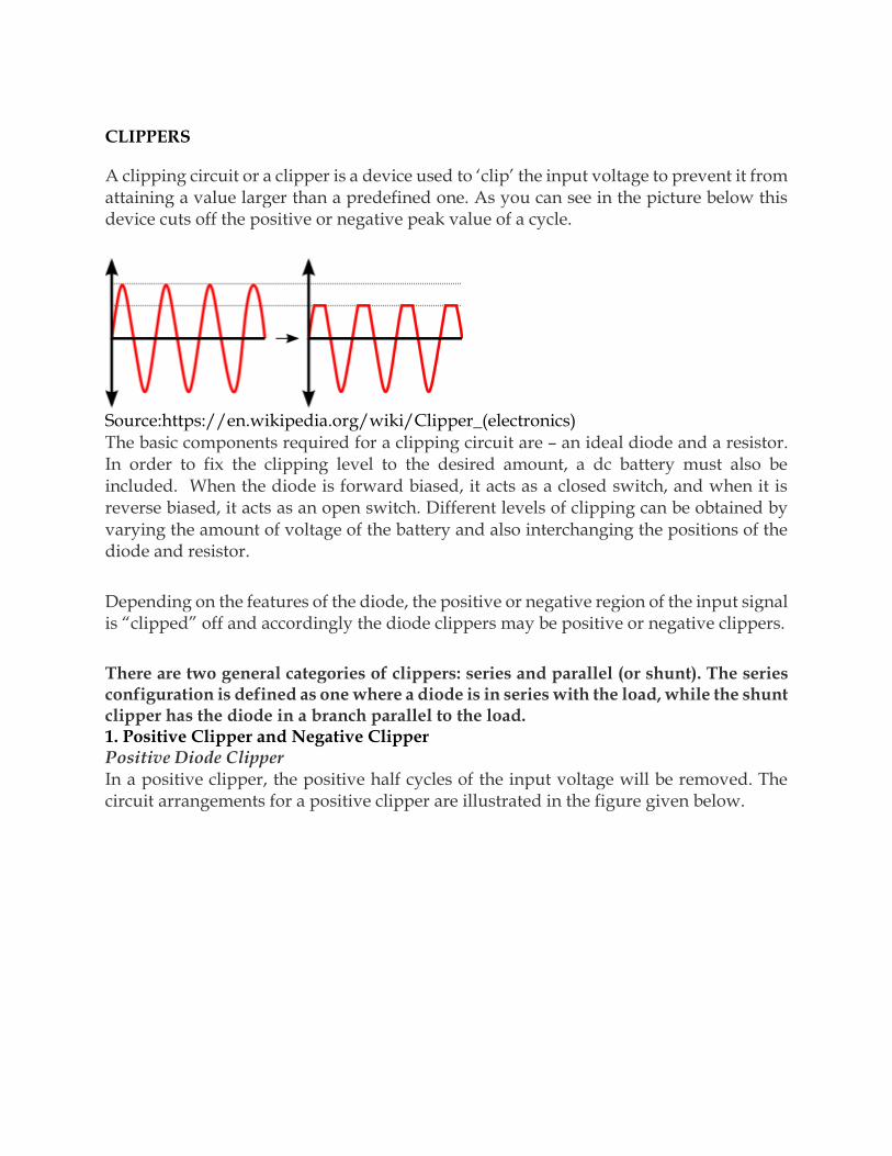
CLIPPERS A clipping circuit or a clipper is a device used to ‘clip’ the input voltage to prevent it from attaining a value larger than a predefined one. As you can see in the picture below this device cuts off the positive or negative peak value of a cycle. Source:https://en.wikipedia.org/wiki/Clipper_(electronics) The basic components required for a clipping circuit are – an ideal diode and a resistor. In order to fix the clipping level to the desired amount, a dc battery must also be included. When the diode is forward biased, it acts as a closed switch, and when it is reverse biased, it acts as an open switch. Different levels of clipping can be obtained by varying the amount of voltage of the battery and also interchanging the positions of the diode and resistor. Depending on the features of the diode, the positive or negative region of the input signal is “clipped” off and accordingly the diode clippers may be positive or negative clippers. There are two general categories of clippers: series and parallel (or shunt). The series configuration is defined as one where a diode is in series with the load, while the shunt clipper has the diode in a branch parallel to the load. 1. Positive Clipper and Negative Clipper Positive Diode Clipper In a positive clipper, the positive half cycles of the input voltage will be removed. The circuit arrangements for a positive clipper are illustrated in the figure given below.
-
Upload
khangminh22 -
Category
Documents
-
view
0 -
download
0
Transcript of CLIPPERS A clipping circuit or a clipper is a device used to ...
CLIPPERS
A clipping circuit or a clipper is a device used to ‘clip’ the input voltage to prevent it from attaining a value larger than a predefined one. As you can see in the picture below this device cuts off the positive or negative peak value of a cycle.
Source:https://en.wikipedia.org/wiki/Clipper_(electronics) The basic components required for a clipping circuit are – an ideal diode and a resistor. In order to fix the clipping level to the desired amount, a dc battery must also be included. When the diode is forward biased, it acts as a closed switch, and when it is reverse biased, it acts as an open switch. Different levels of clipping can be obtained by varying the amount of voltage of the battery and also interchanging the positions of the diode and resistor.
Depending on the features of the diode, the positive or negative region of the input signal is “clipped” off and accordingly the diode clippers may be positive or negative clippers.
There are two general categories of clippers: series and parallel (or shunt). The series configuration is defined as one where a diode is in series with the load, while the shunt clipper has the diode in a branch parallel to the load. 1. Positive Clipper and Negative Clipper Positive Diode Clipper In a positive clipper, the positive half cycles of the input voltage will be removed. The circuit arrangements for a positive clipper are illustrated in the figure given below.
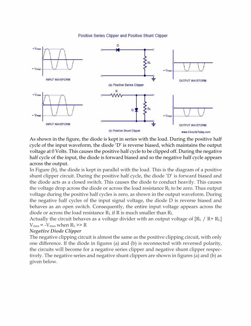
As shown in the figure, the diode is kept in series with the load. During the positive half cycle of the input waveform, the diode ‘D’ is reverse biased, which maintains the output voltage at 0 Volts. This causes the positive half cycle to be clipped off. During the negative half cycle of the input, the diode is forward biased and so the negative half cycle appears across the output. In Figure (b), the diode is kept in parallel with the load. This is the diagram of a positive shunt clipper circuit. During the positive half cycle, the diode ‘D’ is forward biased and the diode acts as a closed switch. This causes the diode to conduct heavily. This causes the voltage drop across the diode or across the load resistance RL to be zero. Thus output voltage during the positive half cycles is zero, as shown in the output waveform. During the negative half cycles of the input signal voltage, the diode D is reverse biased and behaves as an open switch. Consequently, the entire input voltage appears across the diode or across the load resistance RL if R is much smaller than RL Actually the circuit behaves as a voltage divider with an output voltage of [RL / R+ RL] Vmax = -Vmax when RL >> R Negative Diode Clipper The negative clipping circuit is almost the same as the positive clipping circuit, with only one difference. If the diode in figures (a) and (b) is reconnected with reversed polarity, the circuits will become for a negative series clipper and negative shunt clipper respec-tively. The negative series and negative shunt clippers are shown in figures (a) and (b) as given below.
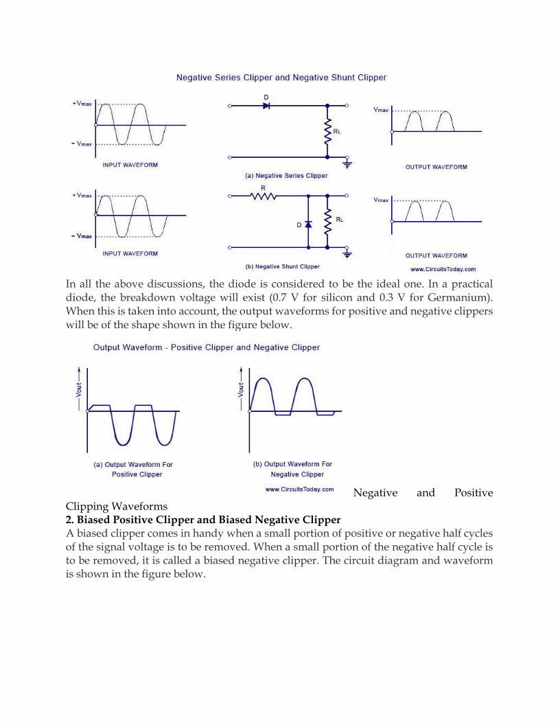
In all the above discussions, the diode is considered to be the ideal one. In a practical diode, the breakdown voltage will exist (0.7 V for silicon and 0.3 V for Germanium). When this is taken into account, the output waveforms for positive and negative clippers will be of the shape shown in the figure below.
Negative and Positive Clipping Waveforms 2. Biased Positive Clipper and Biased Negative Clipper A biased clipper comes in handy when a small portion of positive or negative half cycles of the signal voltage is to be removed. When a small portion of the negative half cycle is to be removed, it is called a biased negative clipper. The circuit diagram and waveform is shown in the figure below.
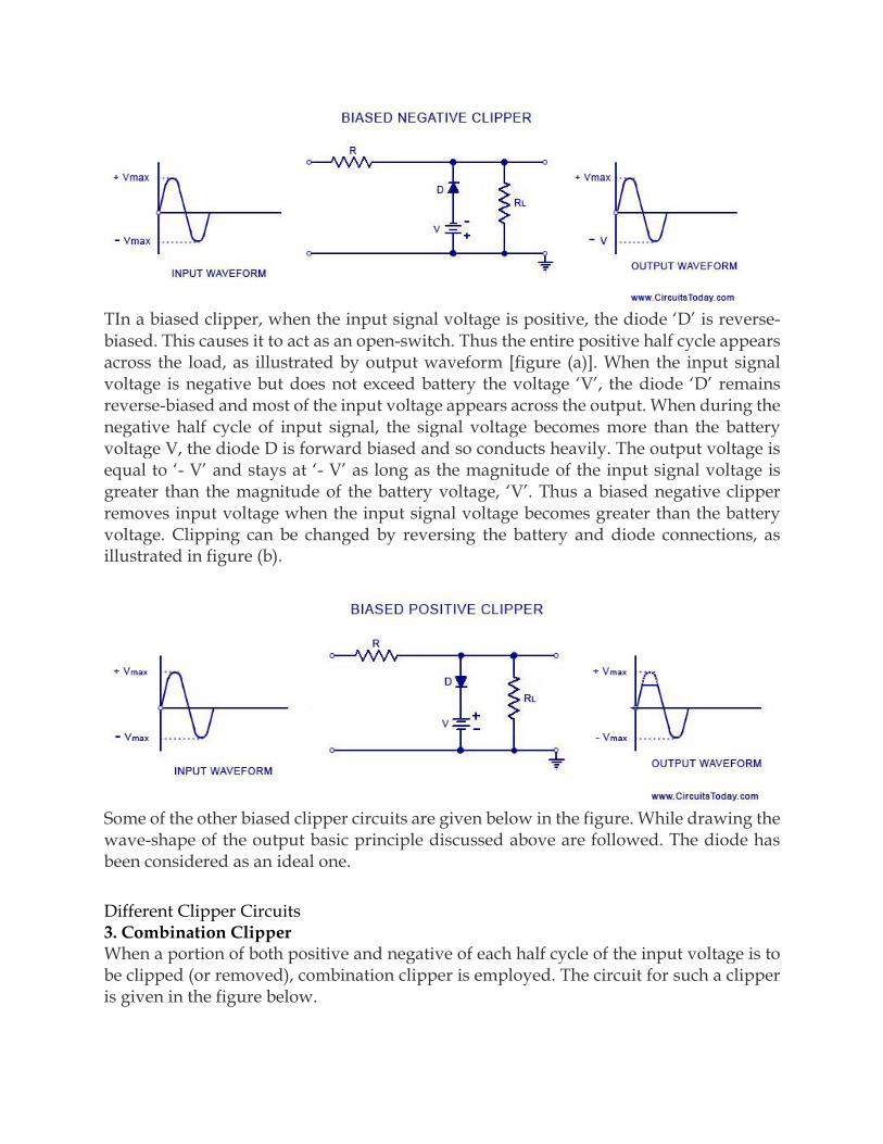
TIn a biased clipper, when the input signal voltage is positive, the diode ‘D’ is reverse-biased. This causes it to act as an open-switch. Thus the entire positive half cycle appears across the load, as illustrated by output waveform [figure (a)]. When the input signal voltage is negative but does not exceed battery the voltage ‘V’, the diode ‘D’ remains reverse-biased and most of the input voltage appears across the output. When during the negative half cycle of input signal, the signal voltage becomes more than the battery voltage V, the diode D is forward biased and so conducts heavily. The output voltage is equal to ‘- V’ and stays at ‘- V’ as long as the magnitude of the input signal voltage is greater than the magnitude of the battery voltage, ‘V’. Thus a biased negative clipper removes input voltage when the input signal voltage becomes greater than the battery voltage. Clipping can be changed by reversing the battery and diode connections, as illustrated in figure (b).
Some of the other biased clipper circuits are given below in the figure. While drawing the wave-shape of the output basic principle discussed above are followed. The diode has been considered as an ideal one.
Different Clipper Circuits 3. Combination Clipper When a portion of both positive and negative of each half cycle of the input voltage is to be clipped (or removed), combination clipper is employed. The circuit for such a clipper is given in the figure below.
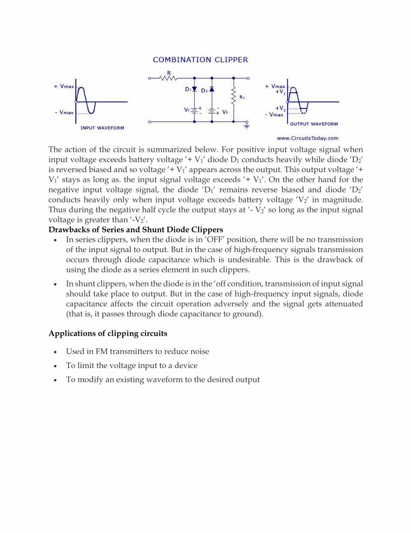
The action of the circuit is summarized below. For positive input voltage signal when input voltage exceeds battery voltage ‘+ V1‘ diode D1 conducts heavily while diode ‘D2‘ is reversed biased and so voltage ‘+ V1‘ appears across the output. This output voltage ‘+ V1‘ stays as long as. the input signal voltage exceeds ‘+ V1‘. On the other hand for the negative input voltage signal, the diode ‘D1‘ remains reverse biased and diode ‘D2‘ conducts heavily only when input voltage exceeds battery voltage ‘V2‘ in magnitude. Thus during the negative half cycle the output stays at ‘- V2‘ so long as the input signal voltage is greater than ‘-V2‘. Drawbacks of Series and Shunt Diode Clippers In series clippers, when the diode is in ‘OFF’ position, there will be no transmission
of the input signal to output. But in the case of high-frequency signals transmission occurs through diode capacitance which is undesirable. This is the drawback of using the diode as a series element in such clippers.
In shunt clippers, when the diode is in the ‘off condition, transmission of input signal should take place to output. But in the case of high-frequency input signals, diode capacitance affects the circuit operation adversely and the signal gets attenuated (that is, it passes through diode capacitance to ground).
Applications of clipping circuits
Used in FM transmitters to reduce noise
To limit the voltage input to a device
To modify an existing waveform to the desired output
CLAMPER CIRCUITS
Clamper definition
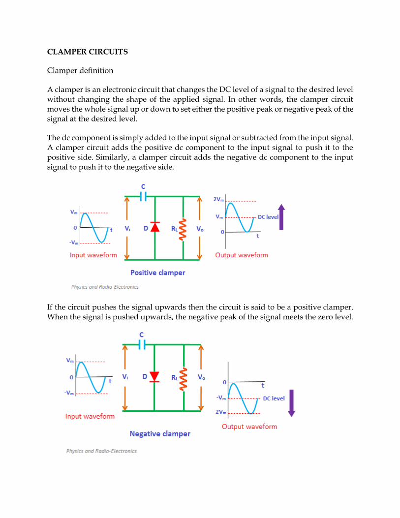
A clamper is an electronic circuit that changes the DC level of a signal to the desired level without changing the shape of the applied signal. In other words, the clamper circuit moves the whole signal up or down to set either the positive peak or negative peak of the signal at the desired level.
The dc component is simply added to the input signal or subtracted from the input signal. A clamper circuit adds the positive dc component to the input signal to push it to the positive side. Similarly, a clamper circuit adds the negative dc component to the input signal to push it to the negative side.
If the circuit pushes the signal upwards then the circuit is said to be a positive clamper. When the signal is pushed upwards, the negative peak of the signal meets the zero level.
On the other hand, if the circuit pushes the signal downwards then the circuit is said to be a negative clamper. When the signal is pushed downwards, the positive peak of the signal meets the zero level.
The construction of the clamper circuit is almost similar to the clipper circuit. The only difference is the clamper circuit contains an extra element called capacitor. A capacitor is used to provide a dc offset (dc level) from the stored charge.
A typical clamper is made up of a capacitor, diode, and resistor. Some clampers contain an extra element called DC battery. The resistors and capacitors are used in the clamper circuit to maintain an altered DC level at the clamper output. The clamper is also referred to as a DC restorer, clamped capacitors, or AC signal level shifter.
Types of clampers
Clamper circuits are of three types:
Positive clampers
Negative clampers
Biased clampers
Positive clamper
The positive clamper is made up of a voltage source Vi, capacitor C, diode D, and load resistor RL. In the below circuit diagram, the diode is connected in parallel with the output load. So the positive clamper passes the input signal to the output load when the diode is reverse biased and blocks the input signal when the diode is forward biased.
During negative half cycle:
During the negative half cycle of the input AC signal, the diode is forward biased and hence no signal appears at the output. In forward biased condition, the diode allows electric current through it. This current will flows to the capacitor and charges it to the peak value of input voltage Vm. The capacitor charged in inverse polarity (positive) with the input voltage. As input current or voltage decreases after attaining its maximum value -Vm, the capacitor holds the charge until the diode remains forward biased.
During positive half cycle:
During the positive half cycle of the input AC signal, the diode is reverse biased and hence the signal appears at the output. In reverse biased condition, the diode does not allow electric current through it. So the input current directly flows towards the output.
When the positive half cycle begins, the diode is in the non-conducting state and the charge stored in the capacitor is discharged (released). Therefore, the voltage appeared at the output is equal to the sum of the voltage stored in the capacitor (Vm) and the input voltage (Vm) { I.e. Vo = Vm+ Vm = 2Vm} which have the same polarity with each other. As a result, the signal shifted upwards.
The peak to peak amplitude of the input signal is 2Vm, similarly the peak to peak amplitude of the output signal is also 2Vm. Therefore, the total swing of the output is same as the total swing of the input.
The basic difference between the clipper and clamper is that the clipper removes the unwanted portion of the input signal whereas the clamper moves the input signal upwards or downwards.
Negative clamper
During positive half cycle:
During the positive half cycle of the input AC signal, the diode is forward biased and hence no signal appears at the output. In forward biased condition, the diode allows electric current through it. This current will flows to the capacitor and charges it to the peak value of input voltage in inverse polarity -Vm. As input current or voltage decreases after attaining its maximum value Vm, the capacitor holds the charge until the diode remains forward biased.
During negative half cycle:
During the negative half cycle of the input AC signal, the diode is reverse biased and hence the signal appears at the output. In reverse biased condition, the diode does not allow electric current through it. So the input current directly flows towards the output.
When the negative half cycle begins, the diode is in the non-conducting state and the charge stored in the capacitor is discharged (released). Therefore, the voltage appeared at the output is equal to the sum of the voltage stored in the capacitor (-Vm) and the input voltage (-Vm) {I.e. Vo = -Vm- Vm = -2Vm} which have the same polarity with each other. As a result, the signal shifted downwards.
Biased clampers
Sometimes an additional shift of DC level is needed. In such cases, biased clampers are used. The working principle of the biased clampers is almost similar to the unbiased clampers. The only difference is an extra element called DC battery is introduced in biased clampers.
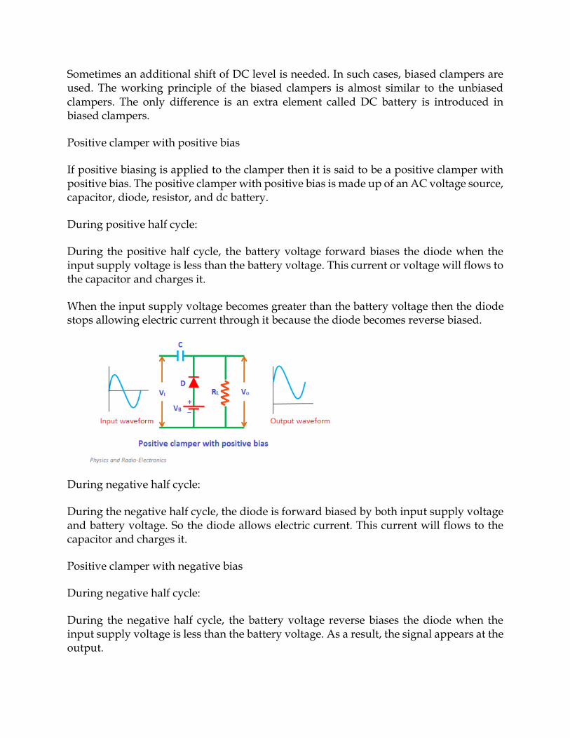
Positive clamper with positive bias
If positive biasing is applied to the clamper then it is said to be a positive clamper with positive bias. The positive clamper with positive bias is made up of an AC voltage source, capacitor, diode, resistor, and dc battery.
During positive half cycle:
During the positive half cycle, the battery voltage forward biases the diode when the input supply voltage is less than the battery voltage. This current or voltage will flows to the capacitor and charges it.
When the input supply voltage becomes greater than the battery voltage then the diode stops allowing electric current through it because the diode becomes reverse biased.
During negative half cycle:
During the negative half cycle, the diode is forward biased by both input supply voltage and battery voltage. So the diode allows electric current. This current will flows to the capacitor and charges it.
Positive clamper with negative bias
During negative half cycle:
During the negative half cycle, the battery voltage reverse biases the diode when the input supply voltage is less than the battery voltage. As a result, the signal appears at the output.
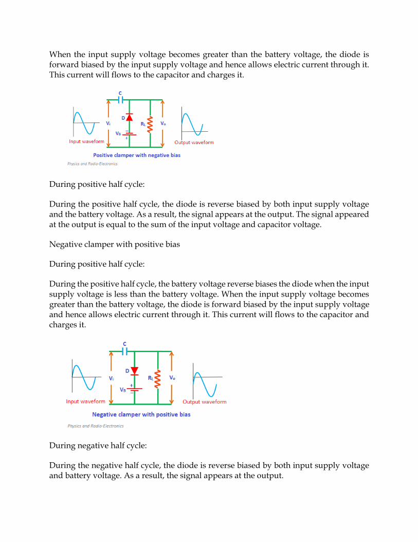
When the input supply voltage becomes greater than the battery voltage, the diode is forward biased by the input supply voltage and hence allows electric current through it. This current will flows to the capacitor and charges it.
During positive half cycle:
During the positive half cycle, the diode is reverse biased by both input supply voltage and the battery voltage. As a result, the signal appears at the output. The signal appeared at the output is equal to the sum of the input voltage and capacitor voltage.
Negative clamper with positive bias
During positive half cycle:
During the positive half cycle, the battery voltage reverse biases the diode when the input supply voltage is less than the battery voltage. When the input supply voltage becomes greater than the battery voltage, the diode is forward biased by the input supply voltage and hence allows electric current through it. This current will flows to the capacitor and charges it.
During negative half cycle:
During the negative half cycle, the diode is reverse biased by both input supply voltage and battery voltage. As a result, the signal appears at the output.
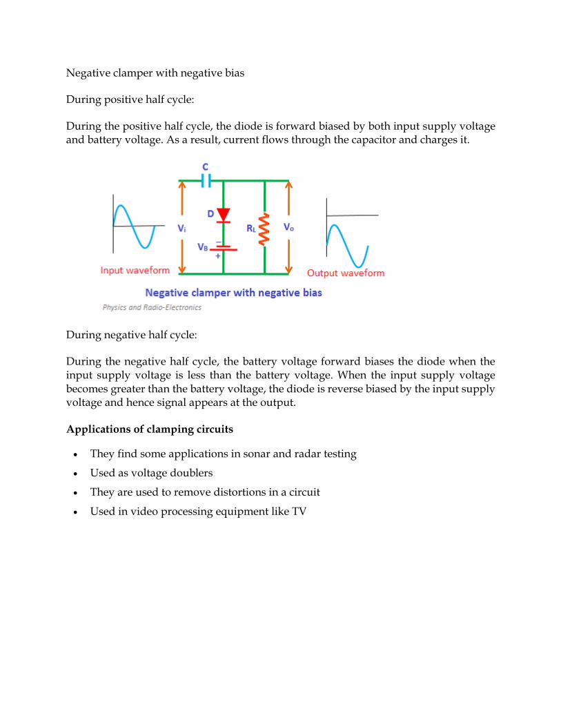
Negative clamper with negative bias
During positive half cycle:
During the positive half cycle, the diode is forward biased by both input supply voltage and battery voltage. As a result, current flows through the capacitor and charges it.
During negative half cycle:
During the negative half cycle, the battery voltage forward biases the diode when the input supply voltage is less than the battery voltage. When the input supply voltage becomes greater than the battery voltage, the diode is reverse biased by the input supply voltage and hence signal appears at the output.
Applications of clamping circuits
They find some applications in sonar and radar testing
Used as voltage doublers
They are used to remove distortions in a circuit
Used in video processing equipment like TV

ASTABLE MULTIVIBRATORS
Regenerative switching circuits such as Astable Multivibrators are the most commonly used type of relaxation oscillator because not only are they simple, reliable and ease of construction they also produce a constant square wave output waveform.
Unlike the Monostable Multivibrator or the Bistable Multivibrator we looked at in the previous tutorials that require an “external” trigger pulse for their operation, the Astable
Multivibrator has automatic built in triggering which switches it continuously between its two unstable states both set and reset.
The Astable Multivibrator is another type of cross-coupled transistor switching circuit that has NO stable output states as it changes from one state to the other all the time. The astable circuit consists of two switching transistors, a cross-coupled feedback network, and two time delay capacitors which allows oscillation between the two states with no external triggering to produce the change in state.
In electronic circuits, astable multivibrators are also known as Free-running
Multivibrator as they do not require any additional inputs or external assistance to oscillate. Astable oscillators produce a continuous square wave from its output or outputs, (two outputs no inputs) which can then be used to flash lights or produce a sound in a loudspeaker.
The basic transistor circuit for an Astable Multivibrator produces a square wave output from a pair of grounded emitter cross-coupled transistors. Both transistors either NPN or PNP, in the multivibrator are biased for linear operation and are operated as Common Emitter Amplifiers with 100% positive feedback.
This configuration satisfies the condition for oscillation when: ( βA = 1∠ 0o ). This results in one stage conducting “fully-ON” (Saturation) while the other is switched “fully-OFF” (cut-off) giving a very high level of mutual amplification between the two transistors. Conduction is transferred from one stage to the other by the discharging action of a capacitor through a resistor as shown below.
Basic Astable Multivibrator Circuit
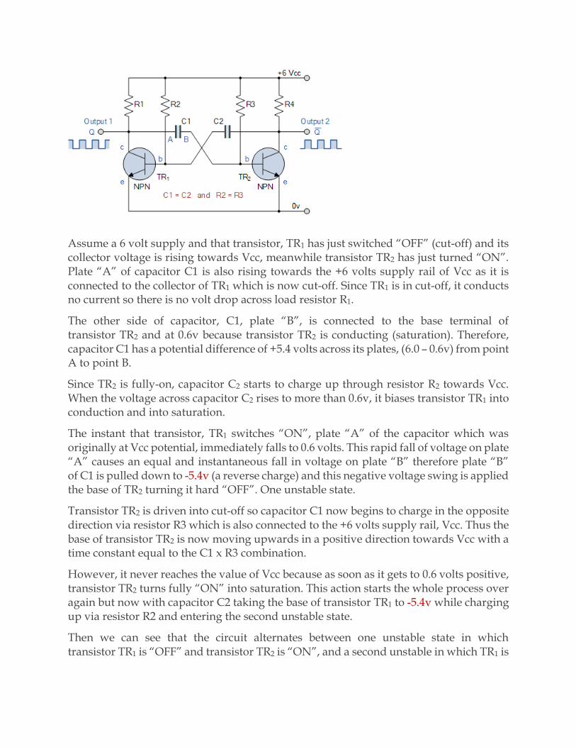
Assume a 6 volt supply and that transistor, TR1 has just switched “OFF” (cut-off) and its collector voltage is rising towards Vcc, meanwhile transistor TR2 has just turned “ON”. Plate “A” of capacitor C1 is also rising towards the +6 volts supply rail of Vcc as it is connected to the collector of TR1 which is now cut-off. Since TR1 is in cut-off, it conducts no current so there is no volt drop across load resistor R1.
The other side of capacitor, C1, plate “B”, is connected to the base terminal of transistor TR2 and at 0.6v because transistor TR2 is conducting (saturation). Therefore, capacitor C1 has a potential difference of +5.4 volts across its plates, (6.0 – 0.6v) from point A to point B.
Since TR2 is fully-on, capacitor C2 starts to charge up through resistor R2 towards Vcc. When the voltage across capacitor C2 rises to more than 0.6v, it biases transistor TR1 into conduction and into saturation.
The instant that transistor, TR1 switches “ON”, plate “A” of the capacitor which was originally at Vcc potential, immediately falls to 0.6 volts. This rapid fall of voltage on plate “A” causes an equal and instantaneous fall in voltage on plate “B” therefore plate “B” of C1 is pulled down to -5.4v (a reverse charge) and this negative voltage swing is applied the base of TR2 turning it hard “OFF”. One unstable state.
Transistor TR2 is driven into cut-off so capacitor C1 now begins to charge in the opposite direction via resistor R3 which is also connected to the +6 volts supply rail, Vcc. Thus the base of transistor TR2 is now moving upwards in a positive direction towards Vcc with a time constant equal to the C1 x R3 combination.
However, it never reaches the value of Vcc because as soon as it gets to 0.6 volts positive, transistor TR2 turns fully “ON” into saturation. This action starts the whole process over again but now with capacitor C2 taking the base of transistor TR1 to -5.4v while charging up via resistor R2 and entering the second unstable state.
Then we can see that the circuit alternates between one unstable state in which transistor TR1 is “OFF” and transistor TR2 is “ON”, and a second unstable in which TR1 is
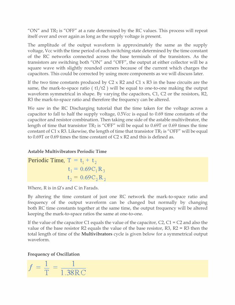
“ON” and TR2 is “OFF” at a rate determined by the RC values. This process will repeat itself over and over again as long as the supply voltage is present.
The amplitude of the output waveform is approximately the same as the supply voltage, Vcc with the time period of each switching state determined by the time constant of the RC networks connected across the base terminals of the transistors. As the transistors are switching both “ON” and “OFF”, the output at either collector will be a square wave with slightly rounded corners because of the current which charges the capacitors. This could be corrected by using more components as we will discuss later.
If the two time constants produced by C2 x R2 and C1 x R3 in the base circuits are the same, the mark-to-space ratio ( t1/t2 ) will be equal to one-to-one making the output waveform symmetrical in shape. By varying the capacitors, C1, C2 or the resistors, R2, R3 the mark-to-space ratio and therefore the frequency can be altered.
We saw in the RC Discharging tutorial that the time taken for the voltage across a capacitor to fall to half the supply voltage, 0.5Vcc is equal to 0.69 time constants of the capacitor and resistor combination. Then taking one side of the astable multivibrator, the length of time that transistor TR2 is “OFF” will be equal to 0.69T or 0.69 times the time constant of C1 x R3. Likewise, the length of time that transistor TR1 is “OFF” will be equal to 0.69T or 0.69 times the time constant of C2 x R2 and this is defined as.
Astable Multivibrators Periodic Time
Where, R is in Ω’s and C in Farads.
By altering the time constant of just one RC network the mark-to-space ratio and frequency of the output waveform can be changed but normally by changing both RC time constants together at the same time, the output frequency will be altered keeping the mark-to-space ratios the same at one-to-one.
If the value of the capacitor C1 equals the value of the capacitor, C2, C1 = C2 and also the value of the base resistor R2 equals the value of the base resistor, R3, R2 = R3 then the total length of time of the Multivibrators cycle is given below for a symmetrical output waveform.
Frequency of Oscillation
Where, R is in Ω’s, C is in Farads, T is in seconds and ƒ is in Hertz.
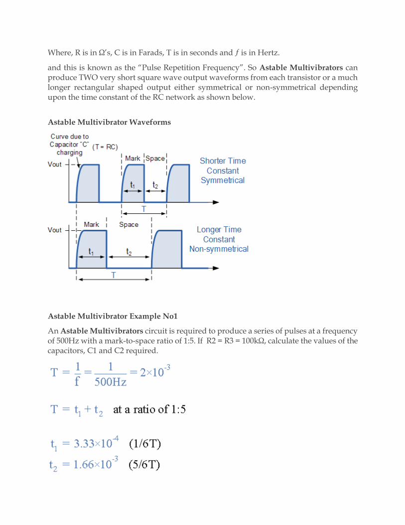
and this is known as the “Pulse Repetition Frequency”. So Astable Multivibrators can produce TWO very short square wave output waveforms from each transistor or a much longer rectangular shaped output either symmetrical or non-symmetrical depending upon the time constant of the RC network as shown below.
Astable Multivibrator Waveforms
Astable Multivibrator Example No1
An Astable Multivibrators circuit is required to produce a series of pulses at a frequency of 500Hz with a mark-to-space ratio of 1:5. If R2 = R3 = 100kΩ, calculate the values of the capacitors, C1 and C2 required.
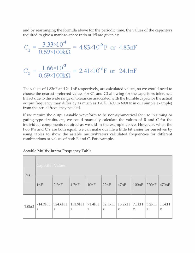
and by rearranging the formula above for the periodic time, the values of the capacitors required to give a mark-to-space ratio of 1:5 are given as:
The values of 4.83nF and 24.1nF respectively, are calculated values, so we would need to choose the nearest preferred values for C1 and C2 allowing for the capacitors tolerance. In fact due to the wide range of tolerances associated with the humble capacitor the actual output frequency may differ by as much as ±20%, (400 to 600Hz in our simple example) from the actual frequency needed.
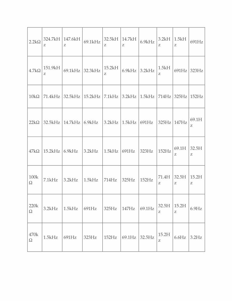
If we require the output astable waveform to be non-symmetrical for use in timing or gating type circuits, etc, we could manually calculate the values of R and C for the individual components required as we did in the example above. However, when the two R’s and C´s are both equal, we can make our life a little bit easier for ourselves by using tables to show the astable multivibrators calculated frequencies for different combinations or values of both R and C. For example,
Astable Multivibrator Frequency Table
Res.
Capacitor Values
1nF 2.2nF 4.7nF 10nF 22nF 47nF 100nF 220nF 470nF
1.0kΩ 714.3kHz
324.6kHz
151.9kHz
71.4kHz
32.5kHz
15.2kHz
7.1kHz
3.2kHz
1.5kHz
2.2kΩ 324.7kHz
147.6kHz
69.1kHz 32.5kHz
14.7kHz
6.9kHz 3.2kHz
1.5kHz
691Hz
4.7kΩ 151.9kHz
69.1kHz 32.3kHz 15.2kHz
6.9kHz 3.2kHz 1.5kHz
691Hz 323Hz
10kΩ 71.4kHz 32.5kHz 15.2kHz 7.1kHz 3.2kHz 1.5kHz 714Hz 325Hz 152Hz
22kΩ 32.5kHz 14.7kHz 6.9kHz 3.2kHz 1.5kHz 691Hz 325Hz 147Hz 69.1Hz
47kΩ 15.2kHz 6.9kHz 3.2kHz 1.5kHz 691Hz 323Hz 152Hz 69.1Hz
32.5Hz
100kΩ
7.1kHz 3.2kHz 1.5kHz 714Hz 325Hz 152Hz 71.4Hz
32.5Hz
15.2Hz
220kΩ
3.2kHz 1.5kHz 691Hz 325Hz 147Hz 69.1Hz 32.5Hz
15.2Hz
6.9Hz
470kΩ
1.5kHz 691Hz 323Hz 152Hz 69.1Hz 32.5Hz 15.2Hz
6.6Hz 3.2Hz
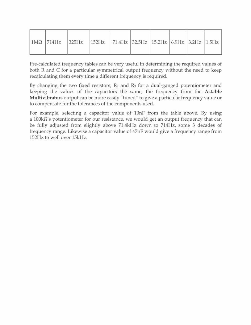
1MΩ 714Hz 325Hz 152Hz 71.4Hz 32.5Hz 15.2Hz 6.9Hz 3.2Hz 1.5Hz
Pre-calculated frequency tables can be very useful in determining the required values of both R and C for a particular symmetrical output frequency without the need to keep recalculating them every time a different frequency is required.
By changing the two fixed resistors, R2 and R3 for a dual-ganged potentiometer and keeping the values of the capacitors the same, the frequency from the Astable
Multivibrators output can be more easily “tuned” to give a particular frequency value or to compensate for the tolerances of the components used.
For example, selecting a capacitor value of 10nF from the table above. By using a 100kΩ’s potentiometer for our resistance, we would get an output frequency that can be fully adjusted from slightly above 71.4kHz down to 714Hz, some 3 decades of frequency range. Likewise a capacitor value of 47nF would give a frequency range from 152Hz to well over 15kHz.
BISTABLE MULTIVIBRATORS Bistable Multivibrator are the Multivibrator which depend upon the external
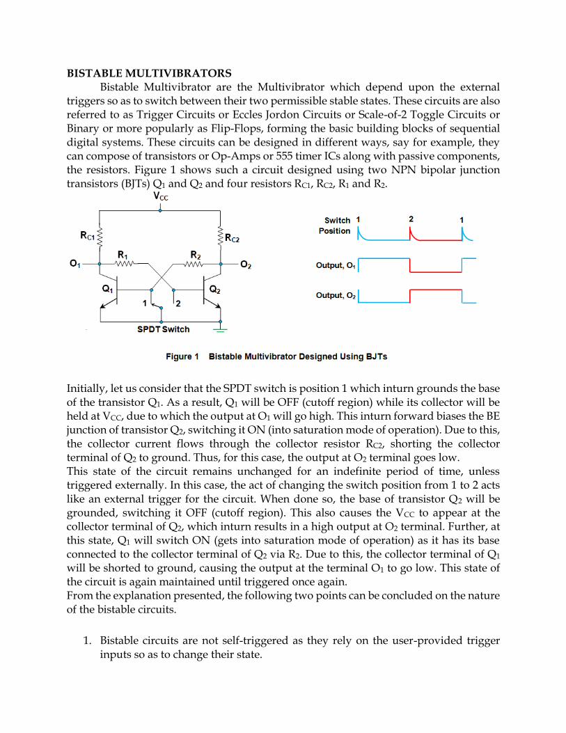
triggers so as to switch between their two permissible stable states. These circuits are also referred to as Trigger Circuits or Eccles Jordon Circuits or Scale-of-2 Toggle Circuits or Binary or more popularly as Flip-Flops, forming the basic building blocks of sequential digital systems. These circuits can be designed in different ways, say for example, they can compose of transistors or Op-Amps or 555 timer ICs along with passive components, the resistors. Figure 1 shows such a circuit designed using two NPN bipolar junction transistors (BJTs) Q1 and Q2 and four resistors RC1, RC2, R1 and R2.
Initially, let us consider that the SPDT switch is position 1 which inturn grounds the base of the transistor Q1. As a result, Q1 will be OFF (cutoff region) while its collector will be held at VCC, due to which the output at O1 will go high. This inturn forward biases the BE junction of transistor Q2, switching it ON (into saturation mode of operation). Due to this, the collector current flows through the collector resistor RC2, shorting the collector terminal of Q2 to ground. Thus, for this case, the output at O2 terminal goes low. This state of the circuit remains unchanged for an indefinite period of time, unless triggered externally. In this case, the act of changing the switch position from 1 to 2 acts like an external trigger for the circuit. When done so, the base of transistor Q2 will be grounded, switching it OFF (cutoff region). This also causes the VCC to appear at the collector terminal of Q2, which inturn results in a high output at O2 terminal. Further, at this state, Q1 will switch ON (gets into saturation mode of operation) as it has its base connected to the collector terminal of Q2 via R2. Due to this, the collector terminal of Q1 will be shorted to ground, causing the output at the terminal O1 to go low. This state of the circuit is again maintained until triggered once again. From the explanation presented, the following two points can be concluded on the nature of the bistable circuits.
1. Bistable circuits are not self-triggered as they rely on the user-provided trigger inputs so as to change their state.
2. In these circuits, the output wave-forms obtained at the terminal O1 and O2 are complementary to each other, always.
In addition, it is to be noted that triggering in the case of Bistable circuit is more conveniently experienced by electronic-means rather than mechanically. This kind of triggering can be either asymmetric or symmetric in nature. In the case of asymmetric triggering, the trigger for each of the transistor is obtained from separate sources and is independent of each other. Next, the symmetrical triggering can be any one of the following types: symmetrical base triggering or symmetrical collector triggering or symmetrical hybrid triggering. These bistable circuits are used as memory storage devices, timing circuits, frequency dividers, electronic toggle switch, counting circuits, shift registers, clock pulse generators, relay controllers and even in the field of radar and communications.
SCHMITT TRIGGER
Schmitt Trigger was invented by Otto Schmitt early 1930’s. It is an electronic circuit that adds hysteresis to the input-output transition threshold with the help of positive feedback. Hysteresis here means it provides two different threshold voltage levels for rising and falling edge.
Essentially, a Schmitt Trigger is a Bi-stable Multivibrator and its output remains in either of the stable states indefinitely. For the output to change from one stable state to other, the input signal must change (or trigger) appropriately.
This Bistable operation of the Schmitt Trigger requires an amplifier with positive feedback (or regenerative feedback) with a loop gin greater than one. Hence, Schmitt Trigger is also known as Regenerative Comparator.
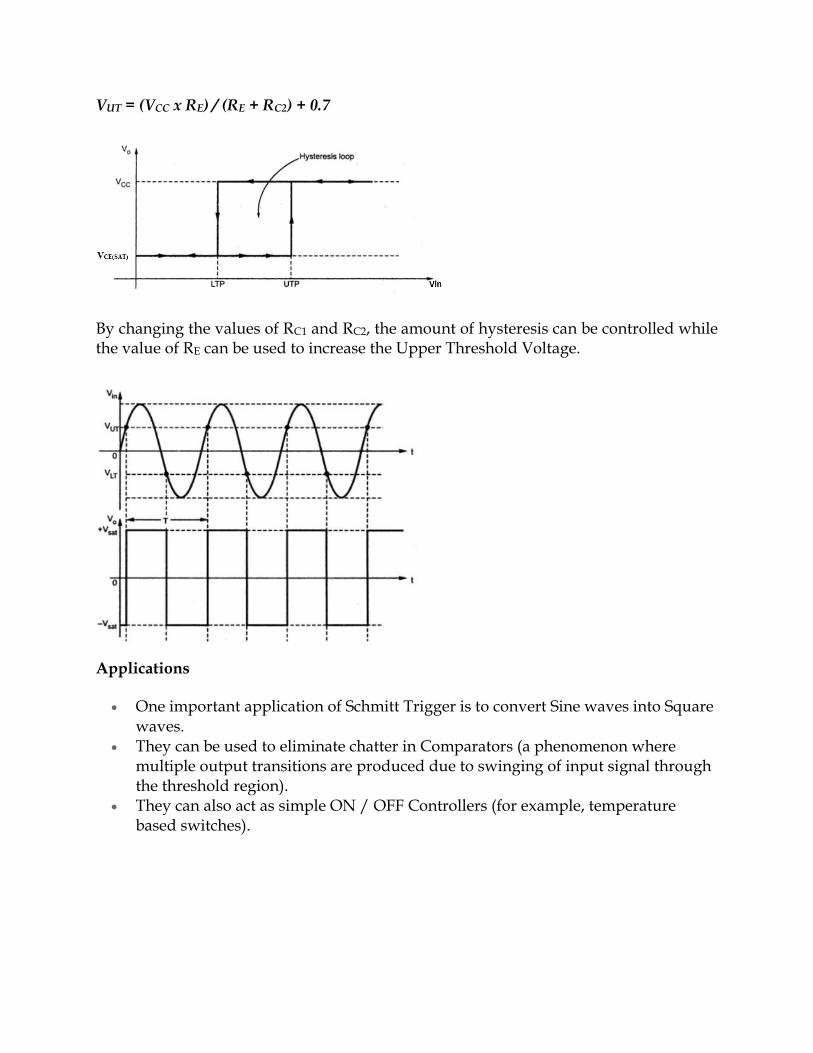
For example, if we have a noisy input signal as shown below, the two thresholds of the Schmitt Trigger Circuit will correctly determine the pulses. Hence, the basic function of a Schmitt Trigger is to convert noisy square, sine, triangular or any periodic signals into clean square pulses with sharp leading and trailing edges.
Schmitt Trigger using Transistors
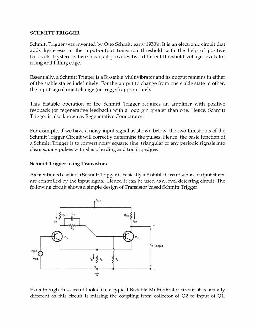
As mentioned earlier, a Schmitt Trigger is basically a Bistable Circuit whose output states are controlled by the input signal. Hence, it can be used as a level detecting circuit. The following circuit shows a simple design of Transistor based Schmitt Trigger.
Even though this circuit looks like a typical Bistable Multivibrator circuit, it is actually different as this circuit is missing the coupling from collector of Q2 to input of Q1.
Emitters of Q1 and Q2 are connected to each other and grounded through RE. Also, RE acts as a feedback path.
Operation of the Circuit
When VIN is zero, Q1 is cut-off and Q2 is in saturation. As a result, the output voltage VO is LOW. If VCE(SAT) is assumed to be 0, then the voltage across RE is given by:
(VCC x RE) / (RE + RC2)
This voltage is also the emitter voltage of Q1. So, for Q1 to conduct, the input voltage VIN must greater than sum of the emitter voltage and 0.7 V i.e.
VIN = (VCC x RE) / (RE + RC2) + 0.7
When the VIN is greater than this voltage, Q1 starts conducting and Q2 is cutoff due to regenerative action. As a result, the output VO goes HIGH. Now the voltage across the RE changes to a new value and is given by:
(VCC x RE) / (RE + RC1)
Transistor Q1 will conduct as long as the input voltage VIN is greater than or equal to the following:
VIN = (VCC x RE) / (RE + RC1) + 0.7
If VIN falls below this value, then Q1 comes out of saturation and the rest of the circuit operates is due to regenerative action of Q1 going to cutoff and Q2 to saturation.
The output states HIGH and LOW are dependent on the input voltage levels given by the equations
(VCC x RE) / (RE + RC1) + 0.7 and (VCC x RE) / (RE + RC2) + 0.7
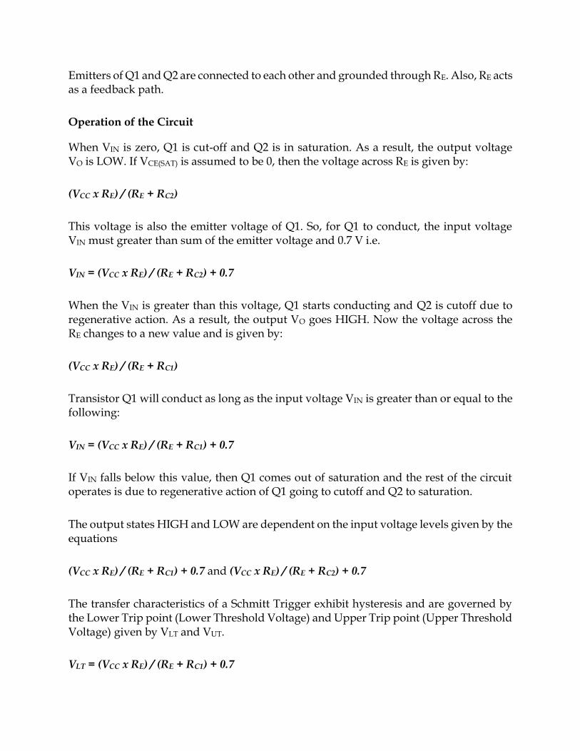
The transfer characteristics of a Schmitt Trigger exhibit hysteresis and are governed by the Lower Trip point (Lower Threshold Voltage) and Upper Trip point (Upper Threshold Voltage) given by VLT and VUT.
VLT = (VCC x RE) / (RE + RC1) + 0.7
VUT = (VCC x RE) / (RE + RC2) + 0.7
By changing the values of RC1 and RC2, the amount of hysteresis can be controlled while the value of RE can be used to increase the Upper Threshold Voltage.
Applications
One important application of Schmitt Trigger is to convert Sine waves into Square waves.
They can be used to eliminate chatter in Comparators (a phenomenon where multiple output transitions are produced due to swinging of input signal through the threshold region).
They can also act as simple ON / OFF Controllers (for example, temperature based switches).
VOLTAGE REGULATOR
A voltage regulator is designed to automatically ‘regulate’ voltage level. It basically steps down the input voltage to the desired level and keeps that in that same level during the supply. This makes sure that even when a load is applied the voltage doesn’t drop.
Thus, a voltage regulator is used for two reasons:-
1. To regulate or vary the output voltage of the circuit.
2. To keep the output voltage constant at the desired value in-spite of variations in the supply voltage or in the load current.
Voltage regulators find their applications in computers, alternators, power generator plants where the circuit is used to control the output of the plant. Voltage regulators may be classified as electromechanical or electronic. It can also be classified as AC regulators or DC regulators.
Electronic Voltage Regulator All electronic voltage regulators will have a stable voltage reference source which is provided by the reverse breakdown voltage operating diode called zener diode. The main reason to use a voltage regulator is to maintain a constant dc output voltage. It also blocks the ac ripple voltage that cannot be blocked by the filter. A good voltage regulator may also include additional circuits for protection like short circuits, current limiting circuit, thermal shutdown, and overvoltage protection.
Zener Controlled Transistor Series Voltage Regulator
Such a circuit is also named an emitter follower voltage regulator. It is called so because the transistor used is connected in an emitter follower configuration. The circuit consists of an N-P-N transistor and a zener diode. As shown in the figure below, the collector and emitter terminals of the transistor are in series with the load. Thus this regulator has the name series in it. The transistor used is a series pass transistor.
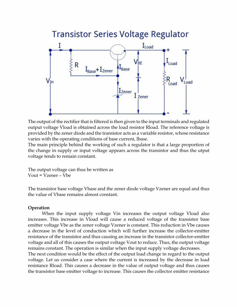
The output of the rectifier that is filtered is then given to the input terminals and regulated output voltage Vload is obtained across the load resistor Rload. The reference voltage is provided by the zener diode and the transistor acts as a variable resistor, whose resistance varies with the operating conditions of base current, Ibase. The main principle behind the working of such a regulator is that a large proportion of the change in supply or input voltage appears across the transistor and thus the utput voltage tends to remain constant.
The output voltage can thus be written as Vout = Vzener – Vbe
The transistor base voltage Vbase and the zener diode voltage Vzener are equal and thus the value of Vbase remains almost constant.
Operation When the input supply voltage Vin increases the output voltage Vload also
increases. This increase in Vload will cause a reduced voltage of the transistor base emitter voltage Vbe as the zener voltage Vzener is constant. This reduction in Vbe causes a decrease in the level of conduction which will further increase the collector-emitter resistance of the transistor and thus causing an increase in the transistor collector-emitter voltage and all of this causes the output voltage Vout to reduce. Thus, the output voltage remains constant. The operation is similar when the input supply voltage decreases. The next condition would be the effect of the output load change in regard to the output voltage. Let us consider a case where the current is increased by the decrease in load resistance Rload. This causes a decrease in the value of output voltage and thus causes the transistor base emitter voltage to increase. This causes the collector emitter resistance
value to decrease due to an increase in the conduction level of the transistor. This causes the input current to increase slightly and thus compensates for the decrease in the load resistance Rload.
The biggest advantage of this circuit is that the changes in the zener current are reduced by a factor β and thus the zener effect is greatly reduced and a much more stabilized output is obtained.
The output voltage of the series regulator is Vout = Vzener – Vbe. The load current Iload of the circuit will be the maximum emitter current that the transistor can pass. For a normal transistor like the 2N3055, the load current can go upto 15A. If the load current is zero or has no value, then the current drawn from the supply can be written as Izener + Ic(min). Such an emitter follower voltage regulator is more efficient than a normal zener regulator. A normal zener regulator that has only a resistor and a zener diode has to supply the base current of the transistor.
Limitations The limitations listed below has proved the use of this series voltage regulator only suitable for low output voltages.
1. With the increase in room temperature, the values of Vbe and Vzener tend to decrease. Thus the output voltage cannot be maintained a constant. This will further increase the transistor base emitter voltage and thus the load.
2. There is no option to change the output voltage in the circuit.
3. Due to the small amplification process provided by only one transistor, the circuit cannot provide good regulation at high currents.
4. When compared to other regulators, this regulator has poor regulation and ripple suppression with respect to input variations.
5. The power dissipation of a pass transistor is large because it is equal to Vcc Ic and almost all variation appears at Vce and the load current is approximately equal to collector current. Thus for heavy load currents pass transistor has to dissipate a lot of power and, therefore, becoming hot.