Experiment No. (4) The Diode Clipper & Clamper Circuits
11
Electronic I Biomedical Engineering Second Year - ١٨ - Experiment No. (4) The Diode Clipper & Clamper Circuits Object: To demonstrate the operation of a diode clipper and clamper circuits. Apparatus: 1. Dual Beam Oscilloscope. 2. Function Generator 3. Bread Board 4. Silicon Diodes 5. Power Supply 6. Capacitors 7. Resistors Theory: (A) The Diode Clipper Circuit: Diode clippers are wave – shaping circuits in that they are used to prevent signal voltages from going above or below certain levels. The clipping level may be either equal to the diode’s barrier potential or made variable with a d.c source voltage. Because of this limiting capability, the clipper is also called a limiter. There are two general categories of clippers: series and parallel. The series configuration is defined as one where the diode is in series with the load, while the parallel variety has the diode in a branch parallel to the load. Series Clipper Circuit: Consider the circuit of fig. (4.1 a). An a.c generator applies a sine – wave voltage V in to a diode in series with a resistor R. In fig. (4.1 b) the input voltage V in and output voltage V out are shown in proper time phase. During the positive
-
Upload
khangminh22 -
Category
Documents
-
view
5 -
download
0
Transcript of Experiment No. (4) The Diode Clipper & Clamper Circuits
Electronic I Biomedical Engineering Second Year
- ١٨ -
Experiment No. (4)
The Diode Clipper & Clamper Circuits
Object:
To demonstrate the operation of a diode clipper and clamper circuits.
Apparatus:
1. Dual Beam Oscilloscope.
2. Function Generator
3. Bread Board
4. Silicon Diodes
5. Power Supply
6. Capacitors
7. Resistors
Theory:
(A) The Diode Clipper Circuit:
Diode clippers are wave – shaping circuits in that they are used to prevent
signal voltages from going above or below certain levels. The clipping level may be
either equal to the diode’s barrier potential or made variable with a d.c source
voltage. Because of this limiting capability, the clipper is also called a limiter. There
are two general categories of clippers: series and parallel. The series configuration is
defined as one where the diode is in series with the load, while the parallel variety
has the diode in a branch parallel to the load.
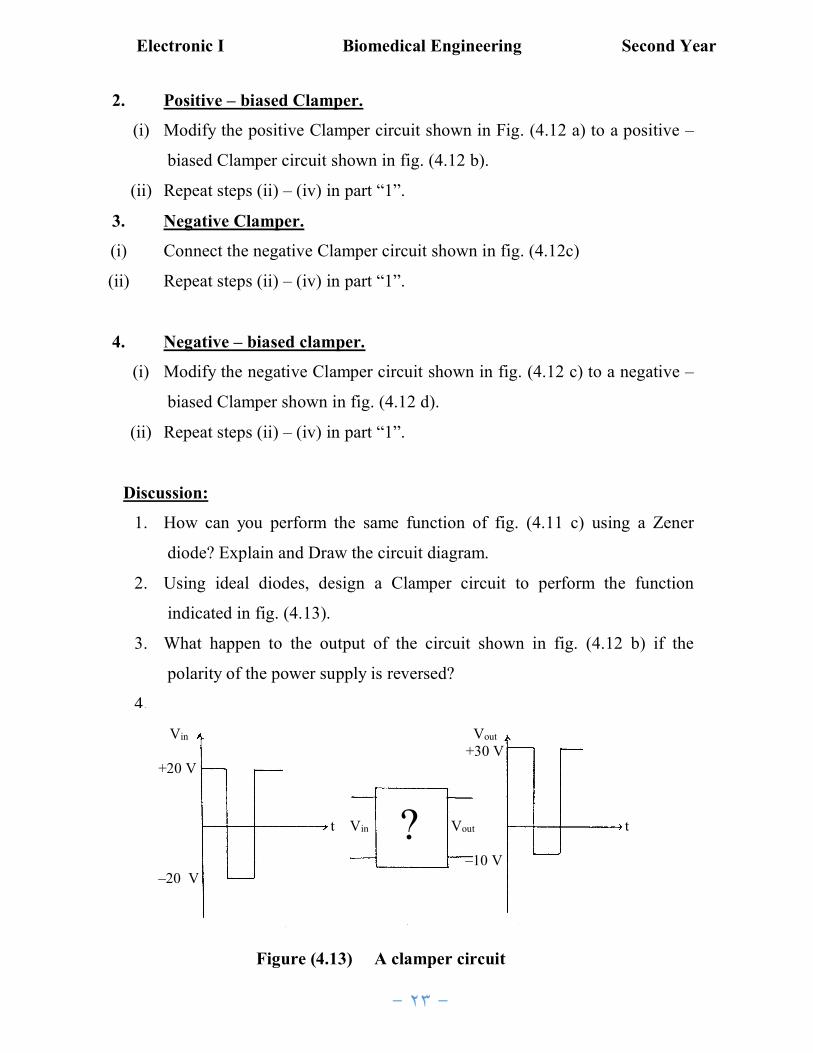
Series Clipper Circuit:
Consider the circuit of fig. (4.1 a). An a.c generator applies a sine – wave
voltage Vin to a diode in series with a resistor R. In fig. (4.1 b) the input voltage Vin
and output voltage Vout are shown in proper time phase. During the positive
Electronic I Biomedical Engineering Second Year
- ١٩ -
alternation the cathode of the diode is positive relative to its anode; that is the diode
is reverse – biased. Hence no current flows in the circuit, and the output Vout across
R is zero. During the negative alternation the diode is forward – biased, acting as a
closed switch and permitting current to flow in R. The voltage across R is the
negative alternation with the polarity shown. This simple circuit is a positive series
limiter, “positive” because the positive alternation has been limited or eliminated
from the output. Fig. (4.2) shows that the series – connected diode may also be used
as a negative limiter by reversing the polarity of the diode in the circuit. The
waveforms of fig. (4.2 b) show that during the positive alternation the diode is
forward – biased, permitting current to flow in R. The voltage developed across R is
positive, following the input alternation. During the negative alternation the diode is
reverse – biased and no current flows. Hence, no output voltage is developed across
R. Thus the series – connected diode in fig. (4.2) act as negative limiter.
Parallel – Clipper Circuit:
The circuits in fig. (4.3 a & c) are examples of parallel connected diode
limiters. They are called parallel limiters because the output is in parallel with the
diode. During the positive alternation, diode D1 (see fig. (4.3 a)) is reversed biased
and exhibits high reverse resistance Rp.R and Rp constitute a voltage divider. If R is
much smaller than Rp, practically the entire positive alternation appears as the
output voltage Vout across the diode. During the negative alternation D1 is forward –
biased. The diode act as closed switch with very low forward resistance Rp. Because
R is sow so very much larger than Rp, there is negligible output across the diode.
That is, the diode conducting acts like a short circuit. Hence no voltage is developed
across the diode, as in fig. (4.3 b). Since the negative alternation is removed
(limited) from the output, this circuit is an example of negative limiter. By reversing
the polarity of the diode, fig. (4.3 c) the parallel diode limiter is used to remove the
positive alternation fig.(4.3 d).
Electronic I Biomedical Engineering Second Year
- ٢٠ -
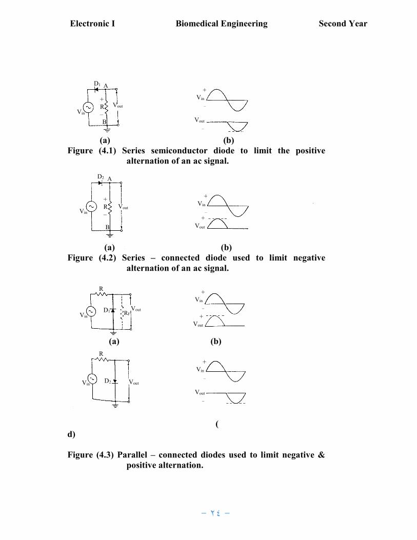
Biased – parallel limiters: Partial limiting:
The circuit of figs. (4.4) and (4.5) accomplish partial limiting of the negative
and positive alternations, respectively of an input sinewave. Diode D1 in fig. (4.4 a)
is reverse – biased by a battery VAA which maintains the anode VAA volts negative
relative to its cathode. During the positive alternation of the input voltage Vin the
cathode of D1 is held positive. The diode acts like an open switch and the positive
alternation appears in the output, Fig. (4.4 b). During the negative alternative the
cathode is driven negative, but the diode will not conduct until VAA is more negative
than the biase voltage VAA which maintains the anode VAA volts negative. Hence,
that part of the negative alternation which is less negative than VAA appears in the
output when the negative alternation of Vin reaches the level where it is more
negative than VAA, the cathode is driven more negative than the anode and the diode
conducts, limiting that portion of the negative alternation between –VAA and –Vm
peak. Similarly the biased parallel limiter of fig. (4.5) limits that portion of the
positive alternation of VAA, which is more positive than VAA (see fig.(4.5 a) & (4.5
b))
Diode Clamper Circuits:
The diode limiter or clipper modifies the input waveform by limiting or
“clipping” part of the waveform. Other diode circuits called clampers (or dc
restorers), do not change the shape of the input waveform; rather, they add a dc level
to it. There are positive, negative and biased clampers.
Positive Clamper:
The effect of a positive clamper on an ac waveform with OV as its axis is
shown in Fig. (4.6). The clamper has added +20 V dc to the 40 Vpp waveform. The
results that the input waveform, which varied from +20 to –20 V, appears in the
output of the circuit as a signal varying between 0 and +40 V, with +20 V dc as its
axis. The output waveform acts as though a +20 V battery where connected in series
with the input.
Electronic I Biomedical Engineering Second Year
- ٢١ -
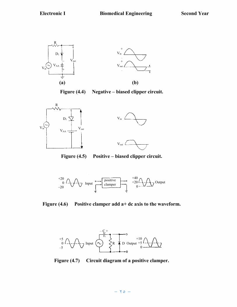
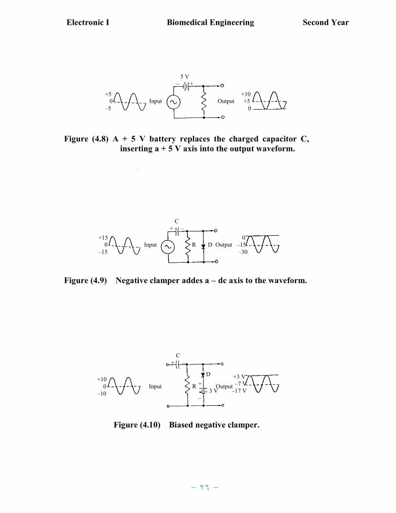
Fig. (4.7) is the circuit diagram of a dc clamper. The circuit operates as
follows: On the negative alternation of the 10 Vp-p input sinewave the cathode of
diode D is driven negative relative to the anode. Therefore D conducts, charging C
through the resistance of the forward – biased diode. Capacitor C will charge to the
peak of the negative alternation, 5 V, with the polarity shown in fig. (4.7). On the
positive alternation D is cut off since its cathode is positive relative to the anode.
Capacitor C tries to discharge through R when D is cut off. However, if the time
constant RC is large compared with the period of the sinewave, the capacitor will
loose very little of its charge and will hold the 5 V across it. The effect of the circuit
is illustrated in fig. (4.8). Capacitor C has been replaced by a +5 V battery which is
in series with the input signal. If the sinusoidaly varying voltage is added, point by
point, to the +5 V of the battery, the results is a waveform which varies between 0
and +10 V peak.
Negative Clamper:
It adds a negative dc level to an ac signal. This is accomplished by reversing
the polarity of the diode, as in the circuit of fig. (4.9). In this circuit, C charges on
the positive alternation of the input signal. If the input signal varies between +15
and –15, the net effect is to charge C to –15 V. The output waveform now varies
from 0 to –30 V.
Biased Clamper:
A biased negative clamper is shown in fig. (4.10). A battery, 3 V in this case,
biases the cathode at +3 V. Since D cannot conduct until its anode is positive
relative to the cathode, the diode must wait until the positive alternation of the input
has risen more than +3 V on the anode. The diode therefore conducts between the
+3 V and +10 V level of the input signal. As a result, capacitor C charges to –7 V.
After this initial charge, the action of the circuit is similar to that of fig. (4.9). The
output waveform is therefore clamped below +3 V, and varies between +3 and –7 V.
Other clamper arrangements, for example positive – biased clamper are possible.

Electronic I Biomedical Engineering Second Year
- ٢٢ -
Procedure:
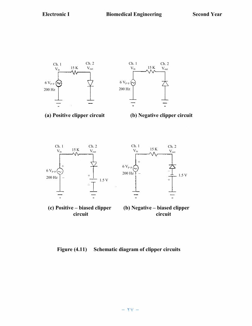
(A) Clipper Circuits:
1. Positive Clipper.
(i) Connect the circuit shown in fig. (4.11 a).
(ii) Set your oscilloscope to the following approximate setting;
Channels 1 & 2 : 1 V / division, dc coupling
Time base : 1 ms / division
(iii) Adjust the signal generators output level at 6 Vp-p at a frequency of 200 Hz.
(iv) Draw the input and the output waveforms.
2. Negative Clipper.
(i) Reverse the polarity of the diode in the circuit shown in fig. (4.11 a) as
shown in fig. (4.11 b).
(ii) Draw the input & the output waveforms.
3. Positive – biased Clipper.
(i) Connect the circuit shown in fig. (4.11 c).
(ii) Draw the input & the output waveform.
4. Negative – biased Clipper.
(i) Modify the circuit shown in fig. (4.11 c) to that shown in fig. (4.11 d).
(ii) Draw the input & the output waveforms.
(B) Clamper Circuits:
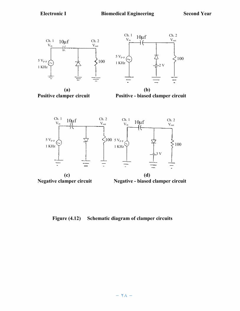
1. Positive Clamper.
(i) Connect the circuit shown in fig. (4.12 a).
(ii) Set your oscilloscope to the following approximate settings:
Channels 1 and 2 : 2 V / division, dc coupling.
Time base : 0.5 ms / division
(iii) Adjust the signal generators output level at 5 Vp-p at a frequency 1 kHz.
(iv) Draw the input & the output – waveforms.
Electronic I Biomedical Engineering Second Year
- ٢٣ -
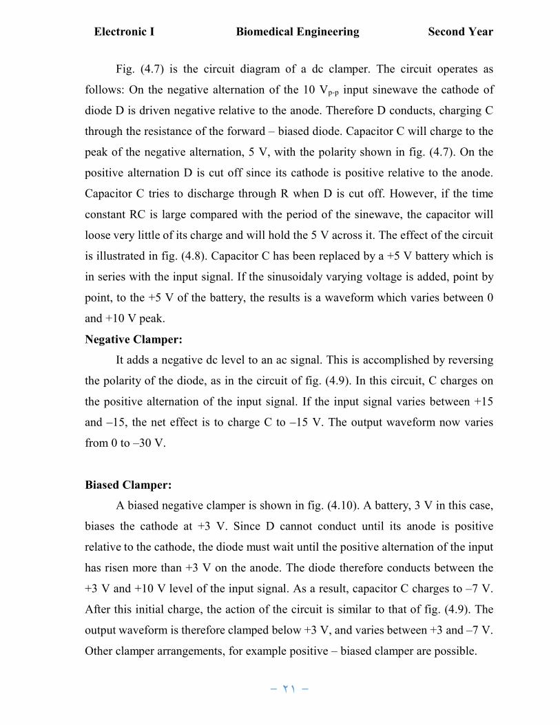
2. Positive – biased Clamper.
(i) Modify the positive Clamper circuit shown in Fig. (4.12 a) to a positive –
biased Clamper circuit shown in fig. (4.12 b).
(ii) Repeat steps (ii) – (iv) in part “1”.
3. Negative Clamper.
(i) Connect the negative Clamper circuit shown in fig. (4.12c)
(ii) Repeat steps (ii) – (iv) in part “1”.
4. Negative – biased clamper.
(i) Modify the negative Clamper circuit shown in fig. (4.12 c) to a negative –
biased Clamper shown in fig. (4.12 d).
(ii) Repeat steps (ii) – (iv) in part “1”.
Discussion:
1. How can you perform the same function of fig. (4.11 c) using a Zener
diode? Explain and Draw the circuit diagram.
2. Using ideal diodes, design a Clamper circuit to perform the function
indicated in fig. (4.13).
3. What happen to the output of the circuit shown in fig. (4.12 b) if the
polarity of the power supply is reversed?
4.
Vin Vout +30 V
+20 V
t Vin Vout t –10 V –20 V
Figure (4.13) A clamper circuit
?
Electronic I Biomedical Engineering Second Year
- ٢٤ -
D1 A
B Vin
Vout + R –
+ Vin
–
+ Vin
–
+ Vin
–
Vout
–
+ Vout
+ Vout
Vout
–
+ Vin
–
Vin
Vin
Vout
Vout
Vout
+ R –
A
B
D2
D1
D2 Vin
R
R
RF
(a) (b) Figure (4.1) Series semiconductor diode to limit the positive
alternation of an ac signal.
(a) (b) Figure (4.2) Series – connected diode used to limit negative
alternation of an ac signal.
(a) (b)
(d)
Figure (4.3) Parallel – connected diodes used to limit negative &
positive alternation.
Electronic I Biomedical Engineering Second Year
- ٢٥ -
D1
– C +
Vin
Vout – VAA
+
+ Vin
–
+20 0 –20
R
(a) (b)
Figure (4.4) Negative – biased clipper circuit.
+ Vout
–
Vout Vin VAA
D1
R
Vin
Vout
Figure (4.5) Positive – biased clipper circuit.
positive clamper Input
+40 +20 Output 0
Figure (4.6) Positive clamper add a+ dc axis to the waveform.
+5 0 –5
+10 +5 0
Input R D Output
Figure (4.7) Circuit diagram of a positive clamper.
Electronic I Biomedical Engineering Second Year
- ٢٦ -
+5 +10 0 Input Output +5 –5 0
5 V – +
Figure (4.8) A + 5 V battery replaces the charged capacitor C, inserting a + 5 V axis into the output waveform.
+15 0 0 Input R D Output –15 –15 –30
C + –
+10 0 Input R Output –10
D
C + –
+ 3 V –
+3 V –7 V –17 V
Figure (4.9) Negative clamper addes a – dc axis to the waveform.
Figure (4.10) Biased negative clamper.
Electronic I Biomedical Engineering Second Year
- ٢٧ -
Ch. 1 Vin
Ch. 2 Vout 15 K
6 Vp–p
200 Hz 6 Vp–p
200 Hz
Ch. 1 Vin
Ch. 2 Vout 15 K
Ch. 1 Vin
Ch. 2 Vout
15 K Ch. 1 Vin
Ch. 2 Vout 15 K
+ 6 Vp–p
200 Hz – + 1.5 V
–
+ 6 Vp–p
200 Hz – – 1.5 V
+
(a) Positive clipper circuit (b) Negative clipper circuit
(c) Positive – biased clipper (b) Negative – biased clipper circuit circuit
Figure (4.11) Schematic diagram of clipper circuits
Electronic I Biomedical Engineering Second Year
- ٢٨ -
Ch. 1 Vin
Ch. 2 Vout
Ch. 1 Vin
Ch. 2 Vout
Ch. 1 Vin
Ch. 2 Vout
5 Vp–p
1 KHz
(a) (b) Positive clamper circuit Positive - biased clamper circuit
Figure (4.12) Schematic diagram of clamper circuits
f10
f10
f10
f10
5 Vp–p
1 KHz
5 Vp–p
1 KHz 5 Vp–p
1 KHz
Ch. 1 Vin
Ch. 2 Vout
2 V
3 V
(c) (d) Negative clamper circuit Negative - biased clamper circuit
100 100
100 100