


circuit cellar - CiteSeerX
100
7 9 25274 75349 01 > CIRCUIT CELLAR ® www.circuitcellar.com THE MAGAZINE FOR COMPUTER APPLICATIONS $4.95 U.S. ($5.95 Canada) #174 January 2005 Nitrox Analyzer for Scuba Diving PC-Controlled RC Device TRENDnet Wi-Fi Project Simplify Signal Processing EMBEDDED APPLICATIONS Nitrox Analyzer for Scuba Diving PC-Controlled RC Device TRENDnet Wi-Fi Project Simplify Signal Processing
-
Upload
khangminh22 -
Category
Documents
-
view
1 -
download
0
Transcript of circuit cellar - CiteSeerX

7 925274 75349
01>
®
T H E M A G A Z I N E F O R C O M P U T E R A P P L I C AT I O N S
$4.95 U.S. ($5.95 Canada)
#174 January 2005
Nitrox Analyzer for Scuba Diving
PC-Controlled RC Device
TRENDnet Wi-Fi Project
Simplify Signal Processing
Nitrox Analyzer for Scuba Diving
PC-Controlled RC Device
TRENDnet Wi-Fi Project
Simplify Signal Processing

We’re starting off the new year with some terrific applications. Someof the best projects we feature aren’t based on original ideas; they’reoften recreations of products that are already available commercially.The lessons learned from the experiences are useful, of course. But thefun part is seeing how the new designs compare to off-the-shelf versionsand what improvements were made. We have some interesting compar-isons in this issue.
TiVo fans will be interested in Miguel Sanchez’s digital personal videorecorder (page 16). He decided to build his own because commercialPVRs aren’t sold in his native Spain. Miguel used Linux, a HauppaugeDVB-S digital satellite receiver card, and a Proxim ORiNOCO Wi-Fi cardto design his own PVR. He warns that the do-it-yourself route is undoubt-edly more expensive than simply buying a PVR, but we agree with himthat it’s definitely more fun.
From home electronics to bar electronics, we also have an articleabout building your own karaoke machine (page 36). Brad Stewart wonSecond Prize in the Zilog 2003 Flash for Cash Z8 Encore! InternationalDesign Contest with this project. (For more information about the designcontest, visit www.circuitcellar.com/magazine/contests.htm.) He designeda programmable, low-cost audio signal processor around a Z8 Encore!evaluation board. One of Brad’s notable achievements is the quality ofthe processor’s pitch shifting capability, which enables him to create har-mony with only one voice.
Back in June 2001, David Smith wrote about an AVR-based sub-mersible data logger he built to upload data to a PC (“Under the Sea: AScuba Dive Monitor,” 131, June 2001). He’s back this month with anoth-er 8-bit AVR-based project designed for scuba divers (page 20). Whendeep diving, breathing Nitrox instead of regular air enables scuba diversto stay at extremely high depths for longer periods. Because Nitrox isenriched with more oxygen than regular air, it’s critical to monitor the ratioof oxygen to nitrogen. An imbalance of too much oxygen can lead to seri-ous health problems or death. David designed an innovative AT90S4433-based analyzer that uses a Teledyne sensor to measure the percentageof oxygen in a Nitrox tank. The analyzer boasts accuracy that rivalscommercial units.
In addition to these projects, this issue also features a number of otherexciting applications, including a couple from the college and universitycontingent. Turn to page 44 to learn how a team from Mesa State College,Colorado, reverse engineered an RC transmitter, modified it for PC-control,and wrote software to design their own PC-controlled RC car. A groupfrom the Jerusalem College of Technology–Machon Lev has made signalprocessing with DSPs easier (page 52). This group demonstrates how toeliminate the need to add external peripherals by using a peripheral-richAnalog Devices ADuC812 to design and implement digital filters.
We enjoyed reading about all of the projects featured this month. Wehope you find them as interesting and useful as we did.
4 Issue 174 January 2005 www.circuitcellar.comCIRCUIT CELLAR®
EDITORIAL DIRECTOR/FOUNDERSteve Ciarcia
MANAGING EDITORJennifer Huber
TECHNICAL EDITORC.J. Abate
WEST COAST EDITORTom Cantrell
CONTRIBUTING EDITORSIngo CyliaxFred Eady George MartinGeorge NovacekJeff Bachiochi
NEW PRODUCTS EDITORJohn Gorsky
PROJECT EDITORSSteve BedfordKen Davidson David Tweed
ADVERTISINGPUBLISHER
Dan Rodrigues E-mail: [email protected] PUBLISHER/DIRECTOR OF SALES
Sean Donnelly Fax: (860) 871-0411(860) 872-3064 E-mail: [email protected] phone: (860) 930-4326
ADVERTISING REPRESENTATIVERachel Humphrey Fax: (860) 871-0411(860) 872-3064 E-mail: [email protected]
ADVERTISING COORDINATORValerie Luster Fax: (860) 871-0411(860) 875-2199 E-mail: [email protected]
ADVERTISING ASSISTANTDeborah Lavoie Fax: (860) 871-0411(860) 875-2199 E-mail: [email protected]
CONTACTING CIRCUIT CELLARSUBSCRIPTIONS:
INFORMATION: www.circuitcellar.com or [email protected] Subscribe: (800) 269-6301, www.circuitcellar.com/subscribe.htm, or [email protected]: [email protected]
GENERAL INFORMATION:TELEPHONE: (860) 875-2199 Fax: (860) 871-0411INTERNET: [email protected], [email protected], or www.circuitcellar.comEDITORIAL OFFICES: Editor, Circuit Cellar, 4 Park St., Vernon, CT 06066 NEW PRODUCTS: New Products, Circuit Cellar, 4 Park St., Vernon, CT [email protected]
AUTHOR CONTACT:E-MAIL: Author addresses (when available) are included at the end of each article
CIRCUIT CELLAR®, THE MAGAZINE FOR COMPUTER APPLICATIONS (ISSN 1528-0608) and Circuit Cellar Online are publishedmonthly by Circuit Cellar Incorporated, 4 Park Street, Suite 20, Vernon, CT 06066 (860) 875-2751. Periodical rates paid at Vernon,CT and additional offices. One-year (12 issues) subscription rate USA and possessions $21.95, Canada/Mexico $31.95, allother countries $49.95. Two-year (24 issues) subscription rate USA and possessions $39.95, Canada/Mexico $55, all othercountries $85. All subscription orders payable in U.S. funds only via VISA, MasterCard, international postal money order, or checkdrawn on U.S. bank.Direct subscription orders and subscription-related questions to Circuit Cellar Subscriptions, P.O. Box 5650, Hanover, NH03755-5650 or call (800) 269-6301.Postmaster: Send address changes to Circuit Cellar, Circulation Dept., P.O. Box 5650, Hanover, NH 03755-5650.
For information on authorized reprints of articles,contact Jeannette Ciarcia (860) 875-2199 or e-mail [email protected].
Circuit Cellar® makes no warranties and assumes no responsibility or liability of any kind for errors in these programs or schematics or for theconsequences of any such errors. Furthermore, because of possible variation in the quality and condition of materials and workmanship of read-er-assembled projects, Circuit Cellar® disclaims any responsibility for the safe and proper function of reader-assembled projects based upon orfrom plans, descriptions, or information published by Circuit Cellar®.
The information provided by Circuit Cellar® is for educational purposes. Circuit Cellar® makes no claims or warrants that readers have a right tobuild things based upon these ideas under patent or other relevant intellectual property law in their jurisdiction, or that readers have a right toconstruct or operate any of the devices described herein under the relevant patent or other intellectual property law of the reader’s jurisdiction.The reader assumes any risk of infringement liability for constructing or operating such devices.
Entire contents copyright © 2004 by Circuit Cellar Incorporated. All rights reserved. Circuit Cellar and Circuit Cellar INK are registered trademarksof Circuit Cellar Inc. Reproduction of this publication in whole or in part without written consent from Circuit Cellar Inc. is prohibited.
CHIEF FINANCIAL OFFICERJeannette Ciarcia
CUSTOMER SERVICEElaine Johnston
CONTROLLERJeff Yanco
ART DIRECTORKC Prescott
GRAPHIC DESIGNERMary Turek
STAFF ENGINEER John Gorsky
QUIZ COORDINATORDavid Tweed
Cover photograph Chris Rakoczy—Rakoczy PhotographyPRINTED IN THE UNITED STATES
When Homemade is Better
TASK MANAGER

6 Issue 174 January 2005 CIRCUIT CELLAR® www.circuitcellar.com
January 2005: Embedded Applications
4 TASK MANAGERWhen Homemade is BetterJennifer Huber
8 NEW PRODUCT NEWSedited by John Gorsky
15 TEST YOUR EQedited by David Tweed
FEATURES
COLUMNS
DEPARTMENTS
94 INDEX OF ADVERTISERSFebruary Preview
96 PRIORITY INTERRUPTDomestic Reality in the Global CommunitySteve Ciarcia
16 Build a Digital Video RecorderMiguel Sanchez
20 Microcontroller-Based Nitrox AnalyzerDavid Smith
28 Artificial Life Display (Part 2)ConstructionBob Armstrong
36 Z8 Encore!-Based Audio ProcessorBrad Stewart
44 PC-Controlled RC DeviceWarren MacEvoy & Dan Stadelman
52 Signal Processing with the ADuC812Shlomo Engelberg, Jonathan Garzon, & Naor Afgin
56 Digitally Control Power Factor CorrectionOlin Lathrop
68 FROM THE BENCHLight-to-Frequency Conversion (Part 2)Pulse and Oxygen ContentJeff Bachiochi
72 APPLIED PCsEmbedded Wi-Fi with TRENDnetFred Eady
78 SILICON UPDATEHot Enough for You?Hot Chips 16 RoundupTom Cantrell
Audio Processor (p. 36)
Nitrox Analyzer for ScubaDivers (p. 20)
Digital Video Recorder (p. 16)
Wireless Design withTRENDnet (p. 72)
PC-Controlled RC Device (p. 44)PC-Controlled RC Device (p. 44)

8 Issue 174 January 2005 CIRCUIT CELLAR® www.circuitcellar.com
NEW PRODUCT NEWS Edited by John Gorsky
POWERLINE NETWORKING CHIPSETThe new INT5500CS, an 85-Mbps powerline networking
chipset, is fully compliant with the 14-Mbps HomePlug 1.0specification. It offers the higher bandwidth performancenecessary to drive next-generation home entertainmentapplications such as standard definition video and wholehouse audio.
The INT5500CS complements the INT51X1 and INT5200products, which implement the 14-Mbps HomePlug 1.0specification. The INT5500CS enables additional applicationsrequiring higher bandwidth, including standard definitionvideo distribution, TV over IP (IPTV), DVR networking,and media center PCs. Other applications include wholehouse audio, the extension and bridging of higher speedwireless technologies such as 802.11x and UWB, and higherdata rate broadband sharing based on technologies such asADSL2 and fiber to the home.
The INT5500CS is the second step in a three-tier productstrategy designed to meet the increasing bandwidth needsof the evolving digital home. The new 85-Mbps INT5500CSwill be joined next year by a 200-Mbps HomePlugAV-com-pliant product line, which will enable distribution of mul-tiple high definition video streams over home powerlines.
HomePlug powerline communications is recognized as akey technology in the home networking ecosystem. Highreliability, resistance to interference, setup and use simplic-ity, and strong Quality of Service (QoS) make powerline
ideal for real-time entertainment content delivery, particu-larly whole-house audio and networked video.
The INT5500CS costs approximately $13 in high vol-umes.
Intellon Corp.www.intellon.com

www.circuitcellar.com CIRCUIT CELLAR® Issue 174 January 2005 9
NEW PRODUCT NEWSThe new LiveDesign evaluation kits include a versatile,
low-cost evaluation board with the choice of either anAltera Cyclone or Xilinx Spartan-3 FPGA device. Theseaffordable evaluation kits enable you to evaluate and fullyexperience the benefits of LiveDesign, a unique new digi-tal systems design methodology.
LiveDesign takes advantage of the availability of low-cost, high-capacity, high-performance FPGAs. It usesthem as a reconfigurable implementation platform fordigital circuitry during system development and effective-ly uses them as a nano-level breadboard. This enables thelive and interactive development and testing of electron-ics systems inside a programmable hardware design space.
LiveDesign provides an iterativedesign-implementation-debugprocess that facilitates interactivehardware/software codesign and uti-lizes an FPGA as the developmentand implementation platform.Reprogrammability eliminates theneed for system-level simulationand minimizes multiple prototypespins. During development the cir-cuit can be probed, analyzed, anddebugged interactively using FPGA-based virtual instruments.
The evaluation kits feature a software evaluationlicense of Altium’s Unified Nexar-Protel 2004 system,which includes a complete range of PCB and FPGA hard-ware design tools, integrated software development tools,ready-to-use FPGA-based components, and processorcores. They also include virtual instrumentation with aversatile, low-cost, FPGA-based LiveDesign evaluationdevelopment board, cabling, and accessories. An exten-sive range of tutorial and support documentation areincluded as well.
Altium’s LiveDesign evaluation kits cost $99 andinclude the Unified Nexar-Protel 2004 software evalua-tion license and a LiveDesign evaluation board with the
choice of either the Altera CycloneEP1C12F324C8 or Xilinx Spartan-3XC3S400-4FG456C FPGA device.Altium’s Unified Nexar-Protel 2004software costs $9,995 and theNanoBoard costs $995. The standardNanoBoard package includes twodaughterboards: the Xilinx Spartan-IIEdaughterboard and the Altera Cyclonedaughterboard.
Altium Ltd.www.altium.com
FPGA DESIGN SOFTWARE AND EVALUATION BOARDS

10 Issue 174 January 2005 CIRCUIT CELLAR® www.circuitcellar.com
NEW PRODUCT NEWSuM-FPU FLOATING-POINT COPROCESSOR
The uM-FPU floating-point coprocessor interfaces tovirtually any microcontroller using an SPI or I2C inter-face, making it ideal for applications requiring floating-point math such as converting sensor readings, roboticcontrol, data manipulation, and other embedded controlapplications.
The uM-FPU provides support for 32-bit IEEE 754-com-patible floating-point operations and 32-bit integer opera-tions. A PIC-compatible mode is also available to supportPIC format floating-point numbers. Many functions arebuilt in, including floating-point math, long integer math,exponential functions, trigonometric functions, and dataconversion and formatting functions. A built-in debug moni-tor is available to assist with developing and debuggingcode.
A unique feature of the uM-FPU is the ability to defineuser functions, which are defined as a series of built-in opera-tions. They are stored in flash memory on the uM-FPU chip.Because they are stored internally, the majority of communi-cations overhead is eliminated. This results in dramaticspeed improvements and greatly reduced code space require-ments on the microcontroller. Software is provided to defineuser functions using standard math expressions and to pro-gram the uM-FPU over a RS-232 connection.
Documentation and software is provided to support awide variety of popular microprocessors. The uM-FPU isavailable in an 8-pin DIP or a 20-pin SSOP package costing$14.95. Volume discounts are available.
Micromega Corp.www.micromegacorp.com

12 Issue 174 January 2005 CIRCUIT CELLAR® www.circuitcellar.com
NEW PRODUCT NEWSThe LTC4060 is an autonomous one- to four-cell, 0.4- to
2-A linear NiMH and NiCd battery charger. The LTC4060includes all the functions required for a battery charger cir-cuit operating without the aid of a microcontroller orfirmware. The simple design needs only three passive com-ponents. The LTC4060 also eliminates the need for a senseresistor and blockingdiode, which increasesefficiency and lowersthe solution cost. ThisIC is targeted at appli-cations includingportable medical equip-ment, automotive diag-nostic systems, andindustrial/telecom testdevices.
The device is offeredin two packages: a 16-lead TSSOP and a 5 mm × 3 mm DFN. Ituses an external PNPtransistor to supplycurrent to the batteryor battery pack. Theoperating voltage
ranges from 4.5 to 10 V. The LTC4060 provides threeoptions for terminating the charge cycle: negative deltaV,maximum voltage, or maximum time. Moreover, the ICpermits the use of a thermistor for temperature-qualifiedbattery charging, which only allows battery charging if thetemperature is in a safe range. The charge current is
adjustable with a resis-tor and has ±5% accura-cy. The LTC4060 alsohas automatic batterydetection, charge andAC present status out-put, precharge qualifi-cation, automaticrecharge, reverse cur-rent protection, andmanual shutdown.Battery drain current isless than 1 µA in Sleepmode.
Pricing starts at $3.80each in 1,000-piecequantities.
Linear Technology Corp.www.linear.com
BATTERY CHARGER REQUIRES NO MICROCONTROLLER

Full support for the C8051F12x and C8051F13x mixedsignal microcontroller units has added to the Crossware8051 Development Suite. Code Creation Wizards are pro-vided for all on-chip peripherals. They allow the phase-locked loop to be rapidly configured to exploit the 100-MIPS
maximum performance. With the compiler and librariesusing multiplication code that exploits the MAC engine,you can instantly take full advantage of the speed thesechips offer.
The environment is fully preconfigured to take advan-tage of the MCU’s 128 KB of in-system programmablebanked flash memory, and when simulating and debuggingthe banking process is virtually transparent to the develop-er. In addition, the flash memory Code Creation Wizardwill generate all the code necessary to erase and rewriteflash memory during program execution.
The source level debugger drives the SiliconLaboratories JTAG emulation cartridge directly. Thisallows it to make use of the full range of on-chip debugfacilities including the hardware data breakpoints andhardware stack overflow and underflow trap.
The 8051 development suite includes a full-featuredANSI C compiler, a relocatable cross assembler, an overlaylinker, a source level simulator that can be extended tosimulate a complete target system, and a debug monitorthat supports source-level debugging on the target system.The suite costs $1,340.
Crossware Productswww.crossware.com
NEW PRODUCT NEWS
www.circuitcellar.comCIRCUIT CELLAR®14 Issue 174 January 2005
DEVELOPMENT SUITE SUPPORTS C8051F12x AND C8051F13x

Problem 1—What exactly does the follow-ing circuit do? Where might it be used?
Problem 2—There is some jitter in the out-put signal of the above circuit. How rele-vant is this in the context of its intendedapplication?
www.circuitcellar.com CIRCUIT CELLAR® Issue 174 January 2005 15
What’s your EQ?—The answers are posted at www.circuitcellar.com/eq.htm
You may contact the quizmasters at [email protected]
CIRCUIT CELLAR—Test Your EQ
Problem 3—The raw data rates for tele-phone toll-quality speech, stereo CD-quali-ty music, and standard-definition digital TVare 64 kbps, 1.4 Mbps, and 300 Mbps,respectively. What are typical correspon-ding compressed data rates for such signals?
Problem 4—What kind of playing timewould you expect to get out of a 20-GBhard drive for the various media types?
Contributed by David Tweed
Edited by David Tweed
74LS04
74LS161A
LOADET
EPCLRDCBACLK
RCO
QD
QBQC
QA
VCC
16 MHz
BAUD_CLOCK
GND

16 Issue 174 January 2005 CIRCUIT CELLAR® www.circuitcellar.com
tens of hours of programming, whichmeans you can stop spending money onVHS tapes for your VCR. It also meansyour son won’t copy cartoons over yourfavorite movie. Yes, my children knowhow to disable the write protection ona VHS tape.
I also found PVR attractive becauseI keep some recordings longer thanothers. For instance, my family watch-es some recordings only once. Otherrecordings, like children’s shows, areviewed several times. Then there arethe recordings we never watch butplan to keep forever. Limiting myselfto 80 hours of recording space on ahard disk seemed like a good way toforce myself to consolidate my collec-tion. Unfortunately, when the firstPVR units appeared in 1999, writableDVDs weren’t commercially availableand the first PVRs couldn’t exportrecorded media to another system. Isuppose PVR manufacturers wanted tokeep content owners happy and avoidpossible litigation.
But things have changed over time.Today, manufacturers include a networkconnection so your PVR can import andexport shows to a computer or anotherPVR box in your house. Some eveninclude a wireless network connection.
The PVR vendor’s business model isbased on a few different revenue flows,the most obvious of which are sellingunits and user subscriptions. PVR man-ufacturers currently send subscriberselectronic program guides so their PVRscan display detailed programmingmenus. This means you can find andrecord a show simply by pressing the
With the introduction of TV tunercards for PCs, you suddenly had theability to watch TV programming onyour computer. Although this isn’t aparticularly exciting technologicaladvance, it has made way for a novelidea: recording TV shows with yourPC. At first, the process was possibleonly when compression techniquesand the CPU power were up to thetask (unless you had an expensivehardware-based compression card).However, when the prices of high-capacity hard drives started dropping,companies began developing personalvideo recorders (PVRs) and digitalvideo recorders (DVRs), which areessentially tapeless VCRs.
When I first started researching thistechnology, I learned that there wasn’t aPVR brand here in Spain. At the time, Isubscribed to a digital satellite package,so I asked my provider for a PVR unit.It turned out they didn’t have oneeither. With nowhere else to turn, Idecided to build my own.
In this article, I’ll explain how I builtmy system. But before I get into thespecifics, let’s take a brief look at thehistory of this technology and why Ifind it so useful.
PVR BACKGROUNDI first became interested in this
technology in 1999 after reading aboutReplayTV and TiVo. These systemsprove you can build a computer thatenables you to watch and record yourfavorite shows. The best part is thatyou don’t have to insert a tape becausehard disks have the capacity to record
buttons on your remote control.Although useful, an electronic programguide comes at a cost in the form of aone-time payment or a monthly fee.The PVR box obtains this informationwith either a built-in modem or a net-work card, so you have to provide aphone line or a broadband Internetconnection.
These companies also make moneyon the information the PVR exchangeswith the manufacturer every time itconnects to get the electronic programguide. Your viewing and recordinghabits can be monitored (this canscare the privacy-conscious user). Inaddition, special recording instruc-tions can be secretly sent to your PVRso a sponsored show will be recordedwithout your approval. As a result, thecompany offering the electronic pro-gram guide might get some moneyfrom studios for promoting (i.e.,recording without your consent) agiven show.
GOING DIGITALUnless you have been living in a
cave for the last 20 years, you knowthat most technology seems to begoing digital. As an engineer, you knowthat storing and transmitting digitalsignals has an important advantageover analog techniques: noise can becanceled and the original bitstream canbe restored (most of the time), whichmeans a recorded copy can be identicalto the original.
You’ve seen how the music industryhas completely phased out vinylrecords and tapes in favor of CDs. The
FEATURE ARTICLE by Miguel Sanchez
Build a Digital Video RecorderAfter learning that personal video recorders (PVR) weren’t available in Spain, Miguel decid-ed to build his own.To do so, he compiled some useful information about building a systemwith Linux and a DVB-S digital satellite receiver card. Read on to learn more about thehardware and software you’ll need to get the job done.

same thing is happening with VHStapes and DVDs, and something simi-lar is happening to TV broadcasting.In Europe, TV analog transmission isexpected to end completely by 2012.
TV broadcasts reach your home viaone of three different technologies:satellite, cable, and terrestrial broad-casting. Most stations have already con-verted to digital or are in the process ofconverting. For broadcasters, going digi-tal means they can pack more chan-nels in the same spectrum because ofMPEG-2 compression technology.
Digital broadcasting requires usersto buy a new set-top box. But it alsomeans better image and sound quality(either live or recorded). In fact, thereis no quality difference between a livedigital show and a recorded one (unlessyou instruct your PVR to transcode theshow to a more compact stream simi-lar to the LP mode of VCRs).
Unfortunately, most of the availablePVRs are based on analog technologyeven though their recording is digital.Notable exceptions are some digitalsatellite receivers that also include ahard disk to act as a PVR and somepay-per-view broadcasters that bundlea PVR with their service (i.e., aPilotime receiver with Canal Satellitein France or Direct TV DVR withTiVo in the U.S.).
BUILD A DIGITAL PVRBefore I begin, I want to stress an
important point: you’re likely to spendmuch more time and money building aPVR than buying one. This definitelyhappened to me, but there was a twist:I had a lot of fun.
Soon after I realized that there weren’tany PVR options in Spain, I startedsearching the Internet for an answer.Fortunately, I found Klaus Schmidinger’sVDR project when I Googled “VDR”(www.cadsoft.de/vdr/index.htm). Klausprovides all the information you needto build a PVR-like device using LinuxOS and a DVB-S digital satellitereceiver card. Now, thanks to theLinux TV people, you can use a rangeof digital TV tuners (satellite, cable, orterrestrial) with the same PVR software(www.linuxtv.org). In fact, you can builda system using any mix of DVB receivercards (up to four cards). Having more
www.circuitcellar.com CIRCUIT CELLAR®Issue 174 January 2005 17
than one tuner enables recording ofshows broadcasted at the same timeon different channels (actually on dif-ferent transponders to be precise).
The full source code is available onthe ’Net. Some Linux distributionsinclude both pieces of software alreadycompiled and ready to use. The DVBdriver even made it to the 2.6 kerneland is included in new Linux kernelssource code.
Although I won’t go into the detailsabout DVB standards, note that DVBfeeds provide not only video and audiostreams grouped into channel streams(so a channel may have more than oneaudio stream, so multi-language pro-grams are possible), but also an electron-ic programming guide (EPG) so receiverscan learn about current and futureshows. With EPG information embed-ded in the channels, there is no need todownload this data from the Internet.Photo 1a shows a sample screen with achannel’s programs.
The beauty of Klaus’s VDR projectis that he encouraged other people toextend the system’s functionality byproviding a clean interface for plug-inmodules. This approach proved suc-
cessful given the number of availableplug-ins with which you can add func-tionality to the basic PVR.
DVB CARDS Digital video broadcasting cards
come in three different flavors: DVB-S,DVB-C or DVB-T, where S is for satel-lite, C is for cable, and T is for digitalterrestrial TV. These are PCI cards youcan plug into your PC or any othercomputer with a PCI interface.
There are Linux distributions fornon-x86 processors, so you could com-pile and run the software on a non-Intel platform. Although DVB cardswere marketed by Fujitsu-Siemens,they are no longer available.Hauppauge and TechnoTrend sellcards that are compatible with theLinux DVB drivers. These cardsinclude a digital tuner plus a hardwareMPEG decoder with OSD capabilityand video out, so you don’t have touse the computer VGA output unlessyou want to.
Photo 2 and Figure 1 show a full-featured DVB-S card. Cheaper cardscontain only a tuner and a demodula-tor. The computer must do the rest ofthe work (i.e., demultiplexing andMPEG decoding), so the card needs afast processor to keep up with thisreal-time job. Full-featured cards canbe used with an old 100-MHzPentium because the computer is onlysetting up the data path inside thecard. Recording a 3- or 4-Mbps datas-tream can be handled by almost anyhard drive, although you’ll need anewer one if you want to get a goodrecording capacity. I’d say 40 GB willgive you about 20 hours of recording.
Photo 1a—Use a remote control to scroll through the electronic program guide. Each program description and itsrecording can be done with one or two clicks. b—This is the main menu. The extra entry Mplayer is used to viewdownloaded content in various MPEG-4 formats.
a) b)
Photo 2—This full-featured DVB satellite receiver hasTV output. The connector on the edge is for an optionalcommon interface slot.

18 Issue 174 January 2005 CIRCUIT CELLAR® www.circuitcellar.com
Please note that this depends onthe data rate of the datastreamyou’re recording.
When you want to view andrecord programs on channels thataren’t freely available (free-to-air),check if your digital package isencrypted using standard systems.Some providers in North Americause nonstandard encryption thatcan’t be used with these DVBcards. The rest of you must buy acommon interface (CI) adapter soyou can plug in your conditionalaccess module (CAM) and slide in yourcustomer card. This way you’ll be ableto access fee-based TV systems.
SAMPLE CASE I built my PVR based on SUSE 8.2
Linux distribution using an old 500-MHzPentium III computer with 64 MB ofRAM and a 120-GB hard disk, aHauppauge Nexus-s DVB-S card, andan ORiNOCO Silver Wi-Fi card. Ibought a CI adapter and an Aston SecaCAM because my local provider usedthat content encryption system.
Although the SUSE distributionincluded binaries of VDR software, Idownloaded the tar ball because I want-ed to add some plug-ins. I wanted touse a remote control instead of the key-board. My card came with an IR receiv-er. Fortunately, there is a remote plug-in. (Klaus keeps a list of plug-ins on hisweb site so it isn’t difficult to figureout what you need.)
Video streaming is another interestingplug-in. You can watch a show from aPC instead of having to go to the TV set.(That’s extremely useful if you happento be in front of your computer most ofthe time.) Another plug-in allows you touse the TV output to watch DivX orXVID files using MPlayer software(another great OSS project). For moreinformation about the MPlayer project,visit www.mplayerhq.hu. This way youcan watch a downloaded show on theTV set with your remote control.
Other plug-ins are for the time,weather, news, additional devices, play-ing a DVD or VCD, and additional con-trol inputs. If you don’t find what youneed, you can program a custom plug-in.
Some of the features built into theVDR include on-screen menus, time-
shifting, instant recording, live TVpausing, and prioritized storage man-agement. The system, which alsoincludes basic editing functions (mark-ers and cutting of recordings), allowsyou to program recordings based on theEPG data using the on-screen menu.You can also remotely control the sys-tem with a TCP interface.
If you aren’t happy with only onesatellite, the VDR can use a motorizeddish or a DiSEQC-compatible switchto choose among several fixed dishes.Either way, you select a channel withthe remote control and that’s it. A selec-tion is sent via special coding throughthe aerial cable connected to the tuner.
For the most computer-addictedusers, there is yet another softwareproject that provides a nice web inter-face. VDRadmin translates the simpleTCP interface of VDR into a web-based one. This interface enables youto view the program list and schedulerecordings using a browser.
If you add a DVD recorder to thesystem, you can record shows on aDVD. If you want to play this DVDusing a standard DVD player, installsome software like vdr2dvd script andthe companion tools (mkisofs, grow-isofs, dvdrecord, transcode, anddvdauthor). If you prefer to storesmaller versions of your shows inDivX format, use mencoder ortranscode to convert your originalrecording to an avi file that you canlater burn to either a DVD+/-R or CD-ROM. As you can see, the possibilitiesare endless.
PVR FREEDOMPVRs give you the freedom to watch
and record whatever you want. You
can buy a commercial system oryou can build your own.Because the only CPU-boundtask is DivX decoding, andbecause this is an optional taskyou might not be interested in,you can build with cheap orleftover hardware. Plus, thesoftware used for this project isfreely available on the Internet.
Photo 1b shows the VDR’smain menu. Although the OSDcannot compete with the latestGUIs in some commercial units
(or even other OSS projects likeFreevo or MythTV), the rest is a fullycapable PVR system with more fea-tures than any single commercial sys-tem. And the best part is that you canadd new features in the future. Maybeyou can program a new plug-in for anew task no one else has eventhought of.
Every now and then I add or changethings on my system, which remainspowered almost 24/7 recording what Ithink I’ll enjoy. If you like some of thethings you’ve learned about this sys-tem, I am sure you will have a greattime building yours. I
Tuner QPSDemodulator
Demultiplexer
Broadcastdata
decoder
MPEG-2Video
decoder
MPEG-2/AC-3Audio
decoderHard disk
Play
Record
Figure 1—The PVR system contains a full-featured DVB card.
Miguel Sanchez holds a B.S., M.S.,and Ph.D. in Computer Science andhas taught computer networking at thePolytechnic University of Valencia,Spain since 1989. His interests in elec-tronics and microprocessors sparked hiscareer in computer science, but his sol-der is always at hand. He currentlyfocuses his research on wireless sensornetworks. Miguel also consults for somelocal companies. You may contact himat [email protected].
PROJECT FILESTo download the code, go to ftp.ciruitcellar.com/pub/Circuit_Cellar/2005/174.
SOURCESWinTV-Nexus-s DVB-S cardHauppauge Computer Workswww.hauppauge.com
ORiNOCO Silver Wi-Fi cardProxim Corp.www.proxim.com

20 Issue 174 January 2005 CIRCUIT CELLAR® www.circuitcellar.com
a redundant check of a dive techni-cian’s analyzer. This is also the reasonthat I must recommend that you usemy analyzer only as an example of aninteresting embedded device.
For the non-divers out there, a littlebackground information is in order.Scuba diving has several inherent risksthat can lead to injury or death. Propertraining is necessary to mitigate theserisks and to allow you to execute safedives. Although a comprehensiveoverview of diving procedures and physi-ology is beyond the scope of this article,there are a few general principles thatare relevant to understanding the func-tions that my Nitrox analyzer performs.
DIVE SCIENCEIn general, the deeper you dive, the
less time you can stay down. One toolyou can use to increase your dive time isNitrox, which decreases the amount ofnitrogen in the gas you breath. Becausethe percentage of nitrogen decreases, thepercentage of oxygen increases to main-tain the same overall volume and pres-sure. This can introduce complications.Oxygen can become toxic to the centralnervous system (CNS) if it’s breathed attoo high a pressure and concentration.CNS oxygen toxicity can result in con-vulsions and loss of consciousness,which can lead to death when you’resubmerged under water. Because thepressure of the gas breathed increaseswith depth, the maximum dive depthmust be limited to prevent the pressureof the oxygen from nearing toxic levels.The higher the percentage of oxygen inthe Nitrox blend, the shallower the max-imum allowable dive depth. For these
Like many Circuit Cellar readers, Ioften find myself combining myenthusiasm for embedded systems withmy other interests to come up withengaging design projects. The project I’lldescribe in this article is no exception.The Nitrox analyzer in Photo 1 is theresult of my interest in a specializedform of diving in which you breath agas called Nitrox instead of regular air.
Typical recreational dives involvebreathing air, which is made up ofapproximately 21% oxygen (O2) and 79%nitrogen (N2). When you breatheenriched air Nitrox, however, you’rebreathing a gas containing more oxygenand less nitrogen than regular air. It’simportant for reasons of safety that whenbreathing Nitrox you know exactly whatpercentage of oxygen you’re breathing.
I originally considered purchasingan analyzer, but after some thought, Ifigured that designing one would be afar more rewarding experience.Although I’m always excited to devel-op and use my own embedded devices,I don’t have a death wish. It’s for thisreason that I only use my analyzer as
reasons, it’s important for you to knowthe percentage of oxygen in the mixturethat you’ll be breathing so you canplan a safe dive.
When you purchase a tank of Nitrox,you must follow the specific proce-dures set by the major dive certifica-tion agencies to minimize the chancesof accidents. Typically, when a techni-cian creates a certain mixture of Nitroxand fills a tank with it, he checks thepercentage of oxygen with a commercialanalyzer. When you’re ready to takepossession of the tank, it’s your respon-sibility to verify the percentage of oxy-gen in the Nitrox. Typically, you’ll usethe same analyzer that the technicianused to make this measurement.
After you know the percentage of oxy-
FEATURE ARTICLE by David Smith
Microcontroller-Based Nitrox Analyzer
Photo 1—I built the Nitrox analyzer because of myinterest in both embedded systems and scuba diving.Here you see the analyzer along with the oxygen sen-sor in the PVC sensor mount and a tank of Nitrox.
Many scuba divers prefer to breathe Nitrox instead of regular air when they dive. To do sosafely, they must use a special analyzer to measure the percentage of oxygen in the tank.David recently designed his own AT90S4433-based Nitrox analyzer.
Photo 2—Take a look at the Nitrox Analyzer’s main elec-tronic components, subsystems, and PCB. Note thehomemade protoboard section in the upper right corner.

www.circuitcellar.com CIRCUIT CELLAR® Issue 174 January 2005 21
gen, the maximum allowable dive depththen can be determined from a set ofNitrox dive tables. Next, the percentageof oxygen, maximum dive depth, date,and your name are recorded in a Nitroxfill logbook as well as on a sticker thatis placed on the tank. As you can see,the extra checking decreases the likeli-hood of an error. However, if you andthe technician were to use different ana-lyzers, an additional margin of safetywould be added. Now that the back-ground and disclaimers are out of theway, let’s move on to the device itself.
ANALYZER HARDWAREThe AT90S4433 microcontroller that
serves as the computing core for thisproject is extremely powerful and loadedwith a full complement of peripherals(see Figure 1 and Photo 2). It’s equippedwith 4 KB of in-system programmablecode flash memory, 128 bytes of dataSRAM, and 256 bytes of data EEPROM.Furthermore, the microcontroller’s native
instruction size is 16 bits, which meansthat its code flash memory can hold atmost 2,048 assembly instructions.
The AT90S4433 contains 32 general-purpose 8-bit registers, a 10-bit ADC,a UART, an SPI port, an 8-bit counter,a 16-bit counter, an analog compara-tor, and a watchdog timer. It can runat up to 8 MHz, with the majority ofits instructions executing in a singlecycle. Atmel has issued an “end-of-life” notification for the microcon-troller, but a pin-compatible upgradepath exists via the ATmega8.
The Teledyne R-17D oxygen sensoris the key to sensing the percentage ofoxygen. It produces a linear outputvoltage that’s proportional to the partialpressure of oxygen to which it’s exposed.The percentage of oxygen is deter-mined with this information by dividingthe measured partial pressure of oxygenby the ambient atmospheric pressure.The sensor is temperature compensatedand rated to operate over a range of 0
to 1 atmosphere of pressure. Its accuracyis within ±1% of full scale at constanttemperature and pressure. A zero-inputoffset error of up to 0.5% also may exist.
The datasheet indicates that thesensor produces a 10-mV, ±3-mV out-put when exposed to approximately21% oxygen, which is present in air atsea level. Because there is the poten-tial for such a relatively large varia-tion in the normal output characteris-tic from sensor to sensor, calibrationis required in order to compensate.
The millivolt-level signal from theoxygen sensor is scaled by an instru-mentation op-amp before being passedto the microcontroller’s ADC input.Certification agencies require recreation-al Nitrox mixes to be between 21% and40% oxygen, so I chose an amplifier gainof 184 to scale 41.6% oxygen to anunclipped, full-scale signal under worst-case conditions. This ensured that thesmallest maximum of slightly more than40% oxygen could be measured for the
Figure 1—The main components of the design are the microcontroller, LCD interface, analog amplifier, and the power control and conditioning.

then expose the sensor to the air. Theunit will take an initial reading, andthen prompt you to expose the sensorto a known sample of Nitrox. After themeasurement, you can specify the actu-al percentage of oxygen in the referencesample. The unit then computes a slopecorrection calibration factor to beapplied to all future measurements andthen stores it in internal EEPROM. Thecorrection factor essentially convertsthe nonideal sensor characteristic to areference ideal characteristic on whichthe AT90S4433 bases its measure-ments. The sensor slope calibrationshould be performed any time a differ-ent R-17D O2 sensor is used with theunit.
When the analyzer powers up nor-mally, it first prompts you to selectthe approximate altitude in feet abovesea level. This allows it to approxi-mate the ambient atmospheric pres-sure, which is required to convert theoxygen sensor’s partial pressure meas-urement to the percentage of oxygen:
Next, you’re prompted to expose thesensor to air, and then the unit takes ameasurement. Using this information,an additive offset compensation factoris computed to eliminate sensor andamplifier offset error. At this point, thedevice displays the percentage oxygenmeasured by the sensor and updates itevery second.
To measure the percentage of oxy-gen from a Nitrox tank, place the oxy-gen sensor in the sensor mount, holdthe mount to the tank valve, and openthe valve just enough to allow a bit ofNitrox to flow through the assembly.The LCD should begin to indicate anincrease in the percentage of oxygen.
After the reading stabilizes on a valuefor about 10 s, the unit displays the cal-culated percentage of oxygen in the tank.At this point, if you press and release the
percent O = partial pressure Oambient pressure2
2
22 Issue 174 January 2005 CIRCUIT CELLAR® www.circuitcellar.com
worst in-spec sensors (see Figure 2). Inthis case, full-scale is 4.8 V, which isused as the theoretical maximumbecause the op-amp’s output is limitedto 70 mV less than the positive supplyrail of 5 V.
The user interface consists of onepush button for input and a 2 × 8 LCDmodule for output. The push buttonturns the unit on and off and allowsyou to select modes and options. Inaddition, the unit saves battery powerby automatically powering down aftervarious specified timeouts haveelapsed. Furthermore, a spare ADCchannel measures battery voltage toprovide a low-battery warning.
The Nitrox analyzer is housed in aPacTec HP-9VB project case thatincludes a built-in compartment forthe unit’s 9-V battery. I’d like to thankGordon Fry and David Manley fortheir assistance in modifying thehousing to accept a bezel for the LCD.
In order to measure the percentage ofoxygen in the Nitrox in a scuba tank, Ibuilt a sensor mount from a small, T-shaped PVC tube. The sensor is in thetop opening. A second opening is heldagainst the tank valve. The third open-ing is covered with a cap with a smallhole in it. The tank valve is openedslightly—just enough to allow theNitrox to begin flowing through thetube. It’s important to keep the pressureof the Nitrox flowing from the tank to aminimum, because pressure will affectthe accuracy of the measurement.
OPERATIONThe first time the Nitrox analyzer
powers up, it enters Sensor Calibrationmode, which you can also achieve byholding down the button for severalseconds at power-up. Calibration modeallows the AT90S4433 to compensatefor deviations from the ideal of theoxygen sensor’s output characteristic.
To perform the calibration, select yourapproximate altitude above sea level and
push button, the analyzer will cal-culate and display the maximumdive depth at which the partialpressure of oxygen being breathedreaches 1.4 atmospheres, which isotherwise known as the maximumoperating depth (MOD). After afew seconds, the LCD will begin
displaying the percentage of oxygencurrently detected by the sensor. Ifyou don’t press a button for 5 min.,the unit automatically shuts down toconserve battery power. To shut downmanually, press and hold the buttonfor several seconds.
FIRMWAREI wrote the AT90S4433’s firmware in
C and compiled it with an ImageCraftC compiler. The structure is the typicalforeground-background paradigm. Themajority of the code is executed in theforeground, with interrupts performingspecific functions in the background,such as timeout management. Becausepower consumption is an issue withbattery-powered devices, the firmwareplaces the microcontroller in a low-power, idle Sleep mode during delays.
The calculations are performed withfixed-point arithmetic, which is amethod of representing numbers with afractional component as integers (usingprogrammer-specified precision). Thismethod is beneficial because it’s treatedas integer math by the compiler and themicrocontroller, which means floating-point libraries don’t need to be linkedin. This saves a substantial amount ofvaluable code space.
Fixed-point math has two main short-comings. First, it creates the burden ofmanually keeping track of the decimallocation during calculations. Second, itrequires you to know the exact range ofthe results of all the calculations in orderto maximize the precision and to preventnumerical overflow. Early in the project,I experimented with floating-point mathand quickly realized that there wouldn’tbe enough code space to accomplishwhat I wanted without switching tofixed-point math. That’s when the projectbecame a personal challenge to wring outas much functionality as possible fromthe AT90S4433’s 4 KB of code space.
To understand what’s involved infixed-point computations, compare
Percent O = 100maximum output
amplitude gain
percent O 2
2× airworst-case sensor output for air
worst-case offset− error
= 100 V mV
×
41 6 4 8184
2113
. % . % −−
0.5%
Figure 2—This equation illustrates the calculation of the worst-case maximum percentage O2 that the analyzer canmeasure.

www.circuitcellar.com CIRCUIT CELLAR®Issue 174 January 2005 25
Listing 1, which is a fixed-point ver-sion of the statement that determinesMOD, to its floating-point equivalent.Obviously, the floating-point expressionis easy to read. The MOD is 46.2divided by the percentage of oxygenminus 33. The result is then typecastto an unsigned short, which results inthe depth being truncated to an inte-gral number of feet.
The fixed-point version is more diffi-cult to understand. During the compilingprocess, the C preprocessor converts((ulong)46.2*10000)<<12) to a 4-byte constant value of 1.892352 × 10⁹.This represents 462,000 with an implieddecimal point between bit 12 and bit 11.The usPercentO2x10000 variable isthe percentage of oxygen scaled by10,000. Because fixed-point calcula-tions are integer-based, fractional val-ues must be manipulated so they canbe represented as integers withenough bits to ensure that calcula-tions are performed with precision.For example, 32.6% oxygen scaled by10,000 results in 3,260, which can bestored in usPercentO2x10000. Next,usPercentO2x10000 is typecast to be4 bytes long and divided into 1.892352× 10⁹. The result is shifted 12 bits tothe right to move the implied decimalpoint to just before bit 0 and thentypecast to an unsigned short. Finally,33 is subtracted from the value toobtain the depth truncated to an inte-gral number of feet.
Another technique I employed toreduce the size of the compiled exe-cutable was based on analysis of theassembly output produced by the Ccompiler. I found that combining mul-tiple statements of a complex calcula-tion into a single C statement signifi-cantly reduced the amount of codegenerated by the compiler. This is
largely due to the elimination of manyunnecessary register loads and storesthat were occurring as values wereswapped in and out of SRAM.Specifically, this technique resulted inan 18% reduction in the code producedfor one particularly large calculation.
Another method I used to conservecode flash memory was to relocate theLCD text strings to EEPROM. Thisfreed up an additional 244 bytes forthe executable. Although this may notsound like much, it represents around6% of the microcontroller’s entirecode flash memory space.
TEST RESULTSAtmel’s AVR Studio simulator is a
valuable aid for testing firmware. I usedit for the verification of the fixed-pointcode to step through the assembly. Ialso used the AVR Studio to verify thecalculations for a wide range of inputvalues. Simulation can take you onlyso far though. To truly test the device, Ineeded access to various samples ofNitrox. Thanks to Dive Connections inCharlottesville, Virginia and theOlympus Dive Center and DiscoveryDiving Company in Morehead, NorthCarolina, I was able to test mydevice’s results against those producedby the shops’ commercial analyzers.
I tested 17 different tanks of Nitrox.It’s evident that the worst-case devia-tion between the Nitrox analyzer andthe commercial analyzers is 0.4%,with the average deviation being onthe order of 0.1% (see Figure 3 on page26). The Professional Association ofDive Instructors (PADI) recommendsthat a Nitrox dive be planned using apercentage of oxygen within 1% of the
Listing 1—This code snippet performs the same calculation in fixed-point and floating-point arithmetic. It par-tially illustrates the additional complexity involved in using fixed-point math.
// Fixed point unsigned short usMaxDepth, usPercentO2x10000;usMaxDepth = ((unsigned short)((((unsigned long)(46.2*10000)<<12)/ (unsigned long)usPercentO2x10000)>>12) - 33);
// Floating pointfloat fPercentO2;usMaxDepth = (unsigned short)(46.2 / fPercentO2 - 33.0);

26 Issue 174 January 2005 CIRCUIT CELLAR® www.circuitcellar.com
RESOURCESAtmel Corp., “ 8-Bit AVR Microcontrollerwith 4K Bytes of In-System ProgrammableFlash: AT90S4433,” rev. 1042H-AVR,2003.
National Association of UnderwaterInstructors (NAUI), www.naui.com.
Professional Association of DivingInstructors, www.padi.com.
Teledyne, “ Oxygen Sensors,” 2001,www.teledyne-ai.com.
SOURCESAT90S4433 and AVR StudioAtmelwww.atmel.com
ICCAVR C CompilerImageCraftwww.imagecraft.com
HP-9VB Handheld enclosurePacTec Enclosureswww.pactecenclosures.com
R17-D Oxygen sensorTeledyne Analytical Instrumentswww.teledyne-ai.com
actual value in thetank.[1] So, the accuracyis acceptable.
Although the resultslook encouraging, it’simportant to considerthe following factors.Commercial analyzersare also susceptible toerrors in measurementand calibration, whichmeans that the testresults illustrated inFigure 3 only provide anindication of accuracyrelative to the commer-cial device being used asthe reference. In otherwords, it isn’t a good indicator ofabsolute accuracy. To measure absoluteaccuracy, precision Nitrox referencesamples are required. Another factor toconsider is that the available sampleswere all between 29% and 32% oxy-gen. More exhaustive testing wouldrequire samples across the 21% to 40%operable range of the analyzer.
FINAL THOUGHTSI started working on this design
approximately two years ago. It wasone of those on again, off again proj-ects marked by periods of feveredactivity followed by months of shelftime. I hate leaving things unfinished,so I always found myself returning toit. I’m pleased with the results nowthat the Nitrox analyzer is complete.
The challenge of packing all of thefunctionality into the 4-KB codespace was definitely instructive. TheNitrox analyzer project serves as yetanother example of the versatility of8-bit microcontrollers and the useful-ness of the C language for program-ming them. I
PROJECT FILESTo download the code, go to ftp.circuitcellar.com/pub/Circuit_Cellar/2005/174.
REFERENCE[1] PADI, Enriched Air Diver Manual,
Rancho Santa Margarita, CA,www.padi.com.
David Smith is a senior electricaldesign engineer with NationalOptronics in Charlottesville, VA. Hehas been designing and programmingembedded systems for the past eightyears. David is a licensed professionalengineer and holds B.S. and M.S.degrees in electrical engineering fromVirginia Tech. You may contact him [email protected].
32.2
31.8
31.4
31.0
30.6
30.2
29.8
29.4
29.01 2 3 4 5 6 7 8 9 10 11 12 13 14 15 16 17
Per
cent
of o
xyge
n
Tank
Nitrox analyzerCommercial analyzer
Figure 3—I put 17 different Nitrox tanks to the test. Here you see the per-centages of oxygen in each tank tested with the analyzer versus the per-centages found with a commercial analyzer.

28 Issue 174 January 2005 CIRCUIT CELLAR® www.circuitcellar.com
instead. The number of LED rows andcolumns isn’t critical. Yours can belarger or smaller. The only dimensionsthat mustn’t change are the distancebetween LEDs (0.3″) and the depth ofeach LED (0.625″). If you don’t want tomake your own LED jig, you can buyone from Spare Time Gizmos.
Install the LEDs before placing otherparts on the PCB. Start by inserting ablock of 45 LEDs in the PCB (assumingyour jig is 5 × 9) and then fit the align-ment jig on top of them. When insertingthe LEDs, watch the polarity. The LEDhas both a long lead, which goes into thehole marked with a positive sign, and aflat spot on the side of the case, whichis shown on the PCB silk screen.
After inserting the LEDs, flip theassembly over and rest the jig on your
My eye-catching Life Game is partart, part microprocessor, and partabstract computer science. Last monthI described the hardware and softwareyou’ll need to build and run the sys-tem. Now it’s time to finish the proj-ect. In this article I’ll show you howto build and operate the Life Game,download the firmware to the micro-processor, run basic tests, and select aremote control.
CONSTRUCTION BASICSThe thought of soldering 256 LEDs
may sound a little daunting, but it isn’tall that bad. I have done it severaltimes. I completed the LED-solderingphase in approximately 1.5 h. If youwant a good-looking display, the singlemost important thing to remember isthat the LEDs must be uniformlyspaced. This is easy to do if you use aspecial jig for installation (see Photo 1).
The dimensions for a suitable LEDjig are shown in Figure 1. The jig inPhoto 2 is made of aluminum, whichis easy to machine but may be tooextravagant for your needs. You coulduse PVC, ABS plastic, or wood
workbench with the PCB on top. Usesomething to prop up the far end of thePCB so that it is level. Carefully tapeach LED’s leads to make sure it iscompletely down and that its face restsagainst the bottom of the hole in the jig.Next, solder all the leads. As you’re sol-dering, make sure each LED is installedproperly. An LED’s long leg should beon the same side as all its neighbors.
Next, flip the board and pop off thejig. You should be rewarded with ablock of 45 perfectly spaced LEDs.Repeat the entire process with anotherblock of LEDs adjacent to this one, butthis time overlap at least one row orcolumn of previously soldered LEDs inthe jig. This ensures that each new sec-tion of LEDs is consistently spacedwith those previously installed.
You’re probably wondering why Ididn’t use four preassembled 8 × 8LED matrix displays instead of dis-crete LEDs. The simple answer is thatalthough 5 × 7 matrix displays are
Figure 1—Use the alignment jig to install the 256 LEDs.You can make your own out of plastic or aluminum, oryou can buy a pre-made jig from Spare Time Gizmos.
FEATURE ARTICLE by Bob Armstrong
Artificial Life Display (Part 2)
Photo 1—This Life Game PCB is slightly different thanthe one described in this article. The current version,which uses an RJ11 for the programming connector,has four capacitors along the bottom edge rather thanthree. The missing components in the upper left corneraren’t used in this version. Refer to the parts list postedon the Circuit Cellar ftp site for more details.
Last month Bob described how his artificial life display simulates a cellular automatondesigned in 1970. Now it’s time to learn how he assembled the system and brought it to life.
Construction
1.50″
1.70″
0.25″
2.90″
2.70″
0.15″
0.30″
0.30″0.15″0.75″
0.625″
Photo 2—I used the LED alignment jig to build the pro-totypes. With a tool like this, it’s possible to solder theentire array of LEDs in approximately 1 h.

www.circuitcellar.com CIRCUIT CELLAR® Issue 174 January 2005 29
common, the 8 × 8 variety is not. Iwas unable to find a supplier that reg-ularly stocks and sells suitable dis-plays in single-piece quantities. Yes,8 × 8 LED displays are often availablefrom surplus parts vendors, but there’sno guarantee they’ll have the partstomorrow. That’s not good whenyou’re trying to publish an articleabout a design project!
A word about selecting LEDs.Super-bright, high-output red LEDsgenerate the brightest display, but youcan use other colors if you want. Thegreen LEDs in Photo 1 look nice. Youalso should be able to use yellow ororange LEDs without any problem.Blue and white LEDs are a differentstory because they have voltage andcurrent requirements beyond the abili-ty of the MAX7219s.
FINISHING THE PCBAfter installing the LEDs, set the
PCB aside and take a break for a fewminutes. The hard part is over.Finishing the rest of the PCB is asnap.
Remember that you must usethe LM2940T-5.0 regulator forVR1. Don’t substitute the morecommon 7805! Also, don’t con-fuse the LM2940T (no suffix),which is an adjustable outputregulator, with the LM2940T-5.0, which is fixed at 5 V.
Whether or not you want aheat sink for the regulator isup to you. Refer to the “PowerSupply” section of last month’sarticle for the trade-offs.Capacitor C19 is optional;don’t install it unless you need
it. Components R3, R4, Y2, B1, andU4 in the upper left corner are for afuture project; they aren’t used in thebasic version of the Life Game. Don’tinstall these parts. If you use a prepro-grammed microprocessor, and if youdon’t plan on updating your firmwarein the future, you can omit SW1, R2,Q1, U3, and J2.
After you finish the constructionbut before installing ICs, apply powerand check for 5 V at the output ofVR1. If this test is successful, installthe remaining ICs and program yourmicroprocessor.
PROGRAMMINGYour microprocessor must be pro-
grammed before you put it to use. Ifyou plan on buying a preprogrammedmicroprocessor from Spare TimeGizmos, or if you’re going to use aconventional EPROM programmer toprogram your microprocessor, thenyou can skip this section.
The wonderful thing about thePhilips and Atmel microprocessors Iused is that any PC can program themwith nothing more than a standardCOM port. Special programmer hard-ware isn’t required. Better yet, themicroprocessor can be erased andreprogrammed without a special UVeraser and without removing it fromthe PCB!
Before you proceed, make a pro-gramming cable to connect the LifeGame’s RJ11 serial port to the DB-9For DB-25F serial port connector onyour PC. Most electronics stores stockDB-9 and DB-25 to RJ11 adapters,which come unfinished, so you must
wire them yourself by inserting thepins and wires in the appropriate holesfor the DB connector. If you have oneof these parts and a standard RJ11telephone cord, you can make shortwork of the programming cable. Notethat if you use a telephone cord, youmust examine it carefully before youuse it. A standard telephone cablereverses the order of the pins and yourcable won’t work unless you take thisinto account. A cable intended fordata instead of a telephone doesn’tordinarily reverse the connections.
Figure 2 shows the pinout of theRJ11 connector on the LIFE game.Table 1 shows the corresponding PCpins for DB-9F and DB-25F connec-tors. Note that only three signals fromthe Life Game are connected to thePC: GND, TxD, and RxD. The fourthpin, PROGRAM, should be connectedto GND. This enables the micro-processor’s Programming mode when-ever the RJ11 connector is pluggedinto the Life Game. Finally, note thatthe connector called for in the partslist posted on the Circuit Cellar ftpsite actually has six pins, but only theinnermost four pins are used.
PROGRAM PHILIPS MCUsTo program the Philips
P89C51xxx microcontrollers,visit the Philips web site anddownload the WinISP file (seePhoto 3). Unpack the file andfollow the instructions toinstall it on your PC.Disconnect power from the LifeGame and connect one end ofthe programming cable to yourPC and the other end to theunit. Run the WinISP programon your PC.
The first step is to click theChip drop-down list and selectthe P89C51xxx chip you’re
GND
TxDRxD
PROGRAM
Figure 2—Take a look at the connector’s pinout whenyou hold the RJ-11 programming connector with theopen end facing you. Match this against the wires in thetelephone cable you use and to Table 1 to make yourprogramming cable.
DB–9F DB–25F
GND Pin 7 Pin 5RxD Pin 2 Pin 3TxD Pin 3 Pin 2
Table 1—Take a look at the positions of the TxD, RxD,and ground pins for both the DB9 and DB25 connec-tors commonly used on PC serial ports. Use this infor-mation along with Figure 2 to build a programming cable.Remember to connect the PROGRAM pin to GND.
Photo 3—Use the Philips WinISP programming software to download theLife Game program to P89C51xxx series microprocessors.

30 Issue 174 January 2005 CIRCUIT CELLAR® www.circuitcellar.com
using. Click the Port drop-downlist and select the COM port. Inthe oscillator box (OSC), enter11 for a 11.0592-MHz crystal.(Enter only the integer part ofthe crystal frequency. It won’taccept a decimal value.)Following this, power the board.In the Misc section back inWinISP, click the Read (Vector)button. All is well if the “BootVector Read OK” messageappears in the status window. Iferrors occur, stop and figure outwhat’s wrong before proceeding.
Next, click the Load File but-ton and browse to the hex filefor the Life Game’s firmware.Click the Erase Blocks buttonand then click Full Chip Erasein the pop-up window. Answer Yes inthe warning window that appears andwait a minute or so for the erase chipto finish. Following this, click BlankCheck to verify that the part is erasedand then click Program Part. If all iswell, a “Flash ProgrammingSuccessful” message will appear inthe status window. You can click theVerify Part button to double check ifyou’d like.
Finally, change the status byte tozero in the Misc window. Don’tchange the vector byte; it should beFC. Make sure all three securityoptions are unchecked and click theWrite button. Answer Yes to the pop-up warning.
If you don’t change the status byteto zero, the microprocessor won’t runthe firmware that you have down-loaded! Don’t forget this step. Andnever, ever change the vector byte toanything other than FC. If you do, youwon’t be able to access the micro-processor’s in-system programmingfeature in the future!
PROGRAM ATMEL MCUsThe procedure for programming the
Atmel microprocessors is similar, butyou can’t use the Philips WinISP soft-ware with Atmel parts. Instead, visit theAtmel 8051 tools web site and down-load the flexible in-system programmer(FLIP). Follow the instructions forinstalling FLIP on your PC (see Photo 4).
First, disconnect power from theLife Game and connect one end of theprogramming cable to your PC and theother end to the game. Next, run theFLIP program on your PC and clickthe Device and Select menu choices.Find your AT89C51Rx2 chip in thelist and click OK. Next, click Settings,Communications, and then RS-232.Select the particular COM port thatyou’re using. Pick 9,600 as the datarate. Apply power to the Life Gameboard and click the Connect button.
The next step is to choose File andLoad Hex File and then browse to thehex file for the Life Game firmware.Regarding the Operations Flow sectionof the main window, make sure allfour steps (Erase, Blank Check,Program, and Verify) are selected.
Finally, click the Run button andwatch the status bar. You’ll see thetool erase the AT89C51. Downloadthe firmware and verify it. If you getany errors, figure out what’s wrongbefore proceeding.
By the way, the Atmel FLIP tool isavailable in both Windows and Linux
versions. To the best of myknowledge, the Philips WinISPtool is only for Windows.
CHECKOUTAfter you’ve successfully pro-
grammed the microprocessor,disconnect the power and pro-gramming cables. After youplug in the power again, holdyour breath! The MAX7219swill reset and turn off all theLEDs. Approximately 1 s later,if the firmware is alive, it willturn on the LEDs for about 1 sand follow up with a short beepfrom the buzzer. After that, thecopyright notice appears and thegame begins. This result meansall is well. Now you can set up
your remote control! If nothing happens, then either the
firmware failed to load properly or youforgot to disconnect the programmingcable. Remember that the programmingcable contains a jumper that groundsthe PROGRAM signal. This places themicroprocessor in Program mode anytime the cable is connected to the LifeGame. If all LEDs remain on, then yourpower supply is inadequate.
When an individual LED doesn’tlight up during the test, it’s either poor-ly soldered or defective. An LED thatstays on all the time is most likelyinstalled backwards. If an entire row orcolumn doesn’t light up correctly, thenyou’re looking for a solder bridge.
The firmware contains a built-inpower-on self test (POST) that exe-cutes at start-up. If the POST detects afailure, the buzzer generates one or more
Beeps Failure
1 ROM checksum failure2 CPU failure3 50/60-Hz clock failure4 MAX7219 failure5 GP1UM272XK failure
Table 2—If the built-in power-on self-test (POST)detects a hardware problem, it signals the failure by asequence of beeps. Here you see the failures that canbe detected and the corresponding beep codes.
Photo 4—The Atmel FLIP programming software is for P89C52xxxMCUs. Although it performs a similar function to the Philips WinISP soft-ware, the two programs aren’t interchangeable.You must use FLIP withthe Atmel chips and WinISP with the Philips parts.
Photo 5—You can use most universal remote controlswith this project.You probably already have one or two suit-able units lying around the house. I used the URC 4605.

www.circuitcellar.com CIRCUIT CELLAR®Issue 174 January 2005 31
short beeps, pauses, and then repeats thecode. This continues until power isremoved. Table 2 shows the POST errorcodes in the current firmware.
POWER SUPPLY PROBLEMSYou’ll know if your power supply is
OK if it passes the all LEDs on part ofthe self test. This is the worst case forthe power supply. If VR1’s output fallsbelow approximately 4.5 V, theDS1233 will hold the microprocessorin Reset mode, leaving the displayfrozen with all the LEDs on. If youhave this problem, don’t leave thegame this way for extended periods oftime. Doing so would cause VR1 toheat up quickly.
Several part substitutions can causethis problem: using a wall wart ratedfor less than 8 V and 1 A; using a reg-ulator other than the LM2940T-5.0 forVR1; using the 5% version of theDS1233 rather than the 10% model;and changing the MAX7219 currentprogramming resistors.
If you haven’t done any of thesethings and you’re still having prob-lems, your line voltage might be low.Installing an additional filter capaci-tor, C19, in the power supply shouldcorrect the problem.
REMOTE CONTROLOnce your Life Game is working,
you can start looking for a suitableplace of honor to hang it. After you’vehung it on the wall, there’s no need toworry about how you’re going to reachit: you can use a conventional infraredremote control to operate it from thecomfort of your favorite chair! Thefirmware can decode the Philips RC5remote control protocol and the gamewill respond to the same commandcodes used by Philips’s televisions.
I used a ONE FOR ALL model URC4605 universal remote (see Photo 5),which many department stores, drugstores, and hardware stores sell forless than $10. The URC 4605 worksperfectly with the Life Game, but youcan use most other models that can beprogrammed for Philips televisions.Consult your remote’s instructionmanual for the correct set-up code fora Philips or Magnavox TV. For theURC 4605, it’s #0054 (#1354 and
#1254 also work).The URC 4605 allows you
to reassign device keys soyou can control more thanone television. For example,you can reassign the DVDkey to a second TV so youcan control your Life Gameand a TV (as well as a VCRand a cable/satellite box)all with just one remotecontrol! Table 3 shows the
Key Life mode Clock mode
MUTE Next mode –POWER Adjust brightness –MENU Reserved –SLEEP Auto pattern change Freeze clockVOL + Next pattern Set hoursCH UP Run faster Set minutesCH DN Run slower Set secondsPREV Show copyright screen –
Table 3—The game functions, in both Life mode and Clock mode,are associated with various keys on the URC 4605 remote. All of theother keys have no effect.

www.circuitcellar.com CIRCUIT CELLAR®Issue 174 January 2005 35
TV keys and their functions in theLife Game.
USING LIFEThe Life Game’s firmware has two
distinct modes, Life and Clock. Eachmode has several sub-modes.
Life Demo mode cycles between thevarious interesting patterns built intothe firmware. Each pattern runs forseveral generations, and then the gamepauses and moves on to the next one.
Digital Clock mode displays thecurrent time of day, hours and min-utes, as decimal digits surrounded by aring of 60 LEDs that light up one byone to indicate the seconds. Thismode doesn’t play Life.
Analog Clock mode displays threeconcentric rings of illuminated LEDsto indicate the hours, minutes, andseconds. This mode doesn’t play Life.
Clock Life mode is similar to theDigital Clock mode; however, afterdisplaying the time for a few seconds,the game begins playing Life with thefont for the hours and minutes digits.After doing so for a while, it returns tothe digital time display and starts overagain. This mode doesn’t display theseconds.
Life Clock mode starts off playingLife, but after a few seconds and adozen or so generations, the current dig-ital time coalesces out of the Life pat-tern. It’s effectively Clock Life mode inreverse. It’s up to you to study the dis-play and discover how this little trickis accomplished. (Don’t cheat by read-ing the source code!)
Pseudo-Random Bitstream mode dis-plays a continuously flowing stream ofpseudo-random bits. It neither tells thetime nor plays Life.
Finally, the last mode is Off mode.The display is blank, although themicroprocessor continues to run and itkeeps track of the time of day and itresponds to keys on the remote.
OPERATIONThe Life Game always powers up in
Life Demo mode, which is the mostuseful and interesting mode. If youdon’t have a remote control, there’s noreason why you can’t simply leave itlocked in this mode forever.
If you have a remote, pressing the
Next Mode button (Mute on the uni-versal remote) rolls between all themodes. In the Life Game modes, theFaster and Slower buttons (theChannel Up and Channel Down but-tons on the universal remote) changethe speed at which the Life genera-tions pass.
In Life Demo mode, the AutoPattern Change button (the Sleep but-ton on the universal remote) locks thedemo in the current Life pattern. Inthis case, the Next Pattern button(Vol+ on the universal remote)advances to the next built-in Life pat-tern. In Digital Clock mode, you canuse the Freeze Clock (Sleep button),Set Hours (Vol+ button), Set Minutes(Channel Up button), and Set Seconds(Channel Down buttons) to set thetime of day.
In any mode, the Brightness button(the Power button on the universalremote) changes the display’s bright-ness. The Show Copyright button (thePrev button on the universal remote)returns you to the copyright screen.
YOUR LIFEThe Life Game is a marvelous device
that you can hang in your home andoffice. If you don’t build one, remem-ber that I’ve described numerousparts you’ll find useful when usedseparately.
Although PIC processors seem to beeverywhere these days, the Atmel andPhilips MCUs I described will give youa more powerful instruction set and in-system programming over a standardRS-232 serial port with no specialhardware. The infrared module showsone way of decoding RC5 infraredremote control messages entirely insoftware without any special hard-ware beyond the IR receiver/demodu-lator. Think about the MAX7219 anytime you need to control large num-bers of LEDs, whether they’re dis-crete or a line of seven segmentnumeric displays.
Finally, if you elect to build the LifeGame, you should occasionally visitthe Spare Time Gizmos web site tokeep up to date with new develop-ments. Spare Time Gizmos deliberate-ly made the Life Game firmware opensource with the hope that other users
will add to the firmware and share theresults. The hardware has room forexpansion too. I
SOURCES8051 toolsAtmel Corp.www.atmel.com/dyn/products/tools.asp?family_id=604
One For All URC 4605 RemoteCT Global, Inc. (distributor)www.ofausa.com
DS275 Level shifter and MAX7219LED DriversMaxim Integrated Productswww.maxim-ic.com
P89C51xxx Microcontrollers andWinISPPhilips Semiconductorswww.semiconductors.philips.com
Life Game Spare Time Gizmoshttp://Life.SpareTimeGizmos.com
PROJECT FILESTo download the code, go to ftp.circuitcellar.com/pub/Circuit_Cellar/2005/174.
Bob Armstrong is currently self-employed as a hardware and softwaredesign consultant in Silicon Valley. Inthe past, he’s worked on process con-trol and automation software forsemiconductor manufacturing, sever-al different EDA software products,image enhancement and Braille dis-play devices, automobile traffic-moni-toring systems, and flat panel LCDsfor computers and HDTV. In his sparetime, Bob runs Spare Time Gizmos, asmall company dedicated to produc-ing electronic projects and kits forhobbyists. You may contact him [email protected].
Author’s note: Special thanks to DanLiddell, who spent endless hours atthe kitchen table with salt shakers andbeer bottles trying to figure out the opti-mal way to move bits around in the8051 Life engine. Thanks also to PhilipFreidin and Fliptronics (www.fliptronics.com), whose CNC milling machinemade the LED jig an easy job.

36 Issue 174 January 2005 CIRCUIT CELLAR® www.circuitcellar.com
this article, I’ll explain how I combinedmy design skills with my love of singingin public to build a karaoke machine ofmy own. It’s easier than you’d think.
WELCOME TO THE MACHINEA typical karaoke machine consists
of a microphone preamplifier, a DVD(or CD) mechanism, a microcontroller(or DSP), and a video graphics genera-tor. The DVDs contain the karaokecontent, which consists of the musicand a graphics file that contains thelyrics and background scenes. Themachine is programmed to synchro-nize the lyrics with the music. Themicrophone amplifier has a gainadjustment and a mixer that blendsthe voice and music levels, along withsome audio signal processing.
My system doesn’t contain the DVDplayer or graphics engine, but it doesperform the audio signal processing,and it’s inexpensive, programmable,and powerful. At first I was going touse a low-cost DSP like the Freescale
Karaoke: Karaoke: Kara means “missing” andoke means “orchestra.” Just the soundof the word brings to mind memoriesof watching brave souls sing out oftune in front of complete strangers.I’ve done it too. Sometimes after con-suming several single-malt beverages,I manage to blurt out acceptable rendi-tions of Joe Walsh’s “Rocky MountainHigh” and Steppenwolf’s “Born to beWild” to standing ovations. I’m surethe inebriated state of my audiencehad nothing to do with the applause.Ah, isn’t karaoke great?
I’ve always been intrigued by theaudio processing capability of karaokemachines. Most machines have a dedi-cated echo chip under the hood that costsapproximately $1. A few of the moreexpensive machines use customizedgeneral-purpose ASICs and DSPs. Irecently needed a few of these chips for aproject I was working on for a leadingkaraoke content provider. It turned out tobe a difficult task. Unless you're a majorconsumer electronics manufacturerwho’s going to pur-chase hundreds of thou-sands of units per year,your e-mails, faxes, andphone calls probablywon’t be returned. So,you must be persist-ent, patient, and pre-pared to pay up to $500for an evaluation board.
Because I’m nor-mally an impatientcheapskate, I decidedto try building a sys-tem from scratch. In
56F8xx hybrid microcontroller, but thenI learned about the Z8 Encore!’s speci-fications. After reading over the docu-mentation, I was confident that the partcould do almost everything I wanted,albeit with some loss of fidelity becauseof the ADC and DAC limitations.
So how complicated are the audioprocessing algorithms? Actually,they’re fairly simple. Years ago, I wroteecho routines for the Commodore 64. Idid the same later on for the originalIBM PC. All I needed were an 8-bitADC and DAC and enough SRAM toact as a delay line. Today, microcon-trollers have all of the necessary hard-ware and speed to processes audio.The Z8 Encore! met the qualifica-tions. It has a 10-bit ADC, PWM, 4 KBof SRAM, and a processor that’s fastenough. All I needed to do was build ananalog interface and write the software.
My system produces acceptable audioquality. But this project does more thanecho. It has a reverb and pitch-changingroutine as well. In fact, you can down-
load some of the results inMP3 format from theCircuit Cellar ftp site.
HARDWAREOne portion of the hard-
ware is based on the Z8Encore! evaluation board.The other section consistsof the analog circuit used forconditioning the input andoutput signals. Because theZ8 board documentation isavailable on Zilog’s website, let’s focus on the ana-
FEATURE ARTICLE by Brad Stewart
Z8 Encore!-Based Audio ProcessorRather than shell out big bucks for a karaoke and audio effects processor, Brad hit the work-bench and built a programmable Z8 Encore!-based system from scratch.Fortunately, he tookcopious notes as he assembled the hardware and wrote the code. In this article, he walksyou step by step through each phase of the design process.
Photo 1a—The microphone input jack is on the left and the headphone/speaker jack is on theright. The TA2011 is the SIP IC in the upper left section. The two op-amps are in the middle (8-pinDIPS). The mixer controls are on the bottom left. The header has two PWM inputs (P1 and P0), A/Doutput (AD), ground (G), and input for 5 V (5). b—The complete system consists of the Z8 Encore!development board, the analog board, a microphone, and headphones. The power supply isn’tshown. Note that only four wires are needed to connect the analog board to the Z8 Encore! board.
b)a)

www.circuitcellar.com CIRCUIT CELLAR® Issue 174 January 2005 37
log board, which consistsof a number of op-ampsand amplifier sections.
The analog board ampli-fies the input from amicrophone or guitar andlow-pass filters the ampli-fied signal to remove aliassignals before it reaches the10-bit ADC (see Photo 1a).It also has potentiometersthat allow for gain and off-set adjustments in order tomaximize the dynamicrange of the on-chip ADC.In addition to the front-endfilter, an output filter converts the PWMsignal from the Z8 Encore! into an ana-log waveform, which is further amplifiedby an LM386 audio amplifier to drivea set of headphones or a small speaker.
Photo 1b shows the complete sys-tem. A minimum of four wires is
needed to connect the analog board tothe evaluation board: 5 V, ground,ADC in, and PWM out. An optionalfifth wire can extend the dynamicrange of the PWM output.
The microphone amplifier containsa Toshiba TA2011S, which is a low-
noise part optimized fora dynamic microphonesource that provides amaximum gain of 47 dBalong with an AGCfunction to keep theoutput from clipping(see Figure 1). Followingthe amplifier is a fourth-order Chebychev filterwith 0.5 dB ripple, a gainof 1.5, and a –0.5-dB cut-off at about 4 kHz. Atthe 10-kHz sampling fre-quency, the filter attenu-ates the input by –47 dB.
This results in some aliasing, but theeffect is minimal, especially if you’reonly using 8 bits for input. The filter’soutput connects to a gain stage withadjustable gain and DC offset, so it’seasy to set up the output to optimize thegain and span for the Z8 ADC section.
Microphone/guitar input TA2011S Fourth-order
LP filterGain and
offsetTo Z8 AN0 input
Gain Offset
From Z8PWM0 Attenuator Third-order
LP filter
From Z8PWM1 Attenuator
Summingnetwork
Livelevel
Processedlevel
Audioamp To headphones
Figure 1—The input signal from a microphone (or electric guitar) is amplified by the TA2011,which also has an automatic gain control. This signal is low-pass filtered and followed by anamplifier with gain and offset adjustments that provide an optimum signal to the A/D converter.The square wave outputs generated by the Z8 Encore!’s PWM peripheral are filtered, mixedwith the microphone input, and then amplified to drive a small speaker or headphones.
Figure 2—The input is amplified by a TA2011. The fourth-order filter consists of both sections of op-amp U1. The offset and gain are controlled by R30, R31, and U2A. The out-put is available at header pin 3. The Z8 Encore! PWM outputs are summed with R22 and R23. They are applied to the low-pass filter consisting of U2B. The PWM outputs andthe microphone inputs are mixed using R15 and R15 with the final result sent to the LM386 audio amplifier.

38 Issue 174 January 2005 CIRCUIT CELLAR® www.circuitcellar.com
The digitized and processed audiooutput is a PWM square wave that’sconverted to an analog waveform by athird-order Chebychev filter with 1 dBof ripple, unity gain, and a –1-dB fre-quency cutoff at 4 kHz. This providesmore than –65 dB attenuation at 36 kHz,which is the PWM switching frequencyfor 9 bits of resolution. The filter’soutput is summed with the unprocessedinput and separate gain controls foreach channel. This allows you toadjust the levels of both the processedand raw audio. The combined signal isthen sent to a LM386 audio poweramplifier.
The op-amps, which are dualTS972s that have high slew rates, highgain-bandwidth products, and lownoise characteristics. They run at lowvoltages and swing rail-to-rail. Theanalog board uses 5-V power.
Capacitor C1 provides a high-passfilter with a cutoff of approximately70 Hz (see Figure 2). This reduces thenoises when you’re handling themicrophone. The input filter consistsof the op-amp sections of U1.Potentiometer R31 sets the gain.Potentiometer R30 sets the DC offset.The output filter consists of the net-work R23, C17 (which forms the realpole), and U2B. All of the filters use amultiple feedback inverting topology.The summing network consists ofpotentiometers R14 and R15. R11 andR13 set relative gains prior to theinput of audio amplifier U3.
In addition to PWM0, I included theability to connect the output PWM1,so you have the option of extendingthe output dynamic range. Most of thesignal-processing math yields 10-bit (orhigher) results. An 8-bit DAC will ren-der only the upper 8 bits of the result.This throws away the lower bits,thereby worsening the audio quality.With a DAC of 10 bits or more, the endresult can be rendered with reduced dis-tortion and improved dynamic range.With a DAC of 10 bits or more, the endresult can be directly output withoutany truncation, which reduces distor-tion and extends the dynamic range.
So, why not simply use a single PWMchannel and set it for 10-bit output? Theproblem is that the switching frequencybecomes audible, in this case, around
9 kHz. You’d need some pretty steeplow-pass filters to remove this annoy-ing and unwanted audio component.
SOFTWAREI used the XTools ZDS II IDE to write
the software in C language. The soft-ware consists of three separate projectmodules: reverb.pro, pitch_shift.pro,and echo.pro. Each module shares thesame I/O initialization routine, whichis called once to set up two timers,the ADC, and some GPIO pins. Thesoftware also shares two commonheader files, ez8.h and api.h, whichyou may download from the CircuitCellar ftp site.
The main C modules (main_echo.c,main_reverb.c, and main_pitch) aresimilar in that only two ISRs are set upfor Timer0 and Timer1. The former isset at the sample rate (10 kHz) and readsthe ADC and performs the signal pro-cessing. Timer1, which is programmedfor the PWM output, is the same forall projects. The main module simplyinitializes functions and data and thenspins ceaselessly in a while() loop.
I set things up this way because the
function calls that originate inside theISR add appreciable overhead. Forexample, a call to the API to set thePWM register values took nearly 30 µs.Because I had only 100 µs to processeach sample, I could have run out oftime. By keeping the signal processinginside the ISR and monitoring the timeit took to service the routine, I was max-imizing performance. Listing 1 showsthe code for the main setup.
I compiled the projects using thelarge model with debugging enabledand maximized for speed. Specifying alarge model was necessary because Iwas using extended SRAM for the audiocircular buffers. Note that a release vari-ant would improve performance andreduce program size. However, all of theroutines performed well within 100-µsper sample limit and they used only afraction of the available flash memory.A future version might combine all theroutines into a jump table and includea suitable human interface (push but-tons and a display).
I used arrays instead of pointers toachieve consistency with other pro-gramming languages like BASIC and to
Listing 1—The main routine simply sets up the two timers and then spins forever.The rest of the processing isdone in the interrupt handlers.The PWM interrupt routine is extremely simple. It consists of only two instructions.
main ()
PHADDR=0x1; //Set up port H for data direction. Pin 7 is//used to measure time in interrupt routine
PHCTL = 0xfe;//Set up ADC for continuous, use external reference, and only//channel 0, CEN=1, nVRE=1, ANAIN=0
ADCCTL = 0xb0;//Set Timer 0 for 10-kHz interrupt. Frequency = 18.432 MHz/10K =//0x733. Normal interrupt priority
init_timer(0, 1,0x00,0x00,0x7,0x33,0x00,0x00);//Set up Timer1 for PWM output, highest priority interrupt//Setting reload value to 0x00200 gives 9 bits pwm (8-bit usable)//resolution with carrier at 36 kHz.//Set to 4 for 10-bit (18 kHz), 1 for 8-bit (72 kHz)
init_timer(1, 0x83,0x00,0x00,0x02,0x00,0x00,0x00);
EI(); //Enable global interruptswhile(1) //and spin forever //end of main
//PWM output interrupt service routine. Is called 36K /sec when//set for 9-bit output.#pragma interruptvoid isr_timer1(void)
T1PWML = pwm_out; //Update pwm registerT1PWMH = 1; //Must set MS bit for best audio quality
//End of Timer1 interrupt handler

www.circuitcellar.com CIRCUIT CELLAR®Issue 174 January 2005 39
ensure clarity. It’s possible that usingpointers would provide a more optimizedcompiler image, but it isn’t always thecase. I also made all the variables global.
The most difficult technical chal-lenge was getting the PWM channelsto work properly. You’d think it wouldbe a no-brainer, but Murphy took hisrevenge on me. The Z8 PWM hardwareblock in the Z8 Encore! doesn’t behavelike other PWM blocks. Normally, I’dwrite the new value to the PWM at anytime and then shadow registers wouldupdate the hardware after the terminalcount. It turns out that you can’t simplyupdate the Z8 registers on the fly with-out generating nasty audible noise.
The solution is to set up a separateinterrupt for the PWM output (Timer1
in this case) and update the registerswhen the timer is ready for a new value.This improved the audio quality, but Istill had noise! After several hours ofpounding my forehead against my PCmonitor, I set the PWM resolution to9 bits instead of 8 bits. Lo and behold,the audio was clean! After additionalexperimentation, I discovered thatyou must set the PWM output rangeat least 1 bit more than what you’dexpect after reading the datasheets.
So, to get things working properly,you must update the PWM output inits own interrupt handler and the out-put resolution must be set to 9 bits.The only downside is that I recentlyadded extra software overhead becausethe PWM output interrupt routine is
called 36,000 times per second. Thiscosts a couple of microseconds andintroduces jitter in the 10-kHz samplingroutine. Fortunately, the additionaloverhead is small, and the jitter does-n’t noticeably affect the audio quality.Now that I have the basic input andoutput routines working smoothly, it’stime to start processing the audio.
ECHO…ECHO…ECHO… An echo routine is the most popular
karaoke effect. The input feeds into adigital delay line. The delay line’s out-put is attenuated and added back tothe input. It’s similar to the analogmethod used in the good old dayswhen echo was produced by reel-to-reeltape recorders with multiple record andplayback heads. The delay line is setfor 2,024 bytes, which corresponds to a205-ms delay (the buffer size dividedby the sample rate). This assumes thebuffer is stuffed with 8-bit samples.With 10-bit samples, the memory sizeneeds to be twice as large.
Figure 3 shows the echo routine.Note that the feedback gain stage mustbe less than unity to remain stable. Thetime domain waveform generated bythe click of my tongue is posted on theCircuit Cellar ftp site.
Listing 2 is the main processingalgorithm. It’s relatively simple andrequires only 33 µs to execute. The firstthing to do is re-enable interrupts sothat the PWM registers can be updated;otherwise, you’ll generate a noisyoutput. Ideally, you should mask allinterrupts except Timer1, but you canget away with using a global enablebecause Timer1 is the only other inter-rupt enabled.
Next, the current ADC value is readand converted to a signed integer(16 bits). The delayed value is readfrom the other end of the buffer (205-msdelay) and also converted to a signed
Σ
Σ
Output
205-ms Delay line
Gain
Input+
+
+
+
Figure 3—To create an echo, the input is delayed by205 ms and summed with the nondelayed input. The out-put is fed back to the input with a gain of less than one.
Listing 2—Echo processing occurs entirely inside the Timer0 interrupt routine, where interrupts occur at 10-kHz audio sample rate. To check the time it takes to execute this routine, a GPIO pin is toggled during entryand exit.You can monitor this with an oscilloscope.
#pragma interruptvoid isr_timer0(void)
EI(); //Enable interrupts so that PWM //can be updated when needed
PHOUT |= 0x01; //Toggle port H bit 0 for timing//measurement us oscilloscope
k = ADCD_H; //Get 8-bit A/D valuebuffer[lindex] = k; //Fill circular buffer with current
//value//begin echo processing
rindex=lindex; //rindex will be used to access //the opposite side of the buffer.
temp = buffer[rindex]-0x80; //Get current value and convert //to signed int.
rindex++; //Get opposite side of circular //buffer (200 ms prior)
rindex &= 0x7ff; //Make sure it doesn’t exceed //buffer size;
temp1 = buffer[rindex]-0x80; //and convert to signed int.//Reduce delay value by 0.75; otherwise, it will never decay. If//you use division, routine takes 60 µs.If you multiply by three//then divide by four using shift, time is reduce to 20 µs.
temp1=temp1*3; //Multiply by three.temp1=temp1>>2; //Divide by four, temp += temp1; //and add back into the current
//value//Check to make sure value is 8-bit
if (temp>127) temp=127;
if (temp<-128) temp =-128;
pwm_out=temp + 0x80; //Convert back to unsignedbuffer[lindex]= pwm_out; //Update the buffer, which is
//unsigned charlindex++; //Update delay buffer pointerlindex &= 0x7ff; //Make sure lindex is limited to
//0x7ff.PHOUT &= 0xFE; //Monitor PH7 for time in
//interrupt routine //End of timer0 interrupt routine
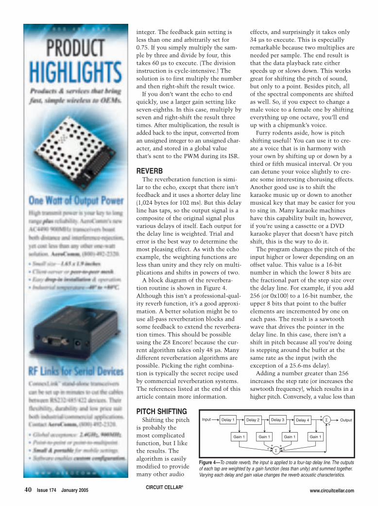
40 Issue 174 January 2005 CIRCUIT CELLAR®
www.circuitcellar.com
integer. The feedback gain setting isless than one and arbitrarily set for0.75. If you simply multiply the sam-ple by three and divide by four, thistakes 60 µs to execute. (The divisioninstruction is cycle-intensive.) Thesolution is to first multiply the numberand then right-shift the result twice.
If you don’t want the echo to endquickly, use a larger gain setting likeseven-eighths. In this case, multiply byseven and right-shift the result threetimes. After multiplication, the result isadded back to the input, converted froman unsigned integer to an unsigned char-acter, and stored in a global valuethat’s sent to the PWM during its ISR.
REVERBThe reverberation function is simi-
lar to the echo, except that there isn’tfeedback and it uses a shorter delay line(1,024 bytes for 102 ms). But this delayline has taps, so the output signal is acomposite of the original signal plusvarious delays of itself. Each output forthe delay line is weighted. Trial anderror is the best way to determine themost pleasing effect. As with the echoexample, the weighting functions areless than unity and they rely on multi-plications and shifts in powers of two.
A block diagram of the reverbera-tion routine is shown in Figure 4.Although this isn’t a professional-qual-ity reverb function, it’s a good approxi-mation. A better solution might be touse all-pass reverberation blocks andsome feedback to extend the reverbera-tion times. This should be possibleusing the Z8 Encore! because the cur-rent algorithm takes only 48 µs. Manydifferent reverberation algorithms arepossible. Picking the right combina-tion is typically the secret recipe usedby commercial reverberation systems.The references listed at the end of thisarticle contain more information.
PITCH SHIFTINGShifting the pitch
is probably themost complicatedfunction, but I likethe results. Thealgorithm is easilymodified to providemany other audio
effects, and surprisingly it takes only34 µs to execute. This is especiallyremarkable because two multiplies areneeded per sample. The end result isthat the data playback rate eitherspeeds up or slows down. This worksgreat for shifting the pitch of sound,but only to a point. Besides pitch, allof the spectral components are shiftedas well. So, if you expect to change amale voice to a female one by shiftingeverything up one octave, you’ll endup with a chipmunk’s voice.
Furry rodents aside, how is pitchshifting useful? You can use it to cre-ate a voice that is in harmony withyour own by shifting up or down by athird or fifth musical interval. Or youcan detune your voice slightly to cre-ate some interesting chorusing effects.Another good use is to shift thekaraoke music up or down to anothermusical key that may be easier for youto sing in. Many karaoke machineshave this capability built in; however,if you’re using a cassette or a DVDkaraoke player that doesn’t have pitchshift, this is the way to do it.
The program changes the pitch of theinput higher or lower depending on anoffset value. This value is a 16-bitnumber in which the lower 8 bits arethe fractional part of the step size overthe delay line. For example, if you add256 (or 0x100) to a 16-bit number, theupper 8 bits that point to the bufferelements are incremented by one oneach pass. The result is a sawtoothwave that drives the pointer in thedelay line. In this case, there isn’t ashift in pitch because all you’re doingis stepping around the buffer at thesame rate as the input (with theexception of a 25.6-ms delay).
Adding a number greater than 256increases the step rate (or increases thesawtooth frequency), which results in ahigher pitch. Conversely, a value less than
ΣDelay 1 Delay 2 Delay 3 Delay 4
Gain 1
Input Output
Gain 1 Gain 1 Gain 1
Σ++ +
+
+
+
Figure 4—To create reverb, the input is applied to a four-tap delay line. The outputsof each tap are weighted by a gain function (less than unity) and summed together.Varying each delay and gain value changes the reverb acoustic characteristics.

www.circuitcellar.com CIRCUIT CELLAR®Issue 174 January 2005 43
256 slows the stepping rate and results ina lower pitch. It’s simple enough, exceptfor one problem: distortion in the form ofclicks and pops are produced wheneverthe delay pointer passes the input signalpointer. This happens because the delaypointer moves at a faster or slower ratethan the input pointer and causes themto overlap (see Figure 5). In this case,when the pointer passes the end of theinput buffer, an abrupt change in thewaveform occurs that produces a notice-able audible discontinuity.
The solution is to use two circularbuffer delay lines that are 180° out ofphase (see Figures 6a and 6b). Eachsample in the delay line is multipliedby a weighting function that acts as across fader. The weighting function is atriangle wave stored in a 256-elementarray. The peak of the triangle wave isat the center going to zero at eitherend. Then when you add the tworesults together, the result is a cleanwaveform (see Figures 6c–6e).
INTERESTING EFFECTS The basic structure of the pitch
change routine can be modified to pro-duce a variety of audio effects. For exam-ple, if you slowly modulate the sawtoothwith a sine wave, you can generate avibrato effect. Using a random modula-tion gives you a chorus effect. Takingseveral simultaneous shifts and addingthem together gives you a harmonizer. Ifthe several shifts are close to 256, youcan get an interesting flanging effect.
I’ve spent many hours playing around.
It’s amazing how many cooleffects you can achieve.
IMPROVEMENTSUp until now, all samples,
both input and output, werelimited to 8 bits sampled at10 kHz. Higher quality audiocan be achieved by increasingthe sample rate and by using10-bit samples. The firstmethod is the easiest toaccomplish, but make sure thesoftware can keep up. If you goto a 20-kHz sample rate, thisshortens the amount of timeyou can process each individ-ual sample from 100 to 50 µs.Increasing the sample size
requires twice the storage, but there isenough SRAM to do the job. The issuemay be in the pitch changing routine,because now the circular buffers aredoubled in size, from 256 to 512 bytes,which requires a 16-bit pointer insteadof an 8-bit pointer, which can doublethe amount of processing time. Finally,you need to alter the output routine todrive two PWM channels as describerearlier in this article. I
Editor’s note: This project won SecondPrize in the 2003 Flash for Cash Z8Encore! International Design Contest.
SOURCESTS972 Op-ampSTMicroelectronicswww.st.com
TA2011S Microphone amplifierToshibawww.semicon.toshiba.co.jp
Xtools ZDS II IDE and Z8 Encore!evaluation boardZilogwww.zilog.com
PROJECT FILESTo download the code and MP3 audiosamples, go to ftp.circuitcellar.com/pub/Circuit_Cellar/2005/174.
REFERENCE[1] “Karaoke,” www.bbc.co.uk/dna/h2g2/alabaster/A139484.OURCESH. Chamberlin, Musical Applications ofMicroprocessors, Hayden Book Co., 1985.
Figure 6a—Take a look at the contents of the circular audiobuffer.The values at the beginning and end are not thesame, which is usually the case. b—This is the result ofsampling the circular buffer at a faster or slower rate. Notethe discontinuity at the center when the pointer passes theend of the buffer. Buffer A (c) and buffer B (d) are 180° outof phase and multiplied by a triangle wave. Both buffers aresampled by the sawtooth function and added together toproduce an output waveform (e). Note the absence of thediscontinuity.The plots were generated in a spreadsheet.
a) b)
c)
d)
e)
Brad Stewart is an independent engi-neering consultant who specializes inmixed signal, embedded processor, andRF design. He graduated from theUniversity of California at SantaBarbara in 1977 with a degree in electri-cal engineering. Brad holds a number ofpatents and is currently developing wire-less speakers and automotive electron-ics. He likes to build electronic gadgetsand ride his Harley-Davidson. You maycontact Brad at [email protected].
Σ
Pointer stepsize (sawtooth)
Input
Delay line #1
Delay line #2(180° out of phasewith delay line #1)
Cross fadefunction
(triangle wave)
Center tap
Output
Center tap
Figure 5—To do pitch-shifting, the input is applied to two 26-ms delaylines that are 180° out of phase from each other. A sawtooth-drivenpointer to both delay lines changes the sample rate by either over-sam-pling or under-sampling the data.The center tap (delay midpoint) of bothdelay lines are multiplied by the cross-fade function (triangle wave) andsummed together.This effectively removes the sampling discontinuities.The end result is sent to the analog summer, which also accepts the raw,unprocessed analog signal to provide special effects like harmony.

44 Issue 174 January 2005 CIRCUIT CELLAR® www.circuitcellar.com
steering RC cars simplified the designprocess because mimicking digital sig-nals is simpler than mimicking analogproportional signals.
We inspected three RC transmitters:a mini RC we found at a mall kiosk, afull-size Spy Kids RC transmitter fromRadio Shack, and a ZipZap mini RCtransmitter from Radio Shack. For allof these simple digital (nonproportion-al control) transmitters, changing con-trol surfaces/buttons mechanically
If you’ve read past the title ofthis article, then you probablylike playing with RC cars andthink controlling one with aPC sounds intriguing. Not onlywill we show you how to dothis, we’ll also teach you someinteresting things about RCtransmitters, PC parallel ports,USB devices, and object-orient-ed software design.
With an off-the-shelf RC carwith nonproportional steering,some elementary electronics,and a good software design,you too can chase your petsaround the house with an RC car fea-turing a live video feed. To get to thatpoint, though, you’ll have to make afew important stops. First, you mustreverse engineer the RC transmitter.Second, you need to modify the trans-mitter so you can control it from aPC. Finally, you have to write the soft-ware that runs the system using a lotof borrowed parts and a few gooddesign ideas. After that, it’s just fun,fun, fun until your significant othertakes the batteries away.
REVERSE ENGINEERINGThe first phase of the design process
involves reverse engineering the RCtransmitter. The basic premise is thateach press of a button on the trans-mitter is a simple (digital) signal tothe electronics inside the transmitter.After looking at the circuit, we want-ed to add components that wouldallow us to fool the transmitter intothinking that the same buttons werepressed even though software controlsthe presses. Choosing nonproportional
grounded certain control linesof the main IC in the transmit-ter. Table 1 displays a few dif-ferent results for our RC trans-mitters. The Spy Kids van useda 16-pin transmitter chip, whilethe two micro cars had 14-pintransmitter chips. Photo 1shows the backside of theZipZap transmitter. The redlines show the traces from thebuttons to the transmitter chip.
INTERFACE TO THE PC Replacing a mechanical
switch with an electronic onecan be complicated. For example, asubtle time-varying signal can passthrough the switch to some other partof the electronics that has detailedrequirements pertaining to voltageand current. This is true for some pro-portional steering control transmit-ters, which is why we didn’t fool withthem. In our case, movement of thecontrol surfaces only caused certainlines to go from a floating (disconnect-ed) state to a grounded state. There aremany ways to do this electronically,but we’ll describe how to do thisthrough the PC parallel and USBports.
PARALLEL & USB PORTS The parallel port represents the sim-
plest and cheapest solution to the PCcontrol problem, but it isn’t the bestoption for three reasons: PCs runningWindows NT or later versions requirespecial drivers to access the parallelport; newer PCs, especially laptops,might not have a parallel port; andwriting to the parallel port causes a
FEATURE ARTICLE by Warren MacEvoy & Dan Stadelman
Warren and Dan recently reverse engineered an RC transmitter, connected the transmitterto a PC, and wrote control software. The result is a platform from which you can build andcontrol everything from simple RC car designs to complex artificial intelligence systems.
PC-Controlled RC Device
Photo 1—Follow the traces from the buttons to thetransmitter chip.The solid lines follow the traces across thefront of the board and the dotted lines represent wherethere are jumper wires on the opposite side of the board.
Action
Pins grounded
Radio Shack Spy Kids van(16-pin transmitter chip)
Radio Shack ZipZaps andFitRacer Micro RC(14-pin transmitter chip)
Turbo 6 and 3 Not Available
Forward 5 and 3 5
Reverse 4 and 3 4
Left 1 and 3 1
Right 16 and 3 14
Table 1—Take a look at the results of reverse engineering three different typesof RC car transmitters.The car with a turbo function has a 16-pin transmitter chipand utilizes an ENABLE pin.The smaller RC cars use a 14-pin transmitter chip.

www.circuitcellar.com CIRCUIT CELLAR® Issue 174 January 2005 45
“bus wait” state that slows your PCconsiderably when the parallel port isactive. Still, tying the lines of the par-allel ports through resistor/NPN tran-sistor pairs is sufficient for bit-bangcontrol of the transmitter. The NPNtransistors are necessary to make abuffer between the transmitter andthe PC to protect the latter’s expen-sive electronics.
The USB route is more expensive toimplement in terms of hardware andsoftware. Our solution, however, isreasonably inexpensive on bothaccounts. We used Igor Cesko’sIgorPlug, which is a software imple-mentation (including drivers) of USB1.2 using an Atmel AVR that allowsbit banging on some of its output pinsand even a simple RS-232 interface.Note that the cost of this solution isless than $10.
There are two variants of the IgorPlug.The one we used is based on theATmega8 (clocked at 12 MHz) and it
provides a TTL RS-232 port and 15 digi-tal I/O lines, which far exceed ourneeds. The other version is based on thesmaller AT90S2313 and slightly over-clocks the microcontroller (12 MHzinstead of 10 MHz). Both work fine, butwe chose the ATmega8 in the endbecause over-clocking wasn’t required.
We didn’t have to modify the driversand firmware to interface to the RCcar. We simply tied digital I/O lineson the ATmega8 to the control linesof the RC transmitter. We used theUSB driver to switch the I/O statesfrom input/high impedance to out-put/low to mimic the operation of thecontrol surfaces. Unlike the parallelport interface, the only part at riskwas the ATmega8 microcontroller, sowe saw no need to protect the controllines with transistors. Figure 1 showsIgorPlug with the ATmega8. Photo 2ashows the IgorPlug installed in atransmitter. Photo 2b shows the finalUSB-controlled RC car.
RC CONTROLLER SOFTWAREHardware without software serves
as little purpose as software withoutthe hardware to make it useful. Likeour hardware design, we chose asmany off-the-shelf components as pos-sible. Unlike hardware, softwaredesign usually starts with a decisionabout the objects. Note that theobjects are based on the physical andlogical components that make up thesoftware system.
The physical components includethe user interface (mouse, keyboard,and display) and the hardware inter-face (USB drivers and device-specificinterfaces). The logical componentsare built with Trolltech’s Qt toolkit(portable graphical user interface) andDirectX SDK (video camera feedback).The DirectIO and IgorPlug drivers arefor the parallel port and USB hardwareinterfaces. Let’s take a closer look atwhy we chose these components.
Trolltech’s Qt toolkit is a well-designed object-oriented and cross-platform widget set for designing niceGUIs. Our application required win-dows-specific components, so thecross-platform features didn’t matter;nevertheless, it still provides a con-venient way to make a clean and fastuser interface.
Unfortunately the Qt toolkit doesnot provide a cross-platform means toaccess video devices. We wanted videofeedback. Fortunately, Larry PaulRodgers was nice enough to providesome classes to use the DirectDraw
Figure 1—You can use the unused pins as I/O pins if your R/C car requires more than five inputs.
a) b)
Photo 2a—Take a look at how we installed IgorPlug in the FitRacer RC transmitter.You can clearly see the USB cable coming in from the bottom. A smaller Atmel part would fitbetter. b—The finished product! Just plug the USB cable into your laptop and start driving!

46 Issue 174 January 2005 CIRCUIT CELLAR® www.circuitcellar.com
component of the DirectX SDK frominside a Qt-based application. Youmay download Larry Paul’s code fromthe Circuit Cellar ftp site.
Because of the (useful) securitymodel of Windows NT, 2000, and XP,the operating system will not allowprograms to simply access the parallelport. The DirectIO driver (www.direc-tio.com) allows old-style outb() andinb() code to work for programs yougive permission to. This is a great wayto support legacy programs on neweroperating systems. Without it, youwould need to write a driver for yourspecific functionality.
We chose the IgorPlug because thefirmware and drivers are free and thehardware is inexpensive. IgorPlug canbit-bang anything, so we can use itwithout having to modify thefirmware and drivers.
We bolted these components togeth-er with C++. Each box in Figure 2 (seepage 46) represents a kind of object inthe system. For example, QtCarUI hasaccess to a CarHI (car hardware inter-face) and is a kind of QPushButton.The major parts are based on theQtCarUI and CarHI objects.
QTCARUIThe QtCarUI object is responsible
for translating your actions intoactions the car hardware interfaceunderstands. Because the QtCarUI is
a type of QPushButton object,QtCarUI gets a key press event fromthe operating system and then manip-ulates the hardware interface in someway. Listing 1 shows how a keyevent is first handled in theQtCarUI::keyEvent() method.First, the function analyzes the keyevent with a switch statement and thensets the Boolean value for the correctcontrol. For example, if the down keyinitiates the key event, the keyDownvariable is set to “pressed” (true).
Next, the code in Listing 2 is exe-cuted. After a button new button ispressed, the user interface has a newstate to send to the hardware inter-face. What is a state? A state is simplya set of conditions for that particularobject. For example, if you press theUp and Right buttons, that’s the stateof the user interface.
The code in Listing 2 simply looksat the current state of the user inter-face and then sets the state in thehardware interface. Note that thehardware interface doesn’t write tothe device yet. After the correct state
is set in the hardware interface object,the config() method writes the newhardware state to the device. Thebasic control scheme we set up allowsyou to use the arrow keys to controlthe RC car, activate turbo power withthe Shift key, and stop everythingwith the space key.
LIVE VIDEO INTERFACEQt doesn’t give you a web camera
interface for free. We wanted videofeedback available in our system. Thetwo pieces that need to be pluggedtogether for this to work are theDirectShow components in theWindows DirectX framework and theQt widget framework.
Thankfully, Larry Paul Rodgers didthis work for us. (You’ve heard the“off-the-shelf” line enough by now,right?) His code makes adding video toa Qt application as hard as adding twovisual components to your design: aPickDeviceBox, which allows you toselect the video source, and a camera,which presents the video feed to theuser. Larry Paul’s source code is public
Listing 1—The key event handler takes care of all events coming into the software controller. After a key ispressed, it sets the Boolean variable for that control.
// Ignore auto-repeat key events...if (e->isAutoRepeat()) return;
switch(e->key()) default: return;case Qt::Key_Space: keySpace = pressed; break;case Qt::Key_Left: keyLeft=pressed; break;case Qt::Key_Right: keyRight=pressed; break;case Qt::Key_Up: keyUp=pressed; break;case Qt::Key_Down: keyDown=pressed; break;case Qt::Key_Shift: keyShift=pressed; break;
QPushButton
+ keyPressEvent()+ keyRelease Event()
QtCarUI
+ keyUp : int+ keyDown : int+ keyLeft : int+ keyRight : int+ keyShift : int+ hi : int
CarHI
+ config()+ left()+ right()+ center()+ reverse ()+ stop()+ forward()+ tubro()
+ keyEvent()
USBMircoCarHI
+ igorio : int+ mask : int+ port : int
PPCarHI
+ mask : int+ port : int
Figure 2—The UML diagram shows how the objects inthe software are related to each other. New objects canbe derived from the CarHI object to add support forother hardware interfaces.
Listing 2—After checking each Boolean control value, the correct function will be called in the hardwarehandler.
hi->reset();if (!keySpace)
if (keyUp && !keyDown) if (keyShift) hi->turbo();
else hi->forward();
else if (!keyUp && keyDown) hi->reverse();
if (keyLeft && !keyRight) hi->left();else if (!keyLeft && keyRight) hi->right();
hi->config();

48 Issue 174 January 2005 CIRCUIT CELLAR® www.circuitcellar.com
domain. Thanks Larry!
HARDWARE INTERFACESWhy is there separation between the
user interface and the hardware inter-face? It seems like a waste of effort,but it’s what gives the design the abil-ity to add any new RC car hardwarewithout touching any of the userinterface code. It also allows you tohave an easier time writing the hard-ware interfaces by logically separatingthe two steps, user input and deviceoutput. You don’t have to worry at allabout the user interface when writingthe code to control a new hardwareinterface.
In software engineering terminolo-gy, CarHI represents an abstract class,meaning that other (more specific)classes will give the details of howeverything gets done. For example, thedetails of how CarHI.config()works is up to the specific car hard-ware interface classes.
The three specific hardware inter-faces we created are PPCarHI,PPMicroCarHI, and USBMicroCar.Because we made the cars from theCarHI abstract class, the user inter-face QtCarUI does not care how thosehardware interfaces are actuallyimplemented. What does this mean?This allows you to make new hard-ware interfaces without modifying thecore user interface. Now you canmake a new RC car controlled by theserial port, or even a network card,and still use the same basic user inter-face as long as the new hardware
interface code is based on the CarHIabstract class.
PPCARHIThe first step in writing the parallel
port hardware interface involves gain-ing access to the parallel port. It’s aroyal pain if you’re using WindowsNT, 2000, or XP because the operatingsystem won’t allow for direct accessto the parallel port. You have to use aset of system calls to gain access. Weused DirectIO to get around this prob-lem. It adds a widget to the controlpanel and allows for the selection ofapplications that can use the raw port
writes. Just enable your program touse the port with the 0x378 address—which is the standard port address forthe parallel port—and, like magic, theoperating system will allow your pro-gram direct use of the port. If you’rerunning an old dog Windows 9x oper-ating system, you don’t have to worryabout setting up DirectIO because youget direct port access without all thosespecial system calls.
All the functions in the parallel porthardware interface, with the exceptionof the config() function, are devotedto preparing the bit mask to send tothe parallel port (see Listing 3). Only
Listing 3—The world of software meets the world of hardware at the hardware interface for the parallel portcar. It’s important to note the similarities to Listing 4.
class PPCarHI : public CarHIpublic:
short port;unsigned mask;CarUI *ui;
PPCarHI(int _port=PORT_DEFAULT) port=_port; mask=0; ui=NULL;
~PPCarHI() reset(); config();
virtual void config() int temp = mask;if (temp) temp |= PORT_ENABLE;temp ^= PORT_XOR;out8(port,temp);
virtual void reset() mask = 0;
virtual void left()
mask = ( mask & ~LRC_MASK ) | LRC_LEFT;virtual void right()
mask = ( mask & ~LRC_MASK ) | LRC_RIGHT;virtual void center()
mask = ( mask & ~LRC_MASK );virtual void reverse()
mask = ( mask & ~FRS_MASK ) | FRS_REVERSE;virtual void stop()
mask = ( mask & ~FRS_MASK );virtual void forward()
mask = ( mask & ~FRS_MASK ) | FRS_FORWARD;virtual void turbo()
mask = ( mask & ~FRS_MASK ) | FRS_TURBO;
;
Photo 3—You can drive the car by clicking on the col-ored box in the middle. The car’s inputs are saved inthe white box. The web camera display, if used, isshown in the black box.

DLL and initializing the device. Don’tworry about using DirectIO if you areusing the USB hardware interface.
FINAL INTERFACEThe sample application’s final output
is shown in Photo 3 (see page 48). Themulticolored square is used for control-ling the car with the mouse. A log ofthe RC car’s inputs is recorded in thetext box on the right. You can modifyand playback the inputs to the RC car.If you installed a web camera (or videocapture card), pressing the play buttonwill place the video feed in the blackbox. It’s a lot of fun to place a wirelesscamera on the top of a large vehicle ora camera over where you are going torace your micro RC car.
www.circuitcellar.com CIRCUIT CELLAR®Issue 174 January 2005 51
the config() function does the actu-al writing to the device. This creates adouble buffering effect similar to thedouble buffering used when workingwith graphics animation. The nextstate is completely formed before youplace it on the device.
USBMICROCARHIThe USB hardware interface is sim-
ilar to the PPCarHI (see Listing 4).We don’t need to worry about theturbo function because the micro RCcar doesn’t have a turbo function.USBMicroCarHI makes use of theigorio object to talk to the IgorPlugdevice. The igorio.h file posted on theCircuit Cellar ftp site contains the nec-essary code for linking to the IgorPlug
Warren MacEvoy teaches at MesaState College in Colorado. He holds aPh.D. in applied mathematics fromthe University of Arizona. Warren’stechnical interests include securityand embedded systems. When he isnot working, he enjoys being a father,canoeing, and playing video games.You may contact Warren at [email protected].
PROJECT FILESTo download the code, go to ftp.circuitcellar.com/pub/Circuit_Cellar/2005/174.
SOURCESATmega8 MicrocontrollerAtmelwww.atmel.com
IgorPlug firmware and driversIgor Ceskowww.cesko.host.sk/IgorPlugUSB_RS232/IgorPlug-USB%20(AVR)%20RS232_eng.htm
ZipZapsRadioShackwww.radioshack.com
Qt toolkitTrolltech, Inc.www.trolltech.com
Dan Stadelman is a student at MesaState College in Colorado and a codemonkey for Pacific NorthwestNational Laboratory. You may reachhim at [email protected].
Listing 4—The hardware interface for the USB micro car isn’t that much different from the parallel port carinterface in Listing 3, but it uses completely different hardware.
#include "igorio.h"
class USBMicroCarHI : public CarHI private:igorio myDev;UCHAR mask;
public:USBMicroCarHI()
myDev.DoSetOutDataPorts(0x3C, 0x03, 0xFB, 0x02);mask = 0;config();
virtual void config() myDev.DoSetDataPortDirections(0x00, (mask << 2), 0x00, 0x02);
virtual void reset() mask = 0;
virtual void left()
mask = ((mask | 0x4) & 0x7);virtual void right()
mask = ((mask | 0x8) & 0xB);virtual void center()
mask = (mask & 0x3);virtual void reverse()
mask = ((mask | 0x1) & 0xD);virtual void stop()
mask = (mask & 0xC);virtual void forward()
mask = ((mask | 0x2) & 0xE);virtual void turbo()
forward();
;
PROJECT APPLICATIONReverse engineering an RC car
transmitter, connecting the transmit-ter to the PC, and then writing con-trol software for the PC results in aninteresting new device. You can makean entire afternoon of chasing yourdogs and cats around your house.Now you can also build your ownIgorPlugs to add USB connectivity toyour projects.
Where else can you go from here?The PC-controlled RC car provides aperfect platform to approach someextremely hard artificial intelligenceproblems. Come to think of it, youcould make your own Martian Rover!We’ll save that for next time. I

52 Issue 174 January 2005 CIRCUIT CELLAR® www.circuitcellar.com
advantages to using the ADuC812 fora signal-processing project. The on-chip user-programmable flash memoryis one example. Another plus is that8052-based microcontrollers are easyto use. A large amount of informationabout programming with an 8052 isavailable if you need it (at sites likewww.8052.com).
If you’re planning on doing somesignal processing work, you also mustkeep in mind that there are some dis-advantages to using the ADuC812. Forinstance, the ADuC812 processes onlyapproximately 1 million instructionsper second. (It actually processessomewhat less than 1 million instruc-tions per second.) Other disadvantagesinclude the ADuC812’s 8-bit wordlength and the lack of hardware sup-port for arithmetic on signed or float-ing-point numbers. Finally, note thatthe ADuC812’s specialized registers(the accumulator in particular) forceyou to move data around more thanotherwise would be necessary.
The 8052 is a slightly modified 8051microcontroller. Although introducedby Intel in 1980, the 8051 and its deriva-tives are popular today. The 8052 is aninexpensive microprocessor. If you don’tneed the extra power a DSP provides,you may be better off with a smallchip. Debugging code is often easierwhen using a relatively simple chip.
Our system allows you to design adigital filter and download the filtercoefficients to the ADuC812 wherethey are stored in the user-program-mable flash memory. After storing thefilter coefficients, you can take the
When it comes to signal process-ing, you often think, “time for a digi-tal signal processor (DSP) chip.” Built toprocess signals, a DSP is generally aheavy-duty processor with special fea-tures like a multiply accumulator(MAC) and perhaps addressing modessuited for computing a fast Fourier trans-form (FFT). These features are designedto help you perform the calculations sig-nal processing often calls for. The chipsare extremely useful, but they’re oftenhard to figure out, and you rarely end upfeeling as though you understand all ofthe microprocessor’s quirks. In addition,many DSPs are peripheral-poor. In orderto use them in signal processing applica-tions, you must add external peripherals.
On the other hand, microprocessorslike the 8052 are simple to use andrelatively easy to understand eventhough they aren’t too powerful. Wedecided to use Analog Devices’sADuC812, which is a chip with an8052 core, for signal processing.Although the ADuC812 is an 8052 atheart, it’s peripheral-rich. If you’re adesigner who would like to use theADuC812 for signal processing, the twomost important non-8052 peripherals arethe eight-channel, 12-bit A/D converterand the two D/A converters provided bythe chip. The ADuC812 has 8 KB ofbuilt-in flash programmable programmemory. In addition, we made gooduse of the 640 bytes of on-board user-programmable flash data memory.
ADUC812In addition to the on-chip A/D and
D/A converters, there are several
board wherever you need the filter anduse it. The system makes it easy toget familiar with working digital fil-ters. If you’re uncomfortable with the-ories until you have seen them appliedto the real world, and if digital filtersare things you have only heard about,read about, and studied, then this proj-ect is for you.
DIGITAL FILTERING BASICSWhen using a microprocessor to fil-
ter signals, you generally assume thatthe microprocessor receives data everyTS seconds from an A/D converter.The microprocessor processes thedata, and then outputs the filteredvalue to a D/A converter.
Let’s call the current sample themicroprocessor receives xi. Earliersamples are denoted by xi – 1 , xi – 2 , etc..After processing the input, the micro-processor produces output referred toas yi by solving an equation like thefollowing:
[1]
Equation 1 defines the filtering opera-tion performed by the digital filter.
Each sample period, the micro-processor takes in a new xi and out-puts a new yi. Because the formula weused to implement the digital filter issimple, you don’t need a talentedmicroprocessor to process the signal.However, because the time betweensamples (TS) is small, you need a rea-sonably fast microprocessor. We wantedto see how good of a system we coulddevelop with a microprocessor that’s
FEATURE ARTICLE by Shlomo Engelberg, Jonathan Garzon, & Naor Afgin
Signal Processing with the ADuC812 Digital signal processor chips can be hard to understand.They also tend to be peripheral-poor, so if you want to use one in a signal processing application, you have to add peripher-als. Shlomo, Jonathan, and Naor have an alternative: signal processing with a peripheral-rich ADuC812 microconverter.

neither brilliant nor particularly fast. There are two basic types of digital
filters: finite impulse response (FIR)and infinite impulse response (IIR).The former are characterized by thefact that all the bi in Equation 1 arezero. When this condition isn’t met,you have an IIR filter.
Let’s stop for a moment to focus onterminology. The impulse response isa filter’s output of the filter when theinput is the impulse sequence:
[2]
If all the bi variables are zero, theresponse to the impulse sequenceends after NTs seconds. If there arenonzero bi variables, the response ofthe filter may continue foreverbecause the filter processes previousvalues of its own output as well ascurrent and previous values of itsinput. In the first instance, theimpulse response is finite. The filterresponse is infinite in the second case.
In applications, FIR filters have theadvantage of nice phase responses. IIRfilters, on the other hand, generallygive the magnitude response that youwant with far fewer coefficients.
SIGNAL PROCESSING & MATLABThe theory of filter design is well
established. All of the design workcan be done by hand—and that’s howthe work was done in the good olddays. Nowadays, the technical work isautomated if you have access to MAT-LAB and its signal processing and fil-ter design toolboxes.
Moreover, the MATLAB GUIDE,which is a GUI development environ-ment, allows you to design a pleasantfront-end for the program that auto-mates the filter design. We used theMATLAB tools to develop an easy-to-use filter design and download tool.
ADUC812 SIGNAL PROCESSING In addition to the generic filter
design problem, you must deal withthe constraints the machine places onyou in order to implement a filter onit. We used the convenient but none-too-powerful ADuC812. On the onehand, we made good use of its on-board D/A and A/D converters. On
x = 1 i = 00 i 0
i ≠
www.circuitcellar.com CIRCUIT CELLAR®Issue 174 January 2005 53
the other hand, we had to sweat a bitto deal with the fact that the 8052 andits derivatives are best suited for workwith short unsigned integers.
When working with filters, you can-not really limit your filter coefficientsto 8-bit positive numbers. In particu-lar, it’s easy to show that if youdesign an FIR filter with positive coef-ficients, the filter will have its maxi-mum output when the input is con-stant. To see this, consider Equation1. When the bi variables are all zero,the output at any time will be a linearcombination of the input values. If theai variables are all positive, take theinput always to be equal to its maxi-mum possible value in order to get thelargest possible output when the inputis limited in voltage. That is, to getthe maximum possible output take aDC input. This is a fairly reasonabledefinition of a low-pass filter.
In order to have the freedom toimplement an FIR filter that isn’t low-pass, you must be able to use negativenumbers. Luckily, we didn’t have towrite all the code for handling nega-tive numbers. A set of math routinesprovided by W.G. Marshall atwww.8052.com has code for doingtwo’s complement arithmetic withthe 8052.
In our program all coefficients arestored as 16-bit, fixed-point numbers.If the filter coefficients that MATLABgenerates use more than 16 bits, wemust round the coefficients. Roundingthe coefficients changes the filter’s
characteristics, so we allow you toview the properties of the filter with aquantized coefficient. In this way ifthe quantized filter is unacceptable,you can redesign the filter.
Finally, we deal with the fact thatthe on-board A/D and D/A convertersare designed to deal with positive volt-ages only by using the op-amp circuitsin Figure 1. These circuits shift theinput voltage level up and the outputvoltage level down by half the maxi-mum allowable voltage. The programfor the ADuC812 also has severallines of code that shift the input tocenter on zero and shift the outputvalues to center on half the maximumallowable voltage.
HOW FAST CAN YOU RUN?At this point it’s clear that there’s
no fundamental difficulty in using anADuC812 to implement a digital filter. Infact, the on-board A/D and D/A convert-ers make it easy. Speed is the problem.
An 11.0592-MHz crystal is on theEVAL-ADUC812QS. The machineclock, which controls the speed withwhich instructions are executed, runsat one-twelfth the crystal speed.Therefore, the machine clock is lessthan 1 MHz. The ADuC812 generallyrequires one or two machine clockperiods to execute an instruction, soyou can’t even execute 1 MIPS on theADuC812.
We found that if we wanted reason-able filters, we had to compromise onspeed. Because of all the arithmetic
Figure 1—Take a look at the level-shifting circuitry. All of the op-amps are 741 op-amps. Note that VREFIN = 2.5 V. Thepower supply voltage is ±15 V.

54 Issue 174 January 2005 CIRCUIT CELLAR® www.circuitcellar.com
operations needed to implement a dig-ital filter, we couldn’t handle toomany samples per second. The mosttime-consuming operation in the8051’s repertoire is the multiplicationoperation. Multiplication takes fourmachine cycles. We couldn’t avoidexecuting numerous multiplications.
We could not process more than500 samples per second. The Nyquistsampling theorem states that in orderto reconstruct a signal from its sam-ples, the sampling frequency must bemore than twice the highest frequen-cy in the signal. Therefore, our filterswill not work properly with input fre-quencies that are greater than or equalto 250 Hz. By changing processors to adifferent 8051-family chip, you shouldbe able to extend the frequency rangeto the 25-kHz range. Roughly speak-ing, this is the range of audio signals,so you can use an enhanced 8052 todo real audio signal processing.
When implementing FIR filters, wehave MATLAB check the coefficients ofthe FIR filters it designs. If all the filtercoefficients in an FIR filter are positive,the program knows not to use two’scomplement arithmetic. Not usingthe complicated two’s complement rou-tines allows you to use more coeffi-cients in the filter’s implementationand, in this way, design a filter whoseperformance is more nearly optimal.
COMPONENTSTo use the system, you need the
ADuC812 evaluation board and MAT-LAB. (We wrote the MATLAB codewith MATLAB 6.5.0 release 13.) Visitwww.analog.com for more informationabout the board. Go to the Microcon-verter Products sub-tab in the DataConverter tab. On the microconverterpage, click on QuickStart Developmentin the Technical Support Resourcessections.
You must build the circuit in Figure 1before using the system. The circuitconnects to the evaluation kit at threepoints. The output of U1 is connectedto channel 0 on the A/D converter.(This leads out to pin 1 on analog I/Oconnector J1.) The noninverting inputon U2 is connected to VREFIN, which isled out to pin 21 of J1. Finally, thenoninverting input on U4 is connect-
ed to channel 0 of the D/A converter,which is available at pin 17 of J1. Theinput to the system is applied by thesignal generator to the 100-kΩ resistorconnected to pin 3 on U1. The voltageapplied to the resistor must be in thefollowing range:
± VREFIN = ±1.25 V [3]
After you download the softwarefiles from the Circuit Cellar ftp site,download the filter.hex file to theADuC812 using the Windows serialdownloader (WSD) program providedwith the evaluation board.Downloading seems to work bestwhen the evaluation board’s UART isconnected to COM1. Leaving theboard connected to COM1, openMATLAB and set its path to the direc-tory in which all the files have beensaved. Type pro_menu to open the fil-ter design window.
Things are self-explanatory fromthis point on. You can design filterseither by specifying the frequencies ofinterest, the amount of ripple you’rewilling to tolerate, and so on, or byspecifying the filter coefficients. Thewindows opened by the filter designprogram provide help.
USING THE SYSTEMRather than providing a detailed
explanation of all the differentoptions, let’s consider an example.Suppose that you would like to designa filter that filters all frequenciesgreater than 50 Hz. After typingpro_menu in the MATLAB commandwindow, the window in Photo 1appears. Next, click on the Filter tab.You get three choices: IIR, FIR, andcoefficients. If you take the first,you’ll have a choice of possible filters.If you take the second, you mustdecide whether your filter will be low-pass, high-pass, band-pass, or band-stop. Finally, if you choose the coeffi-cients option, the program will open awindow so you can input filter coeffi-cients directly.
Let’s focus on the process of design-ing an IIR low-pass filter. Becauseyour maximum frequency is 250 Hz,let’s design a filter with a 50-Hz cut-off frequency.

to work at higher frequencies. Cygnal’sC8051Fxxx family looks interesting.These microcontrollers, which canrun at speeds of up to 100 MIPS, haveon-board D/A and A/D converters.Plus, development kits for them areinexpensive. It ought to be possible touse our programs with these micro-controllers too. The MATLAB-basedfilter design software shouldn’t requirechanging. The assembly language pro-grams for the ADuC812 should notrequire too many changes either.
8051 VERSATILITYWe’ve presented a set of programs
for MATLAB and the ADuC812 thatwill enable you to design and imple-ment digital filters. We limited the fil-ters to low-frequency applications. Thesuite of programs, however, is an excel-lent way to experiment with digital fil-ters. We also described a way to handleaudio frequencies. As the years go by,the 8051 microcontroller family growsever larger and more versatile. I
www.circuitcellar.com CIRCUIT CELLAR®Issue 174 January 2005 55
First, click on the IIR tab and thenchoose to design an elliptic filter.After the IIR design window opens,set the design tool to produce a low-pass filter. Next, enter a cutoff fre-quency of 15 Hz, a filter order of four,band-pass ripple of 2 dB, and a stop-band that is 20 dB below the band-pass. After clicking on Plot (whichplots the magnitude of the frequencyresponse of the filter with MATLAB’soriginal coefficients) and QuantizationPlot (which plots the magnitude of thefrequency response of the filter withquantized coefficients), the windowshown in Photo 2 appears. Note that thecharacteristics of the filterwith quantized coefficients arenoticeably different from thoseof the filter with MATLAB’smore exact coefficients.
The filter design windowhas a tab that opens FVTool,which is MATLAB’s filtervisualization tool. FVToolallows you to examine a fil-ter in greater detail than thePlot button’s plot does.
GO FASTERSuppose you need a filter
that can handle signals thathave components that exceedthe 250 Hz that our programallows. Is there any way tocontinue using a simplemicrocontroller? The simpleanswer is yes.
Although we used theADuC812 to implement ourfilters, there are other micro-controllers that will allow you
Photo 1—As you study the filter design program’s mainscreen, note that “FIR” is pronounced “fear.”
Jonathan Garzon is working toward abachelor’s of technology and appliedscience at the Jerusalem College ofTechnology–Machon Lev. He enjoysprogramming and is interested inmicrocontrollers (the ADuC812 inparticular). In his free time, Jonathanenjoys sports, working with comput-ers, and reading. You may contacthim at [email protected].
Naor Afgin is an academic reservistin the Israeli Defense Force (IDF) cur-rently working toward a bachelor’s oftechnology and applied science at theJerusalem College of Technology–Machon Lev. His interests includemicrocontrollers (the ADuC812 inparticular) and programming. Naoralso enjoys working with computers,sports, and reading. You may contacthim at [email protected]. Shlomo Engelberg received his B.E.E.
degree in 1988 and his M.E.E. in 1990.He also holds an M.S. and Ph.D. inmathematics. Shlomo is a senior lec-turer in the electronics department at
PROJECT FILESTo download the code, go to ftp.circuitcellar.com/pub/Circuit_Cellar/2005/174.
RESOURCESRuss Hersch, “8051Microcontroller FAQ,” 1995,www.esacademy.com/automation/faq/8051/.
Richard G. Lyons,Understanding DigitalSignal Processing, Addison-Wesley Publishing Company,Reading, MA, 1997.
SOURCESADuC812 MicroconverterAnalog Deviceswww.analog.com
C8051Fxxx MCU familyCygnal Integrated Products(now Silicon Laboratories, Inc.)www.silabs.com
MATLAB 6.5.0 release 13MathWorkswww.mathworks.com
Photo 2—This is the program’s response after you click on the Quantization Plotbutton. Because we chose to implement a narrow-band filter, the original and quan-tized frequency responses are somewhat different—even to the unaided eye.
the Jerusalem College of Technology–Machon Lev. He is interested in signalprocessing and control theory. In hisspare time, Shlomo enjoys walkingand reading. You may contact him [email protected].

56 Issue 174 January 2005CIRCUIT CELLAR®
www.circuitcellar.com
power line voltage was 115-V RMS at60 Hz. The capacitor was 500 µF, andthe load was a 250-Ω resistor.
The green trace shows the AC powerline input voltage. The red trace showsthe current drawn by the full-wavebridge circuit in Figure 1. The bluetrace shows the voltage on the storagecapacitor. The power into the load inFigure 1 is about 100 W in this exam-ple. The orange traceshows the current thatwould be drawn by a pure-ly resistive 100-W loadconnected directly to thepower line.
Note that although theload that’s powered inFigure 1 is resistive, theload presented to thepower line is far from resis-tive. A 100-W resistive loadwould draw 870-mA RMSwith peak currents of only1.23 A. As you can see inFigure 2, the full-wavebridge draws peak currentsexceeding 10 A at thesame power level.
So, what’s the big deal?That’s a legitimate ques-
In this article I’ll describe newapproaches to controlling power factorcorrection and switching power sup-plies. The availability of low-cost, 16-bitmicrocontrollers with substantiallymore processing power than the previ-ous generation makes this possible.Replacing analog control electronicswith digital processing power allows forentirely new control schemes. As you’llsee, you can apply such techniques topower factor correction. Measuring thecurrent isn’t required when division andsquare root operations are available.
The examples I’ll describe feature aMicrochip dsPIC30F2010 microcon-troller. Although I assume that you’refamiliar with electronics and have abasic understanding of switching powersupplies, I’ll provide a brief introduc-tion to power factor correction.
POWER BASICS Traditional AC-to-DC power sup-
plies, both switching and linear, usual-ly start with a full-wave bridge feedinga large energy storage capacitor (seeFigure 1). The capacitor is fully chargedtwice per power line cycle at the peakof the full-wave-rectified sine wave. Aheavy pulse of current is drawn from thepower line just before each voltage peak.There’s no current at other times. Theload is powered from the stored energyin the capacitor between the powerline peaks. A sufficiently large capaci-tor maintains the load voltage con-stant to the level required by the load.
Figure 2 shows the various voltagesand currents resulting from a simula-tion of the circuit in Figure 1. The
tion. After all, full-wave bridges andAC power lines have been around for along time and the world hasn’t cometo a stop. Most new televisions,VCRs, and computers contain a full-wave bridge to make a DC voltagethat’s the input to one or more switch-ing power supplies. The switchingpower supplies then provide the regu-lated DC voltages used by the rest of thesystem. But this is also the problem.The recent proliferation of electronicequipment has increased the total powerdrawn from the power grid by full-wavebridge circuits. The problems caused bythese schemes have gone from being acuriosity to a significant enough prob-lem to get the attention of regulatoryagencies. (Regulations in the EuropeanUnion constrain how far load current
FEATURE ARTICLE by Olin Lathrop
Digitally Control Power Factor Correction
AC in
Load
Figure 1—DC power is provided to a load from the ACline. Even though the ultimate load is resistive, the loadpresented to the AC line is far from resistive. Power isdrawn in short spikes twice per power line cycle.
Looking for an affordable way to control switching power supplies and power factor correc-tion? Olin’s got the solution. Replacing analog control electronics with digital processingpower creates the possibility for new control schemes. For instance, you can use a digitalprocessor to implement new algorithms like the PFC algorithm Olin describes in this article.
160150140130120110100908070
60
0 2 4 6 8 10 12 14 16 18 20 22 24 26 28 30 32Milliseconds
-160-150-140-130-120-110-100-90-80-70-60-50-40-30-20-10
01020304050
ACIN (V)ACIN (0.1 A)Cap (V)100W (0.1 A)
Figure 2—The AC line current for the circuit in Figure 1 (red) is drawn inshort spikes twice per power line cycle. Compare this to the orange trace,which is the current that a purely resistive load would draw at the same100-W power. The blue trace shows the internal DC load voltage, and thegreen trace shows the AC line voltage for reference.

58 Issue 174 January 2005 CIRCUIT CELLAR® www.circuitcellar.com
may deviate from a pure sine wave inphase with the voltage for some typesof loads. These regulations will proba-bly get tighter and applied to smallerloads.) Now, let’s take a closer look atseveral of these problems.
SIGNIFICANT PROBLEMSThe generators in power plants
inherently produce sine wave volt-ages. These generators function mostefficiently when the load currents arealso sine waves. Among other things,it allows for a constant torque on thegenerator shaft, which minimizesmechanical stresses. If all the powerwere drawn as a short spike twice perline cycle, it would be like hitting thegenerator with a hammer twice perrevolution. These generators are largemachines capable of handlingmegawatts and powering entire cities, sothat would be a large hammer indeed.
Another problem is that transform-ers and other power-handling equip-ment can only handle currents up to amaximum peak level. A sine wave loadcurrent minimizes this peak current
for a given power level. Conversely,more power can be delivered with thesame equipment at the same peak cur-rents when the load current is a sinewave. In Figure 2, the peak currentdrawn by the full-wave bridge isapproximately eight and a half timeshigher than the peak current of a sinewave load at the same power level.
Many of the losses in the powerdelivery and transmission system areproportional to the square of the cur-rent. A load that draws its power aslarge current spikes has a higher aver-age squared current than a sinusoidalload. This creates wasted power in thetransmission system.
A nonsinusoidal load on the powerline eventually causes the power linevoltage to deviate from a pure sinebecause the power line doesn’t have animpedance of zero. These nonsinusoidalvoltages cause additional inefficienciesin transformers and other equipment.
Finally, note that any deviationfrom a pure sine wave means the sig-nal contains harmonics, or frequencieshigher than the 60-Hz power frequen-
cy. Large short spikes contain signifi-cant harmonic content at high frequen-cies. Some of these frequencies are inthe radio range causing power lines toact as radio transmitting antennas.This can interfere with radio commu-nication and other nearby electronicequipment. If you think this is just atheoretical argument, try holding anAM radio near the power line cominginto your house or near the fuse box.
SOLUTIONSOne approach is to insert a passive
filter between the power line and theequipment drawing power in shortspikes. The power line is then present-ed with a smoothed out load current.This kind of filter can effectivelyreduce the radio frequency harmonicsto acceptable levels, but it wouldrequire prohibitively heavy, large, andexpensive inductors to make the cur-rent appear anything near sinusoidal.
Current regulations specify the maxi-mum level of radio emissions allowedfrom electronic equipment.Manufacturers generally install small
passive filters at the powerinput. These reduce radio inter-ference but do little to addressthe aforementioned problems.
The same advances inpower semiconductors thatlead to the proliferation of cir-cuits causing these problemshave also made a new solutionfeasible: power factor correc-tion (PFC).
ABCs OF PFCPFC is an active electronic
technique to present a nicesinusoidal load to the powerline regardless of the finalload’s characteristics. There area number of topologies forachieving this (and there’sactive research on many fronts).The examples I provide focuson the boost-buck topology.
The PFC part is performedby a boost converter taking theraw rectified AC line as input.The boost converter switchesat many times the power linefrequency so that the powerline voltage changes relatively
Figure 3—The various DC supplies are created from transformer secondaries in this test bed. The AC line is also isolatedthrough the transformer.

www.circuitcellar.com CIRCUIT CELLAR® Issue 174 January 2005 59
little between each boostpulse. The boost converterproduces a voltage somewhathigher than the highest peakof the AC input line. For eachboost pulse, the average cur-rent drawn from the AC linefor that pulse interval is pro-portional to the instanta-neous AC line voltage. Thecurrent drawn from the ACline is sinusoidal and inphase with the voltage. Inother words, the load on theAC line appears resistive,which is the ideal case.
If the AC line voltage dic-tates the current drawn from the ACline, how is the boost switcher outputvoltage regulated (or even controlledat all)? It is controlled, but much moreslowly than at each switching pulse. Inother words, the effective resistance ofthe resistive load presented to the ACline varies slowly according to thepower demands of the actual load. Theline current is still proportional to theline voltage, but this proportionalityconstant varies slowly over a numberof line cycles.
The output of the boost switcher istherefore a DC voltage that’s a littlehigher than the AC line peak voltagewith significant ripple at twice the linefrequency. This supply voltage is rarelydirectly useable. Most electronic cir-cuits require a much lower, well-regu-lated voltage. This is where the “buck”part of the boost-buck topology comesin. The boost output voltage becomesthe input to a traditional buck regulator,which produces the regulated supplyvoltage used by the electronic circuit.
TEST PLATFORM CIRCUITThe purpose of this article is to dis-
cuss digital techniques of controllinga PFC circuit. I built a test platformso I could experiment with differentalgorithms.
As you can see in Figure 3, the ACline power enters through P1, P2, andP3. The circuit comprised of R1, C1,D1, D2, C2, and D3 is a small chargepump that lights the D3 LED whenthe input power is on for reasons ofsafety and convenience when experi-menting and taking measurements.
The rest of the test board is isolatedfrom the AC line by T1.
Real production PFC circuits are typi-cally connected directly to the AC line.Isolation, if necessary at all, is done at alater stage. As for the rest of the circuit,the output of the T1 winding betweenpins 4 and 6 is considered the AC line.
The circuit immediately below andto the left of T1 lights the D10 LEDwhen the power is on. R5 is a current-sensing resistor with P8, P9, and P11test points for measuring the (isolated)AC line voltage and current. C11, L1,and C12 are a filter to reduce thehigh-frequency switching noise drivenback to the AC line. D17, D18, D22,and D23 are the full-wave bridge that
produces the ACRECT line.This is the full-wave-recti-fied AC line that’s the inputto the PFC boost switcher.
The circuit in the lowerright quadrant produces sev-eral low-voltage suppliesderived from a 6.3-V second-ary of T1. These voltages areused to power the digitallogic, the boost FET gatevoltage, and the op-amp usedto drive the microcontrollerA/D inputs. The terminalblock connections AUX+12V IN, AUX GND, andAUX -12V IN allow the low-
voltage circuitry to be powered andtested with the AC line off. Thediodes in series with these inputsallow the external ±12-V supply toremain connected and on even whenthe AC line is switched on.
The small circuit in the top right-hand corner provides the floating sup-ply voltage for driving the buck gateFET. The 200-V line is the output ofthe PFC boost switcher, which is keptat a nominal 200-V level. A P channelFET is used as the buck switching ele-ment, so the gate drive supply is about16-V negative with respect to the 200-Vline tied to the FET source pin.
Figure 4 is the boost converter thattakes the full-wave-rectified AC line as
Figure 5—The internal 200-V supply is regulated down to the desired end supply, which is 12 V in this case.
Figure 4—This section takes the raw rectified AC line voltage and produces the inter-nal 200-V supply. The PFC function is performed by carefully computed switching Q1.

60 Issue 174 January 2005 CIRCUIT CELLAR® www.circuitcellar.com
input and produces a nominal 200-Voutput. This is about as simple as itgets, even though this is the circuit thatperforms the actual power factor correc-tion. The gate of the switching elementQ1 is controlled by the BOOSTGATEsignal entering from the lower left. Themicrocontroller drives BOOSTGATE.Note the total lack of analog PFC con-trol (including any current sense). Allthe control functions are implementedin the microcontroller as firmware.
I chose a fast recovery diode for D24
to allow for experimentation withcontinuous conduction mode. Thealgorithm discussed here uses discon-tinuous conduction at a fixed pulsefrequency. D24 has no need for fastrecovery in this case.
The buck converter in Figure 5starts with the weakly regulatednominal 200-V output of the PFCboost switcher and produces a well-regulated 12 V. Figure 5 looks a lotmore complicated than it really isbecause the high-side P channel FET
drivers seem to be unavailable. An Nchannel FET driver can be used, butsuch parts drive the output low toensure the N channel FET is off dur-ing power-up. This turns on a Pchannel FET during power up.
All the parts on the left and at thetop of Figure 5 form a P channel FETdriver. Note that the FET gate is drivenwith high switching current from the200-V rail to about 10 V less inresponse to the BUCKGATE signalgoing from 0 to 5 V. The circuit alsohas the useful feature of having no qui-escent current when BUCKGATE islow and Q5 is off. The microcontrollerdrives the BUCKGATE signal.
R16, R17, and Q9 produce the BKP-DONE signal to the microcontroller.The signal is driven low when diodeD27 is reverse biased. This indicatesthat the fly back period of the previ-ous buck pulse has ended. D27 isn’t afast recovery diode. A new pulsemustn’t start when it’s still conduct-ing from the previous pulse.
Figure 6 shows how the dsPIC30F2010microcontroller is connected. On theleft side, three analog voltages and aspare input are scaled to the 0 to 5 Vrange and then driven onto four separateA/D input pins. The three voltages(rectified AC line, 200-V intermediatesupply level, and final output voltage),along with the BKPDONE digital signal,are the only inputs to the controllerduring normal operation.
The motor control PWM module ofthe dsPIC is used to produce theBOOSTGATE and BUCKGATE signals.These directly control the boost andbuck FET gate drivers. These are thecontroller’s only outputs during nor-mal operation. The ICD-2 in-circuitdebugger interface and the RX and TXserial lines are for debugging and aidingin experimentation. Neither isrequired for normal operation.
The host interface schematic showsthe details of how the 0- to 5-V proces-sor TX and RX signals are convertedto the host serial RS-232 port (seeFigure 7). The host serial interface wasprovided on the test platform to allowfor data collection and easy experi-mentation. A serial interface certainlywouldn’t be needed on a productionPFC controller.

www.circuitcellar.com CIRCUIT CELLAR®
Issue 174 January 2005 61
PFC DETAILSLet’s look at the details of the power
factor correction algorithm. The job ofthis algorithm is to control the boostconverter switching element so thatthe boost converter produces a nomi-nal 200-V internal supply while pre-senting a resistive load to the AC line.
Using digital computation insteadof analog electronics to control a PFC
switcher allows for control schemesdifferent than what’s feasible in the ana-log domain. The algorithm presentedhere is an example of one such scheme.
The boost switcher runs in discon-tinuous mode at a fixed frequency of25 kHz. The word discontinuousrefers to the fact that the currentthrough L2 drops to zero for sometime between each switching pulse. Inother words, there’s always some deadtime between adjacent pulses.
The fixed frequency of 25 kHzmeans that a new pulse is startedevery 40 µs. The only variable thatcan be controlled per pulse is howlong Q1 is left on to charge L2. Alongwith the ACRECT voltage and the200-V line voltage, this defines all thedynamic parameters of the pulse.
Figure 8 is an example of a boostpulse. The values are for the test plat-form circuit with 115-V AC input atthe peak of a power cycle and an aver-age power draw of 14 W. T1 is the
inductor charge time. During the T1
interval, the switching element Q1 ison and the inductor charges up fromthe AC line voltage. The slope of thecurrent during T1 is therefore propor-tional to the line voltage. Q1 is
Figure 7—This is used only during testing and experi-mentation. It isn’t needed for normal operation.
Figure 6—During normal operation, the processor measures the raw rectified AC input voltage, the internal 200-V supply voltage, and the output supply voltage. Throughfirmware and special PWM hardware, it controls both switching elements. The first is used to perform the PFC function. The second regulates the final output voltage.
500
400
300
200
100
010 20 30 40
mA
IMAX = 457 mA
229 mA
172 mA
T1 T2TI
TP
µs0
Figure 8—During one boost pulse, the inductor ischarged from the rectified AC line during T1 and then dis-charged to the internal 200-V supply during T2. The grayline shows the average inductor current during thesetimes, and the blue line shows the average inductor cur-rent over the complete 40-µs period allotted to each pulse.The blue line represents the total average current drawnfrom the AC input; it’s the quantity that must be kept pro-portional to the AC line voltage by the PFC function.

62 Issue 174 January 2005 CIRCUIT CELLAR® www.circuitcellar.com
switched off at the end of T1. Theinductor current then has nowhere togo except through D24 to the 200-Vinternal power rail. The slope duringT2 is proportional to the differencebetween the 200-V rail and the instan-taneous AC line voltage.
Ti is the total pulse duration (T1 + T2).The red line shows the average currentduring the pulse time Ti. The greenline shows the same current averagedover the whole pulse interval TP. Thisis the average current drawn from theAC line, and it’s the value that mustbe kept proportional to the AC linevoltage by the PFC algorithm.
The problem for each pulse is todetermine T1 given the current values ofthe instantaneous rectified AC line volt-age (VAC), the output voltage (VO), andthe load resistance presented to the ACline (R). The solution is as follows:
Note that 2, TP, and L are constants. Lequals the value of L2. R varies slowlyby a separate control algorithm. Forthe purpose of determining T1 in eachpulse, the equation can be rewrittenthe following way:
where K is an arbitrary proportionali-ty factor adjusted by another algo-rithm to control the 200-V internalsupply voltage. As long as K changesslowly in comparison to the 120-Hzfull-wave-rectified power line, thecurrent drawn from the line will be pro-portional to its voltage for each TP inter-val. In fact, the L and TP values, as wellas the resulting R value, are neithercomputed nor known to the algorithmcontrolling the 200-V internal supply.It simply directly adjusts the K valueto achieve the desired result. If the200-V supply sags, K is increased. If itis too high, K is decreased.
dsPIC AND T1 COMPUTATIONLet’s take a closer look at the
details of the dsPIC implementationfor solving for T1 every 40 µs. ThedsPIC in this example runs at 40 MHz,
T = V V
VK1
O AC
O
−( )
T = T L V V
V R1P O AC
O
2 −( )
which is one-third its maximumspeed. Even at this speed, there are400 instruction cycles available per40-µs pulse period (25-kHz pulse fre-quency), which is more than adequateto perform the various computations
for the PFC, for control of the 200-Vinternal supply, and for the outputbuck switcher. Therefore, running thedsPIC at its full speed immediatelyallows for 75-kHz switching frequencywithout any changes.
Listing 1—This code executes the T1 computation. Keep in mind that the SQRT routine isn’t shown.
mov ad_200v, w2 //Get 200-V internal supply readingmov #diodead, w1 //Get diode drop voltageadd w2, w1, w2 //Make effective boost switcher output
//voltage in W2mov w2, vo //Save it
mov ad_acrect,w1 //Get rectified AC voltage readingmov #acrmul, w0 //Get mult factor to convert to 200-V
//reading scalemul.uu w0, w1, w0 //Make AC rectified voltage in 200-V scale in W1sub w2, w1, w0 //Make boost voltage difference in W0bra nn, 1f //Is result zero or positive?clr w0 //Negative, clip at 01://The effective boost output voltage has been saved in VO, and //the boost difference voltage computed in W0. W0 is guaranteed //to be in the range of 0 to AD_FSCALE, in the same units as the //200-V supply A/D reading.sl w0, #4, w0 //Scale for better rangemov k, w1 //Get current proportionality valuemul.uu w0, w1, w0 //Mult by proportionality value into W1,W0mov vo, w2 //Get boost output voltage//W1:W0 contain the value to be divided by W2. The square root of //the quotient will be the new value to write the PWM duty cycle //register. However, the divide can only produce a 16-bit quotient.//To guarantee the answer will fit into 16 bits, the denominator //in W2 is successively multiplied by four until it exceeds the //high word of the numerator in W1. The square root of the quotient//is then shifted left 1 bit for each 2 the denominator was //shifted left. This recovers the scale of the original quotient.clr w3 //Init number of times denominator shifted
//left by 21: //Back here to check if quotient fits in 16 bitscp w1, w2 //Compare high word of numerator with the
//denominatorbra ltu, 2f //Quotient will fit into 16 bits?sl w2, #2, w2 //Multiply denominator by 4inc w3, w3 //Count one more time shiftedbra 1b //Back and check for 16-bit fit again2: //Quotient will now fit into 16 bits
repeat #17div.ud w0, w2 //Divide by output voltage into W0
mcall sqrt //Take square root to make scaled pulsewidth in W0sl w0, w3, w0 //Restore original scale
mov maxduty, w1 //Get max allowed duty cycle valuecp w0, w1 //Compare computed duty cycle to maxbra leu, 1f //Computed duty cycle is within range?mov w1, w0 //No, set to max allowed1: //Clipped duty cycle value is in W0
mov w0, Pdc1 //Set boost switcher pulse width for nextPWM period;//The pulse width has been set for the next PWM period.;

www.circuitcellar.com CIRCUIT CELLAR®Issue 174 January 2005 63
The A/D converter sample time endsand conversions begin at the start ofeach 40-µs period. This also coincideswith the beginning of the boost pulse,or time 0 (see Figure 8).
An interrupt is generated when allA/D conversions are complete. T1 iscomputed during this interrupt. Channel1 of the motor control PWM modulegenerates the boost FET gate signal, sothe T1 result must be loaded into thePDC1 special-function register beforethe start of the next pulse period.
This algorithm relies on the dsPIC’sfast multiplication capability. It canmultiply two 16-bit values to producea 32-bit result in a single instructioncycle. It also has hardware assistanceso that a 32 × 16 into 16-bit dividecan be performed in 18 instructioncycles. The VO, VAC, K, and T1 valuesare 16-bit unsigned integers. Theintermediate value of (VO – V AC) × K is32 bits wide, which becomes a 16-bitvalue after dividing by VO.
Special care must be taken to ensurethat the result of the division by VO
fits into a 16-bit number. To achievethis, scale up the denominator (VO) byfactors of four until it exceeds the high16 bits of the numerator. The numberof times the denominator is multipliedby four is remembered, and the resultof the square root is multiplied by two(shifted left 1 bit) the same number oftimes in order to compensate. Becauseof the dsPIC’s barrel shifter, the lastoperation is performed in a singlecycle.
The square root routine is the onlypart of the computation that’s performedwith software. Because the value you’retaking the square root of is a 16-bit inte-ger, the result is always an 8-bit integer.For now, this routine is implemented bybrute force. It loops once for each of theeight resulting bits. This probably couldbe optimized for a production imple-mentation pushing the maximum pos-sible pulse frequency.
Listing 1 is the section of code thatperforms the T1 computation. Althoughthe SQRT routine isn’t shown, notethat it computes the square root ofthe unsigned value in w0 and writesthe result back to w0. One additionaldetail is that VO is computed as themeasured 200-V supply value plus the
diode drop caused by D24. This isbecause the 200-V line is measured.But, for the sake of the equation, VO isthe voltage on the other side of thediode. This minor tweak is probablyirrelevant compared to other systemnoise, but it only costs two cycles.
INTERNAL SUPPLY REGULATIONThe main focus of the test unit and
the investigation was the PFC func-tion. The other functions, which wereimplemented to serve as a test bed for
the PFC function, are neither optimizednor particularly clever. The regulation ofthe internal 200-V supply is only dis-cussed briefly. Its implementation ismerely intended to be good enough.
The important point to remember isthat the 200-V supply regulator mustnot respond to individual half powerline cycles. If it did, it would defeat thePFC function. This also means theenergy storage capacitance on the 200-Vsupply must be higher than if it werefed directly from the full-wave-rectified

AC line. This would allow thecapacitors to be recharged every0.5 power line cycles. However,because the 200-V supply con-troller must respond only to loadchanges over several power linecycles, the capacitors must beconsiderably larger. This is one ofthe costs of a PFC implementa-tion with an unpredictable load.A total of 450 µF was used in thisexample (C15, C16, and C17).
To guarantee a sufficientlyslow response, the measuredlevel of the 200-V line is low-pass-filtered before it’s presentedto the controller. A three-pole,low-pass filter is used. The valueof each stage is moved one sixty-fourth closer to its input valuefor each iteration. The stepresponse of the overall three-pole filteris shown in Figure 9.
The filter constant (1/64) is deliber-ately the reciprocal of a power of twoso that a multiplication or divisioncan be accomplished by a bit shift,which the dsPIC can perform in a sin-
gle cycle. I chose a shift of 6 bitsbecause it is the most a 10-bit A/Dvalue can shift to the left and still fitin a 16-bit integer.
In order to not react to individualpower line cycles, the step responsemust be small after half a power line
cycle. At the 25-kHz pulse rate,there are about 208 pulses in ahalf power line cycle. However,as you can see in Figure 9, thestep response is more than 60%after 208 iterations.
The solution, which is to per-form 50 filter iterations per halfa line cycle, results in a stepresponse of only 5% during thatperiod. As a result, a filter opera-tion is performed every fourth orfifth pulse. Each pulse, the pulseperiod is added to an accumula-tor. When the accumulatorreaches the desired time betweenfilter iterations, a new iterationis performed and that time issubtracted from the accumula-tor. This value in instructioncycles is precomputed by assem-
bly time operations. When a new filteroperation is performed, this value issubtracted from the accumulated timeinstead of resetting the accumulatedtime to zero. This guarantees the long-term accuracy of the filter iterationfrequency, although the periodbetween iterations varies between fourand five pulses.
The result of the low-pass-filtered200-V supply voltage is compared tothe desired value (200 V) and K isadjusted accordingly. Again, K mustbe adjusted smoothly so only smallchanges are made each filter iteration.The error (the measured and filtered200-V supply value minus the desiredvalue) is processed in two ways to pro-duce incremental changes for K. First,the direct error value times a fixedscale factor, GAINI, is subtracted fromK. This means K decreases if the 200-V supply level is too high and increas-es when it’s too low. Second, thederivative of the error times a fixedscale factor, GAINP, is subtractedfrom K. This has the effect of dampingovershoots and undershoots. In otherwords, if the supply voltage is alreadyheading in the right direction, don’tchange K as much as you would basedon the instantaneous value of the sup-ply voltage alone.
The GAINI and GAINP values areassembly constants and adjustedupfront. Their values select a trade-offbetween the reaction time to transient
www.circuitcellar.comCIRCUIT CELLAR®64 Issue 174 January 2005
Figure 9—The filter represented by this step response is applied tothe measurement of the internal 200-V supply voltage before beingpresented to the algorithm that regulates it. The regulator must notrespond to individual power line cycles or else it would defeat the PFCfunction. Fifty iterations of this filter are run every half power line cycle,during which time the filter will only respond 5% to a step input.
1.00 Step0.950.900.850.800.750.700.65
0.55
0.45
0.35
0.25
0.15
0.05
0.60
0.50
0.40
0.30
0.20
0.10
050 100 150 200 250 300 350 400 450 500 550
Iteration

The current generally follows theline voltage. This means that PFC isbeing performed. There are also somenotable discrepancies. The voltagewaveform itself isn’t a pure sine wave.The tops of the sine waves are visiblyflattened. This is solely because of trans-former T1. However, the PFC algorithmdoesn’t rely on a particular wave shape,and it should make the input currentfollow the input voltage regardless.
load conditions and the resulting size ofthe voltage excursions caused by thosetransients. In a nutshell, the GAINI andGAINP terms form a PI controller.
Because the incremental changes to Kin each filter iteration can be small, anadditional 16 fraction bits are maintainedfor K. These fraction bits are used onlyby the K adjustment mechanism. ThePFC algorithm uses only the top 16 bits.
RESULTSPhoto 1a shows the AC line voltage
and current. For the purpose of thePFC circuit, the AC line voltage isactually the output of the transformerwinding between pins 4 and 6.
The top trace was measured fromthe “AC ref” to the “AC volt” testpoint, which is the AC line voltagefrom the point of view of the PFC cir-cuit. Its scale is 50 V per division. Thebottom trace is the voltage measuredacross the current-sensing resistor R5filtered by a 2-kΩ resistor and 100-nFcapacitor. This was done because theindividual switching pulses are notfully attenuated by the C11, L1, and
C12 filter. The remaining switchingnoise looked like a haze on the oscillo-scope surrounding the current trace,making it difficult to see the real currentwaveform. The extra filter has a roll-off frequency of approximately 800 Hz.This means it has little effect on the60-Hz signal up to the tenth harmon-ic, which is sufficient to see the gener-al shape of the curve. The scale of thebottom trace is 200 mA per division.
www.circuitcellar.com CIRCUIT CELLAR®Issue 174 January 2005 65
Photo 1a—The top trace is the AC input voltage at 50 V per division. The bottom trace is the AC input current at200 mA per division. Note how the instantaneous current is mostly proportional to the instantaneous voltage, whichpresents the desired resistive load to the AC input. b—Here you see the AC voltage and current without the PFC.This is the control case to compare to Photo 1a. Without the PFC algorithm operating, the input current is not pro-portional to the input voltage, and the load does not appear resistive to the AC line.
a) b)

www.circuitcellar.com CIRCUIT CELLAR®Issue 174 January 2005 67
The current is leading the voltage asmall amount. This is probably causedby filter capacitors C11 and C12, butit hasn’t been verified.
The tip of the current waveform iseven flatter than the voltage waveform.The cause of this hasn’t been determinedand requires further investigation. Theboost inductor (L2) may be gettingoverloaded at the highest current levels.
Photo 1b shows the same signalswith PFC disabled. The boost switcheris never turned on, so the internal200-V supply line is just the full-wave-rectified AC line through L2 and D24.The same load is connected to the buckswitcher’s 12-V regulated output.
The relatively high impedance oftransformer T1 and the high currentdraw at the tips of the waveform causethe voltage tips to be almost completelyflattened. If the AC line voltage hadlower impedance, the current waveformwould look more like the current inPhoto 1b. In any case, Photo 1b illus-trates the highly nonsinusoidal currentdrawn by a traditional full-wave bridgeand shows a clear contrast to Photo 1a.
ONLY THE BEGINNINGDirect digital control of switching
power supplies and power factor cor-rection is a viable and cost-effectivesolution with today’s microcon-trollers. It will probably become thepredominant method within a decade.Control by a digital processor allowsfor new algorithms that are out ofreach for analog electronics.
The PFC algorithm shown here isone such case. The PFC current feed-back path is eliminated with the useof more computational power.Although there are additional pointsto be investigated, the basic algorithmclearly works.
As processing power gets faster andcheaper relative to the power electron-ics it controls, more and more second-ary effects can be modeled and cor-rected. The algorithm presented hereis only the beginning. I
Author’s note: Some of the power fac-tor correction techniques are pendingpatents. Please contact Embed, Inc. formore information (www.embedinc.com).
Olin Lathrop holds a master’s degreein electrical engineering from theRensselaer Polytechnic Institute. Hehas worked at Hewlett Packard,where he designed analog circuits fortest and measurement equipment, atRaster Technologies, where hedesigned high-end 3-D display con-trollers, and at Apollo Computer,where he helped to architect theadvanced graphics subsystem of theDN10000VS. In 1988 Olin cofoundedCognivision to commercialize datavisualization software. The company,now called Embed, Inc., specializes inembedded systems consulting. Olinserves as the chief technical officer. Youmay contact him at [email protected].
SOURCEdsPIC30F2010 MicrocontrollerMicrochip Technologywww.microchip.com
PROJECT FILESTo download the code, go to ftp.circuitcellar.com/pub/Circuit_Cellar/2005/174.

68 Issue 174 January 2005 CIRCUIT CELLAR® www.circuitcellar.com
eliminates this messy front end and iseasy to attach to any microcontrollerthanks to the TTL compatible I/O.
PULSEFigure 1 is similar to the graph I pre-
sented in Part 1. You can see the systolicand diastolic phases of each heartbeat.The former is the contraction, or work-ing, phase of the heart when the pres-sure is highest. As the pressure increas-es, more blood squeezes into the arterialsystem. More blood absorbs more light.Less light getting through reduces thefrequency output of the TSL230R. Lowerfrequencies require longer period counts.Thus, the data has higher counts duringthe systolic phase. During the diastolicphase, the heart rests and pressure dropsas blood draws back to the heart inpreparation for the next heartbeat.
You’ve had your blood pressurechecked. Usually, a cuff is placed onyour upper arm and pumped until itcuts off the flow of blood. A stethoscopeis used to listen for returned blood
Last month I left you with a graphof sampled data from a project thatuses a TAOS TSL230R programmablelight-to-frequency converter to moni-tor the light transmitted through liv-ing tissue. You learned that the heart’spumping action moves blood throughthe body via its distribution system ofarteries, capillaries, and veins. Theoxygen collected in your lungs passesthrough your entire body in this way.When your heart muscle contracts, itincreases arterial pressure as blood cellsare forced out into the arteries. The arte-rial system, which is strong and flexible,slightly expands and contracts duringpressure changes. Although you can feelthis pulsation best at specific points onthe body, it takes place everywhere.
Your bones and tissue block (orabsorb) much of the light passingthrough your body. For the most part,a constant (although small) portion oflight will pass completely through.This light intensity will be modulatedslightly by the arterial system as itpulsates and dynamically changesthe amount of light that is able topass through it. This project moni-tors light passing through the bodyin an effort to extract heartbeatinformation from the small dynam-ically changing portion of light.
As I explained last month, theTSL230R eliminates the need fordesigning high-gain analog circuit-ry to amplify the output of a pho-todiode. This analog circuitry isextremely susceptible to externalnoise and it requires an A/D con-verter to get the signal into amicrocontroller for data analysis.The TSL230R’s frequency output
flow as the pressure in the cuff isreleased. The numbers you receive fromthis test like 120/80 are actually yoursystolic pressure over your diastolicpressure. It’s the systolic reading thatidentifies potential high blood pressure.
What you need to extract from theTSL230R’s data is the amount of time fora complete systolic-diastolic cycle. Inthis case I’ll determine the systolic (max-imum) peaks and calculate the heart ratebased on the number of samples betweenconsecutive peaks. Although the out-put data in Figure 1 might be typical, theactual wave shape might be quite dif-ferent from person to person. (I’m surea specialist could glean a lot of infor-mation about your body’s performancefrom this wave shape. But I’m not adoctor, and I don’t play one on TV.)
One of the biggest problems whenlooking at the sampled data is the levelof constant absorption. It isn’t reallyconstant. This level varies because ofsource lighting changes or light pathchanges. You can control light source
changes by creating a stable cur-rent supply for the LED used as alight source, but beyond creating asnug yet comfortable sensor, eventhe slightest twitch or movement ofthe measured appendage will changethe path of light and look to yoursensor like an AC component whereyou’re considering it a (constant) DClevel. This creates havoc whenyou’re trying to measure the mini-mum/maximum excursions becauseof systolic and diastolic pressures.
PROJECTLet’s take a closer look at how
you can use a TSL230R to monitor
TSL230R Output6,500
6,400
6,300
6,200
6,100
6,000
5,900
Per
iod
(µs)
Sample time (31.25 µs/sample)
— Sample Maximum Minimum
Figure 1—The TSL230R sensor’s sample period counts weretaken every 31.25 ms. Code algorithms pick out the maximumand minimum peaks used to determine a heart rate. Peak valuesare allowed to leak off after a change in slope has been detectedwhen a sample exceeds the opposing peak.
Light-to-Frequency Conversion (Part 2)
FROM THE BENCH by Jeff Bachiochi
Last month, Jeff showed you how to use a TAOS TSL230R light-to-frequency converter. Inthis column he describes a TSL230R-based device that allows you to monitor a heart rate.
Pulse and Oxygen Content

www.circuitcellar.com CIRCUIT CELLAR®
Issue 174 January 2005 69
a heart rate. The push buttons allowfor manual changes to the system soyou can determine the optimum set-tings even during program execution. Ipredefined PB1 as an LED togglebetween red and IR LEDs. PB2 was pre-defined as a Sensitivity mode incrementto the TSL230R. PB3 was predefinedas a Divisor mode increment to theTSL230R. I used these inputs to manual-ly change the TSL230R’s settings andobserve the frequency output of the
device for each of the modes. Becausethese are all based on the light source, itwas convenient to choose between thetwo sources for light, the red LED andthe IR LED. These LED colors werechosen because they’re within theTSL230R’s bandwidth and they have dif-ferent absorption characteristics basedon the amount of oxygen in the blood. Itried choosing LED currents that wouldallow the LEDs to have similar intensi-ties based on having no objects betweenthe LEDs and the TSL230R sensor.
The sensor’s frequency output is con-nected to the external interrupt input ona microprocessor. The frequency’s periodis measured by counting timer ticksbetween any two consecutive risingedges (interrupts) of the input signal.Last month I showed you that the bestmode to use would be that which pro-duced the highest count without over-flowing the 16-bit (1 µs/count) counter.
The maximum count of Timer1 isset at 31.25 ms (or 1/32 s) by reloadingwith a constant each overflow, and itbecomes the sampling rate. However, ifthe tick count exceeds half that value,there is a good chance a count during asuccessive sample period will overflowbecause the count period of the sensorand the sample times are asynchronous.So you can trap any count over thisvalue and assign the 16-bit count an0xFFFF value, which indicates a countthat’s over the maximum limit (or atimer overflow, which wouldalso be over that limit).
Just as the count for a low-frequency output can be toolong, a count can be too shortfor a high-frequency output. Ashort count is limited by howfast the count recovery routine(interrupt) can be serviced. Forobvious reasons, counts neverwill be less than this value,but they could be illegal forcounts up to twice this value.
With the establishment ofmaximum and minimumcount limits, a sample can betaken while the TSL230Rcycles through each mode toautomatically determine thebest one to use (while thesensor is connected to apatient). Mode selection must
be done separately for each LEDbecause there is no guarantee theLEDs will provide acceptable countsusing the same mode for each.
A sample output similar to Figure 1can be recorded at this point. To helpidentify the maximum and minimumsample counts, positive and negativepeak detectors are implemented incode according to certain rules (seeFigure 2). Like a hardware peak detec-tor in which a voltage passes througha diode to charge a capacitor, anytimea sample is greater than the last savedmaximum or less than the last savedminimum, it’s saved as the new maxi-mum or minimum peak (see Figure 3).
To prevent cases in which there’s ashift downward (or upward in the caseof minimums) because of a change inDC level or a change in the absorptionconstant, and a new maximum peakcan’t occur, you must leak off somecharge or allow the maximum to workits way down (like a resistor discharg-ing the capacitor). To determine therate of leakage, find the mean betweenthe maximum and minimum peaksand then reduce the former (or increasethe latter) by some factor of it.
I temporarily programmed PB4 tomanually cycle this value by a factorof two each time (1, 2, 4, … 64, 128, 1,2, etc.). This leakage adjustment recal-culates the maximum and minimumpeaks each sample time, except when
Get a sample
MAX = SampleMIN = Sample
SLOPE = 1CNT = 0
Get a sample
CNT = CNT + 1
Sample >MAX ?
SLOPE= 1 ?
CALLLEAKMAX
MAX = SampleMaxCNT = CNT
SLOPE= 1 ?
COS_SLOPE1 = 1SLOPE = 1
COS_SLOPE0= 1 ?
CNT = CNT – MaxCNTLastMAX = MAXDoSomething = 1COS_SLOPE0 = 0
CALC RATIO
Y
Y
Y
Y
N
N
N
N
Sample <MIN ?
SLOPE= 0 ?
CALLLEAKMIN
MIN = Sample
SLOPE= 0 ?
COS_SLOPE0 = 1SLOPE = 0
COS_SLOPE1= 1 ?
LastMIN = MINCOS_SLOPE1 = 0
Y
Y
Y
Y
N
NN
N
D0Something= 1 ?
NCALL
DOSOMETHING
Y
Figure 2—Maximum and minimum samples are heldfor use when determining both the number of samplesbetween maximum peaks (beats per minute) and theratio of the AC count and the DC count.
VCAP charges toward VIN
when VIN is at least a diode drop > VCAP
D2
+
C1R1
Otherwise VCAP
is discharged via R
+V
0 V
+V
0 V
VIN
VCAP
Figure 3—Code algorithms in this project act like a hardware peakdetector. The diode allows the capacitor to charge and hold the high-est voltage applied to VIN. The resister can be sized to slowly leak offthe capacitor’s charge (VCAP).

70 Issue 174 January 2005 CIRCUIT CELLAR® www.circuitcellar.com
a new peak is detected and held untilthe slope changes state. I ultimately letthe program automatically select theleakage factor by looking at sample data.Too little leakage can cause a maximumor minimum peak to be missed (if theDC level shifts), while too much leakagecan cause the recognition of false peaks.
Referring to Figure 1, notice how a ris-ing slope changes state when a samplefalls below the leaking minimum value.The opposite is true for a falling slope: itchanges state when a sample exceedsthe leaking maximum value. Not onlyis the slope affected by this action, but achange-of-state (COS) flag is recordedfor both a positive slope [SLOPE=1(COS_SLOPE1)] and a negative slope[SLOPE=0 (COS_SLOPE0)]. As you cansee in Figure 2, special events occur dur-ing the execution of the sampling loop.This is when the number of beats perminute (bpm) and O2 can be displayed.
The DoSomething flag is set eachtime the slope equals one and theCOS_SLOPE0 equals one, which meansthe slope has just changed to one. A for-tune telling circuit would be handybecause there’s no way of knowing thatany particular peak sample will be themaximum before the wave’s slopechanges. Wait until some point whenyou can be sure that this has happened.When a sample value falls lower than theleaking minimum peak (a slope change),you can be sure you have the last maxi-mum peak. The CNT (number of sam-ples since the last determined peak) isadjusted to reflect the real CNT wherethe new maximum peak has occurred,such that it will reference that new maxi-mum peak the next time the CNT issaved during a new maximum detection.
The new maximum peak value issaved. A ratio is calculated using thisnew value along with the last mini-mum peak value. The ratio is a num-ber that represents the AC value (thedifference between maximum andminimum peak samples) divided by theDC value (the mean sample). The ratiois calculated and stored separately dur-ing red and IR LED operations. Becausethis is the point in time when a positivepeak has indeed occurred, enablingthe piezo beeper will give an audibleindication of such an event. By simplyenabling Timer0, background inter-
rupts from this timer overflowing willallow the interrupt routine to toggle thepiezo output once each overflow a num-ber of times before disabling itself, self-completing a short beep. Although somecalculations are performed in this por-tion of the code, most display routinesare handled at the end of the loop. Alldisplay routines are serial datastreams.Although this project requires connect-ing to a PC running HyperTerminal tosee the data, it very easily could beformatted for a small LCD.
SERIAL DATA The sampled value is the main
attraction here. By properly shieldingthe TSL230R from extraneous light (thebiggest culprit being 60-Hz light sources),a nice waveform can be producedfrom the sampled data. Pay attentionto the old adage: Garbage in, garbageout. Bogus data will surely cause frustra-tion no mater how good your algorithm.
A number of flags enable various dataoutput. Although the sample values arevaluable, they aren’t too helpful unlessthey’re displayed in a format you caneasily recognize. I found that usingHyperTerminal to grab the data andExcel to view the imported data as agraph was extremely helpful in planningmy algorithm without having to writean application in, say, Visual Basic tograb and display samples either astext or graphs. I’m sure NationalInstrument’s LabView would’ve been agreat tool to use here as well. By addingother values like MaxCNT andMinCNT to the output, I was able to seeexactly how my algorithm was usingthe data and fine-tune it (see Figure 1).
Ultimately, the basis of this projectcomes down to displaying two vari-ables, the beats per minute and oxygensaturation level. I’ve covered how a beepfires off each time a maximum peak isestablished. Text messages to display thebeats per minute and O2 are chosen usingPB4 (after reprogramming its function).
BEATS PER MINUTE Based on the sampling period of
31.25 ms, a heart beating at 60 bpm,or 1 bps, would have 32 samplesbetween maximum peaks. So, thebeats per minute equals 32 divided bythe number of samples (CNT) times

www.circuitcellar.com Issue 174 January 2005 71CIRCUIT CELLAR®
60 bpm: 1,920/CNT. With adesign scope between 50 and250 bpm, that would be approxi-mately 39 samples (at 50 bpm)and seven samples (at 250 bpm).
Converting the number of sam-ples to beats per minute is ade-quate for the low end where thenumber of samples is larger. Atthe upper end where the numberof samples is lower, the resolutionis unacceptable. This can beimproved by averaging a numberof samples. By averaging eightsamples, the calculated beats perminute error (because of resolutiongranularity) can be cut to lessthan 2% in the 250 bpm range.Empirically, the 50 to 250 bpmrange is a bit skewed, where 40 bpmseems like a better low end. When I wasresting, my rate was approximately50 bpm. At the other end of the spec-trum, 250 bpm seemed too high a valuebecause a resting infant measuresapproximately 110 bpm. Even understress rates of 250 bpm seem extreme.
O2 SATURATIONBefore the use of pulse oximetry, the
only way to monitor oxygen levels inblood was to take a blood sample.Discounting the invasiveness of the pro-cedure, this required getting a laboratoryinvolved. Needless to say, this wasn’ta real-time process by any means.
My four-month-old grandson Joshuarecently had surgery (see Photo 1). Asmy family huddled around him in therecovery room, I asked one of the nurs-es about the monitor they were using todisplay bpm and O2. I have the sneakingsuspicion she doesn’t get asked techno-logical questions too often because hereyes popped open and she immediatelywent into a sales pitch about how thistool improves patient care.
Calculating O2 saturation is basedon the fact that the light absorption isdependent on both the wavelength andmaterial. Deoxygenated blood absorbsred light (600 to 700 nm) at a greaterrate than IR light (800 to 940 nm).This means that by comparing themeasurements made at the two wave-lengths, you can calculate the amountof oxygen in the blood. The maximumand minimum excursion values (AC
portion) of the sampled data are relat-ed to the mean value (DC portion). So,it’s the ratio of these values that can becompared between each of the twowavelengths. Depending on which LEDis on, either IR_Ratio or RED_Ratio iscalculated once per heartbeat.
These ratios are used to calculate O2
saturation when PB4 has requested O2
mode. RED_Ratio divided by IR_Ratioshould provide a value less than 10.This nonlinear value relates to an oxy-gen level where 0.4 corresponds to100%, 1 corresponds to 85%, and 3.4corresponds to 0%. Here I’m interest-ed in values between 80% and 100%.For this project, I assumed this por-tion of the curve to be linear.
There are plenty of opportunities forerror when trying to determine O2 sat-uration. The most obvious sources oferror are the actual LED wavelengthsof the devices. Extraneous light, sensormovement, light-absorbing species inthe blood (e.g., dyes and gases like car-bon monoxide), and poor blood flowalso can causes errors. A tool is only asgood as the technician working with it.
FINISHED? This project has potential. You could
build a stand-alone sensor in which aprocessor is mounted along with theLEDs, the TSL230R light-to-frequencyconverter, and a piezo beeper to giveaudible feedback concerning the beats perminute rate. With an on-board 3-V bat-tery, this low-power device could becomea metronome for pointing out radical
problems without being tied tobulky medical equipment. By addinga small LCD, both beats per minuteand O2 data can be determinedwith a highly portable system.
This project is a handy way toexperiment with the TSL230R sen-sor. Although I didn’t get around tosquashing the code into an eight-pin microcontroller, you can easilyput the stand-alone version with apiezo output in that device. Basedon the jungle of wires and tubes Isaw in Joshua’s recovery room, I betfuture medical gizmos will incor-porate wireless networking.
TAOS has unique parts that aregood alternatives to analog opticalsensors. Their digital output pro-
vides a simple interface to all microcon-trollers without the need for potentiallynoisy analog signal conditioning andADCs external or internal to the micro-controller. Check out TAOS’s array ofoptical products the next time you havea design that requires light detection. I
Photo 1—Joshua rejoices in having the nose tube and oxygen maskremoved after surgery. The inset shows a pulse oximetry sensorapplied to his big toe. The glow of a red LED triggered the technicalquestions I put to the nurse on duty.
Jeff Bachiochi (pronounced BAH-key-AH-key) has been writing for CircuitCellar since 1988. His backgroundincludes product design and manufac-turing. He may be reached [email protected].
RESOURCESJ. Mitchell, “Principles of Measurementin Anesthesia,” http://jam.custome r.netspace.net.au/anaesth/measurement.html#09.
Omimeter.org, “Principles of PulseOximetry Technology,” 2002, www.oximeter.org/pulseox/principles.htm.
TAOS, Inc., “Pulse Oximetry,” www.taosinc.com/downloads/pdf/pulse.pdf.
———“TSL230R, TSL230AR, TSL23-0BR: Programmable Light-to-FrequencyConverters,” TAOS048A, 2004.
PROJECT FILESTo download the code, go to ftp.circuitcellar.com/pub/Circuit_Cellar/2005/174.
SOURCETSL230R Light-to-frequency converterTAOS, Inc.www.taosinc.com
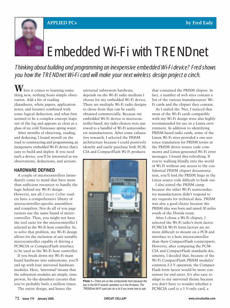
72 Issue 174 January 2005 CIRCUIT CELLAR® www.circuitcellar.com
universal subsystem hardware,depends on the Wi-Fi radio medium Ichoose for my embedded Wi-Fi device.There are multiple Wi-Fi radio designsto chose from that can be easilyobtained commercially. Because myembedded Wi-Fi device is microcon-troller-based, my radio choices were nar-rowed to a handful of Wi-Fi semiconduc-tor manufacturers. After some exhaus-tive research, I selected the PRISMarchitecture because I could positivelyidentify and easily purchase both PCM-CIA and CompactFlash Wi-Fi products
When it comes to learning some-thing new, nothing beats simple obser-vation. Add a bit of reading(datasheets, white papers, applicationnotes, and forums) combined withsome logical deduction, and what firstseemed to be a complex concept leapsout of the fog and appears as clear as aglass of ice cold Tennessee spring water.
After months of observing, reading,and deducing, I found myself on theroad to constructing and programming aninexpensive embedded Wi-Fi device that’seasy to build and deploy. If you needsuch a device, you’ll be interested in myobservations, deductions, and actions.
HARDWARE DEFINEDA couple of microcontrollers imme-
diately come to mind that have morethan sufficient resources to handle thelogic behind my Wi-Fi design.However, not all Circuit Cellar read-ers have a comprehensive library ofmicrocontroller-specific assemblersand compilers. Nor do all of you pageturners use the same brand of micro-controller. Thus, you might not havethe tool suite for the microcontroller Iselected as the Wi-Fi host controller. So,to solve that problem, my Wi-Fi designallows for the inclusion of any suitablemicrocontroller capable of driving aPCMCIA or CompactFlash interfaceto be used as the Wi-Fi host controller.
If you break down my Wi-Fi mainboard hardware into subsystems, you’llend up with four universal hardwaremodules. Here, “universal” means thatthe subsystem modules are simple, time-proven, by-the-datasheet circuits thatyou’ve probably built a million times.
The entire design, and hence the
that contained the PRISM chipset. Infact, a number of web sites contain alist of the various manufacturers’ Wi-Fi cards and the chipset they contain.
As I surfed the ’Net, I noticed thatmost of the Wi-Fi cards compatiblewith my Wi-Fi design were also highlyrecommended for use in a Linux envi-ronment. In addition to identifyingPRISM-based radio cards, some of theLinux Wi-Fi sites provided a one-sen-tence translation for PRISM terms inthe PRISM driver source code com-ments and Linux-generated Wi-Fi errormessages. I found this refreshing. Ifyou’re walking blindly into the worldof Wi-Fi without any access to the con-fidential PRISM chipset documenta-tion, you’ll find the PRISM lingo in theLinux source code difficult to hash out.
I also joined the PRISM campbecause the other Wi-Fi semiconduc-tor manufacturers didn’t respond tomy requests for technical data. PRISMwas also a good choice because thePRISM idea was born and raised 30 milessouth of the Florida room.
After I chose a Wi-Fi chipset, Iselected the Wi-Fi radio’s form factor.PCMCIA Wi-Fi form factors are nomore difficult to mount on a PCB andinterface to a host microcontrollerthan their CompactFlash counterparts.However, after comparing the PCM-CIA and CompactFlash standards doc-uments, I decided that, because of theWi-Fi CompactFlash PRISM modules’common 3.3-V operation, the Compact-Flash form factor would be more con-sistent for end users. It’s also easy toadapt to my universal theme becauseyou don’t have to wonder whether aPCMCIA card is a 5 V-only card, a
Embedded Wi-Fi with TRENDnet
APPLIED PCs by Fred Eady
Thinking about building and programming an inexpensive embedded Wi-Fi device? Fred showsyou how the TRENDnet Wi-Fi card will make your next wireless design project a cinch.
Photo 1—There are so few components here because thekey to the Wi-Fi board’s operation is in the firmware.TheTRENDnet Wi-Fi card can do a lot if you know how to ask.

www.circuitcellar.com CIRCUIT CELLAR®Issue 174 January 2005 73
3.3 V-only card, or a card that auto-matically adapts between the twovoltages. Another important factorwas cost. For the most part, PRISM-based CompactFlash Wi-Fi cards arecheaper than their PCMCIA cousins.As such, the first of the four universalhardware subsystems in my Wi-Fidesign, the Wi-Fi radio, is defined.
A number of suitable PRISM-basedCompactFlash Wi-Fi cards are availablefrom well-known companies likeNetgear, Linksys, and D-Link.However, for the initial design, I chosethe TRENDnet TEW-222CF wirelessCompactFlash network adapter. If any ofthe other CompactFlash Wi-Fi cards arebetter, it really doesn’t matter at thispoint. My main concern was gettingsome Wi-Fi hardware fabricated andwriting the Wi-Fi driver code with aslittle extraneous test gear as possible.
I leaned toward the TRENDnetCompactFlash Wi-Fi card because theTEW-222CF, unlike the otherCompactFlash wireless LAN cards thatprovide only a single link LED indicator,is equipped with both a link LED and an
activity LED. The addition of the activi-ty LED could provide additional visualstatus and aid in the production of theWi-Fi driver code. After the Wi-Fi driveris completed, it should function withany of the PRISM-based CompactFlashcards that I’ve mentioned.
With the Wi-Fi radio hardware mod-ule in place, the second universal Wi-Fi main board hardware subsystem’sdesign points are easily determined.Because the CompactFlash Wi-Fi cardsare all 3.3-V devices, the power supplymodule’s voltage level is fixed at 3.3 Vas well. To keep the power supplymodule universal, I used a National
LM1086CS-3.3 voltage regulator sur-rounded by a pair of 10-µF tantaluminput and output filter capacitors. Theinclusion of an industry standard1N5819 in the power supply circuitguards against the connection of a cen-ter-negative power brick, while an LEDand current-limiting resistor providevisual indication of 3.3 V on the outputpin of the LM1086CS-3.3. Any center-positive power brick that can providebetween 5 and 9 VDC at 400 mA can beused as the design’s DC power source.
The Wi-Fi design’s power supply andCompactFlash radio configurationsalso directly affect the third Wi-Fi mainboard’s universal subsystem’s designpoint. I’ve included a simple 3.3-V RS-232 interface to aid in the Wi-Fi driverdebugging process and to provide auniversally accepted external commu-nications path to the host controller.
A textbook circuit employing theSipex SP3232 brings to bear a standardRS-232 serial port and a pair of modemcontrol signals via a standard femalenine-pin shell connector. The Wi-Fimain board serial port is hardwired as
Photo 2—No more cramped thumbs from pushing syringeplungers. This gadget saves hours of assembly time.

www.circuitcellar.com CIRCUIT CELLAR®Issue 174 January 2005 75
DCE, which eliminates the need forquestionable crossover cables and clum-sy null modem arrangements. TheRTS/CTS control signals are optional. Ididn’t use them in my implementation,but they’re available if you need them.
The Wi-Fi main board’s fourth majorsubsystem consists of a host microcon-troller or microprocessor, a program-ming/debugging interface for the hostmicrocontroller, or a microprocessorand an optional host controller powersupply if your selected microcontrolleror microprocessor doesn’t function toyour satisfaction at the 3.3-V level.
The shelves in the Florida room arepacked with a bunch of extensivemicrocontroller tool suites. I baselineda Wi-Fi design based on one of themicrocontroller manufacturers thatmakes a number of proven hardwareand software development tools.Again, after the Wi-Fi design concept isvalidated, it doesn’t matter whichmicrocontroller or microprocessor youchoose as your host controller. Yourdesign has to do with how you adaptof the Wi-Fi driver code as well as your
ability to construct, debug, and programa custom host microcontroller or micro-processor plug-in hardware module.
The cerebral phase of the project isover when all four of the Wi-Fi design’ssubsystems are defined. The next step isto realize the subsystem definitions bydesigning, fabricating, and populating aPCB based on your Wi-Fi design goals.
WI-FI HARDWARELike the four Wi-Fi main board sub-
systems, the Wi-Fi PCB’s design ispredicated on the CompactFlash Wi-Firadio and its form factor. Photo 1 showsthe four Wi-Fi design subsystems.
I used a four-layer PCB to minimizenoise and create a cleaner PCB layout.The CompactFlash Wi-Fi radio inter-faces to the Wi-Fi design’s host con-troller by way of an off-the-shelf surface-mount CompactFlash card receptacle.The four doublewide rows of mount-ing posts surrounding the baseline QFPland pattern are connected to all fourof the Wi-Fi design’s universal subsys-tems in accordance with the Wi-Fi mainboard circuitry depicted in Figure 1.
If you don’t implement the baselinemicrocontroller in your design, youcan fabricate a separate daughterboardthat contains your selected microcon-troller or microprocessor and its pro-gramming/debugging circuitry andthen plug it into the 0.1″-centereddouble-row positions. The Wi-Fi mainboard’s daughterboard feature allowsany form factor from DIP to QFP touse the Wi-Fi main board’s remainingthree universal subsystems. In addi-tion, any microcontroller core voltage,I/O pin voltage level conversion cir-cuitry, or programming/debugginginterface can be accommodated usingthe daughterboard configuration.
I chose a half-sized crystal oscillatorinstead of the standard crystal/capaci-tor clock configuration. A socketedcrystal oscillator makes it easier tochange clock frequencies. Most stan-dard crystal/capacitor oscillator tanksrequire different types of crystals anddifferent values for the associatedcapacitors; it depends on the micro-controller or microprocessor you’reusing. The socketed crystal oscillator
Figure 1—You can clearly see the four Wi-Fi main board subsystems here. The bulk of the electronics is contained within the TRENDnet Wi-Fi card. Depending on the host con-troller you select, the microcontroller/microprocessor subsystem can be as simple as a single IC.

76 Issue 174 January 2005 CIRCUIT CELLAR® www.circuitcellar.com
design point eliminates the need todesign the PCB to accommodate thedivergent microcontroller and micro-processor oscillator configurations.
Most programming/debugging inter-faces are either JTAG-based or propri-etary to the particular microcontrollerin use. I’ve found that a 10-pin program-ming/debugging interface is normallysufficient. However, I have used 15-pin programming/debugging interfaces.Rather than try to provide all of the pos-sible programming/debugging interfaceconfigurations on the main Wi-Fi PCB, Idecided to include a 10-pin interface tosatisfy the needs of the baseline micro-controller and leave the micro-specificprogramming/debugging interface to beimplemented on the daughterboard.
I always beat myself up when I neg-lect to include power supply points ina PCB design, so this Wi-Fi design has apair of four-pin power supply points.This makes it easy to hook up a logicprobe or any other 3.3-V device you needto power when you’re working with theWi-Fi board. As you can see in Photo 1,I’ve also included some uncommitted0.1″-centered holes for whatever elseyou need to mount on the Wi-Fi board. Iadded a universal Reset switch circuitto the Wi-Fi board to handle thosemoments of operational uncertainty.
The Wi-Fi main board doesn’trequire a lot of components, so assem-bly is quick. Based on the fine-pitch,surface-mount components andCompactFlash connector, you’d thinkthat a stencil and some specialized sol-dering tools would be the only way toassemble this board. That’s mostly true.A stencil would be necessary to producethe Wi-Fi board in quantity; however, Idiscovered a solder dispensing tool thatsaves me the expense of procuring astencil for prototype purposes.
My EFD Ultra 1400 fluid dispensing
system allows me to lie down preciseamounts of solder paste or flux withjust a tap of a foot pedal (see Photo 2).It uses shop air and a computerizeddispensing controller to pump consis-tent quantities of solder paste from aspecially designed syringe system. Ican put down 0.25- to 1.55-mm dropsor lines of solder paste depending onthe size of the tip attached to the Ultra1400’s air-driven syringe. After youmount your desired syringe tip, youcan teach the Ultra 1400 fluid dispens-ing system controller to put down a spe-cific amount of fluid every time you tapthe foot pedal. On the other hand, youcan put the system in Free Flow mode,which allows solder paste to flow aslong as the foot pedal is depressed.
I used the Ultra 1400 to assist withthe mounting and soldering of all ofthe SMT components including theCompactFlash receptacle. After Iapplied the solder and mounted thecomponents, I completed the assem-bly process using a small batch oven.
As a rule I use Metcal soldering sta-tions because they heat up quicklyand can be fitted with a number ofspecial-purpose SMT soldering tips.You can use different equipment tosolder the delicate SMT devices. I waspleasantly surprised to find that WAHLbattery-powered ISO-TIP irons workremarkably well in the SMT environ-ment. I used one to touch up andchange components on the main board.
DRIVE THE TEW-222CFTo learn more about what’s required
to drive a CompactFlash Wi-Fi card,study the CompactFlash card connec-tions shown in Figure 1. The baselinemicrocontroller I selected for the ini-tial Wi-Fi design is an 8-bit device.Note that the CompactFlash card con-nector is pinned for 16 data lines. The
CompactFlash card documentationoutlines a process to read and writeusing a 16-bit data path. Assume thatthe Wi-Fi CompactFlash card can oper-ate in 16- or 8-bit mode, which opensup 16-bit microcontrollers and micro-processors as possible host controllers.
The control and state of the CE1and CE2 lines depend on how youwant to transfer data to and from theCompactFlash card. I chose to controlboth of the CEx lines logically becauseI had the available I/O to do so. Thisled to a self-induced bug that took me aday to smash. I was accidentally logical-ly ANDing the CE2 line low before datatransfer. When both CE1 and CE2 arelow, the CompactFlash card is put into16-bit Read/Write mode. For 8-bit modeyou can save a couple of I/O pins andsimply tie CE1 low and CE2 high. Whenselecting your host controller, plan for11 bits of addressing because it will berequired to access the internals of theCompactFlash card memory structure.
Using the CompactFlash card I/O con-trol lines is no different than any otherI/O control configuration. Combinationsof logic levels on the REG, OE, andWE lines read and write standardCompactFlash internal registers whilelogic levels encompassing the IORD,IOWR, OE, and REG control lines dothings to the PRISM-related parts on theCompactFlash card. These I/O opera-tions are standard for all CompactFlashcards and all the combinations of 8- and16-bit transfers, including the timingsin the CompactFlash specification.
The HI-TECH ANSI C is the base-line C compiler for the Wi-Fi mainboard. I chose it because of HI-TECH’sbroad range of supported platforms.Because the Wi-Fi main board isn’tgeared toward any particular micro-controller or microprocessor, HI-TECH’sline of C compilers will probably sup-port the microcontroller or microproces-sor you select for your Wi-Fi design.For instance, HI-TECH offers ANSI Ccompilers for ARM, 8051, MSP430,z80, H8, PIC, and 68HC11. Using HI-TECH ANSI C to write the baselinedriver and application code, you can portand use the manufacturer’s proprietaryANSI C compiler for your selected hostcontroller. You can also use it to port aprocessor-specific variant of HI-TECH
Listing 1—I wish I could show and tell about what’s behind the API calls.This code makes it look easy, but there areall kinds of code grinding between the host controller and the TRENDnet Wi-Fi card going on in the background.
void main(void)init_USART();wifi_api(INITIALIZE,CF);wifi_api(NETWORK,BSS);wifi_api(CONNECT,EDTP);while(1);

www.circuitcellar.com CIRCUIT CELLAR®Issue 174 January 2005 77
ANSI C to code your Wi-Fi application.Becauase the PRISM chipset’s internal
operation is confidential, the most logicalmethod of giving public access to PRISMoperations is through an API. Listing 1is all it takes to turn on the radio andassociate/authenticate with an accesspoint (AP). wifi_api() is an interfacefunction that you may download fromthe Circuit Cellar ftp site. Suggestions asto how to implement the API functionsare included with the download package.
The matter of business involves start-ing up the interrupt-driven USARThardware. This call (init_USART) alsoenables the printf functionality builtinto the ANSI C compiler. After theUSART is operational, you can receiveerror and info messages from the APIvia the Wi-Fi main board’s serial port.
All CompactFlash cards must be ini-tialized via the manipulation and read-ing of the card information structure(CIS) tuple array. This is accomplishedusing the wifi_api(INITIALIZE,CF)API call. Information needed for com-municating with the CompactFlashcard internals is gathered during thisCompactFlash initialization process.Again, this isn’t a PRISM-only confi-dential operation. Tuples and the CISmechanism are discussed in detail in theCompactFlash specification. The onlysecrets here are what the PRISM tuples
contain and how to decode the infor-mation within them. A simple tupledump program exists in the Linux com-munity, and such a program can be eas-ily written and executed in this embed-ded environment. I did just that, butthere’s no use in blurting out a bunch ofconfidential hexadecimal charactersthat I can’t legally translate for you.
I persuaded the Wi-Fi board to contactthe AP in the Florida room by specifyingthe network type that I wanted theTEW-222CF to join, which is BSS or aninfrastructure network. The Wi-Fi NICwas notified of my choice of networkswith the source line wifi_api(NET-WORK,BSS). I happened to know thatthe SSID of the Florida room wirelessnetwork is “EDTP,” so I instructed theWi-Fi board to search for and connectto an AP beaconing the EDTP SSIDusing wifi_api(CONNECT,EDTP).The following happened: First, the Wi-Fi radio powered up and engaged.Second, the Wi-Fi card transmitted theprobe request. Next, the AP acknowl-edged the probe request. Followingthis, the Wi-Fi card requested authen-tication, the AP authenticated the Wi-Fi card, and the Wi-Fi card requestedassociation. After the AP granted theassociation request, the Wi-Fi boardwas on the EDTP wireless network.
I kicked off the code and the TEW-
Photo 3—The Netasyst wireless sniffer tool is a must-have as far as I’m concerned. I can capture and analyze wireless trafficall over the Florida room domain. It has also informed me that someone in the neighborhood is running a renegade Linksyswireless system.The TRENDnet Wi-Fi card is identified as AbocomBD61A7 and the Netgea86B0C8 is the Florida room AP.
Fred Eady has more than 20 years ofexperience as a systems engineer. He hasworked with computers and communi-cation systems large and small, simpleand complex. His forte is embedded-sys-tems design and communications. Fredmay be reached at [email protected].
SOURCESEFD Ultra 1400 dispensing systemEFDwww.efd-inc.com
ANSI C CompilerHI-TECH Softwarewww.htsoft.com
ISO-TIP Soldering iron (7566-100)ISO-TIP (WAHL)www.iso-tip.com
TRENDnet TEW-222CFTRENDware Internationalwww.trendnet.com
222CF’s link light illuminated. A shorttime later, the Wi-Fi card’s link lightstarted blinking. This indicated that thecard was initialized. At that point I start-ed my Netasyst wireless sniffer applica-tion on my laptop. After the initial proberequests were sent, I noticed a flickeringof the Wi-Fi card’s activity LED and thelink light went solid. This indicated thatthe Wi-Fi board had successfully com-pleted all the necessary steps. I stoppedthe sniffer and verified the results usingthe sniffer capture shown in Photo 3.
WALK IN THE PARKBy putting the Wi-Fi radio on the
air, I’ve verified the basic functionalityof the Wi-Fi API. Up to this point, onlyMAC-level operations between the Wi-Fi board and the AP have been executed.The next step is to integrate some triedand true UDP and TCP/IP routines thatI wrote for wired embedded Ethernetdevices into the Wi-Fi board’s firmwaremix. That will put the IP side of thewireless session into play and then I’llbe able to make some meaningful userdata flow across the wireless link. Asyou can see in the simplicity of the Wi-Fi board hardware, wireless designisn’t complicated, it’s embedded. I
PROJECT FILESTo download the code, go to ftp.circuitcellar.com/pub/Circuit_Cellar/2005/174.

little since the dawn of silicon, withtoday’s memory chips tracing theirbloodlines directly back to the DRAMs,SRAMs, and EPROMs of yore. But underthe hood, the latest and greatest are defi-nitely not your father’s memory chip.
The UV-erasable EPROM of the1970s isn’t totally dead yet becausethere are some applications and pro-duction scenarios for which one-timeprogrammable (OTP) EPROMs stillmake sense. Nevertheless, whether bun-
dled in an SoC or stand-alonechips, flash memory has virtual-ly replaced EPROM across theboard. Although the decisionto go with flash memory is ano-brainer, designers nowhave a little more to thinkabout than they did in the olddays. Most notably, they mustdecide which type of flashmemory (NAND or NOR) isthe best for a particular appli-cation (see Figure 1).
NAND flash memory ismuch smaller (read cheaper)than NOR by virtue of daisy-chained wiring between thecells. The good news is that thesilicon area is cut practically inhalf compared to an equivalentcapacity NOR chip. The badnews is that NAND flash mem-ory needs to operate on largechunks of data at one time.NAND flash memory is greatfor bulk operations (read, write,and erase), but random access-ing a single byte is a slow andconvoluted process. As a result,NAND flash memory is biased
78 Issue 174 January 2005 CIRCUIT CELLAR® www.circuitcellar.com
Furthermore, many of the issues andinsights surrounding the topic arerelevant whether the memory is a stand-alone chip or buried in a SoC. MicronTechnology’s J. Thomas Pawlowskigave a lecture titled “MemoryPerformance Tutorial” that provided awelcome opportunity for Hot Chips 16attendees to get up to speed on the sub-ject without having to wade through lit-erally thousands of pages of datasheets.
From 50,000′, things have changed
Beyond the occasional hot or coldsnap, the weather doesn’t really everchange much in Silicon Valley. Instead,the annual August Hot Chips confer-ence at Stanford University stands inas a virtual passing of the seasons.
Moore’s law may be running out ofgas, but even when sputtering alongon fumes, it’s still headed in the rightdirection. That means the bleeding edgeis still the leading edge of tomorrow’smainstream designs. Better yet, the wiz-ards are already hard at workon the tiny things that will bethe next big things. Don’t youjust love this business?
FORGOTTEN MEMORIES There was a time when I
knew pretty much all there wasto know about memory chips.However, I have to confess Ihaven’t kept up with times. Itisn’t a matter of sloth, mind you,but rather the simple fact thatfor the deeply embedded appli-cations I’m most interested in,memory (along with everythingelse) is shrinking onto a singleSystem-on-a-Chip (SoC). At thesame time, the increasing densi-ty of stand-alone memory chipspushes them ever deeper intomemory-centric applicationssuch as PCs, multimedia, andbig-iron communication infra-structure. Lots of chips are soldto be sure, but only at the behestof relatively few designers.
Nevertheless, the subject ofmemory chips has a lot of“gee whiz” general interest.
NOR Flash memory NAND Flash memory
Applications Code, data Mass storage
Future applications MLC: mass storage
Density range Up to 512 Kb Up to 4 Gb
Code and data
Read latency 60–120 ns 25 µs
Maximum read bandwidth 41–112 MB/s (16 bit) 40 MB/s (16-bit bus)
Maximum write bandwidth 0.25 MBps 5 MBps
Erase time 400 ms (128-KB block) 2 ms (128-KB block)
Read device current
Write device current
1.6x
3x
1x
1x
CellArray
NOR NAND
Layout
Cross-section
Cell size 10F2 4F2
2 F
2 F
Source line
Word line
Unit cell
Bit line
Word line Contact
Unit Cell
Source line
5 F
2 F
Figure 1—Dedicated flash memory chips and cards are tending toward NANDby virtue of higher density, lower cost, and the predominance of multimedia(i.e., bulk operation) applications. By contrast, NOR, with faster and finer gran-ularity access, is typically the call for SoC designs.
Hot Enough for You?SILICON UPDATE by Tom Cantrell
Hot Chips 16 featured lectures on topics like wireless sensor networking and molecular elec-tronics. This month Tom brings you up to speed on the sizzling technology coming your way.
Hot Chips 16 Roundup

www.circuitcellar.com Issue 174 January 2005 79CIRCUIT CELLAR®
toward mass storage-like applicationssuch as the flash memory cards that pluginto digital cameras and MP3 players.
By contrast, NOR flash memory fea-tures fast random access to smallerchunks of data, closer in concept tothe original EPROM. That makes it abetter home for directly executed codeand nonsequential data than NANDflash memory. However, if your sys-tem also includes DRAM, anotheroption is to move a copy of the codefrom NAND flash memory to DRAMfor execution rather than executingdirectly out of NOR flash memory.Although requiring twice the codememory (i.e., both flash memory andDRAM), the strategy can deliver high-er performance at a lower overall costthan using NOR flash memory.
Speaking of DRAM, the tutorialwent a long way toward explainingthe numerous choices designers face.Things were simple back when the IBMPC was introduced with little more thana half meg of RAM; but now that a thou-sand times that fits on a single DRAMchip (4 Gb), they aren’t simple anymore.
I managed to keep up with the subjectthrough the introduction of the synchro-nous DRAM back in ’95, but since thenthe choices have grown to encompass averitable alphabet soup of options: DDR,GDDR, FCRAM, RLDRAM, and more(“I Sync, Therefore I DRAM,” 55, 1995).
The simple way to get a handle on thechoices is to understand the motivationbehind them—namely, speed. Beyondthe basics of cutting the random accesstime (reduced latency), specific DRAMvariants are designed to maximize over-all performance by optimizing for theparticular type of bus traffic encounteredin specific applications. This includessuch factors as the overall read/writeratio, locality of reference (randomversus sequential), typical burst lengths,and any special considerations such asbus width (e.g., wide for graphics) orlow-power (battery-driven) operation.
DRAM is here to stay, at least untilsuch time as one of the brand newtechnologies (MRAM or optical)comes out of the lab to replace it.However, the same can’t be said forSRAM chips, which are on life support
and may not last much longer.The fundamental problem for
SRAMs is that the window of applica-bility is inexorably shrinking, squeezedbetween the SoC on-chip memorytrend and the emergence of faster,designer-friendlier SRAM-like DRAMslike Micron’s CellularRAM and othersuppliers’ psuedo-static offerings.
Ironic, given their once hardyreputation, the ultimate showstopper forSRAM chips is questionable reliability.Why is that? Well, say hello to our lit-tle friend, the alpha particle. It turnsout that because of large cell size andlow cell capacitance, the seeminglyrobust six-transistor SRAM cell is aknock over for the blitz of cosmic raysthat bombard the earth. So-called softerrors were once little more than atopic for discussion around the watercooler, but they’re becoming a realproblem for SRAMs.
Here are the numbers—read ’em andweep. Today, a typical SRAM soft-errorrate (SER) is 10,000 FITs/Mb. A failure intime (FIT) is defined as one failure every109 h. Now, a billion hours sounds like a

80 Issue 174 January 2005 CIRCUIT CELLAR®www.circuitcellar.com
long time, but don’t get your hopes upjust yet. As next-generation SRAMscontinue to reduce voltage (to 1.2 V,for example) and feature size (and thuscharge levels and margins), the SER isexpected to double, triple, or more tobetween 20,000 and 50,000 FITs/Mb.
Now consider the historic reality thatthe sweet spot in the memory markettypically has SRAMs running at one-eighth or so the bit density of DRAMs.With 1-Gb DRAMs a commodity now,I’m talking about 128 Mb and beyondSRAM chips with lousy FIT ratings (i.e.,50,000 FITs/Mb × 128 Mb = 6.4 mil-lion FITs). Such a chip can hobblealong for only little more than a week(200 h) between soft errors. To makematters worse, the effect of cosmic raysincreases quickly with altitude, forexample, doubling at 3,000′ comparedto sea level. So, leave your SRAMs athome when you head to the mountains.
THREAD HEADAlthough memory chips are getting
faster year by year, they just can’t keepup with the latest and greatest gigahertzand beyond processors. Despite addingever more cache, with first,second, and even third lev-els now common, the mem-ory bottleneck betweenCPU and external memorykeeps getting worse.
Processor designers havetaken the matter into theirown hands with multi-threading techniques. Theidea is to try to find some-thing to do to keep theprocessor core busy insteadof just tapping its footwaiting for code and datato wind its way (through
all those caches) to and fromsome pokey DRAM chip.
Multithreading is simply a dis-count version of multiprocessing.Instead of duplicating the entireprocessor, only key portions ofthe state (e.g., program counter,status word, and register file)are replicated. When one threadstalls waiting for memory, hope-fully another one can run (i.e.,one that doesn’t require immedi-ate memory access to proceed).
As the processor-versus-memoryspeed gap grows, naturally so does thethread count, an admittedly extremeexample being the Sun Niagra proces-sor.[1] Designed to take advantage of thethread-level parallelism exploitable innetwork server applications, Niagara canrun up to 32 threads simultaneously.
Now it’s easy to see why somethinglike a 32-port networking box couldexploit such an approach. After all, eachport’s activity is different, reducing thedependencies that ultimately trip up par-allel processing schemes (i.e., multipro-cessing, multithreading, or superscalar).
Unfortunately, such gains aren’t tobe had in more typical applications. Ina Hot Chips 16 presentation called“Intel Pentium 4 Processor on 90nmTechnology,” Intel’s Ronak Singhalcovered the newest version of Pentium 4.A graph showed that even Intel’sHyperThreading (HT) technology deliv-ers only about a 20% speed-up in reallife (see Figure 2). Now, don’t get mewrong, a double-digit improvement inperformance is impressive these dayswhen incremental gains are gettingharder to find. But when it comes to
propping up a struggling Moore’s law,multithreading and other architecturaltrinkets are clearly no panacea.
GRAPHIC EXAMPLE Look no further than the new wun-
derchip under the hood of the new SonyPlayStation Portable (PSP) to see a graph-ic (literally) example of the SoC phenom-enon.[2] I had to laugh when I realized akid’s hand-held toy now has all the com-puting power, and then some, of thezillion-dollar mainframes I grew up on.
Reflecting the SoC trend, the chipincorporates 4 MB of embeddedDRAM (see Figure 3). One nice thingabout putting DRAM on the chip isthat you can brute force your wayaround the memory bottleneck bygoing wide—a healthy 256-bits in thecase of PSP thanks to simultaneous128-bit read and write ports.
The chip needs all the memory band-width it can muster because it’s got notone, not two, but, in fact, three full-blown processors. Two (the game andmedia processors) are 333-MHz, 32-bitR4000 MIPS cores with cache and allthe trimmings. Yeah, the desktop crowdmay sniff at these old-school proces-sors, but 500-plus MIPS in the palm ofyour hand is nothing to sneeze at.
More intriguing is the virtual mobileengine (VME). Behind the marketingmoniker is a 166-MHz, 24-bit dynami-cally reconfigurable processor. Withlocal memory and a DMA controller,the VME is designed to do heavy liftingfor the R4000s (see Figure 4), especiallywhen it comes to I/O and special-pur-pose inner loops (e.g., MP3 and MP4codec). The concept of reconfigurable
computing (typically inFPGAs) isn’t new, but VMEactually delivers in prac-tice because it can switchhats in a single cycle.
Take the idea to the nextlevel and you come up withthe idea of tailoring an archi-tecture to the problem athand. That concept reallyisn’t new either, but untilnow it’s been confined tothe realm of special-pur-pose supercomputers.
In a Hot Chips 16 presen-tation called “MDGRAPE-3
VRAM
GPUDDR-IF DMAC Timer
I/0
I/0
I/0External
Bus
Securitysystem
Datacache
Inst.cache
Main CPUcore
VFPU
FPU
AVC Virtualmobileengine
Datacache
Inst.cache
Mediaengine
eDRAMmemory
Media processing unit
Game processing unit
Figure 3—With multiple processors, memory, and peripherals, the Sony PSP is anexample of the bleeding-edge breed of Systems-on-a-Chip.
1.12 1.19 1.20 1.25 1.28HT Technology disabled HT Technology enabled
1.50
1.00
0.50
0.00Adobe
Photoshop CS
Windows MediaEncoder 9.0
Maxon Cinema4D
MainConcept1.4
MAGIX mp3maker 2004
diamond
Perf
orm
ance
Figure 2—Hyperthreading is the latest tactic in the never-endingbattle against the memory bottleneck, but the effectivenessdepends on the application.You can squeeze neither water from arock nor parallelism from sequential code.

82 Issue 174 January 2005 CIRCUIT CELLAR® www.circuitcellar.com
Chip: A 165-Gflops Application-Specific LSI for Molecular DynamicsSimulations,” Makoto T aiji describeda class of machines designed specifical-ly for particle simulations. The key isthat the algorithms involved canuniquely exploit a broadcast memoryarchitecture to bypass the aforemen-tioned memory bottleneck that other-wise chokes conventional processors.The latest MDGRAPE3 chip incorpo-rates specialized particle memories andforce calculation pipelines to deliver
the goods to the tune of165 Gflops. For theunique applications itserves, GRAPE trouncesa standard processor(Pentium 4 PC), slashingboth price per Gflop andwatts per Gflop by roughlya factor of 30 (see Table 1)!
Back in the real world,today we have a situationwhere hardware definessoftware in the sensethat a particular task(i.e., an application pro-
gram) must be mapped to the fixedarchitecture of a standard CPU. Butdoesn’t it make more sense to turnthe situation around and let the par-ticulars of your application softwaredrive the creation of the hardwarethat serves it? Sure it does.
The custom instruction features oftoday’s soft-core processors (e.g.,Xilinx Microblaze and Altera Nios)are effective and practical examples ofthis concept, but they’re only thestart. Instead of adding a few instruc-
tions to an otherwise standard proces-sor, why not create an optimal proces-sor from scratch? That was the themeof David Goodwin’s presentation,“The End of ISA Design: Power Toolsfor Optimal Processor Generation.”When you compile an application pro-gram, the Tensilica tools generate anoptimal (per your specified perform-ance, power, and gate count trade-offs)application-specific instruction proces-sor, or ASIP in geek-speak.
The tool starts by assessing the realneeds of your application with bothstatic and run-time (i.e., profiling) analy-sis. Here all the critical functions,paths, and dependencies that ultimately
Table 1—As demonstrated by MDGRAPE-3, a littlearchitectural specialization goes a long way when itcomes to slashing the time and power required toaccomplish a particular task.
CPU
VME
CPU
VME
Control tasks Loop-level granularitymapping in source code
Power-consuming heavier tasks
Reconfigure into dedicated circuitson the fly!
Time
Time
for () ]…
Figure 4—A cross between a processor and an FPGA, the Virtual MobileEngine (VME) in Sony’s PSP features a dynamically reprogrammabledatapath to do the dirty work for the main CPU(s).
$/Gflops W/Gflops
MDGRAPE-3 15 0.2BlueGene/L 140 6Pentium 4 PC 400 14Earth Simulator 8,000 128MDGRAPE-2 150 1.5

www.circuitcellar.com Issue 174 January 2005 83CIRCUIT CELLAR®
limit performance are identified. Next,the tool generates and evaluates differentISAs by tweaking three control knobs:Fusion, SIMD, and VLIW (see Figure 5).Fusion is analogous to the custominstructions you see today that performmultiple actions underneath a singleopcode. SIMD refers to the ability torun an instruction against multiplepieces of data all at once (vector func-tions). VLIW defines how many differ-ent instructions can be dispatchedsimultaneously (i.e., just how “verylong” the instruction word is).
The collection of meta-ISAs so gener-ated comprises a stable of machines cov-ering a range of price and performance.Just decide how much speed you need (orhow many gates your silicon budget canspare), and your own custom dreammachine is just a mouse click away.
SMALL CHIPSI’ve never begrudged the bleeding-
edge orientation of the Hot Chips con-ference; in fact, I’ve reveled in theopportunity to escape reality and pon-der the blue sky. And although 8-bitchips may ship a lot, they generallydon’t make good fodder for trade jour-nal headlines, doctoral dissertations,and conference sessions.
Drum roll please. The award for thefirst 8-bit presentation to make the
Hot Chips cut goes to the Smart Dustcrew at the University of California,Berkeley.[3] You may recall that theSmart Dust concept revolves aroundtiny (and ultimately ever tinier) motesof Smart Dust, which are characterizedby two features (T. Cantrell, “The DustFlies,” Circuit Cellar Online, March2002). One is some particular localprocessing and I/O capability that typ-ically revolves around a common sens-ing function such as temperature, pres-sure, light, or sound. There’s nothingnew about that. It’s the second featurethat sets Smart Dust apart. Regardless ofthe other particulars (local processingand I/O), motes are distinguished bytheir reliance on wireless communica-tions and a distributed computing con-cept in which the whole is greater, andmore robust, than the sum of the parts.
The ultimate vision features motesthat are truly dust-like in size. They’rebarely visible chips that integrateeverything (processing, I/O, and com-munications) in a single chip.Furthermore, they run forever on atiny battery or, better yet, harvesttheir power from the environment.
We’re not there yet. Today, SmartDust is still in the prototyping stage,with small 8-bit SBCs serving asresearch and development stand-ins.
The Telos platform looks like a fun
way to experiment, evaluate, and other-wise get your hands, er, dusty (seePhoto 1). It’s one of the first to use therecently blessed IEEE 802.15.4 2.4-GHzwireless standard, thanks to a radio chipfrom Cambridge Consultants, which wasacquired by embedded wireless up andcomer Ember. Smart Dust and 802.15.4are a good match for each other becausethey share a vision of ubiquitous yetunobtrusive intelligence scattered about.
Based on typical MCUs like AtmelAVRs and Texas Instruments MSP430s,motes may not push the MIPS meter.That’s OK because the primary goal isto extend battery life from months, toyears, to forever. As a politician mightsay, when it comes to smart dust, it’sthe power consumption, stupid.
Conventional wisdom might indi-cate that choosing the lowest powerchip and running it really slowly isthe answer. But the research atBerkeley shows the situation is a littlemore complicated than that. First,because the presumption is that motessleep most of the time, it’s the stand-by power consumption specificationthat matters more than active power.Furthermore, when called to duty, lowperformance doesn’t necessarily meanlow power. Notably, the time andpower spent waking up (e.g., waitingfor the MCU clock to stabilize) is purewaste that adds up quickly.
Also, there’s a lot of power overheadto keep an MCU running. Imagine afactory with lots of lights, machines,and HVAC to keep powered. Does itmake sense to have just a few workerswho take a long time to get the jobdone while the factory spins thepower meter? Or, is it more energyefficient to get more workers, run theline at full speed, and finish the job
l operations packed in one long instruction
Multi-issue instructionm copies of storage and function
SIMD operation
Register Register Register
Operation Operation
Operation
Register
Register
n dependentoperations
implementedas a single
fusedoperation
Fused operation
Maximum parallelism: l × m × n
Meta-ISAVLIW • Instruction size • Number of operation slots per instruction • Operation mix in each slotSIMD • Types of vector operations • Number of vector elements • Number and size of vector register filesFusion • Number and type of composing operations • Number of inputs and outputs • Latency
Register and constant inputs
Constant
Figure 5—Raising the abstraction ante, Tensilica goes beyond the synthesis of mere circuits to automatically gen-erate a processor architecture and instruction set specifically optimized for your particular application.
Photo 1—Dust may get in your eyes, but the Telossmart dust mote, with MSP430 MCU, IEEE 802.15.4radio, and USB, doesn’t get into your wallet. It’s just$130 at www.moteiv.com.

quickly so you can turn off the lightsand machines and cut your power bill?In short, the proper strategy is tosleep—extremely deeply (i.e., lowstandby current)—as much as you can.Don’t dillydally when the alarm clockrings. Roll out of bed fast (quick wake-up), mainline some coffee, and get towork (i.e., speedy performance whenactive) so you can get back to sleep.
Smart dust is neat stuff indeed.However, I must confess to some fearthat the concept will cave-in to bloat-ware temptation. Can we resist thesiren call of a 32-bit Windows orLinux-based smart dirt clod? Thankfully,everything still seems to be headed inthe right direction so far.
NANO SOPRANOAs the sun sets on Moore’s law, the
wizards are conjuring up a new spell—nanotechnology—to take the baton ofmore-for-less and run with it. SteveJurvetson, a venture capitalist withDraper Fisher Jurvetson, gave anextremely interesting talk on the sub-ject that was aptly titled “TranscendingMoore’s Law with MolecularElectronics and Nanotechnology.”
While much of the popular press onthe subject falls into the category ofhype and hope, Jurvetson’s Hot Chips16 presentation struck me as especial-ly credible. Sure, his pitch had the sci-fi-like show and tell that makes forgood headlines. For instance, thepromise of molecular electronicsbecomes clear when you consider thatthere are more molecules in a drop of
RESOURCE.CD-ROM of Hot Chips 16 proceed-ings, August 2004, www.hotchips.org.
REFERENCES[1] P. Kongetira (Sun), “A 32-Way
Multithreaded SPARC Processor,” HotChips 16, Stanford University, 2004.
[2] M. Okabe (Sony), “A 90nmEmbedded DRAM Single-Chip LSIwith a 3D Graphics, H.264 CodecEngine, and a ReconfigurableProcessor,” Hot Chips 16, StanfordUniversity, 2004.
[3] J. Polastre, et al. (Berkeley), “TheMote Revolution: Low PowerWireless Sensor Network Devices,”Hot Chips 16, Stanford University,2004.
[4] A. Keane (Cooligy), “Active Micro-Channel Cooling,” Hot Chips 16,Stanford University, 2004.
Tom Cantrell has been working onchip, board, and systems design andmarketing for several years. You mayreach him by e-mail at [email protected].
water than all the transistors everbuilt! But the concept isn’t just bluesky. IBM has already demonstrated theability to fabricate simple circuits atthe molecular level, circuits that arehundreds of thousands of times small-er than their silicon equivalents.
Jurvetson’s presentation went beyondthe usual parade of carnival tricks bygoing further to describe the processes,the tools, and even the philosophy thatwill serve as the foundation for the nan-otech revolution. These are what mat-ter when it comes to turning the conceptinto real products that go beyond mereresearch and development lab curiosities.
Until now, the march of progress hasboiled down to big clumsy humans try-ing to manipulate ever-tinier, morecomplex things from the top down.Moore’s law itself is a classic example.It relies on an ever more intricate tool-chain to keep shrinking a thin veneer oftransistors masked on silicon. Not onlyis it hard and expensive to build finegeometry fabs, but even the IC designtools have trouble keeping up with a 1-billion-transistor chip. Those of you whospend your lives waiting on simulatorsknow what I’m talking about.
Nanotech starts with a fundamen-tally different approach to miniatur-ization. By leveraging the sciences in asynergistic way, the goal is to buildthings from the bottom up (see Figure 6).
That sounds good, but is it more thana catchphrase? You bet. Look no furtherthan the mirror to get a good example ofnanotech in action. Human beings are anexample of systems that are grown byreplication, evolution, and self-assembly.The human brain is 100 million timesmore power-efficient than a microproces-sor. Yet an individual’s entire program(i.e., genetic code) fits on a single CD.
The real challenge for the nanotechrevolution comes with the understandingthat the toolbox you know and love hasto change. Today, tools made of hardwareand software are used to create hardwareand software. Tomorrow, nanotools (e.g.,quantum computers) will be needed todeliver on the promise of nanotech.
COOL DOWNThe problem with hot chips is, well,
they get hot. Thanks to advanced cool-ing techniques from the likes of Cooligy,
www.circuitcellar.comCIRCUIT CELLAR®84 Issue 174 January 2005
Material scienceMechanical engineering
Physics
Life sciencesChemistry
Biology
Electrical engineeringComputer science
Information technology
Nanotechnology
Figure 6—Can we all get along? Nanotechnology callson scientists of every ilk to put aside their differences andjoin hands in a common quest to deliver more for less.
relief for chips with a fevered brow isjust around the corner if you don’t mindthe extra plumbing (see Photo 2).[4]
And now the weather is coolingdown just a bit too, marking the end ofanother summer of silicon fun. Vacationis over and it’s time to get back to thework-a-day world of real world chips.But it won’t be long until the days getlong once again and the next crop ofhot chips comes into full bloom. I’mlooking forward to it, aren’t you? I
Photo 2—Cooligy isn’t the first to contemplate activeliquid cooling, but their solution is novel by virtue of areliable and quiet, no-moving parts electrokinetic pump.

www.circuitcellar.com CIRCUIT CELLAR® Issue 174 January 2005 85
IDEA BOXTHE DIRECTORY OF PRODUCTS AND SERVICES
AD FORMAT: Advertisers must furnish digital submission sheet and digital files that meet the specifications on the digital submission sheet. ALL TEXT AND OTHER ELEMENTS MUST FIT WITHIN A 2″″ ×× 3″″ FORMAT. Call for current rate and deadline information. Send your disk and digital submissionsheet to: IDEA BOX, Circuit Cellar, 4 Park Street, Vernon, CT 06066 or e-mail [email protected]. For more information call Sean Donnelly at (860) 872-3064.
The Suppliers Directory at www.circuitcellar.com/suppliers_dir/ is your guide to a variety of engineering products and services.

86 Issue 174 January 2005 CIRCUIT CELLAR® www.circuitcellar.com

www.circuitcellar.com CIRCUIT CELLAR® Issue 174 January 2005 87

88 Issue 174 January 2005 CIRCUIT CELLAR® www.circuitcellar.com

www.circuitcellar.com CIRCUIT CELLAR® Issue 174 January 2005 89

90 Issue 174 January 2005 CIRCUIT CELLAR® www.circuitcellar.com

www.circuitcellar.com CIRCUIT CELLAR® Issue 174 January 2005 91

92 Issue 174 January 2005 CIRCUIT CELLAR® www.circuitcellar.com

www.circuitcellar.com CIRCUIT CELLAR® Issue 174 January 2005 93

94 Issue 174 January 2005 CIRCUIT CELLAR® www.circuitcellar.com
Minimum Mass Wireless CouplerZeroing in on ZigBee (Part 1): Introduction to the StandardXTstat: A Portable Wireless X-10 ThermostatNoncontact Infrared ThermometryFlexible Wireless Telemetry SystemOpen Source Code Guide
ABOVE THE GROUND PLANE Capacitors at RFAPPLIED PCs ALFAT-Based Embedded System StorageFROM THE BENCH A Look at the M16C LineupSILICON UPDATE More Bits, Less Bucks
87 Abacom Technologies
40 AeroComm, Inc.
86 All Electronics Corp.
88 AP Circuits
13 Arcom
7 Atmel
93 Bagotronix, Inc.
54 Bellin Dynamic Systems, Inc.
34 Beta Layout Ltd.
50 Bitscope Designs
91 Brightan Systems
63 CadSoft Computer, Inc.
87 Carl’s Electronics
92 CCS-Custom Computer Services
92 Conitec
74 CTIA Wireless
1 Cypress MicroSystems
65 CWAV
86 DataRescue
85 Decade Engineering
82 DesignCon 2005
92 Digital Products, Inc.
85 DLP Design
10 Dynon Inst. PPD
15, 82 Earth Computer Technologies
90 EE Tools (Electronic Engineering Tools)
67 EMAC, Inc.
The Index of Advertisers with links to their web sites is located at www.circuitcellar.com under the current issue.Page
91 eMicros
81 ESC West
31 ExpressPCB
15 FaabMedia, Inc.
85 FDI-Future Designs, Inc.
87 FieldServer Technologies
93 Front Panel Express
54 General Assembly
90 Grid Connect
85 Hagstrom Electronics
57 HI-TECH Software, LLC
73, 88 ICOP Technology, Inc.
89 IMAGEcraft
47 Imagine Tools
86 Intec Automation, Inc.
91 Intrepid Control Systems
86 Intronics, Inc.
79 IPC (Printed Circuits Expo)
95 Jameco
64, 86 JK microsystems, Inc.
54 JR Kerr Automation & Engineering
26 Keil Software
70 LabJack Corp.
70 Lakeview Research
91 Lawicel HB
89 Lemon Studios
25 Lemos International
2 Link Instruments
60 Linx Technologies
14 MaxStream
90 MCC (Micro Computer Control)
92 microEngineering Labs, Inc.
90 MJS Consulting
91 Mosaic Industries, Inc.
42 Mouser Electronics
88 Mylydia, Inc.
C2 NetBurner
70 Nurve Networks LLC
89 OKW Electronics, Inc.
92 Ontrak Control Systems
24 PCBexpress
89 PCB Fab Express
C4 Parallax, Inc.
8 PC-Instrument Mart
19 Philips
85 Phytec America LLC
87 Phyton, Inc.
93 Picofab, Inc.
86 Pulsar, Inc.
87 R2 Controls
49 R4 Systems, Inc.
41 R.E. Smith
27 Rabbit Semiconductor
88, 89 Radiotronix
Page Page Page14 Reach
8 Remote Processing Corp.
11 Renesas
93 Rogue Robotics Corp.
66 Saelig Company Inc.
3 Scott Edwards Electronics, Inc.
88 Sealevel Systems
12 Sensatronics
5 Sierra Proto Express
23 Silicon Laboratories, Inc.
93 TAL Technologies
C3 Tech Tools
32, 33 Technologic Systems
87 Technological Arts
90 Tern, Inc.
86 Trace Systems, Inc.
91 Triangle Research Int’l, Inc.
67 Trilogy Design
91 TronicsZone
91 VNISource Design
93 Weeder Technologies
89 Zagros Robotics
9, 90 Z-World
March Issue 176Deadlines
Space Close: Jan. 10Material Due Date: Jan. 18
Theme:Embedded Programming
BONUS DISTRIBUTION: APEC, PCB WEST,
EMBEDDED SYSTEMS CONFERENCE
ATTENTION ADVERTISERS
Call Sean Donnelly now toreserve your space!
860.872.3064e-mail: [email protected]
INDEX OF ADVERTISERS
Preview of February Issue 175Theme: Wireless Communication
96 Issue 174 January 2005 CIRCUIT CELLAR® www.circuitcellar.com
I don’t have to look very far to know that America is part of a global community. Yes, like many of you, I wake up and switch on my Korean TV, puton clothes made everywhere but the U.S., have toast and coffee made by Chinese-manufactured appliances, drive to the office in a German car,sit at a desk made in Denmark, and switch on a Japanese computer (made in Malaysia). Well, at least I used an American stove to cook my eggs.
The saving grace from the realization that virtually every product Americans buy these days is foreign made—increasingly in China—is the beliefthat the U.S. is still the source of all the really cutting-edge science and technology. All of us fancy letting low-wage countries beat each other upto produce the dirt-cheap DVRs we buy at Wal-Mart as long as there is still a skyscraper full of high-paid American white-collar workers who con-tinue owning, managing, and leasing the satellite technology that feed these boxes. Essentially, the common perception is that America has mere-ly moved higher up on the food chain when it comes to science and technology.
The U.S. is presently in jeopardy of losing its preeminent position as the world’s technology leader for a reason that most people would neverunderstand: not enough foreigners. The dirty little secret about American ingenuity is that, while the latest and greatest laser technology may becoming from MIT and revolutionary encryption techniques from Caltech, little of it is done by indigenous Americans. The left-wing cultural swing inAmerican high schools over the last 30 years has helped our youngsters feel warm and fuzzy with lots of self-esteem, but this politically correctsystem has significantly dumbed-down our schools. Social subjects now dominate so much of the curricula that students aren’t prepared with themath and science skills they need to compete in college or the world engineering community. Today, American colleges and universities graduatefar fewer engineers than they did 30 or 40 years ago.
The primary way colleges and universities have remained prolific centers of inventions and ideas, despite the increasing lack of local genius, isthat the U.S. has been a magnet for worldwide talent. Consequently, there was always a significant number of smart foreign nationals studying atAmerican colleges. Americans are used to thinking of the U.S. as the world’s melting pot, but I’m sure they don’t realize that, according to theNational Science Board (NSB), fully 38% of the doctorate holders in science and technology in the American workforce are foreign-born, and themajorities of the staffs and student bodies at a significant number of U.S. engineering schools are composed of foreigners. It may sound trite, butI for one absolutely recognize that much of what we like to call American ingenuity has been built by the foreign-born scientists and engineers whohave come here during the last few decades.
Understanding the benefits of this internationally supported domestic education/invention mill is one thing. Keeping it going in a dynamicallychanging world is another. The Internet has made the world seem a smaller place, but location still matters. If all these foreign scientists and grad-uate students are to keep grinding out ideas at American companies and universities, they have to be here. The unfortunate reality of the changesin American border policy since 9/11 is that an open educational exchange has been replaced with a frustrating exercise in U.S. visa acquisition.As a result, significantly fewer foreign students are applying to U.S. colleges and universities this year, and significantly fewer engineers and com-puter scientists will graduate in the years to come.
Ultra-nationalists would simply say, “good riddance,” but that just means they don’t understand the greater long-term effects. Countries like India,China, and others have filled in the gap for us over the years because their best people have regarded our universities and scientific institutions asmore appealing than theirs. However, the changing economies of these countries along with improving technical infrastructures may ultimatelymean that staying home or going to a country other than the U.S. is the best choice for these people. Unless we can find a way to balance the secu-rity needs of a country under attack with the indispensable benefit of being a destination for the world’s technical elite, we could find ourselves onthe short end of the stick with a declining economy.
I mention the reality of U.S. technical creativity because it is often overlooked in all the nationalistic fervor. Fortunately, the larger engineeringcommunity in India, China, and other places helps Circuit Cellar in the long run. A typical magazine issue has half or more of the articles writtenby non-U.S. authors. Plus, statistics indicate that more than half of our web traffic is international. Our contests are mostly international; sixty per-cent of the sample distribution and prize money goes to non-U.S. residents. Finally, there is that one very real consolation. Circuit Cellar’s dirty lit-tle secret is that we are an international resource that doesn’t require being here to enjoy.
Domestic Reality in the Global Community
by Steve Ciarcia, Founder and Editorial Director
PRIORITY INTERRUPT