Development of 3D silicon module with TSV for system in packaging
7
Copyright © 2008 Year IEEE. Reprinted from IEEE ECTC 2008. 27 - 30 May 2008, Florida USA.. This material is posted here with permission of the IEEE. Such permission of the IEEE does not in any way imply IEEE endorsement of any of Institute of Microelectronics’ products or services. Internal or personal use of this material is permitted. However, permission to reprint/republish this material for advertising or promotional purposes or for creating new collective works for resale or redistribution must be obtained from the IEEE by writing to [email protected].
-
Upload
independent -
Category
Documents
-
view
1 -
download
0
Transcript of Development of 3D silicon module with TSV for system in packaging

Copyright © 2008 Year IEEE. Reprinted from IEEE ECTC 2008. 27 - 30 May 2008, Florida USA.. This material is posted here with permission of the IEEE. Such permission of the IEEE does not in any way imply IEEE endorsement of any of Institute of Microelectronics’ products or services. Internal or personal use of this material is permitted. However, permission to reprint/republish this material for advertising or promotional purposes or for creating new collective works for resale or redistribution must be obtained from the IEEE by writing to [email protected].
Development of 3D Silicon Module with TSV for System in Packaging
Navas Khan, Vempati Srinivasa Rao, Samule Lim, Ho Soon We, Vincent Lee, Zhang Xiao Wu, Yang Rui, Liao Ebin, Ranganathan, TC Chai, V.Kripesh and John Lau
Institute of Microelectronics (IME) 11 Science Park Road, Singapore Science Park 2, Singapore 117685
[email protected] Phone: 65-67705421 Fax: 65 - 677457
Abstract Portable electronic products demand multifunctional
module comprising digital, RF and memory functions. Through-silicon via technology provides a means of implementing complex, multi-functional integration with a higher packing density for a System in Package. A 3D silicon module with through silicon via has been developed in this work. Thermo-mechanical analysis has been performed and through silicon via interconnect design is optimized. Multiple chips representing different functional circuits are assembled using wirebond and flip chip interconnection methods. Silicon carrier is fabricated using via-first approach, the burrier copper via is exposed by special backgrinding process. A two-stack silicon module is developed and characterized in this work. Power distribution design for the silicon carrier suitable for 5GHz digital application is studied and characterized. The module reliability has been evaluated under temperature cycling (-40/125ºC) and drop test. Samples with over-mold and underfill passed the JEDEC drop test of 1500G & 0.5ms pulse duration. Thermal cycle test results showed no solder joint failure. Introduction
Microelectronics packaging is driven by the continuous increase in demands for smaller form factor, faster, high-density interconnection at cheaper cost. Also portable product design requires integration of heterogeneous semiconductor technologies in a module for minimum system board area. High level of silicon integration for baseband functions is achieved with the advances in CMOS technologies. But RF and memory functions integration for cell phones is currently being accomplished by System in Package (SiP) design. Traditional substrate and packaging technologies may not support the high density and heterogeneous integration needed for such application. Newer packaging approaches, such as Through Silicon Via (TSV) and 3D SiP, complement or replace the wire-bond chip stack package and multi-chip package.[1-3] TSV provides electrical connectivity between different functional blocks through the silicon chip/carrier. TSV technology has other potential benefits such as reduced wire length between block-to-block, high-density interconnection. The TSV allows integrating multiple chips with a physical packing density many times better than the MCM.
The conventional substrate technologies have a large via size and wider line width / line spacing. It may not meet the future requirements of line width < 10um and thousands of I/O pads per square centimeter.[4] Silicon carrier based substrate technology provides dense wiring using back-end of- line (BEOL) processing. Matched thermal expansion of the carrier and the chip allows the use of micro bumps and
improve solder interconnects reliability.[5] However, the 3D package construction results in large thermal resistance and it is difficult to cool the chip mounted in the inner layers of the package. High thermal conductivity of silicon carrier helps to spread the heat and reduce package thermal resistance. [6] Development of a 3D-SIP using silicon carrier with TSV for the integration of RF, Baseband, Memory chips have been presented in the paper. The silicon carrier allows further integration of passive devices using thin film technology. Module Construction
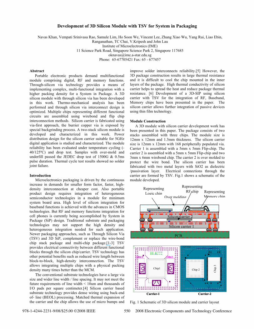
A 3D module with silicon carrier development work has been presented in this paper. The package consists of two stacks assembled with three chips. The module size is 12mm x 12mm and 1.3mm thickness. The silicon carrier size is 12mm x 12mm with 168 peripherally populated via. Carrier 1 is assembled with a 5mm x 5mm Flip-chip. The carrier 2 is assembled with a 5mm x 5mm Flip-chip and two 3mm x 6mm wirebond chip. The carrier 2 is over molded to protect the wire bond. The silicon carrier has been fabricated with two metal layers with SiO2 as dielectric /passivation layer. Electrical connections through the carrier are formed by TSV. Fig.1 shows a schematic of the module developed.
Fig. 1 Schematic of 3D silicon module and carrier layout
Carrier-1 Carrier-2
Chip1 Chip 2
Chi
p 3
Carrier-1 Carrier-2
Chip1Chip1 Chip 2
Chi
p 3
Chip 2
Chi
p 3
Representing Logic chip
Representing RF chip Representing
Memory chipOver molding
Silicon carrier 1
Silicon carrier 2
PCB
978-1-4244-2231-9/08/$25.00 ©2008 IEEE 550 2008 Electronic Components and Technology Conference
Thermo-Mechanical Design Thermo-mechanical design of the silicon module is
important for the reliable package structure. Structural parameters like via size, via shape and solder joint are analyzed for the minimum thermo-mechanical stress. The FE analysis is carried using ABAQUS [7]. Two dimensional eight node solid element is used for the FE model. The stress free temperature state is taken as 125°C for thermo-mechanical analysis. Material properties used for the thermo-mechanical analysis is given in Table 1. Table1. Material properties for Thermo-mechanical analysis
Young Modulus
(Gpa)
Poisson ratio
CTE (ppm/°C)
BCB 2.9 0.34 52
SiO2 70 0.16 0.6 Ti 116 0.34 8.9 Silicon 129.617 (25 °C)
128.425 (150 °C) 0.28 2.813 (25 °C)
3.107 (150 °C)
SnAgCu 44.4 (25 °C) 30.7 (75 °C) 18.8 (125 °C)
0.4 21
PCB Ex,y = 22.4 (30 °C), 19.3 (125 °C) Ez = 16 (30 °C), 1 (125 °C)
vx = 0.2 vy,z = 0.1425
αx,y = 16 αz = 65
Cu
E = 130.0 εp = 0, σ = 0.1379 εp = 0.098982, σ = 0.2715
0.34 18
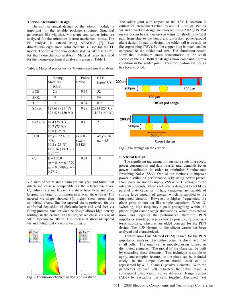
Via sizes of 50um and 100um are analyzed and found that interfacial stress is comparable for the selected via sizes. Cylindrical via and tapered via shape have been analyzed, keeping the target of minimum interfacial shear stress. The tapered via shape showed 8% higher shear stress than cylindrical shape. But the tapered via is preferred for the conformal deposition of dielectric layer and void free via filling process. Smaller via size design allows high density routing in the carrier. In this project we chose via size of 50um tapering to 100um. The interfacial stress of tapered via and cylindrical via is shown in Fig. 2. Fig. 2 Thermo-mechanical analysis of via shape
The solder joint with respect to the TSV is location is critical for interconnect reliability and RDL design. Pad on via and off-set via design are analyzed using ABAQUS. Pad on via design has advantages in terms for shorter electrical path from chip to the board and un-broken power/ground plane design. In pad-on design, the solder ball is directly on the copper plug (TSV), but the copper plug is much smaller compared to the solder pad area. The simulation results show that, maximum stress concentration at the small section of the via. Both the designs show comparable stress condition in the solder joint. Therefore pad-on via design has been selected. Fig.3 Via arrange on the carrier Electrical Design
The significant increasing in transistors switching speed, power consumption and data transfer rate, demands better power distribution in order to minimize Simultaneous Switching Noise (SSN). One of the methods to improve power distribution performance is by using power planes. Plane pairs are used to supply VSS & VCC voltages to the integrated circuits, where each pair is designed to act like a parallel plate capacitor. These capacitors are capable of storing large amount of energy, which is supplied to the integrated circuits. However, at higher frequencies, the plane pairs do not act like simple capacitors. When IC switching, high frequency signals propagating within the planes might cause voltage fluctuations, which translates to noise and degrades the performance, therefore, PDN impedance should be kept as low as possible. Silicon is a lossy substrate, which is an added concern for the PDN design. The PDN design for the silicon carrier has been analyzed and characterized.
Transmission Line Method (TLM) is used for the PDN impedance analysis. The entire plane is discretized into small cells. The small cell is modeled using lumped or distributed elements. The model of the plane can be built by cascading these elements. This technique is simple to apply, and complex features on the plane can be included easily. In the lumped-element model, each cell is represented by R, L, C and G passive elements. With the parameters of each cell extracted, the entire plane is constructed using circuit solver Advance Design System (ADS) by cascading the cells together. Designed Test
200µm
200µm 500 µm
500 µm
500 µm
200µm
200µm
Off-set pad design
On-pad design
200µm
200µm 500 µm
500 µm
200µm
200µm 500 µm
500 µm
500 µm
200µm
200µm
500 µm
200µm
200µm
Off-set pad design
On-pad design
551 2008 Electronic Components and Technology Conference
vehicles are designed and fabricated to identify if any power integrity related issues in our silicon carrier design.
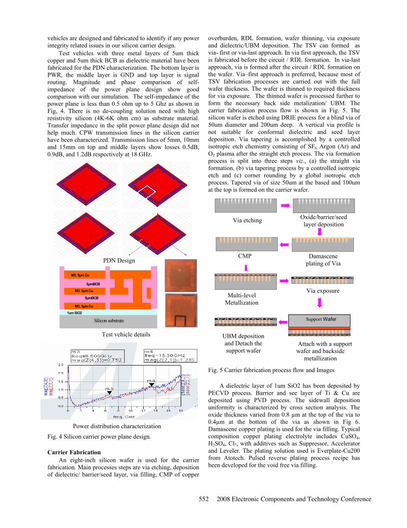
Test vehicles with three metal layers of 5um thick copper and 5um thick BCB as dielectric material have been fabricated for the PDN characterization. The bottom layer is PWR, the middle layer is GND and top layer is signal routing. Magnitude and phase comparison of self-impedance of the power plane design show good comparison with our simulation. The self-impedance of the power plane is less than 0.5 ohm up to 5 Ghz as shown in Fig, 4. There is no de-coupling solution need with high resistivity silicon (4K-6K ohm cm) as substrate material. Transfer impedance in the split power plane design did not help much. CPW transmission lines in the silicon carrier have been characterized. Transmission lines of 5mm, 10mm and 15mm on top and middle layers show losses 0.5dB, 0.9dB, and 1.2dB respectively at 18 GHz. Fig. 4 Silicon carrier power plane design. Carrier Fabrication
An eight-inch silicon wafer is used for the carrier fabrication. Main processes steps are via etching, deposition of dielectric/ barrier/seed layer, via filling, CMP of copper
overburden, RDL formation, wafer thinning, via exposure and dielectric/UBM deposition. The TSV can formed as via- first or via-last approach. In via first approach, the TSV is fabricated before the circuit / RDL formation. In via-last approach, via is formed after the circuit / RDL formation on the wafer. Via–first approach is preferred, because most of TSV fabrication processes are carried out with the full wafer thickness. The wafer is thinned to required thickness for via exposure. The thinned wafer is processed further to form the necessary back side metalization/ UBM. The carrier fabrication process flow is shown in Fig. 5. The silicon wafer is etched using DRIE process for a blind via of 50um diameter and 200um deep. A vertical via profile is not suitable for conformal dielectric and seed layer deposition. Via tapering is accomplished by a controlled isotropic etch chemistry consisting of SF6 Argon (Ar) and O2 plasma after the straight etch process. The via formation process is split into three steps viz., (a) the straight via formation, (b) via tapering process by a controlled isotropic etch and (c) corner rounding by a global isotropic etch process. Tapered via of size 50um at the based and 100um at the top is formed on the carrier wafer.
Fig. 5 Carrier fabrication process flow and Images A dielectric layer of 1um SiO2 has been deposited by
PECVD process. Barrier and see layer of Ti & Cu are deposited using PVD process. The sidewall deposition uniformity is characterized by cross section analysis. The oxide thickness varied from 0.8 µm at the top of the via to 0.4µm at the bottom of the via as shown in Fig 6. Damascene copper plating is used for the via filling. Typical composition copper plating electrolyte includes CuSO4, H2SO4, Cl-, with additives such as Suppressor, Accelerator and Leveler. The plating solution used is Everplate-Cu200 from Atotech. Pulsed reverse plating process recipe has been developed for the void free via filling.
Attach with a support wafer and backside
metallization
Oxide/barrier/seed layer deposition
Damascene plating of Via
Via etching
CMP
Multi-level Metallization
Via exposure
UBM deposition and Detach the support wafer
Support Wafer
PDN Design
M3: 5µm Cu
M3: 5µm Cu
M3: 5µm Cu
5µmBCB
5µmBCB
1um SiO2
Silicon substrate
M3: 5µm Cu
M3: 5µm Cu
M3: 5µm Cu
5µmBCB
5µmBCB
1um SiO2
Silicon substrate
Test vehicle details
Power distribution characterization
552 2008 Electronic Components and Technology Conference
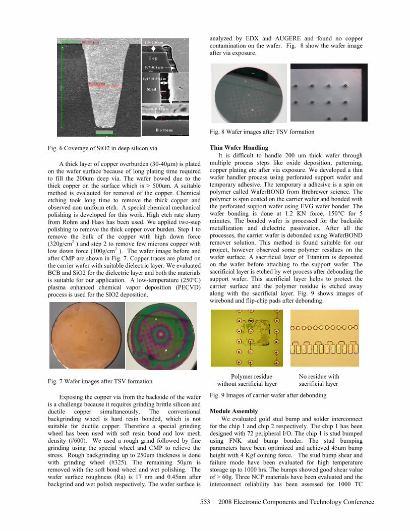
Fig. 6 Coverage of SiO2 in deep silicon via
A thick layer of copper overburden (30-40µm) is plated on the wafer surface because of long plating time required to fill the 200um deep via. The wafer bowed due to the thick copper on the surface which is > 500um. A suitable method is evalauted for removal of the copper. Chemical etching took long time to remove the thick copper and observed non-uniform etch. A special chemical mechanical polishing is developed for this work. High etch rate slurry from Rohm and Hass has been used. We applied two-step polishing to remove the thick copper over burden. Step 1 to remove the bulk of the copper with high down force (320g/cm2 ) and step 2 to remove few microns copper with low down force (100g/cm2 ). The wafer image before and after CMP are shown in Fig. 7. Copper traces are plated on the carrier wafer with suitable dielectric layer. We evaluated BCB and SiO2 for the dielectric layer and both the materials is suitable for our application. A low-temperature (250ºC) plasma enhanced chemical vapor deposition (PECVD) process is used for the SIO2 deposition.
Fig. 7 Wafer images after TSV formation
Exposing the copper via from the backside of the wafer is a challenge because it requires grinding brittle silicon and ductile copper simultaneously. The conventional backgrinding wheel is hard resin bonded, which is not suitable for ductile copper. Therefore a special grinding wheel has been used with soft resin bond and low mesh density (#600). We used a rough grind followed by fine grinding using the special wheel and CMP to relieve the stress. Rough backgrinding up to 250um thickness is done with grinding wheel (#325). The remaining 50µm is removed with the soft bond wheel and wet polishing. The wafer surface roughness (Ra) is 17 nm and 0.45nm after backgrind and wet polish respectively. The wafer surface is
analyzed by EDX and AUGERE and found no copper contamination on the wafer. Fig. 8 show the wafer image after via exposure. Fig. 8 Wafer images after TSV formation Thin Wafer Handling
It is difficult to handle 200 um thick wafer through multiple process steps like oxide deposition, patterning, copper plating etc after via exposure. We developed a thin wafer handler process using perforated support wafer and temporary adhesive. The temporary a adhesive is a spin on polymer called WaferBOND from Brebrewer science. The polymer is spin coated on the carrier wafer and bonded with the perforated support wafer using EVG wafer bonder. The wafer bonding is done at 1.2 KN force, 150°C for 5 minutes. The bonded wafer is processed for the backside metallization and dielectric passivation. After all the processes, the carrier wafer is debonded using WaferBOND remover solution. This method is found suitable for our project, however observed some polymer residues on the wafer surface. A sacrificial layer of Titanium is deposited on the wafer before attaching to the support wafer. The sacrificial layer is etched by wet process after debonding the support wafer. This sacrificial layer helps to protect the carrier surface and the polymer residue is etched away along with the sacrificial layer. Fig. 9 shows images of wirebond and flip-chip pads after debonding. Fig. 9 Images of carrier wafer after debonding Module Assembly
We evaluated gold stud bump and solder interconnect for the chip 1 and chip 2 respectively. The chip 1 has been designed with 72 peripheral I/O. The chip 1 is stud bumped using FNK stud bump bonder. The stud bumping parameters have been optimized and achieved 45um bump height with 4 Kgf coining force. The stud bump shear and failure mode have been evaluated for high temperature storage up to 1000 hrs. The bumps showed good shear value of > 60g. Three NCP materials have been evaluated and the interconnect reliability has been assessed for 1000 TC
Polymer residue without sacrificial layer
No residue with sacrificial layer
T o p
M id
B o t to m
1 .9 -2 .0 µ m
0 .7 -0 .8 µ m
0 .4 5 -0 .5 5 µ m
0 .3 5 -0 .4 5 µ m
553 2008 Electronic Components and Technology Conference
cycles. All the three materials with bonding force > 10 kgf showed no failure after TC test. Fig.10 shows the stud profile and cross section of the chip attachment. The chip 2 has been designed with 252 I/O at 200um bump pitch. The chip 2 is bumped using SAC 305 type 6 solder paste and achieved bump height of 55um. The bump shear has been evaluated for Pb free reflow condition up to 5x. The shear value is > 60g and failure mode is bulk solder. Fig. 10 Images of stud bump interconnection
The chip 3 represents memory die in our module design. Stacking of two chips has been demonstrated using DDAF and wire embedding film. Three DDAF materials have been evaluated and all the materials showed no void after MST level 3. One of the materials has been selected based on minimum bleeding and high hot shear value. Wire embedding film is an emerging technique to stack wire bond chips. The film is soft enough to flow over the wires and there is no need for a spacer die. This method gives small stand-off for the stacked wirebond chips. The bond parameters like top / bottom heater temperature and bond speed have been optimized. The carrier 2 is assembled with flip-chip and wire bond chip. Therefore the pad finish should be suitable for both the chip attachment methods. Pads on the carrier top and bottom side are plated with electoless NiPdAu. Wire bondability and wire pull strength are found good on the NiPdAu pads. Two chips have been stacked and demonstrated low loop height (< 50um) for the chip stacking. Fig 11 show the stacked wire bond die assembled for this work. Fig. 11 Images of stacked wire bond chips
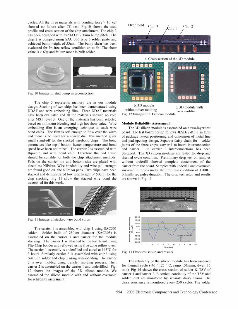
The carrier 1 is assembled with chip 1 using SAC305 solder. Solder balls of 250um diameter (SAC305) is assembled on the carrier 1 and carrier for the module stacking. The carrier 1 is attached to the test board using Flip-Chip bonder and reflowed using five-zone reflow oven. The carrier 1 assembly is underfilled and cured at 165°C for 3 hours. Similarly carrier 2 is assembled with chip2 using SAC305 solder and chip 3 using wire-bonding. The carrier 2 is over molded using transfer molding process. Then carrier 2 is assembled on the carrier 1 and underfilled. Fig. 12 shows the images of the 3D silicon module. We assembled the silicon module with and without overmold for reliability assessment.
Fig. 12 Images of 3D silicon module Module Reliability Assessment
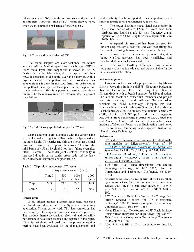
The 3D silicon module is assembled on a two-layer test board. The test board design follows JESD22-B111 in term of package layout positioning and dimension of metal line and pad opening design. Separate daisy chain for solder joints of the three chips, carrier 1 to board interconnection and carrier 1 to carrier 2 interconnections has been designed. The 3D silicon modules are tested for drop and thermal cycle condition. Preliminary drop test on samples without underfill showed complete detachment of the carrier from the board. Samples with underfill and overmold survived 30 drops under the drop test condition of 1500G, 0.5milli-sec pulse duration. The drop test setup and results are shown in Fig. 13 Fig. 13 Drop test set-up and results
The reliability of the silicon module has been assessed for thermal cycle (-40 / 125 º C, ramp 15C/min, dwell 15 min). Fig 14 shows the cross section of solder & TSV of carrier 1 and carrier 2. Electrical continuity of the TSV and solder joint are monitored by separate daisy chains. The daisy resistance is monitored every 250 cycles. The solder
Chip 1 Chip 2Chip 3Over mold
b. 3D module without over molding
c. 3D module with over molding
a. Cross section of the 3D module
-2000
-1500
-1000
-500
0
500
1000
1500
2000
0 1 2 3 4 5 6 7 8 9 10Time (ms)
Acc
eler
atio
n (G
), St
rain
(mic
rost
rain
), 68
0 x
log
R
Strain adj to packageD1D3C2D2C1Shock acceleration
554 2008 Electronic Components and Technology Conference
interconnect and TSV joints showed no crack or detachment at time zero. However some of TSV chains showed open, when we measured the resistance after 500 cycles.
Fig. 14 Cross section of solder and TSV
The failed samples are cross-sectioned for failure analysis. All the failed samples show detachment of RDL / UBM metal layer form copper via as shown in Fig 15. During the carrier fabrication, the via exposed and 1um SiO2 is deposited as dielectric layer and patterned. A thin layer if Ti and Cu is sputtered on the exposed via, then copper plating is done for the RDL formation. Adhesion of the sputtered metal layer on the copper via may be poor due copper oxidation. This is a potential cause for the above failure. The team is working on a cleaning step to prevent such failure. Fig. 15 SEM micro graph failed sample for TC test
Chip 1 and chip 2 are assembled with the carrier using solder. The solder height is ~ 50um, which helps to reduce the stack height. The carrier and chip are silicon, no thermal mismatch between the chip and the carrier. Therefore the mini-bump of ~ 50um height did not show failure even after 2000 TC cycles. The solder joint electrical continuity is measured directly on the carrier probe pads and the daisy chain electrical resistances are given table 2.
Table 2. Chip solder interconnect TC results
Daisy chain resistance (ohm)
Time 0 500 cycles
1000 cycles
2000 cycles
Chip 1 24.3 24.3 24.3 34.3
Chip 2 17.3 18 18.9 20.5
Conclusions
A 3D silicon module platform technology has been developed and demonstrated for System in Packaging application. Silicon carrier with TSV interconnection has been developed for chip attachment and embedded passives. The module thermo-mechanical, electrical and reliability performances have been assessed and reported in the paper. Flip-chip, wirebond and gold stud bump interconnection method have been evaluated for the chip attachment and
joint reliability has been reported. Some important results and recommendations are summarized as follow. • The power distribution and signal transmission in the silicon carrier of size 12mm x 12mm have been analyzed and found suitable for high frequency digital application up to 5 Ghz using three metal layers with 5um BCB dialectic. • A tapered via structure has been designed for 200um deep through silicon via and void free filling has been achieved using damascene pulse -reverse plating. • Silicon carrier fabrication process integration based via-first approach has been established and developed 200um thick carrier with TSV • Thin wafer handling technique using spin-on temporary adhesive is evaluated and found suitable for the silicon carrier fabrication.
Acknowledgments This work is the result of a project initiated by Micro-
System Packaging Initiative (MSPI) Electronic Packaging Research Consortium, EPRC VIII Project 2: Stacked Silicon Module with embedded passives for SiP application. The authors thank the consortium members and project team for their support and guidance. The consortium members are ASM Technology Singapore Pte Ltd, Freescale Semiconductor Malaysia Sdn Bhd., Ltd , Infineon Technologies Asia Pacific Pte Ltd, Microcircuit Technology (2002) Pte Ltd , STATSChipPAC Ltd. , Ibiden Singapore Pte. Ltd., Surface Technology Systems Pte Ltd., United Test and Assembly Center Ltd, Institute of microelectronics, Institute of Materials Research and Engineering, Institute of High Performance Computing and Singapore Institute of Manufacturing Technology.
References 1. CM Val, ”3D-Packaging applications of vertical multi
chip modules for Microsystems”, Proc. of 16th IEEE/CPMT Electronics Manufacturing Technology Symposium, La Joila, CA, Vol 1, pp.387-393, 1994
2. S.F.Al-Sarawi, D. Abbott, P. Franzon, “A Review of 3D-packaging technology”, IEEE Trans-CPMT-B, Vol.21, No.1 (1998), pp.2-14.
3. Yuji Yano et al, “Three-dimensional Thin stacked packaging technology for SiP”, 2002, Electronic Components and Technology Conference, pp 1329-11334
4. Knickerbocker et al., “Development of next-generation system-on-package (SOP) technology based on silicon carriers with fine-pitch chip interconnection”, IBM J. RES. & DEV. VOL. 49 NO. 4/5 JULY/SEPTEMBER 2005
5. S.W Yoon et al., “Reliability Studies of a Through Via Silicon Stacked Modules for 3D Microsystem Packaging”, 2006 Electronics Components Technology Conference ECTC, pp 1449 – 1453.
6. Navas Khan et al., “Development of 3D Stack Package Using Silicon Interposer for High Power Application”, 2006 Electronics Components Technology Conference ECTC, pp 756 – 760
7. ABAQUS 6.41, Hibbitt, Karlsson & Sorensen Inc. RI, USA
555 2008 Electronic Components and Technology Conference