Integration and Packaging of a Macrochip With Silicon Nanophotonic Links
13
546 IEEE JOURNAL OF SELECTED TOPICS IN QUANTUM ELECTRONICS, VOL. 17, NO. 3, MAY/JUNE 2011 Integration and Packaging of a Macrochip With Silicon Nanophotonic Links John E. Cunningham, Ashok V. Krishnamoorthy, Senior Member, IEEE, Ron Ho, Senior Member, IEEE, Ivan Shubin, Member, IEEE, Hiren Thacker, Member, IEEE, Jon Lexau, Member, IEEE, Daniel C. Lee, Dazeng Feng, Eugene Chow, Ying Luo, Xuezhe Zheng, Senior Member, IEEE, Guoliang Li, Senior Member, IEEE, Jin Yao, Thierry Pinguet, Kannan Raj, Mehdi Asghari, and James G. Mitchell (Invited Paper) Abstract—The technologies associated with integration and packaging have a significant impact on the overall system. In this paper, we review a silicon photonic “macrochip” system and its associated packaging that will allow dense wavelength- division multiplexed optical links to be intimately integrated and co-manufactured with the switching electronics. For this to happen, we anticipate a number of integration and packaging advances. Index Terms—CMOS, computing, macrochip, nanophotonics, optical interconnects, routers, silicon photonics, switching, very large scale integration (VLSI). I. INTRODUCTION O VER the past several decades, dramatic improvements in the performance of computing systems have fundamen- tally changed the fabric of everyday life. We can see this in personal computing: today’s gigahertz-frequency mobile pro- cessors are individually more powerful than an entire room full of computers just a decade ago. Even more significant to modern society is the wide availability of clustered computers running large-scale applications from commerce and banking to medicine and scientific research. These advancements in computing horsepower have largely been driven by the engine of Moore’s Law, which calls for a doubling of integrated transistors per chip approximately ev- ery 18 months [1]. Although perhaps more appropriately called “Moore’s self-fulfilling prophecy,” this prediction has closely Manuscript received July 16, 2010; revised September 21, 2010; accepted October 12, 2010. Date of publication January 12, 2011; date of current version June 8, 2011. This work was supported in part by Defense Advanced Research Projects Agency, Microsystems Technology Office under Agreement HR0011– 08-09–0001. The views, opinions, and/or findings contained in this article are those of the authors and should not be interpreted as representing the official views or policies, either expressed or implied, of the Defense Advanced Re- search Projects Agency or the Department of Defense. This document has been approved for public release, distribution unlimited. J. E. Cunningham, A. V. Krishnamoorthy, I. Shubin, H. Thacker, Y. Luo, X. Zheng, G. Li, J. Yao, and K. Raj are with Oracle Labs, San Diego, CA 92121 USA. R. Ho, J. Lexau, and J. G. Mitchell are with Oracle Labs, Menlo Park, CA 94025 USA. D. C. Lee, D. Feng, and M. Asghari are with Kotura Inc., Los Angeles, CA 91754 USA. E. Chow is with the Palo Alto Research Center, Palo Alto, CA 94304 USA. T. Pinguet is with Luxtera Inc., Carlsbad, CA 92011 USA. Color versions of one or more of the figures in this paper are available online at http://ieeexplore.ieee.org. Digital Object Identifier 10.1109/JSTQE.2010.2091674 matched historical trends in integrated circuits since the mid- 1960s. This is a direct consequence of society’s constant in- crease, over the same time period, in technology spending. Only by continually ramping up financial investment in semiconduc- tor processing have we been able to reap the economic advan- tages of larger and larger silicon wafers, each with finer and finer transistors. The reason that this increase in the number of transistors per chip has made possible high-performance microprocessors is because it has given chip designers a way to implement in- creasingly complex systems. A simple CPU from the 1980s would perform a single operation per clock “tick.” Pipelining such a system dramatically increased execution throughput but required many more transistors for data-preserving registers. Similarly, adding large on-chip caches reduced memory stalls and significantly boosted performance of this simple pipelined machine, but also required many more on-chip transistors for static memory cells. Furthermore, doubling the execution units of this simple cache-based pipelined machine enabled it to ex- ploit limited instruction-level parallelism by executing two non- dependent instructions simultaneously, but again required many more transistors. These are three simple examples of an underly- ing reality: that almost every significant architectural improve- ment done to processors involves spending more transistors, and hence, requires ongoing progression of a Moore’s Law-like trend. Of course, transistor integration is only part of the story. Designers have also leveraged a roughly 40% increase per generation in transistor performance that has historically ac- companied the devices’ dimensional scaling. They have also pushed the boundaries of energy efficiency by scaling clock frequency far beyond what basic scaled transistor perfor- mance would have predicted. However, both of these de- sign variables—transistor performance and disproportional fre- quency increases—have plateaued. Transistor performance at 28–32 nm transistor lengths, for example, are only slightly faster than devices at the 40–45 nm generation, and careless layout practices can easily make them slower. Frequency ramping has also settled down from the breakneck pace of ten years ago: while the ITRS roadmap in 2001 had predicted 12 GHz proces- sors by 2010, power efficiency concerns have limited processors to a peak closer to 5 GHz today [2]. As we look forward to fu- ture system designs, it appears that the best remaining lever 1077-260X/$26.00 © 2011 IEEE
-
Upload
seattlecentral -
Category
Documents
-
view
3 -
download
0
Transcript of Integration and Packaging of a Macrochip With Silicon Nanophotonic Links
546 IEEE JOURNAL OF SELECTED TOPICS IN QUANTUM ELECTRONICS, VOL. 17, NO. 3, MAY/JUNE 2011
Integration and Packaging of a MacrochipWith Silicon Nanophotonic Links
John E. Cunningham, Ashok V. Krishnamoorthy, Senior Member, IEEE, Ron Ho, Senior Member, IEEE,Ivan Shubin, Member, IEEE, Hiren Thacker, Member, IEEE, Jon Lexau, Member, IEEE, Daniel C. Lee,
Dazeng Feng, Eugene Chow, Ying Luo, Xuezhe Zheng, Senior Member, IEEE, Guoliang Li, Senior Member, IEEE,Jin Yao, Thierry Pinguet, Kannan Raj, Mehdi Asghari, and James G. Mitchell
(Invited Paper)
Abstract—The technologies associated with integration andpackaging have a significant impact on the overall system. Inthis paper, we review a silicon photonic “macrochip” systemand its associated packaging that will allow dense wavelength-division multiplexed optical links to be intimately integrated andco-manufactured with the switching electronics. For this to happen,we anticipate a number of integration and packaging advances.
Index Terms—CMOS, computing, macrochip, nanophotonics,optical interconnects, routers, silicon photonics, switching, verylarge scale integration (VLSI).
I. INTRODUCTION
OVER the past several decades, dramatic improvements inthe performance of computing systems have fundamen-
tally changed the fabric of everyday life. We can see this inpersonal computing: today’s gigahertz-frequency mobile pro-cessors are individually more powerful than an entire roomfull of computers just a decade ago. Even more significant tomodern society is the wide availability of clustered computersrunning large-scale applications from commerce and banking tomedicine and scientific research.
These advancements in computing horsepower have largelybeen driven by the engine of Moore’s Law, which calls for adoubling of integrated transistors per chip approximately ev-ery 18 months [1]. Although perhaps more appropriately called“Moore’s self-fulfilling prophecy,” this prediction has closely
Manuscript received July 16, 2010; revised September 21, 2010; acceptedOctober 12, 2010. Date of publication January 12, 2011; date of current versionJune 8, 2011. This work was supported in part by Defense Advanced ResearchProjects Agency, Microsystems Technology Office under Agreement HR0011–08-09–0001. The views, opinions, and/or findings contained in this article arethose of the authors and should not be interpreted as representing the officialviews or policies, either expressed or implied, of the Defense Advanced Re-search Projects Agency or the Department of Defense. This document has beenapproved for public release, distribution unlimited.
J. E. Cunningham, A. V. Krishnamoorthy, I. Shubin, H. Thacker, Y. Luo,X. Zheng, G. Li, J. Yao, and K. Raj are with Oracle Labs, San Diego, CA 92121USA.
R. Ho, J. Lexau, and J. G. Mitchell are with Oracle Labs, Menlo Park, CA94025 USA.
D. C. Lee, D. Feng, and M. Asghari are with Kotura Inc., Los Angeles, CA91754 USA.
E. Chow is with the Palo Alto Research Center, Palo Alto, CA 94304 USA.T. Pinguet is with Luxtera Inc., Carlsbad, CA 92011 USA.Color versions of one or more of the figures in this paper are available online
at http://ieeexplore.ieee.org.Digital Object Identifier 10.1109/JSTQE.2010.2091674
matched historical trends in integrated circuits since the mid-1960s. This is a direct consequence of society’s constant in-crease, over the same time period, in technology spending. Onlyby continually ramping up financial investment in semiconduc-tor processing have we been able to reap the economic advan-tages of larger and larger silicon wafers, each with finer andfiner transistors.
The reason that this increase in the number of transistorsper chip has made possible high-performance microprocessorsis because it has given chip designers a way to implement in-creasingly complex systems. A simple CPU from the 1980swould perform a single operation per clock “tick.” Pipeliningsuch a system dramatically increased execution throughput butrequired many more transistors for data-preserving registers.Similarly, adding large on-chip caches reduced memory stallsand significantly boosted performance of this simple pipelinedmachine, but also required many more on-chip transistors forstatic memory cells. Furthermore, doubling the execution unitsof this simple cache-based pipelined machine enabled it to ex-ploit limited instruction-level parallelism by executing two non-dependent instructions simultaneously, but again required manymore transistors. These are three simple examples of an underly-ing reality: that almost every significant architectural improve-ment done to processors involves spending more transistors,and hence, requires ongoing progression of a Moore’s Law-liketrend.
Of course, transistor integration is only part of the story.Designers have also leveraged a roughly 40% increase pergeneration in transistor performance that has historically ac-companied the devices’ dimensional scaling. They have alsopushed the boundaries of energy efficiency by scaling clockfrequency far beyond what basic scaled transistor perfor-mance would have predicted. However, both of these de-sign variables—transistor performance and disproportional fre-quency increases—have plateaued. Transistor performance at28–32 nm transistor lengths, for example, are only slightly fasterthan devices at the 40–45 nm generation, and careless layoutpractices can easily make them slower. Frequency ramping hasalso settled down from the breakneck pace of ten years ago:while the ITRS roadmap in 2001 had predicted 12 GHz proces-sors by 2010, power efficiency concerns have limited processorsto a peak closer to 5 GHz today [2]. As we look forward to fu-ture system designs, it appears that the best remaining lever
1077-260X/$26.00 © 2011 IEEE

CUNNINGHAM et al.: INTEGRATION AND PACKAGING OF A MACROCHIP WITH SILICON NANOPHOTONIC LINKS 547
for pushing performance is to continue Moore’s Law growth intransistor integration.
Unfortunately, the end of Moore’s Law is rapidly approach-ing. From a technical perspective, the roadblocks ahead revolvearound scaling transistor dimensions down to atomic sizes. Thismeans, for example, that the proper doping of tiny volumes ofbulk silicon will require just a handful of atoms, which makesthe resulting doping levels statistically uncertain. However, a farmore fundamental limit looms ahead: today’s global economicreality makes the historical growth in financial investment insemiconductors unsustainable. A single fabrication plant for a20–22-nm process technology will cost in excess of several bil-lion dollars, or a few percent of the entire global semiconductormarket. Development of such finer linewidths will, by necessity,slow down; after all, Moore’s Law is based upon exponentialgrowth, and as one expert on Moore’s Law has noted, “no ex-ponential is forever” [3].
The challenge to designers is clear: if we wish to continue toincrease the performance of large-scale systems, we must findways to economically increase system integration—maintainingor improving energy efficiency—while Moore’s Law continuesto slow down. Building very large chips, to the limit of thelithographic imaging reticle, is a half measure but not an eco-nomically viable one, due to defects inherent to the semicon-ductor manufacturing process. An overly simplified yield model(that still provides useful trends for hand calculation) shows thatyield, as a function of die area in square centimeter, is approx-imately (1 + 0.35×A)(−4) [4]. Thus, the prepackaged die costfor a 7 cm2 chip—the reticle limit today—is nearly 20× moreexpensive than a chip only 2 cm2 in area. If we could somehowmanufacture a 20 cm2 chip, it would be nearly 500×more costlythan a chip only 1/10th its size.
Economically speaking, we would be much better off build-ing many smaller interconnected chips. However, the problemthen arises: how do we provision for communication betweenall of these smaller chips? Recent innovations in chip pack-aging, test, and assembly have made possible tightly packedchips on a common board, or in a common package, or evenstuck together with a form of “3-D” integration. But these manysmaller chips would need an interconnect fabric, whose band-width, latency, and energy efficiency rivals that of on-chip wires,or else their separation would be to no avail: a memory cachethat resides on a separate chip and that is accessed through alow-bandwidth interface would not benefit performance at all.Rather, we would want these several smaller chips to aggregateto a “virtual monolithic” chip, whose performance and energycharacteristics closely model a single integrated chip. Such aconstruction would allow increased integration and increasedperformance without relying on Moore’s Law.
Other benefits accrue to this “macrochip” concept: by inter-connecting together many chips, we need not use individualchips from the same technology. Some could be built on dy-namic memory (DRAM) platforms, others on standard logicprocesses, still others on technologies specialized for radio fre-quency circuits. This mix-and-match paradigm would allow forhigher energy efficiency and higher performance, as each func-tional block can be manufactured with its optimal transistors.
Fig. 1. Macrochip is a logically contiguous piece of densely interconnectedsilicon that integrates CPUs, memory, and a systemwide optical interconnect.
The challenges of the interconnect between chips are largelyphysical and package-based, not topological; the latter has beenalready addressed by a host of research and industrial designs(for an overview, see [5]). Yet the physical design space ap-pears to be already overly constrained. First, connecting chipsthrough traditional solder balls (or worse, bond wires) to ei-ther a package or a board leads to a wire density problem: thepitch of solder balls ranges from 0.12 to 0.15 mm, or roughlytwo orders of magnitude larger than the pitch of on-chip wires.This areal “impedance mismatch” forces designers to overclockthe few channels available to them, at high overhead, and ul-timately limits the total available off-chip bandwidth. Second,although “through-silicon vias” employs small-pitch I/O thatmore closely matches on-chip wires, they require chips to bevertically stacked, and for thermal and power delivery reasons,this limits their applications primarily to memory or other verylow power chips.
In this paper, we discuss a set of technologies: optical, packag-ing, and electrical, which offers a way through this scaling prob-lem. The next sections briefly define and review the macrochipand describe electrical and optical packaging advances that willhelp enable the implementation of this system vision.
II. REVIEW OF THE MACROCHIP
As motivated earlier, a macrochip is a logically contigu-ous piece of photonically interconnected silicon that integratesCPUs, memory, and a system-wide interconnect [6]. It pro-vides significant advantages in computational density, energyefficiency, bisection bandwidth, and reduced message latencyover traditional integrated multichip systems. Optical proximitycommunication (OPxC) connects the CPUs distributed on themacrochip to optical routing layers; these support low-latency,wavelength-division multiplexed (WDM) optical links betweensites using silicon-on-insulator (SOI) photonic waveguides (seeFig. 1). The photonic network on a macrochip provides lowpower, high bandwidth, and high-density communication be-tween sites. Every site in a macrochip is interconnected to everyother site via WDM links that run in orthogonal directions ontwo routing layers. The optical signals from the sites are coupledinto, and between, the routing layers through OPxC face-to-faceoptical couplers. Such a system could achieve switched opticalinterconnect at ≤1 pJ/bit, provide waveguide transport band-width densities in excess of 10 TB/s/mm, and surface normal
548 IEEE JOURNAL OF SELECTED TOPICS IN QUANTUM ELECTRONICS, VOL. 17, NO. 3, MAY/JUNE 2011
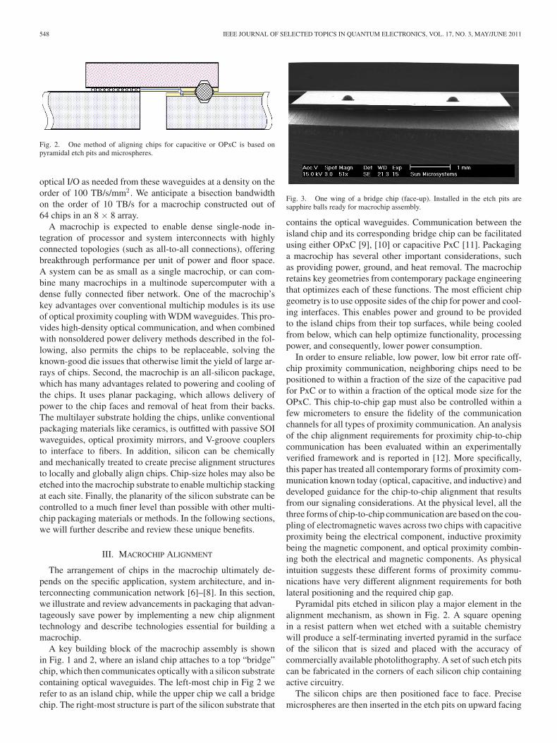
Fig. 2. One method of aligning chips for capacitive or OPxC is based onpyramidal etch pits and microspheres.
optical I/O as needed from these waveguides at a density on theorder of 100 TB/s/mm2 . We anticipate a bisection bandwidthon the order of 10 TB/s for a macrochip constructed out of64 chips in an 8 × 8 array.
A macrochip is expected to enable dense single-node in-tegration of processor and system interconnects with highlyconnected topologies (such as all-to-all connections), offeringbreakthrough performance per unit of power and floor space.A system can be as small as a single macrochip, or can com-bine many macrochips in a multinode supercomputer with adense fully connected fiber network. One of the macrochip’skey advantages over conventional multichip modules is its useof optical proximity coupling with WDM waveguides. This pro-vides high-density optical communication, and when combinedwith nonsoldered power delivery methods described in the fol-lowing, also permits the chips to be replaceable, solving theknown-good die issues that otherwise limit the yield of large ar-rays of chips. Second, the macrochip is an all-silicon package,which has many advantages related to powering and cooling ofthe chips. It uses planar packaging, which allows delivery ofpower to the chip faces and removal of heat from their backs.The multilayer substrate holding the chips, unlike conventionalpackaging materials like ceramics, is outfitted with passive SOIwaveguides, optical proximity mirrors, and V-groove couplersto interface to fibers. In addition, silicon can be chemicallyand mechanically treated to create precise alignment structuresto locally and globally align chips. Chip-size holes may also beetched into the macrochip substrate to enable multichip stackingat each site. Finally, the planarity of the silicon substrate can becontrolled to a much finer level than possible with other multi-chip packaging materials or methods. In the following sections,we will further describe and review these unique benefits.
III. MACROCHIP ALIGNMENT
The arrangement of chips in the macrochip ultimately de-pends on the specific application, system architecture, and in-terconnecting communication network [6]–[8]. In this section,we illustrate and review advancements in packaging that advan-tageously save power by implementing a new chip alignmenttechnology and describe technologies essential for building amacrochip.
A key building block of the macrochip assembly is shownin Fig. 1 and 2, where an island chip attaches to a top “bridge”chip, which then communicates optically with a silicon substratecontaining optical waveguides. The left-most chip in Fig 2 werefer to as an island chip, while the upper chip we call a bridgechip. The right-most structure is part of the silicon substrate that
Fig. 3. One wing of a bridge chip (face-up). Installed in the etch pits aresapphire balls ready for macrochip assembly.
contains the optical waveguides. Communication between theisland chip and its corresponding bridge chip can be facilitatedusing either OPxC [9], [10] or capacitive PxC [11]. Packaginga macrochip has several other important considerations, suchas providing power, ground, and heat removal. The macrochipretains key geometries from contemporary package engineeringthat optimizes each of these functions. The most efficient chipgeometry is to use opposite sides of the chip for power and cool-ing interfaces. This enables power and ground to be providedto the island chips from their top surfaces, while being cooledfrom below, which can help optimize functionality, processingpower, and consequently, lower power consumption.
In order to ensure reliable, low power, low bit error rate off-chip proximity communication, neighboring chips need to bepositioned to within a fraction of the size of the capacitive padfor PxC or to within a fraction of the optical mode size for theOPxC. This chip-to-chip gap must also be controlled within afew micrometers to ensure the fidelity of the communicationchannels for all types of proximity communication. An analysisof the chip alignment requirements for proximity chip-to-chipcommunication has been evaluated within an experimentallyverified framework and is reported in [12]. More specifically,this paper has treated all contemporary forms of proximity com-munication known today (optical, capacitive, and inductive) anddeveloped guidance for the chip-to-chip alignment that resultsfrom our signaling considerations. At the physical level, all thethree forms of chip-to-chip communication are based on the cou-pling of electromagnetic waves across two chips with capacitiveproximity being the electrical component, inductive proximitybeing the magnetic component, and optical proximity combin-ing both the electrical and magnetic components. As physicalintuition suggests these different forms of proximity commu-nications have very different alignment requirements for bothlateral positioning and the required chip gap.
Pyramidal pits etched in silicon play a major element in thealignment mechanism, as shown in Fig. 2. A square openingin a resist pattern when wet etched with a suitable chemistrywill produce a self-terminating inverted pyramid in the surfaceof the silicon that is sized and placed with the accuracy ofcommercially available photolithography. A set of such etch pitscan be fabricated in the corners of each silicon chip containingactive circuitry.
The silicon chips are then positioned face to face. Precisemicrospheres are then inserted in the etch pits on upward facing
CUNNINGHAM et al.: INTEGRATION AND PACKAGING OF A MACROCHIP WITH SILICON NANOPHOTONIC LINKS 549
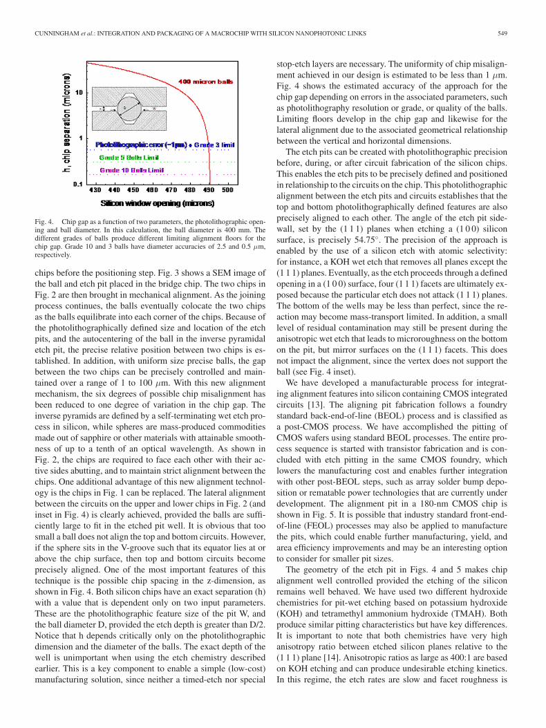
Fig. 4. Chip gap as a function of two parameters, the photolithographic open-ing and ball diameter. In this calculation, the ball diameter is 400 mm. Thedifferent grades of balls produce different limiting alignment floors for thechip gap. Grade 10 and 3 balls have diameter accuracies of 2.5 and 0.5 μm,respectively.
chips before the positioning step. Fig. 3 shows a SEM image ofthe ball and etch pit placed in the bridge chip. The two chips inFig. 2 are then brought in mechanical alignment. As the joiningprocess continues, the balls eventually colocate the two chipsas the balls equilibrate into each corner of the chips. Because ofthe photolithographically defined size and location of the etchpits, and the autocentering of the ball in the inverse pyramidaletch pit, the precise relative position between two chips is es-tablished. In addition, with uniform size precise balls, the gapbetween the two chips can be precisely controlled and main-tained over a range of 1 to 100 μm. With this new alignmentmechanism, the six degrees of possible chip misalignment hasbeen reduced to one degree of variation in the chip gap. Theinverse pyramids are defined by a self-terminating wet etch pro-cess in silicon, while spheres are mass-produced commoditiesmade out of sapphire or other materials with attainable smooth-ness of up to a tenth of an optical wavelength. As shown inFig. 2, the chips are required to face each other with their ac-tive sides abutting, and to maintain strict alignment between thechips. One additional advantage of this new alignment technol-ogy is the chips in Fig. 1 can be replaced. The lateral alignmentbetween the circuits on the upper and lower chips in Fig. 2 (andinset in Fig. 4) is clearly achieved, provided the balls are suffi-ciently large to fit in the etched pit well. It is obvious that toosmall a ball does not align the top and bottom circuits. However,if the sphere sits in the V-groove such that its equator lies at orabove the chip surface, then top and bottom circuits becomeprecisely aligned. One of the most important features of thistechnique is the possible chip spacing in the z-dimension, asshown in Fig. 4. Both silicon chips have an exact separation (h)with a value that is dependent only on two input parameters.These are the photolithographic feature size of the pit W, andthe ball diameter D, provided the etch depth is greater than D/2.Notice that h depends critically only on the photolithographicdimension and the diameter of the balls. The exact depth of thewell is unimportant when using the etch chemistry describedearlier. This is a key component to enable a simple (low-cost)manufacturing solution, since neither a timed-etch nor special
stop-etch layers are necessary. The uniformity of chip misalign-ment achieved in our design is estimated to be less than 1 μm.Fig. 4 shows the estimated accuracy of the approach for thechip gap depending on errors in the associated parameters, suchas photolithography resolution or grade, or quality of the balls.Limiting floors develop in the chip gap and likewise for thelateral alignment due to the associated geometrical relationshipbetween the vertical and horizontal dimensions.
The etch pits can be created with photolithographic precisionbefore, during, or after circuit fabrication of the silicon chips.This enables the etch pits to be precisely defined and positionedin relationship to the circuits on the chip. This photolithographicalignment between the etch pits and circuits establishes that thetop and bottom photolithographically defined features are alsoprecisely aligned to each other. The angle of the etch pit side-wall, set by the (1 1 1) planes when etching a (1 0 0) siliconsurface, is precisely 54.75◦. The precision of the approach isenabled by the use of a silicon etch with atomic selectivity:for instance, a KOH wet etch that removes all planes except the(1 1 1) planes. Eventually, as the etch proceeds through a definedopening in a (1 0 0) surface, four (1 1 1) facets are ultimately ex-posed because the particular etch does not attack (1 1 1) planes.The bottom of the wells may be less than perfect, since the re-action may become mass-transport limited. In addition, a smalllevel of residual contamination may still be present during theanisotropic wet etch that leads to microroughness on the bottomon the pit, but mirror surfaces on the (1 1 1) facets. This doesnot impact the alignment, since the vertex does not support theball (see Fig. 4 inset).
We have developed a manufacturable process for integrat-ing alignment features into silicon containing CMOS integratedcircuits [13]. The aligning pit fabrication follows a foundrystandard back-end-of-line (BEOL) process and is classified asa post-CMOS process. We have accomplished the pitting ofCMOS wafers using standard BEOL processes. The entire pro-cess sequence is started with transistor fabrication and is con-cluded with etch pitting in the same CMOS foundry, whichlowers the manufacturing cost and enables further integrationwith other post-BEOL steps, such as array solder bump depo-sition or rematable power technologies that are currently underdevelopment. The alignment pit in a 180-nm CMOS chip isshown in Fig. 5. It is possible that industry standard front-end-of-line (FEOL) processes may also be applied to manufacturethe pits, which could enable further manufacturing, yield, andarea efficiency improvements and may be an interesting optionto consider for smaller pit sizes.
The geometry of the etch pit in Figs. 4 and 5 makes chipalignment well controlled provided the etching of the siliconremains well behaved. We have used two different hydroxidechemistries for pit-wet etching based on potassium hydroxide(KOH) and tetramethyl ammonium hydroxide (TMAH). Bothproduce similar pitting characteristics but have key differences.It is important to note that both chemistries have very highanisotropy ratio between etched silicon planes relative to the(1 1 1) plane [14]. Anisotropic ratios as large as 400:1 are basedon KOH etching and can produce undesirable etching kinetics.In this regime, the etch rates are slow and facet roughness is
550 IEEE JOURNAL OF SELECTED TOPICS IN QUANTUM ELECTRONICS, VOL. 17, NO. 3, MAY/JUNE 2011
Fig. 5. Etch pit integrated into a commercial CMOS node using a BEOLmicrofabrication module.
hard to control. In our applications, we have instead deployed aprocess with lower anisotropic ratios near 40:1, where the etchrates are close to 1 μm/min. This results in an etching processwith more manufacturable timing compatible with flows in atypical commercial foundry. We note that this develops an un-dercut because of the small but finite etch rate for the (1 1 1)silicon planes. However, such undercuts of the hard mask arefound to be highly reproducible. The resulting difference in thechip gap owing to a reduced anisotropic etch can be factoredin numerically in the mask window (photolithographic defini-tion) and the same accuracy in chip gap is achieved for typicalanisotropic ratios of (40:1) compared with (400:1). The undercutof the silicon beneath the hard mask for TMAH etching is abouttwice as large as that found for KOH. KOH is a very aggressivemetal containing chemistry to integrate into a CMOS processflow. KOH is therefore problematic when developing either aFEOL or a BEOL pitting process in a commercial foundry. Onthe other hand, TMAH is a chemistry commonly found in re-sist developers in similar concentrations, and hence is highlycompatible with CMOS processing.
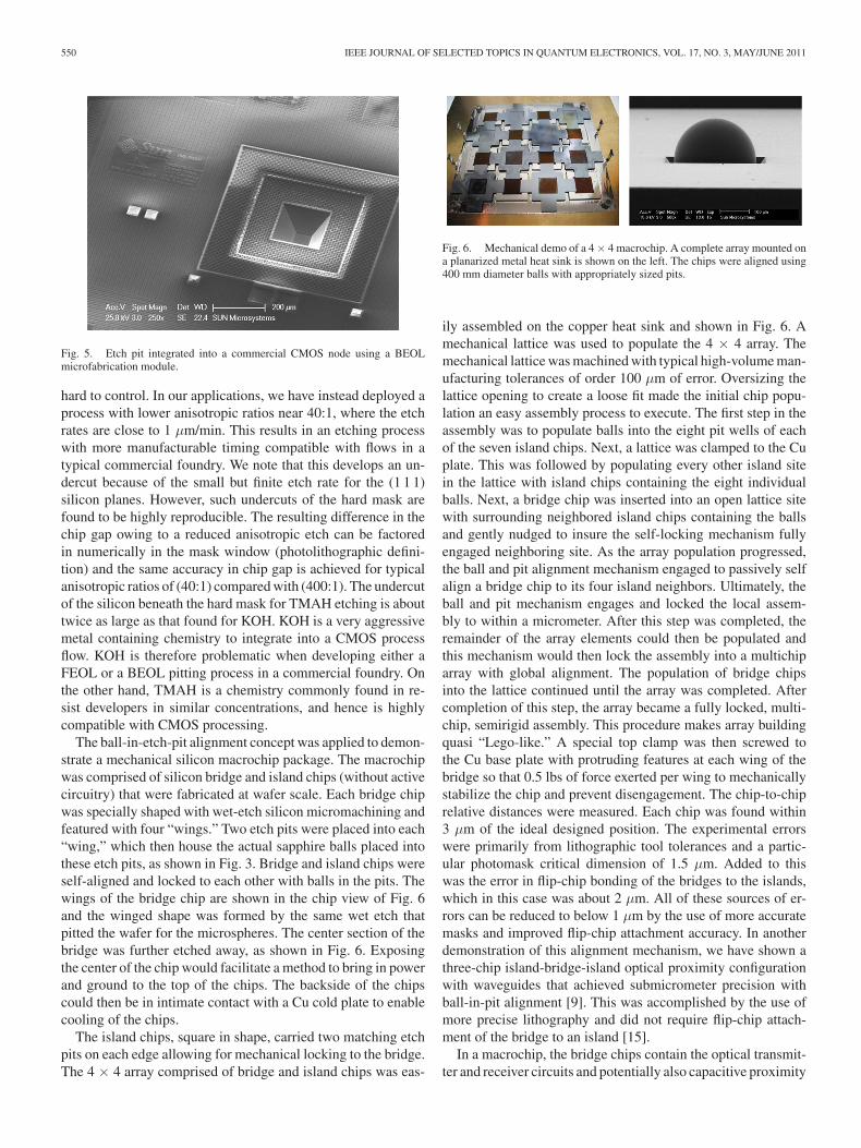
The ball-in-etch-pit alignment concept was applied to demon-strate a mechanical silicon macrochip package. The macrochipwas comprised of silicon bridge and island chips (without activecircuitry) that were fabricated at wafer scale. Each bridge chipwas specially shaped with wet-etch silicon micromachining andfeatured with four “wings.” Two etch pits were placed into each“wing,” which then house the actual sapphire balls placed intothese etch pits, as shown in Fig. 3. Bridge and island chips wereself-aligned and locked to each other with balls in the pits. Thewings of the bridge chip are shown in the chip view of Fig. 6and the winged shape was formed by the same wet etch thatpitted the wafer for the microspheres. The center section of thebridge was further etched away, as shown in Fig. 6. Exposingthe center of the chip would facilitate a method to bring in powerand ground to the top of the chips. The backside of the chipscould then be in intimate contact with a Cu cold plate to enablecooling of the chips.
The island chips, square in shape, carried two matching etchpits on each edge allowing for mechanical locking to the bridge.The 4 × 4 array comprised of bridge and island chips was eas-
Fig. 6. Mechanical demo of a 4 × 4 macrochip. A complete array mounted ona planarized metal heat sink is shown on the left. The chips were aligned using400 mm diameter balls with appropriately sized pits.
ily assembled on the copper heat sink and shown in Fig. 6. Amechanical lattice was used to populate the 4 × 4 array. Themechanical lattice was machined with typical high-volume man-ufacturing tolerances of order 100 μm of error. Oversizing thelattice opening to create a loose fit made the initial chip popu-lation an easy assembly process to execute. The first step in theassembly was to populate balls into the eight pit wells of eachof the seven island chips. Next, a lattice was clamped to the Cuplate. This was followed by populating every other island sitein the lattice with island chips containing the eight individualballs. Next, a bridge chip was inserted into an open lattice sitewith surrounding neighbored island chips containing the ballsand gently nudged to insure the self-locking mechanism fullyengaged neighboring site. As the array population progressed,the ball and pit alignment mechanism engaged to passively selfalign a bridge chip to its four island neighbors. Ultimately, theball and pit mechanism engages and locked the local assem-bly to within a micrometer. After this step was completed, theremainder of the array elements could then be populated andthis mechanism would then lock the assembly into a multichiparray with global alignment. The population of bridge chipsinto the lattice continued until the array was completed. Aftercompletion of this step, the array became a fully locked, multi-chip, semirigid assembly. This procedure makes array buildingquasi “Lego-like.” A special top clamp was then screwed tothe Cu base plate with protruding features at each wing of thebridge so that 0.5 lbs of force exerted per wing to mechanicallystabilize the chip and prevent disengagement. The chip-to-chiprelative distances were measured. Each chip was found within3 μm of the ideal designed position. The experimental errorswere primarily from lithographic tool tolerances and a partic-ular photomask critical dimension of 1.5 μm. Added to thiswas the error in flip-chip bonding of the bridges to the islands,which in this case was about 2 μm. All of these sources of er-rors can be reduced to below 1 μm by the use of more accuratemasks and improved flip-chip attachment accuracy. In anotherdemonstration of this alignment mechanism, we have shown athree-chip island-bridge-island optical proximity configurationwith waveguides that achieved submicrometer precision withball-in-pit alignment [9]. This was accomplished by the use ofmore precise lithography and did not require flip-chip attach-ment of the bridge to an island [15].
In a macrochip, the bridge chips contain the optical transmit-ter and receiver circuits and potentially also capacitive proximity
CUNNINGHAM et al.: INTEGRATION AND PACKAGING OF A MACROCHIP WITH SILICON NANOPHOTONIC LINKS 551
communication circuitry. A primary function of the bridge willbe to connect two or more island chips together. Bridge chipscontaining processor cores may also be bonded to the mem-ory chips. The bridge chips can be flip-chip bonded to islandchips, and derive power from the island. This allows separationof the cooling and power delivery functions on opposite sidesof the macrochip. The bridge chip can be thinned and can havean arbitrary shape, defined by saw-cut edges as well as etchedand lapped features. Two, three, or four wings can be provided,which allows compliant overlap with neighboring chips alongone or two dimensions, as shown in Figs. 1 and 6.
IV. REMATABLE ELECTRICAL CONNECTIONS
TO THE MACROCHIP
We have developed a potential rematable power deliverysolution for the macrochip. Our approach is based on stress-engineered spring interconnects that can improve testing, re-mateability, and conductive connection tolerance for the powerdelivery infrastructure deployed within large chip array pack-ages, such as the macrochip [16], [17]. Further, as I/O pad sizeand pitch reduce over the course of new technology generations,our spring-based interconnect approach can be miniaturized tokeep pace owing to their lithographic definition. These inter-connects can be tailored to particular die and package targets; assuch, they can be specified to have the required level of compli-ance and to exert adequate force for reliable electrical connectionwithout causing damage to the low-κ interlayer dielectric mate-rials to which current generation CMOS nodes have transitioned.In the previous section, we introduced and demonstrated thecointegration of pyramidal etch pits micromachined in siliconand matching high-precision microballs in order to meet tightplacement tolerances and alleviate chip-to-chip alignment lim-itations. Here, we report progress on the development and test-ing of spring-based interconnects for macrochip applications.Second, we discuss the integration of the spring interconnectswith etched alignment pits and microballs to provide rematableelectrical connections to deliver power and concurrently achievethe necessary accuracy in alignment, and facilitate assembly andrework of the macrochip modules.
The described packaging approach combines benefits of com-pliant spring interconnect with the passive alignment techniquedescribed earlier. The working prototypes were assembled intopackages with the spring chips mated to pad chips containingdaisy chains. The assembly is simplified and limited to twochips (one bottom chip already carries microballs housed in theetched pits). In this package, both chips are initially coarselyaligned within half the ball diameter, then the microballs cap-ture the opposing etch pits and autocenter them; therefore, bring-ing the chips into micrometer-scale alignment leads to low-costplacement. The package is fastened with a clamp providing0.5 pounds of force to secure chips and can be taken apartand put back together to original tolerances allowing immediatechip replacement. This is a powerful, cost-effective packagingtechnique simultaneously capable of supporting high alignmenttolerance requirements and large current density.
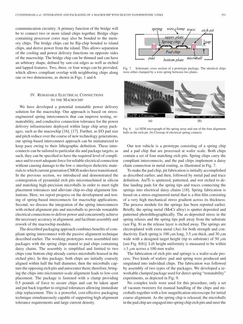
Fig. 7. Schematic cross section of a prototype package. The identical chipswere either clamped by a wire spring between two plates.
Fig. 8. (a) SEM micrograph of the spring array and one of the four alignmentballs in the etch pit. (b) Closeup of electrical spring contacts.
Our test vehicle is a prototype consisting of a spring chipand a pad chip that are processed at wafer scale. Both chipscontain a set of four matching etch pits. Spring chips carry thecompliant interconnects, and the pad chips implement a daisychain connection in metal routing, as illustrated in Fig. 7.
To make the pad chip, pit fabrication is initially accomplishedas described earlier, and then, followed by metal pad and tracedefinition. Au/Ti is sputtered, patterned, and wet etched to de-fine landing pads for the spring tips and traces connecting thesprings into electrical daisy chains [18]. Spring fabrication isbased on a stress-engineered metal that is a thin film consistingof a very high mechanical stress gradient across its thickness.The process module for the springs has been reported earlier.Briefly, the spring metal (MoCr alloy) is sputter deposited andpatterned photolithographically. The as-deposited stress in thespring relaxes and the spring tips pull away from the substrate(see Fig. 8) as the release layer is etched away. The springs areelectroplated with extra metal (Au) for both strength and con-ductivity. Each spring is 100 μm long, 3.5 μm thick, and 30 μmwide with a designed target height (tip to substrate) of 50 μm[see Fig. 8(b)]. Lift height uniformity is measured to be within±3 μm across a 100-mm wafer.
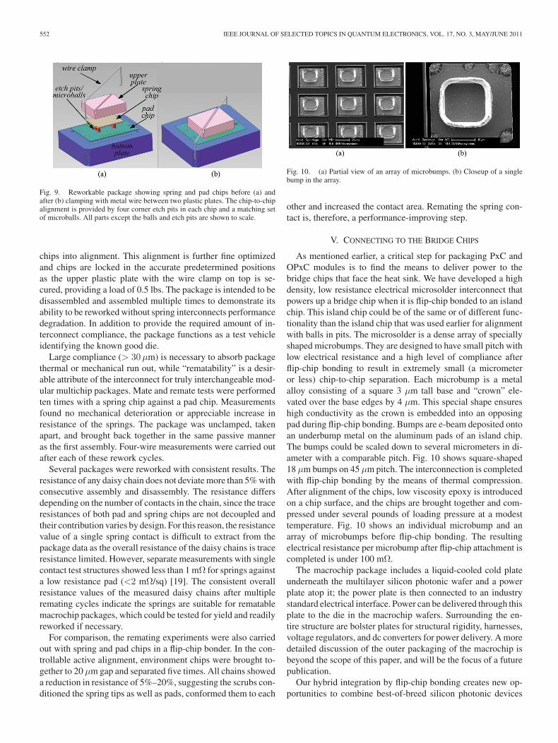
The fabrication of etch pits and springs is a wafer-scale pro-cess. Two kinds of wafers: pad and spring were produced andsingulated into individual chips. The fabrication was followedby assembly of two types of the packages. We developed a re-workable clamped package used for direct spring “rematability”experiments, as depicted in Fig. 9.
No complex tools were used for this procedure, only a setof vacuum tweezers for manual handling of the chips and mi-croballs together with a low magnification microscope for initialcoarse alignment. As the spring chip is released, the microballsin the pad chip are engaged into spring chip etch pits and steer the
552 IEEE JOURNAL OF SELECTED TOPICS IN QUANTUM ELECTRONICS, VOL. 17, NO. 3, MAY/JUNE 2011
Fig. 9. Reworkable package showing spring and pad chips before (a) andafter (b) clamping with metal wire between two plastic plates. The chip-to-chipalignment is provided by four corner etch pits in each chip and a matching setof microballs. All parts except the balls and etch pits are shown to scale.
chips into alignment. This alignment is further fine optimizedand chips are locked in the accurate predetermined positionsas the upper plastic plate with the wire clamp on top is se-cured, providing a load of 0.5 lbs. The package is intended to bedisassembled and assembled multiple times to demonstrate itsability to be reworked without spring interconnects performancedegradation. In addition to provide the required amount of in-terconnect compliance, the package functions as a test vehicleidentifying the known good die.
Large compliance (> 30μm) is necessary to absorb packagethermal or mechanical run out, while “rematability” is a desir-able attribute of the interconnect for truly interchangeable mod-ular multichip packages. Mate and remate tests were performedten times with a spring chip against a pad chip. Measurementsfound no mechanical deterioration or appreciable increase inresistance of the springs. The package was unclamped, takenapart, and brought back together in the same passive manneras the first assembly. Four-wire measurements were carried outafter each of these rework cycles.
Several packages were reworked with consistent results. Theresistance of any daisy chain does not deviate more than 5% withconsecutive assembly and disassembly. The resistance differsdepending on the number of contacts in the chain, since the traceresistances of both pad and spring chips are not decoupled andtheir contribution varies by design. For this reason, the resistancevalue of a single spring contact is difficult to extract from thepackage data as the overall resistance of the daisy chains is traceresistance limited. However, separate measurements with singlecontact test structures showed less than 1 mΩ for springs againsta low resistance pad (<2 mΩ/sq) [19]. The consistent overallresistance values of the measured daisy chains after multipleremating cycles indicate the springs are suitable for rematablemacrochip packages, which could be tested for yield and readilyreworked if necessary.
For comparison, the remating experiments were also carriedout with spring and pad chips in a flip-chip bonder. In the con-trollable active alignment, environment chips were brought to-gether to 20 μm gap and separated five times. All chains showeda reduction in resistance of 5%–20%, suggesting the scrubs con-ditioned the spring tips as well as pads, conformed them to each
Fig. 10. (a) Partial view of an array of microbumps. (b) Closeup of a singlebump in the array.
other and increased the contact area. Remating the spring con-tact is, therefore, a performance-improving step.
V. CONNECTING TO THE BRIDGE CHIPS
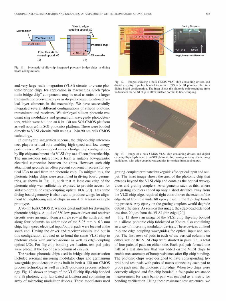
As mentioned earlier, a critical step for packaging PxC andOPxC modules is to find the means to deliver power to thebridge chips that face the heat sink. We have developed a highdensity, low resistance electrical microsolder interconnect thatpowers up a bridge chip when it is flip-chip bonded to an islandchip. This island chip could be of the same or of different func-tionality than the island chip that was used earlier for alignmentwith balls in pits. The microsolder is a dense array of speciallyshaped microbumps. They are designed to have small pitch withlow electrical resistance and a high level of compliance afterflip-chip bonding to result in extremely small (a micrometeror less) chip-to-chip separation. Each microbump is a metalalloy consisting of a square 3 μm tall base and “crown” ele-vated over the base edges by 4 μm. This special shape ensureshigh conductivity as the crown is embedded into an opposingpad during flip-chip bonding. Bumps are e-beam deposited ontoan underbump metal on the aluminum pads of an island chip.The bumps could be scaled down to several micrometers in di-ameter with a comparable pitch. Fig. 10 shows square-shaped18 μm bumps on 45 μm pitch. The interconnection is completedwith flip-chip bonding by the means of thermal compression.After alignment of the chips, low viscosity epoxy is introducedon a chip surface, and the chips are brought together and com-pressed under several pounds of loading pressure at a modesttemperature. Fig. 10 shows an individual microbump and anarray of microbumps before flip-chip bonding. The resultingelectrical resistance per microbump after flip-chip attachment iscompleted is under 100 mΩ.
The macrochip package includes a liquid-cooled cold plateunderneath the multilayer silicon photonic wafer and a powerplate atop it; the power plate is then connected to an industrystandard electrical interface. Power can be delivered through thisplate to the die in the macrochip wafers. Surrounding the en-tire structure are bolster plates for structural rigidity, harnesses,voltage regulators, and dc converters for power delivery. A moredetailed discussion of the outer packaging of the macrochip isbeyond the scope of this paper, and will be the focus of a futurepublication.
Our hybrid integration by flip-chip bonding creates new op-portunities to combine best-of-breed silicon photonic devices
CUNNINGHAM et al.: INTEGRATION AND PACKAGING OF A MACROCHIP WITH SILICON NANOPHOTONIC LINKS 553
Fig. 11. Schematic of flip-chip integrated photonic bridge chips in divingboard configurations.
and very large scale integration (VLSI) circuits to create pho-tonic bridge chips for application in macrochips. Such “pho-tonic bridge chip” components may be used as units in a largertransmitter or receiver array or as drop-in communication phys-ical layer elements in the macrochip. We have successfullyintegrated several different configurations of silicon photonictransmitters and receivers. We deployed silicon photonic res-onant ring modulators and germanium waveguide photodetec-tors, which were built on an 8-in 130 nm SOI-CMOS platformas well as on a 6-in SOI-photonics platform. These were bondeddirectly to VLSI circuits built using a 12-in 90 nm bulk CMOStechnology.
In our hybrid integration scheme, the chip-to-chip intercon-nect plays a critical role enabling high-speed and low-energyperformance. We developed various bridge chip configurationsby flip-chip attachment of a VLSI chip to a silicon photonic chip.The microsolder interconnects form a suitably low-parasiticelectrical connection between the chips. However such chipattachment geometries often prevent convenient access for op-tical I/Os to and from the photonic chip. To mitigate this, thephotonic bridge chips were assembled in diving board geome-tries, as shown in Fig. 11, such that at least one edge of thephotonic chip was sufficiently exposed to provide access forsurface-normal or edge-coupling optical I/Os [20]. This samediving board geometry is also used to produce wings for align-ment to neighboring island chips in our 4 × 4 array exampleprototype.
A 90-nm bulk CMOS IC was designed and built for driving thephotonic bridges. A total of 330 low-power driver and receivercircuits were arranged along a single row at the north end andalong four columns on either side of the 5.25 mm × 6.3 mmchip; high-speed electrical input/output pads were located at thesouth end. Having the driver and receiver circuits laid out inthis configuration allowed us to bond the same VLSI chip tophotonic chips with surface-normal as well as edge-couplingoptical I/Os. For flip-chip bonding verification, test-pad pairswere placed at the top of each column of circuits.
The various photonic chips used in bridge chip constructionincluded resonant microring modulator chips and germaniumwaveguide photodetector chips built in both a 130-nm CMOSprocess technology as well as a SOI-photonics process technol-ogy. Fig. 12 shows an image of the VLSI chip flip-chip bondedto a Si photonic chip fabricated at Luxtera and containing anarray of microring modulator devices. These modulators used
Fig. 12. Images showing a bulk CMOS VLSI chip containing drivers anddigital circuitry flip-chip bonded to an SOI CMOS VLSI photonic chip in adiving board configuration. The inset shows the photonic chip extending fromunderneath the VLSI chip to allow surface normal to fiber coupling.
Fig. 13. Image of a bulk CMOS VLSI chip containing drivers and digitalcircuitry flip-chip bonded to an SOI photonic chip bearing an array of microringmodulators with edge-coupled waveguides for optical input and output.
grating-coupler terminated waveguides for optical input and out-put. The inset image shows the area of the photonic chip thatextends beyond the VLSI chip and contains the optical waveg-uides and grating couplers. Arrangements such as this, wherethe grating couplers ended up only a short distance away fromthe VLSI chip edge, required tight control over the extent of theedge-bead from the underfill epoxy used in the flip-chip bond-ing process. Any epoxy on the grating couplers would degradeoutput efficiency. As seen on this image, the edge-bead extendedless than 20 μm from the VLSI chip edge [20].
Fig. 13 shows an image of the VLSI chip flip-chip bondedto a silicon photonic chip fabricated at Kotura also containingan array of microring modulator devices. These devices utilizedin-plane edge coupling waveguides for optical input and out-put. The first rows of pads in each of the vertical columns oneither side of the VLSI chip were shorted in pairs, i.e., a totalof four pairs of pads on either side. Each pad pair formed onehalf of a test structure that was added on the VLSI chips toenable measurement of bump resistance after flip-chip bonding.The photonic chips were designed to have corresponding hy-brid bond test pads with pairs of traces connecting each pad toprobe pads near the photonic chip edge. When two chips werecorrectly aligned and flip-chip bonded, a four-point resistancemeasurement for each bump pair was enabled as a metric forbonding verification. Using these resistance test structures, we

554 IEEE JOURNAL OF SELECTED TOPICS IN QUANTUM ELECTRONICS, VOL. 17, NO. 3, MAY/JUNE 2011
measured an average bump resistance of 0.6 Ω across severalhybrid bridge chips; the minimum measured bump resistancewas 0.05 Ω. We expect the bump capacitance to be on the orderof 20 fF.
Hybrid integration of photonic chips having edge-couplingwaveguides requires additional consideration related to theirpreparation prior to use. Specifically, the input and output wave-guide facets need to be polished and coated with an antireflection(AR) material for optimal fiber-to-waveguide optical coupling.Typically, these processes are carried out on singulated die, butdoing so would require handling the tiny singulated chips formicrosolder postprocessing, while also preserving the quality ofthe waveguide facets—a tall order. As such, the adopted process-of-record was to carry out waveguide polishing and AR coatingafter flip-chip integration. This process itself is not without risk;polishing is a harsh mechanical process, and components mustbe held with a significant amount of force to keep them stablewhile the polishing wheel is in operation. In this case, the com-ponent is a flip-chip bonded hybrid, which would not toleratesignificant surface-normal or shear forces over the bond zone.In addition, standard AR-coating processes require a 200 ◦C en-vironment, which is beyond the tolerance limit of the underfillused.
Two process improvements helped to overcome these hurdles.First, for the polishing process, a small piece of the polishinggasket material was taped down to the exposed area of the edge-coupling photonic chip in the hybrid. Using this as both a spacerand load-bearing segment, the hybrids were mounted onto apolishing fixture to carry out the process. With this fixture, noload is applied directly on the VLSI chip and the bond zone,which contains the microsolder bump connections. Second, forthe AR coating, a room temperature process was developed andqualified for use on the hybrid chips. Additionally, a temporaryprotective cover was placed over the exposed wire-bond pads.
We measured the bump resistance at different stages of thehybrid integration process for edge-coupled photonic chips: af-ter flip-chip bonding, after polishing, and after AR coating. Nosignificant change in resistance was observed and the bumpscontinued to maintain their subohm resistance characteristicsthrough this process sequence. In addition, the polished andAR-coated waveguides were measured to have approximately–14 dB reflection.
VI. WDM MULTIPLEXERS, DEMULTIPLEXERS, ROUTING, AND
INTERLAYER COUPLERS, AND WAVEGUIDE ROUTING
ON THE “MACROCHIP”
So far we have focused on integrating optical device chips tosystem chips, and assumed that silicon waveguides would con-nect chips to their distant data origins and destinations acrossthe macrochip. As previously noted, one of the macrochip’s keyadvantages over conventional multichip modules is its use ofoptical proximity coupling with WDM waveguides. In previ-ous work, we reported OPxC results for chip-to-chip couplingbased on reflective pits in waveguide geometries that were basedon large, quasi-single-mode waveguides [9]. The waveguideshad lateral mode sizes near 10 μm wide to facilitate low-loss
Fig. 14. Optical proximity coupler based on reflecting mirror facet. An ex-ploded view of the mode transformer is shown on the upper left and an SEM ofthe facet is shown on the upper right.
Fig. 15. Integration of the reflecting pit coupler and an echelle grating-basedWDM mux/demux [21]. In the top view, the left waveguide is tapered for fibercoupling, while the waveguides on the right side that follow the grating areeach terminated with an OPxC coupler. The echelle grating provides the 1 × 4mux/demux functionality with a 1.6 nm wavelength separation. Demonstrationvehicle shown in bottom view.
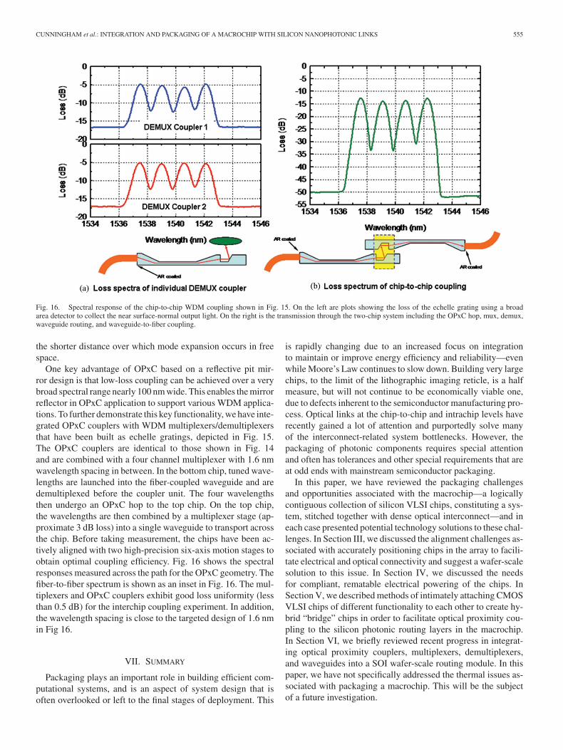
chip-to-chip coupling of 3.5 dB for a mirror pair. However, ourmacrochip-link budget is optimized with 3-μm wide waveg-uides for optimum interlayer routing and 0.5 μm waveguidesfor device geometries that deploy tight bending radii. Here, wereview recent results on OPxC coupling based on the 3-μmwide waveguides, wherein mode tapering is used to expand thewaveguide to 12 μm for accomplishing the optical hop from abottom to top chip [21]. Fig. 14 depicts the associated geometry.Starting left to right in Fig. 14, the bottom chip is fiber coupledinto 12 μm wide waveguide, which then undergoes mode trans-formation down to 3 μm before traversing over a centimeterlength of bottom chip upon reaching the OPxC coupler. Thespecific design of the chip-to-chip coupler is similar to the de-sign reported earlier; however, as Fig. 14 depicts, the mode isexpanded from the 3 μm waveguide to a 12 μm waveguide be-fore reaching the end terminating facet. The actual details of theOPxC coupler is similar to our previously reported geometrywith exception that the mode expands in the free space sectiona shorter distance (55 μm) than previously reported (66 μm).Continuing left to right in Fig. 14 for the top chip, the opticalpath has similar functionality while going from the reflecting pitto the fiber coupler. The OPxC hop is composed of the pair ofreflecting facets and end face waveguide facets on both top andbottom chips and has a measured loss of 2.7 dB. This couplingloss is improved from previous results that range from 3.5 to3 dB [9]. Part of this improvement is associated with improvedmicrofabrication in the next generation iteration, and second,
CUNNINGHAM et al.: INTEGRATION AND PACKAGING OF A MACROCHIP WITH SILICON NANOPHOTONIC LINKS 555
Fig. 16. Spectral response of the chip-to-chip WDM coupling shown in Fig. 15. On the left are plots showing the loss of the echelle grating using a broadarea detector to collect the near surface-normal output light. On the right is the transmission through the two-chip system including the OPxC hop, mux, demux,waveguide routing, and waveguide-to-fiber coupling.
the shorter distance over which mode expansion occurs in freespace.
One key advantage of OPxC based on a reflective pit mir-ror design is that low-loss coupling can be achieved over a verybroad spectral range nearly 100 nm wide. This enables the mirrorreflector in OPxC application to support various WDM applica-tions. To further demonstrate this key functionality, we have inte-grated OPxC couplers with WDM multiplexers/demultiplexersthat have been built as echelle gratings, depicted in Fig. 15.The OPxC couplers are identical to those shown in Fig. 14and are combined with a four channel multiplexer with 1.6 nmwavelength spacing in between. In the bottom chip, tuned wave-lengths are launched into the fiber-coupled waveguide and aredemultiplexed before the coupler unit. The four wavelengthsthen undergo an OPxC hop to the top chip. On the top chip,the wavelengths are then combined by a multiplexer stage (ap-proximate 3 dB loss) into a single waveguide to transport acrossthe chip. Before taking measurement, the chips have been ac-tively aligned with two high-precision six-axis motion stages toobtain optimal coupling efficiency. Fig. 16 shows the spectralresponses measured across the path for the OPxC geometry. Thefiber-to-fiber spectrum is shown as an inset in Fig. 16. The mul-tiplexers and OPxC couplers exhibit good loss uniformity (lessthan 0.5 dB) for the interchip coupling experiment. In addition,the wavelength spacing is close to the targeted design of 1.6 nmin Fig 16.
VII. SUMMARY
Packaging plays an important role in building efficient com-putational systems, and is an aspect of system design that isoften overlooked or left to the final stages of deployment. This
is rapidly changing due to an increased focus on integrationto maintain or improve energy efficiency and reliability—evenwhile Moore’s Law continues to slow down. Building very largechips, to the limit of the lithographic imaging reticle, is a halfmeasure, but will not continue to be economically viable one,due to defects inherent to the semiconductor manufacturing pro-cess. Optical links at the chip-to-chip and intrachip levels haverecently gained a lot of attention and purportedly solve manyof the interconnect-related system bottlenecks. However, thepackaging of photonic components requires special attentionand often has tolerances and other special requirements that areat odd ends with mainstream semiconductor packaging.
In this paper, we have reviewed the packaging challengesand opportunities associated with the macrochip—a logicallycontiguous collection of silicon VLSI chips, constituting a sys-tem, stitched together with dense optical interconnect—and ineach case presented potential technology solutions to these chal-lenges. In Section III, we discussed the alignment challenges as-sociated with accurately positioning chips in the array to facili-tate electrical and optical connectivity and suggest a wafer-scalesolution to this issue. In Section IV, we discussed the needsfor compliant, rematable electrical powering of the chips. InSection V, we described methods of intimately attaching CMOSVLSI chips of different functionality to each other to create hy-brid “bridge” chips in order to facilitate optical proximity cou-pling to the silicon photonic routing layers in the macrochip.In Section VI, we briefly reviewed recent progress in integrat-ing optical proximity couplers, multiplexers, demultiplexers,and waveguides into a SOI wafer-scale routing module. In thispaper, we have not specifically addressed the thermal issues as-sociated with packaging a macrochip. This will be the subjectof a future investigation.
556 IEEE JOURNAL OF SELECTED TOPICS IN QUANTUM ELECTRONICS, VOL. 17, NO. 3, MAY/JUNE 2011
ACKNOWLEDGMENT
The authors would like to thank many colleagues for theirinput to this work. They would also like to thank Dr. S. Liao, Dr.R. Shafiiha, and the rest of the Kotura team for their excellentwork on the optical proximity coupler reviewed in Section V.They would also like to thank Dr. G. Shevchuk for designingthe package used for the spring resistance measurements and J.Simons for its assembly.
REFERENCES
[1] G. Moore, “Cramming more components onto integrated circuits,” Elec-tronics, vol. 38, no. 8, pp. 114–117, Apr. 1965.
[2] International Technology Roadmap for Semiconductors, 2001 edition,www.itrs.net.
[3] G. Moore, “No exponential is forever,” in Proc. IEEE Int. Solid-StateCircuits Conf., Feb. 2003, pp. 20–23.
[4] C. Stapper, “On Murphy’s yield integral,” IEEE Trans. Semicond. Manuf.,vol. 4, no. 4, pp. 294–297, Nov. 2001.
[5] W. Dally B. Towles, Principles and Practices of Interconnection Networks.San Francisco, CA: Morgan Kaufmann, 2004.
[6] A. V. Krishnamoorthy, R. Ho, X. Zheng, H. Schwetman, J. Lexau, P. Koka,G. Li, I. Shubin, and J. E. Cunningham, “Computer systems based onsilicon photonic interconnect,” Proc. IEEE, vol. 97, no. 7, pp. 1337–1361, Jul. 2010.
[7] P. Koka, M. O. McCracken, H. Schwetman, X. Zheng, R. Ho, and A.V. Krishnamoorthy, “Silicon-photonic network architectures for scalable,power-efficient multi-chip systems,” in Proc. Int. Symp. Comput. Arch.,Jun. 2010, pp. 117–128.
[8] X. Zheng, P. Koka, H. Schwetman, J. Lexau, R. Ho, J. E. Cunningham, andA. V. Krishnamoorthy, “Silicon photonic WDM point-to-point networkfor multi-chip processor interconnects,” in Proc. 5th Int. Conf. Group IVPhoton., 2008, pp. 380–382.
[9] A. V. Krishnamoorthy, J. E. Cunningham, X. Zheng, I. Shubin, J. Simons,D. Feng, H. Liang, C.-C. Kung, and M. Asghari, “Optical proximitycommunication with passively aligned silicon photonic chips,” IEEE J.Quantum Electron., vol. 45, no. 4, pp. 409–414, Apr. 2009.
[10] R. J. Drost, R. D. Hopkins, and I. E. Sutherland, “Electronic alignment forproximity communication,” in Proc. IEEE Int. Solid-State Circuits Conf.,San Francisco, CA, 2004, pp. 144–145.
[11] J. Mitchell, J. Cunningham, A. Krishnamoorthy, R. Drost, and R. Ho, “In-tegrating novel packaging technologies for large scale computer systems,”in Proc. InterPACK, San Francisco, CA, 2009.
[12] A. Majumdar, J. E. Cunningham, and A. V. Krishnamoorthy, “Align-ment and performance considerations for capacitive, inductive, and opti-cal proximity communication,” IEEE Trans. Adv. Packag., vol. 33, no. 3,pp. 690–701, Aug. 2010.
[13] J. E. Cunningham, A. V. Krishnamoothy, I. Shubin, H. Eberle, N. Gura,and D. Hopkins, “Active demonstration of a passively self-aligned, multi-chip package using proximity communication in a switching fabric,” inProc. 42nd Int. Symp. Microelect., San Jose, CA, Nov. 2009, pp. 1–5.
[14] K. Peterson, “Silicon as a mechanical material,” Proc. IEEE, vol. 70,no. 5, pp. 420–457, May 1982.
[15] J. E. Cunningham, A. V. Krishnamoorthy, I. Shubin, X. Zheng, M. Asghari,D. Feng, and J. G. Mitchell, “Aligning chips face-to-face for dense ca-pacitive and optical communication,” IEEE Trans. Adv. Packag., vol. 33,no. 2, pp. 389–397, May 2010.
[16] I. Shubin, E. M. Chow, J. Cunningham, D. De Bruyker, C. Chua, B. Cheng,J. C. Knights, K. Sahasrabuddhe, Y. Luo, A. Chow, J. Simons, A. V. Kr-ishnamoorthy, R. Hopkins, R. Drost, R. Ho, D. Douglas, and J. Mitchell,“Novel packaging with rematable spring interconnect chips for MCM,”in Proc. IEEE 59th Electron. Comp. Technol. Conf., Piscataway, NJ, May2009, pp. 1053–1058.
[17] I. Shubin, A. Chow, J. Cunningham, M. Giere, N. Nettleton, N. Pinckney,J. Shi, J. Simons, R. Hopkins, J. Mitchell, and D. Douglas, “A packagedemonstration with solder free compliant flexible interconnects,” in Proc.IEEE Electron. Comp. Technol. Conf., 2010, pp. 1429–1435.
[18] E. M. Chow, D. DeBruyker, C. Chua, B. Cheng, K. Sahasrabuddhe, I. Shu-bin, J. Cunningham, Y. Luo, and A. V. Krishnamoorthy, “Micro-springsfor microprocessor IC packaging and testing,” in Proc. 42nd Int. Symp.Microelect., 2009.
[19] E. M. Chow, D. De Bruyker, I. Shubin, J. Cunningham, B. Cheng, K. Sa-hasrabuddhe, Y. Luo, and A. V. Krishnamoorthy, “Microspring charac-terization and flip chip assembly reliability,” in Proc. 42nd Int. SympoMicroelect., San Jose, CA, Nov. 2009, pp. 1–5.
[20] H. Thacker, Y. Luo, J. Shi, I. Shubin, J. Lexau, X. Zheng, G. Li, J. Yao,J. Costa, T. Pinguet, A. Mekis, P. Dong, S. Liao, D. Feng, M. Asghari,R. Ho, K. Raj, J. Mitchell, A. Krishnamoorthy, and J. Cunningham, “Flip-chip integrated silicon photonic bridge chips for sub-picojoule per bit op-tical links,” in Proc. IEEE Electron. Comp. Technol. Conf., 2010, pp. 240–246.
[21] D. Lee, D. Feng, C.-C. Kung, J. Fong, W. Qian, X. Zheng, J. E. Cunning-ham, and A. V. Krishnamoorthy, “Monolithic chip-to-chip WDM opticalproximity coupler utilizing echelle grating multiplexer/demultiplexer withmicro-mirrors built on an SOI platform,” in Proc. Photon. Soc. SummerTop. Meeting, Playa del Carmen, Jul. 2010, pp. 215–216.
John E. Cunningham received the B.S. degree in physics from the Universityof Tennessee, Knoxville, TN, and the M.S. and Ph.D. degrees in physics fromUniversity of Illinois, Champaign-Urbana.
He is a Veteran Research Scientist with more than 25 years of University,Bell Labs, Sun Laboratories of Sun Microsystems/Oracle and start-up experi-ence in the area of optoelectronic and semiconductor devices, and packagingused within optical networks. He is currently a Distinguished Engineer at OracleLabs, San Diego, CA, where he is the Principal Lead of the Advanced Pack-aging Group and has lead advanced packaging initiatives to develop interchipproximity communication and worked on Si nanophotonics solutions for datacommunications within computers. He was also the Chief Scientist at Aralight,where he developed products based on the hybrid integration of vertical cav-ity surface emitting lasers and photodetectors with CMOS, a technology, hecodeveloped at Bell Laboratories. While at Bell Laboratories, he also pioneeredeight world records on various types of quantum mechanically engineered de-vices and materials. He was a Member of the Research Faculty in the PhysicsDepartment, University of Illinois, where he initiated the first metals molecu-lar beam epitaxy. He is also a Co-Principal Investigator for the DARPA UNICproject. He has coauthored more than 360 journal papers including some withNobel Prize Laureates, as well as 40 U.S. patents.
Ashok V. Krishnamoorthy (M’90–SM’10) received the B.S. (Hons.) degree inengineering from the California Institute of Technology, Pasadena, CA, the M.S.degree in electrical engineering from the University of Southern California, LosAngeles, CA, and the Ph.D. degree in applied physics from the University ofCalifornia, San Diego, CA.
He is currently a Hardware Architect and a Principal Investigator for Ul-traperformance Nanophotonic Intrachip Communication and related photonicsR&D at Oracle Labs, San Diego, CA. Prior to this, he was a DistinguishedEngineer and a Director at the Sun Microsystems Microelectronics PhysicalSciences Center, San Diego. He was also with AraLight as its President andCTO as part of a Lucent spinout. He was also engaged as Entrepreneur-in-Residence at Lucent’s New Venture group, and as a member of technical staffin the Advanced Photonics Research Department, Bell Laboratories, where heinvestigated methods of integrating optical devices to silicon VLSI circuits. Hehas authored or coauthored more than 185 technical publications, eight bookchapters, and 75 conference invited talks. He holds 48 U.S. patents.
Dr. Krishnamoorthy is a member of Eta Kappa Nu, Tau Beta Pi, and Sigma Xi.He was also the recipient of several individual and team honors including an EtaKappa Nu Outstanding Electrical Engineer Award, an IEEE Distinguished Lec-turer Award, the 2004 ICO Prize in Optics, the Sun Microsystems Chairman’sAward for Innovation, and most recently the Best Paper Award at InternationalSymposium on Microelectronics in 2009. He has also been engaged as a GuestEditor with the Optical Society of America for several journals and programcommittee member or Chair of more than 20 internationals conferences, mostrecently as a Co-Chair for the 2010 IEEE Photonics Society summer topicalmeeting on Optical networks and Devices for Data Centers. He serves on theadvisory board of several early stage technology companies.
Ron Ho (S’92–M’93–SM’08) received the B.S., M.S., and Ph.D. degrees inelectrical engineering from Stanford University, Palo Alto, CA.
He is currently a Hardware Architect at Oracle Labs, Menlo Park, CA, wherehe is engaged in the VLSI Research Group and a Co-Principal Investigator for theDARPA Ultraperformance Nanophotonic Intrachip Communication project. Hehas also been involved in chip-to-chip and on-chip communication technologiesand memory designs. He was also at Intel Corporation for ten years.

CUNNINGHAM et al.: INTEGRATION AND PACKAGING OF A MACROCHIP WITH SILICON NANOPHOTONIC LINKS 557
Ivan Shubin (M’06) received the M.S. degree in solid state and semiconductorphysics from Moscow Institute of Physics and Technology, Moscow, Russia, in1988, and the Ph.D. degree in electrical engineering from Center for Researchand Education in Optics and Lasers, School of Optics, University of CentralFlorida, Orlando, FL, in 2001.
From February 2001 to August 2002, he was a Senior Engineer with OptiumCorporation, Orlando, and from 2002 to 2007, he was a Project Scientist inthe ECE Department, University of California, San Diego, La Jolla, CA. He iscurrently a Principal Hardware Engineer at Oracle, San Diego. He has authoredor coauthored more than 40 technical papers and conference presentations. Hisresearch interests include advanced packaging solutions and platforms for elec-tronic, optoelectronic and microelectromechanical system applications, waferscale packaging, 3-D integration, and novel photonic components.
Hiren Thacker (S’97–M’02) received the B.S. degree in electrical engineering,and the M.S. and Ph.D. degrees in electrical and computer engineering fromthe Georgia Institute of Technology, Atlanta, GA, in 2000, 2002, and 2006,respectively.
He has more than ten years of experience working on interconnects andpackaging. He is currently a Senior Hardware Engineer in the Photonics, In-terconnects, and Packaging Group, Oracle Labs, San Diego, CA, where he isengaged on 2-D and 3-D integration and packaging of ICs deploying advancedelectrical and silicon-photonic interconnects. From 2006 to 2008, he was a LeadMEMS Design Engineer at NanoNexus Inc., where he was involved on stressed-metal MEMS interconnects for wafer probing. He has coauthored more than 30articles in refereed journals and conference proceedings. He has several patentsissued and pending.
Dr. Thacker was the recipient of the S.C. Sun Best Student Paper Award atthe 2008 and 2006 IEEE International Interconnect Technology Conferences,and the Best Paper Honorable Mention Award at the 2006 IEEE InternationalTest Conference.
Jon Lexau (M’07) received the B.S. degree in computer and systems engi-neering from Rensselaer Polytechnic Institute, Troy, NY, in 1989, and the M.S.degree in electrical engineering from Stanford University, Palo Alto, CA, in1994.
From 1989 to 1993, he was with the Amdahl Corporation, where he wasdesigning high-performance mainframe CPUs. Since 1994, he has been withOracle Labs, Menlo Park, CA, where he is engaged with the VLSI ResearchGroup. His current research interests include capacitively coupled proximitycommunication and electrical transceivers for optical interconnect.
Daniel C. Lee received the B. S. degree in physics from the National Tsing HuaUniversity, Hsinchu City, Taiwan, and the Ph.D. degree in electrical engineeringfrom the University of Maryland, Baltimore, MD.
His engineering career began in the Photonics Packaging Automation group,Newport Corporation followed by employment at Telcordia Technology to de-velop optical label switching technology for the Next Generation Internet. In2000, he became a member of technical staff in Tellium, Inc. to build a largeport count MEM-based all-optical cross-connect switch. He was with InplanePhotonics, four years later, as a Senior Optical Designer taking the responsibil-ity for product development of highly cintegrated planar lightwave circuits. In2006, he joined Kotura Inc., Los Angeles, CA, as a Senior Optical Engineer towork on various research and development projects of silicon photonics.
Dazeng Feng received the B.S. and Ph.D. degrees in optics from Fudan Uni-versity, Shanghai, China, in 1986 and 1992, respectively.
From 1992 to 1995, he was a Faculty Member at Fudan University. From1995 to 2000, he was a Research Scientist at Optiwave Corporation. He joinedKotura Inc., Los Angeles, CA, in 2000, where he is currently working on siliconphotonics as a Senior Principal Engineer. He has extensive experience in siliconphotonics, waveguide technology, and optics.
Eugene Chow received the B.S. degree in engineering physics from the Uni-versity of California, Berkeley, and the M.S. degree in electrical engineering,the M.S.degree in engineering management, and the Ph.D. degree in electricalengineering in 2001 from Stanford University, Stanford, CA.
At Stanford he researched MEMS, focusing on through wafer electricalinterconnects, atomic force cantilever arrays, and deep plasma etching. He iscurrently a Principal Scientist at the Palo Alto Research Center (A Xerox Com-pany), in the Electronic Materials and Devices Laboratory. His research interestsinclude MEMS and solid state device research, including microsprings for inte-grated circuit packaging, thin film transistor and MEMS integration, large areaprinted electronics and novel printing concepts.
Ying Luo received the Ph.D. degree in electrical engineering from the Univer-sity of New Mexico, Albuquerque, NM, in 2006.
She is currently a Senior Hardware Engineer in Sun Laboratories, Oracle,San Diego, CA, where she is engaged on the UltraperformanceNanophotonicIntrachip Communication project. Prior to this, she was with Santur Corpora-tion, Fremont, CA, where she was involved in the development of 120 Gb/sdirectly modulated DFB laser arrays. Her research interests include semicon-ductor processing, material characterization, and silicon photonics.
Xuezhe Zheng (M’03–SM’03) received the B.S., M.S., and Ph.D. degrees inoptical instruments from Tsinghua University, Beijing, China, in 1993 and 1997,respectively.
Prior to joining Oracle Labs, San Diego, CA, as a Principal HardwareEngineer, he was with Sun Microsystems as a Senior Staff Engineer, where hewas engaged on advanced optical interconnects. From 2000 to 2005, he waswith Calient Networks Incorporated, San Jose, CA, where he was a Managerof optical engineering working on 3-D MEMs-based photonic switching andits application in wavelength division multiplexing (WDM) networks. From1997 to 1999, he was a Postdoctoral Research Fellow in the Department ofElectrical and Computer Engineering, University of California, San Diego,investigating high-speed, high-density free-space optical interconnects. He hasextensive experiences in photonic switching and optical cross-connect, fiber-optic components, dense WDM optical networks, and optical interconnections.He has authored or coauthored more than 60 papers in technical journals. Heholds ten U.S. patents. His current research interests include WDM Si photonicsfor advanced inter/intrachip interconnects.
Dr. Zheng is a recipient of the Science and Technology Development Awardfrom the National Education Committee of China.
Guoliang Li (S’97–A’01–M’01–SM’05) received the Ph.D. degree in electricaland computer engineering from the University of California, San Diego, in 2002.
He is currently a Principal Hardware Engineer with Oracle Labs, San Diego,CA, where he is engaged with the Ultraperformance Nanophotonic IntrachipCommunication project. In January 2001, he joined the Semiconductor ResearchDepartment, Bell Laboratories, which was subsequently spun off with AgereSystems, working as lead designer for 40 Gb/s InP Mach–Zehnder modulatorsand 40 Gb/s electroabsorption modulated lasers. In 2003, he joined Luxtera,where he was involved in the development of electronic and photonic integratedcircuits, and successfully developed world’s first 10 Gb/s Si optical modulator onCMOS fabrication platform. In 2006 and 2007, he was with the Optical PlatformDivision, Intel Corporation, working on SFP+ and X2 transceiver developmentfor 10GBASE-LRM and 10GBASE-LR applications. In March 2008, he joinedSun Microsystems to work on the Ultraperformance Nanophotonic IntrachipCommunication project. He has coauthored two book chapters and more than40 peer-reviewed technical papers. He holds six U.S. patents with eight morepending. His research interests include high-speed optical devices, Si photonics,and optical interconnects.
Dr. Li has served on the technical program committee of the IEEE MicrowavePhotonics Conference. He is also an External Reviewer for the Research GrantsCouncil of Hong Kong.
558 IEEE JOURNAL OF SELECTED TOPICS IN QUANTUM ELECTRONICS, VOL. 17, NO. 3, MAY/JUNE 2011
Jin Yao received the Ph.D. degree in electrical engineering and computer sciencefrom the University of California, Berkeley, in 2007, together with designatedemphasis in nanoscale science and engineering.
He is currently at Oracle Labs, San Diego, CA. He was also with Luxtera, aleading start-up company in full CMOS-compatible photonics. He has publishedmore than 30 papers. He has three pending U.S. patents. His research interestsinclude photonics components, links and systems, with a focus on innovationof device and system performance, photonic integrated circuits, MEMS/NEMSand their system applications.
Dr. Yao was the recipient of California NanoSystems Institute FellowshipAward in 2002–2003.
Thierry Pinguet received the Engineer degree from the Ecole Polytechnique,Palaiseau, France, in 1995, and the Ph.D. degree in applied physics from Stan-ford University, Palo Alto, CA in 2002. His research was focused on nonlinearoptics in III–V semiconductors.
He is currently a Principal Engineer with Luxtera Inc., Carlsbad, CA, wherehe has been responsible for CMOS photonics technology and process develop-ment since 2002.
Kannan Raj received the M.E. degree in electronics and communication en-gineering from the Indian Institute of Science, Bangalore, India, in 1988, theM.S.E.E. degree from Virginia Tech, Blacksburg, VA, in 1990, and the Ph.D.degree from George Mason University, Fairfax, VA, in 1994.
He is currently an R&D Director and Ultraperformance Nanophotonic Intra-chip Communication Program Manager in Oracle Labs, Menlo Park, CA. Hejoined Oracle through the acquisition of Sun Microsystems. He was a ProductLine Manager for Zarlink Semiconductor and held responsibility for the P&Lfor the I/O Products Group, managing mixed-signal integrated circuit productlines in Phoenix, AZ, and the 850-nm photonic components product lines inJarfalla, Sweden. Prior to this, he held diverse management roles at Primarion,a semiconductor startup, as R&D and Product Development Leader, ProductLine Manager, Operations Head, and Reliability Manager. Prior to this, he wasat Intel Corporation and managed several product development teams, industryprograms, and university collaborative research programs on design, test, andR&D in semiconductors and photonics. Prior to Intel, he was an Assistant Re-search Professor and a Project Coordinator at George Mason University, wherehe facilitated industry/university collaboration on adoption of emerging pho-tonics technologies. He has more than 35 issued U.S. and international patents,and more than 50 conference and journal publications.
Dr. Raj has served on the board of the Arizona Nanotechnology Cluster andthe external Advisory Board of the Materials Science Department at Universityof Arizona, Tucson. He is serving on the program committees for the 2011ECTC conference and IEEE workshop on high-speed interconnects within dig-ital systems.
Mehdi Asghari received the B.A. degree in engineering from Cambridge Uni-versity, Cambridge, U.K., the M.Sc. degree in optoelectronics and laser devicesfrom the Heriot-Watt and St. Andrews Universities, Scotland, U.K., and thePh.D. degree in optoelectronics from the University of Bath, Bath, U.K.
He has more than 15 years of progressive engineering and managementexperience within the silicon photonics and optoelectronics industries. He iscurrently the CTO at Kotura Inc., Los Angeles, CA. He was an R&D VicePresident at Bookham, Inc., San Jose, CA. He has authored or coauthored morethan 70 publications. He holds more than 15 patents within the fields of siliconphotonics and optoelectronics.
James G. Mitchell received the Ph.D. degree from Carnegie-Mellon University,Pittsburgh, PA.
He is currently a Vice President in Oracle, Menlo Park, CA, where he isdirecting and developing novel technologies for chip-to-chip communicationand microelectronics packaging to enable very high performing, compact com-puter, and electronic systems. Previously, he was a Principal Investigator onSun’s High Productivity Computing Systems Research project under contractwith DARPA to develop the technologies to enable petascale supercomputers.He was also the Vice President in charge of Sun Microsystems Laboratories. Hewas Chief Technology Officer for the Java Consumer and Embedded products,which followed his time as Vice President of technology and architecture in theJavaSoft Division. He was in-charge of the Spring distributed, object-orientedoperating system research in Sun Laboratories and SunSoft. In 1988, he was theHead of research and development for Acorn Computers, England, U.K., wherethe ARM RISC chip was developed, and the President of the Acorn ResearchCenter, Palo Alto, CA. During 1980–1981, he was a Senior Visiting Fellow atthe Cambridge University Computing Laboratory. From 1971 to 1984, he was atthe Xerox Palo Alto Research Center, latterly as a Xerox Fellow. Since 1962, hehas been working with computers at the University of Waterloo, where he andthree other undergraduates developed the first WATFOR FORTRAN compiler.He has worked on programming language design and implementation (Mesa,Euclid, C++, and Java), interactive programming systems, dynamic interpreta-tion and compilation in virtual machines, document preparation systems, userinterface design, distributed transactional file systems, and distributed, object-oriented operating systems. He has also worked on the design of hardware forcomputer graphics, high-level language execution, audio input output, and mi-croelectronics packaging.