Assessment of Water-Migration-Gender Interconnections in ...
Upload
independentCategory
view
5download
0
Copyright © 2009 Year IEEE. Reprinted from 2009 Electronic Components and Technology Conference. Such permission of the IEEE does not in any way imply IEEE endorsement of any of Institute of Microelectronics’ products or services. Internal of personal use of this material is permitted. However, permission to reprint/republish this material for advertising or promotional purposes or for creating new collective works for resale or redistribution must be obtained from the IEEE by writing to [email protected].

3D Packaging with Through Silicon Via (TSV) for Electrical and Fluidic Interconnections
Navas Khan*,Li Hong Yu*, Tan Siow Pin*, Soon Wee Ho*, Nandar Su*, Wai Yin Hnin*, Vaidyanathan Kripesh*, Pinjala*, John H. Lau*^, Toh Kok Chuan**
* Institute of Microelectronics, A*STAR (Agency for Science, Technology and Research), 11 Science Park Road, Science Park II, Singapore 117585; Email: [email protected]
** School of Mechanical and Aerospace Engineering, Nanyang Technological University, 50 Nanyang Avenue, Singapore 639798
^Now with Hong Kong University of Science & Technology
Abstract In this paper a liquid cooling solution has been reported
for 3-D package in PoP format. The high heat dissipating chip is mounted on a silicon carrier, which has copper through-silicon via for electrical interconnection and through-silicon hollow via for fluidic circulation. Heat enhancement structures have been embedded in the chip carrier. Cooling liquid, de-ionized water is circulated through the chip carrier and heat from the chip is extracted. The fluidic channels are isolated from electrical traces using hermetic sealing. The research work has demonstrated 100 W of heat dissipation from one stack and total of 200 W from two stacks of the package. The fluidic interconnections and sealing techniques have been discussed.
Introduction System in a Package (SiP) combines semiconductors,
passives and interconnects in one package, enabling higher system integration. Three-dimensional (3-D) packaging is the preferred technology for many SiP design because of the advantages of smaller size, shorter signal routing, and reduced wiring density at the second level. 3-D packaging is achieved by different techniques viz. die level stacking, package level stacking, and wafer level stacking. However, current 3-D package applications are limited to die and package level stacking for lower power applications such as memory devices, base band, and logic devices. On the other hand, the high packaging efficiency of 3D stacking leads to the concentration many heat producing elements in a small volume, resulting in very high flux.[1] The power density of a single chip packaging is incessantly increasing and is expected to be higher than 100 W/cm2 for high performance systems, such as defense systems. [2] Moreover, the space between the stacked modules is much less than 1mm, which reduces the physical space available for coolant. Thus, an integrated cooling solution is required for such application.
Air-cooling is simple, low cost, and reliable cooling solution. However, the low thermal conductivity and low density of the air make it less attractive as a coolant for high heat flux 3-D packages. Liquid cooling using micro-channels is a suitable option for such application. An assessment of cooling schemes available for such high heat flux applications was done with phase change cooling (Boiling) able to handle heat fluxes above 100W/cm2 .[3] However, its application is often hindered by its unpredictable nature. Hence, single phase cooling using micro-channels is applied in this work. Different cooling liquid for the single phase cooling was considered, and DI water had been identified due
to its better thermal properties (i.e. higher thermal conductivity).
Many researchers have explored the advantages of using liquid cooling to tackle high heat flux problem [4-6]. But many challenges have not been addressed for the integration of liquid cooling in 3-D package such as embedding micro-channels in the chip carrier, 3-D fluidic interconnection and fluidic sealing. In this work, a novel integrated liquid cooling technique for 3-D Silicon modules is developed. The cooling solution enables extraction of heat from the chip mounted on a silicon chip carrier and provides fluidic interconnects between two chip carriers stacked vertically. The cooling solution is designed such that no external fluidic interconnections are required to assemble the package on the mother board. Other components such as pump, heat exchanger have been assembled along with the 3-D package.
Integrated cooling solution design The 3D package consists of two carriers assembled one
over other with silicon interposer. Each carrier is mounted with 10mm x10mm chip with heating and temperature sensing elements. Heat transfer enhancement structure is designed as a part of the carrier to extract the heat generated by chip. The stacked module is then attached to a printed circuit board using 300µm solder balls. The footprint of the 3D package is 15mm by 15mm with a height of 2.8mm. The liquid cooling solution consists of the following components in addition to the package: (1) A mini-pump (2) an adapter for flow distribution and (3) a heat exchanger. A schematic of the cooling solution is shown Fig. 1. Electrical and fluidic connectivity between carriers is achieved by TSV. In this arrangement, heat from the chip is transferred to the carrier, and it is transported to the heat exchanger to be rejected to the ambient.
Fig. 1 Scheme of the integrated liquid cooling system for 3D
stacked module (non-scaled)
Gasket Fluid outCarrier 1
Chip 1
Heat Exchanger
Interposer
Mechanical connector
Adaptor
PCB
Carrier 2Chip 2
Mini Pump
Fluid in
TSV Solder ball
978-1-4244-4476-2/09/$25.00 ©2009 IEEE 1153 2009 Electronic Components and Technology Conference

Thermal design of the chip carrier and 3D module has been done using commercial CFD package ICEPAK. One-dimensional thermal resistance network model was used as a first order estimate of various thermal resistances in the package and their contribution to the overall thermal resistance. Chip interconnection thermal resistance is calculated based on area-averaged conductivity of solder balls and underfilling material. The one dimensional model predicted a junction temperature of 98°C based on an inlet temperature of 50°C. The resistance of the chip interconnect is 57% of the overall thermal resistance, remaining 43% is chip carrier thermal resistance. Hence, we investigated enhancement techniques to improve the heat transfer and reduce the Rinterconnects and Rcarrier.
Fig. 2 One dimensional thermal resistance model
dP,genthermal,gen*
refdP,genksinheat
2
refthermal,gen
S*SS
T
G*dPS R
T
QS
Fig. 3 Micro-channel optimization
A chip carrier has been designed with microchannels to remove the heat from the chip to the cooling liquid. Numerical analysis is performed to optimize the carrier thermal resistance. Parametric study on channel dimensions is performed to understand its impact on the carrier performance. Pressure drop and thermal resistance of different channel spacing versus channel depth between 250µm to 400µm have been analyzed. A constant flow rate of water at 200ml/min is taken for the analysis. Microchannel geometry is optimized by considering viscous and thermal effects simultaneously [7]. The entropy generation due to hydraulic losses and heat transfer are combined as an optimization parameter S*, given by the product of the
respective entropy generation. The trend in Fig 3 showed that optimum microchannel spacing is found to be in the region of 80 microns and 110microns for the microchannel depth investigated. Microchannel size of 100µm width and 350µm depth has been taken based on the balance between the thermal resistance and pressure drop.
A common micro-channel arrangement reported in the literature is single inlet / outlet arrangement (S1). The flow enters from one end of the channels and flow through the entire length of the channels and is collected at the outlet. This is a parallel plate type of micro-channel heatsink which has some disadvantages. The pressure drop across a channel is high due to the long flow length. The heat transfer per unit length is also lower as the developed region is a substantial portion of the total flow length.
The flow distribution across channels is governed by pressure differences between the supply and return plenum. The conversion of static and dynamic pressure changes the pressure profile within the plenum. Hence, it is desirable to distribute flow such that the heat transfer per unit area within the channels is the same to minimize temperature variation. Therefore a split flow arrangement (dual-port) has been developed for this work. Schematic of the single port and dual -port design is as shown in Fig 4. There are two fluidic inlets and two outlets. This arrangement has the benefit of reducing the flow length, with the thermal developing length being a substantial portion of the channel length. The mixed mean temperature (Tm) of the cooling liquid in the channels is lower and hence heat rejection occurs across a smaller temperature difference (Tw-Tm). As frictional pressure drop is proportional to flow length (4fL/Dh), the shorter length will reduced the pressure drop significantly.
Fig. 4 Chip carrier design: (Left) Single port design, (Right) Dual-port design
We evaluated two designs of the split flow arrangement such as, design 1 (D1) has a constant supply and return plenum width and design 2 (D2) has reducing width of supply plenum. Due to the symmetry in geometry and boundary conditions of the carrier design, a quarter-model was developed for the numerical analysis. The fin thickness of 50m, the channel width of 100m and channel depth of 350m is taken for the analysis. The supply plenum width is150m and the return plenum is 250m. The inlet temperature of the water is assumed to be 50ºC for all the analysis.
Numerical simulation results have been compared among the three designs. Temperature distribution of the chip is
Chip
Carrier with micro-channel
Liquid Outlet
R Carrier
R Interconnection
Liquid Inlet
1154 2009 Electronic Components and Technology Conference
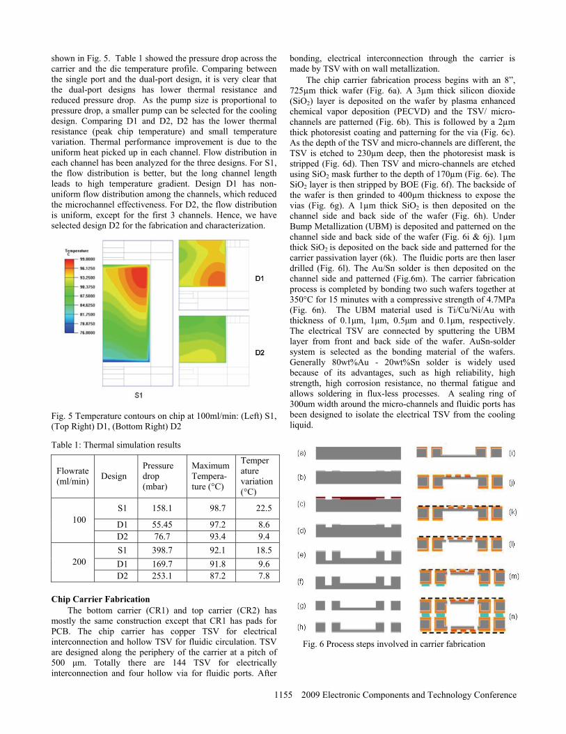
shown in Fig. 5. Table 1 showed the pressure drop across the carrier and the die temperature profile. Comparing between the single port and the dual-port design, it is very clear that the dual-port designs has lower thermal resistance and reduced pressure drop. As the pump size is proportional to pressure drop, a smaller pump can be selected for the cooling design. Comparing D1 and D2, D2 has the lower thermal resistance (peak chip temperature) and small temperature variation. Thermal performance improvement is due to the uniform heat picked up in each channel. Flow distribution in each channel has been analyzed for the three designs. For S1, the flow distribution is better, but the long channel length leads to high temperature gradient. Design D1 has non-uniform flow distribution among the channels, which reduced the microchannel effectiveness. For D2, the flow distribution is uniform, except for the first 3 channels. Hence, we have selected design D2 for the fabrication and characterization.
Fig. 5 Temperature contours on chip at 100ml/min: (Left) S1, (Top Right) D1, (Bottom Right) D2
Table 1: Thermal simulation results
Chip Carrier Fabrication
The bottom carrier (CR1) and top carrier (CR2) has mostly the same construction except that CR1 has pads for PCB. The chip carrier has copper TSV for electrical interconnection and hollow TSV for fluidic circulation. TSV are designed along the periphery of the carrier at a pitch of 500 μm. Totally there are 144 TSV for electrically interconnection and four hollow via for fluidic ports. After
bonding, electrical interconnection through the carrier is made by TSV with on wall metallization.
The chip carrier fabrication process begins with an 8”, 725µm thick wafer (Fig. 6a). A 3µm thick silicon dioxide (SiO2) layer is deposited on the wafer by plasma enhanced chemical vapor deposition (PECVD) and the TSV/ micro-channels are patterned (Fig. 6b). This is followed by a 2µm thick photoresist coating and patterning for the via (Fig. 6c). As the depth of the TSV and micro-channels are different, the TSV is etched to 230µm deep, then the photoresist mask is stripped (Fig. 6d). Then TSV and micro-channels are etched using SiO2 mask further to the depth of 170µm (Fig. 6e). The SiO2 layer is then stripped by BOE (Fig. 6f). The backside of the wafer is then grinded to 400µm thickness to expose the vias (Fig. 6g). A 1µm thick SiO2 is then deposited on the channel side and back side of the wafer (Fig. 6h). Under Bump Metallization (UBM) is deposited and patterned on the channel side and back side of the wafer (Fig. 6i & 6j). 1µm thick SiO2 is deposited on the back side and patterned for the carrier passivation layer (6k). The fluidic ports are then laser drilled (Fig. 6l). The Au/Sn solder is then deposited on the channel side and patterned (Fig.6m). The carrier fabrication process is completed by bonding two such wafers together at 350°C for 15 minutes with a compressive strength of 4.7MPa (Fig. 6n). The UBM material used is Ti/Cu/Ni/Au with thickness of 0.1μm, 1μm, 0.5μm and 0.1μm, respectively. The electrical TSV are connected by sputtering the UBM layer from front and back side of the wafer. AuSn-solder system is selected as the bonding material of the wafers. Generally 80wt%Au - 20wt%Sn solder is widely used because of its advantages, such as high reliability, high strength, high corrosion resistance, no thermal fatigue and allows soldering in flux-less processes. A sealing ring of 300um width around the micro-channels and fluidic ports has been designed to isolate the electrical TSV from the cooling liquid.
Fig. 6 Process steps involved in carrier fabrication
Flowrate (ml/min)
Design Pressure drop (mbar)
Maximum Tempera-ture (°C)
Temper ature variation (°C)
S1 158.1 98.7 22.5
D1 55.45 97.2 8.6 100
D2 76.7 93.4 9.4
S1 398.7 92.1 18.5
D1 169.7 91.8 9.6 200
D2 253.1 87.2 7.8
1155 2009 Electronic Components and Technology Conference

The bonded carrier should have good bonding strength to withstand the dicing force and liquid pressure. The bonded carrier is sheared using DAGE-SERIES-4000-T, the shear strength value measured for 20 different samples ranged from 17.8 MPa to 35.1 MPa, and an average value of 27.2 MPa and a standard deviation of 2.2 are obtained. The shear failure mode is silicon crack, the bonded interface is intact.
Fig. 7 Cross section of the carrier with embedded micro-channels
3D Package Assembly The bonded carrier wafer is diced to 15mm x 15mm size
using mechanical dicing tool. The assembly processes involves pick and place of the chip on the carrier and reflowed. Then solder balls of 300µm diameters are placed on the carrier 1 and reflowed. Two types of solder are used in the assembly namely SnAgCu reflowed at 255°C for 30s (profile 1) and SnPb Solder reflowed at 220°C for 30s (profile 2). The underfill is dispensed after the chip attachment with the carrier and carrier to the PCB.
Fig. 8: Schematic of the 3D package assembly
The fluidic interconnection at difference interfaces is one of the biggest challenges in this work. As the size of 3D package becomes smaller, the available area on the periphery of the package for the fluidic interface also becomes smaller. An adaptor is designed to distribute the fluid between heat exchanger, mini pump and the carriers. Other purpose for the adaptor is split the flow into two inlet ports. A cavity of 1.5mm depth precisely machined on bottom side of the adaptor to align with the fluidic ports on the 3D package. On the top side of the adaptor, one inlet port is fabricated to deliver the fluid from the mini pump to the package and one outflow port to convey the fluid from the package to the heat exchanger. The two ports are fixed with ¼” tap and flexible tube is used for the connection. The fluidic interface between the adapter and the package is sealed using rubber gasket. The integrated cooling solution is shown in Fig. 9.
Fig. 9 Photograph of integrated cooling solution
Cooling solution performance characterization A schematic diagram of the experimental setup for
hydraulic characterization is shown in Fig. 10. A variable-speed gear pump was used to provide the pressure head. A filter with 10 µm mesh filter element was used after the pump to remove particles suspended in the liquid. A flow meter was connected in the closed loop to measure the flow rates. The flow meter was calibrated in-house to achieve a measurement error within 2%. The pressure drop across the 3D package section was measured with a piezo-resistive pressure transducer. The uncertainty at the full range was estimated to be within 0.2%.
Fig. 10: Schematic of the test set-up
As a first step, leakage testing is conducted by running the system at the maximum pressure condition (flow rate is 400 ml/min) for 30 minutes. No leakage was observed during this period, which indicates that the sealing is good. Then the total pressure drop due to adaptor and 3D package was measured. Then pressure drop due to the adaptor alone was measured by removing the 3D package. The pressure drop in the 3D package is obtained by subtracting the adaptor pressure drop from the measured total pressure drop. In addition, the pressure drop of the heat exchanger was measured separately by replacing the adaptor and 3D package
Filter
Flow Meter
Heat Exchanger
3D Package
Pressure Gauge
Pump
Heat Exchanger
Mini- Pump
PCB
Adaptor
Flexible Tube
Interposer
Carrier 1
Solder ball
Flip-Chip Carrier 2
Solder
PCB
1156 2009 Electronic Components and Technology Conference

with the heat exchanger. The system pressure drop comprises of head losses from (a) 3D package (b) Adapter and (c) Heat exchanger. Losses in tubes and fittings are small due to the lower velocities within and ignored. The average pressure drop of five packages is plotted in Fig 11. The dual- port carrier design helps to lower the total pressure drop in the package, with less than 200mbar at 400ml/min in a two stacked package. A maximum of 400ml/min is required for the package cooling. A miniature pump based on this pressure head and flow requirements has been selected. The miniature pump is only 16mm height, which meets the package height requirements. Fig. 11 Pressure drop characterization results
Chip interconnection thermal resistance is measured and compared with the simulation result. A thermal test chip of 10mm by 10mm size is attached on a large silicon substrate (22mm by 22mm). The assembly is then mounted onto a cold plate and a thin layer of thermal interface material is applied in between them. On the test chip, the diode temperatures are measured are at the middle, left and right corner location. The cold plate surface and silicon substrate surface temperature are also measured using thermocouples. A numerical model has been developed similar to the experimental setup to obtain chip and silicon substrate average temperatures, then it is used for interconnect thermal resistance calculation. The TIM thickness in the experimental setup is unknown, therefore the numerical model is solved iteratively by comparing the cold plate temperature in the model with thermocouple reading from the measurement.
The experimental setup to determine thermal characteristic of the 3D package is similar to the arrangement shown in Fig. 11. The filter, flow meter and pressure gauge have been removed from the closed loop. Single and two stack package have been tested. For the stacked module, the bottom and top chip is powered up from 40W to 100W. The water inlet and outlet temperatures are measured to quantify the energy balance. All the tests have been performed with water flowing at 200ml/min for each stack. For thermal resistance calculation, arithmetic mean of the three diodes in the chip is used to represent the average chip temperature. Fig 12 shows average temperature rise of the chip from the
cooling water inlet temperature with heat load from 40W to 100W. Fig 13 shows thermal resistance of the 3D package. Fig. 12 Temperature rise of the chip verses power dissipation
Fig. 13 Total thermal resistance of the 3D package
The 3D package total thermal resistance based on test is 0.577±6% °C/W. The thermal resistance is calculated based on average temperature rise on the chip from inlet liquid temperature. From the experimental results, higher temperature rise has been recorded on the chip compared to the modeling results. The overall thermal resistance measured by experiment is 0.577°C/W compared to 0.41°C/W by simulation. The overall thermal resistance is broken down into Rinterconnects and Rcarrier to understand the contribution of each resistance to the total. Rinterconnects thermal resistance of 0.207°C/W is found experimentally compared to 0.229°C/W by simulation with an absolute error of 10%. The test chip used for the package thermal characterization contains only 400 solder bumps. Therefore Rinterconnects is large, which can be reduced significantly by increasing number of solder bumps.
Table 2: Comparison of thermal resistance
Model
Experiment Error (%)
Rth (°C/W) 0.410 0.577 44.3
Average Chip Temperature Rise
510152025303540455055606570
20 30 40 50 60 70 80 90 100 110
Power (W)
Tem
p ri
se (º
C)
Board 1
Board 2
Thermal Resistance
0
0.1
0.2
0.3
0.4
0.5
0.6
0.7
0.8
20 30 40 50 60 70 80 90 100 110
Power (W)
The
rmal
Res
ista
nce
(ºC
/W)
Board 1Board 2
Pressure Drop in 3D Package
0
50
100
150
200
250
100 150 200 250 300 350 400 450
Flowrate (ml/min)
Pre
ss
ure
dro
p (
mb
ar)
1157 2009 Electronic Components and Technology Conference

The experimental and simulation results of hydraulic/thermal performances of the carriers are showing several discrepancies. The thermal resistance measured is 0.377ºC/W compared to 0.21ºC/W by simulation, which is 44% difference. Possible reason for the differences in modeling and experimental results can be attributed to flow imbalance in the lower and upper sack of the 3D module due to bubbles trapping, other flow obstruction. The second reason can be attributed to flow allocation between the two inlet ports in carrier. There is also a possibility that more flow through one port compared to other due to air bubble clogging or flow obstruction by the sealing ring. Conclusions
In this research work, a novel liquid cooling solution has been developed for 3D package with integrated cooling components like heat exchanger, pump, electrical and fluidic connectivity. The liquid cooling solution is based on microchannel heat sink design. The dual-port microchannel arrangement maximized the heat transfer enhancement, minimized temperature variation in the chip and lowered the pressure drop. A chip carrier with embedded micro-channels and fluidic manifolds has been developed. The chip carrier has been tested up to a flowrate of 400 ml/min and good sealing of the fluidic path was achieved. 3D package thermal performance had also been characterized; the chip is powered up to 100 W / chip. Overall thermal resistance of the chip carrier is 0.577°C/W compared to simulation result of 0.41°C/W. Some important results of the research work are summarized below:
1. Unique design of a silicon carrier with embedded micro-channels for heat transfer enhancement
2. Chip carrier with tapered micro- fin structures for uniform flow distribution and small temperature variation within the chip (< 10°C @ 100 Watts / cm2 heat flux)
3. Dual-port fluidic design to minimize the system pressure drop (< 500 mbar @ 400ml/min)
4. Chip carrier design with copper through-silicon via for electrical interconnection and through-silicon hollow via for the fluidic circulation
5. Fluidic sealing design and hermetic joint using Au/Sn solder for high pressure flow requirements up to 0.8 Bar
6. Micro-to-Macro fluidic interconnection method to connect 500um size holes in the module with 4mm hole in the pump
7. Integrated liquid cooling design with miniature exchanger and pump mounted on the module giving overall module foot print of 50mm x 50mm
Acknowledgments The authors acknowledge the financial grant from
DARPA under agreement number HR0011-06-2-0007 for this project. The support from the process team and management team at Institute of Microelectronics is also greatly appreciated.
References 1. Wu, L., Wang, Yu-Po, Kee, S. C., Wallace, B., Hsiao, C.
S., Yeh, C. K., Her, T. D., Lo, R., “The Advent of 3-D Package Age”, Proc 26th IEEE/CPMT Int’l Electronic Manufacturing Technology Symposium, Santa Clara, 2000, pp. 102-107.
2. http://www.itrs.net/Links/2007ITRS/Home2007.htm 3. Issam Mudawar, “Assessment of high-heat flux thermal
management schemes,” IEEE Trans. On Components and Packaging Technologies, Vol 24, Issue 2, June 2001, pg 122-141.
4. J. Koo, S. Im, L, Jiang, and K. Goodson, “Integrated Microchannel Cooling for Three-Dimensional Electronic Circuit Architectures”, J. Heat Transfer, 2005, Vol. 127, 49-58.
5. X. Chen, K. Toh, and J. Chai, “Direct Liquid Cooling of a Stacked Multichip Module”, Proc. Electronics Packaging Technology Conference, 2002, 380-384.
6. R.H.W. Pijnenburg, R. Dekker, C.C.S. Nicole, A. Aubry, E.H.E.C. Eummelen,” Integrated micro-channel cooling in silicon,” Solid-State Device Research conference, 2004.
7. J.R. Culham, Y.S. Muzychka, “ Optimisation of Plate Fin Heat Sinks Using Entropy Generation Minimization” IEEE CPT Jun 01, Vol 2, Pg 159-165
1158 2009 Electronic Components and Technology Conference
Copyright © 2022 FDOKUMEN