Designing an LLC Resonant Half-Bridge Power Converter
36
Power Supply Design Seminar Power Seminar topics and online power- training modules are available at: power.ti.com/seminars Topic 3 Presentation: Designing an LLC Resonant Half-Bridge Power Converter Reproduced from 2010 Texas Instruments Power Supply Design Seminar SEM1900, Topic 3 TI Literature Number: SLUP256 © 2010, 2011 Texas Instruments Incorporated
-
Upload
khangminh22 -
Category
Documents
-
view
1 -
download
0
Transcript of Designing an LLC Resonant Half-Bridge Power Converter

Power Supply Design Seminar
Power Seminar topics and online power-training modules are available at:
power.ti.com/seminars
Topic 3 Presentation:
Designing an LLC Resonant Half-Bridge Power Converter
Reproduced from2010 Texas Instruments Power Supply Design Seminar
SEM1900, Topic 3TI Literature Number: SLUP256
© 2010, 2011 Texas Instruments Incorporated

SLUP256
Topic 3
Designing an LLC Resonant Half-Bridge Power ConverterHalf-Bridge Power Converter
Hong Huang

SLUP256
Agenda1 Introduction1. Introduction
– Brief review– Advantages
2. Design Prerequisites– Configuration– Operationp– Modeling– Voltage gain function
3 D i C id ti3. Design Considerations– Voltage gain and switching frequency– Line and load regulation– Zero voltage switching (ZVS)– Steps for designing and a design example
4. Conclusions
Texas Instruments—2010 Power Supply Design Seminar 3-2
4. Conclusions
SLUP256
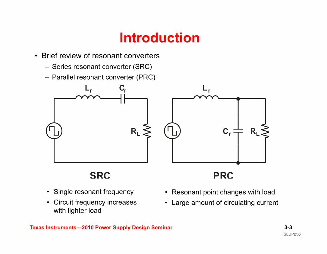
Introduction• Brief review of resonant converters• Brief review of resonant converters
– Series resonant converter (SRC)– Parallel resonant converter (PRC)
L LCLr L rCr
CrRL RL
SRC PRCSRC PRC• Single resonant frequency• Circuit frequency increases
• Resonant point changes with load• Large amount of circulating current
Texas Instruments—2010 Power Supply Design Seminar 3-3
Circuit frequency increases with lighter load
• Large amount of circulating current

SLUP256
Introduction• Brief review of resonant convertersBrief review of resonant converters
– Combination of SRC and PRC LCC• Two resonant frequencies• Requires three elements
LLC: alternative LCC– LLC: alternative LCC• Lr and Lm integrated in a transformer
• Advantages of LLC– High efficiency (ZVS)High efficiency (ZVS)– Less frequency variation and lower circulating current– ZVS over operating range
Lr LrCr1 Crr rr1 r
LmCr2 RL RL
Texas Instruments—2010 Power Supply Design Seminar 3-4LCC LLC
SLUP256
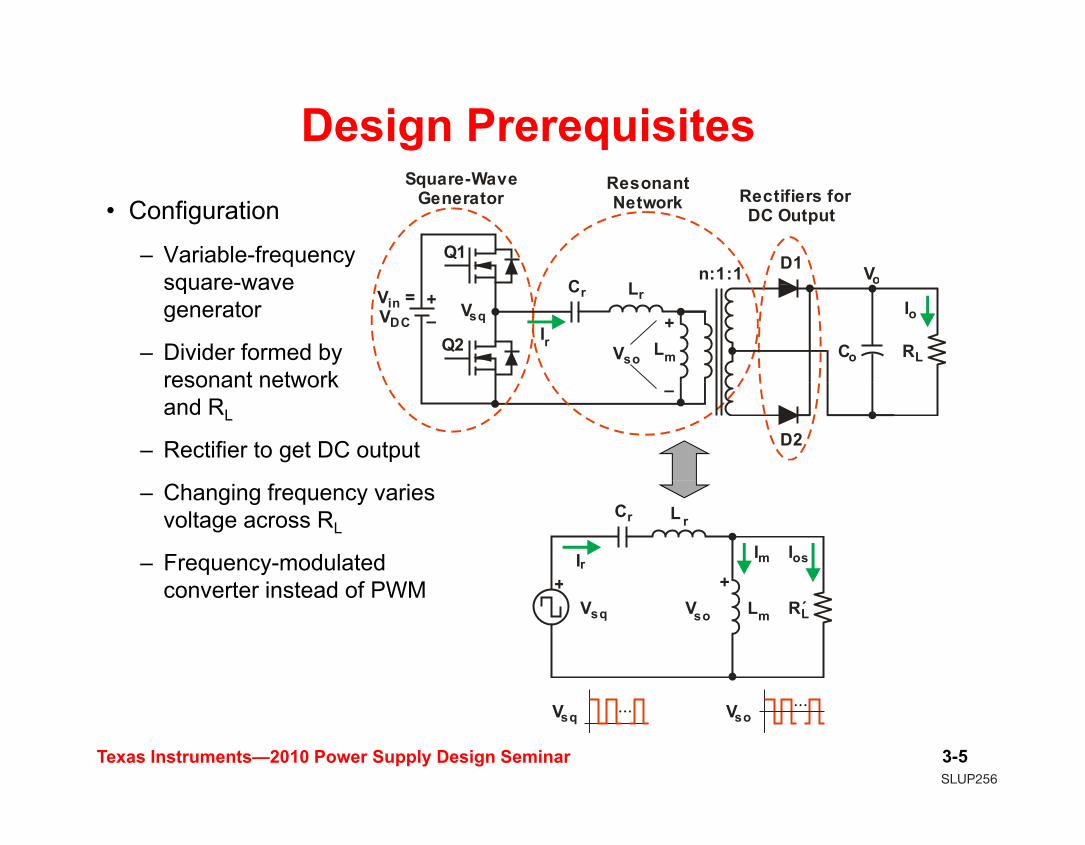
Design Prerequisites Square-Wave Resonant
• Configuration
– Variable-frequency square-wave
Rectifiers for DC Output
qGenerator
Resonant Network
C LVo
D1Q1n:1:1square-wave
generator
– Divider formed by resonant network
Cr Lr
LmVso
++– Vsq
Ir Co
Io
RLQ2
Vin = VDC
resonant network and RL
– Rectifier to get DC output
–
D2
– Changing frequency varies voltage across RL
– Frequency-modulated Ir Ios
L r
+
Cr
Im
converter instead of PWM + +Vsq Vso Lm RL
Texas Instruments—2010 Power Supply Design Seminar 3-5
Vsq Vso
SLUP256
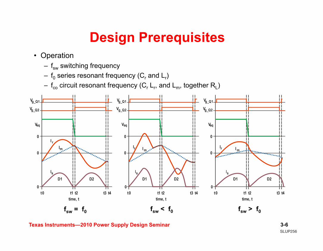
Design Prerequisites • Operation• Operation
– fsw switching frequency – f0 series resonant frequency (Cr and Lr)
f circuit resonant frequency (C L and L together R )– fco circuit resonant frequency (Cr Lr, and Lm, together RL)
Vg_Q1 Vg_Q1 Vg_Q1
Vg_Q2 Vg_Q2 Vg_Q2
I r
Vsq Vsq Vsq
0 0 0
Ir Irr
I I I
I m I mIm0 0 0
Is Is IsD1 D1 D1D2 D2 D2
0 0 0t0t0t0 t1t1t1 t3t3t3 t2t2t2
time, t time, t time, tt4t4t4
Texas Instruments—2010 Power Supply Design Seminar 3-6
fsw = f0
, , ,
fsw < f0 fsw > f0

SLUP256
Design Prerequisites M d li• Modeling– First harmonic approximation (FHA)
LrCrLrCr
Ir
r
++ ++VL R
IrIos
r
Vsq VgeV L
Im
RL– –
VoeLm
Im Ioe
ReVsq VgeVso Lm RL
Vsq Vso
(a) (b)
• Input and output: Square wave voltages
• Sinusoidal current in resonant
• Input and output: Fundamental components to approximate FHA
• Rectifier and RL equivalent to Re
Texas Instruments—2010 Power Supply Design Seminar 3-7
circuit • AC circuit method can be used

SLUP256
Design Prerequisites • Voltage gain function
– Expression from impedance divider o so oen V V V
M M M×
= ≈ = ≈ =pg _DC g _ sw g _ ac
in sq geM M M V /2 V V= ≈ = ≈ =
n V V×
I r
LrCro oe
g _ DCin ge
n V VM V /2 V×
= ≈
r+
–
+
–VoeLm
I I
ReVge
m e
m e rr
( j L ) || R 1( j L ) || R j Lj C
ω=
ω + ω +ωIm Ioe
r
sw
j C
where 2 f 2 f and j = 1
ω
ω = π = π −
Texas Instruments—2010 Power Supply Design Seminar 3-8

SLUP256
Design Prerequisites • Voltage gain function
– Expression (Normalization)
o so oeg _DC g _ sw g _ ac
in sq ge
n V V VM M M V /2 V V
×= ≈ = ≈ =
2( )
2n n
g 2 2n n n n e n
L fM
[(L 1) f 1] j[(f 1) f Q L ]×
=+ × − + − × × ×
Normalized Gain
Resonant Frequency Quality Factor
Normalized Frequency
Inductor Ratio
og
in
VM V /2= 0
r r
1f2 L C
=π
r re
e
L /CQ R= sw
n0
ff f= m
nr
LL L=
Eq. Load R.28 nR R× ×
Texas Instruments—2010 Power Supply Design Seminar 3-9
e L2R R= ×π

SLUP256
Design Prerequisites • Voltage gain function
– Plots of gain magnitude, fixed Ln = 5– Qe (load current) increases ⇒ peak gain decreases ⇒ curves shrinkQe (load current) increases ⇒ peak gain decreases ⇒ curves shrink
1.8
2
Qe Mg_pk
1.2
1.4
1.6
n
Qe = 0.5
0.6
0.8
1Gai
Qe = 0.1 Qe = 10
0
0.2
0.4
0.1 1 10
Texas Instruments—2010 Power Supply Design Seminar 3-10
Normalized Frequency

SLUP256
Design Prerequisites • Voltage gain function
– Plots of gain magnitude, fixed Qe = 0.5
– Ln decreases ⇒ peak gain increases ⇒ ZVS obtained but conduction losses increase
1 8
2
Ln Mg_pk
1 2
1.4
1.6
1.8Ln = 10 Ln = 5
Ln = 3
0 6
0.8
1
1.2
Gai
n
0
0.2
0.4
0.6
Texas Instruments—2010 Power Supply Design Seminar 3-11
00.1 1 10
Normalized Frequency

SLUP256
Design Considerations• Where to base a design?• Where to base a design?
– In the vicinity of series resonance, fn = 1 ⇒ narrowest frequency variation⇒ Mg able to = 1, >1, and <1
– Right side of the resonant peak ⇒ ZVS requirementRight side of the resonant peak ⇒ ZVS requirement
1.6
Frequency in operation
1.4a2
Qe = 0
a3
Gai
n, M
g 1.2
1a0
Qe = 0
Qe= max
0.8
0.6
Qe 0
a4
a1
Texas Instruments—2010 Power Supply Design Seminar 3-12
Normalized Frequency, fn10.5 2

SLUP256
Design Considerations• Line and load regulation• Line and load regulation
– Properly set up Mg_max and Mg_min
– Frequency limit set up
1.6
1.4
Qe = 0Qe = max at full load
3M =g max
n x VV /2
o_max
n, M
g
1.4
1.2
a2a3
Qe= max
g_ V /2in_min
Gai
n
1
0.8
a0
Qe = 0
a1M =g_min
n x VV /2
o_min
in_max
1fn min fn max
0.6a4
Qe= max
Qe = 0 at no load
Texas Instruments—2010 Power Supply Design Seminar 3-13
Normalized Frequency, fn
fn_min n_maxQe

SLUP256
Design ConsiderationsO l d t ti• Overload current operation– Qe = max to include and meet the required Mg_max
– Operation still on the right side of resonant peak
1.6Qe = 0
n x V
Frequency in operation
Mg
1.4
1.2
a2a3
Qe= max
M =g_maxn x VV /2
o_max
in_min
Gai
n, M
1a0
Qe = 0M =i
n x Vo_min
0.8
0.6 Qe = 0a4
a1M =g_min V /2in_max
Texas Instruments—2010 Power Supply Design Seminar 3-14Normalized Frequency, fn
1fn_min fn_maxQe= max

SLUP256
Design Considerations• Load short circuit• Load short circuit • Protection options
– Increase fsw rapidly to reduce Mg to zero – Operation with fn > 1, i.e., fsw > f0 at all times
2
1.8Q = 0e
Operation with fn 1, i.e., fsw f0 at all times– Independent protection function
Mg
1.6
1.4
1.2
a2
Q = 0e
a3M =g_max
n x VV /2
o_max
in_min
Gai
n, M
1
0.8
0.6Curve 1(Q = 0)e
a0
a4a1
Cu
M =g_minn x VV /2
o_min
in_max
0.4
0.2
0
(Q 0)e
Curve 3Curve 4
Curve 2 (Q = max)e
Texas Instruments—2010 Power Supply Design Seminar 3-15
0.1 1 10fn_min fn_max
Normalized Frequency, fn
0

SLUP256
Design Considerations
• Zero voltage switching (ZVS)– How ZVS is achieved?
Vg Q1g_Q1
Vg_Q2
Q2 Turns On
Q1 Turns Off
VsqQ1
CDS1V g 1 1
Body Diode
V = 0ds_Q2
I r0
Q2: C Discharge,ds
Lr Lm+– Vsq
IIrQ2
V in
g
V
n:1:1
Body Diode Turns OnIm
0
tdead
Cr
Im
CDS2
V g
t0 t1 t3t2time, t
t4
Texas Instruments—2010 Power Supply Design Seminar 3-16

SLUP256
Design Considerations
• Zero voltage switching (ZVS)
– Necessary condition
• Input impendence of the resonant network inductive
• Operation on the right side of the resonant peakp g p
– Sufficient conditionSufficient condition
• Enough energy stored in the magnetic field, mainly Lm
• Enough time to discharge the capacitors mainly C• Enough time to discharge the capacitors, mainly CDS
Texas Instruments—2010 Power Supply Design Seminar 3-17

SLUP256
Design Considerations
• Why not design on the left side of the resonant peak?
– Capacitive current results
– ZVS lostHard switching Switching losses increase
– Body diode reverse recovery lossesPrimary MOSFET failure
– Higher EMI noise
– Reversed frequency relationship to feedback loop
Texas Instruments—2010 Power Supply Design Seminar 3-18

SLUP256
Design Considerations
• Design Steps – How to initially select?
f it hi f– fsw, switching frequency
– n, transformer turns ratio
– Ln, inductance ratio
– Qe, series resonant quality factor
Texas Instruments—2010 Power Supply Design Seminar 3-19

SLUP256
Design Considerations
• Design Steps – Switching frequency
– Usually selected for particular applications• Example in off-line applications: Typical below 150 kHz
– Selecting the switching frequencyg g q y• f decrease ⇒ Bulkier converter• f decrease ⇒ Switching losses decrease ⇒ ZVS benefit decrease• f increase ⇒ ZVS benefits increase vs. hard switching converters
• Very High f : – Component availability
Addi i l i hi l– Additional switching losses– Additional concerns due to parasitic effects
Texas Instruments—2010 Power Supply Design Seminar 3-20

SLUP256
Design Considerations
• Design Steps – Transformer turns ratio, n
– Voltage gain can be larger and smaller than unity
– Flexibility in selecting the turns ratio, n
– Turns ratio design with Mg =1, initially, and nominal Vin and Vo
in _ noming
V /2V /2n M V V= × =
g
go o_ nom M = 1
V V
Texas Instruments—2010 Power Supply Design Seminar 3-21

SLUP256
Design ConsiderationsD i St L d Q• Design Steps – Ln and Qe– Ln and Qe to achieve
Mg pk > Mg max for maximum 3.0g_p g_
load– Select Ln and Qe from pre-
plotted peak gain curves Mg_
pk
2.8
2.6
2.4L = 3.0n
L = 1.5nL = 2.0nL = 3.0nL = 4.0nL = 5.0nL = 6 0
– Initial selection • Ln = 5• Q = 0 5 e
Pea
k G
ain,
2.2
2.0
1 8
L = 3.5 byInterpolationM = 1.56Q = 0.45
n
g_pke
L = 6.0nL = 8.0nL = 9.0n
Qe = 0.5– Example: Select Ln and Qe
for Mg_max = 1.2To achieve design margin
Atta
inab
le 1.8
1.6
1.4L = 5M = 1.2Q = 0 5
ng_pk
L = 1.5n
– To achieve design margin –Final selection
• Ln - 3.5, Qe = 0.4530% margin o er
0.15 1.150.950.750.550.35Quality Factor, Qe
1.2
1.0
Q = 0.5e
Texas Instruments—2010 Power Supply Design Seminar 3-22
• 30% margin over

SLUP256
Design Considerations
• Design Steps – Trade-offs to select Ln and Qe
– Different requirements for different applications
– Fixed Qe, Ln decrease ⇒ peak gain increase ⇒ good for ZVS and avoids capacitive currenta d a o ds capac t e cu e t
– But, Ln decrease ⇒ Lm decrease ⇒ conduction losses increase
– Fixed Ln, Qe decrease ⇒ peak gain increase ⇒ frequency variation increase
– Recommend starting with Ln = 5, and Qe = 0.5 (from design practice)
Texas Instruments—2010 Power Supply Design Seminar 3-23

SLUP256
Design Considerations• Resonant circuit design flowResonant circuit design flow
Converter Specifications
inVn =
Mg_
ap
3.0
2.8
2.6
2 4L = 3.0n
L = 1.5nL = 2.0nL = 3.0nL = 4.0nL = 5.0n
Magnetizing Inductance
o2V
o_ming_min
in_max
n VM
V / 2×
=m n rL L L= ×
ttain
able
Pea
k G
ain,
M 2.4
2.2
2.0
1.8
1.6
L = 3.5 byInterpolationM = 1.56Q = 0.45
n
g_ape
L = 5
L = 1.5n
nL = 6.0nL = 8.0nL = 9.0n
Resonant Inductor
Ch L d Q
o_maxg_max
in_min
n VM
V / 2×
=
( )r 2
1L
2 f C=
0.15 1.150.950.750.550.35Quality Factor, Qe
At
1.4
1.2
1.0
L = 5M = 1.2Q = 0.5
ng_ape
Resonant Capacitor
Choose Ln and Qe
Change Check M g and fnAgainst Graph
( )2sw r2 f Cπ ×
1CMg
1 .9
1.7
1.5 M = 1.3g_max
Q = 0e
Q = 0.47e
f = 0 .65n_min
L = 3.5n
Calculate Re
L and Qn e
NoYes
r1C =
π
f = 1.02n max
Gain
, M 1 .3
1.1
0.9
0.7
M = 0.99g_min
Q = 0 .52e
V28 2 8 2
Are Values Within Limits?Mg_maxM i
Texas Instruments—2010 Power Supply Design Seminar 3-24
0 0.5 1 1.5
_ a
0.5L2 2
out
Vo8 × n2 8 × n2Re × R ×
P= =
π π
Mff
g_minn_maxn_min
SLUP256
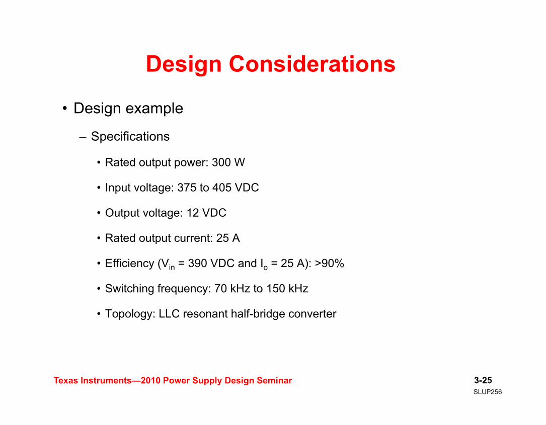
Design Considerations
• Design example
– Specifications
• Rated output power: 300 W
• Input voltage: 375 to 405 VDCp g
• Output voltage: 12 VDC
• Rated output current: 25 ARated output current: 25 A
• Efficiency (Vin = 390 VDC and Io = 25 A): >90%
• Switching frequency: 70 kHz to 150 kHzSwitching frequency: 70 kHz to 150 kHz
• Topology: LLC resonant half-bridge converter
Texas Instruments—2010 Power Supply Design Seminar 3-25
SLUP256
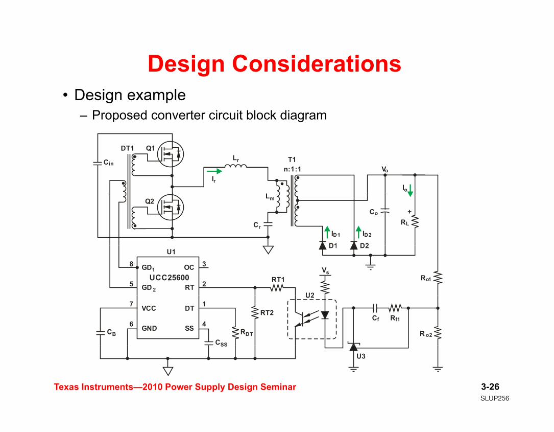
Design Considerations• Design example• Design example
– Proposed converter circuit block diagram
Cin T1Lr
L
IrIo
Vo
Q1DT1
n:1:1
ID1 ID2
Cr
Lm
Co
RL
D1 D2
Q2+
UCC25600
8
5
OC
RT
3
2
GD
GD
1
2
RT1Vs
Ro1
D1 D2
U2
U1
CBCSS
7
6
DT
SS
1
4
VCC
GND RDT
RT2
R o2
U2
Cf Rf1
Texas Instruments—2010 Power Supply Design Seminar 3-26
SS
U3

SLUP256
Design Considerations
8-pin SOIC (D), Top View
• Design example – UCC25600 Features– 8-pin SOIC package
DT
RT
8
7
1
2
GD1
VCC
– Programmable:
• dead time
Drive 1
RT
OC
7
6
2
3
VCC
GND
• fmin and fmax
• soft start time
ProtectionSS 54 GD2
– Protection
• OCP: hiccup and latch-off
• VDD UVLO and OVPDrive 2
• OTP
– Burst operation
Texas Instruments—2010 Power Supply Design Seminar 3-27
Design Considerations• Resonant circuit design flowResonant circuit design flow
Converter Specifications
inVn =g_
ap
3.0
2.8
2.6L = 3.0n
L = 1.5nL = 2.0nL = 3.0nL = 4.0nL = 5 0
n = 16
L = 3.5Q = 0.45
ne
L = 210 µHL =
mr 60 µH
Magnetizing Inductance
on
2V=
o_ming_min
in_max
n VM
V / 2×
=m n rL L L= ×ta
inab
le P
eak
Gai
n, M
g
2.4
2.2
2.0
1.8
1.6
L = 3.5 byInterpolationM = 1.56Q = 0.45
n
g_ape
L 5
L = 1.5n
n L = 5.0nL = 6.0nL = 8.0nL = 9.0n
e L r 60 µHC = 27.3 nFr
Resonant Inductor
Ch L d Q
o_maxg_max
in_min
n VM
V / 2×
=
m n r
( )r 2
1L =
0.15 1.150.950.750.550.35Quality Factor, Qe
Att
1.4
1.2
1.0
L = 5M = 1.2Q = 0.5
ng_ape
Resonant Capacitor
Choose Ln and Qe
Change d Q
Check M g and fnAgainst Graph
( )2sw r2 f Cπ ×
1CMg
1 .9
1.7
1.5 M = 1.3g_max
Q = 0e
Q = 0.47e
f = 0 .65n_min
L = 3.5n
Calculate Re
L and Qn e
NoYes
rC =π
f = 1 .02n_max
Gai
n, M 1 .3
1.1
0.9
0.7
M = 0.99g_min
Q = 0.52e
V28 × n2 8 × n2
Are Values Within Limits?Mg_maxMg min
Texas Instruments—2010 Power Supply Design Seminar 3-28
0 0.5 1 1.50.5
L2 2out
Vo8 × n2 8 × n2Re × R ×
P= =
π π
Mff
g_minn_maxn_min

SLUP256
Design Considerations• Design check• Design check
1.9Q = 0e
L = 3.5n
1.7
1.5 Q = 0.47e
Gai
n, M
g
1.3
1 1
M = 1.3g_max
1.1
0.9M = 0.99g_min
Q = 0.52e
f = 0.65(80 9 kHz)n_min f = 1 02n max
0 0.5 1 1.5
0.7
0.5
(80.9 kHz)
150 kHz70 kHz 124.4 kHz
f 1.02(126.9 kHz)n_max
Texas Instruments—2010 Power Supply Design Seminar 3-29
0 0.5 1 1.5Normalized Frequency, fn

SLUP256
Design Considerations• Design checkg
– Verification with computer-based circuit simulation – Design reiteration, if needed– Size/select componentsSize/select components– Build the board– Verification with bench tests– Re-spin the board/design if neededRe spin the board/design, if needed
Texas Instruments—2010 Power Supply Design Seminar 3-30

SLUP256
Design Considerations• Experiment results (L = 280 µH L = 60 µH C = 24 nF)• Experiment results (Lm = 280 µH, Lr = 60 µH, Cr = 24 nF)
95
Input Voltage,Output Ripple Voltage
(50 mV/div)90 mV Output
Effi
cien
cy ( %
) 85
75
405 V390 V375 V
Input Voltage, Vin
(50 mV/div)
Efficiency
Output Ripple Voltage(full load)
1 5 1510 20 25Load Current (A)
65Time (5 µs/div)
1
3 VLr
VCr
(200 V/div)
(200 V/div)
1
3
Vgs_Q2
Ir
(20 V/div)
(1.2 A/div)Resonant N k
Resonant Network C t
4
3 Lr
VLm
Vds_Q2
(200 V/div)
(500 V/div)
3
VCr
(100 V/div)
Network Voltages (full load)
Current and Voltage(full load)
Texas Instruments—2010 Power Supply Design Seminar 3-31
2
Time (5 µs/div)
(500 V/div)4
2Vds_Q2 (500 V/div)
Time (1 µs/div)
( )

SLUP256
Test Result versus FHA from the Design• In the vicinity of f0, FHA-
based result very accurate to the final test
lt (L 60 H d
2.0Bench Test Measurements
Plot Based on E ti 18
(65, 1.90)
(60 1 57)(80, 1.58)
result (Lr = 60 µH and Cr = 24 nF)
• Away from f0, less Mg
1.4Equation 18(60, 1.57)
(55, 1.27) (100, 1.21)
(135, 0.99)ay o 0, essaccuracy from FHA-based result
Eq ation (18)G
ain,
0.6
(170, 0.87)
(40, 0.70)(200, 0.78)
(240, 0.72)
( )• Equation (18) (30, 0.51) (400, 0.56)
f = 135 kHz0
mL eoeg
ge L e L C
jX || RVMV (jX || R ) j(X X )
= =+ −
10 100 1000Frequency, f (kHz)sw
0.0m r rge L e L C
m e
m e r
( j || ) j( )
( j L ) || R1( j L ) || R j L
ω=
ω + ω +
Texas Instruments—2010 Power Supply Design Seminar 3-32
m e rr
( j L ) || R j Lj C
ω + ω +ω
SLUP256
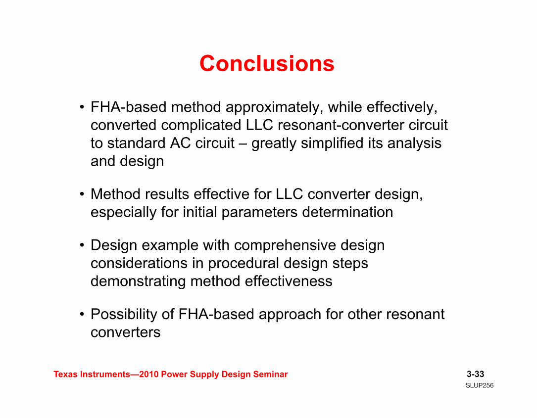
Conclusions
• FHA-based method approximately, while effectively, converted complicated LLC resonant-converter circuit to standard AC circuit greatly simplified its analysisto standard AC circuit – greatly simplified its analysis and design
M th d lt ff ti f LLC t d i• Method results effective for LLC converter design, especially for initial parameters determination
• Design example with comprehensive design considerations in procedural design steps demonstrating method effectivenessg
• Possibility of FHA-based approach for other resonant converters
Texas Instruments—2010 Power Supply Design Seminar 3-33
converters

SLUP256
TI Worldwide Technical Support
InternetTI Semiconductor Product Information Center Home Pagesupport.ti.com
TI E2E™ Community Home Pagee2e.ti.com
Product Information CentersAmericas Phone +1(972)644-5580
Brazil Phone 0800-891-2616
Mexico Phone 0800-670-7544
Fax +1(972)927-6377 Internet/Email support.ti.com/sc/pic/americas.htm
Europe, Middle East, and AfricaPhone EuropeanFreeCall 00800-ASK-TEXAS (0080027583927) International +49(0)8161802121 RussianSupport +7(4)959810701
Note:TheEuropeanFreeCall(TollFree)numberisnotactiveinallcountries.Ifyouhavetechnicaldifficultycallingthefreecallnumber,pleaseusetheinternationalnumberabove.
Fax +(49)(0)8161802045Internet support.ti.com/sc/pic/euro.htmDirectEmail [email protected]
JapanPhone Domestic0120-92-3326
Fax International+81-3-3344-5317 Domestic0120-81-0036
Internet/Email Internationalsupport.ti.com/sc/pic/japan.htm Domesticwww.tij.co.jp/pic
A122010
Important Notice:TheproductsandservicesofTexasInstrumentsIncorporatedanditssubsidiariesdescribedhereinaresoldsubjecttoTI’sstandardtermsandconditionsofsale.CustomersareadvisedtoobtainthemostcurrentandcompleteinformationaboutTIproductsandservicesbeforeplacingorders.TIassumesnoliabilityforapplicationsassistance,customer’sapplicationsorproductdesigns,softwareperformance,orinfringementofpatents.Thepublicationofinformationregardinganyothercompany’sproductsorservicesdoesnotconstituteTI’sapproval,warrantyorendorsementthereof.
AsiaPhone International +91-80-41381665 Domestic Toll-FreeNumber Note:Toll-freenumbersdonotsupport
mobileandIPphones. Australia 1-800-999-084 China 800-820-8682 HongKong 800-96-5941 India 1-800-425-7888 Indonesia 001-803-8861-1006 Korea 080-551-2804 Malaysia 1-800-80-3973 NewZealand 0800-446-934 Philippines 1-800-765-7404 Singapore 800-886-1028 Taiwan 0800-006800 Thailand 001-800-886-0010Fax +8621-23073686Email [email protected]@ti.comInternet support.ti.com/sc/pic/asia.htm
TheplatformbarandE2EaretrademarksofTexasInstruments.Allothertrademarksarethepropertyoftheirrespectiveowners.
IMPORTANT NOTICE
Texas Instruments Incorporated and its subsidiaries (TI) reserve the right to make corrections, modifications, enhancements, improvements,and other changes to its products and services at any time and to discontinue any product or service without notice. Customers shouldobtain the latest relevant information before placing orders and should verify that such information is current and complete. All products aresold subject to TI’s terms and conditions of sale supplied at the time of order acknowledgment.
TI warrants performance of its hardware products to the specifications applicable at the time of sale in accordance with TI’s standardwarranty. Testing and other quality control techniques are used to the extent TI deems necessary to support this warranty. Except wheremandated by government requirements, testing of all parameters of each product is not necessarily performed.
TI assumes no liability for applications assistance or customer product design. Customers are responsible for their products andapplications using TI components. To minimize the risks associated with customer products and applications, customers should provideadequate design and operating safeguards.
TI does not warrant or represent that any license, either express or implied, is granted under any TI patent right, copyright, mask work right,or other TI intellectual property right relating to any combination, machine, or process in which TI products or services are used. Informationpublished by TI regarding third-party products or services does not constitute a license from TI to use such products or services or awarranty or endorsement thereof. Use of such information may require a license from a third party under the patents or other intellectualproperty of the third party, or a license from TI under the patents or other intellectual property of TI.
Reproduction of TI information in TI data books or data sheets is permissible only if reproduction is without alteration and is accompaniedby all associated warranties, conditions, limitations, and notices. Reproduction of this information with alteration is an unfair and deceptivebusiness practice. TI is not responsible or liable for such altered documentation. Information of third parties may be subject to additionalrestrictions.
Resale of TI products or services with statements different from or beyond the parameters stated by TI for that product or service voids allexpress and any implied warranties for the associated TI product or service and is an unfair and deceptive business practice. TI is notresponsible or liable for any such statements.
TI products are not authorized for use in safety-critical applications (such as life support) where a failure of the TI product would reasonablybe expected to cause severe personal injury or death, unless officers of the parties have executed an agreement specifically governingsuch use. Buyers represent that they have all necessary expertise in the safety and regulatory ramifications of their applications, andacknowledge and agree that they are solely responsible for all legal, regulatory and safety-related requirements concerning their productsand any use of TI products in such safety-critical applications, notwithstanding any applications-related information or support that may beprovided by TI. Further, Buyers must fully indemnify TI and its representatives against any damages arising out of the use of TI products insuch safety-critical applications.
TI products are neither designed nor intended for use in military/aerospace applications or environments unless the TI products arespecifically designated by TI as military-grade or "enhanced plastic." Only products designated by TI as military-grade meet militaryspecifications. Buyers acknowledge and agree that any such use of TI products which TI has not designated as military-grade is solely atthe Buyer's risk, and that they are solely responsible for compliance with all legal and regulatory requirements in connection with such use.
TI products are neither designed nor intended for use in automotive applications or environments unless the specific TI products aredesignated by TI as compliant with ISO/TS 16949 requirements. Buyers acknowledge and agree that, if they use any non-designatedproducts in automotive applications, TI will not be responsible for any failure to meet such requirements.
Following are URLs where you can obtain information on other Texas Instruments products and application solutions:
Products Applications
Audio www.ti.com/audio Communications and Telecom www.ti.com/communications
Amplifiers amplifier.ti.com Computers and Peripherals www.ti.com/computers
Data Converters dataconverter.ti.com Consumer Electronics www.ti.com/consumer-apps
DLP® Products www.dlp.com Energy and Lighting www.ti.com/energy
DSP dsp.ti.com Industrial www.ti.com/industrial
Clocks and Timers www.ti.com/clocks Medical www.ti.com/medical
Interface interface.ti.com Security www.ti.com/security
Logic logic.ti.com Space, Avionics and Defense www.ti.com/space-avionics-defense
Power Mgmt power.ti.com Transportation and Automotive www.ti.com/automotive
Microcontrollers microcontroller.ti.com Video and Imaging www.ti.com/video
RFID www.ti-rfid.com
OMAP Mobile Processors www.ti.com/omap
Wireless Connectivity www.ti.com/wirelessconnectivity
TI E2E Community Home Page e2e.ti.com
Mailing Address: Texas Instruments, Post Office Box 655303, Dallas, Texas 75265Copyright © 2011, Texas Instruments Incorporated