Design Your Own Video Game Console - iC0nstruX
187
Design Your Own Video Game Console A Beginner’s Guide to Video Game Console and Embedded System Design, Development, and Programming.
-
Upload
khangminh22 -
Category
Documents
-
view
0 -
download
0
Transcript of Design Your Own Video Game Console - iC0nstruX

Design Your Own Video Game Console A Beginner’s Guide to Video Game Console and Embedded System Design, Development, and Programming.

Design Your Own Video Game Console A Beginner’s Guide to Video Game Console and Embedded System Design, Development, and Programming.
Design Your Own Video Game Console A Beginner’s Guide to Video Game Console and Embedded System Design, Development, and Programming.
Copyright © 2004-2005 Nurve Networks LLC
Publisher Nurve Networks LLC
Author Andre’ LaMothe
Editor/Technical Reviewer Alex Varanese
Printing 0001
ISBN Pending
All rights reserved. No part of this book shall be reproduced, stored in a retrieval system, or transmitted by any means, electronic, mechanical, photocopying, recording, or otherwise, without written permission from the publisher. No patent liability is assumed with respect to the user of the information contained herein. Although every precaution has been taken in the preparation of this book, the publisher and authors assume no responsibility for errors or omissions. Neither is any liability assumed for damages resulting from the use of the information contained herein.
Trademarks All terms mentioned in this book that are known to be trademarks or service marks have been appropriately capitalized. Nurve Networks LLC cannot attest to the accuracy of this information. Use of a term in this book should not be regarded as affecting the validity of any trademark or service mark.
Warning and Disclaimer Every effort has been made to make this book as complete and as accurate as possible, but no warranty or fitness is implied. The information provided is on an “as is” basis. The authors and the publisher shall have neither liability nor any responsibility to any person or entity with respect to any loss or damages arising from the information contained in this book.
The example companies, organizations, products, domain names, e-mail addresses, logos, people, places, and events depicted herein are fictitious. No association with any real company, organization, product, domain name, e-mail address, logo, person, place, or event is intended or should be inferred.
eBook License This eBook may be printed for personal use and (1) copy may be made for archival purposes, but may not be distributed by any means whatsoever, sold, resold, in any form, in whole, or in parts. Additionally, the contents of the CD this eBook came on relating to the design, development, imagery, or any and all related subject matter pertaining to the XGameStation™ Micro Edition are copyrighted as well and may not be distributed in any way whatsoever in whole or in part. Individual programs are copyrighted by their respective owners and may require separate licensing.

Design Your Own Video Game Console A Beginner’s Guide to Video Game Console and Embedded System Design, Development, and Programming.
Licensing, Terms & Conditions NURVE NETWORKS LLC, INC. END-USER LICENSE AGREEMENT FOR XGAMESTATION™ MICRO EDITION HARDWARE, SOFTWARE AND EBOOKS
YOU SHOULD CAREFULLY READ THE FOLLOWING TERMS AND CONDITIONS BEFORE USING THIS PRODUCT. IT CONTAINS SOFTWARE, THE USE OF WHICH IS LICENSED BY NURVE NETWORKS LLC, INC., TO ITS CUSTOMERS FOR THEIR USE ONLY AS SET FORTH BELOW. IF YOU DO NOT AGREE TO THE TERMS AND CONDITIONS OF THIS AGREEMENT, DO NOT USE THE SOFTWARE OR HARDWARE. USING ANY PART OF THE SOFTWARE OR HARDWARE INDICATES THAT YOU ACCEPT THESE TERMS.
GRANT OF LICENSE: NURVE NETWORKS LLC (the "Licensor") grants to you this personal, limited, non-exclusive, non-transferable, non-assignable license solely to use in a single copy of the Licensed Works on a single computer for use by a single concurrent user only, and solely provided that you adhere to all of the terms and conditions of this Agreement. The foregoing is an express limited use license and not an assignment, sale, or other transfer of the Licensed Works or any Intellectual Property Rights of Licensor.
ASSENT: By opening the files and or packaging containing this software and or hardware, you agree that this Agreement is a legally binding and valid contract, agree to abide by the intellectual property laws and all of the terms and conditions of this Agreement, and further agree to take all necessary steps to ensure that the terms and conditions of this Agreement are not violated by any person or entity under your control or in your service.
OWNERSHIP OF SOFTWARE AND HARDWARE: The Licensor and/or its affiliates or subsidiaries own certain rights that may exist from time to time in this or any other jurisdiction, whether foreign or domestic, under patent law, copyright law, publicity rights law, moral rights law, trade secret law, trademark law, unfair competition law or other similar protections, regardless of whether or not such rights or protections are registered or perfected (the "Intellectual Property Rights"), in the computer software and hardware, together with any related documentation (including design, systems and user) and other materials for use in connection with such computer software and hardware in this package (collectively, the "Licensed Works"). ALL INTELLECTUAL PROPERTY RIGHTS IN AND TO THE LICENSED WORKS ARE AND SHALL REMAIN IN LICENSOR.
RESTRICTIONS: (a) You are expressly prohibited from copying, modifying, merging, selling, leasing, redistributing, assigning, or transferring in any matter, Licensed Works or any portion thereof. (b) You may make a single copy of software materials within the package or otherwise related to Licensed Works only as required for backup purposes. (c) You are also expressly prohibited from reverse engineering, decompiling, translating, disassembling, deciphering, decrypting, or otherwise attempting to discover the source code of the Licensed Works as the Licensed Works contain proprietary material of Licensor. You may not otherwise modify, alter, adapt, port, or merge the Licensed Works. (d) You may not remove, alter, deface, overprint or otherwise obscure Licensor patent, trademark, service mark or copyright notices. (e) You agree that the Licensed Works will not be shipped, transferred or exported into any other country, or used in any manner prohibited by any government agency or any export laws, restrictions or regulations. (f) You may not publish or distribute in any form of electronic or printed communication the materials within or otherwise related to Licensed Works, including but not limited to the object code, documentation, help files, examples, and benchmarks.
TERM: This Agreement is effective until terminated. You may terminate this Agreement at any time by uninstalling the Licensed Works and destroying all copies of the Licensed Works both HARDWARE and SOFTWARE. Upon any termination, you agree to uninstall the Licensed Works and return or destroy all copies of the Licensed Works, any accompanying documentation, and all other associated materials.
WARRANTIES AND DISCLAIMER: EXCEPT AS EXPRESSLY PROVIDED OTHERWISE IN A WRITTEN AGREEMENT BETWEEN LICENSOR AND YOU, THE LICENSED WORKS ARE NOW PROVIDED "AS IS" WITHOUT WARRANTY OF ANY KIND, EITHER EXPRESS OR IMPLIED, INCLUDING, BUT NOT LIMITED TO, THE IMPLIED WARRANTIES OF MERCHANTABILITY OR FITNESS FOR A PARTICULAR PURPOSE, OR THE WARRANTY OF NON-INFRINGEMENT. WITHOUT LIMITING THE FOREGOING, LICENSOR MAKES NO WARRANTY THAT (i) THE LICENSED WORKS WILL MEET YOUR REQUIREMENTS, (ii) THE USE OF THE LICENSED WORKS WILL BE UNINTERRUPTED, TIMELY, SECURE, OR ERROR-FREE, (iii) THE RESULTS THAT MAY BE OBTAINED FROM THE USE OF THE LICENSED WORKS WILL BE ACCURATE OR RELIABLE, (iv) THE QUALITY OF THE LICENSED WORKS WILL MEET YOUR EXPECTATIONS, (v) ANY ERRORS IN THE LICENSED WORKS WILL BE CORRECTED, AND/OR (vi) YOU MAY USE, PRACTICE, EXECUTE, OR ACCESS THE LICENSED WORKS WITHOUT VIOLATING THE INTELLECTUAL PROPERTY RIGHTS OF OTHERS. SOME STATES OR JURISDICTIONS DO NOT ALLOW THE EXCLUSION OF IMPLIED WARRANTIES OR LIMITATIONS ON HOW LONG AN IMPLIED WARRANTY MAY LAST, SO THE ABOVE LIMITATIONS MAY NOT APPLY TO YOU. IF CALIFORNIA LAW IS NOT HELD TO APPLY TO THIS AGREEMENT FOR ANY REASON, THEN IN JURISDICTIONS WHERE WARRANTIES, GUARANTEES, REPRESENTATIONS, AND/OR CONDITIONS OF ANY TYPE MAY NOT BE DISCLAIMED, ANY SUCH WARRANTY, GUARANTEE, REPRESENATION AND/OR WARRANTY IS: (1) HEREBY LIMITED TO THE PERIOD OF EITHER (A) Five (5) DAYS FROM THE DATE OF OPENING THE PACKAGE CONTAINING THE LICENSED WORKS OR (B) THE SHORTEST PERIOD ALLOWED BY LAW IN THE APPLICABLE JURISDICTION IF A FIVE (5) DAY LIMITATION WOULD BE UNENFORCEABLE; AND (2) LICENSOR'S SOLE LIABILITY FOR ANY BREACH OF ANY SUCH WARRANTY, GUARANTEE, REPRESENTATION, AND/OR CONDITION SHALL BE TO PROVIDE YOU WITH A NEW COPY OF THE LICENSED WORKS. IN NO EVENT SHALL LICENSOR OR ITS SUPPLIERS BE LIABLE TO YOU OR ANY THIRD PARTY FOR ANY SPECIAL, INCIDENTAL, INDIRECT OR CONSEQUENTIAL DAMAGES OF ANY KIND, OR ANY DAMAGES WHATSOEVER, INCLUDING, WITHOUT LIMITATION, THOSE RESULTING FROM LOSS OF USE, DATA OR PROFITS, WHETHER OR NOT LICENSOR HAD BEEN ADVISED OF THE POSSIBILITY OF SUCH DAMAGES, AND ON ANY THEORY OF LIABILITY, ARISING OUT OF OR IN CONNECTION WITH THE USE OF THE LICENSED WORKS. SOME JURISDICTIONS PROHIBIT THE EXCLUSION OR LIMITATION OF LIABILITY FOR CONSEQUENTIAL OR INCIDENTAL DAMAGES, SO THE ABOVE LIMITATIONS MAY NOT APPLY TO YOU. THESE LIMITATIONS SHALL APPLY NOTWITHSTANDING ANY FAILURE OF ESSENTIAL PURPOSE OF ANY LIMITED REMEDY.
SEVERABILITY: In the event any provision of this License Agreement is found to be invalid, illegal or unenforceable, the validity, legality and enforceability of any of the remaining provisions shall not in any way be affected or impaired and a valid, legal and enforceable provision of similar intent and economic impact shall be substituted therefore.
ENTIRE AGREEMENT: This License Agreement sets forth the entire understanding and agreement between you and NURVE NETWORKS LLC, supersedes all prior agreements, whether written or oral, with respect to the Software, and may be amended only in a writing signed by both parties.
NURVE NETWORKS LLC 402 Camino Arroyo West Danville, CA 94506 [email protected]

Design Your Own Video Game Console A Beginner’s Guide to Video Game Console and Embedded System Design, Development, and Programming.
Version & Support/Web Site This document is valid with the following hardware, software and firmware versions:
• XGS Micro Edition 1.5 or greater.
• XGS Micro Studio IDE version 1.0.
• XGS ME Programmer Unit Firmware version 1.0.
The information herein will usually apply to newer versions but may not apply to older versions. Please contact Nurve Networks LLC for any questions you may have.
Visit www.xgamestation.com for downloads, support, the access to the XGS ME user community, and more!
For technical support, sales, or to ask questions, share feedback, please contact Nurve Networks LLC at:

Design Your Own Video Game Console A Beginner’s Guide to Video Game Console and Embedded System Design, Development, and Programming.
1
Introduction Thank you for purchasing the XGameStation™ Micro Edition! We have worked hard to provide a unique, high-quality, and educational product that will both engage and entertain. The XGameStation™ Micro Edition is the world’s first do-it-yourself video game system and an empowering tool that will bring you an unprecedented level of knowledge and understanding, whether you’re a hobbyist, student, or both.
This document is Chapter 11 from the work “Design Your Own Video Game Console”. We have broken the book up into separate documents, so that you might load and view it more easily with lower performance systems.
Installing the CD
The CD contains all the sources, schematics, tools, and content discussed in this document. There is no installer, simply work from the CD or drag the entire contents from the CD to your hard drive. Also, you may want to install one or more of the tools, especially Labcenter’s Proteus PCB Design Tools, so you can look at the XGS ME designs in their native format.
Please read the README.TXT file at the root of the CD for any last minute instructions and changes. Also, each directory also has a README.TXT explaining the contents. The CD root for this content is laid out as follows:
����������� ������������������������������������� ���������!����"��#���������������� � � ���������$%������&�����'��� ���� ����������� ����������� ����� ���� ������((����) %�
����'������(�*�)�� ������� ����������� ������(� +�)�)�� +���������������)��,������,%�
����'��������� ����-�� �� ����������� ����� �������� ���������-�� %�
����'����� �.��/ �������� ����������� ������(�������� ������.��/ %�
����'���0��� ������������ ����������� �*���((�1� ��%2 ����0�������#���%�
����'���( ���������������� ����������� �3����- ����( �������,�������,%�
����'����/ �������������� ����������� ����.��/�3�� �������4����/ �������������# �,��������������������������������������*��,������,��-�- 5������((� �-��� %�
����'��������-��� �������� ����������� � �-��������+����� +�,��� %�
����'��������-������������ ����������� ����)(�������������-��������#�����������-�(%�
����'�������-�����( ������ ����������� ��-�����( �����������)��,������,%�

Design Your Own Video Game Console A Beginner’s Guide to Video Game Console and Embedded System Design, Development, and Programming.
2
WARNING! READ ONLY FLAG
This is a very important detail, so read on. When creating a CD ROM disk all the files will be written with the READ-ONLY flag enabled. This is fine in most cases unless you copy the files to your hard drive (which you will) and then edit and try to write the files back to disk. You will get a READ-ONLY protection error.
Fixing this is a snap. You simply need to clear the READ-ONLY flag on any files that you want to modify. There are 3 ways to do it. First, you can do it with Windows and simply navigate into the directory with the file you want to clear the READ-ONLY flag and then select the file, press the RIGHT mouse button to get the file properties and then clear the READ-ONLY flag and APPLY you change. You can do this with more than one file at once by selecting a group of files.
The second way is to use the File Manager and perform a similar set of operations as in the example above. The third and best way is to the Shell command:
ATTRIB command with a DOS/Command Shell prompt. Here's how:
Assume you have copied the entire SOURCE directory on your hard drive to the location C:\SOURCE. To reset all the READ-ONLY attributes in one fell swoop you can use the ATTRIB command. Here is the syntax:
C:\DIRECTORY> ATTRIB -r *.* /s
This instructs the command shell to clear the READ-ONLY flag "r" from all files "*.*" and all lower sub-directories "/s".
Getting Started
Before reading this document and experimenting with the hardware and low level programming I highly recommend you read cover to cover the XGameStation™ Micro Edition User Guide which will help you become familiar with the tools, IDE, programming, debugging (if you have an SX-KEY), as well as other aspects of the XGS ME such as adjustments, troubleshooting, and so forth.
Viewing the Schematics
The XGameStation Micro Edition was designed using Labcenter’s Proteus schematic entry and PCB layout tools. I consider these to be the best tools for the price and performance. If you wish to view any of the schematics for the XGS ME then you will need to install Proteus on your computer, you can find a copy of the installer in the Tools\ sub-directory. However, the latest version can always be downloaded from their site directly at:
http://www.labcenter.co.uk/

Design Your Own Video Game Console A Beginner’s Guide to Video Game Console and Embedded System Design, Development, and Programming.
3
Chapter 11 ....................................................................................................................................... 8
The XGS Micro Edition System Design and Programming............................................................. 8
11.1 Introducing the XGS Micro Edition .......................................................................................... 9
11.1.2 XGS Micro Edition Switches, Adjustments and Indicators ............................................. 10
11.1.2.1 The Power Switch .................................................................................................... 10
11.1.2.2 The XGS ME Power Supply..................................................................................... 10
11.1.2.3 The RESET Switch................................................................................................... 10
11.1.2.4 The SYSMODE Switch ............................................................................................ 10
11.1.2.5 Audio Volume Adjustment........................................................................................ 11
11.1.2.6 Video Adjustments ................................................................................................... 11
11.1.2.7 Clock Adjustment ..................................................................................................... 11
11.2 The XGS Micro Edition Hardware / Software Model ............................................................. 12
11.2.1 Basic Operation of the XGS ME ..................................................................................... 14
11.2.1.1 The Control Bus ....................................................................................................... 16
11.2.1.2 The Power Lines ...................................................................................................... 16
11.2.2 Hardware Interfaces and I/O Port Mappings .................................................................. 17
11.3 Programming the XGS ME.................................................................................................... 17
11.4 Power Supply Design ............................................................................................................ 19
11.4.1 The 5.0V Supply ............................................................................................................. 19
11.4.2 The 3.3V Supply ............................................................................................................. 19
11.4.3 The 12.5V Supply ........................................................................................................... 20
11.5 Frequency Divider Circuit Design .......................................................................................... 21
11.6 Joystick Design and Programming........................................................................................ 23
11.6.1 Joystick Hardware Description ....................................................................................... 23
11.6.2 Reading The Joysticks.................................................................................................... 27
11.6.3 Implementing the Read Function in SX52 ASM ............................................................. 27
11.6.4 Joystick Demo................................................................................................................. 30

Design Your Own Video Game Console A Beginner’s Guide to Video Game Console and Embedded System Design, Development, and Programming.
4
11.7 Keyboard Interface and Programming .................................................................................. 32
11.7.1 Communication Protocol from Keyboard to Host ........................................................... 34
11.7.1.1 Keyboard Read Algorithm ........................................................................................ 35
11.8 SRAM Architecture and Programming .................................................................................. 39
11.8.1 SRAM Hardware Interface.............................................................................................. 39
11.8.1.1 Random SRAM Access Bandwidth.......................................................................... 42
11.8.1.2 Sequential Same Page SRAM Access Bandwidth .................................................. 42
11.8.2 Accessing the SRAM ...................................................................................................... 43
11.8.2.1 Address Setup.......................................................................................................... 44
11.8.2.2 Reading from the SRAM .......................................................................................... 45
11.8.2.3 Writing to the SRAM................................................................................................. 48
11.8.3 Demo Program................................................................................................................ 51
11.8.4 Advanced Uses of the SRAM ......................................................................................... 51
11.9 Sound Hardware and Programming...................................................................................... 52
11.9.1 The BU8763’s Hardware Interface ................................................................................. 54
11.9.2 Programming the BU8763 .............................................................................................. 56
11.9.2.1 The BU8763’s Register Map .................................................................................... 58
11.9.2.2 Serial Sound Packet Command Driver .................................................................... 63
11.9.2.3 Sound Packet Driver Globals ................................................................................... 64
11.9.2.4 The Complete Sound Packet Driver......................................................................... 64
11.9.2.5 Calling the Packet Driver.......................................................................................... 66
11.9.3 Sound Demo Program .................................................................................................... 66
11.10 XGS Video Hardware and NTSC/PAL Programming.......................................................... 67
11.10.1 Video Hardware Description ......................................................................................... 68
11.10.2 Review of NTSC Video ................................................................................................. 69
11.10.2.1 Interlaced versus Progressive Scans..................................................................... 70
11.10.3 Video Formats and Interfaces....................................................................................... 71

Design Your Own Video Game Console A Beginner’s Guide to Video Game Console and Embedded System Design, Development, and Programming.
5
11.10.4 Composite Color Video Blanking Sync Interface.......................................................... 72
11.10.5 Color Encoding ............................................................................................................. 74
11.10.6 Putting it All Together.................................................................................................... 75
11.10.6.1 Frame Construction................................................................................................ 75
11.10.6.2 Line Construction ................................................................................................... 76
11.10.6.3 Generating B/W Video Data................................................................................... 77
11.10.6.4 Generating Color Video Data ................................................................................. 77
11.10.6.5 NTSC Signal References ....................................................................................... 78
11.11 Programming The XGS ME Video Hardware...................................................................... 78
11.11.1 Generating a Composite Luma/Chroma Video Signal Voltage .................................... 78
11.11.1.1 Generating Luma.................................................................................................... 78
11.11.11.2 Generating The Color Burst Signal ...................................................................... 79
11.11.11.3 Generating a Single Pixel..................................................................................... 80
11.11.2 Video Demos ................................................................................................................ 82
11.11.2.1 Video Kernel Tips ................................................................................................... 83
11.11.2.1 Single Color Bar Demo .............................................................................................. 84
11.11.2.2 Color Bars Demo.................................................................................................... 90
11.11.2.3 Animated Color Bars Demo ................................................................................... 91
11.12 The Onboard Programmer .................................................................................................. 92
11.13 XGS 30-Pin Interface and SX52 Headers ........................................................................... 96
11.13.1 Expansion Slot Ideas .................................................................................................... 98
11.13.2 SX52 Headers............................................................................................................... 98
11.14 Multiprocessor Support........................................................................................................ 99
11.14.1 Adding Multiprocessor Support in Firmware................................................................. 99
11.15 XGS ME Programming Tutorials ....................................................................................... 100
11.16 XGS Pico Edition – Bonus Section !!!................................................................................ 101
11.16.1 The Pico Edition Kit..................................................................................................... 103

Design Your Own Video Game Console A Beginner’s Guide to Video Game Console and Embedded System Design, Development, and Programming.
6
11.16.1.1 Unpacking the Pico Edition .................................................................................. 103
11.16.1.2 Checking the Parts List and Setting up Your Work Space .................................. 104
11.16.2 The Pico Design Files ................................................................................................. 105
11.16.3 Pico Edition Systems .................................................................................................. 106
11.16.3.1 Processing Unit .................................................................................................... 107
11.16.3.2 Power Supply ....................................................................................................... 108
11.16.3.3 Reset Circuit......................................................................................................... 109
11.16.3.4 System Clock ....................................................................................................... 110
11.16.3.5 The Programming Port ......................................................................................... 111
11.16.3.6 I/O......................................................................................................................... 111
11.16.3.7 Graphics Hardware .............................................................................................. 115
11.16.3.8 Sound Hardware .................................................................................................. 116
11.16.4 Building the Pico Edition ............................................................................................. 117
11.16.4.1 Organizing the Kit Parts and Preparing to Build .................................................. 118
11.16.4.2 Reviewing the Solderless Breadboard ................................................................. 119
11.16.4.3 Building the Power Supply ................................................................................... 121
11.16.4.4 Adding the SX28 Processor ................................................................................. 124
11.16.4.5 Building the Clock Circuit ..................................................................................... 131
11.16.4.6 Adding the LED Output Port................................................................................. 134
11.16.4.7 Building the Video-Out R2R Ladder and Output.................................................. 137
11.16.4.8 Building the Audio-Out R2R Ladder and Output.................................................. 140
11.16.4.9 Adding the Joystick Port....................................................................................... 144
11.16.4.10 Final Systems Check and Wiring Review .......................................................... 147
11.16.5 Powering the Pico Up ................................................................................................. 147
11.16.5.1 Battery or Power Supply ...................................................................................... 148
11.16.5.2 System Start up and Firmware............................................................................. 148
11.16.6 Programming the Pico ................................................................................................ 149

Design Your Own Video Game Console A Beginner’s Guide to Video Game Console and Embedded System Design, Development, and Programming.
7
11.16.6.1 Loading a Program into SX-KEY.......................................................................... 150
11.16.6.2 Downloading and Running a Program ................................................................. 151
11.16.6.3 Changing the Clock in Real-Time ........................................................................ 152
11.16.6.4 Programming Tips ................................................................................................ 152
11.16.7 Blinking Light Test....................................................................................................... 153
11.16.7.1 Loading and Running the LED Program .............................................................. 155
11.16.8 Joystick Programming................................................................................................. 156
11.16.8.1 Loading and Running the Joystick Program ........................................................ 158
11.16.9 Graphics Programming............................................................................................... 158
11.16.9.1 Single White Bar Demo........................................................................................ 159
11.16.9.2 Shaded Bar Demo................................................................................................ 162
11.16.9.3 Racer City Demo.................................................................................................. 163
11.16.9.4 Color Video Generation on the Pico Edition ........................................................ 164
11.16.9.3 Loading and Running the Graphics Demos ......................................................... 169
11.16.10 Sound Programming ................................................................................................. 170
11.16.10.1 Creating Noise.................................................................................................... 171
11.16.10.2 Creating Pure Tones .......................................................................................... 173
11.16.10.3 Loading and Running the Sound Demos ........................................................... 179
11.16.11 Pico Edition Enhancements...................................................................................... 180
Summary ..................................................................................................................................... 180
Epilog........................................................................................................................................... 181
NOTES ........................................................................................................................................ 183

Design Your Own Video Game Console A Beginner’s Guide to Video Game Console and Embedded System Design, Development, and Programming.
8
Chapter 11
The XGS Micro Edition System Design and Programming
In this chapter, we are going to discuss everything about the XGameStation™ Micro Edition’s designs, architecture, programming, and integration. This chapter is probably the most project-centric of the book and more or less reviews the entire design and use of the system. Here are the major highlights of this chapter:
Figure 11.1 – The XGS Micro Edition Revision 1.5.

Design Your Own Video Game Console A Beginner’s Guide to Video Game Console and Embedded System Design, Development, and Programming.
9
11.1 Introducing the XGS Micro Edition The XGS Micro Edition (XGS ME) shown in Figure 11.1 is a high speed, embedded system, game console with the following features:
• A Ubicom SX52 RISC 4-deep pipelined microcontroller running at a maximum speed of 80 MHz, supporting 4K x12 bit WORDS of EEPROM program memory and 262 bytes of internal RAM. There is also an internal on chip clock that runs up to 4 MHz.
• NTSC/PAL Video generated via software control with color phase burst generation helper hardware for a total of 32 colors and approximately 10 intensities.
• 3 Channel Sound with envelop control and full coverage of the entire musical scale via the ROHM BU8763 Programmable Melody Generator.
• Atari 2600 compatible DB9 joystick inputs with extra support for other serial and parallel input devices.
• 128Kx8 of externally accessing high speed 12ns SRAM (Static RAM) via a serializing address bus and parallel data bus for a SRAM access rate of one byte per 2 clocks per 16 byte page.
• Built in support for the Parallax Inc. SX-Key programming module from http://www.parallax.com.
WARNING! Pay close attention to the orientation of the oscillator chips, during transport they may come loose. The topmost oscillator is the main SX clock and should be 80 MHz, pin 1 is the top left pin of the socket viewing the board as shown in the figure. The video generation clock should be 3.579594 MHz (or 4.43 MHz for PAL), this oscillator chip is located to the top left of the SX processor and pin 1 is located at the bottom left of the socket. Finally, the sound oscillator located at the bottom of the ROHM melody generator chip is 5.376 MHz pin 1 is bottom left of the socket. Make sure all oscillator chips are inserted firmly, but do not force them!
The XGS ME was designed with the hobbyist in mind, so there is easy access to the pins of the SX52 via headers surrounding the SX chip as well as headers exporting out the serial interfaces from the joysticks along with a super serial interface. The XGS ME is programmed similarly to an Atari 2600, that is, the programmer controls the timings of the NTSC/PAL raster “on the fly”. However, the XGS ME has some extra hardware to help with the color burst generation, so programming video more or less boils down to a deterministic loop that controls HSYNC, VSYNC, COLOR BURST, LUMA and CHROMA manually, video logic is performed during HSYNC, VSYNC, and between pixels! In most cases, all game logic; AI, sound, input will be performed during the vertical retrace period.

Design Your Own Video Game Console A Beginner’s Guide to Video Game Console and Embedded System Design, Development, and Programming.
10
11.1.2 XGS Micro Edition Switches, Adjustments and Indicators
Referring to Figure 11.1, the XGS ME has two slide switches, one momentary reset switch, and a 5 pole DIP switch to control main clock speed into the SX52.
11.1.2.1 The Power Switch
The switch at J11 Located at the front of the XGS ME is the power switch, simply switch it to ON/OFF to enable or disable power. When you switch the power on you will see the +5V and +3.3V LEDs (light emitting diodes) at the front of the board (D5 and D6) illuminate indicating “power-good” on both supplies. During power on the system will reset.
11.1.2.2 The XGS ME Power Supply
The XGS ME takes a 9-12V 500+ mA DC supply with a 2.1 mm plug with RING = GROUND and TIP = +. 9V is the best as 12V tends to create a lot of heat in the heat sink. So, if you have to use a DC transformer from your region, make sure its 9V, 500 mA+, ring ground, tip plus.
WARNING! Do NOT use an AC power supply, there is no rectification and it will destroy the XGS! Make sure the power supply is DC, however, it does NOT need to be regulated, but if it is then it will not hurt the XGS, only AC will hurt it.
11.1.2.3 The RESET Switch
Referring to Figure 11.1, the system RESET switch is located at the front of the XGS ME to the right of the power indicator LEDs at location J12. Simply press the switch anytime to reset the system.
NOTE The XGS ME also has a power-on reset circuit, so if you cycle the power the XGS will also resets itself. Nonetheless, it’s a good idea to reset the XGS ME whenever you program it or put it into RUN mode to make sure the system starts up clean. Also, during reset the SX and the sound processor are reset only, the SRAM will maintain the data in it, thus you have to manually zero the SRAM if you wish it to be cleared at reset.
11.1.2.4 The SYSMODE Switch
The “SYSMODE” switch is located at the rear of the board by the main SX clock oscillator, its labeled SW1. The “SYSMODE” switch selects one of the following modes:
SK-KEY MODE (SK-KEY) – Leftmost position, puts the board into SX-Key mode and accepts programs and debugging control from an inserted SX-Key.
PROGRAM MODE (PGM) – Middle position, puts the board into internal/on board program mode using XGS Micro Edition studio and the parallel interface cable.
RUN MODE (RUN) – Rightmost position, gates the main clock to the SX52 and runs it at 80, 40, 20, 10, 5 MHz (depending on the clock divider DIP Switch).

Design Your Own Video Game Console A Beginner’s Guide to Video Game Console and Embedded System Design, Development, and Programming.
11
Also, when you want the XGS ME to be controlled by the serially controlled SX-KEY programming module along with the Parallax IDE then you must have the SYSMODE switch to “SX-KEY”. When you have this setting then the XGS 80 MHz clock is deselected (physically gated out of the system) and the SX-KEY is allowed to talk to the SX processor. In this mode, you can use the SX-KEY to generate the clock for the SX, debug, upload software, etc. This mode is how you will develop software with the SX-Key IDE if you prefer this to the XGS Micro Edition Studio.
However, even if you set the SX-KEY and IDE for 80 MHz, you must still verify that your code timing works perfectly with the ONBOARD 80 MHz clock in the “RUN” mode since the SX-KEY generates the 80 MHz electronically and may not be as accurate as our clock. Thus, your normal coding might follow this workflow:
Step 1: Code with SYSMODE switch in “SX-KEY” mode with SX-KEY generating clock.
Step 2: Verify program works.
Step 3: Switch SYSMODE switch to “RUN” mode and hit the RESET button at the front of the XGS ME to insure everything restarts.
Step 4: Verify your program works with the onboard 80 MHz oscillator, GOTO Step 1 and continue coding.
More or less, you simply want to make an effort to make sure that you check of the system works with the onboard 80 MHz oscillator if you are doing tight video timing algorithms since the clock generated by the SK-KEY hardware might be slightly jittery.
11.1.2.5 Audio Volume Adjustment
Located below the clock oscillator of the sound chip is a VOLUME potentiometer (POT) at Pot3 that controls the volume level of the final output signal from barely audible to full volume.
11.1.2.6 Video Adjustments
Most game systems simple generate NTSC/PAL video and leave it to the player to adjust the TV set to their liking, the problem with this of course is that when someone is done playing the game, the TV’s display is changed and normal broadcasts look over saturated, too bright, etc. Thus the XGS ME has two very important controls; BRIGHTNESS at Pot 1, and SATURATION at Pot2. These control potentiometers are located directly under the AV (Audio / Video) ports and allow you to manually adjust them, so you don’t have to play with the TV set. Brightness controls the overall brightness of the signal, and saturation controls the saturation of the color. In many case, you will find that both controls have a bit of overlap, but by adjusting both you can get any desired display you wish and without modifying the TVs settings – no more screaming moms!
11.1.2.7 Clock Adjustment
The XGS ME has a clock divider circuit that allows you to divide and gate the main clock speed without changing the main oscillator chip. The 5 pole DIP switch is located right under the 80MHz oscillator and is labeled SW2. In normal cases, it will be set to 80Mhz as shown in Figure 11.1 (the topmost switch will be set to the right ON), but the other switches allow you use slower clocks, each switch gates in a clock signal that are decreasing powers of two, only one switch can be ON (to the right at once). Table 11.1 shows the frequencies to choose from.

Design Your Own Video Game Console A Beginner’s Guide to Video Game Console and Embedded System Design, Development, and Programming.
12
Table 11.1 – Clock divider circuit frequency select.
SW2 Position Frequency into SX52
1 (ON) 80Mhz (default) 2 (ON) 40Mhz 3 (ON) 20Mhz 4 (ON) 10Mhz 5 (ON) 5Mhz
NOTE When any switch is ON (to the right), the others must be OFF (to the left).
11.2 The XGS Micro Edition Hardware / Software Model The XGS ME is composed of a main MPU, the Ubicom SX52, a video generation module composed of basic TTL/HC logic, a I/O section to serially communicate with joysticks and other serial I/O devices, a 128K Static SRAM module based on a serial address bus and a parallel data bus, a sound generation module based on the ROHM BU8763 Programmable Melody Generator, a IBM PS/2 keyboard/mouse port, a 30-pin (15x2 .1” spaced edge connector for expansion), and a clock divider circuit. Each of the modules is independent of the others and can operate alone or with the other modules.
However, the system needs the MPU to control the rasterization kernel that renders the screen thus the MPU is constantly controlling the raster beam, generating sync, luma, and chroma. Nevertheless, the processor runs at 80 MHz, meaning a clock cycle of 12.5 ns (nanoseconds), hence, a lot of cycles can happen during the HBLANK (horizontal blank) and VBLANK (vertical blank) periods which is more than enough time for game logic and other house keeping.
As a comparison, the old Atari 2600 had hardware to help generate sprite “fragments” on a scanline basis, but still the programmer had to write the “video kernel” that was responsible for rendering and control all synchronization. The 6507 in the Atari 2600 ran at 1.79 MHz (1/2 the 3.58 MHz color burst) and was internally a 8-bit 6502 with 128 bytes of RAM and access to 4K of 8-bit ROM.
The XGS ME on the other hand runs at 80 MHz, nearly 45 times faster, has 256 bytes of internal RAM, has 4K of 12-bit program memory that can be used for ROM assets and data as well. Additionally, the XGS ME has an external 128K byte SRAM that can be used to hold procedurally generated imagery, data, and decompressed data. The XGS ME also has sound generation hardware that can produce sound and music without any MPU load. Thus, with the right programming the XGS in nearly 10x more powerful than the Atari 2600, and hence we should be able to make it do amazing things. The demos thus far definitely attest to that.
Later in the following sections we will go into detail of each sub-system for now, let’s discuss in general how the system works.

Design Your Own Video Game Console A Beginner’s Guide to Video Game Console and Embedded System Design, Development, and Programming.
13
Figure 11.2 – The Ubicom SX52 Processor.
Figure 11.3 – A Block Diagram of the Internal Structure of the SX52 Processor.

Design Your Own Video Game Console A Beginner’s Guide to Video Game Console and Embedded System Design, Development, and Programming.
14
11.2.1 Basic Operation of the XGS ME
The XGS ME’s core is the SX52 processor, this is a stand alone single chip computer with a huge I/O interface, built in timers, interrupts, and much, much more. By itself the SX52 can do amazing things, but with the addition of the hardware it makes for a formidable processing unit. The chip pinout is shown in Figure 11.2, it consists of a control bus, power lines, and I/O interface. These are all detailed in datasheet document located on the CD-ROM here:
CDROOT:\XGSME_HW_CD\Datasheets\SX-DDS-SX4852BD-12.pdf.

Design Your Own Video Game Console A Beginner’s Guide to Video Game Console and Embedded System Design, Development, and Programming.
15
Figure 11.4 – The Functional Description of the SX52 Pins.
Figure 11.3 shows a port system diagram of the SX52 chip, we are mostly interested in the 5 - I/O Ports A, B, C, D, and E. It is thru these ports that the SX52 is interfaces to the peripheral hardware of the XGS ME. Many of the Ports are standard I/O, however some of them have special functionality that is disabled if you use them for general I/O. Figure 11.4 lists the pins of the SX52. As you can see from the pin descriptions most of the port I/Os’ are free for usage,

Design Your Own Video Game Console A Beginner’s Guide to Video Game Console and Embedded System Design, Development, and Programming.
16
however, some ports in particular B and C have very important capabilities. For this reason in the XGS ME design I tended to leave the majority of Ports B and C alone and tried to utilize A, D, and E mostly for the design. This design allows future modifications thru the expansion port as well as hobbyists to use the ports directly since they are not connected to external hardware and minimizes conflicts.
11.2.1.1 The Control Bus
The control bus of the SX52 is amazing simple. It consists only of 4 lines:
RTCC – Input to the real-time clock counter, unused by the XGS ME currently.
MCLR – The master reset line, the XGS ME pulls this low on power up and reset, this resets the SX52.
OSC1 – The clock input and also used as a voltage VPP (12.5V EEPROM programming voltage) programming pin when programming the SX52.
OSC2 – Clock output when using the internal XTAL oscillator, but also used to program the SX52 and debug it.
11.2.1.2 The Power Lines
Vdd, Vss – Power and ground respectively. The SX52 runs at 5.0V.

Design Your Own Video Game Console A Beginner’s Guide to Video Game Console and Embedded System Design, Development, and Programming.
17
Figure 11.5 – A Schematic View of the SX52 to XGS ME Port Mappings.
11.2.2 Hardware Interfaces and I/O Port Mappings
The XGS ME uses a number of lines on the Ports of the SX52 as the I/O interface to each hardware sections as shown in Figure 11.5. The usage of pins was decreased by using a number of serializing hardware constructs rather than parallel for each hardware device. Not as fast in many cases, but definitely 2-3 lines is better than 9-10 lines when port bits are at a premium. In the following sections we will go into detail as to what each pin does and programming the hardware.
11.3 Programming the XGS ME To save you time, I have written a number of basic demo programs that show how to access each one of the hardware modules; video, sound, joysticks, keyboard, and SRAM. The demos don’t use any API per-se, but are a good starting point for you, so you don’t have to reverse engineer the hardware, experiment with the timing etc., use my demos as a model of how the particular hardware works and design your own APIs. Additionally, there are a number of complete tutorials at the end of the book in the appendices by various demo coders explaining how they wrote their demos.
Now, the first thing you will learn when programming the XGS ME is that you have to write the video kernel yourself, this means that you will have to think way out of the box in ways you probably have never though before unless you have programmed on Atari 2600 like hardware.

Design Your Own Video Game Console A Beginner’s Guide to Video Game Console and Embedded System Design, Development, and Programming.
18
INTERESTING FACT
At the peak of Atari in the 80’s it was estimated only 100 programmers in the world had the skill to do it, so this isn’t easy – but if you look at the Atari 2600 games and realize they had a system 45x slower than the XGS ME, programmed via timeshare with a teletype and did the games in weeks to months by themselves with no team, then you will quickly realize anything is possible.
However, the point is that this kind of coding is “Black Art”, your rendering loop must have a completely deterministic timing structure, so no matter which way something branches, the clocks must be the same, etc. I will discuss architectures and algorithms later in the video chapters on this kind of thinking, but it’s very easy once you get the hang of it, and a lot of fun figuring out ways to squeeze more out of the cycles and hardware. Finally, since it is so hard part of our job is to find methods and abstractions to make it easier to program.
So in essence to program the XGS ME, you write your code with the IDE (either the XGS Micro Edition Studio or SX-Key ), you directly control the video, audio, joysticks, and SRAM, upload your demo or game to the system and let it run.
This section has hopefully has given you a general landscape of the XGS ME hardware and its interfaces to the various hardware sub-systems. Now, let’s jump into actually programming each hardware section. We will start with the easiest hardware (the joystick) and work our way to the hardest (the video system). Once you have read all these section you can finally start coding!
Figure 11.6 – The XGS Micro Edition’s Power Supplies.

Design Your Own Video Game Console A Beginner’s Guide to Video Game Console and Embedded System Design, Development, and Programming.
19
11.4 Power Supply Design The XGS ME has three power supplies actually; +5V, +3.3V, and +12.5V. If you take a look at Figure 11.6 the design for all three power supplies. The Proteus design file for the power supplies is located on the CD at:
CDROOT:\XGSME_HW_CD\Schematics_Circuits\xgs_micro_power_05.DSN
11.4.1 The 5.0V Supply
The primary power supply for the XGS ME is the 5.0V supply consisting of the LM7805 at U15. This is a generic 5.0V regulator with a 1.0-1.5A output. The unregulated DC 9-12V comes it at J10 and then is regulated by this regulator. Notice that the 7805 has short protection and reverse voltage protection diodes as well as the standard filtering capacitors. The data sheet for the 7805 is located on the CD here:
CDROOT:\XGSME_HW_CD\Datasheets\ua7805.pdf
Also, notice on the XGS the 7805 is heatsinked with a black aluminum sink. Although, the regulator would work without it, it would burn fingers to the touch. In fact, try touching it you will find that it’s uncomfortable hot, without the heatsink it would definitely burn your fingers!
The XGS ME itself pulls 400-500ma, but the 7805 is rated for 1.5A (however I wouldn’t pull much over 1.0A with the current heatsinking).
11.4.2 The 3.3V Supply
The 3.3V supply is second in line of importance, but ironically only powers a single chip; the ROHM BU8763. In fact, I could have completely omitted the 3.3V and powered the ROHM chip with a Zener diode based regulator since it has such modest current requirements. However, in the future many hobbyists (including myself) will want to create add on cards that need 3.3V, so the 3.3V regulator will pay off in the future. With that in mind, the 3.3V regulator that was selected is a cool little chip manufactured by Texas Instruments called the TPS76933DBVT (the DBVT part is the package). It’s a small package SMT device with a SOT footprint located on the board at U16 as shown in Figure 11.1. The TPS isn’t powered from the main lines, but from the 5.0V supply itself, the TPS is daisy chained from the 5.0V supply. This is not because it was easier or more convenient, but by design. The TPS will dissipate more power depending on the input voltage, so there is no need to have a large input voltage driving the TPS, all that is needed is a volt or two over 3.3V and the TPS will be able to regulate with very little power consumed for the regulation.
TIP In general, give your regulators as much input voltage they need, but try not to drive them with the max, always try to find a source that is somewhere between the min and max recommended input voltage. Driving with too high an input even if it’s within the max input voltage limit will cause extra power consumption and heat dissipation.
Additionally, the TPS is short and reverse voltage protected as was the 7805. The complete data sheet of the TPS is located on the CD here:
CDROOT:\XGSME_HW_CD\Datasheets\tps76933.pdf

Design Your Own Video Game Console A Beginner’s Guide to Video Game Console and Embedded System Design, Development, and Programming.
20
Also, if you’re planning on using 3.3V to power expansion cards plugged into the 30-pin expansion port, you can safely pull 50-75ma out of the 3.3V supply port exported to the 30-pin expansion port.
11.4.3 The 12.5V Supply
The 12.5V supply gave me the most headaches in the power system design. The dilemma was more or less this; the 12.5V supply isn’t for general use, but for programming the SX52. Since the SX52 uses FLASH ROM for its internal program memory, a high voltage is needed to program it. Now, there are two ways to get this voltage; step and step down. The step down method is more straightforward and is how the other two regulators work. A voltage higher than the 12.5V must be brought into the system, maybe 16-18V this then would be regulated down to 12.5V with a fixed or adjustable regulator. The only problem is that its VERY hard to find a 12.5V fixed regulator, so a variable regulator has to be used which means extra parts. But, the really bad news is that a 14-18V transformer must be used as the input to the XGS ME, this is not only expensive, but would cause a lot of heat dissipation and more board space. The 18V unregulated DC would come in, be regulated down to 12.5V then that would be used to feed the 5.0V regulator (which is actually a bit on the high side, 7-9V is preferred), so bottom line is that more power, more heat all the way around – bad choice.
The other solution is to use what’s called a “DC-DC Step-Up Converter” that can take a lower voltage and create a higher voltage. This is accomplished thru a high frequency charge/discharge cycle. This sounds like a lot of drama, but in the end this was the better choice and the XGS ME uses a National Semiconductor LM2705 Step-Up regulator shown in Figure 11.1. The complete data sheet is located on the CD here:
CDROOT:\XGSME_HW_CD\Datasheets\LM2705.pdf
The interesting thing about the LM2705 is that you can set the final output voltage up to 20V regardless of input which can be anywhere from 2.2 – 7.0V. Referring to the datasheet, the output voltage is a function of a pair resistors and the formula is shown below:
R1 = R2*(Vout/1.237 – 1)
rearranging and solving for Vout we get,
Vout = 1.237*(R1/R2 + 1)
The XGS ME uses R1 = 243K, R2 = 26.7K resulting in a nominal voltage of:
Vout = 1.237*(243K/26.7K + 1) = 12.495
The operation of the LM2705 is actually quite fascinating, I recommend you read it since this LM2705 and related families are a great way to get high voltages out of low voltages without much fuss, of course their current drive is limited (50-150ma in most cases).
NOTE The 12.5V supply is not exported out to the 30-pin expansion slot since the current rating on the supply is so low and if an outside source pulls more than 20-30ma it will decrease the voltage to a point that the onboard programmer might not be able to function properly.

Design Your Own Video Game Console A Beginner’s Guide to Video Game Console and Embedded System Design, Development, and Programming.
21
Figure 11.7 – The Frequency Divider Circuit.
11.5 Frequency Divider Circuit Design The frequency divider circuit is shown in Figure 11.7, it consists of three parts more or less; a clock source U17, the binary counter (74F161) at U21, and a 5 pole DIP switch at SW2. The circuit’s purpose is to allow the user to select 80, 40, 20, 10, or 5Mhz as the input into the XGS ME with a simple DIP switch. The operation the of the circuit is as follows; the clock source at U17 is used to clock the 4-bit binary up counter U21, then signal taps are taken from each of the bit positions Qa, Qb, Qc, Qd, in essence these signals are each toggling at 1/2 the rate of the previous, so at the output of Qa is a square wave with frequency f/2 where f is the input clock, similarly at Qb there is a square wave with frequency f/4, and so forth thus:
Qa(f) = f/2
Qb(f) = f/4
Qc(f) = f/8
Qd(f) = f/16
With an input frequency f of 80Mhz this results in:
Qa(80Mhz) = 80Mhz / 2 = 40Mhz
Qb(80Mhz) = 80Mhz / 4 = 20Mhz
Qc(80Mhz) = 80Mhz / 8 = 10 MHz
Qd(80Mhz) = 80Mhz / 16 = 5 MHz

Design Your Own Video Game Console A Beginner’s Guide to Video Game Console and Embedded System Design, Development, and Programming.
22
These signals along with the original 80Mhz are connected to the inputs of the 5 pole DIP switch and are mechanically gated to the main clock output labeled OS1_RUN_IN. Only one switch should be “On” (to the right) at a time. The switch map is shown in Table 11.2.
Table 11.2 – Frequency Selection Switch Settings
Switch (ON) Frequency
SW1 80Mhz
SW2 40Mhz
SW3 20Mhz
SW4 10Mhz
SW5 5Mhz
NOTE The SX52 can also be put into internal oscillator mode with the frequency directives OSC32KHZ, OSC128KHZ, OSC1MHZ, OSC4MHZ. These along with the external clocking give the XGS ME a complete range of operating frequencies.
You might be wondering why there is even a clock divider to slow the XGS ME down? The reason is two fold; first you might want to use a slower clock to make timing calculations easier. For example, a 10Mhz clock makes timing very easy since each clock is exactly 100ns. But, the more important reason why to slow the clock down is to decrease the power consumption of the hardware. CMOS circuits only consume power (for the most part) during transitions from one state to another, so the faster you clock the system the more transitions the hardware is going to make.
Of course, the first key component is the SX52 which you will find consumes the most power in the system, thus if you cut you clock to 40Mhz you will find that the total power in the system is not halved, but maybe decreases by 20-30% (some systems aren’t clocked directly) which might make all the difference in a battery operated environment. For example, I have a 6 pack of AA batteries I used to make a battery pack for the XGS ME, so I can be portable, they last a couple of hours at 80Mhz, at 40Mhz, I could get maybe 3 hours out of the system.

Design Your Own Video Game Console A Beginner’s Guide to Video Game Console and Embedded System Design, Development, and Programming.
23
11.6 Joystick Design and Programming In this section, we are going to discuss both the hardware and the programming of the XGS ME’s joystick interface, much of this should be review from the previous chapter, so you should feel right at home.
Figure 11.8 – Atari 2600 DB-9 Connector Pinouts.
11.6.1 Joystick Hardware Description
The XGS ME joystick interfaces are pin compatible with the Atari 2600/VCS pin outs. There are four directional buttons, and one fire button in each stick that “grounds” the input when activated. Thus, for an interface to work all these inputs must be pulled “HIGH” so the joystick changes can pull them low. Figure 11.8 depicts the Atari 2600 joystick interface pinouts. Considering that each joystick has 5 switches that must be read that would be 10 I/O lines from the SX52 which is unacceptable, thus the joysticks are serialized thru a pair of 74HC166 parallel to serial shift registers that are daisy chained. Figure 11.9 shows the complete design of the joystick interface, it’s a bit hard to see, so the Proteus design file is also available on the CD at:
CDROOT:\XGSME_HW_CD\Schematics_Circuits\xgs_micro_joystick_05.DSN

Design Your Own Video Game Console A Beginner’s Guide to Video Game Console and Embedded System Design, Development, and Programming.
24
Figure 11.9 – The Complete Joystick Input Design.
You can follow along with the design using either reference. Referring to Figure 11.9 and the design file for the joysticks, the joysticks are interfaced via J19 and J12, the inputs from the joysticks are connected to the parallel inputs of the 74HC166 parallel in-serial out chips at U7 and U8. Also, notice the pull up resistor packs RP1 and RP2, these keep all the inputs HIGH until the user grounds an input by moving the stick or firing a button. Also, notice on the DB9 joystick inputs a couple extra signals have been ported to the sticks for extra functionality; JOY_CLK and RB5, they are semi arbitrary. Also, the first page of the 74HC166’s data sheet is shown in Figure 11.10 and you can find the complete data sheet on the CD-ROM at:
CDROOT:\XGSME_HW_CD\Datasheets\74HC_HCT166_CNV_2.pdf

Design Your Own Video Game Console A Beginner’s Guide to Video Game Console and Embedded System Design, Development, and Programming.
25
Figure 11.10 – The 74HC166 Datasheet.
Reading the joysticks is rather easy with this arrangement. The SX52 latches the joysticks data into the shift registers with 3 extra bits per each shift registers (unused now, but useful for more advanced input devices) and then shifts the data out bit by bit by controlling the clock line on the shift registers. Thus, to read both joysticks the steps are to first latch the parallel data from the

Design Your Own Video Game Console A Beginner’s Guide to Video Game Console and Embedded System Design, Development, and Programming.
26
joystick switches and then enter into a shifting loop where each bit of the 16-bit data word is serially shifted into the SX52 for processing. Table 11.3 illustrates the bit mappings for the joystick data word.
Table 11.3 – Joystick Data Word Mapping
Serial Register Bit Description
d0 Joystick 0 – UP. d1 Joystick 0 – DOWN. d2 Joystick 0 – LEFT. d3 Joystick 0 – RIGHT. d4 Joystick 0 – FIRE. d5 Extra Serial Bit Exported to Serial I/O Expansion HDR J5-Pin 1. d6 Extra Serial Bit Exported to Serial I/O Expansion HDR J5-Pin 2. d7 Extra Serial Bit Exported to Serial I/O Expansion HDR J5-Pin 3. d8 Joystick 1 – UP. d9 Joystick 1 – DOWN. d10 Joystick 1 – LEFT. d11 Joystick 1 – RIGHT. d12 Joystick 1 – FIRE. d13 Extra Serial Bit Exported to Serial I/O Expansion HDR J5-Pin 4. d14 Extra Serial Bit Exported to Serial I/O Expansion HDR J5-Pin 5. d15 Extra Serial Bit Exported to Serial I/O Expansion HDR J5-Pin 6.
When you read the data word simply mask off bits 5-7 and 13-15 and then the remaining low byte contains joystick 0’s state and the high byte contains joystick 1’s state.
The control of the joystick interface is accomplished via only 3 pins from the SX52 they are listed below in Table 11.4.
Table 11.4 – The Joystick Hardware Port Mapping Bits.
Port Bit XGS ME Bit Description
RA0 JOY_CLK Controls the clocks of the shift registers.
RA1 JOY_SH/nLD Controls the shift registers mode of operation. 0=Parallel Load mode, 1=Serial Shift Mode.
RA2 JOY_DATOUT As the data is shifted out it is available to the SX52 on this pin.
NOTE If you see a lowercase “n” in front of a signal or a “/”, it means “Active LOW”. In Table 11.4 for example, the signal JOY_SH/nLD has two meanings; if 1 then it selects serial shift, if 0 it means parallel load.

Design Your Own Video Game Console A Beginner’s Guide to Video Game Console and Embedded System Design, Development, and Programming.
27
11.6.2 Reading The Joysticks
The joysticks must be read at the same time since they are both serialized in the same data stream. The steps to read the joysticks are outlined below:
Step 1: Place the joystick hardware into “latch” mode, so it can latch the state of the joysticks in the serial shift registers:
����678�����9�:�;678�����9�:�;678�����9�:�;678�����9�:�;��������
Step 2: Pulse the clock line of the serial registers to actually latch the data (all operations are synchronous, thus occur when there is a complete clock pulse)
����678�90�:�;+��(��+�678�90�:�<+��(��%�678�90�:�;678�90�:�;+��(��+�678�90�:�<+��(��%�678�90�:�;678�90�:�;+��(��+�678�90�:�<+��(��%�678�90�:�;678�90�:�;+��(��+�678�90�:�<+��(��%�678�90�:�;��������
Where Delay is in ns (nanoseconds) and is determined by the maximum clock rate of the shift registers, a value of 10-20 ns or 1-2 clocks at 80 MHz is sufficient for the current XGS ME hardware to settle.
Step 3: Prepare to read in the 16-bits of joystick data in the format outlined in Table 11.4. Data is shifted out at the MSB, so the first data bit available on JOY_DATAOUT will be d15. To read the data, the shift registers must be placed into “shift” mode:
����678�����9�:�<678�����9�:�<678�����9�:�<678�����9�:�<��������
Step 4: Read the data bits into a bit vector:
��������!�:;=�����<>=��??$����!�:;=�����<>=��??$����!�:;=�����<>=��??$����!�:;=�����<>=��??$�������� @@@@�������� ���������������������������������������������������������������������������� ����A�B�:�678�C�7D�=����A�B�:�678�C�7D�=����A�B�:�678�C�7D�=����A�B�:�678�C�7D�=���� �������� ����(��/�������1��"����-�����(��/�������1��"����-�����(��/�������1��"����-�����(��/�������1��"����-��������� 678�90�:�;+��(��+�678�90�:�<+��(��%�678�90�:�;678�90�:�;+��(��+�678�90�:�<+��(��%�678�90�:�;678�90�:�;+��(��+�678�90�:�<+��(��%�678�90�:�;678�90�:�;+��(��+�678�90�:�<+��(��%�678�90�:�;�������� E�E�E�E�����������������������������������������������������
Step 5: Mask and use data.
11.6.3 Implementing the Read Function in SX52 ASM
Next let’s take a look at an actual implementation of the read function that is excerpted from the demo later in the chapter. The code uses a number of defines that represent the various bit encodings. These defines are shown below:
����====������������������������������������������������������������������������������������������������������������������������������������������������������������������������������������������������������������������������������������������������������������������������������������=������ =������ =������ =������ ����=��������������������������������������������������������������������=��������������������������������������������������������������������=��������������������������������������������������������������������=����������������������������������������������������������������������������678�*7����C�0678�*7����C�0678�*7����C�0678�*7����C�0���� ���� �F-�F-�F-�F-���� G;;;;;<<<�=��� /�G;;;;;<<<�=��� /�G;;;;;<<<�=��� /�G;;;;;<<<�=��� /�����"�� �- ���"��H�� ���/��������������������"�� �- ���"��H�� ���/��������������������"�� �- ���"��H�� ���/��������������������"�� �- ���"��H�� ���/������������������>I��>I��>I��>I����

Design Your Own Video Game Console A Beginner’s Guide to Video Game Console and Embedded System Design, Development, and Programming.
28
����678�*7���90678�*7���90678�*7���90678�*7���90���� ���� �F-�F-�F-�F-���� G;;;;;;;<�=��(��/�"����� /G;;;;;;;<�=��(��/�"����� /G;;;;;;;<�=��(��/�"����� /G;;;;;;;<�=��(��/�"����� /����678�*7���90�<678�*7���90�<678�*7���90�<678�*7���90�<�������� �F-�F-�F-�F-���� G;;;;;;;<�=��(��/���,�G;;;;;;;<�=��(��/���,�G;;;;;;;<�=��(��/���,�G;;;;;;;<�=��(��/���,�����678�*7���90�;678�*7���90�;678�*7���90�;678�*7���90�;�������� �F-�F-�F-�F-���� G;;;;;;;;�=��(��/�(�#G;;;;;;;;�=��(��/�(�#G;;;;;;;;�=��(��/�(�#G;;;;;;;;�=��(��/�(�#��������678�*7�������9678�*7�������9678�*7�������9678�*7�������9���� �F-�F-�F-�F-���� G;;;;;;<;�=�H�� ���/� ����(���,� ��� � ��������G;;;;;;<;�=�H�� ���/� ����(���,� ��� � ��������G;;;;;;<;�=�H�� ���/� ����(���,� ��� � ��������G;;;;;;<;�=�H�� ���/� ����(���,� ��� � ����������������������������������������������������������������������������=������������������������=������������������������=������������������������=(����"����� /(����"����� /(����"����� /(����"����� /����678�*7�������9�<678�*7�������9�<678�*7�������9�<678�*7�������9�<���� �F-�F-�F-�F-���� G;;;;;;<;�=�H�� ���/� ����(���,� ���� ���������G;;;;;;<;�=�H�� ���/� ����(���,� ���� ���������G;;;;;;<;�=�H�� ���/� ����(���,� ���� ���������G;;;;;;<;�=�H�� ���/� ����(���,� ���� �������������678�*7�������9�;678�*7�������9�;678�*7�������9�;678�*7�������9�;���� �F-�F-�F-�F-���� G;;;;;;;;�=�H�� ���/� ����(���,� ����(��������G;;;;;;;;�=�H�� ���/� ����(���,� ����(��������G;;;;;;;;�=�H�� ���/� ����(���,� ����(��������G;;;;;;;;�=�H�� ���/� ����(���,� ����(����������������678�*7���C�C678�*7���C�C678�*7���C�C678�*7���C�C���� ���� �F-�F-�F-�F-���� G;;;;;<;;�=�H�� ���/�����������"������� �G;;;;;<;;�=�H�� ���/�����������"������� �G;;;;;<;;�=�H�� ���/�����������"������� �G;;;;;<;;�=�H�� ���/�����������"������� ���������������������������������������������������������������������������������������������=�������������������������=�������������������������=�������������������������=�������������� ����������������� ����������������� ����������������� ������������
Next there are a few globals that the read function passes values back and forth from the caller:
����=�,�����(�=�,�����(�=�,�����(�=�,�����(���������<J����<J����<J����<J���� � � � � ���� <<<<���� =�,�����(�K�<J�"��������3�� =�,�����(�K�<J�"��������3�� =�,�����(�K�<J�"��������3�� =�,�����(�K�<J�"��������3�� ��������K����K����K����K���� ���� � � � � ���� <<<<��������
Below is the actual read function, it is heavily commented and follows the read algorithm exactly.
���������6�� ���/ �����6�� ���/ �����6�� ���/ �����6�� ���/ ��������=���� ��-����������� ��������H�� ���/ +��,���+�������(�������,�=���� ��-����������� ��������H�� ���/ +��,���+�������(�������,�=���� ��-����������� ��������H�� ���/ +��,���+�������(�������,�=���� ��-����������� ��������H�� ���/ +��,���+�������(�������,�"���(����/"���(����/"���(����/"���(����/�� ������ ������ ������ ��������=� �������,� ��� �!LM�<JJ$�#�������3������1��-���(��/� )��������))��1%�I>�=� �������,� ��� �!LM�<JJ$�#�������3������1��-���(��/� )��������))��1%�I>�=� �������,� ��� �!LM�<JJ$�#�������3������1��-���(��/� )��������))��1%�I>�=� �������,� ��� �!LM�<JJ$�#�������3������1��-���(��/� )��������))��1%�I>���N��N��N��NOOOO����=� ��#������������/�� -��=� ��#������������/�� -��=� ��#������������/�� -��=� ��#������������/�� -��������������(��/����K;�������������(��/����K;�������������(��/����K;�������������(��/����K;���N��N��N��N+�������(�� �����(��,�����-,�+�������(�� �����(��,�����-,�+�������(�� �����(��,�����-,�+�������(�� �����(��,�����-,�����=����������(��/+� ��-)+���(�+����%����� �������� ����(����) ��������"��3��(����=����������(��/+� ��-)+���(�+����%����� �������� ����(����) ��������"��3��(����=����������(��/+� ��-)+���(�+����%����� �������� ����(����) ��������"��3��(����=����������(��/+� ��-)+���(�+����%����� �������� ����(����) ��������"��3��(��������=��-�����(�������-�������#��/ �-)����K;�=��-�����(�������-�������#��/ �-)����K;�=��-�����(�������-�������#��/ �-)����K;�=��-�����(�������-�������#��/ �-)����K;���N��N��N��N��������=������-�������#��/ ����������((�#��,� ��) =������-�������#��/ ����������((�#��,� ��) =������-�������#��/ ����������((�#��,� ��) =������-�������#��/ ����������((�#��,� ��) ����====����=� ��)�<P�(������������������=� ��)�<P�(������������������=� ��)�<P�(������������������=� ��)�<P�(�������������������H���;�����H���<���������� ����(���,� ��� �H���;�����H���<���������� ����(���,� ��� �H���;�����H���<���������� ����(���,� ��� �H���;�����H���<���������� ����(���,� ��� ����=� ��)�IP� ���������<J=� ��)�IP� ���������<J=� ��)�IP� ���������<J=� ��)�IP� ���������<J����"�� ����������-��������� �������,� ��� ���)�� �����,�����"�� ����������-��������� �������,� ��� ���)�� �����,�����"�� ����������-��������� �������,� ��� ���)�� �����,�����"�� ����������-��������� �������,� ��� ���)�� �����,���������=���������H�� ���/ �"-����� ���� ������������>I=���������H�� ���/ �"-����� ���� ������������>I=���������H�� ���/ �"-����� ���� ������������>I=���������H�� ���/ �"-����� ���� ������������>I����=� ��)�QP����-�����������=� ��)�QP����-�����������=� ��)�QP����-�����������=� ��)�QP����-�������������������=�)�������� ���������=�)�������� ���������=�)�������� ���������=�)�������� �����������������=����-���3�(-� =����-���3�(-� =����-���3�(-� =����-���3�(-� ��������=�����K���=�����K���=�����K���=�����K��������"�����"�����"�����"������(� �(����H�� ���/���A���&���&���&���&�D*�&�R�&����&�9��&�S ���B��(� �(����H�� ���/���A���&���&���&���&�D*�&�R�&����&�9��&�S ���B��(� �(����H�� ���/���A���&���&���&���&�D*�&�R�&����&�9��&�S ���B��(� �(����H�� ���/���A���&���&���&���&�D*�&�R�&����&�9��&�S ���B����=�����<J��=�����<J��=�����<J��=�����<J�������"������(� ���,���H�� ���/��A���&���&���&���&�D*�&�R�&����&�9��&�S ���B�"������(� ���,���H�� ���/��A���&���&���&���&�D*�&�R�&����&�9��&�S ���B�"������(� ���,���H�� ���/��A���&���&���&���&�D*�&�R�&����&�9��&�S ���B�"������(� ���,���H�� ���/��A���&���&���&���&�D*�&�R�&����&�9��&�S ���B��������=���>I�)����"�����))��, =���>I�)����"�����))��, =���>I�)����"�����))��, =���>I�)����"�����))��, ��������=�C;�����=�C;�����=�C;�����=�C;�����������678�90��678�90��678�90��678�90����=�C<�����=�C<�����=�C<�����=�C<�����������678����9��678����9��678����9��678����9����=�CI�����=�CI�����=�CI�����=�CI�����������678�C�C7D���678�C�C7D���678�C�C7D���678�C�C7D������������� =� ��)�<P�=� ��)�<P�=� ��)�<P�=� ��)�<P���������)���������� /�������(�"�� ��������)���������� /�������(�"�� ��������)���������� /�������(�"�� ��������)���������� /�������(�"�� �������� ���� �������� ��3��3��3��3���� �+��C�+��C�+��C�+��C�������� ���������������� �+�678�*7����C�0�+�678�*7����C�0�+�678�*7����C�0�+�678�*7����C�0������������ =� ��)�IP�)��)������������=� ��)�IP�)��)������������=� ��)�IP�)��)������������=� ��)�IP�)��)������������������������ ������������ �+T!678�*7���90�;�&�678�*7�������9�;$�+T!678�*7���90�;�&�678�*7�������9�;$�+T!678�*7���90�;�&�678�*7�������9�;$�+T!678�*7���90�;�&�678�*7�������9�;$���� �������� ��3��3��3��3���� �C+���C+���C+���C+�������������� =� ��)�QP�(�����H�� ���/ ������ �������,� ��� =� ��)�QP�(�����H�� ���/ ������ �������,� ��� =� ��)�QP�(�����H�� ���/ ������ �������,� ��� =� ��)�QP�(�����H�� ���/ ������ �������,� ��� ������������ �(�"�(�"�(�"�(�"���� �C%<�C%<�C%<�C%<���� ���� =�678����9�:�!;$+� ���)���((�(�(����=�678����9�:�!;$+� ���)���((�(�(����=�678����9�:�!;$+� ���)���((�(�(����=�678����9�:�!;$+� ���)���((�(�(�������������������������������� �9C8!<$�9C8!<$�9C8!<$�9C8!<$������������ ��" ��" ��" ��"���� �C%;�C%;�C%;�C%;���� ���� =�678�90���:�!<$+��(��/=�678�90���:�!<$+��(��/=�678�90���:�!<$+��(��/=�678�90���:�!<$+��(��/������������ �9C8!<$�9C8!<$�9C8!<$�9C8!<$������������ �(�"�(�"�(�"�(�"���� �C%;�C%;�C%;�C%;���� ���� =�678�90���:�!;$+��(��/=�678�90���:�!;$+��(��/=�678�90���:�!;$+��(��/=�678�90���:�!;$+��(��/������������ �9C8!<$�9C8!<$�9C8!<$�9C8!<$��������

Design Your Own Video Game Console A Beginner’s Guide to Video Game Console and Embedded System Design, Development, and Programming.
29
���� =� ��)�MP� ��������������� � ���+�<J=� ��)�MP� ��������������� � ���+�<J=� ��)�MP� ��������������� � ���+�<J=� ��)�MP� ��������������� � ���+�<J����"�� "�� "�� "�� ������������ ��" ��" ��" ��"���� �C%<�C%<�C%<�C%<���� ���� =�678����9�:�!<$+� ��� ����(� ���������=�678����9�:�!<$+� ��� ����(� ���������=�678����9�:�!<$+� ��� ����(� ���������=�678����9�:�!<$+� ��� ����(� ��������������������� =� �����<J=� �����<J=� �����<J=� �����<J����"�� ��������� ������(����"�� ��������� ������(����"�� ��������� ������(����"�� ��������� ������(������������ ��3��3��3��3�������� �-��<+�T<J�-��<+�T<J�-��<+�T<J�-��<+�T<J���� =�<J�"�� �)���H�� ���/�����=�<J�"�� �)���H�� ���/�����=�<J�"�� �)���H�� ���/�����=�<J�"�� �)���H�� ���/�������������P�����6���.���9��)P�����6���.���9��)P�����6���.���9��)P�����6���.���9��)������������ �(�(�(�(���� ����K����K����K����K���� ���� =���������� -(� ���,������-������=���������� -(� ���,������-������=���������� -(� ���,������-������=���������� -(� ���,������-�������������� �(�(�(�(���� ����<J����<J����<J����<J���� ���� =��������-))����� -(� ��������������(-���,������=��������-))����� -(� ��������������(-���,������=��������-))����� -(� ��������������(-���,������=��������-))����� -(� ��������������(-���,������������������ =������H��������������)����"������ �=������H��������������)����"������ �=������H��������������)����"������ �=������H��������������)����"������ ������������� "� "� "� "����� �C%I�C%I�C%I�C%I���� ���� =�H-�)��3������ ��=�H-�)��3������ ��=�H-�)��3������ ��=�H-�)��3������ ���������� H�)�H�)�H�)�H�)����� P6���.���U�P6���.���U�P6���.���U�P6���.���U��������������������� =�"��� ��+�#�����<����H�� ���/��� -(� �)��/��=�"��� ��+�#�����<����H�� ���/��� -(� �)��/��=�"��� ��+�#�����<����H�� ���/��� -(� �)��/��=�"��� ��+�#�����<����H�� ���/��� -(� �)��/�������������� ��"� ��"� ��"� ��"����� ����K%;����K%;����K%;����K%;�������� =�����KAKB�:�!<$=�����KAKB�:�!<$=�����KAKB�:�!<$=�����KAKB�:�!<$�������� H�)H�)H�)H�)���� P6���(��/�R�1��.��P6���(��/�R�1��.��P6���(��/�R�1��.��P6���(��/�R�1��.����������P6���.���U���P6���.���U���P6���.���U���P6���.���U��������������� =�"����(���+�#�����;����H�� ���/��� -(� �)��/��=�"����(���+�#�����;����H�� ���/��� -(� �)��/��=�"����(���+�#�����;����H�� ���/��� -(� �)��/��=�"����(���+�#�����;����H�� ���/��� -(� �)��/�������������� �(�"��(�"��(�"��(�"����� ����K%;����K%;����K%;����K%;�������� =�����KALB�:�!;$=�����KALB�:�!;$=�����KALB�:�!;$=�����KALB�:�!;$��������P6���(��/�R�1��.��P6���(��/�R�1��.��P6���(��/�R�1��.��P6���(��/�R�1��.�������������� =��(��/���1�������"��=��(��/���1�������"��=��(��/���1�������"��=��(��/���1�������"�������������� �9C8!<$�9C8!<$�9C8!<$�9C8!<$������������ ��" ��" ��" ��"���� �C%;�C%;�C%;�C%;���� ���� =�678�90�:�!<$+��(��/=�678�90�:�!<$+��(��/=�678�90�:�!<$+��(��/=�678�90�:�!<$+��(��/������������ �9C8!<$�9C8!<$�9C8!<$�9C8!<$������������ �(�"�(�"�(�"�(�"���� �C%;�C%;�C%;�C%;���� ���� =�678�90�:�!;$+��(��/=�678�90�:�!;$+��(��/=�678�90�:�!;$+��(��/=�678�90�:�!;$+��(��/������������ �9C8!<$�9C8!<$�9C8!<$�9C8!<$�������� ���� �������� �H�N��H�N��H�N��H�N����� �-��<+�P�����6���.���9��)�-��<+�P�����6���.���9��)�-��<+�P�����6���.���9��)�-��<+�P�����6���.���9��)������������ =��� ����((�H�� ���/�������(�"�� =��� ����((�H�� ���/�������(�"�� =��� ����((�H�� ���/�������(�"�� =��� ����((�H�� ���/�������(�"�� �������� ��3��3��3��3���� �+��C�+��C�+��C�+��C�������� ���������������� �+�678�*7����C�0�+�678�*7����C�0�+�678�*7����C�0�+�678�*7����C�0�������� ������������ �+T!678�*7���90�;�&�678�*7�������9�;$�+T!678�*7���90�;�&�678�*7�������9�;$�+T!678�*7���90�;�&�678�*7�������9�;$�+T!678�*7���90�;�&�678�*7�������9�;$���� �������� �����)�)�)�)�������� ��3��3��3��3���� �C+���C+���C+���C+�������������� ��������������������
You may notice the DELAY macro in the code, this is simply a macro that delays the sent number of clocks, for example DELAY(10) would delay 10 clock cycles. The implementation of DELAY is below for reference:
�9C8��C�7��(��/ �9C8��C�7��(��/ �9C8��C�7��(��/ �9C8��C�7��(��/ ��������=���� =���� =���� =���� �����)-������������(��������������<;�������(�������)-������������(��������������<;�������(�������)-������������(��������������<;�������(�������)-������������(��������������<;�������(������ S�!!�(��/ ����<;$���;$ S�!!�(��/ ����<;$���;$ S�!!�(��/ ����<;$���;$ S�!!�(��/ ����<;$���;$����=���� ��Q��(��/���-�/ J=���� ��Q��(��/���-�/ J=���� ��Q��(��/���-�/ J=���� ��Q��(��/���-�/ J�������� ��*��!!�(��/ ����<;$�Q$��*��!!�(��/ ����<;$�Q$��*��!!�(��/ ����<;$�Q$��*��!!�(��/ ����<;$�Q$�������� 6�*�V�?�<6�*�V�?�<6�*�V�?�<6�*�V�?�<�������� ���� �R��R��R��R���������=���#���������������������=���#���������������������=���#���������������������=���#��������������������������������� ��*��!!�(��/ ����<;$��Q$��*��!!�(��/ ����<;$��Q$��*��!!�(��/ ����<;$��Q$��*��!!�(��/ ����<;$��Q$�������� R7*R7*R7*R7*�������� �R��R��R��R������R S�R S�R S�R S����

Design Your Own Video Game Console A Beginner’s Guide to Video Game Console and Embedded System Design, Development, and Programming.
30
����=�(� �����)-���#��(���-(��)(� ����<;+�������(=�(� �����)-���#��(���-(��)(� ����<;+�������(=�(� �����)-���#��(���-(��)(� ����<;+�������(=�(� �����)-���#��(���-(��)(� ����<;+�������(������������ S�!!�(��/ �<;$��:�<$ S�!!�(��/ �<;$��:�<$ S�!!�(��/ �<;$��:�<$ S�!!�(��/ �<;$��:�<$��������=���(���<;W!�(��/ �<;$=���(���<;W!�(��/ �<;$=���(���<;W!�(��/ �<;$=���(���<;W!�(��/ �<;$�������� ��3���-����+�T!�(��/ �<;$���3���-����+�T!�(��/ �<;$���3���-����+�T!�(��/ �<;$���3���-����+�T!�(��/ �<;$����� =�!I$=�!I$=�!I$=�!I$����P9��)P9��)P9��)P9��)�������� ���� ���� ���� �������� H�)�V�?�<H�)�V�?�<H�)�V�?�<H�)�V�?�<���� ���� ���� =�!Q$=�!Q$=�!Q$=�!Q$�������� H�)�V�?�<H�)�V�?�<H�)�V�?�<H�)�V�?�<���� ���� ���� =�!Q$=�!Q$=�!Q$=�!Q$�������� �H�N���-����+�P9��)�H�N���-����+�P9��)�H�N���-����+�P9��)�H�N���-����+�P9��)���� ���� =�!M�I$=�!M�I$=�!M�I$=�!M�I$���������R S�R S�R S�R S�����R��R��R��R���������
WARNING! If you find that the Read_Joysticks function isn’t working then slow it down by increasing the delays between states.
To use the Read_Joysticks function, you might do something like this:
�������� ��3��3��3��3���� ����K+�����K+�����K+�����K+�����T;T;T;T;�=��(����H�� ���/����-���3�� �=��(����H�� ���/����-���3�� �=��(����H�� ���/����-���3�� �=��(����H�� ���/����-���3�� �������� ��3��3��3��3���� ����<J+�T;����<J+�T;����<J+�T;����<J+�T;������������ ��((���((���((���((����������6�� ���/ �����6�� ���/ �����6�� ���/ �����6�� ���/ ��������
And joystick 0 would be placed in data8 on return and joystick 1 in data16 on return respectively
11.6.4 Joystick Demo
To demonstrate reading the joysticks I have written a program that read both joysticks and then exports their values out to ports B and C, so you can view them with the mini-logic probe. We have to stoop to this level since there is no “printf()”! Anyway, load the demo program JOY_XME_01.SRC located on the CD at:
CDROOT:\XGSME_HW_CD\XGSME_Sources\joy_xme_01.src
into the XGS Micro Edition Studio, Assemble it, and program it into the XGS ME unit. Remember, you must have the XGS ME power on and the SYSMODE switch at the rear must be in the PGM or Program mode to upload to the XGS ME. To run the program place the XGS in RUN mode and hit RESET and the program will run at the full 80Mhz.
When you run the program, to verify that things are working, you will plug you joysticks into the ports and then move them around. The demo will drive the ports as shown in Table 11.5.
Table 11.5 – Joystick demo program driver output.
Joystick 0 Joystick 1
Up ----� Port RB0 Up ----� Port RC0 Down ----� Port RB1 Down ----� Port RC1

Design Your Own Video Game Console A Beginner’s Guide to Video Game Console and Embedded System Design, Development, and Programming.
31
Left ----� Port RB2 Left ----� Port RC2 Right ----� Port RB3 Right ----� Port RC3 FIRE ----� Port RB4 FIRE ----� Port RC4
If you wish you can probe these ports with a logic probe (connected to power and ground) and see them change as you move the joysticks around.
In this section we covered all there is to know about the XGS ME’s joystick inputs. There is of course a lot more to the hardware as far as its abilities to interface to other serial devices, but the designs should give you all the insight you need into the extra bits in the shift registers and the serial expansion port (on the right side of the board).

Design Your Own Video Game Console A Beginner’s Guide to Video Game Console and Embedded System Design, Development, and Programming.
32
11.7 Keyboard Interface and Programming The PC keyboard and mouse both follow the exact same kind of protocol, so we are only going to discuss the keyboard since the mouse is very similar. Referring to Figure 11.11 for the keyboard hardware and the design file:
Figure 11.11 – The Keyboard Hardware Interface
The keyboard protocol is straightforward and works as follows; for every key pressed there is a "scan code" referred to as the "make code" that is sent, additionally when every key released there is another scan code referred to as the "break code" that in most cases is composed of $EO followed by the original make code scan value. However, many keys may have multiple make codes and break codes. Table 11.6(a) lists the scan codes for keyboards running in default mode.

Design Your Own Video Game Console A Beginner’s Guide to Video Game Console and Embedded System Design, Development, and Programming.
33
Table 11.6(a) – Default Scan Codes.
KEY MAKE BREAK KEY MAKE BREAK KEY MAKE BREAK A 1C F0,1C 9 46 F0,46 [ 54 FO,54 B 32 F0,32 ` 0E F0,0E INSERT E0,70 E0,F0,70 C 21 F0,21 - 4E F0,4E HOME E0,6C E0,F0,6C D 23 F0,23 = 55 FO,55 PG UP E0,7D E0,F0,7D E 24 F0,24 \ 5D F0,5D DELETE E0,71 E0,F0,71 F 2B F0,2B BKSP 66 F0,66 END E0,69 E0,F0,69 G 34 F0,34 SPACE 29 F0,29 PG DN E0,7A E0,F0,7A H 33 F0,33 TAB 0D F0,0D U ARROW E0,75 E0,F0,75 I 43 F0,43 CAPS 58 F0,58 L ARROW E0,6B E0,F0,6B J 3B F0,3B L SHFT 12 FO,12 D ARROW E0,72 E0,F0,72 K 42 F0,42 L CTRL 14 FO,14 R ARROW E0,74 E0,F0,74 L 4B F0,4B L GUI E0,1F E0,F0,1F NUM 77 F0,77 M 3A F0,3A L ALT 11 F0,11 KP / E0,4A E0,F0,4A N 31 F0,31 R SHFT 59 F0,59 KP * 7C F0,7C O 44 F0,44 R CTRL E0,14 E0,F0,14 KP - 7B F0,7B P 4D F0,4D R GUI E0,27 E0,F0,27 KP + 79 F0,79 Q 15 F0,15 R ALT E0,11 E0,F0,11 KP EN E0,5A E0,F0,5A R 2D F0,2D APPS E0,2F E0,F0,2F KP . 71 F0,71 S 1B F0,1B ENTER 5A F0,5A KP 0 70 F0,70 T 2C F0,2C ESC 76 F0,76 KP 1 69 F0,69 U 3C F0,3C F1 05 F0,05 KP 2 72 F0,72 V 2A F0,2A F2 06 F0,06 KP 3 7A F0,7A W 1D F0,1D F3 04 F0,04 KP 4 6B F0,6B X 22 F0,22 F4 0C F0,0C KP 5 73 F0,73 Y 35 F0,35 F5 03 F0,03 KP 6 74 F0,74 Z 1A F0,1A F6 0B F0,0B KP 7 6C F0,6C 0 45 F0,45 F7 83 F0,83 KP 8 75 F0,75 1 16 F0,16 F8 0A F0,0A KP 9 7D F0,7D 2 1E F0,1E F9 01 F0,01 ] 5B F0,5B 3 26 F0,26 F10 09 F0,09 ; 4C F0,4C 4 25 F0,25 F11 78 F0,78 ' 52 F0,52 5 2E F0,2E F12 07 F0,07 , 41 F0,41
6 36 F0,36 PRNT SCRN
E0,12, E0,7C
E0,F0, 7C,E0, F0,12
. 49 F0,49
7 3D F0,3D SCROLL 7E F0,7E / 4A F0,4A
8 3E F0,3E PAUSE E1,14,77, E1,F0,14,
F0,77 -NONE-
The keyboard hardware interface is either an old style male 5-pin DIN or a new PS/2 male 6-pin mini-DIN connector. The 6-pin mini DIN’s pinout is shown in Figure 11.12 (referenced looking at the computer’s female side where you plug the keyboard into).

Design Your Own Video Game Console A Beginner’s Guide to Video Game Console and Embedded System Design, Development, and Programming.
34
Figure 11.12 - Female PS2 6-Pin Mini Din Connector at computer socket.
Table 11.6(b) – Pinout of PS2 6-Pin Mini Din.
Pin Function
1 DATA (bi-directional open collector). 2 NC. 3 GROUND. 4 VCC (+5 @ 100 mA). 5 CLOCK. 6 NC.
Table 11.6 lists the signals for reference, the descriptions of the signals are as follows:
DATA is bi-directional and used to send and receive data.
CLOCK is bi-directional, however, the keyboard always controls it. The host can pull the CLOCK line low though to inhibit transmissions, additionally during host -> keyboard communications the CLOCK line is used as a request to send line of sorts to initiate the host -> keyboard transmission.
VCC/GROUND – Power for the keyboard (or mouse). Specifications state no more than 100ma will be drawn, but I wouldn’t count on it and at least plan for 200ma.
11.7.1 Communication Protocol from Keyboard to Host
When a key is pressed on the keyboard, the keyboard logic sends the make scan code to the host computer. The scan code data it is clocked out by the keyboard in an 11-bit packet, the packet is shown in Figure 11.13. The packet consists of a single LOW start bit (35 us) followed

Design Your Own Video Game Console A Beginner’s Guide to Video Game Console and Embedded System Design, Development, and Programming.
35
by 8 data bits (70us each), a parity bit, and finally a HIGH stop bit. Data should be sampled by the host computer on the data line on the falling edge of the CLOCK line (driven by keyboard). Below is the general algorithm for reading the keyboard.
Figure 11.13 – Keyboard Serial Data Packet.
11.7.1.1 Keyboard Read Algorithm
The read algorithm makes the assumption that the main host has been forcing the keyboard to buffer the last key. This is accomplished by holding CLOCK LOW. Once the host releases the keyboard, then the keyboard will start clocking the clock line and drop the DATA line with a start bit if there was a key in the buffer, else the DATA line will stay HIGH. So the following steps are after the host releases the keyboard and is trying to determine by means of polling if there is a key in the keyboard buffer.
Step 1: Delay 5 us to allow hold on CLOCK line to release and keyboard to send buffered scan code.
Step 2 (Start of frame): If both CLOCK and DATA are low (start bit) then enter into read loop, else return, no key present.
Step 3 (Start of data): Wait until clock goes high...
Step 4 (Read data): Read data bits loop.
�����������:�;�������:�L�����������:�;�������:�L�����������:�;�������:�L�����������:�;�������:�L�������������#��������970��������#��������970��������#��������970��������#��������970����,��(�#%%%�,��(�#%%%�,��(�#%%%�,��(�#%%%�����������(���>�- ����������� ��)(��������(���>�- ����������� ��)(��������(���>�- ����������� ��)(��������(���>�- ����������� ��)(����������"��!�$�:�C�C�����"��!�$�:�C�C�����"��!�$�:�C�C�����"��!�$�:�C�C�����������1����������1����������1����������1�����������
And that’s it! Of course, if you want to be strict then you should read the parity and stop bit, but you don’t need to unless you want to perform error correction. An implementation of this algorithm is found in this program located on the CD:
CDROOT:\XGSME_HW_CD\XGSME_Sources\kbd_test_xme_01.src
The program basically waits for a key press and then echos the scan code out to port C (if you have LEDs connected you could see it). Another option is to use the SX-KEY debugger and then place a BREAK at the end of the keyboard read function and then look at the scan code that way.

Design Your Own Video Game Console A Beginner’s Guide to Video Game Console and Embedded System Design, Development, and Programming.
36
The entire demo program is listed below, I have cut out much of the comments and white space, so please make sure to look at the original source on the CD. The listing is below for reference.
����=�0.����������;<%���=�0.����������;<%���=�0.����������;<%���=�0.����������;<%���������� � �*�I�0��"����� ����������� � �*�I�0��"����� ����������� � �*�I�0��"����� ����������� � �*�I�0��"����� ������������=����� ��((���/��"���/����� ����*����+�� -�� ����������=����� ��((���/��"���/����� ����*����+�� -�� ����������=����� ��((���/��"���/����� ����*����+�� -�� ����������=����� ��((���/��"���/����� ����*����+�� -�� ��������������=��.Q�:�0.�970=��.Q�:�0.�970=��.Q�:�0.�970=��.Q�:�0.�970����=��.M�:�0.�C�C=��.M�:�0.�C�C=��.M�:�0.�C�C=��.M�:�0.�C�C��������=�������������������������=�������������������������=�������������������������=�������������������������������������������������������������������������������������������������������������������������������������������������������������������������������������������������������������������������������������������������=�������3���������"-�� =�������3���������"-�� =�������3���������"-�� =�������3���������"-�� ����=������������������������������������������������������������������������������=������������������������������������������������������������������������������=������������������������������������������������������������������������������=�������������������������������������������������������������������������������������� �X ��X ��X ��X ����� ��>I��>I��>I��>I�������� ������������������������ ���������������������������� S��Y�S��Y�S��Y�S��Y����� K;�;;;�;;;�K;�;;;�;;;�K;�;;;�;;;�K;�;;;�;;;����� =���� �� ����������3���������������(�=���� �� ����������3���������������(�=���� �� ����������3���������������(�=���� �� ����������3���������������(��������� ���� ���� ������������ =������-�=������-�=������-�=������-�#�������)-�������������������DR�����#�������)-�������������������DR�����#�������)-�������������������DR�����#�������)-�������������������DR������������� ���� ���� ������������ =���-��- ����/�� -�����-�,�����������=���-��- ����/�� -�����-�,�����������=���-��- ����/�� -�����-�,�����������=���-��- ����/�� -�����-�,������������������� ���� ���� ���� =���3���� �����, �������/�� -�������=���3���� �����, �������/�� -�������=���3���� �����, �������/�� -�������=���3���� �����, �������/�� -��������������� ���� ���� ���� =���Q�� ����"(��+�������� ��(����3�����=���Q�� ����"(��+�������� ��(����3�����=���Q�� ����"(��+�������� ��(����3�����=���Q�� ����"(��+�������� ��(����3������������� ���� ���� ���� =�����"��/������� �"(��������������=�����"��/������� �"(��������������=�����"��/������� �"(��������������=�����"��/������� �"(������������������)��,���)��,���)��,���)��,����������� ���� ���� ���� =��������)����*����������������� #����=��������)����*����������������� #����=��������)����*����������������� #����=��������)����*����������������� #������������DR��������DR��������DR��������DR����������������90��C9����������90��C9����������90��C9����������90��C9������ �YD�YD�YD�YD���� KKKK���� =�- ��������/����((��,������9C8��������� ���=�- ��������/����((��,������9C8��������� ���=�- ��������/����((��,������9C8��������� ���=�- ��������/����((��,������9C8��������� ����������� ���� ���� ���� ���� =� ������ �����������F-�������<;+;;;+;;;=� ������ �����������F-�������<;+;;;+;;;=� ������ �����������F-�������<;+;;;+;;;=� ������ �����������F-�������<;+;;;+;;;������������ �X ��X ��X ��X ����� ���� 7���Q7���Q7���Q7���Q���� ���� =���,�=���,�=���,�=���,����� )�����1�����(�� ��((���� )�����1�����(�� ��((���� )�����1�����(�� ��((���� )�����1�����(�� ��((������������ �X ��X ��X ��X ����� ���� S. S. S. S.���� ���� =��� ��(�����"��/��� �"(��=��� ��(�����"��/��� �"(��=��� ��(�����"��/��� �"(��=��� ��(�����"��/��� �"(���������� �X ��X ��X ��X ����� ���� ��9.DS��9.DS��9.DS��9.DS�������� =��� ��(����3�=��� ��(����3�=��� ��(����3�=��� ��(����3���� �"(����� �"(����� �"(����� �"(������=������������������������������������������������������������������������������=������������������������������������������������������������������������������=������������������������������������������������������������������������������=����������������������������������������������������������������������������������=������ =������ =������ =������ ����=������������������������������������������������������������������������������=������������������������������������������������������������������������������=������������������������������������������������������������������������������=����������������������������������������������������������������������������������0.�9700.�9700.�9700.�970���� �YD�YD�YD�YD���� Q�Q�Q�Q����� =��Q=��Q=��Q=��Q����0.�C�C0.�C�C0.�C�C0.�C�C���� �YD�YD�YD�YD���� MMMM���� =��M=��M=��M=��M��������0.�*7��0.�*7��0.�*7��0.�*7������ �YD�YD�YD�YD���� �.�.�.�.���� =�����/��"�����=�����/��"�����=�����/��"�����=�����/��"�����)���)���)���)�������C�C�*7��C�C�*7��C�C�*7��C�C�*7������ �YD�YD�YD�YD���� �������� =������-�)-�������)���=������-�)-�������)���=������-�)-�������)���=������-�)-�������)�������=������������������������������������������������������������������������������=������������������������������������������������������������������������������=������������������������������������������������������������������������������=����������������������������������������������������������������������������������=��(�"�(�3����"(� =��(�"�(�3����"(� =��(�"�(�3����"(� =��(�"�(�3����"(� ����=������������������������������������������������������������������������������=������������������������������������������������������������������������������=������������������������������������������������������������������������������=�������������������������������������������������������������������������������������� ���� ��,�VI;��,�VI;��,�VI;��,�VI;�����-����<�-����<�-����<�-����<���� ���� � � � � ���� <�=������<�=������<�=������<�=������,���(�����-���� ,���(�����-���� ,���(�����-���� ,���(�����-���� �����-����I�-����I�-����I�-����I���� ���� � � � � ���� <<<<����/"�����/"�����/"�����/"������������� � � � � ���� <�=����-�������������/��"������-������<�=����-�������������/��"������-������<�=����-�������������/��"������-������<�=����-�������������/��"������-����������/"���-����/"���-����/"���-����/"���-�������� � � � � ���� <�=���-���������/��"������(,������ <�=���-���������/��"������(,������ <�=���-���������/��"������(,������ <�=���-���������/��"������(,������ ��������=������������������������������������������������������������������������������=������������������������������������������������������������������������������=������������������������������������������������������������������������������=����������������������������������������������������������������������������������=������ =������ =������ =������ ����=��������������������������������=��������������������������������=��������������������������������=������������������������������������������������������������������������������������������������������������������������������������������������������������������������������������������������������������������������������������0.�*7���7D�*D���C�7����0.�*7���7D�*D���C�7����0.�*7���7D�*D���C�7����0.�*7���7D�*D���C�7�������� ��3��3��3��3���� #+�TV<S#+�TV<S#+�TV<S#+�TV<S�������� ��������=������������,� �������#�����������������,� �����������=������������,� �������#�����������������,� �����������=������������,� �������#�����������������,� �����������=������������,� �������#�����������������,� ����������� ��3��3��3��3���� �+#�+#�+#�+#�������� ��3��3��3��3���� 0.�*7��+�TG<<<<<<<<0.�*7��+�TG<<<<<<<<0.�*7��+�TG<<<<<<<<0.�*7��+�TG<<<<<<<<���� =�����)����0.��-�)-��(��������<2 =�����)����0.��-�)-��(��������<2 =�����)����0.��-�)-��(��������<2 =�����)����0.��-�)-��(��������<2 �������� ��3��3��3��3���� O0.�*7��+TG;;;;;;;;O0.�*7��+TG;;;;;;;;O0.�*7��+TG;;;;;;;;O0.�*7��+TG;;;;;;;;���� =�����)����0.��=�����)����0.��=�����)����0.��=�����)����0.���������������-�)-��������������-�)-��������������-�)-��������������-�)-������R��R��R��R�����=������������������������������������������������������������������������������=������������������������������������������������������������������������������=������������������������������������������������������������������������������=��������������������������������������������������������������������������������������0.�*7��� R*D���C�7����0.�*7��� R*D���C�7����0.�*7��� R*D���C�7����0.�*7��� R*D���C�7������������ ��3��3��3��3���� #+�TV<S#+�TV<S#+�TV<S#+�TV<S�������� ��������=������������,� �������#�����������������,� �����������=������������,� �������#�����������������,� �����������=������������,� �������#�����������������,� �����������=������������,� �������#�����������������,� ����������� ��3��3��3��3���� �+#�+#�+#�+#�������� ��3��3��3��3���� 0.�*7��+�TG<<<<<<<<0.�*7��+�TG<<<<<<<<0.�*7��+�TG<<<<<<<<0.�*7��+�TG<<<<<<<<���� =�����)����0.��-�)-�=�����)����0.��-�)-�=�����)����0.��-�)-�=�����)����0.��-�)-��(��������<2 �(��������<2 �(��������<2 �(��������<2 �������� ��3��3��3��3���� O0.�*7��+TG<<<<<<<<O0.�*7��+TG<<<<<<<<O0.�*7��+TG<<<<<<<<O0.�*7��+TG<<<<<<<<���� =�����)����0.����������������)-�=�����)����0.����������������)-�=�����)����0.����������������)-�=�����)����0.����������������)-������R��R��R��R�����=������������������������������������������������������������������������������=������������������������������������������������������������������������������=������������������������������������������������������������������������������=�����������������������������������������������������������������������������������9C8��C�7��(��/ �9C8��C�7��(��/ �9C8��C�7��(��/ �9C8��C�7��(��/ ����=���� ���#�������� � (�,��(���������������������������-��������������� =���� ���#�������� � (�,��(���������������������������-��������������� =���� ���#�������� � (�,��(���������������������������-��������������� =���� ���#�������� � (�,��(���������������������������-��������������� ����=���� =���� =���� =���� ���������������(��(��,����(�� �-)����I>+>;;����(� +� �������((����- ��������((�#��,���������������(��(��,����(�� �-)����I>+>;;����(� +� �������((����- ��������((�#��,���������������(��(��,����(�� �-)����I>+>;;����(� +� �������((����- ��������((�#��,���������������(��(��,����(�� �-)����I>+>;;����(� +� �������((����- ��������((�#��,����=���� ��-����� =���� ��-����� =���� ��-����� =���� ��-����� ��������=����(����(��=����(����(��=����(����(��=����(����(������=��9C8!�-�"�������(��/ $=��9C8!�-�"�������(��/ $=��9C8!�-�"�������(��/ $=��9C8!�-�"�������(��/ $��������=�����K;���N��(��/+������ ������)�������� =�����K;���N��(��/+������ ������)�������� =�����K;���N��(��/+������ ������)�������� =�����K;���N��(��/+������ ������)�������� ����=��9C8!K;W����� ����� $=��9C8!K;W����� ����� $=��9C8!K;W����� ����� $=��9C8!K;W����� ����� $����=��1��)(����-�#������M%>�-����(��=��1��)(����-�#������M%>�-����(��=��1��)(����-�#������M%>�-����(��=��1��)(����-�#������M%>�-����(������=�K;WM%>�:�Q=�K;WM%>�:�Q=�K;WM%>�:�Q=�K;WM%>�:�QJJJJ����=��9C8!QJ$=��9C8!QJ$=��9C8!QJ$=��9C8!QJ$��������

Design Your Own Video Game Console A Beginner’s Guide to Video Game Console and Embedded System Design, Development, and Programming.
37
=�����)��)���� �������R7������(�����,�)���������+� ������������� ��-������#�-(��"�����=�����)��)���� �������R7������(�����,�)���������+� ������������� ��-������#�-(��"�����=�����)��)���� �������R7������(�����,�)���������+� ������������� ��-������#�-(��"�����=�����)��)���� �������R7������(�����,�)���������+� ������������� ��-������#�-(��"����� ��(� ��(� ��(� ��(�����=��((�3�(-� �"��<;�������-(��)(��"��K�������������K;+������1��)(�+���M%>�-����(�����-(��=��((�3�(-� �"��<;�������-(��)(��"��K�������������K;+������1��)(�+���M%>�-����(�����-(��=��((�3�(-� �"��<;�������-(��)(��"��K�������������K;+������1��)(�+���M%>�-����(�����-(��=��((�3�(-� �"��<;�������-(��)(��"��K�������������K;+������1��)(�+���M%>�-����(�����-(��"�"�"�"�����=�#������=�#������=�#������=�#����������=��9C8!KWM>$=��9C8!KWM>$=��9C8!KWM>$=��9C8!KWM>$����=�#������ ���(���(����������-���3=�#������ ���(���(����������-���3=�#������ ���(���(����������-���3=�#������ ���(���(����������-���3������������=���� �����)-������������(��������������<;�������(��=���� �����)-������������(��������������<;�������(��=���� �����)-������������(��������������<;�������(��=���� �����)-������������(��������������<;�������(������ S�!!!�(��/ $����<;$���;$ S�!!!�(��/ $����<;$���;$ S�!!!�(��/ $����<;$���;$ S�!!!�(��/ $����<;$���;$��������=���� ��Q��(��/���-�/ =���� ��Q��(��/���-�/ =���� ��Q��(��/���-�/ =���� ��Q��(��/���-�/ �������� ��*��!!!�(��/ $����<;$�Q$��*��!!!�(��/ $����<;$�Q$��*��!!!�(��/ $����<;$�Q$��*��!!!�(��/ $����<;$�Q$�������� 6�*�V�?�<6�*�V�?�<6�*�V�?�<6�*�V�?�<�������� �R��R��R��R���������=���#���������������������=���#���������������������=���#���������������������=���#��������������������������������� ��*��!!!�(��/ $����<;$��Q$��*��!!!�(��/ $����<;$��Q$��*��!!!�(��/ $����<;$��Q$��*��!!!�(��/ $����<;$��Q$�������� R7*R7*R7*R7*�������� �R��R��R��R������R S�R S�R S�R S��������=���1���-(��)(� ����<;;=���1���-(��)(� ����<;;=���1���-(��)(� ����<;;=���1���-(��)(� ����<;;���� S�!!!� S�!!!� S�!!!� S�!!!�(��/ $���<;;$��:�<$(��/ $���<;;$��:�<$(��/ $���<;;$��:�<$(��/ $���<;;$��:�<$��������=���(���<;;W!�(��/ �<;;$+�(��)��F-�( �<;;+�����������<W!�(��/ �<;;$���������� =���(���<;;W!�(��/ �<;;$+�(��)��F-�( �<;;+�����������<W!�(��/ �<;;$���������� =���(���<;;W!�(��/ �<;;$+�(��)��F-�( �<;;+�����������<W!�(��/ �<;;$���������� =���(���<;;W!�(��/ �<;;$+�(��)��F-�( �<;;+�����������<W!�(��/ �<;;$���������� �������� ��3���-����<+�T!!�(��/ $�<;;$���3���-����<+�T!!�(��/ $�<;;$���3���-����<+�T!!�(��/ $�<;;$���3���-����<+�T!!�(��/ $�<;;$����� =�!I$=�!I$=�!I$=�!I$����P9��)P9��)P9��)P9��)���� ���� ���� ���� ���� �������� ��3���-����I+�TIM��3���-����I+�TIM��3���-����I+�TIM��3���-����I+�TIM���� �������� =�!I$=�!I$=�!I$=�!I$����P9��)<;;P9��)<;;P9��)<;;P9��)<;;���� ���� ���� ���� ���� �������� �H�N���-����I+�P9��)<;;�H�N���-����I+�P9��)<;;�H�N���-����I+�P9��)<;;�H�N���-����I+�P9��)<;;���� ���� =�!M�I$=�!M�I$=�!M�I$=�!M�I$�������� �H�N���-����<+�P9��)�H�N���-����<+�P9��)�H�N���-����<+�P9��)�H�N���-����<+�P9��)���� ���� =�!M�I$=�!M�I$=�!M�I$=�!M�I$��������R SR SR SR S��������=�(� �����)-���#��(���-(��)(� ����<;+�������(��=�(� �����)-���#��(���-(��)(� ����<;+�������(��=�(� �����)-���#��(���-(��)(� ����<;+�������(��=�(� �����)-���#��(���-(��)(� ����<;+�������(������ S�!!�!!�(��/ $����<;;$���<;$��:�<$ S�!!�!!�(��/ $����<;;$���<;$��:�<$ S�!!�!!�(��/ $����<;;$���<;$��:�<$ S�!!�!!�(��/ $����<;;$���<;$��:�<$����=���(���<;W!�(��/ �<;$+�(��)��F-�( �<;+�����������!�(��/ �<;$���������� =���(���<;W!�(��/ �<;$+�(��)��F-�( �<;+�����������!�(��/ �<;$���������� =���(���<;W!�(��/ �<;$+�(��)��F-�( �<;+�����������!�(��/ �<;$���������� =���(���<;W!�(��/ �<;$+�(��)��F-�( �<;+�����������!�(��/ �<;$���������� �������� ��3���-����<+�T!�!!�(��/ $����<;;$���<;$���3���-����<+�T!�!!�(��/ $����<;;$���<;$���3���-����<+�T!�!!�(��/ $����<;;$���<;$���3���-����<+�T!�!!�(��/ $����<;;$���<;$����� =�!I$=�!I$=�!I$=�!I$����P9��)IP9��)IP9��)IP9��)I���� ���� ���� ���� ���� �������� H�)�V�?�<H�)�V�?�<H�)�V�?�<H�)�V�?�<���� ���� ���� =�!Q$=�!Q$=�!Q$=�!Q$�������� H�)�V�?�<H�)�V�?�<H�)�V�?�<H�)�V�?�<���� ���� ���� =�!Q$=�!Q$=�!Q$=�!Q$�������� �H�N���-����<+�P9��)I�H�N���-����<+�P9��)I�H�N���-����<+�P9��)I�H�N���-����<+�P9��)I���� ���� =�!M�I$=�!M�I$=�!M�I$=�!M�I$�����R S�R S�R S�R S�����R��R��R��R���������=������������������������������������������������������������������������������=������������������������������������������������������������������������������=������������������������������������������������������������������������������=����������������������������������������������������������������������������������=��-"��-���� =��-"��-���� =��-"��-���� =��-"��-���� ����=������������������������������������������������������������������������������=������������������������������������������������������������������������������=������������������������������������������������������������������������������=�������������������������������������������������������������������������������������� ���� ��,�V;��,�V;��,�V;��,�V;����=����������������������=����������������������=����������������������=�������������������������������������������������������������������������������������������������������������������������������������������������������������������������������������������������������������������������������������������������������(��JM0�(��JM0�(��JM0�(��JM0���� ���� �������� ���� �(��(��(��(����� ��-����<����-����<����-����<����-����<������ = �����(�N���-��<+��-��I= �����(�N���-��<+��-��I= �����(�N���-��<+��-��I= �����(�N���-��<+��-��I���� �������� ���� �(��(��(��(����� ��-����I��-����I��-����I��-����I���� ���� ���� ���� ���� ���� ����9��)9��)9��)9��)���� ���� �H�N�H�N�H�N�H�N���� ��-����<+(��)��-����<+(��)��-����<+(��)��-����<+(��)���� =���������-���(��((�����N���=���������-���(��((�����N���=���������-���(��((�����N���=���������-���(��((�����N����������� �������� ���� �H�N�H�N�H�N�H�N���� ��-����I+(��)��-����I+(��)��-����I+(��)��-����I+(��)���� ���� ���� ���� ���� ���� �������� ���� ���������������� ���� ���� =��������-��=��������-��=��������-��=��������-������ ���� ���� ���� ����=�������������=�������������=�������������=�������������������������������������������������������������������������������������������������������������������������������������������������������������������������������������������������������������������������������������������������������������������������������������0.����0.����0.����0.����=����������=����������=����������=��������������=�����1��=�����1��=�����1��=�����1������=�/"������������� �����K=�/"������������� �����K=�/"������������� �����K=�/"������������� �����K����"��� ��������"��� ��������"��� ��������"��� ������������=��� �����970�����C�C�����(�#� �,������,�����C���"��=��� �����970�����C�C�����(�#� �,������,�����C���"��=��� �����970�����C�C�����(�#� �,������,�����C���"��=��� �����970�����C�C�����(�#� �,������,�����C���"������P0.������(��/�9�#P0.������(��/�9�#P0.������(��/�9�#P0.������(��/�9�#�������� �"� �"� �"� �"����� 0.�*7��%0.�9700.�*7��%0.�9700.�*7��%0.�9700.�*7��%0.�970�������� H�)�H�)�H�)�H�)����� P0.������(��/P0.������(��/P0.������(��/P0.������(��/�9�#�9�#�9�#�9�#���� =�#��������970:;=�#��������970:;=�#��������970:;=�#��������970:;����=�970:;+�3������ �����"��+��%�%�C�C:;=�970:;+�3������ �����"��+��%�%�C�C:;=�970:;+�3������ �����"��+��%�%�C�C:;=�970:;+�3������ �����"��+��%�%�C�C:;�������� =���(�������� �,��(�>%;�- ����,��� �(��� ��)(�=���(�������� �,��(�>%;�- ����,��� �(��� ��)(�=���(�������� �,��(�>%;�- ����,��� �(��� ��)(�=���(�������� �,��(�>%;�- ����,��� �(��� ��)(��������� =�9C8!90��C9��W�>;$=�9C8!90��C9��W�>;$=�9C8!90��C9��W�>;$=�9C8!90��C9��W�>;$�������� �"� �"� �"� �"����� 0.�*7��%0.�C�C0.�*7��%0.�C�C0.�*7��%0.�C�C0.�*7��%0.�C�C�������� ���������������� =�C�C�� ���,�����-��=�C�C�� ���,�����-��=�C�C�� ���,�����-��=�C�C�� ���,�����-������=�970:;�����C�C:;+����������� �����"�����������=�970:;�����C�C:;+����������� �����"�����������=�970:;�����C�C:;+����������� �����"�����������=�970:;�����C�C:;+����������� �����"���������������=�=�=�=������� ���#�"�������� ���#�"�������� ���#�"�������� ���#�"���,� �����������<;��,� �����������<;��,� �����������<;��,� �����������<;������<J%L0�N+����J;�<J%L0�N+����J;�<J%L0�N+����J;�<J%L0�N+����J;����<;;- ��(��/����(� <;;- ��(��/����(� <;;- ��(��/����(� <;;- ��(��/����(� ����=���#� ���������,���(��/�)-( �=���#� ���������,���(��/�)-( �=���#� ���������,���(��/�)-( �=���#� ���������,���(��/�)-( �����P0.������(��/���,�P0.������(��/���,�P0.������(��/���,�P0.������(��/���,��������� "� "� "� "����� 0.�*7��%0.�9700.�*7��%0.�9700.�*7��%0.�9700.�*7��%0.�970�������� H�)�H�)�H�)�H�)����� P0.������(��/���,�P0.������(��/���,�P0.������(��/���,�P0.������(��/���,����� =�#��������970:<=�#��������970:<=�#��������970:<=�#��������970:<��������=�970:<�����C�C:;+����������� �����"�����������=�970:<�����C�C:;+����������� �����"�����������=�970:<�����C�C:;+����������� �����"�����������=�970:<�����C�C:;+����������� �����"���������������=�=�=�=������� ���#�"���,� ������������� ���#�"���,� ������������� ���#�"���,� ������������� ���#�"���,� �����������<;�����<;�����<;�����<;������<J%L0�N+����J;�<J%L0�N+����J;�<J%L0�N+����J;�<J%L0�N+����J;����<;;- ��(��/����(� <;;- ��(��/����(� <;;- ��(��/����(� <;;- ��(��/����(� ����

Design Your Own Video Game Console A Beginner’s Guide to Video Game Console and Embedded System Design, Development, and Programming.
38
P0.� ���������9��)P0.� ���������9��)P0.� ���������9��)P0.� ���������9��)�������� �(��(��(��(����� /"�����/"�����/"�����/"������������� ���� =��(������������� ����,�=��(������������� ����,�=��(������������� ����,�=��(������������� ����,��������� �(��(��(��(����� ���� ���� ���� =���/�� -���������� ��(����=���/�� -���������� ��(����=���/�� -���������� ��(����=���/�� -���������� ��(������������ ��3��3��3��3���� /"���-����+�TK/"���-����+�TK/"���-����+�TK/"���-����+�TK�������� =������K=������K=������K=������K����"�� "�� "�� "�� ��������P0.�R�1��.��P0.�R�1��.��P0.�R�1��.��P0.�R�1��.���������� =������������������� �(��)+�#���������������,��)�� ����������(��/=������������������� �(��)+�#���������������,��)�� ����������(��/=������������������� �(��)+�#���������������,��)�� ����������(��/=������������������� �(��)+�#���������������,��)�� ����������(��/�����������=��������=��������=��������=�#������������(�#����� ����������� ��)(�%%%#������������(�#����� ����������� ��)(�%%%#������������(�#����� ����������� ��)(�%%%#������������(�#����� ����������� ��)(�%%%�������� =�#��������970����,��(�#=�#��������970����,��(�#=�#��������970����,��(�#=�#��������970����,��(�#����P0.������(��/�9�#IP0.������(��/�9�#IP0.������(��/�9�#IP0.������(��/�9�#I�������� �"� �"� �"� �"����� 0.�*7��%0.�9700.�*7��%0.�9700.�*7��%0.�9700.�*7��%0.�970�������� H�)�H�)�H�)�H�)����� P0.������(��/�9�#IP0.������(��/�9�#IP0.������(��/�9�#IP0.������(��/�9�#I���� =�#��������970:;=�#��������970:;=�#��������970:;=�#��������970:;������������ =������(��/�� ���#�(�#=������(��/�� ���#�(�#=������(��/�� ���#�(�#=������(��/�� ���#�(�#�������� =�������� ��)(��,�)�����>%;�- ������C�C�"��=�������� ��)(��,�)�����>%;�- ������C�C�"��=�������� ��)(��,�)�����>%;�- ������C�C�"��=�������� ��)(��,�)�����>%;�- ������C�C�"���������� =�9C8�!90�=�9C8�!90�=�9C8�!90�=�9C8�!90��C9��W�>;$�C9��W�>;$�C9��W�>;$�C9��W�>;$�������� =� ��)(����������C�C�(�������� ����������)� �����=� ��)(����������C�C�(�������� ����������)� �����=� ��)(����������C�C�(�������� ����������)� �����=� ��)(����������C�C�(�������� ����������)� ������������� ��3"���3"���3"���3"����� /"�����%L+�0.�*7��%0.�C�C/"�����%L+�0.�*7��%0.�C�C/"�����%L+�0.�*7��%0.�C�C/"�����%L+�0.�*7��%0.�C�C���� ���� �������� ������������ /"�����/"�����/"�����/"������������� =��(��/�� � ��((�(�#+�#����������,������ �����=��(��/�� � ��((�(�#+�#����������,������ �����=��(��/�� � ��((�(�#+�#����������,������ �����=��(��/�� � ��((�(�#+�#����������,������ ���������P0.������(��/���,�IP0.������(��/���,�IP0.������(��/���,�IP0.������(��/���,�I�������� "� "� "� "����� 0.�*7��%0.�9700.�*7��%0.�9700.�*7��%0.�9700.�*7��%0.�970�������� H�)�H�)�H�)�H�)����� P0.������(��/���,�IP0.������(��/���,�IP0.������(��/���,�IP0.������(��/���,�I���� =�#��������970:<=�#��������970:<=�#��������970:<=�#��������970:<�������� =�(��)�K����� =�(��)�K����� =�(��)�K����� =�(��)�K����� �������� �H�N�H�N�H�N�H�N���� /"���-����+�P0.�R�1��.��/"���-����+�P0.�R�1��.��/"���-����+�P0.�R�1��.��/"���-����+�P0.�R�1��.���������� =�#���3�� �����������"��+��� ����=�#���3�� �����������"��+��� ����=�#���3�� �����������"��+��� ����=�#���3�� �����������"��+��� ������������ �(��(��(��(����� /"�����/"�����/"�����/"������������� =��� ��,����)���������� ��)�"���������#=��� ��,����)���������� ��)�"���������#=��� ��,����)���������� ��)�"���������#=��� ��,����)���������� ��)�"���������#����=����������������������������������������������������������������������������=����������������������������������������������������������������������������=����������������������������������������������������������������������������=��������������������������������������������������������������������������������=�*(������.��C0�*7 R���������� �����������=�*(������.��C0�*7 R���������� �����������=�*(������.��C0�*7 R���������� �����������=�*(������.��C0�*7 R���������� ��������������,��C0������ ����������"-,,�����,��C0������ ����������"-,,�����,��C0������ ����������"-,,�����,��C0������ ����������"-,,������=�C�����)�� ��,���/����������/��"�����������/�������#�((� ��#�-)�����Z/"�����Z=�C�����)�� ��,���/����������/��"�����������/�������#�((� ��#�-)�����Z/"�����Z=�C�����)�� ��,���/����������/��"�����������/�������#�((� ��#�-)�����Z/"�����Z=�C�����)�� ��,���/����������/��"�����������/�������#�((� ��#�-)�����Z/"�����Z����=����������������������������������������������������������������������������=����������������������������������������������������������������������������=����������������������������������������������������������������������������=������������������������������������������������������������������������������������ ="���/="���/="���/="���/�������� =�/"��������(� �/��"����� ��������=�/"��������(� �/��"����� ��������=�/"��������(� �/��"����� ��������=�/"��������(� �/��"����� ���������������� ����������������=����������������=����������������=����������������=����������������������������������������������������������������������������������������������������������������������������������������������������������������������������������������������������������������������������������������������������������������������������=��.�,���)��,������������ ����=��.�,���)��,������������ ����=��.�,���)��,������������ ����=��.�,���)��,������������ ��������=������������������������������������������������������������������������������=������������������������������������������������������������������������������=������������������������������������������������������������������������������=�������������������������������������������������������������������������������������� ��,��,��,��,���� VK;VK;VK;VK;���������������������������� ���� �������� "��/"��/"��/"��/���� TVI;TVI;TVI;TVI;�������� =�(�������#����������(�N�%%%=�(�������#����������(�N�%%%=�(�������#����������(�N�%%%=�(�������#����������(�N�%%%�������� ��((��((��((��((���� �(��JM0�(��JM0�(��JM0�(��JM0���� =��(��=��(��=��(��=��(������ ���� ���� ���� ���� �������� =� ���0.�)���������)-�=� ���0.�)���������)-�=� ���0.�)���������)-�=� ���0.�)���������)-��������� ��3��3��3��3���� #+�TV<S#+�TV<S#+�TV<S#+�TV<S�������� ��������=������������,� �������#�����������������,� �����������=������������,� �������#�����������������,� �����������=������������,� �������#�����������������,� �����������=������������,� �������#�����������������,� ����������� ��3��3��3��3���� �+#�+#�+#�+#�������� ��3��3��3��3���� 0.�*7��+�TG<<<<<<<<0.�*7��+�TG<<<<<<<<0.�*7��+�TG<<<<<<<<0.�*7��+�TG<<<<<<<<���� =�����)����0.��-�)-��(��������<2 =�����)����0.��-�)-��(��������<2 =�����)����0.��-�)-��(��������<2 =�����)����0.��-�)-��(��������<2 �������� ��3��3��3��3���� O0.�*7��+TG<<<<<<<<O0.�*7��+TG<<<<<<<<O0.�*7��+TG<<<<<<<<O0.�*7��+TG<<<<<<<<���� =�����)����0.����������������)-�=�����)����0.����������������)-�=�����)����0.����������������)-�=�����)����0.����������������)-������������� =����"(��)-((-) ����0.�)�=����"(��)-((-) ����0.�)�=����"(��)-((-) ����0.�)�=����"(��)-((-) ����0.�)����������������� ��3��3��3��3���� #+�TV<�#+�TV<�#+�TV<�#+�TV<��������� ��������=������������,� �������#�����)-((-)��� � �����������=������������,� �������#�����)-((-)��� � �����������=������������,� �������#�����)-((-)��� � �����������=������������,� �������#�����)-((-)��� � ����������� ��3��3��3��3���� �+#�+#�+#�+#�������� ��3��3��3��3���� O0.�*7��+TG;;;;;;;;O0.�*7��+TG;;;;;;;;O0.�*7��+TG;;;;;;;;O0.�*7��+TG;;;;;;;;���� =�����0.�)����)-((-) ����!;:��+�<:���$=�����0.�)����)-((-) ����!;:��+�<:���$=�����0.�)����)-((-) ����!;:��+�<:���$=�����0.�)����)-((-) ����!;:��+�<:���$������������ =� ��������)��������-�)-��#����;2 =� ��������)��������-�)-��#����;2 =� ��������)��������-�)-��#����;2 =� ��������)��������-�)-��#����;2 �������� ��3��3��3��3���� #+�TV<S#+�TV<S#+�TV<S#+�TV<S�������� ���� =������������,� �������#�����������������,� ���=������������,� �������#�����������������,� ���=������������,� �������#�����������������,� ���=������������,� �������#�����������������,� ����������� ��3��3��3��3���� �+#�+#�+#�+#�������� �����3�3�3�3���� C�C�*7��+�TG;;;;;;;;C�C�*7��+�TG;;;;;;;;C�C�*7��+�TG;;;;;;;;C�C�*7��+�TG;;;;;;;;���� =����������)�����-�)-��(��������N���=����������)�����-�)-��(��������N���=����������)�����-�)-��(��������N���=����������)�����-�)-��(��������N����������� ��3��3��3��3���� OC�C�*7��+TG;;;;;;;;��=����������)������������������-�)-�OC�C�*7��+TG;;;;;;;;��=����������)������������������-�)-�OC�C�*7��+TG;;;;;;;;��=����������)������������������-�)-�OC�C�*7��+TG;;;;;;;;��=����������)������������������-�)-������������������������� �������� =�����"���/��"���������� �����,���� ��#����#�((�"-�����/�� �-���(�#��#��������%%%=�����"���/��"���������� �����,���� ��#����#�((�"-�����/�� �-���(�#��#��������%%%=�����"���/��"���������� �����,���� ��#����#�((�"-�����/�� �-���(�#��#��������%%%=�����"���/��"���������� �����,���� ��#����#�((�"-�����/�� �-���(�#��#��������%%%�������� ����0.�*7���7D�*D�����0.�*7���7D�*D�����0.�*7���7D�*D�����0.�*7���7D�*D����� �������� �(�"��(�"��(�"��(�"����� 0.�*7��%0.0.�*7��%0.0.�*7��%0.0.�*7��%0.�970�970�970�970������������ =���(�����#��(��=���(�����#��(��=���(�����#��(��=���(�����#��(�������������=��������=��������=��������=�!��-(��"�������-�+���� � ��# ��������-�����"-���������/���� �(��,�� ���-�#���$!��-(��"�������-�+���� � ��# ��������-�����"-���������/���� �(��,�� ���-�#���$!��-(��"�������-�+���� � ��# ��������-�����"-���������/���� �(��,�� ���-�#���$!��-(��"�������-�+���� � ��# ��������-�����"-���������/���� �(��,�� ���-�#���$�������� ��*��<��*��<��*��<��*��<�������� ��((��((��((��((���� �(��JM0�(��JM0�(��JM0�(��JM0���� =��(��=��(��=��(��=��(������ ���� ���� ���� ���� �������� �R��R��R��R������������� =��((�#�/��"�������� ����"����(�� ��,������(��/�(���=��((�#�/��"�������� ����"����(�� ��,������(��/�(���=��((�#�/��"�������� ����"����(�� ��,������(��/�(���=��((�#�/��"�������� ����"����(�� ��,������(��/�(����������� ��"� ��"� ��"� ��"����� 0.�*7��%0.�9700.�*7��%0.�9700.�*7��%0.�9700.�*7��%0.�970�������� ����0.�*7��� R*D�����0.�*7��� R*D�����0.�*7��� R*D�����0.�*7��� R*D����� ������������ =���((����3��������������������/��%%%=���((����3��������������������/��%%%=���((����3��������������������/��%%%=���((����3��������������������/��%%%�������� ��((���((���((���((����� ����0.����0.����0.����0.�������� ��3��3��3��3���� C�C�*7��+�/"�����C�C�*7��+�/"�����C�C�*7��+�/"�����C�C�*7��+�/"��������� =� �������������=� �������������=� �������������=� ��������������������� H�)H�)H�)H�)���� �������������������� ���� ���� =�,��������=�,��������=�,��������=�,������������ ���� ���� ���� ��������

Design Your Own Video Game Console A Beginner’s Guide to Video Game Console and Embedded System Design, Development, and Programming.
39
11.8 SRAM Architecture and Programming Figure 11.14 – The 128Kx8 SRAM Pinout (Jedec Standard, Multiple Vendors.
11.8.1 SRAM Hardware Interface
The 128K SRAM module is used to augment the terribly small amount of RAM (262 bytes) on the SX52. However, the internal SX52 RAM can be accessed at full clock speed and many programmers think of it more as a huge 256 byte register file rather than RAM. No matter how you think of it, its nice to have more than 256 bytes of RAM to store variables, display buffers, characters, whatever. To this end I decided to add an external high speed 128K SRAM chip, Figure 11.14 shows the logical layout as well as pinout of the chip (it’s a generic 128K x 8 SRAM, prototypes are using Cypress CY7C1009Bs though, the data sheet is locates on the CD at:
CDROOT:\XGSME_HW_CD\Datasheets\CY7C1009B.pdf
The tradeoff using an external SRAM however was the huge amount of control lines that the SRAM needs. There is a R/nW line (actually the chip has three lines to select reading and writing and output enable, but they are mutually exclusive, so with an inverter we can merge and force them into a single line), chip select line, data bus (8-bits), address bus (17-bits), -- add them up and you have 27 lines! Totally unacceptable, that would eat up the entire I/O space, so instead I made a design decision to go with a serial address bus, that is, we serially shift the address bits into serial to parallel shift registers then when we are ready to read or write to the SRAM. Figure 11.15 shows the design module for the SRAM system and you can find the Proteus design file on the CD at:
CDROOT:\XGSME_HW_CD\Schematics_Circuits\xgs_micro_SRAM_05.DSN

Design Your Own Video Game Console A Beginner’s Guide to Video Game Console and Embedded System Design, Development, and Programming.
40
Figure 11.15 – The SRAM Design.
Referring to Figure 11.15 and the design file, the SRAM uses the addresses it sees on the address bus composed on two 74HC164 serial to parallel shift registers at U12 and U13 along with the 4 lower address lines form the SX52 at A0-A3 along with the bank select line BANK_SELECT at A16. Thus a complete 17-bit address is composed of:
BANK (1 bit) | PAGE (12 bits) | REGISTER (4 bits)

Design Your Own Video Game Console A Beginner’s Guide to Video Game Console and Embedded System Design, Development, and Programming.
41
Figure 11.16 – SRAM Addressing Scheme.
Figure 11.16 shows this graphically. In essence, the SX52 can directly access 1 of 16 different memory locations by changing the lower 4 address lines connected directly to the SX52. Also, the 64K bank can be switched immediately via the SRAM_BANKSEL line, the only speed hit occurs when 1 of the 4096 pages must be selected. In this case, the 12-bit page address must be shifted into the shift registers. Therefore, to read or write to the SRAM the process is simple;
Step 1. First shift a 12-bit page address onto the address bus.
Step 2. Select the bank by driving SRAM_BANKSEL LOW or HIGH.
Step 3. Select the register 0-15 within the page by driving SRAM_A0 – SRAM_A3.
Step 4. Drive the R/nW line to high or low depending on if you want to read or write
Step 5. Select the chip with the SRAM chip select.
Step 6. Read the data on the data bus in parallel or write it.
Now, its important to not that once the page and bank is selected with the serial shifting and the setting of SRAM_BANKSEL then 1 of 16 memory locations can be accessed at nearly full speed via the 4 parallel address lines at SRAM_A0 – SRAM_A1, thus as long as you don’t need to change the page that often, the SRAM can be accessed very fast.
With this new design, we only need 17 lines to access the SRAM, 8 for the data bus, and 5 for the control bus, and 4 for the register access for the lower 4 address lines, a much better solution than 27 lines and we still get almost the full benefits of direct access, we simply have to update the page when needed to get to the next block of SRAM. But, the only downside of course is that we can’t access the SRAM at full speed randomly. To address the SRAM randomly we have to shift in 12-bit page address, then set the bank and the lower 4 address bit and then make the access, thus a completely random access takes 16 cycles roughly to read or write memory. Therefore, your memory bandwidth decreases as follows:

Design Your Own Video Game Console A Beginner’s Guide to Video Game Console and Embedded System Design, Development, and Programming.
42
11.8.1.1 Random SRAM Access Bandwidth
system clock/16 clocks = 80 MHz / 16 clocks = 5.0 MHz.
Which is not bad, but makes it hard to access the SRAM during pixel rendering, although accessing it during HBLANK or VBLANK is easy. However, if you access the SRAM non-randomly and can access 16 bytes in a page at a time and then update the page, then you read/write a byte every 3-4 clocks for a memory bandwidth of:
11.8.1.2 Sequential Same Page SRAM Access Bandwidth
system clock/4 clocks = 80 MHz / 4 clocks = 20.0 MHz.
Which is more than enough for video frame buffer techniques. We will discuss some optimizations later and some different ways to think, but for now a little hint is that if we can live with non-linear memory addresses, we can use “hash” algorithms to access memory. For example, to get very fast page changes you don’t necessarily have to shift all 12-bits, you can use pages that change in powers of 2 that only need one shift to generate as in:
0x001 0x002 0x004 0x008 0x010 . . 0x800 0x000
This way you have 13 pages that you can get to with a single shift operation once you feed in the first page at 0x000, so accessing 13*16=208 bytes can be done very quickly with only a shift after each 16th byte in a page is accessed. Hence, think in terms of the minimal amount of changes to an address per cycle that results in a unique memory location that is repeatable accessible, who says they have to be linear? In any case, the final minimized control interface for the SRAM is shown in Table 11.7
Table 11.7 – The SRAM Memory Module Port Mapping Bits.
Port Bit XGS ME Bit Description
RD0 SRAM_D0 Data bus Line D0 (LSB). RD1 SRAM_D1 Data bus Line D1. RD2 SRAM_D2 Data bus Line D2. RD3 SRAM_D3 Data bus Line D3. RD4 SRAM_D4 Data bus Line D4. RD5 SRAM_D5 Data bus Line D5. RD6 SRAM_D6 Data bus Line D6. RD7 SRAM_D7 Data bus Line D7 (MSB). ----------------------------------------------------------------------------------- RC0 SRAM_A0 Address bus Line A0 (LSB). RC1 SRAM_A1 Address bus Line A1. RC2 SRAM_A2 Address bus Line A2. RC3 SRAM_A3 Address bus Line A3. RC4 SRAM_CLK Serial clock line for address shifter.

Design Your Own Video Game Console A Beginner’s Guide to Video Game Console and Embedded System Design, Development, and Programming.
43
RC5 SRAM_DATAIN Serial input for address data. RC6 /SRAM_CE SRAM chip enable, 0=enabled, 1=disabled. RC7 SRAM_RD/nWR SRAM read / write control, 1=read, 0=write. ------------------------------------------------------------------------------------- RA7 SRAM_BANKSEL Selects the upper or lower 64K bank, 0=lower bank, 1=upper bank.
NOTE Data bus is bidirectional from SRAM depending on if the SRAM_RD/nWR is low or high; however, to read or write the SX52 must set the RD port to either output or input respectively.
Figure 11.17 – SRAM Bank Structure.
11.8.2 Accessing the SRAM
The SRAM is composed of two banks of 64K as shown in Figure 11.17, this gives us access to a total of 128K of 8-bit or single byte memory. However, as mentioned earlier in the chapter the SRAM is accessed partially serially in as much as the address bus is generated by serially shifting 12-bits into position as the page address (0-4095) in a pair of serial to parallel shift registers along with 4-bits of lower addressing for the word in the page 0-15. However, once an address is in place then data can be read or written to the SRAM very rapidly.
In general, the steps to read and write the SRAM are same for the address setup, the only step that differs is when the actual read or write operation is performed, so let’s first take a look at how to set up the address bus by serializing the 12-bit address and then we will look at the read and write operations.

Design Your Own Video Game Console A Beginner’s Guide to Video Game Console and Embedded System Design, Development, and Programming.
44
11.8.2.1 Address Setup
There are two steps to setting up the address bus for the SRAM. Order is unimportant, but both steps must be performed. You must serialize the 16-bit address into the shift registers as well as set the bank bit properly. In most cases, it makes more sense to set the bank bit first, so that would be step one. The bank selection bit SRAM_BANKSEL is connected to RA7, when RA7 is low the 0-64K bank is selected, when RA7 is high the 64K-128K bank is selected. In essence, the SRAM_BANKSEL is used as the 17th address bit on the SRAM.
Assuming that you have selecting the bank, then its simply a matter of serializing the address into the shift registers. However, care must be taken that the SRAM is NOT enabled, you don’t want erroneous data to be read or written from the SRAM, so before you begin the serialization of the address, you should set the /SRAM_CE chip enable to high (1), this disables the SRAM (note it is active low). If you wish you can also at this time select a read or write operation with the SRAM_RD/nWR bit; read is high, write is low. Either way, you will have to enable the SRAM for the read or write actually occur.
Once the SRAM is deselected and you have it in a known state then serializing the address is very simple, you take your 16-bit address vector (in whatever format it is) and then send each bit MSB to LSB to the serializer one bit at a time and clock the bit in. Here are the full steps to setting up the address:
Step 1: Deselect the SRAM and place it into either read or write mode:
������������ ���C�������C�������C�������C�������� ���� :�<:�<:�<:�<�������� ��C����������C����������C����������C������������ :�1:�1:�1:�1��������
Step 2: Select the proper bank with the SRAM_BANKSEL bit, 0=bank 0, 1=bank 1.
�������� ���C�����C�����C�����C��.CR0��9.CR0��9.CR0��9.CR0��9�������� :�:�:�:�1111��������
Step 3: Apply each bit of the 12-bit page address to the serial out line and clock it into the serial address shift registers, MSB to LSB order:
�������� ����!�:<����!�:<����!�:<����!�:<IIII=�����;=��=�����;=��=�����;=��=�����;=����������$$$$�������� ����������������@@@@���������������� �������������������������)(������1������� �"������������-��(����)(������1������� �"������������-��(����)(������1������� �"������������-��(����)(������1������� �"������������-��(����������� ������������������C��C�C R��:������ A�B=��C��C�C R��:������ A�B=��C��C�C R��:������ A�B=��C��C�C R��:������ A�B=������������ ��������������������(��/�������1��"����-�����(��/�������1��"����-�����(��/�������1��"����-�����(��/�������1��"����-��������� ������������������C��90�:�;+��C��90�:�;+��C��90�:�;+��C��90�:�;+��(��+���(��+���(��+���(��+���C���C���C���C��90�:�<+��90�:�<+��90�:�<+��90�:�<+��(��+���C��(��+���C��(��+���C��(��+���C��90�:�;�90�:�;�90�:�;�90�:�;����������������������������������������������������E�������������E�������������E�������������E��������������������� ����
Step 4: Write the lower 4-bits of the final address out on RC0 – RC3, these are SRAM_A0 – SRAM_A3 and represent the byte 0-15 of the currently selected page. This of it as the “word” or “register” in the page.
�������� ��C����C����C����C��C;�C;�C;�C;����� :��;:��;:��;:��;�������� ��C����C����C����C��C<�C<�C<�C<����� :��<:��<:��<:��<�������� ��C����C����C����C��CI�CI�CI�CI����� :��I:��I:��I:��I����

Design Your Own Video Game Console A Beginner’s Guide to Video Game Console and Embedded System Design, Development, and Programming.
45
���� ��C����C����C����C��CQ�CQ�CQ�CQ����� :��Q:��Q:��Q:��Q��������
Step 5: The address bus is now fully loaded and you can read or write values as well as simply change the word/register select on the lower 4-address lines or the bank select line.
NOTE Notice the delays in clocking the serial shift registers. Again, they have a maximum clock rate; however, unlike the joystick registers these are much faster and can be clocked safely up to 50Mhz.
11.8.2.2 Reading from the SRAM
Reading from the SRAM is done in parallel with a full 8-bit data bus, so interestingly once you have set up the address to the SRAM you can read and write at full speed, you just can’t change the address. In any case, to read from the SRAM, you must consider the actual read timing diagrams from the manufacturer which have all kinds of complex setup, hold, and minimum cycle times. However, as long as you have the address on the address bus for more than 15ns (the SRAM access time) and as long as you read or write the data at a rate of less than 100Mhz, everything will work out, so there’s nothing to worry about, single cycle delays at judicious locations in the code will take care of any timing problems that could arise.
NOTE When reading from the SRAM the XGS ME uses port RD, hence, you must program it for Input mode if you want the SRAM to be able to drive the port and the SX52 to read it. This direction selection is of course accomplished with the port direction register by setting the direction bits to 1’s for input (0 for output).
With that in mind, let’s read the SRAM assuming that the address bus is already setup with the serial shift registers and the SRAM is currently deselected. The read steps are then as follows:
Step 1: Set the SRAM_RD/nWR to read mode:
�������� ��C��������:�<��C��������:�<��C��������:�<��C��������:�<��������
Step 2: Enable the chip select and delay for 10-15 ns to allow the data to settle:
�������� ���C����:�;+��(�����C����:�;+��(�����C����:�;+��(�����C����:�;+��(����������
Step 3: Read the data off the SRAM’s data bus which is connected to RD0-7.
�������� ��3�����+����3�����+����3�����+����3�����+����������
Step 4: Deselect the SRAM:

Design Your Own Video Game Console A Beginner’s Guide to Video Game Console and Embedded System Design, Development, and Programming.
46
�������� ���C����:�<���C����:�<���C����:�<���C����:�<��������
Step 5: Read cycle complete.
To help you get started accessing the SRAM, I have written both a read and write function which I have excerpted from the demo program that follows later in the chapter. Both functions are based on a set of defines:
������C��*7���7R��79��C�0��C��*7���7R��79��C�0��C��*7���7R��79��C�0��C��*7���7R��79��C�0���� �F-�F-�F-�F-���� G<<<<;;;;G<<<<;;;;G<<<<;;;;G<<<<;;;;���� ������C��*7���C���C�0��C��*7���C���C�0��C��*7���C���C�0��C��*7���C���C�0���� �F-�F-�F-�F-���� G;;;;<<<<G;;;;<<<<G;;;;<<<<G;;;;<<<<���� ��������=��(��/�����3����,�=��(��/�����3����,�=��(��/�����3����,�=��(��/�����3����,�������C��*7���90�<��C��*7���90�<��C��*7���90�<��C��*7���90�<���� ���� �F-�F-�F-�F-���� G;;;<;;;;G;;;<;;;;G;;;<;;;;G;;;<;;;;���� ������C��*7���90�;��C��*7���90�;��C��*7���90�;��C��*7���90�;���� ���� �F-�F-�F-�F-���� G;;;;;;;;G;;;;;;;;G;;;;;;;;G;;;;;;;;���� ��������=������ ������<J=������ ������<J=������ ������<J=������ ������<J����"��� ����("��� ����("��� ����("��� ����(������C��*7���CC�C��C�0��C��*7���CC�C��C�0��C��*7���CC�C��C�0��C��*7���CC�C��C�0���� �F-�F-�F-�F-���� G;;<;;;;;G;;<;;;;;G;;<;;;;;G;;<;;;;;������C��*7���CC�C�<��C��*7���CC�C�<��C��*7���CC�C�<��C��*7���CC�C�<�����F-�F-�F-�F-���� G;;<;;;;;G;;<;;;;;G;;<;;;;;G;;<;;;;;������C��*7���CC�C�;��C��*7���CC�C�;��C��*7���CC�C�;��C��*7���CC�C�;�����F-�F-�F-�F-���� G;;;;;;;;G;;;;;;;;G;;;;;;;;G;;;;;;;;��������=����)����"(������3��(�#=����)����"(������3��(�#=����)����"(������3��(�#=����)����"(������3��(�#������C��*7�����<��C��*7�����<��C��*7�����<��C��*7�����<���� ���� �F-�F-�F-�F-���� G;<;;;;;;G;<;;;;;;G;<;;;;;;G;<;;;;;;���� ������C��*7�����;��C��*7�����;��C��*7�����;��C��*7�����;���� ���� �F-�F-�F-�F-���� G;;;;;;;;G;;;;;;;;G;;;;;;;;G;;;;;;;;���� ��������=������#�����(�����(#=������#�����(�����(#=������#�����(�����(#=������#�����(�����(#�� �����3����,�����(�#�� �����3����,�����(�#�� �����3����,�����(�#�� �����3����,�����(�#������C��*7�����C��C��*7�����C��C��*7�����C��C��*7�����C���� ���� �F-�F-�F-�F-���� G<;;;;;;;G<;;;;;;;G<;;;;;;;G<;;;;;;;������C��*7����� ����C��*7����� ����C��*7����� ����C��*7����� ������ ���� �F-�F-�F-�F-���� G;;;;;;;;G;;;;;;;;G;;;;;;;;G;;;;;;;;��������
Also, there are some globals used to pass address and data information back and forth to and from the functions:
�����-��<�-��<�-��<�-��<���� ���� � � � � ���� <<<<���� =�,�����(���-����=�,�����(���-����=�,�����(���-����=�,�����(���-���������-��I�-��I�-��I�-��I���� ���� � � � � ���� <<<<���� =�,�����(���-=�,�����(���-=�,�����(���-=�,�����(���-������������������������1<����1<����1<����1<���� ���� � � � � ���� <<<<���� =�(��)�����1=�(��)�����1=�(��)�����1=�(��)�����1��������=�,�����(������ ��,���,� ��� =�,�����(������ ��,���,� ��� =�,�����(������ ��,���,� ��� =�,�����(������ ��,���,� ��� ���������#��������#��������#��������#������� � � � � ���� <<<<���� =�,�������#��������� =�,�������#��������� =�,�������#��������� =�,�������#��������� ���������(������(������(������(����� ���� � � � � ���� <<<<���� =�,�������(�#�"��������� =�,�������(�#�"��������� =�,�������(�#�"��������� =�,�������(�#�"��������� ������������������������������������ ���� � � � � ���� <<<<���� =�,���������,��"��������� =�,���������,��"��������� =�,���������,��"��������� =�,���������,��"��������� ��������=�,�����(�=�,�����(�=�,�����(�=�,�����(���������K����K����K����K�������� � � � � ���� <<<<���� =�K=�K=�K=�K����"�������"�������"�������"���������������<J����<J����<J����<J���� ���� � � � � ���� <<<<���� =�<J=�<J=�<J=�<J����"��������!���(-��"��������!���(-��"��������!���(-��"��������!���(-�� �����KP����<J$ �����KP����<J$ �����KP����<J$ �����KP����<J$�������)<���)<���)<���)<�������� � � � � ���� <<<<���� =����)������ ����,�=����)������ ����,�=����)������ ����,�=����)������ ����,��������)I���)I���)I���)I�������� � � � � ���� <<<<���� =����)������ ����,�=����)������ ����,�=����)������ ����,�=����)������ ����,���������
And here’s the SRAM read function:
�����������C��������C��������C��������C�����=���� ��-����������� ���"���������������C�+��������������������������,���(�� �=���� ��-����������� ���"���������������C�+��������������������������,���(�� �=���� ��-����������� ���"���������������C�+��������������������������,���(�� �=���� ��-����������� ���"���������������C�+��������������������������,���(�� �����=������������+���� ����(�� �����,�����(�N��������=������������+���� ����(�� �����,�����(�N��������=������������+���� ����(�� �����,�����(�N��������=������������+���� ����(�� �����,�����(�N�����������"���-��� ��((��+��-(�������-�"����"���-��� ��((��+��-(�������-�"����"���-��� ��((��+��-(�������-�"����"���-��� ��((��+��-(�������-�"�����=�� ������������C� �����<I=�� ������������C� �����<I=�� ������������C� �����<I=�� ������������C� �����<I����<>� ����� �����+���������� ���������������"������ ���<>� ����� �����+���������� ���������������"������ ���<>� ����� �����+���������� ���������������"������ ���<>� ����� �����+���������� ���������������"������ �������=�����-((� )����#����-��������(�������+���#�3��� ���3��)(�����������(�� ��������=�����-((� )����#����-��������(�������+���#�3��� ���3��)(�����������(�� ��������=�����-((� )����#����-��������(�������+���#�3��� ���3��)(�����������(�� ��������=�����-((� )����#����-��������(�������+���#�3��� ���3��)(�����������(�� ������������=���������� ��-)+���(�+��������� ��,������ ��#������-)�-=���������� ��-)+���(�+��������� ��,������ ��#������-)�-=���������� ��-)+���(�+��������� ��,������ ��#������-)�-=���������� ��-)+���(�+��������� ��,������ ��#������-)�- ��,����((�� (�#��������L; ��,����((�� (�#��������L; ��,����((�� (�#��������L; ��,����((�� (�#��������L;����<;;� �<;;� �<;;� �<;;� �����=������������(��� �,�%�������(��)��"(������-,��� ���������� �������,� ��� ���������"��=������������(��� �,�%�������(��)��"(������-,��� ���������� �������,� ��� ���������"��=������������(��� �,�%�������(��)��"(������-,��� ���������� �������,� ��� ���������"��=������������(��� �,�%�������(��)��"(������-,��� ���������� �������,� ��� ���������"������=��"(�����/��)�-)�#���������(��/��,+����� �������,� ��� �����LM�<JM��������� )��2���=��"(�����/��)�-)�#���������(��/��,+����� �������,� ��� �����LM�<JM��������� )��2���=��"(�����/��)�-)�#���������(��/��,+����� �������,� ��� �����LM�<JM��������� )��2���=��"(�����/��)�-)�#���������(��/��,+����� �������,� ��� �����LM�<JM��������� )��2�������

Design Your Own Video Game Console A Beginner’s Guide to Video Game Console and Embedded System Design, Development, and Programming.
47
=�����-�����J;���N���1���������� �>;���N����� ���=�����-�����J;���N���1���������� �>;���N����� ���=�����-�����J;���N���1���������� �>;���N����� ���=�����-�����J;���N���1���������� �>;���N����� ��������- +�#�����2��#������� ����������- +�#�����2��#������� ����������- +�#�����2��#������� ����������- +�#�����2��#������� ���������=������������ ���������>;�=������������ ���������>;�=������������ ���������>;�=������������ ���������>;���N��N��N��N+� ��������������((��"����� �����"���(����/�����������C�O+� ��������������((��"����� �����"���(����/�����������C�O+� ��������������((��"����� �����"���(����/�����������C�O+� ��������������((��"����� �����"���(����/�����������C�O����=��-�����(�� ���3��������(�� ��((� ������I��(��/ ���� � ��-(��#��/�-)����K;�=��-�����(�� ���3��������(�� ��((� ������I��(��/ ���� � ��-(��#��/�-)����K;�=��-�����(�� ���3��������(�� ��((� ������I��(��/ ���� � ��-(��#��/�-)����K;�=��-�����(�� ���3��������(�� ��((� ������I��(��/ ���� � ��-(��#��/�-)����K;���N��N��N��N��������=�"���������� � ����,�� ������ �������-������������C���=�"���������� � ����,�� ������ �������-������������C���=�"���������� � ����,�� ������ �������-������������C���=�"���������� � ����,�� ������ �������-������������C������ ��� ��"�(�N��,����K;?���� ��� ��"�(�N��,����K;?���� ��� ��"�(�N��,����K;?���� ��� ��"�(�N��,����K;?���N��N��N��N+�+�+�+�����=������� ��������(�� ����Q=������� ��������(�� ����Q=������� ��������(�� ����Q=������� ��������(�� ����Q����M��(��/ M��(��/ M��(��/ M��(��/ ������������=�)�������� ���������=�)�������� ���������=�)�������� ���������=�)�������� �������������=������ ���� � � ����<L=������ ���� � � ����<L=������ ���� � � ����<L=������ ���� � � ����<L����"�� �����("�� �����("�� �����("�� �����(����=�"���C<J�:�"��/+�������( �-))������(�#���"��/����JM0=�"���C<J�:�"��/+�������( �-))������(�#���"��/����JM0=�"���C<J�:�"��/+�������( �-))������(�#���"��/����JM0=�"���C<J�:�"��/+�������( �-))������(�#���"��/����JM0����=�"�� �C<>=�"�� �C<>=�"�� �C<>=�"�� �C<>����CM�:�)�,������� +�������( �#�����<JCM�:�)�,������� +�������( �#�����<JCM�:�)�,������� +�������( �#�����<JCM�:�)�,������� +�������( �#�����<J����"����)�,��� ����� ������"����)�,��� ����� ������"����)�,��� ����� ������"����)�,��� ����� ������"��/"��/"��/"��/����=�����������M;[J�)�,� ������ � �"������<I������ � �(��� �C<>=�����������M;[J�)�,� ������ � �"������<I������ � �(��� �C<>=�����������M;[J�)�,� ������ � �"������<I������ � �(��� �C<>=�����������M;[J�)�,� ������ � �"������<I������ � �(��� �C<>����CMCMCMCM����=�"�� �CQ=�"�� �CQ=�"�� �CQ=�"�� �CQ����C;���������"�����������)�,�������C�+�<J�"��� +�;C;���������"�����������)�,�������C�+�<J�"��� +�;C;���������"�����������)�,�������C�+�<J�"��� +�;C;���������"�����������)�,�������C�+�<J�"��� +�;����<>������ ���"��CQ<>������ ���"��CQ<>������ ���"��CQ<>������ ���"��CQ����C;C;C;C;����====����=���C��� ����� ���"�� ������,�����)�,����������� �������,� ��� +� �����,�����"��/���=���C��� ����� ���"�� ������,�����)�,����������� �������,� ��� +� �����,�����"��/���=���C��� ����� ���"�� ������,�����)�,����������� �������,� ��� +� �����,�����"��/���=���C��� ����� ���"�� ������,�����)�,����������� �������,� ��� +� �����,�����"��/�������=�-))������(�#��=�-))������(�#��=�-))������(�#��=�-))������(�#��+�����������))(���,�����M+�����������))(���,�����M+�����������))(���,�����M+�����������))(���,�����M����"���"��������� ��������� ��,�������"���"��������� ��������� ��,�������"���"��������� ��������� ��,�������"���"��������� ��������� ��,�����������=�������#��������)�,�+���-����� ��)(������,������(�#���M=�������#��������)�,�+���-����� ��)(������,������(�#���M=�������#��������)�,�+���-����� ��)(������,������(�#���M=�������#��������)�,�+���-����� ��)(������,������(�#���M����"���"��������� �#������ �"���"��������� �#������ �"���"��������� �#������ �"���"��������� �#������ �����=�������(����������������;=�������(����������������;=�������(����������������;=�������(����������������;�����Q�!���������-� ��)��������,�������������������(�)�������Q�!���������-� ��)��������,�������������������(�)�������Q�!���������-� ��)��������,�������������������(�)�������Q�!���������-� ��)��������,�������������������(�)����������=����������C����������=����������C����������=����������C����������=����������C�����������#����$%�#����$%�#����$%�#����$%����=���� ���-�������� �2��������"�-����� ��)����N���������� ��)(������� � �����������=���� ���-�������� �2��������"�-����� ��)����N���������� ��)(������� � �����������=���� ���-�������� �2��������"�-����� ��)����N���������� ��)(������� � �����������=���� ���-�������� �2��������"�-����� ��)����N���������� ��)(������� � ���������������=����)(���(������������"� ���������� ��������� �)��� =����)(���(������������"� ���������� ��������� �)��� =����)(���(������������"� ���������� ��������� �)��� =����)(���(������������"� ���������� ��������� �)��� ����====����====����====����=&�C<J�&�C<>�&�C<M�&�C<Q�&�C<I�&�C<<�&�C<;�&�C[�&�CK�&�CL�&�CJ�&�C>�&�CM�&�CQ�&�CI�&�C<�&�C;=&�C<J�&�C<>�&�C<M�&�C<Q�&�C<I�&�C<<�&�C<;�&�C[�&�CK�&�CL�&�CJ�&�C>�&�CM�&�CQ�&�CI�&�C<�&�C;=&�C<J�&�C<>�&�C<M�&�C<Q�&�C<I�&�C<<�&�C<;�&�C[�&�CK�&�CL�&�CJ�&�C>�&�CM�&�CQ�&�CI�&�C<�&�C;=&�C<J�&�C<>�&�C<M�&�C<Q�&�C<I�&�C<<�&�C<;�&�C[�&�CK�&�CL�&�CJ�&�C>�&�CM�&�CQ�&�CI�&�C<�&�C;����=���\����=���\����=���\����=���\�����\������������������������������������������������������������\���\���������������\�\������������������������������������������������������������\���\���������������\�\������������������������������������������������������������\���\���������������\�\������������������������������������������������������������\���\���������������\����=���&�����&������������������������������������������������������������&���&���������������&=���&�����&������������������������������������������������������������&���&���������������&=���&�����&������������������������������������������������������������&���&���������������&=���&�����&������������������������������������������������������������&���&���������������&����=���&�����&����������������������������������������������������������������&���=���&�����&����������������������������������������������������������������&���=���&�����&����������������������������������������������������������������&���=���&�����&����������������������������������������������������������������&�������������������������������������������������������������������=���&�����&��������������������������������������������������������������M=���&�����&��������������������������������������������������������������M=���&�����&��������������������������������������������������������������M=���&�����&��������������������������������������������������������������M����"���"��������� �!;"���"��������� �!;"���"��������� �!;"���"��������� �!;����<>�"��� �)���)�,�$�<>�"��� �)���)�,�$�<>�"��� �)���)�,�$�<>�"��� �)���)�,�$�����=���&�����&�����������������������������������������������������������������������������������=���&�����&�����������������������������������������������������������������������������������=���&�����&�����������������������������������������������������������������������������������=���&�����&�����������������������������������������������������������������������������������!�Q!�Q!�Q!�Q�����;$�;$�;$�;$����=���&�����&=���&�����&=���&�����&=���&�����&����=���&���<=���&���<=���&���<=���&���<I�"���*�,��C���� +� ������������ �������,� ��� �!M;[J�)�,� ����<J�"��� $I�"���*�,��C���� +� ������������ �������,� ��� �!M;[J�)�,� ����<J�"��� $I�"���*�,��C���� +� ������������ �������,� ��� �!M;[J�)�,� ����<J�"��� $I�"���*�,��C���� +� ������������ �������,� ��� �!M;[J�)�,� ����<J�"��� $����=���&=���&=���&=���&����=���&=���&=���&=���&����=��C��.CR0��9�!�CL$=��C��.CR0��9�!�CL$=��C��.CR0��9�!�CL$=��C��.CR0��9�!�CL$����====��������=������#����=������#����=������#����=������#���������M�M�M�M����"���#��������� ����"�������)�,��!;"���#��������� ����"�������)�,��!;"���#��������� ����"�������)�,��!;"���#��������� ����"�������)�,��!;����<>$<>$<>$<>$����=������(����=������(����=������(����=������(���������(�#�K�(�#�K�(�#�K�(�#�K����"�� ��������� �!)�,�$"�� ��������� �!)�,�$"�� ��������� �!)�,�$"�� ��������� �!)�,�$����=�����������=�����������=�����������=������������������,��M���,��M���,��M���,��M����"�� ��������� �!)�,�$"�� ��������� �!)�,�$"�� ��������� �!)�,�$"�� ��������� �!)�,�$����=���=���=���=�����K�������K�������K�������K������������(� ��� -(������1�����(� ��� -(������1�����(� ��� -(������1�����(� ��� -(������1����������=�������(�(��� ��������>I=�������(�(��� ��������>I=�������(�(��� ��������>I=�������(�(��� ��������>I��������=��;�=��;�=��;�=��;���������C��C;+������ �(����;����C��C;+������ �(����;����C��C;+������ �(����;����C��C;+������ �(����;����=��<�=��<�=��<�=��<���������C��C<+������ �(����<����C��C<+������ �(����<����C��C<+������ �(����<����C��C<+������ �(����<����=��I�=��I�=��I�=��I���������C��CI+������ �(����I����C��CI+������ �(����I����C��CI+������ �(����I����C��CI+������ �(����I��������=��Q�=��Q�=��Q�=��Q���������C��CQ+������ �(����Q����C��CQ+������ �(����Q����C��CQ+������ �(����Q����C��CQ+������ �(����Q������������=��M�=��M�=��M�=��M���������C��90+�- �������(��/����� ����(������ � �������,�����C��90+�- �������(��/����� ����(������ � �������,�����C��90+�- �������(��/����� ����(������ � �������,�����C��90+�- �������(��/����� ����(������ � �������,� ��� ��� ��� ��� ����=��>�=��>�=��>�=��>���������C��C�C R+� ����(���)-��������� ����(������ � �������,� ��� ����C��C�C R+� ����(���)-��������� ����(������ � �������,� ��� ����C��C�C R+� ����(���)-��������� ����(������ � �������,� ��� ����C��C�C R+� ����(���)-��������� ����(������ � �������,� ��� ����=��J�=��J�=��J�=��J����������C���+���������������������)����"(�����������C�+�����3��(�#�����C���+���������������������)����"(�����������C�+�����3��(�#�����C���+���������������������)����"(�����������C�+�����3��(�#�����C���+���������������������)����"(�����������C�+�����3��(�#����=��L�=��L�=��L�=��L���������C�������+� �(��� ���������#�������������������C�+�����:;+�#����:<����C�������+� �(��� ���������#�������������������C�+�����:;+�#����:<����C�������+� �(��� ���������#�������������������C�+�����:;+�#����:<����C�������+� �(��� ���������#�������������������C�+�����:;+�#����:<����=��CL�=��CL�=��CL�=��CL���������C��.CR0��9+� �(�����C��.CR0��9+� �(�����C��.CR0��9+� �(�����C��.CR0��9+� �(��� �����(�#���JM0����-))���JM0�"��/������C�+�;:(�#���"��/+�<:-))���"��/�� �����(�#���JM0����-))���JM0�"��/������C�+�;:(�#���"��/+�<:-))���"��/�� �����(�#���JM0����-))���JM0�"��/������C�+�;:(�#���"��/+�<:-))���"��/�� �����(�#���JM0����-))���JM0�"��/������C�+�;:(�#���"��/+�<:-))���"��/������������ =� ��)�<P�)(��������� ������(�#���M=� ��)�<P�)(��������� ������(�#���M=� ��)�<P�)(��������� ������(�#���M=� ��)�<P�)(��������� ������(�#���M����"�� �����"�� �����"�� �����"�� ������������� ��3��3��3��3���� �+������#����+������#����+������#����+������#��������������� =� ��)�IP�)��)������������=� ��)�IP�)��)������������=� ��)�IP�)��)������������=� ��)�IP�)��)������������������������ ������������ �+T!��C��*7���CC�C�;�&���C��*7���90�;�&���C��*7�����<�&���C��*7�����C$�+T!��C��*7���CC�C�;�&���C��*7���90�;�&���C��*7�����<�&���C��*7�����C$�+T!��C��*7���CC�C�;�&���C��*7���90�;�&���C��*7�����<�&���C��*7�����C$�+T!��C��*7���CC�C�;�&���C��*7���90�;�&���C��*7�����<�&���C��*7�����C$���� �������� ��3��3��3��3���� ����+��+��+��+�������������� =�)(���������"- ���������������=�)(���������"- ���������������=�)(���������"- ���������������=�)(���������"- ����������������������� ��3��3��3��3���� ��+�TG;;;;;;;;�=����)������-�)-��(����������������;+��3������-,��#������,���,����������+�TG;;;;;;;;�=����)������-�)-��(����������������;+��3������-,��#������,���,����������+�TG;;;;;;;;�=����)������-�)-��(����������������;+��3������-,��#������,���,����������+�TG;;;;;;;;�=����)������-�)-��(����������������;+��3������-,��#������,���,���������������� ��3��3��3��3���� O�+�TG<<<<<<<<�=����)����ALP;B������)-�����������O�+�TG<<<<<<<<�=����)����ALP;B������)-�����������O�+�TG<<<<<<<<�=����)����ALP;B������)-�����������O�+�TG<<<<<<<<�=����)����ALP;B������)-����������������������� =� ��)�QP� ���������� ����������� �"-���� =� ��)�QP� ���������� ����������� �"-���� =� ��)�QP� ���������� ����������� �"-���� =� ��)�QP� ���������� ����������� �"-���� ������������ =� �����<I=� �����<I=� �����<I=� �����<I����"�� ����"�� ����"�� ����"�� ��������� ������)�,������� �(��������� ������)�,������� �(��������� ������)�,������� �(��������� ������)�,������� �(���������������� ��3���3���3���3����� �-��<+�T<I�-��<+�T<I�-��<+�T<I�-��<+�T<I���� =�<I�"�� �)���)�,������� =�<I�"�� �)���)�,������� =�<I�"�� �)���)�,������� =�<I�"�� �)���)�,������� ��������P�����C����.���9��)P�����C����.���9��)P�����C����.���9��)P�����C����.���9��)������������ �(�"��(�"��(�"��(�"����� �%M�%M�%M�%M���� ���� =� �����C��90�:�;=� �����C��90�:�;=� �����C��90�:�;=� �����C��90�:�;������������ =��������1��"����������� � �����=��������1��"����������� � �����=��������1��"����������� � �����=��������1��"����������� � ����������������� "� "� "� "����� �������%Q�������%Q�������%Q�������%Q����=�H-�)��3������ ��=�H-�)��3������ ��=�H-�)��3������ ��=�H-�)��3������ ���������� H�)�H�)�H�)�H�)����� P��C��. ��U���P��C��. ��U���P��C��. ��U���P��C��. ��U��������������� =�"��� ��+�#�����<������C�����=�"��� ��+�#�����<������C�����=�"��� ��+�#�����<������C�����=�"��� ��+�#�����<������C������� ����"���� ����"���� ����"���� ����"�������������� ��"� ��"� ��"� ��"����� �%>��%>��%>��%>����� ���� =���C��C�C R�:�<=���C��C�C R�:�<=���C��C�C R�:�<=���C��C�C R�:�<�������� H�)H�)H�)H�)���� P��C��.������-)P��C��.������-)P��C��.������-)P��C��.������-)��������P��C��.���U���P��C��.���U���P��C��.���U���P��C��.���U��������������� =�"����(���+�#�����;������C��C�C R=�"����(���+�#�����;������C��C�C R=�"����(���+�#�����;������C��C�C R=�"����(���+�#�����;������C��C�C R������������ �(�"��(�"��(�"��(�"����� �%>��%>��%>��%>����� ���� =���C��C�C R�:�;=���C��C�C R�:�;=���C��C�C R�:�;=���C��C�C R�:�;��������P��C��.������-)P��C��.������-)P��C��.������-)P��C��.������-)������������ �9C8!I$�9C8!I$�9C8!I$�9C8!I$���� ���� =� ��-)��������������=� ��-)��������������=� ��-)��������������=� ��-)�������������������������� ��"� ��"� ��"� ��"����� �%M�%M�%M�%M���� ���� =� �����C��90�:�<=� �����C��90�:�<=� �����C��90�:�<=� �����C��90�:�<������������ �9C8!I$�9C8!I$�9C8!I$�9C8!I$���� ���� =���(��=���(��=���(��=���(������������������������������ =� �������1������� �"��������)� �����=� �������1������� �"��������)� �����=� �������1������� �"��������)� �����=� �������1������� �"��������)� ������������� =� �������������-������+� ��������������������� =� �������������-������+� ��������������������� =� �������������-������+� ��������������������� =� �������������-������+� ��������������������� �������� =� ���������� ��3���������1��"��������)� ������L�����������,=� ���������� ��3���������1��"��������)� ������L�����������,=� ���������� ��3���������1��"��������)� ������L�����������,=� ���������� ��3���������1��"��������)� ������L�����������,����

Design Your Own Video Game Console A Beginner’s Guide to Video Game Console and Embedded System Design, Development, and Programming.
48
�������� �(��(��(��(����� �����(������(������(������(��������� �(��(��(��(����� ������������������������������������ ���� �������� �H�N��H�N��H�N��H�N����� �-��<+�P�����C����.���9��)�-��<+�P�����C����.���9��)�-��<+�P�����C����.���9��)�-��<+�P�����C����.���9��)������������ �(��(��(��(����� �����(������(������(������(��������� �(��(��(��(����� ���������������������������������������� =�=�=�=��������������(�,�+� ������� �� �2���� �������(�,�+� ������� �� �2���� �������(�,�+� ������� �� �2���� �������(�,�+� ������� �� �2���� �������������� �(��(��(��(����� �����(������(������(������(��������� �(��(��(��(����� ���������������������������������������� �(��(��(��(����� �����(������(������(������(��������� �(��(��(��(����� ���������������������������������������� �(��(��(��(����� �����(������(������(������(��������� �(��(��(��(����� ���������������������������������������� �(��(��(��(����� �����(������(������(������(��������� �(��(��(��(����� ���������������������������������������� =� ��)�MP����������=� ��)�MP����������=� ��)�MP����������=� ��)�MP���������������������� =������� ���#� ����������������� �(�����+� ����(��/����;+����������=������� ���#� ����������������� �(�����+� ����(��/����;+����������=������� ���#� ����������������� �(�����+� ����(��/����;+����������=������� ���#� ����������������� �(�����+� ����(��/����;+������������������ �(�"��(�"��(�"��(�"����� �%M�%M�%M�%M���� ���� =� ���=� ���=� ���=� �����C��90�:�;��C��90�:�;��C��90�:�;��C��90�:�;�������� ��" ��" ��" ��"���� �%L�%L�%L�%L���� ���� =� �����C��������:�<+����������=� �����C��������:�<+����������=� �����C��������:�<+����������=� �����C��������:�<+������������������ �(�"�(�"�(�"�(�"���� �%J�%J�%J�%J���� ���� =� ������C����:�;+����"(�=� ������C����:�;+����"(�=� ������C����:�;+����"(�=� ������C����:�;+����"(������������� �9C8!I$�9C8!I$�9C8!I$�9C8!I$���� ���� =���(������=���(������=���(������=���(������������������ ��3��3��3��3���� ����K+������K+������K+������K+������=�������������������������"- =�������������������������"- =�������������������������"- =�������������������������"- ������������ �9C8!I$�9C8!I$�9C8!I$�9C8!I$���� ���� =���(������=���(������=���(������=���(������������������ ��" ��" ��" ��"���� �%J�%J�%J�%J���� ���� =� ������C����:�<+��� �"(�=� ������C����:�<+��� �"(�=� ������C����:�<+��� �"(�=� ������C����:�<+��� �"(������������� =� ������������)(���+�=� ������������)(���+�=� ������������)(���+�=� ������������)(���+�(��3��)����� �� %(��3��)����� �� %(��3��)����� �� %(��3��)����� �� %�������� =��� -(� ��������K+�(��3����C��������������+��� �"(��+��(��/�(�#=��� -(� ��������K+�(��3����C��������������+��� �"(��+��(��/�(�#=��� -(� ��������K+�(��3����C��������������+��� �"(��+��(��/�(�#=��� -(� ��������K+�(��3����C��������������+��� �"(��+��(��/�(�#������������ ��������������������
The function is slightly long, but most if its size is due to its generalization. In any case, here’s an example of making a call to it to read from page 0x000, word 0x01, assuming bank 0 has already been selected.
�������� =�������� ��,(����C��(��=�������� ��,(����C��(��=�������� ��,(����C��(��=�������� ��,(����C��(���������� ��3��3��3��3���� ����K+���TV;;����K+���TV;;����K+���TV;;����K+���TV;;���� =��(�����-��,��"�,�=��(�����-��,��"�,�=��(�����-��,��"�,�=��(�����-��,��"�,������������� ��3��3��3��3���� �����#���+�TV;<�����#���+�TV;<�����#���+�TV;<�����#���+�TV;<���� =�M=�M=�M=�M����"���(�#�������� "���(�#�������� "���(�#�������� "���(�#�������� ������������ ��3��3��3��3���� �����(�+�TV;;�����(�+�TV;;�����(�+�TV;;�����(�+�TV;;���� =�<I=�<I=�<I=�<I����"���)�,�"���)�,�"���)�,�"���)�,��������� ��3��3��3��3���� �������+�TV;;�������+�TV;;�������+�TV;;�������+�TV;;������������ ��((���((���((���((������������C��������C��������C��������C���������
On return the data will be in data8.
11.8.2.3 Writing to the SRAM
Writing to SRAM is nearly identical to reading as far as the setup, the address must be available and the bank selected. Assuming these events then writing is accomplished in these steps:
NOTEI When writing to the SRAM the XGS ME uses port RD, hence, you must program it for Output mode if you want it to drive the data bus. This direction selection is of course accomplished with the port direction register.
Step 1: Set the SRAM_RD/nWR to write mode:
�������� ��C���������C���������C���������C��������:��:��:��:�;;;;����

Design Your Own Video Game Console A Beginner’s Guide to Video Game Console and Embedded System Design, Development, and Programming.
49
����
Step 2: Enable the chip select and delay for 10-15 ns to allow the data to settle:
�������� ���C����:�;+��(�����C����:�;+��(�����C����:�;+��(�����C����:�;+��(����������
Step 3: Place data on Port RD, so the SRAM’s data bus can sense it, delay for 10-15 ns
�������� ��3��+�������3��+�������3��+�������3��+������������� ��(����(����(����(����������
Step 4: Deselect the SRAM:
�������� ���C������C������C������C����:�<�:�<�:�<�:�<��������
Step 5: Write cycle complete.
That’s all there is to it. As an example of writing to the SRAM, below is a complete function much like the read:
������������C���������C���������C���������C���������=���� ��-�������#���� ���"�������������C�+��������������������������,���(�� �=���� ��-�������#���� ���"�������������C�+��������������������������,���(�� �=���� ��-�������#���� ���"�������������C�+��������������������������,���(�� �=���� ��-�������#���� ���"�������������C�+��������������������������,���(�� �����=������������+�=������������+�=������������+�=������������+���� ����(�� �����,�����(�N�����������"���-��� ��((��+��-(�������-�"���� ����(�� �����,�����(�N�����������"���-��� ��((��+��-(�������-�"���� ����(�� �����,�����(�N�����������"���-��� ��((��+��-(�������-�"���� ����(�� �����,�����(�N�����������"���-��� ��((��+��-(�������-�"�����=�� ������������C� �����<I=�� ������������C� �����<I=�� ������������C� �����<I=�� ������������C� �����<I����<>� ����� �����+���������� ���������������"������ ���<>� ����� �����+���������� ���������������"������ ���<>� ����� �����+���������� ���������������"������ ���<>� ����� �����+���������� ���������������"������ �������=�����-((� )����#����-��������(�������+���#�3��� ���3��)(�����������(�� ��������=�����-((� )����#����-��������(�������+���#�3��� ���3��)(�����������(�� ��������=�����-((� )����#����-��������(�������+���#�3��� ���3��)(�����������(�� ��������=�����-((� )����#����-��������(�������+���#�3��� ���3��)(�����������(�� ������������=���������� ��-)+���(�+=���������� ��-)+���(�+=���������� ��-)+���(�+=���������� ��-)+���(�+��������� ��,������ ��#������-)�- ��,����((�� (�#��������L;��������� ��,������ ��#������-)�- ��,����((�� (�#��������L;��������� ��,������ ��#������-)�- ��,����((�� (�#��������L;��������� ��,������ ��#������-)�- ��,����((�� (�#��������L;����<;;� �<;;� �<;;� �<;;� �����=������������(��� �,�%�������(��)��"(������-,��� ���������� �������,� ��� ���������"��=������������(��� �,�%�������(��)��"(������-,��� ���������� �������,� ��� ���������"��=������������(��� �,�%�������(��)��"(������-,��� ���������� �������,� ��� ���������"��=������������(��� �,�%�������(��)��"(������-,��� ���������� �������,� ��� ���������"������=��"(�����/��)�-)�#���������(��/��,+����� �������,� ��� �����LM�<JM��������� )��2���=��"(�����/��)�-)�#���������(��/��,+����� �������,� ��� �����LM�<JM��������� )��2���=��"(�����/��)�-)�#���������(��/��,+����� �������,� ��� �����LM�<JM��������� )��2���=��"(�����/��)�-)�#���������(��/��,+����� �������,� ��� �����LM�<JM��������� )��2�������=�����-�����J;�=�����-�����J;�=�����-�����J;�=�����-�����J;���N���1���������� �>;���N����� ��������- +�#�����2��#������� �������N���1���������� �>;���N����� ��������- +�#�����2��#������� �������N���1���������� �>;���N����� ��������- +�#�����2��#������� �������N���1���������� �>;���N����� ��������- +�#�����2��#������� ���������=������������ ���������>;�=������������ ���������>;�=������������ ���������>;�=������������ ���������>;���N��N��N��N+� ��������������((��"����� �����"���(����/�����������C�O+� ��������������((��"����� �����"���(����/�����������C�O+� ��������������((��"����� �����"���(����/�����������C�O+� ��������������((��"����� �����"���(����/�����������C�O����=��-�����(�� ���3��������(�� ��((� ������I��(��/ ���� � ��-(��#��/�-)����K;�=��-�����(�� ���3��������(�� ��((� ������I��(��/ ���� � ��-(��#��/�-)����K;�=��-�����(�� ���3��������(�� ��((� ������I��(��/ ���� � ��-(��#��/�-)����K;�=��-�����(�� ���3��������(�� ��((� ������I��(��/ ���� � ��-(��#��/�-)����K;���N��N��N��N��������=�"���������� � ����,=�"���������� � ����,=�"���������� � ����,=�"���������� � ����,�� ������ �������-������������C������ ��� ��"�(�N��,����K;?��� ������ �������-������������C������ ��� ��"�(�N��,����K;?��� ������ �������-������������C������ ��� ��"�(�N��,����K;?��� ������ �������-������������C������ ��� ��"�(�N��,����K;?���N��N��N��N+�+�+�+�����=������� ��������(�� ����Q=������� ��������(�� ����Q=������� ��������(�� ����Q=������� ��������(�� ����Q����M��(��/ M��(��/ M��(��/ M��(��/ ������������=�)�������� ���������=�)�������� ���������=�)�������� ���������=�)�������� �������������=������ ���� � � ����<L=������ ���� � � ����<L=������ ���� � � ����<L=������ ���� � � ����<L����"�� �����("�� �����("�� �����("�� �����(����=�"���C<J�:�"��/+�������( �-))������(�#���"��/����JM0=�"���C<J�:�"��/+�������( �-))������(�#���"��/����JM0=�"���C<J�:�"��/+�������( �-))������(�#���"��/����JM0=�"���C<J�:�"��/+�������( �-))������(�#���"��/����JM0����=�"�� �C<>=�"�� �C<>=�"�� �C<>=�"�� �C<>����CM�:�)�,������� +�������( �CM�:�)�,������� +�������( �CM�:�)�,������� +�������( �CM�:�)�,������� +�������( �#�����<J#�����<J#�����<J#�����<J����"����)�,��� ����� ������"��/"����)�,��� ����� ������"��/"����)�,��� ����� ������"��/"����)�,��� ����� ������"��/����=�����������M;[J�)�,� ������ � �"������<I������ � �(��� �C<>=�����������M;[J�)�,� ������ � �"������<I������ � �(��� �C<>=�����������M;[J�)�,� ������ � �"������<I������ � �(��� �C<>=�����������M;[J�)�,� ������ � �"������<I������ � �(��� �C<>����CMCMCMCM����=�"�� �CQ=�"�� �CQ=�"�� �CQ=�"�� �CQ����C;���������"�����������)�,�������C�+�<J�"��� +�;C;���������"�����������)�,�������C�+�<J�"��� +�;C;���������"�����������)�,�������C�+�<J�"��� +�;C;���������"�����������)�,�������C�+�<J�"��� +�;����<>������ ���"��CQ<>������ ���"��CQ<>������ ���"��CQ<>������ ���"��CQ����C;C;C;C;����====����=���C��� ����� ���"�� ������,�����)�,����������� �������,� ��� +� �=���C��� ����� ���"�� ������,�����)�,����������� �������,� ��� +� �=���C��� ����� ���"�� ������,�����)�,����������� �������,� ��� +� �=���C��� ����� ���"�� ������,�����)�,����������� �������,� ��� +� �����,�����"��/�������,�����"��/�������,�����"��/�������,�����"��/�������=�-))������(�#��+�����������))(���,�����M=�-))������(�#��+�����������))(���,�����M=�-))������(�#��+�����������))(���,�����M=�-))������(�#��+�����������))(���,�����M����"���"��������� ��������� ��,�������"���"��������� ��������� ��,�������"���"��������� ��������� ��,�������"���"��������� ��������� ��,�����������=�������#��������)�,�+���-����� ��)(������,������(�#���M=�������#��������)�,�+���-����� ��)(������,������(�#���M=�������#��������)�,�+���-����� ��)(������,������(�#���M=�������#��������)�,�+���-����� ��)(������,������(�#���M����"���"��������� �#������ �"���"��������� �#������ �"���"��������� �#������ �"���"��������� �#������ �����=�������(����������������;=�������(����������������;=�������(����������������;=�������(����������������;�����Q�!���������-� ��)��������,������������������Q�!���������-� ��)��������,������������������Q�!���������-� ��)��������,������������������Q�!���������-� ��)��������,�������������������(�)��������(�)��������(�)��������(�)����������=����������C�����������#����$%=����������C�����������#����$%=����������C�����������#����$%=����������C�����������#����$%����=���� ���-�������� �2��������"�-����� ��)����N���������� ��)(������� � �����������=���� ���-�������� �2��������"�-����� ��)����N���������� ��)(������� � �����������=���� ���-�������� �2��������"�-����� ��)����N���������� ��)(������� � �����������=���� ���-�������� �2��������"�-����� ��)����N���������� ��)(������� � ���������������=����)(���(������������"� ���������� ��������� �)��� =����)(���(������������"� ���������� ��������� �)��� =����)(���(������������"� ���������� ��������� �)��� =����)(���(������������"� ���������� ��������� �)��� ����====����====����====����=&�C<J�&�C<>�&�C<M�&�C<Q�&�C<I�&�C<<�&�C<;�&�C[�&�CK�&�CL�&�CJ�&�C>�=&�C<J�&�C<>�&�C<M�&�C<Q�&�C<I�&�C<<�&�C<;�&�C[�&�CK�&�CL�&�CJ�&�C>�=&�C<J�&�C<>�&�C<M�&�C<Q�&�C<I�&�C<<�&�C<;�&�C[�&�CK�&�CL�&�CJ�&�C>�=&�C<J�&�C<>�&�C<M�&�C<Q�&�C<I�&�C<<�&�C<;�&�C[�&�CK�&�CL�&�CJ�&�C>�&�CM�&�CQ�&�CI�&�C<�&�C;&�CM�&�CQ�&�CI�&�C<�&�C;&�CM�&�CQ�&�CI�&�C<�&�C;&�CM�&�CQ�&�CI�&�C<�&�C;����=���\�����\������������������������������������������������������������\���\���������������\=���\�����\������������������������������������������������������������\���\���������������\=���\�����\������������������������������������������������������������\���\���������������\=���\�����\������������������������������������������������������������\���\���������������\����=���&�����&������������������������������������������������������������&���&���������������&=���&�����&������������������������������������������������������������&���&���������������&=���&�����&������������������������������������������������������������&���&���������������&=���&�����&������������������������������������������������������������&���&���������������&����=���&�����&����������������������������������=���&�����&����������������������������������=���&�����&����������������������������������=���&�����&����������������������������������������������������������������&������������������������������������������������&������������������������������������������������&������������������������������������������������&����������������������=���&�����&��=���&�����&��=���&�����&��=���&�����&�����������������������������������������������������������������������������M�������������������������������������������������������M�������������������������������������������������������M�������������������������������������������������������M����"���"��������� �!;"���"��������� �!;"���"��������� �!;"���"��������� �!;����<>�"��� �)���)�,�$<>�"��� �)���)�,�$<>�"��� �)���)�,�$<>�"��� �)���)�,�$����=���&�����&=���&�����&=���&�����&=���&�����&������������������������������������������������������������������������������������������������������������������������������������������������������������������������������������������������������������������������������������������������������������������������������������������������������������������������������������!�Q!�Q!�Q!�Q�����;$�;$�;$�;$����=���&���<I�"���*�,��C���� +� ������������ �������,� ��� �!M;[J�)�,� ����<J�"��� $=���&���<I�"���*�,��C���� +� ������������ �������,� ��� �!M;[J�)�,� ����<J�"��� $=���&���<I�"���*�,��C���� +� ������������ �������,� ��� �!M;[J�)�,� ����<J�"��� $=���&���<I�"���*�,��C���� +� ������������ �������,� ��� �!M;[J�)�,� ����<J�"��� $����=���&=���&=���&=���&����=���&=���&=���&=���&����=��C��.CR0��9�!�CL$=��C��.CR0��9�!�CL$=��C��.CR0��9�!�CL$=��C��.CR0��9�!�CL$����====��������=������#����=������#����=������#����=������#���������M�M�M�M����"���#��������� ����"�������)�,��!;"���#��������� ����"�������)�,��!;"���#��������� ����"�������)�,��!;"���#��������� ����"�������)�,��!;����<>$<>$<>$<>$����=������(����=������(����=������(����=������(���������(�#�K�(�#�K�(�#�K�(�#�K����"�� ��������� �!)�,�$"�� ��������� �!)�,�$"�� ��������� �!)�,�$"�� ��������� �!)�,�$����=�����������=�����������=�����������=������������������,��M���,��M���,��M���,��M����"�� ����"�� ����"�� ����"�� ��������� �!)�,�$����� �!)�,�$����� �!)�,�$����� �!)�,�$����=�����K�����=�����K�����=�����K�����=�����K����������"�������#�����"�������#�����"�������#�����"�������#������������=�������(�(��� ��������>I=�������(�(��� ��������>I=�������(�(��� ��������>I=�������(�(��� ��������>I��������=��;�=��;�=��;�=��;���������C��C;+������ �(����;����C��C;+������ �(����;����C��C;+������ �(����;����C��C;+������ �(����;����=��<�=��<�=��<�=��<���������C��C<+������ �(����<����C��C<+������ �(����<����C��C<+������ �(����<����C��C<+������ �(����<����=��I�=��I�=��I�=��I���������C��CI+������ �(����I����C��CI+������ �(����I����C��CI+������ �(����I����C��CI+������ �(����I����=��Q�=��Q�=��Q�=��Q���������C��CQ+������ �(����Q����C��CQ+������ �(����Q����C��CQ+������ �(����Q����C��CQ+������ �(����Q��������

Design Your Own Video Game Console A Beginner’s Guide to Video Game Console and Embedded System Design, Development, and Programming.
50
����=��M�=��M�=��M�=��M���������C��90+�- �������(��/����� ����(������ ����C��90+�- �������(��/����� ����(������ ����C��90+�- �������(��/����� ����(������ ����C��90+�- �������(��/����� ����(������ � �������,� ��� � �������,� ��� � �������,� ��� � �������,� ��� ����=��>�=��>�=��>�=��>���������C��C�C R+� ����(���)-��������� ����(������ � �������,� ��� ����C��C�C R+� ����(���)-��������� ����(������ � �������,� ��� ����C��C�C R+� ����(���)-��������� ����(������ � �������,� ��� ����C��C�C R+� ����(���)-��������� ����(������ � �������,� ��� ����=��J�=��J�=��J�=��J����������C���+���������������������)����"(�����������C�+�����3��(�#�����C���+���������������������)����"(�����������C�+�����3��(�#�����C���+���������������������)����"(�����������C�+�����3��(�#�����C���+���������������������)����"(�����������C�+�����3��(�#����=��L�=��L�=��L�=��L���������C�������+� �(��� ���������#�������������������C�+�����:;+�#����:<����C�������+� �(��� ���������#�������������������C�+�����:;+�#����:<����C�������+� �(��� ���������#�������������������C�+�����:;+�#����:<����C�������+� �(��� ���������#�������������������C�+�����:;+�#����:<����=��CL�=��CL�=��CL�=��CL���������C��.C����C��.C����C��.C����C��.CR0��9+� �(��� �����(�#���JM0����-))���JM0�"��/������C�+�;:(�#���"��/+�<:-))���"��/R0��9+� �(��� �����(�#���JM0����-))���JM0�"��/������C�+�;:(�#���"��/+�<:-))���"��/R0��9+� �(��� �����(�#���JM0����-))���JM0�"��/������C�+�;:(�#���"��/+�<:-))���"��/R0��9+� �(��� �����(�#���JM0����-))���JM0�"��/������C�+�;:(�#���"��/+�<:-))���"��/���������������� =� ��)�<P�)(��������� ������(�#���M=� ��)�<P�)(��������� ������(�#���M=� ��)�<P�)(��������� ������(�#���M=� ��)�<P�)(��������� ������(�#���M����"�� �����"�� �����"�� �����"�� ������������� ��3��3��3��3���� �+������#����+������#����+������#����+������#����������� �������� =� ��)�IP�)��)��������#����=� ��)�IP�)��)��������#����=� ��)�IP�)��)��������#����=� ��)�IP�)��)��������#�������� �������� ������������ �+T!��C��*7���CC�C�;�&���C��*7���90�;�&���C��*7�����<�&���C��*7����+T!��C��*7���CC�C�;�&���C��*7���90�;�&���C��*7�����<�&���C��*7����+T!��C��*7���CC�C�;�&���C��*7���90�;�&���C��*7�����<�&���C��*7����+T!��C��*7���CC�C�;�&���C��*7���90�;�&���C��*7�����<�&���C��*7����� ��$�� ��$�� ��$�� ��$���� �������� ��3��3��3��3���� �+���+���+���+������ ���� =�7-�)-��������(�����#��������� �#������)�,��=�7-�)-��������(�����#��������� �#������)�,��=�7-�)-��������(�����#��������� �#������)�,��=�7-�)-��������(�����#��������� �#������)�,�������������� =�)(�����������������"- =�)(�����������������"- =�)(�����������������"- =�)(�����������������"- �������� ��3��3��3��3���� ��+�����K��+�����K��+�����K��+�����K���� =����)������-�)-��(������������=����)������-�)-��(������������=����)������-�)-��(������������=����)������-�)-��(�������������������� ��3��3��3��3���� O�+�TG;;;;;;;;�=����)����ALP;B�����-�)-�����������O�+�TG;;;;;;;;�=����)����ALP;B�����-�)-�����������O�+�TG;;;;;;;;�=����)����ALP;B�����-�)-�����������O�+�TG;;;;;;;;�=����)����ALP;B�����-�)-����������������������� =� ��)�QP� ���������� ����������� �"-���� =� ��)�QP� ���������� ����������� �"-���� =� ��)�QP� ���������� ����������� �"-���� =� ��)�QP� ���������� ����������� �"-���� ������������ =� ���=� ���=� ���=� �����<I��<I��<I��<I����"�� ����)�,������� ������(����"�� ����)�,������� ������(����"�� ����)�,������� ������(����"�� ����)�,������� ������(���������������� ��3���3���3���3����� �-��<+�T<I�-��<+�T<I�-��<+�T<I�-��<+�T<I���� =�<I�"�� �)�������� =�<I�"�� �)�������� =�<I�"�� �)�������� =�<I�"�� �)�������� ��������P�����C����.���9��)P�����C����.���9��)P�����C����.���9��)P�����C����.���9��)������������ �(�"��(�"��(�"��(�"����� �%M�%M�%M�%M���� ���� =� �����C��90�:�;=� �����C��90�:�;=� �����C��90�:�;=� �����C��90�:�;������������ =��������1��"������)�,������� � �����=��������1��"������)�,������� � �����=��������1��"������)�,������� � �����=��������1��"������)�,������� � ����������������� "� "� "� "����� �������%Q�������%Q�������%Q�������%Q����=�H-�)��3������ ��=�H-�)��3������ ��=�H-�)��3������ ��=�H-�)��3������ ���������� H�)�H�)�H�)�H�)����� P��C��. ��U���P��C��. ��U���P��C��. ��U���P��C��. ��U��������������� =�"��� ��+�#�����<������C=�"��� ��+�#�����<������C=�"��� ��+�#�����<������C=�"��� ��+�#�����<������C������� ����"��������� ����"��������� ����"��������� ����"�������������� ��"� ��"� ��"� ��"����� �%>��%>��%>��%>����� ���� =���C��C�C R�:�<=���C��C�C R�:�<=���C��C�C R�:�<=���C��C�C R�:�<�������� H�)H�)H�)H�)���� P��C��.������-)P��C��.������-)P��C��.������-)P��C��.������-)��������P��C��.���U���P��C��.���U���P��C��.���U���P��C��.���U��������������� =�"����(���+�#�����;������C��C�C R=�"����(���+�#�����;������C��C�C R=�"����(���+�#�����;������C��C�C R=�"����(���+�#�����;������C��C�C R������������ �(�"��(�"��(�"��(�"����� �%>��%>��%>��%>����� ���� =���C��C�C R�:�;=���C��C�C R�:�;=���C��C�C R�:�;=���C��C�C R�:�;��������P��C��.������-)P��C��.������-)P��C��.������-)P��C��.������-)������������ �9C8!I$�9C8!I$�9C8!I$�9C8!I$���� ���� =� ��-)��������������=� ��-)��������������=� ��-)��������������=� ��-)�������������������������� ��"� ��"� ��"� ��"����� �%M�%M�%M�%M���� ���� =� �����C��90�:�<=� �����C��90�:�<=� �����C��90�:�<=� �����C��90�:�<������������ �9C8!I$�9C8!I$�9C8!I$�9C8!I$���� ���� =�=�=�=���(��������(��������(��������(������������������ =� �������1������� �"��������)� �����=� �������1������� �"��������)� �����=� �������1������� �"��������)� �����=� �������1������� �"��������)� ������������� =� �������������-������+� ��������������������� =� �������������-������+� ��������������������� =� �������������-������+� ��������������������� =� �������������-������+� ��������������������� �������� =� ���������� ��3���������1��"��������)� ������L�����������,=� ���������� ��3���������1��"��������)� ������L�����������,=� ���������� ��3���������1��"��������)� ������L�����������,=� ���������� ��3���������1��"��������)� ������L�����������,������������ �(��(��(��(����� �����(������(������(������(��������� �(��(��(��(����� ������������������������������������ ���� �������� �H�N��H�N��H�N��H�N����� �-��<+�P�����C����.���9��)�-��<+�P�����C����.���9��)�-��<+�P�����C����.���9��)�-��<+�P�����C����.���9��)���������������� �(��(��(��(����� �����(������(������(������(��������� �(��(��(��(����� ���������������������������������������� =��1���� ���� ������=��1���� ���� ������=��1���� ���� ������=��1���� ���� �����������(�,�+� ������� �� �2���� �������(�,�+� ������� �� �2���� �������(�,�+� ������� �� �2���� �������(�,�+� ������� �� �2���� �������������� �(��(��(��(����� �����(������(������(������(��������� �(��(��(��(����� ���������������������������������������� �(��(��(��(����� �����(������(������(������(��������� �(��(��(��(����� ���������������������������������������� �(��(��(��(����� �����(������(������(������(��������� �(��(��(��(����� ���������������������������������������� �(��(��(��(����� �����(������(������(������(��������� �(��(��(��(����� ���������������������������������������� =� ��)�MP�#���������+�=� ��)�MP�#���������+�=� ��)�MP�#���������+�=� ��)�MP�#���������+������������� =������� ���#� ����������������� �(�����+� ����(��/����;+�#���=������� ���#� ����������������� �(�����+� ����(��/����;+�#���=������� ���#� ����������������� �(�����+� ����(��/����;+�#���=������� ���#� ����������������� �(�����+� ����(��/����;+�#����������������������������������� �(�"��(�"��(�"��(�"����� �%M�%M�%M�%M���� ���� =� �����C��90����:�;=� �����C��90����:�;=� �����C��90����:�;=� �����C��90����:�;�������� �(�"�(�"�(�"�(�"���� �%L�%L�%L�%L���� ���� =� �����C��������:�;+�#���������=� �����C��������:�;+�#���������=� �����C��������:�;+�#���������=� �����C��������:�;+�#����������������� �(�"�(�"�(�"�(�"���� �%J�%J�%J�%J���� ���� =� ������C�������:�;+����"(�=� ������C�������:�;+����"(�=� ������C�������:�;+����"(�=� ������C�������:�;+����"(������������� �9C8!I$�9C8!I$�9C8!I$�9C8!I$���� ���� =���(������=���(������=���(������=���(������������������ ��" ��" ��" ��"���� �%J�%J�%J�%J���� ���� =� ������C�������:�<+��� �"(�=� ������C�������:�<+��� �"(�=� ������C�������:�<+��� �"(�=� ������C�������:�<+��� �"(������������� =� ����#��������)(���+�(��3��)����� �� +����� ����������=� ����#��������)(���+�(��3��)����� �� +����� ����������=� ����#��������)(���+�(��3��)����� �� +����� ����������=� ����#��������)(���+�(��3��)����� �� +����� �������������#�������#�������#�������#������������ =� ����� ��� �"(��+��(��/�� ���#�+�#���������=� ����� ��� �"(��+��(��/�� ���#�+�#���������=� ����� ��� �"(��+��(��/�� ���#�+�#���������=� ����� ��� �"(��+��(��/�� ���#�+�#��������������������� ��������������������
Once again, the function is long, but it’s just a lot of housekeeping to perform the operation and all the shifting. Here’s an example of write a 0x55 to page 0xFFF, word 0x08:

Design Your Own Video Game Console A Beginner’s Guide to Video Game Console and Embedded System Design, Development, and Programming.
51
�������� =�#������� ��=�#������� ��=�#������� ��=�#������� ��,(����C��(��,(����C��(��,(����C��(��,(����C��(���������� ��3��3��3��3���� ����K+���TV>>����K+���TV>>����K+���TV>>����K+���TV>>���� =���������#����=���������#����=���������#����=���������#������������ �������� ��3��3��3��3���� �����#���+�TV;K�����#���+�TV;K�����#���+�TV;K�����#���+�TV;K���� =�M=�M=�M=�M����"���(�#�������� "���(�#�������� "���(�#�������� "���(�#�������� ������������ ��3��3��3��3���� �����(�+�T�����(�+�T�����(�+�T�����(�+�TVSSVSSVSSVSS���� =�<I=�<I=�<I=�<I����"���)�,�"���)�,�"���)�,�"���)�,��������� ��3��3��3��3���� �������+�T�������+�T�������+�T�������+�TV;SV;SV;SV;S��������
11.8.3 Demo Program
To demo the SRAM is rather hard without any other graphics or sounds to rely on for feedback, so I will leave it to you. However, if you do have the SX-KEY and its debugger support then you can trace the program and verify that the data is written and read properly. The demo program is located on the CD at
CDROOT:\XGSME_HW_CD\XGSME_Sources\sram_xme_04.src
Simply load it into the editor, assembly it, and run it. Of course make sure the XGS ME is in PGM mode when programming and you have reset it after placing the XGS ME in RUN mode.
11.8.4 Advanced Uses of the SRAM
You have seen how to use the SRAM as it was intended; to be serially addressed and then accessed; however, as a game developer there are many more ways to improve its usage and speed of access. Here are some ideas to get you thinking:
• Instead of accessing the memory randomly use powers of 2 or other hashing, interleaving structures. In general, it takes 12 cycles to shift an address into the serial registers, if you could decrease this shifting by a factor of anything it would be better. Once way is of course to use pages at powers of two: 1,2,4,8,16,… a total of 13 locations with near single cycle access time.
• If you don’t need to use bytes then use 4-bit nibbles, the XGS was designed so that a single color or brightness can be stored in a nibble, hence, you could store data in nibble format and store 2 values at once in the same byte.
• Procedurally generate graphics data and store it in the SRAM. There are numerous articles are fractals, cellular automata, plasmas, etc. that can be used to make graphics “textures” that you can use in your game.
• Decompress data into the SRAMs, you can use RLE encoding to encode large amounts of data in your ROM and then decompress it into the SRAM and use it when you wish.

Design Your Own Video Game Console A Beginner’s Guide to Video Game Console and Embedded System Design, Development, and Programming.
52
• Use the SRAM as interpreter memory. You can write a script engine or interpreter that runs out of ROM, but runs programs out of SRAM.
In this section, we covered the SRAM more or less. There isn’t much more to it. The actual hardware is simpler than the software. The only considerations when using the SRAM are speed, clever addressing schemes, and that it’s not initialized, so make sure you don’t assume on RESET or power up, the SRAM contains anything, but garbage.
11.9 Sound Hardware and Programming Figure 11.18 – Block diagram of the ROHM BU8763 melody generator.
The sound system is based on the ROHM BU8763 Melody Generator shown in Figure 11.18. This chip is used in many cell phones as the melody generator and is pretty powerful. It has 3 channels that can all play independently. Each channel is capable of playing either a pure sine wave or a square wave. Additionally, there is envelope control for each channel, meaning a channel can be played at a constant amplitude or an “envelope” will modulate the amplitude. Unfortunately, the chip does not support total control over the envelope in a programmable manner like the SID chip or AY-3-8910, but rather allows you to turn the envelop on and off, this results in a note length that is roughly the envelope of striking a piano key. However, there are two envelop lengths for fast notes and slow notes giving you a little control. Finally, the total volume and independent volume of each channel is controllable.

Design Your Own Video Game Console A Beginner’s Guide to Video Game Console and Embedded System Design, Development, and Programming.
53
NOTE You might wonder why the BU8763 is capable of sending out either a sine or square wave. The answer lies in the “texture” or “thickness” of the sound. Both words completely arbitrary; however, they try to give the listner more or less harmonics. A harmonic of a pure sine wave is a multiple of that sine wave’s frequency. For example, a note with frequency 440 Hz has harmonics at 880 Hz, 1320 Hz, and so forth. If you take a pure sine and add a few harmonics you get a much more textured or rich sound, it doesn’t sound so “electronic”. In any case, if you take a sine wave of frequency f and then add all possible harmonics to it you will get a square wave with frequency f. Therefore, a square wave is really an infinite sum of harmonics of a root frequency. Refer to Fourier Transforms if you are interested about the mathematical construction and proof of this. In any case, the BU8763 allows both a pure sine and a modified square wave, giving you the ability to play pure tones and well as richer square wave notes.
The full technical specs and programming model for the BU8763 is located on the CD-ROM here:
CDROOT:\XGSME_HW_CD\Datasheets\BU8763fv.pdf
please read it thoroughly since I am only going to go over the chip’s general functionality and sending commands to it. The commands and programming model is too long to paraphrase here, so read the document for more details. Figure 11.19 details the functions of each pin of the chip.
Figure 11.19 – The BU8763 Pin Descriptions.
The sounds chip is controlled thru a simple serialized protocol. Table 11.8 lists the I/O pins the SX52 uses to communicate with the BU8763 chip.

Design Your Own Video Game Console A Beginner’s Guide to Video Game Console and Embedded System Design, Development, and Programming.
54
Table 11.8 – The Sound Hardware Port Mapping Bits.
Port Bit XGS ME Bit Description
RA3 SND_SCLK Serial data stream clock input. RA4 SND_SDATA Serial data input. RA5 SND_SSTB Serial strobe input. RA6 SND_CKSEL Master clock frequency select.
The protocol will be explained in detail when we discuss sound programming, but in short. The SX52 must send a “packet” of information containing a command to the BU8763, this packet is sent serially via the 3 serial lines. The last line simply controls the frequency of the master clock; if SND_CKSEL (RA6) is low then the 5.376 MHz clock is selected, if (RA6) is high then the master clock is divided by 2 resulting in a 2.688 MHz, clock thus increasing your tone coverage.
Figure 11.20 – The Design of the XGS Sound System Module.
11.9.1 The BU8763’s Hardware Interface
The XGS ME is attached to the BU873 thru only a few I/O lines are you can see in Table 11.8; however, there are some interesting design decisions that we should discuss. Please refer to Figure 11.20, the sound module design for the XGS ME along with the actual Proteus design file located on the CD here:
CDROOT:\XGSME_HW_CD\Schematics_Circuits\xgs_micro_sound_05.DSN

Design Your Own Video Game Console A Beginner’s Guide to Video Game Console and Embedded System Design, Development, and Programming.
55
Starting with U9 this oscillator generates the basic clock for the BU8763. In fact, this oscillator should be a 3.3V oscillator, but in the XGS ME design, a 5.0V oscillator is used, but he inputs are tolerant, so there isn’t a problem. Moving on in the design, the left side of the sheet shows all the inputs, but since these are from the SX52 which is a 5.0V device a voltage divider network is used to roughly half each signal so a LOW is 0V and a HIGH is 2.5V roughly. This works for the BU8763 and doesn’t keep it overdriven by constantly sending 0-5V signals into it. The next interesting thing is the final output AUDIO_OUTPUT at R55. R55 isn’t really a resistor, but a “ferrite bead”, ferrite beads are used for RF filters in audio and video circuits, basically, the ferrite bead is a piece of ferrite material with wire wound around it as shown in Figure 11.21. As a signal is passed thru the bead the bead acts as a frequency dependant resistor and passes low frequencies while not passing higher ones. This way we can filter out noise on the audio like that it might have picked up from the system clocks etc. You can get beads that are tuned to have low impedance at some frequency range and then their impedance goes up 10-100 fold as the frequency goes up thus becoming filters.
Figure 11.21 – Close up of Ferrite Bead Used for Filtering.
Also, note that the audio signal out of the BU8763 first goes thru a coupling capacitor and then a potentiometer. The coupling capacitor “strips” away any DC offset voltage since capacitors only pass AC, so the output is only AC, finally the potentiometer allows the volume to be adjusted.

Design Your Own Video Game Console A Beginner’s Guide to Video Game Console and Embedded System Design, Development, and Programming.
56
Figure 11.22 – The BU8763 Programming Packet Description and Timing.
11.9.2 Programming the BU8763
Programming the BU8763 is entirely performed via a serial interface to the BU8763 from the SX52. Commands must be constructed by the SX52 and then serially shifted into the BU8763 with the proper timing and protocol. Figure 11.22 depicts the timing data and packet protocol for the BU8763. Referring to Figure 11.22, all BU8763 commands consist of 11 serial bits, LSB D0 first, and MSB D10 last. To send a command to the BU8763, first each bit must be clocked into the BU8763 this is accomplished by placing each bit on the SND_SDATA line and then strobing the SND_SCLK line with a duty cycle of 50-50 roughly and a total period of 400 ns. Refer to Figure 11.22 for the exact specs. Once the entire ll-bits of the current command are sent the BU8763 then SND_SSTB line must be pulsed LOW to HIGH for a minimum duration of during of 200 ns then the chip processes the command immediately. Taking the protocol into consideration, the first hurdle is to simple write a driver to perform the communications. This is more or less a serial driver that we pass the 11-bit command in the form of 2-bytes and the driver sends the command with the proper timings and returns.

Design Your Own Video Game Console A Beginner’s Guide to Video Game Console and Embedded System Design, Development, and Programming.
57
Figure 11.23 – The BU8763’s Register Map and Bit Encodings.

Design Your Own Video Game Console A Beginner’s Guide to Video Game Console and Embedded System Design, Development, and Programming.
58
11.9.2.1 The BU8763’s Register Map
The register map of the BU8763 consists of 8 addresses, only 4 of which are used (these are shown in the first part of Figure 11.23):
Register Address 0: OPERATING Register Address 1: MODE Register Address 2: FREQUENCY Register Address 3: GAIN

Design Your Own Video Game Console A Beginner’s Guide to Video Game Console and Embedded System Design, Development, and Programming.
59
Figure 11.24 – MODE and OUTPUT FREQUENCY Register Mappings.

Design Your Own Video Game Console A Beginner’s Guide to Video Game Console and Embedded System Design, Development, and Programming.
60
Figure 11.25 – The GAIN Register Mapping
Each registers has a number of bits that define what the register does. Figures 11.24 - 11.25 illustrate the register maps and bit definitions for registers 0-3. The only register which has more information encoded is the FREQUENCY bits within address 2, the OUPUT FREQUENCY register. There are 6 bits [5:0] that define the frequency. This gives a total of 64 notes that any channel can play. Additionally, with the use of the SND_CKSEL line the master clock can be halved doubling the frequency range or dropping the sounds down a number of octaves. In essence giving the sound system a total range of 128 notes.

Design Your Own Video Game Console A Beginner’s Guide to Video Game Console and Embedded System Design, Development, and Programming.
61
Figure 11.26a – Frequency Settings and their Musical Note Values.

Design Your Own Video Game Console A Beginner’s Guide to Video Game Console and Embedded System Design, Development, and Programming.
62
Figure 11.26b - Frequency Settings and their Musical Note Values (Continued).
Figures 11.26a and 11.26b illustrate the note values for all the values 0-63 of the frequency selection bits.

Design Your Own Video Game Console A Beginner’s Guide to Video Game Console and Embedded System Design, Development, and Programming.
63
NOTE You may notice all the DTMF values. DTMF stands for Duel Tone Multi Frequency. These are the tone pairs used to make phone calls, each tone pair represents a different symbol on the hand set, by playing these tones phones make phone calls. The BU8763 is used in many cell phones and thus has support for DTMF coding – you might be able to use these if you want to make the XGS ME make a phone call if you place the phone up to it with it loud enough!
11.9.2.2 Serial Sound Packet Command Driver
The sound packet driver is amazingly short and works up to 85 MHz before the timing falls apart as written; however, the XGS ME has a nominal clock of 80 MHz, so this isn’t a consideration really. In any case, let’s start with the defines for the driver, they are all more or less derived by extracting all the bit values for the BU8763’s registers maps and trying to make sense of them:
����=�=�=�=���-���*��/�����3�������� ��-���*��/�����3�������� ��-���*��/�����3�������� ��-���*��/�����3�������� ����=�)���������� ����=�)���������� ����=�)���������� ����=�)���������� �������>I�������������>I�������������>I�������������>I���������������90�. ��90�. ��90�. ��90�. ����� �F-�F-�F-�F-���� QQQQ�����C�C�. ��C�C�. ��C�C�. ��C�C�. ����� �F-�F-�F-�F-���� MMMM�������.�. ����.�. ����.�. ����.�. ����� �F-��F-��F-��F-����� >>>>��������=� �-������)���,� ��������� � =� �-������)���,� ��������� � =� �-������)���,� ��������� � =� �-������)���,� ��������� � �����R�����7*���R�����7*���R�����7*���R�����7*������ �F-�F-�F-�F-���� V;;V;;V;;V;;�����R������7��R������7��R������7��R������7����� �F-�F-�F-�F-���� V;<V;<V;<V;<�����R�����S��Y�R�����S��Y�R�����S��Y�R�����S��Y���� �F-�F-�F-�F-���� V;IV;IV;IV;I�����R������C R�R������C R�R������C R�R������C R���� �F-�F-�F-�F-���� V;QV;QV;QV;Q�����R��������<�R��������<�R��������<�R��������<���� �F-�F-�F-�F-���� V;MV;MV;MV;M�����R��������I�R��������I�R��������I�R��������I���� �F-�F-�F-�F-���� V;>V;>V;>V;>�����R��������Q�R��������Q�R��������Q�R��������Q���� �F-�F-�F-�F-���� V;JV;JV;JV;J�����R��������M�R��������M�R��������M�R��������M���� �F-�F-�F-�F-���� V;LV;LV;LV;L��������=�"� ���((��������((�#��,��(�, �����"������ ���� ������((� ����,����-��=�"� ���((��������((�#��,��(�, �����"������ ���� ������((� ����,����-��=�"� ���((��������((�#��,��(�, �����"������ ���� ������((� ����,����-��=�"� ���((��������((�#��,��(�, �����"������ ���� ������((� ����,����-������=�=�=�=��������.DKLJQ3%*S���(��������� ���"� �����.DKLJQ����)�������.DKLJQ3%*S���(��������� ���"� �����.DKLJQ����)�������.DKLJQ3%*S���(��������� ���"� �����.DKLJQ����)�������.DKLJQ3%*S���(��������� ���"� �����.DKLJQ����)��������=��)������,��(�, =��)������,��(�, =��)������,��(�, =��)������,��(�, �����R�7*����CX�<�7R�R�7*����CX�<�7R�R�7*����CX�<�7R�R�7*����CX�<�7R�������� �F-�F-�F-�F-���� G<;;;;;;;G<;;;;;;;G<;;;;;;;G<;;;;;;;�����R�7*����CX�<�7SS�R�7*����CX�<�7SS�R�7*����CX�<�7SS�R�7*����CX�<�7SS���� �F-�F-�F-�F-���� G;;;;;;;;G;;;;;;;;G;;;;;;;;G;;;;;;;;���������R�7*����CX�I�7R�R�7*����CX�I�7R�R�7*����CX�I�7R�R�7*����CX�I�7R�������� �F-�F-�F-�F-���� G;<;;;;;;G;<;;;;;;G;<;;;;;;G;<;;;;;;�����R�7*����CX�I�7SS�R�7*����CX�I�7SS�R�7*����CX�I�7SS�R�7*����CX�I�7SS���� �F-�F-�F-�F-���� G;;;;;;;;G;;;;;;;;G;;;;;;;;G;;;;;;;;���������R�7*����CX�Q�7R�R�7*����CX�Q�7R�R�7*����CX�Q�7R�R�7*����CX�Q�7R�������� �F-�F-�F-�F-���� G;;<;;;;;G;;<;;;;;G;;<;;;;;G;;<;;;;;�����R�7*����CX�Q�7SS�R�7*����CX�Q�7SS�R�7*����CX�Q�7SS�R�7*����CX�Q�7SS���� �F-�F-�F-�F-���� G;;;;;;;;G;;;;;;;;G;;;;;;;;G;;;;;;;;���������R�7*����R��9���S�R�7*����R��9���S�R�7*����R��9���S�R�7*����R��9���S���� �F-�F-�F-�F-���� G;;;<;;;;G;;;<;;;;G;;;<;;;;G;;;<;;;;�����R�7*����R��9���978�R�7*����R��9���978�R�7*����R��9���978�R�7*����R��9���978���� �F-�F-�F-�F-���� G;;;;;;;;G;;;;;;;;G;;;;;;;;G;;;;;;;;���������R�7*���S��9���S�R�7*���S��9���S�R�7*���S��9���S�R�7*���S��9���S���� �F-�F-�F-�F-���� G;;;<;;;;G;;;<;;;;G;;;<;;;;G;;;<;;;;�����R�7*���S��9���978�R�7*���S��9���978�R�7*���S��9���978�R�7*���S��9���978���� �F-�F-�F-�F-���� G;;;;;;;;G;;;;;;;;G;;;;;;;;G;;;;;;;;���������R�7*����9��*�R�7*����9��*�R�7*����9��*�R�7*����9��*�7R�7R�7R�7R�������� �F-�F-�F-�F-���� G;;;;;;;<G;;;;;;;<G;;;;;;;<G;;;;;;;<�����R�7*����9��*�7SS�R�7*����9��*�7SS�R�7*����9��*�7SS�R�7*����9��*�7SS���� �F-�F-�F-�F-���� G;;;;;;;;G;;;;;;;;G;;;;;;;;G;;;;;;;;��������=�������(�, =�������(�, =�������(�, =�������(�, �����R��7����7���CX�<�R��7����7���CX�<�R��7����7���CX�<�R��7����7���CX�<���� �F-�F-�F-�F-���� G;;;;;;;;G;;;;;;;;G;;;;;;;;G;;;;;;;;�����R��7����7���CX�I�R��7����7���CX�I�R��7����7���CX�I�R��7����7���CX�I���� �F-�F-�F-�F-���� G;<;;;;;;G;<;;;;;;G;<;;;;;;G;<;;;;;;�����R��7����7���CX�Q�R��7����7���CX�Q�R��7����7���CX�Q�R��7����7���CX�Q���� �F-�F-�F-�F-���� G<;;;;;;;G<;;;;;;;G<;;;;;;;G<;;;;;;;��������

Design Your Own Video Game Console A Beginner’s Guide to Video Game Console and Embedded System Design, Development, and Programming.
64
�R��7��S9CX7���YDC���R��7��S9CX7���YDC���R��7��S9CX7���YDC���R��7��S9CX7���YDC������ �F-�F-�F-�F-���� G;;;;;;;;G;;;;;;;;G;;;;;;;;G;;;;;;;;�����R��7��S9CX7��� R��R��7��S9CX7��� R��R��7��S9CX7��� R��R��7��S9CX7��� R����� �F-�F-�F-�F-���� G;;<;;;;;G;;<;;;;;G;;<;;;;;G;;<;;;;;���������R��7���R�R��7���R�R��7���R�R��7���RX7R�7SSX7R�7SSX7R�7SSX7R�7SS���� �F-�F-�F-�F-���� G;;;;;;;;G;;;;;;;;G;;;;;;;;G;;;;;;;;�����R��7���RX7R�7R�R��7���RX7R�7R�R��7���RX7R�7R�R��7���RX7R�7R�������� �F-�F-�F-�F-���� G;;;<;;;;G;;;<;;;;G;;;<;;;;G;;;<;;;;���������R��7���RX���97��R��7���RX���97��R��7���RX���97��R��7���RX���97����� �F-�F-�F-�F-���� G;;;;;;;;G;;;;;;;;G;;;;;;;;G;;;;;;;;�����R��7���RX��SC���R��7���RX��SC���R��7���RX��SC���R��7���RX��SC������ �F-�F-�F-�F-���� G;;;;<;;;G;;;;<;;;G;;;;<;;;G;;;;<;;;���������R��7��C��R�;�;.�R��7��C��R�;�;.�R��7��C��R�;�;.�R��7��C��R�;�;.���� �F-�F-�F-�F-���� G;;;;;;;;G;;;;;;;;G;;;;;;;;G;;;;;;;;�����R��7��C��R�I�>.�R��7��C��R�I�>.�R��7��C��R�I�>.�R��7��C��R�I�>.���� �F-�F-�F-�F-���� G;;;;;;;<G;;;;;;;<G;;;;;;;<G;;;;;;;<�����R��7��C��R�J�;.�R��7��C��R�J�;.�R��7��C��R�J�;.�R��7��C��R�J�;.���� �F-�F-�F-�F-���� G;;;;;;<;G;;;;;;<;G;;;;;;<;G;;;;;;<;�����R��7��C��R�K�>.�R��7��C��R�K�>.�R��7��C��R�K�>.�R��7��C��R�K�>.���� �F-�F-�F-�F-���� G;;;;;;<G;;;;;;<G;;;;;;<G;;;;;;<<<<<�����R��7��C��R�<I�;.�R��7��C��R�<I�;.�R��7��C��R�<I�;.�R��7��C��R�<I�;.���� �F-�F-�F-�F-���� G;;;;;<;;G;;;;;<;;G;;;;;<;;G;;;;;<;;�����R��7��C��R�<M�>.�R��7��C��R�<M�>.�R��7��C��R�<M�>.�R��7��C��R�<M�>.���� �F-�F-�F-�F-���� G;;;;;<;<G;;;;;<;<G;;;;;<;<G;;;;;<;<�����R��7��C��R�<K�;.�R��7��C��R�<K�;.�R��7��C��R�<K�;.�R��7��C��R�<K�;.���� �F-�F-�F-�F-���� G;;;;;<<;G;;;;;<<;G;;;;;<<;G;;;;;<<;�����R��7��C��R�IM�;.�R��7��C��R�IM�;.�R��7��C��R�IM�;.�R��7��C��R�IM�;.���� �F-�F-�F-�F-���� G;;;;;<<<G;;;;;<<<G;;;;;<<<G;;;;;<<<�����R��7��C��R��C�0�R��7��C��R��C�0�R��7��C��R��C�0�R��7��C��R��C�0���� �F-�F-�F-�F-���� G;;;;;<<<G;;;;;<<<G;;;;;<<<G;;;;;<<<��������=����F-������(�, =����F-������(�, =����F-������(�, =����F-������(�, �����R�S��Y��CX�<�R�S��Y��CX�<�R�S��Y��CX�<�R�S��Y��CX�<���� ���� �F-�F-�F-�F-���� G;;;;;;;;G;;;;;;;;G;;;;;;;;G;;;;;;;;�����R�S��Y��CX�I�R�S��Y��CX�I�R�S��Y��CX�I�R�S��Y��CX�I���� ���� �F-�F-�F-�F-���� G;<;;;;;;G;<;;;;;;G;<;;;;;;G;<;;;;;;�����R�R�R�R�S��Y��CX�Q�S��Y��CX�Q�S��Y��CX�Q�S��Y��CX�Q���� ���� �F-�F-�F-�F-���� G<;;;;;;;G<;;;;;;;G<;;;;;;;G<;;;;;;;���������R�S��Y��C�0�R�S��Y��C�0�R�S��Y��C�0�R�S��Y��C�0���� ���� �F-�F-�F-�F-���� G;;;<<<<<G;;;<<<<<G;;;<<<<<G;;;<<<<<��������=�,�����(�, =�,�����(�, =�,�����(�, =�,�����(�, �����R��C R�X79D���;.�R��C R�X79D���;.�R��C R�X79D���;.�R��C R�X79D���;.���� �F-�F-�F-�F-���� G;;;;;;;;G;;;;;;;;G;;;;;;;;G;;;;;;;;�����R��C R�X79D���I.�R��C R�X79D���I.�R��C R�X79D���I.�R��C R�X79D���I.���� �F-�F-�F-�F-���� G;;;;;;;<G;;;;;;;<G;;;;;;;<G;;;;;;;<�����R��C R�X79D���M.�R��C R�X79D���M.�R��C R�X79D���M.�R��C R�X79D���M.���� �F-�F-�F-�F-���� G;;;;;;<;G;;;;;;<;G;;;;;;<;G;;;;;;<;�����R��C R�X79D���J.�R��C R�X79D���J.�R��C R�X79D���J.�R��C R�X79D���J.���� �F-�F-�F-�F-���� G;;;;;;<<G;;;;;;<<G;;;;;;<<G;;;;;;<<�����R��C R�X79D���K.�R��C R�X79D���K.�R��C R�X79D���K.�R��C R�X79D���K.���� �F-�F-�F-�F-���� G;;;;;<;;G;;;;;<;;G;;;;;<;;G;;;;;<;;�����R��C R�X79D��R��C R�X79D��R��C R�X79D��R��C R�X79D���<;.��<;.��<;.��<;.���� �F-�F-�F-�F-���� G;;;;;<;<G;;;;;<;<G;;;;;<;<G;;;;;<;<�����R��C R�X79D���<I.�R��C R�X79D���<I.�R��C R�X79D���<I.�R��C R�X79D���<I.���� �F-�F-�F-�F-���� G;;;;;<<;G;;;;;<<;G;;;;;<<;G;;;;;<<;�����R��C R�X79D���<M.�R��C R�X79D���<M.�R��C R�X79D���<M.�R��C R�X79D���<M.���� �F-�F-�F-�F-���� G;;;;;<<<G;;;;;<<<G;;;;;<<<G;;;;;<<<�����R��C R�X79D����C�0�R��C R�X79D����C�0�R��C R�X79D����C�0�R��C R�X79D����C�0���� �F-�F-�F-�F-���� G;;;;<<<<G;;;;<<<<G;;;;<<<<G;;;;<<<<����
By logically OR’ing and AND’ing these together and then building commands up and sending them to the BU8763 any command / function can be selected.
11.9.2.3 Sound Packet Driver Globals
Next up are the globals used by the serial packet driver, they are used mostly to construct the awkward 11-bit command packet in a sane manner. They are listed below:
����=�3����"(� � �� �-����-��������=�3����"(� � �� �-����-��������=�3����"(� � �� �-����-��������=�3����"(� � �� �-����-�����������"����((���3�����������#����)�������� ���"����((���3�����������#����)�������� ���"����((���3�����������#����)�������� ���"����((���3�����������#����)�������� ���� ���, ���, ���, ���,�������� � � � � ���� <<<<���� =�����������������I��<��;=�����������������I��<��;=�����������������I��<��;=�����������������I��<��;���� ����� ����� ����� ��������� ���� � � � � ���� <�<�<�<����� =�L�J�>�M�Q�I�<�;=�L�J�>�M�Q�I�<�;=�L�J�>�M�Q�I�<�;=�L�J�>�M�Q�I�<�;���� ����F ����F ����F ����F���� ���� � � � � ���� <�<�<�<����� =�����S>�SM�SQ�SI�S<�S;=�����S>�SM�SQ�SI�S<�S;=�����S>�SM�SQ�SI�S<�S;=�����S>�SM�SQ�SI�S<�S;��������
11.9.2.4 The Complete Sound Packet Driver
Finally, here’s the packet driver in SX52 assembly language:
��������������������������������������������������������������������������������

Design Your Own Video Game Console A Beginner’s Guide to Video Game Console and Embedded System Design, Development, and Programming.
65
=�#���� ������������������.DKLJQ+��((��������(�� �,����-)����K;�=�#���� ������������������.DKLJQ+��((��������(�� �,����-)����K;�=�#���� ������������������.DKLJQ+��((��������(�� �,����-)����K;�=�#���� ������������������.DKLJQ+��((��������(�� �,����-)����K;���N��N��N��N��������=����������+�(�#���Q�"�� ���� ���,�������������� =����������+�(�#���Q�"�� ���� ���,�������������� =����������+�(�#���Q�"�� ���� ���,�������������� =����������+�(�#���Q�"�� ���� ���,�������������� ����=������((�K�"�� ���� ������������������=������((�K�"�� ���� ������������������=������((�K�"�� ���� ������������������=������((�K�"�� ���� ����������������������=� ���,��:�����������������I��<��;=� ���,��:�����������������I��<��;=� ���,��:�����������������I��<��;=� ���,��:�����������������I��<��;����=� ������:�L�J�>�M�Q�I�<�;=� ������:�L�J�>�M�Q�I�<�;=� ������:�L�J�>�M�Q�I�<�;=� ������:�L�J�>�M�Q�I�<�;����=�����(� �,��( P=�����(� �,��( P=�����(� �,��( P=�����(� �,��( P����====����=��CQ�=��CQ�=��CQ�=��CQ��������90�����90�����90�����90������� ����(��(��/�I;;� �I;;� ����� ����(��(��/�I;;� �I;;� ����� ����(��(��/�I;;� �I;;� ����� ����(��(��/�I;;� �I;;� ��������=��CM�=��CM�=��CM�=��CM��������C�C����C�C����C�C����C�C������M;;� �M;;� �M;;� �M;;� ����=��C>�=��C>�=��C>�=��C>����������.�������.�������.�������.�������I;;� �����I;;� �����I;;� �����I;;� ��������====����=�C((�������� ����� ��������� ����(� ������<<�"�� ��������������������((�#��,�������P=�C((�������� ����� ��������� ����(� ������<<�"�� ��������������������((�#��,�������P=�C((�������� ����� ��������� ����(� ������<<�"�� ��������������������((�#��,�������P=�C((�������� ����� ��������� ����(� ������<<�"�� ��������������������((�#��,�������P����====����=�&���C���� ���&�������������������������������=�&���C���� ���&�������������������������������=�&���C���� ���&�������������������������������=�&���C���� ���&��������������������������������������������������&�������������������&�������������������&�������������������&����=�WWWWWWWWWWWWWWWWWWWWWWWWWWWWWWWWWWWWWWWWWWWWWWWWWWWWWWWWWWWWWWWWWWW=�WWWWWWWWWWWWWWWWWWWWWWWWWWWWWWWWWWWWWWWWWWWWWWWWWWWWWWWWWWWWWWWWWWW=�WWWWWWWWWWWWWWWWWWWWWWWWWWWWWWWWWWWWWWWWWWWWWWWWWWWWWWWWWWWWWWWWWWW=�WWWWWWWWWWWWWWWWWWWWWWWWWWWWWWWWWWWWWWWWWWWWWWWWWWWWWWWWWWWWWWWWWWW����=�W�<;�W�[��W�K��W�L��W�J��W�>��W�M��W�Q��W�I��W�<��W�;��W=�W�<;�W�[��W�K��W�L��W�J��W�>��W�M��W�Q��W�I��W�<��W�;��W=�W�<;�W�[��W�K��W�L��W�J��W�>��W�M��W�Q��W�I��W�<��W�;��W=�W�<;�W�[��W�K��W�L��W�J��W�>��W�M��W�Q��W�I��W�<��W�;��W����=�WWWWWWWWWWWWWWWWWWWWWWWWWWWWWWWWWWWWWWWWWWWWWWWWWWWWWWWWWWWWWWWWWWW=�WWWWWWWWWWWWWWWWWWWWWWWWWWWWWWWWWWWWWWWWWWWWWWWWWWWWWWWWWWWWWWWWWWW=�WWWWWWWWWWWWWWWWWWWWWWWWWWWWWWWWWWWWWWWWWWWWWWWWWWWWWWWWWWWWWWWWWWW=�WWWWWWWWWWWWWWWWWWWWWWWWWWWWWWWWWWWWWWWWWWWWWWWWWWWWWWWWWWWWWWWWWWW����====����====����=����������������F-�=����������������F-�=����������������F-�=����������������F-�����* -�����������* -�����������* -�����������* -�����������====����=��� ����� ����!>� $=��� ����� ����!>� $=��� ����� ����!>� $=��� ����� ����!>� $����====����=��������������.�,��%%%=��������������.�,��%%%=��������������.�,��%%%=��������������.�,��%%%����====����=�����AB�� �"������3��������(���,�<<�"�� �����������=�����AB�� �"������3��������(���,�<<�"�� �����������=�����AB�� �"������3��������(���,�<<�"�� �����������=�����AB�� �"������3��������(���,�<<�"�� ���������������====����=������=������=������=����������====����====����=�����"���:�<;����;=�����"���:�<;����;=�����"���:�<;����;=�����"���:�<;����;����====���� "�,��"�,��"�,��"�,������====���� ����====���� �C�C�:�����A"��B�C�C�:�����A"��B�C�C�:�����A"��B�C�C�:�����A"��B����====���� �������-)�����+��90�:�!;+�I>;� $�������-)�����+��90�:�!;+�I>;� $�������-)�����+��90�:�!;+�I>;� $�������-)�����+��90�:�!;+�I>;� $����====���� �90�:�!<+�I>;� $�90�:�!<+�I>;� $�90�:�!<+�I>;� $�90�:�!<+�I>;� $����====���� ����====���� ��1��"����1��"����1��"����1��"������====����=����.!<+�I>;� $=����.!<+�I>;� $=����.!<+�I>;� $=����.!<+�I>;� $����====����=�����������������=�����������������=�����������������=������������������������� �������� ��3���3���3���3����� �-��<+�T<<�-��<+�T<<�-��<+�T<<�-��<+�T<<���� =�<<�"�� �)����������=�<<�"�� �)����������=�<<�"�� �)����������=�<<�"�� �)������������������P�����.����������9��)P�����.����������9��)P�����.����������9��)P�����.����������9��)������������ �(�"��(�"��(�"��(�"����� �C%�90�. ��C%�90�. ��C%�90�. ��C%�90�. ����� =��90�:�!;$=��90�:�!;$=��90�:�!;$=��90�:�!;$������������ =��������1��"�������������� �����=��������1��"�������������� �����=��������1��"�������������� �����=��������1��"�������������� ������������� "� "� "� "����� ���,%I ���,%I ���,%I ���,%I�������� =�H-�)��3������ ��=�H-�)��3������ ��=�H-�)��3������ ��=�H-�)��3������ ���������� H�)�H�)�H�)�H�)����� P.����������U���P.����������U���P.����������U���P.����������U��������������� =�"��� ��+�#�����<��=�"��� ��+�#�����<��=�"��� ��+�#�����<��=�"��� ��+�#�����<�����C�C���C�C���C�C���C�C�������� ��"� ��"� ��"� ��"����� �C%�C�C�. ���C%�C�C�. ���C%�C�C�. ���C%�C�C�. ������ =��C�C�:�!<$=��C�C�:�!<$=��C�C�:�!<$=��C�C�:�!<$������������ H�)H�)H�)H�)���� P.�������������-)P.�������������-)P.�������������-)P.�������������-)��������P.����������U���P.����������U���P.����������U���P.����������U��������������� =�"����(���+�#�����;�����C�C=�"����(���+�#�����;�����C�C=�"����(���+�#�����;�����C�C=�"����(���+�#�����;�����C�C�������� �(�"��(�"��(�"��(�"����� �C%�C�C�. ���C%�C�C�. ���C%�C�C�. ���C%�C�C�. ������ =��C�C�:�!;$=��C�C�:�!;$=��C�C�:�!;$=��C�C�:�!;$��������P.�������������-)P.�������������-)P.�������������-)P.�������������-)������������ �9C8!Q;$�9C8!Q;$�9C8!Q;$�9C8!Q;$���� ���� =� ��-)��������������=� ��-)��������������=� ��-)��������������=� ��-)�������������������������� ��"� ��"� ��"� ��"����� �C%�90�. ��C%�90�. ��C%�90�. ��C%�90�. ����� =��90�:�!<$=��90�:�!<$=��90�:�!<$=��90�:�!<$������������ �9C8!Q;$�9C8!Q;$�9C8!Q;$�9C8!Q;$���� ���� ====�#����I;;� ?�#����I;;� ?�#����I;;� ?�#����I;;� ?������������ =� �������1��"��������)� �����=� �������1��"��������)� �����=� �������1��"��������)� �����=� �������1��"��������)� ������������� =� �������������-������+� ��������������������� =� �������������-������+� ��������������������� =� �������������-������+� ��������������������� =� �������������-������+� ��������������������� �������� =� ���������� ��3���������1��"��������)� ������I�����������,=� ���������� ��3���������1��"��������)� ������I�����������,=� ���������� ��3���������1��"��������)� ������I�����������,=� ���������� ��3���������1��"��������)� ������I�����������,�������� �(��(��(��(����� ����� ����� ����� ������������� �(��(��(��(����� ���, ���, ���, ���,�������� ���� �������� �H�N��H�N��H�N��H�N����� �-��<+�P�����.����������9��)�-��<+�P�����.����������9��)�-��<+�P�����.����������9��)�-��<+�P�����.����������9��)��������

Design Your Own Video Game Console A Beginner’s Guide to Video Game Console and Embedded System Design, Development, and Programming.
66
���� =� ���"����������������=� ���"����������������=� ���"����������������=� ���"������������������������ ��3���3���3���3����� �C+�T;��C+�T;��C+�T;��C+�T;��������� =��(�����C���� �=��(�����C���� �=��(�����C���� �=��(�����C���� ��������� �9C8!Q;$�9C8!Q;$�9C8!Q;$�9C8!Q;$���� ���� =�#����I;;� ?=�#����I;;� ?=�#����I;;� ?=�#����I;;� ?�������� ��"� ��"� ��"� ��"����� �C%���.�. ���C%���.�. ���C%���.�. ���C%���.�. ������ =� ���"��.DJLQ����.�(���=� ���"��.DJLQ����.�(���=� ���"��.DJLQ����.�(���=� ���"��.DJLQ����.�(����������� �9C8!Q;$�9C8!Q;$�9C8!Q;$�9C8!Q;$���� ���� =�#����I;;� =�#����I;;� =�#����I;;� =�#����I;;� �������� �(�"��(�"��(�"��(�"����� �C%���.�. ��C%���.�. ��C%���.�. ��C%���.�. ����� =�N����.DJLQ����.�(���=�N����.DJLQ����.�(���=�N����.DJLQ����.�(���=�N����.DJLQ����.�(��������������� ��������������������
Interestingly, the entire driver is less than 20 lines of code - and it’s un-optimized! Again, reaffirming the incredibly rich instruction set of the SX52.
11.9.2.5 Calling the Packet Driver
Calling the packet driver consists of building up a command and making a call to the sub-routine. I have opted to do the construction of the 11-bit encoding in the subroutine itself, so the caller simply places an address and data into 2 bytes and calls the function. Here’s an example of initializing the OPERATING register (0):
������3���3���3���3����� ���,+��T�R�����7*�� ���,+��T�R�����7*�� ���,+��T�R�����7*�� ���,+��T�R�����7*������������3���3���3���3����� �����+�T!�R�7*����CX�<�7R�&��R�7*����CX �����+�T!�R�7*����CX�<�7R�&��R�7*����CX �����+�T!�R�7*����CX�<�7R�&��R�7*����CX �����+�T!�R�7*����CX�<�7R�&��R�7*����CX�I�7R�&��I�7R�&��I�7R�&��I�7R�&����������������������������������������������������������������������R�7*����CX�Q�7R�&��R�7*����R��9���978�&��R�7*����CX�Q�7R�&��R�7*����R��9���978�&��R�7*����CX�Q�7R�&��R�7*����R��9���978�&��R�7*����CX�Q�7R�&��R�7*����R��9���978�&����������������������������������������������������������������������R�7*���S��9���978�&��R�7*����9��*�7SS$�R�7*���S��9���978�&��R�7*����9��*�7SS$�R�7*���S��9���978�&��R�7*����9��*�7SS$�R�7*���S��9���978�&��R�7*����9��*�7SS$����������((���((���((���((�����������������������������������������������������������������������������
The screg and scdata bytes will be merged into a single 11-bit value and serially sent to the BU8763 and the command will be executed. Now, let’s see a fully demo.
11.9.3 Sound Demo Program
The sound demo sets up all three channels with various settings, so you can experiment with them and then plays a number of notes up the scale with envelopes on etc. The program shows off all the major aspects of programming the BU8763. The file is located on the CD here:
CDROOT:\XGSME_HW_CD\XGSME_Sources\sound_xme_02.src
To run the program, first put the XGS ME into PGM mode, load the program into the XGS Micro Edition Studio IDE, make sure the XGS ME is powered up of course, cable inserted, and then RUN the program, this will Assembly and Program the code into the XGS ME, when complete switch the XGS ME into Run mode with the SYSMODE switch. Of course, you must have the audio cable connected to your TV set. You should immediately hear the audio scale playing.
For fun try, changing the main clock of the XGS ME by changing the clock divider setting DIP switch at SW2, the sounds will also have the same length and frequency since they are being generated by asynchronous hardware (the BU8763), but the rate at which the scales change or the tempo will slow down.
In this section we covered the venerable ROHM BU8763 and its interfacing to the XGS ME. This is a great chip and amazingly powerful. Although the chip does not have distortion or white noise, I am confident that high speed random tone commands can help in this area, and that voice synthesis should be easy with the chip as well, only your imagination limits what it can do.
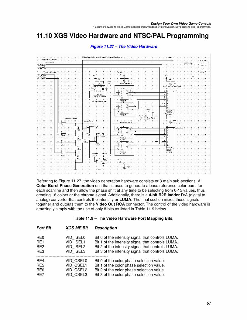
Design Your Own Video Game Console A Beginner’s Guide to Video Game Console and Embedded System Design, Development, and Programming.
67
11.10 XGS Video Hardware and NTSC/PAL Programming Figure 11.27 – The Video Hardware
Referring to Figure 11.27, the video generation hardware consists or 3 main sub-sections. A Color Burst Phase Generation unit that is used to generate a base reference color burst for each scanline and then allow the phase shift at any time to be selecting from 0-15 values, thus creating 16 colors or the chroma signal. Additionally, there is a 4-bit R2R ladder D/A (digital to analog) converter that controls the intensity or LUMA. The final section mixes these signals together and outputs them to the Video Out RCA connector. The control of the video hardware is amazingly simply with the use of only 8-bits as listed in Table 11.9 below.
Table 11.9 – The Video Hardware Port Mapping Bits.
Port Bit XGS ME Bit Description
RE0 VID_ISEL0 Bit 0 of the intensity signal that controls LUMA. RE1 VID_ISEL1 Bit 1 of the intensity signal that controls LUMA. RE2 VID_ISEL2 Bit 2 of the intensity signal that controls LUMA. RE3 VID_ISEL3 Bit 3 of the intensity signal that controls LUMA. ----------------------------------------------------- RE4 VID_CSEL0 Bit 0 of the color phase selection value. RE5 VID_CSEL1 Bit 1 of the color phase selection value. RE6 VID_CSEL2 Bit 2 of the color phase selection value. RE7 VID_CSEL3 Bit 3 of the color phase selection value.

Design Your Own Video Game Console A Beginner’s Guide to Video Game Console and Embedded System Design, Development, and Programming.
68
There are 4-bits of D/A conversion for the intensity signal VID_ISEL0-3 thus giving a total of 16 values, however, a number of them at the low scale of the range must be used to “jump” from “sync” 0.0V to “black” 0.25 - 0.3V. For example if the entire D/A range is 1.0V then 0.3 / 1.0 = 30%, 30% of 15 is 5, thus the 4-bit value of 0 is sync while the 4-bit value of 5 is black, leaving us with only the values 6-15 or 10 different intensity levels.
The color phase selection value VID_CSEL0-3 gives a total of 16 values. Value 0 is used as the “reference” color burst at the beginning of a scanline. Then when you want color you use value greater than 0. Each increment of 1 is approximately 10-12 ns which causes a phase shift around the NTSC color wheel, so that after 15 shifts you make your way around more than half the color wheel or on average 12*15 = 180 ns. This is more than enough colors to make a game. However, there are tricks to get the other half of the color wheel which I will discuss later in the chapter when we talk about programming.
11.10.1 Video Hardware Description
Referring to Figure 11.27 and the Proteus design file of the video hardware located on the CD at:
CDROOT:\XGSME_HW_CD\Schematics_Circuits\xgs_micro_video_05.DSN
Let’s take a look at the how the video hardware works from an electrical point of view. The interface to the video hardware is via 8-port bits, VID_ISEL0-3, and VID_CSEL0-3. The data of these ports is completely under control of the SX52. Let’s begin with the intensity/sync control bits VID_ISEL0-3. These 4-bits are fed into a R2R digital to analog converter which converts bit values 0-15 to voltage 0-1.5V (approximately), thus by send out different bit codes the raster can be instructed to sync, draw black, white, or grays in-between. The final output of the R2R ladder is fed into a potentiometer (5-20K value), which allows the overall intensity of the signal to be controlled, also there is a 100 ohm to ground resistor to help match the input impedance of the TV of 75 ohms. 100 ohms was chosen since when taken in parallel with the reflected impedance of the systems behind it, the overall impedance is about 75 ohms creating a maximum power transfer to the load. That’s all there is to the intensity or luma signal. This alone can be used to generate black and white video. The chroma or color hardware is much more interesting.
The details of NTSC are of course in the previous chapter and re-iterated below, but in essence we need to create a phase shifted 3.58Mhz (4.43Mhz PAL) color burst signal at the beginning of each line and then phase shift this amount by some angle 0-360 to select various colors. This is accomplished almost all by hardware for you. The lines VID_CSEL0-3 are used to select the color you which sent out to the analog mixing hardware. The operation is as follows; U6 generates the color burst reference clock (3.58Mhz NTSC or 4.43Mhz PAL), this clock is fed into a pair of 74HC244 buffers in a chained configuration. Digitally, the input and output are identical; however, the timing is skewed. Each buffer in the 244s create a delay of 8-12ns, this delay causes a phase shift in the digital signal. Together the two 244s create 16 different delays. These delays are “tapped” into a pair of 74HC4051 8:1 multiplexers which basically allow the signal VID_CSEL0-3 to select of 1-16 of the phase delayed signals, each representing one of sixteen colors around the color wheel, equidistant spaced.
The final phase delayed signals is of course still a square wave, and the TV needs a sine wave so a low pass filter is used to filter out the higher harmonics. The filter is composed of R10 and C1. Then the chroma signal is AC coupled thru C2, so only the AC component comes thru and the DC offset does not. This AC only chroma signal is then summed with the luma signal thru the saturation potentiometer and then final sent to the video output via a ferrite filter to once again remove higher frequency noise that might be present on the line from the board, so the TV signal is clean.
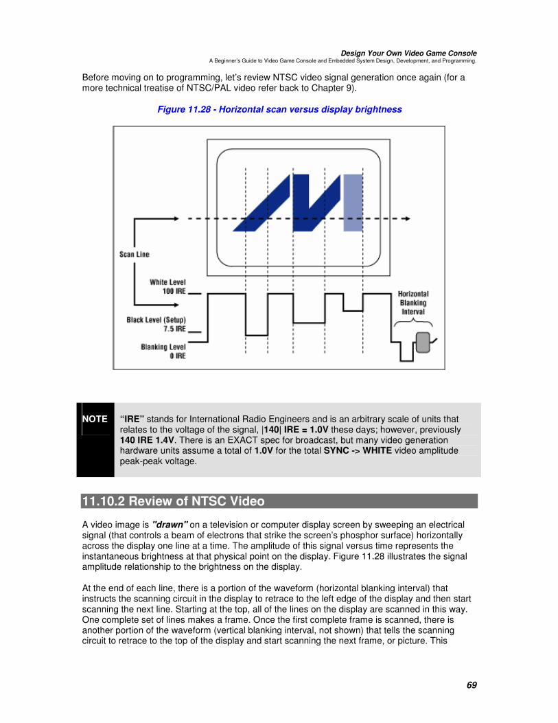
Design Your Own Video Game Console A Beginner’s Guide to Video Game Console and Embedded System Design, Development, and Programming.
69
Before moving on to programming, let’s review NTSC video signal generation once again (for a more technical treatise of NTSC/PAL video refer back to Chapter 9).
Figure 11.28 - Horizontal scan versus display brightness
NOTE “IRE” stands for International Radio Engineers and is an arbitrary scale of units that relates to the voltage of the signal, |140| IRE = 1.0V these days; however, previously 140 IRE 1.4V. There is an EXACT spec for broadcast, but many video generation hardware units assume a total of 1.0V for the total SYNC -> WHITE video amplitude peak-peak voltage.
11.10.2 Review of NTSC Video
A video image is "drawn" on a television or computer display screen by sweeping an electrical signal (that controls a beam of electrons that strike the screen’s phosphor surface) horizontally across the display one line at a time. The amplitude of this signal versus time represents the instantaneous brightness at that physical point on the display. Figure 11.28 illustrates the signal amplitude relationship to the brightness on the display.
At the end of each line, there is a portion of the waveform (horizontal blanking interval) that instructs the scanning circuit in the display to retrace to the left edge of the display and then start scanning the next line. Starting at the top, all of the lines on the display are scanned in this way. One complete set of lines makes a frame. Once the first complete frame is scanned, there is another portion of the waveform (vertical blanking interval, not shown) that tells the scanning circuit to retrace to the top of the display and start scanning the next frame, or picture. This

Design Your Own Video Game Console A Beginner’s Guide to Video Game Console and Embedded System Design, Development, and Programming.
70
sequence is repeated at a fast enough rate so that the displayed images are perceived to have continuous motion.
11.10.2.1 Interlaced versus Progressive Scans
These are two different types of scanning systems. They differ in the technique used to "render" the picture on the screen. Television signals and compatible displays are typically interlaced, and computer signals and compatible displays are typically progressive (non-interlaced). These two formats are incompatible with each other; one would need to be converted to the other before any common processing could be done. Interlaced scanning is where each picture, referred to as a frame, is divided into two separate sub-pictures, referred to as “fields”.
Two fields make up a single frame. An interlaced picture is painted on the screen in two passes, by first scanning the horizontal lines of the first field and then retracing to the top of the screen and then scanning the horizontal lines for the second field in-between the first set. Field 1 consists of lines 1 through 262 1/2, and field 2 consists of lines 262 1/2 through 525. The interlaced principle is illustrated in Figure 11.29. Only a few lines at the top and the bottom of each field are shown.
NOTE Most computer displays that output to TVs are progressive scans, that is, they draw a single frame 60 times a second without interlacing. However, some computers and game systems do put out interlaced video. The old Amiga computer was one such example that had an interlaced video mode option to double the number of scanlines.
Figure 11.29 - Interlaced scanning system

Design Your Own Video Game Console A Beginner’s Guide to Video Game Console and Embedded System Design, Development, and Programming.
71
A progressive, or non-interlaced, picture is painted on the screen by scanning all of the horizontal lines of the picture in one pass from the top to the bottom. This is illustrated in Figure 11.30.
Figure 11.30 - Progressive (non-interlaced) scanning system
11.10.3 Video Formats and Interfaces
There are many different kinds of video signals, which can be divided into either two classes; those for television and those for computer displays. The format of television signals varies from country to country. In the United States and Japan, the NTSC format is used. NTSC stands for National Television Systems Committee, which is the name of the organization that developed the standard. In Europe, the PAL format is common. PAL (phase alternating line), developed after NTSC, is an improvement over NTSC. SECAM is used in France and stands for sequential coleur avec memoire (color with memory). It should be noted that there is a total of about 15 different sub-formats contained within these three general formats. Each of the formats is generally not compatible with the others.
Although they all utilize the same basic scanning system and represent color with a type of phase modulation, they differ in specific scanning frequencies, number of scan lines, and color modulation techniques, among others. The various computer formats (such as VGA, SVGA, XGA) also differ substantially, with the primary difference in the scan frequencies and resolutions. These differences do not cause as much concern, because most computer equipment is now designed to handle variable scan rates (multisync monitors are now the de-facto standard). This compatibility is a major advantage for computer formats in that media, and content can be interchanged on a global basis.
Table 11.10 - Typical Frequencies for Common TV and Computer Video Formats

Design Your Own Video Game Console A Beginner’s Guide to Video Game Console and Embedded System Design, Development, and Programming.
72
Video Format NTSC PAL HDTV/SDTV VGA XGA
Description
Television Format for
North America and Japan
Television Format for
Most of Europe and South America
High Definition/ Standard
Definition Digital Television
Format
Video Graphics
Array (PC)
Extended Graphics
Array (PC)
Vertical Resolution Format (visible lines per frame)
Approx 480 (525 total lines)
Approx 575 (625 total lines)
1080 or 720 or 480; 18 different
formats 480 768
Horizontal Resolution Format (visible pixels per line)
Determined by bandwidth, ranges from 320 to 650
Determined by bandwidth,
ranges from 320 to 720
1920 or 704 or 640; 18 different
formats 640 1024
Horizontal Rate (kHz) 15.734 15.625 33.75-45 31.5 60
Vertical Frame Rate (Hz) 29.97 25 30-60 60-80 60-80
Highest Frequency (MHz)
4.2 5.5 25 15.3 40.7
There are three basic levels of baseband signal interfaces. In order of increasing quality, they are:
• Composite video (or CVBS), which uses one wire pair.
• Y/C (or S-video), which uses two wire pairs.
• Component Video, which uses three wire pairs.
Each wire pair consists of a signal and a ground. These three interfaces differ in their level of information combination (or encoding). More encoding typically degrades the quality but allows the signal to be transported using fewer wires. Component video obviously has the least amount of encoding, and composite video the most.
11.10.4 Composite Color Video Blanking Sync Interface
Composite signals are the most commonly used analog video interface. Composite video is also referred to as CVBS, which stands for color, video, blanking, and sync, or composite video

Design Your Own Video Game Console A Beginner’s Guide to Video Game Console and Embedded System Design, Development, and Programming.
73
baseband signal. It combines the brightness information (luma), the color information (chroma), and the synchronizing signals on just one cable. The connector is typically an RCA jack. This is the same connector as that used for standard line level audio connections. A typical waveform of an all-white NTSC composite video signal is shown in Figure 11.31(a).
Figure 11.31(a) - NTSC composite video waveform
This figure depicts the portion of the signal that represents one horizontal scan line. Each line is made up of the active video portion and the horizontal blanking portion. The active video portion contains the picture brightness (luma) and color (chroma) information. The brightness information is the instantaneous amplitude at any point in time. The unit of measure for the amplitude is in terms of an IRE unit. IRE is an arbitrary unit where 140 IRE = 1Vp-p (or sometimes 1.4Vp-p). From the figure, you can see that the voltage during the active video portion would yield a bright-white picture for this horizontal scan line, whereas the horizontal blanking portion would be displayed as black and therefore not seen on the screen. Please refer back to Figure 11.31(a) for a pictorial explanation. Some video systems (NTSC only) use something called "setup" which places reference black a point equal to 7.5 IRE or about 54mV above the blanking level.
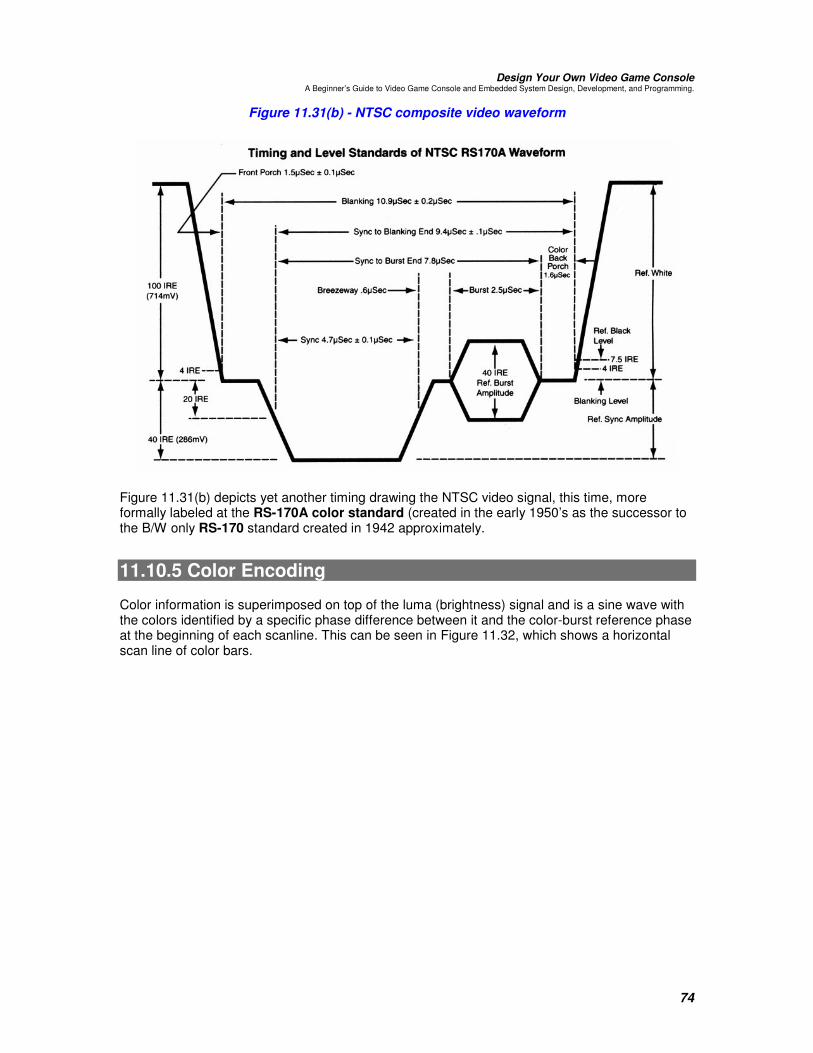
Design Your Own Video Game Console A Beginner’s Guide to Video Game Console and Embedded System Design, Development, and Programming.
74
Figure 11.31(b) - NTSC composite video waveform
Figure 11.31(b) depicts yet another timing drawing the NTSC video signal, this time, more formally labeled at the RS-170A color standard (created in the early 1950’s as the successor to the B/W only RS-170 standard created in 1942 approximately.
11.10.5 Color Encoding
Color information is superimposed on top of the luma (brightness) signal and is a sine wave with the colors identified by a specific phase difference between it and the color-burst reference phase at the beginning of each scanline. This can be seen in Figure 11.32, which shows a horizontal scan line of color bars.

Design Your Own Video Game Console A Beginner’s Guide to Video Game Console and Embedded System Design, Development, and Programming.
75
Figure 11.32 - Composite Video Waveform of the Color Bars.
The amplitude of the modulation is proportional to the amount of color (or saturation), and the phase information denotes the tint (or hue) of the color. The horizontal blanking portion contains the horizontal synchronizing pulse (sync pulse) as well as the color reference (color burst) located just after the rising edge of the sync pulse (called the "back porch"). It is important to note here that the horizontal blanking portion of the signal is positioned in time such that it is not visible on the display screen.
11.10.6 Putting it All Together
Generating a NTSC (or PAL) signal means controlling the signal into the TV such that all the timing specifications are met. There are a number of aspects that must be taken into consideration to achieve this successfully. However, one important detail is that the video signal does not have to be perfect, that is, the timings can be slightly off per line, per frame, per color burst, etc. nevertheless, the amount of “slack” must be consistent. In general here are the steps to generating an NTSC signal.
11.10.6.1 Frame Construction
A Frame is composed of 262.5 lines (non-interlaced), 262 will suffice. Of those 262 lines, many of them are invisible due to overscan, and some must be used for the vertical retrace pulse. Therefore, a rule of them is to generate a video signal frame with the following algorithm:
���������#���������3����,����������� ���+�IM;�(��� �����#���������3����,����������� ���+�IM;�(��� �����#���������3����,����������� ���+�IM;�(��� �����#���������3����,����������� ���+�IM;�(��� ����S���(����:�<����IM;S���(����:�<����IM;S���(����:�<����IM;S���(����:�<����IM;�������� .�,��.�,��.�,��.�,���������� ���������������1�� ���(������������������1�� ���(������������������1�� ���(������������������1�� ���(����������� �������������������������#�����"�������3��� ��������#�����"�������3��� ��������#�����"�������3��� ��������#�����"�������3��� �������S���(����:�<����<S���(����:�<����<S���(����:�<����<S���(����:�<����<;;;;����

Design Your Own Video Game Console A Beginner’s Guide to Video Game Console and Embedded System Design, Development, and Programming.
76
���� .�,��.�,��.�,��.�,���������� ���������������1��"(��/� ���(������������������1��"(��/� ���(������������������1��"(��/� ���(������������������1��"(��/� ���(����������� ����������������������������������3������(� ����)-( �+�"� ���((���))(��;X�������� �,��(�������������������3������(� ����)-( �+�"� ���((���))(��;X�������� �,��(�������������������3������(� ����)-( �+�"� ���((���))(��;X�������� �,��(�������������������3������(� ����)-( �+�"� ���((���))(��;X�������� �,��(�������������������������������-���������� ���(��� ����������-���������� ���(��� ����������-���������� ���(��� ����������-���������� ���(��� ����X�����:�;%;XX�����:�;%;XX�����:�;%;XX�����:�;%;X���������(��!M�����(��� $�(��!M�����(��� $�(��!M�����(��� $�(��!M�����(��� $�������������#�������)��3��� ��������#�������)��3��� ��������#�������)��3��� ��������#�������)��3��� �������S���(����:�<����KS���(����:�<����KS���(����:�<����KS���(����:�<����K�������� .�,��.�,��.�,��.�,���������� ���������������������������������������������������������1��"(��/� ���(����1��"(��/� ���(����1��"(��/� ���(����1��"(��/� ���(����������� ��������������������
If you add up the lines, you will get a total of 262 lines including active, inactive, and retrace or vertical sync. However, in reality even this is too many. I find that most TVs can display 192 lines safely, some 224, so unless your demos can look “ok” missing the top and bottom of the image on some sets then a safe rule of thumb is 192 lines of active video sandwiched within equal amounts of overscan on the top and bottom.
11.10.6.2 Line Construction
Generating a line is a little more tricky that generating a frame since the real work must be done on each line. The basic idea is that you must generate the video signal which controls the luma (brightness), the chroma (color), and synchronization all within the same signal. This is accomplished by mimicking the signals you see in Figures 11.31(a) and 11.31(b). Each line consists of a total of 63.5us where 52.6us is actual video data and the other 10.9us is sync and setup data. However, you can slightly alter them if you wish. For example, if you want to make the video portion of a line 50us rather than 52.6us then it will work since you can just stuff black into non-active region; however, the more you alter the spec (especially in terms of the length of the sync and color burst) the higher the chances are that the signal will not work on some older (or newer sets).
To generate the actual video signal the XGS ME gives you total control over the actual output voltage of the video line, therefore, you program the voltages as a function of time to create each video line. For example, each line consists of the following areas:
“Front Porch” - The spec calls for a “front porch” of 1.5 us consisting of black, therefore you would tell the XGS ME video hardware to send out black, then you would delay for 1.5 us (talking into consideration the amount of time to execute the actual instruction that turns black on).
“Sync Tip”- The next part of the spec is the horizontal sync or HSYNC, this should be approximately 4.7 us, therefore, you would tell the video hardware to output a 0.0V for 4.7 us.
The next portion of the video signal is the “Color Burst” which consists of a pre-burst phase called the “Breezeway”, the burst itself called the “Color Burst” and finally the post-burst called the “Back Porch”.
“Breezeway”- This part of the spec says to output black for 0.6 us.
“Color Burst”- This is the most complex part of the specification and the one that would be nearly impossible to do without the extra hardware support of the XGS ME. You could do the color burst totally with software, but the MPU would be so tied up during each pixel it would leave

Design Your Own Video Game Console A Beginner’s Guide to Video Game Console and Embedded System Design, Development, and Programming.
77
little time for anything, but a pong game. In any case, we will explain how this works shortly, but for now, you need to know that you must generate 8-10 cycles of color burst tone (9-10 for PAL). This is a 3.579545Mhz “tone” (4.433Mhz for PAL) signal that the TV locks onto and uses as a phase reference for the remainder of the video line. The color of each pixel is determined by the phase difference from the color burst reference at the beginning of each line and the color burst tone of each pixel. In any case, 8-10 clocks must be sent, I usually send 9-10 cycles of color burst. Each cycle at 3.579594 MHz takes 279.36ns, therefore, if you want 10 cycles of color burst, you must turn the color burst hardware on for 279.36ns * 10 = 2.79us approximately.
“Back Porch”- Immediately following the color burst is the final part of the setup for the actual pixel data, this is called the “back porch” and should last 1.6 us.
11.10.6.3 Generating B/W Video Data
The remainder of the video information is 52.6 us, this is where you insert your pixel data. Now, if you wanted a B/W only signal then you would modulate the video signal from BLACK (0.3V) to WHITE (1.0+ V) for the remainder of the line and be done with it. For example, each line could rasterize a line buffer, or a sprite and different values would map to different voltages from BLACK to WHITE. With this approach most TVs have an input bandwidth wide enough to display about 320 luminance changes per active line, that means that no matter how fast you try to change the luminance signal only 320 times a line will you see anything. Let’s see how we roughly estimate this.
The line length is 52.6us, we want to make 320 changes in that time, that means that we need to send data at a rate of:
52.6 us / 320 = 164.375 ns per change
Inverting this gives us the frequency which is 1/164.375 ns = 6.0 MHz roughly! Ouch, that means that the input to the TV’s luminance has to be 6.0 MHz or greater. Sorry to say, it’s not. In most cases, you are lucky if you get 4.5 – 5.0 MHz input bandwidth, this 320 is a definitely upper limit on B/W luminance transitions per line.
11.10.6.4 Generating Color Video Data
Generating color video is much more complicated than B/W, however, if we take a practical approach rather that a mathematical, its quite easy. Forgoing the complex quadrature encoding of color and luminance and the encoding and decoding of the signals, creating a color is very easy. For each color clock on the active scan line, you must generate a 3.579545Mhz sine wave, this must ride on top or be super imposed on the luminance signal (the XGS ME hardware does all this). The overall amplitude of the signal is the brightness or luminance just as it was with B/W, but the color signal’s saturation is simple the peak-peak (p-p) value of the color signal 3.579545 MHz signal as shown in Figure 7.6. The actual color that is displayed has nothing to do with the amplitude of the video signal, but only the PHASE difference from the reference burst from the original color burst reference at the beginning of each line.
To re-iterate, to generate color, we simply produce a 3.579594 MHz signal, super impose or add it to the overall luminance signal, and the phase difference between our color signal and the reference is the color on the screen! Cool.
Taking this further, let’s break up the line into pixels once again and see how many can be displayed each line. There are 52.6 us of active video time. We have to generate a 3.579545 MHz signal and stuff it into each pixel; given this how many pixels can fit into a line?

Design Your Own Video Game Console A Beginner’s Guide to Video Game Console and Embedded System Design, Development, and Programming.
78
Color Clocks Per Line
52.6us / (3.579545Mhz -1) = 188.
This means that at best case you can have 188 colored pixels per active scanline, but it gets worst! That doesn’t necessarily mean that you can have 188 DIFFERENT colored pixels across the screen, it just means you can request that from the poor TV with limited bandwidth. Again, this is a give take world, and in many cases, you would never have 188 different colors on the same line, it would look like a rainbow. In most cases, objects have constant color for a few pixels at a time. In any case, many video system over drive the video to 224, 240, or 256 virtual pixels (but, the color will not change that fast), you can do this if you wish, however, I suggest using a nice 160 x 192 display or thereabouts which will always look pretty good, has enough resolution, and you will almost get a 1:1 color change per pixel even if you change each pixel’s color. However, give everything a try and see what you get.
11.10.6.5 NTSC Signal References
Here are a number of web sites and documents to help you understand the NTSC / PAL video formats:
http://www.ee.washington.edu/conselec/CE/kuhn/ntsc/95x4.htm http://www.bealecorner.com/trv900/tech/RS170A.jpg http://www.bealecorner.com/trv900/tech/ http://www.maxim-ic.com/appnotes.cfm/appnote_number/734/ln/en http://pdfserv.maxim-ic.com/en/an/AN734.pdf
11.11 Programming The XGS ME Video Hardware The XGS ME’s video hardware has both a D/A to convert the overall voltage requested for luminance to the video line as well as a color burst generator and selector. The color burst circuitry gives the XGS a very powerful shortcut for generating color. Nevertheless, you must control the video completely with software via the VID_ISEL port (intensity select) and VID_CSEL (color burst select), refer back to Table 11.9. Both controls are 4-bits wide (a nibble each) and encoded into the single Port E. This was by design. By using a single port to contain both the intensity (lower 4-bits) and the color (upper 4-bits) we can make changes to the video much faster (only one port has to be written) and we can play with bit shifting algorithms to do cool things.
11.11.1 Generating a Composite Luma/Chroma Video Signal Voltage
The first step to generating a video signal is being able to generate a voltage in the luminance section of the video hardware. This is trivial, just place a number into the lower nibble of Port E and that number 0-15 will be converted into a voltage 0.0V to 1.0V roughly.
11.11.1.1 Generating Luma
For example, let’s see you are constructing your video line and need the “front porch”, this is BLACK which is approximately 0.3V, let’s compute the value needed to generate 0.3V:
Proportion of total range we must traverse: 0.3 V / 1.0 V = .3

Design Your Own Video Game Console A Beginner’s Guide to Video Game Console and Embedded System Design, Development, and Programming.
79
Compute binary value to generate voltage for 4-bit D/A: (0.3) * (15) = 4.5, rounding up to 5. Therefore, if we output the integer 5 to the luminance bits (lower 4-bits) we will generate a 0.3V at the video output:
������3��3��3��3���� ��+�T>���+�T>���+�T>���+�T>����� =�,��������"(��/=�,��������"(��/=�,��������"(��/=�,��������"(��/��������
Similarly, “sync” is 0.0V which would obviously be integer 0:
������3��3��3��3���� ��+�T;���+�T;���+�T;���+�T;����� =�,�������� ���=�,�������� ���=�,�������� ���=�,�������� �����������
Finally, “white” is 1.0V which would be full power or integer 15:
������3��3��3��3���� ��+�T<>�=�,����������+�T<>�=�,����������+�T<>�=�,����������+�T<>�=�,��������#����#����#����#������������
Considering this, we loose the values 0-5 to represent sync to black and thus have the values 7 – 15 (9 values) for “shades” of color or B/W gray scale. Of course, you can fudge this, you can get away with using 4 for the black and inch up to 8-15 values for shades, but this will not work on some set, so better safe than sorry. Like I said, TVs are very forgiving, but not all of them. Table 11.11 lists the integral luminance values and their rough meanings.
Table 11.11 – Integral Luminance Values and Their Meanings.
VID_ISEL (RE lower 4-bits) Value Voltage (V) Meaning
0 0.0 SYNC 1 0.66 2 0.132 3 0.198 4 0.264 5 0.330 BLACK 6 0.396 DARK GRAY 7 0.462 8 0.528 9 0.594 10 0.660 MEDIUM GRAY 11 0.726 12 0.792 13 0.858 LIGHT GRAY 14 0.924 15 1.0 WHITE
11.11.11.2 Generating The Color Burst Signal
At this point, if all you were to do is generate a B/W signal with the lower 4-bits of Port E and followed the RS-170 spec you would see video. And in fact it, would even be color, yellow to be exact, since the upper 4-bits would have 0000b in them which defines a color burst reference and a color of yellow all the time. Now, let’s cover in detail how to generate the color signal.

Design Your Own Video Game Console A Beginner’s Guide to Video Game Console and Embedded System Design, Development, and Programming.
80
Let’s begin with the color burst signal at the beginning of the RS-170A spec for each line. After the initial SYNC pulse, there is a 0.6 us pre-burst delay then you need to generate 8-10 clocks of color burst 3.579545 MHz tone. To do this, in you loop all you need to do is send out BLACK in the lower bits (integer value 5, 0101b) and in VID_CSEL you will send out the value for the color burst reference which is also 0000b. You will do this for a time of approximately 2.5-2.8 us depending on if you want 8-10 cycles of color burst. During this 2.5 - 2.8us you are free to do what you want, as is when you are doing the sync pulse, you just have to make sure you are BACK to your raster code when the time is up. For example, when you request an HSYNC you can sit in a dead loop for 4.7us or you can do something. At a system clock rate of 80 MHz, that means each clock cycle is 12.5ns, therefore, in the HSYNC alone you have:
4.7us / 12.5ns = 376 clocks!
Which with the SX52 and its pipelined RISC CPU is more or less 376 instructions! Also, during the actual color burst you have another 2.8us which is equal to:
2.8us / 12.5ns = 224 clocks!
So you have a total of 376 + 224 = 600 cycles to set things up. A ton of time to get ready for the line. To send the actual color burst, you need to send both a luma value of BLACK (0.3V) in the lower 4-bits of Port E as well as the color burst in the upper 4-bits or Port E. Here’s an example:
����=�����<;����(� +��))��1%�I%K�-�� ������(���"-� ������"(��/=�����<;����(� +��))��1%�I%K�-�� ������(���"-� ������"(��/=�����<;����(� +��))��1%�I%K�-�� ������(���"-� ������"(��/=�����<;����(� +��))��1%�I%K�-�� ������(���"-� ������"(��/����=�=�=�=�;;;;�����X ���9;;;;�����X ���9;;;;�����X ���9;;;;�����X ���9+���(���;+������+���(���;+������+���(���;+������+���(���;+�������������(���"-� ��������(���"-� ��������(���"-� ��������(���"-� �����=�=�=�=�;<;<;<;<;<;<;<;<�����X � ��9+������X � ��9+������X � ��9+������X � ��9+�(-��������>�!"(��/(-��������>�!"(��/(-��������>�!"(��/(-��������>�!"(��/$$$$������3��3��3��3���� ��+�TG;;;;;<;<��+�TG;;;;;<;<��+�TG;;;;;<;<��+�TG;;;;;<;<��������
And then you would delay for 2.8us to let the system output the 10 cycles of color burst,. You can delay either with code that does work or a dead loop. After the color burst, there is a 1.6 us “back porch” where you must keep the LUMA at BLACK, but you need to turn OFF the color burst. To turn off the color burst signal completely in all cases, you send it a value of integer 15, this send a “ground” the summing circuit in the analog section and basically kills the 3.579594 MHz signal from getting into the video amplifier. Here’s how you would do that:
����=�����<%J�- � ���������(�������"(��/=�����<%J�- � ���������(�������"(��/=�����<%J�- � ���������(�������"(��/=�����<%J�- � ���������(�������"(��/����=�<<<<=�<<<<=�<<<<=�<<<<�����X ���9�����X ���9�����X ���9�����X ���9+������(�������((+������(�������((+������(�������((+������(�������((����=�=�=�=�;<;<;<;<;<;<;<;<�����X � ��9+������X � ��9+������X � ��9+������X � ��9+�(-��������>�!"(��/(-��������>�!"(��/(-��������>�!"(��/(-��������>�!"(��/$$$$������3��3��3��3���� ��+�TG��+�TG��+�TG��+�TG<<<<<<<<<<<<<<<<;;;;<;<<;<<;<<;<��������
And that’s it. You are now ready to send pixels.
11.11.11.3 Generating a Single Pixel
Once the scanline is set up you make your way into the active region of the line. This is 52.6us of time. Here is where you modulate both the intensity of the video signal for the LUMA (brightness) in the lower 4-bits of Port E as well as selecting colors with the upper 4-bits. And here comes the cool part – wherever you want color, just put the color into the upper 4-bits of Port E and the color will show up! This is the hardware working for us. The hardware is always oscillating at 3.579545 MHz, so when you send the color burst the hardware send the burst, but then stays in steps with the original signal, so no matter where you turn the color signal back on, it is phase locked to the original color burst. How we get color is to phase shift our color signal for

Design Your Own Video Game Console A Beginner’s Guide to Video Game Console and Embedded System Design, Development, and Programming.
81
each pixel with the original color burst, but how? This is where the “phase shift modulation” hardware comes into play. There is a chain of 16 delay buffers connected to the color burst generator. Each delay is about 10-12ns depending on the chip technology. This gives us a total delay of about 15 * 12ns = 180 ns. Table 11.12 lists the phase angle delays and their general color and angle.
Table 11.12 – Colors Generated by Phase Shifted Color Burst
Color Approx. Phase Approx. Delay VID_CSEL Value
Burst 0 degrees 0 ns 0 Yellow 15 12 1 Red 75 58 5 Magenta 135 105 9 Blue 195 151 13 Cyan 255 198 15 Green 315 244 -
If you look at the table and consider that the largest delay we can get is 15 * 12ns = 18 0ns then you quickly realize we are barely going to get to CYAN let alone GREEN. The problem is that we need a total of 360 degrees to cover the circle or a total or 288 ns of delay, so how can we get Cyan and Green? The trick is to understand the color burst signal is a “reference”, no on said that we MUST use the non-delayed value for color burst, why not use the END of the delay chain for the color burst and then we can use negative phase shifts, or in other words if we use the very last color as the color burst and then draw a color with the color right before it then we get (-15) degrees phase angle or (+345) degrees, thus we can work our way backward to get the rest of the colors.
TIP To get the first half of the color circle use color 0 as the color burst and then color 0, 1, 2, 3, 4…14 as the colors. To get the second half of the color circle use color 14 as the color burst and then colors 0, 1, 2,….14 as the colors.

Design Your Own Video Game Console A Beginner’s Guide to Video Game Console and Embedded System Design, Development, and Programming.
82
Figure 11.33(a) – Color Burst Reference 0, Colors 0 – 14.
Figure 11.33(b) – Color Burst Reference 14, Colors 0 – 14.
Figure 11.33(a) and 11.33(b) depict actual screen shot examples when color 0 is used as a color burst reference (Figure 11.33(a)) as well as color 14 as a color burst reference (Figure 11.33(b)). Color 15 is NO COLOR or GROUND, so it’s unused as a possible color.
11.11.2 Video Demos
First some terminology – historically, video systems that controlled the raster mostly with software are called “video kernels”. Old Atari 2600 and video arcade game programmers used to write a game that was also the kernel, that is, the game logic was so closely tied to the video they were the same thing. Thus, generalizing a software only video system is rather hard. There are some techniques that can be coded such as crude frame buffers, line buffer, sprite systems, and so

Design Your Own Video Game Console A Beginner’s Guide to Video Game Console and Embedded System Design, Development, and Programming.
83
forth which I will code in the next chapter (when I get a chance on the next revision of this document). But, for now I leave it all to you. Given that, I have written two of the easiest programs to experiment with. The first program draws a single blue bar in the middle of the screen. It’s very short and you should be able to follow it in detail and experiment with it. Like I said, I don’t follow the RS-170A spec to the letter, but I am always close. For example, there are really 262.5 lines per screen, I use 262, and other small changes to the color burst, syncs, and general timing to make things easier. The general technique I use to code these demos is a “hard coded” kernel, that is, the kernel is the display. In the second demo, I make a little more complex kernel that shows how during the VSYNC you can do animation.
The key to all this raster programming is that your code can NOT deviate a SINGLE cycle, not even ONE! All paths thru your code must be the SAME. This is a little hard to get used to, but you will get the hang of it by counting clocks, adding delays and so forth. I suggest you start by experimenting with color bars and then move onto writing kernels with logic that track the beam each frame and draw dots or simple sprites, then you can try scanline buffers, and full frame buffers. Remember, each color clock is free since the hardware does the color for you, so you have about 20-22 cycles per pixel to do work with a color display, that means you can be fetching from memory, doing translations, and so forth. The trick to writing video kernels is to organize your games and demos like this:
11.11.2.1 Video Kernel Tips
• During the vertical blank and sync do all game logic, input, and sound, generate all static data for the video kernel.
• During each line rasterization, the HSYNC should be used to access the new “row” or “data set” for that line.
• During each pixel you should send out the pixel data and fetch and decode the next or do any comparison logic.
There literally is no limit to what can be done at 80 MHz with color and intensity support, I estimate Wolfenstein 3D can definitely be written on the XGS ME, considering I have seen something like it on the Atari 2600! With that in mind let’s look at the demos.
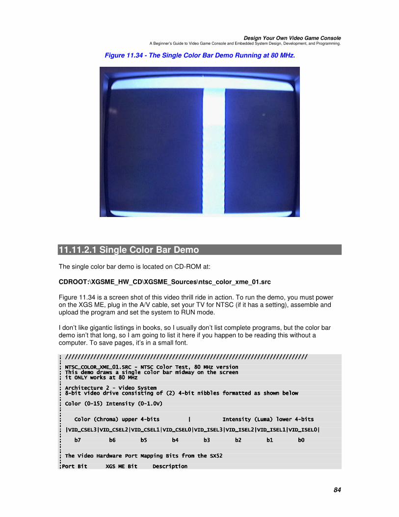
Design Your Own Video Game Console A Beginner’s Guide to Video Game Console and Embedded System Design, Development, and Programming.
84
Figure 11.34 - The Single Color Bar Demo Running at 80 MHz.
11.11.2.1 Single Color Bar Demo
The single color bar demo is located on CD-ROM at:
CDROOT:\XGSME_HW_CD\XGSME_Sources\ntsc_color_xme_01.src
Figure 11.34 is a screen shot of this video thrill ride in action. To run the demo, you must power on the XGS ME, plug in the A/V cable, set your TV for NTSC (if it has a setting), assemble and upload the program and set the system to RUN mode.
I don’t like gigantic listings in books, so I usually don’t list complete programs, but the color bar demo isn’t that long, so I am going to list it here if you happen to be reading this without a computer. To save pages, it’s in a small font.
=������������������������������������������������������������������������������=������������������������������������������������������������������������������=������������������������������������������������������������������������������=����������������������������������������������������������������������������������====����=�R���797������;<%���=�R���797������;<%���=�R���797������;<%���=�R���797������;<%��������R����(����� �+�K;��R����(����� �+�K;��R����(����� �+�K;��R����(����� �+�K;���N��N��N��N�3�� ����3�� ����3�� ����3�� �������=���� ���������# ��� ��,(����(���"������#���������� �����=���� ���������# ��� ��,(����(���"������#���������� �����=���� ���������# ��� ��,(����(���"������#���������� �����=���� ���������# ��� ��,(����(���"������#���������� ���������=����7R98�#��/ ����K;�=����7R98�#��/ ����K;�=����7R98�#��/ ����K;�=����7R98�#��/ ����K;���N��N��N��N����====����=�C��������-���I�=�C��������-���I�=�C��������-���I�=�C��������-���I������X������� ����X������� ����X������� ����X������� �������=�K=�K=�K=�K����"���3��������3����� � ���,����!I$�M"���3��������3����� � ���,����!I$�M"���3��������3����� � ���,����!I$�M"���3��������3����� � ���,����!I$�M����"�����""(� ������������ � ��#��"�(�#"�����""(� ������������ � ��#��"�(�#"�����""(� ������������ � ��#��"�(�#"�����""(� ������������ � ��#��"�(�#����====����=��(���!;=��(���!;=��(���!;=��(���!;����<>$� ���� ����!;<>$� ���� ����!;<>$� ���� ����!;<>$� ���� ����!;����<%;X$<%;X$<%;X$<%;X$����====����====����=�����(���!�����$�-))���M=�����(���!�����$�-))���M=�����(���!�����$�-))���M=�����(���!�����$�-))���M����"�� ���������&���������� ���� ����!9-��$�(�#���M"�� ���������&���������� ���� ����!9-��$�(�#���M"�� ���������&���������� ���� ����!9-��$�(�#���M"�� ���������&���������� ���� ����!9-��$�(�#���M����"�� "�� "�� "�� ����====����=�&X ���9Q&X ���9I&X ���9<&X ���9=�&X ���9Q&X ���9I&X ���9<&X ���9=�&X ���9Q&X ���9I&X ���9<&X ���9=�&X ���9Q&X ���9I&X ���9<&X ���9;&X � ��9Q&X � ��9I&X � ��9<&X � ��9;&;&X � ��9Q&X � ��9I&X � ��9<&X � ��9;&;&X � ��9Q&X � ��9I&X � ��9<&X � ��9;&;&X � ��9Q&X � ��9I&X � ��9<&X � ��9;&����====����=����"L����=����"L����=����"L����=����"L������������"J��������">��������"M��������"Q��������"I��������"<��������";�������������������������������������������������"J��������">��������"M��������"Q��������"I��������"<��������";�������������������������������������������������"J��������">��������"M��������"Q��������"I��������"<��������";�������������������������������������������������"J��������">��������"M��������"Q��������"I��������"<��������";���������������������������������������������=������=������=������=����������====����=�����X���������#����*������))��,�.�� ������������>I=�����X���������#����*������))��,�.�� ������������>I=�����X���������#����*������))��,�.�� ������������>I=�����X���������#����*������))��,�.�� ������������>I����====����=*����.��=*����.��=*����.��=*����.������ �������.���������.���������.���������.������ � ���)����� ���)����� ���)����� ���)��������

Design Your Own Video Game Console A Beginner’s Guide to Video Game Console and Embedded System Design, Development, and Programming.
85
����=���;�=���;�=���;�=���;����� ���� X � ��9;X � ��9;X � ��9;X � ��9;���� .���;������������� ���� �,��(������������( �9D�C%.���;������������� ���� �,��(������������( �9D�C%.���;������������� ���� �,��(������������( �9D�C%.���;������������� ���� �,��(������������( �9D�C%����=���<�=���<�=���<�=���<����� ���� X � ��9<X � ��9<X � ��9<X � ��9<���� .���<������������� ���� �,��(������������( �9D�C%.���<������������� ���� �,��(������������( �9D�C%.���<������������� ���� �,��(������������( �9D�C%.���<������������� ���� �,��(������������( �9D�C%����=���I�=���I�=���I�=���I����� ���� X � ��9I��X � ��9I��X � ��9I��X � ��9I������ .���I������������� ���� �,��(������������( �9D�C%.���I������������� ���� �,��(������������( �9D�C%.���I������������� ���� �,��(������������( �9D�C%.���I������������� ���� �,��(������������( �9D�C%����=���Q�=���Q�=���Q�=���Q����� ���� X � ��9Q�X � ��9Q�X � ��9Q�X � ��9Q����� .���Q������������� .���Q������������� .���Q������������� .���Q������������� ���� �,��(������������( �9D�C%���� �,��(������������( �9D�C%���� �,��(������������( �9D�C%���� �,��(������������( �9D�C%��������=���M�=���M�=���M�=���M����� ���� X ���9;X ���9;X ���9;X ���9;���� .���;����������(���)�� �� �(�������3�(-�%.���;����������(���)�� �� �(�������3�(-�%.���;����������(���)�� �� �(�������3�(-�%.���;����������(���)�� �� �(�������3�(-�%����=���>��=���>��=���>��=���>���������� X ���9<X ���9<X ���9<X ���9<���� .���<����������(���)�� �� �(�������3�(-�%.���<����������(���)�� �� �(�������3�(-�%.���<����������(���)�� �� �(�������3�(-�%.���<����������(���)�� �� �(�������3�(-�%����=���J��=���J��=���J��=���J���������� X ���9IX ���9IX ���9IX ���9I���� .���I����������(���)�� �� �(�������3�(-�%.���I����������(���)�� �� �(�������3�(-�%.���I����������(���)�� �� �(�������3�(-�%.���I����������(���)�� �� �(�������3�(-�%����=���L��=���L��=���L��=���L���������� X ���9QX ���9QX ���9QX ���9Q���� .���Q����������(���)�� .���Q����������(���)�� .���Q����������(���)�� .���Q����������(���)�� �� �(�������3�(-�%�� �(�������3�(-�%�� �(�������3�(-�%�� �(�������3�(-�%����====����=�R��� ����3���������#���� )�� =�R��� ����3���������#���� )�� =�R��� ����3���������#���� )�� =�R��� ����3���������#���� )�� ����=��(���;�=��(���;�=��(���;�=��(���;������*�� ������������*�� ������������*�� ������������*�� ���������������=��(���<�=��(���<�=��(���<�=��(���<������<M��<M��<M��<M������)�� ����(�������(�� ����<;�)�� ����(�������(�� ����<;�)�� ����(�������(�� ����<;�)�� ����(�������(�� ����<;����<I� �)�����(����))��1%<I� �)�����(����))��1%<I� �)�����(����))��1%<I� �)�����(����))��1%����=��(���;P���((�#%%%%����,�%%%���%%%%)��/%%%%��,����%%%%3��(��%%%%%"(-�P�(���<M=��(���;P���((�#%%%%����,�%%%���%%%%)��/%%%%��,����%%%%3��(��%%%%%"(-�P�(���<M=��(���;P���((�#%%%%����,�%%%���%%%%)��/%%%%��,����%%%%3��(��%%%%%"(-�P�(���<M=��(���;P���((�#%%%%����,�%%%���%%%%)��/%%%%��,����%%%%3��(��%%%%%"(-�P�(���<M����====����=��(���<>�=��(���<>�=��(���<>�=��(���<>������,��-��+����"�,��-��+����"�,��-��+����"�,��-��+����"-� �+�- ������.��� �,��(�,���������%-� �+�- ������.��� �,��(�,���������%-� �+�- ������.��� �,��(�,���������%-� �+�- ������.��� �,��(�,���������%����====����=� ���� ����%Q3�!J$��))��1%�"(��/+�;%;3� ����!;$+��((�# �<;� ���� �P$=� ���� ����%Q3�!J$��))��1%�"(��/+�;%;3� ����!;$+��((�# �<;� ���� �P$=� ���� ����%Q3�!J$��))��1%�"(��/+�;%;3� ����!;$+��((�# �<;� ���� �P$=� ���� ����%Q3�!J$��))��1%�"(��/+�;%;3� ����!;$+��((�# �<;� ���� �P$����====����=������������������������������������������������������������������������������=������������������������������������������������������������������������������=������������������������������������������������������������������������������=����������������������������������������������������������������������������������=�������3���������"-�� =�������3���������"-�� =�������3���������"-�� =�������3���������"-�� ����=����������������������������������������=����������������������������������������=����������������������������������������=������������������������������������������������������������������������������������������������������������������������������������������������������������������������������������������������������������ �X ��X ��X ��X ����� ��>I��>I��>I��>I�������� ������������������������ ���������������������������� S��Y�S��Y�S��Y�S��Y����� K;�;;;�;;;�K;�;;;�;;;�K;�;;;�;;;�K;�;;;�;;;����� =���� �� ����������3���������������(�=���� �� ����������3���������������(�=���� �� ����������3���������������(�=���� �� ����������3���������������(��������� ���� ���� ������������ =������-�#�������)-�������������������DR�����=������-�#�������)-�������������������DR�����=������-�#�������)-�������������������DR�����=������-�#�������)-�������������������DR������������� ���� ���� ������������ =���-��- ����/�� -�����-�,�����������=���-��- ����/�� -�����-�,�����������=���-��- ����/�� -�����-�,�����������=���-��- ����/�� -�����-�,������������������� ���� ���� ���� =���3���� �����, �������/�� -����=���3���� �����, �������/�� -����=���3���� �����, �������/�� -����=���3���� �����, �������/�� -������������������������ ���� ���� ���� =���Q�� ����"(��+�������� ��(����3�����=���Q�� ����"(��+�������� ��(����3�����=���Q�� ����"(��+�������� ��(����3�����=���Q�� ����"(��+�������� ��(����3������������� ���� ���� ���� =�����"��/������� �"(��������������=�����"��/������� �"(��������������=�����"��/������� �"(��������������=�����"��/������� �"(������������������)��,���)��,���)��,���)��,����������� ���� ���� ���� =��������)����*����������������� #������������DR=��������)����*����������������� #������������DR=��������)����*����������������� #������������DR=��������)����*����������������� #������������DR��������90��C9��90��C9��90��C9��90��C9������ �YD�YD�YD�YD���� KKKK���� =�- ��������/����((��,������9C8��������� ���=�- ��������/����((��,������9C8��������� ���=�- ��������/����((��,������9C8��������� ���=�- ��������/����((��,������9C8��������� ����������� ���� ���� ���� =� ������ �����������F-�������<;+;;;+;;=� ������ �����������F-�������<;+;;;+;;=� ������ �����������F-�������<;+;;;+;;=� ������ �����������F-�������<;+;;;+;;;;;;������������ �X ��X ��X ��X ����� ���� 7���Q7���Q7���Q7���Q���� ���� ���� =���,�=���,�=���,�=���,����� )�����1�����(�� ��((���� )�����1�����(�� ��((���� )�����1�����(�� ��((���� )�����1�����(�� ��((������������ �X ��X ��X ��X ����� ���� S. S. S. S.���� ���� ���� =��� ��(�����"��/��� �"(��=��� ��(�����"��/��� �"(��=��� ��(�����"��/��� �"(��=��� ��(�����"��/��� �"(���������� �X ��X ��X ��X ����� ���� ��9.DS��9.DS��9.DS��9.DS�������� ���� =��� ��(����3���� �"(��=��� ��(����3���� �"(��=��� ��(����3���� �"(��=��� ��(����3���� �"(������������������=������������������������������������������������������������������������������=������������������������������������������������������������������������������=������������������������������������������������������������������������������=����������������������������������������������������������������������������������=������ =������ =������ =������ ����=��������������������=��������������������=��������������������=��������������������������������������������������������������������������������������������������������������������������������������������������������������������������������������������������������������������������������������������������������������������=� ��������"(��/=� ��������"(��/=� ��������"(��/=� ��������"(��/��������.9C0�9�X�9.9C0�9�X�9.9C0�9�X�9.9C0�9�X�9���� �YD�YD�YD�YD���� !J$!J$!J$!J$���� ���� ���� =��))��1%�%Q3=��))��1%�%Q3=��))��1%�%Q3=��))��1%�%Q3�����8R�8R�8R�8R���� ���� �YD�YD�YD�YD���� !<>W<J�?�;$!<>W<J�?�;$!<>W<J�?�;$!<>W<J�?�;$���� ���� =������(���"-� ��#����;3=������(���"-� ��#����;3=������(���"-� ��#����;3=������(���"-� ��#����;3����.9C0.9C0.9C0.9C0���� ���� �YD�YD�YD�YD���� !<>W<J�?�.9C0�9�X�9$!<>W<J�?�.9C0�9�X�9$!<>W<J�?�.9C0�9�X�9$!<>W<J�?�.9C0�9�X�9$���� =������(���"-� ��#����%Q3=������(���"-� ��#����%Q3=������(���"-� ��#����%Q3=������(���"-� ��#����%Q3��������=�������������(���"-� ������L���(�=�������������(���"-� ������L���(�=�������������(���"-� ������L���(�=�������������(���"-� ������L���(�� � � � ��������.D����7R.D����7R.D����7R.D����7R���� �YD�YD�YD�YD���� !;W<J��?�>$�!;W<J��?�>$�!;W<J��?�>$�!;W<J��?�>$�����.D����7SS.D����7SS.D����7SS.D����7SS���� �YD�YD�YD�YD���� !<>W<J�?�>$=� ����� �"(��/!<>W<J�?�>$=� ����� �"(��/!<>W<J�?�>$=� ����� �"(��/!<>W<J�?�>$=� ����� �"(��/��������797�;797�;797�;797�;���� ���� �YD�YD�YD�YD���� !;W<J�?�.9C0�9�X�9$�!;W<J�?�.9C0�9�X�9$�!;W<J�?�.9C0�9�X�9$�!;W<J�?�.9C0�9�X�9$�����797�<797�<797�<797�<���� ���� �YD�YD�YD�YD���� !<W<J�?�.9C0�9�X�9$�!<W<J�?�.9C0�9�X�9$�!<W<J�?�.9C0�9�X�9$�!<W<J�?�.9C0�9�X�9$�����797�I797�I797�I797�I���� ���� �YD�YD�YD�YD���� !IW<J�?�.9C0�9�X�9$�!IW<J�?�.9C0�9�X�9$�!IW<J�?�.9C0�9�X�9$�!IW<J�?�.9C0�9�X�9$�����797�Q797�Q797�Q797�Q���� ���� �YD�YD�YD�YD���� !QW<J�?�.9C0�9�X�9$�!QW<J�?�.9C0�9�X�9$�!QW<J�?�.9C0�9�X�9$�!QW<J�?�.9C0�9�X�9$�����797�M797�M797�M797�M���� ���� �YD�YD�YD�YD���� !MW<J�?�.9C0�9�X�9$�!MW<J�?�.9C0�9�X�9$�!MW<J�?�.9C0�9�X�9$�!MW<J�?�.9C0�9�X�9$�����797�>797�>797�>797�>���� ���� �YD�YD�YD�YD���� !>W<J�?�.9C0�9�X�9$�!>W<J�?�.9C0�9�X�9$�!>W<J�?�.9C0�9�X�9$�!>W<J�?�.9C0�9�X�9$�����797�J797�J797�J797�J���� ���� �YD�YD�YD�YD���� !JW<J�?�.9C0�9�X�9$�!JW<J�?�.9C0�9�X�9$�!JW<J�?�.9C0�9�X�9$�!JW<J�?�.9C0�9�X�9$�����797�L797�L797�L797�L���� ���� �YD�YD�YD�YD���� !LW<J�?�.9C0�9�X�9$�!LW<J�?�.9C0�9�X�9$�!LW<J�?�.9C0�9�X�9$�!LW<J�?�.9C0�9�X�9$�����797�K797�K797�K797�K���� ���� �YD�YD�YD�YD���� !KW<J�?�.9C0�9�X�9$�!KW<J�?�.9C0�9�X�9$�!KW<J�?�.9C0�9�X�9$�!KW<J�?�.9C0�9�X�9$�����797�[797�[797�[797�[���� ���� �YD�YD�YD�YD���� 
Design Your Own Video Game Console A Beginner’s Guide to Video Game Console and Embedded System Design, Development, and Programming.
86
7X���CR7X���CR7X���CR7X���CR�797��797��797��797������YD�YD�YD�YD���� �� ���� ���� ���� ��������8R�7�*��8R�7�*��8R�7�*��8R�7�*���� �YD�����!?;$�YD�����!?;$�YD�����!?;$�YD�����!?;$������������=������������������������������������������������������������������������������=������������������������������������������������������������������������������=������������������������������������������������������������������������������=����������������������������������������������������������������������������������=��(�"�(�3����"(� =��(�"�(�3����"(� =��(�"�(�3����"(� =��(�"�(�3����"(� ����=������������������������������������������������������������������������������=������������������������������������������������������������������������������=������������������������������������������������������������������������������=�������������������������������������������������������������������������������������� ���� ��,��,��,��,���� VI;VI;VI;VI;����������-��<��-��<��-��<��-��<���� ���� � �� �� �� ����� <�=���(����<�=���(����<�=���(����<�=���(�����-�����-�����-�����-����������-��I��-��I��-��I��-��I���� ���� � �� �� �� ����� <�=���(�����-����<�=���(�����-����<�=���(�����-����<�=���(�����-������������=���� ������H- ��#��/��,�3�� �������������+�������,� )����(=���� ������H- ��#��/��,�3�� �������������+�������,� )����(=���� ������H- ��#��/��,�3�� �������������+�������,� )����(=���� ������H- ��#��/��,�3�� �������������+�������,� )����(��������(-��(-��(-��(-������ ���� � � � � ���� <�=����)�����(-��<�=����)�����(-��<�=����)�����(-��<�=����)�����(-���������������������������������� ���� � � � � ���� <�=����)�����������<�=����)�����������<�=����)�����������<�=����)������������������)�3�������)�3�������)�3�������)�3�������� � � � � ���� <�=����)� -�����(-�������������<�=����)� -�����(-�������������<�=����)� -�����(-�������������<�=����)� -�����(-�����������������"-� ��)�� �"-� ��)�� �"-� ��)�� �"-� ��)�� ����� � � � � ���� <�=����)�����"-� ��)�� ������1<�=����)�����"-� ��)�� ������1<�=����)�����"-� ��)�� ������1<�=����)�����"-� ��)�� ������1�������� ���(� ���(� ���(� ���(������������� � �� �� �� ����� <�=� ���(������-����<�=� ���(������-����<�=� ���(������-����<�=� ���(������-����������-������-������-������-������������ � �� �� �� ����� <�=�,�����(���-����<�=�,�����(���-����<�=�,�����(���-����<�=�,�����(���-����������-����I��-����I��-����I��-����I���� � �� �� �� ����� <�=�,�����(���-����<�=�,�����(���-����<�=�,�����(���-����<�=�,�����(���-�������������(�#�����(�#�����(�#�����(�#���� � � � � ���� <�=�������(�#�������,�<�=�������(�#�������,�<�=�������(�#�������,�<�=�������(�#�������,����������������������������������������� � � � � ���� <<<<��������=������������������������������������������������������������������������������=������������������������������������������������������������������������������=������������������������������������������������������������������������������=����������������������������������������������������������������������������������=������ =������ =������ =������ ����=����������������������=����������������������=����������������������=��������������������������������������������������������������������������������������������������������������������������������������������������������������������������������������������������������������������������������������������������������������=������������������������������������������������������������������������������=������������������������������������������������������������������������������=������������������������������������������������������������������������������=���������������������������������������������������������������������������������������9C8��C�7��(��/ �9C8��C�7��(��/ �9C8��C�7��(��/ �9C8��C�7��(��/ ����=���� ���#�������� � (�,��(���������������������������-��������������� =���� ���#�������� � (�,��(���������������������������-��������������� =���� ���#�������� � (�,��(���������������������������-��������������� =���� ���#�������� � (�,��(���������������������������-��������������� ����=���� ���������������(��(�=���� ���������������(��(�=���� ���������������(��(�=���� ���������������(��(��,����(�� �-)����I>+>;;����(� +� �������((����- ��������((�#��,�,����(�� �-)����I>+>;;����(� +� �������((����- ��������((�#��,�,����(�� �-)����I>+>;;����(� +� �������((����- ��������((�#��,�,����(�� �-)����I>+>;;����(� +� �������((����- ��������((�#��,����=���� ��-����� =���� ��-����� =���� ��-����� =���� ��-����� ��������=����(����(��=����(����(��=����(����(��=����(����(������=��9C8!�-�"�������(��/ $=��9C8!�-�"�������(��/ $=��9C8!�-�"�������(��/ $=��9C8!�-�"�������(��/ $��������=�����K;���N��(��/+������ ������)�������� =�����K;���N��(��/+������ ������)�������� =�����K;���N��(��/+������ ������)�������� =�����K;���N��(��/+������ ������)�������� ����=��9C8!K;W����� ����� $=��9C8!K;W����� ����� $=��9C8!K;W����� ����� $=��9C8!K;W����� ����� $����=��1��)(����-�#������M%>�-����(��=��1��)(����-�#������M%>�-����(��=��1��)(����-�#������M%>�-����(��=��1��)(����-�#������M%>�-����(������=�K;WM%>�:�QJ=�K;WM%>�:�QJ=�K;WM%>�:�QJ=�K;WM%>�:�QJ����=��9C8!QJ$=��9C8!QJ$=��9C8!QJ$=��9C8!QJ$��������=����=����=����=�����)��)���� �������R7������(�����,�)���������+� ������������� ��-������#�-(��"������)��)���� �������R7������(�����,�)���������+� ������������� ��-������#�-(��"������)��)���� �������R7������(�����,�)���������+� ������������� ��-������#�-(��"������)��)���� �������R7������(�����,�)���������+� ������������� ��-������#�-(��"����� ��(� ��(� ��(� ��(�����=��((�3�(-� �"��<;�������-(��)(��"��K�������������K;+������1��)(�+���M%>�-����(�����-(��=��((�3�(-� �"��<;�������-(��)(��"��K�������������K;+������1��)(�+���M%>�-����(�����-(��=��((�3�(-� �"��<;�������-(��)(��"��K�������������K;+������1��)(�+���M%>�-����(�����-(��=��((�3�(-� �"��<;�������-(��)(��"��K�������������K;+������1��)(�+���M%>�-����(�����-(��"�"�"�"�����=�#������=�#������=�#������=�#����������=��9C8!KWM>$=��9C8!KWM>$=��9C8!KWM>$=��9C8!KWM>$����=�#������ ���(���(���������-���3�=�#������ ���(���(���������-���3�=�#������ ���(���(���������-���3�=�#������ ���(���(���������-���3���������=���� �����)-�����=���� �����)-�����=���� �����)-�����=���� �����)-������������(��������������<;�������(���������(��������������<;�������(���������(��������������<;�������(���������(��������������<;�������(������ S�!!!�(��/ $����<;$���;$ S�!!!�(��/ $����<;$���;$ S�!!!�(��/ $����<;$���;$ S�!!!�(��/ $����<;$���;$��������=���� ��Q��(��/���-�/ =���� ��Q��(��/���-�/ =���� ��Q��(��/���-�/ =���� ��Q��(��/���-�/ �������� ��*��!!!�(��/ $����<;$�Q$��*��!!!�(��/ $����<;$�Q$��*��!!!�(��/ $����<;$�Q$��*��!!!�(��/ $����<;$�Q$�������� 6�*�V�?�<6�*�V�?�<6�*�V�?�<6�*�V�?�<�������� �R��R��R��R���������=���#���������������������=���#���������������������=���#���������������������=���#��������������������������������� ��*��!!!�(��/ $����<;$��Q$��*��!!!�(��/ $����<;$��Q$��*��!!!�(��/ $����<;$��Q$��*��!!!�(��/ $����<;$��Q$�������� R7*R7*R7*R7*�������� �R��R��R��R������R S�R S�R S�R S��������=���1���-(��)(� ����<;;=���1���-(��)(� ����<;;=���1���-(��)(� ����<;;=���1���-(��)(� ����<;;���� S�!!!�(��/ $���<;;$��:�<$ S�!!!�(��/ $���<;;$��:�<$ S�!!!�(��/ $���<;;$��:�<$ S�!!!�(��/ $���<;;$��:�<$��������=���(���<;;W!�(��/ �<;;$+�(��)��F-�( �<;;+�����������<W!�(��/ �<;;$���������� =���(���<;;W!�(��/ �<;;$+�(��)��F-�( �<;;+�����������<W!�(��/ �<;;$���������� =���(���<;;W!�(��/ �<;;$+�(��)��F-�( �<;;+�����������<W!�(��/ �<;;$���������� =���(���<;;W!�(��/ �<;;$+�(��)��F-�( �<;;+�����������<W!�(��/ �<;;$���������� �������� ��3���-����+�T!!�(��/ $�<;;$���3���-����+�T!!�(��/ $�<;;$���3���-����+�T!!�(��/ $�<;;$���3���-����+�T!!�(��/ $�<;;$�����=�!I$=�!I$=�!I$=�!I$����P9��)P9��)P9��)P9��)���� ���� ���� ���� ���� ������������ ��3���-����I+�TIM��3���-����I+�TIM��3���-����I+�TIM��3���-����I+�TIM���� �������� =�!I$=�!I$=�!I$=�!I$����P9��)<;;P9��)<;;P9��)<;;P9��)<;;���� ���� ���� ���� ���� �������� �H�N���-����I+�P9��)<;;�H�N���-����I+�P9��)<;;�H�N���-����I+�P9��)<;;�H�N���-����I+�P9��)<;;���� ���� =�!M�I$=�!M�I$=�!M�I$=�!M�I$������������ �H�N���-����+�P9��)�H�N���-����+�P9��)�H�N���-����+�P9��)�H�N���-����+�P9��)���� ���� =�!M�I$=�!M�I$=�!M�I$=�!M�I$����

Design Your Own Video Game Console A Beginner’s Guide to Video Game Console and Embedded System Design, Development, and Programming.
87
�����R S�R S�R S�R S������������=�(� �����)-�=�(� �����)-�=�(� �����)-�=�(� �����)-���#��(���-(��)(� ����<;+�������(����#��(���-(��)(� ����<;+�������(����#��(���-(��)(� ����<;+�������(����#��(���-(��)(� ����<;+�������(������ S�!!�!!�(��/ $����<;;$���<;$��:�<$ S�!!�!!�(��/ $����<;;$���<;$��:�<$ S�!!�!!�(��/ $����<;;$���<;$��:�<$ S�!!�!!�(��/ $����<;;$���<;$��:�<$��������=���(���<;W!�(��/ �<;$+�(��)��F-�( �<;+�����������!�(��/ �<;$���������� =���(���<;W!�(��/ �<;$+�(��)��F-�( �<;+�����������!�(��/ �<;$���������� =���(���<;W!�(��/ �<;$+�(��)��F-�( �<;+�����������!�(��/ �<;$���������� =���(���<;W!�(��/ �<;$+�(��)��F-�( �<;+�����������!�(��/ �<;$���������� �������� ��3���-����+�T!�!!�(��/ $����<;;$���<;$���3���-����+�T!�!!�(��/ $����<;;$���<;$���3���-����+�T!�!!�(��/ $����<;;$���<;$���3���-����+�T!�!!�(��/ $����<;;$���<;$����� =�!I$=�!I$=�!I$=�!I$����P9��)IP9��)IP9��)IP9��)I���� ���� ���� ���� ���� �������� H�)�V�?�<H�)�V�?�<H�)�V�?�<H�)�V�?�<���� ���� ���� =�!Q$=�!Q$=�!Q$=�!Q$�������� H�)�V�?�<H�)�V�?�<H�)�V�?�<H�)�V�?�<���� ���� ���� =�!Q$=�!Q$=�!Q$=�!Q$�������� �H�N���-�����H�N���-�����H�N���-�����H�N���-����+�P9��)I+�P9��)I+�P9��)I+�P9��)I���� ���� =�!M�I$=�!M�I$=�!M�I$=�!M�I$�����R S�R S�R S�R S���������R��R��R��R���������=������������������������������������������������������������������������������=������������������������������������������������������������������������������=������������������������������������������������������������������������������=����������������������������������������������������������������������������������=�����#����� =�����#����� =�����#����� =�����#����� ����=������������������������������������������������������������������������������=������������������������������������������������������������������������������=������������������������������������������������������������������������������=������������������������������������������������������������������������������������������ ���� �C���C���C���C������ (-��+K+D�(-��+K+D�(-��+K+D�(-��+K+D��������� ���� �C���C���C���C������ ������+K+D�������+K+D�������+K+D�������+K+D��������� ���� �C���C���C���C������ ���)�3����+K+D����)�3����+K+D����)�3����+K+D����)�3����+K+D���������=������������������������������������������������������������������������������=������������������������������������������������������������������������������=������������������������������������������������������������������������������=����������������������������������������������������������������������������������=��-"��-���� =��-"��-���� =��-"��-���� =��-"��-���� ����=������������������������������������������������������������������������������=������������������������������������������������������������������������������=������������������������������������������������������������������������������=������������������������������������������������������������������������������������������ ���� ��,���,���,���,����� V;V;V;V;��������=���� ��-��������(�� ����-((�J>>QJ���-�� ��������-=���� ��-��������(�� ����-((�J>>QJ���-�� ��������-=���� ��-��������(�� ����-((�J>>QJ���-�� ��������-=���� ��-��������(�� ����-((�J>>QJ���-�� ��������-�� �� �� �� �������� ���� �����(���9��,�(���9��,�(���9��,�(���9��,���� �(��(��(��(����� ��-��<����-��<����-��<����-��<������ = �����(�N���-��<+��-��I= �����(�N���-��<+��-��I= �����(�N���-��<+��-��I= �����(�N���-��<+��-��I���� �������� ���� �(��(��(��(����� ��-��I��-��I��-��I��-��I���� ���� ====���� ���� ���� ���� ���� ��������P9��)P9��)P9��)P9��)���� ���� �H�N�H�N�H�N�H�N���� ��-��<+�P9��)��-��<+�P9��)��-��<+�P9��)��-��<+�P9��)���� =���������-���(��((�����N���=���������-���(��((�����N���=���������-���(��((�����N���=���������-���(��((�����N����������� �������� ���� �H�N�H�N�H�N�H�N���� ��-��I+�P9��)��-��I+�P9��)��-��I+�P9��)��-��I+�P9��)���� ====���� ���� ���� ���� ���� �������� ���� ���������������� ���� ���� =��������-��=��������-��=��������-��=��������-������ ���� ���� ���� ������������=�������������������������������������������������������������=�������������������������������������������������������������=�������������������������������������������������������������=�������������������������������������������������������������������������������������������������������������������������������������=��.�,���)��,������������ ����=��.�,���)��,������������ ����=��.�,���)��,������������ ����=��.�,���)��,������������ ��������=������������������������������������������������������������������������������=������������������������������������������������������������������������������=������������������������������������������������������������������������������=�������������������������������������������������������������������������������������������������������������� ���� ������������ ���� "��/"��/"��/"��/���� TVI;TVI;TVI;TVI;��������=� �����(�N�� �7�������((��=� �����(�N�� �7�������((��=� �����(�N�� �7�������((��=� �����(�N�� �7�������((�������������� ���� ��3��3��3��3���� ��+�TG;;;;;;;;��+�TG;;;;;;;;��+�TG;;;;;;;;��+�TG;;;;;;;;����=����)�������-�)-��(��������N���=����)�������-�)-��(��������N���=����)�������-�)-��(��������N���=����)�������-�)-��(��������N����������� ���� ��3��3��3��3���� O��+TG;;;;;;;;O��+TG;;;;;;;;O��+TG;;;;;;;;O��+TG;;;;;;;;����=����)���������������=����)���������������=����)���������������=����)��������������������������� ���� ��3��3��3��3���� �.+�TG;;;;;;;;���.+�TG;;;;;;;;���.+�TG;;;;;;;;���.+�TG;;;;;;;;������ =����)����.��-�)-��(��������N���=����)����.��-�)-��(��������N���=����)����.��-�)-��(��������N���=����)����.��-�)-��(��������N����������� ���� ��3��3��3��3���� O�.+TG;;;;;;;;O�.+TG;;;;;;;;O�.+TG;;;;;;;;O�.+TG;;;;;;;;����=����)����.����������=����)����.����������=����)����.����������=����)����.���������������������� ���� ��3��3��3��3���� (-��+�T;(-��+�T;(-��+�T;(-��+�T;�������� ���� ��3���3���3���3����� �����(�#+�T;�����(�#+�T;�����(�#+�T;�����(�#+�T;�������� ���� ��3��3��3��3���� �������+�T;�������+�T;�������+�T;�������+�T;������������ ���� ��3��3��3��3���� "-� ��)�� �+�T!797�;"-� ��)�� �+�T!797�;"-� ��)�� �+�T!797�;"-� ��)�� �+�T!797�;����<$<$<$<$�������� ����=���������������������������������������������=���������������������������������������������=���������������������������������������������=�������������������������������������������������������������������������������������������������������������������������������������������������������������������������������������=�������)��,����(��)=�������)��,����(��)=�������)��,����(��)=�������)��,����(��)����=������������������������������������������������������������������������������=������������������������������������������������������������������������������=������������������������������������������������������������������������������=���������������������������������������������������������������������������������������������������������� ���� ��������=�<[I� ���(��� ��������3��3�����=�<[I� ���(��� ��������3��3�����=�<[I� ���(��� ��������3��3�����=�<[I� ���(��� ��������3��3�������������.�,����� ���.�,����� ���.�,����� ���.�,����� ��������������� ���� ��3� ���(���+�T<[I��3� ���(���+�T<[I��3� ���(���+�T<[I��3� ���(���+�T<[I���� =��������<[I�����3�� ���(��� =��������<[I�����3�� ���(��� =��������<[I�����3�� ���(��� =��������<[I�����3�� ���(��� ������ ����9��)<�� ����9��)<�� ����9��)<�� ����9��)<��������=�������)�����<%>- �=�������)�����<%>- �=�������)�����<%>- �=�������)�����<%>- ������������� ���� ��3���+�T.9C0��3���+�T.9C0��3���+�T.9C0��3���+�T.9C0�������� =�!�I����(� �$�"(��/=�!�I����(� �$�"(��/=�!�I����(� �$�"(��/=�!�I����(� �$�"(��/�������� ���� �9C8�!90��C9�W<>�9C8�!90��C9�W<>�9C8�!90��C9�W<>�9C8�!90��C9�W<>����I$I$I$I$����

Design Your Own Video Game Console A Beginner’s Guide to Video Game Console and Embedded System Design, Development, and Programming.
88
���� ���� =��((��(���9��,=��((��(���9��,=��((��(���9��,=��((��(���9��,��������=�� ����M%L- =�� ����M%L- =�� ����M%L- =�� ����M%L- �������� ���� ��3���+�T�8R��3���+�T�8R��3���+�T�8R��3���+�T�8R���� ���� =�!�I����(� �$� ���=�!�I����(� �$� ���=�!�I����(� �$� ���=�!�I����(� �$� ����������� ���� �9C8�!90��C9�WML��9C8�!90��C9�WML��9C8�!90��C9�WML��9C8�!90��C9�WML������I$�I$�I$�I$�������� ���� =��((��(���9��,=��((��(���9��,=��((��(���9��,=��((��(���9��,��������=�)��=�)��=�)��=�)������"-� ��%J- "-� ��%J- "-� ��%J- "-� ��%J- �������� ���� ��3���+�T.9C0��3���+�T.9C0��3���+�T.9C0��3���+�T.9C0�������� =�!�I����(� �$� =�!�I����(� �$� =�!�I����(� �$� =�!�I����(� �$� �������������������� ���� �9C8�!90��C9�WJ��9C8�!90��C9�WJ��9C8�!90��C9�WJ��9C8�!90��C9�WJ������I$�I$�I$�I$�������� ���� =��((��(���9��,=��((��(���9��,=��((��(���9��,=��((��(���9��,��������=���(���"-� ������������I%>- �
Design Your Own Video Game Console A Beginner’s Guide to Video Game Console and Embedded System Design, Development, and Programming.
89
=���������������������������������������������������������������������=���������������������������������������������������������������������=���������������������������������������������������������������������=�������������������������������������������������������������������������������������������������������������=��R�.7��7������R�7X���CR=��R�.7��7������R�7X���CR=��R�.7��7������R�7X���CR=��R�.7��7������R�7X���CR����=������������������������������������������������������������������������������=������������������������������������������������������������������������������=������������������������������������������������������������������������������=������������������������������������������������������������������������������������������=������������������������������������������������������������������������������=������������������������������������������������������������������������������=������������������������������������������������������������������������������=����������������������������������������������������������������������������������=�X��� C9��8R�*D9��=�X��� C9��8R�*D9��=�X��� C9��8R�*D9��=�X��� C9��8R�*D9������=��������������������������������=��������������������������������=��������������������������������=���������������������������������������������������������������������������������������������������������������������������������������������������������������������������������������������������������������������������������������� ���� ��3� ���(���+�TM��3� ���(���+�TM��3� ���(���+�TM��3� ���(���+�TM����X"(��/�9��)I�X"(��/�9��)I�X"(��/�9��)I�X"(��/�9��)I��������� ���� ��3���+�T�8R��3���+�T�8R��3���+�T�8R��3���+�T�8R���� ���� =�!�I����(� �$� ���=�!�I����(� �$� ���=�!�I����(� �$� ���=�!�I����(� �$� ����������� ���� �9C8�!90��C9�WJQ>��9C8�!90��C9�WJQ>��9C8�!90��C9�WJQ>��9C8�!90��C9�WJQ>������I��I��I��I������M$�M$�M$�M$�������� ���� �H�N� ���(���+�X"(��/�9��)I�H�N� ���(���+�X"(��/�9��)I�H�N� ���(���+�X"(��/�9��)I�H�N� ���(���+�X"(��/�9��)I������������=������������������������������������������������������������������������=������������������������������������������������������������������������=������������������������������������������������������������������������=����������������������������������������������������������������������������������������������������=��R�X��� C9��8R�*D9��=��R�X��� C9��8R�*D9��=��R�X��� C9��8R�*D9��=��R�X��� C9��8R�*D9������=������������������������������������������������������������������������������=������������������������������������������������������������������������������=������������������������������������������������������������������������������=������������������������������������������������������������������������������������������=������������������������������������������������������������������������������=������������������������������������������������������������������������������=������������������������������������������������������������������������������=����������������������������������������������������������������������������������=��7*�����R�7X���CR=��7*�����R�7X���CR=��7*�����R�7X���CR=��7*�����R�7X���CR����=��������������������������������������=��������������������������������������=��������������������������������������=������������������������������������������������������������������������������������������������������������������������������������������������������������������������������������������������������������������ ���� ��3� ���(���+�TQK��3� ���(���+�TQK��3� ���(���+�TQK��3� ���(���+�TQK���� =�������� ���(��� =�������� ���(��� =�������� ���(��� =�������� ���(��� ����X"(��/�9��)QX"(��/�9��)QX"(��/�9��)QX"(��/�9��)Q��������=�������)�����<%>- �=�������)�����<%>- �=�������)�����<%>- �=�������)�����<%>- ��������� ���� ��3���+�T.9C0��3���+�T.9C0��3���+�T.9C0��3���+�T.9C0�������� =�!�I����(� �$�"(��/=�!�I����(� �$�"(��/=�!�I����(� �$�"(��/=�!�I����(� �$�"(��/�������� ���� �9C8�!90��C9�W<>�9C8�!90��C9�W<>�9C8�!90��C9�W<>�9C8�!90��C9�W<>����I$I$I$I$�������� ���� =��((��(���9��,=��((��(���9��,=��((��(���9��,=��((��(���9��,����=�� ����M%L- =�� ����M%L- =�� ����M%L- =�� ����M%L- �������� ���� ��3���+�T�8R��3���+�T�8R��3���+�T�8R��3���+�T�8R���� ���� =�!�I����(� �$� ���=�!�I����(� �$� ���=�!�I����(� �$� ���=�!�I����(� �$� ����������� ���� �9C�9C�9C�9C8�!90��C9�WML�8�!90��C9�WML�8�!90��C9�WML�8�!90��C9�WML������I$�I$�I$�I$�������� ���� =��((��(���9��,=��((��(���9��,=��((��(���9��,=��((��(���9��,��������=�)��=�)��=�)��=�)������"-� ��%J- "-� ��%J- "-� ��%J- "-� ��%J- �������� ���� ��3���+�T.9C0��3���+�T.9C0��3���+�T.9C0��3���+�T.9C0�������� =�!�I����(� �$� ���=�!�I����(� �$� ���=�!�I����(� �$� ���=�!�I����(� �$� ����������� ���� �9C8�!90��C9�WJ��9C8�!90��C9�WJ��9C8�!90��C9�WJ��9C8�!90��C9�WJ������I$�I$�I$�I$�������� ���� =��((��(���9��,=��((��(���9��,=��((��(���9��,=��((��(���9��,��������=���(���"-� ������������I%>- �
Design Your Own Video Game Console A Beginner’s Guide to Video Game Console and Embedded System Design, Development, and Programming.
90
2.5 microseconds I can use the number 25 (10*2.5) scaled by a number. This makes it easier to write, think, and represent fractional delays as well. Refer to the DELAY macro for more details.
The code that draws the scanline is highlighted for reference. In essence, it sets the raster to black, then delays enough time for the raster to get to the middle of the screen, then turns the raster to blue, then delays for 5us which creates a blue region, then turns the raster back to black and delays the remainder of the time needed for a total of 52.6us scanline time.
Figure 11.35 – Color Bar Demo.
11.11.2.2 Color Bars Demo
The next demo is much more complex. The kernel draws a number of color bars and then changes the reference color phase each time step to animate the colors. Figure 11.35 shows the demo in action. The demo is located on the CD at:
CDROOT:\XGSME_HW_CD\ XGSME_Sources\ntsc_color_xme_02.src
The code for the demo is very similar to the single color demo, except for the code that draws the raster line during the active scan has been replaced with this code that basically draws a few pixels of each shade of each color:
����=����#� ���(����!>I%J�- $=����#� ���(����!>I%J�- $=����#� ���(����!>I%J�- $=����#� ���(����!>I%J�- $������������ ���� �9C8!90��C9�W>;$�9C8!90��C9�W>;$�9C8!90��C9�W>;$�9C8!90��C9�W>;$�����(���9��)� ����(���9��)� ����(���9��)� ����(���9��)� ����������� ���� ��3�������+�T797�;��3�������+�T797�;��3�������+�T797�;��3�������+�T797�;���� =!I$=!I$=!I$=!I$�����(���9��)�.����(���9��)�.����(���9��)�.����(���9��)�.����������� ���� ��3���+���������3���+���������3���+���������3���+����������� ���� =!I$=!I$=!I$=!I$����
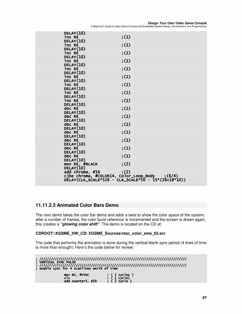
Design Your Own Video Game Console A Beginner’s Guide to Video Game Console and Embedded System Design, Development, and Programming.
91
���� ���� �9C8!<;$�9C8!<;$�9C8!<;$�9C8!<;$�������� ���� ���������������������������� ���� ���� =!<$=!<$=!<$=!<$�������� ���� �9C8!<;$�9C8!<;$�9C8!<;$�9C8!<;$�������� ���� ���������������������������� ���� ���� =!<$=!<$=!<$=!<$�������� ���� �9C8!<;$�9C8!<;$�9C8!<;$�9C8!<;$�������� ���� ���������������������������� ���� ���� =!<$=!<$=!<$=!<$�������� ���� �9C8!<;$�9C8!<;$�9C8!<;$�9C8!<;$�������� ���� ���������������������������� ���� ���� =!<$=!<$=!<$=!<$�������� ���� �9C8!<;$�9C8!<;$�9C8!<;$�9C8!<;$�������� ���� ���������������������������� ���� ���� =!<$=!<$=!<$=!<$�������� ���� �9C8!<;$�9C8!<;$�9C8!<;$�9C8!<;$�������� ���� ���������������������������� ���� ���� =!<$=!<$=!<$=!<$�������� ���� �9C8!<;$�9C8!<;$�9C8!<;$�9C8!<;$�������� ���� ���������������������������� ���� ���� =!<$=!<$=!<$=!<$�������� ���� �9C8!<;$�9C8!<;$�9C8!<;$�9C8!<;$�������� ���� ���������������������������� ���� ���� =!<$=!<$=!<$=!<$�������� ���� �9C8!<;$�9C8!<;$�9C8!<;$�9C8!<;$�������� ���� ���������������������������� ���� ���� =!<$=!<$=!<$=!<$�������� ���� �9C8!<;$�9C8!<;$�9C8!<;$�9C8!<;$�������� ���� ���������������������������� ���� ���� =!<$=!<$=!<$=!<$�������� ���� �9C8!<;$�9C8!<;$�9C8!<;$�9C8!<;$�������� ���� ���������������������������� ���� ���� =!<$=!<$=!<$=!<$�������� ���� �9C8!<;$�9C8!<;$�9C8!<;$�9C8!<;$�������� ���� ���������������������������� ���� ���� =!<$=!<$=!<$=!<$�������� ���� �9C8!<;$�9C8!<;$�9C8!<;$�9C8!<;$�������� ���� ���������������������������� ���� ���� ====!<$!<$!<$!<$�������� ���� �9C8!<;$�9C8!<;$�9C8!<;$�9C8!<;$�������� ���� ���������������������������� ���� ���� =!<$=!<$=!<$=!<$�������� ���� �9C8!<;$�9C8!<;$�9C8!<;$�9C8!<;$�������� ���� ���������������������������� ���� ���� =!<$=!<$=!<$=!<$�������� ���� �9C8!<;$�9C8!<;$�9C8!<;$�9C8!<;$�������� ���� ���������������������������� ���� ���� =!<$=!<$=!<$=!<$�������� ���� �9C8!<;$�9C8!<;$�9C8!<;$�9C8!<;$�������� ���� ��3���+�T.9C0��3���+�T.9C0��3���+�T.9C0��3���+�T.9C0���� ���� =!I$=!I$=!I$=!I$�������� ���� �9C8!<;$�9C8!<;$�9C8!<;$�9C8!<;$�������� ���� ����������+�T<J����������+�T<J����������+�T<J����������+�T<J���� ���� =!I$=!I$=!I$=!I$�������� ���� �H"��������+�T797�<M+��(���9��)�.����H"��������+�T797�<M+��(���9��)�.����H"��������+�T797�<M+��(���9��)�.����H"��������+�T797�<M+��(���9��)�.������� =!J�M$=!J�M$=!J�M$=!J�M$�������� ���� �9C8!90��C9�W>IJ��9C8!90��C9�W>IJ��9C8!90��C9�W>IJ��9C8!90��C9�W>IJ������90��C9�W>;��90��C9�W>;��90��C9�W>;��90��C9�W>;������<>W!IK?<KW�<>W!IK?<KW�<>W!IK?<KW�<>W!IK?<KW<;$$<;$$<;$$<;$$��������
11.11.2.3 Animated Color Bars Demo
The next demo takes the color bar demo and adds a twist to show the color space of the system; after a number of frames, the color burst reference is incremented and the screen is drawn again, this creates a “glowing color shift”. The demo is located on the CD at:
CDROOT:\XGSME_HW_CD\ XGSME_Sources\ntsc_color_xme_03.src
The code that performs the animation is done during the vertical blank sync period (4 lines of time is more than enough). Here’s the code below for review:
����=������������������������������������������������������������������������������=������������������������������������������������������������������������������=������������������������������������������������������������������������������=����������������������������������������������������������������������������������=�X��� C9��8R�*D9��=�X��� C9��8R�*D9��=�X��� C9��8R�*D9��=�X��� C9��8R�*D9������=������������������������������������������������������������������������������=������������������������������������������������������������������������������=������������������������������������������������������������������������������=����������������������������������������������������������������������������������=����"(�� ��������M� ���(��� �#������������=����"(�� ��������M� ���(��� �#������������=����"(�� ��������M� ���(��� �#������������=����"(�� ��������M� ���(��� �#������������������������ ���� ��3���+�T�8R��3���+�T�8R��3���+�T�8R��3���+�T�8R���� ���� =�=�=�=�!�I����(� �$!�I����(� �$!�I����(� �$!�I����(� �$�������� ���� �(��(��(��(����� ���� ���� =�!�<����(�$=�!�<����(�$=�!�<����(�$=�!�<����(�$�������� ���� ������-����Q+�TI;������-����Q+�TI;������-����Q+�TI;������-����Q+�TI;���� =�!�I����(��$=�!�I����(��$=�!�I����(��$=�!�I����(��$����

Design Your Own Video Game Console A Beginner’s Guide to Video Game Console and Embedded System Design, Development, and Programming.
92
���� ���� H���R�1��.-� �����H���R�1��.-� �����H���R�1��.-� �����H���R�1��.-� ��������� =�!�I�M����(� �$=�!�I�M����(� �$=�!�I�M����(� �$=�!�I�M����(� �$����R�1��.-� �������R�1��.-� �������R�1��.-� �������R�1��.-� ��������������� ���� ����"-� ��)�� �+�T<J����"-� ��)�� �+�T<J����"-� ��)�� �+�T<J����"-� ��)�� �+�T<J���� =�!�I����(� �$=�!�I����(� �$=�!�I����(� �$=�!�I����(� �$����R�1��.-� �����R�1��.-� �����R�1��.-� �����R�1��.-� ������������� ���� �9C8�!90��C9�WMWJQ>��9C8�!90��C9�WMWJQ>��9C8�!90��C9�WMWJQ>��9C8�!90��C9�WMWJQ>������I��I��I��I������Q��Q��Q��Q������M$�M$�M$�M$���� =�M� ���(��� ���� ���=�M� ���(��� ���� ���=�M� ���(��� ���� ���=�M� ���(��� ���� �����������
The code basically sets the raster to “sync” then performs the “game logic” to change the color burst, when the code completes then it delays the remainder of the time needed for the 4 sync pulses.
Figure 11.36 – The Connection Diagram for the XGS ME Programming System.
11.12 The Onboard Programmer The SX series processors are programmed via the OSC1/OSC2 pins via a complex serial protocol. Referring to Figure 11.36, the programming of the SX52 is accomplished via the PC->Parallel Cable->XGS ME. On the XGS ME another processor, an SX20 that is used to handle the high speed timing and ultra accurate cycle counting that is necessary to program the SX52 core. Thus, the XGS ME has an entire “slave” processor (an SX20) just to program the SX52. The PC talks to the SX20 then the SX20 talks to the SX52.
INTERESTING FACT
The SX20 isn’t absolutely necessary since the parallel port is fast enough to communicate directly with the SX52, however, the problem is that the timing of the parallel port isn’t reliable due to asynchronous processes, threads, etc. In the days of DOS, it would have worked, but under Windows 98/ME/XP/2000/2003, parallel port access is too unreliable when tight timing constraints are imposed.
The interesting thing about programming the SX processors is that they can be programmed “in circuit”, this is called “In System Programming” or ISP. Anyway, the process follows the following steps more or less:
Step 1 (Initialization): The host programmer places the SX processor into ISP mode.
Step 2 (Programming): The host programmer communicates with the SX processor via a serial protocol and sends commands and receives information. Programming is performed in this step.

Design Your Own Video Game Console A Beginner’s Guide to Video Game Console and Embedded System Design, Development, and Programming.
93
Step 3 (Shutdown): The host programmer releases the SX and pulls out of ISP mode, the SX resets and runs the program.
WARNING! Programming FLASH based memories is usually a repetitive process where the memory is programmed then tested, if the value isn’t correct then its reprogrammed until it reads the correct value. For example, the XGS ME IDE allows you to change the number of times the programming of a word occurs and other various repeat counts. You can find this dialog from the main menul; Build -> Tool Settings -> Configure Tools -> Hardware Tab -> Programmer Repetition.
The details of ISP mode are beyond the scope of this text, but you can read about them in the following document located on the CD:
CDROOT:\XGSME_HW_CD\SX_Docs_Books\sxisp.pdf
Figure 11.37 – Programming Waveforms for the SX52.

Design Your Own Video Game Console A Beginner’s Guide to Video Game Console and Embedded System Design, Development, and Programming.
94
But, briefly take a look at Figure 11.37 which shows the waveforms for entering into ISP mode. The hard part about entering into ISP mode is that that the system external oscillator must be electrically switched out of the system. Also, the programming hardware must be able to generate the Vpp voltage of 12.5V (we have this handled though), and this voltage along with 0V, 5V, must be able to be gated to the OSC1 pin, we will see the hardware that does this momentarily.
Figure 11.38 – ISP Protocal.
Figure 11.38 shows the actual protocol for ISP mode. As you can see there are 4 command cycles C3-C0, followed by 12 data cycles D11-D0, each “cycle” is composed of 4 clocks. The communications system is a single wire protocol that is pulled HIGH at the SX end, so commands are inserted by pulling the line LOW at either end. The transmission rate is 128Khz. So, the system is anything but simple, and getting it to work in practice is fraught with details. Also, you can see the commands that ISP supports, nine in total, but they are more than enough to program the SX chips.
NOTE For more information on the actual programmer’s code and firmware refer to the XGameStation™ Micro Edition User Guide on CD.

Design Your Own Video Game Console A Beginner’s Guide to Video Game Console and Embedded System Design, Development, and Programming.
95
Figure 11.39 – The XGS ME Programmer’s Schematic.
Now, let’s take a brief look at the schematics for the programmer module, Figure 11.39 shows the complete programmer system and the file below contains the Proteus design file:
CDROOT:\XGSME_HW_CD\Schematics_Circuits\xgs_micro_programmer_05.DSN
The design includes the parallel port interface at J2, the firmware programming port (to program the SX20 itself, this is done at the factory) at J3, an array of indicator LEDs at D9-D13, the SX20 itself at U18, and a transistor array Q1-Q7. The circuit works as follows; the PC establishes contact with the SX20 via the parallel port and the 4 data/control lines:
PP_DATA_OUT – Data out to the parallel port from the SX20. PP_DATA_IN – Data in from the parallel port to the SX20. PP_CLOCK – The clock form the PC. PP_STROBE – The strobe from the PC.
The SX20’s firmware allows the PC to send commands to it and then the SX20 controls the analog transistor array and can gate signals to the OSC1 pin (0V, 5V, 12.5V) for purposes of entering ISP mode and programming. The communications on OSC2 are sent back to the SX20 and thru the protocol back to the PC. The transistor array operates each transistor is a simple saturated mode where when the transistor is turned on the voltage is gated out and summed at the OSC1 node.
NOTE A cleaner solution would have been to use an analog switch rather than the transistors, but analog switches require that the VCC voltage is greater than the maximum voltage conducted, thus we would have to power the analog switch with the 12.5V supply to get it to pass the signal which I didn’t want to do, also the transistors are an excellent

Design Your Own Video Game Console A Beginner’s Guide to Video Game Console and Embedded System Design, Development, and Programming.
96
example of gating signals with discrete components.
Figure 11.40 – Closeup of the 30-Pin Expansion Interface.
11.13 XGS 30-Pin Interface and SX52 Headers The last topic of discussion is the 30-pin expansion port on the XGS ME and the headers surrounding the SX52. Let’s start with the 30-pin expansion interface. Figure 11.40 shows a screen shot of the board that indicates where pin 1, 15, 16, and 30 are on the 30-pin interface. Also, Table 11.13 lists the pins and their function.
Table 11.13 – Pinout for 30-pin expansion slot.
Pin # Signal Name
1 RB0 2 RB1 3 RB2 4 RB3 5 RB4 6 RB5 7 RB6 8 RB7 9 RC0 10 RC1 11 RC2 12 RC3 13 RC4 14 RC5
Pin # Signal Name
15 RC6 16 RC7 17 RD0 18 RD1 19 RD2 20 RD3 21 RD4 22 RD5 23 RD6 24 RD7 25 RA7 26 33VCC 27 5VCC 28 MAIN_OSC_OUT 29 OSC1_RUN_IN 30 GROUND
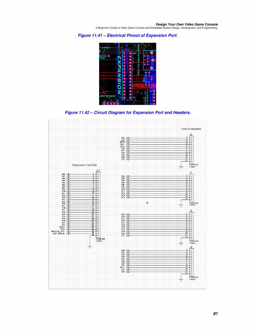
Design Your Own Video Game Console A Beginner’s Guide to Video Game Console and Embedded System Design, Development, and Programming.
97
Figure 11.41 – Electrical Pinout of Expansion Port.
Figure 11.42 – Circuit Diagram for Expansion Port and Headers.

Design Your Own Video Game Console A Beginner’s Guide to Video Game Console and Embedded System Design, Development, and Programming.
98
You can create a board to plug into the this edge connector with double sided contacts at .1” spacing (2.54mm) 15 fingers per side (or you can purchase them from us). Figure 11.41 shows the actual pinout of the connector in a mechanical view. The circuit diagram is shown in Figure 11.42 and the design files are on the CD at:
CDROOT:\XGSME_HW_CD\Schematics_Circuits\xgs_micro_expansion_05.DSN
The design is very straightforward, just a selection of key I/O, power, and clock lines have been exported to the 30-pin header. To build devices that use the expansion port you simply make sure that you grab the signal from the appropriate pins. However, there are some things to look out for. Some pins on the expansion port are used by other parts of the XGS ME system and if you drive them or load them you might disturb other sub-systems. For example, the PS/2 keyboard/mouse interface’s clock and data lines are on RB3, RB4, so if you were to drive these lines and try to read the mouse/keyboard you would get garbage, so the trick is to look at the main SX52 interface map in the design file:
CDROOT:\XGSME_HW_CD\Schematics_Circuits\xgs_micro_interfacemap_05.DSN
And based on this select which lines of the 30-pin you can use or want to use or are willing to disturb. For example, you might make a GPU card that must use all of RB, no problem, just tell the user he can’t use the keyboard at the same time.
Also, you will notice the lines MAIN_OSC_OUT and OSC1_RUN_IN, referring to the clocking system in Figure 11.7 these are the main clock and the divided clock, this way you can always run your card at the max speed if you wish, but you also can tell what speed the processor is being clocked at. Finally, the 5.0V and 3.3V supplies are exported, please try not to load them too much, I suggest using CMOS or LS chips, don’t try and run relays off the card!
11.13.1 Expansion Slot Ideas
There are so many things you can do with the expansion slots, but here are some of my favorites:
• A USB interface.
• An IDE interface.
• An Ethernet interface.
• A FLASH memory module.
• Interface a 6502, Z80, ARM7 or other processor on the card.
• A GPU on a FPGA and output NTSC or VGA graphics.
• Wireless communications card using Motorola Zigbee technology.
• Take the audio or video outputs and plug them into ports on the card and further process them and or mix them with extra hardware.
11.13.2 SX52 Headers
You may notice the headers around the SX52. There are 4 banks of 12 headers around the SX52, these connect 1:1 with the pins of the SX except for the +5 supplies on each side of the

Design Your Own Video Game Console A Beginner’s Guide to Video Game Console and Embedded System Design, Development, and Programming.
99
chip. You can connect directly to these ports and probe signals or extract signals that aren’t available on the 30-pin.
Figure 11.43 – SX52 to SX20 Inter-processor Communications Block Diagram.
11.14 Multiprocessor Support Although there is no firmware currently to support multiprocessing, there is hardware support for it. At the last minute I decided to add a pair of lines between the SX20 and the SX52. The motivation for this what that it seemed such a waste to let the SX20 just sit there underutilized while the SX52 does all the work. I didn’t want to make a lot of connections between the two chips to load the SX52’s interface, but at least a pair of them would suffice to support full duplex bi-directional communications. Figure 11.43 shows a block diagram of the connections. Table 11.14 shows the connections as well.
Table 11.14 – Interprocessor communications ports.
Pin on SX52 Pin on SX20
RA7 (2) <--------------> RB1 (8)
RB7 (19) <--------------> RB2 (9)
The only caveat is that RA7 on the SX52 is also connected to the SRAM’s SRAM_BANKSEL line, thus if you send data thru this line you would be changing the A16 line on the SRAM, but as long as you know this there is no problem. Or you could completely forget the RA7 line from the SX52 and do all communications thru the RB7 <-> RB2 gateway, the choice is yours.
11.14.1 Adding Multiprocessor Support in Firmware
The first step in getting multiprocessor support is that you are going to have to take the firmware that is programmed on the SX20 that communicates with the XGameStation™ Micro Edition Studio and augment it with extra code that allows programming to occur transparently, but then after programming the SX20 goes to work for you and waits and listens on the communications lines for commands. The source code for the firmware is located on the CD at:
CDROOT:\XGSME_HW_CD\XGSME_Sources\Firmware\sx_prog_unit01.SRC
Remember, to program the SX20 you will need a SX compatible programmer such as a SX-KEY from Parallax Inc., we have added a “Firmware Input Port” located on the bottom left of the XGS ME, Figure 11.44 shows a closeup. So step 1 is to take our source, modify it, add extra

Design Your Own Video Game Console A Beginner’s Guide to Video Game Console and Embedded System Design, Development, and Programming.
100
functionality to receive and send commands thru the interprocessor I/O ports and then upload the new firmware.
Figure 11.44 – The Firmware Programming Port for the SX20.
The next question is what kinds of support to add? Well, there are trillions of things you can add, for example, you can create a very complex math engine on the SX20 that supports 32 bit fixed point, floating point, vectors, matrices, etc. and then each frame you send all the math to the SX20, let it do it, then simply collect the results next frame! This way you could offload heavy calculations or the generation of algorithm data to the SX20. Also, if you’re really smart, why not store more data on the SX20? The SX20 has 2K WORDS of memory, our firmware takes about half of the memory as is, so you could write your communication handler and then use the rest of the memory for data storage. Or another cool idea is to use the SX20 as a remote register file if you for some reason couldn’t use the SRAM.
The only downside is that the SX20 runs at 4Mhz max since its internally clocked, so there is no direct way of getting around that. However, if you really wanted to you could jump the 80Mhz clock to the OSC1 pin of the SX20 if you really wanted to push it, then of course the firmware timing would be off and have to be adjusted since it was designed for 4Mhz.
11.15 XGS ME Programming Tutorials On the CD there are programming tutorials that cover specific examples of both NTSC and PAL demo/game programs. There are located here:
CDROOT:\XGSME_HW_CD\XGSME_Tutorials\*.*

Design Your Own Video Game Console A Beginner’s Guide to Video Game Console and Embedded System Design, Development, and Programming.
101
11.16 XGS Pico Edition – Bonus Section !!! For readers that like a more “hands on” approach and actually want to build something from the ground up then the XGS Pico Edition is for you. The XGS Pico Edition is a “specification” of how to build a small game system using many of the technologies from the commercial XGS Micro Edition, but scaled down, so the number of parts is a bare minimum and the parts don’t include any surface mount components that aren’t manageable.
The Pico Edition (PE) is based on the SX28 based embedded system developed in Chapter 9 and then augmented with simplified graphics, sound, input, power and clocking based on the XGS Micro’s design philosophies. Therefore, to understand the Pico Edition you must read in detail this chapter completely since the section below is more of a practical treatise on construction rather than technical explanation and simply shows you the systems of the Pico Edition along with construction instructions.
To begin with you might be asking how do you get the parts for the Pico Edition?
� You can buy them yourself from a distributor like DigiKey.com, Mouser.com, JDR Micro Devices, Jaycar etc.
� You can buy a Pico Edition kit from the www.xgamestation.com site or get one bundled with this book in eBook or printed format.
If you want to save the time of hunting the parts down, ordering, and then waiting for them then the pre-packaged kit might be the way to go. However, if you’re like me then finding the parts is half the fun and it’s a very educational process to go thru at least once in your life. Gives you respect for people that do parts procurement for battleships!
Figure 11.45(a) – The Hand Built XGS Pico Edition.

Design Your Own Video Game Console A Beginner’s Guide to Video Game Console and Embedded System Design, Development, and Programming.
102
Figure 11.45(b) – The Hand Built XGS Pico Edition with Color Coding.
The Pico Edition is built on a single “solderless” breadboard as shown in Figure 11.45(a) (which shows a completed unit with optional SX-KEY programmer plugged in). Figure 11.45(b) shows the same image with color coding to indicate the various sub-systems. The fun thing about the Pico Edition is that you build it yourself and it’s very small and can be battery powered, plus you can make modifications to it very easily without taking a soldering iron to it as you would your $200 XGS Micro Edition or other equally expensive manufactured embedded system or kit.
Next, the Pico Edition’s graphics are very similar to the Micro, so coding for both is very similar. However, the Pico does NOT have color helper hardware as does the Micro Edition, thus if you want color, you have to “code” it yourself, but you will learn more about this later in this section.
Finally, the Pico Edition is designed around the SX28 rather than the SX52. The main reason is the SX28 comes in a 28-pin DIP package, so we can work with it without a soldering iron; furthermore, the programming of the two processors is nearly identical. The major differences between the processors are shown in Table 11.15
Table 11.15 – Comparison of SX28 and SX52
SX28 (Pico Edition) SX52 (Micro Edition)
Program FLASH 2048 12-bit WORDS 4096 12-bit WORDS
User SRAM 128+8 = 136 BYTES 256+6 = 262 BYTES
Max Speed 75MHz+ 75MHz+
I/O Ports A(4), B(8) ,C(8) = 20 A(8), B(8), C(8), D(8), E(8)=40
Note: The parenthetical numbers define how many bits are supported by each port.

Design Your Own Video Game Console A Beginner’s Guide to Video Game Console and Embedded System Design, Development, and Programming.
103
Other than the memory size differences and the number of I/O ports the SX28 and SX52 are nearly identical from a programmer’s point of view. The major difference architecturally is simply that the memory addressing is slightly different in both processors and some minor code changes have to be made to perform direct, indirect, semi-direct addressing between to two processors respectively with the same code.
Please refer to the SX28 User Manual and data sheet located on the CD here for details:
CDROOT:\XGSME_HW_CD\Datasheets\SX-DDS-SX2028AC-16.pdf
Lastly, the engineering of the Pico Edition is based largely on the Micro Edition outlined in the beginning of this chapter, so please read all about the Micro Edition even if you don’t have one, so that you can understand the engineering that the Pico Edition was derived from, we won’t cover it yet again here since its already explained in the pages above as well as the body of the book in a general sense. Also, if you do have a complete copy of this book and not just this excerpted chapter then make sure to read Chapter’s 8, 9, and 10 as well.
11.16.1 The Pico Edition Kit
If you have purchased a Pico Edition kit then you should have in your possession a bag of loose parts along with a CD that contains this chapter alone or the entire eBook “Design Your Own Video Game Console” or possibly you have a hard copy of the book. In any case, if you’re reading this chapter then you are ready to build the Pico Edition and start experimenting.
WARNING!
The XGS Pico Edition kit contains mostly discrete electronic components that are fairly immune to static discharge. However, the SX28 chip itself is a CMOS component and is susceptible to static damage. Therefore, make sure that before handling the kit parts and the SX28 itself you ground yourself by touching some nearby metal (a lamp, leg of the table, computer case, etc.) to discharge any static charge that might have built up on you. And when handling the SX28 don’t walk on carpets with it if possible unless the chip is stuck in the black anti-static foam. Basically, unpack the parts on a table, work there. No break dancing or twister on the carpet with the SX28!
11.16.1.1 Unpacking the Pico Edition
The first step before unpacking the XGS Pico Edition parts is to clear off a clean, open, work space that is free of dust, dirt, etc. and is well lit; If you have an anti-static mat to work on that’s even better, just make sure to connect the ground strap to something metal nearby. Next, simply take out the parts from the kit, first remove the solderless white breadboard and place it down, then remove the video cable, joystick assembly, and battery, finally remove the foam that the SX28 is mounted on. Next, slowly pour the parts out on your work area. It’s amazing how little parts can bounce 2-5 ft when you pour them out, so do this slowly! Then organize everything neatly. Figure 11.46 shows a complete kit organized on a white piece of construction paper after I have organized all the parts and inserted them into the black anti-static foam that comes with the kit.

Design Your Own Video Game Console A Beginner’s Guide to Video Game Console and Embedded System Design, Development, and Programming.
104
Figure 11.46 – A Complete XGS Pico Edition Kit.
Now that you have your kit organized, let’s do a parts check and begin putting the XGS Pico Edition together.
11.16.1.2 Checking the Parts List and Setting up Your Work Space
After you have organized all the parts, the first step is to take a survey and make sure you have everything. All our kits are triple checked, but if you put the kit together then you need to have all the parts listed below. In either case, you should have all the parts (or substitutes) shown in Table 11.16.
Table 11.16 – XGS Pico Edition Parts List
Quantity Reference Description Designator
ICs / Active
(1) U1 Ubicom SX28 Microcontroller DIP 28 (1) U2 80.000 MHz 8-Pin DIP, Half Size Oscillator (1) U2 (extra) 78.750 (22X NTSC) MHz 8-Pin DIP, Half Size Oscillator (1) U3 LM7805 Voltage Regulator, TO220 Package.
Optronics
(4) D1-D4 Red LEDs (Light Emitting Diode). (1) D5 Green LED (Light Emitting Diode).

Design Your Own Video Game Console A Beginner’s Guide to Video Game Console and Embedded System Design, Development, and Programming.
105
Capacitors
(1) C2 10uF Electrolytic Radial, 0.1” Lead Spacing (polarized). (1) C5 1uF Tantalum Dipped, 0.1” Lead Spacing (polarized). (3) C1, 3, 4 0.1uF Monolithic, 0.1” Lead Spacing (non-polarized).
Resistors / Pots
(2) POT1, 2 500 Ohm Potentiometers. (5) R2, 3, 4, 5, 22 200 Ohm Axial 0.25W Resistors. (10) R6-9, 13, 14-17, 21 360 Ohm Axial, 0.25W Resistors. (6) R10-12, 18-20 180 Ohm Axial, 0.25W Resistors. (1) R1 10K Ohm Axial, 0.25W Resistors.
Other / Mechanical / Cable / Wiring / Power
(1) J4 4-Pin Right Angle Header for SX28 Programming. (1) N/A 9V Battery. (1) J1 9V Battery Clip/Strap W/4” Leads. (1) SW1 SPST Micro Switch 2-Lead. (20) N/A 4.5” 24 Gauge Hookup Wire. (15) N/A 2.5” 24 Gauge Hookup Wire. (1) J2 DB9 Male Color Coded Cable Assembly. (1) J5, 6 RCA Male A/V Cable Assembly (red/white).
11.16.2 The Pico Design Files
The XGS Pico Edition consists of a single design file in Proteus Labcenter format, thus to open the file you will need to install the Proteus Labcenter demo from the CD located in the \Tools sub-directory. The actual ISIS design file can be found on the CD here:
CDROOT:\XGSME_HW_CD\Datasheets\xgs_pico_edition_kit_01.DSN
Also, I have exported the file out to a high resolution image file, so you can use that instead. The image file is located here:
CDROOT:\XGSME_HW_CD\Datasheets\xgs_pico_edition_kit_01.GIF
Either way you want to work with the schematic is fine as long as you can see the symbols and read the reference designators for the parts. Figure 11.47(a) shows the complete schematic of the XGS Pico Edition. Figure 11.47(b) is the same schematic with color coded areas depicting each sub-section for easy reference.

Design Your Own Video Game Console A Beginner’s Guide to Video Game Console and Embedded System Design, Development, and Programming.
106
Figure 11.47 (a) – The XGS Pico Edition Schematic.
Figure 11.47 (b) – The XGS Pico Edition Schematic with Color Coding.
11.16.3 Pico Edition Systems
In this section, we are going to describe the design of each sub-system of the Pico Edition. Since the majority of the Pico Edition’s capabilities are derived from software rather than hardware augmentation (as in the XGS Micro Edition) the explanations will be rather brief and non-technical (for a more technical explanation, refer the Micro Edition coverage in the sections above).

Design Your Own Video Game Console A Beginner’s Guide to Video Game Console and Embedded System Design, Development, and Programming.
107
Figure 11.48 – The XGS Pico Edition’s SX28 Main Processing Unit.
11.16.3.1 Processing Unit
The XGS Pico Edition is based on the Ubicom SX28 microcontroller (U1). Figure 11.48 shows a close up of the SX28 in the Pico’s design. There is nothing special about the design. The SX28 is simply powered up and the power lines at 2 and 4 are bypassed with a 0.1uF monolithic capacitor and that’s about it. The clock for the SX28 can be either internal or external via the OSC1, OSC2 pins fed by an external oscillator (80.000Mhz or 78.750Mhz) or even an SX-KEY programmer.
As noted elsewhere, the main differences between the SX52 and SX28 are that the SX28 has half the FLASH ROM and half the RAM as the SX52 does. Other than that, the processors are nearly identical as far as their programming models and internal peripherals go. Of course the SX28 also has less external I/O pins than the SX52.

Design Your Own Video Game Console A Beginner’s Guide to Video Game Console and Embedded System Design, Development, and Programming.
108
Figure 11.49 – The XGS Pico Edition Power Supply.
11.16.3.2 Power Supply
The Pico Edition needs power like any embedded system. However, we can be a little less robust in the design of the power supply for the Pico Edition than we were for the XGS Micro Edition. The power requirements of the Pico Edition are in the 50-200 mA depending on what’s on / off and what the system is doing. This can easily be met with an external regulated power supply, but I thought it would be nice to be able to use either battery power or unregulated power for the Pico Edition, so a complete voltage regulator circuit was still used. Figure 11.49 shows the power supply for the Pico Edition.
The power supply is based on the LM7805-5V regulator and is almost identical to our other 5V designs, but with the protection diodes removed. Let’s review the design now. Referring to the Pico’s design file or Figure 11.49 the power supply consists of the input J1 (battery clip), the filtering capacitors C2, C4, and C5. Also, there is a “power good” indicator made from LED D5 and resistor R22 that illuminates showing that the power is on in some form at least.
The circuit’s operation is rather straightforward. Unregulated power comes in from J1 (usually a battery connected to the J1 battery clip), C2 filters this power which is then brought into the LM7805 regulator at U3, U3 then regulates the power down to 5V and outputs across two more filter capacitors C4 and C5 where the output is taken.
NOTE I have found that the XGS Pico Edition will work for hours on a standard 9V battery.

Design Your Own Video Game Console A Beginner’s Guide to Video Game Console and Embedded System Design, Development, and Programming.
109
Figure 11.50 – The XGS Pico Edition Reset Circuit.
11.16.3.3 Reset Circuit
The SX processors actually have complete POR (power on reset) circuits internally, however, if you’re going to hook other devices up to a global reset, its best to have some form of reset in your system. The XGS Micro Edition has a more complete RC charging external POR, but that’s overkill for the Pico Edition. All we need with the Pico Edition, is something to keep the SX28 out of reset as well as a way to reset the Pico via a momentary button. These two design goals are met with a single resistor and momentary switch as shown in Figure 11.50.
When the system is powered up the internal POR circuit will bring the SX28 out of reset and into run mode. When you want to reset the SX28 then pressing SW1 grounds the reset pin and resets the SX28, when SW1 is released then the SX28 will come out of reset and the resistor R1 makes sure that any noise on the reset line won’t be detected as a weak logic LOW and inadvertently reset the SX28.

Design Your Own Video Game Console A Beginner’s Guide to Video Game Console and Embedded System Design, Development, and Programming.
110
Figure 11.51 – The XGS Pico Edition System Clock Circuit and Programming Port.
11.16.3.4 System Clock
All SX processors have internal oscillators based on RC circuits that can run from 31.25KHz to 4MHz. Additionally, the SX can be clocked with a simple external RC circuit (this is not recommended if accuracy is important since the RC circuit is inaccurate due to the parts and can drift due to temperature changes). The best idea is to use an external clock source. The Pico Edition takes this route and uses an independent crystal oscillator in a 8-pin DIP package (half size package). Both an 80.000MHz and a 78.750MHz oscillator are supplied with the Pico kit when purchased from www.xgamestation.com. The 80.000MHz oscillator allows software to be ported from the XGS Micro Edition very easily while the 78.750MHz oscillator helps with generating color NTSC signals and counting clocks since 78.750 MHz is an even multiple (22 times) of the NTSC color burst frequency of 3.579545 MHz:
78.750 MHz = 22 * 3.579545 MHz.
In either case, the SX28 can be clocked either by an external oscillator or by the SX-KEY inputs from connector J4, a jumper (or wire) is used to gate this. Figure 11.51 shows the complete clock circuit paths. Referring to Figure 11.51 the SX28 can be clocked by either the clock oscillator’s output at pin 5 thru the jumper at J3 into OSC1 OR the SX28 can be clocked from the OSC1 input via the SX-KEY port at J4.

Design Your Own Video Game Console A Beginner’s Guide to Video Game Console and Embedded System Design, Development, and Programming.
111
NOTE
Typically, you will disable the jumper at J3 while you are programming and working with the Pico Edition while using the SX-KEY, that is, you will let the SX-KEY generate the clock signal and gate it into OSC1. When you are satisfied with your code, you will remove the SX-KEY from the programming port at J4 and then enable the system external clock from U2 by connecting the jumper at J3 to OSC1 (which is just a piece of wire).
11.16.3.5 The Programming Port
Referring back to diagram Figure 11.51 you can see the programming port for the SX28. This is nothing more than a simple 4-pin right angled header that you plug the SX-KEY into and then connect the lines VCC (+5), GND, OSC1, and OSC2. However, when the SX-KEY is plugged in or in control, the jumper at J3 must be disconnected, that is, the oscillator U2 must not output into the SX28, that is, two sources can’t drive the OSC1 pin! Just make sure only one source is clocking the SX28, either the SX-KEY or the oscillator at U2.
11.16.3.6 I/O
The I/O for the XGS Pico Edition consists of the media outputs (that we will discus in the next section) along with conventional digital I/Os that are provided by the SX28 and augmented with a little bit of hardware into useful groups:
� Four LED indictors.
� A joystick port.
� A general 3-bit I/O port.
There are no complex design decisions here, just a hard fast delineation of the port bits into useful group that allow a programmer to see output, plug in a joystick, and finally do some other communication with the port bits that are left.

Design Your Own Video Game Console A Beginner’s Guide to Video Game Console and Embedded System Design, Development, and Programming.
112
Figure 11.52 - The Pico Edition’s LED Outputs.
LED Indicators
The one thing I should have added to the XGS Micro Edition were some LEDs! In hindsight, they would have helped with debugging and general information indicators. The problem was of course I ran out of I/O ports and board space, so LEDs and an even better 2-digit 7-segment display didn’t make it into the final cut. But, the Pico Edition is the perfect place to correct this omission and add some LEDs. Two LEDs probably would have been sufficient, but four LEDs allows a nibble (4-bits) to be displayed which is very useful. Figure 11.52 shows the hardware that makes up the LED outputs. Basically, LEDs D1-D4 and current limiting resistors R2-R4 make up each individual indicator. They are gated to SX28 ports RA0-3 respectively. Table 11.17 lists the I/O assignments for the LEDs.
Table 11.17 – Port Bit Mappings for LEDs.
Port LED Designator
RA0 D1 RA1 D2 RA2 D3 RA3 D4

Design Your Own Video Game Console A Beginner’s Guide to Video Game Console and Embedded System Design, Development, and Programming.
113
Figure 11.53 - The Pico Edition Joystick Cable Assembly.
Joystick Port
The Pico Edition uses an Atari 2600 compatible joystick just like the Micro Edition. This interface specification is the absolute simplest joystick on the planet (well the joysticks used on SpaceWar! might be simpler). You can refer back to section 11.6 if you want to refresh yourself about the details of the pinouts and so forth for the Atari 2600 joystick, but in a nutshell we need to read the 5 signals:
up, down, left, right, and fire.
Additionally, we need to connect ground to the joystick. If you recall that’s how the Atari sticks work, they simply “ground” the directional inputs and / or fire button and then you read this data. This system works if you tie each input from the joystick to an I/O pin with a weak pull up connected to it (1-10K is a good choice). This is easy for the SX28 since we can turn on the internal pull up for any I/O pin with the MODE register. We will see this code in detail when we discuss programming the joystick later in the section.
Now, the one big difference in the Pico Edition and Micro Edition’s joystick design is that in the Micro Edition’s design two sticks can be used and the data is latched into a pair of 74HC164 parallel to series shift registers and then serialized into the SX52. This is a minimalist approach to save a lot of I/O pins. However, for the Pico Edition I opted to simply connect each joystick input bit switch directly to an I/O pin using up a total of 5 of the SX28’s I/Os. However, the nice thing is we do not need external pull up resistors for each signal since we can use the SX28’s built in pull up resistors via the SX28 mode register and of course there is no 74HC164 needed.
Finally, we need some kind of cable to actually get the signals into the Pico Edition, so the kit comes with a manufactured cable assembly with a male DB9 along with color coded solid wires connected to it, so you can use the cable in the Pico Edition and your other experiments. Figure 11.53 shows a close up of the cable and Table 11.18 lists all the pinouts and signals.

Design Your Own Video Game Console A Beginner’s Guide to Video Game Console and Embedded System Design, Development, and Programming.
114
Table 11.18 – The Color Coding and Mapping for the Pico’s Joystick Cable Assembly.
DB9 Pin# Color (backup) Function
1 White Up 2 Blue Down 3 Green Left 4 Brown (yellow) Right 5 NC None 6 Orange (red) Fire 7 NC None 8 Black Ground 9 NC None
NOTE
The colors used for the cable might vary slightly due to manufacturing availability. Your kit might have a pink instead of red, etc. just use the colors closest to the color stated in Table 11.18 and match each color to its best mapping and everything will be fine. Otherwise, it will feel like maneuvering hyperspace for “Star Raiders” on the Atari 400/800!
That’s all there is to the joystick port, the Atari joystick is nothing more than a set of normally open digital switches that are “grounded” when depressed. Of course, don’t forget to hook up the ground (black) wire when you actually assemble the hardware, otherwise there will be no ground signal.
Figure 11.54 - The Pico Edition’s 3-bit General I/O Port.
General Purpose I/O Port
The last bit of I/O for the Pico Edition is a 3-bit port is made from the left over bits of port RB:
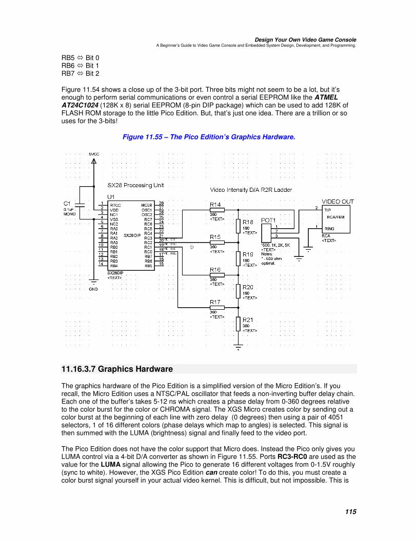
Design Your Own Video Game Console A Beginner’s Guide to Video Game Console and Embedded System Design, Development, and Programming.
115
RB5 � Bit 0 RB6 � Bit 1 RB7 � Bit 2
Figure 11.54 shows a close up of the 3-bit port. Three bits might not seem to be a lot, but it’s enough to perform serial communications or even control a serial EEPROM like the ATMEL AT24C1024 (128K x 8) serial EEPROM (8-pin DIP package) which can be used to add 128K of FLASH ROM storage to the little Pico Edition. But, that’s just one idea. There are a trillion or so uses for the 3-bits!
Figure 11.55 – The Pico Edition’s Graphics Hardware.
11.16.3.7 Graphics Hardware
The graphics hardware of the Pico Edition is a simplified version of the Micro Edition’s. If you recall, the Micro Edition uses a NTSC/PAL oscillator that feeds a non-inverting buffer delay chain. Each one of the buffer’s takes 5-12 ns which creates a phase delay from 0-360 degrees relative to the color burst for the color or CHROMA signal. The XGS Micro creates color by sending out a color burst at the beginning of each line with zero delay (0 degrees) then using a pair of 4051 selectors, 1 of 16 different colors (phase delays which map to angles) is selected. This signal is then summed with the LUMA (brightness) signal and finally feed to the video port.
The Pico Edition does not have the color support that Micro does. Instead the Pico only gives you LUMA control via a 4-bit D/A converter as shown in Figure 11.55. Ports RC3-RC0 are used as the value for the LUMA signal allowing the Pico to generate 16 different voltages from 0-1.5V roughly (sync to white). However, the XGS Pico Edition can create color! To do this, you must create a color burst signal yourself in your actual video kernel. This is difficult, but not impossible. This is

Design Your Own Video Game Console A Beginner’s Guide to Video Game Console and Embedded System Design, Development, and Programming.
116
possible since the XGS Pico Edition is so fast (80 MHz) that you can synthesize a 3.58 MHz NTSC or 4.43MHz PAL color burst. For, now though, let’s just look at the hardware.
Referring to Figure 11.55 RC3-RC0 feeds a R2R ladder network with its output feed into a 500-1K Ohm potentiometer. This construction results in the range 0-1.5V and can be adjusted with the POT, so the overall amplitude (and brightness) can be limited. The R2R ladder is simply a more precise D/A that a power of 2 resistor network and easier to build since the R2R ladder is built on values of R, and 2R which are easier to find rather than incremental powers of 2 starting at R. R2R ladders are covered numerous times in the book in the early chapters.
The video signal is generated simply by controlled the port RC3-RC0 with the proper timing and sending 4-bit values that represent sync, black, and LUMA values.
WARNING! The lower 4-bits of Port RC are used for video, but the upper 4-bits RC7-RC4 are used for the audio DAC, therefore, care must be taken not to overwrite or mix data when writing to either of these ports.
Figure 11.56 – The Pico Edition’s Sound Hardware.
11.16.3.8 Sound Hardware
The sound hardware of the Pico Edition is radically different that the XGS Micro Edition. The Pico Edition doesn’t have a sound synthesizer chip like the XGS Micro does (ROHM8763), rather the Pico Edition leaves the sound completely up to the programmer via a simple D/A 4-bit port connected directly to a POT and the audio out port as shown in Figure 11.56. Therefore, to create sounds the actual PCM (pulse coded modulation) values must be sent to the audio D/A. This is

Design Your Own Video Game Console A Beginner’s Guide to Video Game Console and Embedded System Design, Development, and Programming.
117
good and bad. It’s bad because you have to interleave all your sound effects with your game code and logic and can skip beat. Also, it’s bad since you only have 2K of total memory and data space, so I doubt you are going to digitize and play any MP3s! Unless you add fat EEPROM to the system. That gives me an idea – “build a MP3 player out of the Pico Edition”!
However, the directly controlled audio D/A is nice because it gives you the ability to play synthesized sounds directly and to plug it into algorithms to create very unique sounds. For example, say you want to hear a noise when a ship explodes. No problem, just output a combination of variables that have something to do with the ship’s state, position, etc. directly to the audio D/A -- chances are it will sound cool.
This in fact is how many Atari 2600 and early 8-bit console/arcade sounds effects where made. Engineers would simply plug the audio output directly to some algorithm’s output or state and see if it sounded good. This way there were no direct algorithms or memory used on sound. Of course, this doesn’t mean you can’t have a digitized sine wave with say 128 steps and then code a simple synthesizer that plays the sine wave faster or slower with amplitude scaling based on a series of notes – do that, and presto you have a crude MOD player!
In any event, the hardware for the sound system is identical to the video system’s, simply a D/A constructed from a R2R ladder as shown in Figure 11.56. The POT on the output of the audio controls the volume from 50-100% roughly. Lastly, values from 500-2K OHM for the POT work best.
11.16.4 Building the Pico Edition
Now that we have discussed the hardware behind all of the sub-systems of the XGS Pico Edition, its time to build it. I suggest you read this section once completely and then once again as you build the XGS Pico, so you don’t miss anything. Of course, if you are a boy genius then just use the design file located here:
CDROOT:\XGSME_HW_CD\Datasheets\xgs_pico_edition_kit_01.DSN
Or you can work directly from the schematic capture shown in Figure 11.57.
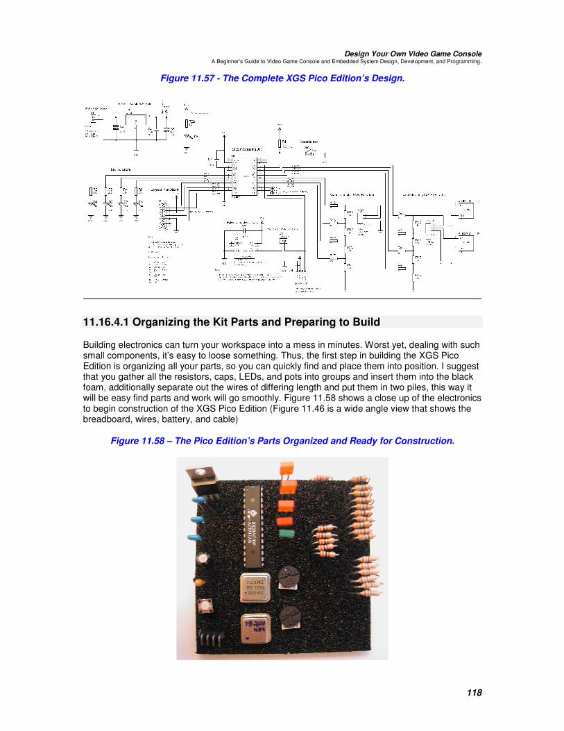
Design Your Own Video Game Console A Beginner’s Guide to Video Game Console and Embedded System Design, Development, and Programming.
118
Figure 11.57 - The Complete XGS Pico Edition’s Design.
11.16.4.1 Organizing the Kit Parts and Preparing to Build
Building electronics can turn your workspace into a mess in minutes. Worst yet, dealing with such small components, it’s easy to loose something. Thus, the first step in building the XGS Pico Edition is organizing all your parts, so you can quickly find and place them into position. I suggest that you gather all the resistors, caps, LEDs, and pots into groups and insert them into the black foam, additionally separate out the wires of differing length and put them in two piles, this way it will be easy find parts and work will go smoothly. Figure 11.58 shows a close up of the electronics to begin construction of the XGS Pico Edition (Figure 11.46 is a wide angle view that shows the breadboard, wires, battery, and cable)
Figure 11.58 – The Pico Edition’s Parts Organized and Ready for Construction.

Design Your Own Video Game Console A Beginner’s Guide to Video Game Console and Embedded System Design, Development, and Programming.
119
The next thing to do is review the design file for the XGS Pico Edition over, and over, and over again!
Figure 11.57 shows the design as an image for reference. The design is a little hard to follow in some areas since the symbols and or mechanical assemblies might not make sense unless you see the final product, therefore, be sure to use the design as well as the final physical device which is shown in Figure 11.45(a). This way if there is a certain connector you see on the design, but you can’t figure out which connector it is based on the parts kit, you should be able to when you look at the finished product.
Bottom line is review all this information before starting!
Figure 11.59 – The Solderless Breadboard.
11.16.4.2 Reviewing the Solderless Breadboard
The solderless breadboard used for the Pico Edition should look something like that shown in Figure 11.59 (your particular model might be larger, smaller, or have different color codings). Referring to the Figure, the breadboard is basically a platform with hidden electrical connections under the plastic (you should have already read all this). In this particular breadboard, the top and bottom rows have horizontal groupings of 5 hole rows each with a RED and BLUE line above and below respectively. The way the board is connected electrically is very simple, here are the rules:
Rule 1. The + (Red, positive) rows are all connected together on the top as are the – (Blue, negative). However, the + and – are not connected together. Similarly, on the bottom of the board the + row is all connected and the negative row is all connected, but not together. These + and – rows are where you connect power usually. Some people connect + and – to both the top and bottom, that is there are + and – rails on the top of the board that are used as feeds as well on the bottom of the board, but I prefer to only connect +5 to the top Red + row and then connect 0V (ground) to the bottom – line. This way the top of the board is +5 and the bottom is 0V (ground) and nothing gets shorted out. It always makes me nervous when +5 and GND are next to each other.
Rule 2. There are 64 pairs of columns, each column consists of 5 holes, each of the 5 holes in one set of holes is connected. Therefore in column 25 for example, hole a, b, c, d, e is all connected as well as f, g, h, I, j, but those sets are not connected together. Figure 11.60 illustrates the connectivity with color coding and shading.

Design Your Own Video Game Console A Beginner’s Guide to Video Game Console and Embedded System Design, Development, and Programming.
120
Figure 11.60 – The Solderless Breadboard with Color Coding to Help Show Connectivity.
So the point of the solderless breadboard is that you can plug chips and components into it and use the properties of the vertical columns to electrical connect things together. This gives you a platform to insert parts and helps minimize how many wires you have to use to connect things together.
Now, were going to build the XGS Pico Edition system by system, step by step. The technique will be to first insert the parts for the system and then to insert the passive components and then finally any hook up wires. This way you will the maximum working space and will minimize errors. Additionally, there will be photos of the XGS Pico Edition as we progress thru each stage.
WARNING!
At the time of this writing the solderless breadboard was identical to the one shown in the figures and described thereof. However, due to out of stock problems, changing vendors, etc. you might have a board that looks slightly different, especially if you put the kit together yourself. If so, just look closely at it and make sure you understand what is connected to what and where the connection paths are.
Figure 11.61 – The Design for the XGS Pico Edition Power Supply.

Design Your Own Video Game Console A Beginner’s Guide to Video Game Console and Embedded System Design, Development, and Programming.
121
11.16.4.3 Building the Power Supply
The power supply is always a good place to start when building anything electronic. It’s like building the foundation of a house, everything relies on it. The XGS Pico Edition has a very simple voltage regulator based design. Figure 11.61 shows the actual design file with an excerpt of the power supply. The design for the power supply alone can be found on the CD here:
CDROOT:\XGSME_HW_CD\Datasheets\xgs_pico_edition_kit_power_01.DSN
The first step is to collect the parts you will need for the power supply. There are listed in Table 11.19.
Table 11.19 – Parts List for Power Supply Construction.
Reference Designator Description
U3 The 7805 voltage regulator. J1 The 9V battery clip. C2 10.0uF polarized electrolytic capacitor (canister shaped). C4 0.1uF non-polarized monolithic ceramic capacitor (flat, small). C5 1.0uF polarized tantalum capacitor (tear drop shaped). R22 200 Ohm current limiting resistor. D5 Green LED for power good indicator.
Figure 11.62 – The Parts Needed to Build the XGS Pico Edition’s Power Supply.
Figure 11.62 shows the parts needed to build the power supply to help you identify them. Now, before you begin there are some rules of thumb;
Rule 1. Try to use the most appropriate length wires for each connection. There are only two lengths of wires, so use common sense, don’t use long wires for short contacts, don’t use short wires for long contacts.
Rule 2. Use Figure 11.xx as a master guide to the positioning of the parts, I have build the Pico Edition many times and found these locations to be optimal for the most part. You don’t have to be exactly perfect in your positioning relative to Figure 11.xx, but you will find that it evenly spaces the design as much as possible.

Design Your Own Video Game Console A Beginner’s Guide to Video Game Console and Embedded System Design, Development, and Programming.
122
Rule 3. Remember, the electrical contacts run vertically for each column and break across the middle of the solderless breadboard. Also, the +/- rows on the top and bottom are continuous, but do not connect to each other across the top and bottom! That is the + on the top and the + on the bottom are not connected, similarly the – on the top and bottom are not connected. If you want to connect them run a wire(s) across the + and – from top to bottom respectively. However, as a rule I usually connect only the – on the bottom rail and the + on the top rail.
Figure 11.63 – The Completed XGS Pico Edition Power Supply.
Let’s begin by looking at the completed power supply section by itself, Figure 11.63 shows this. Use this as your model as you build the system. As long as you assemble the power supply as shown in Figure 11.63 and it matches the design file then you are fine. Here is a step by step list to follow:
Step 1: Insert the 7805 5V voltage regulator U3 into the breadboard.
Step 2: Insert the 10.0uF electrolytic filtering capacitor (C2) from pin 1 of the 7805 to ground. Note that (C2) is polarized and must be inserted correctly with the + and – leads connected properly. Inspect the capacitor to verify, it will either have both the + and – contacts labeled or possibly just the – (negative) contact. Make sure to insert the – lead into the ground rail of the breadboard (use the bottom most – rail ).
Step 3: Insert the monolithic filtering capacitor (the flat small one) C4 from pin 3 of the 7805 to ground. The monolithic is non-polarized, so either direction is fine.
Step 4: Insert the 1.0uF tantalum filtering capacitor C5 from pin 3 of the 7805 to the ground rail. The tantalum capacitor is polarized once again. However, the polarization is very hard to read. Look closely and you should see a small “+” and “-“ indicator marking each lead, make sure to triple check the polarity and insert with the + lead connected to pin 3 of the 7805 and the – lead to ground.
Step 5: Pin 2 of the 7805 (U3) is the “ground” for the 7805, this must connected to the ground rail. Use a short wire and connect pin 2 of the 7805 to the ground rail. Also, the output of the regulator is at pin 3, connect a wire from pin 3 of the 7805 to the + rail at the top of the breadboard.

Design Your Own Video Game Console A Beginner’s Guide to Video Game Console and Embedded System Design, Development, and Programming.
123
Step 6: At this point, the regulation circuit is complete, but we need a way to get power into the regulator. This is what the 9V battery clip is for, connect the black (-) lead of the battery clip to the lower – ground rail and connect the red (+) lead to the + (positive) top rail of the breadboard.
Step 7: Insert the green power good LED into the ground rail and the column of contacts above it, make sure that the cathode (-) is connected to ground. You can always tell the cathode or negative lead of an LED by looking inside carefully, the larger of the two contacts is the negative or cathode (it looks like an upside down “L”). Additionally, insert the 200 Ohm current limiting resistor R22 into the board making contact with the (+) side of the LED and crossing over the center of the breadboard, then insert a connecting wire from the other side of the resistor to the (+) rail at the top of the breadboard.
Step 8: Verify all connections three times! That’s right (3) times. Verify them with the picture in Figure 11.63 as well as the actual design shown in Figure 11.61. Also, make sure you have all your polarities correct for the capacitors that are polarized (C2 and C5).
Step 9: Preliminary power check. Now that the power supply is built, there’s no time better than the present to test it out. So insert the 9V battery into the battery clip and you should see the green LED turn on to a reasonable brightness. If you don’t there’s a mistake, unplug the battery and check everything.
TIP
If you want to test the regulation of the circuit use a multimeter and measure the voltage from the ground rail to the positive rail, it should be 4.99 – 5.0V. If its not then there is a problem. Also, realize that the circuit is actually “loaded” already. The LED and resistor R22 are using about 10-20mA.
Figure 11.64 – The SX28, Power On Reset and the Programming Port Design.

Design Your Own Video Game Console A Beginner’s Guide to Video Game Console and Embedded System Design, Development, and Programming.
124
11.16.4.4 Adding the SX28 Processor
The next logical step is to add the SX28 to the board, with it we can immediately start programming and experimenting with the Pico Edition. Figure 11.64 shows the design file for the SX28, power on reset circuit as well as the programming port. This is of course an excerpt of the complete design file. The excerpted file is located on the CD here:
CDROOT:\XGSME_HW_CD\Datasheets\xgs_pico_edition_kit_sx28_01.DSN
Next, let’s collect the parts needed to add the processor, Table 11.20 lists all the parts out.
Table 11.20 – Parts List for SX28, Power On Reset, and Programming Port.
Reference Designator Description
U1 SX28 (28-pin DIP package). C1 0.1uF non-polarized monolithic ceramic capacitor (flat, small). J4 4-Pin right angle connector for SX-Key. R1 10K Ohm current limiting resistor for reset circuit. SW1 SPST momentary switch for reset.
Figure 11.65 – The Parts Needed for the Pico’s Processor, Power On Reset, and Programming Port.

Design Your Own Video Game Console A Beginner’s Guide to Video Game Console and Embedded System Design, Development, and Programming.
125
Figure 11.66 – The Completed Processor Assembly, Power On Reset Circuit, and Programming Port.
Additionally, Figure 11.65 shows all the parts laid out for reference and identification and Figure 11.66 shows the processor, reset circuit, and programming port all wired up. Use this image as a reference you build each system.
Figure 11.67 – The Inserted SX28 Processor.
11.16.4.4.1 Inserting the Processor
The first step is to insert the SX28 processor into the breadboard. Referring to Figure’s 11.66 and 11.67, the processor should be inserted so that pin 1 of the SX28 aligns with column 32 roughly of the breadboard (this is just a suggestion though).

Design Your Own Video Game Console A Beginner’s Guide to Video Game Console and Embedded System Design, Development, and Programming.
126
WARNING!
Before inserting the SX28 make sure that all the pins are straight and at 90 degree angles to the DIP body, this will help the chip during insertion. If the pins are bent straighten them with a pair of needle nose pliers or use a flat surface to “align” the pins in a plane.
Figure 11.68 – Close-up of the SX28 with Power and Filtering Capacitor Inserted.
11.16.4.4.2 Connecting Power
Once the processor is inserted then its time to add the power lines and the filtering capacitor (C1) across the power pins as shown in Figure 11.68. Here are the steps:
Step 1: Connect the filtering capacitor (C1) between pins 2 (VDD) and 4 (GND) of the SX28. (C1) is not polarized, so the orientation is irrelevant.
Step 2: Connect the +5 (VDD) line at pin 2 of the SX28 to the top +5 power rail and connect GND line at pin 4 of the SX28 to the ground rail at the bottom of the breadboard.
That’s it! The SX28 is now connected to power and filtered by (C1).
TIP
You might want to add a 1-10uF tantalum “storage” capacitor in parallel with the existing 0.1uF decoupling capacitor across the power leads of the SX28. This will help with ground bounce and give the SX28 a source of power that is lower impedance than the power supply which is father away. However, I have found that the SX28 is ok with our regulation circuit and 0.1uF filter. Nonetheless, if you draw more current from the I/O ports of the SX28 then you will need to add this extra capacitor to keep the power clean.

Design Your Own Video Game Console A Beginner’s Guide to Video Game Console and Embedded System Design, Development, and Programming.
127
Figure 11.69 – A Close up of the Power On Reset Circuit Added to the SX28 Design.
11.16.4.4.3 Adding the Power On Reset Circuit (POR)
The power on reset circuit consists of a momentary SPST switch (SW1) that momentarily grounds the SX28 along with a 10K Ohm pull up resistor (R1) that makes sure the SX28 stays out of reset. Figure 11.69 shows a close up of the reset switch and resistor that you need for this part of the assembly.
Figure 11.70 – The Parts Needed for the POR Circuit.
As you can see from Figure 11.70, there’s not much! To assemble the POR circuit; follow these steps:
Step 1: Insert the SPST switch (SW1) into column 31 roughly on the breadboard and the lower ground rail, refer to Figure 11.69 for a close up view.
Step 2: Make a connection from the non-grounded side of the SPST switch to the reset line of the SX28 (/MCLR) at pin 28. This basically grounds the reset pin when the switch is depressed.

Design Your Own Video Game Console A Beginner’s Guide to Video Game Console and Embedded System Design, Development, and Programming.
128
Step 3: Insert the 10K Ohm resistor (R1) to make contact with pin 28 of the SX28 (top left pin) and contact with the (+5) upper power rail. This maintains a “weak” digital HIGH on the /MCLR line keep the SX28 out of reset.
That’s it, make sure to verify everything with the images and design file.
Figure 11.71 – A Close up of the Programming Port.
11.16.4.4.4 Adding the Programming port
The programming port as shown in Figure 11.71 doesn’t consist of much thanks to the amazing hardware design of the SX series of processors (which of course makes the software a nightmare when programming the unit). Basically, the programming port needs to interface to the Parallax SX-Key programming unit shown in Figure 11.72. Note: that this image is the underside of the key with markings, but when you plug the key in, its component side up.
Figure 11.72 – The Parallax Inc. SX-KEY Programming Unit.
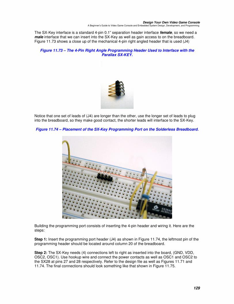
Design Your Own Video Game Console A Beginner’s Guide to Video Game Console and Embedded System Design, Development, and Programming.
129
The SX-Key interface is a standard 4-pin 0.1” separation header interface female, so we need a male interface that we can insert into the SX-Key as well as gain access to on the breadboard. Figure 11.73 shows a close up of the mechanical 4-pin right angled header that is used (J4)
Figure 11.73 – The 4-Pin Right Angle Programming Header Used to Interface with the Parallax SX-KEY.
Notice that one set of leads of (J4) are longer than the other, use the longer set of leads to plug into the breadboard, so they make good contact, the shorter leads will interface to the SX-Key.
Figure 11.74 – Placement of the SX-Key Programming Port on the Solderless Breadboard.
Building the programming port consists of inserting the 4-pin header and wiring it. Here are the steps:
Step 1: Insert the programming port header (J4) as shown in Figure 11.74, the leftmost pin of the programming header should be located around column 20 of the breadboard.
Step 2: The SX-Key needs (4) connections left to right as inserted into the board, (GND, VDD, OSC2, OSC1). Use hookup wire and connect the power contacts as well as OSC1 and OSC2 to the SX28 at pins 27 and 28 respectively. Refer to the design file as well as Figures 11.71 and 11.74. The final connections should look something like that shown in Figure 11.75.

Design Your Own Video Game Console A Beginner’s Guide to Video Game Console and Embedded System Design, Development, and Programming.
130
Figure 11.75 – The SX-Key Programming Port Fully Connected to Power and the SX28.
As usual verify the connections of the programming port, it is very important they are perfect. The wrong power lines connected can burn out your SX-Key! Once again, from left to right the pins are labeled:
HDR Pins: 4,3,2,1 Labels: GND, VDD, OSC2, OSC1

Design Your Own Video Game Console A Beginner’s Guide to Video Game Console and Embedded System Design, Development, and Programming.
131
Figure 11.76 – The Design for the Pico Edition’s Clock Circuit.
11.16.4.5 Building the Clock Circuit
The clocking of the XGS Pico Edition comes from one of three potential sources:
1. An external oscillator (the kit comes with an 80.000 MHz and a 78.750 MHz). 2. The internal oscillator from 32KHz – 4MHz. 3. The SX-Key’s clock generation.
Now, there is a little bit of a trick to getting either the external oscillator or the SX-Key to clock the SX28 processor. The problem is that you need to “jumper” the clock oscillator into the circuit, but remove it if you want to program the SX28 with the SX-Key. If you refer to the design file located here:
CDROOT:\XGSME_HW_CD\Datasheets\xgs_pico_edition_kit_clock_01.DSN
The design file shows just clocking aspects of the complete Pico design. Figure 11.76 illustrates the actual circuitry for the clock. In the design jumper (J3) is used to connect/disconnect the external oscillator from the SX28 processor. However, (J3) is nothing more than a piece of hookup wire. So if you want to clock the SX28 with the external 80.000 MHZ (or whatever)

Design Your Own Video Game Console A Beginner’s Guide to Video Game Console and Embedded System Design, Development, and Programming.
132
oscillator then you need to make sure that the SX-Key is not plugged in, but the jumper from the output of oscillator at pin 5 (upper right hand corner) is connected to pin 27 (OSC1) of the SX28. Likewise, when you want to program the SX28 or use the SX-Key in any other way, you need to disconnect the oscillator’s pin 5 from the SX28 processor’s pin 27 (OSC1) pin – simple.
Figure 11.77 – The Parts for the Oscillator Clocking Circuit.
Figure 11.77 shows the parts that come with the kit for the clocking circuit. Basically, there are two oscillators; one is the standard 80.000 MHz that the XGS Micro Edition uses, so porting programs is easy. The other is a more specialized 78.750 MHz oscillator which as you know is an integral multiple of the NTSC color burst frequency to help make color programming easier. Lastly there is a decoupling capacitor that must be placed across the power leads of the oscillator to minimize noise and filter the power. In any case, Table 11.21 lists the parts for the oscillator circuit.
Table 11.21 – The Pico Edition Clocking Circuitry Parts List.
Reference Designator Description
U2 80.000 / 78.750 MHz 8-pin DIP / half size oscillator. C3 0.1uF non-polarized monolithic ceramic capacitor (flat, small).
Figure 11.78 – Placement of the Oscillator.

Design Your Own Video Game Console A Beginner’s Guide to Video Game Console and Embedded System Design, Development, and Programming.
133
To assemble the clocking circuit, it’s a matter of selecting a place to insert the oscillator, connecting the power leads and finally inserting the de-coupling capacitor. Here are the steps:
Step 1: Insert the 80.000 MHz oscillator (U2) (the pre-loaded demo on the XGS Pico uses the 80.000 MHz). Refer to Figure 11.78 for placement, pin 1 of the oscillator (U2), that’s the bottom left pin as shown in the figure, should be inserted to align with column 26 of the breadboard (remember just a suggestion that works and makes for a nicely and open layout). Also, your oscillators might have slightly different text on them, just make sure that the pin 1 indicator (the black dot) is oriented to the bottom left of the insertion point.
Step 2: Insert the decoupling capacitor (C3) as shown in Figure 11.79. Remember, (C3) is non-polarized, so either orientation is fine. Also, be careful that the leads do not make contact with the casing of the oscillator, this could cause a short. The capacitor needs to be across or in parallel with VCC (+5) and GND of the oscillator. In other words, pin 8 (top left) which is +5 and pin 4 (bottom right) which is GND. The problem is that you can’t straddle the oscillator with the capacitor since the leads will touch, so you must insert the cap as I have in the figure and then run a line from the cap to the GND pin of the OSC. This is shown in Figure 11.79 as well.
Step 3: Power the oscillator (U3) up by connecting power and ground. VCC (+5) for the oscillator is located at pin 8 (upper left), connect this to the +5 top power rail, then connect GND of the oscillator at pin 4 (lower right) to the lower ground rail of the breadboard.
Step 4: Although, not shown in the figures, I want you to connect the jumper wire (J4) from the output of the oscillator to the OSC1 pin (27) of the SX28 with a hookup wire. Remember, you must connect / disconnect this line when you want to program the SX28 and / or use the SX-Key for clocking the SX28.
Figure 11.79 – The Complete Clocking Circuit for the XGS Pico Edition.
As usual make sure to verify the connections of everything with the images and the design file. Even though there isn’t much to the clocking circuit, I have seen people put the oscillators in backwards and they can potentially burn up in seconds if you do this! Pin 1 of the oscillator is marked with a black dot usually, or is always to the bottom left of how the text is printed on the oscillator itself as read from left to right, top to bottom.

Design Your Own Video Game Console A Beginner’s Guide to Video Game Console and Embedded System Design, Development, and Programming.
134
Figure 11.80 – The LED Output Design File.
11.16.4.6 Adding the LED Output Port
The LED output port for the XGS Pico Edition is rather simple, but very useful nonetheless, as discussed its nothing more than a direct port link from RA3-0 to a set of LEDS via current limiting resistors. Figure 11.80 shows the design file image excerpt from the master design for the LED output port. Figure 11.81 shows the parts needed to build the port.
Figure 11.81 – The Parts Needed for the LED Output Port.
The first step to build the LED output port is to collect the parts. In this case, that’s rather easy since they are all the same. You just need the (4) red LEDs along with (4) 200 Ohm resistors. Table 11.22 shows the exact parts list and reference designators for the sub-system and Figure 11.81 shows the parts you need for the assembly.

Design Your Own Video Game Console A Beginner’s Guide to Video Game Console and Embedded System Design, Development, and Programming.
135
Table 11.22 - The Parts List for the XGS Pico Edition’s LED Output Port.
Reference Designator Description
D1-D1 Red colored LED. R2-R5 200 Ohm current limiting resistor.
Figure 11.82 – The Completed LED Output Port all Wired Up.
Figure 11.82 depicts a close-up of the completed LED output port and its connections to the SX28, use it as a reference as you build the port yourself. Here are the steps to assemble the port:
Figure 11.83 – The Placement of the LEDS and Resistors for the Output Port.
Step 1: Insert the LEDs (D1-D5) into the breadboard as shown in Figure 11.83. Remember, the negative (-) GND side of each LED is the larger mechanical internally if you look inside the LED, that is the one that looks like a ledge. I suggest inserting D1 at column 15, D2 at column 16, and so forth. One end of the LED should go into the ground rail at the bottom the other end to the column of contacts.

Design Your Own Video Game Console A Beginner’s Guide to Video Game Console and Embedded System Design, Development, and Programming.
136
Step 2: Insert the 200 Ohm current limiting resistors (R2-R5) in parallel with each LED (D1-D5) respectively. Refer to Figure 11.83 for this, but basically each resistor should make contact with the LED’s (anode) (+) side and then cross over the middle of the breadboard and make contact with the same column on the other side.
Step 3: Now that you have all the LEDs and current limiting resistors in place, the last thing to do is connect them to the outputs of the SX28. Refer back to Figure 11.82 for this that shows a long shot of the entire board. You will need (4) hook up wires for this. Start by hooking up the left most LED circuit at open end of the current limiting resistor to RA0 (pin 6 of the SX28), then the next current limiting resistor (attached to D2) to RA1 (pin 7 of the SX28), do this until each LED circuit is driven by an output RA0, RA1, RA2, RA3.
TIP
You can either decide to drive the LEDS from left to right or right to left. For example, if you connect RA3,2,1,0 to the LEDs left to right then when you output a binary number you will see it on the LEDs, however, if you want to think of bit 0, 1, 2, 3 starting from the left and moving to the right on the LED display then you would connect them in the opposite order. It’s up to you. In either case, just make sure that each current limiting resistor circuit for each LED is connected to one of the outputs at RA0:3 (pins 6-9 on the SX28).
Once again, re-verify the design file against the circuit against your wiring. Also, make sure that you have the polarity of the LEDs correct. Referring to the internal leads inside each LED, the larger cathode goes to ground, and the smaller anode connects to the current limiting resistor.
Figure 11.84 – The Video Output Design File.

Design Your Own Video Game Console A Beginner’s Guide to Video Game Console and Embedded System Design, Development, and Programming.
137
11.16.4.7 Building the Video-Out R2R Ladder and Output
The video generation circuit is built from a simple R2R ladder consisting of 4-bits of D/A accuracy. This gives us 16 voltages to vary the video signal, more than enough to represent sync, black, and 10-12 different intensities or LUMA values. Figure 11.84 shows the circuit diagram excerpt for the design. Notice how this is different from the Micro Edition design – the Pico Edition does not have color “helper” hardware. Thus, if you want to generate color you can surely do so, but you must generate the timing directly and simulate the CHROMA signal on top of the LUMA signal (more on this later).
Figure 11.85 – The Parts for the Pico Edition’s Video Output Circuit.
The video circuit is deceptively simple since software is used to drive it. More or less it’s nothing, but a 4-bit D/A converter with a 500 Ohm potentiometer at the tail of it to give you some control over the overall amplitude of the signal. From your reading you should know that an R2R ladder consists of resistors with value R and 2*R, thus any resistor value can be used for R and you don’t need power of 2 resistor values as you would with a D/A consisting of R, 2R, 4R, 8R…2nR networks. In this case, I have chosen the value of R to be 180 Ohms and thus 2R is 360 Ohms. Also, as noted there is a POT at the end of the circuit that acts as a voltage divider and impedance matcher that allows some control over the overall voltage output and hence brightness of the video. I find values from 500 – 2K Ohm work well for this POT. Table 11.23 lists the parts needed to construct the video circuit and Figure 11.85 shows the parts laid out for reference.
Table 11.23 - The Parts List for the XGS Pico Edition’s Video Output Circuit.
Reference Designator Description
R14-R17, R21 360 Ohm Axial, 0.25W Resistors. R18 – R20 180 Ohm Axial, 0.25W Resistors. POT1 500 Ohm Potentiometer. J5 (1/2) RCA Male A/V Cable Assembly (red portion).

Design Your Own Video Game Console A Beginner’s Guide to Video Game Console and Embedded System Design, Development, and Programming.
138
Figure 11.86 – The Complete Pico Edition Video Circuit.
To begin with refer to the design file image shown in Figure 11.84 along with the complete circuit shown in Figure 11.86. The complete circuit is a bit hard to follow due to the rats nest of wires, but it’s a good frame of reference.
Figure 11.87 – The Initial Placement of the R2R Network Resistors, POT, and A/V Cable for the Video Circuit.
The construction of the video circuit consists of inserting the 360, 180 Ohm resistors, the POT, the A/V cable (video portion) and finally the connection wires from the SX28. Referring to the figures above, here are the steps you should take.
Step 1: Create the R2R network using the topmost section of the breadboard to the right of the SX28. I suggest starting with column 47 or so as your first insertion point to place R14, following the circuit diagram, continue to insert all the 260 Ohm resistors R14-R17, and R21. This is very tricky since you need to have the exact electrical connectivity shown in the circuit diagram of

Design Your Own Video Game Console A Beginner’s Guide to Video Game Console and Embedded System Design, Development, and Programming.
139
Figure 11.84. You might end up doing it a couple times, but just keep working on it until you are satisfied the network is correct.
Step 2: Add the 500 Ohm potentiometer POT at column 61 as shown in Figure 11.87. Finally, make sure that you insert R21 as shown in Figure 11.87.
Step 3: Now insert the 180 Ohm “bridge” resistors R18-R20. These are very simple electrically as far as the network goes and more or less “bridge” each sub-circuit together, there are (3) resistors and they simply connect between the nodes of each D/A bit as shown in the design and Figure 11.87.
Step 4: Next insert the A/V cable’s video leads into the breadboard. It really doesn’t matter if you use the RED (YELLOW) or WHITE leads, but lets just use the convention that RED (or YELLOW if you have it) is video and WHITE is always audio. If you inspect the cable J5/J6 you will see that each of the stripped end pairs has a colored wire (RED or WHITE) along with a bare wire (GROUND). You need to connect the RED wire pair to the video circuit. The RED lead should go to the center contact of POT1 and the GROUND lead should go to the rightmost contact of the POT1 as shown in Figure 11.87.
Step 5: Now it’s time to complete the wiring from the SX28’s output port to the video R2R ladder. As shown in the design and Figure 11.84, the SX28 drives the R2R ladder via port RC0-3. Refer to Table 11.24 for the port mappings as a second reference. Connect a wire from each pin of the SX28’s port bits RC0,1,2,3 to the appropriate network resistor node. There should be (4) connections.
Table 11.24 – Bit Mappings for the Pico Edition Graphics Hardware.
Port Bit Bit Signal Name Reference Designator
RC0 Bit 0 VID_ISEL0 R17 RC1 Bit 1 VID_ISEL1 R16 RC2 Bit 2 VID_ISEL2 R15 RC3 Bit 3 VID_ISEL3 R14
Step 6: The last part of the video circuit is to connect the (GROUND) from the potentiometer to the system ground rail at the bottom of the board. This is shown as the rightmost wire in Figure 11.86. Simply connect the rightmost contact of POT1 to the BLUE ground rail at the bottom of the board. When complete your circuit should look identical to that shown in Figure 11.86.
WARNING!
The video and audio R2R ladder circuits are by far the most complex of the design, so make sure you triple check them. It’s very easy to confuse your eyes with all the similar looking wires all over the place. Take your time and check it over and over and over and make sure you haven’t made an incorrect assumption about conductivity of the breadboard. Remember, only the columns are shorted together on either side of the center separator, these columns act as shorts or connections, that is all.

Design Your Own Video Game Console A Beginner’s Guide to Video Game Console and Embedded System Design, Development, and Programming.
140
Figure 11.88 – The Audio Output Design File.
11.16.4.8 Building the Audio-Out R2R Ladder and Output
The audio generation circuit is identical to the video output circuit. It uses a simple R2R ladder consisting of 4-bits of D/A accuracy. This gives us 16 voltages to vary the audio signal (about 2V P-P). Although, 4-bit sound may seem like its not enough amplitude range to create good sound, trust me, it’s more than enough for a video game system and can reproduce digital sounds just fine as long as the playback rate is high enough.
Figure 11.88 shows the circuit diagram excerpt for the design. Notice that the audio system for the Pico Edition is radically different from the Micro Edition’s. The Micro Edition of course uses a ROHM BU8763 sound chip to generate sound whereas the Pico Edition uses a more direct D/A digital output approach. This is good and bad. Its good since you can directly control the DAC and generate any waveform you wish, but its bad since you must control the DAC to create any waveform you wish thus eating processor cycles at all times. Therefore, most sound effects must be interleaved with rendering code to maintain enough “bandwidth” to keep the sound running smoothly without pops or stops. Of course, you can always play a sound “offline” and halt the game logic while the sound effect takes place.

Design Your Own Video Game Console A Beginner’s Guide to Video Game Console and Embedded System Design, Development, and Programming.
141
Figure 11.89 – The Parts for the Pico Edition’s Audio Output Circuit.
The audio circuit is identical to the video circuit and thus uses the exact same parts. To reiterate the audio circuit is nothing, but a 4-bit D/A converter with a 500 Ohm potentiometer at the tail of it to give you some control over the overall amplitude of the signal. From your reading you should know that an R2R ladder consists of resistors with value R and 2*R, thus any resistor value can be used for R and you don’t need power of 2 resistor values as you would with a D/A consisting of R, 2R, 4R, 8R…2nR networks. In this case, I have chosen the value of R to be 180 Ohms and thus 2R is 360 Ohms. Also, as noted there is a POT at the end of the circuit that acts as a voltage divider and impedance matcher (to help match the input of the audio amplifier) that allows some control over the overall voltage output and hence brightness of the video. I find values from 500 – 2K Ohm work well for this POT. Table 11.25 lists the parts needed to construct the audio circuit and Figure 11.89 shows the parts laid out for reference.
Table 11.25 - The Parts List for the XGS Pico Edition’s Audio Output Circuit.
Reference Designator Description
R6-R9, R13 360 Ohm Axial, 0.25W Resistors. R10 – R12 180 Ohm Axial, 0.25W Resistors. POT2 500 Ohm Potentiometer. J6 (1/2) RCA Male A/V Cable Assembly (white portion).

Design Your Own Video Game Console A Beginner’s Guide to Video Game Console and Embedded System Design, Development, and Programming.
142
Figure 11.90 – The Complete Pico Edition Audio/Video Circuit.
To begin with refer to the design file image shown in Figure 11.88 along with the complete circuit shown in Figure 11.91 (this shows both the audio and video circuits wired).
Figure 11.91 – The Initial Placement of the R2R Network Resistors, POT, and A/V Cable for the Audio Circuit.

Design Your Own Video Game Console A Beginner’s Guide to Video Game Console and Embedded System Design, Development, and Programming.
143
The construction of the video circuit consists of inserting the 360, 180 Ohm resistors, the POT, the A/V cable (audio portion) and finally the connection wires from the SX28. Referring to the figures above, here are the steps you should take.
Step 1: Create the R2R network using the bottommost section of the breadboard to the right of the SX28. I suggest starting with column 47 or so as your first insertion point to place R6, following the circuit diagram, continue to insert all the resistors 260 Ohm resistors R6-R9, and R13. This is very tricky since you need to have the exact electrical connectivity shown in the circuit diagram of Figure 11.88. You might end up doing it a couple times, but just keep working on it until you are satisfied the network is correct.
Step 2: Add the 500 Ohm potentiometer POT at column 61 as shown in Figure 11.91. Finally, make sure that you insert R13 as shown in Figure 11.91. Remember, the audio and video circuits are literally copies of each other.
Step 3: Now insert the 180 Ohm “bridge” resistors R10-R12. These are very simple electrically as far as the network goes and more or less “bridge” each sub-circuit together, there are (3) resistors and they simply connect between the nodes of each D/A bit as shown in the design and Figure 11.91.
Step 4: Next insert the A/V cable’s “audio” leads into the breadboard. It really doesn’t matter if you use the RED (YELLOW) or WHITE leads, but lets just use the convention that RED (or YELLOW if you have it) is video and WHITE is always audio, thus insert the WHITE leads. If you inspect the cable J5/J6 you will see that each of the stripped end pairs has a colored wire (RED or WHITE) along with a bare wire (GROUND). You need to connect the WHITE wire pair to the video circuit. The WHITE lead should go to the center contact of POT2 and the GROUND lead should go to the rightmost contact of the POT2 as shown in Figure 11.91.
Step 5: Now it’s time to complete the wiring from the SX28’s output port to the audio R2R ladder. As shown in the design and Figure 11.90, the SX28 drives the R2R ladder via port RC4-7 (the lower bits are video if you recall). Refer to Table 11.26 for the port mappings as a second reference. Connect a wire from each pin of the SX28’s port bits RC4,5,6,7 to the appropriate network resistor node. There should be (4) connections.
Table 11.26 – Bit Mappings for the Pico Edition Audio Hardware.
Port Bit Bit Signal Name Reference Designator
RC4 Bit 0 AUD_ISEL0 R9 RC5 Bit 1 AUD_ISEL1 R8 RC6 Bit 2 AUD_ISEL2 R7 RC7 Bit 3 AUD_ISEL3 R6
Step 6: The last part of the video circuit is to connect the (GROUND) from the potentiometer to the system ground rail at the bottom of the board. This is shown as the rightmost wire in Figure 11.91. Simply connect the rightmost contact of POT2 to the BLUE ground rail at the bottom of the board. When complete your circuit should look identical to that shown in Figure 11.90.

Design Your Own Video Game Console A Beginner’s Guide to Video Game Console and Embedded System Design, Development, and Programming.
144
Figure 11.92 – The Pico Edition Joystick Port Design.
11.16.4.9 Adding the Joystick Port
The Pico Edition’s joystick port is nothing more than the mechanical DB9 connector with 6 wires soldered to it. This simple design is a result of directly connecting the joystick inputs to the I/O pins of the SX28. Figure 11.92 shows the joystick design which is really just a DB9 male connector along with the pin mapping.
Figure 11.93 – The Male DB9 Joystick Connector.

Design Your Own Video Game Console A Beginner’s Guide to Video Game Console and Embedded System Design, Development, and Programming.
145
Figure 11.94 – The Joystick Connector’s Color Coding.
Figure 11.93 and Figure 11.94 show images of the DB9 male itself along with the opposite end with the bare wires you will insert into your board. The color coding may be slightly different, refer to Table 11.27 as your guide.
Figure 11.95 – The Pico Edition Joystick Assembly.
TIP
If you are making your own joystick cable assembly, then simple get a “solder cup” DB9 male connector along with the wire colors listed in Table 11.26 (use the non-parenthetical colors) and build a nice cable. When you’re done it should look something like that shown in Figure 11.95. Also, make sure to reinforce the wires with tape or shrink tubing.
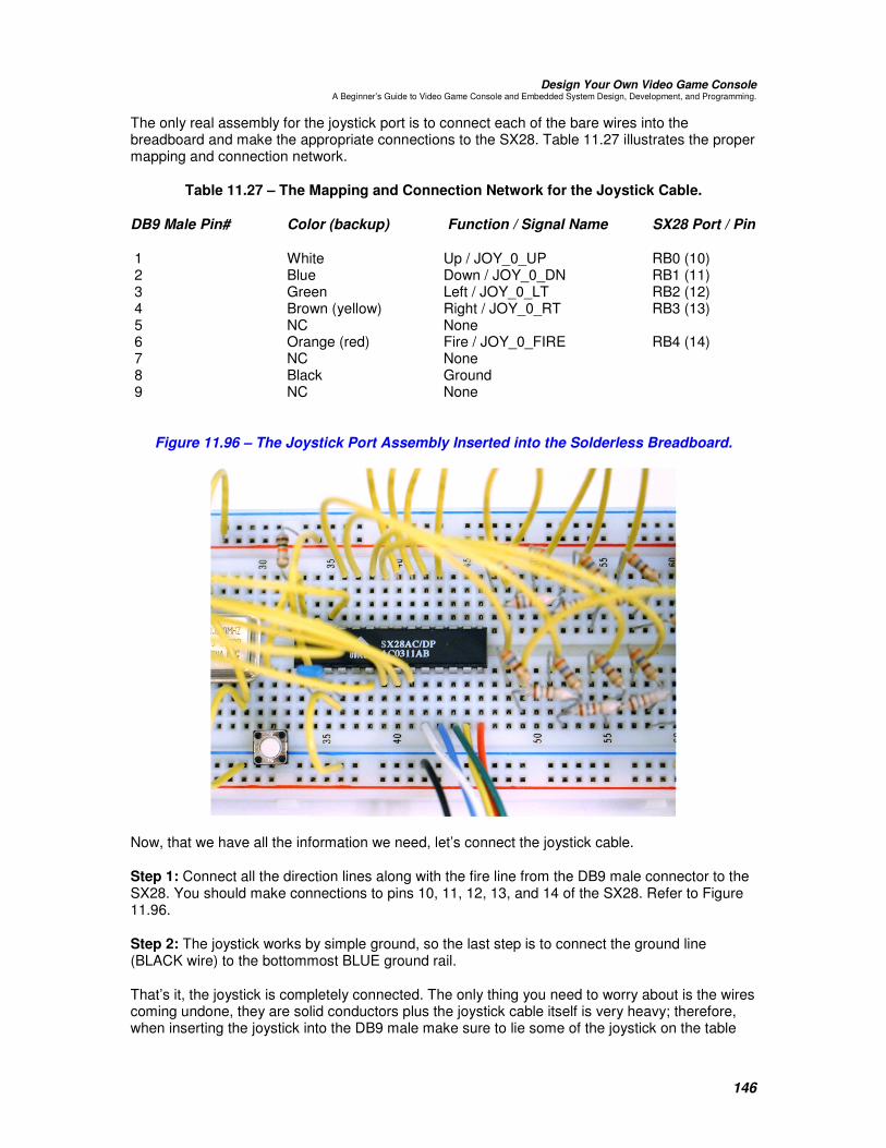
Design Your Own Video Game Console A Beginner’s Guide to Video Game Console and Embedded System Design, Development, and Programming.
146
The only real assembly for the joystick port is to connect each of the bare wires into the breadboard and make the appropriate connections to the SX28. Table 11.27 illustrates the proper mapping and connection network.
Table 11.27 – The Mapping and Connection Network for the Joystick Cable.
DB9 Male Pin# Color (backup) Function / Signal Name SX28 Port / Pin
1 White Up / JOY_0_UP RB0 (10) 2 Blue Down / JOY_0_DN RB1 (11) 3 Green Left / JOY_0_LT RB2 (12) 4 Brown (yellow) Right / JOY_0_RT RB3 (13) 5 NC None 6 Orange (red) Fire / JOY_0_FIRE RB4 (14) 7 NC None 8 Black Ground 9 NC None
Figure 11.96 – The Joystick Port Assembly Inserted into the Solderless Breadboard.
Now, that we have all the information we need, let’s connect the joystick cable.
Step 1: Connect all the direction lines along with the fire line from the DB9 male connector to the SX28. You should make connections to pins 10, 11, 12, 13, and 14 of the SX28. Refer to Figure 11.96.
Step 2: The joystick works by simple ground, so the last step is to connect the ground line (BLACK wire) to the bottommost BLUE ground rail.
That’s it, the joystick is completely connected. The only thing you need to worry about is the wires coming undone, they are solid conductors plus the joystick cable itself is very heavy; therefore, when inserting the joystick into the DB9 male make sure to lie some of the joystick on the table

Design Your Own Video Game Console A Beginner’s Guide to Video Game Console and Embedded System Design, Development, and Programming.
147
next to the unit, so you don’t accidentally pull the conductors out when moving the joystick around.
11.16.4.10 Final Systems Check and Wiring Review
Now that you’re completely done with building the XGS Pico Edition it’s time to verify the design. I suggest you perform this step, not once, not twice, but three times. I usually verify all my work four times and have someone else verify it if possible. With electronics you have to be careful since unlike a computer program, you can’t press CTRL-ALT-DEL you have to buy new electronics! Of course, I am being a bit dramatic here, the XGS Pico Edition doesn’t have much to blow out, so in most cases if something is connected wrong it just won’t work. However, I suggest verifying each system with the design files as well as the images from all the figures in this section. When you are absolutely certain everything is correct then you are ready to connect power.
11.16.5 Powering the Pico Up
The next step it to power up the Pico Edition. There are two ways you can power the Pico; either with the 9V battery and clip or if you wish you can connect a 7-9V external unregulated / regulated DC power supply to the regulation circuit (the Pico has a voltage regulator, but no bridge rectifier, so it at least wants DC). Also, before powering up the Pico, you should connect the A/V cables to your TV set (sorry only NTSC is supported with the onboard demo). Make sure to connect the Video cable to the video input and the Audio cable to the audio input of your set and set the TV to “external video input”. Remember, we used RED or YELLOW for video and WHITE for audio.
Each Pico Edition’s SX28 (if you get it from the XGameStation Site) is loaded with a graphical demo program that will immediately run and test the system. Allowing you to see something, and move around with the joystick (if you have one).
Figure 11.97 – Connecting the 9V Battery to the XGS Pico Edition

Design Your Own Video Game Console A Beginner’s Guide to Video Game Console and Embedded System Design, Development, and Programming.
148
Figure 11.98 – A Typical External Power Supply to Connect to the XGS Pico Edition.
11.16.5.1 Battery or Power Supply
Once you have completely verified the XGS Pico Edition’s assembly and you are confident its good to go then there is nothing else to try, but to power this baby up and see what happens. I suggest you use the 9V battery that comes with the kit (if you bought it) otherwise you can use a 7-9V unregulated or regulated power supply connected to the 9V battery clip. Figure 11.97 shows a close up connection of the 9V battery to the battery clip, while Figure 11.98 shows an external power supply that you might use to power the Pico Edition, you would need the FEMALE connector to accept the supply input, but as long as its 9-12V DC at 500mA+ then it will work fine.
WARNING!
If you do use an external power supply, do not apply more than 9V to the voltage regulation circuit of the Pico Edition. There is no heat sink on the 7805, therefore the 7805 regulator will get VERY hot and might burn up with voltages over 10-12V. So play it safe and don’t input anything over 9V DC into the Pico if you want to directly connect an external power supply.
Figure 11.99 – The Pico Edition Demo Program Running.
11.16.5.2 System Start up and Firmware
Once you power the Pico Edition up you should immediately see the black and white display shown in Figure 11.99. This is a port of the XGS Micro Edition Demo “Racer City” by Alex

Design Your Own Video Game Console A Beginner’s Guide to Video Game Console and Embedded System Design, Development, and Programming.
149
Varanese to the Pico. The port took about 1-2 days and was derived from. The source is too long to list, but can be found here on the CD:
CDROOT:\XGSME_HW_CD\XGSME_Sources\racer_city_pico_01.SRC
Additionally, Alex wrote a small article on the porting of “Racer City” which can be found on the CD here:
CD FILE FOR RACER CITY PORTING
If you don’t see the game demo running, then make sure to press the “reset” SPST switch (SW1), and make sure that the 80.000 MHz oscillator is jumped to the SX28’s OSC1 pin 27. If the game looks fuzzy or too bright/dim then adjust the video brightness adjustment POT1.
WARNING! If you have the SX-KEY programmer connected to the Pico Edition then you must disable the jumper from the 80.000MHz oscillator and set the output of the SX-KEY to 80.000 MHz.
Figure 11.100 – The SX-KEY Inserted into the XGS Pico Edition for Programming and Debugging.
11.16.6 Programming the Pico
If you purchased an XGS Pico Edition kit from the XGameStation site or other distributors then the SX28 chip will already be pre-loaded with a game demo of some kind (Racer City at the time of this writing); however, if you want to re-program the SX28 then you are obviously going to need the SX-KEY hardware and software to do this. If you haven’t already purchased an SX-KEY from the XGameStation site then you will need to do so to program the XGS Pico Edition. You can however, use any 3rd party programmer that has the same 4-pin electrical interface as the Parallax Inc. SX-Key. However, I don’t know of any that work as well as the Parallax SX-KEY. In

Design Your Own Video Game Console A Beginner’s Guide to Video Game Console and Embedded System Design, Development, and Programming.
150
either case, you will need the SX-KEY hardware and to install the SX-KEY software. The SX-KEY software can be found on the CD here:
CDROOT:\XGSME_HW_CD\SX_Key_IDE\SX-KeyEditor3_0.exe
Or you can download the latest version from Parallax Inc. at:
http://www.parallax.com/
Once you have the SK-KEY software loaded, you will load ASM programs into it and then download them into the SX28 via a serial connection and the SX-KEY hardware. The connection you need to make is from your PC thru a serial cable (connected to COM1 or 2) into the SK-KEY itself and then the SX-KEY connects to the Pico Edition, the final portion of this arrangement is shown in Figure 11.100. This book doesn’t show how to use the SX-KEY software since there is a free copy of “Beginning Assembly Language for the SX” on the CD which has detailed instructions on using the SX-KEY software. The PDF file is located here:
CDROOT:\XGSME_HW_CD\SX_Docs_Books\BegAssemforSX.pdf
However, the process is so simple, let’s briefly take a look at the steps. Also, please make sure to install the SX-KEY software and read the help file in detail.
Figure 11.101 – Loading a Program into SX-KEY.
11.16.6.1 Loading a Program into SX-KEY
To load a source program into SX-KEY select FILE->OPEN from the main menu as shown in Figure 11.101, navigate to the file you wish to open and then select and open it. The file should immediately load into the source display window. For example, let’s open up the Racer City program. It’s located on the CD here:
CDROOT:\XGSME_HW_CD\XGSME_Sources\racer_city_pico_01.SRC
Either copy the source contents from the CD to your hard drive, or navigate manually to the CD ROM and load the source file into SX-KEY.

Design Your Own Video Game Console A Beginner’s Guide to Video Game Console and Embedded System Design, Development, and Programming.
151
WARNING!
SX-KEY does not like long pathnames, therefore, if you do decide to copy the source files to your hard drive, I suggest you copy them to the root of your hard drive only one directory deep. Also, try and make a habit of using short filenames. The SX-KEY software is a console application at its heart and therefore only has so much room for string space when passing parameters – long file names and paths can overrun this buffer and cause your source code not to work!
Figure 11.102 – The SX-KEY RUN Menu.
11.16.6.2 Downloading and Running a Program
The SX-KEY software allows you to perform assembly, downloading (programming) and running with a single click. Referring to Figure 11.102, the RUN submenu, below are the operations and their functionality:
Assemble – Assembles the source program and displays any errors.
Program – Assembles the program if it already hasn’t been recently assembled then programs or downloads the binary object to the target device via the SX-KEY hardware.
Run – Assembles, programs, and then starts the clock on the SX-KEY which drives the target device, effectively does everything for you, so you can always RUN to assemble, program, and start your program.
Debug – Assembles your code with special debugging hooks in it and then starts the debugging interface allowing you to single step thru your code.
View List – Displays a source level dump of your assembled program with all symbolic and binary information along with map and symbol table.

Design Your Own Video Game Console A Beginner’s Guide to Video Game Console and Embedded System Design, Development, and Programming.
152
Clock – Displays the Clocking dialog which allows you to control the SX-KEY hardware and generate a clock signal via the SX-KEY on the OSC1 pin of the key interface -- very handy for experimenting.
Device – Opens the Device dialog window which allows you the ultimate control over the target chip connected to the SX-KEY. You can upload/download binary data, change fuse registers, and other very low level hardware settings.
Configure – Opens the SX-KEY general configuration dialog.
In most cases, you will simply use the RUN command from the RUN menu since it assembles, programs, and runs you code all in one click. However, if you just want to test your source to see if it assembles properly then of course RUN->ASSEMBLE is the best choice. Please refer to the SX-KEY online help for more information.
Figure 11.103 – The Clock Dialog.
11.16.6.3 Changing the Clock in Real-Time
The SX-KEY hardware not only allows you to download and upload code to and from the target its connected to, but the SX-KEY hardware has an onboard programmable oscillator that allows you to vary the frequency for 0 Hz to 100 MHz roughly. Figure 11.103 shows the Clock device dialog launched from the main menu RUN->CLOCK. You simply, slide the control or select the text edit field that displays the frequency and enter a new frequency. This tool is great for experimenting with different system frequencies, determining power consumption at different frequencies and doing design runs without committing to a specific fixed oscillator.
11.16.6.4 Programming Tips
The first thing to remember is that when you are programming the SX28 processor with the SX-KEY the onboard Pico Edition oscillator must not be connected. The SX-KEY takes over OSC1 and OSC2, so if you have the onboard clock connected them you have a “bus contingency” of sorts on the OSC1 line. Also, there is absolutely no way to program the SX28 without an SX-KEY

Design Your Own Video Game Console A Beginner’s Guide to Video Game Console and Embedded System Design, Development, and Programming.
153
(or similar hardware). Therefore, if you want to change the program that comes pre-loaded into the SX28 (if you bought the kit from the XGameStation) site then you must buy an SX-KEY.
Lastly, when programming the “target” SX28 with the SX-KEY hardware/software remember that what’s really going on is that a binary image of the program is being “flashed” into the SX28 and this is a slow process (up to 2 mins for the entire 2K). Also, since the process is so timing intensive, it’s a bad idea to switch to other applications while the program is being burnt. You can try if you like, but this may mess up the download.
11.16.7 Blinking Light Test
The “Hello World” of embedded systems is of course a blinking LED. This is the first program you should try to get running on any embedded system since it tests the main functionality of the system and gives instantaneous feedback.
To blink the LEDs is nothing more than writing 1’s and 0’s to the LED array with a delay between writes. As you know the LED array uses positive logic (the LEDs will light when there is a digital HIGH sent them to) and is connected to the I/O port bits RA0 – RA3, therefore, a simple write to the port with 1’s and then 0’s with a delay is all we need. The program that does this is named XGS_PE_BLINK_01.SRC and is located on the CD here:
CDROOT:\XGSME_HW_CD\XGSME_Sources\XGS_PE_BLINK_01.SRC
You can load the program into the SX-KEY IDE from the source file or if you wish you can type it in from the source listing below:
=������������������������������������������������������������������������������=������������������������������������������������������������������������������=������������������������������������������������������������������������������=����������������������������������������������������������������������������������====����=���-����S�(�����P�����*��.9 R0�;<%���=���-����S�(�����P�����*��.9 R0�;<%���=���-����S�(�����P�����*��.9 R0�;<%���=���-����S�(�����P�����*��.9 R0�;<%�������=�� ���)=�� ���)=�� ���)=�� ���)����P�*������������.(��/��,�9�,�����������P�*������������.(��/��,�9�,�����������P�*������������.(��/��,�9�,�����������P�*������������.(��/��,�9�,�����������=�9� ����������P�<%I>%I;;>=�9� ����������P�<%I>%I;;>=�9� ����������P�<%I>%I;;>=�9� ����������P�<%I>%I;;>����====����=� � ��-����� P=� � ��-����� P=� � ��-����� P=� � ��-����� P����====����=������������������������������������������������������������������������������=������������������������������������������������������������������������������=������������������������������������������������������������������������������=��������������������������������������������������������������������������������������=������������������������������������������������������������������������������=������������������������������������������������������������������������������=������������������������������������������������������������������������������=����������������������������������������������������������������������������������=�������=�������=�������=�������3���������"-�� 3���������"-�� 3���������"-�� 3���������"-�� ����=������������������������������������������������������������������������������=������������������������������������������������������������������������������=������������������������������������������������������������������������������=��������������������������������������������������������������������������������������=�������3���������IK+����"(���1�����(���,�� )����� ��((����=�������3���������IK+����"(���1�����(���,�� )����� ��((����=�������3���������IK+����"(���1�����(���,�� )����� ��((����=�������3���������IK+����"(���1�����(���,�� )����� ��((������������ ���� �X ���X ���X ���X ��������IK9+���C0�+�7*� 7R�+��D�.7��IK9+���C0�+�7*� 7R�+��D�.7��IK9+���C0�+�7*� 7R�+��D�.7��IK9+���C0�+�7*� 7R�+��D�.7�������� ���� ��C9� ��SC�� ��C9� ��SC�� ��C9� ��SC�� ��C9� ��SC�������������� ���� ������������������������ ������������������������ ���� =� ����� �����3���������=� ����� �����3���������=� ����� �����3���������=� ����� �����3��������� ������������ ������������ ������������ �������������������� ���� S��Y�S��Y�S��Y�S��Y����� <;�;;;�;;;<;�;;;�;;;<;�;;;�;;;<;�;;;�;;;��������=������������������������������������������������������������������������������=������������������������������������������������������������������������������=������������������������������������������������������������������������������=����������������������������������������������������������������������������������=������ =������ =������ =������ ����=������������������������������������������������������������������������������=������������������������������������������������������������������������������=������������������������������������������������������������������������������=������������������������������������������������������������������������������������������=�������������������������������������������������=�������������������������������������������������=�������������������������������������������������=�������������������������������������������������������������������������������������������������������������������������������������������������������������������������=��(�"�(�3����"(� =��(�"�(�3����"(� =��(�"�(�3����"(� =��(�"�(�3����"(� ����=������������������������������������������������������������������������������=������������������������������������������������������������������������������=������������������������������������������������������������������������������=��������������������������������������������������������������������������������������=�X����"(�� ����,�=�X����"(�� ����,�=�X����"(�� ����,�=�X����"(�� ����,�������-��<��-��<��-��<��-��<���� ���� �YD�YD�YD�YD���� V;KV;KV;KV;K������-��I��-��I��-��I��-��I���� ���� �YD�YD�YD�YD���� V;[V;[V;[V;[��������=�������������������������������������������������������������������������=�������������������������������������������������������������������������=�������������������������������������������������������������������������=�������������������������������������������������������������������������������������������������=������ =������ =������ =������ ����=������������������������������������������������������������������������������=������������������������������������������������������������������������������=������������������������������������������������������������������������������=��������������������������������������������������������������������������������������

Design Your Own Video Game Console A Beginner’s Guide to Video Game Console and Embedded System Design, Development, and Programming.
154
=������������������������������������������������������������������������������=������������������������������������������������������������������������������=������������������������������������������������������������������������������=����������������������������������������������������������������������������������=�����#����� =�����#����� =�����#����� =�����#����� ����=����������������������������������������������������������������=����������������������������������������������������������������=����������������������������������������������������������������=��������������������������������������������������������������������������������������������������������������������������������=������������������������������������������������������������������������������=������������������������������������������������������������������������������=������������������������������������������������������������������������������=����������������������������������������������������������������������������������=��.�,���*��,����C������� ����=��.�,���*��,����C������� ����=��.�,���*��,����C������� ����=��.�,���*��,����C������� ��������=������������������������������������������������������������������������������=������������������������������������������������������������������������������=������������������������������������������������������������������������������=������������������������������������������������������������������������������������������ ���� 7���V;;;7���V;;;7���V;;;7���V;;;���������������������������� ���� �������� =� �����(�N�� �7�������((���=� �����(�N�� �7�������((���=� �����(�N�� �7�������((���=� �����(�N�� �7�������((�������*������������C����*������������C����*������������C����*������������C����� �)-�+�.� �)-�+�.� �)-�+�.� �)-�+�.�����7-�)-�+��7-�)-�+��7-�)-�+��7-�)-�+������7-�)-��7-�)-��7-�)-��7-�)-������������� ���� ��3��3��3��3���� #+�TV<S#+�TV<S#+�TV<S#+�TV<S�������� =������������,� �������#�����������������,� ���=������������,� �������#�����������������,� ���=������������,� �������#�����������������,� ���=������������,� �������#�����������������,� ����������� ���� ��3��3��3��3���� �+#�+#�+#�+#������������ ���� ��3��3��3��3���� ��C+�TG;;;;;;;;��C+�TG;;;;;;;;��C+�TG;;;;;;;;��C+�TG;;;;;;;;���� =�����)����C��-�)-��(��������N���=�����)����C��-�)-��(��������N���=�����)����C��-�)-��(��������N���=�����)����C��-�)-��(��������N����������� ���� ��3��3��3��3���� O�C+�TG;;;;;;;;O�C+�TG;;;;;;;;O�C+�TG;;;;;;;;O�C+�TG;;;;;;;;���� =�����)����C����������=�����)����C����������=�����)����C����������=�����)����C���������������������� ���� ��3��3��3��3���� ��+�TG;;;;;;;;��+�TG;;;;;;;;��+�TG;;;;;;;;��+�TG;;;;;;;;���� =�����)��=�����)��=�����)��=�����)������-�)-��(��������N�������-�)-��(��������N�������-�)-��(��������N�������-�)-��(��������N����������� ���� ��3��3��3��3���� O�+�TG;;;;;;;;O�+�TG;;;;;;;;O�+�TG;;;;;;;;O�+�TG;;;;;;;;���� =�����)��������������=�����)��������������=�����)��������������=�����)�������������������������� ���� ��3���3���3���3����� O�.+�TG<<<<<<<<�=�����)����.�����������O�.+�TG<<<<<<<<�=�����)����.�����������O�.+�TG<<<<<<<<�=�����)����.�����������O�.+�TG<<<<<<<<�=�����)����.������������������� ���� ��3��3��3��3���� #+�TV<�#+�TV<�#+�TV<�#+�TV<��������� ����=������������,� �������#�����)-((-)��� � ���=������������,� �������#�����)-((-)��� � ���=������������,� �������#�����)-((-)��� � ���=������������,� �������#�����)-((-)��� � ����������� ���� ��3��3��3��3���� �+#�+#�+#�+#�������� ���� ��3��3��3��3���� O�.+�TG;;;;;;;;�=�����H�� ���/���)-� �)-((-) ����!;:��+�<:���O�.+�TG;;;;;;;;�=�����H�� ���/���)-� �)-((-) ����!;:��+�<:���O�.+�TG;;;;;;;;�=�����H�� ���/���)-� �)-((-) ����!;:��+�<:���O�.+�TG;;;;;;;;�=�����H�� ���/���)-� �)-((-) ����!;:��+�<:���$$$$��������=������������������������������������������������������������������������������=������������������������������������������������������������������������������=������������������������������������������������������������������������������=����������������������������������������������������������������������������������=�������*��,����9��)=�������*��,����9��)=�������*��,����9��)=�������*��,����9��)����=������������������������������������������������������������������������������=������������������������������������������������������������������������������=������������������������������������������������������������������������������=�������������������������������������������������������������������������������������� ������������������������ ���� �������� ���� ��3��3��3��3���� �+��C�+��C�+��C�+��C���� ���� =�,��"���3�� ���C=�,��"���3�� ���C=�,��"���3�� ���C=�,��"���3�� ���C�������� ���� ��3��3��3��3���� �C+��C+��C+��C+����� ���� =����� ��������"��/�=����� ��������"��/�=����� ��������"��/�=����� ��������"��/�����C����C����C����C�������� ���� �������� ���� ��*��<;��*��<;��*��<;��*��<;������������ ���� ��((��((��((��((���� ��(����(����(����(������ ���� =���(������ (�#���#��"(��/��,=���(������ (�#���#��"(��/��,=���(������ (�#���#��"(��/��,=���(������ (�#���#��"(��/��,�������� ���� �R��R��R��R������������� ���� H�)H�)H�)H�)���� �������������������� ���� =�,��������=�,��������=�,��������=�,������������ ���� ���� ���� ��������=������������������������������������������������������������������������������=������������������������������������������������������������������������������=������������������������������������������������������������������������������=����������������������������������������������������������������������������������=���-"��-���� =���-"��-���� =���-"��-���� =���-"��-���� ����=�����������������������������������������������������������=�����������������������������������������������������������=�����������������������������������������������������������=�����������������������������������������������������������������������������������������������������������������������������������������������=���(����-���������-�� �JM0���-�� ��������-�� =���(����-���������-�� �JM0���-�� ��������-�� =���(����-���������-�� �JM0���-�� ��������-�� =���(����-���������-�� �JM0���-�� ��������-�� �����(���(���(���(������ ���� �(��(��(��(����� �-��<���-��<���-��<���-��<������ =� �����(�N���-��<+��-��I=� �����(�N���-��<+��-��I=� �����(�N���-��<+��-��I=� �����(�N���-��<+��-��I���� �������� ���� �(��(��(��(����� �-��I�-��I�-��I�-��I���� ���� ���� ���� ���� ���� ���� ��������9��)9��)9��)9��)���� ���� �H�N�H�N�H�N�H�N���� �-��<+(��)�-��<+(��)�-��<+(��)�-��<+(��)���� =����������-���(��((�����N���=����������-���(��((�����N���=����������-���(��((�����N���=����������-���(��((�����N������� ���� �������� ���� �H�N�H�N�H�N�H�N���� �-��I+(��)�-��I+(��)�-��I+(��)�-��I+(��)���� ���� ���� ���� ���� ���� �������� ���� ���������������� ���� ���� =���������-��=���������-��=���������-��=���������-������ ���� ���� ���� ��������=���������=���������=���������=�������������������������������������������������������������������������������������������������������������������������������������������������������������������������������������������������������������������������������������������������������������������������������������������������=������*��,���=������*��,���=������*��,���=������*��,�������=������������������������������������������������������������������������������=������������������������������������������������������������������������������=������������������������������������������������������������������������������=��������������������������������������������������������������������������������������=������������������������������������������������������������������������������=������������������������������������������������������������������������������=������������������������������������������������������������������������������=����������������������������������������������������������������������������������=��.�,���=��.�,���=��.�,���=��.�,���������������������������������������������������=������������������������������������������������������������������������������=������������������������������������������������������������������������������=������������������������������������������������������������������������������=��������������������������������������������������������������������������������������=������������������������������������������������������������������������������=������������������������������������������������������������������������������=������������������������������������������������������������������������������=����������������������������������������������������������������������������������=�����������������=�����������������=�����������������=���������������������=��������������������������������������������������������������=��������������������������������������������������������������=��������������������������������������������������������������=����������������������������������������������������������������������������������������������������������������������������������
The program has a number of code elements or sections each with a very specific purpose, let’s discuss what each section does along with a detailed explanation of how to load the program and run it:
Setting the Device Attributes – In this section a number of hardware options are set that control the fuse and option registers on the target hardware (SX28). You can control the carry flag behavior, the stack, if the processor is to run in full speed and so forth. In general, you should copy this section for all your programs. The only directive that might change is the FREQ directive. This is for the SX-KEY software and has nothing to do with the hardware, the FREQ

Design Your Own Video Game Console A Beginner’s Guide to Video Game Console and Embedded System Design, Development, and Programming.
155
directive tells the SX-KEY software to instruct the SX-KEY hardware to run the internal oscillator on the OSC1 pin at the desired frequency. In this case, it’s set for 10.000 MHz.
Entry Point – In the device attributes section you will notice a directive “RESET start” this is the entry point directive that tells the assembler where you want code to start execution once the processor powers up or is reset. Along with this directive is the actual entry point into the code that has the first instruction(s) you want executed. Here’s where you should start all your initialization.
Initializing the I/O Controller – Now we are getting into the program specific code. The first step with any embedded system CPU/MPU it to set up the processor’s internal peripherals. In this case, we are only using the I/O controller aspects of the SX28, and thus need to set the ports directions properly, specifically we need to make sure the LED port at RA is set for output.
Main Program Loop – This is where all the action takes place, the program basically reads the RA port, invert the data, and writes it back out thus toggling or blinking the LEDs. Additionally there is a call to the delay (10 calls actually) that slow the blinking down.
Delay Subroutine – The delay subroutine is a 16-bit timer that counts 65535 counts and then returns. The length of the delay consists of the counting operations and any “dead” delay code you wish to put inside the loop body to slow it down.
11.16.7.1 Loading and Running the LED Program
Now that you have seen the code and have a basic understanding of it, let’s load the code into the Pico Edition and execute it. The first steps are of course to power up the Pico Edition, insert the SX-KEY programmer hardware, and make sure that the on-board oscillator is disabled (the jumper is pulled). Also, hit the reset button on the Pico Edition a couple times to make sure the SX28 is good to go. Once you have your hardware ready, follow the steps below to load and run the LED blinking program.
Step 1: Launch the SX-KEY IDE, make sure that you have the SX-KEY hardware plugged into the Pico Edition programming port and that your serial cable is connected and power is good. If there is a com problem when SX-KEY boots it will tell you it can’t communicate with the SX-KEY.
Step 2: Load the source file for the blinking program into the SX-KEY IDE, you can either type it in manually if you want some practice with SX28 source code mnemonics or you can load it from the CD (or hard drive if you copied the files), the file is located here:
CDROOT:\XGSME_HW_CD\XGSME_Sources\XGS_PE_BLINK_01.SRC
Step 3: Once you load the program, then its time to assemble, program, and run it. We can do all these steps with a single click or keyboard macro. Use RUN->RUN from the main menu or <CTRL-R> will do the same. The program should assemble perfectly, and you should see the success dialog. At this point the lights will be blinking at about 1.5-2 Hz.
As an experiment let’s try changing the clock frequency on the fly. To do this select RUN->CLOCK or press <CTRL-K> and the Clock dialog will display. Try changing the frequency to 5 MHz or 20 MHz and see if the speed slows down and speeds up linearly.

Design Your Own Video Game Console A Beginner’s Guide to Video Game Console and Embedded System Design, Development, and Programming.
156
WARNING!
There is a bug in SX-KEY that when you hit the close window icon which looks like “[x]” in the Clock dialog’s upper right hand corner, it will lock up the program and the entire system, so always hit the <Okay> button when you’re done with the dialog!
At this point, you have seen how to load a program and run it and alter the frequency. Remember, when the SX-KEY is connected to the Pico Edition, its running from the clock generator on the SX-KEY hardware. If you were to pull the SX-KEY, the lights would stop blinking since there is no clock. However, if you were to connect the jumper from OSC1 to the on-board oscillator then you would see the lights are on, but blinking very fast. What happened? The 80.000 MHz is of course 8x faster than the 10.000 MHz that the program default clock frequency was, so the blinking is faster.
TIP
Remember, the FREQ directive has nothing to do with the SX28, it only controls the SX-KEY’s hardware oscillator. The assembler disregards it as far as the binary image is concerned. The FREQ directive is read upstream by the IDE and controls only the SX-KEY’s onboard oscillator (if you have one connected).
11.16.8 Joystick Programming
Joystick programming couldn’t be easier than with the XGS Pico Edition. Unlike the XGS Micro Edition, the Pico doesn’t use a serialized stream of switch states that need to be streamed in from the joystick port after parallel latching. Instead, the Pico’s joystick port is directly connected to the joystick switches, so the joystick is read by reading the port and referring to the port bit states. The port bits for the joystick are of course RB0-RB4 (refer to Table 11.18 for details).
To write a program that reads the joystick directionals along with the fire button means we need to read in the port bits RB0-RB4 and do something with them. There are 4 LEDs, so I decided to map up, down, left, right to the LEDs directly, but the Fire button was the odd man out. However, I decided that when you press Fire, I would turn off all the LEDs at once. Therefore, at run time, you can move the joystick around, see the LEDs illuminate, but when you press the Fire button the intensity decreases, since in effect turning off the LEDs with the Fire button changes the duty cycle to 50%. Anyway, the program simply needs to set up the I/O controller, then enable the pull-ups on the joystick port bits RB0-RB4 and then read then joystick bits and then write the directionals right back out to the LED port while at the same time conditionally checking for the Fire button down. If Fire is down then the LEDs are temporarily turned off until the next loop, in affect, causing a “dimming” when the Fire button is down. The program is named XGS_PE_JOYSTICK_01.SRC and the course code is located on the CD here:
CDROOT:\XGSME_HW_CD\XGSME_Sources\XGS_PE_JOYSTICK_01.SRC
You can load the program into the SX-KEY IDE from the source file or if you wish you can type it in from the source listing below:
=�������=�������=�������=�������������������������������������������������������������������������������������������������������������������������������������������������������������������������������������������������������������������������������������������������������������������������������������������������������====����=���-����S�(�����P�����*��678�� 0�;<%���=���-����S�(�����P�����*��678�� 0�;<%���=���-����S�(�����P�����*��678�� 0�;<%���=���-����S�(�����P�����*��678�� 0�;<%�������=�� ���)����P�*������������6�� ���/��� ������=�� ���)����P�*������������6�� ���/��� ������=�� ���)����P�*������������6�� ���/��� ������=�� ���)����P�*������������6�� ���/��� ����������=�9� ����������P�<%I>%I;;>=�9� ����������P�<%I>%I;;>=�9� ����������P�<%I>%I;;>=�9� ����������P�<%I>%I;;>����====����=� � ��-����� P=� � ��-����� P=� � ��-����� P=� � ��-����� P����====����=�������������������������������������������=�������������������������������������������=�������������������������������������������=�������������������������������������������������������������������������������������������������������������������������������������������������������������������������������������������

Design Your Own Video Game Console A Beginner’s Guide to Video Game Console and Embedded System Design, Development, and Programming.
157
����=������������������������������������������������������������������������������=������������������������������������������������������������������������������=������������������������������������������������������������������������������=����������������������������������������������������������������������������������=�������3���������"-�� =�������3���������"-�� =�������3���������"-�� =�������3���������"-�� ����=������������������������������������������������������������������������������=������������������������������������������������������������������������������=������������������������������������������������������������������������������=��������������������������������������������������������������������������������������=�������3���������IK+����"(���1���=�������3���������IK+����"(���1���=�������3���������IK+����"(���1���=�������3���������IK+����"(���1�����(���,�� )����� ��((������(���,�� )����� ��((������(���,�� )����� ��((������(���,�� )����� ��((������������ ���� �X ���X ���X ���X ��������IK9+���C0�+�7*� 7R�+��D�.7��IK9+���C0�+�7*� 7R�+��D�.7��IK9+���C0�+�7*� 7R�+��D�.7��IK9+���C0�+�7*� 7R�+��D�.7�������� ���� ��C9� ��SC�� ��C9� ��SC�� ��C9� ��SC�� ��C9� ��SC�������������� ���� ������������������������ ������������������������ ���� =� ����� �����3��������� ������������=� ����� �����3��������� ������������=� ����� �����3��������� ������������=� ����� �����3��������� �������������������� ���� S��Y�S��Y�S��Y�S��Y����� <;�;;;�;;;<;�;;;�;;;<;�;;;�;;;<;�;;;�;;;��������=������������������������������������������������������������������������������=������������������������������������������������������������������������������=������������������������������������������������������������������������������=����������������������������������������������������������������������������������=������ =������ =������ =������ ����=������=������=������=������������������������������������������������������������������������������������������������������������������������������������������������������������������������������������������������������������������������������������������������������������������������������������������������������������������=������������������������������������������������������������������������������=������������������������������������������������������������������������������=������������������������������������������������������������������������������=����������������������������������������������������������������������������������=��(�"�(�3����"(� =��(�"�(�3����"(� =��(�"�(�3����"(� =��(�"�(�3����"(� ����=������������������������������������������������������������������������������=������������������������������������������������������������������������������=������������������������������������������������������������������������������=��������������������������������������������������������������������������������������====�X����"(�� ����,��X����"(�� ����,��X����"(�� ����,��X����"(�� ����,�������-��<��-��<��-��<��-��<���� ���� �YD�YD�YD�YD���� V;KV;KV;KV;K���� =�- ���������(����-������ =�- ���������(����-������ =�- ���������(����-������ =�- ���������(����-������ ������-��I��-��I��-��I��-��I���� ���� �YD�YD�YD�YD���� V;[V;[V;[V;[��������=������������������������������������������������������������������������������=������������������������������������������������������������������������������=������������������������������������������������������������������������������=����������������������������������������������������������������������������������=������ =������ =������ =������ ����=������������������������������������������������������������������������������=������������������������������������������������������������������������������=������������������������������������������������������������������������������=��������������������������������������������������������������������������������������=�������=�������=�������=�������������������������������������������������������������������������������������������������������������������������������������������������������������������������������������������������������������������������������������������������������������������������������������������������������=�����#����� =�����#����� =�����#����� =�����#����� ����=������������������������������������������������������������������������������=������������������������������������������������������������������������������=������������������������������������������������������������������������������=��������������������������������������������������������������������������������������=������������������������������������������������������������������������������=������������������������������������������������������������������������������=������������������������������������������������������������������������������=����������������������������������������������������������������������������������=��.�,��=��.�,��=��.�,��=��.�,���*��,����C������� �����*��,����C������� �����*��,����C������� �����*��,����C������� ��������=������������������������������������������������������������������������������=������������������������������������������������������������������������������=������������������������������������������������������������������������������=������������������������������������������������������������������������������������������ ���� 7���V;;;7���V;;;7���V;;;7���V;;;���������������������������� ���� �������� =� �����(�N�� �7�������((�������*������������C=� �����(�N�� �7�������((�������*������������C=� �����(�N�� �7�������((�������*������������C=� �����(�N�� �7�������((�������*������������C����� �)-�+�.� �)-�+�.� �)-�+�.� �)-�+�.�����7-�)-�+��7-�)-�+��7-�)-�+��7-�)-�+������7-�)-��7-�)-��7-�)-��7-�)-������������� ���� ��3��3��3��3���� #+�TV<S#+�TV<S#+�TV<S#+�TV<S�������� =������������,� �������#����������������=������������,� �������#����������������=������������,� �������#����������������=������������,� �������#�����������������,� ����,� ����,� ����,� ����������� ���� ��3��3��3��3���� �+�#�+�#�+�#�+�#������������ ���� ��3��3��3��3���� ��C+�TG;;;;;;;;��C+�TG;;;;;;;;��C+�TG;;;;;;;;��C+�TG;;;;;;;;���� =�����)����C��-�)-��(��������N���=�����)����C��-�)-��(��������N���=�����)����C��-�)-��(��������N���=�����)����C��-�)-��(��������N����������� ���� ��3��3��3��3���� O�C+�TG;;;;;;;;O�C+�TG;;;;;;;;O�C+�TG;;;;;;;;O�C+�TG;;;;;;;;���� =�����)����C����������=�����)����C����������=�����)����C����������=�����)����C���������������������� ���� ��3��3��3��3���� ��+�TG;;;;;;;;��+�TG;;;;;;;;��+�TG;;;;;;;;��+�TG;;;;;;;;���� =�����)������-�)-��(��������N���=�����)������-�)-��(��������N���=�����)������-�)-��(��������N���=�����)������-�)-��(��������N����������� ���� ��3��3��3��3���� O�+�TG;;;;;;;;O�+�TG;;;;;;;;O�+�TG;;;;;;;;O�+�TG;;;;;;;;���� =�����)��������������=�����)��������������=�����)��������������=�����)�������������������������� ���� ��3���3���3���3����� O�.+�TG<<<<<<<<�=�����)��O�.+�TG<<<<<<<<�=�����)��O�.+�TG<<<<<<<<�=�����)��O�.+�TG<<<<<<<<�=�����)����.�������������.�������������.�������������.������������������� ���� ��3��3��3��3���� #+�TV<�#+�TV<�#+�TV<�#+�TV<��������� =������������,� �������#�����)-((-)��� � ���=������������,� �������#�����)-((-)��� � ���=������������,� �������#�����)-((-)��� � ���=������������,� �������#�����)-((-)��� � ����������� ���� ��3��3��3��3���� �+�#�+�#�+�#�+�#�������� ���� ��3��3��3��3���� O�.+�TG;;;;;;;;�=�����H�� ���/���)-� �)-((-) ����!;:��+�<:���$O�.+�TG;;;;;;;;�=�����H�� ���/���)-� �)-((-) ����!;:��+�<:���$O�.+�TG;;;;;;;;�=�����H�� ���/���)-� �)-((-) ����!;:��+�<:���$O�.+�TG;;;;;;;;�=�����H�� ���/���)-� �)-((-) ����!;:��+�<:���$��������=������������������������������������������������������������������������������=������������������������������������������������������������������������������=������������������������������������������������������������������������������=����������������������������������������������������������������������������������=�������*��,����9��)=�������*��,����9��)=�������*��,����9��)=�������*��,����9��)����=������������������������������������������������������������������������������=������������������������������������������������������������������������������=������������������������������������������������������������������������������=�������������������������������������������������������������������������������������� ������������������������ ���� ��������6�� ���/��� ��9��)<6�� ���/��� ��9��)<6�� ���/��� ��9��)<6�� ���/��� ��9��)<�������� ���� ��3��C+��.��3��C+��.��3��C+��.��3��C+��.���� ���� =������H�� ���/�)��������.!MP;$=������H�� ���/�)��������.!MP;$=������H�� ���/�)��������.!MP;$=������H�� ���/�)��������.!MP;$�������� ���� ���� ���� ���� =��-�)-�� ��������9� �����C!QP;$=��-�)-�� ��������9� �����C!QP;$=��-�)-�� ��������9� �����C!QP;$=��-�)-�� ��������9� �����C!QP;$�������� ���� �������� ���� =��� �����������"-����=��� �����������"-����=��� �����������"-����=��� �����������"-������������ ���� =��������:;������ ����C:;=��������:;������ ����C:;=��������:;������ ����C:;=��������:;������ ����C:;������������ ���� "��.%M"��.%M"��.%M"��.%M�������� ���� ��3��C+�T;��3��C+�T;��3��C+�T;��3��C+�T;������������ ���� H�)�6�� ���/��� ��9��)<H�)�6�� ���/��� ��9��)<H�)�6�� ���/��� ��9��)<H�)�6�� ���/��� ��9��)<��������=������������������������������������������������������������������������������=������������������������������������������������������������������������������=������������������������������������������������������������������������������=����������������������������������������������������������������������������������=���-"��-���� =���-"��-���� =���-"��-���� =���-"��-���� ����=������������������������������������������������������������������������������=������������������������������������������������������������������������������=������������������������������������������������������������������������������=��������������������������������������������������������������������������������������=���(����-���������-�� �JM0���-�=���(����-���������-�� �JM0���-�=���(����-���������-�� �JM0���-�=���(����-���������-�� �JM0���-�� ��������-�� � ��������-�� � ��������-�� � ��������-�� �����(���(���(���(������ ���� �(��(��(��(����� �-��<���-��<���-��<���-��<������ =� �����(�N���-��<+��-��I=� �����(�N���-��<+��-��I=� �����(�N���-��<+��-��I=� �����(�N���-��<+��-��I���� �������� ���� �(��(��(��(����� �-��I�-��I�-��I�-��I���� ���� ���� ���� ���� ���� ���� ����

Design Your Own Video Game Console A Beginner’s Guide to Video Game Console and Embedded System Design, Development, and Programming.
158
����9��)9��)9��)9��)���� ���� �H�N�H�N�H�N�H�N���� �-��<+(��)�-��<+(��)�-��<+(��)�-��<+(��)���� =����������-���(��((�����N���=����������-���(��((�����N���=����������-���(��((�����N���=����������-���(��((�����N������� ���� �������� ���� �H�N�H�N�H�N�H�N���� �-��I+(��)�-��I+(��)�-��I+(��)�-��I+(��)���� ���� ���� ���� ���� ���� �������� ���� ���������������� ���� ���� =���������-��=���������-��=���������-��=���������-������ ���� ���� ���� ��������=��������������������������������������������������������������=��������������������������������������������������������������=��������������������������������������������������������������=����������������������������������������������������������������������������������������������������������������������������������=������*��,���=������*��,���=������*��,���=������*��,�������=������������������������������������������������������������������������������=������������������������������������������������������������������������������=������������������������������������������������������������������������������=��������������������������������������������������������������������������������������=������������������������������������������������������������������������������=������������������������������������������������������������������������������=������������������������������������������������������������������������������=����������������������������������������������������������������������������������=��.�,��������������=��.�,��������������=��.�,��������������=��.�,������������������=����������������������������������������=����������������������������������������=����������������������������������������=��������������������������������������������������������������������������������������������������������������������������������������������������������������������������������������������������������=������������������������������������������������������������������������������=������������������������������������������������������������������������������=������������������������������������������������������������������������������=����������������������������������������������������������������������������������=�����������������=�����������������=�����������������=���������������������=������������������������������������������������������������������������������=������������������������������������������������������������������������������=������������������������������������������������������������������������������=����������������������������������������������������������������������������������
Since we already detailed the sections of the blinking LED program, we don’t need to go into review it here since the prolog and epilog sections are the same. The important part of the program is in the “Main” section which coincidentally has the entry point Main. If you take a look at the code listing above then you will see the Main entry point and right under it is Joystick_Test_Loop1 this is where the action takes place. The code is well commented, so please review the comments to understand what’s going on.
11.16.8.1 Loading and Running the Joystick Program
Now that you have seen the code and have a basic understanding of it, let’s load the code into the Pico Edition and execute it. The first steps are of course to power up the Pico Edition, insert the SX-KEY programmer hardware, and make sure that the on-board oscillator is disabled (the jumper is pulled). Also, hit the reset button on the Pico Edition a couple times to make sure the SX28 is good to go. Once you have your hardware ready, follow the steps below to load and run the LED blinking program.
Step 1: Launch the SX-KEY IDE, make sure that you have the SX-KEY hardware plugged into the Pico Edition programming port and that your serial cable is connected and power is good. If there is a com problem when SX-KEY boots it will tell you it can’t communicate with the SX-KEY.
Step 2: Load the source file for the joystick program into the SX-KEY IDE you can load it from the CD (or hard drive if you copied the files), the file is located here:
CDROOT:\XGSME_HW_CD\XGSME_Sources\XGS_PE_JOYSTICK_01.SRC
Step 3: Once you load the program, then its time to assemble, program, and run it. We can do all these steps with a single click or keyboard macro. Use RUN->RUN from the main menu or <CTRL-R> will do the same. The program should assemble perfectly, and you should see the success dialog. At this point the LEDs will all be on (remember we are pulling up the inputs and the depression of the joystick switches causes a LOW).
Step 4: Plug in your Atari 2600 compatible joystick and start trying the directionals, you will notice that as you move around the LEDs will turn OFF/ON. Then try pressing the Fire button, you will notice that the LEDs will dim.
11.16.9 Graphics Programming
Graphics programming on the XGS Pico Edition is similar to the XGS without the color support. In essence, you are responsible for all timing and raster generation. You accomplish this by sending 4-bit values to the lower bits of RC, RC3:0 which are converted to a voltage 0 - 1.5V that is then sent out to the video cable and ultimately applied to your TV set’s video input. As mentioned, it is

Design Your Own Video Game Console A Beginner’s Guide to Video Game Console and Embedded System Design, Development, and Programming.
159
possible to generate color with your Pico Edition, but you must simulate the color burst and color information with software (which is very tricky). Thus we will focus on black and white demos first followed by color video generation later in the section. Of course, the detailed information in this chapter and Chapters 9 and 10 on video generation and NTSC should be more than enough for you to program color or anything else you wish with the Pico Edition.
Figure 11.104 – Pico Edition Running the Single White Bar Demo.
11.16.9.1 Single White Bar Demo
An absolute bare minimum demo to show video timings for NTSC/Mono RS170 video is to generate a single vertical bar in the middle of the screen. Basically, the program must generate 192 lines or so of video each consisting of an HSYNC pulse, followed by black, then a brief WHITE signal, followed by more BLACK and then repeat. These lines are then followed by the bottom screen over scan (blank lines), VSYNC, top screen over scan which all together compose a full frame of video. Figure 11.104 shows this thrill ride of a demo program running. The source code is named XGS_PE_NTSC_MONO_01.SRC and is located on the CD here:
CDROOT:\XGSME_HW_CD\XGSME_Sources\XGS_PE_NTSC_MONO_01.SRC
A partial listing of the code is below with white space removed, so you can see the core of the program logic.
=������������������������������������������������������������������������������=������������������������������������������������������������������������������=������������������������������������������������������������������������������=����������������������������������������������������������������������������������=�������)��,����(��)=�������)��,����(��)=�������)��,����(��)=�������)��,����(��)����=������������������=������������������=������������������=���������������������������������������������������������������������������������������������������������������������������������������������������������������������������������������������������������������������������������������������������������������������������������������������� ���� ��������=�<[I� ���(��� ��������3��3�����=�<[I� ���(��� ��������3��3�����=�<[I� ���(��� ��������3��3�����=�<[I� ���(��� ��������3��3�������������.�,����� ���.�,����� ���.�,����� ���.�,����� ��������������� ���� ��3� ���(���+�T<[I��3� ���(���+�T<[I��3� ���(���+�T<[I��3� ���(���+�T<[I���� =��������<[I�����3�� ���(��� =��������<[I�����3�� ���(��� =��������<[I�����3�� ���(��� =��������<[I�����3�� ���(��� ������ ����9��)<�� ����9��)<�� ����9��)<�� ����9��)<��������=�������)�����<%>- �=�������)�����<%>- �=�������)�����<%>- �=�������)�����<%>- ��������� ���� ��3��+�T.9C0��3��+�T.9C0��3��+�T.9C0��3��+�T.9C0�������� =�!�I����(� �$=�!�I����(� �$=�!�I����(� �$=�!�I����(� �$�������� ���� �9C8�!90��C9�W�9C8�!90��C9�W�9C8�!90��C9�W�9C8�!90��C9�W<>�<>�<>�<>������I$�I$�I$�I$��������=�� ����M%L- =�� ����M%L- =�� ����M%L- =�� ����M%L- �������� ���� ��3��+�T�8R��3��+�T�8R��3��+�T�8R��3��+�T�8R���� ���� =�!�I����(� �$=�!�I����(� �$=�!�I����(� �$=�!�I����(� �$�������� ���� �9C8�!90��C9�WML��9C8�!90��C9�WML��9C8�!90��C9�WML��9C8�!90��C9�WML������I$�I$�I$�I$��������=�)��=�)��=�)��=�)������"-� ��%J- "-� ��%J- "-� ��%J- "-� ��%J- �������� ���� ��3��+�T.9C0��3��+�T.9C0��3��+�T.9C0��3��+�T.9C0�������� =�!�I����(� �$=�!�I����(� �$=�!�I����(� �$=�!�I����(� �$�������� ���� �9C8�!90��C9�WJ��9C8�!90��C9�WJ��9C8�!90��C9�WJ��9C8�!90��C9�WJ������I$�I$�I$�I$����

Design Your Own Video Game Console A Beginner’s Guide to Video Game Console and Embedded System Design, Development, and Programming.
160
����=���(���"-� ������������I%>- �
Design Your Own Video Game Console A Beginner’s Guide to Video Game Console and Embedded System Design, Development, and Programming.
161
=������������������������������������������������������������������������������=������������������������������������������������������������������������������=������������������������������������������������������������������������������=������������������������������������������������������������������������������������������ ���� ��3� ���(���+�TQK��3� ���(���+�TQK��3� ���(���+�TQK��3� ���(���+�TQK���� =�������� ���(��� =�������� ���(��� =�������� ���(��� =�������� ���(��� ����X"(��/�9��)QX"(��/�9��)QX"(��/�9��)QX"(��/�9��)Q��������=�������)�����<%>- �=�������)�����<%>- �=�������)�����<%>- �=�������)�����<%>- ��������� ���� ��3��+�T.9C0��3��+�T.9C0��3��+�T.9C0��3��+�T.9C0�������� =�!�I����(� �$=�!�I����(� �$=�!�I����(� �$=�!�I����(� �$�������� ���� �9C8�!90��C9�W<>�9C8�!90��C9�W<>�9C8�!90��C9�W<>�9C8�!90��C9�W<>����I$I$I$I$�������� ���� ����=�� ����M%L- =�� ����M%L- =�� ����M%L- =�� ����M%L- �������� ���� ��3��+�T�8R��3��+�T�8R��3��+�T�8R��3��+�T�8R���� ���� =�!�I����(� �$=�!�I����(� �$=�!�I����(� �$=�!�I����(� �$�������� ���� �9C8�!90��C9�WML��9C8�!90��C9�WML��9C8�!90��C9�WML��9C8�!90��C9�WML������I$�I$�I$�I$�������� ���� ����=�)��=�)��=�)��=�)������"-� ��%J- "-� ��%J- "-� ��%J- "-� ��%J- �������� ���� ��3��+�T.9C0��3��+�T.9C0��3��+�T.9C0��3��+�T.9C0�������� =�!�I����(� �$=�!�I����(� �$=�!�I����(� �$=�!�I����(� �$�������� ���� �9C8�!90��C9�WJ��9C8�!90��C9�WJ��9C8�!90��C9�WJ��9C8�!90��C9�WJ������I$�I$�I$�I$�������� ���� ����=���(���"-� ������=���(���"-� ������=���(���"-� ������=���(���"-� ������������I%>- �
Design Your Own Video Game Console A Beginner’s Guide to Video Game Console and Embedded System Design, Development, and Programming.
162
Figure 11.105(a) – Pico Edition Running the Shaded Bar Demo.
Figure 11.105(b) – Video Signal from Pico Edition Shaded Bar Demo.
11.16.9.2 Shaded Bar Demo
Once you play with the single white bar demo a bit, you might come up with the idea of modulating the video intensity or the brightness (LUMA) signal as the bar is drawn. To do this instead of sending a constant WHITE signal out which generates a 1.5V signal, you could slowly raise the video level from BLACK to WHITE and back down to BLACK again with a loop. This is usually the next step in video generation. Figure 11.105(a) shows a display with this exact algorithm running. Additionally, as an aside Figure 11.05(b) shows the actual video signal generated by the Pico Edition when running the program – notice the “stair step” voltage on the screen, this is exactly what you would expect as the values from BLACK to WHITE are linearly interpolated (discretely) up and down (this o-scope image shows 3 scanlines, note the HSYNC pulses). The demo itself is called XGS_PE_NTSC_MONO_02.SRC and is located on the CD here:

Design Your Own Video Game Console A Beginner’s Guide to Video Game Console and Embedded System Design, Development, and Programming.
163
CDROOT:\XGSME_HW_CD\XGSME_Sources\XGS_PE_NTSC_MONO_02.SRC
The listing for the program is almost identical, so to save space I am going to omit the majority of the listing and show on the changes in the rendering core that draws the shaded bar, that code is below:
=����#� ������"��������� ��,������ ���=����#� ������"��������� ��,������ ���=����#� ������"��������� ��,������ ���=����#� ������"��������� ��,������ �������.���9��)� ���.���9��)� ���.���9��)� ���.���9��)� ��������������� ���� ��3��+�T.9C0��3��+�T.9C0��3��+�T.9C0��3��+�T.9C0�������� =�!I����(� $=�!I����(� $=�!I����(� $=�!I����(� $����.���9��)�9��)<.���9��)�9��)<.���9��)�9��)<.���9��)�9��)<�������� ���� ������������������������ ���� ���� =�!<����(�$=�!<����(�$=�!<����(�$=�!<����(�$�������� ���� �9C8!I$�9C8!I$�9C8!I$�9C8!I$���� ���� =�!<;����(� =�!<;����(� =�!<;����(� =�!<;����(� $$$$������������ ���� �H"��+�T�� ��+�H"��+�T�� ��+�H"��+�T�� ��+�H"��+�T�� ��+���� .���9��)�9��)<.���9��)�9��)<.���9��)�9��)<.���9��)�9��)<����=�!M�J����(� $=�!M�J����(� $=�!M�J����(� $=�!M�J����(� $����=������,���(� =������,���(� =������,���(� =������,���(� ����=�!I?J$W!<>=�!I?J$W!<>=�!I?J$W!<>=�!I?J$W!<>����J$J$J$J$��������=����#� ������"��������� ��,������ ���=����#� ������"��������� ��,������ ���=����#� ������"��������� ��,������ ���=����#� ������"��������� ��,������ �������.���9��)�9��)I.���9��)�9��)I.���9��)�9��)I.���9��)�9��)I�������� ���� ������������������������ ���� ���� =�!<����(�$=�!<����(�$=�!<����(�$=�!<����(�$�������� ���� �9C8!I$�9C8!I$�9C8!I$�9C8!I$���� ���� =�!<;����(� $=�!<;����(� $=�!<;����(� $=�!<;����(� $���� ���� ������������ ���� �H���+�T.9C0+�H���+�T.9C0+�H���+�T.9C0+�H���+�T.9C0+���� .���9��)�9��)I.���9��)�9��)I.���9��)�9��)I.���9��)�9��)I����=�!M�J����(� $=�!M�J����(� $=�!M�J����(� $=�!M�J����(� $��������=������,���(� =������,���(� =������,���(� =������,���(� ����=�!I=�!I=�!I=�!I?J$W!<>?J$W!<>?J$W!<>?J$W!<>����J?<$�J?<$�J?<$�J?<$������I�I�I�I������������=���(�������������(���=���(�������������(���=���(�������������(���=���(�������������(����������� ���� �9C8!90��C9�WI>$�9C8!90��C9�WI>$�9C8!90��C9�WI>$�9C8!90��C9�WI>$��������.���9��)����.���9��)����.���9��)����.���9��)��������
Remember the 3 lines of code for the single white bar demo in the previous section? The code above replaces that with two loops; one that outputs increasing intensity and one that decreases intensity, together they created a single “strip” of shaded bar and each raster of this creates the final image – cool huh? You’ll also notice me counting clock cycles in the comments. This is a good habit to get into, don’t be afraid to sprinkle calculations in your code, later when you come back to it you will know why there is a random (13*7+1) some where in you code!
Figure 11.106 – Racer City Demo Pico Edition Version.
11.16.9.3 Racer City Demo
As an example of porting XGS Micro Edition programs to the Pico Edition to see how easy it was, I asked Alex Varanese (the author of the Racer City demo for the XGS ME) port the program to

Design Your Own Video Game Console A Beginner’s Guide to Video Game Console and Embedded System Design, Development, and Programming.
164
the Pico Edition, Figure 11.106 shows a screen shot of the program running on the Pico. More or less, it went flawlessly, only a few things you must keep in mind when porting to the Pico Edition programs written for the Micro Edition.
• There is half as much memory in the Pico Edition.
• The memory addressing is slightly different in the SX28 that the Pico uses in contrast to the SX52 that the Micro Edition uses.
• There is no sound hardware support in the Pico, no color hardware, and finally no SRAM.
• The joystick port in the Pico is directly connected to the I/O ports of the SX28, thus there is no shifting logic as in the Micro Edition.
Taking all these constraints into account, the steps to port are to first start by ripping all the sound code out. The commenting out color code and replacing it with BLACK signal dummy code. Of course, the I/O port the Pico uses for video is different as well. Next, the code needs to fit into a smaller space and if and careful attention must be made with BANK instructions and memory addressing code. Finally, if there is any joystick code, the low level driver must be ripped and replaced with a more simplified port read to RB4:0 and decoded as illustrated previously. Take all these steps and you are on your way to porting demos. The ported Racer City demo for the Pico edition is named RACER_CITY_PICO_01.SRC and is located on the CD here:
CDROOT:\XGSME_HW_CD\XGSME_Sources\RACER_CITY_PICO_01.SRC
The program is much too large to list, so please load it from the CD into your editor for review.
Figure 11.107 - The Color Video Demo on the Pico Edition.
11.16.9.4 Color Video Generation on the Pico Edition
Based on the NTSC video explanations from chapter’s 9, 10, and this one along with your knowledge of how the color burst works and the relationship between phase shift of the color burst signal modulated on the LUMA signal you should have a good understanding of how color works. To synthesize a color signal isn’t impossible with pure software, it just takes a very fast processor. Figure 11.107 shows a screen shot of the NTSC color demo

Design Your Own Video Game Console A Beginner’s Guide to Video Game Console and Embedded System Design, Development, and Programming.
165
XGS_PE_NTSC_COLOR_01.SRC running. As you can see it generates three colored bars in the middle of the screen. The code for the demo is located on the CD here:
CDROOT:\XGSME_HW_CD\XGSME_Sources\XGS_PE_NTSC_COLOR_01.SRC
However, before delving into the code, let’s discuss the strategy and technique to generate color via pure software. The trick is to run the processor at a frequency that is a multiple of the color burst of 3.579545Mhz. The Pico Edition comes with an 80.000Mhz oscillator as well as a 78.750 MHz which is roughly 22 times the color burst and exactly for this purpose. Therefore, we can think of like this. It takes 22 instruction clocks for a single 3.579545Mhz color burst cycle to occur. This is the key to generating color with software, we simply need to “synthesize” a color burst sine wave on the LUMA signal at a rate of 3.579545Mhz. To make this example real, let’s use some numbers from the demo program. I elected to use 12 times the color burst frequency for the demo because the SX-KEY hardware when attached to the little Pico Edition can barely sustain 50 MHz due to noise on the solderless breadboard as the clock is sent into the SX28 via the connection wires. Additionally, when experimenting with color you are going to want to have an SX-KEY, so you can change things. Therefore, assuming that you are going to use a SX-KEY to generate the clock is what most people will do while experimenting, I have decided to clock the program at 12 times the color burst frequency or 12*3.579545 = 42.95454 MHz.
Figure 11.108 – Synthesizing a Color Burst with Software.
Referring to Figure 11.108, the color burst signal is 9-10 clocks of 3.579545Mhz in the back porch area of the initial HSYNC signal. The color burst has a peak to peak of about 0.25 - 0.3V. To synthesize this signal we can output a square wave at a frequency of 3.579545Mhz by rapidly change the output LUMA at that frequency while riding it at a little higher voltage, so we don’t go into sync. This synthesis of a 3.579545Mhz signal is possible since an instruction cycle is 23.380 nS with the processor being clocked at 42.95454 MHz and we can create frequencies that are sub-harmonics easily. We will get to than in a moment though. The other trick to getting the color signal to work is to stay in “lock” with the initial color burst. With the XGS Micro Edition, we didn’t have to do this since the hardware handles it. Basically, on the Micro Edition, at any time you just select a color 0-15 and the rest is taken care for you. But, on the Pico Edition we have to be a little more careful. The idea is to think of each line in terms of color clocks rather than in microseconds. For example, the typical video line is usually 63.5uS, this consists of the HSYNC and actual data. But, how many color cycles are in a single line? This is easy to compute, you take the time it takes for a 3.579545Mhz cycle, the period in other words which is 279.365nS and divide it into 63.5uS:
Number of color clocks per line = 63.5uS / 279.365nS = 227.3 color clocks (approx).

Design Your Own Video Game Console A Beginner’s Guide to Video Game Console and Embedded System Design, Development, and Programming.
166
Or 227 rounding down. Therefore, the trick is to think of everything in terms of color clocks not time. So instead of the HSYNC consisting of 4.7uS in the time domain, we convert this to “color clocks” like so:
4.7uS / 279.365nS = 16.82 color clocks.
Rounding down or truncating we get 16 color clocks. This is the technique used to generate color and keep the signal locked to the color burst time base. You do everything in terms of color clocks then when you want a color, you phase shift the video output with a few cycles that take the lock step out of phase, then you bring it back in phase and render your next color. With 12 instruction cycles at 42.950 MHz equaling the period of a single synthesized 3.579545 MHz color signal, that means we can create 12 colors!
As an example, here’s how you would normally create a sync signal based on time:
=�� ����M%L- =�� ����M%L- =�� ����M%L- =�� ����M%L- �������� ���� ��3��+�T�8R��3��+�T�8R��3��+�T�8R��3��+�T�8R���� ���� ���� =�!�I����(� �$� ���=�!�I����(� �$� ���=�!�I����(� �$� ���=�!�I����(� �$� ����������� ���� �9C8�!90��C9�WML��9C8�!90��C9�WML��9C8�!90��C9�WML��9C8�!90��C9�WML������I$�I$�I$�I$����
Assuming CLK_SCALE was set such that the number we multiply by is converted to time, this is exactly how the monochrome demos work. However, in the color demo, we think in terms of color clocks, and we know we are running at 42.95454 MHz, the CLK_SCALE is 12, but instead of using time, we use color clocks we want to delay for. We already converted 4.7uS to color clocks and found that it’s equal to 16 color clocks, so we can re-write the above code as follows:
=�� ����M%L- ��:�<J���(����(��/ =�� ����M%L- ��:�<J���(����(��/ =�� ����M%L- ��:�<J���(����(��/ =�� ����M%L- ��:�<J���(����(��/ �������� ���� ��3��+�T�8R��3��+�T�8R��3��+�T�8R��3��+�T�8R���� ���� ���� =�!�I����(� �$� ���=�!�I����(� �$� ���=�!�I����(� �$� ���=�!�I����(� �$� ����������� ���� �9C8�!90��C9�W<J��9C8�!90��C9�W<J��9C8�!90��C9�W<J��9C8�!90��C9�W<J������I$�I$�I$�I$����
And that’s all there is to it. You simply convert the monochrome program into color clocks wherever there is time involved. The only additions of course are the actual color burst and drawing the actual pixels with the color signal. Let’s discuss that now.
11.16.9.4.1 Creating the Color Burst Signal
Referring back to Figure 11.108 the color burst signal is 9-10 clocks of 3.579545 MHz, let’s call it 10 cycles to make the math easy. So our goal is to create 10 cycles of a 3.579545 MHz frequency using a processor running at 12 times the color burst frequency. This is easy, we simply have to send out a square wave to the LUMA circuit at RC3:0 that has 6 clocks of HIGH followed by 6 clocks of LOW. Additionally, the color burst needs to be 0.25-0.3V peak to peak, but ride at a 0.3V level roughly, therefore, we must make sure we send a square wave out that meets these voltages requirement properly. The code to do this is below:
=� ����� �N����(���"-� ������=� ����� �N����(���"-� ������=� ����� �N����(���"-� ������=� ����� �N����(���"-� �������������� ���� ��*��<;��*��<;��*��<;��*��<;�������� ���� ��3��+�T.D����� ����3��+�T.D����� ����3��+�T.D����� ����3��+�T.D����� ������ =�!�I����(� �$�=�!�I����(� �$�=�!�I����(� �$�=�!�I����(� �$��������� ���� �9C8�!J��9C8�!J��9C8�!J��9C8�!J������I$�I$�I$�I$������������ ���� ��3��+�T.D����97���3��+�T.D����97���3��+�T.D����97���3��+�T.D����97����� =�!�I����(� �$�=�!�I����(� �$�=�!�I����(� �$�=�!�I����(� �$��������� ���� �9C8�!J��9C8�!J��9C8�!J��9C8�!J������I$�I$�I$�I$�������� ���� �R��R��R��R�����
Amazingly simple isn’t it? The value CBURST_HIGH is loaded into the lower 4-bits of RC, a delay equal to 6 clocks (which includes the time of the load) is performed, then this is followed by yet another load into RC of CBURST_LOW, and the same delay is performed. The values of these constants are defined in the “defines” section of the program as:

Design Your Own Video Game Console A Beginner’s Guide to Video Game Console and Embedded System Design, Development, and Programming.
167
.D����97�.D����97�.D����97�.D����97����� ���� �YD�����!I$�YD�����!I$�YD�����!I$�YD�����!I$�������� =����������(���(���"-� ��(�#=����������(���(���"-� ��(�#=����������(���(���"-� ��(�#=����������(���(���"-� ��(�#����.D����� �������.D����� �������.D����� �������.D����� ����������� �YD�����!J$�YD�����!J$�YD�����!J$�YD�����!J$�������� =����������(���(���"-� ����,�=����������(���(���"-� ����,�=����������(���(���"-� ����,�=����������(���(���"-� ����,�����
Figure 11.109 – The Actual Synthesized Video Signal.
Now the fascinating thing is the actual video signal, Figure 11.109 shows a photograph of the o-scope displaying the video signal, it’s not the greatest image, but you can see the actual synthesized color burst! A thing of beauty, all software generated!
NOTE Notice, the slight voltage shift from the sync level of 0.
So during each scanline, instead of sending out BLACK during the back porch of the sync signal, we delay for 0.6uS for the pre-burst delay then perform the color burst, then delay 1.6uS for the post-burst delay, exactly as outlined in the NTSC spec. Of course, the delays are converted into color clocks as well.
11.16.9.4.2 Drawing Three Colored Bars
To draw colored bars the technique of the color signal is extended, so that we are constantly advancing out on the scanline “color clocks” in sync with the original color burst. Then when we want to draw something with color, we synthesize a color signal as we did with the color burst, but we additionally add a base LUMA and finally phase shift the whole process with a few cycles to create the color. With the example of a 42.95454 MHz clock, each single cycle is 1/12th of the total color clock. Or in other words, if we think of the phase shift being from 0-359 degrees, then we can delay 1/12th of that with a single NOP instruction, or:
minimum color phase delay = 360/12 = 15 degrees
So we can create 12 colors equidistant around the color wheel for NTSC. The entire color program is too long, but here’s an excerpt of XGS_PE_NTSC_COLOR_01.SRC, the following code draws each raster line:

Design Your Own Video Game Console A Beginner’s Guide to Video Game Console and Embedded System Design, Development, and Programming.
168
=������������������������������������������������������������������������������=������������������������������������������������������������������������������=������������������������������������������������������������������������������=����������������������������������������������������������������������������������=�������)��,����(��)=�������)��,����(��)=�������)��,����(��)=�������)��,����(��)����=������������������������������������������������������������������������������=������������������������������������������������������������������������������=������������������������������������������������������������������������������=���������������������������������������������������������������������������������������������������������� ���� ��������=�<[I� ���(��� ��������3��3�����=�<[I� ���(��� ��������3��3�����=�<[I� ���(��� ��������3��3�����=�<[I� ���(��� ��������3��3�������������.�,����� ���.�,����� ���.�,����� ���.�,����� ��������������� ���� ��3� ���(���3� ���(���3� ���(���3� ���(���+�T<[I��+�T<[I��+�T<[I��+�T<[I���� =��������<[I�����3�� ���(��� =��������<[I�����3�� ���(��� =��������<[I�����3�� ���(��� =��������<[I�����3�� ���(��� ������ ����9��)<�� ����9��)<�� ����9��)<�� ����9��)<��������=�������)�����<%>- �=�������)�����<%>- �=�������)�����<%>- �=�������)�����<%>- ��������� ���� ��3��+�T.9C0��3��+�T.9C0��3��+�T.9C0��3��+�T.9C0�������� =�!�I����(� �$�"(��/=�!�I����(� �$�"(��/=�!�I����(� �$�"(��/=�!�I����(� �$�"(��/�������� ���� �9C8�!90��C9�W>��9C8�!90��C9�W>��9C8�!90��C9�W>��9C8�!90��C9�W>������I$�I$�I$�I$�������� ���� ����=�� ����M%L- =�� ����M%L- =�� ����M%L- =�� ����M%L- �������� ���� ��3��+�T�8R��3��+�T�8R��3��+�T�8R��3��+�T�8R���� ���� =�!�I����(� �$� ���=�!�I����(� �$� ���=�!�I����(� �$� ���=�!�I����(� �$� ����������� ���� �9C8�!90��C9�W<J��9C8�!90��C9�W<J��9C8�!90��C9�W<J��9C8�!90��C9�W<J������I$�I$�I$�I$��������=�)��=�)��=�)��=�)������"-� ��%J�- "-� ��%J�- "-� ��%J�- "-� ��%J�- ���� ���� �������� ���� ��3��+�T.9C��3��+�T.9C��3��+�T.9C��3��+�T.9C0000�������� =�!�I����(� �$� ���=�!�I����(� �$� ���=�!�I����(� �$� ���=�!�I����(� �$� ����������� ���� �9C8�!90��C9�WI��9C8�!90��C9�WI��9C8�!90��C9�WI��9C8�!90��C9�WI������I$�I$�I$�I$��������=� ����� �N����(���"-� ������=� ����� �N����(���"-� ������=� ����� �N����(���"-� ������=� ����� �N����(���"-� �������������� ���� ��*��<;��*��<;��*��<;��*��<;�������� ���� ��3��+�T.D����� ����3��+�T.D����� ����3��+�T.D����� ����3��+�T.D����� ������ =�!�I����(� �$�=�!�I����(� �$�=�!�I����(� �$�=�!�I����(� �$��������� ���� �9C8�!J��9C8�!J��9C8�!J��9C8�!J������I$�I$�I$�I$������������ ���� ��3��+�T.D����97���3��+�T.D����97���3��+�T.D����97���3��+�T.D����97����� =�!�I����(� �$�=�!�I����(� �$�=�!�I����(� �$�=�!�I����(� �$��������� ���� �9C8�!J��9C8�!J��9C8�!J��9C8�!J������I$�I$�I$�I$�������� ���� �R��R��R��R���������=�)� �=�)� �=�)� �=�)� �����"-� ��<%J�- "-� ��<%J�- "-� ��<%J�- "-� ��<%J�- ���� ���� �������� ���� ��3��+�T.9C0��3��+�T.9C0��3��+�T.9C0��3��+�T.9C0�������� =�!�I���=�!�I���=�!�I���=�!�I����(� �$� ����(� �$� ����(� �$� ����(� �$� ����������� ���� �9C8�!90��C9�WJ��9C8�!90��C9�WJ��9C8�!90��C9�WJ��9C8�!90��C9�WJ������I$�I$�I$�I$��������=����#� ���(����!>I%J�- $=����#� ���(����!>I%J�- $=����#� ���(����!>I%J�- $=����#� ���(����!>I%J�- $������������ ���� =� ��)��-��������� �������))��1%�>I%J- �I=� ��)��-��������� �������))��1%�>I%J- �I=� ��)��-��������� �������))��1%�>I%J- �I=� ��)��-��������� �������))��1%�>I%J- �I�������� ���� �9C8�!90��C9�WK>$�9C8�!90��C9�WK>$�9C8�!90��C9�WK>$�9C8�!90��C9�WK>$������������=����#���(���"���<�#����;���,��� �!�))��1$�)�� �� �����!��((�#$=����#���(���"���<�#����;���,��� �!�))��1$�)�� �� �����!��((�#$=����#���(���"���<�#����;���,��� �!�))��1$�)�� �� �����!��((�#$=����#���(���"���<�#����;���,��� �!�))��1$�)�� �� �����!��((�#$����=�=�=�=����#�>����)(������(����(��/ ���#�>����)(������(����(��/ ���#�>����)(������(����(��/ ���#�>����)(������(����(��/ ������������ ���� ��*��>��*��>��*��>��*��>�������� ���� ��3��+�T.D����3��+�T.D����3��+�T.D����3��+�T.D����� ��?J��� ��?J��� ��?J��� ��?J����=�!�I����(� �$�=�!�I����(� �$�=�!�I����(� �$�=�!�I����(� �$��������� ���� �9C8�!J��9C8�!J��9C8�!J��9C8�!J������I$�I$�I$�I$������������ ���� ��3��+�T.D����97�?J��3��+�T.D����97�?J��3��+�T.D����97�?J��3��+�T.D����97�?J���� =�!�I����(� �$�=�!�I����(� �$�=�!�I����(� �$�=�!�I����(� �$��������� ���� �9C8�!J��9C8�!J��9C8�!J��9C8�!J������I$�I$�I$�I$�������� ���� �R��R��R��R���������=���(�����"��+���� ���- � ���)�� �� ������������=���(�����"��+���� ���- � ���)�� �� ������������=���(�����"��+���� ���- � ���)�� �� ������������=���(�����"��+���� ���- � ���)�� �� ����������������=�=�=�=���(���)�� ��#�������"�-������ ����� �N���,�����(���)�� ��#�������"�-������ ����� �N���,�����(���)�� ��#�������"�-������ ����� �N���,�����(���)�� ��#�������"�-������ ����� �N���,�������=�����)�� ����(���� � ��)(����������������/� ��������=�����)�� ����(���� � ��)(����������������/� ��������=�����)�� ����(���� � ��)(����������������/� ��������=�����)�� ����(���� � ��)(����������������/� ���������!��) ���Q%>L[>M>�!��) ���Q%>L[>M>�!��) ���Q%>L[>M>�!��) ���Q%>L[>M>����<$�W�QJ;���,��� <$�W�QJ;���,��� <$�W�QJ;���,��� <$�W�QJ;���,��� ����=��))��1�����(��#������MI%[>;��N��(��/���-,�(�+�#��,���IQ� �)����� ��-���������(�+����=��))��1�����(��#������MI%[>;��N��(��/���-,�(�+�#��,���IQ� �)����� ��-���������(�+����=��))��1�����(��#������MI%[>;��N��(��/���-,�(�+�#��,���IQ� �)����� ��-���������(�+����=��))��1�����(��#������MI%[>;��N��(��/���-,�(�+�#��,���IQ� �)����� ��-���������(�+��������=�=�=�=� ��,(�� ��,(�� ��,(�� ��,(����(����(��/����Q%>L[>M>��N�� �IK;� +�������������������-(��� P��(����(��/����Q%>L[>M>��N�� �IK;� +�������������������-(��� P��(����(��/����Q%>L[>M>��N�� �IK;� +�������������������-(��� P��(����(��/����Q%>L[>M>��N�� �IK;� +�������������������-(��� P����=�)�� ����,(��:�QJ;�W�!����(��$���!����(����(��/$+�����������)=�)�� ����,(��:�QJ;�W�!����(��$���!����(����(��/$+�����������)=�)�� ����,(��:�QJ;�W�!����(��$���!����(����(��/$+�����������)=�)�� ����,(��:�QJ;�W�!����(��$���!����(����(��/$+�����������)����(��/����(������(��/����(������(��/����(������(��/����(������=�=�=�=����MI%[>;��N�#��,���)�� ����,(��:�QJ;�W�!IQ� $���IK;� ����MI%[>;��N�#��,���)�� ����,(��:�QJ;�W�!IQ� $���IK;� ����MI%[>;��N�#��,���)�� ����,(��:�QJ;�W�!IQ� $���IK;� ����MI%[>;��N�#��,���)�� ����,(��:�QJ;�W�!IQ� $���IK;� �����=�=�=�=�:�<>���,��� ���(���)�� �� �����)����� ��-�������(��/���-,�(�:�<>���,��� ���(���)�� �� �����)����� ��-�������(��/���-,�(�:�<>���,��� ���(���)�� �� �����)����� ��-�������(��/���-,�(�:�<>���,��� ���(���)�� �� �����)����� ��-�������(��/���-,�(������������� ���� =�Q;���,����)�� �� ����=�Q;���,����)�� �� ����=�Q;���,����)�� �� ����=�Q;���,����)�� �� ������������ ���� ��)��)��)��)���� =�!<����(����(��$=�!<����(����(��$=�!<����(����(��$=�!<����(����(��$�������� ���� ��)��)��)��)���� =�!<����(����(��$�=�!<����(����(��$�=�!<����(����(��$�=�!<����(����(��$���������=����#���(���"���I�#������)�� �� ��=����#���(���"���I�#������)�� �� ��=����#���(���"���I�#������)�� �� ��=����#���(���"���I�#������)�� �� ������F-�����F-�����F-�����F-�(����Q;���,��� �!����,�$(����Q;���,��� �!����,�$(����Q;���,��� �!����,�$(����Q;���,��� �!����,�$����=�=�=�=����#�>����)(������(����(��/ ���#�>����)(������(����(��/ ���#�>����)(������(����(��/ ���#�>����)(������(����(��/ ������������ ���� ��*��>��*��>��*��>��*��>�������� ���� ��3��+�T.D����� ��?J��3��+�T.D����� ��?J��3��+�T.D����� ��?J��3��+�T.D����� ��?J����=�!�I����(� �$�=�!�I����(� �$�=�!�I����(� �$�=�!�I����(� �$��������� ���� �9C8�!J��9C8�!J��9C8�!J��9C8�!J������I$�I$�I$�I$������������ ���� ��3��+�T.D����97�?J��3��+�T.D����97�?J��3��+�T.D����97�?J��3��+�T.D����97�?J���� =�!�I����(� �$�=�!�I����(� �$�=�!�I����(� �$�=�!�I����(� �$��������� ���� �9C8�!J��9C8�!J��9C8�!J��9C8�!J������I$�I$�I$�I$�������� ���� �R��R��R��R������������� ���� =���������Q;���,����)�� �� ����=���������Q;���,����)�� �� ����=���������Q;���,����)�� �� ����=���������Q;���,����)�� �� ��������

Design Your Own Video Game Console A Beginner’s Guide to Video Game Console and Embedded System Design, Development, and Programming.
169
���� ���� ��)��)��)��)���� =�!<����(����(��$=�!<����(����(��$=�!<����(����(��$=�!<����(����(��$�������� ���� ��)��)��)��)���� =�!<=�!<=�!<=�!<����(����(��$�����(����(��$�����(����(��$�����(����(��$���������=����#���(���"���Q�#������)�� �� ������F-�(����J;���,��� �����(�!(�3�����$=����#���(���"���Q�#������)�� �� ������F-�(����J;���,��� �����(�!(�3�����$=����#���(���"���Q�#������)�� �� ������F-�(����J;���,��� �����(�!(�3�����$=����#���(���"���Q�#������)�� �� ������F-�(����J;���,��� �����(�!(�3�����$����=�=�=�=����#�>����)(������(����(��/ ���#�>����)(������(����(��/ ���#�>����)(������(����(��/ ���#�>����)(������(����(��/ ������������ ���� ��*��>��*��>��*��>��*��>�������� ���� ��3��+�T.D����� ��?J��3��+�T.D����� ��?J��3��+�T.D����� ��?J��3��+�T.D����� ��?J����=�!�I����(� �$�=�!�I����(� �$�=�!�I����(� �$�=�!�I����(� �$��������� ���� �9C8�!J��9C8�!J��9C8�!J��9C8�!J������I$�I$�I$�I$������������ ���� ��3��+�T.D����97�?J��3��+�T.D����97�?J��3��+�T.D����97�?J��3��+�T.D����97�?J���� =�!�I����(� �$�=�!�I����(� �$�=�!�I����(� �$�=�!�I����(� �$��������� ���� �9C8�!J��9C8�!J��9C8�!J��9C8�!J������I$�I$�I$�I$�������� ���� �R��R��R��R�������������====���#����#�"(��/�������������������������� ���(������#����#�"(��/�������������������������� ���(������#����#�"(��/�������������������������� ���(������#����#�"(��/�������������������������� ���(��������������� ���� ��3��+�T.9C0��3��+�T.9C0��3��+�T.9C0��3��+�T.9C0��������������������9C8�!90��C9�W<[;����������������9C8�!90��C9�W<[;����������������9C8�!90��C9�W<[;����������������9C8�!90��C9�W<[;����90��C9�WK>90��C9�WK>90��C9�WK>90��C9�WK>����>W<I>W<I>W<I>W<I����IIII����>W<I>W<I>W<I>W<I����IIII����>W<I>W<I>W<I>W<I����IIII����M$M$M$M$����=�(��)=�(��)=�(��)=�(��)�������� ���� �H�N� ���(���+��� ����9��)<�H�N� ���(���+��� ����9��)<�H�N� ���(���+��� ����9��)<�H�N� ���(���+��� ����9��)<��������
Review the code that draws each colored segment, notice it’s identical except for the accumulation of phase shift.
In conclusion, generating color NTSC (or PAL) with software is feasible and even fun. The idea of synthesizing one frequency with a higher harmonic is very cool. Of course, realize that the color demo as-is won’t work with the 80.000 MHz or 78.750 MHz oscillator, you have to fiddle with the code to do that since the timing is different. Basically, you will need to change the CLK_SCALE to 22, along with synthesizing the color burst with 11 HIGH and 11 LOW instruction cycles rather than 6 HIGH and 6 LOW respectively. This is because at 42.95454 MHz the processor was running at 12 times the color burst, but when you put the 78.750 MHz oscillator in the Pico Edition, it will be running 22 times as fast as the color burst.
TIP For another excellent treatise on color NTSC generation with pure software and the SX28 check out Rickard Gunée’s website at http://www.rickard.gunee.com/projects/.
11.16.9.3 Loading and Running the Graphics Demos
As usual, the steps are the same to load and run any of the graphics demos. The only difference of course is that you need to connect the video out RCA cable into the Video in of your NTSC TV set.
TIP Make sure your TV or monitor is NTSC compatible and you select “Video In” rather than the external antenna or tuner.
Step 1: Launch the SX-KEY IDE, make sure that you have the SX-KEY hardware plugged into the Pico Edition programming port and that your serial cable is connected and power is good. If there is a com problem when SX-KEY boots it will tell you it can’t communicate with the SX-KEY.

Design Your Own Video Game Console A Beginner’s Guide to Video Game Console and Embedded System Design, Development, and Programming.
170
Step 2: Load the source file for any of the graphics programs into the SX-KEY IDE, you can either type it in manually if you want some practice with SX28 source code mnemonics or you can load it from the CD (or hard drive if you copied the files), the files are located here:
CDROOT:\XGSME_HW_CD\XGSME_Sources\XGS_PE_NTSC_MONO_01.SRC CDROOT:\XGSME_HW_CD\XGSME_Sources\XGS_PE_NTSC_MONO_02.SRC CDROOT:\XGSME_HW_CD\XGSME_Sources\XGS_PE_NTSC_COLOR_01.SRC CDROOT:\XGSME_HW_CD\XGSME_Sources\ RACER_CITY_PICO_01.SRC
Step 3: Once you load the program, then its time to assemble, program, and run it. We can do all these steps with a single click or keyboard macro. Use RUN->RUN from the main menu or <CTRL-R> will do the same. The program(s) should assemble perfectly, and you should see the success dialog. At this point if you have your video connector connected to your TV or monitor you will see the image on the screen. If it’s too bright/dim try adjusting the brightness POT.
11.16.10 Sound Programming
The XGS Pico Edition has no sound generation hardware, thus sound is generated via software algorithmically. This is a bit tricky since you must interleave sound generation with video, input, and your game, but that’s the fun part! In any event, the “sound port” is simply a 4-bit D/A connected to the upper bits of the SX28’s port RC or RC[7:4]. To generate sound you must stream 4-bit values out to RC[7:4], these values are converted to voltages and sent out to the audio RCA connector and to your audio device. Therefore, in essence you use the SX28 to generate waveforms in real-time. The only downside is that you have to feed this audio stream at a constant rate and can’t let the stream stop, otherwise you will “hear” it. Therefore, in a real system the best way to implement the audio driver is via an internal interrupt based on the RTCC. Additionally, there is the limitation that you only have 4-bits of range or 16 different values, this might seem impossibly useless, but in reality its more than enough to reproduce arcade game sounds, speech, music, and digitized sounds.
As an example of how to do sound programming we are going to take a look at two demos. The first demo uses a pseudo-random number generator based on a linear feedback shift register or LSFR to generate “white noise” like a car or engine sound makes. The second demo is a little more complex and uses a “wave table” that has digitized version of pre-selected wave forms. This wave table data is then selected and streamed out the audio port reproducing the waveform. With both demos in hand you will know how to make white noise for your engines, rockets, and explosions as well as how to play tones needed for musical applications.
Figure 11.110 – A White Noise Signal.

Design Your Own Video Game Console A Beginner’s Guide to Video Game Console and Embedded System Design, Development, and Programming.
171
11.16.10.1 Creating Noise
Most game consoles or sound chips have some facility to create “noise” or more specifically “white noise” which is random signal with spectral energy covering the entire frequency band as shown in Figure 11.110. Noise, is the basis for sounds like water rushing, an engine idling, or an explosion. To generate white noise you need a source of random values. Computers aren’t very good at doing anything randomly; however, they can create pseudo-random numbers with numerous algorithms that are well documented. One such class of algorithms that create pseudo-random sequences is called linear feedback shift registers or LFSRs. These are a class of constructs that circulate binary data and then feed that data back using a number of “taps” and logic operations to create out of sequence count sequences that are deterministic, but seem random. Figure 11.111 shows a circuit diagram for a 3-bit LFSR that generates a 3-bit pseudo-random sequence of: 7, 3, 1, 4, 2, 5, 6, 7,3,1,…(0 is an invalid state).
NOTE
LFSRs are used widely in the design of the Atari 2600’s sound and graphics hardware. In fact, the use of LFSRs to create novel counting sequences in the Atari 2600’s run-time behavior are one of the reasons it was so hard to program, and why its still to this day so hard to emulate the “sound” of the Atari 2600. However, the LFSRs in the Atari 2600 were also the source of its power. The clever use of these simple constructs allowed very simple hardware to do very complex things.
Figure 11.111 – A 3-Bit LFSR that Generates a Pseudo-Random Sequence.
There are books with hundreds of LFSRs in them that generate all kinds of different sequences, some randomish, some less random. In any case, we can use a LFSR to create white noise on the Pico Edition. What I did was to take an initial value in an 8-bit register, shift it, then take the bits from a couple positions, perform logical operations on them and then feed these bits back into the circulating stream. The results are a nice pseudo-random sequence that makes perfect engine, water, and general white noise effects for games. The first demo is called XGS_PE_SOUND_01.SRC and is located on the CD here:
CDROOT:\XGSME_HW_CD\XGSME_Sources\XGS_PE_SOUND_01.SRC
The excerpted source code for the demo is show below:
����=������������������������������������������������������������������������������=������������������������������������������������������������������������������=������������������������������������������������������������������������������=����������������������������������������������������������������������������������=�������3���������"-�� =�������3���������"-�� =�������3���������"-�� =�������3���������"-�� ����

Design Your Own Video Game Console A Beginner’s Guide to Video Game Console and Embedded System Design, Development, and Programming.
172
=������������������������������������������������������������������������������=������������������������������������������������������������������������������=������������������������������������������������������������������������������=��������������������������������������������������������������������������������������=�������3���������IK+����"(���1�����(���,�� )����� ��(=�������3���������IK+����"(���1�����(���,�� )����� ��(=�������3���������IK+����"(���1�����(���,�� )����� ��(=�������3���������IK+����"(���1�����(���,�� )����� ��((����(����(����(������������ ���� �X ���X ���X ���X ��������IK9+���C0�+�7*� 7R�+��D�.7��IK9+���C0�+�7*� 7R�+��D�.7��IK9+���C0�+�7*� 7R�+��D�.7��IK9+���C0�+�7*� 7R�+��D�.7�������� ���� ��C9� ��SC�� ��C9� ��SC�� ��C9� ��SC�� ��C9� ��SC�������������� ���� ������������������������ ������������������������ ���� =� ����� �����3��������� ������������=� ����� �����3��������� ������������=� ����� �����3��������� ������������=� ����� �����3��������� �������������������� ���� S��Y�S��Y�S��Y�S��Y����� <;�;;;�;;;<;�;;;�;;;<;�;;;�;;;<;�;;;�;;;���� =�������(����F-����=�������(����F-����=�������(����F-����=�������(����F-���������������� ���� =�- ��������=�- ��������=�- ��������=�- ������������0�8������3����(��/�������(���� (�#(��0�8������3����(��/�������(���� (�#(��0�8������3����(��/�������(���� (�#(��0�8������3����(��/�������(���� (�#(���������� ���� =�����,���������F-����������<;=�����,���������F-����������<;=�����,���������F-����������<;=�����,���������F-����������<;����L;�L;�L;�L;���N��N��N��N��������������(� ����� ����� �-����(� ����� ����� �-����(� ����� ����� �-����(� ����� ����� �-���������� ���� =�����,� ���������Z��(��,���,���Z������Z�-����,���,���Z=�����,� ���������Z��(��,���,���Z������Z�-����,���,���Z=�����,� ���������Z��(��,���,���Z������Z�-����,���,���Z=�����,� ���������Z��(��,���,���Z������Z�-����,���,���Z���� ���� �������� ���� ��������=������������������������������������������������������������������������������=������������������������������������������������������������������������������=������������������������������������������������������������������������������=����������������������������������������������������������������������������������=������ =������ =������ =������ ����=������������������������������������������������������������������������������=������������������������������������������������������������������������������=������������������������������������������������������������������������������=��������������������������������������������������������������������������������������R7 ������R7 ������R7 ������R7 ���������� �YD��YD��YD��YD����� G<;<;<;<<G<;<;<;<<G<;<;<;<<G<;<;<;<<����R7 ���X�97 �8R7 ���X�97 �8R7 ���X�97 �8R7 ���X�97 �8�����YD��YD��YD��YD����� G;;;;;;<;G;;;;;;<;G;;;;;;<;G;;;;;;<;��������=������������������������������������������������������������������������������=������������������������������������������������������������������������������=������������������������������������������������������������������������������=����������������������������������������������������������������������������������=��(�"�(�3����"(� =��(�"�(�3����"(� =��(�"�(�3����"(� =��(�"�(�3����"(� ����=������������������������������������������������������������������������������=������������������������������������������������������������������������������=������������������������������������������������������������������������������=��������������������������������������������������������������������������������������=�X����"(�� ����,�=�X����"(�� ����,�=�X����"(�� ����,�=�X����"(�� ����,�������-��<��-��<��-��<��-��<���� ���� �YD�YD�YD�YD���� V;KV;KV;KV;K���� ������-��I��-��I��-��I��-��I���� ���� �YD�YD�YD�YD���� V;[V;[V;[V;[����3���;3���;3���;3���;���� ���� �YD�YD�YD�YD���� V;CV;CV;CV;C����3���<3���<3���<3���<���� ���� �YD�YD�YD�YD���� V;.V;.V;.V;.��������=������������������������������������������������������������������������������=������������������������������������������������������������������������������=������������������������������������������������������������������������������=����������������������������������������������������������������������������������=������ =������ =������ =������ ����=������������������������������������������������������������������������������=������������������������������������������������������������������������������=������������������������������������������������������������������������������=��������������������������������������������������������������������������������������=��������������������=��������������������=��������������������=����������������������������������������������������������������������������������������������������������������������������������������������������������������������������������������������������������������������������������������������������������������=�����#����� =�����#����� =�����#����� =�����#����� ����=������������������������������������������������������������������������������=������������������������������������������������������������������������������=������������������������������������������������������������������������������=��������������������������������������������������������������������������������������=������������������������������������������������������������������������������=������������������������������������������������������������������������������=������������������������������������������������������������������������������=����������������������������������������������������������������������������������=��.�,���*��,����C���=��.�,���*��,����C���=��.�,���*��,����C���=��.�,���*��,����C������� �������� �������� �������� ��������=������������������������������������������������������������������������������=������������������������������������������������������������������������������=������������������������������������������������������������������������������=������������������������������������������������������������������������������������������ ���� 7���V;;;7���V;;;7���V;;;7���V;;;���������������������������� ���� �������� ���� =� �����(�N�� �7�������((�������*������������=� �����(�N�� �7�������((�������*������������=� �����(�N�� �7�������((�������*������������=� �����(�N�� �7�������((�������*�������������������� ���� =�=�=�=�CCCC����� �)-�+�.� �)-�+�.� �)-�+�.� �)-�+�.�����7-�)-�+��7-�)-�+��7-�)-�+��7-�)-�+������7-�)-��7-�)-��7-�)-��7-�)-������������� ���� ��3��3��3��3���� #+�TV<S#+�TV<S#+�TV<S#+�TV<S�������� =������������,� �������#�����������������,� ���=������������,� �������#�����������������,� ���=������������,� �������#�����������������,� ���=������������,� �������#�����������������,� ����������� ���� ��3��3��3��3���� �+#�+#�+#�+#������������ ���� ��3��3��3��3���� ��C+�TG;;;;;;;;��C+�TG;;;;;;;;��C+�TG;;;;;;;;��C+�TG;;;;;;;;���� =�����)����C��-�)-��(��������N���=�����)����C��-�)-��(��������N���=�����)����C��-�)-��(��������N���=�����)����C��-�)-��(��������N����������� ���� ��3��3��3��3���� O�C+�TG;;;;;;;;O�C+�TG;;;;;;;;O�C+�TG;;;;;;;;O�C+�TG;;;;;;;;���� =�����)����C����������=�����)����C����������=�����)����C����������=�����)����C���������������������� ���� ��3��3��3��3���� ��+�TG;;;;;;;;��+�TG;;;;;;;;��+�TG;;;;;;;;��+�TG;;;;;;;;���� =�����)������-�)-��(��������N���=�����)������-�)-��(��������N���=�����)������-�)-��(��������N���=�����)������-�)-��(��������N����������� ���� ��3��3��3��3���� O�+�TG;;;;;;;;O�+�TG;;;;;;;;O�+�TG;;;;;;;;O�+�TG;;;;;;;;���� =�����)��������������=�����)��������������=�����)��������������=�����)�������������������������� ���� ��3���3���3���3����� O�.+�TG<<<<<<<<�=�����)����.�����O�.+�TG<<<<<<<<�=�����)����.�����O�.+�TG<<<<<<<<�=�����)����.�����O�.+�TG<<<<<<<<�=�����)����.������������������������������������� ���� ��3��3��3��3���� #+�TV<�#+�TV<�#+�TV<�#+�TV<��������� =������������,� �������#�����)-((-)��� � ���=������������,� �������#�����)-((-)��� � ���=������������,� �������#�����)-((-)��� � ���=������������,� �������#�����)-((-)��� � ����������� ���� ��3��3��3��3���� �+#�+#�+#�+#�������� ���� ��3��3��3��3���� O�.+�TG;;;;;;;;�=�����H�� ���/���)-� �)-((-) ����!;:��+�<:���$O�.+�TG;;;;;;;;�=�����H�� ���/���)-� �)-((-) ����!;:��+�<:���$O�.+�TG;;;;;;;;�=�����H�� ���/���)-� �)-((-) ����!;:��+�<:���$O�.+�TG;;;;;;;;�=�����H�� ���/���)-� �)-((-) ����!;:��+�<:���$��������=������������������������������������������������������������������������������=������������������������������������������������������������������������������=������������������������������������������������������������������������������=����������������������������������������������������������������������������������=�������*��,����9��)=�������*��,����9��)=�������*��,����9��)=�������*��,����9��)����=�������=�������=�������=����������������������������������������������������������������������������������������������������������������������������������������������������������������������������������������������������������������������������������������������������������������������������������������������������������� ������������������������ ���� ����������-����� �� �����-����� �� �����-����� �� �����-����� �� ����������� ���� ��3�3���;+�TR7 ��������3�3���;+�TR7 ��������3�3���;+�TR7 ��������3�3���;+�TR7 �������������� =� ������,� ��������=� ������,� ��������=� ������,� ��������=� ������,� ���������������� ���� ���� ���� ���� ���� =�=�=�=�(����������"��/�(����������"��/�(����������"��/�(����������"��/� ����� ����� ����� �������-������-������-������-������������=���� ���)(����� ��� ���#����9S���#��������-)(������"��/���) =���� ���)(����� ��� ���#����9S���#��������-)(������"��/���) =���� ���)(����� ��� ���#����9S���#��������-)(������"��/���) =���� ���)(����� ��� ���#����9S���#��������-)(������"��/���) ����=���� �#� =���� �#� =���� �#� =���� �#� �,�������������((���1)��������((�+� �����(�������������,�������������((���1)��������((�+� �����(�������������,�������������((���1)��������((�+� �����(�������������,�������������((���1)��������((�+� �����(����������������=�������������)�)����+��)������� ��������"�� +����%=�������������)�)����+��)������� ��������"�� +����%=�������������)�)����+��)������� ��������"�� +����%=�������������)�)����+��)������� ��������"�� +����%����=���������/�� ����/��)����� �F-�����Z�(�3�Z�����/��)����Z������Z=���������/�� ����/��)����� �F-�����Z�(�3�Z�����/��)����Z������Z=���������/�� ����/��)����� �F-�����Z�(�3�Z�����/��)����Z������Z=���������/�� ����/��)����� �F-�����Z�(�3�Z�����/��)����Z������Z����������-����� ��9��)<��-����� ��9��)<��-����� ��9��)<��-����� ��9��)<������������ ���� ��3�3���<+�3���;��3�3���<+�3���;��3�3���<+�3���;��3�3���<+�3���;����

Design Your Own Video Game Console A Beginner’s Guide to Video Game Console and Embedded System Design, Development, and Programming.
173
�������� ���� �(�3���<�(�3���<�(�3���<�(�3���<���� ���� =���"�������=���"�������=���"�������=���"��������������� ���� �(�3���<�(�3���<�(�3���<�(�3���<�������� ���� �������� ���� 1���1���1���1���3���;+�3���<3���;+�3���<3���;+�3���<3���;+�3���<���� =�����"��/���)�T<=�����"��/���)�T<=�����"��/���)�T<=�����"��/���)�T<������������ ���� ����3���;+�TR7 ���X�97 �8����3���;+�TR7 ���X�97 �8����3���;+�TR7 ���X�97 �8����3���;+�TR7 ���X�97 �8���� =����������� �����3�(-�������)���� �,��(=����������� �����3�(-�������)���� �,��(=����������� �����3�(-�������)���� �,��(=����������� �����3�(-�������)���� �,��(������������ ���� ��3�3���<+�3���;��3�3���<+�3���;��3�3���<+�3���;��3�3���<+�3���;���� =��� /�������)�M�"�� ������� �=��� /�������)�M�"�� ������� �=��� /�������)�M�"�� ������� �=��� /�������)�M�"�� ������� ����� �������� ���� ����3���<+�TVS;����3���<+�TVS;����3���<+�TVS;����3���<+�TVS;������������ ���� ��3��+�3���<��3��+�3���<��3��+�3���<��3��+�3���<���� ���� =��-�)-�����������)���� �-���������(�=��-�)-�����������)���� �-���������(�=��-�)-�����������)���� �-���������(�=��-�)-�����������)���� �-���������(��������� ���� ���� ���� ���� =�=�=�=�!-))���M�"�� �����$!-))���M�"�� �����$!-))���M�"�� �����$!-))���M�"�� �����$���������������� ���� ��*��<��*��<��*��<��*��<�������� ���� ��((��((��((��((���� ��(����(����(����(������ ���� =���(������ (�#���#�� �-��=���(������ (�#���#�� �-��=���(������ (�#���#�� �-��=���(������ (�#���#�� �-���������� ���� �R��R��R��R������������� ���� H�)���-����� ��9��)<H�)���-����� ��9��)<H�)���-����� ��9��)<H�)���-����� ��9��)<��������=������������������������������������������������������������������������������=������������������������������������������������������������������������������=������������������������������������������������������������������������������=����������������������������������������������������������������������������������=���-"��-���� =���-"��-���� =���-"��-���� =���-"��-���� ����=����������������������������������������������������������������������������=����������������������������������������������������������������������������=����������������������������������������������������������������������������=��������������������������������������������������������������������������������������������=���(����-���������-�� �JM0���-�� ��������-�� =���(����-���������-�� �JM0���-�� ��������-�� =���(����-���������-�� �JM0���-�� ��������-�� =���(����-���������-�� �JM0���-�� ��������-�� �����(���(���(���(������ ���� �(��(��(��(����� �-��<���-��<���-��<���-��<������ =� �����(�N���-��<+��-��I=� �����(�N���-��<+��-��I=� �����(�N���-��<+��-��I=� �����(�N���-��<+��-��I���� �������� ���� �(��(��(��(����� �-��I�-��I�-��I�-��I���� ���� ���� ���� ���� ���� ���� ��������9��)9��)9��)9��)���� ���� �H�N�H�N�H�N�H�N���� �-��<+(��)�-��<+(��)�-��<+(��)�-��<+(��)���� =����������-���(��((�����N���=����������-���(��((�����N���=����������-���(��((�����N���=����������-���(��((�����N������� ���� �������� ���� �H�N�H�N�H�N�H�N���� �-��I+(��)�-��I+(��)�-��I+(��)�-��I+(��)���� ���� ���� ���� ���� ���� �������� ���� ���������������� ���� ���� =���������-��=���������-��=���������-��=���������-������ ���� ���� ���� ��������
The action all happens in the main section of the code, here you will see the software implementation of an LFSR. And remember, there is nothing special about this LFSR, I created it more or less experimentally until it sounded “good”, Try running the program and adjusting the frequency of the SX-Key from 10-70 MHz, the sound will vary from an idling engine to a racing redline.
This demo shows the incredible power of software, procedural sound, and just a little programming. See if you can alter the code to get more of a water quality or hissing sound rather than the “engine” sound that it currently makes.
11.16.10.2 Creating Pure Tones
Music is usually based on pure tones rather than white noise, thus we need a way to create pure tones. The simplest way to create a tone with software is to output a square wave. You can do this with pseudo-code such as:
��)��������3�����)��������3�����)��������3�����)��������3����������� "�,��"�,��"�,��"�,���������� 7-�)-��� ������ �-�������#���7-�)-��� ������ �-�������#���7-�)-��� ������ �-�������#���7-�)-��� ������ �-�������#����������� ��(��!��,������$��(��!��,������$��(��!��,������$��(��!��,������$�������� 7-�)-��97����� �-�������#���7-�)-��97����� �-�������#���7-�)-��97����� �-�������#���7-�)-��97����� �-�������#����������� ��(��!(�#�����$��(��!(�#�����$��(��!(�#�����$��(��!(�#�����$�������� ����������������
This code basically generates a square wave that has a duty cycle consisting of “high time” followed by “low time”. This is perfectly legitimate and will work on the XGS Pico Edition. You would simply write a $F to the upper 4-bits for RC, delay, then write a $0 to the upper 4-bits of RC, delay, and repeat the process. This is called “procedural” or “algorithmic” sound. However, this starts to become cumbersome as you want more complex waveforms. A better approach is to use a “wave table” or a digitized sample of a waveform. This way you can store a wave form as a stream of data elements, play them back at some rate, and reconstruct the waveform. Figure 11.112 shows this concept graphically.

Design Your Own Video Game Console A Beginner’s Guide to Video Game Console and Embedded System Design, Development, and Programming.
174
Figure 11.112 – Playing Sound from a Wave Table.
The cool thing about using wave tables and other digitized wave forms is that you can apply algorithmic filters to the data itself. For example, you can play it back at any rate, you can scale or multiply it, you can “accumulate” the sound data, you can clip it, etc. The possibilities are limitless.
As an example of wave table based sound, I thought it would be interesting to show how to create a square wave, sine wave, and sawtooth wave audio signal based on wave table data.
Figure 11.113 - Waveforms for Sine, Square, and Sawtooth Waves.

Design Your Own Video Game Console A Beginner’s Guide to Video Game Console and Embedded System Design, Development, and Programming.
175
Referring to Figure 11.113 these are the waves (and their mathematical descriptions for a single cycle) that we want to generate using wave tables, so the first step is to generate the wave table data for each wave form. There are a billion ways to do this; manually, use the computer, or a hybrid of the two. But, first we need to decide on a few things. For example, how many samples per cycle are we going to have? Secondly, what’s the maximum amplitude of the waveform? The second question helps us answer the first. We want to have enough samples, so we cover both the temporal quality of the waveform as well as the total amplitude or stride of the final D/A used in the audio system. In our case, we are using 4-bits for the audio D/A, thus there are a total of 16 values (0-15) we need to cover to get the full amplitude range provided by the hardware. Given that and looking at a sine wave for example, we know that we are going to have to fit the sine wave into 16 amplitude values, assuming we pretend that 8 is ground and 0-8 are the negative going half cycle and 8-15 are the positive going half cycle then it stands to reason that we might want 32 samples at least to cover enough values temporally, so the sound doesn’t “jump”. This also makes since if we wanted to implement a triangle wave with a slope of 1, starting at 0, increasing linearly to 15, then sloping down at -1 from 15 back to 0. This again would take 32 values. Thus, we select all wave table entries will have 32 values.
The frequency of the perceived waveform as it’s played from the Pico Edition can be computed from the frequency that the code streams each 32 values out to the D/A. For example, let’s say that we run the streaming code at 1 MHz, and there are 20 instructions executed to send a single value out to the D/A. Additionally, there are 32 values per complete wave table entry or wave form. Assuming one cycle per instruction, the final apparent or perceived audio frequency of playback is:
Perceived Audio Frequency = (1 MHz) / (20 * 32) = 1.5625 KHz
The tone demo we are about to see actually takes about 20 clocks give or take to stream each wave table value out, thus the wave form frequency is about 1.5 KHz.
TIP
A good engineer always knows what his experiments are going to do. Therefore, always perform some pre-experiment calculations, so you know what to expect. For example, after I wrote the code, I saw that it takes about 20 cycles per value streamed out, then assuming a 1 MHz clock signal for the SX28, I can estimate that the audio will be at 1.5 KHz roughly. This tells me to set my o-scope so that each time delta per division is .1 – 1ms, so I can see the wave form immediately.
Taking all this in, the second sound demo is called XGS_PE_SOUND_02.SRC and is located on the CD here:
CDROOT:\XGSME_HW_CD\XGSME_Sources\XGS_PE_SOUND_02.SRC
The demo plays back a sine, square, and sawtooth wave from the Pico Edition. The excerpted core code from the demo is below:
=������������������������������������������������������������������������������=������������������������������������������������������������������������������=������������������������������������������������������������������������������=����������������������������������������������������������������������������������=��(�"�(�3����"(� =��(�"�(�3����"(� =��(�"�(�3����"(� =��(�"�(�3����"(� ����=��������������������������=��������������������������=��������������������������=��������������������������������������������������������������������������������������������������������������������������������������������������������������������������������������������������������������������������������������������������=�X����"(�� ����,�=�X����"(�� ����,�=�X����"(�� ����,�=�X����"(�� ����,�������-��<��-��<��-��<��-��<���� ���� �YD�YD�YD�YD���� V;KV;KV;KV;K���� =�,���������-�����3�� =�,���������-�����3�� =�,���������-�����3�� =�,���������-�����3�� ������-��I��-��I��-��I��-��I���� ���� �YD�YD�YD�YD���� V;[V;[V;[V;[����3���;3���;3���;3���;���� ���� �YD�YD�YD�YD���� V;CV;CV;CV;C���� =�,������� �������3�� =�,������� �������3�� =�,������� �������3�� =�,������� �������3�� ����3���<3���<3���<3���<���� ���� �YD�YD�YD�YD���� V;.V;.V;.V;.���� ��)(������1 ��)(������1 ��)(������1 ��)(������1���� �YD�YD�YD�YD���� V;V;V;V;���� =�����1�3��=�����1�3��=�����1�3��=�����1�3����������)���(�#����)���(�#����)���(�#����)���(�#���� �YD�YD�YD�YD���� V;V;V;V;���� =�<J=�<J=�<J=�<J����"����������)�����"����������)�����"����������)�����"����������)�����������������)���������)���������)���������)��������� �YD�YD�YD�YD���� V;�V;�V;�V;���������

Design Your Own Video Game Console A Beginner’s Guide to Video Game Console and Embedded System Design, Development, and Programming.
176
=������������������������������������������������������������������������������=������������������������������������������������������������������������������=������������������������������������������������������������������������������=����������������������������������������������������������������������������������=������ =������ =������ =������ ����=������������������������������������������������������������������������������=������������������������������������������������������������������������������=������������������������������������������������������������������������������=��������������������������������������������������������������������������������������=���������������������������������������������������������������=���������������������������������������������������������������=���������������������������������������������������������������=�������������������������������������������������������������������������������������������������������������������������������=�����#����� =�����#����� =�����#����� =�����#����� ����=������������������������������������������������������������������������������=������������������������������������������������������������������������������=������������������������������������������������������������������������������=��������������������������������������������������������������������������������������=������������������������������������������������������������������������������=������������������������������������������������������������������������������=������������������������������������������������������������������������������=����������������������������������������������������������������������������������=��.�,���*��,����C������� ����=��.�,���*��,����C������� ����=��.�,���*��,����C������� ����=��.�,���*��,����C������� ��������=��������������������������������=��������������������������������=��������������������������������=������������������������������������������������������������������������������������������������������������������������������������������������������������������������������������������������������������������������������������ ���� 7���V;;;7���V;;;7���V;;;7���V;;;���������������������������� ���� �������� ���� =� �����(�N�� �7�������((�������*������������=� �����(�N�� �7�������((�������*������������=� �����(�N�� �7�������((�������*������������=� �����(�N�� �7�������((�������*�������������������� ���� =�=�=�=�CCCC����� �)-�+�.� �)-�+�.� �)-�+�.� �)-�+�.�����7-�)-�+��7-�)-�+��7-�)-�+��7-�)-�+������7-�)-��7-�)-��7-�)-��7-�)-������������� ���� ��3��3��3��3���� #+�TV<S#+�TV<S#+�TV<S#+�TV<S�������� =������������,� �������#�����������������,� ���=������������,� �������#�����������������,� ���=������������,� �������#�����������������,� ���=������������,� �������#�����������������,� ����������� ���� ��3��3��3��3���� �+#�+#�+#�+#������������ ���� ��3��3��3��3���� ��C+�TG;;;;;;;;��C+�TG;;;;;;;;��C+�TG;;;;;;;;��C+�TG;;;;;;;;���� =�����)��=�����)��=�����)��=�����)����C��-�)-��(��������N�����C��-�)-��(��������N�����C��-�)-��(��������N�����C��-�)-��(��������N����������� ���� ��3��3��3��3���� O�C+�TG;;;;;;;;O�C+�TG;;;;;;;;O�C+�TG;;;;;;;;O�C+�TG;;;;;;;;���� =�����)����C����������=�����)����C����������=�����)����C����������=�����)����C���������������������� ���� ��3��3��3��3���� ��+�TG;;;;;;;;��+�TG;;;;;;;;��+�TG;;;;;;;;��+�TG;;;;;;;;���� =�����)������-�)-��(��������N���=�����)������-�)-��(��������N���=�����)������-�)-��(��������N���=�����)������-�)-��(��������N����������� ���� ��3��3��3��3���� O�+�TG;;;;;;;;O�+�TG;;;;;;;;O�+�TG;;;;;;;;O�+�TG;;;;;;;;���� =�����)��������������=�����)��������������=�����)��������������=�����)�������������������������� ���� ��3���3���3���3����� O�.+�TG<<<<<<<<�=�����)����.�����������O�.+�TG<<<<<<<<�=�����)����.�����������O�.+�TG<<<<<<<<�=�����)����.�����������O�.+�TG<<<<<<<<�=�����)����.������������������� ���� ��3��3��3��3���� #+�TV<�#+�TV<�#+�TV<�#+�TV<��������� =������������,� �����=������������,� �����=������������,� �����=������������,� �������#�����)-((-)��� � �����#�����)-((-)��� � �����#�����)-((-)��� � �����#�����)-((-)��� � ����������� ���� ��3��3��3��3���� �+#�+#�+#�+#�������� ���� ��3��3��3��3���� O�.+�TG;;;;;;;;�=�����H�� ���/���)-� �)-((-) ����!;:��+�<:���$O�.+�TG;;;;;;;;�=�����H�� ���/���)-� �)-((-) ����!;:��+�<:���$O�.+�TG;;;;;;;;�=�����H�� ���/���)-� �)-((-) ����!;:��+�<:���$O�.+�TG;;;;;;;;�=�����H�� ���/���)-� �)-((-) ����!;:��+�<:���$��������=������������������������������������������������������������������������������=������������������������������������������������������������������������������=������������������������������������������������������������������������������=����������������������������������������������������������������������������������=�������*��,����9��)=�������*��,����9��)=�������*��,����9��)=�������*��,����9��)����=��������������������������������������������������=��������������������������������������������������=��������������������������������������������������=�������������������������������������������������������������������������������������������������������������������������������������������������������������������������� ������������������������ ���� ����=�)(��������#�3���������������������)��������3��=�)(��������#�3���������������������)��������3��=�)(��������#�3���������������������)��������3��=�)(��������#�3���������������������)��������3�������������� ���� =�)(������� ����#�3�����=�)(������� ����#�3�����=�)(������� ����#�3�����=�)(������� ����#�3������������� ���� ��3��3��3��3���� ����)�����+�T ������"(�����K����)�����+�T ������"(�����K����)�����+�T ������"(�����K����)�����+�T ������"(�����K���� =�)������P���������#�3����"(��=�)������P���������#�3����"(��=�)������P���������#�3����"(��=�)������P���������#�3����"(���������� ���� ���� ���� ���� ���� ���� =�=�=�=�!-))���M!-))���M!-))���M!-))���M����"�� $"�� $"�� $"�� $�������� ���� ��3��3��3��3���� ����)���(�#+�T ������"(�����)���(�#+�T ������"(�����)���(�#+�T ������"(�����)���(�#+�T ������"(����� =�(�#���M�"�� =�(�#���M�"�� =�(�#���M�"�� =�(�#���M�"�� �������� ���� ��3��3��3��3�������� ��-��I+�T>��-��I+�T>��-��I+�T>��-��I+�T>���� ���� ���� =���#�(��,����)(�������#�3�����=���#�(��,����)(�������#�3�����=���#�(��,����)(�������#�3�����=���#�(��,����)(�������#�3������������� ���� ��((���((���((���((����� *(�����3�*(�����3�*(�����3�*(�����3����� ���� ���� =�)(�������#�3�����=�)(�������#�3�����=�)(�������#�3�����=�)(�������#�3����������������� ���� =�)(������� F-����#�3�����=�)(������� F-����#�3�����=�)(������� F-����#�3�����=�)(������� F-����#�3������������� ���� ��3��3��3��3���� ����)�����+�T F-������"(�����K=�)������P���������#�3����"(������)�����+�T F-������"(�����K=�)������P���������#�3����"(������)�����+�T F-������"(�����K=�)������P���������#�3����"(������)�����+�T F-������"(�����K=�)������P���������#�3����"(���������� ���� ���� ���� ���� ���� ���� =�=�=�=�!-))���M!-))���M!-))���M!-))���M����"�� $"�� $"�� $"�� $�������� ���� ��3��3��3��3���� ����)���(�#+�T F-������"(�����)���(�#+�T F-������"(�����)���(�#+�T F-������"(�����)���(�#+�T F-������"(����� =�(�#���M�"�� =�(�#���M�"�� =�(�#���M�"�� =�(�#���M�"�� �������� ���� ��3���3���3���3����� ��-��I+�T>��-��I+�T>��-��I+�T>��-��I+�T>���� ���� ���� =���#�(��,����)(�������#�3�����=���#�(��,����)(�������#�3�����=���#�(��,����)(�������#�3�����=���#�(��,����)(�������#�3������������� ���� ��((���((���((���((����� *(�����3�*(�����3�*(�����3�*(�����3����� ���� ���� =�)(�������#�3�����=�)(�������#�3�����=�)(�������#�3�����=�)(�������#�3����������������� ���� =�)(������� �#������#�3�����=�)(������� �#������#�3�����=�)(������� �#������#�3�����=�)(������� �#������#�3������������� ���� ��3��3��3��3���� ����)�����+�T �#��������"(�����K=�)������P���������#�3����"(�����)�����+�T �#��������"(�����K=�)������P���������#�3����"(�����)�����+�T �#��������"(�����K=�)������P���������#�3����"(�����)�����+�T �#��������"(�����K=�)������P���������#�3����"(��������� ���� ���� ���� ���� ���� ���� ��=���=���=���=�!-))���M!-))���M!-))���M!-))���M����"�� $"�� $"�� $"�� $�������� ���� ��3��3��3��3���� ����)���(�#+�T �#��������"(�����)���(�#+�T �#��������"(�����)���(�#+�T �#��������"(�����)���(�#+�T �#��������"(����� =�(=�(=�(=�(�#���M�"�� �#���M�"�� �#���M�"�� �#���M�"�� �������� ���� ��3���3���3���3����� ��-��I+�T>��-��I+�T>��-��I+�T>��-��I+�T>���� ���� ���� =���#�(��,����)(�������#�3�����=���#�(��,����)(�������#�3�����=���#�(��,����)(�������#�3�����=���#�(��,����)(�������#�3������������� ���� ��((���((���((���((����� *(�����3�*(�����3�*(�����3�*(�����3����� ���� ���� =�)(�������#�3�����=�)(�������#�3�����=�)(�������#�3�����=�)(�������#�3����������������� ���� H�)H�)H�)H�)���� �������������������� ���� ���� ���� =���)��������3��=���)��������3��=���)��������3��=���)��������3����������=������������������������������������������������������������������������������=������������������������������������������������������������������������������=������������������������������������������������������������������������������=����������������������������������������������������������������������������������=���-"��-���� =���-"��-���� =���-"��-���� =���-"��-���� ����=�����������������������=�����������������������=�����������������������=�����������������������������������������������������������������������������������������������������������������������������������������������������������������������������������������������������������������������������������������������������������=������������������������������������������������������������������������������=������������������������������������������������������������������������������=������������������������������������������������������������������������������=����������������������������������������������������������������������������������=�)(�� ���#�3������������ )��������-�"��������-�� =�)(�� ���#�3������������ )��������-�"��������-�� =�)(�� ���#�3������������ )��������-�"��������-�� =�)(�� ���#�3������������ )��������-�"��������-�� ����=��1)��� P�=��1)��� P�=��1)��� P�=��1)��� P����� ����)�����,�P����)���(�#�:� ���������� ����QI�3�(-����"����)�����,�P����)���(�#�:� ���������� ����QI�3�(-����"����)�����,�P����)���(�#�:� ���������� ����QI�3�(-����"����)�����,�P����)���(�#�:� ���������� ����QI�3�(-����"(�(�(�(�����=�=�=�=����� ���� �-��I�:��-��I�:��-��I�:��-��I�:�����*(�����3�*(�����3�*(�����3�*(�����3���������=�������������#�������� �������-�)-� ��((�QI�3�(-� ���������� �(�����=�������������#�������� �������-�)-� ��((�QI�3�(-� ���������� �(�����=�������������#�������� �������-�)-� ��((�QI�3�(-� ���������� �(�����=�������������#�������� �������-�)-� ��((�QI�3�(-� ���������� �(���������=�#�3���"(��������� ������3���((�Z���F-����Z���������-���=�#�3���"(��������� ������3���((�Z���F-����Z���������-���=�#�3���"(��������� ������3���((�Z���F-����Z���������-���=�#�3���"(��������� ������3���((�Z���F-����Z���������-�����������=�)(���#�3������I>J����� �����������-��I=�)(���#�3������I>J����� �����������-��I=�)(���#�3������I>J����� �����������-��I=�)(���#�3������I>J����� �����������-��I������������ ���� �(��(��(��(����� ��-��<��-��<��-��<��-��<���� ���� ���� =��� ���������(��)���-����=��� ���������(��)���-����=��� ���������(��)���-����=��� ���������(��)���-����������3��9��)� �����3��9��)� �����3��9��)� �����3��9��)� ����������� ���� ��3���3���3���3����� ��)(������1+�T; ��)(������1+�T; ��)(������1+�T; ��)(������1+�T;���� =��(�����-������1=��(�����-������1=��(�����-������1=��(�����-������1������3��9��)��3��9��)��3��9��)��3��9��)����

Design Your Own Video Game Console A Beginner’s Guide to Video Game Console and Embedded System Design, Development, and Programming.
177
���� ���� ��3��3��3��3���� �+�����)������+�����)������+�����)������+�����)��������� ���� =�!I$�)������P���������#�3����"(��=�!I$�)������P���������#�3����"(��=�!I$�)������P���������#�3����"(��=�!I$�)������P���������#�3����"(���������� ���� ���� ���� ���� ���� =�=�=�=�!-))���M!-))���M!-))���M!-))���M����"�� $"�� $"�� $"�� $�������� ���� ��3��3��3��3���� �+�����)���(�#�+�����)���(�#�+�����)���(�#�+�����)���(�#�������� =�!I$�(�#���M�"�� =�!I$�(�#���M�"�� =�!I$�(�#���M�"�� =�!I$�(�#���M�"�� �������� ���� �(��(��(��(����� ���� ���� ���� =�!<$�=�!<$�=�!<$�=�!<$��������� ���� ���������������� �+� ��)(������1�+� ��)(������1�+� ��)(������1�+� ��)(������1���� =�!<$������������ ������������=�!<$������������ ������������=�!<$������������ ������������=�!<$������������ �������������������� ���� ���� ���� ���� ���� =�=�=�=�#�3���#�3���#�3���#�3����"(�������"(�������"(�������"(�������������� ���� ������������������������ ���� ���� ���� =�!M$�,�������#�3����"(�������3�(-�=�!M$�,�������#�3����"(�������3�(-�=�!M$�,�������#�3����"(�������3�(-�=�!M$�,�������#�3����"(�������3�(-��������� ���� ���� ���� ���� ���� =�������������#����3��=�������������#����3��=�������������#����3��=�������������#����3���������� ���� ���� ���� ���� ���� =�=�=�=��P��:� ������"(�A�B�P��:� ������"(�A�B�P��:� ������"(�A�B�P��:� ������"(�A�B�������� ���� ��3���3���3���3����� 3���;+��3���;+��3���;+��3���;+������ ���� =�!<$���3��������3���;=�!<$���3��������3���;=�!<$���3��������3���;=�!<$���3��������3���;�������� ���� #�)� #�)� #�)� #�)����� 3���;3���;3���;3���;���� ���� ���� =�!<$� #�)�-))�������(�#���=�!<$� #�)�-))�������(�#���=�!<$� #�)�-))�������(�#���=�!<$� #�)�-))�������(�#����������� ���� ���� ���� ���� ���� =�=�=�=���""(�����3���;��""(�����3���;��""(�����3���;��""(�����3���;�������� ���� ���������������� 3���;+�TVS;3���;+�TVS;3���;+�TVS;3���;+�TVS;���� ���� =�!I$��� /�(�#�=�!I$��� /�(�#�=�!I$��� /�(�#�=�!I$��� /�(�#���"�� ��"�� ��"�� ��"�� �������� ���� ���� ���� ���� ���� =�=�=�=� ����������2���� �-�"�3���� ����������2���� �-�"�3���� ����������2���� �-�"�3���� ����������2���� �-�"�3������������ ���� ��3���3���3���3����� �+�3���;�+�3���;�+�3���;�+�3���;������������ ���� =��� ������) ������(����������� (�#���#������Z���F-����Z����)(��"��/=��� ������) ������(����������� (�#���#������Z���F-����Z����)(��"��/=��� ������) ������(����������� (�#���#������Z���F-����Z����)(��"��/=��� ������) ������(����������� (�#���#������Z���F-����Z����)(��"��/������������ ���� ���������������� ��)(������1 ��)(������1 ��)(������1 ��)(������1���� ���� ���� =�!<$����������������)������=�!<$����������������)������=�!<$����������������)������=�!<$����������������)�������������� ���� �H"���H"���H"���H"������ ��)(������1+�TQ<+���3��9��) ��)(������1+�TQ<+���3��9��) ��)(������1+�TQ<+���3��9��) ��)(������1+�TQ<+���3��9��)���� =�!M�J$�#��(�� ��)(������1��:�Q<=�!M�J$�#��(�� ��)(������1��:�Q<=�!M�J$�#��(�� ��)(������1��:�Q<=�!M�J$�#��(�� ��)(������1��:�Q<������������ ���� �H�N�H�N�H�N�H�N���� ��-��<+���3��9��)� �����-��<+���3��9��)� �����-��<+���3��9��)� �����-��<+���3��9��)� ����������� =�)�������������(��)���-��<�:I>>=�)�������������(��)���-��<�:I>>=�)�������������(��)���-��<�:I>>=�)�������������(��)���-��<�:I>>�������� ���� �H�N�H�N�H�N�H�N���� ��-��I+���3��9��)� �����-��I+���3��9��)� �����-��I+���3��9��)� �����-��I+���3��9��)� ����������� =�#��(����-��I���;�=�#��(����-��I���;�=�#��(����-��I���;�=�#��(����-��I���;��������� ���� ���������������� ���� ���� ���� ���� =����-��������((��=����-��������((��=����-��������((��=����-��������((����������=������������������������������������������������������������������������������=������������������������������������������������������������������������������=������������������������������������������������������������������������������=����������������������������������������������������������������������������������=������*��,���=������*��,���=������*��,���=������*��,�������=�����������������=�����������������=�����������������=�����������������������������������������������������������������������������������������������������������������������������������������������������������������������������������������������������������������������������������������������������������������������������=������������������������������������������������������������������������������=������������������������������������������������������������������������������=������������������������������������������������������������������������������=����������������������������������������������������������������������������������=��.�,��������������=��.�,��������������=��.�,��������������=��.�,������������������=������������������������������������������������������������������������������=������������������������������������������������������������������������������=������������������������������������������������������������������������������=��������������������������������������������������������������������������������������=�#�3����"=�#�3����"=�#�3����"=�#�3����"(� (� (� (� ����=������#�3���- ��"��QI�3�(-� �(��,�����- ����(������(�#���M=������#�3���- ��"��QI�3�(-� �(��,�����- ����(������(�#���M=������#�3���- ��"��QI�3�(-� �(��,�����- ����(������(�#���M=������#�3���- ��"��QI�3�(-� �(��,�����- ����(������(�#���M����"�� ����������������#���"�� ����������������#���"�� ����������������#���"�� ����������������#����������� ���� 7���VI;;7���VI;;7���VI;;7���VI;;�������� ������"(�� ������"(�� ������"(�� ������"(������ ��K+�[+�<<+�<I+�<Q+�<M+�<M+�<>+�<>+�<>+�<M+�<M+�<Q+�<I+�<<+�[+�K+�L+�>+���K+�[+�<<+�<I+�<Q+�<M+�<M+�<>+�<>+�<>+�<M+�<M+�<Q+�<I+�<<+�[+�K+�L+�>+���K+�[+�<<+�<I+�<Q+�<M+�<M+�<>+�<>+�<>+�<M+�<M+�<Q+�<I+�<<+�[+�K+�L+�>+���K+�[+�<<+�<I+�<Q+�<M+�<M+�<>+�<>+�<>+�<M+�<M+�<Q+�<I+�<<+�[+�K+�L+�>+��������� ���� M+�Q+�I+�I+�<+�<+�<+�I+�I+�Q+�M+�>+�L+�M+�Q+�I+�I+�<+�<+�<+�I+�I+�Q+�M+�>+�L+�M+�Q+�I+�I+�<+�<+�<+�I+�I+�Q+�M+�>+�L+�M+�Q+�I+�I+�<+�<+�<+�I+�I+�Q+�M+�>+�L+����� �#��������"(����;+�;+�<+� �#��������"(����;+�;+�<+� �#��������"(����;+�;+�<+� �#��������"(����;+�;+�<+�<+�I+�I+�Q+�Q+�M+�M+�>+�>+�J+�J+�L+�L+�K+�K+�K+�[+�[+�<;+�<;+�<+�I+�I+�Q+�Q+�M+�M+�>+�>+�J+�J+�L+�L+�K+�K+�K+�[+�[+�<;+�<;+�<+�I+�I+�Q+�Q+�M+�M+�>+�>+�J+�J+�L+�L+�K+�K+�K+�[+�[+�<;+�<;+�<+�I+�I+�Q+�Q+�M+�M+�>+�>+�J+�J+�L+�L+�K+�K+�K+�[+�[+�<;+�<;+��������� ���� <<+�<<+�<I+�<I+�<Q+�<Q+�<M+�<M+�<>+<<+�<<+�<I+�<I+�<Q+�<Q+�<M+�<M+�<>+<<+�<<+�<I+�<I+�<Q+�<Q+�<M+�<M+�<>+<<+�<<+�<I+�<I+�<Q+�<Q+�<M+�<M+�<>+���� F-������"(�� F-������"(�� F-������"(�� F-������"(������ ��<>+�<>+�<>+�<>+�<>+�<>+�<>+�<>+�<>+�<>+�<>+�<>+�<>+�<>+�<>+�<>+�;+�;+���<>+�<>+�<>+�<>+�<>+�<>+�<>+�<>+�<>+�<>+�<>+�<>+�<>+�<>+�<>+�<>+�;+�;+���<>+�<>+�<>+�<>+�<>+�<>+�<>+�<>+�<>+�<>+�<>+�<>+�<>+�<>+�<>+�<>+�;+�;+���<>+�<>+�<>+�<>+�<>+�<>+�<>+�<>+�<>+�<>+�<>+�<>+�<>+�<>+�<>+�<>+�;+�;+��������� ���� ;+�;+�;+�;+�;+�;+�;+�;+�;+�;+�;+�;+�;+�;+;+�;+�;+�;+�;+�;+�;+�;+�;+�;+�;+�;+�;+�;+;+�;+�;+�;+�;+�;+�;+�;+�;+�;+�;+�;+�;+�;+;+�;+�;+�;+�;+�;+�;+�;+�;+�;+�;+�;+�;+�;+������������
The code consists of three main sections;
The playback controller in the Main – This section calls on the Play_Wave subroutine and passes the starting address of the desired 32 word wave table entry to play. Additionally, it passes how long to play the sample.
The Play_Wave function – This subroutine is the workhorse of the demo, it more or less takes the starting address passes in mem_ptr_hi:mem_ptr_low and streams the wave from that location in 32 WORDs per cycle. It repeats the process 256*count2 and returns. Notice the use of the IREAD instruction to read the data stored in the wave tables.
The wave table data – This contains the wave data that I generated using a small C/C++ program. There are 32 WORDS per wave form and each data value only uses 4-bits of the 12-bits available per WORD. This is of course wasteful, but easier to understand in a demo. In a real application, you would want to compress three samples per WORD and then extract them out on the fly during playback.

Design Your Own Video Game Console A Beginner’s Guide to Video Game Console and Embedded System Design, Development, and Programming.
178
NOTE
The program I used to generate the wave table data isn’t special or complicated to write, just a tool I made, so I didn’t have to use a calculator or do it manually. The name of the C/C++ file is xgs_pe_wavegen_01.cpp and it’s located on the CD (along with the .EXE) here:
CDROOT:\XGSME_HW_CD\XGSME_Sources\xgs_pe_wavegen_01.cpp.
The program should compile with any ANSI C/C++ compiler. To use it simple run the .EXE and redirect the output to a text file and then copy and paste the data out and into your application.
Figure 11.114(a) (b) (c) – The Waveform Data Graphed on Graph Paper.

Design Your Own Video Game Console A Beginner’s Guide to Video Game Console and Embedded System Design, Development, and Programming.
179
Figure 11.115 (a) (b) (c) – The Waveforms as they appear on the Oscilloscope.
When you get to running the programs you will hear all three waveforms; sine, square, and sawtooth. You will notice a slight “quality” difference in each sound. That is, each waveform has a particular “quality” to it. Also, remember that square waves are really composed of an infinite series of odd harmonics of the fundamental frequency. So the square wave is really a number of sine waves all playing in harmony, but of course the filtering on the audio input as well as the output impedance of the Pico Edition limits the actual sine wave harmonics that make it thru, but for the most part, the square wave will look nearly perfect to naked eyes on the o-scope. Figure 11.114 (a), (b), and (c) shows graphs of the waveforms from their data sets and Figure 11.115 (a), (b), (c) shows the actual o-scope output, notice they are almost perfect!
TIP
To get a “smoothing” action on the output waveforms try putting a 0.1 - 0.33uf mono/electrolytic capacitor across the audio output. This will minimize the digital aliasing as the samples jump thru the 16 finite values by smoothly interpolating each value with a slight piecewise curve based on the exponential charging / discharging of the capacitor.
11.16.10.3 Loading and Running the Sound Demos
As usual, the steps are the same to load and run any of the sound demos. The only difference of course is that you need to connect the audio out RCA cable into the Audio in of your TV set or audio amplifier.
Step 1: Launch the SX-KEY IDE, make sure that you have the SX-KEY hardware plugged into the Pico Edition programming port and that your serial cable is connected and power is good. If there is a com problem when SX-KEY boots it will tell you it can’t communicate with the SX-KEY.
Step 2: Load the source file for either of the sound programs into the SX-KEY IDE, you can either type it in manually if you want some practice with SX28 source code mnemonics or you can load it from the CD (or hard drive if you copied the files), the files are located here:
CDROOT:\XGSME_HW_CD\XGSME_Sources\XGS_PE_SOUND_01.SRC CDROOT:\XGSME_HW_CD\XGSME_Sources\XGS_PE_SOUND_02.SRC
Step 3: Once you load the program(s), then its time to assemble, program, and run it. We can do all these steps with a single click or keyboard macro. Use RUN->RUN from the main menu or <CTRL-R> will do the same. The program(s) should assemble perfectly, and you should see the
Design Your Own Video Game Console A Beginner’s Guide to Video Game Console and Embedded System Design, Development, and Programming.
180
success dialog. At this point, if you have your audio connector connected to your TV or amplifier you will hear the sounds. If they are too loud or soft, adjust the volume control POT.
11.16.11 Pico Edition Enhancements
The Pico Edition is designed to be a starting point for your own designs. Some ideas to get you started in moding it are:
1. Add a serial EEPROM to hold data and to increase storage space. One possible idea is to write a virtual machine or byte code interpreter that runs on the SX28 core that pulls code from the EERPOM. Or you could use the EEPROM to store data, graphics, sounds, etc. Of course, you will need a way to program the EEPROM, but this is as simple as hooking up a parallel port and some electronics to the 3-pin interface. One of my favorite EEPROMs is the Atmel series, specifically the AT24C1024 (128K x 8) EEPROM. It’s a 8-pin DIP package and very easy to program. The data sheet can be found here:
CDROOT:\XGSME_HW_CD\DATASHEETS\at24C1024.pdf
2. Add a serial port. This seems like a no brainer considering the 3-bit port is all you need for a serial port’s TXD, RXD lines. However, care must be taken since serial ports under the RS232 standard transmit at +-12V. But, you can actually transmit a +5 and 0V to represent 0 and 1 (remember serial communications is inverted) and then use a current limiting resistor on the input to the RXD line into the Pico Edition (10-50K) to make sure the +-12V inputs don’t hurt the Pico. Also, another option is to use the MAX2332 or MAX2333 level converters for serial communications. Their datasheet is located here:
CDROOT:\XGSME_HW_CD\DATASHEETS\
3. Put the Pico Edition on a printed circuit board. The ultimate enhancement is to put the Pico Edition on a printed circuit board, so it’s not so fragile. You can use the Proteus tools, or EagleCAD or whatever tool you like to design the PCB. To manufacture the PCB in small quantities, I suggest either www.pcbfabexpress.com or www.pcb123.com.
4. Add a serial LCD interface. There are numerous serial LCDs on the market, search Digikey.com or any other large distributor and you will find hundreds of LCDs which vary in price, performance, characters, graphics abilities and so forth. However, I suggest starting off with something very simple at first. Hantronix.com is a good LCD company that I have used many times and has a good variety of LCDs.
Summary Hopefully this chapter has answered all your questions about the XGameStation™ Micro Edition and its little homebrewed brother the XGameStation™ Pico Edition. We have discussed every single sub-system, reviewed the schematics, as well as seen demo code that shows how to communicate with each module. Hopefully, you have a firm foundation now to do anything with the system; whether hardware or software related. Also, if you’re interested in learning more about graphics programming please refer to the programming tutorials on the CD.

Design Your Own Video Game Console A Beginner’s Guide to Video Game Console and Embedded System Design, Development, and Programming.
181
Epilog I hope that this book and the design of the XGS ME and PE at least get you started on a journey to a whole new world of hardware design, gaming and exploration. I have to admit, I am frustrated that there are so few hours in the day and there is so much more I have to say; however, as we continually evolve the XGS and the documentation I will continue to add more information, videos, etc. to this book in newer editions.
This book and the XGS is really a 27 year long project for me started back in 1977, when I was about 10 years old which is when I started programming computers, my only motivation of course was to make video games. What I really wanted to do was make my own video game systems which I did a few years later; however, I had no one to share this amazingly cool stuff with that I was building. Then about 10 years ago I felt that the time was right to start writing books about game development, but still I was limited by software only. What I really wanted to show people was the HARDWARE, but again I had to bide my time and wait for the world to catch up to make it easy enough for anyone to build a computer, PCB, get software and tools needed to do it, etc.
It was only a few years ago that I felt the pieces were in place, so that anyone could build a game system; however, I wanted something more commercial to start with so I came up with the NanoGear concept, but the cost of development and more importantly manufacturing made is nearly impossible without investment from outside sources which of course would wreck the point of the device – to make it hacker / programmer / hobbyist / student friendly.
Alas, I put part two of my plan into action which was the development of the XGameStation concept. More or less I just wanted to build game development boards and kits for people to play with. The end result of all the work, compromise, and research group feedback is of course the XGS Micro Edition. I am pretty proud of it actually. Not because it’s very powerful, or does amazing things, but mostly because it actually works as designed, is fun to play with, and really is so simple anyone can understand it with a little work.
I am so glad I came to my senses and made a lateral move from the XGS Mega Edition and put it on hold until “later”. The Mega was the system I wanted to play with, but not appropriate for anyone else to learn from. I was thinking “in the box” too much, basically building a Playstation level system in the end, and when it was done sitting in my room I realized, “this is way too much, the message is lost in this hardware”. That day I started on the XGS Micro Edition and I am very happy I did.
An endorsement of the XGS Micro’s design was how fast the demo coders assimilated the system. None of them hardware hackers, but all of them within a week or two of reading the XGS Demo Coder Hardware Manual (I wrote in 4 days, so it was sketchy at best) were writing amazing applications and games with this little 4K machine, at that point, I knew I had something good. When I saw the PacMan clone (by Remi Veilluex”) running on the XGS Micro a huge sigh of relief came out since all my theoretical calculations, estimations, and intuitions were all correct. It was a nice example of what can be done with very little and I was happy that it all worked out.
At this point, I am already developing the variations of the XGS Micro Edition code named “F-Type” which are slightly more advanced, contain FPGAs instead of discrete logic and have less chips, but slower processors in general. Again, these systems solve another problem, the problem of customers that are interested in FPGA development. However, FPGA based systems are completely different that discrete systems, just as interesting, but you loose a lot of the “hands on” fun that you have with the discrete systems since you end up “programming the hardware” instead of building it. I plan on doing a 6502, Z80, 6809, and ARM based “F-Type” Micro Edition, but don’t hold your breath – lots to do in the meantime like work on my “Video Game Processor”, a single chip game console that is ultra easy to program.

Design Your Own Video Game Console A Beginner’s Guide to Video Game Console and Embedded System Design, Development, and Programming.
182
What else? Well, I guess what I hope happens is that the XGS Micro and the material in this book spawns a new generation of hardware hackers. These days software has reached a peak of “Imperfection” if you ask me, from bloated web programming to buggy operating systems, seems no one knows how to do it anymore, and never on time! – I hope that the XGS Micro forces everyone to STOP, RESET, and learn from the ground up, what a computer is, how to build it, how to program it, and of course how to make the most important applications on it – games! That’s how my generation did it. It’s not just a coincidence the greatest computer related revolutions happened in the 70’s and 80’s, people simply knew more, they could do it all.
Nevertheless, it would be pretty cool to see 10,000 – 100,000 new hardware hackers out there building cool projects and flooding the internet with some desperately needed “deep knowledge”, right now, its like reading VCR instructions, seems like the quality of information on the net is very low, I actually never use it, I read books still.
With that, I leave it to you. I have hopefully shown you a new side to computing and gaming and you have something to get excited about. If you’re like me the “shininess” has worn off just programming video games. They are released like movies; each week, becoming more and more the same, sure they look amazing, take years, $5-25M to develop, and hundreds of programmers, artists, etc., but is it just me or did something get really lost in the translation a few years ago? I think you know what I mean? It’s hard to put your finger on, but they just aren’t the same. I think one reason is many of us like to play them since we dream of making them, but no single person is going to make another AAA game again (99.9999% sure of that), so where does that leave us? As cogs in the machine, that’s it – and that’s just not good enough for me.
Hence, I say let’s try some new stuff; hardware seems to be that new frontier that was forgotten about, but is always there like a favorite toy in the closet that you put away one day and forgot to take out and play with.
Software is cool, but there is nothing like building something REAL and watching it turn on and work – not to mention most embedded game systems boot in 50ms!
Andre’ LaMothe
2004/2005

Design Your Own Video Game Console A Beginner’s Guide to Video Game Console and Embedded System Design, Development, and Programming.
183
NOTES