Design Techniques for EMC Part 2 - Cables and Connectors ...
24
Design Techniques for EMC Part 2 - Cables and Connectors (second half of part 2) By Eur Ing Keith Armstrong C.Eng MIEE MIEEE, Cherry Clough Consultants This is the second in a series of six articles on basic good-practice electromagnetic compatibility (EMC) techniques in electronic design, to be published during 2006. It is intended for designers of electronic modules, products and equipment, but to avoid having to write modules/products/equipment throughout - everything that is sold as the result of a design process will be called a ’product’ here. This series is an update of the series first published in the UK EMC Journal in 1999 [1], and includes basic good EMC practices relevant for electronic, PCB and mechanical designers in all applications areas (household, commercial, entertainment, industrial, medical and healthcare, automotive, railway, marine, aerospace, military, etc.). Safety risks caused by electromagnetic interference (EMI) are not covered here; see [2] for more on this issue. These articles deal with the practical issues of what EMC techniques should generally be used and how they should generally be applied. Why they are needed or why they work is not covered (or, at least, not covered in any theoretical depth) - but they are well understood academically and well proven over decades of practice. A good understanding of the basics of EMC is a great benefit in helping to prevent under- or over-engineering, but goes beyond the scope of these articles. The techniques covered in these six articles will be: 1. Circuit design (digital, analogue, switch-mode, communications), and choosing components 2. Cables and connectors 3. Filters and transient suppressors 4. Shielding 5. PCB layout (including transmission lines) 6. ESD, surge, electromechanical devices, power factor correction, voltage fluctuations, supply dips and dropouts Many textbooks and articles have been written about all of the above topics, so this magazine article format can do no more than introduce the various issues and point to the most important of the basic good-practice EMC design techniques. References are provided for further study and more in-depth EMC design techniques. Table of contents for this article In Issue 64 May 2006: 2. Part 2 - Cables and Connectors 2.1 Introduction 2.2 All conductors are ’accidental antennas’ 2.2.1 All conductors should use EMC design
-
Upload
khangminh22 -
Category
Documents
-
view
0 -
download
0
Transcript of Design Techniques for EMC Part 2 - Cables and Connectors ...

Design Techniques for EMC Part 2 - Cables andConnectors (second half of part 2)By Eur Ing Keith Armstrong C.Eng MIEE MIEEE, Cherry Clough Consultants
This is the second in a series of six articles on basic good-practice electromagnetic compatibility (EMC)techniques in electronic design, to be published during 2006. It is intended for designers of electronicmodules, products and equipment, but to avoid having to write modules/products/equipment throughout -everything that is sold as the result of a design process will be called a ’product’ here.
This series is an update of the series first published in the UK EMC Journal in 1999 [1], and includesbasic good EMC practices relevant for electronic, PCB and mechanical designers in all applications areas(household, commercial, entertainment, industrial, medical and healthcare, automotive, railway, marine,aerospace, military, etc.). Safety risks caused by electromagnetic interference (EMI) are not covered here;see [2] for more on this issue.
These articles deal with the practical issues of what EMC techniques should generally be used and howthey should generally be applied. Why they are needed or why they work is not covered (or, at least, notcovered in any theoretical depth) - but they are well understood academically and well proven overdecades of practice. A good understanding of the basics of EMC is a great benefit in helping to preventunder- or over-engineering, but goes beyond the scope of these articles.
The techniques covered in these six articles will be:
1. Circuit design (digital, analogue, switch-mode, communications), and choosing components2. Cables and connectors3. Filters and transient suppressors4. Shielding5. PCB layout (including transmission lines)6. ESD, surge, electromechanical devices, power factor correction, voltage fluctuations, supply dips
and dropouts
Many textbooks and articles have been written about all of the above topics, so this magazine articleformat can do no more than introduce the various issues and point to the most important of the basicgood-practice EMC design techniques. References are provided for further study and more in-depth EMCdesign techniques.
Table of contents for this article
In Issue 64 May 2006:
2. Part 2 - Cables and Connectors2.1 Introduction2.2 All conductors are ’accidental antennas’2.2.1 All conductors should use EMC design

2.2.2 It might be cost-effective not to use conductors at all 2.2.3 Controlling the DM and CM current paths 2.2.4 Coaxial and twisted-send/return conductors2.2.5 Differential (’balanced’) interconnections2.3 Cable segregation2.4 Unshielded interconnections2.4.1 Unshielded wires and cables2.4.2 Unshielded connectors2.5 Earthing and grounding conductors2.6 Shielded (screened) cables2.6.1 How do we shield a wire or cable?2.6.2 How shielded interconnections work2.6.3 Why coaxial cables aren’t very cost-effective for EMC 2.6.4 The ZT and Shielding Effectiveness (SE) of various types of cable
In this Issue:
2.6.5Shielded connectors and glands for shielded cables2.6.6 Problems with some traditional connector types2.6.7 Terminating cable shields when not using shielded connectors or glands2.6.8 Why ’ground loops’ are not a problem for correct design 2.6.9 When galvanic isolation is a requirement2.6.10 Intermodulation in RF connectors2.6.11 Checking connectors after assembly, and in the field2.7 Transmission line interconnections2.7.1 What are they? 2.7.2 Why and when are matched transmission lines needed?2.7.3 Matching transmission lines2.7.4 Matching the characteristic impedances of differential (balanced) lines 2.7.5 Matching resistors mustbe resistive at the highest frequency of concern2.7.6 Impedance matched transmission-line connectors 2.8 References:2.9 Acknowledgements
2.6.5 Shielded connectors and glands for shielded cables
To obtain the full EM performance that a shielded cable is capable of, it is important to electrically bondthe shield correctly at both ends of the cable. Figure 32-3 on page 32-7 of [10] gives some usefulcomparisons between the SEs of different types of shielded cables with their shields terminated at one orboth ends. (Many people who are not EMC engineers and have never tried to get a product through EMCcompliance tests will be horrified by the idea of the ’ground loops’ that will result from bonding cableshields at both ends, but in fact if the good modern electronic design techniques described in this seriesare used, ground loops do not cause problems even with the most sensitive circuits, as discussed later.)
As was mentioned earlier, correctly terminating a shield requires 360ø shielding to be maintained rightthrough all connectors or glands, to another shielded cable or a metal (or metallised) enclosure. Thismeans that a metal or metallised shell must be provided, to keep the internal and external surface currentsseparated right through from one cable’s shield to the shield of another cable, or to the shield of a metalenclosure as shown in Figure 2P above. Figure 2T shows an example of a well-shielded military-stylecircular connector, which uses a conductive O-ring to connect the cable’s braid in 360ø to its outer metalshell, and maintains 360ø bonding to its mating connector using another circular conductive gasket(sometimes using a circular arrangement of spring finger gaskets).

Figure 2T Example of a shielded circular connector
Figure 2U shows an example of a low-cost metallised-plastic D-type shielded connector. A variety of suchconnectors are available - this type uses a metal ’saddleclamp’ to bond the shield to the metallised surfaceof the connector’s backshell. The backshell then makes multiple bonds to the metal body of the connectoritself, and the multiple dimples in the socket part make multiple connections to the mating connector.Although such connectors are not as good as the proper 360ø shield bonding shown in Figure 2T, eitherfor high levels of SE or for frequencies above 1GHz, they are often adequate for less-demandingrequirements.
The saddleclamp is an approximation to 360ø shield bonding, and has the significant advantage thatbraided shields need not be disturbed at all during assembly. Any connector or cable that requires theshield to be worked on (e.g. unpicked and formed into a pigtail for trapping under a spring or clamp), orrelies upon making connection to a drain wire, is not going to provide very good EMC performance.

Figure 2U Example of 360ø cable shield termination in a D connector backshell
Figures 2T and 2U show braided cable shields being used. Foil-wrapped cables can be used, but themetallised surface of the plastic foil must be on the outside of the foil wrap so that the conductive O-ringor saddleclamp makes a good connection all around it. Cables in which the metallised surfaces are on theinside of their plastic foil wraps (which will also have their drain wires on the inside of their foil wraps)are difficult to use to achieve good EMC at higher frequencies, because it is impossible to achieve a good360ø bond to their shielding surfaces. So when using foil-shielded cables with their metallisation (and anydrain wires) on the inside surfaces of their foils, the EMC performance is not the best and can varyconsiderably depending on the quality of the workmanship.
Figure 2V shows some types of cable glands that provide 360ø shield termination to a shielded enclosure.One type (the example from KEC) uses a conductive O-ring like the connector sketched in Figure 2T, andachieves a very good EMC performance. This type of gland also allows the shield to be carried throughthe wall of the enclosure without a break, so that it can be connected directly to the reference plane for theelectronics (e.g. the PCB’s 0V plane) to make an ideal return path for its internal surface currents. (Theexternal surface currents not penetrating the enclosure wall, and remaining on the outside of the shieldedenclosure due to skin effect, as shown by Figure 2P.) A similar type is shown by the example from LappKabel, using a multiple spring finger contact to approach 360ø shield bonding instead of a conductive O-ring.
Figure 2V Some 360ø shield-bonding cable glands
Figure 2V includes an example of a shielded gland from Hummel, which should cost less to purchase thanthe two examples discussed above, but requires careful workmanship in cutting the cable shield andspreading it around the perimeter of a plastic or metal part before it is assembled. The EMC performanceof this type of gland (or similar shield termination methods in connectors) depends upon the quality of theworkmanship, especially when foil-wrapped cables are used, and it does not allow the shield (with itsinternal surface currents) to be carried through the gland to the PCB.
Figure 2V also shows an example of a mass shield termination system from Holland Shielding Systems.Essentially, this is an arrangement of two strips of soft conductive gaskets in some sort of clamp - cableshields are exposed, laid on one of the gaskets, and the cables held in place by plastic ties or some suitablemethod. When all the cables are in place the other strip of conductive gasket is clamped over them all, and

the deformation of the soft gaskets ensures close-to-360ø shield bonding. Of course, this method onlyworks where the cables use metal braids or externally-metallised foils.
It is quite easy for any mechanical engineer to design similar shield termination systems intoelectrical/electronic control panels, cabinets or cubicles, but a little more difficult to achieve 360ø shieldbonding to the wall of the panel, cabinet or cubicle. Where the best EMC performance is not required,360ø bonding might not be necessary, but it is always very important to bond cable shields metal-to-metaland not to use a pigtail, as discussed later.
Figure 2W shows two D-type connectors and a cable gland connecting shielded cables to the wall of ashielded enclosure. The important point being made here is that chassis-mounted shielded connectors andglands must make a direct metal-to-metal electrical contact with the metal or metallised wall of theenclosure they penetrate. This requires the wall of the enclosure to present a high conductivity metalsurface to the mating surface of shielding connectors and glands, usually achieved by appropriate plating.
The high conductivity metal, metallised or plated surfaces must be resistant to oxidation or other surfaceeffects over their life, to help ensure that good SE is maintained. This is why plain aluminium is notpreferred - aluminium is very reactive and always forms a skin of aluminium oxide, which gets thickerwith time. Aluminium oxide is a very hard material, requiring immense contact pressure to break throughto the conductive metal underneath, making plain or anodised aluminium a bad choice for shieldedenclosures.
Another important point is that the metal or plating used for the enclosure must be galvanicallycompatible with the metal or plating of the connector or gland bodies, and with any conductive gasketsused. This is to help ensure that the inevitable metal corrosion over the lifetime of the product does notdegrade EMC performance by too much. Good manufacturers of EMC gaskets will provide all thenecessary assistance with minimising corrosion, including accelerated lifecycle test results to provide thenecessary confidence in metal and gasket selection.
Figure 2W Shielded cables entering a shielded cabinet
Where the EMC requirements are not very high, metal-to-metal bonding between connectors, glands andthe chassis they are mounted on may be sufficient. But where high levels of SE are required, or wherefrequencies of over 300MHz are to be shielded, multi-point bonding and/or conductive gaskets will be

required to approach or achieve 360ø termination between the cable shield and the enclosure shield. If it ishoped to be able to avoid the use of gaskets, the design should still permit them to be employed, so as notto delay the project if it is found that they are needed.
Figure 2X provides an overview of interconnecting two shielded enclosures with both shielded andunshielded cables. This issue is discussed in more detail in Part 4 of [1] or Part 4 of this series, but it isimportant to note that to maintain the shielding of the enclosures, all of the conductors that enter themmust either be shielded or filtered at the walls of the enclosures (and ’grounded’ conductors such as thePEC must be directly connected to the wall) at their point of entry. There can never be any exceptions tothis rule, for any types of wires or cables whatever the signals or power they are carrying. This rule evenapplies to anything metal that penetrates the wall of a shielded enclosure - such as cable armour; metaldraw-wires or armour in some types of fibre-optic cables; or metal pipes carrying hydraulic fluids,pneumatic power, or ventilation ductwork.
Figure 2X Interconnecting shielded enclosures
Some types of shielded connector (e.g. BNC) can be supplied with a choice of characteristic impedances,for use in matched transmission-line interconnections (see later). Although such connectors might lookidentical, their different characteristic impedances mean that they have different dimensions internally. Sowhen using a given type of connector it is important not to mix impedances, because this can causeproblems with contact reliability, or even actual damage to one or both mating connectors.
2.6.6 Problems with some traditional connector types
Digital processing devices and switch-mode power converters are emitting increasingly higher levels ofCM noise at increasingly higher frequencies. And the environment is also suffering increasing levels andfrequencies of RF noise due to the huge growth in wireless communications for voice and data(Bluetooth, Wi-Fi, Zigbee, etc.). As a result, wherever cable shielding is required, 360ø shield terminationmethods are increasingly necessary to maintain functional performance characteristics (e.g. signal/noiseratio) and prevent interference.
Unfortunately, many of the shield terminating practices that became established in some industries andapplication areas in previous decades do not maintain the SE of the cables. For instance, some connectorsand glands require shields to be connected using a short length of wire or twisted braid, or the drain wire

in a foil-wrapped cable. Such a shield connection is often called a ’pigtail’, and it completely ruins the RFshielding performance of the cable, allowing external surface currents (see Figure 2P) to access internalcircuits and devices (causing problems for immunity), and allowing internal surface currents to accessexternal surfaces (causing problems for emissions).
It has been the habit in some industries in the past to classify cables as ’Low Frequency’ or ’RF’ accordingto the DM signals they are intended to carry, and applying shield terminations at one end (usually with apigtail) or at both ends accordingly. But in the world we are creating for ourselves, CM noise and/or RFnoise in the environment mean that all cables now need to be treated as RF cables, and use appropriateshield bonding techniques.
It has also been standard practice in certain industries for decades to terminate a cable shield by routing itthrough one of the pins in the connector to connect it to the shield of another cable or enclosure, ratherthan using the outer metal shell to make that connection. These pins require cable shields to be pigtailed,and are themselves extensions of pigtails. Any length of pigtail ruins the shielding performance of cableshields at RF, as Figure 2Y shows using the example of a 25-way subminiature D-type, and is taken from[9].
Figure 2Y An example of the effect of a pigtail on the ZT of a connector
Some traditional types of shielded cable connectors also cannot make a 360ø bond to their product’senclosure, creating more EMC problems. Figure 2Z shows some gaskets that have been developed to helpachieve reasonable levels of SE when using DIN and D-type connectors in modern equipment.

Figure 2Z Some examples of gaskets for non-ideal connectors
Products need to use standard connectors to maintain compatibility with legacy systems and installations,but where these connectors do not allow 360ø shield termination it prevents the achievement of goodEMC performance. A typical example is the use of ’phono’, ’jack’ and ’XLR’ connectors in the audio andprofessional audio industries. This situation is best solved by connector manufacturers designing andmanufacturing versions of their decades-old connector types to permit correct 360ø shield termination tothe cable and to mating connectors or metal enclosures. In the case of the venerable XLR connector, atleast one manufacturer (Neutrik) has started to produce versions that allow 360ø shielding, advertised bythem as being suitable for digital signals. In fact they are much better for the EMC of all types of signals,including microphones and low-voltage power, than the traditional designs of XLR connectors.
2.6.7 Terminating cable shields when not using shielded connectors or glands
Sometimes 360ø shield termination is not practical, and/or is not required for reasons of EMCperformance. For example, in the industrial control industry it is common practice for industrial controlproducts to provide screw-terminals even for shielded cables. Nevertheless it is possible to obtain someuseful SE performance at RF from the shielded cables, by minimising the impedance between theirshields and the ’reference plane’ by using metal-to-metal bonding. Even where a product or equipmentenclosure is not a shielded type (e.g. the typical industrial cabinet) - metal-to-metal cable shield bondingcan improve EMC performance hugely.
The reference plane of a product is the metal frame, chassis or enclosure that carries or contains theelectronic units or circuits or devices that the cables connect to. In the industrial control industry, it can bethe metal backplate upon which the industrial control products are mounted (see Part 3 of [6] and Chapter6 of [7] for more on this). Such frames, chassis or enclosures should be metal-to-metal bonded to thereference planes of the electronic units or circuits (e.g. the 0V plane in their PCBs) to help provide a low-impedance return path for their CM currents (see Figure 2P) to help reduce emissions.
A typical method for connecting cable shields to the reference plane is the saddleclamp or P-clip, asshown in Figure 2AA. At one time suitable components had to be purchased from suppliers of plumbing,hydraulic or pneumatic components, but now some EMC component manufacturers supply suitable parts,such as the plated plastic P-clips from Kitagawa also shown in Figure 2AA.
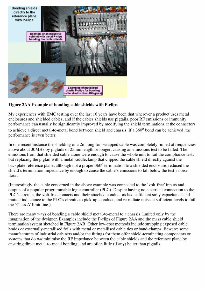
Figure 2AA Example of bonding cable shields with P-clips
My experiences with EMC testing over the last 16 years have been that wherever a product uses metalenclosures and shielded cables, and if the cables shields use pigtails, poor RF emissions or immunityperformance can usually be significantly improved by modifying the shield terminations at the connectorsto achieve a direct metal-to-metal bond between shield and chassis. If a 360ø bond can be achieved, theperformance is even better.
In one recent instance the shielding of a 2m long foil-wrapped cable was completely ruined at frequenciesabove about 30MHz by pigtails of 25mm length or longer, causing an emissions test to be failed. Theemissions from that shielded cable alone were enough to cause the whole unit to fail the compliance test,but replacing the pigtail with a metal saddleclamp that clipped the cable shield directly against thebackplate reference plane, although not a proper 360ø termination to a shielded enclosure, reduced theshield’s termination impedance by enough to cause the cable’s emissions to fall below the test’s noisefloor.
(Interestingly, the cable concerned in the above example was connected to the ’volt-free’ inputs andoutputs of a popular programmable logic controller (PLC). Despite having no electrical connection to thePLC’s circuits, the volt-free contacts and their attached conductors had sufficient stray capacitance andmutual inductance to the PLC’s circuits to pick-up, conduct, and re-radiate noise at sufficient levels to failthe ’Class A’ limit line.)
There are many ways of bonding a cable shield metal-to-metal to a chassis, limited only by theimagination of the designer. Examples include the P-clips of Figure 2AA and the mass cable shieldtermination system sketched in Figure 2AB. Other low-cost methods include strapping exposed cablebraids or externally-metallised foils with metal or metallised cable ties or band-clamps. Beware: somemanufacturers of industrial cabinets and/or the fittings for them offer shield-terminating components orsystems that do not minimise the RF impedance between the cable shields and the reference plane byensuring direct metal-to-metal bonding, and are often little (if any) better than pigtails.

Figure 2AB Example of method for bonding multiple cable shields to a chassis
Some supplier’s EMC installation instructions require that shielded cables only be terminated at one end.This can be a sign of bad EMC practices in electronic design, and should be considered a possiblewarning that the supplier’s products could cause EMC problems for the product, equipment or installationthat employs them. It is fair to say that some suppliers write such installation instructions because they areafraid that ’ground loop’ cable shield currents might overheat their cables, but in this case they would bebetter advised to recommend the use of the good installation practices of IEC 61000-5-2 [11], especiallyits ’parallel earth conductor’ (PEC) technique, which is discussed in Part 4 of [6] and Chapter 7 of [7].
A problem sometimes arises with such suppliers’ equipment, when it is necessary for its shielded cable(s)to interconnect two shielded enclosures. As Figure 2X showed, when interconnecting two shieldedenclosures, shielded cables must be 360ø terminated as they penetrate the walls of each of the enclosures -for their SE not to be degraded. This conflicts with the supplier’s instructions to only bond the shield atone end.
Figure 2AC shows one way around this problem - using a double-insulated-shield cable (two shieldsinsulated from each other). Terminating the outer shield at both ends preserves the SE of both enclosures,whilst the inner shield can be terminated according to the device supplier’s instructions. Now, if thedevice does not work to specification, the supplier cannot claim that his installation instructions were notfollowed.
Figure 2AC When suppliers insist on bonding cable shields at one end
2.6.8 Why ’ground loops’ are not a problem for correct design
’Ground loops’ or ’earth loops’ are sometimes called ’hum loops’ because of the noise they can make inpoorly-designed audio systems. Traditional installation practice uses single-point earthing/grounding andcable shield termination at only one end, to avoid creating ground loops, but the ground loop problem is infact caused by poor electronic design practices.
On an electronic test bench it is usually found that it is easiest and lowest-cost to obtain the best signal-to-noise ratio (SNR) for a low-frequency amplifier circuit, by connecting the 0V from the DC power supply,and the input cable shield, at a single point on the circuit - usually somewhere near the most sensitiveamplifier stage. Attempts to make this type of design give good SNR in the real world of systems andinstallations resulted in the policy of single-point grounding and isolating DC power supplies (althoughDC power supply isolation was needed for safety reasons anyway).
Every mains-powered product suffers from ground-leakage current, and - since every product had its ownground wire (with unavoidable impedance) back to some ’star point’ common ground connection - withrespect to the star point each product had a different ’ground’ voltage on its chassis. So if any shield wasconnected at both ends, the ground potential difference between the two products resulted in a ’groundloop’ current in the shield, which was of course connected directly into the reference voltage of the mostsensitive electronic circuits. As this current flowed through the traditionally high-impedance 0V systemsused in non-RF amplifiers, it gave rise to noise voltages that degraded the SNR.
Hence the bogey of ’ground loop currents’ was created by the original mistake, which was to try to forcethe lowest-cost test bench solution for individual PCB assemblies into the real world of systems andinstallations. Over time, that mistake has resulted in an overall cost to industry that is at least an order ofmagnitude higher (maybe two or three orders) than it would have cost if the circuits had been properlydesigned in the first place to cope with real-world ground potential differences. In the professional audioindustry, for example, costly high-specification isolation transformers are often employed to counteractthe effects of poor electronic design.
In fact, ground loops are a problem of the CM impedance coupling of single-sided signals using single-point earthing. It is rarely an issue for shielded signals in a well-designed system [12].
An unavoidable fact about the modern environment is that it is badly polluted with RF noise, which isgetting higher in amplitude and frequency all the time. But another problem with the single-pointgrounding method is that it is impossible to use it to control RF currents - the ground wires have too muchimpedance to be effective, and behave as accidental antennas just as shown in Figure 2C, allowing the RFcurrents to flow uncontrolled, causing interference problems. As has been shown above, the bestconnections for an RF shield are 360ø terminations at both ends, and anything else has worse EMperformance.
A cable shield that is only terminated at one end is an accidental antenna as shown in Figure 2C, just likeany other conductor, and not a shield at all for frequencies at which the cable is longer than one-sixth of awavelength. And a shielded enclosure penetrated by a cable that is neither shielded nor filtered is nolonger a shielded enclosure (see Figure 2X).
Since we now have no option but to control real-world RF, we have two choices - filtering and shielding.Cost-effective design uses both techniques, either separately or combined, but where shielded cables arealready used the best cost-effectiveness is generally achieved by allowing the cables to provide the SEthey have always been capable of, instead of wasting their SE by employing the ’traditional’ approach ofonly terminating the shield at one end (and that using a pigtail).
Effective shielding will of course create ’ground loops’, but there are simple and relatively low-costtechniques for dealing with them. The first is to always connect the shield to the chassis of the product -the low impedances in the product’s metalwork will divert most of the current away from the sensitivecircuits and into the ground structure. The 360ø shield termination method described in Figure 2P is idealfor this purpose.
The next step is to recognise that there are noisy potential differences between the chassis of differentitems, and so to interconnect them using balanced (differential) signalling circuits as shown in Figure 2Gand also as discussed in Part 1 of both [1] and [13]. The better the common-mode rejection ratio (CMRR)of the circuits at the power supply frequency, the lower will be the resulting noise due to the chassisvoltage differences.
In a well-designed balanced signalling circuit, screen currents (which are CM) do not cause significantDM signals, even when using very poor quality unbalanced cables, even with 50Hz currents high enoughto heat up the cable, as shown by the tests described in [14]. The only significant cause of the DMinterference that causes the hum noise is the potential difference between the earths (grounds) of theequipment at both ends of the cable, and the CMRR of the sending and receiving circuits.
Terminating all of the cable shields at both ends creates a ’meshed ground’ (what [6] [7] and [11] call aMESH-CBN, for Meshed Common Bonding Network), and the more such a structure is meshed, the morethe potential number of paths for ground current, the lower its ground impedance. Since earth/groundleakage currents mostly cause potential differences between items of equipment, the lower groundimpedance of a MESH-CBN results in lower hum noise and better SNR, not worse.
Another traditional worry is that damage to cables might occur due to high levels of shield currents insome high-power installations, or during a surge caused by a thunderstorm or power distribution fault. Ingeneral, when an installation has been correctly earth-bonded for safety reasons, the current that will flowin the relatively high-impedance cable shields cannot be high enough to damage them. But thegrounding/earthing structures in some legacy installations are very poor, and sometimes cables are routedwhere there is no low-impedance ground structure common to the equipment at both of its ends. In suchcases, adding a PEC as recommended in [11] will protect the shield from overcurrent damage, and willalso help protect the electronics at both ends from overvoltage damage during thunderstorms, see [15] formore on this. Care should be taken when routing a PEC between two separate installations, to avoidinjecting power-fault currents from one installation into parts of the other that cannot handle them.

Where very high performance signals are required (e.g. in Professional Audio), it may be necessary toimprove the CMRR by using high-CMRR balanced transformers, or high-CMRR electronic circuits.Another technique is to add a PEC in parallel with the cable shield, as recommended in [11]. This willconsiderably reduce the low-frequency shield currents, but for balanced interconnections shield currentscannot cause significant levels of noise in any case, and the main benefit of the PECs is in reducing thepotential differences between the chassis of the products at each end of the cable, see [14] for simple teststhat can quickly demonstrate this.
Some industries use very long coaxial cables, for example for ’75Ω’ video (e.g. in broadcasting studios).These are very prone to ground loop current noise because of the tradition amongst video designers ofusing single-ended signalling and connecting the coaxial cable shields directly to their circuits’ 0Vreferences. Single-ended signalling is also commonplace in the computer industry, for example for dataconnections between servers, because it results in the lowest cost electronics (but not the lowest overallcost of ownership). But as well as injecting external surface current noise into the reference voltage of themost sensitive circuits as mentioned earlier, this also results in the ground potential differences betweenthe items of equipment appearing directly in series with the DM return path of the signal. In single-endedsignalling, any voltage noise in the ’ground’ return has exactly the same noise effect as if it appeared inthe signal conductor.
Where single-ended signalling cannot be replaced by the much better technique of balanced (differential)signalling, the techniques described earlier of connecting the shields directly to the product’s referenceplane (as well as to the circuit 0V, as shown in Figure 2P) and reducing the ground impedance by theMESH-CBN and PEC techniques described in [3] [6] [7] [11] [14] and [15] are very effective ways ofreducing the noise whilst also helping to achieve good EMC.
Creating a low-impedance mesh-bonded ground is easy to justify and achieve for a dedicated server room,where it is often called the System Reference Potential Plane (SRPP) or ’Bonding Mat’. In the 1970sIBM’s guide for ground potential differences between opposite corners of a computer room was around1.5V, but the guides for modern server farms require a few tens of milliVolts. But mesh bonding is usuallynot easy to achieve in the legacy installations that many video systems have to contend with. As a result,the 75Ω video industry often finds it necessary to use devices variously called Ground-Loop Breaking,Hum-Bucking, Anti-Hum and Hum Suppressor Transformers. Some of these are CM chokes optimised tocreate a high CM impedance to power line frequencies, and some are 75Ω isolating transformers.
From this analysis, we see that having a great many ’ground loops’ actually reduces the levels of powersupply noise in the interconnections - providing we design our circuits so that their cable shields alwaysconnect directly to the product or equipment’s reference plane (chassis, frame, backplate, metal enclosure,etc.) as shown in Figure 2P - as they should to help achieve good EMC anyway.
2.6.9 When galvanic isolation is a requirement
Where true galvanic isolation is needed, bonding a cable’s shield at both ends is not possible. In suchcases isolating transformers, infra-red, fibre-optics, wireless and free-space microwave and lasertechniques should be considered instead for communicating signals of all types (analogue, control, data,etc.). There are now commercially-available products for passing up to 5 Watts of isolated electricalpower over a fibre-optic link (e.g. from the Photonic Power division of JDSU, http://www.jdsu.com).
Of course, the transformers, transmitters and receivers should not degrade the EMC. Unfortunately this isnot easy to achieve when using isolating transformers, because of the break they create in the shielding,and the fact that their interwinding capacitance makes an excellent path for CM currents at RF.
Where a shielded cable is used despite a requirement for galvanic isolation at powerline frequencies, itmay be possible to use a capacitor to bridge across the necessary gap in the cable shield, at one or bothends or at some point along the cable (e.g. where an isolating transformer is fitted). These capacitors
should be rated for the maximum voltage they will be exposed to over their life, which could be severalkV due to surges and other transients, and in many cases they will need to be safety-rated (preferablysafety approved) types too, possibly with limitations on their maximum value to limit leakage currents atpower frequencies. But unless special coaxial or annular capacitors, or radial arrays of multiple capacitorsare used - such shield-linking capacitors will degrade the RF shielding performance of the cable.
2.6.10 Intermodulation in RF connectors
Oxides formed on metal surfaces, and corrosion products formed between dissimilar metals, can causesmall but non-linear impedances to arise where connectors are used in the return current paths of cableshields. Mostly, these cause problems in RF power applications such as cellphone basestations, where anumber of different frequencies are transmitted from the same antenna, using coaxial cable so the returncurrents in the cable shield and mating connector shells are high. The result is intermodulation, generatingnumerous new noise frequencies from the sums and differences of the wanted frequencies. Another causeof intermodulation is the non-linear B-H curve of any magnetic materials in such connectors.
Screwed backshell connectors (e.g. N-type) are the most suitable types of connectors to use in suchapplications, and additional precautions include using connectors made from non-magnetic metals, whitebronze or silver plated, with soldered rather than crimped connections. It is also important to ensure thatthe connectors used are not damaged, and are clean when assembled.
2.6.11 Checking connectors after assembly, and in the field
Bad workmanship, oxidation and corrosion can affect the shielding performance of connectors and glands.Following training in correct shield termination practices, there is a tendency for assembly personnel torevert to earlier assembly methods, causing problems for EMC compliance and increasing warrantyclaims due to interference incidents in real life.
However, almost all modern products and equipment include digital processing and/or switch-modepower conversion, and as a direct result all of their power and signals interconnections carry CM RFnoise. Leakage of this noise at badly assembled or otherwise poor connectors and glands is very easy todetect very quickly with low skill requirements using low-cost portable spectrum analysers and home-made close-field probes.
Three examples of portable spectrum analysers are shown in Figure 2AD, with the PSA1301T being theleast costly at just under £800. Suitable designs for very low-cost close-field probes are given in Part 1 of[16]. I use small unshielded loop probes like those in Figure 2AD - merely a single-turn of enamelledcopper wire soldered to a BNC or SMA connector - making a probe that is sensitive to both electric andmagnetic fields at the same time, handy for saving time when one doesn’t know which type of field mightbe leaking.

Figure 2AD Three portable spectrum analysers, two home-made close-field probes
Checking a connector or gland requires that the spectrum analyser be set to its greatest sensitivity and torepetitively scan the frequency range of the CM RF noise (where this is unknown: scan from 1MHzto1GHz). Then simply holding the close-field probe against the surface of a connector or gland will revealany leakage within one scan of the spectrum, typically just a few seconds. Properly 360ø bonded cableshields do not show any leakage at all on this test, but pigtails (for example) do.
Close-field probes are not very sensitive to ambient EM fields in their environment, but will often pick upsome noise, especially when held close to the metal chassis or enclosure. So it is necessary to learn whichof the noises displayed on the spectrum analyser screen are due to the ambient, and which are due toimperfect shielding - but this is not difficult.
This close-field probe test is of course a quick, crude and low-cost test for revealing gross problems, butnevertheless it is very useful indeed. It can be used to check products in serial manufacture to helpmaintain regulatory compliance and keep warranty costs low - and it can also be used to quickly checkother workmanship aspects, such as errors in filter bonding and enclosure shielding (see Parts 3 and 4 of[1], or Parts 3 and 4 of this series). It can also be used at intervals throughout a product’s life to checkwhether oxidation, corrosion or misuse has degraded a correctly-assembled connector or gland.
Another use for close-field probing with a portable spectrum analyser is at Goods Inward, to check the’RF signatures’ of ICs and complex sub-assemblies (such as computer cards and switch-mode powersupplies). This can be a useful part of a procedure to help ensure that ’bad’ or counterfeit parts do notbecome assembled into products - but this is outside the scope of this series.
It is of course possible to perform more searching tests on assemblies of shielded cables, connectors andglands, often using a tracking signal generator and suitable coupling device to put voltage or current noiseonto a cable, and a suitable current or voltage probe connected to a spectrum analyser to analyse theshielding performance more accurately, and with better rejection of ambient noise.
2.7 Transmission line interconnections
2.7.1 What are they?

The send/return current loops of all types of conductors have a ’characteristic impedance’, which we callZ0. This is determined by the stray inductances (partial and mutual) and stray capacitances in theconductors, according (approximately) to the following equation -
where: C = capacitance per unit length (e.g. F/m), and L = inductance per unit length (e.g. H/m)
The stray inductances and capacitances associated with a conductor depend upon the geometry of themetal structures carrying the send and return current paths; the relative permittivity (i.e. dielectricconstant) and relative permeability of the medium filling the space around the conductors, and theirproximity to other conductors or conductive objects or surfaces.
In normal wiring, cables and connectors, the stray inductances and capacitances are not intentionallycontrolled, so their Z0 will vary from point to point along the interconnection. RF signals and noisesexperience reflections whenever Z0 changes, resulting in worsened SI (e.g. eye patterns more closed),increased emissions and increased pick-up of noise from external E, H and EM fields. When the distancebetween two Z0 changes is a quarter or half a wavelength (depending on the type of Z0 change at eachend) that portion of the interconnect becomes resonant, and the resonant gain significantly amplifies theeffects on SI, emissions and immunity. The largest impedance changes usually occur at the ends of theconductor, where there is a large mismatch between the conductor’s Z0 and the impedances of the sourceand/or the load, making the whole length of the cable resonate. Knowing this can help during EMC fault-finding, as it can allow the peak emissions or worst immunity frequencies to be related to cable length, tohelp identify which cable is causing the problem.
But when the Z0 of an interconnection is controlled so that it remains closer to the same value all along itslength, right from the source to the load, then the effects on SI, emissions and immunity are reduced. Thisis called ’controlled-impedance transmission line design’ and it has many benefits for SI and EMC. It isimportant to note that a controlled-impedance transmission line requires the impedance of the signal ornoise source to be a close match with the characteristic impedance of the interconnecting cable, and alsowith the impedance of the load. All joints and connectors along the path must also have a closely-matchedcharacteristic impedance.
A well-matched transmission-line exhibits minimal resonance effects, avoiding the resonant gain atparticular frequencies that causes ’accidental antenna’ problems for all other types of conductiveinterconnection. Transmission lines can use unshielded or shielded cables, but the shielded types (ideallyshielded twisted pairs) generally provide significantly better EM performance for both emissions andinmunity.
Some cable construction topologies are more vulnerable than others to suffering changes in Z0 along theirlength when they are bent at too sharp an angle, squashed, or run close to metal objects.
2.7.2 Why and when are matched transmission lines needed?
Where Z0 varies along a line, or when the source or load impedances don’t match Z0, the forwardpropagating electromagnetic energy (which is what all signals and power really are) suffers fromreflections. Reflections create an undesirable backwards-propagating wave, and when the cable length issome integer multiple of the wavelength this results in resonance, manifested as ’standing waves’ on theline. Resonant amplification of the currents and voltages cause the EMC performance to be very much

worse at the resonant frequencies.
Oscilloscopes show that reflections create overshoot, undershoot and other waveform distortions whichcan cause mis-operation of digital circuits, for example double-clocking. Network analysers show thatthey create a non-flat frequency response (some frequencies attenuated, others amplified).
From an EMC point of view, resonances and standing waves make conductors behave like efficientantennas, increasing emissions. Such unintentional antennas are also good at picking up EM fields in theirenvironment and converting them into conducted noise in the signals they carry, worsening immunity.
When a conductor length is shorter than one-seventh of the wavelength at the highest frequency ofconcern, it is said to be ’electrically short’ and Z0 is generally not considered to be important for SIreasons. For example, imagine that a digital signal repeating at 20MHz needs harmonics up to its 5th(100MHz) to be square enough for circuit functionality, so the higher harmonics are filtered out to preventthem causing problems for SI and EMC. At 100MHz the wavelength in air is 3.108/100.106 = 3 metres,but because the dielectric constant of cable insulation increases capacitance per unit length it slows thevelocity of propagation, so 2 metres is a more realistic estimate for one wavelength of 100MHz in a cable.One-seventh of this is 285mm, so cables longer than this are ’electrically long’ for this 20MHz digitalsignal and should use matched transmission line techniques to maintain a sufficiently accurate waveformfor SI.
But the ’one-seventh of the wavelength at the highest frequency of concern’ guideline still results inconductors that are relatively efficient accidental antennae at 100MHz, as shown by Figure 2C. For goodEMC, matched transmission-line techniques should be used for cables longer than about 1/28 of thewavelength (71mm in the above example) - maybe even shorter, depending on the EMC performancerequired.
Digital circuit designers tend to work in the time domain rather than the frequency domain, so theirversion of the above ’one-seventh of the wavelength at the highest frequency of concern’ guideline is tosay that a conductor is ’electrically long’ when the time that the signal edges take to travel from its sourceto its furthest receiver exceeds half of its rise or fall time (whichever is the shorter). Some SI experts (e.g.Dr Howard Johnson) use a one-third of the rise or fall time instead. As above, these half or third rise/falltime guides are only for SI - for good EMC matched transmission-line techniques should be used forcables with propagation times longer than about 1/8 of the rise or fall time - maybe even shorter,depending on the EMC performance required.
But these guides based on rise/fall times can lead to problems if their assumptions are not understood. Forexample, the rise or fall times used should be the real values, not databook specifications. Device dataonly gives rise/fall times as maximum values; so that the semiconductor manufacturers can shrink theirsilicon dies whenever a new silicon chip manufacturing process becomes cost-effective. Shrunk silicondevices switch faster, but because the databooks only publish maximum values, they are not reissued,giving a false idea about the switching speeds likely to be met in practice.
For instance, when HCMOS devices first became available in the 1980s, their switching speed was around5ns, and SI and EMC problems above 60MHz were rare. But purchasing HCMOS devices with the samepart numbers and package styles as in the 1980s now gets you a very much smaller silicon die, which canhave SI and EMC problems up to at least 800MHz, implying rise/fall times of around 0.4ns.
So when using rise/fall time based rules for deciding whether matched transmission line techniques arerequired, we need to know the real-life rise/fall times - measured with oscilloscopes and probes that havea combined bandwidth of at least 5GHz. Alternatively, measure the noise created by the IC up to thehighest frequency of concern using a spectrum analyser and tiny close-field probe, and use thewavelength-based guidelines instead.

Another assumption in the rise/fall time based guides is that the propagation time of the cable can be hadfrom the cable’s velocity factor data - but this is only true for point-to-point interconnections. Where acable supplies multiple devices along its length, the capacitive loading of the connectors and device inputsslows the velocity of propagation along the cable below what is achieved by the cable alone.
2.7.3 Matching transmission lines
’Matching’ means that the termination resistance at the end of the transmission line equals thetransmission-line’s Z0. When choosing matching resistor values, the effects of the internal impedances ofthe source and load devices must be taken into account.
Classical or ’both-ends’ transmission-line matching
Matched resistances terminate classical transmission lines at both ends - the signal’s source and its finalload - as shown in Figure 2AE. This is an ideal and sometimes necessary technique, and is often used forlong cables between products, and for RF signals inside products.
But classical matching halves the received voltage, so has not generally been used in the past for digitalcircuits communicating within a product, to save the cost of the extra amplification that would be needed.However, the present trend for replacing parallel busses with asynchronous serial interconnectionsoperating at high speed is making classical termination more commonplace. Some LVDS receivers havehigh sensitivity, so function quite happily with signal voltages halved by classical line matching.
Figure 2AE Classical transmission-line matching examples
It can be difficult to achieve accurate line matching at the driver end, when using drivers whose sourceimpedance varies between their high and low output states, as ordinary TTL and CMOS ’glue logic’devices do. Accurate line matching, hence good SI and improved EMC, requires drivers that are designedfor transmission-line driving, with low-impedance outputs (lower than Z0) that are the same whetherdriving high or low.
Series and shunt transmission-line matching
To avoid losing half the signal voltage by using classical transmission-line matching, most digital signalscommunicated within the same product with TTL or CMOS devices use low-impedance drivers and high-

impedance loads, with the transmission line terminated in a matching resistor at one end only. Two basicmethods are available, called ’series’ and ’shunt’, each of them using just one of the end terminations ofthe classical termination method described above.
Series (source) termination uses a matched resistor at the driver’s end only, as shown in Figure 2AF.Signals launched into the line by the driver are attenuated by the series resistor and propagate down theline at 50% of their amplitude. Eventually they are reflected in-phase at the mismatched high-impedanceload, and the reflected signal then propagates back down the line, adding to the incoming signal along theway, creating the desired 100% amplitude as it does so. When the reflected signal edge reaches thematching resistor at the source it is fully absorbed by the matched series resistor, so no further reflectionsoccur. This reliance on signal reflection at the load to create 100% amplitude is why this technique is alsoknown as ’reflected wave switching’.
Figure 2AF Series or source transmission-line matching
Series termination is most suitable for lines with a single load device at their far end, often called point-to-point interconnections. Where other loads exist along the length of the line they experience ’reflectedwave switching’ as the forward wave going past at 50% amplitude, followed a little while later by thereflected wave reaching them at 100% amplitude. The response of devices along a series-terminated linemight need to be slowed to prevent double clocking.
Series termination consumes very little power, and (as for classical termination above) accurate linematching (hence good SI and improved EMC) requires drivers that provide low-impedance outputs thatare the same impedance whether driving high or low.
Parallel (shunt, or load) termination uses a matched resistor at the furthest receiver. The mismatch at thesource might result in a little higher dissipation in the driver, but the signal is launched into thetransmission line with 100% amplitude. There are no reflections from the load because it is impedance-matched, so it achieves what is called ’incident wave switching’. It is most often used where high datarate is important and there are a number of receivers spread along the length of the transmission line.
Figure 2AG shows the matching resistor connected to the 0V plane, but some logic families use otherreference voltages (e.g. ECL uses the positive supply rail). Problems with parallel termination includehigh dissipation in the load resistors, and a driver DC current requirement that might be too high for somedrivers.

Figure 2AG Shunt, parallel or load transmission-transmission-line matching
Figure 2AG also shows RC termination - an attempt to reduce shunt termination’s power dissipation andDC loading problems. It typically uses capacitor values between 10 and 620pF, and only matches the lineat high frequencies (e.g. when a digital signal is changing state). Some care is needed to choose thecorrect capacitance value, which will depend upon the length of the transmission line and type of dataexpected. The RC time constant must be greater than twice the propagation delay of the loadedtransmission line. And to achieve power dissipation savings when compared with plain resistive shunttermination, the RC time constant must be shorter than the data period.
Thévenin transmission-line matching
An alternative type of shunt line termination is called ’Thévenin’, shown in Figure 2AH, with the aim ofreducing power consumption and the DC loading on the driver. It uses resistor values designed so thattheir parallel resistance equals Z0, and also so that if disconnected from the line they would provide a DCvoltage at their junction equal to the average line voltage of the data, to minimise power dissipation andthe DC current loading in the driver. Another design issue is that when undriven (e.g. a tristated driver, ora broken or disconnected line) the receiver’s input should have a defined voltage that is either a logic 0 or1 - unfortunately this often prevents the achievement of minimum power dissipation.

>
Figure 2AH Thévenin transmission-line matching
Thévenin termination is very useful for ’weak’ drivers (such as ordinary TTL or CMOS glue logic), andfor long lines, as it helps them achieve good switching waveforms at the receiver. Note that the positivepower rail requires a very low impedance at the highest frequency of concern, so will probably need tohave a power decoupling capacitor nearby, at least (not shown in Figure 2AH).
Proprietary Thévenin and RC termination devices are available from a number of componentmanufacturers (e.g. California Micro Devices) usually as arrays of 8 or more in very small surface mountpackages which have good characteristics to over 1GHz.
Active transmission-line matching
’Active termination’ is a shunt termination method that connects the matching resistor to a bias voltage,instead of to the 0V plane. At the point where a matching resistor connects to the bias voltage rail, theimpedance at the highest frequency of concern must be very low. The bias voltage source must be able tosource as well as sink current.
The main aim is to set the bias voltage to the average value of the digital signals, to minimise powerconsumption and/or suit the line to the pull-up and pull-down currents available from the driver. But (asfor Thévenin line-matching above) it may be necessary to set the bias to a different voltage so that if theline becomes undriven (e.g. a tristated driver or a broken or disconnected line) the receiver’s input has adefined voltage that is either a logic 0 or 1 - but this can prevent the achievement of minimum powerdissipation.
Active line matching is a different way of achieving Thévenin termination, and so is very useful for’weak’ drivers (such as ordinary TTL or CMOS glue logic), and for long lines, as it helps them achievegood switching waveforms at the receiver. But it can reduce the power consumption below that of theelectrically equivalent Thévenin method, if the bias voltage generator operates in Class AB mode, so thatit only consumes maximum currents when needed.

Figure 2AJ Active transmission-line matching
’Diode termination’
This is not a transmission-line matching technique at all, but is mentioned here to avoid confusion. Ithelps to prevent device damage or latch-up due to signal overshoots or undershoots that go beyond thepower rails. It also helps prevent damage due to transient disturbances such as ESD or fast transientbursts. However, it has little if any other benefits for SI, and no benefits for EMC.
2.7.4 Matching the characteristic impedances of differential (balanced) lines
Differential transmission lines are being used a great deal more these days for high-speed clocks and data,for SI reasons, but they can also help achieve good EMC. They use two conductors to carry antiphasesignals, and might also have a common reference conductor, such as a third conductor in the cable or ashield.

Figure 2AK Some examples of differential transmission lines
But differential transmission lines have several different Z0s:
The Z0 of each conductor when driven individually with respect to the reference conductorTheir balanced Z0 when both conductors are driven with DM signals (pure antiphase signals)Their CM Z0 when both conductors are driven together, with CM signals (with respect to thereference conductor)
Real differential drivers never have perfectly balanced output signals, so all the above three modesexperience signals. For SI, it is usually sufficient to match the impedance of the balanced Z0, but to helpimprove EMC each one should be terminated correctly so that none of the modes can experience standingwave resonances.
It is common to find differential transmission lines for which only the DM Z0 is matched, often becausethere is no common reference connection between the source and receive ends, for example Ethernetusing unshielded twisted pair (UTP) cable. Such transmission lines usually need CM chokes at theirsource to reduce their CM currents and improve their EMC performance.
Figure 2AL Some examples of differential line matching
2.7.5 Matching resistors must be resistive at the highest frequency of concern
Transmission-line matching resistors must behave resistively up to the highest frequency of concern,which may need to be a higher frequency for EMC reasons than for SI. Cable terminators use resistorsintegrated into the bodies of controlled-impedance connectors, so they can easily be plugged into a cableconnector. They are fitted internally with the correct value of resistor, using a resistor type and assemblymethod that matches the impedance of the transmission line from DC up to a frequency specified by theirmanufacturer. Some cable terminators can handle high power dissipations, using high-power resistors andfinned heatsinks.
When terminating transmission lines with resistors mounted on PCBs, there are a number of design issuesto be taken into account. Leaded resistors suffer from the inductance of their leads and the straycapacitance of their end-caps, often limiting them to frequencies below 100MHz. Surface mount resistors

(but not MELF types) are much better, and providing the PCB trace routing is done well (see Part 5 of [1],or Part 5 of this series) even ordinary low-cost types can match a transmission line to over 1GHz.
Resistors in smaller surface-mounted package styles will generally have better performance at higherfrequencies than large ones (e.g. 0603 will be better than 0805), and arrays of resistors in small surfacemount packages are available from a number of suppliers to help save space on PCBs. At microwavefrequencies above a few GHz, RF resistors in controlled-impedance packages and/or special assemblytechniques may be needed.
Some PCB suppliers can provides embedded terminating resistors, created by selectively etching a layerof resistive material laminated inside the PCB.
2.7.6 Impedance matched transmission-line connectors
Connectors used with transmission-line cables must have a Z0 that matches the Z0 of the cable they are tobe used with, otherwise the resulting impedance discontinuity can cause reflections leading to resonancesand standing waves along the cable, hence poor EMC and possibly also degraded SI.
Impedance-matched connectors are common in RF applications, and we are all familiar with coaxial typessuch as the 50Ω BNC. Shielded transmission-line cables and connectors will generally be better for EMC,even within a product where they help improve SI by reducing crosstalk, and also help avoid the need forenclosure shielding/filtering, or at least save cost by reducing their specifications.
Don’t forget that, as mentioned earlier, connectors of apparently the same type but with a choice of Z0smight look identical, but their different Z0