
EMC Design Guideline
23
1/22 © 2022 ROHM Co., Ltd. No. 65AN017E Rev.001 July 2022 Application Note Automotive Motor Solution EMC Design Guideline Designing automotive motor applications, EMC compliance is one of the most important things. Your project may be often stopped by EMC compliance test’s fail just before mass production. It takes long time to solve issues by redesigning application boards and retest. This document describes how to design application boards for EMC issues by using our reference board as example. EMC tests covered in this document are conducted emission and radiated emission tests (CISPR 25 standards). Contents 1. Example of system configuration for automotive motor solution・・・・・・・・・・・・・・・・・・・・・・・・・・・・・・・・・・・・・・・・・・・・・・・・・・・・2 2. Example of EMC test result for automotive motor solution・・・・・・・・・・・・・・・・・・・・・・・・・・・・・・・・・・・・・・・・・・・・・・・・・・・・・・・・・3 3. How to design hardware peripheral circuit・・・・・・・・・・・・・・・・・・・・・・・・・・・・・・・・・・・・・・・・・・・・・・・・・・・・・・・・・・・・・・・・・・・・・・5 4. How to design PCB layout・・・・・・・・・・・・・・・・・・・・・・・・・・・・・・・・・・・・・・・・・・・・・・・・・・・・・・・・・・・・・・・・・・・・・・・・・・・・・・・・・・・10 5. Reference example 5.1. PCB circuit diagram・・・・・・・・・・・・・・・・・・・・・・・・・・・・・・・・・・・・・・・・・・・・・・・・・・・・・・・・・・・・・・・・・・・・・・・・・・・・・・・・・・・・・・・15 5.2. Parts list・・・・・・・・・・・・・・・・・・・・・・・・・・・・・・・・・・・・・・・・・・・・・・・・・・・・・・・・・・・・・・・・・・・・・・・・・・・・・・・・・・・・・・・・・・・・・・・・・16 5.3. PCB layout・・・・・・・・・・・・・・・・・・・・・・・・・・・・・・・・・・・・・・・・・・・・・・・・・・・・・・・・・・・・・・・・・・・・・・・・・・・・・・・・・・・・・・・・・・・・・・17 6. Example of EMC countermeasures 6.1. EMC countermeasure due to charge pump noise・・・・・・・・・・・・・・・・・・・・・・・・・・・・・・・・・・・・・・・・・・・・・・・・・・・・・・・・・・・・・・19 6.2. EMC countermeasure due to clock noise・・・・・・・・・・・・・・・・・・・・・・・・・・・・・・・・・・・・・・・・・・・・・・・・・・・・・・・・・・・・・・・・・・・・・20 6.3. EMC countermeasure due to switching noise of motor output・・・・・・・・・・・・・・・・・・・・・・・・・・・・・・・・・・・・・・・・・・・・・・・・・・・21
-
Upload
khangminh22 -
Category
Documents
-
view
0 -
download
0
Transcript of EMC Design Guideline
1/22
© 2022 ROHM Co., Ltd. No. 65AN017E Rev.001
July 2022
Application Note
Automotive Motor Solution
EMC Design Guideline
Designing automotive motor applications, EMC compliance is one of the most important things. Your project may be
often stopped by EMC compliance test’s fail just before mass production. It takes long time to solve issues by
redesigning application boards and retest.
This document describes how to design application boards for EMC issues by using our reference board as example.
EMC tests covered in this document are conducted emission and radiated emission tests (CISPR 25 standards).
Contents
1. Example of system configuration for automotive motor solution・・・・・・・・・・・・・・・・・・・・・・・・・・・・・・・・・・・・・・・・・・・・・・・・・・・・2
2. Example of EMC test result for automotive motor solution・・・・・・・・・・・・・・・・・・・・・・・・・・・・・・・・・・・・・・・・・・・・・・・・・・・・・・・・・3
3. How to design hardware peripheral circuit・・・・・・・・・・・・・・・・・・・・・・・・・・・・・・・・・・・・・・・・・・・・・・・・・・・・・・・・・・・・・・・・・・・・・・5
4. How to design PCB layout・・・・・・・・・・・・・・・・・・・・・・・・・・・・・・・・・・・・・・・・・・・・・・・・・・・・・・・・・・・・・・・・・・・・・・・・・・・・・・・・・・・10
5. Reference example
5.1. PCB circuit diagram・・・・・・・・・・・・・・・・・・・・・・・・・・・・・・・・・・・・・・・・・・・・・・・・・・・・・・・・・・・・・・・・・・・・・・・・・・・・・・・・・・・・・・・15
5.2. Parts list・・・・・・・・・・・・・・・・・・・・・・・・・・・・・・・・・・・・・・・・・・・・・・・・・・・・・・・・・・・・・・・・・・・・・・・・・・・・・・・・・・・・・・・・・・・・・・・・・16
5.3. PCB layout・・・・・・・・・・・・・・・・・・・・・・・・・・・・・・・・・・・・・・・・・・・・・・・・・・・・・・・・・・・・・・・・・・・・・・・・・・・・・・・・・・・・・・・・・・・・・・17
6. Example of EMC countermeasures
6.1. EMC countermeasure due to charge pump noise・・・・・・・・・・・・・・・・・・・・・・・・・・・・・・・・・・・・・・・・・・・・・・・・・・・・・・・・・・・・・・19
6.2. EMC countermeasure due to clock noise・・・・・・・・・・・・・・・・・・・・・・・・・・・・・・・・・・・・・・・・・・・・・・・・・・・・・・・・・・・・・・・・・・・・・20
6.3. EMC countermeasure due to switching noise of motor output・・・・・・・・・・・・・・・・・・・・・・・・・・・・・・・・・・・・・・・・・・・・・・・・・・・21

2/22
© 2022 ROHM Co., Ltd. No. 65AN017E Rev.001
July 2022
Application Note EMC Design Guideline
1. Example of system configuration for automotive motor solution
As an example of automotive motor solution, system configuration diagram for Hall Sensor Driver is shown in Figure 1.
Figure 1. Example of system configuration for automotive motor solution
H-Bridge, Gate Driver, and Sensor-less Driver are basically the same configuration as Hall Sensor Driver, only without hall signal
input. Motor is driven by inputting PWM signal or DC voltage as control signal after supplying power to driver. The information of
rotation speed and error detection may be output as feedback signals.
①②③④
⑤ ⑥
⑦
⑧
⑨
3/22
© 2022 ROHM Co., Ltd. No. 65AN017E Rev.001
July 2022
Application Note EMC Design Guideline
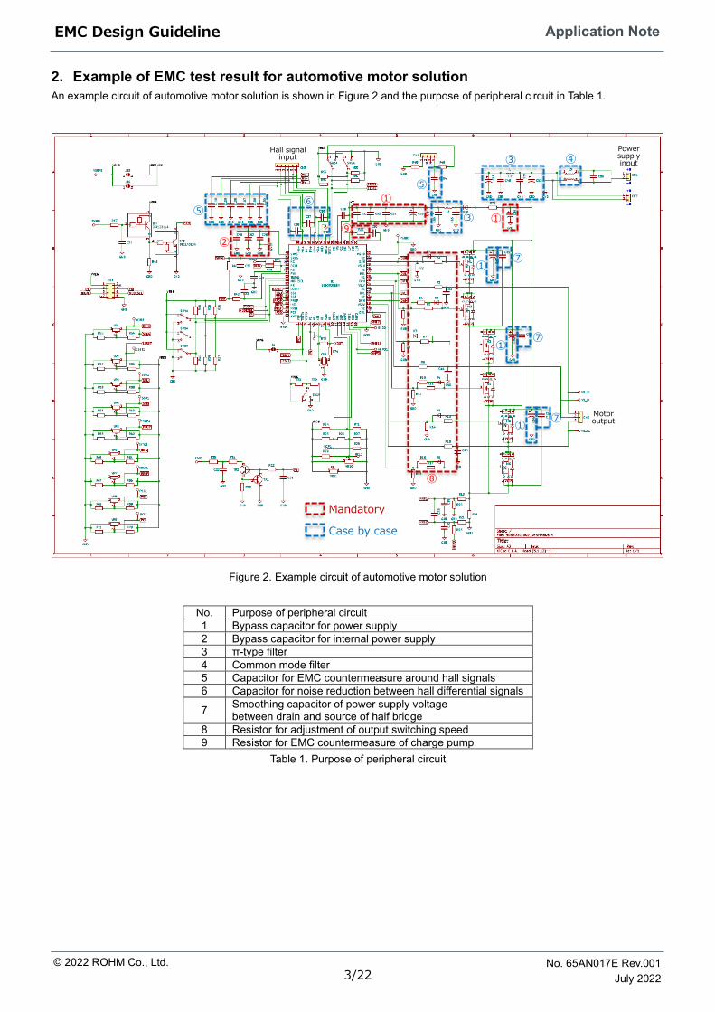
2. Example of EMC test result for automotive motor solution
An example circuit of automotive motor solution is shown in Figure 2 and the purpose of peripheral circuit in Table 1.
Figure 2. Example circuit of automotive motor solution
No. Purpose of peripheral circuit
1 Bypass capacitor for power supply
2 Bypass capacitor for internal power supply
3 π-type filter
4 Common mode filter
5 Capacitor for EMC countermeasure around hall signals
6 Capacitor for noise reduction between hall differential signals
7 Smoothing capacitor of power supply voltage between drain and source of half bridge
8 Resistor for adjustment of output switching speed
9 Resistor for EMC countermeasure of charge pump
Table 1. Purpose of peripheral circuit
①
①
①
①
①
②
③
③
④
⑤
⑤
⑥
⑦
⑦
⑦
⑧
⑨
Mandatory
Case by case
Power supply input
Motor output
Hall signal input

4/22
© 2022 ROHM Co., Ltd. No. 65AN017E Rev.001
July 2022
Application Note EMC Design Guideline
An example of EMC test result (conducted emission in accordance with CISPR25) for automotive motor solution is shown in
Figure 3.
Figure 3. Example of EMC test result for automotive motor solution
A: Depending on characteristics of power supply that inputs VCC voltage, noise may be generated in this frequency band, causing
EMC test to fail. As a countermeasure, use a battery power supply or a power supply that does not generate noise.
B: Noise in this band is reduced by a π-type filter. About the detail, refer to section 3-3 on page 6.
C: Switching of motor output cause power supply voltage to fluctuate, and EMC test may fail in this frequency band. One effective
countermeasure is to slow slew rate when motor outputs turn on. About the detail, refer to section 3-7 on page 9 and section 6-3
on page 21.
D: EMC test may fail in this frequency band due to noise on power supply caused by switching of motor output. Effective
countermeasures are to add a capacitor between drain and source of each half bridge and to add a common mode filter to power
supply line. About the detail, refer to section 3-4 on page 7, section 3-6 on page 8, section 4-3 on page 12 and section 4-4 on
page 13.
E: EMC test may fail in this frequency band due to propagation and amplification of noise caused by the operating clock of
internal logic inside motor driver. Effective countermeasures are to add bypass capacitors for logic power supply, to optimize
PCB layout of current loop and to add capacitors to propagation point of noise. About the detail, refer to section 3-2 on page 6,
section 3-5 on page 8, section 4-2 on page 11, section 4-6 on page 14 and section 6-2 on page 20.
A D E C B

5/22
© 2022 ROHM Co., Ltd. No. 65AN017E Rev.001
July 2022
Application Note EMC Design Guideline
3. How to design hardware peripheral circuit
[Power supply]
3-1. Purpose of bypass capacitors and how to select it
Bypass capacitors have the purpose of escaping (bypassing) noise on power supply line to ground and supplying current
temporarily when load current suddenly changes. Since fluctuation of power supply voltage may cause unstable operation of LSI
and MOS, bypass capacitors should be added between power supply pin and ground pin to stabilize power supply voltage. When
bypass capacitors are added, place it as close to the terminals as possible because parasitic resistance and inductance of the
board pattern affect the characteristics. Using capacitors with low impedance allows AC current to be bypassed to ground
efficiently and it provides a significant noise reduction effect. When AC impedance of power supply line needs to be decreased in
wide frequency bandwidth, place ceramic capacitors with low impedance (e.g., 0.1 µF and 470nF in 0.01 µF to 1 μF) in parallel
with electrolytic capacitor.
Figure 5 shows an example of three capacitors connected in parallel to keep impedance low in wide frequency bandwidth.
Figure 4. Bypass capacitors for power supply line
Figure 5. Example of combined impedance with parallel connection of capacitors

6/22
© 2022 ROHM Co., Ltd. No. 65AN017E Rev.001
July 2022
Application Note EMC Design Guideline
An example of calculating the capacitance value of an electrolytic capacitor is shown below.
Assuming PWM frequency 20 kHz (duty 50 %), maximum output current 10 A and allowable supply voltage fluctuation 0.5 V, ON
pulse width is 25 µs. Substituting t: 25 [µs], I: 10 [A] and V: 0.5 [V] for C ≥ it / V, C ≥ 500 [µF].
Select the capacitance value for electrolytic capacitors, taking into consideration that capacitance may drop at low temperatures.
For example, it is recommended to divide 100 µF for power supply of LSI and every 330 µF for power supply of each half bridge.
3-2. Adding bypass capacitors to regulator output for power supply of internal block
If regulator is built in for power supply of internal block of LSI and the regulator output is output external as a pin, the fluctuation
of internal regulator (VREG) output voltage may cause unstable operation of LSI. To stabilize VREG output voltage, add a bypass
capacitor of the recommended value (e.g., 1μF) between VREG output and ground. Also, noise may be improved by adding
ceramic capacitors with low impedance in frequency band for which you want to reduce noise (e.g., 470 nF in 0.01µF to 1μF) in
parallel with it. These capacitors should be placed as close to the terminals as possible because parasitic resistance and
inductance of board pattern affect their characteristics. An actual example is shown on page 20.
3-3. Purpose of π-type filter and how to select the values
π-type filter is a third-order low-pass filter for removing differential mode noise and provides a steeply sloped frequency response.
It is highly effective in removing noise and allows signals to pass through to higher frequency.
Figure 6. π-type filter
The cutoff frequency fc is expressed by the following equation.
𝑓𝑐 =1
2𝜋√𝐿𝐶
Where L is inductance value of coil.
C is capacitance value of capacitor.
Determine L and C so that frequency response is sufficiently attenuated in frequency band for which you want to remove noise.
As an example, if you want to obtain an attenuation effect of 40 dB or more at 1 MHz, selecting 1 µH as L and 220 µF as C and
setting fc to 10 kHz, you can theoretically obtain an attenuation effect of 120 dB at 1 MHz. But in reality, parasitic inductance and
capacitance will reduce the attenuation effect as shown in the dashed line in Figure 7. Therefore, it is important to confirm the
characteristics sufficiently on actual device.
Figure 7. Example of frequency characteristic of π-type filter
L
C C
IN OUT

7/22
© 2022 ROHM Co., Ltd. No. 65AN017E Rev.001
July 2022
Application Note EMC Design Guideline
3-4. Purpose of common mode filter and how to select it
Normally, noise is generated from switching circuits connected to power supply. Current path of noise current is same as one of
power supply current. Since this current's direction is different as (a) in Figure 8, this current is called differential mode current.
Noise caused by differential mode current is called as differential mode noise. To reduce this noise, adding bypass capacitors or
π-type filter are effective. On the other hand, current’s direction may be same as (b) in Figure 8 due to parasitic capacitance
between board and reference ground. This is called common mode current. Noise caused by this common mode current is called
as common mode noise. Adding bypass capacitors or π-type filter are not effective countermeasures.
Therefore, countermeasures for common mode noise are important.
Common mode filter (or common mode choke coil) is a filter to reduce common mode noise. Figure 8 shows structure and
operating principles of common mode filter. It works as inductor only for common mode noise.
Figure 8. Structure and operating principles of common mode filter
Select filter with high common mode impedance in frequency band for which you want to reduce noise. Also, pay attention to the
allowable current.
For reference, Figure 9 shows EMC test (conducted emission) results for motor solution of Hall Sensor Driver BD63030EKV-C
without common mode filter in power supply line and with common mode filter with different common mode impedance.
common mode filter common mode impedance common mode impedance common mode impedance
none 45 Ω@10 MHz, 30 A product 500 Ω@10 MHz, 10 A product 1000 Ω@10 MHz, 6 A product
Figure 9. Example of difference in effect depending on common mode filter characteristic
The lower the common mode impedance of common mode filter, the smaller the noise reduction effect, and the higher the common
mode impedance, the larger the noise reduction effect.
As EMC countermeasures for power supply line, a common mode filter and a π-type filter may be used together as shown in
Figure 10.
(b) Common mode current and magnetic fluxes
(a) Differential mode current and magnetic fluxes
Common mode
current
Differential mode
current Core Core
Magnetic fluxes
are in the direction
of strengthening
each other.
→Currents are less
likely to flow.
Magnetic fluxes
are in the direction
of cancelling
each other
→Currents flow
without change.

8/22
© 2022 ROHM Co., Ltd. No. 65AN017E Rev.001
July 2022
Application Note EMC Design Guideline
Figure 10. Use both common mode filter and π-type filter
[Input]
3-5. Cautions for inputting hall signals
If signals from hall sensors are fed back to LSI for position detection and output voltage of LSI's internal regulator (VREG) is used
as power supply of hall sensor, noise on VREG output may propagate to hall signals and EMC countermeasures may be required.
See page 20 for actual example. Also, adding capacitor of about 0.1 µF between hall differential signals is also effective for noise
reduction.
[Output]
(In case of external output stage)
3-6. Purpose of electrolytic capacitors for power supply line of output stage and ceramic capacitors between drain and
source of half bridge, and how to select it
Electrolytic capacitor added to power supply line of output stage is responsible for stabilizing power supply voltage as well as
supplying current when high side MOS of half bridge is turned on. The current supplied by this capacitor flows through parasitic
inductance and resistance of board pattern in power supply line, causing voltage fluctuation that may lead to noise and
malfunctions. Therefore, electrolytic capacitors should be placed as close to each half bridge as possible, dividing the calculated
capacitance value into the capacitance of LSI side and each half bridge, as described in section 3-1 on page 5. Also, the smaller
loop through which transient current flows decrease parasitic inductance, reducing voltage fluctuation and noise.
Figure 11. Capacitors around power supply of half bridges
Capacitor between drain and source of half bridge should be added for each half bridge and placed as close to each half bridge
as possible, since it stabilizes power supply voltage and supplies current when high side external MOS is turned on. To select the
capacitance value, select capacitor with low impedance in frequency band corresponding to slew rate of motor output when high
side MOS in output stage is turned on. An example of calculation of capacitance value is shown below.
Assuming that slew rate of motor output at output turn-on is 100 ns, it is 10 MHz in terms of frequency.
Select capacitor with low impedance at 10 MHz (e.g., 0.1 µF) and add it to each half bridge.

9/22
© 2022 ROHM Co., Ltd. No. 65AN017E Rev.001
July 2022
Application Note EMC Design Guideline
3-7. Adjustment of gate resistor value for voltage output and current value for current output
When LSI is pre-driver and gates of external MOS are driven by output stage, the method to adjust slew rate of motor output as
EMC countermeasures depends on whether output of pre-driver is voltage output or current output.
Figure 12. Example of voltage drive for MOS’s gate Figure 13. Example of current drive for MOS’s gate
・When MOS’s gate is driven by voltage (Figure 12), adjust external gate resistor value
・When MOS’s gate is driven by current (Figure 13), adjust output current value of pre-driver by SPI setting etc.
For example, if you want to reduce noise at 6 MHz, fluctuation of power supply voltage must be less than 0.045 mV, since limit
value is 33 dBµV. This is the value after passing through filters on power supply line (connector side). Assuming that total
attenuation effect of filters (common mode filter or π-type filter) at 6MHz is 80dB, fluctuation of power supply voltage before
passing through filters on power supply line (LSI and MOS side) must be less than 450mV (45 mV times 80 dB). Adjust capacitance
value of bypass capacitors and slew rate of motor output to satisfy this requirement.
See page 21 and 22 for actual example of EMC countermeasures by adjusting slew rate of motor output when external MOS is
turned on.
(External / Built-in output stage)
When output stage is external, slew rate of motor output can be adjusted by the method described above.
On the other hand, if output stage is built into LSI, capacitors (e.g., 0.1 µF) may be added between each motor output and ground
for EMC countermeasures.
[Others]
3-8. Precautions and noise reduction for using drivers with built-in charge pump circuit
Refer to page 19 for actual example.
BAT
V
VL
UL
WL
WH
UH
U
VH
W
Gate Drive
Pre-driver
PGND
VCPL
UL
VL WL
U, V, W
VCPH
UH VH WH
M
BAT
V
VL
UL
WL
WH
UH
U
VH
W
Gate Drive
Pre-driver
PGND
VCPL
UL
VL WL
U, V, W
VCPH
UH VH WH
M
Output Current Setting

10/22
© 2022 ROHM Co., Ltd. No. 65AN017E Rev.001
July 2022
Application Note EMC Design Guideline
4. How to design PCB layout
The following are six key points to note PCB layout design for EMC countermeasures in automotive motor solutions.
1. Number of layers for the board
2. Layout of ground
3. Placement and wiring around external MOS of output stage
4. Patten layout of the filter for EMC countermeasure of power supply line
5. Pattern layout of external oscillator and clock line
6. Layout of the wiring to connect to hall sensor
4-1. Number of layers for the board
・From the point of view of EMC, the number of PCB layers is recommended to be 4 or more. The advantage of using a multilayer
PCB is that power supply and ground layers can be placed next to each other. The interlayer capacitance of these two layers is
expressed by equation (1) and functions as a decoupling capacitor. Since ESL (Equivalent Series Inductance) of this capacitance
is very small, it has a high self-resonant frequency and is effective in reducing impedance from several hundred MHz to several
GHz.
𝐶 =𝜀0𝜀𝑟𝑠
𝑑 ・・・(1)
Where C is interlayer capacitance between power supply and ground layers.
ε0 is vacuum dielectric constant 8.854×10⁻¹².
ε𝑟 is relative dielectric constant of board (approx. 4.7 for FR-4).
S is area of parallel conductor plates.
d is distance between conductor plates.
Figure 14 shows an example of the assignments of power supply and ground layers for 4-layers and 2-layers board.
Figure 14. Example of PCB layer assignments
The number of layers for the board is a trade-off with board cost, so consider sufficiently.
・When wiring pattern is right-angled, the wiring width changes at the corners and the impedance changes. Since this effect
may increase noise in high-current or high-frequency signal lines, be careful not to make the sharp-edged patterns when
bending the wiring. (For example, bend the wiring at 45 degrees, etc.)
Figure 15. Layout of corner wiring

11/22
© 2022 ROHM Co., Ltd. No. 65AN017E Rev.001
July 2022
Application Note EMC Design Guideline
4-2. Layout of ground
When grounds are separated by application, such as small signal ground and large current ground, pattern separation is the basic
method. However, pattern separation is not necessary if ground layout can be designed with low impedance so that ground voltage
is not affected when current flows into parasitic impedance or inductance of board pattern. By not separating the ground, current
loop area can be reduced. Electromagnetic waves propagate when current flows through conductor and alternating magnetic and
electric fields are generated. Therefore, reducing current loop area leads to reduction of electromagnetic waves.
Figure 16. Relation of current, magnetic field and electric field
As an example, the following is an example of the placement and wiring layout of bypass capacitors between internal regulator
output (VREG) of LSI and ground.
Figure 17. Example of the circuit around VREG
1. Bypass capacitors are placed near the terminal and the wiring of ground is connected to ground of inner layer through Via.
2. If bypass capacitors are added in parallel, place the ones of low capacitance on terminal side.
3. Ground terminal of LSI is connected to ground plane of inner layer through Via near the terminal.
4. EXP-PAD is connected to ground plane of inner layer though Via.
5. Ground terminal of LSI is connected to EXP-PAD.
before countermeasures after countermeasures
Figure 18. Example of the layout around VREG

12/22
© 2022 ROHM Co., Ltd. No. 65AN017E Rev.001
July 2022
Application Note EMC Design Guideline
4-3. Placement and wiring around external MOS for output stage
For the layout of parts around external MOS in output stage, it is important to minimize current loop area for EMC countermeasures.
Ceramic capacitor C49 stabilizes power supply voltage of half bridges and supplies current when high side external MOS is turned
on. Select capacitance value that does not affect current sensing by shunt resistor. And add C49 between drain of high side MOS
and source of low side MOS and place it as close to each half bridge as possible. Electrolytic capacitor C47 should also be placed
as close as possible to each half bridge to reduce current loop area.
※TV band: 41 MHz to 88 MHz, FM band: 76 MHz to 108 MHz
Figure 19. Example of EMC countermeasure effect by the capacitor around half bridge
Common mode noise also occurs when each phase current flowing through the motor is not the same.
Figure 20. Example of the layout of 3-phase output lines
To solve this issue, design the pattern layout of board for output and gate wirings of half bridges as follows.
1. Wiring from output of each half bridge to connector should be the same width and as equal length as possible.
2. Wiring of U and W phase output should be line-symmetrical with wiring of V phase output.
3. Wiring between output of pre-driver and each gate terminal of external MOS should be the same width and equal length as
much as possible.

13/22
© 2022 ROHM Co., Ltd. No. 65AN017E Rev.001
July 2022
Application Note EMC Design Guideline
As reference data, comparison results of noise measurements when wiring lengths of 3-phase outputs are not same are shown
in Table 2.
※MW band: 0.53 MHz to 1.8 MHz, SW band: 5.9 MHz to 6.2 MHz
Table 2. Comparison results of noise measurements when wiring length of U-phase output is different
4-4. Pattern layout of the filter for EMC countermeasure of power supply line
If ground plane is placed under the coil of a common mode filter or π-type filter, crosstalk may occur due to parasitic capacitance
of board pattern. Therefore, it is recommended to remove ground plane under common mode filter or coil.
Figure 21. Pattern layout around common mode filter
4-5. Pattern layout of external oscillator and clock line
When external oscillator is used for reference clock, generated clock may become noise source and cause EMC issues, and it
may cause crosstalk with other signals or malfunctions depending on board layout. When designing pattern layout around external
oscillator, pay attention to the following four points.
・Place external oscillator and LSI on the same layer and minimize wiring length between oscillator and LSI.
・Don’t route other wirings between oscillator and LSI, and near oscillator-related wiring.
・If capacitors for oscillator are required, place and wire them near oscillator.
・Don’t wire under oscillator, damping resistor, feedback resistor and capacitors.
Figure 22. Pattern layout around oscillator

14/22
© 2022 ROHM Co., Ltd. No. 65AN017E Rev.001
July 2022
Application Note EMC Design Guideline
4-6. Layout of the wiring to connect to hall sensor
Hall differential signals should be wired with equal lengths and route side by side. Interconnection capacitance of differential
signals is effective in eliminating common mode noise, as is external capacitor between differential signals. Also, the wiring to hall
sensor should be as short as possible.
Figure 23. Pattern layout of hall signal lines

15/22
© 2022 ROHM Co., Ltd. No. 65AN017E Rev.001
July 2022
Application Note EMC Design Guideline
5. Reference example
5-1. PCB circuit diagram
PCB circuit diagram of Hall Sensor Driver BD63030EKV-C is shown in Figure 24.
Figure 24. PCB circuit diagram of Hall Sensor Driver

16/22
© 2022 ROHM Co., Ltd. No. 65AN017E Rev.001
July 2022
Application Note EMC Design Guideline
5-2. Parts list
Parts list of PCB for Hall Sensor Driver BD63030EKV-C is shown in Table 3.
Table 3. Parts list of PCB for Hall Sensor Driver
Designator Type Parts Value Description Product Name Manufacturer Footprint
- EVALUATION BOARD - Board Evaluation board - -
C104 Capacitor 0.1uF 50V,±10% CGA2B3X7R1H104K050BB TDK 1005
C105,C106,C107,C108,C109,C110 Capacitor 4700pF 50V,±10% CGA2B2X7R1H472K050BE TDK 1005
C19, C20, C24, C25, C27, C28, C29, C30,
C36, C37, C38, C49, C52, C55Capacitor 0.1uF 50V,±10% CGA2B3X5R1H104K050BB TDK 1005
C22 Capacitor 22000pF 50V,±10% CGA2B3X7R1H223K050BB TDK 1005
C23, C39 Capacitor 100pF 50V,±10% CGA2B2C0G1H101J050BA TDK 1005
C26,C31 Capacitor 470nF 50V,±10% CGA3E3X7R1H474K080AB TDK 1608
C33 Aluminum Electrolytic Capacito 100uF 50V,±10% UBT1H101MPD8 Nichicon φD×L(mm):10x20
C34,C46,C47,C50,C54 Aluminum Electrolytic Capacito 330uF 50V,±10% UBT1H331MHD8 Nichicon φD×L(mm):12.5x20
C40 Capacitor 1uF 16V CGA3E1X7R1C105K080AC TDK 1608
C48,C51,C56 Capacitor 0.1uF 50V,±10% CGA2B3X7R1H104K050BB TDK 1005
C53 Aluminum Electrolytic Capacitor 1000uF 50V,±10% UBT1H102MHD8 Nichicon 16x31.5
CK1 OSCILLATOR 10MHz ±0.5%,40Ω,33pF CSTNE10M0G55A Murata CSTCE_G_A
CN1 Header Connector - - HDR 2X4 - HDR(2X4)
CN3 Header Connector - - HDR 1X6 - HDR(1X6)
CN4 Header Connector - - HDR 1X4 - HDR(1X4)
CN5, CN7 Connector - - OSTT7022150 ON-SHORE TECHNOLOGY -
CN6 Connector - - OSTT7032150 ON-SHORE TECHNOLOGY -
D1, D2, D3, D4, D5, D6 Diode - - RRE01VM4SFHTE-17 ROHM D_3216
D10 Diode - - RR1LAM4STF ROHM D1F60
D9 Zenner Diode 30V - KDZVTF30B ROHM D_MCR50WLEAD
DCIN1 CHECK PIN - Test Pin, Through Hole LC-2-G Yellow - TP/1.6/2.3
DCIN2,LCSET1,SSU1,SSD1,PROP1,INTG1
RREF1,PCG1,PCI1,OCP1,OCL1CHECK PIN - Test Pin, Through Hole LC-2-G Yellow - TP/1.6/2.3
FGO1、VS_U1、VS_V1、VS_W1 CHECK PIN - Test Pin, Through Hole LC-2-G White - TP/1.6/2.3
J1, J16 Jumper - - - - SS/1.5X1.5/0.5
J15 Jumper - - - - SS/1.5X1.5/0.5
L2 Inductor 1.3uH ±20% XAL1350-132MED CoilCraft 14mm□
L3 Common mode choke 500Ω@10MHz Commom mode choke PLT10HH501100PN murata 12.9x6.6
L4 - short - - - 1608
M1, M2, M3, M4, M5, M6 Nch MOSFET Under development ROHM MOSFET(3x3)
PWMI1 CHECK PIN - Test Pin, Through Hole LC-2-G Yellow - TP/1.6/2.3
R1, R7, R13 Resistor 1200Ω 50V,±1% MCR03EZPFX2400 ROHM 1608
R19, R21 Resistor 2.2kΩ 50V,±1% MCR01MZPF2201 ROHM 1005
R2, R8, R14, R20, R23, R42, R46 Resistor 47kΩ 50V,±1% MCR01MZPF4702 ROHM 1005
R22 Resistor 10Ω 50V,±1% MCR01MZPF10R0 ROHM 1005
R24 Resistor 1.4kΩ 50V,±1% MCR01MZPF1401 ROHM 1005
R3, R9, R15 Resistor 62Ω 50V,±1% MCR03EZPFX51R0 ROHM 1608
R33 Resistor 75Ω 50V,±1% MCR01MZPF75R0 ROHM 1005
R34, R43, R44 - short - - - 1005
R35 Resistor 100Ω 50V,±1% MCR01MZPF1000 ROHM 1005
R4, R10, R16 Resistor 120Ω 50V,±1% MCR03EZPFX51R0 ROHM 1608
R47 Resistor 2.4kΩ 50V,±1% MCR01MZPF2401 ROHM 1005
R48, R49, R74 Resistor 150Ω 50V,±1% MCR01MZPF1500 ROHM 1005
R5, R11, R17 Resistor 620Ω 50V,±1% MCR03EZPFX75R0 ROHM 1608
R6, R12, R18, R32, R45 Resistor 10kΩ 50V,±1% MCR01MZPF1002 ROHM 1005
R75 Resistor 1MΩ 50V,±1% MCR01MZPF1004 ROHM 1005
R76 - short - - - JUMPER(B)
RT1 NTC THERMISTORS 100kΩ Thermistor NTCG164KF104FTDS TDK 1608
SR1 Resistor 1mΩ/8W Shunt Resistor PSR400ITQFH1L00 ROHM PSR400
SW1, SW2, SW3,SW4, SW5, SW6 3 state switch - Switch FT 1E-2M-Z NIDEC COPAL SW_FT1E-2M-Z
TR1, TR2 SILICON TRANSISTOR - NPN Transistor 2SC4081U3T106R ROHM TR_UMT3_SC-70_SOT-323
TR3 SILICON TRANSISTORS - NPN Digital Transistor DTC143EU3HZGT106 ROHM TR_UMT3_SC-70_SOT-323
TR4 SILICON TRANSISTORS - PNP Digital Transistor DTA123EU3HZGT106 ROHM TR_UMT3_SC-70_SOT-323
U1 INTEGRATED CIRCUITS - 3 Phase Motor Driver BD63030EKV-C ROHM TQFP-64V
VR1, VR2, VR3, VR4, VR5, VR6, VR7, VR8,
VR9, VR10, VR11Resistor 50kΩ Variable Resistor CT-6EP 50k Ohm NIDEC COPAL CT-6EP
VSUP1 CHECK PIN - Test Pin, Through Hole LC-2-G Red - TP/1.6/2.3
BVdss=40V, Ron(max)=3.0Ω, Ciss=1770pF

17/22
© 2022 ROHM Co., Ltd. No. 65AN017E Rev.001
July 2022
Application Note EMC Design Guideline
5-3. PCB Layout
PCB layout of Hall Sensor Driver BD63030EKV-C is shown in Figure 25 through 30.
Figure 25. Top silk of PCB for Hall Sensor Driver
Figure 27. 2nd layer of PCB for Hall Sensor Driver
Figure 26. Top layer of PCB for Hall Sensor Driver
Figure 28. 3rd layer of PCB for Hall Sensor Driver

18/22
© 2022 ROHM Co., Ltd. No. 65AN017E Rev.001
July 2022
Application Note EMC Design Guideline
5-3. PCB Layout (continued)
Figure 29. Bottom layer of PCB for Hall Sensor Driver
Figure 30. Bottom silk of PCB for Hall Sensor Driver

19/22
© 2022 ROHM Co., Ltd. No. 65AN017E Rev.001
July 2022
Application Note EMC Design Guideline
6. Example of EMC countermeasures
6-1. EMC countermeasures due to charge pump noise
If charge pump is built into LSI, two type of noise may be generated. One is noise caused by slew rate of switching output for
boost and the other is harmonic noise of the switching frequency.
Normally, only a capacitor of about 0.1 µF is inserted between switching terminals (CPP and CPM) for boost, but noise can be
reduced by adding resistors on both sides of the capacitor to slow down rising and falling time of the switching, as shown in Figure
31 and 32.
However, since the addition of resistors cause boost voltage to drop, select resistance value that is sufficient to drive the MOSs
of output stage even at the maximum expected load.
Gate voltage of external high side MOS in output stage must be sufficient to be turned on. It is the same when power supply
voltage is low (e.g., 6 V). In case of Figure 31, if the drop of boost voltage is allowed up to 1 V, maximum value of additional
resistors R is 33 ohm.
Figure 31. Example of resistance value vs CP voltage characteristics
Figure 32. Example of boost voltage, CPP and CPM voltage waveform
Since above noise also propagates to power supply line, the noise may be improved by taking the following countermeasures.
・Place ceramic capacitors (e.g., 1 nF and 4.7 nF) with low impedance in 100 MHz to 200 MHz frequency band for which between
power supply and ground as close to the terminals as possible. Because there are cases that noise is NG in 100 MHz to 200
MHz band.
・Add ferrite beads with high impedance in 100 MHz to 200 MHz frequency band for which you want to reduce noise for power
supply line.
R
R
A
B
A
B
Boost voltage
1V drop

20/22
© 2022 ROHM Co., Ltd. No. 65AN017E Rev.001
July 2022
Application Note EMC Design Guideline
6-2. EMC countermeasures due to clock noise
If internal logic of LSI operates by clock, harmonic noise of clock frequency will propagate to power supply line of the logic. Figure
33 shows an example where the logic is operated by external clock under internal power supply, and Figure 34 is an example of
its EMC measurement result. Place ceramic capacitor (e.g., 470 nF) with low impedance in 10 MHz band as close to the terminals
as possible, along with capacitor (e.g., 1μF) for voltage stabilization.
Figure 33. Example of block diagram around VREG and Logic Figure 34. Result of conducted emission
When VREG output voltage is used as power supply for external parts or ladder resistor, pattern impedance from VREG terminal
to external parts (e.g., hall element or ladder resistor for setting voltage) should be as low as possible.
As an example, when internal power supply (VREG, 5V) in Hall Sensor Driver is used as power supply of hall element, the noise
due to 10 MHz clock propagates to VREG. If the wiring between VREG and hall element is long, the noise on VREG is propagated
and amplified by the wiring and also propagates to hall signal input.
Figure 35. Example of block diagram when using hall elements
As a countermeasure, it is effective to shorten the wiring between VREG and hall element. Also, the noise may be improved by
adding the following capacitors.
1. Add a capacitor between power supply of hall element and ground
2. Add capacitors between each hall signal input and ground
21/22
© 2022 ROHM Co., Ltd. No. 65AN017E Rev.001
July 2022
Application Note EMC Design Guideline
For item 1, select a capacitor (e.g., 0.1 µF) with low impedance in 20 MHz band between 10 MHz and 100 MHz . For item 2, select
capacitance value (e.g., 4700 pF) that does not affect the phase of hall signal input .
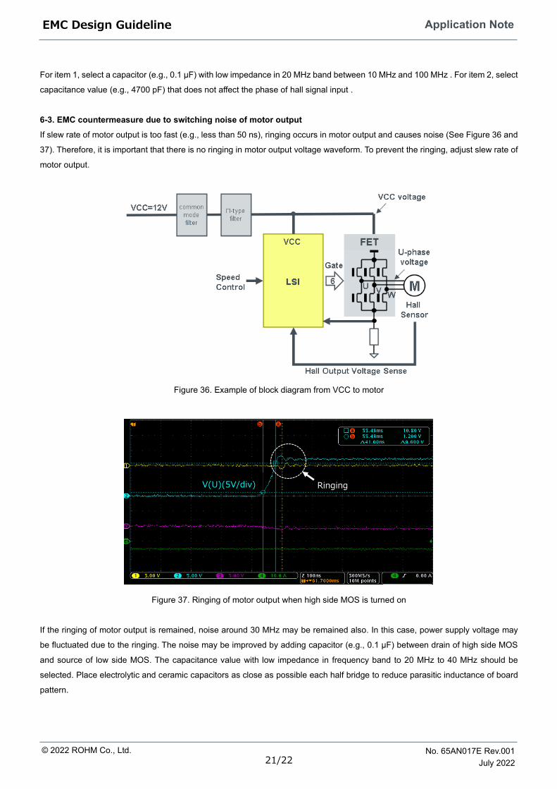
6-3. EMC countermeasure due to switching noise of motor output
If slew rate of motor output is too fast (e.g., less than 50 ns), ringing occurs in motor output and causes noise (See Figure 36 and
37). Therefore, it is important that there is no ringing in motor output voltage waveform. To prevent the ringing, adjust slew rate of
motor output.
Figure 36. Example of block diagram from VCC to motor
Figure 37. Ringing of motor output when high side MOS is turned on
If the ringing of motor output is remained, noise around 30 MHz may be remained also. In this case, power supply voltage may
be fluctuated due to the ringing. The noise may be improved by adding capacitor (e.g., 0.1 µF) between drain of high side MOS
and source of low side MOS. The capacitance value with low impedance in frequency band to 20 MHz to 40 MHz should be
selected. Place electrolytic and ceramic capacitors as close as possible each half bridge to reduce parasitic inductance of board
pattern.
Ringing V(U)(5V/div)
22/22
© 2022 ROHM Co., Ltd. No. 65AN017E Rev.001
July 2022
Application Note EMC Design Guideline
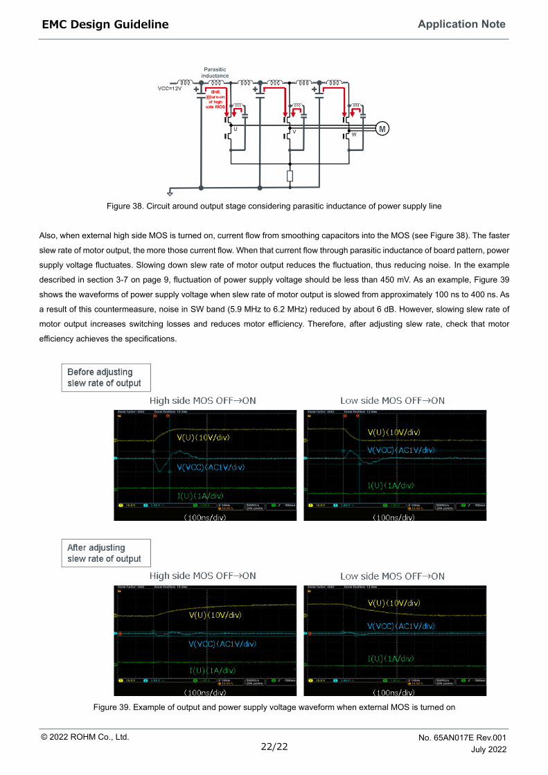
Figure 38. Circuit around output stage considering parasitic inductance of power supply line
Also, when external high side MOS is turned on, current flow from smoothing capacitors into the MOS (see Figure 38). The faster
slew rate of motor output, the more those current flow. When that current flow through parasitic inductance of board pattern, power
supply voltage fluctuates. Slowing down slew rate of motor output reduces the fluctuation, thus reducing noise. In the example
described in section 3-7 on page 9, fluctuation of power supply voltage should be less than 450 mV. As an example, Figure 39
shows the waveforms of power supply voltage when slew rate of motor output is slowed from approximately 100 ns to 400 ns. As
a result of this countermeasure, noise in SW band (5.9 MHz to 6.2 MHz) reduced by about 6 dB. However, slowing slew rate of
motor output increases switching losses and reduces motor efficiency. Therefore, after adjusting slew rate, check that motor
efficiency achieves the specifications.
Figure 39. Example of output and power supply voltage waveform when external MOS is turned on

R1102Bwww.rohm.com© 2016 ROHM Co., Ltd. All rights reserved.
Notice
ROHM Customer Support System http://www.rohm.com/contact/
Thank you for your accessing to ROHM product informations. More detail product informations and catalogs are available, please contact us.
N o t e s
The information contained herein is subject to change without notice.
Before you use our Products, please contact our sales representative and verify the latest specifica-tions :
Although ROHM is continuously working to improve product reliability and quality, semicon-ductors can break down and malfunction due to various factors.Therefore, in order to prevent personal injury or fire arising from failure, please take safety measures such as complying with the derating characteristics, implementing redundant and fire prevention designs, and utilizing backups and fail-safe procedures. ROHM shall have no responsibility for any damages arising out of the use of our Poducts beyond the rating specified by ROHM.
Examples of application circuits, circuit constants and any other information contained herein are provided only to illustrate the standard usage and operations of the Products. The peripheral conditions must be taken into account when designing circuits for mass production.
The technical information specified herein is intended only to show the typical functions of and examples of application circuits for the Products. ROHM does not grant you, explicitly or implicitly, any license to use or exercise intellectual property or other rights held by ROHM or any other parties. ROHM shall have no responsibility whatsoever for any dispute arising out of the use of such technical information.
The Products specified in this document are not designed to be radiation tolerant.
For use of our Products in applications requiring a high degree of reliability (as exemplified below), please contact and consult with a ROHM representative : transportation equipment (i.e. cars, ships, trains), primary communication equipment, traffic lights, fire/crime prevention, safety equipment, medical systems, servers, solar cells, and power transmission systems.
Do not use our Products in applications requiring extremely high reliability, such as aerospace equipment, nuclear power control systems, and submarine repeaters.
ROHM shall have no responsibility for any damages or injury arising from non-compliance with the recommended usage conditions and specifications contained herein.
ROHM has used reasonable care to ensure the accuracy of the information contained in this document. However, ROHM does not warrants that such information is error-free, and ROHM shall have no responsibility for any damages arising from any inaccuracy or misprint of such information.
Please use the Products in accordance with any applicable environmental laws and regulations, such as the RoHS Directive. For more details, including RoHS compatibility, please contact a ROHM sales office. ROHM shall have no responsibility for any damages or losses resulting non-compliance with any applicable laws or regulations.
When providing our Products and technologies contained in this document to other countries, you must abide by the procedures and provisions stipulated in all applicable export laws and regulations, including without limitation the US Export Administration Regulations and the Foreign Exchange and Foreign Trade Act.
This document, in part or in whole, may not be reprinted or reproduced without prior consent of ROHM.
1)
2)
3)
4)
5)
6)
7)
8)
9)
10)
11)
12)
13)