Pcb design techniques for lowest-cost EMC a compliance: part 1
10
PCB design techniques for lowest-cost EMC compliance: Part 1 by M. K. Armstrong Application of good EMC (electromagnetic compatibility) practices to the design of printed circuit boards (PCBs) usually helps to achieve the EMC performance required of equipment and systems at much lower cost than alternative EMC measures at higher levels of integration, such as whole-product shielding. EMC design is a complex topic, but the proven best EMC practices for generalised PCB layout can be fairly simply stated and grouped into five techniques, which interact with each other to give dramatic improvements in EMC performance. Part 1 of this paper discusses the techniques of circuit segregation, interface suppression and the use of ground and power planes. Part 2 will discuss techniques for power decoupling and the use of transmission lines. 1 Introduction The requirement to comply with the Electromagnetic Compatibility (EMC) Directive 89/336/EEC*x2 for almost every electrical and/or electronic equipment or system sold in the European Union is focusing many minds on the best ways to achieve this in the most cost-effective manner. Printed circuit boards (PCBs) are very widely used in such equipment and systems, and there is a very large body of experience which shows that it is possible to incorporate good EMC practices during their design. These PCB-level EMC practices usually help achieve the required EMC performance at a much lower cost than alternative EMC measures at higher levels of integration, such as whole-product shielding. They also improve signal integrity in both analogue and digital circuits, and so help reduce the number of iterations of hardware and software before a product functions adequately, saving significant engineering costs and reducing time-to-market. As modern electronic circuits increase their digital clock or analogue oscillator frequencies (especially above 50 MHz) , these EMC practices become increasingly necessary for functionality. EMC design is a complex topic, but the proven best EMC practices for generalised PCB layout can be fairly simply stated, and this is the purpose of this paper. The techniques are discussed under five headings. ‘Circuit segregation’, ‘Interface suppression’ and the use of ‘Ground and power lines’ are discussed in Part 1 of the paper. ‘Power decoupling’ and the use of ‘Transmission lines’ will be considered in Part 2, to be published in a future issue of this journal. The paper deals with the practical ‘what’ and ‘how’ of these techniques rather than the ‘why’ (although understanding the ’why’will of course help any practising engineer to use these techniques to the full, and to compromise where necessary). In the context of this paper, EMC includes all relevant electromagnetic (EM) emissions and immunity phenomena as they concern all types of analogue and digital circuits. The best-practice EMC techniques described here interact with each other to give dramatic improvements in the EMC of electronic circuits which use PCBs. Good control of EMC up to 1 GHz will only be realised on PCBs by fully implementing all these techniques, and the cost- effectiveness of using all of them together generally exceeds that of other methods. Note that there are also requirements in some market areas for EMC at frequencies exceeding 1 GHz. For EM interference to occur (i.e. inadequate EMC) there must be a source of EM disturbances (an aggressor), a coupling path, and a circuit which is susceptible to EM disturbances (the victim). Coupling out of or into a circuit can occur through: the finite impedance of shared circuits (most often AC mains, DC power rails, earth and 0 V references) capacitive coupling, where the voltages on one conductor give rise to currents in the victim conductor 0 inductive coupling, where the currents flowing in one circuit give rise to voltages in the victim circuit 0 EM. coupling (mostly at high frequencies), where the voltages or currents in one circuit give rise to EM fields, which in turn give rise to currents and voltages in the victim circuit. ELECTRONICS & COMMUNICATION ENGINEERING JOURNAL AUGUST 1999 185
-
Upload
khangminh22 -
Category
Documents
-
view
0 -
download
0
Transcript of Pcb design techniques for lowest-cost EMC a compliance: part 1

PCB design techniques for lowest-cost EMC
compliance: Part 1 by M. K. Armstrong
Application of good EMC (electromagnetic compatibility) practices to the design of printed circuit boards (PCBs) usually helps to achieve the EMC performance required of equipment and systems a t much lower cost than alternative EMC measures a t higher levels of integration, such as whole-product shielding. EMC design is a complex topic,
but the proven best EMC practices for generalised PCB layout can be fairly simply stated and grouped into five techniques, which interact with each other to give dramatic improvements in EMC performance. Part 1 of this paper discusses the
techniques of circuit segregation, interface suppression and the use of ground and power planes. Part 2 will discuss techniques for power decoupling and the use of
transmission lines.
1 Introduction
The requirement to comply with the Electromagnetic Compatibility (EMC) Directive 89/336/EEC*x2 for almost every electrical and/or electronic equipment or system sold in the European Union is focusing many minds on the best ways to achieve this in the most cost-effective manner.
Printed circuit boards (PCBs) are very widely used in such equipment and systems, and there is a very large body of experience which shows that it is possible to incorporate good EMC practices during their design. These PCB-level EMC practices usually help achieve the required EMC performance at a much lower cost than alternative EMC measures at higher levels of integration, such as whole-product shielding. They also improve signal integrity in both analogue and digital circuits, and so help reduce the number of iterations of hardware and software before a product functions adequately, saving significant engineering costs and reducing time-to-market. As modern electronic circuits increase their digital clock or analogue oscillator frequencies (especially above 50 MHz) , these EMC practices become increasingly necessary for functionality.
EMC design is a complex topic, but the proven best EMC practices for generalised PCB layout can be fairly simply stated, and this is the purpose of this paper. The techniques are discussed under five headings. ‘Circuit segregation’, ‘Interface suppression’ and the use of ‘Ground and power lines’ are discussed in Part 1 of the paper. ‘Power decoupling’ and the use of ‘Transmission lines’ will be considered in Part 2, to be published in a future issue of this journal.
The paper deals with the practical ‘what’ and ‘how’ of
these techniques rather than the ‘why’ (although understanding the ’why’ will of course help any practising engineer to use these techniques to the full, and to compromise where necessary).
In the context of this paper, EMC includes all relevant electromagnetic (EM) emissions and immunity phenomena as they concern all types of analogue and digital circuits.
The best-practice EMC techniques described here interact with each other to give dramatic improvements in the EMC of electronic circuits which use PCBs. Good control of EMC up to 1 GHz will only be realised on PCBs by fully implementing all these techniques, and the cost- effectiveness of using all of them together generally exceeds that of other methods. Note that there are also requirements in some market areas for EMC at frequencies exceeding 1 GHz.
For EM interference to occur (i.e. inadequate EMC) there must be a source of EM disturbances (an aggressor), a coupling path, and a circuit which is susceptible to EM disturbances (the victim). Coupling out of or into a circuit can occur through:
the finite impedance of shared circuits (most often AC mains, DC power rails, earth and 0 V references) capacitive coupling, where the voltages on one conductor give rise to currents in the victim conductor
0 inductive coupling, where the currents flowing in one circuit give rise to voltages in the victim circuit
0 EM. coupling (mostly at high frequencies), where the voltages or currents in one circuit give rise to EM fields, which in turn give rise to currents and voltages in the victim circuit.
ELECTRONICS & COMMUNICATION ENGINEERING JOURNAL AUGUST 1999 185

The techniques described here mostly improve the PCB’s EM coupling mechanisms and do little for the actual sources, or for the susceptible circuits themselves (although techniques do exist for improving these too).
Because they operate on the coupling between the circuits on a PCB, and between the PCB circuits and their external environment, these techniques are equally effective for improving both EM emissions and immunity.
To create competitive products it is necessary to use these proven good EMC techniques from the start of a project, continuing all through it. If it is not thought commercially sensible to fully implement all these techniques, additional project costs and lengthened timescales should be allowed for extra EMC testing and extra design iterations.
2 Circuit segregation
In a cost-efficient design process circuit segregation is the first technique to be applied, and it needs to be employed right at the beginning of the real design process. The layout of the PCB cannot begin until it is known where (physically) any shielding and filtering techniques need to be applied, so this overview of the mechanical assembly should precede PCB design, and should be done as early in the product development lifecycle as possible.
To employ this technique the following areas are first identified:
0 the outside world, i.e. any part of the circuit for which total control of the EM environment is not available to the product designers
0 the inside world, i.e. any part of the circuit for which total control of the EM environment is achieved by the product designers.
The boundary between the outside and inside worlds Where a product has an adequately shielded enclosure,
the outside world is easily identified as being everything outside that enclosure. But where a shielded enclosure is not used it can be quite difficult to identify the boundary between the outside and inside worlds.
It is generally undesirable for all but the most benign circuits to be exposed to the outside world environment. It is often possible to fit PCBs inside screened ‘module’ enclosures of their own, to create their own inside worlds. PCBs designed using all the practices described here will have a good degree of control over their local EM environment, and some types of products will be able to create their own inside worlds even without module or enclosure shielding.
Conductors which run outside of a product’s enclosure are clearly subject to the full outside world EM environment, but cables which run inside a product may also suffer a subset of those phenomena if the product enclosure is not adequately shielded. For example, a ribbon cable or jumper strip connecting two shielded PCBs will not be protected from the outside-world radiated R?? environment unless there is an enclosure that provides adequate shielding. The frequencies at which
internal cables start to act as antennas for outside-world radiated fields depend upon the types and lengths of the cables, and upon the circuitry and filters they are connected to.
The use of a single-PCB for all the circuitry in a product is usually the most cost-effective way to meet EMC requirements. This is because it is easier and least costly to control the EM environment of a single PCB, with its obvious boundary between ‘inside’ and ‘outside’ worlds, than it is to control that of a product with several PCBs and internal wires and cables. Many types of .electronic products will not need a shielded enclosure if made using a single PCB with no internal wires and cables and the techniques described here. This promises to save considerable costs in both materials and assembly, and to allow a great deal more aesthetic freedom in styling.
Considerable manufacturing-cost savings and improvements in reliability result from a single PCB approach, even where EMC is not an issue. Where a single flat PCB is impractical, flexi-rigid techniques are increasingly cost-effective, for EMC purposes, at realising complex three-dimensional circuit arrangements as if they were a single PCB.
Boundaries within an inside world When the circuitry which is in the inside world has been
determined, it should be further subdivided into dirty, high-speed, noisy, (etc.) potentially aggressive areas, and clean, sensitive, quiet, (etc.) potential victim areas.
All of the above terms are poorly defined jargon used by electronics engineers to describe the likelihood of one circuit emitting EM disturbances, or being interfered with by EM disturbances. A better rule of thumb for ranking the likelihood of a circuit node to emit ‘noise’ is to refer to its maximum dV/dt and dI/dt (rates of change of voltage and current). Arule of thumb for the likelihood of a circuit node to su~erfi-om interference is to refer to its signal levels and noise margins (lower level signals and/or lower noise margins imply greater potential for susceptibility). This analysis should result in identification of the worst-case sources and victims of EM disturbance.
Segregation The various inside-world areas identified are to be
physically segregated from each other, and from the outside world. This activity should segregate all these areas mechanically and electrically, starting at the earliest design phase b y showing the various areas clearly on all drawings. This is usually done by drawing dotted lines around rectangular areas, each consisting solely of a segregated portion of the overall circuit.
It is necessary to ensure that this segregation is maintained throughout the rest of the design process, including system design, PCB layout, wiring harness design, mechanical packaging, etc. Showing the segregation clearly on all system, wiring, and circuit diagrams will prove to be a great help to communications between the electronics designers and others who may not have the necessary EM skills - such as mechanical designers and PCB layout persons - especially where
186 ELECTRONICS & COMMUNICATION ENGINEERING JOURNAL AUGUST 1999
such work is contracted to industrial designers or PCB layout companies.
Most design occurs in two dimensions. It is not uncommon to find that in the final assembly, a PCB carrying a very sensitive circuit (such as a thermocouple or microphone amplifier) turns out to be in close proximity to, a PCB carrying a very noisy circuit (such as a switch-mode power convertor), with consequent signal quality problems. Such unpleasant and time-consuming three- dimensional assembly issues should be avoided by detailed visualisation of the final assembly from the start, even before the circuits are designed and the PCBs laid out.
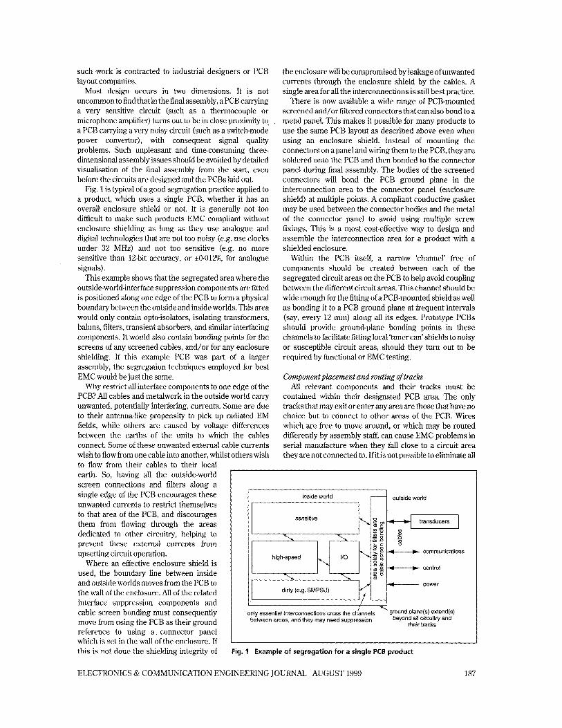
Fig. 1 is typical of a good segregation practice applied to a product, which uses a single PCB, whether it has an overall enclosure shield or not. It is generally not too difticult to make such products EMC compliant without enclosure shielding as long as they use analogue and digital technologies that are not too noisy (e.g. use clocks under 32 MHz) and not too sensitive (e.g. no more sensitive than 12-bit accuracy, or +0.012%, for analogue signals).
This example shows that the segregated area where the outside-world-interface suppression components are fitted is positioned along one edge of the PCB to form a physical boundary between the outside and inside worlds. This area would only contain opto-isolators, isolating transformers, baluns, filters, transient absorbers, and similar interfacing components. It would also contain bonding points for the screens of any screened cables, and/or for any enclosure shielding. If this example PCB was part of a larger assembly, the segregation techniques employed for best EMC would be just the same.
Why restrict all interface components to one edge of the PCB? All cables and metalwork in the outside world carry unwanted, potentially interfering, currents. Some are due to their antenna-like propensity to pick up radiated EM fields, while others are caused by voltage differences between the earths of the units to which the cables connect. Some of these unwanted external cable currents wish to flow from one cable into another, whilst others wish
cable screen bonding must consequently move from using the PCB as their ground reference to using a connector panel
the enclosure will be compromised by leakage of unwanted currents through the enclosure shield by the cables. A single area for all the interconnections is still best practice.
There is now available a wide range of PCB-mounted screened and/or filtered connectors that can also bond to a metal panel. This makes it possible for many products to use the same PCB layout as described above even when using an enclosure shield. Instead of mounting the connectors on a panel and wiring them to the PCB, they are soldered onto the PCB and then bonded to the connector panel during final assembly. The bodies of the screened connectors will bond the PCB ground plane in the interconnection area to the connector panel (enclosure shield) at multiple points. A compliant conductive gasket may be used between the connector bodies and the metal of the connector panel to avoid using multiple screw furings. This is a most cost-effective way to design and assemble the interconnection area for a product with a shielded enclosure.
Within the PCB itself, a narrow ‘channel’ free of components should be created between each of the segregated circuit areas on the PCB to help avoid coupling between the different circuit areas. This channel should be wide enough for the fitting of a PCB-mounted shield as well as bonding it to a PCB ground plane at frequent intervals (say, every 12 mm) along all its edges. Prototype PCBs should provide ground-plane bonding points in these channels to facilitate fitting local ‘tuner can’ shields to noisy or susceptible circuit areas, should they turn out to be required by functional or EMC testing.
/ only essential interconnections cross the channels ground plane(s) extend(s)
their tracks between areas, and they may need suppression beyond all and
Component placement and routing of tracks All relevant components and their tracks must be
contained within their designated PCB area. The only tracks that may exit or enter any area are those that have no choice but to connect to other areas of the PCB. Wires which are free to move around, or which may be routed differently by assembly staff, can cause EMC problems in serial manufacture when they fall close to a circuit area they are not connected to. If it is not possible to eliminate all
to flow from their cables to their local earth. So, having all the outside-world I screen connections and filters along a single edge of the PCB encourages these unwanted currents to restrict themselves to that area of the PCB, and discourages them from flowing through the areas dedicated to other circuitry, helping to prevent these external currents from upsetting circuit operation.
Where an effective enclosure shield is used, the boundary line between inside and outside worlds moves from the PCB to the wall of the enclosure. All of the related interface suppression components and
7
inside world outside world
sensitive V m
‘I ‘I. - z - L
”Q h -
high-speed I10 - w :: m
“I \ , 2 m
transducers
communications
control al
power dirty (e.g. SMPSU)
ELECTRONICS & COMMUNICATION ENGINEERING JOURNAL AUGUST 1999 187

use of wires inside a product, care is needed to ensure that the lengths and routes of any remaining wires are fixed.
The most noisy or susceptible components in each area should be positioned first, as close to the centre of their areas as possible and as far away from any cables or wires as possible. Examples of such components include clock generators and distribution (extremely noisy); bussed digital ICs (very noisy); microcontrollers (noisy) ; switch- mode power transistors and rectifiers and their chokes, transformers, and heatsinks (all very noisy); analogue ICs (sensitive); and millivolt level amplifiers (very sensitive).
It is not commonly realised that analogue devices such as operational amplifiers can be extremely susceptible to interference, even up to 1 GHz, when their fastest slew-rate may be as low as 1 V/vs. This susceptibility can easily occur even in integrator circuits with very slow (e.g. several seconds) time constants.
Digital clock distributions (being very aggressive signals) must be the first ‘nets’ to be routed, and must be run on a single PCB layer adjacent to a ground plane (see Section 4). Clock tracks must be kept as short as possible and even then may require the use of transmission-line techniques (see Part 2). It may be necessary to experiment with a variety of component placements to achieve the minimum lengths of clock tracks. Where clock tracks have to be lengthened to minimise skew between different devices, a ‘serpentine’ layout is preferred.
Digital busses and high-speed input/output should be routed next, and should be treated exactly the same as clock tracks, deferring to clock tracks where there is any conflict of design rules. Very susceptible tracks, such as those carrying millivolt transducer signals, should also be routed as if they were clock or data bus tracks, although they will always be in a different segregated area of the PCB.
All other types of analogue, digital and power signals should also be routed according to how aggressive they are at emitting EM disturbances, or how sensitive they are to being interfered with by them. Where these characteristics are not obvious from a circuit analysis, probing a prototype with a wideband oscilloscope (and/or spectrum analyser) with both voltage or current probes will reveal which are the most aggressive, and injecting voltages or currents from a wideband sweep generator will reveal which are most sensitive.
There should be no layer changes for any digital clock or other very aggressive tracks, or for very sensitive tracks (i.e. these tracks should not have any via holes). Where there is no reasonable alternative to changing the layers of such tracks, the techniques described in section 3 of Part 2 should be used.
Communicating with PCB layout personnel PCB layout personnel need to understand that the
segregation applies not only to the components, but also to all tracks and other conductors. Only tracks or conductors that must interconnect segregated areas are allowed to cross the channels between them.
It is best to check that segregation instructions have been followed on draft PCB layouts, well before PCB
manufacture. An easy check is to count the tracks and other conductors which cross the dotted lines showing the segregated areas on the circuit diagram - there should be exactly the same number crossing the channels between areas on the draft PCB layout, Where PCBs have been autorouted it is usual to find additional tracks crossing area boundaries; these are often the source of much design heartache, so eliminate them right away by applying more skill to the track layout.
3 Interface suppression
This is the second technique which should be employed during a cost-efficient EMC design procedure.
Overview of the technique EM disturbances can be radiated and/or conducted
across interfaces between segregated areas. Shielding, filtering and isolation techniques (such as optocoupling) are used to reduce this coupling to acceptable levels.
To decide on the most cost-effective methods to apply at each interface, it is necessary to analyse them for all the EMC phenomena possible, given the operational EM environment, circuits and components.
It is important not to ignore internal power supplies and other common connections such as ‘0 volts’ or grounds. Circuit designers usually abbreviate such connections on their circuit diagrams, often to the point of invisibility. This leads to inevitable problems when EM disturbance coupling via overlooked common connections is ”not anticipated and so not suppressed, and is a frequent cause of additional PCB layout iterations. A common error of this type is the powering of both sides of an opto-isolator from the same power supply rails.
Suppressing outside-inside world interfaces Conductors passing from outside to inside worlds may
need to employ the full range of suppression techniques - shielding, filters, isolating transformers, opto-isolators, surge protection devices, etc. - to cope with all the EMC threats and susceptibilities appropriate to the EM environment, the EMC standards it is hoped to declare compliance to, and the product’s internal design. As described above, best practice is to use a single PCB area for all outside-inside world interconnections.
Visual displays (such as liquid crystal devices (LCDs), light emitting diodes (LEDs), visual display units (VDUs) and moving-coil meters) and controls (such as pushbuttons, potentiometers and rotary knobs) are usually exposed at an interface between outside and inside worlds, because they need to be connected to the circuit and also be seen and touched by operators. They experience a different balance of EM phenomena from the cables discussed above, and personnel electrostatic discharge (ESD) is often an important consideration. Once again, numerous suppression techniques may need to be employed, depending on the circumstances. For example, a small LED mounted in a hole in a plastic front panel provides an easy route for ESD to enter a circuit by sparking to the LED’s leads and into vulnerable circuitry.
188 ELECTRONICS & COMMUNICATION ENGINEERING JOURNAL AUGUST 1999
Solutions could include covering the LED with a clear plastic window, using an earthed metal front panel to divert the ESD, or fitting surge protection devices to each of the LED’s leads.
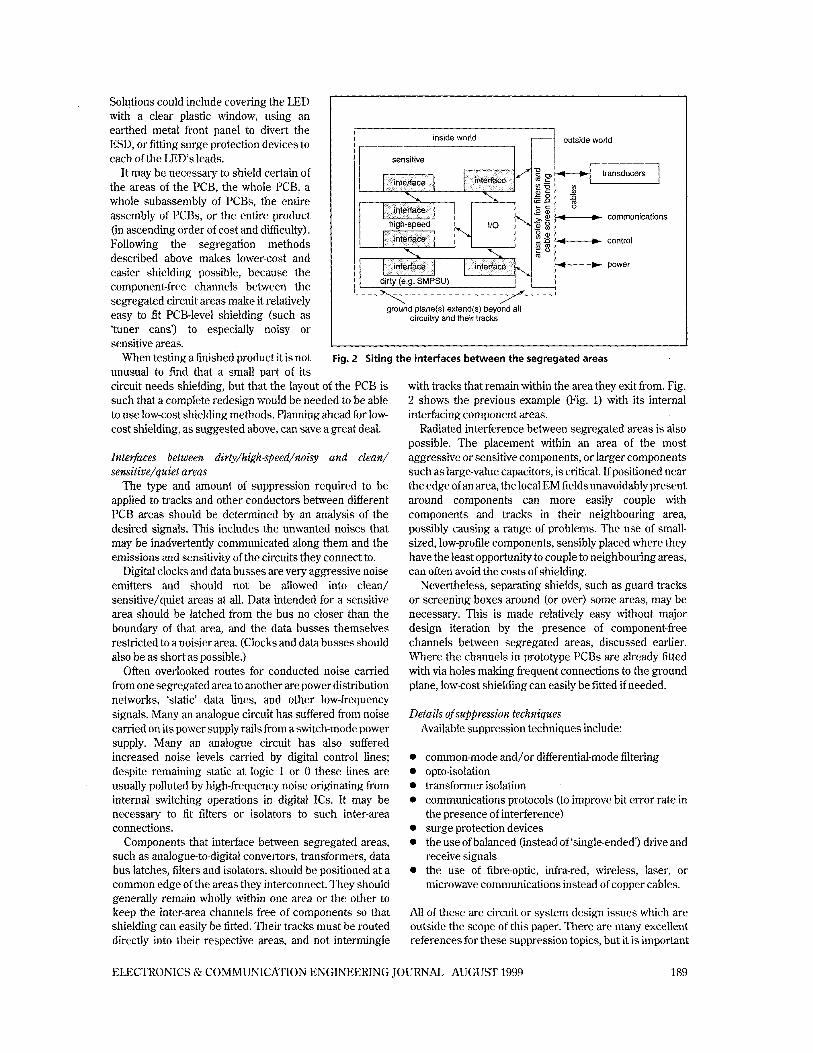
It may be necessary to shield certain of the areas of the PCB, the whole PCB, a whole subassembly of PCBs, the entire assembly of PCBs, or the entire product (in ascending order of cost and difficulty). Following the segregation methods described above makes lowercost and ‘easier shielding possible, because the component-free channels between the segregated circuit areas make it relatively easy to fit PCB-level shielding (such as ‘tuner cans’) to especially noisy or
inside world outside world I I sensitive I I
transducers
communications
control
power I- ground plane(s) extend(s) beyond all
circuitry and their tracks
sensitive areas. When testing a finished product it is not Fig. 2 Siting the interfaces between the segregated areas
unusual to find that a small part of its circuit needs shielding, but that the layout of the PCB is such that a complete redesign would be needed to be able to use low-cost shielding methods. Planning ahead for low- cost shielding, as suggested above, can save a great deal.
Inte~aces between dirty/high-speed/noisy and clean/ sensitiue/quiet areas
The type and amount of suppression required to be applied to tracks and other conductors between different PCB areas should be determined by an analysis of the desired signals. This includes the unwanted noises that may be inadvertently communicated along them and the emissions and sensitivity of the circuits they connect to.
Digital clocks and data busses are very aggressive noise emitters and should not be allowed into clean/ sensitive/quiet areas at all. Data intended for a sensitive area should be latched from the bus no closer than the boundary of that area, and the data busses themselves restricted to a noisier area. (Clocks and data busses should also be as short as possible.)
Often overlooked routes for conducted noise carried from one segregated area to another are power distribution networks, ‘static’ data lines, and other low-frequency signals. Many an analogue circuit has suffered from noise carried on its power supply rails from a switch-mode power supply. Many an analogue circuit has also suffered increased noise levels carried by digital control lines: despite remaining static at logic 1 or 0 these lines are usually polluted by high-frequency noise originating from internal switching operations in digital ICs. It may be necessary to fit filters or isolators to such inter-area connections.
Components that interface between segregated areas, such as analogue-to-digital convertors, transformers, data bus latches, filters and isolators, should be positioned at a common edge of the areas they interconnect. They should generally remain wholly within one area or the other to keep the inter-area channels free of components so that shielding can easily be fitted. Their tracks must be routed directly into their respective areas, and not intermingle
with tracks that remain within the area they exit from. Fig. 2 shows the previous example (Fig. 1) with its internal interfacing component areas.
Radiated interference between segregated areas is also possible. The placement within an area of the most aggressive or sensitive components, or larger components such as large-value capacitors, is critical. If positioned near the edge of an area, the local EM fields unavoidably present around components can more easily couple with components and tracks in their neighbouring area, possibly causing a range of problems. The use of small- sized, low-profile components, sensibly placed where they have the least opportunity to couple to neighbouring areas, can often avoid the costs of shielding.
Nevertheless, separating shields, such as guard tracks or screening boxes around (or over) some areas, may be necessary. This is made relatively easy without major design iteration by the presence of component-free channels between segregated areas, discussed earlier. Where the channels in prototype PCBs are already fitted with via holes making frequent connections to the ground plane, low-cost shielding can easily be fitted if needed.
Details of suppression techniques Available suppression techniques include:
0 common-mode and/or differential-mode filtering 0 opto-isolation 0 transformer isolation 0 communications protocols (to improve bit error rate in
the presence of interference) 0 surge protection devices 0 the use of balanced (instead of ‘single-ended’) drive and
receive signals 0 the use of fibre-optic, infra-red, wireless, laser, or
microwave communications instead of copper cables.
All of these are circuit or system design issues which are outside the scope of this paper. There are many excellent references for these suppression topics, but it is important
ELECTRONICS & COMMUNICATION ENGINEElUNG JOURNAL AUGUST 1999 189
to realise that on a PCB only a ground plane (as described next) can provide a good enough RF reference ground to allow the full performance of filters, cable screens and internal shields to be achieved. Providing a good RF connection to an effective local RF reference plane is one of the secrets of EMC ‘black magic’, without which a perfectly designed, simulated, and expensive filter may provide no benefits, or even make EMC worse.
4 Ground and power planes
It is not possible to use a length of track or wire (or star grounding) as an equipotential ground except for the very lowest frequencies (usually below 1 MHz). Only a solid area of conductor can provide a good ground up to 1 GHz (and beyond), and these are called ground planes.
Ground and power plane techniques allow dramatic reductions in all unwanted EM coupling when used in conjunction with the other techniques described here. Ground planes are also essential for all the other techniques to function properly.
Ground and power plane techniques A high-quality high-frequency ground plane can easily
be created by devoting one layer of the PCB to a solid copper sheet and using it as the 0 V and RF reference ground for all the circuits. Ground planes must lie under all their components and all their associated tracks. Power planes may also be created in the same way as ground planes to provide similar benefits for other common connections. The segregation and interface suppression techniques of Sections 2 and 3 above must be followed even where a common ground plane is used for a number (or all) of the circuit areas.
High-performance circuits using PCBs with more than four layers may need to devote a number of layers to ground planes to use with transmissions lines and for other EMC reasons described later. PCB areas can also be divided up into different ground plane areas, each serving a segregated circuit area as described in Section 2. In these cases the interconnections between the ground planes can
become quite complicated if high-frequency performance is to be maintained, and this is described later.
Most practical PCBs are perforated with via holes, even if they are not also perforated with through-holes for leaded components. These perforations increase the inductance of a ground plane, making it less effective at higher frequencies. ‘Buried via’ techniques have had to be developed for the PCBs used in cellphones, allowing interconnections to occur between tracking layers without the via needing also to perforate the ground plane. The general rule is that any gaps must have dimensions of 0.01h or less at the maximum frequency concerned. For a good ground plane at 1 GHz (e.g. to help meet EU harmonised EMC standards cost-effectively), no ground-plane gap should have any dimensions greater than 1.5 mm. ‘Sneaking’ tracks into a ground plane layer to make layout easier is therefore not allowed.
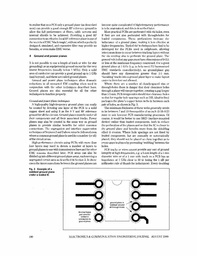
Where there are a number of closely-spaced vias or through-holes there is danger that their clearance holes through a plane will merge together, creating a gap longer than 1.5 mm. PCB design rules should size clearance holes so that for regular hole spacings such as DIL (dual-in-line) packages the plane’s copper forms webs in between each pair of holes, as shown in Fig. 3.
The minimum thickness of these webs generally needs to be between 7 and 10 thousandths of an inch (0.18-0.25 mm) to suit low-cost PCB manufacturing processes. Of course, it would be better to use SMD (surface-mounted device) rather than leaded components, both to reduce the perforation of the planes and so that the IC is closer to the ground plane and benefits more from the shielding effect it creates. Where hole spacings are not fixed by leaded components, but are manually or automatically placed, they should not be placed so close together as to create gaps in planes by preventing ‘webbing’ between the holes.
PCB tracks or wires cannot provide any sort of ground integrity at high frequencies, e.g. a 5 mm length of a 1 mm diameter wire or of a 1 mm wide track on a PCB has an impedance at 1 GHz close to 30 Q (using the 1 nH per millimetre rule of thumb for inductance). Every doubling
Fig. 3 Example of a webbed ground plane under a leaded IC
4 thermal pad used break for
soldered connection to ground plane
ground plane is ‘webbed’ around all through-holes
190 ELECTRONICS & COMMUNICATION ENGINEERING JOURNAL AUGUST 1999

poor
adequate good best
IC connections (Flow soldered SMDs may use several vias to plane underneath the component terminattons themselves
-giving the best possible high-frequency performance)
Fig. 4 Comparison of ground and power plane connection methods for reflow soldered SMD components
of the width of a track will reduce its impedance by only around 20%. Consequently, ‘ground fills’, ‘ground tracks’, ‘guard rings’ and all the other traditional ground techniques used on PCB layers which carry signal or power tracks are all completely ineffective at high frequencies, and at high frequencies might even resonate and make EMC and signal integrity worse. Some PCB CAD (computer-aided design) packages claim to automate the creation of planes, but actually only create useless ‘area fills’.
Tracks, area fills, guard rings, etc. used as grounds on signal layers can be used to good effect at high frequencies - but only when bonded to an underlying ground plane with at least one via hole every 5 to15 mm (using a random allocation of spacings). Signal tracks will get the best benefits from the proximity of a plane if they have awidth of at least 0.7 times (preferably 1 or 2 times) the thickness of the PCB material between them and the plane.
Ground planes should extend as far as possible beyond the boundaries of components and their tracks and power planes. Reference 3 recommends using a ‘20H rule’: ground planes should extend beyond power planes and any tracks by at least 20 times their layer spacing (W. High-speed components (such as digital clocks, processors and memory) and their tracks should always be placed near the centre of their segregated areas, well away from the edges of their ground and power planes. Where it is essential to route a high-speed track close to the edge of its respective ground plane, a guard track should be routed just outside it and on the same layer (bonded frequently with via holes to the edge of the ground plane as described above). Spacing between power and ground planes should be minimised, so they are best run on adjacent PCB layers. Part 2 of this paper will show that this has benefits for power supply decoupling. Reference 4 shows that a spacing of 0-2 mm can reduce emissions by 15 dB compared with a spacing of 1 mm.
All 0 V and power connections must bond directly to their respective ground and power planes. The 0 V and power leads of through-hole components must have their through-plated holes directly connected into their planes using thermal-break pads (sometimes called wagon-wheel pads) to allow their automated soldering, as shown by
Fig. 3. The 0V and power pads of SMDs must be connected to via holes which connect directly into the respective ground and power planes. This is easy for flow-soldered SMDs, but when reflow soldering the vias can suck the solder away from the pad, leaving a dry joint, so plane vias are not usually included in the SMD pads but are positioned nearby and tracked to the pad. The inductance of these tracks has a deleterious effect, so it is vital to use the shortest and fattest tracks possible, whilst taking account of reflow soldering requirements.
Fig. 4 compares alternative methods for connecting SMD components to planes. Where very high-frequency performance is required multiple plane vias and short, fat tracks will help by reducing the inevitable inductance of the tracks and vias. Using an oversized SMD pad with multiple vias to the plane actually in the pad itself (tented over by solder resist to avoid removing solder from the joint) makes a very significant improvement to the high- frequency performance of plane connections5.
Where ground plane connections do not need to be soldered (typical of reflow-soldered SMD components), solid connections to planes should be used. This will give better EMC performance than the use of thermal break connections.
Rectangular ground planes are preferred, as long as their aspect ratio is not extreme (although square plane areas should generally be avoided to minimise the effects of resonances in the plane). Rectangular shapes perform better than exotically shaped ground plane areas or thin, extended areas, and also aid the fitting of PCB-level shielding if it is found to be needed. Sometimes several power planes are placed on one PCB layer, in which case they may need to have complex shapes (avoiding any long or thin areas).
Benefit of using low-profile components with ground planes Ground planes also provide a substantial degree of
volumetric shielding close to their surface and combining them with low-profile components (e.g. SMD, BGA (ball- grid array), TAB (tape automated bonding), chip and wire, etc.) is strongly recommended for the best EMC performance (emissions and immunity).
For example, axial electrolytic capacitors lying close to
ELECTRONICS & COMMUNICATION ENGINEERING JOURNAL AUGUST 1999 19 1

the PCB ground plane are better than taller radial types. To benefit from a useful shielding effect up to 1 GHz, no part of any PCB-mounted components should be more than 10 mm above the ground plane layer, and should be $3 mm for especially high-speed (i.e. most digital clocks, processing, and memory) or sensitive components. No IC sockets should be used, and this often means using field- programmable memory ICs in place of socketed PROMS (programmable read only memories) or ROMs.
Increasingly, modern digital products are only able to function at all by using ground planes and SMD devices. Larger digital ICs are best used in flipchip, TAB, or BGA packages. Quad flat-pack (QFP) , J-lead, and pin-grid-array (PGA) devices are not too much of a liability for EMC if they are soldered directly to the PCB.
Splitting planes Split planes may give either better or worse performance
than unsplit planes, depending strongly on the details of the PCB layout and circuit design6, ’. It may be hard to determine in advance which will give the best performance, so it is recommended here that both options be allowed for, on prototype PCBs at least, by gapping all planes at the natural boundaries between the segregated circuit areas, but also by providing the means to ‘stitch’ them together with pairs of via holes placed along the split every 10 mm or so (random spacing allocation of 5 to 15 mm is preferred). The inevitable stray capacitance ‘shorts out’ the split at very high frequencies, so the benefits of splitting only exist below 1 GHz.
The pairs of vias across plane splits can be linked directly together with short wires, or with small capacitors, so it helps to pitch the via pairs so that small capacitors or ‘zero- ohm links’ may readily be fitted (preferably SMD types). The use of capacitors instead of direct bonds across splits allows the achievement of ‘star grounding’ techniques for wanted low-frequency signals, while achieving the effect of a single overall plane for the best high-frequency performance. Capacitors all have self-resonances (described in Part 2 of this paper), which can worsen performance, but these can be taken into account to improve their performance.
The author has had considerable success with improving signal integrity and noise in mixed technology PCBs using powerful digital processing and sensitive analogue circuits by using a common ground plane for all circuits, but most EMC debate revolves around whether to split the ground plane for the 1/0 interconnection area (see Figs. 1 and 2). Common-mode noise often exists on ground planes, especially for PCBs with digital processing. This is not an issue for the circuits on that PCB, but it is an EMC problem for any wires and cables exiting the PCB. Providing a ‘clean ground plane’ for the interconnection devices and filters is one way of dealing with this. An I/O ground plane split off from the main ground plane must be directly connected to the chassis or shielded enclosure of the connector panel area at multiple points spread over its area (or else by a conductive gasket).
For a split I/O area ground plane to provide the required benefits, all tracks crossing the split must have carefully-
defined return current paths physically adjacent to them, as shown by Fig. 5. The return.path should, if practical, be limited to the bandwidth of the wanted signal. For high- speed signals with no low-frequency content the return path can be a capacitor (chosen to have a suitably low impedance over the frequency range of the signal) connected across the split between the ground planes, adjacent to the signal track. For low-speed signals with no high-frequency content the return path can be a ferrite bead, also bridging the planes and adjacent to the signal track. Some high-rate data streams can also need DC coupling because their data can include low-frequency patterns, and such broadband signals (and DC power supplies) should use an adjacent direct link across the split planes. Balanced signals should need no ground return path, but this depends on the degree of their balance and some adjacent ground bridging may prove necessary. Common-mode chokes fitted to signals and their ground returns may also be used, and may provide advantages over direct links for DC power or broadband signals.
Galvanically isolated planes (e.g. associated with an isolation transformer or optocoupler) will usually benefit from being bridged by a number of low-value capacitors to the main ground plane. Where the isolation is for safety reasons, only suitably rated safety-approved capacitors should be used, and care should be taken not to exceed earth leakage safety requirements.
Testing a prototype PCB for emissions (or immunity) with a close-field EM probe helps obtain the best EMC performance from a split I/O ground plane, although only testing the (almost) finished product in an EMC test laboratory can give definitive results. The first part of the exercise is to make sure that the ground plane bridges associated with the tracks that cross the split are of the optimum type for both the signal and EMC. When this is completed, additional capacitors or links should be added at the spare bond positions to optimise EMC further. Clearly, this can be a time-consuming process if the product needs to be dismantled to make the changes to the PCB.
Connectingground planes to chassis PCB components and tracks have rapidly fluctuating
voltages on them. These will experience weak capacitive coupling to everything in their vicinity (if they are not already fitted with shields soldered to their ground planes). Weak currents inevitably flow in these parasitic capacitances, one cause of common-mode emissions. Very noisy circuits (such as modern computer motherboards), or especially susceptible circuits (e.g. >12 bit analogue resolution), generally need at least a nearby metal plate, and preferably a fully shielded enclosure, to catch and return these leaked currents before they can interact with the outside world.
When such metalwork (or .plated plastic) has been provided, it must be connected to the ground plane of the PCB at many points to encourage as much as possible of the leaked currents to return quickly to their origin on the PCB. Mechanical mountings are usually used for these ’chassis bonds’, but they must be as short as possible
192 ELECTRONICS & COMMUNICATION ENGINEERING JOURNAL AUGUST 1999

panel/chassis/enclosure shield
I , , _ _ _ _ _ _ _ - _ _ _ _ spare bonds every I
!.i E $6
ferrite bead
low- frequency signals or
power
I 1
common-mode
broadband signals
DC coupled or broadband signals,
or power
I I I direct link
J I/Oground I : plane area 1 _ _ _ - - - - - - - _ - I
capacitoi nominal ‘star point’
high-speed signals
any signals or power
Fig. 5 Crossing a split between ground planes
(stand-off pillars taller than 4 mm are not recommended). There should be one chassis bond in the centre of each area of high-speed circuitry, especially clock generators and their distribution. Reference 3 recommends a A/20 rule for the spacing of chassis bonds: maximum spacing between bonds should not exceed 1/20 of the wavelength at the highest frequency of interest. At 1 GHz this rule would result in chassis bonds every 15 mm, which would clearly create significant track layout and assembly difEiculties. For high-speed digital boards aground plane to chassis bond every 75 to 100 mm is recommended.
It is usual to bond the ground planes of digital circuits to the local chassis at each mechanical mounting using an M3 or larger screw in an appropriately-sized plated-through via hole. Where there are concerns about this technique, or where the ground plane must be isolated from chassis for functional reasons (e.g. galvanic isolation), the large vias for the mounting screws should be isolated from the ground planes and provision made for a connection between them to be made using a passive component. Then each individual chassis bond may be connected to its local ground plane with a link, or a capacitor of appropriate type and value, or even left unconnected.
On PCBs which just carry digital processing, direct links at every mounting point are likely to be best. But for analogue (or mixed analogue/digital) boards the ability to vary the type of ground plane-chassis bond can be useful during product development. This technique makes it possible to fit a link at one bonding point whilst fitting the others with appropriate capacitors, so that at low frequencies there is only a single-point connection
between ground plane and chassis (to reduce the flow of DC or 50 Hz ‘earth loop’ currents in the ground plane), whilst at very high frequencies the multiple bonds created by the capacitors help improve EMC. Where ground planes must be galvanically isolated from chassis, capacitors to chassis at each generally provide significant EMC benefits, but care should be taken not to exceed any earth-leakage requirements (e.g. for patient-coupled medical apparatus).
A single link or other component can have enough self- inductance to limit its EMC benefits at very high frequencies. For #is reason surface mount components (being smaller and hence less inductive) are preferred to leaded types, and even so it may be found that an arrangement of three or more components with equal radial spacing around the screw’s via hole is required to reduce their inductance enough to achieve the necessary EMC performance. The track lengths associated with such components should be minimal (refer to Fig. 4).
Interconnecting planes in multi-PCB assemblies Where two or more PCBs are in close proximity and
sharing signals (e.g. card cage systems) there will generally be considerable functional performance and EMC advantages in linking their ground planes together at RF. This is achieved by making frequent short interconnections between the cards’ planes, uniformly distributed along the full length of their common boundary (e.g. via a full-height card connector to a ground plane in the backplane card).
For better RF performance, ground plane
ELECTRONICS & COMMUNICATION ENGINEERING JOURNAL AUGUST 1999 193

and a Group 1 European Engineer since 1988. He is currently chairman of the IEE’s Professional Group (E21 on EMC and also chairman of the IEE’s Working Group on EMC and Functional Safety. Keith started Cherry Clough Consultants in 1990 as an independent company providing EMC and safety services, especially to help companies improve their products and competitiveness by using good engineering practices to achieve EMC and regulatory compliance.
Address: Cherry Clough Consultants, Cherry Clough House, Rochdale Road, Denshaw, OL3 5UE, UK. Email: [email protected]
interconnecting pins or wires should be shorter, have reduced pitch, and be spread over more of the interconnecting boundary. Using one ground-plane link pin alongside every signal or power pin is not excessive, and although it seems expensive it is often the lowest-cost way to reduce the emissions and improve the immunity of a multiple-PCB product. Card-cage and similar systems can also benefit from bonding ground planes together at all card edges, e.g. by means of front panels and/or card guides.
What ifmultilayer PCBs are too costly? It is important to realise that, in volume, four-layer PCBs
now only cost between 20% and 50% more than two-layer boards. Where a ground plane is not used, an enclosure shield (or higher-specification shield) is more likely to be needed, resulting in a higher overall manufacturing cost. Also, the project timescale improvements afforded by the improved signal integrity of these EMC best practices will not materialise. The use of ground planes usually turns out in retrospect to have been the most cost-effective EMC technique, especially when the overall financial break-even time and profitability of a product is considered.
Where the scale of silicon integration used is low, and/or where SMD technology is used, it is possible to get all signal and power tracks of a double-sided PCB onto one side, leaving the other side free for a solid ground plane. This is an appropriate technique for two-layer PCBs. When used for digital products, the lack of a power plane might require a number of ferrite beads (see Part 2) and it may not prove to be the most cost-effective construction.
Where restricting signal and power tracks to one layer of a double-sided PCB is not feasible, signal integrity and EMC become more difficult to achieve. However, useful improvements in the EMC performance of two-layer PCBs without ground planes can be had by ‘gridding’ ground tracks between two tracking layers to reduce inductance. This is often done most easily by using a ‘maximum copper’
or ‘area fill’ on the ground tracks of two layers whose tracks run perpendicularly to each other. This results in many horizontal ground runs on one side, and many vertical runs on the other. As it is, this is useless - the EMC improvements are achieved by ‘stitching’ these horizontal and vertical runs together with vias wherever they cross, to create a grid over the whole area of the components and their tracks. This gridding technique depends upon keeping the longest diagonals of all the grid openings as short as possible, especially underneath the most sensitive or aggressive components. This is often difficult to achieve for through-hole microprocessors and support chips, but less difficult for SMD types. It is usually necessary to spend considerable time shuffling components and tracks around to achieve the required gridding.
Gridded grounds only provide barely adequate ground integrity up to the frequency where the longest grid diagonal equals 1/20th of a wavelength. Remembering that velocity of propagation is roughly 60% of free-space velocity in an FR4 PCB, this implies that a square grid with a 50 mm diagonal could only provide a barely effective ground up to 150 MHz. Gridded grounds also suffer from high resistive impedance, making them significantly less effective than ground planes at any frequency.
Single-sided PCBs are extremely difficult to make EMC compliant for all emissions and immunity phenomena without expensive external shielding, with the exception of circuits which naturally have low emissions (signals with low values of dWdt and dI/dt) and which also have naturally high susceptibility (usually due to high signal levels and low impedances).
References
1 RIDLEY, P.: ‘Implications of the Electromagnetic Compatibility Directive’, Electron. Cummun. Eng.J, October 1995,7, (5), pp. 195-199
2 JACKSON, G. A.: ‘EMC directives and standards’, Eng. Sci. Educ. J., October 1993,2, (5), pp. 225-232
3 MONTROSE, M.: ‘EMC and the printed circuit board: design, theory, and layout made simple’ (IEEE Press, 1999), ISBN 0-
4 OSAMU OENO et al.: ‘Three-dimensional noise current distribution on power and ground planes in printed circuit boards’. IEEE EMC Symposium, Denver, 24th-28th August 1998,2, pp. 1136-1141
5 HUBING, T. H. et al.: ‘Power bus decoupling on multilayer printed circuit boards’, IEEE Trans. Electromagn. Compat., May 1995,37, (Z), pp. 155-166
6 ARCHAMBEAULT, B.: ‘Proper design of intentional splits in the ground reference plane of PC boards to minimise emissions on 1/0 wires and cables’. IEEE EMC Symposium, Denver,
7 MOONGILAN, D.: ‘Grounding optimisation techniques for controlling radiation and crosstalk in mixed signal PCBs’. IEEE EMC Symposium, Denver, 24th-28th August 1998, 1, pp. 495-500
7803-4703-X
24th-28th August 1998,2, pp. 768-773
OIEE, 1999 First received 23rd March 1998 and in final revised form 16th June 1999
194 ELECTRONICS & COMMUNICATION ENGINEERING JOURNAL AUGUST 1999