Design of radio frequency integrated circuits for ultra wide ...
221
"#$%$ &'("')*+ &,-./0 12 )34.1 56,78,09: %0;,/63;,4 (.698.;- 216 <=;63 >.4, ?304 (1@@80.93;.10- &A )1B,6;1 &C3D '6;,/3 %0-;.;8;1 <0.E,6-.;36.1 4, F.961,=,9;6G0.93 *H=.9343 +3- I3=@3- 4, J630 (3036.3K F3:1 LMNL
-
Upload
khangminh22 -
Category
Documents
-
view
1 -
download
0
Transcript of Design of radio frequency integrated circuits for ultra wide ...

!
!
!
!
!
!
!
!
"#$%$!&'("')*+!!
&,-./0!12!)34.1!56,78,09:!%0;,/63;,4!(.698.;-!216!<=;63!>.4,!?304!(1@@80.93;.10-!
!!
!
!
!
!
!
&A!)1B,6;1!&C3D!'6;,/3!%0-;.;8;1!<0.E,6-.;36.1!4,!F.961,=,9;6G0.93!*H=.9343!
+3-!I3=@3-!4,!J630!(3036.3K!F3:1!LMNL!
D/Dª..........................................................................SECRETARIO/A INSTITUTO UNIVERSITARIO DE MICROELECTRONICA APLICADA DE LA UNIVERSIDAD DE LAS PALMAS DE GRAN CANARIA,
CERTIFICA,
Que el Consejo de Doctores del Departamento en su sesión de fecha..................................tomó el acuerdo de dar el consentimiento para su tramitación, a la tesis doctoral titulada “Design of Radio Frequency Integrated Circuits for Ultra Wide Band Communications” presentada por el doctorando D. Roberto Díaz Ortega y dirigida por los doctores D. Francisco Javier del Pino Suárez, D. Sunil Lalchand Khemchandani y D. Antonio Hernández Ballester. Y para que así conste, y a efectos de lo previsto en el Artº 6 del Reglamento para la elaboración, defensa, tribunal y evaluación de tesis doctorales de la Universidad de Las Palmas de Gran Canaria, firmo la presente en Las Palmas de Gran Canaria, a…....de.............................................de dos mil............
Departamento: Instituto Universitario de Microelectrónica Aplicada Programa de doctorado: Doctorado en Tecnologías de Telecomunicación.
Título de la Tesis
Design of Radio Frequency Integrated Circuits for Ultra Wide Band Communications
Tesis Doctoral presentada por D. Roberto Díaz Ortega Dirigida por el Dr. D. Francisco Javier del Pino Suárez Codirigida por el Dr. D. Sunil Lalchand Khemchandani Codirigida por el Dr. D. Antonio Hernández Ballester El Director, Los Codirectores, El Doctorando, (firma) (firma) (firma)
Las Palmas de Gran Canaria, a _____ de_________________ de 20__

“The most incomprehensible thing about our universe
is that it can be comprehended.”
Albert Einstein.
Agradecimientos
Quiero comenzar agradeciendo a mis directores, los doctores Javier del
Pino, Sunil Lalchand y Antonio Hernandez que siempre han estado ahı
ayudandome a encaminar y sacar adelante este trabajo que presento
ahora. Sin lugar a dudas, sin su ayuda los resultados que presento hoy
no habrıan sido posibles.
Tambien quisiera darles las gracias a Hugo, Ruben, Dailos, Jonathan,
Enara y Gustavo, que me han acompanado durante estos anos de trabajo,
porque de una forma u otra tambien estan presentes en este trabajo.
Este trabajo no podrıa haberse llevado a cabo sin la colaboracion del
IUMA que ha puesto a mi alcance todos los medios necesarios para
poder hacer los disenos que se presentan en este trabajo ası como el
instrumental para la medida de los mismos.
Por otro lado quiero agradecer tambien a la Agencia Canaria de Inves-
tigacion Innovacion y Sociedad de la Informacion, que a traves del pro-
grama de movilidad de personal investigador, me permitio llevar a cabo
mi estancia en la Universidad Mons, donde me incorpore al equipo de
trabajo del Dr. Valderrama y el Dr. Dualibe. Quisiera tambien agrade-
cer a ellos el trato que me dieron durante los tres meses de estancia como
si fuera uno mas del equipo.
Para terminar, quiero agradecer a mis padres y a Gema, que son los que
al fin y al cabo me aguantan a diario, pero que gracias a ellos, soy lo que
soy y he llegado hasta aquı gracias a su apoyo incondicional.
Contents
Contents i
List of Figures v
List of Tables xi
1 Introduction 1
1.1 Introduction . . . . . . . . . . . . . . . . . . . . . . . . . . . . . . . . 1
1.2 Objectives . . . . . . . . . . . . . . . . . . . . . . . . . . . . . . . . . 3
1.3 Outline of the Research . . . . . . . . . . . . . . . . . . . . . . . . . . 4
2 Ultra Wide Band Overview and System Approach 5
2.1 Introduction . . . . . . . . . . . . . . . . . . . . . . . . . . . . . . . . 5
2.2 History of Ultra Wide Band Communications . . . . . . . . . . . . . 5
2.3 ECMA-368 / ISO/IEC 26907 Receiver Specifications . . . . . . . . . 7
2.3.1 Operating Frequency Band . . . . . . . . . . . . . . . . . . . . 7
2.3.2 Receiver Sensitivity . . . . . . . . . . . . . . . . . . . . . . . . 9
2.4 Receiver System Design . . . . . . . . . . . . . . . . . . . . . . . . . 9
2.4.1 Noise Figure . . . . . . . . . . . . . . . . . . . . . . . . . . . . 10
2.4.2 Channel Filter and ADC Specifications . . . . . . . . . . . . . 11
2.4.3 ADC and Frontend Gain Specifications . . . . . . . . . . . . . 13
2.4.4 Automatic Gain Control . . . . . . . . . . . . . . . . . . . . . 14
2.4.5 Linearity Requirements . . . . . . . . . . . . . . . . . . . . . . 15

iv CONTENTS
2.4.6 Synthesizer Requirements . . . . . . . . . . . . . . . . . . . . 15
2.4.7 Budget Simulations . . . . . . . . . . . . . . . . . . . . . . . . 16
2.5 Conclusion . . . . . . . . . . . . . . . . . . . . . . . . . . . . . . . . . 19
3 Distributed Amplifiers 21
3.1 Introduction . . . . . . . . . . . . . . . . . . . . . . . . . . . . . . . . 21
3.2 Theoretical Approach . . . . . . . . . . . . . . . . . . . . . . . . . . . 21
3.3 Area Optimization . . . . . . . . . . . . . . . . . . . . . . . . . . . . 25
3.3.1 Compact Design . . . . . . . . . . . . . . . . . . . . . . . . . 25
3.3.2 Stacked Inductors . . . . . . . . . . . . . . . . . . . . . . . . . 27
3.4 Experimental Results . . . . . . . . . . . . . . . . . . . . . . . . . . . 29
3.5 Conclusions . . . . . . . . . . . . . . . . . . . . . . . . . . . . . . . . 34
4 Wide Band Low Noise Amplifiers 37
4.1 Introduction . . . . . . . . . . . . . . . . . . . . . . . . . . . . . . . . 37
4.2 Wide Band Low Noise Amplifier . . . . . . . . . . . . . . . . . . . . . 37
4.2.1 Narrow Band Inductively Degenerated Amplifier . . . . . . . . 37
4.2.2 Wide Band Inductively Degenerated Amplifier . . . . . . . . . 39
4.2.3 Wide Band Low Noise Amplifier Design . . . . . . . . . . . . 41
4.2.4 Experimental Results . . . . . . . . . . . . . . . . . . . . . . . 44
4.3 Flatness Improvement . . . . . . . . . . . . . . . . . . . . . . . . . . 47
4.3.1 Circuit Description . . . . . . . . . . . . . . . . . . . . . . . . 47
4.3.2 Experimental Results . . . . . . . . . . . . . . . . . . . . . . . 49
4.4 Wide Band Folded Cascode Amplifier . . . . . . . . . . . . . . . . . . 50
4.4.1 Narrow Band Folded Cascode Amplifier . . . . . . . . . . . . 52
4.4.2 Wide Band Folded Cascode Amplifier Topology . . . . . . . . 54
4.4.3 Experimental Results . . . . . . . . . . . . . . . . . . . . . . . 55
4.5 Conclusions . . . . . . . . . . . . . . . . . . . . . . . . . . . . . . . . 58
5 Feedback Wide Band Low Noise Amplifiers 59
5.1 Introduction . . . . . . . . . . . . . . . . . . . . . . . . . . . . . . . . 59
5.2 Circuit Analysis . . . . . . . . . . . . . . . . . . . . . . . . . . . . . . 59
5.3 Modified Miniatured 3D Inductor . . . . . . . . . . . . . . . . . . . . 64
5.4 Circuit Design . . . . . . . . . . . . . . . . . . . . . . . . . . . . . . . 66
5.5 Experimental Results . . . . . . . . . . . . . . . . . . . . . . . . . . . 68

CONTENTS v
5.6 Conclusions . . . . . . . . . . . . . . . . . . . . . . . . . . . . . . . . 72
6 Inductorless Techniques 75
6.1 Introduction . . . . . . . . . . . . . . . . . . . . . . . . . . . . . . . . 75
6.2 Common Gate LNA . . . . . . . . . . . . . . . . . . . . . . . . . . . 75
6.2.1 Input Matching and Voltage Gain . . . . . . . . . . . . . . . . 75
6.2.2 Noise of a CG Stage . . . . . . . . . . . . . . . . . . . . . . . 77
6.2.3 Differential Operation of CG Stage . . . . . . . . . . . . . . . 78
6.3 Mixer Design . . . . . . . . . . . . . . . . . . . . . . . . . . . . . . . 78
6.3.1 Quadrature Mixers . . . . . . . . . . . . . . . . . . . . . . . . 78
6.3.2 Mixers with Current Boosting . . . . . . . . . . . . . . . . . . 79
6.4 Inductorless Operation . . . . . . . . . . . . . . . . . . . . . . . . . . 81
6.5 Experimental Results . . . . . . . . . . . . . . . . . . . . . . . . . . . 81
6.5.1 Frontend I . . . . . . . . . . . . . . . . . . . . . . . . . . . . . 81
6.5.2 Frontend II . . . . . . . . . . . . . . . . . . . . . . . . . . . . 82
6.6 Conclusions . . . . . . . . . . . . . . . . . . . . . . . . . . . . . . . . 86
7 Conclusions and Areas for Further Research 89
7.1 Conclusions . . . . . . . . . . . . . . . . . . . . . . . . . . . . . . . . 89
7.2 Areas for Further Research . . . . . . . . . . . . . . . . . . . . . . . . 91
A Resumen en Castellano 93
References 147
B Publications 153
C Other Publications 203

vi CONTENTS

List of Figures
1.1 Veebeam HD system. . . . . . . . . . . . . . . . . . . . . . . . . . . . 2
1.2 Generic receiver architecture. . . . . . . . . . . . . . . . . . . . . . . 3
2.1 WiMedia layers stack. . . . . . . . . . . . . . . . . . . . . . . . . . . 6
2.2 UWB operating bands limitations. . . . . . . . . . . . . . . . . . . . 7
2.3 Direct conversion architecture. . . . . . . . . . . . . . . . . . . . . . . 9
2.4 BER stimation. . . . . . . . . . . . . . . . . . . . . . . . . . . . . . . 11
2.5 Filter requirements. . . . . . . . . . . . . . . . . . . . . . . . . . . . . 12
2.6 System simulations schematic. . . . . . . . . . . . . . . . . . . . . . . 16
2.7 SNR budget simulation. . . . . . . . . . . . . . . . . . . . . . . . . . 17
2.8 Gain budget simulation. . . . . . . . . . . . . . . . . . . . . . . . . . 18
2.9 Noise figure budget simulation. . . . . . . . . . . . . . . . . . . . . . 18
2.10 Linearity budget simulation. . . . . . . . . . . . . . . . . . . . . . . . 19
3.1 Distributed amplifier schematic. . . . . . . . . . . . . . . . . . . . . . 22
3.2 (a) Layout and design parameters for an on-chip spiral inductor. (b)
Simplified lumped-component inductor model. . . . . . . . . . . . . . 25
3.3 (a) Model of two on-chip inductors in series. (b) Simplified model of
two inductors in series. . . . . . . . . . . . . . . . . . . . . . . . . . . 26
3.4 Layouts of series inductors coiled in the same way (a) and in the
opposite way (b). . . . . . . . . . . . . . . . . . . . . . . . . . . . . . 28

viii LIST OF FIGURES
3.5 Influence of mutual coupling in series connected inductors over quality
factor and inductance. . . . . . . . . . . . . . . . . . . . . . . . . . . 28
3.6 Stacked inductor layout. . . . . . . . . . . . . . . . . . . . . . . . . . 29
3.7 Conventional inductor Vs. Stacked inductor. . . . . . . . . . . . . . . 30
3.8 a) DA1: conventional design (0.7 mm2), (b) DA2: compact design
(0.6mm2), (c) DA3: compact design with stacked inductors (0.4mm2). 30
3.9 Inductors employed in the DA. . . . . . . . . . . . . . . . . . . . . . 31
3.10 S21 and noise figure measurements. . . . . . . . . . . . . . . . . . . . 33
4.1 Simplified schematic of the LNA with inductive degeneration. . . . . 38
4.2 Simplified schematic of the LNA with wide band impedance matching
and wide band load. . . . . . . . . . . . . . . . . . . . . . . . . . . . 40
4.3 Schematic of the wide band LNA. . . . . . . . . . . . . . . . . . . . . 41
4.4 (a) Quality factor and inductance of spirals suitable for LB. (b) Power
gain for differents LB. . . . . . . . . . . . . . . . . . . . . . . . . . . 42
4.5 (a) Quality factor and inductance of spirals suitable for LE. (b) Power
gain for differents LE. . . . . . . . . . . . . . . . . . . . . . . . . . . . 43
4.6 (a) Quality factor and inductance of spirals suitable for LS. (b) Power
gain for differents LS. . . . . . . . . . . . . . . . . . . . . . . . . . . . 43
4.7 (a) Quality factor and inductance of spirals suitable for LL. (b) Power
gain for differents LL. . . . . . . . . . . . . . . . . . . . . . . . . . . . 44
4.8 Wide band amplifier layout. . . . . . . . . . . . . . . . . . . . . . . . 45
4.9 Measured and simulated scattering parameters for the designed wide
band LNA. . . . . . . . . . . . . . . . . . . . . . . . . . . . . . . . . 46
4.10 Measured and simulated NF for the designed wide band LNA. . . . . 46
4.11 Wide band LNA simplified schematic with wide band input impedance
matching. . . . . . . . . . . . . . . . . . . . . . . . . . . . . . . . . . 48
4.12 Conventional shunt-peaking load (a) and modified shunt peaking load
(b). . . . . . . . . . . . . . . . . . . . . . . . . . . . . . . . . . . . . . 49
4.13 Photograph of the LNA with the shunt-peaking load and modified
shunt-peaking load respectively. . . . . . . . . . . . . . . . . . . . . . 50
4.14 Measured S-parameters for LNA with shunt-peaking load and modi-
fied shunt-peaking load. . . . . . . . . . . . . . . . . . . . . . . . . . 51
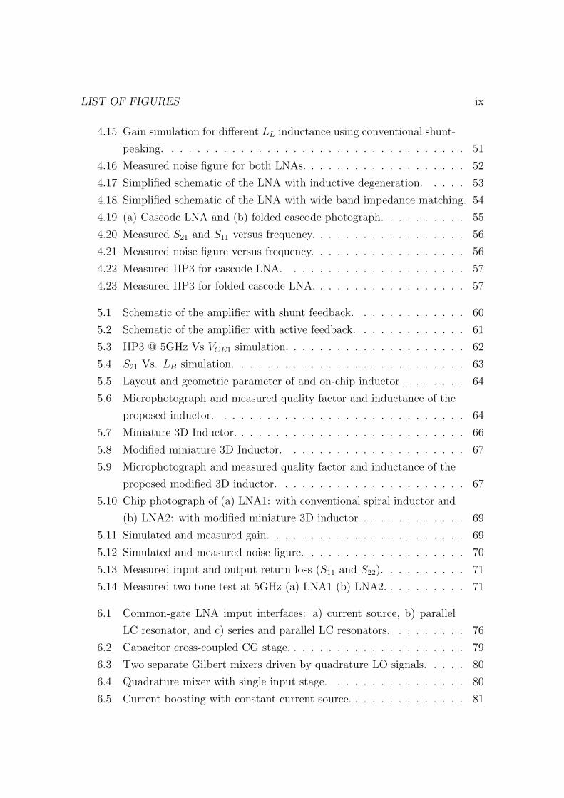
LIST OF FIGURES ix
4.15 Gain simulation for different LL inductance using conventional shunt-
peaking. . . . . . . . . . . . . . . . . . . . . . . . . . . . . . . . . . . 51
4.16 Measured noise figure for both LNAs. . . . . . . . . . . . . . . . . . . 52
4.17 Simplified schematic of the LNA with inductive degeneration. . . . . 53
4.18 Simplified schematic of the LNA with wide band impedance matching. 54
4.19 (a) Cascode LNA and (b) folded cascode photograph. . . . . . . . . . 55
4.20 Measured S21 and S11 versus frequency. . . . . . . . . . . . . . . . . . 56
4.21 Measured noise figure versus frequency. . . . . . . . . . . . . . . . . . 56
4.22 Measured IIP3 for cascode LNA. . . . . . . . . . . . . . . . . . . . . 57
4.23 Measured IIP3 for folded cascode LNA. . . . . . . . . . . . . . . . . . 57
5.1 Schematic of the amplifier with shunt feedback. . . . . . . . . . . . . 60
5.2 Schematic of the amplifier with active feedback. . . . . . . . . . . . . 61
5.3 IIP3 @ 5GHz Vs VCE1 simulation. . . . . . . . . . . . . . . . . . . . . 62
5.4 S21 Vs. LB simulation. . . . . . . . . . . . . . . . . . . . . . . . . . . 63
5.5 Layout and geometric parameter of and on-chip inductor. . . . . . . . 64
5.6 Microphotograph and measured quality factor and inductance of the
proposed inductor. . . . . . . . . . . . . . . . . . . . . . . . . . . . . 64
5.7 Miniature 3D Inductor. . . . . . . . . . . . . . . . . . . . . . . . . . . 66
5.8 Modified miniature 3D Inductor. . . . . . . . . . . . . . . . . . . . . 67
5.9 Microphotograph and measured quality factor and inductance of the
proposed modified 3D inductor. . . . . . . . . . . . . . . . . . . . . . 67
5.10 Chip photograph of (a) LNA1: with conventional spiral inductor and
(b) LNA2: with modified miniature 3D inductor . . . . . . . . . . . . 69
5.11 Simulated and measured gain. . . . . . . . . . . . . . . . . . . . . . . 69
5.12 Simulated and measured noise figure. . . . . . . . . . . . . . . . . . . 70
5.13 Measured input and output return loss (S11 and S22). . . . . . . . . . 71
5.14 Measured two tone test at 5GHz (a) LNA1 (b) LNA2. . . . . . . . . . 71
6.1 Common-gate LNA imput interfaces: a) current source, b) parallel
LC resonator, and c) series and parallel LC resonators. . . . . . . . . 76
6.2 Capacitor cross-coupled CG stage. . . . . . . . . . . . . . . . . . . . . 79
6.3 Two separate Gilbert mixers driven by quadrature LO signals. . . . . 80
6.4 Quadrature mixer with single input stage. . . . . . . . . . . . . . . . 80
6.5 Current boosting with constant current source. . . . . . . . . . . . . . 81
x LIST OF FIGURES
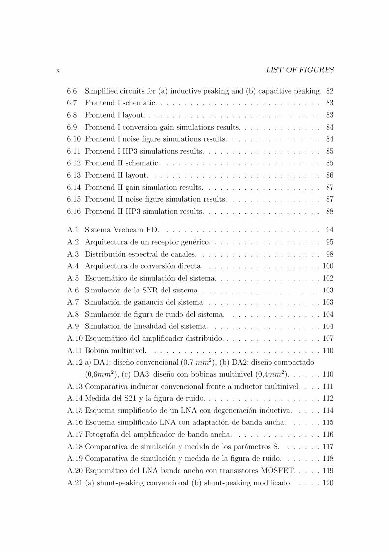
6.6 Simplified circuits for (a) inductive peaking and (b) capacitive peaking. 82
6.7 Frontend I schematic. . . . . . . . . . . . . . . . . . . . . . . . . . . . 83
6.8 Frontend I layout. . . . . . . . . . . . . . . . . . . . . . . . . . . . . . 83
6.9 Frontend I conversion gain simulations results. . . . . . . . . . . . . . 84
6.10 Frontend I noise figure simulations results. . . . . . . . . . . . . . . . 84
6.11 Frontend I IIP3 simulations results. . . . . . . . . . . . . . . . . . . . 85
6.12 Frontend II schematic. . . . . . . . . . . . . . . . . . . . . . . . . . . 85
6.13 Frontend II layout. . . . . . . . . . . . . . . . . . . . . . . . . . . . . 86
6.14 Frontend II gain simulation results. . . . . . . . . . . . . . . . . . . . 87
6.15 Frontend II noise figure simulation results. . . . . . . . . . . . . . . . 87
6.16 Frontend II IIP3 simulation results. . . . . . . . . . . . . . . . . . . . 88
A.1 Sistema Veebeam HD. . . . . . . . . . . . . . . . . . . . . . . . . . . 94
A.2 Arquitectura de un receptor generico. . . . . . . . . . . . . . . . . . . 95
A.3 Distribucion espectral de canales. . . . . . . . . . . . . . . . . . . . . 98
A.4 Arquitectura de conversion directa. . . . . . . . . . . . . . . . . . . . 100
A.5 Esquematico de simulacion del sistema. . . . . . . . . . . . . . . . . . 102
A.6 Simulacion de la SNR del sistema. . . . . . . . . . . . . . . . . . . . . 103
A.7 Simulacion de ganancia del sistema. . . . . . . . . . . . . . . . . . . . 103
A.8 Simulacion de figura de ruido del sistema. . . . . . . . . . . . . . . . 104
A.9 Simulacion de linealidad del sistema. . . . . . . . . . . . . . . . . . . 104
A.10 Esquematico del amplificador distribuido. . . . . . . . . . . . . . . . . 107
A.11 Bobina multinivel. . . . . . . . . . . . . . . . . . . . . . . . . . . . . 110
A.12 a) DA1: diseno convencional (0.7 mm2), (b) DA2: diseno compactado
(0,6mm2), (c) DA3: diseno con bobinas multinivel (0,4mm2). . . . . . 110
A.13 Comparativa inductor convencional frente a inductor multinivel. . . . 111
A.14 Medida del S21 y la figura de ruido. . . . . . . . . . . . . . . . . . . . 112
A.15 Esquema simplificado de un LNA con degeneracion inductiva. . . . . 114
A.16 Esquema simplificado LNA con adaptacion de banda ancha. . . . . . 115
A.17 Fotografıa del amplificador de banda ancha. . . . . . . . . . . . . . . 116
A.18 Comparativa de simulacion y medida de los parametros S. . . . . . . 117
A.19 Comparativa de simulacion y medida de la figura de ruido. . . . . . . 118
A.20 Esquematico del LNA banda ancha con transistores MOSFET. . . . . 119
A.21 (a) shunt-peaking convencional (b) shunt-peaking modificado. . . . . 120
LIST OF FIGURES xi
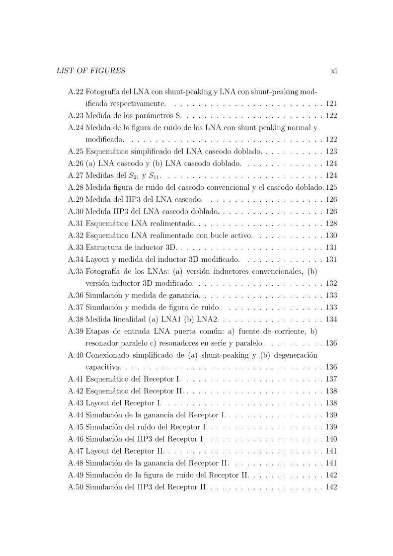
A.22 Fotografıa del LNA con shunt-peaking y LNA con shunt-peaking mod-
ificado respectivamente. . . . . . . . . . . . . . . . . . . . . . . . . . 121
A.23 Medida de los parametros S. . . . . . . . . . . . . . . . . . . . . . . . 122
A.24 Medida de la figura de ruido de los LNA con shunt peaking normal y
modificado. . . . . . . . . . . . . . . . . . . . . . . . . . . . . . . . . 122
A.25 Esquematico simplificado del LNA cascodo doblado. . . . . . . . . . . 123
A.26 (a) LNA cascodo y (b) LNA cascodo doblado. . . . . . . . . . . . . . 124
A.27 Medidas del S21 y S11. . . . . . . . . . . . . . . . . . . . . . . . . . . 124
A.28 Medida figura de ruido del cascodo convencional y el cascodo doblado. 125
A.29 Medida del IIP3 del LNA cascodo. . . . . . . . . . . . . . . . . . . . 126
A.30 Medida IIP3 del LNA cascodo doblado. . . . . . . . . . . . . . . . . . 126
A.31 Esquematico LNA realimentado. . . . . . . . . . . . . . . . . . . . . . 128
A.32 Esquematico LNA realimentado con bucle activo. . . . . . . . . . . . 130
A.33 Estructura de inductor 3D. . . . . . . . . . . . . . . . . . . . . . . . . 131
A.34 Layout y medida del inductor 3D modificado. . . . . . . . . . . . . . 131
A.35 Fotografıa de los LNAs: (a) version inductores convencionales, (b)
version inductor 3D modificado. . . . . . . . . . . . . . . . . . . . . . 132
A.36 Simulacion y medida de ganancia. . . . . . . . . . . . . . . . . . . . . 133
A.37 Simulacion y medida de figura de ruido. . . . . . . . . . . . . . . . . 133
A.38 Medida linealidad (a) LNA1 (b) LNA2. . . . . . . . . . . . . . . . . . 134
A.39 Etapas de entrada LNA puerta comun: a) fuente de corriente, b)
resonador paralelo c) resonadores en serie y paralelo. . . . . . . . . . 136
A.40 Conexionado simplificado de (a) shunt-peaking y (b) degeneracion
capacitiva. . . . . . . . . . . . . . . . . . . . . . . . . . . . . . . . . . 136
A.41 Esquematico del Receptor I. . . . . . . . . . . . . . . . . . . . . . . . 137
A.42 Esquematico del Receptor II. . . . . . . . . . . . . . . . . . . . . . . . 138
A.43 Layout del Receptor I. . . . . . . . . . . . . . . . . . . . . . . . . . . 138
A.44 Simulacion de la ganancia del Receptor I. . . . . . . . . . . . . . . . . 139
A.45 Simulacion del ruido del Receptor I. . . . . . . . . . . . . . . . . . . . 139
A.46 Simulacion del IIP3 del Receptor I. . . . . . . . . . . . . . . . . . . . 140
A.47 Layout del Receptor II. . . . . . . . . . . . . . . . . . . . . . . . . . . 141
A.48 Simulacion de la ganancia del Receptor II. . . . . . . . . . . . . . . . 141
A.49 Simulacion de la figura de ruido del Receptor II. . . . . . . . . . . . . 142
A.50 Simulacion del IIP3 del Receptor II. . . . . . . . . . . . . . . . . . . . 142

xii LIST OF FIGURES

List of Tables
2.1 Band group allocation. . . . . . . . . . . . . . . . . . . . . . . . . . . 8
2.2 Sensitivity versus data rate. . . . . . . . . . . . . . . . . . . . . . . . 9
2.3 Receiver noise figure. . . . . . . . . . . . . . . . . . . . . . . . . . . . 11
2.4 Channel filter and ADC specifications. . . . . . . . . . . . . . . . . . 12
2.5 Minimum receiver gain specifications. . . . . . . . . . . . . . . . . . . 14
2.6 Receiver blocks specifications. . . . . . . . . . . . . . . . . . . . . . . 16
2.7 Budget simulation results. . . . . . . . . . . . . . . . . . . . . . . . . 17
2.8 Low noise amplifier specifications. . . . . . . . . . . . . . . . . . . . . 19
3.1 Calculated components values. . . . . . . . . . . . . . . . . . . . . . . 24
3.2 Inductors Geometrical Parameters. . . . . . . . . . . . . . . . . . . . 31
3.3 Sumary of LNA performance and comparison with previously pub-
lished designs. . . . . . . . . . . . . . . . . . . . . . . . . . . . . . . . 32
3.4 Distributed amplifiers specifications. . . . . . . . . . . . . . . . . . . 34
4.1 Comparison with recently published wide band amplifiers. . . . . . . 47
4.2 Comparison between cascode and folded cascode LNA. . . . . . . . . 58
4.3 Wide band amplifiers specifications. . . . . . . . . . . . . . . . . . . . 58
5.1 Comparative Results. . . . . . . . . . . . . . . . . . . . . . . . . . . . 72
5.2 Wide band feedback amplifiers specifications. . . . . . . . . . . . . . . 72
6.1 Frontends performance summary. . . . . . . . . . . . . . . . . . . . . 86
xiv LIST OF TABLES
7.1 Designed circuits specifications. . . . . . . . . . . . . . . . . . . . . . 90
A.1 Dstribucion de canales. . . . . . . . . . . . . . . . . . . . . . . . . . . 99
A.2 Sensibilidad para las diferentes tasas de transferencia. . . . . . . . . . 100
A.3 Resultados de simulacion del sistema. . . . . . . . . . . . . . . . . . . 102
A.4 Especificaciones del LNA. . . . . . . . . . . . . . . . . . . . . . . . . 105
A.5 Valores de los componentes calculados. . . . . . . . . . . . . . . . . . 109
A.6 Especificaciones de los amplificadores distribuidos. . . . . . . . . . . . 113
A.7 Comparacion entre el cascodo convencional y el cascodo doblado. . . 125
A.8 Especificaciones de los amplificadores desarrollados. . . . . . . . . . . 127
A.9 Especificaciones de los amplificadores. . . . . . . . . . . . . . . . . . . 135
A.10 Resumen de especificaciones de los receptores. . . . . . . . . . . . . . 143
A.11 Especificaciones de los circuitos disenados. . . . . . . . . . . . . . . . 145
1Introduction
1.1 Introduction
In the last years the so-called wireless personal area network (WPAN) systems are
becoming popular replacing cables and enabling new consumer applications. Such
systems are nowadays dominated by standards like Bluetooth and Zigbee, which
operate in the 2.4 GHz ISM band. In order to improve the data rate to several
hundreds of Mb/s with a low power transmission, it has been proposed Ultra Wide
Band (UWB) communications.
Since ultra wide band communications has appeared such as a suitable solution
for high data rate wireless transmission, a great number of companies have focused
their effort to develop commercial solutions based on it. Some examples of these
companies could be the following:
Alereon [1]: Alereon is a fabless semiconductor company based on Austin
(Texas) which develops high-bandwidth, high-performance low-power CertifiedWire-
less USB and WiMedia ultra wide band chipsets. One of their products is the
AL5100/AL5301 Worldwide ultra wide band Chipset.
The Alereon AL5100 transceiver integrates sensitive analog frontend components
including synthesizer VCO/PLL, anti-alias filters, LNAs, PAs, and transmit/receive
(T/R) switches it supports a single-ended connection to the antenna eliminating
external baluns. When combined with the Alereon AL5301 BBP/MAC, the AL5100
RF transceiver supports all current mandatory WiMedia specifications for worldwide
band groups 1, 3, 4, and 6.
Wisair [2]: Wisair is a fabless semiconductor company based on Israel which
2
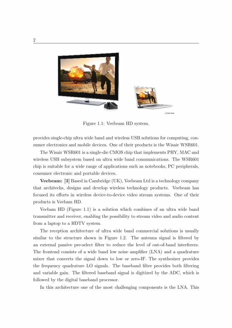
Figure 1.1: Veebeam HD system.
provides single-chip ultra wide band and wireless USB solutions for computing, con-
sumer electronics and mobile devices. One of their products is the Wisair WSR601.
The Wisair WSR601 is a single-die CMOS chip that implements PHY, MAC and
wireless USB subsystem based on ultra wide band communications. The WSR601
chip is suitable for a wide range of applications such as notebooks, PC peripherals,
consumer electronic and portable devices.
Veebeam: [3] Based in Cambridge (UK), Veebeam Ltd is a technology company
that architechs, designs and develop wireless technology products. Veebeam has
focused its efforts in wireless device-to-device video stream systems. One of their
products is Veebam HD.
Veebam HD (Figure 1.1) is a solution which combines of an ultra wide band
transmitter and receiver, enabling the possibility to stream video and audio content
from a laptop to a HDTV system.
The reception architecture of ultra wide band commercial solutions is usually
similar to the structure shown in Figure 1.2. The antenna signal is filtered by
an external passive pre-select filter to reduce the level of out-of-band interferers.
The frontend consists of a wide band low noise amplifier (LNA) and a quadrature
mixer that converts the signal down to low or zero-IF. The synthesizer provides
the frequency quadrature LO signals. The baseband filter provides both filtering
and variable gain. The filtered baseband signal is digitized by the ADC, which is
followed by the digital baseband processor.
In this architecture one of the most challenging components is the LNA. This
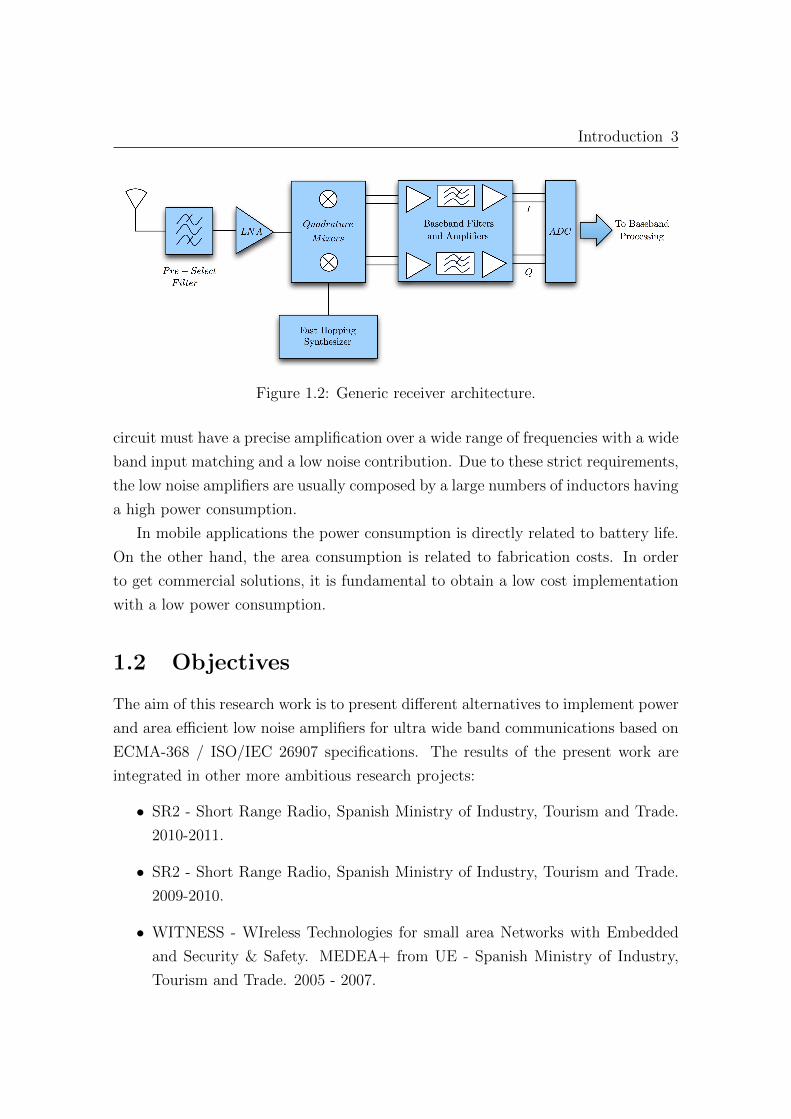
Introduction 3
Figure 1.2: Generic receiver architecture.
circuit must have a precise amplification over a wide range of frequencies with a wide
band input matching and a low noise contribution. Due to these strict requirements,
the low noise amplifiers are usually composed by a large numbers of inductors having
a high power consumption.
In mobile applications the power consumption is directly related to battery life.
On the other hand, the area consumption is related to fabrication costs. In order
to get commercial solutions, it is fundamental to obtain a low cost implementation
with a low power consumption.
1.2 Objectives
The aim of this research work is to present different alternatives to implement power
and area efficient low noise amplifiers for ultra wide band communications based on
ECMA-368 / ISO/IEC 26907 specifications. The results of the present work are
integrated in other more ambitious research projects:
• SR2 - Short Range Radio, Spanish Ministry of Industry, Tourism and Trade.
2010-2011.
• SR2 - Short Range Radio, Spanish Ministry of Industry, Tourism and Trade.
2009-2010.
• WITNESS - WIreless Technologies for small area Networks with Embedded
and Security & Safety. MEDEA+ from UE - Spanish Ministry of Industry,
Tourism and Trade. 2005 - 2007.
4
In order to achieve the objective, the following milestones have been determined
and achieved:
1. From the ECMA-368 / ISO/IEC 26907 is important obtain a reference system
in order to stablish the low noise amplifier specification.
2. Explore different alternatives to implement low noise amplifiers for ultra wide
band in order to optimize the power and area consumption.
3. Explore different inductors structures in order to reduce the area consumption.
4. Explore the inductorless techniques to avoid the use of inductors in order to
reduce the area consumption.
1.3 Outline of the Research
This work consists of seven chapters, which are briefly outlined in this section.
Chapter 1 (the current chapter) introduces the reader to ultra wide band com-
munications, shows some commercial implementations and outlines the research
objectives. After getting an insight into the research context, the system design
is presented in Chapter 2. In this chapter the main requirements of ECMA-368 /
ISO/IEC 26907 are presented. With those requirements a reference system is de-
signed and the low noise amplifier specifications are extracted. Chapter 3 is devoted
to the most classical wide band amplifier architecture, the distributed amplifiers. Af-
ter this first approach and with the objective of solving the distributed amplifiers
drawbacks, in Chapter 4 different implementations of wide band low noise amplifier
are presented. In order to continue improving the area and power consumption,
in Chapter 5 feedback techniques and some inductors structures suited for that
topologies are explored. Chapter 6 is devoted to explore inductorless techniques to
improve the area saving of low noise amplifiers. Finally some conclusions and areas
for further research are presented in Chapter 7.

2Ultra Wide Band Overview and System Approach
2.1 Introduction
As a starting point of this work, this chapter will cover a study about ECMA-368 /
ISO/IEC 26907 specification.
After a brief summary about the history and the main specifications adopted by
the standard, a receiver system analysis will be developed. This process will take
into account the restrictions and specifications imposed by the standard.
The obtained receiver specifications will be taken as a reference point for the
circuits designed in the rest of the work.
2.2 History of Ultra Wide Band Communications
The origins of UWB technology has been established around 1962 and it was referred
to impulse radio or baseband carrier-free communications. However, the term “ultra
wide band” was first used in 1989 in a patent document by U.S. defence department.
In 2002, the Federal Communications Commission (FCC), with the inform 02-
48, allocates an unlicensed radio spectrum from 3.1 GHz to 10.6 GHz. In order
to define a device as an UWB device, it must be considered that channels have
to occupy a band greater than 20 percent of the centre frequency or a minimum
channel bandwidth of 500 MHz.
After the first attempt of standardization by the FCC, the MultiBand OFDM
Alliance (MBOA), was established in 2003. It is dedicated to promoting the global
standard for ubiquitous UWB wireless solutions. The MBOA created a complete

6
Figure 2.1: WiMedia layers stack.
specification for a Physical Layer (PHY) and a Media Access Controller layer (MAC).
In parallel to the MBOA, in January of 2003 was created the IEEE 802.15.3a task
group in order to study the possibility of using the new FCC spectrum specifications
in wireless local area networks and personal area networks.
Outside the IEEE 802.15.3a, different companies formalized their relationships
to provide a legal context. From this formalization, in 2004 the WiMedia Alliance
was born to promote wireless connectivity and interoperability among multimedia
devices. The objective of WiMedia is developing a common abstraction platform as
shown in Figure 2.1, which enable multiple applications to run over one common
radio. The WiMedia radio platform is based technically on MB-OFDM specifica-
tions. The combination of MB-OFDM and this convergence platform allows the
implementation of wireless version of USB, IEEE 1394, DLNA and other IP-based
application protocols.
On January 2006, after three years of a jammed process, the IEEE 802.15.3a
was abandoned without conclusion. At this moment, without the support of the
IEEE, the WiMedia Alliance had to seek for a new alternative to standardize UWB
communications. After this process of seeking and hard work, in 2007 was approved
the first version of standard ECMA-368 / ISO/IEC 26907 that regulate the UWB
communications at Physical and Media Access Controller layers.
Ultra Wide Band Overview and System Approach 7
2.3 ECMA-368 / ISO/IEC 26907 Receiver Spec-
ifications
2.3.1 Operating Frequency Band
The physical layer operates in a frequency range from 3.1 to 10.6 GHz. The relation-
ship between the centre frequency (fc) and the channel number (BAND ID number
or nb) is given by Equation 2.1.
fc(nb) = 2904 + 528 · nb MHz where nb = 1, ..., 14 (2.1)
Figure 2.2: UWB operating bands limitations.
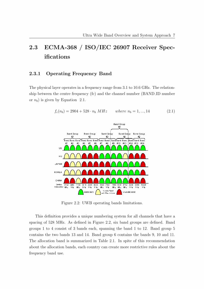
This definition provides a unique numbering system for all channels that have a
spacing of 528 MHz. As defined in Figure 2.2, six band groups are defined. Band
groups 1 to 4 consist of 3 bands each, spanning the band 1 to 12. Band group 5
contains the two bands 13 and 14. Band group 6 contains the bands 9, 10 and 11.
The allocation band is summarized in Table 2.1. In spite of this recommendation
about the allocation bands, each country can create more restrictive rules about the
frequency band use.

8
BandGroup
BandID(nb)
LowerFrequency(MHz)
CenterFrequency(MHz)
UpperFrequency(MHz)
1 1 3168 3432 36962 3696 3960 42243 4224 4488 4752
2 4 4752 5016 52805 5280 5544 58086 5808 6072 6336
3 7 6336 6600 68648 6864 7128 73929 7392 7656 7920
4 10 7920 8184 844811 8448 8712 897612 8976 9240 9504
5 13 9504 9768 1003214 10032 10296 10560
6 9 7392 7656 792010 7920 8184 844811 8448 8712 8976
Table 2.1: Band group allocation.

Ultra Wide Band Overview and System Approach 9
Figure 2.3: Direct conversion architecture.
2.3.2 Receiver Sensitivity
For a Packet Error Rate (PER) of less than 8% with a Physical layer Service Data
Unit (PSDU) of 1024 octets, the minimum receiver sensitivity numbers with a Ad-
ditive White Gaussian Noise (AWGN) for the different data rates are listed in Table
2.
Data Rate (Mb/s) Sensitivity (dBm)
53.3 -80.8
80 -78.9
106.6 -77.8
160 -75.9
200 -74.5
320 -72.8
400 -71.5
480 -70.4
Table 2.2: Sensitivity versus data rate.
2.4 Receiver System Design
Due to the huge channel bandwidth, a direct conversion receiver architecture has
been chosen. Figure 2.3 shows the direct conversion receiver diagram block, where
the LO frequency is equal to the input carrier frequency. Note that channel selection
requires only a low pass filter with relative sharp cut-off characteristics.
This architecture has several issues. First, in a direct conversion topology, the

10
down converted band extends to zero frequency. As a result, offset voltages can
corrupt the signal and saturate the following stages. This issue is also related to the
LO leakage because the LO radiation could appear as a DC voltage at the receiver
output. Second, as shown in Figure 2.3, phase and frequency modulation requires
shifting either RF or LO signal output by 90o. This shifting generally introduces
errors and noise. Due to this error I/Q mismatches could appear, thereby raising
the bit error rate. Third, in baseband, the even-order harmonics could be into
the desired channel. Fourth, due to the desired channel is translated directly to
baseband, the Flicker noise could affect the signal.
On the contrary, the simplicity of the direct conversion architecture offers two
important advantages. First, the problem of the image frequency does not ap-
pears. As a result, no image filter is required. Second, the IF-SAW filter and other
down-conversion stages, used for instance in heterodyne receivers, are replaced with
low-pass filters and baseband amplifiers, so this architecture is more suitable for a
monolithic integration with a relatively low area and low power consumption.
2.4.1 Noise Figure
As shown in previous section, the ECMA-368 / ISO/IEC 26907 specifies a sensitivity
of -70.4 dBm (Sin) for the highest data rate of 480 Mb/s (R) and a sensitivity of -
80.8 dBm for the lowest data rate (53.3 Mb/s) with a channel bandwidth of 528MHz
(BW). The noise figure is defined as the degradation of the signal to noise ratio as
it is shown in Equation 2.2:
NF = SNRin − SNRout (2.2)
Where,
SNRin = Sin − (174 + 10 · log(BW )) (2.3)
SNRout =
Eb
N0
dB
+
R
BW
dB
(2.4)
In order to obtain the value of energy per bit to noise power spectral density
ratio (Eb/N0), the standard defines a QPSK modulation for each sub-carrier and a
Ultra Wide Band Overview and System Approach 11
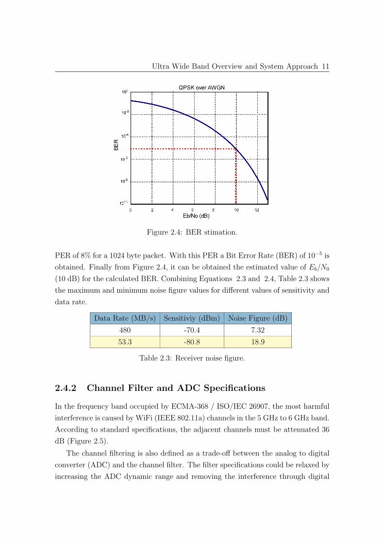
Figure 2.4: BER stimation.
PER of 8% for a 1024 byte packet. With this PER a Bit Error Rate (BER) of 10−5 is
obtained. Finally from Figure 2.4, it can be obtained the estimated value of Eb/N0
(10 dB) for the calculated BER. Combining Equations 2.3 and 2.4, Table 2.3 shows
the maximum and minimum noise figure values for different values of sensitivity and
data rate.
Data Rate (MB/s) Sensitiviy (dBm) Noise Figure (dB)
480 -70.4 7.32
53.3 -80.8 18.9
Table 2.3: Receiver noise figure.
2.4.2 Channel Filter and ADC Specifications
In the frequency band occupied by ECMA-368 / ISO/IEC 26907, the most harmful
interference is caused by WiFi (IEEE 802.11a) channels in the 5 GHz to 6 GHz band.
According to standard specifications, the adjacent channels must be attenuated 36
dB (Figure 2.5).
The channel filtering is also defined as a trade-off between the analog to digital
converter (ADC) and the channel filter. The filter specifications could be relaxed by
increasing the ADC dynamic range and removing the interference through digital
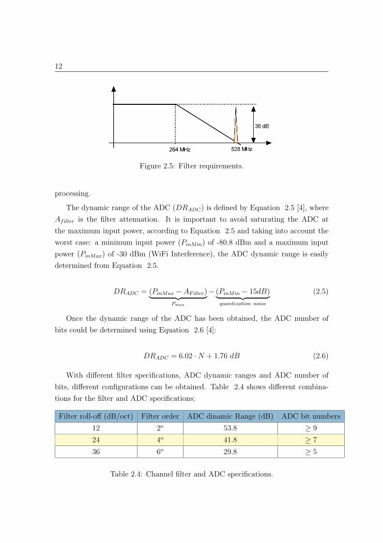
12
Figure 2.5: Filter requirements.
processing.
The dynamic range of the ADC (DRADC) is defined by Equation 2.5 [4], where
Afilter is the filter attenuation. It is important to avoid saturating the ADC at
the maximum input power, according to Equation 2.5 and taking into account the
worst case: a minimum input power (PinMin) of -80.8 dBm and a maximum input
power (PinMax) of -30 dBm (WiFi Interference), the ADC dynamic range is easily
determined from Equation 2.5.
DRADC = (PinMax − AFilter) Pmax
− (PinMin − 15dB) quantization noise
(2.5)
Once the dynamic range of the ADC has been obtained, the ADC number of
bits could be determined using Equation 2.6 [4]:
DRADC = 6.02 ·N + 1.76 dB (2.6)
With different filter specifications, ADC dynamic ranges and ADC number of
bits, different configurations can be obtained. Table 2.4 shows different combina-
tions for the filter and ADC specifications:
Filter roll-off (dB/oct) Filter order ADC dinamic Range (dB) ADC bit numbers
12 2o 53.8 ≥ 9
24 4o 41.8 ≥ 7
36 6o 29.8 ≥ 5
Table 2.4: Channel filter and ADC specifications.
Ultra Wide Band Overview and System Approach 13
According to the standard specifications, the maximum input power is -41 dBm
for a desired in-band signal. In the worst case, the maximum dynamic range is 39.8
dB. In consequence, in Table 2.4 the third configuration must be rejected because
in this configuration the ADC will be saturated with the input power worst case.
2.4.3 ADC and Frontend Gain Specifications
The quantization noise is given by [4]:
NQ =(VFS
2N )2
12 · ( 2·fsfbW
) ·Ro
=(VFS
2N )2
12 · p · ρo(2.7)
Expressed in dBm with Ro = 50 Ω, the quantization noise results in:
NQ = −6.02 ·N + 20 · log(VFS)− 10 · log(ρ) + 2.2 dBm (2.8)
where, VFS is the ADC full range voltage input, N is the ADC number of bits and
ρ is the oversampling factor expressed as ρ = 2 · fs/BW . Considering a VFS of 2V
the quantization noise is given by:
NQ = −6.02 ·N − 10 · log(p) + 8.22 (2.9)
On the other hand, the output thermal noise is given by the following expression:
NT = −174 + 10 · log(BW ) +Gmax +NF = Gmax − 79.77 (2.10)
Combining Equations 2.9 and 2.10 and taking into account that NT = NQ+15,
The minimum total gain of the receiver could be expressed as:
Gmin = −6.02 ·N − 10 · log(p) + 102.99 (2.11)
In Table 2.5, the gain values for different oversampling factors and ADC number
of bits are shown.
14
ADC bits Oversampling factor (p) Gmin (dB)
7 1 60.86
2 57.86
9 1 48.81
2 45.81
Table 2.5: Minimum receiver gain specifications.
2.4.4 Automatic Gain Control
In the previous section, the minimum gain value has been determined to obtain a
quantization noise level 15 dB less than the thermal noise. However, the calculated
gain values could saturate the ADC input. The maximum power level at the ADC
input is given by:
PADC =
VFS2
2 ∗R0
2
= 10 mW ⇒ 10 dBm (2.12)
In consequence, in order to avoid to saturate the ADC, the system should satisfy
the following expression:
SImax +Gmin ≤ 10 dBm (2.13)
In the worst case, the maximum desired input power (SImax) is -41 dBm. Under
this condition, the maximum permitted gain for the entire reception chain should
be less than 51 dB because with this gain value, the power level at ADC input is 10
dBm. As it can be observed in Table 2.5, the ADC number of bits should be fixed
at least to 9 bits, because with this number of bits, the minimum system gain is less
than the maximum permitted gain at the ADC input.
On the other hand, to obtain the maximum receiver gain, the ADC dynamic
range should be considered. From Table 2.4, an ADC of 9 bits should have a
dynamic range of 53.8 dB. The ADC dynamic range is defined by the following
expression:
∆AGC = SImax − SImin (2.14)
Table 2.5, shows the receiver gain specifications, as mentioned above, the maxi-
mum power level at the ADC input is 10 dBm so, from Equation 2.14, the minimum

Ultra Wide Band Overview and System Approach 15
ADC input signal level is: -43.8 dBm. On the other hand, for the weak signal and
the minimum gain established in 48.81 dB, so in this condition the power level at
the ADC input is -32dBm.
As a conclusion from the previous results, the AGC is not needed because in
the minimum and maximum input power level condition, the ADC input is not
saturated.
2.4.5 Linearity Requirements
The interference scenario is dominated by IEEE 802.11a. In a typical case, a IEEE
802.11a channel at a distance of 0.2m could reach a power level of -31.9 dBm. This
interference should coexist with a desired ECMA-368 / ISO/IEC 26907 signal with
a power level of -80.8 dBm. From this interference scenario, the linearity is defined
by the following expression:
IIP3 = Sdesired +3
2· (Sinterference − Sdesired) ⇒ IIP3 ≥ −8.65 dBm (2.15)
where Sdesired is the desired signal power and Sinterference is interference signal power.
2.4.6 Synthesizer Requirements
As the radio has to cover the six bands defined in the ECMA-368 / ISO/IEC 26907
and a zero-IF architecture is proposed, the synthesizer should provide the center
frequencies of the bands shown in Table 2.1.
In the MBOA proposal, frequency hopping between sub-bands occurs once every
symbol period of 312.5 ns. This period contains a 60.6 ns suffix, which is followed
by a 9.5 ns guard interval. The frequency generator used to drive the switching core
of both, the down-conversion mixer in the receive path and up-conversion mixer in
the transmit path, needs to switch within this 9.5 ns to accomplish the frequency
hopping.
The demands on the purity of the generated carriers are also very stringent due
to the presence of strong interferer signals. For example, for Mode 1 operation all
spurious tones in the 5 GHz range must be below 50 dBc to avoid down-conversion
of strong out-of-band Wireless LAN (WLAN) interferers into the wanted bands. For
16
Figure 2.6: System simulations schematic.
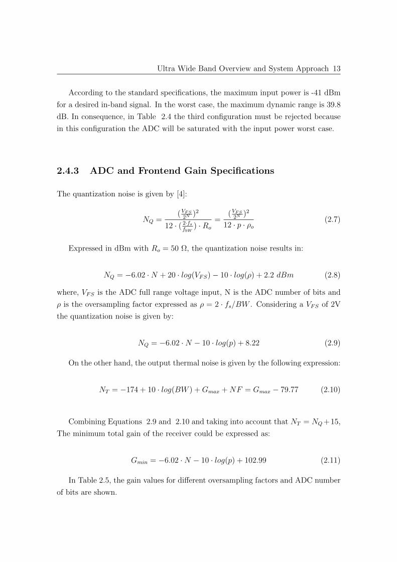
Component Gain (dB) Noise Figure (dB) IIP3 (dBm)LNA 15 3 -20Mixer 20 12 -9
Baseband filter -3 3 -Baseband amplifier 19 25 -8
Table 2.6: Receiver blocks specifications.
the same reason, the spurious tones in the 2 GHz range should be below 45 dBc
to allow co-existence with the systems operating in the 2.4 GHz ISM band, such as
802.11 b/g and Bluetooth.
Finally, to ensure that the system SNR will not be degraded by more than 0.1 dB
due to the LO generation, the VCO phase noise specification is set to 100 dBc/Hz
at 1 MHz offset and the overall integrated phase noise should not exceed 3.5 degrees
rms [5, 6].
2.4.7 Budget Simulations
In order to obtain the receiver block specifications, the simulation tool ADS has
been used. The budget simulation checks the receiver chain performance to verify
that the specifications of each block of the receiver allow to the entire reception
chain to fulfil the specifications stated in above sections.
As starting point, a first assumption for each block parameter has been set, with
the help of the state of art and the design group experience. The final value of the
specifications have been set using the simulation tool ADS with the budget analysis
and a iterative simulation process. Figure 2.6 shows the simulation schematic for
the budget analysis. It can be observed how the entire receiver chain follows the
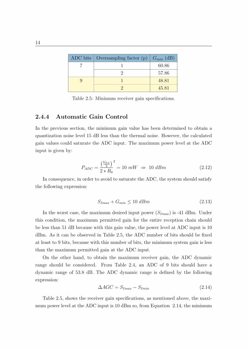
Ultra Wide Band Overview and System Approach 17
Receiver parameter Specification Budget simulationSensitive (dBm) -80.8 -85Noise Figure (dB) 7.32 7.27
Gain (dB) 48.81 50.9Maximum input level (dBm) -41 -35
IIP3 (dBm) -8.65 -8.15
Table 2.7: Budget simulation results.
Figure 2.7: SNR budget simulation.
schematic shown in Figure 2.3.
Table 2.6 summarizes the final specifications of each receiver component, ob-
tained from simulations. As it can be observed in Table 2.7, the budget simulation
results are compliant with the global receiver requirements.
Figure 2.7 shows the SNR variation through the receiver. Obviously, at the
receiver input, the SNR is the highest; however as the signal moves through the
receiver chain, it is corrupted by noise and in consequence the SNR drops. The
difference between the SNR at the input and output of the receiver is the noise
figure. In this case, there is a different between input and output of 7.2 dB.
Figure 2.8 shows the gain contribution of each block to the entire receiver. As it
can be observed, the gain specification is divided equally between the LNA, the mixer
and the baseband amplifier. This situation provides a relaxed scenario for circuit
designers because if one block does not reach the proposed gain, this situation could
be solved increasing the gain in a subsequent block.
As it can be observed in Figure 2.9, the noise figure contribution depends mainly
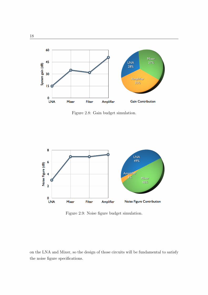
18
Figure 2.8: Gain budget simulation.
Figure 2.9: Noise figure budget simulation.
on the LNA and Mixer, so the design of those circuits will be fundamental to satisfy
the noise figure specifications.
Ultra Wide Band Overview and System Approach 19
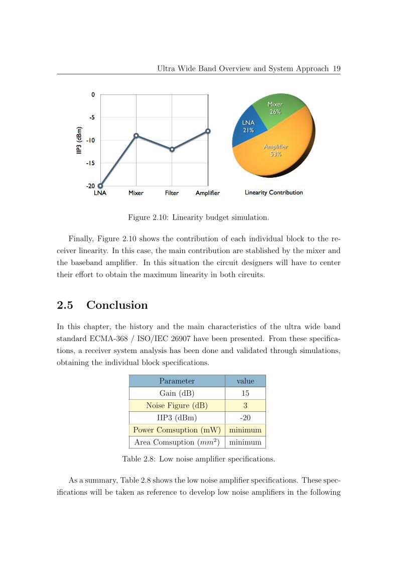
Figure 2.10: Linearity budget simulation.
Finally, Figure 2.10 shows the contribution of each individual block to the re-
ceiver linearity. In this case, the main contribution are stablished by the mixer and
the baseband amplifier. In this situation the circuit designers will have to center
their effort to obtain the maximum linearity in both circuits.
2.5 Conclusion
In this chapter, the history and the main characteristics of the ultra wide band
standard ECMA-368 / ISO/IEC 26907 have been presented. From these specifica-
tions, a receiver system analysis has been done and validated through simulations,
obtaining the individual block specifications.
Parameter value
Gain (dB) 15
Noise Figure (dB) 3
IIP3 (dBm) -20
Power Comsuption (mW) minimum
Area Comsuption (mm2) minimum
Table 2.8: Low noise amplifier specifications.
As a summary, Table 2.8 shows the low noise amplifier specifications. These spec-
ifications will be taken as reference to develop low noise amplifiers in the following
20
chapters.
The next chapter is devoted to the distributed amplifier, one of the most classical
structure to develop wide band low noise amplifiers.
3Distributed Amplifiers
3.1 Introduction
The design of low noise amplifiers for ultra wide band communications has a big
challenge to solve, the huge bandwidth.
Distributed amplifiers is the first approach to obtain a low noise amplifier for
ultra wide band systems. With this structure a high bandwidth with a relative low
noise and a moderate gain can be obtained.
3.2 Theoretical Approach
The frequency response of a MOS device degrades due to the pole formed by the
input/output capacitance of the transistor and the resistance it sees. The MOS-
FET’s transconductance rapidly falls with frequency and any attempt to increase
the transconductance by increasing the size of the device will also increase its in-
put/output capacitance. Thus, while low-frequency gain has been increased, the
gain-bandwidth product remains about the same. The distributed amplification
(DA) was proposed to overcome this limitation.
Distributed amplifier employs a topology in which the gain stages are connected
such that their capacitances are separated, yet the output currents still combine
in an additive fashion (Figure 3.1). Series inductive elements are used to sepa-
rate capacitances at the inputs and outputs of adjacent gain stages. The resulting
topology, given by the interlaying series inductors and shunt capacitances, forms
a lumped-parameter artificial transmission line. The additive nature of the gain
22
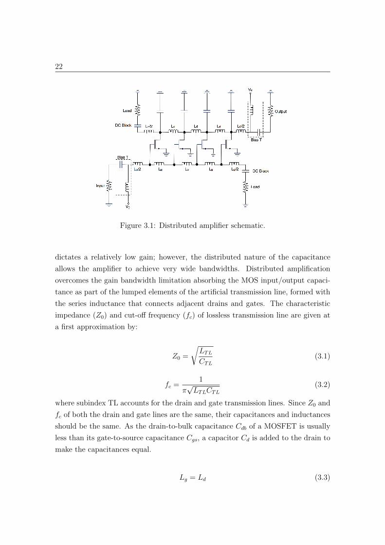
Figure 3.1: Distributed amplifier schematic.
dictates a relatively low gain; however, the distributed nature of the capacitance
allows the amplifier to achieve very wide bandwidths. Distributed amplification
overcomes the gain bandwidth limitation absorbing the MOS input/output capaci-
tance as part of the lumped elements of the artificial transmission line, formed with
the series inductance that connects adjacent drains and gates. The characteristic
impedance (Z0) and cut-off frequency (fc) of lossless transmission line are given at
a first approximation by:
Z0 =
LTL
CTL
(3.1)
fc =1
π√LTLCTL
(3.2)
where subindex TL accounts for the drain and gate transmission lines. Since Z0 and
fc of both the drain and gate lines are the same, their capacitances and inductances
should be the same. As the drain-to-bulk capacitance Cdb of a MOSFET is usually
less than its gate-to-source capacitance Cgs, a capacitor Cd is added to the drain to
make the capacitances equal.
Lg = Ld (3.3)
Distributed Amplifiers 23
Cgs = Cdb + Cd (3.4)
As the amplified signals at each stage travels towards the load, the signal gets
attenuated due to non-zero losses associated with the transmission lines. Finite
inductors quality factor (Q) are the primary source of losses in the gate line. Losses
in the drain line can be attributed to lossy inductors Ld and the drain-to-source
resistance (rds). The gain of the DA can be expressed as [7]:
A = −gmZ0
2
1−
f
fc
2.e−N
(Ag+Ad)2 .sinh
N Ad−Ag
2
sinhN Ad−Ag
2
(3.5)
where Ad and Ag are the attenuation of the drain and gate lines, gm is the MOSFET
transconductance and N is the total number of stages. This equation assumes the
following:
• Unilateral MOSFET model (ignores Cgd).
• Image impedance matched terminations.
• Equal gate and drain phase velocities.
The optimum number of stages that maximizes the gain is a function of gate and
drain line attenuation. Those attenuations are complex functions and depend on
the specific MOSFET parameters and also on the operating and cut-off frequencies.
As the signal propagates along the gate line towards the termination, less signal
is available for each MOSFET because of attenuation and, as a consequence, the
overall gain degrades with further increase in the number of stages. The number of
stages for this work is chosen as 4.
Knowing the gain, number of stages, and drain-line inductance and capacitance,
the required gm can be found from the low frequency gain using Equation 3.5:
gm =2.A
N
Cd
Ld
⇒ gm =2.A
N.Z0(3.6)
Then, the transistor width-length ratio can be derived from:
W
L=
gmµnCox(Vgs − VT )
(3.7)
24
Component ValueLg = Ld 1.465 nH
Lg/2 = Ld/2 1.15 nHCd 586 fF
L (transistor length) 0.425 µmW (transistor width) 4.42 µm
Table 3.1: Calculated components values.
where
• W transistor gate width.
• L transistor gate length.
• n electron mobility.
• Cox gate oxide capacitance per unit area.
• VT threshold voltage.
• Vgs gate-source voltage.
Finally, the device length and width can be found by combining Equation 3.7
with the following expression:
W.L =Cg
Cox(3.8)
Taking into consideration the previous equations and a four stage structure, a
DA with a gain of 10 dB and a cut-off frequency of 11 GHz has been designed. Table
3.1 shows the calculated component values.
An important conclusion can be extracted from the previous analysis: this kind
of circuits is composed by a considerable number of inductors. As it will be pointed
out in the next section, inductors occupy a big amount of layout area and, as a con-
sequence, it is very important to study the effect of inductors and their distribution
over the circuit area.
Distributed Amplifiers 25
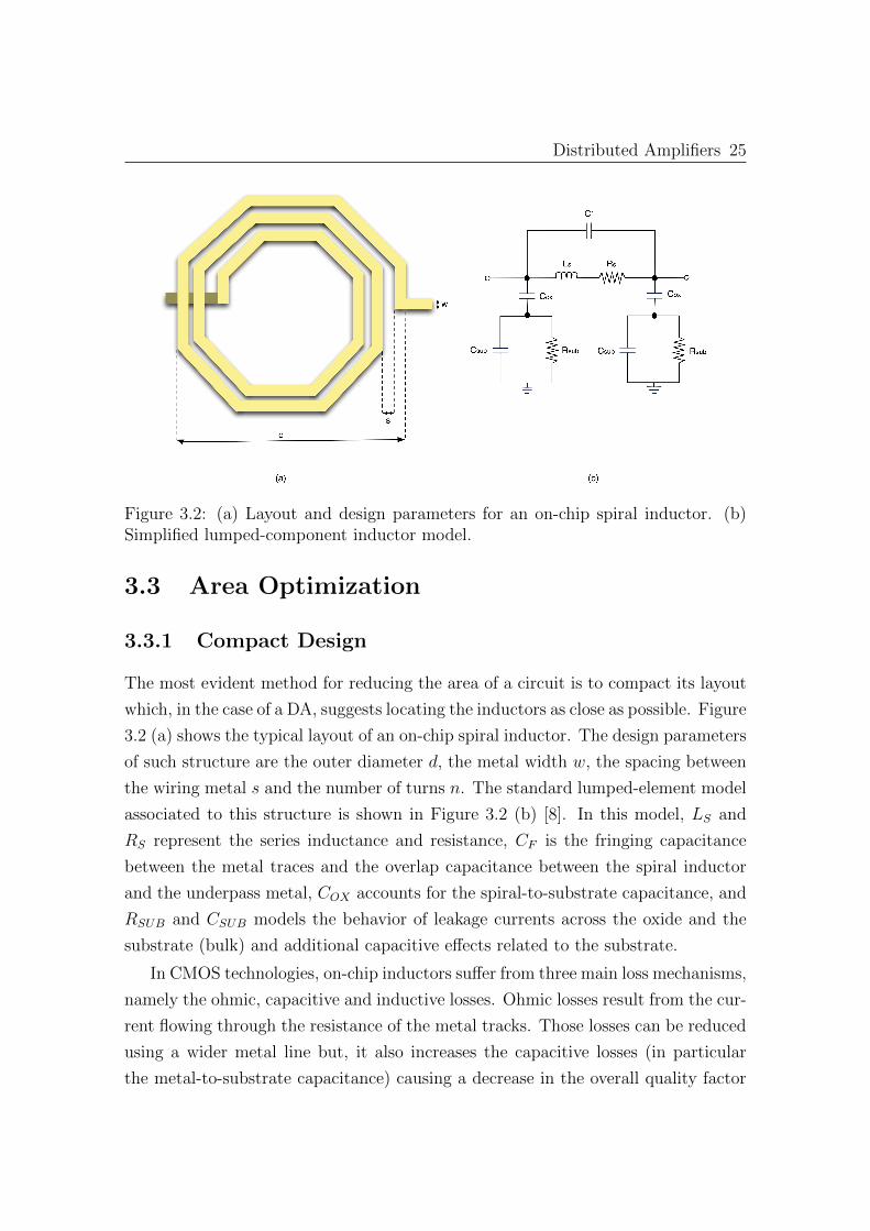
Figure 3.2: (a) Layout and design parameters for an on-chip spiral inductor. (b)Simplified lumped-component inductor model.
3.3 Area Optimization
3.3.1 Compact Design
The most evident method for reducing the area of a circuit is to compact its layout
which, in the case of a DA, suggests locating the inductors as close as possible. Figure
3.2 (a) shows the typical layout of an on-chip spiral inductor. The design parameters
of such structure are the outer diameter d, the metal width w, the spacing between
the wiring metal s and the number of turns n. The standard lumped-element model
associated to this structure is shown in Figure 3.2 (b) [8]. In this model, LS and
RS represent the series inductance and resistance, CF is the fringing capacitance
between the metal traces and the overlap capacitance between the spiral inductor
and the underpass metal, COX accounts for the spiral-to-substrate capacitance, and
RSUB and CSUB models the behavior of leakage currents across the oxide and the
substrate (bulk) and additional capacitive effects related to the substrate.
In CMOS technologies, on-chip inductors suffer from three main loss mechanisms,
namely the ohmic, capacitive and inductive losses. Ohmic losses result from the cur-
rent flowing through the resistance of the metal tracks. Those losses can be reduced
using a wider metal line but, it also increases the capacitive losses (in particular
the metal-to-substrate capacitance) causing a decrease in the overall quality factor
26
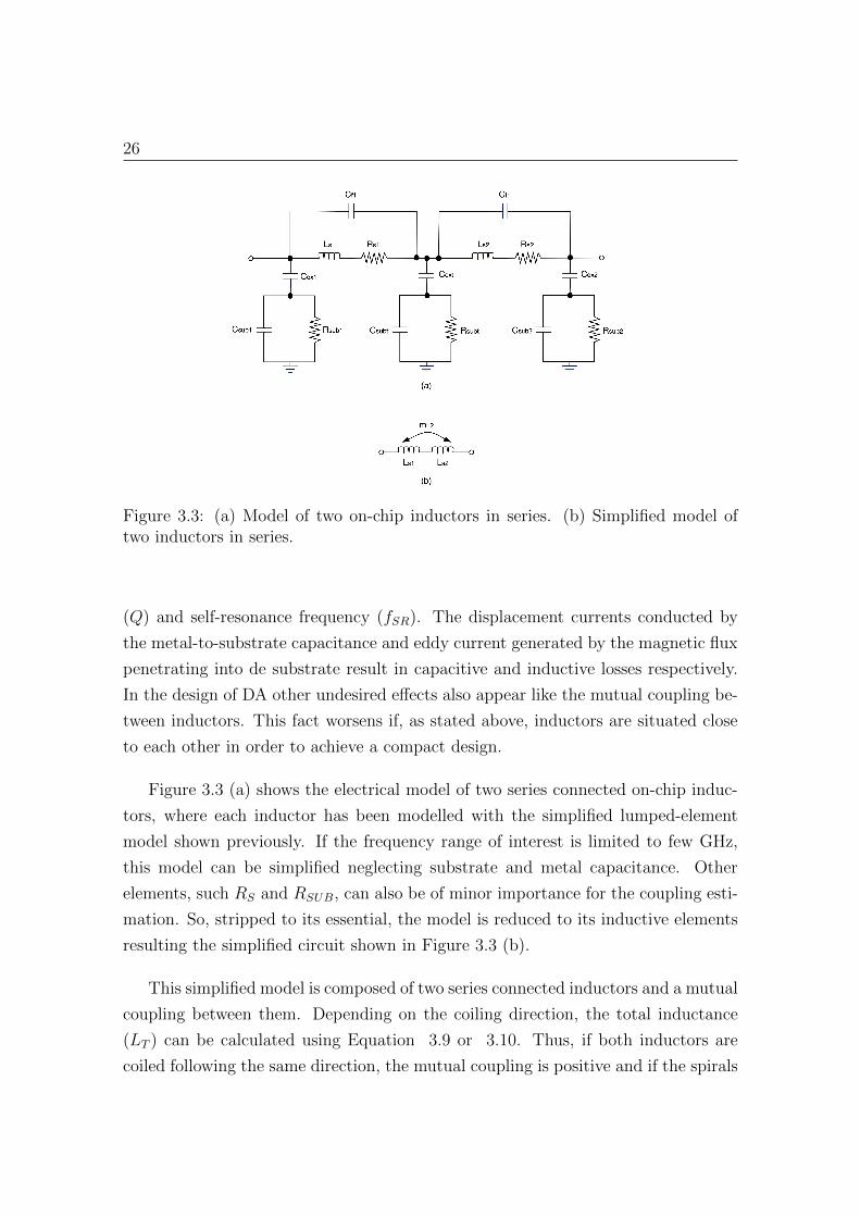
Figure 3.3: (a) Model of two on-chip inductors in series. (b) Simplified model oftwo inductors in series.
(Q) and self-resonance frequency (fSR). The displacement currents conducted by
the metal-to-substrate capacitance and eddy current generated by the magnetic flux
penetrating into de substrate result in capacitive and inductive losses respectively.
In the design of DA other undesired effects also appear like the mutual coupling be-
tween inductors. This fact worsens if, as stated above, inductors are situated close
to each other in order to achieve a compact design.
Figure 3.3 (a) shows the electrical model of two series connected on-chip induc-
tors, where each inductor has been modelled with the simplified lumped-element
model shown previously. If the frequency range of interest is limited to few GHz,
this model can be simplified neglecting substrate and metal capacitance. Other
elements, such RS and RSUB, can also be of minor importance for the coupling esti-
mation. So, stripped to its essential, the model is reduced to its inductive elements
resulting the simplified circuit shown in Figure 3.3 (b).
This simplified model is composed of two series connected inductors and a mutual
coupling between them. Depending on the coiling direction, the total inductance
(LT ) can be calculated using Equation 3.9 or 3.10. Thus, if both inductors are
coiled following the same direction, the mutual coupling is positive and if the spirals
Distributed Amplifiers 27
are coiled in opposite directions the coupling is negative.
LT1 = LS1 + LS2 + 2.m12 (3.9)
LT2 = LS1 + LS2 − 2.m12 (3.10)
To evaluate the coupling between integrated spiral inductors, electromagnetic
(EM) simulations have carried on using a commercially available planar EM simula-
tor (Momentum). In order to get the simulator to generate useful data, the substrate
definition was first calibrated. This was accomplished by using measured data from
previously fabricated inductors as a reference, and adjusting the substrate definition
until it produced closely correlated data [9],[10],[11].
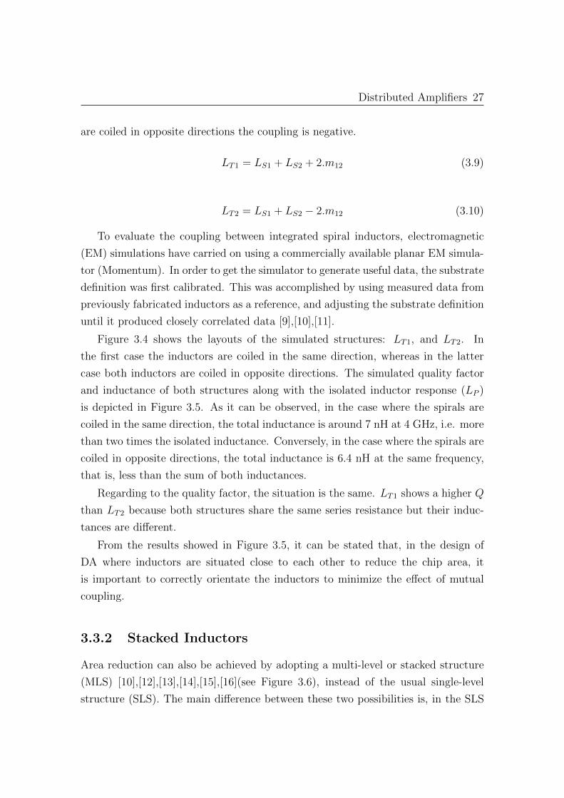
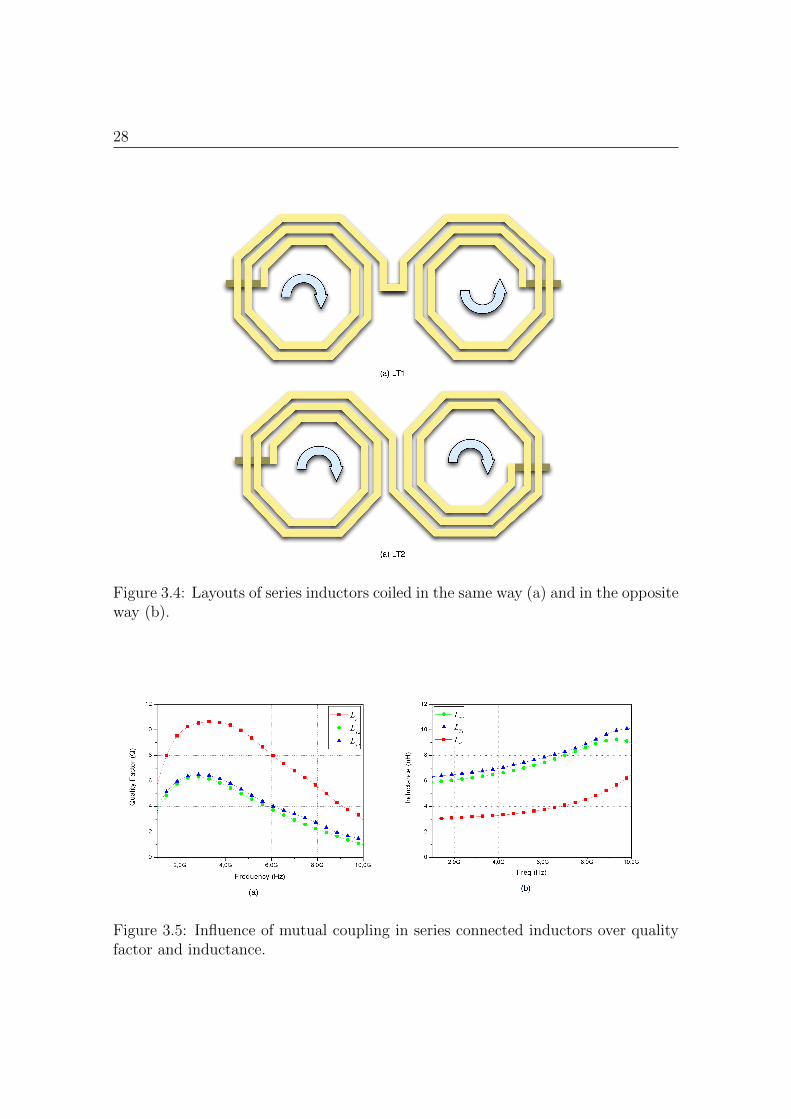
Figure 3.4 shows the layouts of the simulated structures: LT1, and LT2. In
the first case the inductors are coiled in the same direction, whereas in the latter
case both inductors are coiled in opposite directions. The simulated quality factor
and inductance of both structures along with the isolated inductor response (LP )
is depicted in Figure 3.5. As it can be observed, in the case where the spirals are
coiled in the same direction, the total inductance is around 7 nH at 4 GHz, i.e. more
than two times the isolated inductance. Conversely, in the case where the spirals are
coiled in opposite directions, the total inductance is 6.4 nH at the same frequency,
that is, less than the sum of both inductances.
Regarding to the quality factor, the situation is the same. LT1 shows a higher Q
than LT2 because both structures share the same series resistance but their induc-
tances are different.
From the results showed in Figure 3.5, it can be stated that, in the design of
DA where inductors are situated close to each other to reduce the chip area, it
is important to correctly orientate the inductors to minimize the effect of mutual
coupling.
3.3.2 Stacked Inductors
Area reduction can also be achieved by adopting a multi-level or stacked structure
(MLS) [10],[12],[13],[14],[15],[16](see Figure 3.6), instead of the usual single-level
structure (SLS). The main difference between these two possibilities is, in the SLS
28
Figure 3.4: Layouts of series inductors coiled in the same way (a) and in the oppositeway (b).
Figure 3.5: Influence of mutual coupling in series connected inductors over qualityfactor and inductance.
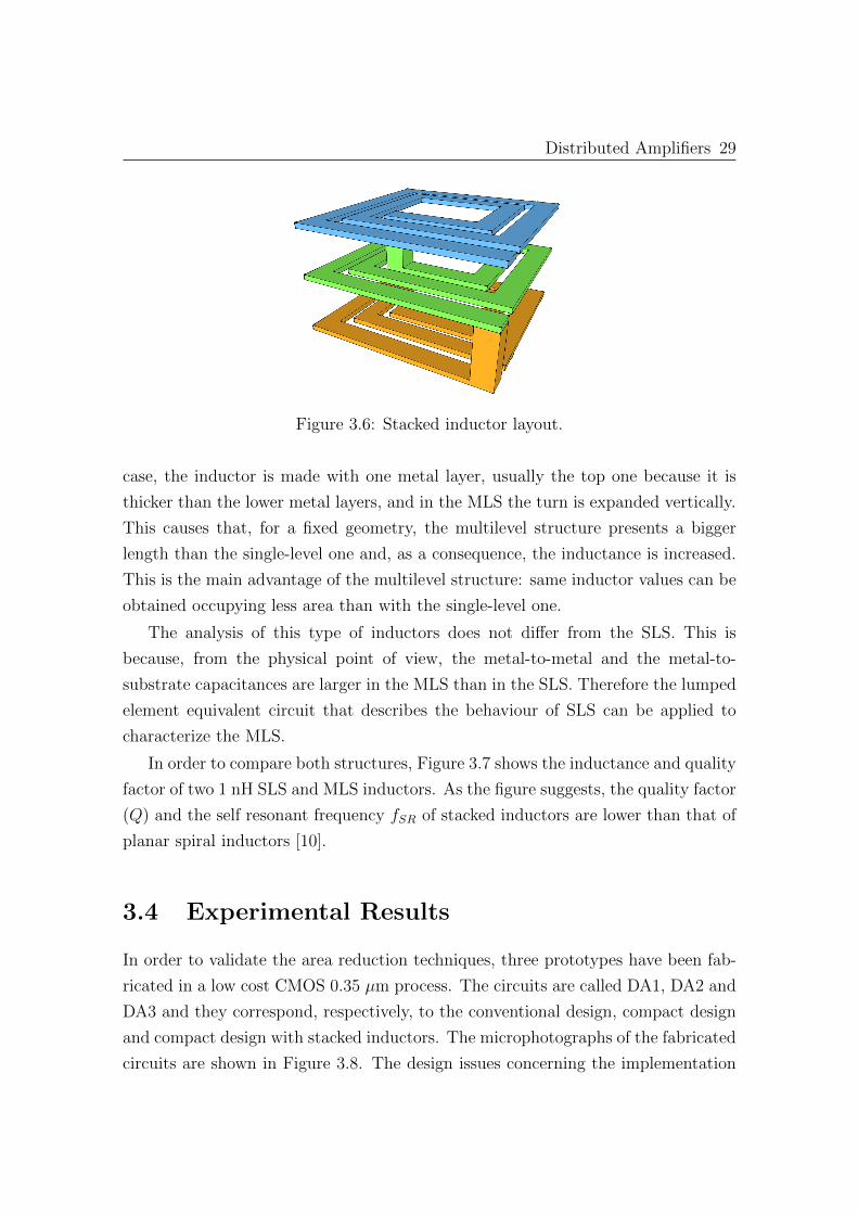
Distributed Amplifiers 29
Figure 3.6: Stacked inductor layout.
case, the inductor is made with one metal layer, usually the top one because it is
thicker than the lower metal layers, and in the MLS the turn is expanded vertically.
This causes that, for a fixed geometry, the multilevel structure presents a bigger
length than the single-level one and, as a consequence, the inductance is increased.
This is the main advantage of the multilevel structure: same inductor values can be
obtained occupying less area than with the single-level one.
The analysis of this type of inductors does not differ from the SLS. This is
because, from the physical point of view, the metal-to-metal and the metal-to-
substrate capacitances are larger in the MLS than in the SLS. Therefore the lumped
element equivalent circuit that describes the behaviour of SLS can be applied to
characterize the MLS.
In order to compare both structures, Figure 3.7 shows the inductance and quality
factor of two 1 nH SLS and MLS inductors. As the figure suggests, the quality factor
(Q) and the self resonant frequency fSR of stacked inductors are lower than that of
planar spiral inductors [10].
3.4 Experimental Results
In order to validate the area reduction techniques, three prototypes have been fab-
ricated in a low cost CMOS 0.35 µm process. The circuits are called DA1, DA2 and
DA3 and they correspond, respectively, to the conventional design, compact design
and compact design with stacked inductors. The microphotographs of the fabricated
circuits are shown in Figure 3.8. The design issues concerning the implementation

30
Figure 3.7: Conventional inductor Vs. Stacked inductor.
Figure 3.8: a) DA1: conventional design (0.7 mm2), (b) DA2: compact design(0.6mm2), (c) DA3: compact design with stacked inductors (0.4mm2).
of the three circuits will be described in the following paragraphs.
One of the difficulties in designing a fully integrated DA is creating the required
high-quality inductors. Figure 3.9 shows the simulated quality factor and inductance
of the inductors used in the three designs. Table 3.2 shows the geometrical param-
eters of the chosen coils. The first one is a conventional planar spiral inductor and
the second is a stacked inductor. The conventional inductor was used to generate
Ld = Lg and Ld/2 = Lg/2 in DA1 and DA2. As it can be observed in Figure 3.9,
at 5 GHz this inductor presents a quality factor and an inductance of 9.28 and 1.3
nH, respectively. Although this inductor does not have half of the inductance than
Ld = Lg, its physical layout perfectly match with the other components in both
designs. On the other hand, the stacked inductor was used in the gate line of DA3.
This circuit keeps the conventional inductor in the drain line because the current

Distributed Amplifiers 31
Figure 3.9: Inductors employed in the DA.
s(µm) n r(µm) W(µm)Conventional 2 2.5 100 16
Stacked 2 2x1.5 40 10
Table 3.2: Inductors Geometrical Parameters.
flowing through this line is too high to be supported by stacked inductors.
Due to the very high frequency of operation, special attention has been paid to
the layout. Thus, enough design accuracy has been achieved by adding accurate
high-Q inductor model and optimizing parasitic effects coming from discontinuity
and interconnection. The designed DAs utilize a transistor size of 130 µm (equivalent
to a 13 gates with 10 µm gate width) and a capacitance Cd of 150 fF.
The DA1 circuit occupies an area of 0.74 mm2, which includes the pad frame.
In contrast to the conventional design, the compact design DA2 occupies a total
area of 0.61 mm2, i.e. 17% a reduction of area. Finally, the Compact design with
stacked inductors DA3 occupies a total area of 0.47 mm2 which implies a 36% of
saving area.
After the measurement of several samples, the frequency response is shown in
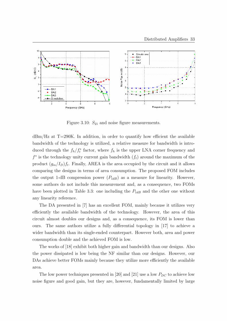
Figure 3.10. The power gain of DA1 is 6 dB with ±0.6 dB flatness from 1 GHz to 5
GHz and a unity gain around 8.6 GHz. The input and output matching are better
than -10 dB over the bandwidth. The increase in gain at low frequency is due to the
higher impedance of the blocking capacitance at low frequency. All measurements
were taken under identical DC bias condition, 3 V on the drain and 0.8 V on the
gate. At this bias point the DA consumes 30 mA giving a total power dissipation

32
Ref. Gain(dB)
BW(GHz)
NF(dB)
P1dB
(dBm)Area(mm2)
ft∗ (Tech.) PDC
(mW)FOM1 FOM2
[7] 6.1 5.5 6.8 8.8 1.12 10.5(0.6µ) 83.4 151 132[17] 5.5 8.5 10.85 N/A 2.86 10.5(0.6µ) 286 57 -[18] 7.3 22 5.2 10 1.6 33.7(0.18µ) 52 108 95[18] 10.6 14 4.35 5.3 1.35 33.7 (0.18µ) 52 124 106[19] 6 27 6 10 1.62 33.7 (0.18µ) 68 107 94[20] 4 8 5.4 8 0.84 33.7 (0.18µ) 23 208 182[21] 10 11 4.6 N/A 1.44 33.7 (0.18µ) 19.6 119 -[21] 16 11 4.5 N/A 1.44 33.7 (0.18µ) 100 110 -DA1 7 6.5 5 12.3 0.74 8.13 (0.35µ) 90 231 207DA2 7 6.5 4.5 12.4 0.61 8.13 (0.35µ) 90 282 253DA3 5.5 6.5 6 11.2 0.47 8.13 (0.35µ) 90 364 3251FOM not including P1dB, 2FOM including P1dB
Table 3.3: Sumary of LNA performance and comparison with previously publisheddesigns.
of 90 mW. Finally, Figure 3.10 shows the noise response. The noise figure is under
5 dB from 1 GHz to 6.5 GHz, and it is around 7.5 dB at 8.5 GHz.
The frequency response of DA2 is approximately the same of DA1. Regarding to
the noise figure, DA2 performance is better than DA1 mainly because the parasitics
associated to the connection tracks have been reduced.
With respect to DA3, in spite of the stacked inductor performance is worse than
the conventional ones, its response is very similar to DA1 and DA2. The noise
figure is a little bit higher than that of the conventional design. This is due to the
series resistance associated to stacked inductors is larger than that of conventional
inductors.
Table 3.3 summarizes the performance of the presented amplifiers, with compar-
ison to previously published DAs.
To provide an objective method to compare the developed circuits and other
similar works, a figure of merit has been used:
FOM =P1dB
Pnoise
1
PDC
fhf ∗t
1
AREA(3.11)
This expression includes the DC power consumption (PDC) and output noise
power (Pnoise = PthFGain), where Pth = kT is the thermal noise floor given by -174
Distributed Amplifiers 33
Figure 3.10: S21 and noise figure measurements.
dBm/Hz at T=290K. In addition, in order to quantify how efficient the available
bandwidth of the technology is utilized, a relative measure for bandwidth is intro-
duced through the fh/f ∗tfactor, where fh is the upper LNA corner frequency and
f ∗ is the technology unity current gain bandwidth (ft) around the maximum of the
product (gm/ID)ft. Finally, AREA is the area occupied by the circuit and it allows
comparing the designs in terms of area consumption. The proposed FOM includes
the output 1-dB compression power (P1dB) as a measure for linearity. However,
some authors do not include this measurement and, as a consequence, two FOMs
have been plotted in Table 3.3: one including the P1dB and the other one without
any linearity reference.
The DA presented in [7] has an excellent FOM, mainly because it utilizes very
efficiently the available bandwidth of the technology. However, the area of this
circuit almost doubles our designs and, as a consequence, its FOM is lower than
ours. The same authors utilize a fully differential topology in [17] to achieve a
wider bandwidth than its single-ended counterpart. However both, area and power
consumption double and the achieved FOM is low.
The works of [18] exhibit both higher gain and bandwidth than our designs. Also
the power dissipated is low being the NF similar than our designs. However, our
DAs achieve better FOMs mainly because they utilize more efficiently the available
area.
The low power techniques presented in [20] and [21] use a low PDC to achieve low
noise figure and good gain, but they are, however, fundamentally limited by large
34
area.
Finally the DA reported in [19] uses coplanar waveguides to implement the re-
quired inductances. This technique achieves a very high frequency of operation but
at the cost of a very large area.
Regarding to the presented designs, the best FOM is achieved, as expected, by
DA3. This design employs stacked inductors to reduce area. This kind of inductor
occupies less chip area than that of planar spiral since the turn is expanded vertically.
Usually, top metal is thicker than lower metal layers, and thus the Q-factor of
stacked inductors is lower than that of planar spiral inductors. However, as the area
occupation is much smaller, substrate losses are smaller, so only little performance
degradation of the stacked inductor circuit is achieved over the planar spiral inductor
one. This result demonstrates that it is possible to reduce the area with a minimum
influence over the circuit response.
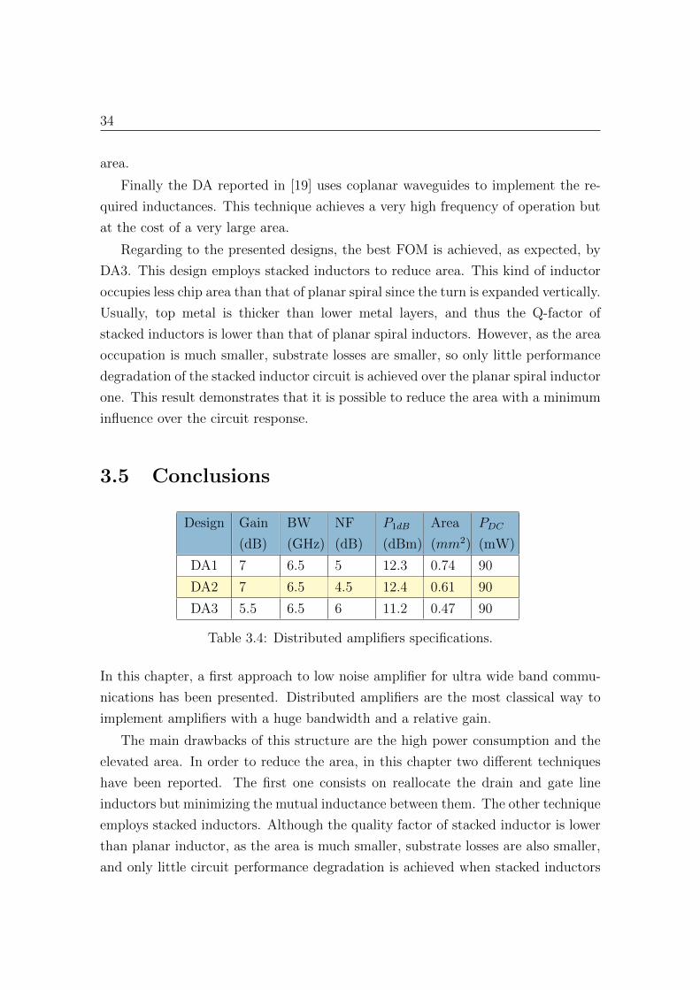
3.5 Conclusions
Design Gain
(dB)
BW
(GHz)
NF
(dB)
P1dB
(dBm)
Area
(mm2)
PDC
(mW)
DA1 7 6.5 5 12.3 0.74 90
DA2 7 6.5 4.5 12.4 0.61 90
DA3 5.5 6.5 6 11.2 0.47 90
Table 3.4: Distributed amplifiers specifications.
In this chapter, a first approach to low noise amplifier for ultra wide band commu-
nications has been presented. Distributed amplifiers are the most classical way to
implement amplifiers with a huge bandwidth and a relative gain.
The main drawbacks of this structure are the high power consumption and the
elevated area. In order to reduce the area, in this chapter two different techniques
have been reported. The first one consists on reallocate the drain and gate line
inductors but minimizing the mutual inductance between them. The other technique
employs stacked inductors. Although the quality factor of stacked inductor is lower
than planar inductor, as the area is much smaller, substrate losses are also smaller,
and only little circuit performance degradation is achieved when stacked inductors
Distributed Amplifiers 35
are used. Using the above techniques, three fully integrated distributed amplifiers
have been designed, fabricated and tested. Table 3.4 shows a summary of their
specifications.
The next chapter will explore other alternatives to implement low noise amplifiers
for ultra wide band communications trying to reduce the power consumption and
the occupied area.

36
4Wide Band Low Noise Amplifiers
4.1 Introduction
The distributed amplifiers developed in the previous chapter exhibit a high power
consumption and occupy a considerable area. In this chapter, different alternatives
of low noise amplifiers will be exposed in order to reduce the power consumption
and area.
4.2 Wide Band Low Noise Amplifier
4.2.1 Narrow Band Inductively Degenerated Amplifier
In this section, the typical narrow band inductively degenerated amplifier configu-
ration is studied as it is the base of the wide band LNA.
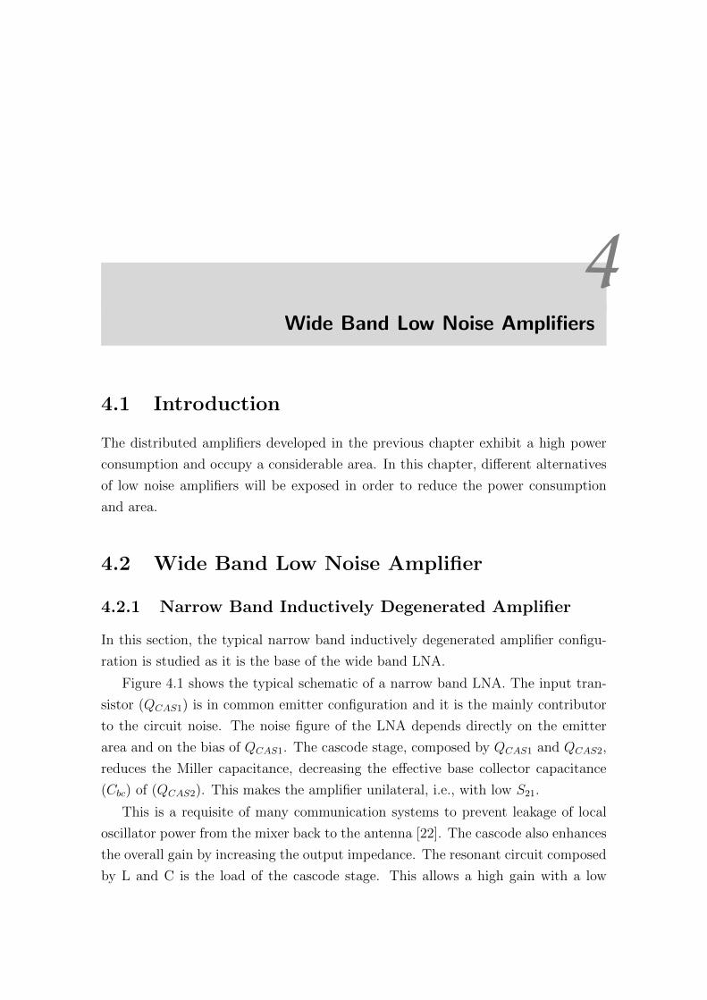
Figure 4.1 shows the typical schematic of a narrow band LNA. The input tran-
sistor (QCAS1) is in common emitter configuration and it is the mainly contributor
to the circuit noise. The noise figure of the LNA depends directly on the emitter
area and on the bias of QCAS1. The cascode stage, composed by QCAS1 and QCAS2,
reduces the Miller capacitance, decreasing the effective base collector capacitance
(Cbc) of (QCAS2). This makes the amplifier unilateral, i.e., with low S21.
This is a requisite of many communication systems to prevent leakage of local
oscillator power from the mixer back to the antenna [22]. The cascode also enhances
the overall gain by increasing the output impedance. The resonant circuit composed
by L and C is the load of the cascode stage. This allows a high gain with a low
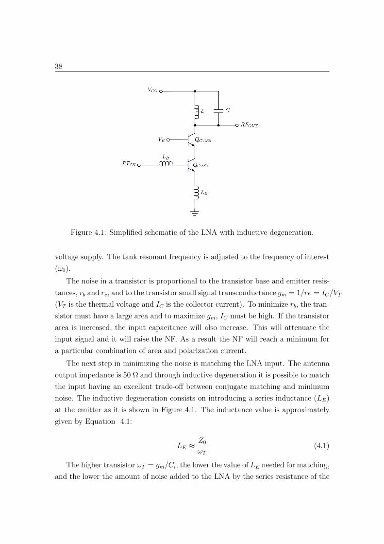
38
Figure 4.1: Simplified schematic of the LNA with inductive degeneration.
voltage supply. The tank resonant frequency is adjusted to the frequency of interest
(ω0).
The noise in a transistor is proportional to the transistor base and emitter resis-
tances, rb and re, and to the transistor small signal transconductance gm = 1/re = IC/VT
(VT is the thermal voltage and IC is the collector current). To minimize rb, the tran-
sistor must have a large area and to maximize gm, IC must be high. If the transistor
area is increased, the input capacitance will also increase. This will attenuate the
input signal and it will raise the NF. As a result the NF will reach a minimum for
a particular combination of area and polarization current.
The next step in minimizing the noise is matching the LNA input. The antenna
output impedance is 50 Ω and through inductive degeneration it is possible to match
the input having an excellent trade-off between conjugate matching and minimum
noise. The inductive degeneration consists on introducing a series inductance (LE)
at the emitter as it is shown in Figure 4.1. The inductance value is approximately
given by Equation 4.1:
LE ≈ Z0
ωT
(4.1)
The higher transistor ωT = gm/Ci, the lower the value of LE needed for matching,
and the lower the amount of noise added to the LNA by the series resistance of the
Wide Band Low Noise Amplifiers 39
inductor. LE changes the real part of the input impedance, and to modify the
imaginary part another inductor LB is introduced as shown in Figure 4.1. An
expression of the noise factor for the LNA with inductive degeneration that takes
into account the above discussion is shown in Equation 4.2 [8]:
F = 1 +Rb +Re
Z0+
gm2
· Z0 ·ω0
ωT
2
(4.2)
Alternatively this expression can be expressed as:
F = 1 +rb + reZ0
+1
2 · gm · Z0 ·Q2(4.3)
where Q is the quality factor of the input matching network. The noise factor
improves with a higher Q because more voltage gain is seen across the input capac-
itance of the transistor. The input impedance is resistive only in a narrow band-
width (ω0/Q) around the resonance frequency ω0. To obtain a wide band impedance
matching, the Q of the matching circuit should be significantly lowered. This will
largely degrade the noise figure which defeats the purpose. As a result, this type of
amplifier cannot be used for wide band applications.
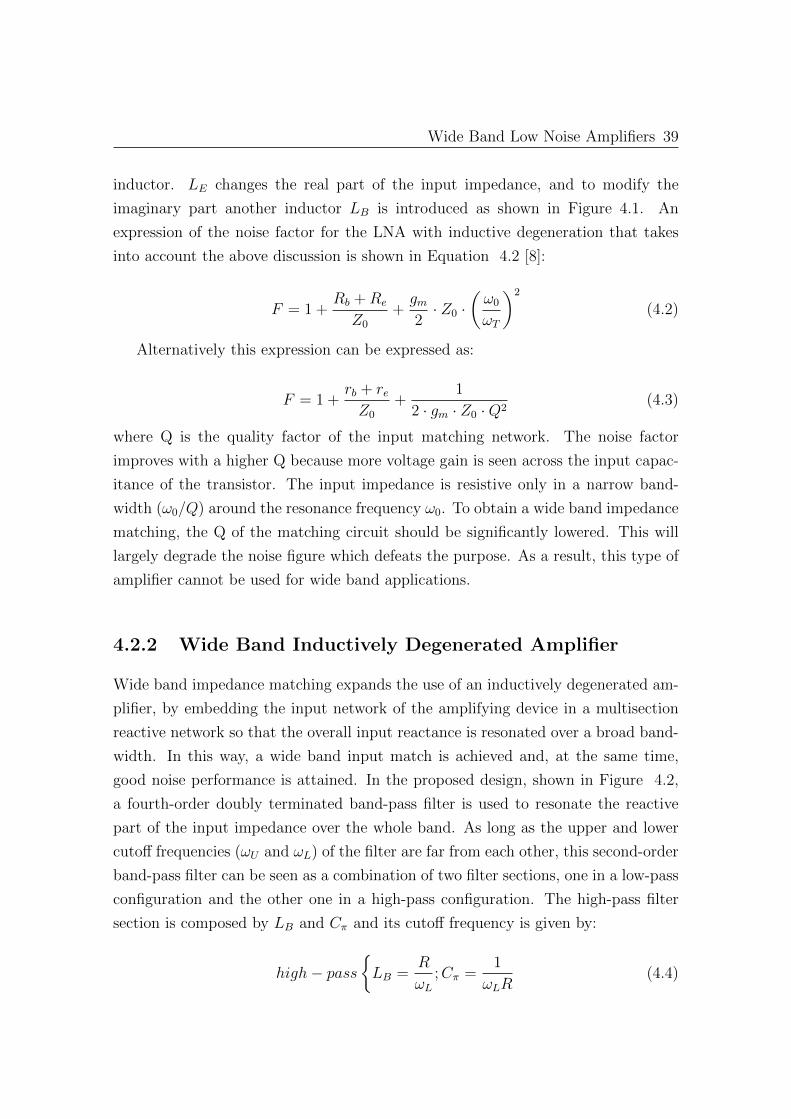
4.2.2 Wide Band Inductively Degenerated Amplifier
Wide band impedance matching expands the use of an inductively degenerated am-
plifier, by embedding the input network of the amplifying device in a multisection
reactive network so that the overall input reactance is resonated over a broad band-
width. In this way, a wide band input match is achieved and, at the same time,
good noise performance is attained. In the proposed design, shown in Figure 4.2,
a fourth-order doubly terminated band-pass filter is used to resonate the reactive
part of the input impedance over the whole band. As long as the upper and lower
cutoff frequencies (ωU and ωL) of the filter are far from each other, this second-order
band-pass filter can be seen as a combination of two filter sections, one in a low-pass
configuration and the other one in a high-pass configuration. The high-pass filter
section is composed by LB and Cπ and its cutoff frequency is given by:
high− pass
LB =
R
ωL
;Cπ =1
ωLR(4.4)
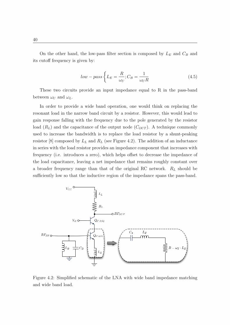
40
On the other hand, the low-pass filter section is composed by LE and CB and
its cutoff frequency is given by:
low − pass
LE =
R
ωU
;CB =1
ωUR(4.5)
These two circuits provide an input impedance equal to R in the pass-band
between ωU and ωL.
In order to provide a wide band operation, one would think on replacing the
resonant load in the narrow band circuit by a resistor. However, this would lead to
gain response falling with the frequency due to the pole generated by the resistor
load (RL) and the capacitance of the output node (COUT ). A technique commonly
used to increase the bandwidth is to replace the load resistor by a shunt-peaking
resistor [8] composed by LL and RL (see Figure 4.2). The addition of an inductance
in series with the load resistor provides an impedance component that increases with
frequency (i.e. introduces a zero), which helps offset to decrease the impedance of
the load capacitance, leaving a net impedance that remains roughly constant over
a broader frequency range than that of the original RC network. RL should be
sufficiently low so that the inductive region of the impedance spans the pass-band.
Figure 4.2: Simplified schematic of the LNA with wide band impedance matching
and wide band load.

Wide Band Low Noise Amplifiers 41
Figure 4.3: Schematic of the wide band LNA.
With this configuration the inductive load equalizes the voltage gain to a con-
stant value across the pass-band. The problem is that COUT introduces a spurious
resonance with LL (peaking), which must be kept out-of-band. As long as COUT
represents all the loading on the output node, including the transistor output capac-
itance, the loading by interconnect and subsequent stages and parasitic capacitances
of the inductor, all these contributions should be minimized to ensure self resonance
beyond ωU .
4.2.3 Wide Band Low Noise Amplifier Design
Figure 4.3 shows the designed wide band LNA circuit. For measurement purposes,
an emitter follower buffer is included to drive an external 50 Ω load. C2 and C5
capacitors are for AC decoupling and RBIAS has a large value in order to bias the
output buffer with VBIAS1 voltage.
The performance of a narrow band LNA is determined by the limited quality fac-
tor of the integrated inductors [23]. Its optimization relies on achieving the highest
Q for a given inductance value at the frequency of operation. In the case of a wide
band operation, this assumption is not convenient and a further study is needed. In
shunt peaking applications, the biggest issue is the reduction of bandwidth because
of additional parasitic capacitance introduced by on-chip inductors. As a conse-

42
Figure 4.4: (a) Quality factor and inductance of spirals suitable for LB. (b) Powergain for differents LB.
quence, prior to their use in any circuit, spiral planar inductors must be modelled
accurately over a wide range of frequencies. In this work, the analytical model pro-
posed in [11] has been used to implement an optimization algorithm that provides
the geometry of the inductor with the best quality factor for a given inductance
value and frequency of operation. For every inductor of the circuit, a set of spirals
with the same inductance but optimized for different frequencies were simulated. In
order to better predict the inductor performance, S parameters from full-wave elec-
tromagnetic simulations were used to simulate the circuit. A commercially available
planar EM simulator (Momentum) was used to predict the broadband response of
inductors. The inductors were designed using the top level metal, which is thicker
and more conductive than the rest. All of them were laid out in an octagonal fash-
ion, with external radio (r) up to 170 µm, metal width (w) between 5 and 25 µm
and up to 5.5 turns (n). The spacing between tracks is fixed to the minimum allowed
by the technology, 2 µm, in order to maximize the inductance value.
The simulated quality factor and inductance of the spirals are reported in Figures
4.4 to 4.7. In the same Figures, the wide band LNA simulated power gain using the
above spirals is also plotted.
As it can be seen the circuit performance is insensitive to inductors LB and LE
quality factors. With maximum quality factor frequencies (fQmax) for LB ranging
from 2 to 5 GHz, the gain remains unaltered. Only little variations are observed at
low frequency and must be attributed to the slight differences in inductance value.
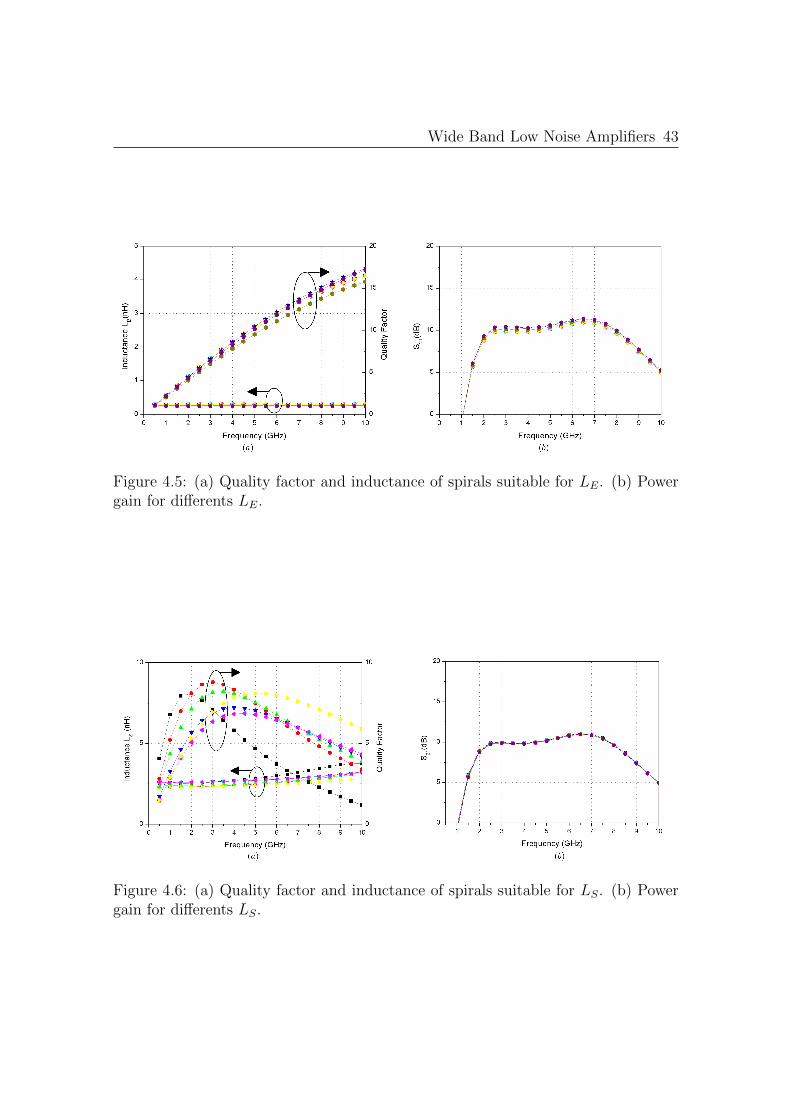
Wide Band Low Noise Amplifiers 43
Figure 4.5: (a) Quality factor and inductance of spirals suitable for LE. (b) Powergain for differents LE.
Figure 4.6: (a) Quality factor and inductance of spirals suitable for LS. (b) Powergain for differents LS.
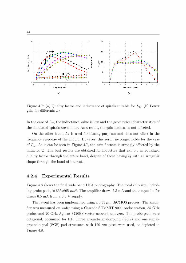
44
Figure 4.7: (a) Quality factor and inductance of spirals suitable for LL. (b) Powergain for differents LL.
In the case of LE, the inductance value is low and the geometrical characteristics of
the simulated spirals are similar. As a result, the gain flatness is not affected.
On the other hand, LS is used for biasing purposes and does not affect in the
frequency response of the circuit. However, this result no longer holds for the case
of LL. As it can be seen in Figure 4.7, the gain flatness is strongly affected by the
inductor Q. The best results are obtained for inductors that exhibit an equalized
quality factor through the entire band, despite of those having Q with an irregular
shape through the band of interest.
4.2.4 Experimental Results
Figure 4.8 shows the final wide band LNA photography. The total chip size, includ-
ing probe pads, is 665x665 µm2. The amplifier draws 5.3 mA and the output buffer
draws 6.5 mA from a 3.3 V supply.
The layout has been implemented using a 0.35 µm BiCMOS process. The ampli-
fier was measured on wafer using a Cascade SUMMIT 9000 probe station, 35 GHz
probes and 20 GHz Agilent 8720ES vector network analyzer. The probe pads were
octagonal, optimized for RF. Three ground-signal-ground (GSG) and one signal-
ground-signal (SGS) pad structures with 150 µm pitch were used, as depicted in
Figure 4.8.
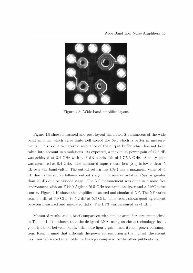
Wide Band Low Noise Amplifiers 45
Figure 4.8: Wide band amplifier layout.
Figure 4.9 shows measured and post layout simulated S parameters of the wide
band amplifier which agree quite well except the S22, which is better in measure-
ments. This is due to parasitic resonance of the output buffer which has not been
taken into account in simulations. As expected, a maximum power gain of 12.5 dB
was achieved at 3.4 GHz with a -3 dB bandwidth of 1.7-5.3 GHz. A unity gain
was measured at 9.4 GHz. The measured input return loss (S11) is lower than -5
dB over the bandwidth. The output return loss (S22) has a maximum value of -4
dB due to the source follower output stage. The reverse isolation (S12) is greater
than 23 dB due to cascode stage. The NF measurement was done in a noise free
environment with an E4440 Agilent 26.5 GHz spectrum analyzer and a 346C noise
source. Figure 4.10 shows the amplifier measured and simulated NF. The NF varies
from 4.3 dB at 3.9 GHz, to 5.2 dB at 5.3 GHz. This result shows good agreement
between measured and simulated data. The IIP3 was measured as -4 dBm.
Measured results and a brief comparison with similar amplifiers are summarized
in Table 4.1. It is shown that the designed LNA, using an cheap technology, has a
good trade-off between bandwidth, noise figure, gain, linearity and power consump-
tion. Keep in mind that although the power consumption is the highest, the circuit
has been fabricated in an older technology compared to the other publications.
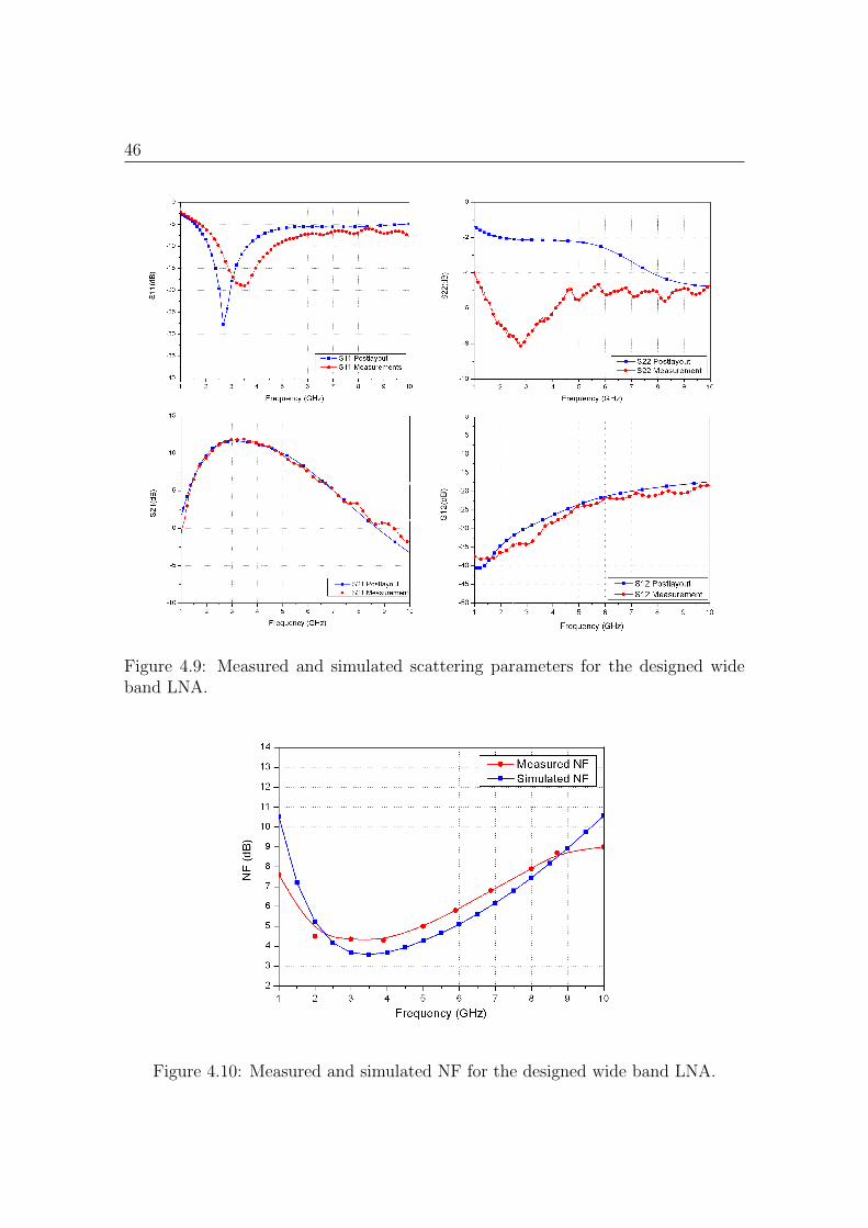
46
Figure 4.9: Measured and simulated scattering parameters for the designed wideband LNA.
Figure 4.10: Measured and simulated NF for the designed wide band LNA.

Wide Band Low Noise Amplifiers 47
Author BW 3 dB Max. Gain Max. NF IIP3 PDC Technology Year(GHz) (dB) (dB) (dBm) (mW)
[24] 3.1-10.6 9.18 7.2 7.25 23.5 0.18 µm 2007[25] 2.0-4.6 9.8 5.2 -7 12.6 0.18 µm 2005[26] 3.1-4.8 15 4.9 -2.2 20 0.25 µm 2006[27] 3.0-5.0 12.7 5.02 -9.7 16.4 0.18 µm 2005[28] 3.1-7.5 19.1 3.8 -2.2 32 0.18 µm 2006[29] 3.0-5.0 12 4.5 - 20 0.18 µm 2009
This work 1.7-5.3 12.5 5.0 -4 32 0.35 µm 2011
Table 4.1: Comparison with recently published wide band amplifiers.
4.3 Flatness Improvement
One of the main drawbacks of the wide band amplifier is the gain flatness. Usually,
to extend the gain bandwidth, the load is composed of a shunt-peaking resistor.
This technique imposes an upper limit to maximum gain and flatness. To overcome
this issue, a modification of the conventional shunt-peaking will be presented. In
this case a CMOS technology has been used.
4.3.1 Circuit Description
The schematic of the wide band input matched CMOS LNA is shown in Figure 4.11.
As in the previous circuit, it consists of a wide band input matching circuit, a gain
stage with inductive degeneration (Lg and Ls) and a wide band output load. In
order to buffer the output to an external 50 Ω load, an emitter follower (M3) has
been included. As the figure shows, the input matching circuit consists of a filter
embedded with the input impedance of M1. In this case, a third-order bandpass
Chebyshev filter in T configuration was selected. In order to increase the flexibility
of the filter, CP is introduced between the gate and source of M1.
The gain stage is composed of a cascode stage where the width and polarization
current of the transistors are optimized for noise and power consumption.
Figure 4.12 shows the typical shunt peaking resistor load used to provide a wide
band operation [8]. With this configuration the overall amplifier gain should be flat
across the pass-band. The amplifier gain is given by the product of the transistor
transconductance (gm) and the magnitude of the impedance of the shunt-peaking
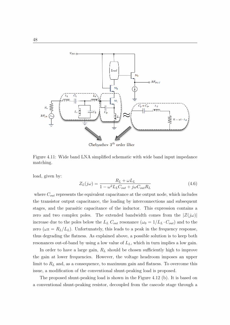
48
Figure 4.11: Wide band LNA simplified schematic with wide band input impedancematching.
load, given by:
ZL(jω) =RL + ωLL
1− ω2LLCout + jωCoutRL
(4.6)
where Cout represents the equivalent capacitance at the output node, which includes
the transistor output capacitance, the loading by interconnections and subsequent
stages, and the parasitic capacitance of the inductor. This expression contains a
zero and two complex poles. The extended bandwidth comes from the |Z(jω)|increase due to the poles below the LL Cout resonance (ω0 = 1/LL ·Cout) and to the
zero (ωz = RL/LL). Unfortunately, this leads to a peak in the frequency response,
thus degrading the flatness. As explained above, a possible solution is to keep both
resonances out-of-band by using a low value of LL, which in turn implies a low gain.
In order to have a large gain, RL should be chosen sufficiently high to improve
the gain at lower frequencies. However, the voltage headroom imposes an upper
limit to RL and, as a consequence, to maximum gain and flatness. To overcome this
issue, a modification of the conventional shunt-peaking load is proposed.
The proposed shunt-peaking load is shown in the Figure 4.12 (b). It is based on
a conventional shunt-peaking resistor, decoupled from the cascode stage through a
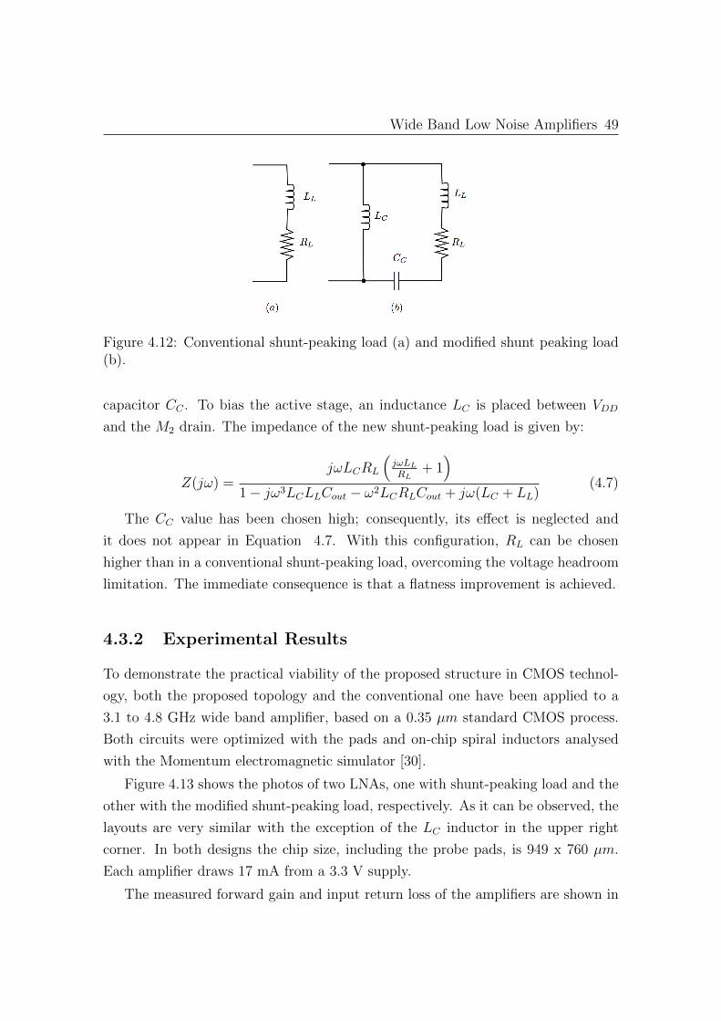
Wide Band Low Noise Amplifiers 49
Figure 4.12: Conventional shunt-peaking load (a) and modified shunt peaking load(b).
capacitor CC . To bias the active stage, an inductance LC is placed between VDD
and the M2 drain. The impedance of the new shunt-peaking load is given by:
Z(jω) =jωLCRL
jωLL
RL+ 1
1− jω3LCLLCout − ω2LCRLCout + jω(LC + LL)(4.7)
The CC value has been chosen high; consequently, its effect is neglected and
it does not appear in Equation 4.7. With this configuration, RL can be chosen
higher than in a conventional shunt-peaking load, overcoming the voltage headroom
limitation. The immediate consequence is that a flatness improvement is achieved.
4.3.2 Experimental Results
To demonstrate the practical viability of the proposed structure in CMOS technol-
ogy, both the proposed topology and the conventional one have been applied to a
3.1 to 4.8 GHz wide band amplifier, based on a 0.35 µm standard CMOS process.
Both circuits were optimized with the pads and on-chip spiral inductors analysed
with the Momentum electromagnetic simulator [30].
Figure 4.13 shows the photos of two LNAs, one with shunt-peaking load and the
other with the modified shunt-peaking load, respectively. As it can be observed, the
layouts are very similar with the exception of the LC inductor in the upper right
corner. In both designs the chip size, including the probe pads, is 949 x 760 µm.
Each amplifier draws 17 mA from a 3.3 V supply.
The measured forward gain and input return loss of the amplifiers are shown in
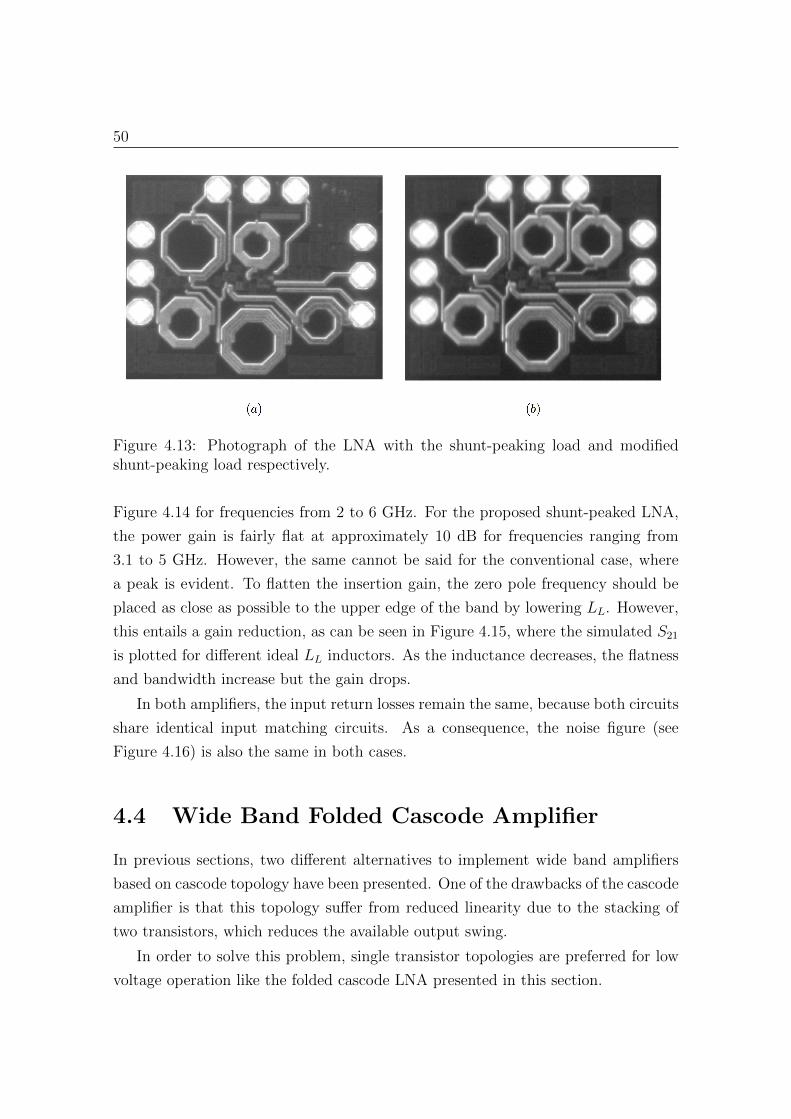
50
Figure 4.13: Photograph of the LNA with the shunt-peaking load and modifiedshunt-peaking load respectively.
Figure 4.14 for frequencies from 2 to 6 GHz. For the proposed shunt-peaked LNA,
the power gain is fairly flat at approximately 10 dB for frequencies ranging from
3.1 to 5 GHz. However, the same cannot be said for the conventional case, where
a peak is evident. To flatten the insertion gain, the zero pole frequency should be
placed as close as possible to the upper edge of the band by lowering LL. However,
this entails a gain reduction, as can be seen in Figure 4.15, where the simulated S21
is plotted for different ideal LL inductors. As the inductance decreases, the flatness
and bandwidth increase but the gain drops.
In both amplifiers, the input return losses remain the same, because both circuits
share identical input matching circuits. As a consequence, the noise figure (see
Figure 4.16) is also the same in both cases.
4.4 Wide Band Folded Cascode Amplifier
In previous sections, two different alternatives to implement wide band amplifiers
based on cascode topology have been presented. One of the drawbacks of the cascode
amplifier is that this topology suffer from reduced linearity due to the stacking of
two transistors, which reduces the available output swing.
In order to solve this problem, single transistor topologies are preferred for low
voltage operation like the folded cascode LNA presented in this section.
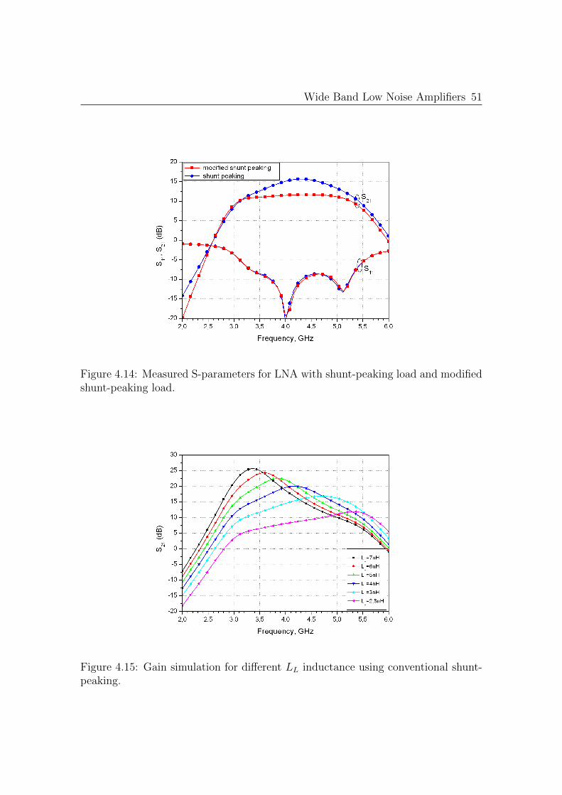
Wide Band Low Noise Amplifiers 51
Figure 4.14: Measured S-parameters for LNA with shunt-peaking load and modifiedshunt-peaking load.
Figure 4.15: Gain simulation for different LL inductance using conventional shunt-peaking.
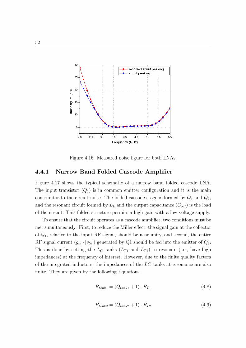
52
Figure 4.16: Measured noise figure for both LNAs.
4.4.1 Narrow Band Folded Cascode Amplifier
Figure 4.17 shows the typical schematic of a narrow band folded cascode LNA.
The input transistor (Q1) is in common emitter configuration and it is the main
contributor to the circuit noise. The folded cascode stage is formed by Q1 and Q2,
and the resonant circuit formed by LL and the output capacitance (Cout) is the load
of the circuit. This folded structure permits a high gain with a low voltage supply.
To ensure that the circuit operates as a cascode amplifier, two conditions must be
met simultaneously. First, to reduce the Miller effect, the signal gain at the collector
of Q1, relative to the input RF signal, should be near unity, and second, the entire
RF signal current (gm · |vbe|) generated by Q1 should be fed into the emitter of Q2.
This is done by setting the LC tanks (LT1 and LT2) to resonate (i.e., have high
impedances) at the frequency of interest. However, due to the finite quality factors
of the integrated inductors, the impedances of the LC tanks at resonance are also
finite. They are given by the following Equations:
Rtank1 = (Qtank1 + 1) ·RL1 (4.8)
Rtank2 = (Qtank2 + 1) ·RL2 (4.9)
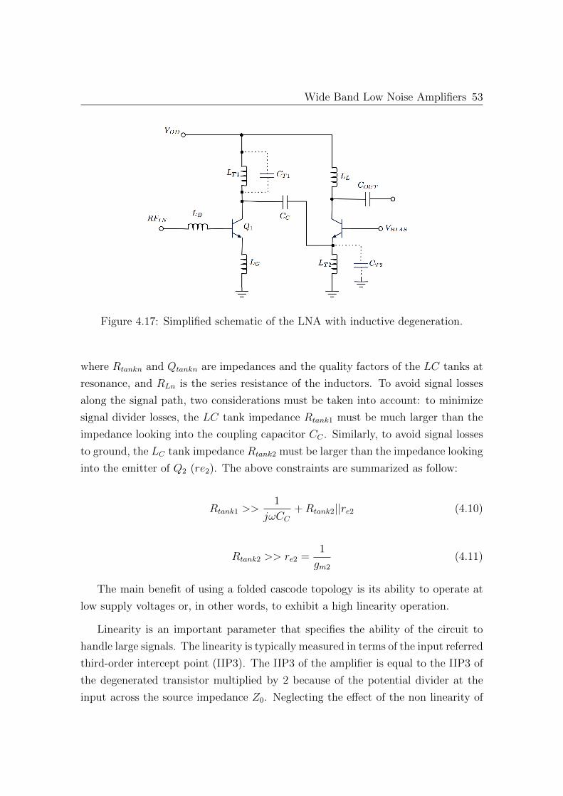
Wide Band Low Noise Amplifiers 53
Figure 4.17: Simplified schematic of the LNA with inductive degeneration.
where Rtankn and Qtankn are impedances and the quality factors of the LC tanks at
resonance, and RLn is the series resistance of the inductors. To avoid signal losses
along the signal path, two considerations must be taken into account: to minimize
signal divider losses, the LC tank impedance Rtank1 must be much larger than the
impedance looking into the coupling capacitor CC . Similarly, to avoid signal losses
to ground, the LC tank impedance Rtank2 must be larger than the impedance looking
into the emitter of Q2 (re2). The above constraints are summarized as follow:
Rtank1 >>1
jωCC
+Rtank2||re2 (4.10)
Rtank2 >> re2 =1
gm2(4.11)
The main benefit of using a folded cascode topology is its ability to operate at
low supply voltages or, in other words, to exhibit a high linearity operation.
Linearity is an important parameter that specifies the ability of the circuit to
handle large signals. The linearity is typically measured in terms of the input referred
third-order intercept point (IIP3). The IIP3 of the amplifier is equal to the IIP3 of
the degenerated transistor multiplied by 2 because of the potential divider at the
input across the source impedance Z0. Neglecting the effect of the non linearity of

54
Figure 4.18: Simplified schematic of the LNA with wide band impedance matching.
the transistor parasitic capacitor, the amplifier IIP3 is given by [8]:
VIIP3 = 4 ·
2 · VT ·1 +
ICωLE
VT
2 3
4
(4.12)
This means that, unlike the noise factor, IIP3 gets better with frequency and, to
obtain a wide band operation, special care should be taken at the lower end of the
band.
4.4.2 Wide Band Folded Cascode Amplifier Topology
In the proposed wide band design, shown in Figure 4.18 as in previous circuits a
fourth order doubly terminated band-pass filter is used to resonate the active part
of the input impedance over the whole band. The typical cascode has been divided
in two different branches. The LT1 and LT2 has been added in order to bias the
collector of Q1 and the emitter of Q2 respectively. On the other hand, the capacitor
CC has been added in order to decouple the signal between the two branches. The
output load is formed with a shunt-peaking as in previous designs.
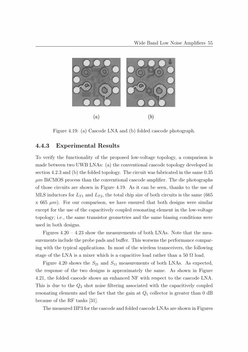
Wide Band Low Noise Amplifiers 55
Figure 4.19: (a) Cascode LNA and (b) folded cascode photograph.
4.4.3 Experimental Results
To verify the functionality of the proposed low-voltage topology, a comparison is
made between two UWB LNAs: (a) the conventional cascode topology developed in
section 4.2.3 and (b) the folded topology. The circuit was fabricated in the same 0.35
µm BiCMOS process than the conventional cascode amplifier. The die photographs
of those circuits are shown in Figure 4.19. As it can be seen, thanks to the use of
MLS inductors for LT1 and LT2, the total chip size of both circuits is the same (665
x 665 µm). For our comparison, we have ensured that both designs were similar
except for the use of the capacitively coupled resonating element in the low-voltage
topology; i.e., the same transistor geometries and the same biasing conditions were
used in both designs.
Figures 4.20 – 4.23 show the measurements of both LNAs. Note that the mea-
surements include the probe pads and buffer. This worsens the performance compar-
ing with the typical applications. In most of the wireless transceivers, the following
stage of the LNA is a mixer which is a capacitive load rather than a 50 Ω load.
Figure 4.20 shows the S21 and S11 measurements of both LNAs. As expected,
the response of the two designs is approximately the same. As shown in Figure
4.21, the folded cascode shows an enhanced NF with respect to the cascode LNA.
This is due to the Q2 shot noise filtering associated with the capacitively coupled
resonating elements and the fact that the gain at Q1 collector is greater than 0 dB
because of the RF tanks [31].
The measured IIP3 for the cascode and folded cascode LNAs are shown in Figures

56
Figure 4.20: Measured S21 and S11 versus frequency.
Figure 4.21: Measured noise figure versus frequency.
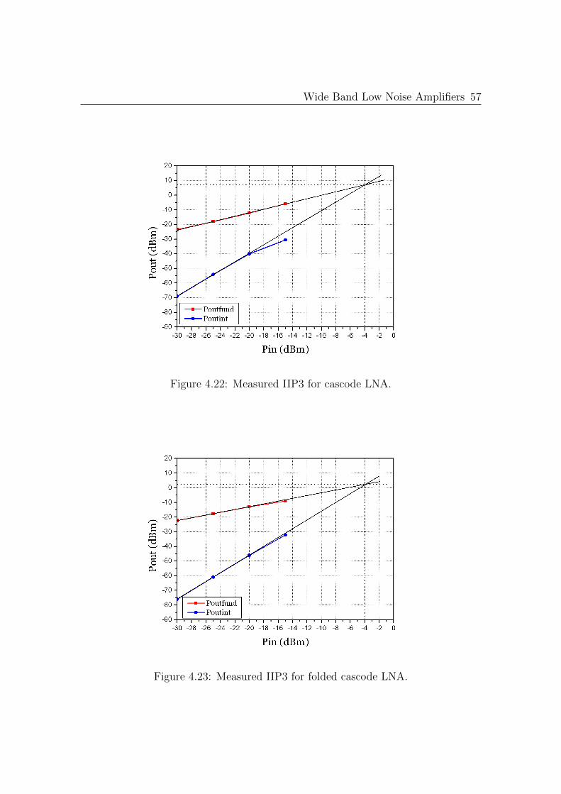
Wide Band Low Noise Amplifiers 57
Figure 4.22: Measured IIP3 for cascode LNA.
Figure 4.23: Measured IIP3 for folded cascode LNA.
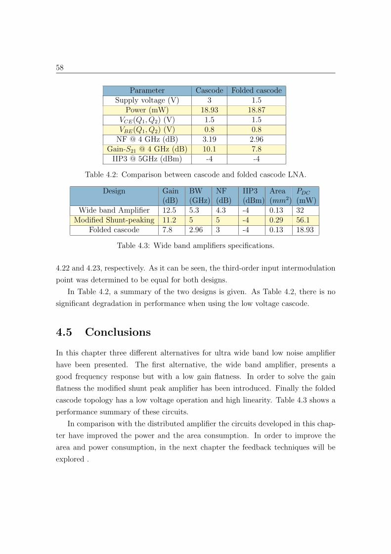
58
Parameter Cascode Folded cascodeSupply voltage (V) 3 1.5
Power (mW) 18.93 18.87VCE(Q1, Q2) (V) 1.5 1.5VBE(Q1, Q2) (V) 0.8 0.8NF @ 4 GHz (dB) 3.19 2.96
Gain-S21 @ 4 GHz (dB) 10.1 7.8IIP3 @ 5GHz (dBm) -4 -4
Table 4.2: Comparison between cascode and folded cascode LNA.
Design Gain(dB)
BW(GHz)
NF(dB)
IIP3(dBm)
Area(mm2)
PDC
(mW)Wide band Amplifier 12.5 5.3 4.3 -4 0.13 32
Modified Shunt-peaking 11.2 5 5 -4 0.29 56.1Folded cascode 7.8 2.96 3 -4 0.13 18.93
Table 4.3: Wide band amplifiers specifications.
4.22 and 4.23, respectively. As it can be seen, the third-order input intermodulation
point was determined to be equal for both designs.
In Table 4.2, a summary of the two designs is given. As Table 4.2, there is no
significant degradation in performance when using the low voltage cascode.
4.5 Conclusions
In this chapter three different alternatives for ultra wide band low noise amplifier
have been presented. The first alternative, the wide band amplifier, presents a
good frequency response but with a low gain flatness. In order to solve the gain
flatness the modified shunt peak amplifier has been introduced. Finally the folded
cascode topology has a low voltage operation and high linearity. Table 4.3 shows a
performance summary of these circuits.
In comparison with the distributed amplifier the circuits developed in this chap-
ter have improved the power and the area consumption. In order to improve the
area and power consumption, in the next chapter the feedback techniques will be
explored .
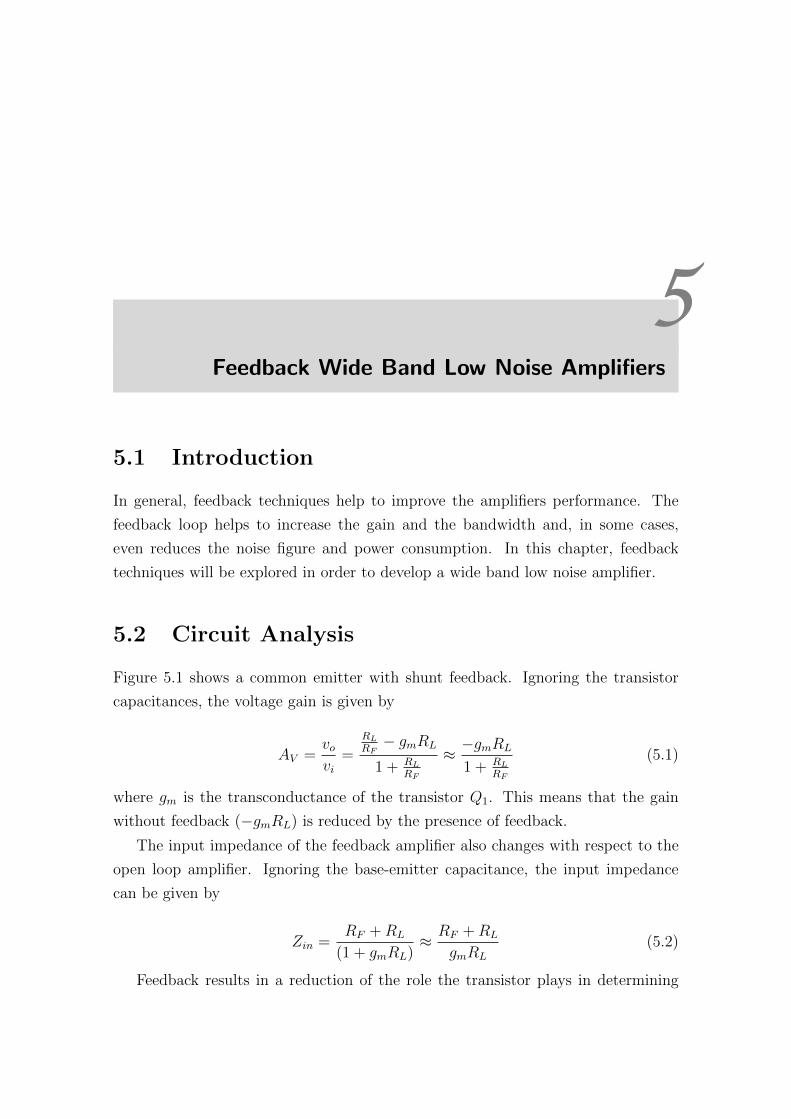
5Feedback Wide Band Low Noise Amplifiers
5.1 Introduction
In general, feedback techniques help to improve the amplifiers performance. The
feedback loop helps to increase the gain and the bandwidth and, in some cases,
even reduces the noise figure and power consumption. In this chapter, feedback
techniques will be explored in order to develop a wide band low noise amplifier.
5.2 Circuit Analysis
Figure 5.1 shows a common emitter with shunt feedback. Ignoring the transistor
capacitances, the voltage gain is given by
AV =vovi
=RLRF
− gmRL
1 + RLRF
≈ −gmRL
1 + RLRF
(5.1)
where gm is the transconductance of the transistor Q1. This means that the gain
without feedback (−gmRL) is reduced by the presence of feedback.
The input impedance of the feedback amplifier also changes with respect to the
open loop amplifier. Ignoring the base-emitter capacitance, the input impedance
can be given by
Zin =RF +RL
(1 + gmRL)≈ RF +RL
gmRL
(5.2)
Feedback results in a reduction of the role the transistor plays in determining
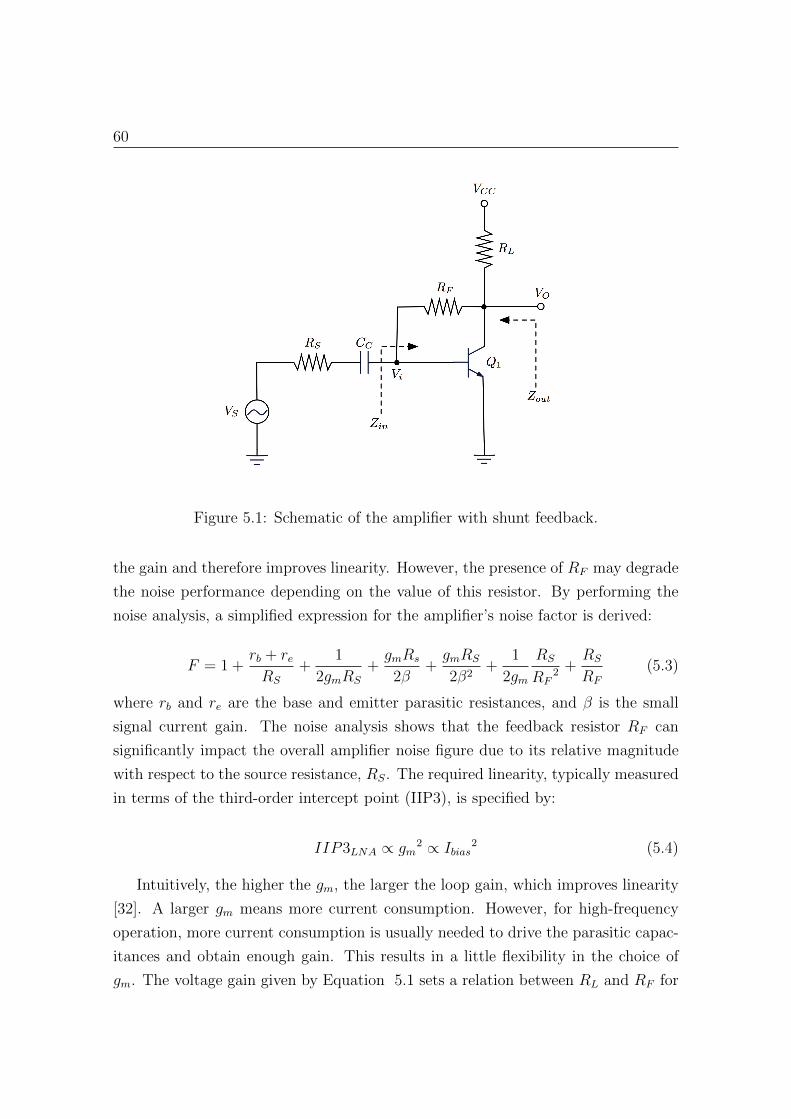
60
Figure 5.1: Schematic of the amplifier with shunt feedback.
the gain and therefore improves linearity. However, the presence of RF may degrade
the noise performance depending on the value of this resistor. By performing the
noise analysis, a simplified expression for the amplifier’s noise factor is derived:
F = 1 +rb + reRS
+1
2gmRS
+gmRs
2β+
gmRS
2β2+
1
2gm
RS
RF2 +
RS
RF
(5.3)
where rb and re are the base and emitter parasitic resistances, and β is the small
signal current gain. The noise analysis shows that the feedback resistor RF can
significantly impact the overall amplifier noise figure due to its relative magnitude
with respect to the source resistance, RS. The required linearity, typically measured
in terms of the third-order intercept point (IIP3), is specified by:
IIP3LNA ∝ gm2 ∝ Ibias
2 (5.4)
Intuitively, the higher the gm, the larger the loop gain, which improves linearity
[32]. A larger gm means more current consumption. However, for high-frequency
operation, more current consumption is usually needed to drive the parasitic capac-
itances and obtain enough gain. This results in a little flexibility in the choice of
gm. The voltage gain given by Equation 5.1 sets a relation between RL and RF for

Feedback Wide Band Low Noise Amplifiers 61
Figure 5.2: Schematic of the amplifier with active feedback.
a given gm. As a result, the noise factor and input resistance are coupled because,
as shown in Equations 5.2 and 5.3, they both depend on RL and RF . Because of
this trade-off, it is generally difficult to achieve an arbitrarily low noise factor for an
input impedance of 50 Ω with a reasonable current consumption.
To resolve this issue, the resistive feedback can be replaced by a feedback through
an emitter follower. Figure 5.2 shows the proposed topology. The amplifier consists
of a single stage in common emitter configuration and an emitter follower in the
feedback path.
At low frequency the input impedance can be given by
Zin =1 + gm2RF
gm2(1 + gm1RL)≈ RF
gm1RL
(5.5)
where gm2 is the transconductance of the transistor Q2 in the source follower.
Under the input matching condition (Zin = 50 Ω) and for the same voltage gain,
the required value of RF is now enhanced compared with the previous case, and
from Equation 5.3 a low noise factor is achieved.
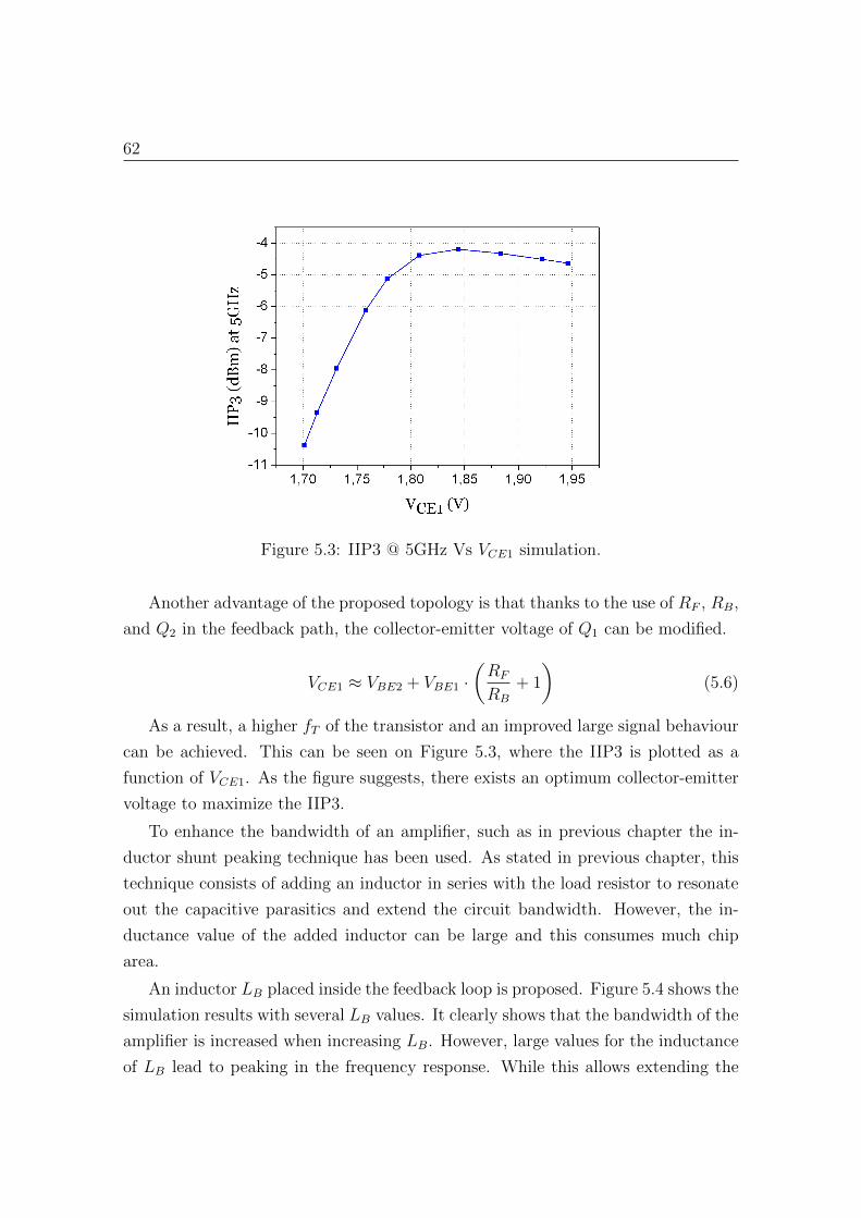
62
Figure 5.3: IIP3 @ 5GHz Vs VCE1 simulation.
Another advantage of the proposed topology is that thanks to the use of RF , RB,
and Q2 in the feedback path, the collector-emitter voltage of Q1 can be modified.
VCE1 ≈ VBE2 + VBE1 ·RF
RB
+ 1
(5.6)
As a result, a higher fT of the transistor and an improved large signal behaviour
can be achieved. This can be seen on Figure 5.3, where the IIP3 is plotted as a
function of VCE1. As the figure suggests, there exists an optimum collector-emitter
voltage to maximize the IIP3.
To enhance the bandwidth of an amplifier, such as in previous chapter the in-
ductor shunt peaking technique has been used. As stated in previous chapter, this
technique consists of adding an inductor in series with the load resistor to resonate
out the capacitive parasitics and extend the circuit bandwidth. However, the in-
ductance value of the added inductor can be large and this consumes much chip
area.
An inductor LB placed inside the feedback loop is proposed. Figure 5.4 shows the
simulation results with several LB values. It clearly shows that the bandwidth of the
amplifier is increased when increasing LB. However, large values for the inductance
of LB lead to peaking in the frequency response. While this allows extending the
Feedback Wide Band Low Noise Amplifiers 63
Figure 5.4: S21 Vs. LB simulation.
bandwidth to higher frequencies, excessive peaking is undesirable for broadband
communications systems which require a flat group delay. The quality factor (Q) of
this inductor is only of minor importance in this application, due to its low noise
contribution in the signal path. Indeed, the lower the quality factor, the higher the
series resistance associated to it. This series resistance adds to RF enhancing the
circuit noise performance.
In this work, we propose two options to implement LB: a conventional spiral
inductor and a modified miniature 3D inductor. A detailed study of the latter will
be presented in next section.
The inductor Linput is used to achieve a good response the whole frequency
range (from 0 GHz to 15 GHz). This coil is in the direct path of the signal but its
inductance value is low. Fortunately, as low inductance spirals are achieved with a
small number of turns, the quality factor is high and, in consequence, its contribution
to the total noise figure will be low.

64
Figure 5.5: Layout and geometric parameter of and on-chip inductor.
Figure 5.6: Microphotograph and measured quality factor and inductance of theproposed inductor.
5.3 Modified Miniatured 3D Inductor
As explained earlier, the conventional approach to design an integrated inductor on
silicon is to layout a simple metallic spiral directly on the substrate (see Figure 5.5).
At least two metal levels must be available, because an underpass is required to give
access to one of the inductor’s port. The challenge is to choose, for a given technology
with fixed metal properties, the optimum combination of the number of turns (n),
the metal width (w), the spacing between tracks (s), and the external radio (r) to
provide a specific inductance and optimum quality factor at the frequency we are
working on. This task is disturbed at high frequencies by the eddy current effects
in substrate and metal turns and skin effect in the metal conductor.
Large inductance values typically combine with large areas and small QS: an

Feedback Wide Band Low Noise Amplifiers 65
increase of the number of turns in the spiral coil or an increase of the coil radii
results in an increased magnetic flux and thus a higher inductance value, but also in
a proportionally higher series resistance. This can be seen in Figure 5.6, where the
micro photograph and measured L and Q of a conventional high inductance spiral
coil is shown (n=3.5, w=10 µm, s=2 µm and r=120 µm). The low-cost employed
technology, SiGe 0.35 µm, provides four metal levels. Three of them are similar,
with equal thickness and conductivity, and the top level metal is thicker and more
conductive. Standard coils are designed using this top metal, which presents a lower
series resistance and is far from substrate enough to work at high frequencies.
As discussed in section 3.3.2, to save some silicon area, some authors employ
stacked inductors. As it can be seen in Figure 3.6, it consists of series connected
spiral inductors in different metal layers. Since the spirals are identical, the induc-
tance value of each spiral separately will be the same. Spiral inductor segments in
different layers, close to each other, have positive mutual inductance between them
because current flows to the same direction. So, the total inductance value of the
structure will increase due to the strong mutual coupling between them, and it can
be achieved high inductance in small area.
However, the use of more metal layers makes the capacitive parasitic effects
amplify because of the metal-to-metal new capacitance and the increase of the metal-
to-substrate oxide capacitance. Thus, the stacked inductor suffers from low self-
resonance frequency. In an attempt to preserve the advantages of stacked inductor,
and at the same time, to increase the resonant frequency and the quality factor, Tang
et al. proposed in 2002 the miniature 3D inductors [33]. This structure consists of
at least two or more stacked inductors by series connections, and every stacked
inductor has only one turn in every metal layer.
For example, if there are two stacked inductors with different diameters, and one
of them is a one-turn stacked inductor from the metal layer 4 to the metal layer 1,
and the other is a one turn stacked inductor from the metal layer 1 to the metal layer
3, then the miniature 3D inductor is formed by connecting two stacked inductors at
the metal 1, as Figure 5.7 shows.
The proposed structure for inductor LB consists of two 3D rectangular coils
serially connected through the lower metal level, as shown in Figure 5.8. This
way, part of the magnetic flux generated by the coils is shared. Consequently, the
structure total inductance is greater than the addition of both 3D inductance values
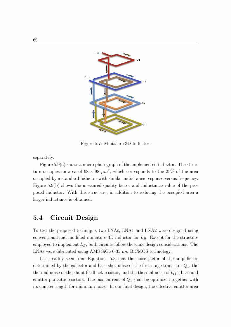
66
Figure 5.7: Miniature 3D Inductor.
separately.
Figure 5.9(a) shows a micro photograph of the implemented inductor. The struc-
ture occupies an area of 98 x 98 µm2, which corresponds to the 25% of the area
occupied by a standard inductor with similar inductance response versus frequency.
Figure 5.9(b) shows the measured quality factor and inductance value of the pro-
posed inductor. With this structure, in addition to reducing the occupied area a
larger inductance is obtained.
5.4 Circuit Design
To test the proposed technique, two LNAs, LNA1 and LNA2 were designed using
conventional and modified miniature 3D inductor for LB. Except for the structure
employed to implement LB, both circuits follow the same design considerations. The
LNAs were fabricated using AMS SiGe 0.35 µm BiCMOS technology.
It is readily seen from Equation 5.3 that the noise factor of the amplifier is
determined by the collector and base shot noise of the first stage transistor Q1, the
thermal noise of the shunt feedback resistor, and the thermal noise of Q1’s base and
emitter parasitic resistors. The bias current of Q1 shall be optimized together with
its emitter length for minimum noise. In our final design, the effective emitter area
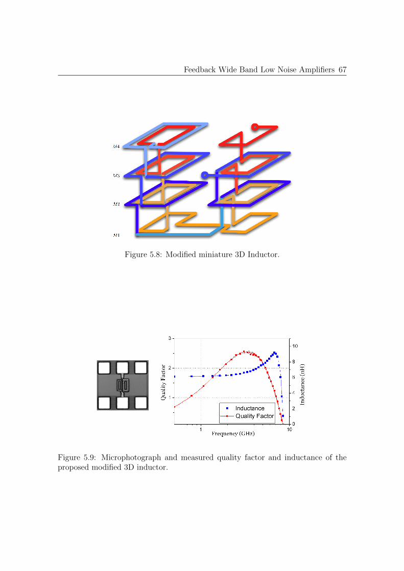
Feedback Wide Band Low Noise Amplifiers 67
Figure 5.8: Modified miniature 3D Inductor.
Figure 5.9: Microphotograph and measured quality factor and inductance of theproposed modified 3D inductor.
68
of Q1 is 36 µm2. The emitter follower Q2 contributes only little to the output noise
and an effective emitter area of 1.6 µm has been chosen.
The feedback resistor, RF , has a large impact on the noise factor. To reduce its
noise contribution, a large value shall be used in conjunction with the consideration
for input impedance match. The choice of the feedback resistor determines the
operating bandwidth. Low RF increases the operating bandwidth with the sacrifice
of the gain and noise performance. The use of the peaking inductor LB in the
feedback path allows alleviating this trade-off, and its inductance value should be
chosen as high as possible up to where it can meet the bandwidth requirement
without excessive peaking. As explained in previous sections, the quality factor of
inductor LB is not relevant. In this case, achieving a high-value inductance in a small
area is the major requirement. For that reason a modified miniature 3D inductor
could be a better solution for LB. A different situation is observed for Linput. This
inductor is in series with the input and is used to help matching the input impedance
within the entire band. Its quality factor should be as high as possible, since its
value affects the overall noise performance. As the required inductance value is low,
a conventional spiral inductor can be used in the implementation (1.5 turns).
The load, consisting of a poly-silicon resistor RL, is designed to achieve a flat
broadband gain over the entire UWB band. According to analysis showed in previous
sections, amplifier linearity depends on VCE1 selection through the feedback circuit.
The value of RB is chosen to maximize IIP3 and is calculated using bias current and
supply voltage to bias the device at its low tolerance point to the distortion.
5.5 Experimental Results
The die photographs of LNA1 and LNA2 are shown in Figure 5.10. The chip area
excluding the test pads is 490 x 355 µm2 for LNA1 and 330 x 310 µm2 for LNA2.
Note that the proposed technique achieves a 40% of area reduction, and as we will
show later, with minor performance degradation over the same circuit implemented
with conventional inductors.
The S parameters and the noise figure of both circuits were measured using
ground-signal-ground microwave probes. Both circuits operate with a supply voltage
of 3.3 V and consume 4 mA.
Figures 5.11 and 5.12 show the measured gain and noise figure for 50 Ω source

Feedback Wide Band Low Noise Amplifiers 69
Figure 5.10: Chip photograph of (a) LNA1: with conventional spiral inductor and(b) LNA2: with modified miniature 3D inductor
Figure 5.11: Simulated and measured gain.
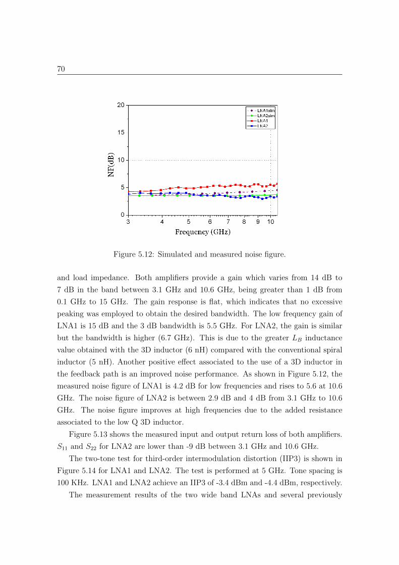
70
Figure 5.12: Simulated and measured noise figure.
and load impedance. Both amplifiers provide a gain which varies from 14 dB to
7 dB in the band between 3.1 GHz and 10.6 GHz, being greater than 1 dB from
0.1 GHz to 15 GHz. The gain response is flat, which indicates that no excessive
peaking was employed to obtain the desired bandwidth. The low frequency gain of
LNA1 is 15 dB and the 3 dB bandwidth is 5.5 GHz. For LNA2, the gain is similar
but the bandwidth is higher (6.7 GHz). This is due to the greater LB inductance
value obtained with the 3D inductor (6 nH) compared with the conventional spiral
inductor (5 nH). Another positive effect associated to the use of a 3D inductor in
the feedback path is an improved noise performance. As shown in Figure 5.12, the
measured noise figure of LNA1 is 4.2 dB for low frequencies and rises to 5.6 at 10.6
GHz. The noise figure of LNA2 is between 2.9 dB and 4 dB from 3.1 GHz to 10.6
GHz. The noise figure improves at high frequencies due to the added resistance
associated to the low Q 3D inductor.
Figure 5.13 shows the measured input and output return loss of both amplifiers.
S11 and S22 for LNA2 are lower than -9 dB between 3.1 GHz and 10.6 GHz.
The two-tone test for third-order intermodulation distortion (IIP3) is shown in
Figure 5.14 for LNA1 and LNA2. The test is performed at 5 GHz. Tone spacing is
100 KHz. LNA1 and LNA2 achieve an IIP3 of -3.4 dBm and -4.4 dBm, respectively.
The measurement results of the two wide band LNAs and several previously
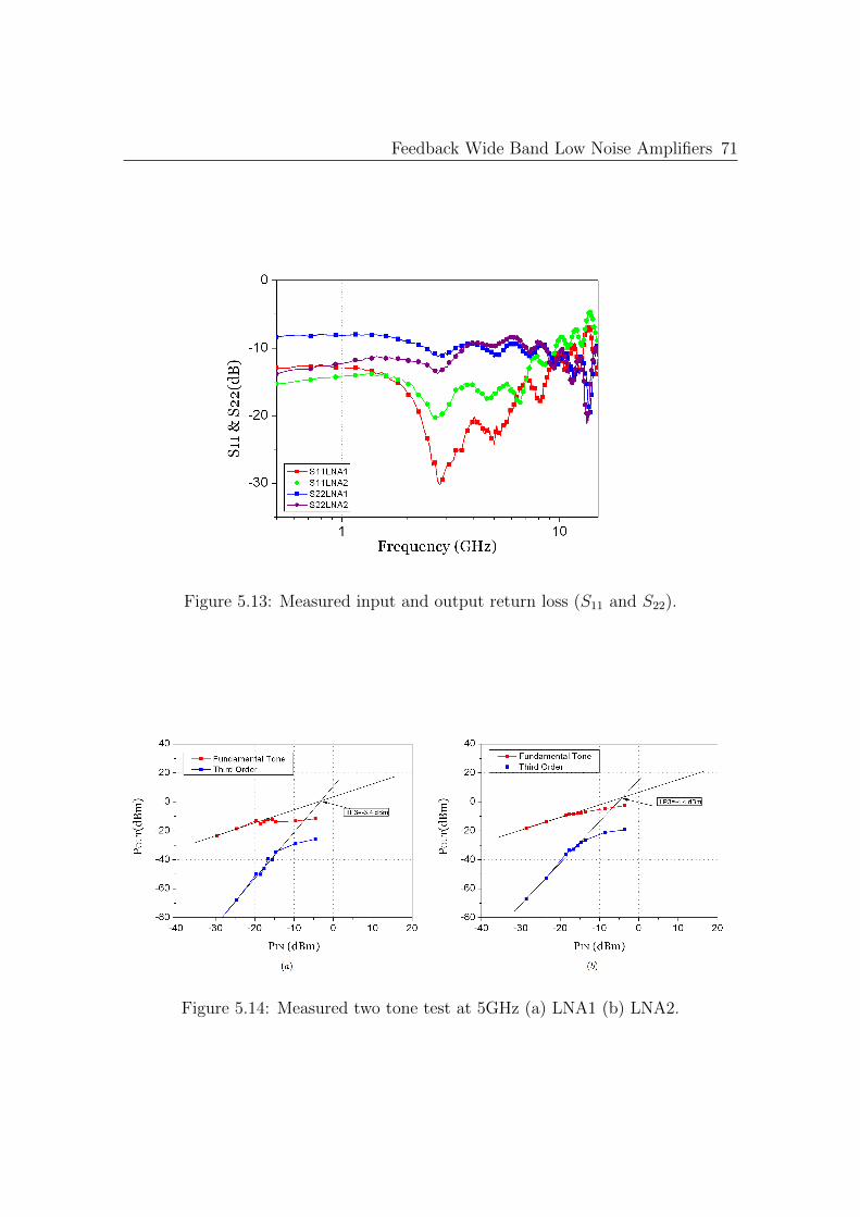
Feedback Wide Band Low Noise Amplifiers 71
Figure 5.13: Measured input and output return loss (S11 and S22).
Figure 5.14: Measured two tone test at 5GHz (a) LNA1 (b) LNA2.
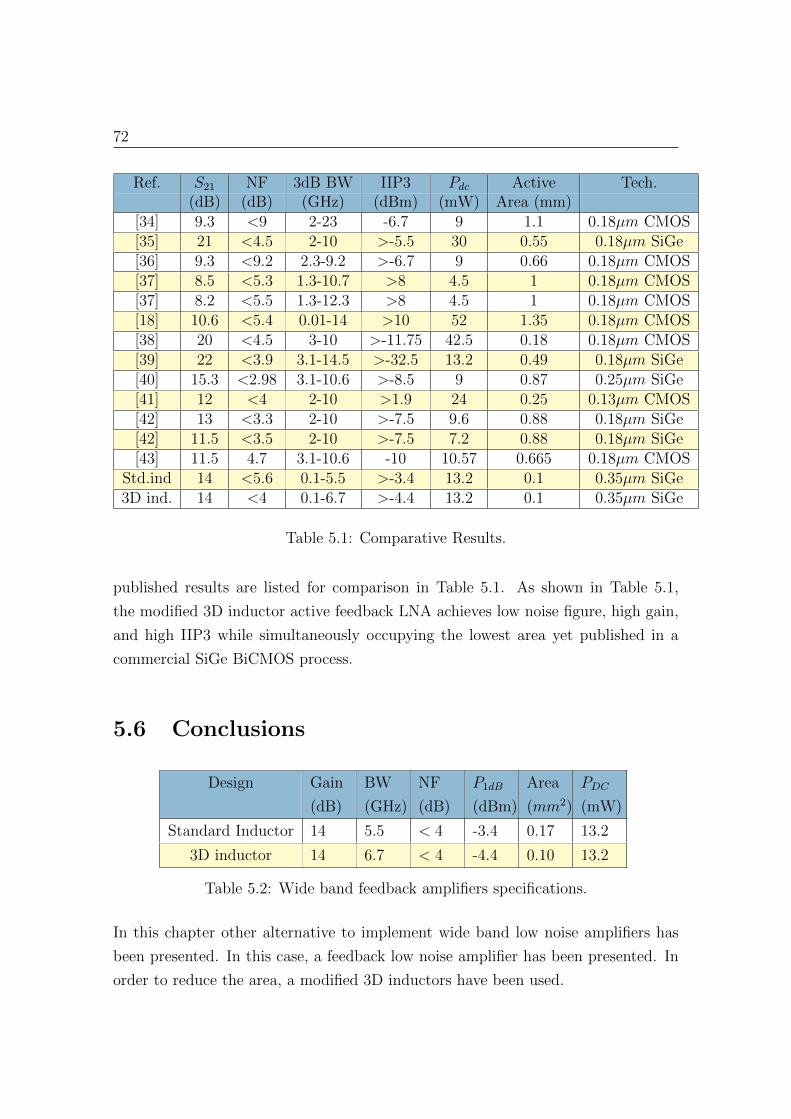
72
Ref. S21 NF 3dB BW IIP3 Pdc Active Tech.(dB) (dB) (GHz) (dBm) (mW) Area (mm)
[34] 9.3 <9 2-23 -6.7 9 1.1 0.18µm CMOS[35] 21 <4.5 2-10 >-5.5 30 0.55 0.18µm SiGe[36] 9.3 <9.2 2.3-9.2 >-6.7 9 0.66 0.18µm CMOS[37] 8.5 <5.3 1.3-10.7 >8 4.5 1 0.18µm CMOS[37] 8.2 <5.5 1.3-12.3 >8 4.5 1 0.18µm CMOS[18] 10.6 <5.4 0.01-14 >10 52 1.35 0.18µm CMOS[38] 20 <4.5 3-10 >-11.75 42.5 0.18 0.18µm CMOS[39] 22 <3.9 3.1-14.5 >-32.5 13.2 0.49 0.18µm SiGe[40] 15.3 <2.98 3.1-10.6 >-8.5 9 0.87 0.25µm SiGe[41] 12 <4 2-10 >1.9 24 0.25 0.13µm CMOS[42] 13 <3.3 2-10 >-7.5 9.6 0.88 0.18µm SiGe[42] 11.5 <3.5 2-10 >-7.5 7.2 0.88 0.18µm SiGe[43] 11.5 4.7 3.1-10.6 -10 10.57 0.665 0.18µm CMOS
Std.ind 14 <5.6 0.1-5.5 >-3.4 13.2 0.1 0.35µm SiGe3D ind. 14 <4 0.1-6.7 >-4.4 13.2 0.1 0.35µm SiGe
Table 5.1: Comparative Results.
published results are listed for comparison in Table 5.1. As shown in Table 5.1,
the modified 3D inductor active feedback LNA achieves low noise figure, high gain,
and high IIP3 while simultaneously occupying the lowest area yet published in a
commercial SiGe BiCMOS process.
5.6 Conclusions
Design Gain
(dB)
BW
(GHz)
NF
(dB)
P1dB
(dBm)
Area
(mm2)
PDC
(mW)
Standard Inductor 14 5.5 < 4 -3.4 0.17 13.2
3D inductor 14 6.7 < 4 -4.4 0.10 13.2
Table 5.2: Wide band feedback amplifiers specifications.
In this chapter other alternative to implement wide band low noise amplifiers has
been presented. In this case, a feedback low noise amplifier has been presented. In
order to reduce the area, a modified 3D inductors have been used.
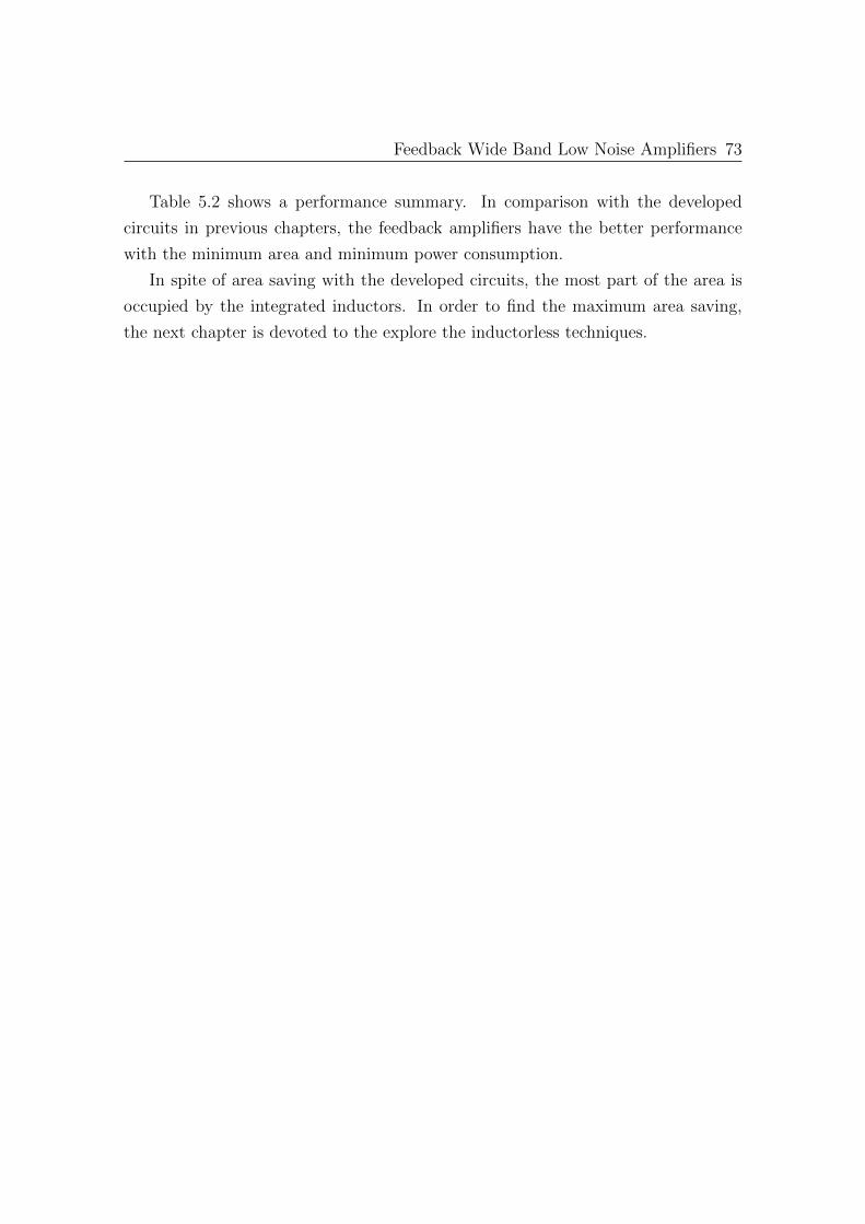
Feedback Wide Band Low Noise Amplifiers 73
Table 5.2 shows a performance summary. In comparison with the developed
circuits in previous chapters, the feedback amplifiers have the better performance
with the minimum area and minimum power consumption.
In spite of area saving with the developed circuits, the most part of the area is
occupied by the integrated inductors. In order to find the maximum area saving,
the next chapter is devoted to the explore the inductorless techniques.

74
6Inductorless Techniques
6.1 Introduction
The number of inductors and the area occupied by them is an inconvenience in ra-
diofrequency integrated circuit design. In previous chapters, an area saving has been
achieved with different topologies of inductors but the inductors are still necessary
in these designs.
In order to reduce the area consumption, it is important trying to avoid the
use of inductors, for this reason, this chapter is devoted to explore the inductorless
techniques with the design of a front-end based on a common gate LNA inductorless
and a quadrature Gilbert cell mixer.
6.2 Common Gate LNA
Common-gate (CG) LNA is a widely used topology in wireless communications
[44],[8],[4],[45]. In this section, the CG LNA is studied, i.e., the relationship between
the input matching and voltage gain or the noise figure.
6.2.1 Input Matching and Voltage Gain
The desired input impedance of a CG input stage is achieved by adjusting the bias
current, aspect ratio, and overdrive voltage. Thus, for an input impedance of 50 Ω,
the objective is to obtain 1/gm of approximately of 20 mS . The CG stage does not
suffer from the Miller effect, and thus an adequate reverse isolation can be achieved
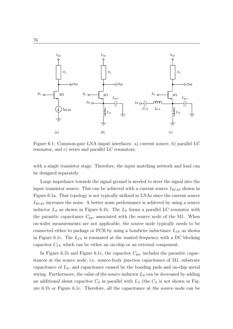
76
Figure 6.1: Common-gate LNA imput interfaces: a) current source, b) parallel LCresonator, and c) series and parallel LC resonators.
with a single transistor stage. Therefore, the input matching network and load can
be designed separately.
Large impedance towards the signal ground is needed to steer the signal into the
input transistor source. This can be achieved with a current source IBIAS shown in
Figure 6.1a. That topology is not typically utilized in LNAs since the current source
IBIAS increases the noise. A better noise performance is achieved by using a source
inductor LS as shown in Figure 6.1b. The LS forms a parallel LC resonator with
the parasitic capacitance Cpar associated with the source node of the M1. When
on-wafer measurements are not applicable, the source node typically needs to be
connected either to package or PCB by using a bondwire inductance LIN as shown
in Figure 6.1c. The LIN is resonated at the wanted frequency with a DC blocking
capacitor CIN which can be either an on-chip or an external component.
In Figure 6.1b and Figure 6.1c, the capacitor Cpar includes the parasitic capac-
itances at the source node, i.e. source-body junction capacitance of M1, substrate
capacitance of LS, and capacitance caused by the bonding pads and on-chip metal
wiring. Furthermore, the value of the source inductor LS can be decreased by adding
an additional shunt capacitor CS in parallel with LS (the CS is not shown in Fig-
ure 6.1b or Figure 6.1c. Therefore, all the capacitance at the source node can be

Inductorless Techniques 77
included in a single source capacitor CT used in the following calculations:
CT = CGS + CPAR + CS (6.1)
The input impedance ZIN of a CG input stage, shown in Figure 6.1b, can be
calculated as
ZIN =sLS
1 + sLSgm+ s2 + LSCT
(6.2)
The source inductance LS resonates with the capacitance CT at the frequency of
ωo =1√
LSCT
(6.3)
and at that frequency, Equation 6.2 simplifies to 1/gm. The impedance ZIN of a
CG input stage shown in Figure 6.1c is
ZIN =1 + s2CINLIN
sCIN
+sLS
1 + sLsgm+ s2LSCT
(6.4)
With a perfect impedance matching (1/gm = RS), where RS is the source output
resistance. The voltage gain of the CG amplifier becomes a division of output load
versus the source impedance, i.e. ZL/RS. The assumption is valid if the drain-to-
source resistor rds is much larger than the load resistance at the drain. Otherwise,
the gain and input resistance formulas should be modified to:
AV =gmZLa+ ZL
rds
(6.5)
and
RIN =1
gm
1 +
ZL
rds
(6.6)
6.2.2 Noise of a CG Stage
The noise factor of a CG LNA is expressed as [46]:
F = 1 +γ
α
1
1 + χ
2 1
gmRS
(6.7)
78
where γ is the coefficient of channel thermal noise, gm is the transistor transconduc-
tance, χ is the ratio of the transistor substrate transconductance gmb and gm, RS
is the source resistance and α is gm/gdo. Because the minimum NF of a common
source LNA increases along with the frequency, CG LNAs can be a better option at
very high frequencies. When χ is neglected and perfect input matching is assumed,
the minimum noise factor typically presented in the literature is achieved:
F = 1 +γ
χ=
5
3= 2.2dB (6.8)
With imperfect input matching, the noise factor can be lowered according to
F = 1 + γ1 + S11
1− S11(6.9)
where α is neglected.
Equation 6.8 does not take into account the noise of the load. If resistive load
RL is used, taking into account its noise contribution, assuming that gm = 1/RS
the noise factor becomes
F = 1 +1
gmRS
γ
α+
(1 + gmRs)2
gmRL
1 +
γ
α+
4RS
RL
(6.10)
Thus, the resistive load can make a significant contribution to the overall noise.
6.2.3 Differential Operation of CG Stage
In Figure 6.2, the capacitor cross-coupling method, which is suitable for differential
input configurations, is presented. Due to the capacitor divider between CGS and
coupling capacitance Cp, the inverting gain is approximately A = Cp/(Cp + CGS),
which is always less than one.
6.3 Mixer Design
6.3.1 Quadrature Mixers
Normally, the down conversion to zero or IF frequency is usually performed with
quadrature (I/Q) mixers [47]. For I/Q mixers, there are different possibilities to
implement the interface between input transconductor and switch quad. The first
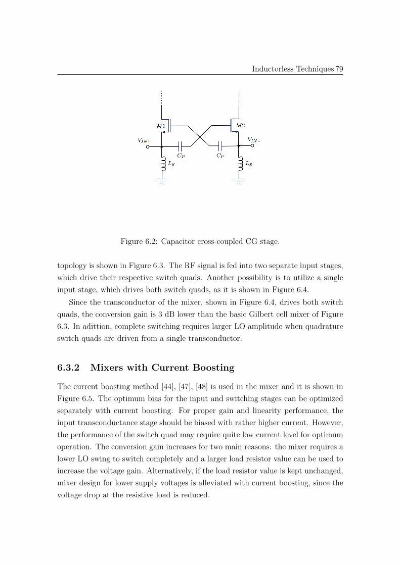
Inductorless Techniques 79
Figure 6.2: Capacitor cross-coupled CG stage.
topology is shown in Figure 6.3. The RF signal is fed into two separate input stages,
which drive their respective switch quads. Another possibility is to utilize a single
input stage, which drives both switch quads, as it is shown in Figure 6.4.
Since the transconductor of the mixer, shown in Figure 6.4, drives both switch
quads, the conversion gain is 3 dB lower than the basic Gilbert cell mixer of Figure
6.3. In adittion, complete switching requires larger LO amplitude when quadrature
switch quads are driven from a single transconductor.
6.3.2 Mixers with Current Boosting
The current boosting method [44], [47], [48] is used in the mixer and it is shown in
Figure 6.5. The optimum bias for the input and switching stages can be optimized
separately with current boosting. For proper gain and linearity performance, the
input transconductance stage should be biased with rather higher current. However,
the performance of the switch quad may require quite low current level for optimum
operation. The conversion gain increases for two main reasons: the mixer requires a
lower LO swing to switch completely and a larger load resistor value can be used to
increase the voltage gain. Alternatively, if the load resistor value is kept unchanged,
mixer design for lower supply voltages is alleviated with current boosting, since the
voltage drop at the resistive load is reduced.
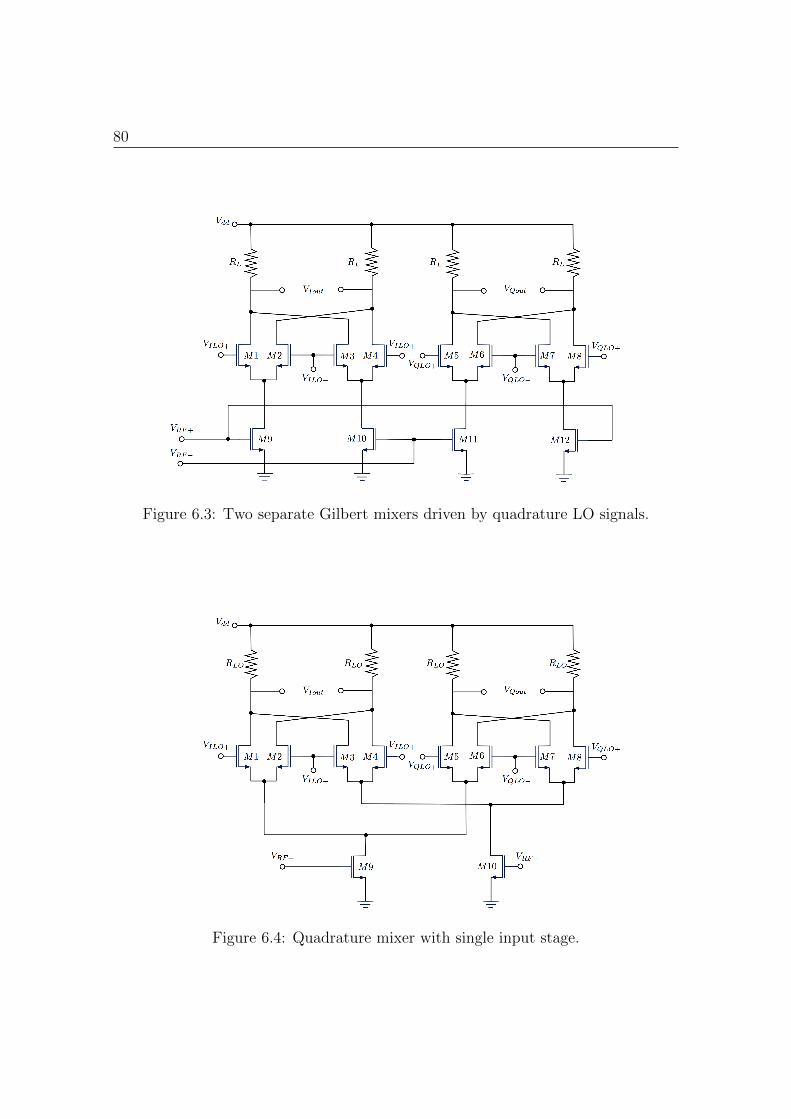
80
Figure 6.3: Two separate Gilbert mixers driven by quadrature LO signals.
Figure 6.4: Quadrature mixer with single input stage.

Inductorless Techniques 81
Figure 6.5: Current boosting with constant current source.
6.4 Inductorless Operation
Figure 6.6 shows a simplified interface between the LNA and mixer. Biasing and
AC coupling have been omitted for clarify. In this Figure, M0 represents the LNA
transconductor, wich is realized as a CG stage. Further, M1 represents the RF
transconductor of the mixer. The circuit in Figure 6.6a shows the use of conventional
inductive peaking to extend the bandwidth at the LNA output (It is really the
LNA-mixer interface bandwidth that is being extended.). This bandwidth extension
occurs due to the addition of a zero in the transfer function due to the inductor. A
zero can also be introduced by capacitive degeneration as shown in Figure 6.6b [49].
In this circuit, the RC combination of CS and RS provides a zero that extends the
high frequency response. Effectively, capacitive degeneration provides bandwidth
extension properties similar to inductive peaking [50].
6.5 Experimental Results
6.5.1 Frontend I
Figure 6.7 shows an RF frontend composed by a differential common-gate shunt-
peaking LNA followed by differential double balanced Gilbert mixer. The layout of

82
Figure 6.6: Simplified circuits for (a) inductive peaking and (b) capacitive peaking.
the circuit, named as Frontend I, is shown in Figure 6.8. The Frontend I chip area,
including the test pads, is 1410.63 x 693.39 µm2.
Conversion gain and noise figure simulation results are shown in Figure 6.9 and
Figure 6.10 respectively, for a 400 MHz channel located at the center of the band.
Frontend I has a conversion gain of 12.1 dB at 5.2 GHz and a noise figure of 11.2
dB (IF=200MHz).
The two-tone test for third-order intermodulation distortion (IIP3) of Frontend
I is shown in Figure 6.11. The test was performed at 5 GHz and an IIP3 of -5.7
dBm was obtained.
6.5.2 Frontend II
Figure 6.12 shows an RF frontend composed by a differential common-gate resistive
load LNA followed by differential double balanced Gilbert mixer with capacitive
degeneration. The layout of the circuit, named as Frontend II, is shown in Figure
6.13.
The Frontend II chip area, including the test pads, is 698.89 x 744.76µm2. Due
to the non existence of inductors, the occupied area of this design is 54% lower than
Frontend I.
Conversion gain and noise figure simulation results are shown in Figure 6.14 and
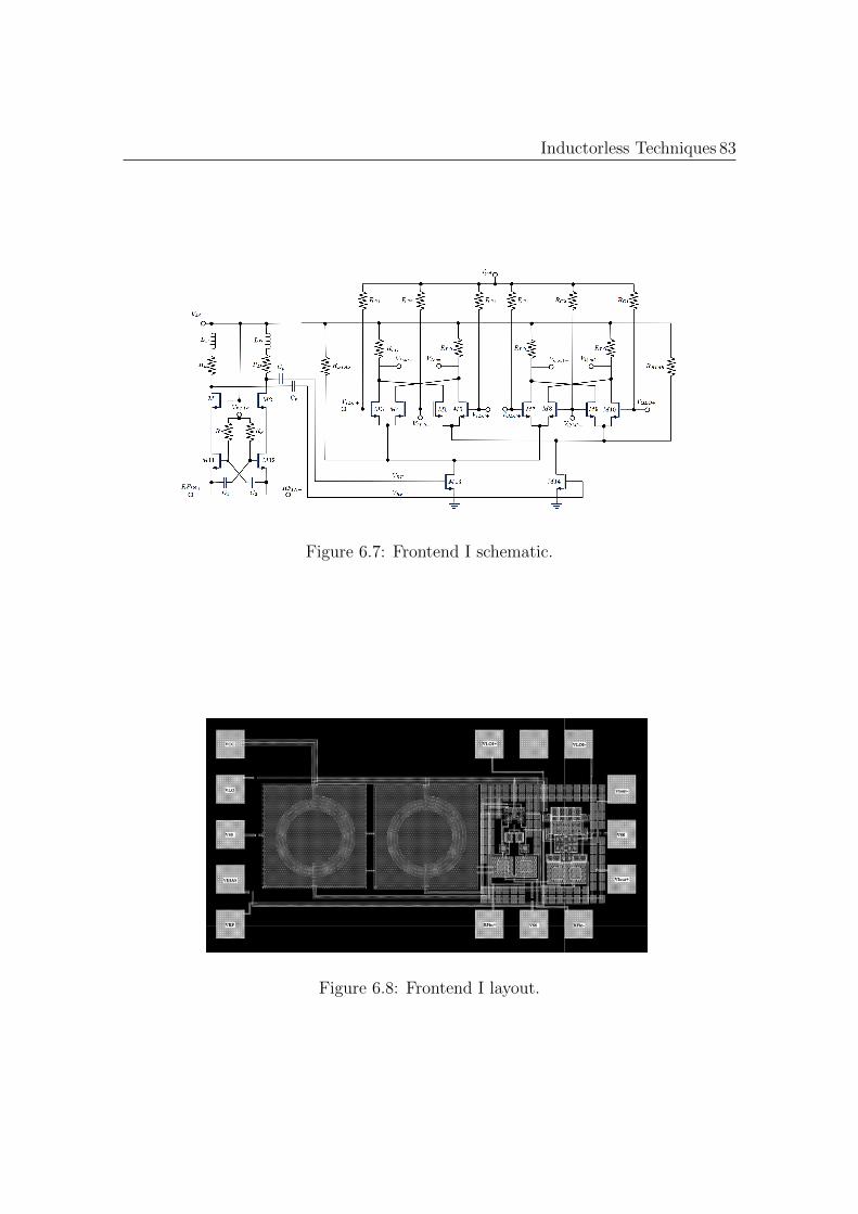
Inductorless Techniques 83
Figure 6.7: Frontend I schematic.
Figure 6.8: Frontend I layout.
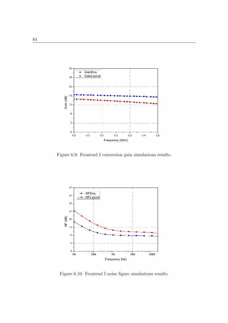
84
Figure 6.9: Frontend I conversion gain simulations results.
Figure 6.10: Frontend I noise figure simulations results.
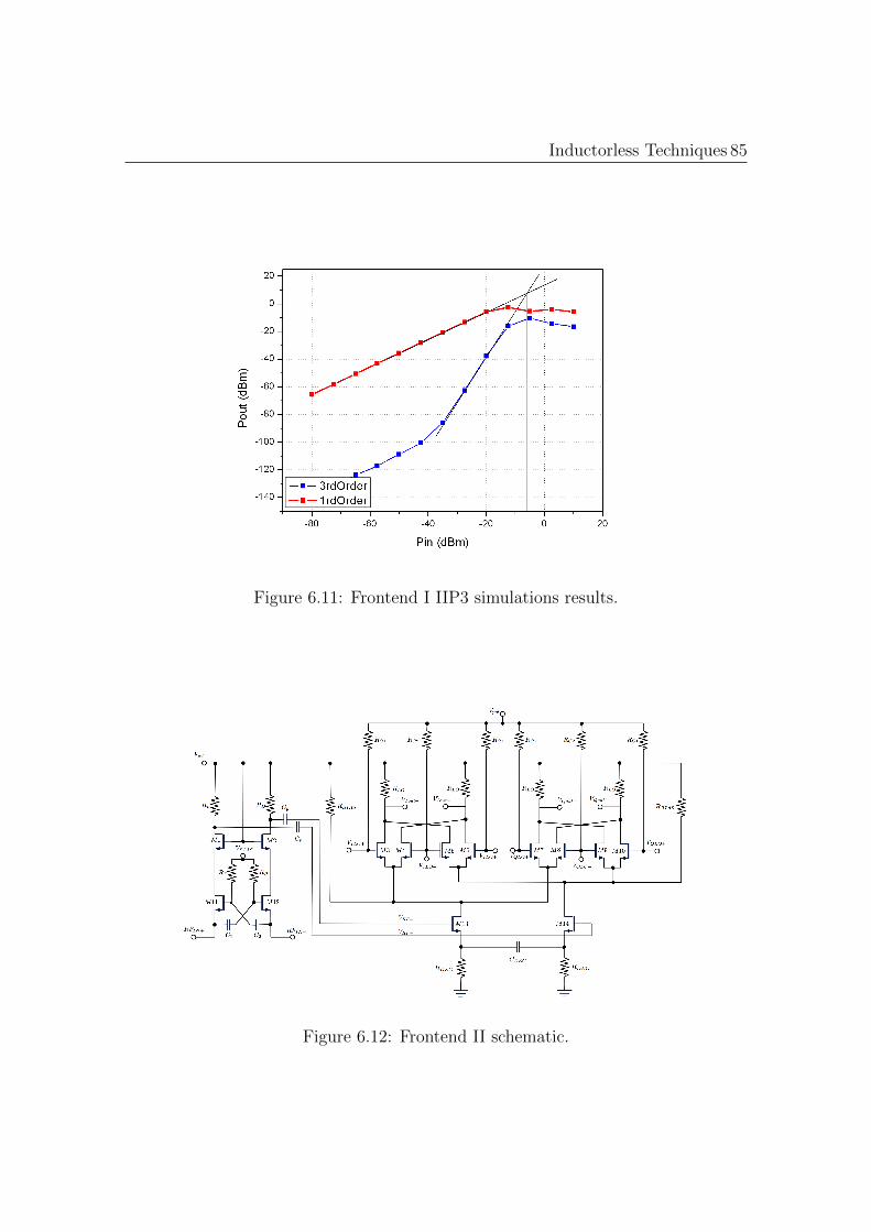
Inductorless Techniques 85
Figure 6.11: Frontend I IIP3 simulations results.
Figure 6.12: Frontend II schematic.
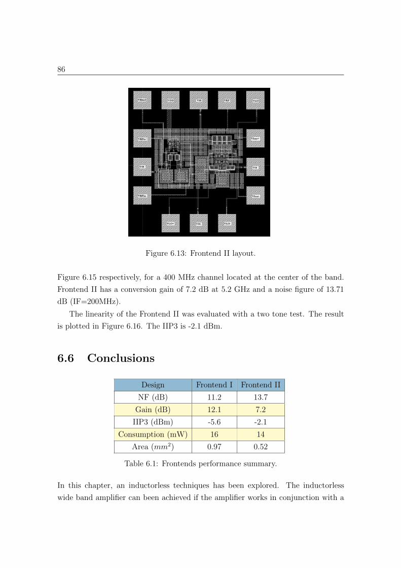
86
Figure 6.13: Frontend II layout.
Figure 6.15 respectively, for a 400 MHz channel located at the center of the band.
Frontend II has a conversion gain of 7.2 dB at 5.2 GHz and a noise figure of 13.71
dB (IF=200MHz).
The linearity of the Frontend II was evaluated with a two tone test. The result
is plotted in Figure 6.16. The IIP3 is -2.1 dBm.
6.6 Conclusions
Design Frontend I Frontend II
NF (dB) 11.2 13.7
Gain (dB) 12.1 7.2
IIP3 (dBm) -5.6 -2.1
Consumption (mW) 16 14
Area (mm2) 0.97 0.52
Table 6.1: Frontends performance summary.
In this chapter, an inductorless techniques has been explored. The inductorless
wide band amplifier can been achieved if the amplifier works in conjunction with a
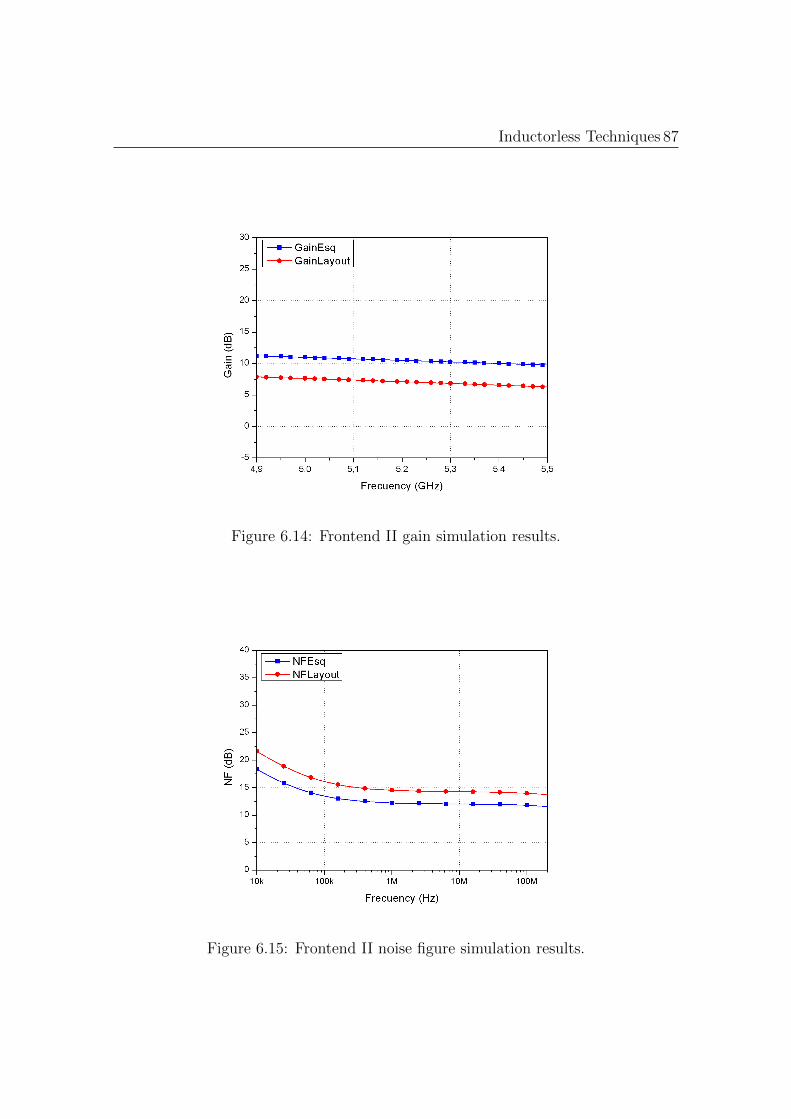
Inductorless Techniques 87
Figure 6.14: Frontend II gain simulation results.
Figure 6.15: Frontend II noise figure simulation results.
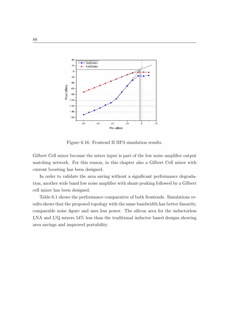
88
Figure 6.16: Frontend II IIP3 simulation results.
Gilbert Cell mixer because the mixer input is part of the low noise amplifier output
matching network. For this reason, in this chapter also a Gilbert Cell mixer with
current boosting has been designed.
In order to validate the area saving without a significant performance degrada-
tion, another wide band low noise amplifier with shunt-peaking followed by a Gilbert
cell mixer has been designed.
Table 6.1 shows the performance comparative of both frontends. Simulations re-
sults shows that the proposed topology with the same bandwidth has better linearity,
comparable noise figure and uses less power. The silicon area for the inductorless
LNA and I/Q mixers 54% less than the traditional inductor based designs showing
area savings and improved portability.
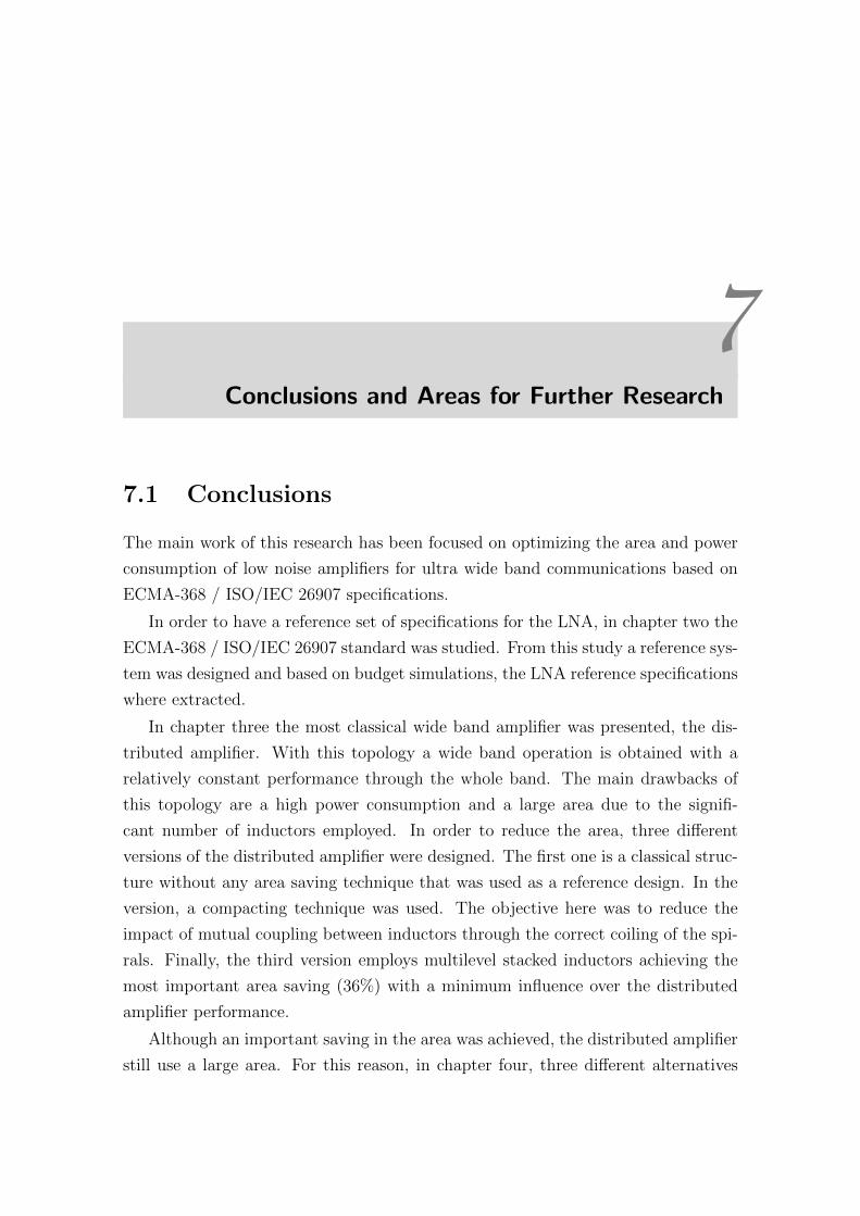
7Conclusions and Areas for Further Research
7.1 Conclusions
The main work of this research has been focused on optimizing the area and power
consumption of low noise amplifiers for ultra wide band communications based on
ECMA-368 / ISO/IEC 26907 specifications.
In order to have a reference set of specifications for the LNA, in chapter two the
ECMA-368 / ISO/IEC 26907 standard was studied. From this study a reference sys-
tem was designed and based on budget simulations, the LNA reference specifications
where extracted.
In chapter three the most classical wide band amplifier was presented, the dis-
tributed amplifier. With this topology a wide band operation is obtained with a
relatively constant performance through the whole band. The main drawbacks of
this topology are a high power consumption and a large area due to the signifi-
cant number of inductors employed. In order to reduce the area, three different
versions of the distributed amplifier were designed. The first one is a classical struc-
ture without any area saving technique that was used as a reference design. In the
version, a compacting technique was used. The objective here was to reduce the
impact of mutual coupling between inductors through the correct coiling of the spi-
rals. Finally, the third version employs multilevel stacked inductors achieving the
most important area saving (36%) with a minimum influence over the distributed
amplifier performance.
Although an important saving in the area was achieved, the distributed amplifier
still use a large area. For this reason, in chapter four, three different alternatives
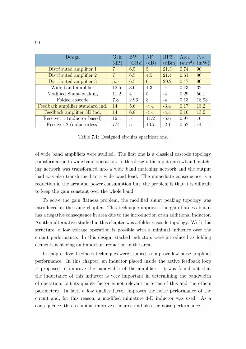
90
Design Gain(dB)
BW(GHz)
NF(dB)
IIP3(dBm)
Area(mm2)
PDC
(mW)Distributed amplifier 1 7 6.5 5 21.3 0.74 90Distributed amplifier 2 7 6.5 4.5 21.4 0.61 90Distributed amplifier 3 5.5 6.5 6 20.2 0.47 90Wide band amplifier 12.5 3.6 4.3 -4 0.13 32
Modified Shunt-peaking 11.2 4 5 -4 0.29 56.1Folded cascode 7.8 2.96 3 -4 0.13 18.93
Feedback amplifier standard ind. 14 5.6 < 4 -3.4 0.17 13.2Feedback amplifier 3D ind. 14 6.8 < 4 -4.4 0.10 13.2Receiver 1 (inductor based) 12.1 5 11.2 -5.6 0.97 16Receiver 2 (inductorless) 7.2 5 13.7 -2.1 0.52 14
Table 7.1: Designed circuits specifications.
of wide band amplifiers were studied. The first one is a classical cascode topology
transformation to wide band operation. In this design, the input narrowband match-
ing network was transformed into a wide band matching network and the output
load was also transformed to a wide band load. The immediate consequence is a
reduction in the area and power consumption but, the problem is that it is difficult
to keep the gain constant over the whole band.
To solve the gain flatness problem, the modified shunt peaking topology was
introduced in the same chapter. This technique improves the gain flatness but it
has a negative consequence in area due to the introduction of an additional inductor.
Another alternative studied in this chapter was a folder cascode topology. With this
structure, a low voltage operation is possible with a minimal influence over the
circuit performance. In this design, stacked inductors were introduced as folding
elements achieving an important reduction in the area.
In chapter five, feedback techniques were studied to improve low noise amplifier
performance. In this chapter, an inductor placed inside the active feedback loop
is proposed to improve the bandwidth of the amplifier. It was found out that
the inductance of this inductor is very important in determining the bandwidth
of operation, but its quality factor is not relevant in terms of this and the others
parameters. In fact, a low quality factor improves the noise performance of the
circuit and, for this reason, a modified miniature 3-D inductor was used. As a
consequence, this technique improves the area and also the noise performance.
Conclusions and Areas for Further Research 91
The area is mainly related with the number of inductors employed in the circuit.
In chapter six a circuit methodology for designing UWB RF frontends without the
use of inductors is described. To validate this design methodology two receiver RF
frontends were designed; a traditional inductor based design and an inductorless de-
sign. Both design use a common-gate LNA followed by two quadrature Gilbert cell
mixers. In the inductorless version, the LNA shunt-peaking load was replaced by a
resistive load and a capacitive degeneration was included in the mixer. Simulations
results show that the inductorless topology has better linearity, comparable noise
figure and uses less power with the same bandwidth. The silicon area for the induc-
torless LNA and I/Q mixers is roughly 54% less than the traditional inductor based
design, showing an important area saving and improving the circuit portability.
As a summary, Table 7.1 shows the main features of all the circuits developed in
the framework of this research work.
7.2 Areas for Further Research
In this research work several alternatives to implement an UWB LNA in low cost
technologies have been explored. An inductor less frontend was also introduced.
The main objective was to reduce the power consumption and area with a relatively
high bandwidth. There are several technical challenges that need further research
as:
• Design and integration of the rest of the receiver: This includes the
study and design of mixers, filters and baseband amplifiers for ultra wide band,
optimizing the power consumption and area.
• Inductors structures: Explore different alternatives to reduce the area of
integrated inductors with minimum impact on the circuit performance. This
implies also exploring new circuit topologies that require inductors with lower
performance.
• Inductor less structure: Improve the performance of inductorless receivers.
This is a promising technique since avoiding the use of inductors improve the
portability to other process technologies.

92

AResumen en Castellano
A.1 Introduccion
En los ultimos anos las de Redes de Area Personal (WPAN) se estan volviendo cada
vez mas populares. Estos sistemas permiten llevar a cabo la eliminacion del cableado
de interconexion en muchas aplicaciones a la vez que abren nuevas oportunidades
para el desarrollo de novedosas aplicaciones de consumo. Actualmente, los siste-
mas WPAN estan dominados por comunicaciones basadas en las especificaciones de
Bluetooth y Zigbee, que son estandares de comunicacion que operan en la banda
libre de 2.4 GHz. Para aumentar la tasa de transferencia de datos a unos cientos de
Mb/s, sin una incidencia considerable en el consumo de potencia, se han propuesto
las comunicaciones de ultra banda ancha (UWB).
El hecho de que las comunicaciones de ultra banda ancha suponen una solucion
viable al problema de la transferencia de datos en comunicaciones WPAN, esta
provocando que numerosas empresas estan centrando sus esfuerzos para sacar al
mercado soluciones basadas en esta tecnologıa. Algunas de estas empresas son las
siguientes:
Alereon [1]: Es una empresa con sede en Austin (Texas) que desarrolla cir-
cuitos de banda ancha con bajo consumo y que cumplen la especificacion de USB
inalambrico, ası como la especificacion ”WiMedia Ultra Wide Band”. Uno de los
productos desarrollador por Alereon es el Chipset AL5100/5301.
El chip Alereon AL5100 integra todo lo necesario para llevar a cabo una comu-
nicacion de ultra banda ancha. Internamente incluye los sintetizadores de frecuen-
cia, osciladores controlados por tension, amplificadores de bajo ruido y de potencia

94
Figura A.1: Sistema Veebeam HD.
ası como un conmutador interno para poder llevar a cabo la recepcion y la transmi-
sion con una unica antena. En combinacion con el chip AL5301, que implementa la
capa de control de acceso al medio, el AL5100 constituye una solucion integrada de
comunicacion de ultra banda ancha.
Wisair [2]: Es una empresa Israelı, que desarrolla soluciones integradas para
sistemas de comunicaciones de ultra banda ancha y USB inalambrico para equipos
electronicos de consumo y dispositivos moviles. Uno de los productos desarrollados
por Wisair es el WSR601.
El chip WSR601 integra todo lo necesario a nivel de capa fısica, control de acceso
al medio e implementacion de protocolo de comunicaciones de USB inalambrico para
poder ser integrado en cualquier tipo de producto de consumo, habilitando de esta
forma la posibilidad de llevar a cabo comunicaciones de ultra banda ancha a un bajo
coste.
Veebeam [3]: Es una empresa inglesa con sede en Cambridge que disena y
desarrolla productos basados en tecnologıas inalambricas. Veebeam ha centrado sus
esfuerzos en el desarrollo de soluciones inalambricas de transmision de video en
tiempo real con alta definicion.
Uno de sus productos, el Veebeam HD (Figura A.1), es la combinacion de un
emisor y un receptor de ultra banda ancha que permite llevar a cabo la realizacion
de streaming de audio y vıdeo en tiempo real y con alta definicion desde un equipo
portatil a un equipo de television.
La arquitectura interna de la etapa de recepcion de cualquiera de los productos
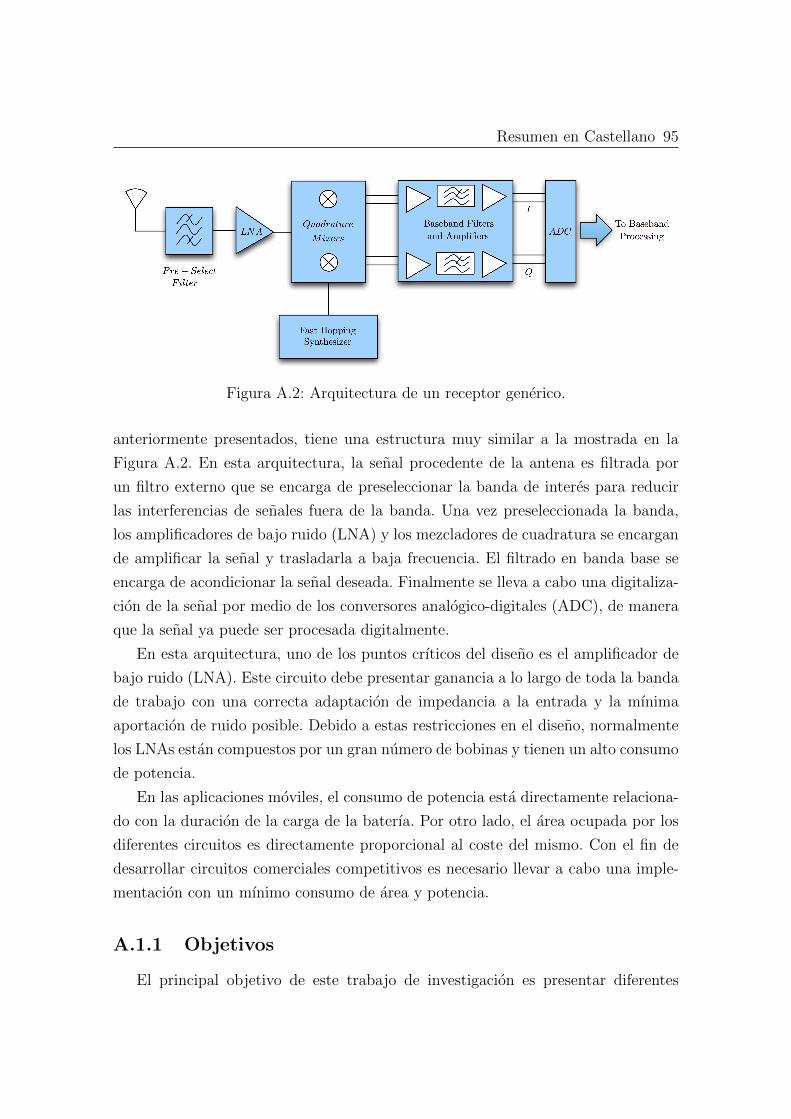
Resumen en Castellano 95
Figura A.2: Arquitectura de un receptor generico.
anteriormente presentados, tiene una estructura muy similar a la mostrada en la
Figura A.2. En esta arquitectura, la senal procedente de la antena es filtrada por
un filtro externo que se encarga de preseleccionar la banda de interes para reducir
las interferencias de senales fuera de la banda. Una vez preseleccionada la banda,
los amplificadores de bajo ruido (LNA) y los mezcladores de cuadratura se encargan
de amplificar la senal y trasladarla a baja frecuencia. El filtrado en banda base se
encarga de acondicionar la senal deseada. Finalmente se lleva a cabo una digitaliza-
cion de la senal por medio de los conversores analogico-digitales (ADC), de manera
que la senal ya puede ser procesada digitalmente.
En esta arquitectura, uno de los puntos crıticos del diseno es el amplificador de
bajo ruido (LNA). Este circuito debe presentar ganancia a lo largo de toda la banda
de trabajo con una correcta adaptacion de impedancia a la entrada y la mınima
aportacion de ruido posible. Debido a estas restricciones en el diseno, normalmente
los LNAs estan compuestos por un gran numero de bobinas y tienen un alto consumo
de potencia.
En las aplicaciones moviles, el consumo de potencia esta directamente relaciona-
do con la duracion de la carga de la baterıa. Por otro lado, el area ocupada por los
diferentes circuitos es directamente proporcional al coste del mismo. Con el fin de
desarrollar circuitos comerciales competitivos es necesario llevar a cabo una imple-
mentacion con un mınimo consumo de area y potencia.
A.1.1 Objetivos
El principal objetivo de este trabajo de investigacion es presentar diferentes
96
alternativas para implementar amplificadores de bajo ruido con un bajo consumo
de potencia y un uso eficiente del area ocupada. Los resultados de este trabajo de
investigacion estan integrados dentro de los siguientes proyectos de investigacion:
• SR2 - Short Range Radio, Ministerio Espanol de Industria, Turismo y Comer-
cio. 2010-2011.
• SR2 - Short Range Radio, Ministerio Espanol de Industria, Turismo y Comer-
cio. 2009-2010.
• WITNESS - WIreless Technologies for small area Networks with Embedded
and Security & Safety. MEDEA+ de la Union Europea - Ministerio Espanol
de Industria, Turismo y Comercio. 2005 - 2007.
De cara a alcanzar el objetivo de este trabajo se han planteado los siguientes
hitos:
1. Obtener las especificaciones de un sistema de referencia basado en las especi-
ficaciones impuestas por el estandar ECMA-368 / ISO/IEC 26907.
2. Explorar diferentes alternativas para la implementacion de amplificadores de
bajo ruido para sistemas de ultra banda ancha, prestando especial atencion en
la optimizacion de consumo de area y potencia.
3. Explorar diferentes estructuras de inductores integrados con el fin de reducir
el consumo de area de las misma.
4. Explorar nuevas alternativas de desarrollo de amplificadores de bajo ruido para
sistemas de ultra banda ancha que eviten el uso de inductores integrados con
el fin de reducir el consumo de area.
A.1.2 Estructura de la memoria
El documento principal de este trabajo de investigacion esta compuesto por siete
capıtulos distribuidos de la siguiente manera. El Capıtulo 1 introduce al lector a las
comunicaciones de ultra banda ancha mostrando una vision general del estado actual
del mercado. Por otro lado, en este capıtulo se plantean los objetivos del trabajo de
investigacion. Despues de esta pequena introduccion, en el Capıtulo 2 se plantean
Resumen en Castellano 97
las principales caracterısticas de la especificacion ECMA-368 / ISO/IEC 26907. A
partir de estas especificaciones se lleva a cabo el diseno de un sistema de recepcion a
nivel de bloques. A partir de este sistema de referencia se extraen las especificaciones
de partida para los diferentes amplificadores de bajo ruido que se iran desarrollando
en capıtulos posteriores.
El Capıtulo 3 se centra en estudiar una de las estructuras mas clasicas en el
desarrollo de amplificadores de ultra banda ancha, los amplificadores distribuidos.
Con el fin de solucionar algunos de los principales inconvenientes de los amplifi-
cadores distribuidos, en el Capıtulo 4, se presentan diferentes alternativas para la
implementacion de amplificadores de bajo ruido para ultra banda ancha.
Con el fin de continuar llevando a cabo una optimizacion de consumo de potencia
y area, en el Capıtulo 5 se exploran las tecnicas de realimentacion aplicadas al diseno
de amplificadores de bajo ruido. El Capıtulo 6 esta centrado en el desarrollo de
amplificadores de bajo ruido evitando el uso de inductores integrados, consiguiendo
de esta forma una mejora importante en el consumo de area total de los LNAs.
Finalmente, en el Capıtulo 7 se presentan las principales conclusiones obtenidas
del trabajo realizado. Por otro lado, se presentan las posibles lıneas de trabajo para
continuar avanzando y explorando en el desarrollo de amplificadores de bajo ruido
para comunicaciones de ultra banda ancha.
En las siguientes secciones, tal y como regula la Universidad de Las Palmas de
Gran Canaria en el Reglamento para la elaboracion, tribunal, defensa y evaluacion
de tesis doctorales en el artıculo 2, se presentara un resumen de cada uno de los
capıtulos del trabajo de investigacion donde se recogeran los siguientes aspectos:
Objetivos, Planteamiento y metodologıa, Aportaciones originales y Conclusiones
obtenidas.
A.2 Analisis del Sistema
A.2.1 Objetivos
Como punto de partida de la investigacion, los principales objetivos de este
capıtulo son: llevar a cabo un estudio de la especificacion ECMA-368 / ISO/IEC
26907 y obtener un conjunto de especificaciones de referencia para los amplificadores
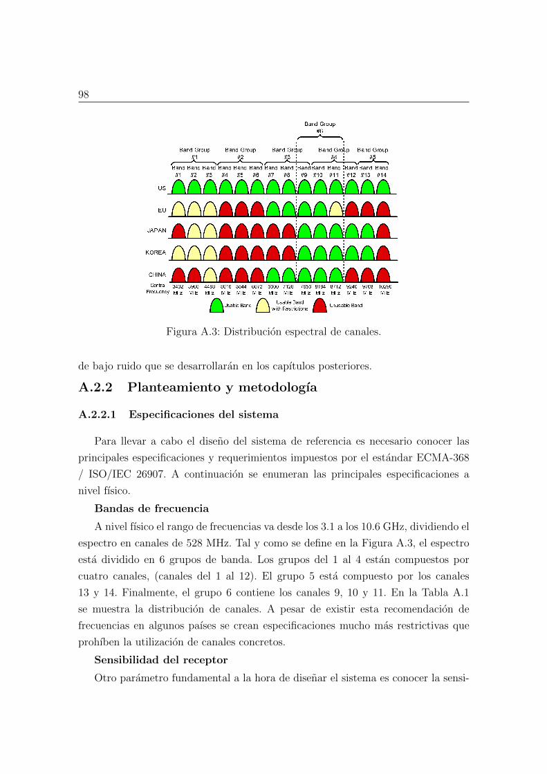
98
Figura A.3: Distribucion espectral de canales.
de bajo ruido que se desarrollaran en los capıtulos posteriores.
A.2.2 Planteamiento y metodologıa
A.2.2.1 Especificaciones del sistema
Para llevar a cabo el diseno del sistema de referencia es necesario conocer las
principales especificaciones y requerimientos impuestos por el estandar ECMA-368
/ ISO/IEC 26907. A continuacion se enumeran las principales especificaciones a
nivel fısico.
Bandas de frecuencia
A nivel fısico el rango de frecuencias va desde los 3.1 a los 10.6 GHz, dividiendo el
espectro en canales de 528 MHz. Tal y como se define en la Figura A.3, el espectro
esta dividido en 6 grupos de banda. Los grupos del 1 al 4 estan compuestos por
cuatro canales, (canales del 1 al 12). El grupo 5 esta compuesto por los canales
13 y 14. Finalmente, el grupo 6 contiene los canales 9, 10 y 11. En la Tabla A.1
se muestra la distribucion de canales. A pesar de existir esta recomendacion de
frecuencias en algunos paıses se crean especificaciones mucho mas restrictivas que
prohıben la utilizacion de canales concretos.
Sensibilidad del receptor
Otro parametro fundamental a la hora de disenar el sistema es conocer la sensi-
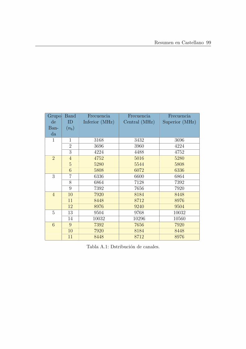
Resumen en Castellano 99
Grupode
Ban-da
BandID(nb)
FrecuenciaInferior (MHz)
FrecuenciaCentral (MHz)
FrecuenciaSuperior (MHz)
1 1 3168 3432 36962 3696 3960 42243 4224 4488 4752
2 4 4752 5016 52805 5280 5544 58086 5808 6072 6336
3 7 6336 6600 68648 6864 7128 73929 7392 7656 7920
4 10 7920 8184 844811 8448 8712 897612 8976 9240 9504
5 13 9504 9768 1003214 10032 10296 10560
6 9 7392 7656 792010 7920 8184 844811 8448 8712 8976
Tabla A.1: Dstribucion de canales.
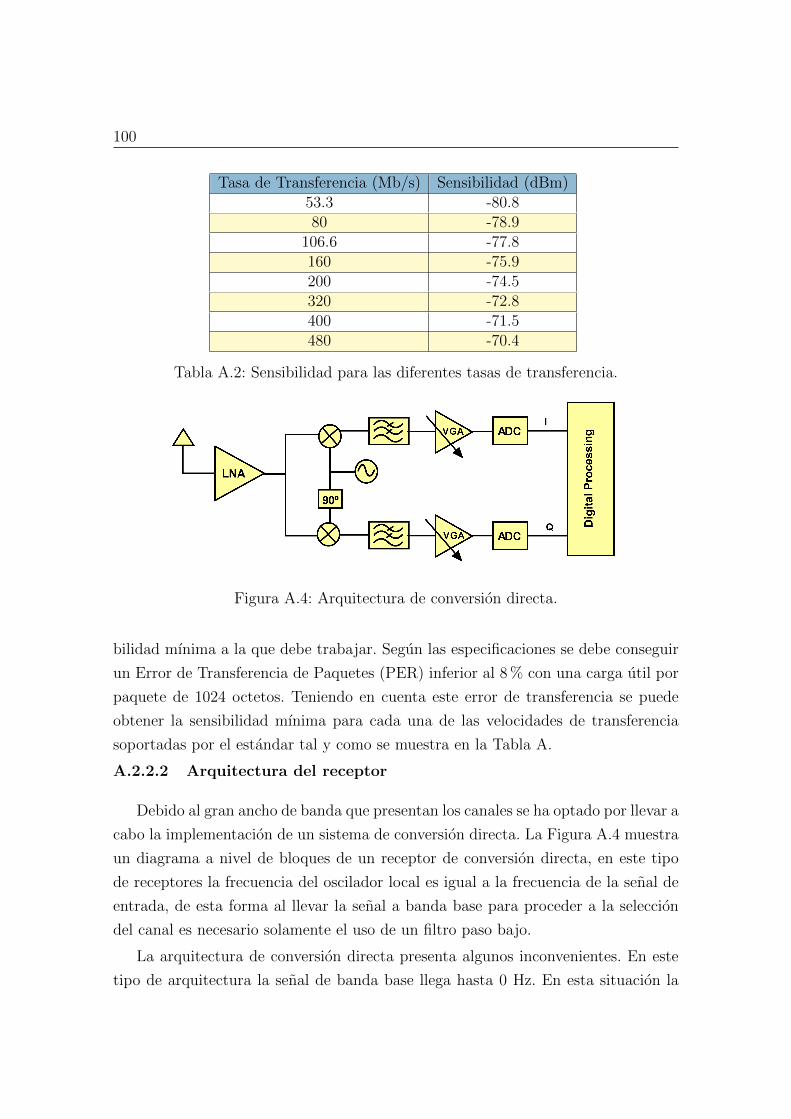
100
Tasa de Transferencia (Mb/s) Sensibilidad (dBm)53.3 -80.880 -78.9
106.6 -77.8160 -75.9200 -74.5320 -72.8400 -71.5480 -70.4
Tabla A.2: Sensibilidad para las diferentes tasas de transferencia.
Figura A.4: Arquitectura de conversion directa.
bilidad mınima a la que debe trabajar. Segun las especificaciones se debe conseguir
un Error de Transferencia de Paquetes (PER) inferior al 8% con una carga util por
paquete de 1024 octetos. Teniendo en cuenta este error de transferencia se puede
obtener la sensibilidad mınima para cada una de las velocidades de transferencia
soportadas por el estandar tal y como se muestra en la Tabla A.
A.2.2.2 Arquitectura del receptor
Debido al gran ancho de banda que presentan los canales se ha optado por llevar a
cabo la implementacion de un sistema de conversion directa. La Figura A.4 muestra
un diagrama a nivel de bloques de un receptor de conversion directa, en este tipo
de receptores la frecuencia del oscilador local es igual a la frecuencia de la senal de
entrada, de esta forma al llevar la senal a banda base para proceder a la seleccion
del canal es necesario solamente el uso de un filtro paso bajo.
La arquitectura de conversion directa presenta algunos inconvenientes. En este
tipo de arquitectura la senal de banda base llega hasta 0 Hz. En esta situacion la
Resumen en Castellano 101
aparicion de senales continuas pueden corromper e incluso saturar a las etapas de
procesado en banda base. Asociado a este fenomeno estan relacionados los acopla-
mientos de la senal del oscilador local a traves del puerto de RF. Este acoplamiento
resulta en una senal continua que puede contribuir a corromper la senal en banda
base. Por otro lado, en este tipo de receptores es necesario llevar a cabo el proce-
so de mezclado en cuadratura, por lo que cualquier desajuste en los desfasadores
pueden provocar un empeoramiento de la calidad de la senal. Otro inconveniente de
esta arquitectura es que los armonicos de tercer orden pueden aparecen dentro de la
senal deseada provocando una degradacion de la misma. Finalmente, como la senal
se lleva directamente a cero el ruido Flicker asociado a los dispositivos puede influir
negativamente en la senal deseada.
A pesar de estos inconvenientes, la simplicidad de los receptores de conversion
directa presentan dos importantes ventajas. En este tipo de arquitectura no aparece
el problema de la frecuencia imagen porque la senal se lleva a banda base en un
unico paso. Como resultado de esto no es necesario el uso de filtros externos para
el rechazo de imagen. Por otro lado, al llevar a cabo todo el proceso de conversion
en un unico paso, esta arquitectura es mucho mas sencilla de integrar en un unico
chip con un consumo de potencia significativamente menor que otras arquitecturas
de receptores.
Una vez definida la arquitectura del sistema teniendo en cuenta las diferentes
especificaciones establecidas por el estandar ECMA-368 / ISO/IEC 26907, se puede
proceder a obtener las especificaciones a nivel de bloques del sistema. En este aspecto
inicialmente se obtiene la figura de ruido total a partir de las especificaciones de
sensibilidad, ancho de banda del canal y tasa de transferencia en el canal.
Una vez definida la figura de ruido total del sistema, se procede a calcular las
especificaciones del filtrado de banda base ası como las especificaciones de los con-
versores analogico digital necesarios para transformar la senal al dominio digital
para su posterior proceso digital.
Con la especificacion de los conversores analogico digitales se puede obtener la
ganancia general que necesita el sistema. Una vez determinada la ganancia maxima
y mınima que debe tener el sistema se determina si es necesario el uso de un control
automatico de ganancia para asegurar que la ganancia esta siempre entre los valores
maximos y mınimos determinados.
Finalmente, para terminar de llevar a cabo el diseno del sistema es necesario
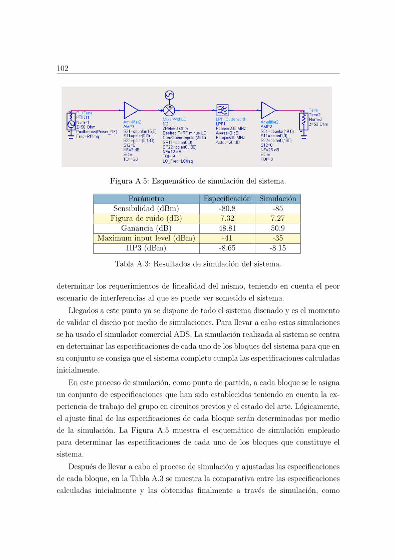
102
Figura A.5: Esquematico de simulacion del sistema.
Parametro Especificacion SimulacionSensibilidad (dBm) -80.8 -85Figura de ruido (dB) 7.32 7.27
Ganancia (dB) 48.81 50.9Maximum input level (dBm) -41 -35
IIP3 (dBm) -8.65 -8.15
Tabla A.3: Resultados de simulacion del sistema.
determinar los requerimientos de linealidad del mismo, teniendo en cuenta el peor
escenario de interferencias al que se puede ver sometido el sistema.
Llegados a este punto ya se dispone de todo el sistema disenado y es el momento
de validar el diseno por medio de simulaciones. Para llevar a cabo estas simulaciones
se ha usado el simulador comercial ADS. La simulacion realizada al sistema se centra
en determinar las especificaciones de cada uno de los bloques del sistema para que en
su conjunto se consiga que el sistema completo cumpla las especificaciones calculadas
inicialmente.
En este proceso de simulacion, como punto de partida, a cada bloque se le asigna
un conjunto de especificaciones que han sido establecidas teniendo en cuenta la ex-
periencia de trabajo del grupo en circuitos previos y el estado del arte. Logicamente,
el ajuste final de las especificaciones de cada bloque seran determinadas por medio
de la simulacion. La Figura A.5 muestra el esquematico de simulacion empleado
para determinar las especificaciones de cada uno de los bloques que constituye el
sistema.
Despues de llevar a cabo el proceso de simulacion y ajustadas las especificaciones
de cada bloque, en la Tabla A.3 se muestra la comparativa entre las especificaciones
calculadas inicialmente y las obtenidas finalmente a traves de simulacion, como
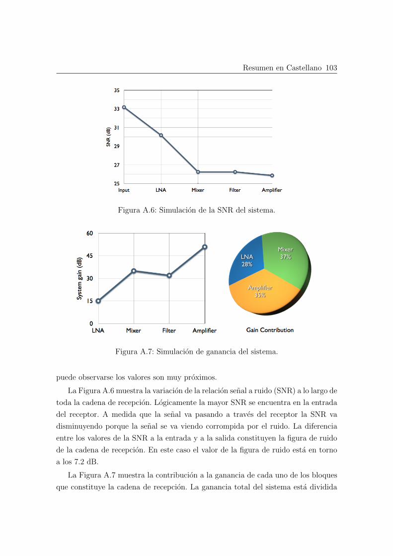
Resumen en Castellano 103
Figura A.6: Simulacion de la SNR del sistema.
Figura A.7: Simulacion de ganancia del sistema.
puede observarse los valores son muy proximos.
La Figura A.6 muestra la variacion de la relacion senal a ruido (SNR) a lo largo de
toda la cadena de recepcion. Logicamente la mayor SNR se encuentra en la entrada
del receptor. A medida que la senal va pasando a traves del receptor la SNR va
disminuyendo porque la senal se va viendo corrompida por el ruido. La diferencia
entre los valores de la SNR a la entrada y a la salida constituyen la figura de ruido
de la cadena de recepcion. En este caso el valor de la figura de ruido esta en torno
a los 7.2 dB.
La Figura A.7 muestra la contribucion a la ganancia de cada uno de los bloques
que constituye la cadena de recepcion. La ganancia total del sistema esta dividida
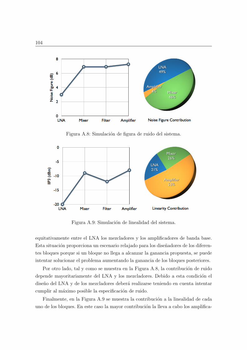
104
Figura A.8: Simulacion de figura de ruido del sistema.
Figura A.9: Simulacion de linealidad del sistema.
equitativamente entre el LNA los mezcladores y los amplificadores de banda base.
Esta situacion proporciona un escenario relajado para los disenadores de los diferen-
tes bloques porque si un bloque no llega a alcanzar la ganancia propuesta, se puede
intentar solucionar el problema aumentando la ganancia de los bloques posteriores.
Por otro lado, tal y como se muestra en la Figura A.8, la contribucion de ruido
depende mayoritariamente del LNA y los mezcladores. Debido a esta condicion el
diseno del LNA y de los mezcladores debera realizarse teniendo en cuenta intentar
cumplir al maximo posible la especificacion de ruido.
Finalmente, en la Figura A.9 se muestra la contribucion a la linealidad de cada
uno de los bloques. En este caso la mayor contribucion la lleva a cabo los amplifica-

Resumen en Castellano 105
Parametro valorGanancia (dB) 15
Figura de Ruido (dB) 3IIP3 (dBm) -20
Consumo de potencia (mW) mınimo
Consumo de Area (mm2) minimo
Tabla A.4: Especificaciones del LNA.
dores de banda base. Teniendo en cuenta esto, a la hora de disenar los amplificadores
de banda base habra que prestar especial atencion a este parametro en concreto.
A.2.3 Aportaciones originales
Como principal aportaciones de este capıtulo cabe destacar el diseno de una
cadena de recepcion a nivel de bloques ası como la verificacion del sistema y distri-
bucion de las especificaciones globales en especificaciones particulares de cada uno
de los bloques que constituyen el sistema.
A.2.4 Conclusiones obtenidas
En este capıtulo se han sentado las bases para el trabajo posterior. Despues de
estudiar las especificaciones de ECMA-368 / ISO/IEC 26907 se procedio a disenar
un sistema completo a nivel de bloques y se llevo a cabo la distribucion de las
especificaciones globales en las diferentes especificaciones locales de cada uno de los
bloques. En la Tabla A.4 se muestra un resumen de las especificaciones de los LNAs
que seran tomadas como especificaciones de referencia en los capıtulos posteriores.
A.3 Amplificadores distribuidos
A.3.1 Objetivos
El diseno de amplificadores de bajo ruido para sistemas de ultra banda ancha es
un desafıo debido precisamente al gran ancho de banda. El principal objetivo de este
capıtulo es explorar una de las estructuras mas clasicas para la implementacion de
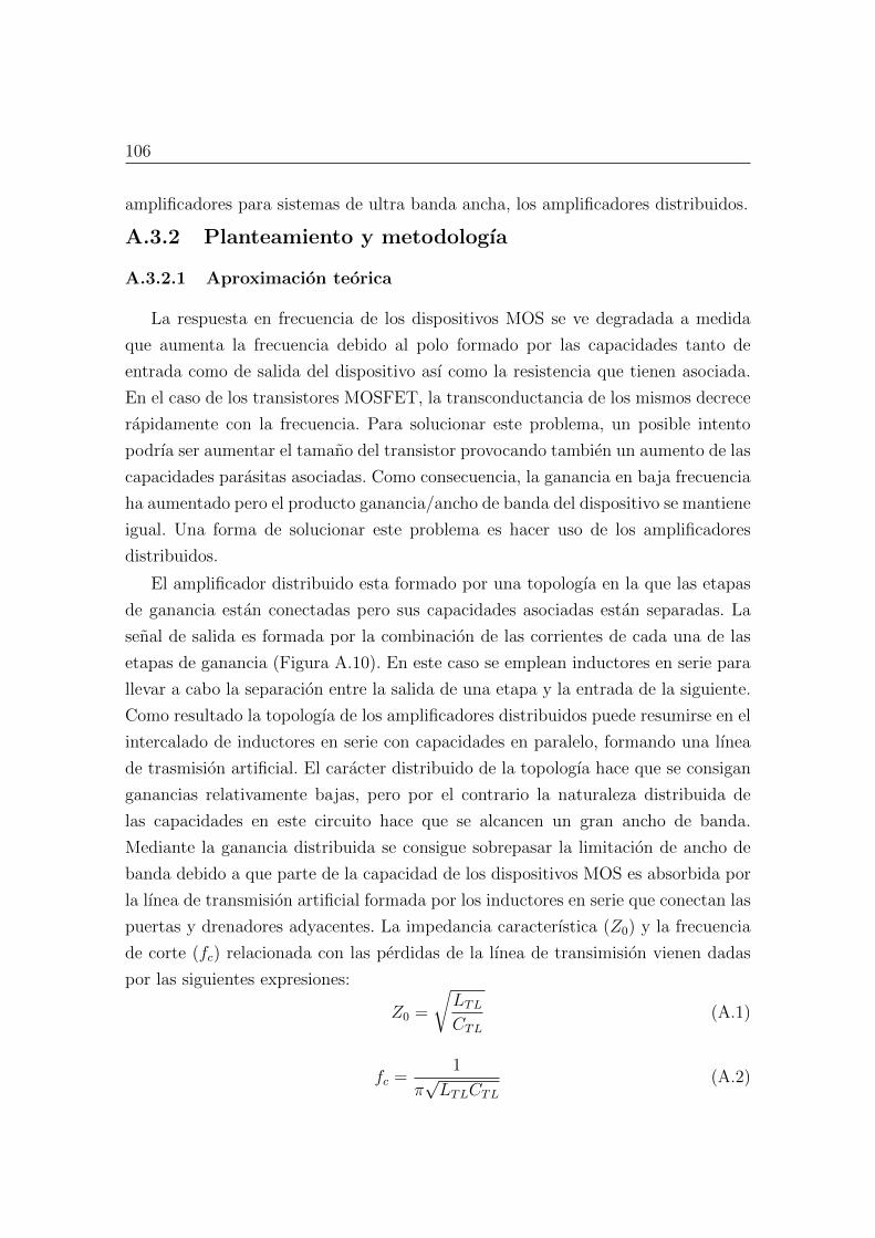
106
amplificadores para sistemas de ultra banda ancha, los amplificadores distribuidos.
A.3.2 Planteamiento y metodologıa
A.3.2.1 Aproximacion teorica
La respuesta en frecuencia de los dispositivos MOS se ve degradada a medida
que aumenta la frecuencia debido al polo formado por las capacidades tanto de
entrada como de salida del dispositivo ası como la resistencia que tienen asociada.
En el caso de los transistores MOSFET, la transconductancia de los mismos decrece
rapidamente con la frecuencia. Para solucionar este problema, un posible intento
podrıa ser aumentar el tamano del transistor provocando tambien un aumento de las
capacidades parasitas asociadas. Como consecuencia, la ganancia en baja frecuencia
ha aumentado pero el producto ganancia/ancho de banda del dispositivo se mantiene
igual. Una forma de solucionar este problema es hacer uso de los amplificadores
distribuidos.
El amplificador distribuido esta formado por una topologıa en la que las etapas
de ganancia estan conectadas pero sus capacidades asociadas estan separadas. La
senal de salida es formada por la combinacion de las corrientes de cada una de las
etapas de ganancia (Figura A.10). En este caso se emplean inductores en serie para
llevar a cabo la separacion entre la salida de una etapa y la entrada de la siguiente.
Como resultado la topologıa de los amplificadores distribuidos puede resumirse en el
intercalado de inductores en serie con capacidades en paralelo, formando una lınea
de trasmision artificial. El caracter distribuido de la topologıa hace que se consigan
ganancias relativamente bajas, pero por el contrario la naturaleza distribuida de
las capacidades en este circuito hace que se alcancen un gran ancho de banda.
Mediante la ganancia distribuida se consigue sobrepasar la limitacion de ancho de
banda debido a que parte de la capacidad de los dispositivos MOS es absorbida por
la lınea de transmision artificial formada por los inductores en serie que conectan las
puertas y drenadores adyacentes. La impedancia caracterıstica (Z0) y la frecuencia
de corte (fc) relacionada con las perdidas de la lınea de transimision vienen dadas
por las siguientes expresiones:
Z0 =
LTL
CTL
(A.1)
fc =1
π√LTLCTL
(A.2)

Resumen en Castellano 107
Figura A.10: Esquematico del amplificador distribuido.
donde el subındice TL hace referencia a la lınea de transmision de puerta y de drena-
dor. Z0 y fc tanto para la lınea de drenador como la de puerta deberıan ser iguales,
por lo tanto las capacidades y la inductancia asociada a cada lınea de transmision
deberıa ser la misma. Como normalmente la capacidad drenador-sustrato (Cdb) de
un MOSFET es menor que la capacidad puerta-surtidor (Cgs), se anade una capa-
cidad adicional Cd para conseguir que la capacidad del drenador sea igual que la
capacidad de la puerta.
Lg = Ld (A.3)
Cgs = Cdb + Cd (A.4)
Como la senal amplificada va viajando a traves de toda la lınea de transmision,
se vera afectada por las perdidas de la misma. En la lınea de puerta estas perdidas
estan asociadas principalmente a los valores finitos de factor de calidad (Q) que
presentan los inductores integrados. En el caso de la lınea de drenador, las perdidas
estan asociadas principalmente a los inductores Ld y a la resistencia parasita que
aparece entre el drenador y el surtidor (rds). La ganancia del amplificador distribuido
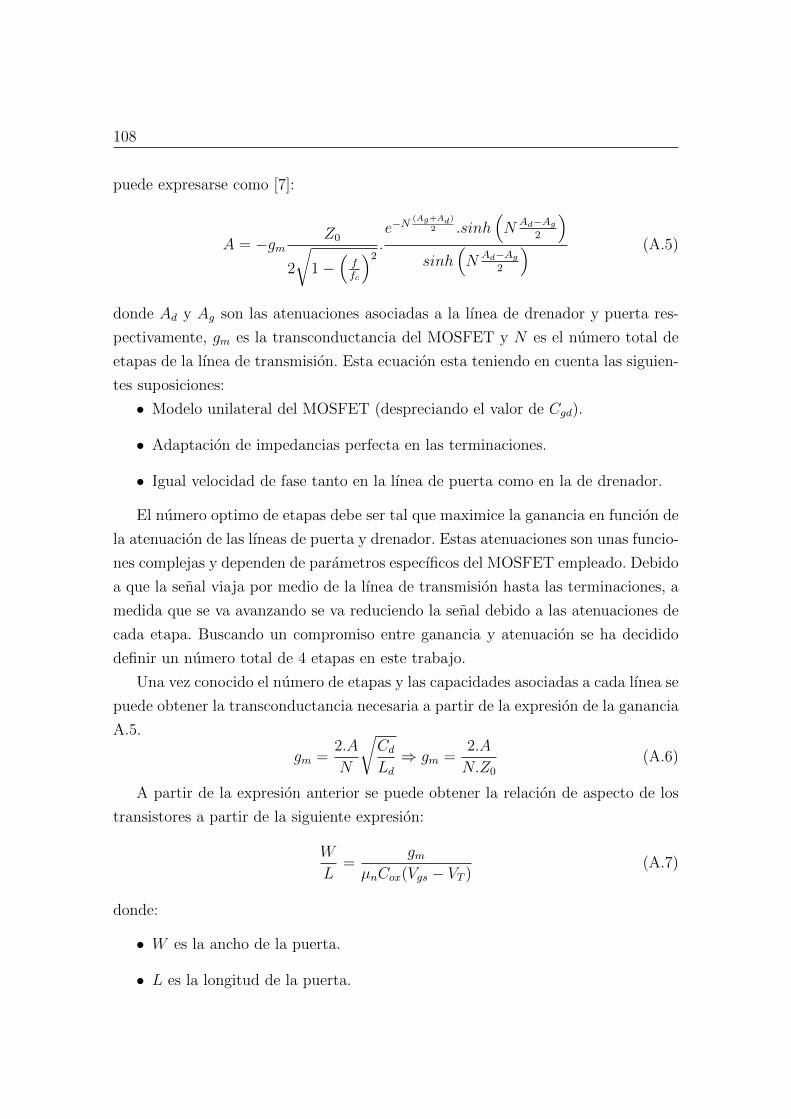
108
puede expresarse como [7]:
A = −gmZ0
2
1−
f
fc
2.e−N
(Ag+Ad)2 .sinh
N Ad−Ag
2
sinhN Ad−Ag
2
(A.5)
donde Ad y Ag son las atenuaciones asociadas a la lınea de drenador y puerta res-
pectivamente, gm es la transconductancia del MOSFET y N es el numero total de
etapas de la lınea de transmision. Esta ecuacion esta teniendo en cuenta las siguien-
tes suposiciones:
• Modelo unilateral del MOSFET (despreciando el valor de Cgd).
• Adaptacion de impedancias perfecta en las terminaciones.
• Igual velocidad de fase tanto en la lınea de puerta como en la de drenador.
El numero optimo de etapas debe ser tal que maximice la ganancia en funcion de
la atenuacion de las lıneas de puerta y drenador. Estas atenuaciones son unas funcio-
nes complejas y dependen de parametros especıficos del MOSFET empleado. Debido
a que la senal viaja por medio de la lınea de transmision hasta las terminaciones, a
medida que se va avanzando se va reduciendo la senal debido a las atenuaciones de
cada etapa. Buscando un compromiso entre ganancia y atenuacion se ha decidido
definir un numero total de 4 etapas en este trabajo.
Una vez conocido el numero de etapas y las capacidades asociadas a cada lınea se
puede obtener la transconductancia necesaria a partir de la expresion de la ganancia
A.5.
gm =2.A
N
Cd
Ld
⇒ gm =2.A
N.Z0(A.6)
A partir de la expresion anterior se puede obtener la relacion de aspecto de los
transistores a partir de la siguiente expresion:
W
L=
gmµnCox(Vgs − VT )
(A.7)
donde:
• W es la ancho de la puerta.
• L es la longitud de la puerta.
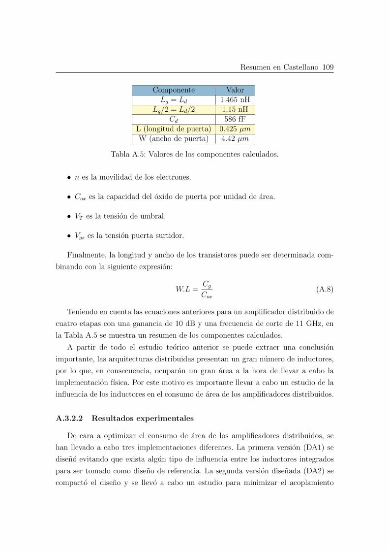
Resumen en Castellano 109
Componente ValorLg = Ld 1.465 nH
Lg/2 = Ld/2 1.15 nHCd 586 fF
L (longitud de puerta) 0.425 µmW (ancho de puerta) 4.42 µm
Tabla A.5: Valores de los componentes calculados.
• n es la movilidad de los electrones.
• Cox es la capacidad del oxido de puerta por unidad de area.
• VT es la tension de umbral.
• Vgs es la tension puerta surtidor.
Finalmente, la longitud y ancho de los transistores puede ser determinada com-
binando con la siguiente expresion:
W.L =Cg
Cox
(A.8)
Teniendo en cuenta las ecuaciones anteriores para un amplificador distribuido de
cuatro etapas con una ganancia de 10 dB y una frecuencia de corte de 11 GHz, en
la Tabla A.5 se muestra un resumen de los componentes calculados.
A partir de todo el estudio teorico anterior se puede extraer una conclusion
importante, las arquitecturas distribuidas presentan un gran numero de inductores,
por lo que, en consecuencia, ocuparan un gran area a la hora de llevar a cabo la
implementacion fısica. Por este motivo es importante llevar a cabo un estudio de la
influencia de los inductores en el consumo de area de los amplificadores distribuidos.
A.3.2.2 Resultados experimentales
De cara a optimizar el consumo de area de los amplificadores distribuidos, se
han llevado a cabo tres implementaciones diferentes. La primera version (DA1) se
diseno evitando que exista algun tipo de influencia entre los inductores integrados
para ser tomado como diseno de referencia. La segunda version disenada (DA2) se
compacto el diseno y se llevo a cabo un estudio para minimizar el acoplamiento
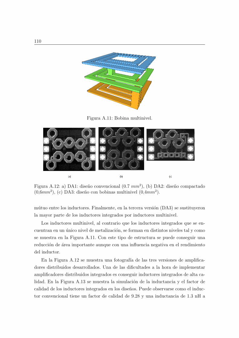
110
Figura A.11: Bobina multinivel.
Figura A.12: a) DA1: diseno convencional (0.7 mm2), (b) DA2: diseno compactado(0,6mm2), (c) DA3: diseno con bobinas multinivel (0,4mm2).
mutuo entre los inductores. Finalmente, en la tercera version (DA3) se sustituyeron
la mayor parte de los inductores integrados por inductores multinivel.
Los inductores multinivel, al contrario que los inductores integrados que se en-
cuentran en un unico nivel de metalizacion, se forman en distintos niveles tal y como
se muestra en la Figura A.11. Con este tipo de estructura se puede conseguir una
reduccion de area importante aunque con una influencia negativa en el rendimiento
del inductor.
En la Figura A.12 se muestra una fotografıa de las tres versiones de amplifica-
dores distribuidos desarrollados. Una de las dificultades a la hora de implementar
amplificadores distribuidos integrados es conseguir inductores integrados de alta ca-
lidad. En la Figura A.13 se muestra la simulacion de la inductancia y el factor de
calidad de los inductores integrados en los disenos. Puede observarse como el induc-
tor convencional tiene un factor de calidad de 9.28 y una inductancia de 1.3 nH a
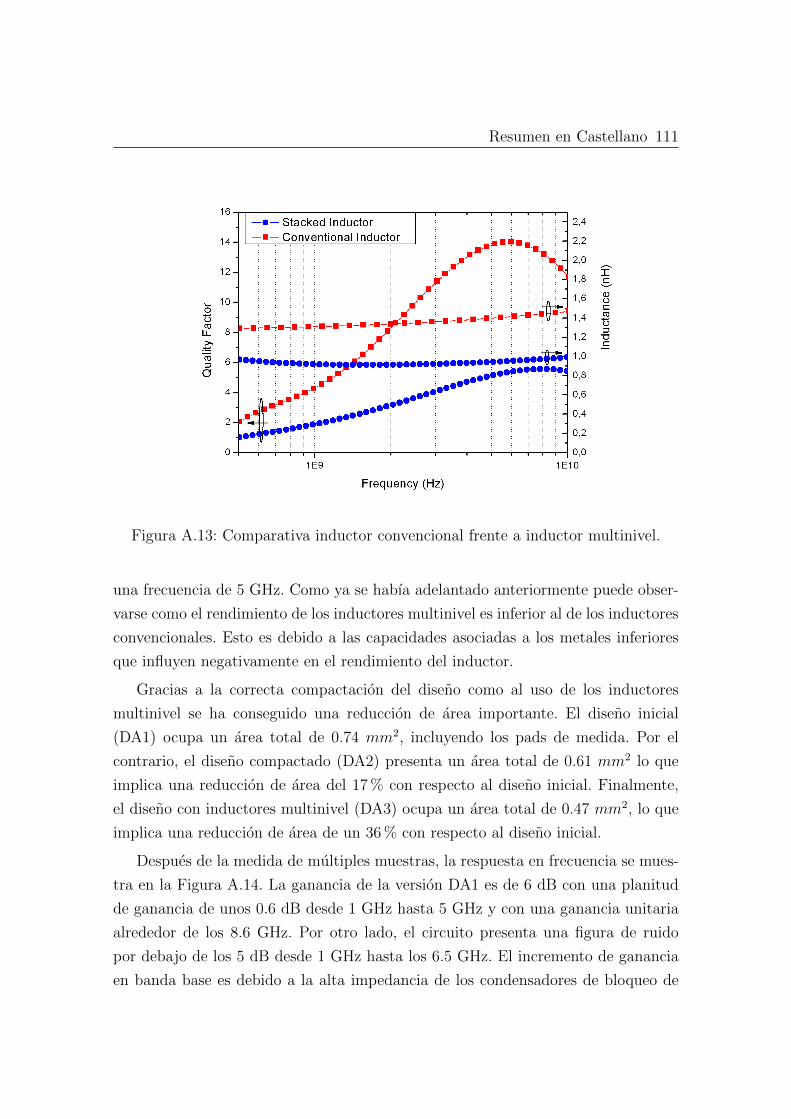
Resumen en Castellano 111
Figura A.13: Comparativa inductor convencional frente a inductor multinivel.
una frecuencia de 5 GHz. Como ya se habıa adelantado anteriormente puede obser-
varse como el rendimiento de los inductores multinivel es inferior al de los inductores
convencionales. Esto es debido a las capacidades asociadas a los metales inferiores
que influyen negativamente en el rendimiento del inductor.
Gracias a la correcta compactacion del diseno como al uso de los inductores
multinivel se ha conseguido una reduccion de area importante. El diseno inicial
(DA1) ocupa un area total de 0.74 mm2, incluyendo los pads de medida. Por el
contrario, el diseno compactado (DA2) presenta un area total de 0.61 mm2 lo que
implica una reduccion de area del 17% con respecto al diseno inicial. Finalmente,
el diseno con inductores multinivel (DA3) ocupa un area total de 0.47 mm2, lo que
implica una reduccion de area de un 36% con respecto al diseno inicial.
Despues de la medida de multiples muestras, la respuesta en frecuencia se mues-
tra en la Figura A.14. La ganancia de la version DA1 es de 6 dB con una planitud
de ganancia de unos 0.6 dB desde 1 GHz hasta 5 GHz y con una ganancia unitaria
alrededor de los 8.6 GHz. Por otro lado, el circuito presenta una figura de ruido
por debajo de los 5 dB desde 1 GHz hasta los 6.5 GHz. El incremento de ganancia
en banda base es debido a la alta impedancia de los condensadores de bloqueo de

112
Figura A.14: Medida del S21 y la figura de ruido.
continua a baja frecuencia. La adaptacion tanto de entrada como de salida es mejor
de -10 dB en todo el ancho de banda.
La respuesta en frecuencia de la version DA2 es aproximadamente la misma que
la version DA1, excepto en la mejora que aparece en la figura de ruido. Esta mejora
es debido a una reduccion de los parasitos asociados al reducir la longitud de muchas
lıneas de interconexion.
Finalmente, con respecto a la version DA3 y a pesar de que el rendimiento de los
inductores multinivel es peor que el de los inductores convencionales, la respuesta
de DA3 es muy similar a la obtenida con las versiones DA1 y DA2. La figura de
ruido en este caso es un poco superior debido a la resistencia serie asociada a los
inductores multinivel que es un poco superior a la resistencia serie de los inductores
convencionales.
Hay que mencionar que todas las medidas se hicieron bajo las mismas condiciones
de polarizacion y que las tres versiones tienen un consumo de potencia de 90 mW.
A.3.3 Aportaciones originales
La principal aportacion de este capıtulo es la implementacion de diferentes tecni-
cas para la reduccion de area en los amplificadores distribuidos. Como se ha podido
comprobar, se ha pasado de un area total ocupada de 0.7 mm2 a un area total de
0.4 mm2 gracias a las tecnicas de compactacion empleadas y al uso de inductores

Resumen en Castellano 113
Circuito Ganan.(dB)
BW(GHz)
NF(dB)
P1dB
(dBm)Area(mm2)
PDC
(mW)DA1 7 6.5 5 12.3 0.74 90DA2 7 6.5 4.5 12.4 0.61 90DA3 5.5 6.5 6 11.2 0.47 90
Tabla A.6: Especificaciones de los amplificadores distribuidos.
multinivel.
A.3.4 Conclusiones
Con la implementacion de los amplificadores distribuidos se ha tomado contacto
con el diseno de amplificadores de bajo ruido para sistemas de ultra banda ancha.
Como se ha podido comprobar, los amplificadores distribuidos presentan un gran
ancho de banda aunque con relativamente poca ganancia.
El principal problema de esta estructura radica en el alto consumo de poten-
cia que presenta ası como el area ocupada. Para conseguir reducir el area ocupada
se han presentado dos soluciones diferentes. Primeramente se ha llevado a cabo
una recolocacion de los inductores en el circuito intentando minimizar la influencia
del acoplamiento mutuo entre estas. Por otro lado, se han introducido los inducto-
res multinivel que a pesar de tener unas especificaciones peores que los inductores
convencionales, el area ocupada es mucho menor. A pesar de tener peores especifica-
ciones los inductores multinivel provocaron una influencia mınima en el rendimiento
de los amplificadores distribuidos.
Usando estas tecnicas se disenaron tres versiones de amplificadores distribuidos
para poder llevar a cabo comparaciones entre ellos y se obtuvieron resultados satis-
factorios en cuanto a la reduccion de area. En la Tabla A.6 se muestra un resumen
de las especificaciones de los amplificadores distribuidos desarrollados.
A.4 Amplificadores de banda ancha
A.4.1 Objetivos
Los amplificadores distribuidos presentan un elevado consumo de potencia y ocu-
pan un area elevada. De cara a optimizar el consumo de potencia y el area ocupada,
el principal objetivo de este capıtulo es la exploracion de diferentes arquitecturas
de amplificadores para sistemas de comunicacion de ultra banda ancha intentando
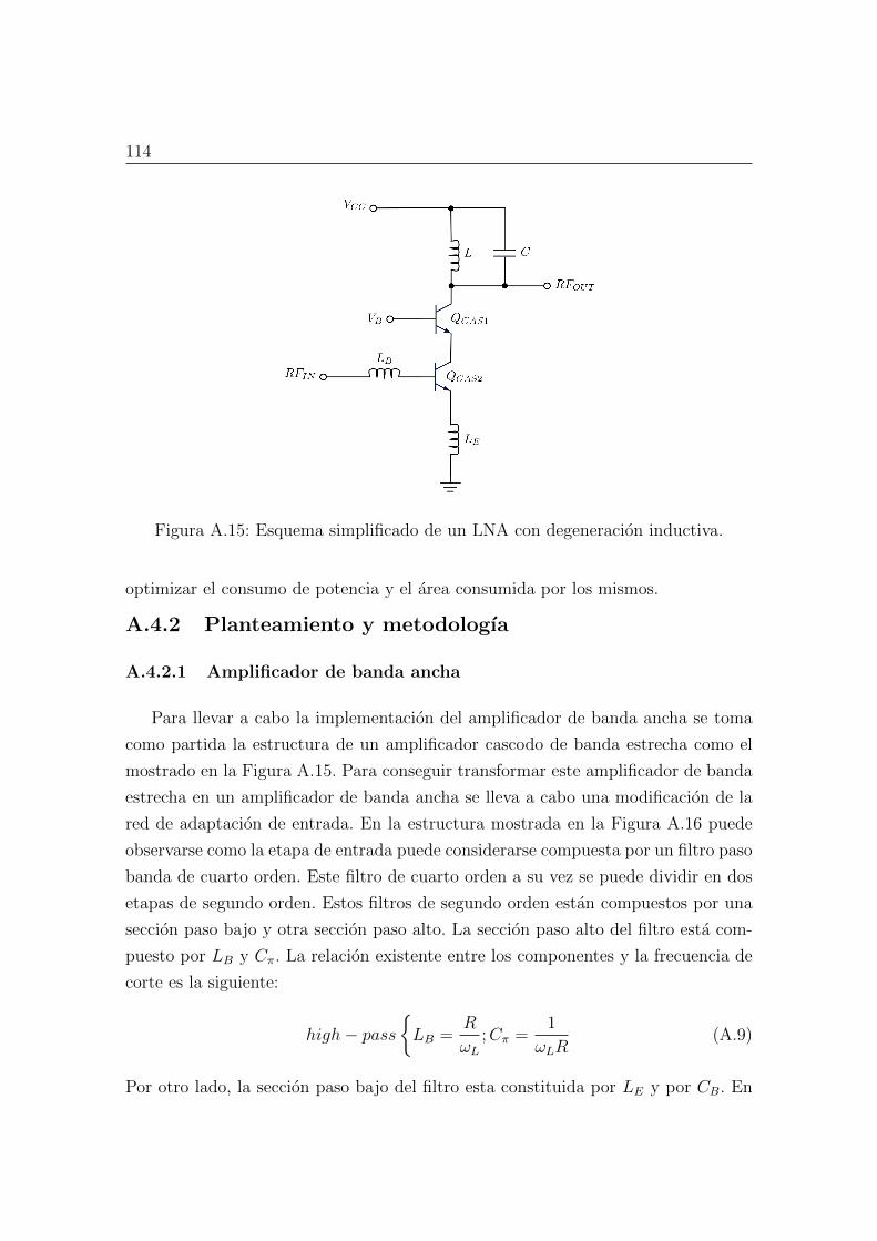
114
Figura A.15: Esquema simplificado de un LNA con degeneracion inductiva.
optimizar el consumo de potencia y el area consumida por los mismos.
A.4.2 Planteamiento y metodologıa
A.4.2.1 Amplificador de banda ancha
Para llevar a cabo la implementacion del amplificador de banda ancha se toma
como partida la estructura de un amplificador cascodo de banda estrecha como el
mostrado en la Figura A.15. Para conseguir transformar este amplificador de banda
estrecha en un amplificador de banda ancha se lleva a cabo una modificacion de la
red de adaptacion de entrada. En la estructura mostrada en la Figura A.16 puede
observarse como la etapa de entrada puede considerarse compuesta por un filtro paso
banda de cuarto orden. Este filtro de cuarto orden a su vez se puede dividir en dos
etapas de segundo orden. Estos filtros de segundo orden estan compuestos por una
seccion paso bajo y otra seccion paso alto. La seccion paso alto del filtro esta com-
puesto por LB y Cπ. La relacion existente entre los componentes y la frecuencia de
corte es la siguiente:
high− pass
LB =
R
ωL
;Cπ =1
ωLR(A.9)
Por otro lado, la seccion paso bajo del filtro esta constituida por LE y por CB. En
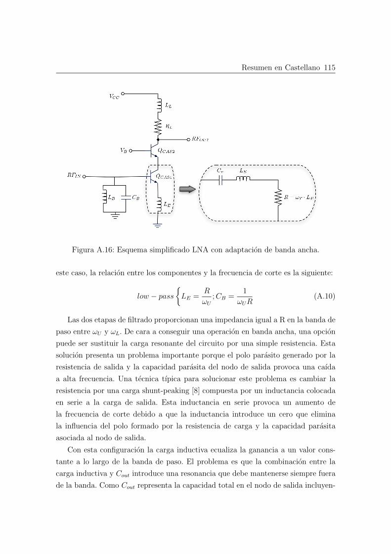
Resumen en Castellano 115
Figura A.16: Esquema simplificado LNA con adaptacion de banda ancha.
este caso, la relacion entre los componentes y la frecuencia de corte es la siguiente:
low − pass
LE =
R
ωU
;CB =1
ωUR(A.10)
Las dos etapas de filtrado proporcionan una impedancia igual a R en la banda de
paso entre ωU y ωL. De cara a conseguir una operacion en banda ancha, una opcion
puede ser sustituir la carga resonante del circuito por una simple resistencia. Esta
solucion presenta un problema importante porque el polo parasito generado por la
resistencia de salida y la capacidad parasita del nodo de salida provoca una caıda
a alta frecuencia. Una tecnica tıpica para solucionar este problema es cambiar la
resistencia por una carga shunt-peaking [8] compuesta por un inductancia colocada
en serie a la carga de salida. Esta inductancia en serie provoca un aumento de
la frecuencia de corte debido a que la inductancia introduce un cero que elimina
la influencia del polo formado por la resistencia de carga y la capacidad parasita
asociada al nodo de salida.
Con esta configuracion la carga inductiva ecualiza la ganancia a un valor cons-
tante a lo largo de la banda de paso. El problema es que la combinacion entre la
carga inductiva y Cout introduce una resonancia que debe mantenerse siempre fuera
de la banda. Como Cout representa la capacidad total en el nodo de salida incluyen-
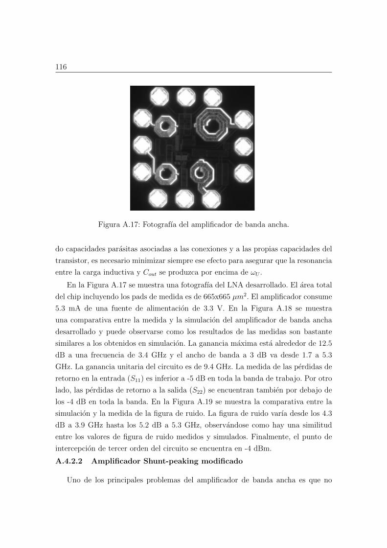
116
Figura A.17: Fotografıa del amplificador de banda ancha.
do capacidades parasitas asociadas a las conexiones y a las propias capacidades del
transistor, es necesario minimizar siempre ese efecto para asegurar que la resonancia
entre la carga inductiva y Cout se produzca por encima de ωU .
En la Figura A.17 se muestra una fotografıa del LNA desarrollado. El area total
del chip incluyendo los pads de medida es de 665x665 µm2. El amplificador consume
5.3 mA de una fuente de alimentacion de 3.3 V. En la Figura A.18 se muestra
una comparativa entre la medida y la simulacion del amplificador de banda ancha
desarrollado y puede observarse como los resultados de las medidas son bastante
similares a los obtenidos en simulacion. La ganancia maxima esta alrededor de 12.5
dB a una frecuencia de 3.4 GHz y el ancho de banda a 3 dB va desde 1.7 a 5.3
GHz. La ganancia unitaria del circuito es de 9.4 GHz. La medida de las perdidas de
retorno en la entrada (S11) es inferior a -5 dB en toda la banda de trabajo. Por otro
lado, las perdidas de retorno a la salida (S22) se encuentran tambien por debajo de
los -4 dB en toda la banda. En la Figura A.19 se muestra la comparativa entre la
simulacion y la medida de la figura de ruido. La figura de ruido varıa desde los 4.3
dB a 3.9 GHz hasta los 5.2 dB a 5.3 GHz, observandose como hay una similitud
entre los valores de figura de ruido medidos y simulados. Finalmente, el punto de
intercepcion de tercer orden del circuito se encuentra en -4 dBm.
A.4.2.2 Amplificador Shunt-peaking modificado
Uno de los principales problemas del amplificador de banda ancha es que no

Resumen en Castellano 117
Figura A.18: Comparativa de simulacion y medida de los parametros S.

118
Figura A.19: Comparativa de simulacion y medida de la figura de ruido.
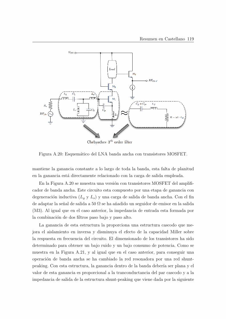
Resumen en Castellano 119
Figura A.20: Esquematico del LNA banda ancha con transistores MOSFET.
mantiene la ganancia constante a lo largo de toda la banda, esta falta de planitud
en la ganancia esta directamente relacionado con la carga de salida empleada.
En la Figura A.20 se muestra una version con transistores MOSFET del amplifi-
cador de banda ancha. Este circuito esta compuesto por una etapa de ganancia con
degeneracion inductiva (Lg y Ls) y una carga de salida de banda ancha. Con el fin
de adaptar la senal de salida a 50 Ω se ha anadido un seguidor de emisor en la salida
(M3). Al igual que en el caso anterior, la impedancia de entrada esta formada por
la combinacion de dos filtros paso bajo y paso alto.
La ganancia de esta estructura la proporciona una estructura cascodo que me-
jora el aislamiento en inversa y disminuya el efecto de la capacidad Miller sobre
la respuesta en frecuencia del circuito. El dimensionado de los transistores ha sido
determinado para obtener un bajo ruido y un bajo consumo de potencia. Como se
muestra en la Figura A.21, y al igual que en el caso anterior, para conseguir una
operacion de banda ancha se ha cambiado la red resonadora por una red shunt-
peaking. Con esta estructura, la ganancia dentro de la banda deberıa ser plana y el
valor de esta ganancia es proporcional a la tranconductancia del par cascodo y a la
impedancia de salida de la estructura shunt-peaking que viene dada por la siguiente
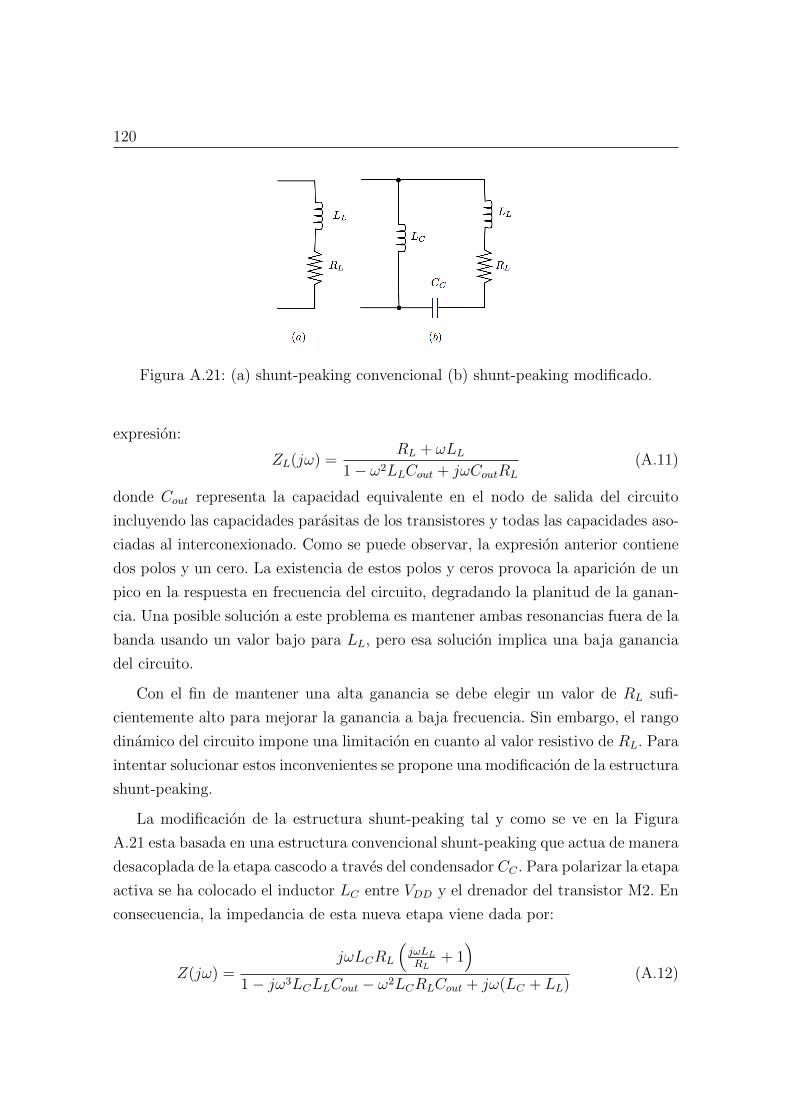
120
Figura A.21: (a) shunt-peaking convencional (b) shunt-peaking modificado.
expresion:
ZL(jω) =RL + ωLL
1− ω2LLCout + jωCoutRL
(A.11)
donde Cout representa la capacidad equivalente en el nodo de salida del circuito
incluyendo las capacidades parasitas de los transistores y todas las capacidades aso-
ciadas al interconexionado. Como se puede observar, la expresion anterior contiene
dos polos y un cero. La existencia de estos polos y ceros provoca la aparicion de un
pico en la respuesta en frecuencia del circuito, degradando la planitud de la ganan-
cia. Una posible solucion a este problema es mantener ambas resonancias fuera de la
banda usando un valor bajo para LL, pero esa solucion implica una baja ganancia
del circuito.
Con el fin de mantener una alta ganancia se debe elegir un valor de RL sufi-
cientemente alto para mejorar la ganancia a baja frecuencia. Sin embargo, el rango
dinamico del circuito impone una limitacion en cuanto al valor resistivo de RL. Para
intentar solucionar estos inconvenientes se propone una modificacion de la estructura
shunt-peaking.
La modificacion de la estructura shunt-peaking tal y como se ve en la Figura
A.21 esta basada en una estructura convencional shunt-peaking que actua de manera
desacoplada de la etapa cascodo a traves del condensador CC . Para polarizar la etapa
activa se ha colocado el inductor LC entre VDD y el drenador del transistor M2. En
consecuencia, la impedancia de esta nueva etapa viene dada por:
Z(jω) =jωLCRL
jωLL
RL+ 1
1− jω3LCLLCout − ω2LCRLCout + jω(LC + LL)(A.12)
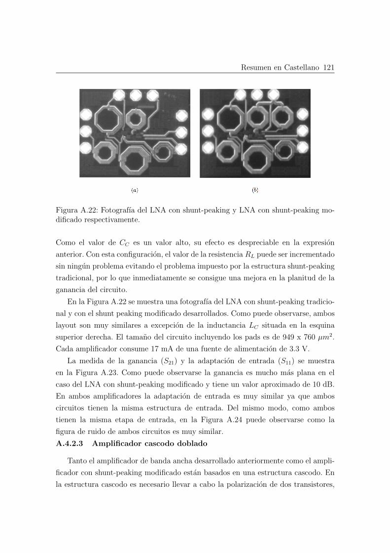
Resumen en Castellano 121
Figura A.22: Fotografıa del LNA con shunt-peaking y LNA con shunt-peaking mo-dificado respectivamente.
Como el valor de CC es un valor alto, su efecto es despreciable en la expresion
anterior. Con esta configuracion, el valor de la resistencia RL puede ser incrementado
sin ningun problema evitando el problema impuesto por la estructura shunt-peaking
tradicional, por lo que inmediatamente se consigue una mejora en la planitud de la
ganancia del circuito.
En la Figura A.22 se muestra una fotografıa del LNA con shunt-peaking tradicio-
nal y con el shunt peaking modificado desarrollados. Como puede observarse, ambos
layout son muy similares a excepcion de la inductancia LC situada en la esquina
superior derecha. El tamano del circuito incluyendo los pads es de 949 x 760 µm2.
Cada amplificador consume 17 mA de una fuente de alimentacion de 3.3 V.
La medida de la ganancia (S21) y la adaptacion de entrada (S11) se muestra
en la Figura A.23. Como puede observarse la ganancia es mucho mas plana en el
caso del LNA con shunt-peaking modificado y tiene un valor aproximado de 10 dB.
En ambos amplificadores la adaptacion de entrada es muy similar ya que ambos
circuitos tienen la misma estructura de entrada. Del mismo modo, como ambos
tienen la misma etapa de entrada, en la Figura A.24 puede observarse como la
figura de ruido de ambos circuitos es muy similar.
A.4.2.3 Amplificador cascodo doblado
Tanto el amplificador de banda ancha desarrollado anteriormente como el ampli-
ficador con shunt-peaking modificado estan basados en una estructura cascodo. En
la estructura cascodo es necesario llevar a cabo la polarizacion de dos transistores,

122
Figura A.23: Medida de los parametros S.
Figura A.24: Medida de la figura de ruido de los LNA con shunt peaking normal ymodificado.
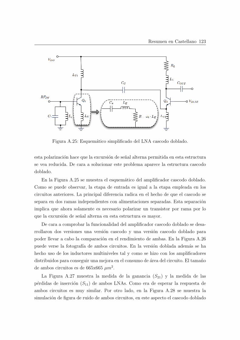
Resumen en Castellano 123
Figura A.25: Esquematico simplificado del LNA cascodo doblado.
esta polarizacion hace que la excursion de senal alterna permitida en esta estructura
se vea reducida. De cara a solucionar este problema aparece la estructura cascodo
doblado.
En la Figura A.25 se muestra el esquematico del amplificador cascodo doblado.
Como se puede observar, la etapa de entrada es igual a la etapa empleada en los
circuitos anteriores. La principal diferencia radica en el hecho de que el cascodo se
separa en dos ramas independientes con alimentaciones separadas. Esta separacion
implica que ahora solamente es necesario polarizar un transistor por rama por lo
que la excursion de senal alterna en esta estructura es mayor.
De cara a comprobar la funcionalidad del amplificador cascodo doblado se desa-
rrollaron dos versiones una version cascodo y una version cascodo doblado para
poder llevar a cabo la comparacion en el rendimiento de ambas. En la Figura A.26
puede verse la fotografıa de ambos circuitos. En la version doblada ademas se ha
hecho uso de los inductores multiniveles tal y como se hizo con los amplificadores
distribuidos para conseguir una mejora en el consumo de area del circuito. El tamano
de ambos circuitos es de 665x665 µm2.
La Figura A.27 muestra la medida de la ganancia (S21) y la medida de las
perdidas de insercion (S11) de ambos LNAs. Como era de esperar la respuesta de
ambos circuitos es muy similar. Por otro lado, en la Figura A.28 se muestra la
simulacion de figura de ruido de ambos circuitos, en este aspecto el cascodo doblado
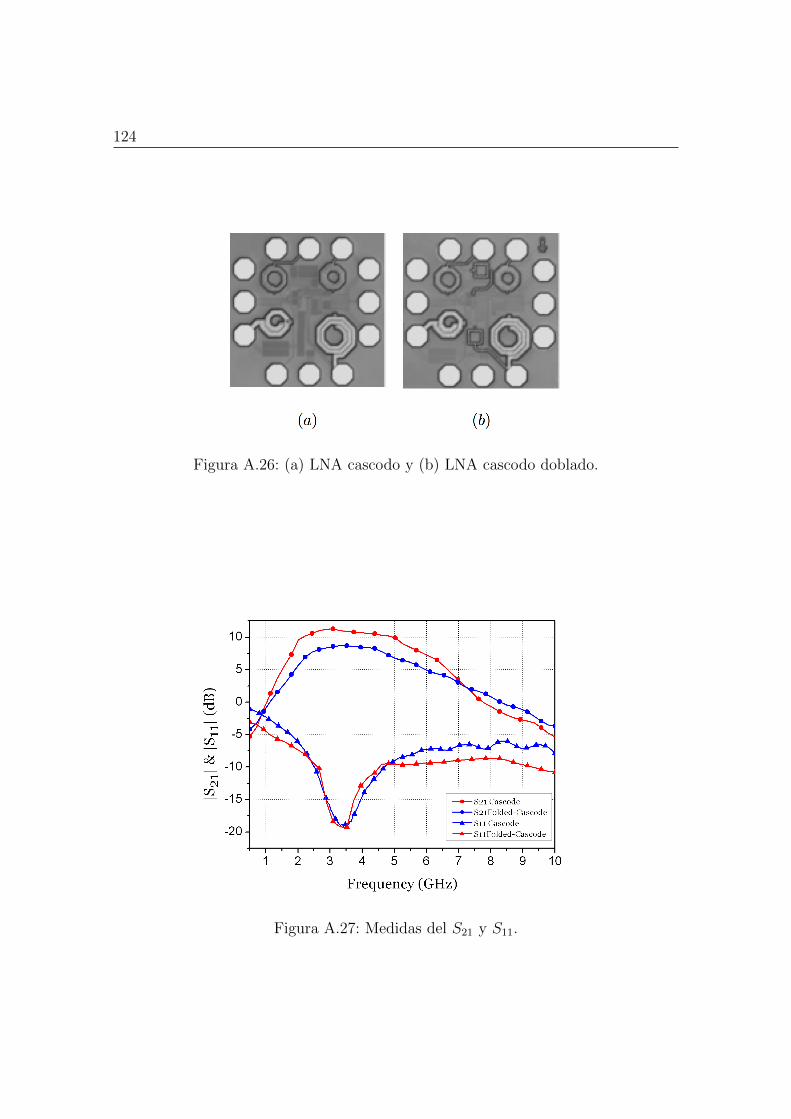
124
Figura A.26: (a) LNA cascodo y (b) LNA cascodo doblado.
Figura A.27: Medidas del S21 y S11.

Resumen en Castellano 125
Figura A.28: Medida figura de ruido del cascodo convencional y el cascodo doblado.
Parametro Cascodo Cascodo dobladoTension de alimentacion (V) 3 1.5Consumo de potencia (mW) 18.93 18.87
VCE(Q1, Q2) (V) 1.5 1.5VBE(Q1, Q2) (V) 0.8 0.8NF @ 4 GHz (dB) 3.19 2.96
Ganancia-S21 @ 4 GHz (dB) 10.1 7.8IIP3 @ 5GHz (dBm) -4 -4
Tabla A.7: Comparacion entre el cascodo convencional y el cascodo doblado.
presenta una mejora con respecto al diseno cascodo convencional.
Finalmente tal y como se muestra en las figuras A.29 y A.30 la linealidad es
similar en ambos circuitos teniendo en cuenta que el amplificador en cascodo doblado
esta alimentado con la mitad de tension que el cascodo convencional. En la Tabla
A.7 se muestra un resumen de las especificaciones de ambos circuitos.
A.4.3 Aportaciones originales
Las aportaciones de este capıtulo han sido el desarrollo de tres amplificadores
para comunicaciones de ultra banda ancha, mejorando las especificaciones obtenidas
por los amplificadores distribuidos. Ademas de desarrollar estos tres circuitos se ha
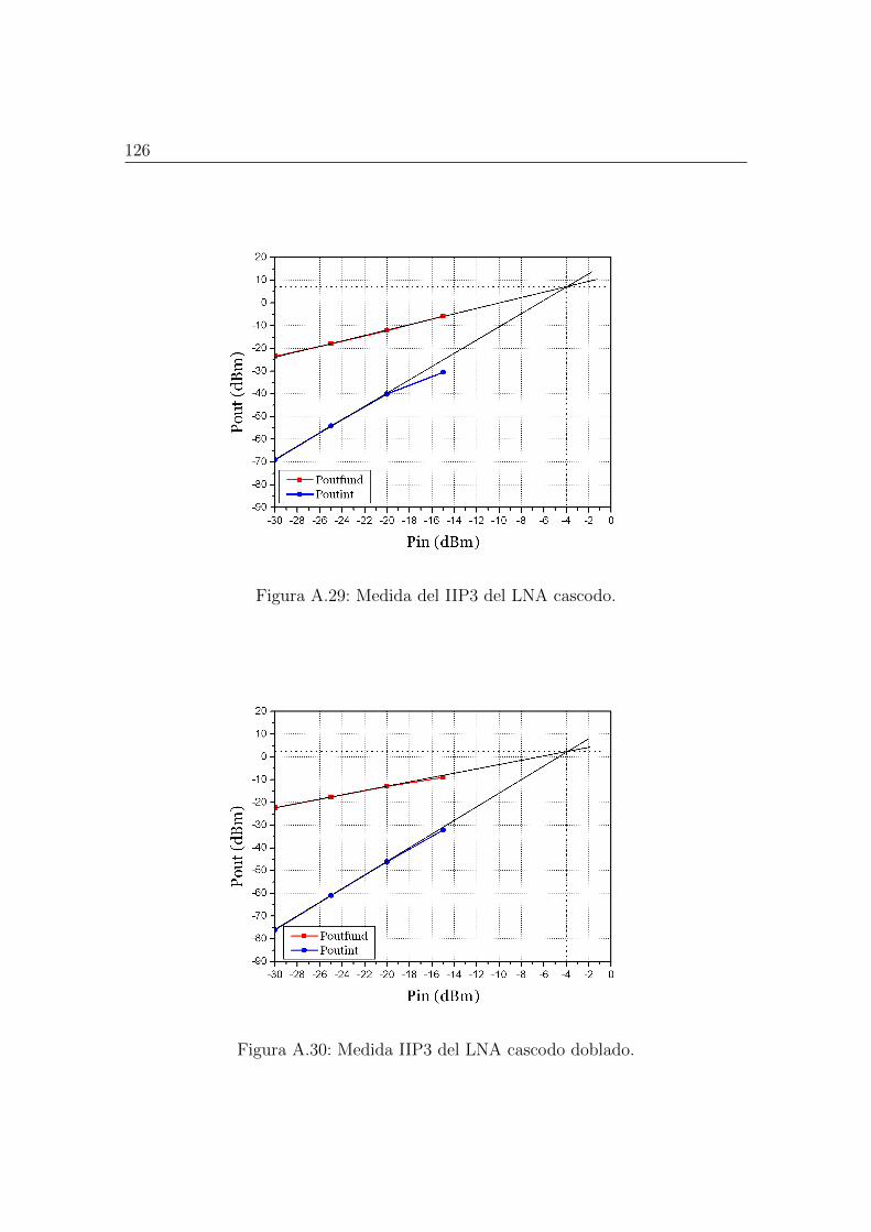
126
Figura A.29: Medida del IIP3 del LNA cascodo.
Figura A.30: Medida IIP3 del LNA cascodo doblado.
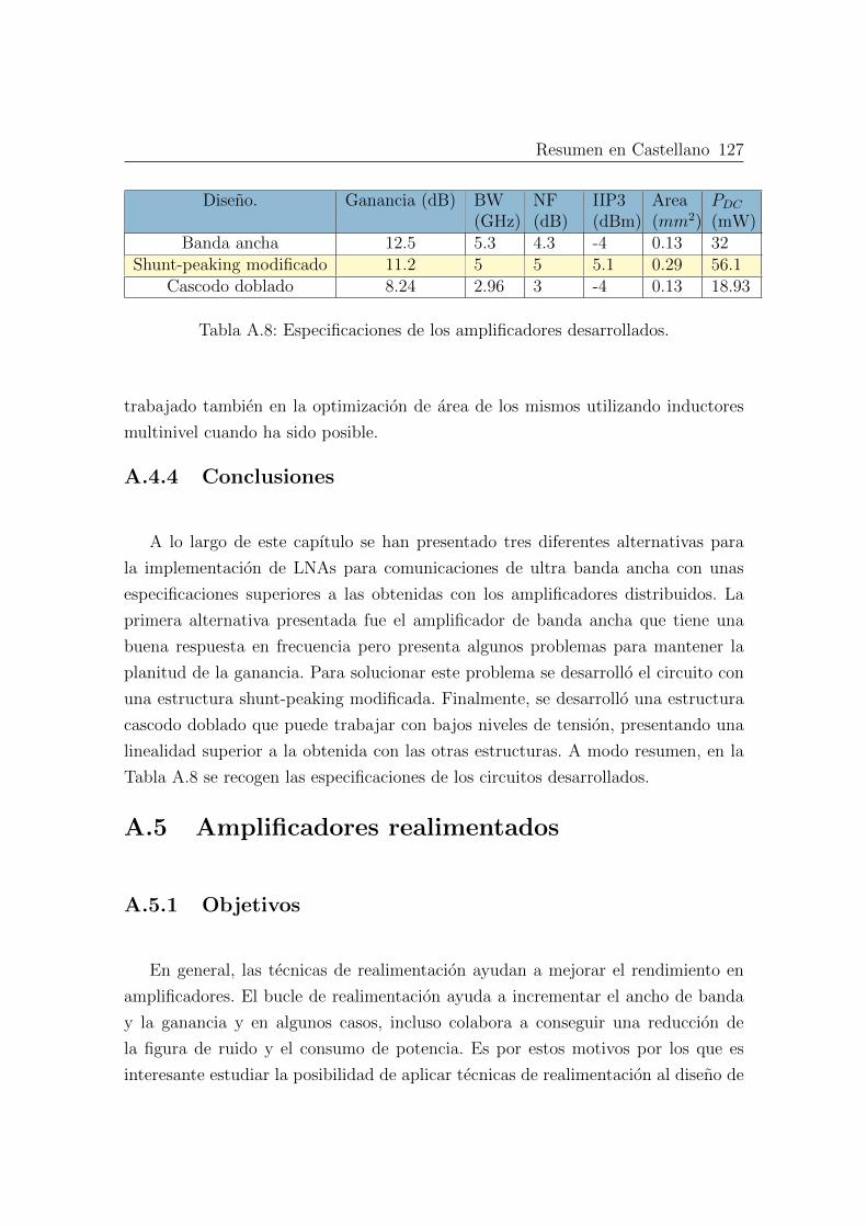
Resumen en Castellano 127
Diseno. Ganancia (dB) BW(GHz)
NF(dB)
IIP3(dBm)
Area(mm2)
PDC
(mW)Banda ancha 12.5 5.3 4.3 -4 0.13 32
Shunt-peaking modificado 11.2 5 5 5.1 0.29 56.1Cascodo doblado 8.24 2.96 3 -4 0.13 18.93
Tabla A.8: Especificaciones de los amplificadores desarrollados.
trabajado tambien en la optimizacion de area de los mismos utilizando inductores
multinivel cuando ha sido posible.
A.4.4 Conclusiones
A lo largo de este capıtulo se han presentado tres diferentes alternativas para
la implementacion de LNAs para comunicaciones de ultra banda ancha con unas
especificaciones superiores a las obtenidas con los amplificadores distribuidos. La
primera alternativa presentada fue el amplificador de banda ancha que tiene una
buena respuesta en frecuencia pero presenta algunos problemas para mantener la
planitud de la ganancia. Para solucionar este problema se desarrollo el circuito con
una estructura shunt-peaking modificada. Finalmente, se desarrollo una estructura
cascodo doblado que puede trabajar con bajos niveles de tension, presentando una
linealidad superior a la obtenida con las otras estructuras. A modo resumen, en la
Tabla A.8 se recogen las especificaciones de los circuitos desarrollados.
A.5 Amplificadores realimentados
A.5.1 Objetivos
En general, las tecnicas de realimentacion ayudan a mejorar el rendimiento en
amplificadores. El bucle de realimentacion ayuda a incrementar el ancho de banda
y la ganancia y en algunos casos, incluso colabora a conseguir una reduccion de
la figura de ruido y el consumo de potencia. Es por estos motivos por los que es
interesante estudiar la posibilidad de aplicar tecnicas de realimentacion al diseno de
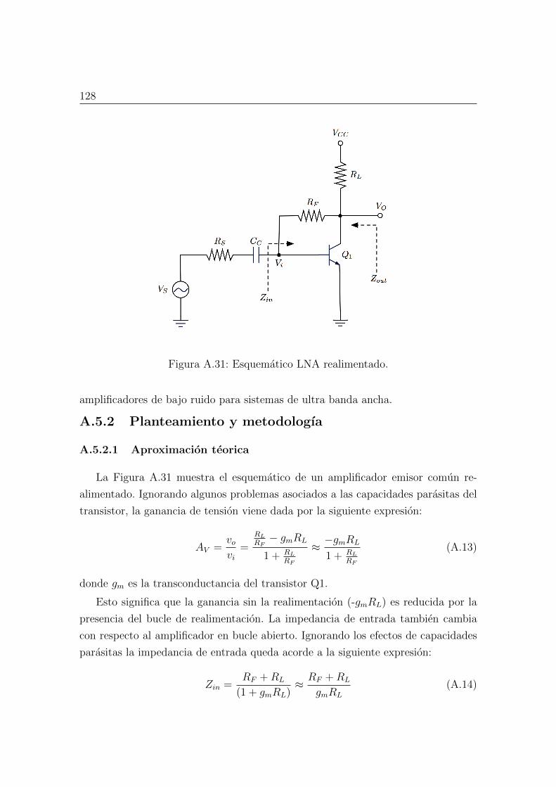
128
Figura A.31: Esquematico LNA realimentado.
amplificadores de bajo ruido para sistemas de ultra banda ancha.
A.5.2 Planteamiento y metodologıa
A.5.2.1 Aproximacion teorica
La Figura A.31 muestra el esquematico de un amplificador emisor comun re-
alimentado. Ignorando algunos problemas asociados a las capacidades parasitas del
transistor, la ganancia de tension viene dada por la siguiente expresion:
AV =vovi
=RLRF
− gmRL
1 + RLRF
≈ −gmRL
1 + RLRF
(A.13)
donde gm es la transconductancia del transistor Q1.
Esto significa que la ganancia sin la realimentacion (-gmRL) es reducida por la
presencia del bucle de realimentacion. La impedancia de entrada tambien cambia
con respecto al amplificador en bucle abierto. Ignorando los efectos de capacidades
parasitas la impedancia de entrada queda acorde a la siguiente expresion:
Zin =RF +RL
(1 + gmRL)≈ RF +RL
gmRL
(A.14)
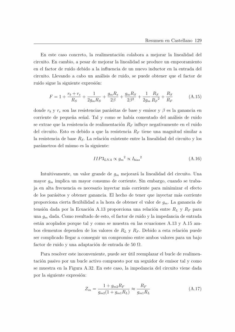
Resumen en Castellano 129
En este caso concreto, la realimentacion colabora a mejorar la linealidad del
circuito. En cambio, a pesar de mejorar la linealidad se produce un empeoramiento
en el factor de ruido debido a la influencia de un nuevo inductor en la entrada del
circuito. Llevando a cabo un analisis de ruido, se puede obtener que el factor de
ruido sigue la siguiente expresion:
F = 1 +rb + reRS
+1
2gmRS
+gmRs
2β+
gmRS
2β2+
1
2gm
RS
RF2 +
RS
RF
(A.15)
donde rb y re son las resistencias parasitas de base y emisor y β es la ganancia en
corriente de pequena senal. Tal y como se habıa comentado del analisis de ruido
se extrae que la resistencia de realimentacion RF influye negativamente en el ruido
del circuito. Esto es debido a que la resistencia RF tiene una magnitud similar a
la resistencia de base RS. La relacion existente entre la linealidad del circuito y los
parametros del mismo es la siguiente:
IIP3LNA ∝ gm2 ∝ Ibias
2 (A.16)
Intuitivamente, un valor grande de gm mejorara la linealidad del circuito. Una
mayor gm implica un mayor consumo de corriente. Sin embargo, cuando se traba-
ja en alta frecuencia es necesario inyectar mas corriente para minimizar el efecto
de los parasitos y obtener ganancia. El hecho de tener que inyectar mas corriente
proporciona cierta flexibilidad a la hora de obtener el valor de gm. La ganancia de
tension dada por la Ecuacion A.13 proporciona una relacion entre RL y RF para
una gm dada. Como resultado de esto, el factor de ruido y la impedancia de entrada
estan acoplados porque tal y como se muestra en las ecuaciones A.13 y A.15 am-
bos elementos dependen de los valores de RL y RF . Debido a esta relacion puede
ser complicado llegar a conseguir un compromiso entre ambos valores para un bajo
factor de ruido y una adaptacion de entrada de 50 Ω.
Para resolver este inconveniente, puede ser util reemplazar el bucle de realimen-
tacion pasivo por un bucle activo compuesto por un seguidor de emisor tal y como
se muestra en la Figura A.32. En este caso, la impedancia del circuito viene dada
por la siguiente expresion:
Zin =1 + gm2RF
gm2(1 + gm1RL)≈ RF
gm1RL
(A.17)
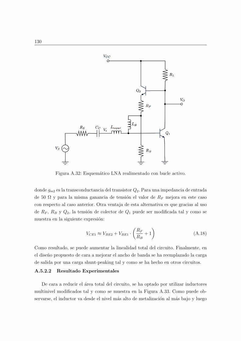
130
Figura A.32: Esquematico LNA realimentado con bucle activo.
donde gm2 es la transconductancia del transistorQ2. Para una impedancia de entrada
de 50 Ω y para la misma ganancia de tension el valor de RF mejora en este caso
con respecto al caso anterior. Otra ventaja de esta alternativa es que gracias al uso
de RF , RB y Q2, la tension de colector de Q1 puede ser modificada tal y como se
muestra en la siguiente expresion:
VCE1 ≈ VBE2 + VBE1 ·RF
RB
+ 1
(A.18)
Como resultado, se puede aumentar la linealidad total del circuito. Finalmente, en
el diseno propuesto de cara a mejorar el ancho de banda se ha reemplazado la carga
de salida por una carga shunt-peaking tal y como se ha hecho en otros circuitos.
A.5.2.2 Resultado Experimentales
De cara a reducir el area total del circuito, se ha optado por utilizar inductores
multinivel modificados tal y como se muestra en la Figura A.33. Como puede ob-
servarse, el inductor va desde el nivel mas alto de metalizacion al mas bajo y luego

Resumen en Castellano 131
Figura A.33: Estructura de inductor 3D.
Figura A.34: Layout y medida del inductor 3D modificado.

132
Figura A.35: Fotografıa de los LNAs: (a) version inductores convencionales, (b)version inductor 3D modificado.
vuelve a subir. En la Figura A.34 se puede ver el layout y resultados de simulacion
del inductor. Como se puede observar, presenta un factor de calidad relativamente
bajo. Este factor de calidad tan bajo es debido al incremento de los parasitos con
respecto al sustrato al bajar a traves de los diferentes niveles de metalizacion.
Para comprobar el correcto funcionamiento del circuito con la bobina 3D modi-
ficada, se han desarrollado dos versiones del circuito. En la primera version se han
empleado inductores convencionales y en la segunda version se ha usado el inductor
modificado 3D. En la Figura A.35 se muestra una fotografıa de ambos circuitos. las
dimensiones del area activa de ambos circuitos es de 490x355 µm2 para el LNA1 y de
330x310 µm2 para el LNA2. Utilizando los inductores 3D modificados, se ha conse-
guido un ahorro de area de un 40% con una influencia mınima en las especificaciones
del circuito.
En la Figura A.36 y en la Figura A.37 se muestra la simulacion de ganancia del
circuito y de la figura de ruido. Ambos amplificadores tienen una ganancia que varıa
desde los 14 dB hasta los 7 dB en la banda que va desde los 3.1 GHz hasta los 10.6
GHz. La figura de ruido para el LNA1 va desde los 4.2 dB hasta los 5.6 dB a 10.6
GHz. En el caso del LNA2 la figura de ruido pasa desde los 2.9 a 4 dB en el rango
de 3.1 a 10.6 GHz. Ambos circuitos presentan una correcta adaptacion de entrada
y salida en el rango de 3.1 GHz a 10.6 GHz.
Finalmente, en la Figura A.38 se muestra la simulacion de linealidad de ambos
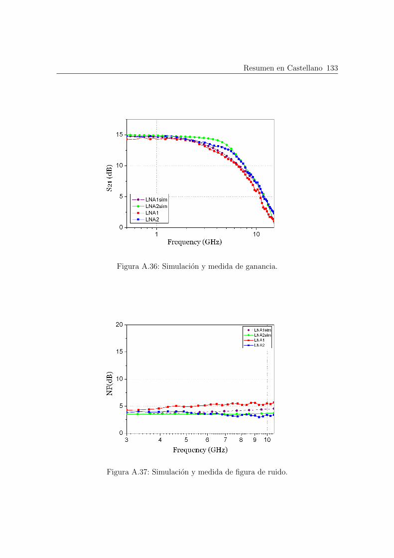
Resumen en Castellano 133
Figura A.36: Simulacion y medida de ganancia.
Figura A.37: Simulacion y medida de figura de ruido.
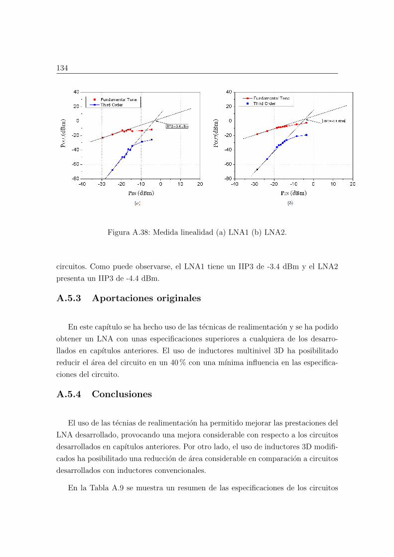
134
Figura A.38: Medida linealidad (a) LNA1 (b) LNA2.
circuitos. Como puede observarse, el LNA1 tiene un IIP3 de -3.4 dBm y el LNA2
presenta un IIP3 de -4.4 dBm.
A.5.3 Aportaciones originales
En este capıtulo se ha hecho uso de las tecnicas de realimentacion y se ha podido
obtener un LNA con unas especificaciones superiores a cualquiera de los desarro-
llados en capıtulos anteriores. El uso de inductores multinivel 3D ha posibilitado
reducir el area del circuito en un 40% con una mınima influencia en las especifica-
ciones del circuito.
A.5.4 Conclusiones
El uso de las tecnias de realimentacion ha permitido mejorar las prestaciones del
LNA desarrollado, provocando una mejora considerable con respecto a los circuitos
desarrollados en capıtulos anteriores. Por otro lado, el uso de inductores 3D modifi-
cados ha posibilitado una reduccion de area considerable en comparacion a circuitos
desarrollados con inductores convencionales.
En la Tabla A.9 se muestra un resumen de las especificaciones de los circuitos
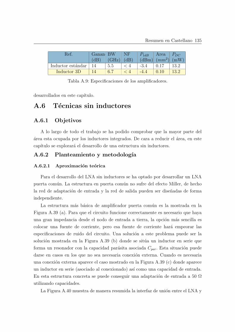
Resumen en Castellano 135
Ref. Ganancia(dB)
BW(GHz)
NF(dB)
P1dB
(dBm)Area(mm2)
PDC
(mW)Inductor estandar 14 5.5 < 4 -3.4 0.17 13.2
Inductor 3D 14 6.7 < 4 -4.4 0.10 13.2
Tabla A.9: Especificaciones de los amplificadores.
desarrollados en este capıtulo.
A.6 Tecnicas sin inductores
A.6.1 Objetivos
A lo largo de todo el trabajo se ha podido comprobar que la mayor parte del
area esta ocupada por los inductores integrados. De cara a reducir el area, en este
capıtulo se explorara el desarrollo de una estructura sin inductores.
A.6.2 Planteamiento y metodologıa
A.6.2.1 Aproximacion teorica
Para el desarrollo del LNA sin inductores se ha optado por desarrollar un LNA
puerta comun. La estructura en puerta comun no sufre del efecto Miller, de hecho
la red de adaptacion de entrada y la red de salida pueden ser disenadas de forma
independiente.
La estructura mas basica de amplificador puerta comun es la mostrada en la
Figura A.39 (a). Para que el circuito funcione correctamente es necesario que haya
una gran impedancia desde el nodo de entrada a tierra, la opcion mas sencilla es
colocar una fuente de corriente, pero esa fuente de corriente hara empeorar las
especificaciones de ruido del circuito. Una solucion a este problema puede ser la
solucion mostrada en la Figura A.39 (b) donde se situa un inductor en serie que
forma un resonador con la capacidad parasita asociada Cpar. Esta situacion puede
darse en casos en los que no sea necesaria conexion externa. Cuando es necesaria
una conexion externa aparece el caso mostrado en la Figura A.39 (c) donde aparece
un inductor en serie (asociado al conexionado) ası como una capacidad de entrada.
En esta estructura concreta se puede conseguir una adaptacion de entrada a 50 Ω
utilizando capacidades.
La Figura A.40 muestra de manera resumida la interfaz de union entre el LNA y
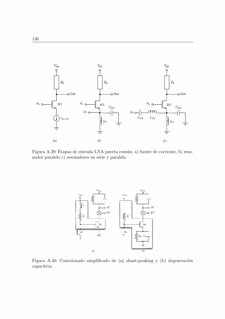
136
Figura A.39: Etapas de entrada LNA puerta comun: a) fuente de corriente, b) reso-nador paralelo c) resonadores en serie y paralelo.
Figura A.40: Conexionado simplificado de (a) shunt-peaking y (b) degeneracioncapacitiva.
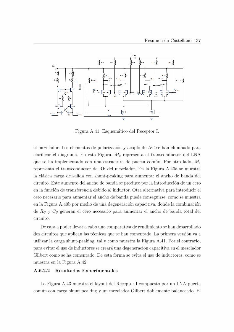
Resumen en Castellano 137
Figura A.41: Esquematico del Receptor I.
el mezclador. Los elementos de polarizacion y acoplo de AC se han eliminado para
clarificar el diagrama. En esta Figura, M0 representa el transconductor del LNA
que se ha implementado con una estructura de puerta comun. Por otro lado, M1
representa el transconductor de RF del mezclador. En la Figura A.40a se muestra
la clasica carga de salida con shunt-peaking para aumentar el ancho de banda del
circuito. Este aumento del ancho de banda se produce por la introduccion de un cero
en la funcion de transferencia debido al inductor. Otra alternativa para introducir el
cero necesario para aumentar el ancho de banda puede conseguirse, como se muestra
en la Figura A.40b por medio de una degeneracion capacitiva, donde la combinacion
de RC y CS generan el cero necesario para aumentar el ancho de banda total del
circuito.
De cara a poder llevar a cabo una comparativa de rendimiento se han desarrollado
dos circuitos que aplican las tecnicas que se han comentado. La primera version va a
utilizar la carga shunt-peaking, tal y como muestra la Figura A.41. Por el contrario,
para evitar el uso de inductores se creara una degeneracion capacitiva en el mezclador
Gilbert como se ha comentado. De esta forma se evita el uso de inductores, como se
muestra en la Figura A.42.
A.6.2.2 Resultados Experimentales
La Figura A.43 muestra el layout del Receptor I compuesto por un LNA puerta
comun con carga shunt peaking y un mezclador Gilbert doblemente balanceado. El
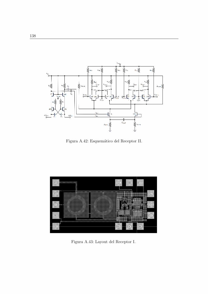
138
Figura A.42: Esquematico del Receptor II.
Figura A.43: Layout del Receptor I.
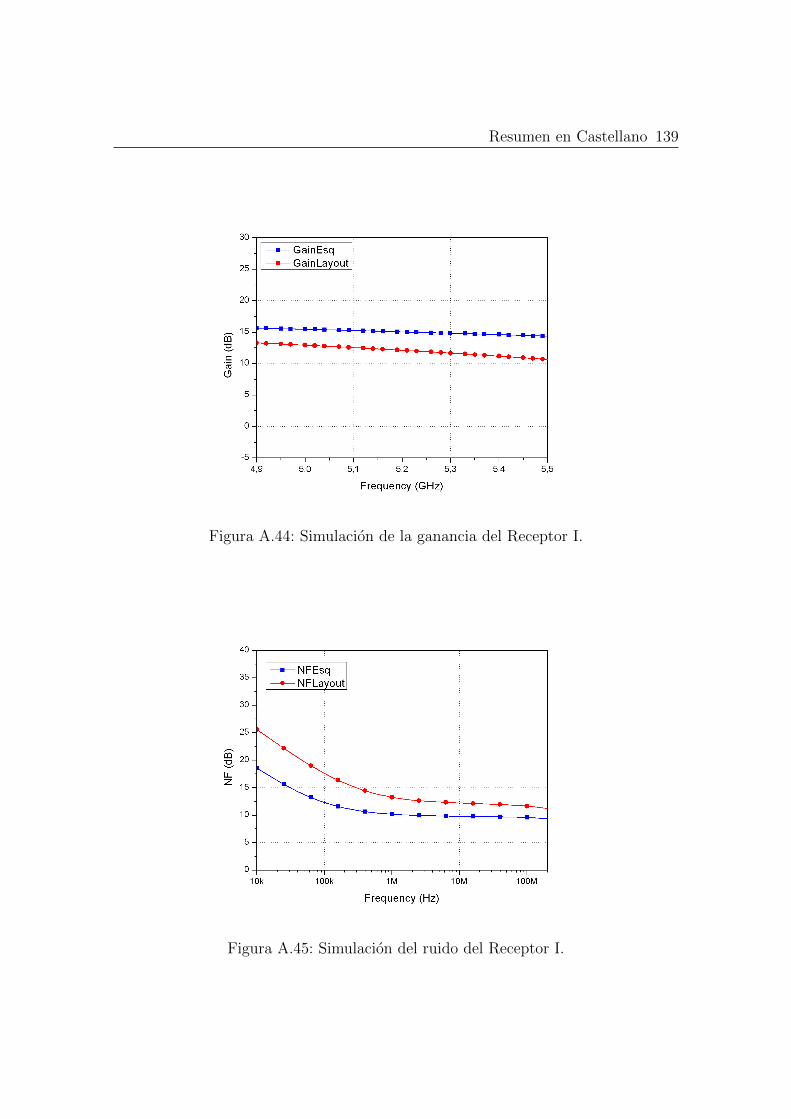
Resumen en Castellano 139
Figura A.44: Simulacion de la ganancia del Receptor I.
Figura A.45: Simulacion del ruido del Receptor I.
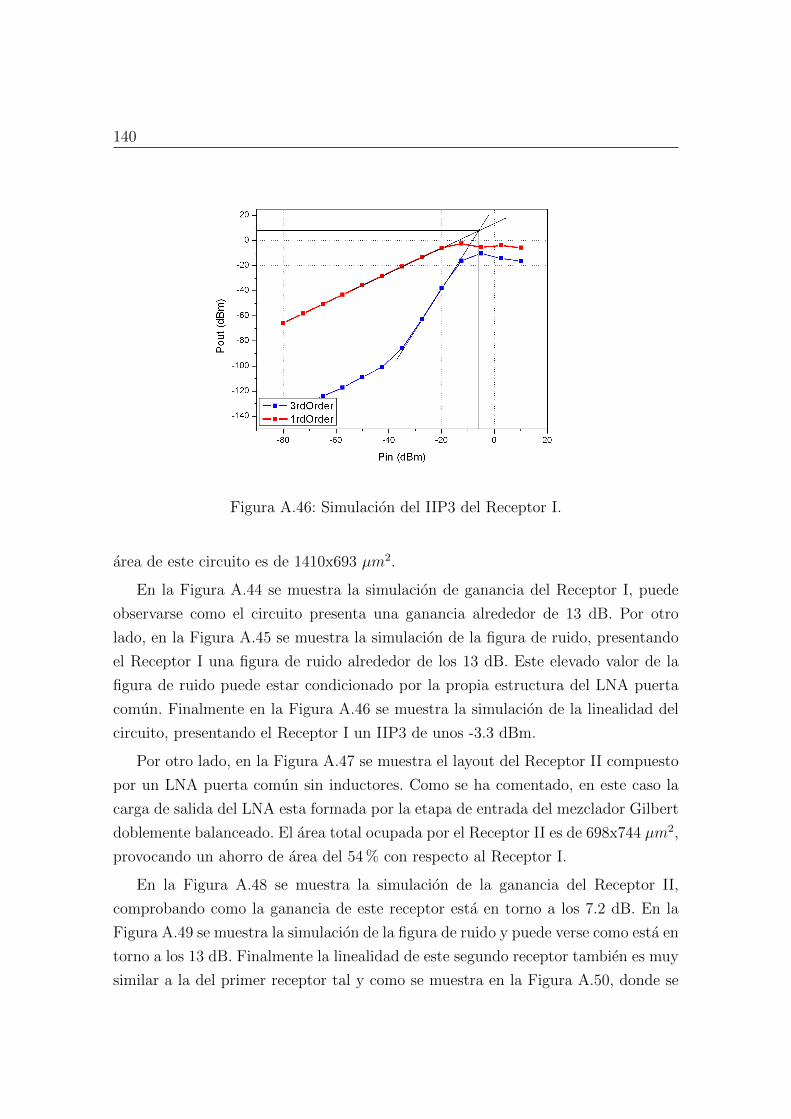
140
Figura A.46: Simulacion del IIP3 del Receptor I.
area de este circuito es de 1410x693 µm2.
En la Figura A.44 se muestra la simulacion de ganancia del Receptor I, puede
observarse como el circuito presenta una ganancia alrededor de 13 dB. Por otro
lado, en la Figura A.45 se muestra la simulacion de la figura de ruido, presentando
el Receptor I una figura de ruido alrededor de los 13 dB. Este elevado valor de la
figura de ruido puede estar condicionado por la propia estructura del LNA puerta
comun. Finalmente en la Figura A.46 se muestra la simulacion de la linealidad del
circuito, presentando el Receptor I un IIP3 de unos -3.3 dBm.
Por otro lado, en la Figura A.47 se muestra el layout del Receptor II compuesto
por un LNA puerta comun sin inductores. Como se ha comentado, en este caso la
carga de salida del LNA esta formada por la etapa de entrada del mezclador Gilbert
doblemente balanceado. El area total ocupada por el Receptor II es de 698x744 µm2,
provocando un ahorro de area del 54% con respecto al Receptor I.
En la Figura A.48 se muestra la simulacion de la ganancia del Receptor II,
comprobando como la ganancia de este receptor esta en torno a los 7.2 dB. En la
Figura A.49 se muestra la simulacion de la figura de ruido y puede verse como esta en
torno a los 13 dB. Finalmente la linealidad de este segundo receptor tambien es muy
similar a la del primer receptor tal y como se muestra en la Figura A.50, donde se
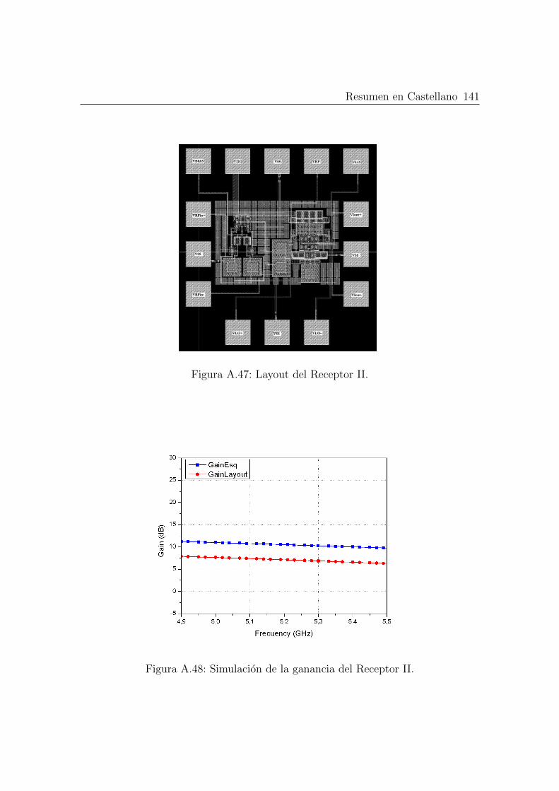
Resumen en Castellano 141
Figura A.47: Layout del Receptor II.
Figura A.48: Simulacion de la ganancia del Receptor II.

142
Figura A.49: Simulacion de la figura de ruido del Receptor II.
Figura A.50: Simulacion del IIP3 del Receptor II.
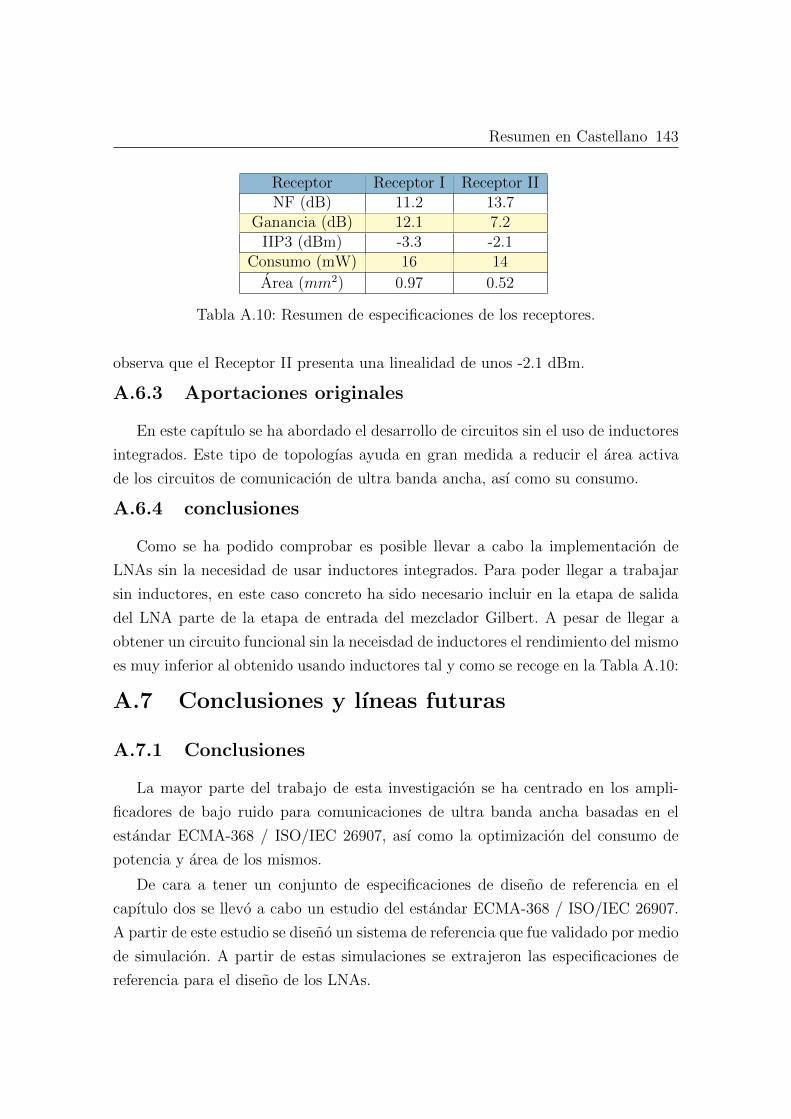
Resumen en Castellano 143
Receptor Receptor I Receptor IINF (dB) 11.2 13.7
Ganancia (dB) 12.1 7.2IIP3 (dBm) -3.3 -2.1
Consumo (mW) 16 14
Area (mm2) 0.97 0.52
Tabla A.10: Resumen de especificaciones de los receptores.
observa que el Receptor II presenta una linealidad de unos -2.1 dBm.
A.6.3 Aportaciones originales
En este capıtulo se ha abordado el desarrollo de circuitos sin el uso de inductores
integrados. Este tipo de topologıas ayuda en gran medida a reducir el area activa
de los circuitos de comunicacion de ultra banda ancha, ası como su consumo.
A.6.4 conclusiones
Como se ha podido comprobar es posible llevar a cabo la implementacion de
LNAs sin la necesidad de usar inductores integrados. Para poder llegar a trabajar
sin inductores, en este caso concreto ha sido necesario incluir en la etapa de salida
del LNA parte de la etapa de entrada del mezclador Gilbert. A pesar de llegar a
obtener un circuito funcional sin la neceisdad de inductores el rendimiento del mismo
es muy inferior al obtenido usando inductores tal y como se recoge en la Tabla A.10:
A.7 Conclusiones y lıneas futuras
A.7.1 Conclusiones
La mayor parte del trabajo de esta investigacion se ha centrado en los ampli-
ficadores de bajo ruido para comunicaciones de ultra banda ancha basadas en el
estandar ECMA-368 / ISO/IEC 26907, ası como la optimizacion del consumo de
potencia y area de los mismos.
De cara a tener un conjunto de especificaciones de diseno de referencia en el
capıtulo dos se llevo a cabo un estudio del estandar ECMA-368 / ISO/IEC 26907.
A partir de este estudio se diseno un sistema de referencia que fue validado por medio
de simulacion. A partir de estas simulaciones se extrajeron las especificaciones de
referencia para el diseno de los LNAs.
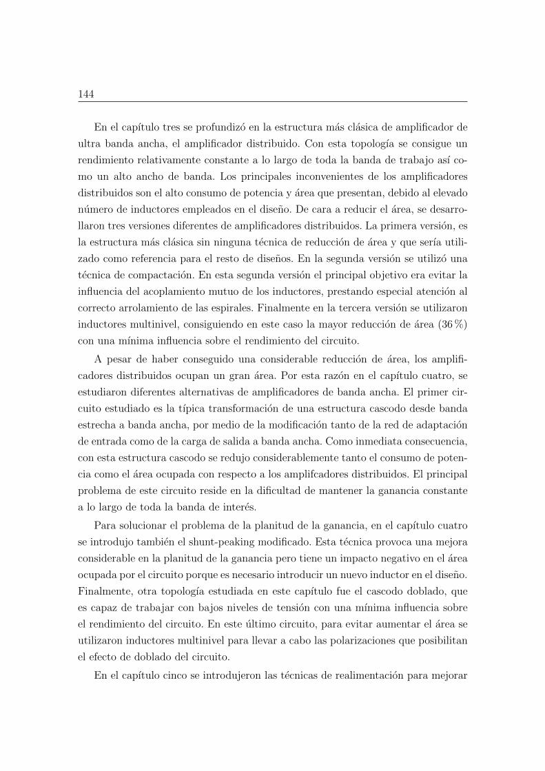
144
En el capıtulo tres se profundizo en la estructura mas clasica de amplificador de
ultra banda ancha, el amplificador distribuido. Con esta topologıa se consigue un
rendimiento relativamente constante a lo largo de toda la banda de trabajo ası co-
mo un alto ancho de banda. Los principales inconvenientes de los amplificadores
distribuidos son el alto consumo de potencia y area que presentan, debido al elevado
numero de inductores empleados en el diseno. De cara a reducir el area, se desarro-
llaron tres versiones diferentes de amplificadores distribuidos. La primera version, es
la estructura mas clasica sin ninguna tecnica de reduccion de area y que serıa utili-
zado como referencia para el resto de disenos. En la segunda version se utilizo una
tecnica de compactacion. En esta segunda version el principal objetivo era evitar la
influencia del acoplamiento mutuo de los inductores, prestando especial atencion al
correcto arrolamiento de las espirales. Finalmente en la tercera version se utilizaron
inductores multinivel, consiguiendo en este caso la mayor reduccion de area (36%)
con una mınima influencia sobre el rendimiento del circuito.
A pesar de haber conseguido una considerable reduccion de area, los amplifi-
cadores distribuidos ocupan un gran area. Por esta razon en el capıtulo cuatro, se
estudiaron diferentes alternativas de amplificadores de banda ancha. El primer cir-
cuito estudiado es la tıpica transformacion de una estructura cascodo desde banda
estrecha a banda ancha, por medio de la modificacion tanto de la red de adaptacion
de entrada como de la carga de salida a banda ancha. Como inmediata consecuencia,
con esta estructura cascodo se redujo considerablemente tanto el consumo de poten-
cia como el area ocupada con respecto a los amplifcadores distribuidos. El principal
problema de este circuito reside en la dificultad de mantener la ganancia constante
a lo largo de toda la banda de interes.
Para solucionar el problema de la planitud de la ganancia, en el capıtulo cuatro
se introdujo tambien el shunt-peaking modificado. Esta tecnica provoca una mejora
considerable en la planitud de la ganancia pero tiene un impacto negativo en el area
ocupada por el circuito porque es necesario introducir un nuevo inductor en el diseno.
Finalmente, otra topologıa estudiada en este capıtulo fue el cascodo doblado, que
es capaz de trabajar con bajos niveles de tension con una mınima influencia sobre
el rendimiento del circuito. En este ultimo circuito, para evitar aumentar el area se
utilizaron inductores multinivel para llevar a cabo las polarizaciones que posibilitan
el efecto de doblado del circuito.
En el capıtulo cinco se introdujeron las tecnicas de realimentacion para mejorar
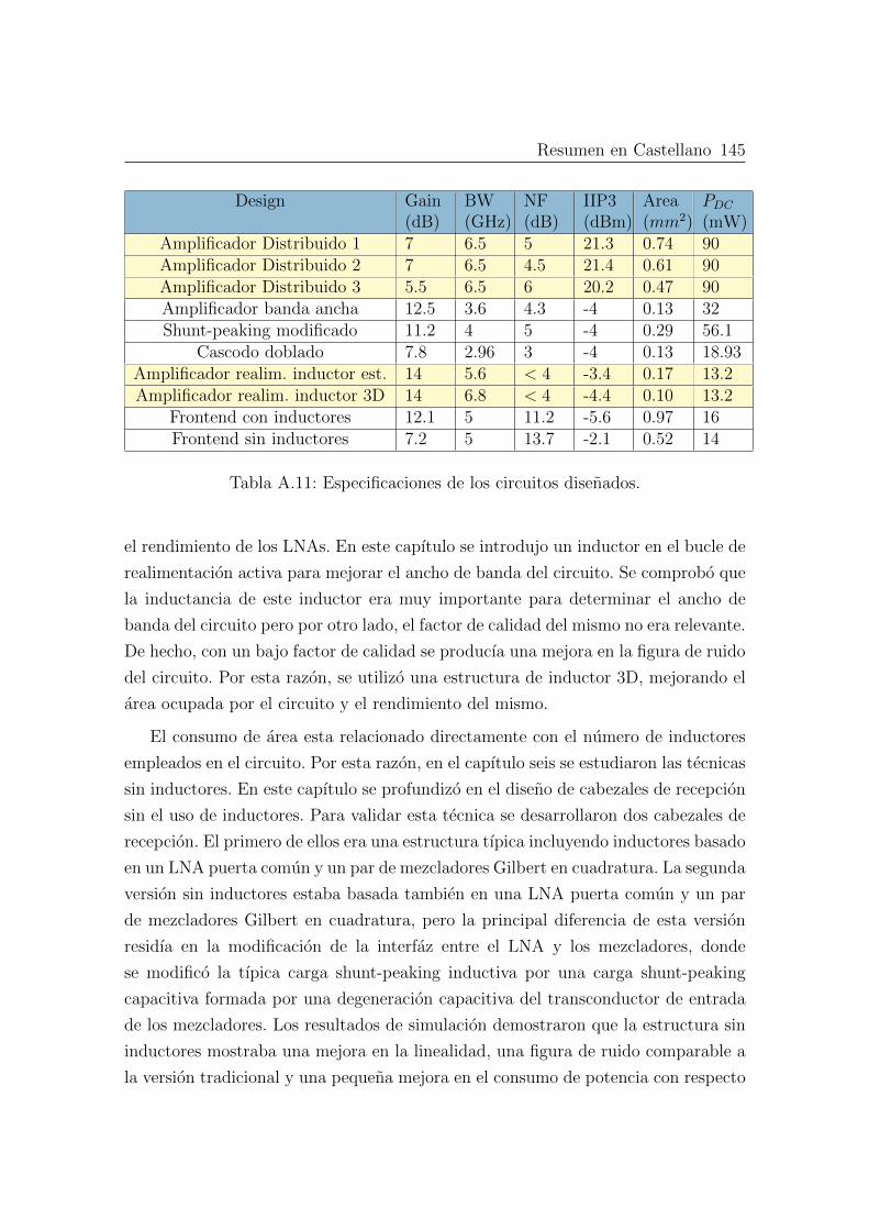
Resumen en Castellano 145
Design Gain(dB)
BW(GHz)
NF(dB)
IIP3(dBm)
Area(mm2)
PDC
(mW)Amplificador Distribuido 1 7 6.5 5 21.3 0.74 90Amplificador Distribuido 2 7 6.5 4.5 21.4 0.61 90Amplificador Distribuido 3 5.5 6.5 6 20.2 0.47 90Amplificador banda ancha 12.5 3.6 4.3 -4 0.13 32Shunt-peaking modificado 11.2 4 5 -4 0.29 56.1
Cascodo doblado 7.8 2.96 3 -4 0.13 18.93Amplificador realim. inductor est. 14 5.6 < 4 -3.4 0.17 13.2Amplificador realim. inductor 3D 14 6.8 < 4 -4.4 0.10 13.2
Frontend con inductores 12.1 5 11.2 -5.6 0.97 16Frontend sin inductores 7.2 5 13.7 -2.1 0.52 14
Tabla A.11: Especificaciones de los circuitos disenados.
el rendimiento de los LNAs. En este capıtulo se introdujo un inductor en el bucle de
realimentacion activa para mejorar el ancho de banda del circuito. Se comprobo que
la inductancia de este inductor era muy importante para determinar el ancho de
banda del circuito pero por otro lado, el factor de calidad del mismo no era relevante.
De hecho, con un bajo factor de calidad se producıa una mejora en la figura de ruido
del circuito. Por esta razon, se utilizo una estructura de inductor 3D, mejorando el
area ocupada por el circuito y el rendimiento del mismo.
El consumo de area esta relacionado directamente con el numero de inductores
empleados en el circuito. Por esta razon, en el capıtulo seis se estudiaron las tecnicas
sin inductores. En este capıtulo se profundizo en el diseno de cabezales de recepcion
sin el uso de inductores. Para validar esta tecnica se desarrollaron dos cabezales de
recepcion. El primero de ellos era una estructura tıpica incluyendo inductores basado
en un LNA puerta comun y un par de mezcladores Gilbert en cuadratura. La segunda
version sin inductores estaba basada tambien en una LNA puerta comun y un par
de mezcladores Gilbert en cuadratura, pero la principal diferencia de esta version
residıa en la modificacion de la interfaz entre el LNA y los mezcladores, donde
se modifico la tıpica carga shunt-peaking inductiva por una carga shunt-peaking
capacitiva formada por una degeneracion capacitiva del transconductor de entrada
de los mezcladores. Los resultados de simulacion demostraron que la estructura sin
inductores mostraba una mejora en la linealidad, una figura de ruido comparable a
la version tradicional y una pequena mejora en el consumo de potencia con respecto
146
a la version con inductores. La mayor diferencia entre ambos circuitos estaba en el
area total ocupada, ya que con la version sin inductores se consiguio un ahorro de
area de un 54%.
A modo de resumen en la Tabla A.11 se muestran las principales caracterısticas
de los circuitos desarrollados a lo largo de este trabajo de investigacion.
A.7.2 Lıneas de trabajo
En este trabajo de investigacion se han presentado diferentes alternativas para
la implementacion de LNAs para sistemas de comunicacion de ultra banda ancha en
tecnologıas de bajos coste. Por otro lado, se han introducido tambien las tecnicas sin
inductores. El principal objetivo de este trabajo era conseguir mejorar el consumo de
potencia ası como el area ocupada por los LNAs intentando conseguir una mınima
influencia sobre las prestaciones de los circuitos. A partir de este trabajo se abren
algunas vıas de investigacion que necesitan ser estudiadas mas en profundidad como:
• Diseno e integracion del resto del receptor: Donde se incluye el estu-
dio, diseno e implementacion de mezcladores, amplificadores de banda base
y elementos de filtrado para comunicaciones de ultra banda ancha, prestando
especial atencion en la optimizacion de consumo de potencia y area.
• Estructuras de inductores: Explorar diferentes alternativas para conseguir
una reduccion de area de los inductores con un mınimo impacto sobre sus
caracterısticas y sobre los circuitos que las utilizan. En esta lınea se incluye
tambien el estudio de nuevas topologıas que no requieran de inductores con
exigentes prestaciones.
• Estructuras sin inductores integrados: Mejorar el rendimiento de los ca-
bezales sin inductores. Esta es una tecnica muy prometedora, ya que evitar
el uso de inductores en los disenos abre la puerta a mejorar los procesos de
portabilidad de disenos a otros procesos tecnologicos.
References
[1] Alereon. http://www.alereon.com/, [Online; accessed 14-May-2012].
[2] Wisair. http://www.wisair.com/, [Online; accessed 14-May-2012].
[3] Veebeam. http://www.veebeam.com/, [Online; accessed 14-May-2012].
[4] B. Razavi, RF Microelectronics. Prentice Hall PTR, 1998.
[5] B. R. et all, “A 0.13 µm CMOS UWB transceiver,” in IEEE Int. Solid-State
Circuits Conf. Dig. Tech. Papers, (San Francisco, CA), pp. 216–217, 2005.
[6] R. Roovers, D. M. W. Leenaerts, J. Bergervoet, K. S. Harish, R. C. H. van de
Beek, G. van der Weide, H. Waite, Y. Zhang, S. Aggarwal, and C. Razzell, “An
interference-robust receiver for ultra-wideband radio in SiGe BiCMOS techno-
logy,” IEEE Journal of Solid-State Circuits, vol. 40, no. 12, 2005.
[7] B. M. Ballweber, R. Gupta, and D. J. Allstot, “Fully integrated 0.5-5.5 GHz
CMOS distributed amplifier,” IEEE Journal of Solid-State Circuits, vol. 37,
pp. 231–239, 2000.
[8] T. H. Lee, The design of CMOS Radio-Frequency Integrated Circuits. Cambrid-
ge University Press, 1998.
[9] O. Medina, J. del Pino, A. Goni, S. L. Khemchandani, J. Garcıa, and
A. Hernandez, “A method to build-up an integrated inductor library,” in XX
Design of Integrated Circuits and Systems Conference, 2005.
148
[10] A. Goni, F. J. del Pino, S. L. Khemchandani, J. A. Garcıa, B. Gonzalez, and
A. Hernandez, “Study of stacked and miniature three-dimensional inductor per-
formance for RF IC design,” in SPIE - The International Society for Optical
Engineering’s - Microtechnologies for the New Millennium Design (VLSI Cir-
cuits and Systems Conference), 2007.
[11] A. Goni, J. del Pino, B. Gonzalez, and A. Hernandez, “An analytical model of
electric substrate losses for planar spiral inductors on silicon,” IEEE Transac-
tion on Electronic Devices, vol. 54, pp. 546–553, 2007.
[12] A. M. Niknejad, “Analysis, design and optimization of spiral inductors and
transformers for si RF ICs,” Master’s thesis, Univ. California, Berkeley, CA,
1998.
[13] J. N. Burghartz, K. A. Jenkins, and M. Soyuer, “Multilevel-spiral inductors
using VLSI interconnect technology,” IEEE Electron Devices Letter, vol. 17,
pp. 428–430, 1996.
[14] M. Geen, R. Green, R. G. Arnold, and J. A. Jenkins, “Miniature multilayer
spiral inductors for GAAS MMICs,” in 11th Annual GaAs IC Symp., pp. 381–
394, 1989.
[15] J. Aguilera, J. Melendez, R. Berenguer, J. R. Sendra, A. Hernandez, and J. del
Pino, “A novel geometry for circular series connected multilevel inductors for
CMOS RF integrated circuits,” IEEE Transaction on Electron Devices, vol. 46,
pp. 1084–1086, 2006.
[16] A. Zolfaghari, A. Chan, and B. Razavi, “Stacked inductors and transformers in
CMOS technology,” IEEE Journal of Solid-State Circuits, vol. 36, pp. 620–628,
2001.
[17] H. Ahn and D. J. Allstot, “A 0.5-8.5 GHz fully differential CMOS distributed
amplifier,” IEEE Journal of Solid-State Circuits, vol. 37, pp. 985–993, 2000.
[18] R. Liu, C. Lin, K. Deng, and H. Wang, “Design and analysis of DC-to-14-GHz
and 22-GHz CMOS cascode distributed amplifiers,” IEEE Journal of Solid-
State Circuits, vol. 39, pp. 1370–1374, 2004.
References 149
[19] R. E. Amaya, N. G. Tarr, and C. Plett, “A 27 GHz fully integrated CMOS
distributed amplifier using coplanar waveguide,” in IEEE RFIC Symp., pp. 193–
196, 2004.
[20] H.-L. Huang, M.-F. Chou, K.-A. W. Wuenand W., and C.-Y. Chang, “A low
power CMOS distributed amplifier,” in IEEE Annual Conference Wireless and
Microwave Technology, pp. 47–50, 2005.
[21] X. Guan and C. Nguyen, “Low-power-consumption and high-gain CMOS distri-
buted amplifiers using cascade of inductively coupled common-source gain cells
for UWB systems,” IEEE Transaction on Microwave Theory and Techniques,
vol. 54, pp. 3278–3283, 2006.
[22] Y. Yun, M. Nishijima, M. Katsuno, H. Ishida, K. Minagawa, T. Nobusada, and
T. Tanaka, “A fully integrated broad-band amplifier MMIC employing a novel
chip-size package,” in IEEE Trans. Microw. Theory Tech., pp. 2930–2937, 2002.
[23] J. del Pino, S. L. Khemchandani, A. Hernandez, J. Sendra, J. Garcıa,
B. Gonzalez, and A. Nunez, “The impact of integrated inductors on low noise
amplifiers,” in XVIII Design of Integrated Circuits and Systems Conference,
(Ciudad Real), Nov. 2003.
[24] R. Wang, M. Lin, C. C. Lin, and C. Yang, “A 1V full-band cascoded UWB LNA
with resistive feedback,” in Proc. IEEE 2007 Int. Workshop on Radio-Frequency
Integration Tech., (Singapore), Dec. 2007.
[25] K. Chang-Wan, K. Min-Suk, A. Tuan, K. Hoon-Tae, and L. Sang-Gug, “An
ultra-wideband CMOS low noise amplifier for 3-5 GHz UWB system,” IEEE J.
Solid-State Circuits, vol. 40, pp. 544–547, 2005.
[26] A. Medi and N. Won, “A fully integrated low cost packaged CMOS low noise
amplifier for the UWB radio,” in Proc. IEEE 2006 Radio and Wireless Symp.,
(San Diego, CA), Jan. 2006.
[27] C. S. Chih, W. Ruey-Lue, K. Ming-Lung, and K. Hsiang-Chen, “An integrated
CMOS low noise amplifier for 3-5 GHz UWB applications,” in Proc. IEEE 2005
Conf. on Electron Devices and Solid-State Circuits, (San Diego, CA), pp. 225–
228, Dec. 2005.

150
[28] Y. Huang and T. E. Chen, “A fully-integrated UWB CMOS LNA using network
synthesis approach,” in Proc.IEEE 2006 Microwave Symposium, (San Francis-
co, CA), Jun. 2006.
[29] F. Gong, K. F. Lam, M. Ismail, S.-B. Park, and J. DeGroat, “A 3-5 GHz
frequency tunable ultra wideband LNA for OFDM applications,” in Proc. 52nd
IEEE International Midwest Symposium on Circuits and Systems, (Cancun),
Aug. 2009.
[30] J. Sendra, J. del Pino, A. Hernandez, J. Hernandez, J. Aguilera, A. Garcıa-
Alonso, and A. Nunez, “Integrated inductors modeling and tools for automatic
selection and layout generation,” in IEEE International Symposium on Quality
in Electronic Design, (San Jose), 2002.
[31] T. Manku, G. Beck, and E. Shin, “A low-voltage design technique for RF in-
tegrated circuits,” IEEE Trans Circuits Syst II Analog Digit Signal Process,
vol. 39, pp. 1408–1413, 1998.
[32] H. Hashemi and A. Hajimiri, “Concurrent multi-band low-noise amplifiers-
theory, design, and applications,” IEEE Trans Microwave Theory Tech, vol. 16,
pp. 290–294, 1968.
[33] C.-C. Tang, C.-H. Wu, and S.-I. Liu, “Miniature 3-D inductors in standard
CMOS process,” IEEE J Solid State Circuits, vol. 37, 2002.
[34] B. R. et al., “A 0.13 µm CMOS UWB transceiver,” in IEEE International
Solid State Circuits Conference Digest of Technical Papers, (San Francisco,
CA), pp. 216–217, 2005.
[35] A. Ismail and A. Abidi, “A 3 to 10 GHz LNA using a wideband LC-ladder
matching network,” in ISSCC Digest of TechnicalPapers, (San Francisco, CA),
pp. 382–383, 2004.
[36] A. Bevilacqua and A. Niknejad, “An ultra-wideband CMOS LNA for 3.1 to 10.6
GHz wireless receivers,” in ISSCC Digest of Technical Papers, (San Francisco,
CA), pp. 384–385, 2004.
[37] S. Shekhar, J. Walling, and D. Allstot, “Bandwidth extension techniques for
CMOS amplifiers,” IEEE J Solid State Circuits, vol. 41, pp. 2424–2439, 2004.
References 151
[38] J. Lee and J. Cressler, “A 3–10 GHz SiGe resistive feedback low noise amplifier
for UWB applications,” in IEEE Radio Frequency Integrated Circuits (RFIC)
Symposium, (Long Beach, CA), pp. 545–548, 2005.
[39] N. Shiramizu, T. Masuda, M. Tanabe, and K. Washio, “A 3–10 GHz band-
width low-noise and low-power amplifier for full-band UWB communications
in 0.25 SiGe BiCMOS technology,” in IEEE Radio Frequency Integrated Circuits
(RFIC) Symposium, (Long Beach, CA), pp. 39–42, 2005.
[40] M. Reiha and J. Long, “A 1.2-V reactive-feedback 3.1–10.6 GHz low-noise am-
plifier in 0.13 µm CMOS,” IEEE J Solid State Circuits, vol. 42, pp. 1023–1033,
2007.
[41] H. Knapp, D. Zoschg, T. Meister, K. Aufinger, S. Boguth, and L.Treitinger, “15
GHz wideband amplifier with 2.8 dB noise figure in SiGe bipolar technology,”
in Radio Frequency Integrated Circuits (RFIC) Symposium, 2001. Digest of
Papers, (Phoenix. AZ), pp. 287–290, 2001.
[42] Y. Park, C.-H. Lee, J. Cressler, and J. Laskar, “The analysis of UWB SiGe
HBT LNA for its noise, linearity, and minimum group delay variation,” IEEE
Trans Microwave Theory Tech, vol. 54, pp. 1687–1697, 2006.
[43] C.-T. Fu and C.-N. Kuo, “3–11-GHz CMOS UWB LNA using dual feedback
for broadband matching,” in Radio Frequency Integrated Circuits Digest, (San
Francisco, CA), pp. 67–70, 2006.
[44] J. Kaukovuori, CMOS Radio Frequency Circuits For Short-Range Direct-
Conversion Receivers. PhD thesis, Helsinki University of Technology, Faculty
of Electronics, Communications and Automation, Department of Micro and
Nanosciences, 2008.
[45] B. Razavi, Design of Analog CMOS Integrated Circuits. Mc Graw Hill, 2001.
[46] L. C-F and L. S-I, “A broadband noise-canceling CMOS LNA for 3.1–10.6-GHz
UWB receivers,” IEEE Journal of Solid-State Circuits, vol. 42, pp. 329–339,
2007.
152
[47] J. del Pino, Modelado y aplicaciones de inductores integrados en tecnologıas
de silicio. PhD thesis, Departamento de Ingenierıa Electronica y Automatica,
Universidad de Las Palmas de Gran Canaria, 2002.
[48] R. Harjani and L. Cai, “1-10GHz inductorless receiver in 0,13µm CMOS,” in
IEEE Radio Frequency Integrated Circuits Symposium, University of Minneso-
ta, Minneapolis, 2009.
[49] B. Razavi, Design of Integrated Circuits for Optical Communications. McGraw
Hill, 2002.
[50] Q. Li and Y. P. Zhang, “An inductorless LNA with noise cancellation an in-
ductorless LNA with noise cancellation for UWB receiver front-end,” in IEEE
ASSCC, 2006.
BPublications
A list of journals and conference contributions directly related this research work
are listed in this appendix.
Journal Papers
1. J. del Pino, Sunil L. Khemchandani, Roberto Dıaz-Ortega, Ruben Pulido-
Medina and Hugo Garcıa-Vazquez, ”On-Chip Inductors Optimization For Ul-
tra Wide Band Low Noise Amplifiers”, Journal of Circuits, Systems, and Com-
puters, Nov. 2011
2. J. del Pino, R. Dıaz and S.L. Khemchandani, ”Area Reduction Techniques for
Full Integrated Distributed Amplifiers”, International Journal in Electronics
and Communications, Nov. 2010
Conference Papers
3. H. Garcıa-Vazquez, R. Dıaz, D. Ramos-Valido, A. Santana, J. del Pino and S.L.
Khemchandani, ”Area Reduction in RF Fully Integrated Front-Ends for Ultra-
Wideband”, XXV Conference on Design of Circuits and Integrated Systems,
Nov 2010.
4. H. Garcıa, R. Pulido, R. Dıaz, S.L. Khemchandani, A. Goni and J. del Pino,
”A Feedback Wideband LNA with a Modified 3D Inductor for UWB Applica-
tions”, XXIII Conference on Design of Circuits and Integrated Systems, Nov
2008.
5. G. Martın, R. Dıaz, J. del Pino, S.L. Khemchandani, A. Hernandez, ”Design
of a Fully Integrated DC to 8.5 GHz Distributed Amplifier in CMOS 0.35”,
XXI Conference on Design of Circuits and Integrated Systems, Nov 2006.

154

!
!
!
!
!
!
!
!
!
"#$%&! '()*+#,!-(./0$123!',$#4#56$#1(!712!8%$26!9#.&!:6(.!;1<!=1#3&!>4,%#?#&23!
>/$+123! @A!.&%!B#(1!C/(#%!;A!D+&40+6(.6(#!E1F&2$1!GH65)'2$&I6!E/FJ(!B/%#.1)K&.#(6!L/I1!M620H6)NO5P/&5!
@1/2(6%! @1/2(6%!1?!*#20/#$3Q!CR3$&43Q!6(.!*14,/$&23!B/F%#3+&2! 912%.!C0#&($#?#0!B/F%#3+#(I!*14,6(R!G6$&! =1S&4F&2!TUVV!
!
!
!
!
!
!
!
!
!
!
!
!
Publications 155

156

Journal of Circuits, Systems, and Computers ! World Scientific Publishing Company
1
ON-CHIP INDUCTORS OPTIMIZATION FOR ULTRA WIDE BAND LOW NOISE AMPLIFIERS
J. del Pino, Sunil L. Khemchandani, Roberto Díaz-Ortega, Rubén Pulido-Medina and Hugo García-Vázquez.
Institute for Applied Microelectronics, Universidad de Las Palmas de Gran Canaria, Las Palmas de Gran Canaria, Spain
Received (Day Month Year) Revised (Day Month Year)
Accepted (Day Month Year)
In this work, the influence of the inductor quality factor in wide band low noise amplifiers has been studied. Electromagnetic simulations have been used to model the integrated inductor broad band response. The influence of the quality factor on LNA performance of the inductors that compound the impedance matching networks, inductive degeneration and broadband load has been studied, obtaining design guidelines for optimizing the amplifier gain flatness. Using this guidelines, an LNA with wideband input matching, shunt-peaking load, and an output buffer was designed. Using Austria Mikro Systems BiCMOS 0.35 !m process, a prototype has been fabricated achieving the following measured specifications: maximum gain of 12.5 dB at 3.4 GHz with a -3 dB bandwidth of 1.7-5.3 GHz, noise figure from 4.3 to 5.2 dB, and unity gain at 9.4 GHz.
Keywords: LNA; BiCMOS; UWB; wide band matching; shunt-peaking; RF.
1. Introduction
The design of wide band low noise amplifiers (LNA) for wireless communication is not easy. It presents two levels of challenges. First, having fast and low noise transistors depends on the available technology. Traditionally, microwave amplifiers relied on transistors fabricated with composite semiconductors, e.g., GaAs, because of the intrinsic superior frequency characteristics of such devices1,3. On the other hand, silicon technology has been employed to design amplifiers4,5, even wide band ones, in the range of several GHz. In wireless mobile communications systems, silicon integrated circuits have been widely employed in narrow-band systems, where limited gain and increased parasitics are tolerable due to lower operating frequencies, and the application of tuned networks. Most of them are distributed amplifiers6,8 which require high levels of power consumption, high area, and they are not optimized for noise. A new methodology to extend the reactively matched LNAs to wide bandwidths is presented in 9. This approach satisfies the tough system requirement of a UWB system
Publications 157

2 J. del Pino, Sunil L. Khemchandani, R Díaz-Ortega, Rubén Pulido-Medina and Hugo García-Vázquez. with moderate power consumption. The proposed methodology is based on the concept of wide band impedance matching which makes extensive use of spiral inductors. However, the problem is that the overall amplifier gain should be flat across the pass-band, whiles the frequency response of integrated inductors is not. The purpose of this paper is to study the influence of inductor parasitics on LNA wide band response. As an example, an amplifier with on-chip matching network spanning from 1.7 to 5.3 GHz is designed. To provide some background, section II briefly describes the design tradeoffs on the narrow band inductively degenerated amplifier. The concept of wide band impedance matching is explained in section III and it is used to extend the bandwidth of the narrow band LNA. The design methodology as well as some practical considerations regarding to the influence of the integrated inductors are discussed in section IV. Experimental results from a chip prototype are provided in Section V. Finally, some conclusions are given in Section VI.
2. Narrow band Inductively Degenerated Amplifier
First, the typical narrow band inductively degenerated amplifier configuration is studied. Fig. 1 shows the typical schematic of a narrow band LNA. The input transistor (QCAS1) is in common emitter configuration and it is the mainly contributor to the circuit noise. The noise figure (NF) of the LNA depends directly on the emitter area and on the bias of QCAS1. The cascode stage, composed by QCAS1 and QCAS2, reduces Miller capacitance, decreasing the effective base-collector capacitance (Cµ) of QCAS1. This makes the amplifier unilateral, i.e., with low S12. This is a requisite of many communication systems to prevent leakage of local oscillator power from the mixer back to the antenna2. The cascode also enhances the overall gain by increasing the stage’s output impedance. The resonant circuit composed by L and C is the load of the cascode stage. This allows a high gain with a low voltage supply. The tank resonant frequency is adjusted to the frequency of interest ("0).
Fig. 1. Simplified schematic of the LNA with inductive degeneration.
158

On-Chip Inductors Optimization in Ultra Wide Band Low Noise Amplifier 3 The noise in a transistor is proportional to the transistor base and emitter resistances, rb and re, and to the transistor small-signal transconductance gm=1/r’e= IC/VT (VT is the thermal voltage and IC is the collector current). To minimize rb, the transistor must present a great area and to maximize gm, IC must be high. If the transistor area is increased the input capacitance (Ci= C#+Cµ) will also increase. This will attenuate the input signal and it will raise the NF. As a result the NF will reach a minimum for a particular combination of area and polarization current. The next step in minimizing the noise is matching the LNA input. The antenna output impedance is 50 $ and through inductive degeneration it is possible to match the input having an excellent trade-off between conjugate matching and minimum noise. The inductive degeneration consists on introducing a series inductance (LE) at the emitter as it is shown in Fig. 1. The inductance value is approximately given by (1):
(1)
The higher transistor "T=gm/Ci, the lower the value of LE needed for matching, and the lower the amount of noise added to the LNA by the series resistance of the inductor. LE changes the real part of the input impedance, and to modify the imaginary part another inductor LB is introduced as presented in Fig.1. An expression of the noise factor for the LNA with inductive degeneration that takes into account the above discussion is the following:
(2)
Alternatively this expression can be expressed as:
(3)
where Q is the quality factor of the input matching network. The noise factor improves with a higher Q because more voltage gain is seen across the input capacitance of the transistor. The input impedance is resistive only in a narrow bandwidth ("0/Q) around the resonance frequency "0. To obtain a wide band impedance matching, the Q of the matching circuit should be significantly lowered. This will largely degrade the noise figure which defeats the purpose. As a result, this type of amplifier cannot be used for wide band applications.
Publications 159
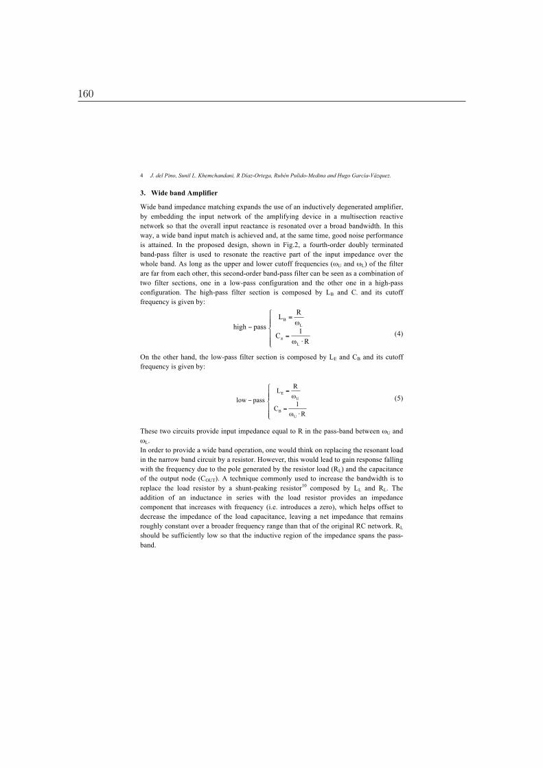
4 J. del Pino, Sunil L. Khemchandani, R Díaz-Ortega, Rubén Pulido-Medina and Hugo García-Vázquez. 3. Wide band Amplifier
Wide band impedance matching expands the use of an inductively degenerated amplifier, by embedding the input network of the amplifying device in a multisection reactive network so that the overall input reactance is resonated over a broad bandwidth. In this way, a wide band input match is achieved and, at the same time, good noise performance is attained. In the proposed design, shown in Fig.2, a fourth-order doubly terminated band-pass filter is used to resonate the reactive part of the input impedance over the whole band. As long as the upper and lower cutoff frequencies ("U and "L) of the filter are far from each other, this second-order band-pass filter can be seen as a combination of two filter sections, one in a low-pass configuration and the other one in a high-pass configuration. The high-pass filter section is composed by LB and C# and its cutoff frequency is given by:
(4)
On the other hand, the low-pass filter section is composed by LE and CB and its cutoff frequency is given by:
(5)
These two circuits provide input impedance equal to R in the pass-band between "U and "L. In order to provide a wide band operation, one would think on replacing the resonant load in the narrow band circuit by a resistor. However, this would lead to gain response falling with the frequency due to the pole generated by the resistor load (RL) and the capacitance of the output node (COUT). A technique commonly used to increase the bandwidth is to replace the load resistor by a shunt-peaking resistor10 composed by LL and RL. The addition of an inductance in series with the load resistor provides an impedance component that increases with frequency (i.e. introduces a zero), which helps offset to decrease the impedance of the load capacitance, leaving a net impedance that remains roughly constant over a broader frequency range than that of the original RC network. RL should be sufficiently low so that the inductive region of the impedance spans the pass-band.
160
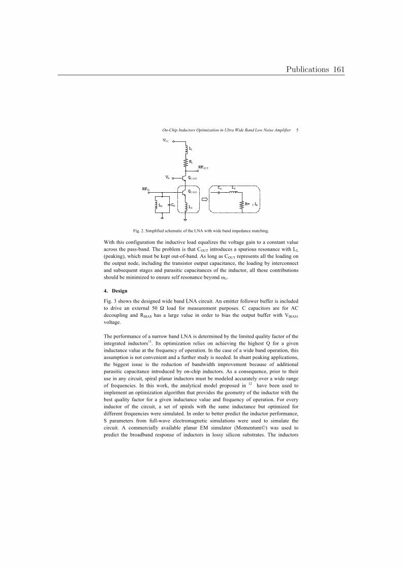
On-Chip Inductors Optimization in Ultra Wide Band Low Noise Amplifier 5
Fig. 2. Simplified schematic of the LNA with wide band impedance matching.
With this configuration the inductive load equalizes the voltage gain to a constant value across the pass-band. The problem is that COUT introduces a spurious resonance with LL (peaking), which must be kept out-of-band. As long as COUT represents all the loading on the output node, including the transistor output capacitance, the loading by interconnect and subsequent stages and parasitic capacitances of the inductor, all these contributions should be minimized to ensure self resonance beyond "U.
4. Design
Fig. 3 shows the designed wide band LNA circuit. An emitter follower buffer is included to drive an external 50 $ load for measurement purposes. C capacitors are for AC decoupling and RBIAS has a large value in order to bias the output buffer with VBIAS1 voltage. The performance of a narrow band LNA is determined by the limited quality factor of the integrated inductors11. Its optimization relies on achieving the highest Q for a given inductance value at the frequency of operation. In the case of a wide band operation, this assumption is not convenient and a further study is needed. In shunt peaking applications, the biggest issue is the reduction of bandwidth improvement because of additional parasitic capacitance introduced by on-chip inductors. As a consequence, prior to their use in any circuit, spiral planar inductors must be modeled accurately over a wide range of frequencies. In this work, the analytical model proposed in 12 have been used to implement an optimization algorithm that provides the geometry of the inductor with the best quality factor for a given inductance value and frequency of operation. For every inductor of the circuit, a set of spirals with the same inductance but optimized for different frequencies were simulated. In order to better predict the inductor performance, S parameters from full-wave electromagnetic simulations were used to simulate the circuit. A commercially available planar EM simulator (Momentum©) was used to predict the broadband response of inductors in lossy silicon substrates. The inductors
Publications 161
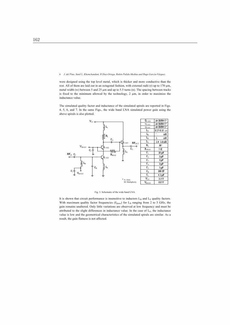
6 J. del Pino, Sunil L. Khemchandani, R Díaz-Ortega, Rubén Pulido-Medina and Hugo García-Vázquez. were designed using the top level metal, which is thicker and more conductive than the rest. All of them are laid out in an octagonal fashion, with external radii (r) up to 170 !m, metal width (w) between 5 and 25 !m and up to 5.5 turns (n). The spacing between tracks is fixed to the minimum allowed by the technology, 2 !m, in order to maximize the inductance value. The simulated quality factor and inductance of the simulated spirals are reported in Figs. 4, 5, 6, and 7. In the same Figs., the wide band LNA simulated power gain using the above spirals is also plotted.
Fig. 3. Schematic of the wide band LNA.
It is shown that circuit performance is insensitive to inductors LB and LE quality factors. With maximum quality factor frequencies (fQmax) for LB ranging from 2 to 5 GHz, the gain remains unaltered. Only little variations are observed at low frequency and must be attributed to the slight differences in inductance value. In the case of LE, the inductance value is low and the geometrical characteristics of the simulated spirals are similar. As a result, the gain flatness is not affected.
162
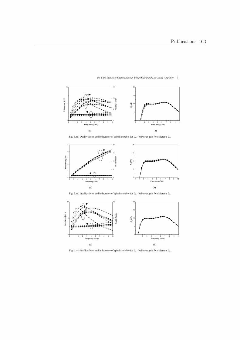
On-Chip Inductors Optimization in Ultra Wide Band Low Noise Amplifier 7
(a) (b)
Fig. 4. (a) Quality factor and inductance of spirals suitable for LB. (b) Power gain for differents LB.
(a) (b)
Fig. 5. (a) Quality factor and inductance of spirals suitable for LE. (b) Power gain for differents LE.
(a) (b)
Fig. 6. (a) Quality factor and inductance of spirals suitable for LS. (b) Power gain for differents LS.
Publications 163
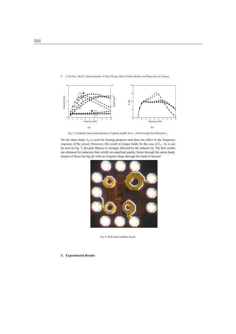
8 J. del Pino, Sunil L. Khemchandani, R Díaz-Ortega, Rubén Pulido-Medina and Hugo García-Vázquez.
(a) (b)
Fig. 7. (a) Quality factor and inductance of spirals suitable for LL. (b) Power gain for differents LL.
On the other hand, LS is used for biasing purposes and does not affect in the frequency response of the circuit. However, this result no longer holds for the case of LL. As it can be seen in Fig. 7, the gain flatness is strongly affected by the inductor Q. The best results are obtained for inductors that exhibit an equalized quality factor through the entire band, despite of those having Qs with an irregular shape through the band of interest.
Fig. 8. Wide band amplifier layout.
5. Experimental Results
164

On-Chip Inductors Optimization in Ultra Wide Band Low Noise Amplifier 9 Fig. 8 shows the final wide band LNA photography. The total chip size, including probe pads, is 665%665 !m2. The amplifier draws 5.3 mA and the output buffer draws 6.5 mA from a 3.3 V supply. The layout has been implemented using a 0.35 !m BiCMOS process. The amplifier was measured on wafer using a Cascade SUMMIT 9000 probe station, 35 GHz probes and 20 GHz Agilent 8720ES vector network analyzer. The probe pads were octagonal, optimized for RF. Three ground-signal-ground (GSG) and one signal-ground-signal (SGS) pad structures with 150 !m pitch were used, as depicted in Fig. 8.
Fig. 9. Measured and simulated scattering parameters for the designed wide band LNA.
Fig. 9 shows measured and post layout simulated S parameters of the wide band amplifier which agree quite well except the S22, which is better in measurements. This is due to parasitic resonance of the output buffer which has not been taken into account in simulations. As expected, a maximum power gain of 12.5 dB was achieved at 3.4 GHz with a -3 dB bandwidth of 1.7-5.3 GHz. A unity gain was measured at 9.4 GHz. The measured input return loss (S11) is higher than 5 dB over the bandwidth. The output return loss (S22) has a maximum value of 13 dB due to the source follower output stage.
Publications 165

10 J. del Pino, Sunil L. Khemchandani, R Díaz-Ortega, Rubén Pulido-Medina and Hugo García-Vázquez. The reverse isolation (S12) is greater than 23 dB due to cascode stage. The NF measurement was done in a noise free environment with an E4440 Agilent 26.5 GHz spectrum analyzer and a 346C noise source. Fig. 10 shows the amplifier measured and simulated NF. The NF varies from 4.3 dB at 3.9 GHz, to 5.2 dB at 5.3 GHz. This result shows good agreement between measured and simulated data. The P1-dB compression point was measured as &4.5 dBm.
Fig. 10. Measured and simulated NF of the wide band LNA.
Measured results and a brief comparison with similar amplifiers are summarized in Table I. It is shown that the designed LNA, using an cheap technology, has a good trade-off between bandwidth, noise figure, gain, linearity and power consumption. Keep in mind that although the power consumption is the highest, the circuit has been fabricated in an older technology compared to the other publications.
TABLE I: Comparison with recently published wide band amplifiers
Author BW 3-dB (GHz)
Max. Gain (dB)
Max. NF (dB)
IIP3 (dBm)
PDC (mW) Technology Year
13 3.1-10.6 9.18 7.2 7.25 23.5 CMOS 0.18 !m 2007 14 2.0-4.6 9.8 5.2 -7 12.6 CMOS 0.18 !m 2005 15 3.1-4.8 15 4.9 -2.2 20 CMOS 0.25 !m 2006 16 3.0-5.0 12.7 5.02 -9.7 16.4 CMOS 0.18 !m 2005 17 3.1-7.5 19.1 3.8 -2.2 32 CMOS 0.18 !m 2006 18 3.0-5.0 12 4.5 - 20 CMOS 0.18 !m 2009
This work 1.7-5.3 12.5 5.0 5.1 32 BiCMOS 0.35 !m 2009
6. Conclusions
166
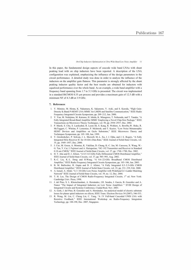
On-Chip Inductors Optimization in Ultra Wide Band Low Noise Amplifier 11 In this paper, the fundamental design aspects of cascode wide band LNAs with shunt peaking load with on chip inductors have been reported. A description of the LNA configuration was explained, emphasizing the influence of the design parameters in the circuit performance. A detailed study was done in order to analyze the influence of the inductors on the amplifier gain flatness. This parameter is strongly affected by the shunt peaking inductor quality factor and the best results are obtained for inductors with equalized performance over the whole band. As an example, a wide band amplifier with a frequency band spanning from 1.7 to 5.3 GHz is presented. The circuit was implemented in a standard BiCMOS 0.35 !m process and provides a maximum gain of 12.5 dB with a minimum NF of 4.3 dB at 3.9 GHz.
7. References
1. Y. Mimino, M. Hirata, K. Nakamura, K. Sakamoto, Y. Aoki, and S. Kuroda, “High Gain-Density K-Band P-HEMT LNA MMIC for LMDS and Satellite Communication,” IEEE Radio Frequency Integrated Circuits Symposium, pp. 209–212, Jun. 2000.
2. Y. Yun, M. Nishijima, M. Katsuno, H. Ishida, K. Minagawa, T. Nobusada, and T. Tanaka, “A Fully Integrated Broad-Band Amplifier MMIC Employing a Novel Chip-Size Package,” IEEE Transactions on Microwave Theory Techniques, vol. 50, pp. 2930–2937, Dec. 2002.
3. P. Marsh, S. Chu, S. Lardizabal, R. Leoni III, S. Kang, R. Wohlert, A. Bowlby,W. Hoke, R. McTaggart, C. Whelan, P. Lemonias, P. McIntosh, and T. Kazior, “Low Noise Metamorphic HEMT Devices and Amplifiers on GaAs Substrates,” IEEE Microwave Theory and Techniques Symposium, pp. 105–108, Jun. 1999.
4. Y. Greshishchev, P. Schvan, J. L. Showell, M.-L. Xu, J. J. Ojha, and J. E. Rogers, “A Fully Integrated SiGe Receiver IC for 10-Gb/s Data Rate,” IEEE Journal of Solid-State Circuits, vol. 35, pp. 1949–1957, Dec. 2000.
5. J. Cao, M. Green, A. Momtaz, K. Vakilian, D. Chung, K.-C. Jen, M. Caresosa, X. Wang, W.-G. Tan, Y. Cai, I. Fujimori and A. Hairapetian, “OC-192 Transmitter and Receiver in Standard 0.18 um CMOS,” IEEE Journal of Solid-State Circuits, vol. 37, pp. 1768–1780, Dec. 2002.
6. H. T. Ahn and D. J. Allstot, “A 0.5–8.5-GHz Fully Differential CMOS Distributed Amplifier,” IEEE Journal of Solid-State Circuits, vol. 37, pp. 985–993, Aug. 2002.
7. R.-C. Liu, K.-L. Deng and H.Wang, “A 0.6–22-GHz Broadband CMOS Distributed Amplifier,” IEEE Radio Frequency Integrated Circuits Symposium, pp. 103–106, Jun. 2003.
8. B. M. Ballweber, R. Gupta and D. J. Allstot, “A Fully Integrated 0.5–5.5-GHz CMOS Distributed Amplifier,” IEEE Journal of Solid-State Circuits, vol. 35, pp. 231–239, Feb. 2000.
9. A. Ismail, A. Abidi, “A 3–10-GHz Low-Noise Amplifier with Wideband LC-Ladder Matching Network” IEEE Journal of Solid-State Circuits, vol. 39, no. 12, Dec. 2004.
10. T. H. Lee, The Design of CMOS Radio-Frequency Integrated Circuits, 1st ed. New York: Cambridge Univ. Press, 1998.
11. J. del Pino, S. L. Khemchandani, A. Hernández, J.R. Sendra, J. García, B. González and A. Nunez “The Impact of Integrated Inductors on Low Noise Amplifiers “ XVIII Design of Integrated Circuits and Systems Conference, Ciudad Real, Nov. 2003.
12. A. Goñi, J. del Pino, B. González and A. Hernández, An analytical model of electric substrate losses for planar spiral inductors on silicon, IEEE Trans. Electron Devices 54 (2007), 546-553.
13. R. Wang, M. Lin, C. Cheng Lin, C. Yang, “A 1V Full-band Cascoded UWB LNA with Resistive Feedback,” IEEE International Workshop on Radio-Frequency Integration Technology, pp. 188-190, Dec. 2007, Singapore.
Publications 167
12 J. del Pino, Sunil L. Khemchandani, R Díaz-Ortega, Rubén Pulido-Medina and Hugo García-Vázquez. 14. K. Chang-Wan, K. Min-Suk, A. Tuan, K. Hoon-Tae and L. Sang-Gug, “An Ultra-Wideband
CMOS Low Noise Amplifier for 3-5 GHz UWB System,” IEEE Journal of Solid-State Circuits, vol. 40, iss. 2, pp. 544-547, Feb. 2005.
15. A. Medi and Namgoong Won, A Fully Integrated Low Cost Packaged CMOS Low Noise Amplifier for the UWB Radio,” IEEE 2006 Radio and Wireless Symposium, pp. 115-118, Jan. 2006.
16. C. S. Chih, W. Ruey-Lue, K. Ming-Lung and K. Hsiang-Chen, “An Integrated CMOS Low Noise Amplifier for 3-5 GHz UWB Applications,” 2005 IEEE Conference on Electron Devices and Solid-State Circuits, pp. 225-228, Dec. 2005.
17. Y. Huang, T. Emery Chen, “A Fully-Integrated UWB CMOS LNA Using Network Synthesis Approach,” 2006 IEEE Microwave Symposium Digest, pp. 320-323, Jun. 2006.
18. F. Gong, K. F. Lam, M. Ismail, Seok-Bae Park J. DeGroat, "A 3-5 GHz Frequency Tunable Ultra Wideband LNA for OFDM Applications," IEEE International Midwest Symposium on Circuits and Systems. 2009, pp. 1018-1021, Aug. 2009.
Acknowledgments
This work has been partially supported by the Spanish MEC and MCyT under projects TEC2008-06881-C03-01 and TSI-020400-2010-55.
168

!
!
!
!
!
!
!
!
"#$%&! '(&)!*&+,-$#./!"&-0/#1,&2!3.(!4,%%!5/$&6()$&+!7#2$(#8,$&+!'9:%#3#&(2!
',$0.(2! ;<!+&%!=#/.!*<!7>)?!@<A<!B0&9-0)/+)/#!
;.,(/)%! 5/$&(/)$#./)%!;.,(/)%!#/!C%&-$(./#-2!)/+!D.99,/#-)$#./2!=,8%#20&(! C%2&E#&(!7)$&! F.E&98&(!GHIH!
!
!
!
!
!
!
!
!
!
!
!
!
!
Publications 169

170
Author's personal copy
Area reduction techniques for full integrated distributed amplifier
J. del Pino !, R. Diaz, S.L. Khemchandani
Institute for Applied Microelectronics (IUMA), Department of Electronic and Automatic Engineering (DIEA), University of Las Palmas de Gran Canaria,Campus Universitario de Tafira, 35017 Las Palmas, Spain
a r t i c l e i n f o
Article history:Received 24 April 2009Accepted 15 October 2009
Keywords:Area reductionDistributed amplifierIntegrated inductorsCMOSUWB
a b s t r a c t
This paper presents two techniques to reduce the area in the design of CMOS distributed amplifiers. Theproposed techniques take into account the influence of compacting the layout and the use of stackedinductor for the artificial transmission lines on the distributed amplifier performance. Following thesedesign guidelines, three prototypes have been fabricated in a low cost CMOS 0:35mm process. Themeasured gain is about 6 dB with a cutoff frequency around 8GHz. The noise figure varies from 5 to 7dBand the circuits draw 30mA from a 3.3V voltage supply. With the developed area optimization designtechniques, a maximum area reduction of 37% with respect to a conventional design has been achieved,without any significant performance degradation.
& 2010 Elsevier GmbH. All rights reserved.
1. Introduction
In the last years the so-called wireless personal area network(WPAN) systems are becoming popular replacing cables andenabling new consumer applications. Such systems are nowadaysdominated by standards like Bluetooth and Zigbee, which operatein the 2.4GHz ISM band, and offer a limited data rate, typicallyaround 1 or 2Mb/s, which is insufficient for many applicationslike fast transfer of large files and high-quality video streaming. Inorder to increase the data rate to several hundreds of Mb/s with alow power transmission, it has been proposed ultra-wideband(UWB).
An UWB receiver is composed of an analog front-end, whichtranslates the signal from radiofrequency to baseband, and adigital stage, that processes the signal at low frequency. One ofthe most important blocks in the front-end is the low noiseamplifier because the receiver noise figure depends directly onthis block. There are many research works related to ultra-wideband low noise amplifier design with new structures anddesign techniques [1]. Among them, one of the most usedstructures is the distributed amplifier (DA) [2].
In previous works related to CMOS based DA, authors focusedtheir research on gain and bandwidth optimization. For example,in [2] the authors developed a method based on the concept ofsimulated annealing to optimize the gain flatness and phaselinearity of a DA. The same procedure was used in a fullydifferential DA in [3]. Other authors tried to improve the gain-bandwidth product using other topologies like cascode [4] and
cascade stages [5–7], or using coplanar waveguides [8] or bondingwires as inductive elements [9]. Those works show how theoperating frequencies and gains of DAs have increased. However,they do not consider one of the main lacks of this kind of circuits,its large chip area due to the extensive use of integrated inductors.
In this paper design guidelines to optimize DA area based onmodifying the circuit layout and using different kind of inductorsis proposed. The organization of this paper is the following. InSection 2 the DA theory is presented. Section 3 is devoted to areareduction techniques and in Section 4 experimental results and acomparative with other works are shown. Finally some conclu-sions are given.
2. Distributed amplifier design
The frequency response of a MOS device degrades due to thepole formed by the input/output capacitance of the transistor andthe resistance it sees. The MOSFET’s transconductance rapidlyfalls with frequency and any attempt to increase the transcon-ductance by increasing the size of the device will also increase itsinput/output capacitance. Thus, while low-frequency gain hasbeen increased, the gain-bandwidth product remains about thesame. The distributed amplification was proposed to overcomethis limitation.
Distributed amplifier employ a topology in which the gainstages are connected such that their capacitances are separated,yet the output currents still combine in an additive fashion(Fig. 1). Series inductive elements are used to separatecapacitances at the inputs and outputs of adjacent gain stages.The resulting topology, given by the interlaying series inductorsand shunt capacitances, forms a lumped-parameter artificial
Contents lists available at ScienceDirect
journal homepage: www.elsevier.de/aeue
Int. J. Electron. Commun. (AEU)
1434-8411/$ - see front matter & 2010 Elsevier GmbH. All rights reserved.doi:10.1016/j.aeue.2009.12.006
! Corresponding author.E-mail address: [email protected] (J. del Pino).
Int. J. Electron. Commun. (AEU) 64 (2010) 1055–1062
Publications 171
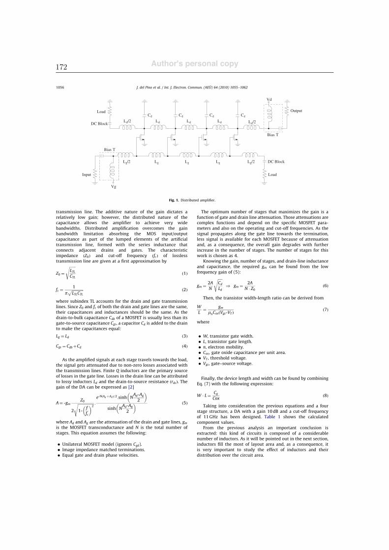
Author's personal copy
transmission line. The additive nature of the gain dictates arelatively low gain; however, the distributed nature of thecapacitance allows the amplifier to achieve very widebandwidths. Distributed amplification overcomes the gainbandwidth limitation absorbing the MOS input/outputcapacitance as part of the lumped elements of the artificialtransmission line, formed with the series inductance thatconnects adjacent drains and gates. The characteristicimpedance !Z0" and cut-off frequency !fc" of losslesstransmission line are given at a first approximation by
Z0 #
!!!!!!!LTLCTL
s
!1"
fc #1
p!!!!!!!!!!!!!LTLCTL
p !2"
where subindex TL accounts for the drain and gate transmissionlines. Since Z0 and fc of both the drain and gate lines are the same,their capacitances and inductances should be the same. As thedrain-to-bulk capacitance Cdb of a MOSFET is usually less than itsgate-to-source capacitance Cgs, a capacitor Cd is added to the drainto make the capacitances equal:
Lg # Ld !3"
Cgs # Cdb$Cd !4"
As the amplified signals at each stage travels towards the load,the signal gets attenuated due to non-zero losses associated withthe transmission lines. Finite Q inductors are the primary sourceof losses in the gate line. Losses in the drain line can be attributedto lossy inductors Ld and the drain-to-source resistance !rds". Thegain of the DA can be expressed as [2]
A# -gmZ0
2
!!!!!!!!!!!!!!!!!!
1-ffc
" #2s :
e-N!Ag $Ad"=2:sinh NAd-Ag
2
" #
sinh NAd-Ag
2
" # !5"
where Ad and Ag are the attenuation of the drain and gate lines, gmis the MOSFET transconductance and N is the total number ofstages. This equation assumes the following:
% Unilateral MOSFET model (ignores Cgd).% Image impedance matched terminations.% Equal gate and drain phase velocities.
The optimum number of stages that maximizes the gain is afunction of gate and drain line attenuation. Those attenuations arecomplex functions and depend on the specific MOSFET para-meters and also on the operating and cut-off frequencies. As thesignal propagates along the gate line towards the termination,less signal is available for each MOSFET because of attenuationand, as a consequence, the overall gain degrades with furtherincrease in the number of stages. The number of stages for thiswork is chosen as 4.
Knowing the gain, number of stages, and drain-line inductanceand capacitance, the required gm can be found from the lowfrequency gain of (5):
gm #2AN
!!!!!Cd
Ld
s
) gm #2A
N & Z0!6"
Then, the transistor width-length ratio can be derived from
WL
#gm
mnCox!Vgs-VT "!7"
where
% W, transistor gate width.% L, transistor gate length.% n, electron mobility.% Cox, gate oxide capacitance per unit area.% VT , threshold voltage.% Vgs, gate–source voltage.
Finally, the device length and width can be found by combiningEq. (7) with the following expression:
W & L#Cg
Cox!8"
Taking into consideration the previous equations and a fourstage structure, a DA with a gain 10dB and a cut-off frequencyof 11GHz has been designed. Table 1 shows the calculatedcomponent values.
From the previous analysis an important conclusion isextracted: this kind of circuits is composed of a considerablenumber of inductors. As it will be pointed out in the next section,inductors fill the most of layout area and, as a consequence, itis very important to study the effect of inductors and theirdistribution over the circuit area.
Vd
CdLoad
DC Block
Output
Bias T
Load
DC Block
Input
Vg
Bias T
Ld
Cd
Ld
Cd
Ld
Cd
Lg Lg LgLg/2 Lg/2
Ld/2Ld/2
Fig. 1. Distributed amplifier.
J. del Pino et al. / Int. J. Electron. Commun. (AEU) 64 (2010) 1055–10621056
172
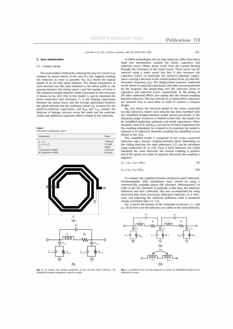
Author's personal copy
3. Area optimization
3.1. Compact design
The most evident method for reducing the area of a circuit is tocompact its layout which, in the case of a DA, suggests locatingthe inductors as close as possible. Fig. 2(a) shows the typicallayout of an on-chip spiral inductor. The design parameters ofsuch structure are the outer diameter d, the metal width w, thespacing between the wiring metal s and the number of turns n.The standard lumped-element model associated to this structureis shown in Fig. 2(b) [10]. In this model, LS and RS represent theseries inductance and resistance, CF is the fringing capacitancebetween the metal traces and the overlap capacitance betweenthe spiral inductor and the underpass metal, COX accounts for thespiral-to-substrate capacitance, and RSUB and CSUB models thebehavior of leakage currents across the oxide and the substrate(bulk) and additional capacitive effects related to the substrate.
In CMOS technologies, the on-chip inductors suffer from threemain loss mechanisms, namely the ohmic, capacitive andinductive losses. Ohmic losses result from the current flowingthrough the resistance of the metal tracks. Those losses can bereduced using a wider metal line but, it also increases thecapacitive losses (in particular the metal-to-substrate capaci-tance) causing a decrease in the overall quality factor (Q) and self-resonance frequency !fSR". The displacement currents conductedby the metal-to-substrate capacitance and eddy current generatedby the magnetic flux penetrating into the substrate result incapacitive and inductive losses, respectively. In the design ofDA other undesired effects also appear like the mutual couplingbetween inductors. This fact worsens if, as stated above, inductorsare situated close to each other in order to achieve a compactdesign.
Fig. 3(a) shows the electrical model of two series connectedon-chip inductors, where each inductor has been modeled withthe simplified lumped-element model shown previously. If thefrequency range of interest is limited to few GHz, this model canbe simplified neglecting substrate and metal capacitance. Otherelements, such as RS and RSUB, can also be of minor importance forthe coupling estimation. So, stripped to its essential, the model isreduced to its inductive elements resulting the simplified circuitshown in Fig. 3(b).
This simplified model is composed of two series connectedinductors and a mutual coupling between them. Depending onthe coiling direction the total inductance (LT) can be calculatedusing expression (9) or (10). Thus, if both inductors are coiledfollowing the same direction, the mutual coupling is positiveand if the spirals are coiled in opposite directions the coupling isnegative:
LT1 # LS1$LS2$2m12 !9"
LT2 # LS1$LS2-2m12 !10"
To evaluate the coupling between integrated spiral inductors,electromagnetic (EM) simulations have carried on using acommercially available planar EM simulator (Momentum&). Inorder to get the simulator to generate useful data, the substratedefinition was first calibrated. This was accomplished by usingmeasured data from previously fabricated inductors as a refer-ence, and adjusting the substrate definition until it producedclosely correlated data [11–13].
Fig. 4 shows the layouts of the simulated structures: LT1, andLT2. In the first case the inductors are coiled in the same direction,
Table 1Calculated components values.
Component Value
Lg # Ld 1.465nHLg=2# Ld=2 1.15nHCd 586 fFL (transistor length) 0:425mmW (transistor width) 4:42mm
Fig. 2. (a) Layout and design parameter of the on-chip spiral inductor. (b)Simplified lumped-component inductor model.
Fig. 3. (a) Model of two on-chip inductors in series. (b) Simplified model of twoinductors in series.
J. del Pino et al. / Int. J. Electron. Commun. (AEU) 64 (2010) 1055–1062 1057
Publications 173
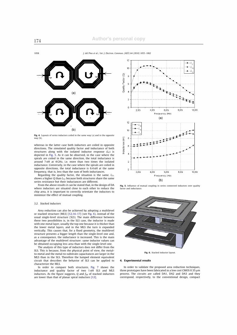
Author's personal copy
whereas in the latter case both inductors are coiled in oppositedirections. The simulated quality factor and inductance of bothstructures along with the isolated inductor response !LP" isdepicted in Fig. 5. As it can be observed, in the case where thespirals are coiled in the same direction, the total inductance isaround 7nH at 4GHz, i.e. more than two times the isolatedinductance. Conversely, in the case where the spirals are coiled inopposite directions, the total inductance is 6.4 nH at the samefrequency, that is, less than the sum of both inductances.
Regarding the quality factor, the situation is the same. LT1shows a higher Q than LT2 because both structures share the sameseries resistance but their inductances are different.
From the above results it can be stated that, in the design of DAwhere inductors are situated close to each other to reduce thechip area, it is important to correctly orientate the inductors tominimize the effect of mutual coupling.
3.2. Stacked inductors
Area reduction can also be achieved by adopting a multilevelor stacked structure (MLS) [12,14–17] (see Fig. 6), instead of theusual single-level structure (SLS). The main difference betweenthese two possibilities is, in the SLS case, the inductor is madewith one metal layer, usually the top one because it is thicker thanthe lower metal layers, and in the MLS the turn is expandedvertically. This causes that, for a fixed geometry, the multilevelstructure presents a bigger length than the single-level one and,as a consequence, the inductance is increased. This is the mainadvantage of the multilevel structure: same inductor values canbe obtained occupying less area than with the single-level one.
The analysis of this type of inductors does not differ from theSLS. This is because, from the physical point of view, the metal-to-metal and the metal-to-substrate capacitances are larger in theMLS than in the SLS. Therefore the lumped element equivalentcircuit that describes the behavior of SLS can be applied tocharacterize the MLS.
In order to compare both structures, Fig. 7 shows theinductance and quality factor of two 1nH SLS and MLSinductors. As the figure suggests, Q and fSR of stacked inductorsare lower than that of planar spiral inductors [12].
4. Experimental results
In order to validate the proposed area reduction techniques,three prototypes have been fabricated in a low cost CMOS 0:35mmprocess. The circuits are called DA1, DA2 and DA3 and theycorrespond, respectively, to the conventional design, compact
Fig. 4. Layouts of series inductors coiled in the same way (a) and in the oppositeway (b).
Fig. 5. Influence of mutual coupling in series connected inductors over qualityfactor and inductance.
Fig. 6. Stacked inductor layout.
J. del Pino et al. / Int. J. Electron. Commun. (AEU) 64 (2010) 1055–10621058
174
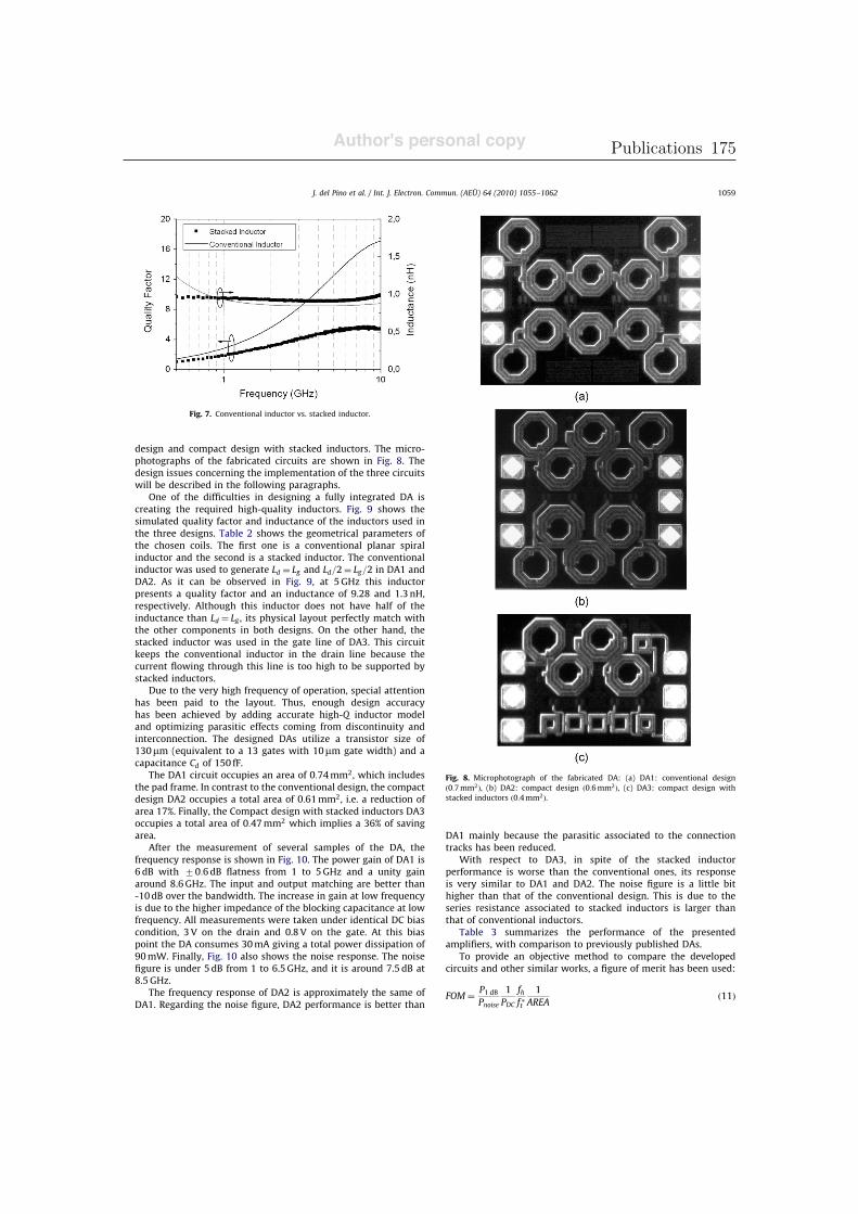
Author's personal copy
design and compact design with stacked inductors. The micro-photographs of the fabricated circuits are shown in Fig. 8. Thedesign issues concerning the implementation of the three circuitswill be described in the following paragraphs.
One of the difficulties in designing a fully integrated DA iscreating the required high-quality inductors. Fig. 9 shows thesimulated quality factor and inductance of the inductors used inthe three designs. Table 2 shows the geometrical parameters ofthe chosen coils. The first one is a conventional planar spiralinductor and the second is a stacked inductor. The conventionalinductor was used to generate Ld # Lg and Ld=2# Lg=2 in DA1 andDA2. As it can be observed in Fig. 9, at 5GHz this inductorpresents a quality factor and an inductance of 9.28 and 1.3nH,respectively. Although this inductor does not have half of theinductance than Ld # Lg , its physical layout perfectly match withthe other components in both designs. On the other hand, thestacked inductor was used in the gate line of DA3. This circuitkeeps the conventional inductor in the drain line because thecurrent flowing through this line is too high to be supported bystacked inductors.
Due to the very high frequency of operation, special attentionhas been paid to the layout. Thus, enough design accuracyhas been achieved by adding accurate high-Q inductor modeland optimizing parasitic effects coming from discontinuity andinterconnection. The designed DAs utilize a transistor size of130mm (equivalent to a 13 gates with 10mm gate width) and acapacitance Cd of 150 fF.
The DA1 circuit occupies an area of 0:74mm2, which includesthe pad frame. In contrast to the conventional design, the compactdesign DA2 occupies a total area of 0:61mm2, i.e. a reduction ofarea 17%. Finally, the Compact design with stacked inductors DA3occupies a total area of 0:47mm2 which implies a 36% of savingarea.
After the measurement of several samples of the DA, thefrequency response is shown in Fig. 10. The power gain of DA1 is6 dB with 70:6dB flatness from 1 to 5GHz and a unity gainaround 8.6GHz. The input and output matching are better than-10dB over the bandwidth. The increase in gain at low frequencyis due to the higher impedance of the blocking capacitance at lowfrequency. All measurements were taken under identical DC biascondition, 3V on the drain and 0.8V on the gate. At this biaspoint the DA consumes 30mA giving a total power dissipation of90mW. Finally, Fig. 10 also shows the noise response. The noisefigure is under 5dB from 1 to 6.5GHz, and it is around 7.5 dB at8.5GHz.
The frequency response of DA2 is approximately the same ofDA1. Regarding the noise figure, DA2 performance is better than
DA1 mainly because the parasitic associated to the connectiontracks has been reduced.
With respect to DA3, in spite of the stacked inductorperformance is worse than the conventional ones, its responseis very similar to DA1 and DA2. The noise figure is a little bithigher than that of the conventional design. This is due to theseries resistance associated to stacked inductors is larger thanthat of conventional inductors.
Table 3 summarizes the performance of the presentedamplifiers, with comparison to previously published DAs.
To provide an objective method to compare the developedcircuits and other similar works, a figure of merit has been used:
FOM#P1 dB
Pnoise
1PDC
fhf 't
1AREA
!11"
Fig. 7. Conventional inductor vs. stacked inductor.
Fig. 8. Microphotograph of the fabricated DA: (a) DA1: conventional design!0:7mm2", (b) DA2: compact design !0:6mm2", (c) DA3: compact design withstacked inductors !0:4mm2".
J. del Pino et al. / Int. J. Electron. Commun. (AEU) 64 (2010) 1055–1062 1059
Publications 175

Author's personal copy
This expression includes the DC power consumption !PDC" andoutput noise power !Pnoise # PthFGain", where Pth # kT is thethermal noise floor given by -174dBm=Hz at T # 290K. Inaddition, in order to quantify how efficient the availablebandwidth of the technology is utilized, a relative measure forbandwidth is introduced through the fh=f
't factor, where fh is the
upper LNA corner frequency and fh=f't is the technology unity
current gain bandwidth ft around the maxima of the product!gm=ID"ft . Finally, AREA is the area occupied by the circuit and itallows comparing the designs in terms of area consumption. Theproposed FOM includes the output 1-dB compression power!P1 dB" as a measure for linearity. However, some authors do notinclude this measurement and, as a consequence, two FOMs havebeen plotted in Table 3: one including the P1 dB and the other onewithout any linearity reference.
The DA presented in [2] has an excellent FOM, mainly because itutilizes very efficiently the available bandwidth of the technology.However, the area of this circuit almost doubles our designs and, asa consequence, its FOM is lower than ours. The same authors utilizea fully differential topology in [3] to achieve a wider bandwidththan its single-ended counterpart. However, both area and powerconsumption double and the achieved FOM is low.
The works of [4] exhibit both higher gain and bandwidth thanour designs. Also the power dissipated is low being the NF similarthan our designs. However, our DAs achieve better FOMs mainlybecause they utilize more efficiently the available area.
The low power techniques presented in [19,7] use a low PDC toachieve low noise figure and good gain, but they are, however,fundamentally limited by large area.
Finally the DA reported in [18] uses coplanar waveguides toimplement the required inductances. This technique achieves avery high frequency of operation but at the cost of a very largearea.
Regarding the presented designs, the best FOM is achieved, asexpected, by DA3. This design employs stacked inductors toreduce area. This kind of inductor occupies less chip area than that
Fig. 9. Inductors employed in the DA.
Table 2Inductors geometrical parameters.
s !mm" n r !mm" W !mm"
Conventional 2 2.5 100 16Stacked 2 2( 1:5 40 10
Fig. 10. S21 and noise figure measurements.
J. del Pino et al. / Int. J. Electron. Commun. (AEU) 64 (2010) 1055–10621060
176
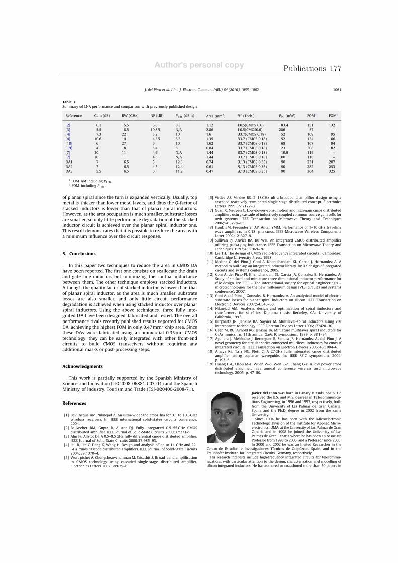
Author's personal copy
of planar spiral since the turn is expanded vertically. Usually, topmetal is thicker than lower metal layers, and thus the Q-factor ofstacked inductors is lower than that of planar spiral inductors.However, as the area occupation is much smaller, substrate lossesare smaller, so only little performance degradation of the stackedinductor circuit is achieved over the planar spiral inductor one.This result demonstrates that it is possible to reduce the area witha minimum influence over the circuit response.
5. Conclusions
In this paper two techniques to reduce the area in CMOS DAhave been reported. The first one consists on reallocate the drainand gate line inductors but minimizing the mutual inductancebetween them. The other technique employs stacked inductors.Although the quality factor of stacked inductor is lower than thatof planar spiral inductor, as the area is much smaller, substratelosses are also smaller, and only little circuit performancedegradation is achieved when using stacked inductor over planarspiral inductors. Using the above techniques, three fully inte-grated DA have been designed, fabricated and tested. The overallperformance rivals recently published results reported for CMOSDA, achieving the highest FOM in only 0:47mm2 chip area. Sincethese DAs were fabricated using a commercial 0:35mm CMOStechnology, they can be easily integrated with other front-endcircuits to build CMOS transceivers without requiring anyadditional masks or post-processing steps.
Acknowledgments
This work is partially supported by the Spanish Ministry ofScience and Innovation (TEC2008-06881-C03-01) and the SpanishMinistry of Industry, Tourism and Trade (TSI-020400-2008-71).
References
[1] Bevilacqua AM, Niknejad A. An ultra-wideband cmos lna for 3.1 to 10.6GHzwireless receivers. In: IEEE international solid-states circuits conference,2004.
[2] Ballweber BM, Gupta R, Allstot DJ. Fully integrated 0.5–55GHz CMOSdistributed amplifier. IEEE Journal of Solid-State Circuits 2000;37:231–9.
[3] Ahn H, Allstot DJ. A 0.5–8.5GHz fully differential cmos distributed amplifier.IEEE Journal of Solid-State Circuits 2000;37:985–93.
[4] Liu R, Lin C, Deng K, Wang H. Design and analysis of dc-to-14-GHz and 22-GHz cmos cascode distributed amplifiers. IEEE Journal of Solid-State Circuits2004;39:1370–4.
[5] Worapishet A, Chongcheawchamnan M, Srisathit S. Broad-band amplificationin CMOS technology using cascaded single-stage distributed amplifier.Electronics Letters 2002;38:675–6.
[6] Virdee AS, Virdee BS. 2–18GHz ultra-broadband amplifier design using acascaded reactively terminated single stage distributed concept. ElectronicsLetters 1999;35:2122–3.
[7] Guan X, Nguyen C. Low-power-consumption and high-gain cmos distributedamplifiers using cascade of inductively coupled common-source gain cells foruwb systems. IEEE Transaction on Microwave Theory and Techniques2006;54:3278–83.
[8] Frank BM, Freundorfer AP, Antar YMM. Performance of 1–10GHz travelingwave amplifiers in 0:18)mm cmos. IEEE Microwave Wireless ComponentsLetter 2002;12:327–9.
[9] Sullivan PJ, Xavier BA, Ku WH. An integrated CMOS distributed amplifierutilizing packaging inductance. IEEE Transaction on Microwave Theory andTechniques 1997;45:1969–76.
[10] Lee TH. The design of CMOS radio-frequency integrated circuits. Cambridge:Cambridge University Press; 1998.
[11] Medina O, del Pino J, Goni A, Khemchandani SL, Garcia J, Hernandez A. Amethod to build-up an integrated inductor library. In: XX design of integratedcircuits and systems conference, 2005.
[12] Goni A, del Pino FJ, Khemchandani SL, Garcia JA, Gonzalez B, Hernandez A.Study of stacked and miniature three-dimensional inductor performance forrf ic design. In: SPIE – The international society for optical engineering’s –microtechnologies for the new millennium design (VLSI circuits and systemsconference), 2007.
[13] Goni A, del Pino J, Gonzalez B, Hernandez A. An analytical model of electricsubstrate losses for planar spiral inductors on silicon. IEEE Transaction onElectronic Devices 2007;54:546–53.
[14] Niknejad AM. Analysis, design and optimization of spiral inductors andtransformers for si rf ics. Diploma thesis. Berkeley, CA: University ofCalifornia, 1998.
[15] Burghartz JN, Jenkins KA, Soyuer M. Multilevel-spiral inductors using vlsiinterconnect technology. IEEE Electron Devices Letter 1996;17:428–30.
[16] Geen M, RG, Arnold RG, Jenkins JA. Miniature multilayer spiral inductors forGaAs mmics. In: 11th annual GaAs IC symposium, 1989. p. 381–94.
[17] Aguilera J, Melendez J, Berenguer R, Sendra JR, Hernandez A, del Pino J. Anovel geometry for circular series connected multilevel inductors for cmos rfintegrated circuits. IEEE Transaction on Electron Devices 2006;46:1084–6.
[18] Amaya RE, Tarr NG, Plett C. A 27GHz fully integrated cmos distributedamplifier using coplanar waveguide. In: IEEE RFIC symposium, 2004.p. 193–6.
[19] Huang H-L, Chou M-F, Wuen W-S, Wen K-A, Chang C-Y. A low power cmosdistributed amplifier. IEEE annual conference wireless and microwavetechnology, 2005. p. 47–50.
Javier del Pino was born in Canary Islands, Spain. Hereceived the B.S. and M.S. degrees in Telecommunica-tions Engineering, in 1996 and 1997, respectively, bothfrom the University of Las Palmas de Gran Canaria,Spain, and the Ph.D. degree in 2002 from the sameUniversity.
Since 1994 he has been with the MicroelectronicTechnologic Division of the Institute for Applied Micro-electronics IUMA, at the University of Las Palmas de GranCanaria and in 1998 he joined the University of LasPalmas de Gran Canaria where he has been an AssociateProfessor from 1998 to 2005, and a Professor since 2005.In 2000 and 2002 he was an Invited Researcher in the
Centro de Estudios e Investigaciones Tecnicas de Guipuzcoa, Spain, and in theFraunhofer Institute for Integrated Circuits, Germany, respectively.
His research interests include high-frequency integrated circuits for telecommu-nications, with particular attention to the design, characterization and modelling ofsilicon integrated inductors. He has authored or coauthored more than 50 papers in
Table 3Summary of LNA performance and comparison with previously published design.
Reference Gain (dB) BW (GHz) NF (dB) P1 dB (dBm) Area !mm2" ft' (Tech.) PDC (mW) FOMa FOMb
[2] 6.1 5.5 6.8 8.8 1.12 10.5(CMOS 0.6) 83.4 151 132[3] 5.5 8.5 10.85 N/A 2.86 10.5(CMOS0.6) 286 57 –[4] 7.3 22 5.2 10 1.6 33.7(CMOS 0.18) 52 108 95[4] 10.6 14 4.35 5.3 1.35 33.7 (CMOS 0.18) 52 124 106[18] 6 27 6 10 1.62 33.7 (CMOS 0.18) 68 107 94[19] 4 8 5.4 8 0.84 33.7 (CMOS 0.18) 23 208 182[7] 10 11 4.6 N/A 1.44 33.7 (CMOS 0.18) 19.6 119 –[7] 16 11 4.5 N/A 1.44 33.7 (CMOS 0.18) 100 110 –DA1 7 6.5 5 12.3 0.74 8.13 (CMOS 0.35) 90 231 207DA2 7 6.5 4.5 12.4 0.61 8.13 (CMOS 0.35) 90 282 253DA3 5.5 6.5 6 11.2 0.47 8.13 (CMOS 0.35) 90 364 325
a FOM not including P1 dB.b FOM including P1 dB.
J. del Pino et al. / Int. J. Electron. Commun. (AEU) 64 (2010) 1055–1062 1061
Publications 177
Author's personal copy
international journals and conferences and leads research projects funded by publicinstitutions and local companies.
Roberto Diaz Ortega was born in Las Palmas de GranCanaria (Spain) in 1982. He received his M.S. degree inElectronic Engineering from the University of LasPalmas de Gran Canaria in 2006. Since 2003 heresearches with the Institute for Applied Microelec-tronics (IUMA) involved in the Microelectronic Tech-nology Division (TME) in the same university.
His research interests and works include high-fre-quency integrated circuits for telecommunications, withparticular attention to the design circuits for ultra wide-bands applications in CMOS and ultra low power and lowvoltage circuits design for wireless communications.
Sunil Lalchand Khemchandani was born in LasPalmas de Gran Canaria, Spain. In 2000 he receivedthe M.S. degree in Telecommunication Engineeringfrom the University of Las Palmas de Gran Canaria, andthe Ph.D. degree in 2007.
From 1998 he is in the Research Institute for AppliedMicroelectronics of University of Las Palmas de GranCanaria. His research work involved GaAs IC’s for videoand image processing. From 2001 to 2003 he wasworking in INCIDE, where he was involved in themodelling of inductors in CMOS technology, designingLNAs for GPS applications, transimpedance amplifiersfor SONET/SDH and PLLs for MMDS application. His
research interests include high-frequency integrated circuits for telecommunica-tions, with particular attention to the design of VCOs, LNAs and mixers in CMOStechnology.
J. del Pino et al. / Int. J. Electron. Commun. (AEU) 64 (2010) 1055–10621062
178

!
!
!
!
!
!
!
!
!
!
"#$%&! '(&)!*&+,-$#./!#/!*0!0,%%1!2/$&3()$&+!0(./$45/+6!7.(!8%$()49#+&:)/+!
',$;.(6! <=!>)(-?)4@ABC,&B!*=!D?)B!D=!*)E.64@)%#+.!'=!F)/$)/)!G=!+&%!H#/.!F=I=!J;&E-;)/+)/#!
K./7&(&/-&! LL@!K./7&(&/-&!./!D&6#3/!.7!K#(-,#$6!)/+!2/$&3()$&+!F16$&E6!
D)$&! M.N&E:&(!OPQP!!
Publications 179

180
!"#$%&#'()*+,-%+-%&.%.(//0%1-*#2"$*#'%.",-*34-'5%6,"%7/*"$38+'#9$-'%
:;%<$")=$3>?@A(#@B%&;%C=$@B%C;%&$D,53>$/+',B%!;%E$-*$-$B%F;%'#/%G+-,B%E(-+/%H;%IJ#D)J$-'$-+%1-5*+*(*#%6,"%!KK/+#'%L+)",#/#)*",-+)5B%C#K$"*$D#-*,%'#%1-2#-+#"=$%4/#)*"M-+)$%0%!(*,D?*+)$B%7-+N#"5+'$'%'#%H$5%G$/D$5%'#%<"$-%O$-$"+$%
%%
Abstract— This paper describes two RF front-ends for Ultra Wideband (3.1-10.6 GHz) implemented in UMC CMOS 0.18 µm process. The first one uses a differential common-gate with shunt peaking LNA followed by a Gilbert Cell based quadrature mixer. Post-layout simulations show a conversion gain of 12 dB, a 9.4 dB of noise figure and a third-order intermodulation intercept point of -3.3 dBm. This combination draws 16 mW from a 1.8 V supply. The second design, which is inductor less, uses a differential common-gate with resistive loaded LNA followed by a quadrature capacitive degeneration mixer circuit. Simulation results are 7.2 dB of conversion gain, 13.7 dB of noise figure and -2.1 dBm of IIP3. This combination draws 14 mW from a 1.8 V supply. The occupied area of this design is 54% lower than the first front-end. Keywords-component: Front-end, Receiver, Low-Noise Amplifier (LNA), Mixer, Shunt-peaking, Ultra-Wideband.
1; %1PQ&RC7OQ1RP%%7/*"$38+'#9$-'% *#)J-,/,20% S78TU% VWX% J$5% D,*+N$*#'% $%
2"#$*%+-*#"#5*%+-%*J#%',D#5*+)%$-'%,66+)#%#-N+",-D#-*5%Y+*J%*J#%+DK/#D#-*$*+,-% ,6% -#Y% #/#)*",-+)% '#N+)#5Z% GO5B% '+2+*$/% N+'#,%$-'% $('+,% 505*#D5B% '+2+*$/% *#/#N+5+,-B% /$5*% 2#-#"$*+,-% D,9+/#%KJ,-#5B% GC!5B% #*);% QJ#0% '#D$-'% $% Y+"#/#55% 5,/(*+,-% Y+*J% $%D$[+D(D%9$-'Y+'*J%$-'%D+-+D(D%K,Y#"%),-5(DK*+,-;%
QJ#% 8+L#'+$% !//+$-)#% Y$5% 9,"-% *,% 9,,5*% (K% *J#% 78T%*#)J-,/,20;% C(#% *,% *J+5% $)*+N#% K$"*+)+K$*+,-B% +-% \]]^% *J#%8+L#'+$% !//+$-)#% K(9/+5J#'% *J#% 1ER_14O% \`a]^% V\X% $-'%1ER_14O%\`a]b% VcX% 5*$-'$"'5% *,% "#2(/$*#% *J#%KJ05+)$/% $-'% *J#%L!O%/$0#"5B%+-)/('+-2%*J#%+-*#"6$)#%9#*Y##-%*J#D;%QJ#%78T%6"#A(#-)0%9$-'%,6%c;W3W];`%<:@% +5%'+N+'#'% +-*,%Wd%5(939$-'5%,6%e\b%L:@%#$)J%$-'%#DK/,05%R.CL%+-%#$)J%9$-'%*,%*"$-5D+*%'$*$% "$*#5% $5% J+2J% $5% db]%LT_5;%Q,% #-5("#% 5D$//% +-*#"6#"#-)#%Y+*J% #[+5*+-2% 5*$-'$"'5B% *J#% ,(*K(*% K,Y#"% /#N#/% ,6% 78T%*"$-5D+**#"5%J$5%9##-%6+[#'%*,%3dW%'TD;%R-%*J#%,*J#"%J$-'B%*J#%D+-+D(D%5#-5+9+/+*0%*J$*%$//,Y5%$-%78T%"#)#+N#"%+5%3^c%'TD;%
QJ+5% K$K#"% '#$/5% Y+*J% *J#% &.% 6",-*3#-'% ,6% $-% 78T%"#)#+N#";% 1-% *J+5%Y,"f% *Y,% K,55+9/#% ),-6+2("$*+,-5% 6,"% *J#%&.%6",-*3#-'%J$N#%9##-%'#N#/,K#';%R-#%,6%*J#D%+5%+-'()*,"%/#55B%5,%+*%,))(K+#5%/#55%$"#$%$-'%$/5,%J$5%/,Y%K,Y#"%),-5(DK*+,-;%QJ#%K$K#"% +5% ,"2$-+@#'% $5% 6,//,Y5Z% 1-% 5#)*+,-% 11% *J#% ),DD,-%2$*#%HP!%*,K,/,20%+5%#[K/$+-#';%QJ#%A($'"$*("#%D+[#"5%$"#%5*('+#'%+-% 5#)*+,-% 111;% 1-% 5#)*+,-% 1>% *J#% *Y,% 6",-*3#-'5% $"#% '#5)"+9#'%$-'% 5+D(/$*+,-5% "#5(/*5% $"#% 5J,Y-;% .+-$//0B% 5,D#% ),-)/(5+,-5%$"#%'"$Y-%+-%5#)*+,-%>;%
%
11; ORLLRP3<!Q4%HP!%%O,DD,-32$*#% SO<U% HP!% +5% $% Y+'#/0% (5#'% *,K,/,20% +-%
Y+"#/#55%),DD(-+)$*+,-5%VdX3V^X;%1-%*J+5%5#)*+,-B%*J#%O<%HP!%+5% 5*('+#'B% +;#;B% Y#% '+5)(55% *J#% "#/$*+,-5J+K% 9#*Y##-% *J#% +-K(*%D$*)J+-2% $-'% N,/*$2#% 2$+-B% Y#% #N$/($*#% *J#% -,+5#% 6+2("#% $-'%6+-$//0%Y#%5J,Y%*J#%<D39,,5*#'%*,K,/,20;%
A. Input Matching and voltage gain QJ#% '#5+"#'% +-K(*% +DK#'$-)#% ,6% $% O<% +-K(*% 5*$2#% +5%
$)J+#N#'% 90% $'g(5*+-2% *J#% 9+$5% )(""#-*B% $5K#)*% "$*+,B% $-'%,N#"'"+N#%N,/*$2#%5()J%*J$*%W_2D%,6%$KK",[+D$*#/0%\]%DE;%QJ#%O<% 5*$2#% ',#5% -,*% 5(66#"% 6",D% *J#%L+//#"% #66#)*B% $-'% *J(5% $-%$'#A($*#% "#N#"5#% +5,/$*+,-% )$-% 9#% $)J+#N#'% Y+*J% $% 5+-2/#%*"$-5+5*,"% 5*$2#;% QJ#"#6,"#B% *J#% +-K(*% D$*)J+-2% -#*Y,"f% $-'%/,$'%)$-%9#%'#5+2-#'%5#K$"$*#/0;%%
H$"2#% +DK#'$-)#% *,Y$"'5% *J#% 5+2-$/% 2",(-'% +5% -##'#'% *,%5*##"% *J#% 5+2-$/% +-*,% *J#% +-K(*% *"$-5+5*,"% 5,(")#;% QJ+5% )$-% 9#%$)J+#N#'%Y+*J%$%)(""#-*%5,(")#%1T1!E%5J,Y-%+-%.+2("#%W$;%QJ$*%*,K,/,20%+5%-,*%*0K+)$//0%(*+/+@#'%+-%*J#%HP!%5+-)#%*J#%)(""#-*%5,(")#%1T1!E%+-)"#$5#5%*J#%-,+5#;%!%9#**#"%-,+5#%K#"6,"D$-)#%+5%$)J+#N#'%90%(5+-2%$%5,(")#%+-'()*,"%HE%$5%5J,Y-%+-%.+2("#%W9;%QJ#% HE% 6,"D5% $% K$"$//#/% HO% "#5,-$*,"% Y+*J% *J#% K$"$5+*+)%)$K$)+*$-)#%OG!&% $55,)+$*#'%Y+*J% *J#% 5,(")#% -,'#% ,6% *J#%LW;%8J#-% ,-3Y$6#"% D#$5("#D#-*5% $"#% -,*% $KK/+)$9/#B% *J#% 5,(")#%-,'#%*0K+)$//0%-##'5%*,%9#%),--#)*#'%#+*J#"%*,%K$)f$2#%,"%GOT%90%(5+-2%$%9,-'Y+"#%+-'()*$-)#%H1P%$5%5J,Y-%+-%.+2("#%W);%QJ#%H1P%+5% "#5,-$*#'% $*% *J#%Y$-*#'% 6"#A(#-)0%Y+*J% $%CO%9/,)f+-2%)$K$)+*,"% O1P% YJ+)J% )$-% 9#% #+*J#"% $-% ,-3)J+K% ,"% $-% #[*#"-$/%),DK,-#-*;%
1T1!E
>CC
hH
R(*
>9 LW
>CC
hH
R(*
>9 LW
HE
1-H1P
OG!&
>CC
hH
>9 LW
HE
1-OG!&
O1P
R(*
S$U S9U S)U !
.+2("#%W O,DD,-32$*#%HP!%+DK(*%+-*#"6$)#5Z%$U%)(""#-*%5,(")#B%9U%K$"$//#/%HO%"#5,-$*,"B%$-'%)U%5#"+#5%$-'%K$"$//#/%HO%"#5,-$*,"5;%
QJ+5%Y,"f%+5%K$"*+$//0%5(KK,"*#'%90%*J#%EK$-+5J%L+-+5*"0%,6%E)+#-)#%$-'%1--,N$*+,-% SQ4O\]]b3]`bbW3O]c3]WUB% *J#% EK$-+5J% L+-+5*"0% ,6% 1-'(5*"0B%Q,("+5D% $-'%Q"$'#% SQE13]\]d]]3\]]b3^WU% $-'% *J#% iG",2"$D$% '#% $0('$5% '#%.,"D$)+M-%'#/%G#"5,-$/%+-N#5*+2$',"B%'#%/$%!2#-)+$%O$-$"+$%'#%1-N#5*+2$)+M-B%1--,N$)+M-% 0% E,)+#'$'% '#% /$% 1-6,"D$)+M-% '#/% <,9+#"-,% '#% O$-$"+$5% 0% /$%),6+-$-)+$)+M-%0%*$5$%'#%),6+-$-)+$)+M-%'#/%.;E;4;j;%
ISBN 978-84-693-7393-4 DCIS 2010 Proceedings 649
Publications 181

1-%.+2("#%W9%$-'%.+2("#%W)B%*J#%)$K$)+*,"%OG!&%+-)/('#5%*J#%K$"$5+*+)% )$K$)+*$-)#5% $*% *J#% 5,(")#% -,'#B% +;#;% 5,(")#39,'0%g(-)*+,-% )$K$)+*$-)#% ,6%LWB% 5(95*"$*#% )$K$)+*$-)#% ,6%HEB% $-'%)$K$)+*$-)#% )$(5#'% 90% *J#% 9,-'+-2% K$'5% $-'% ,-3)J+K% D#*$/%Y+"+-2;%.("*J#"D,"#B% *J#%N$/(#%,6% *J#% 5,(")#% +-'()*,"%HE% )$-%9#% '#)"#$5#'% 90% $''+-2% $-% $''+*+,-$/% 5J(-*% )$K$)+*,"% OE% +-%K$"$//#/%Y+*J%HE% S*J#%OE% +5% -,*% 5J,Y-% +-%.+2("#%W9%,"%.+2("#%W)U;%QJ#"#6,"#B% $//% *J#% )$K$)+*$-)#% $/% *J#% 5,(")#%-,'#% )$-%9#%+-)/('#'%+-%$%5+-2/#%5,(")#%)$K$)+*,"%OQ%(5#'%+-%*J#%6,//,Y+-2%)$/)(/$*+,-5Z%%
%SWU%
QJ#% +-K(*% +DK#'$-)#% h1P% ,6% $% O<% +-K(*% 5*$2#B% 5J,Y-% +-%.+2("#%W9B%)$-%9#%)$/)(/$*#'%$5%
%S\U%
QJ#% 5,(")#% +-'()*$-)#% HE% "#5,-$*#5% Y+*J% *J#% )$K$)+*$-)#%OQ%$*%*J#%6"#A(#-)0%,6%
%ScU%
$-'% $*% *J#% 6"#A(#-)0B% S\U% 5+DK/+6+#5% *,% W_2D;%QJ#% +DK#'$-)#%h1P%,6%$%O<%+-K(*%5*$2#%5J,Y-%+-%.+2("#%W)%+5%
%%SdU%
8+*J% $% K#"6#)*% +DK#'$-)#% D$*)J+-2% S1/gm = RSUB% *J#%N,/*$2#%2$+-%,6%*J#%O<%$DK/+6+#"%9#),D#5%$%'+N+5+,-%,6%,(*K(*%/,$'%N#"5(5%*J#%5,(")#%+DK#'$-)#B%+;#;%hH_&E;%QJ#%$55(DK*+,-%+5% N$/+'% +6% *J#% '"$+-3*,35,(")#% "#5+5*,"% "'5% +5%D()J% /$"2#"% *J$-%*J#%/,$'%"#5+5*$-)#%$*%*J#%'"$+-;%R*J#"Y+5#B%*J#%2$+-%$-'%+-K(*%+DK#'$-)#%6,"D(/$5%5J,(/'%9#%D,'+6+#'%*,%
%SeU%
%
$-'%
%S`U%
B. Noise of a CG stage
QJ#%-,+5#%6$)*,"%,6%$%O<%HP!%+5%#[K"#55#'%$5%
S^U%
YJ#"#% %+5%*J#%),#66+)+#-*%%,6%)J$--#/%*J#"D$/%-,+5#B%2D%+5%*J#%*"$-5+5*,"% *"$-5),-'()*$-)#B% % +5% *J#% "$*+,% ,6% *J#% *"$-5+5*,"%5(95*"$*#% *"$-5),-'()*$-)#% 2D9% $-'% 2DB% &E% +5% *J#% 5,(")#%"#5+5*$-)#% $-'% % +5% 2D_2',;% T#)$(5#% *J#%D+-+D(D%P.% ,6% $-%),DD,-%5,(")#%HP!%+-)"#$5#5%$/,-2%Y+*J%*J#%6"#A(#-)0B%O<%
HP!%)$-%9#%$%9#**#"%,K*+,-%$*%N#"0%J+2J%6"#A(#-)+#5;%8J#-% %%+5% -#2/#)*#'% $-'% K#"6#)*% +-K(*% D$*)J+-2% +5% $55(D#'B% *J#%D+-+D(D% -,+5#% 6$)*,"% *0K+)$//0% K"#5#-*#'% +-% *J#% /+*#"$*("#% +5%$)J+#N#'Z%
dBF \;\ceW
SbU%
8+*J% +DK#"6#)*% +-K(*% D$*)J+-2B% *J#% -,+5#% 6$)*,"% )$-% 9#%/,Y#"#'%$)),"'+-2%*,%
WW
WW
WWW
SSF SaU%
SPARGST CCCC
YJ#"#% %+5%-#2/#)*#';%
1-%$''+*+,-B%S^U%',#5%-,*%*$f#%+-*,%$)),(-*%*J#%-,+5#%,6%*J#%/,$';%16%"#5+5*+N#%/,$'%&H%+5%(5#'B%*$f+-2%+-*,%$)),(-*%+*5%-,+5#%),-*"+9(*+,-B%$55(D+-2%*J$*%2DkW_&E%*J#%-,+5#%6$)*,"%9#),D#5%TSS
sin CLsgmsL
sLZ \W
SW]U%
QJ(5B%*J#%"#5+5*+N#%/,$'%)$-%D$f#%$%5+2-+6+)$-*%),-*"+9(*+,-%*,%*J#%,N#"$//%-,+5#;%
C. Gm-boosted CG stage
QJ#%+-K(*%D$*)J+-2%"#A(+"#D#-*%K"#N#-*5%+-)"#$5+-2%gm%,6%*J#%+-K(*%*"$-5+5*,"%*,%/,Y#"%*J#%-,+5#%6$)*,";%QJ#%/+-f%9#*Y##-%-,+5#% 6$)*,"% $-'% +-K(*% D$*)J+-2% )$-% 9#% 5#K$"$*#'% 90%+-*",'()+-2% +-N#"*+-2%2$+-% 6",D% *J#% 5,(")#% *,% *J#% 2$*#%,6% *J#%+-K(*% *"$-5+5*,"% S.+2("#% \U;% !5% $% "#5(/*B% *J#% #66#)*+N#%*"$-5),-'()*$-)#%,6%*J#%9,,5*#'%O<%5*$2#%+5%
L
SR
gmAgm eff
L
S
S RgmRgmR
gmRF
dWWWW\
TSo CL
W
TSS
S
IN
ININin CLsgmsL
sLsC
LCsZ \
\
WW
SWWU%W
YJ#"#% !% +5% *J#% 2$+-% 9#*Y##-% 5,(")#% $-'% 2$*#;% QJ#% +-K(*%D$*)J+-2%+5%$)J+#N#'B%YJ#-%
ds
L
LV
rZ
gmZAW
ARgm
S WWW
%SW\U%
$-'%*J#%-,+5#%6$)*,"%+5%"#'()#'%*,%
AF
WWW
ds
LIN r
Zgm
R WW;%SWcU%
!)),"'+-2% *,% SW\U% /#55%9+$5% )(""#-*% +5% "#A(+"#'% *,% $)J+#N#%*J#% "#A(+"#'% +-K(*%D$*)J+-2% $-'% *J#"#6,"#B% /#55% '"$+-% )(""#-*%-,+5#%6",D%*J#%+-K(*%*"$-5+5*,"%+5%,9*$+-#';%
SgmRF W
WWW
\
ISBN 978-84-693-7393-4 DCIS 2010 Proceedings 650
182
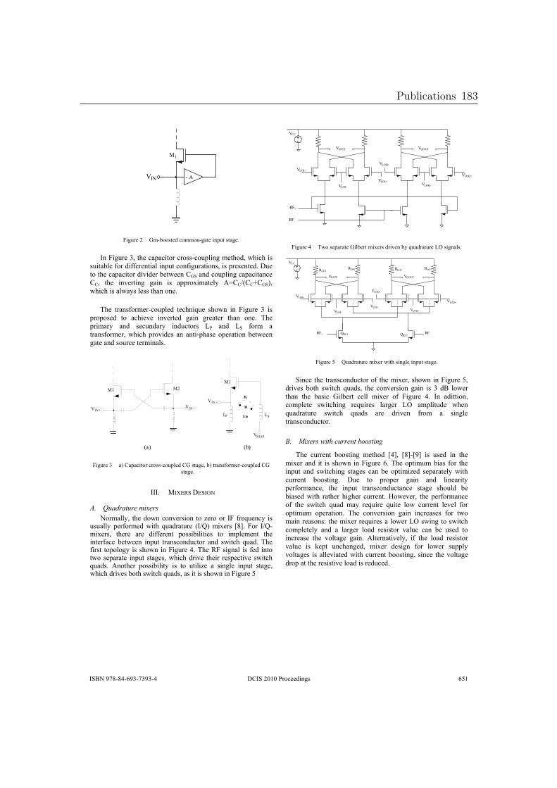
LW
3%!>1P
!
.+2("#%\ <D39,,5*#'%),DD,-32$*#%+-K(*%5*$2#;%
1-%.+2("#%cB%*J#%)$K$)+*,"%)",553),(K/+-2%D#*J,'B%YJ+)J%+5%5(+*$9/#%6,"%'+66#"#-*+$/%+-K(*%),-6+2("$*+,-5B%+5%K"#5#-*#';%C(#%*,%*J#%)$K$)+*,"%'+N+'#"%9#*Y##-%O<E%$-'%),(K/+-2%)$K$)+*$-)#%OOB% *J#% +-N#"*+-2% 2$+-% +5% $KK",[+D$*#/0% !kOO_SOOlO<EUB%YJ+)J%+5%$/Y$05%/#55%*J$-%,-#;%%
QJ#% *"$-56,"D#"3),(K/#'% *#)J-+A(#% 5J,Y-% +-% .+2("#% c% +5%K",K,5#'% *,% $)J+#N#% +-N#"*#'% 2$+-% 2"#$*#"% *J$-% ,-#;% QJ#%K"+D$"0% $-'% 5#)(-'$"0% +-'()*,"5% HG% $-'% HE% 6,"D% $%*"$-56,"D#"B%YJ+)J%K",N+'#5%$-% $-*+3KJ$5#%,K#"$*+,-%9#*Y##-%2$*#%$-'%5,(")#%*#"D+-$/5;%
LW L\
>1Pl >1P 3
LW
>1P lK
T1
1:n
; ;>T1!E
S9US$U
HG HE
%
.+2("#%c $U%O$K$)+*,"%)",553),(K/#'%O<%5*$2#B%9U%*"$-56,"D#"3),(K/#'%O<%5*$2#;%
111; L1m4&E%C4E1<P%
A. Quadrature mixers P,"D$//0B% *J#%',Y-%),-N#"5+,-% *,%@#",%,"% 1.% 6"#A(#-)0% +5%
(5($//0% K#"6,"D#'%Y+*J% A($'"$*("#% S1_nU%D+[#"5% VbX;% .,"% 1_n3D+[#"5B% *J#"#% $"#% '+66#"#-*% K,55+9+/+*+#5% *,% +DK/#D#-*% *J#%+-*#"6$)#% 9#*Y##-% +-K(*% *"$-5),-'()*,"% $-'% 5Y+*)J% A($';% QJ#%6+"5*% *,K,/,20% +5%5J,Y-% +-%.+2("#%d;%QJ#%&.%5+2-$/% +5% 6#'% +-*,%*Y,% 5#K$"$*#% +-K(*% 5*$2#5B%YJ+)J%'"+N#% *J#+"% "#5K#)*+N#% 5Y+*)J%A($'5;% !-,*J#"% K,55+9+/+*0% +5% *,% (*+/+@#% $% 5+-2/#% +-K(*% 5*$2#B%YJ+)J%'"+N#5%9,*J%5Y+*)J%A($'5B%$5%+*%+5%5J,Y-%+-%.+2("#%e%%
%
&.l
&.3
>HR1l
>HR13>HR1l
>HRnl
>HRn3
>HRnl
>1R7Q >nR7Q
+-
>OO
!
.+2("#%d QY,%5#K$"$*#%<+/9#"*%D+[#"5%'"+N#-%90%A($'"$*("#%HR%5+2-$/5;%
&.l &.3
>HR1l
>HR13>HR1l
>HRnl
>HRn3
>HRnl
&HRW>1R7Q >nR7Q
+-
>OO&HRW &HRW &HRW
n&.W n&.\
!
.+2("#%e n($'"$*("#%D+[#"%Y+*J%5+-2/#%+-K(*%5*$2#;%
E+-)#%*J#%*"$-5),-'()*,"%,6%*J#%D+[#"B%5J,Y-%+-%.+2("#%eB%'"+N#5% 9,*J% 5Y+*)J% A($'5B% *J#% ),-N#"5+,-% 2$+-% +5% c% 'T% /,Y#"%*J$-% *J#% 9$5+)% <+/9#"*% )#//% D+[#"% ,6% .+2("#% d;% 1-% $'+**+,-B%),DK/#*#% 5Y+*)J+-2% "#A(+"#5% /$"2#"% HR% $DK/+*('#% YJ#-%A($'"$*("#% 5Y+*)J% A($'5% $"#% '"+N#-% 6",D% $% 5+-2/#%*"$-5),-'()*,";%
B. Mixers with current boosting
QJ#% )(""#-*% 9,,5*+-2% D#*J,'% VdXB% VbX3VaX% +5% (5#'% +-% *J#%D+[#"%$-'% +*% +5% 5J,Y-% +-%.+2("#%`;%QJ#%,K*+D(D%9+$5% 6,"% *J#%+-K(*% $-'% 5Y+*)J+-2% 5*$2#5% )$-% 9#% ,K*+D+@#'% 5#K$"$*#/0%Y+*J%)(""#-*% 9,,5*+-2;% C(#% *,% K",K#"% 2$+-% $-'% /+-#$"+*0%K#"6,"D$-)#B% *J#% +-K(*% *"$-5),-'()*$-)#% 5*$2#% 5J,(/'% 9#%9+$5#'%Y+*J% "$*J#"% J+2J#"% )(""#-*;%:,Y#N#"B% *J#% K#"6,"D$-)#%,6% *J#% 5Y+*)J% A($'% D$0% "#A(+"#% A(+*#% /,Y% )(""#-*% /#N#/% 6,"%,K*+D(D% ,K#"$*+,-;% QJ#% ),-N#"5+,-% 2$+-% +-)"#$5#5% 6,"% *Y,%D$+-%"#$5,-5Z%*J#%D+[#"%"#A(+"#5%$%/,Y#"%HR%5Y+-2%*,%5Y+*)J%),DK/#*#/0% $-'% $% /$"2#"% /,$'% "#5+5*,"% N$/(#% )$-% 9#% (5#'% *,%+-)"#$5#% *J#% N,/*$2#% 2$+-;% !/*#"-$*+N#/0B% +6% *J#% /,$'% "#5+5*,"%N$/(#% +5% f#K*% (-)J$-2#'B% D+[#"% '#5+2-% 6,"% /,Y#"% 5(KK/0%N,/*$2#5% +5%$//#N+$*#'%Y+*J%)(""#-*%9,,5*+-2B%5+-)#% *J#%N,/*$2#%'",K%$*%*J#%"#5+5*+N#%/,$'%+5%"#'()#';%
ISBN 978-84-693-7393-4 DCIS 2010 Proceedings 651
Publications 183
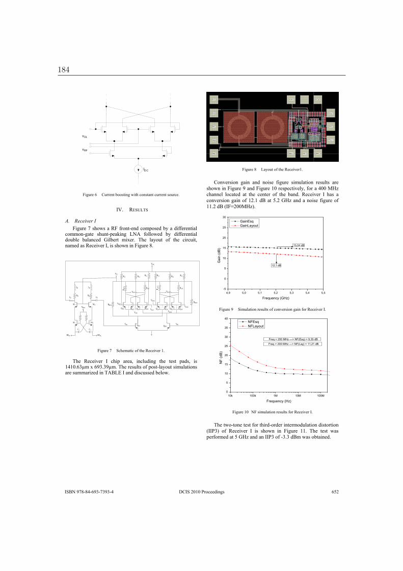
vOL
vRF
ID C
!
.+2("#%` O(""#-*%9,,5*+-2%Y+*J%),-5*$-*%)(""#-*%5,(")#;%
1>; &4E7HQE%
A. Receiver I .+2("#%^%5J,Y5%$%&.%6",-*3#-'%),DK,5#'%90%$%'+66#"#-*+$/%
),DD,-32$*#% 5J(-*3K#$f+-2% HP!% 6,//,Y#'% 90% '+66#"#-*+$/%',(9/#% 9$/$-)#'% <+/9#"*% D+[#";% QJ#% /$0,(*% ,6% *J#% )+")(+*B%-$D#'%$5%&#)#+N#"%1B%+5%5J,Y-%+-%.+2("#%b;%
%
LW L\
Lc Ld>T1!E
&.1Pl &.1P3
&C &C
HC HC
O W O \
>&.l
>HR1l
>HR13>HR1l
>HRnl
>HRn3
>HRnl&T1!E
&T1!E
& HRW
>1R7Q >nR7Q
&OW>OO
>GRH
&OW &OW &OW&O\ &O\
&HRW &HR
W
&HRW
nHR\nHRW nHRc nHRd
n&.W n&.\
nHRe nHR` nHR^ nHRb
OGOG
>&.3
%
.+2("#%^ E)J#D$*+)%,6%*J#%&#)#+N#"%W;%
QJ#% &#)#+N#"% 1% )J+K% $"#$B% +-)/('+-2% *J#% *#5*% K$'5B% +5%WdW];`coD%[%`ac;caoD;%QJ#%"#5(/*5%,6%K,5*3/$0,(*%5+D(/$*+,-5%$"#%5(DD$"+@#'%+-%Q!TH4%1%$-'%'+5)(55#'%9#/,Y;%
%
.+2("#%b H$0,(*%,6%*J#%&#)#+N#"W;%
O,-N#"5+,-% 2$+-% $-'% -,+5#% 6+2("#% 5+D(/$*+,-% "#5(/*5% $"#%5J,Y-%+-%.+2("#%a%$-'%.+2("#%W]%"#5K#)*+N#/0B%6,"%$%d]]%L:@%)J$--#/% /,)$*#'% $*% *J#% )#-*#"% ,6% *J#% 9$-';% &#)#+N#"% 1% J$5% $%),-N#"5+,-%2$+-%,6%W\;W%'T%$*%e;\%<:@%$-'%$%-,+5#% 6+2("#%,6%WW;\%'T%S1.k\]]L:@U;%
4,9 5,0 5,1 5,2 5,3 5,4 5,5-5
0
5
10
15
20
25
30G
ain
(dB)
Frequency (GHz)
GainEsq GainLayout
15,04 dB
12,1 dB
%
.+2("#%a E+D(/$*+,-%"#5(/*5%,6%),-N#"5+,-%2$+-%6,"%&#)#+N#"%1;%
10k 100k 1M 10M 100M0
5
10
15
20
25
30
35
40
Freq = 200 MHz ---> NF(Esq) = 9,35 dB
Freq = 200 MHz ---> NF(Lay) = 11,21 dB
NF
(dB
)
Frequency (Hz)
NFEsq NFLayout
%
.+2("#%W] P.%5+D(/$*+,-%"#5(/*5%6,"%&#)#+N#"%1;%
QJ#%*Y,3*,-#%*#5*%6,"%*J+"'3,"'#"%+-*#"D,'(/$*+,-%'+5*,"*+,-%S11GcU% ,6% &#)#+N#"% 1% +5% 5J,Y-% +-% .+2("#% WW;% QJ#% *#5*% Y$5%K#"6,"D#'%$*%e%<:@%$-'%$-%11Gc%,6%3c;c%'TD%Y$5%,9*$+-#';%
ISBN 978-84-693-7393-4 DCIS 2010 Proceedings 652
184
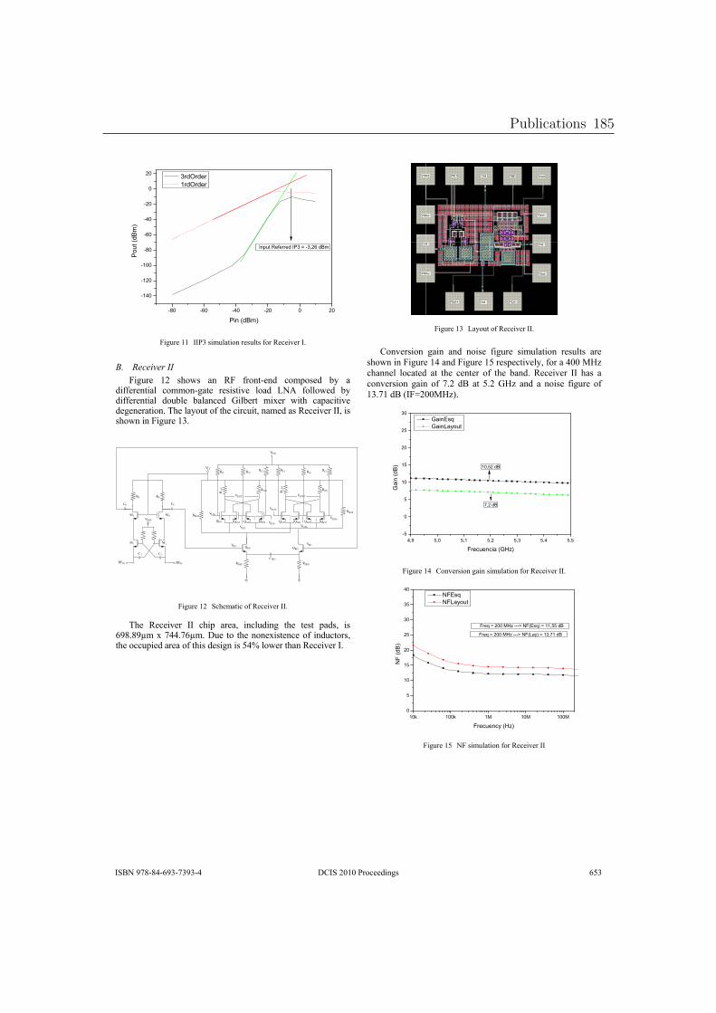
-80 -60 -40 -20 0 20
-140
-120
-100
-80
-60
-40
-20
0
20
Pou
t (dB
m)
Pin (dBm)
3rdOrder 1rdOrder
Input Referred IP3 = -3,26 dBm
%
.+2("#%WW 11Gc%5+D(/$*+,-%"#5(/*5%6,"%&#)#+N#"%1;%
B. Receiver II .+2("#% W\% 5J,Y5% $-% &.% 6",-*3#-'% ),DK,5#'% 90% $%
'+66#"#-*+$/% ),DD,-32$*#% "#5+5*+N#% /,$'% HP!% 6,//,Y#'% 90%'+66#"#-*+$/% ',(9/#% 9$/$-)#'% <+/9#"*% D+[#"% Y+*J% )$K$)+*+N#%'#2#-#"$*+,-;%QJ#%/$0,(*%,6%*J#%)+")(+*B%-$D#'%$5%&#)#+N#"%11B%+5%5J,Y-%+-%.+2("#%Wc;%
%
LW L\
Lc Ld>T1!E
&.1Pl &.1P3
&C &C
O W O \
>&.l
>HR1l
>HR13>HR1l
>HRnl
>HRn3
>HRnl&T1!E
&T1!E
&HRW
>1R7Q >nR7Q
&OW>OO
>GRH
&OW &OW &OW&O\ &O\
&HRW &HRW
&HRW
nHR\nHRW nHRc nHRd
n&.W n&.\
nHRe nHR` nHR^ nHRb
OGOG
OC4<&C4< &C4<
>&.3
%
.+2("#%W\ E)J#D$*+)%,6%&#)#+N#"%11;%
QJ#% &#)#+N#"% 11% )J+K% $"#$B% +-)/('+-2% *J#% *#5*% K$'5B% +5%`ab;baoD%[%^dd;^`oD;%C(#% *,% *J#%-,-#[+5*#-)#%,6% +-'()*,"5B%*J#%,))(K+#'%$"#$%,6%*J+5%'#5+2-%+5%edp%/,Y#"%*J$-%&#)#+N#"%1;%
%
.+2("#%Wc H$0,(*%,6%&#)#+N#"%11;%
O,-N#"5+,-% 2$+-% $-'% -,+5#% 6+2("#% 5+D(/$*+,-% "#5(/*5% $"#%5J,Y-%+-%.+2("#%Wd%$-'%.+2("#%We%"#5K#)*+N#/0B%6,"%$%d]]%L:@%)J$--#/% /,)$*#'% $*% *J#% )#-*#"% ,6% *J#% 9$-';% &#)#+N#"% 11% J$5% $%),-N#"5+,-% 2$+-% ,6% ^;\% 'T% $*% e;\%<:@% $-'% $% -,+5#% 6+2("#% ,6%Wc;^W%'T%S1.k\]]L:@U;%
4,9 5,0 5,1 5,2 5,3 5,4 5,5-5
0
5
10
15
20
25
30
Gai
n (d
B)
Frecuencia (GHz)
GainEsq GainLayout
10,52 dB
7,2 dB
%
.+2("#%Wd O,-N#"5+,-%2$+-%5+D(/$*+,-%6,"%&#)#+N#"%11;%
10k 100k 1M 10M 100M0
5
10
15
20
25
30
35
40
NF
(dB
)
Frecuency (Hz)
NFEsq NFLayout
Freq = 200 MHz ---> NF(Esq) = 11,55 dB
Freq = 200 MHz ---> NF(Lay) = 13,71 dB
%
.+2("#%We P.%5+D(/$*+,-%6,"%&#)#+N#"%11%%
ISBN 978-84-693-7393-4 DCIS 2010 Proceedings 653
Publications 185
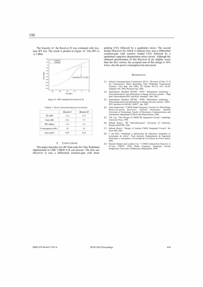
QJ#% /+-#$"+*0%,6% % *J#%&#)#+N#"% 11%Y$5%#N$/($*#'%Y+*J% *Y,3*,-#% 1Gc% *#5*;% QJ#% "#5(/*% +5% K/,**#'% +-% .+2("#% W`;% QJ#% 11Gc% +5%%%%%%3\;W%'TD;%
-80 -60 -40 -20 0 20
-160
-140
-120
-100
-80
-60
-40
-20
0
20
40
Pou
t (dB
m)
Pin (dBm)
3rdOrder 1rdOrder
Input Referred IP3 = -2,11 dBm
%
.+2("#%W` 11Gc%5+D(/$*+,-%6,"%&#)#+N#"%11;%
Q!TH4%1 .&RPQ34PCE%G4&.R&L!PO4%E7LL!&q%
% Receiver I Receiver II
P.%S'TU% WW;\% Wc;^%
<$+-%S'TU% W\;W% ^;\%
11Gc%S'TDU% 3c;c% 3\;W%
O,-5(DK*+,-%SD8U% W`% Wd%
!"#$%SDD\U% ];a^% ];e\%
%
>; ORPOH7E1RPE%QJ+5%K$K#"%'#5)"+9#5%*Y,%&.%6",-*3#-'5%6,"%7/*"$%8+'#9$-'%
+DK/#D#-*#'% +-%7LO%OLRE%];Wb%oD%K",)#55;%QJ#% 6+"5*% ,-#%S&#)#+N#"% 1U% (5#5% $% '+66#"#-*+$/% ),DD,-32$*#% Y+*J% 5J(-*%
K#$f+-2% HP!% 6,//,Y#'% 90% $% A($'"$*("#% D+[#";% QJ#% 5#),-'%'#5+2-%S&#)#+N#"%11UB%YJ+)J%+5%+-'()*,"%/#55B%(5#5%$%'+66#"#-*+$/%),DD,-32$*#% Y+*J% "#5+5*+N#% /,$'#'% HP!% 6,//,Y#'% 90% $%A($'"$*("#%)$K$)+*+N#%'#2#-#"$*+,-%D+[#"%)+")(+*;%%!/*J,(2J%*J#%,9*$+-#'% 5K#)+6+)$*+,-5% ,6% *J+5% &#)#+N#"% 11% $"#% 5/+2J*/0% Y,"5#%*J$-% *J#%6+"5*%N#"5+,-B% *J#%,))(K+#'%$"#$%,6% *J+5%'#5+2-% +5%edp%/,Y#"B%$/5,%*J#%K,Y#"%),-5(DK*+,-%J$5%'#)"#$5#';%
%
&4.4&4PO4E%%
VWX .#'#"$/% O,DD(-+)$*+,-5% O,DD+55+,-% S.OOU;% i&#N+5+,-% ,6% G$"*% We% ,6%*J#% O,DD+55+,-r5% &(/#5% $"'+-2% 7/*"$% 8+'#9$-'% Q"$-5D+55+,-%E05*#D5Bj% .+"5*% &#K;% $-'% R"'#"B% 4Q% C,)f#*% ab3WecB% .OO% ]\3dbB%!',K*#'Z%.#9;%\]]\s%&#/#$5#'%!K";%\]]\;%
V\X 1-*#"-$*+,-$/% E*$-'$"'% 1ER_14O% \`a]^% t1-6,"D$*+,-% *#)J-,/,20% 3%Q#/#),D(-+)$*+,-5% $-'% 1-6,"D$*+,-% #[)J$-2#% 9#*Y##-% 505*#D5% 3% :+2J%&$*#%7/*"$Y+'#9$-'%G:q%$-'%L!O%E*$-'$"'tB%L$";%\]]^;%
VcX 1-*#"-$*+,-$/% E*$-'$"'% 1ER_14O% \`a]b% t1-6,"D$*+,-% *#)J-,/,20% 3%Q#/#),D(-+)$*+,-5%$-'%1-6,"D$*+,-%#[)J$-2#%9#*Y##-%505*#D5%3%L!O3G:q%1-*#"6$)#%6,"%1ER_14O%\`a]^tB%!K";%\]]^;%
VdX F,(-+%I$(f,N(,"+B% iOLRE%&$'+,%."#A(#-)0%O+")(+*5%.,"%EJ,"*3&$-2#%C+"#)*3O,-N#"5+,-% &#)#+N#"5jB% C,)*,"$/% C+55#"*$*+,-B% :#/5+-f+%7-+N#"5+*0%,6%Q#)J-,/,20B%.$)(/*0%,6%4/#)*",-+)5B%O,DD(-+)$*+,-5%$-'%!(*,D$*+,-B%C#K$"*D#-*%,6%L+)",%$-'%P$-,5)+#-)#5B%\]]b;%
VeX Q;:;% H##B% iQJ#% C#5+2-% ,6% OLRE% &.% 1-*#2"$*#'% O+")(+*5j% O$D9"+'2#%7-+N#"5+*0%G"#55B%Waab;%
V`X T#J@$'% &$@$N+B% i&.% L+)",#/#)*",-+)5j% 7-+N#"5+*0% ,6% O$/+6,"-+$Z%G"#-*+)#%:$//%GQ&B%Waab;%
V^X T#J@$'% &$@$N+B% iC#5+2-% ,6% !-$/,2% OLRE% 1-*#2"$*#'% O+")(+*5j% L)%<"$Y%:+//B%\]]W;%
VbX F;% '#/% G+-,B% iL,'#/$',% 0% $K/+)$)+,-#5% '#% +-'()*,"#5% +-*#2"$',5% #-%*#)-,/,2=$5% '#% 5+/+)+,jB% Q#5+5% ',)*,"$/B% C#K$"*$D#-*,% '#% 1-2#-+#"=$%4/#)*"M-+)$%0%!(*,D?*+)$B%7-+N#"5+'$'%'#%H$5%G$/D$5%'#%<"$-%O$-$"+$B%\]]\;%
VaX &$D#5J%:$"g$-+% $-'% H+()J(-% O$+B% iW3W]<:@% 1-'()*,"/#55% &#)#+N#"% +-%]BWcoD% OLREjB% 1444% &$'+,% ."#A(#-)0% 1-*#2"$*#'% O+")(+*5%E0DK,5+(DB%7-+N#"5+*0%,6%L+--#5,*$B%L+--#$K,/+5B%\]]a;%
%
%
ISBN 978-84-693-7393-4 DCIS 2010 Proceedings 654
186
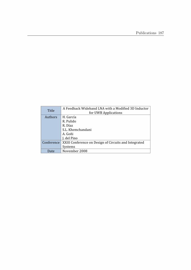
!
!
!
!
!
!
!
!
!
"#$%&! '!(&&)*+,-!.#)&*+/)!01'!2#$3!+!45)#6#&)!78!9/):,$5;!65;!<.=!'>>%#,+$#5/?!
':$35;?! @A!B+;,C+!DA!E:%#)5!DA!8C+F!GA0A!H3&I,3+/)+/#!'A!B5J#!KA!)&%!E#/5!
L5/6&;&/,&! MM999!L5/6&;&/,&!5/!8&?#N/!56!L#;,:#$?!+/)!9/$&N;+$&)!GO?$&I?!
8+$&! 15P&I*&;!QRRS!!
!
!
!
!
!
!
!
!
!
Publications 187

188
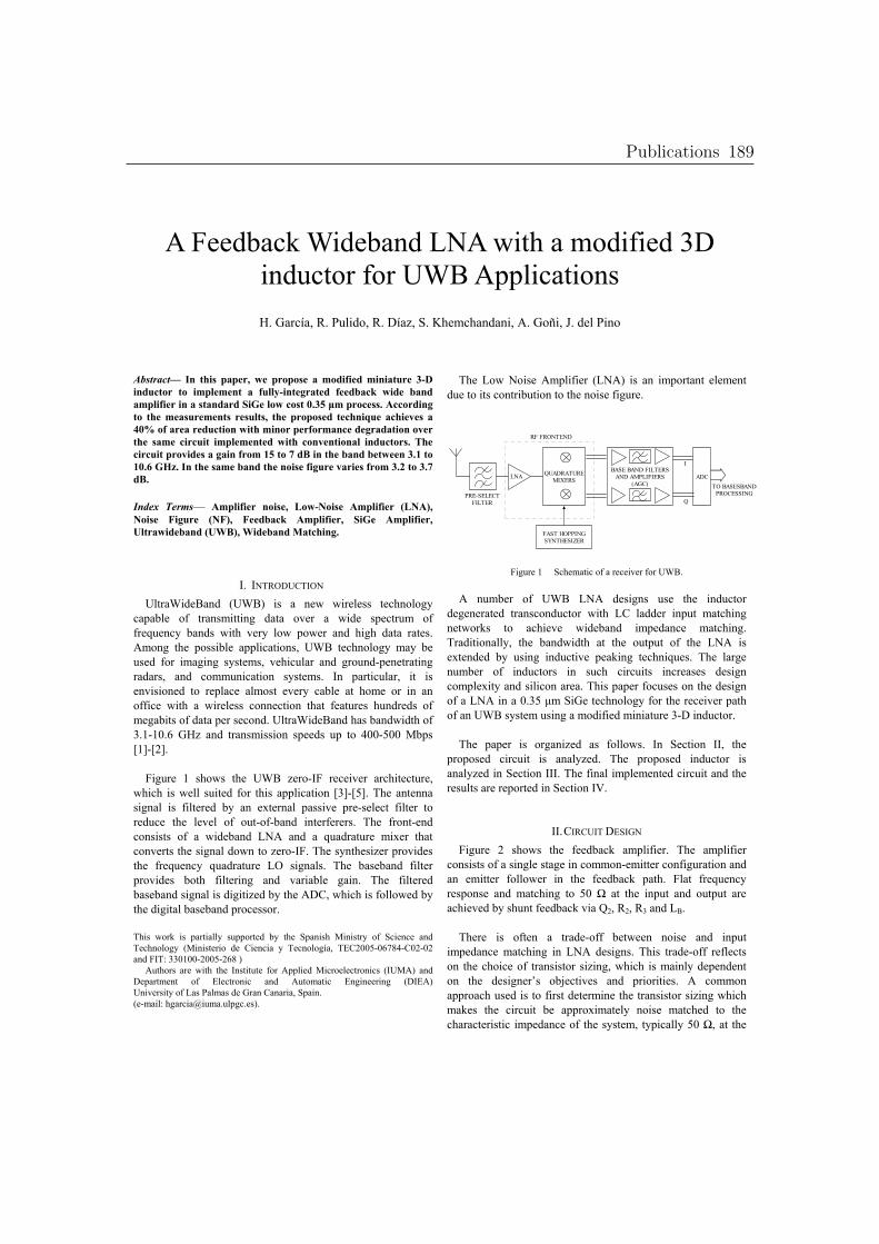
A Feedback Wideband LNA with a modified 3D inductor for UWB Applications H. García, R. Pulido, R. Díaz, S. Khemchandani, A. Goñi, J. del Pino
Abstract— In this paper, we propose a modified miniature 3-D inductor to implement a fully-integrated feedback wide band amplifier in a standard SiGe low cost 0.35 µm process. According to the measurements results, the proposed technique achieves a 40% of area reduction with minor performance degradation over the same circuit implemented with conventional inductors. The circuit provides a gain from 15 to 7 dB in the band between 3.1 to 10.6 GHz. In the same band the noise figure varies from 3.2 to 3.7 dB. Index Terms— Amplifier noise, Low-Noise Amplifier (LNA), Noise Figure (NF), Feedback Amplifier, SiGe Amplifier, Ultrawideband (UWB), Wideband Matching.
I. INTRODUCTION UltraWideBand (UWB) is a new wireless technology
capable of transmitting data over a wide spectrum of frequency bands with very low power and high data rates. Among the possible applications, UWB technology may be used for imaging systems, vehicular and ground-penetrating radars, and communication systems. In particular, it is envisioned to replace almost every cable at home or in an office with a wireless connection that features hundreds of megabits of data per second. UltraWideBand has bandwidth of 3.1-10.6 GHz and transmission speeds up to 400-500 Mbps [1]-[2].
Figure 1 shows the UWB zero-IF receiver architecture,
which is well suited for this application [3]-[5]. The antenna signal is filtered by an external passive pre-select filter to reduce the level of out-of-band interferers. The front-end consists of a wideband LNA and a quadrature mixer that converts the signal down to zero-IF. The synthesizer provides the frequency quadrature LO signals. The baseband filter provides both filtering and variable gain. The filtered baseband signal is digitized by the ADC, which is followed by the digital baseband processor.
This work is partially supported by the Spanish Ministry of Science and Technology (Ministerio de Ciencia y Tecnología, TEC2005-06784-C02-02 and FIT: 330100-2005-268 )
Authors are with the Institute for Applied Microelectronics (IUMA) and Department of Electronic and Automatic Engineering (DIEA) University of Las Palmas de Gran Canaria, Spain. (e-mail: [email protected]).
The Low Noise Amplifier (LNA) is an important element due to its contribution to the noise figure.
QUADRATUREMIXERS
FAST HOPPINGSYNTHESIZER
BASE BAND FILTERSAND AMPLIFIERS
(AGC)ADC
I
QPRE-SELECT
FILTER
LNA
TO BASESBANDPROCESSING
RF FRONTEND
Figure 1 Schematic of a receiver for UWB.
A number of UWB LNA designs use the inductor degenerated transconductor with LC ladder input matching networks to achieve wideband impedance matching. Traditionally, the bandwidth at the output of the LNA is extended by using inductive peaking techniques. The large number of inductors in such circuits increases design complexity and silicon area. This paper focuses on the design of a LNA in a 0.35 m SiGe technology for the receiver path of an UWB system using a modified miniature 3-D inductor.
The paper is organized as follows. In Section II, the
proposed circuit is analyzed. The proposed inductor is analyzed in Section III. The final implemented circuit and the results are reported in Section IV.
II. CIRCUIT DESIGN Figure 2 shows the feedback amplifier. The amplifier
consists of a single stage in common-emitter configuration and an emitter follower in the feedback path. Flat frequency response and matching to 50 at the input and output are achieved by shunt feedback via Q2, R2, R3 and LB. B
There is often a trade-off between noise and input
impedance matching in LNA designs. This trade-off reflects on the choice of transistor sizing, which is mainly dependent on the designer’s objectives and priorities. A common approach used is to first determine the transistor sizing which makes the circuit be approximately noise matched to the characteristic impedance of the system, typically 50 , at the
Publications 189
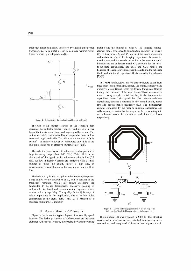
frequency range of interest. Therefore, by choosing the proper transistor size, noise matching can be achieved without signal losses or noise figure degradation [6].
LINPUTRFIN
Q2
VCC
R3
R2
R1
Q1
LB
RFOUT
Figure 2 Schematic of the feedback amplifier for wideband.
The use of an emitter follower in the feedback path increases the collector-emitter voltage, resulting in a higher fmax of the transistor and improved large-signal behaviour. The emitter size of Q1 is determined by a compromise between low noise and large bandwidth. The effective emitter area of Q1 is 36 m2. The emitter follower Q2 contributes only little to the output noise and has an effective emitter area of 1 m2.
The inductor LINPUT is used to achieve a good response in a
huge frequency range (from 0-15 GHz). This coil is in the direct path of the signal but its inductance value is low (0.5 nH). As low inductance spirals are achieved with a small number of turns, the quality factor is high and, in consequence, its contribution to the total noise figure will be low.
The inductor LB is used to optimize the frequency response.
Large values for the inductance of LB
BB lead to peaking in the frequency response. While this allows extending the bandwidth to higher frequencies, excessive peaking is undesirable for broadband communications systems which require a flat group delay. The quality factor Q is only of minor importance in this application, due to its low noise contribution in the signal path. Thus, LB is realized as a modified miniature 3-D inductor.
B
III. MODIFIED MINIATURE 3-D INDUCTOR Figure 3 (a) shows the typical layout of an on-chip spiral
inductor. The design parameters of such structure are the outer diameter d, the metal width w, the spacing between the wiring
metal s and the number of turns n. The standard lumped-element model associated to this structure is shown in Figure 3 (b). In this model, LS and RS represent the series inductance and resistance, CF is the fringing capacitance between the metal traces and the overlap capacitance between the spiral inductor and the underpass metal, COX accounts for the spiral-to-substrate capacitance, and RSUB and CSUB models the behavior of leakage currents across the oxide and the substrate (bulk) and additional capacitive effects related to the substrate [7]-[8].
In CMOS technologies, the on-chip inductors suffer from
three main loss mechanisms, namely the ohmic, capacitive and inductive losses. Ohmic losses result from the current flowing through the resistance of the metal tracks. Those losses can be reduced using a wider metal line but, it also increases the capacitive losses (in particular the metal-to-substrate capacitance) causing a decrease in the overall quality factor (Q) and self-resonance frequency (fSR). The displacement currents conducted by the metal-to-substrate capacitance and eddy current generated by the magnetic flux penetrating into de substrate result in capacitive and inductive losses respectively.
(a)
(b)
Figure 3 Layout and design parameters of the on-chip spiral
inductor. (b) Simplified lumped-element inductor model.
The miniature 3-D was proposed in 2002 [8]. This structure consists of at least two or more stacked inductors by series connections, and every stacked inductor has only one turn in
190

every metal layer. For example, if there are two stacked inductors with
different diameters, and one of them is a one-turn stacked inductor from the metal layer 4 to the metal layer 1, and the other is a one-turn stacked inductor from the metal layer 1 to the metal layer 3, then the miniature 3-D inductor is formed by connecting two stacked inductors at the metal 1, as Figure 4 shows.
Figure 4 Miniature 3-D inductor.
The proposal structure consists in two 3-D rectangular coils connected in series, as shown in Figure 5. The objective is to share the magnetic flux generated by the coils, so that the total inductance is greater than the sum of each one of them separately, increasing the inductance of the coil without diminishing the quality factor too [7].
Figure 5 Modified miniature 3-D inductor.
Figure 5 shows a photograph of the modified miniature 3-D inductor, the size is 98 µm x 98 µm. The modified miniature 3-D saves about 75% area with respect to conventional spiral inductor with the same inductance. Figure 6 shows the results of the measures. The modified miniature 3-D inductor has the
larger inductance due to magnetic flux, but it also suffers from low quality factor.
Figure 6 Photograph of the modified miniature 3-D inductor.
1 10
-1
0
1
2
3
-8
-6
-4
-2
0
2
4
6
8
10
Ind
uct
ance
(n
H)
Q
Qu
alit
y F
acto
r
Frequency (GHz)
L
Figure 7 Measurements of the modified miniature 3-D inductor.
IV. EXPERIMENTAL RESULTS The final wideband LNA layout is shown in Figure 8 (a).
The total chip size is 580 µm 600 µm. The amplifier draws 5.1 mA from a 3.3-V supply. The proposed technique achieves a 40% of area reduction with minor performance degradation over the same circuit implemented with conventional inductors (Figure 8 (b)).
(a) (b)
Figure 8 (a) Layout with modified miniature 3-D inductor. (b) Layout with typical Spiral inductor.
Publications 191
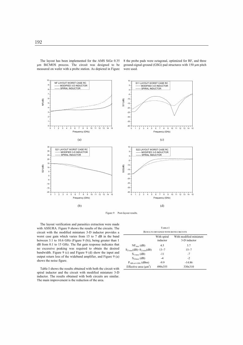
The layout has been implemented for the AMS SiGe 0.35 µm BiCMOS process. The circuit was designed to be measured on wafer with a probe station. As depicted in Figure
8 the probe pads were octagonal, optimized for RF, and three ground-signal-ground (GSG) pad structures with 150 µm pitch were used.
0 1 2 3 4 5 6 7 8 9 10 11 12 13 14 150
1
2
3
4
5
6
7
8
9
10
NF(
dB)
Frequency (GHz)
NF LAYOUT WORST CASE RC MODIFIED 3-D INDUCTOR
------- SPIRAL INDUCTOR
0 1 2 3 4 5 6 7 8 9 10 11 12 13 14 15-40
-35
-30
-25
-20
-15
-10
-5
0
5
10
S11(
dB)
Frequency (GHz)
S11 LAYOUT WORST CASE RC MODIFIED 3-D INDUCTOR
------- SPIRAL INDUCTOR
(a) (c)
0 1 2 3 4 5 6 7 8 9 10 11 12 13 14 15-20
-15
-10
-5
0
5
10
15
20
25
30
35
S21(
dB)
Frequency (GHz)
S21 LAYOUT WORST CASE RC MODIFIED 3-D INDUCTOR
------- SPIRAL INDUCTOR
0 1 2 3 4 5 6 7 8 9 10 11 12 13 14 15-40
-35
-30
-25
-20
-15
-10
-5
0
5
10
S22
(dB)
Frequency (GHz)
S22 LAYOUT WORST CASE RC MODIFIED 3-D INDUCTOR
------- SPIRAL INDUCTOR
(b) (d)
Figure 9 Post-layout results.
The layout verification and parasitics extraction were made
with ASSURA. Figure 9 shows the results of the circuits. The circuit with the modified miniature 3-D inductor provides a worst case gain which varies from 15 to 7 dB in the band between 3.1 to 10.6 GHz (Figure 9 (b)), being greater than 1 dB from 0.1 to 15 GHz. The flat gain response indicates that no excessive peaking was required to obtain the desired bandwidth. Figure 9 (c) and Figure 9 (d) show the input and output return loss of the wideband amplifier, and Figure 9 (a) shows the noise figure.
Table I shows the results obtained with both the circuit with
spiral inductor and the circuit with modified miniature 3-D inductor. The results obtained with both circuits are similar. The main improvement is the reduction of the area.
TABLE I
RESULTS OBTAINED WITH BOTH CIRCUITS
With spiral inductor
With modified miniature 3-D inductor
NFmax (dB) 4.5 3.7 S21max(dB)~S21min(dB) 13~7 15~7
S11max (dB) -11 -7 S22max (dB) -4 -2
P1dB at 6 GHz (dBm) -9.9 -14.86 Effective area (µm2) 490x355 330x310
192
V. CONCLUSIONS In this paper we propose a modified miniature 3-D inductor
to implement a fully-integrated feedback wide band amplifier. A description of the LNA configuration was explained emphasizing the influence of the design parameters in the circuit performance. The circuit was implemented in a standard low cost 0.35 µm process and provides a worst case gain that ranges from 15 to 7 dB in the band between 3.1 to 10.6 GHz. The noise figure ranges from 3.2 to 3.7 dB in the same band. The circuit only requires 5 mA from a 3.3-V supply. The modified miniature 3-D inductor saves about 75% area with respect to conventional spiral inductor with the same inductance.
REFERENCES [1] FCC, “Revision of Part 15 of the Commission’s Rules Regarding Ultra-
Wideband Transmission Systems” FCC 02-48, First Report and order, 2002.
[2] MB OFDM Alliance-SIG, “Multiband OFDM Phisical Layer Proposal for IEEE 802.15 Task Group 3a”, Sept, 2004.
[3] R. Roovers, D. M. W. Leenaerts, J. Bergervoet, K. S. Harish, R. C. H. van de Beek, G. van der Weide, H. Waite, Y Zhang, S. Aggarwal, and C. Razzell, “An Interference-Robust Receiver for Ultra-Wideband Radio in SiGe BiCMOS Technology”, IEEE Journal of Solid-State Circuits, vol. 40, no. 12, Dec 2005.
[4] A. Ismail and A. Abidi, “A 3.1 to 8.2 GHz direct conversion receiver for MB-OFDMUWB communication,” in IEEE Int. Solid-State Circuits Conf. Dig. Tech. Papers, San Francisco, CA, 2005, pp. 208–209.
[5] B. Razavi et al., “A 0.13 m CMOS UWB transceiver,” in IEEE Int. Solid-State Circuits Conf. Dig. Tech. Papers, San Francisco, CA, 2005, pp. 216–217.
[6] R. Pulido, H. García, J. del Pino, S. L. Khemchandani, A. Hernández, “A Feedback Wideband LNA for UWB Applications” XXI Design of Integrated Circuits and Systems Conference, 2007.
[7] Aportaciones al diseño, simulación, caracterización y modelado de inductores integrados sobre silicio / tesis doctoral presentada por Amaya Goñi Iturri ; dirigida por el Dr. D. Antonio Hernández Ballester, codirigida por el Dr. D. Francisco Javier del Pino Suárez (2007)
[8] Chih-Chun Tang, Chia-Hsin Wu, Shen-Iuan Liu, “Miniature 3-D Inductors in Standard CMOS Process” IEEE Journal of Solid-State Circuits, Vol. 37, Nº. 4, 2002.
Publications 193

!
!
!
!
!
!
!
!
!
"#$%&!'&(#)*!+,!-!./%%0!1*$&)2-$&3!'4!$+!567!89:!'#($2#;/$&3!
<=>%#,#&2!#*!4?@A!B6C7!</$D+2(! 86!?-2$E*!
F6!'E-:!G6!3&%!H#*+!A6I6!JD&=KD-*3-*#!<6!9&2*L*3&:!
4+*,&2&*K&! MM1!4+*,&2&*K&!+*!'&(#)*!+,!4#2K/#$(!-*3!1*$&)2-$&3!A0($&=(!
'-$&! N+O&=;&2!PBBQ!!
!
!
!
!
!
!
!
!
!
!


42
Abstract—A fully-integrated Distributed Amplifier was implemented in a standard 0.35 µm CMOS process up to 10 dB of gain and a bandwidth of 8.6 GHz. Octagonal inductors with no ground shield were implemented in top available metal. Design guidelines for optimizing amplifier gain are presented. Chip dimensions are 0.75 ! 1 mm2 and power dissipation is 107 mW, drawn from a 3.3 V supply.
Index Terms—Radio-frequency (RF) Integrated Circuit, Distributed Amplifier, Spiral Inductor, Ultra Wide Band.
I. INTRODUCTION The need for devices that can deliver large amounts of
power without sacrificing any bandwidth has inspired researchers to develop fancy semi-compound technologies (GaAs, InP, GaN and others). One disadvantage of such technologies is the relatively high cost of integration, when compared with standard CMOS substrates. CMOS devices on the other hand, exhibit relatively low speed and passive structures with much lower quality factors, due to the lossy substrate [1]. This problem can be overcome by using a high resistivity substrate, but this usually adds more complexity and cost to the overall process. It is in the context of an SOC solution that researchers have continued their effort to demonstrate that CMOS can be used as an alternative to conventional microwave solutions.
The use of distributed amplification is proposed in this paper to push the limit of operation of an old technology (0.35 µm CMOS) to 8.6 GHz with possible applications to Ultra Wide Band (UWB) systems.
The organization of this paper is the following. In section II we present the distributed amplifier basics. Sections III is devoted to the distributed amplifier and integrated inductors design methodology. The results of the designed circuit are presented in section IV, where the layout design issues are also addressed. Finally some conclusions are given.
This work has been partially supported by the Spanish MEC and MCyT
under projects TEC-2005-08091-C03-03 and FIT-330100-2006-43. Authors are with the Institute for Applied Microelectronics (IUMA) and
Department of Electronic and Automatic Engineering (DIEA) University of Las Palmas de Gran Canaria, Spain. (e-mail: [email protected]).
II. DISTRIBUTED AMPLIFIER BASICS The frequency response of a MOS device degrades due to
the pole formed by the input/output capacitance of the transistor and the resistance it sees. The MOSFET’s transconductance rapidly falls with frequency and any attempt to increase the transconductance by increasing the size of the device will also increase its input/output capacitance. Thus, while low-frequency gain has been increased, the gain-bandwidth product remains about the same.
The gain-bandwidth product limits conventional circuit design to approximately 40% of the device’s fmax.
The concept of distributed amplification has been around for over a half century [2][3]. Distributed amplifiers employ a topology in which the gain stages are connected such that their capacitances are separated, yet the output currents still combine in an additive fashion (Fig. 1). Series-inductive elements are used to separate capacitances at the inputs and outputs of adjacent gain stages. The resulting topology, given by the interlaying series inductors and shunt capacitances, forms what is essentially a lumped-parameter artificial transmission line. The additive nature of the gain dictates a relatively low gain; however, the distributed nature of the capacitance allows the amplifier to achieve very wide bandwidths.
Distributed amplification overcomes the gain bandwidth limitation absorbing the MOS input/output capacitance as part of the lumped elements of the artificial transmission line, formed with the series inductance that connects adjacent drains and gates.
As the amplified signals at each stage travels towards the load, the signal gets attenuated due to non-zero losses associated with the transmission lines. Finite Q inductors are the primary source of losses in the gate line. Losses in the drain line can be attributed to lossy inductors Ld and the drain-source resistance (rds).
The characteristic impedance (Z0) and cut-off frequency (fc) of lossless transmission line are given by
(1)
(2)
Design of a Fully Integrated DC to 8.5 GHz Distributed Amplifier in CMOS 0.35
G. Martín, R. Diaz, J. del Pino, S. L. Khemchandani, A. Goñi, A. Hernández
CL
Z0
LCfc
1
DCIS 2006
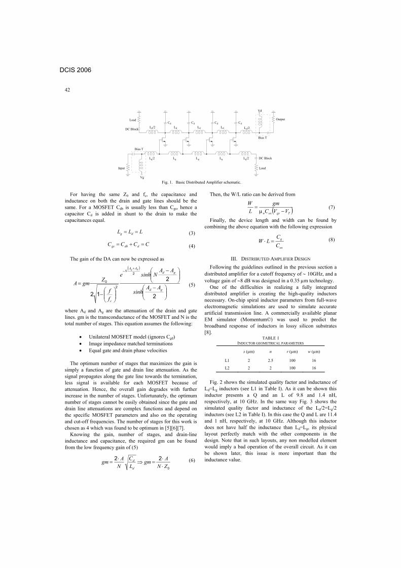
42
Vd
CdLoad
DC Block
Output
Bias T
Load
DC Block
Input
Vg
Bias T
Ld
Cd
Ld
Cd
Ld
Cd
Lg Lg LgLg/2 Lg/2
Ld/2Ld/2
Fig. 1. Basic Distributed Amplifier schematic.
For having the same Z0 and fc, the capacitance and
inductance on both the drain and gate lines should be the same. For a MOSFET Cdb is usually less than Cgs, hence a capacitor Cd is added in shunt to the drain to make the capacitances equal.
(3)
(4)
The gain of the DA can now be expressed as
(5)
where Ad and Ag are the attenuation of the drain and gate lines. gm is the transconductance of the MOSFET and N is the total number of stages. This equation assumes the following:
Unilateral MOSFET model (ignores Cgd) Image impedance matched terminations Equal gate and drain phase velocities
The optimum number of stages that maximizes the gain is
simply a function of gate and drain line attenuation. As the signal propagates along the gate line towards the termination, less signal is available for each MOSFET because of attenuation. Hence, the overall gain degrades with further increase in the number of stages. Unfortunately, the optimum number of stages cannot be easily obtained since the gate and drain line attenuations are complex functions and depend on the specific MOSFET parameters and also on the operating and cut-off frequencies. The number of stages for this work is chosen as 4 which was found to be optimum in [5][6][7].
Knowing the gain, number of stages, and drain-line inductance and capacitance, the required gm can be found from the low frequency gain of (5)
(6)
Then, the W/L ratio can be derived from
(7) Finally, the device length and width can be found by
combining the above equation with the following expression
(8)
III. DISTRIBUTED AMPLIFIER DESIGN Following the guidelines outlined in the previous section a
distributed amplifier for a cutoff frequency of 10GHz, and a voltage gain of 8 dB was designed in a 0.35 m technology.
One of the difficulties in realizing a fully integrated distributed amplifier is creating the high-quality inductors necessary. On-chip spiral inductor parameters from full-wave electromagnetic simulations are used to simulate accurate artificial transmission line. A commercially available planar EM simulator (Momentum©) was used to predict the broadband response of inductors in lossy silicon substrates [8].
TABLE I INDUCTOR GEOMETRICAL PARAMETERS
s (µm) n r (µm) w (µm)
L1 2 2.5 100 16
L2 2 2 100 16
Fig. 2 shows the simulated quality factor and inductance of
Ld=Lg inductors (see L1 in Table I). As it can be shown this inductor presents a Q and an L of 9.8 and 1.4 nH, respectively, at 10 GHz. In the same way Fig. 3 shows the simulated quality factor and inductance of the Ld/2=Lg/2 inductors (see L2 in Table I). In this case the Q and L are 11.4 and 1 nH, respectively, at 10 GHz. Although this inductor does not have half the inductance than Ld=Lg, its physical layout perfectly match with the other components in the design. Note that in such layouts, any non modelled element would imply a bad operation of the overall circuit. As it can be shown later, this issue is more important than the inductance value.
LLL dg
CCCC ddbgs
2
2
12
2
20
gd
gdAA
N
c
AAsinh
AANsinhe
ff
ZgmA
dg
0
22ZNA
gmLC
NA
gmd
d
Tgsoxn VVCgm
LW
ox
g
CC
LW
DCIS 2006
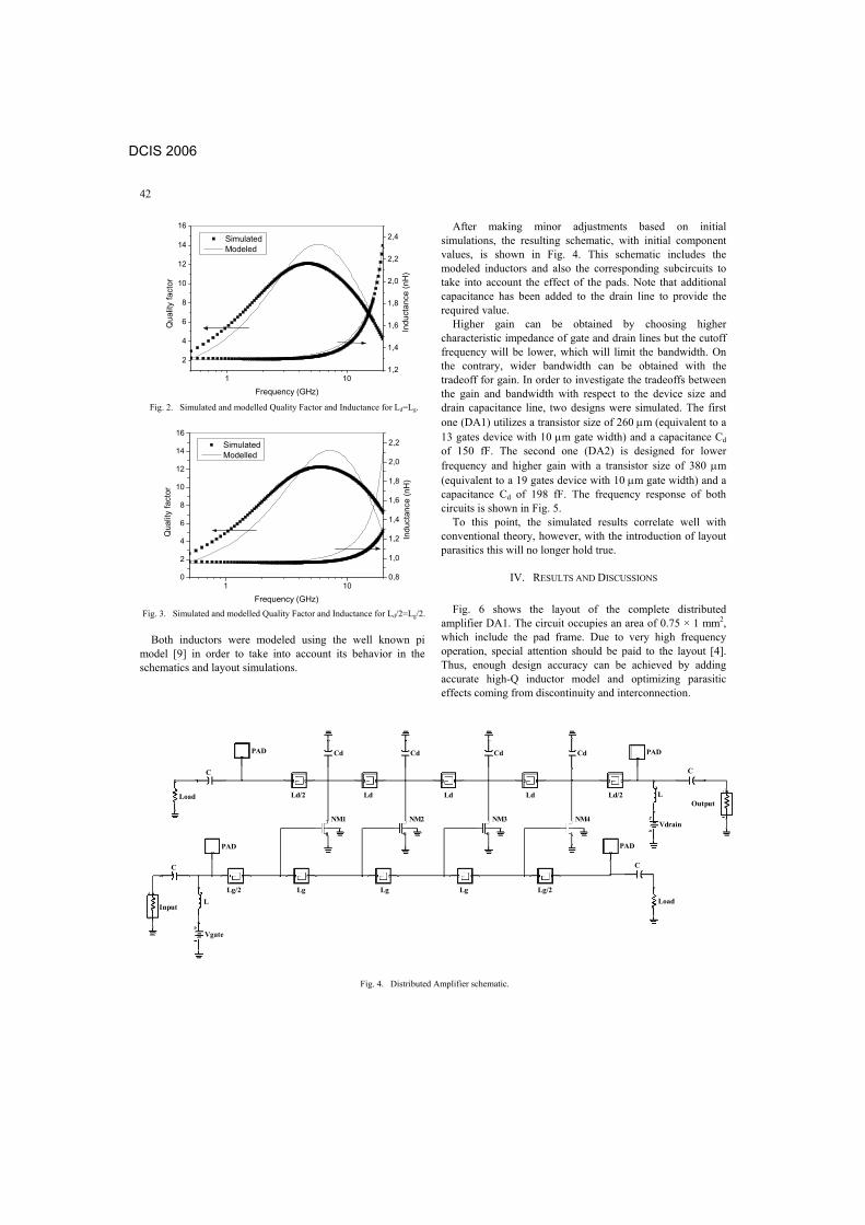
42
1 10
2
4
6
8
10
12
14
16
1,2
1,4
1,6
1,8
2,0
2,2
2,4 Simulated Modeled
Qua
lity
fact
or
Frequency (GHz) In
duct
ance
(nH
)
Fig. 2. Simulated and modelled Quality Factor and Inductance for Ld=Lg.
1 100
2
4
6
8
10
12
14
16
0,8
1,0
1,2
1,4
1,6
1,8
2,0
2,2
Qua
lity
fact
or
Frequency (GHz)
Simulated Modelled
Indu
ctan
ce (n
H)
Fig. 3. Simulated and modelled Quality Factor and Inductance for Ld/2=Lg/2.
Both inductors were modeled using the well known pi
model [9] in order to take into account its behavior in the schematics and layout simulations.
After making minor adjustments based on initial simulations, the resulting schematic, with initial component values, is shown in Fig. 4. This schematic includes the modeled inductors and also the corresponding subcircuits to take into account the effect of the pads. Note that additional capacitance has been added to the drain line to provide the required value.
Higher gain can be obtained by choosing higher characteristic impedance of gate and drain lines but the cutoff frequency will be lower, which will limit the bandwidth. On the contrary, wider bandwidth can be obtained with the tradeoff for gain. In order to investigate the tradeoffs between the gain and bandwidth with respect to the device size and drain capacitance line, two designs were simulated. The first one (DA1) utilizes a transistor size of 260 m (equivalent to a 13 gates device with 10 m gate width) and a capacitance Cd of 150 fF. The second one (DA2) is designed for lower frequency and higher gain with a transistor size of 380 m (equivalent to a 19 gates device with 10 m gate width) and a capacitance Cd of 198 fF. The frequency response of both circuits is shown in Fig. 5.
To this point, the simulated results correlate well with conventional theory, however, with the introduction of layout parasitics this will no longer hold true.
IV. RESULTS AND DISCUSSIONS Fig. 6 shows the layout of the complete distributed
amplifier DA1. The circuit occupies an area of 0.75 ! 1 mm2, which include the pad frame. Due to very high frequency operation, special attention should be paid to the layout [4]. Thus, enough design accuracy can be achieved by adding accurate high-Q inductor model and optimizing parasitic effects coming from discontinuity and interconnection.
Ld/2 Ld/2Ld Ld Ld
Lg/2 Lg/2Lg Lg Lg
L
C
Load
C
LoadL
PAD
PAD PAD
PAD
NM1 NM2 NM3 NM4
Vgate
Vdrain
Input
Output
C
C
Cd Cd Cd Cd
Fig. 4. Distributed Amplifier schematic.
DCIS 2006
42
The post-layout frequency response of the distributed amplifier is shown in Fig. 7. The gain is 8.5 dB with ± 1.2 dB flatness from 1 GHz to 5 GHz and the unity gain frequency is 8.6 GHz. The input and output match are generally much better than -10 dB over most of the bandwidth. The increase in gain in low frequency was due to the higher impedance of the blocking capacitance at low frequency. All simulations were taken under identical DC bias conditions, 3 V on the drain line and 0.8 V on the gate line; at this bias point the distributed amplifier consumed 35.64 mA for a total power dissipation of 107 mW. The phase response of this circuit is shown in Fig. 8. Result shows linear variation up to cutoff frequency.
In Fig. 9 the schematic and post-layout simulations are compared. As warned in the previous section, with the introduction of layout parasitics the simulated results differ with schematic simulations. In particular the bandwidth is reduced due to the capacitance added to the gate and drain artificial transmission lines by the routing metals. As a consequence special care should be taken on the routing metals and on the inductor layout in order to maximize the circuit performance. This is the motivation of using a Ld/2=Lg/2 inductors that do not have half the inductance than Ld=Lg but that hold a physical layout which match with the other components in the design.
0,0 2,5 5,0 7,5 10,0 12,5 15,0
-40
-30
-20
-10
0
10
S21
(dB
)
Frequency (GHz)
S21DA1 S21DA2
0,0 2,5 5,0 7,5 10,0 12,5 15,00
5
10
15
20
25
30
35
40
45
NF
(dB)
Frequency (GHz)
nfda1 nfda2
Fig. 5. The tradeoffs between the gain and bandwidth with respect to the
device size and drain capacitance line. DA1: W=260 m (ng=13), cd=150 fF and DA2 W=380 m (ng=19), cd=198 fF.
Fig. 6. Distributed Amplifier layout.
0,0 2,5 5,0 7,5 10,0 12,5 15,0
-40
-30
-20
-10
0
10
Mag
nitu
de (d
B)
Frequency (GHz)
S21 S11 S22 S12
Fig. 7. Distributed amplifier post-layout S-parameter response.
0,0 2,5 5,0 7,5 10,0 12,5 15,0-800
-600
-400
-200
0
200
Phas
e S
21 (d
egre
es)
Frequency (GHz)
Fig. 8. Distributed amplifier post-layout phase response.
DCIS 2006

42
0,0 2,5 5,0 7,5 10,0 12,5 15,0
-40
-30
-20
-10
0
10
S21
(dB
)
Frequency (GHz)
schematic layout
Fig. 9. Comparison between schematic and post-layout simulations.
V. CONCLUSIONS A four-stage fully integrated CMOS distributed amplifier
with 8.5 dB forward gain and 1.2 dB gain flatness over a 4 GHz bandwidth was implemented. Distributed Amplification opens the possibility for CMOS circuits to be considered as an alternative microwave solution and pushes the limit of operation of an old technology (0.35 µm CMOS) to 8.6 GHz. Since this DA was designed using a commercial CMOS technology, it can be easily integrated with other front-end
circuits to build CMOS transceivers without requiring any post-processing steps.
REFERENCES [1] Brian M. Ballweber, Ravi Gupta and David J. Allstot, “A Fully
Integrated 0.5–5.5-GHz CMOS Distributed Amplifier” IEEE TRANSACTIONS ON SOLID-STATE CIRCUITS, VOL. 35, NO. 2, FEBRUARY 2000.
[2] E. L. Ginzton, W. R. Hewlett, J. H. Jasberg, and J. D. Noe, “Distributed amplification,” Proc. IRE, vol. 36, pp. 956–969, Aug. 1948.
[3] W. S. Percival, “Thermonic valve circuits,” British Patent 460 562, Jan. 25, 1937.
[4] Jinho Park, Kiyong Choi, and David J. Allstot “Parasitic-Aware RF Circuit Design and Optimization” IEEE TRANSACTIONS ON CIRCUITS AND SYSTEMS—I: REGULAR PAPERS, VOL. 51, NO. 10, OCTOBER 2004.
[5] Y. Ayasli, R.L. Mozzi, J.L. Vorhaus, L D. Reynolds and R.A. Pucel, “A Mono-lithic GaAs 1-13 GHz Traveling-Wave Amplifier,” IEEE Transactions on Mi-crowave Theory and Techniques, vol. 30, pp. 976–981, July 1982.
[6] Michael Ross, Investigation of Taper and Forward-Feed in GaAs MMIC Dis-tributed Amplifiers, M.E. thesis, Department of Electronics, Carleton University, June 1987.
[7] J.B. Beyer, S.N. Prasad, R.C. Becker, J.E. Nordman, and G.K. Hohenwarter, “MESFET Distributed Amplifier Guidelines,” IEEE Transactions on Microwave Theory and Techniques, vol. 32, pp. 268–275, July 1984.
[8] Momentum User’s Manual, 2004A ed., Agilent Technologies, Sept. 2004.
[9] A. Goni-Iturri S. Khemchandani, J. del Pino, J. García, B. González and A. Hernández, “Design and Modeling of an on Silicon Spiral Inductor Library Using Improved EM Simulations”, SPIE’s International Symposium on Microtechnologies for the New Millennium 2005 (VLSI Circuits and Systems, Sevilla, 2005.
DCIS 2006

202
COther Publications
A list of journals and conference contributions related to other works are listed in
this appendix.
Journal Papers
1. Sunil L. Khemchandani, Javier del Pino, Roberto Dıaz and Antonio Hernandez,
”A fully Integrated Single Core VCO with a Wide Tunning for DVB-H”, Mi-
crowave and Optical Technology Letter, Vol. 51, Ed. Wiley, Mar 2009.
2. S.L. Khemchandani, J. del Pino Suarez, Amaya Goni-Iturri, Roberto Dıaz and
Antonio Hernandez, ”A VCO with On-Chip Tank for IEEE 802.11a”, Micro-
wave and Optical Technology Letter, Vol. 50, Num 10, Ed. Wiley, Oct. 2008.
Conference Papers
3. H. Garcıa-Vazquez, K. Orbaiceta-Ezcurra, S.L. Khemchandani, R. Dıaz, J.
Arias, J. del Pino, ”Analysis of Package Effects on an UWB Feedback LNA”,
XXVI Design of Circuits and Integrated Systems Conference (DCIS), Albufei-
ra, Portugal, Nov. 2011.
4. R. Dıaz, G. Garcıa-Saavedra, J. Arias-Perez, S.L. Khemchandani, J. del Pino,
”A Current Conveyor Based Mixer for an UltraWide Band Receiver”, XXV
Design of Circuits and Integrated Systems Conference, Lanzarote, Spain, Nov.
2010.
204
5. R. Dıaz, A. Castillo, H. Garcıa, D. Ramos and S. L. Khemchandani, ”Low
Power Consumption Mixer Based on Current Conveyors for Wireless Sys-
tems”,XXIV Conference on Design of Circuits and Integrated System, Za-
ragoza Espana, Nov. 2009.
6. G. Perez, S. L. Khemchandani, R. Dıaz, R. Pulido, D. Ramos and J. del Pino,
”A Multiband LNA Switched Loads and Wideband Input Matching”,XXIV
Conference on Design of Circuits and Integrated System, Zaragoza Espana,
Nov. 2009.
7. J. del Pino, R. Dıaz, M. Afonso, F. Cabrera, A. Iturri, S. L. Khemchandani, ”A
Fully Integrated Folder Mixer in CMOS 0.35 µm Technology for 802.11a WiFi
Applications”, SPIE Conferece on Microtechnologies for the New Millenium,
Las Palmas de Gran Canaria – Espana, May 2007.
8. J. Perez, N. Barrera, R. Dıaz, R. Pulido, J. del Pino, S. L. Khemchandani and
A. Hernandez, ” A SiGe Front-End for a Portable DVB-H Receiver”, XXII
Conference on Design of Circuits and Integrated System, Sevilla – Espana,
Nov 2007.
9. R. Pulido, S.L. Khemchandani, A. Goni-Iturri, R.Dıaz, A. Hernandez and J.
del Pino, ”A Fully Integrated Low Noise Amplifier in SiGe 0.35 µm Technology
for 802.11a WiFi Applications”, SPIE Conferece on Microtechnologies for the
New Millenium, Sevilla – Espana, Nov. 2005.
10. R. Dıaz, R. Pulido, A. Goni-Iturri, S.L. Khemchandani, B. Gonzalez, J. del
Pino,”A fully Integrated Mixer in CMOS 0.35 µm Technology for 802.11a
WiFi Applications”, Conference on Design Circuits and Integrated Systems,
Burdeos – Francia, Nov 2004.