
Design of an OFDM baseband receiver with space diversity
7
Design of an OFDM baseband receiver with space diversity M.-L. Liou, P.-H. Lin, C.-J. Jan, S.-C. Lin and T.-D. Chiueh Abstract: An orthogonal frequency division multiplexing (OFDM) baseband receiver chip is proposed. Carrier frequency synchronisation, symbol boundary estimation, and channel estimation and frequency-domain equalisation, all based on well known and proven algorithms, have been integrated in the receiver. The complexity and power consumption of the chip are minimised by full-custom memory blocks, word-length optimisation and innovative architecture. This chip has a core area of 4.1 mm 4.6 mm. When running at 20 MHz, the chip consumes 66 mW from a 2.3 V supply. By using two such ICs and some diversity combining hardware, competitive measured packet error rates have been obtained, indicating that the chip, and the diversity receiver based on this chip, can operate reliably in a multipath fading environment. 1 Introduction Wireless local area network (WLAN) has received much attention recently. Interest in wireless communication has also produced several extensive studies in communi- cation and very large scale integration (VLSI) technologies, such as channel bandwidth utilisation, low-power dissipa- tion, high-speed processors, and so on. Wireless commu- nication quality is determined by several factors, including multipath fading, accuracy of local oscillator, noise and interference. Due to the impairment to communication quality and reliability, we have to pay more attention to the system design and implementation process [1] . Orthogonal frequency division multiplexing (OFDM) attracts a lot of interest because it can efficiently reduce frequency selective fading [2, 3] . This is achieved by increasing the symbol duration for the lower-rate parallel subcarriers transmission, so that each subcarrier suffers only flat fading. The IEEE 802.11a/g WLAN standard [4] adopts OFDM modulation and is designed to operate at the unlicensed bands at 2.4 GHz and above 5 GHz. The data rates supported vary from 6 Mbps to 54 Mbps. The highest data rate is similar to that of wired networks and is suitable for short-range data transmission. Besides accurate functional operation, low power con- sumption is a very critical issue for a portable device. It is for extending battery life, reducing the cooling related cost and increasing the system reliability [5]. Although some 802.11a receiver chips for high speed WLAN applications have been reported [6, 7] , low-power design with customised flow and performance comparison are not available. This paper aims at designing a low-power OFDM baseband receiver IC based on our developed design methodology [8] and building a high-performance space-diversity WLAN receiver based on the designed IC. The proposed chip has the following features: 0.35 mm CMOS baseband OFDM receiver operates at 20 MHz at a supply voltage of 2.3–3.3 V adjustable symbol boundary estimation range for different environments low-power and low-complexity latch-based delay buffer high-speed, low-latency complex reciprocal module. In addition, by using two antennas and two receivers and properly combining the received baseband signals from these two antennas, the combined signal can be more robust even under link conditions with severe multipath fading. Increasing diversity order implies linear growth in receiver complexity (including the number of antennas, analogue front-end and baseband chip die size). From the system design perspective, it is natural to use more receiving antennas to boost the received signal quality. In this paper, we show the implementation of an OFDM baseband receiver that achieves space diversity by using two simple baseband receiver chips (one for each antenna) and a signal processing module built in field-programmable gate array (FPGA). The receiver architecture and practical implementation aspect are the main focus and will be described in more detail. 2 Baseband receiver for OFDM wireless LAN In this section we present the OFDM WLAN standard and the major tasks and scheduling of the OFDM WLAN baseband receiver. 2.1 OFDM wireless LAN OFDM is a modulation scheme that splits data into parallel streams and transmits them over a number of orthogonal subcarriers. A discrete-time formulation of the transmitter is equivalent to an inverse discrete Fourier transform on the data [9] as shown in Fig. 1. After the inverse DFT processing, a cyclic prefix is inserted in each symbol to mitigate intersymbol interference (ISI) and make the received signal easy to equalise. One of the salient features E-mail: [email protected] The authors are with the Graduate Institute of Electronics Engineering and the Department of Electrical Engineering, National Taiwan University, Taipei, Taiwan 10617, Republic of China r The Institution of Engineering and Technology 2006 IEE Proceedings online no. 20050148 doi:10.1049/ip-com:20050148 Paper first received 10th April and in revised form 13th July 2005 894 IEE Proc.-Commun., Vol. 153, No. 6, December 2006 Authorized licensed use limited to: National Taiwan University. Downloaded on February 27, 2009 at 00:33 from IEEE Xplore. Restrictions apply.
-
Upload
khangminh22 -
Category
Documents
-
view
0 -
download
0
Transcript of Design of an OFDM baseband receiver with space diversity

Design of an OFDM baseband receiver with spacediversity
M.-L. Liou, P.-H. Lin, C.-J. Jan, S.-C. Lin and T.-D. Chiueh
Abstract: An orthogonal frequency division multiplexing (OFDM) baseband receiver chip isproposed. Carrier frequency synchronisation, symbol boundary estimation, and channel estimationand frequency-domain equalisation, all based on well known and proven algorithms, have beenintegrated in the receiver. The complexity and power consumption of the chip are minimised byfull-custom memory blocks, word-length optimisation and innovative architecture. This chip has acore area of 4.1mm� 4.6mm. When running at 20MHz, the chip consumes 66mW from a 2.3 Vsupply. By using two such ICs and some diversity combining hardware, competitive measuredpacket error rates have been obtained, indicating that the chip, and the diversity receiver based onthis chip, can operate reliably in a multipath fading environment.
1 Introduction
Wireless local area network (WLAN) has received muchattention recently. Interest in wireless communication hasalso produced several extensive studies in communi-cation and very large scale integration (VLSI) technologies,such as channel bandwidth utilisation, low-power dissipa-tion, high-speed processors, and so on. Wireless commu-nication quality is determined by several factors, includingmultipath fading, accuracy of local oscillator, noise andinterference. Due to the impairment to communicationquality and reliability, we have to pay more attention to thesystem design and implementation process [1].
Orthogonal frequency division multiplexing (OFDM)attracts a lot of interest because it can efficiently reducefrequency selective fading [2, 3]. This is achieved byincreasing the symbol duration for the lower-rate parallelsubcarriers transmission, so that each subcarrier suffers onlyflat fading. The IEEE 802.11a/gWLAN standard [4] adoptsOFDM modulation and is designed to operate at theunlicensed bands at 2.4GHz and above 5GHz. The datarates supported vary from 6Mbps to 54Mbps. The highestdata rate is similar to that of wired networks and is suitablefor short-range data transmission.
Besides accurate functional operation, low power con-sumption is a very critical issue for a portable device. It isfor extending battery life, reducing the cooling related costand increasing the system reliability [5]. Although some802.11a receiver chips for high speed WLAN applicationshave been reported [6, 7], low-power design with customisedflow and performance comparison are not available. Thispaper aims at designing a low-power OFDM basebandreceiver IC based on our developed design methodology [8]
E-mail: [email protected]
The authors are with the Graduate Institute of Electronics Engineering and theDepartment of Electrical Engineering, National Taiwan University, Taipei,Taiwan 10617, Republic of China
r The Institution of Engineering and Technology 2006
IEE Proceedings online no. 20050148
doi:10.1049/ip-com:20050148
Paper first received 10th April and in revised form 13th July 2005
894
Authorized licensed use limited to: National Taiwan University. Downloaded on February 27
and building a high-performance space-diversity WLANreceiver based on the designed IC.
The proposed chip has the following features:
� 0.35mm CMOS baseband OFDM receiver
� operates at 20MHz at a supply voltage of 2.3–3.3V
� adjustable symbol boundary estimation range for differentenvironments
� low-power and low-complexity latch-based delay buffer
� high-speed, low-latency complex reciprocal module.
In addition, by using two antennas and two receivers andproperly combining the received baseband signals fromthese two antennas, the combined signal can be more robusteven under link conditions with severe multipath fading.Increasing diversity order implies linear growth in receivercomplexity (including the number of antennas, analoguefront-end and baseband chip die size). From the systemdesign perspective, it is natural to use more receivingantennas to boost the received signal quality.
In this paper, we show the implementation of an OFDMbaseband receiver that achieves space diversity by using twosimple baseband receiver chips (one for each antenna) and asignal processing module built in field-programmable gatearray (FPGA). The receiver architecture and practicalimplementation aspect are the main focus and will bedescribed in more detail.
2 Baseband receiver for OFDM wireless LAN
In this section we present the OFDMWLAN standard andthe major tasks and scheduling of the OFDM WLANbaseband receiver.
2.1 OFDM wireless LANOFDM is a modulation scheme that splits data into parallelstreams and transmits them over a number of orthogonalsubcarriers. A discrete-time formulation of the transmitter isequivalent to an inverse discrete Fourier transform on thedata [9] as shown in Fig. 1. After the inverse DFTprocessing, a cyclic prefix is inserted in each symbol tomitigate intersymbol interference (ISI) and make thereceived signal easy to equalise. One of the salient features
IEE Proc.-Commun., Vol. 153, No. 6, December 2006
, 2009 at 00:33 from IEEE Xplore. Restrictions apply.

of OFDM technology is robustness against frequency-selective fading since corrupted data carried on fadedsubcarriers can be reconstructed by error correcting code.Nonetheless, OFDM systems are sensitive to carrier/timingoffset and phase noise [10]. Therefore, synchronisation is acrucial issue in OFDM receiver design.
An IEEE 802.11a/g WLAN standard compliant packetthat adopts OFDM contains three fields, preamble field,SIGNAL field and data field. The preamble is used for gaincontrol, synchronisation and channel estimation. TheSIGNAL field contains coding rate and modulation type.The data field carries user data. The autocorrelationproperty of the short preamble and the long preamble issimilar to that of pseudonoise (PN) codes, making itpossible to do accurate timing/channel profile estimation asin spread-spectrum systems [11]. The data symbol of each sub-carrier uses either quaternary phase shift keying (QPSK),16-point quadrature amplitude modulation (16-QAM), or64-QAM.
2.2 Synchronisation and equalisationTo align frequency and avoid intercarrier interference (ICI),it is necessary to compensate the carrier frequency offset(CFO) before the receiver DFT operation. Usually delayedautocorrelation is used for detecting the carrier frequencyoffset and also the periodic structure of the short preamble.Furthermore, the magnitude of the delayed autocorrelationsignal can be used to detect the boundary between short andlong preamble segments.
To minimise ISI, the receiver tries to locate the firstsignificant path of the channel impulse response (CIR) anddetermines the DFT window accordingly. One suchtechnique transforms the frequency-domain channel res-ponse to time domain with an additional IDFT block [12].To avoid long latency, the proposed receiver estimates thesymbol boundary in the time domain using a bank ofcorrelators matched to the long preamble. Since the longpreamble is PN-code-like, the correlator outputs approx-imate the CIR, from which the DFT window can bederived.
The channel effect is compensated by multiplying eachsubcarrier data with the reciprocal of the correspondingchannel gain on each subcarrier. For simplicity the gain ofthe nth subcarrier is derived using the simple least-squarecriteria
bH n ¼ R�1n Ln
Fig. 1 Block diagram of OFDM communication systems
IEE Proc.-Commun., Vol. 153, No. 6, December 2006
Authorized licensed use limited to: National Taiwan University. Downloaded on February 27
where bHn, Rn and Ln are the channel gain of the nthsubcarrier, the transmitted and received nth subcarrier ofthe long preamble symbol, respectively. Finally, theequalised frequency-domain symbols are passed to thedecision-directed phase detector that derives a frequencycontrol signal for a controlled oscillator, which in turncompensates the residual CFO [13].
2.3 Receiver processing scheduleAt the start of a packet, the analogue front-end wakes upand performs automatic gain control (AGC). In the middleof the short preamble, the baseband receiver starts toperform coarse carrier synchronisation and symbol bound-ary detection. The coarsely estimated CFO is compensatedbefore the DFT operation. The correlator bank then refinesthe symbol boundary selection. Two frequency-domainlong preamble symbols generated by the DFT module areaveraged, from which the frequency-domain equalisercoefficients are derived. Then the SIGNAL and datasymbols can be demodulated accordingly. Meanwhile, thecompensation for the offset between coarse and fine symbolboundaries is incorporated in the estimated channel gain.After that the receiver applies a QAM slicer to decide theoutput bits and also performs the non-data-aided decision-directed phase detection to track the residual CFO in thefrequency domain.
3 Architecture design
According to the algorithm and scheduling described in theprevious section, we will now present an architecture for thebaseband receiver. We carefully arrange the function ofeach block and optimise the power consumption andhardware utilisation and come up with the receiver blockdiagram illustrated in Fig. 2. Although the basebandreceiver is made up of carrier synchronisation, symbolsynchronisation, fast fourier transform (FFT) and equal-isation, there exists some joint estimation and compensationmechanism in the first two blocks. Therefore, we will discussthem together.
3.1 Carrier synchronisation and symbolsynchronisationThe carrier and symbol synchronisation blocks are shownin Fig. 3. The coarse carrier synchronisation block consistsof the delay correlator and the PLL/rotator for coarse CFOestimation and time-domain compensation. The residualCFO is tracked by the CFO tracking block and compen-sated in the frequency domain. The symbol synchronisationpart consists of the CIR estimator, the symbol boundary
Fig. 2 Architecture of the proposed OFDM baseband receiver
895
, 2009 at 00:33 from IEEE Xplore. Restrictions apply.
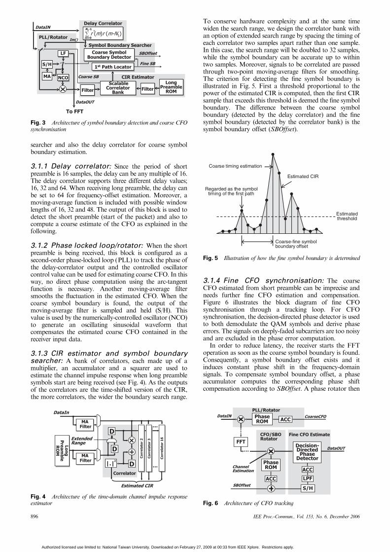
searcher and also the delay correlator for coarse symbolboundary estimation.
3.1.1 Delay correlator: Since the period of shortpreamble is 16 samples, the delay can be any multiple of 16.The delay correlator supports three different delay values;16, 32 and 64. When receiving long preamble, the delay canbe set to 64 for frequency-offset estimation. Moreover, amoving-average function is included with possible windowlengths of 16, 32 and 48. The output of this block is used todetect the short preamble (start of the packet) and also tocompute a coarse estimate of the CFO as explained in thefollowing.
3.1.2 Phase locked loop/rotator: When the shortpreamble is being received, this block is configured as asecond-order phase-locked loop (PLL) to track the phase ofthe delay-correlator output and the controlled oscillatorcontrol value can be used for estimating coarse CFO. In thisway, no direct phase computation using the arc-tangentfunction is necessary. Another moving-average filtersmooths the fluctuation in the estimated CFO. When thecoarse symbol boundary is found, the output of themoving-average filter is sampled and held (S/H). Thisvalue is used by the numerically-controlled oscillator (NCO)to generate an oscillating sinusoidal waveform thatcompensates the estimated coarse CFO contained in thereceiver input data.
3.1.3 CIR estimator and symbol boundarysearcher: A bank of correlators, each made up of amultiplier, an accumulator and a squarer are used toestimate the channel impulse response when long preamblesymbols start are being received (see Fig. 4). As the outputsof the correlators are the time-shifted version of the CIR,the more correlators, the wider the boundary search range.
Fig. 3 Architecture of symbol boundary detection and coarse CFOsynchronisation
Fig. 4 Architecture of the time-domain channel impulse responseestimator
896
Authorized licensed use limited to: National Taiwan University. Downloaded on February 27
To conserve hardware complexity and at the same timewiden the search range, we design the correlator bank withan option of extended search range by spacing the timing ofeach correlator two samples apart rather than one sample.In this case, the search range will be doubled to 32 samples,while the symbol boundary can be accurate up to withintwo samples. Moreover, signals to be correlated are passedthrough two-point moving-average filters for smoothing.The criterion for detecting the fine symbol boundary isillustrated in Fig. 5. First a threshold proportional to thepower of the estimated CIR is computed, then the first CIRsample that exceeds this threshold is deemed the fine symbolboundary. The difference between the coarse symbolboundary (detected by the delay correlator) and the finesymbol boundary (detected by the correlator bank) is thesymbol boundary offset (SBOffset).
3.1.4 Fine CFO synchronisation: The coarseCFO estimated from short preamble can be imprecise andneeds further fine CFO estimation and compensation.Figure 6 illustrates the block diagram of fine CFOsynchronisation through a tracking loop. For CFOsynchronisation, the decision-directed phase detector is usedto both demodulate the QAM symbols and derive phaseerrors. The signals on deeply-faded subcarriers are too noisyand are excluded in the phase error computation.
In order to reduce latency, the receiver starts the FFToperation as soon as the coarse symbol boundary is found.Consequently, a symbol boundary offset exists and itinduces constant phase shift in the frequency-domainsignals. To compensate symbol boundary offset, a phaseaccumulator computes the corresponding phase shiftcompensation according to SBOffset. A phase rotator then
Fig. 5 Illustration of how the fine symbol boundary is determined
Fig. 6 Architecture of CFO tracking
IEE Proc.-Commun., Vol. 153, No. 6, December 2006
, 2009 at 00:33 from IEEE Xplore. Restrictions apply.

Fig. 7 Radix-22FFT architecture
compensates the FFT outputs with phases computed fromboth the CFO loop and SBOffset. Note that this phaserotator is actually a complex-valued multiplier and inaddition to phase rotation it also equalises the frequency-domain data by multiplying them with the equalisercoefficients obtained from channel estimation.
3.2 FFT moduleFFT algorithms have been extensively studied and they canbe categorised according to the radix used. Radix-2 FFTalgorithm is by far the simplest to understand and toimplement. An approach called radix-22 FFT algorithmretains the regular structure of the radix-2 FFT algorithmand cuts the number of complex multiplications in half [14].Therefore, the proposed receiver adopts the radix-22 FFTalgorithm. Two classes of FFT architectures are popular inthe literature; single-path delay feedback (SPDF) [15] andmulti-path delay commutator (MPDC) [16]. Selection of theFFT architecture is a tradeoff between cost, complexity andthroughput. In this design, we choose the SPDF architec-ture and the radix-22 64-point SPDF FFT architecture isshown in Fig. 7.
3.3 Frequency-domain channel estimationand equalisationDuring the reception of long preamble, FFT outputs aredivided by the long preamble subcarrier signals to estimatethe channel gains of all subcarriers. In the case of a noisyand low delay-spread channel, we can compute a movingaverage of neighbouring subcarrier channel gains in orderto get a more accurate channel gain estimation (see Fig. 8).After channel estimation, the subcarrier signals in datasymbols are equalised in the frequency domain by multi-plication of the reciprocal of their respective estimatedchannel gains.
The reciprocal operation is accomplished by the complexreciprocal module shown in Fig. 9. The reciprocal of acomplex number Iin+jQin takes the form of
Iout þ jQout ¼1
Iin þ jQin¼ Iin � jQin
I2in þ Q2in
ð1Þ
Fig. 8 Architecture of channel estimation and frequency domainequalisation
IEE Proc.-Commun., Vol. 153, No. 6, December 2006
Authorized licensed use limited to: National Taiwan University. Downloaded on February 2
Note that an accurate implementation requires a divisioncircuit, which is very costly especially when the dynamicrange of the signal magnitude is large.
To this end, we propose an alternative approach tobalance the hardware complexity and the system perfor-mance. At first we represent the power of the input in afloating-point number format, i.e. mantissa and exponent.The mantissa is further partitioned into groups of four-bitnumbers
I2in þ Q2in ¼ ðaþ bxþ cx2 þ dx3 þ � � �Þ � 2E ð2Þ
where 8rar15, 0rb, c, dr15 and x¼ 2� 4 and E isthe exponent. The reciprocal of the mantissa can beexpanded as a polynomial
1
aþ bxþ cx2 þ dx3 þ � � � ¼1
aþ�b
a2xþ � � �
An approximation can be made by ignoring the higher-order terms. Considering the SNR requirement of the 64-QAM constellation, we found that keeping the first twoterms is good enough and the output of the complexreciprocal module is approximated by
Iout;a þ jQout;a ¼ ðIin � jQinÞ �a� bx
a2
� �� 2�E ð3Þ
3.4 Delay buffersIn baseband signal processing systems many tasks have aneed for delay buffers. Conceptually a W-bit delay buffer ismade up by W parallel flip-flop strings that propagate theincoming bits throughout all flip-flops. Since the flip-flop-based design is extremely power hungry, we use anotherdelay buffer design that consumes much less power.Figure 10 shows a latch-based delay buffer design [17]. Itis very similar to an SRAM design. An N-tap delay bufferconsists of an (N-2)-column latch array, an address decoderand two extra pipeline registers. The address decoder is aflip-flop ring that controls the read–write address of thelatch array. At any given time, it enables a column oflatches for read and the next column for write. As most ofthe cells are not active, it consumes much lower power thanthe flip-flop-based design. The two pipeline registers aredesigned for input and output buffering to ensure that themodule timing behaviour is the same as the flip-flop-based
Fig. 9 Architecture of the complex reciprocal module
897
7, 2009 at 00:33 from IEEE Xplore. Restrictions apply.

Fig. 10 Block diagram of the delay buffer
design. This architecture is highly scalable because allcomponents of the module can be extended easily.
4 Experimental results
This chip is fabricated in a 0.35mm single-poly-quadruple-metal CMOS process and packaged in a 68-pin package. Itis a cell-based design with many customised blocks (bitreversal module and delay buffers) to reduce both powerconsumption and active area. The transistor count is 429659and the die measures 4102mm� 4600mm. Figure 11 showsthe microphotograph of the receiver chip.
To simulate the channel effects, several exponential-decaychannel profiles depicted in Fig. 12 are used to generate thesimulated input signal for the receiver. The simulationresults are averaged for performance evaluation. Moreover,channel profiles with stronger tails are selected to confirmthe robustness of symbol boundary detection schemes. Thefunctionality of the receiver chip is verified by a patterngenerator and a logic analyser. Figure 13 plots the simulatedand measured receiver performance under different delayspread with 100-kHz carrier frequency offset. The signal-to-noise ratio (SNR) is defined as the ratio between OFDMdata symbol energy and in-channel noise energy. The slightdegradation in PER performance of the fabricated chiparises from the fact that a charge-sharing node in the chipsometimes makes the chip estimate the coarse CFOerroneously, and thus increases the measured PER.
898
Authorized licensed use limited to: National Taiwan University. Downloaded on February 27
The power consumption of the chip is measured underdifferent operation voltage when it is running at 20MHz.The results are shown in Fig. 14. The chip consumes168mW at 3.3V and 66mW at 2.3V supply voltage.
Fig. 11 Photograph of the receiver chip (4.1� 4.6 mm2)
Fig. 12 Channel delay profiles used for receiver performance evaluation
IEE Proc.-Commun., Vol. 153, No. 6, December 2006
, 2009 at 00:33 from IEEE Xplore. Restrictions apply.
A summary of the chip and its comparison with twoOFDM-based WLAN receiver chips are listed in Table 1.The chip consumes less power than the other two, thoughusing the least advanced technology. The chip has far fewertransistors, yet one other chip incorporates a channeldecoder and medium access control (MAC) processor,
Fig. 13 Simulated and measured packet error rate (PER)performance of the OFDM receiver chip
2.3 2.4 2.5 2.6 2.7 2.8 2.9 3 3.1 3.2 3.30
20
40
60
80
100
120
140
160
180
Supply Voltage (V)
Po
wer
(m
W)
Fig. 14 Power consumption (including core and pad) of theproposed chip under different supply voltages
Table 1: Comparison with other OFDM WLAN basebandreceiver chips
Carnival [6] Thomson [7] Proposed IC
Embedded A/D not included included not included
Baseband processing included included included
FEC and MAC modules not included included not included
Clock rate (MHz) 20 80 20
Technology (mm) 0.18 OLM 0.25 1P5M 0.35 1P4M
Core voltage (V) 1.8 2.5 2.3
Die size (mm2) 20.8 46.24 18.80
Transistor count(million)
1.72 4.0 0.43
RX Power (mW) 146 203 66
IEE Proc.-Commun., Vol. 153, No. 6, December 2006
Authorized licensed use limited to: National Taiwan University. Downloaded on February 27
making it more powerful. All in all, the proposed chip stillprovides a low-power solution to the baseband receiverimplementation of the IEEE 802.11a/g OFDM-basedWLAN systems.
5 Receiver with space diversity
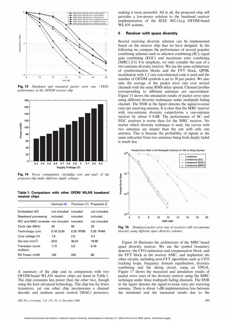
Several receiving diversity schemes can be implementedbased on the receiver chip that we have designed. In thefollowing we compare the performance of several popularcombining schemes such as selection combining (SC), equalgain combining (EGC) and maximum ratio combining(MRC) [11]. For simplicity, we only consider the case of atwo-antenna diversity receiver. We use the same architectureof synchronisation blocks and the FFT block. QPSKmodulation with 1/2 rate convolutional code is used and thenumber of OFDM symbols is set to 50 per packet. We alsotake the average of the packet error rate over severalchannels with the same RMS delay spread. Channel profilescorresponding to different antennas are uncorrelated.Figure 15 shows the simulation results of packet error ratesusing different diversity techniques under multipath fadingchannel. The SNR in the figure denotes the signal-to-noiseratio per receiving antenna. It is clear that theMRC receiverwith two-antenna diversity outperforms a one-antennareceiver by about 8–9dB. The performance of SC andEGC receivers is worse than for the MRC receiver. Nomatter which diversity technique is used, the curves withtwo antennas are steeper than the one with only oneantenna. This is because the probability of signals at thesame subcarrier from two antennas being both deeply fadedis much less.
Figure 16 illustrates the architecture of the MRC-basedspace diversity receiver. We use the symbol boundarydetector, the CFO estimation and compensation block, andthe FFT block in the receiver ASIC, and implement theother circuits, including post-FFT algorithms such as CFOtracking loops, frequency domain equalisation, diversitycombining and the slicing circuit, using an FPGA.Figure 17 shows the measured and simulation results ofpacket error rates of the diversity receiver using the MRCtechnique under three multipath fading channels. The SNRin the figure denotes the signal-to-noise ratio per receivingantenna. There is about 1-dB implementation loss betweenthe simulated and the measured results due to the
4 6 8 10 12 14 16 18 2010-3
10-2
10-1
100Packet Error Rate in the Multipath Channel of 100 ns Delay Spread
SNR (dB)
Pac
ket
Err
or
Rat
e
1-antenna2-antenna (SC)2-antenna (EGC)2-antenna (MRC)
Fig. 15 Simulated packet error rate of receivers with two-antennadiversity using different space diversity schemes
899
, 2009 at 00:33 from IEEE Xplore. Restrictions apply.

synchronisation issue between the baseband IC and theFPGA module. In summary, the space-diversity receiveroutperforms the single-antenna receiver by about 5–8dB inSNR and the effectiveness of the diversity receiver forOFDM-based wireless LAN systems in long delay-spreadenvironments is confirmed.
6 Conclusions
In this paper, we have presented the design, implementationand measurement results of an OFDM space-diversityreceiver forWLAN.We design a baseline OFDMbasebandchip, and implement a space-diversity receiver based on thechip. The complexity and power consumption of the chipare minimised through innovative architecture, word-length
4 5 6 7 8 9 10 11 1210 -3
10 -2
10 -1
10 0Packet Error Rate with 2antenna Diversity of MRC
SNR (dB)
Pac
ket
Err
or
Rat
e
Delay Spread = 100ns (Simulation)Delay Spread = 75ns (Simulation)Delay Spread = 50ns (Simulation)Delay Spread = 100ns (Measurement)Delay Spread = 75ns (Measurement)Delay Spread = 50ns (Measurement)
Fig. 17 Measured packet error rate of MRC-diversity receiverunder channels with different delay spread
Fig. 16 Block diagram of the OFDM baseband receiver withspace diversity
900
Authorized licensed use limited to: National Taiwan University. Downloaded on February 2
optimisation and several circuit design techniques. Thefabricated chip is then tested and shown to be functionallycorrect. Measurement results indicate that the powerconsumption of the proposed chip is as low as 66mWrunning at 20 MHz from a 2.3-V supply voltage. Measuredpacket error rates show very good receiving performanceunder multipath fading channels. Moreover, the additionalMRC scheme with two-antenna diversity outperforms aone-antenna receiver by about 5–8dB, making it moresuitable for situations with severe multipath fading.
7 Acknowledgments
The authors greatly appreciate the Chip ImplementationCenter (CIC), Taiwan for fabrication of the proposed chip.This work was supported in part by the National ScienceCouncil, Taiwan, ROC under grant no. 93-2220-E-002-013and 93-2219-E-002-014.
8 References
1 Engels, M., Eberle, W., and Gyselinckx, B.: ‘Implementation of ahigh performance wireless LAN’. Proc. IEEE Universal PersonalCommun. Conf., 1994, pp. 253–256
2 Nee, R.V., and Prasad, R.: ‘OFDM wireless multimedia communica-tions’ (Artech House, 2000)
3 Zou, W., and Wu, Y.: ‘COFDM: an overview’, IEEE Trans.Broadcast., 1995, 41, (1), pp. 1–8
4 ‘Wireless LAN medium access controol (MAC) and physical layer(PHY) specifications: High-speed physical layer in the 5 GHz band’.IEEE Std 802.11a-1999, 1999
5 Rabaey, J.M., and Pedram, M.: ‘Low power design methodologies’(Kluwer, Norwell, MA, 1995)
6 Eberle, W. et al.: ‘80-Mb/s QPSK and 72-Mb/s 64-QAM flexible andscalable digital OFDM transceiver ASICs for wireless local areanetworks in the 5-GHz band’, IEEE J. Solid-State Circuits, 2001, 36,(11), pp. 1829–1838
7 Thomson, J. et al.: ‘An integrated 802.11a baseband and MACprocessor’. Tech. Dig., IEEE Int. Solid State Circuits Conf. (ISSCC),2002, Vol. 1, pp. 338–339
8 Liou, M.L., and Chiueh, T.D.: ‘A parametric module designframework and its application to gate-level datapath/dsp mosulesynthesis’. Proc. IEEE Int. Symp. on Circuits and Systems (ISCAS),May 2000, Vol. 2, pp. 41–44
9 Weinstein, S.B., and Ebert, P.M.: ‘Data transmission by frequency-division multiplexing using the discrete Fourier transform’, IEEETrans. Commun., 1971, 19, (5), pp. 628–634
10 Pollet, T., Bladel, M.V., and Moeneclaey, M.: ‘BER sensitivity ofOFDM systems to carrier frequency offset and Wiener phase noise’,IEEE Trans. Commun., 1995, 43, (2), pp. 191–193
11 Rappaport, T.S.: ‘Wireless communications, principles and practice’(Prentice Hall, Inc., NJ, 2002, 2nd edn.)
12 Yang, B., Letaief, K.B., Cheng, R.S., and Cao, Z.: ‘Burst framesynchronization for OFDM transmission in multipath fading link’.Proc. IEEE Veh. Tech. Conf., 1999, pp. 300–304
13 Nogami, H., and Nagashima, T.: ‘A frequency and timing periodacquisition technique for OFDM systems’. Proc. IEEE Personal,Indoor, Mobile Radio Commun., 1995, pp. 1010–1015
14 Shousheng, H., and Torkelson, M.: ‘A new approach to pipeline FFTprocessor’. Parallel Processing Symp., Proc 10th Int. IPPS, Apr. 1996,pp. 766–770
15 Wold, E.H., and Despain, A.M.: ‘Pipeline and parallel-pipeline FFTprocessors for VLSI implementation’, IEEE Trans. Comput., 1984, 33,(5), pp. 414–426
16 Rabiner, L.R., and Gold, B.: ‘Theory and application of digital signalprocessing’ (Prentice Hall, Englewood Cliffs, NJ, 1975)
17 Ma, H.P., Liou, M.L., and Chiueh, T.D.: ‘A 123-mW W-CDMAuplink basedband receiver IC with beamforming capability’, IEEE J.Solid-State Circuits, 2004, 39, (5), pp. 785–794
IEE Proc.-Commun., Vol. 153, No. 6, December 2006
7, 2009 at 00:33 from IEEE Xplore. Restrictions apply.