A LOW-POWER RECEIVER FOR SIMULTANEOUS ...
87
A LOW-POWER RECEIVER FOR SIMULTANEOUS ELECTROCARDIOGRAM AND RESPIRATORY RATE DETECTION by JIFU LIANG Submitted in partial fulfillment of the requirements For the degree of Master of Science Department of Electrical Engineering and Computer Science CASE WESTERN RESERVE UNIVERSITY August, 2016
-
Upload
khangminh22 -
Category
Documents
-
view
0 -
download
0
Transcript of A LOW-POWER RECEIVER FOR SIMULTANEOUS ...
A LOW-POWER RECEIVER FOR SIMULTANEOUS
ELECTROCARDIOGRAM AND RESPIRATORY RATE DETECTION
by
JIFU LIANG
Submitted in partial fulfillment of the requirements
For the degree of Master of Science
Department of Electrical Engineering and Computer Science
CASE WESTERN RESERVE UNIVERSITY
August, 2016

A Low-Power Receiver for Simultaneous Electrocardiogram and
Respiratory Rate Detection
Case Western Reserve University
Case School of Graduate Studies
We hereby approve the thesis1 of
JIFU LIANG
for the degree of
Master of Science
Dr. Soumyajit Mandal
Committee Chair, Adviser July 1st, 2016Department of Electrical Engineering and Computer Science
Dr. Pedram Mohseni
Committee Member July 1st, 2016Department of Electrical Engineering and Computer Science
Dr. Dominique Durand
Committee Member July 1st, 2016Department of Biomedical Engineering
1We certify that written approval has been obtained for any proprietary material contained therein.

I would like to dedicate this thesis to my advisor, Dr. Soumyajit Mandal,for his endless guidance of my research.
I would also dedicate this thesis to my parents, Yanjun Liang and Jinju Lu,for their support of my study in America.
I would also dedicate this thesis to my girlfriend, Shuyue Li,for her encouragement of my study at CWRU.

Table of Contents
List of Tables vi
List of Figures vii
Acknowledgements xiii
Acknowledgements xiii
Abstract xiv
Abstract xiv
Chapter 1. Introduction 1
Motivation 1
Research Goals 2
Literature Review 3
Structure of the Thesis 13
Chapter 2. First Chip Design 14
Impedance Pneumography 14
Block Diagram 16
Clock Generator Block 18
Controlled Injected Current Block and Mixer 20
Preamplifier Block 21
Wide-linear Range OTA and Filters 24
Second Gain Stage for Amplifying RR signal 29
Chapter 3. Measurement Result of First Chip 32
Programmable Injected Current Block and Mixer 34
iv

ECG Amplifier 35
RR Measurement 40
Chapter 4. Second Chip Design 43
Fully Differential Wide-linear-range OTA 43
Fully Differential Filters 45
Fully Differential Preamplifier Block 47
Digital Block 52
Second Gain Stage for Amplifying RR signal 57
Layout 60
Chapter 5. Conclusions 63
Appendix A. PCB for testing the AFE 66
Appendix. Complete References 68
v

List of Tables
3.1 Comparison table with the state of the art 34
vi

List of Figures
1.1 Conceptual view of a wireless biopotential measurement system
integrated into a chest band. The three patch electrodes are denoted
RA, LA, and REF, respectively. 3
1.2 One of the most frequently used topology of bioelectric amplifier1. 6
1.3 (a) Typology of MOS pseudo resistor. (b) Basic structure of switched
capacitor. 7
1.4 Schematic of ECG amplifier in reference2. 8
1.5 Schematic of ECG amplifier presented by Wen et al.3. 10
1.6 Schematic of ECG amplifier presented by Burke and Gleeson4. 11
2.1 Simplified structure of the respiration circuit when RA and LA
electrodes are used. 15
2.2 Detected respiratory rate signal after filtering with a fourth-order
LPF with cutoff frequency of 2 Hz. A commercial AFE (ADS1298R)
designed by Texas Instruments is used here to measure RR signal
when the volunteer took deep breath. 16
2.3 Simplified block diagram of the integrated front-end receiver. 17
2.4 Typical spectra of the ECG, modulated RR, and baseband RR signals
before the HPF, before the quadrature modulator, and after the
modulator. 19
2.5 Clock generator circuit used to generate 0, 90, 180, and 270 clocks. 19
vii

2.6 Simulation result of the clock generator block. clk1 and clk2 have 90
phase shift. 20
2.7 Programmable current mirrors and double balanced mixer used for
generating I AC . The amplitude of I AC can be programmed over a 1:16
range (4 bits) by the switches φ1-φ4. 21
2.8 Schematic of the low-noise ECG amplifier. 22
2.9 Schematic of the OTA used four times in the preamplifier. 23
2.10 Simulation results of (a) the AC response of the preamplifier. (b) the
output of the preamplifier when an input of 2 mV 100 Hz sinusoid
wave is used. (c) the output of the ECG path when an input of 2 mV
100 Hz sinusoid wave is used. 25
2.11 (a) First-order Gm −C LPF topology. (b) First-order Gm −C HPF
topology. 25
2.12 Basic single-stage five transistor OTA with NMOS input transistors. 26
2.13 The wide-linear-range OTA used several times in the AFE. 27
2.14 Schematic of the BPF and second gain stage used to process each
demodulated RR signal component. The capacitors C1 and C2
are 400 pF off-chip capacitors, while C3 and C4 are 2 pF on-chip
capacitors. 29
2.15 Simulation results of (a) the AC response of the BPF after demodulator.
(b) the I component of RR at the output of mixer if a 1 µV RR signal is
applied at the input of the preamplifier. (c) the final output of RR path
if a 1 µV RR signal is applied at the input of the preamplifier. 31
viii

3.1 Die photograph of the fabricated AFE, which has an active area of
1050 µm × 600 µm. Major blocks are labeled. 32
3.2 The PCB used to test the first chip. 33
3.3 The measured transistor I-V curve used to set the 200 nA off-chip bias
current. This curve was measured by using a Keithley source meter. 34
3.4 Circuit used to test the programmable injected current block and the
mixer. A fixed resistor (100 kΩ) was placed between LA and RA. 35
3.5 (a) Square voltage waveforms across the RA and LA with different
injected currents when a 100 kΩ resistor was used between RA and
LA. (b) Measured positive and negative currents as a function of the
digital code. 36
3.6 (a) Differential frequency response of both the ECG amplifier and the
following LPF. (b) Common-mode frequency response of both the
ECG amplifier and the following LPF without utilizing driven-ground
circuit. 36
3.7 (a) Output noise of the both the ECG amplifier and the following LPF.
(b) Input noise of the both the ECG amplifier and the following LPF. 37
3.8 (a) Output of the ECG path when high-frequency clock is disabled.
The input signal is a 2 mV, 10 Hz sinusoid wave. (b) Output of the ECG
path to the sum of a 1.5 mV, 10 Hz sinusoid (simulating ECG) and a
1.4 mV, 100 Hz square wave (simulating RR carrier). 38
3.9 Detected ECG signal after baseline removal and filtering with a
fourth-order LPF ( fc = 50 Hz). 39
ix

3.10 The DC voltage at the output of the ECG path shifted from 0.3 V to
2.4 V in around 900 seconds. 40
3.11 (a) Body model used to generate ECG-like and RR-like signals. (b)
Simulation result of the modulated RR-like signal when 100 nA 1 kHz
AC currents are fed to LA and RA. (c) The FFT result of the transient
signal generated by the body model. 41
3.12 Input triangle wave used to modulate the impedance between RA and
LA at 0.5 Hz, and measured I and Q RR outputs after filtering with a
fourth-order Butterworth LPf with cutoff frequency of 5 Hz. 42
4.1 (a) Fully differential version of wide-linear-range OTA. (b) Differential-
difference OTA used in CMFB. (c) Fully differential OTA stage. 45
4.2 (a) A single stage of fully differential OTA in the preamplifier. (b) Bode
plot of the fully differential OTA stage. 46
4.3 (a) Fully differential LPF. (b) Fully differential HPF. 47
4.4 The AC simulation results of (a) HPF with cutoff frequency of 1 kHz to
remove ECG signal in RR path. (b) LPF with cutoff frequency of 5 Hz
to remove high-frequency RR carrier signal in RR path. 3 nF off-chip
capacitor is used. 47
4.5 Circuit of fully differential preamplifier. 49
4.6 Modified switched capacitor topology. 51
4.7 Equivalent circuits of the modified switched capacitor topology in
two phases. (a) Equivalent circuit when clk1 is on and clk2 is off. (b)
Equivalent circuit when clk1 is off and clk2 is on. 51
x

4.8 Transient simulation result at the output of the preamplifier when
a 2 mV 100 Hz sinusoid wave simulating ECG signal and a 10 kHz
square wave simulating RR carrier signal are used at the input of the
circuit. 52
4.9 Digital blocks in the AFE. 53
4.10 Frequency response of the first-order LPF by using switched capacitor. 54
4.11 Programmable counter. 55
4.12 Two-phase non-overlapping clocks generator block. 55
4.13 (a) Programmable bus used to set digital inputs. (b) Timing diagram
of SPI. 56
4.14 Simulation results of the circuits generating clocks used in the mixer
for modulation and demodulation. (a) The 38 kHz input square wave
simulating the off-chip clock. (b) The first output clock with one
fourth of the frequency of the input wave. (c) The second output clock
with one fourth of the frequency of the input wave and 90 phase
shift. 57
4.15 Simulation results of the circuits generating clocks used in the
switched capacitor. (a) The first output clock. (b) The second output
clock. (c) 2 ns delay between the two non-overlapping output clocks. 58
4.16 Second gain stage for amplifying RR signal. 58
4.17 Open-loop Bode plot of the op-amp stage. 59
4.18 Closed-loop Bode plot of the op-amp stage. 60
xi

4.19 Transient simulation result at the output of I branch in RR path
(I+− I−). The frequency of RR signal is chosen as 5 Hz to increase the
simulation speed. 60
4.20 Layout of the second chip. 62
A.1 Schematic of the PCB board. 66
A.2 Layout of the PCB board. 67
xii

Acknowledgements
0.1 Acknowledgements
I would especially like to thank my mentor, research advisor, Dr. Soumyajit Mandal, for
his endless support of my research during my M.S. study. I would never accomplish
this project without his guidance. Not only has he taught me much knowledge about IC
design, but also he has assisted me to adapt to the study at CWRU.
Thanks to my parents, Yanjun Liang and Jinju Lu, for their continuously support of
my study in America. Thank you for providing me an opportunity to study abroad. You
will always be my beloved parents.
To my girlfriend, Shuyue Li, who keeps giving me encouragement during my study
at CWRU. Although we are studying at different universities, but your support makes me
a better student and a better man.
I would also dedicate to my M.S. committee members, Dr. Pedram Mohseni and Dr.
Dominique Durand. Thank you for your advice and help on my thesis.
I am very grateful to Yingying Wang, for your enduring help on my chip design.
Thank you for being patient and answering all my questions.
I would also thank many of the students and staffs at CWRU. Thanks to Dr. Steve
Majerus for your instruction in the lab. Thanks to my partner in this project, Shixiong
Li, who helped me design my first chip. Thanks to another partner in this project, Gre-
gory Hessler, who helped me to study the method to transmit data by using RFduino
board. Thanks to my friend, Ali Nikoofard, who helped me test my first chip. Thanks
to my friends, Cheng Chen and Xinyao Tang, for all the happy and tough time we spent
together.
Last but not least, thanks to all the people who helped me finish this thesis.
xiii
Abstract
A Low-Power Receiver for Simultaneous Electrocardiogram and
Respiratory Rate Detection
Abstract
by
JIFU LIANG
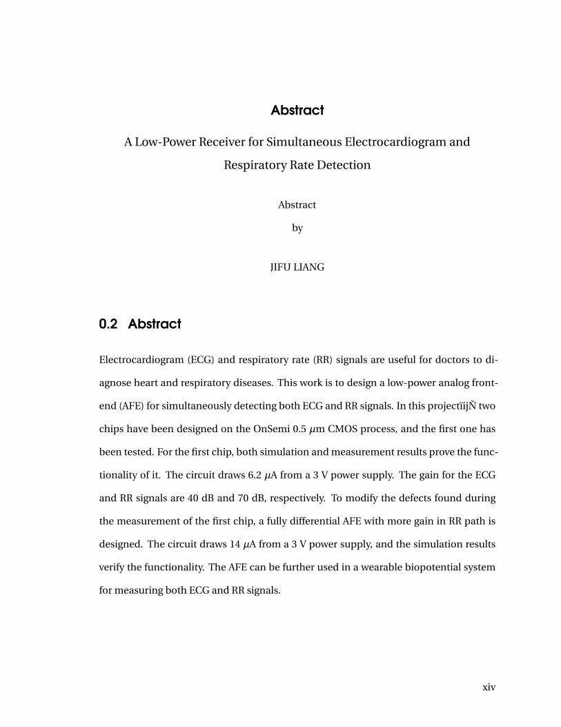
0.2 Abstract
Electrocardiogram (ECG) and respiratory rate (RR) signals are useful for doctors to di-
agnose heart and respiratory diseases. This work is to design a low-power analog front-
end (AFE) for simultaneously detecting both ECG and RR signals. In this projectïijN two
chips have been designed on the OnSemi 0.5 µm CMOS process, and the first one has
been tested. For the first chip, both simulation and measurement results prove the func-
tionality of it. The circuit draws 6.2 µA from a 3 V power supply. The gain for the ECG
and RR signals are 40 dB and 70 dB, respectively. To modify the defects found during
the measurement of the first chip, a fully differential AFE with more gain in RR path is
designed. The circuit draws 14 µA from a 3 V power supply, and the simulation results
verify the functionality. The AFE can be further used in a wearable biopotential system
for measuring both ECG and RR signals.
xiv

1
1 Introduction
1.1 Motivation
Heart disease is the leading cause of death in the United States. According to the Amer-
ican Heart Association (AHA), an estimated 85.6 million American adults (more than
one-third of the total population) have one or more types of cardiovascular diseases
(CVDs). Heart disease happens on someone in the United States every 43 seconds,
killing more than 375,000 people a year. Based on the fact that many people are suf-
fering from CVDs, a large amount of money is spent on their healthcare. In 2011, it cost
207.3 billion for direct heart disease, 48.6 billion for hypertension, 33 billion for stroke
and 27.7 for other CVDs5. Consequently, monitoring heart activity has gained consid-
erable attention. It has been known that Electrocardiogram (ECG) shows the heart elec-
trical activity, and it contains much information related to heart rate and rhythm which
can be helpful for doctors to diagnose heart disease. So many different kinds of ECG
monitors have been produced and utilized6.
Respiratory rate (RR) is defined as the number of breaths a person has in one minute.
It is very useful for doctors to diagnose pneumonia and many other respiratory dis-
eases7. High respiratory rate has also been observed on a large proportion of cardiac
arrest patients8,9. Based on the study from Health Grades in 2011, 20% of postoperative

Introduction 2
respiratory failures resulted in death10. However, monitoring RR has not gained much
attention compared to other vital signs11. RR is also not recorded in many hospitals,
even when respiratory condition is the primary problem for patients12,13. One main
reason is that there are not enough reliable RR monitoring systems14.
Wearable health-monitoring systems have drawn much interests in recent years15.
From the study of Trans-European Network Home-Care Management Systems (TEN-
HMS), home telemonitoring systems get better feedback from patients. For home tele-
monitoring patients, it costs 26% fewer days in hospital, leading to a 10% cost savings.
Survival rate is also substantially better for home telemonitoring patients16. Wearable
systems not only have those advantages, but also fulfill the need for monitoring patients
over a long period of time. A distinct example is ECG monitoring. It is desirable that
ECG can be monitored over several weeks or months, and wearable monitoring systems
are more suitable compared to the normal ambulatory systems in this case17. But chal-
lenges for wearable monitoring systems exist, and one main problem is the considera-
tion of power consumption.
1.2 Research Goals
In this project, the goal is to design an integrated low-power analog front-end (AFE) for
simultaneously detecting ECG and RR signals. We assume that there are three electrodes
connecting to the body, including right arm (RA), left arm (LA), and reference electrode
(REF). The impedance pneumography (IP) method18,19, which will be described in the
second chapter in detail, is utilized to detect RR signal. Both ECG and RR are measured
between RA and LA chest electrodes. A driven-ground circuit using the REF electrode is
also utilized to boost common-mode rejection ratio (CMRR).

Introduction 3
This chip could be ultimately used in a wearable biopotential measurement sys-
tem, which can continuously wirelessly monitor heart activity and respiratory condi-
tion. Fig. 1.1 shows the desired chest band, including all the three electrodes, AFE, ADC,
antennas, and batteries. All the raw data is processed by an AFE and then digitized by
an ADC. After that, the digitized signals are buffered and then wirelessly transmitted to
a Simband or a mobile phone. The Simband can be programmed so that users can have
good interface with it, and users can also directly read the data collected from the chest
band. Another advantage of using Simband is that it reduces power consumption by
allowing the chest band to transmit data to a local unit over short distance (i.e., by cre-
ating a so-called body area network20). In this case, it is easy for people to wear this
user-friendly monitoring system for long time.
Figure 1.1. Conceptual view of a wireless biopotential measurement sys-tem integrated into a chest band. The three patch electrodes are denotedRA, LA, and REF, respectively.
1.3 Literature Review
Wet electrodes, dry electrodes and non-contact electrodes are widely used to collect
electro-physiology signals in biopotential systems. The difference between these three
electrodes is discussed in this section. Also, monitoring ECG has gained much attention,
Introduction 4
and there have been many different kinds of ECG monitors in the market6. Several re-
searchers have integrated AFEs with ADCs and digital processors (to extract heart rate,
etc.) into complete systems-on-chips (SoCs)2,21,22, but in this section the literature re-
view is limited to analog front-ends since the focus of this thesis is on the AFE. Some of
the ECG measuring circuits have the active ground circuit but some don’t. The differ-
ence between them is discussed in the following content. In addition, the amplitudes
of physiological signals are in the order of tens of µV to tens of mV and the frequency
varies from DC to a few kHz23. Typically, the frequency of ECG signal is from 1 Hz to
100 Hz and the amplitude of it varies from 0.5 mV to 4 mV24, while the RR signal has a
typical bandwidth of 0.5 Hz. Since the frequencies of the ECG and RR signals are rather
low, filters with very low corner frequency are always needed. It is easy to implement
filters with low cut-off frequencies by using off-chip capacitors and resistors. But either
switched capacitor resistors25 or MOS pseudo resistors1,26 are required for on-chip im-
plementations.
1.3.1 Electrodes
Electrodes are an important part of physiology monitoring systems. And the three kinds
of most common electrodes are wet electrodes, dry electrodes and non-contact elec-
trodes. Wet electrodes like Ag/AgCl electrodes are widely used in bioelectric applica-
tions currently27. The advantages of Ag/AgCl electrodes is obvious that they are simple,
disposable and easy to be used28. And the most important advantage of Ag/AgCl elec-
trodes is the low impedance29. But the electrolytic gel has to be applied, which may
cause allergic reactions28. And they can not be used for long time because of the dehy-
dration30. Also, short circuiting may happen since the gel can smear31. But for the dry
electrodes, these problems do not exist since the gel is not applied. However, since there

Introduction 5
is no adhesion between the dry electrodes and the body, electrodes may shift when the
body moves30. Compared to wet electrodes and dry electrodes, non-contact electrodes
do not have an ohmic connection to the skin. No preparation is needed if non-contact
electrodes are utilized. The non-contact electrodes are insensitive to skin conditions,
so they are very suitable for wearable monitoring systems since they can be embedded
within a comfortable layers of fabric32. But the input impedance of the AFE should be
high so that it can extract the signal from non-contact electrodes29. And any motion of
the non-contact electrodes with respect to the skin may generate artifact.
1.3.2 Amplifiers Using Two Electrodes
It is very appealing that bioelectric amplifiers only uses two electrodes because only
minimal number of contacts are utilized to collect signals. It also saves power since the
active-ground circuit is not utilized. However, without driven-ground circuit, the elec-
tric potential of the human body can not be controlled. It is necessary to eliminate DC
component and very low-frequency signals prior to amplifying biopotentials because of
electrode offset voltages, motion artifacts, and so on. Therefore, AC-coupled amplifiers
are often used to remove DC component and very low-frequency signals. There is one
basic topology as shown in Fig. 1.2 which is commonly used in many biomedical ampli-
fiers with only two electrodes1. The mid-band gain is set by the ratio of capacitors in the
feedback loop. The bandwidth is approximately gm/(AmCL), where gm is the transcon-
ductance of the OTA and Am is the mid-band gain. The low-frequency cutoff is set by
the effective resistance of the pseudo resistor and the capacitor in parallel with it. How-
ever, some circuits use pseudo resistor to work as large resistors1,33–35, while some other
circuits use switched capacitor resistors to behave as large resistors36.

Introduction 6
C1
C1C2
C2
CLVo
V1
V2
Figure 1.2. One of the most frequently used topology of bioelectric amplifier1.
For the MOS pseudo resistor in Fig. 1.2, it behaves as a resistor-like device, which has
a monotonic I-V relationship1,26. To simply understand the device, it contains a pair of
diodes in parallel with different polarity. Therefore, the current increases exponentially
with voltage across them. With negative VGS , the device acts like a diode-connected
PMOS device. With positive VGS , the device acts like a diode-connected bipolar device.
High resistance exists when the voltage across the device is small, so two pseudo resis-
tors are commonly used in series as shown in Fig. 1.2 so that the distortion for large
signals can be reduced.
The switched capacitor is a discrete-time system that can also be used to replace the
large resistor. The basic structure of switched capacitor resistor is shown in Fig. 1.3(b).

Introduction 7
ϕ1 and ϕ2 are nonoverlapping two-phase clocks with the period of T . The average cur-
rent i1 is
i1 = 1
T
∫ T
0i1(t )d t = 1
T
∫ T2
0i1(t )d t (1.1)
i1(t ) = d q1(t )
d t(1.2)
From the equation (1.1) and (1.2), we can get
i1 = 1
T
∫ T2
0
d q1(t )
d td t = C ·VC ( T
2 )−C ·VC (0)
T≈ C ·V1 −C ·V2
T(1.3)
From the continuous time perspective, we also know
i1 = V1 −V2
R(1.4)
where R is the effective resistance of the circuit. By comparing the equation (1.3) and
(1.4), we can get the following conclusion that
R = T
C(1.5)
The structure of switched capacitor can be modified and different equivalent resis-
tance can be obtained, which may be different from the equation (1.5). But all of them
share the same idea that a charge q is transferred from the input to the output in each
clock cycle.
P+ P+ N+
N-well
P-sub
ɸ2ɸ1
CV1
+
V2
+
Vc
+
i1
Figure 1.3. (a) Typology of MOS pseudo resistor. (b) Basic structure ofswitched capacitor.

Introduction 8
Liang et al. present a system of portable ECG monitoring system based on Bluetooth
connectivity to a mobile phone2. In his system, ECG signal is collected by the dry skin
electrodes, and then amplified, filtered, and analog-digital converted. After that, the
digital data is sent to a mobile phone through Bluetooth. In his core monitoring circuit,
a preamplifier and a band-pass filter are designed in his AFE. A commercial microcon-
troller with a built-in ADC is also included. The schematic of preamplifier is shown in
Fig. 1.4.
Vip
Vin
Vt
Vt
C1=20pf
C1=20pf
C2=0.1pf
C2=0.1pf
C3=12pf
C3=1
2p
f
R1=100kΩ
R1=100kΩ
R2=1MΩ
R2=1
MΩ
Vo
Vcm
Figure 1.4. Schematic of ECG amplifier in reference2.
In this preamplifier, two stages of amplification are utilized. The gain of each stage
is set by the ratio of two capacitors or two resistors in negative feedback. Besides, the
PMOS transistors in the feedback loop work as pseudo resistors. The pseudo resistor
and the capacitor in parallel with it form the high-pass pole. The PMOS transistors are
biased in subthreshold region, and the equivalent resistance is set by Vt . As the author
states, the equivalent resistance changes from 109 Ω to 1014 Ω if Vt changes from 0.8 V to
1.6 V, resulting the pole changing from around 10 mHz to several hundred Hz. Measured

Introduction 9
result shows that the passband is from around 0.01 Hz to 100 Hz, and the input referred
noise is around 2.3 µVr ms . But in this preamplifier, there is a disadvantage that several
resistors are used in the amplifier which produce noise. The thermal noise in a resistor
is described by the following equation.
v2n = 4kT R∆ f (1.6)
where k is Boltzmann’s constant in joules per Kelvin, T is the temperature in Kelvin, and
R is the resistor value in Ohms.
For the amplifiers without driven-ground circuit, there are several advantages. For
example, the circuit takes less area and it may have less power consumption. But the
disadvantage is obvious that the AC common-mode voltage can not be reduced. Al-
though AC coupled amplifier can be used to remove the DC component of the common
mode signal, the power-line interference still needs to be removed. However, for wear-
able monitoring systems, the AC interference is a smaller problem since the short leads
are utilized.
1.3.3 Amplifiers Using Reference Electrodes
Now the amplifiers with driven-ground circuit is discussed. The goal of the driven-
ground circuit is to reduce the common-mode signal by using negative feedback37. Three
electrodes are widely used in the amplifiers with active ground circuit, including two
electrodes measuring electric signals and one electrode working as reference electrode.
The reduction of the common-mode voltage is related to the gain of the driven-ground
circuit. Thus, a relatively high gain is desired in the driven-ground circuit. However, a
high gain feedback loop may lead instability. Also in the driven-ground circuit, buffers
may be needed to drive the body impedance.
Introduction 10
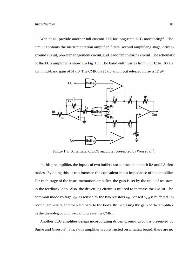
Wen et al. provide another full custom AFE for long-time ECG monitoring3. The
circuit contains the instrumentation amplifier, filters, second amplifying stage, driven-
ground circuit, power management circuit, and leadoff monitoring circuit. The schematic
of the ECG amplifier is shown in Fig. 1.5. The bandwidth varies from 0.5 Hz to 100 Hz
with mid-band gain of 51 dB. The CMRR is 75 dB and input referred noise is 12 µV.
Buffer
Buffer
Buffer
LA
RA
RLOut
R1 R2 R3
R1 R2
R0
R0
Vcm
R3
R4Rr
RL
Cr
Figure 1.5. Schematic of ECG amplifier presented by Wen et al.3.
In this preamplifier, the inputs of two buffers are connected to both RA and LA elec-
trodes. By doing this, it can increase the equivalent input impedance of the amplifier.
For each stage of the instrumentation amplifier, the gain is set by the ratio of resistors
in the feedback loop. Also, the driven-leg circuit is utilized to increase the CMRR. The
common mode voltage Vcm is sensed by the two resistors R0. Sensed Vcm is buffered, in-
verted, amplified, and then fed back to the body. By increasing the gain of the amplifier
in the drive-leg circuit, we can increase the CMRR.
Another ECG amplifier design incorporating driven-ground circuit is presented by
Burke and Gleeson4. Since this amplifier is constructed on a matrix board, there are no

Introduction 11
constraints of resistors and capacitors with large values. The amplifier draws 9 µA from
a 3.3 V power supply. The bandwidth of the amplifier is from 0.05 Hz to 1.9 kHz with the
gain of 43 dB. The CMRR is 55 dB without active ground circuit, and it increases to 88 dB
if driven-ground circuit is used.
VCC
VCC
R1
R1R2
R2
R3
R4
R4
R5R5
R6
R6
R7
R7
R8
R8
R9
R10
R10 R11
R11
R12R13
R14
R15
C1
C1
C2
C2
C3 C4
C4
C5
C6
C7
V1
V2
Vref
Vo
Figure 1.6. Schematic of ECG amplifier presented by Burke and Gleeson4.
The amplifier has three stages. The first stage is AC coupled by using C1, causing
attenuation of DC offset and low-frequency input signals. R1 provides patient protection
by limiting the current coming from the electrodes, and R6 with R3 set up the DC bias
voltage for the op-amps. R2 defines the input impedance of the amplifier to meet CMRR
requirements in the presence of inevitable electrode impedance mismatch. The second
stage is also a differential stage with DC coupled at the input. R9 and C3 set the DC
gain to unity. Since the input capacitance of the op-amp generates a zero, C2 is used

Introduction 12
here to define the zero more reliably. The third stage is a simple DC coupled stage with
resistors in the negative feedback. Besides all the three stages, the reference circuit is
used to increase the CMRR. R7 detects the common-mode voltage. Then, it is inverted,
amplified, and sent to the reference electrode. More information of this amplifier can
be found in reference4.
By using driven-ground circuit, the common-mode voltage including the DC value
and the powerline interference can be greatly reduced. This explains why in this project
the driven-leg circuit is used in AFE.
1.3.4 Summary of Bioelectric Amplifiers
From the overview of the research field, to design a good preamplifier, several conditions
should be satisfied.
The first one is noise. A high-quality amplifier should have very low equivalent input
noise since the amplitude of ECG signal and other bioelectric signals are rather small.
For example, the amplitude of ECG signal varies from 0.5 mV to 4 mV24. To reduce the
noise, several methods like increasing the bias current for the amplifier can be utilized.
The second constraint is common-mode rejection ratio (CMRR). The CMRR should
be good enough to decrease the power-line interference so that the power-line inter-
ference is not able to have effect on the measurement of ECG signal. For a body-worn
device, 20 dB CMRR is needed since there is not a big common-mode voltage38. But for
a device not entirely worn on the body, at least 80 dB CMRR is needed.
The third constraint is low high-pass filter corner frequency to allow low-frequency
signal components (as low as 0.1 Hz for ECG) to be amplified. It is easy to implement
off-chip large capacitors or resistors to get a low cutoff frequency. However, switched

Introduction 13
capacitor or MOS pseudo resistor can also be integrated in the chip if the designer wants
to reduce the size of the monitoring system.
The fourth condition is power consumption. Power consumption should be as low
as possible so that monitoring systems can work for a longer period of time without
changing batteries. This is also good when a bioelectric signal needs to be monitored
for long periods of time to detect transient and infrequent symptoms (such as missing
or irregular heartbeats) that can be used by doctors for diagnosis. Another advantage
of systems with low power consumption is that the weight of the devices is light since
smaller batteries can be used for a given operating lifetime.
1.4 Structure of the Thesis
In this project, two AFE chips have been designed. This thesis is divided into the follow-
ing parts. In Chapter 2, the design of the first chip is introduced in detail. In Chapter
3, the measurement result of the first chip is presented. In Chapter 4, the design of the
second chip is introduced in detail. And Chapter 5 contains the conclusion.

14
2 First Chip Design
In this chapter, the first AFE chip design is presented in detail. ECG signal is collected
directly by two conventional contact electrodes RA and LA. To detect RR, impedance
pneumography (IP) method, which will be described later, is used so that the low-frequency
RR signal is modulated on a high-frequency carrier signal. The low-noise preamplifier
in the AFE amplifies both the ECG and modulated RR signals. After the preamplifier,
LPFs are used to remove modulated RR signal in ECG path. In RR path, HPFs are used to
remove ECG. Then, the mixer is utilized to extract the RR signal, and the following BPF
is used to remove high-frequency carrier and low-frequency noise. Since the amplitude
of RR is small, there is another gain stage for further amplification of the RR signal.
2.1 Impedance Pneumography
Impedance pneumography method is widely used to measure respiratory rate. Fig. 2.1
shows the simplified structure of the respiration circuit when RA and LA electrodes are
used. During respiration, the thorax can be treated as two impedance components: a
constant baseline impedance (Zbod y+2Zel ectr ode ) and a varying impedance (∆Z )18,19,39.
For the relatively constant term, the value of Zbod y is around 500 Ω based on the study
from Grenvik et al18, and Zel ectr ode is related to the kind of electrodes used (around

First Chip Design 15
2 kΩ impedance for a standard patch electrode). For the varying term caused by res-
piration, there are two reasons causing the change of the electrical resistance. Firstly,
the chest expands (contracts) during respiration, causing the length of the conductance
paths increasing (decreasing), which increases (decreases) the impedance of the thorax.
Secondly, the gas volume of the chest increases (decreases), causing the conductivity
decreasing (increasing) because the conductivity of gas is not as good as the one of tis-
sue, which increases (decreases) the impedance of the thorax. Taken together, ∆Z in-
creases when the chest expands and ∆Z decreases while the chest contracts. Typically,
∆Z varies from 0.1Ω to 1Ω19.
Zbody ΔZ
ZElectrode
Body
IAC
ZElectrode
Figure 2.1. Simplified structure of the respiration circuit when RA and LAelectrodes are used.
If a high-frequency AC current is injected into a body through the two electrodes,
a varying voltage is then generated across the electrodes. The AC current behaves as
the carrier signal, and it is amplitude-modulated by the low-frequency respiratory sig-
nal. In the following circuit, the low-frequency RR signal is extracted and the carrier
signal is filtered. Fig. 2.2 shows the detected respiratory rate signal after filtering with a
fourth-order LPF with cutoff frequency of 2 Hz. A commercial AFE (ADS1298R) designed
by Texas Instruments, which utilizes impedance pneumography method to measure RR

First Chip Design 16
signal, is used here when the volunteer took deep breath. From Fig. 2.2, it can be es-
timated that the frequency of detected RR signal is around 0.25 Hz. In addition, since
the gain of this AFE is set to 6 and the injected current is around 30 µA, the estimated
varying impedance ∆Z in thorax is around 1.2 Ω. In this design, the impedance pneu-
mography method mentioned above is used to detect RR signal. Another method to
measure RR signal is to extract it directly from ECG signal40. Studies have shown that
ECG signal is modulated because of the respiration. So ECG-derived respiratory activity
measurement is a method to derive RR signal from modulated ECG by using some signal
processing algorithms.
Time (s)4 6 8 10 12 14 16 18 20
Vo
ltag
e (m
V)
0
0.1
0.2
0.3
0.4
0.5
0.6
Figure 2.2. Detected respiratory rate signal after filtering with a fourth-order LPF with cutoff frequency of 2 Hz. A commercial AFE (ADS1298R)designed by Texas Instruments is used here to measure RR signal whenthe volunteer took deep breath.
2.2 Block Diagram
A simplified block diagram of the integrated AFE is shown in Fig. 2.3. The amplitude
of ECG signal varies from 0.5 mV to 4 mV24. For RR, ∆Z typically varies from 0.1 Ω
to 1 Ω19. The AHA recommends that the safe limit current is 10 µA41. In this project,
the maximum injected current is 1.6 µA, which causes the maximum amplitude of RR

First Chip Design 17
signal to be 1.6µA x 1Ω = 1.6µV. Since the quantization step size, i.e., least significant bit
(LSB), of a moderate-resolution (8-10bits) low-power analog-to-digital converter (ADC)
is typically 0.5 - 5 mV, the AFE should provide at least 20 dB gain for ECG signal and 70 dB
gain for RR signal to ensure that output SNR is not affected by the ADC’s quantization
noise.
VCC
VREF
Left Arm (LA)Right Arm (RA)
Left Leg (LL)
ECG signal
RR Q-branch
RR I-branch
Mo
du
lati
on
VCM
10kHz
Clk
Q-Path
I-Path
Chip
Off-chip20kHz Clk
Pre-amp
Figure 2.3. Simplified block diagram of the integrated front-end receiver.
To collect ECG signal, two electrodes (LA and RA) are used to make a differential
voltage measurement. To collect RR signal, a high-frequency AC current of known am-
plitude is injected into the tissue through the two electrodes as mentioned before. The
AC current is the carrier signal which is amplitude-modulated by the RR signal, and the
differential voltage is generated across two electrodes since ∆Z changes during respira-
tion. The modulation frequency of the AC current is set to 10 kHz which is much larger
than the frequency of the ECG signal so that there is little interference between ECG and
modulated RR signals.

First Chip Design 18
After collecting both of the signals, a low-noise preamplifier is used to amplify both
ECG and RR signals. In the amplifier, the active ground circuit is utilized to increase
CMRR, and the third electrode (LL) is used as reference electrode here.
After the preamplifier, in order to get ECG signal, LPFs are needed to remove the
modulated RR signal. To get RR signal, HPFs are utilized first so that the ECG signal is at-
tenuated. A quadrature demodulator is then employed, and both the real and imaginary
components of RR signal are extracted. At the output of the demodulator, band-pass fil-
ters (BPFs) are used to remove the high-frequency carrier signal and the RR signal is
selected. The resulting spectra is shown in Fig. 2.4. Since the amplitude of RR signal is
small and the gain of the preamplifier is not enough, to ensure that the signal can be
digitized without adding significant quantization noise, there is another gain stage for
further amplification of the RR signal.
2.3 Clock Generator Block
In this design, since the RR signal needs to be modulated and demodulated, four clocks
are needed to be fed into the mixers, including 0, 90, 180, and 270 clocks. An easy
method to generate these four clocks is shown in Fig. 2.5 if an off-chip clock is utilized.
D-flip-flop is used to divide the frequency of the input signal by two, and an inverter fol-
lowed by the D-flip-flop is able to generate a clock with 90 phase shift. The simulation
result of the clock generator block is shown in Fig. 2.6. It’s shown that clk1 and clk2 have
90 phase shift, and the frequency of them is half of the frequency of off-chip clock.
Clocks are only needed when user wants to monitor RR signal. The NAND gate can
disable the clocks when user only wants to monitor ECG signal so that clock feedthrough
has no influence on the measurement of the ECG signal.

First Chip Design 19
0-fModulated-RR
-700 Hz
-10 kHz
fModulated-RR
+700 Hz
10 kHz
ECG
f
0-fModulated-RR
-10 kHz
fModulated-RR
10 kHz
ECGf
LO
-fModulated-RR
-20 kHz
fModulated-RR
20 kHz
f
0.65 Hz
LOerror
10 kHz-10 kHz
Signal
Signal
Signal
0.1 Hz
-0.65 Hz
-0.1 Hz
fRR
0.5 Hz
-fRR
-0.5 Hz
LO
LOerror
Figure 2.4. Typical spectra of the ECG, modulated RR, and baseband RRsignals before the HPF, before the quadrature modulator, and after themodulator.
Q
QSET
CLR
S
R
D
clk
Q
QSET
CLR
S
R
D
clk
NAND
1x
1x
1x
3x
3x
9x
9x 9x
9x
clk2_ba
clk1_ba
clk2
clk1clk_in
enable
Figure 2.5. Clock generator circuit used to generate 0, 90, 180, and 270clocks.

First Chip Design 20
Time (ms)0 0.2 0.4 0.6 0.8 1
Vo
ltag
e (V
)
0
1
2
3offchip clock
Time (ms)0 0.2 0.4 0.6 0.8 1
Vo
ltag
e (V
)
0
1
2
3clk1
Time (ms)0 0.2 0.4 0.6 0.8 1
Vo
ltag
e (V
)
0
1
2
3clk2
Figure 2.6. Simulation result of the clock generator block. clk1 and clk2have 90 phase shift.
2.4 Controlled Injected Current Block and Mixer
Since the varying impedance term of thorax ∆Z is hard to predict, the amplitude of AC
current should be able to be controlled. The preamplifier has a limited linear range of
around 7.5 mV and a fixed amount of input-referred noise of 8.1 µVr ms over a band-
width of 300 Hz. Therefore, the SNR will be poor if the modulated RR is small, while the
circuit will saturate and generate inter-modulation distortion between the ECG and RR
signals if the modulated RR signal is too large. To control the injected current in this
design, two programmable binary-weighted 4-bit current mirrors are used to generate
controllable injected current. As Fig. 2.7 shows, the minimum injected current is 100 nA.
If all the switches are closed, the maximum injected current should be 1.6 µA, which is
still smaller than the AHA-recommended safe limit current of 10 µA. Because of the four
switches, the injected current is able to vary from 100 nA to 1.6 µA in steps of 100 nA. In
this case, the user is able to change the injected current if ∆Z changes.
First Chip Design 21
10
0n
A
Inmos-out
VCC
Ipmos-out
RA
LA
Clk
Clk
Clk
ɸ1 ɸ2 ɸ3 ɸ4
ɸ1 ɸ2 ɸ3 ɸ4
8I4I2III
8I4I2III10
0n
A
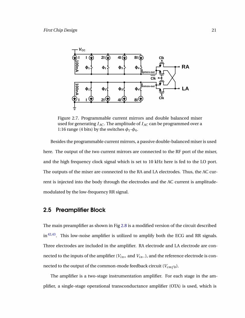
Figure 2.7. Programmable current mirrors and double balanced mixerused for generating I AC . The amplitude of I AC can be programmed over a1:16 range (4 bits) by the switches φ1-φ4.
Besides the programmable current mirrors, a passive double-balanced mixer is used
here. The output of the two current mirrors are connected to the RF port of the mixer,
and the high frequency clock signal which is set to 10 kHz here is fed to the LO port.
The outputs of the mixer are connected to the RA and LA electrodes. Thus, the AC cur-
rent is injected into the body through the electrodes and the AC current is amplitude-
modulated by the low-frequency RR signal.
2.5 Preamplifier Block
The main preamplifier as shown in Fig 2.8 is a modified version of the circuit described
in42,43. This low-noise amplifier is utilized to amplify both the ECG and RR signals.
Three electrodes are included in the amplifier. RA electrode and LA electrode are con-
nected to the inputs of the amplifier (Vi n+ and Vi n−), and the reference electrode is con-
nected to the output of the common-mode feedback circuit (Vcm f b).
The amplifier is a two-stage instrumentation amplifier. For each stage in the am-
plifier, a single-stage operational transconductance amplifier (OTA) is used, which is

First Chip Design 22
VDD
Vref
Vin+
Vin-
Vcmfb
Vref
Vout
A
A
A
A
A
A
A=
VCMsense
Figure 2.8. Schematic of the low-noise ECG amplifier.
biased in sub-threshold mode to reduce power consumption. The schematic of the OTA
is shown in Fig 2.9. In the OTA, the input differential signals are fed to PMOS devices
since the flicker noise in this process is significantly lower (about 5x) for PMOS devices.
Also, by increasing W/L, the transistors are driven into sub-threshold mode.
For the instrumentation amplifier, the mid-band gain of each stage is set to 10 by
choosing the ratio of capacitors in the feedback loop. Therefore, the total gain of the
amplifier is 100 (40 dB). Compared to some standard instrumentation amplifiers, ca-
pacitors instead of resistors are utilized in the feedback loop to set up the gain. That is
because resistors contribute noise and the matching property of resistors is poor. How-
ever, using capacitors can not provide the DC voltage levels for the OTA. To overcome
this problem, the MOS pseudo resistors described earlier are used so that DC current is
able to flow. These pseudo resistors act as very large resistors for small signals, shown
as the "A" block in Fig 2.8. To reduce the distortion of large signals, two pseudo resistors

First Chip Design 23
are placed in series. Thus, the DC gain is set to 1 by using these pseudo resistors, while
the AC gain is set by the capacitors in parallel with the pseudo resistors.
VCC
OUT
V+ V-
VB
Figure 2.9. Schematic of the OTA used four times in the preamplifier.
Besides, a common-mode feedback path is included in the amplifier to remove common-
mode signal, such as the powerline interference. The reference electrode, usually placed
on the leg, is connected to the output of the driven-ground circuit denoted as Vcm f b in
Fig. 2.8. The common-mode voltage is sensed in the first stage of the instrumentation
amplifier. And the OTA in the common-mode feedback amplifies the difference between
the sensed common-mode voltage and the reference voltage which is set to 0.75 V in this
design. Since the output impedance of the feedback is in series with the impedance of
the reference electrode, it is necessary to reduce the output impedance of the circuit so
that the electrode with an impedance of around 2 kΩ can be driven. Therefore, a super-
buffer circuit is utilized to lower the output impedance.

First Chip Design 24
For the standard source follower, the output impedance is Ro = 1gm+gmb
. However,
for this super-buffer circuit, the negative feedback through the additional PMOS re-
duces the impedance by a factor of about gm2ro1, resulting the output impedance of
Ro = 1gm+gmb
1gm2ro1
. Therefore, a typical electrode with an impedance of around 2 kΩ
can be driven effectively. Another thing that needs to be mentioned is that the open
circuit voltage gains of both standard buffer and super buffer do not have much differ-
ence. The gain of the standard source follower is vovi
= gm ro1+(gm+gmb )ro
, while the gain of the
super-buffer circuit is vovi
= gm1ro1
1+(gm1+gmb1)ro1+ 1gm2ro2
. Thus, if gm2ro2 À 1, both voltage gains
are approximately equal to 1, and the super source follower has little effect on the open
circuit voltage gain. The detail description of the super source follower is in44.
Fig. 2.10 shows the simulation result of the ECG path. The mid-band gain is around
40 dB as shown in Fig. 2.10(a). If a 2 mV 100 Hz sinusoid wave and a 10 kHz carrier signal
are applied, both of them get amplified as shown in Fig. 2.10(b). Fig. 2.10(c) shows the
output of the ECG path, and it is clear to see that the high-frequency carrier is reduced
by the LPFs. From Fig. 2.10(c), it can be estimated that the gain in ECG path is around
40 dB, which is in the agreement with the design value.
2.6 Wide-linear Range OTA and Filters
This AFE is designed to monitor ECG and RR simultaneously. Therefore, LPFs are needed
to remove high-frequency modulated RR signal in ECG path, and both HPFs and LPFs
are needed to remove ECG as well as high-frequency carrier in RR path. First-order
Gm −C LPF and HPF topologies, as shown in Fig. 2.11(a) and (b), are used several times

First Chip Design 25
Frequency (Hz)10-2 100 102 104 106
Gai
n (
dB
)-40
-20
0
20
40
Time (ms)0 2 4 6 8 10 12
Vo
ltag
e (V
)
0.2
0.4
0.6
0.8
ECG Amp output
Time (ms)0 2 4 6 8 10 12
Vo
ltag
e (V
)0.2
0.4
0.6
0.8
ECG output
Figure 2.10. Simulation results of (a) the AC response of the preamplifier.(b) the output of the preamplifier when an input of 2 mV 100 Hz sinusoidwave is used. (c) the output of the ECG path when an input of 2 mV 100 Hzsinusoid wave is used.
in the AFE. The cutoff frequency of the filter shown in Fig. 2.11 is
fcuto f f =1
2πRC= Gm
2πC(2.1)
Vin
CVoutGm
Vin
CVout
Gm
Vref
Figure 2.11. (a) First-order Gm −C LPF topology. (b) First-order Gm −CHPF topology.
First Chip Design 26
VCC
Out
V+ V-
VB
i+ i+
i-iB
iout
Vs
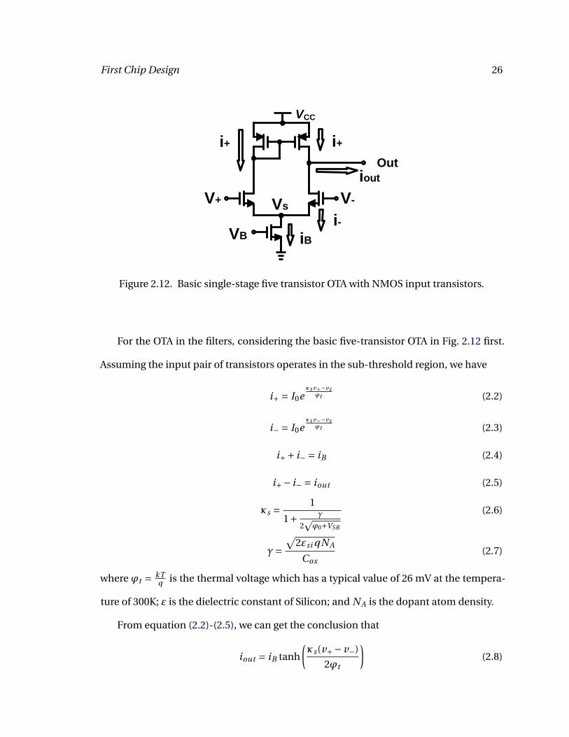
Figure 2.12. Basic single-stage five transistor OTA with NMOS input transistors.
For the OTA in the filters, considering the basic five-transistor OTA in Fig. 2.12 first.
Assuming the input pair of transistors operates in the sub-threshold region, we have
i+ = I0eκs v+−vs
ϕt (2.2)
i− = I0eκs v−−vs
ϕt (2.3)
i++ i− = iB (2.4)
i+− i− = iout (2.5)
κs = 1
1+ γ
2pϕ0+VSB
(2.6)
γ=√
2εsi qNA
Cox(2.7)
where ϕt = kTq is the thermal voltage which has a typical value of 26 mV at the tempera-
ture of 300K; ε is the dielectric constant of Silicon; and NA is the dopant atom density.
From equation (2.2)-(2.5), we can get the conclusion that
iout = iB tanh
(κs(v+− v−)
2ϕt
)(2.8)
First Chip Design 27
and we define the linear range as the slope of iout at the origin, i.e., when v+− v− = 0:
VL = 2ϕt
κs(2.9)
If ks=0.7 and ϕt =26 mV, then the linear range of the basic five-transistor OTA VL is
around 75 mV, which is not sufficient to filter the amplified ECG signal (typical ampli-
tude = 100-200 mV). To overcome this, the OTA used in the AFE is a modified version
of the wide-linear-range OTA (WLR OTA) presented in45, as shown in Fig. 2.13. In this
design, source degeneration and bump linearization techniques are used to increase the
linear range, similar to the circuit in45. However, the circuit here uses gate terminals as
inputs instead of well terminals so that the layout is simplified. In this case, the cost is
the reduced linear range, but it is still sufficient for this application.
VCC
M3
M7
M11
M9
Iout
V+V-
VB
VCC VCC
M1
M4
M2
M5 M6
M8
M10
M12
Figure 2.13. The wide-linear-range OTA used several times in the AFE.
The source degeneration method is a common technique to increase the linear range.
It was first used in vacuum-tube design46, and it was then used in bipolar design as
emitter degeneration47. By using source degeneration, the current flowing a transistor

First Chip Design 28
is converted to a voltage through a resistor, and that voltage is then fed back to the source
of the transistor. In this case, the current is decreased. The linear range increases by a
factor of approximately 2 by using source degeneration method.
The bump linearization is a technique to linearize a hyperbolic tangent function48.
In a bump differential pair, there is a central arm including two transistors in series. The
current flowing through these two bump transistors is a bump-shaped function of the
differential voltage. The current in the outer arm (I) is the usual hyperbolic tangent func-
tion of the differential voltages (V). However, the bump transistors steal current near the
origin of the I-V curve. If ω is the ratio of the W/L of the bump transistors and the W/L
of the transistors in the outer arm, we can get the following equation
iout = si nhx
β+ coshx(2.10)
where
β= 1+ ω
2(2.11)
x = κ(v+− v−)
ϕt(2.12)
The optimal value of β is 2, in the following sense. If we Taylor expand the equation
(2.10) at β=2, it can be found that no cubic distortion term exists.
si nhx
2+ coshx= x
3− x5
540+ x7
4536+· · · (2.13)
As a comparison, the cubic distortion exists when β=0.
t anhx
2= x
2− x3
24+ x5
240+· · · (2.14)
The bump linearization increases the linear range by a factor of around 1.5, and it
does not contribute noise. Therefore, by using both the source degeneration and bump
linearization techniques, the linear range is increased by a factor of 2×1.5 = 3, setting
First Chip Design 29
the VL to around 270 mV, which is enough to filter out the amplified ECG and RR signals.
In the ECG path, two first-order Gm −C LPFs with cutoff frequency of 1 kHz are used to
reduce the high-frequency modulated RR signal in ECG path. In RR path, four first-order
HPFs with cutoff frequency of 700 Hz are first used to reduce the ECG signal before the
demodulator.
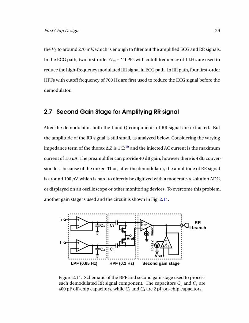
2.7 Second Gain Stage for Amplifying RR signal
After the demodulator, both the I and Q components of RR signal are extracted. But
the amplitude of the RR signal is still small, as analyzed below. Considering the varying
impedance term of the thorax ∆Z is 1 Ω19 and the injected AC current is the maximum
current of 1.6 µA. The preamplifier can provide 40 dB gain, however there is 4 dB conver-
sion loss because of the mixer. Thus, after the demodulator, the amplitude of RR signal
is around 100 µV, which is hard to directly be digitized with a moderate-resolution ADC,
or displayed on an oscilloscope or other monitoring devices. To overcome this problem,
another gain stage is used and the circuit is shown in Fig. 2.14.
I+
I-
Ibia
s1
Ibia
s2
RR
I-branchGm1
Gm
2
Vref
LPF (0.65 Hz) HPF (0.1 Hz) Second gain stage
C1
C2
C3
C4
Vref
Figure 2.14. Schematic of the BPF and second gain stage used to processeach demodulated RR signal component. The capacitors C1 and C2 are400 pF off-chip capacitors, while C3 and C4 are 2 pF on-chip capacitors.

First Chip Design 30
The signals coming from the output of the demodulator, including both the I+ (Q+)
and I− (Q−) components, are passed through pseudo-differential BPFs. The upper side-
band, the high-frequency carrier, DC offset, and low-frequency noise are removed. In
the BPF, two first order Gm −C LPFs, in which the WLR OTA described earlier is used,
are utilized in each path of I+ (Q+) and I− (Q−). The -3 dB frequency of the LPFs is set
to 0.65 Hz, which contains the fundamental frequency of RR signal (a typical bandwidth
of 0.5 Hz). Also, since the corner frequency of the LPF is relatively low, 400 pF off-chip
capacitors are used here while the bias current of OTAs is kept at a reasonable value
(1 nA). The HPF is a simple CR circuit, in which adaptive element is used to behave as
a big resistor. The -3 dB frequency of the HPF is set to 0.1 Hz. Also, by using this HPF,
the DC voltage of the input of the OTA can be set to the reference voltage. However,
the disadvantage of using a pseudo resistor in the filter is that its effective resistance
is process-dependent because of threshold voltage variations, which makes the cutoff
frequency also process-dependent.
The circuit following the BPF is the second gain stage for amplifying the RR signal.
The OTAs used here are still the WLR OTA described earlier. This stage also performs the
differential to single-ended conversion. The relationship between the output signal and
the input signal is described by the following equation.
Vout
(Vi n1 −Vi n2)= Gm1
Gm2= Ibi as1
Ibi as2(2.15)
From the equation (2.15), it is easy to set the gain of this stage by choosing the ratio
of two bias currents. Here a current ratio of 50 (34 dB) is set. By doing this, the total gain
for RR signal is around 40−4+34 = 70 dB. And the -4 dB term comes from the loss of the
mixer.

First Chip Design 31
Fig. 2.15 shows the simulation results of RR path. The AC response of the second
RR gain stage is presented in Fig. 2.15(a). If a 1 µV RR signal is applied at the input
of the preamplifier, the output signals of the demodulator in I branch are presented in
Fig. 2.15(b). The final outputs of RR path, including both the I and Q components, are
presented in Fig. 2.15(c). From Fig. 2.15(c), it can be estimated that the gain in RR path
is around 72 dB, which is in good agreement with the theoretical design value.
Freq (Hz)10-3 10-2 10-1 100 101 102
Vo
ltag
e (d
B)
-40
-30
-20
-10
0
10
LPF (0.65 Hz)HPF (0.1 Hz)
Time (ms)0 0.2 0.4 0.6 0.8 1
Vo
ltag
e (V
)
0.7
0.75
0.8
0.85 I+I-
Time (sec)0 0.5 1 1.5 2
Vo
ltag
e (m
V)
-3
-2
-1
0
1
2
3
I branch outputQ branch output
Figure 2.15. Simulation results of (a) the AC response of the BPF after de-modulator. (b) the I component of RR at the output of mixer if a 1 µV RRsignal is applied at the input of the preamplifier. (c) the final output of RRpath if a 1 µV RR signal is applied at the input of the preamplifier.

32
3 Measurement Result of First Chip
In this chapter, the measurement of the first chip is discussed. The chip was fab-
ricated in the OnSemi 0.5 µm CMOS process through the MOSIS Educational Program
(MEP). The die photograph of the AFE is shown in Fig. 3.1, which includes the active area
of 1050 µm × 600 µm.
Q-path RR Amp and LPF I-path RR Amp and LPF
CL
K d
ivid
er RR HPF
LPF
Amp
EC
G p
art
Current
mirrorAFE
Figure 3.1. Die photograph of the fabricated AFE, which has an activearea of 1050 µm × 600 µm. Major blocks are labeled.
To test the chip, a printed circuit board (PCB) was designed to set up the measure-
ment environment. All off-chip capacitors for the filters were soldered on the board. Sig-
nal generators were used to provide a sinusoid wave (simulating ECG) and a square wave
(simulating high-frequency RR carrier). These signals were fed into the chip through the
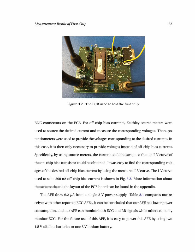
Measurement Result of First Chip 33
Figure 3.2. The PCB used to test the first chip.
BNC connectors on the PCB. For off-chip bias currents, Keithley source meters were
used to source the desired current and measure the corresponding voltages. Then, po-
tentiometers were used to provide the voltages corresponding to the desired currents. In
this case, it is then only necessary to provide voltages instead of off-chip bias currents.
Specifically, by using source meters, the current could be swept so that an I-V curve of
the on-chip bias transistor could be obtained. It was easy to find the corresponding volt-
ages of the desired off-chip bias current by using the measured I-V curve. The I-V curve
used to set a 200 nA off-chip bias current is shown in Fig. 3.3. More information about
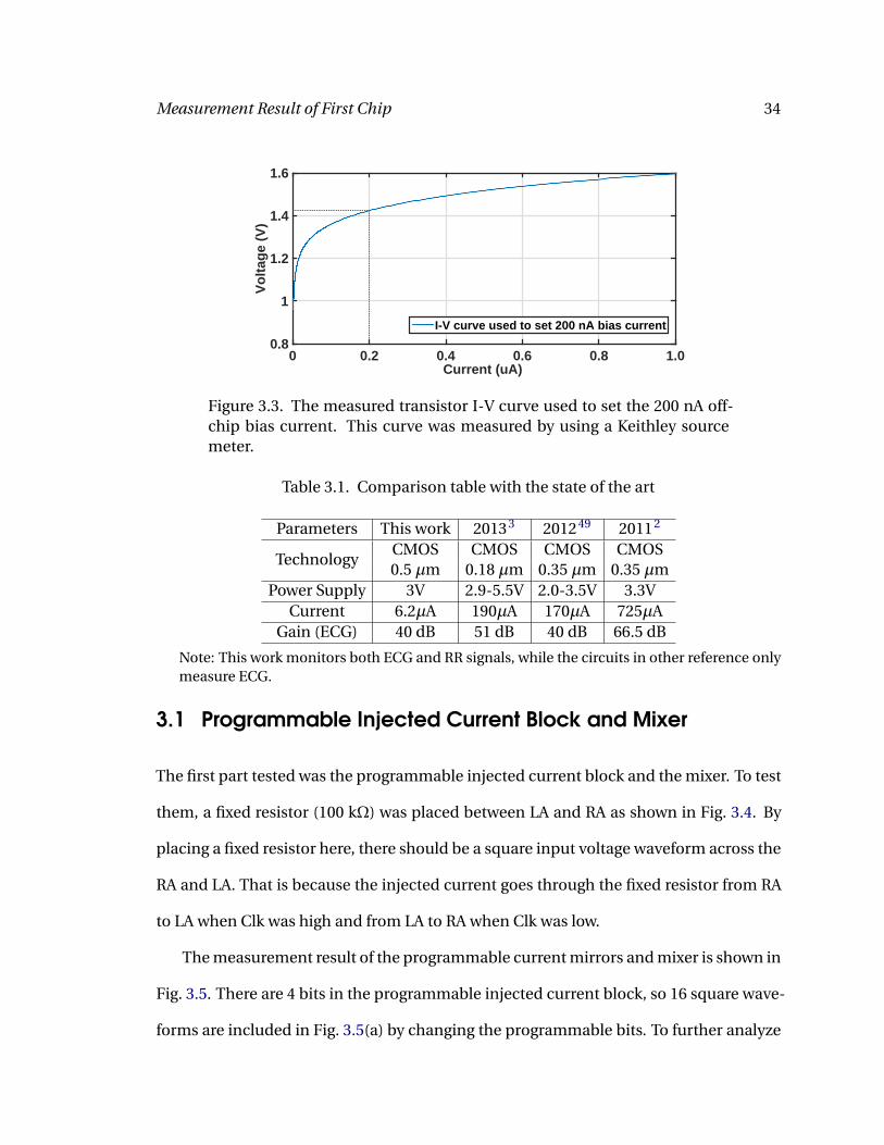
the schematic and the layout of the PCB board can be found in the appendix.
The AFE drew 6.2 µA from a single 3 V power supply. Table 3.1 compares our re-
ceiver with other reported ECG AFEs. It can be concluded that our AFE has lower power
consumption, and our AFE can monitor both ECG and RR signals while others can only
monitor ECG. For the future use of this AFE, it is easy to power this AFE by using two
1.5 V alkaline batteries or one 3 V lithium battery.
Measurement Result of First Chip 34
Current (uA)0 0.2 0.4 0.6 0.8 1.0
Vo
ltag
e (V
)
0.8
1
1.2
1.4
1.6
I-V curve used to set 200 nA bias current
Figure 3.3. The measured transistor I-V curve used to set the 200 nA off-chip bias current. This curve was measured by using a Keithley sourcemeter.
Table 3.1. Comparison table with the state of the art
Parameters This work 20133 201249 20112
TechnologyCMOS CMOS CMOS CMOS0.5 µm 0.18 µm 0.35 µm 0.35 µm
Power Supply 3V 2.9-5.5V 2.0-3.5V 3.3VCurrent 6.2µA 190µA 170µA 725µA
Gain (ECG) 40 dB 51 dB 40 dB 66.5 dB
Note: This work monitors both ECG and RR signals, while the circuits in other reference onlymeasure ECG.
3.1 Programmable Injected Current Block and Mixer
The first part tested was the programmable injected current block and the mixer. To test
them, a fixed resistor (100 kΩ) was placed between LA and RA as shown in Fig. 3.4. By
placing a fixed resistor here, there should be a square input voltage waveform across the
RA and LA. That is because the injected current goes through the fixed resistor from RA
to LA when Clk was high and from LA to RA when Clk was low.
The measurement result of the programmable current mirrors and mixer is shown in
Fig. 3.5. There are 4 bits in the programmable injected current block, so 16 square wave-
forms are included in Fig. 3.5(a) by changing the programmable bits. To further analyze

Measurement Result of First Chip 35
10
0n
A
Inmos-out
VCC
Ipmos-out
RA
LA
Clk
Clk
Clk
ɸ1 ɸ2 ɸ3 ɸ4
ɸ1 ɸ2 ɸ3 ɸ4
8I4I2III
8I4I2III10
0n
A
100k
Figure 3.4. Circuit used to test the programmable injected current blockand the mixer. A fixed resistor (100 kΩ) was placed between LA and RA.
the function of this block, the actual amount of injected current from the programmable
current mirrors were calculated. Fig. 3.5(b) shows the calculated positive and negative
currents from current mirrors as a function of the four-bits code. The actual currents
are larger than the theoretical values, and this is probably because the I-V curves used
to set the off-chip bias currents were not calibrated well. The injected current is depen-
dent on the off-chip bias current, therefore the actual injected current is different from
the design value when the off-chip bias current is not the theoretical value. In addition,
there is an offset |IP − IN | which has an average value of 65 nA, which is relatively small
(less than 1 LSB = 100 nA).
3.2 ECG Amplifier
The ECG amplifier is the most important part in the AFE. And the measurement result
is presented here.
The differential frequency response of the ECG signal path (consisting of ECG am-
plifier and LPF) is shown in Fig. 3.6(a). The measured upper cutoff frequency is around

Measurement Result of First Chip 36
Time (sec)0 0.02 0.04 0.06 0.08 0.1
Vo
ltag
e (V
)
-0.4
-0.2
0
0.2
0.4
Digital code1 2 3 4 5 6 7 8 9 10 11 12 13 14 15 16
Cu
rren
t (μ
A)
0
0.5
1
1.5
2
2.5
3PositiveNegativeOffset
Figure 3.5. (a) Square voltage waveforms across the RA and LA with dif-ferent injected currents when a 100 kΩ resistor was used between RA andLA. (b) Measured positive and negative currents as a function of the digi-tal code.
150 Hz, however, the theoretical value is 1 kHz. The reason for this is probably a differ-
ent off-chip bias current was used so that the cutoff frequency of the LPF changed. Also,
the mid-band gain is around 39.5 dB, which is in good agreement with the design value
of 40 dB. Fig. 3.6(b) is the common-mode frequency response of the ECG path without
utilizing driven-ground circuit. The average gain of common-mode signal in the band of
100 Hz is around 0.8 dB, resulting in the CMRR in ECG path of 39.5 dB - 0.8 dB = 38.7 dB
without driven-ground circuit.
Frequency (Hz)100 101 102 103 104
Gai
n (
dB
)
-20
-10
0
10
20
30
40
Frequency (Hz)100 101 102 103
Gai
n (
dB
)
-40
-30
-20
-10
0
10
Figure 3.6. (a) Differential frequency response of both the ECG amplifierand the following LPF. (b) Common-mode frequency response of both theECG amplifier and the following LPF without utilizing driven-ground cir-cuit.

Measurement Result of First Chip 37
The input and output noise measurement results of the both the ECG amplifier and
the following LPFs is shown in Fig. 3.7(a) and (b). From the result, it is easy to con-
clude that the 1/ f corner frequency is around 25 Hz. The thermal noise PSD is around
254 nV/Hz1/2, which is slightly larger than the simulation result of 162 nV/Hz1/2. The
minimum detectable signal is around 38 µV in the band of 1-150 Hz. Since the upper
cutoff frequency of the LPF is around 150 Hz, the thermal noise is flat in the range of
25 Hz to 150 Hz but not flat when frequency is higher than 150 Hz.
Freq (Hz)100 101 102 103
No
ise
(V2 /H
z)
10-12
10-10
10-8
10-6
10-4
Output noise
Freq (Hz)100 101 102 103
No
ise
(V/s
qrt
(Hz)
)
10-7
10-6
10-5
10-4
Input noise
Figure 3.7. (a) Output noise of the both the ECG amplifier and the follow-ing LPF. (b) Input noise of the both the ECG amplifier and the followingLPF.
Fig. 3.8 proves that the preamplifier can amplify both the ECG and high-frequency
carrier signals as expected. As described in the second chapter, the high-frequency clock
can be disabled when user only wants to monitor ECG signal. Fig. 3.8(a) shows the out-
put of the ECG path when clock was disabled. The input signal, a 2 mV, 10 Hz sinusoid
wave generated from a signal generator, which simulated ECG signal, was amplified by
around 40 dB as expected.
Fig. 3.8(b) shows the output of the ECG path when input signal was the sum of a
1.5 mV, 10 Hz sinusoid (simulating ECG) and a 1.4 mV, 100 Hz square wave (simulating

Measurement Result of First Chip 38
RR carrier). Since the upper cutoff frequency of the ECG LPF is around 150 Hz as de-
scribed earlier, a relatively low-frequency clock (100 Hz) was used here so that the ECG
LPF did not have effect on it. It is easy to see that both the ECG and the RR carrier signals
got amplified by around 40 dB in good agreement with simulations.
Time (s)0 0.2 0.4 0.6 0.8 1
Vo
ltag
e (V
)
-0.2
-0.1
0
0.1
0.2ECG output
Time (s)0 0.05 0.1 0.15 0.2
Vo
ltag
e (V
)
-0.2
0
0.2
output signal
Figure 3.8. (a) Output of the ECG path when high-frequency clock is dis-abled. The input signal is a 2 mV, 10 Hz sinusoid wave. (b) Output of theECG path to the sum of a 1.5 mV, 10 Hz sinusoid (simulating ECG) and a1.4 mV, 100 Hz square wave (simulating RR carrier).
Fig. 3.9 shows a real ECG signal detected from human body by using two standard
patch electrodes which were placed on the right and left upper arms. The data pre-
sented has been filtered with a fourth-order Butterworth LPF with cutoff frequency of
50 Hz. The frequency of R wave in the output ECG signal is around 1.3 Hz which is in
good agreement with the frequency of the heart rate. But the amplitude of the output
signal is smaller than what we expected. One possible reason is that the placement of
the electrodes may not be optimal for measuring ECG signal.
Although the measurement results above have proven that the preamplifier can am-
plify both ECG and RR carrier signals as expected, there is a major problem that we
found during the experiment. The DC voltage at the output of the ECG path shifted
as time went by as shown in Fig. 3.10. Theoretically, the DC voltage at the output of the
preamplifier should be equal to the reference voltage (0.75 V) which was provided from

Measurement Result of First Chip 39
0 1 2 3 4 50
5
Time (s)0 1 2 3 4 5
Vo
ltag
e (m
V)
0
3
6
9
12
15
ECG signal
Figure 3.9. Detected ECG signal after baseline removal and filtering witha fourth-order LPF ( fc = 50 Hz).
a external power supply. But every time the chip was turned on, the DC voltage at the
output of the ECG path started to increase from around 0.3 V and finally saturated at
around 2.4 V after approximately 900 seconds. To make the AFE work as expected, a
suitable range for this DC voltage was concluded during the experiment, in which 40 dB
gain could be obtained from this preamplifier. And this DC voltage range is from around
0.6 V to 1.5 V. In this case, the preamplifier could only work well for about 2 minutes.
The reason causing this problem is the leakage current in the adaptive element, which is
a well-known problem with pseudo resistors50. In this AFE, NMOS transistors are used
in the pseudo resistors. The body terminal of NMOS transistor has to be connected to
ground because of the process of this chip. In this case, if we assume the source is the
high-impedance node, connecting bulk to ground creates a non-zero reverse-bias volt-
age across the source to body junction diode, resulting in the leakage current in a pseudo
resistor. Because of this leakage current, the DC voltage starts to change slowly when the
leakage current flowing through the adaptive element. It is possible to avoid this prob-
lem by using PMOS transistors instead of NMOS transistors to work as pseudo resistors
because the body terminal of a PMOS transistor can be connected to the drain so that

Measurement Result of First Chip 40
all diodes are zero biased. Another way to avoid this problem is to use switched capaci-
tor resistors instead of pseudo resistors, but the cost is that the complexity of the circuit
increases.
Time (s)100 200 300 400 500 600 700 800 900 1000
Vo
ltag
e (V
)
0
0.5
1
1.5
2
2.5
Output of ECG path
Figure 3.10. The DC voltage at the output of the ECG path shifted from0.3 V to 2.4 V in around 900 seconds.
3.3 RR Measurement
To test the functionality of the RR path, a body model as shown in Fig. 3.11(a) was used
to generate both the ECG-like and RR-like signals at the same time. In the body model,
the source V1 is a sinusoid wave behaved as ECG signal. By choosing the values of resis-
tors and capacitors, the ECG-like signal can be fed to RA and LA. The source V2 is a 1 Hz
triangle wave which is able to turn the discrete FETs on or off, so that the impedance
between RA and LA is modulated by around 1%. Fig. 3.11(b) shows the transient sim-
ulation result of this body model. It is able to find the modulated RR-like signal when
a 100 nA 1 kHz AC current was used. Fig. 3.11(c) shows that the body model is able to
generate the modulated RR signal (999 Hz and 1001 Hz). This body model was soldered
on the PCB board.

Measurement Result of First Chip 41
LA
RA
33
μF
33
μF
1.8 k
1.8 k
1.8 k
1.8 k
0.56 k
0.56 k
5.6 k
5.6 k
VrefV1 V2
Time (s)0 1 2 3 4 5
Vo
ltag
e (V
)
×10-3
-1.5
-1
-0.5
0
0.5
1
1.5
2
Frequency (Hz)997 998 999 1000 1001 1002 1003
20lo
g(a
mp
litu
de/
1Vo
lt)
(dB
)
-160
-140
-120
-100
-80
Figure 3.11. (a) Body model used to generate ECG-like and RR-like sig-nals. (b) Simulation result of the modulated RR-like signal when 100 nA1 kHz AC currents are fed to LA and RA. (c) The FFT result of the transientsignal generated by the body model.
Fig. 3.12 shows the measured I and Q components of RR signal after filtering with a
fourth-order Butterworth LPF with cutoff frequency of 5 Hz. The 0.5 Hz ramp wave was
used to control the FETs on or off. The results prove the functionality of the RR path with
a total gain of around 72 dB.

Measurement Result of First Chip 42
Time (s)0 2 4 6 8 10 12
Vo
ltag
e (V
)
-0.04-0.03-0.02-0.01
00.010.020.030.04
I branch outputQ branch output
Time (s)0 2 4 6 8 10 12
Vo
ltag
e (V
)
0
2
4
6Input ramp wave
Figure 3.12. Input triangle wave used to modulate the impedance be-tween RA and LA at 0.5 Hz, and measured I and Q RR outputs after fil-tering with a fourth-order Butterworth LPf with cutoff frequency of 5 Hz.

43
4 Second Chip Design
From the measurement results of the first chip, several updates are needed. For the
second chip, a fully differential AFE is designed to improve CMRR and reduce distor-
tion. Also, more gain in RR path is needed since the amplitude of RR is small. Besides, it
is necessary to get rid of the DC voltage shifting problem caused by the leakage current
in the adaptive element. In addition, the driven-ground circuit needs to be updated be-
cause it did not work well during the experiment. Finally, four-terminal sensing method
is utilized to detect respiratory rate. AC current is injected into body through a pair of
electrodes while the signal is sensed by another pair of electrodes, resulting more accu-
rate measurement of body impedance. The simulation result proves the functionality of
the second AFE, which draws 14 µA from a 3 V power supply. The gain for ECG signal is
40 dB (46 dB if the preamplifier works in high gain mode) while the gain for RR signal is
82 dB (88 dB if the preamplifier works in high gain mode).
4.1 Fully Differential Wide-linear-range OTA
The second chip is a fully differential AFE. Therefore, a fully differential WLR OTA is
needed. Fig. 4.1(a) is the fully differential version of the wide-linear-range OTA. For this
fully differential OTA, a common-mode feedback (CMFB) must be used. In the feedback,

Second Chip Design 44
the common-mode voltage is sensed and then compared with a suitable reference volt-
age. Then the circuit feeds back the correcting signal so that the output common-mode
voltage is set to a desired value. Normally, two resistors are used to detect the common-
mode voltage, and an OTA is used to compare the sensed common-mode voltage with a
reference. However, in our chip, a differential-difference operational transconductance
amplifier (DDOTA)51, as shown in Fig. 4.1(b), is used to detect the common-mode volt-
age and compare it with a reference voltage. No passive component is used to detect
the common-mode voltage here, which ensures that the CMFB circuit has high input
impedance and does not load the main OTA (which would reduce its differential voltage
gain). The stage of the fully differential OTA with the common-mode feedback is shown
in Fig. 4.1(c). For the load capacitors C1 and C2, the CMFB half circuit only sees C1 as
the load capacitor while the differential half circuit sees C1+2C2 as the load capacitor52.
Thus, the values of C1 and C2 can be adjusted to independently set the bandwidths of
the differential and common-mode paths. We connect the output of the DDOTA (V f b)
to the bias voltage node (VB ) so the negative common-mode feedback is generated. The
fully differential OTA stage in the preamplifier is shown in Fig. 4.2(a), and the gain is set
by the ratio of capacitors in the feedback loop. To set up the input DC voltage, a modified
switched capacitor resistors topology is used, which will be described in detail later.
To check the stability of this single stage of fully differential OTA in the preamplifier
shown in Fig. 4.2(a), the Bode plot is plotted as shown in Fig. 4.2(b). From the Bode plot,
it is clear to see that the phase margin is around 80 and the gain margin is around 12 dB,
which proves the stability of the fully differential OTA.

Second Chip Design 45
VCC
M3
M7
M11
M9
out+
V+V-
Vbias
VCC VCC
M1
M4
M2
M5 M6
M8
M10
M12
out-
VB
Vpp
Vfb
Vpn Vnp Vnn
VCC VCC
Ib
Vref
C1
C1
C2
Figure 4.1. (a) Fully differential version of wide-linear-range OTA. (b)Differential-difference OTA used in CMFB. (c) Fully differential OTA stage.
4.2 Fully Differential Filters
In order to design fully differential filters, the fully differential OTA presented above is
used. In ECG path, the LPFs are needed to remove high-frequency modulated RR signal.
In RR path, HPFs are needed to remove ECG signal before the demodulator. After the
demodulator, LPFs with off-chip capacitors are needed to remove high-frequency RR
carrier signal.
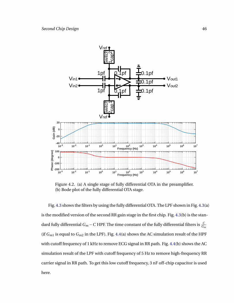
Second Chip Design 46
Vin1
Vin2
1pf
1pf
0.1pf
0.1pf
Sw
itch
cap
12
Sw
itch
cap
12
0.1pf
0.1pf
0.1pf
Vout1
Vout2
Vref
Vref
Frequency (Hz)10-3 10-2 10-1 100 101 102 103 104 105 106 107
Ph
ase
(deg
ree)
-200
-100
0
100Frequency (Hz)
10-3 10-2 10-1 100 101 102 103 104 105 106 107
Gai
n (
dB
)
-40
-20
0
20
Figure 4.2. (a) A single stage of fully differential OTA in the preamplifier.(b) Bode plot of the fully differential OTA stage.
Fig. 4.3 shows the filters by using the fully differential OTA. The LPF shown in Fig. 4.3(a)
is the modified version of the second RR gain stage in the first chip. Fig. 4.3(b) is the stan-
dard fully differential Gm −C HPF. The time constant of the fully differential filters is CGm
(if Gm1 is equal to Gm2 in the LPF). Fig. 4.4(a) shows the AC simulation result of the HPF
with cutoff frequency of 1 kHz to remove ECG signal in RR path. Fig. 4.4(b) shows the AC
simulation result of the LPF with cutoff frequency of 5 Hz to remove high-frequency RR
carrier signal in RR path. To get this low cutoff frequency, 3 nF off-chip capacitor is used
here.

Second Chip Design 47
Ibia
s1
Ibia
s2
Gm1
Gm
2
C
C
Ibia
s
C
C
Figure 4.3. (a) Fully differential LPF. (b) Fully differential HPF.
Frequency (Hz)10-2 100 102 104 106
Gai
n (
dB
)
-120
-100
-80
-60
-40
-20
0
Frequency (Hz)10-4 10-2 100 102 104 106 108
Gai
n (
dB
)
-150
-100
-50
0
Figure 4.4. The AC simulation results of (a) HPF with cutoff frequency of1 kHz to remove ECG signal in RR path. (b) LPF with cutoff frequency of5 Hz to remove high-frequency RR carrier signal in RR path. 3 nF off-chipcapacitor is used.
4.3 Fully Differential Preamplifier Block
By using the fully differential OTA described above, a fully differential preamplifier is de-
signed as shown in Fig. 4.5. There are two stages in the preamplifier. In each stage, the

Second Chip Design 48
OTA is AC coupled. The gain is set by the ratio of capacitors in the feedback loop. The
gain of the first stage is set to 10 while the gain of the second stage is programmable.
By turning the switches on and off, the gain can be set to 10 or 20 in the second stage.
In addition, the driven-ground circuit is updated. Two OTAs in unity feedback work as
buffers to sense the common-mode voltage. Then, the sensed common-mode voltage
will be compared to a reference voltage, and the difference of them is amplified by two
gain stages. The first gain stage in the driven-ground circuit includes two OTAs, with
the one in unity feedback acting as a buffered resistor. The gain is set by the ratio of
two bias currents. In order to ensure that Gm2 can work in linear range, Ibi as1 is a pro-
grammable bias current so that the gain of this stage can be controlled. In this design,
the programmable gain varies from 1 to 8. The second gain stage includes an op-amp
with resistors in the feedback loop. The gain is set by the ratio of two resistors, which is
10 (20 dB) in this case. Another reason that an op-amp is used here is that the output
impedance of it is relatively high to drive the electrode impedance of around 2 kΩ.
To set up the DC voltage in the preamplifier, MOS pseudo resistors are generally used
but the DC voltage shifting problem exists. Therefore, in order to create a large resistor
to generate a low-frequency pole, switched capacitor instead of pseudo resistor is used
here. Instead of the standard switched capacitor as described in the first chapter, a novel
structure of switched capacitor shown in Fig. 4.6, which is described in53, is utilized to
provide DC voltage for the amplifier. The idea to design this modified switched capaci-
tor topology is the same as the standard switched capacitor. It works by moving charges
into and out of capacitors when switches are on and off. The equivalent circuits in two
phases are presented in Fig. 4.7, and the effective capacitances are 0.5C and 2.5C, re-
spectively.

Second Chip Design 49
Vin1
Vin2
1pf
1pf
0.1pf
0.1pfS
witch
cap
12
Sw
itch
cap
12
1pf
1pf
0.1pf
0.1pf
Sw
itch
ca
p1
2S
witch
ca
p1
2
0.1pf
0.1pf
0.1pf
Vout1
Vout2
0.1pf
0.1pf
0.1pf
Vref Vref
Vref Vref
Ibia
s1
Ibia
s2
Gm1
Gm
2
Vref
Vref
15pf
Vcmfb
1pf
1pf
200k20k
Vref
Figure 4.5. Circuit of fully differential preamplifier.
When clk2 is high, the effective capacitance is 0.5C as shown in Fig. 4.7(a), and the
total charge q0 is
q0 = (V1 −V2)×0.5C (4.1)
When clk2 becomes low and clk1 becomes high, the effective capacitance is 2.5C as
shown in Fig. 4.7(b). Since the total charge in the switched capacitor keeps the same, the
voltage Vclk1 becomes
Vclk1 =(V1 −V2)×0.5C
2.5C(4.2)

Second Chip Design 50
Thus, some charge transfers from the two capacitors in parallel to the two capacitors
in series, and the amount of it is
q1 =Vclk1 ×0.5C (4.3)
From equation (4.2) and (4.3), it can be concluded that
q1 = (V1 −V2)×0.5C
2.5C×0.5C = (V1 −V2)×0.1C (4.4)
The term q1 here is the charge that is transferred during one cycle. From the con-
tinuous time perspective, we also know that the rate of transfer of charge per unit time
is
I = q × f (4.5)
where f is the transfer rate.
Taking equation (4.4) and (4.5) together, we can get
I = (V1 −V2)×0.1C × f (4.6)
Therefore, for this modified switched capacitor topology as shown in Fig. 4.6, the
equivalent resistance is
Req = (V1 −V2)
I= 10
f ×C(4.7)
This equivalent resistance is 10 times larger than the standard switched capacitor
topology when the same frequency and capacitor value are used. There are several rea-
sons that this modified topology is needed. Since the frequencies of ECG and RR are low,
a low cutoff frequency of around 0.1 Hz is needed, resulting in a big resistor of around
200 GΩ. By using switched capacitor, reducing the clock frequency or reducing the on-
chip capacitor value can generate a larger resistor, as shown in equation (4.7). However,
the minimum reliable on-chip capacitor value is around 50 fF. To get a cutoff frequency

Second Chip Design 51
of 0.1 Hz, the equivalent resistance should be around 200 GΩ if a big on-chip capacitor
of 10 pF is used. In this case, for the standard switched capacitor topology, if the ca-
pacitor in the switched capacitor is 50 fF, the clock frequency should be around 100 Hz,
which is in the band of ECG signal. Therefore, this modified switched capacitor topology
is needed. By using this new structure, we can set the capacitor value as 50 fF and the
clock frequency as 1000 Hz, which is not in the band of ECG signal anymore.
clk1clk2
C
C
C
C
clk2
clk2
clk2
clk2
clk1
clk1
clk1
V1 V2
Figure 4.6. Modified switched capacitor topology.
C CV1 V2
C C C
C
V1 V2Vclk1
Figure 4.7. Equivalent circuits of the modified switched capacitor topol-ogy in two phases. (a) Equivalent circuit when clk1 is on and clk2 is off.(b) Equivalent circuit when clk1 is off and clk2 is on.
Fig. 4.8 shows the simulation result at the output of the preamplifier (Vout1 −Vout2)
when a 2 mV 100 Hz sinusoid wave simulating ECG signal and a 10 kHz square wave sim-
ulating RR carrier signal are used at the input of the circuit. It can be seen that both the
ECG-like signal and the high-frequency carrier signal can be amplified by the preampli-
fier.

Second Chip Design 52
Time (ms)0 2 4 6 8 10 12
Vo
ltag
e (V
)
-0.6
-0.4
-0.2
0
0.2output of preamplifier
Figure 4.8. Transient simulation result at the output of the preamplifierwhen a 2 mV 100 Hz sinusoid wave simulating ECG signal and a 10 kHzsquare wave simulating RR carrier signal are used at the input of the cir-cuit.
4.4 Digital Block
Since the switched capacitor is used in the AFE, some digital circuits are needed to gen-
erate the clocks for switched capacitor. Fig. 4.9 shows the digital blocks in the AFE. The
input frequency is chosen as 38 kHz. To generate clocks for the mixer to extract I com-
ponent and Q component of RR signal, a D flip-flop and the same clock generator block
described in the second chapter are used in the AFE. In this case, clock generator block
has four outputs, and clk1 and clk2 have 90 phase shift. Since there is a D flip-flop in
this branch, the frequency of clk1 and clk2 is 38 kHz/4=9.5 kHz, which is the frequency
of RR carrier signal. Also, the enable function is still available in this block. If the user
only wants to monitor ECG, the high-frequency RR carrier can be disabled.
The other branch of the digital circuit is used to generate the clocks for switched
capacitor. A programmable frequency divider block and a nonoverlapping clock gen-
erator block are included. For the programmable frequency divider block as shown in
Fig. 4.11. Five D flip-flops are placed in series so that they behave like a counter. The
Q of each D flip-flop connects to the input of a XNOR gate, while the other input of the

Second Chip Design 53
Q
QSET
CLR
S
R
D
clk
Programmable
freq divider
clock
generator
nonoverlapping
clk_in
enableclk1
clk1_ba
clk2
clk2_ba
clk1_sc
clk2_sc
Figure 4.9. Digital blocks in the AFE.
XNOR gate is the programmable bit. The programmable bits are set to the desired fre-
quency divider ratio. The reason we need to use the programmable frequency divider
is that the switched capacitor resistor is a discrete-time system. The switched capaci-
tor resistor along with any load capacitance presented at its output acts as an RC LPF.
The frequency response is periodic, and the peaks exist at integer multiples of the clock
frequency fSC . The frequency of signals should be midway between these peaks so the
maximum attenuation can be obtained from the filter, as shown in Fig. 4.10. Therefore,
we need to set the frequency of RR carrier ( fRR ) signal to be an odd multiple of fSC /2,
i.e., fRR = (2n +1) fSC /2, where n = 0,1,2 · ··. In this case, it is easy for users to adjust the
frequency divider ratio by using the programmable frequency divider circuit.
The way this block works is that the counter counts one by one until it is reset when it
counts the value of programmable bits. For example, if the programmable bits are 11000,
which is 24 in decimal, the counter counts starting from 1. When the counter counts 24,
all the Q outputs of each D flip-flop are equal to the corresponding programmable bits,
resulting the following NAND gate generating a high output. This output triggers all the
D flip-flops to reset. The problem of this block is that the delays in each path are not the
same. Therefore, another D flip-flop clocked with the inverse of the input clock is used

Second Chip Design 54
Chapter 9 – Section 1 (5/2/04) Page 9.1-20
CMOS Analog Circuit Design © P.E. Allen - 2004
Example 9.1-5 - Continued
Frequency Response of the First-order, Switched Capacitor, Low Pass Circuit:
0
0.2
0.4
0.6
0.8
1
0 0.2 0.4 0.6 0.8 1
Mag
nitu
de
0.707
|H(jω)|
|Hoo(ejωT)|
ω = 1/τ1
ω/ωc
-100
-50
0
50
100
0 0.2 0.4 0.6 0.8 1
Phas
e Sh
ift (
Deg
rees
)
ω/ωc
Arg[Hoo(ejωT)]
Arg[H(jω)]
ω = 1/τ1
Fig. 9.1-12
Better results would be obtained if fc > 20kHz.
Chapter 9 – Section 1 (5/2/04) Page 9.1-21
CMOS Analog Circuit Design © P.E. Allen - 2004
SUMMARY• Resistance emulation is the replacement of continuous time resistors with switched
capacitor approximations
- Parallel switched capacitor resistor emulation
- Series switched capacitor resistor emulation
- Series-parallel switched capacitor resistor emulation
- Bilinear switched capacitor resistor emulation• Time constant accuracy of switched capacitor circuits is proportional to the
capacitance ratio and the clock frequency• Analysis of switched capacitor circuits includes the following steps:
1.) Analyze the circuit in the time-domain during a selected phase period.2.) The resulting equations are based on q = Cv.3.) Analyze the following phase period carrying over the initial conditions from the
previous analysis.4.) Identify the time-domain equation that relates the desired voltage variables.5.) Convert this equation to the z-domain.6.) Solve for the desired z-domain transfer function.
7.) Replace z by ejωT and examine the frequency response.
Figure 4.10. Frequency response of the first-order LPF by using switchedcapacitor.
following the output of the AND gate. This additional D flip-flop removes all the glitches
at the output of the AND gate, and the output of this additional D flip-flop is used to
reset the five D flip-flops in the counter. This reset signal does not have 50% duty cycle.
Thus, another D flip-flop is used to divide the frequency by two, generating a 50% duty
cycle clock.
There are five programmable bits so the maximum frequency divider ratio is 32. The
frequency of the output clock is described as
fout = fi n
r ati o ×2(4.8)
The clocks of switched capacitor should be two-phase non-overlapping clocks, so
the non-overlapping clocks generator circuit is needed. The circuit of this block is shown
in Fig. 4.11. Several inverters in series are used so that a delay is generated. By using the
NOR gates and these inverters with feedback, two output clocks are non-overlapping
and the delay between them comes from the delay generated by the inverters in series.
Since many digital inputs are needed for the digital circuit, in order to save some
pins of the chip, the programmable three-wire serial bus circuit is used, as shown in

Second Chip Design 55
Q
QSET
CLR
S
R
D
clkQ
QSET
CLR
S
R
D
clkQ
QSET
CLR
S
R
D
clkQ
QSET
CLR
S
R
D
clkQ
QSET
CLR
S
R
D
clk
ratio5
ratio4
ratio3
ratio2
ratio1
Q
QSET
CLR
S
R
D
clk
Q
QSET
CLR
S
R
D
clk
1x
AND
clk_in
clk_outreset
Figure 4.11. Programmable counter.
1x 1x 1x1x 1x 1x 1x 3x 9x
1x 1x 1x 1x 3x 9x
clk1_sc
clk2_sc
Figure 4.12. Two-phase non-overlapping clocks generator block.
Fig. 4.13(a). Microcontroller can be used off-chip and some code can be written to trans-
mit all the digital inputs by using Serial Peripheral Interface (SPI). The D flip-flops work
as shift registers, and the latches are used to save the bits. When the enable signal is high,
the latches retain their previous values to ensure that incorrect values are not passed
into the circuit while the shift register is being programmed. The enable signal goes low
after shift register programming is complete, thus the circuit loads the correct data val-
ues into the latches. The timing diagram for enable, clk, and data signals are shown in
Fig. 4.13(b).
To test the functionality of all the digital circuit in the AFE, the circuit shown in
Fig. 4.9 has been simulated. The following simulation results prove the functionality
of all the digital blocks, as shown in Fig. 4.14 and Fig. 4.15. The input clock is a 38 kHz

Second Chip Design 56
Q
QSET
CLR
S
R
D
clk
DATA
Q
en
Q
QSET
CLR
S
R
D
clk
DATA
Q
en
Q
QSET
CLR
S
R
D
clk
DATA
Q
en
Q
QSET
CLR
S
R
D
clk
DATA
Q
en
clk clk clk clk
DATA
enable enable enable enable
bit[1] bit[2] bit[n] bit[n+1]
enable
clk
data
Figure 4.13. (a) Programmable bus used to set digital inputs. (b) Timingdiagram of SPI.
square wave simulating the off-chip clock, as shown in Fig. 4.14(a). The Fig. 4.14(b) and
Fig. 4.14(c) are the outputs of two clocks with 90 phase shift, which are further used in
the mixer for modulation and demodulation. It is clear to see that the frequencies of the
two clocks in the Fig. 4.14(b) and Fig. 4.14(c) are same and one fourth of the frequency
of the input clock shown in Fig. 4.14(a).
The other branch of the digital circuit shown in Fig. 4.9 is used to generate non-
overlapping clocks for switched capacitor. The simulation results are in Fig. 4.15. Fig. 4.15(a)
and Fig. 4.15(b) show the outputs of two non-overlapping clocks. In this simulation, the
programmable frequency divider ratio is set to 19, therefore the frequency of the clocks
in Fig. 4.15(a) and Fig. 4.15(b) is 1 kHz, which is in agreement with the theoretical value.
If these two clocks are zoomed in, it is clear to see that they are non-overlapping, as
shown in Fig. 4.15(c). In the non-overlapping clock generator block as shown in Fig. 4.12,
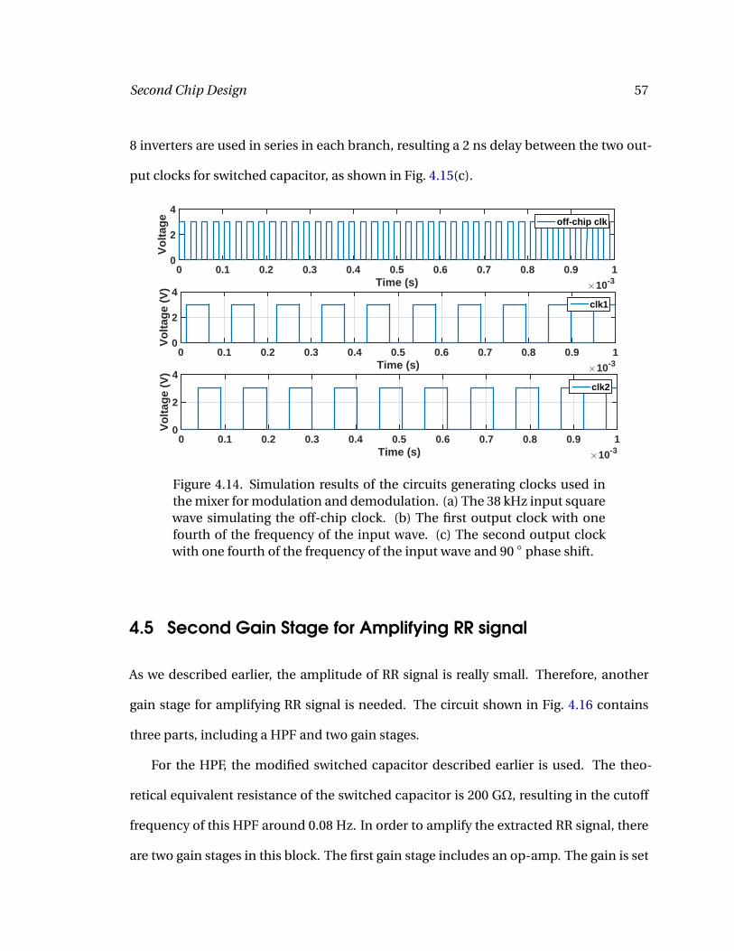
Second Chip Design 57
8 inverters are used in series in each branch, resulting a 2 ns delay between the two out-
put clocks for switched capacitor, as shown in Fig. 4.15(c).
Time (s) ×10-30 0.1 0.2 0.3 0.4 0.5 0.6 0.7 0.8 0.9 1
Vo
ltag
e
0
2
4off-chip clk
Time (s) ×10-30 0.1 0.2 0.3 0.4 0.5 0.6 0.7 0.8 0.9 1
Vo
ltag
e (V
)
0
2
4clk1
Time (s) ×10-30 0.1 0.2 0.3 0.4 0.5 0.6 0.7 0.8 0.9 1
Vo
ltag
e (V
)
0
2
4clk2
Figure 4.14. Simulation results of the circuits generating clocks used inthe mixer for modulation and demodulation. (a) The 38 kHz input squarewave simulating the off-chip clock. (b) The first output clock with onefourth of the frequency of the input wave. (c) The second output clockwith one fourth of the frequency of the input wave and 90 phase shift.
4.5 Second Gain Stage for Amplifying RR signal
As we described earlier, the amplitude of RR signal is really small. Therefore, another
gain stage for amplifying RR signal is needed. The circuit shown in Fig. 4.16 contains
three parts, including a HPF and two gain stages.
For the HPF, the modified switched capacitor described earlier is used. The theo-
retical equivalent resistance of the switched capacitor is 200 GΩ, resulting in the cutoff
frequency of this HPF around 0.08 Hz. In order to amplify the extracted RR signal, there
are two gain stages in this block. The first gain stage includes an op-amp. The gain is set

Second Chip Design 58
Time (s) ×10-30 0.2 0.4 0.6 0.8 1 1.2 1.4 1.6 1.8 2
Vo
ltag
e (V
)
0
2
4
SC clk1
Time (s) ×10-30 0.2 0.4 0.6 0.8 1 1.2 1.4 1.6 1.8 2
Vo
ltag
e (V
)
0
2
4SC clk2
Time (us)494.01 494.011 494.012 494.013 494.014 494.015 494.016 494.017 494.018 494.019 494.02
Vo
ltag
e (V
)
0
2
4
SC clk1SC clk2
Figure 4.15. Simulation results of the circuits generating clocks used inthe switched capacitor. (a) The first output clock. (b) The second outputclock. (c) 2 ns delay between the two non-overlapping output clocks.
Ibia
s1
Ibia
s2
Gm1
Gm
2
Sw
itch
cap
12
Sw
itch
cap
12
Sw
itch
ca
p1
2S
witch
cap
12
10pF
10pF
2pF
2pF
0.1pF
0.1pFVref
Vref
Vref
Iout+
Iout-
Iin+
Iin-
HPF (0.08 Hz) Gain stage 1 Gain stage 2
Figure 4.16. Second gain stage for amplifying RR signal.
by the ratio of the capacitors in the feedback loop, which is set to 20 in the design. To
set up the input DC voltages, the same switched capacitors are used. The second gain
stage is the fully differential version of the second RR gain stage used in the first AFE,
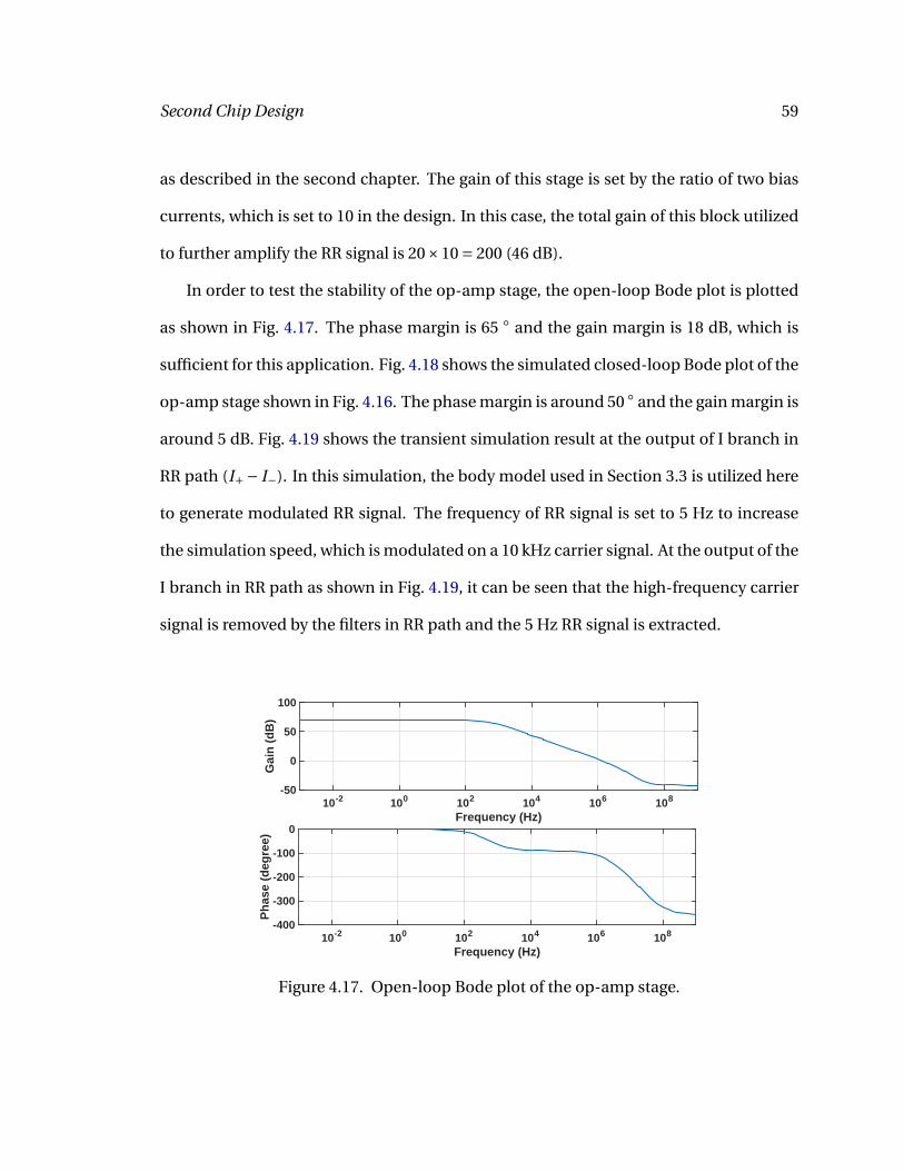
Second Chip Design 59
as described in the second chapter. The gain of this stage is set by the ratio of two bias
currents, which is set to 10 in the design. In this case, the total gain of this block utilized
to further amplify the RR signal is 20×10 = 200 (46 dB).
In order to test the stability of the op-amp stage, the open-loop Bode plot is plotted
as shown in Fig. 4.17. The phase margin is 65 and the gain margin is 18 dB, which is
sufficient for this application. Fig. 4.18 shows the simulated closed-loop Bode plot of the
op-amp stage shown in Fig. 4.16. The phase margin is around 50 and the gain margin is
around 5 dB. Fig. 4.19 shows the transient simulation result at the output of I branch in
RR path (I+− I−). In this simulation, the body model used in Section 3.3 is utilized here
to generate modulated RR signal. The frequency of RR signal is set to 5 Hz to increase
the simulation speed, which is modulated on a 10 kHz carrier signal. At the output of the
I branch in RR path as shown in Fig. 4.19, it can be seen that the high-frequency carrier
signal is removed by the filters in RR path and the 5 Hz RR signal is extracted.
Frequency (Hz)10-2 100 102 104 106 108
Gai
n (
dB
)
-50
0
50
100
Frequency (Hz)10-2 100 102 104 106 108
Ph
ase
(deg
ree)
-400
-300
-200
-100
0
Figure 4.17. Open-loop Bode plot of the op-amp stage.

Second Chip Design 60
Frequency (Hz)10-2 100 102 104 106 108
Gai
n (
dB
)-10
0
10
20
30
Frequency (Hz)10-2 100 102 104 106 108
Ph
ase
(deg
ree)
-200
-100
0
100
Figure 4.18. Closed-loop Bode plot of the op-amp stage.
Time (s)0 0.1 0.2 0.3 0.4 0.5 0.6 0.7 0.8 0.9 1
Vo
ltag
e (V
)
-0.1
0
0.1
0.2
0.3
0.4
0.5I component of RR signal
Figure 4.19. Transient simulation result at the output of I branch in RRpath (I+− I−). The frequency of RR signal is chosen as 5 Hz to increasethe simulation speed.
4.6 Layout
Good layout leads to good performance. In the design, several methods are utilized to
make layout better.
For critical components like differential pairs and current mirrors, they should be
laid out carefully. The first technique is common-centroid layout. A common-centroid
array should cancel systematic mismatches due to gradients. Also, making devices larger
is another way to improve matching, while the trade-off is the increased layout area.

Second Chip Design 61
It is also useful to use small transistors to create many fingers so that transistors with
large W/L can be achieved. Metal instead of poly should be used to interconnect gates if
possible. In addition, guard rings are often utilized to reduce substrate coupling noise.
NMOS rings should be tied to ground while PMOS rings should be connected to the
power supply. It is also very important to use as many contacts as possible to increase
the conductance between two layers.
For passive components, poly-poly capacitors with the typical capacitance density
of around 900 aF/µm2 and high resistance (Hi-Res) resistors with typical resistivity of
around 1192 Ω/ä are widely used in this AFE. To have better layout, both of them have
common-centroid layouts to improve matching. Guard rings are also used to protect
capacitors and resistors.
Fig. 4.20 shows the final layout of the whole AFE. The active area is around 1050 µm
× 1050 µm, and the total area is around 1500 µm × 1500 µm.
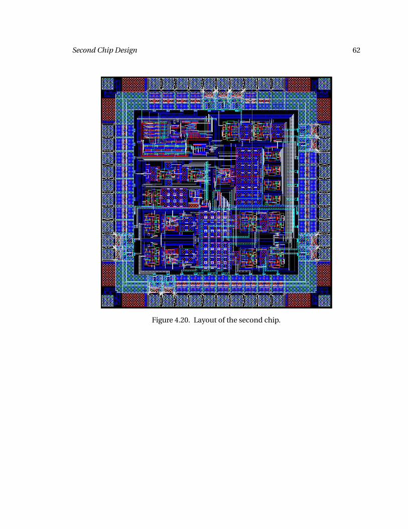
Second Chip Design 62
Figure 4.20. Layout of the second chip.

63
5 Conclusions
This thesis has demonstrated two AFEs for simultaneous measurement of ECG and
RR signals. The first chip has been fabricated on the OnSemi 0.5 µm CMOS process and
it has been tested. Both simulation and measurement results prove the functionality of
it. One conference paper emerged based on the results of the first chip54. The second
AFE has been designed to correct the defects in the first chip, and it will be submitted
for fabrication on the same process. In this chapter, we will summarize the results of the
main blocks in the AFEs and discuss the future work.
ECG Amplifier: Two different preamplifiers have been designed in each AFE. In the
first chip, the preamplifier used is a modified version of the amplifier presented in42,43.
Since the frequencies of bioelectrical signals are low (typical ECG bandwidth of 1 Hz to
100 Hz and RR bandwidth of 0.5 Hz)24, the MOS pseudo resistors are used to generate
a low cutoff frequency. The driven-ground circuit is also utilized to boost the CMRR.
Measured results show that the 1/ f corner frequency is around 25 Hz and the thermal
noise PSD is around 254 nV/Hz1/2, which are in good agreement with simulations. The
minimum detectable signal is around 38 µV in the band of 1-150 Hz. The mid-band gain
is 40 dB as expected.

Conclusions 64
However, certain design defects were found during the measurement. The DC volt-
age at the output of the amplifier shifted. This is because the leakage current exists in
the pseudo resistor. To overcome this problem, another preamplifier is designed in the
second AFE. For the second amplifier, switched capacitor is used to replace the MOS
pseudo resistor so that the leakage current in the pseudo resistor does not have effect on
the circuit. Another advantage of using switched capacitor resistors is that the effective
resistance can be easily controlled by changing the clock frequency fed to switched ca-
pacitor. In this case, the high-pass cutoff frequency can be controlled during operation.
It is possible to control the effective resistance of pseudo resistor by changing the gate
bias voltage23,55, but this method is much less straightforward. Also in this preampli-
fier, the second gain stage has programmable gain. Besides, the driven-ground circuit is
updated since we found the original driven-ground circuit did not work well. Source fol-
lowers and on-chip resistors are used to detect the common-mode voltage. Two OTAs,
with the one in unity feedback acting as a buffered resistor, are used to compare the
sensed common-mode voltage with a reference voltage and amplify the difference be-
tween them. An op-amp in unity feedback is then used to act as a buffer so that the
driven-ground circuit is able to drive the electrode impedance.
Second Gain Stage for RR:
In the first AFE, the circuit uses two WLR OTAs, with the one in unity feedback be-
having as a resistor. The gain is set by the ratio of two bias currents, which is set to 50
(34 dB) in the chip. However, it is not good to set the ratio of bias currents too high since
the OTA in unity feedback may be saturated. The second chip is a fully differential AFE,
and a fully differential version of the original RR gain stage is used. The gain is set to
10 (20 dB) which is more reasonable. To provide more gain in RR path, the circuit also

Conclusions 65
uses an op-amp to amplify the RR signal. The gain of the op-amp stage is set by the ratio
of capacitors in the feedback loop, which is set to 20 (26 dB) in the AFE, resulting the
total RR gain of 40 dB+20 dB+26 dB-4 dB=82 dB. Here the -4 dB term comes from the
conversion loss of the mixer.
Future Work: The ultimate goal of this thesis is to use the AFE designed in a wearable
biopotential measurement system, which can continuously monitor high-quality ECG
and respiratory condition. The chest band with three electrodes collects the signals. The
AFE designed can amplify the sensed signals and an ADC is also needed to digitize the
amplified outputs. Digitized signals shall be buffered locally and transmitted to a wrist
band or a personal computer through low-power Bluetooth.
The biopotential measurement system can be further used in several applications.
One application is to use the system to discriminate between the non-epileptic seizures
and epileptic seizures56. This technique has been demonstrated on a limited number
of patients at University Hospitals (UH) Case Medical Center (CMC) to identify psy-
chogenic non-epileptic seizures (PNES).

Appendix 66
Appendix A
PCB for testing the AFE
This appendix presents the schematic and layout of the PCB board used to test the
first AFE.
1
1
2
2
3
3
4
4
D D
C C
B B
A A
Title
Number RevisionSize
A4
Date: 2016/6/7 Sheet ofFile: C:\Users\..\chiptest1.SchDoc Drawn By:
B1
51K101-400A4
C9CAP 1uF 6.3V 0805(2012)
C10CAP 100nF 6.3V 0805(2012)
GND
C11CAP 1uF 6.3V 0805(2012)
C12CAP 100nF 6.3V 0805(2012)
GND
C1
CAP 1nF 6.3V 0805(2012)
C2
CAP 1nF 6.3V 0805(2012)
C3
CAP 1nF 6.3V 0805(2012)
C4
CAP 1nF 6.3V 0805(2012)
C5
CAP 1nF 6.3V 0805(2012)
C6
CAP 1nF 6.3V 0805(2012)
C7
CAP 1nF 6.3V 0805(2012)
C8
CAP 1nF 6.3V 0805(2012)
GND
GND
GND
C16CAP 100nF 6.3V 0805(2012)
GND
VDD APVDD
APVDD
VDDVDD
5
4
3
2
1
13
12
11
10 17
16
9
614
715
8
D-Sub
212612043
SCLK1
CS2
GND 3
AIN0 4
AIN1 5
AIN2 6
AIN3 7
VDD8
DOUT/DRDY9 DIN10
U1
ADS1118IDGSTGND
APVDD
Iout
IoutQout
Qout
ECGout
ECGout
SC1SC2SC3SC4
GND GND
C18CAP 100nF 6.3V 0805(2012)
GND
APVDD
0.75V
0.75V
B3
51K101-400A4
GND
clk
clk
PADFOL
PADFOL
C20CAP 100nF 6.3V 0805(2012)
GND
APVDD
C13
CAP 100nF 6.3V 0805(2012)C14
CAP 100nF 6.3V 0805(2012)
C24
CAP 100nF 6.3V 0805(2012)
C15
CAP 100nF 6.3V 0805(2012)
GND
GND GND
GND
C17CAP 100nF 6.3V 0805(2012)
C19CAP 100nF 6.3V 0805(2012)
C21CAP 100nF 6.3V 0805(2012)
GND GND GND
LL
RALA
123
P5
Header 3
J1
Socket
C22CAP 100nF 6.3V 0805(2012)
GND
APVDD
C23CAP 100nF 6.3V 0805(2012)
GND
123
P6
Header 3
J2
Socket200nA
200nA
5nA
5nA
123
P1
Header 3GND
APVDDSC1
123
P2
Header 3GND
APVDDSC2
123
P3
Header 3GND
APVDDSC3
123
P4
Header 3GND
APVDDSC4
123
P7
Header 3
123
P8
Header 3
123
P9
Header 3
LL
LA
RA12
P11
Header 2
12
P12
Header 2
123
P10
Header 3GND
APVDDCLK_en
CLK_en
J6
SocketJ7
Socket
J8Socket
GND
J9Socket
GND
SC11
SC22
SC33
SC44
55
66
77
88
99
1010
1111
1212
1313
1414
APGND15
APVDD16
PADFOL17
VDDD18
GNDD19
CLK_en20 0.75v 21clk 22VDDA 23Qout 24Gnda 25cap1 26cap2 27cap3 28cap4 29cap5 30cap6 31cap7 32cap8 335nA 34Iout 35ECGout 36RA 37LA 38LL 39200nA 40CH1
chip1
1234
P13
Header 4
B2
51K101-400A4
VDDin APVDDin
J11Socket
J10Socket
1
32
Pot3pot11
32
Pot2pot11
32
Pot1pot1 1
32
Pot4pot1
GNDAPVDD
21R2
21
R5
21
R7
21
R8
21
R621
R421
R3
21R1
D1
G 2
S3
Tran1
2n7000
D1 G 2S3Tran2
2n7000
12
c31cap33u
12
c32cap33u
J21
Socket
J22
SocketJ20Socket
LLB
LLB
RAB
RAB
LAB
LAB
PIB101
PIB10MH
COB1PIB201
PIB20MH
COB2PIB301
PIB30MH
COB3
PIC101 PIC102
COC1 PIC201 PIC202
COC2 PIC301 PIC302
COC3 PIC401 PIC402
COC4PIC501 PIC502
COC5PIC601 PIC602
COC6 PIC701 PIC702
COC7 PIC801 PIC802
COC8
PIC901
PIC902COC9
PIC1001
PIC1002COC10
PIC1101
PIC1102COC11
PIC1201
PIC1202COC12
PIC1301PIC1302
COC13
PIC1401PIC1402
COC14
PIC1501PIC1502
COC15
PIC1601
PIC1602COC16
PIC1701
PIC1702COC17 PIC1801
PIC1802COC18
PIC1901
PIC1902COC19 PIC2001
PIC2002COC20
PIC2101
PIC2102COC21 PIC2201
PIC2202COC22
PIC2301
PIC2302COC23
PIC2401PIC2402
COC24
PIc3101
PIc3102COc31
PIc3201
PIc3202COc32
PICH101
PICH102
PICH103
PICH104
PICH105
PICH106
PICH107
PICH108
PICH109
PICH1010
PICH1011
PICH1012
PICH1013
PICH1014
PICH1015
PICH1016
PICH1017
PICH1018
PICH1019
PICH1020 PICH1021
PICH1022
PICH1023
PICH1024
PICH1025
PICH1026
PICH1027
PICH1028
PICH1029
PICH1030
PICH1031
PICH1032
PICH1033
PICH1034
PICH1035
PICH1036
PICH1037
PICH1038
PICH1039
PICH1040
COCH1
PID0Sub01
PID0Sub02
PID0Sub03
PID0Sub04
PID0Sub05
PID0Sub06
PID0Sub07
PID0Sub08
PID0Sub09
PID0Sub010
PID0Sub011
PID0Sub012
PID0Sub013
PID0Sub014
PID0Sub015
PID0Sub016
PID0Sub017
COD0Sub
PIJ101
COJ1
PIJ201
COJ2
PIJ601COJ6
PIJ701
COJ7
PIJ801COJ8
PIJ901COJ9
PIJ1001COJ10
PIJ1101COJ11
PIJ2001COJ20
PIJ2101
COJ21
PIJ2201
COJ22
PIP101
PIP102
PIP103
COP1
PIP201
PIP202
PIP203
COP2
PIP301
PIP302
PIP303
COP3
PIP401
PIP402
PIP403
COP4
PIP501
PIP502
PIP503
COP5
PIP601
PIP602
PIP603
COP6
PIP701
PIP702
PIP703
COP7
PIP801
PIP802
PIP803
COP8
PIP901
PIP902
PIP903
COP9
PIP1001
PIP1002
PIP1003
COP10
PIP1101
PIP1102
COP11PIP1201
PIP1202
COP12
PIP1301
PIP1302
PIP1303
PIP1304
COP13
PIPot101
PIPot102
PIPot103 COPot1
PIPot201
PIPot202
PIPot203 COPot2
PIPot301
PIPot302
PIPot303 COPot3
PIPot401
PIPot402
PIPot403 COPot4
PIR101 PIR102
COR1PIR201 PIR202
COR2
PIR301 PIR302
COR3PIR401 PIR402
COR4
PIR501
PIR502COR5
PIR601
PIR602COR6
PIR701
PIR702COR7
PIR801
PIR802COR8
PITran101
PITran102
PITran103
COTran1
PITran201
PITran202
PITran203
COTran2
PIU101
PIU102
PIU103
PIU104
PIU105
PIU106
PIU107
PIU108
PIU109
PIU1010
COU1
PIC1702
PICH1021
PIPot101
NL0075V
PICH1034
PIP602NL5nA
PICH1040
PIP502
NL200nA
PIC1102 PIC1202
PIC1301
PIC1602 PIC1802 PIC2002 PIC2202
PIC2401
PICH1016
PIP103 PIP203
PIP303 PIP403
PIP1003
PIP1202
PIPot103 PIPot203 PIPot303 PIPot403
PIU108NLAPVDD
PIB201 PIP1201NLAPVDDin
PIB301
PICH1022NLclk
PICH1020
PIP1002
NLCLK0en
PICH1036PIJ601
PIU106NLECGout
PIB10MH PIB20MH PIB30MH
PIC102
PIC202
PIC302
PIC402
PIC502
PIC602
PIC702
PIC802
PIC901 PIC1001 PIC1101 PIC1201
PIC1302
PIC1402 PIC1501
PIC1601PIC1701
PIC1801PIC1901
PIC2001PIC2101
PIC2201PIC2301
PIC2402
PICH1015
PICH1019
PICH1025
PIJ901 PIJ1001 PIJ1101
PIP101 PIP201
PIP301 PIP401
PIP1001
PIPot102 PIPot202 PIPot302 PIPot402
PIU103
PIU107
PICH1035 PIJ701
PIU105NLIout
PICH1038
PIP802NLLA
PIP801
PIR402NLLAB
PICH1039
PIP902NLLL
PIP901
PIR701
PIR802
PITran103
PITran203
NLLLB
PIC101PICH1026
PIC201PICH1027
PIC301PICH1028
PIC401PICH1029
PIC501PICH1030
PIC601PICH1031
PIC701PICH1032
PIC801PICH1033
PIC2102
PIP503
PIPot301 PIC2302
PIP603
PIPot401
PIc3101PIJ2101
PIc3102
PIR101
PIc3201
PIR301
PIc3202PIJ2201
PICH105
PICH106
PICH107
PICH108
PICH109
PICH1010
PICH1011
PICH1012
PICH1013
PICH1014
PID0Sub01
PID0Sub02
PID0Sub03
PID0Sub04
PID0Sub05
PID0Sub06
PID0Sub07
PID0Sub08
PID0Sub09PIP703
PID0Sub010
PIP803
PID0Sub011
PIP903
PID0Sub012
PID0Sub013
PID0Sub014
PID0Sub015
PID0Sub016
PID0Sub017
PIJ101 PIP501 PIJ201 PIP601
PIJ2001
PITran102
PITran202
PIP1301 PIU102
PIP1302 PIU109
PIP1303 PIU1010
PIP1304 PIU101
PIR102 PIR201PIR502
PIR302 PIR401PIR601
PIR501
PIR702 PITran101
PIR602
PIR801 PITran201
PIC1902
PICH1017
PIPot201
NLPADFOLPICH1024
PIJ801
PIU104NLQout
PICH1037
PIP702NLRA
PIP701
PIR202NLRAB
PICH101PIP102NLSC1
PICH102
PIP202NLSC2
PICH103
PIP302
NLSC3
PICH104
PIP402
NLSC4
PIC902 PIC1002
PIC1401 PIC1502PICH1018 PICH1023
PIP1102
NLVDD
PIB101 PIP1101NLVDDin
Figure A.1. Schematic of the PCB board.

Appendix 67
PAB10MH
PAB101
COB1
PAB20MH
PAB201
COB2PAB30MH
PAB301
COB3
PAC102PAC101 COC1
PAC202PAC201 COC2PAC302PAC301
COC3
PAC402PAC401 COC4
PAC502PAC501 COC5
PAC602PAC601 COC6
PAC702PAC701 COC7
PAC802PAC801 COC8
PAC902PAC901
COC9PAC1002PAC1001
COC10
PAC1102PAC1101
COC11
PAC1202PAC1201COC12
PAC1302PAC1301
COC13
PAC1402PAC1401
COC14
PAC1502 PAC1501
COC15
PAC1602PAC1601COC16
PAC1702PAC1701COC17
PAC1802PAC1801
COC18
PAC1902PAC1901
COC19
PAC2002PAC2001
COC20
PAC2102
PAC2101COC21
PAC2202PAC2201 COC22
PAC2302PAC2301
COC23
PAC2402PAC2401
COC24
PAc3101
PAc3102
COc31PAc3201
PAc3202COc32
PACH1021
PACH1022
PACH1023PACH1024
PACH1025PACH1026
PACH1027
PACH1028
PACH1029
PACH1030
PACH1031
PACH1032
PACH1033
PACH1034
PACH1035
PACH1036
PACH1037
PACH1038
PACH1039
PACH1040
PACH1020
PACH1019PACH1018PACH1017
PACH1016PACH1015PACH1014
PACH1013
PACH1012
PACH1011
PACH1010
PACH109
PACH108
PACH107
PACH106
PACH105
PACH104
PACH103
PACH102
PACH101
COCH1
PAD0Sub09
PAD0Sub014
PAD0Sub015
PAD0Sub01
PAD0Sub08
PAD0Sub07
PAD0Sub02
PAD0Sub03PAD0Sub04
PAD0Sub05
PAD0Sub06PAD0Sub013PAD0Sub012
PAD0Sub011
PAD0Sub010
PAD0Sub016
PAD0Sub017
COD0Sub
PAJ101COJ1
PAJ201COJ2
PAJ601
COJ6
PAJ701
COJ7
PAJ801
COJ8
PAJ901 COJ9
PAJ1001
COJ10
PAJ1101 COJ11
PAJ2001 COJ20
PAJ2101
COJ21
PAJ2201COJ22
PAP103PAP102PAP101COP1
PAP203PAP202PAP201COP2
PAP303PAP302PAP301COP3
PAP403PAP402PAP401COP4
PAP503PAP502PAP501COP5
PAP603 PAP602 PAP601COP6
PAP703PAP702PAP701
COP7PAP803PAP802PAP801
COP8
PAP903PAP902PAP901
COP9
PAP1003PAP1002
PAP1001
COP10
PAP1102PAP1101
COP11
PAP1202PAP1201
COP12PAP1301
PAP1302PAP1303
PAP1304
COP13
PAPot103PAPot101PAPot102COPot1
PAPot203PAPot201PAPot202
COPot2
PAPot303PAPot301
PAPot302
COPot3
PAPot403PAPot401PAPot402
COPot4
PAR101
PAR102
COR1
PAR201
PAR202 COR2
PAR301
PAR302
COR3
PAR401
PAR402COR4 PAR501 PAR502 COR5PAR601 PAR602COR6
PAR701 PAR702
COR7
PAR801 PAR802
COR8
PATran101PATran102PATran103
COTran1
PATran201 PATran202 PATran203
COTran2
PAU101PAU102
PAU103PAU104PAU105
PAU1010PAU109
PAU108PAU107PAU106
COU1
PAC1702
PACH1021
PAPot101
PACH1034
PAP602
PACH1040
PAP502
PAC1102
PAC1202
PAC1301
PAC1602
PAC1802
PAC2002
PAC2202
PAC2401
PACH1016
PAP103
PAP203
PAP303
PAP403
PAP1003PAP1202
PAPot103
PAPot203
PAPot303
PAPot403
PAU108
PAB201PAP1201
PAB301
PACH1022
PACH1020
PAP1002
PACH1036
PAJ601
PAU106
PAB10MH
PAB20MH
PAB30MH
PAC102
PAC202
PAC302
PAC402
PAC502
PAC602
PAC702
PAC802
PAC901PAC1001
PAC1101
PAC1201
PAC1302
PAC1402
PAC1501
PAC1601
PAC1701
PAC1801
PAC1901
PAC2001
PAC2101
PAC2201
PAC2301
PAC2402
PACH1015
PACH1019
PACH1025
PAJ901
PAJ1001
PAJ1101
PAP101
PAP201
PAP301
PAP401
PAP1001 PAPot102
PAPot202
PAPot302
PAPot402
PAU103PAU107
PACH1035
PAJ701
PAU105
PACH1038
PAP802PAP801
PAR402
PACH1039
PAP902PAP901
PAR701PAR802
PATran103PATran203
PAC101
PACH1026
PAC201
PACH1027PAC301
PACH1028PAC401
PACH1029 PAC501
PACH1030PAC601
PACH1031PAC701PACH1032
PAC801PACH1033
PAC2102
PAP503 PAPot301
PAC2302PAP603
PAPot401
PAc3101
PAJ2101
PAc3102
PAR101
PAc3201
PAR301
PAc3202 PAJ2201
PAD0Sub09
PAP703
PAD0Sub010
PAP803
PAD0Sub011
PAP903PAJ101
PAP501
PAJ201
PAP601
PAJ2001
PATran102PATran202
PAP1301
PAU102
PAP1302
PAU109
PAP1303
PAU1010
PAP1304PAU101
PAR102
PAR201PAR502
PAR302
PAR401 PAR601 PAR501
PAR702
PATran101
PAR602
PAR801
PATran201
PAC1902
PACH1017
PAPot201
PACH1024
PAJ801
PAU104
PACH1037
PAP702PAP701
PAR202
PACH101
PAP102
PACH102PAP202PACH103
PAP302 PACH104
PAP402
PAC902PAC1002
PAC1401 PAC1502PACH1018 PACH1023
PAP1102
PAB101
PAP1101
Figure A.2. Layout of the PCB board.

Bibliography 68
Complete References
[1] Reid R Harrison and Cameron Charles. A low-power low-noise CMOS amplifier forneural recording applications. Solid-State Circuits, IEEE Journal of, 38(6):958–965,2003.
[2] Liang Kai, Xu Zhang, Yuan Wang, Huang Suibiao, Guan Ning, Pang Wangyong,Li Bin, and Hongda Chen. A system of portable ECG monitoring based on Blue-tooth mobile phone. In IT in Medicine and Education (ITME), 2011 InternationalSymposium on, volume 2, pages 309–312. IEEE, 2011.
[3] Meiying Wen, Yayu Cheng, and Ye Li. A full custom analog front-end for long-timeECG monitoring. In Engineering in Medicine and Biology Society (EMBC), 201335th Annual International Conference of the IEEE, pages 3234–3237. IEEE, 2013.
[4] Martin J Burke and Denis T Gleeson. A micropower dry-electrode ECG preamplifier.Biomedical Engineering, IEEE Transactions on, 47(2):155–162, 2000.
[5] Dariush Mozaffarian, Emelia J Benjamin, Alan S Go, Donna K Arnett, Michael JBlaha, Mary Cushman, Sandeep R Das, Sarah de Ferranti, Jean-Pierre Després,Heather J Fullerton, et al. Heart disease and stroke statistics-2016 update a reportfrom the American Heart Association. Circulation, pages CIR–0000000000000350,2015.
[6] M Ayat, K Assaleh, and H Al-Nashash. Prototype of a standalone fetal ECG monitor.In Industrial Electronics & Applications (ISIEA), 2010 IEEE Symposium on, pages617–622. IEEE, 2010.
[7] World Health Organization et al. Pocket book of hospital care for children:guidelines for the management of common illnesses with limited resources.Geneva: World Health Organization, 2005.
[8] Timothy J Hodgetts, Gary Kenward, Ioannis G Vlachonikolis, Susan Payne, andNicolas Castle. The identification of risk factors for cardiac arrest and formulationof activation criteria to alert a medical emergency team. Resuscitation, 54(2):125–131, 2002.
[9] Jerry P Nolan, Jasmeet Soar, David A Zideman, Dominique Biarent, Leo L Bossaert,Charles Deakin, Rudolph W Koster, Jonathan Wyllie, Bernd Böttiger, et al. Euro-pean resuscitation council guidelines for resuscitation 2010 section 1. executivesummary. Resuscitation, 81(10):1219–1276, 2010.

Bibliography 69
[10] Jason J Liu, Ming-Chun Huang, Wenyao Xu, Xiaoyi Zhang, Luke Stevens, NabilAlshurafa, and Majid Sarrafzadeh. Breathsens: A continuous on-bed respiratorymonitoring system with torso localization using an unobtrusive pressure sensingarray. Biomedical and Health Informatics, IEEE Journal of, 19(5):1682–1688, 2015.
[11] Michelle A Cretikos, Rinaldo Bellomo, Ken Hillman, Jack Chen, Simon Finfer, andArthas Flabouris. Respiratory rate: the neglected vital sign. Medical Journal ofAustralia, 188(11):657, 2008.
[12] Jackie McBride, Debbie Knight, Jo Piper, and Gary B Smith. Long-term effect ofintroducing an early warning score on respiratory rate charting on general wards.Resuscitation, 65(1):41–44, 2005.
[13] Jacqueline Hogan. Why don’t nurses monitor the respiratory rates of patients?British Journal of Nursing, 15(9), 2006.
[14] Michelle Cretikos, Jack Chen, Ken Hillman, Rinaldo Bellomo, Simon Finfer, ArthasFlabouris, Merit Study Investigators, et al. The objective medical emergency teamactivation criteria: a case–control study. Resuscitation, 73(1):62–72, 2007.
[15] Paolo Bonato. Wearable sensors and systems. Engineering in Medicine and BiologyMagazine, IEEE, 29(3):25–36, 2010.
[16] Philips Med. Syst. North Amer. Corp. TEN-HMS study demonstrates clinical andfinancial efficacy of home telemonitoring. Sep. 2003.
[17] Paolo Bonato et al. Wearable sensors/systems and their impact on biomedical en-gineering. IEEE Engineering in Medicine and Biology Magazine, 22(3):18–20, 2003.
[18] Ake Grenvik, Stanley Ballou, Edward McGinley, J Eugene Millen, Wils L Cooley, andPeter Safar. Impedance pneumography: Comparison between chest impedancechanges and respiratory volumes in II healthy volunteers. Chest Journal, 62(4):439–443, 1972.
[19] Sameer P Kelkar, Niranjan D Khambete, and Sujata S Agashe. Development ofmovement artefacts free breathing monitor. J. Instrum. Soc. India, 38:34–43, 2004.
[20] Min Chen, Sergio Gonzalez, Athanasios Vasilakos, Huasong Cao, and Victor CMLeung. Body area networks: A survey. Mobile networks and applications, 16(2):171–193, 2011.
[21] Mahmood Khayatzadeh, Xiaoyang Zhang, Jun Tan, Wen-Sin Liew, and Yong Lian.A 0.7 V 17.4 µW 3-lead wireless ECG SoC. Biomedical Circuits and Systems, IEEETransactions on, 7(5):583–592, 2013.

Bibliography 70
[22] Hyejung Kim, Sunyoung Kim, Nick Van Helleputte, Antonio Artes, Mario Konijnen-burg, Jos Huisken, Chris Van Hoof, and Refet Firat Yazicioglu. A configurable andlow-power mixed signal SoC for portable ECG monitoring applications. BiomedicalCircuits and Systems, IEEE Transactions on, 8(2):257–267, 2014.
[23] Xiaodan Zou, Xiaoyuan Xu, Libin Yao, and Yong Lian. A 1 V 450 nW fully integratedprogrammable biomedical sensor interface chip. Solid-State Circuits, IEEE Journalof, 44(4):1067–1077, 2009.
[24] Gari D Clifford and Matt B Oefinger. ECG acquisition, storage, transmission, andrepresentation.
[25] Bedrich J Hosticka, Robert W Brodersen, and Paul R Gray. MOS sampled data recur-sive filters using switched capacitor integrators. Solid-State Circuits, IEEE Journalof, 12(6):600–608, 1977.
[26] Tobi Delbruck and Carver A Mead. Adaptive photoreceptor with wide dy-namic range. In Circuits and Systems, 1994. ISCAS’94., 1994 IEEE InternationalSymposium on, volume 4, pages 339–342. IEEE.
[27] Nika Zolfaghari, Shahini Sirikantharajah, Mohsen Shafeie, and Kristiina M ValterMcConville. Adaptive filtering technique and comparison of PS25015A dry elec-trodes and two different Ag/AgCl wet electrodes for wearable ECG applications.Sensors & Transducers, 184(1):84, 2015.
[28] Yu Wang, WeiHua Pei, Kai Guo, Qiang Gui, XiaoQian Li, HongDa Chen, and Jian-Hong Yang. Dry electrode for the measurement of biopotential signals. ScienceChina Information Sciences, 54(11):2435–2442, 2011.
[29] F Refet, Chris Van Hoof, Robert Puers, et al. Biopotential readout circuits forportable acquisition systems. Springer Science & Business Media, 2008.
[30] Ebrahim Nemati, M Jamal Deen, and Tapas Mondal. A wireless wearable ECGsensor for long-term applications. Communications Magazine, IEEE, 50(1):36–43,2012.
[31] A Searle and L Kirkup. A direct comparison of wet, dry and insulating bioelectricrecording electrodes. Physiological measurement, 21(2):271, 2000.
[32] Yu M Chi and Gert Cauwenberghs. Wireless non-contact EEG/ECG electrodesfor body sensor networks. In Body Sensor Networks (BSN), 2010 InternationalConference on, pages 297–301. IEEE, 2010.

Bibliography 71
[33] Woradorn Wattanapanitch, Michale Fee, and Rahul Sarpeshkar. An energy-efficientmicropower neural recording amplifier. Biomedical Circuits and Systems, IEEETransactions on, 1(2):136–147, 2007.
[34] Honglei Wu and Yong Ping Xu. A 1V 2.3µW biomedical signal acquisition IC. In 2006IEEE International Solid State Circuits Conference-Digest of Technical Papers.
[35] Roy H Olsson, Derek L Buhl, Anton M Sirota, Gyorgy Buzsaki, and Kensall DWise. Band-tunable and multiplexed integrated circuits for simultaneous record-ing and stimulation with microelectrode arrays. Biomedical Engineering, IEEETransactions on, 52(7):1303–1311, 2005.
[36] Tim Denison, Kelly Consoer, Wesley Santa, Al-Thaddeus Avestruz, John Cooley, andAndy Kelly. A 2µW 100 nV/sqrtHz chopper-stabilized instrumentation amplifier forchronic measurement of neural field potentials. Solid-State Circuits, IEEE Journalof, 42(12):2934–2945, 2007.
[37] Bruce B Winter and John G Webster. Driven-right-leg circuit design. BiomedicalEngineering, IEEE Transactions on, (1):62–66, 1983.
[38] AC Metting van Rijn. The Modelling of Biopotential Recordings and its Implicationsfor Instrumentation Design. PhD thesis, TU Delft, Delft University of Technology,1993.
[39] David Prutchi and Michael Norris. Design and development of medical electronicinstrumentation: a practical perspective of the design, construction, and test ofmedical devices. John Wiley & Sons, 2005.
[40] Shishir Dash, Kirk H Shelley, David G Silverman, and Ki H Chon. Estimation of res-piratory rate from ECG, photoplethysmogram, and piezoelectric pulse transducersignals: a comparative study of time–frequency methods. IEEE Transactions onBiomedical Engineering, 57(5):1099–1107, 2010.
[41] Michael M Laks, Robert Arzbaecher, James J Bailey, David B Geselowitz, and Alan SBerson. Recommendations for safe current limits for electrocardiographs a state-ment for healthcare professionals from the committee on electrocardiography,American Heart Association. Circulation, 93(4):837–839, 1996.
[42] Leon Fay, Vinith Misra, and Rahul Sarpeshkar. A micropower electrocardiogramamplifier. Biomedical Circuits and Systems, IEEE Transactions on, 3(5):312–320,2009.

Bibliography 72
[43] Lorenzo Turicchia, Bruno Do Valle, Jose L Bohorquez, William R Sanchez, VinithMisra, Leon Fay, Maziar Tavakoli, and Rahul Sarpeshkar. Ultralow-power elec-tronics for cardiac monitoring. Circuits and Systems I: Regular Papers, IEEETransactions on, 57(9):2279–2290, 2010.
[44] Mr DK Shedge, Mr DA Itole, Mr MP Gajare, and PW Wani. Analysis and design ofCMOS source followers and super source follower. 2013.
[45] Rahul Sarpeshkar, Richard F Lyon, and Carver Mead. A low-power wide-linear-range transconductance amplifier. Analog Integrated Circuits and SignalProcessing, 13(1-2):123–151, 1997.
[46] Robert W Landee. Electronic designers. 1957.
[47] Paul R Gray, Paul Hurst, Robert G Meyer, and Stephen Lewis. Analysis and design ofanalog integrated circuits. Wiley, 2001.
[48] Tobi Delbruck. Bump circuits for computing similarity and dissimilarity of ana-log voltages. In Neural Networks, 1991., IJCNN-91-Seattle International JointConference on, volume 1, pages 475–479. IEEE, 1991.
[49] Single-Lead, Heart Rate Monitor Front End, 2012.
[50] Yi Chen, Anirban Basu, Lei Liu, Xiaodan Zou, Ramamoorthy Rajkumar, Gavin Stew-art Dawe, and Minkyu Je. A digitally assisted, signal folding neural recording ampli-fier. Biomedical Circuits and Systems, IEEE Transactions on, 8(4):528–542, 2014.
[51] Eduard Säckinger and Walter Guggenbuhl. A versatile building block: the CMOSdifferential difference amplifier. Solid-State Circuits, IEEE Journal of, 22(2):287–294, 1987.
[52] Scott K Arfin, Soumyajit Mandal, and Rahul Sarpeshkar. Dynamic-range analysisand maximization of micropower Gm-C bandpass filters by adaptive biasing. InCircuits and Systems, 2009. ISCAS 2009. IEEE International Symposium on, pages2954–2957. IEEE, 2009.
[53] Naveen Verma, Ali Shoeb, Jose Bohorquez, Joel Dawson, John Guttag, and Anan-tha P Chandrakasan. A micro-power EEG acquisition SoC with integrated featureextraction processor for a chronic seizure detection system. 2010.
[54] Jifu Liang, Shixiong Li, Ali Nikoofard, and Soumyajit Mandal. A low-power receiverfor simultaneous electrocardiogram and respiration rate detection. Poster sessionpresented at IEEE International Symposium on Circuits and Systems, Montreal,Canada, May 2016.

Bibliography 73
[55] Xiaoyuan Xu, Xiaodan Zou, Libin Yao, and Yong Lian. A 1 V 450 nW fully integratedbiomedical sensor interface system. In VLSI Circuits, 2008 IEEE Symposium on,pages 78–79. IEEE, 2008.
[56] Sándor Beniczky, Isa Conradsen, Mihai Moldovan, Poul Jennum, Martin Fabricius,Krisztina Benedek, Noémi Andersen, Helle Hjalgrim, and Peter Wolf. Automateddifferentiation between epileptic and nonepileptic convulsive seizures. Annals ofneurology, 77(2):348–351, 2015.