Design of a generalized chebyshev filter by the method of the ...
139
Democratic Republic of Algeria Ministry of Higher Education and Scientific Research ـــــــــــــــــــــــــــــــــــــــــــــــــــــــDr. Moulay Tahar University of Saida Faculty of Technology Department of Electronics telecommunication technology specialty graduation memory To obtain a master's degree in Telecommunications Theme Editor: presented by : Mr.bouhafs bouras Mr. Djelaili bouziane Mr.Chergui mohamed Before the jury: Mr.bouhafs bouras Mr.bouhmidi rachid Mr.chetioui mohamed Academic year: 2015/2016 Design of a generalized chebyshev filter by the method of the coupling matrix
-
Upload
khangminh22 -
Category
Documents
-
view
2 -
download
0
Transcript of Design of a generalized chebyshev filter by the method of the ...

Democratic Republic of Algeria
Ministry of Higher Education and Scientific Research
ـــــــــــــــــــــــــــــــــــــــــــــــــــــــ
Dr. Moulay Tahar University of Saida
Faculty of Technology
Department of Electronics
telecommunication technology specialty
graduation memory To obtain a master's degree in Telecommunications
Theme
Editor: presented by :
Mr.bouhafs bouras Mr. Djelaili bouziane
Mr.Chergui mohamed
Before the jury:
Mr.bouhafs bouras
Mr.bouhmidi rachid
Mr.chetioui mohamed
Academic year: 2015/2016
Design of a generalized chebyshev filter by the method of the
coupling matrix

DEDICATION
I am grateful to GOD, to help me in finishing this work and achieve this goal.
From this place, I would like to dedicate this work to my parents, to
All My friends …..
I would like to express my thanks to my supervisers ,mycolleagues and who taught all during these five years

Table of contents
Dedication
General introduction
Chapter I
Introduction…………………………………………………………………………01
I.1. Transfer functions………………………………………………………………01
I.1.1. General definitions…………………………………….............…………01
I.1.2.Poles and zeros on the complex plan……………………………...…….03
I.1.3.The butterworth prototype……………………………………………......03
I.1.4.The chebyshev prototype………………………………………………....04
I.1.5.Butterworth (maximally flat) response………………………………......17
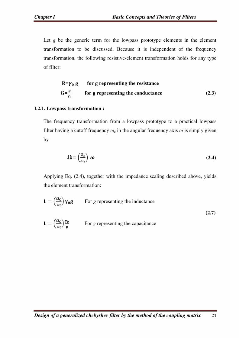
I.2. Frequency and element transformations……………………………………..19
I.2.1. Lowpass transformation………………………………......……………..21
I.2.2. Highpass transformation…………………………..……………...…….22
I.2.3. Bandpass transformation……………………………………………….24
I.2.4. Bandstop transformation…………………………………….................26
I.3. Immittance inverters……………………………………………………...........27
I.3.1. Definition of immittance, impedance, and admittance inverters….....27
I.4. Filters with immittance inverters………………………………………..........29
I.5. Practical realization of immittance inverters……………………………….34
Conclusion ………………………………………………………………………38

Chapter II
Introduction…………………………………………………………………….40
II .1.Series and parallel resonant circuits…………………………………...........40
II .1.1.Series resonant circuit……………………………….............……........40
II .1.2.Parallel resonant circuit………………….................……………........44
II .2.Loaded and unloaded Q…………………………………………………........48
II.3.Formulation for extracting external quality factor Q e………………............49
II .3.1 Singly loaded resonator……………………………........……….........49
II .3.2 .Doubly loaded resonator……………………………............…..........53
II.4. General coupling matrix for coupled-resonator filters……………...........56
II.4.1. Loop equation formulation………………….............…………...........56
II.4.2. Node equation formulation……….........………………………...........60
II.4.3. General coupling matrix……………............……………………........64
II.5. General theory of couplings………………….………………………..........65
II.5.1. Synchronously tuned coupled-resonator circuits…........................67
II.5.1.1. Electric coupling…………...........……………………...........67
II.5.1.2.Magnetic coupling…………………………………….………69
II.5.2. Asynchronously tuned coupled-resonator circuits…............……..72
II.5.2.1. Electric coupling ......................................................................72
II.5.2.2.Magnetic coupling .....................................................................74
II.6. General coupling matrix including source and load........................................76

Conclusion…………………………………………………………………………..80
Chapter III
Introduction …………………………………………………..……………………82
III.1.Polynomial forms of the transfer and reflection parameter (s) and (S)
for a two-port network……………………………………………............................82
III.1.1- Polynomial synthesis…………...................……………………..........92
III.1.2. Design of a generalized chybechev band pass filter...................................99
III.1.2.1. Specifications.......................................................................................99
III.1.3.Polynomial forms for symmetric and asymmetric filtering functions....102
III.2. Synthesis of network-circuit approch………………………………............104
III.2.1 Circuit synthesis approch………………..............................…..........106
III.2.2.Buildup of [ABCD] matrix for the third-degree network.............107
III.3. Similarity transformation and annihilation of matrix elements…..........108
Conclusion………………………………………………………………………......113
List of figures .
References.


general introduction
Designing a chebyshev filter generalized by the method of the coupling matrix
General introduction:
With the rapid development of the communication technology requirements for filters
are more and more high meaning filters requiring characteristics of lower insertion
loss, higher frequency selectivity, linear phase, and so on.
Generalized Chebyshev function is very useful, it can be used to design filters with
cross coupling. This gives rise to a method of synthesis in designing microwave filters
called coupling matrix method. A.E.Atia and A.E.Williams proposed a classical
method of extracting the cross coupling matrix, and published it in 1974 on MTT .
H.C.Bell proposed another method called RCJ's in 1982, and R.J.Cameron made
improvements to RCJ's method in 1999 . In 2003, R.J.Cameron proposed an
orthogonal matrix method which is simpler.
Passive implementations of linear filters are based on combinations
of resistors (R), inductors (L) capacitor (C). These types are collectively known
as passive filters, because they do not depend upon an external power supply and/or
they do not contain active components such as transistors.
Inductors block high-frequency signals and conduct low-frequency signals,
while capacitors do the reverse. A filter in which the signal passes through an inductor,
or in which a capacitor provides a path to ground, presents less attenuation to low-
frequency signals than high-frequency signals and is therefore a low-pass filter. If the
signal passes through a capacitor, or has a path to ground through an inductor, then the
filter presents less attenuation to high-frequency signals than low-frequency signals
and therefore is a high-pass filter. Resistors on their own have no frequency-selective
properties, but are added to inductors and capacitors to determine the time-constants of
the circuit, and therefore the frequencies to which it responds.

general introduction
Designing a chebyshev filter generalized by the method of the coupling matrix
The inductors and capacitors are the reactive elements of the filter. The number of
elements determines the order of the filter. In this context, an LC tuned circuit being
used in a band-pass or band-stop filter is considered a single element even though it
consists of two components.
At high frequencies (above about 100 megahertz), sometimes the inductors consist of
single loops or strips of sheet metal, and the capacitors consist of adjacent strips of
metal. These inductive or capacitive pieces of metal are called stubs.
Chebyshev filters have a steeper roll-off and more passband ripple (type I)
or stopband ripple (type II) than Butterworth filters. They have the property that they
minimize the error between the idealized and the actual filter characteristic over the
range of the filter, but with ripples in the passband. This type of filter is named
after Pafnuty Chebyshev because its mathematical characteristics are derived
from Chebyshev polynomials.
Because of the passband ripple inherent in Chebyshev filters, the ones that have a
smoother response in the passband but a more irregular response in the stopband are
preferred for some applications.

Chapter I Basic Concepts and Theories of Filters
Design of a generalized chebyshev filter by the method of the coupling matrix 1
Introduction :
Filters are networks that process signals in a frequency-dependent manner. The basic
concept of a filter can be explained by examining the frequency dependent nature of
the impedance of capacitors and inductors.
Consider a voltage divider where the shunt leg is a reactive impedance. As the
frequency is changed, the value of the reactive impedance changes, and the voltage
divider ratio changes. This mechanism yields the frequency dependent change in the
input/output transfer function that is defined as the frequency response.
Filters have many practical applications. A simple, single-pole, low-pass filter (the
integrator) is often used to stabilize amplifiers by rolling off the gain at higher
frequencies where excessive phase shift may cause oscillations.
A simple, single-pole, high-pass filter can be used to block dc offset in high gain
amplifiers or single supply circuits. Filters can be used to separate signals, passing
those of interest, and attenuating the unwanted frequencies. An example of this is a
radio receiver, where the signal you wish to process is passed through, typically with
gain, while attenuating the rest of the signals. In data conversion, filters are also used
to eliminate the effects of aliases in A/D systems.
I.1. Transfer functions :
I.1.1. General definitions :
The transfer function of a twoport filter network is a mathematical description of
network response characteristics, namely, a mathematical expression of . On
many occasions, an amplitude-squared transfer function for a lossless passive filter
network is defined as
| Ω | = + Ω (1.1)
Where ε is a ripple constant (Ω) represents a filtering or characteristic function, and
Ω is a frequency variable. For our discussion here, it is convenient to let Ω represent a
Chapter I Basic Concepts and Theories of Filters
Design of a generalized chebyshev filter by the method of the coupling matrix 2
radian frequency variable of a lowpass prototype filter that has a cutoff frequency at
Ω =Ω for Ω = 1 (rad/s). Frequency transformations to the usual radian frequency
for practical lowpass, highpass, bandpass, and bandstop filters will be discussed later.
For linear time-invariant networks, the transfer function may be defined as a rational
function, that is
= (1.2)
Where N(p) and D(p) are polynomials in a complex frequency variable = σ + jΩ .
For a lossless passive network, the neper frequency σ = and p = jΩ . To find a
realizable rational transfer function that produces response characteristics
approximating the required response is the so-called approximation problem and, in
many cases, the rational transfer function of Eq. (1.2) can be constructed from the
amplitude-squared transfer function of Eq. (1.1).
For the transfer function of Eq. (1.1), the insertion loss response of the filter,
can be computed by :
LA (Ω ) =10log| Ω | (1.3)
Since |S11|2 + | S21|
2 = 1 for a lossless passive two-port network the return loss
response of the filter is then:
LR(Ω =10log[ − | Ω | ]dB (1.4)
If a rational transfer function is available, the phase response of the filter can be
found as
∅ Ω = Ω (1.5)
The group-delay response of this network can then be calculated by

Chapter I Basic Concepts and Theories of Filters
Design of a generalized chebyshev filter by the method of the coupling matrix 3
Ω = − ∅ Ω
Ω s (1.6)
Where (Ω) is in radians and Ω is in rad/s.
I.1.2.Poles and zeros on the complex plane:
The (σ, Ω) plane, where a rational transfer function is defined, is called the complex
plane or p-plane. The horizontal axis of this plane is called the real or σ-axis and the
vertical axis is called the imaginary or jΩ-axis. The values of p at which the function
becomes zero are the zeros of the function and the values of p at which the function
becomes infinite are the singularities (the poles) of the function. Therefore,
the zeros of (p) are the roots of the numerator N(p) and the poles of (p) are the
roots of denominator D(p).
These poles will be the natural frequencies of the filter whose response is described by
(p). For the filter to be stable, these natural frequencies must lie in the left half of
the p-plane, or on the imaginary axis. If this were not so, the oscillations would be of
exponentially increasing magnitude with respect to time, a condition that is impossible
in a passive network. Hence, D(p) is a Hurwitz polynomial, that is its
roots (or zeros) are in the inside of the left half-plane, or on the jΩ-axis. The roots (or
zeros) of N(p) may occur any where on the entire complex plane. The zeros of N (p)
are called finite-frequency transmission zeros of the filter.
The poles and zeros of a rational transfer function may be depicted on the p-plane. We
will see in the following that different types of transfer functions will be distinguished
from their pole-zero patterns of the diagram.
I.1.3.The butterworth prototype:
The maximally flat approximation is the simplest meaningful approximation to the
ideal lowpass filter. It is maximally flat at d.c. and infinity, but rolls off to
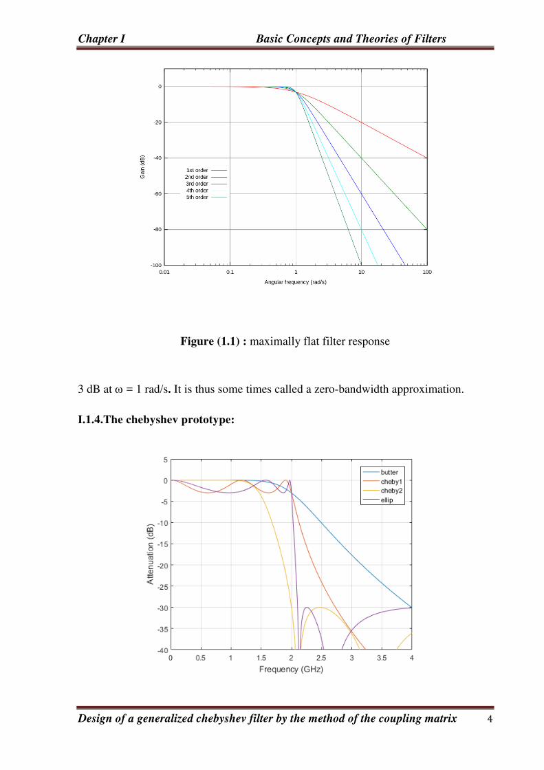
Chapter I Basic Concepts and Theories of Filters
Design of a generalized chebyshev filter by the method of the coupling matrix 4
Figure (1.1) : maximally flat filter response
3 dB at = 1 rad/s. It is thus some times called a zero-bandwidth approximation.
I.1.4.The chebyshev prototype:
Chapter I Basic Concepts and Theories of Filters
Design of a generalized chebyshev filter by the method of the coupling matrix 5
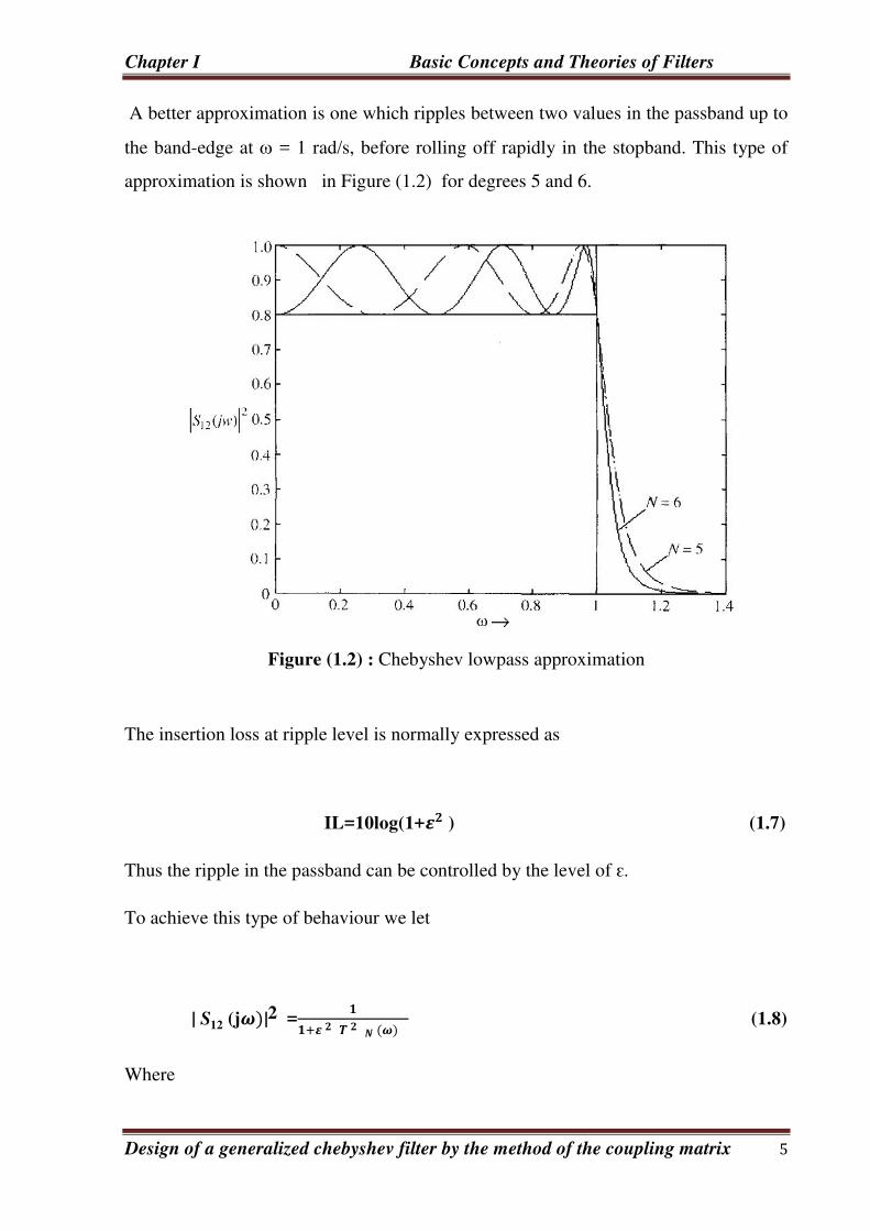
A better approximation is one which ripples between two values in the passband up to
the band-edge at = 1 rad/s, before rolling off rapidly in the stopband. This type of
approximation is shown in Figure (1.2) for degrees 5 and 6.
Figure (1.2) : Chebyshev lowpass approximation
The insertion loss at ripple level is normally expressed as
IL=10log(1+ ) (1.7)
Thus the ripple in the passband can be controlled by the level of ԑ.
To achieve this type of behaviour we let
| S12 (j |2 = + (1.8)
Where
Chapter I Basic Concepts and Theories of Filters
Design of a generalized chebyshev filter by the method of the coupling matrix 6
Thus
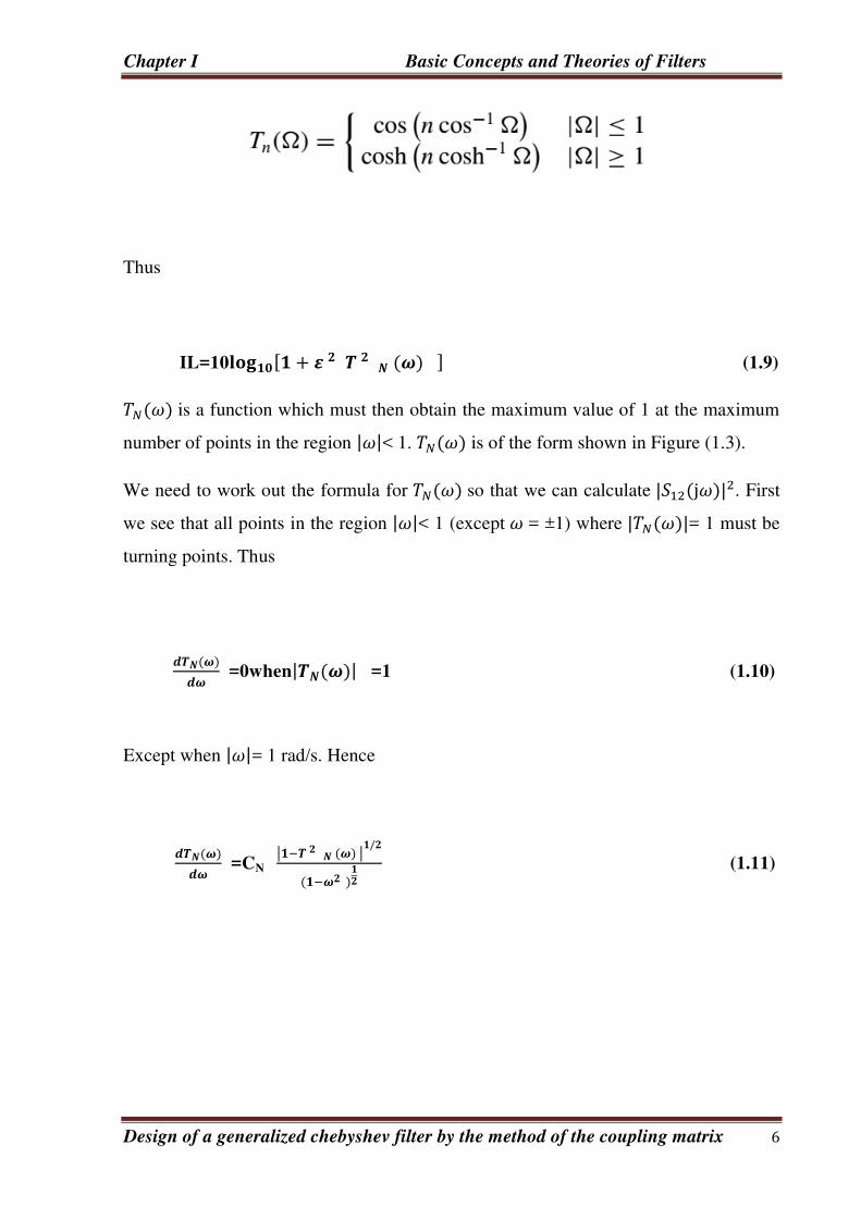
IL=10 [ + ] (1.9)
is a function which must then obtain the maximum value of 1 at the maximum
number of points in the region ||< 1. is of the form shown in Figure (1.3).
We need to work out the formula for so that we can calculate | j | . First
we see that all points in the region ||< 1 (except = ±1) where | |= 1 must be
turning points. Thus
=0when| | =1 (1.10)
Except when ||= 1 rad/s. Hence
=CN
| − | /− (1.11)

Chapter I Basic Concepts and Theories of Filters
Design of a generalized chebyshev filter by the method of the coupling matrix 7
Figure (1.3) : Equiripple response
From Figure (1.3) we see that
| ± |=1 (1.12)
Thus 1- ( ±1)=0 when − / = 0 and d /d is finite at = ±1.
Rewriting (1.11)
| − | / =C
− / (1.13)
Integrating both sides of (1.13) gives
− [ ] =CN − ( ) (1.14) must be determined so that is an nth-degree polynomial in .

Chapter I Basic Concepts and Theories of Filters
Design of a generalized chebyshev filter by the method of the coupling matrix 8
Let () be written as = ( ). Then
=cos( CN) (1.15)
And =0 when
CN =−
(r=1.2etc.) (1.16)
Or
= − (1.17)
For to have N zeros then = N, and
TN ()=cos[ − ] (1.18)
Thus
| | = + [ − ] (1.19)
Now (1.19) must be a polynomial in , other Wise it could not represent the response
of a real network. In fact is known as the Chebyshev polynomial and is given
by the formula

Chapter I Basic Concepts and Theories of Filters
Design of a generalized chebyshev filter by the method of the coupling matrix 9
+ = - − (1.20)
With initial conditions
=1 and = (1.21)
Thus
=2 -1=2 -1 (1.22)
=2 − − = -3 (1.23)
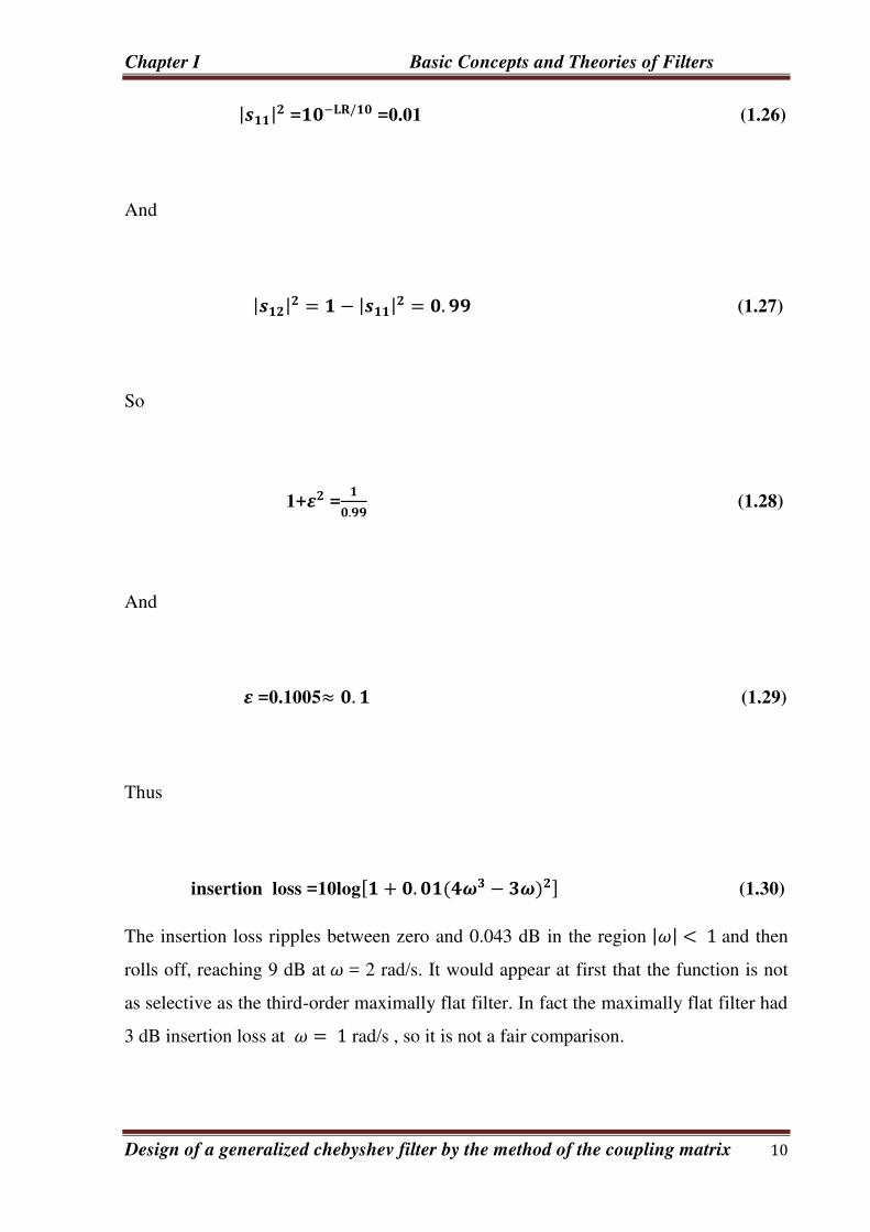
Let us now do an evaluation ofthe response of a third-order Chebyshev filter.
Say we want 20 dB minimum passband return loss. Then (in the worst case)
insertion loss =10 (1+ )=10log(| | ) (1.24)
And
return loss =10log(| | ) =LR (1.25)
Then
Chapter I Basic Concepts and Theories of Filters
Design of a generalized chebyshev filter by the method of the coupling matrix 10
| | = −/ =0.01 (1.26)
And
| | = − | | = . (1.27)
So
1+ = . (1.28)
And
=0.1005≈ . (1.29)
Thus
insertion loss =10log[ + . − ] (1.30)
The insertion loss ripples between zero and 0.043 dB in the region || < and then
rolls off, reaching 9 dB at = 2 rad/s. It would appear at first that the function is not
as selective as the third-order maximally flat filter. In fact the maximally flat filter had
3 dB insertion loss at = rad/s , so it is not a fair comparison.

Chapter I Basic Concepts and Theories of Filters
Design of a generalized chebyshev filter by the method of the coupling matrix 11
The passband insertion loss ripple in the Chebyshev filter is 0.043 dB. The third-
degree maximally flat filter achieved this at = . 6 . As a comparison the ratio of
stopband to passband frequency is 4.64 for the maximally flat filter and 3 for the
Chebyshev filter. Thus we see that the Chebyshev response is considerably more
selective than the maximally flat response.
A formula to calculate the degree of a Chebyshev filter to meet a specified response is
now given. The proof of this formula is similar to the proof for the maximally flat
response. The formula is
N≥ + + [ + − / ] (1.31)
Where is the stopband insertion loss, is the passband return loss and S is the
ratio of stopband to passband frequencies.
As an example, for = 50 dB, = 20 dB, S = 2 then N must be greater than 6.64,
i.e. N = 7. The maximally flat filter required N = 12 to meet this specification.
Synthesis of the Chebyshev filter proceeds as follows. Given
| | = + (1.32)
The poles occur when
= − / (1.33)
That is
Chapter I Basic Concepts and Theories of Filters
Design of a generalized chebyshev filter by the method of the coupling matrix 12
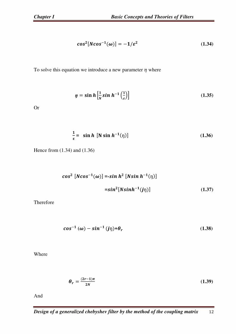
[ − ] = − / (1.34)
To solve this equation we introduce a new parameter where
ŋ = [ − ] (1.35)
Or
= [ − ŋ ] (1.36)
Hence from (1.34) and (1.36)
[ − ] =- [ − ŋ ] = [ − ŋ ] (1.37)
Therefore
− ( − − ŋ + (1.38)
Where
= − (1.39)
And
Chapter I Basic Concepts and Theories of Filters
Design of a generalized chebyshev filter by the method of the coupling matrix 13
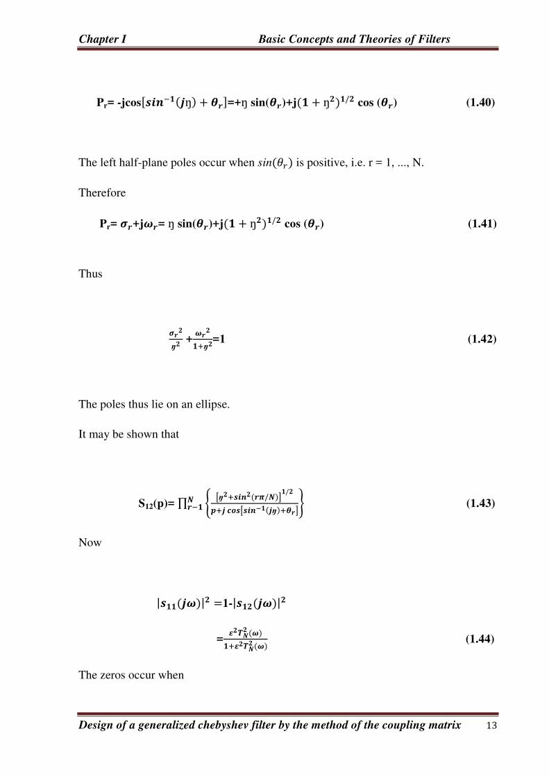
Pr= -jcos[ − ŋ + ]=+ŋ sin( )+j + ŋ / cos ( ) (1.40)
The left half-plane poles occur when sin is positive, i.e. r = 1, ..., N.
Therefore
Pr= +j = ŋ sin( )+j + ŋ / cos ( ) (1.41)
Thus
ŋ
++ŋ =1 (1.42)
The poles thus lie on an ellipse.
It may be shown that
S12(p)= ∏ [ŋ + / ] /+ [ − ŋ + ]− (1.43)
Now
| | =1-| |
= + (1.44)
The zeros occur when

Chapter I Basic Concepts and Theories of Filters
Design of a generalized chebyshev filter by the method of the coupling matrix 14
cos2[ − ] =0 (1.45)
That is
P=-jcos( ) (1.46)
Now
S11(∞)=1 (1.47)
Then
S11(p)= ∏ + + [ − ŋ + ]= (1.48)
The network can then be synthesised as a lowpass ladder network by formulating (P).
As an example we will synthesise a degree 3 Chebyshev filter.
For r=1 = /6 cos( )=√ / (1.49)
For r=2 = /2 cos( )=0 (1.50)
For r=3 = /6 cos( )=- √ / (1.51)
Therefore
Chapter I Basic Concepts and Theories of Filters
Design of a generalized chebyshev filter by the method of the coupling matrix 15
S11(p)=+ √ − √
+ŋ [ +ŋ+ √ +ŋ / ][ +ŋ− √ +ŋ / ] =
+ /+ ŋ + ŋ + +ŋ ŋ + (1.52)
Now
Zin(p)=+ ŋ + ŋ + +ŋ ŋ +ŋ + ŋ +ŋ ŋ + (1.53)
Removing a series inductor of value 1/η we are left with
Z1(p)= Z(p)-p/ŋ
=ŋ + +ŋ
ŋ + ŋ +ŋ ŋ + (1.54)
Extracting an inverter of characteristic admittance
K12= ŋ + /
ŋ (1.55)
The remaining impedance is
Z2(p)= + ŋ + ŋ +ŋ +ŋ (1.56)
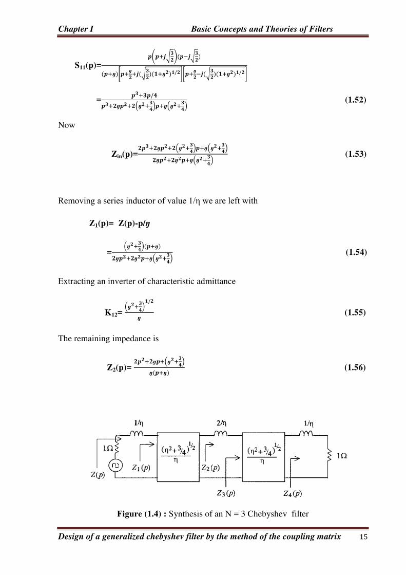
Figure (1.4) : Synthesis of an N = 3 Chebyshev filter
Chapter I Basic Concepts and Theories of Filters
Design of a generalized chebyshev filter by the method of the coupling matrix 16
Now extracting a second inductor of value 2/η we are left with
Z3(p)= Z2(p)-2p/ ŋ
=ŋ + /ŋ +ŋ (1.57)
Extracting a second admittance inverter of characteristic admittance
K23=ŋ + /
ŋ (1.58)
The remaining impedance is
Z4(p)=1+p/ ŋ (1.59)
i.e. an inductor of value 1/η followed by a load resistor of value unity. The complete
synthesis cycle is shown in Figure (1.4).
The synthesised element values given here are actually formulae in terms of η. These
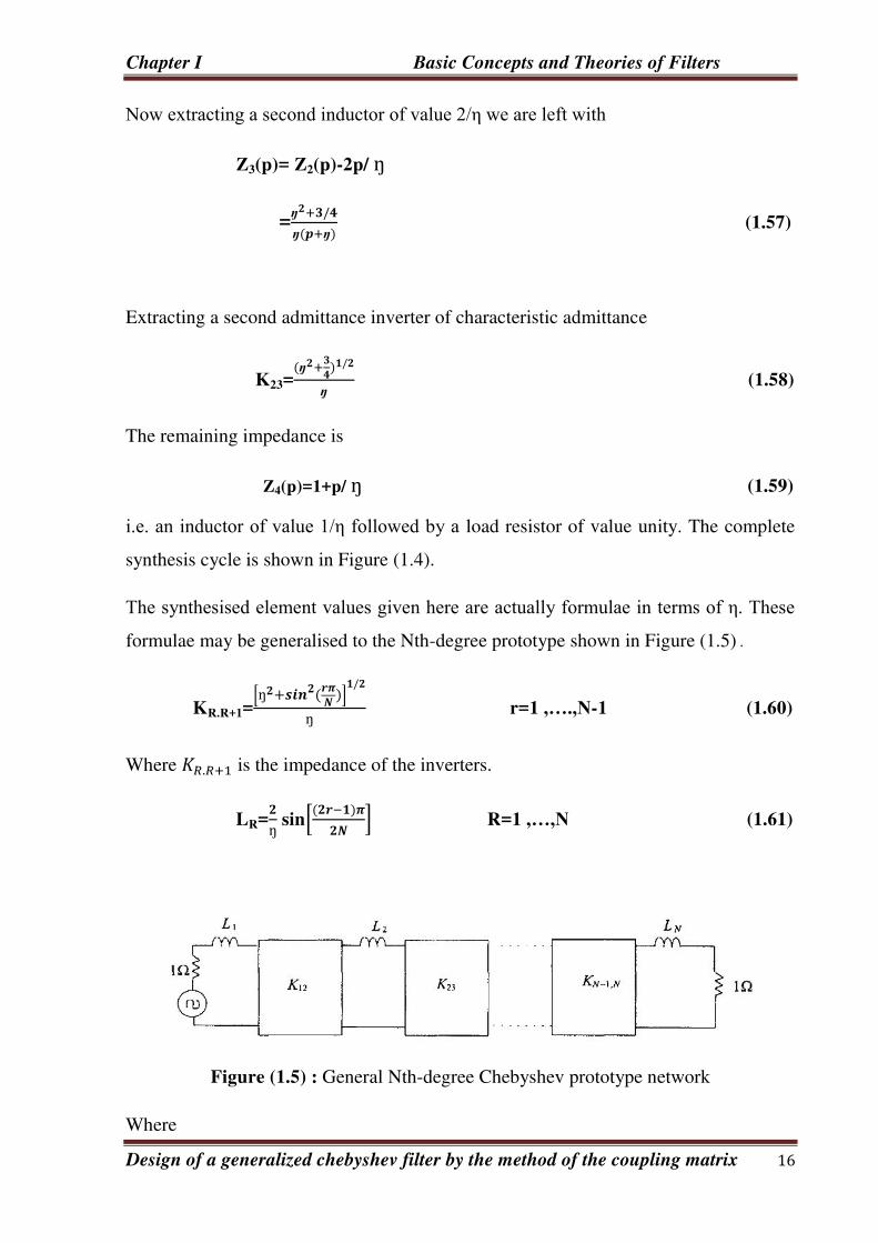
formulae may be generalised to the Nth-degree prototype shown in Figure (1.5) .
KR.R+1=[ŋ + ] /ŋ r=1 ,….,N-1 (1.60)
Where .+ is the impedance of the inverters.
LR=ŋ sin[ − ] R=1 ,…,N (1.61)
Figure (1.5) : General Nth-degree Chebyshev prototype network
Where
Chapter I Basic Concepts and Theories of Filters
Design of a generalized chebyshev filter by the method of the coupling matrix 17
ŋ = [ − / ] (1.62)
ԑ is related to the insertion loss ripple and hence the passband return loss. Since
| | = + (1.63)
| | = + (1.64)
Therefore
LR=10 (1+1/ (1.65)
Hence
= / − − / (1.66)
Note that the dual of Figure (1.5) would consist of shunt capacitors separated by
inverters. Formulae (1.60)-(1.62) still apply but they would then represent the values
of the capacitors and the characteristic admittance of the inverters.
I.1.5.Butterworth (maximally flat) response :
The amplitude-squared transfer function for Butterworth filters, which have an
insertion loss = 3.01 dB at the cutoff frequency Ωc = 1 is given by
| Ω | = +Ω (1.67)
Where n is the degree or the order of filter, which corresponds to the number of
reactive elements required in the lowpass prototype filter. This type of response is
also referred to as maximally flat, because its amplitude-squared transfer function

Chapter I Basic Concepts and Theories of Filters
Design of a generalized chebyshev filter by the method of the coupling matrix 18
defined in Eq (1.67) has the maximum number of (2n − 1) zero derivatives at
Ω = 0. Therefore, the maximally flat approximation to the ideal lowpass filter in
the passband is best at Ω = 0, but deteriorates as Ω approaches the cutoff
frequency Ω . Figure (1.6) shows a typical maximally flat response.
Figure (1.6) : Butterworth (maximally flat) lowpass response.

Chapter I Basic Concepts and Theories of Filters
Design of a generalized chebyshev filter by the method of the coupling matrix 19
Figure (1.7) : Pole distribution for Butterworth (maximally flat) response.
A rational transfer function constructed from Eq. (1.67) is
S21(p)= ∏ −= (1.68)
=j exp[ − ]
There is no finite-frequency transmission zero [all the zeros of S21(p) are at
infinity], and the poles pi lie on the unit circle in the left half-plane at equal
angular spacings, since |pi| = 1 and Arg pi = (2i − 1) π/2n. This is illustrated in
Figure (1.7).
I.2. Frequency and element transformations :
Thus far, we have only considered the lowpass prototype filters, which have a
normalized source resistance/conductance g0 = 1 and a cutoff frequency
of Ω = . To obtain frequency characteristics and element values for practical
Chapter I Basic Concepts and Theories of Filters
Design of a generalized chebyshev filter by the method of the coupling matrix 20
filters, based on the lowpass prototype, one may apply frequency and element
transformations.
The frequency transformation, which is also referred to as frequency mapping, is
required to map, for example, a Chebyshev response in the lowpass prototype
frequency domain Ω to that in the frequency domain ω in which a practical filter
response such as lowpass, highpass, bandpass, and bandstop are expressed. The
frequency transformation will have an effect on all the reactive elements
accordingly, but no effect on the resistive elements.
In addition to the frequency mapping, impedance scaling is also required to
accomplish the element transformation. The impedance scaling will remove the = 1 normalization and adjusts the filter to work for any value of the source
impedance denoted by . For our formulation, it is convenient to define an
impedance scaling factor as
= (2.1)
Where Y0 = 1/Z0 is the source admittance. In principle, applying the impedance
scaling upon a filter network in such a way that
L→ L
C → /
R→ R
G→ / (2.2)
Has no effect on the response shape.
Chapter I Basic Concepts and Theories of Filters
Design of a generalized chebyshev filter by the method of the coupling matrix 21
Let g be the generic term for the lowpass prototype elements in the element
transformation to be discussed. Because it is independent of the frequency
transformation, the following resistive-element transformation holds for any type
of filter:
R= g for g representing the resistance
G= for g representing the conductance (2.3)
I.2.1. Lowpass transformation :
The frequency transformation from a lowpass prototype to a practical lowpass
filter having a cutoff frequency ωc in the angular frequency axis ω is simply given
by
Ω = Ω (2.4)
Applying Eq. (2.4), together with the impedance scaling described above, yields
the element transformation:
= Ω For g representing the inductance
(2.7) = Ω For g representing the capacitance

Chapter I Basic Concepts and Theories of Filters
Design of a generalized chebyshev filter by the method of the coupling matrix 22
Figure (1.8) : Lowpass prototype to lowpass transformation: (a) basic element
transformation; (b) a practical lowpass filter based on the transformation
I.2.2. Highpass transformation :
For highpass filters with a cutoff frequency ωc in the ω-axis, the frequency
transformation is
Ω =− Ω (2.8)
Applying this frequency transformation to a reactive element g in the lowpass
prototype leads to

Chapter I Basic Concepts and Theories of Filters
Design of a generalized chebyshev filter by the method of the coupling matrix 23
jΩ → Ω
Figure (1.9) : Lowpass prototype to highpass transformation: (a) basic element
transformation; (b) a practical highpass filter based on the transformation.
It is then obvious that an inductive/capacitive element g in the lowpass prototype
will be inversely transformed to a capacitive/inductive element in the highpass
filter. With impedance scaling, the element transformation is given by
= Ω for g representing the inductance
(2.9)
Chapter I Basic Concepts and Theories of Filters
Design of a generalized chebyshev filter by the method of the coupling matrix 24
= Ω for g representing the capacitance
This type of element transformation is shown in Figure 9a. Figure (1.9b)
demonstrates a practical highpass filter with a cutoff frequency at 2 GHz and 50-
Ω terminals, which is obtained from the transformation of the three-pole
Butterworth lowpass prototype given above.
I.2.3. Bandpass transformation :
Assume that a lowpass prototype response is to be transformed to a bandpass
response having a passband ω2 − ω1, where ω1 and ω2 indicate the passband-edge
angular frequency. The required frequency transformation is
Ω = Ω
− (2.10 a)
With
= −
=√ (2.10 b)
Where c denotes the center angular frequency and FBW is defined as the
fractional bandwidth. If we apply this frequency transformation to a reactive
element g of the lowpass prototype, we have
J Ω → j Ω +
Ω
Which implies that an inductive/capacitive element g in the lowpass prototype
will transform to a series/parallel LC resonant circuit in the bandpass filter.
The elements for the series LC resonator in the bandpass filter are

Chapter I Basic Concepts and Theories of Filters
Design of a generalized chebyshev filter by the method of the coupling matrix 25
Ls= ( Ω ) For g representing the inductance (2.11 a)
Cs=
Ω
Where the impedance scaling has been taken into account as well. Similarly, the
elements for the parallel LC resonator in the bandpass filter are
Cp= ( Ω ) For g representing the capacitance (2.11 b)
Lp= Ω
It should be noted that = / and = / hold in
Eq. (2.11). The element transformation, in this case, is shown in Figure (1.10a).
Figure (1.10b) illustrates a bandpass having a passband from 1 to 2 GHz obtained
using the element transformation.
Figure (1.10) : Lowpass prototype to bandpass transformation: (a) basic element
transformation; (b) a practical bandpass filter based on the transformation.
Chapter I Basic Concepts and Theories of Filters
Design of a generalized chebyshev filter by the method of the coupling matrix 26
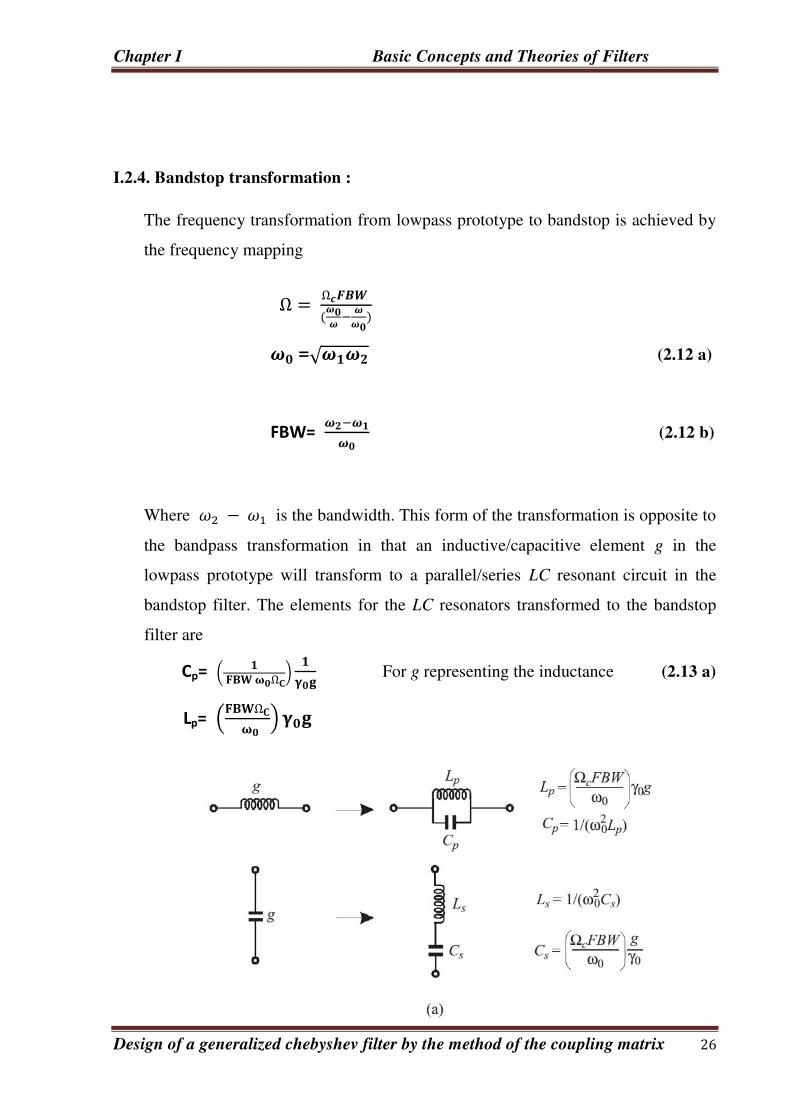
I.2.4. Bandstop transformation :
The frequency transformation from lowpass prototype to bandstop is achieved by
the frequency mapping
Ω = Ω −
=√ (2.12 a)
FBW= − (2.12 b)
Where − is the bandwidth. This form of the transformation is opposite to
the bandpass transformation in that an inductive/capacitive element g in the
lowpass prototype will transform to a parallel/series LC resonant circuit in the
bandstop filter. The elements for the LC resonators transformed to the bandstop
filter are
Cp= ( Ω ) For g representing the inductance (2.13 a)
Lp=
Ω

Chapter I Basic Concepts and Theories of Filters
Design of a generalized chebyshev filter by the method of the coupling matrix 27
Figure (1.11) : Lowpass prototype to bandstop transformation: (a) basic element
transformation; (b) a practical bandstop filter based on the transformation.
Ls= ( Ω )
For g representing the capacitance (2.13b)
Cs= ( Ω )
It is also true in Eq. (2.13) that = / and = / . The
element transformation of this type is shown in Figure (1.11a). An example of its
application for designing a practical bandstop filter, with a bandwidth of 1 to 2
GHz, is demonstrated in Figure (1.11b), which is based on the three-pole
Butterworth lowpass prototype, as described previously.
I.3. Immittance inverters :
I.3.1. Definition of immittance, impedance, and admittance inverters :
Immittance inverters are either impedance or admittance inverters. An idealized
impedance inverter is a two-port network that has a unique property at all
frequencies, that is, if it is terminated in an impedance Z2 on one port, the
impedance Z1 seen looking in at the other port is
Z1= (3.1)

Chapter I Basic Concepts and Theories of Filters
Design of a generalized chebyshev filter by the method of the coupling matrix 28
Where K is real and defined as the characteristic impedance of the inverter. As can
be seen, if Z2 is inductive/conductive, Z1 will become conductive/inductive, and,
hence, the inverter has a phase shift of ±90 or an odd multiple thereof. Impedance
inverters are also known as K inverters. The ABCD matrix of ideal impedance
inverters may generally be expressed as
(3.2)
Likewise, an ideal admittance inverter is a two-port network, which exhibits such
a property at all frequencys that if an admittance Y2 is connected at one port, the
admittance Y1 seen into the other port is
Y1= (3.3)
Where J is real and called the characteristic admittance of the inverter. Similarly,
the admittance inverter has a phase shift of ±90 or an odd multiple thereof.
Admittance inverters are also referred to as J inverters. In general, ideal
admittance inverters have the ABCD matrix
(3.4)
Chapter I Basic Concepts and Theories of Filters
Design of a generalized chebyshev filter by the method of the coupling matrix 29
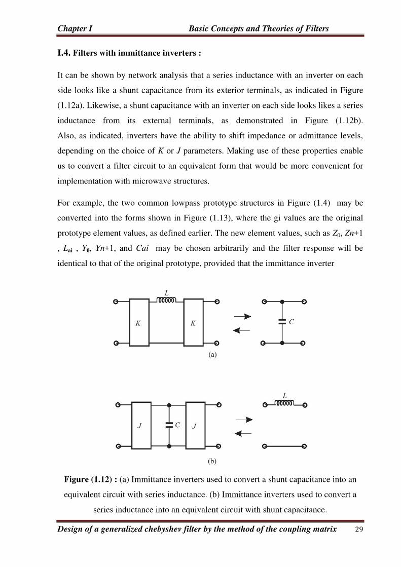
I.4. Filters with immittance inverters :
It can be shown by network analysis that a series inductance with an inverter on each
side looks like a shunt capacitance from its exterior terminals, as indicated in Figure
(1.12a). Likewise, a shunt capacitance with an inverter on each side looks likes a series
inductance from its external terminals, as demonstrated in Figure (1.12b).
Also, as indicated, inverters have the ability to shift impedance or admittance levels,
depending on the choice of K or J parameters. Making use of these properties enable
us to convert a filter circuit to an equivalent form that would be more convenient for
implementation with microwave structures.
For example, the two common lowpass prototype structures in Figure (1.4) may be
converted into the forms shown in Figure (1.13), where the gi values are the original
prototype element values, as defined earlier. The new element values, such as Z0, Zn+1
, Lai , Y0, Yn+1, and Cai may be chosen arbitrarily and the filter response will be
identical to that of the original prototype, provided that the immittance inverter
Figure (1.12) : (a) Immittance inverters used to convert a shunt capacitance into an
equivalent circuit with series inductance. (b) Immittance inverters used to convert a
series inductance into an equivalent circuit with shunt capacitance.

Chapter I Basic Concepts and Theories of Filters
Design of a generalized chebyshev filter by the method of the coupling matrix 30
Figure (1.13) : Lowpass prototype filters modified to include immittance inverters.
Parameters ,i+1 and Ji ,i+1 are specified as indicated by the equations in Figure
(1.13). These equations can be derived by expanding the input immittances of the
original prototype networks and the equivalent ones in continued fractions and by
equating corresponding terms.
Since, ideally, immittance inverter parameters are frequency invariable, the lowpass
filter networks in Figure (1.13) can easily be transformed to other types of filter by
applying the element transformations similar to those described in the previous
section. For instance, Figure (1.14) illustrates two bandpass filters using immittance
inverters. In the case of Figure (1.14a), only series resonators are involved, whereas
the filter in Figure (1.14b) consists of only shunt-parallel resonators. The element
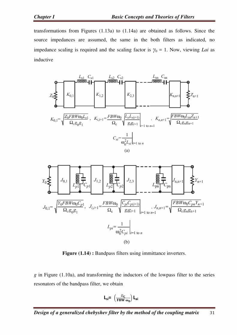
Chapter I Basic Concepts and Theories of Filters
Design of a generalized chebyshev filter by the method of the coupling matrix 31
transformations from Figures (1.13a) to (1.14a) are obtained as follows. Since the
source impedances are assumed, the same in the both filters as indicated, no
impedance scaling is required and the scaling factor is γ0 = 1. Now, viewing Lai as
inductive
Figure (1.14) : Bandpass filters using immittance inverters.
g in Figure (1.10a), and transforming the inductors of the lowpass filter to the series
resonators of the bandpass filter, we obtain
Lsi= ( Ω ) Lai
Chapter I Basic Concepts and Theories of Filters
Design of a generalized chebyshev filter by the method of the coupling matrix 32
Csi= As mentioned above, the K parameters must remain unchanged with respect to the
frequency transformation. Replacing Lai in the equations in Figure (1.13a) with
Lai = (FBWω0/Ω ) Lsi yields the equations in Figure (1.14a). Similarly, the
transformations and equations in Figure (1.14b) can be obtained on a dual basis.
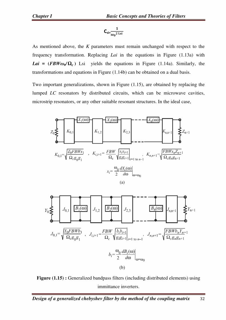
Two important generalizations, shown in Figure (1.15), are obtained by replacing the
lumped LC resonators by distributed circuits, which can be microwave cavities,
microstrip resonators, or any other suitable resonant structures. In the ideal case,
Figure (1.15) : Generalized bandpass filters (including distributed elements) using
immittance inverters.

Chapter I Basic Concepts and Theories of Filters
Design of a generalized chebyshev filter by the method of the coupling matrix 33
The reactances or susceptances of the distributed circuits (not restricted to bandpass
filters) should equal those of the lumped resonators at all frequencies. In practice, they
approximate the reactances or susceptances of the lumped resonators only near
resonance. Nevertheless, this is sufficient for narrow-band filters. For convenience, the
distributed resonator reactance/susceptance and reactance/susceptance slope are made
equal to their corresponding lumped-resonator values at band center. For this, two
quantities, called the reactance- and susceptance-slope parameter, respectively, are
introduced. The reactance-slope parameter for resonators having zero reactance at
center frequency ω0 is defined by
X= ⎢= (4.1)
Where X(ω) is the reactance of the distributed resonator. In the dual case, the
susceptance slope parameter for resonators having zero susceptance at center
frequency ω0 is defined by
b= ⎢= (4.2)
Where B(ω) is the susceptance of the distributed resonator. It can be shown that the
reactance-slope parameter of a lumped LC series resonator is ω0L, and the
susceptance-slope parameters of a lumped LC parallel resonator is ω0C. Thus,
replacing ω0 Lsi and ω0 Cpi in the equations in Figure (1.14) with the general terms xi
and bi , as defined by Eqs. (4.1) and (4.2), respectively, results in the equations
indicated in Figure (1.15).
Chapter I Basic Concepts and Theories of Filters
Design of a generalized chebyshev filter by the method of the coupling matrix 34
I.5. Practical realization of immittance inverters :
One of the simplest forms of inverters is a quarter-wavelength of transmission line. It
can easily be shown that such a line has a ABCD matrix of the form given in Eq. (3.2)
with K = Zc Ω, where Zc is the characteristic impedance of the line. Therefore, it will
obey the basic impedance inverter definition of Eq. (3.1). Of course, a quarter-
wavelength of line can be also used as an admittance inverter with J = Yc, where
Yc = 1/Zc is the characteristic admittance of the line. Although its inverter properties
are relatively narrow-band in nature, a quarter-wavelength line can be used
satisfactorily as an immittance inverter in narrow-band filters Besides a quarter-
wavelength line, there are numerous other circuits that operate as immittance inverters.
All necessarily produce a phase shift of some odd multiple of ±90 and many work
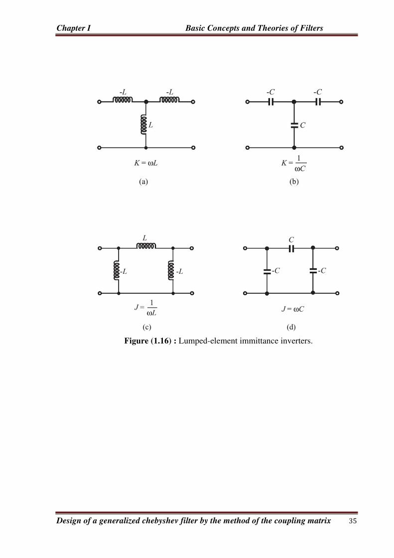
over a much wider bandwidth than does a quarter-wavelength line. Figure (1.16)
shows four typical lumped-element immittance inverters. While the inverters in Figure
(1.16 a and b) are of interest for use as K inverters, those shown in Figure (16 c and d)
are of interest for use as J inverters. This is simply because of the consideration that
the negative elements of the inverters could conveniently be absorbed into adjacent
elements in practical filters. Otherwise, any one of these inverters can be treated as
either K or J inverter. It can be shown that the inverters in Figure (1.16 a and d) have a
phase shift (the phase of S21) of +90, while those in Figure (1.16 b and c) have a phase
shift of −90. This is why the “±” and “∓” signs appear in the ABCD matrix
expressions of immittance inverters.
Chapter I Basic Concepts and Theories of Filters
Design of a generalized chebyshev filter by the method of the coupling matrix 35
Figure (1.16) : Lumped-element immittance inverters.
Chapter I Basic Concepts and Theories of Filters
Design of a generalized chebyshev filter by the method of the coupling matrix 36
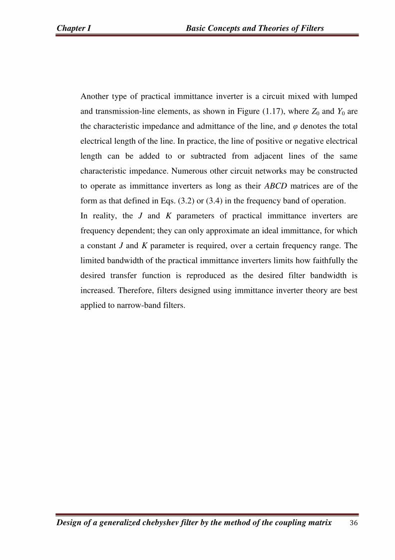
Another type of practical immittance inverter is a circuit mixed with lumped
and transmission-line elements, as shown in Figure (1.17), where Z0 and Y0 are
the characteristic impedance and admittance of the line, and φ denotes the total
electrical length of the line. In practice, the line of positive or negative electrical
length can be added to or subtracted from adjacent lines of the same
characteristic impedance. Numerous other circuit networks may be constructed
to operate as immittance inverters as long as their ABCD matrices are of the
form as that defined in Eqs. (3.2) or (3.4) in the frequency band of operation.
In reality, the J and K parameters of practical immittance inverters are
frequency dependent; they can only approximate an ideal immittance, for which
a constant J and K parameter is required, over a certain frequency range. The
limited bandwidth of the practical immittance inverters limits how faithfully the
desired transfer function is reproduced as the desired filter bandwidth is
increased. Therefore, filters designed using immittance inverter theory are best
applied to narrow-band filters.

Chapter I Basic Concepts and Theories of Filters
Design of a generalized chebyshev filter by the method of the coupling matrix 37
Figure (1.17) : immittance inverters comprised of lumped and transmission-line
elements.

Chapter I Basic Concepts and Theories of Filters
Design of a generalized chebyshev filter by the method of the coupling matrix 38
Conclusion :
Filters play an important role in the field of digital and analog signal processing and
telecommunication systems. The traditional analog filter design consists of two major
portions: the approximation problem and the synthesis problem. In early days the
digital filter also faced accuracy problems because of the finite word length, but in the
modern days because of the availability of 32 bit word lengths and floating point
capabilities, digital filters are widely used.
The primary functions of a filter are to confine a signal into a prescribed frequency
band or channel or to model the input-output relation of a system such as a mobile
communication channel, telephone line echo etc. Filters have many practical uses. To
stabilize amplifiers by rolling off the gain at higher frequencies where extreme phase
shifts may cause oscillations a single-pole low-pass filter (the integrator) is often used.

Chapter II Coupled resonators
Design of a generalized chebyshev filter by the method of the coupling matrix 40
Introduction:
Resonators are the basic building blocks of any bandpass filter. A resonator is an
element that is capable of storing both frequency-dependent electric energy and
frequency-dependent magnetic energy. A simple example is an LC resonator,
where the magnetic energy is stored in the inductance L and the electric energy is
stored in the capacitance C. The resonant frequency of a resonator is the frequency
at which the energy stored in electric field equals the energy stored in the magnetic
field. At microwave frequencies, resonators can take various shapes and forms. The
shape of the microwave structure affects the field distribution and hence the stored
electric and magnetic energies. Potentially, any microwave structure should be
capable of constructing a resonator whose resonant frequency is determined by
the structure's physical characteristics and dimensions.
Coupled-resonator circuits are of importance for design of RF/microwave filters,
in particular, the narrow-band bandpass filters that play a significant role in many
applications. There is a general technique for designing coupled-resonator filters in
the sense that it can be applied to any type of resonator despite its physical structure.
It has been applied to the design of waveguide filters
This design method is based on coupling coefficients of intercoupled resonators and
the external quality factors of the input and output resonators.
II .1.Series and parallel resonant circuits:
At frequencies near resonance, a microwave resonator can usually be modelled by
either a series or parallel RLC lumped-element equivalent circuit, and so we will now
review some of the basic properties of these circuits.
II .1.1.Series resonant circuit:
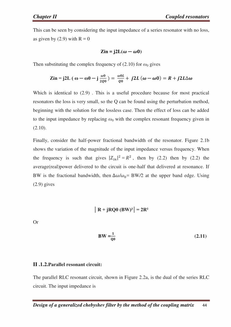
A series RLC resonant circuit is shown in Figure 2.1a. The input impedance is
= R+j L-j (2.1)
and the complex power delivered to the resonator is
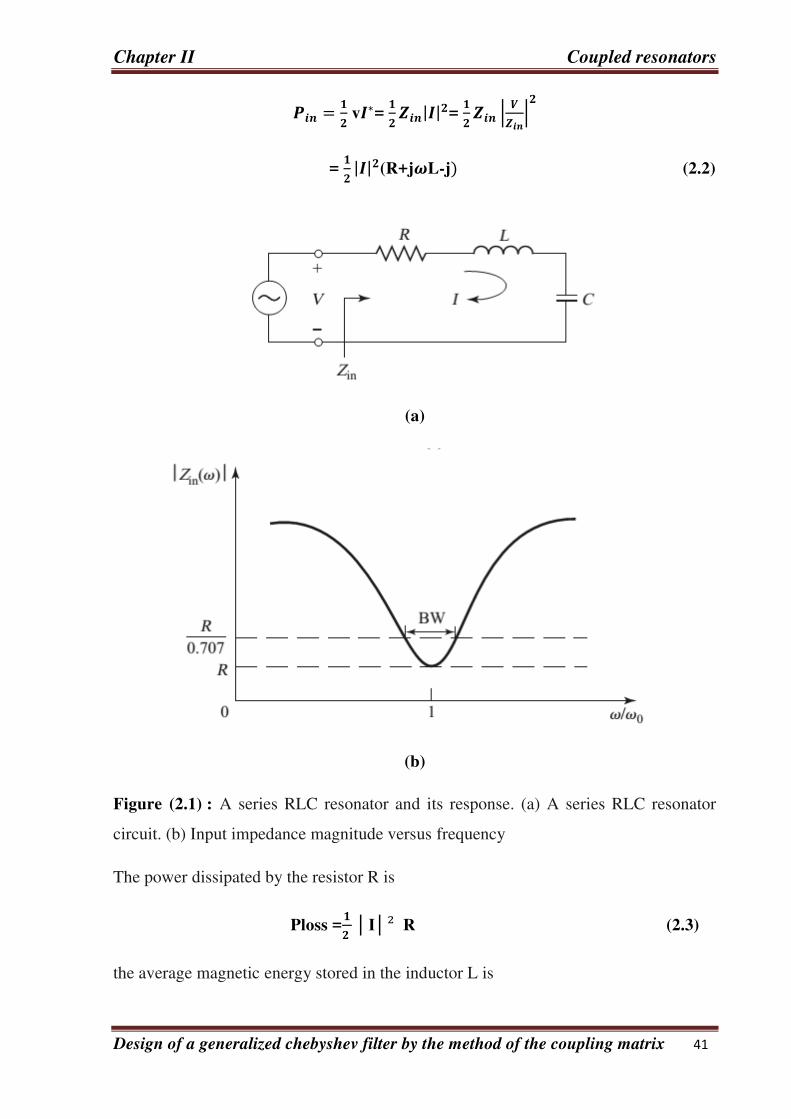
Chapter II Coupled resonators
Design of a generalized chebyshev filter by the method of the coupling matrix 41
= v ∗= | | = | |
= | | (R+j L-j (2.2)
(a)
(b)
Figure (2.1) : A series RLC resonator and its response. (a) A series RLC resonator
circuit. (b) Input impedance magnitude versus frequency
The power dissipated by the resistor R is
Ploss = I² R (2.3)
the average magnetic energy stored in the inductor L is
Chapter II Coupled resonators
Design of a generalized chebyshev filter by the method of the coupling matrix 42
Wm = I²L (2.4)
and the average electric energy stored in the capacitor C is
We = = I ² ² (2.5)
Where is the voltage across the capacitor. Then the complex power of (2.2) can be
rewritten as
Pin = Ploss + 2 jω ( Wm We ) (2.6)
and the input impedance of (1.1) can be rewritten as
Zin = ² = + ² (2.7)
Resonance occurs when the average stored magnetic and electric energies are equal, or = . Then from (2.5) and (2.3,a), the input impedance at resonance is
Zin = ² = Which is purely real. From (2.3b, c), = implies that the resonant frequency,
can be defined as
=√ (2.8)
Another important parameter of a resonant circuit is its Q, or quality factor, which is
defined as
Q= ω ⁄ = ω
+ (2.7)
Thus Q is a measure of the loss of a resonant circuit—lower loss implies a higher Q.
Resonator losses may be due to conductor loss, dielectric loss, or radiation loss, and
are represented by the resistance, of the equivalent circuit. An external connecting

Chapter II Coupled resonators
Design of a generalized chebyshev filter by the method of the coupling matrix 43
network may introduce additional loss. Each of these loss mechanisms will have the
effect of lowering the Q. The Q of the resonator itself, disregarding external loading
effects, is called the unloaded Q, denoted as .
For the series resonant circuit of Figure 6.1a, the unloaded Q can be evaluated from
(2.7), using (2.3) and the fact that = at resonance, to give
= = = (2.8)
Which shows that Q increases as R decreases .
Next, consider the behaviour of the input impedance of this resonator near its resonant
frequency .Let ω= ω0 + ω, where ωis small. The input impedance can then be
rewritten from (2.1) as
Zin = R+jωL(1 ²
)=R + jωL ( ²− ²²
Since = 1/LC. Now − = (ω − )(ω + ) = ∆ω (2ω− ∆ω) ≈ 2ω∆ωfor
small ∆. T
≃ + ∆ ≃ + ∆ (2.9)
This form will be useful for identifying equivalent circuits with distributed element
resonators.
Alternatively, a resonator with loss can be modelled as a lossless resonator whose
resonant frequency, ω0, has been replaced with a complex effective resonant
frequency:
← + (2.10)
Chapter II Coupled resonators
Design of a generalized chebyshev filter by the method of the coupling matrix 44
This can be seen by considering the input impedance of a series resonator with no loss,
as given by (2.9) with R = 0
Zin = j2L( )
Then substituting the complex frequency of (2.10) for ω0 gives
Zin = j2L ( ω ω0 j = + = + ∆
Which is identical to (2.9) . This is a useful procedure because for most practical
resonators the loss is very small, so the Q can be found using the perturbation method,
beginning with the solution for the lossless case. Then the effect of loss can be added
to the input impedance by replacing ω0 with the complex resonant frequency given in
(2.10).
Finally, consider the half-power fractional bandwidth of the resonator. Figure 2.1b
shows the variation of the magnitude of the input impedance versus frequency. When
the frequency is such that gives | | = , then by (2.2) then by (2.2) the
average(real)power delivered to the circuit is one-half that delivered at resonance. If
BW is the fractional bandwidth, then∆/ = BW/2 at the upper band edge. Using
(2.9) gives
R + jRQ0 (BW)²= 2R²
Or
BW = (2.11)
II .1.2.Parallel resonant circuit:
The parallel RLC resonant circuit, shown in Figure 2.2a, is the dual of the series RLC
circuit. The input impedance is
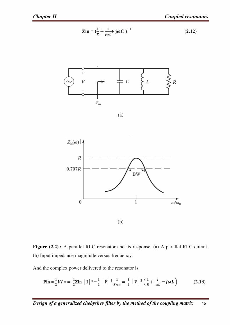
Chapter II Coupled resonators
Design of a generalized chebyshev filter by the method of the coupling matrix 45
Zin = ( + + jωC )¯ (2.12)
(a)
(b)
Figure (2.2) : A parallel RLC resonator and its response. (a) A parallel RLC circuit.
(b) Input impedance magnitude versus frequency.
And the complex power delivered to the resonator is
Pin = ∗= Zin I² = ∗ = + (2.13)

Chapter II Coupled resonators
Design of a generalized chebyshev filter by the method of the coupling matrix 46
The power dissipated by the resistor, R, is
Ploss = ²
(2.14a)
The average electric energy stored in the capacitor, C, is
We = (2.14b)
And the average magnetic energy stored in the inductor, L, is
Wm = = V²²
(2.14c)
Where is the current through the inductor. Then the complex power of (6.13) can be
rewritten a
Pin = Ploss + 2jω ( Wm We ) (2.15)
Which is identical to (6.4). Similarly, the input impedance can be expressed as
Zin = ²= + ² (2.16)
Which is identical to (6.5) .
As in the series case, resonance occurs when Wm = We. Then from (2.16) and (2.14a)
the input impedance at resonance is
= | | =
Which is purely real impedance. From (2.14b) and (2.14c), Wm = We implies that the
resonant frequency, ω0, can be defined as
= √ (2.17)

Chapter II Coupled resonators
Design of a generalized chebyshev filter by the method of the coupling matrix 47
Which is identical to the series resonant circuit case. Resonance in the case of a
parallel RLC circuit is sometimes referred to as an ant resonance.
From the definition of (2.7), and the results in (2.14), the unloaded Q of the parallel
resonant circuit can be expressed as
Q0 = = (2.18)
Since Wm = We at resonance. This result shows that the Q of the parallel resonant
circuit increases as R increases
Near resonance, the input impedance of (2.12) can be simplified using the series
expansion result that
+ ≃ + ⋯,
Again letting ω= + ∆ω, where∆ωis small, allows (2.12) to be rewritten as
Zin ≃ ( + ∆ + + ∆ ≃ + j
∆ + ∆ −
≃ + ∆ ¯ ≃ + ∆ = + ∆ / (2.19)
Since = 1/LC. When R = ∞ (2.19) reduces to
Zin =
As in the series resonator case, the effect of loss can be accounted for by replacing
in this expression with a complex effective resonant frequenc

Chapter II Coupled resonators
Design of a generalized chebyshev filter by the method of the coupling matrix 48
← + (2.20)
Figure 2.2b shows the behaviour of the magnitude of the input impedance versus
frequency. The half-power bandwidth edges occur at frequencies (∆ω/ = BW/2)
such that
Zin² = ²
Which, from (2.19), implies that
BW = (2.20)
As in the series resonance case
II .2.Loaded and unloaded Q:
The unloaded , , defined in the preceding sections is a characteristic of the
resonator itself, in the absence of any loading effects caused by external circuitry. In
practice, however, a resonator is invariably coupled to other circuitry, which will have
the effect of lowering the overall, or loaded, , of the circuit. Figure 2.3 depicts a
resonator coupled to an
Figure (2.3) : A resonant circuit connected to an external load,
External load resistor, . If the resonator is a series RLC circuit, the load resistor.
Adds in series with R, so the effective resistance in (2.8) is R + . If the resonator is
a parallel RLC circuit, the load resistor combines in parallel with R, so the effective
resistance in (2.18) is R/ (R + ). If we define n external Q ,, a (2.23)
Chapter II Coupled resonators
Design of a generalized chebyshev filter by the method of the coupling matrix 49
Qe = , Then the loaded Q can be expressed as
= = (2.23)
II.3.Formulation for extracting external quality factor Q e:
Two typical input/output (I/O) coupling structures for coupled micro strip resonator
filters, namely the tapped-line and the coupled-line structures, are shown with the
micro strip open-loop resonator, although other types of resonator may be used (see
Figure 2.4). For the tapped-line coupling, usually a 50-Ωfeed line is directly tapped
on to the I/O resonator, and the coupling or the external quality factor is controlled
by the tapping position t, as indicated in Figure 2.4a. For example, the smaller the
t, the closer is the tapped line to a virtual grounding of the resonator, which results
in a weaker coupling or a larger external quality factor. The coupling of the coupled
line stricture in Figure 2.4b can be found from the coupling gap g and the line width
w. normally, a smaller gap and a narrower line result in a stronger I/O coupling or a
smaller external quality factor of the resonator.
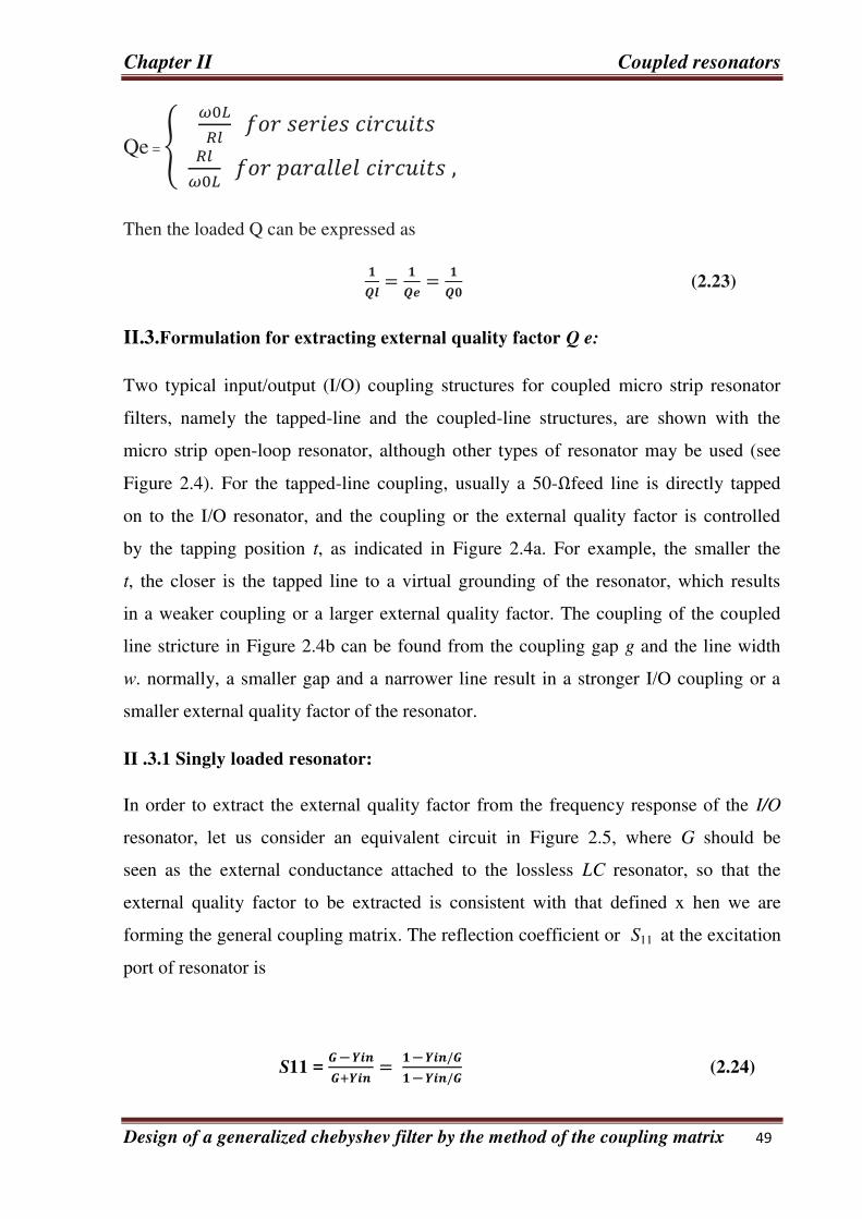
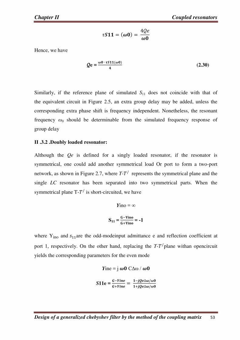
II .3.1 Singly loaded resonator:
In order to extract the external quality factor from the frequency response of the I/O
resonator, let us consider an equivalent circuit in Figure 2.5, where G should be
seen as the external conductance attached to the lossless LC resonator, so that the
external quality factor to be extracted is consistent with that defined x hen we are
forming the general coupling matrix. The reflection coefficient or S11 at the excitation
port of resonator is
S11 = + = / / (2.24)

Chapter II Coupled resonators
Design of a generalized chebyshev filter by the method of the coupling matrix 50
Where is the input admittance of the resonator
Yin = jωC + = (2.25)
(a) (b)
Figure (2.4) : Typical I/O coupling structures for coupled resonator filters. (a)
Tapped-line coupling. (b) Coupled-line coupling.
Formulation for extracting external quality factor Qe
Figure (2.5) : Equivalent circuit of the I/O resonator with singly loading.

Chapter II Coupled resonators
Design of a generalized chebyshev filter by the method of the coupling matrix 51
Note that = 1/√ is the resonant frequency. In the vicinity of resonance, say,
ω= +∆ω, Eq. (2.25) may be simplified as
Yin = j C.∆
(2.26)
Where the approximation ( - /ω ≈ 2 ∆ ωhas been used. By substituting
Eq. (2.26) into Eq. (2.24) and noting Qe= C/G, we obtain
= . ∆ /+ . ∆ /
Since we have assumed that the resonator is lossless, the magnitude of in
Eq. (2.27) is always equal to 1. This is because that in the vicinity of resonance, the
parallel resonator of Figure 2.5 behaviour likes an open circuit. However, the phase
response of changes against frequency. A plot of the phase of as a function of
ω/ is given in Figure 2.6. When the phase is ±90 the corresponding value of ∆ω is found to be
2e∆∓ =∓ (2.27)
Hence, the absolute bandwidth between the ±90 points is
∆ω∓ ° =∆ −∆ =
The external quality factor can then be extracted from this relation
e = ∆ ∓ ° (2.28)
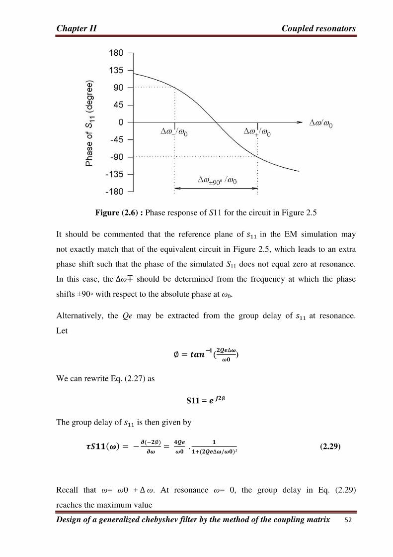
Chapter II Coupled resonators
Design of a generalized chebyshev filter by the method of the coupling matrix 52
Figure (2.6) : Phase response of S11 for the circuit in Figure 2.5
It should be commented that the reference plane of in the EM simulation may
not exactly match that of the equivalent circuit in Figure 2.5, which leads to an extra
phase shift such that the phase of the simulated S11 does not equal zero at resonance.
In this case, the ∆ω∓ should be determined from the frequency at which the phase
shifts ±90 with respect to the absolute phase at ω0.
Alternatively, the Qe may be extracted from the group delay of at resonance.
Let ∅ = ¯ ∆)
We can rewrite Eq. (2.27) as
S11 = ∅
The group delay of is then given by
= − − ∅ = . + ∆ / ² (2.29)
Recall that ω= ω0 + ∆ ω. At resonance ω= 0, the group delay in Eq. (2.29)
reaches the maximum value
Chapter II Coupled resonators
Design of a generalized chebyshev filter by the method of the coupling matrix 53
= = 4
Hence, we have
e = ∙ (2.30)
Similarly, if the reference plane of simulated S11 does not coincide with that of
the equivalent circuit in Figure 2.5, an extra group delay may be added, unless the
corresponding extra phase shift is frequency independent. Nonetheless, the resonant
frequency ω0 should be determinable from the simulated frequency response of
group delay
II .3.2 .Doubly loaded resonator:
Although the Qe is defined for a singly loaded resonator, if the resonator is
symmetrical, one could add another symmetrical load Or port to form a two-port
network, as shown in Figure 2.7, where T-/ represents the symmetrical plane and the
single LC resonator has been separated into two symmetrical parts. When the
symmetrical plane T-/ is short-circuited, we have
Yino = ∞
S11 = −+ = -1
where Yino and are the odd-modeinput admittance e and reflection coefficient at
port 1, respectively. On the other hand, replacing the T-/plane withan opencircuit
yields the corresponding parameters for the even mode
Yine = j C∆ω /
S11e = −+ = − ∆ /+ ∆ /
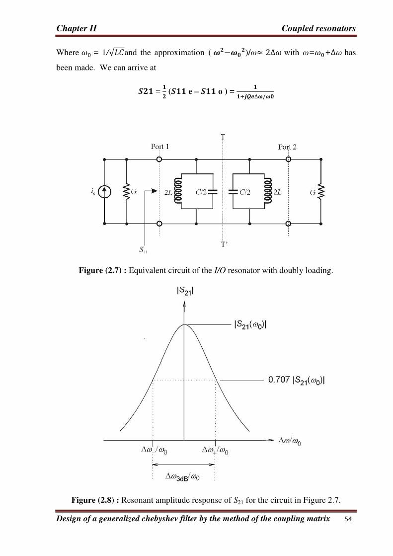
Chapter II Coupled resonators
Design of a generalized chebyshev filter by the method of the coupling matrix 54
Where = 1/√and the approximation ( − )/ω≈ ∆ with ω= +∆ has
been made. We can arrive at
= ( e – o ) = + ∆ /
Figure (2.7) : Equivalent circuit of the I/O resonator with doubly loading.
Figure (2.8) : Resonant amplitude response of S21 for the circuit in Figure 2.7.

Chapter II Coupled resonators
Design of a generalized chebyshev filter by the method of the coupling matrix 55
Whose magnitude is given by
S21=√ + ∆ / ² (2.31)
Shown in Figure 2.8 is a plot of | | against ∆ω/ At resonance, ∆ω= 0 and, thus,
|S21| reaches its maximum value, namely, | ( )| = 1. When the frequency shifts
such that
∆ ± = ± (2.32)
The value of | | has fallen to 0.707 (or −3 dB) of its maximum value according to
Eq. (2.31). Define a bandwidth based on Eq. (2.32)
∆ω3dB = ∆ω −∆ = / (2.33)
Where ∆ω3dB is the bandwidth for which the attenuation for is up 3 dB from that
at resonance, as indicated in Figure 2.8. Define a doubly loaded external quality
factor Qe as
e´ = = ∆ (2.34)
Using Eq. (2.34) to extract the /first and then the singly loaded external quality
factor Qe is simply the twice of /. It should be mentioned that even though the formulations made in this section are
based on the parallel resonator, there is no loss of generality, because the same
formulas as seen in Eqs. (2.28), (2.30), and (2.34) could be found for the series
resonator as well.
Chapter II Coupled resonators
Design of a generalized chebyshev filter by the method of the coupling matrix 56
II.4. General coupling matrix for coupled-resonator filters :
II.4.1. Loop equation formulation:
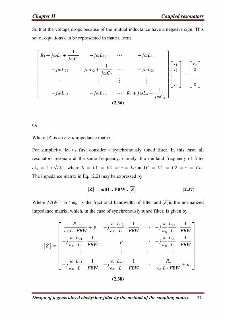
Shown in Figure 3.1a is an equivalent circuit of n-coupled resonators. L, C, and R
denote the inductance, capacitance, and resistance, respectively, i represent the loop
current, and es the voltage source. Using the voltage law, which is one of Kirchhoff’s
two circuit laws, and states that the algebraic sum of the voltage drops around any
closed path in a network is zero, we can write down the loop equations for the circuit
of Figure 3.1a
(R1 + jωL1 + − …− =
-jωL21i1 + (jωL2 + …− =
- jωLn1i1 – jωLn2i2 ... + (Rn + jωLn + = (2.35)
In which = represents the mutual inductance between resonators i and j and
the all loop currents are supposed to have the same direction, as shown in Figure 3.1a,
Figure (3.1) : (a) Equivalent circuit of n-coupled resonators for loop-equation
formulation. (b) Its network representation.
Chapter II Coupled resonators
Design of a generalized chebyshev filter by the method of the coupling matrix 57
So that the voltage drops because of the mutual inductance have a negative sign. This
set of equations can be represented in matrix form
(2.36)
Or
Where [Z] is an n × n impedance matrix .
For simplicity, let us first consider a synchronously tuned filter. In this case, all
resonators resonate at the same frequency, namely, the midland frequency of filter = /√ , where = = =···= and = = =···= .
The impedance matrix in Eq. (2.2) may be expressed by
[ ] = L . FBW . [ ] (2.37)
Where FBW = ω / ω0 is the fractional bandwidth of filter and []is the normalized
impedance matrix, which, in the case of synchronously tuned filter, is given by
(2.38)
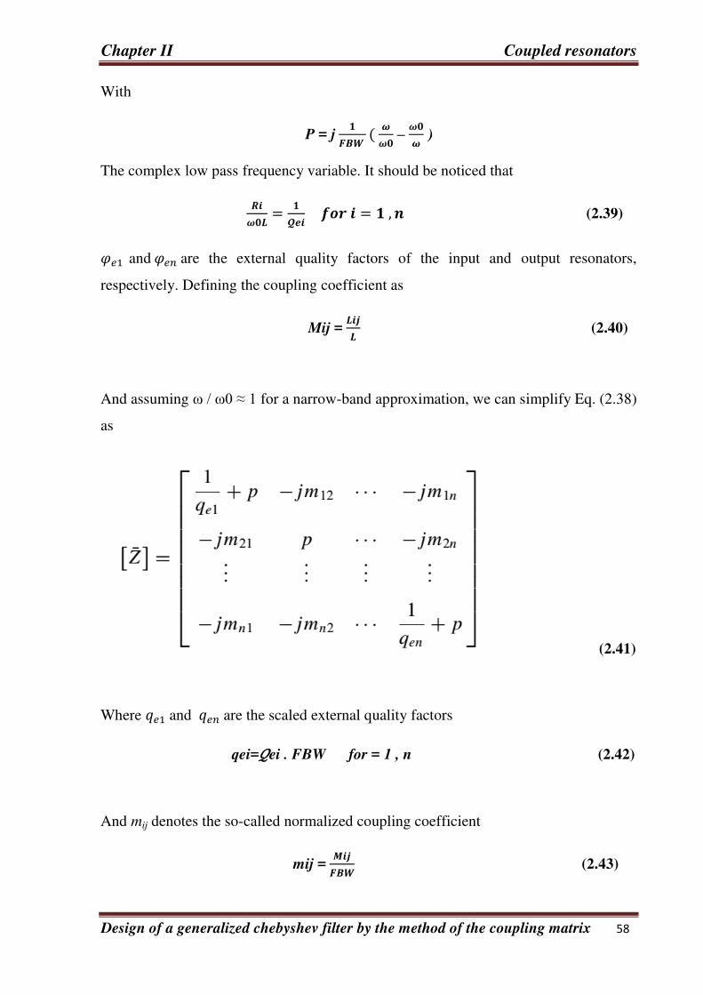
Chapter II Coupled resonators
Design of a generalized chebyshev filter by the method of the coupling matrix 58
With
P = j – )
The complex low pass frequency variable. It should be noticed that
= = , (2.39)
and are the external quality factors of the input and output resonators,
respectively. Defining the coupling coefficient as
Mij = (2.40)
And assuming ω / ω0 ≈ 1 for a narrow-band approximation, we can simplify Eq. (2.38)
as
(2.41)
Where and are the scaled external quality factors
qei=ei . FBW for = 1 , n (2.42)
And mij denotes the so-called normalized coupling coefficient
mij = (2.43)
Chapter II Coupled resonators
Design of a generalized chebyshev filter by the method of the coupling matrix 59
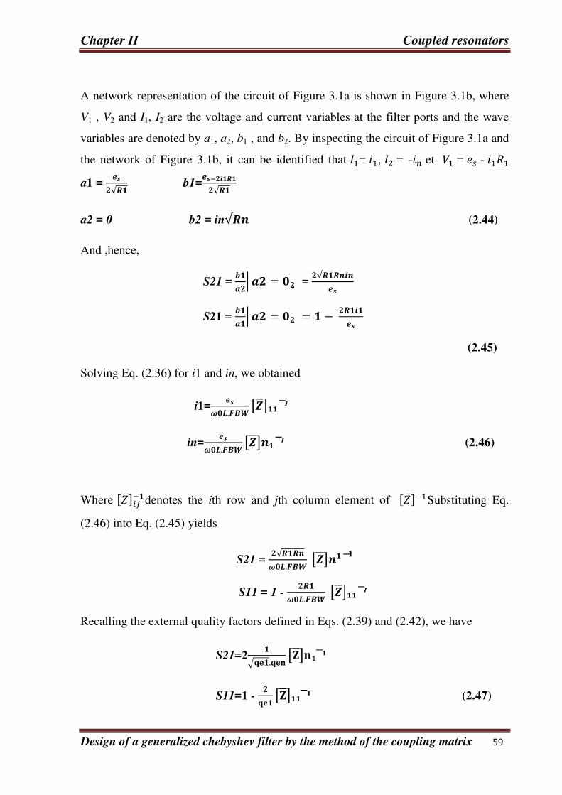
A network representation of the circuit of Figure 3.1a is shown in Figure 3.1b, where
V1 , V2 and I1, I2 are the voltage and current variables at the filter ports and the wave
variables are denoted by a1, a2, b1 , and b2. By inspecting the circuit of Figure 3.1a and
the network of Figure 3.1b, it can be identified that = , = - et = -
a1 = √ b1=−√
a2 = 0 b2 = in√ (2.44)
And ,hence,
S21 = | = = √
S21 = | = = −
(2.45)
Solving Eq. (2.36) for i1 and in, we obtained
i1= . [ ]₁₁¯¹
in= . [ ] ₁¯¹ (2.46)
Where []− denotes the ith row and jth column element of []− Substituting Eq.
(2.46) into Eq. (2.45) yields
S21 = √ . [ ] ¯
S11 = 1 - . [ ]₁₁¯¹
Recalling the external quality factors defined in Eqs. (2.39) and (2.42), we have
S21=2√ . []₁¯¹
S11=1 - []₁₁¯¹ (2.47)
Chapter II Coupled resonators
Design of a generalized chebyshev filter by the method of the coupling matrix 60
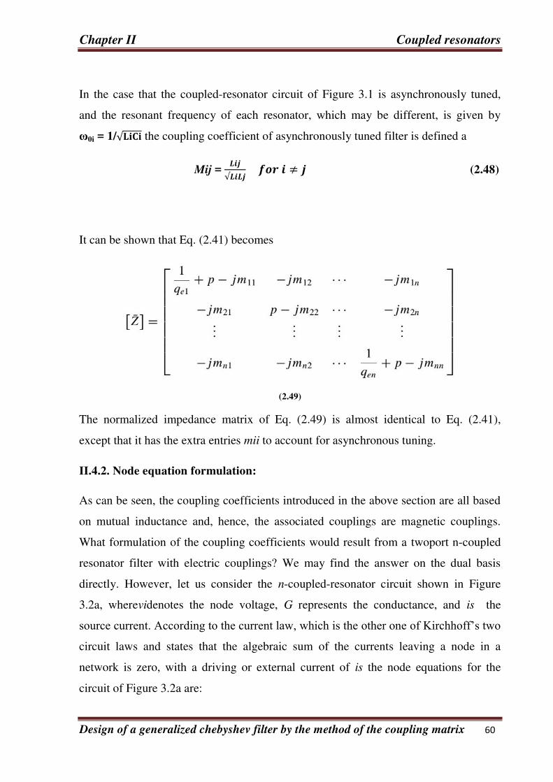
In the case that the coupled-resonator circuit of Figure 3.1 is asynchronously tuned,
and the resonant frequency of each resonator, which may be different, is given by
ω0i = 1/√ the coupling coefficient of asynchronously tuned filter is defined a
Mij = √ ≠ (2.48)
It can be shown that Eq. (2.41) becomes
(2.49)
The normalized impedance matrix of Eq. (2.49) is almost identical to Eq. (2.41),
except that it has the extra entries mii to account for asynchronous tuning.
II.4.2. Node equation formulation:
As can be seen, the coupling coefficients introduced in the above section are all based
on mutual inductance and, hence, the associated couplings are magnetic couplings.
What formulation of the coupling coefficients would result from a twoport n-coupled
resonator filter with electric couplings? We may find the answer on the dual basis
directly. However, let us consider the n-coupled-resonator circuit shown in Figure
3.2a, wherevidenotes the node voltage, G represents the conductance, and is the
source current. According to the current law, which is the other one of Kirchhoff’s two
circuit laws and states that the algebraic sum of the currents leaving a node in a
network is zero, with a driving or external current of is the node equations for the
circuit of Figure 3.2a are:

Chapter II Coupled resonators
Design of a generalized chebyshev filter by the method of the coupling matrix 61
-(G1 + jωC1 + − … .− =
-J + + …− =
-j − …+ + + = (2.50)
Where Cij= Cji represents the mutual capacitance across resonators iand j. Note that
all node voltages are determined with respect to the reference node (ground), so
Figure (3.2) : (a) Equivalent circuit of n-coupled resonators for node-equation
formulation. (b) Its network representation.
That the currents resulting from the mutual capacitance have a negative sign. Arrange
this set of equations in matrix form
(2.51)
Or
Chapter II Coupled resonators
Design of a generalized chebyshev filter by the method of the coupling matrix 62
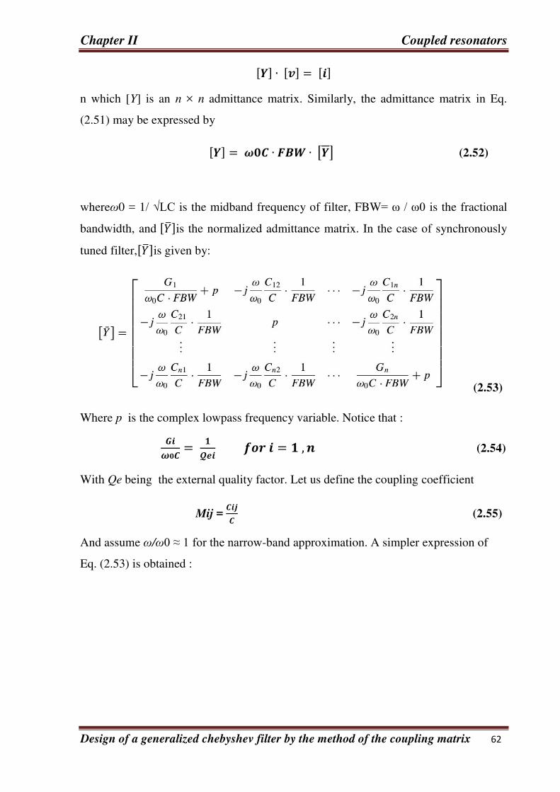
[ ] ∙ [] = [ ] n which [Y] is an n × n admittance matrix. Similarly, the admittance matrix in Eq.
(2.51) may be expressed by
[ ] = ∙ ∙ [ ] (2.52)
whereω0 = 1/ √LC is the midband frequency of filter, FBW= ω / ω0 is the fractional
bandwidth, and []is the normalized admittance matrix. In the case of synchronously
tuned filter,[]is given by:
(2.53)
Where p is the complex lowpass frequency variable. Notice that :
= = , (2.54)
With Qe being the external quality factor. Let us define the coupling coefficient
Mij = (2.55)
And assume ω/ω0 ≈ 1 for the narrow-band approximation. A simpler expression of
Eq. (2.53) is obtained :
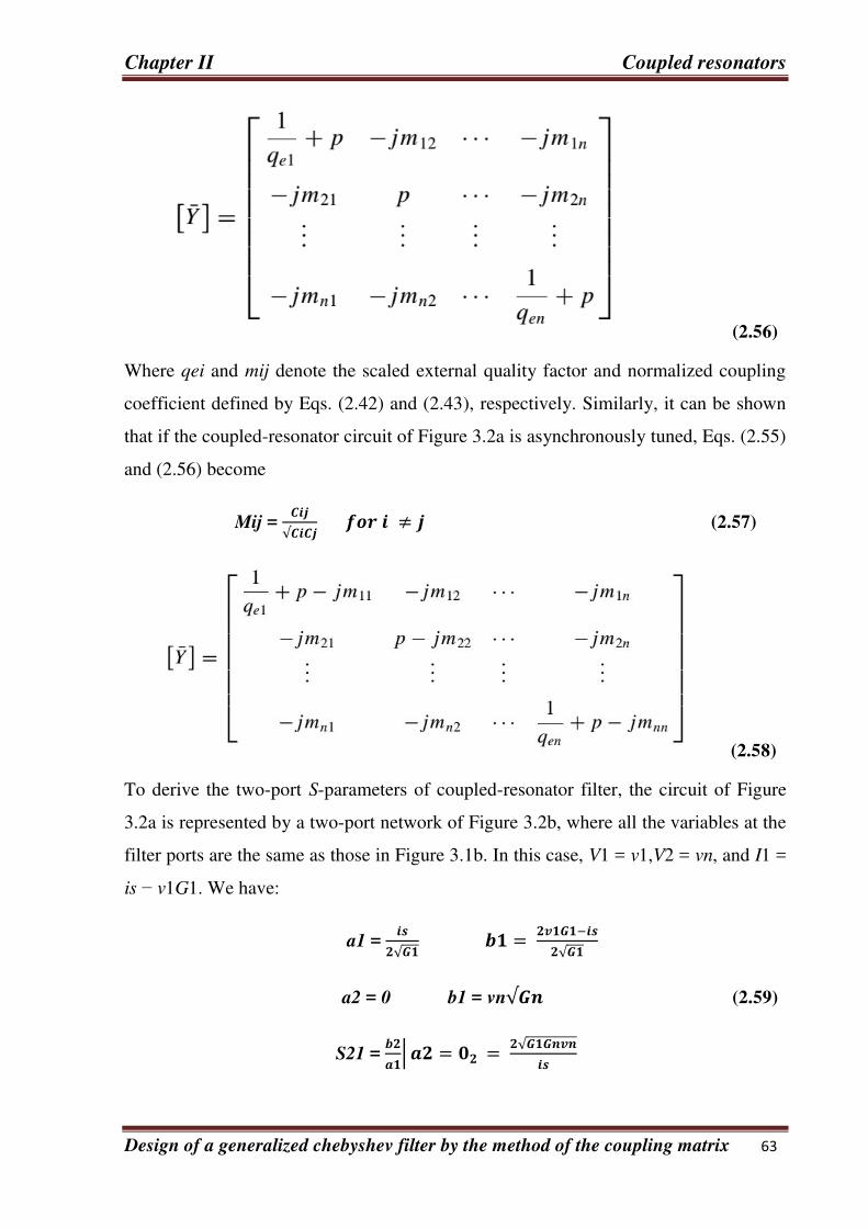
Chapter II Coupled resonators
Design of a generalized chebyshev filter by the method of the coupling matrix 63
(2.56)
Where qei and mij denote the scaled external quality factor and normalized coupling
coefficient defined by Eqs. (2.42) and (2.43), respectively. Similarly, it can be shown
that if the coupled-resonator circuit of Figure 3.2a is asynchronously tuned, Eqs. (2.55)
and (2.56) become
Mij = √ ≠ (2.57)
(2.58)
To derive the two-port S-parameters of coupled-resonator filter, the circuit of Figure
3.2a is represented by a two-port network of Figure 3.2b, where all the variables at the
filter ports are the same as those in Figure 3.1b. In this case, V1 = v1,V2 = vn, and I1 =
is − v1G1. We have:
a1 = √ = −√ a2 = 0 b1 = vn√ (2.59)
S21 = | = = √
Chapter II Coupled resonators
Design of a generalized chebyshev filter by the method of the coupling matrix 64
S11 = | = = − (2.60)
Finding the unknown node voltages v1 and vnfrom Eq. (2.51)
V1 = ∙ [ ] ¯¹
Vn = ∙ [ ] ¯ (2.61)
Where []− denotes the ith row and jth column element of []Replacing the node
voltages in Eq. (2.60) with those given by Eq. (2.61) results in
S21= √ ∙ [ ] ¯¹
S11= ∙ [ ] ¯ −
(2.62)
which can be simplified as
S21= 2√ ∙ [ ] ¯¹ S11= [ ] ¯ −
(2.63)
II.4.3. General coupling matrix :
In the foregoing formulations, the most notable is that the formulation of normalized
impedance matrix []is identical to that of normalized admittance matrix [] . This is
very important, because it implies that we could have a unified formulation for an-
coupled resonator filter regardless of whether the couplings are magnetic or electric or
even the combination of both. Accordingly, Eqs. (2.47) and (2,63) may be
incorporated into a general one:
Chapter II Coupled resonators
Design of a generalized chebyshev filter by the method of the coupling matrix 65
S11=± − [] ¯¹ (2.64)
With [] = [] + [] − [] where [U] is the n × n unit or identity matrix, [q] is an n × n matrix with all entries
zero, except forq11 = 1/qe1 and qnn= 1/qen, and [m] is the so-called general coupling
matrix, which is an n × n reciprocal matrix (that is, mij= mji) and is allowed to have
nonzero diagonal entries mii for an asynchronously tuned filter.
II.5. General theory of couplings:
After determining the required coupling matrix for the desired filtering characteristic, a
next important step for the filter design is to establish the relationship between the
value of every required coupling coefficient and the physical structure of coupled
resonators in order to find the physical dimensions of the filter for fabrication.
In general, the coupling coefficient of coupled RF/microwave resonators, which can be
different in structure and can have different self-resonant frequencies (see Figure 3.3),
may be defined on the basis of a ratio of coupled to stored energy [12], i.e.,
k= ∭ ∙ √∭ ² ×∭ ² + ∭ √∭ ² ×∭ ² (2.65)
Whereand represent the electric and magnetic field vectors, respectively; we now
use the more traditional notation k instead of M for the coupling coefficient. Note that
all fields are determined at resonance and the volume integrals are over entire effecting
regions with permittivity of ε and permeability of µ. The first term on the right-hand
side represents the electric coupling, while the second term represents the magnetic

Chapter II Coupled resonators
Design of a generalized chebyshev filter by the method of the coupling matrix 66
Figure (3.3) : General coupled RF/microwave resonators where resonators 1 and 2 can
be different in structure and have different resonant frequencies.
Coupling .It should be remarked that the interaction of the coupled resonators is
mathematically described by the dot operation of their space vector fields, which
allows the coupling to have either positive or negative sign. A positive sign would
imply that the coupling enhances the stored energy of uncoupled resonators, whereas a
negative sign would indicate a reduction. Therefore, the electric and magnetic
couplings could either have the same effect if they have the same sign, or have the
opposite effect if their signs are opposite. Obviously, the direct evaluation of coupling
coefficient from Eq. (2.65) requires the knowledge of the field distributions and
performance of the space integrals. This is not an easy task unless analytical solutions
of the fields exist. On the other hand, it may be much easier by using full-wave EM
simulation or experiment to find some characteristic frequencies that are associated
with the coupling of coupled RF/microwave resonators. The coupling coefficient can
then be determined against the physical structure of coupled resonators if the
relationship between the coupling coefficient and the characteristic frequencies is
established.In what follows; we derive the formulation of such relationships. Before
processing further, it might be worth pointing out that although the following
derivations are based on lumped-element circuit models, the outcomes are also valid
for distributedelement coupled structures on a narrow-band basis.[8]

Chapter II Coupled resonators
Design of a generalized chebyshev filter by the method of the coupling matrix 67
II.5.1. Synchronously tuned coupled-resonator circuits:
II.5.1.1. Electric coupling :
An equivalent lumped-element circuit model for electrically coupled RF/microwave
resonators is given in Figure 3.4a, where L and C are the self-inductance and self-
capacitance, so that − / equals the angular resonant frequency of uncoupled
resonators, and Cm represents the mutual capacitance. As mentioned earlier, if the
coupled structure is a distributed element, the lumped-element circuit equivalence is
valid on a narrow-band basis namely, near its resonance. The same comment is
applicable for the other coupled structures discussed later. If we look into reference
planes − ′ and − ′ , we can see a two-port network that may be described by
the following set of equations:
I1 = jωCV1 – jωCmV2
I2 = jωCV2 – jωCmV1 (2.66)
in which a sinusoidal waveform is assumed. It might be well to mention that Eq. (2.66)
implies that the self-capacitance C is the capacitance seen in one resonant loop of
Figure 3.4a when the capacitance in the adjacent loop is shorted out. Thus, the second
terms on the R.H.S. of Eq. (2.66) are the induced currents resulting from the increasing
voltage in resonant loops 2 and 1, respectively. From Eq. (2.66) four parameters
Y11 = Y22 = jωC
Y12 = Y21 = -jωCm (2.67)
can easily be found from definitions.

Chapter II Coupled resonators
Design of a generalized chebyshev filter by the method of the coupling matrix 68
Figure (3.4) : (a) Synchronously tuned coupled resonator circuit with electric
coupling. (b) An alternative form of the equivalent circuit with an admittance inverter
J = ωCm to represent the coupling.
According to the network theory , an alternative form of the equivalent circuit in
Figure 3.4a can be obtained, and is shown in Figure 3.4b. This form yields the same
two-port parameters as those of the circuit of Figure 3.4a, but it is more convenient for
our discussions. Actually, it can be shown that the electric coupling between the two
resonant loops is represented by an admittance inverter J = ωCm. If the symmetry
plane − ′ in Figure 3.4b is replaced by an electric wall (or a short-circuit), the
resultant circuit has a resonant frequency
Chapter II Coupled resonators
Design of a generalized chebyshev filter by the method of the coupling matrix 69
= √ + (2.68)
This resonant frequency is lower than that of an uncoupled single resonator. A
physical explanation is that the coupling effect enhances the capability to store charge
of the single resonator when the electric wall is inserted in the symmetrical plane of
the coupled structure. Similarly, replacing the symmetry plane in Figure 3.4b by a
magnetic wall (or an open-circuit) results in a single resonant circuit having a resonant
frequency
= √ + (2.69)
In this case, the coupling effect reduces the capability to store charge so that
theresonant frequency is increased.
Equations (2.68) and (2.69) can be used to find the electric coupling coefficient
= ²−²²+²= (2.70)
which is not only identical to the definition of ratio of the coupled electric energy to
the stored energy of uncoupled single resonator, but also consistent with the coupling
coefficient defined by Eq. (2.55) for coupled-resonator filter.
II.5.1.2.Magnetic coupling:
Shown in Figure 3.5a is an equivalent lumpedelement circuit model for magnetically
coupled resonator structures, where L and C are the self-inductance and self-
capacitance, and Lm represents the mutual inductance. In this case, the coupling
equations describing the two-port network at reference planes − ′ and − ′ are :
= +
= + (2.71)
Chapter II Coupled resonators
Design of a generalized chebyshev filter by the method of the coupling matrix 70
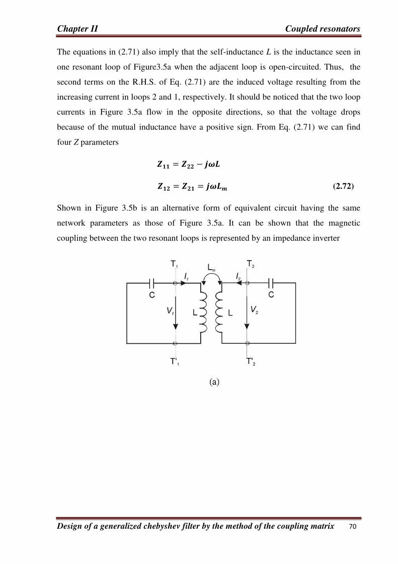
The equations in (2.71) also imply that the self-inductance L is the inductance seen in
one resonant loop of Figure3.5a when the adjacent loop is open-circuited. Thus, the
second terms on the R.H.S. of Eq. (2.71) are the induced voltage resulting from the
increasing current in loops 2 and 1, respectively. It should be noticed that the two loop
currents in Figure 3.5a flow in the opposite directions, so that the voltage drops
because of the mutual inductance have a positive sign. From Eq. (2.71) we can find
four Z parameters
= −
= = (2.72)
Shown in Figure 3.5b is an alternative form of equivalent circuit having the same
network parameters as those of Figure 3.5a. It can be shown that the magnetic
coupling between the two resonant loops is represented by an impedance inverter

Chapter II Coupled resonators
Design of a generalized chebyshev filter by the method of the coupling matrix 71
Figure (3.5) :(a) Synchronously tuned coupled resonator circuit with magnetic
coupling. (b) An alternative form of the equivalent circuit with an impedance inverter
K = ωLm to represent the coupling.
K = ωLm. If the symmetry plane T-T in Figure 3.5b is replaced by an electric wall (or
a short-circuit), the resultant single-resonant circuit has a resonant frequency
= √ − (2.73)
It can be shown that the increase in resonant frequency is because the coupling effect
reducing the stored flux in the single resonator circuit when the electric wall is inserted
in the symmetric plane. If a magnetic wall (or an open-circuit) replaces the symmetry
plane in Figure 7.5b, the resultant single-resonant circuit has a resonant frequency
= √ + (2.74)
In this case, it turns out that the coupling effect increases the stored flux, so that the
resonant frequency is shifted down.
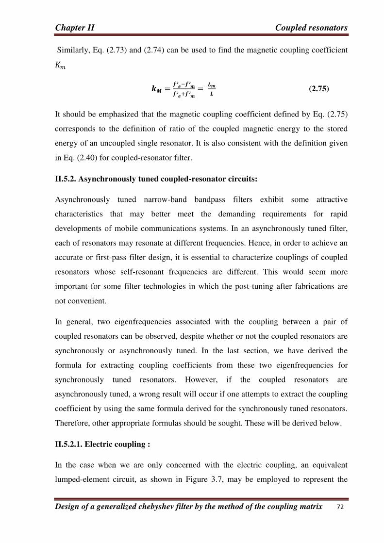
Chapter II Coupled resonators
Design of a generalized chebyshev filter by the method of the coupling matrix 72
Similarly, Eq. (2.73) and (2.74) can be used to find the magnetic coupling coefficient
= ² − ²
² + ²= (2.75)
It should be emphasized that the magnetic coupling coefficient defined by Eq. (2.75)
corresponds to the definition of ratio of the coupled magnetic energy to the stored
energy of an uncoupled single resonator. It is also consistent with the definition given
in Eq. (2.40) for coupled-resonator filter.
II.5.2. Asynchronously tuned coupled-resonator circuits:
Asynchronously tuned narrow-band bandpass filters exhibit some attractive
characteristics that may better meet the demanding requirements for rapid
developments of mobile communications systems. In an asynchronously tuned filter,
each of resonators may resonate at different frequencies. Hence, in order to achieve an
accurate or first-pass filter design, it is essential to characterize couplings of coupled
resonators whose self-resonant frequencies are different. This would seem more
important for some filter technologies in which the post-tuning after fabrications are
not convenient.
In general, two eigenfrequencies associated with the coupling between a pair of
coupled resonators can be observed, despite whether or not the coupled resonators are
synchronously or asynchronously tuned. In the last section, we have derived the
formula for extracting coupling coefficients from these two eigenfrequencies for
synchronously tuned resonators. However, if the coupled resonators are
asynchronously tuned, a wrong result will occur if one attempts to extract the coupling
coefficient by using the same formula derived for the synchronously tuned resonators.
Therefore, other appropriate formulas should be sought. These will be derived below.
II.5.2.1. Electric coupling :
In the case when we are only concerned with the electric coupling, an equivalent
lumped-element circuit, as shown in Figure 3.7, may be employed to represent the
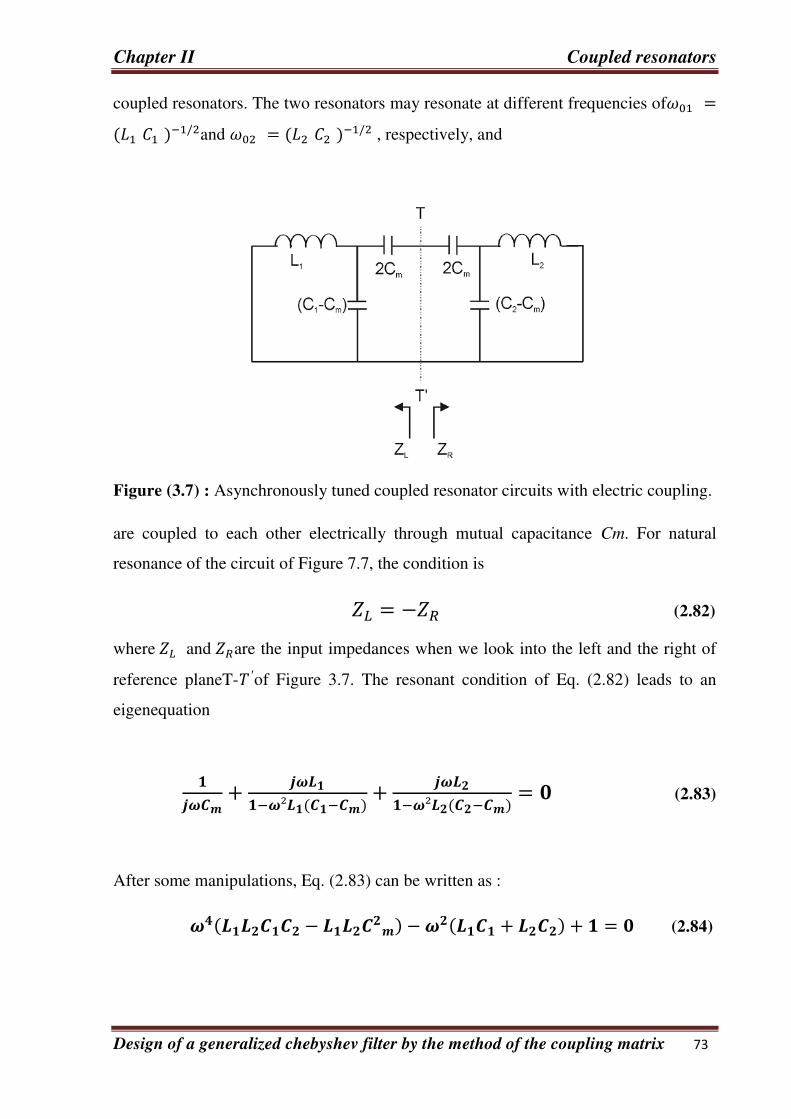
Chapter II Coupled resonators
Design of a generalized chebyshev filter by the method of the coupling matrix 73
coupled resonators. The two resonators may resonate at different frequencies of = − / and = − / , respectively, and
Figure (3.7) : Asynchronously tuned coupled resonator circuits with electric coupling.
are coupled to each other electrically through mutual capacitance Cm. For natural
resonance of the circuit of Figure 7.7, the condition is
= − (2.82)
where and are the input impedances when we look into the left and the right of
reference planeT-′of Figure 3.7. The resonant condition of Eq. (2.82) leads to an
eigenequation
+ − ² − + − ² − = (2.83)
After some manipulations, Eq. (2.83) can be written as :
− − + + = (2.84)
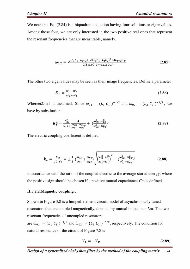
Chapter II Coupled resonators
Design of a generalized chebyshev filter by the method of the coupling matrix 74
We note that Eq. (2.84) is a biquadratic equation having four solutions or eigenvalues.
Among those four, we are only interested in the two positive real ones that represent
the resonant frequencies that are measurable, namely,
. = √ + ±√ + + ²− ² (2.85)
The other two eigenvalues may be seen as their image frequencies. Define a parameter
= ² − ²² + ²
(2.86)
Whereω2>ω1 is assumed. Since = − / and = − / , we
have by substitution
= + ²+ −+ ² (2.87)
The electric coupling coefficient is defined
= √ = ± + √ −+ − −+ ² (2.88)
in accordance with the ratio of the coupled electric to the average stored energy, where
the positive sign should be chosen if a positive mutual capacitance Cm is defined.
II.5.2.2.Magnetic coupling :
Shown in Figure 3.8 is a lumped-element circuit model of asynchronously tuned
resonators that are coupled magnetically, denoted by mutual inductance Lm. The two
resonant frequencies of uncoupled resonators
are = − / and = − / , respectively. The condition for
natural resonance of the circuit of Figure 7.8 is
= − (2.89)
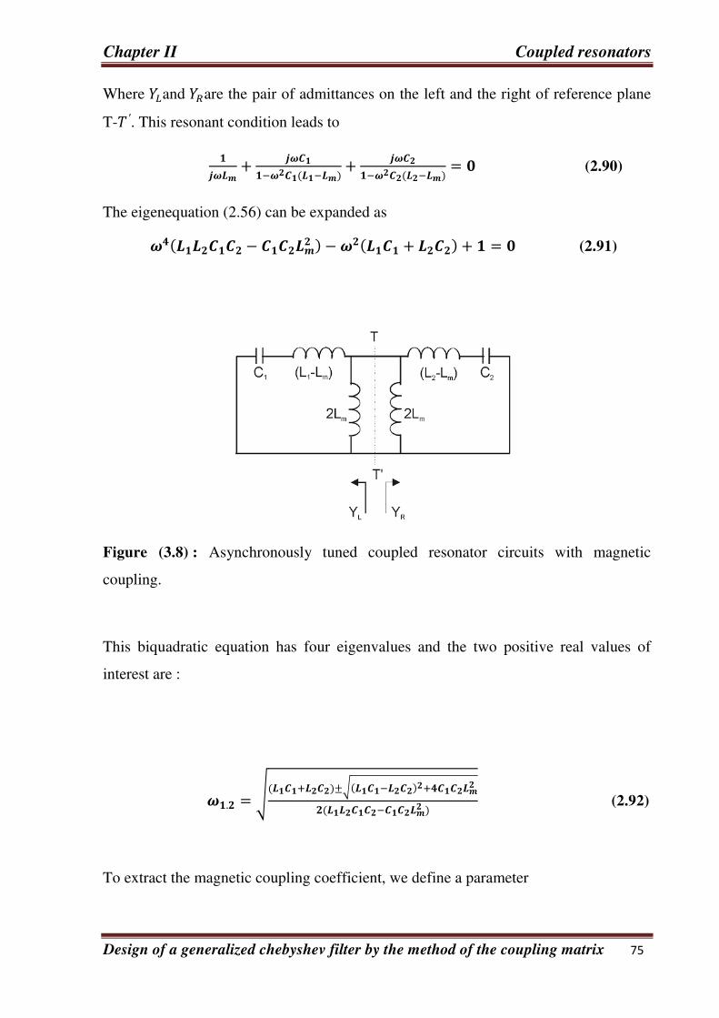
Chapter II Coupled resonators
Design of a generalized chebyshev filter by the method of the coupling matrix 75
Where and are the pair of admittances on the left and the right of reference plane
T- ′. This resonant condition leads to
+ − − + − − = (2.90)
The eigenequation (2.56) can be expanded as
− − + + = (2.91)
Figure (3.8) : Asynchronously tuned coupled resonator circuits with magnetic
coupling.
This biquadratic equation has four eigenvalues and the two positive real values of
interest are :
. = √ + ±√ − +− (2.92)
To extract the magnetic coupling coefficient, we define a parameter
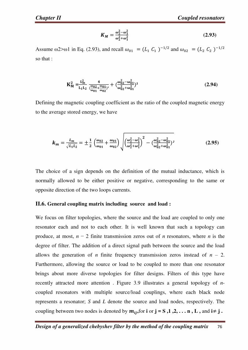
Chapter II Coupled resonators
Design of a generalized chebyshev filter by the method of the coupling matrix 76
= −+ (2.93)
Assume ω2>ω1 in Eq. (2.93), and recall = − / and = − /
so that :
= + ²
+ − + ² (2.94)
Defining the magnetic coupling coefficient as the ratio of the coupled magnetic energy
to the average stored energy, we have
= √ = ± + √ −+ − −+ ² (2.95)
The choice of a sign depends on the definition of the mutual inductance, which is
normally allowed to be either positive or negative, corresponding to the same or
opposite direction of the two loops currents.
II.6. General coupling matrix including source and load :
We focus on filter topologies, where the source and the load are coupled to only one
resonator each and not to each other. It is well known that such a topology can
produce, at most, n − 2 finite transmission zeros out of n resonators, where n is the
degree of filter. The addition of a direct signal path between the source and the load
allows the generation of n finite frequency transmission zeros instead of n – 2.
Furthermore, allowing the source or load to be coupled to more than one resonator
brings about more diverse topologies for filter designs. Filters of this type have
recently attracted more attention . Figure 3.9 illustrates a general topology of n-
coupled resonators with multiple source/load couplings, where each black node
represents a resonator; S and L denote the source and load nodes, respectively. The
coupling between two nodes is denoted by ,for i or j = S ,1 ,2, . . . n , L , and i≠ j .
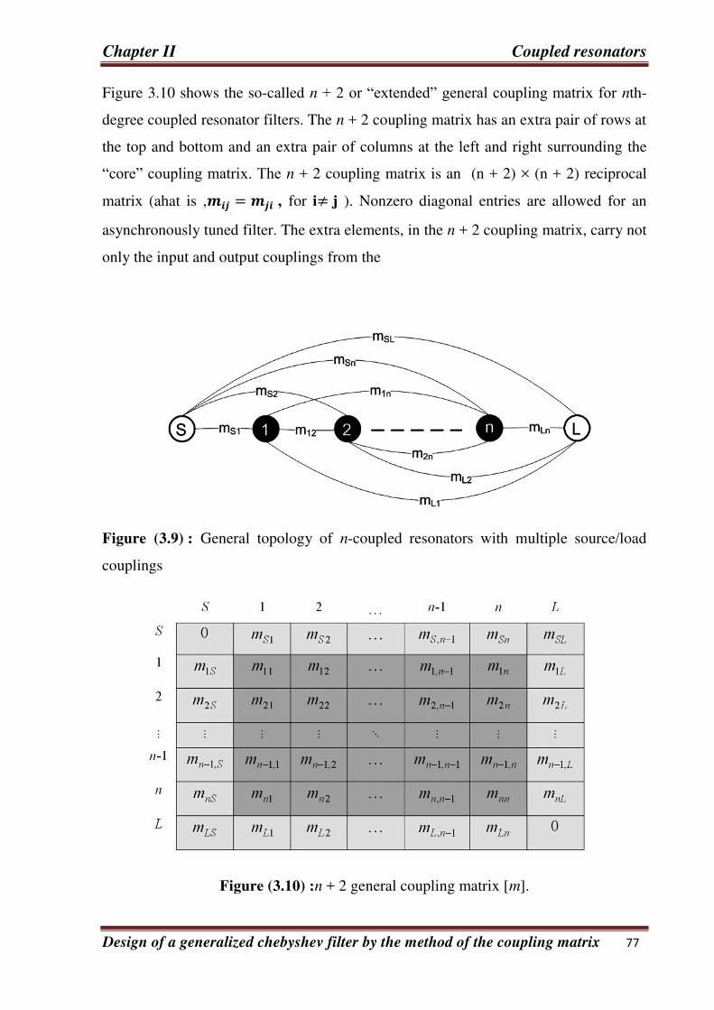
Chapter II Coupled resonators
Design of a generalized chebyshev filter by the method of the coupling matrix 77
Figure 3.10 shows the so-called n + 2 or “extended” general coupling matrix for nth-
degree coupled resonator filters. The n + 2 coupling matrix has an extra pair of rows at
the top and bottom and an extra pair of columns at the left and right surrounding the
“core” coupling matrix. The n + 2 coupling matrix is an (n + 2) × (n + 2) reciprocal
matrix (ahat is , = , for i≠ j ). Nonzero diagonal entries are allowed for an
asynchronously tuned filter. The extra elements, in the n + 2 coupling matrix, carry not
only the input and output couplings from the
Figure (3.9) : General topology of n-coupled resonators with multiple source/load
couplings
Figure (3.10) :n + 2 general coupling matrix [m].
Chapter II Coupled resonators
Design of a generalized chebyshev filter by the method of the coupling matrix 78
Source and load terminations to resonator nodes in the core matrix, but also a direct
coupling between the source and the load(that is , = ) . [10]
and ,which represent the input and output couplings from the source and load
to resonator i, can be converted to external quality factors by
, = ∙
, = ∙ (2.96)
Where FBW is the fractional bandwidth of bandpass filter.
For a given filter topology, the n + 2 coupling matrix may be obtained using synthesis
methods described . Once the coupling matrix [m] is determined, the filter frequency
responses can be computed in terms of scattering parameters:
= − [ ] + ,¯¹
= + [ ]¯¹ (2.97)
Where []− denotes the ith row and jth column element of []− The matrix [A] is
given by :
[ ] = [ ] + [ ] − [ ] (2.98)
in which [U] is similar to the (n + 2) × (n + 2) identity matrix, except that [] =[] + , + = ,[q] is the (n + 2) × (n+ 2) matrix with all entries zeros, except for [] = [] + , + = , and Ω is the frequency variable of lowpass prototype. The
lowpass prototype response can be transformed to a bandpass response having a
fractional bandwidth FBW at a center frequency ω0 using the well-known frequency
transformation:
= − (2.99)
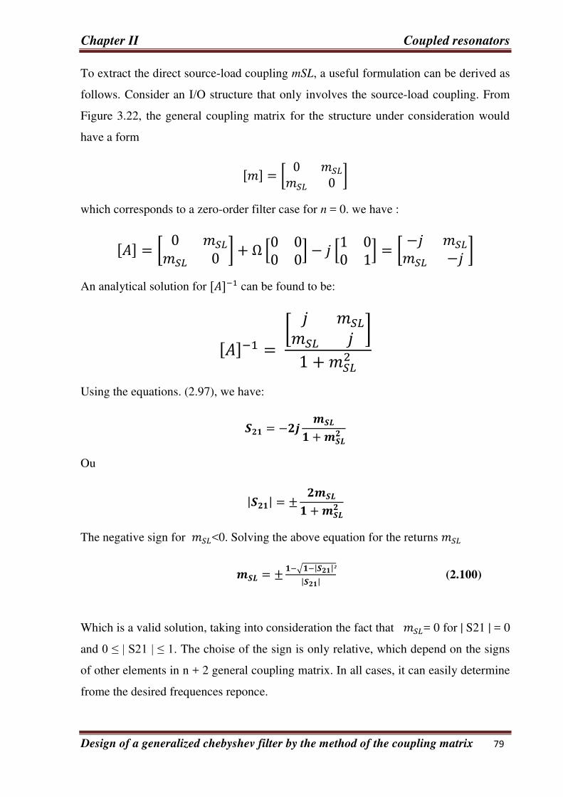
Chapter II Coupled resonators
Design of a generalized chebyshev filter by the method of the coupling matrix 79
To extract the direct source-load coupling mSL, a useful formulation can be derived as
follows. Consider an I/O structure that only involves the source-load coupling. From
Figure 3.22, the general coupling matrix for the structure under consideration would
have a form
[] = [ ] which corresponds to a zero-order filter case for n = 0. we have : [] = [ ] + Ω [ ] − [ ] = [ − − ] An analytical solution for []− can be found to be:
[]− = [ ]+
Using the equations. (2.97), we have:
= − +
Ou
| | = ± +
The negative sign for <0. Solving the above equation for the returns
= ± −√ −| |²| | (2.100)
Which is a valid solution, taking into consideration the fact that = 0 for | S21 | = 0
and 0 ≤ | S21 | ≤ 1. The choise of the sign is only relative, which depend on the signs
of other elements in n + 2 general coupling matrix. In all cases, it can easily determine
frome the desired frequences reponce.

Chapter II Coupled resonators
Design of a generalized chebyshev filter by the method of the coupling matrix 80
Conclusion :
The coupling coefficient of resonators is a dimensionless value that characterizes
interaction of two resonators. Coupling coefficients are used in resonator filter theory.
The coupling may be electrical or magnetic or both. Coupling coefficients together
with resonant frequencies and external quality factors of resonators are the generalized
parameters of filters. In order to adjust the frequency response of the filter it is
sufficient to optimize only these generalized parameters.

Chapter III Synthesis of the Chebyshev function generalise
Design of a generalized chebyshev filter by the method of the coupling matrix 82
Introduction :
In low frequency systems, Ohm’s Law is a suitable approximation for analysis of a
circuit schematic and transfer function H(s) provides important details such as gain,
stability, filter properties, and time-domain output information. On the contrary, at
high frequencies (microwave and higher) Ohm’s Law is not a suitable, and instead we
must use the transmission line theory. The Scattering (S) Matrix parameters play a key
role at higher frequencies by detailing a system’s gain, return loss, voltage standing
wave ratio (VSWR), reflection coefficient and amplifier stability (Wiki –
Sparameters). When we are designing filters, commonly we are dealing with two-port
networks where conveniently transfer function and S-Parameters analysis are both
possible. It is therefore a very a useful tool to be able to take a filter’s transfer function
properties and demonstrate a relationship with its scattering parameters for high
frequency information. In reality, there is a relationship between the two. S21 and H(s)
have a causal relationship, and S11 is nearly the inverse of H(s) which can be derived
in a lossless network using the lossless network property of S-Matrices. We can then
use the reciprocity and symmetry properties of S-Matrices such that |S22|=|S11| and
|S21|=|S12| where S22, S11, S21, and S12 may have different phase properties. Other
papers related to this topic describe other relationships of the S-Parameters from
transfer function qualities other than this method.
III.1.Polynomial forms of the transfer and reflection parameter (s) and (S)
for a two-port network:
For the great majority of the filter circuits, we shall initially consider two-port net-
works, a "source port" and a "load port" (Fig. 3.1).
For a two-port network, the scattering matrix is represented by a 2 x 2 matrix
[ ] = [ ] . [ ] (3.1)
Where b1, and b2 are the power waves propagating away from ports 1 and 2,
respectively, and a1, and a2 are the power waves incident at ports 1 and 2,
respectively.

Chapter III Synthesis of the Chebyshev function generalise
Design of a generalized chebyshev filter by the method of the coupling matrix 82
Figure (3.1): Twoport network
If the network is passive, lossless, and reciprocal, its 2 x 2 S-parameter matrix yields
conservation of energy equations:
(s) (s)* + (s) (s)* =1 (3.2)
(s) (s)* + (s) (s)* =1 (3.3)
And one unique orthogonality equation:
(s) (s)* + (s) (s)* =0 (3 .4)
Where the S parameters are now assumed to be functions of s (j) , the frequency
variable.
The reflection parameter (s) at port 1 of the network is expressed as the ratio of two
finite-degree polynomials E(s) and F(s), and real constant
(s)=⁄
(3.5)
For an Nth degree polynomial Q(s) with purely imaginary variable s = j and complex
coefficients , i = 0, 1, 2,. . . , N, (s) * is the same as ∗ ∗ or ∗ − , which
might be a little more familiar to the reader
If Q(s) = + + ² +....+
Then Q(s)* =Q*(-s)= ∗ − ∗ s + ∗ ²- ....+ ∗ ( N even)
......- ∗ ( N odd)

Chapter III Synthesis of the Chebyshev function generalise
Design of a generalized chebyshev filter by the method of the coupling matrix 82
The effect of this conjugating operation (paraconjugation)is to reflect the complex
singularities of Q(s) Symmetrically about the imaginary axis [as opposed to reflecting
about the real axis for the operation (s)→ ∗ (conjugation)].If the N complex-
plane singularitie of (s) are , k=1,2,...,N, I
then the singularities of ∗ or ∗ − will be − ∗ . When generating the
polynomial ∗ or ∗ − from the singularities of (s) using the transformed
variable → − ∗ , the resultant polynomial must be multiplied through by of − N
to give the correct sign to the new leading coefficient :
Q(s)* =Q*(-s) = − ∏ = (s + ∗ )
Where E(s) is an Nth-degree polynomial with complex coefficients , , ,…. ,
Where N is the degree of the filter network under consideration . Also, F(s) is an NTH
degree with complex coefficients , , ,…., . Allows the normalization of the
highest degree coefficients of E(s) and F(s) unity (i.e., and = 1). Because this is
a lossless passive network, E(s)is strictly Hurwitz; that is, all the roots of
E(s) [poles of (s)] are in the left half of the complex
plane, these poles need not be symmetric about the real axis.F(s), the numerator
polynomial of (s), for lowpass and bandpass filters is also of degree N. For
bandstop filters the degree of F(s) can be < . The roots of F(s) [zeros of (s)] are
the Points of zero reflected power ( =0),or points of perfect transmission.
by reorganizing equation (3.2) and substituting for (s),we obtain
(s) (-s)* = 1 - ∗/∗
= ∗ /∗
Thus, the transfer parameter (s) can be expressed as the ratio of two polynomials
(s) = /
(3.6)
Where p(s)p(s)*/2 = E(s)E(s)* - F(S)F(S)*/ .
Chapter III Synthesis of the Chebyshev function generalise
Design of a generalized chebyshev filter by the method of the coupling matrix 82
From equations (3.5) and (3.6) it is seen that (s) and (s) share a common
denominator polynomial E(s). The numerator of (s) is a polynomial P (s)/ is a
polynomial P(s)/E whose zeros are the transmission zeros (Tx zeros or TZs) of the
filtering function. The degree of the polynomial P (s) corresponds to the number of
finite-position Tx zeros that the transfer function incorporates. This also implies that
≤N, other wise (s) exceeds unity as s→ + j∞, which is, of course, impossible for
a passive network. A transmission zero can be realized in two ways. The first case
occurs when the degree of P (s) is less than the degree N of the denominator
polynomial E (s), and s → + j∞, at s= j∞, (s)=0 and this is known as a transmission
zero at infinity. When there are no finite-position zeros (fz= O) , the filtering function
is known as an 011-pole response. When 0 <fz<N, the number of Tx zeros at infinity
is N - .
The second case occurs the frequency variables coincides with an imaginary-axis root
of its numerator polynomial P (s) , that is, s = , , where , is a purely imaginary
root of P (s). The zeros are not necessarily on the imaginary axis, and if there is one
roo , that is complex, there must be a second root - ∗ to make up a pair having
symmetry about the imaginary axis. This ensures that polynomial P(s) has coefficients
that alternate between purely real and purely imaginary as the power of s increases.
This is a condition that must hold if the filter is to he realized with purely reactive
components.
Consideration of the orthogonality unitary condition provides an important t relation
between the phases of the (s), (s), and (s) polynomials, and between the zeros
of (s) and (s) in the complex s plane. If we apply the
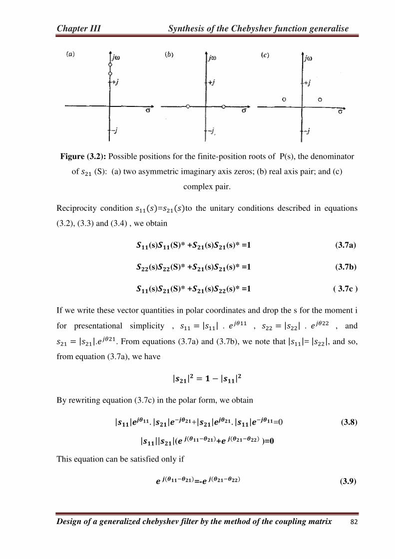
Chapter III Synthesis of the Chebyshev function generalise
Design of a generalized chebyshev filter by the method of the coupling matrix 82
Figure (3.2): Possible positions for the finite-position roots of P(s), the denominator
of (S): (a) two asymmetric imaginary axis zeros; (b) real axis pair; and (c)
complex pair.
Reciprocity condition = to the unitary conditions described in equations
(3.2), (3.3) and (3.4) , we obtain
(s) (S)* + (s) (s)* =1 (3.7a)
(s) (S)* + (s) (s)* =1 (3.7b)
(s) (S)* + (s) (s)* =1 ( 3.7c )
If we write these vector quantities in polar coordinates and drop the s for the moment i
for presentational simplicity , = | | . , = | | . , and = | |. . From equations (3.7a) and (3.7b), we note that | |= | |, and so,
from equation (3.7a), we have | | = − | |
By rewriting equation (3.7c) in the polar form, we obtain
| | . | | − +| | . | | − =0 (3.8) | || |( − + − )=0
This equation can be satisfied only if
− =- − (3.9)

Chapter III Synthesis of the Chebyshev function generalise
Design of a generalized chebyshev filter by the method of the coupling matrix 82
By replacing the minus sign in equation (3.9) with ± , where k is an integer,
we have
− = − + −
or
− + = + (3.10)
Since the vectors (s), , and (s), are represented by rational polynomials in
the variable s and share a common denominator polynomial E(s). Their phases are
= -
= - (3.11)
= -
(s) is the angle of the common denominator polynomial E(s).and (s), are
the angles of the numerator polynomials of (s) etc.
by substituting these separated phases into equation (3.10), the cancel and the
following important relationship is obtained:
− + + = + (3.12)
The equation states that at any value of the frequency variable s, the difference
between the angle of the , numerator vector, and the average of phases of the and numerator vectors must be an odd multiple of / 2 radians, that is,
orthogonal. The frequency independence of the right-hand side of equation (3.12)
allows us to observe two important properties of (s) , (s), and (s) :

Chapter III Synthesis of the Chebyshev function generalise
Design of a generalized chebyshev filter by the method of the coupling matrix 82
The numerator polynomial of (s) (P (s) / ) must have zeros that are either on the
imaginary axis of the complex s plane or in mirror-image pairs symmetrically arranged
about the imaginary axis. In this way, the value of (s) [the angle of P(s)] remains
at an integral number of /2 radians at any position of s, along the imaginary axis
from -∞ à +∞.
Similarly, the average of the phases of the (s) and (s) numerator polynomials
,( (s) + ( (s) ) / 2, must be evaluated to an integral number of / 2 radians at
any value of s between - ∞ and This means that the zeros of the numerator
polynomial of [. . , ] and the zeros of the numerator
polynomial of [the roots of (s)], must either be coincident on the imaginary
axis or arranged in mirror-image pairs about the imaginary axis.
The definition of these angles is illustrated in Figure (3.3).
The second statement allows us to relate the numerator polynomials of (s) and
(s) ,namely, F(s) and (s), respectively. If their zeros (roots) are coincident the
formally, d the numerator polynomial of (s) is (s), then the numerator
polynomial (s) should be denoted (s). However, common usage in this book
and elsewhere has meant that F(s)= (s).

Chapter III Synthesis of the Chebyshev function generalise
Design of a generalized chebyshev filter by the method of the coupling matrix 82
Figure ( 3.3): Angles of (s), (s), and (s), ) numerator polynomials for an
arbitrary position of the frequency variable s on the imaginary axis: (a) for a
transmission zero pair;(b) for an (s)) zero and the complementary (s) zero.
Imaginary axis or are symmetrically arranged about the imaginary axis, then the zero
of (s) namely (s) , is related to the corresponding zero of F (s), as follows
(s) = ∗ (3.13)
Where i= 1, 2, . . . ,N.
By forming the (s) polynomial from the (s) , zeros, we obtain
F22(s)=∏ − =
=∏ + ∗= (3.14a)
=(-1)N∏ − = ∗
(3.14b)
Since we already know that the polynomial F(s)=∏ −= , it is obvious that
(s) = − ∗ (3.15)
This leads to the first of two rules associated with the orthogonality condition:

Chapter III Synthesis of the Chebyshev function generalise
Design of a generalized chebyshev filter by the method of the coupling matrix 82
The numerator polynomial of (s), (s), can be formed from the product of, the
negative conjugate zeros of F (s) [equation (3.14a)], or from the conjugate of the F (s)
polynomial multiplied by -1 when N is an odd integer [equations (3.14b) and (3.15)].
Multiplication by -1, when N is odd, gives an expression for the angle of (s),
equation (3.1):
= − +N (3.16)
By substituting equation (3.16) into equation (3.12), we have
− + = + (3.17)
Finally, let us turn to . This is the angle of the numerator polynomial of (s),
P (s) , which is of degree i, the number of finite-position transmission zeros in the
transfer function. Because of the symmetry of these transmission zeros about the
imaginary axis, .Is an integral number of ⁄ radians regardless of the values
of s and (Fig.3.3a), represented as nfz
= +k1 (3.18)
Where is an integer. Now by substituting into equation (3.17); we obtain
-
-k1+
=(2K±
(N- –k1 = ± (3.19)
Equation (3.19) implies that the integer quantity (N - ) must be odd so that its right-
hand side (RHS) is satisfied. For the cases where (N - )is even, then an extra / 2
radians must be added to the left-hand side (LHS) of equation (3.19) to maintain the
orthogonality condition, which is the same as adding / 2 to on the LHS de
(3.18). Adding ⁄ ) is the equivalent of multiplying the polynomial P (s) by
j. Table 3.1.

Chapter III Synthesis of the Chebyshev function generalise
Design of a generalized chebyshev filter by the method of the coupling matrix 82
When the highest-degree coefficients of the Nth
-degree polynomials E (s) and F (s),
and the ( -degree polynomial P(s) are normalized to unity (i.e., monic
polynomials), then the P (s) polynomial must be multiplied by j when the integer
quantity (N - - ) is even.
In practice the polynomials E (s) F (s), and P (s) are usually formed as products of
their singularities, such as F(s)=∏ −= ; so, their leading coefficients are
automatically equal to unity in the majority of cases.
N nfz N- nfz Multiply P(s) by j
Odd
Odd
Even
Even
Odd
Even
Odd
Even
Even
Odd
Odd
Even
Yes
No
No
Yes
Table (3.1): Multiplications of P(s) by j to Satisfy the Orthogonality Condition.
By applying the orthogonality unitary condition to the scattering matrix, we obtain
For (N - ) odd, F (s) ∗+ ∗ =0 (3.20a)
For (N - ) even, F (s)[ ∗ ] + [ ] ∗=0
Or F (s) ∗ - ∗ = (3.20b)
For (N - ) even or odd, F (s) ∗ - − − ∗ = (3.20c)
This is represented in the following S-matrix form:
[ ]= [ − − − ] (3.21)
Since (s) = − F (s) * [equation (3.15)], the polynomial S matrix is rewritten as

Chapter III Synthesis of the Chebyshev function generalise
Design of a generalized chebyshev filter by the method of the coupling matrix 82
[ ]= [ − − + ∗ ] (3.22)
In a similar way, we can obtain alternative forms to represent the S matrix by
manipulating equation (3.20c).Whatever the form the unitary conditions will always be
satisfied.
From unitary conditions, two additional relationships are derived:
- The relationship between the real constant and used to normalize the
polynomials P(s) and F(s), respectively.
- The alternating pole-principle, which allows the accurate determination of either
E(s), F(s), or P(s) while knowing the other two.
III .1.1. Polynomial synthesis:
To simplify the mathematics in this section, we shall work in the w plane, where is
the real frequency variable related to the more familiar complex frequency variable s
by s = j. For any two-port lossless filter network composed of a series of N intercoupled
resonators, the transfer and reflection functions can he expressed as a ratio of two Nth-
degree polynomials
S 11 =
/ , S21 = / (3.23)
= √ +⁄ | / |=± (3.24)
Where RL is the prescribed return loss level in dB at =± 1. It is assumed that the
polynomials P ( ), ,and E (p)are normalized such that their highest-degree
coefficients are unity. , and , share a common denominator E(w), and the
polynomia p( )= ∏ − = , carries transfer function finite-position
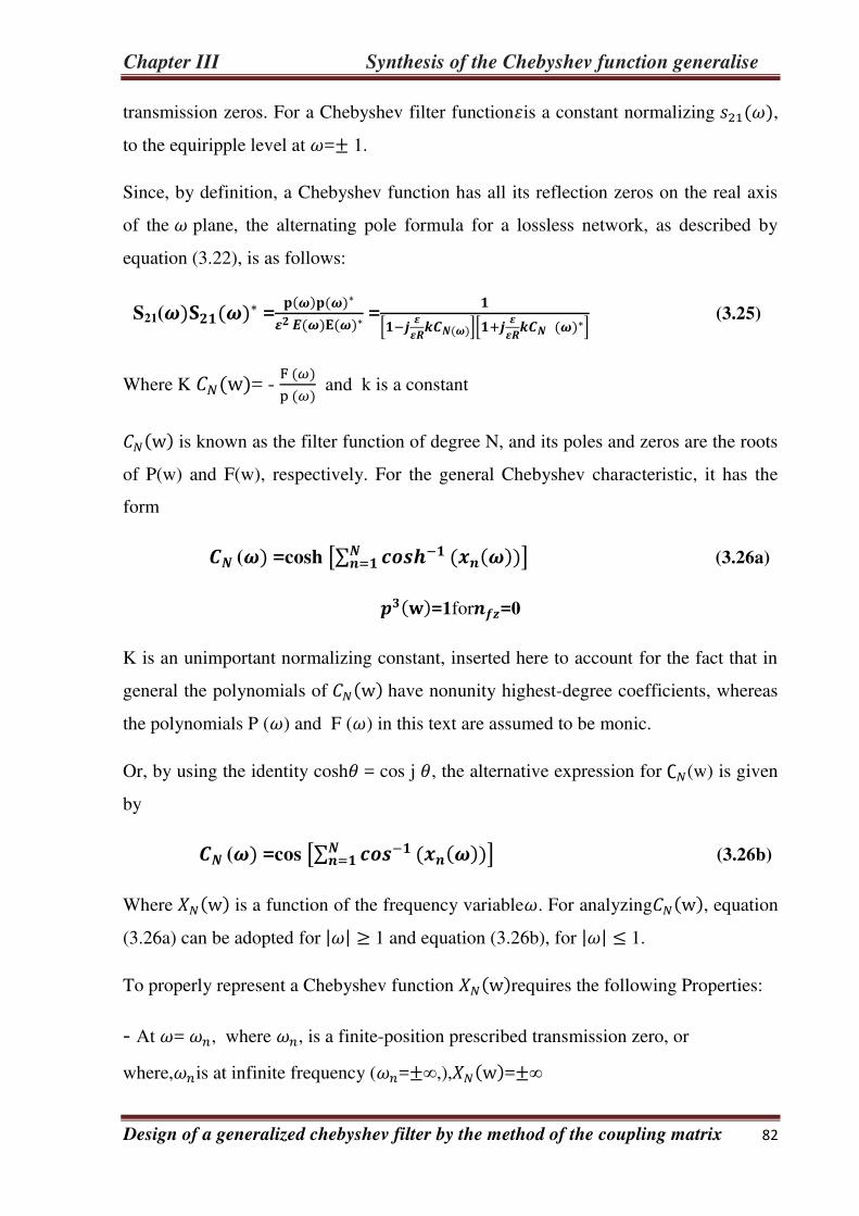
Chapter III Synthesis of the Chebyshev function generalise
Design of a generalized chebyshev filter by the method of the coupling matrix 82
transmission zeros. For a Chebyshev filter functionis a constant normalizing ,
to the equiripple level at =± 1.
Since, by definition, a Chebyshev function has all its reflection zeros on the real axis
of the plane, the alternating pole formula for a lossless network, as described by
equation (3.22), is as follows:
S21( ∗ = ∗ ∗ =[ − ][ + ∗] (3.25)
Where K = - F p and k is a constant
is known as the filter function of degree N, and its poles and zeros are the roots
of P(w) and F(w), respectively. For the general Chebyshev characteristic, it has the
form
( =cosh [∑ −= ] (3.26a) =1for =0
K is an unimportant normalizing constant, inserted here to account for the fact that in
general the polynomials of have nonunity highest-degree coefficients, whereas
the polynomials P () and F () in this text are assumed to be monic.
Or, by using the identity cosh = cos j , the alternative expression for ∁(w) is given
by
( =cos [∑ −= ] (3.26b)
Where is a function of the frequency variable. For analyzing , equation
(3.26a) can be adopted for || 1 and equation (3.26b), for || 1.
To properly represent a Chebyshev function requires the following Properties:
- At = , where , is a finite-position prescribed transmission zero, or
where, is at infinite frequency ( =±∞,), =±∞
Chapter III Synthesis of the Chebyshev function generalise
Design of a generalized chebyshev filter by the method of the coupling matrix 82
- at = ± , =±
- Between = − and = (in -band), 1 −
The first condition is satisfied if (w) is a rational function with its denominator = − :
xn ()= − (3.27)
The second condition states that a = ±
xn ()⎢−± = − ⎢−± = ± (3.28)
This condition is satisfied if f (1) = 1 - and f (-1) = 1 + giving F()=1− . therefore
xn ()=−− (3.29)
Differentiating , with respect to w shows that there are no turning points or
inflection points between = − and = + if = − at = − and = + = − , then,| | ℎ || , thus satisfying the
third condition. Figure 3.4 illustrates the behaviour of , for a case where the
finite transmission zero =+1,3.
By dividing through by to deal with any transmission zeros at =±∞, we
Obtain the final form for the function as
xn ( =− /−/ (3.30)
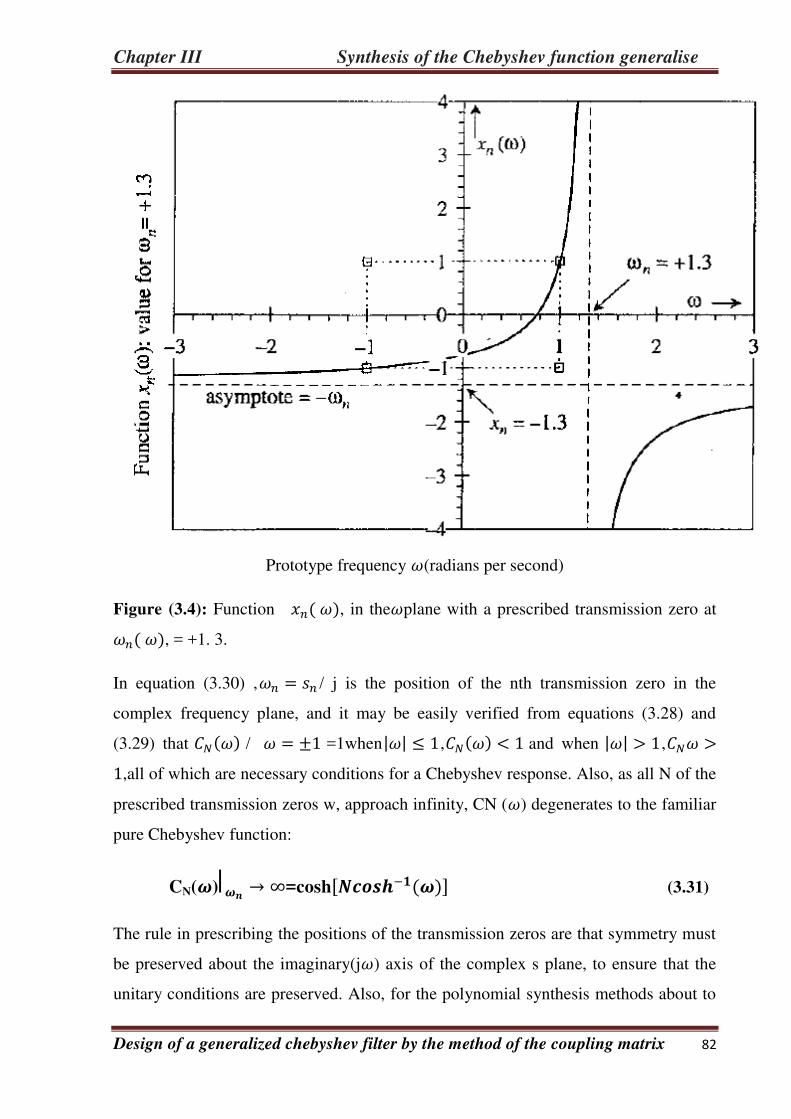
Chapter III Synthesis of the Chebyshev function generalise
Design of a generalized chebyshev filter by the method of the coupling matrix 82
Prototype frequency (radians per second)
Figure (3.4): Function , in theplane with a prescribed transmission zero at , = +1. 3.
In equation (3.30) , = / j is the position of the nth transmission zero in the
complex frequency plane, and it may be easily verified from equations (3.28) and
(3.29) that / = ± =1when|| , < and when || > , >,all of which are necessary conditions for a Chebyshev response. Also, as all N of the
prescribed transmission zeros w, approach infinity, CN () degenerates to the familiar
pure Chebyshev function:
CN()⎢ → ∞=cosh[ − ] (3.31)
The rule in prescribing the positions of the transmission zeros are that symmetry must
be preserved about the imaginary(j) axis of the complex s plane, to ensure that the
unitary conditions are preserved. Also, for the polynomial synthesis methods about to
Chapter III Synthesis of the Chebyshev function generalise
Design of a generalized chebyshev filter by the method of the coupling matrix 82
be descry bed, the number of transmission zeros with finite positions in the s plane
must be < , those zeros without finite positions must be placed at infinity.
Although the N + 2coupling matrix can accommodate fully canonical filtering
functions (i.e., the number of finite-position transmission zeros , equals the degree
N of the filter), the N x N matrix can accommodate a maximum of only N - 2 finite-
position zeros (minimum path rule.') In synthesizing the polynomials for the N x N
coupling matrix, at least two of the transmission zeros must be placed at infinity.
The next step is to solve equation (3.26a) to determine the coefficients of the
numerator polynomial of . Normalizing this polynomial to set its the minimum
path rule is a simple formula for calculating the number of finite-position transmission
zeros (i.e., those that are not at =±∞ that an Nth-degree direct-coupled resonator
network can realize. If the number of resonators in the shortest path (along nonzero
inter resonator couplings) between the input (source) and output (load) terminals of a
network equals then the maxim urn number of finite-position TZs ( ) that the
network may realize is =N- . Highest-degree coefficient to unity will yield the polynomial F (). By knowing
form equation (3.24) and the prescribed polynomial P () = ∏ − = ), the
hurwitz polynomial E (w) common to the denominators of () and () can be
evaluated from equation (3.25). It then becomes possible to proceed onward to
prototype network synthesis, from which a real electrical network with the transfer and
reflection characteristics () and ()may be synthesized.
the first step in the polynomial synthesis procedure is to replace the cos h term in
equation (3.26a) with its identity
CN ( = cosh[∑ += ]
where
= ( and = − / (3.32)
then
Chapter III Synthesis of the Chebyshev function generalise
Design of a generalized chebyshev filter by the method of the coupling matrix 82
CN()= 1/2 [ ∑ + + −∑ + ] =1/2[∏ + + ∏ +== ] (3.33)
By multiplying the second term im (3.33) top and bottom ∏= - ) yields
CN()=1/2[∏ + + ∏ −== ] (3.34)
From equation (3.32). it is evident that ∏= + ). ∏= - )= ∏= - ) will always be unity equation (3.34) is expressed in its
final form by substituting for , , () using equations (3.30) and (3.32) as
an=− /−/
bn=√ − − − −/ (3.35)
=√ − − /−/
=/√ − /−/
Where , = √ − a- transformed frequency variable.
Equation (3.34) then becomes
CN( =1/2[∏ [ − +√ − / /]+∏ [ − −√ − / /]== ∏ − = ] =1/2[∏ + += ∏ −=∏ − = ]
where
Chapter III Synthesis of the Chebyshev function generalise
Design of a generalized chebyshev filter by the method of the coupling matrix 82
Cn=( − and dn= / √ − (3.36)
In comparison with equation (3.25), it is obvious that the denominator of ()has
the same zeros as P ( ), the numerator polynomial of ( )generated formthe
prescribed transmission zerosFrom equation (3.25) it is also observed that the
numerator of () has the same zeros as the numerator F() of (), and appears
at first to be a mixture of two finite-degree polynomials, one in the variable w purely,
whilst the other has each coefficient multiplied by the transformed variable '.
However, the coefficients multiplied by cancel each other when equation (3.36) is
multiplied out. This is best proven by demonstration, by multiplying out the left- and
right-hand product terms in the numerator of () in (3.36) for a few low values
Of N:
For N=1, Nnm[ ] = [∏ = + + ∏ = − . ]=
For N=2, Num[ ] = +
For N=3, Num[ ]= + + +
(and so on)
At each stage, the expansions result in a sum of factors, where each factor is composed
of multiples of and ,, elements. Because of the positive sign in the LH product
term in equation (3.36), the , , factors, resulting from multiplying out the LH
term, are always positive in sign. Multiplying out the RH product term 1 in equation
(3.36) produces the same , , factors; however, the negative sign indi cates that
those factors containing an odd number of d,, elements are negative in sign and are
canceled with the corresponding factors from the LH product term.
Now, the remaining factors contain only the even numbers of ,elements. Con-
sequently, , = √ − , which is a common multiplier for all the d, elements
[equation (3.36)], is raised by even powers only, producing sub polynomials in the

Chapter III Synthesis of the Chebyshev function generalise
Design of a generalized chebyshev filter by the method of the coupling matrix 82
variable w. As a result, the numerator of () will be a polynomial in the variable only.
These relationships can be used to develop a simple algorithm to determine the of
ccofficientsof the numerator polynomial of () .Normalizing Num
[ () ] to set its highest-degree coefficient to unity yields F (), the numerator of
().
III.1.2. Design of a generalized chybechev band pass filter:
III.1.2. 1. Specifications :
Central frequency (MHz) =2.4407 +03
Bandwidth (MHz) BW = 40
Return loss RL = 22
Order N = 4
Finite zeros Zp = 2
Ep ԑ= 1.1547

Chapter III Synthesis of the Chebyshev function generalise
Design of a generalized chebyshev filter by the method of the coupling matrix 82
Table 3.2: (4-2) Asymmetric Chebyshev Filter Function with Two Prescribed
Transmission Zros

Chapter III Synthesis of the Chebyshev function generalise
Design of a generalized chebyshev filter by the method of the coupling matrix 82
-3 -2 -1 0 1 2 3 4-40
-35
-30
-25
-20
-15
-10
-5
0S21 and S11 from polynomials P, F and E
2200 2250 2300 2350 2400 2450 2500 2550 2600 2650-40
-35
-30
-25
-20
-15
-10
-5
0S21 and S11 from Reduced Coupling Matrix
data1
data2
-0.4936 0.3796 0.8732
-22
1.3217 1.8082
The proto type low pass filter
filfiltre
The band pass filter
4-2 Asymmetric
Chebyshev filter

Chapter III Synthesis of the Chebyshev function generalise
Design of a generalized chebyshev filter by the method of the coupling matrix 82
Figure show Lowpas S prototype transfer and reflection charactelistics of the (4-2)
symmetric Chebyshev filter with two prescribed transmission zeros at = + j1.3217
and = + j1.8082.
III.1.3.Polynomial forms for symmetric and asymmetric filtering functions :
Table 3.2b lists the coefficients of the E (s), F (s), and P (s) polynomials formed from
the singularities in Table 3.2a, normalized in each case to set the highest-degree
coefficient to unityIn addition, the coefficients of P (s) are multiplied by j to preserve
the unitary conditions, because in this case, N - =2 is an even integer. With these
polynomials, we are now ready to proceed with the synthesis of a prototype electrical
network, which, under analysis, results in exactly the same performance characteristics
as the original polynomials.
At this stage it is worth studying the form of the polynomials of the preceding 4th
degree asymmetric filter to help understand the distinctive characteristics of the
electrical network that will be synthesized from them:
. Because the zeros of E (s) [the poles of the filter function] are asymmetrically located
about both the real and the imaginary axes, all except the leading coefficient of E (s) )
are complex. Zeros of F (s) [the zeros of the reflection function (s)] are distributed.
Asymmetrically along the imaginary axis . This means that the coefficients of
F (s) alternate between purely real and purely imaginary as the power of s increases
Similarly, because the zeros of P (s)) [the zeros of the transfer function (s)] all lie
on the imaginary axis (or can be distributed symmetrically about the imaginary axis),
the coefficients of P (s) also alternate between purely real and purely imaginary as the
power of S increases.
By analyzing these polynomials with frequency variable s, ranging from -∞to +∞, the
asymmetric transfer and reflection characteristics are as shown in Figure 3.4.

Chapter III Synthesis of the Chebyshev function generalise
Design of a generalized chebyshev filter by the method of the coupling matrix 82
we examine the network synthesis techniques. After the polynomials of the [ABCD]
transfer matrix are formed from the coefficients of E (s) and F (s), an electrical
network is synthesized from these matrix polynomials. As the network 1 progressively
builds up component by component, the polynomials are correspo,,d. ingly reduced in
degree one by one. This procedure is refened to as "extracting" the components from
the polynomials. At the end of a successful synthesis cycle, when 1 r the electrical
network has been fully synthesized, the coefficients of the polynmils are zero apart
from one or two constants.
It can be demonstrated that if the coefficients of the polynomials are complex, it is q
necessary to extract components known as frequency-invariant reactances firs, from
the polynomials, in addition to the capacitors and inductors in the course of building
up the network and reducing the polynomial coefficients to zero. Even. 1 tually, the
firs translate into frequency offsets from the bandpass filter's nominal i center
frequency ("asynchronously tuned"), giving the required asymmetric performance.
If the transmission zeros of the filter function are prescribed symmetrically about 5 the
real axis, then the pattern of the singularities of the polynomials E(s)andF (s),which
are generated from these transmission zeros, are also symmetric about the real axis.
Symmetry about the real and imaginary axes means that the polynomials are composed
of purely real coefficients :
- E (s) is an Nth-degree polynomial with real coefficients.
- P (s) is an even polynomial of degree nfz with real coefficients, where nfz is the
number of prescribed finite-position transmission zeros ranging from zero ("all pole"
function) to N ("fully canonical").
- F (s) is an Nth-degree even polynomial if N is even and odd if N is odd, again with
purely real coefficients
Chapter III Synthesis of the Chebyshev function generalise
Design of a generalized chebyshev filter by the method of the coupling matrix 82
The purely real coefficients indicate that any FIR that is extracted during the synthesis
process is zero in value, and that all the resonators of the filter are synchronously tuned
at centre frequency.
III .2. Synthesis of network-circuit approch:
Methods were established to derive the transfer and flection polynomials for a broad
class of lowpass prototype filter functions. The next step in the design process is to
translate these polynomials into a prototype electrical circuit from which a real
microwave filter may be développedTwo methods for doing this are available: the
classical circuit synthesis method and the direct coup- ling matrix synthesis approach.
In this chapter, the circuit synthesis approach, based on the [ABCD] transfer matrix, or
the "chain" matrix, as it is sometimes known,is described.
The techniques described here include both, the symmetric as well as asymmetric
lowpass prototype filters. such pro- totype networks require the hypothetical
frequency-invariant reactive elements, referred to by the acronym FIR . Inclusion of
such elements leads to transfer and reflection polynomials to have complex
coefficients. In bandpass or bandstop filters, FIR elements appear as frequency offsets
to the resonant circuits. The various components used in the microwave synthesis
process include the following :
- Frequency-dependent reactive elements: lumped capacitors and inductors. Their
number in the lowpass prototype network determines the "degree" or "order" of.the
filter network. Capacitors and inductors in a ladder network are interchange. able
through the dual-network theorem.
- Frequency-invariant reactance OFIR' elements. The classical network synthesis
theory is founded on the concept of the positive real condition for the driving point
immittance function Z (s ) or Y (s ) , that is, for a realizable network, Re ( Z ( s) ) or
Re (Y ( s) )> 0, or Re ( s )> 0, and Z (s) or Y (s ) and varied pour s reel . is real for s
real . With the introduction of FIRS into the network,

Chapter III Synthesis of the Chebyshev function generalise
Design of a generalized chebyshev filter by the method of the coupling matrix 82
The second condition (which implies symmetry of the frequency response) is no
longer necessary and the driving-point function becomes a positive function. The FIR
rep. Resents an offset in the resonant frequency of a resonator from nominal (nominal
here means zero for a lowpass resonator, and of for a bandpass rezone. tor), as
described in Figure 3.4. For the asymmetric class of filters, the driving .Point
immittance polynomials possess coefficients that cannot be extracted as capacitors or
inductors. However, these coefficients can be extracted as FIRs that are realized
eventually by a microwave resonant element (a waveguide cavity or a dielectric
resonator) that is tuned to the offset from the nominal centre frequency of the filter;
thus, the filter is asynchronously tuned.
- Frequency-independent transmission-line phase lengths, particularly the quarter-
wave (90") impedance or admittance inverters (collectively known as immittance
inverters). In a microwave circuit, these elements act as transformers with a frequency-
invariant 90" phase shift, and are approximately realized by a variety of microwave
structures such as inductive irises and coupling probes. The uses of inverters
significantly simplify the physical realization of filters at microwave frequencies.
- Coupling inverters act as coupling elements between the resonant nodes of a
network, representing a microwave filter. Those that couple directly between
sequentially numbered resonators are known as mainline couplings; those between non
sequential resonators are known as cross-couplings, and those that couple between the
source port and the load port and internal resonators of the filter are known as
input/output couplings. There can be more than one coupling from the source or load
ports to the internal resonators nodes in the filter, and there is a direct source-load
coupling for canonical filter functions
Figure (3.4):( a) = 0 where = s , =0 here for this lowpass resonator resonates at
zero frequency ;( b ), = SCI + JBI = 0 when s = Thus the resonant frequenc
Chapter III Synthesis of the Chebyshev function generalise
Design of a generalized chebyshev filter by the method of the coupling matrix 82
So = jwo=-jBI/Cl ,that is, is offset by = -Bl / Cl from the nominal center
frequency.
III .2.1. Circuit synthesis approch:
For a two-port network operating between unity source and load terminations, the ving
[ABCD] matrix representing the network has the following form [9]
[ ] = / .[ ] (3.37a)
Where
S12(s)=s21(s)= /
= /+ + + (3.37b)
Where
S11(s)= / =
+ − −+ + + (3.37c)
S22(s)= − ∗/ =
+ − −+ + + (3.37d)
The j that multiplies P ( s) in the denominator of equation (3.37) allows the cross- the
couplings to be extracted as inverters, and is there, in addition to the j that multiplies
p (s ) when N - is even, to preserve the orthogonality unitary condition (see For-
Section 6.2). For non unity source and load terminations Rs and RL , the [ ABCD ]
matrix is scaled as follows :
[ ] = / .[⎢⎢ √ √√ √ ]
(3.38)
From equation (3.37) . it is immediately clear that the A (s ) , B (s ) , C (s ) and D(s)
poly- me nominal’s share a common denominator polynomial P (s ) / . It is
demonstrated that these polynomials can be built up from the elements of the circuit
that models the 1s. Real microwave filter, and then related to the coefficients of the E
(s) and F (s ) /

Chapter III Synthesis of the Chebyshev function generalise
Design of a generalized chebyshev filter by the method of the coupling matrix 82
Polynomials, which, together with P (s) /, represent the desired transfer and reflection
performance of the filter, respectively .
Our first task, therefore, is to relate the A ( s) , B (s ) , C (s ) and D (s) polynomials to
the S parameters that represent the transfer and reflection characteristics of the filter
function. This is accomplished by building the [ABCD] matrix for a simple three-
element ladder network, relating it to a real filter circuit and examining the form of the
resulting A ( s) , B ( s) , C ( s) , D ( s ), and P ( s) polynomials.
These polynomials :to are then compared directly with the coefficients of the
polynomials that constitute (S) and (S).We also study the form of the [ABCD]
polynomials for the more advanced circuits, namely, the asymmetric, cross-coupled,
and single-ended types, in order to generalize the procedure
Figure 3.38 depicts a simple lossless three-element prototype ladder circuit that is
capable of realizing a lowpass filter. The three transmission zeros for this circuit all.
Figure (3.5):Basic lowpass prototype circuit
Lie at s = j∞ , which means that it is an all-pole filter. The network synthesis is
demonstrated by first building the A (s ), B ( s) , C ( s) and D(s)polynomials
corresponding to a third-order lowpass prototype ladder network with the elements, ,
, and C2 (some times known as the g values gl, g2, g3, . . . of the prototype ladder
network [S]). Then, the synthesis procedure is applied to demonstrate the recovery of
the values of the original network elements , and C2 from the A (s ), B ( s) , C ( s )
and D ( s) polynomials.
III .2.2.Buildup of [ABCD] matrix for the third-degree network:
Figure 3.5 represents a third-degree lowpass network..
StepA.CascadeShuntClwithSeriesL1 [ ] = [ ] . [ ]
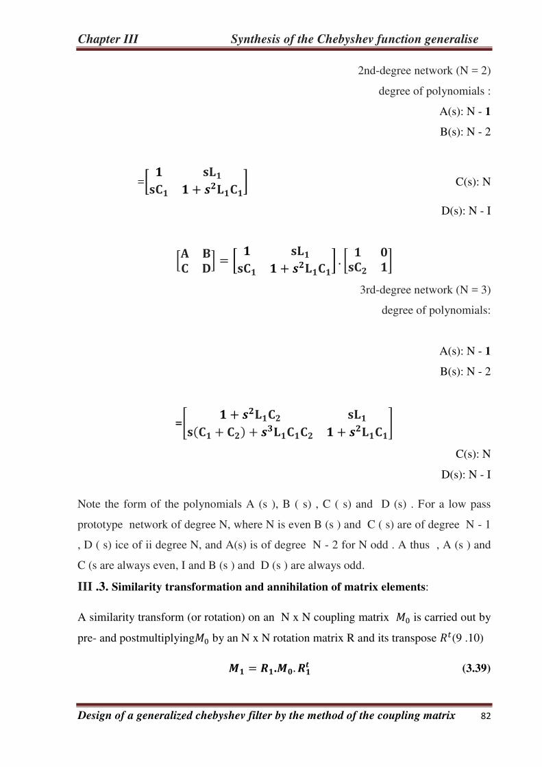
Chapter III Synthesis of the Chebyshev function generalise
Design of a generalized chebyshev filter by the method of the coupling matrix 82
2nd-degree network (N = 2)
degree of polynomials :
A(s): N - 1
B(s): N - 2
=[ + ] C(s): N
D(s): N - I
[ ] = [ + ] . [ ]
3rd-degree network (N = 3)
degree of polynomials:
A(s): N - 1
B(s): N - 2
=[ + + + + ]
C(s): N
D(s): N - I
Note the form of the polynomials A (s ), B ( s) , C ( s) and D (s) . For a low pass
prototype network of degree N, where N is even B (s ) and C ( s) are of degree N - 1
, D ( s) ice of ii degree N, and A(s) is of degree N - 2 for N odd . A thus , A (s ) and
C (s are always even, I and B (s ) and D (s ) are always odd.
III .3. Similarity transformation and annihilation of matrix elements:
A similarity transform (or rotation) on an N x N coupling matrix is carried out by
pre- and postmultiplying by an N x N rotation matrix R and its transpose (9 .10)
= . . (3.39)
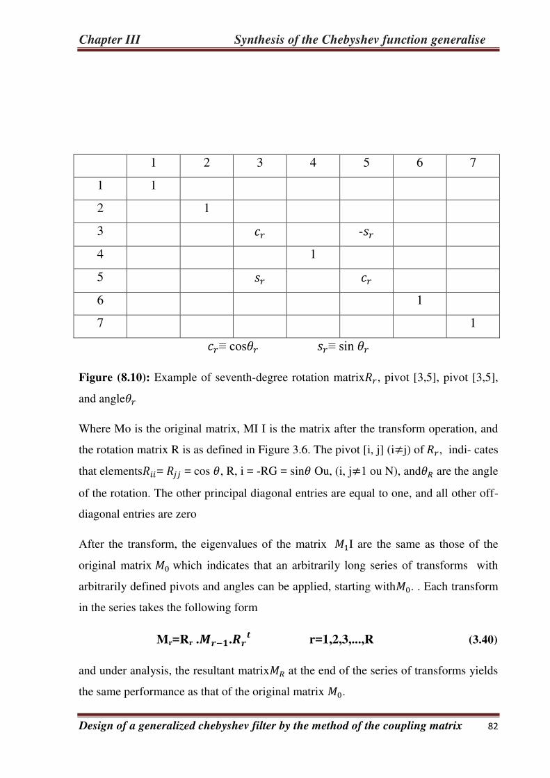
Chapter III Synthesis of the Chebyshev function generalise
Design of a generalized chebyshev filter by the method of the coupling matrix 82
1 2 3 4 5 6 7
1 1
2 1
3 -
4 1
5
6 1
7 1
≡ cos ≡ sin
Figure (8.10): Example of seventh-degree rotation matrix , pivot [3,5], pivot [3,5],
and angle
Where Mo is the original matrix, MI I is the matrix after the transform operation, and
the rotation matrix R is as defined in Figure 3.6. The pivot [i, j] (i≠j) of , indi- cates
that elements = = cos , R, i = -RG = sin Ou, (i, j≠1 ou N), and are the angle
of the rotation. The other principal diagonal entries are equal to one, and all other off-
diagonal entries are zero
After the transform, the eigenvalues of the matrix I are the same as those of the
original matrix which indicates that an arbitrarily long series of transforms with
arbitrarily defined pivots and angles can be applied, starting with . . Each transform
in the series takes the following form
Mr=Rr . − . r=1,2,3,...,R (3.40)
and under analysis, the resultant matrix at the end of the series of transforms yields
the same performance as that of the original matrix .
Chapter III Synthesis of the Chebyshev function generalise
Design of a generalized chebyshev filter by the method of the coupling matrix 82
When a similarity transform of pivot [i, j] and angle (≠0) ) is applied to coup- ling
matrix - 1, the elements in rows i and j and columns i and j of the resultant
matrix , change, in value, from the corresponding element values in − .For the
kth element in the row or column i orj of , and not on the cross-points of the pivot
(i.e., k ≠ i, j), , the value changes according to the following formulas:
Mk = crMik + srMjk for an element in row
Mik = s, Mik + c, Mjk for an element in row j'
Mkii = C, Mki - S, Mki for an element in column i
Mij = s, Mki + C, Mkl for an element in column j (3.41a)
Where k (# i, j) = 1,2, 3,. . . N, c, = cos , s, = sin ; the undashed matrix elements
belong to the matrix − ; and the dashed to − . . For the elements on the cross-
points of the pivot ( , ,, , (= Mji)):
/ = − +
/ = + +
/
= ( - )+ ( - ) (3.41b)
Two properties of the similarity transform are exploited for the matrix reduction
process:
1. Only those elements in the rows and columns i and j of the pivot [i,j] of a trans-
form are affected by the transform (provided its angle ≠ ) All the other
elements retain their previous values.
2. If two elements, facing each other across the rows and columns of the pivot of a
transform, are both zero before the application of the transform, they are still
zero after the transform. For example, if the elements 5in
Figure 3.7 Seventh-degree coupling matrix reduction sequence for folded canonical
form, The shaded elements are those that can be affected by a similarity transform
at pivot [3,5] and angle ≠ ).. All the others remain unchanzed

Chapter III Synthesis of the Chebyshev function generalise
Design of a generalized chebyshev filter by the method of the coupling matrix 82
1 2 3 4 5 6 7
1 S M 4 3 2 1 Xa
2 . S m 9 8 xa xs
3 . . s M xa xs 5
4 . . . S m 10 6
5 . . . . s m 7
6 . . . . . s m
7 . . . . . . s
Figure (3.7): Seventh-degree coupling matrix reduction sequence for folded
canonical form, The shaded elements are those that can be affected by a
similarity transform at pivot [3,5] and angle ≠ ).. All the others remain
unchanzed
Figure 3 .7 happen to be both zero before the transform with pivot [3,5], they will still
be zero after the transform, regardless of the transform angle
The equations in (3.41) can be applied to annihilate (zero) specific elements in the
coupling matrix. For example, to annihilate the nonzero element 5 (and simul-
taneously, 5 ') in the seventh-degree coupling matrix of Figure 3.7, a transform of
pivot and (transformation of pivot [3,5] and of angle, = − − ( 5, / ,) is
applied to the coupling matrix [see the last formula in (3.41a) withk = 1, i = 3, and
j = 5.. In the transformed matrix, 5, and 5, , are zero and all the values in rows and
columns three and five (shown shaded in Fig. 3.7) are changed. Equation set (3.42)
summarizes the angle formulas for annihilating specific elements in the coupling
matrix with a rotation at pivot [i,j]: , = − ( / ) for the kth element in row i (Mik) (3.42a) , = − − ( / ) for the kth element in row j (Mik) (3.42b)

Chapter III Synthesis of the Chebyshev function generalise
Design of a generalized chebyshev filter by the method of the coupling matrix 82
= − ( / ) for the kth element in column i (Mik) (3,42c) = − − ( / ) for the kth element in column j (Mik) (3.42d)
= − − ±√ −
for cross-pivot element ( ) (3.42e)
= − ( ± √ −
)
for cross-pivot element ( ( ) (3.42f)
= − −
for cross-pivot element ( ) (3.42g)
The method for reducing the full coupling matrix , resultant from the synthesis
Procedure of Section 8.2 to the folded form of Figure 3.7, involves applying a series
of similarity transforms to the matrix that progressively annihilates the unrealizable or
inconvenient elements one by one. The transforms are applied in a certain order and
pattern that takes advantage of the two effects, mentioned previously, ensuring that
once annihilated, an element is not regenerated by a sub- sequent transform in the
sequence.

Chapter III Synthesis of the Chebyshev function generalise
Design of a generalized chebyshev filter by the method of the coupling matrix 82
Conclusion :
General methods have been presentedk for the generation of the transfer and reflection
polynomials for the equiripple (Chebyshev) class of a filtering function with
prescribed transmission zeros and then the efficient direct synthesis of the coupling
matrix for the folded form of canonical network. If practical, microwave bandpass
filters in a variety of technologies may be realized directly from the folded-network.
Coupling matrix or a further series of similarity transforms may be applied to
reconfigure the coupling matrix to other more convenient forms. The methods are
applicable for symmetric or asymmetric even- or odd-degree transfer characteristics;
also for single- or double-terminated realizations. No restrictions apply to the
prescription of the finite-position transmission zeros to be built into the characteristics,
except that the pattern of their positions must be symmetric about the imaginary axis
of the complex -plane, and their total numbers must not exceed , being the degree of
the transfer characteristic.

Chapter III Synthesis of the Chebyshev function generalise
Design of a generalized chebyshev filter by the method of the coupling matrix 82
General Conclusion
Designing a chebyshev filter generalized by the method of the coupling matrix
General conclusion:
In the previous chapters, we introduced methods to generate the transfer and the
reflection polynomials for some filter functions. The next step in the design process is
to translate these polynomials into a prototype electrical circuit from which a
practical microwave filter can be developed. There are two ways to accomplish it: the
classical circuit synthesis method and the direct coupling matrix synthesis approach.
Circuit elements used for the classical filter synthesis include the lossless inductors
and capacitors, and the terminating resistors. The lowpass prototype filters derived
from these elements inherently lead to symmetric response filters.Such prototype
networks are generalized to include asymmetric response filters by including the
hypothetical frequency-invariant reactance, referred to by the acronym FIR. The
inclusion of such elements gives rise to transfer and reflection polynomials with
complex coefficients, rendering the lowpass prototype filter response to be
asymmetric. In pracactical bandpass or bandstop filters, FIR elements appear as
frequency offsets to the resonant circuits. Another element that is required in the
synthesis of' filters at microwave frequencies is the frequency-invariant
impedance or admittance inverter, commonly referred to as the immnitance
inverter. Such inverters significantly simplify the physical realization of the distributed
microwave filter structure. In a microwave circuit, immitance inverters can be
realized approximately over narrow bandwidths by a variety of microwave
structures, such as inductive irises and coupling probes. The use of such inverters
allows for the prototype electrical circuit in a form suitable for realization with
intercoupled microwave resonators.
Modeling the circuit in matrix form is particularly useful because matrix operations
can then be applied, such as inversion, similarity transformation, and partitioning.
Such operations simplify the synthesis, reconfiguration of the topology, and

General Conclusion
Designing a chebyshev filter generalized by the method of the coupling matrix
performance simulation of complex circuits. Moreover, the coupling matrix is able to
include some of the real-world properties of the elements of the filter. Each element in
the matrix can be identified uniquely with an element in the finished microwave
device. This enables us to account for the attributions of electrical characteristics of
each element, such as the Q, values for each resonator cavity, different dispersion
characteristics for the various types of mainline coupling and cross-coupling within the
filter. This is difficult or impossible to achieve with a polynomial representation of the
filter's characteristics. The basic circuit that the coupling matrix represents is reviewed,
and the method used to construct the matrix directly from a lowpass prototype circuit,
is outlined. This is followed by the presentation of two methods for synthesis of the
coupling matrix directly from the filter's transfer and the reflection polynomials,
the N x N and the N + 2 matrices.

Chybeshev generalized programme
%------(N+2 x N+2) coupling matrix (Cameroun 2003) Exdended Matrix---------
--------- clear close all hold off clc % format long %-----------Filter Specification --------------- %---------Low-Pass Filter Prototype%-- ------------------------------------
-------- %---------------Input data ------ Cahier des charges --------------------
%-----------BAndpass to lowpass filter------------- fc2=2478; fc1=2404; f0=sqrt(fc1*fc2); BW=fc2-fc1;BW=40; FBW=BW/f0; Df=60; % Bande de transition fs2=fc2+Df;fs2=2509; fs1=fc1-Df RL=22; % fs1=f0*f0/fs2; fs2n=abs((1/FBW)*(fs2/f0-f0/fs2)); fs1n=abs((1/FBW)*(fs1/f0-f0/fs1)); fs=min(fs1n,fs2n);Amin=20; %fs=960;fs=abs((1/FBW)*(fs/f0-f0/fs));%----------------------ghrhyhyr Amax=-10*log10(1-10^(-0.1*RL)); fc=1; OmegaP=2*pi*fc;OmegaS=2*pi*fs;
%% calculé l'ordre du filtre %Nb = ceil((log10((10^(Amin/10)-1)/(10^(Amax/10)-
1)))/(2*log10(OmegaS/OmegaP))); %% Butterworth Lowpass filter %-------------------------------------------------------------------------
--------------------- N=4; %--------------------------------------------- nfz=2; % Nb of finite transmission zeros
w0=2*pi*f0; f1=2510; %First Zero Transmission f2=2350;
%Second Zero Transmission %-----Normalization of specification--------------- wz1=(1/FBW)*(f1/f0-f0/f1); wz2=(1/FBW)*(f2/f0-f0/f2);
%wz2=(1/FBW)*(f2/f0-f0/f2); % %zp=[ inf inf inf inf];3 %zp=[inf*ones(1,N)];
wz1=1.3217;wz2=1.8082, zp=[wz1*j wz2*j inf*ones(1,N-2)];

ep=1.1548;
%--------Recursive technique of cameron u,v ---------------------- syms w zp=zp/j; u=w-1/zp(1); v=((1-1/zp(1)^2)^0.5)*(w^2-1)^0.5;
for k=2:N ut=u; vt=v; u=w*ut-ut/zp(k)+((w^2-1)^0.5)*((1-1/zp(k)^2)^0.5)*vt; v=w*vt-vt/zp(k)+((w^2-1)^0.5)*((1-1/zp(k)^2)^0.5)*ut;
end coefu= sym2poly(u); rootf=roots(coefu); % roots of F(w) polynomial polyp= poly(zp); % coefficients of P(w) polynomial polyf=poly(rootf); % coefficients of F(w) polynomial pp=conv(polyp,polyp); % P(w)^2 ff=conv(polyf,polyf); % F(w)^2
% linear ep (ripple) ep=1./sqrt(10^(RL/10)-1)*abs(polyval(polyp,1)/polyval(polyf,1));
%E(w)^2=P(w)^2/(ep^2)+F(w)^2 ee=[zeros(1,length(ff)-length(pp)) pp]/(ep^2)+ff;
% roots in p from roots in w of E rootee=roots(ee)*i; % roots with négative real part (Hurwitz) zei=find(real(rootee)<0); % ze=rootee(zei);
%----------------Determination of polynomials coefficients----------------
----- P = poly(zp); % P(w) F = poly(rootf); % F(w) E = poly(ze/j); % convert E(p) to E(w)
test=1; if rem(N-nfz,2)==0 % orthogonality condition p=j*p test=j; end
P1 = test*poly(j*zp); % P(s) F1 = poly(j*rootf); % F(s) E1 = poly(ze); % E(s)
%-----------plots of figures from polynomials------------------------------
--------------- pas=0.00001; w1=-10:pas:10;
Ps=polyval(P,w1); Fs=polyval(F,w1); Es=polyval(E,w1); S21db=-20*log10(abs(ep*Es))+20*log10(abs(Ps));
S11db=-20*log10(abs(Es))+20*log10(abs(Fs));
plot(w1,S21db,'-',w1,S11db,'m'),grid on; axis([-3 4 -40 0])
%-------Denormalization----------------- WL=w1; wp1=0.5*w0*(WL*FBW+sqrt((WL.*FBW).^2+4)); w1=wp1./(2*pi); % Denormalization %-------------------------------------
%plot(w1,S21db,'-',w1,S11db,'m'),grid on; % axis([2200 2650 -40 0]) title('S21 and S11 from polynomials P, F and E')
figure
%--------------------------------------------------------------------------
-- %--- Computation of Coupling Matrix from polynomials F, P and E
% EF=E+F for double terminated % EF=E for single terminated EF=E1+F1; % Double % EF=E1; % single
% m1, n1 even and odd complexe polynomial parts of E+F % figure(2) for k=N+1:-2:1 m1(k)=real(EF(k)); n1(k)=j*imag(EF(k)); end for k=N:-2:1 m1(k)=j*imag(EF(k)); n1(k)=real(EF(k)); end %-------y22=n1/m1 y21=P/(eps*m1) if N even %-------y22=m1/n1 y21=P/(eps*n1) if N odd
Ny22=m1; Dy22=n1; Ny21=P1/ep; Dy21=n1; %------R22 and R21 are residues %----- P22 and P21 are eigenvalues if rem(N,2)==0 [R22,P22,K22] =residue(Dy22,Ny22); [R21,P21,K21] = residue(Ny21,Ny22); else [R22,P22,K22] =residue(Ny22,Dy22); [R21,P21,K21] = residue(Ny21,Dy21); end
%-----Matrix Exdended (N+2 x N+2)-------------- lamda1=-imag(P22); Tnk=sqrt(R22); T1k=(R21)./Tnk; T1k=real(T1k);

Tnk=real(Tnk);
R1=sum(T1k.^2); RN=sum(Tnk.^2);
M=diag([ 0;lamda1;0]);
ML=M; M(1,:)=[0 T1k' 0]; M(N+2,:)=[0 Tnk' 0]; M(:,1)=[0 T1k' 0]'; M(:,N+2)=[0 Tnk' 0]'; %------------------------------------------------------ MM=M; M2=similiraty1(M,N);
% x1=1/sqrt(FBW*15.7203); % M2=[0 x1 0 0 0;... % x1 -0.27644 1.07534 -0.65769 0;... % 0 1.07534 0.48564 1.07534 0;... % 0 -0.65769 1.07534 -0.27644 x1;... % 0 0 0 x1 0]; %--------plot from reduced matrix--------------------
R1=1; RN=1;
Q=zeros(N+2);Q(1,1)=R1;Q(N+2,N+2)=RN; k1=1; pas=0.001; for wb1=-10:pas:10
U=eye(N+2); U(1,1)=0; U(N+2,N+2)=0; AA=(Q+j*wb1*U+j*M2);
AAI=inv(AA); s21b(k1)=2*sqrt(R1*RN)*AAI(N+2,1); s11b(k1)=1-2*R1*AAI(1,1); k1=k1+1; end
figure(2)
pas=0.001;
% --------------------plot figures from coupling matrix wb=-10:pas:10; %---------Denormalization----------------- WL=wb; wp1=0.5*w0*(WL*FBW+sqrt((WL.*FBW).^2+4)); wb=wp1./(2*pi); % ------------------------------------- plot(wb,20*log10(abs(s21b)),'b',wb,20*log10(abs(s11b)),'r')
grid on

title('S21 and S11 from Reduced Coupling Matrix') axis([2200 2650 -40 0])
RPL=roots(P); RPB=0.5*w0*(RPL*FBW+sqrt((RPL.*FBW).^2+4));


References :
1-CAMERON, R. J. (2007). MICROWAVE FILTERS FOR COMMUNICATION
SYSTEMS:FUNDAMENTALS,DESIGN, AND APPLICATIONS. Published by John Wiley &
Sons, Inc. Hoboken, New Jersey.
2-HONG, J.-S. (2011). Microstrip Filters for RF/Microwave Applications. John Wiley &
Sons, Inc.
3-Hunter, I. (2001 ). Theory and Design of Microwave Filters. The UK by University
Press, Cambridge,Reprinted in the UK by Lightning Source UK Ltd, Milton Keynes.
4-Lee, J. S. (2009). Microwave Resonator Filters for Advanced Wireless Systems.
Michigan.
5-ONNES, H.K.: Communications of the Physics Laboratory, University of
Leiden, 1911, 120b
6-BEDNORZ, J.G., and MULLER, K.A.: 'Possible high Tc super conductivity in the Ba-La-
Cu-O system', Zeitschrift fur Physik, 1986, B64, p. 189
7-LANCASTER, M.J.: 'Passive microwave device applications of high temperature
superconductors' (Cambridge University Press, Cambridge, 1997), pp. 159-66

8-CAMPBELL, C.K.: 'Surface acoustic wave devices' (Academic Press,
London, 1998)
9-LARSON, J.D., RUBY, R.C., BRADLEY, P., WEN, J., KOK, S., and CHIEN, A.: 'Power
handling and temperature coefficient studies in FBAR duplexers for 1900 MHz PCS
band', IEEE Ultrasonics Symposium, 2000, Paper no. 3H-6
10-CHANG, C.Y., and ITOH, T: 'Microwave active filters base on a coupled negative
resistance method', IEEE Transactions on Microwave Theory and Techniques, 1990
1
LIST OF FIGURES:
Figure (1.1) : maximally flat filter response…………………………………….(4)
Figure (1.2) : Chebyshev lowpass approximation…………………………….......(4)
Figure (1.3) : Equiripple response ..........................................................................(6)
Figure (1.4) : Synthesis of an N = 3 Chebyshev filter…………………..………(15)
Figure (1.5) : General Nth-degree Chebyshev prototype network……………....(16)
Figure (1.6) : Butterworth (maximally flat) lowpass response…………..............(18)
Figure (1.7) : Pole distribution for butterworth (maximally flat) response……..(18)
Figure (1.8) : Lowpass prototype to lowpass transformation: (a) basic element
transformation; (b) a practical lowpass filter based on the transformation…………(21)
Figure (1.9) : Lowpass prototype to highpass transformation: (a) basic element
transformation; (b) a practical highpass filter based on the transformation………..(22)
Figure (1.10) : Lowpass prototype to bandpass transformation: (a) basic element
transformation; (b) a practical bandpass filter based on the transformation………..(25)
Figure (1.11) : Lowpass prototype to bandstop transformation: (a) basic element
transformation; (b) a practical bandstop filter based on the transformation………..(26)
Figure (1.12) : (a) Immittance inverters used to convert a shunt capacitance into an
equivalent circuit with series inductance. (b) immittance inverters used to convert a
series inductance into an equivalent circuit with shunt capacitance……………..(29)
Figure (1.13) : Lowpass prototype filters modified to include immittance
inverters..(30)
Figure (1.14) : Bandpass filters using immittance inverters………………………..(31)
Figure (1.15) : Generalized bandpass filters (including distributed elements) using
immittance inverters……………………………………………………………..….(33)
2
Figure (1.16) : Lumped-element immittance inverters…………………………….(35)
Figure (1.17) : immittance inverters comprised of lumped and transmission-line
elements……………………………………………………………………………..(36)
Figure (2.1) : A series RLC resonator and its response. (a) A series RLC resonator
circuit. (b) Input impedance magnitude versus
frequency.................................................................................................................(41)
Figure (2.2) : A parallel RLC resonator and its response. (a) A parallel RLC circuit.
(b) Input impedance magnitude versus
frequency....................................................................................................................(46)
Figure (2.3) : A resonant circuit connected to an external load,R...........................(50)
Figure (2.4) : Typical I/O coupling structures for coupled resonator filters. (a)
Tapped-line coupling. (b) coupled-line coupling......................................................(51)
Figure (2.5) : Equivalent circuit of the I/O resonator with singly loading................(53)
Figure (2.6) : Phase response of S11 for the circuit in Figure 2.5.............................(55)
Figure (2.7) : Equivalent circuit of the I/O resonator with doubly loading...............(58)
Figure (2.8) : Resonant amplitude response of S21 for the circuit in Figure 2.7........(58)
Figure (3.1) : (a) Equivalent circuit of n-coupled resonators for loop-equation
formulation. (b) Its network representation................................................................(60)
Figure (3.2) : (a) Equivalent circuit of n-coupled resonators for node-equation
formulation. (b) Its network representation................................................................(66)
Figure (3.3) : General coupled RF/microwave resonators where resonators 1 and 2 can
be different in structure and have different resonant frequencies...............................(70)
Figure (3.4) : (a) Synchronously tuned coupled resonator circuit with electric
coupling. (b) An alternative form of the equivalent circuit with an admittance inverter
J = ωCm to represent the coupling.............................................................................(72)
3
Figure (3.5) :(a) Synchronously tuned coupled resonator circuit with magnetic
coupling. (b) An alternative form of the equivalent circuit with an impedance inverter
K = ωLm to represent the coupling..................................................................................................(75)
Figure (3.7) : Asynchronously tuned coupled resonator circuits with electric
coupling......................................................................................................................(77)
Figure (3.8) : Asynchronously tuned coupled resonator circuits with magnetic
coupling......................................................................................................................(80)
Figure (3.9) : General topology of n-coupled resonators with multiple source/load
couplings.....................................................................................................................(82)
Figure (3.10) :n + 2 general coupling matrix [m]......................................................(83)
Figure (3.1): Two por network..................................................................................(88)
Figure (3.2): Possible positions for the finite-position roots of P(s), the denominator
of (S): (a) two asymmetric imaginary axis zeros; (b) real axis pair; and (c)
complex pair...............................................................................................................(91)
Figure ( 3.3): Angles of (s), (s), and (s), ) numerator polynomials for an
arbitrary position of the frequency variable s on the imaginary axis: (a) for a
transmission zero pair;(b) for an (s) zero and the complementary (s) zero....(94)
Figure (3.4): Function , in theplane with a prescribed transmission zero at , = +1. 3.........................................................................................................(100)
Figure (3.5) Lowpas S prototype transfer and reflection charactelistics of the (4-2)
symmetric Chebyshev filter with two prescribed transmission zeros at = + j1.3217
and = + j1.8082....................................................................................................(105)
Figure (3.6):( a) = 0 where = s , =0 here for this lowpass resonator resonates at
zero frequency ;( b ), = SCI + JBI = 0 when s = Thus the resonant frequenc
So = jwo=-jBI/Cl ,that is, is offset by = -Bl / Cl from the nominal center
frequency..................................................................................................................(109)

4
Figure (3.7):Basic lowpass proto typcircuit.............................................................(110)
Figure (3.8): Example of seventh-degree rotation matrix , pivot [3,5], pivot [3,5],
and angle...............................................................................................................(112)
Figure (3.9): Seventh-degree coupling matrix reduction sequence for folded canonical
form, the shaded elements are those that can be affected by a similarity transform at
pivot [3,5] and angle ≠ 0).. All the others remain unchanzed............................(114)