Design, fabrication and characterization of a VMOS monolithic ...
Design and optimisation of power rectifiers for passive RFIDsystems in monolithic CMOS circuit.
Behnam Jamali, Damith Ranasinghe, Peter ColeSchool of Electrical andElectronics Engineering
The University of AdelaideS.A. 5005 AUSTRALIA
Email: bjamali, damith, cole @eleceng.adelaide.edu.au
ABSTRACT
In this paper, we present and analyze the most fundamental constraint of RFID systems, power rectification.This issue plays an important role in development of long-range RFID systems. Rectifiers are the key componentsin power rectifications and efficiency of an RFID system. Therefore this paper is concentrated in investigatingthis major issue. To tackle this problem a novel Schottky Barrier Diode (SBD) has been proposed. The proposedSBD provides good power conversion rate and switching properties.
Keywords: CMOS, Schottky Diode, Power rectification, Passive RFID
1. INTRODUCTION
Passive radio frequency identification (RFID) systems provide an inexpensive means to automatically and accu-rately capture information remotely. This facility combined with the Internet provides immediate and accessibledelivery of information.
A goal of this project was to design a new transponder tag with increased reading range and reliability whichis able to handle anti-collision algorithm by using a new voltage rectifier/multiplier topology by employing a verywell matured standard CMOS process. The technology used is a four-metal, two-poly 0.35µm digital CMOSprocess supporting E2PROM . Advanced low-voltage, low-power circuit design techniques and fast control logiccircuits have been employed.
A passive RFID tag draws power from the RF field created by an RFID reader and uses it to energize itscircuitry. It does this by rectification of the reader’s radiated RF field using rectifying circuitry. The power thenavailable to the tag is dependent upon both the available field strength and the efficiency of the rectificationprocess. One option for increasing the operating range of an RFID system without increasing the reader’s fieldstrength is to increase the efficiency of the tag’s rectification structure. A major component of any rectificationcircuit is a diode type device and so, the first part of this project was focused on the design and implementationof a novel high efficiency Schottky Barrier Diode (SBD) on a standard CMOS process. The forward voltagedrop of the SBD diode was investigated and analytic equations formulated considering the Schottky barrier driftregion resistance and the contributions from the p+ guard-grid. A design procedure to minimize the drift regionresistance for any blocking voltage was derived. The fundamental trade-off between the forward voltage andleakage current in the novel SBD concept was determined
Based on the critical review of the Schottky diodes fabricated in the first part, new structures of novel SBDwere designed to address most of the open issues related to its reverse break-down voltage and series resistance.Detailed analysis of the important design parameters of the novel Schottky barrier diode were performed usingHSPICE with the parameter set used in the calibration process. The novel structure was also compared to analternative fabrication approache, specifically, a NMOS and PMOS gate-cross-connected bridge. The comparison

Figure 1. Architecture of a transponder RFID IC.
shows that the novel structure provides higher figure of merit for power rectification.
In the later part of the project, an analysis of circuit advantages enabled by the novel SBD were performed.The circuit simulation showed that by utilizing the novel SBD the operating frequency of the circuit can beincreased to the UHF region while maintaining approximately the same power efficiency as that achievable whenusing a discrete Schottky diode. This leads to the possibility of dramatic improvements in size, weight and costof the RFID transponder circuits.
Passive RFID systems increase productivity and efficiency in every segment of the global supply chain. RFIDlabeling has a number of advantages over conventional bar code systems. The optics based bar code system couldbe rendered useless due to common everyday environments containing dirt, dust, smoke, grease, condensation,disorientation and misalignment. Furthermore bar codes are subject to fraudulent duplication and counterfeit-ing. As such the need for low cost high volume and small size transponder tags is increasing. At the same timestringent regulation of transmit power and bandwidth have to be met. In order to meet this requirement it isnecessary to build a very low power transponder.
Clever techniques exist to build Schottky diodes but they are fabricated with special processes which are notavailable in a full-scale standard CMOS fabrication facility. The purpose of this paper is to describe a layoutdesign which can be used to implement Schottky diodes in standard normal CMOS process. That means thatthe design can be directly implemented into a standard CMOS process without adding costly procedure steps orMask layers.
This paper presents a design procedure and fabrication of a Schottky Barrier Diode (SBD) diode in com-mercially standard 0.35µm CMOS technology. The specially designed Schottky Barrier Diodes with low seriesresistance allow high frequency conversion of the received RF input power into dc supply voltage.
In order to reduce the series resistance of the Schottky contact, interdigitating the fingers of the Schottky diodelayout was adopted. This technique increase the perimeter of the contact while keeping its area to minimum, so ineffect, not only does it decrease the junction capacitance but also it reduces the series resistance. Interdigitating

also greatly reduces the distance from anode to cathode, mitigating the likelihood of electrons being swept downto the substrate.
Sections II and III describe the system architecture and the Schottky diode properties and design layouts.
2. ARCHITECTURE
Figure 1 shows a block diagram of a transponder IC. In the following paragraph we will cover each of the indi-vidual block diagrams in more detail. The most important section of a transponder IC is its power supply. Thepower supply consists of a voltage multiplier that converts a part of incoming RF signal power into dc voltage topower up all the active circuit elements on the chip. A 300pF reserviour capacitor stores and filters the suppliedenergy.
2.1. DC Supply Voltage Generation
The dc power is generated form the incident RF signal by a voltage rectifier/multiplier as shown in Figure 2.The diodes used in the voltage rectification are Silicon-Titanium Schottky diodes with low series resistance andlow junction capacitance.
2.2. Voltage Multiplier
The high voltage during erase and programming of the EEPROM are generated by an on-chip charge pump.It is responsible to convert the dc voltage of about 2 volts to a voltage of approximately 14 volts needed forprogramming eeprom circuit. The charge pump utilizes the same Schottky diodes as the one of the power supply.
2.3. Power On Reset
Power on Reset circuit provides voltage supervisory circuit to monitor power supplies in the transponder. Itasserts a reset signal whenever the Vcc supply voltage falls below a reset threshold. Reset remains asserted foran interval after Vcc has risen above the threshold voltage.
2.4. Modulator and Demodulator
A reader talks to a tag using AM modulation in its forward link. Therefore an AM demodulator (an envelopdetector) is used in transponder to shift the carrier frequency of an amplitude modulated signal to a lower fre-quency and to recover the signal sent by the reader.
A tag talks to its reader using Amplitude or Phase modulation. As such an appropriate modulator is requiredto modulate and back-scatter the incident signal. When the downlink is active, the reader transmits a continueswave carrier with some small gaps for the tag to syncronise its response.
3. DESIGN AND LAYOUT OF SBD
Nwell
p-substrate
Al
WD
Ohmiccontact
Substratecontact
SiO2
n+p+ p+n+ n+
Nwell
Ti
n+
Ti
p+
p-substrate
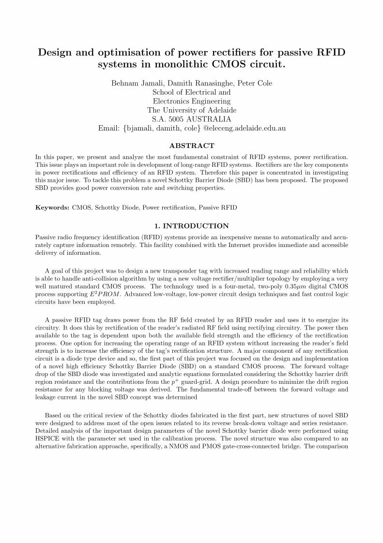
Figure 2. Cross sectional view of a planer Schottky Barrier Diode.
3.1. Theory and Background
In designing a Schottky diode for RFID systems, both non-linearity of the capacitance and the RC cutoff fre-quency of the diode are of primary concern. A brief discussion of the diode fabrication is necessary at the outestbecause the parasitics of the diode are a function of its geometry and physical implementation. Implementingdiodes on a standard CMOS process is designed specifically for ease of integration into circuits where the de-vices must be heavily packed and fabricated as a monolithic system. Figure 2 shows a cross-sectional view ofthe Schottky Barrier diode that was fabricated for this project. It consists of a Schottky contact to an n-wellactive region and ohmic contacts to a heavily doped n+ layer. With this diode geometry the layout is compactand the extrinsic parasitics are minimized. That is an important factor for high frequency operation of the circuit.
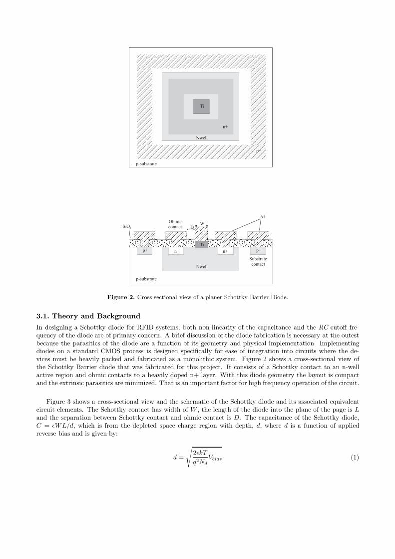
Figure 3 shows a cross-sectional view and the schematic of the Schottky diode and its associated equivalentcircuit elements. The Schottky contact has width of W , the length of the diode into the plane of the page is Land the separation between Schottky contact and ohmic contact is D. The capacitance of the Schottky diode,C = εWL/d, which is from the depleted space charge region with depth, d, where d is a function of appliedreverse bias and is given by:
d =
√2εkT
q2NdVbias (1)
Nwell
p-substrate
WD
Ohmiccontact
TiRc
Rs
Rc
Rn
Csub
Cdep
Rsub
Rs
Rn+ Rn+
Figure 3. Equivalent circuit of Schottky diode, illistrating the various components of the series resistance.
The sum resistance in series with this capacitance, Rsum, can be modeled as the sum of four components.The first element, Rn, is the n-well vertical resistance through the un-depleted portion of the n-well layer, where,the amount of un-depleted material is a function of bias. A 0V bias is used as a conservative value because thisresistance will be at its largest value, that is given by:
Rn =1
WL· ρn · Tundep (2)
where ρn is the resistivity of the n-well material and Tundep is the thickness of the undepeleted region at 0Vbias. Because this is a sheet resistance, it is an area term and so its value is inversly proportional to W · L.The second component of the resistance is the spreading resistance, Rs, that acccounts for the spreading of thecurrent flow under and around the Schottky contact into the n-well region. Value of Rs is given by:
Rs =13· W
4· 1L
· ρn
Tn(3)
where ρn is the resistivity of the n-well material and Tn is thickness of the n-well layer. A factor of W/4comes form the fact that the current travel only half the contact width as it spreads out to either side andthat these reistances are in parallel. Another additional factor of 1/3 arises form the distributed nature of thespreading resistance and capacitance under the contact, which is analoges to the spreading resistance in the baseof a bipolar junction transistor or distributed resistance of the gate finger of a MESFET.
The third component, RN , comes from the resistance of the N+ contact region due to the separation betweenthe n-well and ohmic contacts:
RN =12· D
L· ρN+
TN+(4)
and again the factor of 1/2 arises because there are two in parallel. The final component of the seriesresistance, Rc, is from the ohmic contacts:
Rc =1
2L
√ρcont · ρN+
TN+(5)

where ρcont is the specific contact resistivity. Because Rs, RN , and Rc are inversely proportional to L andthe capacitance is directly proportional to W · L, decreasing W and increasing L to maintain a constant diodearea reduces Rsum in proportion to C and consequently increases fcls, which is defined using the large signalcapacitance of the diode:
fcls =12πClsRs (6)
This is analogous to the design of the base-emitter junction of a bipolar transistor where the dominant resis-tance is the base resistance, which is also a periphery dependent term, so by decreasing the emitter stripe width,the RbaseCeb time constant is reduced.
Schottky contact
CdepCdep Cdep
Rn RnRn
RsRsRsRs
Figure 4. Diagram, illistrating the distribution nature of the resistance and capacitance of the Schottky contact.
Equation 6 for the diode cutoff frequency is valid at low frequencies, but neglects several high frequencyphenomenon that adversely affect the series resistance of the diode. The following discussion of these effects istaken directly from the work by Champlin and Eisenstein4 and also includes their references to original work.Dickens5 was the first to treat this problem in the context of a Schottky diode and showed that the high-frequencyextension of the spreading resistance is an impedance Z that for circular geometries given by:
Z =1
2πσaarctan(b/a) +
(1 + j)2πσδ
ln (b/a) (7)
where b and a are the radii of the semiconductor and contact, respectively, σ is the dc conductivity of thesemiconductor and δ is the skin depth given by:
δ =√
2wµ0σ
(8)
in which µ0 is the magnetic permeability.
Equation 7 is based on two assumptions that are not generally valid for semiconductors in the sub-millimeterwave region. They are
w wdr =σ
ε(9)
where wdr is the dielectric realisation frequency and
w wscat =q
m∗µe(10)
where wscat is the scattering frequency, m∗e is the effective mass of the electrons and µe is the mobility of the
electrons. Making assumption 9 is tantamount to ignoring the displacement current and is the usual assumptionthat leads to 8. Assumption 10 is equivalent to ignoring the inertial mass behavior of the carriers in their responseto an applied electric field.6
Both assumptions can be removed from 7 by replacing the dc conductivity σ with the complex quantity
σ′+ jwε = σ 1
1 + j(w/wscat)+ j(w/wd) (11)
and by replacing (1 + j)/σ with the actual propagation constant of the semiconductor material:
γ =√
jwµ0
√σ′ + jwε
=(1 + j)
δ 11 + j(w/wscat)
+ j(w/wd)1/2 (12)
Substituting 11 and 12 into 7 and assuming (b/a) 1 leads to Z = Zs + Z0 where Zs is the complexbulk-spreading impedance given by:
Zs =1
4σa 11 + j(w/wscat)
+ j(w/wd)−1 (13)
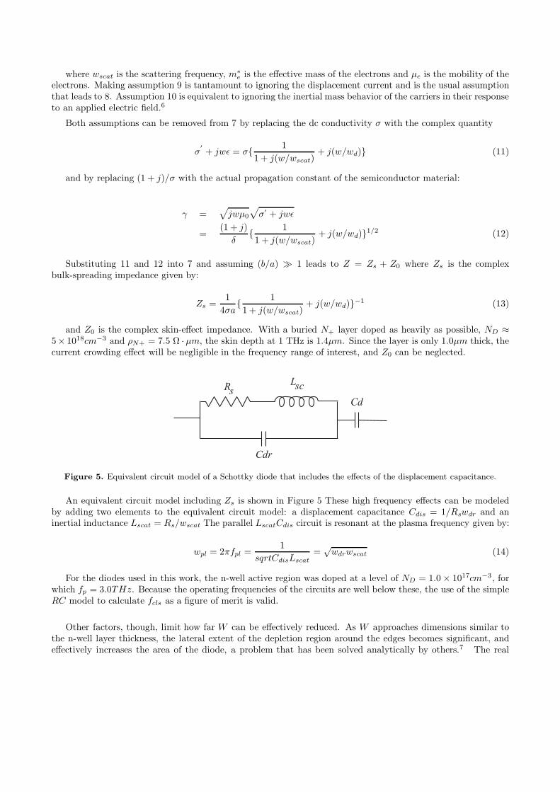
and Z0 is the complex skin-effect impedance. With a buried N+ layer doped as heavily as possible, ND ≈5× 1018cm−3 and ρN+ = 7.5 Ω ·µm, the skin depth at 1 THz is 1.4µm. Since the layer is only 1.0µm thick, thecurrent crowding effect will be negligible in the frequency range of interest, and Z0 can be neglected.
RsLsc
Cd
Cdr
Figure 5. Equivalent circuit model of a Schottky diode that includes the effects of the displacement capacitance.
An equivalent circuit model including Zs is shown in Figure 5 These high frequency effects can be modeledby adding two elements to the equivalent circuit model: a displacement capacitance Cdis = 1/Rswdr and aninertial inductance Lscat = Rs/wscat The parallel LscatCdis circuit is resonant at the plasma frequency given by:
wpl = 2πfpl =1
sqrtCdisLscat=
√wdrwscat (14)
For the diodes used in this work, the n-well active region was doped at a level of ND = 1.0 × 1017cm−3, forwhich fp = 3.0THz. Because the operating frequencies of the circuits are well below these, the use of the simpleRC model to calculate fcls as a figure of merit is valid.
Other factors, though, limit how far W can be effectively reduced. As W approaches dimensions similar tothe n-well layer thickness, the lateral extent of the depletion region around the edges becomes significant, andeffectively increases the area of the diode, a problem that has been solved analytically by others.7 The real

problem is that as the depletion depth increases under reverse bias, the lateral depletion region becomes propor-tionately larger, flattening out the C-V curve. This effect can be eliminated by using a self-aligned guard-ringto remove the n-well layer not directly under the Schottky contact, so there is no material remaining to becomelaterally depleted.
3.2. Models and Parameters of the SBDNumerical device modeling and simulation are essential for analyzing and developing semiconductor devices.They help a design engineer, not only to gain an increased understanding of the device operation, but alsothey provide the ability to predict electrical characteristics, behavior and parameter effects that influence thedevice behaviour. With this knowledge and abilities the designer can design a better structure, estimate thedevice performance, perform worst case analysis and optimize device parameters to yield an optimized deviceperformance.
As in any device simulator, any quantative, or qualitative simulation of a device, relies heavily on the devicemodels and their parameter values. Although many device models with their default parameters are availablein many commercial simulators, some of their parameters do not provide realistic characteristics of the semicon-ductor materials. As for the SBD developed in this work, there is no model available that takes into account allthe parameters affecting its performance.
Therefore, it is important to develop a model for the SBD fabricated on a standard CMOS process. Indeveloping a model the following were the main purposes taken into consideration:
• To define the electrical circuit equivalent of the SBD structure to enable improved analysis of circuitperformance.
• To define the magnitude and location of relevant parasitic electric elements to enable prediction of perfor-mance effects.
• To manipulate parasitic elements to obtain improved or enhanced circuit performance.
• It shall consist of conventional lumped circuit elements.
• It should accurately re-produce the diode IV characteristics and S parameters.
• It shall be compatible with the commonly used simulation tools.
The aim of this section is to analyze the applicability of CMOS material parameters from the literature andmeasurements, and implement them into SPICE program as a way to calibrate the simulation process with thereal device characteristics.
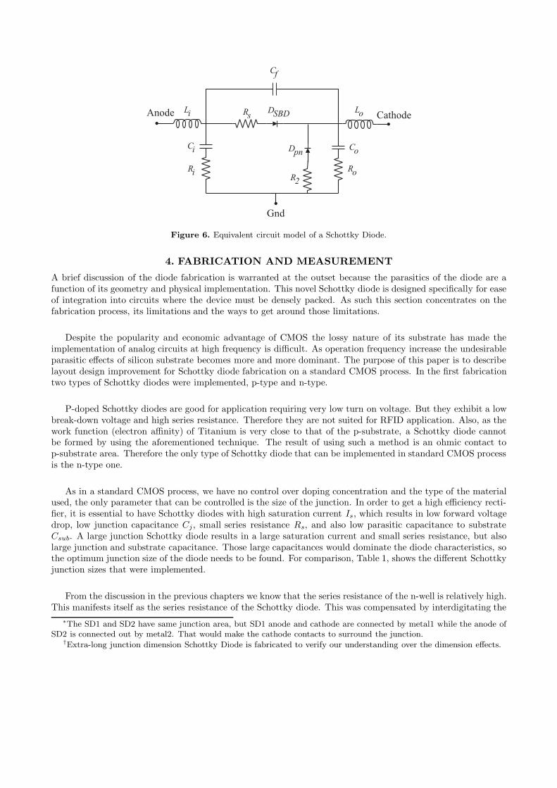
3.3. Simplified ModelFigure 6 shows a simplified model developed for the Schottky diode fabricated on a standard CMOS process.Data collected with measurement tools in the later phase of this work, was used to develop and refine this model.The refining process was done through iterative data collection and analysis and comparing expected resultswith actual data.
In this figure Li and Lo are the anode and cathode series wire inductance respectively. Ci and Co are the inputand output capacitance. Cf is the equivalent capacitance of the interdigitating fingers of anode and cathode.Ri and Ro are the anode and cathode parasitic n-well resistance to the substrate (or Gnd). Dpn models theparasitic n-well to p-substrate pn junction diode. Its characteristics can be obtained from the Spice model filesupplied by the foundry. R2 is the n-well vertical resistance just above the Dpn diode.
Anode Cathode
Gnd
RoR2
Li
Cf
DSBD
Co
Rs
Ci
Ri
Lo
Dpn
Figure 6. Equivalent circuit model of a Schottky Diode.
4. FABRICATION AND MEASUREMENT
A brief discussion of the diode fabrication is warranted at the outset because the parasitics of the diode are afunction of its geometry and physical implementation. This novel Schottky diode is designed specifically for easeof integration into circuits where the device must be densely packed. As such this section concentrates on thefabrication process, its limitations and the ways to get around those limitations.
Despite the popularity and economic advantage of CMOS the lossy nature of its substrate has made theimplementation of analog circuits at high frequency is difficult. As operation frequency increase the undesirableparasitic effects of silicon substrate becomes more and more dominant. The purpose of this paper is to describelayout design improvement for Schottky diode fabrication on a standard CMOS process. In the first fabricationtwo types of Schottky diodes were implemented, p-type and n-type.
P-doped Schottky diodes are good for application requiring very low turn on voltage. But they exhibit a lowbreak-down voltage and high series resistance. Therefore they are not suited for RFID application. Also, as thework function (electron affinity) of Titanium is very close to that of the p-substrate, a Schottky diode cannotbe formed by using the aforementioned technique. The result of using such a method is an ohmic contact top-substrate area. Therefore the only type of Schottky diode that can be implemented in standard CMOS processis the n-type one.
As in a standard CMOS process, we have no control over doping concentration and the type of the materialused, the only parameter that can be controlled is the size of the junction. In order to get a high efficiency recti-fier, it is essential to have Schottky diodes with high saturation current Is, which results in low forward voltagedrop, low junction capacitance Cj, small series resistance Rs, and also low parasitic capacitance to substrateCsub. A large junction Schottky diode results in a large saturation current and small series resistance, but alsolarge junction and substrate capacitance. Those large capacitances would dominate the diode characteristics, sothe optimum junction size of the diode needs to be found. For comparison, Table 1, shows the different Schottkyjunction sizes that were implemented.
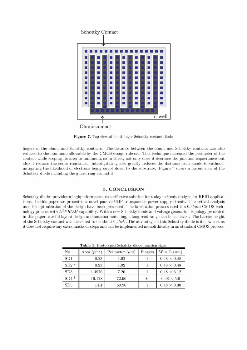
From the discussion in the previous chapters we know that the series resistance of the n-well is relatively high.This manifests itself as the series resistance of the Schottky diode. This was compensated by interdigitating the
∗The SD1 and SD2 have same junction area, but SD1 anode and cathode are connected by metal1 while the anode ofSD2 is connected out by metal2. That would make the cathode contacts to surround the junction.
†Extra-long junction dimension Schottky Diode is fabricated to verify our understanding over the dimension effects.
n-well
Ohmic contact
Schottky Contact
Figure 7. Top view of multi-finger Schottky contact diode.
fingers of the ohmic and Schottky contacts. The distance between the ohmic and Schottky contacts was alsoreduced to the minimum allowable by the CMOS design rule-set. This technique increased the perimeter of thecontact while keeping its area to minimum, so in effect, not only does it decrease the junction capacitance butalso it reduces the series resistance. Interdigitating also greatly reduces the distance from anode to cathode,mitigating the likelihood of electrons being swept down to the substrate. Figure 7 shows a layout view of theSchottky diode including the guard ring around it.
5. CONCLUSION
Schottky diodes provides a highperformance, cost-effective solution for today’s circuit designs for RFID applica-tions. In this paper we presented a novel passive UHF transponder power supply circuit. Theoretical analysisused for optimization of the design have been presented. The fabrication process used is a 0.35µm CMOS tech-nology process with E2PROM capability. With a new Schottky diode and voltage generation topology presentedin this paper, careful layout design and antenna matching, a long read range can be achieved. The barrier heightof the Schottky contact was measured to be about 0.45eV. The advantage of this Schottky diode is its low cost asit does not require any extra masks or steps and can be implemented monolithically in an standard CMOS process.
Table 1. Prototyped Schottky diode junction sizes
No Area (pm2) Perimeter (µm) Fingers W × L (µm)
SD1 0.23 1.92 1 0.48 × 0.48
SD2 ∗ 0.23 1.92 1 0.48 × 0.48
SD3 1.4976 7.20 1 0.48 × 3.12
SD4 † 16.128 72.90 6 0.48 × 5.6
SD5 14.4 60.96 1 0.48 × 0.30

REFERENCES1. K. V. S. Rao, ”An overview of backscattered radio frequency indentification system (RFID)”,in Proc Asia
Pacific Microwave Conf,. Vol3, Singapore: 1999.2. B. L. Sharma, ”Metal-Semiconductor Schottky Barrier Junction and their Applications” New York: Plenum
19843. Hudait M K ”Electrical transport characteristics of Au/n-GaAs Schottky diodes on n-Ge at low temperature”
Solid State electron 20014. K. S. Champlin and G. Eisenstein, ”Cutoff frequency of submillimeter Schottky-barrier diodes,” Microwave
Theory and Techniques, vol. MTT-26,no. 1, pp. 31-34, January, 1978.5. L.E. Dickens, ”Spreading resistance as a function of frequency” Microwave Theory and Techniques, vol.
MTT-15, no. 2, pp. 101-109, February, 1967.6. K. S. Champlin, D.B. Armstrong and P.D. Gunderson, ”Charge carrier inertia in semiconductors,” Proceed-
ings of I.R.E., vol. 52, no. 6, pp. 677-685, June, 1964.7. B. Gelmont, M. Shur, and R.J. Mattauch, ”Capacitance-voltage characteristics of microwave Schottky
diodes,” Microwave Theory and Techniques, vol. MTT-39, no. 5, pp. 857-862, May, 1991.
Copyright © 2022 FDOKUMEN