次世代サブミリ波天文観測装置DESHIMA の開発と実験室での ...
43
1 次世代サブミリ波天文観測装置DESHIMA の開発と実験室での性能評価 2016/11/24 KEK 測定器開発室セミナー Kenichi Karatsu, Akira Endo, David Thoen, Nuri van Marrewijk, Ozan Yurdseven, Nuria Llombart, Teun Klapwijk, Jochem Baselmans Vignesh Murugesan, Stephen Yates, Juan Bueno, Jochem Baselmans Nozomu Tomita, Shun Ishii, Kotaro Kohno Tatsuya Takekoshi, Tai Oshima
-
Upload
khangminh22 -
Category
Documents
-
view
4 -
download
0
Transcript of 次世代サブミリ波天文観測装置DESHIMA の開発と実験室での ...
1
次世代サブミリ波天文観測装置DESHIMAの開発と実験室での性能評価
2016/11/24 KEK 測定器開発室セミナー
Kenichi Karatsu, Akira Endo, David Thoen,Nuri van Marrewijk, Ozan Yurdseven, Nuria Llombart,Teun Klapwijk, Jochem BaselmansVignesh Murugesan, Stephen Yates, Juan Bueno,Jochem Baselmans
Nozomu Tomita, Shun Ishii, Kotaro Kohno
Tatsuya Takekoshi, Tai Oshima

2
IntroductionSubmm astronomyDESHIMA
DESHIMAOn-chip Filterbank SpectrometerMKID
Cryogenic SystemOpticsReadout
Experimental Results
Contents

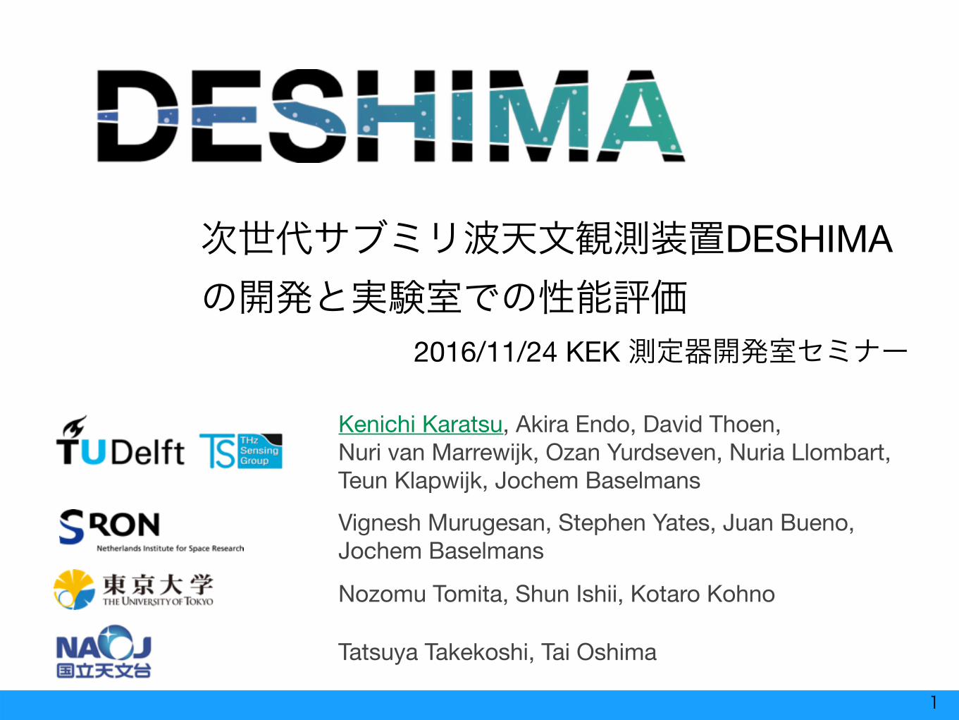
3Credit: STScI/JHU/NASA
4Credit: STScI/JHU/NASA
Credit: http://www.ccatobservatory.org/docs/ccat-reports-publications/Giovanelli-CCAT.pdf
Visible Infrared Submm

5Credit: STScI/JHU/NASA

6Credit: STScI/JHU/NASA
Microwave, Radio Wavelength: 10-1 – 10-4 m, > 0.1 mFreq.: 3×10⁹ – 3×10¹² Hz, < 3×10⁹ Hz
CMBSubmm galaxies (Star formation)Quasars
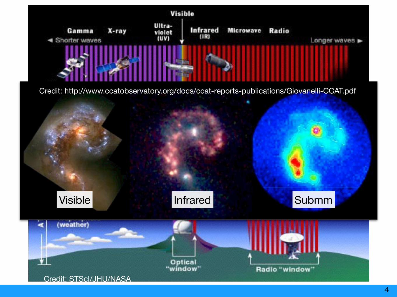
7Credit: STScI/JHU/NASA

8
(Obreschkow 2009)
(Kravtsov et al.)
Curiosity:Evolution of galaxies, in the Cosmic Large Scale Structure
‘Submm Galaxies’- Galaxies found in
submillimeter-wave surveys - Aggressive Star Formation:
Important ingredient for cosmic star-formation history and evolution of galaxies
- Dust extinction—> difficult to detect in vis-NIR Thermal reemission from dust —> Bright at THz-submm
What mysteries will we solve?- Cosmic Star Formation History - Evolution of Galaxies - Cosmic Structure Formation
1 3 10
5000
frequency THz
fluxdensity
Jy1 3 10
5000
frequency THz
fluxdensity
Jy
C+ 1.9 THz
O
O2+O
N2+
O2+
Si+S2+
S2+
[CII] 1.9 THz linefrom galaxies

9
The effect of FIR lines on the selection of high-z galaxies L97
Figure 2. The rest-frame SED of SMM J2135−0102, a typical high-redshiftSMG at z = 2.3259, showing the bright, narrow molecular and atomic emis-sion lines seen in the FIR and submillimetre. The continuum component ofthe SED is derived from fits to the Herschel and ground-based photometry(Ivison et al. 2010a; Swinbank et al. 2010) corrected for the emission-linecontributions. Added to this are the emission lines derived from the obser-vations of Danielson et al. (2011) or for lines shortward of 100 µm fromthe predictions from the PDR model used in that work. The observed [C II]line in this source contributes 0.27 per cent of LFIR and along with otherstrong lines may make a significant contribution to broad-band fluxes at cer-tain redshifts (to better illustrate this, the inset shows the same SED aroundthe dust peak, with a linear flux scaling). We also indicate the observed-frame passbands for the Herschel PACS (160 µm) and SPIRE (250, 350 and500 µm), SCUBA-2 (450 and 850 µm) and LABOCA (870 µm) filters.
Before continuing, we stress that SMM J2135−0102 was firstidentified at 870 µm, a passband which is not influenced by strongline emission in this source and hence the strength of its emissionlines is likely to be representative of typical high-redshift SMGs,rather than the most extreme examples. This is illustrated in Fig. 1,which shows an L[C II]/LFIR ratio which is not extreme for luminous,high-redshift sources, where line emitters have already been foundwith greater than or equal to four times higher ratios. In fact, as wediscuss below, the selection of the brightest sources in a particularwaveband may select a population with line-to-continuum ratios inthat waveband which are far higher than typical.
3 R ESULTS
As an illustration of the effects of line contamination on the broad-band fluxes of high-redshift SMGs, we redshift our template SEDand at each redshift we find the fluxes which would be observedin the Herschel 160-, 250-, 350- and 500-µm bands, and the 450-and 850-µm SCUBA-2 bands (the latter matching the LABOCA870-µm filter). In Fig. 3, we plot the fractional increase in thesefluxes as a function of the redshift for the SMM J2135−0102 SED,compared to a line-free SED. This figure demonstrates that evenfor relatively weak-lined SEDs there can be moderate variationsin the expected fluxes, 5–10 per cent, for many passbands at z !1. These line contributions are comparable to the absolute fluxcalibration uncertainty of typical submillimetre maps (e.g. Weisset al. 2009) and the residual errors in source fluxes after correctingfor confusion effects in these low-resolution maps (so-called flux
Figure 3. The contribution as a function of the source redshift to the contin-uum emission in the Herschel PACS and SPIRE, SCUBA-2 and LABOCAbands, from the emission lines shown in Fig. 2. The influence of the[C II] 158 µm line can be seen in the 250-, 350-, 500- and 850-µm bands atz ∼ 0.6, 1.2, 2.2 and 4.4, respectively, with a contribution to the broad-bandfluxes of 5–10 per cent. Note that these contributions are based on a [C II]line comprising 0.27 per cent of the galaxy’s LFIR. The line contributionswill scale linearly with the line-to-FIR luminosity ratio, so sources withL[C II]/LFIR ! 1 per cent (Fig. 1) will have contributions greater than orequal to four times larger, ∼20–40 per cent, corresponding to the right-handflux scale. We caution that the contributions for the higher redshift sourcesin the shorter wavelength filters (e.g. at z ∼ 4 and z ∼ 6 at 250 and 350 µm,respectively) are based on predicted, rather than observed, line fluxes.
boosting, Coppin et al. 2006), although unlike these two sources offlux error, the line contamination is redshift-dependent.
However, given that we already know of examples of high-redshift sources with stronger lines than our template SED (Fig. 1),there is the potential for even larger variations. As an example,we renormalize the atomic lines in our template SED so that [C II]158 µm corresponds to 1 per cent of the bolometric emission andrecalculate their contribution to the broad-band fluxes. We findthat for such strong-lined emitters the emission lines can boost thebroad-band fluxes by ∼20–40 per cent or greater (as shown by theright-hand scale in Fig. 3). Such variation in the apparent flux ofsources due to emission lines falling in the passband have two ob-vious consequences: (i) the presence of lines in only a subset ofpassbands may result in unusual colours for some combinationsof filters at certain redshifts; and (ii) the visibility of strong-linedsources at particular redshifts is enhanced, resulting in their over-representation in flux-limited samples.
To show the influence of line contamination on properties derivedfrom the broad-band photometry, we look at the effect of includingemission lines on the dust temperature and luminosity estimates.We fit the fluxes from our redshifted template SED, with and with-out emission lines, with a modified blackbody with β = 1.5 at theknown redshift and determine the characteristic temperature, Tdust,and FIR luminosity, LFIR. Using the SMM J2135−0105 SED, wefind negligible effects on the derived temperatures and luminosities,"1 K and "10 per cent, respectively, when complete, high-qualityphotometric data are available. However, sources with stronger linesmay suffer more significant biases, for example, ∼30 per cent inluminosity. Moreover, the increased flux in the line-contaminatedpassbands, and hence the apparently higher significance of the de-tections in these passbands coupled with incomplete photometriccoverage, may lead to even larger discrepancies. Such effects would
C⃝ 2011 The Authors, MNRAS 414, L95–L99Monthly Notices of the Royal Astronomical Society C⃝ 2011 RAS
Submm:No wideband spectrometer
Smail et al., 2011
ALMA (8 GHz)
Vis-NIR: Extremely faint because of dust extinction
Submm(ALMA)
Vis-NIR (Subaru)
Umehata et al. 2015
Bottleneck:Redshift measurement of submillimeter galaxies

The effect of FIR lines on the selection of high-z galaxies L97
Figure 2. The rest-frame SED of SMM J2135−0102, a typical high-redshiftSMG at z = 2.3259, showing the bright, narrow molecular and atomic emis-sion lines seen in the FIR and submillimetre. The continuum component ofthe SED is derived from fits to the Herschel and ground-based photometry(Ivison et al. 2010a; Swinbank et al. 2010) corrected for the emission-linecontributions. Added to this are the emission lines derived from the obser-vations of Danielson et al. (2011) or for lines shortward of 100 µm fromthe predictions from the PDR model used in that work. The observed [C II]line in this source contributes 0.27 per cent of LFIR and along with otherstrong lines may make a significant contribution to broad-band fluxes at cer-tain redshifts (to better illustrate this, the inset shows the same SED aroundthe dust peak, with a linear flux scaling). We also indicate the observed-frame passbands for the Herschel PACS (160 µm) and SPIRE (250, 350 and500 µm), SCUBA-2 (450 and 850 µm) and LABOCA (870 µm) filters.
Before continuing, we stress that SMM J2135−0102 was firstidentified at 870 µm, a passband which is not influenced by strongline emission in this source and hence the strength of its emissionlines is likely to be representative of typical high-redshift SMGs,rather than the most extreme examples. This is illustrated in Fig. 1,which shows an L[C II]/LFIR ratio which is not extreme for luminous,high-redshift sources, where line emitters have already been foundwith greater than or equal to four times higher ratios. In fact, as wediscuss below, the selection of the brightest sources in a particularwaveband may select a population with line-to-continuum ratios inthat waveband which are far higher than typical.
3 R ESULTS
As an illustration of the effects of line contamination on the broad-band fluxes of high-redshift SMGs, we redshift our template SEDand at each redshift we find the fluxes which would be observedin the Herschel 160-, 250-, 350- and 500-µm bands, and the 450-and 850-µm SCUBA-2 bands (the latter matching the LABOCA870-µm filter). In Fig. 3, we plot the fractional increase in thesefluxes as a function of the redshift for the SMM J2135−0102 SED,compared to a line-free SED. This figure demonstrates that evenfor relatively weak-lined SEDs there can be moderate variationsin the expected fluxes, 5–10 per cent, for many passbands at z !1. These line contributions are comparable to the absolute fluxcalibration uncertainty of typical submillimetre maps (e.g. Weisset al. 2009) and the residual errors in source fluxes after correctingfor confusion effects in these low-resolution maps (so-called flux
Figure 3. The contribution as a function of the source redshift to the contin-uum emission in the Herschel PACS and SPIRE, SCUBA-2 and LABOCAbands, from the emission lines shown in Fig. 2. The influence of the[C II] 158 µm line can be seen in the 250-, 350-, 500- and 850-µm bands atz ∼ 0.6, 1.2, 2.2 and 4.4, respectively, with a contribution to the broad-bandfluxes of 5–10 per cent. Note that these contributions are based on a [C II]line comprising 0.27 per cent of the galaxy’s LFIR. The line contributionswill scale linearly with the line-to-FIR luminosity ratio, so sources withL[C II]/LFIR ! 1 per cent (Fig. 1) will have contributions greater than orequal to four times larger, ∼20–40 per cent, corresponding to the right-handflux scale. We caution that the contributions for the higher redshift sourcesin the shorter wavelength filters (e.g. at z ∼ 4 and z ∼ 6 at 250 and 350 µm,respectively) are based on predicted, rather than observed, line fluxes.
boosting, Coppin et al. 2006), although unlike these two sources offlux error, the line contamination is redshift-dependent.
However, given that we already know of examples of high-redshift sources with stronger lines than our template SED (Fig. 1),there is the potential for even larger variations. As an example,we renormalize the atomic lines in our template SED so that [C II]158 µm corresponds to 1 per cent of the bolometric emission andrecalculate their contribution to the broad-band fluxes. We findthat for such strong-lined emitters the emission lines can boost thebroad-band fluxes by ∼20–40 per cent or greater (as shown by theright-hand scale in Fig. 3). Such variation in the apparent flux ofsources due to emission lines falling in the passband have two ob-vious consequences: (i) the presence of lines in only a subset ofpassbands may result in unusual colours for some combinationsof filters at certain redshifts; and (ii) the visibility of strong-linedsources at particular redshifts is enhanced, resulting in their over-representation in flux-limited samples.
To show the influence of line contamination on properties derivedfrom the broad-band photometry, we look at the effect of includingemission lines on the dust temperature and luminosity estimates.We fit the fluxes from our redshifted template SED, with and with-out emission lines, with a modified blackbody with β = 1.5 at theknown redshift and determine the characteristic temperature, Tdust,and FIR luminosity, LFIR. Using the SMM J2135−0105 SED, wefind negligible effects on the derived temperatures and luminosities,"1 K and "10 per cent, respectively, when complete, high-qualityphotometric data are available. However, sources with stronger linesmay suffer more significant biases, for example, ∼30 per cent inluminosity. Moreover, the increased flux in the line-contaminatedpassbands, and hence the apparently higher significance of the de-tections in these passbands coupled with incomplete photometriccoverage, may lead to even larger discrepancies. Such effects would
C⃝ 2011 The Authors, MNRAS 414, L95–L99Monthly Notices of the Royal Astronomical Society C⃝ 2011 RAS
No wideband spectrometer
Smail et al., 2011
ALMA (8 GHz)
TU Delft/SRON Breakthrough for Panoramic 3D view of the THz Universe:
10
No wide-field imager
ALMA(FoV: ~10 arcsec)
(Vis: >1 Gpixel)
A-MKID (25,000 pixel)
A-MKID (25,000 beams)
(A-MKID breakthrough)
(480 GHz)
(DESHIMA breakthrough)

DESHIMA
✴ The 3rd dimension = distance (time)
Goal: 3D map of massive star-forming galaxies (Bright in the THz)
Deep Spectroscopic High-redshift Mapper Delft SRON High-redshift Mapper
Probing the cosmic history of Star- and Galaxy-Formation in THz
11
Galaxies in3D space
distance (time)
2D projectionImaging camera → 2D projection

12
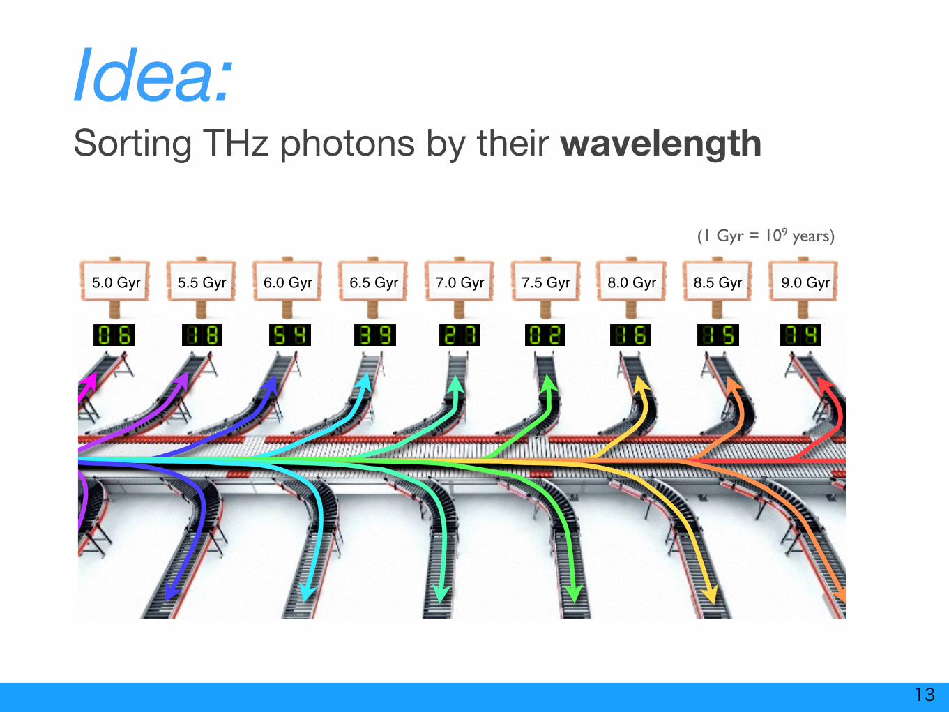
5.0 Gyr 5.5 Gyr 6.0 Gyr 6.5 Gyr 7.0 Gyr 7.5 Gyr 8.0 Gyr 8.5 Gyr 9.0 Gyr
(1 Gyr = 109 years)
Idea: Sorting THz photons by their age
13
5.0 Gyr 5.5 Gyr 6.0 Gyr 6.5 Gyr 7.0 Gyr 7.5 Gyr 8.0 Gyr 8.5 Gyr 9.0 Gyr
(1 Gyr = 109 years)
Idea: Sorting THz photons by their wavelength

Microwave Trick: Photon sorting with superconducting micro-filters
14
λ2
λ1
λ3
λ4
λ1/2
λ2/2
λ3/2
λ4/2
Signal from the sky
To separate detectors
~500 filters
Filters
100 µm

15
~500channels
widebandsignal
Microwave Readout(4-6 GHz)
antenna(lens in behind)
NbTiN
Al
No metal
(absorber)
326 GHz
326.6 GHz
327.2 GHz
905GHz
903.2GHz
901.4GHz
6.000 GHz 5.996
GHz 5.992GHz
4.000 GHz
4.004 GHz
4.008 GHz
MKID:Readout
Frequency
Filter:Signal Frequency
DESHIMA [CII] survey
Concept: Superconducting On-chip Filterbank Spectrometer

16
DESHIMA
collimating lenspupil LPFparabolic mirror x 2
LPF
IR blockers/shaders300K50K4K
LPF
Polarizer
LPFx2 (150 mK)
Lens + chip (150 mK)
double layer magnetic shield
800 mK intermediate stage
coax filters
150 mK box
Figure 5. Cross section of the optical/thermal/mechanical structure of DESHIMA.
~500 channels
AbsorberSubmm signal (326-906 GHz)
Microwave Readout(4-6 GHz)
Submm wave bandpass filter
Microwave Kinetic Inductance Detector
antenna(lens in behind)
NbTiN
Al
No metal
Filterbank chip @ 100 mK
Cryo-optical assembly(100 mK, 800 mK, 3.5K)
- Filterbank chip- F = 326-905 GHz (redshift 1-5 for [CII] 1.9 THz)- F/ΔF = 500- Max 7 spatial pixels
- Cryogenics: 2-stage ADR + 2-stage PTC- 4000 MKID detectors, read out with 1 pair of coax
cables- Optics: 2x parabolic mirrors (M=1)- Compatible with ASTE and APEX telescopes in
Chile (5 km alt.)

17
Deep Spectroscopic High-z Mapper
on
[ Sensitivity ]
Fig. 1. Predicted Minimum Detectable Line Flux of DESHIMA on ASTE, for an on-source time of 1 hour and a detection threshold of S/N = 5. It is assumed that the dominant noise source is the photon noise of the atmosphere. We have demonstrated MKID sensors that have a low enough NEP to reach this limit., and the challenge is to combine it with a filterbank on chip.
Details of the calculation are described a separate document “The photon-noise limited sensitivity of a single DESHIMA pixel.”
300 400 500 600 700 800 90010
−19
10−18
10−17
frequency (GHz)
MD
LF
(W
m−
2)
PWV = 0.5 mmPWV = 1 mm
[ Key Applications ]
Rapid redshift searches DESHIMA on ASTE will provide a deeper and more complete redshift search than ALMA in the same observing time. The power of blind redshift searches in the submm has recently been shown by Vieira et al (Nature 495, 344 (2013)), and Weiss et al (ApJ 767, 88 (2013), who obtained blind ALMA redshifts of a number of gravitationally lensed galaxies, with 850 μm fluxes of typically 100 mJy: DESHIMA on ASTE, under the conditions given in Fig. 1, would measure a [CII]-based redshift for such a luminous source in less than a minute.
Detailed multi-line spectroscopy: The power of very wide-band multi-line spectroscopy has been shown by the SPIRE FTS on Herschel. Such spectra provide multiple lines from the same molecular species, enabling immediate physical analysis, and revealing the full range of physical conditions present (densities, temperatures, radiation environments, etc.) Multiline spectroscopy of this type can be applied to distant gravitationally lensed submm galaxies, galaxies in the local universe, and to Galactic star forming regions and molecular clouds. DESHIMA with 6 spatial pixels will enable in-extenso mapping of galactic disks or star forming regions in the Milky Way, and map out the energetics of these systems.
[ Unique Selling Points ]
✴ Ultra-broadband spectroscopy
✴ Photon-noise limited sensitivity
✴ Scalable concept, towards a larger instrument that will spectroscopically resolve the complete CIB (MOSAIC)
single shot!
57’’
SCUBA-2 850 µm
ASTEASTEASTE
θFWHM = 23.6ʺ @ 326 GHz, 8.5ʺ@ 906 GHz
60°EL range
7 spatial pixels (maximum)θFWHM = 23.6ʺ @ 326 GHz, 8.5ʺ@ 906 GHz
A S T E t e l e s c o p e ( A t a c a m a d e s e r t , 4 8 0 0 m )
‘1st light demo’ ‘maximum’
F 326-368 GHz 326-905 GHz
F/ΔF 500 500
Npixels 1-2 max 7
NKIDs 100-200 max 4,000
DESHIMA

18
IntroductionSubmm astronomyDESHIMA
DESHIMAOn-chip Filterbank SpectrometerMKID
Cryogenic SystemOpticsReadout
Experimental Results
Contents

Cosmology with Nanotechnology
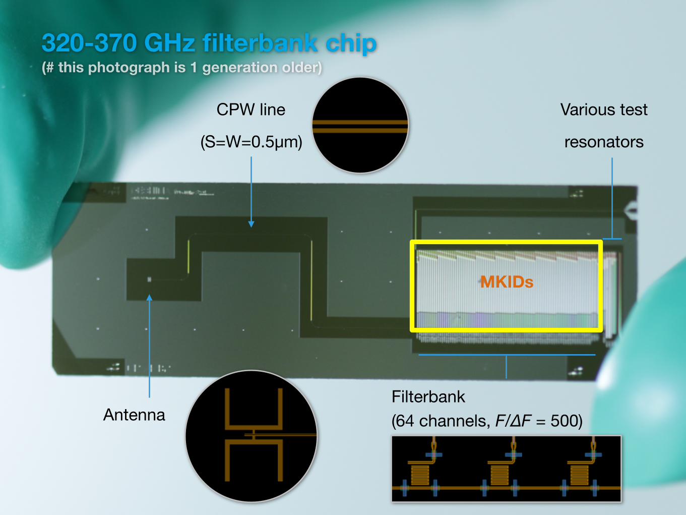
320-370 GHz filterbank chip(# this photograph is 1 generation older)
Antenna
CPW line(S=W=0.5µm)
Filterbank (64 channels, F/ΔF = 500)
Various test resonators
MKIDs

Filter bank design
20
from antenna(or previous filter) to next filter
to KID
bridge(PEC on vacuum)
short
NbTiN 100 nm(Ls = 1 pH/sq)on c-plane Sapphire
You can look at it as a meandered slot line…
… or as an LC circuit.
C
L
L
Interdigitated Capacitor Filter film thickness: 100 nm

Transmission
21
1st harmonic
2nd harmonic
3rd harmonic
!
"
"
Interdigitated Capacitor Filter
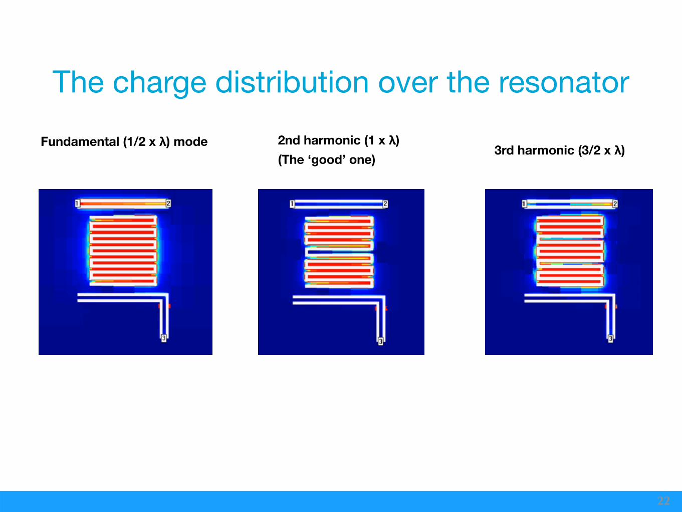
2nd harmonic (1 x λ) (The ‘good’ one)
Fundamental (1/2 x λ) mode 3rd harmonic (3/2 x λ)
The charge distribution over the resonator
22

23
+
+
-
-
- Top and bottom resemble 2 dipoles with opposite polarity.
- Efficient cancellation of radiation?
Why does the 2nd harmonic show low radiation loss??

Cosmology with Nanotechnology
320-370 GHz filterbank chip(# this photograph is 1 generation older)
Antenna
CPW line(S=W=0.5µm)
Filterbank (64 channels, F/ΔF = 500)
Various test resonators
MKIDs
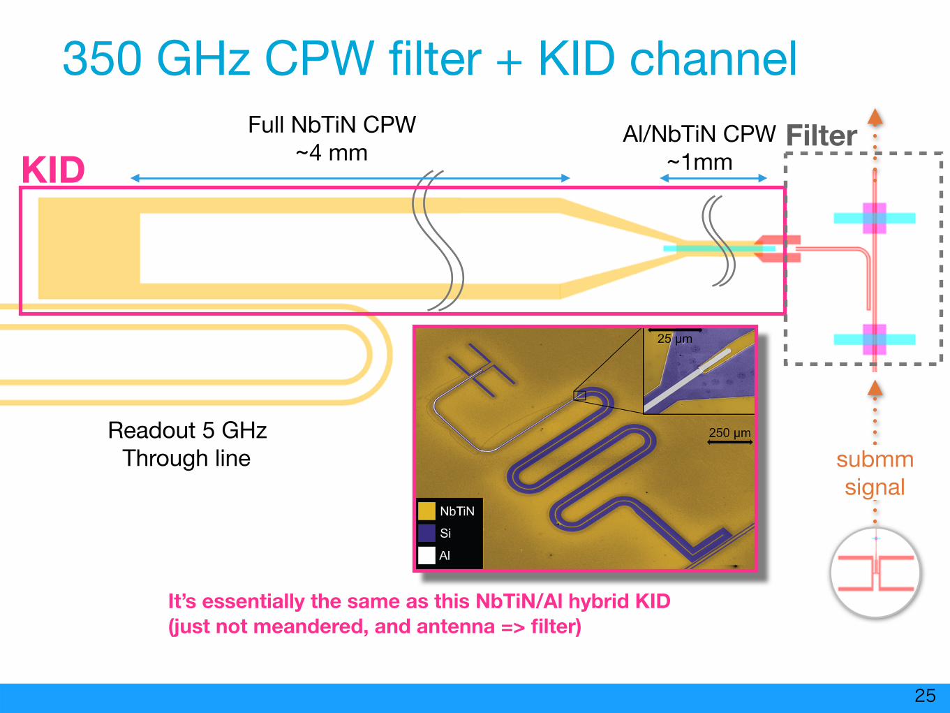
350 GHz CPW filter + KID channel
25
Full NbTiN CPW ~4 mm
Al/NbTiN CPW ~1mm
submmsignal
Readout 5 GHzThrough line
KIDFilter
It’s essentially the same as this NbTiN/Al hybrid KID (just not meandered, and antenna => filter)
High optical efficiency and photon noise limited sensitivity of microwavekinetic inductance detectors using phase readout
R. M. J. Janssen,1,a) J. J. A. Baselmans,2 A. Endo,1 L. Ferrari,3 S. J. C. Yates,3
A. M. Baryshev,3,4 and T. M. Klapwijk1,5
1Kavli Institute of Nanoscience, Faculty of Applied Sciences, Delft University of Technology, Lorentzweg 1,2628CJ Delft, The Netherlands2SRON Netherlands Institute for Space Research, Sorbonnelaan 2, 3584CA Utrecht, The Netherlands3SRON Netherlands Institute for Space Research, Landleven 12, 9747AD Groningen, The Netherlands4Kapteyn Astronomical Institute, University of Groningen, P.O. Box 800, 9700 AV Groningen,The Netherlands5Physics Department, Moscow State Pedagogical University, Moscow 119991, Russia
(Received 30 September 2013; accepted 26 October 2013; published online 14 November 2013)
We demonstrate photon noise limited performance in both phase and amplitude readout inmicrowave kinetic inductance detectors (MKIDs) consisting of NbTiN and Al, down to 100 fW ofoptical power. We simulate the far field beam pattern of the lens-antenna system used to coupleradiation into the MKID and derive an aperture efficiency of 75%. This is close to the theoreticalmaximum of 80% for a single-moded detector. The beam patterns are verified by a detailedanalysis of the optical coupling within our measurement setup. VC 2013 AIP Publishing LLC.[http://dx.doi.org/10.1063/1.4829657]
In the next decades millimeter and sub-mm astronomyrequire1 large format imaging arrays to complement thehigh spatial resolution of the Atacama Large Millimeter/submillimeter Array.2 The desired sensors should have abackground limited sensitivity and a high optical efficiencyand enable arrays of up to megapixels in size. The mostpromising candidates to fulfill these requirements are micro-wave kinetic inductance detectors (MKIDs)3 due to their in-herent potential for frequency domain multiplexing. MKIDsare superconducting resonators, thousands of which can becoupled to a single feedline. Each resonator is sensitive tochanges in the Cooper pair density induced by absorption ofsub-mm radiation. By monitoring the change in either phaseor amplitude of the complex feedline transmission at theMKID resonance one can measure the absorbed photonpower. Using amplitude readout photon noise limited per-formance has been shown.4 However, for practical applica-tions two key properties need to be demonstrated: (1) Photonnoise limited operation in phase readout. (2) A measurementof the aperture efficiency,5 which describes the absolute opti-cal coupling of a MKID imaging array to a plane wave.
In this letter we present antenna coupled hybrid NbTiN-Al MKIDs designed for groundbased sub-mm astronomy. Weshow that these devices achieve photon noise limited perform-ance in both amplitude and phase readout. Through a detailedanalysis of the optical coupling within our setup we validatethe simulation of the lens-antenna far field beam pattern. Fromthis we derive an aperture efficiency of 75%. This is close tothe theoretical maximum of 80% for a single-moded detector.
The device design, shown in Fig. 1, aims to simultane-ously maximize the phase response and minimize the two-levelsystem (TLS) noise contribution.8 The device is a L! 5 mmlong quarter wavelength coplanar waveguide (CPW) resonatorconsisting of two sections. The first section ("4 mm), at the
open end of the resonator, is a wide CPW made entirely from200 nm thick NbTiN. NbTiN has 10 dB lower TLS noise thanconventional superconductors such as Al.9 The TLS noise isfurther reduced by the width of the CPW,9 23.7 lm and 5.4 lmfor the CPW gap and central line, respectively.
The second section (1 mm), at the shorted end of the res-onator, is a narrow CPW with NbTiN groundplanes and a48 nm thick Al central line. The Al is galvanically connectedto the NbTiN central line (Fig. 1, inset) and the NbTiNgroundplane at the resonator short. The NbTiN is lossless forfrequencies up to the gap 2D0=h ¼ 1:1 THz ðTc ! 14 KÞ.Any radiation with a frequency 0:09 < ! < 1:1 THz is there-fore absorbed in the Al (Tc¼ 1.28 K) central line of the sec-ond section. The optically excited quasiparticles are trappedin the Al because it is connected to a high gap superconduc-tor. This quantum well structure confines the quasiparticles in
FIG. 1. Scanning electron micrograph of the antenna-coupled hybridNbTiN-Al MKIDs used. A wide NbTiN CPW resonator is used to minimizethe two-level system noise contribution. At the shorted end where the planarantenna is located, one millimeter of CPW is reduced in width, and the cen-tral line is made from thin Al. The Al is galvanically connected to theNbTiN at both ends (inset).a)Electronic mail: [email protected]
0003-6951/2013/103(20)/203503/4/$30.00 VC 2013 AIP Publishing LLC103, 203503-1
APPLIED PHYSICS LETTERS 103, 203503 (2013)
This article is copyrighted as indicated in the article. Reuse of AIP content is subject to the terms at: http://scitation.aip.org/termsconditions. Downloaded to IP:131.180.83.130 On: Thu, 05 Dec 2013 15:24:11

26
✓ MKID = Microwave-Kinetic-Inductance-Detector:Detect photons from changes in surface impedance (Zs) of superconducting resonators
Easy to read out large number of channels (>1000) with single readout line!
frwith photon
Detector Technology
Readout signal~5 GHz

High optical efficiency and photon noise limited sensitivity of microwavekinetic inductance detectors using phase readout
R. M. J. Janssen,1,a) J. J. A. Baselmans,2 A. Endo,1 L. Ferrari,3 S. J. C. Yates,3
A. M. Baryshev,3,4 and T. M. Klapwijk1,5
1Kavli Institute of Nanoscience, Faculty of Applied Sciences, Delft University of Technology, Lorentzweg 1,2628CJ Delft, The Netherlands2SRON Netherlands Institute for Space Research, Sorbonnelaan 2, 3584CA Utrecht, The Netherlands3SRON Netherlands Institute for Space Research, Landleven 12, 9747AD Groningen, The Netherlands4Kapteyn Astronomical Institute, University of Groningen, P.O. Box 800, 9700 AV Groningen,The Netherlands5Physics Department, Moscow State Pedagogical University, Moscow 119991, Russia
(Received 30 September 2013; accepted 26 October 2013; published online 14 November 2013)
We demonstrate photon noise limited performance in both phase and amplitude readout inmicrowave kinetic inductance detectors (MKIDs) consisting of NbTiN and Al, down to 100 fW ofoptical power. We simulate the far field beam pattern of the lens-antenna system used to coupleradiation into the MKID and derive an aperture efficiency of 75%. This is close to the theoreticalmaximum of 80% for a single-moded detector. The beam patterns are verified by a detailedanalysis of the optical coupling within our measurement setup. VC 2013 AIP Publishing LLC.[http://dx.doi.org/10.1063/1.4829657]
In the next decades millimeter and sub-mm astronomyrequire1 large format imaging arrays to complement thehigh spatial resolution of the Atacama Large Millimeter/submillimeter Array.2 The desired sensors should have abackground limited sensitivity and a high optical efficiencyand enable arrays of up to megapixels in size. The mostpromising candidates to fulfill these requirements are micro-wave kinetic inductance detectors (MKIDs)3 due to their in-herent potential for frequency domain multiplexing. MKIDsare superconducting resonators, thousands of which can becoupled to a single feedline. Each resonator is sensitive tochanges in the Cooper pair density induced by absorption ofsub-mm radiation. By monitoring the change in either phaseor amplitude of the complex feedline transmission at theMKID resonance one can measure the absorbed photonpower. Using amplitude readout photon noise limited per-formance has been shown.4 However, for practical applica-tions two key properties need to be demonstrated: (1) Photonnoise limited operation in phase readout. (2) A measurementof the aperture efficiency,5 which describes the absolute opti-cal coupling of a MKID imaging array to a plane wave.
In this letter we present antenna coupled hybrid NbTiN-Al MKIDs designed for groundbased sub-mm astronomy. Weshow that these devices achieve photon noise limited perform-ance in both amplitude and phase readout. Through a detailedanalysis of the optical coupling within our setup we validatethe simulation of the lens-antenna far field beam pattern. Fromthis we derive an aperture efficiency of 75%. This is close tothe theoretical maximum of 80% for a single-moded detector.
The device design, shown in Fig. 1, aims to simultane-ously maximize the phase response and minimize the two-levelsystem (TLS) noise contribution.8 The device is a L! 5 mmlong quarter wavelength coplanar waveguide (CPW) resonatorconsisting of two sections. The first section ("4 mm), at the
open end of the resonator, is a wide CPW made entirely from200 nm thick NbTiN. NbTiN has 10 dB lower TLS noise thanconventional superconductors such as Al.9 The TLS noise isfurther reduced by the width of the CPW,9 23.7 lm and 5.4 lmfor the CPW gap and central line, respectively.
The second section (1 mm), at the shorted end of the res-onator, is a narrow CPW with NbTiN groundplanes and a48 nm thick Al central line. The Al is galvanically connectedto the NbTiN central line (Fig. 1, inset) and the NbTiNgroundplane at the resonator short. The NbTiN is lossless forfrequencies up to the gap 2D0=h ¼ 1:1 THz ðTc ! 14 KÞ.Any radiation with a frequency 0:09 < ! < 1:1 THz is there-fore absorbed in the Al (Tc¼ 1.28 K) central line of the sec-ond section. The optically excited quasiparticles are trappedin the Al because it is connected to a high gap superconduc-tor. This quantum well structure confines the quasiparticles in
FIG. 1. Scanning electron micrograph of the antenna-coupled hybridNbTiN-Al MKIDs used. A wide NbTiN CPW resonator is used to minimizethe two-level system noise contribution. At the shorted end where the planarantenna is located, one millimeter of CPW is reduced in width, and the cen-tral line is made from thin Al. The Al is galvanically connected to theNbTiN at both ends (inset).a)Electronic mail: [email protected]
0003-6951/2013/103(20)/203503/4/$30.00 VC 2013 AIP Publishing LLC103, 203503-1
APPLIED PHYSICS LETTERS 103, 203503 (2013)
This article is copyrighted as indicated in the article. Reuse of AIP content is subject to the terms at: http://scitation.aip.org/termsconditions. Downloaded to IP:131.180.83.130 On: Thu, 05 Dec 2013 15:24:11
27
the most responsive part of the MKID and allows us to maxi-mize the response by minimizing this active volume.Therefore, we use a narrow CPW in section two, 2.3 lm and3.7 lm for the central line and slots, respectively. Using anarrow Al line at the shorted end of the MKID does notincrease the TLS noise significantly because of the negligibleelectric field strength in this part of the detector.
At the shorted end of the resonator light is coupled intothe device through a single polarization twin-slot antenna,which is optimized for ! ¼ 350 GHz. The advantage of usingantenna coupling is that it can be designed independentlyfrom the distributed CPW resonator. The disadvantage isthat the antenna occupies only "1% of the total pixel foot-print. To achieve a high filling fraction we use ellipticallenses to focus the light on the antennas.
The design presented here is an improvement on that byYates et al.4 Our design has a wider body in section one,which provides "7 dB reduction of the TLS noise. In addi-tion we have thinner Al, 48 nm instead of 80 nm. Thisincreases the kinetic inductance fraction by 45% to a¼ 0.09and reduces the volume by 40%. Both give a linear increasein the phase response.
An array of 24 pixels has been fabricated10,11 on a highresistivity ð>10 kX cmÞ h100i-oriented Si substrate. All pix-els are capacitively coupled to a single feedline with a cou-pling Qc " 58 k, which is matched to the Qi expected for anoptical loading of "10 pW. After mounting an array of 16laser machined Si lenses with a diameter of 2 mm on thecentral pixels, the array is evaluated using a pulse tube pre-cooled adiabatic demagnetization refrigerator with a box-in-a-box cold stage design.12 In this design the array is fullyenclosed in a 100 mK environment with the exception of a2 mm aperture, which is located 15.05 mm above the approxi-mate center of the MKID array. This aperture is isotropicallyilluminated by a large temperature-controlled blackbody.6
Two metal mesh filters provide a minimum rejection of
20 dB at all wavelengths outside the 50 GHz bandpass cen-tered on ! ¼ 350 GHz. This allows us to create a variableunpolarized illumination over a wide range of powers.
Fig. 2(a) shows the amplitude and phase noise spectrameasured for a typical device as a function of the opticalpower absorbed in the Al, P350GHz. In this figure we observetwo characteristics that prove our device is photon noiselimited:
1. The noise spectra in both phase and amplitude are whitewith a roll-off given by the quasiparticle lifetime, sqp, orresonator ring time, sres. For our devices we observe awhite noise spectrum for P350GHz % 100 fW, which has aroll-off due to sqp, because sqp > sres.
2. When reducing the optical loading from the photonnoise limited situation one should observe at negligiblepower levels the transition to a noise spectrum that islimited by intrinsic noise sources of the detector. At anegligible optical loading (P350GHz¼ 4 fW) the phasenoise spectrum is no longer white and the noise level inboth phase and amplitude readout is lower with respectto P350GHz > 4 fW.
Fig. 2 shows three more features, which may be presentin a photon noise limited MKID.
The photon noise level of the spectra observed in Fig.2(a) is independent of the optical loading because the prod-uct of quasiparticle number and quasiparticle lifetime is con-stant,6,13 and the loaded Q did not change.
By fitting a Lorentzian roll-off6 to the spectra presentedin Fig. 2(a) we derive the quasiparticle lifetime as a functionof the optical loading. Fig. 3 shows that the quasiparticlelifetime obtained from phase and amplitude readout is equalfor all loading levels. For P350GHz > 100 fW the quasiparticlelifetimes show a sqp / P&0:5060:02
350GHz relation, which matchesthe expected sqp / 1=
ffiffiffiffiffiffiffiffiffiffiffiffiffiffiffiP350GHz
prelation13–15 for a homoge-
neously illuminated superconductor. At P350GHz¼ 4 fW we
FIG. 2. (a) The power spectral density of the amplitude (dashed line) and phase (solid line) noise measured under various optical loading. A white noise spec-trum is observed, the level of which is constant with loading power, for P350GHz > 100 fW. The roll-off above 1 kHz is due to the quasiparticle lifetime, whichis reduced by an increasing optical load. Note that the photon noise level is 16 dB higher in phase readout. Nevertheless, at a given loading the NEP is thesame for phase and amplitude readout as shown in (b). (b) The optical NEP6,7 for amplitude (dashed line) and phase (solid line) readout as a function of opticalloading. (c) The optical NEP measured at a modulation frequency of 200 Hz, NEPopt, as a function of the estimated optical loading, Pcalc. For every opticalloading the NEP in phase (magenta dots) and amplitude (black dots) readout is equal if for the latter the amplifier contribution (black diamonds) is subtracted.This contribution is insignificant in phase readout. The error bars on the NEP measurement are of the order of the symbol size. The measured NEP follows thesame slope as NEPcalc /
ffiffiffiffiffiffiffiffiffiPcalcp
(dashed black line). By fitting the relation between measured amplitude NEP and NEPcalc (solid black line) " ¼ 1:0660:06 isdetermined.
203503-2 Janssen et al. Appl. Phys. Lett. 103, 203503 (2013)
This article is copyrighted as indicated in the article. Reuse of AIP content is subject to the terms at: http://scitation.aip.org/termsconditions. Downloaded to IP:131.180.83.130 On: Thu, 05 Dec 2013 15:24:11
- NbTiN: Fgap = 1.1 THz- Lossless- Al: Fgap = 90 GHz- Quasiparticle excitation
✴Quasiparticle Trapping in Al
Relevant forDESHIMAphoton noise lim
it
the most responsive part of the MKID and allows us to maxi-mize the response by minimizing this active volume.Therefore, we use a narrow CPW in section two, 2.3 lm and3.7 lm for the central line and slots, respectively. Using anarrow Al line at the shorted end of the MKID does notincrease the TLS noise significantly because of the negligibleelectric field strength in this part of the detector.
At the shorted end of the resonator light is coupled intothe device through a single polarization twin-slot antenna,which is optimized for ! ¼ 350 GHz. The advantage of usingantenna coupling is that it can be designed independentlyfrom the distributed CPW resonator. The disadvantage isthat the antenna occupies only "1% of the total pixel foot-print. To achieve a high filling fraction we use ellipticallenses to focus the light on the antennas.
The design presented here is an improvement on that byYates et al.4 Our design has a wider body in section one,which provides "7 dB reduction of the TLS noise. In addi-tion we have thinner Al, 48 nm instead of 80 nm. Thisincreases the kinetic inductance fraction by 45% to a¼ 0.09and reduces the volume by 40%. Both give a linear increasein the phase response.
An array of 24 pixels has been fabricated10,11 on a highresistivity ð>10 kX cmÞ h100i-oriented Si substrate. All pix-els are capacitively coupled to a single feedline with a cou-pling Qc " 58 k, which is matched to the Qi expected for anoptical loading of "10 pW. After mounting an array of 16laser machined Si lenses with a diameter of 2 mm on thecentral pixels, the array is evaluated using a pulse tube pre-cooled adiabatic demagnetization refrigerator with a box-in-a-box cold stage design.12 In this design the array is fullyenclosed in a 100 mK environment with the exception of a2 mm aperture, which is located 15.05 mm above the approxi-mate center of the MKID array. This aperture is isotropicallyilluminated by a large temperature-controlled blackbody.6
Two metal mesh filters provide a minimum rejection of
20 dB at all wavelengths outside the 50 GHz bandpass cen-tered on ! ¼ 350 GHz. This allows us to create a variableunpolarized illumination over a wide range of powers.
Fig. 2(a) shows the amplitude and phase noise spectrameasured for a typical device as a function of the opticalpower absorbed in the Al, P350GHz. In this figure we observetwo characteristics that prove our device is photon noiselimited:
1. The noise spectra in both phase and amplitude are whitewith a roll-off given by the quasiparticle lifetime, sqp, orresonator ring time, sres. For our devices we observe awhite noise spectrum for P350GHz % 100 fW, which has aroll-off due to sqp, because sqp > sres.
2. When reducing the optical loading from the photonnoise limited situation one should observe at negligiblepower levels the transition to a noise spectrum that islimited by intrinsic noise sources of the detector. At anegligible optical loading (P350GHz¼ 4 fW) the phasenoise spectrum is no longer white and the noise level inboth phase and amplitude readout is lower with respectto P350GHz > 4 fW.
Fig. 2 shows three more features, which may be presentin a photon noise limited MKID.
The photon noise level of the spectra observed in Fig.2(a) is independent of the optical loading because the prod-uct of quasiparticle number and quasiparticle lifetime is con-stant,6,13 and the loaded Q did not change.
By fitting a Lorentzian roll-off6 to the spectra presentedin Fig. 2(a) we derive the quasiparticle lifetime as a functionof the optical loading. Fig. 3 shows that the quasiparticlelifetime obtained from phase and amplitude readout is equalfor all loading levels. For P350GHz > 100 fW the quasiparticlelifetimes show a sqp / P&0:5060:02
350GHz relation, which matchesthe expected sqp / 1=
ffiffiffiffiffiffiffiffiffiffiffiffiffiffiffiP350GHz
prelation13–15 for a homoge-
neously illuminated superconductor. At P350GHz¼ 4 fW we
FIG. 2. (a) The power spectral density of the amplitude (dashed line) and phase (solid line) noise measured under various optical loading. A white noise spec-trum is observed, the level of which is constant with loading power, for P350GHz > 100 fW. The roll-off above 1 kHz is due to the quasiparticle lifetime, whichis reduced by an increasing optical load. Note that the photon noise level is 16 dB higher in phase readout. Nevertheless, at a given loading the NEP is thesame for phase and amplitude readout as shown in (b). (b) The optical NEP6,7 for amplitude (dashed line) and phase (solid line) readout as a function of opticalloading. (c) The optical NEP measured at a modulation frequency of 200 Hz, NEPopt, as a function of the estimated optical loading, Pcalc. For every opticalloading the NEP in phase (magenta dots) and amplitude (black dots) readout is equal if for the latter the amplifier contribution (black diamonds) is subtracted.This contribution is insignificant in phase readout. The error bars on the NEP measurement are of the order of the symbol size. The measured NEP follows thesame slope as NEPcalc /
ffiffiffiffiffiffiffiffiffiPcalcp
(dashed black line). By fitting the relation between measured amplitude NEP and NEPcalc (solid black line) " ¼ 1:0660:06 isdetermined.
203503-2 Janssen et al. Appl. Phys. Lett. 103, 203503 (2013)
This article is copyrighted as indicated in the article. Reuse of AIP content is subject to the terms at: http://scitation.aip.org/termsconditions. Downloaded to IP:131.180.83.130 On: Thu, 05 Dec 2013 15:24:11
AMKID camera array
Photon noise PSD NEP vs. P350 GHz
flat: photon noise
Al Quantum-well
(2Δ < hν)
photon
NbTiN Resonator(2Δ > hν)
e-
e-
Janssen et al., Appl. Phys. Lett. 103, 203503 (2013)Janssen et al., Appl. Phys. Lett. 105, 193504 (2014)
Photon-noise limited NbTiN/Al hybrid MKIDs
Cosmology with Nanotechnology
320-370 GHz filterbank chip(# this photograph is 1 generation older)
Antenna
CPW line(S=W=0.5µm)
Filterbank (64 channels, F/ΔF = 500)
Various test resonators
MKIDs

29
IntroductionSubmm astronomyDESHIMA
DESHIMAOn-chip Filterbank SpectrometerMKID
Cryogenic SystemOpticsReadout
Experimental Results
Contents

30
Integration of DESHIMA
Google map

Cryogenic Optics: Cool Down Test
31
FAA
Magnet current
14:00:0027.03.2016
18:10:0027.03.2016
22:20:0027.03.2016
02:30:0028.03.2016
06:40:0028.03.2016
10:50:0028.03.2016
15:00:0028.03.2016
Time
0
0.1
0.2
0.3
0.4
0.5
0.6
0.7
0.8
Tem
pera
ture
[K]
log_2016-03-25 1657
Configuration:• 4 K: Pulse tube cooler• 100 mK: ADR (2 stages)Specification:• Hold time (w 1 uW loading) ~ 18h
hold time ~ 26hw. 0.4 uW loading

32
300 K scatter filter (two-in-one)
50 K thermal filters
4 K thermal filters
field lens
2 THz (66 cm-1) Low Pass Filter
1 .1 THz (36 cm-1) Low Pass Filter
1.5 THz (58 cm-1) Low Pass Filter
polarizer
1THz (33 cm-1) LPF + 390 GHz (13 cm-1) LPF
stray light baffle
Parabolic Mirrors
Cryoperm shield
Nb shield
filterbank chip & lens(at 100 mK)
(or 1THz (33 cm-1) LPF + 0.9THz (30 cm-1) LPF
800 mK ‘finger’
100 mK ‘finger’
4 K stage
heat switch
field lens
Cryogenic Optics
33
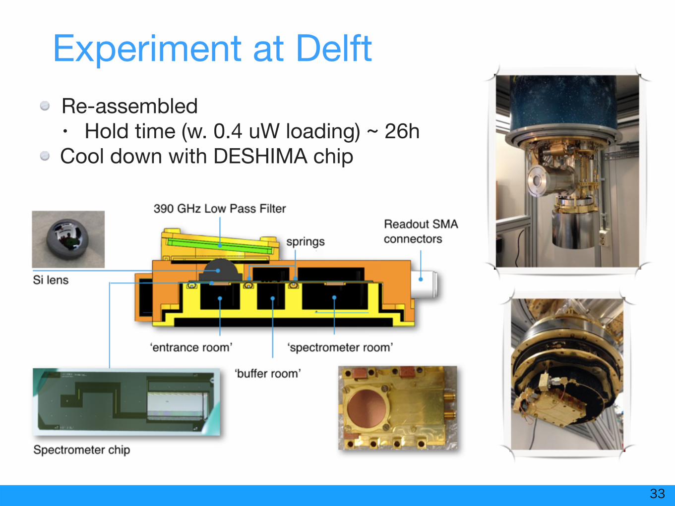
Re-assembled• Hold time (w. 0.4 uW loading) ~ 26hCool down with DESHIMA chip
Experiment at Delft

Developed by SRON for SpaceKIDs project• J. van Rantwijk et al., IEEE TMTT, 64, 6, 1876-1883 (2016)
RF cabinet (RF board)
Digital cabinet (ADC/DAC board)Computer
DESHIMA Readout System

35
DESHIMA Readout SystemDeveloped by SRON for SpaceKIDs project• J. van Rantwijk et al., IEEE TMTT, 64, 6, 1876-1883 (2016)
Specifications:• FFT based readout• 2 GHz band width• Can read 4000 KIDs simultaneously• Maximum data rate ~1.3 kHz
36
IntroductionSubmm astronomy and DESHIMA
DESHIMAOn-chip Filterbank SpectrometerMKID
Cryogenic SystemOpticsReadout
Experimental Results
Contents
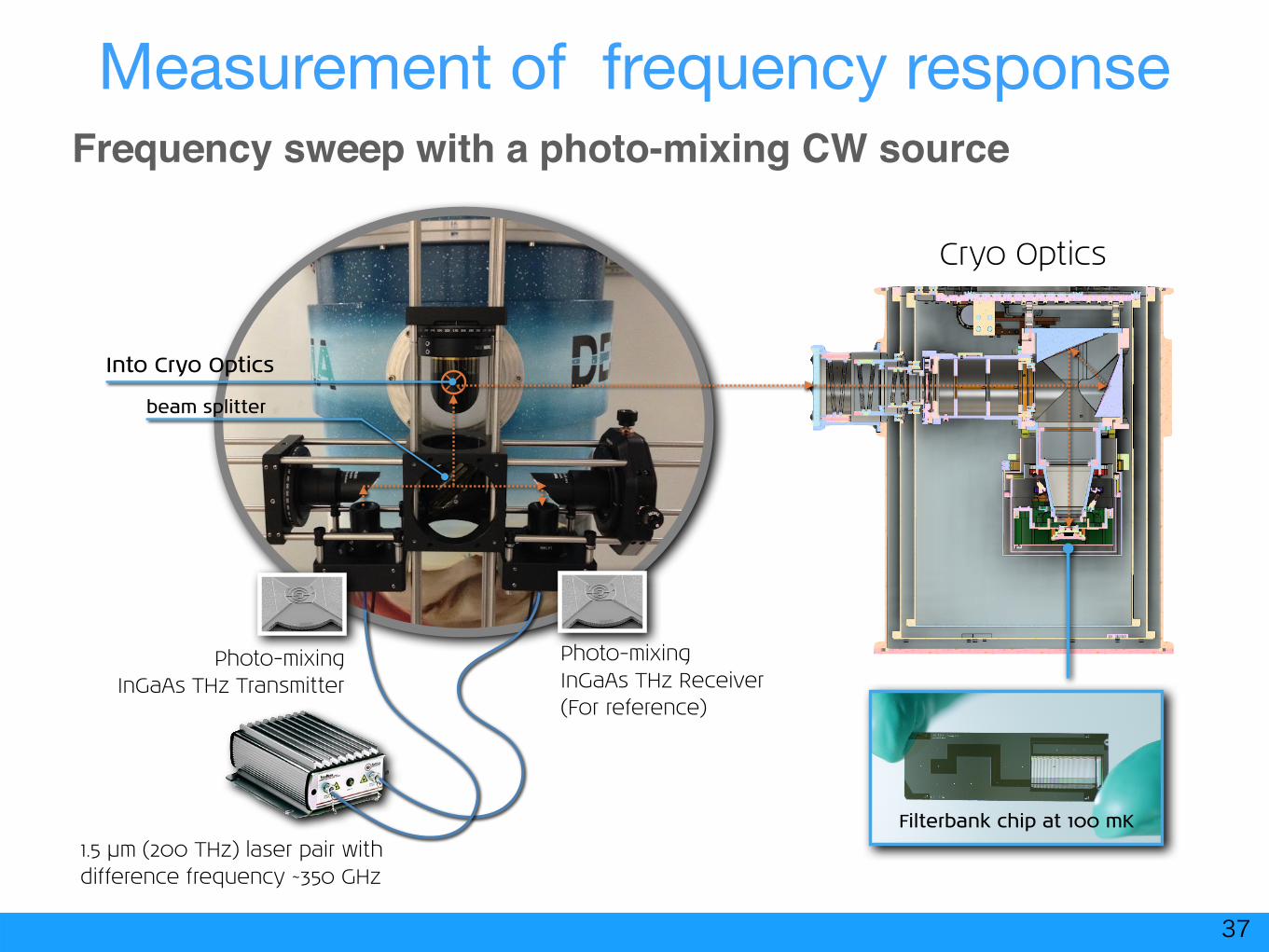
Measurement of frequency response
37
Experimental setup
Photo-mixingInGaAs THz Receiver(For reference)
Into Cryo Optics
1.5 µm (200 THz) laser pair with difference frequency ~350 GHz
High power from InGaAs emittersInGaAs-based terahertz emitters comprise ultrafast p-i-n photodiodes, with an intrinsic layer embedded between p-doped and n-doped semiconductor layers. The laser light is coupled into the intrinsic layer from an underlying waveguide structure. In this design, the extended absorption length leads to highly-efficient terahertz generation. InGaAs has a semiconductor bandgap of 1.68 μm and telecom lasers at 1.5 μm are thus a perfect match. The combination of ToPTIcA’s TeraBeam laser and InGaAs emitter/detector modules presents a highly-compact terahertz platform, and achieves power levels up to 10 μW.
order information
850nm#EK-000685
GaAs photomixer for cw terahertz generation and detection, with log-spiral antenna and SM/PM fiber pigtail
1550nm#EK-000724
InGaAs/InP based waveguide-integrated photodiode for cw terahertz generation, with bow-tie antenna and SM/PM fiber pigtail
#EK-000725InGaAs/InP based photoconductor for cw terahertz detection,with bow-tie antenna and SM/PM fiber pigtail
note: The photomixers are available as individual modules or as part of the Spectroscopy extension (p. 25). operation requires a set of seed lasers (e.g., the Standard Package SyST Thz STd / 850, or the TeraBeam 1550).
Specifications #EK-000685 #EK-000724/#EK-000725
Semiconductor material GaAs InGaAs on InP
Wavelength 853 + 855 nm 1546 + 1550 nm
Emitter PhotomixerWaveguide-integrated
p-i-n photodiode
Receiver Photomixer Photomixer
Antenna type Log-spiral Bow-tie
Emitter/receiverbandwidth* > 3 Thz > 2 Thz
Terahertz power (typ.)2 μW @ 100 Ghz
0.3 μW @ 500 Ghz4 μW @ 100 Ghz
0.5 μW @ 500 Ghz
Terahertz dynamic range (@300msintegrationtime)
80 dB @ 100 Ghz 70 dB @ 500 Ghz
70 dB @ 100 Ghz 50 dB @ 500 Ghz
Packagecylindrical, Ø 1”,
integrated Si lens & SM/PM fiber pigtailcylindrical, Ø 30 mm,
integrated Si lens & SM/PM fiber pigtail
Recommended operating conditions
Laser power < 50 mW Bias ± 10 V
Laser power 20 mW Bias 0 / -1.5 V
Key advantages high bandwidth, high dynamic range compact laser unit, low cost
* Tuning range of lasers may differ
www.toptica.com | 23
Demonstration: Response of a MKID sensor behind a filterbank to a Continuous-wave THz line emitter
78channels
widebandsignal
Microwave Readout(5.0-5.4 GHz)
antenna(lens in behind)
NbTiN
Al
No metal
(absorber)
Source frequency is repeatedlyoscillating around this range
MKID sensor responds when FFilter = Fsignal
• On the VNA display, you can monitor the state of a single MKID sensor, behind a bandpass filter with a center frequency Ffilter.
• The frequency Fsignal of the THz source is modulated around the center frequency of the bandpass filter
• When Ffilter = Fsignal, the MKID sensor responds.
• The bottom-right plot shows the response of different detectors as functions of Fsignal. (Operation principle of a filterbank spectrometer)
Photo-mixingInGaAs THz Transmitter
beam splitter
Filterbank chip at 100 mK
Cryo Optics
VNA display Fsignal response of different channels
Schematic of the filterbank chip used in this demo
DelftUniversity ofTechnology Cosmology with NanotechnologyCosmology with Nanotechnology
Frequency sweep with a photo-mixing CW source
38
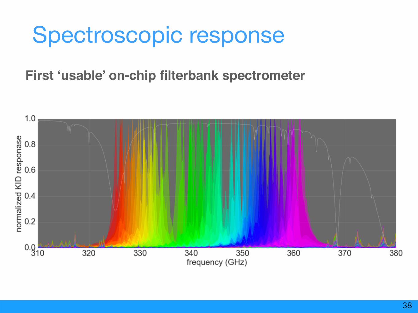
atmospheric transmissionat Atacama
First ‘usable’ on-chip filterbank spectrometer
Spectroscopic response

39
design: 500
Frequency resolution (Q factor)
40
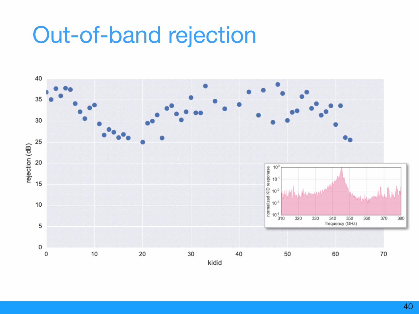
Out-of-band rejection
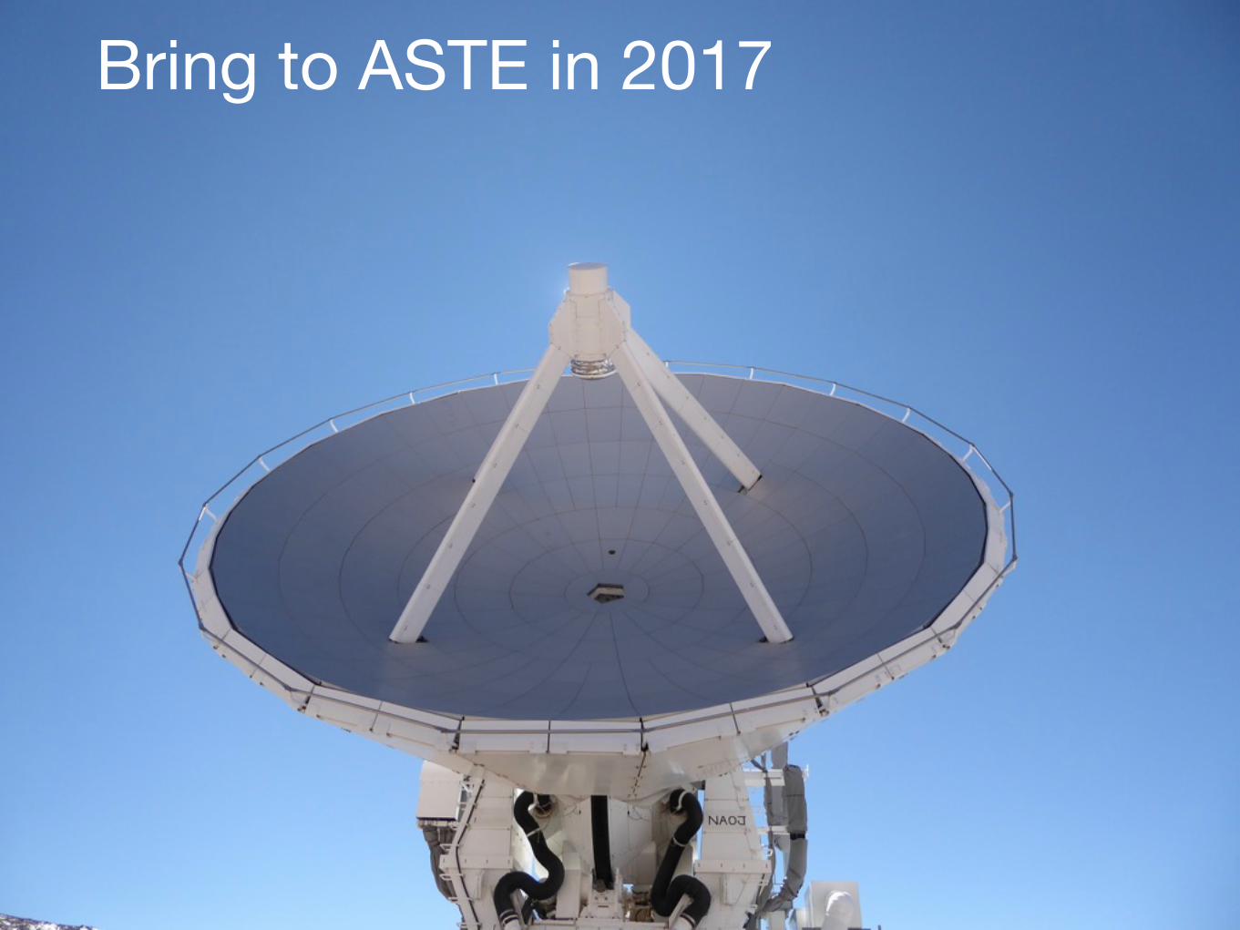
Bring to ASTE in 2017

Bring to ASTE in 2017

43
Summary and Outlook- The submicron CPW process is capable of producing CPW filters
with F/ΔF = 500 at ~300 GHz.
- Successfully integrated the telescope instrument hardware for DESHIMA
- Can accelerate the R&D cycle to approach the following problems towards a working filterbank chip that can be field-tested at ASTE:
1) High end-to-end coupling efficiency2) Even frequency spacing throughout the band3) Good stray light rejection
First light of DESHIMA is expected in autumn 2017 at the ASTE Telescope !


![コプト・エジプト語の他動詞の「前名詞形」の軽動詞性と文法化[The "Prenominal" Form of Verbs in Coptic Egyptian -Frequency, Light-Verbalness and Grammaticalization-]](https://static.fdokumen.com/doc/165x107/631a725620bd5bb1740c49fd/the-1674634661.jpg)