Deposition and modelling of lead zirconate titanate thin films ...
191
Materials and Earth Sciences Department Institute of Materials Science Advanced Thin Film Technology Deposition and modelling of lead zirconate titanate thin films on stainless steel for MEMS applications Wachstum und Modellierung von Blei-Zirkonat-Titanat Dünnschichten auf Edelstahl für MEMS-Anwendungen Zur Erlangung des akademischen Grades Doktor-Ingenieur (Dr.-Ing.) Genehmigte Dissertation von Juliette Marie Alice Cardoletti aus Chamonix Mont-Blanc, Frankreich Tag der Einreichung: June 2, 2021, Tag der Prüfung: September 7, 2021 1. Gutachten: Prof. Dr. Lambert Alff 2. Gutachten: Prof. Dr. Mario Kupnik Darmstadt – D 17
-
Upload
khangminh22 -
Category
Documents
-
view
3 -
download
0
Transcript of Deposition and modelling of lead zirconate titanate thin films ...

Materials and EarthSciences DepartmentInstitute of MaterialsScienceAdvanced Thin FilmTechnology
Deposition and modelling oflead zirconate titanate thin filmson stainless steel for MEMS applicationsWachstum und Modellierung von Blei-Zirkonat-Titanat Dünnschichten auf Edelstahl für MEMS-AnwendungenZur Erlangung des akademischen Grades Doktor-Ingenieur (Dr.-Ing.)Genehmigte Dissertation von Juliette Marie Alice Cardoletti aus Chamonix Mont-Blanc, FrankreichTag der Einreichung: June 2, 2021, Tag der Prüfung: September 7, 2021
1. Gutachten: Prof. Dr. Lambert Alff2. Gutachten: Prof. Dr. Mario KupnikDarmstadt – D 17
Deposition and modelling of lead zirconate titanate thin films on stainless steel for MEMS applicationsWachstum und Modellierung von Blei-Zirkonat-Titanat Dünnschichten auf Edelstahl fürMEMS-Anwendungen
Accepted doctoral thesis by Juliette Marie Alice Cardoletti
1. Review: Prof. Dr. Lambert Alff2. Review: Prof. Dr. Mario Kupnik
Date of submission: June 2, 2021Date of thesis defense: September 7, 2021
Darmstadt – D 17
Bitte zitieren Sie dieses Dokument als:URN: urn:nbn:de:tuda-tuprints-196634URL: http://tuprints.ulb.tu-darmstadt.de/id/eprint/19663
Dieses Dokument wird bereitgestellt von tuprints,E-Publishing-Service der TU Darmstadthttp://[email protected]
Die Veröffentlichung steht unter folgender Creative Commons Lizenz:Namensnennung – Nicht kommerziell – Keine Bearbeitungen 4.0 Internationalhttps://creativecommons.org/licenses/by-nc-nd/4.0/This work is licensed under a Creative Commons License:Attribution–NonCommercial–NoDerivatives 4.0 Internationalhttps://creativecommons.org/licenses/by-nc-nd/4.0/

Erklärungen laut Promotionsordnung
§8 Abs. 1 lit. c PromO
Ich versichere hiermit, dass die elektronische Version meiner Dissertation mit der schriftlichen Versionübereinstimmt.
§8 Abs. 1 lit. d PromO
Ich versichere hiermit, dass zu einem vorherigen Zeitpunkt noch keine Promotion versucht wurde. Indiesem Fall sind nähere Angaben über Zeitpunkt, Hochschule, Dissertationsthema und Ergebnis diesesVersuchs mitzuteilen.
§9 Abs. 1 PromO
Ich versichere hiermit, dass die vorliegende Dissertation selbstständig und nur unter Verwendung derangegebenen Quellen verfasst wurde.
§9 Abs. 2 PromO
Die Arbeit hat bisher noch nicht zu Prüfungszwecken gedient.
Darmstadt, June 2, 2021J. Cardoletti
Declarations according to the doctoral regulations
§8 Par. 1 lit. c PromO
I hereby certify that the electronic version of my dissertation corresponds to the written version.
§8 Par. 1 lit. d PromO
I hereby affirm that no doctorate has been attempted at any time prior to this. In this case, more detailedinformation on the date, university, dissertation topic and result of this attempt must be provided.
§9 Par. 1 PromO
I hereby certify that this dissertation has been written independently and only using the sources indicated.
§9 Par. 2 PromO
The thesis has not yet been used for examination purposes.
iii


A mes grands-parents maternels
La science n’a pas de patrie.Science has no homeland.
Louis PasteurInaugural speech of the Pasteur Institute
14 November 1888
v


Acknowledgements
First and foremost, I would like to thank Prof. Lambert Alff for believing in me and giving me theopportunity to carry out research in his group. I have been exceptionally fortunate to have his supportand advice during the course of my doctoral studies. Under his guidance, I developed a strong interest forthin films and their fascinating properties. He gave me a chance to grow as a scientist and encouraged meto be more daring in front of professional challenges. I am thankful for the numerous opportunities hehas offered me, whether it was an extensive stay as a research scholar in the United States to broaden myknowledge, to participate in international conferences or to get access to a wide range of experimentalsystems. I truly appreciate his accessibility, his feedback and encouragements to push my own boundariesfurther back.
I also express my sincere gratitude to Prof. Susan Trolier-Mckinstry for inviting me to stay in her researchgroup at The Pennsylvania State University for six months. Her knowledge is invaluable and this work wouldnot be what it is without her expertise. Her dedication to scientific research and teaching is tremendousand she deeply cares for people. In her group, I have learnt a lot about ferroelectrics and that a goodscientist is above all a good person.
I would like to thank Prof. Mario Kupnik for kindly taking on the position of second reviewer. His timespend to review this dissertation is well appreciated. Besides him, I would like to acknowledge Prof. Bai-Xiang Xu and Dr. Jurij Koruza for their support by serving in my Ph.D. thesis committee and for theinsightful discussions through the last few years.
I am grateful to Dr. Philipp Komissinskiy for sharing his knowledge of pulsed laser deposition and forhis attention to detail which always makes me strive to improve my work. I am thankful for his feedbackand the numerous hours he spent reviewing the articles we co-authored. I would also like to thankDr. Aldin Radetinac for his scientific curiosity and his support at the beginning of my doctoral studies. Hisreminder that there should be a life outside of work was a great (and certainly needed) one.
This thesis could not have been completed without the support of many people who provided their helpand technical expertise. I would like to thank Gabi Haindl and Jürgen Schreeck for their assistance inthe laboratory. I am grateful to the electronics and mechanics workshops of the Institute of MaterialsScience, in particular to Michael Weber and Jochen Rank without whom the e31,f measurement systemwould never have been built. I also thank Andreas Hönl and Stephan Diefenbach for their help solvingconnection problems with a P-E loop tracer running on Windows NT.
From my stay at Penn State, I would like to acknowledge the Materials Research Institute staff from theNanofabrication Lab. I thank notably Kathy Gehoski for teaching me photolithography, Bangzhi Liu forhelping me with the SEM, Bill Drawl and Andy Fitzgerald for training me on several tools from thecleanroom. From the Materials Characterization Lab, I particularly give thanks to Nichole Wonderlingand Gino Tambourine for their help with the XRD and for always answering my questions, and also toMaria Dicola for her help as I was struggling to polish stainless steel pieces.
I would like to thank Marion Bracke for her efficiency, the nice discussions we had and her useful tipson life in Darmstadt. I am grateful to Sandie Elder for always being kind, especially when I got sick. Iwould also like to acknowledge all the administrative staff, at the Technische Universität Darmstadt, at The
vii

Pennsylvania State University and at the IDS-FunMat-Inno doctoral school for their assistance with thepaperwork that my stay in the USA required.
Numerous thanks go to my co-workers past and present from the ATFT group for their support and friend-ship through the last few years. I am grateful to Dr. Arzhang Mani for giving me a chance during mymaster thesis and introducing me to the group. I would like to thank Dr. Philipp Kehne who, during thattime, taught me how to use the PLD system (following a conversation with Prof. Alff on whether or nota “PLD crash course” could be taught, he did so in four days). I am grateful to Dr. Alexey Arzumanovfor programming the e31,f measurement system and teaching me ion beam etching. I greatly appre-ciate the kindness of Dr. Márton Major and the time he gave to answer my questions, in particularabout the analysis of XRD patterns. I would like to thank Dr. Erwin Hildebrandt for his help duringthe preparation of my stay at Penn State. Special thanks go to my fellow PLD users Dr. Patrick Salg,Dr. Lukas Zeinar and Mahdad Mohammadi for all their advice and the good times. I am thankful toThorsten Schneider for the great discussions during the (anti)ferroelectrics meetings. I would like toacknowledge Parastoo Agharezaei, Aaquib Shamim and Sadegh Yahyazadeh whose work I guided andwho helped me a lot. I am thankful to Nico Kaiser and Tobias Vogel for being wonderful office mates. I amespecially grateful to Dr. Shalini Sharma and Eszter Piros, I am fortunate to enjoy their friendship. Notonly did they have good advice but they made being away from home a much nicer experience than it couldhave been. I also acknowledge the support of the whole ATFT group including Dr. Gennady Cherkashinin,Dr. Dominik Gölden, Dr. Jasnamol Palakkal, Dr. Stefan Petzold, Dr. Sareh Sabet, Dr. Vikas Shabadi,Dr. Sharath Ulhas, Supratik Dasgupta, Robert Eilhardt, Georgia Gkouzia, Jing-Jia Huang,Christian Lampa, Corinna Müller, Berthold Rimmler, Yating Ruan, Nils Schäfer, Seyma Topcu andKatrin Walter.
I also own a lot to the STM group at Penn State. In particular to Dr. Hong Goo Yeo who taught mesol-gel deposition and whose guidance and experience with PZT thin films on nickel foils was very useful. Iwould like to thank Dr. Julian Walker for teaching me how to perform e31,f measurements and for thediscussions on polarisation switching. I am also grateful to Dr. Carl Morandi for his valuable input onPZT thin films, notably on their growth by pulsed laser deposition. I am thankful to Prof. Wanlin Zhu,Dr. Betul Akkopru-Akgun and Dr. Lyndsey Denis for teaching me how to electrically characterise ferro-electric thin films. I would like to thank Dr. Adarsh Rajashekhar for guiding me through the differentlabs during my first weeks at Penn State. I am grateful for Beth Jones’ constantly good mood and forthe time she gave to teach me how to prepare PZT solution for sol-gel method. I would like to thankDr. Kathleen Coleman for her help with e31,f measurements and for being a kind and cheerful cube mate.I am also glad to have had Jared Carter from Prof. Clive Randall’s group and Chris Cheng as cube matesand would like to thank Dr. Tianning Liu, Dr. Dixiong Wang and Leonard Jacques for contributing tomake my stay at Penn State a good one.
I am grateful to Prof. Helmut Schlaak and Daniel Thiem from the Department of Electrical Engineeringand Information Technology of the Technische Universität Darmstadt for their collaboration and advicethrough the early stages of this work. I would like to thank Prof. Barbara Malič and Silvo Drnovšek fromthe Electronic Ceramics Department of the Jožef Stefan Institute in Slovenia for producing the PNZT leadzirconate target for pulsed laser deposition which enabled an important part of this work. I would also like tothank Dr. Enrico Bruder for performing the EBSD measurements reported in this work and Ulrike Kunz forpreparing the sample with focused ion beam cutting. I would like to acknowledge Prof. Wolfgang Donnerfor his willingness to discuss the XRD patterns of my trickiest samples. I thankDr. Ali Nowroozi, Felix Naglerand Mao-Hua Zhang for their help with the preparation of the LNO target for pulsed laser deposition.I would also like to thank Dr. Marion Höfling, Dr. Lalitha Kodumudi Venkataraman, Alena Bell,Daniel Isaia and Heinz Mohren for their help at various points of this work. I am also grateful to
viii
Jean-Christophe Jaud for our discussions in French which cheeredme up duringmy stay in Darmstadt. Theformatting of this thesis would have been muchmore hazardous without the team behind the LATEX templatespackage for the Technische Universität Darmstadt and their prompt answers to any questions which arose.
A large “Merci!” goes to Birgit Franz for her kindness and wisdom. She is well aware of the academiaenvironment without being part of it and she lent me an attentive ear over the last few years. From the bestlandlady one could wish for, she has become a friend and I will dearly miss our conversations on weekends.
I would also like to thank my childhood friends, in particular Mathilde, Maryne, Océane and Guillaumefor always being there. Having known most of them for over three quarters of my life is a privilege forwhich I shall always be grateful. I would certainly not be the person I am today without the Club de SkiNordique de la Vallée de Chamonix Mont-Blanc with whom I trained for more than a decade beforestarting university. I am thankful to all its members, past and present, and particularly to the coachesFlorence, Christophe, Georges and Pek. More than cross-country skiing, they taught me resilience.
Last but certainly not least, I would like to thank my family, especially my parents, my brother and mymaternal grandparents. Each of them gave me their unconditional love and support. My mother Nicolehas always been there for me, following my progresses and inviting me to go further. She taught meself-discipline and gave me the love of reading (despite how much I now read in English, I greatly appreciateher persistence to gift me books in French). My father Patrice has also been there with his own words andregardless of how much he understood what I was doing. He is still trying to teach me that sometimes it isokay not to care as much. Now that I have seen more of the world outside of the valley where I grew up, Iam even more grateful to my younger brother Théo for his strongly voiced opinion that being a womanshall never be a synonym of weakness. It is a treasure to know that he cares and is always there when itmatters the most. I am proud to call him my brother and delighted that keeping up with him is such athrilling challenge. Mala might not be a relative but I have always considered her as a grandmother. Shepassed away long ago and it is only lately that I understood her most precious gift. Even if I am far fromsucceeding, I shall strive to listen without judgment, simply being there.
Georges and Ginette, my maternal grandparents, both passed away while I was preparing this thesis.Being raised at a time where a toolbox was not meant for women, they have always shown exceptionalsupport along the path I chose. They taught me to always act at the best of my capabilities and were eagerto share their knowledge. I would never forget the time I spent as a child poring over (sometimes a centuryold) books in my grandfather study nor the times where my grandmother told me, looking at a speechfrom the French President, to observe and articulate my own discourse. By their love, encouragements andpresence, they have helped shape my life on a better path.
This manuscript is based on work supported by the Deutsche Forschungsgemeinschaft (DFG), under Grantnumber AL 560/19-1. A travel grant from the EIT RawMaterials IDS-FunMat- Inno is also acknowledged.
Note: The findings and conclusions in this thesis do not necessarily reflect the view of the funding agencies.
ix


Abstract
Technological development is permanently advancing in the direction of miniaturisation and energyconsumption reduction. One of the keys to this pathway lies in the integration of ferroelectric thin filmsinto Micro-Electro-Mechanical Systems (MEMS) applications. For this purpose, due to its large piezoelectricresponse, lead zirconate titanate is the material of choice in industry. To broaden the range of applications,substrates less brittle than the currently favoured silicon must be implemented into MEMS. In this work,lead zirconate titanate thin films on stainless steel substrates were both experimentally investigated andmodelled.
Lead zirconate titanate thin films of composition PbZr0.52Ti0.48O3 were grown on AISI 304 stainless steelsubstrates by pulsed laser deposition with 001 texture to improve their piezoelectric response. Asdemonstrated using X-ray and electron backscatter diffraction, the texture engineering is achieved througha selection of two buffer layers, Al2O3 and LaNiO3. The former buffer prevents the oxidation of the stainlesssteel substrate during deposition of the subsequent layers. The latter serves as both a bottom electrode anda growth template to promote the 001 texture of PbZr0.52Ti0.48O3 thin films. The lead zirconate titanatethin films ferroelectric properties are improved through 2 mol.% Nb-doping, resulting in dielectric constantsand losses at 1 kHz for a 200 nm thick film of 350 and below 5 %, respectively, before measurement ofpolarisation versus electrical field hysteresis. Following these measurements, the Nb-doped lead zirconatetitanate thin films permittivity increases up to 430. With a thickness of 400 nm, the films exhibit a remanentpolarisation of 16.5 µC·cm−2 and a coercive field of 92 kV·cm−1.
In the modelling, based on a ferroelectric switching criterion and the Euler-Bernoulli beam theory, it wasinvestigated how the vertical deflection of ferroelectric bending tongues behaves with a load at their freeend. The model developed here bridges the gap existing in literature between the modelling of ferroelectricswitching and the mechanical description of linear piezoelectric structures. Furthermore, the ferroelectricswitching criterion model is improved by the inclusion of strain saturation at high fields, which is inherentto ferroelectrics. The model includes parameters describing the geometry of the bending tongue, itsmechanical and material properties, the crystallographic state and built-in strain of the ferroelectric thinfilm and the applied electrical field to determine the vertical deflection for MEMS applications based onferroelectric bending tongues.
In summary, the technically relevant 001 texture of lead zirconate titanate thin films on stainless steelsubstrates has been successfully engineered. The thin films, especially with 2 mol.% Nb-doping, areexcellent candidates for MEMS applications on non-brittle substrates, in particular in sensor technology.Furthermore, the model established in this work indicates that ferroelectric bending tongues made oflead zirconate titanate on stainless steel substrates can develop sufficient vertical deflection for MEMSapplications.
xi

Zusammenfassung
Die technologische Entwicklung schreitet permanent in Richtung Miniaturisierung und Reduzierung desEnergieverbrauchs voran. Einer der Schlüssel zu diesem Weg liegt in der Integration von ferroelektrischenDünnschichten in die Mikrosystemtechnik (Englisch: Micro-Electro-Mechanical Systems (MEMS)). Zudiesem Zweck ist Blei-Zirkonat-Titanat aufgrund seines großen piezoelektrischen Koeffizienten das Materialder Wahl. Um den Anwendungsbereich zu erweitern, müssen Substrate, die weniger spröde sind als dasderzeit favorisierte Silizium, in MEMS implementiert werden. In dieser Arbeit wurden Blei-Zirkonat-Titanat-Dünnschichten auf Edelstahlsubstraten sowohl experimentell untersucht als auch modelliert.
Die Blei-Zirkonat-Titanat-Dünnschichten der Zusammensetzung PbZr0.52Ti0.48O3wurden auf AISI 304Edelstahl-Substraten durch gepulster Laserabscheidung mit 001 Textur aufgewachsen, um ihr piezoelek-trisches Verhalten zu verbessern. Wie mittels Röntgen- und Elektronenrückstreubeugung gezeigt werdenkonnte, wird die Texturoptimierung durch die Auswahl von zwei Pufferschichten, Al2O3 und LaNiO3, er-reicht. Die erste Pufferschicht verhindert die Oxidation des Edelstahlsubstrats während der Abscheidung dernachfolgenden Schichten. Die zweite dient sowohl als Bodenelektrode als auch als Wachstumsschablone zurFörderung der 001 Textur von PbZr0.52Ti0.48O3-Dünnschichten. Die ferroelektrischen Eigenschaften derBlei-Zirkonat-Titanat-Dünnschichten werden durch 2 mol.% Nb-Dotierung verbessert, was im Rohzustandzu Dielektrizitätskonstanten und Verlusten bei 1 kHz für einen 200 nm dicken Film von 350 bzw. unter5 % führt. Nach Messung der Hysteresekurve (elektrische Polarisation gegen das elektrische Feld) steigtdie Permittivität der Nb-dotierten Blei-Zirkonat-Titanat Dünnschichten auf bis zu 430. Bei einer Dicke von400 nm zeigen die Schichten eine remanente Polarisation von 16, 5 µC·cm−2 und ein Koerzitivfeld von92 kV·cm−1.
In der Modellierung wurde basierend auf einem ferroelektrischen Schaltkriterium und der Euler-Bernoulli-Strahlentheorie untersucht, wie sich die vertikale Auslenkung von ferroelektrischen Biegezungen miteiner Last an ihrem freien Ende verhält. Das hier entwickelte Modell überbrückt die in der Literaturbestehende Lücke zwischen der Modellierung des ferroelektrischen Schaltens und der mechanischenBeschreibung von linearen piezoelektrischen Strukturen. Darüberhinausgehend wird das Modell desferroelektrischen Schaltkriteriums durch den Einbezug der Dehnungssättigung bei hohen Feldern, die denFerroelektrika inhärent ist, verbessert. Das Modell enthält Parameter, die Geometrie der Biegezunge, ihremechanischen und Materialeigenschaften, den kristallographischen Zustand, die eingebaute Verspannungder ferroelektrischen Dünnschicht sowie das angelegte elektrische Feld berücksichtigen, um die vertikaleAuslenkung für MEMS-Anwendungen zu bestimmen, die auf ferroelektrischen Biegezungen basieren.
Zusammenfassend wurde die technisch 001 Textur von Blei-Zirkonat-Titanat-Dünnschichten auf Edel-stahlsubstraten erfolgreich eingestellt. Die dünnen Schichten, insbesondere mit 2 mol.% Nb-Dotierung,sind hervorragende Kandidaten für MEMS-Anwendungen auf nicht-spröden Substraten, insbesondere inder Sensorik. Darüber hinaus zeigt das in dieser Arbeit aufgestellte Modell, dass ferroelektrische Biegezun-gen aus Blei-Zirkonat-Titanat auf Edelstahlsubstraten eine ausreichende vertikale Auslenkung für MEMSAnwendungen entwickeln können.
xiii


Table of contents
List of Tables xix
List of Figures xxi
List of abbreviations and notations xxiii
List of notations specific to modelling chapter xxv
1. Introduction and motivations 11.1. Literature review: state of the art . . . . . . . . . . . . . . . . . . . . . . . . . . . . . . . 2
1.1.1. Overview of lead zirconate titanate thin films in literature . . . . . . . . . . . . . 21.1.2. Modelling of piezoelectric bending tongues and ferroelectric behaviour, a review . 3
1.2. Statement of purpose . . . . . . . . . . . . . . . . . . . . . . . . . . . . . . . . . . . . . . 41.3. Thesis structure . . . . . . . . . . . . . . . . . . . . . . . . . . . . . . . . . . . . . . . . . 5
2. Fundamentals 72.1. Ferroelectric materials: dielectrics, piezoelectrics and pyroelectrics . . . . . . . . . . . . . 7
2.1.1. Dielectrics and electrostriction . . . . . . . . . . . . . . . . . . . . . . . . . . . . . 72.1.2. Piezoelectricity . . . . . . . . . . . . . . . . . . . . . . . . . . . . . . . . . . . . . 82.1.3. Pyroelectricity . . . . . . . . . . . . . . . . . . . . . . . . . . . . . . . . . . . . . . 112.1.4. Ferroelectricity . . . . . . . . . . . . . . . . . . . . . . . . . . . . . . . . . . . . . 122.1.5. Perovskite structure and ferroelectric materials . . . . . . . . . . . . . . . . . . . . 17
2.2. Materials relevant to this work . . . . . . . . . . . . . . . . . . . . . . . . . . . . . . . . . 192.2.1. Ferroelectric layer: lead zirconate titanate . . . . . . . . . . . . . . . . . . . . . . 192.2.2. Buffer layers and electrodes: lanthanum nickelate, aluminium oxide and platinum 222.2.3. Substrate material: AISI 304 stainless steel . . . . . . . . . . . . . . . . . . . . . . 23
2.3. Thin film growth theory . . . . . . . . . . . . . . . . . . . . . . . . . . . . . . . . . . . . 232.3.1. Thin film nucleation . . . . . . . . . . . . . . . . . . . . . . . . . . . . . . . . . . 242.3.2. Thin film growth . . . . . . . . . . . . . . . . . . . . . . . . . . . . . . . . . . . . 272.3.3. Crystallographic structure of thin film . . . . . . . . . . . . . . . . . . . . . . . . . 28
3. Experimental procedures 293.1. Sample configurations and custom-built sample holder . . . . . . . . . . . . . . . . . . . 293.2. Substrate preparation . . . . . . . . . . . . . . . . . . . . . . . . . . . . . . . . . . . . . . 31
3.2.1. Substrate dicing . . . . . . . . . . . . . . . . . . . . . . . . . . . . . . . . . . . . . 313.2.2. Substrate lapping and polishing . . . . . . . . . . . . . . . . . . . . . . . . . . . . 313.2.3. Substrate cleaning . . . . . . . . . . . . . . . . . . . . . . . . . . . . . . . . . . . 32
3.3. Thin film deposition methods . . . . . . . . . . . . . . . . . . . . . . . . . . . . . . . . . 323.3.1. DC and RF magnetron sputtering . . . . . . . . . . . . . . . . . . . . . . . . . . . 323.3.2. Pulsed laser deposition . . . . . . . . . . . . . . . . . . . . . . . . . . . . . . . . . 35
3.4. Electrodes preparation . . . . . . . . . . . . . . . . . . . . . . . . . . . . . . . . . . . . . 393.4.1. Photolithography: lift-off process . . . . . . . . . . . . . . . . . . . . . . . . . . . 403.4.2. Argon ion milling . . . . . . . . . . . . . . . . . . . . . . . . . . . . . . . . . . . . 42
xv

3.5. Structure characterisation methods . . . . . . . . . . . . . . . . . . . . . . . . . . . . . . 433.5.1. X-ray diffraction . . . . . . . . . . . . . . . . . . . . . . . . . . . . . . . . . . . . . 443.5.2. Scanning electron microscopy and energy-dispersive X-ray spectroscopy . . . . . . 473.5.3. Electron Backscatter Diffraction . . . . . . . . . . . . . . . . . . . . . . . . . . . . 48
4. Ferroelectrics characterisation methods 494.1. Dielectric characterisation . . . . . . . . . . . . . . . . . . . . . . . . . . . . . . . . . . . 49
4.1.1. Parameters sweeps . . . . . . . . . . . . . . . . . . . . . . . . . . . . . . . . . . . 504.1.2. Dielectric characterisation experimental systems and parameters . . . . . . . . . . 51
4.2. Ferroelectric characterisation . . . . . . . . . . . . . . . . . . . . . . . . . . . . . . . . . 524.2.1. Accessing ferroelectric characteristic values . . . . . . . . . . . . . . . . . . . . . . 534.2.2. Ferroelectric characterisation experimental system and parameters . . . . . . . . 54
4.3. Hot poling process . . . . . . . . . . . . . . . . . . . . . . . . . . . . . . . . . . . . . . . 544.3.1. Key parameters of hot poling process . . . . . . . . . . . . . . . . . . . . . . . . . 554.3.2. Hot poling experimental system and parameters . . . . . . . . . . . . . . . . . . . 55
4.4. Piezoelectric characterisation . . . . . . . . . . . . . . . . . . . . . . . . . . . . . . . . . 554.4.1. Wafer flexure technique principle . . . . . . . . . . . . . . . . . . . . . . . . . . . 564.4.2. Piezoelectric characterisation experimental system and parameters . . . . . . . . 57
4.5. Leakage measurements . . . . . . . . . . . . . . . . . . . . . . . . . . . . . . . . . . . . . 604.5.1. Key aspects of leakage measurements . . . . . . . . . . . . . . . . . . . . . . . . . 604.5.2. Leakage measurements experimental system and parameters . . . . . . . . . . . . 61
5. Experimental results and discussion 635.1. 001-textured PZT thin films: getting the orientation . . . . . . . . . . . . . . . . . . . 63
5.1.1. Substrate curvature during thin films deposition . . . . . . . . . . . . . . . . . . . 635.1.2. PZT thin films texture and morphology analysis . . . . . . . . . . . . . . . . . . . 645.1.3. PZT thin films dielectric and ferroelectric properties . . . . . . . . . . . . . . . . . 675.1.4. Leakage current measurements on PZT stacks . . . . . . . . . . . . . . . . . . . . 68
5.2. 001-textured PNZT thin films: improving the properties . . . . . . . . . . . . . . . . . 715.2.1. Influence of O2 deposition pressure on ferroelectric properties . . . . . . . . . . . 715.2.2. Influence of deposition temperature on ferroelectric properties . . . . . . . . . . . 765.2.3. Influence of PNZT layer thickness in PNZT stacks . . . . . . . . . . . . . . . . . . . 815.2.4. Effect of parameters sweeps on PNZT stacks dielectric constant and loss . . . . . . 865.2.5. Leakage current measurements on PNZT stacks . . . . . . . . . . . . . . . . . . . 895.2.6. e31,f measurements on PNZT stacks . . . . . . . . . . . . . . . . . . . . . . . . . . 93
5.3. Conclusions relative to the experimental results . . . . . . . . . . . . . . . . . . . . . . . 94
6. Modelling of ferroelectric bending tongues 956.1. Approach to the modelling . . . . . . . . . . . . . . . . . . . . . . . . . . . . . . . . . . . 956.2. Extent and limits of the modelling . . . . . . . . . . . . . . . . . . . . . . . . . . . . . . . 96
6.2.1. Extent of the model . . . . . . . . . . . . . . . . . . . . . . . . . . . . . . . . . . . 966.2.2. Assumptions of the model . . . . . . . . . . . . . . . . . . . . . . . . . . . . . . . 98
6.3. Equations of the model . . . . . . . . . . . . . . . . . . . . . . . . . . . . . . . . . . . . . 986.3.1. Deflection due to loads . . . . . . . . . . . . . . . . . . . . . . . . . . . . . . . . . 996.3.2. Deflection due to strains . . . . . . . . . . . . . . . . . . . . . . . . . . . . . . . . 100
6.4. Results and discussion of the modelling . . . . . . . . . . . . . . . . . . . . . . . . . . . . 1086.5. Conclusions relative to the modelling . . . . . . . . . . . . . . . . . . . . . . . . . . . . . 115
xvi

7. Conclusions and outlooks 1177.1. Conclusions and answers to the statement of purpose . . . . . . . . . . . . . . . . . . . . 1177.2. Outlooks and future work . . . . . . . . . . . . . . . . . . . . . . . . . . . . . . . . . . . 120
7.2.1. Potential improvements to ferroelectric bending tongues modelling . . . . . . . . 1207.2.2. Potential improvements in materials selection and deposition methods . . . . . . 1207.2.3. Towards future MEMS applications . . . . . . . . . . . . . . . . . . . . . . . . . . 121
List of appendices I
References XL
List of publications and scientific contributions XLI
Curriculum Vitae XLIII
xvii


List of Tables
2.1. Standard composition of AISI 304 stainless steel. . . . . . . . . . . . . . . . . . . . . . . 23
5.1. Effect of PNZT O2 deposition pressure on dielectric constant and loss values. . . . . . . . 745.2. Effect of PNZT O2 deposition pressure on ferroelectric characteristic values. . . . . . . . . 755.3. Effect of PNZT deposition temperature on dielectric constant and loss values. . . . . . . . 795.4. Effect of PNZT deposition temperature on ferroelectric characteristic values. . . . . . . . 805.5. Effect of PNZT layer thickness on dielectric constant and loss values. . . . . . . . . . . . . 835.6. Effect of PNZT layer thickness on ferroelectric characteristic values. . . . . . . . . . . . . 85
6.1. Physical and mechanical properties of materials used for modelling. . . . . . . . . . . . . 109
xix


List of Figures
2.1. Schematic representation of the direct and converse piezoelectric effects. . . . . . . . . . 92.2. Helmholtz free energy density versus polarisation for paraelectric and ferroelectric phases. 132.3. Spontaneous polarisation as a function of temperature for second-order and first-order phase
transitions. . . . . . . . . . . . . . . . . . . . . . . . . . . . . . . . . . . . . . . . . . . . 142.4. Typical hysteresis loops for ferroelectrics. Polarisation and elastic strain versus applied
electrical field hysteresis loops for an ideal single-crystal and a polycrystalline sample. . . 152.5. Schematic representation of the accessible polarisation directions in a tetragonal crystal. 162.6. Two dimensional schematic representation of ferroelectric domains in a crystal. . . . . . 162.7. Equivalent representations of the ABO3 ideal cubic perovskite structure with the unit cell
centred around the B site cation or the A site cation. . . . . . . . . . . . . . . . . . . . . 182.8. Pb(ZrγTi1−γ)O3 phase diagram. . . . . . . . . . . . . . . . . . . . . . . . . . . . . . . . . 202.9. Influence of PZT composition on relative dielectric permittivity and e31,f piezoelectric
coefficient. . . . . . . . . . . . . . . . . . . . . . . . . . . . . . . . . . . . . . . . . . . . . 212.10.Schematic representation of possible processes during thin film vapour-phase based growth. 252.11.Model of the interaction potential energy as a function of the distance between the impinging
particle and the surface. . . . . . . . . . . . . . . . . . . . . . . . . . . . . . . . . . . . . 262.12.Schematic representation of a film island growing on a substrate. . . . . . . . . . . . . . 262.13.Schematic representation of the three basic thin film growth modes. . . . . . . . . . . . . 27
3.1. Schematic representations of sample configurations for PZT stacks and PNZT stacks andoptical microscope image of a PNZT stack. . . . . . . . . . . . . . . . . . . . . . . . . . . 30
3.2. Schematic representation of a modified flag style holder. . . . . . . . . . . . . . . . . . . 303.3. Schematic representation of a sputtering chamber for DC and for RF magnetron sputtering. 343.4. Schematic representation of the small PLD system. . . . . . . . . . . . . . . . . . . . . . . 373.5. Schematic representation of the photolithography lift-off process to pattern Pt top electrodes. 403.6. Layout of the photolithography mask to pattern top electrodes and strain gauges onto samples. 413.7. Schematic representation of the Ar ion milling process to access LaNiO3 bottom electrodes. 433.8. Schematic representation of the X-ray diffractometer with its degrees of freedom. . . . . 453.9. Simulation of reflectivity curves of PZT 52/48 thin films on NdGaO3 substrates. . . . . . 47
4.1. Equivalent circuit model to measure the capacitance of dielectric thin films. . . . . . . . . 504.2. Schematic representation of the combined experimental setups for dielectric and ferroelectric
characterisation. . . . . . . . . . . . . . . . . . . . . . . . . . . . . . . . . . . . . . . . . 524.3. Flowchart of the e31,f measurement program. . . . . . . . . . . . . . . . . . . . . . . . . 574.4. Schematic representation of the wafer flexure e31,f measurement system. . . . . . . . . . 58
5.1. 2θ-θ XRD patterns of an Al2O3/Pt/steel sample covered with LNO and PZT layers. . . . . 645.2. Pole figure of the PZT layer of a PZT stack by EBSD. . . . . . . . . . . . . . . . . . . . . . 655.3. SEM image of the surface and the cross-section of a PZT stack. . . . . . . . . . . . . . . . 665.4. Polarisation and corresponding switching current versus electrical field hysteresis loops of
PZT layers of PZT stacks. . . . . . . . . . . . . . . . . . . . . . . . . . . . . . . . . . . . . 685.5. Leakage current density for the PZT layer of a PZT stack. . . . . . . . . . . . . . . . . . . 69
xxi

5.6. Effect of PNZT O2 deposition pressure on 2θ-θ XRD patterns, values of dielectric constantand P-E loops of PNZT stacks. . . . . . . . . . . . . . . . . . . . . . . . . . . . . . . . . . 72
5.7. Effect of PNZT deposition temperature on 2θ-θ XRD patterns, values of dielectric constantand P-E loops of PNZT stacks. . . . . . . . . . . . . . . . . . . . . . . . . . . . . . . . . . 77
5.8. Effect of PNZT layer thickness on 2θ-θ XRD patterns, values of dielectric constant and P-Eloops of PNZT stacks. . . . . . . . . . . . . . . . . . . . . . . . . . . . . . . . . . . . . . . 82
5.9. Dielectric constant and loss of PNZT stacks as a function of subswitching field amplitudeand frequency and DC bias field. . . . . . . . . . . . . . . . . . . . . . . . . . . . . . . . 87
5.10.Leakage current density for the PNZT layer of a PNZT stack. . . . . . . . . . . . . . . . . 905.11.First and second series of P-E loops for PNZT thin film within a PNZT stack for increasing
maximum applied voltage. . . . . . . . . . . . . . . . . . . . . . . . . . . . . . . . . . . . 92
6.1. Interface of the FeBeTo – Ferroelectric Bending Tongues modelling program. . . . . . . . . . 966.2. Schematic representation of the modelled bending tongue. . . . . . . . . . . . . . . . . . 976.3. Schematic representation of the three Euler angles. . . . . . . . . . . . . . . . . . . . . . 1026.4. Flowchart of the process to calculate the vertical deflection of a ferroelectric bending tongue
loaded at its free end with the proposed model. . . . . . . . . . . . . . . . . . . . . . . . 1076.5. Modelled P-E loop in the case of an epitaxial and a polycrystalline ferroelectric layer. . . . 1086.6. Evolution of the vertical deflection at the free end of the bending tongue as a function of the
percentage of textured grains. . . . . . . . . . . . . . . . . . . . . . . . . . . . . . . . . . 1106.7. Modelled strain in the z-direction and vertical deflection at the free end of the bending
tongue versus applied electrical field curve in the case of an epitaxial ferroelectric layer. . 1116.8. Contributions to the vertical deflection of the bending tongue. . . . . . . . . . . . . . . . 1126.9. Evolution of the vertical deflection at the free end of the bending tongue as a function of the
ferroelectric layer thickness. . . . . . . . . . . . . . . . . . . . . . . . . . . . . . . . . . . 1136.10.Evolution of the vertical deflection at the free end of the bending tongue as a function of the
length of the bending tongue. . . . . . . . . . . . . . . . . . . . . . . . . . . . . . . . . . 1146.11.Evolution of the vertical deflection at the free end of the bending tongue as a function of the
load at its free end. . . . . . . . . . . . . . . . . . . . . . . . . . . . . . . . . . . . . . . . 115
A.1. Electrical schematic of the loudspeaker amplifier for the e31,f measurement system. . . . IIIB.1. Representation of the cavity on which the loudspeaker is fitted for the e31,f measurement
system. . . . . . . . . . . . . . . . . . . . . . . . . . . . . . . . . . . . . . . . . . . . . . VB.2. Technical drawing of the four supports of the cavity for the e31,f measurement system. . . VB.3. Technical drawing of the cavity on which the loudspeaker is fitted for the e31,f measurement
system. . . . . . . . . . . . . . . . . . . . . . . . . . . . . . . . . . . . . . . . . . . . . . VIC.1. Representation of the assembled uniform pressure rig on which the silicon carrier wafer
supporting the piezoelectric sample to characterise is fixed. . . . . . . . . . . . . . . . . . VIIC.2. Technical drawing of the rig housing component of the uniform pressure rig for the e31,f
measurement system. . . . . . . . . . . . . . . . . . . . . . . . . . . . . . . . . . . . . . . VIIIC.3. Technical drawing of the base plate component of the uniform pressure rig for the e31,f
measurement system. . . . . . . . . . . . . . . . . . . . . . . . . . . . . . . . . . . . . . . IXC.4. Technical drawing of the bushing component of the uniform pressure rig for the e31,f
measurement system. . . . . . . . . . . . . . . . . . . . . . . . . . . . . . . . . . . . . . . XC.5. Technical drawing of the retention ring component of the uniform pressure rig for the e31,f
measurement system. . . . . . . . . . . . . . . . . . . . . . . . . . . . . . . . . . . . . . . XID.1. Electrical schematic of the electronics box for the e31,f measurement system. . . . . . . . XIIIE.1. Electrical schematic of the charge integrator for the e31,f measurement system. . . . . . . XVI
xxii
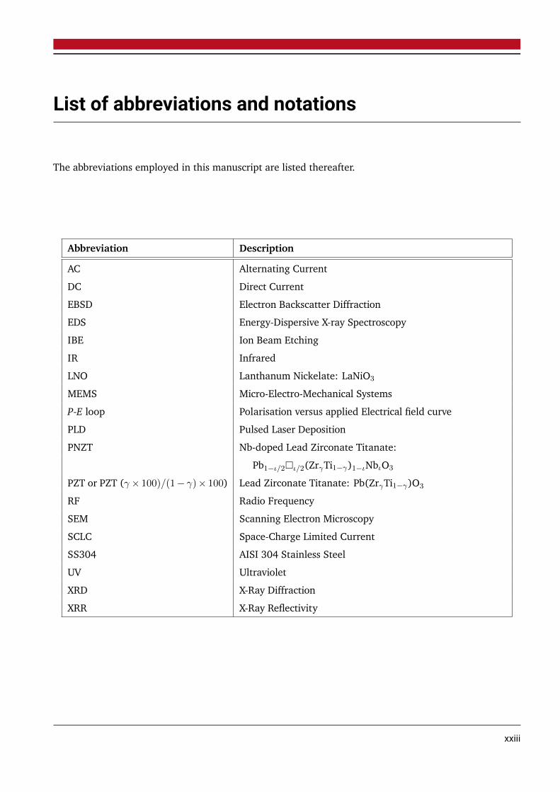
List of abbreviations and notations
The abbreviations employed in this manuscript are listed thereafter.
Abbreviation Description
AC Alternating Current
DC Direct Current
EBSD Electron Backscatter Diffraction
EDS Energy-Dispersive X-ray Spectroscopy
IBE Ion Beam Etching
IR Infrared
LNO Lanthanum Nickelate: LaNiO3
MEMS Micro-Electro-Mechanical Systems
P-E loop Polarisation versus applied Electrical field curve
PLD Pulsed Laser Deposition
PNZT Nb-doped Lead Zirconate Titanate:
Pb1−ι/2ι/2(ZrγTi1−γ)1−ιNbιO3
PZT or PZT (γ× 100)/(1− γ)× 100) Lead Zirconate Titanate: Pb(ZrγTi1−γ)O3
RF Radio Frequency
SEM Scanning Electron Microscopy
SCLC Space-Charge Limited Current
SS304 AISI 304 Stainless Steel
UV Ultraviolet
XRD X-Ray Diffraction
XRR X-Ray Reflectivity
xxiii
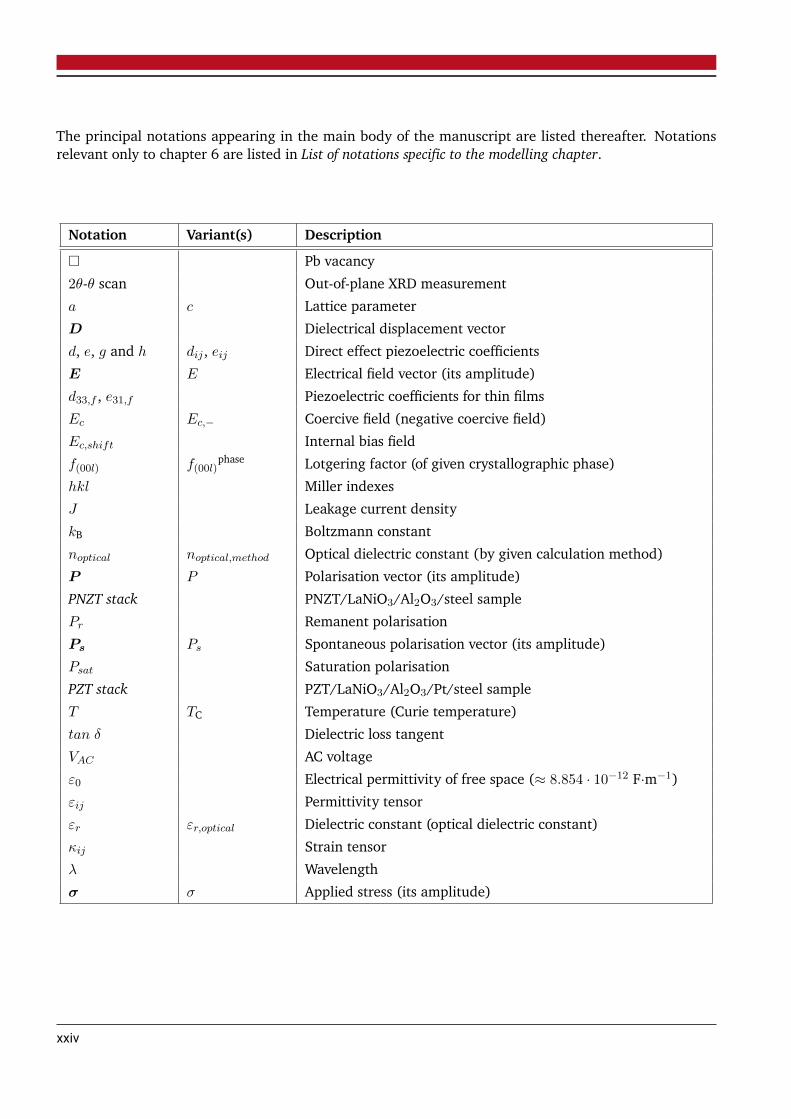
The principal notations appearing in the main body of the manuscript are listed thereafter. Notationsrelevant only to chapter 6 are listed in List of notations specific to the modelling chapter.
Notation Variant(s) Description
Pb vacancy2θ-θ scan Out-of-plane XRD measurementa c Lattice parameterD Dielectrical displacement vectord, e, g and h dij , eij Direct effect piezoelectric coefficientsE E Electrical field vector (its amplitude)d33,f , e31,f Piezoelectric coefficients for thin filmsEc Ec,− Coercive field (negative coercive field)Ec,shift Internal bias fieldf(00l) f(00l)
phase Lotgering factor (of given crystallographic phase)hkl Miller indexesJ Leakage current densitykB Boltzmann constantnoptical noptical,method Optical dielectric constant (by given calculation method)P P Polarisation vector (its amplitude)PNZT stack PNZT/LaNiO3/Al2O3/steel samplePr Remanent polarisationPs Ps Spontaneous polarisation vector (its amplitude)Psat Saturation polarisationPZT stack PZT/LaNiO3/Al2O3/Pt/steel sampleT TC Temperature (Curie temperature)tan δ Dielectric loss tangentVAC AC voltageε0 Electrical permittivity of free space (≈ 8.854 · 10−12 F·m−1)εij Permittivity tensorεr εr,optical Dielectric constant (optical dielectric constant)κij Strain tensorλ Wavelengthσ σ Applied stress (its amplitude)
xxiv
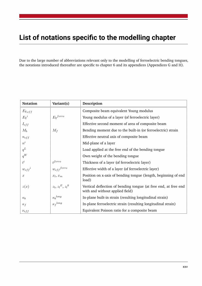
List of notations specific to the modelling chapter
Due to the large number of abbreviations relevant only to the modelling of ferroelectric bending tongues,the notations introduced thereafter are specific to chapter 6 and its appendices (Appendices G and H).
Notation Variant(s) Description
EY,eff Composite beam equivalent Young modulus
EYi EY
ferro Young modulus of a layer (of ferroelectric layer)
Ieff Effective second moment of area of composite beam
Mb Mf Bending moment due to the built-in (or ferroelectric) strain
neff Effective neutral axis of composite beam
ni Mid-plane of a layer
qL Load applied at the free end of the bending tongue
qW Own weight of the bending tongue
ti tferro Thickness of a layer (of ferroelectric layer)
weffi weff
ferro Effective width of a layer (of ferroelectric layer)
x xl, xm Position on x-axis of bending tongue (length, beginning of endload)
z(x) zl, zlE , zl0 Vertical deflection of bending tongue (at free end, at free endwith and without applied field)
κb κblong In-plane built-in strain (resulting longitudinal strain)
κf κflong In-plane ferroelectric strain (resulting longitudinal strain)
νeff Equivalent Poisson ratio for a composite beam
xxv

1. Introduction and motivations
Discovered a century ago, the field of ferroelectrics underwent a substantial development since WorldWar II, when the need for capacitors arose. Today, ferroelectrics are omnipresent in modern society; theirmain markets, as capacitors and for piezoelectric applications, represent an annual value of $6 billion and$1 billion, respectively. While the capacitors market is fully mature with trillions of barium titanate-basedmultilayer ceramic capacitors produced annually, piezoelectric applications still offer a wide range ofprogress for new opportunities [1–3].
Ferroelectrics possess large dielectric coefficients granting them a high volumetric efficiency for dielectriccharge storage. Furthermore, their unique properties provide them with high piezoelectric coefficients,opening the possibility for efficient low-voltage actuators, and switchable polarisation, which, throughpoling, can produce net piezoelectric response [1].
The versatility of ferroelectric materials allows them to be employed in numerous fields for a wide-scope ofapplications, ranging from ultrasound imaging (medical ultrasound imaging, sonar [1,2,4]) through non-volatile memory (ferroelectric random access memory [5,6]), energy harvesters (thermal and mechanical[7–9]), optical components (wave-guides, modulators, adjustable optics [10–12]), electrical components(resonators, filters [13]), pyroelectric devices (heat detectors, infrared-imagers [14–16]) to robotics(piezoelectric Micro-Electro-Mechanical Systems (MEMS), ink-jet printing, ultrasonic motors [4,17–19]).
Future technological developments, notably wearable sensors and the Internet of Things, are stronglydependent on solving two issues: miniaturisation and energy consumption reduction [8, 20]. Theformer entails the need to integrate functional materials into MEMS and the progressive transition towardsNano-Electro-Mechanical Systems [4, 18]. The latter is a vital imperative, both environmentally andeconomically, impacting societies and their legislation. Within the framework of the European Green Dealand through the European Climate Law proposed in March 2020, the European Union aims to reduceenergy consumption to reach climate-neutrality by 2050, affecting for instance the direction of research fordecades to come [21].
Through their piezoelectric applications, ferroelectrics can contribute to energy consumption reduction askey components for self-powered sensors, actuators with low driving voltage and energy harvesters [4,17].The continuous progress of ferroelectrics integration into MEMS applications is decisive for theimplementation of future technologies.
Particularly, the dimensions of ferroelectric thin films make them better suited than bulk ceramics forintegration as functional materials into MEMS. Not only do the dimensions promote miniaturisation butthinner films lead to higher applied electrical field at a given voltage [17]. However, in industry, ferroelectricthin films are generally deposited on silicon substrates, which have a limited toughness. To expand therange of potential applications of ferroelectric thin films, the use of less brittle substrates, better suited fordemanding mechanical applications is necessary. With manufacturing and processing methods alreadywell established in industry, a relatively good resistance to corrosion and a comparatively high toughness,stainless steel is an ideal substrate candidate [22].
Lead zirconate titanate, with its large piezoelectric coefficient, have long imposed itself as the choicematerial for transducers, sensors, and actuators design [17]. Despite its lead content, shaped into the
1

simplest piezoelectric MEMS device that is a bending tongue, it remains an excellent proof-of-conceptcandidate for deposition on the unconventional substrate that is stainless steel.
Nonetheless, MEMS efficiency depends on several factors besides the choice of materials. Modelling isan economical method to probe the influence of some parameters, such as MEMS geometry or appliedelectrical field. Therefore, this thesis shall endeavour to both model and deposit lead zirconate titanatethin films on stainless steel for MEMS applications.
This chapter aims to give an overview of the deposition methods of lead zirconate titanate thin films onvarious substrates. Afterwards, it proposes a literature review of the modelling of both piezoelectric bendingtongues and ferroelectric behaviour. This chapter also states the purpose of this thesis and introduces thethesis structure.
1.1. Literature review: state of the art
This section presents the state of the art regarding lead zirconate titanate thin films grown by differentmethods on a variety of substrates with a particular focus on metallic substrates. Then, it introduces theexisting models describing piezoelectric bending tongues and those representing ferroelectric behaviour.
1.1.1. Overview of lead zirconate titanate thin films in literature
Since the first study on lead zirconate - lead titanate solid solutions seventy years ago, numerous inves-tigations have been carried out on the compound nowadays known as lead zirconate titanate, both onits bulk form and as thin films [23]. Lead zirconate titanate is a ferroelectric solid solution of formulaPb(ZrγTi1−γ)O3 (PZT) whose perovskite structure and properties are described in sections 2.1.5 and 2.2.1,respectively.
A wide array of deposition methods has been used to grow PZT thin films, historically starting withphysical vapour deposition methods in the early 1980s [24]. The first PZT depositions were performedby sputtering, either ion beam sputtering [25,26], Radio Frequency (RF) magnetron sputtering [27] orDirect Current (DC) magnetron sputtering [28,29]. Almost a decade later, the growth of PZT thin films bychemical vapour deposition methods was investigated using chemical solution deposition, notably sol-gelprocesses [30–32] and metal-organic-decomposition [33]. Additionally, metal-organic-chemical vapourdeposition also proved to be a reliable method for PZT films deposition [34–36]. Pulsed Laser Deposition(PLD) of PZT thin films was also established around the same period [37,38].
Forty years after the growth of the first PZT thin films, novel depositions methods are still investigated, suchas aerosol deposition [39]. Nowadays, chemical solution deposition and metal-organic-chemical vapourdeposition methods are largely used in sensor and integrated circuit industries, respectively. The former,when aimed at small-scale production, is the less expensive method despite requiring post-annealingto crystallise the film. The latter process offers a good conformal coverage, as needed for integratedcircuits [24].
The choice of substrates for PZT thin films is mostly dependent on applications, most of them requiring aparallel-plate capacitor structure with top and bottom electrodes. In order to remain electrically conductiveand to avoid oxidation, the electrodes must be thermally and environmentally stable during PZT thinfilms deposition. Besides electrodes oxidation, it is often necessary to prevent substrate oxidation by
2

applying buffer layers between substrates and thin films. Furthermore, PZT thin films are susceptibleto interdiffusion from substrates which can also be prevented by appropriate buffer layers [24]. Theseconstraints limit the possibility of materials on which PZT thin films can be deposited.
As a result, while PZT can be grown on numerous substrates, e.g. silicon, single crystal oxides or glass,the most common choices of electrodes are platinum and some metallic oxides, e.g. RuO2 or SrRuO3
[17,40–44]. The electrode material often plays a part in the diffusion barrier, along with additional bufferlayers. For example, with a Si substrate, the most frequent combination of electrode and buffer layers isPZT/Pt/Ti/SiO2/Si [24]. However, the electrode by itself is rarely a sufficient diffusion barrier, e.g. oxygencan migrate through a platinum electrode [45].
Regarding lead zirconate titanate thin films deposited on metallic substrates, the number of pertinentreports is more limited. These investigations mainly focus on chemical solution deposition proceduresapplied on various metallic substrates [46–50]. Recently, several reports on the growth of 001-orientedlead zirconate titanate thin films on Ni foils have been published [8, 51–54]. Growth of lead zirconatetitanate films on flexible Ni-Cr substrates have also been reported [55].
The case of stainless steel substrates has been approached by several authors reporting PZT thin filmsof various textures deposited by sol-gel process [56–59], electron beam evaporation technique [60],electrochemical reduction [61] or RF magnetron sputtering [22,62–67]. A noteworthy report presents001-oriented Nb-doped lead zirconate titanate thin films grown by RF magnetron sputtering on stainlesssteel substrates [68].
This is of particular relevance as crystallographic orientation is another aspect of PZT thin films whichis crucial to MEMS applications. Indeed, an improvement of lead zirconate titanate films piezoelectricresponse can be engineered by promoting a 001 texture [17]. There are, however, no compellingreports demonstrating tetragonal 001-textured lead zirconate titanate films grown directly onstainless steel by pulsed laser deposition.
1.1.2. Modelling of piezoelectric bending tongues and ferroelectric behaviour, a review
When modelling ferroelectrics MEMS, two aspects have to be taken into consideration. The first is themechanical system itself, including its linear piezoelectric response when subjected to an applied electricalfield. The second is the ferroelectric behaviour, i.e. the possibility to switch the polarisation directionbetween discrete crystallographically allowed orientations by applying an external electrical field [17].
As linear piezoelectric structures have been extensively studied, this review focuses on systems composed ofbending tongues (cantilevers or wider beams) based on piezoelectric ceramics. However, to date, bendingtongue-based devices have been modelled without simulating the ferroelectric switching occurring ingrains [69–72].
On the other hand, ferroelectric switching has been described through various micromechanical mod-els. Particularly, polarisation switching in single or multicrystals has been studied through phase-fieldmodels, which require no switching criteria [73–75]. Nonetheless, to model polycrystalline ferroelectrics,micromechanical approaches are more efficient in view of the large amount of grains they encompass. Anumber of micromechanical models are self-consistent estimates [76] while others, e.g. Hwang, Lynch andMcMeeking’s model, take hysteretic polarisation-field and strain-field behaviour into account [77].
The above-mentioned model by Hwang et al. estimates the response of a bulk ferroelectric ceramic subjectedto both mechanical and electrical external loads. The bulk ferroelectric response is calculated from the
3

strain and polarisation for an individual grain, resulting from an applied electrical field and applied stress.The model postulates that when the loading level is larger than a work energy criterion, polarisationswitching occurs. The individual grains being assumed to display a statistically random orientation, theirresponse is averaged to estimate the bulk response. Over time, to take more physical aspects into account,Hwang’s model has been extended in various directions, including mean-field approach, and numericallyimplemented with the finite-element method [78–84].
The modelling of piezoelectric/metal/piezoelectric actuators by the finite-element method and the lami-nated beam theory, taking into account static electromechanical displacement and polarisation switching,is noteworthy, although it only concerns three-point-loaded actuators [85]. Therefore, to describe aferroelectric bending tongue, it remains necessary to bridge the gap between the mechanical andferroelectric approaches.
1.2. Statement of purpose
The issues of miniaturisation and energy consumption reduction are critical for the continuous advancementof technology. Therefore, technological innovations are dependent on the integration of ferroelectrics intoMEMS applications. However, some fundamental questions arise:
1. How to incite the growth of tetragonal 001-oriented or textured lead zirconate titanate thin filmson steel substrates by pulsed laser deposition to engineer a larger piezoelectric response?
2. Are the ferroelectric properties of lead zirconate titanate thin films on steel substrates suitable forpiezoelectric MEMS applications?
3. How to calculate the accessible vertical deflection of ferroelectric bending tongues, taking into accountboth their linear piezoelectric structure and ferroelectric switching?
The first purpose of this work is to establish a procedure to grow 001-textured lead zirconate titanatethin films on stainless steel substrates by pulsed laser deposition. This method encompasses substratepreparation, buffer layers selection and deposition. The chosen buffer layers aim to prevent oxidation ofthe steel substrates during thin films deposition and to act as a growth template to direct the lead zirconatetitanate thin films into a 001 orientation. The phase and crystallographic orientation of the thin filmsare both ascertained using notably X-ray diffraction.
The second aim of this work is to characterise the dielectric, piezoelectric and ferroelectric properties of001-textured lead zirconate titanate thin films on stainless steel substrates to assess their potential forpiezoelectric MEMS applications. For this purpose, characterisation techniques previously not implementedin the research group are set up. The effect of Nb-doping on lead zirconate titanate thin films is analysedand the deposition parameters are tuned to optimise the films properties.
The third objective of this thesis is to develop a model which describes the vertical displacement offerroelectric bending tongues with a load at their free end to replicate MEMS applications. This modelrelies on both the ferroelectric switching criterion established by Hwang et al. [77] and the Euler-Bernoullibeam theory. The model intends to calculate bending tongues vertical deflection as a function of the appliedelectrical field while taking into account the physical characteristics of bending tongues, e.g. geometry,material properties, load at the free end, crystallographic state, etc. It provides insight into the relativeimportance of the different contributions controlling the vertical deflection to allow an optimisation ofbending tongues characteristics.
4

1.3. Thesis structure
Chapter 2 outlines the fundamentals that lay the foundations of this thesis, starting with the characteristicsof piezoelectrics and ferroelectrics. It also introduces lead zirconate titanate and other materials pertinentto this work. Additionally, the chapter discusses thin film growth theory.
Chapter 3 introduces the different sample configurations involved in this work and the procedures toprepare the samples, from substrate preparation and thin film deposition methods to electrodes patterning.It also describes the methods to characterise the structure of thin films.
Chapter 4 presents the various experimental setups and procedures, previously not implemented in theresearch group, which are used in this thesis to characterise the samples ferroelectric properties, includingdielectric permittivity and piezoelectric coefficient.
Chapter 5 describes and discusses the experimental results obtained with heterostructures produced andcharacterised according to the methods and processes introduced in chapters 3 and 4. The texture andferroelectric properties of lead zirconate titanate thin films deposited on stainless steel substrates areinvestigated along with the effect of Nb-doping on the properties of these thin films.
Chapter 6 describes the modelling of ferroelectric bending tongues loaded at their free end to understandthe influence of some parameters on the vertical deflection. Equations of the model are introduced and theresults are illustrated with examples.
Chapter 7 provides answers to the statement of purpose of this thesis and summarises the main conclusionsof this work. Its outlooks are outlined, along with and potential future work.
5

2. Fundamentals
This chapter examines the literature pertinent to the work done in this thesis. Section 2.1 introducesferroelectric materials along with dielectricity, piezoelectricity and pyroelectricity. This section also discussesthe perovskite structure in relation to ferroelectricity. Afterwards, section 2.2 gives an overview of thematerials relevant to this thesis, including lead zirconate titanate as the selected ferroelectric material,the various buffer layer materials and AISI 304 stainless steel as the substrate of choice for this work.Subsequently, section 2.3 introduces thin film growth theory and crystallographic structure of thin films.
2.1. Ferroelectric materials: dielectrics, piezoelectrics and pyroelectrics
All ferroelectric materials are pyroelectrics which, themselves, are part of the piezoelectric class. Piezoelec-tric materials belong to the preeminent class of dielectrics [86]. Therefore, it is necessary to understandferroelectricity in relation with these other phenomena as shown in this section.
Through this section, the physical properties of crystals will be defined in a Cartesian coordinates systemwith a point O for origin and three base vectors e1, e2 and e3. These base vectors are orthogonal in pairs(ei ⊥ ej for i = j with i, j = 1, 2, 3) and of unit length (∥e1∥ = ∥e2∥ = ∥e3∥ = 1). The scalar product ofany of these two base vectors is equal to [87]:
ei · ej = δij with i, j = 1, 2, 3, (2.1)
where δij is the Kronecker symbol defined by:
δij =
1, i = j
0, i = j.(2.2)
In this thesis, both the Einstein convention summation over repeated indices and the reduced matrixnotation for tensor properties, also known as Voigt notation, are employed [88,89].
2.1.1. Dielectrics and electrostriction
Dielectric materials are insulators that can be polarised by the application of an external electrical field, E.The dielectric polarisation is due to the electrical charges shifting slightly out of their equilibrium positionsunder the influence of the electrical field. The ability of a dielectric to polarise under the applied field iscalled electrical susceptibility, described by the dielectric susceptibility tensor χij , and is defined as theconstant of proportionality between the polarisation density vector, also called polarisation, P , and theapplied electrical field by [90,91]:
Pi = ε0χijEj , (2.3)
7

where ε0 is the electrical permittivity of free space with ε0 ≈ 8.854 · 10−12 F·m−1. The permittivity tensor,εij , and the relative permittivity or dielectric constant of a material, εr,ij , are defined by:
εij = εr,ijε0 = (χij + δij) ε0. (2.4)
The electrical displacement vector, D, is linked to the polarisation vector and to the applied electrical fieldby [90,91]:
Di = ε0Ej + Pi = ε0εr,ijEj . (2.5)
Under an alternating electrical field, a dielectric material tends to dissipate some energy due to themovement of its electrical charges, generating heat. This lost energy is known as dielectric loss and isquantified with the loss tangent, tan δ, defined as [92]:
tan δ =ε′′
ε′, (2.6)
where ε′ and ε′′ are the real and imaginary components of the permittivity, respectively.
In any material, including dielectrics, electrostriction is the fundamental electromechanical coupling definedas a mechanical deformation due to an applied electrical excitation [91]. Electrostriction is a quadraticeffect expressing the dependence, at zero stress values, of the induced strain tensor, κij , on the electricalstimulation or on an induced dielectric displacement [93]. These relations are expressed respectively by:
κij = MijklEkEl, (2.7)κij = QijklDkDl, (2.8)
where Mijkl and Qijkl are the fourth rank tensors electrostriction coefficients. It should be noticed thatelectrostriction can be neglected at lower stress and strain values, with regard to the linear effect ofpiezoelectricity described in the following section [93].
2.1.2. Piezoelectricity
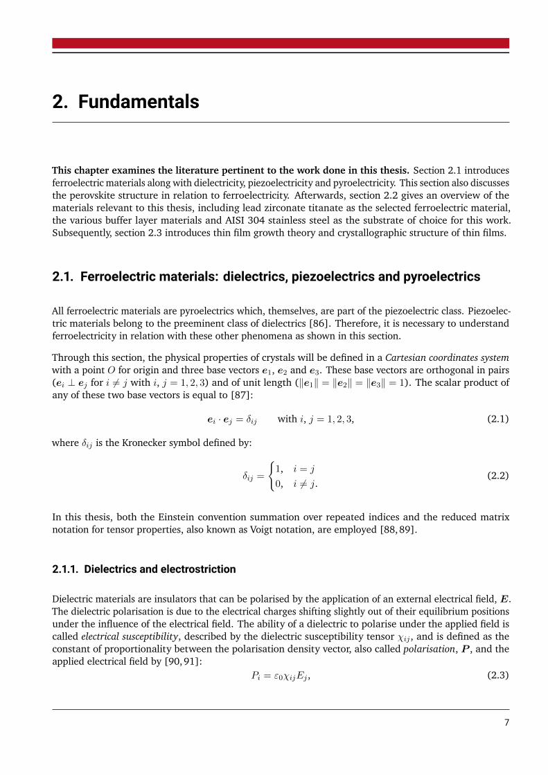
Direct piezoelectric effect is displayed by a material when, being mechanically deformed, it generates achange in electrical polarisation proportional to the deformation. Oppositely, the converse piezoelectric effectcorresponds to the application of an external electrical field on the material giving rise to strain in thematerial [94,95]. These two effects are illustrated in Figure 2.1.
In 1880, Jacques Curie and Pierre Curie were the first to experimentally demonstrate the existence ofpiezoelectricity in several materials, e.g. tourmaline, quartz or topaz [96]. Piezoelectricity correspondsto a linear relation between electrical and mechanical states in crystals which do not possess a centre ofsymmetry [94,95].
Piezoelectricity emerges in a material from its crystal structure: for electrical polarisation to appear whenan external mechanical force is applied, the crystal must have a symmetry sufficiently low [97]. As theyare polarisable, i.e. can develop charges on their surfaces, all piezoelectrics are also dielectrics [98]. While32 crystal classes exist, only 21 are non-centrosymmetric, potentially allowing piezoelectricity. However,the crystal class 432, while not possessing a centre of symmetry, does not display piezoelectricity due toadditional symmetry elements. Therefore, the 20 crystal classes producing the piezoelectric effect are thefollowing: 1, 2, m, 222, 2mm, 3, 32, 3m, 4, 4, 422, 4mm, 42m, 6, 6, 622, 6mm, 62m, 23, 43m [99]. For
8

−σ
+σ
+σ
−σ
−V
+V
+V
−V
+ + + + + + + + + +
− − − − − − − − − −
− − − − − − −
+ + + + + + +
+ + + + + + + + + +
− − − − − − − − − −
− − − − − − −
+ + + + + + +
P P
P P
Direct effect (Applied force)
Converse effect (Applied voltage)
Figure 2.1.: Schematic representation of the direct (top schematics) and converse (bottom schematics)piezoelectric effects on a piezoelectric crystal. The dashed lines indicate the shape of thecrystals before stress, ±σ, or voltage, ±V , (generating a polarisation, P ) are applied. The bluecolour indicates applied quantities and the red colour highlights induced polarisation andstrain. The ⊕ and ⊖ symbols represent qualitatively positive and negative electrical charges,respectively. Adapted from [95].
each of these space groups, the non-zero components of their piezoelectric coefficient tensors and theirrelationship can be found in literature [89,100].
It should be noted that the linearity of the piezoelectric response is only valid at low applied stress andfield levels. At higher levels, electrostriction becomes non-negligible (see section 2.1.1) and, in the case offerroelectrics, domain wall motion contributes to the non-linearity of the response (see section 2.1.4) [101].Therefore, the relations given below (Equations (2.15) and (2.16)) are only valid in the linear range of thepiezoelectric response of the material under consideration.
The piezoelectric response of a material is described by a series of coefficients known as piezoelectriccoefficients. The coefficients d, g, e and h correspond to the direct effect while the coefficients d∗, g∗,e∗ and h∗ correspond to the converse effect. The piezoelectric coefficients are defined by the following
9

equations [102]:
d = +
(∂D
∂σ
)E,T
, d∗ = +
(∂κ
∂E
)σ,T
, (2.9)
g = −(∂E
∂σ
)D,T
, g∗ = +
(∂κ
∂D
)σ,T
, (2.10)
e = +
(∂D
∂κ
)E,T
, e∗ = −(∂σ
∂E
)κ,T
, (2.11)
h = −(∂E
∂κ
)D,T
, h∗ = −(∂σ
∂D
)κ,T
, (2.12)
where σ is the applied stress, κ is the induced strain and T is the temperature. The variables kept constantare indicated by the subscripts.
Due to thermodynamics, the piezoelectric coefficients for the direct effect are equal to their respectivecounterparts for the converse piezoelectric effect [102].
From the experimental approach, it should be noted that when the stress is kept constant, i.e. σ = cst, thepiezoelectric sample is said to be in a mechanically free state [90]. It is difficult to realise this conditionexperimentally as the sample must be held without generating stress, e.g. in nodes of vibration [103].Contrarily, when the strain is kept constant, i.e. κ = cst, the piezoelectric is in a mechanically clampedstate [90]. It can be achieved experimentally by maintaining the sample in an infinitely stiff neighbourhood[103]. Analogue states can be expressed electrically: electrically free and electrically clamped states areobtained by keeping the electrical field strength constant, i.e. E = cst, or by maintaining the electricalflux density constant, i.e. D = cst, respectively [90]. Experimentally, the electrodes collecting the chargesmust be shortened in the first case and must be kept in an insulating environment in the latter [103].
The coefficients d and e both refer to electrically free states and to mechanically free and clamped states,respectively. The coefficient d is known as piezoelectric charge constant and describes the relation betweenthe dielectric displacement and the stress. It is expressed in C·N−1. The coefficient e characterises therelation between the dielectric displacement and the strain. Its unit is C·m−2. Conversely, the coefficientsg and h apply to electrically clamped states with mechanically free and clamped states, respectively. Thecoefficient g or piezoelectric voltage constant and the coefficient h describe the relation between the electricalfield and the stress or the strain, respectively. Their respective units are C−1·m2 and C−1·N [90,103].
Piezoelectric coefficients are third rank tensors and therefore contain 27 components. However, as thecoefficients, e.g. dijk, are symmetrical in i and j, the number of independent components is limited at18 [89,103]. This allows the use of the Voigt notation to simplify piezoelectric coefficients into a matrixnotation. The coefficients dijk and eijk and their matrix notations diµ and eiµ follow, respectively, therelations [103]:⎛⎝d111 d122 d133 2d123 2d113 2d112
d211 d222 d233 2d223 2d213 2d212d311 d322 d333 2d323 2d313 2d312
⎞⎠ ∼=
⎛⎝d11 d12 d13 d14 d15 d16d21 d22 d23 d24 d25 d26d31 d32 d33 d34 d35 d36
⎞⎠ , (2.13)
and ⎛⎝e111 e122 e133 e123 e113 e112e211 e222 e233 e223 e213 e212e311 e322 e333 e323 e313 e312
⎞⎠ ∼=
⎛⎝e11 e12 e13 e14 e15 e16e21 e22 e23 e24 e25 e26e31 e32 e33 e34 e35 e36
⎞⎠ . (2.14)
10
The coefficients g and h follow the same rules as the coefficients d and e, respectively.
In practice, the conditions for mechanically and electrically free or clamped states are rarely met. Therefore,the elastic and dielectric linear equations of state for piezoelectric are written as:
Di = diµσµ + εikEk (direct effect) κλ = dkλEk + sλµσµ (converse effect), (2.15)
and
Di = eiλκλ + εikEk (direct effect) σµ = −ekµEk + cλµκλ (converse effect), (2.16)
where sλµ is the elastic compliance and cλµ is the elastic stiffness [103]. Equations of state for thecoefficients g and h can also be written but are not relevant to this work.
It should be noted that the piezoelectric coefficients described above refer to bulk coefficients. In thecase of piezoelectric thin films, the boundary conditions to which the film is subjected needs to be takeninto account [104]. Indeed, for the majority of MEMS applications, piezoelectrics are integrated into acomposite structure. This imposes a mixed boundary condition as the piezoelectric layer is clamped toanother elastic body whose properties are often predominant in the composite [17,24].
Therefore, the piezoelectric coefficients e31,f and d33,f relate to thin films clamped to rigid substrates inthe (e1, e2) plane and with unconstrained off-plane motion in the e3 direction. e31,f and d33,f describe thetransverse effect, i.e. the in-plane stress as a function of the applied field, and the longitudinal effect, i.e.the thickness change as a function of the applied field, respectively. The e31,f and d33,f coefficients for thinfilms are defined as follow: [17,24].
e31,f =d31
s11E + s12E, (2.17)
d33,f = d33 −2s13
E
s11E + s12E, (2.18)
where s11E , s12E and s13E are the s11, s12 and s13 elastic compliances at constant electrical field, respectively.
2.1.3. Pyroelectricity
Within the piezoelectric classes, ten point groups, presenting a unique polar axis, are characteristic ofpyroelectrics: 1, 2, m, 2mm, 3, 3m, 4, 4mm, 6 and 6mm. Known as the polar classes, they exhibit a sponta-neous polarisation, i.e. non-zero electrical polarisation in zero applied electrical field, which is temperaturedependent [103]. The term polar axis refers to the direction of the spontaneous polarisation [105].
Similar to piezoelectricity, pyroelectricity displays direct and converse effects, referred to as pyroelectriceffect and electrocaloric effect, respectively. The pyroelectric effect corresponds to a change in spontaneouspolarisation due to a change in temperature. Conversely, the electrocaloric effect describes a change intemperature originating from an applied electrical field [103].
The relation between the change in spontaneous polarisation vector, P s, and the change in temperature,T , is described by the vector of pyroelectric coefficients, pi [98]:
pi =∂P s,i
∂T. (2.19)
11
2.1.4. Ferroelectricity
A system is ferroelectric if it is insulating and possesses at least two stable or metastable states of differentspontaneous polarisation between which it is possible to switch under an applied electrical field. Theability to switch from one state to another is due to the field-to-polarisation coupling through which anapplied electrical field varies the states relative energy [106].
Ferroelectricity was identified experimentally for the first time in Rochelle salt in 1920 by Valasek [107,108].However, Rochelle salt or sodium potassium tartrate tetrahydrate of chemical formula NaKC4H4O6 · 4H2Owas the only known ferroelectric material for more than a decade after being discovered, leading ferroelec-tricity to be known as Seignette-electricity from the name of the company preparing Rochelle salt until theearly 1940s [86].
Ferroelectric materials are pyroelectrics in which the polarisation switching is accessible through very smalllattice distortions. In case substantial lattice reconstruction is needed to change the orientation of thespontaneous polarisation, the material is pyroelectric without being ferroelectric as the large energeticrequirements for polarisation switching are likely to result in dielectric breakdown [103].
Polarisation itself has long been challenging to define until the beginning of the 1990s. In the case of afinite system, the Clausius-Mossotti model can be applied and the task is simple enough. Indeed, the dipolemoment corresponds to the polarisation and can be calculated as the volumic charge density. However,difficulties arise when considering polarisation as the bulk property of an infinite crystal [109].
The first obstacle emerges when attempting to choose a dipole in a periodic continuous distribution. Itis not possible to separate such a distribution in localised contributions without ambivalence: a dipolecould either be composed by ⊕−⊖ (positive - negative) or ⊖−⊕ (negative - positive) electrical chargescombinations and selecting one of the options would arbitrarily define the polarisation direction [109,110].Another complication derives from the nature of the bonding inside the ferroelectric. In real materials, e.g.in typical ferroelectric oxides, as opposed to a perfect modelled material, the bonding is a mixture of ionicand covalent characters. As such, the ions are sharing the electronic charge which is delocalised, makingimpossible the utilisation of the Clausius-Mossotti model [109].
The modern theory of polarisation, developed by Resta, King-Smith and Vanderbilt [111–113], arises from achange of perspective on the problematic: it aims to define the change in polarisation and no longer reachthe absolute value of polarisation [109]. This theory relies on Berry phases and Wannier functions. Formore details, the reader is referred to [112–115].
Previous attempts to define polarisation based on a charge distribution proved to be flawed as they failedto differentiate bulk contributions from surface ones. The modern theory of polarisation not only providesa definition separating bulk from surface contributions, independently of both the shape and location ofthe unit cell, but it also produces a unique solution for the polarisation. Assuming that any charge pumpedto the surface of the dielectric cannot be conducted away, the change in polarisation is defined by [109]:
∆P =
∫dt
1
Vcell
∫cell
dr j(r, t), (2.20)
where ∆P is the change in internal polarisation, Vcell is the volume of the unit cell, t is the time, r is theposition vector and j is the current density vector.
Ferroelectrics ability to switch their spontaneous polarisation between discrete states at lower temperaturesis due to the instability of the transverse optical lattice vibration mode at high temperature. As the
12
temperature decreases, the phonon frequency diminishes until it reaches zero at the Curie temperature,TC. This vibration mode is called soft mode and leads to a crystal structure with lower symmetry when theatomic position freezes at TC [103,116,117].
In terms of thermodynamics, the transition from the higher symmetry phase, called paraelectric phase, to thelower symmetry ferroelectric phase is described by the Landau-Devonshire theory. The thermodynamic stateof a bulk ferroelectric system in equilibrium can be described by the temperature, polarisation, electricalfield, strain and stress variables. In practice, electrical fields and elastic stresses are the physical quantitiesapplied on ferroelectrics. Therefore, polarisation and strain are considered as “internal” variables [118].
It should be noted that the Landau-Devonshire theory is intended to handle poled bulk ferroelectrics andthat for unpoled ferroelectrics the Levanyuk-Ginzburg criterion should be used. For more details on thelatter, the reader is referred to [118].
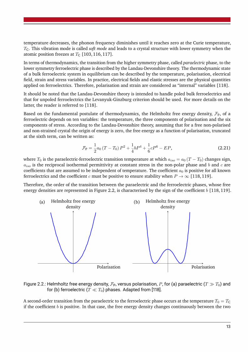
Based on the fundamental postulate of thermodynamics, the Helmholtz free energy density, FP, of aferroelectric depends on ten variables: the temperature, the three components of polarisation and the sixcomponents of stress. According to the Landau-Devonshire theory, assuming that for a free non-polarisedand non-strained crystal the origin of energy is zero, the free energy as a function of polarisation, truncatedat the sixth term, can be written as:
FP =1
2a0 (T − T0)P
2 +1
4bP 4 +
1
6cP 6 − EP , (2.21)
where T0 is the paraelectric-ferroelectric transition temperature at which aiso = a0 (T − T0) changes sign,aiso is the reciprocal isothermal permittivity at constant stress in the non-polar phase and b and c arecoefficients that are assumed to be independent of temperature. The coefficient a0 is positive for all knownferroelectrics and the coefficient c must be positive to ensure stability when P → ∞ [118,119].
Therefore, the order of the transition between the paraelectric and the ferroelectric phases, whose freeenergy densities are represented in Figure 2.2, is characterised by the sign of the coefficient b [118,119].
(a)
Polarisation
Helmholtz free energydensity
(b)
Polarisation
Helmholtz free energydensity
Figure 2.2.: Helmholtz free energy density, FP, versus polarisation, P , for (a) paraelectric (T ≫ T0) andfor (b) ferroelectric (T ≪ T0) phases. Adapted from [118].
A second-order transition from the paraelectric to the ferroelectric phase occurs at the temperature T0 = TCif the coefficient b is positive. In that case, the free energy density changes continuously between the two
13
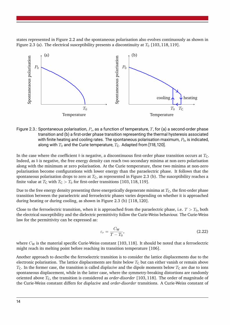
states represented in Figure 2.2 and the spontaneous polarisation also evolves continuously as shown inFigure 2.3 (a). The electrical susceptibility presents a discontinuity at T0 [103,118,119].
(a)
T0
P0
Temperature
Spon
tane
aous
polaris
ation
cooling heating
(b)
T0 TC
P0
TemperatureSp
ontane
aous
polaris
ation
Figure 2.3.: Spontaneous polarisation, Ps, as a function of temperature, T , for (a) a second-order phasetransition and (b) a first-order phase transition representing the thermal hysteresis associatedwith finite heating and cooling rates. The spontaneous polarisation maximum, P0, is indicated,along with T0 and the Curie temperature, TC. Adapted from [118, 120].
In the case where the coefficient b is negative, a discontinuous first-order phase transition occurs at TC.Indeed, as b is negative, the free energy density can reach two secondary minima at non-zero polarisationalong with the minimum at zero polarisation. At the Curie temperature, these two minima at non-zeropolarisation become configurations with lower energy than the paraelectric phase. It follows that thespontaneous polarisation drops to zero at TC, as represented in Figure 2.3 (b). The susceptibility reaches afinite value at TC with TC > T0 for first-order transitions [103,118,119].
Due to the free energy density presenting three energetically degenerate minima at TC, the first-order phasetransition between the paraelectric and ferroelectric phases varies depending on whether it is approachedduring heating or during cooling, as shown in Figure 2.3 (b) [118,120].
Close to the ferroelectric transition, when it is approached from the paraelectric phase, i.e. T > T0, boththe electrical susceptibility and the dielectric permittivity follow the Curie-Weiss behaviour. The Curie-Weisslaw for the permittivity can be expressed as:
εr =CW
T − T0, (2.22)
where CW is the material specific Curie-Weiss constant [103,118]. It should be noted that a ferroelectricmight reach its melting point before reaching its transition temperature [106].
Another approach to describe the ferroelectric transition is to consider the lattice displacements due to theelectronic polarisation. The lattice displacements are finite below TC but can either vanish or remain aboveTC. In the former case, the transition is called displacive and the dipole moments below TC are due to ionsspontaneous displacement, while in the latter case, where the symmetry-breaking distortions are randomlyoriented above TC, the transition is considered as order-disorder [103,118]. The order of magnitude ofthe Curie-Weiss constant differs for displacive and order-disorder transitions. A Curie-Weiss constant of
14
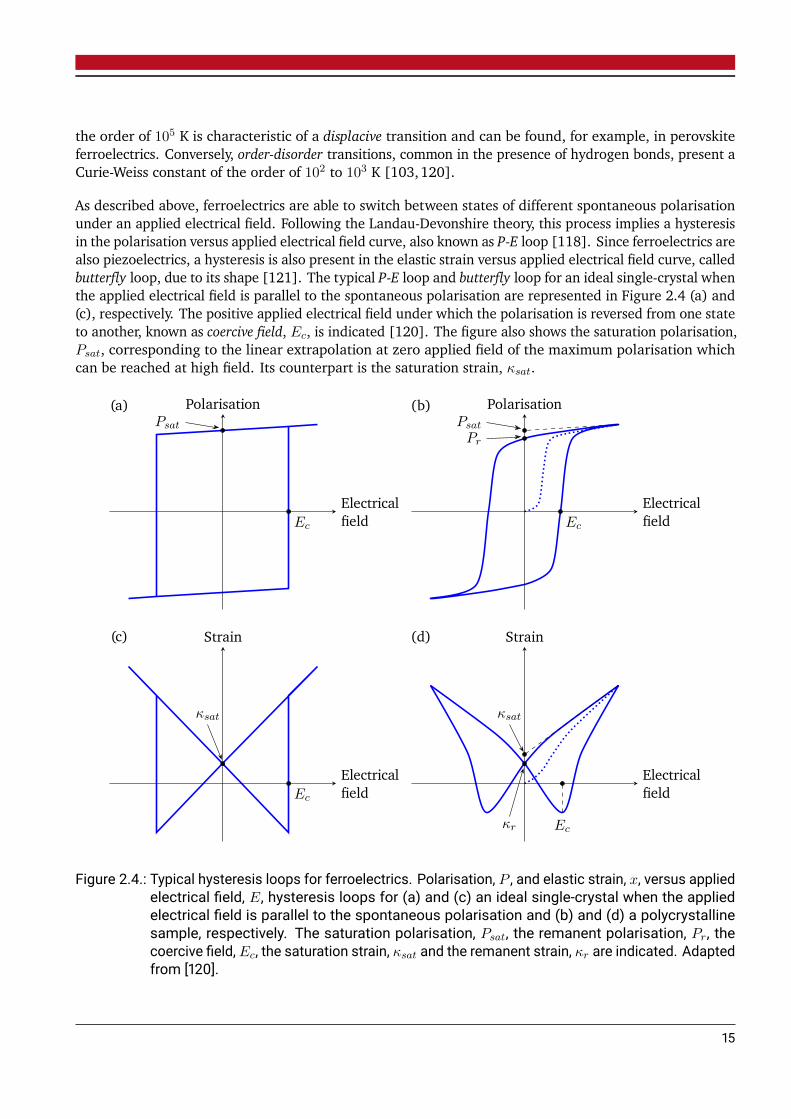
the order of 105 K is characteristic of a displacive transition and can be found, for example, in perovskiteferroelectrics. Conversely, order-disorder transitions, common in the presence of hydrogen bonds, present aCurie-Weiss constant of the order of 102 to 103 K [103,120].
As described above, ferroelectrics are able to switch between states of different spontaneous polarisationunder an applied electrical field. Following the Landau-Devonshire theory, this process implies a hysteresisin the polarisation versus applied electrical field curve, also known as P-E loop [118]. Since ferroelectrics arealso piezoelectrics, a hysteresis is also present in the elastic strain versus applied electrical field curve, calledbutterfly loop, due to its shape [121]. The typical P-E loop and butterfly loop for an ideal single-crystal whenthe applied electrical field is parallel to the spontaneous polarisation are represented in Figure 2.4 (a) and(c), respectively. The positive applied electrical field under which the polarisation is reversed from one stateto another, known as coercive field, Ec, is indicated [120]. The figure also shows the saturation polarisation,Psat, corresponding to the linear extrapolation at zero applied field of the maximum polarisation whichcan be reached at high field. Its counterpart is the saturation strain, κsat.
Psat
Ec
(a)
Electricalfield
PolarisationPsat
Ec
Pr
(b)
Electricalfield
Polarisation
κsat
Ec
(c)
Electricalfield
Strain
κr Ec
κsat
(d)
Electricalfield
Strain
Figure 2.4.: Typical hysteresis loops for ferroelectrics. Polarisation, P , and elastic strain, x, versus appliedelectrical field, E, hysteresis loops for (a) and (c) an ideal single-crystal when the appliedelectrical field is parallel to the spontaneous polarisation and (b) and (d) a polycrystallinesample, respectively. The saturation polarisation, Psat, the remanent polarisation, Pr , thecoercive field, Ec, the saturation strain, κsat and the remanent strain, κr are indicated. Adaptedfrom [120].
15

The shape of the ferroelectric hysteresis loops for polycrystalline samples, presented in Figure 2.4 (b) and(d), as well as for non-ideal single-crystals, is due to the existence of ferroelectric domains. Domains areregions within which the polarisation is oriented in a given direction. They are separated from each otherby domain walls. The apparition of domain structures in ferroelectrics aims to minimise the system freeenergy by balancing the electrical field energy reduction and the domain walls energy [103,120].
It should be noted that while the number of domains depends on several parameters, e.g. crystal sizeand applied forces, the type of domains, i.e. the directions in which the polarisation can be oriented, arelimited by the crystal symmetry [120]. For example, in a tetragonal crystal, the polarisation can take sixdistinct directions, as shown in Figure 2.5.
(100) (010) (001)
Figure 2.5.: Schematic representation of the accessible polarisation directions in a tetragonal crystalalong (100), (010) and (001) orientations.
Domain walls are named by the angle between the polarisation of their two neighbouring domains [120].In the case of a tetragonal crystal, due to the six accessible directions of polarisation, two sorts of domainwall exist: 180 and 90 domain walls, the latter also referred to as non-180 domain wall [118]. Aschematic representation of ferroelectric domains with either 180 or non-180 domain walls is shownin Figure 2.6. The dielectric response is impacted by both 180 and non-180 domain walls, while thepiezoelectric response is dependent only on non-180 domain walls. This is due to all domain walls beingferroelectrically active, while only non-180 domain walls are ferroelastically active [122].
(a) (b)
Figure 2.6.: Two dimensional schematic representation of ferroelectric domains in a crystal with (a) 180domain walls and (b) non-180 domain walls. Adapted from [123] and [124], respectively.
Due to their multiple-domains states, the net polarisation of ferroelectric crystals is generally zero or verylimited. The re-orientation, under a unipolar applied electrical field, of the domain polarisations to create
16
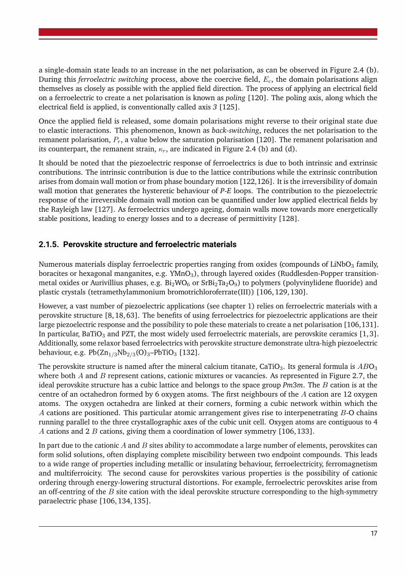
a single-domain state leads to an increase in the net polarisation, as can be observed in Figure 2.4 (b).During this ferroelectric switching process, above the coercive field, Ec, the domain polarisations alignthemselves as closely as possible with the applied field direction. The process of applying an electrical fieldon a ferroelectric to create a net polarisation is known as poling [120]. The poling axis, along which theelectrical field is applied, is conventionally called axis 3 [125].
Once the applied field is released, some domain polarisations might reverse to their original state dueto elastic interactions. This phenomenon, known as back-switching, reduces the net polarisation to theremanent polarisation, Pr, a value below the saturation polarisation [120]. The remanent polarisation andits counterpart, the remanent strain, κr, are indicated in Figure 2.4 (b) and (d).
It should be noted that the piezoelectric response of ferroelectrics is due to both intrinsic and extrinsiccontributions. The intrinsic contribution is due to the lattice contributions while the extrinsic contributionarises from domain wall motion or from phase boundary motion [122,126]. It is the irreversibility of domainwall motion that generates the hysteretic behaviour of P-E loops. The contribution to the piezoelectricresponse of the irreversible domain wall motion can be quantified under low applied electrical fields bythe Rayleigh law [127]. As ferroelectrics undergo ageing, domain walls move towards more energeticallystable positions, leading to energy losses and to a decrease of permittivity [128].
2.1.5. Perovskite structure and ferroelectric materials
Numerous materials display ferroelectric properties ranging from oxides (compounds of LiNbO3 family,boracites or hexagonal manganites, e.g. YMnO3), through layered oxides (Ruddlesden-Popper transition-metal oxides or Aurivillius phases, e.g. Bi2WO6 or SrBi2Ta2O9) to polymers (polyvinylidene fluoride) andplastic crystals (tetramethylammonium bromotrichloroferrate(III)) [106,129,130].
However, a vast number of piezoelectric applications (see chapter 1) relies on ferroelectric materials with aperovskite structure [8,18,63]. The benefits of using ferroelectrics for piezoelectric applications are theirlarge piezoelectric response and the possibility to pole these materials to create a net polarisation [106,131].In particular, BaTiO3 and PZT, the most widely used ferroelectric materials, are perovskite ceramics [1,3].Additionally, some relaxor based ferroelectrics with perovskite structure demonstrate ultra-high piezoelectricbehaviour, e.g. Pb(Zn1/3Nb2/3(O)3–PbTiO3 [132].
The perovskite structure is named after the mineral calcium titanate, CaTiO3. Its general formula is ABO3
where both A and B represent cations, cationic mixtures or vacancies. As represented in Figure 2.7, theideal perovskite structure has a cubic lattice and belongs to the space group Pm3m. The B cation is at thecentre of an octahedron formed by 6 oxygen atoms. The first neighbours of the A cation are 12 oxygenatoms. The oxygen octahedra are linked at their corners, forming a cubic network within which theA cations are positioned. This particular atomic arrangement gives rise to interpenetrating B-O chainsrunning parallel to the three crystallographic axes of the cubic unit cell. Oxygen atoms are contiguous to 4A cations and 2 B cations, giving them a coordination of lower symmetry [106,133].
In part due to the cationicA andB sites ability to accommodate a large number of elements, perovskites canform solid solutions, often displaying complete miscibility between two endpoint compounds. This leadsto a wide range of properties including metallic or insulating behaviour, ferroelectricity, ferromagnetismand multiferroicity. The second cause for perovskites various properties is the possibility of cationicordering through energy-lowering structural distortions. For example, ferroelectric perovskites arise froman off-centring of the B site cation with the ideal perovskite structure corresponding to the high-symmetryparaelectric phase [106,134,135].
17
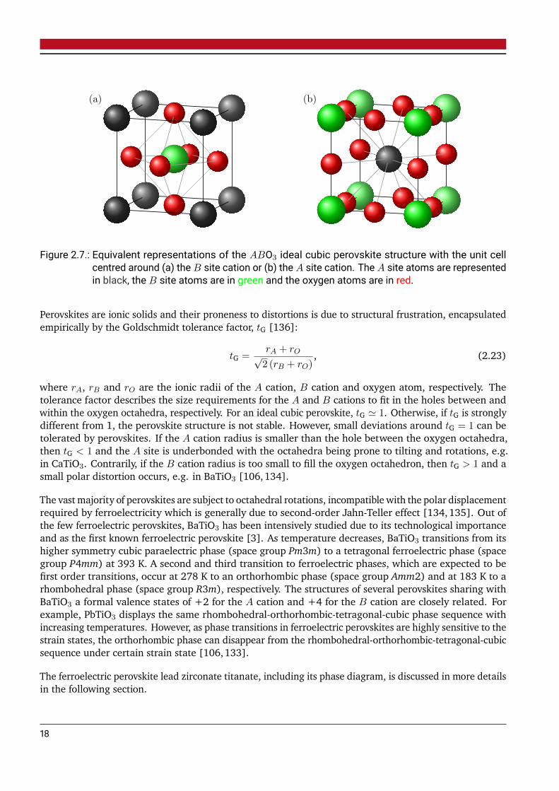
(a) (b)
Figure 2.7.: Equivalent representations of the ABO3 ideal cubic perovskite structure with the unit cellcentred around (a) the B site cation or (b) the A site cation. The A site atoms are representedin black, the B site atoms are in green and the oxygen atoms are in red.
Perovskites are ionic solids and their proneness to distortions is due to structural frustration, encapsulatedempirically by the Goldschmidt tolerance factor, tG [136]:
tG =rA + rO√2 (rB + rO)
, (2.23)
where rA, rB and rO are the ionic radii of the A cation, B cation and oxygen atom, respectively. Thetolerance factor describes the size requirements for the A and B cations to fit in the holes between andwithin the oxygen octahedra, respectively. For an ideal cubic perovskite, tG ≃ 1. Otherwise, if tG is stronglydifferent from 1, the perovskite structure is not stable. However, small deviations around tG = 1 can betolerated by perovskites. If the A cation radius is smaller than the hole between the oxygen octahedra,then tG < 1 and the A site is underbonded with the octahedra being prone to tilting and rotations, e.g.in CaTiO3. Contrarily, if the B cation radius is too small to fill the oxygen octahedron, then tG > 1 and asmall polar distortion occurs, e.g. in BaTiO3 [106,134].
The vast majority of perovskites are subject to octahedral rotations, incompatible with the polar displacementrequired by ferroelectricity which is generally due to second-order Jahn-Teller effect [134,135]. Out ofthe few ferroelectric perovskites, BaTiO3 has been intensively studied due to its technological importanceand as the first known ferroelectric perovskite [3]. As temperature decreases, BaTiO3 transitions from itshigher symmetry cubic paraelectric phase (space group Pm3m) to a tetragonal ferroelectric phase (spacegroup P4mm) at 393 K. A second and third transition to ferroelectric phases, which are expected to befirst order transitions, occur at 278 K to an orthorhombic phase (space group Amm2) and at 183 K to arhombohedral phase (space group R3m), respectively. The structures of several perovskites sharing withBaTiO3 a formal valence states of +2 for the A cation and +4 for the B cation are closely related. Forexample, PbTiO3 displays the same rhombohedral-orthorhombic-tetragonal-cubic phase sequence withincreasing temperatures. However, as phase transitions in ferroelectric perovskites are highly sensitive to thestrain states, the orthorhombic phase can disappear from the rhombohedral-orthorhombic-tetragonal-cubicsequence under certain strain state [106,133].
The ferroelectric perovskite lead zirconate titanate, including its phase diagram, is discussed in more detailsin the following section.
18
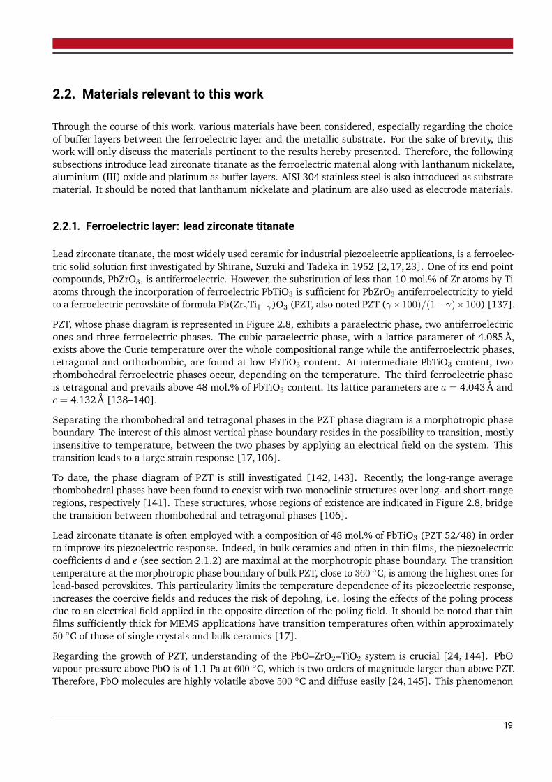
2.2. Materials relevant to this work
Through the course of this work, various materials have been considered, especially regarding the choiceof buffer layers between the ferroelectric layer and the metallic substrate. For the sake of brevity, thiswork will only discuss the materials pertinent to the results hereby presented. Therefore, the followingsubsections introduce lead zirconate titanate as the ferroelectric material along with lanthanum nickelate,aluminium (III) oxide and platinum as buffer layers. AISI 304 stainless steel is also introduced as substratematerial. It should be noted that lanthanum nickelate and platinum are also used as electrode materials.
2.2.1. Ferroelectric layer: lead zirconate titanate
Lead zirconate titanate, the most widely used ceramic for industrial piezoelectric applications, is a ferroelec-tric solid solution first investigated by Shirane, Suzuki and Tadeka in 1952 [2,17,23]. One of its end pointcompounds, PbZrO3, is antiferroelectric. However, the substitution of less than 10 mol.% of Zr atoms by Tiatoms through the incorporation of ferroelectric PbTiO3 is sufficient for PbZrO3 antiferroelectricity to yieldto a ferroelectric perovskite of formula Pb(ZrγTi1−γ)O3 (PZT, also noted PZT (γ×100)/(1−γ)×100) [137].
PZT, whose phase diagram is represented in Figure 2.8, exhibits a paraelectric phase, two antiferroelectricones and three ferroelectric phases. The cubic paraelectric phase, with a lattice parameter of 4.085Å,exists above the Curie temperature over the whole compositional range while the antiferroelectric phases,tetragonal and orthorhombic, are found at low PbTiO3 content. At intermediate PbTiO3 content, tworhombohedral ferroelectric phases occur, depending on the temperature. The third ferroelectric phaseis tetragonal and prevails above 48 mol.% of PbTiO3 content. Its lattice parameters are a = 4.043Å andc = 4.132Å [138–140].
Separating the rhombohedral and tetragonal phases in the PZT phase diagram is a morphotropic phaseboundary. The interest of this almost vertical phase boundary resides in the possibility to transition, mostlyinsensitive to temperature, between the two phases by applying an electrical field on the system. Thistransition leads to a large strain response [17,106].
To date, the phase diagram of PZT is still investigated [142, 143]. Recently, the long-range averagerhombohedral phases have been found to coexist with two monoclinic structures over long- and short-rangeregions, respectively [141]. These structures, whose regions of existence are indicated in Figure 2.8, bridgethe transition between rhombohedral and tetragonal phases [106].
Lead zirconate titanate is often employed with a composition of 48 mol.% of PbTiO3 (PZT 52/48) in orderto improve its piezoelectric response. Indeed, in bulk ceramics and often in thin films, the piezoelectriccoefficients d and e (see section 2.1.2) are maximal at the morphotropic phase boundary. The transitiontemperature at the morphotropic phase boundary of bulk PZT, close to 360 C, is among the highest ones forlead-based perovskites. This particularity limits the temperature dependence of its piezoelectric response,increases the coercive fields and reduces the risk of depoling, i.e. losing the effects of the poling processdue to an electrical field applied in the opposite direction of the poling field. It should be noted that thinfilms sufficiently thick for MEMS applications have transition temperatures often within approximately50 C of those of single crystals and bulk ceramics [17].
Regarding the growth of PZT, understanding of the PbO–ZrO2–TiO2 system is crucial [24, 144]. PbOvapour pressure above PbO is of 1.1 Pa at 600 C, which is two orders of magnitude larger than above PZT.Therefore, PbO molecules are highly volatile above 500 C and diffuse easily [24,145]. This phenomenon
19

Pcubic
Ftetra
Aortho
Frhombo(HT)
Frhombo(LT)
MPB
(a)
0 10 20 30 40 50 60 70 80 90 1000
50
100
150
200
250
300
350
400
450
500
550
PbTiO3 content (mol.%)
Tempe
rature
(C)
Pcubic
Aortho
Atetra
Frhombo(HT)
(b)
0 1 2 3 4190
200
210
220
230
240
PbTiO3 content (mol.%)
Tempe
rature
(C)
PbZrO3 PbTiO3
Figure 2.8.: Pb(ZrγTi1−γ)O3 phase diagram. (a) PZT phase diagram with PbTiO3, γ, content ranging from0 mol.% to 100 mol.%, (b) Detailed view of (a), indicated by the red box, with PbTiO3 contentranging from 0 mol.% to 4 mol.%. Full lines and data points correspond to the widely used1971 diagram from [138]. The paraelectric phase with a cubic lattice is indicated by Pcubic.Antiferroelectric phases with orthorhombic and tetragonal lattices are denoted by Aortho andAtetra, respectively. Ferroelectric phases with tetragonal and rhombohedral, at high and lowtemperature, are indicated by Ftetra, Frhombo(HT) and Frhombo(LT), respectively. The morphotropicphase boundary is indicated by MPB. The green coloured and orange coloured areas, datafrom [141], represent two monoclinic structures coexisting in long- and short-range regions,respectively, with the long-range average rhombohedral phases described by [138].
leads to important lead loss and the formation of a secondary phase with pyrochlore structure [24]. Yet,phases with pyrochlore as well as fluorite structures should be avoided as they are competing with thedesired perovskite structure. In consequence, precise stoichiometric control is required for nucleation andgrowth [146].
Additionally, the activation energy of 441 kJ·mol−1 required to nucleate the perovskite structure of PZTis four times larger than the one of 112 kJ·mol−1 for its growth [147]. This indicates that PZT growth isnucleation controlled and allows the thin film texture to be selected by choosing appropriate electrodesas growth template [17,24]. It should be noted that an increase in Zr content leads to higher activationenergies for both nucleation and growth [147].
Due to smaller dimensions, a homogeneous composition can be obtained in thin films through diffusionon smaller distances than in bulk ceramics. Therefore, the growth temperatures for PZT thin films arelower than the sintering temperatures for bulk PZT. Consequently, deviations from stoichiometry may notbe entirely redressed by local diffusion, leading to the formation of undesirable secondary phases. Tocompensate lead loss, which leads to pyrochlore formation, deposition methods generally provide excesslead. In cases where post-annealing is necessary for crystallisation, e.g. for chemical vapour depositionmethods, rapid thermal annealing can be employed to limit lead loss [24].
20
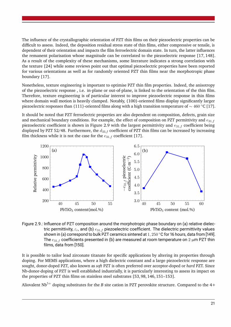
The influence of the crystallographic orientation of PZT thin films on their piezoelectric properties can bedifficult to assess. Indeed, the deposition residual stress state of thin films, either compressive or tensile, isdependent of their orientation and impacts the film ferroelectric domain state. In turn, the latter influencesthe remanent polarisation whose magnitude can be correlated to the piezoelectric response [17, 148].As a result of the complexity of these mechanisms, some literature indicates a strong correlation withthe texture [24] while some reviews point out that optimal piezoelectric properties have been reportedfor various orientations as well as for randomly oriented PZT thin films near the morphotropic phaseboundary [17].
Nonetheless, texture engineering is important to optimise PZT thin film properties. Indeed, the anisotropyof the piezoelectric response , i.e. in-plane or out-of-plane, is linked to the orientation of the thin film.Therefore, texture engineering is of particular interest to improve piezoelectric response in thin filmswhere domain wall motion is heavily clamped. Notably, 100-oriented films display significantly largerpiezoelectric responses than 111-oriented films along with a high transition temperature of∼ 460 C [17].
It should be noted that PZT ferroelectric properties are also dependent on composition, defects, grain sizeand mechanical boundary conditions. For example, the effect of composition on PZT permittivity and e31,fpiezoelectric coefficient is shown in Figure 2.9 with the largest permittivity and e31,f coefficient beingdisplayed by PZT 52/48. Furthermore, the d33,f coefficient of PZT thin films can be increased by increasingfilm thickness while it is not the case for the e31,f coefficient [17].
(a)
40 45 50 55200
400
600
800
1000
1200
PbTiO3 content(mol.%)
Relativ
epe
rmittivity
(b)
40 45 50 55 603.0
3.5
4.0
4.5
5.0
5.5
6.0
6.5
PbTiO3 content (mol.%)
−e 3
1,fpiezoe
lectric
coeffi
cien
t(C·m
−2)
Figure 2.9.: Influence of PZT composition around the morphotropic phase boundary on (a) relative dielec-tric permittivity, εr , and (b) e31,f piezoelectric coefficient. The dielectric permittivity valuesshown in (a) correspond to bulk PZT ceramics sintered at 1, 250 C for 16 hours, data from [149].The e31,f coefficients presented in (b) are measured at room temperature on 2 µm PZT thinfilms, data from [150].
It is possible to tailor lead zirconate titanate for specific applications by altering its properties throughdoping. For MEMS applications, where a high dielectric constant and a large piezoelectric response aresought, donor-doped PZT, also known as soft PZT is often preferred over acceptor-doped or hard PZT. SinceNb-donor-doping of PZT is well established industrially, it is particularly interesting to assess its impact onthe properties of PZT thin films on stainless steel substrates [53,98,146,151–153].
Aliovalent Nb5+ doping substitutes for the B site cation in PZT perovskite structure. Compared to the 4+
21
valence of both Zr and Ti atoms, an additional positive charge is present in the lattice. To compensate for thischarge created by donor-doping, one Pb2+ vacancy is created for every two Nb atoms introduced in the struc-ture [98,146,151]. The general formula of Nb-doped PZT, noted PNZT, is Pb1−ι/2ι/2(ZrγTi1−γ)1−ιNbιO3
where represents Pb vacancies [53,146].
It has been established that the effects of Nb doping are extrinsic, due to the stabilisation of a pyrochlorephase and to structural changes, e.g. increased perovskite lateral grain size [146]. Notable propertiesmodifications due to Nb doping in PZT thin films are an increase in electrical resistivity and dielectricconstant [53, 98, 146, 151, 154]. The latter has notably been found to increase from 800 to 1,100 forundoped PZT and PZT doped with 2 mol.% Nb, respectively [155]. However, at larger concentrations,Nb-doping is detrimental to PZT properties, lowering the dielectric constant through the stabilisation ofthe pyrochlore phase [154].
Additional effects of Nb-doping are improved piezoelectric response and increased domain wall mobilitythough high dielectric loss has been reported [53, 98, 153–155]. Nb-doping up to 2 mol.% is reportedto improve PZT thin films e31,f piezoelectric coefficient while larger amount of Nb leads to a decrease inthe piezoelectric response [156]. The influence of Nb-doping on coercive field values for PZT thin filmswith compositions close to the morphotropic phase boundary remains ambiguous. While decreases ofEc values have been been reported with increasing Nb concentrations in PZT [98, 155, 157], there areliterature reports of similar Ec values between undoped and 2 mol.% Nb-doped PZT [154]. Further studieson PZT 53/47 indicate an increase of Ec with 1 mol.% Nb-doping followed by a decrease of Ec at higherNb concentrations [151].
2.2.2. Buffer layers and electrodes: lanthanum nickelate, aluminium oxide and platinum
Lanthanum nickelate
Lanthanum nickelate (LNO) is a rare earth nickelate of formula LaNiO3 which crystallises with a rhombo-hedral structure in the space group R3c. Its unit cell can be assimilated to a rhombohedrally distortedpseudocubic perovskite cell with a lattice parameter a = 3.84Å. In this description, adjacent NiO6 octahedraundergo an antiphase rotation around the [111] trigonal axis [158–160].
LNO is a metallic oxide with an isotropic resistivity at room temperature below 100 µΩ·cm. Hybridisationbetween Ni3d and O2p bands is responsible for its metallic behaviour [158,159]. The metallicity of LNOand its origin is described in more details in [160].
Most of the time, when deposited on a perovskite single crystal substrate or electrode, PZT thin films growwith the same orientation as the growth template [17]. Therefore, LNO being a pseudocubic perovskite witha high chemical stability, it can be used as an efficient growth template for oriented PZT thin films [158].Furthermore, its electrical conductivity also makes it a suitable bottom electrode in a parallel-plate capacitorstructure [51,159,161,162].
Aluminium (III) oxide
With the formula Al2O3, the only thermodynamically stable structure of aluminium (III) oxide is α-Al2O3.Its unit cell is hexagonal with lattice parameters a = 4.754Å and c = 12.99Å. Aluminium oxide is aninsulating material and, therefore, cannot be employed as a bottom electrode. However, it is mostlyinsensitive to further oxidation and can act as a barrier layer for oxygen diffusion [163].
22

Platinum
Platinum, Pt, is a transition metal with a resistivity of 10.6 µΩ·cm, making it a good conductor [43].As processes to deposit Pt by DC sputtering are well developed, Pt is a choice material for electrodes[18,22,46,52,54]. It is worthwhile to note that platinum might form intermetallic alloys, notably withchromium [164].
2.2.3. Substrate material: AISI 304 stainless steel
Stainless steels are a category of steels containing at least 11.5 wt.% of Cr which increases their oxidationresistance. Among these, austenitic steels contain between 17 wt.% and 25 wt.% of Cr and 8 wt.% to20 wt.% of Ni. Austenitic steels have a face-centred cubic unit cell and may contain inclusions of magneticferritic steel, which is body-centred cubic, depending on their processing [165,166]. AISI 304 austeniticstainless steel (SS304), also known as EN 1.4301 according to European norms, is the most commonlyused stainless steel. Its standard composition is given in Table 2.1.
Table 2.1.: Standard composition of AISI 304 stainless steel, data from [165].
Elements C Mn P S Si Cr Ni
Minimum chemical composition (wt.%) - - - - - 18.00 8.00
Maximum chemical composition (wt.%) 0.08 2.00 0.045 0.030 1.00 20.00 10.50
Due to a low carbon content, austenitic steels are low-strength steels [165,166]. For the ferroelectric bendingtongue applications envisioned in this work, this property of austenitic steels facilitate flexure. Indeed,strength is proportional to axial stiffness and a low axial stiffness is required to promote bending [167].Furthermore, austenitic steels have a good high-temperature oxidation resistance in air which makesSS304 a substrate candidate likely to withstand the deposition conditions of the ferroelectric and bufferlayers [165,166].
Austenitic steels are easily shaped, notably into sheets through cold-rolling procedures [165]. This processleads to strain hardening of the steel due to the increase of the dislocation density [168]. However, itshould be noted that stress relief occurs when the austenitic steel sheet is annealed above 500 C [165].
Another side effect of annealing austenitic steel between 550 C and 800 C, is the formation of chromiumcarbide, Cr23C6, predominantly at grain boundaries, as chromium is rejected from the steel solid solu-tion [166].
2.3. Thin film growth theory
While lacking a formal definition, the terminology thin film, by general agreement, encompasses layerswhose thicknesses range from a few nanometres to one micrometre. It applies to films with one dimensionsufficiently small relative to the other two to generate a high surface to volume ratio. As a result, somenew properties, inexistent in the bulk, arise. The film can be considered as a thin film until the criticalthickness where these surface properties are no longer predominant relative to the bulk properties [169].
23
Nowadays, the importance of thin films is increasing as large sectors of the economy are driven bytechnology: not only computers can be found in countless fields from industry, health care, transportationor even agriculture but numerous other technologies are also readily available ranging from coated glass tobio-compatible prostheses. For these applications, thin films are crucial as they can provide new optic ormagnetic properties as well as exhibit conflicting properties. The reduced dimensions of thin films allow anincrease in both dielectric breakdown voltages and device packing density in the semiconductors industry.Furthermore, different materials can be stacked in layers, creating heterostructures. For instance, the uniqueproperties of transistors originate from the interfaces between the thin films composing them [169,170].
The desired properties of thin films are achieved not only by controlling the composition but also thethermodynamic and kinetic conditions of the thin film growth [171]. Hence, the chosen growth methodhas a substantial impact on thin films. The atoms can be provided to the film from a solid, liquid or vapourphase; the latter being the most widely used approach. Indeed, solid-phase growth does not allow totransport atoms over long ranges while liquid-phase growth provides only limited control of the growthwhich must occur in conditions close to the thermodynamic equilibrium [172].
Within the growth methods providing the atoms from a vapour phase, two categories of processes canbe distinguished: chemical vapour deposition and physical vapour deposition. The former processes relyon materials which are in a gaseous state under the reactor conditions. Conversely, the latter processesgenerate the vapour phase through physical means, for example, by impacting high energy particles with atarget in a sputtering process or by heating a source in an evaporation process [172].
According to the kinetic theory of gases, the mean free path of a gas molecule between scattering events,λgas, is given by:
λgas =kBT√
2σcross−sectionPgas
, (2.24)
where kB is the Boltzmann constant, T is the absolute temperature, σcross−section is the collision cross-section and Pgas is the pressure. Therefore, the pressure inside the deposition chamber must be sufficientlylow to allow atoms to reach the substrate [172].
2.3.1. Thin film nucleation
The mechanisms described thereafter can apply to either atoms, ions or molecules. To facilitate under-standing, the term particle will be employed in the current subsection.
Once particles reach the substrate, various processes might happen as schematically represented in Fig-ure 2.10. The impinging particle might either reflect on, penetrate into or adsorb on the surface. In thetwo last cases, some energetic conditions must be met by the particle. If these conditions are not fulfilled,reflection occurs. For penetration to take place, the particle must impinge on the surface with a relativelyhigh energy, though sufficiently low to avoid sputtering. Typically, particles reaching the surface withan energy of approximately 15 eV to 50 eV can penetrate into the surface [173]. The last possibility foran impinging particle is to adsorb on the surface. It is this process that leads to thin film nucleation andsubsequent growth.
Based on the type of bonding between the impinging particle and the surface, two types of adsorptionprocesses can be identified. If the particle is only bonded to the surface by weak van der Walls interactions,the mechanism is known as physisorption. Conversely, once ionic or covalent bonding are involved, theprocess is referred to as chemisorption. The physisorption energy, Ephys, is typically around 0.25 eV while
24
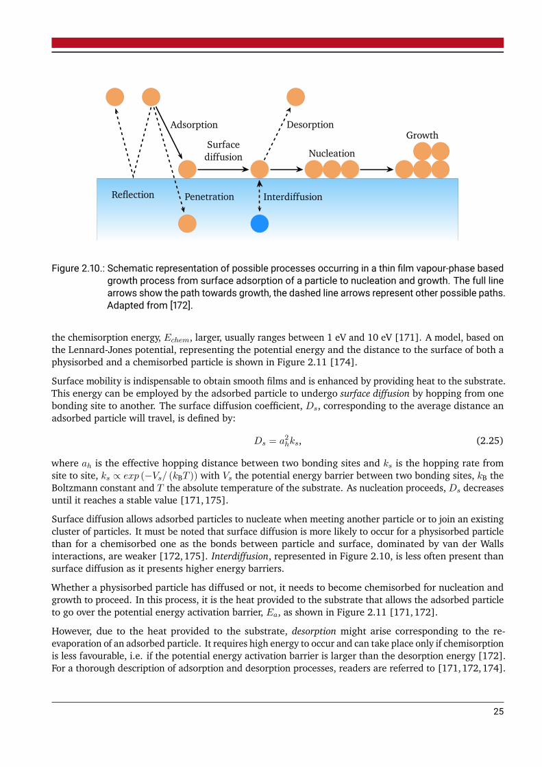
Nucleation
Growth
Reflection
Adsorption
Penetration
Surfacediffusion
Interdiffusion
Desorption
Figure 2.10.: Schematic representation of possible processes occurring in a thin film vapour-phase basedgrowth process from surface adsorption of a particle to nucleation and growth. The full linearrows show the path towards growth, the dashed line arrows represent other possible paths.Adapted from [172].
the chemisorption energy, Echem, larger, usually ranges between 1 eV and 10 eV [171]. A model, based onthe Lennard-Jones potential, representing the potential energy and the distance to the surface of both aphysisorbed and a chemisorbed particle is shown in Figure 2.11 [174].
Surface mobility is indispensable to obtain smooth films and is enhanced by providing heat to the substrate.This energy can be employed by the adsorbed particle to undergo surface diffusion by hopping from onebonding site to another. The surface diffusion coefficient, Ds, corresponding to the average distance anadsorbed particle will travel, is defined by:
Ds = a2hks, (2.25)
where ah is the effective hopping distance between two bonding sites and ks is the hopping rate fromsite to site, ks ∝ exp (−Vs/ (kBT )) with Vs the potential energy barrier between two bonding sites, kB theBoltzmann constant and T the absolute temperature of the substrate. As nucleation proceeds, Ds decreasesuntil it reaches a stable value [171,175].
Surface diffusion allows adsorbed particles to nucleate when meeting another particle or to join an existingcluster of particles. It must be noted that surface diffusion is more likely to occur for a physisorbed particlethan for a chemisorbed one as the bonds between particle and surface, dominated by van der Wallsinteractions, are weaker [172,175]. Interdiffusion, represented in Figure 2.10, is less often present thansurface diffusion as it presents higher energy barriers.
Whether a physisorbed particle has diffused or not, it needs to become chemisorbed for nucleation andgrowth to proceed. In this process, it is the heat provided to the substrate that allows the adsorbed particleto go over the potential energy activation barrier, Ea, as shown in Figure 2.11 [171,172].
However, due to the heat provided to the substrate, desorption might arise corresponding to the re-evaporation of an adsorbed particle. It requires high energy to occur and can take place only if chemisorptionis less favourable, i.e. if the potential energy activation barrier is larger than the desorption energy [172].For a thorough description of adsorption and desorption processes, readers are referred to [171,172,174].
25
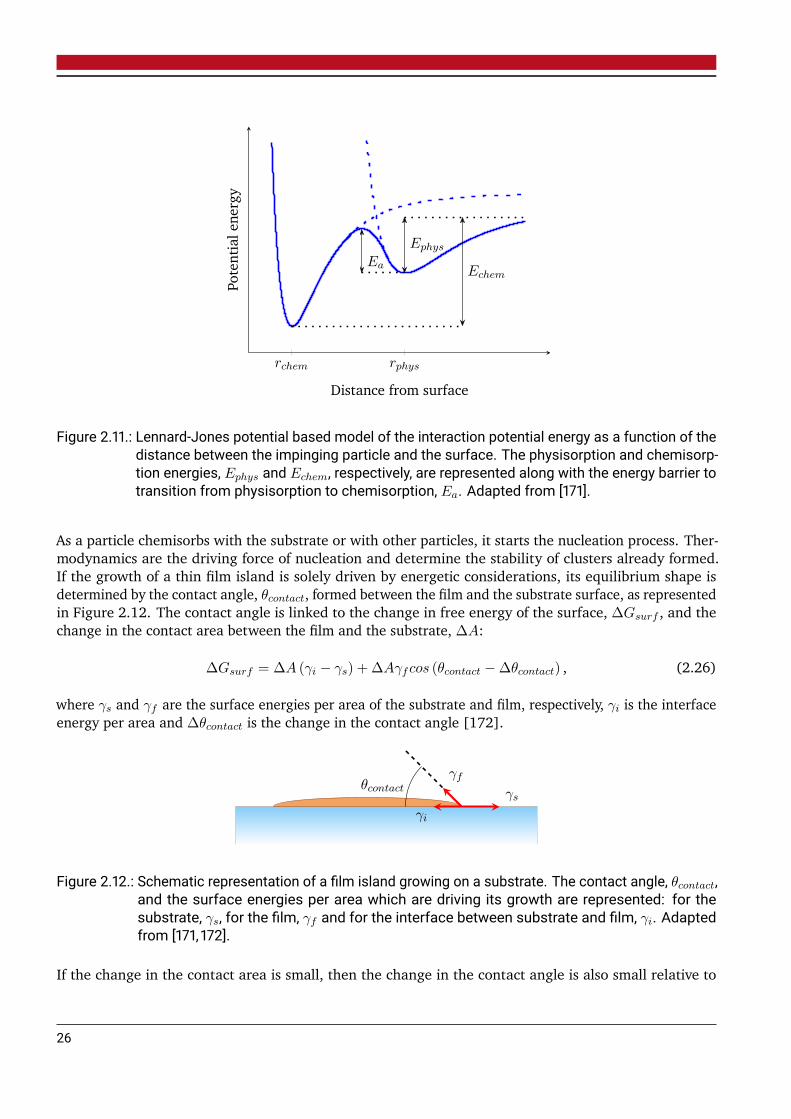
rchem rphys
Ephys
EchemEa
Distance from surface
Potentiale
nergy
Figure 2.11.: Lennard-Jones potential based model of the interaction potential energy as a function of thedistance between the impinging particle and the surface. The physisorption and chemisorp-tion energies, Ephys and Echem, respectively, are represented along with the energy barrier totransition from physisorption to chemisorption, Ea. Adapted from [171].
As a particle chemisorbs with the substrate or with other particles, it starts the nucleation process. Ther-modynamics are the driving force of nucleation and determine the stability of clusters already formed.If the growth of a thin film island is solely driven by energetic considerations, its equilibrium shape isdetermined by the contact angle, θcontact, formed between the film and the substrate surface, as representedin Figure 2.12. The contact angle is linked to the change in free energy of the surface, ∆Gsurf , and thechange in the contact area between the film and the substrate, ∆A:
∆Gsurf = ∆A (γi − γs) + ∆Aγfcos (θcontact −∆θcontact) , (2.26)
where γs and γf are the surface energies per area of the substrate and film, respectively, γi is the interfaceenergy per area and ∆θcontact is the change in the contact angle [172].
γs
γi
γfθcontact
Figure 2.12.: Schematic representation of a film island growing on a substrate. The contact angle, θcontact,and the surface energies per area which are driving its growth are represented: for thesubstrate, γs, for the film, γf and for the interface between substrate and film, γi. Adaptedfrom [171, 172].
If the change in the contact area is small, then the change in the contact angle is also small relative to
26
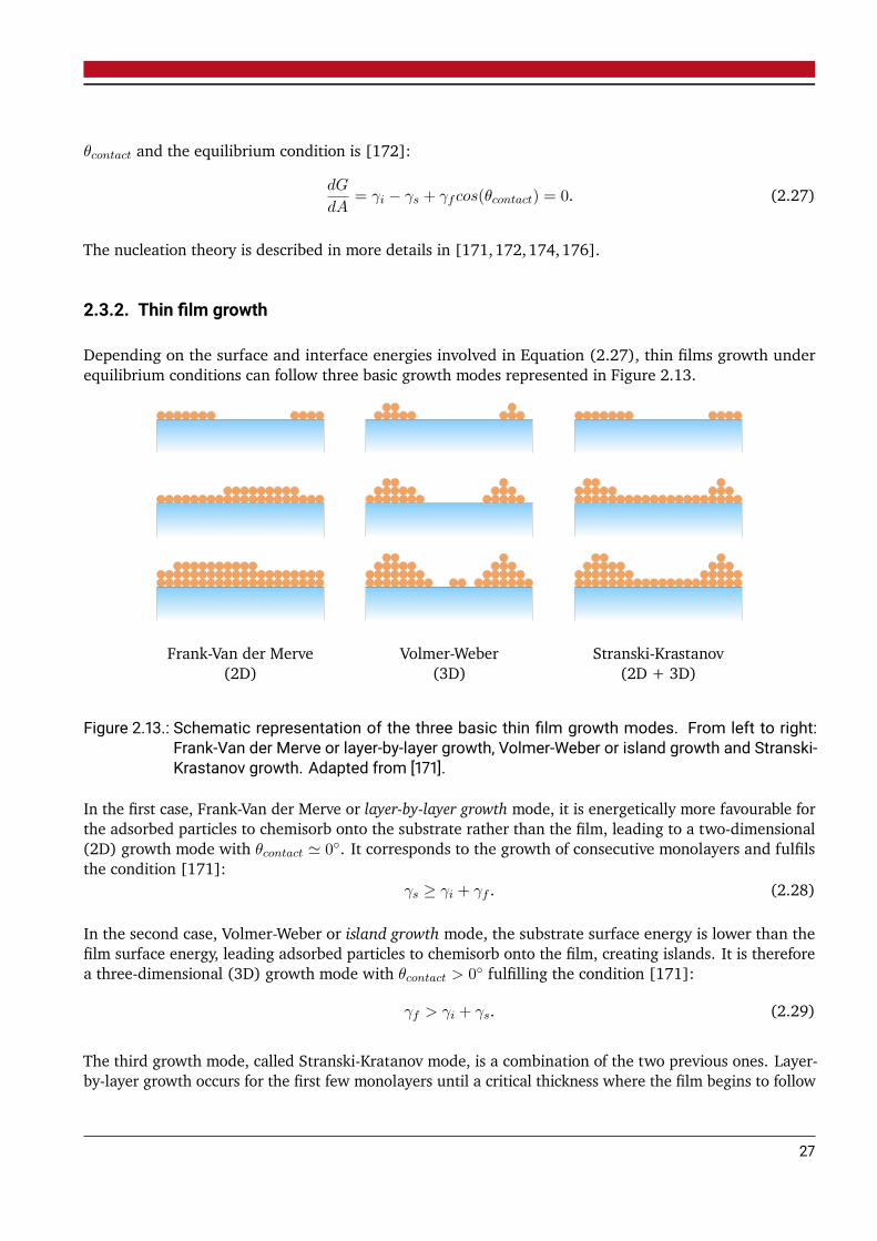
θcontact and the equilibrium condition is [172]:
dG
dA= γi − γs + γfcos(θcontact) = 0. (2.27)
The nucleation theory is described in more details in [171,172,174,176].
2.3.2. Thin film growth
Depending on the surface and interface energies involved in Equation (2.27), thin films growth underequilibrium conditions can follow three basic growth modes represented in Figure 2.13.
Frank-Van der Merve(2D)
Volmer-Weber(3D)
Stranski-Krastanov(2D + 3D)
Figure 2.13.: Schematic representation of the three basic thin film growth modes. From left to right:Frank-Van der Merve or layer-by-layer growth, Volmer-Weber or island growth and Stranski-Krastanov growth. Adapted from [171].
In the first case, Frank-Van der Merve or layer-by-layer growth mode, it is energetically more favourable forthe adsorbed particles to chemisorb onto the substrate rather than the film, leading to a two-dimensional(2D) growth mode with θcontact ≃ 0. It corresponds to the growth of consecutive monolayers and fulfilsthe condition [171]:
γs ≥ γi + γf . (2.28)
In the second case, Volmer-Weber or island growth mode, the substrate surface energy is lower than thefilm surface energy, leading adsorbed particles to chemisorb onto the film, creating islands. It is thereforea three-dimensional (3D) growth mode with θcontact > 0 fulfilling the condition [171]:
γf > γi + γs. (2.29)
The third growth mode, called Stranski-Kratanov mode, is a combination of the two previous ones. Layer-by-layer growth occurs for the first few monolayers until a critical thickness where the film begins to follow
27
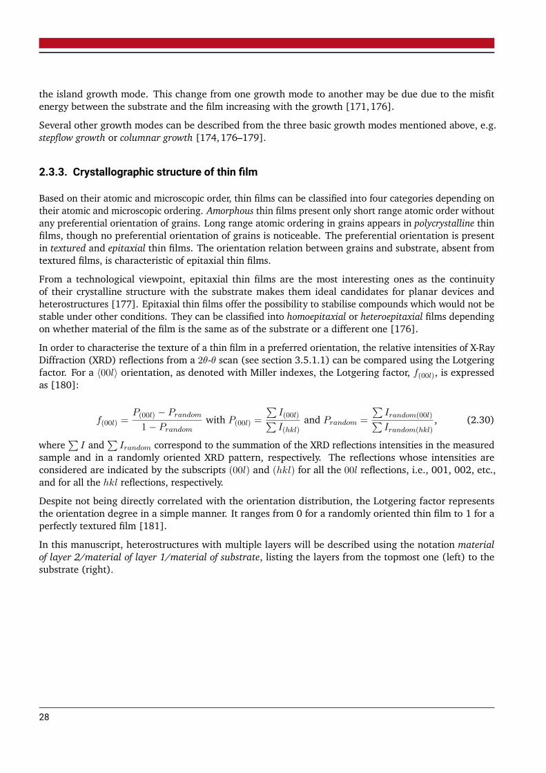
the island growth mode. This change from one growth mode to another may be due due to the misfitenergy between the substrate and the film increasing with the growth [171,176].
Several other growth modes can be described from the three basic growth modes mentioned above, e.g.stepflow growth or columnar growth [174,176–179].
2.3.3. Crystallographic structure of thin film
Based on their atomic and microscopic order, thin films can be classified into four categories depending ontheir atomic and microscopic ordering. Amorphous thin films present only short range atomic order withoutany preferential orientation of grains. Long range atomic ordering in grains appears in polycrystalline thinfilms, though no preferential orientation of grains is noticeable. The preferential orientation is presentin textured and epitaxial thin films. The orientation relation between grains and substrate, absent fromtextured films, is characteristic of epitaxial thin films.
From a technological viewpoint, epitaxial thin films are the most interesting ones as the continuityof their crystalline structure with the substrate makes them ideal candidates for planar devices andheterostructures [177]. Epitaxial thin films offer the possibility to stabilise compounds which would not bestable under other conditions. They can be classified into homoepitaxial or heteroepitaxial films dependingon whether material of the film is the same as of the substrate or a different one [176].
In order to characterise the texture of a thin film in a preferred orientation, the relative intensities of X-RayDiffraction (XRD) reflections from a 2θ-θ scan (see section 3.5.1.1) can be compared using the Lotgeringfactor. For a ⟨00l⟩ orientation, as denoted with Miller indexes, the Lotgering factor, f(00l), is expressedas [180]:
f(00l) =P(00l) − Prandom
1− Prandomwith P(00l) =
∑I(00l)∑I(hkl)
and Prandom =
∑Irandom(00l)∑Irandom(hkl)
, (2.30)
where∑
I and∑
Irandom correspond to the summation of the XRD reflections intensities in the measuredsample and in a randomly oriented XRD pattern, respectively. The reflections whose intensities areconsidered are indicated by the subscripts (00l) and (hkl) for all the 00l reflections, i.e., 001, 002, etc.,and for all the hkl reflections, respectively.
Despite not being directly correlated with the orientation distribution, the Lotgering factor representsthe orientation degree in a simple manner. It ranges from 0 for a randomly oriented thin film to 1 for aperfectly textured film [181].
In this manuscript, heterostructures with multiple layers will be described using the notation materialof layer 2/material of layer 1/material of substrate, listing the layers from the topmost one (left) to thesubstrate (right).
28
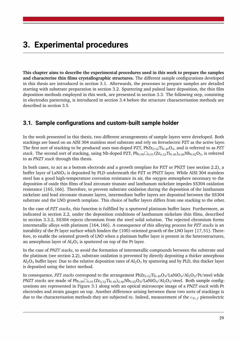
3. Experimental procedures
This chapter aims to describe the experimental procedures used in this work to prepare the samplesand characterise thin films crystallographic structures. The different sample configurations developedin this thesis are introduced in section 3.1. Afterwards, the processes to prepare samples are detailedstarting with substrate preparation in section 3.2. Sputtering and pulsed laser deposition, the thin filmdeposition methods employed in this work, are presented in section 3.3. The following step, consistingin electrodes patterning, is introduced in section 3.4 before the structure characterisation methods aredescribed in section 3.5.
3.1. Sample configurations and custom-built sample holder
In the work presented in this thesis, two different arrangements of sample layers were developed. Bothstackings are based on an AISI 304 stainless steel substrate and rely on ferroelectric PZT as the active layer.The first sort of stacking to be produced uses non-doped PZT, PbZr0.52Ti0.48O3, and is referred to as PZTstack. The second sort of stacking, using Nb-doped PZT, Pb0.990.01(Zr0.52Ti0.48)0.98Nb0.02O3, is referredto as PNZT stack through this thesis.
In both cases, to act as a bottom electrode and a growth template for PZT or PNZT (see section 2.2), abuffer layer of LaNiO3 is deposited by PLD underneath the PZT or PNZT layer. While AISI 304 stainlesssteel has a good high-temperature corrosion resistance in air, the oxygen atmosphere necessary to thedeposition of oxide thin films of lead zirconate titanate and lanthanum nickelate impedes SS304 oxidationresistance [165,166]. Therefore, to prevent substrate oxidation during the deposition of the lanthanumnickelate and lead zirconate titanate layers, intermediate buffer layers are deposited between the SS304substrate and the LNO growth template. This choice of buffer layers differs from one stacking to the other.
In the case of PZT stacks, this function is fulfilled by a sputtered platinum buffer layer. Furthermore, asindicated in section 2.2, under the deposition conditions of lanthanum nickelate thin films, describedin section 3.3.2, SS304 rejects chromium from the steel solid solution. The rejected chromium formsintermetallic alloys with platinum [164,166]. A consequence of this alloying process for PZT stacks is aninstability of the Pt layer surface which hinders the 100-oriented growth of the LNO layer [17,51]. There-fore, to enable the oriented growth of LNO when a platinum buffer layer is present in the heterostructures,an amorphous layer of Al2O3 is sputtered on top of the Pt layer.
In the case of PNZT stacks, to avoid the formation of intermetallic compounds between the substrate andthe platinum (see section 2.2), substrate oxidation is prevented by directly depositing a thicker amorphousAl2O3 buffer layer. Due to the relative deposition rates of Al2O3 by sputtering and by PLD, this thicker layeris deposited using the latter method.
In consequence, PZT stacks correspond to the arrangement PbZr0.52Ti0.48O3/LaNiO3/Al2O3/Pt/steel whilePNZT stacks are made of Pb0.990.01(Zr0.52Ti0.48)0.98Nb0.02O3/LaNiO3/Al2O3/steel. Both sample config-urations are represented in Figure 3.1 along with an optical microscope image of a PNZT stack with Ptelectrodes and strain gauges on top. Another difference arising between these two sorts of stackings isdue to the characterisation methods they are subjected to. Indeed, measurement of the e31,f piezoelectric
29
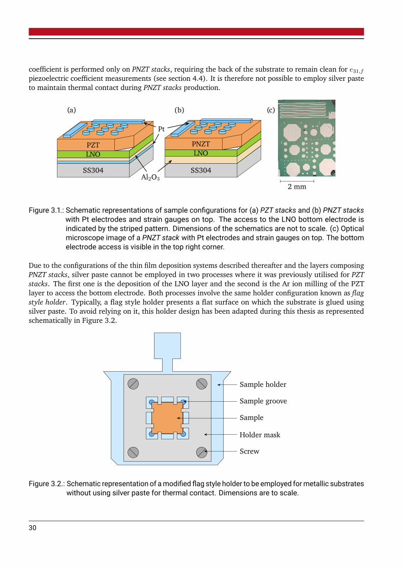
coefficient is performed only on PNZT stacks, requiring the back of the substrate to remain clean for e31,fpiezoelectric coefficient measurements (see section 4.4). It is therefore not possible to employ silver pasteto maintain thermal contact during PNZT stacks production.
SS304 SS304
Pt
Al2O3
LNO LNOPZT PNZT
2 mm
(a) (b) (c)
Figure 3.1.: Schematic representations of sample configurations for (a) PZT stacks and (b) PNZT stackswith Pt electrodes and strain gauges on top. The access to the LNO bottom electrode isindicated by the striped pattern. Dimensions of the schematics are not to scale. (c) Opticalmicroscope image of a PNZT stack with Pt electrodes and strain gauges on top. The bottomelectrode access is visible in the top right corner.
Due to the configurations of the thin film deposition systems described thereafter and the layers composingPNZT stacks, silver paste cannot be employed in two processes where it was previously utilised for PZTstacks. The first one is the deposition of the LNO layer and the second is the Ar ion milling of the PZTlayer to access the bottom electrode. Both processes involve the same holder configuration known as flagstyle holder. Typically, a flag style holder presents a flat surface on which the substrate is glued usingsilver paste. To avoid relying on it, this holder design has been adapted during this thesis as representedschematically in Figure 3.2.
Sample holder
Sample groove
Sample
Holder mask
Screw
Figure 3.2.: Schematic representation of amodified flag style holder to be employed formetallic substrateswithout using silver paste for thermal contact. Dimensions are to scale.
30
The flag style holder is modified by manufacturing a groove to partially fit the sample within the holder.The substrate being metallic, it is considered that this configuration should provide sufficient thermalcontact. The sample is maintained in contact with the modified holder by a mask reaching in front ofthe substrate and screwed in the sample holder. The mask design aims to cover a minimal surface of thesample to leave a sufficiently large area for the patterning of top electrodes. Furthermore, the mask designdoes not cover the sample corners where the bottom electrodes must be contacted, requiring the LNO layerto be deposited in the sample corners.
It should be noted that the absence of silver paste on the back of PNZT stacks lead to some oxidation of theSS304 substrates during the deposition processes. Therefore, to prevent oxidation, 30 nm of platinumare sputtered on the back of the substrates of PNZT stacks. This procedure has no impact on the polishedside of the substrate were the thin films are deposited. The sputtering is performed according to the sameprocess as described in section 3.3.1.
3.2. Substrate preparation
Substrates are produced from commercially available cold-rolled AISI 304 stainless steel sheets. A thicknessof 0.2 mm was arbitrarily chosen for proof-of-concept of the growth of tetragonal 001-textured PZTfilms on stainless steel while permitting some flexibility of the substrate for piezoelectric applications.As a preliminary step, the metal sheets are laser cut into 30 × 30 mm2 pieces by the workshop of theDepartment of Electrical Engineering and Information Technology of the Technische Universität Darmstadt.To transform these metal pieces into substrates, they undergo dicing, lapping, polishing and cleaning, asdescribed in the following sections.
3.2.1. Substrate dicing
The dicing of AISI 304 stainless steel is performed using a Microace 3 dicing saw by Loadpoint (Swindon,UK). The dicing saw is equipped with a resin bonded blade and operated at 10,000 rpm. The produced5× 5 mm2 SS304 pieces are hereby referred to as substrates.
3.2.2. Substrate lapping and polishing
The average roughness of as-bought SS304 is measured by a Dektak XT profilometer by Bruker (Billerica,MA, USA) at 189 nm with a standard deviation of 236 nm. Such roughness, larger than or in the order ofmagnitude of thin films thickness, must be reduced to permit the growth of textured thin films. Therefore,diced substrates are lapped and subsequently mechanically polished using a PM5 Precision Lapping &Polishing Machine by Logitech (Glasgow, UK).
For these processes, the metallic substrates are glued by batches of 9 samples on a circular glass carrierplate using Crystalbond 509 by Aremco (Valley Cottage, NY, USA) adhesive. A minimal amount of adhesiveis used in order to maintain the substrates parallel to the glass carrier. To ensure optimal adhesion duringthe lapping and polishing processes, the substrates are pressed onto the glass carrier before the adhesivecools down.
31
The substrates are lapped using a slurry of calcined Al2O3. The 3 µm particles are diluted into deionisedwater with a ratio of 200 mL of Al2O3 powder for 1.5 L of solvent. The lapping is carried out with anaverage jig load of 2 kg applied over a batch of 9 samples of 5 × 5 mm2 at a speed of 5 rpm for about100 minutes. The lapping time is adjusted by visual inspection of the sample through the process.
Once lapped, the substrates are polished using SF1 Polishing Fluid by Logitech (Glasgow, UK) containingamorphous SiO2 particles with a size of 32 nm. The process is performed with an average jig load of 2 kgapplied over a batch of 9 samples of 5× 5 mm2 at a speed of 30 rpm for 150 to 240 minutes. The polishingtime is adjusted by visual inspection of the sample through the process to ensure the whole surface ofeach substrate is polished. In order to clean off the majority of the slurry, the substrates are rinsed withdeionised water before being removed from the glass carrier. Further cleaning procedures are described inthe following section.
After polishing, the substrate thicknesses are of 0.16 mm to 0.18 mm while their average roughnessesand standard deviations are reduced to 3 nm and 4 nm, respectively. This lowered roughness comparedto as-bought SS304 is important to promote 100 texture of the LNO layer and, therefore, of the PZTlayer [17,51].
3.2.3. Substrate cleaning
The first step of the substrate cleaning process consists in removing from the substrates any slurry left overfrom the polishing. For this purpose, wearing latex gloves, the SS304 pieces are washed individually byrubbing them between fingers with detergent. Substrates are then rinsed thoroughly with deionised waterand dried with nitrogen gas. The process is repeated until no traces of slurry remain on substrates.
Afterwards, in order to remove both polar and non-polar molecules from substrates, they are cleanedsuccessively in aceton (99.8 %, Roth) and isopropyl alcohol (99.5 %, Roth) for 30 minutes each with anultrasonic bath Transsonic Digital 3 by Elma (Singen, Germany). After each bath, substrates are dried withnitrogen gas. The use of an ultrasonic bath allows for a better impurity removal from substrate surfacesdue to the cavitation phenomenon.
After storage, shortly before the thin film deposition process begins, substrate surfaces are cleaned againusing an ultrasonic bath with successively aceton (99.8 %, Roth) and isopropyl alcohol (99.5 %, Roth) for10 minutes each. After each bath, substrates are dried with nitrogen gas.
3.3. Thin film deposition methods
Through this thesis, several thin film deposition methods are utilised, depending on the nature of the layerto be grown. DC magnetron sputtering and RF magnetron sputtering are employed to deposit layers ofplatinum and aluminium oxide, respectively. It should be noted that Al2O3 was also grown by PLD alongwith lanthanum nickelate and lead zirconate titanate thin films.
3.3.1. DC and RF magnetron sputtering
Sputtering is a technique suitable for industrial scale, large-area deposition of both elemental and compoundmaterials. Depending on the experimental setup, conducting or insulating materials can be deposited [182].
32
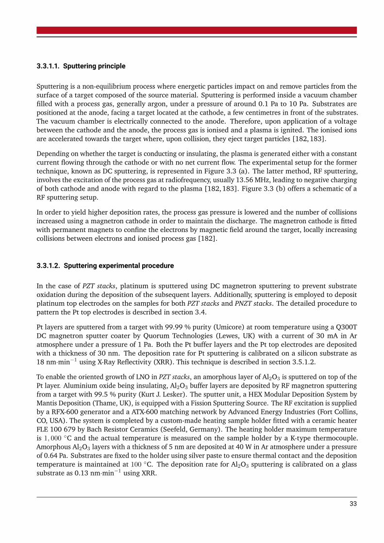
3.3.1.1. Sputtering principle
Sputtering is a non-equilibrium process where energetic particles impact on and remove particles from thesurface of a target composed of the source material. Sputtering is performed inside a vacuum chamberfilled with a process gas, generally argon, under a pressure of around 0.1 Pa to 10 Pa. Substrates arepositioned at the anode, facing a target located at the cathode, a few centimetres in front of the substrates.The vacuum chamber is electrically connected to the anode. Therefore, upon application of a voltagebetween the cathode and the anode, the process gas is ionised and a plasma is ignited. The ionised ionsare accelerated towards the target where, upon collision, they eject target particles [182,183].
Depending on whether the target is conducting or insulating, the plasma is generated either with a constantcurrent flowing through the cathode or with no net current flow. The experimental setup for the formertechnique, known as DC sputtering, is represented in Figure 3.3 (a). The latter method, RF sputtering,involves the excitation of the process gas at radiofrequency, usually 13.56 MHz, leading to negative chargingof both cathode and anode with regard to the plasma [182,183]. Figure 3.3 (b) offers a schematic of aRF sputtering setup.
In order to yield higher deposition rates, the process gas pressure is lowered and the number of collisionsincreased using a magnetron cathode in order to maintain the discharge. The magnetron cathode is fittedwith permanent magnets to confine the electrons by magnetic field around the target, locally increasingcollisions between electrons and ionised process gas [182].
3.3.1.2. Sputtering experimental procedure
In the case of PZT stacks, platinum is sputtered using DC magnetron sputtering to prevent substrateoxidation during the deposition of the subsequent layers. Additionally, sputtering is employed to depositplatinum top electrodes on the samples for both PZT stacks and PNZT stacks. The detailed procedure topattern the Pt top electrodes is described in section 3.4.
Pt layers are sputtered from a target with 99.99 % purity (Umicore) at room temperature using a Q300TDC magnetron sputter coater by Quorum Technologies (Lewes, UK) with a current of 30 mA in Aratmosphere under a pressure of 1 Pa. Both the Pt buffer layers and the Pt top electrodes are depositedwith a thickness of 30 nm. The deposition rate for Pt sputtering is calibrated on a silicon substrate as18 nm·min−1 using X-Ray Reflectivity (XRR). This technique is described in section 3.5.1.2.
To enable the oriented growth of LNO in PZT stacks, an amorphous layer of Al2O3 is sputtered on top of thePt layer. Aluminium oxide being insulating, Al2O3 buffer layers are deposited by RF magnetron sputteringfrom a target with 99.5 % purity (Kurt J. Lesker). The sputter unit, a HEX Modular Deposition System byMantis Deposition (Thame, UK), is equipped with a Fission Sputtering Source. The RF excitation is suppliedby a RFX-600 generator and a ATX-600 matching network by Advanced Energy Industries (Fort Collins,CO, USA). The system is completed by a custom-made heating sample holder fitted with a ceramic heaterFLE 100 679 by Bach Resistor Ceramics (Seefeld, Germany). The heating holder maximum temperatureis 1, 000 C and the actual temperature is measured on the sample holder by a K-type thermocouple.Amorphous Al2O3 layers with a thickness of 5 nm are deposited at 40 W in Ar atmosphere under a pressureof 0.64 Pa. Substrates are fixed to the holder using silver paste to ensure thermal contact and the depositiontemperature is maintained at 100 C. The deposition rate for Al2O3 sputtering is calibrated on a glasssubstrate as 0.13 nm·min−1 using XRR.
33
Ar
N2
Exhaust
−+ DC
Mass flowcontroller
InsulatorCathode South pole
Cathode North pole
Target (conducting)Magnetic field
Ar plasma
SubstrateAnode
Ar
N2
Exhaust
Matchingnetwork
RFgenerator
Mass flowcontroller
Insulator
Cathode North pole
Cathode South pole Target (insulating)Magnetic field
Ar plasma
SubstrateAnodeHeater
(a)
(b)
Figure 3.3.: Schematic representation of a sputtering chamber for (a) DC magnetron sputtering and(b) RF magnetron sputtering.
34
3.3.2. Pulsed laser deposition
Interest for pulsed laser deposition (PLD) as a physical vapour deposition technique started in earnest inthe late 1980s after the successful deposition of epitaxial high temperature superconducting thin films.PLD allows the deposition of thin films with several cations in stoichiometric conditions, notably metals,semiconductors, polymers or biological materials [184, 185]. PLD offers the possibility to synthesisemetastable materials and can be combined with reflective high energy electron diffraction to monitor thinfilm growth in situ, making it a widely used technique for research purposes, in particular to grow oxidethin films [186–188].
3.3.2.1. PLD principle
Performed between 10−7 Pa and 100 Pa, the PLD process relies upon a pulsed laser ablating material froma target and the material subsequent deposition on a substrate. Each laser pulse ablates a small amountof material, creating a forward-directed plume, providing a material flux for thin film growth, in mostlystoichiometric conditions with regard to the target [184,185].
Upon incidence of a laser beam on a material, two concurrent processes might occur: thermal evaporationand non-thermal ablation. The former is an equilibrium process which occurs when the laser energyabsorbed by the target is not sufficiently high. It leads to non-stoichiometric transfer of material to theplume and should be avoided during PLD. The latter is an out-of-equilibrium process accessible at energyabove an ablation threshold when the optical penetration depth of the laser beam in the target material islonger than the heat diffusion length [186–190].
The pulse energy density is quantified by the laser fluence, εlaser corresponding to the time integral of thelaser energy intensity per surface unit over the pulse duration and expressed by [190]:
εlaser =Elaser
Aspot, (3.1)
where Elaser is the laser energy reaching the target and Aspot is the laser spot size. Both the target ablationrate and the film growth rate, usually of 0.001 Å to 1 Å per laser pulse, are dependent on the fluence [184].
In order to control the fluence through the laser energy and spot size, a series of optics must be employedbetween the laser and the deposition chamber. Typically, the setup is composed of an optical attenuator toadjust the laser pulse energy and a telescope to change the beam cross-section from rectangular to square.These devices are followed by a field lens to focus the laser beam towards the objective lens, an aperture,several mirrors to guide the beam towards the PLD chamber, an objective lens to focus the laser beam onthe target, and an entrance window [184,190,191].
To obtain a homogeneous deposition, the ablation plume must be symmetric. It is the case on a flat targetsurface where the plume follows a cosnlaser(θtarget) distribution where nlaser depends on the laser spot sizeand θtarget is the angle to the target normal. However, repetitive ablation creates a trench on the targetsurface and plume inhomogeneity, modifying its stoichiometry. Trenching can be avoided by scanning thelaser on the target surface or by sweeping and rotating the target, which is often preferred [184,185,192].
Targets for PLD processes must have a high optical absorption coefficient at the chosen laser wavelengthfor the ablation process to be efficient. The cations stoichiometry provided by one or several targets mustbe identical to that of the film due to the mainly stoichiometric transfer of cations from the target to the
35

plume through the ablation process [184, 185]. However, recent literature indicates the possibility ofoff-stoichiometry cations transfer from target to thin film, notably in perovskite structures, which couldrequire to adjust target stoichiometry [193,194]. To limit the amount of particles or droplets ejected fromthe target during the ablation process and deposited on the substrate, target density must be high. In thecase of polycrystalline targets, made from bulk polycrystalline oxides, their density must be superior to atleast 80 % of the single crystal density [184,185].
To promote nucleation and growth of homogeneous layers, surface diffusion of atomic species must beenhanced through heating of the substrate. This is done from the substrate back side, notably by meansof resistive-type heaters or infrared (IR) laser diodes. Inexpensive, robust and reliable, resistive-typeheaters can be used for temperatures up to 950 C but require the utilisation of silver or platinum pasteto fix the substrate to the heating block, limiting uniform heating of large substrates. Fast and reliable,IR laser diodes are limited to small area substrates due to the laser beam size but can be scanned on thesubstrate back to make heating uniform. Deposition temperature can be monitored via a thermocouple ora pyrometer. The former is less reliable than the latter, however, it can be used with substrates transparentto IR [191].
As mentioned above, PLD can be performed at 10−7 Pa, in ultra-high vacuum. However, most of the time,a background gas is required both as a reactive specie and to decrease the kinetic energy of the ablatedspecies which may damage the deposited film upon impingement with its surface. The most commonlyused background gases are oxygen, argon or nitrogen. When employed as reactive species, the requiredquantity of gases depends on thermodynamics. Furthermore, it should be noted that post-depositiondesorption from the film at high temperatures can be limited by high pressures [184,185,195].
3.3.2.2. PLD experimental systems
In the course of this work, four different thin film materials have been deposited by PLD: Al2O3, LaNiO3,PbZr0.52Ti0.48O3 and Pb0.990.01(Zr0.52Ti0.48)0.98Nb0.02O3. At the exception of LNO, these materials aredeposited in a custom-built PLD system known as small PLD. Equipped with a quartz deposition chamberthat can be exchanged between different materials, it allows to deposit materials with volatile compounds,e.g. PbO, without risking cross-contamination of other samples. However, due to the geometry of the laserbeam optical path, the accessible fluence is limited and hinders the deposition of LNO. To remedy to thisaspect, the LaNiO3 layer is deposited in another custom-made PLD system, part of the DAISY-BAT system(DArmstadt Integrated SYstem for BATtery research) known as Daisy-Bat PLD.
A schematic representation of the small PLD system can be found in Figure 3.4. Due to the many similaritiesbetween the two systems and the utilisation of the second one being limited to the deposition of LNOlayers, a schematic of the Daisy-Bat PLD is not provided. Instead, differences between the two PLD systemsare described thereafter.
The small PLD and the Daisy-Bat PLD are equipped, respectively, with COMPex 205 and LPXpro 210 FKrF excimer lasers with a wavelength λ = 248 nm by Coherent (Santa Clara, CA, USA). The laser pulsesduration are shorter than 30 ns to minimise heat diffusion in the target. For both PLD systems, the laserenergy is measured using a FieldMaxII energy meter coupled to an Excimer Laser EnergyMax Sensor, bothby Coherent.
The small PLD deposition chamber is made of quartz and can be pumped down to approximately 10−3 Pa.Its pressure is monitored by a hot ion vacuum gauge BPG400 by Inficon (Bad Ragaz, Switzerland). Incomparison, the Daisy-Bat PLD stainless steel spherical deposition chamber can be pumped down to
36
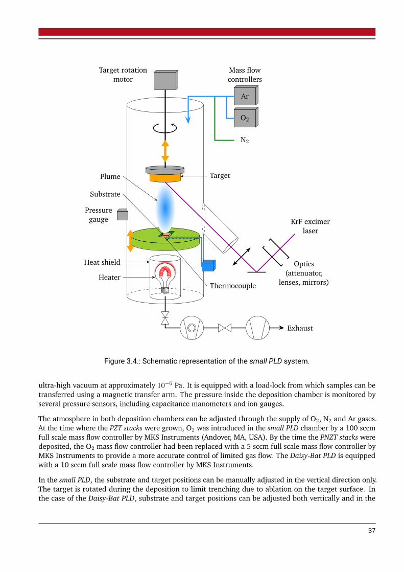
Ar
O2
N2
Optics(attenuator,
lenses, mirrors)
KrF excimerlaser
Exhaust
Mass flowcontrollers
Target rotationmotor
Pressuregauge
Thermocouple
TargetPlume
Substrate
Heater
Heat shield
Figure 3.4.: Schematic representation of the small PLD system.
ultra-high vacuum at approximately 10−6 Pa. It is equipped with a load-lock from which samples can betransferred using a magnetic transfer arm. The pressure inside the deposition chamber is monitored byseveral pressure sensors, including capacitance manometers and ion gauges.
The atmosphere in both deposition chambers can be adjusted through the supply of O2, N2 and Ar gases.At the time where the PZT stacks were grown, O2 was introduced in the small PLD chamber by a 100 sccmfull scale mass flow controller by MKS Instruments (Andover, MA, USA). By the time the PNZT stacks weredeposited, the O2 mass flow controller had been replaced with a 5 sccm full scale mass flow controller byMKS Instruments to provide a more accurate control of limited gas flow. The Daisy-Bat PLD is equippedwith a 10 sccm full scale mass flow controller by MKS Instruments.
In the small PLD, the substrate and target positions can be manually adjusted in the vertical direction only.The target is rotated during the deposition to limit trenching due to ablation on the target surface. Inthe case of the Daisy-Bat PLD, substrate and target positions can be adjusted both vertically and in the
37
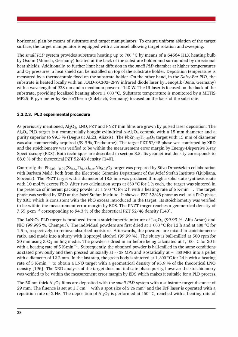
horizontal plan by means of substrate and target manipulators. To ensure uniform ablation of the targetsurface, the target manipulator is equipped with a carousel allowing target rotation and sweeping.
The small PLD system provides substrate heating up to 700 C by means of a 64664 HLX heating bulbby Osram (Munich, Germany) located at the back of the substrate holder and surrounded by directionalheat shields. Additionally, to further limit heat diffusion in the small PLD chamber at higher temperaturesand O2 pressures, a heat shield can be installed on top of the substrate holder. Deposition temperature ismeasured by a thermocouple fixed on the substrate holder. On the other hand, in the Daisy-Bat PLD, thesubstrate is heated locally with an JOLD-x-CPXF-2PW infrared diode laser by Jenoptik (Jena, Germany)with a wavelength of 938 nm and a maximum power of 140 W. The IR laser is focused on the back of thesubstrate, providing localised heating above 1, 000 C. Substrate temperature is monitored by a METISMP25 IR pyrometer by SensorTherm (Sulzbach, Germany) focused on the back of the substrate.
3.3.2.3. PLD experimental procedure
As previously mentioned, Al2O3, LNO, PZT and PNZT thin films are grown by pulsed laser deposition. TheAl2O3 PLD target is a commercially bought cylindrical α-Al2O3 ceramic with a 15 mm diameter and apurity superior to 99.5 % (Degussit AL23, Aliaxis). The PbZr0.52Ti0.48O3 target with 15 mm of diameterwas also commercially acquired (99.9 %, Testbourne). The target PZT 52/48 phase was confirmed by XRDand the stoichiometry was verified to be within the measurement error margin by Energy-Dispersive X-raySpectroscopy (EDS). Both techniques are described in section 3.5. Its geometrical density corresponds to88.0 % of the theoretical PZT 52/48 density [140].
Contrarily, the Pb0.990.01(Zr0.52Ti0.48)0.98Nb0.02O3 target was prepared by Silvo Drnovšek in collaborationwith Barbara Malič, both from the Electronic Ceramics Department of the Jožef Stefan Institute (Ljubljana,Slovenia). The PNZT target with a diameter of 18.5 mm was produced through a solid state synthesis routewith 10 mol.% excess PbO. After two calcination steps at 850 C for 1 h each, the target was sintered inthe presence of inherent packing powder at 1, 200 C for 2 h with a heating rate of 5 K·min−1. The targetphase was verified by XRD at the Jožef Stefan Institute. It shows a PZT 52/48 phase as well as a PbO phaseby XRD which is consistent with the PbO excess introduced in the target. Its stoichiometry was verifiedto be within the measurement error margin by EDS. The PNZT target reaches a geometrical density of7.55 g·cm−3 corresponding to 94.3 % of the theoretical PZT 52/48 density [140].
The LaNiO3 PLD target is produced from a stoichiometric mixture of La2O3 (99.99 %, Alfa Aesar) andNiO (99.995 %, Chempur). The individual powders are first dried at 1, 000 C for 12 h and at 400 C for1.5 h, respectively, to remove absorbed moisture. Afterwards, the powders are mixed in stoichiometricratio, and made into a slurry with isopropyl alcohol (99.99 %). The slurry is ball-milled at 500 rpm for30 min using ZrO2 milling media. The powder is dried in air before being calcinated at 1, 100 C for 20 hwith a heating rate of 5 K·min−1. Subsequently, the obtained powder is ball-milled in the same conditionsas stated previously and then pressed uniaxially at ∼ 28 MPa and isostatically at ∼ 360 MPa into a pelletwith a diameter of 12.2 mm. In the last step, the green body is sintered at 1, 300 C for 24 h with a heatingrate of 5 K·min−1 to obtain a LNO target with a geometrical density of 95.9 % of the theoretical LNOdensity [196]. The XRD analysis of the target does not indicate phase purity, however the stoichiometrywas verified to be within the measurement error margin by EDS which makes it suitable for a PLD process.
The 50 nm thick Al2O3 films are deposited with the small PLD system with a substrate-target distance of29 mm. The fluence is set at 1 J·cm−1 with a spot size of 2.26 mm2 and the KrF laser is operated with arepetition rate of 2 Hz. The deposition of Al2O3 is performed at 150 C, reached with a heating rate of
38

50 K·min−1, under 3 Pa of O2 and a flow of 1.6 sccm of O2. The oxygen pressure is maintained duringthe sample cooling down at 30 K·min−1. The deposition rate for Al2O3 by PLD is calibrated on a glasssubstrate as 10 nm per 1,000 pulses using XRR (see section 3.5.1.2).
The LNO thin films are grown using the Daisy-Bat PLD with a substrate-target distance of 40 mm. Asmentioned in section 3.1, the samples for PZT stacks are fixed onto a flag style holder with silver paste whilethe samples for PNZT stacks are held by a modified flag style holder. A fluence of 2 J·cm−1 is employedwith a spot size of 2.29 mm2, the excimer laser repetition rate being set at 2 Hz. LaNiO3 is deposited at500 C, reached with a heating rate of 50 K·min−1, under 1.3 Pa of O2 and a flow of ∼ 3 sccm of O2. Theoxygen pressure is maintained during the sample cooling down at 30 K·min−1. The thickness of the LNOlayer in PZT stacks and in PNZT stacks is approximately 57 nm and 110 nm, respectively. The increasedthickness in PNZT stacks is justified in section 3.4.2. Using the Laue oscillations (see section 3.5.1.1) tocalculate the film thickness, the deposition rate for LNO by PLD is estimated on a NdGaO3 substrate as47 nm per 1,000 pulses.
Both PZT and PNZT thin films are deposited using the small PLD setup with a substrate-target distance of32 mm. For the two materials, the fluence is set at 1 J·cm−1 with a spot size of 2.26 mm2. The O2 flow isof 3.0 sccm for both materials with a heating rate fixed at 50 K·min−1. To limit the evaporation of PbOduring the sample cooling down for PZT and PNZT thin films, the heater is turned off immediately at theend of the deposition and the O2 pressure is increased to 1 · 103 Pa during the cooling down process [145].
Additionally, the repetition rate of the excimer laser is set at 10 Hz to deposit PZT thin films. The depositiontemperature is of 650 C under 6.5 Pa of O2. The PZT films were grown with a thickness of either 200 nmor 400 nm. The 400 nm thick film was grown to see the influence of potential leakage currents. Thedeposition rate for PZT by PLD is estimated on a NdGaO3 substrate as 12 nm per 1,000 pulses using XRR.
Regarding the growth of PNZT, the impact of several parameters on the material ferroelectric properties isstudied during this work. The excimer laser repetition rate is set at 4 Hz and the deposition temperatureranges between 600 C and 700 C. During this thesis, the O2 pressure during PNZT deposition is variedbetween 5 Pa and 10 Pa. The PNZT film thicknesses range from 187 nm to 400 nm. The deposition ratefor PNZT by PLD is estimated using XRR on a NdGaO3 substrate as 12.5 nm to 15.6 nm per 1,000 pulses,depending on the deposition conditions.
3.4. Electrodes preparation
To characterise the ferroelectric properties of PZT and PNZT thin films, it is necessary to complete theparallel plate capacitor structure. This is performed by patterning sputtered platinum top electrodes byphotolithography before accessing the LNO bottom electrode for electrical contacting using Ar ion milling.
To avoid contributions from the Pt top electrodes, the samples are characterised by X-ray diffraction methodsprior to the processes described in this section. When required, surface characterisation methods, e.g.Scanning Electron Microscopy (SEM), are also performed before top electrodes patterning.
39

3.4.1. Photolithography: lift-off process
Photolithography is a process which requires precise environmental conditions and for which exteriorcontaminants must be avoided. Therefore, the photolithography process is performed inside a cleanroom.The steps of the lift-off process are represented in Figure 3.5 and are described thereafter.
SS304(Pt +) Al2O3
LNOPZT or PNZT
SS304(Pt +) Al2O3
LNOPZT or PNZT
SS304(Pt +) Al2O3
LNOPZT or PNZT
SS304(Pt +) Al2O3
LNOPZT or PNZT
SS304(Pt +) Al2O3
LNOPZT or PNZT
ma-N 1420 ma-N 1420
UV exposure
Pt sputtering
(a) (b) (c)
(d) (e)
Figure 3.5.: Schematic representation of the photolithography lift-off process to pattern Pt top electrodes:(a) photoresist coating, (b) ultraviolet (UV) light exposure, (c) pattern development, (d) Ptsputtering and (e) photoresist lift-off. Dimensions are not to scale.
It should be noted that, while flat after substrates preparation steps, SS304 substrates bend in an U-shapeconcavely around the PZT or PNZT-deposited sample side during the deposition of buffer and ferroelectriclayers. The sample curvature, with a bending radius of a few millimetres, is sufficiently pronouncedto be observable by eye. While the cause of this phenomenon will be discussed in section 5.1.1, it hasconsequences on the photolithography process.
Initially, negative photoresist ma-N 1420 (Microresist) is spin coated onto the sample surface, i.e. thePZT or PNZT layer for PZT stacks or PNZT stacks, respectively (see Figure 3.5 (a)). The spin coating isperformed at 6,000 rpm for 34 s, creating a 1.4 µm thick photoresist layer. To allow complete samplesurface coverage by the photoresist despite the concave surface, the rotation speed is larger than requiredwith a flat surface. Afterwards, the negative photoresist is soft baked for two minutes at 105 C on a heatingplate to evaporate the photoresist solvent. The spinning process generates a centripetal force applied onthe photoresist which creates heaps at the sample edges. The pile-up is removed after baking with a razorblade to allow accurate mask alignment.
The photoresist is hardened according to a given pattern using ultraviolet (UV) light and a mask. The mask,
40

made of soda-lime glass and with chromium printed patterning, has been designed during this thesis toallow both electrical and electromechanical characterisation of the samples. It is represented in Figure 3.6.
Figure 3.6.: Layout of the photolithography mask to pattern top electrodes and strain gauges onto 5×5 mm2 samples. The electrode areas range from 0.0019 mm2 to 0.7842 mm2. The straingauges are orthogonal and their straight sections are wide of 50 μm and have a total lengthof 229 mm. The length of curved sections is negligible. The strain gauges contact pads are400× 400 µm2. Dimensions are to scale.
The designed photolithography mask is composed of electrodes and strain gauges. The electrodes areoctagonal and their sizes vary from 0.0019 mm2 to 0.7842 mm2. The smaller electrodes are meant tofacilitate samples electrical characterisation as it reduces the probability of inhomogeneities and defects inthe thin film region located under the electrode. The larger electrodes are intended for measurement ofthe e31,f piezoelectric coefficient, as described in section 4.4 along with usage of the strain gauges.
The mask is precisely positioned onto the sample using a mask aligner MJB4 by Süss MicroTec (Garching,Germany). Once the alignment accuracy is ensured using an integrated microscope, the mask is brought incontact with the sample surface. It should be noted that the substrate curvature previously mentionedprevents uniform contact over the entire sample surface which might lead to inaccurate electrodes pattern-ing. However, the resulting pattern does not display defects when checked with an Axio Lab.A1 opticalmicroscope by Carl Zeiss (Oberkochen, Germany).
The UV light to harden the photoresist is generated by a mercury lamp emitting at Hg g-line (λ = 436 nm),h-line (λ = 405 nm) and i-line (λ = 365 nm). The exposure time is adjusted depending on the UVlight intensity to obtain a dose of 0.81 mW·cm−2·s. The regions where the negative photoresist was notprotected by the mask during exposure to UV light harden (see Figure 3.5 (b)). Afterwards, the regionswhich are not hardened are removed by immersing the sample in ma-D-533s developer (Microresist) for80 s (see Figure 3.5 (c)). To rinse the developer and stop the development process, the sample is thenimmersed in deionised water and dried with nitrogen gas. The quality of the pattern is verified with anoptical microscope.
The next step in the process to pattern top electrodes is to clean the sample surface using a Femto O2
plasma cleaner by Diener electronic (Ebhausen, Germany) for 1 min at 70 W. This cleaning procedureimproves adhesion of the Pt top electrodes which are then sputtered according to the process described insection 3.3.1 (see Figure 3.5 (d)). Once the electrodes are deposited, the hardened photoresist is removed
41
from the sample by immersing it into aceton (99.8 %, Roth). After the photoresist has been entirely stripedfrom the sample, the latter is dried with nitrogen gas and the electrodes and strain gauges quality is verifiedwith an optical microscope (see Figure 3.5 (e)).
In the case of PNZT stacks, the Pt electrodes are annealed post-deposition to improve adhesion with thePNZT layer. Rapid thermal annealing would be the optimal technique for this process as it is sufficientlyfast to limit lead loss in the sample [24]. However, in the absence of a rapid thermal annealing furnace,the electrodes and strain gauges are post-annealed at 400 C for 1 min on a hot plate. To enhancetemperature homogeneity at the sample surface during the annealing process, the sample is placed undera 30× 30× 30 mm3 heat shield made of 0.5 mm thick stainless steel.
3.4.2. Argon ion milling
Argon ion milling, also known as Ion Beam Etching (IBE), is a dry plasma etching technique relying onan ion bombardment from a plasma to anisotropically remove atoms from a material [197]. The IBEsystem used during this work was built by Mantis Deposition (Thame, UK) and operates with a backgroundpressure of 1 · 10−2 Pa. Due to this low pressure, the Ar ions, excited by a RF generator and acceleratedwith an energy of 500 eV, have a mean free path longer than the chamber dimensions. Equipped witha quadrupole mass spectrometer by Hiden Analytical (Warrington, UK), the IBE system allows in situmonitoring of the elements being etched. The mass spectrometer permits etch rate calibration and interfacedetection during the etching of successive layers with different chemical compositions.
Samples are introduced in the IBE system using a flag style holder or, in the case of PNZT stacks, a modifiedflag style holder, as mentioned in section 3.1. The Ar ion beam provides homogeneous etching of the5× 5 mm2 samples with its diameter of 40 mm. To protect the areas that shall not be etched, photoresistis patterned on the sample surface. During the process, the sample heats up under the ion bombardment,leading, notably, to a hardening of the photoresist. The sample stage is cooled down with liquid nitrogenwhich limits the hardening of the photoresist and facilitates its lift-off at the end of the etching process.
The Ar ion milling process of the samples is represented schematically in Figure 3.7. In a similar mannerto the photolithography process, described in section 3.4.1, it starts with the spin coating of negativephotoresist ma-N 1420 (Microresist) onto the sample surface (see Figure 3.7 (a)). However, to facilitatethe removal of the photoresist at the end of the etching process, its hardening must be limited as much aspossible. For this purpose, the photoresist is not soft baked after spin coating, facilitating the removal of thephotoresist after Ar ion milling and limiting damage to the Pt top electrodes and strain gauges previouslydeposited.
Due to the relatively large size of the combined top electrodes and strain gauges as compared to the samplesize, the positioning and size of the bottom electrodes must be decided individually for each sample. Thesubstrate bending described in section 3.4.1 and impeding sample alignment with the mask aligner alsocontributes to the difficulty to position the bottom electrodes. Additionally, in the case of PNZT stacks,there are areas of the sample lacking the LNO bottom electrode due to the modified flag style holder actingas a shadow mask during its deposition (see section 3.1). For these combined reasons, the photoresistpatterning for the bottom electrodes must be done manually. The photoresist is removed in the samplecorners using an aceton (99.8 %, Roth) soaked cleanroom wipe (see Figure 3.7 (b)). To allow precisephotoresist removal, the wipe is wrapped around a razor blade.
Once the photoresist has been patterned, the sample is etched with Ar ion milling until the LNO layer isreached in the areas not covered by photoresist (see Figure 3.7 (c)). The etching end point is determined by
42
SS304(Pt +) Al2O3
LNOPZT or PNZT
SS304(Pt +) Al2O3
LNOPZT or PNZT
SS304(Pt +) Al2O3
LNOPZT or PNZT
SS304(Pt +) Al2O3
LNOPZT or PNZT
ma-N 1420 ma-N 1420
Ar ion milling
(a) (b)
(c) (d)
Figure 3.7.: Schematic representation of the Ar ion milling process to access LaNiO3 bottom electrodes:(a) photoresist coating, (b) patterned photoresist lift-off, (c) Ar ion milling, (d) completephotoresist lift-off. Dimensions are not to scale.
monitoring the quantity of Ti, Zr and La etched from the sample surface using the IBE system quadrupolemass spectrometer. Due to the imprecision of manual patterning of the photoresist, the transition fromferroelectric to LNO layer during etching is not necessarily sharp. To allow optimal etching of the ferroelectriclayer without risking milling the entire LaNiO3 layer, the latter thickness has been increased in PNZT stackscompared to PZT stacks.
Afterwards, the photoresist is removed from the sample by immersing it into aceton (99.8 %, Roth). Insome instances, the photoresist might be removed only partially due to hardening during the Ar ion millingprocess (see black spots on bottom right corner of Figure 3.1 (c)). Once the photoresist has been stripedfrom the sample, the latter is dried with nitrogen gas and the bottom electrodes quality is verified with anoptical microscope. The integrity of the electrodes and strain gauges quality is also checked in the process(see Figure 3.7 (d)). If, during the sample electrical characterisation described in chapter 4, electricalcontact with the bottom electrodes is only partial or difficult to establish, a drop of silver paste can beapplied on top of the bottom electrodes.
3.5. Structure characterisation methods
Before preparing the electrodes for electrical and electromechanical characterisation, sample structures arecharacterised with non-destructive methods. The phase and crystallographic orientation of the films are
43
analysed by X-ray diffraction. The latter is further investigated by electron backscatter diffraction whilethe microstructure is assessed by scanning electron microscopy. These techniques are also employed tocharacterise PLD targets.
3.5.1. X-ray diffraction
X-rays are electromagnetic radiations with an energy of 100 eV to 10 MeV and a wavelength of 10 nm to1 pm. These wavelengths, in the same order of magnitude as crystallographic interatomic distances, allowX-rays to diffract on atoms, providing information on crystal structure [198]. X-Ray Diffraction (XRD) is aversatile characterisation technique for thin films from which several crystal properties can be accesseddepending on the measurement method [199].
The thin films and targets produced in this work are characterised using a SmartLab diffractometer byRigaku (Tokyo, Japan). The diffractometer is equipped with a tungsten filament and a rotating 9 kWCu anode to generate a divergent X-ray beam. The measurements are performed in the parallel beamgeometry were the X-ray beam is monochromatised around the Cu Kα line (λ = 1.5406 Å) and collimatedon a paraboloidal synthetic multilayer mirror. The multilayer mirror reduces the divergence angle down toapproximately 0.04. The irradiated sample area is restricted by a combination of vertical and horizontalslits placed in the incident beam path which define the width and height of the X-ray beam. Additionally,horizontal Soller slits consisting of evenly spaced metal foils are used to suppress the incident beam in-planedivergence.
The sample stage can be translated vertically or in the horizontal plane, as represented in Figure 3.8. Thestage is incorporated in the Eulerian cradle of a four-circle goniometer, allowing the sample to be rotatedaround the axes perpendicular and parallel to the sample surface, respectively. The X-ray source, sampleand detector are located in the measurement plane which they define. In this measurement plane, theX-ray source angle with respect to the sample surface is defined as ω. The diffraction angle, correspondingto the sum of the source angle and the angle between the detector and the sample surface, is known as 2θ.
On the receiving side of the diffractometer, slits can be employed to determine the 2θ resolution of themeasurement or to shield the X-rays scattered by the sample. The optics are completed by a Soller slit to setthe resolution and an attenuator to protect the scintillation counter measuring the diffracted X-ray intensity.Due to the crystallinity of the samples produced in this work, the use of an incident channel-cut crystalmonochromator is not possible as the X-ray intensity would be too limited for accurate measurements.Therefore, a flat graphite monochromator is employed before the detector. This configuration leads to acollimation of 150 arcseconds.
The different measurement methods used in this work are described in the following sections.
3.5.1.1. X-ray diffraction: 2θ-ω scan
The 2θ-ω scan is an out-of-plane diffraction method giving notably access to the film phase, orientationand thickness [200]. In the case of a symmetrical-reflection measurement, as performed in this thesis, theangle between the detector and the sample surface is equal to the X-ray source angle ω and the diffractionangle is set as 2θ = 2× ω. The source and detector are varied simultaneously while the sample position isfixed. In a symmetrical-reflection measurement, the collected X-rays are diffracted by crystal lattice planes
44
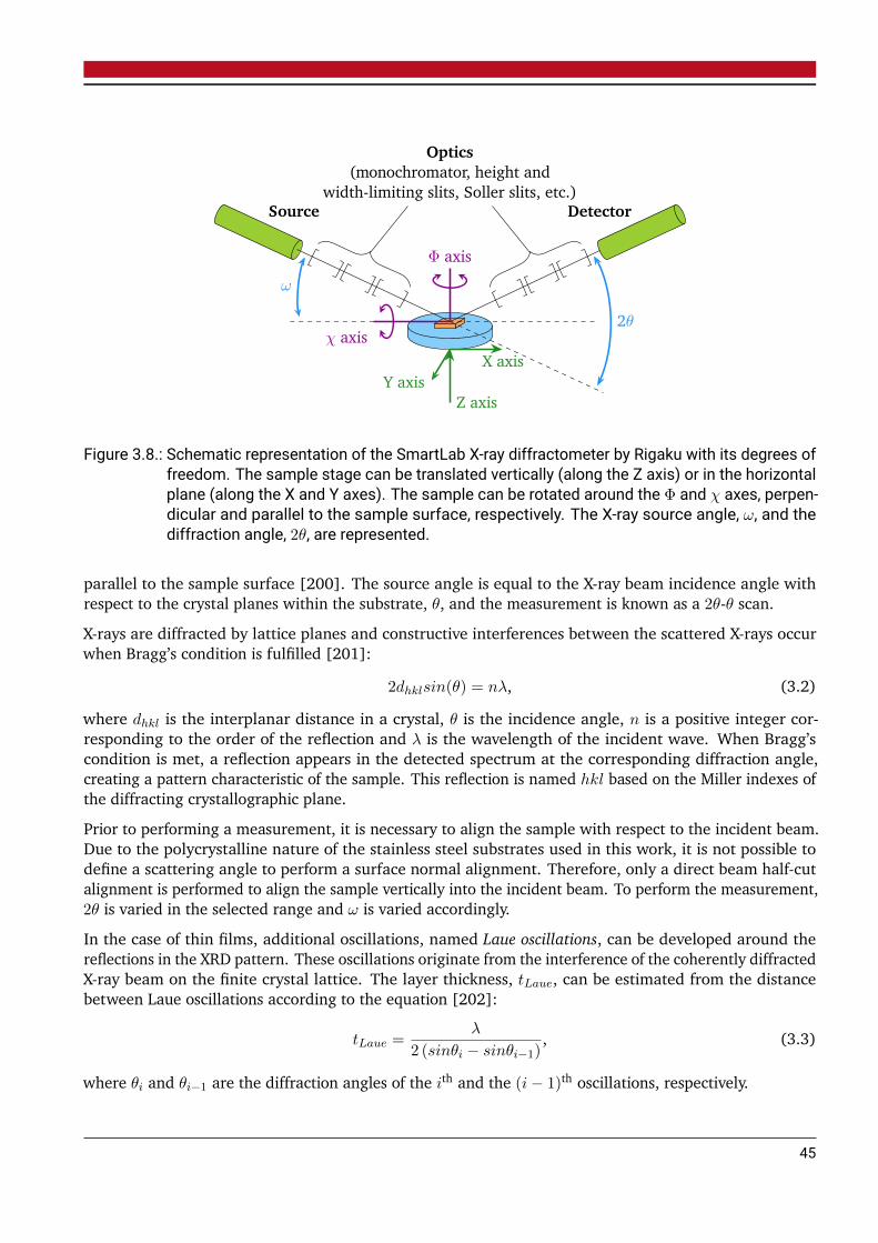
Source Detector
Optics(monochromator, height and
width-limiting slits, Soller slits, etc.)
χ axis
Φ axis
X axisY axis
Z axis
2θ
ω
Figure 3.8.: Schematic representation of the SmartLab X-ray diffractometer by Rigaku with its degrees offreedom. The sample stage can be translated vertically (along the Z axis) or in the horizontalplane (along the X and Y axes). The sample can be rotated around the Φ and χ axes, perpen-dicular and parallel to the sample surface, respectively. The X-ray source angle, ω, and thediffraction angle, 2θ, are represented.
parallel to the sample surface [200]. The source angle is equal to the X-ray beam incidence angle withrespect to the crystal planes within the substrate, θ, and the measurement is known as a 2θ-θ scan.
X-rays are diffracted by lattice planes and constructive interferences between the scattered X-rays occurwhen Bragg’s condition is fulfilled [201]:
2dhklsin(θ) = nλ, (3.2)
where dhkl is the interplanar distance in a crystal, θ is the incidence angle, n is a positive integer cor-responding to the order of the reflection and λ is the wavelength of the incident wave. When Bragg’scondition is met, a reflection appears in the detected spectrum at the corresponding diffraction angle,creating a pattern characteristic of the sample. This reflection is named hkl based on the Miller indexes ofthe diffracting crystallographic plane.
Prior to performing a measurement, it is necessary to align the sample with respect to the incident beam.Due to the polycrystalline nature of the stainless steel substrates used in this work, it is not possible todefine a scattering angle to perform a surface normal alignment. Therefore, only a direct beam half-cutalignment is performed to align the sample vertically into the incident beam. To perform the measurement,2θ is varied in the selected range and ω is varied accordingly.
In the case of thin films, additional oscillations, named Laue oscillations, can be developed around thereflections in the XRD pattern. These oscillations originate from the interference of the coherently diffractedX-ray beam on the finite crystal lattice. The layer thickness, tLaue, can be estimated from the distancebetween Laue oscillations according to the equation [202]:
tLaue =λ
2 (sinθi − sinθi−1), (3.3)
where θi and θi−1 are the diffraction angles of the ith and the (i− 1)th oscillations, respectively.
45
Furthermore, based on the Scherrer equation, it is possible to estimate the crystallite size, sc, from thebroadening of the breadth of the XRD reflections, β [203]. Various evaluation methods have been developed,including the Hall method following the equation [204]:
βcosθ
λ= 4sc
sinθ
λ+
1
κlattice, (3.4)
where κlattice is the lattice strain. The Hall method can be applied by the software PDXL 2 v.2.8.4.0 byRigaku Corporation (Tokyo, Japan), yielding the crystallite size from the XRD pattern.
3.5.1.2. X-ray reflectivity
X-Ray Reflectivity (XRR) is a technique based on both specular reflection and X-rays refraction at aninterface between two media with different refractive indexes. From the analysis of the intensity of grazingincidence X-rays refracted by a sample, information on the thicknesses and densities of the sample layeras well as on interface roughnesses can be obtained [205]. The film thickness can be calculated moreaccurately from XRR than from Laue oscillations. However, the maximum thickness of the films that can beanalysed by XRR is dependent on both the film properties and the diffractometer optics.
A XRR measurement corresponds to a 2θ-ω scan at low diffraction angles, typically with 0 < 2θ < 6.When reaching the sample under this grazing angle, inferior to the critical angle for total reflection θc, allthe incident X-rays are reflected. As ω the X-ray source angle increases and equals θc, the X-rays are onlypartially reflected and propagate along the sample surface. When ω becomes larger than θc, the X-rays areboth reflected and penetrating inside the sample by refraction. Above θc, the ratio of reflected to refractedX-rays decreases proportionally to θ4 [205].
Similar to a 2θ-ω scan, it is necessary to align the sample with respect to the incident beam before performinga measurement. After a direct beam half-cut alignment, a surface normal alignment is executed for agrazing incidence measurement at a scattering angle of 2θ = 0.5. In these conditions, the polycrystallinenature of the stainless steel substrates used in this work does not prevent the surface normal alignment.To extract film characteristics from the reflectivity measurements, data are modelled using the softwareRocking Curve & Reflectivity Curve Simulation & Fitting (RCRefSiW) v.1.09 by IHP Solutions (Frankfurtan der Oder, Germany).
The X-rays can be reflected on several interfaces in a sample including the atmosphere-film and the film-substrate interfaces. If the sample is composed of several layers, reflection can also occur on internalfilm-film interfaces. The alternation of constructive and destructive interferences from the X-rays reflectedat these various interfaces creates oscillations in the intensity of the reflectivity profile named Kiessig fringes.The oscillation curve extracted from Kiessig fringes is a function of the refracted index of the layer and ofits thickness which can be obtained by Fourier transformation. The period of these oscillations decreasesas the film thickness increases [205]. The impact of several parameters on the oscillations, includingthickness, is simulated using the software RCRefSiW for PZT 52/48 films deposited NdGaO3 substratesand represented in Figure 3.9.
Additionally, the layer density can be extrapolated from the total reflection critical angle as indicatedin Figure 3.9. The Kiessig fringes amplitude is dependent on the difference between film and substratedensities. Figure 3.9 also shows the effects of film surface and interface roughnesses. An increasing filmsurface roughness leads to a decrease of the reflectivity curve slope while the Kiessig fringes amplitudedecreases when the interface roughness increases.
46

Density
Thickness
Surface roughness
Interface roughness
1 2 3 4 5
2θ ()
Intensity
(a.u
.)
t = 30 nm, Rs = 0 nm, Ri = 0 nmt = 30 nm, Rs = 1 nm, Ri = 0 nmt = 30 nm, Rs = 1 nm, Ri = 1 nmt = 10 nm, Rs = 0 nm, Ri = 0 nm
Figure 3.9.: Simulation of reflectivity curves of PZT 52/48 thin films on NdGaO3 substrates with differentthicknesses, t, surface roughnesses, Rs and interface roughnesses, Ri, using the softwareRCRefSiW.
3.5.2. Scanning electron microscopy and energy-dispersive X-ray spectroscopy
Scanning Electron Microscopy (SEM) is used to analyse the microstructure of PLD targets and of PZT thinfilms deposited in PZT stacks. Coupled with Energy-Dispersive X-ray Spectroscopy (EDS), SEM is alsoemployed to assess the cations stoichiometry of the PLD targets. These non-destructive, ex situ techniquesare based on the interactions between the sample material and an electron beam scanned point by pointacross the sample surface.
A scanning electron microscope relies on an ultra-high vacuum chamber in which an electron beam isgenerated by applying a high voltage of 1 keV to 30 keV between a cathode and an anode. The electronbeam is focused on the sample using electromagnetic lenses. At each point where the beam is scannedover the sample, the impacting or primary electrons are scattered both elastically and inelastically by thematerial. Due to this electron bombardment, the sample emits characteristic X-rays and electrons whichare measured and quantified by several detectors located inside the ultra-high vacuum chamber. Both SEMand EDS techniques are described in more details in [206].
During this work, unless otherwise mentioned, an SEM XL30 FEG from Phillips (Amsterdam, Netherlands)is employed, coupled with an EDS-CDU LEAP detector with a silicon crystal drifted with lithium, Si(Li),cooled with liquid N2 and with an energy resolution of 135 eV to perform EDS. Imaging of the surfacetopography is performed with a secondary electrons detector to measure the low-energy secondary electronsat approximately 50 eV interacting only with the first few nanometres of the sample material. To avoidsurface charging of the electrically insulating targets due to the electron beam, thin metallic layers aresputtered on the target surface before measurement.
For cross-section images, the cross-section is accessed by cutting a trench in the sample with a focused ion
47

beam after depositing a thick Pt capping layer. This process is performed by Ulrike Kunz from the Instituteof Materials Science of the Technische Universität Darmstadt (Darmstadt, Germany).
3.5.3. Electron Backscatter Diffraction
Electron Backscatter Diffraction (EBSD) is performed by Enrico Bruder from the Institute of MaterialsScience of the Technische Universität Darmstadt (Darmstadt, Germany) to analyse the texture of PZT thinfilms deposited in PZT stacks. The EBSD data are acquired using a Mira3-XMH high resolution SEM byTESCAN (Brno, Czech Republic), equipped with a DigiView 5 EBSD Camera by EDAX (Mahwah, NJ, USA).An acceleration voltage of 15 keV and a beam current of 500 pA are chosen to operate the system andachieve a high spatial resolution.
The EBSD analysis, also performed by Enrico Bruder, is done with a 10 nm step size, which is below thephysical resolution of conventional EBSD, owing to the coarsening effect induced by the NPAR® (NeighborPattern Averaging and Reindexing) post-processing routine that is used to improve the data quality withoutfurther clean-up procedures. To calculate the crystallographic texture, the harmonic series expansionmethod is used on an EBSD dataset with more than 7,000 indexed grains with a series rank of 24, aGaussian half width of 5, and no enforced symmetry. The measured sample does not have Pt top electrodesand, to avoid electrical charging, a thin layer of carbon is sputter-coated on the surface.
48
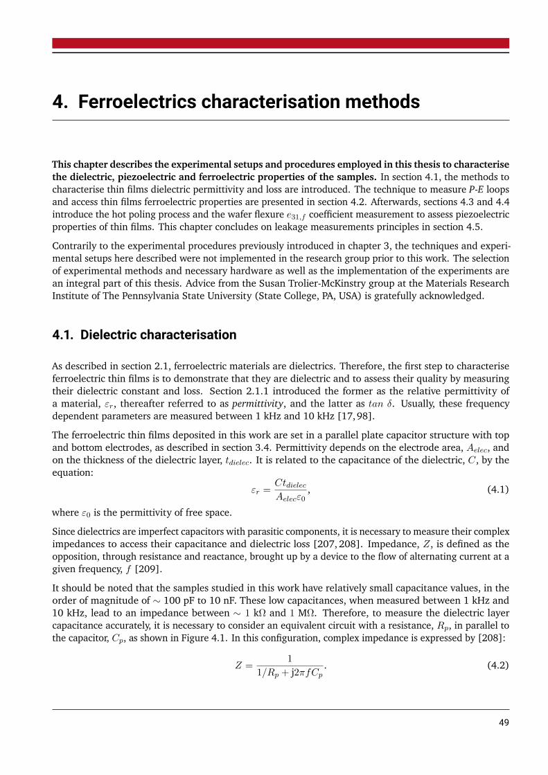
4. Ferroelectrics characterisation methods
This chapter describes the experimental setups and procedures employed in this thesis to characterisethe dielectric, piezoelectric and ferroelectric properties of the samples. In section 4.1, the methods tocharacterise thin films dielectric permittivity and loss are introduced. The technique to measure P-E loopsand access thin films ferroelectric properties are presented in section 4.2. Afterwards, sections 4.3 and 4.4introduce the hot poling process and the wafer flexure e31,f coefficient measurement to assess piezoelectricproperties of thin films. This chapter concludes on leakage measurements principles in section 4.5.
Contrarily to the experimental procedures previously introduced in chapter 3, the techniques and experi-mental setups here described were not implemented in the research group prior to this work. The selectionof experimental methods and necessary hardware as well as the implementation of the experiments arean integral part of this thesis. Advice from the Susan Trolier-McKinstry group at the Materials ResearchInstitute of The Pennsylvania State University (State College, PA, USA) is gratefully acknowledged.
4.1. Dielectric characterisation
As described in section 2.1, ferroelectric materials are dielectrics. Therefore, the first step to characteriseferroelectric thin films is to demonstrate that they are dielectric and to assess their quality by measuringtheir dielectric constant and loss. Section 2.1.1 introduced the former as the relative permittivity ofa material, εr, thereafter referred to as permittivity, and the latter as tan δ. Usually, these frequencydependent parameters are measured between 1 kHz and 10 kHz [17,98].
The ferroelectric thin films deposited in this work are set in a parallel plate capacitor structure with topand bottom electrodes, as described in section 3.4. Permittivity depends on the electrode area, Aelec, andon the thickness of the dielectric layer, tdielec. It is related to the capacitance of the dielectric, C, by theequation:
εr =CtdielecAelecε0
, (4.1)
where ε0 is the permittivity of free space.
Since dielectrics are imperfect capacitors with parasitic components, it is necessary to measure their compleximpedances to access their capacitance and dielectric loss [207, 208]. Impedance, Z, is defined as theopposition, through resistance and reactance, brought up by a device to the flow of alternating current at agiven frequency, f [209].
It should be noted that the samples studied in this work have relatively small capacitance values, in theorder of magnitude of ∼ 100 pF to 10 nF. These low capacitances, when measured between 1 kHz and10 kHz, lead to an impedance between ∼ 1 kΩ and 1 MΩ. Therefore, to measure the dielectric layercapacitance accurately, it is necessary to consider an equivalent circuit with a resistance, Rp, in parallel tothe capacitor, Cp, as shown in Figure 4.1. In this configuration, complex impedance is expressed by [208]:
Z =1
1/Rp + j2πfCp. (4.2)
49
Cp
Rp
Figure 4.1.: Equivalent circuit model of a capacitor, Cp, with a parallel resistance, Rp, to measure thecapacitance of dielectric thin films.
Furthermore, the dissipation factor, equivalent to the dielectric loss tangent, tan δ, corresponds to the ratioof the real to the imaginary part of the impedance. In a parallel equivalent circuit, it is defined as [208]:
tan δ =1
2πfRpCp. (4.3)
Complex impedance measurements are performed with an Alternating Current (AC) impedance capacitancemeter, also known as LCR meter, measuring both the impedance amplitude and phase angle. For thispurpose, a LCR meter is equipped with four terminals called Hcurr, Hpot, Lcurr and Lpot corresponding tothe high current, high potential, low current and low potential terminals, respectively. An AC voltage issupplied from the Hcurr terminal and the current through the dielectric layer is measured by the Lcurrterminal. Simultaneously, the voltage across the dielectric is measured by the Hpot and Lpot terminalswhile being phase-locked with the current. This allows to measure the phase angle between current andvoltage [207].
When measuring low capacitance values, stray capacitances are a large source of measurement error.They can appear between the sample and a nearby conductor, e.g. a metallic sample stage. During themeasurement, a difference of voltage is created between sample and conductor, leading to the measurementsignal leaking towards the conductor. The leakage signal is then measured along with the sample signal,generating measurement errors due to stray capacitances. To suppress the voltage difference, a shieldingplate, e.g. made of ceramic or quartz, is inserted between the sample and the sample stage [208].
In order to reduce the effects of lead impedances and contact resistances, the signal current path andthe voltage sensing leads must be independent. This is achieved with a four-terminal configuration byconnecting together the outer shields of the Hcurr and Hpot, Lcurr and Lpot terminals, respectively. Theconnection must be made as close as possible to the sample. To further compensate stray admittance andresidual impedance due to the experimental setup, open and short compensations must be performed [208].
Since the dielectric layers characterised in this work are also ferroelectric, ferroelectric switching and polingmust be avoided. Therefore, the amplitude of the AC voltage applied to the sample is chosen to produce asubswitching field, below the ferroelectric coercive field [98].
4.1.1. Parameters sweeps
Permittivity and dielectric loss depend on several parameters including the AC subswitching field frequencyand amplitude. If a DC bias voltage is applied, these properties are also dependent on the resulting appliedfield. It is necessary to quantify these dependences through parameters sweeps.
50

At subswitching fields, field frequency and amplitude dependence of the permittivity are mainly due toextrinsic effects, e.g. domain wall motion and defect displacement. Besides the necessity for applications toaccount for their impact on devices, analysis of these dependences can provide information on the extrinsicmechanisms nature [98].
While the effect of subswitching field amplitude and frequency are measured at zero DC bias field, measuringa permittivity versus electrical field curve, also known as εr-E curve, requires a DC bias field to be appliedsimultaneously to the AC subswitching field. In this method, sometimes referred to as capacitance versusvoltage or C-V curve, the DC bias is varied as a step-like function while the AC field is employed to measurethe capacitance as described in the previous section [98]. As εr-E curves lead to ferroelectric switchingand, therefore, remanent polarisation, they must be performed after P-E loops are measured.
In the absence of a DC field, domain walls can be pinned by defects, e.g. oxygen vacancies, limiting theirmobility [6,98]. Upon increase of the DC bias, domain walls are released from the defects which lead to anincrease in permittivity. Furthermore, some ferroelectric domains with relatively low coercive fields can beswitched by the combined AC and DC applied fields. The proportion of switching domains increases withthe applied DC bias until the sample coercive field is reached. For DC bias fields larger than the coercivefield, the permittivity decreases. This phenomenon is due both to the reduction of the number of domainsas they aligned themselves with the applied field and to the domain wall motion inhibition by the DC biasfield [98].
4.1.2. Dielectric characterisation experimental systems and parameters
At the exception of DC bias sweeps, permittivity and dielectric loss measurements are performed with acustom-built probe station. The probe station is contained in a lidded enclosure made of film faced plywoodto dampen outside mechanical noise [210]. Its exterior is covered by metallic plates and electricallygrounded to ensure electrical insulation of the measurement setup. This electrical ground is commonto the probe tips positioners and, when required, sample. The probe station is equipped with S-725micropositioners by Signatone (Gilroy, CA, USA) on which tungsten tips of 25 µm in diameter are mounted.
Permittivity and dielectric loss measurements are performed using an E4980A LCR meter by Agilent (SantaClara, CA, USA). In order to perform accurate permittivity calculations from the measured capacitancevalue (see Equation (4.1)) the electrode area must be known. Therefore, the sample is driven by thebottom electrode, i.e. the top electrode, patterned by photolithography, is grounded so measurements areperformed on an electrode whose exact area is known. The experimental setup is schematically representedin Figure 4.2 without the plywood enclosure.
As the E4980A LCR meter does not permit DC bias sweeping, DC bias sweeps are performed using a4200-SCS Semiconductor Characterization System by Keithley Instruments (Solon, OH, USA) equippedwith a 4210-CVU Multi-Frequency Capacitance Voltage Measure Unit card. This measurement systemis connected to a commercial TTPX probe station by Lake Shore Cryotronics (Westerville, OH, USA),equipped with beryllium-copper tips of 25 µm in diameter. This particular experimental setup was alreadyimplemented in the research group prior to this work.
In the absence of parameters sweeps, permittivity and dielectric loss are measured at zero DC bias withan AC driving signal of VAC = 30 mV at 1 kHz or 10 kHz. This amplitude of the driving signal is lowerthan half of the coercive field of the thin films. Sweeps of subswitching field frequency and amplitudeare performed between 100 Hz and 10 kHz and between 0 kV·cm−1 and 20 kV·cm−1, respectively. εr-Ecurves are measured between −200 kV·cm−1 and 200 kV·cm−1.
51
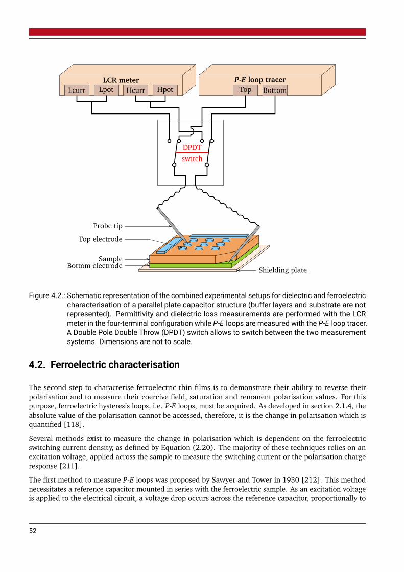
LCR meter P-E loop tracerLcurr Lpot Hcurr Hpot Top Bottom
switchDPDT
Probe tip
Shielding plateBottom electrodeSample
Top electrode
Figure 4.2.: Schematic representation of the combined experimental setups for dielectric and ferroelectriccharacterisation of a parallel plate capacitor structure (buffer layers and substrate are notrepresented). Permittivity and dielectric loss measurements are performed with the LCRmeter in the four-terminal configuration while P-E loops are measured with the P-E loop tracer.A Double Pole Double Throw (DPDT) switch allows to switch between the two measurementsystems. Dimensions are not to scale.
4.2. Ferroelectric characterisation
The second step to characterise ferroelectric thin films is to demonstrate their ability to reverse theirpolarisation and to measure their coercive field, saturation and remanent polarisation values. For thispurpose, ferroelectric hysteresis loops, i.e. P-E loops, must be acquired. As developed in section 2.1.4, theabsolute value of the polarisation cannot be accessed, therefore, it is the change in polarisation which isquantified [118].
Several methods exist to measure the change in polarisation which is dependent on the ferroelectricswitching current density, as defined by Equation (2.20). The majority of these techniques relies on anexcitation voltage, applied across the sample to measure the switching current or the polarisation chargeresponse [211].
The first method to measure P-E loops was proposed by Sawyer and Tower in 1930 [212]. This methodnecessitates a reference capacitor mounted in series with the ferroelectric sample. As an excitation voltageis applied to the electrical circuit, a voltage drop occurs across the reference capacitor, proportionally to
52
the polarisation charge. While this method is suitable for high speed measurements, its main drawbacksare parasitic effects and the difficulty to find sufficiently precise reference capacitors [105,106,211,212].
The second technique, known as the shunt method, is similar to the Sawyer Tower methodwhile replacing thereference capacitor of the latter by a reference resistance. In this configuration, the charge is obtained bynumerically integrating the measured switching current. This method can be accurate for large electrodesizes but parasitic capacitances make it unreliable for small area electrodes. Furthermore, the valueof the reference resistance must be adapted to both the sample capacitance and the excitation voltagefrequency [211].
The virtual ground method, is the third technique based on an excitation voltage. More complex, itselectrical circuit comprises an operational amplifier and a feedback resistor, converting the measuredswitching current to voltage. This technique is efficient for samples with small capacitances. Despite thenecessity to take into account several parameters linked to the operational amplifier, this method is themost precise for ferroelectric measurements [211].
The fourth method to measure ferroelectric hysteresis loop is the current step method. In that case,an excitation current is applied directly across the ferroelectric sample, creating a voltage drop overit. Since it does not necessitate a reference component, this method has the advantage of avoidingapproximations [211].
Each of the methods described above presents advantages and drawbacks. The choice of a specific methoddepends not only on the sample but also on several technical considerations, e.g. range of signal magnitude,bandwidth or parasitic effects [211]. In consequence, ferroelectric hysteresis loops are often measuredwith commercial setups [106].
4.2.1. Accessing ferroelectric characteristic values
Before measuring a ferroelectric hysteresis loop, the sample must be pre-polarised by measuring a hysteresisloop with the same parameters and called pre-polarisation pulse. This creates a defined polarisation state,usually set as the negative state of the remanent polarisation. It is important to note that P-E loops aredependent on the sample electrical and mechanical history and also on the measurement method [211].
As described in section 2.1.4, P-E loops are obtained by measuring the sample polarisation versus theapplied electrical field. Commonly, the excitation voltage applied to the sample is a triangular symmetricwaveform. The shape of the ferroelectric hysteresis loop depends on the frequency of the excitation signal.Indeed, it defines the time constant for the sample to undergo a full P-E loop and, therefore, impacts therelaxation time between each data point [211,213]. This measurement is known as a dynamic hysteresiscurve in opposition to a static hysteresis curve. The latter aims to remove the influence of the excitation signalfrequency on the P-E loop shape by measuring a quasi-static hysteresis loop. For this purpose, a definedrelaxation time is set between each measured point of the hysteresis curve. Static hysteresis measurementsallow the investigation of irreversible and reversible contributions to the sample polarisation [211,214].
Saturation and remanent polarisation values can be obtained from the ferroelectric hysteresis loop, asmentioned in section 2.1.4 (see Figure 2.4) [120]. However, as the polarisation reversal is progressivefor non-ideal single crystals and polycrystalline samples, measuring the coercive field from the P-E loopyields inaccurate values. To circumvent this problem, coercive fields are determined from the switchingcurrent versus voltage curve corresponding to the P-E loop and where the switching peaks are clearlyidentifiable [106,120].
53
Another sample characteristic which can be obtained from ferroelectric hysteresis loops is the imprint,corresponding to an internal bias field in the ferroelectric sample. Generally present in virgin ferroelectriccapacitors, imprint is manifested as a shift of the hysteresis loop along the electrical field axis. It correspondsto a preferred polarisation state over the other and can be due to defect dipoles [120,211].
Depending on the respective directions of the internal bias field and applied field, imprint can either hinderor enhance the piezoelectric response for MEMS applications. Its consequences are a diminution or anincrease of the remanent polarisation value and an asymmetry of the P-E loop along the electrical field axis.The internal bias field, Ec,shift can be calculated by [211]:
Ec,shift =Ec − |Ec,−|
2, (4.4)
where Ec,− is the negative coercive field.
Additionally, qualitative information on the ferroelectric sample can be obtained from the shape of P-Eloops. More “square” ferroelectric hysteresis loops indicate an abrupt reversal of the polarisation directionand the loop area is linked with the energy dissipated as heat within the sample. Avoiding heat generationis the reason for which P-E loops are measured at low frequency, typically at 100 Hz or below [213].
4.2.2. Ferroelectric characterisation experimental system and parameters
Ferroelectric hysteresis loops are measured using a TF Analyzer 2000 P-E loop tracer by aixACCT Systems(Aachen, Germany) equipped with a FE module. Electrical contacting of the samples is performed with thecustom-built probe station described in section 4.1.2. To avoid field spreading, the sample is driven by thebottom electrode, as is done for permittivity and dielectric loss measurements. Connections between theP-E loop tracer and the ferroelectric sample are schematically represented in Figure 4.2.
To measure the P-E loops, dynamic hysteresis measurements are performed using a single triangularwaveform with a frequency of 100 Hz. A pre-polarisation pulse loop is applied.
4.3. Hot poling process
As described in section 2.1.4, a poling process is necessary to generate a net polarisation by align thepolarisations of ferroelectric domains in the direction of an applied electrical field, larger than the samplecoercive field. As heating up a ferroelectric reduces its coercive field, poling is generally performed atelevated temperatures. Afterwards, the sample is cooled down before the poling field is removed [120].
It has been demonstrated in literature that poling at elevated temperatures creates imprint in ferroelectrics,leading to more stable polarisation states [215,216]. This can notably be explain by the limited mobilityof non-180 domain walls in ferroelectric thin films, hindering modification of the ferroelastic domainorientation at room temperature once it has been set [17].
54
4.3.1. Key parameters of hot poling process
The efficiency of hot poling is dependent on the applied poling field, the poling temperature and theduration for which the poling field is applied before the cooling down process.
Literature reports that, for Pb(Yb1/2Nb1/2)O3-PbTiO3 perovskite thin films, the optimal applied poling fieldis at least twice higher than the sample coercive field. Above this value, the e31,f coefficient absolute valuesaturates, indicating the maximum piezoelectric response. It has also been shown for these films that apoling duration longer than 10 minutes does not further improve the value of the e31,f coefficient [217].
An increase in the poling temperature of PNZT thin films from 25 C to 150 C leads to a sharper distributionof switching fields and an increased degree of imprint which improves the films d33,f coefficient. It shouldbe noted that the internal bias field is further increased when poling is done at 200 C [216].
The parameters described above can be applied to PZT thin films and several authors report the poling ofPZT thin films at 150 C under an applied field 2 to 3 times higher than the coercive field during 10 min to15 min [53,218].
4.3.2. Hot poling experimental system and parameters
During hot poling, the sample electrodes are electrically contacted with the custom-built probe stationdescribed in section 4.1.2. To avoid unnecessary heating of the film faced plywood, the interior of the probestation enclosure is protected with 5 mm thick plates of high-temperature glass wool type 1300-IN-LD-02by Kager Industrieprodukte (Dietzenbach, Germany).
The sample is heated at 150 C on a Fisherbrand™Isotemp™Hot Plate by fisher scientific (Pittsburgh, PA,USA) with an electrically insulating top surface. A DC electrical field is applied from the top to the bottomelectrode with a Voltcraft Programmable Power Supply Unit DIGI 35 CPU by Conrad Electronic (Hirschau,Germany). The applied field is chosen equal to 2.5 times the sample coercive field and is maintainedduring 15 min before the sample is cooled down. Once the sample reaches room temperature the electricalfield is removed.
4.4. Piezoelectric characterisation
Some key parameters for piezoelectric applications are the material piezoelectric coefficients introducedin section 2.1.2. In the case of thin films clamped to rigid substrates, the effective e31,f coefficient (seeEquation (2.17)) is particularly relevant as it links the d31 piezoelectric coefficient and the thin film elasticcompliances at constant electrical field [17,24].
Several methods allow to measure the e31,f coefficient, either by measuring the substrate deflection whenapplying an electrical field (converse piezoelectric effect) or by collecting the charges related to in-planestrain developed when bending the substrate (direct piezoelectric effect) [17,24]. The former possibility isgenerally implemented with laser interferometry where sample dielectric displacement can be measured byvarious interferometry techniques, including single-beam Michelson interferometer [219]. A comparisonbetween single and double beam methods can be found in [220]. Another technique to measure e31,fcoefficients when applying an electrical field on the sample is the impulse method [221,222]. However,
55
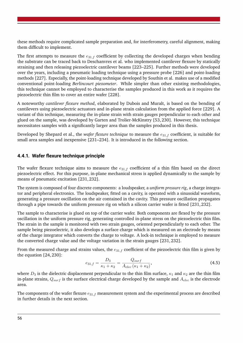
these methods require complicated sample preparation and, for interferometry, careful alignment, makingthem difficult to implement.
The first attempts to measure the e31,f coefficient by collecting the developed charges when bendingthe substrate can be traced back to Deschanvres et al. who implemented cantilever flexure by staticallystraining and then releasing piezoelectric cantilever beams [223–225]. Further methods were developedover the years, including a pneumatic loading technique using a pressure probe [226] and point-loadingmethods [227]. Especially, the point-loading technique developed by Southin et al. makes use of a modifiedconventional point-loading Berlincourt piezometer. While simpler than other existing methodologies,this technique cannot be employed to characterise the samples produced in this work as it requires thepiezoelectric thin film to cover an entire wafer [228].
A noteworthy cantilever flexure method, elaborated by Dubois and Muralt, is based on the bending ofcantilevers using piezoelectric actuators and in-plane strain calculation from the applied force [229]. Avariant of this technique, measuring the in-plane strain with strain gauges perpendicular to each other andglued on the sample, was developed by Garten and Trolier-McKinstry [53,230]. However, this techniquenecessitates samples with a significantly larger area than the samples produced in this thesis.
Developed by Shepard et al., the wafer flexure technique to measure the e31,f coefficient, is suitable forsmall area samples and inexpensive [231–234]. It is introduced in the following section.
4.4.1. Wafer flexure technique principle
The wafer flexure technique aims to measure the e31,f coefficient of a thin film based on the directpiezoelectric effect. For this purpose, in-plane mechanical stress is applied dynamically to the sample bymeans of pneumatic excitation [231,232].
The system is composed of four discrete components: a loudspeaker, a uniform pressure rig, a charge integra-tor and peripheral electronics. The loudspeaker, fitted on a cavity, is operated with a sinusoidal waveform,generating a pressure oscillation on the air contained in the cavity. This pressure oscillation propagatesthrough a pipe towards the uniform pressure rig on which a silicon carrier wafer is fitted [231,232].
The sample to characterise is glued on top of the carrier wafer. Both components are flexed by the pressureoscillation in the uniform pressure rig, generating controlled in-plane stress on the piezoelectric thin film.The strain in the sample is monitored with two strain gauges, oriented perpendicularly to each other. Thesample being piezoelectric, it also develops a surface charge which is measured on an electrode by meansof the charge integrator which converts the charge to voltage. A lock-in technique is employed to measurethe converted charge value and the voltage variation in the strain gauges [231,232].
From the measured charge and strains values, the e31,f coefficient of the piezoelectric thin film is given bythe equation [24,230]:
e31,f =D3
κ1 + κ2=
Qsurf
Aelec (κ1 + κ2), (4.5)
where D3 is the dielectric displacement perpendicular to the thin film surface, κ1 and κ2 are the thin filmin-plane strains, Qsurf is the surface electrical charge developed by the sample and Aelec is the electrodearea.
The components of the wafer flexure e31,f measurement system and the experimental process are describedin further details in the next section.
56
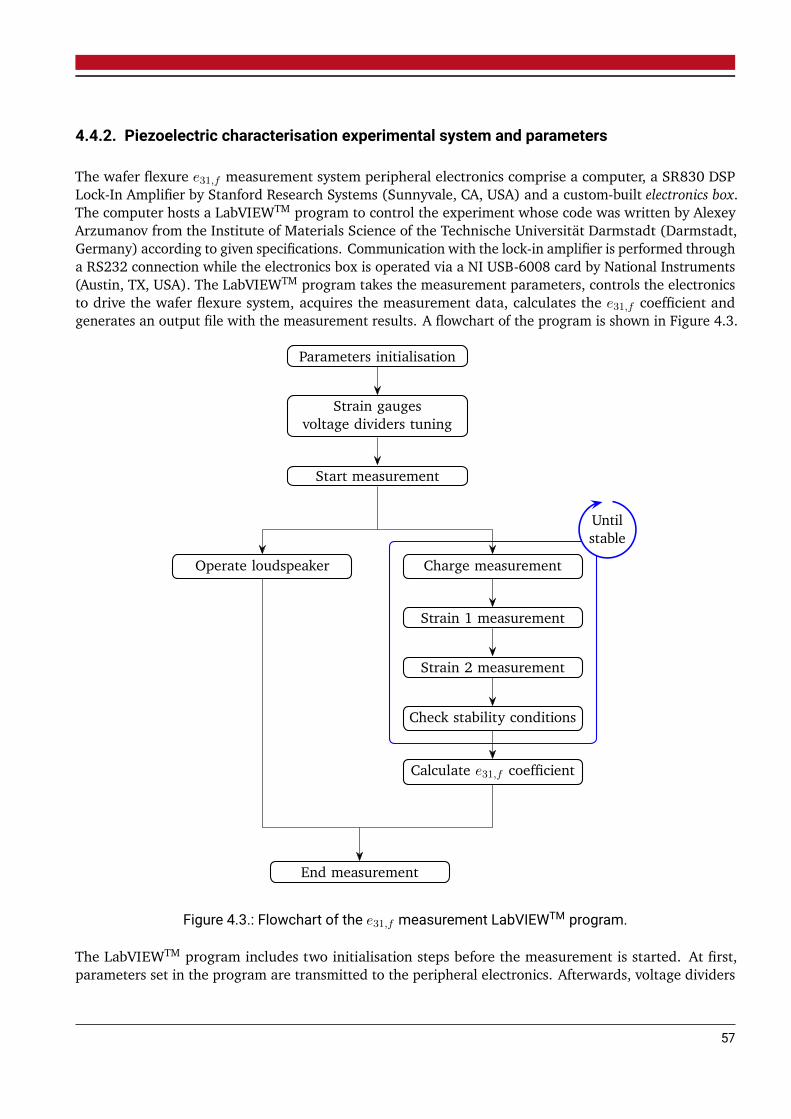
4.4.2. Piezoelectric characterisation experimental system and parameters
The wafer flexure e31,f measurement system peripheral electronics comprise a computer, a SR830 DSPLock-In Amplifier by Stanford Research Systems (Sunnyvale, CA, USA) and a custom-built electronics box.The computer hosts a LabVIEWTM program to control the experiment whose code was written by AlexeyArzumanov from the Institute of Materials Science of the Technische Universität Darmstadt (Darmstadt,Germany) according to given specifications. Communication with the lock-in amplifier is performed througha RS232 connection while the electronics box is operated via a NI USB-6008 card by National Instruments(Austin, TX, USA). The LabVIEWTM program takes the measurement parameters, controls the electronicsto drive the wafer flexure system, acquires the measurement data, calculates the e31,f coefficient andgenerates an output file with the measurement results. A flowchart of the program is shown in Figure 4.3.
Parameters initialisation
Strain gaugesvoltage dividers tuning
Start measurement
Operate loudspeaker Charge measurement
Strain 1 measurement
Strain 2 measurement
Check stability conditions
Calculate e31,f coefficient
End measurement
Untilstable
Figure 4.3.: Flowchart of the e31,f measurement LabVIEWTM program.
The LabVIEWTM program includes two initialisation steps before the measurement is started. At first,parameters set in the program are transmitted to the peripheral electronics. Afterwards, voltage dividers
57
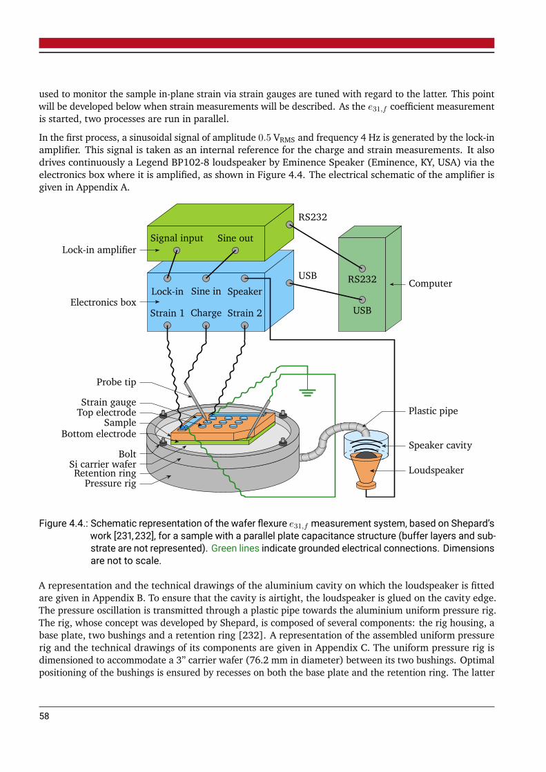
used to monitor the sample in-plane strain via strain gauges are tuned with regard to the latter. This pointwill be developed below when strain measurements will be described. As the e31,f coefficient measurementis started, two processes are run in parallel.
In the first process, a sinusoidal signal of amplitude 0.5 VRMS and frequency 4 Hz is generated by the lock-inamplifier. This signal is taken as an internal reference for the charge and strain measurements. It alsodrives continuously a Legend BP102-8 loudspeaker by Eminence Speaker (Eminence, KY, USA) via theelectronics box where it is amplified, as shown in Figure 4.4. The electrical schematic of the amplifier isgiven in Appendix A.
Strain 1 Charge Strain 2
Lock-in Sine in SpeakerUSB
Signal input Sine out
RS232
RS232
USB
Lock-in amplifier
Electronics box
Probe tip
Strain gaugeTop electrode
SampleBottom electrode
BoltSi carrier waferRetention ring
Pressure rig
Computer
Plastic pipe
Speaker cavity
Loudspeaker
Figure 4.4.: Schematic representation of the wafer flexure e31,f measurement system, based on Shepard’swork [231,232], for a sample with a parallel plate capacitance structure (buffer layers and sub-strate are not represented). Green lines indicate grounded electrical connections. Dimensionsare not to scale.
A representation and the technical drawings of the aluminium cavity on which the loudspeaker is fittedare given in Appendix B. To ensure that the cavity is airtight, the loudspeaker is glued on the cavity edge.The pressure oscillation is transmitted through a plastic pipe towards the aluminium uniform pressure rig.The rig, whose concept was developed by Shepard, is composed of several components: the rig housing, abase plate, two bushings and a retention ring [232]. A representation of the assembled uniform pressurerig and the technical drawings of its components are given in Appendix C. The uniform pressure rig isdimensioned to accommodate a 3” carrier wafer (76.2 mm in diameter) between its two bushings. Optimalpositioning of the bushings is ensured by recesses on both the base plate and the retention ring. The latter
58
is held by four screws and bolts, sufficiently tightened to prevent horizontal motion of the carrier wafer.To improve the uniform pressure rig air tightness, paper rings at the bushings dimensions are insertedbetween each bushing and the carrier wafer [232].
Piezoelectric samples are glued at the centre of the silicon carrier wafer with Loctite Super Glue Ultra LiquidControl by Henkel (Düsseldorf, Germany). Once dry, this glue allows proper strain transmission betweencarrier wafer and sample. As mentioned in section 3.1, to ensure homogeneous gluing the substrate backmust remain clean [232]. For more details on the mechanical equations describing strain in a sample fixedon the uniform pressure rig, the reader is referred to [232].
In the second process running as the measurement starts, the sample developed surface charge and appliedin-plane strains in perpendicular directions are measured in succession until stability criteria are metsimultaneously for each physical quantity. Switching between the different measurements is performedwithin the electronics box. The electrical schematic of the electronics box and the purpose of its componentsare given in Appendix D.
To monitor its surface charge, the sample is electrically contacted using the custom-built probe stationdescribed in section 4.1.2. Contrary to measurements previously introduced in this manuscript (seesections 4.1 and 4.2), the charge is measured by the top electrode while the bottom electrode is grounded.Indeed, in this mechanically oscillating configuration, the large area bottom electrode would generate ahigh noise to signal ratio if it was not electrically grounded. To ensure constant electrical contact despitethe sample oscillation, a sufficiently large top electrode is chosen for contacting.
The surface charge developed by the sample as a function of mechanical stress is monitored by a chargeintegrator which converts the AC current to voltage and amplifies it, leading to more stable and reliablemeasurements [231, 232]. The electrical schematic of the charge integrator and the purpose of itscomponents are given in Appendix E. The charge input into the integrator, Qin, can be expressed as afunction of the output voltage, Vout, by:
Qin = −VoutCref , (4.6)
where Cref = 10 nF is the reference capacitance on which the charge is developed.
Once the surface charge value is acquired, in-plane strains in perpendicular directions, κ1 and κ2 referredto as strain 1 and strain 2 in Figures 4.3 and 4.4, are measured using strain gauges. Each in-plane strain ismeasured using a voltage divider in which the strain gauge constitutes a resistor. The in-plane strain as afunction of the measured voltage crossing the voltage divider is given by:
x =1
GF
[Rref
Rg
(Vapp
Vno_strain + Vmeas,RMS/0.707− 1
)−1
− 1
], (4.7)
where GF is the gauge factor, Rref = 1.2 kΩ is the reference resistance in the voltage divider and Rg is thestrain gauge nominal resistance. Vapp = 1.1 V corresponds to the voltage applied on the voltage divider bythe NI USB-6008 card, Vno_strain = 0.1 V is the output voltage when no strain is applied and Vmeas,RMS
is the output voltage as function of the strain measured by the lock-in amplifier. The 0.707 coefficientconverts the RMS voltage value into voltage.
The strain measurements can be performed with two sort of strain gauges [232]. Platinum sputtered straingauges give a more accurate value of strain as they are placed directly on the piezoelectric sample surfaceduring the photolithography process, as described in section 3.4.1. However, due to the non-standardisedresistance value of the sputtered strain gauges, the reference resistances in the voltage dividers are tuned
59

with 5 kΩ potentiometers before the e31,f measurement starts to ensure that Vno_strain = 0.1 V (seeAppendix D). To be within the tunable range of the reference resistances in the voltage dividers, sputteredstrain gauges must have a nominal resistance of approximately 200 Ω. With their length of 229 mm andtheir width of 50 µm, as indicated in Figure 3.6, it corresponds to an approximate thickness of 240 nm.
However, due to the large aspect ratio of the sputtered strain gauges, with a very high thickness as comparedto their width, the platinum adhesion to the sample surface is not sufficient and the strain gauges presentdefects. These defects are missing areas where the sputtered platinum lifted-off from the sample and thestrain gauge pattern is incomplete. To remediate to this problem, 2 mm long 120 Ω commercial straingauges by RS PRO (Frankfurt am Main, Germany) are utilised. In aluminium, these strain gauges totaldimensions are 6× 2.5 mm2. They have a gauge factor of 2.0 and are equipped with lead wires on whichextension copper wires can be soldered. The commercial strain gauges are glued on the carrier wafernext to the sample with Loctite Super Glue Ultra Liquid Control by Henkel (Düsseldorf, Germany). Tomeasure in-plane strain accurately, the strain gauges are glued as close as possible to the sample edges andperpendicular to each other. When commercial strain gauges are utilised, the potentiometers allowingtuning of the reference resistances in the voltage dividers are by-passed by switches in the electronics box(see Appendix D).
The charge and strains measurements are iterated until two stability conditions are met. The first condition,arising from the surface charge being developed in response to the in-plane strain, is for the charge signalto be in-phase or exactly out-of-phase with the strain signals with a ±20 tolerance. The second conditionis for the standard deviation of each strain signal over the last 20 data points to be inferior to a terminationcondition multiplied by the strain mean value. The termination condition is set at 0.05. If both stabilityconditions are met over 20 sets of data points, the e31,f coefficient is calculated using Equation (4.5).
4.5. Leakage measurements
Leakage measurements aim to quantify leakage currents through a dielectric and to identify the mechanismsinvolved in the process. Often complex, these mechanisms depend notably on the dielectric material itselfand the interfaces with its electrodes. Several leakage mechanisms can take place under different values ofapplied field in a sample [235].
4.5.1. Key aspects of leakage measurements
Leakage measurements are performed on dielectric thin films by applying a constant voltage to the sampleand measuring the resulting current after a given period, the soak time. Indeed, under an applied DCfield, a transient current is present which decays exponentially with time. Therefore, it is necessary for theleakage current to stabilise before being measured [236]. For ferroelectrics, the transient current originatesfrom dielectric relaxation and from polarisation [237,238].
It should be noted that leakage measurements differ from switching current versus voltage measurements(see section 4.2.1) by the applied voltage being DC instead of AC. Furthermore, switching current versusvoltage measurements do not involve soak time.
The source measure unit is a method to measure leakage in which the ammeter is connected to the voltagesource internally. Generally, leakage currents have very small amplitude, in the order of magnitude of
60

the nanoampere. To protect the measurement devices in case of dielectric breakdown of the sample, acompliance value is set to limit the measured current [236].
4.5.2. Leakage measurements experimental system and parameters
Leakage measurements are performed using the 4200-SCS Semiconductor Characterization System byKeithley Instruments (Solon, OH, USA) employed for DC bias sweeps during dielectric characterisation.However, in this case, it is equipped with two 4200-SMU source measure unit cards and a 4200-PApreamplifier. The sample is contacted, using the TTPX probe station by Lake Shore Cryotronics (Westerville,OH, USA), equipped with beryllium-copper tips of 25 µm in diameter. This particular experimental setupwas already implemented in the research group prior to this work. The bottom electrode is grounded,while the DC bias is applied to the top electrode.
Before measuring each data point, a soak time of 75 s is observed. The selected soak time is sufficient forthe transient current to decrease to the order of magnitude of nanoamperes [237]. It is therefore negligiblewith regard to the measured leakage currents. The compliance value is set at 0.1 A.
61

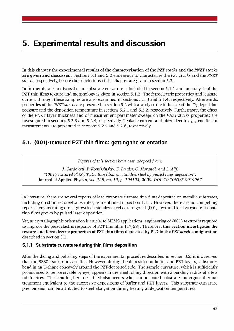
5. Experimental results and discussion
In this chapter the experimental results of the characterisation of the PZT stacks and the PNZT stacksare given and discussed. Sections 5.1 and 5.2 endeavour to characterise the PZT stacks and the PNZTstacks, respectively, before the conclusions of the chapter are given in section 5.3.
In further details, a discussion on substrate curvature is included in section 5.1.1 and an analysis of thePZT thin films texture and morphology is given in section 5.1.2. The ferroelectric properties and leakagecurrent through these samples are also examined in sections 5.1.3 and 5.1.4, respectively. Afterwards,properties of the PNZT stacks are presented in section 5.2 with a study of the influence of the O2 depositionpressure and the deposition temperature in sections 5.2.1 and 5.2.2, respectively. Furthermore, the effectof the PNZT layer thickness and of measurement parameter sweeps on the PNZT stacks properties areinvestigated in sections 5.2.3 and 5.2.4, respectively. Leakage current and piezoelectric e31,f coefficientmeasurements are presented in sections 5.2.5 and 5.2.6, respectively.
5.1. 001-textured PZT thin films: getting the orientation
Figures of this section have been adapted from:
J. Cardoletti, P. Komissinskiy, E. Bruder, C. Morandi, and L. Alff,“001-textured Pb(Zr, Ti)O3 thin films on stainless steel by pulsed laser deposition”,
Journal of Applied Physics, vol. 128, no. 10, p. 104103, 2020. DOI: 10.1063/5.0019967
In literature, there are several reports of lead zirconate titanate thin films deposited on metallic substrates,including on stainless steel substrates, as mentioned in section 1.1.1. However, there are no compellingreports demonstrating direct growth on stainless steel of tetragonal 001-textured lead zirconate titanatethin films grown by pulsed laser deposition.
Yet, as crystallographic orientation is crucial to MEMS applications, engineering of 001 texture is requiredto improve the piezoelectric response of PZT thin films [17,53]. Therefore, this section investigates thetexture and ferroelectric properties of PZT thin films deposited by PLD in the PZT stack configurationdescribed in section 3.1.
5.1.1. Substrate curvature during thin films deposition
After the dicing and polishing steps of the experimental procedure described in section 3.2, it is observedthat the SS304 substrates are flat. However, during the deposition of buffer and PZT layers, substratesbend in an U-shape concavely around the PZT-deposited side. The sample curvature, which is sufficientlypronounced to be observable by eye, appears in the steel rolling direction with a bending radius of a fewmillimetres. The bending here described also occurs when an uncoated substrate undergoes thermaltreatment equivalent to the successive depositions of buffer and PZT layers. This substrate curvaturephenomenon can be attributed to steel elongation during heating at deposition temperatures.
63
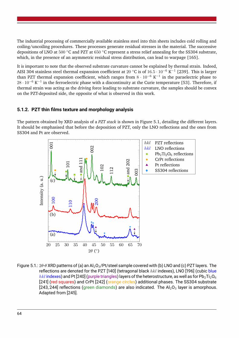
The industrial processing of commercially available stainless steel into thin sheets includes cold rolling andcoiling/uncoiling procedures. These processes generate residual stresses in the material. The successivedepositions of LNO at 500 C and PZT at 650 C represent a stress relief annealing for the SS304 substrate,which, in the presence of an asymmetric residual stress distribution, can lead to warpage [165].
It is important to note that the observed substrate curvature cannot be explained by thermal strain. Indeed,AISI 304 stainless steel thermal expansion coefficient at 20 C is of 16.5 · 10−6 K−1 [239]. This is largerthan PZT thermal expansion coefficient, which ranges from 8 · 10−6 K−1 in the paraelectric phase to28 · 10−6 K−1 in the ferroelectric phase with a discontinuity at the Curie temperature [53]. Therefore, ifthermal strain was acting as the driving force leading to substrate curvature, the samples should be convexon the PZT-deposited side, the opposite of what is observed in this work.
5.1.2. PZT thin films texture and morphology analysis
The pattern obtained by XRD analysis of a PZT stack is shown in Figure 5.1, detailing the different layers.It should be emphasised that before the deposition of PZT, only the LNO reflections and the ones fromSS304 and Pt are observed.
001
101
and11
1
002
102
112
and20
2
003
100
110 200
(a)
(b)
(c)
20 25 30 35 40 45 50 55 60 65 70
2θ ()
Intensity
(a.u
.)
hkl PZT reflectionshkl LNO reflections
Pb2Ti2O6 reflectionsCrPt reflectionsPt reflectionsSS304 reflections
Figure 5.1.: 2θ-θ XRD patterns of (a) an Al2O3/Pt/steel sample coveredwith (b) LNO and (c) PZT layers. Thereflections are denoted for the PZT [140] (tetragonal black hkl indexes), LNO [196] (cubic bluehkl indexes) and Pt [240] (purple triangles) layers of the heterostructure, aswell as for Pb2Ti2O6
[241] (red squares) and CrPt [242] (orange circles) additional phases. The SS304 substrate[243, 244] reflections (green diamonds) are also indicated. The Al2O3 layer is amorphous.Adapted from [245].
64
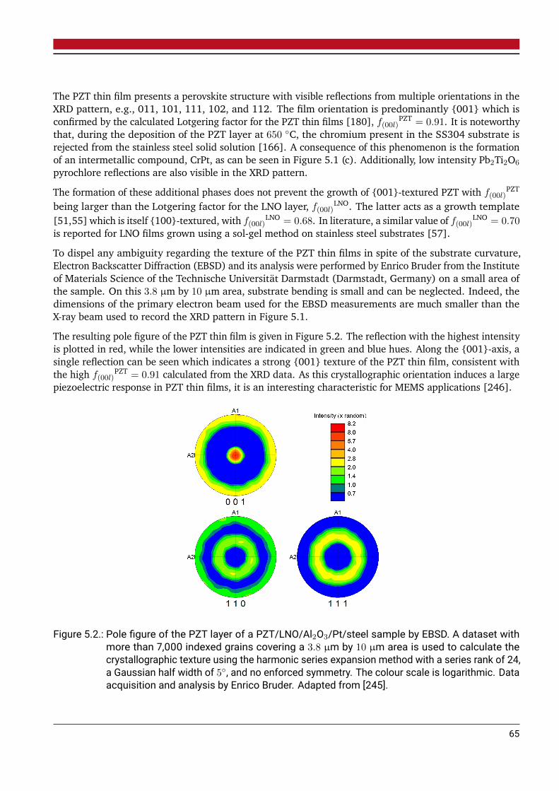
The PZT thin film presents a perovskite structure with visible reflections from multiple orientations in theXRD pattern, e.g., 011, 101, 111, 102, and 112. The film orientation is predominantly 001 which isconfirmed by the calculated Lotgering factor for the PZT thin films [180], f(00l)PZT = 0.91. It is noteworthythat, during the deposition of the PZT layer at 650 C, the chromium present in the SS304 substrate isrejected from the stainless steel solid solution [166]. A consequence of this phenomenon is the formationof an intermetallic compound, CrPt, as can be seen in Figure 5.1 (c). Additionally, low intensity Pb2Ti2O6
pyrochlore reflections are also visible in the XRD pattern.
The formation of these additional phases does not prevent the growth of 001-textured PZT with f(00l)PZT
being larger than the Lotgering factor for the LNO layer, f(00l)LNO. The latter acts as a growth template[51,55] which is itself 100-textured, with f(00l)
LNO = 0.68. In literature, a similar value of f(00l)LNO = 0.70is reported for LNO films grown using a sol-gel method on stainless steel substrates [57].
To dispel any ambiguity regarding the texture of the PZT thin films in spite of the substrate curvature,Electron Backscatter Diffraction (EBSD) and its analysis were performed by Enrico Bruder from the Instituteof Materials Science of the Technische Universität Darmstadt (Darmstadt, Germany) on a small area ofthe sample. On this 3.8 µm by 10 µm area, substrate bending is small and can be neglected. Indeed, thedimensions of the primary electron beam used for the EBSD measurements are much smaller than theX-ray beam used to record the XRD pattern in Figure 5.1.
The resulting pole figure of the PZT thin film is given in Figure 5.2. The reflection with the highest intensityis plotted in red, while the lower intensities are indicated in green and blue hues. Along the 001-axis, asingle reflection can be seen which indicates a strong 001 texture of the PZT thin film, consistent withthe high f(00l)
PZT = 0.91 calculated from the XRD data. As this crystallographic orientation induces a largepiezoelectric response in PZT thin films, it is an interesting characteristic for MEMS applications [246].
Figure 5.2.: Pole figure of the PZT layer of a PZT/LNO/Al2O3/Pt/steel sample by EBSD. A dataset withmore than 7,000 indexed grains covering a 3.8 µm by 10 µm area is used to calculate thecrystallographic texture using the harmonic series expansion method with a series rank of 24,a Gaussian half width of 5, and no enforced symmetry. The colour scale is logarithmic. Dataacquisition and analysis by Enrico Bruder. Adapted from [245].
65
Within the resolution limit of the EBSD, other reflections along the 111- and 110-axes cannot beobserved, which indicates the absence of other orientations in the PZT thin films. However, it remainspossible for a limited number of grains with orientations other than 001 to occur in the investigatedsamples. Nonetheless, a strong texture is achieved which is a key parameter to improve piezoelectricresponse, as will be demonstrated in chapter 6.
The surface and cross-section of the sample analysed by EBSD were imaged by Enrico Bruder using theMira3-XMH high resolution SEM (see section 3.5.3). The SEM images of the PZT film surface and cross-section are depicted in Figure 5.3. Both images are taken in secondary electrons mode, using the in-beamdetector for the cross-section.
(a) (b)
Figure 5.3.: SEM image of (a) the surface and (b) the cross-section of a PZT/LNO/Al2O3/Pt/steel sample.The heterostructure layers are ordered from top to bottom in the SEM image. The imagesare taken using secondary electrons mode and the in-beam detector for the cross-section.Images by Enrico Bruder. Adapted from [245].
The PZT grain size is estimated to be ∼ 45.3 nm by the intercept method averaged over 30 measurementsfrom the surface image presented in Figure 5.3 (a). The grain size is mainly homogeneous over thearea covered by the SEM image. The grain size calculated from the SEM image is larger than the out-of-plane crystallite size of 30 ± 5 nm. The latter is calculated using the Hall method with the softwarePDXL 2 v.2.8.4.0 by Rigaku Corporation (Tokyo, Japan) on the 00l reflections of the XRD pattern shown inFigure 5.1 [204]. The difference between these dimensions can be attributed to both the film strain andthe XRD instrumental error.
Surface pyrochlore phase generally forms small grains of few nanometres in size and located at the grainboundaries [51]. Grains presenting these characteristics are not visible in the SEM image, indicating thatthe pyrochlore phase observed in the XRD pattern in Figure 5.1 is located in the film depth.
In the cross-section SEM image shown in Figure 5.3 (b), a “veil” effect is visible on the surface which iscreated by the focused ion beam cutting. Both this effect and the physical resolution limitations of the SEMimpede a clear view of the microstructure. Nonetheless, porosities can be observed at the Pt/steel interface.This interface is sensitive to the diffusion of Cr, rejected from the stainless steel during the depositionat 650 C of the PZT thin film, into the Pt layer, leading to the formation of a CrPt phase, observed inFigure 5.1. It is not possible to observe porosities at the other interfaces.
66

5.1.3. PZT thin films dielectric and ferroelectric properties
Before P–E loop measurements, the 200 nm and 400 nm thick PZT films exhibit a permittivity at 1 kHz of350 and 349 and a dielectric loss of 4.1 % and 2.6 %, respectively. The instrumental error is of 0.15 %.
The predominantly 001 texture of the PZT films leads to the occurrence of ferroelectric domains with anout-of-plane polarisation, referred to as c-domains, which can partially explain the low permittivity values.It has indeed been demonstrated in literature that the permittivity of c-domains is lower than the one ofa-domains with an in-plane polarisation [51,53].
The dielectric permittivity values of the PZT films, measured at 1 kHz before P–E loop measurements,are lower than that reported in literature of ∼ 600 for 0.6 µm thick 001-oriented Nb-doped PZT filmson Ni foils [53]. The higher values reported in literature, as compared to the non-doped PZT thin filmsfrom PZT stacks, are consistent with the effects of Nb-doping. Indeed, domain wall mobility in PZT isenhanced by Nb-doping, leading to increased permittivity [53]. The values reported in this thesis are alsosignificantly lower than these of ∼ 780 for 1 µm thick PZT films on Ni foils [51] and ∼ 790 for 500 nmthick rhombohedral PZT films on ferritic steel deposited by the sol-gel method [57] which are reported inliterature. The difference can be attributed to the presence, even in limited quantities, of pyrochlore phasein the thin films deposited in this work which would also contribute to lower their permittivity.
Nevertheless, the values of permittivity for the 001-textured PZT thin films deposited in this workare higher than the value of 192 reported in the literature for non-textured films on austenitic stainlesssteel [64]. Furthermore, the dielectric losses of 4.1 % and 2.6 % for the PZT films in PZT stacks is lowerthan that of 10.2 % reported for those films.
Moreover, it should be noted that the grain size calculated here is relatively small as compared to thevalues of 63 nm to 192 nm reported in literature for PZT films grown by PLD on various substrates [247].The density of both grain boundaries and domain walls is increased by small grain sizes which mightlower domain wall mobility, hence limiting ferroelectric properties [248]. The reduced thicknesses of theproduced PZT films as compared to that of about 1 µm, which is usually reported in the literature [51,53],might also be the cause of their lower permittivity [249].
For both the 200 nm and 400 nm thick samples, the P–E loops are measured at 100 kHz and with amaximum applied field of 200 kV·cm−1. They are presented in Figure 5.4 along with the correspondingswitching current versus electrical field hysteresis loops. For each sample, both curves, represented inFigure 5.4 (a) and (b), originate from the same dataset. The 200 nm thick film displays a larger and morerounded hysteresis than the 400 nm thick film for which the polarisation is nearly saturated. The differencecan be attributed to the 200 nm thick film reduced thickness, leading to larger leakage.
The positive and negative branches of the 200 nm thick sample P–E loop are shaped differently along thepolarisation axis; there is higher conduction on the upper branch. In the 400 nm thick PZT film, due to thelower leakage, this phenomenon is less pronounced. Leakage current measurements on a PZT stack with a400 nm thick PZT layer will be presented in the next section.
To improve accuracy, the values of the coercive fields for the 200 nm and 400 nm thick samples aredetermined from the switching current versus field hysteresis loops in Figure 5.4 (b). The positive andnegative coercive fields are the fields corresponding to the switching current peaks. In the case of the200 nm thick sample, the positive coercive field at 100 Hz is Ec = 135.9 kV·cm−1 and the displayed internalbias field is Ec,shift = 21.0 kV·cm−1. The coercive field for the 400 nm thick sample is Ec = 93.9 kV·cm−1
and its internal bias field is Ec,shift = 12.0 kV·cm−1.
67

200 nm
400 nm(a)
−200 −100 0 100 200
−30
−20
−10
0
10
20
30
Electrical field (kV·cm−1)
Polaris
ation(µ
C·cm
−2) 200 nm
400 nm
(b)
−200 −100 0 100 200
−0.3
−0.2
−0.1
0
0.1
0.2
Electrical field (kV·cm−1)
Switc
hing
curren
t(mA)
Figure 5.4.: (a) Polarisation, P , versus electrical field, E , hysteresis loops and (b) corresponding switchingcurrent versus electrical field hysteresis loops at 100 Hz of 200 nm (red curves) and 400 nm(blue curves) thick PZT layers of PZT/LNO/Al2O3/Pt/steel samples, respectively. The dashedand dotted lines indicate the position of the positive and negative coercive fields of 200 nmand 400 nm thick PZT films, respectively. Adapted from [245].
The coercive fields reported in this work for PZT thin films are larger than those of ∼ 73 kV·cm−1 for 1 µmthick PZT films deposited on Ni foils reported in literature [51]. The presence of an internal bias fieldcauses the asymmetry of the P-E loop along the electrical field axis and indicates a preferred polarisationdirection [120,211]. Therefore, an external field applied in the opposite direction would result in significantchanges in the polarisation [233].
The remanent polarisation, Pr, of the 200 nm and 400 nm thick PZT films after the applied electrical fieldof 200 kV·cm−1 was released is obtained from the P–E loops in Figure 5.4 (a). It is of Pr = 16.7 µC·cm−2
and Pr = 16.4 µC·cm−2, respectively.
In PZT stacks, both 200 nm and 400 nm thick PZT films show similar remanent polarisation and permittivityvalues. The major difference between the behaviour of these thin films is the higher leakage in the thinnerfilm, leading to a less saturated P–E loop.
5.1.4. Leakage current measurements on PZT stacks
In order to identify the leakage current mechanism in the 400 nm thick PZT layer of PZT stacks from avirgin top electrode with an area of 0.0327 mm2, several representations of the DC leakage current density,J , are plotted Figure 5.5. The first representation in Figure 5.5 (a), known as a J–E curve, plots the DCleakage current density as a function of the positive and negative applied electrical field.
The J–E curve can be fitted with polynomial functions of the electrical field for the positive and negativepolarities, J ∝ E3.15 and J ∝ E3.12, respectively. These functions are attributed to a Space-Charge LimitedCurrent (SCLC) mechanism with trap filling which is described by J ∝ EN with N > 2 [235,250].
For both polarities, the leakage current density is similar. With regard to the rounded shape of the P–Eloops in Figure 5.4 (a), the presence of leakage in the PZT thin films is coherent, particularly for the thinner
68

(b)
−8 −6 −4 −2 0 2 4 6 8
−20
−15
−10
−5
(E (V·m−1))1/2 [×103]
ln(J/T
2(A·m
−2·K
−2))
(c)
−8 −6 −4 −2 0 2 4 6 8−20
−18
−16
−14
−12
−10
(E (V·m−1))1/2 [×103]
ln(J/E
(A·V
−1·m
−1))
(a)
−6 −4 −2 0 2 4 6
10−4
10−2
100
102
104
Electrical field [×107] (V·m−1)
Curren
tden
sity
(A·m
−2)
Figure 5.5.: Leakage current density, J , as a function of the applied electrical field, E, for the 400 nmthick PZT layer of a PZT/LNO/Al2O3/Pt/steel sample (blue squares) (a) fitted within the space-charge limited current scenariowith the polynomial functions J ∝ E3.15 for the positive polarityand J ∝ E3.12 for the negative polarity (red curves), (b) plotted for the Schottky emissionscenario with a linear fit (red lines) between 100 kV·cm−1 and 550 kV·cm−1 for the positivepolarity and between −400 kV·cm−1 and −25 kV·cm−1 for the negative polarity, (c) plottedfor the Poole-Frenkel emission scenario with a linear fit (red lines) between 100 kV·cm−1 and550 kV·cm−1 for the positive polarity and between −250 kV·cm−1 and −10 kV·cm−1 for thenegative polarity. Adapted from [245].
200 nm thick film. However, as the SCLC fit of the J–E curve in Figure 5.5 (a) is not perfect, it indicatesthe potential contributions of other physical mechanisms in the leakage transfer through the PZT film.Therefore, in addition to the SCLC mechanism, the DC leakage current density is fitted according toSchottky emission and to Poole-Frenkel emission in Figure 5.5 (b) and (c), respectively.
69
Under the hypothesis of Schottky emission, the current density can be expressed as [235]:
J = A∗T 2exp
[−q
(φB −
√qE/4πεr,opticalε0
)kBT
], (5.1)
where A∗ is the effective Richardson constant, T is the absolute temperature, q is the electronic charge, qφB
is the Schottky barrier height, εr,optical is the optical dielectric constant, and kB is the Boltzmann constant.
In consequence, by plotting the J-E measurements as ln(J/T 2
)versus E1/2, the optical dielectric constant
under the hypothesis of Schottky emission can be calculated from the slope of the linear region. It isexpressed as:
εr,optical =q3
4πε0(slope · kBT )2, (5.2)
and the optical refractive index, noptical =√εr,optical, can be estimated from this slope.
On the plot of ln(J/T 2
)versus E1/2 presented in Figure 5.5 (b), linear fits are represented. Under the
hypothesis of Schottky emission, at room temperature (T = 298 K), for the positive polarity, the fittingbetween 100 kV·cm−1 and 550 kV·cm−1 has a slope absolute value of 1.4 · 10−3 with a linear fit coefficientR2 = 0.987. The corresponding refractive index is noptical,Schottky = 1.06. For the negative polarity, thelinear fit between −250 kV·cm−1 and −10 kV·cm−1 presents a slope absolute value of 1.7 · 10−3 withR2 = 0.977. The corresponding refractive index is noptical,Schottky = 0.88.
The theoretical refractive index of PZT 52/48 is noptical,th = 2.2 − 2.7 [251]. Therefore, the Schottkyemission hypothesis cannot be validated for the PZT layer of PZT stacks as the refractive indexes obtainedin this work by applying this hypothesis are less than half the value of noptical,th.
Under the hypothesis of Poole-Frenkel emission, the current density is expressed by [235]:
J = qµelecNCEexp
[−q
(φT −
√qE/πεr,opticalε0
)kBT
], (5.3)
with µelec the electronic drift mobility, NC the density of states in the conduction band and qφT the trapenergy level.
Therefore, the optical dielectric constant under the hypothesis of Poole-Frenkel emission can be calculatedfrom the slope of the linear region when plotting ln (J/E) versus E1/2 with:
εr,optical =q3
πε0(slope · kBT )2, (5.4)
and the refractive index can be estimated.
On the plot of ln (J/E) versus E1/2 given in Figure 5.5 (c), linear fits are indicated. Under the hypothesisof Poole-Frenkel emission, for the positive polarity, the linear fit between 100 kV·cm−1 and 550 kV·cm−1
presents a slope absolute value of 1.0 · 10−3 with a linear fit coefficient R2 = 0.973. The correspondingrefractive index is noptical,Poole−Frenkel = 2.92. For the negative polarity, the fitting between 10 kV·cm−1
and 250 kV·cm−1 has a slope absolute value of 8.9 · 10−4 with R2 = 0.945. The corresponding refractiveindex is noptical,Poole−Frenkel = 3.31.
The optical dielectric constants for the PZT layer under the hypothesis of Poole-Frenkel emission are slightlylarger than noptical,th and, therefore, the hypothesis can be neither validated nor dismissed.
70

While the conduction mechanism in the PZT thin films deposited in this work is not predominantly interfacedriven, the interfaces between the PZT layer and the electrodes, influenced by the electrode materials,impact on leakage current. This is particularly pronounced on the thinner 200 nm thick film. If the Schottkyemission hypothesis gives a refractive index incoherent with literature values for PbZr0.52Ti0.48O3, thePoole-Frenkel emission hypothesis, contrarily, remains a possibility. Nevertheless, the hypothesis of a SCLCmechanism with trap filling is the most likely to occur of the conduction mechanisms studied in this work.
5.2. 001-textured PNZT thin films: improving the properties
In the previous section, predominantly 001-textured PbZr0.52Ti0.48O3 thin films have been depositedon stainless steel substrates by PLD. The films low dielectric constant and high coercive fields indicatetheir potential as transducer applications. In order to improve the ferroelectric properties achievedwith the PZT stacks, series of PNZT stacks are deposited to study the impact of several depositionparameters, as well as film thickness influence. Increased dielectric constants and lower coercive fieldsare expected from the 2 mol.% Nb-doping of PZT 52/48 (see section 2.2.1). As key parameters to controlthe evaporation of PbO during the growth of PNZT by PLD, substrate temperature and O2 pressure arevaried between 600 C and 700 C and from 5.0 Pa to 10.0 Pa, respectively.
Preliminaries studies have shown that the laser repetition rate of 10 Hz previously employed for the PZTstacks leads to the presence of a Pb phase in the films. Originating from the 10 mol.% excess PbO includedin the PNZT target to hinder the formation of a pyrochlore phase during deposition (see section 2.2.1), theformation of the Pb phase can be avoided by lowering the laser repetition rate. However, this introducesa strong reflection of the pyrochlore phase in the XRD patterns of the films. Additional preliminariesstudies established that the presence of pyrochlore phase in PZT thin films can be avoided if the depositiontemperature is superior or equal to 650 C. Below this temperature, PZT and pyrochlore phases coexistin the films. It should be noted that Nb-doping of the PZT thin films, while improving the piezoelectricresponse, might tends to stabilise the formation of a pyrochlore phase [146,154].
Therefore, to both avoid the formation of a Pb phase and limit the presence of a pyrochlore phase, theinitial deposition parameters for PNZT stacks have been chosen at 700 C for the deposition temperatureand of 4 Hz for the laser repetition rate, respectively higher and lower than for PZT stacks.
As for the PZT stacks, dielectric and ferroelectric characterisations have been performed on PNZT stacks.Additionally, e31,f piezoelectric coefficients, which could not be measured on the PZT stacks due to thepresence of silver paste on the back of the samples (see section 3.1), have been measured on the PNZTstacks. The possibility to perform these measurements is enabled by the utilisation of a modified flag styleholder, designed specifically to hold samples during LNO deposition and argon ion milling processes (seesection 3.1).
5.2.1. Influence of O2 deposition pressure on ferroelectric properties
The patterns obtained by XRD analysis of PNZT/LNO/Al2O3/steel heterostructures with PNZT layersdeposited under 5.0 Pa, 6.5 Pa, 8.0 Pa and 10.0 Pa of O2 are shown in Figure 5.6 (a). The PNZT reflections,assimilated to those of PZT, and the Pb2Ti2O6 reflections both appear during the deposition of the PNZTlayer.
71
(b)
5 6 7 8 9 10320
340
360
380
400
420
440
460
480
Pressure (Pa)
Dielectric
constant
Legend for (b):at 1 kHz, before P-E loopat 10 kHz, before P-E loopat 1 kHz, after P-E loopat 10 kHz, after P-E loop
(c)
−400 −200 0 200 400
−40
−20
0
20
40
Electrical field (kV·cm−1)
Polaris
ation(µ
C·cm
−2)
Legend for (c):5.0 Pa6.5 Pa8.0 Pa10.0 Pa
001
101
002
102
112
003
100
110
200
(a)
20 25 30 35 40 45 50 55 60 65 70
2θ ()
Intensity
(a.u
.)Legend for (a):
hkl PZT reflectionshkl LNO reflections
Pb2Ti2O6 reflectionsSS304 reflections5.0 Pa6.5 Pa8.0 Pa10.0 Pa
Figure 5.6.: Effect of PNZT O2 deposition pressure on PNZT stackswith∼ 170−208 nm thick PNZT layerson (a) 2θ-θ XRD patterns with reflections denoted for PZT [140] (tetragonal black hkl indexes),LNO [196] (cubic blue hkl indexes) and SS304 [243, 244] (light blue diamonds) as well asfor Pb2Ti2O6 [241] (light green squares) additional phase, the Al2O3 layer being amorphous,(b) values of PNZT dielectric constant, εr , at 1 kHz (purple marks) and at 10 kHz (grey marks)with VAC = 30 mV before (closed squares) and after (open circles) measuring P-E loops,(c) PNZT polarisation, P , versus electrical field, E, hysteresis loops at 100 Hz. In (a) and (c),PNZT O2 deposition pressures of 5.0 Pa, 6.5 Pa, 8.0 Pa and 10.0 Pa are represented by theblue, red, green and orange curves, respectively.
72

As for the PZT thin films discussed in section 5.1.2, the PNZT films present a perovskite structure and arepredominantly 001-oriented despite visible reflections from multiple orientations in the XRD pattern.Contrary to the PZT thin films, the 111 reflection is absent from the XRD pattern. The predominantly001 orientation is indicated by the Lotgering factors of the PNZT layers which, while slightly lower thanf(00l)
PZT = 0.91 from section 5.1.2, remain high, ranging between f(00l)PNZT = 0.82 and f(00l)
PNZT = 0.89.
It is suggested that the lower PNZT Lotgering factors originate not from a lower quality of the LNO seedlayer but from the PNZT layer itself, either due to the Nb doping or to non-optimised deposition parameters.Indeed, the LNO Lotgering factor for PNZT stacks ranges from f(00l)
LNO = 0.72 to f(00l)LNO = 0.84 which
is higher than the value of f(00l)LNO = 0.68 reported in this work for PZT stacks. The improvement isattributed to the absence of the Pt buffer layer in PNZT stacks which was forming an intermetallic phasewith Cr from the stainless steel substrate in PZT stacks. It is considered that this CrPt phase was hinderingthe oriented growth of the LNO layer. It should be noted that the LNO Lotgering factor achieved for PNZTstacks is larger than the value of f(00l)LNO = 0.70 reported in literature on stainless steel substrates using asol-gel method [57].
Additionally, Pb2Ti2O6 reflections are visible in the XRD patterns of the PNZT films deposited under an O2
pressure of 5.0 Pa and 6.5 Pa. This is not the case for the thin films deposited under 8.0 Pa and 10.0 Pa ofO2, indicating that the last two O2 deposition pressures could be suitable parameters for the growth ofPNZT by PLD, producing a limited amount of pyrochlore phase which cannot be detected by XRD.
To determine the appropriate O2 deposition pressure, further measurements are conducted on the PNZTthin films. Figure 5.6 (b) gives the values of PNZT dielectric constant at 1 kHz and at 10 kHz withVAC = 30 mV before and after measuring P-E loops at 100 Hz which are represented in Figure 5.6 (c). Foreach sample, the permittivity and P-E loop measurements shown in Figure 5.6 are performed on the sameelectrode. To facilitate comparison of the results, all electrodes are chosen with an area of 0.0327 mm2, atthe exception of the sample deposited under 5.0 Pa of O2 for which this size of electrode is not availablefor measurement and, therefore, a 0.1252 mm2 electrode is selected.
Concerning PNZT dielectric constant, no clear trends emerge as a function of the O2 deposition pressure,neither before or after measuring P-E loops. This phenomenon can partly be explained by the absence ofdata for samples deposited under 5.0 Pa and 8.0 Pa of O2 before measuring P-E loops due to importantdielectric losses, larger than 10 %. It is further illustrated in Table 5.1 which summarises the average valuesand standard deviations of both dielectric constant and loss depending on the O2 deposition pressure at1 kHz and at 10 kHz with VAC = 30 mV before measuring P-E loops. Data are collected from a selectionof four electrodes which comprises two 0.0327 mm2, one 0.1252 mm2 and one 0.2828 mm2 electrodes.Should there be electrodes with a dielectric loss superior to 10 % on the sample, they are not taken intoaccount. Due to the limited number of electrodes analysed in this work, Table 5.1 also indicates minimaland maximal values to give a more accurate representation of the samples.
Compared with the permittivity of 350 for the 200 nm thick PZT thin films at 1 kHz before measuringP-E loops discussed in section 5.1.3, the average dielectric constant of the PNZT films under the sameconditions is higher at 354.4, 391.6 and 424.3 for O2 deposition pressures of 6.5 Pa, 8.0 Pa and 10.0 Pa,respectively. It is noteworthy that the minimal values of permittivity for PNZT films deposited under 8.0 Paand 10.0 Pa of O2 are higher than the values reported in this work for PZT. This permittivity increase canbe attributed to the Nb-doping of PZT [53,146,151] and, at higher O2 deposition pressures, to the absenceor limited amount of pyrochlore phase in the PNZT thin films.
Under these conditions, the PNZT thin films deposited under 6.5 Pa, 8.0 Pa and 10.0 Pa of O2 have averagedielectric losses of 8.6 %, 5.9 % and 4.1 %, respectively. This is globally higher than the 4.1 % reported in
73

Table 5.1.: Effect of PNZT O2 deposition pressure on PNZT stacks with ∼ 170− 208 nm thick PNZT layerson their dielectric constant, εr , and loss values at 1 kHz and at 10 kHz with VAC = 30mV beforeP-E loop measurements. Minimum, average, maximum and standard deviation values areindicated. When only one electrode could bemeasured, the single value is given as the average.
O2 pressure (Pa) 5.0 6.5 8.0 10.0
Measured at 1 kHz 10 kHz 1 kHz 10 kHz 1 kHz 10 kHz 1 kHz 10 kHz
Dielectricconstant
Minimum - - - - - 376.4 399.7 385.9
Average - - 354.4 337.8 391.6 388.6 424.3 408.7
Maximum - - - - - 404.9 448.9 432.4
Standarddeviation - - - - - 12.0 24.6 17.1
Dielectricloss (%)
Minimum - - - - - 3.1 2.8 2.6
Average - - 8.6 3.6 5.9 5.7 4.1 4.8
Maximum - - - - - 7.2 5.3 8.1
Standarddeviation - - - - - 0.4 1.3 2.0
this thesis for the 200 nm thick PZT sample and can be an effect of Nb-doped on PZT [98]. It is suggestedthat the increased dielectric losses are linked to the presence of more defects in the crystalline structure.This hypothesis is consistent with the less pronounced 001 orientation of the PNZT layers compared tothat of the PZT thin films, as indicated by their respective Lotgering factors.
Moreover, an important feature of Figure 5.6 (b) is the increase of the dielectric constant after P-E loopsare measured for the samples deposited under 8.0 Pa and 10.0 Pa of O2, reaching 429.2 and 426.3 at1 kHz, respectively. This aspect will be discussed in section 5.2.4.
The analysis of PNZT thin films dielectric constants as a function of their O2 deposition pressures beinginsufficient to indicate an optimal choice of deposition parameter, their ferroelectric characteristic valuesprovide additional insight. From Figure 5.6 (c), it appears that the PNZT layer deposited under 6.5 Paof O2 presents a rounded P-E loop without clear saturation, characteristic of a thin film with significantleakage. This is sensible with the presence of a pyrochlore phase in this thin film as well as with the reduceddielectric constant of 354 at 1 kHz coupled with a dielectric loss of 8.6 %.
On the other hand, PNZT thin films deposited under 5.0 Pa, 8.0 Pa and 10.0 Pa of O2 exhibit well definedP-E loops with marked saturation, characteristic of ferroelectrics. Similar to the behaviour of the PZTstacks, the positive and negative branches of the P-E loops are asymmetrical along the polarisation andthe electrical field axes. The values of remanent polarisation, saturation polarisation, coercive field andinternal bias field are given in Table 5.2. The coercive fields values are determined from the switchingcurrent versus field hysteresis loops, with the same methodology as in section 5.1.3 where the positiveand negative coercive fields are the fields corresponding to the switching current peaks. To determine theferroelectric characteristic values P-E loops with the same maximum applied voltage are selected for all
74
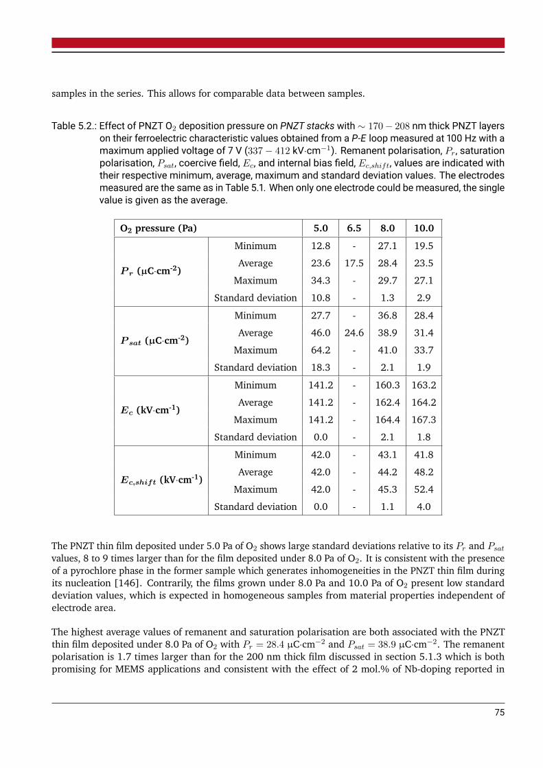
samples in the series. This allows for comparable data between samples.
Table 5.2.: Effect of PNZT O2 deposition pressure on PNZT stacks with ∼ 170− 208 nm thick PNZT layerson their ferroelectric characteristic values obtained from a P-E loop measured at 100 Hz with amaximum applied voltage of 7 V (337− 412 kV·cm−1). Remanent polarisation, Pr , saturationpolarisation, Psat, coercive field, Ec, and internal bias field, Ec,shift, values are indicated withtheir respective minimum, average, maximum and standard deviation values. The electrodesmeasured are the same as in Table 5.1. When only one electrode could be measured, the singlevalue is given as the average.
O2 pressure (Pa) 5.0 6.5 8.0 10.0
P r (µC·cm-2)
Minimum 12.8 - 27.1 19.5
Average 23.6 17.5 28.4 23.5
Maximum 34.3 - 29.7 27.1
Standard deviation 10.8 - 1.3 2.9
P sat (µC·cm-2)
Minimum 27.7 - 36.8 28.4
Average 46.0 24.6 38.9 31.4
Maximum 64.2 - 41.0 33.7
Standard deviation 18.3 - 2.1 1.9
Ec (kV·cm-1)
Minimum 141.2 - 160.3 163.2
Average 141.2 - 162.4 164.2
Maximum 141.2 - 164.4 167.3
Standard deviation 0.0 - 2.1 1.8
Ec,shift (kV·cm-1)
Minimum 42.0 - 43.1 41.8
Average 42.0 - 44.2 48.2
Maximum 42.0 - 45.3 52.4
Standard deviation 0.0 - 1.1 4.0
The PNZT thin film deposited under 5.0 Pa of O2 shows large standard deviations relative to its Pr and Psat
values, 8 to 9 times larger than for the film deposited under 8.0 Pa of O2. It is consistent with the presenceof a pyrochlore phase in the former sample which generates inhomogeneities in the PNZT thin film duringits nucleation [146]. Contrarily, the films grown under 8.0 Pa and 10.0 Pa of O2 present low standarddeviation values, which is expected in homogeneous samples from material properties independent ofelectrode area.
The highest average values of remanent and saturation polarisation are both associated with the PNZTthin film deposited under 8.0 Pa of O2 with Pr = 28.4 µC·cm−2 and Psat = 38.9 µC·cm−2. The remanentpolarisation is 1.7 times larger than for the 200 nm thick film discussed in section 5.1.3 which is bothpromising for MEMS applications and consistent with the effect of 2 mol.% of Nb-doping reported in
75
literature [154]. However, it should be noted that the remanent polarisation of PNZT thin films wasobtained after the release of an applied electrical field of 412 kV·cm−1, about twice larger than the appliedfield of 200 kV·cm−1 employed for the PZT films in section 5.1.3, which might lead to a larger ferroelectricresponse by switching a larger number of ferroelectric domains.
A better assessment of the remanent polarisation can be obtained by comparison with the value of∼ 39.5 µC·cm−2 reported in literature for 600 nm thick PNZT films on Ni foils after the release of a900 kV·cm−1 applied field, i.e. a value 1.4 times higher than for the PNZT thin films deposited in thiswork for an applied field more than twice larger [53]. Furthermore, 500 nm thick rhombohedral PZT filmson ferritic steel and 1 µm thick PZT films on Ni foils display remanent polarisations of 41.5 µC·cm−2 and∼ 36 µC·cm−2, i.e. only 1.5 and 1.3 times higher than the value reported in this thesis for applied fieldsat least 2.4 times larger, respectively [51,57]. Therefore, the PNZT thin films deposited in this work onstainless steel substrates by PLD present encouraging values of remanent polarisation, indicating both agood ferroelectric response and a limited amount of back switching from the saturation polarisation.
The average positive coercive field, Ec, and internal bias field, Ec,shift, obtained from a P-E loop measuredat 100 Hz range from Ec = 141.2 kV·cm−1 to Ec = 167.3 kV·cm−1 and between Ec,shift = 42.0 kV·cm−1
and Ec,shift = 48.2 kV·cm−1, respectively, for the PNZT thin films deposited under 5.0 Pa, 8.0 Pa and10.0 Pa of O2. The coercive field of the sample deposited under 6.5 Pa of O2 cannot be determined sinceits switching current versus field hysteresis loop does not show a marked switching current peak. Thecoercive field of the PNZT layer is slightly larger than the one of the 200 nm thick PZT thin film discussedin section 5.1.3 while its internal bias field is approximately twice larger. This increase is consistent withliterature reports of similar Ec values between 2 mol.% Nb-doped and undoped PZT thin films [154]. It isalso suggested that the comparatively high dielectric losses reported in this work for the PNZT thin filmshinder efficient ferroelectric switching, leading to higher coercive fields.
The O2 deposition pressure of Pb0.990.01(Zr0.52Ti0.48)0.98Nb0.02O3 thin films in PNZT stacks impacts theircomposition and ferroelectric properties. Higher O2 pressures of 8.0 Pa and above are necessary to limitthe amount of pyrochlore phase below levels detectable in XRD patterns. The thin film deposited under8.0 Pa of O2 shows a good permittivity and tolerable dielectric loss while exhibiting the largest remanentand saturation polarisation of the series. Therefore, an O2 deposition pressure of 8.0 Pa is selected forfurther experiments.
5.2.2. Influence of deposition temperature on ferroelectric properties
Figure 5.7 (a) presents the XRD patterns for 170 nm thick PNZT thin film deposited at temperatures of600 C, 650 C, 675 C and 700 C within PNZT stacks.
The PNZT reflections, assimilated to those of PZT, appear during the deposition of the PNZT thin films,along with the Pb2Ti2O6 and Pb reflections. The perovskite structure and the predominant 001 textureof the PNZT thin films reported in section 5.2.1 are confirmed by the XRD patterns. The 111 reflectionremains absent from the XRD pattern of the PNZT layers.
At a deposition temperature of 600 C, additional reflections of both Pb2Ti2O6 and Pb phases are visible onthe XRD pattern. The presence of these additional phases hinders the 001 texture of the thin film and isaccompanied by a small Lotgering factor of f(00l)PNZT = 0.72. More elevated temperatures of 650 C and675 C prevent the formation of a Pb phase but not of a pyrochlore phase. The associated Lotgering factorsare f(00l)
PNZT = 0.79 and f(00l)PNZT = 0.88, respectively. The thin film grown at 700 C is the same sample
76
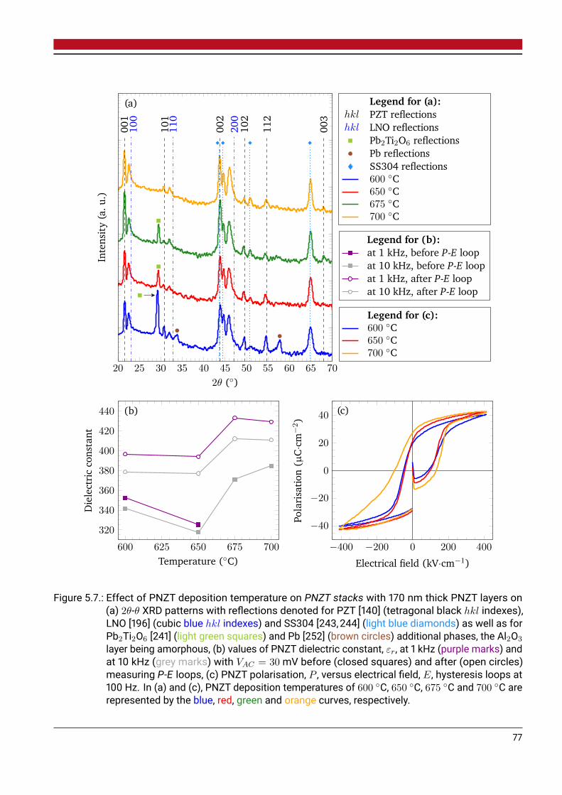
(b)
600 625 650 675 700
320
340
360
380
400
420
440
Temperature (C)
Dielectric
constant
Legend for (b):at 1 kHz, before P-E loopat 10 kHz, before P-E loopat 1 kHz, after P-E loopat 10 kHz, after P-E loop
(c)
−400 −200 0 200 400
−40
−20
0
20
40
Electrical field (kV·cm−1)
Polaris
ation(µ
C·cm
−2)
Legend for (c):600 C650 C700 C
001
101
002
102
112
003
100
110
200
(a)
20 25 30 35 40 45 50 55 60 65 70
2θ ()
Intensity
(a.u
.)Legend for (a):
hkl PZT reflectionshkl LNO reflections
Pb2Ti2O6 reflectionsPb reflectionsSS304 reflections600 C650 C675 C700 C
Figure 5.7.: Effect of PNZT deposition temperature on PNZT stacks with 170 nm thick PNZT layers on(a) 2θ-θ XRD patterns with reflections denoted for PZT [140] (tetragonal black hkl indexes),LNO [196] (cubic blue hkl indexes) and SS304 [243,244] (light blue diamonds) as well as forPb2Ti2O6 [241] (light green squares) and Pb [252] (brown circles) additional phases, the Al2O3
layer being amorphous, (b) values of PNZT dielectric constant, εr , at 1 kHz (purple marks) andat 10 kHz (grey marks) with VAC = 30 mV before (closed squares) and after (open circles)measuring P-E loops, (c) PNZT polarisation, P , versus electrical field, E, hysteresis loops at100 Hz. In (a) and (c), PNZT deposition temperatures of 600 C, 650 C, 675 C and 700 C arerepresented by the blue, red, green and orange curves, respectively.
77
as the one previously included in the deposition pressure series and standing for deposition under 8.0 Pa ofO2. Its Lotgering factor is f(00l)PNZT = 0.82 and no additional phases can be observed in its XRD pattern.
The presence of a pyrochlore phase competing with the PNZT phase at lower deposition temperatures isconsistent with preliminaries studies performed on PZT thin films (see introduction of section 5.2). The222 Pb2Ti2O6 reflection being more intense than the 001 reflection of PZT in the XRD pattern of the filmdeposited at 600 C, contrary to the XRD patterns of the films deposited at 650 C and 675 C, confirmsthis trend. The concomitant formation of a pyrochlore phase, characteristic of lead loss [24], and of a Pbphase, indicating an excess of lead, hints towards kinetics at the film surface with a substrate temperatureof 600 C being inadequate to the growth of PNZT.
Similar to the results reported in section 5.2.1, LNO Lotgering factor ranges from f(00l)LNO = 0.73 to
f(00l)LNO = 0.84, larger than literature values [57].
Dielectric permittivity measurements at 1 kHz and at 10 kHz with VAC = 30 mV are conducted on thedeposition temperature series of PNZT thin films before and after measuring P-E loops and results aregiven in Figure 5.7 (b). The polarisation versus electrical field hysteresis loops acquired at 100 Hz arerepresented in Figure 5.7 (c). For each sample, the dielectric constant and P-E loop measurements inFigure 5.7 are performed on the same electrode. To facilitate comparison of the results, all electrodes areselected with an area of 0.0327 mm2.
Regarding PNZT permittivity values, there is a slight trend indicating that dielectric constant at 10 kHzbefore P-E loops increases from ∼ 330 to ∼ 370 with deposition temperature. This effect is most likelylinked with the presence of additional phases in the thin films, notably Pb2Ti2O6 pyrochlore at lowerdeposition temperatures. A similar trend is observed at 1 kHz and 10 kHz after P-E loop measurements andis also noticeable in Table 5.3 compiling the average values and standard deviations of dielectric constantand loss as a function of the deposition temperature at 1 kHz and 10 kHz with VAC = 30 mV beforemeasuring P-E loops. In the same manner as for the O2 deposition pressure series, data are collected froma set of four electrodes which comprises two 0.0327 mm2, one 0.1252 mm2 and one 0.2828 mm2 electrodes.Should there be electrodes with a dielectric loss superior to 10 % on the sample, they are not taken intoaccount. Due to the limited number of electrodes analysed in this work, Table 5.3 also gives minimal andmaximal values to allow a more accurate representation of the samples.
The dielectric constant average values at 1 kHz and 10 kHz before measuring P-E loops are largest for thesample deposited at 700 C and previously discussed in section 5.2.1. It should be noted that both theminimal and maximal values of permittivity follow the same trend. The standard deviation values aremoderate except for the sample deposited at 600 C which contains pyrochlore and Pb additional phases,creating inhomogeneities during the PNZT film nucleation [146]. The absence of data for the sampledeposited at 675 C is due to important dielectric losses, larger than 10 %.
The average dielectric losses at 1 kHz of the PNZT thin films deposited at 600 C, 650 C and 700 C are of2.8 %, 1.7 % and 5.9 %, respectively. These values are on par with the 4.1 % reported in section 5.1.3 forthe 200 nm thick PZT sample and with literature values being below 5 % [24,51,53].
Similar to the phenomenon observed in Figure 5.6 (b), there is an increase of the dielectric constant afterP-E loop measurements for all samples which will be discussed in section 5.2.4.
To complete the study of PNZT thin films deposition temperature impact on their properties, their ferroelec-tric characteristic values are analysed. In Figure 5.7 (c), the polarisation versus electrical field hysteresisloops display clear saturation accompanied by the convex and concave shapes characteristic of ferroelectric
78
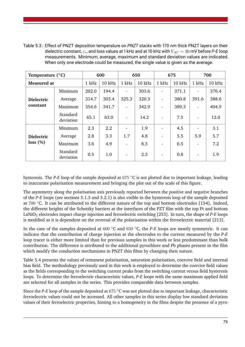
Table 5.3.: Effect of PNZT deposition temperature on PNZT stacks with 170 nm thick PNZT layers on theirdielectric constant, εr , and loss values at 1 kHz and at 10 kHz with VAC = 30mV before P-E loopmeasurements. Minimum, average, maximum and standard deviation values are indicated.When only one electrode could be measured, the single value is given as the average.
Temperature (C) 600 650 675 700
Measured at 1 kHz 10 kHz 1 kHz 10 kHz 1 kHz 10 kHz 1 kHz 10 kHz
Dielectricconstant
Minimum 202.0 194.4 - 303.6 - 371.1 - 376.4
Average 314.7 303.4 325.3 320.3 - 380.8 391.6 388.6
Maximum 354.6 341.7 - 342.9 - 389.3 - 404.9
Standarddeviation 65.1 63.0 - 14.2 - 7.5 - 12.0
Dielectricloss (%)
Minimum 2.3 2.2 - 1.9 - 4.5 - 3.1
Average 2.8 3.3 1.7 4.8 - 5.5 5.9 5.7
Maximum 3.6 4.9 - 8.3 - 6.5 - 7.2
Standarddeviation 0.5 1.0 - 2.3 - 0.8 - 1.9
hysteresis. The P-E loop of the sample deposited at 675 C is not plotted due to important leakage, leadingto inaccurate polarisation measurement and bringing the plot out of the scale of this figure.
The asymmetry along the polarisation axis previously reported between the positive and negative branchesof the P-E loops (see sections 5.1.3 and 5.2.1) is also visible in the hysteresis loop of the sample depositedat 700 C. It can be attributed to the different nature of the top and bottom electrodes [154]. Indeed,the different heights of the Schottky barriers at the interfaces of the PZT film with the top Pt and bottomLaNiO3 electrodes impact charge injection and ferroelectric switching [253]. In turn, the shape of P-E loopsis modified as it is dependent on the reversal of the polarisation within the ferroelectric material [213].
In the case of the samples deposited at 600 C and 650 C, the P-E loops are mostly symmetric. It canindicate that the contribution of charge injection at the electrodes to the current measured by the P-Eloop tracer is either more limited than for previous samples in this work or less predominant than bulkcontribution. The difference is attributed to the additional pyrochlore and Pb phases present in the filmwhich modify the conduction mechanisms in PNZT thin films by changing their nature.
Table 5.4 presents the values of remanent polarisation, saturation polarisation, coercive field and internalbias field. The methodology previously used in this work is employed to determine the coercive field valuesas the fields corresponding to the switching current peaks from the switching current versus field hysteresisloops. To determine the ferroelectric characteristic values, P-E loops with the same maximum applied fieldare selected for all samples in the series. This provides comparable data between samples.
Since the P-E loop of the sample deposited at 675 C was not plotted due to important leakage, characteristicferroelectric values could not be accessed. All other samples in this series display low standard deviationvalues of their ferroelectric properties, hinting to a homogeneity in the films despite the presence of a pyro-
79

Table 5.4.: Effect of PNZT deposition temperature on PNZT stacks with 170 nm thick PNZT layers ontheir ferroelectric characteristic values obtained from a P-E loop measured at 100 Hz with amaximum applied field of 412 kV·cm−1. Remanent polarisation, Pr , saturation polarisation,Psat, coercive field, Ec, and internal bias field, Ec,shift, values are indicated with their respectiveminimum, average, maximum and standard deviation values. The electrodes measured arethe same as in Table 5.3 except for the PNZT film deposited at 675 C for which no reasonableP-E loop could be measured due to large leakage.
Temperature (C) 600 650 675 700
P r (µC·cm-2)
Minimum 19.3 21.1 - 27.1
Average 24.0 22.3 - 28.4
Maximum 29.7 24.2 - 29.7
Standard deviation 4.1 1.1 - 1.3
P sat (µC·cm-2)
Minimum 31.9 34.0 - 36.8
Average 36.8 36.1 - 38.9
Maximum 40.4 38.8 - 41.0
Standard deviation 3.2 1.8 - 2.1
Ec (kV·cm-1)
Minimum 144.0 144.0 - 160.3
Average 146.0 144.0 - 162.4
Maximum 148.0 144.0 - 164.4
Standard deviation 2.0 0.0 - 2.1
Ec,shift (kV·cm-1)
Minimum 41.2 47.4 - 43.1
Average 43.8 48.9 - 44.2
Maximum 47.4 51.4 - 45.3
Standard deviation 2.3 1.7 - 1.1
chlore phase in those deposited at lower temperatures. The smaller standard deviations presented by thedeposition temperature series as compared to the O2 deposition pressure series could also be associatedwith an improvement of the film-electrode interface homogeneity between different top electrodes.
The highest average values of both remanent and saturation polarisation are displayed by the PNZT thinfilm deposited at 700 C and previously discussed in section 5.2.1. It should be noted that this sample alsopresents the highest values of both minimal and maximal values of remanent and saturation polarisation.
The average positive coercive fields and internal bias fields at 100 Hz remain similar to those of theO2 deposition pressure series. For the PNZT thin films deposited at 600 C, 650 C and 700 C theyrange from Ec = 144.0 kV·cm−1 to Ec = 160.3 kV·cm−1 and between Ec,shift = 41.2 kV·cm−1 andEc,shift = 47.4 kV·cm−1, respectively.
80
According to the data acquired with this series of PNZT thin films, PNZT deposition temperature mainlyinfluences the co-existence of the PNZT phase with additional phases. The presence of Pb2Ti2O6 pyrochloreand Pb phases is noticeable in the XRD patterns of the samples deposited at lower temperatures andindicates that 700 C is the optimal deposition temperature for PNZT thin films. This conclusion is bolsteredby this sample displaying the largest dielectric constant, remanent polarisation and saturation polarisationof the series. It should be noted that higher deposition temperatures could be more suitable but cannot beimplemented on the small PLD system used in this thesis for the deposition of PNZT thin films.
5.2.3. Influence of PNZT layer thickness in PNZT stacks
A series of PNZT/LNO/Al2O3/steel heterostructures are deposited with PNZT layer thicknesses of 200 nm,300 nm and 400 nm. The O2 deposition pressure and the deposition temperature of the PNZT layer arechosen as 8.0 Pa and 700 C, as previously optimised. The patterns obtained by XRD analysis of the PNZTstacks are shown in Figure 5.8 (a). The PNZT reflections, assimilated to those of PZT, and the Pb2Ti2O6
reflections both appear during the deposition of the PNZT layer and are not visible after the deposition ofthe LNO layer.
The perovskite structure and the predominance of the 001 texture of the PNZT thin films is confirmed bythe XRD patterns for each of the thicknesses of the PNZT layer. However, the 111 PZT reflection becomesdistinctly visible in the XRD patterns of the 300 nm and 400 nm thick PNZT thin films. The ratio of itsintensity compared to the intensity of the 001 PZT reflection is of 0.060 and 0.045 for the 300 nm and400 nm thick layers, respectively, indicating that the relative quantity does not increase with the filmthickness. A small amount of grains with this orientation is most likely present in every film deposited inthis work. However, the reduced thickness of the previously deposited thin films led to smaller amounts ofgrains in the 111 orientation with a lower intensity of the associated reflection, preventing its detectionby XRD analysis.
For the 200 nm and 300 nm thick PNZT films, additional reflections of Pb2Ti2O6 pyrochlore phase arevisible on the XRD patterns. The lack of visible pyrochlore reflection in the XRD pattern of the thicker PNZTthin film is consistent with the observation made in section 5.1.2 that the pyrochlore phase is located inthe depth of the films deposited in this work. It is an indication that while the pyrochlore phase nucleatesalong with the PNZT phase, the latter becomes predominant as the film grows.
The Lotgering factors of the PNZT thin films are on par with values previously reported in this work withf(00l)
PNZT = 0.87, f(00l)PNZT = 0.85 and f(00l)PNZT = 0.85 for 200 nm, 300 nm and 400 nm thick films,
respectively. This is also the case for the LNO Lotgering factor which ranges from f(00l)LNO = 0.75 to
f(00l)LNO = 0.79, remaining larger than literature values on stainless steel [57].
The results of dielectric permittivity measurements at 1 kHz and at 10 kHz with VAC = 30 mV beforeand after measuring P-E loops for PNZT stacks with varying PNZT layer thicknesses are introduced inFigure 5.8 (b) while the P-E loops at 100 Hz are given in Figure 5.8 (c). The dielectric constant and P-Eloop measurements for each sample in Figure 5.8 are performed on the same electrode. To facilitatecomparison of the results, all electrodes are selected with an area of 0.0327 mm2.
Due to the different thicknesses of the PNZT layers and the AC driving signal to measure the permittivitybeing constant, the subswitching field amplitude is specific to each sample. Therefore, since dielectricconstant is dependent on the subswitching field amplitude, comparison between the samples of this seriesis meaningless [98]. The only features of interest are the trends common to all samples that permittivity
81

(b)
200 250 300 350 400
300
320
340
360
380
Thickness (nm)
Dielectric
constant
Legend for (b):at 1 kHz, before P-E loopat 10 kHz, before P-E loopat 1 kHz, after P-E loopat 10 kHz, after P-E loop
(c)
−200 −100 0 100 200
−40
−20
0
20
40
Electrical field (kV·cm−1)
Polaris
ation(µ
C·cm
−2)
Legend for (c):200 nm300 nm400 nm
001
101
111
002
102
112
003
100
110
200
(a)
20 25 30 35 40 45 50 55 60 65 70
2θ ()
Intensity
(a.u
.)Legend for (a):
hkl PZT reflectionshkl LNO reflections
Pb2Ti2O6 reflectionsSS304 reflections200 nm300 nm400 nm
Figure 5.8.: Effect of PNZT layer thickness in PNZT stacks on (a) 2θ-θ XRD patterns with reflectionsdenoted for PZT [140] (tetragonal black hkl indexes), LNO [196] (cubic blue hkl indexes) andSS304 [243, 244] (light blue diamonds) as well as for Pb2Ti2O6 [241] (light green squares)additional phase, the Al2O3 layer being amorphous, (b) values of PNZT dielectric constant, εr ,at 1 kHz (purple marks) and at 10 kHz (grey marks) with VAC = 30mV before (closed squares)and after (open circles) measuring P-E loops, (c) PNZT polarisation, P , versus electrical field,E, hysteresis loops at 100 Hz. In (a) and (c), PNZT layer thicknesses of 200 nm, 300 nm and400 nm are represented by the blue, red and green curves, respectively.
82
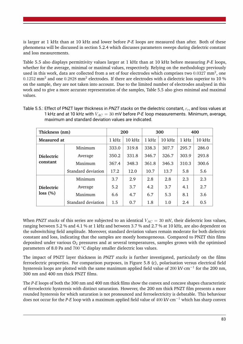
is larger at 1 kHz than at 10 kHz and lower before P-E loops are measured than after. Both of thesephenomena will be discussed in section 5.2.4 which discusses parameters sweeps during dielectric constantand loss measurements.
Table 5.5 also displays permittivity values larger at 1 kHz than at 10 kHz before measuring P-E loops,whether for the average, minimal or maximal values, respectively. Relying on the methodology previouslyused in this work, data are collected from a set of four electrodes which comprises two 0.0327 mm2, one0.1252 mm2 and one 0.2828 mm2 electrodes. If there are electrodes with a dielectric loss superior to 10 %on the sample, they are not taken into account. Due to the limited number of electrodes analysed in thiswork and to give a more accurate representation of the samples, Table 5.5 also gives minimal and maximalvalues.
Table 5.5.: Effect of PNZT layer thickness in PNZT stacks on the dielectric constant, εr , and loss values at1 kHz and at 10 kHz with VAC = 30 mV before P-E loop measurements. Minimum, average,maximum and standard deviation values are indicated.
Thickness (nm) 200 300 400
Measured at 1 kHz 10 kHz 1 kHz 10 kHz 1 kHz 10 kHz
Dielectricconstant
Minimum 333.0 319.8 338.3 307.7 295.7 286.0
Average 350.2 331.8 346.7 326.7 303.9 293.8
Maximum 367.4 348.3 361.8 346.3 310.3 300.6
Standard deviation 17.2 12.0 10.7 13.7 5.8 5.6
Dielectricloss (%)
Minimum 3.7 2.9 2.8 2.8 2.3 2.3
Average 5.2 3.7 4.2 3.7 4.1 2.7
Maximum 6.6 4.7 6.7 5.3 8.1 3.6
Standard deviation 1.5 0.7 1.8 1.0 2.4 0.5
When PNZT stacks of this series are subjected to an identical VAC = 30 mV, their dielectric loss values,ranging between 5.2 % and 4.1 % at 1 kHz and between 3.7 % and 2.7 % at 10 kHz, are also dependent onthe subswitching field amplitude. Moreover, standard deviation values remain moderate for both dielectricconstant and loss, indicating that the samples are mostly homogeneous. Compared to PNZT thin filmsdeposited under various O2 pressures and at several temperatures, samples grown with the optimisedparameters of 8.0 Pa and 700 C display smaller dielectric loss values.
The impact of PNZT layer thickness in PNZT stacks is further investigated, particularly on the filmsferroelectric properties. For comparison purposes, in Figure 5.8 (c), polarisation versus electrical fieldhysteresis loops are plotted with the same maximum applied field value of 200 kV·cm−1 for the 200 nm,300 nm and 400 nm thick PNZT films.
The P-E loops of both the 300 nm and 400 nm thick films show the convex and concave shapes characteristicof ferroelectric hysteresis with distinct saturation. However, the 200 nm thick PNZT film presents a morerounded hysteresis for which saturation is not pronounced and ferroelectricity is debatable. This behaviourdoes not occur for the P-E loop with a maximum applied field value of 400 kV·cm−1 which has sharp convex
83

and concave features along with a marked saturation. It is suggested that this phenomenon is due to largerleakage currents in the PNZT films before P-E loop at higher maximum applied fields are measured. Furtherdiscussion on this topic will be introduced in section 5.2.5.
The positive and negative branches of the P-E loops for the 300 nm and 400 nm thick PNZT films are largelysymmetric. A similar behaviour is observed in the 400 nm thick PZT thin film described in section 5.1.3and for the PNZT films deposited at 600 C and 650 C in section 5.2.2. In the former case, it is suggestedthat the thicker film lead to less leakage and, along the polarisation axis, to a less asymmetric loop thanthe 200 nm thick PZT film deposited under the same conditions. In the later instance, it is hypothesisedthat charge injection at the electrodes is more limited than for the sample deposited at 700 C or that thebulk contribution to the current measured by the P-E loop tracer is predominant. This hypothesis is basedon the presence in the PNZT thin film of additional pyrochlore and Pb phases which modify its conductionmechanisms.
To unify the hypotheses concerning the symmetry along the polarisation axis of the P-E loop shapes, it issuggested that the asymmetry of the positive and negative branches is indeed linked to charge injection andto the different nature of the top and bottom electrodes [154,253]. This effect can become secondary inregard to bulk conduction mechanisms, leading to more symmetric P-E loops. Bulk conduction mechanismscan become prevalent over interface mechanisms if the nature of the film is modified by additional phases(see section 5.2.2) or if the film thickness is increased, as is the case for the 400 nm thick PZT film insection 5.1.3 and for the 300 nm and 400 nm thick PNZT thin films introduced in this section.
The remanent polarisation, saturation polarisation, coercive field and internal bias field values for the200 nm, 300 nm and 400 nm thick PNZT films in PNZT stacks are given in Table 5.6. To accuratelydetermine these values, data for each sample are obtained from P-E loops measured with a maximumapplied field of 8 V to avoid the more rounded P-E loop shape of the 200 nm thick sample at lowermaximum fields (see Figure 5.8 (c)). The coercive field values are determined as the fields correspondingto the switching current peaks from the switching current versus field hysteresis loops according to themethodology previously used in this work.
All ferroelectric properties given in Table 5.6 present very low standard deviation values for each analysedthickness of the PNZT layer. It is indicative of homogeneous samples and of good film-electrode interfacehomogeneity between different top electrodes. It is consistent with the fact that only a limited amount ofpyrochlore phase is found in PNZT stacks by XRD analysis.
Since the maximum applied voltage for P-E loop from which characteristic values are obtained is constant,thinner films are subjected to a higher electrical field. It induces switching of a larger number of ferroelectricdomains and leads to a larger ferroelectric response. This phenomenon is evidenced by the 200 nm, 300 nmand 400 nm thick PNZT thin films exhibiting average remanent polarisation values of Pr = 34.0 µC·cm−2,Pr = 22.0 µC·cm−2 and Pr = 16.5 µC·cm−2 after the release of maximal applied fields of 400 kV·cm−1,300 kV·cm−1 and 200 kV·cm−1, respectively. The remanent polarisation exhibited by samples of this PNZTlayer thickness series increases proportionally to the maximal applied field applied during the P-E loopwith a remanent polarisation approximately doubled between a 200 kV·cm−1 and a 400 kV·cm−1 appliedfield. Similar trends can be observed with the average saturation polarisation and with minimum andmaximum values of both remanent and saturation polarisation.
It is interesting to compare the properties of the PNZT stacks with those of the PZT stacks described insection 5.1.3. The remanent polarisation of both 200 nm and 400 nm thick PZT thin films are measuredafter a 200 kV·cm−1 field was released and with values of Pr = 16.7 µC·cm−2 and Pr = 16.4 µC·cm−2,respectively. Therefore, the 400 nm thick films of PZT and PNZT are measured under the same conditions
84
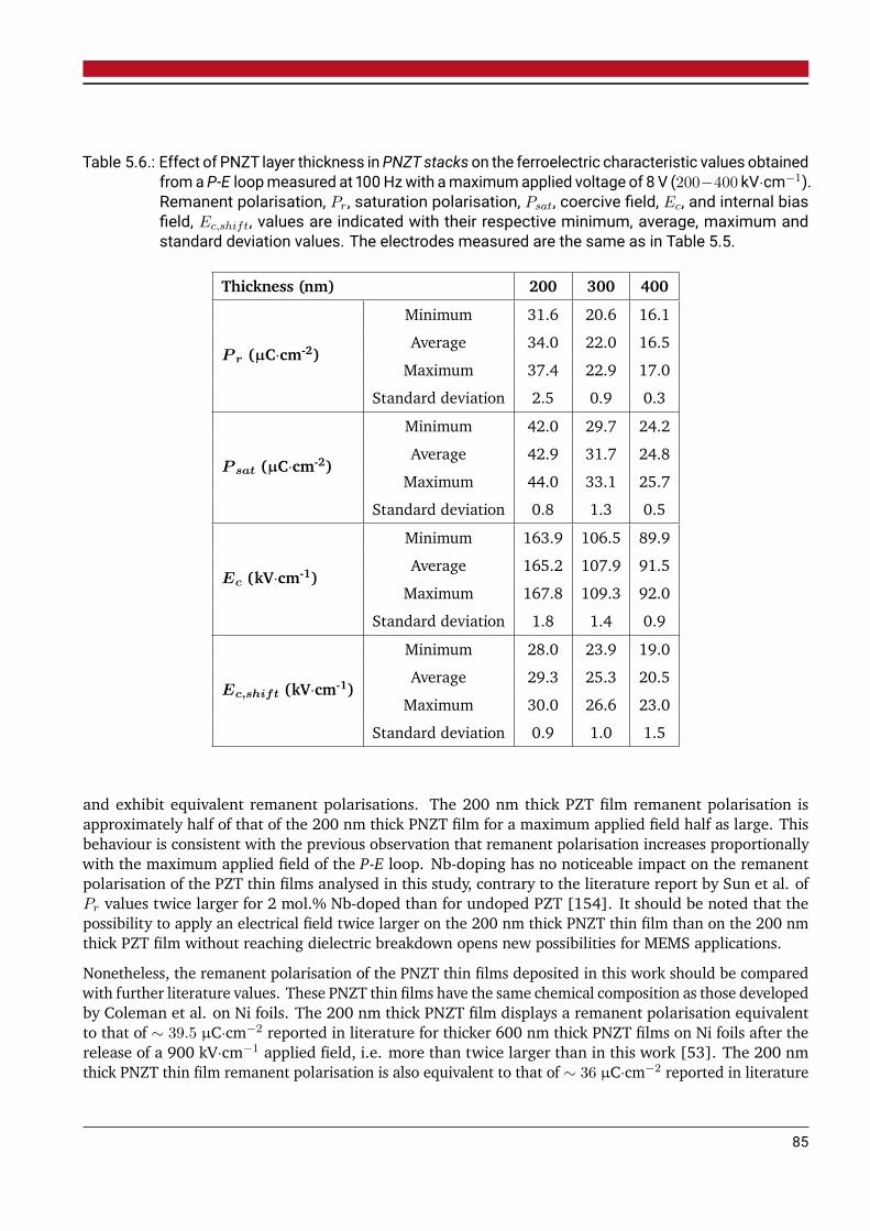
Table 5.6.: Effect of PNZT layer thickness inPNZTstacks on the ferroelectric characteristic values obtainedfrom a P-E loopmeasured at 100Hzwith amaximumapplied voltage of 8 V (200−400 kV·cm−1).Remanent polarisation, Pr , saturation polarisation, Psat, coercive field, Ec, and internal biasfield, Ec,shift, values are indicated with their respective minimum, average, maximum andstandard deviation values. The electrodes measured are the same as in Table 5.5.
Thickness (nm) 200 300 400
P r (µC·cm-2)
Minimum 31.6 20.6 16.1
Average 34.0 22.0 16.5
Maximum 37.4 22.9 17.0
Standard deviation 2.5 0.9 0.3
P sat (µC·cm-2)
Minimum 42.0 29.7 24.2
Average 42.9 31.7 24.8
Maximum 44.0 33.1 25.7
Standard deviation 0.8 1.3 0.5
Ec (kV·cm-1)
Minimum 163.9 106.5 89.9
Average 165.2 107.9 91.5
Maximum 167.8 109.3 92.0
Standard deviation 1.8 1.4 0.9
Ec,shift (kV·cm-1)
Minimum 28.0 23.9 19.0
Average 29.3 25.3 20.5
Maximum 30.0 26.6 23.0
Standard deviation 0.9 1.0 1.5
and exhibit equivalent remanent polarisations. The 200 nm thick PZT film remanent polarisation isapproximately half of that of the 200 nm thick PNZT film for a maximum applied field half as large. Thisbehaviour is consistent with the previous observation that remanent polarisation increases proportionallywith the maximum applied field of the P-E loop. Nb-doping has no noticeable impact on the remanentpolarisation of the PZT thin films analysed in this study, contrary to the literature report by Sun et al. ofPr values twice larger for 2 mol.% Nb-doped than for undoped PZT [154]. It should be noted that thepossibility to apply an electrical field twice larger on the 200 nm thick PNZT thin film than on the 200 nmthick PZT film without reaching dielectric breakdown opens new possibilities for MEMS applications.
Nonetheless, the remanent polarisation of the PNZT thin films deposited in this work should be comparedwith further literature values. These PNZT thin films have the same chemical composition as those developedby Coleman et al. on Ni foils. The 200 nm thick PNZT film displays a remanent polarisation equivalentto that of ∼ 39.5 µC·cm−2 reported in literature for thicker 600 nm thick PNZT films on Ni foils after therelease of a 900 kV·cm−1 applied field, i.e. more than twice larger than in this work [53]. The 200 nmthick PNZT thin film remanent polarisation is also equivalent to that of ∼ 36 µC·cm−2 reported in literature
85
for 1 µm thick PZT films on Ni foils with a maximum applied field of 1,000 kV·cm−1 [51]. Therefore, thePNZT thin films deposited by PLD on stainless steel substrates exhibit a remanent polarisation on par withliterature values and potentially larger should comparable fields be applied to measure the P-E loops.
For the P-E loop measured at 100 Hz with a maximum applied field of 200 kV·cm−1, the average value ofthe 200 nm thick PNZT thin film positive coercive field is Ec = 165.2 kV·cm−1, slightly larger than the valueof 135.9 kV·cm−1 for the 200 nm thick PZT thin film discussed in section 5.1.3. On the other hand, the400 nm thick PNZT thin film displays a positive coercive field average value of Ec = 91.5 kV·cm−1, slightlylower than the coercive field of the 400 nm thick PZT sample at 93.9 kV·cm−1. The influence of 2 mol.%Nb-doping on PZT thin films coercive field is therefore, negligible. Despite diverging from the majority ofliterature which states that Ec values decrease with increasing Nb concentrations in PZT [98,155,157],the stability of the coercive field between PZT and PNZT thin films deposited in this work is consistent withliterature reports of equivalent Ec values between undoped and 2 mol.% Nb-doped PZT [154]. The resultsof this work are also in agreement with literature reports indicating limited effect of low concentrations ofNb-doping on the coercive field of PZT thin films [151,153].
It is noteworthy that both coercive field and internal bias field also present a dependency on the PNZTlayer thickness. While it can be attributed to a lower maximum field applied on thicker samples during P-Eloop measurement, leading to a more moderate ferroelectric response, this observation is coherent withliterature reports of Ec decreasing with increasing thickness [157,254].
This series of PNZT stacks shows 001-textured PNZT layers for thicknesses of 200 nm, 300 nm and400 nm. Nb-doping does not appear to influence remanent polarisation and coercive field values. However,PNZT thin films deposited in this work can withstand larger applied electrical fields without reachingdielectric breakdown than the PZT thin films. While this phenomenon is not formally linked to Nb-doping,an increased electrical resistivity as compared to non-doped PZT is reported in literature [98,146]. Indeed,Nb-doping reduces the hole conductivity in PZT by bringing additional electrons as compared to the B sitecation for which it substitutes [255]. It is thought that these intrinsic changes are also responsible for thehigher dielectric breakdown field which is a significant improvement for MEMS applications. Nonetheless,further investigations are needed to draw thorough conclusions on the influence of 2 mol.% Nb-doping onPZT thin films ferroelectric properties.
Indeed, as Nb-doping effect is extrinsic, notably leading to structural changes, e.g. increased grain size [146],it is difficult to establish whether these changes are due only to Nb-doping or also to other factors. Forexample, bulk Nb-doped PZT 52/48 is known to display a decrease in Ec values and an increase in Pr
values for increasing grain sizes, the later being due to a change in sintering temperature [256]. The PZTand PNZT thin films produced in this work are deposited under different conditions which can impact theirstructural characteristics, independently of Nb-doping effect.
5.2.4. Effect of parameters sweeps on PNZT stacks dielectric constant and loss
The influence of measurement parameters on the dielectric constant and loss values of a 300 nm thickPNZT layer within a PNZT stack are shown in Figure 5.9. The impact of subswitching field amplitudeand frequency are both quantified before and after high electrical field measurements while the effect ofDC bias field amplitude is analysed only after high electrical field measurements. Dielectric constant andloss are measured on an electrode with an area of 0.2828 mm2 and the high electrical field measurementscorrespond to the P-E loops described in section 5.2.3 with a maximum applied field of 300 kV·cm−1.
86

(c)
340
360
380
400
420
Dielectric
constant
(e)
240
280
320
360
400
Dielectric
constant
(d)
0.1 1 102
4
6
Frequency (kHz)
Loss
(%) (f)
−200 −100 0 100 200
2
4
6
8
DC bias field (kV·cm−1)
Loss
(%)
(a)
400
500
600
700
Dielectric
constant
300 nm, before P-E loop300 nm, after P-E loopLinear fit
(b)
0 2 4 6 8 10 12 14 16 18 200
10
20
EAC (kV·cm−1)
Loss
(%)
Figure 5.9.: Dielectric constant, εr , and loss of a 300 nm thick PNZT thin film inPNZTstacks as a function of(a), (b)EAC , the subswitching field amplitude at 1 kHz and zero bias field, (c), (d) subswitchingfield frequency with an AC driving signal amplitude of 30 mV and zero bias field, and (e), (f) DCbias field at 10 kHz with an AC driving signal amplitude of 30 mV, respectively. Measurementstaken before (green circles) and after (blue open squares) high electrical field ferroelectricmeasurements, i.e. P-E loops. Linear fits (red lines) are indicated in (a), (b) and (c).
87
The dependence between dielectric constant and both amplitude and frequency of the subswitching fieldis usually considered within the framework of the Rayleigh analysis of domain walls dynamics. Rayleighanalysis aims to quantify the contribution of irreversible domain wall motion to the piezoelectric responseunder low applied electrical fields [127].
The dielectric constant of a ferroelectric, εr, has both intrinsic and extrinsic components. The formercorresponds to the average dielectric response of single domains with a given orientation distribution and isdue to reversible interface motion. The later originates from motion of phase boundaries and ferroelectricdomain wall motion. Within the framework of Rayleigh analysis, the dielectric permittivity can be expressedas [51,248]:
εr = εinit + αirrEAC , (5.5)
where εinit and αirr are the reversible and irreversible Rayleigh constants, respectively, and EAC is the sub-switching field amplitude. In this context, the linear dependence of dielectric permittivity on subswitchingfield amplitude is due to ferroelectric domain walls pinning on a random distribution of defects, hinderingtheir mobility [98].
As shown in Figure 5.9 (a), the PNZT thin film dielectric constant increases from 360 and 391 at 1 kV·cm−1
to 578 and 701 at 20 kV·cm−1 before and after P-E loop measurements, respectively. It should be noted thatthe amplitude of the driving field EAC , is largely inferior to half of the coercive field value of ∼108 kV·cm−1
reported in section 5.2.3 for 300 nm thick PNZT thin films. In both cases, this increase is linear between7 kV·cm−1 and 20 kV·cm−1, above the low field region, as is characteristic of a Rayleigh regime. BeforeP-E loop measurements, extrapolation at EAC = 0 kV·cm−1 yields εinit = 308 and the linear fit slope givesαirr = 13.3 cm·kV−1 with a linear fit coefficient R2 = 0.9978. After P-E loop measurements, permittivitycan be expressed with εinit = 326 and αirr = 18.6 cm·kV−1 with R2 = 0.9992.
The increase of both reversible and irreversible Rayleigh constants after high electrical field measurements ascompared to before indicates larger contributions from both reversible domain wall motion and irreversiblemotions, e.g. phase boundaries and ferroelectric domain wall motion [51, 53]. While further studiesare necessary to understand which phenomena lead to increased εinit and αirr, it is suggested that theferroelectric underwent significant intrinsic changes, either in its ferroelectric domain state or in its defectdistribution during P-E loop measurements. The improvement of PNZT thin films dielectric performancemight be linked to leakage mechanisms which will be discussed in section 5.2.5.
Following a trend similar to that of the permittivity, 300 nm thick PNZT thin film dielectric loss increasesfrom 3.1 % and 3.6 % at 1 kV·cm−1 to 17.1 % and 21.6 % at 20 kV·cm−1 before and after P-E loopmeasurements, respectively, as shown in Figure 5.9 (b). This increase is linear between 7 kV·cm−1 and20 kV·cm−1 with linear fits displaying coefficients R2 = 0.9996 and R2 = 0.9989, respectively.
Increasing the subswitching field frequency from 100 Hz to 10 kHz, as represented in Figure 5.9 (c), leadsto a decrease of the PNZT thin film dielectric constant from 380 and 416 to 347 and 374 before andafter P-E loop measurements, respectively. Due to the pinning of domain walls controlling the extrinsicpiezoelectric response, this decrease is linear with the logarithm of the subswitching field frequency [98].This applies to the 300 nm thick PNZT thin film for which linear fits can be established between 100 Hzand 10 kHz with R2 = 0.9963 and R2 = 0.9968 before and after P-E loop measurements, respectively.
The larger values of permittivity after P-E loops as compared to before their measurements which isobserved here is consistent with the results presented in Figure 5.9 (a). It also conforms with previousobservations made in sections 5.2.1 to 5.2.3.
88
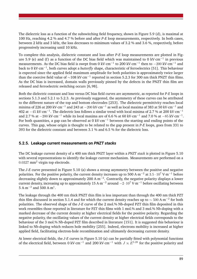
The dielectric loss as a function of the subswitching field frequency, shown in Figure 5.9 (d), is maximal at100 Hz, reaching 4.2 % and 4.7 % before and after P-E loop measurements, respectively. In both cases,between 2 kHz and 3 kHz, the loss decreases to minimum values of 3.2 % and 3.6 %, respectively, beforeprogressively increasing until 10 kHz.
To complete this analysis, dielectric constant and loss after P-E loop measurements are plotted in Fig-ure 5.9 (e) and (f) as a function of the DC bias field which was maintained to 0 kV·cm−1 in previousmeasurements. As the DC bias field is swept from 0 kV·cm−1 to 200 kV·cm−1 then to −200 kV·cm−1 andback to 0 kV·cm−1, both curves adopt a butterfly shape, characteristic of ferroelectrics [51]. This behaviouris expected since the applied field maximum amplitude for both polarities is approximately twice largerthan the coercive field value of ∼108 kV·cm−1 reported in section 5.2.3 for 300 nm thick PNZT thin films.As the DC bias is increased, domain walls previously pinned by the defects in the PNZT thin film arereleased and ferroelectric switching occurs [6,98].
Both the dielectric constant and loss versus DC bias field curves are asymmetric, as reported for P-E loops insections 5.1.3 and 5.2.1 to 5.2.3. As previously suggested, the asymmetry of these curves can be attributedto the different nature of the top and bottom electrodes [253]. The dielectric permittivity reaches localminima of 226 at 200 kV·cm−1 and 243 at −200 kV·cm−1 as well as local maxima of 383 at 50 kV·cm−1 and402 at −45 kV·cm−1. The dielectric loss follows a similar trend with local minima of 2.7 % at 200 kV·cm−1
and 2.7 % at −200 kV·cm−1 while its local maxima are of 6.6 % at 60 kV·cm−1 and 7.0 % at −85 kV·cm−1.For both quantities, a gap can be observed at 0 kV·cm−1 between the starting and ending points of thecurves. This gap, whose origin is thought to be related to the gap present in P-E loops, goes from 331 to393 for the dielectric constant and between 3.1 % and 6.5 % for the dielectric loss.
5.2.5. Leakage current measurements on PNZT stacks
The DC leakage current density of a 400 nm thick PNZT layer within a PNZT stack is plotted in Figure 5.10with several representations to identify the leakage current mechanism. Measurements are performed on a0.0327 mm2 virgin top electrode.
The J-E curve presented in Figure 5.10 (a) shows a strong asymmetry between the positive and negativepolarities. For the positive polarity, the current density increases up to 500 A·m−2 at 3.5 · 107 V·m−1 beforedecreasing slightly down to approximately 200 A·m−2. Contrarily, the negative polarity displays a lowercurrent density, increasing up to approximately 15 A·m−2 around −2 ·107 V·m−1 before oscillating between5 A·m−2 and 500 A·m1.
The leakage through the 400 nm thick PNZT thin film is less important than through the 400 nm thick PZTthin film discussed in section 5.1.4 and for which the current density reaches up to ∼ 500 A·m−2 for bothpolarities. The observed shape of the J-E curve of the 2 mol.% Nb-doped PZT thin film deposited in thiswork resembles those reported in literature for PZT thin films with 1 mol.% and 3 mol.% Nb-doping with amarked decrease of the current density at higher electrical fields for the positive polarity. Regarding thenegative polarity, the oscillating values of the current density at higher electrical fields corresponds to thebehaviour of the 3 mol.% Nb-doped PZT film described in literature [151]. It is suggested this behaviour islinked to Nb-doping which reduces hole mobility [255]. Indeed, electrons mobility is increased at higherapplied field, facilitating electron-hole recombination and ultimately decreasing current density.
At lower electrical fields, the J-E curves in Figure 5.10 (a) can be partially fitted with polynomial functionsof the electrical field, between 0 kV·cm−1 and 200 kV·cm−1 with J ∝ E5.28 for the positive polarity and
89
(b)
−8 −6 −4 −2 0 2 4 6 8−12
−10
−8
−6
−4
−2
(E (V·m−1))1/2 [×103]
ln(J/T
2(A·m
−2·K
−2))
(c)
−8 −6 −4 −2 0 2 4 6 8
−25
−20
−15
−10
(E (V·m−1))1/2 [×103]
ln(J/E
(A·V
−1·m
−1))
(a)
−4 −2 0 2 410−6
10−4
10−2
100
102
104
Electrical field [×107] (V·m−1)
Curren
tden
sity
(A·m
−2)
Figure 5.10.: Leakage current density, J , as a function of the applied electrical field,E , for the 400 nm thickPNZT layer of a PNZT/LNO/Al2O3/steel sample (blue squares) (a) fitted within the space-charge limited current scenario between 0 kV·cm−1 and 200 kV·cm−1 with the polynomialfunctions J ∝ E5.28 for the positive polarity and between −200 kV·cm−1 and 0 kV·cm−1
with J ∝ E3.22 for the negative polarity (red curves), (b) plotted for the Schottky emissionscenario with linear fits (red lines) between 100 kV·cm−1 and 400 kV·cm−1 for the positivepolarity and between −500 kV·cm−1 and 0 kV·cm−1 for the negative polarity, (c) plotted forthe Poole-Frenkel emission scenario with linear fits (red lines) between 100 kV·cm−1 and400 kV·cm−1 for the positive polarity and between −500 kV·cm−1 and −70 kV·cm−1 for thenegative polarity.
between−200 kV·cm−1 and 0 kV·cm−1 with J ∝ E3.22 for the negative polarity. These polynomial functionsdescribed J ∝ EN with N > 2 are characteristic of a SCLC mechanism with trap filling [235,250].
However, as the J-E curves cannot be fitted over the whole range of analysed electrical fields, at leastanother mechanism must be involved in the leakage process besides the SCLC mechanism with trap filling.The DC leakage current is therefore also fitted according to Schottky emission and Poole-Frenkel emissionto verify the validity of these hypotheses.
90
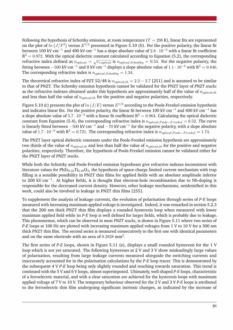
Following the hypothesis of Schottky emission, at room temperature (T = 298 K), linear fits are representedon the plot of ln
(J/T 2
)versus E1/2 presented in Figure 5.10 (b). For the positive polarity, the linear fit
between 100 kV·cm−1 and 400 kV·cm−1 has a slope absolute value of 2.8 · 10−3 with a linear fit coefficientR2 = 0.972. With the optical dielectric constant calculated according to Equation (5.2), the correspondingrefractive index defined as noptical =
√εr,optical is noptical,Schottky = 0.53. For the negative polarity, the
fitting between −500 kV·cm−1 and 0 kV·cm−1 displays a slope absolute value of 1.1 · 10−3 with R2 = 0.846.The corresponding refractive index is noptical,Schottky = 1.34.
The theoretical refractive index of PZT 52/48 is noptical,th = 2.2− 2.7 [251] and is assumed to be similarto that of PNZT. The Schottky emission hypothesis cannot be validated for the PNZT layer of PNZT stacksas the refractive indexes obtained under this hypothesis are approximately half of the value of noptical,th
and less than half the value of noptical,th for the positive and negative polarities, respectively.
Figure 5.10 (c) presents the plot of ln (J/E) versus E1/2 according to the Poole-Frenkel emission hypothesisand indicates linear fits. For the positive polarity, the linear fit between 100 kV·cm−1 and 400 kV·cm−1 hasa slope absolute value of 5.7 · 10−3 with a linear fit coefficient R2 = 0.963. Calculating the optical dielectricconstant from Equation (5.4), the corresponding refractive index is noptical,Poole−Frenkel = 0.52. The curveis linearly fitted between −500 kV·cm−1 and −70 kV·cm−1 for the negative polarity, with a slope absolutevalue of 1.7 · 10−3 with R2 = 0.721. The corresponding refractive index is noptical,Poole−Frenkel = 1.74.
The PNZT layer optical dielectric constants under the Poole-Frenkel emission hypothesis are approximatelytwo thirds of the value of noptical,th and less than half the value of noptical,th for the positive and negativepolarities, respectively. Therefore, the hypothesis of Poole-Frenkel emission cannot be validated either forthe PNZT layer of PNZT stacks.
While both the Schottky and Poole-Frenkel emission hypotheses give refractive indexes inconsistent withliterature values for PbZr0.52Ti0.48O3, the hypothesis of space-charge limited current mechanism with trapfilling is a sensible possibility in PNZT thin films for applied fields with an absolute amplitude inferiorto 200 kV·cm−1. At higher fields, it is thought that electron-hole recombination due to Nb-doping isresponsible for the decreased current density. However, other leakage mechanisms, unidentified in thiswork, could also be involved in leakage in PNZT thin films [255].
To supplement the analysis of leakage currents, the evolution of polarisation through series of P-E loopsmeasured with increasing maximum applied voltage is investigated. Indeed, it was remarked in section 5.2.3that the 200 nm thick PNZT thin film displays a rounded hysteresis loop when measured with lowermaximum applied field while its P-E loop is well defined for larger fields, which is probably due to leakage.This phenomenon, which can be observed in most PNZT stacks, is shown in Figure 5.11 where two series ofP-E loops at 100 Hz are plotted with increasing maximum applied voltages from 1 V to 10 V for a 300 nmthick PNZT thin film. The second series is measured consecutively to the first one with identical parametersand on the same electrode with an area of 0.2828 mm2.
The first series of P-E loops, shown in Figure 5.11 (a), displays a small rounded hysteresis for the 1 Vloop which is not yet saturated. The following hystereses at 2 V and 3 V show misleadingly large valuesof polarisation, resulting from large leakage currents measured alongside the switching currents andinaccurately accounted for in the polarisation calculations by the P-E loop tracer. This is demonstrated bythe subsequent 4 V P-E loop being only slightly rounded and reaching towards saturation. This trend iscontinued with the 5 V and 6 V loops, almost superimposed. Ultimately, well-shaped P-E loops, characteristicof a ferroelectric material, and with a clear saturation are achieved for the hysteresis loops with maximumapplied voltage of 7 V to 10 V. The temporary behaviour observed for the 2 V and 3 V P-E loops is attributedto the ferroelectric thin film undergoing significant intrinsic changes, as indicated by the increase of
91
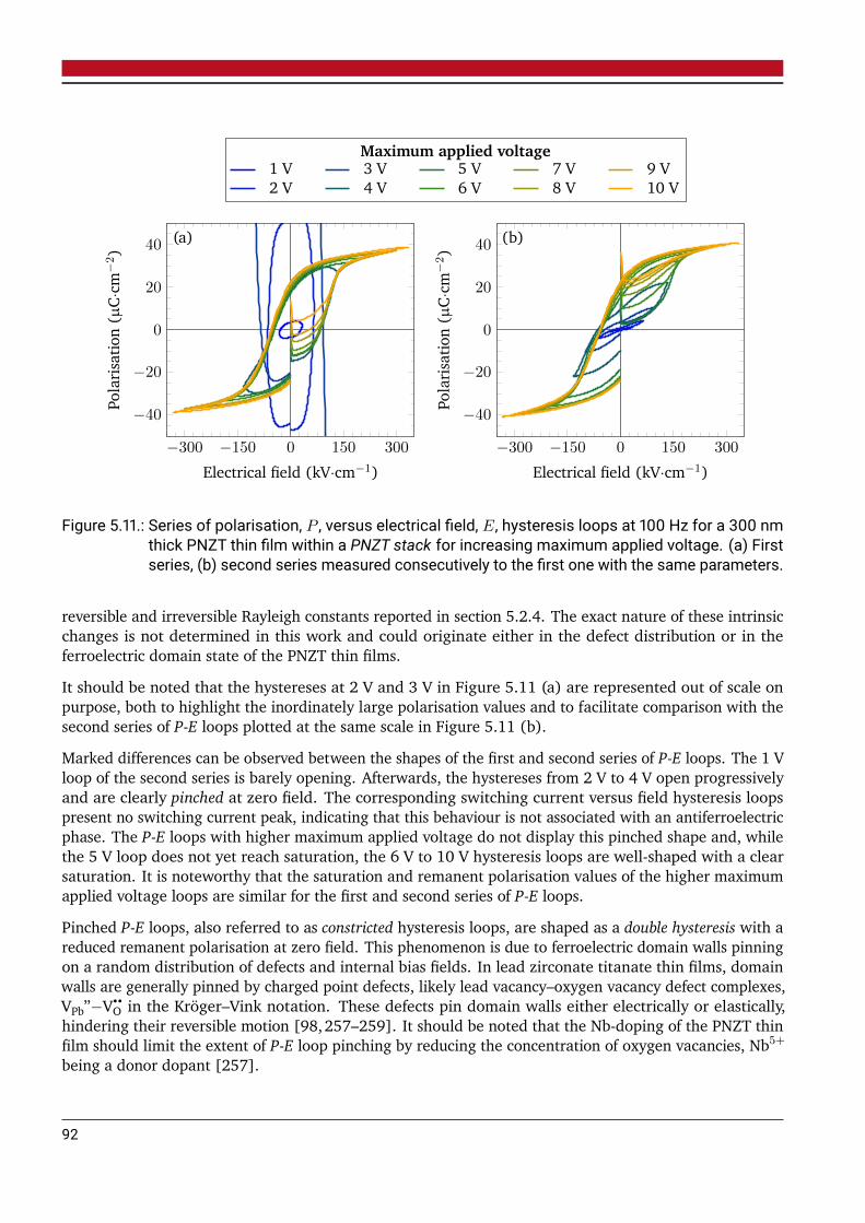
(a)
−300 −150 0 150 300
−40
−20
0
20
40
Electrical field (kV·cm−1)
Polaris
ation(µ
C·cm
−2)
M1 V 3 V 5 V 7 V 9 V2 V 4 V 6 V 8 V 10 V
(b)
−300 −150 0 150 300
−40
−20
0
20
40
Electrical field (kV·cm−1)
Polaris
ation(µ
C·cm
−2)
Maximum applied voltage
Figure 5.11.: Series of polarisation, P , versus electrical field, E, hysteresis loops at 100 Hz for a 300 nmthick PNZT thin film within a PNZT stack for increasing maximum applied voltage. (a) Firstseries, (b) second series measured consecutively to the first one with the same parameters.
reversible and irreversible Rayleigh constants reported in section 5.2.4. The exact nature of these intrinsicchanges is not determined in this work and could originate either in the defect distribution or in theferroelectric domain state of the PNZT thin films.
It should be noted that the hystereses at 2 V and 3 V in Figure 5.11 (a) are represented out of scale onpurpose, both to highlight the inordinately large polarisation values and to facilitate comparison with thesecond series of P-E loops plotted at the same scale in Figure 5.11 (b).
Marked differences can be observed between the shapes of the first and second series of P-E loops. The 1 Vloop of the second series is barely opening. Afterwards, the hystereses from 2 V to 4 V open progressivelyand are clearly pinched at zero field. The corresponding switching current versus field hysteresis loopspresent no switching current peak, indicating that this behaviour is not associated with an antiferroelectricphase. The P-E loops with higher maximum applied voltage do not display this pinched shape and, whilethe 5 V loop does not yet reach saturation, the 6 V to 10 V hysteresis loops are well-shaped with a clearsaturation. It is noteworthy that the saturation and remanent polarisation values of the higher maximumapplied voltage loops are similar for the first and second series of P-E loops.
Pinched P-E loops, also referred to as constricted hysteresis loops, are shaped as a double hysteresis with areduced remanent polarisation at zero field. This phenomenon is due to ferroelectric domain walls pinningon a random distribution of defects and internal bias fields. In lead zirconate titanate thin films, domainwalls are generally pinned by charged point defects, likely lead vacancy–oxygen vacancy defect complexes,VPb”−VO in the Kröger–Vink notation. These defects pin domain walls either electrically or elastically,hindering their reversible motion [98,257–259]. It should be noted that the Nb-doping of the PNZT thinfilm should limit the extent of P-E loop pinching by reducing the concentration of oxygen vacancies, Nb5+
being a donor dopant [257].
92
P-E loop pinching normally occurs as a result of an ageing process. De-ageing can be achieved either bycycling at higher fields or by thermal treatment, leading to a depinched P-E loop [98,260]. It is suggestedthat, during the first series of P-E loops performed in this work on the 300 nm thick PNZT sample, anageing process takes place, generating large leakage currents as it occurs (see Figure 5.11 (a)) and inducingintrinsic changes in the sample, transforming the defect distribution or the domain state. It is hypothesisedthat the same phenomenon is responsible for the increase of both reversible and irreversible Rayleighconstants after P-E loops which was described in section 5.2.4. The cycling through the second series ofP-E loops appears to have a de-ageing effect on the PNZT thin film as the maximum applied field increases.
A gap is present at 0 kV·cm−1 between the starting and ending points of the 4 V to 10 V P-E loops of thefirst series and for the 3 V to 10 V loops of the second series. In both series, the gap amplitude increaseswith the maximum applied voltage. It should also be noted that the asymmetry along the polarisation axisincreases with the maximum applied voltage. As the nature of the top and bottom electrodes to whichthe asymmetry was previously attributed remain unchanged [253], it suggests that changes occur at theferroelectric-electrode interfaces. These modifications are associated to the migration of oxygen vacancies,involved in domain wall pinning and reported to accumulate at the film-electrode interface under fieldcycling [98,261,262].
5.2.6. e31,f measurements on PNZT stacks
To measure the piezoelectric response of the PNZT stacks, e31,f coefficient measurements are performed ona sample with a 200 nm thick PNZT layer using the wafer flexure method described in section 4.4. Anelectrode with an area of 0.5006 mm2 yields e31,f = −1.2 C·m−2 while a value of e31,f = −4.4 C·m−2 isobtained for an electrode of 0.7842 mm2. Further measurements on a 400 nm thick PNZT thin film give apiezoelectric coefficient e31,f = −1.1 C·m−2 for a 0.1252 mm2 electrode.
The values obtained in this work for the e31,f coefficient of the PNZT stacks are in the same order ofmagnitude as literature values for 2.5 µm thick PZT thin films deposited on austenitic and ferritic stainlesssteel foils of −1.5 C·m−2 and −2.4 C·m−2, respectively [64]. However, the e31,f values reported in this workare up to 9 times lower that those of |e31,f | = 10.6 C·m−2 reported in literature for 1 µm thick PZT 52/48on Ni foils [51].
It is estimated that the discrepancies between the different PNZT stacks and their respective electrodesmight be due to inhomogeneous gluing of the substrates on the carrier wafer while using the wafer flexuremethod. A direct consequence of non-optimal gluing would be a reduced efficiency in the transmissionof in-plane mechanical strain from the carrier wafer to the sample, leading to reduced e31,f coefficients.Furthermore, the utilisation of commercial strain gauges, glued on the carrier wafer next to the sample,instead of Pt strain gauges, sputtered directly on the sample surface (see section 4.2), might lead tomeasurement of in-plane strains larger than effectively experienced by the sample. This experimentalsetup configuration can also lead to reduced e31,f coefficients values for the PNZT thin films.
Nonetheless, the value of e31,f = −4.4 C·m−2 measured for the 200 nm thick PNZT thin film, beinglarger than literature values for PZT thin films on stainless steel foils, is promising for future MEMSapplications [64].
93

5.3. Conclusions relative to the experimental results
The growth of nearly single oriented 001-textured ferroelectric PbZr0.52Ti0.48O3 thin films by pulsedlaser deposition onto AISI 304 stainless steel substrates is achieved. Their orientation is assessed byXRD and EBSD and the thin films have a Lotgering factor f(00l)PZT = 0.91. To prevent substrate oxidation,Pt and Al2O3 buffer layers are used. A LaNiO3 layer promotes the 001 orientation of the PZT thinfilm in which additional CrPt and Pb2Ti2O6 pyrochlore phases are present. The PZT thin films displaya permittivity of approximately 350 at 1 kHz with dielectric loss below 5 %. Polarisation versuselectrical field hysteresis loops indicate that the films are ferroelectric with a remanent polarisationP r ∼16.5 µC·cm-2. Analysis of leakage currents infers that leakage is most likely due to a space-chargelimited current with trap filling mechanism.
In order to improve the properties of the PZT thin films, the effect of 2 mol.% Nb-doping is studied underseveral deposition conditions. Pb0.990.01(Zr0.52Ti0.48)0.98Nb0.02O3 thin films are also predominantly001-oriented, as verified by XRD. Compared to the PZT stacks, the Pt buffer layer was omitted, efficientlypreventing the formation of an additional CrPt intermetallic phase while protecting the stainless steelsubstrates against oxidation with a thicker Al2O3 layer. The Lotgering factors up to 0.84 reported inthis work for the LNO buffer layers are larger than literature values on steel substrates [57]. For the PNZTthin films, Lotgering factors are similar to those of PZT layers with f(00l)
PNZT = 0.89.
It is showed that higher O2 deposition pressures and deposition temperatures are necessary to hinder theformation of additional pyrochlore and Pb phases. Optimised PNZT thin films are deposited under8.0 Pa of O2 and with a substrate temperature of 700 C. The PNZT thin films are ferroelectric and a200 nm thick layer displays a dielectric permittivity up to 370 at 1 kHz, increasing up to 430 after P-Eloop measurements, with a dielectric loss inferior to 5 %. Measured under the same conditions as thePZT thin films, 400 nm thick PNZT layers have a remanent polarisation Pr = 16.5 µC·cm−2 and exhibit acoercive field Ec = 91.5 kV·cm−1. The 2 mol.% Nb-doping has no noticeable impact on the propertiesof the PNZT thin films as compared to those of the PZT layers. The effect of doping is extrinsic andmight be damped by other phenomena as the PNZT stacks and the PZT stacks are deposited under differentconditions. However, PNZT thin films ability to withstand higher applied electrical fields than PZTthin films without breaking down electrically could be due to Nb-doping. This improvement of the thinfilms properties is promising for MEMS applications.
The PNZT thin films undergo intrinsic changes in the sample during P-E loop measurements with increasingmaximum applied field. This leads to increased reversible and irreversible Rayleigh constants alongwith larger permittivity and dielectric loss values after P-E loop measurements. Analysis of leakagecurrent measurements suggests the existence of a space-charge limited current with trap filling mechanismcombined with at least another mechanism at higher applied fields. Furthermore, a de-ageing processappears to take place while measuring a second series of P-E loops, indicating that the intrinsic changesoccurring during the first series of P-E loop measurements could act as an ageing process. The piezoelectrice31,f coefficient of the PNZT thin films reaches up to −4.4 C·m-2 for the 200 nm thick thin film whichis within range of literature reports for PZT thin films on metallic substrates.
Globally, the 001 orientation and ferroelectric properties of the PZT and PNZT thin films depositedby PLD on stainless steel substrates make them suitable candidates for future MEMS applications.
94
6. Modelling of ferroelectric bending tongues
Portions of this chapter have been reproduced from:
J. Cardoletti, A. Radetinac, D. Thiem, J. Walker, P. Komissinskiy, B.-X. Xu, H. Schlaak,S. Trolier-McKinstry, and L. Alff,
“Modelling of the vertical deflection of ferroelectric bending tongues loaded at their free end”,AIP Advances, vol. 9, no. 2, p. 025017, 2019. DOI: 10.1063/1.5082392
This chapter aims to understand the influence of some parameters, e.g. applied electrical fieldor geometry, on MEMS efficiency. For this purpose, a model to describe the vertical deflection of afundamental MEMS system composed of a ferroelectric bending tongue loaded at its free end is developed.The approach to the modelling chosen in this work is presented in section 6.1. Section 6.2 indicates theextents and limits of the proposed model. The fundamentals of the model will be introduced in section 6.3.Afterwards, the results of the modelling are discussed in section 6.4 before the conclusions of the chapterare given in section 6.5.
6.1. Approach to the modelling
As stated in section 1.1.2, to model the behaviour of ferroelectric MEMS it is necessary to bridgethe gap between the description of ferroelectric switching and the mechanical approach for linearpiezoelectric structures. Therefore, the model here described is based on the ferroelectric switchingcriterion developed by Hwang et al. [77] and the Euler-Bernoulli beam theory. It endeavours to giveaccurate estimates of the vertical deflection for MEMS applications based on ferroelectric bending tonguesfixed at one end and loaded at their free end while taking into account ferroelectric switching at the grainscale.
The MEMS modelled in this work have been restricted to ferroelectric bending tongues fixed at oneend as these are the most fundamental piezoelectric devices. This constraint is necessary to both limitthe number of parameters and determine bases that could later be applied to more complex systems. Thebending tongues are modelled with a load at their free end to emulate practical applications, e.g. anactuator applying strength against a mechanical element or a displacement sensor. The bending tonguesconsidered here are composed of a substrate, one or several buffer layers and a ferroelectric layer.
The model studies the impact of the geometry of the bending tongue, the mechanical and piezoelectricmaterial properties, the applied electrical field, the crystallographic state (polycrystalline, textured orepitaxial) of the ferroelectric thin film and its built-in strain on the vertical deflection. The accuracy of themodel initially proposed by Hwang et al. is improved by incorporating macroscopic polarisation and strainsaturation at high field, as expected for the butterfly loop. By analysing in details the different contributionsto the vertical deflection, the proposed model also allows optimisation of the geometry of the bendingtongue for various applications.
The model is implemented through a MATLAB® program. Named FeBeTo – Ferroelectric Bending Tonguesmodelling program, it is designed so internal functions could easily be replaced by more advanced ones
95
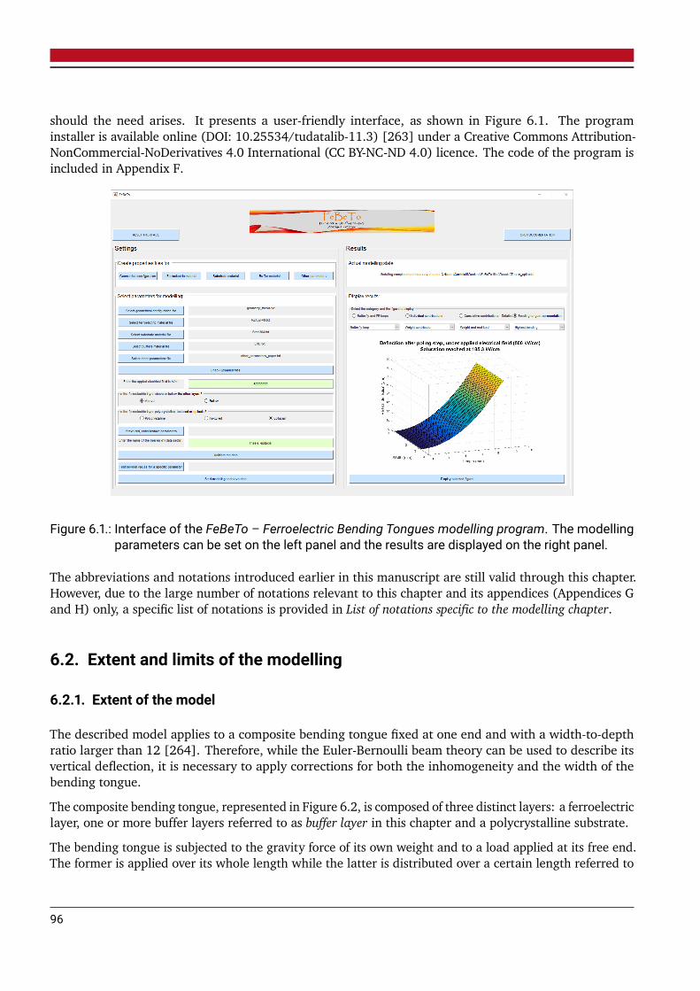
should the need arises. It presents a user-friendly interface, as shown in Figure 6.1. The programinstaller is available online (DOI: 10.25534/tudatalib-11.3) [263] under a Creative Commons Attribution-NonCommercial-NoDerivatives 4.0 International (CC BY-NC-ND 4.0) licence. The code of the program isincluded in Appendix F.
Figure 6.1.: Interface of the FeBeTo – Ferroelectric Bending Tongues modelling program. The modellingparameters can be set on the left panel and the results are displayed on the right panel.
The abbreviations and notations introduced earlier in this manuscript are still valid through this chapter.However, due to the large number of notations relevant to this chapter and its appendices (Appendices Gand H) only, a specific list of notations is provided in List of notations specific to the modelling chapter.
6.2. Extent and limits of the modelling
6.2.1. Extent of the model
The described model applies to a composite bending tongue fixed at one end and with a width-to-depthratio larger than 12 [264]. Therefore, while the Euler-Bernoulli beam theory can be used to describe itsvertical deflection, it is necessary to apply corrections for both the inhomogeneity and the width of thebending tongue.
The composite bending tongue, represented in Figure 6.2, is composed of three distinct layers: a ferroelectriclayer, one or more buffer layers referred to as buffer layer in this chapter and a polycrystalline substrate.
The bending tongue is subjected to the gravity force of its own weight and to a load applied at its free end.The former is applied over its whole length while the latter is distributed over a certain length referred to
96
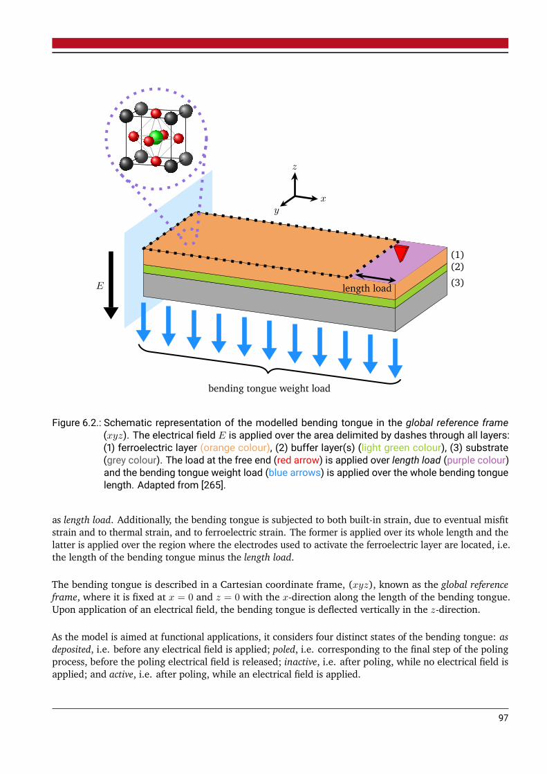
bending tongue weight load
length loadE
(1)(2)(3)
z
xy
Figure 6.2.: Schematic representation of the modelled bending tongue in the global reference frame(xyz). The electrical field E is applied over the area delimited by dashes through all layers:(1) ferroelectric layer (orange colour), (2) buffer layer(s) (light green colour), (3) substrate(grey colour). The load at the free end (red arrow) is applied over length load (purple colour)and the bending tongue weight load (blue arrows) is applied over the whole bending tonguelength. Adapted from [265].
as length load. Additionally, the bending tongue is subjected to both built-in strain, due to eventual misfitstrain and to thermal strain, and to ferroelectric strain. The former is applied over its whole length and thelatter is applied over the region where the electrodes used to activate the ferroelectric layer are located, i.e.the length of the bending tongue minus the length load.
The bending tongue is described in a Cartesian coordinate frame, (xyz), known as the global referenceframe, where it is fixed at x = 0 and z = 0 with the x-direction along the length of the bending tongue.Upon application of an electrical field, the bending tongue is deflected vertically in the z-direction.
As the model is aimed at functional applications, it considers four distinct states of the bending tongue: asdeposited, i.e. before any electrical field is applied; poled, i.e. corresponding to the final step of the polingprocess, before the poling electrical field is released; inactive, i.e. after poling, while no electrical field isapplied; and active, i.e. after poling, while an electrical field is applied.
97
6.2.2. Assumptions of the model
The model presumes several general assumptions: each individual layer composing the bending tongue ishomogeneous and its properties are either isotropic or transversely isotropic in the xy-plane. The bondingbetween the individual layers is assumed to be perfect.
Mechanical hypotheses are also assumed in order to apply the Euler-Bernoulli beam theory [167]: thecomposite beam has the same modulus of elasticity for both tension and compression and is presumedto be straight or slightly curved in the plane of bending, i.e. with a radius of curvature at least 10 timesas long as the thickness of the bending tongue. The cross-section of the beam is assumed to be uniformalong the x-axis and the bending tongue has at least one longitudinal plane of symmetry, i.e. the xz-plane.All loads and reactions are presumed to be perpendicular to the axis of the bending tongue, i.e. alongthe z-direction, as well as to lie in the same plane as the bending tongue which is a longitudinal plane ofsymmetry, i.e. in the xz-plane. Deformations are assumed to be small and within the range of linear elasticdeformation. The bending tongue is also presumed to be long with respect to its thickness: considering itas a metal beam of compact section, its span-to-thickness ratio is at least equal to 8.
The model also supposes the following crystallographic assumptions: the ferroelectric layer contains onlytetragonal unit cells and the substrate is polycrystalline. It is presumed that there is no phase transitionin any of the materials, neither during the thin film deposition processes nor during the bending tongueoperation.
Since this model is based on Hwang et al.’s model for ferroelectric switching [77], it takes into accountneither the correlation between ferroelectric domains nor domain wall motion. For such purpose, the phasefield models can be utilised [73–75]. The model also considers that 180 and 90 switching requires thesame amount of energy.
Due to the large number of parameters required for the modelling, the results might be strongly impactedby the selected values.
6.3. Equations of the model
As mentioned in section 6.2.1, the bending tongue, being a composite, requires a correction for itsinhomogeneity by means of an equivalent cross-section [167]. The substrate is taken as the reference layer,implying:
weffsubs = wsubs, (6.1)
wefffilm = wfilmEY
film
EYsubs
, (6.2)
where wsubs and weffsubs refer to the width and the effective width of the substrate, respectively. The
width and the effective width of any subsequent layer are noted wfilm and wefffilm, respectively, and
EYsubs and EY
film refer to the Young moduli of the substrate and of any subsequent layer, respectively.
The neutral axis of the equivalent cross-section of the bending tongue and its second moment of area areimpacted by taking the effective width of each layer into account. It is therefore necessary to consider theeffective neutral axis, neff and the effective second moment of area Ieff calculated using weff .
98
Therefore, neff , which is also dependent on the mid-plane of each individual layer, ni, can be expressed as:
neff =
∑iweff
itini∑iweff
iti, (6.3)
where ti corresponds to the thickness of every individual layer of the bending tongue, and with ni definedas:
ni =ti
2+
i−1∑j=0
tj . (6.4)
Using Equation (6.3), Ieff can be calculated as:
Ieff =∑i
weffiti
12+ weff
iti(ni − neff
)2 . (6.5)
As the bending tongue is incorporated in a wide beam, i.e. width-to-depth ratio larger than 12 [264], it isalso necessary to apply a correction in order to use the Euler-Bernoulli beam theory [167]. The Youngmodulus of the composite beam, EY,eff should be substituted by:
EY,eff →EY,eff
1− νeff 2, (6.6)
where νeff corresponds to the Poisson ratio of the substrate as per the equivalent cross-section obtainedfrom Equation (6.2).
Due to both loads, i.e. the own weight of the bending tongue and load applied at its free end, and strains,i.e. built-in and ferroelectric strains, acting simultaneously on the bending tongue, the equation describingits vertical deflection, z(x), along the z-axis, is complex. However, the method of superposition [167]allows the total vertical deflection to be defined as the sum of the deflections due to both loads and strains.Therefore, each component of the deflection can be calculated independently.
6.3.1. Deflection due to loads
Q(x), the load distribution of the own weight of the bending tongue, qW , over its whole length and theload applied at its free end, qL, over the length load can be described by the following equation using theMacaulay brackets:
Q(x) = qW + qL < x− xm >0 , (6.7)
where xm corresponds to the position on the x-axis at which length load begins, ranging from x = xm tox = xl, the position at the free end of the bending tongue. The Macaulay brackets describe a discontinuousfunction expressed by the following equation [266]:
< x− xm >p=
0 x ≤ xm
(x− xm)p x > xm, (6.8)
where p is an integer.
99
According to the Euler-Bernoulli beam theory, the equation describing the vertical deflection of the bendingtongue can be obtained through four consecutive integrations of the load distribution over the length of thebending tongue. As the bending tongue is fixed at one end in x = 0 and z = 0, it is subjected to neitherany shear force nor bending moment at its free end at which x = xl. It also does not have a slope or adeflection at its fixed end. Therefore, the following boundary conditions can be applied:
zIII(x = xl)= 0, (6.9)zII(x = xl)= 0, (6.10)zI(x = 0) = 0, (6.11)z(x = 0) = 0, (6.12)
where zI , zII and zIII are the first, second and third derivatives of z(x), the vertical deflection.
From Equations (6.7) and (6.9) to (6.12), the equation of vertical deflection due to the own weight of thebending tongue and the load applied at its free end can be obtained:
z(x) =1− νeff
2
24EY,effIeff
[qWx4 + qL < x− xm >4
+4(−qWxl − qL(xl − xm)
)x3 + 12
[qW
xl2
2+ qL(xl − xm)
(xl −
xl − xm2
)]x2
]. (6.13)
The detailed calculations from Equation (6.7) to Equation (6.13) are given in Appendix G.
6.3.2. Deflection due to strains
Both terms of the built-in strain in the ferroelectric layer, i.e thermal strain and eventual misfit strain,as well as ferroelectric strain have components in the xy-plane and in the z-direction. However, theircomponents in the z-direction can be neglected as the top surface of the bending tongue is free and,therefore, unconstrained.
To maintain the force equilibrium in the bending tongue, the in-plane built-in strain, κb, and the in-planeferroelectric strain, κf , generate longitudinal strains in both the x-direction and the y-direction [267].These created strains, κblong and κf
long, respectively, are defined as:
κblong = −EY
ferrotferroκb∑iEY
iti, (6.14)
κflong = −
EYferrotferroκf∑
iEY
iti, (6.15)
where EYferro and EY
i correspond to the Young moduli of the ferroelectric layer and of every individuallayer of the bending tongue, respectively. tferro corresponds to the thickness of the ferroelectric layer ofthe bending tongue.
The in-plane built-in and ferroelectric strains also generate a bending moment due to a net force createdin each individual layer and acting through a moment arm spanning from the mid-plane of the layer, ni
(see Equation (6.4)), to the neutral axis of the bending tongue with the equivalent cross-section, neff
100
(see Equation (6.3)) [267]. The bending moment due to the built-in strain, Mb, and the one due to theferroelectric strain Mf , arising from the forces acting in each layer due to κb
long and to κflong, respectively,
as well as to the forces acting in the ferroelectric layer due to κb and to κf , respectively, are expressed as:
Mb =∑i
EYitiweff
i(ni − neff
)κb
long sin(θstrain)
+ EYferrotferroweff
ferro(nferro − neff
)κb sin(θstrain), (6.16)
Mf =∑i
EYitiweff
i(ni − neff
)κf
long sin(θstrain)
+ EYferrotferroweff
ferro(nferro − neff
)κf sin(θstrain), (6.17)
where weffferro and nferro are the effective width and the mid-plane of the ferroelectric layer, respectively.
The angle between the in-plane force due to the strain and the moment arm is noted θstrain. If the mid-planeof a layer, ni, is located above the effective neutral axis of the bending tongue, neff , then θstrain = −90
and if ni is smaller than neff then θstrain = 90.
The bending moment Mb, due to the built-in strain, is acting over the whole length of the bending tonguewhile Mf , due to the ferroelectric strain, is acting over the length of the bending tongue minus the lengthload. The distribution of these bending moments, M(x), is described by the following equation using theMacaulay brackets:
M(x) = Mb +Mf
(1− < x− xm >0
). (6.18)
According to the Euler-Bernoulli beam theory, integrating twice the equation for the distribution of thebending moments due to κb and κf gives the corresponding equation for the vertical deflection. It can beobtained from Equations (6.11), (6.12) and (6.18):
z(x) =1− νeff
2
2EYeffIeff
[(Mb +Mf )x
2 −Mf < x− xm >2]. (6.19)
The detailed calculations from Equation (6.18) to Equation (6.19) are given in Appendix H.
Both the built-in strain and the ferroelectric strain are dependent on the crystallographic state of theferroelectric layer (polycrystalline, textured or epitaxial). Therefore, it is necessary to describe thecrystallographic state mathematically.
6.3.2.1. Mathematical formulation of the crystallographic state
Following Hwang’s model [77] for ferroelectric switching, the orientation of each crystallographic grain hasan impact on the global ferroelectric strain and should therefore be taken into account. For this purpose, aseries of systems of local coordinates defined relative to the global reference frame and referred to as graincoordinates is defined.
The orientation of each grain is set by a group of three Euler angles, ϕ1, φ, ϕ2, allowing conversion ofcoordinates from the global reference frame to the grain coordinates of each grain. As various conventionsexist to define the Euler angles, the one chosen here is described below and represented in Figure 6.3.
The first rotation of angle ϕ1 around the z-axis creates the u-axis and v-axis in the xy-plane. The secondrotation is made around the v-axis with an angle of φ. It creates the w-axis as well as the z’-axis. The third
101
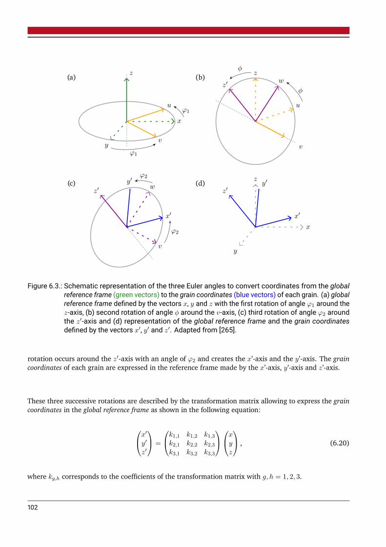
x
y
z
u
v
ϕ1
ϕ1u
v
zw
z′φ
φ
v
wz′
x′
y′
ϕ2
ϕ2
x
y
z
x′
y′
z′
(a) (b)
(c) (d)
Figure 6.3.: Schematic representation of the three Euler angles to convert coordinates from the globalreference frame (green vectors) to the grain coordinates (blue vectors) of each grain. (a) globalreference frame defined by the vectors x, y and z with the first rotation of angle ϕ1 around thez-axis, (b) second rotation of angle φ around the v-axis, (c) third rotation of angle ϕ2 aroundthe z′-axis and (d) representation of the global reference frame and the grain coordinatesdefined by the vectors x′, y′ and z′. Adapted from [265].
rotation occurs around the z′-axis with an angle of ϕ2 and creates the x’-axis and the y’-axis. The graincoordinates of each grain are expressed in the reference frame made by the x’-axis, y’-axis and z’-axis.
These three successive rotations are described by the transformation matrix allowing to express the graincoordinates in the global reference frame as shown in the following equation:
⎛⎝x′
y′
z′
⎞⎠ =
⎛⎝k1,1 k1,2 k1,3k2,1 k2,2 k2,3k3,1 k3,2 k3,3
⎞⎠⎛⎝xyz
⎞⎠ , (6.20)
where kg,h corresponds to the coefficients of the transformation matrix with g, h = 1, 2, 3.
102

The coefficients kg,h are given in the following equations:
k1,1 = cos(ϕ1)cos(ϕ2)− sin(ϕ1)sin(ϕ2)cos(φ), (6.21)k1,2 = −sin(ϕ2)cos(ϕ1)− cos(φ)sin(ϕ1)cos(ϕ2), (6.22)k1,3 = sin(φ)sin(ϕ1), (6.23)k2,1 = cos(ϕ2)sin(ϕ1) + cos(φ)cos(ϕ1)sin(ϕ2), (6.24)k2,2 = −sin(ϕ2)sin(ϕ1) + cos(φ)cos(ϕ1)cos(ϕ2), (6.25)k2,3 = −sin(φ)cos(ϕ1), (6.26)k3,1 = sin(φ)sin(ϕ2), (6.27)k3,2 = sin(φ)cos(ϕ2), (6.28)k3,3 = cos(φ). (6.29)
The Euler angles inherent to the grains are defined according to the three possible crystallographic statesof the modelled ferroelectric layer. If the sample is polycrystalline, then all grains of the ferroelectric arerandomly oriented and, therefore, the values of the three Euler angles are each randomly defined withintheir bounds, i.e. 0 < ϕ1 < 2 π; 0 < φ < π and 0 < ϕ2 < 2π.
In the case of a textured ferroelectric layer, a given percentage of grains are rotated by a few degreesaround a given orientation, Oferro, while the remaining grains are randomly oriented. The distribution ofgrains around the orientation Oferro can be simulated by the following Gaussian function [268]:
S(Ψ) =8√π
ζΨ30
exp(−Ψ2
Ψ30
), (6.30)
where Ψ is the rotation angle around the orientation Oferro, Ψ0 is the full width at half-maximum of theGaussian distribution and ζ is the multiplicity due to the symmetry of the crystallographic unit cell.
Once normalised, the Gaussian distribution given in Equation (6.30) contains 99.9 % of the grains orientedaround the orientation Oferro between −3Ψ and +3Ψ. The distance between these two angles is separatedinto 10 segments, each containing a number of grains as defined by the Gaussian distribution. The grainscontained in each segment are rotated by the average angle of the given segment around the orientationOferro.
If the ferroelectric layer is textured in-plane, the angle of rotation is the first Euler angle, ϕ1, while φ andϕ2 are set to 0. In the case of an out-of-plane texture, it is the second Euler angle, φ, which correspondsto the angle of rotation while ϕ1 and ϕ2 are set to 0. A combination of in-plane and out-of-plane texturecan be described by simultaneous rotations of ϕ1 and φ.
The remaining grains which do not display texture around the orientation Oferro are modelled by applyingrandom values to their three Euler angles, as it is the case for a polycrystalline ferroelectric.
In this model, epitaxy is defined as the perfect alignment of grains in a given orientation Oferro. Therefore,if the ferroelectric layer is epitaxial, all the Euler angles are set to 0, independent of any possible longrange order between ferroelectric layer and substrate.
103
6.3.2.2. Built-in strain
The built-in strain in the ferroelectric layer, κb, is the sum of the thermal strain and the misfit strain. Thechoice of equation to calculate the former is dependent on the thickness of the thin film. The equation forthe latter is dependent on both the thin film thickness and its crystallographic state.
The thickness of the thin film mainly impacts the ability of the ferroelectric layer to relax. As the nature(strain, morphology, etc.) of the modelled thin film is unknown, its relaxation threshold should bedetermined and the corresponding equations should be used.
If the ferroelectric is not relaxed, its thermal strain, κbthermal, due to cooling down from its depositiontemperature, Tdepo, to the operating temperature of the bending tongue, Toper, is expressed by:
κbthermal = (Tdepo − Toper)
(αsubs − αferro
), (6.31)
where αsubs and αferro correspond to the thermal expansion coefficients of the substrate and of theferroelectric layer, respectively.
If the ferroelectric layer is relaxed, the bi-axial stress present at the Curie temperature, TC, is partiallyreleased through the development of a domain structure [269]. The transformation stress concept impliesthat the thermal strain of a relaxed ferroelectric layer is described by [270]:
κbthermal = (Tdepo − TC)
(αsubs − αferro
). (6.32)
Regarding the misfit strain, polycrystalline films are relaxed. For non-relaxed epitaxial ferroelectric filmsthe misfit strain, κbmisfit, calculated at the film deposition temperature is described by:
κbmisfit =
(abuffer − aferro
aferro
)Tdepo
, (6.33)
where aferro and abuffer are the lattice parameters for misfit strain calculation for the ferroelectric layerand the adjacent buffer layer, respectively.
If the ferroelectric layer is textured and not relaxed, its misfit strain is calculated from Equation (6.33) andis multiplied by the ratio of textured grains.
In all of the above mentioned cases, the total strain can be reduced by a given degree of relaxation to modelany further relaxation which could happen after the ferroelectric layer deposition.
6.3.2.3. Ferroelectric strain
The ferroelectric strain originates from both the ferroelectric switching strain component and the linearstrain component. Hwang’s model [77] processes each grain individually before averaging the ferroelectricstrain and polarisation values over the number of grains modelled. This individual processing of the grainsimposes the need to work in grain coordinates. Therefore, every value in the global reference frame shouldbe converted into grain coordinates through the use of the Euler angles. Once the ferroelectric strain andmatching polarisation values are known for each individual grain, they should be converted back into theglobal reference frame before averaging.
104
Each grain is treated as if it is composed of unit cells displaying the same behaviour, i.e. the same orientationrelative to the global reference frame, simultaneous ferroelectric switching, etc., and therefore in this sectiongrain can be replaced by unit cell for ease of comprehension.
Hwang et al. considered the sum of the electrical and mechanical work resulting from switching thepolarisation from its current direction to another one. Ferroelectric switching occurs if the applied electricalfield is larger than a switching criterion expressed by [77]:
E∆P + σ∆κint > 2PsEc, (6.34)
where E and σ correspond to the electrical field and to the stress, respectively, applied to the ferroelectricduring the switching process. ∆P and ∆κint refer to the difference between before and after ferroelectricswitching for the polarisation and internal unit cell strain values, respectively. Ps refers to the spontaneouspolarisation of the ferroelectric and Ec refers to its coercive field.
According to Hwang’s model, the polarisation vector is parallel to the edge of the tetragonal unit cell. Inthe model presented in this thesis, the polarisation vector lies at the centre of the unit cell and can onlytake six different orientations which is in agreement with Hwang’s model. The six possible orientations ofthe polarisation in a tetragonal perovskite ferroelectric (see Figure 2.5), labelled from 1 to 6, are expressedin grain coordinates as [100], [100], [010], [010], [001] and [001], respectively.
The internal unit cell strain values correspond to the elongation or the contraction of the cubic unit cellinto the tetragonal one. These values are expressed as a function of strain along the unit cell a-axis, κa, oralong its c-axis, κc. These two quantities are defined by:
κa =atetragonal − acubic
acubic, (6.35)
κc =ctetragonal − acubic
acubic, (6.36)
where a and c refer to the lattice parameters of the ferroelectric unit cell. The crystal system is indicatedby the superscript, either tetragonal or cubic.
The internal unit cell strains inherent to the polarisation orientations from 1 to 6 are [κc, κa, κa], [κc, κa, κa],[κa, κc, κa], [κa, κc, κa], [κa, κa, κc] and [κa, κa, κc], respectively.
From the values of the polarisation orientations and of the internal unit cell strains, it can be noted that180 ferroelectric switching would give rise to electrical work only while 90 switching would give rise toboth electrical and mechanical work if dynamic poling is ignored [122].
If several switching cases are possible for the same grain, i.e. the work associated with several switchingevents between the current polarisation direction and a resulting one are larger than Hwang’s switchingcriterion (see Equation (6.34)), then switching occurs in the direction resulting in the largest possiblework.
The stress σ applied on the ferroelectric layer which is used to calculate the mechanical work is the oneinherent to the built-in strain κb described in section 6.3.2.2. According to the assumptions stated insection 6.2.2, the ferroelectric material is a linear, homogeneous and isotropic material. In this case:
κbx = κb, (6.37)
κby = κb
x, (6.38)
κbz = − κb
x
νferro, (6.39)
105
where the superscripts x, y and z correspond to the directions in which the built-in strain is expressed inthe global reference frame and νferro in the Poisson ratio of the ferroelectric layer.
By combining Equations (6.37) to (6.39) with Hooke’s law for a linear, homogeneous and isotropic material,it yields:
σx = 0, (6.40)σy = 0, (6.41)
σz = EYferro
2νferro − 1νferro
+ 1
(1 + νferro) (1− 2νferro)κb
x. (6.42)
The electrical field applied to the ferroelectric layer which is used to calculate the electrical work dependson which one of the four states of the bending tongue is being modelled (see section 6.2.1). While thestates as deposited and inactive are not subjected to any electrical field, the states poled and active aresubjected to the poling and applied electrical fields, respectively.
The ferroelectric switching strain corresponds to the average, in the global reference frame, of the strainresulting from Hwang’s switching criterion method. The second component of the ferroelectric strain is thelinear strain in the xy-plane, κf linear, described by:
κflinear = Ed31, (6.43)
where E is the applied electrical field along the z-axis and d31 is the piezoelectric coefficient linking E andthe strain along the x-axis.
While Hwang’s model allows the calculation of the ferroelectric strain, it has two severe limitations: thesaturation of the linear ferroelectric strain is not taken into account and the remanent strain is calculatedempirically. The model here described proposes a solution to these two points.
From Hwang’s model the polarisation can be plotted versus the applied electrical field, E. It is possible todetermine the applied field at which saturation is reached, Esat, as the point where the P-E loop closes. Thispoint is located on loops subsequent to the poling step, when the respective values of E and polarisationare equal on the branches of increasing and decreasing applied field.
Once the value of the applied electrical field at which saturation is reached is known, all further calculationscan be adapted by replacing E with Esat in Equation (6.43) once E becomes larger than Esat. Thisapproach generates underestimated strain values above saturation, which is more relevant for applicationsthan neglecting saturation.
It is also possible, by plotting the ferroelectric strain κf versus the applied electrical field E, to obtain theremanent strain which corresponds to the value of κf at E = 0, after the poling step.
In summary, the bending tongue is subjected to the ferroelectric switching and linear strains in the poledstate, to the remanent strain in the inactive state and to the remanent and linear strains in the active state.This is due to the fact that during operation the bending tongue is driven between the inactive and activestates which does not cause any ferroelectric switching.
To recapitulate the calculation method of the vertical deflection of a ferroelectric bending tongue loaded atits free end with the model introduced in this thesis, a flowchart of the process is shown in Figure 6.4.
106
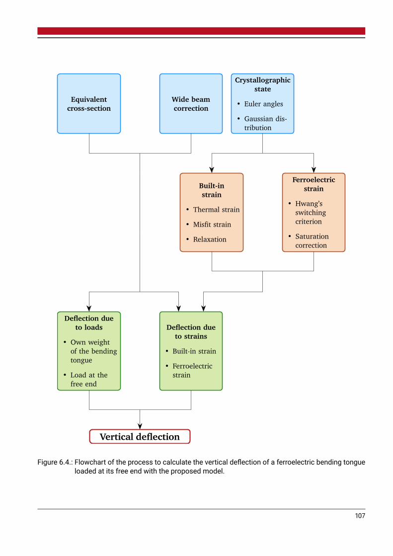
Vertical deflection
Deflection dueto loads
• Own weightof the bendingtongue
• Load at thefree end
Deflection dueto strains
• Built-in strain
• Ferroelectricstrain
Equivalentcross-section
Wide beamcorrection
Built-instrain
• Thermal strain
• Misfit strain
• Relaxation
Ferroelectricstrain
• Hwang’sswitchingcriterion
• Saturationcorrection
Crystallographicstate
• Euler angles
• Gaussian dis-tribution
Figure 6.4.: Flowchart of the process to calculate the vertical deflection of a ferroelectric bending tongueloaded at its free end with the proposed model.
107

6.4. Results and discussion of the modelling
The modelling results presented in this section are not calculated based on the material properties of thesamples deposited in this thesis (see chapter 5). Indeed, due to the large number of material propertiesnecessary for the modelling, the measurement of a significant number of these properties is out of thescope of this thesis, e.g. Young modulus, Poisson ratio, thermal expansion coefficient, etc. Therefore, thematerial properties used thereafter are extracted from literature.
Unless otherwise mentioned, the results given hereafter correspond to the modelling with the developedFeBeTo program [263] of a bending tongue composed of AISI 304 stainless steel as a substrate, LaNiO3 as abuffer layer and PbZr0.52Ti0.48O3 for the ferroelectric layer. The layers have thicknesses of 100 µm, 0.004 µmand 1 µm, respectively. The modelled bending tongue has a length of 10 mm, a width of 3 mm and issubjected to a load of 5 · 10−5 N applied over 1 mm at its free end. The PbZr0.52Ti0.48O3 layer is epitaxialand has the density of tetragonal PZT, as assumed in the model. The applied electrical field is 500 kV·cm−1.The modelling parameters used for the physical and mechanical properties of the ferroelectric, buffer andsubstrate layers are given in Table 6.1.
A polarisation versus applied electrical field curve, or P-E loop, has been modelled in Figure 6.5 for anepitaxial and a polycrystalline PbZr0.52Ti0.48O3 layer. It can be noted that the polycrystalline P-E loopis rounded and wider than the epitaxial one, which is more square-shaped. Indeed, due to the randomorientation of grains in the polycrystalline layer, the alignment of each grain polarisation towards theapplied field direction is progressive. Each grain perceives the applied electrical field differently due to itsown orientation.
−400 −200 0 200 400−60
−40
−20
0
20
40
60(1) (2)
Electrical field (kV·cm−1)
Polaris
ation(µ
C·cm
−2)
Ferroelectric layer:EpitaxialPolycrystalline
Figure 6.5.: Modelled polarisation, P , versus applied electrical field, E, curve in the case of an epitaxial(green squares) and a polycrystalline (blue circles) ferroelectric layer. (1) and (2) indicate 180
and 90 switching of the epitaxial film, respectively.
108

Table 6.1.: Physical and mechanical properties of materials used for modelling. Ferroelectric material:PbZr0.52Ti0.48O3, buffer layer: LaNiO3 and substrate: AISI 304 stainless steel (EN: 1.4301).Adapted from [265].
Parameter Value
Ferroe
lectriclaye
r
Young modulus [271] 9.9 · 1010 Pa
Poisson ratio [272] 0.31
Coercive field [273] 1.5 · 107 V·m−1
Spontaneaous polarisation [274] 0.5 C·m−2
Piezoelectric coefficient d31 [275] −97 · 10−12 V·m−1
Lattice parameter tetragonal a [140] 4.043 · 10−10 m
Lattice parameter tetragonal c [140] 4.132 · 10−10 m
Lattice parameter cubic a (above the Curie temperature) [139] 4.085 · 10−10 m
Thermal expansion coefficient [276] 2 · 10−6 K−1
Curie temperature [275] 573 K
Density [275] 7,600 kg·m−3
Buffe
r
laye
r Young modulus [277] 5.63 · 107 Pa
Lattice parameter for epitaxial strain calculation [196] 3.851 · 10−10 m
Density [196] 7,141 kg·m−3
Subs
trate Young modulus [239] 2.0 · 1011 Pa
Poisson ratio [278] 0.27
Thermal expansion coefficient [239] 16.5 · 10−6 K−1
Density [239] 7,900 kg·m−3
The sharp ferroelectric P-E loop for the epitaxial case, on the other hand, is due to the perfect alignment ofall grains. As they perceive the applied electrical field in the same manner, they answer to it simultaneously.
Furthermore, in the epitaxial P-E loop the poling appears as a two steps process. 180 ferroelectric switchingoccurs at a lower applied field of 175 kV·cm−1 than 90 switching which occurs at 360 kV·cm−1. Thisphenomenon is consistent with the modelling of the ferroelectric strain described in section 6.3.2.3: as 180switching is only due to electrical work, it requires less energy than 90 switching, which is due to bothelectrical and mechanical work. Indeed, while both 180 and 90 switching involve a change in polarisation,90 switching also implies a change in strain. The tetragonal unit cell is deformed, shortening along itsc-axis and elongating along its a-axis, effectively inverting its a-axis and its c-axis.
Once the individual polarisation of each grain has been switched and aligned as closely as possible withthe applied field direction, only 180 switching remains.
Both epitaxial and polycrystalline P-E loops are shifted towards the right-hand side of the graph by
109
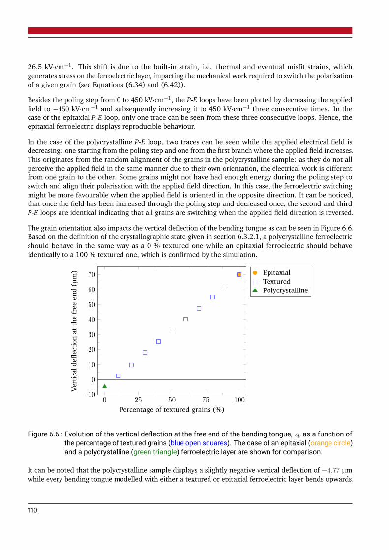
26.5 kV·cm−1. This shift is due to the built-in strain, i.e. thermal and eventual misfit strains, whichgenerates stress on the ferroelectric layer, impacting the mechanical work required to switch the polarisationof a given grain (see Equations (6.34) and (6.42)).
Besides the poling step from 0 to 450 kV·cm−1, the P-E loops have been plotted by decreasing the appliedfield to −450 kV·cm−1 and subsequently increasing it to 450 kV·cm−1 three consecutive times. In thecase of the epitaxial P-E loop, only one trace can be seen from these three consecutive loops. Hence, theepitaxial ferroelectric displays reproducible behaviour.
In the case of the polycrystalline P-E loop, two traces can be seen while the applied electrical field isdecreasing: one starting from the poling step and one from the first branch where the applied field increases.This originates from the random alignment of the grains in the polycrystalline sample: as they do not allperceive the applied field in the same manner due to their own orientation, the electrical work is differentfrom one grain to the other. Some grains might not have had enough energy during the poling step toswitch and align their polarisation with the applied field direction. In this case, the ferroelectric switchingmight be more favourable when the applied field is oriented in the opposite direction. It can be noticed,that once the field has been increased through the poling step and decreased once, the second and thirdP-E loops are identical indicating that all grains are switching when the applied field direction is reversed.
The grain orientation also impacts the vertical deflection of the bending tongue as can be seen in Figure 6.6.Based on the definition of the crystallographic state given in section 6.3.2.1, a polycrystalline ferroelectricshould behave in the same way as a 0 % textured one while an epitaxial ferroelectric should behaveidentically to a 100 % textured one, which is confirmed by the simulation.
0 25 50 75 100−10
0
10
20
30
40
50
60
70
Percentage of textured grains (%)
Vertical
defle
ctionat
thefree
end(µ
m) Epitaxial
TexturedPolycrystalline
Figure 6.6.: Evolution of the vertical deflection at the free end of the bending tongue, zl, as a function ofthe percentage of textured grains (blue open squares). The case of an epitaxial (orange circle)and a polycrystalline (green triangle) ferroelectric layer are shown for comparison.
It can be noted that the polycrystalline sample displays a slightly negative vertical deflection of −4.77 µmwhile every bending tongue modelled with either a textured or epitaxial ferroelectric layer bends upwards.
110
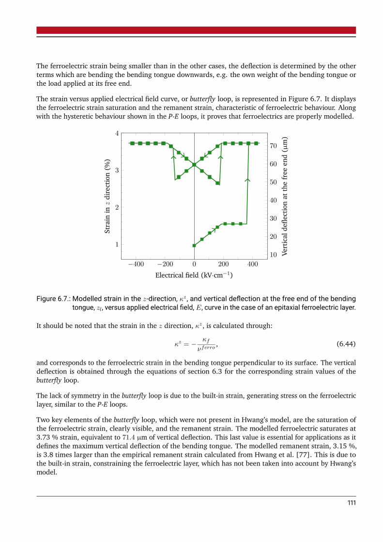
The ferroelectric strain being smaller than in the other cases, the deflection is determined by the otherterms which are bending the bending tongue downwards, e.g. the own weight of the bending tongue orthe load applied at its free end.
The strain versus applied electrical field curve, or butterfly loop, is represented in Figure 6.7. It displaysthe ferroelectric strain saturation and the remanent strain, characteristic of ferroelectric behaviour. Alongwith the hysteretic behaviour shown in the P-E loops, it proves that ferroelectrics are properly modelled.
1
2
3
4
−400 −200 0 200 400
10
20
30
40
50
60
70
Strain
inzdirection(%
)
Electrical field (kV·cm−1)Ve
rtical
defle
ctionat
thefree
end(µ
m)
Figure 6.7.: Modelled strain in the z-direction, κz , and vertical deflection at the free end of the bendingtongue, zl, versus applied electrical field, E , curve in the case of an epitaxial ferroelectric layer.
It should be noted that the strain in the z direction, κz, is calculated through:
κz = −κf
νferro, (6.44)
and corresponds to the ferroelectric strain in the bending tongue perpendicular to its surface. The verticaldeflection is obtained through the equations of section 6.3 for the corresponding strain values of thebutterfly loop.
The lack of symmetry in the butterfly loop is due to the built-in strain, generating stress on the ferroelectriclayer, similar to the P-E loops.
Two key elements of the butterfly loop, which were not present in Hwang’s model, are the saturation ofthe ferroelectric strain, clearly visible, and the remanent strain. The modelled ferroelectric saturates at3.73 % strain, equivalent to 71.4 µm of vertical deflection. This last value is essential for applications as itdefines the maximum vertical deflection of the bending tongue. The modelled remanent strain, 3.15 %,is 3.8 times larger than the empirical remanent strain calculated from Hwang et al. [77]. This is due tothe built-in strain, constraining the ferroelectric layer, which has not been taken into account by Hwang’smodel.
111
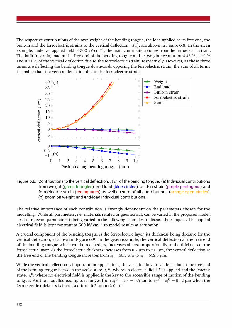
The respective contributions of the own weight of the bending tongue, the load applied at its free end, thebuilt-in and the ferroelectric strains to the vertical deflection, z(x), are shown in Figure 6.8. In the givenexample, under an applied field of 500 kV·cm−1, the main contribution comes from the ferroelectric strain.The built-in strain, load at the free end of the bending tongue and its weight account for 4.43 %, 1.19 %and 0.71 % of the vertical deflection due to the ferroelectric strain, respectively. However, as these threeterms are deflecting the bending tongue downwards opposing the ferroelectric strain, the sum of all termsis smaller than the vertical deflection due to the ferroelectric strain.
(a)
−5
0
5
10
15
20
25
30
35
40
Vertical
defle
ction(µ
m)
WeightEnd loadBuilt-in strainFerroelectric strainSum
(b)0 1 2 3 4 5 6 7 8 9 10
−1−0.5
0
Position along bending tongue (mm)
Figure 6.8.: Contributions to the vertical deflection, z(x), of the bending tongue. (a) Individual contributionsfrom weight (green triangles), end load (blue circles), built-in strain (purple pentagons) andferroelectric strain (red squares) as well as sum of all contributions (orange open circles),(b) zoom on weight and end-load individual contributions.
The relative importance of each contribution is strongly dependent on the parameters chosen for themodelling. While all parameters, i.e. materials related or geometrical, can be varied in the proposed model,a set of relevant parameters is being varied in the following examples to discuss their impact. The appliedelectrical field is kept constant at 500 kV·cm−1 to model results at saturation.
A crucial component of the bending tongue is the ferroelectric layer, its thickness being decisive for thevertical deflection, as shown in Figure 6.9. In the given example, the vertical deflection at the free endof the bending tongue which can be reached, zl, increases almost proportionally to the thickness of theferroelectric layer. As the ferroelectric thickness increases from 0.2 µm to 2.0 µm, the vertical deflection atthe free end of the bending tongue increases from zl = 50.2 µm to zl = 552.9 µm.
While the vertical deflection is important for applications, the variation in vertical deflection at the free endof the bending tongue between the active state, zlE , where an electrical field E is applied and the inactivestate, zl0, where no electrical field is applied is the key to the accessible range of motion of the bendingtongue. For the modelled example, it ranges from zl
E − zl0 = 9.5 µm to zl
E − zl0 = 91.2 µm when the
ferroelectric thickness is increased from 0.2 µm to 2.0 µm.
112

0.0 0.4 0.8 1.2 1.6 2.0
100
200
300
400
500
600
Thickness of ferroelectric layer (µm)
Vertical
defle
ctionat
thefree
end(µ
m)
0 1 2
50
100
z lE−z l
0(µ
m)
Figure 6.9.: Evolution of the vertical deflection at the free end of the bending tongue, zl, as a function ofthe ferroelectric layer thickness with a length of 10 mm and a load at its free end of 5 · 10−5 N.zl
E − zl0 represents the variation in vertical deflection between the states where an electrical
fieldE is applied and where no electrical field is applied. AsE is kept constant at 500 kV·cm−1,saturation is reached.
On the other hand, the vertical deflection at the free end of the bending tongue is not proportional tothe length of the bending tongue, as can be seen in Figure 6.10. The vertical deflection increases fromzl = 2.1 µm to zl = 279.4 µm as the length is extended from 2 mm to 20 mm. The most important resultis once more the variation in vertical deflection between the active state and the inactive state, reachingzl
E − zl0 = 0.4 µm at a length of 2 mm and zl
E − zl0 = 46.8 µm at a length of 20 mm. The length of the
bending tongue, if not restricted in a given application, is therefore an interesting parameter to increasethe vertical deflection.
Other parameters also impact the vertical deflection, like the load applied at the free end as representedin Figure 6.11. As the end load increases from 0 mN to 10 mN, the deflection of the bending tongue isinverted from upwards to downwards. This corresponds to the increase of the end load component relativeto the ferroelectric component up to the point where it becomes the dominant component of deflection.The critical point at which the direction of the deflection is inverted is reached at an end load of 3.9 mN.
Increasing the load applied at the free end of the bending tongue does not impact the variation in verticaldeflection between the active state and the inactive state, which is mainly determined by the ferroelectriclayer thickness and the length of the bending tongue.
It should be noted that some of the parameters impact the vertical deflection in various ways throughEquations (6.13) and (6.19). This is the case for the geometrical dimensions of the bending tongue, i.e.length, width, thicknesses of the layers and length load, which are parameters of both the own weight ofthe bending tongue and its effective second moment or area, Ieff . This is particularly relevant for the
113
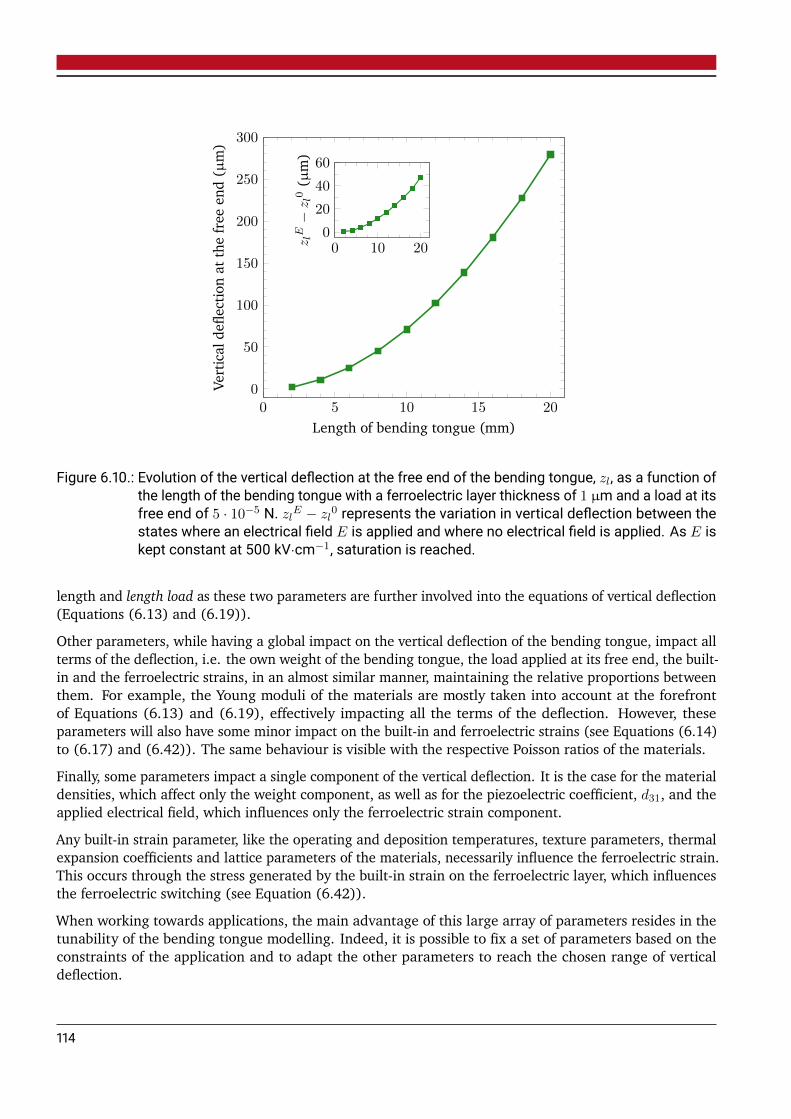
0 5 10 15 200
50
100
150
200
250
300
Length of bending tongue (mm)
Vertical
defle
ctionat
thefree
end(µ
m)
0 10 200
20
40
60
z lE−z l
0(µ
m)
Figure 6.10.: Evolution of the vertical deflection at the free end of the bending tongue, zl, as a function ofthe length of the bending tongue with a ferroelectric layer thickness of 1 µm and a load at itsfree end of 5 · 10−5 N. zlE − zl
0 represents the variation in vertical deflection between thestates where an electrical field E is applied and where no electrical field is applied. As E iskept constant at 500 kV·cm−1, saturation is reached.
length and length load as these two parameters are further involved into the equations of vertical deflection(Equations (6.13) and (6.19)).
Other parameters, while having a global impact on the vertical deflection of the bending tongue, impact allterms of the deflection, i.e. the own weight of the bending tongue, the load applied at its free end, the built-in and the ferroelectric strains, in an almost similar manner, maintaining the relative proportions betweenthem. For example, the Young moduli of the materials are mostly taken into account at the forefrontof Equations (6.13) and (6.19), effectively impacting all the terms of the deflection. However, theseparameters will also have some minor impact on the built-in and ferroelectric strains (see Equations (6.14)to (6.17) and (6.42)). The same behaviour is visible with the respective Poisson ratios of the materials.
Finally, some parameters impact a single component of the vertical deflection. It is the case for the materialdensities, which affect only the weight component, as well as for the piezoelectric coefficient, d31, and theapplied electrical field, which influences only the ferroelectric strain component.
Any built-in strain parameter, like the operating and deposition temperatures, texture parameters, thermalexpansion coefficients and lattice parameters of the materials, necessarily influence the ferroelectric strain.This occurs through the stress generated by the built-in strain on the ferroelectric layer, which influencesthe ferroelectric switching (see Equation (6.42)).
When working towards applications, the main advantage of this large array of parameters resides in thetunability of the bending tongue modelling. Indeed, it is possible to fix a set of parameters based on theconstraints of the application and to adapt the other parameters to reach the chosen range of verticaldeflection.
114
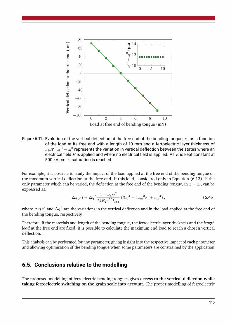
0 2 4 6 8 10−100
−80
−60
−40
−20
0
20
40
60
80
Load at free end of bending tongue (mN)
Vertical
defle
ctionat
thefree
end(µ
m)
0 5 1010
12
14
z lE−z l
0(µ
m)
Figure 6.11.: Evolution of the vertical deflection at the free end of the bending tongue, zl, as a functionof the load at its free end with a length of 10 mm and a ferroelectric layer thickness of1 µm. zlE − zl
0 represents the variation in vertical deflection between the states where anelectrical field E is applied and where no electrical field is applied. As E is kept constant at500 kV·cm−1, saturation is reached.
For example, it is possible to study the impact of the load applied at the free end of the bending tongue onthe maximum vertical deflection at the free end. If this load, considered only in Equation (6.13), is theonly parameter which can be varied, the deflection at the free end of the bending tongue, in x = xl, can beexpressed as:
∆z(x) = ∆qL1− νeff
2
24EYeffIeff
(3xl
4 − 4xm3xl + xm
4), (6.45)
where ∆z(x) and ∆qL are the variations in the vertical deflection and in the load applied at the free end ofthe bending tongue, respectively.
Therefore, if the materials and length of the bending tongue, the ferroelectric layer thickness and the lengthload at the free end are fixed, it is possible to calculate the maximum end load to reach a chosen verticaldeflection.
This analysis can be performed for any parameter, giving insight into the respective impact of each parameterand allowing optimisation of the bending tongue when some parameters are constrained by the application.
6.5. Conclusions relative to the modelling
The proposed modelling of ferroelectric bending tongues gives access to the vertical deflection whiletaking ferroelectric switching on the grain scale into account. The proper modelling of ferroelectric
115
switching can be verified through the P-E loop and the butterfly loop, both displaying hystereticbehaviour and saturation.
The description of the saturation in the butterfly loop is an improvement of Hwang et al.’s model on whichthe description of ferroelectric switching is based. This addition is crucial for applications were themaximum accessible deflection and the corresponding applied electrical field required to reach itare needed.
Additional features have been added, notably the calculation of the remanent strain and the impact ofthe crystallographic state of the ferroelectric (polycrystalline, textured or epitaxial). The influence ofbuilt-in strain on the polarisation highlighted by this model has been demonstrated experimentally byColeman, Walker, Beechem and Trolier-McKinstry [53] since its publication [265].
The large amount of parameters taken into account in this model allows the relative importance of thecontributions to the vertical deflection, i.e. own weight of the bending tongue, load applied at its free end,built-in and ferroelectric strains, to be ascertained and the geometry of the bending tongue to be optimised.As the material properties cannot be changed easily, the geometry of the bending tongue optimisation isessential for specific applications, ensuring that ferroelectric strain is the main driving force of the bendingtongue vertical deflection.
The model predicts, for a 10 mm long and 3 mm wide bending tongue with a load of 5 · 10−5 N applied atits free end, a change in vertical deflection under an applied electrical field of 500 kV·cm−1 ranging from9.5 µm to 91.5 µm as the epitaxial PZT layer thickness increases from 0.2 µm to 2.0 µm. These resultsindicate that PZT thin films deposited on stainless steel substrates are good candidates as bendingtongues in MEMS applications.
116
7. Conclusions and outlooks
Numerous future technological developments, including the implementation of wearable sensors and theInternet of Things, are dependent on the integration of ferroelectrics into MEMS applications. However,fundamentals questions, stated in section 1.2, must be answered to enable the direct deposition of leadzirconate titanate thin films on stainless steel substrates by pulsed laser deposition and to establish thesuitability of these films for piezoelectric MEMS applications.
This chapter formulate the answers that this work has endeavoured to provide to these questions.Section 7.1 treats each of the aforementioned questions individually to draw the conclusions of this work.The outlooks of this thesis and future work necessary to expand knowledge on the topic are discussed insection 7.2.
7.1. Conclusions and answers to the statement of purpose
The fundamental questions regarding the integration of ferroelectrics into MEMS applications that thisthesis aims to address are recalled and answered below.
1. How to incite the growth of tetragonal 001-oriented or textured lead zirconate titanate thin filmson steel substrates by pulsed laser deposition to engineer a larger piezoelectric response?
This thesis establishes that the crystallographic orientation of lead zirconate titanate thin films growndirectly on stainless steel by pulsed laser deposition can be tailored with selected buffer layers andappropriate substrate preparation.
As demonstrated in literature with sol-gel procedures, it is possible to obtain predominantly 001-texturedPZT thin films using pseudo-cubic 100-oriented LaNiO3 as a growth template and bottom electrode.Furthering the state of the art, this work shows that LNO thin films can be deposited with a 001orientation on stainless steel substrates by physical vapour deposition and, therefore, that PZT thinfilms orientation can be engineered on stainless steel substrates.
The process necessitates substrates with limited roughnesswhich can be obtained bymechanical polishing,reducing as-bought AISI 304 stainless steel substrates roughness from 189 nm down to 3 nm. To maintainsurface quality through the subsequent depositions, substrate oxidation must be prevented. For thispurpose, a Pt buffer layer was initially used, however, it interacts with the substrate at elevated temperatures,creating an intermetallic phase, CrPt. The formation of the CrPt phase generates surface instability duringLNO deposition, preventing the latter from growing in a 001 orientation. This can be circumventedwith an amorphous Al2O3 buffer layer between the Pt and LNO thin films. Thereby, 001-textured PZTthin films have been deposited in PbZr0.52Ti0.48O3/LaNiO3/Al2O3/Pt/steel heterostructures. ThesePZT stacks display Lotgering factors for the LNO and PZT layers of f(00l)LNO = 0.68 and f(00l)
PZT = 0.91,respectively.
Further series of samples have been deposited, confirming that tetragonal 001 texture can also beachieved for 2 mol.% Nb-doped PZT thin films. To prevent the formation of an intermetallic phase,the Pt buffer layer is removed from these Pb0.990.01(Zr0.52Ti0.48)0.98Nb0.02O3/LaNiO3/Al2O3/steel
117
heterostructures and the thickness of the Al2O3 layer is increased to 50 nm to avoid oxidation of thestainless steel substrates during the deposition of the LNO and PNZT layers. The Lotgering factor for theLNO layer of PNZT stacks reaches up to f(00l)
LNO = 0.84, an improved value compared to those reportedin literature on steel substrates. The PNZT thin films show Lotgering factors of f(00l)PNZT = 0.89, a valueequivalent to those observed for the PZT thin films deposited in this work.
The keys elements enabling 001-textured deposition of PZT and PNZT thin films on stainless steelsubstrates by pulsed laser deposition are a limited substrate roughness, the prevention of substrateoxidation with an Al2O3 buffer layer and the deposition of a pseudo-cubic 100-oriented LaNiO3thin film as a growth template.
2. Are the ferroelectric properties of lead zirconate titanate thin films on steel substrates suitable forpiezoelectric MEMS applications?
This work shows that the ferroelectric properties of 001-textured lead zirconate titanate thin filmsdeposited on AISI 304 stainless steel substrates make them good candidates for future piezoelectricMEMS applications.
The dielectric constant of both 200 nm thick PZT and PNZT thin films is approximately 350 at 1 kHzwith dielectric loss lower than 5 %. In the case of the PNZT thin films, higher permittivity is reported forsome electrodes, up to 370 at 1 kHz. Furthermore, PNZT dielectric constant can increase up to 430 afterP-E loop measurements. While these permittivity values are lower than most reported in literature for PZTthin films on metallic substrates [51,53,57], they are larger than those of 192 reported for non-texturedPZT on austenitic stainless steel [64]. The dielectric losses here described are equivalent to literaturevalues.
Thin films of both undoped PZT and PZT doped with 2 mol.% Nb are ferroelectric, displaying welldefined polarisation versus electrical field hysteresis loops with a clear saturation. Measured underthe same conditions, 400 nm thick PZT and PNZT thin films both present a remanent polarisationP r ∼16.5 µC·cm-2 and a coercive field Ec ∼92 kV·cm-1. The values of remanent polarisation andcoercive field are on par with and larger than those reported in literature for thicker PZT thin films,respectively [51,53].
While 2 mol.% Nb-doping has no noticeable impact on the properties of the PNZT thin films ascompared to those of the PZT layers, the effect of doping could be damped by other phenomena as thePNZT stacks and the PZT stacks are deposited under different conditions. Nonetheless, the PNZT thin filmsdeposited in this work can withstand higher applied electrical fields than PZT thin films withoutundergoing dielectric breakdown.
Phenomena not yet fully understood occur in the PNZT thin films, leading to intrinsic changes withinsamples during P-E loop measurements with increasing maximum applied field. The reversible andirreversible Rayleigh constants are increased after these measurements, along with larger dielectricconstant and loss values. It appears from leakage current measurements that the space-charge limitedcurrent with trap filling mechanism, which was identify for the PZT thin films, is combined with at leastanother mechanism at higher applied fields for the PNZT thin films.
The piezoelectric e31,f coefficient of the PNZT thin films is within range of literature reports for PZTthin films on metallic substrates. However, the e31,f coefficient reaching up only to −4.4 C·m-2 for the200 nm thick PNZT thin film, improvement would be advisable.
118
The lead zirconate titanate thin films deposited in this work present acceptable dielectric constants.Nonetheless, future piezoelectric MEMS applicationswould benefit from an increase of their permittivity.Contrarily, dielectric losses are satisfying, being below 5 %. The remanent polarisation values are onpar with literature and could potentially be higher if the P-E loops were measured with larger maximumapplied field. This is possible with the PNZT thin films on which larger electrical field can be appliedwithout reaching dielectric breakdown than on the PZT thin films. Therefore, the remanent polarisationvalues are promising for MEMS applications and are combined with rather larger coercive fieldsas compared to literature. The presence of an internal bias field should be noted in both the PZT andthe PNZT thin films, indicating a preferred polarisation direction which can be used efficiently forpiezoelectric MEMS applications. The current properties hint towards sensor technology rather thanactuation applications.
The ferroelectric tetragonal 001-textured lead zirconate titanate thin films, in particular with2 mol.% Nb-doping, deposited by pulsed laser deposition on stainless steel substrates are noteworthycandidates for future piezoelectric MEMS applications requiring non-brittle substrates.
3. How to calculate the accessible vertical deflection of ferroelectric bending tongues, taking into accountboth their linear piezoelectric structure and ferroelectric switching?
This work demonstrates that the gap between the description of ferroelectric switching and themechanical approach for linear piezoelectric structures can be bridged. A model is proposed tocalculate the vertical deflection of ferroelectric bending tongues based on the Euler-Bernoulli beam theorywhile taking ferroelectric switching on the grain scale into consideration, relying on the switching criteriondeveloped by Hwang et al. [77].
The proposed model gives rise to both P-E loops and butterfly loops, displaying hysteretic behaviourand saturation, indicating the proper modelling of ferroelectric switching. An improvement of Hwanget al’s model is the description of the saturation in the butterfly loop which is critical to calculate themaximum accessible deflection and corresponding applied electrical field required to reach it forMEMS applications.
The combination of the ferroelectric switching criterion with the Euler-Bernoulli beam theory and theinclusion of a significant number of parameters to the model give access to additional features. With theloading at the bending tongue free end to represent practical MEMS applications, and parameters describingbending tongues physical characteristics, i.e. geometry, material properties, crystallographic state, etc., itbecomes possible to optimise the geometry of the bending tongue. Since the material properties cannotbe modified easily, this is essential to tailor bending tongues for specific MEMS applications.
This wide range of available parameters has notably permitted to highlight the impact of the crystal-lographic state of the ferroelectric (polycrystalline, textured or epitaxial) onto vertical deflection.Furthermore, the modelling confirms that PZT thin films deposited on stainless steel substrates aresuitable candidates as bending tongues in MEMS applications with a change in vertical deflection up to9.5 µm under an applied electrical field of 500 kV·cm−1 for a 10 mm long bending tongue with a 5 · 10−5 Nload applied at its free end.
Through the analysis of the impact of the different parameters onto the bending tongue vertical deflection,the full potential of combining the modelling of the mechanical approach for linear piezoelectricstructures and the description of ferroelectric switching to predict the behaviour of ferroelectricMEMS is unequivocal.
119
7.2. Outlooks and future work
To fully exploit the potential of this work and create piezoelectric MEMS applications based on 001-oriented lead zirconate titanate thin films deposited directly on stainless steel substrates, additionalinvestigations are necessary. Future work towards this goal can be sundered into several segments.
7.2.1. Potential improvements to ferroelectric bending tongues modelling
The FeBeTo - Ferroelectric Bending Tongues modelling program introduced in chapter 6 was developedwith the possibility to easily replace internal functions within the main program. Despite the significantimprovements brought by the modelling proposed in this work, further enhancement could be achieved byrelying on a new function to calculate ferroelectric strain in the program.
Indeed, in this work, the calculation of ferroelectric strain relies on Hwang et al.’s model for ferroelectricswitching [77]. Domain wall motion and the correlation between ferroelectric domains are not accountedfor in the proposed model despite the large impact they have on ferroelectric switching [248]. Therefore, itwould be interesting to integrate in the FeBeTo program several models of ferroelectric behaviour developedin the recent years and described in literature. These models could bring additional information onthe dynamics of the switching process [279] or on the impact of domain wall pinning [74] which wouldcontribute to a more accurate prediction of the accessible vertical deflection of ferroelectric bending tongues.
Additionally, it would be interesting to fully characterise the lead zirconate titanate thin films depositedin this work to perform the modelling with the effective material properties. It would give more insightinto the capabilities of lead zirconate titanate thin films on stainless steel in MEMS applications and wouldfurther enable the optimisation of device geometry for a specific application.
7.2.2. Potential improvements in materials selection and deposition methods
Several improvements can also be made in the materials selection for the PZT stacks and the PNZT stacks,ranging from the choice of stainless steel for the substrate to the doping of the lead zirconate titanate thinfilms.
As passive components in MEMS applications, substrates must not hinder the action of the active ferroelectriclayer. Therefore, it would be interesting to reduce the current substrate thickness of 0.2 mm down to a fewtens of microns as reported in literature for some experimental investigations [51,53]. However, we notethat thinner substrates would pose difficulties for the substrates mechanical polishing with the currentexperimental setup and would require to establish new polishing procedures.
Furthermore, as described in section 5.1.1, substrate bending occurs during the deposition of the bufferand lead zirconate titanate layers at elevated temperatures. This bending, due to a relief of processingstresses, could be avoided by utilising a thermally treated stainless steel in which stress is relieved prior tothin films deposition [165]. During this thermal treatment, cooling down should be performed sufficientlyfast to avoid the precipitation of chromium carbide during the process, which would make the steel easilyoxidisable [166]. Due to the technical difficulties to achieve such rapid cooling, the process should beperformed industrially.
120
Besides improvements of the substrate characteristics, the current work could benefit from a tuning of theamount of Nb-doping into the PNZT thin films as only 2 mol.% Nb-doping has been investigated. Thesometimes contradictory literature reports on Nb-doping effects on lead zirconate titanate properties, e.g.on coercive field, emphasise the importance of investigating the impact of doping in the specific depositionconditions encountered in the heterostructures developed in this work [98,154]. Indeed, ferroelectricscoercive fields, determining their ease to be poled and depoled, are critical for some applications.
Additionally, it is conceivable to replace the pulsed laser deposition employed for the different layersby sol-gel methods. While out of the scope of this thesis, these procedures can be performed at lowertemperatures, followed by post-deposition rapid thermal annealing, efficiently limiting the oxidation ofstainless steel and reducing thermal strain on the heterostructures [24]. It should also be pointed outthat the pulsed laser deposition system currently used to deposit lead zirconate titanate thin films hasa relatively slow deposition rate compared to that of a sol-gel procedure. Furthermore, a PbO cappinglayer deposited on top of lead zirconate titanate thin films would compensate lead evaporation during thedeposition and stabilise the perovskite phase [51]. However, the current pulsed laser deposition systemdoes not permit to switch between two different targets while maintaining the deposition conditions,suppressing the possibility to deposit a capping layer from a secondary PbO target. For this reason, theheterostructures deposited in this work would also benefit from the implementation of a sol-gel procedure.
7.2.3. Towards future MEMS applications
As for any devices, MEMS applications require not only to optimise material properties but to meet a setof technical specifications. For this purpose, an accurate understanding of the phenomena within thelead zirconate titanate thin films under an applied electrical field is needed. Therefore, the nature of theintrinsic changes described in section 5.2.5 and, notably, their relation with the large leakage currents inthe first measured series of P-E loops, must be determined.
Furthermore, the effective e31,f transverse piezoelectric coefficient could be asserted more accurately if thein-plane strain was measured by Pt strain gauges sputtered directly on the sample surface (see section 4.4)instead of commercial strain gauges glued next to the sample. Accessing this improved characterisationmethod necessitate to solve the adhesion problem between the lead zirconate titanate thin films and thesputtered strain gauges.
Moreover, the adhesion between the different layers of the heterostructures must be assessed to ensuretheir structural integrity when operated as MEMS devices. Studies under various conditions are yet to becarried out, in particular, the impact of temperature, crucial for ferroelectric properties [54], needs to beinvestigated. After selection of a specific application for MEMS devices based on this work’s heterostructures,the corresponding figure of merit should be calculated.
Ultimately, the replacement of lead zirconate titanate thin films by lead-free ferroelectrics could beconsidered as the Restriction of Hazardous Substances (RoHS) in Electrical and Electronic Equipment setby the European Union in February 2003 [280] is getting increasingly stringent [281,282]. This last pointshould be carefully examined in terms of advantages and drawbacks outside of the academic perspective asthe industrial significance of lead-free materials is, to date, not clearly established and they might ultimatelyhave a larger environmental impact [283].
Until lead-free ceramics can fully replace PZT and while further improvements and characterisationof the ferroelectric 001-textured lead zirconate titanate thin films deposited on stainless steel
121

substrates are necessary, the results presented in this thesis position them as good candidates forpiezoelectric MEMS applications.
122

List of appendices
A. Wafer flexure e31,f measurement system loudspeaker amplifier . . . . . . . . . . . . . . . IIIB. Wafer flexure e31,f measurement system loudspeaker cavity . . . . . . . . . . . . . . . . . VC. Wafer flexure e31,f measurement system uniform pressure rig . . . . . . . . . . . . . . . . VIID. Wafer flexure e31,f measurement system electronics box . . . . . . . . . . . . . . . . . . . XIIIE. Wafer flexure e31,f measurement system charge converter . . . . . . . . . . . . . . . . . . XVF. Modelling of ferroelectric bending tongues: Code of the FeBeTo - Ferroelectric Bending Tongues
modelling program . . . . . . . . . . . . . . . . . . . . . . . . . . . . . . . . . . . . . . . XVIIG. Modelling of ferroelectric bending tongues: Development from the load distribution equation
to the equation of vertical deflection due to loads . . . . . . . . . . . . . . . . . . . . . . XIXH. Modelling of ferroelectric bending tongues: Development from the bending moments due to
strain distribution equation to the equation of vertical deflection due to bending moments XXI
I

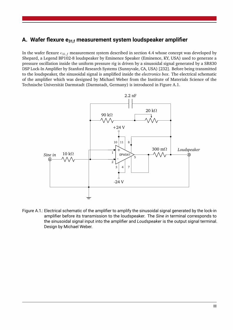
A. Wafer flexure e31,f measurement system loudspeaker amplifier
In the wafer flexure e31,f measurement system described in section 4.4 whose concept was developed byShepard, a Legend BP102-8 loudspeaker by Eminence Speaker (Eminence, KY, USA) used to generate apressure oscillation inside the uniform pressure rig is driven by a sinusoidal signal generated by a SR830DSP Lock-In Amplifier by Stanford Research Systems (Sunnyvale, CA, USA) [232]. Before being transmittedto the loudspeaker, the sinusoidal signal is amplified inside the electronics box. The electrical schematicof the amplifier which was designed by Michael Weber from the Institute of Materials Science of theTechnische Universität Darmstadt (Darmstadt, Germany) is introduced in Figure A.1.
Sine in 10 kΩ OPA541
300 mΩ Loudspeaker
+24 V
-24 V
+
-1
23 4
5
7
810 11
90 kΩ20 kΩ
2.2 nF
Figure A.1.: Electrical schematic of the amplifier to amplify the sinusoidal signal generated by the lock-inamplifier before its transmission to the loudspeaker. The Sine in terminal corresponds tothe sinusoidal signal input into the amplifier and Loudspeaker is the output signal terminal.Design by Michael Weber.
III

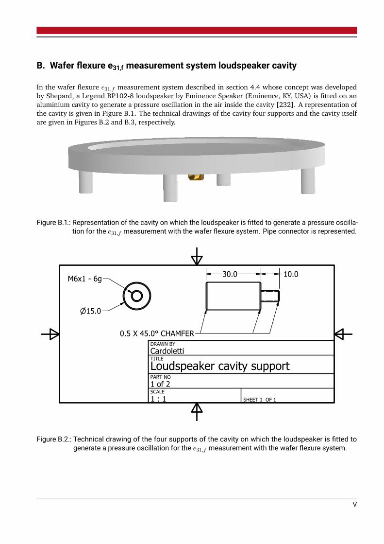
B. Wafer flexure e31,f measurement system loudspeaker cavity
In the wafer flexure e31,f measurement system described in section 4.4 whose concept was developedby Shepard, a Legend BP102-8 loudspeaker by Eminence Speaker (Eminence, KY, USA) is fitted on analuminium cavity to generate a pressure oscillation in the air inside the cavity [232]. A representation ofthe cavity is given in Figure B.1. The technical drawings of the cavity four supports and the cavity itselfare given in Figures B.2 and B.3, respectively.
Figure B.1.: Representation of the cavity on which the loudspeaker is fitted to generate a pressure oscilla-tion for the e31,f measurement with the wafer flexure system. Pipe connector is represented.
SHEET 1 OF 1
DRAWN BY
Cardoletti
PART NO
1 of 2
SCALE
1 : 1
TITLE
Loudspeaker cavity support
M6x1 - 6g
30.0 10.0
15.0
0.5 X 45.0° CHAMFER
Figure B.2.: Technical drawing of the four supports of the cavity on which the loudspeaker is fitted togenerate a pressure oscillation for the e31,f measurement with the wafer flexure system.
V
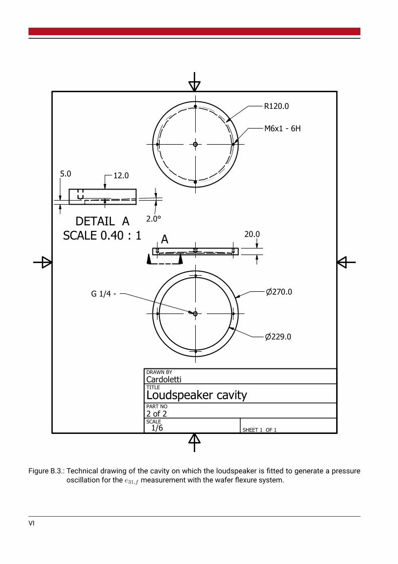
DETAIL A
SCALE 0.40 : 1
A
SHEET 1 OF 1
DRAWN BY
Cardoletti
PART NO
2 of 2
SCALE
1/6
TITLE
Loudspeaker cavity
G 1/4 -
270.0
229.0
M6x1 - 6H
R120.0
2.0°
20.0
5.0
12.0
Figure B.3.: Technical drawing of the cavity on which the loudspeaker is fitted to generate a pressureoscillation for the e31,f measurement with the wafer flexure system.
VI
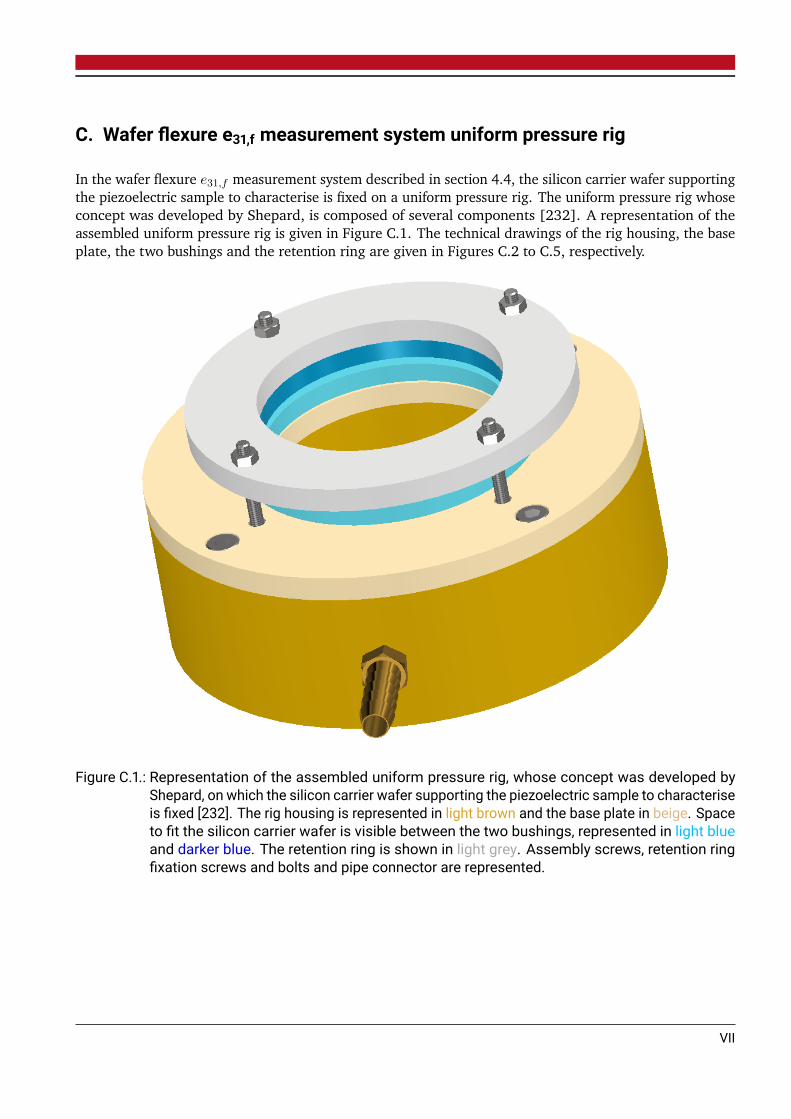
C. Wafer flexure e31,f measurement system uniform pressure rig
In the wafer flexure e31,f measurement system described in section 4.4, the silicon carrier wafer supportingthe piezoelectric sample to characterise is fixed on a uniform pressure rig. The uniform pressure rig whoseconcept was developed by Shepard, is composed of several components [232]. A representation of theassembled uniform pressure rig is given in Figure C.1. The technical drawings of the rig housing, the baseplate, the two bushings and the retention ring are given in Figures C.2 to C.5, respectively.
Figure C.1.: Representation of the assembled uniform pressure rig, whose concept was developed byShepard, on which the silicon carrier wafer supporting the piezoelectric sample to characteriseis fixed [232]. The rig housing is represented in light brown and the base plate in beige. Spaceto fit the silicon carrier wafer is visible between the two bushings, represented in light blueand darker blue. The retention ring is shown in light grey. Assembly screws, retention ringfixation screws and bolts and pipe connector are represented.
VII

SHEET 1 OF 1
DRAWN BY
Cardoletti
PART NO
1 of 4
SCALE
1 / 2
TITLE
Rig housing
127.00
38.00
26.00 19.00
82.00
R44.50
R56.00
45.0°
G 1/8 -
6.00 4.00
M5x0.5 - 6H
Figure C.2.: Technical drawing of the rig housing component of the uniform pressure rig for the e31,fmeasurement with the wafer flexure system.
VIII
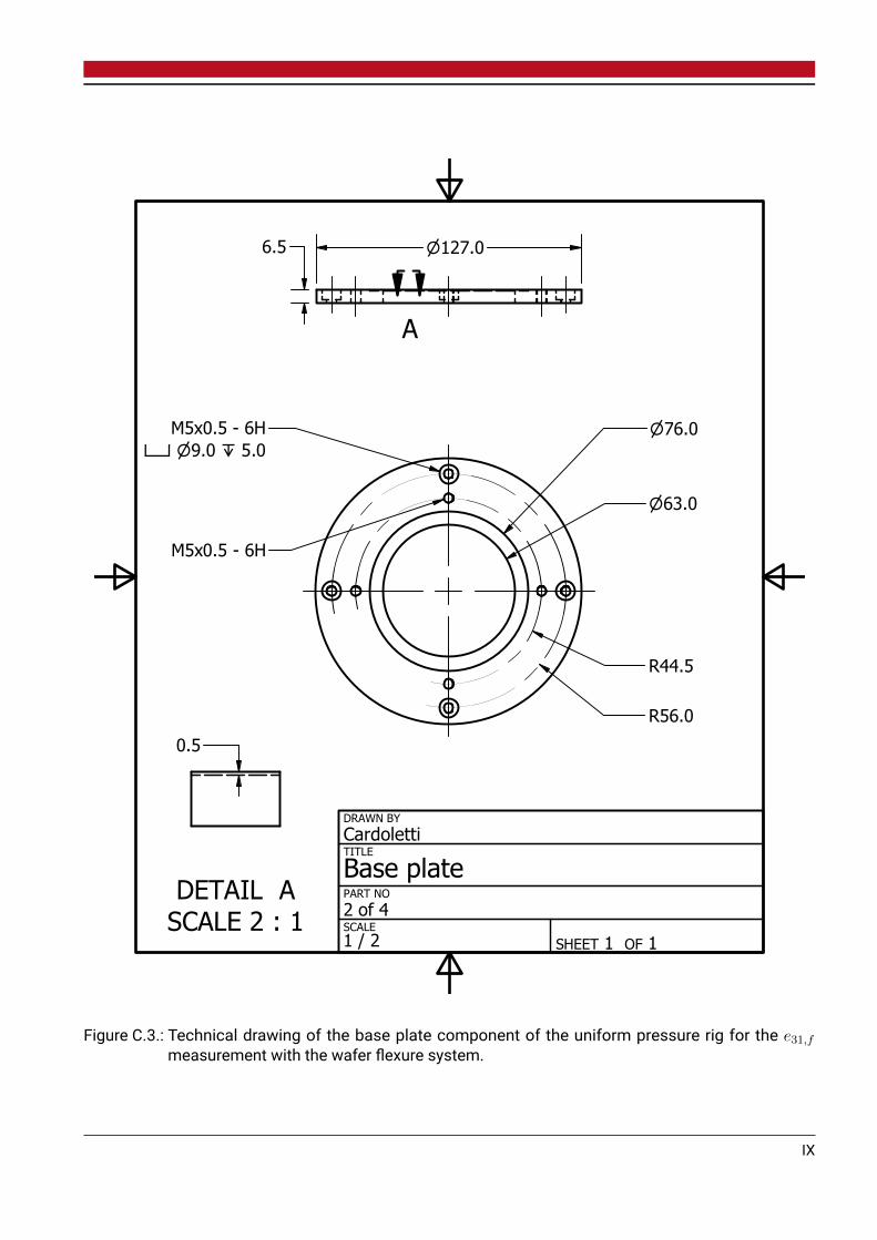
DETAIL A
SCALE 2 : 1
A
SHEET 1 OF 1
DRAWN BY
Cardoletti
PART NO
2 of 4
SCALE
1 / 2
TITLE
Base plate
127.0
0.5
76.0
63.0
R44.5
R56.0
6.5
M5x0.5 - 6H
M5x0.5 - 6H
9.0 5.0
Figure C.3.: Technical drawing of the base plate component of the uniform pressure rig for the e31,fmeasurement with the wafer flexure system.
IX
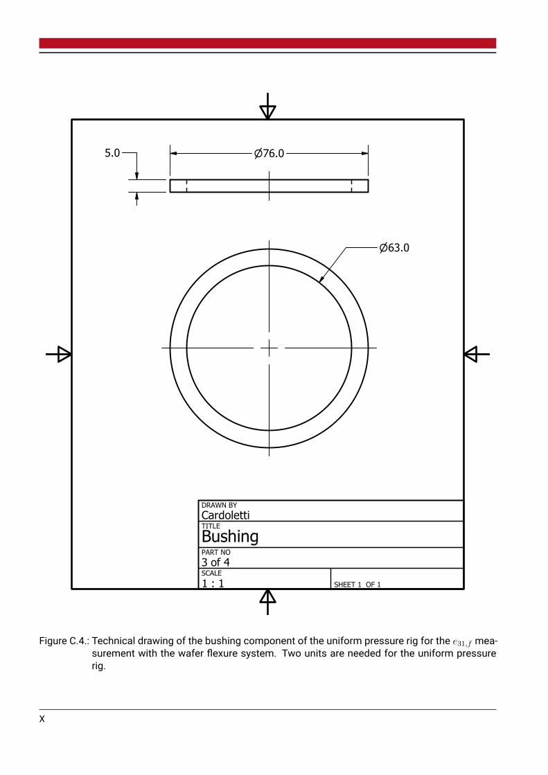
SHEET 1 OF 1
DRAWN BY
Cardoletti
PART NO
3 of 4
SCALE
1 : 1
TITLE
Bushing
76.05.0
63.0
Figure C.4.: Technical drawing of the bushing component of the uniform pressure rig for the e31,f mea-surement with the wafer flexure system. Two units are needed for the uniform pressurerig.
X
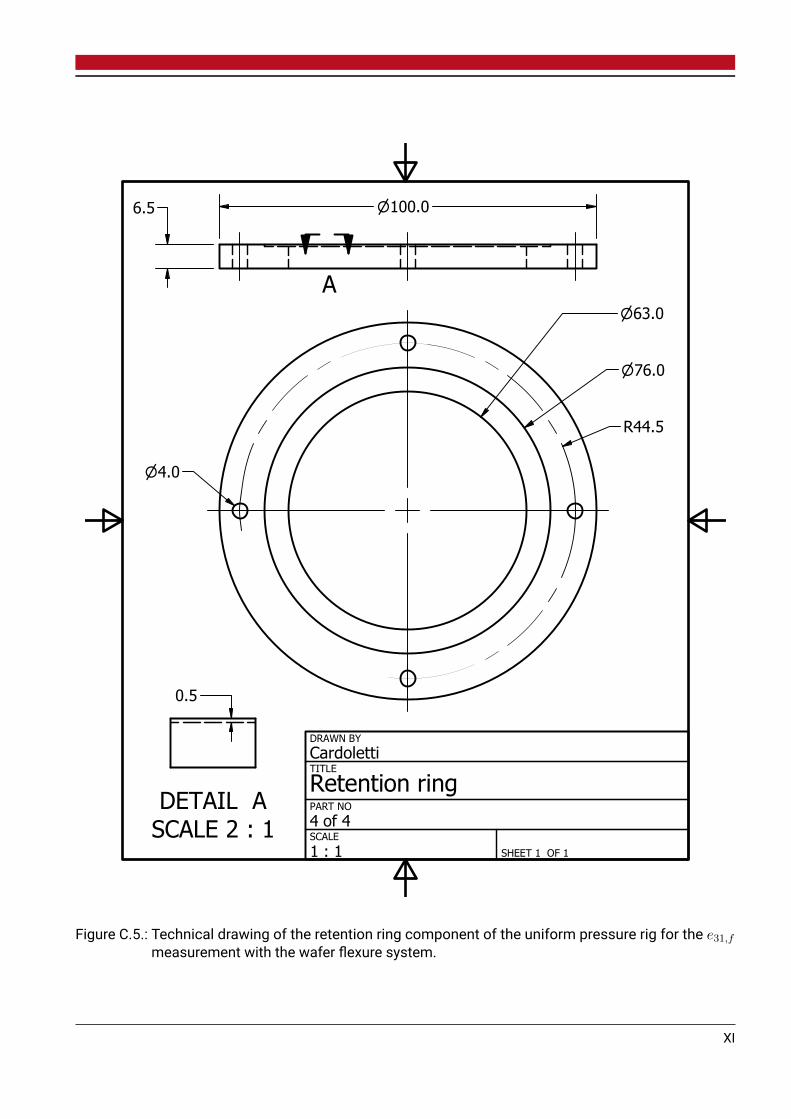
DETAIL A
SCALE 2 : 1
A
SHEET 1 OF 1
DRAWN BY
Cardoletti
PART NO
4 of 4
SCALE
1 : 1
TITLE
Retention ring
100.0
6.5
0.5
4.0
R44.5
63.0
76.0
Figure C.5.: Technical drawing of the retention ring component of the uniform pressure rig for the e31,fmeasurement with the wafer flexure system.
XI

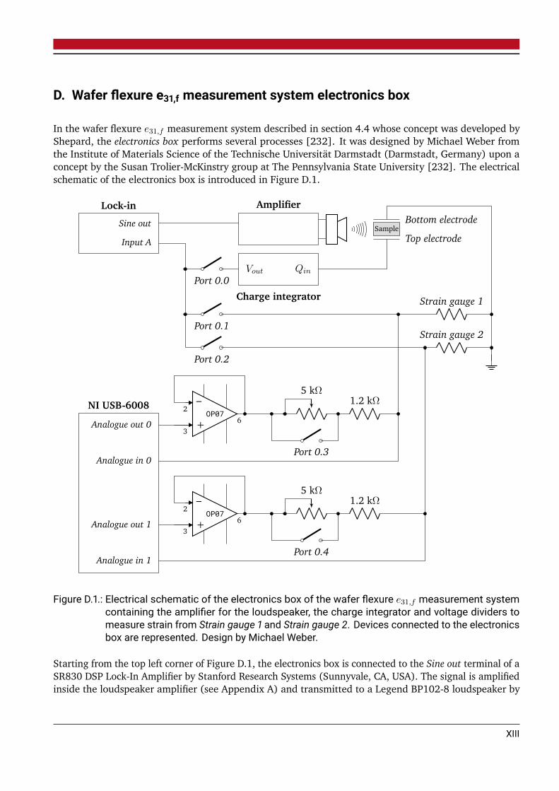
D. Wafer flexure e31,f measurement system electronics box
In the wafer flexure e31,f measurement system described in section 4.4 whose concept was developed byShepard, the electronics box performs several processes [232]. It was designed by Michael Weber fromthe Institute of Materials Science of the Technische Universität Darmstadt (Darmstadt, Germany) upon aconcept by the Susan Trolier-McKinstry group at The Pennsylvania State University [232]. The electricalschematic of the electronics box is introduced in Figure D.1.
NI USB-6008
Analogue out 0
Analogue in 0
Analogue out 1
Analogue in 1
Strain gauge 2
Strain gauge 1
OP07
5 kΩ
Port 0.4
1.2 kΩ–
+2
36
OP07
5 kΩ
Port 0.3
1.2 kΩ–
+2
36
Lock-in
Sine out
Input A
Amplifier
Charge integrator
Vout Qin
Port 0.2
Port 0.1
SampleBottom electrode
Top electrode
Port 0.0
Figure D.1.: Electrical schematic of the electronics box of the wafer flexure e31,f measurement systemcontaining the amplifier for the loudspeaker, the charge integrator and voltage dividers tomeasure strain from Strain gauge 1 and Strain gauge 2. Devices connected to the electronicsbox are represented. Design by Michael Weber.
Starting from the top left corner of Figure D.1, the electronics box is connected to the Sine out terminal of aSR830 DSP Lock-In Amplifier by Stanford Research Systems (Sunnyvale, CA, USA). The signal is amplifiedinside the loudspeaker amplifier (see Appendix A) and transmitted to a Legend BP102-8 loudspeaker by
XIII

Eminence Speaker (Eminence, KY, USA).
The electronics box transfers the measured surface charge and in-plane strains to the Input A terminal ofthe lock-in amplifier. Switching between the different signals is performed by the relay contacts labelledPort 0.0 to Port 0.2 which are commanded by a NI USB-6008 card by National Instruments (Austin, TX,USA) inside the electronics box.
Port 0.0 controls the surface charge measurement via the charge integrator which converts the AC currentto voltage and amplifies it (see Appendix E). Port 0.1 and Port 0.2 control the in-plane strain measurementsvia Strain gauge 1 and Strain gauge 2, respectively. Both strain gauges are mounted into identical voltagedividers with 1.2 kΩ reference resistors.
The 5 kΩ potentiometers in parallel to Port 0.3 and Port 0.4 allow tuning of the reference resistance inthe voltage dividers in case of sputtered strain gauges with non-standard resistances values. In case ofcommercial strain gauges, the potentiometers are by-passed by closing Port 0.3 and Port 0.4.
The OP07 operational amplifiers ensure stability at 1.1 V of the analogue outputs of the NI USB-6008 carddespite resistance variations in the voltage dividers. The connections with the analogue inputs of the NIUSB-6008 card allow to measure the output of the voltage dividers to tune, if necessary, the potentiometersbefore the e31,f measurement starts.
XIV
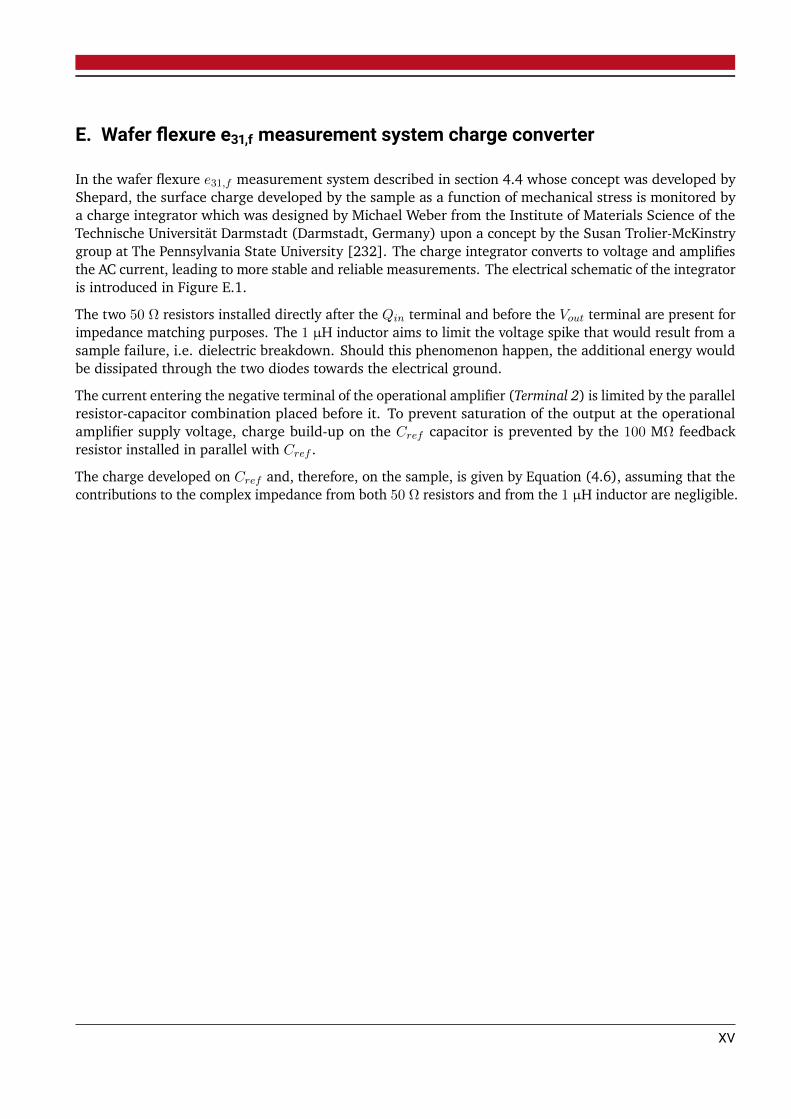
E. Wafer flexure e31,f measurement system charge converter
In the wafer flexure e31,f measurement system described in section 4.4 whose concept was developed byShepard, the surface charge developed by the sample as a function of mechanical stress is monitored bya charge integrator which was designed by Michael Weber from the Institute of Materials Science of theTechnische Universität Darmstadt (Darmstadt, Germany) upon a concept by the Susan Trolier-McKinstrygroup at The Pennsylvania State University [232]. The charge integrator converts to voltage and amplifiesthe AC current, leading to more stable and reliable measurements. The electrical schematic of the integratoris introduced in Figure E.1.
The two 50 Ω resistors installed directly after the Qin terminal and before the Vout terminal are present forimpedance matching purposes. The 1 µH inductor aims to limit the voltage spike that would result from asample failure, i.e. dielectric breakdown. Should this phenomenon happen, the additional energy wouldbe dissipated through the two diodes towards the electrical ground.
The current entering the negative terminal of the operational amplifier (Terminal 2) is limited by the parallelresistor-capacitor combination placed before it. To prevent saturation of the output at the operationalamplifier supply voltage, charge build-up on the Cref capacitor is prevented by the 100 MΩ feedbackresistor installed in parallel with Cref .
The charge developed on Cref and, therefore, on the sample, is given by Equation (4.6), assuming that thecontributions to the complex impedance from both 50 Ω resistors and from the 1 µH inductor are negligible.
XV
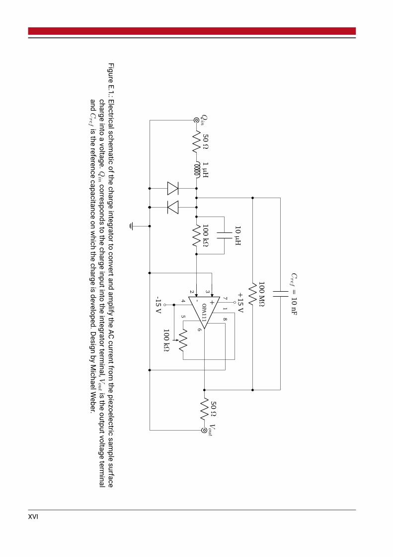
Qin
50Ω
1µH
100kΩ
OPA111
50Ω
Vout
+15
V
-15V
100kΩ
+-
1
2 3
45
6
78
10µH
100MΩ
Cref
=10
nF
FigureE.1.:Electricalschem
aticofthe
chargeintegratorto
convertandam
plifythe
ACcurrentfrom
thepiezoelectric
sample
surfacecharge
intoavoltage.
Qin
correspondsto
thecharge
inputintothe
integratorterminal,V
out is
theoutputvoltage
terminal
andCref
isthe
referencecapacitance
onwhich
thecharge
isdeveloped.Design
byMichaelW
eber.
XVI

F. Modelling of ferroelectric bending tongues: Code of the FeBeTo -Ferroelectric Bending Tongues modelling program
The MATLAB® code of the FeBeTo – Ferroelectric Bending Tongues modelling program whose concept isdeveloped in chapter 6 is stored on TUdatalib Repository, the institutional repository of the TechnischeUniversität Darmstadt, under the DOI 10.25534/tudatalib-11.3.
Due to its length of more than 3,000 lines, the code could not be printed in this appendix. The programinstaller, the main code file and the files containing the various functions can be found in the onlinerepository. All code files are extensively commented.
The FeBeTo program is distributed under a Creative Commons Attribution-NonCommercial-NoDerivatives4.0 International (CC BY-NC-ND 4.0) licence.
XVII

G. Modelling of ferroelectric bending tongues: Development from the loaddistribution equation to the equation of vertical deflection due to loads
For the modelling of ferroelectric bending tongues, the load distribution on the bending tongues is describedby Equation (6.7), using the Macaulay brackets. Its development until the equation of vertical deflectiondue to loads (Equation (6.13)) is given below. According to the Euler-Bernoulli beam theory, Equation (6.7)can be written:
EflexIzIV = qW + qL < x− xm >0 , (G.1)
where Eflex is the flexural modulus, which is taken as equivalent to the Young modulus, EY, based onthe assumptions of the model (see section 6.2.2). I is the second moment of area and zIV is the fourthderivative of z(x), the vertical deflection.
It is necessary to take into account the corrections of the beam inhomogeneity through EY,eff and Ieff(Equation (6.5)) and of its disproportionate width (Equation (6.6)). Therefore, Equation (G.1) can beformulated as:
1− νeff2
EY,effIeffzIV = qW + qL < x− xm >0 . (G.2)
Following the Euler-Bernoulli beam theory, Equation (G.2) should be integrated four consecutive timesover the length of the bending tongue. The first integration yields:
1− νeff2
EY,effIeffzIII = qWx+ qL < x− xm >1 +cst1, (G.3)
where zIII is the third derivative of z(x) and cst1 is an integration constant. It can be calculated using theboundary conditions given in Equation (6.9):
zIII(x = xl) = 0 → cst1 = −qWxl − qL(xl − xm). (G.4)
By combining Equations (G.3) and (G.4), it yields:
1− νeff2
EY,effIeffzII = qW
x2
2+
qL
2< x− xm >2 −
[qWxl + qL(xl − xm)
]x+ cst2, (G.5)
where zII is the second derivative of z(x) and cst2 is an integration constant. It can be calculated usingthe boundary conditions given in Equation (6.10):
zII(x = xl) = 0 → cst2 = qWxl
2
2+ qL(xl − xm)
(−xl − xm
2+ xl
). (G.6)
By combining Equations (G.5) and (G.6), it yields:
XIX

1− νeff2
EY,effIeffzI = qW
x3
6+
qL
6< x− xm >3 −
[qWxl + qL(xl − xm)
] x22
+
[qW
xl2
2+ qL(xl − xm)
(xl −
xl − xm2
)]x+ cst3, (G.7)
where zI is the first derivative of z(x) and cst3 is an integration constant. It can be calculated using theboundary conditions given in Equation (6.11):
zI(x = 0) = 0 → cst3 = 0. (G.8)
By combining Equations (G.7) and (G.8), it yields:
1− νeff2
EY,effIeffz = qW
x4
24+
qL
24< x− xm >4 −
[qWxl + qL(xl − xm)
] x36
+
[qW
xl2
2+ qL(xl − xm)
(xl −
xl − xm2
)]x2
2+ cst4, (G.9)
where cst4 is an integration constant. It can be calculated using the boundary conditions given in Equa-tion (6.12):
z(x = 0) = 0 → cst4 = 0. (G.10)
By combining Equations (G.9) and (G.10), it yields:
z(x) =1− νeff
2
24EY,effIeff
[qWx4 + qL < x− xm >4 +4
(−qWxl − qL(xl − xm)
)x3
+12
[qW
xl2
2+ qL(xl − xm)
(xl −
xl − xm2
)]x2
], (G.11)
corresponding to Equation (6.13).
XX

H. Modelling of ferroelectric bending tongues: Development from the bendingmoments due to strain distribution equation to the equation of verticaldeflection due to bending moments
For the modelling of ferroelectric bending tongues, the bending moments due to strain distribution on thebending tongue is described by Equation (6.18), using the Macaulay brackets. Its development until theequation of vertical deflection due to bending moments (Equation (6.19)) is given below. According to theEuler-Bernoulli beam theory, Equation (6.18) can be written:
EflexIzII = Mb +Mf
(1− < x− xm >0
), (H.1)
where Eflex is the flexural modulus, which is taken as equivalent to the Young modulus, EY, based onthe assumptions of the model (see section 6.2.2). I is the second moment of area and zII is the secondderivative of z(x), the vertical deflection.
It is necessary to take into account the corrections of the beam inhomogeneity through EY,eff and Ieff(Equation (6.5)) and of its disproportionate width (Equation (6.6)). Therefore, Equation (H.1) can beformulated as:
1− νeff2
EY,effIeffzII = Mb +Mf
(1− < x− xm >0
). (H.2)
Following the Euler-Bernoulli beam theory, Equation (H.2) should be integrated two consecutive timesover the length of the bending tongue. The first integration yields:
1− νeff2
EY,effIeffzI = (Mb +Mf )x−Mf < x− xm >1 +cst5, (H.3)
where zI is the first derivative of z(x) and cst5 is an integration constant. It can be calculated using theboundary conditions given in Equation (6.11):
zI(x = 0) = 0 → cst5 = 0. (H.4)
By combining Equations (H.3) and (H.4), it yields:
1− νeff2
EY,effIeffz = (Mb +Mf )
x2
2−
Mf
2< x− xm >2 +cst6, (H.5)
where cst6 is an integration constant. It can be calculated using the boundary conditions given in Equa-tion (6.12):
z(x = 0) = 0 → cst6 = 0. (H.6)
By combining Equations (H.5) and (H.6), it yields:
XXI

z(x) =1− νeff
2
2EY,effIeff
[(Mb +Mf )x
2 −Mf < x− xm >2], (H.7)
corresponding to Equation (6.19).
XXII

References
[1] S. Trolier-McKinstry, “Impact of ferroelectricity,” American Ceramic Society Bulletin, vol. 99, no. 1,pp. 22–23, 2020.
[2] G. Brennecka, R. Sherbondy, R. Schwartz, and J. Ihlefeld, “Ferroelectricity - A revolutionary centuryof discovery,” American Ceramic Society Bulletin, vol. 99, no. 1, pp. 24–30, 2020.
[3] C. A. Randall, R. E. Newnham, and L. E. Cross, “History of the first ferroelectric oxide, BaTiO3.”Materials Research Institute, The Pennsylvania State University, University Park, PA, USA, 2004.
[4] C.-B. Eom and S. Trolier-McKinstry, “Thin-film piezoelectric MEMS,” MRS Bulletin, vol. 37, no. 11,pp. 1007–1017, 2012.
[5] H. Kohlstedt, Y. Mustafa, A. Gerber, A. Petraru, M. Fitsilis, R. Meyer, U. Böttger, and R. Waser,“Current status and challenges of ferroelectric memory devices,” Microelectronic Engineering, vol. 80,pp. 296–304, 2005.
[6] N. Setter, D. Damjanovic, L. Eng, G. Fox, S. Gevorgian, S. Hong, A. Kingon, H. Kohlstedt, N. Y.Park, G. B. Stephenson, I. Stolitchnov, A. K. Taganstev, D. V. Taylor, T. Yamada, and S. Streiffer,“Ferroelectric thin films: Review of materials, properties, and applications,” Journal of Applied Physics,vol. 100, no. 5, p. 051606, 2006.
[7] S. P. Alpay, J. Mantese, S. Trolier-Mckinstry, Q. Zhang, and R. W. Whatmore, “Next-generationelectrocaloric and pyroelectric materials for solid-state electrothermal energy interconversion,” MRSBulletin, vol. 39, no. 12, pp. 1099–1109, 2014.
[8] T. Xue, H. G. Yeo, S. Trolier-Mckinstry, and S. Roundy, “A wrist-worn rotational energy harvesterutilizingmagnetically plucked 001 oriented bimorph PZT thin-film beams,” 2017 19th InternationalConference on Solid-State Sensors, Actuators and Microsystems (TRANSDUCERS), pp. 375–378, 2017.
[9] A. Erturk and D. J. Inman, Piezoelectric energy harvesting. Chichester, UK: John Wiley & Sons, Ltd,2011.
[10] I. P. Kaminow, “Optical waveguide modulators,” IEEE Transactions on Microwave Theory and Tech-niques, vol. 23, no. 1, pp. 57–70, 1975.
[11] P. Tang, D. J. Towner, A. L. Meier, and B. W. Wessels, “Low-voltage, polarization-insensitive, electro-optic modulator based on a polydomain barium titanate thin film,” Applied Physics Letters, vol. 85,no. 20, pp. 4615–4617, 2004.
[12] N. Bishop, J. Walker, C. T. DeRoo, T. Liu, M. Tendulkar, C. Vincenzo, E. N. Hertz, V. Kradinov, E. D.Schwartz, P. B. Reid, T. N. Jackson, and S. Trolier-McKinstry, “Thickness distribution of sputteredfilms on curved substrates for adjustable X-ray optics,” Journal of Astronomical Telescopes, Instruments,and Systems, vol. 5, no. 2, p. 021005, 2019.
[13] J. T. Van Beek and R. Puers, “A review of MEMS oscillators for frequency reference and timingapplications,” Journal of Micromechanics and Microengineering, vol. 22, no. 1, p. 013001, 2012.
XXIII
[14] S. B. Lang, “Pyroelectricity: From ancient curiosity to modern imaging tool,” Physics Today, vol. 58,no. 8, pp. 31–36, 2005.
[15] R. W. Whatmore, P. C. Osbond, and N. M. Shorrocks, “Ferroelectric materials for thermal IRdetectors,” Ferroelectrics, vol. 76, no. 1, pp. 351–367, 1987.
[16] N. M. Shorrocks, R. W. Whatmore, and P. C. Osbond, “Lead scandium tantalate for thermal detectorapplications,” Ferroelectrics, vol. 106, no. 1, pp. 387–392, 1990.
[17] S. Trolier-McKinstry and P. Muralt, “Thin film piezoelectrics for MEMS,” Journal of Electroceramics,vol. 12, pp. 7–17, 2004.
[18] I. Kanno, “Piezoelectric MEMS: Ferroelectric thin films for MEMS applications,” Japanese Journal ofApplied Physics, vol. 57, p. 040101, 2018.
[19] K. Uchino, Piezoelectric actuators and ultrasonic motors. Springer US, 1997.
[20] M. Weiser, “The computer for the 21st century,” Scientific American, vol. 265, no. 3, pp. 94–104,1991.
[21] European Commission, “Proposal for a regulation of the European Parliament and of the Coun-cil establishing the framework for achieving climate neutrality and amending Regulation (EU)2018/1999 (European Climate Law) - COM/2020/80 final,” 2020.
[22] K. Morimoto, I. Kanno, K. Wasa, and H. Kotera, “High-efficiency piezoelectric energy harvesters ofc-axis-oriented epitaxial PZT films transferred onto stainless steel cantilevers,” Sensors and Actuators,A: Physical, vol. 163, no. 1, pp. 428–432, 2010.
[23] G. Shirane, K. Suzuki, and A. Takeda, “Phase transitions in solid solutions of PbZrO3 and PbTiO3(II) X-ray study,” Journal of the Physical Society of Japan, vol. 7, no. 1, pp. 12–18, 1952.
[24] P. Muralt, “Ferroelectric thin films for micro-sensors and actuators: A review,” Journal of Microme-chanics and Microengineering, vol. 10, no. 2, pp. 136–146, 2000.
[25] R. N. Castellano and L. G. Feinstein, “Ion-beam deposition of thin films of ferroelectric lead zirconatetitanate (PZT),” Journal of Applied Physics, vol. 50, no. 6, pp. 4406–4411, 1979.
[26] R. N. Castellano, “Deposition of thin films of PZT by a focused ion beam sputtering technique,”Ferroelectrics, vol. 28, no. 1, pp. 387–390, 1980.
[27] S. B. Krupanidhi, N. Maffei, M. Sayer, and K. El-Assal, “RF planar magnetron sputtering andcharacterization of ferroelectric Pb(Zr,Ti)O3 films,” Journal of Applied Physics, vol. 54, no. 11,pp. 6601–6609, 1983.
[28] T. Fukami, T. Sakuma, K. Tokunaga, and H. Tsuchiya, “Ferroelectric films deposited by reactivesputtering and their properties,” Japanese Journal of Applied Physics, vol. 22, no. S2, pp. 18–21,1983.
[29] K. Sreenivas, M. Sayer, and P. Garrett, “Properties of D.C. magnetron-sputtered lead zirconatetitanate thin films,” Thin Solid Films, vol. 172, no. 2, pp. 251–267, 1989.
[30] S. K. Dey, K. D. Budd, and D. A. Payne, “Thin-film ferroelectrics of PZT of sol-gel processing,” IEEETransactions on Ultrasonics, Ferroelectrics, and Frequency Control, vol. 35, no. 1, pp. 80–81, 1988.
[31] G. Yi, M. Sayer, C. K. Jen, J. C. H. Yu, and E. L. Adler, “Coaxial thin film transducers based on PZT,”Proceedings., IEEE Ultrasonics Symposium,, vol. 2, pp. 1231–1235, 1989.
XXIV
[32] H. Kueppers, T. Leuerer, U. Schnakenberg, W. Mokwa, M. J. Hoffmann, T. Schneller, U. Boettger,and R. Waser, “PZT thin films for piezoelectric microactuator applications,” Sensors and Actuators A:Physical, vol. 97-98, pp. 680–684, 2002.
[33] G. A. C. M. Spierings, M. J. E. Ulenaers, G. L. M. Kampschöer, H. A. M. van Hal, and P. K. Larsen,“Preparation and ferroelectric properties of PbZr0.53Ti0.47O3 thin films by spin coating and metalor-ganic decomposition,” Journal of Applied Physics, vol. 70, no. 4, p. 2290, 1991.
[34] M. Okada, K. Tominaga, T. Araki, S. Katayama, and Y. Sakashita, “Metalorganic chemical vapordeposition of c-axis oriented PZT thin films,” Japanese Journal of Applied Physics, vol. 29, no. 4R,pp. 718–722, 1990.
[35] Y. Sakashita, O. Toshiyuki, H. Segawa, K. Tominaga, and M. Okada, “Preparation and electricalproperties of MOCVD-deposited PZT thin films,” Journal of Applied Crystallography, vol. 69, no. 12,p. 8352, 1991.
[36] H. Itoh, K. Kashihara, T. Okudaira, K. Tsukamoto, and Y. Akasaka, “MOCVD for PZT thin films byusing novel metalorganic sources,” International Electron Devices Meeting 1991 [Technical Digest],pp. 831–834, 1991.
[37] D. Roy, S. B. Krupanidhi, and J. P. Dougherty, “Excimer laser ablated lead zirconate titanate thinfilms,” Journal of Applied Physics, vol. 69, no. 11, pp. 7930–7932, 1991.
[38] H. Kidoh, T. Ogawa, A. Morimoto, and T. Shimizu, “Ferroelectric properties of lead-zirconate-titanatefilms prepared by laser ablation,” Applied Physics Letters, vol. 58, no. 25, pp. 2910–2912, 1991.
[39] J. Akedo, J. H. Park, and Y. Kawakami, “Piezoelectric thick film fabricated with aerosol depositionand its application to piezoelectric devices,” Japanese Journal of Applied Physics, vol. 57, no. 7,p. 07LA02, 2018.
[40] M. D. Nguyen, H. Nazeer, K. Karakaya, S. V. Pham, R. Steenwelle, M. Dekkers, L. Abelmann, D. H. A.Blank, and G. J. H. M. Rijnders, “Characterization of epitaxial Pb(Zr,Ti)O3 thin films depositedby pulsed laser deposition on silicon cantilevers,” Journal of Micromechanics and Microengineering,vol. 20, no. 8, p. 085022, 2010.
[41] S. Dunn and R. W. Whatmore, “Substrate effects on domain structures of PZT 30/70 sol-gel filmsvia piezoAFM,” Journal of the European Ceramic Society, vol. 22, no. 6, pp. 825–833, 2002.
[42] L. Ceresara, A. Iembo, F. Fuso, M. Labardi, M. Allegrini, E. Arimondo, A. Diodati, B. E. Watts,F. Leccabue, G. Bocelli, A. Diodatiz, B. E. Watts, F. Leccabue, and G. Bocelli, “Pulsed laser ablationdeposition and characterization of superconductive/ferroelectric bilayers,” Superconductor Scienceand Technology, vol. 9, no. 8, pp. 671–677, 1996.
[43] H. N. Al-Shareef, K. D. Gifford, S. H. Rou, P. D. Hren, O. Auciello, and A. I. Kingon, “Electrodes forferroelectric thin films,” Integrated Ferroelectrics, vol. 3, no. 4, pp. 321–332, 1993.
[44] H. D. Chen, K. R. Udayakumar, C. Gaskey, and L. E. Cross, “Fabrication and electrical properties of leadzirconate titanate thick films,” Journal of American Ceramic Society, vol. 79, no. 8, pp. 2189–2192,1996.
[45] K. Sreenivas, I. Reaney, T. Maeder, N. Setter, C. Jagadish, and R. G. Elliman, “Investigation of Pt/Tibilayer metallization on silicon for ferroelectric thin film integration,” Journal of Applied Physics,vol. 75, no. 1, pp. 232–239, 1994.
XXV
[46] J.-R. Cheng, W. Zhu, N. Li, and L. E. Cross, “Electrical properties of sol-gel-derived Pb(Zr0.52Ti0.48)O3thin films on a PbTiO3-coated stainless steel substrate,” Applied Physics Letters, vol. 81, no. 25,pp. 4805–4807, 2002.
[47] Q. Zou, H. E. Ruda, B. G. Yacobi, K. Saegusa, and M. Farrell, “Dielectric properties of lead zirconatetitanate thin films deposited on metal foils,” Applied Physics Letters, vol. 77, no. 7, pp. 1038–1040,2000.
[48] Q. Zou, H. E. Ruda, and B. G. Yacobi, “Improved dielectric properties of lead zirconate titanatethin films deposited on metal foils with LaNiO3 buffer layers,” Applied Physics Letters, vol. 78, no. 9,pp. 1282–1284, 2001.
[49] J. H. Yi, R. Seveno, and H. W. Gundel, “Sol-gel derived PZT/RuO2 multilayer films on stainless steelsubstrates,” Integrated Ferroelectrics, vol. 23, no. 1, pp. 199–214, 1999.
[50] R. Seveno and D. Averty, “Ultra light tunable capacitor based on PZT thin film deposited ontoaluminium foil,” Journal of Sol-Gel Science and Technology, vol. 68, no. 2, pp. 175–179, 2013.
[51] H. G. Yeo and S. Trolier-McKinstry, “001 oriented piezoelectric films prepared by chemical solutiondeposition on Ni foils,” Journal of Applied Physics, vol. 116, no. 1, p. 014105, 2014.
[52] H. G. Yeo, T. Xue, S. Roundy, X. Ma, C. Rahn, and S. Trolier-McKinstry, “Strongly (001) oriented bi-morph PZT film on metal foils grown by rf -sputtering for wrist-worn piezoelectric energy harvesters,”Advanced Functional Materials, vol. 28, no. 36, pp. 1–9, 2018.
[53] K. Coleman, J. Walker, T. Beechem, and S. Trolier-Mckinstry, “Effect of stresses on the dielectric andpiezoelectric properties of Pb(Zr0.52Ti0.48)O3 thin films,” Journal of Applied Physics, vol. 126, no. 3,p. 034101, 2019.
[54] K. Coleman, S. Shetty, B. Hanrahan, W. Zhu, and S. Trolier-McKinstry, “Extrinsic contributions tothe dielectric and pyroelectric properties of Pb0.99[(Zr0.52Ti0.48)0.98Nb0.02]O3 thin films on Si andNi substrates,” Journal of Applied Physics, vol. 128, no. 11, p. 114102, 2020.
[55] Y. J. Ko, D. Y. Kim, S. S. Won, C. W. Ahn, I. W. Kim, A. I. Kingon, S.-H. Kim, J.-H. Ko, and J. H. Jung,“Flexible Pb(Zr0.52Ti0.48)O3 films for a hybrid piezoelectric-pyroelectric nanogenerator under harshenvironments,” ACS Applied Materials & Interfaces, vol. 8, no. 10, pp. 6504–6511, 2016.
[56] H.-J. Tseng, W.-C. Tian, and W.-J. Wu, “Flexible PZT thin film tactile sensor for biomedical monitor-ing,” Sensors (Basel, Switzerland), vol. 13, no. 5, pp. 5478–5492, 2013.
[57] G. Magagnin, Chemical solution processed ferroelectric thick films on metal foil. Final year internshipthesis (Supervisor: N. Bassiri-Gharb), Ecole Centrale de Lyon (France) - Georgia Tech (USA), 2019.
[58] H. Li, S. Wang, J. Jian, H. Dong, J. Chen, D. Jin, and J. Cheng, “Improved ferroelectric propertiesof (100)-oriented PZT thin films deposited on stainless steel substrates with La0.5Sr0.5CoO3 bufferlayers,” Journal of Materials Science: Materials in Electronics, vol. 29, no. 17, pp. 14651–14656,2018.
[59] S. S. Won, H. Seo, M. Kawahara, S. Glinsek, J. Lee, Y. Kim, C. K. Jeong, A. I. Kingon, and S. H. Kim,“Flexible vibrational energy harvesting devices using strain-engineered perovskite piezoelectric thinfilms,” Nano Energy, vol. 55, pp. 182–192, 2019.
[60] M. Oikawa and K. Toda, “Preparation of Pb(Zr,Ti)O3 thin films by an electron beam evaporationtechnique,” Applied Physics Letters, vol. 29, no. 8, pp. 491–492, 1976.
XXVI
[61] M. Koinuma, H. Ohmura, Y. Fujioka, Y. Matsumoto, and S. Yamada, “Preparation of PZT thin filmson stainless steel using electrochemical reduction,” Journal of Solid State Chemistry, vol. 136, no. 2,pp. 293–297, 1998.
[62] T. Suzuki, I. Kanno, J. J. Loverich, H. Kotera, and K. Wasa, “Characterization of Pb(Zr,Ti)O3 thinfilms deposited on stainless steel substrates by RF-magnetron sputtering for MEMS applications,”Sensors and Actuators A: Physical, vol. 125, no. 2, pp. 382–386, 2006.
[63] T. Nishi, T. Ito, H. Hida, and I. Kanno, “Shoe-mounted vibration energy harvester of PZT piezoelectricthin films on metal foils,” Journal of Physics: Conference Series, vol. 773, no. 1, p. 012062, 2016.
[64] T. Ito, T. Nishi, T. Umegaki, H. Hida, and I. Kanno, “The piezoelectric PZT thin films deposited onmetal substrates,” Journal of Physics: Conference Series, vol. 1052, no. 1, p. 012094, 2018.
[65] Y. Tsujiura, E. Suwa, F. Kurokawa, H. Hida, and I. Kanno, “Reliability of vibration energy harvestersof metal-based PZT thin films,” Journal of Physics: Conference Series, vol. 557, no. 1, pp. 3–8, 2014.
[66] Y. Tsujiura, E. Suwa, T. Nishi, F. Kurokawa, H. Hida, and I. Kanno, “Airflow energy harvester ofpiezoelectric thin-film bimorph using self-excited vibration,” Sensors and Actuators A: Physical,vol. 261, pp. 295–301, 2017.
[67] A. Bose, M. Sreemany, and S. Bysakh, “Influence of processing parameters on the growth character-istics and ferroelectric properties of sputtered PZT thin films on stainless steel substrates,” AppliedSurface Science, vol. 282, pp. 202–210, 2013.
[68] T. Fujii, Y. Hishinuma, T. Mita, and T. Naono, “Characterization of Nb-doped Pb(Zr,Ti)O3 films de-posited on stainless steel and silicon substrates by RF-magnetron sputtering for MEMS applications,”Sensors and Actuators A: Physical, vol. 163, no. 1, pp. 220–225, 2010.
[69] R. G. Ballas, H. F. Schlaak, and A. J. Schmid, “The constituent equations of piezoelectric multilayerbending actuators in closed analytical form and experimental results,” Sensors and Actuators A:Physical, vol. 130-131, pp. 91–98, 2006.
[70] R. G. Ballas, Piezoelectric multilayer beam bending actuators. Springer-Verlag Berlin Heidelberg,2007.
[71] K. G. Webber, D. J. Franzbach, and J. Koruza, “Determination of the true operational range of apiezoelectric actuator,” Journal of the American Ceramic Society, vol. 97, no. 9, pp. 2842–2849, 2014.
[72] K. G. Webber, “Application of a classical lamination theory model to the design of piezoelectriccomposite unimorph actuators,” Journal of Intelligent Material Systems and Structures, vol. 17, no. 1,pp. 29–34, 2006.
[73] L. Q. Chen, “Phase-field method of phase transitions/domain structures in ferroelectric thin films: Areview,” Journal of the American Ceramic Society, vol. 91, no. 6, pp. 1835–1844, 2008.
[74] Y. Su and C. M. Landis, “Continuum thermodynamics of ferroelectric domain evolution: Theory,finite element implementation, and application to domain wall pinning,” Journal of the Mechanicsand Physics of Solids, vol. 55, no. 2, pp. 280–305, 2007.
[75] B. X. Xu, D. Schrade, R. Müller, D. Gross, T. Granzow, and J. Rödel, “Phase field simulation andexperimental investigation of the electro-mechanical behavior of ferroelectrics,” ZAMM Zeitschriftfur Angewandte Mathematik und Mechanik, vol. 90, no. 7-8, pp. 623–632, 2010.
XXVII
[76] J. E. Huber, N. A. Fleck, C. M. Landis, and R. M. McMeeking, “A constitutive model for ferroelectricpolycrystals,” Journal of the Mechanics and Physics of Solids, vol. 47, no. 8, pp. 1663–1697, 1999.
[77] S. C. Hwang, C. S. Lynch, and R. M. McMeeking, “Ferroelectric/ferroelastic interactions and apolarization switching model,” Acta Metallurgica et Materialia, vol. 43, no. 5, pp. 2073–2084, 1995.
[78] S. Hwang, J. Huber, R. McMeeking, and N. Fleck, “The simulation of switching in polycrystallineferroelectric ceramics,” Journal of Applied Physics, vol. 84, no. 3, pp. 1530–1540, 1998.
[79] R. M. McMeeking and S. C. Hwang, “On the potential energy of a piezoelectric inclusion and thecriterion for ferroelectric switching,” Ferroelectrics, vol. 200, no. 1-4, pp. 151–173, 1997.
[80] X. Chen, D. N. Fang, and K. C. Hwang, “Micromechanics simulation of ferroelectric polarizationswitching,” Acta Materialia, vol. 45, no. 8, pp. 3181–3189, 1997.
[81] W. Chen and C. S. Lynch, “Amicro-electro-mechanical model for polarization switching of ferroelectricmaterials,” Acta Materialia, vol. 46, no. 15, pp. 5303–5311, 1998.
[82] S. Hwang and R. Waser, “Study of electrical and mechanical contribution to switching in ferroelec-tric/ferroelastic polycrystals,” Acta Materialia, vol. 48, no. 12, pp. 3271–3282, 2000.
[83] Y. Fotinich and G. P. Carman, “Stresses in piezoceramics undergoing polarization switchings,”Journal of Applied Physics, vol. 88, no. 11, pp. 6715–6725, 2000.
[84] J. Li and G. J. Weng, “A micromechanics-based hysteresis model for ferroelectric ceramics,” Journalof Intelligent Materials Systems and Structures, vol. 12, no. 2, pp. 79–91, 2001.
[85] F. Narita, Y. Shindo, and K. Hayashi, “Bending and polarization switching of piezoelectric lam-inated actuators under electromechanical loading,” Computers & Structures, vol. 83, no. 15-16,pp. 1164–1170, 2005.
[86] M. E. Lines and A. M. Glass, “Basic concepts,” in Principles and applications of ferroelectrics andrelated materials, ch. 1, pp. 1–23, Oxford, UK: Oxford University Press, 1977.
[87] J. Tichý, J. Erhart, E. Kittinger, and J. Přívratská, “Introduction to phenomenological crystal structure,”in Fundamentals of piezoelectric sensorics, ch. 2, pp. 15–29, Springer Heidelberg Dordrecht LondonNew York, 2010.
[88] J. F. Nye, “The groundwork of crystal physics,” in Physical properties of crystals, ch. 1, pp. 3–32,Oxford, UK: Clarendon Press, 1957.
[89] J. F. Nye, “Piezoelectricity. Third-rank tensors,” in Physical properties of crystals, ch. 7, pp. 110–130,Oxford, UK: Clarendon Press, 1957.
[90] J. Tichý, J. Erhart, E. Kittinger, and J. Přívratská, “Basic thermodynamics of piezoelectric crystals,” inFundamentals of piezoelectric sensorics, ch. 4, pp. 55–68, Springer Heidelberg Dordrecht LondonNew York, 2010.
[91] S. M. Pilgrim, “Electrostrictive ceramics for low-frequency active transducers,” IEEE Transactions onUltrasonics, Ferroelectrics, and Frequency Control, vol. 47, no. 4, pp. 861–876, 2000.
[92] M. Mehdizadeh, “The impact of fields on materials at RF/microwave frequencies,” in Microwave/RFApplicators and Probes, ch. 1, pp. 1–34, Elsevier, 2010.
[93] J. F. Nye, “Natural and artificial double refraction. Second-order effects,” in Physical properties ofcrystals, ch. 13, pp. 235–259, Oxford, UK: Clarendon Press, 1957.
XXVIII
[94] G. Gautschi, “Background of piezoelectric sensors,” in Piezoelectric sensorics, ch. 2, pp. 5–11, Springer-Verlag Berlin Heidelberg, 2002.
[95] J. Tichý, J. Erhart, E. Kittinger, and J. Přívratská, “Principles of piezoelectricity,” in Fundamentals ofpiezoelectric sensorics, ch. 1, pp. 1–14, Springer Heidelberg Dordrecht London New York, 2010.
[96] J. Curie and P. Curie, “Développement par compression de l’électricité polaire dans les cristauxhémièdres à faces inclinées,” Bulletin de Minéralogie, vol. 3-4, pp. 90–93, 1880.
[97] P. Curie, “Sur la symétrie dans les phénomènes physiques, symétrie d’un champ électrique et d’unchamp magnétique,” Journal de Physique Théorique et Appliquée, vol. 3, no. 1, pp. 393–415, 1894.
[98] D. Damjanovic, “Ferroelectric, dielectric and piezoelectric properties of ferroelectric thin films andceramics,” Reports on Progress in Physics, vol. 61, no. 11, pp. 1267–1324, 1998.
[99] H. Klapper and T. Hahn, “Point-group symmetry and physical properties of crystals,” in Internationaltables for crystallography volume A: Space-group symmetry (T. Hahn, ed.), ch. 10.2, pp. 804–808,Dordrecht, Netherlands: Springer, 5th ed., 2006.
[100] W. G. Cady, “Principles of piezoelectricity,” in Piezoelectricity - Volume one, ch. 8, pp. 177–199,Mineola, NY, USA: Courier Dover Publications, revised ed., 2018.
[101] D. A. Hall, “Nonlinearity in piezoelectric ceramics,” Journal of Materials Science, vol. 36, no. 19,pp. 4575–4601, 2001.
[102] A. J. Moulson and J. M. Herbert, “Piezoelectric ceramics,” in Electroceramics, ch. 6, pp. 339–410,Chichester, UK: John Wiley & Sons, Inc., 2nd ed., 2003.
[103] J. Tichý, E. Jiří, E. Kittinger, and J. Přívratská, “Piezoelectric properties,” in Fundamentals of piezo-electric sensorics, ch. 5, pp. 69–100, Springer Heidelberg Dordrecht London New York, 2010.
[104] D. Horsley, Y. Lu, and O. Rozen, “Flexural piezoelectric resonators,” in Piezoelectric MEMS resonators(H. Bhugra and G. Piazza, eds.), ch. 6, pp. 153–173, Springer Berlin Heidelberg, 2017.
[105] F. Jona and G. Shirane, “Introduction,” in Ferroelectric crystals, ch. 1, pp. 1–27, New York City, NY,USA: Dover Publications, 1993.
[106] K. M. Rabe, M. Dawber, C. Lichtensteiger, C. H. Ahn, and J.-M. Triscone, “Modern physics offerroelectrics: Essential background,” in Physics of ferroelectrics (K. M. Rabe, C. H. Ahn, and J.-M.Triscone, eds.), ch. 1, pp. 1–30, Springer-Verlag Berlin Heidelberg, 2007.
[107] The American Physical Society, “Minutes of the Washington meeting, April 23 and 24, 1920,” PhysicalReview, vol. 15, no. 6, p. 505, 1920.
[108] J. Valasek, “Piezo-electric and allied phenomena in Rochelle salt,” Physical Review, vol. 17, no. 4,p. 475, 1921.
[109] R. Resta and D. Vanderbilt, “Theory of polarization: A modern approach,” in Physics of ferroelectrics(K. M. Rabe, C. H. Ahn, and J.-M. Triscone, eds.), ch. 2, pp. 31–68, Springer-Verlag Berlin Heidelberg,2007.
[110] N. A. Spaldin, “A beginners guide to the modern theory of polarization,” Journal of Solid StateChemistry, vol. 195, pp. 2–10, 2012.
[111] R. Resta, “Theory of the electric polarization in crystals,” Ferroelectrics, vol. 136, no. 1, pp. 51–55,1992.
XXIX
[112] R. D. King-Smith and D. Vanderbilt, “Theory of polarization of crystalline solids,” Physical Review B,vol. 47, no. 3, pp. 1651–1654, 1993.
[113] R. Resta, “Macroscopic polarization in crystalline dielectrics: The geometric phase approach,”Reviews of Modern Physics, vol. 66, no. 3, pp. 889–915, 1994.
[114] D. Vanderbilt and R. D. King-Smith, “Electric polarization as a bulk quantity and its relation tosurface charge,” Physical Review B, vol. 48, no. 7, pp. 4442–4455, 1993.
[115] R. Resta, “Macroscopic electric polarization as a geometric quantum phase,” Europhysics Letters,vol. 22, no. 2, pp. 133–138, 1993.
[116] K. M. Rabe and P. Ghosez, “First-principles studies of ferroelectric oxides,” in Physics of ferroelectrics(K. M. Rabe, C. H. Ahn, and J.-M. Triscone, eds.), ch. 4, pp. 117–174, Springer-Verlag BerlinHeidelberg, 2007.
[117] M. E. Lines and A. M. Glass, “Statistical theory, soft modes, and phase transitions,” in Principles andapplications of ferroelectrics and related materials, ch. 2, pp. 24–58, Oxford, UK: Oxford UniversityPress, 1977.
[118] P. Chandra and P. B. Littlewood, “A Landau primer for ferroelectrics,” in Physics of ferroelectrics (K. M.Rabe, C. H. Ahn, and J.-M. Triscone, eds.), ch. 3, pp. 69–115, Springer-Verlag Berlin Heidelberg,2007.
[119] M. E. Lines and A. M. Glass, “Macroscopics and phenomenology,” in Principles and Applications ofFerroelectrics and Related Materials, ch. 3, pp. 59–86, Oxford, UK: Oxford University Press, 1977.
[120] “An american national standard IEEE standard definitions of terms associated with ferroelectric andrelated materials,” IEEE Transactions on Ultrasonics, Ferroelectrics, and Frequency Control, vol. 50,no. 12, pp. 1–32, 2003.
[121] J. Tichý, E. Jiří, E. Kittinger, and J. Přívratská, “Piezoelectric materials,” in Fundamentals of piezoelec-tric sensorics, ch. 7, pp. 119–185, Springer Heidelberg Dordrecht London New York, 2010.
[122] S. Trolier-McKinstry, N. Bassiri Gharb, and D. Damjanovic, “Piezoelectric nonlinearity due to motionof 180 domain walls in ferroelectric materials at subcoercive fields: A dynamic poling model,”Applied Physics Letters, vol. 88, no. 20, p. 202901, 2006.
[123] T. Mitsui and J. Furuichi, “Domain structure of rochelle salt and KH2PO4,” Physical Review, vol. 90,no. 2, pp. 193–202, 1953.
[124] G. Arlt and P. Sasko, “Domain configuration and equilibrium size of domains in BaTiO3 ceramics,”Journal of Applied Physics, vol. 51, no. 9, pp. 4956–4960, 1980.
[125] S. Trolier-McKinstry and P. Muralt, “Thin film piezoelectrics for MEMS,” in Electroceramic-BasedMEMS (N. Setter, ed.), ch. 10, pp. 199–216, Springer US, 2005.
[126] A. K. Tagantsev, L. E. Cross, and J. Fousek, “Switching phenomena and small-signal response,” inDomains in ferroic crystals and thin films, ch. 8, pp. 351–520, Springer-Verlag New York, 2010.
[127] D. Damjanovic and M. Demartin, “The Rayleigh law in piezoelectric ceramics,” Journal of Physics D:Applied Physics, vol. 29, no. 7, pp. 2057–2060, 1996.
[128] B. Lewis, “Energy loss processes in ferroelectric ceramics,” Proceedings of the Physical Society (1958-1967), vol. 73, no. 1, pp. 17–24, 1959.
XXX
[129] J.-H. Bae and S.-H. Chang, “PVDF-based ferroelectric polymers and dielectric elastomers for sensorand actuator applications: A review,” Functional Composites and Structures, vol. 1, no. 1, p. 012003,2019.
[130] J. Walker, S. Scherrer, N. S. Løndal, T. Grande, and M. A. Einarsrud, “Electric field dependentpolarization switching of tetramethylammonium bromotrichloroferrate(III) ferroelectric plasticcrystals,” Applied Physics Letters, vol. 116, no. 24, p. 242902, 2020.
[131] W. Wersing, W. Heywang, H. Beige, and H. Thomann, “The role of ferroelectricity for piezoelectricmaterials,” in Piezoelectricity (W. Heywang, K. Lubitz, and W. Wersing, eds.), ch. 3, pp. 37–87,Springer-Verlag Berlin Heidelberg, 2008.
[132] S.-E. Park and T. R. Shrout, “Ultrahigh strain and piezoelectric behavior in relaxor based ferroelectricsingle crystals,” Journal of Applied Physics, vol. 82, no. 4, pp. 1804–1811, 1997.
[133] M. E. Lines and A. M. Glass, “Oxygen octahedra,” in Principles and applications of ferroelectrics andrelated materials, ch. 8, pp. 241–292, Oxford, UK: Oxford University Press, 1977.
[134] N. A. Benedek and C. J. Fennie, “Why are there so few perovskite ferroelectrics?,” Journal of PhysicalChemistry C, vol. 117, no. 26, pp. 13339–13349, 2013.
[135] J. M. Rondinelli and C. J. Fennie, “Octahedral rotation-induced ferroelectricity in cation orderedperovskites,” Advanced Materials, vol. 24, no. 15, pp. 1961–1968, 2012.
[136] V. M. Goldschmidt, “Die Gesetze der Krystallochemie,” Naturwissenschaften, vol. 14, no. 21,pp. 477–485, 1926.
[137] G. Shirane and A. T. Tokyo, “Phase transitions in solid solutions of PbZrO3 and PbTiO3 (I) Smallconcentrations of PbTiO3,” Journal of the Physical Society of Japan, vol. 7, no. 1, pp. 5–11, 1952.
[138] B. Jaffe, J. Cook, William R., and H. Jaffe, “Solid solutions of Pb(Ti, Zr, Sn, Hf)O3,” in Piezoelectricceramics, ch. 7, pp. 135–184, London, UK: Academic Press, 1971.
[139] International Centre for Diffraction (ICDD), “Powder Diffraction File (PDF): 04-011-7309,”Pb(Zr0.52Ti0.48)O3 @ 850 K, 2013.
[140] International Centre for Diffraction (ICDD), “Powder Diffraction File (PDF): 01-072-7167,”Pb(Zr0.52Ti0.48)O3 @ 298 K, 2013.
[141] N. Zhang, H. Yokota, A. M. Glazer, Z. Ren, D. A. Keen, D. S. Keeble, P. A. Thomas, and Z. G. Ye, “Themissing boundary in the phase diagram of PbZr1-xTixO3,” Nature Communications, vol. 5, pp. 1–9,2014.
[142] A. Bouzid, E. M. Bourim, M. Gabbay, and G. Fantozzi, “PZT phase diagram determination by mea-surement of elastic moduli,” Journal of the European Ceramic Society, vol. 25, no. 13, pp. 3213–3221,2005.
[143] B. Noheda, J. A. Gonzalo, A. C. Caballero, C. Moure, D. E. Cox, and G. Shirane, “New features ofthe morphotropic phase boundary in the Pb(Zr1-xTix)O3 system,” Ferroelectrics, vol. 237, no. 1-4,pp. 237–244, 2000.
[144] N. J. Donnelly and C. A. Randall, “Pb loss in Pb(Zr,Ti)O3 ceramics observed by in situ ionic conductivitymeasurements,” Journal of Applied Physics, vol. 109, no. 10, p. 104107, 2011.
XXXI
[145] K. H. Härdtl and H. Rau, “PbO vapour pressure in the Pb(Ti1-xZrx)O3 system,” Solid State Communi-cations, vol. 7, no. 1, pp. 41–45, 1969.
[146] R. D. Klissurska, K. G. Brooks, I. M. Reaney, C. Pawlaczyk, M. Kosec, and N. Setter, “Effect of Nbdoping on the microstructure of sol-gel-derived PZT thin films,” Journal of the American CeramicSociety, vol. 78, no. 6, pp. 1513–1520, 1995.
[147] C. K. Kwok and S. B. Desu, “Formation kinetics of PbZrxTi1-xO3 thin films,” Journal of MaterialsResearch, vol. 9, no. 7, pp. 1728–1733, 1994.
[148] B. A. Tuttle, J. A. Voigt, T. J. Garino, D. C. Goodnow, R. W. Schwartz, D. L. Lamppa, T. J. Headley, andM. O. Eatough, “Chemically prepared Pb(Zr,Ti)O3 thin films: The effects of orientation and stress,”ISAF ’92: Proceedings of the Eighth IEEE International Symposium on Applications of Ferroelectrics,pp. 344–348, 1992.
[149] M. R. Soares, A. M. Senos, and P. Q. Mantas, “Phase coexistence region and dielectric properties ofPZT ceramics,” Journal of the European Ceramic Society, vol. 20, no. 3, pp. 321–334, 2000.
[150] R. A. Wolf and S. Trolier-McKinstry, “Temperature dependence of the piezoelectric response in leadzirconate titanate films,” Journal of Applied Physics, vol. 95, no. 3, pp. 1397–1406, 2004.
[151] V. Kayasu and M. Ozenbas, “The effect of Nb doping on dielectric and ferroelectric properties of PZTthin films prepared by solution deposition,” Journal of the European Ceramic Society, vol. 29, no. 6,pp. 1157–1163, 2009.
[152] E. C. Souza, A. Z. Simões, M. Cilense, E. Longo, and J. A. Varela, “The effect of Nb doping onferroelectric properties of PZT thin films prepared from polymeric precursors,” Materials Chemistryand Physics, vol. 88, no. 1, pp. 155–159, 2004.
[153] M. D. Nguyen, T. Q. Trinh, M. Dekkers, E. P. Houwman, H. N. Vu, and G. Rijnders, “Effect of dopantson ferroelectric and piezoelectric properties of lead zirconate titanate thin films on Si substrates,”Ceramics International, vol. 40, no. 1, pp. 1013–1018, 2014.
[154] H. Sun, Y. Zhang, X. Liu, S. Guo, Y. Liu, and W. Chen, “The effect of Mn/Nb doping on dielectricand ferroelectric properties of PZT thin films prepared by sol–gel process,” Journal of Sol-Gel Scienceand Technology, vol. 74, no. 2, pp. 378–386, 2015.
[155] T. Haccart, E. Cattan, D. Remiens, S. Hiboux, and P. Muralt, “Evaluation of niobium effects on thelongitudinal piezoelectric coefficients of Pb(Zr, Ti)O3 thin films,” Applied Physics Letters, vol. 76,no. 22, pp. 3292–3294, 2000.
[156] W. Zhu, I. Fujii, W. Ren, and S. Trolier-Mckinstry, “Domain wall motion in A and B site donor-dopedPb(Zr0.52Ti0.48)O3 films,” Journal of the American Ceramic Society, vol. 95, no. 9, pp. 2906–2913,2012.
[157] D. F. Ryder and N. K. Raman, “Sol-gel processing of Nb-doped Pb(Zr, Ti)O3 thin films for ferroelectricmemory applications,” Journal of Electronic Materials, vol. 21, no. 10, pp. 971–975, 1992.
[158] M. Zhu, P. Komissinskiy, A. Radetinac, M. Vafaee, Z. Wang, and L. Alff, “Effect of composition andstrain on the electrical properties of LaNiO3 thin films,” Applied Physics Letters, vol. 103, no. 14,p. 141902, 2013.
XXXII

[159] X. Guo, C. Li, Y. Zhou, and Z. Chen, “High-quality LaNiO3 thin-film electrode grown by pulsed laserdeposition,” Journal of Vacuum Science & Technology A: Vacuum, Surfaces, and Films, vol. 17, no. 3,pp. 917–920, 1999.
[160] G. Gou, I. Grinberg, A. M. Rappe, and J. M. Rondinelli, “Lattice normal modes and electronicproperties of the correlated metal LaNiO3,” Physical Review B - Condensed Matter and MaterialsPhysics, vol. 84, no. 14, pp. 1–13, 2011.
[161] L. Sun, T. Yu, Y.-F. Chen, J. Zhou, and N.-B. Ming, “Conductive LaNiO3 electrode grown by pulsedlaser ablation on Si substrate,” Journal of Materials Research, vol. 12, no. 4, pp. 931–935, 1997.
[162] Y. H. Yu, M. O. Lai, and L. Lu, “Highly (100) oriented Pb(Zr0.52Ti0.48)O3/LaNiO3 films grown onamorphous substrates by pulsed laser deposition,” Applied Physics A: Materials Science and Processing,vol. 88, no. 2, pp. 365–370, 2007.
[163] D. Galusek and K. Ghillányová, “Ceramic oxides,” in Ceramics science and technology - Volume 2(R. Riedel and I.-W. Chen, eds.), ch. 1, pp. 3–58, Wheinheim, Germany: Wiley-VCH, 2010.
[164] M. Venkatraman and J. P. Neumann, “The Cr-Pt (chromium-platinum) system,” Bulletin of AlloyPhase Diagrams, vol. 11, no. 1, pp. 16–21, 1990.
[165] W. C. Leslie, “Stainless steels,” in The physical metallurgy of steels, ch. 12, pp. 326–357, London, UK:Hemisphere Publishing Corporation, 1981.
[166] R. Honeycombe and H. K. D. H. Bhadeshia, “Stainless steel,” in Steels: Microstructure and properties,ch. 12, pp. 250–279, London, UK: Edward Arnold, 2 ed., 1995.
[167] W. C. Young and R. G. Budynas, “Beams; Flexure of straight bars,” in Roark’s Formulas for Stress andStrain, ch. 8, pp. 125–266, New York City: McGraw-Hill Book Company, 7 ed., 2002.
[168] W. C. Leslie, “Properties of high-purity iron,” in The physical metallurgy of steels, ch. 1, pp. 1–67,London, UK: Hemisphere Publishing Corporation, 1981.
[169] K. Sree Harsha, “Structure and properties of films,” in Principles of vapor deposition of thin films,ch. 12, pp. 961–1072, Oxford, UK: Elsevier, 2006.
[170] K. Sree Harsha, “Introduction,” in Principles of vapor deposition of thin films, ch. 1, pp. 1–10, Oxford,UK: Elsevier, 2006.
[171] M. Ohring, “Substrate surfaces and thin-film nucleation,” in Materials science of thin films, ch. 7,pp. 357–415, San Diego, CA, USA: Academic Press, 2nd ed., 2002.
[172] A. Rockett, “Thin film growth processes,” in The materials science of semiconductors, ch. 10,pp. 455–503, Springer US, 2008.
[173] A. Rockett, “Physical vapor deposition,” in Thematerials science of semiconductors, ch. 11, pp. 505–572,Springer US, 2008.
[174] H. Ibach, “Adsorption,” in Physics of surfaces and interfaces, ch. 6, pp. 245–308, Springer-VerlagBerlin Heidelberg, 2006.
[175] Z. Zhang and M. G. Lagally, “Atomistic processes in the early stages of thin-film growth,” Science,vol. 276, no. 5311, pp. 377–383, 1997.
[176] U. W. Pohl, “Thermodynamics of epitaxial layer-growth,” in Epitaxy of semiconductors, ch. 4,pp. 131–170, Springer-Verlag Berlin Heidelberg, 2013.
XXXIII
[177] K. Sree Harsha, “Nucleation and growth of films,” in Principles of vapor deposition of thin films, ch. 9,pp. 685–829, Oxford, UK: Elsevier, 2006.
[178] H. Ibach, “Equilibrium thermodynamics,” in Physics of surfaces and interfaces, ch. 4, pp. 149–206,Springer-Verlag Berlin Heidelberg, 2006.
[179] F. Bechstedt, “Thermodynamics,” in Principles of surface physics, ch. 2, pp. 45–80, Springer-VerlagBerlin Heidelberg, 2003.
[180] F. K. Lotgering, “Topotactical reactions with ferrimagnetic oxides having hexagonal crystal struc-tures - I,” Journal of Inorganic and Nuclear Chemistry, vol. 9, no. 2, pp. 113–123, 1959.
[181] R. Furushima, S. Tanaka, Z. Kato, and K. Uematsu, “Orientation distribution-Lotgering factorrelationship in a polycrystalline material - As an example of bismuth titanate prepared by a magneticfield,” Journal of the Ceramic Society of Japan, vol. 118, no. 10, pp. 921–926, 2010.
[182] L. Alff, A. Klein, P. Komissinskiy, and J. Kurian, “Vapor-phase deposition of oxides,” in Ceramicsscience and technology - Volume 1 (R. Riedel and I.-W. Chen, eds.), vol. 3, ch. 11, pp. 269–290,Wheinheim, Germany: Wiley-VCH, 2012.
[183] M. Ohring, “Discharges, plasmas, and ion-surface interactions,” in Materials science of thin films,ch. 4, pp. 145–202, San Diego, CA, USA: Academic Press, 2nd ed., 2002.
[184] D. P. Norton, “Pulsed laser deposition of complex materials: Progress towards applications,” inPulsed laser deposition of thin films (R. Eason, ed.), ch. 1, pp. 3–31, Hoboken, NJ, USA: John Wiley& Sons, Inc., 2007.
[185] D. P. Norton, “Synthesis and properties of epitaxial electronic oxide thin-film materials,” MaterialsScience and Engineering: R: Reports, vol. 43, no. 5-6, pp. 139–247, 2004.
[186] D. W. Bäuerle, “Thin-film formation by pulsed-laser deposition and laser-induced evaporation,” inLaser processing and chemistry, ch. 22, pp. 397–421, Springer-Verlag Berlin Heidelberg, 2nd ed.,1996.
[187] G. J. H. M. Rijnders, G. Koster, D. H. A. Blank, H. Rogalla, G. Koster, and H. Rogalla, “In situmonitoring during pulsed laser deposition of complex oxides using reflection high energy electrondiffraction under high oxygen pressure,” Applied Physics Letters, vol. 70, no. 14, pp. 1888–1890,1997.
[188] G. J. H. M. Rijnders and D. H. A. Blank, “In situ diagnostics by high-pressure RHEED during PLD,”in Pulsed laser deposition of thin films (R. Eason, ed.), ch. 4, pp. 85–97, Hoboken, NJ, USA: JohnWiley & Sons, Inc., 2007.
[189] M. Wehner and J. Ihlemann, “Ablative micro-fabrication,” in Excimer laser technology (D. Bastingand G. Marowsky, eds.), ch. 11, pp. 158–186, Springer-Verlag Berlin Heidelberg, 2005.
[190] E. G. Gamaly, A. V. Rode, and B. Luther-Davies, “Ultrafast laser ablation and film deposition,” inPulsed laser deposition of thin films (R. Eason, ed.), ch. 5, pp. 99–130, Hoboken, NJ, USA: JohnWiley & Sons, Inc., 2007.
[191] J. Greer, “Large-area commercial pulsed laser deposition,” in Pulsed laser deposition of thin films(R. Eason, ed.), ch. 9, pp. 191–213, Hoboken, NJ, USA: John Wiley & Sons, Inc., 2007.
[192] E. G. Gamaly, A. V. Rode, and B. Luther-Davies, “Ultrafast ablation with high-pulse-rate lasers. PartI: Theoretical considerations,” Journal of Applied Physics, vol. 85, no. 8, pp. 4213–4221, 1999.
XXXIV
[193] D. J. Keeble, S. Wicklein, R. Dittmann, L. Ravelli, R. A. MacKie, and W. Egger, “Identification of A-and B-site cation vacancy defects in perovskite oxide thin films,” Physical Review Letters, vol. 105,no. 22, p. 226102, 2010.
[194] D. Preziosi, A. Sander, A. Barthélémy, and M. Bibes, “Reproducibility and off-stoichiometry issues innickelate thin films grown by pulsed laser deposition,” AIP Advances, vol. 7, no. 1, p. 015210, 2017.
[195] A. V. Gusarov, A. G. Gnedovets, and I. Smurov, “Gas dynamics of laser ablation : Influence of ambientatmosphere,” Journal of Applied Physics, vol. 88, no. 7, pp. 4352–4364, 2000.
[196] International Centre for Diffraction (ICDD), “Powder Diffraction File (PDF): 04-007-6256,” LaNiO3
@ 298 K, 2013.
[197] M. Ohring, “Plasma and ion beam processing of thin films,” in Materials science of thin films, ch. 5,pp. 203–275, San Diego, CA, USA: Academic Press, 2nd ed., 2002.
[198] Y. Waseda, E. Matsubara, and K. Shinoda, “Fundamental properties of X-rays,” in X-Ray diffractioncrystallography, ch. 1, pp. 1–20, Springer-Verlag Berlin Heidelberg, 2011.
[199] K. Inaba, “X-ray thin-film measurement techniques I. Overview,” The Rigaku Journal, vol. 24, no. 1,pp. 10–15, 2008.
[200] T. Mitsunaga, “X-ray thin-film measurement techniques II. Out-of-plane diffraction measurements,”The Rigaku Journal, vol. 25, no. 1, pp. 7–12, 2009.
[201] W. H. Bragg and W. L. Bragg, “The reflection of X-rays by crystals,” Proceedinds of the Royal Society A- Mathematical, Physical and Engineeting Sciences, vol. 88, no. 605, pp. 428–438, 1913.
[202] M. Maul, B. Schulte, P. Häussler, G. Frank, T. Steinborn, H. Fuess, and H. Adrian, “Epitaxial CeO2buffer layers for YBa2Cu3O7-δ films on sapphire,” Journal of Applied Physics, vol. 74, no. 4, p. 2942,1993.
[203] P. Scherrer, “Bestimmung der inneren Struktur und der Größe von Kolloidteilchen mittels Röntgen-strahlen,” in Kolloidchemie ein Lehrbuch, pp. 387–409, Springer Berlin Heidelberg, 1912.
[204] W. H. Hall, “X-ray line broadening in metals,” Proceedings of the Physical Society. Section A, vol. 62,no. 11, pp. 741–743, 1949.
[205] M. Yasaka, “X-ray thin-film measurement techniques V. X-ray reflectivity measurement,” The RigakuJournal, vol. 26, no. 2, pp. 1–9, 2010.
[206] J. I. Goldstein, D. E. Newbury, D. C. Joy, C. E. Lyman, P. Echlin, E. Lifshin, L. Sawyer, and J. R.Michael, Scanning electron microscopy and X-ray microanalysis. New York City, NY, USA: SpringerNature, 3rd ed., 2003.
[207] L. Stauffer, C-V measurement tips, tricks, and traps - Keithley Instruments white paper. 2011.
[208] Keysight Technologies, Impedance measurement handbook - A guide to measurement technology andtechniques. 6th ed., 2020.
[209] A. E. Kennelly, “Impedance,” Transactions of the American Institute of Electrical Engineers, vol. X,pp. 172–232, 1893.
[210] Finnish Forest Industries Federation, Handbook of Finnish plywood. 2002.
XXXV
[211] K. Prume, T. Schmitz, and S. Tiedke, “Electrical characterization of ferroelectrics,” in Polar oxides(R. Waser, U. Böttger, and S. Tiedke, eds.), ch. 3, pp. 53–75, Weinheim, Germany: Wiley-VCH, 2005.
[212] C. B. Sawyer and C. H. Tower, “Rochelle salt as a dielectric,” Physical Review, vol. 35, no. 3,pp. 269–273, 1930.
[213] B. Jaffe, J. Cook, William R., and H. Jaffe, “Measurement techniques,” in Piezoelectric ceramics, ch. 3,pp. 23–47, London, UK: Academic Press, 1971.
[214] D. Bolten, O. Lohse, M. Grossmann, and R. Waser, “Reversible and irreversible domain wall contri-butions to the polarization in ferroelectric thin films,” Ferroelectrics, vol. 221, no. 1-4, pp. 251–257,1999.
[215] R. G. Polcawich and S. Trolier-McKinstry, “Piezoelectric and dielectric reliability of lead zirconatetitanate thin films,” Journal of Materials Research, vol. 15, no. 11, pp. 2505–2513, 2000.
[216] B. Akkopru-Akgun, W. Zhu, M. T. Lanagan, and S. Trolier-McKinstry, “The effect of imprint onremanent piezoelectric properties and ferroelectric aging of PbZr0.52Ti0.48O3 thin films,” Journal ofthe American Ceramic Society, vol. 102, no. 9, pp. 5328–5341, 2019.
[217] N. Bassiri Gharb, Dielectric and piezoelectric nonlinearities in oriented Pb(Yb1/2Nb1/2)O3-PbTiO3thin films. Ph.D. thesis, The Pennsylvania State University, Department of Materials Science andEngineering, 2005.
[218] H. G. Yeo, X. Ma, C. Rahn, and S. Trolier-McKinstry, “Efficient piezoelectric energy harvestersutilizing (001) textured bimorph PZT films on flexible metal foils,” Advanced Functional Materials,vol. 26, no. 32, pp. 5940–5946, 2016.
[219] Q. M. Zhang, W. Y. Pan, and L. E. Cross, “Laser interferometer for the study of piezoelectric andelectrostrictive strains,” Journal of Applied Physics, vol. 63, no. 8, pp. 2492–2496, 1988.
[220] A. L. Kholkin, C. Wütchrich, D. V. Taylor, and N. Setter, “Interferometric measurements of electricfield-induced displacements in piezoelectric thin films,” Review of Scientific Instruments, vol. 67,no. 5, pp. 1935–1941, 1996.
[221] M. Sakata, S. Wakabayashi, H. Totani, M. Ikeda, H. Goto, M. Takeuchi, T. Yada, and W. Tsukuba-city,“Basic characteristics of a piezoelectric buckling type of actuator,” Proceedings of the InternationalSolid-State Sensors and Actuators Conference - TRANSDUCERS ’95, pp. 422–425, 1995.
[222] M. Sakata, S. Wakabayashi, H. Goto, H. Totani, M. Takeuchi, and T. Yada, “Sputtered high | d31 |coefficient PZT thin film for micro actuators,” Proceedings of Ninth International Workshop on MicroElectromechanical Systems, pp. 263–266, 1996.
[223] J. L. Deschanvres, P. Rey, G. Delabouglise, M. Labeau, J. C. Joubert, and J. C. Peuzin, “Characterizationof piezoelectric properties of zinc oxide thin films deposited on silicon for sensors applications,”Sensors and Actuators: A. Physical, vol. 33, no. 1-2, pp. 43–45, 1992.
[224] M. Toyama, R. Kubo, E. Takata, K. Tanaka, and K. Ohwada, “Characterization of piezoelectricproperties of PZT thin films deposited on Si by ECR sputtering,” Sensors and Actuators: A. Physical,vol. 45, no. 2, pp. 125–129, 1994.
[225] E. Cattan, T. Haccart, and D. Rémiens, “e31 piezoelectric constant measurement of lead zirconatetitanate thin films,” Journal of Applied Physics, vol. 86, no. 12, pp. 7017–7023, 1999.
XXXVI
[226] D.-G. Kim and H.-G. Kim, “Piezoelectric properties of lead zirconate titanate thin films characterizedby the pneumatic loading method,” Integrated Ferroelectrics, vol. 24, no. 1-4, pp. 107–119, 1999.
[227] K. Lefki and G. J. Dormans, “Measurement of piezoelectric coefficients of ferroelectric thin films,”Journal of Applied Physics, vol. 76, no. 3, pp. 1764–1767, 1994.
[228] J. E. A. Southin, S. A. Wilson, D. Schmitt, and R. W. Whatmore, “e31,f determination for PZT filmsusing a conventional ‘d33’ meter,” Journal of Physics D: Applied Physics, vol. 34, no. 10, pp. 1456–1460,2001.
[229] M.-A. Dubois and P. Muralt, “Measurement of the effective transverse piezoelectric coefficient e31,fof AlN and Pb(Zrx,Ti1-x)O3 thin films,” Sensors and Actuators A: Physical, vol. 77, no. 2, pp. 106–112,1999.
[230] L. M. Garten and S. Trolier-Mckinstry, “The field induced e31,f piezoelectric and Rayleigh responsein barium strontium titanate thin films,” Applied Physics Letters, vol. 105, no. 13, p. 132905, 2014.
[231] J. F. Shepard, P. J. Moses, and S. Trolier-McKinstry, “The wafer flexure technique for the determinationof the transverse piezoelectric coefficient (d31) of PZT thin films,” Sensors and Actuators A: Physical,vol. 71, no. 1-2, pp. 133–138, 1998.
[232] J. F. Shepard, The investigation of biaxial stress effects and the transverse piezoelectric (d31) char-acterization of lead zirconate titanate thin films. Ph.D. thesis, The Pennsylvania State University,Department of Materials Science and Engineering, 1998.
[233] J. F. Shepard, F. Chu, I. Kanno, and S. Trolier-McKinstry, “Characterization and aging response of thed31 piezoelectric coefficient of lead zirconate titanate thin films,” Journal of Applied Physics, vol. 85,no. 9, pp. 6711–6716, 1999.
[234] Q. Zhou, J. M. Cannata, R. J. Meyer, D. J. Van Tol, S. Tadigadapa, W. J. Hughes, K. K. Shung, andS. Trolier-McKinstry, “Fabrication and characterization of micromachined high-frequency tonpilztransducers derived by PZT thick films,” IEEE Transactions on Ultrasonics, Ferroelectrics, and FrequencyControl, vol. 52, no. 3, pp. 350–356, 2005.
[235] F.-C. Chiu, “A review on conduction mechanisms in dielectric films,” Advances in Materials Scienceand Engineering, vol. 2014, p. 578168, 2014.
[236] Keithley Instruments, Low level measurements handbook. 7th ed., 2014.
[237] I. K. Yoo, C. J. Kim, and S. B. Desu, “Breakdown mechanisms in PZT thin film capacitors,” IntegratedFerroelectrics, vol. 11, no. 1-4, pp. 269–275, 1995.
[238] A. K. Tagantsev, A. L. Kholkin, E. L. Colla, K. G. Brooks, and N. Setter, “Effect of ferroelectricpolarization on current response of PZT thin films,” Integrated Ferroelectrics, vol. 10, no. 1-4,pp. 189–204, 1995.
[239] Euro Inox - The European Stainless Steel Development Association, Stainless steel: Table of technicalproperties. Luxembourg: Euro Inox, 2nd ed., 2007.
[240] International Centre for Diffraction (ICDD), “Powder Diffraction File (PDF): 00-004-0802,” Pt @298 K, 2013.
[241] International Centre for Diffraction (ICDD), “Powder Diffraction File (PDF): 00-026-0142,” Pb2Ti2O6
@ 298 K, 2019.
XXXVII
[242] International Centre for Diffraction (ICDD), “Powder Diffraction File (PDF): 03-065-4629,” CrPt @298 K, 2019.
[243] International Centre for Diffraction (ICDD), “Powder Diffraction File (PDF): 00-033-0397,”Fe0.49Cr0.29Ni0.16C0.06 @ 298 K, 2019.
[244] International Centre for Diffraction (ICDD), “Powder Diffraction File (PDF): 00-034-0396,”Cr0.26Fe1.74 @ 298 K, 2019.
[245] J. Cardoletti, P. Komissinskiy, E. Bruder, C. Morandi, and L. Alff, “001-textured Pb(Zr, Ti)O3 thinfilms on stainless steel by pulsed laser deposition,” Journal of Applied Physics, vol. 128, no. 10,p. 104103, 2020.
[246] G. L. Brennecka, W. Huebner, B. a. Tuttle, and P. G. Clem, “Use of stress to produce highly orientedtetragonal lead zirconate titanate (PZT 40/60) thin films and resulting electrical properties,” Journalof the American Ceramic Society, vol. 87, no. 8, pp. 1459–1465, 2004.
[247] M. D. Nguyen, E. P. Houwman, H. Yuan, B. J. Wylie-Van Eerd, M. Dekkers, G. Koster, J. E. Ten Elshof,and G. Rijnders, “Controlling piezoelectric responses in Pb(Zr0.52Ti0.48)O3 films through depositionconditions and nanosheet buffer layers on glass,” ACS Applied Materials and Interfaces, vol. 9, no. 41,pp. 35947–35957, 2017.
[248] N. Bassiri-Gharb, I. Fujii, E. Hong, S. Trolier-Mckinstry, D. V. Taylor, and D. Damjanovic, “Domainwall contributions to the properties of piezoelectric thin films,” Journal of Electroceramics, vol. 19,no. 1, pp. 47–65, 2007.
[249] J. Pérez de la Cruz, E. Joanni, P. M. Vilarinho, and A. L. Kholkin, “Thickness effect on the dielectric,ferroelectric, and piezoelectric properties of ferroelectric lead zirconate titanate thin films,” Journalof Applied Physics, vol. 108, no. 11, p. 114106, 2010.
[250] A. Rose, “Space-charge-limited currents in solids,” Physical Review, vol. 97, no. 6, pp. 1538–1544,1955.
[251] S. Trolier-McKinstry, J. Chen, K. Vedam, and R. E. Newnham, “In situ annealing studies of sol-gelferroelectric thin films by spectroscopic ellipsometry,” Journal of American Ceramic Society, vol. 78,no. 7, pp. 1907–1913, 1995.
[252] International Centre for Diffraction (ICDD), “Powder Diffraction File (PDF): 04-016-0218,” Pb @298 K, 2020.
[253] A. K. Tagantsev and I. A. Stolichnov, “Injection-controlled size effect on switching of ferroelectricthin films,” Applied Physics Letters, vol. 74, no. 9, pp. 1326–1328, 1999.
[254] T. Haccart, E. Cattan, and D. Remiens, “Dielectric, ferroelectric and piezoelectric properties ofsputtered PZT thin films on Si substrates: Influence of film thickness and orientation,” SemiconductorPhysics, Quantum Electronics & Optoelectronics, vol. 5, no. 1, pp. 78–88, 2002.
[255] B. Jaffe, J. Cook, William R., and H. Jaffe, “Interpretation of some experimental results,” in Piezo-electric ceramics, ch. 10, pp. 237–252, London, UK: Academic Press, 1971.
[256] C. A. Randall, N. Kim, J. P. Kucera, W. Cao, and T. R. Shrout, “Intrinsic and extrinsic size effectsin fine-grained morphotropic-phase-boundary lead zirconate titanate ceramics,” Journal of theAmerican Ceramic Society, vol. 81, no. 3, pp. 677–688, 1998.
XXXVIII

[257] T. Rojac, S. Drnovšek, A. Bencan, B. Malič, and D. Damjanovic, “Role of charged defects on theelectrical and electromechanical properties of rhombohedral Pb(Zr,Ti)O3 with oxygen octahedratilts,” Physical Review B, vol. 93, no. 1, p. 014102, 2016.
[258] T. M. Kamel and G. de With, “Poling of hard ferroelectric PZT ceramics,” Journal of the EuropeanCeramic Society, vol. 28, no. 9, pp. 1827–1838, 2008.
[259] Y. A. Genenko, J. Glaum, M. J. Hoffmann, and K. Albe, “Mechanisms of aging and fatigue inferroelectrics,” Materials Science and Engineering B, vol. 192, pp. 52–82, 2015.
[260] M. I. Morozov and D. Damjanovic, “Hardening-softening transition in Fe-doped Pb(Zr,Ti)O3 ceramicsand evolution of the third harmonic of the polarization response,” Journal of Applied Physics, vol. 104,no. 3, p. 034107, 2008.
[261] G. Arlt and H. Neumann, “Internal bias in ferroelectric ceramics: Origin and time dependence,”Ferroelectrics, vol. 87, no. 1, pp. 109–120, 1988.
[262] M. Dawber and J. F. Scott, “A model for fatigue in ferroelectric perovskite thin films,” Applied PhysicsLetters, vol. 76, no. 8, p. 1060, 2000.
[263] J. Cardoletti, “FeBeTo – Ferroelectric Bending Tongues modelling program,” Technische UniversitätDarmstadt, 2018.
[264] F. I. Baratta, “When is a beam a plate?,” Communications of the American Ceramic Society, vol. 64,no. 5, pp. C–86, 1981.
[265] J. Cardoletti, A. Radetinac, D. Thiem, J. Walker, P. Komissinskiy, B. X. Xu, H. Schlaak, S. Trolier-Mckinstry, and L. Alff, “Modelling of the vertical deflection of ferroelectric bending tongues loadedat their free end,” AIP Advances, vol. 9, no. 2, p. 025017, 2019.
[266] W. H. Macaulay, “Note on the deflection of beams,” The Messenger of Mathematics, vol. 48,pp. 129–130, 1919.
[267] T. Bailey and J. E. Hubbard Jr., “Distributed piezoelectric-polymer active vibration control of acantilever beam,” Journal of Guidance, Control, and Dynamics, vol. 8, no. 5, pp. 605–611, 1985.
[268] K. Lücke, J. Pospiech, K. H. Virnich, and J. Jura, “On the problem of the reproduction of the trueorientation distribution from pole figures,” Acta Metallurgica, vol. 29, no. 1, pp. 167–185, 1981.
[269] B. Tuttle, T. Headley, C. Drewien, J. Michael, J. Voigt, and T. Garino, “Comparison of ferroelectricdomain assemblages in Pb(Zr,Ti)O3 thin films and bulk ceramics,” Ferroelectrics, vol. 221, no. 1-4,pp. 209–218, 1999.
[270] C. B. Yeager and S. Trolier-McKinstry, “Epitaxial Pb(Zrx,Ti1-x)O3 (0.30≤x≤0.63) films on (100) MgOsubstrates for energy harvesting applications,” Journal of Applied Physics, vol. 112, no. 7, p. 074107,2012.
[271] Q. Sunder and Bakialakshmi, “Human energy harvesting based on piezoelectric transduction us-ing MEMS technology,” International Journal of Advanced Research in Electrical, Electronics andInstrumentation Engineering, vol. 3, no. 4, pp. 8958–8965, 2014.
[272] A. J. Fleming and K. K. Leang, “Piezoelectric transducers,” in Design, modeling and control ofnanopositioning systems, ch. 2, pp. 17–42, Springer International Publishing, 2014.
XXXIX

[273] N. A. Pertsev, J. Rodríguez Contreras, V. G. Kukhar, B. Hermanns, H. Kohlstedt, and R. Waser,“Coercive field of ultrathin Pb(Zr0.52Ti0.48)O3 epitaxial films,” Applied Physics Letters, vol. 83, no. 16,pp. 3356–3358, 2003.
[274] M. J. Haun, E. Furman, S. J. Jang, and L. E. Cross, “Thermodynamic theory of the lead zirconate-titanate solid solution system, part V: Theoretical calculations,” Ferroelectrics, vol. 99, no. 1, pp. 63–86,1989.
[275] J. L. Butler and C. H. Sherman, “Appendix,” in Transducers and arrays for underwater sound, ch. 13,pp. 637–680, Springer International Publishing, 2nd ed., 2016.
[276] S. N. Kallaev, G. G. Gadzhiev, I. K. Kamilov, Z. M. Omarov, S. A. Sadykov, and L. A. Reznichenko,“Thermal properties of PZT-based ferroelectric ceramics,” Physics of the Solid State, vol. 48, no. 6,pp. 1169–1170, 2006.
[277] Y. H. Yu, M. O. Lai, L. Lu, and G. Y. Zheng, “Measurement of Young’s modulus and Poisson’s ratioof thin films by synchrotron X-ray diffraction,” Advances in Synchrotron Radiation, vol. 1, no. 2,pp. 179–187, 2008.
[278] H. Rohloff and A. Zastera, Physikalische Eigenschaften gebräuchlicher Stähle. Düsseldorf, Germany:Verlag Stahleisen, 1996.
[279] Y. A. Genenko, R. Khachaturyan, J. Schultheiß, A. Ossipov, J. E. Daniels, and J. Koruza, “Stochasticmultistep polarization switching in ferroelectrics,” Physical Review B, vol. 97, no. 22, p. 144101,2018.
[280] “Directive 2002/95/EC of the European Parliament and of the Council of 27 January 2003 on therestriction of the use of certain hazardous substances in electrical and electronic equipment,” OfficialJournal of the European Union, vol. L 37, no. 13.2.2003, pp. 19–23, 2003.
[281] “Directive 2011/65/EU of the European Parliament and of the Council of 8 June 2011 on therestriction of the use of certain hazardous substances in electrical and electronic equipment,” OfficialJournal of the European Union, vol. L 174, no. 1.7.2011, pp. 88–110, 2011.
[282] “Commission delegated directive (EU) 2015/863 of 31 March 2015 amending Annex II to Direc-tive 2011/65/EU of the European Parliament and of the Council as regards the list of restrictedsubstances,” Official Journal of the European Union, vol. L 137, no. 4.6.2015, pp. 10–12, 2015.
[283] A. J. Bell and D. Damjanovic, “Balancing hyperbole and impact in research communications relatedto lead-free piezoelectric materials,” Journal of Materials Science, vol. 55, no. 25, pp. 10971–10974,2020.
XL

List of publications and scientific contributions
Publications
Peer-reviewed publications
J. Cardoletti, P. Komissinskiy, S. Drnovšek, B. Malič, and L. Alff, “001-textured Nb-doped Pb(Zr, Ti)O3
thin films on stainless steel by pulsed laser deposition”, 2021 IEEE International Symposium on Applicationsof Ferroelectrics (ISAF), pp. 1-4, 2021, DOI: 10.1109/ISAF51943.2021.9477358.
J. Cardoletti, P. Komissinskiy, E. Bruder, C. Morandi, and L. Alff , “001-textured Pb(Zr, Ti)O3 thin filmson stainless steel by pulsed laser deposition”, Journal of Applied Physics, vol. 128, no. 10, p. 104103, 2020,DOI: 10.1063/5.0019967.
M. Rutsch, O. Ben Dali, A. Jäger, G. Allevato, K. Beerstecher, J. Cardoletti, A. Radetinac, L. Alff, andM. Kupnik, “Air-coupled ultrasonic bending plate transducer with piezoelectric and electrostatic trans-duction element combination”, 2019 IEEE International Ultrasonics Symposium (IUS), pp. 147-150, 2019,DOI: 10.1109/ULTSYM.2019.8925701.
J. Cardoletti, A. Radetinac, D. Thiem, J. Walker, P. Komissinskiy, B. X. Xu, H. Schlaak, S. Trolier-McKinstry,and L. Alff, “Modelling of the vertical deflection of ferroelectric bending tongues loaded at their free end”,AIP Advances, vol. 9, no. 2, p. 025017, 2019, DOI: 10.1063/1.5082392.
Other publications
J. Cardoletti, “FeBeTo - Ferroelectric Bending Tongues modelling program”, Technische Universität Darm-stadt, 2018, DOI: 10.25534/tudatalib-11.3.
D.B. Thiem, A. Carrasco, J. Cardoletti, L. Alff, and H. F. Schlaak, “Rotary planar actuator using mechanicalanisotropy of tilted carbon fiber arrays”, Innovative Small Drives and Micro-Motor Systems; 11th GMM/ETG-Symposium, 2017, pp. 1-5.
XLI
Conference contributions
Invited presentations
Deposition of PbZr0.52Ti0.48O3 thin films on stainless steel for actuators applications, J. Cardoletti, P. Komissin-skiy, and L. Alff, F2cπ2 2019 Joint conference - IEEE International Symposium on Applications of Ferro-electrics (ISAF) (Lausanne, Switzerland, 14-19 July 2019).
Contributed presentations
001-Textured Nb-Doped Pb(Zr,Ti)O3 Thin Films on Stainless Steel by Pulsed Laser Deposition, J. Cardoletti,P. Komissinskiy, S. Drnovšek, B. Malič, and L. Alff, 2021 Joint ISAF-ISIF-PFM Virtual Conference (16-21May 2021).
Deposition of 001-oriented PbZr0.52Ti0.48O3 thin films on stainless steel, J. Cardoletti, P. Komissinskiy,E. Bruder, C. Morandi, and L. Alff, Electroceramics XVII (Darmstadt, Germany, 24-28 August 2020).
Modelling of the vertical deflection of ferroelectric bending tongues, J. Cardoletti, A. Radetinac, J. Walker,P. Komissinskiy, S. Trolier-McKinstry, and L. Alff, 2018 Joint meeting of the DPG and EPS Condensed MatterDivisions (Berlin, Germany, 11-16 March 2018).
Posters
Pulsed Laser Deposition of PbZr0.52Ti0.48O3 thin films on stainless steel, J. Cardoletti, A. Radetinac, P. Komissin-skiy, and L. Alff, 2018 Joint meeting of the DPG and EPS Condensed Matter Divisions (Berlin, Germany,11-16 March 2018).
Academic contributions
Ferroelectric thin films and their applications, lecture within the Materials science of thin films course,Master level (2018 – 2020, summer semester) at the Institute of Materials Science, Technische UniversitätDarmstadt, Germany
XLII
Curriculum Vitae
Education
09/2016 – 06/2021 Doctoral studies at Institute of Materials Science, Technische UniversitätDarmstadt, Germany
09/2014 – 08/2016 Double Master degree: Erasmus Mundus FAME Master of Science inFunctional Advanced Materials for Engineering:
- Engineer Degree (Titre d’Ingénieur diplômé de l’Institut polytechniquede Grenoble) at Grenoble INP Institute of Engineering – Phelma (Écolenationale supérieure de physique, électronique, matériaux), France
- Master of Science in Materials Science at Institute of Materials Science,Technische Universität Darmstadt, Germany
09/2013 – 06/2014 Bachelor in Engineering Sciences (Diplôme de Bachelor en Sciences del’Ingénieur) at Grenoble INP Institute of Engineering – Phelma (Écolenationale supérieure de physique, électronique, matériaux), France
09/2011 – 06/2013 University Degree in Technology – Instrumentation & Applied Physics(Diplôme Universitaire de Technology - Mesures Physiques) at Université deSavoie, Institut Universitaire de Technologie d’Annecy, France
Research experiences
03/2017 – 09/2017 Research scholar at The Materials Research Institute, The Pennsylvania StateUniversity, United States of America
03/2016 – 08/2016 Master thesis at Institute of Materials Science, Technische UniversitätDarmstadt, Germany
05/2015 – 08/2015 Research internship at Department of Materials, Imperial College London,United Kingdom
04/2013 – 06/2013 University Degree in Technology thesis at SYMME laboratory (SYstems andMaterials for MEchatronics), Université de Savoie, France
Scholarships
2017, 2018 Mobility allowance from the International Doctoral School in FunctionalMaterials: Research and Innovation (EIT RawMaterials) for internationalmobility and training schools attendance
XLIII