Delta-Sigma Digital-RF Modulation for High Data Rate ...
162
Delta-Sigma Digital-RF Modulation for High Data Rate Transmitters by Albert Jerng B.S. Electrical Engineering Stanford University, 1994 M.S. Electrical Engineering Stanford University, 1996 Submitted to the Department of Electrical Engineering and Computer Science in partial fulfillment of the requirements for the degree of Doctor of Philosophy in Electrical Engineering and Computer Science at the MASSACHUSETTS INSTITUTE OF TECHNOLOGY Sept Z006 Sept ý006 @ Massachusetts Institute of Technology 2006. All rights reserved. Author partment of lectrical Engineering and Computer Science Department of Q letrical Engineering and Comput'er" S' ience September 21, 2006 C ertified by .... ... . .............................. Charles G. Sodini -I Professor Th 2 iess Supervisor MASSACHUSErr OF TECHN APR 3 0 Accepted by............ .-......... . ............... Arthur C. Smith LIBRARIES Uhairman, Department Committee on Graduate Students ARCHIVES S INSTITUTE OLOGY 2007
-
Upload
khangminh22 -
Category
Documents
-
view
4 -
download
0
Transcript of Delta-Sigma Digital-RF Modulation for High Data Rate ...
Delta-Sigma Digital-RF Modulation for High Data
Rate Transmitters
by
Albert Jerng
B.S. Electrical EngineeringStanford University, 1994
M.S. Electrical EngineeringStanford University, 1996
Submitted to the Department of Electrical Engineering and ComputerScience
in partial fulfillment of the requirements for the degree of
Doctor of Philosophy in Electrical Engineering and Computer Science
at the
MASSACHUSETTS INSTITUTE OF TECHNOLOGYSept Z006Sept ý006
@ Massachusetts Institute of Technology 2006. All rights reserved.
Author partment of lectrical Engineering and Computer ScienceDepartment of Q letrical Engineering and Comput'er" S' ience
September 21, 2006
C ertified by .... ... . ..............................Charles G. Sodini
-IProfessor
Th2iess Supervisor
MASSACHUSErrOF TECHN
APR 3 0
Accepted by............ .-......... . ...............Arthur C. Smith
LIBRARIES
Uhairman, Department Committee on Graduate Students
ARCHIVES
S INSTITUTEOLOGY
2007

Delta-Sigma Digital-RF Modulation for High Data Rate
Transmitters
by
Albert Jerng
Submitted to the Department of Electrical Engineering and Computer Scienceon September 21, 2006, in partial fulfillment of the
requirements for the degree ofDoctor of Philosophy in Electrical Engineering and Computer Science
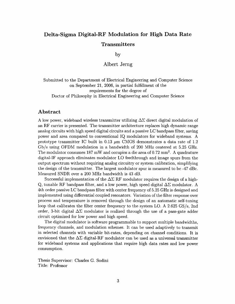
Abstract
A low power, wideband wireless transmitter utilizing AE direct digital modulation ofan RF carrier is presented. The transmitter architecture replaces high dynamic rangeanalog circuits with high speed digital circuits and a passive LC bandpass filter, savingpower and area compared to conventional IQ modulators for wideband systems. Aprototype transmitter IC built in 0.13 pm CMOS demonstrates a data rate of 1.2Gb/s using OFDM modulation in a bandwidth of 200 MHz centered at 5.25 GHz.The modulator consumes 187 mW and occupies a die area of 0.72 mm2 . A quadraturedigital-IF approach eliminates modulator LO feedthrough and image spurs from theoutput spectrum without requiring analog circuitry or system calibration, simplifyingthe design of the transmitter. The largest modulator spur is measured to be -47 dBc.Measured SNDR over a 200 MHz bandwidth is 43 dB.
Successful implementation of the AE RF modulator requires the design of a high-Q, tunable RF bandpass filter, and a low power, high speed digital AE modulator. A4th order passive LC bandpass filter with center frequency of 5.25 GHz is designed andimplemented using differential coupled resonators. Variation of the filter response overprocess and temperature is removed through the design of an automatic self-tuningloop that calibrates the filter center frequency to the system LO. A 2.625 GS/s, 2ndorder, 3-bit digital AE modulator is realized through the use of a pass-gate addercircuit optimized for low power and high speed.
The digital modulator is software programmable to support multiple bandwidths,frequency channels, and modulation schemes. It can be used adaptively to transmitin selected channels with variable bit-rates, depending on channel conditions. It isenvisioned that the AE digital-RF modulator can be used as a universal transmitterfor wideband systems and applications that require high data rates and low powerconsumption.
Thesis Supervisor: Charles G. SodiniTitle: Professor


Acknowledgments
The completion of my PhD program has been a very rewarding process and experi-
ence. In particular, I have been enriched by the interactions with faculty, and fellow
students both inside and outside the classroom and lab. I'd like to thank my advisor
Prof. Charles Sodini - his guidance and judgement throughout my thesis project has
been greatly appreciated. Thanks for pushing me with thought-provoking questions,
which helped me realize the full potential of this project. I'd like to thank my com-
mittee member Prof. Anantha Chandrakasan for providing me with knowledge on
digital design issues and giving me a kickstart on the high speed adder design. I'd like
to thank my committee member Prof. Mike Perrott for providing helpful suggestions
on the phase detector design in my tuning loop, providing advice throughout my pro-
gram, and sharing lab equipment with our group. I'd also like to thank Prof. Vladimir
Stoyanovic for helpful discussions regarding high speed digital interfaces. During my
summer at ADI, I got some great feedback regarding my project. In particular, I'd
like to thank Bill Schofield and Richard Schreier for their helpful discussions and
comnments.
I have enjoyed the comaraderie and help of many labmates over the years. Andy
Wang was a great source of knowledge on system issues. Todd Sepke has helped me
a lot through technical discussions, and by proofreading papers for me. Anh Pham
provided great advice on RF board design and was a magician soldering ICs for me.
Lunal Khuon provided lots of helpful lab parts and was a great conference roommate
and fellow senior citizen/dad. Andrew Chen was a great die photographer and helped
me out on digital testability issues. Ken Tan, Nir Matalon, Farinaz Edalat, and Khoa
Nguyen helped me understand the WiGLAN system and use the boards to test EVM
on my transmitter. Mark Spaeth provided lots of help with PCB design questions and
lab troubles. It has been fun socializing with the all the above and other members of
the lab John Fiorenza, Matt Guyton, Albert Chow, Johnna Powell, and Kevin Ryu.
I'd also like to thank Rhonda Maynard for all her help with taking care of purchase
orders, and quotes, and reimbursements, and just making life easier for me.

I'd like to thank my family and friends for always being there for me. To my
parents, thank you for all your support over the years, and for providing the framework
that makes this all possible. To my wife, Veronica, thank you for embracing the change
of lifestyle and weather so whole-heartedly, and for being such a good mother and
partner. And to my little one, Elliot, thank you for brightening each day with your
smile.
Contents
1 Introduction
1.1 WiGLAN Transmitter ..........................
1.2 Conventional IQ Transmitter . ......................
1.2.1 IQ Modulator Impairments . ...................
1.3 AZ Digital-RF Modulation .......................
1.3.1 Process Scaling . .........................
1.3.2 Circuit Integration . .......................
2 Digital-RF Conversion
2.1 Previous Research .............................
2.2 RF Bandpass Reconstruction Filter . ..................
2.3 Filtering Requirements . .........................
3 LC Bandpass Filter Design
3.1 Challenges . ...............
3.2 Differential Coupled Resonator Topology
3.2.1 Area Considerations .......
3.2.2 Impedance Considerations .
3.2.3 Inductor Design ..........
3.2.4 Varactor Design ..........
3.2.5 5.25 GHz Filter Design ......
3.3 Automatic Tuning Loop .........
3.3.1 Non-Idealities ...........
7

3.4
3.5
3.6
4 AE
4.1
4.2
4.3
4.4
4.5
3.3.2 Digital Tuning Loop.....
Q-enhancement . ...........
Test Filter Measurements ......
Summary ...............
System Architecture
Choosing Clock Frequency ......
Co-Design of AE NTF and RF BPF
Comparison to Oversampling with No
UWB System Example ........
Summary ...............
Noise-Shaping
5 Quadrature Digital-IF AE Modulator
5.1 Digital-IF .................
5.2 Quadrature Digital-IF ..........
5.2.1 Bandpass AE ...........
5.3 Frequency Planning ............
5.4 Summary .................
6 Digital Circuit Design
6.1 Low Power Design Challenges ......
6.1.1 General Techniques ........
6.2 AE Modulator Topology . ........
6.3 Low Power, High Speed Adder Design .
6.3.1 Conventional Static Mirror Adder
6.3.2 Passgate Adder . .........
6.4 Top Level Implementation and Results .
6.4.1 Interpolation Filter . .......
6.4.2 Digital-IF Up-Converter .....
6.4.3 Simulation . ............
6.5 Summary . .... ............
93
93
94
96
99
99
102
107
108
110
110
112

7 DRFC Circuit Design 113
7.1 Unit Cell Mismatches ........................... 114
7.1.1 DAC Mismatches .......... ................ 115
7.1.2 AE DRFC Mismatches ............ ........... 118
7.2 Behavioral Simulations .......................... 120
7.2.1 LO Phase Mismatch ............ ..... ...... 124
7.3 Circuit Implications ................... ........ 124
7.4 DRFC Unit Cell Implementation ................... . 126
7.5 Simulation Results .............. ........... 130
7.6 Summary .............. ................... 134
8 Measurement Results 135
8.1 Fabricated Test Chips ....... ........... ....... 135
8.2 Test Setup ................ . .............. 138
8.3 Test Chip Results ................... .......... 139
8.4 Power/Area Comparison ................ ........ 150
9 Conclusion 153
9.1 Future Directions ........... . .. ............ 154
9.1.1 Mismatch Shaping ................... ..... 154


List of Figures
1-1 Conventional IQ Modulator ................... .... 22
1-2 IQ Modulator Output Spectrum ................... .. 25
1-3 Digital QPSK Modulator ................... ...... 26
1-4 Digital AE RF Modulator ................... ..... 27
2-1 RF DAC Unit Cell ....... .. .......... 30
2-2 DRFC Unit Cell ....... . .............. 31
2-3 Up-Converted Clock Images ................... .... 32
2-4 Up-Converted Quantization Noise ................... . 32
2-5 Quadrature Digital-RF Converter Core . ................ 33
3-1 Filter Topology ........... ..... . ............. 38
3-2 Differential Resonator with Non-linear C(V) . ........... . 43
3-3 LC BPF Schematic ................... ....... . 45
3-4 Differential Inductor Lumped Element Model . ............ 45
3-5 Differential Tank Capacitance C(V) . .................. 46
3-6 Coupled Resonator Model ................... ..... 48
3-7 Tuning Loop Block Diagram ................... .... 49
3-8 Tuning Loop Model ........ ......... ......... 50
3-9 Filter Block and Phase Detector Transfer Functions ......... . 51
3-10 Phase Detector Schematic ........... ..... . .... . . 52
3-11 Filter Block Transfer Function vs. Temperature . ........... 53
3-12 Phase Detector Transfer Function . .................. . 54
3-13 Filter Input-Output Phase Difference . ................. 54

3-14 Filter Response ................... .. ........ 56
3-15 Q-enhanced Resonator Model ................... ... 57
3-16 Simplified Test Filter Schematic ................... .. 61
3-17 Test Filter Die Photo ................... ........ 62
3-18 Filter Response vs. Vtune ................... ..... 63
3-19 Automatic vs. Manual Tuning ................... ... 63
3-20 Q-enhanced Filter Response Tuning Curves . ............. 64
3-21 Automatic vs. Manual Tuning, Q-enhanced version . ......... 65
3-22 Measured Filter with and without Q-enhancement . .......... 65
3-23 Q-enhanced Filter : Measured vs. Simulated . ............. 66
4-1 AE Digital-RF Modulator ................... ..... 67
4-2 AE Modulator Output Spectrum ................... . 68
4-3 Aliasing Problem in Up-Conversion . .................. 69
4-4 No Aliasing with fLo = 2 flk .................... ... 70
4-5 Normalized Magnitude of Zero-Order Hold Frequency Response . . . 71
4-6 Image Rejection vs. OSR ........ ................. 71
4-7 SNR (dB) vs. Loop Filter Order for various OSR . .......... 73
4-8 RF Output Spectrum using 3rd order, 1-bit AE Modulator ...... 74
4-9 RF Output Spectrum using 2nd order, 3-bit AE Modulator ...... 75
4-10 UWB Output Spectrum using System Parameters from Table 4.3 . . 78
5-1 Digital-IF AE RF Modulator . ................... .. 82
5-2 Aliasing when fIF = LK .............. . . . . . . . ... 84
5-3 Quadrature Digital-IF AE RF Modulator . ............ . 84
5-4 SNR vs. LO Phase Error for Quadrature Digital-IF . ......... 85
5-5 Digital-IF Bandpass AE Modulator . ................. 86
5-6 Single PLL LO Generation for Digital-IF Architecture ........ . 88
5-7 Zero Order Hold Impulse Response . .................. 89
5-8 Frequency Response of Zero Order Hold . ............... 90
5-9 Single PLL LO and CLK generation avoiding spurs at 5.25 GHz . . . 91

6-1 Pipeline of (4) 3-bit Ripple Carry Adders .........
6-2 Pipeline of (2) 6-bit Ripple Carry Adders .........
6-3 Error Feedback Topology . ...............
6-4 2nd Order MASH Error Feedback Topology . . . . . . .
6-5 MATLAB Simulation of 2nd Order, 3-bit AE Modulator
6-6 Mirror Adder Even Cell . .................
6-7 Mirror Adder Odd Cell ...................
6-8 NMOS Passgate Adder Simplified Schematic .......
6-9 PMOS Sense Amplifier ...................
6-10 RC Network to Model Carry Chain Delay . . . . . . ..
6-11 Passgate Adder Transistor-Level Schematic ........
6-12 Pass-Gate Adder Carry Chain Waveforms . . . . . . ..
6-13 Digital Block Diagram ...................
6-14 4x Interpolator Implementation . ...........
6-15 Digital-IF I,Q Bitstreams. ..................
6-16 Digital-IF Up-Converter Implementation .........
6-17 Verification of Digital Block ................
7-1
7-2
7-3
7-4
7-5
7-6
7-7
7-8
7-9
7-10
7-11
Quadrature Digital-RF Converter Core .
DRFC Unit Cell Mismatches . . . . . . .
LO Amplitude Mismatch . . . . . . . ..
LO Phase Mismatch ...........
Data Timing Error ............
Behavioral Mismatch Simulation . . . . .
SNDR (Mean) vs. Percent Mismatch . .
SNDR (Std Dev) vs. Percent Mismatch.
LO Timing Spread vs. Gain Mismatch
SNDR vs. LO Delay/Segment . . . . . .
Unit Cell Transistor Mismatches . . . . .
. . . . . 94
. . . . . 95
. . . . . 96
. . . . . 97
. . . . . 98
. . . . . 100
. . . . . 100
. . . . . 102
. . . . . 103
. . . . . 104
. . . . . 105
. . . . . 106
. . . . . 107
. . . . . 108
. . . . . 109
. . . . . 109
..... 111
. . . . . . . . . . 114
. . . . . . . 116
. . . . . . . 117
. . . . . . 118
. . . . . . 119
. . . . . . . 121
. . . . . . . . . . 122
. . . . . . . . . . . 122
. . . . . . . . . . 123
. . . . . . . . 123
. . . . . . . . . 125
7-12 LO Differential Pair Output Current Matching . 126

7-13
7-14
7-15
7-16
7-17
7-18
7-19
7-20
7-21
7-22
Test Chip 1 Block Diagram
Test Chip 2 Block Diagram .
Testing Setup .........
8-4 Test Chip 1 :
Test Chip 1 :
Test Chip 1 :
Test Chip 1 :
Test Chip 2 :
Test Chip 2 :
Test Chip 2 :
Test Chip 2 :
Test Chip 2 :
Test Chip 2 :
Test Chip 2 :
Test Chip 2 :
12 MHz Input ................
102 MHz Input ...............
Wideband Plot ...............
OFDM Signal .............. ..
Direct Up-Conversion of 12 MHz Input . .
Two-Tone Simulation . . . . . .
Digital-IF, 12 MHz .............
Digital-IF, 12 MHz, Shift Clock Frequency
Digital-IF, Wideband Plot .........
200 MHz OFDM Signal ...........
20 MHz OFDM Channel for 802.11a. ....
Pair of 20 MHz OFDM Channels . . . . .
8-16 SNR Measurement using WiGLAN Receiver . . . .
8-17 Test Chip 1 Die Photo . ...............
8-18 Test Chip 2 Die Photo ................
. . . . . . 136
. . . . . . 137
. . . . . 138
. . . . . . 139
. . . . . . 140
. . . . . . 141
. . . . . . 141
. . . . . . . 142
. . . . . . 143
. . . . . . 144
. . . . . . . 144
. . . . . . 145
. . . . . . 146
. . . . . . . 146
. . . . . . . 147
. . . . . . . 147
. . . . . . . 149
. . . . . . 149
DRFC Unit Cell and Data Driver . . . . . . . . . . . . ..
Differential Output Current of Unit Cell . . . . . . . . . . . . ..
Combined Sum of Unit Cell Currents . . . . . . . . . . . . ......
Quadrature DRFC Filtered Output . . . . . . . . . . . . . ..
FFT of QDRFC Output . ...... . . . . . . . . . . . . . ..
FFT of Digital-IF QDRFC Output . . . . . . . . . . . . ..
Simulation of Extracted Layout . . . . . . . . . . . . . ..
Simulation of Revised Extracted Layout . . . . . . . . . . ......
Simulation of Quadrature Digital-IF DRFC using Extracted Layout
Simulation of Quadrature Digital-IF DRFC using Revised Extracted
Layout ........................... .......
127
128
129
129
130
131
132
133
133
134
8-1
8-2
8-3
8-5
8-6
8-7
8-8
8-9
8-10
8-11
8-12
8-13
8-14
8-15

9-1 Element Rotation Hardware Implementation . . . .. . . .. ... .. . 155
9-2 Behavioral Model Simulation using Element Rotation .... ..... . 155


List of Tables
1.1 Target SNR for WiGLAN Transmitter.................
3.1 2nd Order Bessel k and q values . . . . . . . . . . . .
3.2 Simulated Inductor Q at 2 GHz ...... . . . . . . . . . . ..
3.3 Filter Performance with Resonator Mismatch . . . . . . . . . . . ..
3.4 Current vs. Q-enhancement for DR=60 dB over 200 MHz BW . . . .
4.1 Simulated AE SNR with OSR=13 ....................
4.2 Clock Image Attenuation vs. Clock Frequency for 200 MHz RF BW .
4.3 UWB System Example (Band 1, Channel 2 at 3.96 GHz) .......
39
41
55
60
5.1 LO, Clock, and IF frequencies for DIVIDE = 8 or 16 ........ . 91
6.1 Pipelined 2-bit Mirror Adder Simulation Results ......... . . . 101
6.2 6-bit Pass-Gate Adder Simulation Results . .............. 106
6.3 Digital Block Simulation Summary . .................. 112
8.1 AE Modulator Power Consumption/Die Area . ............ 148
8.2 FOM Comparison ................... .......... 150
8.3 Conventional IQ Modulator Implementation . ............. 151
9.1 Element Rotation Algorithm ........ . . .. 154

Chapter 1
Introduction
This research introduces a new transmitter architecture that targets high data rate
wideband systems. AE digital-RF modulation efficiently modulates an RF carrier
with very wide bandwidths. A wideband digital-RF modulator can be software-
defined to transmit multiple frequency channels, with variable bandwidths and mod-
ulation schemes, within the band. Thus, the modulator can be programmed to utilize
a band of spectrum on an adaptive basis, depending on wireless channel conditions
and interferers, or upon the specifications of a given standard.
Next generation wireless systems such as 802.11n and UWB aim to provide higher
data rates approaching 1 Gb/s in order to support demand for high data rate wireless
communications. These systems use OFDM modulation in order to utilize spectrum
efficiently, leading to high peak to average power ratios and high dynamic range
requirements. As data rates and signal bandwidths increase, the DAC, analog recon-
struction filter, and analog mixer found in conventional IQ transmitters become more
difficult to design given constraints on power, noise, and linearity. The scaling of
CMOS transistors and supply voltages creates further challenges from the standpoint
of dynamic range. A transmitter architecture based on AE direct digital modulation
of the RF carrier replaces high dynamic range analog circuits with high speed digital
circuits, and enables power and area savings in the implementation of a wideband
transmitter as CMOS transistors continue scaling. This thesis makes the following
contributions.

1. Design of a wideband direct digital-RF modulator architecture that efficiently
provides Gb/s data rates.
2. Integration of a digital-RF converter with an RF bandpass reconstruction filter,
eliminating spurious signals and noise associated with digital-RF conversion.
3. Demonstration of a quadrature digital-IF AE RF Modulator with < -60 dBc
LO and image spurious signals.
Successful implementation of the AE Digital-RF modulator was enabled through
the design of two novel circuit blocks.
1. A high-Q passive LC bandpass filter with automatic center frequency tuning
loop.
2. A low power 2.6 GS/s Digital AE modulator utilizing an adder design based
on NMOS passgate chains and sense-amplifier flip-flops.
The outline of the thesis will be as follows. A Wireless Gigabit Local Area Network
(WiGLAN) project that aims to provide Gb/s data rates for next generation networks
will be introduced. Conventional IQ transmitter design will be discussed and the new
AE Digital-RF modulator will be introduced. Design details of the high-Q tunable
LC bandpass filter and AE system architecture will be presented, and the importance
of co-designing the digital AE modulator and RF BPF will be explained. The method
and benefits of quadrature digital-IF up-conversion will be described. The design of
the high speed digital modulator and current-switching digital-RF converter will be
presented. Finally, measurement results from two test-chips will be provided and the
thesis will conclude with a power and area comparison between the new architecture
and the conventional IQ modulator.
1.1 WiGLAN Transmitter
The WiGLAN transmitter aims to achieve Gb/s data rates by increasing the RF
bandwidth to 200 MHz, employing an adaptive M-ary QAM modulation format up to
Table 1.1: Target SNR for WiGLAN Transmitter
256-QAM SNR 30 dB
Peak-Average Symbol Power 4 dB
Peak-Average Power Ratio due to multiple sub-carriers 15 dB
TOTAL 49 dB
256-QAM, and utilizing spatial diversity gain from a multiple-input multiple-output
(MIMO) antenna system and MIMO signal processing. WiGLAN uses an OFDM
frequency multiplexing scheme with a 1 MHz sub-carrier spacing to increase spectral
efficiency and mitigate the effects of multipath. It intends to operate in the 5.15-5.35
GHz UN-II band with a center frequency of 5.25 GHz. If 256-QAM is used on all 200
sub-carriers, a raw throughput of 1.6 Gb/s can be achieved.
While the large number of constellation points in 256-QAM increases the data. rate
for a given symbol rate, it also raises the required SNR of the transmit signal. Because
the constellation points are closer together for a fixed transmit power, it takes smaller
amounts of random noise to cause symbol decision errors. Also, because information
is encoded in the amplitude of the symbol as well as its phase, a transmitter with
high linearity is required to avoid compression of the signal. Further exacerbating the
situation is the fact that in OFDM systems, the peak-to-average power ratio (PAPR)
is high because the transmit signal is the aggregate sum of a large number of sub-
carriers. Coherent addition of the sub-carriers in phase results in large signal peaks.
As a result of these system choices, the transmit signal dynamic range requirements
increase significantly.
Assuming an SNR requirement of 30 dB [1] due to additive white gaussian noise
(AWGN) for 256-QAM, the proposed WiGLAN system would require - 50 dB of
dynamic range according to Table 1.1. In addition to AWGN, other impairments
that can affect the BER performance include phase noise, narrowband interference,
and group delay variation. It has been shown that while phase noise and group delay
variation specifications require approximately 6 dB higher performance in 256-QAM

10 Modulator- - - - -- - - - - - - - - - - --. .
a
Figure 1-1: Conventional IQ Modulator
compared to 64-QAM, signal to interferer (S/I) ratios must increase by approxi-
mately 12 dB when going from 64-QAM to 256-QAM [1]. LO feedthrough and image
rejection performance determine the level of narrowband interferers generated in IQ
transmitters. A S/I ratio of roughly 37 dB is required for 256-QAM [1].
The challenge for the WiGLAN transmitter is achieving high dynamic range over
a wide RF bandwidth with excellent LO and image spurious performance. Currently,
the widest RF bandwidth supported by 802.11 systems is 20 MHz [2].
1.2 Conventional IQ Transmitter
Fig. 1-1 shows a block diagram of a conventional IQ transmitter used to up-convert
digital baseband signals to an intermediate or final RF frequency. The output of the
IQ modulator can be mathematically written as
I cos(w t) + Q sin(w t) = A cos(w t + ¢) (1.1)
where
A= I 2 + Q2 (1.2)
andI
S= arctan( ) (1.3)Q

This architecture is popular because it can produce arbitrary phase and/or ampli-
tude modulation. Furthermore, it is attractive in integrated implementations because
when the I and Q paths are well-matched, accurate modulation is achieved regardless
of temperature, supply, or process variations.
In order for the IQ modulator to correctly reproduce equation (1.1), the I and
Q signal paths from the DAC to the output of the mixer must be linear and well-
matched. The analog circuits in this path must maintain noise and distortion to
levels satisfying the required dynamic range of the system. As the baseband signal
bandwidth increases, the DAC and analog filter blocks become more difficult to design.
Current-steering DAC architectures have achieved the best performance at high
sampling rates [3],[4],[5]. At high frequencies, their spurious-free dynamic range is
limited by dynamic errors rather than static DC errors. Imperfect synchronization
between the control signals of current switches causes code-dependent timing errors
[3]. The code dependency results in distortion at high frequencies. A voltage glitch
can appear at the source node of the current steering switches [4]. Any non-linear
capacitance on this source node will produce distortion [5]. Transient waveforms
that do not, settle within a clock period can alter the value of the next data sample.
This inter-symbol interference causes disturbances to circuit nodes that are data-
dependent, again introducing distortion [4]. Recent DACs with SFDR > 60 dB
have been reported in the literature with sampling speeds greater than 1 GS/s and
output frequencies greater than several hundred MHz [4],[3]. However, reported power
consumption for these DACs are in the range of 110 mW - 400 mW.
Power consumption in the analog reconstruction filter increases proportional to
signal bandwidth for a constant dynamic range [6]. This can be shown by writing the
following expressions for a- filter.
NSD vn 2 4kTSD = oc -- (1.4)
Af gm
Bandwidth oc 9 (1.5)C

4kTNoisePower = (NSD)(Bandwidth) c C4 (1.6)
Linearity oc (Vg, - Vt) = (1.7)gm
Eqn. (1.7) is derived from the classical long-channel approximation for a MOS
device, assuming square law behavior.
If the bandwidth of the filter is increased by a factor s while keeping noise power
fixed, it follows from eqns. (1.5) and (1.6) that gm must also increase by a factor
s. If gm increases by a factor s, then to maintain the same linearity, Id must also
increase by the same factor s using eqn. (1.7). Eqn. (1.6) also indicates that analog
filter design involves a fundamental tradeoff between noise and capacitor area.
1.2.1 IQ Modulator Impairments
The output spectrum of an ideal IQ modulator contains a single tone at frequency
WLO + WBB (assuming a sine-wave baseband input). In practice, spurious signals due
to LO leakage, baseband harmonic distortion, and finite image rejection accompany
the desired signal as shown in Fig. 1-2.
LO leakage is typically caused by random device mismatches in the baseband
transconductor of the mixer. This creates a dc offset that up-converts to the LO
frequency at the output of the mixer. The magnitude of the LO leakage relative
to the desired output signal is proportional to the ratio between the DC offset and
the baseband input signal. One can minimize LO leakage by increasing the ampli-
tude of the baseband signal. The tradeoff is that the baseband harmonic distortion
increases when the signal amplitude is increased. The transconductor is typically
designed to keep harmonic distortion < -50 dBc at the expense of LO leakage and
noise performance.
Image rejection is limited by the amplitude and phase matching of the quadra-
ture LO signals and the I and Q baseband paths. Without additional calibration

10 Modulator TypicalOutput Spectrum
Desired
Figure 1-2: IQ Modulator Output Spectrum
algorithms and correction circuitry, the LO and image signals are typically -30 to -40
dBc.
1.3 AE Digital-RF Modulation
This research proposes direct digital modulation of the RF carrier as the basis for
a transmitter architecture that can eliminate high performance DACs and analog
filters. Before discussing this architecture, we will briefly review other transmitter
approaches found in the literature.
Closed loop PLL modulation directly modulates the VCO without requiring a
DAC or analog filter [7]. However, the data bandwidth is limited by the relatively
narrow PLL loop bandwidth required to suppress synthesizer phase noise. It is un-
suitable for wideband applications with bandwidths on the order of 100 MHz.
A simple realization of wideband direct digital modulation is shown in Fig. 1-3 [8],
which implements a QPSK modulator capable of generating one of four quadrature
phases of the RF input. This brute-force approach is limited in its applicability.
An OFDM system with multiple sub-carriers each being modulated by 256-QAM

(0 LO
Digital Inputs
Figure 1-3: Digital QPSK Modulator
would require the generation of much more than four phase angles. In addition,
this approach introduces abrupt phase transitions in the RF signal. By sending the
data with ideal rectangular pulses, the frequency spectrum of the output signal takes
on a Sin profile, producing a wide transmitted spectrum. In order to accomodate
many users and avoid interference problems, Nyquist filtering is applied to digital
data in wireless transmitters to narrow the transmit spectrum without introducing
inter-symbol interference (ISI). In the time domain, the data transitions are smoothed
while the data points at ideal sampling instants remain unaffected.
The desire for a band-limited transmit spectrum requires the phase shifter design
to have continuously adjustable phase rather than discrete phase levels. An analog
phase shifter is more complicated to design and requires a DAC and analog filter to
interface to digital data. In addition, accurate modulation is difficult to achieve due
to changes in an analog phase shifter's characteristics over process, temperature, and
voltage.
Over-sampling AE concepts [9] can be applied to create a digitally controlled
vector modulator that provides a continuous range of output phase and amplitude
values. In Fig. 1-4, filtered I,Q digital data are over-sampled and converted into 1-bit

0 or 180
I*cos( co t)+Q*sin(o t)0
Figure 1-4: Digital AE RF Modulator
output streams by digital AE modulators. The phase shifter needs to either pass the
LO signal or invert it, and can be realized trivially by a differential current steering
switch in CMOS. While the quadrature LO signals being modulated toggle between
only two phases, their sum represents a continuous range of phase/amplitude modu-
lation based on the duty cycle of the over-sampled AE bit-stream. The modulation of
the RF carrier is correctly encoded but obscured by a large amount of high frequency
quantization noise. An RF bandpass filter removes the out-band quantization noise
and reconstructs the modulated RF signal. The concept can be extended to multi-bit
AE modulators using binary weighted or unary weighted LO current steering cells.
This architecture replaces the DAC, analog reconstruction filter, and analog mixer
with a high speed AE modulator, a digital-RF converter (DRFC) based on current
steering switches, and a passive RF BPF. The primary advantage is that the analog
baseband signal path has been eliminated, removing noise and linearity considerations
from the design and enabling power and area savings for wide bandwidths. Both
baseband and RF inputs to the DRFC are fully switching digital signals and no
distortion results from signal clipping. In addition, a passive RF BPF consumes no
power and has little noise and distortion, in contrast to active analog filtering.
1.3.1 Process Scaling
The analog circuit design in conventional IQ transmitters becomes even more chal-
lenging as transistor sizes and supply voltages continue scaling downward. However,

the AE digital-RF modulator benefits from the faster digital circuits available from
scaled CMOS processes. Scaling directly reduces the power and area of the high
speed digital AE modulator. In digital process scaling, there has also been a trend of
increasing levels of metallization and lower resistance routing. As a result, on-chip in-
ductors with higher Q can be built using lower loss metals that are farther away from
the substrate. Higher inductor Q allows the design of sharper, more selective passive
bandpass filters, improving the quantization noise suppression of a AE digital-RF
modulator.
1.3.2 Circuit Integration
In conventional IQ transmitters, the DAC, analog reconstruction filter, and analog
mixer are designed as distinct blocks that must interface to each other. The DAC is
often on a separate digital chip. Each block contributes its own noise and distortion
to the transmit signal. In order to meet the dynamic range specifications of the
transmitter, each individual block must be designed such that its dynamic range
exceeds the overall specifications. The AE digital-RF modulator can be integrated in
a digital CMOS process. In addition, the DRFC and bandpass filter can be combined
into a single circuit structure, as will be shown in the next chapter. Noise and linearity
constraints do not apply to the digital circuits, and only mismatches between DRFC
current-steering switch cells can cause distortion, as will be discussed later.
Chapter 2
Digital-RF Conversion
In a conventional transmitter, the digital baseband signal is first converted to an
analog signal using a DAC, and then up-converted to RF frequency using a mixer. A
digital-RF converter (DRFC) combines these two steps into one circuit. The DRFC
inputs are the digital baseband bits and the DRFC output contains the analog base-
band signal modulated around an RF carrier.
2.1 Previous Research
A radio frequency digital-analog converter (RF DAC) was introduced in [10]. In
general, the output of a DAC contains the desired analog signal as well as its images
around each multiple of the DAC clock frequency. The RF DAC uses one of these high
frequency clock images as an RF output. A simple schematic representation of an RF
DAC unit cell is shown in Fig. 2-1. A sine-wave at the desired clock image frequency
modulates the DC bias voltage of the DAC current source. This increases the clock
image power by mixing the DAC impulse response to the clock image frequency.
One drawback is that the RF DAC outputs substantial energy at other frequencies,
including its primary output near DC.
The digital-RF converter (DRFC) in [11] features a balanced version of the RF
DAC unit cell, as shown in Fig. 2-2. The balanced unit cell is a more efficient RF
modulator because the low frequency response around DC is rejected and the RF

RF DAC Unit Cell
DigitData
Vbias
Figure 2-1: RF DAC Unit Cell
output is now the primary output. This balanced unit cell is identical in structure to
a Gilbert-cell mixer. The difference is that in a DRFC, the digital baseband inputs
directly drive the top pair of current-steering switches, multiplying an RF carrier
signal by +1 based on the digital data. In contrast, the Gilbert-cell mixer's bottom
differential pair is driven by an analog baseband signal and must be linearized.
The DRFC performs a mixing operation between the digital baseband signal and
the local oscillator signal to produce a modulated RF output. It merges the func-
tions of the DAC and mixer, while eliminating the analog filtering between the two.
However, the frequency spectrum of the digital signal repeats itself at all multiples
of the sampling rate or clock frequency. These clock images are up-converted by the
DRFC without any filtering besides the sinc response associated with the zero-order
hold in the digital-RF interface. When using a digital AE modulator, high frequency
shaped quantization noise is up-converted without any filtering. In either case, an
RF bandpass filter is required at the output of the DRFC, as illustrated in Fig. 2-3
and Fig. 2-4. In the previous work [10], [11], substantial off-chip filtering is required
to eliminate high frequency clock images and quantization noise and produce a clean
Digital-RF Converter Unit Cell
DigitalData
+
Figure 2-2: DRFC Unit Cell
transmit spectrum. The fundamental difficulty with direct digital-RF conversion is
the transmission of spurious emissions outside the signal band that are difficult to
filter at RF frequencies.
One approach to the filtering problem involves embedding a semi-digital FIR
reconstruction filter in the digital-RF interface. In [12], the 1-bit output of a AE
modulator goes through a 6-tap digital delay line. Each output of the delay line is
applied to the switch input of an RF DAC cell whose current source is weighted with
the appropriate FIR filter coefficient. The drawback to this approach is that a large
number of taps is needed to implement an FIR filter with reasonable attenuation. For
example, in [13], a 128-tap delay line realizes the equivalent transfer function of a 2nd
order analog filter with -20 dB/decade slope in the stopband. For high RF output
frequencies and wide baseband bandwidths with high sampling rates, a large number
of delay taps and weighted current sources in the digital-RF interface will consume a
large amount of power. In [12] with a 6 tap FIR filter, the RF output spectrum at 1

Up-Converted Clock Images
fLQ/fCLK fLO fLO +
Figure 2-3: Up-Converted Clock Images
Up-Converted Quantization Noise
Figure 2-4: Up-Converted Quantization Noise

I+
Q it
I sint wt
Figure 2-5: Quadrature Digital-RF Converter Core
GHz contains a significant amount of out-of-band quantization noise. The magnitude
of this noise is approximately -35 dBc at a frequency offset of 15 MHz from a 1 GHz
single-tone output.
2.2 RF Bandpass Reconstruction Filter
Our design integrates a high-Q passive LC bandpass filter into the load of the digital-
RF conversion circuit. Fig. 2-5 shows a circuit schematic of our quadrature DRFC
with load filter.
This realization integrates both the DRFC and RF BPF under a single supply.
In the unit cells, quadrature phases of an RF carrier are applied to differential pairs
biased by tail current sources. The output currents of the differential pairs are routed
through differential current steering switches controlled by the I and Q digital AE
modulator output bits. The resulting output currents from each unit cell are summed
and then filtered by a passive LC network that also performs I-V conversion. The
filter does not consume any additional voltage headroom due to the inductor, and
acts as a tuned load to provide high gain for the DRFC.
Passive LC filtering at RF is attractive because it provides high dynamic range
with no power consumption. At multi-GHz RF frequencies, LC filters are relatively
small in terms of die area. However, the steepness of a passive LC filter's roll-off is
limited by the finite Q of on-chip passives. The feasibility of this approach depends
on the RF filtering requirements.
2.3 Filtering Requirements
The required Q of the bandpass filter can be approximated using the relation
Q = fo (2.1)BW
where fo is the filter center frequency and BW is the signal bandwidth. A typical
narrowband wireless system such as GSM has a signal bandwidth of 200 kHz and a
center frequency of 1-2 GHz, requiring a Q of 5,000-10,000. Fortunately, the required
Q decreases as the signal bandwidth increases. For wideband systems with signal
bandwidths on the order of 100 MHz, conventional analog filtering becomes more
difficult while RF bandpass filtering becomes practical. The WiGLAN transmitter,
with a bandwidth of 200 MHz and a center frequency of 5.25 GHz, requires a Q of -
25, which is still difficult but possible.
The selectivity requirements of the BPF also depend on the location and mag-
nitude of the spurious signals. Oversampling of the digital input signal places clock
images farther out in frequency and reduces RF filtering requirements. A high speed
current-steering DRFC requires accurate distribution and matching of the LO path
signal [11]. For multi-GHz LO and clock frequencies and a typical segmented archi-
tecture with a large number of unit cells, the power consumption of the LO and data
buffers becomes substantial. Oversampling AE modulation pushes the clock images
farther away and also reduces the number of unit cells required by the converter.
This reduces the power consumption and area of the DRFC, and minimizes routing
parasitics in a high frequency converter. The spurious signals are dominated by the

shaped out-of-band quantization noise, whose magnitude can be engineered through
design of the AE noise transfer function (NTF).
In the following sections, the design of a fully integrated high-Q LC BPF and the
architecture of the AE digital-RF modulator will be described. The design of the
AE modulator will be dictated by the required in-band SNR, as well as the required
out-of-band noise requirements and achievable RF filtering.


Chapter 3
LC Bandpass Filter Design
3.1 Challenges
The design of a passive LC bandpass filter involves several challenges. In order to
attain a sharp roll-off, the on-chip passives used in the filter must have high Q.
The finite Q of on-chip inductors typically limits the overall Q to the range of 10-20,
depending on the parameters of the process. With high Q and a narrow passband, any
varia.tions in capacitance or inductance over process and temperature will cause a, shift
in the filter center frequency and a large amplitude loss in the fixed RF bandwidth of
the system. Meanwhile, noise and spurious signals at out-of-band frequencies may fall
in the shifted passband of the filter. A practical realization must include an automatic
control loop to stabilize the filter center frequency over process and temperature
variations. In order to attain higher resonator Q, active Q-enhancement can be added
but will be accompanied by a penalty in power consumption and dynamic range.
3.2 Differential Coupled Resonator Topology
A conventional bandpass design method is to take a lowpass prototype ladder filter
and perform a lowpass to bandpass transformation by placing a capacitor in series
with all inductors and an inductor in parallel with all capacitors. The resulting ladder
contains too many inductors, occupying large die area. A narrowband approximation

BandpassLC LadderFilter
CoupledResonatorFilter
DifferentialCoupledResonators
Figure 3-1: Filter Topology
to the bandpass ladder filter can be realized with shunt LC resonator sections that are
capacitively coupled [14]. This topology minimizes the number of inductors required
in the filter. Further area reduction is achieved by converting the topology into its
differential form, as shown in Fig. 3-1. Symmetric differentially-wound inductors take
up less area than two equivalent single-ended inductors. In addition, wasteful spacing
between inductors is eliminated, allowing a more compact layout. The capacitor area
is reduced by a factor of 4 in the differential resonator implementation.
The coupled resonator design methodology follows in a manner analogous to con-
ventional ladder design using filter look-up tables [14]. Based on the normalized
resonator quality factor defined as,
11
_Filter

Table 3.1: 2nd Order Bessel k and q values
qo Insertion Loss (dB) q1 qn k12
00 0 0.5755 2.1478 0.8995
9.078 1.335 0.61 1.7737 0.8329
4.539 2.734 0.6523 1.4920 0.7685
3.026 4.187 0.7093 1.2606 0.7068
2.269 5.680 0.8138 1.0263 0.6486
1.816 7.270 0.9078 0.9078 0.6360
1.513 9.208 0.9078 0.9078 0.6360
1.297 11.707 0.9078 0.9078 0.6360
Afq0 = Qo (3.1)
fmnormalized coefficients of coupling k, and normalized source and load q values
are tabulated for coupled ladder lowpass prototypes. In eqn. (3.1), Af is the filter
bandwidth, f, is the filter center frequency, and Q0 is the unloaded resonator Q. For
example, in Table 3.1 [14], the normalized k and q values are listed for a 2nd order
Bessel lowpass filter prototype.
The un-normalized bandpass parameters are given by [14]
AfKi,k = k,kA (3.2)fm
Qi = q, (3.3)AfChoosing an inductance value L, the filter component values can be calculated
using [14]
1= fm (3.4)
where CN are the nodal capacitances with all other nodes shorted to ground. CCi,k
are the coupling capacitances between nodes i and k and are equal to Ki,k'CN. The i'th

resonator will consist of an inductance L and a capacitance C = CN - CCi_1 - CCi+1.
The source and load resistances can be found from the un-normalized Qi using [14]
R, = wLQi (3.5)
The loss represented by the finite Q of the resonator can be approximated with
a resistor Rp in parallel with the inductor. If we make the approximation that R, is
constant over the narrow bandwidth of the filter, then the physical source and load
resistors required by the design can be calculated using
Ri R,RS,L = R (3.6)Rp - RiFor a particular filter order, there is a minimum resonator quality factor Qo re-
quired to realize the filter's transfer function. The minimum resonator Q required for
a 4th order Bessel BPF at 5.25 GHz with bandwidth 260 MHz is
f 5.25e9Q = m () = 5.25e9 (1.297) = 26.2 (3.7)Af 260e6
In a given filter type, i.e. Chebyshev, or Bessel, higher order filters provide sharper
selectivity, but require pole locations with higher Q's.
3.2.1 Area Considerations
A straightforward way to reduce filter area is to minimize the required order of the
filter and thus the number of resonators. A Chebyshev filter has the sharpest at-
tenuation characteristics and can be used to minimize the required order. However,
the Chebyshev response will also require a higher resonator Q to realize the desired
pole locations. In a given process, there is generally a design space for inductors that
trades off area for Q [15]. The area of the inductor increases to maximize Q. Table 3.2
lists simulated Q vs. area for several foundry modelled inductor designs at 2 GHz in
IBM's 7WL 0.18 /im BiCMOS process. Because of the tradeoff between area and Q,
a 4th order Chebyshev BPF with 2 resonators is not necessarily smaller in area than
a 6th order Bessel BPF, whose 3 resonators each require lower Q.

Table 3.2: Simulated Inductor Q at 2 GHz
Inductor Type Outer Dimension Metal Width Turns Area Inductance Q
Parallel M7/M6 280 pm 6 pm 4.5 .078 mm 2 7 nH 25.9
Series M7-M6 230 ptm 10 pm 5 .053 mm 2 7 nH 18.7
Series M7-M6 200 A/m 10 A/m 6 .04 mm 2 7 nH 17.2
3.2.2 Impedance Considerations
According to eqn. (3.5), the equivalent resistance of the i'th resonator is proportional
to both L and Qi. Higher equivalent resistance at resonance is advantageous because
for a given desired output voltage swing, less current is required in the DRFC driving
the filter. Higher Q filter designs such as Chebyshev, and larger value inductances in
the resonator can save power in the DRFC.
3.2.3 Inductor Design
In general, the inductance should be chosen to optimize the Q and resonator impedance
at resonance. This will allow one to achieve the maximum selectivity available from
the process. If the filter design does not require a high Q, then inductor Q can be
traded off to minimize area.
A high-Q passive LC filter must be tunable. This is most readily accomplished
by incorporating a varactor as the resonator's capacitance. A large ratio between the
tunable capacitance and fixed capacitance in the resonator maximizes tuning range.
The fixed capacitance is made up of parasitic routing capacitances and loading capac-
itances on the filter nodes. A larger inductor value reduces the overall capacitance
required at resonance, and causes the fixed parasitic capacitances to be a greater
percentage of the total capacitance. The inductance must be chosen small enough to
insure that the tuning range is greater than the expected center frequency variation.

3.2.4 Varactor Design
Varactor design is influenced by Q and linearity. Q is typically limited by the on-chip
inductor, although at higher frequencies the varactor Q can become significant since
1Qvar = (3.8)
wCR,
The overall resonator Q can be expressed as
Qres = ( + ) (3.9)Qind Qvar
The varactor can also cause signal distortion through its nonlinear C-V character-
istic. The voltage across the varactor varies as a function of the input signal driving
the filter. This creates a signal-dependent capacitance in the filter that will result in
distortion.
The magnitude of the distortion products can be calculated by first writing an
equation for the tank capacitance, C, a.s a function of the input signal, V, using a
power series expansion.
C(V) = Co + CiV + C2 V 2 + C 3V 3 + C 4 V 4 + ... (3.10)
Fig. 3-2 depicts a typical differential resonator design consisting of two inductors,
a varactor in series with a fixed capacitor, and a resistor representing the overall
resonator loss. The input to the resonator is a current-mode sine wave at the resonance
frequency, w,. The resulting output voltage will consist of a sine wave at o, as well as
harmonics due to the nonlinear capacitance. The output voltage, V, can be expressed
as
V = I -Z = I(RlljwLI (3.11)jwc(V)
The solution to eqn. (3.11) is not staightforward because C is a function of V,
which in turn is a function of C. The analysis can be greatly simplified by assuming
that V only contains frequencies of the original input current signal. This assump-
tion is valid because the distortion products will generally be much smaller than the

L
VCC
/
C1 CV1 CV2 C2
Vtune
R
0 + V - 0
VCC-- -- sin(wot) -2 sin(wot)
Figure 3-2: Differential Resonator with Non-linear C(V)
fundamental signals and will not influence C(V). Using this assumption, one can de-
rive an expression for the resonator current as a function of the resonator voltage to
determine the level of distortion products.
1(3.12)I = V -Y = V - ( + jwC(V) - ) (3.12)R wLThe relevant distortion products to consider are those that will fall into the pass-
band of the filter. Harmonics of w, will be at much higher frequencies and be fil-
tered. When two tones at closely spaced frequencies wl and w2 undergo 3rd order
non-linearity, distortion known as IM3 products will appear as tones at frequencies
2wl - w2 and 2w2 - wl. When the tone spacing is small compared to the bandwidth
of the filter, the IM3 products will appear in-band.
In the general case, one will substitute V = Asin(wt) + Asin(w2t) into eqn. (3.12)
and find the ratio between the coefficients of the fundamental currents and the IM3
currents. Since both the fundamental and IM3 frequencies are in the passband of the
filter, the actual output voltage can be calculated as the current times the impedance
at resonance, R. The ratio between fundamental and IM3 voltages can be used to
calculate the output IP3 voltage (OIP3) of the filter.
In a differential implementation, as shown in Fig. 3-2, the tank capacitance C(V)

will be an even function of the differential tank voltage. In other words, C(+A) =
C(-A) due to the symmetry of the circuit. Note that the differential capacitance
C(V) in Fig. 3-2 is the series combination of C1, C2, CV1, and CV2. Since C(V) is
an even function, only the even powers of V in eqn. (3.10) are required. We can now
substitute eqn. (3.10) and V = Asin(wit) + Asin(w2t) into eqn. (3.12). The following
equation for I can be written where we have only used the even powers of C(V) up
to 2. It is also assumed that wl W2 W-.
I1= [Asin(wJt) + jwC, + jwo C2(Asin(wit) + Asin(w2t))2]R wL
(3.13)
Near resonance, - and jwoCo, will approximately cancel. The relevant terms
from the multiplication in eqn. (3.13) for IM3 calculations are then
A A 3I = -sin(wit)+ -±sin(w2t)+ jwC 2Aa[sin(2wl - w2)t+ sin(2w2 -w i)t] (3.14)
R R 4
Given the voltage magnitude, A, of the two tones, the power ratio between the
IM3 tones and the fundamental tones is calculated to be
3woC2 RA 2IM3(dBc) = 20 * loglO C A 1 (3.15)
4
The IM3 depends on the 2nd order coefficient, C2, of the power series expansion
of C(V), and the effective resistance R of the tank at resonance. A higher tank Q will
have higher R and result in worse IM3 performance. This indicates a tradeoff between
filter selectivity and filter distortion in tunable filters. A higher C2 also causes worse
distortion. In general, reducing the tuning range of the filter will lower C2. Thus,
there is also a tradeoff between tuning range and distortion in tunable filters.
3.2.5 5.25 GHz Filter Design
A passive LC bandpass filter at 5.25 GHz was designed using Table 3.1 with qo =
1.297. The filter order is limited to a 4th order Bessel bandpass due to the Q of the

L=2.2 nH
6.3 fFI
L=2.2 nH
VCC
Vtune
Vout
Figure 3-3: LC BPF Schematic
L = 1.1 nHRs = 1.05Rp = 2.7 KC = 25 fF
Figure 3-4: Differential Inductor Lumped Element Model
on-chip inductors. A schematic of the filter is shown in Fig. 3-3. A 3-turn differential
inductor was designed and optimized for Q using the EM simulator Sonnet. Simulated
differential inductance and Q were 2.2 nH and 26 at 5.25 GHz. The metal width and
spacing was 8 pm and 4 jm, respectively. A M1 shield was placed underneath the
inductor to reduce substrate losses. The lumped element model of the inductor used
for simulation is shown in Fig. 3-4.
PN-junction varactors were used for the resonator load capacitances. The varactor
capacitance varies from 0.2 pF to 0.46 pF when the tuning voltage across the varactor
ranges from 2.2 V to 0.3 V. 1.2 pF MiM capacitors in series with the varactors
serve two purposes. First, they linearize the C-V characteristics of the varactor and
minimize distortion. Second, they allow the varactor to be configured with its cathode
IJ
V

Tank Capacitance C(V)
U-
5
Figure 3-5: Differential Tank Capacitance C(V)
at the virtual ground point of the differential resonator. The parasitic diode from n-
to substrate is then at a virtual ground, preventing it from degrading the resonator
Q. The series MiM caps do, however, reduce the filter tuning range. The filter is
designed to tune from 4.8 GHz to 5.6 GHz, corresponding to a tuning range of +/- 8
Parallel plate capacitors using the top two metal layers were utilized to implement
the small 26.3 fF coupling capacitors. Minimizing resistance in the layout connections
to the varactors and inductors was critical for maintaining a high quality factor in
the resonator.
The differential tank capacitance C(V) for the 5.25 GHz filter in Fig. 3-3 was found
through simulations that included extracted layout parasitics. The actual tuning
range with parasitics was approximately 500 MHz. Using MATLAB, C(V) at Vtune = 2
V was fit to a polynomial expression with coefficients Co = 416.06 fF and C2 = 1.1739
fF. The simulated C(V) and polynomial approximation are plotted together in Fig. 3-
5. Using eqn. (3.15) and assuming a maximum expected differential peak voltage of 0.6
V in the filter, the IM3 products are calculated to be -46.5 dBc with 0.3 V differential

output for each of the two fundamental tones. Circuit simulations in SpectreRF
showed the IM3 products to be -51 dBc for the same conditions. Simulations show
that for a larger tuning range of 1 GHz, the IM3 products increase to -25 dBc.
The tradeoff between tuning range and distortion can be alleviated by providing
an additional coarse tuning capability using switchable fixed capacitances [16]. This
allows a reduction in tuning sensitivity of the varactor which minimizes C2. Another
potential technique to improve the distortion is to use a varactor configuration that
can linearize the tank capacitance without reducing the tuning range. The work in
[17] uses a back-to-back series varactor topology to achieve this goal.
3.3 Automatic Tuning Loop
Automatic frequency tuning can be implemented by configuring a replica resonator
or the filter itself as a VCO and locking it to a separate reference frequency in a
PLL [18]. These PLL tuning systems are costly in terms of die area and circuit
complexity. This design adapts a tuning technique used in baseband filters [19] for
use at RF frequencies.
The tuning scheme takes advantage of the fact that the phase difference between
filter input and filter output is 900 at the center frequency. According to eqn. (3.4),
there is a resonant condition between L and CN at the filter center frequency, where
CN = C, + Cc. This condition can be written using admittances as
1 1w + joC = j + jwoCp + jwoCc = 0 (3.16)jwoL jwoL
The admittance of each resonator, consisting of L and C,, at the filter center
frequency is then
Yesonator = + jwoC = -jwoCc (3.17)
The impedance of each resonator at the filter center frequency is thus

Coupled Resonator Model at w
lin R
X=1/(Wo,C,)
Figure 3-6: Coupled Resonator Model
Zresonator = (3.18)
By modelling each resonator as an impedance of jX as in Fig. 3-6, where X = 1
one can derive the transfer function and the input to output phase relationship of the
coupled resonator filter at the filter center frequency.
Vout jRV = -j(3.19)V n X
Vou t Vin Vou t RX 2 j R R2 X= - x - X x - (3.20)
'in n Vn R 2 + X 2 X R 2 + X 2
From eqn. (3.19), it can be seen that the filter output will lead the filter input
by 900. As the resonator Q decreases, R 2 << X 2, and the insertion loss of the filter
will increase proportional to R2 or Q2 since Q = R
Fig. 3-7 shows a simplified block diagram of the self-tuning loop using single-ended
signals. All circuits are implemented differentially and all signals are taken differen-
tially except for the opamp output. The filter input and output are lightly coupled
through small capacitors to a high frequency phase detector. The differential outputs
of the phase detector are applied to a differential-input, single-ended-output opamp
that drives the control voltage of the varactors in the resonators. The feedback loop
forces zero differential voltage between the phase detector outputs which corresponds

Miller CompensatedOpamp
. Enable
Figure 3-7: Tuning Loop Block Diagram
to the condition of 900 phase difference between the phase detector inputs. Since the
filter will always be centered at the system LO frequency, the 5.25 GHz LO signal
driving the digital-RF converter can be used to calibrate the filter. The filter does
not need to be re-configured as an oscillator. Self-tuning avoids matching issues, and
adds minimal additional circuitry. Most importantly, the filter is calibrated in its
actual circuit implementation within the integrated digital-RF converter, including
all parasitic effects of the circuit and layout.
The tuning loop can be modelled with the block diagram shown in Fig 3-8. The
filter block is characterized by an output that represents the input-output phase
difference and an input control voltage that is driven by the opamp output. Thus, it
converts voltage to a phase difference. The phase detector block converts an input
phase difference back to a voltage. The cascade of the filter and phase detector can
thus be treated as a gain block or equivalent feedback factor 0 within the loop. The
opamp is a basic two stage Miller-compensated differential to single-ended amplifier.
It has a DC gain of 77 dB, unity-gain bandwidth WT of 2 MHz, and phase margin of
880. An additional non-dominant pole at 100 MHz is introduced at the output of the
phase detector to reduce the ripple caused by the high frequency product term at 2X
the LO frequency.
Fig. 3-9 plots the voltage-phase transfer function of the filter block and the phase-
voltage transfer function of the phase detector. The phase difference between filter

Phase Detector
Figure 3-8: Tuning Loop Model
input and output increases monotonically as Vtune increases, guaranteeing that the
feedback loop will always converge to a stable solution. The phase detector output is
positive for phase differences greater than 900 and negative for phases differences less
than 900. When the filter is mistuned, the filter output can become much smaller in
amplitude. KPD is a function of both the phase difference as well as the amplitudes
of its inputs. Thus, KPD is not linear and levels off for very high or very low phase
differences. However, as long as the polarity of the phase detector output remains
correct, it will always force the loop in the correct direction towards convergence. In
cases where the filter is initially mistuned by a large amount, the feedback factor 3
will be small and the loop may take longer to settle. For small excursions from the
900 condition, the effective feedback factor is close to 1 and the settling time can be
approximated by
1 1 1t - 0.5p-s (3.21)
W-3dB 3 WT 2e6
The phase detector circuit is based on the use of a Gilbert-cell multiplier [20]. At
high frequencies such as 5 GHz, the conventional Gilbert-cell multiplier suffers from
phase mismatches between its two unsymmetrical input ports. The mismatch arises
from a difference in effective input capacitance between the bottom port and top port.
A finite driving resistance causes a phase delay related to the RC product. If the two
ports have a phase mismatch term err,,, the multiplier will output a non-zero DC
voltage when its inputs are in quadrature. By using two Gilbert-cell multipliers with
cross-coupled inputs as in Fig. 3-7, the DC term due to the phase mismatch can be
Filter OpAmp

1 OU
S100
0• 5
0 5
A
S0.5 1 1.5 2 2.5Vtune (V)
Phase (degrees)
Figure 3-9: Filter Block and Phase Detector Transfer Functions
cancelled by summing the outputs together. This can be seen through the following
equation where a phase mismatch 0er, is assigned to one of the ports.
PDout = sin(wt)cos(wt + ,error) + sin(wt + Oerror)COS(wt)
1 1 1 1= -sin(2wt + ,error) + -sin(--error) + -sin(2wt + Oerror) + -sin(Oerror)2 2 2 2
1 1= sin(2wt + Oerror) - -sin(4error) + -sifn(4error)
2 2
= sin(2wt + Oerror) + 0 (3.22)
The circuit schematic of the phase detector is shown in Fig. 3-10. The design
cancels out any imbalance between the two input ports of the multipliers as well as
any imbalances due to layout routing. It also helps equalize the loading on the input
and output nodes of the filter.
3.3.1 Non-Idealities
After initial calibration of the filter, temperature variations can change the varactor
capacitance as well as the parasitic capacitances loading the resonator, causing a shift
-Input-Output Phase A
1C_
t0
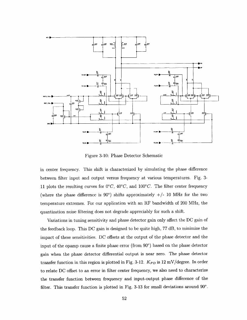
Figure 3-10: Phase Detector Schematic
in center frequency. This shift is characterized by simulating the phase difference
between filter input and output versus frequency at various temperatures. Fig. 3-
11 plots the resulting curves for O'C, 400C, and 1000C. The filter center frequency
(where the phase difference is 900) shifts approximately +/- 10 MHz for the two
temperature extremes. For our application with an RF bandwidth of 200 MHz, the
quantization noise filtering does not degrade appreciably for such a shift.
Variations in tuning sensitivity and phase detector gain only affect the DC gain of
the feedback loop. This DC gain is designed to be quite high, 77 dB, to minimize the
impact of these sensitivities. DC offsets at the output of the phase detector and the
input of the opamp cause a finite phase error (from 90') based on the phase detector
gain when the phase detector differential output is near zero. The phase detector
transfer function in this region is plotted in Fig. 3-12. KPD is 12 mV/degree. In order
to relate DC offset to an error in filter center frequency, we also need to characterize
the transfer function between frequency and input-output phase difference of the
filter. This transfer function is plotted in Fig. 3-13 for small deviations around 90'.

.·""~ri5~G
of-
i
tcr

-PD Output
-0.1
80 85 90 95Phase (degrees)
Figure 3-12: Phase Detector Transfer Function
Figure 3-13: Filter Input-Output Phase Difference
27

Table 3.3: Filter Performance with Resonator Mismatch
Capacitance Mismatch (fF) fo fgoo Atten. at +200/-200 MHz
0 5250 MHz 5250 MHz 6.3/7 dB
20 5220 MHz 5186 MHz 6/6.9 dB
40 5190 MHz 5126 MHz 5.4/6 dB
addition, the filter center frequency will no longer correspond to the condition of 90'
phase difference between input and output. Routing lines to the filter input and out-
put must be carefully extracted and equalized during the layout phase. The loading
on filter input and output must also be equalized. In this implementation, dummy
transistor loads are placed on the output nodes to match the cascode transistors from
the DRFC that load the filter input nodes. Table 3.3 summarizes simulation data for
capacitance mismatches of 20 fF and 40 fF. For a 40 fF mismatch, f o and fgoo differ
by 64 MHz which would be unacceptable.
The automatic tuning loop adjusts the resonator center frequency to always be
equal to the system LO frequency, 5.25 GHz in this case. However, it does not
account for variations in the coupling capacitor Cc, which can impact the filter transfer
function as well. When Cc is larger than the designed value, the coupling factor is
too high, resulting in a wider filter bandwidth. When Cc is smaller than the designed
value, the coupling factor is too small, resulting in a narrower filter bandwidth. Fig. 3-
14 plots the filter transfer functions for the nominal value of Cc and for +/- 15%
variation in Co. The variation in C, results in a 1.5 dB variation in insertion loss
and a +/- 8% variation in bandwidth. The filter needs to be designed to meet the
particular system specifications with this variation in mind. In our case, we choose
a slightly lower nominal value of Cc resulting in a nominal filter bandwidth of 240
MHz instead of the original 260 MHz. The narrower bandwidth does not appreciably
affect the amplitude response of our 200 MHz signal bandwidth, but does increase
the attenuation of out-band quantization noise.

Filter Response with Variation in Cc
MV
4.4 4.6 4.8 5 5.2 5.4 5.6 5.8 6 6.2Frequency (GHz)
Figure 3-14: Filter Response
3.3.2 Digital Tuning Loop
The automatic tuning loop can be slightly modified to implement an all-digital tuning
loop. This was not implemented, but will be discussed to show how a couple simple
changes can improve the tuning loop with respect to varactor non-linearity. In Fig. 3-
7, the op-amp can be replaced with a comparator, and the analog varactor can be
replaced with a bank of digitally switchable capacitors. The output of the compara-
tor can be applied to a digital state machine, which will increment or decrement the
number of capacitors being switched in, starting from a pre-determined initial con-
dition. When the comparator output bit switches polarity, the tuning loop is locked
and the digital state machine outputs are held constant. The advantage of the digital
tuning loop is that the resonator capacitance will remain fixed as a large signal is
applied to the filter. Thus, the distortion due to non-linear varactor capacitance will
be eliminated.
i•n,2n,ldin4kT2
4kT/R
Figure 3-15: Q-enhanced Resonator Model
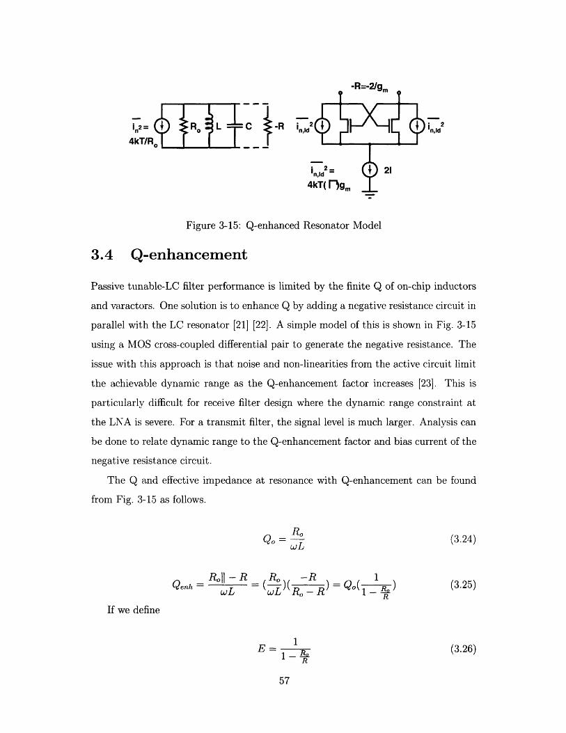
3.4 Q-enhancement
Passive tunable-LC filter performance is limited by the finite Q of on-chip inductors
and varactors. One solution is to enhance Q by adding a negative resistance circuit in
parallel with the LC resonator [21] [22]. A simple model of this is shown in Fig. 3-15
using a MOS cross-coupled differential pair to generate the negative resistance. The
issue with this approach is that noise and non-linearities from the active circuit limit
the achievable dynamic range as the Q-enhancement factor increases [23]. This is
particularly difficult for receive filter design where the dynamic range constraint at
the LNA is severe. For a transmit filter, the signal level is much larger. Analysis can
be done to relate dynamic range to the Q-enhancement factor and bias current of the
negative resistance circuit.
The Q and effective impedance at resonance with Q-enhancement can be found
from Fig. 3-15 as follows.
RoQo = L (3.24)
Roll - R R -R 1Qenh w ( o)( R = o( ) (3.25)wL wL & - R - R
If we define
E 1 = (3.26)R
-R

then
Renh = RoE (3.27)
Lowering R increases the Q-enhancement factor E. Since R = 2 for the cross-9m
coupled MOS pair, a larger E also implies larger gm which increases the noise power
spectral density of the MOS drain current noise sources. Thus, Q-enhancement in-
creases the noise power at the resonator nodes both through the increased Renh as
well as through an increase in gm.
The maximum linear signal swing at the resonator nodes with the negative resis-
tance circuit can be approximated as being proportional to the gate overdrive of the
MOS transistors V,1 - Vt. For short channel devices, the following equations hold
[24].
I = WVsatCox(Vgs - Vt) (3.28)
gm= WVsatCox (3.29)
I
(Vg - Vt) = (3.30)gm
Eqn. (3.30) indicates that an increase in gm must be accompanied by an increase
in current to maintain the same linear signal swing. Accordingly, the current in
the negative resistance circuit must increase as Q is enhanced to maintain constant
linearity.
Using Fig. 3-15, we can find a general expression for the approximate dynamic
range of the Q-enhanced LC filter.
MaxPowerDR = (3.31)
NoisePower
The maximum linear power at the resonator output is defined as
( v (Vg - V))2 2MaxPower 4 2Re 16g2 RE (3.32)
2R58 16gm2 oE
58
In Eqn. (3.32), a voltage swing that yields IM3 products that are < -60 dBc is
chosen as the maximum linear voltage swing. The value 1 4 (Vg, - Vt) is found from
simulations.
The noise power at the resonator output is equal to
NoisePower = in,Ro2RenhAf + n,Id2RenhAf (3.33)
4kTin,Ro2Renh =R RoE = 4kTE (3.34)Ro
2in,d 2 Renh = (2)4kTygmRoE (3.35)
NoisePower = 4kTE[1 + 2ygmRo]Af (3.36)
In eqn. (3.35) and eqn. (3.36), -7 represents the channel noise coefficient [25] that
is equal to 2/3 in long-channel devices. Measurements have shown that -, is higher
than 2/3 for short channel devices [26].
Substituting eqn. (3.32) and eqn. (3.36) into eqn. (3.31),
DR = Af (3.37)(16)4kTgm2RoE 2[1 + 2 gmRo]f (3.37)Using Eqn. (3.37), one can calculate the required current I vs. enhancement factor
E, given an initial Qo and a desired dynamic range. Table 3.4 lists the required I, gm,
and V,1 - I% for a cross-coupled pair negative resistance circuit assuming an initial
Qo of 20, a, noise bandwidth of 200 MHz, -y = 2, and a dynamic range requirement
of 60 dB. Also, a center frequency of 5.25 GHz and a. 2.2 nH differential inductance
in the resonator is assumed. According to Table 3.4, a Q-enhancement factor of
2 is achievable with a total current of 1.7 mA, yielding a resonator Q of 40. For
enhancement factors greater than 2, voltage headroom becomes an issue due to the
high required V,, - Vt to maintain a dynamic range > 60 dB. The corresponding
currents also become quite large given that each resonator requires its own negative
resistance circuit.
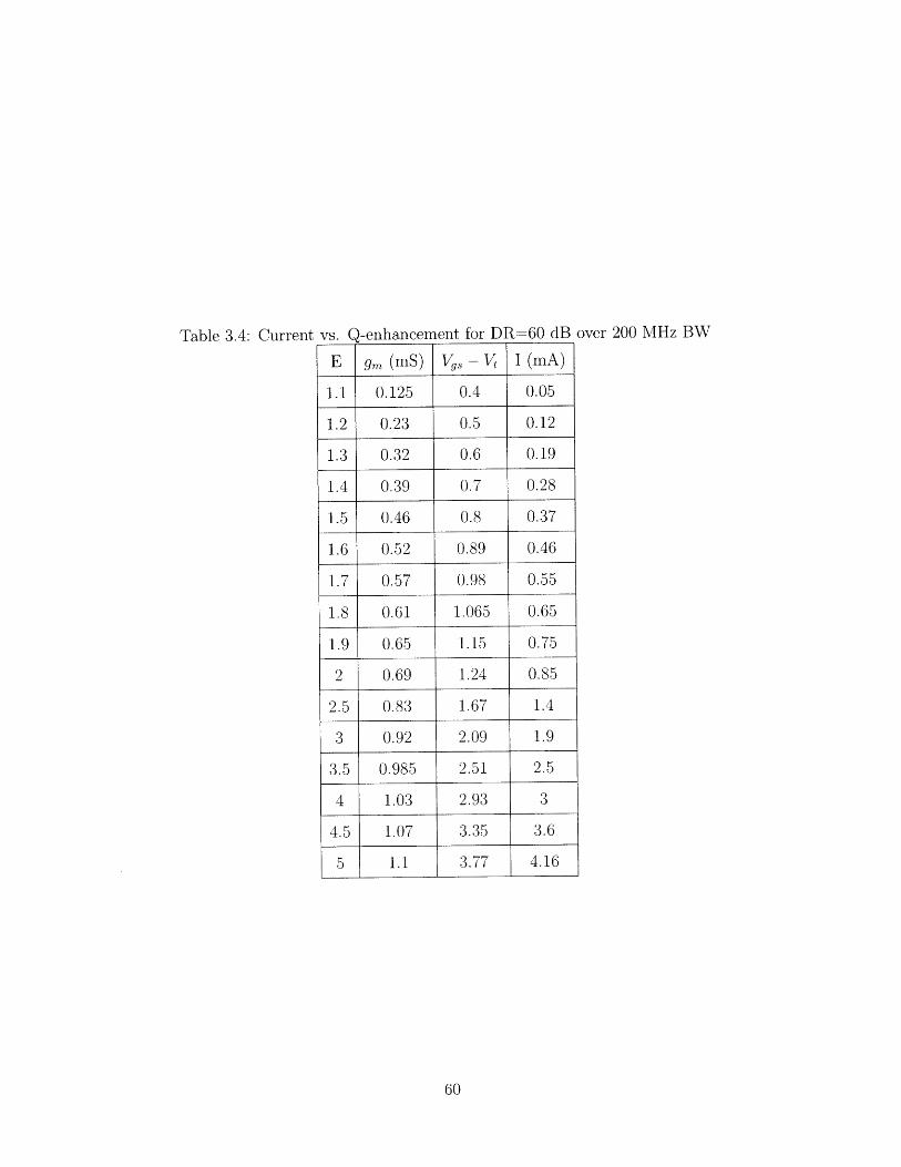
Table 3.4: Current vs. Q-enhancement for DR=60 dB over 200 MHz BW
E g (nmS) V, - Vt I(mA)
1.1 0.125 0.4 0.05
1.2 0.23 0.5 0.121.3 0.32 0.6 0.191.4 0.39 0.7 0.28
1.5 0.46 0.8 0.37
1.6 0.52 0.89 0.46
1.7 0.57 0.98 0.55
1.8 0.61 1.065 0.65
1.9 0.65 1.15 0.75
2 0.69 1.24 0.85
2.5 0.83 1.67 1.4
3 0.92 2.09 1.9
3.5 0.985 2.51 2.5
4 1.03 2.93 3
4.5 1.07 3.35 3.6
5 1.1 3.77 4.16

VCC
II
Figure 3-16: Simplified Test Filter Schematic
The negative resistance circuit based on a cross-coupled pair can be biased with
a constant-gm current [27], making the negative resistance fairly stable over process
and temperature. For moderate Q-enhancement factors, the Q-enhanced resonator
will not oscillate. By factoring the expected Q variation of the resonator into the
filter design, it is likely that no explicit Q-tuning loop will be required.
3.5 Test Filter Measurements
The performance of the filter and automatic tuning loop was verified using an on-
wafer probe test structure. Broadband on-chip buffers resistively matched to 50 ohms
were used at the input and output ports to interface to the filter. The test filter was
driven in current-mode, in the same way it would be used in the actual RF modulator
system. A simplified circuit schematic is shown in Fig. 3-16. A die photo of the test
filter is shown in Fig. 3-17. Two versions of the test filter were fabricated, one without
Q-enhancement and one with Q-enhancement.
Results from the test filter without Q-enhancement are shown in Fig. 3-18 and
Fig. 3-19. In Fig. 3-18, the tuning voltage to the varactors is manually adjusted and
the resulting filter responses are plotted. The filter tunes from 4.8 GHz to 5.4 GHz.
?UT

Figure 3-17: Test Filter Die Photo
The ideal response, assuming a resonator Q of 26, is plotted alongside the measured
response centered at 5.2 GHz. In Fig. 3-19, tuning curves are plotted both for manual
tuning and automatic tuning. In the case of automatic tuning, the input frequency
to the filter is varied and the resulting tune voltage is read out. The two curves track
fairly closely, but have an offset. Through parasitic RC extracted simulations, it was
found that this offset was due to a 20 fF difference in differential capacitance between
the two resonators (equivalent to 40 fF single-ended) as a result of unequal loading in
the layout. The resonator mismatch causes a shift between the filter center frequency
and the frequency at which the input-output phase difference is 900 of 60 MHz,
according to Table 3.3. This shift agrees well with the measurements.
In Fig. 3-18, the measured response at 5.2 GHz does not achieve the attenuation
of the ideal response. Two mechanisms account for the deviation. First, the resonator
mismatch degrades the filter attenuation by approximately 1 dB. Second, losses in the
varactor and routing cause a degradation in resonator Q. As a result, the measured -3
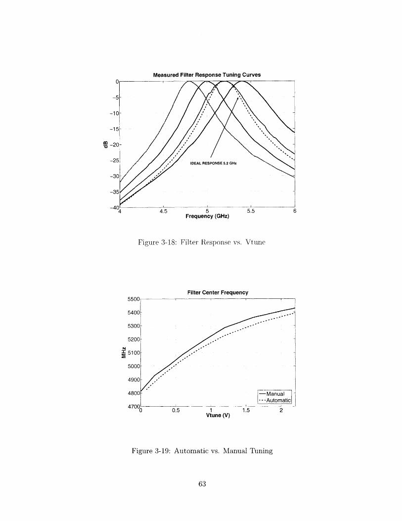
Measured Filter Response Tuning Curves
Frequency (GHz)
Figure 3-18: Filter Response vs. Vtune
Filter Center Frequency
Vtune (V)
Figure 3-19: Automatic vs. Manual Tuning
N-

Q-enhanced Filter Response
me0
Frequency (GHz)
Figure 3-20: Q-enhanced Filter Response Tuning Curves
dB filter bandwidth is 280 MHz, wider than the targeted 240 MHz bandwidth. The
measured response at 5.2 GHz correlates with a resonator Q of 16. In simulation,
resonator Q due to the inductors alone is 26. Resonator Q including the varactor loss
is 20. The remaining degradation in Q is attributed to metal losses in the layout.
Results from the test filter with Q-enhancement are shown .in Fig. 3-20 and Fig. 3-
21. A Q-enhancement factor of 1.8 was designed using 1.5 mA current in each cross-
coupled differential pair. The chosen enhancement factor was based on an initial Q
of 16. In this version, the resonator mismatch due to layout mismatches was fixed,
resulting in good agreement between the manual and automatic tuning curves as
shown in Fig. 3-21. Due to the absence of resonator mismatch and the enhanced
resonator Q of 29, the measured filter responses were much sharper than the version
without Q-enhancement as seen in Fig. 3-22. The Q-enhanced filter has a -3 dB
bandwidth of 210 MHz and approximately 14 dB attenuation at +/- 300 MHz offsets.
Measured and simulated filter response at 5.2 GHz is plotted in Fig. 3-23, showing
good agreement.

Filter Center Frequency vs. Vtune
5Vtune (V)
Figure 3-21: Automatic vs. Manual Tuning, Q-enhanced version
Measured Filter Response at 5.2 GHz
Figure 3-22: Measured Filter with and without Q-enhancement

Q-enhanced Filter Response at 5.2 GHz
mVr
4 4.5 5 5.5 bFrequency (GHz) x 109
Figure 3-23: Q-enhanced Filter : Measured vs. Simulated
3.6 Summary
The design of a 5.25 GHz 4th order high-Q LC BPF using differential coupled res-
onators has been presented. A self-tuning loop automatically calibrates the filter
response to be centered at the desired LO frequency of 5.25 GHz. An equation relat-
ing the IM3 due to the non-linear varactor capacitance of the tunable filter has been
derived. Q-enhancement is effective in maintaining a high resonator Q after account-
ing for losses in the varactor and layout. An equation relating the dynamic range of
the filter vs. the Q-enhancement factor and bias current of the negative resistance
circuit is derived. A passive LC filter and a Q-enhanced LC filter achieve measured
3 dB bandwidths of 280 MHz and 210 MHz respectively. Resonator mismatch due to
parasitic capacitances causes an error in the automatic tuning loop as well as a degra-
dation in the filter's stopband attenuation. Careful layout with respect to extraction
of parasitics and minimizing metal losses is essential to optimizing filter performance.
The successful design of the filter enables a practical integrated realization of a AE
digital-RF modulator for wideband applications.

Chapter 4
AE System Architecture
In designing the AE RF modulator, the oversampling clock frequency and AE NTF
must be carefully chosen to maximize the in-band SNR, minimize out-of-band spu-
rious signals, and prevent aliasing of clock images and quantization noise. These
choices are dependent upon the system LO frequency, system bandwidth, as well as
the achievable RF bandpass filtering.
4.1 Choosing Clock Frequency
The IQ digital-RF converter circuit was shown in Fig. 2-5. An equivalent functional
block diagram is shown in Fig. 4-1. The I and Q AE modulator outputs contain the
digital signal plus quantization noise that is shaped outside the signal band, reaching
AL Digital-RF Modulator.......................
QDRFC
Figure 4-1: AE Digital-RF Modulator

I' -
I 1 ·\I I II
-3fclk/2 -fclk -fclk/2 0 fclk/2 fclk 3fclk/2
Figure 4-2: AE Modulator Output Spectrum
a maximum at f-k. The frequency spectrum repeats itself at multiples of flk as
shown in Fig. 4-2. Clock images associated with the signal occur at
(n * fclk) fsig, n = ... - 3, - 2 , -1, 1, 2, 3 ,... (4.1)
The DRFC performs multiplication of the sampled and held AE modulator output
and the RF carrier signal. In the frequency domain, this corresponds to a convolution
of the frequency spectra of the respective signals, as depicted in Fig. 4-3 for DC
inputs. In digital-RF conversion, the consequence of up-converting the quantization
noise before filtering is that potential aliasing of quantization noise and sampling clock
images can occur. Quantization noise and clock images from the convolution with
-fLO spill into the positive frequency spectrum and can corrupt the signal spectrum
centered at fLO. Likewise, noise and images from the convolution with fLO spills into
the negative frequency spectrum. The only filtering that occurs before the convolution
is the sinc response associated with the zero-order-hold in the digital-RF interface.
Two problems result:
1. Aliased quantization noise can degrade the in-band SNR of the signal.
2. Aliased clock images will appear as an image signal in the RF passband, de-
grading the achievable image rejection of the transmitter.
In order to prevent the first problem, the following condition must be met between
fclk and fLo,n * fclk
fLO = , n = 1, 2,3,... (4.2)2
Now, only quantization noise notches will alias into the RF passband, having neg-
ligible impact on in-band SNR. This scenario is depicted in Fig. 4-4 with n = 4 in
1 ~11 d

DATA (f) LO (f)
-fCLK 0 fCLK -fLo 0 fLO
-fLO 0 fLo
Figure 4-3: Aliasing Problem in Up-Conversion
eqn. (4.2).
Although the digital-RF converter circuit is a double-balanced structure, device
mismatches in the lower differential pair can cause leakage from the digital input port
to the output. Referring to Fig. 4-2, it can be seen that large amounts of quantization
noise in the digital input signal appear at odd multiples of f. This noise can leak to
the output and corrupt the signal spectrum when fLo is chosen to be an odd multiple
of fk . In order to prevent this, Eqn. (4.2) should be modified to
fLo = n *fclk, n = 1,2,3,... (4.3)
Given a system LO frequency, the clock frequency is then chosen as
fLofclk - n=1,2,3,... (4.4)
There is still the issue of clock images aliasing into the RF passband. The quadra-
ture DRFC is ideally a single-sideband upconverter. However, the clock images from
the negative frequency spectrum will appear in the RF passband of the positive fre-
quency spectrum as another sideband, and vice-versa. As a result, the converter will
have finite image rejection.
The clock images and quantization noise of the digital signal are filtered by the
zero-order-hold transfer function H(f).

DATA (f) LO (f)
-fCLK 0 fCL, -fL to
-fLO 6 f
Figure 4-4: No Aliasing with fLO = 2fclk
H(f) = e- j fT s i n c ( (4.5)fclk
The normalized magnitude of H(f) is plotted in Fig. 4-5 with fclk = 2.5 GHz.
The sinc function has nulls at integer multiples of the clock frequency. For a large
over-sampling ratio (OSR), the signal frequency f is small relative to fclk. The clock
images lie near the nulls and are heavily attenuated. As the OSR becomes smaller,
the clock images are located farther away from the nulls and undergo less attenuation.
For larger n in eqn. (4.2), the RF passbands in the positive and negative frequency
spectrum are farther away from each other. Since the sinc function slowly rolls off
as f increases, larger n results in more filtering of the aliasing clock images. Fig. 4-6
plots the level of the maximum in-band aliased clock image with respect to the desired
sideband for n = 1, 2, 3. For n = 2, the image is < -40 dBc when the OSR is > 12.
In order to maximize the image rejection, a high OSR and large n should be used.
The finite image rejection, however, is correctable. Since the signal is known
and the sinc transfer function is known, the magnitude and phase of the aliasing
clock images are known as well. This image signal is not caused by random gain
or phase variations but rather by the signal processing of our architecture itself. We
can purposely construct a signal in our system with the same magnitude but opposite
phase of the image signal to cancel it. Because the image signal is small, the increased

IH(f)12 : Ideal Zero Order Hold
Frequency (GHz)
Figure 4-5: Normalized Magnitude of Zero-Order Hold Frequency Response
In-Band Clock Image vs. OSR
OSR
Figure 4-6: Image Rejection vs. OSR

dynamic range necessary to accomodate the cancellation signal is minimal. Since the
I and Q input signals are digital, this solution is a form of digital pre-distortion and
involves no analog design.
4.2 Co-Design of AE NTF and RF BPF
The noise-shaping transfer function of a AE modulator depends on its oversampling
ratio (OSR). In a AE RF modulator, an upper bound on OSR can be related to the
Q of the RF BPF.
The Q of the bandpass filter elements is limited by Qind and related to the system
center frequency, fo, and RF bandwidth, BW, through
Qind > AO = fLO < Qind * BW (4.6)BW
Meanwhile, the OSR is related to the oversampling clock frequency, fclk, and RF
bandwidth, BW, through
fclk = OSR * BW. (4.7)
Expressing fdlk in terms of fLO in eqn. (4.7) using eqn. (4.4), and then substituting
into eqn. (4.6), we can find a relation between OSR and Qind.
OSR < , n = 1, 2,3,... (4.8)n
In eqn. (4.8), n is the ratio between fLo and fclk. The upper bound on OSR
limits the modulator SNR for a given NTF, quantizer resolution, and clock frequency.
Intuitively, the inductor Q limits how narrow a bandwidth can be filtered at high RF
frequencies. A narrower bandwidth allows the OSR to be higher for a given clock
frequency, increasing the achievable in-band SNR. Conversely, a wider bandwidth is
easier to filter at RF frequencies but results in a lower OSR.
The OSR is constrained to be low by eqn. (4.8) and the need to avoid an exces-
sively high clock frequency. Using n larger than 1 in eqn. (4.8) reduces the OSR but
also reduces the clock frequency. This tradeoff may be worthwhile when the clock

SNR vs. Loop Filter Order'U
80
70
60
50
40
30
On2 3 4
Order of Loop Filter
Figure 4-7: SNR (dB) vs. Loop Filter Order for various OSR
frequency pushes the performance limits of the technology. Qind in current technolo-
gies ranges from 10-25, depending on the top level metal's resistance and distance to
the substrate.
Given the low OSR, the AE modulator must be designed to meet the in-band
SNR and out-of-band noise specifications of the system. The out-of-band noise at the
output of the RF modulator is also a function of the RF bandpass filter characteristics
and links the modulator design and RF filter design together.
A 2nd order, 1-bit modulator is an ideal modulator choice due to its inherent
linearity and stability. For low OSR in the range of 10-16, a 2nd order, 1-bit modulator
is limited to an SNR of around 40 dB [28]. It has been shown that the effectiveness of
increasing the order of noise shaping is significantly diminished as the over-sampling
ratio is reduced [29]. In addition, higher order single-bit modulators require the use
of poles in their NTF to maintain stability, which limits the SNR. The location of the
zeros must be optimized to recover some of the loss in SNR [28].
Fig. 4-7 plots the optimized SNR vs. order for 1-bit modulators at various OSR.
In general, the improvement of SNR with higher order decreases as the order is
- -- OSR=8-OSR=16
OSR=32
:c_ _, , , .....- ---------.
I-

m
3.b 4 4.5 b 5.5b 6.5 7Frequency (GHz)
Figure 4-8: RF Output Spectrum using 3rd order, 1-bit AE Modulator
increased. For low OSR, the effect is more dramatic and very little gain in SNR is
achieved for higher order. The use of cascaded lower order modulators in a MASH
topology [30] can alleviate the stability issue and provide higher SNR, but entails
stringent matching requirements between the outputs of the cascaded stages.
The use of a high order 1-bit modulator also significantly increases the amount
of out-of-band quantization noise that must be filtered at RF. Higher order noise
shaping increases the slope at which the out-of-band quantization noise rises, and a
single-bit quantizer increases the magnitude of the quantization noise in comparison
to a multi-bit quantizer.
Fig. 4-8 and Fig. 4-9 plot the output spectrum of a AE RF modulator using a
3rd order, 1-bit modulator and a 2nd order, 3-bit modulator respectively, before and
after filtering with a 4th order Bessel RF BPF with 260 MHz bandwidth. The RF
output is centered at 5.25 GHz with a signal bandwidth of 200 MHz. The OSR of the
modulators is ~ 13 with a clock frequency of 2.625 GS/s. In this simulation, the 3rd
order, 1-bit modulator uses a 1-2 MASH topology and has 50 dB SNR in the 200 MHz
signal bandwidth. This modulator exhibits very high out-of-band quantization noise.

Filter Requirements
Ve
3.b 4 4.5 5 5.5 6 6.5 IFrequency (GHz)
Figure 4-9: RF Output Spectrum using 2nd order, 3-bit AE Modulator
In contrast, the 2nd order, 3-bit modulator has 52 dB in-band SNR and much lower
out-of-band quantization noise, allowing it to pass the spurious emission requirements
outside the 5.15-5.35 GHz UN-II band.
The spurious emission limits shown in Fig. 4-9 are derived from requirements
specified by the FCC for operation in the UN-II band [31]. Accordingly, spurious
emissions must be below -27 dBm/MHz outside the 5.15-5.35 GHz UN-II band. The
limits drawn assume a maximum power of +20 dBm and a PAPR of 16 dB for the final
transmit signal out the antenna. The spectral density (dBm/MHz) of the spurious
emissions must be 47 dB below the RF output signal power. 16 dB is added to
account for the PAPR, giving 63 dB. In Fig. 4-9, the output signal is a pure sine
wave with PAPR of 3 dB and its power is normalized to 0 dB. It then follows that
the spurious emissions limits are -60 dBc/MHz.
Fig. 4-8 and Fig. 4-9 highlight the importance of co-designing the AE modulator
and RF BPF together at the system level. Since the RF BPF has the most difficult
specifications, the choice of a lower order, multi-bit AE modulator alleviates the RF
filtering requirements and enables full integration of the direct RF modulator. This

Table 4.1: Simulated AE SNR with OSR=13
Loop Filter Quantizer SNR Matching RF Filtering
Order Bits Requirements (a) Requirements
2nd 1 37 dB None Difficult
4th 1 47 dB None Very Difficult
3 rd (1-2 MASH) 1 50 dB - 0.5 % Very Difficult
2 nd 3 52 dB , 1 % Moderate
choice also means that attention must be paid to mismatches between the digital-RF
converter unit cells, which can introduce distortion and degrade the dynamic range.
The matching requirements and design issues of a multi-bit digital-RF interface will
be discussed further in Chapter 7.
For our OFDM system with center frequency 5.25 GHz and RF bandwidth of 200
MHz, n is chosen to be 2 in eqn. (4.4) so that fclk = 2.625 GS/s and OSR - 13.
Choosing n = 1 would allow a higher OSR but result in folk = 5.25 GS/s, which may
not be practical in current technology. Table 4.1 lists several AE topologies and their
simulated SNR with OSR = 13. The 1-bit topologies all use optimized zero locations
[32]. Matching requirements to maintain the SNR of the AE modulator are based
on Monte Carlo simulations in MATLAB using random mismatches with variance
a between unit elements. The results show that the 2nd order, 3-bit modulator
maximizes the in-band SNR and also relaxes the RF filtering requirements.
4.3 Comparison to Oversampling with No Noise-
Shaping
An alternative to the AE modulator approach is to drive the quadrature DRFC with
oversampled digital data with no noise shaping. This method increases the power
and area of the DRFC since a large number of unit cells will be required to interface
to the full bit width of the digital I,Q data (- 9-10 bits). The larger area also makes
it harder to match the timing of the clock and data signals over all the unit cells in

Table 4.2: Clock Image Attenuation vs. Clock Frequency for 200 MHz RF BW
fclk Frequency Offset of Sinc RF BPF Total
Closet Clock Image Atten. (dB) Atten. (dB) Atten. (dB)
625 MHz 525 MHz 15 19 34
1.25 GHz 1.15 GHz 21 30 51
2.5 GHz 2.4 GHz 28 40 68
the layout.
With no noise-shaping, the RF filtering in the DRFC must attenuate the clock
images of the up-converted digital spectrum rather than shaped quantization noise.
Again, increasing the clock frequency pushes the clock images farther away from the
main signal and relaxes the filtering requirements. However, this also increases the
power consumption and timing requirements of the digital-RF interface. It is useful
to find the clock frequency that results in all clock images < -50 dBc, assuming the
same RF BPF and bandwidth used in the AE design. Table 4.2 lists the attenuation
of the closest clock image for various flk from both the sinc filtering and the RF
bandpass filtering.
In order to suppress the clock images by 50 dB, a minimum clock frequency of
1.25 GHz is required. The difference with the AE modulator approach is that the
quadrature DRFC will have more unit cells but can be clocked at approximately half
the speed. When using thermometer decoding, a much larger decoder running at half
the clock speed will have to be designed compared to the AE case.
4.4 UWB System Example
UWB is an emerging short-range, high data rate system. The proposed channel
bandwidth for UWB is 528 MHz, with channels occupying frequencies between 3.1
and 10.6 GHz [33]. Each channel uses 128 OFDM sub-carriers and the targeted EVM
is -20 dB [33]. Assuming a PAPR of - 15 dB, an SNR of 35 dB is required.
A AE digital-RF modulator with 500 MHz bandwidth can be used to provide the
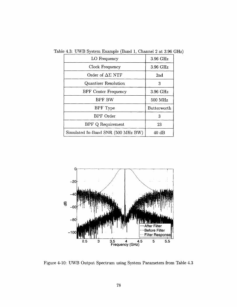
Table 4.3: UWB System Example (Band 1, Channel 2 at 3.96 GHz)
LO Frequency 3.96 GHz
Clock Frequency 3.96 GHz
Order of AE NTF 2nd
Quantizer Resolution 3
BPF Center Frequency 3.96 GHz
BPF BW 500 MHz
BPF Type Butterworth
BPF Order 3
BPF Q Requirement 23
Simulated In-Band SNR (500 MHz BW) 40 dB
-After Filter---Before Filter....... Filter Response
2.5 3 3.5 4 4.5 5 5.5Frequency (GHz)
Figure 4-10: UWB Output Spectrum using System Parameters from Table 4.3

targeted SNR of 35 dB. As an example, Table 4.3 summarizes the system parame-
ters for transmitting a UWB channel centered at 3.96 GHz. The simulated output
spectrum is plotted in Fig. 4-10. The simulated SNR over the 500 MHz channel
bandwidth was 40 dB.
4.5 Summary
In AE digital-RF modulation, the LO frequency should be an integer multiple of
the AE clock frequency to avoid aliasing of quantization noise into the signal pass-
band after RF up-conversion. Image signals appearing in the RF passband can be
eliminated through digital pre-distortion.
It is found that the OSR of the AE modulator is limited to be less than the Q of the
RF BPF. Minimizing the out-of-band quantization noise of the AE modulator helps
relax the difficult RF filtering requirements. A low order multi-bit AE modulator is
effective in achieving a high in-band SNR at low OSR, while also minimizing out-of-
band quantization noise. A 2nd order, 3-bit AE modulator is designed with a clock
frequency of 2.5 GHz. The modulator achieves greater than 50 dB SQNR in a 200
MHz bandwidth.


Chapter 5
Quadrature Digital-IF AE
Modulator
5.1 Digital-IF
The AE RF modulator, as shown in Fig. 4-1, is a direct conversion transmitter. LO
feedthrough due to offset voltages in the current-steering switches or coupling from
the LO circuits will appear at the center of the RF output spectrum. Although the
digital I,Q baseband signals will be in perfect quadrature, image rejection will be
limited by the gain and phase matching of the 5.25 GHz quadrature LO signals. The
accuracy is dependent upon device mismatches and careful matching of the layout. In
order to ensure adequate image rejection over process and temperature, a calibration
scheme is often used to correct for the I,Q imbalances.
An indirect conversion transmitter first translates the baseband spectrum to an
IF frequency before subsequent up-conversion to the RF output frequency. The LO
frequency used in the final up-conversion is no longer located at the center of the
RF output spectrum. Finite image rejection in the RF up-converter results in an
image signal that is separated from the RF output frequency by 2 x the IF frequency
and does not degrade the output signal's EVM. However, although the baseband-IF
modulator is at a lower frequency and easier to design, it will itself still have finite LO
and image suppresion appearing in the passband of the IF signal. The baseband-IF

I
Q
DIGITAL LO
Figure 5-1: Digital-IF AE RF Modulator
modulator also adds analog design complexity, power consumption, and area to the
transmitter design.
A solution is to implement the baseband-IF modulator in the digital domain.
A quadrature digital mixer that up-converts the digital baseband signal to an IF
frequency will have infinite image rejection and LO suppression. When the digital-IF
signal is applied to the digital-RF converter, the LO feedthrough and image will be
separated from the RF output by fIF and 2 x fIF respectively. If the IF frequency
is chosen high enough, both signals will be additionally filtered by the RF BPF. The
advantages of an indirect conversion transmitter are enabled without the drawbacks
of implementing an analog IF modulator.
Fig. 5-1 shows a block diagram of a digital-IF AE RF modulator. Note that
quadrature phases of the LO frequency are not required and the quadrature DRFC
is replaced by a single DRFC.
5.2 Quadrature Digital-IF
We have seen how the AE RF modulator architecture is more amenable to wide-
band systems due to the inherent difficulties of narrowband RF filtering. The wide
bandwidths processed by the AE digital modulators require a high clock frequency.
Digital multipliers operating at GS/s clock frequencies result in high power consump-
tion. They also require bit precisions equivalent to the dynamic range of the system.
This is a drawback since the 3-bit digital output words from the AE modulators
---------------------------------'~~

would turn back into > 10-bit wide words at the output of the digital mixers. The
digital-RF interface of the DRFC would then be 10-bits wide and consume more
power and area as well.
By choosing the IF frequency to be cik, one can implement a multiplier-free
quadrature modulation and eliminate the power consumption of the high speed digital
mixer [34]. Quadrature digital sines and cosines at 41k only have values of 1, -1, or 0.
sin( 2 nfifF) = sin( 7) = 0, 1, 0, 1,... (5.1)fclk 2
cos( nfIF) = cos( ) = 1,0,-1, 0,... (5.2)fclk 2
Because one of the quadrature digital sine-waves is always 0 when the other is non-
zero, the IF mixer output is alternately equal to +/- I or +/- Q. Digital quadrature
modulation at fck can be implemented using only multiplexors and inverters.
There is an aliasing issue when implementing digital quadrature modulation at fclk4
with a AE modulator. The digital output of the AE modulator is not band-limited
and has a large amount of high frequency quantization noise at Lf=&. Quadrature up-
conversion to 4/ means that one copy of the digital spectrum is placed at -- and
another at + fc as shown in Fig. 5-2. Large amounts of quantization noise originating
from the spectrum centered at - fc will alias into the signal centered at + f,, and
vice-versa, corrupting the SNR of the digital-IF signal.
In order to eliminate this aliasing, the digital spectrum centered at - fc must
not be up-converted. This can be accomplished through a complex mixing operation
using quadrature phases of both the digital-IF and LO signals. The quadrature
digital-IF is implemented using two sets of quadrature IF up-converters in the digital
domain. The complex mixing is completed in the quadrature DRFC block where the
aliasing spectrum rejection is limited by the quadrature accuracy of the LO signals.
The complete system is shown in Fig. 5-3, where the LO frequency is now equal to
fRF ± fIF-
A quadrature digital-IF DRFC will produce an output spectrum that does not
have any in-band LO or image signals. Since fIF = , the digital-IF frequency
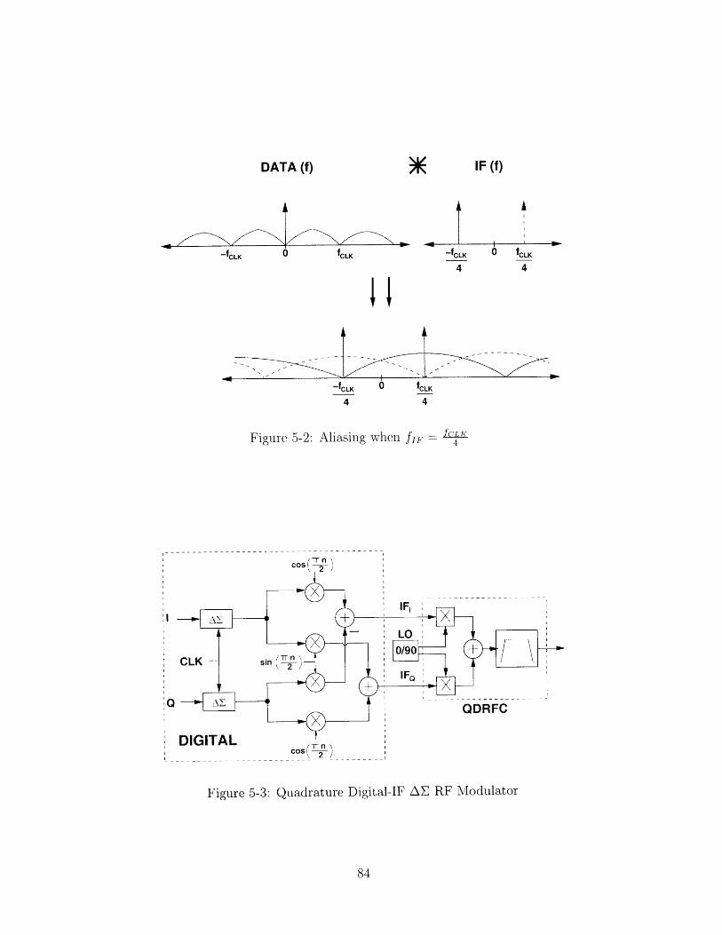
DATA (f)
-fCLK 0 fCLK
IF (f)
-fCLK 0 fCLK
4 4
Figure 5-2: Aliasing when fIF =fCLK
C os, ncos
Q
SI .Jl | I AI -cos (TV,-) I
Figure 5-3: Quadrature Digital-IF AE RF Modulator
m
-•LM C·LR

SNR due to Phase Error with Digital-IF
m"O
Phase Error (degrees)
Figure 5-4: SNR vs. LO Phase Error for Quadrature Digital-IF
in the wideband modulator is fairly high and - 650 MHz for our system. The LO
and image signals are thus far away from the desired output and will be strongly
attenuated by the RF BPF at the output of the DRFC.
Finite gain and phase matching of the LO signals causes out-of-band quantization
noise from the digital-IF rejected sideband to leak into the RF passband and degrade
SNR. Increasing the number of bits in the quantizer of the AE modulator will reduce
the level of out-of-band quantization noise and reduce the sensitivity of SNR to noise
aliasing. Simulations of the system in Fig. 5-3 are run in MATLAB to benchmark
the degradation in SNR due to quadrature LO phase inaccuracies when using a 2nd
order, 3-bit AE modulator. The results are plotted in Fig. 5-4. The SNR remains
above 50 dB for LO phase errors less than 1.20. The equivalent image rejection for a
direct quadrature modulator with the same LO phase error is 40 dB.
Similar to the conventional direct up-conversion DRFC, clock images originating
from the digital-IF spectrum centered at -fLo can alias into the passband of the
positive frequency spectrum and vice-versa. In the digital-IF case, the clock images
are not filtered as much by the zero-order-hold of the digital-RF interface since they

f IF = (1/4)fCLK
DIGITAL CLK LO
Figure 5-5: Digital-IF Bandpass AE Modulator
are now located at frequencies fIF away from the nulls of the sinc function. Because
the sinc function rolls off slowly, the filtering is moderate and digital pre-distortion
is required to reduce the clock images to acceptable levels. Again, since the clock
image is known and due to the signal processing of the architecture itself, it can reli-
ably be cancelled with digital pre-distortion independent of process and temperature
variations.
One key benefit arising from embedding the baseband-IF translation in the digital
domain is that the transmitter can be easily switched from a digital-IF architecture
back to a direct conversion architecture. The two architectures can be digitally se-
lectable by either passing the AE modulator outputs through the digital-IF quadra-
ture modulation stage, or bypassing the stage and using the AE outputs directly.
Because the IF frequency is at f-k, the digital-IF outputs remain 3 bits wide.
5.2.1 Bandpass AE
Another approach is to implement the digital-IF up-converter first, and then apply the
IF signal to a bandpass AE modulator centered at L. The bandpass AE architecture
is shown in Fig. 5-5. The advantage of this approach is that because digital-IF up-
conversion is performed before AE modulation, aliasing of AE noise is avoided and
quadrature digital-IF outputs are not required. Bandpass AE modulation could have
been used, but was not chosen in this work because the digital implementation of a
bandpass AE modulator is more complex than a lowpass AE modulator. For a N-

order NTF. the required order of the bandpass modulator is 2N compared to N for a
lowpass modulator. Due to the stringent timing requirements in the digital circuits of
the modulator (which will be discussed in Chapter 6), the lowpass AE approach was
chosen to minimize digital circuit complexity and power, and ensure first-pass silicon
success. For future work, bandpass AE modulation is an attractive architecture to
explore especially as technology scales.
5.3 Frequency Planning
The following equations relate the IF, clock, and LO frequencies given a desired RF
output frequency.
fI =ck (5.3)4
fLo = fRF ± fIF = fRF ± f-• (5.4)
In order to avoid aliasing in the digital-RF conversion process, fRF should be an
integer multiple of folk. If fRF = 2 * fclk = 5.25GHz, then
2.625GHzfLO = 5.25GHz + = 5.90625GHz/4.59375GHz (5.5)4
The required fLO and fclk can be generated using a single PLL with output fre-
quency at 5.25 GHz. The PLL output can be divided by 2 to generate fclk at 2.625
GHz. This signal can be further divided by 4 and single-sideband mixed with the orig-
inal PLL output at 5.25 GHz to generate fLO at either the upper or lower sideband.
A block diagram of this frequency generation scheme is shown in Fig. 5-6.
One of the drawbacks of this frequency plan is the presence of spurious energy at
5.25 GHz. Parasitic coupling from the VCO, PLL, and LO circuits to the RF output
can cause undesired LO leakage at 5.25 GHz. The high speed digital circuits clocking
at 2.625 GHz can also contribute via the 2nd harmonic of the rail-to-rail clock signal.
In order to prevent the spur at 5.25 GHz, the PLL output frequency should be
equal to the LO frequency rather than the RF output frequency. Then, any coupling

Figure 5-6: Single PLL LO Generation for Digital-IF Architecture
from the VCO and PLL will only cause a tone at fRF ± fIF. In addition, the clock
frequency for the AE modulator should be offset from LRE while minimizing degra-
dation of SNR due to aliasing. For example, the choice of fclk = 2.4 GHz sets fIF =
600 MHz and fLo = 5.85 GHz. In this approach, two PLLs would be required with
output frequencies of 5.85 GHz and 2.4 GHz, respectively. Spurious tones may exist
at 5.85 GHz, 2.4 GHz, and 4.8 GHz, but will all be far away from the RF passband
centered at 5.25 GHz. Since fLo is no longer an integer multiple of fclk, violating
the condition set forth in eqn. (4.2), quantization noise will alias from the digital-IF
spectrum centered at -fLO into the RF passband in the positive frequency spectrum
and vice versa. The amount of aliasing depends on the magnitude of the quantization
noise appearing at ± 5.25 GHz, and the level of filtering provided by the frequency re-
sponse of the zero order hold. Assuming an ideal zero order hold, a system simulation
of Fig. 5-3 with fLo = 5.85 GHz and fclk = 2.4 GHz shows that the aliasing causes
a degraded SNR of 38 dB compared to the ideal value of 55 dB when fdlk = 2
This appears to prevent the digital-IF architecture with no spurious energy at
fRF from being feasible. In an actual circuit implementation, however, the zero order
hold in the digital-RF interface is not ideal due to finite rise and fall times of the
clock signal. The rectangular pulse impulse response of the zero order hold assumes
infinitely fast clock edges. When considering the actual rise and fall times of the clock
signal, the impulse response looks like a trapezoidal pulse. The two impulse responses
are compared in Fig. 5-7.

1
0.8
0.6
0.4
0.2
03
Zero Order Hold
-trt -0
-3,O 0 200 400 600 800Time (ps)
Figure 5-7: Zero Order Hold Impulse Response
The frequency response of the trapezoidal pulse with sampling period T and
rise/fall time T is derived as
1 1Htrap(f) (f)2 [sin(rfT)si(in(fT)] = sinc(fT) sinc(fT) (5.6)
Htrap(f) equals the multiplication of two sinc functions. The first sinc function has
nulls at multiples of fclk similar to the ideal zero order hold. The second sinc function
has nulls at multiples of I and adds additional attenuation at higher frequencies. The
difference in filtering is shown in Fig. 5-8, which compares the frequency responses
of the rectangular pulse with infinite rise/fall times and the trapezoidal pulse with
rise/fall time of 75 ps.
In the quadrature digital-IF architecture, we are interested in the attenuation
provided at around ± 11 GHz since -fRF and fRF are separated by 10.5 GHz.
According to Fig. 5-8, the realistic trapezoidal impulse response provides > 15 dB
additional attenuation in the frequency range of interest. As a result, the simulated
SNR that was limited to 38 dB by aliased quantization noise can be expected to
improve by > 15 dB to 53 dB.
II II :
I .· I - - ·,I II II III
.I
IIIIr-II
-- r,rf = sDPSi-.-..
I
t
I • t
I

IH(f)I2 : Zero Order Hold
Frequency (GHz)
Figure 5-8: Frequency Response of Zero Order Hold
With this in mind, it is expected that in practice, fclk can be offset from IRf
in the quadrature digital-IF AE modulator without substantial degradation in SNR.
By doing so, we can eliminate spurious energy at fRF from the RF modulator out-
put spectrum. The architecture then approaches the performance of an ideal trans-
mitter where the RF output spectrum contains only the desired signal with no LO
feedthrough and no image signal.
With this frequency scheme, two PLLs are required to generate fLo and fclk. The
2nd PLL can be eliminated by utilizing dividers and a mixer to generate fclk from
fLO through the following equation.
fLo fLOfclk = f L + (5.7)
2 DIVIDE
In addition, fLO is related to fRF and fclk through eqn. (5.4). DIVIDE is a
design variable that needs to be chosen.
Table 5.1 lists the resulting LO, clock, and IF frequencies for two different divide
values and fLO < fRF-
The divide value of 8 is preferable because both fLo and 2 * fclk are farther away

Table 5.1: LO, Clock, and IF frequencies for DIVIDE = 8 or 16
DIVIDE fLO fclk fIF
8 4.54 GHz 2.84 GHz 709 MHz
16 4.603 GHz 2.589 GHz 647 MHz
LO I
fCLK
84 GHz
Figure 5-9: Single PLL LO and CLK generation avoiding spurs at 5.25 GHz
from the RF passband centered at 5.25 GHz. It requires a higher clock frequency
but also provides a higher OSR. With this choice, the IF frequency is 709 MHz and
fclk is 2.84 GHz. An LO frequency of 4.54 GHz will result in the digital-IF signal
being converted to the final RF output frequency at 5.25 GHz. The block diagram
implementing this choice of fLO and fCLK for DIVIDE = 8 is shown in Fig. 5-9.
5.4 Summary
A quadrature AE digital-IF topology eliminates in-band LO feedthrough and image
spurs, and allows an IF frequency of flk to be chosen without causing aliasing of
quantization noise. This choice of IF greatly simplifies the digital implementation.
The transmitter can be digitally selectable between direct modulation and indirect IF
modulation. The IF architecture requires a non-integer relationship between fLo and
fclk. The influence of finite switching time on the frequency response of a zero-order
hold is analyzed, and the results explains why the non-integer relationship does not
cause a substantial degradation in SNR performance. Methods to derive the necessary
LO and clock frequencies from a single PLL are given.

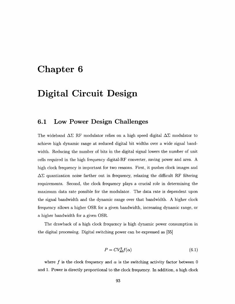
Chapter 6
Digital Circuit Design
6.1 Low Power Design Challenges
The wideband An RF modulator relies on a high speed digital AE modulator to
achieve high dynamic range at reduced digital bit widths over a wide signal band-
width. Reducing the number of bits in the digital signal lowers the number of unit
cells required in the high frequency digital-RF converter, saving power and area. A
high clock frequency is important for two reasons. First, it pushes clock images and
AE quantization noise farther out in frequency, relaxing the difficult RF filtering
requirements. Second, the clock frequency plays a crucial role in determining the
maximum data rate possible for the modulator. The data rate is dependent upon
the signal bandwidth and the dynamic range over that bandwidth. A higher clock
frequency allows a higher OSR for a given bandwidth, increasing dynamic range, or
a higher bandwidth for a, given OSR.
The drawback of a high clock frequency is high dynamic power consumption in
the digital processing. Digital switching power can be expressed as [35]
P = CVd f (a) (6.1)
where f is the clock frequency and a is the switching activity factor between 0
and 1. Power is directly proportional to the clock frequency. In addition, a high clock

SFO:21 Sr3:51 Si6:81 Si9:111
Figure 6-1: Pipeline of (4) 3-bit Ripple Carry Adders
frequency imposes stringent timing constraints on the digital circuits, which results in
higher power consumption due to the tradeoff between energy and delay. Optimizing
the digital circuit power consumption at a high clock frequency is important to justify
replacing the analog circuits in conventional IQ modulators.
6.1.1 General Techniques
Digital circuits operating at high sample rates are typically pipelined. If a complex
logic function cannot be computed in a single clock period, the logic can be divided
into pipelined stages driving flip-flops that store stage outputs and pass them forward
for processing during the next clock period. Pipelining trades off timing constraints
for latency. For many applications, latency of the data does not affect the digital
system performance.
However, excessive pipelining adds a large overhead of flip-flop elements to the
circuit design. Since the flip-flops are clocked elements, the clock load is also greatly
increased. The extra power dissipation in the flip-flops and clock trees can contribute
significantly to the overall digital power consumption. Fig. 6-1 and Fig. 6-2 illustrate
the drawbacks of pipelining for the case of a 12-bit adder. In Fig. 6-1, the 12-bit adder
is composed of 4 pipelined 3-bit ripple carry adders. The resulting implementation
includes a total of 57 D flip-flops. The adder in Fig. 6-2 is composed of 2 pipelined

SfO:51 Sr6:111
Figure 6-2: Pipeline of (2) 6-bit Ripple Carry Adders
6-bit adders. The number of single-bit adder cells remains the same, at 12, but the
number of required D flip-flops is reduced by a factor of 3 to 19. Although the 3-
bit adder cell may consume less power than the 6-bit adder cell, this difference is
outweighed by the much larger number of flip-flops and much larger clock load in the
4x pipeline.
Clock power is often substantial due to a large capacitive clock net distributed
throughout the digital block. The switching activity factor, a, for the clock network
is 1. An efficient static implementation is preferable to a dynamic implementation
since the latter utilizes clocked transistors in every logic gate. It is important to avoid
the use of multipliers when architecting the digital system. Digital multipliers are
implemented with a cascade of adds and shifts and consume much greater power than
a single adder.
1]
6

vrnl ,Arnl ,rinlALE
uantizer
Figure 6-3: Error Feedback Topology
6.2 AE Modulator Topology
As discussed in Chapter 4, a low order, multi-bit AE modulator can simultaneously
maximize the in-band SNR and ease the filtering requirements of the RF BPF. A
2nd order, 3-bit AE modulator with clock frequency of 2.625 GS/s was designed to
achieve greater than 50 dB SNR for our targeted RF bandwidth of 200 MHz.
An error feedback topology is chosen for its advantages of simplicity in all-digital
implementations of AE loops [29]. Fig. 6-3 illustrates the structure for a general error
feedback loop [29]. The noise transfer function (NTF) and signal transfer function
(STF) can be derived using Z-transforms through the following equations .
X(Z) - E(Z)F(Z) = W(Z) (6.2)
W(Z) - Y(Z) = -E(Z) (6.3)
Solving for W(Z) in eqn. (6.3) and substituting into eqn. (6.2), we can write the
following equations.
X(Z) - E(Z)F(Z) = Y(Z) - E(Z) (6.4)
Y(Z) = X(Z) + E(Z)(1 - F(Z)) (6.5)

Critical Path--------
IN3 MSBs
OUT
Figure 6-4: 2nd Order MASH Error Feedback Topology
According to eqn. (6.5), the output of the error feedback loop equals the input
plus the quantizer error, E(Z), shaped by 1 - F(Z). Accordingly,
STF(Z) = 1
NTF(Z) = 1 - F(Z)
(6.6)
(6.7)
F(Z) = z - 1 implements a 1st order loop with NTF(Z) = 1 - z- 1. In this case,
F(Z) is a single delay element.
The error feedback topology is impractical for use in ADCs due to the high sensi-
tivity of the analog loop to any imperfections in either the loop filter or the subtractor
[29]. In a digital implementation, these functions are implemented exactly.
In Fig. 6-4, two 1st order error feedback stages are cascaded in a MASH topology
[36]. Quantization noise from the first stage is cancelled by the second stage. The
equations describing the MASH operation are listed below.
Yl(Z) = z- 1 X(Z) + el(Z)(1 - z -1 ) (6.8)

2nd Order, 3-bit AE Modulator IQ Output Spectrum Up-Converted to 5 GHz
0
Frequency (GHz)
Figure 6-5: MATLAB Simulation of 2nd Order, 3-bit AE Modulator
Y2(Z) = z-l(-el(Z)) + e2 (Z)(1 - z -1) (6.9)
Y(Z) = z-2yI(Z) + z-1 (1 - z- 1 )Y2 (Z) = z-3X(Z) + z-le2(Z)( - z 1-) 2 (6.10)
The MASH topology implements 2nd order noise shaping. The critical path con-
sists of a single 12-bit adder. The cancellation of 1st stage quantization noise is
perfect in the all-digital implementation.
I and Q 2nd order MASH AE modulators were simulated in MATLAB with a
complex baseband input near 10 MHz. The simulation included an ideal RF up-
converter to shift the spectrum to 5 GHz. The clock rate for the modulators in the
simulation was 2.5 GHz. Fig. 6-5 shows the resulting AE output spectrum at 5 GHz.
The SNR in a 200 MHz bandwidth centered at 5 GHz was 55 dB.

6.3 Low Power, High Speed Adder Design
A low power, high speed adder is the critical design block in the AE modulator.
A word length of 12 bits was chosen to minimize the digital power and area while
maintaining low quantization noise compared to the dynamic range of the system.
This word length is small compared to microprocessors, which typically use 32 or 64
bits. When the number of bits is small, the ripple-carry adder is attractive because
it has no overhead circuitry and can be implemented in the smallest area. The delay
of an N-bit ripple-carry adder is approximated by [35]
tadder (N - 1)tcarry + tsum (6.11)
where tcarr, and tsum are the propagation delays from CiO to CoQt and Ci, to Sum
in a full-adder cell. The delay is dominated by the carry chain for N greater than 4
or 5.
Conventional static adders require extensive pipelining to operate at 2.5 GS/s in
0.13 pm CMOS. A faster carry chain can be designed using a pass-gate style adder,
whose carry chain consists of 1 NMOS pass-gate per bit. The reduced logic swing in
the carry chain can be amplified back to full CMOS levels using a differential sense-
amplifier flip-flop scheme [37]. In the following sections, a conventional static mirror
adder and a pass-gate adder are compared for 12-bit addition at 2.5 GS/s and 1.3 V
using Spice simulation.
6.3.1 Conventional Static Mirror Adder
The mirror adder has been a popular full-adder topology for designs targeting low
power and minimum area [38]. The circuit schematics for the mirror adder are shown
in Fig. 6-6 and Fig. 6-7 [35]. An inverter in the carry chain is eliminated by cascading
even and odd versions of the mirror adder cell in a ripple-carry adder [35]. N, the
number of carry bits that can be rippled in 400 ps, is small. Thus, tsm is significant
and the sum stage transistors must also be optimized for speed, and cannot simply
be minimum size.

SUM
ALL TRANSISTOR SIZES MIN LENGTH
TRANSISTOR WIDTHS IN MICRONS
Figure 6-6: Mirror Adder Even Cell
ALL TRANSISTOR SIZES MIN LENGTH
TRANSISTOR WIDTHS IN MICRONS
Figure 6-7: Mirror Adder Odd Cell
100

Table 6.1: Pipelined 2-bit Mirror Adder Simulation Results
Critical Path Propagation Delays Rise/Fall (ps)
CLK -~ C, 75/100
Cin C1 68/64
C1 -- Sum 2 137/130
Worst Case Total (2-bit add) 305
Power Dissipation
Adder Cells 3 mW
Flip-Flops 15.3 mW
Clock Driver 7.7 mW
Total 26 mW
In the simulation set-up, an inverter is used to drive the clock signal with worst
case rise/fall time of 80 ps. The sum outputs drive 10 fF loads. The adder inputs
are driven by ideal piecewise linear voltage sources with rise/fall times of 80 ps.
A static transmission-gate edge-triggered flip-flop is used to implement all pipeline
delays. Power consumption results do not include the power needed to drive the
adder inputs, but do include the power consumed by the clock driver. The adder
cell's layout parasitics are extracted and included in the simulations.
Simulation results at 750 C and 1.3 V supply using nominal process models are
summarized in Table 6.1. A 6 stage pipeline of 2-bit ripple-carry adders meets the
timing requirements. The adder power dissipation is 26 mW, with the majority of
the power consumed by the flip-flops and clock driver. The adder cells can be sized
larger to enable a 4 stage pipeline of 3-bit adders, but the savings in flip-flop power
is offset by a doubling in adder cell current and input capacitance.
101

out
Figure 6-8: NMOS Passgate Adder Simplified Schematic
6.3.2 Passgate Adder
The pass-gate style adder reduces the number of pipeline stages in the adder due to
a faster carry chain. The adder utilizes a dual-rail complementary Manchester carry
chain in conjunction with a differential sense amplifier for both the carry out as well
as the sum [37]. A simplified schematic of our implementation is shown in Fig. 6-8.
The implementation is based on the following two equations.
P, = AiE DB (6.12)
Si = Pi ( Cin (6.13)
For Pi, CMOS transmission gates implement the XOR function. For Si, NMOS
pass-gates are used since full logic levels are not required.
The gate count is reduced by not requiring logic to produce generate and kill
signals from the adder inputs Ai and Bi. Instead, transmission-gate-based adder logic
is adopted where the output carry is either equal to the input carry or Ai, depending
on the value of Pi [35]. A pair of NMOS pass-gates with drains connected together
102
·
RLLA I nM•WND I %JM OlrO MIP LCNI X I nTRANSISTOR WIDTHS IN MICRONS
Figure 6-9: PMOS Sense Amplifier
provide two parallel paths to implement the logic, minimizing the capacitance on the
critical carry chain nodes. Carry skip techniques are not used at these high clock
rates because they introduce substantial routing parasitics on the carry chain nodes
and require wide AND gate logic. Static CMOS is used rather than dynamic logic to
minimize the number of clocked transistors and reduce clock driver power.
The sense-amplifier flip-flop is a PMOS version of the modified SAFF design in
[39]. It is designed for a CLK -+ DATA delay of less than 170 ps for input differential
voltages as small as 200 mV. The circuit schematic is shown in Fig. 6-9, including
reset circuitry.
The speed of the carry chain, for the worst case of propagating a carry through
all N bits, can be analyzed using a linearized RC network model. Fig. 6-10 shows an
example of an RC model for a 6-bit pass-gate adder. The propagation delay can be
approximated by the following equation [35].
tp = 0.69[(R 1C1) + ((R + R 2 ) + . ((R 1 + R2 + R3 + R4 + R 5 + R6 )C 6 )] (6.14)
In eqn. (6.14), with equal size pass-gate transistors, all Ci are equal. The values
of Ri depend on the starting values of the intermediate carry bits. In the best-case
103

Cin
Cin R1 R2 R3 R4 R5 R6 CoutrIn 1Cout
- C1 C2 C3 C4 C5 C6111111II
Figure 6-10: RC Network to Model Carry Chain Delay
scenario, all intermediate carry nodes are at a logic low of 0 V and Cin is driven high.
All pass-gates are in their linear region, with maximum V, - Vt and minimum Ron,
except for the first pass-gate which is in its saturation region with a maximum gate
drive of Vdd. In this case, R 1 = 1.25 kQ and the remaining Ri = 200 Q for a transistor
width of 2.8 pm and minimum length. Using eqn. (6.14), the delay for a 6-bit carry
chain is 72 ps, corresponding to 12 ps/bit. The delay for the final sum bit is the carry
chain delay plus one additional pass-gate delay.
In the worst-case scenario, all intermediate carry nodes start at a logic high of
Vdd - Vt (since the carry chain does not have any PMOS transistors). If Ci, is a
logic low, the first pass transistor is turned on at the edge of saturation, while the
remaining pass transistors are initially cutoff. The starting resistance in the chain
is high, leading to a slow initial response. Simulations of the chain in Fig. 6-10 for
the worst-case scenario indicate a propagation delay of 200 ps. This corresponds
to 33 ps/bit, which is still substantially faster than the static mirror adder. In the
differential carry chain, the best and worst case scenarios will occur on Ci and Ci
simultaneously.
A reset technique is used to pull all carry chain nodes to ground through a small
NMOS transistor during the first half of the clock cycle [37]. This reduces the available
time for carry propagation to less than half the clock period (200 ps), but it also
104

B P
Cin Cout Cin SUM
A CLK o.08 CinX
-,-PCLK -
P
Cout Cin.6 lrCin SUM
-Cmp CLK-j o.s
P
ITB PROP ALL TRANSISTOR SIZES MIN LENGTH
TRANSISTOR WIDTHS IN MICRONS
PROP P P CLK-1 1.2 PCLK
cLK- PRO 0.6
Figure 6-11: Passgate Adder Transistor-Level Schematic
insures that all pass-gates start in their linear region. Given the typical delay of the
sense-amplifier flip-flop driving an adder input, the propagate signal gating the carry
chain will not be valid until approximately the end of the first half of the clock cycle
anyway.
The final schematic for the pass-gate adder cell is shown in Fig. 6-11, including
the reset NMOS transistors. When the carry chain nodes reset to ground, there
is a possibility that the input Ai may be shorted to ground through the pass-gate
controlled by Pi, which is not valid yet. In order to prevent current from flowing,
a clock gated version of PF is used to open the pass-gate whenever the clock signal
is high. The additional logic does not affect the resistance or capacitance of the
carry chain RC network. The adder consists mainly of static CMOS inverters and
pass-gates with low logical effort.
A 12-bit adder was built using a two stage pipeline of 6-bit pass-gate adders.
This is an efficient choice since in the AE modulator architecture, a delay element
is required after the adder. Most of the pipelining flip-flops are absorbed into the
modulator implementation at no cost. Simulation results for the pass-gate adder
105

Table 6.2: 6-bit Pass-Gate Adder Simulation Results
Critical Path Propagation Delays Rise/Fall (ps)
CLK t-- Cot(300mVdif ference) 73/72
CLK --+ S6(300mVdi f ference) 86/85
Power Dissipation
Adder Cells 1.8 mW
Flip-Flops 8 mW
Clock Driver 2.5 mW
Total 12.3 mW
Figure 6-12: Pass-Gate Adder Carry Chain Waveforms
106
,: CLK"nnnnnn

0
cos(r " )
4x Interpolator Al Digital-IF Up-ConverterModulator
Figure 6-13: Digital Block Diagram
are shown in Table 6.2. Fig. 6-12 plots the carry chain node waveforms that are
propagating down the RC network. Compared to the static mirror adder, the pass-
gate adder dissipates less than half the power for the same simulation conditions.
Most of the power savings are in the flip-flops and clock driver. Thus, the pass-gate
adder was chosen for use in the high-speed AE modulator design.
6.4 Top Level Implementation and Results
The top level digital block architecture is shown in Fig. 6-13. The digital block takes
I,Q digital data as input bits and outputs 3-bit, I and Q, IF AE bitstreams. The
I,Q processing consists of a 4x interpolator, a 2nd order, 3-bit, Digital AE modu-
lator, and a digital up-converter with IF frequency of fl . The digital-IF function
can also be bypassed, allowing the I and Q baseband AE bits to directly drive the
subsequent digital-RF converter. Thus, both homodyne and digital-IF transmitters
are supported.
107

II
0,LLINEAR INTERPOLATOR-J LZERO-ORDER J
HOLD
Figure 6-14: 4x Interpolator Implementation
6.4.1 Interpolation Filter
The interpolation filter up-samples the input bits by a factor of 4 and attenuates the
digital images. It is implemented in two stages of 2x interpolation with a cascade of a
linear interpolator and a zero-order hold. For an input sample rate of 650 MHz and an
input bandwidth of +/- 100 MHz, the closest image lies 550 MHz away. Since the RF
bandpass filter at the output of the DRFC provides greater than 20 dB attenuation
at +/- 550 MHz, the digital interpolation filter needs to attenuate this image by 30
dB to achieve an overall rejection greater than 50 dB.
The digital implementation of the interpolator is shown in Fig. 6-14. The fre-
quency response of the first 2x interpolation stage is given by [29]
1 sin( )(6.15)H(e"') = (- 2 K (6.15)
M sin(f)
where M is the interpolation factor and K equals 2 for a linear interpolator. At
550 MHz, it provides 25 dB attenuation. The zero-order holds in the second 2x inter-
polation stage and the digital-RF converter provide an additional 5 dB of attenuation
at 550 MHz offset.
108
^ ý P% f

cos( )
sin (IT ) 0,1,0,-1,0,1,0,-1,...
cos( ) = 1,0,-1,0,1,0,-1,0,...
Figure 6-15: Digital-IF I,Q Bitstrearns
0, 03
Figure 6-16: Digital-IF Up-Converter Implementation
109
-Q,-I, QI-Q,-,..
ý5,-1, Q, 1,-Q9,-IQ,..

6.4.2 Digital-IF Up-Converter
The digital-IF up-converter is greatly simplified by setting the IF frequency to be
l-i [34]. In a quadrature up-converter, one digital mixer output is always zero when
the other mixer output is non-zero, following from eqn. (5.1) and eqn. (5.2). This
amounts to multiplexing between the I and Q input bits since the up-converter output
equals the sum of the two mixer outputs. The resulting quadrature-IF bitstreams from
the two quadrature up-converters are shown in Fig. 6-15. The bitstreams alternate
between I and Q at the sample rate fclk. The bits are inverted every two clock
samples. The quadrature bitstreams are offset by one clock sample, corresponding to
a 900 phase shift at the IF frequency of fclk
The gate-level digital implementation is shown in Fig. 6-16. A transmission gate
multiplexor controlled by a half-rate clock is used to swap between I and Q bits at
the full sample rate. Another multiplexor, with one inverter in series with one of its
transmission gates, is controlled by a quarter-rate clock to invert the bits every two
clock samples. The entire block can be bypassed with another multiplexor, which
either directly routes I and Q to the output, or passes I and Q through the digital-IF
up-converter. The I and Q digital words remain 3 bits wide throughout the entire
block. The simplicity of the implementation saves power at the high clock rate.
6.4.3 Simulation
The digital block was first modelled and simulated using MATLAB with fixed point
numbers. The MATLAB model included an ideal digital-RF converter block followed
by an ideal RF bandpass filter. An FFT was performed on the RF output to measure
SNR for single-tone sine wave inputs.
Before transitioning to SPICE, a gate-level schematic was created using Verilog-
XL to perform a bit-level simulation. The digital output bits were ported back into
MATLAB as inputs to the digital-RF converter block. MATLAB SNR simulations
were used to verify that the gate-level schematic was functional. Fig. 6-17 shows the
RF output spectrum resulting from the Verilog-XL/MATLAB simulation for a single-
110

Verilog-XL/MATLAB RF Output Spectrum
m
Frequency (GHz)
Figure 6-17: Verification of Digital Block
tone sinewave at 10 MHz. The SNR, integrated over a 200 MHz RF bandwidth, was
54.9 dB.
Finally, the gate-level schematic views were replaced with transistor-level schemat-
ics. A SPICE simulation of the entire digital block including layout parasitics was
then done using Spectre. The output waveforms were converted into digital bits using
ideal A/D blocks and then compared bit-by-bit to the Verilog-XL simulation results.
Signal waveforms in the adders were viewed to quantify the margin with which timing
constraints were being met.
The feedback loop in the AE modulator, encompassing the adder and sense-
amplifier flip-flop, contained the most difficult timing constraint. If the sense-amplifier
output delay is too long, then this input to the adder arrives late. The late arriving
input causes the adder's differential sum output to be smaller in amplitude. Since the
sense-amplifier delay is a function of its differential input voltage, a positive feedback
loop increases the delay of the sense amplifier until the circuit loses functionality. The
sizing of the sense-amplifier transistors had to be adjusted after the layout phase in
order to decrease its delay.
111

Table 6.3: Digital Block Simulation Summary
The results for the final version are summarized in Table 6.3.
6.5 Summary
The high speed digital processing required by the AE digital-RF modulator architec-
ture has been implemented at 2.5 GS/s. A MASH error-feedback implementation of
the 2nd order, 3-bit AE modulator reduces the modulator critical path to a single
12-bit adder. A static pass-gate adder with fast carry chain is found to be an optimal
adder style for high speeds and low-medium bit widths. It consumes less than half
the power of a conventional static mirror adder, and about one third the power of a
dynamic logic carry-lookahead adder. The digital block consumes 85 mW at 1.4 V
supply and can be used to replace traditional analog circuits in the implementation
of wideband direct digital-RF transmitters.
112
Supply Voltage
Temperature (C)
Clock Speed
SNR (200 MHz BW)
Power Consumption
1.4 V
75
2.5 GHz
54.9 dB
85 mW
1
Chapter 7
DRFC Circuit Design
A simplified schematic of the quadrature digital-RF converter is shown in Fig. 7-1. It
consists of two digital-RF converters, driven by quadrature phases of an LO signal,
whose output currents are summed in an LC filter load. Cascode transistors isolate
the high swing output signal from the switches in the converter cells.
The DRFC is similar in operation to a differential DAC. A differential DAC
switches the polarity of a DC current based on a sequence of digital bits. Its unit cell
consists of a current source and a current-steering switch. Addition of the unit cell
currents and reconstruction filtering results in the desired analog signal. The DRFC
switches the polarity of an RF current. The DRFC unit cell uses a differential pair,
being driven by a high frequency LO signal, on top of the DC current source. The
differential LO output current is multiplied by +1 or -1 using two current-steering
switches. Addition of the unit cell currents and bandpass reconstruction filtering
results in a, modulated RF signal. Since the digital data is an over-sampled AE bit-
stream, the modulation is obscured by a large amount of quantization noise before
filtering.
Both the LO signal and baseband data signals are fully switching digital signals.
Analog design considerations such as noise and linearity are removed from the base-
band path. LO feedthrough is reduced because the digital baseband signals are large
compared to the DC offsets in the switches. A large analog baseband signal in an
IQ mixer causes harmonic distortion. Similar to the IQ mixer, quadrature LO phase
113

I II i
I sin(wt)
I- - I I
SConverterIUnit Cetll
I
Figure 7-1: Quadrature Digital-RF Converter Core
inaccuracy creates an image spur. The quadrature digital-IF architecture eliminates
both LO and image spurs.
The quadrature 3-bit AE DRFC is susceptible to mismatches between unit ele-
ments. Amplitude and timing mismatches between the RF currents cause distortion
and noise. The mismatches can be random or systematic in nature. In the following
section, the quantitative effect of mismatches on the signal to noise and distortion
ratio (SNDR) will be analyzed.
7.1 Unit Cell Mismatches
Traditional DACs are characterized by metrics such as differential non-linearity (DNL)
and integral non-linearity (INL) at DC, and spurious-free dynamic range (SFDR) at
high frequencies. However, the output of a DRFC is a digitally modulated RF signal.
Mismatches between elements in a multi-bit DRFC cause noise and distortion.
SNDR is a more meaningful metric for the DRFC output. It is the ratio between
the signal power and the error power due to noise and distortion. Knowledge of
114

the quantitative relation between element mismatch and SNDR is useful to circuit
designers.
SNDR is related to the inverse of the error vector magnitude (EVM) of a digital
symbol. EVM is a measure of the deviation of a received constellation point from its
ideal constellation point. In some definitions, EVM is simply the magnitude of the
error vector. In others, EVM is normalized to be the ratio between the error vector
and the ideal symbol vector. In the 802.11a standards [2], the rms value of the EVM
is defined as
/ { (I(N) - lo(N))2 + (Q(N) -Qo(N)) 2}EVMRMS (7.1)
N * Po
where the summation takes place over N, with N=(number of sub-carriers*packet
length), and where 1o(N) and Qo(N) are the ideal constellation points, I(N) and
Q(N) are the received constellation points, and Po is the average power. Eqn. (7.1)
computes the square root of the rms average of a sequence of error vectors divided
by the average signal power of that sequence.
Using this definition of EVM, SNDR can be related to EVM as
SNDR = -(201oglO(EVM)) (7.2)
Since EVM is a ratio of voltages, 201loglO is used to find the power ratio.
Fig. 7-2 shows a DRFC unit cell with different types of mismatches. Each unit
cell is nominally identical to every other unit cell. In practice, the amplitude of the
DC current source, the amplitude and phase of the LO signal, the timing of the data
signal, and the propagation delay of the output current can all vary from cell to cell.
Except for the LO signal variations, these mismatches occur in DACs and have been
analyzed extensively.
7.1.1 DAC Mismatches
The size versus matching relation for MOS transistors has been studied in [40]. The
standard deviation of current in a set of parallel current sources can be calculated
115

I-UrQE
Figure 7-2: DRFC Unit Cell Mismatches
using [40]
2( d)1 4u2( VTO) 22()Id (Vs V )+ (7.3)d2 -(VGS - TO)2 P2
where a2(VTo) and U2(0) are statistical measures of a particular process. It isfound that the standard deviation is proportional to - [40]. Better matching can
be achieved through larger area current sources. In [3], a formula has been derived
that relates the unit current standard deviation to the resolution of the DAC and
the desired INL yield. This provides a link for the designer to go between circuit
mismatch and INL yield.
The work in [41] analyzes the effect of timing errors between the data signals on
DAC distortion. It is found that the resulting output error is proportional to the
spread of the timing error and to the discrete-time derivative of the digital input
signal. Larger timing spreads and larger step-sizes lead to greater distortion. For a
non-noise-shaped DAC, a formula for the signal to distortion ratio (SDR) in dB is
given as [41]
116

LO
0
0 0.2 0.4 0.6 0.8 1 1.2x 10
-9
DATA
0--1
0 0.2 0.4 0.6 0.8 1 1.2x 10
-
OUTPUT
0
-1
0 0.2 0.4 0.6 0.8 1 1.2x 10-
ERROR0.05
-0. 02 0.4 0.6 0.8 1 1.2x 10'
9
Figure 7-3: LO Amplitude Mismatch
SDR(dB) = 3(N - 1) - lOlog(a 2fsigfclk) - 9.03 (7.4)
where a 2 is the variance of the timing error. The SDR decreases 20 dB per decade
with the timing error and 10 dB per decade with the signal frequency and clock
frequency [41]. According to [42], for a 400 MS/s DAC and 120 MHz output signal,
the timing error across all unit cells needs to be less than 5 ps to achieve a SFDR of
70 dB.
The impact of timing errors on DAC design becomes more prominent as the sam-
pling frequency increases. In [5], a 16-bit 400 MS/s DAC was presented in which
the clock tree was modelled as a transmission line and terminated to ensure uniform
clock distribution matched to the output propagation delay. In [4], a 14-bit 1.4 GS/s
was presented in which the output current summation tree was carefully constructed
in layout to minimize output timing errors.
117

LO
10
-1
0 0.2 0.4 0.6 0.8 1 1.2x 10o
DATA
0-
-10 0.2 0.4 0.6 0.8 1 1.2
x 10-F
OUTPUT
1 I
-1
0 0.2 0.4 0.6 0.8 1 1.2x 10
-
ERROR0.5
0
-0.5 "0 0.2 0.4 0.6 0.8 1 1.2
x 10-9
Figure 7-4: LO Phase Mismatch
7.1.2 AE DRFC Mismatches
The design of a DRFC introduces a new mismatch term due to the need to match the
high frequency LO signal current in amplitude and phase across all unit cell differential
pairs. The LO amplitude and phase mismatches can be treated in the same way, as an
effective gain mismatch between unit cell LO currents. Fig. 7-3 and Fig. 7-4 illustrate
a pair of unit cell currents being switched by ideally matched data signals. LO plots
the two mismatched LO unit cell currents, DATA plots the data signal applied to the
current switches, OUT plots the two current switch outputs, and ERROR plots the
difference between the currents. In Fig. 7-3, the unit cell currents have an amplitude
mismatch. Due to the amplitude mismatch, the error signal consists of a sinusoid at
the LO frequency with a peak value equal to the amplitude mismatch. In Fig. 7-4,
the unit cell currents have a phase mismatch. The error signal is again a sinusoid at
the LO frequency. In this case, the peak value of the error waveform is approximately
equal to ,mismatch. Mathematically, this follows from the equation below.
sin(wt + Omismatch) = sin(wt) * Cos(€mismatch) + cos(wt) * sin(lmismatch) (7.5)
118

A IA H
0 0.2 0.4 0.6 0.8 1 1.2
X 10-9DATA
0
-10 0.2 0.4 0.6 0.8 1 1.2
x 10-9
OUTPUT
1
-110 0.2 0.4 0.6 0.8 1 1.2
X 10-'ERROR
0.5-
-0.5- I
0 0.2 0.4 0.6 0.8 1 1.2x 10-
Figure 7-5: Data Timing Error
For small ,mismatch, eqn. (7.5) can be approximated as
sin(wt)* COs(¢mismatch) + cos(wt) * sin(€mismatch) - sin(wt) + (Omismatch) cos(wt) (7.6)
The error signal represents a gain mismatch that can be characterized in the same
way that the DC current mismatch in a conventional DAC is characterized. The
error power is independent of the LO frequency, and the DRFC signal and clock
frequencies.
In contrast, clock skew on data bits being applied to the unit cells results in
an error signal that is dependent upon the DRFC signal and clock frequencies. An
intuitive picture for this is provided in Fig. 7-5. In this picture, two unit cells differ
only in the timing of their data signals. The resulting output and error waveforms are
plotted. From the plot, it can be seen that the amount of time that the error is non-
zero is proportional to the ratio between the time skew and the clock period. If the
sample rate increases, the clock period decreases and the average power of the error
increases. The magnitude of the error during the switching instants is proportional
to the amount of current being switched. This current is, in turn, proportional to the
119
1 - I I

step size of the digital input signal. For a fixed sample rate, a higher signal frequency
will result in a larger step size.
An advantage of the AE approach is that the number of DRFC unit cells is small.
A 3-bit AE modulator requires only 7 unit cells, leading to small layout area and
minimal timing skew between cells. The maximum step size of the over-sampled 3-
bit digital input is not large. As a result, timing skew requirements in a AE DRFC
are relatively easy to meet.
7.2 Behavioral Simulations
A behavioral model of a multi-bit AE DRFC was developed in MATLAB to find
the quantitative relationship between the gain mismatch among DRFC unit cells and
SNDR. It is assumed that the various sources of amplitude and phase mismatch are
statistically independent, and a single Gaussian random variable is used to model the
combined effect of all the mismatches. The DRFC architecture is pseudo-segmented.
7 unit cells are used, but there is no thermometer decoding. The MSB drives 4 unit
cells in parallel, the ISB drives 2 unit cells in parallel, and the LSB drives 1 unit cell.
The data signals have a sample rate of 2.5 GS/s and switch linearly with a rise/fall
time of 50 ps.
Single-tone sine-wave inputs are used to characterize the SNDR performance.
In a Nyquist DAC, mismatches between unit cells cause distortion of a sine-wave
input. In a AE DRFC, the input waveform is not a pure sine-wave but rather the
linear combination of the the desired single-tone sine-wave and high-pass filtered
quantization noise. This can be expressed in the Z-domain as
Y(Z) = X(Z) + (1 - z- 1)2E(Z) (7.7)
where Y(Z) is the output of the AE modulator and also the input to the DRFC.
Mismatches create distortion from the periodic signal component of the waveform,
and noise from the random high frequency component of the waveform. A metric
such as SFDR fails to capture the total error power due to mismatch.
120
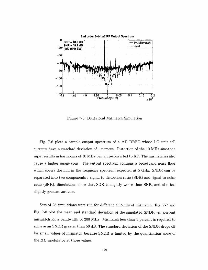
2nd order 3-bit AL RF Output Spectrum
2Frequency (Hz) x 109
Figure 7-6: Behavioral Mismatch Simulation
Fig. 7-6 plots a sample output spectrum of a AE DRFC whose LO unit cell
currents have a standard deviation of 1 percent. Distortion of the 10 MHz sine-tone
input results in harmonics of 10 MHz being up-converted to RF. The mismatches also
cause a higher image spur. The output spectrum contains a broadband noise floor
which covers the null in the frequency spectrum expected at 5 GHz. SNDR can be
separated into two components : signal to distortion ratio (SDR) and signal to noise
ratio (SNR). Simulations show that SDR is slightly worse than SNR, and also has
slightly greater variance.
Sets of 25 simulations were run for different amounts of mismatch. Fig. 7-7 and
Fig. 7-8 plot the mean and standard deviation of the simulated SNDR vs. percent
mismatch for a bandwidth of 200 MHz. Mismatch less than 1 percent is required to
achieve an SNDR greater than 50 dB. The standard deviation of the SNDR drops off
for small values of mismatch because SNDR is limited by the quantization noise of
the AE modulator at those values.
121

2nd Order 3-bit Al: SNDR (Mean)
Percent Mismatch
Figure 7-7: SNDR (Mean) vs. Percent Mismatch
2nd Order 3-bit A: SNDR (Std Dev)
Figure 7-8: SNDR (Std Dev) vs. Percent Mismatch
122

LO Time Spread
Effective Gain Mismatch (%)
Figure 7-9: LO Timing Spread vs. Gain Mismatch
SNDR (dB) vs. Linear Delay/Segment
55
50
45
4014
10
1013 10 11210
- 13 10- 12
Delay/Segment (s)
Figure 7-10: SNDR vs. LO Delay/Segment
123
I · I I I 11/1 1 I I r~T

7.2.1 LO Phase Mismatch
The gain mismatch requirements are translated into phase mismatch requirements
using eqn. (7.6). The phase mismatch requirements, in turn, can be translated into
timing error requirements for the LO unit cell currents. Fig. 7-9 plots the equivalent
timing spread vs. effective gain mismatch for different LO frequencies. The plot
shows that as the LO frequency becomes higher, the allowable timing spread of the
LO signal becomes very small. For a 5 GHz LO frequency, the spread in timing needs
to be less than 250 fs to maintain SNDR greater than 50 dB.
Timing spread of LO unit cell currents also results from systematic layout effects.
A simple assumption is that there is a linear delay per unit cell segment [43]. Fig. 7-10
plots the SNDR vs. delay per segment. In order to maintain SNDR above 50 dB, the
delay per segment must be less than approximately 300 fs. For a non-noise-shaped
DRFC with large number of unit cells, these requirements are difficult to meet due
to the larger layout area.
According to simulations, data skew tolerances are an order of magnitude greater
than LO timing requirements, and are much easier to satisfy.
7.3 Circuit Implications
Fig. 7-11 shows the relevant differential pairs in the high frequency path of the DRFC
unit cell. To minimize the impact of transistor mismatches, the LO differential pair
and data switches should be operated in their fully switched regions. This makes
the differential output current equal to the input tail current. However, the voltage
rise seen at the source node [3] [5] for large differential voltages induces a current at
high frequencies that flows into the parasitic source node capacitance. A mismatch
occurs because the magnitude of the voltage rise at the source node depends on the
differential pair mismatch, which will vary from unit cell to unit cell. The result is
that at high frequencies, the LO current matching is not set by the matching of the
DC current sources, but by the mismatches in the LO and data switch differential
pairs.
124

TRANSISTORMISMATCH
I
Figure 7-11: Unit Cell Transistor Mismatches
Fig. 7-12 plots the simulated LO differential pair current matching versus LO
input swing for an ideal current source, a real current source and 250 MHz LO, and
a real current source and 5 GHz LO. With an ideal current source, the matching
improves as the LO input swing increases. With a real current source, the matching
improves until the swing is large enough to cause the source node to move. The
current matching is then limited by the finite impedance at the source node, which is
lower at 5 GHz than at 250 MHz due to the sizable parasitic capacitance of the bias
transistor. The simulation results show about 1.5 percent matching at 5 GHz. The
contribution to mismatch from the top current-steering switches is smaller since the
LO differential pair transistors beneath them have much smaller parasitic capacitances
than the biasing transistor.
The LO path time constants need to be short to insure that variations in the time
constants across unit cells do not exceed the allowable LO timing spread. According
to Fig. 7-9, 1 percent effective gain mismatch corresponds to - 0.25 ps timing spread.
When the LO differential pair and data switch transistors are fully switched, the LO
path can be modelled as a cascode gain stage. The time constant of the cascode
can be approximated as (l/gm) * Ctotal, where gm is the transconductance of the
data switch transistor and Ctota, is the total capacitance at the source node of the
125
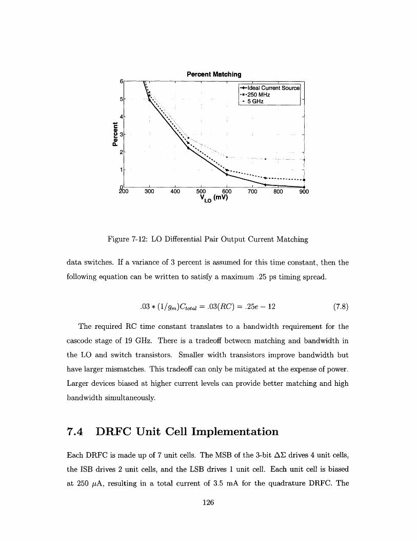
Percent Matching
0)0)
VLO (mV)
Figure 7-12: LO Differential Pair Output Current Matching
data switches. If a variance of 3 percent is assumed for this time constant, then the
following equation can be written to satisfy a maximum .25 ps timing spread.
.03 * (1/gm)Ctotal = .03(RC) = .25e - 12 (7.8)
The required RC time constant translates to a bandwidth requirement for the
cascode stage of 19 GHz. There is a tradeoff between matching and bandwidth in
the LO and switch transistors. Smaller width transistors improve bandwidth but
have larger mismatches. This tradeoff can only be mitigated at the expense of power.
Larger devices biased at higher current levels can provide better matching and high
bandwidth simultaneously.
7.4 DRFC Unit Cell Implementation
Each DRFC is made up of 7 unit cells. The MSB of the 3-bit AE drives 4 unit cells,
the ISB drives 2 unit cells, and the LSB drives 1 unit cell. Each unit cell is biased
at 250 /A, resulting in a total current of 3.5 mA for the quadrature DRFC. The
126

RLLA. I Snni1O•l1 I 1i 1.1 Ir in MAill L I NSIUnnEl I WTVUH1nC3TRANSISTOR WIDTHS IN MICRONS
Figure 7-13: DRFC Unit Cell and Data Driver
current is chosen to maximize the output voltage swing while keeping the cascode
transistor in its saturation region. The tuned LC filter saves current by presenting a
high impedance load to the DRFC at the LO frequency.
Fig. 7-13 shows a circuit schematic of the DRFC unit cell and data driver, including
transistor widths and nominal bias voltages and currents. Standard techniques [40]
are used to match the current sources to " 0.5 percent based on values for a 2(VT)
and a 2(f) provided by the foundry. The current source transistor V,8 - Vt is limited
to 0.25 V based on the available voltage headroom in the circuit. The LO differential
pair gates are biased at 1 V and the gates of the current-steering switches are biased at
1.5/0.9 V depending on the value of the data. The gates of the cascode transistors are
connected directly to the supply voltage of 2.5 V. It is acceptable to use a minimum
length device for the cascode transistor since the maximum source-drain voltage across
the device is - 0.8 V during circuit operation. When the circuit is biased off, the
cascode's gate and drain will be at 2.5 V and the source will float to 2.5 V. The other
devices in the circuit are protected from the 2.5 V supply by the cascode transistor
and will see a maximum effective rail voltage of - 1.7 V. The biasing voltages are
127

Unit Cell Output Current
Figure 7-14: Differential Output Current of Unit Cell
chosen to allow differential voltage swings of 0.6 V pk-pk in both the LO signal and
data signals.
The LO and current-steering switch transistors are sized for high ft and minimum
capacitance. The data drivers consist of a latch and buffer, implemented using source-
coupled logic. The latch re-times the data in each driver to a global clock signal, and
is placed close to the DRFC in layout. The buffer removes glitches from the latch
output and isolates the DRFC from the clock signal. The load resistance and buffer
current are chosen to be 1.5 k2 and 400 pA respectively. This provides a 0.6 V pk-pk
differential swing with approximately 75 ps transition time. The three buffers need
to be scaled to provide identical timing of their data signals. It turned out that the
parasitic capacitances of the routing lines to the DRFC were larger than the input
capacitance of the DRFC current-steering switches. The ISB and LSB buffers were
identical in size, and biased at 400 pA each, while the MSB buffer was biased at 500
IA, accounting for its slightly larger capacitive load.
128
30o8u
- 10u
-20fu
-300u

Quadrature DRFC Output Current
Figure 7-15: Combined Sum of Unit Cell Currents
Quadrature DRFC Filtered Output
Figure 7-16: Quadrature DRFC Filtered Output
129
30m ': Output Voltage

QDRFC OUTPUT SPECTRUM
4.6 4.7 4.8 4.9 5 5.1 5.2 5.3 5.4GHz
Figure 7-17: FFT of QDRFC Output
7.5 Simulation Results
The DRFC, including data drivers and LC BPF, was simulated with I,Q digital data
generated in MATLAB. The simulation results shown below are for a single-tone 10
MHz sine-wave input with a clock frequency of 2.5 GHz and an LO frequency of 5 GHz.
Both direct up-conversion and digital-IF up-conversion topologies are simulated. For
digital-IF up-conversion, the LO frequency is shifted to 4.575 GHz with a digital-IF
frequency of 625 MHz.
Fig. 7-14 plots the differential output current of one of the unit cells. The plot
shows the abrupt 180 ' transitions that the sinusoidal current waveform undergoes.
Fig. 7-15 plots the sum of all unit cell currents in the quadrature DRFC. This wave-
form contains the modulated RF signal in addition to out-of-band shaped quanti-
zation noise from the 2nd order, 3-bit AE modulator. The DRFC output voltage
after bandpass filtering is plotted in Fig. 7-16. Here, the quantization noise has been
removed by the LC bandpass filter, and the resulting output voltage is a single-tone
sine-wave at 5.010 GHz. There is a slight ripple on the envelope due to the presence
of a spurious tone at the image frequency of 4.990 GHz. The FFT of the voltage
130

Digital-IF QDRFC OUTPUT SPECTRUM
GHz
Figure 7-18: FFT of Digital-IF QDRFC Output
waveform in Fig. 7-16 is shown in Fig. 7-17. The image spur is -55 dBc. The cal-
culated SNR over a 200 MHz bandwidth centered at the LO frequency of 5 GHz is
54.7 dB, agreeing well with the MATLAB system-level simulations. Fig. 7-18 shows
the output spectrum when using the quadrature digital-IF architecture. In this case,
there are no image or LO spurs inside the signal bandwidth. Calculated in-band SNR
is 57.2 dB.
RC extracted simulations revealed a layout mismatch between unit cells that
caused a dominant 3rd harmonic baseband tone and an elevated noise floor. Fig. 7-
19 plots the output spectrum of an RC extracted simulation of the QDRFC. LO
feedthrough is -48 dBc. This is due to parasitic coupling of the LO signal from the
bottom differential pair to the output node. The 3rd harmonic of the input tone is
up-converted and is -48 dBc. This spur reflects the presence of a systematic mis-
match in the layout. The problem in the layout was that the routing lines were not
laid out in unit cell fashion. The MSB cell consisted of 4 differential pairs in parallel,
and 4 switches in parallel. However, the connection between the LO differential pair
and the current-steering switch was a single connection. This parasitic was difficult
131
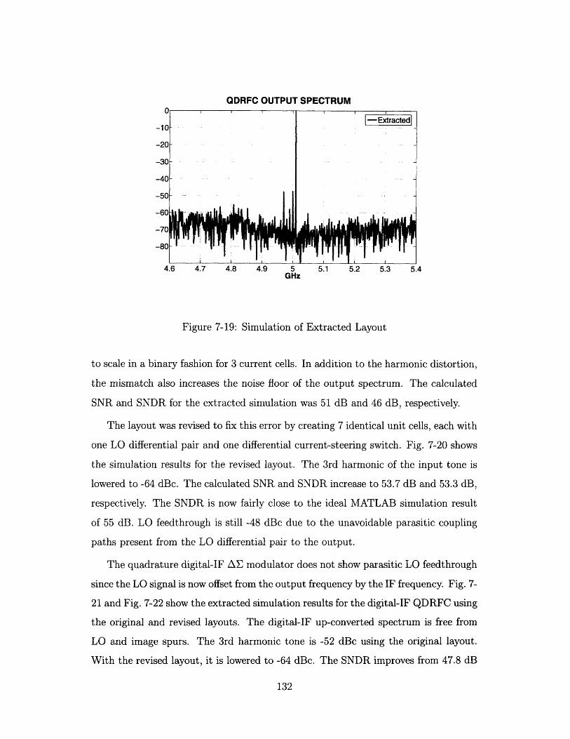
QDRFC OUTPUT SPECTRUM
4.6 4.7 4.8 4.9 5 5.1 5.2 5.3 5.4GHz
Figure 7-19: Simulation of Extracted Layout
to scale in a binary fashion for 3 current cells. In addition to the harmonic distortion,
the mismatch also increases the noise floor of the output spectrum. The calculated
SNR and SNDR for the extracted simulation was 51 dB and 46 dB, respectively.
The layout was revised to fix this error by creating 7 identical unit cells, each with
one LO differential pair and one differential current-steering switch. Fig. 7-20 shows
the simulation results for the revised layout. The 3rd harmonic of the input tone is
lowered to -64 dBc. The calculated SNR and SNDR increase to 53.7 dB and 53.3 dB,
respectively. The SNDR is now fairly close to the ideal MATLAB simulation result
of 55 dB. LO feedthrough is still -48 dBc due to the unavoidable parasitic coupling
paths present from the LO differential pair to the output.
The quadrature digital-IF AE modulator does not show parasitic LO feedthrough
since the LO signal is now offset from the output frequency by the IF frequency. Fig. 7-
21 and Fig. 7-22 show the extracted simulation results for the digital-IF QDRFC using
the original and revised layouts. The digital-IF up-converted spectrum is free from
LO and image spurs. The 3rd harmonic tone is -52 dBc using the original layout.
With the revised layout, it is lowered to -64 dBc. The SNDR improves from 47.8 dB
132

QDRFC OUTPUT SPECTRUM
4.6 4.7 4.8 4.9 5 5.1 5.2 5.3 5.4GHz
Figure 7-20: Simulation of Revised Extracted Layout
Digital-IF QDRFC OUTPUT SPECTRUM
Figure 7-21: Simulation of Quadrature Digital-IF DRFC using Extracted Layout
133

Digital-IF QDRFC OUTPUT SPECTRUM
4.8 4.9 5 5.1 5.2 5.3 5.4 5.5 5.6GHz
Figure 7-22: Simulation of Quadrature Digital-IF DRFC using Revised Extracted
Layout
to 52.8 dB using the revised layout.
7.6 Summary
The circuit design of the DRFC unit cells has been reviewed. A quantitative relation
between SNDR and circuit mismatches was detailed through behavioral modelling of
the DRFC. 1 percent matching is required to attain 50 dB SNDR. Good matching
of the high frequency LO path currents requires careful attention to parasitic capac-
itances in the unit cell transistors and unit cell layout. Simulated SNDR was limited
to 46 dB by a layout error that caused phase mismatches between DRFC LO cell
currents. The error was found through extracted RC simulations and corrected in
layout, improving the simulated SNDR to 53 dB. Mismatch shaping is an effective
method to mitigate the effects of element mismatch.
134

Chapter 8
Measurement Results
8.1 Fabricated Test Chips
Two test chips were fabricated in IBM's 8HP 0.13 pm BiCMOS process to demon-
strate the performance of the wideband AE digital-RF modulator. All modulator
circuits exclusively used 0.13 pm CMOS transistors. The ICs were packaged in 88-
QFN packages with exposed ground paddle. The 88-QFN package has very small
lead inductance, which is helpful for bringing high speed digital signals onto the chip,
and for getting 5 GHz RF signals into and out of the chip. Multiple ground pads on
the chip were down bonded to the paddle, providing short ground connections with
low inductance. The exposed paddle was soldered directly to a ground plane on the
PCB. The PCB was a standard 4 layer FR4 board.
The first test chip included all modulator circuits except for the high speed digital
AE modulator. A block diagram is shown in Fig. 8-1. All I/O's are shown single-
ended, but are implemented differentially. The LO path consists of an input buffer,
a polyphase filter to produce quadrature phase LO signals, and limiting LO buffers
to drive the DRFC. The quadrature-DRFC includes data/clk drivers, the DRFC unit
cells, and the integrated LC BPF with automatic frequency tuning loop. The DRFC
differential output is driven off-chip by a differential output buffer.
The I,Q 3-bit AE digital inputs are generated in MATLAB and loaded into the
RAM of a Xilinx Virtex-4 XC4VLX25 FPGA. The FPGA is programmed to provide
135

MATLAB
CLK/4
CLK
Figure 8-1: Test Chip 1 Block Diagram
de-serialized I,Q 12-bit digital inputs in low voltage differential signaling (LVDS) for-
mat [44] at a clock rate equal to 1/4 the DRFC sample rate, - 650 MHz. The FPGA
clock rate is limited to about 700 MHz. In addition, signal integrity of high speed
digital lines on the PCB and through the package becomes difficult to maintain at
sample rates higher than 700 MHz. 48 transmission lines containing the differential I
and Q 12-bit digital inputs are routed on the PCB from an AV bus connector inter-
facing the FPGA to the IC. The transmission lines are designed for a characteristic
impedance of 100 Q and terminated with on-board 200 Q differential resistors close
to the IC for each pair of differential inputs. An on-chip 4:1 multiplexor serializes
the data back into 3-bit I and Q digital bitstreams at the DRFC sample rate of 2.625
GS/s. The 4:1 multiplexor is implemented with source-coupled logic (SCL) and uses
a tree architecture.
The second test chip includes the modulator and LO path circuitry, and also
integrates the high speed digital processing, including 4x interpolation filters, AE
modulators, and digital-IF up-converter. A block diagram of the second test chip
is shown in Fig. 8-2. The second test chip does not use the 4:1 multiplexor. 11-bit
digital inputs from the FPGA at ' 650 MS/s interface to the digital block, where
136
.,,,,,,,,,,,,,,,,,,,,,,,,,,I
I r\ I
L .. ... .... ... .... ... ... .... ... .... ... ... .... ... .... ... ...

MATLAB CLK/411 11
Sinewaveor FPGA 11OFDM 11 Q
CHIP
Figure 8-2: Test Chip 2 Block Diagram
they are up-sampled by a factor of 4, filtered, and processed by the AE modulators.
Attention is paid in the layout to isolating the high speed digital circuitry from
the DRFC converter circuit. Separate power and ground are provided to the digital
circuits and RF circuits. The digital supplies are further sub-divided, with separate
power and ground assigned to the clock circuitry. Guard rings are placed around the
digital block, the DRFC cells, and the LC bandpass filter. Each of the guard rings
are tied to separate dedicated ground pads. Space is intentionally left between the
DRFC/BPF block and the digital block to minimize substrate coupling. In addition,
a BFMOAT layer is drawn on the empty space between blocks. This layer blocks
P-well and N-well implants, creating regions with higher substrate resistance.
All on-chip RF signals are differential to minimize coupling of noise and spurs.
In the first test chip, all digital signals use differential source-coupled logic. In the
second test chip, the digital inputs are brought in using source-coupled logic. They
are then converted into CMOS logic for lower power in the AE modulator. The
digital-IF outputs of the digital block are then converted back into source-coupled
logic to interface with the DRFC data drivers.
137
- - - - - -..... ----- ..... .... - ..... -- ...... .... ....... .....

Figure 8-3: Testing Setup
8.2 Test Setup
A diagram of the testing setup is shown in Fig. 8-3. Single-tone sine-waves and OFDM
QAM-modulated digital signals are applied as digital inputs to the modulator. The
modulator spurious performance is characterized using a spectrum analyzer at the
output frequency of 5.25 GHz.
Digital control inputs are used to select between direct up-conversion and digital-
IF up-conversion, and select between manual BPF tuning or automatic BPF tuning.
During testing, the filter is first placed in automatic tuning mode and the tuning
voltage is read out of the chip. The filter is then placed into manual tuning mode,
and the read out tuning voltage is dialed in using an on-board potentiometer.
The FPGA/IC interface requires synchronization between the two clock domains
to guarantee a reliable data interface. The FPGA clocks data out on its rising edge.
FPGA clock and data lines are routed with minimal skew to the IC. On the IC, data is
input to a first set of flip-flops that are clocked by the falling edge of the FPGA clock.
The data then goes to a second set of flip-flops that are clocked by an on-chip clock
derived from the 2.625 GHz clock using a divide by 4. It is possible that the data
transitions will violate the setup/hold requirements of these flip-flops. The simple
solution adopted here is that the FPGA clock can be inverted. This works because
138

12 MHz Sine-wave
5.15 5.2 5.25 5.3 5.35GHz
Figure 8-4: Test Chip 1 : 12 MHz Input
the flip-flops are edge-triggered on the rising edge. The phase relation between the
FGPA clock and IC clock is monitored through an on-chip phase detector whose
output is brought off-chip. If the phase detector output indicates a timing problem,
the FPGA clock is inverted.
8.3 Test Chip Results
Output spectrum plots from the first test chip are shown in the following 4 figures.
The resolution BW used in all plots is 1 MHz. The plots are normalized with respect
to the main signal's output power. Un-normalized output power was -5 dBm. Fig. 8-
4 shows the output spectrum with a 12 MHz sine-wave input. LO feedthrough and
image spurs are both less than -50 dBc. The 3rd harmonic of the baseband tone is
the largest spur, about -44 dBc. This distortion is believed to be due to the layout
mismatch described in Chapter 7, which caused a simulated 3rd harmonic of about
-48 dBc. The spur was present at the same level on three other measured test chips,
always on the opposite side of the LO from the main tone. This provides evidence that
139
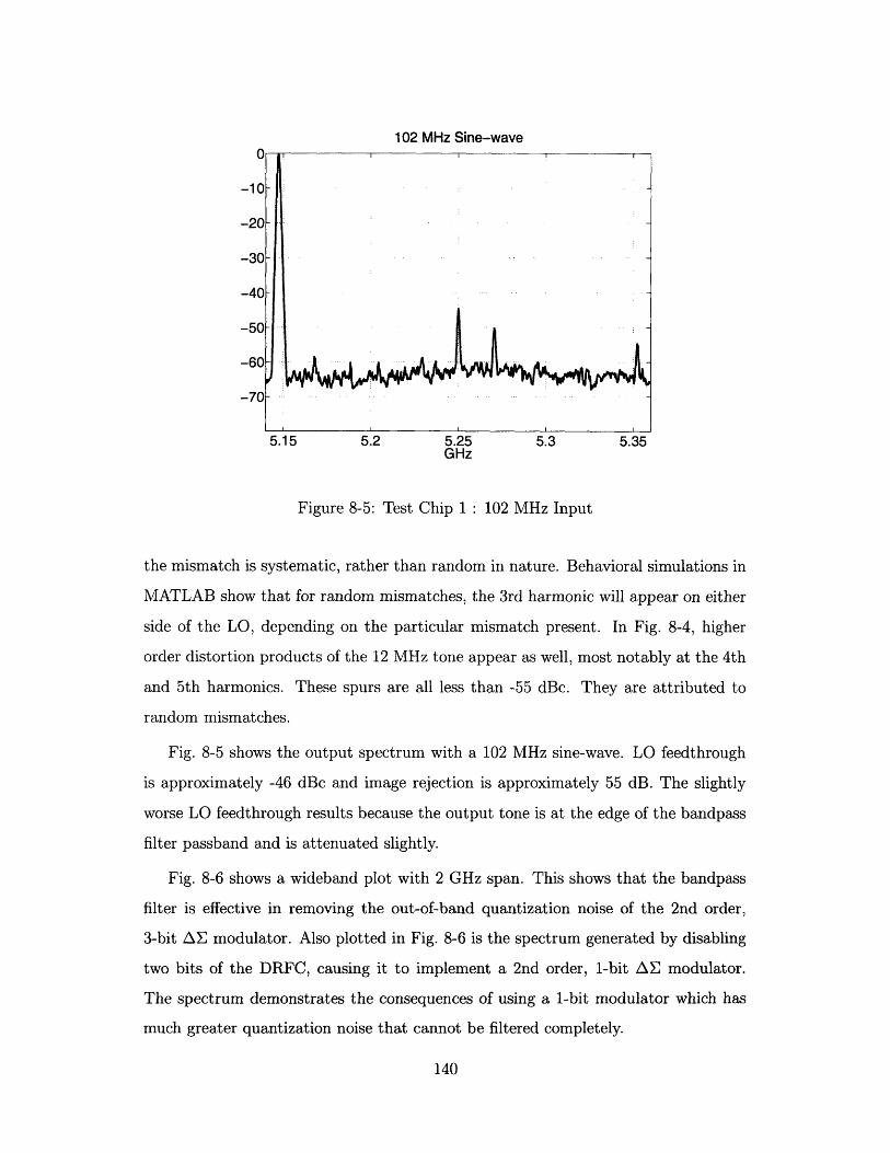
102 MHz Sine-wave
5.15 5.2 5.25 5.3 5.35GHz
Figure 8-5: Test Chip 1 : 102 MHz Input
the mismatch is systematic, rather than random in nature. Behavioral simulations in
MATLAB show that for random mismatches, the 3rd harmonic will appear on either
side of the LO, depending on the particular mismatch present. In Fig. 8-4, higher
order distortion products of the 12 MHz tone appear as well, most notably at the 4th
and 5th harmonics. These spurs are all less than -55 dBc. They are attributed to
random mismatches.
Fig. 8-5 shows the output spectrum with a 102 MHz sine-wave. LO feedthrough
is approximately -46 dBc and image rejection is approximately 55 dB. The slightly
worse LO feedthrough results because the output tone is at the edge of the bandpass
filter passband and is attenuated slightly.
Fig. 8-6 shows a wideband plot with 2 GHz span. This shows that the bandpass
filter is effective in removing the out-of-band quantization noise of the 2nd order,
3-bit AE modulator. Also plotted in Fig. 8-6 is the spectrum generated by disabling
two bits of the DRFC, causing it to implement a 2nd order, 1-bit AE modulator.
The spectrum demonstrates the consequences of using a 1-bit modulator which has
much greater quantization noise that cannot be filtered completely.
140
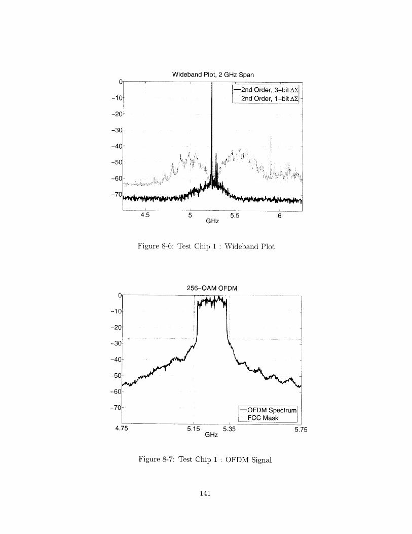
Wideband Plot, 2 GHz Span
4.5 5 5.5 6GHz
Figure 8-6: Test Chip 1 : Wideband Plot
256-QAM OFDM
4.75 5.15 5.35 5.75GHz
Figure 8-7: Test Chip 1 : OFDM Signal
141

12 MHz Sine-wave
5.15 5.2 5.25 5.3 5.35GHz
Figure 8-8: Test Chip 2 : Direct Up-Conversion of 12 MHz Input
Fig. 8-7 shows the output spectrum of a 160 MHz 256-QAM OFDM signal. The
FCC spectral limits outside the 5.15-5.35 GHz UN-II band are also shown, indicating
that the spurious requirements are met.
Output power was higher on the second chip at -1 dBm due to an optimized filter
layout with less loss. The spectrum plots are normalized to 0 dB. Fig. 8-8 plots the
output spectrum with a 12 MHz input using direct up-conversion, i.e. the digital-IF
up-converter is not used. The 3rd harmonic is approximately -47 dBc due to the
same layout mismatch, image rejection is 50 dB, and other harmonics are less than
-55 dBc. The LO feedthrough is about -44 dBc. The results are similar to test chip 1,
indicating that the integration of the high speed AE modulators was successful. LO
feedthrough is slightly higher, and is attributed to coupling from the 2nd harmonic of
the AE clock frequency, which is exactly at 5.25 GHz. Unlike test chip 1, the second
test chip has full-swing CMOS clock drivers which can generate substantial harmonics
of the clock frequency. Fig. 8-9 shows the spectrum for two-tone inputs separated by
- 2 MHz. The IM3 products are -42 dBc, which corresponds to an OIP3 of 8.6 dBm.
The IM3 performance is limited by the linearity of the output amplifier which has a
142
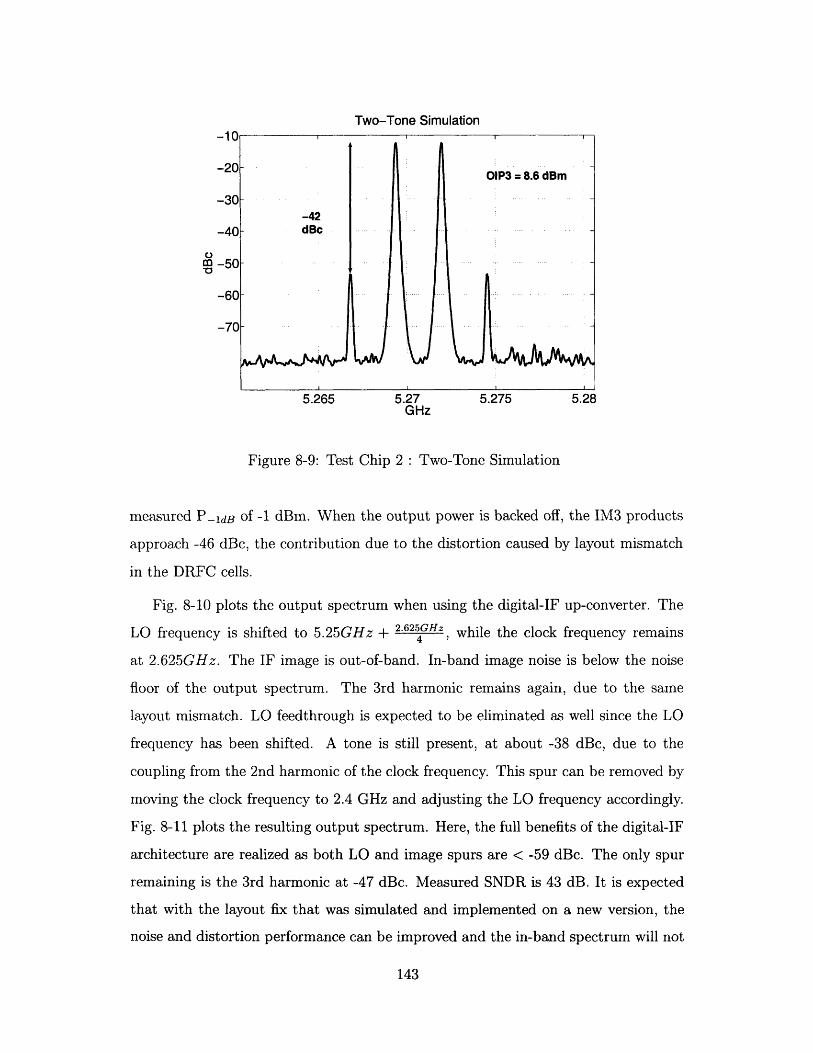
Two-Tone Simulation-1U
-20
-30
-40
m -50
-60
-70
526 5 7 5.
5.265 5.27 5.275 5.28GHz
Figure 8-9: Test Chip 2 : Two-Tone Simulation
measured P-ldB of -1 dBm. When the output power is backed off, the IM3 products
approach -46 dBc, the contribution due to the distortion caused by layout mismatch
in the DRFC cells.
Fig. 8-10 plots the output spectrum when using the digital-IF up-converter. The
LO frequency is shifted to 5.25GHz + 2.625Gz, while the clock frequency remains
at 2.625GHz. The IF image is out-of-band. In-band image noise is below the noise
floor of the output spectrum. The 3rd harmonic remains again, due to the same
layout mismatch. LO feedthrough is expected to be eliminated as well since the LO
frequency has been shifted. A tone is still present, at about -38 dBc, due to the
coupling from the 2nd harmonic of the clock frequency. This spur can be removed by
moving the clock frequency to 2.4 GHz and adjusting the LO frequency accordingly.
Fig. 8-11 plots the resulting output spectrum. Here, the full benefits of the digital-IF
architecture are realized as both LO and image spurs are < -59 dBc. The only spur
remaining is the 3rd harmonic at -47 dBc. Measured SNDR is 43 dB. It is expected
that with the layout fix that was simulated and implemented on a new version, the
noise and distortion performance can be improved and the in-band spectrum will not
143
,,i I I
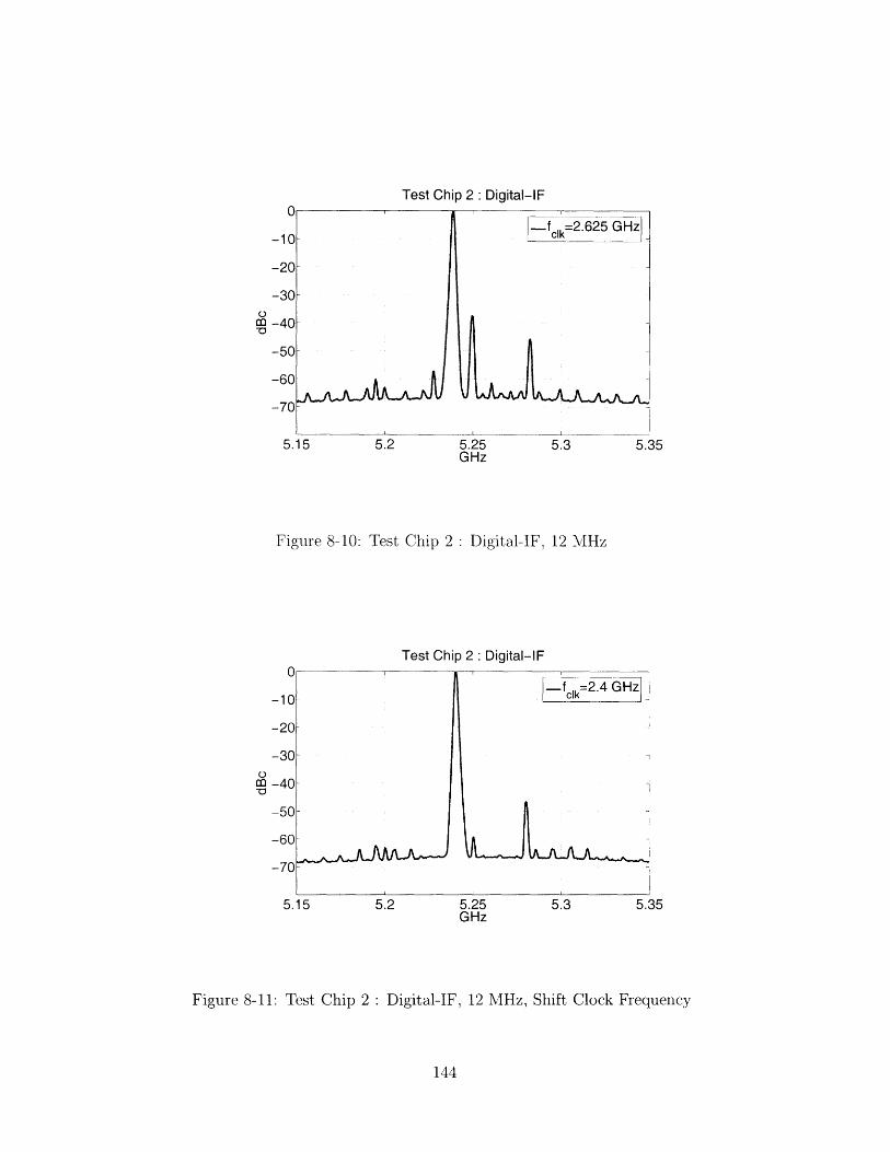
Test Chip 2 : Digital-IF
5.15 5.2 5.25 5.3GHz
5.35
Figure 8-10: Test Chip 2 : Digital-IF, 12 MHz
Test Chip 2 : Digital-IF
5.15 5.2 5.25 5.3GHz
5.35
Figure 8-11: Test Chip 2 : Digital-IF, 12 MHz, Shift Clock Frequency
144
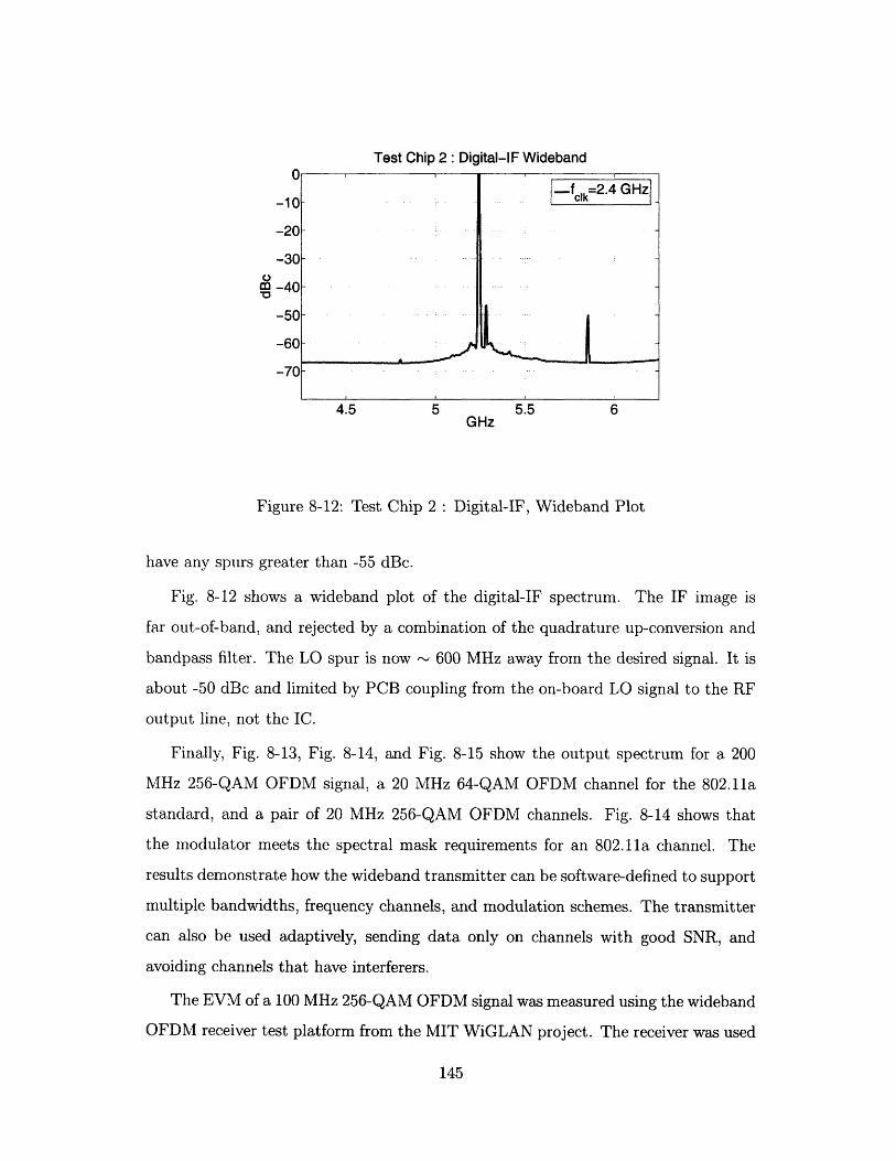
Test Chip 2: Digital-IF WidebandU
-10-20
-30
cm -40
-50
-60
-70
4.5 5 5.5 6GHz
Figure 8-12: Test Chip 2 : Digital-IF, Wideband Plot
have any spurs greater than -55 dBc.
Fig. 8-12 shows a wideband plot of the digital-IF spectrum. The IF image is
far out-of-band, and rejected by a combination of the quadrature up-conversion and
bandpass filter. The LO spur is now - 600 MHz away from the desired signal. It is
about -50 dBc and limited by PCB coupling from the on-board LO signal to the RF
output line, not the IC.
Finally, Fig. 8-13, Fig. 8-14, and Fig. 8-15 show the output spectrum for a 200
MHz 256-QAM OFDM signal, a 20 MHz 64-QAM OFDM channel for the 802.11a
standard, and a pair of 20 MHz 256-QAM OFDM channels. Fig. 8-14 shows that
the modulator meets the spectral mask requirements for an 802.11a channel. The
results demonstrate how the wideband transmitter can be software-defined to support
multiple bandwidths, frequency channels, and modulation schemes. The transmitter
can also be used adaptively, sending data only on channels with good SNR, and
avoiding channels that have interferers.
The EVM of a 100 MHz 256-QAM OFDM signal was measured using the wideband
OFDM receiver test platform from the MIT WiGLAN project. The receiver was used
145
fclk=2.4 GHz
L ...i .... .- iiI I I I

200 MHz 256-QAM OFDM Signal
GHz
Figure 8-13: Test Chip 2 : 200 MHz OFDM Signal
802.11 a Channel
GHz
Figure 8-14: Test Chip 2 : 20 MHz OFDM Channel for 802.11a
146
35
-~--

Pair of 20 MHz 256-QAM OFDM Channels
EcO
Figure 8-15: Test Chip 2 :
35
5GHz
Pair of 20 MHz OFDM Channels
SNR vs Freq
[256QAMS64QAM016QAMF-4QAMIBPSKMNULL
-60 -40 -20 0Freq (MHz)
20 40 60
Figure 8-16: SNR Measurement using WiGLAN Receiver
147
·I·I I I I .... ·I I
r

Table 8.1: AE Modulator Power Consumption/Die Area
Power Consumption Die Area
Digital Block (I and Q) 120 mW @ 1.5 V .16 mm 2
Quadrature DRFC Core 10 mW 0 2.5 V .03 mm 2
Quadrature DRFC Data/Clock Drivers 33 mW 0 1.5 V Included in Core
LO Polyphase/Buffers 20 mW A 1.5 V .21 mm 2
BPF Tuning Circuitry 4 mW L 1.5 V, 2.5 V .12 mm 2
BPF 0 mW .2 mm2
Total 187 mW .72 mm 2
Total (including 0 dBm output amplifier) 227 mW 1 mm 2
to down-convert and digitize the RF output signal from the AE digital-RF modulator.
The digitized signal was then captured using an FPGA and processed with MATLAB
scripts. Measured SNR, the inverse of EVM, is plotted on a per sub-carrier basis in
Fig. 8-16.
The WiGLAN testing indicated that the test platform SNR was limited to - 30
dB by the resolution of the ADC. A reasonable estimate for the SNR of the AE
digital-RF modulator alone is around 30 dB. This would provide a composite SNR of
the transceiver of 27 dB, which is approximately the value of the SNR averaged over
all bins. 30 dB also agrees well with the measured SNDR of 43 dB. Since the OFDM
signal had a peak to average power ratio of 15 dB, an SNDR of 43 dB for a sine-wave
translates into an SNDR of 31 dB for the OFDM signal.
According to Fig. 8-16, almost every sub-carrier can support 64-QAM modulation
while several can support 256-QAM. Assuming 64-QAM modulation across all 200
MHz, the presented modulator can transmit a data rate of at least 1.2 Gb/s over its
intended bandwidth.
The power consumption and die area of the entire modulator integrated in test
148
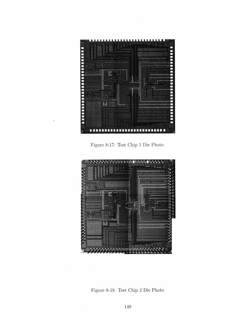
Figure 8-17: Test Chip 1 Die Photo
Figure 8-18: Test Chip 2 Die Photo
149

Table 8.2: FOM Comparison
Digital-RF Modulator ENOB BW Power FOM
Eloranta [11] 8 20 MHz 60 mW 0.375 nJ/bit
Taleie [12] 11 15 MHz 122 mW 0.74 nJ/bit
This Work 7 200 MHz 187 mW 0.13 nJ/bit
chip 2 are summarized in Table 8.1. Die photos of both test chips are shown in
Fig. 8-17 and Fig. 8-18.
The modulator consumes 187 mW and occupies a die area of 0.72 mm2. A metric
that characterizes the energy/bit efficiency of an RF modulator is defined as
P 187e - 3 nJ
ENOB * BW 7 * 200e6 bit
In eqn. (8.1), ENOB stands for the effective number of bits. With an SNDR
of 43 dB, the ENOB is 7 bits. Since 2/3 of the power is consumed in the digital
processing, this FOM can be expected to improve with digital process scaling. Table
8.2 compares the energy/bit efficiency of our RF modulator with other digital-RF
converters reported in the literature. This work provides an order of magnitude
higher bandwidth than [11] and [12], and is also approximately 3 times and 6 times
more efficient, respectively.
A general figure of merit characterizing the energy/bit efficiency of a transmitter
system is (Power/Data Rate). For our modulator,
Power 187e - 3 nJS = 0.16 (8.2)
DataRate 1.2e9 bit
8.4 Power/Area Comparison
The wideband AE digital-RF modulator is compared to a conventional IQ modula-
tor in terms of power and area for 200 MHz bandwidth and 45 dB dynamic range.
Specifically, the AE digital-RF modulator replaces two high speed DACs, two analog
lowpass filters, and two analog mixers. The LO polyphase/buffer circuitry is common
150
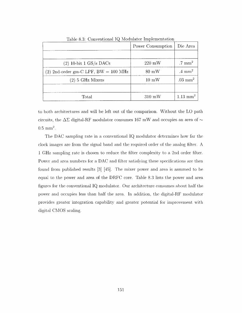
Table 8.3: Conventional IQ Modulator Implementation
Power Consumption Die Area
(2) 10-bit 1 GS/s DACs 220 mW .7 mm2
(2) 2nd-order gm-C LPF, BW = 100 MHz 80 mW .4 mm 2
(2) 5 GHz Mixers 10 mW .03 mm2
Total 310 mW 1.13 mmn2
to both architectures and will be left out of the comparison. Without the LO path
circuits, the AE digital-RF modulator consumes 167 mW and occupies an area of -
0.5 mnm2
The DAC sampling rate in a conventional IQ modulator determines how far the
clock images are from the signal band and the required order of the analog filter. A
1 GHz sampling rate is chosen to reduce the filter complexity to a 2nd order filter.
Power and area numbers for a DAC and filter satisfying these specifications are then
found from published results [3] [45]. The mixer power and area is assumed to be
equal to the power and area of the DRFC core. Table 8.3 lists the power and area
figures for the conventional IQ modulator. Our architecture consumes about half the
power and occupies less than half the area. In addition, the digital-RF modulator
provides greater integration capability and greater potential for improvement with
digital CMOS scaling.
151

152

Chapter 9
Conclusion
The AE digital-RF modulator is a power and area efficient modulator for wideband
systems. Measured results demonstrate 1.2 Gb/s data rates over 200 MHz RF band-
width at 5.25 GHz using OFDM modulation. The fabricated modulator consumes
187 mW and occupies a die area of 0.72 mm 2. The AE digital-RF modulator relies
on high speed digital circuits instead of high dynamic range analog circuits. The
architecture is attractive because the power and area savings versus conventional
IQ modulators is expected to increase as digital CMOS scaling continues. Dynamic
range performance of the transmitter is not limited by the noise, linearity, and power
tradeoffs fomnd in analog design. The output spectrum of the modulator is free from
in-band LO feedthrough and image signals due to the use of a quadrature digital-
IF scheme. Thus, excellent transmitter spurious performance, suitable for complex
modulation formats such as 256-QAM, is possible.
The wideband digital modulator enables the design of flexible, software-defined
transmitters. This IC can transmit multiple bandwidths up to 200 MHz, and multiple
modulation schemes up to 256-QAM. Furthermore, it can vary the usage of different
channels depending on the channel conditions. A fixed frequency LO can be used
since the channel selection is done in the digital domain.
153

Table 9.1: Element Rotation Algorithm
3-bit Digital Input
100
001
011
010
110
Unit Cell Usage
1111000
0000100
1000011
0110000
1101111
9.1 Future Directions
9.1.1 Mismatch Shaping
The SNDR performance of the multi-bit DRFC is ultimately determined by how well
the LO path unit cells match. Current source calibration [46] can reduce mismatches
between the tail current sources, but does not influence mismatches associated with
high frequency effects in the LO path. Mismatch shaping [47] [43] [48] [49] is a
technique that noise-shapes the error due to element mismatch through an element
selection algorithm. The noise-shaping causes the error to lie outside the AE signal
bandwidth, improving the SNR within the signal band.
The key issue in employing mismatch-shaping for the AE DRFC involves reducing
the complexity and power of the required high speed digital hardware. A mismatch
shaper for a 3-bit 2 GS/s AE DAC was presented in [50], but consumes 3.1 W.
We investigate the performance of a lst-order mismatch noise shaper with mis-
match transfer function of H(Z) = 1 - z - 1 for its simplicity. 1st order mismatch noise
shaping can be efficiently implemented using an algorithm known as element rotation
[51] or data-weighted averaging [48]. The algorithm picks which elements to use by
rotating around an array of unit cells. Table 9.1 illustrates this for a 3-bit DAC by
showing how unit cells are selected for the sequence of digital inputs 4,1,3,2, and 6.
A hardware implementation for element rotation is shown in Fig. 9-1 [29]. It
consists of an 8-bit thermometer decoder, a 3-bit accumulator, and an 8-bit barrel
shifter. The implementation was added to the MATLAB mismatch simulation model
154

Figure 9-1: Element Rotation Hardware Implementation
2nd Order 3-bit AX: SNDR (Mean) vs. Mismatch
Percent Mismatch
Figure 9-2: Behavioral Model Simulation using Element Rotation
155
BIT!
JT

to compare 1st order mismatch shaping to no mismatch shaping. Fig. 9-2 plots
the simulated SNDR versus percent mismatch with and without 1st order mismatch
shaping, for a bandwidth of 200 MHz and a clock frequency of 2.5 GHz. The rotation
algorithm is effective in shaping virtually all the mismatch noise out-of-band, even for
mismatches as high as 16 percent. At that level of mismatch, a non-mismatch-shaped
DRFC achieves an SNDR of only 30 dB. The element rotation implementation appears
to be a practical solution to mismatches. Hardware requirements are reasonable when
the number of thermometer bits is small, as is the case with a 3-bit AE.
Another area of research is to push the dynamic range performance even higher,
towards 70 dB or 80 dB. For example, one can increase the resolution of the multi-bit
quantizer, increase the order of the noise-shaping, or increase the OSR further. Any
changes to the modulator design will also impact the requirements of the bandpass
filter.
The modulator has demonstrated its potential for use as a universal transmitter
targeting applications in the 5.25 GHz UN-II band. A further improvement would
involve being able to program the transmitter for operation in multiple frequency
bands. A multi-band PLL would be required to generate a wide range of frequencies
for the LO. A key challenge would be to make the RF bandpass filter tunable over the
same range of frequencies. This may involve using multiple staggered bandpass filters
that are selectable. Another area for additional programmability is automatic gain
control. The modulator output power can be varied in the digital domain, but its
SNDR will eventually be limited at low output powers by the fixed quantization noise
of the AE modulator. An RF variable gain amplifier (VGA) following the modulator
can be used to provide variable gain with greater gain control range.
A final aspect of wideband transmitters not addressed yet is the design of an
efficient wideband PA. Traditional PAs use low loss matching networks to achieve
high efficiency over narrow bandwidths. Optimizing the efficiency and gain of a PA
over a wide bandwidth involves additional design issues.
156

Bibliography
[1] R. Howald, "QAM Bulks Up Once Again : Modulation to the Power of 10,"
http://broadband.motorola.com/ips/pdf/QAM.pdf.
[2] "Part 11 : Wireless LAN Medium Access Control (MAC) and Physical Layer
(PHY) Specifications," IEEE Std 802.11, 1999.
[3] A. V. den Bosch, M. Borremans, M. Steyaert, and W. Sansen, "A 10-bit 1-
GSample/s Nyquist Current Steering CMOS D/A Converter," IEEE J. Solid-
State Circuits, vol. 36, no. 3, pp. 315-324, March 2001.
[4] B. Schafferer and R. Adams, "A 3v CMOS 400mW 14b 1.4GS/s DAC for Multi-
Carrier Applications," in International Solid-State Circuits Conference, 2004,
pp. 360-361.
[5] W. Schofield, D. Mercer, and L. S. Onge, "A 16b 400MS/s DAC with < -
160dBm/Hz Noise Power Spectral Density," in International Solid-State Circuits
Conference, 2003, pp. 126-127.
[6] F. Rezzi, I. Bietti, M. Cazzaniga, and R. Castello, "A 70-mW Seventh-Order
Filter with 7-50 MHz Cutoff Frequency and Programmable Boost and Group
Delay Equalization," IEEE J. Solid-State Circuits, vol. 32, no. 12, pp. 1987-
1998. December 1997.
[7] M. Perrott, T. Tewksbury, and C. Sodini, "A 27-mW CMOS Fractional-N Syn-
thesizer Using Digital Compensation for 2.5-Mb/s GFSK Modulation," IEEE J.
Solid-State Circuits, vol. 32, no. 12, pp. 2048-2060, 1997.
157
[8] L. E. Larson, Ed., RF and Microwave Circuit Design For Wireless Communica-
tions. Artech House, 1996.
[9] J. Candy and G. Temes, Oversampling Delta-Sigma Data Converters. IEEE
Press, 1992.
[10] S. Luschas, R. Schreier, and H. Lee, "Radio Frequency Digital-to-Analog Con-
verter," IEEE J. Solid-State Circuits, vol. 39, no. 9, pp. 1462-1467, September
2004.
[11] P. Eloranta and P. Seppinen, "Direct-Digital RF Modulator IC in 0.13 pm CMOS
for Wide-Band Multi-Radio Applications," in ISSCC, 2005, pp. 532-533.
[12] S. M. Taleie, T. Copani, B. Bakkaloglu, and S. Kiaei, "A Bandpass Delta-Sigma
RF-DAC with Embedded FIR Reconstruction Filter," in ISSCC, 2006, pp. 578-
579.
[13] D. Su and B. Wooley, "A CMOS Oversampling D/A Converter with a Current-
Mode Semidigital Reconstruction Filter," IEEE J. Solid-State Circuits, vol. 28,
no. 12, pp. 1224-1233, December 1993.
[14] A. Zverev, Handbook of Filter Synthesis. J. Wiley and Sons, Inc., 1967.
[15] F. Rotella, D. Howard, M. Racanelli, and P. Zampardi, "Characterizing and
Otimizing High Q Inductors for RFIC Design in Silicon Processes," in IEEE
Radio Frequency Integrated Circuits Symposium, 2003, pp. 339-342.
[16] A. Kral, F. Behbahani, and A. Abidi, "RF CMOS Oscillators with switched
tuning," in Custom Integrated Circuits Conference, 1998, pp. 555-558.
[17] A. Bonfanti, S. Levantino, C. Samori, and A. Lacaita, "A Varactor Configuration
Minimizing the Amplitude-to-Phase Noise Conversion in VCOs," IEEE J. Solid-
State Circuits, vol. 53, no. 3, pp. 481-488, March 2006.
158

[18] X. He and W. Kuhn, "A 2.5 GHz Low Power, High Dynamic Range, Self-Tuned
Q Enhanced LC Filter in SOI," IEEE J. Solid-State Circuits, vol. 40, no. 8, pp.
1618-1628, August 2005.
[19] H. Khorramabadi and P. Gray, "High-frequency CMOS Continuous-Time Fil-
ters," IEEE J. Solid-State Circuits, vol. SC-19, no. 6, pp. 939-948, December
1984.
[20] B. Gilbert, "A Precise Four-Quadrant Multiplier with Subnanosecond Re-
sponse," IEEE J. Solid-State Circuits, vol. SC-3, no. 4, pp. 365-373, December
1968.
[21] R. Duncan, K. Martin, and A. Sedra, "A Q-Enhanced Active-RLC Bandpass
Filter," IEEE Trans. Circuits Syst. II, vol. 44, no. 5, pp. 341-347, May 1997.
[22] T. Soorapanth and S. Wong, "A 0-dB IL 2140 +/- 30 MHz Bandpass Filter
Utilizing Q-Enhanced Spiral Inductors in Standard CMOS," IEEE J. Solid-State
Circuits, vol. 37, no. 5, pp. 579-586, May 2002.
[23] W. Kuhn, D. Nobbe, D. Kelly, and A. Orsborn, "Dynamic Range Performance
of On- Chip RF Bandpass Filters," IEEE Trans. Circuits Syst. II, vol. 50, no. 10,
pp. 685-694, October 2003.
[24] D. Hodges, H. Jackson, and R. Saleh, Analysis and Design of Digital Integrated
CircuitIs, 3rd ed. McGraw Hill, 2004.
[25] A. vain der Ziel, "Thermal Noise in Field Effect Transistors," in Proc. IEEE,
Aug. 1962, pp. 1801-1812.
[26] A. Abidi, "High-Frequency Noise Measurements on FETs with Small Dimen-
sions," IEEE Trans. Electron Devices, vol. ED-33, no. 11, pp. 1801-1805, Novem-
ber 1986.
[27] J. Steininger, "Understanding Wide-Band MOS Transistors," IEEE J. Solid-
State Circuits, vol. 6, no. 3, pp. 26-31, May 1990.
159

[28] R. Schreier, "An empirical study of high-order single-bit delta-sigma modula-
tors," IEEE Trans. Circuits Syst. II, vol. 40, no. 8, pp. 461-466, August 1993.
[29] S. Norsworthy, R. Schreier, and G. Temes, Eds., Delta-Sigma Data Converters
: Theory, Design, and Simulation. IEEE PRESS, 1997.
[30] L. Longo and M. Copeland, "A 13 bit ISDN-band oversampled ADC using two-
stage third-order noise shaping," in Custom Integrated Circuits Conference, 1988,
pp. 21.2.1-21.2.4.
[31] "Radio Frequency Devices," in Title 47 - Telecommunications, Chapter 1, Part
15. Federal Communications Commission, 2006, p. 128.
[32] R. Schreier, "Matlab Delta-Sigma Toolbox,"
http://www.mathworks.com/support/ftp/controlssv5.shtml.
[33] ECMA-368, "High Rate Ultra Wideband PHY and MAC Standard," www.ecma-
international.org, December 2005.
[34] J. Vankka, J. Sommarek, J. Ketola, I. Teikari, and K. Halonen, "A Digital
Quadrature Modulator With On-Chip D/A Converter," IEEE J. Solid-State
Circuits, vol. 38, no. 10, pp. 1635-1642, October 2003.
[35] J. Rabaey, A. Chandrakasan, and B. Nikolic, Digital Integrated Circuits A Design
Perspective, 2nd ed., C. G. Sodini, Ed. Prentice Hall, 2003.
[36] J. Candy and A. Huynh, "Double interpolation for digital-to-analog conversion,"
IEEE Trans. Commun., vol. COM-34, pp. 77-81, 1986.
[37] M. Matsui, H. Hara, Y. Uetani, L. Kim, T. Nagamatsu, Y. Watanabe, A. Chiba,
K. Matsuda, and T. Sakurai, "A 200 MHz 13 mm2 2-D DCT Macrocell Us-
ing Sense-Amplifying Pipeline Flip-Flop Scheme," IEEE J. Solid-State Circuits,
vol. 29, no. 12, pp. 1482-1490, December 1994.
160

[38] T. Gemmeke, M. Gansen, H. Stockmanns, and T. Noll, "Design Optimization
of Low-Power High Performance DSP Building Blocks," IEEE J. Solid-State
Circuits, vol. 39, no. 7, pp. 1131-1139, July 2004.
[39] B. Nikolic, V. Oklobdzija, V. Stoyanovic, W. Jia, J. Chiu, and M. Leung, "Im-
proved Sense-Amplifier-Based Flip-Flop : Design and Measurements," IEEE J.
Solid-State Circuits, vol. 35, no. 6, pp. 876-884, June 2000.
[40] M. Pelgrom, C. Duinmaijer, and A. Welbers, "Matching Properties of MOS
Transistors," IEEE Trans. Circuits Syst. II, vol. 24, pp. 1433-1439, October
1989.
[41] K. Doris, A. van Roermund, and D. Leenaerts, "Mismatch-Based Timing Errors
in Current Steering DACs," in ISCAS, 2003, pp. 977-980.
[42] K. Doris, J. Briare, D. Leenaerts, M. Vertregt, and A. van Roermund, "A 12b
500 MS/s DAC with > 70 dB SFDR up to 120 MHz in 0.18pm CMOS," in
International Solid-State Circuits Conference, 2005, pp. 116-117.
[43] F. Chen and B. Leung, "A High Resolution Multibit Sigma-Delta Modulator
with Individual Level Averaging," IEEE J. Solid-State Circuits, vol. 30, no. 4,
pp. 453-459, April 1995.
[44] M. Adhiwiyogo, "Virtex-4 High-Speed Single Data Rate LVDS Transceiver,"
Application Note : Virtex-4 Family, August 2005.
[45] A. Carusone and D. Johns, "A 5th Order Gm-C Filter in 0.25uM CMOS with
Digitally Programmable Poles and Zeroes," in Custom Integrated Circuits Con-
ference, 2002, pp. 635-638.
[46] D. Wouter, J. Groeneveld, H. Shouwenaars, H. Termeer, and C. Bastiaansen, "A
Self-Calibration Technique for Monolithic High-Resolution D/A Converters,"
IEEE J. Solid-State Circuits, vol. 24, pp. 1517-1522, December 1989.
161

[47] I. Galton, "Spectral Shaping of Circuit Errors in Digital-to-Analog Converters,"
IEEE Trans. Circuits Syst. II, vol. 44, no. 10, pp. 808-817, October 1997.
[48] R. Baird and T. Fiez, "Linearity Enhancement of Multibit 6a A/D and D/A
Converters Using Data Weighted Averaging," IEEE Trans. Circuits Syst. II,
vol. 42, no. 12, pp. 753-762, December 1995.
[49] T. Shui, R. Schreier, and F. Hudson, "Mismatch Shaping for a Current-Mode
Multibit Delta-Sigma DAC," IEEE J. Solid-State Circuits, vol. 34, no. 3, pp.
331-338, March 1999.
[50] T. Kaplan, J. Jensen, C. Fields, and F. Chang, "A 2 GS/s 3-bit 3a-Modulated
DAC With Tunable Bandpass Mismatch Shaping," IEEE J. Solid-State Circuits,
vol. 4, no. 3, pp. 603-610, March 2005.
[51] H. Jackson, "Circuit and method for cancelling nonlinearity error associated with
component value mismatches in a data converter," U.S. Patent 5 221 926, June
1993.
162