A 3.3V Single-Poly CMOS Audio ADC Delta-Sigma Modulator with 98dB Peak SINAD
11
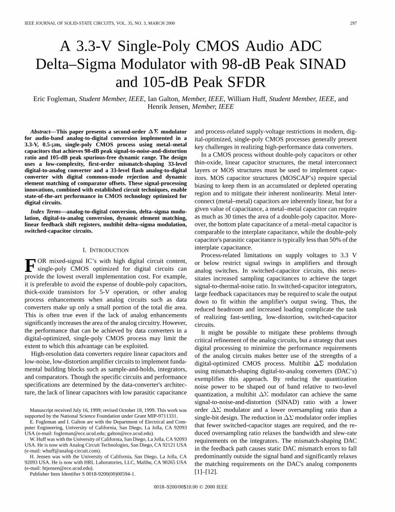
IEEE JOURNAL OF SOLID-STATE CIRCUITS, VOL. 35, NO. 3,MARCH 2000 297 A 3.3-V Single-Poly CMOS Audio ADC Delta–Sigma Modulator with 98-dB Peak SINAD and 105-dB Peak SFDR Eric Fogleman, Student Member, IEEE, Ian Galton, Member, IEEE, William Huff, Student Member, IEEE, and Henrik Jensen, Member, IEEE Abstract—This paper presents a second-order modulator for audio-band analog-to-digital conversion implemented in a 3.3-V, 0.5-μm, single-poly CMOS process using metal–metal capacitors that achieves 98-dB peak signal-to-noise-and-distortion ratio and 105-dB peak spurious-free dynamic range. The design uses a low-complexity, first-order mismatch-shaping 33-level digital-to-analog converter and a 33-level flash analog-to-digital converter with digital common-mode rejection and dynamic element matching of comparator offsets. These signal-processing innovations, combined with established circuit techniques, enable state-of-the-art performance in CMOS technology optimized for digital circuits. Index Terms—analog-to-digital conversion, delta–sigma modu- lation, digital-to-analog conversion, dynamic element matching, linear feedback shift registers, multibit delta–sigma modulation, switched-capacitor circuits. I. INTRODUCTION F OR mixed-signal IC’s with high digital circuit content, single-poly CMOS optimized for digital circuits can provide the lowest overall implementation cost. For example, it is preferable to avoid the expense of double-poly capacitors, thick-oxide transistors for 5-V operation, or other analog process enhancements when analog circuits such as data converters make up only a small portion of the total die area. This is often true even if the lack of analog enhancements significantly increases the area of the analog circuitry. However, the performance that can be achieved by data converters in a digital-optimized, single-poly CMOS process may limit the extent to which this advantage can be exploited. High-resolution data converters require linear capacitors and low-noise, low-distortion amplifier circuits to implement funda- mental building blocks such as sample-and-holds, integrators, and comparators. Though the specific circuits and performance specifications are determined by the data-converter's architec- ture, the lack of linear capacitors with low parasitic capacitance Manuscript received July 16, 1999; revised October 18, 1999. This work was supported by the National Science Foundation under Grant MIP-9711331. E. Fogleman and I. Galton are with the Department of Electrical and Com- puter Engineering, University of California, San Diego, La Jolla, CA 92093 USA (e-mail: [email protected]; [email protected]). W. Huff was with the University of California, San Diego, La Jolla, CA 92093 USA. He is now with Analog Circuit Technologies, San Diego, CA 92121 USA (e-mail: [email protected]). H. Jensen was with the University of California, San Diego, La Jolla, CA 92093 USA. He is now with HRL Laboratories, LLC, Malibu, CA 90265 USA (e-mail: [email protected]). Publisher Item Identifier S 0018-9200(00)00594-1. and process-related supply-voltage restrictions in modern, dig- ital-optimized, single-poly CMOS processes generally present key challenges in realizing high-performance data converters. In a CMOS process without double-poly capacitors or other thin-oxide, linear capacitor structures, the metal interconnect layers or MOS structures must be used to implement capac- itors. MOS capacitor structures (MOSCAP’s) require special biasing to keep them in an accumulated or depleted operating region and to mitigate their inherent nonlinearity. Metal inter- connect (metal–metal) capacitors are inherently linear, but for a given value of capacitance, a metal–metal capacitor can require as much as 30 times the area of a double-poly capacitor. More- over, the bottom plate capacitance of a metal–metal capacitor is comparable to the interplate capacitance, while the double-poly capacitor's parasitic capacitance is typically less than 50% of the interplate capacitance. Process-related limitations on supply voltages to 3.3 V or below restrict signal swings in amplifiers and through analog switches. In switched-capacitor circuits, this neces- sitates increased sampling capacitances to achieve the target signal-to-thermal-noise ratio. In switched-capacitor integrators, large feedback capacitances may be required to scale the output down to fit within the amplifier's output swing. Thus, the reduced headroom and increased loading complicate the task of realizing fast-settling, low-distortion, switched-capacitor circuits. It might be possible to mitigate these problems through critical refinement of the analog circuits, but a strategy that uses digital processing to minimize the performance requirements of the analog circuits makes better use of the strengths of a digital-optimized CMOS process. Multibit modulation using mismatch-shaping digital-to-analog converters (DAC’s) exemplifies this approach. By reducing the quantization noise power to be shaped out of band relative to two-level quantization, a multibit modulator can achieve the same signal-to-noise-and-distortion (SINAD) ratio with a lower order modulator and a lower oversampling ratio than a single-bit design. The reduction in modulator order implies that fewer switched-capacitor stages are required, and the re- duced oversampling ratio relaxes the bandwidth and slew-rate requirements on the integrators. The mismatch-shaping DAC in the feedback path causes static DAC mismatch errors to fall predominantly outside the signal band and significantly relaxes the matching requirements on the DAC's analog components [1]–[12]. 0018–9200/00$10.00 © 2000 IEEE
Transcript of A 3.3V Single-Poly CMOS Audio ADC Delta-Sigma Modulator with 98dB Peak SINAD
IEEE JOURNAL OF SOLID-STATE CIRCUITS, VOL. 35, NO. 3, MARCH 2000 297
A 3.3-V Single-Poly CMOS Audio ADCDelta–Sigma Modulator with 98-dB Peak SINAD
and 105-dB Peak SFDREric Fogleman, Student Member, IEEE, Ian Galton, Member, IEEE, William Huff, Student Member, IEEE, and
Henrik Jensen, Member, IEEE
Abstract—This paper presents a second-order�� modulatorfor audio-band analog-to-digital conversion implemented in a3.3-V, 0.5-µm, single-poly CMOS process using metal–metalcapacitors that achieves 98-dB peak signal-to-noise-and-distortionratio and 105-dB peak spurious-free dynamic range. The designuses a low-complexity, first-order mismatch-shaping 33-leveldigital-to-analog converter and a 33-level flash analog-to-digitalconverter with digital common-mode rejection and dynamicelement matching of comparator offsets. These signal-processinginnovations, combined with established circuit techniques, enablestate-of-the-art performance in CMOS technology optimized fordigital circuits.
Index Terms—analog-to-digital conversion, delta–sigma modu-lation, digital-to-analog conversion, dynamic element matching,linear feedback shift registers, multibit delta–sigma modulation,switched-capacitor circuits.
I. INTRODUCTION
FOR mixed-signal IC’s with high digital circuit content,single-poly CMOS optimized for digital circuits can
provide the lowest overall implementation cost. For example,it is preferable to avoid the expense of double-poly capacitors,thick-oxide transistors for 5-V operation, or other analogprocess enhancements when analog circuits such as dataconverters make up only a small portion of the total die area.This is often true even if the lack of analog enhancementssignificantly increases the area of the analog circuitry. However,the performance that can be achieved by data converters in adigital-optimized, single-poly CMOS process may limit theextent to which this advantage can be exploited.
High-resolution data converters require linear capacitors andlow-noise, low-distortion amplifier circuits to implement funda-mental building blocks such as sample-and-holds, integrators,and comparators. Though the specific circuits and performancespecifications are determined by the data-converter's architec-ture, the lack of linear capacitors with low parasitic capacitance
Manuscript received July 16, 1999; revised October 18, 1999. This work wassupported by the National Science Foundation under Grant MIP-9711331.
E. Fogleman and I. Galton are with the Department of Electrical and Com-puter Engineering, University of California, San Diego, La Jolla, CA 92093USA (e-mail: [email protected]; [email protected]).
W. Huff was with the University of California, San Diego, La Jolla, CA 92093USA. He is now with Analog Circuit Technologies, San Diego, CA 92121 USA(e-mail: [email protected]).
H. Jensen was with the University of California, San Diego, La Jolla, CA92093 USA. He is now with HRL Laboratories, LLC, Malibu, CA 90265 USA(e-mail: [email protected]).
Publisher Item Identifier S 0018-9200(00)00594-1.
and process-related supply-voltage restrictions in modern, dig-ital-optimized, single-poly CMOS processes generally presentkey challenges in realizing high-performance data converters.
In a CMOS process without double-poly capacitors or otherthin-oxide, linear capacitor structures, the metal interconnectlayers or MOS structures must be used to implement capac-itors. MOS capacitor structures (MOSCAP’s) require specialbiasing to keep them in an accumulated or depleted operatingregion and to mitigate their inherent nonlinearity. Metal inter-connect (metal–metal) capacitors are inherently linear, but for agiven value of capacitance, a metal–metal capacitor can requireas much as 30 times the area of a double-poly capacitor. More-over, the bottom plate capacitance of a metal–metal capacitor iscomparable to the interplate capacitance, while the double-polycapacitor's parasitic capacitance is typically less than 50% of theinterplate capacitance.
Process-related limitations on supply voltages to 3.3 Vor below restrict signal swings in amplifiers and throughanalog switches. In switched-capacitor circuits, this neces-sitates increased sampling capacitances to achieve the targetsignal-to-thermal-noise ratio. In switched-capacitor integrators,large feedback capacitances may be required to scale the outputdown to fit within the amplifier's output swing. Thus, thereduced headroom and increased loading complicate the taskof realizing fast-settling, low-distortion, switched-capacitorcircuits.
It might be possible to mitigate these problems throughcritical refinement of the analog circuits, but a strategy that usesdigital processing to minimize the performance requirementsof the analog circuits makes better use of the strengths of adigital-optimized CMOS process. Multibit modulationusing mismatch-shaping digital-to-analog converters (DAC’s)exemplifies this approach. By reducing the quantizationnoise power to be shaped out of band relative to two-levelquantization, a multibit modulator can achieve the samesignal-to-noise-and-distortion (SINAD) ratio with a lowerorder modulator and a lower oversampling ratio than asingle-bit design. The reduction in modulator order impliesthat fewer switched-capacitor stages are required, and the re-duced oversampling ratio relaxes the bandwidth and slew-raterequirements on the integrators. The mismatch-shaping DACin the feedback path causes static DAC mismatch errors to fallpredominantly outside the signal band and significantly relaxesthe matching requirements on the DAC's analog components[1]–[12].
0018–9200/00$10.00 © 2000 IEEE
298 IEEE JOURNAL OF SOLID-STATE CIRCUITS, VOL. 35, NO. 3, MARCH 2000
Fig. 1. The high-level�� modulator topology.
Fig. 2. Mismatch-shaping DAC encoder.
The multibit approach eases the design requirements on theswitched-capacitor circuits, but it also introduces several newdesign challenges. The transfer function from the first integratorinput to the modulator output provides no noise shaping.Therefore, the first-stage feedback DAC must have the samesignal-band precision as the overall data converter. Furthermore,the reduced modulator order and oversampling ratio implythat the noise transfer function provides less attenuation of cir-cuit noise and distortion in the flash analog-to-digital converter(ADC) quantizer. Thus the flash ADC must provide sufficientcommon-mode noise rejection and spurious-free dynamic range(SFDR) performance to meet the overall data-converter's perfor-mance targets.
This paper presents an audio ADC modulator imple-mented in a 3.3-V, 0.5-µ CMOS process using metal–metalcapacitors that achieves 98-dB SINAD and 105-dB SFDR [13].To the knowledge of the authors, this level of performance hasnot been achieved previously under these process constraints[14]–[16]. The modulator makes extensive use of digitalprocessing to simplify or avoid analog circuit design problemsand minimize the use of large-area metal–metal capacitors.A low-complexity mismatch-shaping DAC digital encoderprovides spur-free, first-order shaping of static mismatches inthe feedback DAC. The differential input flash ADC uses a pairof single-ended, 33-level flash ADCs whose binary outputsare subtracted to reject common-mode noise. The flash ADC
FOGLEMAN et al.: SINGLE-POLY CMOS AUDIO ADC DELTA–SIGMA MODULATOR 299
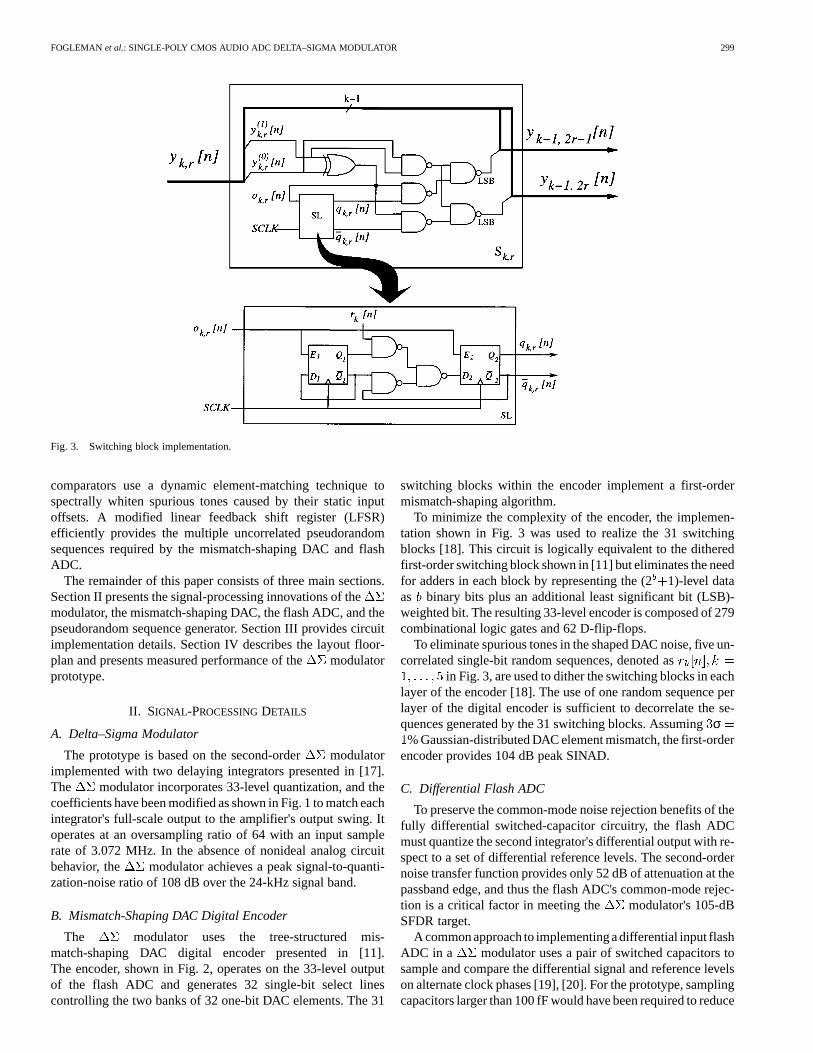
Fig. 3. Switching block implementation.
comparators use a dynamic element-matching technique tospectrally whiten spurious tones caused by their static inputoffsets. A modified linear feedback shift register (LFSR)efficiently provides the multiple uncorrelated pseudorandomsequences required by the mismatch-shaping DAC and flashADC.
The remainder of this paper consists of three main sections.Section II presents the signal-processing innovations of themodulator, the mismatch-shaping DAC, the flash ADC, and thepseudorandom sequence generator. Section III provides circuitimplementation details. Section IV describes the layout floor-plan and presents measured performance of themodulatorprototype.
II. SIGNAL-PROCESSINGDETAILS
A. Delta–Sigma Modulator
The prototype is based on the second-order modulatorimplemented with two delaying integrators presented in [17].The modulator incorporates 33-level quantization, and thecoefficients have been modified as shown in Fig. 1 to match eachintegrator's full-scale output to the amplifier's output swing. Itoperates at an oversampling ratio of 64 with an input samplerate of 3.072 MHz. In the absence of nonideal analog circuitbehavior, the modulator achieves a peak signal-to-quanti-zation-noise ratio of 108 dB over the 24-kHz signal band.
B. Mismatch-Shaping DAC Digital Encoder
The modulator uses the tree-structured mis-match-shaping DAC digital encoder presented in [11].The encoder, shown in Fig. 2, operates on the 33-level outputof the flash ADC and generates 32 single-bit select linescontrolling the two banks of 32 one-bit DAC elements. The 31
switching blocks within the encoder implement a first-ordermismatch-shaping algorithm.
To minimize the complexity of the encoder, the implemen-tation shown in Fig. 3 was used to realize the 31 switchingblocks [18]. This circuit is logically equivalent to the ditheredfirst-order switching block shown in [11] but eliminates the needfor adders in each block by representing the (21)-level dataas binary bits plus an additional least significant bit (LSB)-weighted bit. The resulting 33-level encoder is composed of 279combinational logic gates and 62 D-flip-flops.
To eliminate spurious tones in the shaped DAC noise, five un-correlated single-bit random sequences, denoted as
in Fig. 3, are used to dither the switching blocks in eachlayer of the encoder [18]. The use of one random sequence perlayer of the digital encoder is sufficient to decorrelate the se-quences generated by the 31 switching blocks. Assumingσ% Gaussian-distributed DAC element mismatch, the first-order
encoder provides 104 dB peak SINAD.
C. Differential Flash ADC
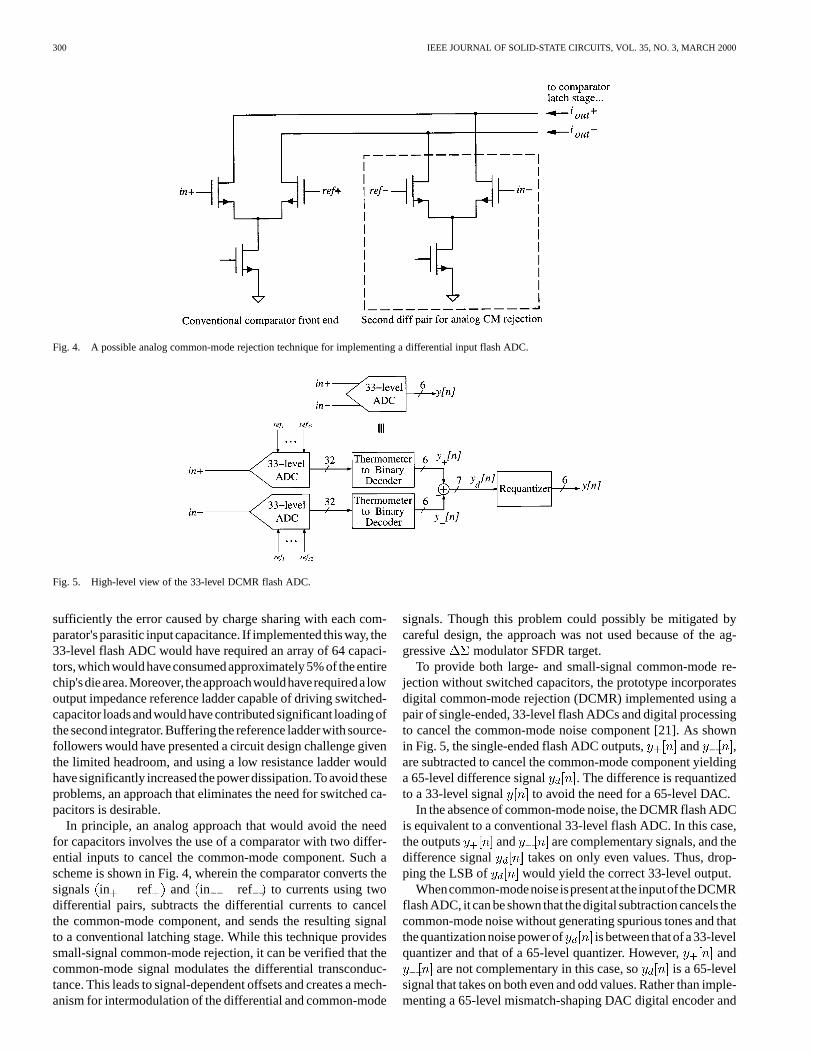
To preserve the common-mode noise rejection benefits of thefully differential switched-capacitor circuitry, the flash ADCmust quantize the second integrator's differential output with re-spect to a set of differential reference levels. The second-ordernoise transfer function provides only 52 dB of attenuation at thepassband edge, and thus the flash ADC's common-mode rejec-tion is a critical factor in meeting the modulator's 105-dBSFDR target.
A commonapproach to implementing a differential input flashADC in a modulator uses a pair of switched capacitors tosample and compare the differential signal and reference levelson alternate clock phases [19], [20]. For the prototype, samplingcapacitors larger than 100 fF would have been required to reduce
300 IEEE JOURNAL OF SOLID-STATE CIRCUITS, VOL. 35, NO. 3, MARCH 2000
Fig. 4. A possible analog common-mode rejection technique for implementing a differential input flash ADC.
Fig. 5. High-level view of the 33-level DCMR flash ADC.
sufficiently the error caused by charge sharing with each com-parator'sparasitic inputcapacitance. If implemented thisway, the33-level flash ADC would have required an array of 64 capaci-tors,whichwouldhaveconsumedapproximately5%of theentirechip'sdiearea.Moreover, theapproachwouldhaverequireda lowoutput impedance reference ladder capable of driving switched-capacitor loadsandwouldhave contributedsignificant loadingofthe second integrator.Buffering the reference ladder withsource-followers would have presented a circuit design challenge giventhe limited headroom, and using a low resistance ladder wouldhavesignificantly increased thepowerdissipation.Toavoid theseproblems, an approach that eliminates the need for switched ca-pacitors is desirable.
In principle, an analog approach that would avoid the needfor capacitors involves the use of a comparator with two differ-ential inputs to cancel the common-mode component. Such ascheme is shown in Fig. 4, wherein the comparator converts thesignals in ref and in ref to currents using twodifferential pairs, subtracts the differential currents to cancelthe common-mode component, and sends the resulting signalto a conventional latching stage. While this technique providessmall-signal common-mode rejection, it can be verified that thecommon-mode signal modulates the differential transconduc-tance. This leads to signal-dependent offsets and creates a mech-anism for intermodulation of the differential and common-mode
signals. Though this problem could possibly be mitigated bycareful design, the approach was not used because of the ag-gressive modulator SFDR target.
To provide both large- and small-signal common-mode re-jection without switched capacitors, the prototype incorporatesdigital common-mode rejection (DCMR) implemented using apair of single-ended, 33-level flash ADCs and digital processingto cancel the common-mode noise component [21]. As shownin Fig. 5, the single-ended flash ADC outputs, and ,are subtracted to cancel the common-mode component yieldinga 65-level difference signal . The difference is requantizedto a 33-level signal to avoid the need for a 65-level DAC.
In the absence of common-mode noise, the DCMR flash ADCis equivalent to a conventional 33-level flash ADC. In this case,the outputs and are complementary signals, and thedifference signal takes on only even values. Thus, drop-ping the LSB of would yield the correct 33-level output.
Whencommon-modenoiseispresentat the inputof theDCMRflash ADC, it can be shown that the digital subtraction cancels thecommon-mode noise without generating spurious tones and thatthequantizationnoisepowerof isbetween thatofa33-levelquantizer and that of a 65-level quantizer. However, and
are not complementary in this case, so is a 65-levelsignal that takes on both even and odd values. Rather than imple-menting a 65-level mismatch-shaping DAC digital encoder and
FOGLEMAN et al.: SINGLE-POLY CMOS AUDIO ADC DELTA–SIGMA MODULATOR 301
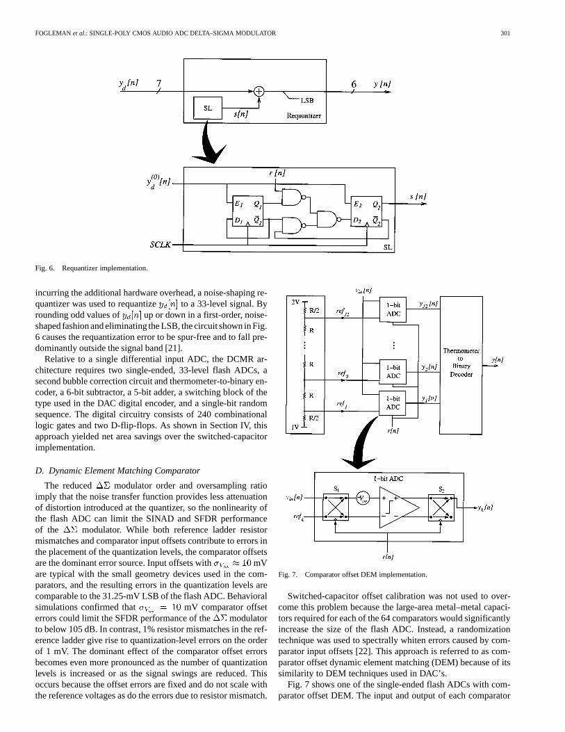
Fig. 6. Requantizer implementation.
incurring the additional hardware overhead, a noise-shaping re-quantizer was used to requantize to a 33-level signal. Byrounding odd values of up or down in a first-order, noise-shaped fashion and eliminating the LSB, the circuit shown in Fig.6 causes the requantization error to be spur-free and to fall pre-dominantly outside the signal band [21].
Relative to a single differential input ADC, the DCMR ar-chitecture requires two single-ended, 33-level flash ADCs, asecond bubble correction circuit and thermometer-to-binary en-coder, a 6-bit subtractor, a 5-bit adder, a switching block of thetype used in the DAC digital encoder, and a single-bit randomsequence. The digital circuitry consists of 240 combinationallogic gates and two D-flip-flops. As shown in Section IV, thisapproach yielded net area savings over the switched-capacitorimplementation.
D. Dynamic Element Matching Comparator
The reduced modulator order and oversampling ratioimply that the noise transfer function provides less attenuationof distortion introduced at the quantizer, so the nonlinearity ofthe flash ADC can limit the SINAD and SFDR performanceof the modulator. While both reference ladder resistormismatches and comparator input offsets contribute to errors inthe placement of the quantization levels, the comparator offsetsare the dominant error source. Input offsets with mVare typical with the small geometry devices used in the com-parators, and the resulting errors in the quantization levels arecomparable to the 31.25-mV LSB of the flash ADC. Behavioralsimulations confirmed that mV comparator offseterrors could limit the SFDR performance of the modulatorto below 105 dB. In contrast, 1% resistor mismatches in the ref-erence ladder give rise to quantization-level errors on the orderof 1 mV. The dominant effect of the comparator offset errorsbecomes even more pronounced as the number of quantizationlevels is increased or as the signal swings are reduced. Thisoccurs because the offset errors are fixed and do not scale withthe reference voltages as do the errors due to resistor mismatch.
Fig. 7. Comparator offset DEM implementation.
Switched-capacitor offset calibration was not used to over-come this problem because the large-area metal–metal capaci-tors required for each of the 64 comparators would significantlyincrease the size of the flash ADC. Instead, a randomizationtechnique was used to spectrally whiten errors caused by com-parator input offsets [22]. This approach is referred to as com-parator offset dynamic element matching (DEM) because of itssimilarity to DEM techniques used in DAC’s.
Fig. 7 shows one of the single-ended flash ADCs with com-parator offset DEM. The input and output of each comparator
302 IEEE JOURNAL OF SOLID-STATE CIRCUITS, VOL. 35, NO. 3, MARCH 2000
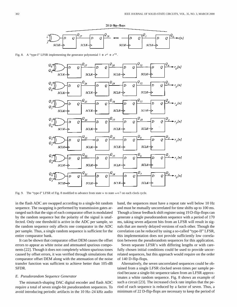
Fig. 8. A “type-I” LFSR implementing the generator polynomial1 + x + x .
Fig. 9. The “type-I” LFSR of Fig. 8 modified to advance from staten to staten+7 on each clock cycle.
in the flash ADC are swapped according to a single-bit randomsequence. The swapping is performed by transmission gates ar-ranged such that the sign of each comparator offset is modulatedby the random sequence but the polarity of the signal is unaf-fected. Only one threshold is active in the ADC per sample, sothe random sequence only affects one comparator in the ADCper sample. Thus, a single random sequence is sufficient for theentire comparator bank.
It can be shown that comparator offset DEM causes the offseterrors to appear as white noise and attenuated spurious compo-nents [22]. Though it does not completely whiten spurious tonescaused by offset errors, it was verified through simulations thatcomparator offset DEM along with the attenuation of the noisetransfer function was sufficient to achieve better than 105-dBSFDR.
E. Pseudorandom Sequence Generator
The mismatch-shaping DAC digital encoder and flash ADCrequire a total of seven single-bit pseudorandom sequences. Toavoid introducing periodic artifacts in the 10 Hz–24 kHz audio
band, the sequences must have a repeat rate well below 10 Hzand must be mutually uncorrelated for time shifts up to 100 ms.Though a linear feedback shift register using 19 D-flip-flops cangenerate a single pseudorandom sequence with a period of 170ms, taking seven adjacent bits from an LFSR will result in sig-nals that are merely delayed versions of each other. Though thecorrelation can be reduced by using a so-called “type-II” LFSR,this implementation does not provide sufficiently low correla-tion between the pseudorandom sequences for this application.
Seven separate LFSR’s with differing lengths or with care-fully chosen initial conditions could be used to provide uncor-related sequences, but this approach would require on the orderof 140 D-flip-flops.
Alternatively, the seven uncorrelated sequences could be ob-tained from a single LFSR clocked seven times per sample pe-riod because a single-bit sequence taken from an LFSR approx-imates a white random sequence. Fig. 8 shows an example ofsuch a circuit [23]. The increased clock rate implies that the pe-riod of each sequence is reduced by a factor of seven. Thus, aminimum of 22 D-flip-flops are necessary to keep the period of
FOGLEMAN et al.: SINGLE-POLY CMOS AUDIO ADC DELTA–SIGMA MODULATOR 303
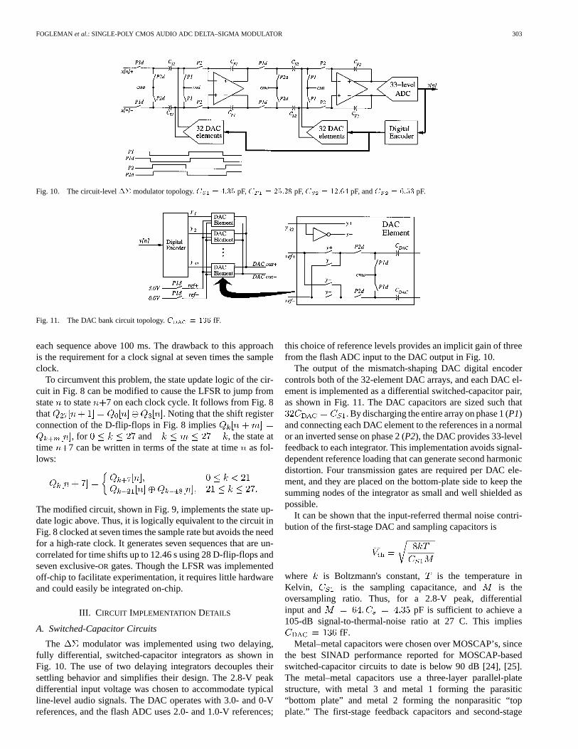
Fig. 10. The circuit-level�� modulator topology.C = 4:35 pF,C = 25:28 pF,C = 12:64 pF, andC = 6:53 pF.
Fig. 11. The DAC bank circuit topology.C = 136 fF.
each sequence above 100 ms. The drawback to this approachis the requirement for a clock signal at seven times the sampleclock.
To circumvent this problem, the state update logic of the cir-cuit in Fig. 8 can be modified to cause the LFSR to jump fromstate to state 7 on each clock cycle. It follows from Fig. 8that . Noting that the shift registerconnection of the D-flip-flops in Fig. 8 implies
, for and , the state attime 7 can be written in terms of the state at timeas fol-lows:
The modified circuit, shown in Fig. 9, implements the state up-date logic above. Thus, it is logically equivalent to the circuit inFig. 8 clocked at seven times the sample rate but avoids the needfor a high-rate clock. It generates seven sequences that are un-correlated for time shifts up to 12.46 s using 28 D-flip-flops andseven exclusive-OR gates. Though the LFSR was implementedoff-chip to facilitate experimentation, it requires little hardwareand could easily be integrated on-chip.
III. CIRCUIT IMPLEMENTATION DETAILS
A. Switched-Capacitor Circuits
The modulator was implemented using two delaying,fully differential, switched-capacitor integrators as shown inFig. 10. The use of two delaying integrators decouples theirsettling behavior and simplifies their design. The 2.8-V peakdifferential input voltage was chosen to accommodate typicalline-level audio signals. The DAC operates with 3.0- and 0-Vreferences, and the flash ADC uses 2.0- and 1.0-V references;
this choice of reference levels provides an implicit gain of threefrom the flash ADC input to the DAC output in Fig. 10.
The output of the mismatch-shaping DAC digital encodercontrols both of the 32-element DAC arrays, and each DAC el-ement is implemented as a differential switched-capacitor pair,as shown in Fig. 11. The DAC capacitors are sized such that
. By discharging the entire array on phase 1 (P1)and connecting each DAC element to the references in a normalor an inverted sense on phase 2 (P2), the DAC provides 33-levelfeedback to each integrator. This implementation avoids signal-dependent reference loading that can generate second harmonicdistortion. Four transmission gates are required per DAC ele-ment, and they are placed on the bottom-plate side to keep thesumming nodes of the integrator as small and well shielded aspossible.
It can be shown that the input-referred thermal noise contri-bution of the first-stage DAC and sampling capacitors is
where is Boltzmann's constant, is the temperature inKelvin, is the sampling capacitance, and is theoversampling ratio. Thus, for a 2.8-V peak, differentialinput and pF is sufficient to achieve a105-dB signal-to-thermal-noise ratio at 27 C. This implies
fF.Metal–metal capacitors were chosen over MOSCAP’s, since
the best SINAD performance reported for MOSCAP-basedswitched-capacitor circuits to date is below 90 dB [24], [25].The metal–metal capacitors use a three-layer parallel-platestructure, with metal 3 and metal 1 forming the parasitic“bottom plate” and metal 2 forming the nonparasitic “topplate.” The first-stage feedback capacitors and second-stage
304 IEEE JOURNAL OF SOLID-STATE CIRCUITS, VOL. 35, NO. 3, MARCH 2000
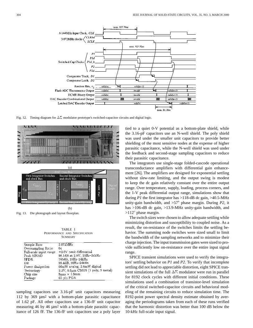
Fig. 12. Timing diagram for�� modulator prototype's switched-capacitor circuits and digital logic.
(a)
(b)
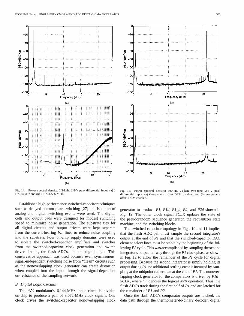
Fig. 13. Die photograph and layout floorplan.
TABLE IPERFORMANCE AND SPECIFICATION
SUMMARY
sampling capacitors use 3.16-pF unit capacitors measuring112 by 369µm2 with a bottom-plate parasitic capacitanceof 1.62 pF. All other capacitors use a 136-fF unit capacitormeasuring 46 by 46µm2 with a bottom-plate parasitic capac-itance of 126 fF. The 136-fF unit capacitors use a poly layer
tied to a quiet 0-V potential as a bottom-plate shield, whilethe 3.16-pF capacitors use an N-well shield. The poly shieldwas used under the smaller unit capacitors to provide bettershielding of the most sensitive nodes at the expense of higherparasitic capacitance, while the N-well shield was used underthe feedback and second-stage sampling capacitors to reducetheir parasitic capacitance.
The integrators use single-stage folded-cascode operationaltransconductance amplifiers with differential gain enhance-ment [26]. The amplifiers are designed for exponential settlingwithout slew-rate limiting, and the output swing is modestto keep the dc gain relatively constant over the entire outputrange. Over temperature, supply, loading, process corners, andthe 1-V peak differential output range, simulations show thatduringP1 the first integrator has >118-dB dc gain, >40.5-MHzunity-gain bandwidth, and >57phase margin. DuringP2, ithas >106-dB dc gain, >13.9-MHz unity-gain bandwidth, and>112 phase margin.
The switch sizes were chosen to allow adequate settling whileminimizing distortion and susceptibility to coupled noise. As aresult, the on-resistance of the switches limits the settling be-havior. The summing node switches were sized small to limitthe bandwidth of the sampling networks and to minimize theircharge injection. The input transmission gates were sized to pro-vide sufficiently low on-resistance over the entire input signalrange.
SPICE transient simulations were used to verify the integra-tors' settling behavior onP1 andP2. To verify that incompletesettling did not lead to appreciable distortion, eight SPICE tran-sient simulations of the full modulator were run in parallelfor 8192 clock cycles with different initial conditions. Thesesimulations used a combination of transistor-level simulationof the critical switched-capacitor circuits and behavioral mod-eling of the remaining circuits to reduce simulation time. The8192-point power spectral density estimate obtained by aver-aging the periodograms taken from each of these runs verifiedthat the harmonic distortion was better than 100 dB below the10-kHz full-scale input signal.
FOGLEMAN et al.: SINGLE-POLY CMOS AUDIO ADC DELTA–SIGMA MODULATOR 305
(a)
(b)
Fig. 14. Power spectral density; 1.5-kHz, 2.8-V peak differential input. (a) 0Hz–24 kHz and (b) 0 Hz–1.536 MHz.
Established high-performance switched-capacitor techniquessuch as delayed bottom plate switching [27] and isolation ofanalog and digital switching events were used. The digitalcells and output pads were designed for modest switchingspeed to minimize noise generation. The substrate ties forall digital circuits and output drivers were kept separatefrom the current-bearing lines to reduce noise couplinginto the substrate. Four on-chip supply domains were usedto isolate the switched-capacitor amplifiers and switchesfrom the switched-capacitor clock generation and switchdriver circuits, the flash ADCs, and the digital logic. Thisconservative approach was used because even synchronous,signal-independent switching noise from “clean” circuits suchas the nonoverlapping clock generator can create distortionwhen coupled into the input through the signal-dependenton-resistance of the sampling network.
B. Digital Logic Circuits
The modulator's 6.144-MHz input clock is dividedon-chip to produce a pair of 3.072-MHz clock signals. Oneclock drives the switched-capacitor nonoverlapping clock
(a)
(b)
Fig. 15. Power spectral density; 500-Hz, 21-kHz two-tone, 2.8-V peakdifferential input. (a) Comparator offset DEM disabled and (b) comparatoroffset DEM enabled.
generator to produceP1, P1d, P1_b, P2, and P2d shown inFig. 12. The other clock signalSCLK updates the state ofthe pseudorandom sequence generator, the requantizer statemachine, and the switching blocks.
The switched-capacitor topology in Figs. 10 and 11 impliesthat the flash ADC pair must sample the second integrator'soutput at the end ofP1 and that the switched-capacitor DACelement select lines must be stable by the beginning of the fol-lowingP2cycle. This was accomplished by sampling the secondintegrator's output halfway through theP1clock phase as shownin Fig. 12 to allow the remainder of theP1 cycle for digitalprocessing. Because the second integrator is simply holding itsoutput duringP1, no additional settling error is incurred by sam-pling at the midpoint rather than at the end ofP1. The nonover-lapping clock generator for the comparators is driven byP1dSCLK, where “·” denotes the logicalAND operation. Thus, theflash ADCs track during the first half ofP1 and are latched forthe remainder ofP1 andP2.
Once the flash ADC's comparator outputs are latched, thedata path through the thermometer-to-binary decoder, digital
306 IEEE JOURNAL OF SOLID-STATE CIRCUITS, VOL. 35, NO. 3, MARCH 2000
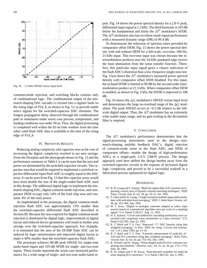
Fig. 16. 1.5-kHz SINAD versus input level.
common-mode rejection, and switching blocks consists onlyof combinational logic. The combinational output of the mis-match-shaping DAC encoder is clocked into a register bank onthe rising edge ofP1d_b, as shown in Fig. 12, to provide stableselect signals for the switched-capacitor DAC elements. Thelongest propagation delay observed through the combinationalpath in simulation under worst case process, temperature, andloading conditions was under 50 ns. Thus, the digital processingis completed well within the 81-ns time window from the timewhen valid flash ADC data is available to the time of the risingedge ofP1d_b.
IV. PROTOTYPERESULTS
Reducing analog complexity and capacitor area at the cost ofincreasing the digital complexity resulted in net area savings.From the floorplan and die photograph shown in Fig. 13 and theperformance summary in Table I, it can be seen that the area andpower are dominated by the switched-capacitor circuits. The ca-pacitor area that would be required to implement a switched-ca-pacitor differential input flash ADC is roughly equal to the DACarray. It can be seen from Fig. 13 that this capacitor array wouldhave been double the size of the single-ended flash ADC usedin this design. The additional digital logic to implement the mis-match-shaping DAC, digital common-mode rejection, and com-parator DEM occupy only 14% of the total chip area and con-sume 4% of the total power.
As implemented in the prototype, the digital common-moderejection flash ADC was approximately 13% smaller thanthe switched-capacitor differential flash ADC described inSection III. Because the area required for digital common-moderejection is dominated by digital logic, improvements in digitallayout and reduced device geometries will result in further areasavings over the switched-capacitor approach. For example,it is estimated that the area of the DCMR flash ADC can bereduced by logic minimization and improved digital layout tomake it 40% smaller than the switched-capacitor flash ADC.
The prototype achieves 98-dB peak SINAD for single-toneaudio-band inputs and 105-dB SFDR for single- and two-toneinputs. These results represent the worst case measured perfor-mance for a wide range of single- and two-tone audio-band in-
puts. Fig. 14 shows the power spectral density for a 2.8-V peak,differential input signal at 1.5 kHz. The third harmonic is 105 dBbelow the fundamental and limits the modulator's SFDR.The modulator also has excellent small-signal performancewith a measured dynamic range (DR) of 99.4 dB.
To demonstrate the reduction of spurious tones provided bycomparator offset DEM, Fig. 15 shows the power spectral den-sity with and without DEM for a full-scale, two-tone, 500-Hz,21-kHz input. This two-tone input was chosen because the in-termodulation products near the 24-kHz passband edge receivethe least attenuation from the noise transfer function. There-fore, this particular input signal gives a clearer indication ofthe flash ADC's distortion than a low-frequency single-tone test.Fig. 15(a) shows the modulator's measured power spectraldensity with comparator offset DEM disabled. For this input,the in-band SFDR is limited to 99 dB by the second-order inter-modulation product at 21.5 kHz. When comparator offset DEMis enabled, as shown in Fig. 15(b), the SFDR is improved to 108dB.
Fig. 16 shows the modulator's SINAD versus input leveland demonstrates the large no-overload range of themod-ulator. The peak SINAD occurs at−0.5 dB relative to the full-scale digital output. Thus, the modulator has an extremelywide usable input range, and no gain scaling in the decimationfilter is required.
V. CONCLUSION
The modulator's performance demonstrates that thesignal-processing innovations used in the design—mis-match-shaping multibit feedback DAC’s, digital rejectionof common-mode noise in the flash ADC, and DEM ofcomparator offsets—enable the design of high-performanceADCs in a single-poly 3.3-V CMOS process. The designapproach used here shifted the design burden away from theswitched-capacitor circuits at the expense of increased digitallogic complexity and proved to be a successful tradeoff in afabrication process optimized for digital logic.
REFERENCES
[1] B. H. Leung and S. Sutarja, “Multi-bit sigma-delta A/D converter incor-porating a novel class of dynamic element matching techniques,”IEEETrans. Circuits Syst. II, vol. 39, pp. 35–51, Jan. 1992.
[2] F. Chen and B. H. Leung, “A high resolution multibit sigma-delta modu-lator with individual level averaging,”IEEE J. Solid-State Circuits, vol.30, pp. 453–460, Apr. 1995.
[3] M. J. Story, “Digital to analogue converter adapted to select inputsources based on a preselected algorithm once per cycle of a samplingsignal,” U.S. Patent 5 138 317, Aug. 11, 1992.
[4] H. S. Jackson, “Circuit and method for cancelling nonlinearity error as-sociated with component value mismatches in a data converter,” U.S.Patent 5 221 926, June 22, 1993.
[5] R. T. Baird and T. S. Fiez, “Improved�� DAC linearity using dataweighted averaging,” inProc. IEEE Int. Symp. Circuits and Systems,vol. 1 of 3, May 1995, pp. 13–16.
[6] R. T. Baird and T. S. Fiez, “Linearity enhancement of multi-bit��A/D and D/A converters using data weighted averaging,”IEEE Trans.Circuits Syst. II, vol. 42, pp. 753–762, Dec. 1995.
[7] R. Schreier and B. Zhang, “Noise-shaped multi-bit D/A converter em-ploying unit elements,”Electron. Lett., vol. 31, no. 20, pp. 1712–1713,Sept. 28, 1995.
[8] R. W. Adams and T. W. Kwan, “Data-directed scrambler for multi-bitnoise shaping D/A converters,” U.S. Patent 5 404 142, Apr. 4, 1995.

FOGLEMAN et al.: SINGLE-POLY CMOS AUDIO ADC DELTA–SIGMA MODULATOR 307
[9] T. W. Kwan, R. W. Adams, and R. Libert, “A stereo multi-bit�� D/Awith asynchronous master-clock interface,” inIEEE ISSCC Dig. Tech.Papers, vol. 39, Feb. 1996, pp. 226–227.
[10] T. W. Kwan, R. W. Adams, and R. Libert, “A stereo multibit Sigma DeltaDAC with asynchronous master-clock interface,”IEEE J. Solid-StateCircuits, vol. 31, pp. 1881–1887, Dec. 1996.
[11] I. Galton, “Spectral shaping of circuit errors in digital-to-analog con-verters,”IEEE Trans. Circuits Syst. II, vol. 44, pp. 808–817, Oct. 1997.
[12] I. Galton, “Spectral shaping of circuit errors in digital-to-analog con-verters,” U.S. Patent 5 684 482, Nov. 4, 1997.
[13] E. Fogleman, I. Galton, W. Huff, and H. Jensen, “A 3.3 V single-polyCMOS audio ADC Delta-Sigma modulator with 98 dB peak SINAD,”in IEEE Custom Integrated Circuits Conf., May 1999, pp. 121–124.
[14] S. Rabii and B. A. Wooley, “A 1.8 V digital-audio sigma-delta modulatorin 0.8µ CMOS,” IEEE J. Solid-State Circuits, vol. 32, pp. 783–796, June1997.
[15] E. J. van der Zwan, “A 2.3 mW CMOS�� modulator for audio ap-plications,” in IEEE ISSCC Dig. Tech. Papers, vol. 40, Feb. 1997, pp.220–221.
[16] A. Yasuda, H. Tanimoto, and T. Iida, “A 100 kHz 9.5 mW multi-bit��DAC and ADC using noise shaping dynamic elements matching withtree structure,” inIEEE ISSCC Dig. Tech. Papers, vol. 41, Feb. 1998,pp. 64–65.
[17] G. Lainey, R. Saintlaurens, and P. Senn, “Switched-capacitor second-order noise-shaping coder,”Electron. Lett., vol. 19, pp. 149–150, Feb.1983.
[18] H. T. Jensen and I. Galton, “A reduced-complexity mismatch-shapingDAC for delta-sigma data converters,” inProc. IEEE Int. Symp. Circuitsand Systems, vol. 1 of 6, June 1998, pp. 504–507.
[19] S. H. Lewis and P. R. Gray, “A pipelined 5-Msample/s 9-bit analog-to-digital converter,”IEEE J. Solid-State Circuits, vol. SC-22, pp. 954–961,Dec. 1987.
[20] T. Shih, L. Der, S. H. Lewis, and P. J. Hurst, “A fully differentialcomparator using a switched-capacitor differencing circuit withcommon-mode rejection,”IEEE J. Solid-State Circuits, vol. 32, pp.250–253, Feb. 1997.
[21] E. Fogleman, I. Galton, and H. Jensen, “An area-efficient differentialinput ADC with digital common mode rejection,” inProc. IEEE Int.Symp. Circuits and Systems, vol. 2 of 6, June 1999, pp. 347–350.
[22] E. Fogleman, I. Galton, and H. Jensen, “A dynamic element matchingtechnique for reduced-distortion multibit quantization in Delta-SigmaADCs,” in Proc. IEEE Int. Symp. Circuits and Systems, vol. 2 of 6, June1999, pp. 290–293.
[23] E. J. McCluskey,Logic Design Principles. Englewood Cliffs, NJ:Prentice-Hall, 1986, pp. 457–461.
[24] L. Williams III, “An audio DAC with 90 dB linearity using MOS tometal-metal charge transfer,” inIEEE ISSCC Dig. Tech. Papers, vol. 41,Feb. 1998, pp. 58–59.
[25] H. Yoshizawa, Y. Huang, P. F. Ferguson , and G. C. Temes,“MOSFET-only switched-capacitor circuits in digital CMOS tech-nology,” IEEE J. Solid-State Circuits, vol. 34, pp. 734–747, June 1999.
[26] J. Lloyd and H. S. Lee, “A CMOS opamp with fully-differential gain-enhancement,”IEEE Trans. Circuits Syst. II, vol. 41, pp. 241–243, Mar.1994.
[27] D. G. Haigh and B. Singh, “A switching scheme for switched-capacitorfilters, which reduces effect of parasitic capacitances associated withcontrol terminals,” inProc. IEEE Int. Symp. Circuits and Systems, vol.2 of 3, June 1983, pp. 586–589.
Eric Fogleman (S'97) received the B.S. degreefrom the University of Maryland, College Park, in1990 and the M.S. degree from the University ofCalifornia, San Diego (UCSD), in 1998, both inelectrical engineering. He is currently pursuing thePh.D. degree in electrical engineering at UCSD.
From 1990 to 1993, he was with Analog Devices,Wilmington, MA as a Product/Test Engineer foraudio converter products. From 1993 to 1996, he waswith Brooktree Corp., San Diego, CA, as a ProductEngineer and Design Engineer for computer audio
and multimedia graphics products. Since 1996, he has been a Graduate StudentResearcher at UCSD. His current research is in the area of data-converter andsignal-processing hardware design.
Ian Galton (M'92) received the Sc.B. degree fromBrown University, Providence, RI, in 1984 and theM.S. and Ph.D. degrees from the California Instituteof Technology, Pasadena, in 1989 and 1992, respec-tively, all in electrical engineering.
He is currently an Associate Professor at theUniversity of California, San Diego. He wasformerly with the University of California, Irvine;NASA Jet Propulsion Laboratory; Acuson; andMead Data Central. He acts as a regular Consultantfor several companies. His research interests involve
integrated signal-processing circuits and systems for communications. He hasreceived four patents. He currently serves on the Board of Directors of AnalogCircuit Technologies and on the Technical Advisory Board for ProminentCommunications Inc.
Prof. Galton received the Caltech Charles Wilts doctoral thesis prize. He ison the Board of Governors for the IEEE Circuits and Systems Society.
William J. Huff (S'97) received the B.S. degree inelectrical engineering from the University of Cali-fornia, Los Angeles, in 1990. He is currently pursuingthe Ph.D. degree in electrical engineering at the Uni-versity of California, San Diego.
From 1990 to 1996, he was an Analog CircuitDesigner at Lear Astronics, Santa Monica, CA.His present research interests include frequencysynthesis, signal processing for communicationssystems, and delta–sigma data converters.
Henrik T. Jensenwas born in Odense, Denmark, in1968. He received the B.S. degree in computer engi-neering from Odense University, Odense, Denmark,in 1992, the M.S. degree in electrical and computerengineering from the University of California, Irvine,in 1994, and the Ph.D. degree in electrical and com-puter engineering from the University of California,San Diego, in 1997.
From July 1997 to June 1998, he was a Post-graduate Research Engineer at the University ofCalifornia, San Diego, and is currently with HRL
Laboratories, LLC, Malibu, CA. His research interests include digital signalprocessing and data conversion techniques.