A 6-fJ/conversion-step 200-kSps asynchronous SAR ADC with attenuation capacitor in 130-nm CMOS
14
A 6-fJ/conversion-step 200-kSps asynchronous SAR ADC with attenuation capacitor in 130-nm CMOS Stefano Brenna • Andrea Bonfanti • Andrea Leonardo Lacaita Received: 22 March 2014 / Revised: 29 May 2014 / Accepted: 30 July 2014 Ó Springer Science+Business Media New York 2014 Abstract The conventional binary weighted array suc- cessive approximation register (SAR) analog-to-digital converter (ADC) is the common topology adopted to achieve high efficiency conversion, i.e. with less than 10 fJ/ conversion-step, even if it requires extra effort to design and simulate full custom fF or sub-fF capacitors. This paper presents the design and the optimization of an asynchronous fully-differential SAR ADC with attenuation capacitor achieving an efficiency similar to conventional binary weighted array converters but adopting standard MiM capacitors. A monotonic switching algorithm further reduces the capacitive array consumption while an asyn- chronous and fully-differential dynamic logic minimizes the digital power consumption. The 10-bit converter pro- totype has been fabricated in a standard 0.13-lm CMOS technology. At a 0.5-V supply and 200-kSps sampling frequency, the ADC achieves a SNDR of 52.6 dB, an ENOB of 8.45, and a power consumption of 420 nW, corresponding to a figure-of-merit (FOM) of 6 fJ/conver- sion-step. This efficiency is comparable to the best results published so far and it’s the lowest among ADCs in 130-nm or less scaled technology. The ADC core occupies an active area of only 0.045 mm 2 . Keywords ADC Analog-to-digital conversion Nonlinearity Mismatch Asynchronous logic Successive approximation register 1 Introduction In energy-limited applications, such as wireless sensor nodes, implantable medical devices or portable amuse- ments, the adoption of ultra-low power circuits is manda- tory in order to extent the system battery lifetime. ADCs featuring moderate sampling rate (0.01–1 Msps) and res- olution (8–10 bit) are key components in such devices. Among different converter architectures, SAR ADC is the best choice due to its good trade-off among power effi- ciency, conversion accuracy and design complexity. In such converters, the primary sources of power con- sumption are the digital control circuit and the capacitive DAC array. While the digital power consumption benefits from the technology advancement, the power consumption due to the capacitive array is limited by the capacitor mismatch, which is almost technology-independent. For this reason, a great number of DAC topologies and switching algorithms have been proposed in order to reduce DAC power consumption without penalty in terms of accuracy. The latest trend is to rely on the high linearity properties of the conventional binary weighted (CBW) array adopting full-custom unit capacitance in the sub-fF range [1–3]. In fact, the minimum value of capacitors supplied by general-purpose design-kits is much larger than necessary to meet the linearity requirements, resulting in a considerably large array capacitance and thus in a high switching power. This approach requires extra-efforts to design and model the unit capacitance or error correction techniques, thus increasing area and circuit complexity. S. Brenna A. Bonfanti (&) A. L. Lacaita Dipartimento di Elettronica, Informazione e Bioingeneria, Politecnico di Milano, Via Golgi 40, 20133 Milano, Italy e-mail: [email protected] S. Brenna e-mail: [email protected] A. L. Lacaita e-mail: [email protected] 123 Analog Integr Circ Sig Process DOI 10.1007/s10470-014-0384-z
Transcript of A 6-fJ/conversion-step 200-kSps asynchronous SAR ADC with attenuation capacitor in 130-nm CMOS

A 6-fJ/conversion-step 200-kSps asynchronous SAR ADCwith attenuation capacitor in 130-nm CMOS
Stefano Brenna • Andrea Bonfanti •
Andrea Leonardo Lacaita
Received: 22 March 2014 / Revised: 29 May 2014 / Accepted: 30 July 2014
� Springer Science+Business Media New York 2014
Abstract The conventional binary weighted array suc-
cessive approximation register (SAR) analog-to-digital
converter (ADC) is the common topology adopted to
achieve high efficiency conversion, i.e. with less than 10 fJ/
conversion-step, even if it requires extra effort to design
and simulate full custom fF or sub-fF capacitors. This
paper presents the design and the optimization of an
asynchronous fully-differential SAR ADC with attenuation
capacitor achieving an efficiency similar to conventional
binary weighted array converters but adopting standard
MiM capacitors. A monotonic switching algorithm further
reduces the capacitive array consumption while an asyn-
chronous and fully-differential dynamic logic minimizes
the digital power consumption. The 10-bit converter pro-
totype has been fabricated in a standard 0.13-lm CMOS
technology. At a 0.5-V supply and 200-kSps sampling
frequency, the ADC achieves a SNDR of 52.6 dB, an
ENOB of 8.45, and a power consumption of 420 nW,
corresponding to a figure-of-merit (FOM) of 6 fJ/conver-
sion-step. This efficiency is comparable to the best results
published so far and it’s the lowest among ADCs in
130-nm or less scaled technology. The ADC core occupies
an active area of only 0.045 mm2.
Keywords ADC � Analog-to-digital conversion �Nonlinearity � Mismatch � Asynchronous logic �Successive approximation register
1 Introduction
In energy-limited applications, such as wireless sensor
nodes, implantable medical devices or portable amuse-
ments, the adoption of ultra-low power circuits is manda-
tory in order to extent the system battery lifetime. ADCs
featuring moderate sampling rate (0.01–1 Msps) and res-
olution (8–10 bit) are key components in such devices.
Among different converter architectures, SAR ADC is the
best choice due to its good trade-off among power effi-
ciency, conversion accuracy and design complexity.
In such converters, the primary sources of power con-
sumption are the digital control circuit and the capacitive
DAC array. While the digital power consumption benefits
from the technology advancement, the power consumption
due to the capacitive array is limited by the capacitor
mismatch, which is almost technology-independent. For
this reason, a great number of DAC topologies and
switching algorithms have been proposed in order to
reduce DAC power consumption without penalty in terms
of accuracy. The latest trend is to rely on the high linearity
properties of the conventional binary weighted (CBW)
array adopting full-custom unit capacitance in the sub-fF
range [1–3]. In fact, the minimum value of capacitors
supplied by general-purpose design-kits is much larger than
necessary to meet the linearity requirements, resulting in a
considerably large array capacitance and thus in a high
switching power. This approach requires extra-efforts to
design and model the unit capacitance or error correction
techniques, thus increasing area and circuit complexity.
S. Brenna � A. Bonfanti (&) � A. L. Lacaita
Dipartimento di Elettronica, Informazione e Bioingeneria,
Politecnico di Milano, Via Golgi 40, 20133 Milano, Italy
e-mail: [email protected]
S. Brenna
e-mail: [email protected]
A. L. Lacaita
e-mail: [email protected]
123
Analog Integr Circ Sig Process
DOI 10.1007/s10470-014-0384-z

In order to investigate the possibility to design a high-
efficient SAR converter without adopting custom unit
capacitance in favor of more reliable standard process
capacitors, in this paper a binary weighted with attenuation
capacitor (BWA) array is proposed and optimized. This
topology, even often adopted in literature to reduce the
DAC capacitance and thus its power consumption, is not
considered the best choice to achieve high conversion
efficiency due to its larger sensitivity to capacitor mis-
match. However, taking into account the typically worse
matching properties of custom capacitors, the BWA
topology adopting standard MiM capacitors can be con-
sidered a valuable alternative to conventional binary-
weighted architecture. Thus, the purpose of this work is to
demonstrate that a BWA SAR converter can achieve effi-
ciency well below 10 fJ/conversion-step and a remarkable
compactness, without requiring the design, modeling and
accurate simulations of custom capacitors. Moreover, by
applying for the first time to a BWA array an efficient
switching procedure as the monotonic switching algorithm
proposed in [4], the DAC power consumption is further
reduced. Finally, an asynchronous and fully-differential
dynamic logic is proposed to minimize the power con-
sumption of the digital logic.
The proposed 10-bit SAR converter (see Fig. 1) was
integrated in 0.13 lm UMC technology with a power
supply ranging from 0.4 to 0.8V [5]. At a nominal supply-
voltage of 0.5 V, the ADC achieves an efficiency of 6 fJ/
conversion-step, in line with the best conventional binary
weighted topologies but adopting as unit element a stan-
dard MiM capacitor of 34 fF.
The paper is organized as follows. Section 2 is devoted
to compare the traditional CBW and the bridge-capacitor
DAC architecture in terms of power consumption and
linearity due to capacitance mismatch. The role of the
parasitic capacitances in the BWA topology is also high-
lighted. Section 3 describes in detail the implementation of
the switched capacitor network, of the asynchronous
dynamic logic and of the dynamic comparator, while
measurement results are shown in Sect. 4. Finally, con-
clusions are drawn in Sect. 5.
2 Comparison between CBW and BWA array
topologies
The fundamental building blocks of a SAR ADC are the
sample-and-hold circuits, the charge-redistribution DAC,
the comparator and the digital logic implementing the
successive approximation algorithm. A capacitive net-
works typically serves as both sampling capacitance and
feedback DAC, its linearity usually limiting the overall AD
converter performance.
The single-ended conventional N-bit binary weighted
capacitive array [6] is depicted in Fig. 2(a), where Cu is the
unit capacitance.
The main alternative to this topology is the binary
weighted with attenuation (or bridge) capacitor array [7, 8],
shown Fig. 2(b). It features an attenuation capacitor, Catt, in
order to divide the array into two binary weighted sub-
arrays: a main-DAC and a sub-DAC of m and l capacitors,
respectively. In particular, since this topology is often used
to reduce the overall capacitance, and thus the power
consumption, we will refer to the BWA architecture with
equal main- and sub-DACs (i.e. m ¼ l ¼ N=2) and
Catt ¼ Cu, which has been shown to be the most energy
efficient among all the possible combinations [9]. In this
SAR
C
C 2C 16C C 2C 16C
+
-
VDD
VDD
Bo
ots
trap
ped
Vin,P
Vin,N
Bo
ots
trap
ped
C
D1
C 2C 16C C 2C 16C
D0-9
Reset
Start
inP
inN
Valid
CK
DQ R
tdelay
Temporizer
Start
Sample Logic
EoCSample
D9
OutP
OutN
........D4 D5 D6 D9
D1........D4 D5 D6 D9
D0-9
D9
D0
D0 EoC
Fig. 1 Schematic of the proposed 10-bit converter
2 C( -1)mu 2Cu Cu
Out
VDDGND
Cu2Cu 2 C( -1)lu
Catt
DMSB,m DMSB,2 DMSB,1 DLSB,l DLSB,2 DLSB,1
Main-DAC Sub-DAC
2 C(N-1)u Cu Cu
Out
VDDGND
4Cu2 C(N-2)u 2Cu
DN DN-1 D3 D2 D1
(a)
(b)
Cpar,subCpar,main
Cpar
Fig. 2 Schematic of a N-bit CBW (a) and of a ðmþ lÞ-bit BWA
(b) capacitive DAC. Also the parasitic capacitances affecting the
arrays are represented
Analog Integr Circ Sig Process
123

section, the impact of the capacitance mismatch on the
performance of both CBW and BWA arrays will be
accurately handled as well the effect of the parasitics that
can limit the converter linearity. The comparison is carried
out on single-ended topologies, even if a fully-differential
architecture is adopted for the proposed converter, without
loss of generality.
2.1 Capacitive mismatch analysis
It’s well established that mismatch in capacitive array
degrades the overall performance of SAR converters.
Although differential nonlinearity (DNL), integral nonlin-
earity (INL) and effective number of bits (ENOB) are
important indicators, ENOB is the best metric of the
overall system performance [10]. Moreover, when com-
paring different converter topologies, the most common
figure-of-merit (FOM) [11], defined as
FOM ¼ Pdiss
2ENOB � fsample
; ð1Þ
relies on the effective number of bits. However, while a
precise formulation of the relationship between capacitive
mismatch and ENOB is still lacking, the maximum stan-
dard deviation of the DNL ðrDNL;maxÞ and INL ðrINL;maxÞhas been analytically derived as function of the unit
capacitance relative standard deviation, r�DCCu
�, for the most
common adopted capacitive arrays [9]. Unfortunately,
ENOB depends on the distribution of the INL and, in
particular, on the variance of the INL along the output code
[10]. Thus, two questions arise: which is the relationship
between ENOB and rDNL;max (or rINL;max)? Do the CBW
and the BWA topologies feature the same ENOB, once the
two topologies are sized to have the same rDNL;max?
In order to answer to these questions, statistical simu-
lations have been carried out on both a single-ended CBW
and BWA 10-bit SAR converter, assuming that the only
contribution to the nonlinearity is the capacitive mismatch.
The simulations have been carried out by means of the
CSAtool [12], which is a simulation and modeling envi-
ronment for the analysis of charge-redistribution DACs for
SAR converters. The result is shown in Fig. 3. For the
same maximum standard deviation of the DNL, the two
topologies feature approximately the same average and
standard deviation of ENOB. Moreover, a rDNL;max lower
than 0.5 is enough to limit the average drop of the ENOB to
0.2 bit and its standard deviation to 0.1. This assures that
the effective number of bit is always larger than 9.5.
Once the correspondence between rDNL;max and ENOB
has been assured, the two topologies can be compared
exploring their inherent trade-off between static nonlin-
earity and power consumption, the latter being proportional
to the overall network capacitance [9] to a first order
approximation. Table 1 shows the expressions of the
overall capacitance, together with rDNL;max and rINL;max, as
function of r�DCCu
�[9, 13], for a single-ended N-bit BWA
and CBW array. The standard deviation of the unit
capacitor can be expressed in terms of Pelgrom mismatch
coefficient, kc, and specific capacitance, cspec, being
r
�DC
Cu
�¼ kc �
ffiffiffiffiffiffiffiffifficspec
2Cu
r; ð2Þ
where the factor 2 takes into account that DC is referred to
a single capacitance with respect to its nominal value.
Considering the same number of bits and the same unit
capacitance for both the topologies, the single-ended BWA
array features an overall capacitance that is approximately
a factor 2N2�1 lower than in the CBW architecture. Despite
this prospected advantage, the BWA array is more sensitive
to mismatch with respect to the CBW array leading to
worse nonlinearity performance. As shown in Table 1, the
effect of mismatch on static nonlinearity is a factor 2N4
larger in the BWA array than in the CBW topology. Since
rDNL is inversely proportional to the square root of the unit
capacitance, the same rDNL;max is achieved in the BWA
(a)
(b)
Fig. 3 Average (a) and standard deviation (b) of ENOB as function
of rDNL;max for a 10-bit CBW and BWA charge redistribution
capacitive DAC
Table 1 Comparison of the CBW and BWA array performance
CBW BWA
Ctot 2N � Cu
�2 � ð2N
2 � 1Þ þ 1�� Cu
rDNL;max 2N2 � r
�DCCu
�2
3N4 � r
�DCCu
�
rINL;max 2N2�1 � r
�DCCu
�2
3N4�1 � r
�DCCu
�
Analog Integr Circ Sig Process
123
architecture with a unit capacitance that is a factor 2N2 larger
than in the conventional array. In this case, the overall
array capacitance of the BWA network is approximately
twice that of a conventional array, independently on the
number of bits.
However, considering the traditional switching algo-
rithm [6] for both the topologies, the energy consumption
depends on the output code. In [9] the average switching
energy for the CBW and the BWA topologies is analyti-
cally derived. When sized to have the same rDNL;max, the
average switching energy consumption of the conventional
array is a factor 1.91 lower than in the BWA topology,
independently on the number of the converter bits, con-
firming that the average power is mainly function of the
overall array capacitance.
The results reported in Table 1 allow to accurately size a
10-bit capacitive array of a SAR ADC in a technology with
a mismatch coefficient kc of 1 % � lm and a specific
capacitance of 1fF=lm2. If we assume to size the array to
achieve 3rDNL;max\0:5 [2, 14], this corresponds to a unit
capacitance of about 59 fF for the BWA topology, while
this value decreases to 1.8 fF for the conventional array.
Moreover, the latest trend is to shrink further the value of
the unit capacitance to reduce as much as possible area
occupation and power consumption [1, 3, 4], relying on the
fact that ENOB is not compromised even with larger
rDNL;max, as verified by the statistical simulations shown in
Fig. 3. Since capacitance smaller than 10 fF are not
available among standard design-kit MiM and poly
capacitors, the CBW topology requires a custom design of
the array capacitors and an extra effort for their charac-
terization, which needs dedicated CAD tools [3]. Thus, a
significant work of capacitor modeling is required without
producing results accurate and reliable enough to be con-
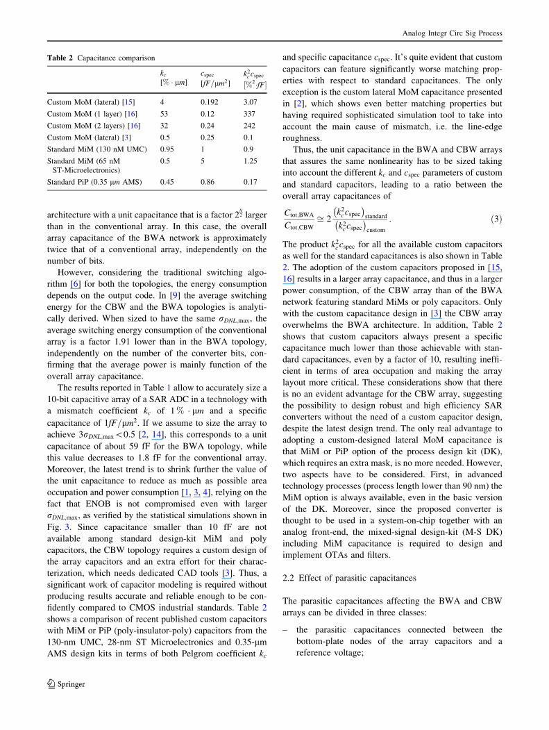
fidently compared to CMOS industrial standards. Table 2
shows a comparison of recent published custom capacitors
with MiM or PiP (poly-insulator-poly) capacitors from the
130-nm UMC, 28-nm ST Microelectronics and 0.35-lm
AMS design kits in terms of both Pelgrom coefficient kc
and specific capacitance cspec. It’s quite evident that custom
capacitors can feature significantly worse matching prop-
erties with respect to standard capacitances. The only
exception is the custom lateral MoM capacitance presented
in [2], which shows even better matching properties but
having required sophisticated simulation tool to take into
account the main cause of mismatch, i.e. the line-edge
roughness.
Thus, the unit capacitance in the BWA and CBW arrays
that assures the same nonlinearity has to be sized taking
into account the different kc and cspec parameters of custom
and standard capacitors, leading to a ratio between the
overall array capacitances of
Ctot;BWA
Ctot;CBW
ffi 2k2
c cspec
� �standard
k2ccspec
� �custom
: ð3Þ
The product k2c cspec for all the available custom capacitors
as well for the standard capacitances is also shown in Table
2. The adoption of the custom capacitors proposed in [15,
16] results in a larger array capacitance, and thus in a larger
power consumption, of the CBW array than of the BWA
network featuring standard MiMs or poly capacitors. Only
with the custom capacitance design in [3] the CBW array
overwhelms the BWA architecture. In addition, Table 2
shows that custom capacitors always present a specific
capacitance much lower than those achievable with stan-
dard capacitances, even by a factor of 10, resulting ineffi-
cient in terms of area occupation and making the array
layout more critical. These considerations show that there
is no an evident advantage for the CBW array, suggesting
the possibility to design robust and high efficiency SAR
converters without the need of a custom capacitor design,
despite the latest design trend. The only real advantage to
adopting a custom-designed lateral MoM capacitance is
that MiM or PiP option of the process design kit (DK),
which requires an extra mask, is no more needed. However,
two aspects have to be considered. First, in advanced
technology processes (process length lower than 90 nm) the
MiM option is always available, even in the basic version
of the DK. Moreover, since the proposed converter is
thought to be used in a system-on-chip together with an
analog front-end, the mixed-signal design-kit (M-S DK)
including MiM capacitance is required to design and
implement OTAs and filters.
2.2 Effect of parasitic capacitances
The parasitic capacitances affecting the BWA and CBW
arrays can be divided in three classes:
– the parasitic capacitances connected between the
bottom-plate nodes of the array capacitors and a
reference voltage;
Table 2 Capacitance comparison
kc
[% � lm]
cspec
[fF=lm2]
k2c cspec
½%2�fF�
Custom MoM (lateral) [15] 4 0.192 3.07
Custom MoM (1 layer) [16] 53 0.12 337
Custom MoM (2 layers) [16] 32 0.24 242
Custom MoM (lateral) [3] 0.5 0.25 0.1
Standard MiM (130 nM UMC) 0.95 1 0.9
Standard MiM (65 nM
ST-Microelectronics)
0.5 5 1.25
Standard PiP (0.35 lm AMS) 0.45 0.86 0.17
Analog Integr Circ Sig Process
123
– the parasitic capacitances connected between the top-
plate nodes of the DAC (Cpar, Cpar;main, Cpar;sub in
Fig. 2) and a reference voltage;
– the parasitic capacitances between the top- and the
bottom-plate nodes of the array capacitors.
The parasitics of the first category do not affect the line-
arity behavior of the converter in either CBW and BWA
topology since the bottom-plate nodes of the array capac-
itances are always connected to the supply-voltage or
ground.
As far as the second class of parasitic capacitances is
concerned, it is commonly assumed [9] that these parasitics
can degrade the linearity performance of the BWA con-
verter, even if constant and voltage independent, while they
only cause a gain error without affecting the linearity in the
conventional array. This statement can be easily verified
expressing the voltage at the output node of the DAC. For
the conventional DAC (see Fig. 2(a)), the analog output
voltage corresponding to a given digital input word (Di for
i ¼ 1; 2; . . .;N) can be expressed as function of the overall
DAC capacitance, Ctot ¼ 2NCu, and of the parasitic
capacitance connected to the top-plate node, Cpar
Vout ¼PN
i¼1Di � Ci
Ctot þ Cpar
VDD; ð4Þ
Ci being equal to 2i�1Cu. As evident from Eq. (4), the
parasitic capacitance only affects the converter gain.
A similar expression of the DAC output voltage can be
derived for the BWA converter in Fig. 2(b) with m ¼ l ¼N=2 and Catt ¼ Cu. By indicating with Cmain and Csub the
overall capacitance of the main- and the sub-DAC,
respectively, and with Cpar;main and Cpar;sub the parasitic
capacitances at the top-plate node of the corresponding
array, the analog output voltage results
Vout ffi" PN
i¼N2þ1 Di � Ci
Cmain þ Cpar;main
þ AR �PN
2
i¼1 Di � Ci
Csub þ Cpar;sub
#
VDD;
ð5Þ
Ci being the capacitance associated to the i-th bit and AR
the attenuation ratio
AR ffi Cu
Cmain þ Cpar;main
: ð6Þ
Equations (5) and (6) show that only the parasitics Cpar;sub
affects the linearity since its effect on the value of the DAC
output voltage is not constant for different input signals,
while Cpar;main only causes gain error. In particular, Cpar;sub
is responsible of a deterministic pattern of the DNL, and
hence of the INL. The differential nonlinearity shows a
peak every 2N2 codes whose amplitude is
DNLpeak ffi2N � 2
N2
� �Cpar;sub þ Cu
2NCu
: ð7Þ
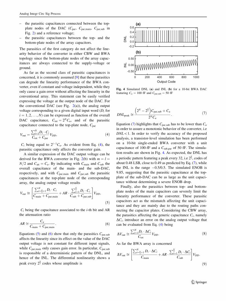
Equation (7) highlights that Cpar;sub has to be lower than Cu
in order to assure a monotonic behavior of the converter, i.e
DNL\1. In order to verify the accuracy of the proposed
analysis, a transistor-level simulation has been performed
on a 10-bit single-ended BWA converter with a unit
capacitance of 100-fF and a Csub;par of 50 fF. The simula-
tion results are shown in Fig. 4. As expected, the DNL has
a periodic pattern featuring a peak every 32, i.e 2N2 , codes of
about 0.48 LSB, close to 0.49 as predicted by Eq. (7), while
the INL is the range -0.5/0.5. The simulated ENOB is
9.85, suggesting that the parasitic capacitance at the top-
plate of the sub-DAC can be as large as the unit capaci-
tance without determining a severe ENOB drop.
Finally, also the parasitics between top- and bottom-
plate nodes of the main capacitors can severely limit the
linearity performance of the converter. These parasitic
capacitors act as the mismatch affecting the unit capaci-
tance and they are mainly due to the routing paths con-
necting the capacitor plates. Considering the CBW array,
the parasitics affecting the generic capacitance Ci, namely
DCi, introduce an error on the analog output voltage that
can be evaluated from Eq. (4) being
DVout ffiPN
i¼1Di � DCi
Ctot
VDD: ð8Þ
As far the BWA array is concerned
DVout ffi"PN
i¼N2þ1 Di � DCi
Cmain
þ AR �PN
2
i¼1 Di � DCi
Csub
#
VDD:
ð9Þ
(a)
(b)
Fig. 4 Simulated DNL (a) and INL (b) for a 10-bit BWA DAC
featuring Cu ¼ 100 fF and Cpar;sub ¼ 50 fF
Analog Integr Circ Sig Process
123

Since Cmain and Csub in the BWA array are approximately
equal to the overall capacitance of the CBW array, Ctot,
when sized to have equal rDNL;max, a same parasitic
capacitance DCi in the main-DAC affects the output volt-
age, and thus the linearity, in the same way as in the CBW
array. Indeed, the same parasitic capacitance associated to
a sub-DAC element has a lower effect than in the CBW
array counterpart. In fact, its effect is attenuated by the
bridge capacitor, i.e. by the ratio Cu
Cmainffi 1
2N=2.
In conclusion, the above analysis shows that the BWA
array can achieve linearity performance comparable to the
conventional array only if the parasitic capacitance
affecting the top-plate node of the sub-DAC is kept con-
siderably lower than the unit capacitance.
3 Circuit design
The scheme of the proposed 10-bit AD converter is shown
in Fig. 1. In order to achieve a better common-mode noise
rejection and less distortion, a fully-differential topology is
adopted. This section is devoted to describe the three main
sections of the converter, i.e. the capacitive network, the
comparator and the asynchronous logic.
3.1 Capacitive array and switching algorithm
In SAR converters, the capacitor network serves as both
sample-and-hold (S/H) circuit and reference DAC capaci-
tor array. Being the converter fully-differential, the
capacitive DAC is realized by means of two 10-bit binary
weighted arrays with attenuation capacitor, one per branch,
with symmetrical main- and sub-DACs. The fully-differ-
ential structure allows to reduce rDNL;max and rINL;max by a
factor offfiffiffi2p
with respect to the single-ended counterpart
featuring the same unit capacitance [14], i.e. the same
nonlinearity can be obtained with half the unit capacitance.
In order to further reduce the array power consumption,
an efficient switching procedure, as the monotonic algo-
rithm [4], has been applied to the capacitive DAC. In fact,
the conventional trial-and-error search procedure [6], even
if simple and intuitive, is not energy efficient, especially
when unsuccessful trials occur. The proposed capacitive
array samples the differential input signal directly on the
top of the two main-DACs via two bootstrapped switches,
which allow low-voltage operation, with the bottom-plates
connected to the positive power supply, VDD. After the
switches are turned off, the first comparison is done with-
out switching any array capacitance. According to the
comparator output, the largest capacitor on the main-DAC
corresponding to the positive input signal is switched to
ground while the other one remains at VDD. The ADC
repeats the procedure until the LSB is decided. For each
cycle, only a capacitor is switched reducing the charge
transfer and thus the array power consumption. Note that
the proposed BWA array featuring a monotonic switching
scheme has the same overall capacitance of the original
fully-differential BWA architecture, i.e. about 2N2þ2Cu.
Figure 5 shows the array energy consumption as func-
tion of the ADC output code for the classical and for the
monotonic algorithm applied to a fully-differential BWA
architecture featuring the same unit capacitance and ref-
erence voltage. The monotonic switching scheme deter-
mines a significant efficiency improvement, reducing the
average switching energy from 81.5 CuV2DD to roughly 32
CuV2DD, i.e. by a factor of 2.5 with respect to the traditional
switching approach.
Another advantage of the monotonic switching algo-
rithm is that it reduces the effect of capacitor mismatch on
the non-linearity of the converter. It can be verified fol-
lowing the same procedure adopted in [13] that the effect
Fig. 5 Switching energy versus output code
Cu 2Cu 4Cu 8Cu 16Cu Cu 2Cu 4Cu 16Cu
VDD D1
Catt
8Cu
Out
D2 D3 D4 D5 D6 D7 D8 D9
C0 C1 C2 C3 C4 C5 C6 C7 C8 C9
Cu
D D D D D D D D D D D
D C3 C3 C4 C4 D C1 C3 C9 C9 D
D C3 C3 C4 C4 D C1 C3 C9 C9 D
D C3 C3 C4 C4 D C0 C3 C9 C9 D
D C3 C3 C4 C4 D D C3 C9 C9 D
D D D D D D D D D D D
D C4 C4 C2 Catt D C9 C9 C8 C8 D
D C4 C4 C2 C5 D C9 C9 C8 C8 D
D C4 C4 C2 C6 D C9 C9 C8 C8 D
D C4 C4 C2 C6 D C9 C9 C8 C8 D
D D D D D D D D D D D
Fig. 6 Adopted layout scheme for the capacitive DAC of one branch
(D stands for dummy element)
Analog Integr Circ Sig Process
123

of mismatch on both rDNL;max and rINL;max is reduced by a
factorffiffiffi2p
with respect to the traditional algorithm. This
allows to adopt half the unit capacitance without impairing
the linearity of the DAC, thus further reducing the array
power consumption.
Based on statistical simulations [12], the unit capaci-
tance Cu of the proposed converter was set to 34 fF, close
to the technology minimum of 17 fF. Also the attenuation
capacitance was set equal to Cu. Adopting this value for the
unit capacitance, the rDNL;max is expected to be lower than
0.5 LSB, while the total capacitance is 4.28 pF. In order to
compensate process gradients, the layout of each branch
array was designed to keep symmetrical the functional
blocks of the two sub-arrays, as shown in Fig. 6. A par-
ticular care was dedicated to minimizing the sub-DAC top-
plate parasitic capacitance, which was limited to about 12
fF, according to the result of the parasitic extraction tool.
Figure 7 shows the DNL and INL curves obtained from
post layout simulations of the overall converter [12]. All
the parasitic capacitances in the array were taken into
account, while the comparator and the logic circuit were
implemented as ideal blocks using Verilog-A models. The
negative peaks in the DNL curve occurring every 64 codes
are due to the parasitic capacitance between top- and bot-
tom-plate of C5 (see Fig. 6), i.e. the smallest capacitance
of the main-DAC. The simulated ENOB is about 8.85.
3.2 Dynamic comparator
A two-stage dynamic comparator, shown in Fig. 8, is
adopted in the proposed converter since it does not con-
sume static current, being suitable for energy efficient
design. It consists of a first stage similar to the one adopted
in [1] followed by a differential latch. Since the monotonic
algorithm makes the common-mode input voltage varying
from VDD=2 to 0 along the conversion cycle [4], the input
stage features a PMOS differential pair. The operation is
determined by the Reset signal, which is generated from
the logic circuit (see Fig. 1). Before the comparison takes
part, the first stage output nodes are pre-charged low by a
positive Reset signal. Its falling edge stops the pre-charging
phase and starts the amplification of the differential input
signal. In fact, as Reset becomes low, a current starts to
flow into the differential pair charging the parasitic
capacitances Cp at the drain nodes. The voltage on the two
capacitors increases at a different speed, the difference
depending on the input signal, Vin;p–Vin;n. As the first stage
output voltages reach the threshold voltage of the second
stage input transistors, the latch starts to amplify the signal
until the positive feedback takes over providing a rail-to-
rail differential output. Consequently, the Valid signal is
pulled high to enable the asynchronous control logic.
According to simulation, the first stage differential gain is
about 5, high enough to make the noise of the second stage
negligible. Thus, the equivalent input noise of the com-
parator is mainly determined by the input differential pair,
its transistor working in weak-inversion region to
(a)
(b)
Fig. 7 DNL and INL obtained from post-layout simulations consid-
ering all the parasitic capacitances of the array
Reset
VIN,N
VDD
GND
VIN,P
Cp Cp
Reset ResetReset
Reset
OutP
OutN
Valid
Fig. 8 Schematic of the dynamic comparator
Fig. 9 Deterministic effect of the comparator input capacitance on
the INL curve
Analog Integr Circ Sig Process
123

maximize the comparator efficiency. The equivalent inte-
grated input noise of the comparator is approximately [1]
vn;rms ffiffiffiffiffiffiffikT
Cp
s
�ffiffiffiffiffiffiffiffi8kT
qVT
s
; ð10Þ
VT being the threshold voltage of the second stage input
transistors. In order to make this noise negligible with
respect to the LSB for the minimum supply voltage of
0.5 V (i.e. 1 V=2N ffi 1 mV), the parasitic capacitance has
to be larger than approximately 3.3 fF. In the proposed
comparator, the parasitic capacitance Cp is about 15 fF.
Another issue related to the proposed converter
employing a monotonic switching algorithm is that the
common-mode voltage at the comparator input decreases
during the conversion cycle. Unfortunately, the depen-
dence of the comparator offset on the common mode input
voltage may results in distortion [4, 17]. In fact, the offset
voltage of the comparator can be expressed as
Vos ffi DVT þVGS � VT
2
�Dbb
�; ð11Þ
where DVT is the threshold voltage offset of the differential
pair transistors, VGS � VT is the effective voltage of the
input pair and Db is the overall conductivity mismatch
between the input transistors. The first term is a static offset
that does not affect the ADC performance, while the sec-
ond term is a dynamic offset that varies with the input
signal common-mode voltage, and thus during the con-
version cycle, degrading the converter linearity. The sim-
plest way to reduce its effect is to force these transistors to
work in subthreshold region and to increase their area,
slightly degrading the comparator power consumption
performance.
However, another effect has to be taken into account
when sizing the comparator input transistors. When the
comparator is turned on by a falling edge of the Reset
signal, the gate capacitance of the two input transistor
becomes signal dependent. For example, considering the
first comparison, i.e. when the MSB has to be evaluated,
the two input voltages can be considerably different, the
difference being even equal to the supply voltage. Thus,
when the comparator is turned on, two different gate
capacitances are applied directly to the top-plate nodes of
the main-DACs causing a variation of the differential input
voltage. Being signal dependent, this effect causes non-
linearity. Moreover, it is a deterministic effect since it
happens also with completely matched input transistors.
This is due to the dependence of the input gate capacitance
on the applied voltage. This effect has been quantitatively
assessed simulating the overall converter with an ideal
capacitive array. The simulated INL curves are shown in
Fig. 9 for three different values of the input transistor
dimensions. The INL curve shows a typical ‘‘S’’-shape.
The effect of the signal-dependent gate capacitance is
minimum at the mid-code since the voltage signal is the
same on the tap-plate nodes of both the main-DACs, i.e. at
the two comparator inputs. Moreover, this effect is exac-
erbated for larger transistor sizes, as evident from Fig. 9.
This suggests to use small input transistors, thus trading off
the effects of the dynamic offset and of the signal-depen-
dent gate capacitances at the comparator input terminals. In
order to size the input transistors, we performed a set of
simulations with a size mismatch between the input devices
and for different transistor areas. Figure 10 shows the INL
curves obtained employing transistors with W ¼ 1 lm, L ¼0:2 lm and W ¼ 5 lm, L ¼ 1 lm. As the ratio between the
two areas is 25, we assumed a mismatch on the transistor
width of 5 % and 1 % (i.e. proportional to the square root of
the area [18]), for the small and the large area devices,
Fig. 10 Effect of the comparator on the INL curve considering a
mismatch of the aspect ratio between the input transistors
CK
D Q
R
td
Valid
Start
Reset
EoCSample
TDL
R
Q
CK
RCK CK
D
CKR
VDD
GND
VDD
TDL
TQ
Fig. 11 Logic temporizer
Analog Integr Circ Sig Process
123
respectively. In the former case, the converter shows
missing codes and a INL peak as large as �0:85. Thus, not-
minimum area transistors (W ¼ 5 lm, L ¼ 1 lm) were
chosen as comparator input devices in order to limit the
effect of the dynamic offset without compromising the
deterministic effect of the signal-dependent input
capacitances.
3.3 Asynchronous logic
The SAR logic generates the necessary commands to
control the comparator and the capacitive DAC. In order to
reduce its power consumption, an asynchronous dynamic
logic is adopted. By using a dynamic logic, less transistor
are needed to implement the same functionality, and, being
asynchronous, it requires only a low-speed sampling clock
instead of an oversampled clock, thereby saving power.
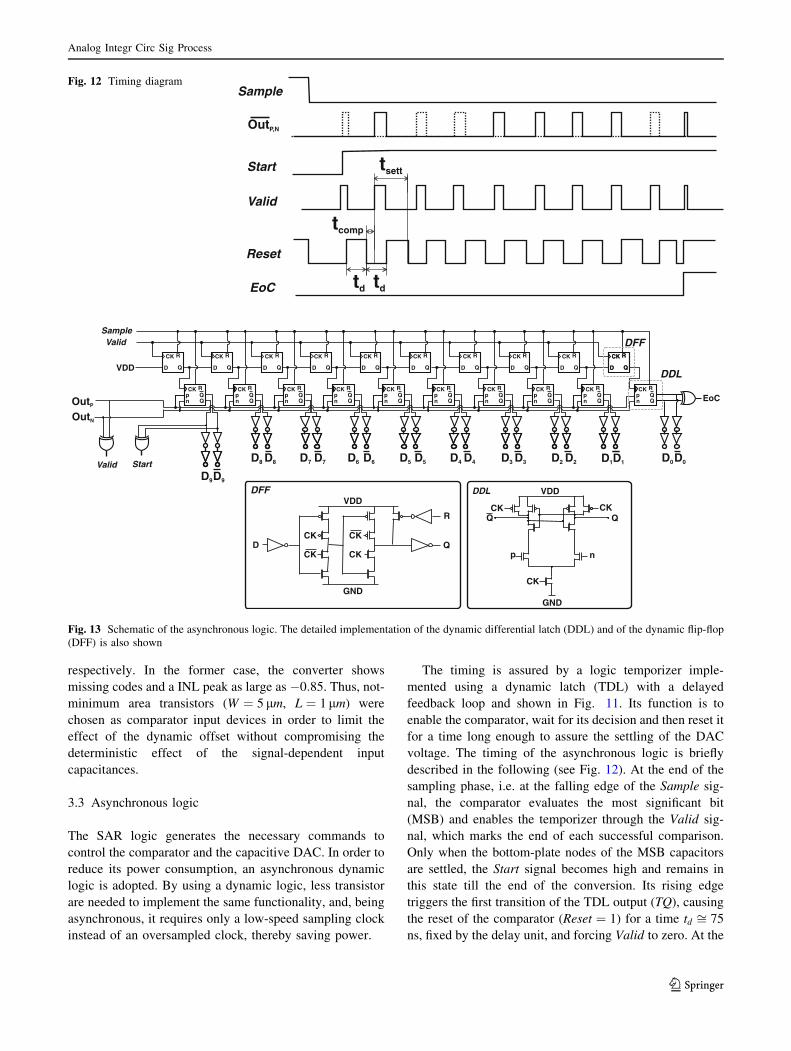
The timing is assured by a logic temporizer imple-
mented using a dynamic latch (TDL) with a delayed
feedback loop and shown in Fig. 11. Its function is to
enable the comparator, wait for its decision and then reset it
for a time long enough to assure the settling of the DAC
voltage. The timing of the asynchronous logic is briefly
described in the following (see Fig. 12). At the end of the
sampling phase, i.e. at the falling edge of the Sample sig-
nal, the comparator evaluates the most significant bit
(MSB) and enables the temporizer through the Valid sig-
nal, which marks the end of each successful comparison.
Only when the bottom-plate nodes of the MSB capacitors
are settled, the Start signal becomes high and remains in
this state till the end of the conversion. Its rising edge
triggers the first transition of the TDL output (TQ), causing
the reset of the comparator (Reset ¼ 1) for a time td ffi 75
ns, fixed by the delay unit, and forcing Valid to zero. At the
Valid
Reset
Sample
EoC
OutP,N
Start
td td
tcomp
tsett
Fig. 12 Timing diagram
DFF
D Q
VDD
GND
R
EoC
Valid
VDD
Sample
CK
n QQpR
D Q
CK R
D Q
CK R
D Q
CK R
D Q
CK R
D Q
CK R
D Q
CK R
D Q
CK R
D Q
CK R
D Q
CK R
CK
n QQpR CK
n QQpR CK
n QQpR CK
n QQpR CK
n QQpR
D Q
CK R
CK
n QQpR CK
n QQpR CK
n QQpR
D Q
CK R
CK
n QQpR
D8
OutP
OutN
Start
DFF
Valid
CK
CK
CK
CK
DDL
CK
CK CK
p n
Q Q
GND
VDD
DDL
D8 D1D1
D9D9
D2 D2D3 D3D4 D4D5 D5D6 D6D7 D7 D0D0
Fig. 13 Schematic of the asynchronous logic. The detailed implementation of the dynamic differential latch (DDL) and of the dynamic flip-flop
(DFF) is also shown
Analog Integr Circ Sig Process
123

end of the reset phase, the comparator evaluates the MSB-1
bit and sets the Valid signal high. However, the comparator
is not reset till the falling edge of TQ has completed the
feedback path, i.e. after a time td. Thus, the Reset signal
resembles a square wave with a period of 2td . Since the
comparator takes approximately tcomp ffi 10 ns for a deci-
sion, a time of tsett ¼ 2td � tcomp ffi 140 ns is left to the
logic circuit and to the array to switch and settle, respec-
tively, during each bit evaluation phase. When also the
least significant bit (LSB) has been evaluated, the EoC
rises and the conversion stops till the end of the successive
sampling phase, keeping the comparator in the reset state.
Figure 13 shows the logic circuit implementing the
successive approximation algorithm. It features a first row
of dynamic flip–flops (DFFs) and a second row of dynamic
differential latches (DDLs). The flip-flops implement a
serial register triggered by the Valid signal. Its function is
to set the current bit that is being evaluated and to enable
the correspondent latch to store the result. The aim of the
logic circuit design was to minimize the capacitive load of
the most active signal lines, i.e. the Valid signal and the
outputs of flip-flops, latches and comparator, in order to
reduce the power consumption. The DFFs have a C2MOS
topology with the clock pin connected to 2 n-gates and
2 p-gates. Thus, each DFF output is loaded by 2 n-gates
and 3 p-gates, while the DDL outputs are directly con-
nected to a minimum area inverter that drives the corre-
sponding array capacitors. Moreover, since the monotonic
algorithm requires the bottom plates of all capacitors to
remain at VDD during the sampling phase, the DDLs have
been implemented by means of a differential topology
(Fig. 13), making possible to use a single set of 10 ele-
ments shared by both arrays, instead of 10 elements per
each array. In fact, the outputs of the DDLs are kept high
till the positive edge trigger of the corresponding DFF
output, then they switches according to the state of the
comparator decision. Finally, the total differential capacitance
loading the comparator is equal to 10x2 n-gates (plus 4 n-gates
and 4 p-gates due to the XOR gate generating the Valid signal).
4 Measurement results
The ADC was fabricated using a two-poly-eight-metal
(2P8M) 0.13-lm CMOS technology featuring 1.11-fF/lm2
MiM capacitors. The die photograph is shown in Fig. 14. The
core occupies 188 lm x 238 lm, while two 1-pF capacitors
are used as decoupling capacitances. The performance of the
ADC have been measured at the nominal supply-voltage of
0.5 V as well as varying VDD from 0.4V to 0.8V and for 8
samples of the same wafer. The measurement results are
presented below and summarized in Table 3.
4.1 Static performance
The measured static performance of the ADC in terms of
DNL and INL are shown in Fig. 15. The two curves
resemble the simulated ones depicted in Fig. 7. The
Fig. 14 Die photo of the ADC
(a)
(b)
Fig. 15 Measured DNL and INL characteristics
Fig. 16 Measured spectrum with an input sine-wave at 5.13 and
96.48 kHz for 200-kSps sampling frequency and 0.5-V supply
Analog Integr Circ Sig Process
123
measured DNL and INL are -0.4/0.5 and -2/2 LSBs,
respectively, slightly larger than the corresponding simu-
lated values reported in Sect. 3.1. However, this suggests
that the DNL/INL performance are mainly due to the
parasitic capacitances induced by the layout routing.
4.2 Dynamic performance
Figure 16 shows the output spectra at 0.5-V supply,
200-kSps sampling rate and for an input sinewave at 5.13
and 96.48-kHz frequency, i.e. well below and slightly
below the Nyquist frequency. At low frequency, the aver-
age measured SNDR and SFDR are 52.6 and 67.5 dB,
respectively. The resultant ENOB is 8.45 and its standard
deviation is limited to 0.04, considering the 8 tested sam-
ples. This value is just lower than 8.9 obtained from post-
layout simulations. The discrepancy from the simulated
and measured ENOB can be mainly ascribed to the com-
bined effect of mismatch and parasitic capacitances. When
the input frequency is increased close to the Nyquist rate,
the measured SNDR and SFDR drop to 50.8 and 62.1 dB,
respectively.
The maximum rate increases with the supply voltage,
being 50 kSps at 0.4 V and 1 MSps at 0.8 V. The SNDR
was measured for different supply voltages at the max-
imum sampling frequency. The results in terms of
average ENOB is scheduled in Table 3 showing that the
dynamic performance does not vary significantly for
supply in the 0.4/0.8-V range. The slight decrease of the
ENOB for VDD ¼ 0:8 V can be ascribed to the non
linearity introduced by the bootstrapped switches, adop-
ted to make the converter working at very low supply
voltage.
4.3 Power consumption
The power consumption as function of the sampling rate
and for different power supply voltage are shown in Fig.
17. Based on post-layout simulations, most of the power
consumption (50 %) is due to the logic and 35 % to the
comparator. Only 15 % of the power is due to the array.
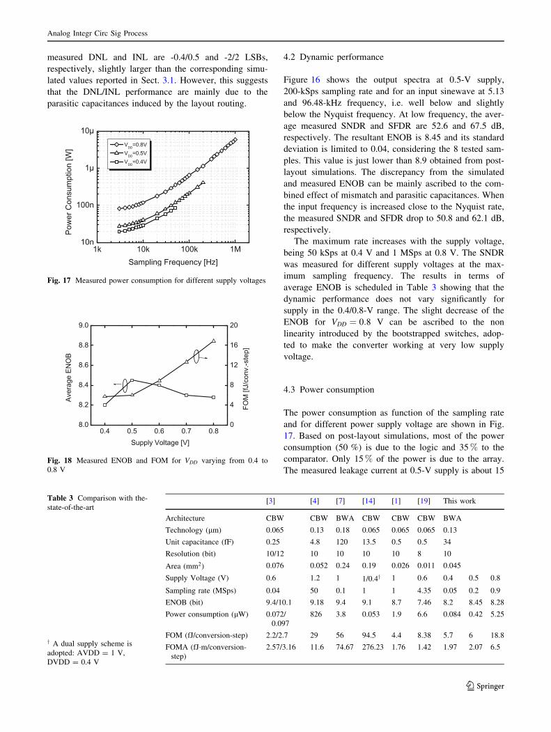
The measured leakage current at 0.5-V supply is about 15
Fig. 17 Measured power consumption for different supply voltages
Fig. 18 Measured ENOB and FOM for VDD varying from 0.4 to
0.8 V
Table 3 Comparison with the-
state-of-the-art
y A dual supply scheme is
adopted: AVDD = 1 V,
DVDD = 0.4 V
[3] [4] [7] [14] [1] [19] This work
Architecture CBW CBW BWA CBW CBW CBW BWA
Technology (lm) 0.065 0.13 0.18 0.065 0.065 0.065 0.13
Unit capacitance (fF) 0.25 4.8 120 13.5 0.5 0.5 34
Resolution (bit) 10/12 10 10 10 10 8 10
Area (mm2) 0.076 0.052 0.24 0.19 0.026 0.011 0.045
Supply Voltage (V) 0.6 1.2 1 1/0.4y 1 0.6 0.4 0.5 0.8
Sampling rate (MSps) 0.04 50 0.1 1 1 4.35 0.05 0.2 0.9
ENOB (bit) 9.4/10.1 9.18 9.4 9.1 8.7 7.46 8.2 8.45 8.28
Power consumption (lW) 0.072/
0.097
826 3.8 0.053 1.9 6.6 0.084 0.42 5.25
FOM (fJ/conversion-step) 2.2/2.7 29 56 94.5 4.4 8.38 5.7 6 18.8
FOMA (fJ�m/conversion-
step)
2.57/3.16 11.6 74.67 276.23 1.76 1.42 1.97 2.07 6.5
Analog Integr Circ Sig Process
123

nA, thus becoming significant only at low sampling rates.
The leakage current was measured by means of HP 4140B
pA Meter/DC voltage source having a resolution in the fA
range. The clock frequency was kept very low (below 1
kHz) in order to make the leakage current to be the dom-
inant contribution to supply current. Having adopted PADs
with reduced and custom designed ESD protection to
supply the ADC, the measured leakage current can be
entirely ascribed to the converter.
4.4 Performance summary and comparison
with the state-of-the-art
To compare the proposed ADC with other works featuring
different sampling rate and resolutions, the FOM in Eq. (1)
is adopted. The FOM of the proposed ADC at the nominal
supply of 0.5 V and for a 200-kSps sampling rate is 6 fJ/
conversion-step. For a 0.4-V supply and 50-kSps sampling
rate it is even lower, being 5.5 fJ/conversion-step, while it
increases to 18.8 fJ/conversion-step at 0.8-V supply and
1-MSps sampling rate. The converter performance in terms
of ENOB and FOM are depicted in Fig. 18 for a supply
voltage varying from 0.4 to 0.8 V.
Table 3 shows that the proposed ADC well compares in
terms of efficiency to the best recent published works,
without adopting a CBW topology and sub-fF custom
capacitors, even if it is implemented in an older technol-
ogy. It’s worth noting that, since about 80 % of the power
consumption is due to the digital circuits (asynchronous
logic and comparator), the adoption of a more scaled
technology would reduce the power consumption improv-
ing the efficiency of the converter. If compared to the
converters implemented in 0.13-lm technology, the pro-
posed ADC is by far the best in terms of FOM, as shown in
Fig. 19 that shows the efficiency of published converters as
function of the technology node, from 32-nm to 0.5-lm
feature size.
The proposed ADC favorably compares with the other
converters in Table 3 in terms of area, with the exception of
the work in [1] that adopts high-density custom capacitors
and a conventional binary weighted array. The ADC pro-
posed in [14] features a CBW array with 2 standard MIM
capacitors connected in series in order to decrease the unit
capacitance, but determining a large waste of area and an
efficiency that is not so high as in other CBW converters.
In order to take into account both the efficiency and the
die area of the converter, a figure-of-merit, FOMA, has
been introduced and adopted in literature [20], being
defined as
FOMA ¼ FOM � A
lprocess
; ð12Þ
where A and lprocess are the core area expressed in m2 and
the process minimum length in m, respectively. Even if
adopting a BWA architecture and a large unit capacitor, the
proposed work favorably compares to the state-of-the-art
converters in terms of FOMA.
5 Conclusions
In this paper a high efficient SAR ADC in 130-nm UMC
technology was presented. It adopts a binary-weighted with
attenuation capacitor array featuring a linearity and a total
capacitance similar to a conventional binary weighted array
but without requiring full-custom sub-fF capacitors. The
design and the layout of the array is accurately optimized
in order to reduce the parasitic capacitance at the top-plate
node of the sub-DAC, which degrades the converter line-
arity. Moreover, an efficient switching scheme is adopted
in order to further reduce its power consumption. Finally,
an asynchronous and fully-differential dynamic logic
decreases the transistor count minimizing the digital power
consumption.
The measured prototype shows an efficiency compara-
ble to the state-of-the art converters even if realized in a
less scaled technology, i.e. a 130-nm process, that is still
one of the most commonly adopted to implement analog-
front end ICs.
Acknowledgments The work has been supported by the Italian
Ministry of the University within the frame of the PRIN 2009-42ZJJ5
project.
References
1. van Elzakker, M., van Tuijl, E., Geraedts, P., Schinkel, D.,
Klumperink, E., & Nauta, B. (2010). 10-bit charge-redistribution
ADC consuming 1.9 lW at 1 MS/s. IEEE Journal of Solid State
Circuits, 45(5), 1007–1015.
0
Fig. 19 Measured FOM of state-of-the-art SAR ADCs
Analog Integr Circ Sig Process
123
2. Harpe, P., Zhou, C., Bi, Y., van der Meijs, N. P., Wang, X.,
Philips, K., et al. (2012). A 26 lW 8 bit 10 MS/s asynchronous
SAR ADC for low energy radios. IEEE Journal of Solid State
Circuits, 46(7), 1585–1595.
3. Harpe, P., Cantatore, E., Haller, G., & Murmann, B. (2013). A
2.2/2.7fJ/conversion-step 10/12b 40kS/s SAR ADC with data-
driven noise reduction. IEEE International Solid-State Circuits
Conference Digest of Technical Papers (ISSCC), pp. 270–271.
4. Liu, C., Chang, S., Huang, G., & Lin, Y. (2010). A 10-bit 50-MS/
s SAR ADC with a monotonic capacitor switching procedure.
IEEE Journal of Solid State Circuits, 45(4), 731–740.
5. Brenna, S., Bonfanti, A., Caponio, F., Abba, A., & Lacaita, A.
(2014). Analysis and optimization of a SAR ADC with attenua-
tion capacitor. In Proceedings of the 37th International Con-
vention on Information and Communication Technology,
Electronics and Microelectronics (MIPRO) (pp. 68–73).
6. McCreary, J., & Gray, P. (1975). All-MOS charge redistribution
analog-to-digital conversio tecqniques. I. IEEE Journal of Solid
State Circuits, SC–10(6), 371–379.
7. Agnes, A., Bonizzoni, E., Malcovati, P., & Maloberti, F. (2010).
An ultra-low power successive approximation A/D converter
with time-domain comparator. Analog Integrated Circuits and
Signal Processing, 64, 183–190.
8. Agnes, A., Bonizzoni, E., & Maloberti, F. (2008). A 9.4-ENOB
1V 3.8 lW 100 kS/s SAR ADC with time-domain comparator.
IEEE International Solid-State Circuits Conference Digest of
Technical Papers (ISSCC), (Vol. 37(2), pp. 246–610).
9. Saberi, M., Lotfi, R., Mafinezhad, K., & Serdjin, W. (2011).
Analysis of power consumption and linearity in capacitive digi-
tal-to-analog converters used in successive approximation ADCs.
IEEE Transaction on Circuits and Systems I: Regular Paper,
58(7), 1736–1747.
10. Fredenburg, J. A., & Flynn, M. P. (2012). Statistical analysis of
ENOB and yield in binary weighted ADCs and DACs with ran-
dom element mismatch. IEEE Transaction on Circuits and Sys-
tems I: Regular Paper, 59(7), 1396–1408.
11. Walden, R. H. (1999). Analog to digital converter survey and
analysis. IEEE Journal on Selected Areas in Communications, 17,
539–550.
12. Brenna, S., Bonetti, A., Bonfanti, A., & Lacaita, A. (2014). A
simulation and modeling environment for the analysis and design
of charge redistribution DACs used in SAR ADCs. In Proceed-
ings of the 37th International Convention on Information and
Communication Technology, Electronics and Microelectronics
(MIPRO) (pp. 74–79).
13. Chandrakasan, A., & Ginsburg, B. (2007). 500-MS/s 5-bit ADC
in 65-nm CMOS with split capacitor array DAC. IEEE Journal of
Solid State Circuits, 42(4), 739–747.
14. Zhang, D., Bhide, A., & Alvandpour, A. (2012). A 53-nW 9.1-
ENOB 1-kS/s SAR ADC in 0.13-m CMOS for medical implant
devices. IEEE Journal of Solid State Circuits, 47(7), 1585–1593.
15. Tripathi, V., & Murmann, B. (2013). Mismatch characterization
of small metal fringe capacitors. In Proceedings of Custom
Integrated Circuits Conference (CICC) (pp. 1–4).
16. Abusleme, A., Dragone, A., Haller, G., & Murmann, B. (2012).
Mismatch of lateral field metal-oxide-metal capacitors in 180 nm
CMOS process. IEEE Electronic Letters, 48, 286–287.
17. Hong, H., & Lee, G. (2007). A 65-fj/conversion-step 0.9-V
200-kS/s rail-to-rail 8-bit successive approximation ADC. IEEE
Journal of Solid State Circuits, 42(10), 2161–2168.
18. Pelgrom, M., Tuinhout, H., & Vertregt, M. (1998). Transistor
matching in analog CMOS applications. In Electron Devices
Meeting, 1998, IEDM ’98, Technical Digest (pp. 915–918).
19. Huang, G., & Lin, P. (2012). An 8.38 fJ/conversion-step 0.6 V
8-b 4.35 MS/s aysnchronous SAR ADC in 65 nm CMOS. Analog
Integrated Circuits and Signal Processing, 73, 265–272.
20. Wu, H., Li, B., Huang, W., Li, Z., Zou, M., & Wang, Y. (2012).
A 1.2 V 8-bit 1 MS/s SAR ADC with res-cap segment dac for
temperature sensor in LTE. Analog Integrated Circuits and Sig-
nal Processing, 73, 225–232.
Stefano Brenna was born in
Monza, Italy, in 1986. He
received the Bachelor degree in
Biomedical Engineering and the
Master degree in Electrical
Engineering from Politecnico di
Milano in 2009 and 2012
respectively. His Master
research was focused on the
design of a 130 nm CMOS inte-
grated ultra-low power front-end
for neural signal (LFPs and APs)
amplification and digitalization.
In 2010, he collaborated with the
human physiology department of
Universit Statale di Milano where he worked on the preliminary
development of an EMG based system to restore the eyelid blink
functionality in patients affected by facial palsies. He joined the Ph.D.
program at the Politecnico di Milano in November 2012 and his current
research activity is focused on the design of ultra low power analog
mixed-mode integrated front-ends for the signal conditioning in neural
probing integrated systems and also for MEMS and AMR magnetic
field sensors.
Andrea Bonfanti was born in
Besana Brianza (Milan), Italy,
in 1972. He received the Laurea
degree in Electrical Engineering
and the Ph.D. in Electronics and
Communications from the Po-
litecnico di Milano, Italy, in
1999 and 2003, respectively.
During his Ph.D. program, he
studied the up-conversion of
flicker noise into phase noise in
bipolar and CMOS LC-tuned
oscillator. From 2003 to 2008 he
was a Postdoctoral Researcher
at the Politecnico di Milano
involved in the study and design of fully-integrated oscillators, RF
frequency synthesizers, D–R A–D converters and low-power analog
and mixed-signal circuits for neural signal processing. During this
period he was a consultant for ST-Microelectronics (Agrate Brianza,
Italy), Accent (Vimercate, Italy) and Center of Excellence for
Research, Innovation and Industrial Laboratories (CEFRIEL), Mi-
lano, Italy. From 2008 to 2009 he had a post-doc position at Italian
Institute of Technology (IIT, Genova, Italy) where he was involved in
the design of integrated circuits for neural signals acquisition in the
framework of Brain Machine Interface Project. Currently, Dr. Bon-
fanti is Assistant Professor with Dipartimento di Elettronica, Infor-
mazione e Bioingegneria, Politecnico di Milano. He is coauthor of
approximately 40 papers published in journals or presented to inter-
national conferences.
Analog Integr Circ Sig Process
123

Andrea Leonardo Lacaitagraduated in Nuclear Engineer-
ing in 1985. From 1987 to 1992
he was Researcher of the CNR
(Italian National Research
Council). Since 1992 he has
been EE Professor at the Po-
litecnico di Milano (Full Pro-
fessor since 2000). He has been
Visiting Scientist/Professor at
the AT&T Bell Laboratories,
Murray Hill, NJ (1989–1990)
and the IBM T.J. Watson
Research Center, Yorktown
Heights, NY (1999). From 2006
to 2008 he served as Department Chair of the Dipartimento di
Elettronica e Informazione and as a member of the Academic Senate
(2007–2008). He began his research activity on Physics and
Technology of SPADs (Single Photon Avalanche Diodes) and related
electronics. He contributed to the understanding of the ultimate per-
formance and potentials of these detectors, pioneering their applica-
tions in the near-infrared. He investigated quantum effects in
nanoscale MOSFETs and contributed to the development of charac-
terization techniques and numerical models of nonvolatile memories,
both Flash and emerging (PCM, RRAM). In the field of RF integrated
circuit design, he devoted research activity to noise optimization of
fully integrated VCOs and to designing novel PLL frequency syn-
thesizers for multistandard terminals. Some of the results are descri-
bed in the book Integrated Frequency Synthesizers for Wireless
Systems’’ (Cambridge University Press, 2007). He is a coauthor of
more than 250 papers published in international journals or presented
to international conferences, patents, and several educational books in
electronics. Dr. Lacaita has served on several scientific committees,
including IEEE IEDM (2001–2002), IEDM European Chair
(2003–2004), IEEE VLSI Symposium (2005–2008), and ESSDERC
(2005, 2007 to date).
Analog Integr Circ Sig Process
123