Decoupling Diameter and Pitch in Silicon Nanowire Arrays Made by Metal-Assisted Chemical Etching
11
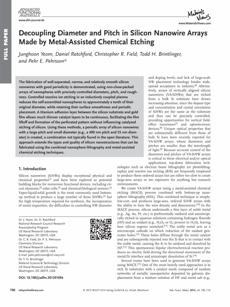
www.afm-journal.de FULL PAPER © 2013 WILEY-VCH Verlag GmbH & Co. KGaA, Weinheim 106 www.MaterialsViews.com wileyonlinelibrary.com Junghoon Yeom, Daniel Ratchford, Christopher R. Field, Todd H. Brintlinger, and Pehr E. Pehrsson* 1. Introduction Silicon nanowires (SiNWs) display exceptional physical and chemical properties [1] and have been explored as potential building blocks for numerous functional devices, including cir- cuit elements, [2] solar cells, [3] and chemical/biological sensors. [4] Vapor-liquid-solid growth is the most commonly used bottom- up method to produce a large number of these SiNWs, [5] but the high temperature required for synthesis, the incorporation of metal impurities, the difficulties in controlling NW diameter and doping levels, and lack of large-scale NW placement technology hinder wide- spread acceptance in industry. [6] Alterna- tively, arrays of vertically aligned silicon nanowires (VA-SiNWs) that are etched from a bulk Si substrate have drawn increasing attention, since the dopant type and concentration and crystal orientation of SiNWs are the same as the substrate and thus can be precisely controlled, providing opportunities for vertical field- effect transistors [7] and optoelectronic devices. [8] Unique optical properties that are substantially different from those of bulk Si have been recently reported for VA-SiNW arrays, whose diameters and pitches are smaller than the wavelength of light. [9] Because accurate control of the diameters and pitches of VA-SiNW arrays is critical to these electrical and/or optical applications, top-down fabrication tech- nologies such as electron beam lithography (or photolithog- raphy) and reactive ion etching (RIE) are frequently employed to produce these ordered arrays but are either too slow to create large-area arrays or too expensive for anything but research environments. We create VA-SiNW arrays using a metal-assisted chemical etching (MACE) process combined with bottom-up nano- sphere lithography (NSL). This combined technique is simple, low-cost, and produces large-area, ordered SiNW arrays with the ability to tune the wire density and dimensions. [10] In the MACE process, silicon underneath a thin layer of noble metal (e.g., Ag, Au, Pt, etc.) is preferentially oxidized and anisotropi- cally etched in aqueous solutions containing hydrogen fluoride (HF) and an oxidant (e.g., H 2 O 2 or O 2 present in H 2 O), leaving bare silicon regions unetched. [11] The noble metal acts as a microscopic cathode on which reduction of the oxidant gen- erates holes. [12] These holes diffuse through the metal catalyst and are subsequently injected into the Si that is in contact with the noble metal, causing the Si to be oxidized and dissolved by HF. [13] This spontaneous bipolar electrochemical reaction pro- duces an electric field driving the directional movement of the metal/Si interface and anisotropic dissolution of Si. [14] Several routes have been used to generate VA-SiNW arrays using MACE. [15] One of the most heavily used approaches is to etch Si substrates with a catalyst mesh composed of random networks of metallic nanoparticles deposited by galvanic dis- placement from a mixture solution of HF and metal salt (e.g., Decoupling Diameter and Pitch in Silicon Nanowire Arrays Made by Metal-Assisted Chemical Etching The fabrication of well-separated, narrow, and relatively smooth silicon nanowires with good periodicity is demonstrated, using non-close-packed arrays of nanospheres with precisely controlled diameters, pitch, and rough- ness. Controlled reactive ion etching in an inductively coupled plasma reduces the self-assembled nanospheres to approximately a tenth of their original diameter, while retaining their surface smoothness and periodic placement. A titanium adhesion layer between the silicon substrate and gold film allows much thinner catalyst layers to be continuous, facilitating the film liftoff and formation of the perforated pattern without influencing catalyzed etching of silicon. Using these methods, a periodic array of silicon nanowires with a large pitch and small diameter (e.g., a 490 nm pitch and 55 nm diam- eter) is created, a combination not typically found in the open literature. This approach extends the types and quality of silicon nanostructures that can be fabricated using the combined nanosphere lithography and metal-assisted chemical etching techniques. DOI: 10.1002/adfm.201301094 Dr. J. Yeom, Dr. D. Ratchford National Research Council Research Associateship Program US Naval Research Laboratory Washington, DC 20375, USA Dr. C. R. Field, Dr. P. E. Pehrsson Chemistry Division US Naval Research Laboratory Washington, DC 20375, USA E-mail: [email protected] Dr. T. H. Brintlinger Material Science & Technology Division US Naval Research Laboratory Washington, DC 20375, USA Adv. Funct. Mater. 2014, 24, 106–116
-
Upload
independent -
Category
Documents
-
view
1 -
download
0
Transcript of Decoupling Diameter and Pitch in Silicon Nanowire Arrays Made by Metal-Assisted Chemical Etching
www.afm-journal.de
FULL
PAPER
106
www.MaterialsViews.com
Junghoon Yeom , Daniel Ratchford , Christopher R. Field , Todd H. Brintlinger , and Pehr E. Pehrsson *
Decoupling Diameter and Pitch in Silicon Nanowire Arrays Made by Metal-Assisted Chemical Etching
The fabrication of well-separated, narrow, and relatively smooth silicon nanowires with good periodicity is demonstrated, using non-close-packed arrays of nanospheres with precisely controlled diameters, pitch, and rough-ness. Controlled reactive ion etching in an inductively coupled plasma reduces the self-assembled nanospheres to approximately a tenth of their original diameter, while retaining their surface smoothness and periodic placement. A titanium adhesion layer between the silicon substrate and gold fi lm allows much thinner catalyst layers to be continuous, facilitating the fi lm liftoff and formation of the perforated pattern without infl uencing catalyzed etching of silicon. Using these methods, a periodic array of silicon nanowires with a large pitch and small diameter (e.g., a 490 nm pitch and 55 nm diam-eter) is created, a combination not typically found in the open literature. This approach extends the types and quality of silicon nanostructures that can be fabricated using the combined nanosphere lithography and metal-assisted chemical etching techniques.
1. Introduction
Silicon nanowires (SiNWs) display exceptional physical and chemical properties [ 1 ] and have been explored as potential building blocks for numerous functional devices, including cir-cuit elements, [ 2 ] solar cells, [ 3 ] and chemical/biological sensors. [ 4 ] Vapor-liquid-solid growth is the most commonly used bottom-up method to produce a large number of these SiNWs, [ 5 ] but the high temperature required for synthesis, the incorporation of metal impurities, the diffi culties in controlling NW diameter
© 2013 WILEY-VCH Verlag GmbH & Co. KGaA, Weinhewileyonlinelibrary.com
DOI: 10.1002/adfm.201301094
Dr. J. Yeom, Dr. D. RatchfordNational Research Council Research Associateship ProgramUS Naval Research LaboratoryWashington, DC 20375, USA Dr. C. R. Field, Dr. P. E. PehrssonChemistry DivisionUS Naval Research LaboratoryWashington, DC 20375, USAE-mail: [email protected] Dr. T. H. BrintlingerMaterial Science & Technology DivisionUS Naval Research LaboratoryWashington, DC 20375, USA
and doping levels, and lack of large-scale NW placement technology hinder wide-spread acceptance in industry. [ 6 ] Alterna-tively, arrays of vertically aligned silicon nanowires (VA-SiNWs) that are etched from a bulk Si substrate have drawn increasing attention, since the dopant type and concentration and crystal orientation of SiNWs are the same as the substrate and thus can be precisely controlled, providing opportunities for vertical fi eld-effect transistors [ 7 ] and optoelectronic devices. [ 8 ] Unique optical properties that are substantially different from those of bulk Si have been recently reported for VA-SiNW arrays, whose diameters and pitches are smaller than the wavelength of light. [ 9 ] Because accurate control of the diameters and pitches of VA-SiNW arrays is critical to these electrical and/or optical applications, top-down fabrication tech-
nologies such as electron beam lithography (or photolithog-raphy) and reactive ion etching (RIE) are frequently employed to produce these ordered arrays but are either too slow to create large-area arrays or too expensive for anything but research environments.
We create VA-SiNW arrays using a metal-assisted chemical etching (MACE) process combined with bottom-up nano-sphere lithography (NSL). This combined technique is simple, low-cost, and produces large-area, ordered SiNW arrays with the ability to tune the wire density and dimensions. [ 10 ] In the MACE process, silicon underneath a thin layer of noble metal (e.g., Ag, Au, Pt, etc.) is preferentially oxidized and anisotropi-cally etched in aqueous solutions containing hydrogen fl uoride (HF) and an oxidant (e.g., H 2 O 2 or O 2 present in H 2 O), leaving bare silicon regions unetched. [ 11 ] The noble metal acts as a microscopic cathode on which reduction of the oxidant gen-erates holes. [ 12 ] These holes diffuse through the metal catalyst and are subsequently injected into the Si that is in contact with the noble metal, causing the Si to be oxidized and dissolved by HF. [ 13 ] This spontaneous bipolar electrochemical reaction pro-duces an electric fi eld driving the directional movement of the metal/Si interface and anisotropic dissolution of Si. [ 14 ]
Several routes have been used to generate VA-SiNW arrays using MACE. [ 15 ] One of the most heavily used approaches is to etch Si substrates with a catalyst mesh composed of random networks of metallic nanoparticles deposited by galvanic dis-placement from a mixture solution of HF and metal salt (e.g.,
im Adv. Funct. Mater. 2014, 24, 106–116

FULL P
APER
www.afm-journal.dewww.MaterialsViews.com
AgNO 3 ) [ 16 ] or by physical vapor deposition. [ 15 ] The resulting NW arrays are very dense but lack spatial ordering, and have a broad diameter distribution, restricting their use to applications where the exact location and morphology of NWs is less important. [ 17 ] Examples include antirefl ection coatings, [ 18 ] superhydrophobic/superhydrophilic surfaces, [ 19 ] photocatalysts, [ 20 ] Li-ion bat-teries, [ 21 ] and chemical/biological sensors. [ 22 ] On the other hand, well-ordered arrays of VA-SiNWs with consistent pitch, diam-eter, and surface morphology are necessary for applications whose device performance is highly sensitive to the geomet-rical parameters, for example, photovoltaics, [ 23 ] photonic crystal devices, [ 24 ] and electronic devices. [ 25 ] These ordered SiNW arrays typically begin with a periodic metal mesh atop the silicon sur-face. This periodic metal mesh can be patterned using top-down patterning techniques (e.g., electron beam lithography [ 12,13 ] and laser interference lithography) [ 26 ] or by masks prepared using bottom-up template-based approaches such as nanosphere lithography (NSL), [ 10a , 27 ] block copolymer lithography, [ 28 ] and porous anodic alumina membrane. [ 29 ] Among these bottom-up approaches, NSL is the most popular method because it can be modifi ed to produce a wide range of NW diameters and densities. [ 10a ] NSL employs an array of hexagonally close-packed polystyrene (PS) colloidal spheres as a template for creating a nanomesh of the metal catalyst layer. The diameter of the spheres is typically fi rst reduced to separate them, ultimately leading to hexagonal non-close-packed arrays of SiNWs.
Accurate control over the nanosphere (NS) array is critical since the diameter of the resulting SiNWs refl ects the sphere diameter and spacing (i.e., array density). While the NW array pitch is determined by the initial NS diameter, the diameter of the resulting NWs can be adjusted by reducing the NS diam-eter. Various techniques are used to generate non-close-packed arrays of the colloidal spheres: gel trapping, [ 30 ] templating by spin-coating, [ 31 ] soft lithographic transfer, [ 32 ] electron irradia-tion, [ 33 ] and reactive ion etching (RIE). [ 34 ] Among these, RIE is the most suitable for parallel processing and compatibility with other device fabrication steps. However, plasma etching of NSs almost inevitably roughens the sphere surfaces and distorts their spherical shape. [ 35 ] As a result, the NWs made from these spheres have rough sidewalls and non-circular cross-sections, making it diffi cult to independently control the NW diameter and the array pitch. Etching using inductively coupled plasma (ICP)-RIE at cryogenic temperatures have been shown to result in smooth, isotropic size reduction of the PS NSs, [ 36 ] but to the best of our knowledge, large-scale size reduction ( > 70%) has not been demonstrated.
In this paper, we present the fabrication of an ordered, sparse SiNW array using the ultra-large-reduction of NSs to form a sparsely perforated metal fi lm as a catalyst for MACE. While the top-down fabrication methods have been routinely employed to create sparse, ordered NWs, [ 37 ] an inexpensive, scalable bottom-up method for such NW arrays has been rarely reported. Our method is shown to reduce NS diameter by ≈ 90% while main-taining the surface smoothness and hexagonal array placement, enabling decoupling of diameter and pitch in SiNW arrays and further design fl exibility. Once NSs are reduced to a fi fth of their original diameter, metal lift-off and MACE steps pose additional challenges. For greatly reduced NSs, the NS size is comparable to the metal fi lm thickness. As a result, the metal fi lm encapsulates
© 2013 WILEY-VCH Verlag GAdv. Funct. Mater. 2014, 24, 106–116
the NS, which inhibits NS liftoff. We show that angle-resolved deposition of the metal fi lm or the use of an adhesion layer with a reduced metal fi lm thickness allows an improved NS removal. Titanium is found to be an effective adhesion layer between the Au catalyst and Si without delaying Si etching. Another chal-lenge is that MACE with a sparsely perforated Au fi lm causes the tips of resulting NWs to be undesirably tapered and porous. Through a careful study of the Si etch rate as a function of the catalyst coverage, we optimize the etching parameters to mini-mize the tapering and porosity in SiNWs. A highly regular array of SiNWs with 490 nm pitch and 55 nm diameters was demon-strated. The large separation between SiNWs in a sparse array provides an opportunity to engineer various core-shell or other nanostructures around SiNWs. These large-area, ordered, sparse SiNWs created using NSL and MACE have numerous applica-tions in optical applications such as photonic crystals [ 24 , 38 ] and biological applications, such as cell growth platforms. [ 39 ]
2. Results and Discussion
Figure 1 a shows the three key fabrication steps to generate an array of SiNWs using NSL and MACE. Each of these key steps, depicted in the SEM images in Figure 1 b–e, poses critical chal-lenges to the creation of a sparse NW array. Assuming that a two-dimensional hexagonal close-packed array of PS NSs can be reproducibly formed on a substrate, the fi rst critical challenge is large-scale reduction of the NS size. The pitch of the NW array is determined by the interparticle distance of the close-packed array, which is fi xed by the original size of the NSs. Therefore, large-scale reduction of the NS diameter is necessary to make a well-separated NW array. RIE has been the most popular method to etch the NSs and form a two-dimensional hexag-onal non-close-packed array because of its rapid and scalable nature. [ 10a ] However, once the diameters of the NSs are reduced by more than approximately half, their spherical morphology, surface smoothness, and placement in the hexagonal NS array degrade. Figure 1 b shows the roughened PS NSs during etching in a conventional parallel plate RIE. When the 490 nm NSs were reduced to below 250 nm, undesirable roughness emerged on the NS surfaces, distorting their spherical morphology. Since the morphology of the reduced NSs translates directly to the NW cross-section, it is important to precisely control their shape as well as roughness during etching. Conserving the hexagonal symmetry of close-packed arrays is also problematic since some of the particles shift position during etching, diminishing the regularity of the array. Continued RIE reduction completely destroys the NS's spherical shape (see Figure 1 c).
The second critical issue relates to the formation of the metal layer with an array of holes by NS lift-off. When the NS diameter is reduced to a size comparable with the deposited metal fi lm thick-ness, the metal layer deposited by the best line-of-sight deposition tool forms a continuous layer over the reduced spheres, making the lift-off process extremely challenging. Figure 1 d shows incom-plete lift-off of the PS NSs ( ≈ 120 nm in diameter) covered with a 25-nm-thick Au layer, even after extensive ( > 2 h) sonication in chloroform. Most of the PS NSs remain embedded in the metal fi lm, resulting in little Si etching in the MACE solution and few, if any, NWs. Those that do form are highly non-uniform.
107wileyonlinelibrary.commbH & Co. KGaA, Weinheim

FULL
PAPER
10
www.afm-journal.dewww.MaterialsViews.com
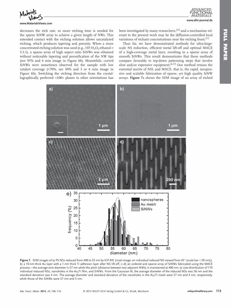
Figure 1 . a) A schematic of SiNW fabrication using NSL and MACE with three key steps: A) NS reduction, B) lift-off of the metal catalyst layer, and C) MACE. Scanning electron microscopy (SEM) images demonstrate the process challenges of each step, b) roughened PS NSs with the disrupted hexagonal array after RIE etching, (the inset image showing an individual NS with scale bar in 100 nm), c) NSs virtually destroyed after excessive RIE, d) incomplete liftoff of a Au layer, e) NWs becoming tapered and porous when etched using MACE.
The last challenge is the tendency for porosity to develop in SiNWs prepared under some MACE conditions. A sparse NW array entails the high coverage of the metal layer on the surface, and such high catalyst coverage slows down the etch rate. The resulting SiNWs etched in HF/H 2 O 2 solution are often tapered, and the extended exposure to HF renders the top portion of the SiNWs highly porous and structurally unstable (see Figure 1 e). In the following, we present approaches to address these chal-lenges and create a sparse, periodic array of VA-SiNWs in a step-by-step manner.
2.1. NS Reduction
An ideal process for reducing PS NS arrays preserves the NS spherical shape, surface smoothness, and hexagonal sym-metry of the array throughout the reduction process. The
8 wileyonlinelibrary.com © 2013 WILEY-VCH Verlag G
surface roughness that emerges on arrayed PS NSs etched by RIE subsequently disturbs the NS spherical shape and array regularity. Several previous studies reported procedures to etch NSs while retaining their spherical shape, surface smoothness, and hexagonal symmetry. Tan et al. used a mixture of CF 4 and O 2 in a conventional parallel-plate (PP) RIE unit and found that a higher concentration of CF 4 , in addition to O 2 plasma, smoothed the surface morphology of PS particles, compared to NSs etched with pure O 2 or a high O 2 content mixture. [ 35a , 40 ] However, a high CF 4 concentration also etched the underlying Si substrate, which is undesirable for subsequent processes. Plettl et al. developed an isotropic etching process with pure O 2 in a commercial ICP-RIE system, and demonstrated that a slow ( ≈ 10 nm min − 1 ), isotropic etch rate offered much better control over the size and morphology of the NSs. [ 36 ] All of these pre-vious studies, however, stopped short of demonstrating a large-scale (more than 70% of the original diameter) size reduction with the same dimensional and morphological control. Here, we used a commercial ICP-RIE system and a plasma discharge with a mixture of O 2 and CF 4 (but a higher concentration of O 2 ) to reduce the NS diameters by almost 90%.
Figure 2 compares the etching performance of PP-RIE and ICP-RIE. The PS NSs were reduced from the same starting diameter ( ≈ 490 nm), and the process parameters were tuned to yield similar etch rates (Figure 2 a). The SEM images of the etched NSs at comparable sizes are shown in Figure 2 b–g for each process at different total etching times. The NSs etched in ICP-RIE retained their spherical shape and surface smooth-ness, as well as hexagonal symmetry throughout the etching process. The NSs were reduced to 55 nm in diameter, or about an 89% reduction (data shown later). Such large-scale reduc-tion with retention of the NS shape has, to our knowledge, not been reported before. The smooth reduction was accomplished without sacrifi cing etch rate. The 89% reduction took place in just 70 s, for an etch rate of 6.4 nm s − 1 ; about forty times faster than similar work. [ 36 ] By comparison, in PP-RIE, the NSs disin-tegrated when their diameter was reduced by more than 75% (similar to Figure 1 c).
Three metrics were used to quantitatively assess the improvement in NS reduction by ICP-RIE compared to PP-RIE: roughness factor, aspect ratio, and interparticle dis-tance. The roughness factor is defi ned as a ratio between the actual perimeter of the two-dimensional projection of the etched sphere and the perimeter of a fi tted ellipse of the same two-dimensional projection. The roughness factor quanti-fi es the ruggedness (or smoothness) of the NSs after etching. Aspect ratio is one of the shape descriptors, and is defi ned as the ratio of the major and minor axis of the fi tted ellipse of the etched sphere. The disturbance of the array lattice was quan-tifi ed by using the interparticle distance distribution between the etched array and original array. Interparticle distance is a center-to-center distance between two adjacent etched spheres. The magnitude of the error bar (i.e., standard deviation) of the interparticle distance distribution refl ects how much each array was disturbed from the original hexagonal symmetry during etching. Any increase from “1” for roughness factor and aspect ratio means that the spheres get rougher or more non-spherical. The larger the error bar for the interparticle distance distribution, the less symmetric the array lattice becomes.
mbH & Co. KGaA, Weinheim Adv. Funct. Mater. 2014, 24, 106–116

FULL P
APER
www.afm-journal.dewww.MaterialsViews.com
Figure 3 . Plots of a) roughness factor, b) aspect ratio, and c) interparticle distance as a function of RIE etching time for ICP-RIE and PP-RIE. See the text for the defi nitions of roughness factor, aspect ratio, and interpar-ticle distance. Error bars were constructed using standard errors (one standard deviation) based on the analysis of at least 15 NSs.
Figure 2 . a) A plot of RIE etching time and reduced NS diameter in ICP-RIE and conventional PP-RIE; b–d) SEM images of an array of PS NSs that were etched for 40, 60, and 70 s, respectively, in PP-RIE; e–g) SEM images of an array of PS NSs that were etched for 40, 55, and 65 s, respectively, in ICP-RIE. (Scale bar is 400 nm.)
Figure 3 presents the roughness factor, aspect ratio, and inter-particle distance distribution of NSs etched by the PP-RIE and ICP-RIE for different etch durations. Roughness factor values measured from PP-RIE-etched NSs were always higher than those from ICP-RIE-etched NSs, and the difference grew larger with increased etching. Before NS etching reached 50% size reduction, both PP-RIE and ICP-RIE produced similar aspect ratio and interparticle distance distribution values. After reduc-tion by more than 50% (50 s or more etch time), the aspect ratio increased at a much faster rate for PP-RIE-etched NSs, meaning that reduced NSs became less and less spherical much more quickly. The error bar magnitude of interparticle distance distribution for the ICP-RIE-etched NSs was kept con-sistently small throughout the etching process. The interpar-ticle distance distribution of the 89% reduced NSs was roughly the same as that of the original hexagonal close-pack array,
© 2013 WILEY-VCH Verlag GAdv. Funct. Mater. 2014, 24, 106–116
indicating that the hexagonal array remained intact during the entire etching process.
Accurate control over the morphology, roughness, and hex-agonal array can be attributed to a combination of the superior features of ICP-RIE and process optimization. In ICP-RIE, an ICP power (primarily responsible for generating plasma) and a platen power (used to adjust the dc bias) can be manipulated independently for better control of the plasma density and ion energy distribution. [ 41 ] Therefore, ICP-RIE enabled us to use a relatively high ICP power (e.g., 1000 W) for generating a large density of reactants while keeping the platen power low (≤10 W) to limit ion bombardment energy and anisotropic etching. In addition, including CF 4 in otherwise pure O 2 plasma greatly reduced the surface roughness during etching. With all other
109wileyonlinelibrary.commbH & Co. KGaA, Weinheim

FULL
PAPER
110
www.afm-journal.dewww.MaterialsViews.com
parameters held constant, a plasma discharge consisting of 50% O 2 and 50% CF 4 resulted in NS etching almost twice as fast and yet signifi cantly smoother than one with 100% O 2 (see Supporting Information, Figure S1). It has been proposed that, under a UV-ozone or oxygen plasma environment, low-molecular-weight backbone segments (e.g., C–C–C bonds) of PS cleave and convert to carboxyl functional groups. [ 42 ] The higher bond energy of these carboxyl functional groups means they persist longer in the oxygen plasma and therefore act as nanoscale masks for selective etching on PS NSs. [ 35b ] We hypothesize that the addition of CF 4 to the discharge removes the carboxylate nanomasks that form on the NS surface, but additional study is needed for confi rmation. The plasma dis-charge from a mixture of 20% CF 4 and 80% O 2 (40 sccm of O 2 and 10 sccm of CF 4 ) was ultimately selected as the best combi-nation of smooth NS reduction and minimal substrate etching by excessive CF 4 . Note, however, that a CF 4 /O 2 discharge in PP-RIE did not produce as a smoother reduction as ICP-RIE (see Supporting Information, Figure S2). Other etching param-eters, such as chamber pressure, gas fl ow rates, and mixture ratios, did not signifi cantly alter the quality of NS reduction and were adjusted to optimize its etch rate.
Effective heat removal from the substrate was critical in pre-venting the spheres from disintegrating and in preserving the array's hexagonal symmetry. Plettl et al. reported that cryogenic temperature (around − 150 ° C) on the platen electrode helped to preserve the hexagonal symmetry of the array during etching. [ 36 ] In ICP-RIE, the substrate wafer is typically cooled with a fl ow of helium impinging onto the backside of the wafer. However, in many cases, the NSL substrate is much smaller than the platen electrode (here the sample is 2 cm × 2 cm while the platen is a 10 cm disk), so a carrier wafer of the same size as the platen is often used to cool the substrate during etching and facilitate the etching of small samples. However, it is diffi cult to remove energy (or heat) deposited into the sample during etching because of the high thermal resistance across the gap between the sample and carrier wafer. Application of vacuum thermal grease to the inter-face reduces the thermal contact resistance and helps cool the sample substrate, signifi cantly improving the etch quality. The hexagonal symmetry of the array was well preserved at the platen temperature of 20 ° C (i.e., no cryogenic temperature required), but etching at − 20 ° C produced the best results (Figure 2 e–g).
2.2. Lift-off of the Metal Catalyst Layer
Reduced spheres are excellent lift-off masks because the re-entrant profi le of the spherical shape breaks up the deposited fi lm and thereby promotes solvent removal of the NSs during lift-off (see Figure 4 a,e). For diameter of the reduced spheres ranging from 200 to < 500 nm, the thickness of the Au cata-lyst layer was varied from 25 to 50 nm. The large ratio of the reduced sphere diameter to fi lm thickness ( > 10) produced dis-continuities in the metal layer and facilitated subsequent lift-off. Lift-off became increasingly diffi cult when the Au layer thickness exceeded a fi fth of the sphere diameter. As shown in Figure 4 b, an unbroken Au fi lm limits the etchant access to the etching sites in the subsequent MACE process. This problem can be circumvented by depositing the Au fi lm at an
wileyonlinelibrary.com © 2013 WILEY-VCH Verlag G
angle with respect to the substrate normal, creating a crescent shaped opening in the fi lm on the shadowed side of the NS (see Figure 4 c). Figure 4 f shows a scanning electron micros-copy (SEM) image of a 25-nm-thick Au fi lm deposited at an incident angle of 30 ° onto NSs reduced to ≈ 50 nm in diameter. The resulting array of sub-10 nm openings in the fi lm allows solvents to more easily reach the NSs for removal. An array of SiNWs etched from the fi lm in Figure 4 f is shown in Figure 4 g. One distinct feature of this approach is that small, hinged Au cusps were created on the NSs during deposition and were not removed after lift-off or MACE. These cusps remained at the bases of the SiNWs (see the inset image of Figure 4 g).
NS removal is also encouraged by reducing the metal fi lm thickness so that the ratio of the Au thickness to the reduced sphere diameter is below roughly 0.2 (Figure 4 d). However, the Au fi lm can become discontinuous below a certain thickness, typically about 20 nm in an electron beam evaporator such as the one used here. [ 13b , 43 ] Gold fi lms below that thickness had irreg-ular holes or were even discontinuous (see Figure 4 h). MACE on such fi lms resulted in extraneous ribbon-like features together with the SiNWs (see Figure 4 i). This patchy Au fi lm morphology is attributable to a low sticking coeffi cient, causing dewetting (Ostwald ripening) and delaying the growth of the continuous fi lm. [ 44 ] We found that a thin layer (1–5 nm) of Ti served as an adequate adhesion layer for the Au fi lm without affecting the Si etch rate during MACE. Figure 4 j shows a 10-nm-thick Au fi lm with a 1-nm-thick Ti adhesion layer. The fi lm was continuous over the entire sample, as opposed to the Au fi lm of the same thickness without the adhesion layer (Figure 4 h).
Adding an adhesion layer before Au deposition not only decreases the critical thickness required for the continuous fi lm, it also increases the robustness of the catalyst layer. The improved adhesion between the catalyst layer and the Si sub-strate prevents the fi lm from delaminating during lift-off or MACE, thus improving the fabrication yield. The main concern in using an adhesion layer is whether it prevents intimate con-tact between the catalyst layer and the Si substrate, impeding catalytic etching. In order to investigate the effect of Ti on Si etching in an HF/H 2 O 2 solution, four coupons were prepared with Ti thicknesses of 0 (straight Au), 1, 2, and 5 nm. We mini-mized other etching variables by fi xing the metal surface area coverage (40%) as well as the Au thickness (25 nm). The sam-ples were etched in a 5:1:1 solution of HF/H 2 O 2 /ethanol for different etching times. Figure 5 a shows that the Si etch rate was not signifi cantly affected by the different thicknesses of the Ti adhesion layer. In fact, the Au fi lm without Ti exhibited the slowest etch rate. Three more samples of the same catalyst cov-erage (40%) and the same adhesion layer thickness (Ti = 1 nm) were prepared with different Au thickness (10, 15, and 25 nm). When etched in the same 5:1:1 solution of HF/H 2 O 2 /ethanol for different etching times, the overall etch rate was not signifi -cantly infl uenced by the Au thickness (Figure 5 b). This experi-mental result corroborates the recent report that diffusion of etchants and byproducts along the Si/metal interface during MACE dominates diffusion through the metal fi lm. [ 45 ] The NW length increased linearly with etching time for all cases, which agrees with previous studies. [ 13b , 46 ]
Ti etches rapidly in an aqueous mixture of HF and H 2 O 2 ( > 200 nm min − 1 ). [ 47 ] Therefore, the Ti adhesion layer may
mbH & Co. KGaA, Weinheim Adv. Funct. Mater. 2014, 24, 106–116

FULL P
APER
www.afm-journal.dewww.MaterialsViews.com
Figure 4 . Schematics of metal deposition on reduced NS arrays showing a) a discontinuous Au fi lm for NSs with modest RIE reduction, b) a con-tinuous Au fi lm deposited over NSs reduced by > 80%, c) angled-deposition using shadowing by the reduced NSs to create openings in the Au fi lm, and d) a thin (10 nm) Au fi lm with a Ti adhesion layer deposited over reduced NSs. SEM images showing e) an array of reduced 280-nm NSs covered with 25 nm of Au deposited normal to the substrate, f) 52-nm NSs covered with 25 nm of Au deposited at 30 ° from normal, and g) an array of SiNWs etched from (f). SEM images showing the effect of the Ti adhesion layer; h) a 10-nm-thick Au fi lm with no Ti after NS liftoff, i) top view of an array of SiNWs etched from (h) using MACE, and j) a 10-nm-thick Au fi lm with a 1-nm-thick Ti adhesion layer after lift-off. Scale bars of inset images: 50 nm in (f,g) and 100 nm in (h,j).
dissolve almost instantly, bringing the Au layer into an inti-mate contact with the Si substrate, and allowing MACE of Si to occur regardless of the Ti adhesion layer thickness. Another common adhesion layer, Cr, is stable in the etchant solution, and so prevents contact between the Au and the Si substrate. No Si etching was reported with a Cr/Au layer because Cr itself does not act as a MACE catalyst. [ 45 , 48 ]
2.3. Metal-assisted Chemical Etching of a Sparse SiNW Array
Sparsely perforated gold layers deposited on NSs reduced by 70% or more have a high catalyst coverage (see Supporting Informa-tion, Figure S3, for the defi nition of catalyst coverage). As intro-duced in Figure 1 e, MACE of Si using these sparsely perforated Au layers (i.e., catalyst coverage of over 90%) produces highly porous and tapered SiNWs. Similar to the previous report, [ 49 ] a
© 2013 WILEY-VCH Verlag GAdv. Funct. Mater. 2014, 24, 106–116
gradually increasing density of nanopores and lateral etching (tapering) was observed from the root (bottom part) to the tip of the SiNWs. When etched in the same solution, a SiNW array with lower catalyst coverage (40–60%) was not porosifi ed and did not taper at the tips (see Figure S4, Supporting Information). The pore formation mechanism may differ with the Si doping level and type, [ 27 ] but the SiNWs typically become more porous when i) the substrates are highly doped ( < 0.05 Ω cm), [ 16b , 50 ] ii) the MACE etchant is H 2 O 2 (or oxidant) rich, [ 8 , 11a ] and iii) the less stable metal (e.g., Ag) is used as catalyst. [ 15 , 51 ] Here, a lightly doped N-type wafer (8–12 Ω cm) was used with stable Au as a catalyst and HF-rich etchant ( ρ = [HF]/([HF] + [H 2 O 2 ]) > 0.9), all of which encourage the formation of non-porous SiNWs. The fact that we observed more porosifi cation for SiNWs with high catalyst coverage under otherwise identical etching condi-tions suggests that the ratio of Si and Au areas exposed to the etchant affects the porosity of SiNWs. A possible explanation is
111wileyonlinelibrary.commbH & Co. KGaA, Weinheim
FULL
PAPER
112
www.afm-journal.dewww.MaterialsViews.com
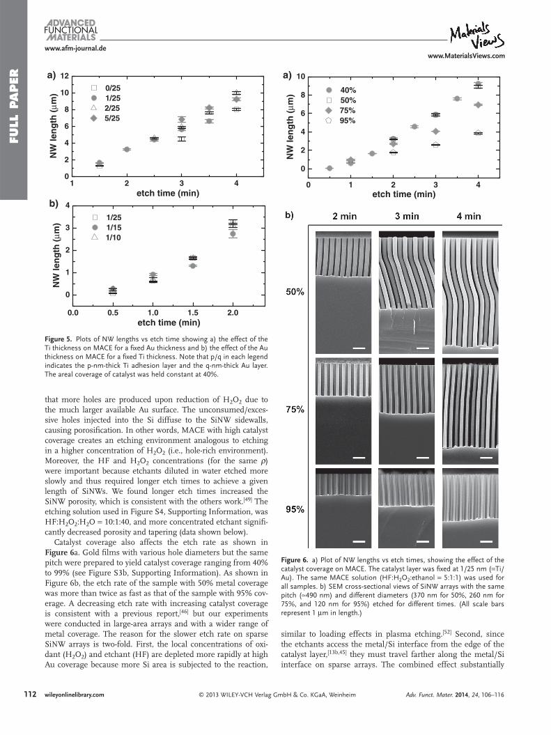
Figure 5 . Plots of NW lengths vs etch time showing a) the effect of the Ti thickness on MACE for a fi xed Au thickness and b) the effect of the Au thickness on MACE for a fi xed Ti thickness. Note that p/q in each legend indicates the p-nm-thick Ti adhesion layer and the q-nm-thick Au layer. The areal coverage of catalyst was held constant at 40%.
1 2 3 40
2
4
6
8
10
12a)
NW
len
gth
(µm
)
etch time (min)
0/251/252/255/25
0.0 0.5 1.0 1.5 2.0
0
1
2
3
4b)
NW
len
gth
(µm
)
etch time (min)
1/251/151/10
Figure 6 . a) Plot of NW lengths vs etch times, showing the effect of the catalyst coverage on MACE. The catalyst layer was fi xed at 1/25 nm ( = Ti/Au). The same MACE solution (HF:H 2 O 2 :ethanol = 5:1:1) was used for all samples. b) SEM cross-sectional views of SiNW arrays with the same pitch ( ≈ 490 nm) and different diameters (370 nm for 50%, 260 nm for 75%, and 120 nm for 95%) etched for different times. (All scale bars represent 1 μ m in length.)
0 1 2 3 4
0
2
4
6
8
10a)
NW
len
gth
(µm
)
etch time (min)
40%50%75%95%
that more holes are produced upon reduction of H 2 O 2 due to the much larger available Au surface. The unconsumed/exces-sive holes injected into the Si diffuse to the SiNW sidewalls, causing porosifi cation. In other words, MACE with high catalyst coverage creates an etching environment analogous to etching in a higher concentration of H 2 O 2 (i.e., hole-rich environment). Moreover, the HF and H 2 O 2 concentrations (for the same ρ ) were important because etchants diluted in water etched more slowly and thus required longer etch times to achieve a given length of SiNWs. We found longer etch times increased the SiNW porosity, which is consistent with the others work. [ 49 ] The etching solution used in Figure S4, Supporting Information, was HF:H 2 O 2 :H 2 O = 10:1:40, and more concentrated etchant signifi -cantly decreased porosity and tapering (data shown below).
Catalyst coverage also affects the etch rate as shown in Figure 6 a. Gold fi lms with various hole diameters but the same pitch were prepared to yield catalyst coverage ranging from 40% to 99% (see Figure S3b, Supporting Information). As shown in Figure 6 b, the etch rate of the sample with 50% metal coverage was more than twice as fast as that of the sample with 95% cov-erage. A decreasing etch rate with increasing catalyst coverage is consistent with a previous report, [ 46 ] but our experiments were conducted in large-area arrays and with a wider range of metal coverage. The reason for the slower etch rate on sparse SiNW arrays is two-fold. First, the local concentrations of oxi-dant (H 2 O 2 ) and etchant (HF) are depleted more rapidly at high Au coverage because more Si area is subjected to the reaction,
wileyonlinelibrary.com © 2013 WILEY-VCH Verlag G
similar to loading effects in plasma etching. [ 52 ] Second, since the etchants access the metal/Si interface from the edge of the catalyst layer, [ 13b , 45 ] they must travel farther along the metal/Si interface on sparse arrays. The combined effect substantially
mbH & Co. KGaA, Weinheim Adv. Funct. Mater. 2014, 24, 106–116
FULL P
APER
www.afm-journal.dewww.MaterialsViews.com
decreases the etch rate, so more etching time is needed for the sparse SiNW array to achieve a given length of NWs. This extended contact with the etching solution allows uncatalyzed etching, which produces tapering and porosity. When a more concentrated etching solution was used (e.g., HF:H 2 O 2 :ethanol = 5:1:1), a sparse array of high aspect ratio SiNWs was obtained without noticeable tapering and porosifi cation of the NW tips (see 95% and 4 min image in Figure 6 b). Meanwhile, curved SiNWs were sometimes observed for the sample with low catalyst coverage ( < 70%, see 50% and 3 or 4 min image in Figure 6 b). Switching the etching direction from the crystal-lographically preferred < 100 > planes to other orientations has
© 2013 WILEY-VCH Verlag Gm
Figure 7 . SEM images of a) PS NSs reduced from 490 to 55 nm by ICP-RIE (inb) a 10-nm-thick Au layer with a 1-nm thick Ti adhesion layer after NS lift-ofprocess—the average wire diameter is 57 nm while the pitch (distance betweindividual reduced NSs, nanoholes in the Au/Ti fi lm, and SiNWs. From the Gstandard deviation was 4 nm. The average diameter and standard deviationwhile those of the SiNWs were 57 nm and 5 nm.
Adv. Funct. Mater. 2014, 24, 106–116
been investigated by many researchers, [ 53 ] and a mechanism rel-evant to the present work may be the diffusion-controlled local variations of etchant concentrations near the etching front. [ 17 ]
Thus far, we have demonstrated methods for ultra-large-scale NS reduction, effi cient metal lift-off and optimal MACE of a high-coverage metal layer, resulting in a sparse array of smooth SiNWs. This result demonstrates that these methods compare favorably to top-down patterning steps that involve slow and/or expensive equipment. [ 6 , 37 ] Our method retains the essential merits of NSL and MACE, that is, the rapid, inexpen-sive and scalable fabrication of sparse, yet high quality SiNW arrays. Figure 7 a shows the SEM image of an array of etched
113wileyonlinelibrary.combH & Co. KGaA, Weinheim
set image: an individual reduced NS viewed from 45 ° (scale bar = 50 nm)), f, c–d) an ordered and sparse array of SiNWs fabricated using the MACE en two adjacent NWs) is maintained at 490 nm, e) size-distribution of 110 aussian fi t, the average diameter of the reduced NSs was 56 nm and the
of the nanoholes in the Au/Ti mesh were 57 nm and 4 nm, respectively,

FULL
PAPER
1
www.afm-journal.dewww.MaterialsViews.com
Figure 8 . Transmission electron microcopy images of a solid SiNW (65 nm in diameter, 8–12 Ω cm n-Si, 10:1:2 of HF:H 2 O 2 :ethanol) with a) low mag-nifi cation (the inset scale bar is 100 nm) and b) high magnifi cation.
PS NSs reduced in diameter from 490 nm to 55 nm, or an 89% size reduction. The single etched NS in the inset image shows that they retained their near-spherical shape. The small amount of CF 4 ( ≈ 20%) present during ICP-RIE helped the Si substrate remain relatively unetched. The sparse array of non-hexagonal close-packed NSs was coated with a 1-nm-thick Ti adhesion layer and 10-nm-thick Au catalyst layer. The NSs were then easily removed with chloroform, producing a sparsely perforated, but continuous metal fi lm. The Ti adhesion layer increased the continuity of the 10 nm Au fi lm, and the use of the thinner metal layer improved the NS lift-off yield to > 99% (see Figure 7 b) from < 5%, when 25-nm of gold was used. The use of highly concentrated etchant and oxidant with the rela-tive concentration ratio ( ρ ) higher than the stoichiometric ratio (HF:H 2 O 2 = 5:1) [ 15 , 48 ] minimized the formation of tapered and porous SiNWs. For instance, when the sparsely perforated Au fi lm (Figure 7 b) was etched in a 20:1:4 mixture (by vol) of HF:H 2 O 2 :ethanol, [ 54 ] an array of SiNWs was created without severe tapering or porosifi cation. Figure 7 c shows a large array of sparse SiNWs with a diameter-to-pitch ratio of close to 1:10 that was prepared by etching for 5 min. The high molar con-centration of HF and H 2 O 2 increased the etch rate, reducing the overall contact time of the NWs to the etching solution. As a result, the individual NWs seen in Figure 7 d are straight and non-porous. The size of the as-etched SiNWs correlated strongly to the size of the reduced NSs and the perforated holes in the metal layer, as shown in the histogram of the SiNW diameters and the size of the spheres and nanoholes in Figure 7 e. The Gaussian fi t shows that the mean diameter and the standard deviation of the SiNWs (57 ± 5 nm) closely match with those of the etched NSs (56 ± 4 nm) and the nanoholes in the catalyst layer (57 ± 4 nm). A narrow size distribution also suggests that fi ne tuning of diameter and spacing of SiNW arrays is feasible using our methods.
Finally, SiNW porosity was qualitatively investigated by transmission electron microscopy (TEM). Figure 8 a,b shows low magnifi cation and high resolution TEM images of a SiNW that was harvested from a sparse NW array. The continuous lattice fringes seen in Figure 8 b indicate the single-crystalline nature of the resulting NWs. These TEM images also manifest the absence of any apparent pores in the SiNW and support our claim that the optimized MACE process produced a sparse array of solid NWs.
14 wileyonlinelibrary.com © 2013 WILEY-VCH Verlag G
3. Conclusions
We have formed ordered and sparse arrays of VA-SiNWs using combined NSL and MACE. A large pitch-to-diameter ratio requires the dramatic but smooth reduction of the templating NSs, which was achieved using an O 2 /CF 4 discharge in ICP-RIE. Inclusion of CF 4 in the plasma and substrate cooling were important for such a uniform, isotropic reduction. Retention of the NSs’ smoothness, spherical morphology, and hexagonal placement enabled patterning of a highly ordered, sparsely per-forated Au catalyst layer and fabrication of NWs with smooth sidewalls and spherical cross-section. To promote the lift-off of the Au layer atop reduced NSs, discontinuities in the metal fi lm were intentionally introduced either by depositing at an off-normal incident angle or by decreasing the fi lm thickness. The Ti adhesion layer played a pivotal role in enabling formation of thinner, defect-free Au fi lms. The Ti was removed quickly by the MACE solution, thus bringing the Au fi lm into inti-mate contact with the Si substrate. High molar concentration, HF-rich etchant mixtures decreased the formation of tapering and porosity in the tips of the SiNWs. The combination of all of these improved methods enabled a scalable and inexpensive fabrication of large-area, ordered and sparse VA-SiNW arrays. Such arrays are potentially useful in electronic/optical applica-tions such as photonic crystals, vertical transistors, and biolog-ical applications, such as multifunctional platforms for guiding cell growth and functions.
4. Experimental Section Substrate Preparation : Four-inch single-side polished silicon
wafers (Montco Silicon, < 100 > orientation and 500 μ m in thickness, N-type, 8–12 Ω cm) were cut into 2 cm by 2 cm coupons, which were ultrasonically cleaned in acetone and isopropyl alcohol. The Si coupons were further cleaned in piranha solution (3 parts of H 2 SO 4 and 1 part of H 2 O 2 ) for 30 min and subsequently in SC-1 solution (1 part of H 2 O 2 , 1 part of NH 4 OH and 5 parts of deionized water) for 30 min to render their surfaces hydrophilic. The coupons were then thoroughly rinsed with DI water and stored in DI water until used.
Nanosphere Lithography : Colloidal monodispersed PS NSs with nominal diameters of 490 nm were purchased from Polysciences Inc. and mixed with a 400:1 solution of methanol:Triton X-100. In order to form a hexagonal close-pack monolayer, the NS solution was spin-coated onto each substrate at 400, 500, and 1400 rpm for 30 s, 2 min, and 10 s, respectively. Once completely dried, the NSs were etched in
mbH & Co. KGaA, Weinheim Adv. Funct. Mater. 2014, 24, 106–116
FULL P
APER
www.afm-journal.dewww.MaterialsViews.com
an ICP-RIE (Oxford Plasmalab System 100) with a mixture of O 2 and CF 4 (0 to 50 sccm) at various ICP (300 to 2500 W) and RF power (3 to 20 W) levels and chamber pressures (12 to 40 mTorr). For comparison, a conventional parallel-plate (PP)-RIE system (March CS 1701) was also used to reduce the NS diameter. The PP-RIE etching parameters were 25 sccm of O 2 , 150 W of RF power, and 320 mTorr of chamber pressure. The etching time was varied to yield the desired diameter reduction, leading to a hexagonal non-close-packed NS array. A gold nanomesh template for MACE was then generated by evaporating Au on the Si topped with the NS array (Temescal e-beam evaporator, background pressure less than 1 × 10 − 6 Torr). After the gold was evaporated, the NSs were removed by dissolution in CHCl 3 (Sigma-Aldrich). In most cases, mild sonication was used to accelerate lift-off. The Au thickness was changed from 10 to 25 nm, with and without a thin layer of Ti (1 to 5 nm) as an adhesion layer.
Silicon Nanowire Fabrication : The SiNWs were formed when the coupon was immersed into an etching mixture consisting of HF (49%), H 2 O 2 (30%), and ethanol (DI water) as a diluent. The HF and H 2 O 2 concentrations were varied to investigate the effect of etching mixtures on NW porosity. In a typical run, 150 mL of HF, 30 mL of H 2 O 2 and 30 mL of ethanol (5:1:1 of HF:H 2 O 2 :ethanol) were mixed with a Tefl on-coated stir bar. A mixture of 20:1:4 of HF:H 2 O 2 :ethanol was used to minimize porosity while etching sparse arrays of SiNWs. [ 54 ] The NW lengths were adjusted by changing the etching duration, which ranged from 30 s to 30 min. The remaining Au layer was removed in a gold etchant TFA (Transene). After rinsing the SiNW coupons in isopropanol alcohol multiple times, the coupons were dried under a stream of N 2 . For long NWs, a CO 2 critical point dryer (Tousimis, Automegasamdri-815B) was used to prevent NWs from bundling.
Imaging and Analysis : SEM images were obtained using a Carl Zeiss SMT Supra 55 (fi eld-emission high-resolution SEM) instrument. The SiNW lengths were measured from the SEM images of the cleaved SiNW samples. Image analysis was performed using the freeware software, ImageJ. TEM images were obtained using a JEOL 2010F electron microscope. SiNWs (average diameter = 65 ± 4 nm) etched with a concentrated MACE solution (10:1:2 of HF:H 2 O 2 :ethanol) were scratched off from a sparse NW array of the n-type substrate (8–12 Ω cm) and transferred to isopropanol alcohol. SiNWs were then dispersed in isopropanol alcohol with 20 min of sonication. A couple of drops of this mixture were applied to a lacey carbon fi lm on a Cu TEM grid for imaging and analysis.
Supporting Information Supporting Information is available from the Wiley Online Library or from the author.
Received: March 28, 2013 Revised: May 31, 2013
Published online: July 24, 2013
[ 1 ] V. Schmidt , J. V. Wittemann , S. Senz , U. Gösele , Adv. Mater. 2009 , 21 , 2681 .
[ 2 ] a) Y. Cui , C. M. Lieber , Science 2001 , 291 , 851 ; b) S. Hoffmann , J. Bauer , C. Ronning , T. Stelzner , J. Michler , C. Ballif , V. Sivakov , S. H. Christiansen , Nano Lett. 2009 , 9 , 1341 ; c) Y. Cui , Z. Zhong , D. Wang , W. U. Wang , C. M. Lieber , Nano Lett. 2003 , 3 , 149 .
[ 3 ] a) B. Tian , X. Zheng , T. J. Kempa , Y. Fang , N. Yu , G. Yu , J. Huang , C. M. Lieber , Nature 2007 , 449 , 885 ; b) V. Sivakov , G. Andra , A. Gawlik , A. Berger , J. Plentz , F. Falk , S. H. Christiansen , Nano Lett. 2009 , 9 , 1549 .
[ 4 ] a) Y. Cui , Q. Wei , H. Park , C. M. Lieber , Science 2001 , 293 , 1289 ; b) J. Hahm , C. M. Lieber , Nano Lett. 2004 , 4 , 51 .
© 2013 WILEY-VCH Verlag GmAdv. Funct. Mater. 2014, 24, 106–116
[ 5 ] a) M. Shao , D. D. D. Ma , S.-T. Lee , Eur. J. Inorg. Chem. 2010 , 2010 , 4264 ; b) S. Barth , F. Hernandez-Ramirez , J. D. Holmes , A. Romano-Rodriguez , Prog. Mater. Sci. 2010 , 55 , 563 .
[ 6 ] R. G. Hobbs , N. Petkov , J. D. Holmes , Chem. Mater. 2012 , 24 , 1975 . [ 7 ] a) T. Bryllert , L.-E. Wernersson , L. E. Fröberg , L. Samuelson , IEEE
Electron Device Lett. 2006 , 27 , 323 ; b) J. Goldberger , A. I. Hochbaum , R. Fan , P. Yang , Nano Lett. 2006 , 6 , 973 ; c) V. Schmidt , H. Riel , S. Senz , S. Karg , W. Riess , U. Gösele , Small 2006 , 2 , 85 .
[ 8 ] Y. Qu , L. Liao , Y. Li , H. Zhang , Y. Huang , X. Duan , Nano Lett. 2009 , 9 , 4539 .
[ 9 ] S. M. Wells , I. A. Merkulov , I. I. Kravchenko , N. V. Lavrik , M. J. Sepaniak , ACS Nano 2012 , 6 , 2948 .
[ 10 ] a) Z. Huang , H. Fang , J. Zhu , Adv. Mater. 2007 , 19 , 744 ; b) D. H. Lee , Y. Kim , G. S. Doerk , I. Laboriante , R. Maboudian , J. Mater. Chem. 2011 , 21 , 10359 .
[ 11 ] a) C. Chartier , S. Bastide , C. Levy-Clement , Electrochim. Acta 2008 , 53 , 5509 ; b) M.-L. Zhang , K.-Q. Peng , X. Fan , J.-S. Jie , R.-Q. Zhang , S.-T. Lee , N.-B. Wong , J. Phys. Chem. C 2008 , 112 , 4444 .
[ 12 ] O. J. Hildreth , W. Lin , C. P. Wong , ACS Nano 2009 , 3 , 4033 . [ 13 ] a) O. J. Hildreth , D. Brown , C. P. Wong , Adv. Funct. Mater. 2011 , 21 ,
3119 ; b) Z. Huang , N. Geyer , P. Werner , J. de Boor , U. Goesele , Adv. Mater. 2011 , 23 , 285 .
[ 14 ] K. Peng , A. Lu , R. Zhang , S.-T. Lee , Adv. Funct. Mater. 2008 , 18 , 3026 .
[ 15 ] J. Kim , H. Han , Y. H. Kim , S.-H. Choi , J.-C. Kim , W. Lee , ACS Nano 2011 , 5 , 3222 .
[ 16 ] a) A. I. Hochbaum , R. Chen , R. D. Delgado , W. Liang , E. C. Garnett , M. Najarian , A. Majumdar , P. Yang , Nature 2008 , 451 , 163 ; b) A. I. Hochbaum , D. Gargas , Y. J. Hwang , P. Yang , Nano Lett. 2009 , 9 , 3550 .
[ 17 ] J. Kim , Y. H. Kim , S.-H. Choi , W. Lee , ACS Nano 2011 , 5 , 5242 . [ 18 ] a) K. Q. Peng , Y. Xu , Y. Wu , Y. J. Yan , S. T. Lee , J. Zhu , Small 2005 , 1 ,
1062 ; b) Y. Li , J. Zhang , S. Zhu , H. Dong , Z. Wang , Z. Sun , J. Guo , B. Yang , J. Mater. Chem. 2009 , 19 , 1806 ; c) T.-H. Pei , S. Thiyagu , Z. Pei , Appl. Phys. Lett. 2011 , 99 , 153108 .
[ 19 ] a) M. K. Dawood , H. Zheng , T. H. Liew , K. C. Leong , Y. L. Foo , R. Rajagopalan , S. A. Khan , W. K. Choi , Langmuir 2011 , 27 , 4126 ; b) Y. Chen , Z. G. Guo , J. S. Xu , L. Shi , J. Li , Y. B. Zhang , MRS Bull. 2012 , 47 , 1687 .
[ 20 ] F.-Y. Wang , Q.-D. Yang , G. Xu , N.-Y. Lei , Y. K. Tsang , N.-B. W. J. C. Ho , Nanoscale 2011 , 3 , 3269 .
[ 21 ] a) C. K. Chan , H. L. Peng , G. Liu , K. McIlwrath , X. F. Zhang , R. A. Huggins , Y. Cui , Nat. Nanotechnol. 2008 , 3 , 31 ; b) R. Huang , X. Fan , W. Shen , J. Zhu , Appl. Phys. Lett. 2009 , 95 , 133119 .
[ 22 ] a) B. H. Zhang , H. S. Wang , L. H. Lu , K. L. Ai , G. Zhang , X. L. Cheng , Adv. Funct. Mater. 2008 , 18 , 2348 ; b) K. Q. Peng , X. Wang , S. T. Lee , Appl. Phys. Lett. 2009 , 95 , 143119 ; c) H. J. In , C. R. Field , P. E. Pehrsson , Nanotechnology 2011 , 22 , 355501 .
[ 23 ] B. M. Kayes , H. A. Atwater , N. S. Lewis , J. Appl. Phys. 2005 , 97 , 114302 .
[ 24 ] K. Seo , M. Wober , P. Steinvurzel , E. Schonbrun , Y. P. Dan , T. Ellenbogen , K. B. Crozier , Nano Lett. 2011 , 11 , 1851 .
[ 25 ] J. M. Weisse , C. H. Lee , D. R. Kim , X. L. Zheng , Nano Lett. 2012 , 12 , 3339 .
[ 26 ] a) W. K. Choi , T. H. Liew , M. K. Dawood , H. I. Smith , C. V. Thompson , M. H. Hong , Nano Lett. 2008 , 8 , 3799 ; b) M. K. Dawood , T. H. Liew , P. L. M. H. Hong , S. Tripathy , J. T. L. Thong , W. K. Choi , Nanotech-nology 2010 , 21 , 205305 .
[ 27 ] B. Mikhael , B. Elise , M. Xavier , S. Sebastian , M. Johann , P. Laetitia , ACS Appl. Mater. Interfaces 2011 , 3 , 3866 .
[ 28 ] B. M. Bang , H. Kim , J.-P. Lee , J. Cho , S. Park , Energy Environ. Sci. 2011 , 4 , 3395 .
[ 29 ] J. Huang , S. Y. Chiam , H. H. Tan , S. Wang , W. K. Chim , Chem. Mater. 2010 , 22 , 4111 .
115wileyonlinelibrary.combH & Co. KGaA, Weinheim

FULL
PAPER
116
www.afm-journal.dewww.MaterialsViews.com
[ 30 ] O. J. Cayre , V. N. Paunov , J. Mater. Chem. 2004 , 14 , 3300 . [ 31 ] P. Jiang , M. J. McFarland , J. Am. Chem. Soc. 2005 , 127 , 3710 . [ 32 ] X. Yan , J. M. Yao , G. Lu , X. Li , J. H. Zhang , K. Han , B. Yang , J. Am.
Chem. Soc. 2005 , 127 , 7688 . [ 33 ] Y. Li , E. J. Lee , W. Cai , K. Y. Kim , S. O. Cho , ACS Nano 2008 , 2 ,
1108 . [ 34 ] C. Haginoya , M. Ishibashi , K. Koike , Appl. Phys. Lett. 1997 , 71 , 2934 . [ 35 ] a) B. J. Y. Tan , C. H. Sow , K. Y. Lim , F. C. Cheong , G. L. Chong ,
A. T. S. Wee , C. K. Ong , J. Phys. Chem. B 2004 , 108 , 18575 ; b) H. Y. Hsieh , J. L. Xiao , C. H. Lee , T. W. Huang , C. S. Yang , P. C. Wang , F. G. Tseng , J. Phys. Chem. C 2011 , 115 , 16258 .
[ 36 ] A. Plettl , F. Enderle , M. Saitner , A. Manzke , C. Pfahler , S. Wiedemann , P. Ziemann , Adv. Funct. Mater. 2009 , 19 , 3279 .
[ 37 ] M. Khorasaninejad , N. Abedzadeh , A. S. Jawanda , O. Nixon , M. P. Anantram , S. S. Saini , J. Appl. Phys. 2012 , 111 , 044328 .
[ 38 ] M. Khorasaninejad , N. Abedzadeh , J. Walia , S. Patchett , S. S. Saini , Nano Lett. 2012 , 12 , 4228 .
[ 39 ] M. A. Bucaro , Y. Vasquez , B. D. Hatton , J. Aizenberg , ACS Nano 2012 , 6 , 6222 .
[ 40 ] B. J. Y. Tan , C. H. Sow , T. S. Koh , K. C. Chin , A. T. S. Wee , C. K. Ong , J. Phys. Chem. B 2005 , 109 , 11100 .
[ 41 ] J. Yeom , Y. Wu , J. C. Selby , M. A. Shannon , J. Vac. Sci. Technol. B 2005 , 23 , 2319 .
[ 42 ] a) S. Guruvenket , G. M. Rao , M. Komath , A. M. Raichur , Appl. Surf. Sci. 2004 , 236 , 278 ; b) A. Mahfoudh , J. Barbeau , M. Moisan , A. Leduc , J. Seguin , Appl. Surf. Sci. 2010 , 256 , 3063 .
wileyonlinelibrary.com © 2013 WILEY-VCH Verlag G
[ 43 ] X. Li , P. W. Bohn , Appl. Phys. Lett. 2000 , 77 , 2572 . [ 44 ] a) C. M. Mueller , F. C. F. Mornaghini , R. Spolenak , Nanotechnology
2008 , 19 , 485306 ; b) H. Sun , M. Yu , G. Wang , X. Sun , J. Lian , J. Phys. Chem. C 2012 , 116 , 9000 .
[ 45 ] N. Geyer , B. Fuhrmann , Z. Huang , J. de Boor , H. S. Leipner , P. Werner , J. Phys. Chem. C 2012 , 116 , 13446 .
[ 46 ] K. Rykaczewski , O. J. Hildreth , C. P. Wong , A. G. Fedorov , J. H. J. Scott , Nano Lett. 2011 , 11 , 2369 .
[ 47 ] K. R. Williams , R. S. Muller , J. Microelectromech. Syst. 1996 , 5 , 256 . [ 48 ] W. Chern , K. Hsu , I. S. Chun , B. P. de Azeredo , N. Ahmed ,
K.-H. Kim , J.-M. Zuo , N. Fang , P. Ferreira , X. Li , Nano Lett. 2010 , 10 , 1582 .
[ 49 ] G. D. Yuan , R. Mitdank , A. Mogilatenko , S. F. Fischer , J. Phys. Chem. C 2012 , 116 , 13767 –.
[ 50 ] Y. Qu , H. Zhou , X. Duan , Nanoscale 2011 , 3 , 4060 . [ 51 ] K. Tsujino , M. Matsumura , Adv. Mater. 2005 , 17 , 1045 . [ 52 ] C. J. Mogab , J. Electrochem. Soc. 1977 , 124 , 1262 . [ 53 ] a) C.-Y. Chen , C.-S. Wu , C.-J. Chou , T.-J. Yen , Adv. Mater. 2008 ,
20 , 3811 ; b) Z. Huang , T. Shimizu , S. Senz , Z. Zhang , X. Zhang , W. Lee , N. Geyer , U. Gösele , Nano Lett. 2009 , 9 , 2519 ; c) H. Chen , H. Wang , X.-H. Zhang , C.-S. Lee , S.-T. Lee , Nano Lett. 2010 , 10 , 864 ; d) Z. Huang , T. Shimizu , S. Senz , Z. Zhang , N. Geyer , U. Goesele , J. Phys. Chem. C 2010 , 114 , 10683 .
[ 54 ] K. Balasundaram , J. S. Sadhu , J. C. Shin , B. Azeredo , D. Chanda , M. Malik , K. Hsu , J. A. Rogers , P. Ferreira , S. Sinha , X. L. Li , Nano-technology 2012 , 23 , 305304 .
mbH & Co. KGaA, Weinheim Adv. Funct. Mater. 2014, 24, 106–116